2014 年第1 季度模拟应用杂志
35
Texas Instruments Incorporated 2014年第1季度 德州仪器2014年版权所有 模拟应用杂志 高性能模拟产品
-
Upload
khangminh22 -
Category
Documents
-
view
2 -
download
0
Transcript of 2014 年第1 季度模拟应用杂志

Texas Instruments Incorporated
High-Performance Analog Products
Analog ApplicationsJournal
First Quarter, 2014
© Copyright 2014 Texas Instruments
2014年第1季度
德州仪器2014年版权所有
模拟应用杂志
高性能模拟产品

Texas Instruments Incorporated
2
Analog Applications JournalHigh-Performance Analog Products www.ti.com/aaj 3Q 2012
IMPORTANT NOTICE
Texas Instruments Incorporated and its subsidiaries (TI) reserve the right to make corrections, enhancements, improvements and other changes to its semiconductor products and services per JESD46C and to discontinue any product or service per JESD48B. Buyers should obtain the latest relevant information before placing orders and should verify that such information is current and complete. All semiconductor products (also referred to herein as “components”) are sold subject to TI’s terms and conditions of sale supplied at the time of order acknowledgment.
TI warrants performance of its components to the specifications applicable at the time of sale, in accordance with the warranty in TI’s terms and conditions of sale of semiconductor products. Testing and other quality control techniques are used to the extent TI deems necessary to support this warranty. Except where mandated by applicable law, testing of all parameters of each component is not necessarily performed.
TI assumes no liability for applications assistance or the design of Buyers’ products. Buyers are responsible for their products and applications using TI components. To minimize the risks associated with Buyers’ products and applications, Buyers should provide adequate design and operating safeguards.
TI does not warrant or represent that any license, either express or implied, is granted under any patent right, copyright, mask work right, or other intellectual property right relating to any combination, machine, or process in which TI components or services are used. Information published by TI regarding third-party products or services does not constitute a license to use such products or services or a warranty or endorsement thereof. Use of such information may require a license from a third party under the patents or other intellectual property of the third party, or a license from TI under the patents or other intellectual property of TI.
Reproduction of significant portions of TI information in TI data books or data sheets is permissible only if reproduction is without alteration and is accompanied by all associated warranties, conditions, limitations, and notices. TI is not responsible or liable for such altered documentation. Information of third parties may be subject to additional restrictions.
Resale of TI components or services with statements different from or beyond the parameters stated by TI for that component or service voids all express and any implied warranties for the associated TI component or service and is an unfair and deceptive business practice. TI is not responsible or liable for any such statements.
Buyer acknowledges and agrees that it is solely responsible for compliance with all legal, regulatory and safety-related require-ments concerning its products, and any use of TI components in its applications, notwithstanding any applications-related information or support that may be provided by TI. Buyer represents and agrees that it has all the necessary expertise to create and implement safeguards which anticipate dangerous consequences of failures, monitor failures and their consequences, lessen the likelihood of failures that might cause harm and take appropriate remedial actions. Buyer will fully indemnify TI and its representatives against any damages arising out of the use of any TI components in safety-critical applications.
In some cases, TI components may be promoted specifically to facilitate safety-related applications. With such components, TI’s goal is to help enable customers to design and create their own end-product solutions that meet applicable functional safety standards and requirements. Nonetheless, such components are subject to these terms.
No TI components are authorized for use in FDA Class III (or similar life-critical medical equipment) unless authorized officers of the parties have executed a special agreement specifically governing such use.
Only those TI components which TI has specifically designated as military grade or “enhanced plastic” are designed and intended for use in military/aerospace applications or environments. Buyer acknowledges and agrees that any military or aerospace use of TI components which have not been so designated is solely at the Buyer’s risk, and that Buyer is solely responsible for compliance with all legal and regulatory requirements in connection with such use.
TI has specifically designated certain components which meet ISO/TS16949 requirements, mainly for automotive use. Components which have not been so designated are neither designed nor intended for automotive use; and TI will not be responsible for any failure of such components to meet such requirements.
ProductsAudio www.ti.com/audio Amplifiers amplifier.ti.com Data Converters dataconverter.ti.com DLP® Products www.dlp.comDSP dsp.ti.com Clocks and Timers www.ti.com/clocksInterface interface.ti.com Logic logic.ti.com Power Management power.ti.com Microcontrollers microcontroller.ti.com RFID www.ti-rfid.comOMAP™ Mobile Processors www.ti.com/omapWireless Connectivity www.ti.com/wirelessconnectivity
ApplicationsAutomotive and Transportation www.ti.com/automotive Communications and Telecom www.ti.com/communicationsComputers and Peripherals www.ti.com/computers Consumer Electronics www.ti.com/consumer-appsEnergy and Lighting www.ti.com/energyIndustrial www.ti.com/industrialMedical www.ti.com/medicalSecurity www.ti.com/security Space, Avionics and Defense www.ti.com/space-avionics-defense Video and Imaging www.ti.com/video
TI E2E™ Community e2e.ti.com
Mailing Address: Texas Instruments, Post Office Box 655303, Dallas, Texas 75265SSZZ022D
(TI) , ,
TI
TI TI TI , TI ,
TI TI
TI TI TI TI TI TI
TI
TI TI
TI TI TI
TI TI
TI TI
TI TI
TI / TI TI TI
TI TI ISO/TS 16949 TI
URL TI
www.ti.com.cn/audio www.ti.com.cn/telecomhttp://www.ti.com.cn/amplifierswww.ti.com.cn/computerers http://www.ti.com.cn/dataconvert www.ti.com/consumer-apps
DLP® www.dlp.com www.ti.com/energy
DSP - http://www.ti.com.cn/dsp www.ti.com.cn/industrialers http://www.ti.com.cn/clockandtim www.ti.com.cn/medical
http://www.ti.com.cn/interface www.ti.com.cn/securityhttp://www.ti.com.cn/logic www.ti.com.cn/automotivehttp:///www.ti.com.cn/powerwww.ti.com.cn/video(MCU) ershttp://www.ti.com.cn/microcontroll www.ti.com.cn/wireless
RFID http://www.ti.com.cn/rfidsysRF/IF ZigBee® www.ti.com.cn/radiofre
TI E2E http://e2e.ti.com/cn/ IMPORTANT NOTICE 1568 32 200122Copyright © 2011
1Q 20131Q 2014

Texas Instruments Incorporated
3
Analog Applications Journal 1Q, 2014 www.ti.com/aaj High-Performance Analog Products
Introduction . . . . . . . . . . . . . . . . . . . . . . . . . . . . . . . . . . . . . . . . . . . . . . . . . . . . . . . . . . . . . . .4
Power ManagementSplit-rail approaches extend boost-converter input-voltage ranges . . . . . . . . . . . . . . . .5
Wide-input-range DC/DC controllers usually have built-in UVLO circuits that set the lower input-voltage limits in single-rail configuration, preventing the controllers from working with input voltage lower than their UVLO thresholds. This article presents several split-rail approaches to extend boost-converter input-voltage ranges, enabling the use of these controllers with input voltage lower than their UVLO thresholds. Design examples along with test results are provided to validate these approaches.
Low-cost flyback solutions for 10-mW standby power . . . . . . . . . . . . . . . . . . . . . . . . . . .9The simplicity and cost-effectiveness of the flyback topology have made it the preferred choice for the many low-power AC/DC designs powering consumer electronics. The standby-power consumption of the flyback converter is being heavily scrutinized to minimize the overall power drain when it seems the converter is doing nothing. This article provides insights into achieving the same performance at lower cost or improved performance at the same cost. It also discusses how the cost of a power-supply solution can be addressed with the smart choice of a power-efficient controller.
Accurately measuring efficiency of ultralow-IQ devices . . . . . . . . . . . . . . . . . . . . . . . . .13There are many important nuances that must be considered when measuring the efficiency of a device with ultralow quiescent current (IQ). For a device that consumes less than 1 µA, the circuit’s currents are very small and difficult to measure. This article reviews the basics of measuring efficiency, discusses common mistakes in measuring the light-load efficiency of ultralow-IQ devices, and demonstrates how to overcome them in order to get accurate efficiency measurements.
Data ConvertersWhen is the JESD204B interface the right choice? . . . . . . . . . . . . . . . . . . . . . . . . . . . . .18
Anyone involved in high-speed data-capture designs that use an FPGA has probably considered the JESD204B standard because it supports interface speeds of up to 12.5 Gbps. So what is the JESD204B interface all about? This article discusses the evolution of the JESD204B standard and what it means to a systems design engineer.
InterfaceCAN bus, Ethernet, or FPD-Link: Which is best for automotive communications? . . .20
The CAN bus currently reigns supreme for low-speed, low-cost control applications. However, when higher bandwidths are required, Ethernet or FPD-Link can step in as an enhanced interface. This article examines three automotive communications standards—the CAN bus, Ethernet, and FPD-Link—and explores which interface best suits which system.
New-generation ESD-protection devices need no VCC connection . . . . . . . . . . . . . . . .23Discrete ESD-protection diodes have become necessary in many applications to guarantee sufficient system-level ESD protection. In the past, the VCC connection was added to diodes to reduce their junction capacitance. With the advent of new diode technology, this is no longer required. This article explains the VCC connection’s necessity in the past and the advantages of not having to use it in the present.
Index of Articles . . . . . . . . . . . . . . . . . . . . . . . . . . . . . . . . . . . . . . . . . . . . . . . . . . . . . . . . . .27
TI Worldwide Technical Support . . . . . . . . . . . . . . . . . . . . . . . . . . . . . . . . . . . . . . . . . .34
Contents
To view past issues of the Analog Applications Journal, visit the Web site:
www.ti.com/aaj
Subscribe to the AAJ:www.ti.com/subscribe-aaj
目录引言 ....................................................................................................................... 4
电源管理
分轨法可扩展升压转换器的输入电压范围...............................................................宽输入范围 DC/DC 控制器常常具有内置的 UVLO 电路,其负责在单轨配置中设定输入电压的下限,从而避免控制
器在低于其 UVLO 门限的输入电压条件下工作。本文介绍了几种用于扩展升压转换器输入电压范围的分轨法,借
助此类方法可在输入电压低于其 UVLO 门限的情况下使用这些控制器。文中还提供了设计实例与测试结果以验证
这些方法的有效性。
5
用于 10 mW 待机电源的低成本反激式解决方案.....................................................对于许多用于给消费电子产品供电的低功率 AC/DC 设计而言,反激式拓扑的简单性与成本效益性使其成为优选
方案。业界正在对反激式转换器的待机功耗进行细致的研究观察,以最大限度地降低当转换器似乎未执行任何操
作时的总体功率消耗。本文深入探讨了如何以较低的成本实现同样的性能或者在成本不变的情况下改善性能。另
外,文中还讨论了怎样通过明智地选择高电源效率的控制器来降低电源解决方案的成本。
9
准确地测量超低 IQ 器件的效率 ...............................................................................在测量具有超低静态电流 (IQ) 之器件的效率时,有许多重要的细微差异是必须加以考虑的。对于流耗低于 1μA 的器件而言,电路的电流非常之小以至于很难测量。本方评述了测量效率的基本要素,讨论了在测量超低 IQ 器件的
轻负载效率过程中所常见的错误,并演示了克服此类错误以获得准确效率测量结果的方法。
13
数据转换器
在什么情况下 JESD204B 接口是正确的选择?......................................................任何从事过那种采用 FPGA 之高速数据捕获设计的开发人员很可能都考虑过 JESD204B 标准,因为该标准可支持
高达 12.5 Gbps 的接口速度。那么,JESD204B 接口是什么呢?本文将讨论 JESD204B 标准的发展历程及其对于
系统设计工程师意味着什么。
18
接口
CAN 总线、以太网、或 FPD-Link:哪个最适合汽车通信 .....................................目前,CAN 总线主宰着低速、低成本的控制应用。然而,当需要较高的带宽时,以太网或 FPD-Link 可作为一种增
强型接口而介入。本文审查了三种汽车通信标准 - CAN 总线、以太网和 FPD-Link,并探究了哪种接口最适合哪
类系统
20
新一代 ESD 保护器件无需 VCC 连接 .......................................................................在许多应用中,为了保证足够的系统级 ESD 保护能力,分立式 ESD 保护二极管已经成为必不可少的元件。过去,
采取的做法是给二极管增添 VCC 连接以减小其结电容。随着新型二极管技术的出现,不再需要采用这种做法。本文
说明了过去采用 VCC 连接的必要性以及现今无需使用该连接所具备的优势。
23
文章索引 ................................................................................................................ 27
TI 全球技术支持 ..................................................................................................... 34
如需查阅《模拟应用杂志》 (Analog Applications Journal)
的过往期刊,敬请访问以下网址:
www.ti.com/aaj
通过下面的网址订阅 AAJ:www.ti.com/subscribe-aaj

Texas Instruments Incorporated
4
Analog Applications JournalHigh-Performance Analog Products www.ti.com/aaj 1Q, 2014
The Analog Applications Journal is a digest of technical analog articles published quarterly by Texas Instruments. Written with design engineers, engineering managers, system designers and technicians in mind, these “how-to” articles offer a basic understanding of how TI analog products can be used to solve various design issues and requirements. Readers will find tutorial information as well as practical engineering designs and detailed mathematical solutions as they apply to the following product categories:
• Data Converters
• Power Management
• Interface
• Amplifiers
• Low-Power RF
• General Interest
Analog Applications Journal articles include many helpful hints and rules of thumb to guide readers who are new to engineering, or engineers who are just new to analog, as well as the advanced analog engineer. Where applicable, readers will also find software routines and program structures.
Introduction引言
《模拟应用期刊》是一本模拟技术文摘,由 TI 按季度发行。这些文章面向广大设计工程师、工程经理、系统设计师和技术员,旨在让他们了解如何运用TI模拟产品解决各种设计问题和满足设计要求。读者可以在文中找到一些指导性的内容、实际工程设计和详细的数学计算方法,其适用产品类别如下:
数据转换器
电源管理
接口
放大器
低功耗RF 一般产品
《模拟应用期刊》文章包括许多有用的建议和经验法则,为广大年青工程人员或者刚刚进入模拟行业的新手以及高级模拟技术工程师们提供指导。适当情况下,读者还会看到软件程序和程序结构相关内容。
5
Analog Applications Journal
Texas Instruments Incorporated
1Q, 2014 www.ti.com/aaj High-Performance Analog Products
Split-rail approaches extend boost- converter input-voltage ranges
IntroductionWide-input-range DC/DC controllers usu-ally have built-in undervoltage lockout (UVLO) circuits to prevent the converters from misoperating when the input voltage is below the UVLO threshold. However, the UVLO circuit might also cause undesirable shutdown in the event of a load transient or a supercapacitor discharge in applications where input voltage is above the UVLO threshold at start-up but later may drop below this threshold. In addition, these controllers normally cannot be used in applications where the input voltage is always under the UVLO threshold. This article presents several split-rail approaches to extend boost-converter input-voltage ranges, enabling the use of these control-lers with input voltage lower than their UVLO thresholds. Design examples along with test results are provided to validate these approaches.
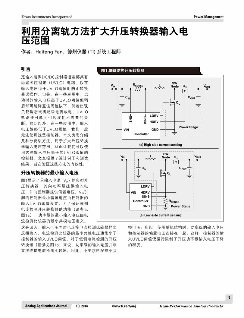
Minimum input voltage of a boost converterFigure 1 shows typical boost converters with a single input supply (VIN) that pro-vides the input voltage to the power stage and the bias voltage to the controller. The minimum bias voltage to the controller at the VIN pin is set by the controller’s input UVLO threshold. To guarantee functionality of boost converters with high-side current sensing (Figure 1a), the minimum input voltage to the power stage is defined by the minimum common-mode voltage of the current-sense com-parator. This is because the input voltage is also connected with the non-inverting input of the current-sense compar-ator. The minimum common-mode voltage of the current-sense comparator often is less than the controller’s input UVLO threshold. For the boost converter with low-side current sensing (Figure 1b), the input voltage to the power stage is not directly connected to the current-sense
Power Management
By Haifeng FanSystems Engineer
VINIS
NS
+
ISN
S–
GND
VOUTL QH
QL
CIN COUT
LDRV
Power Stage
HDRV
RSENSE
Controller
VIN
SWNode
Figure 1. Boost converters in single-rail configuration
(a) High-side current sensing
(b) Low-side current sensing
VIN
GND
VOUTL QH
QL
CIN COUT
LDRV
Power Stage
RSENSE
HDRV
ISNS
VIN
SWNode
Controller
comparator. Therefore, it is not required to match the minimum common-mode voltage. Consequently, in the single-rail configuration where the input voltage to the power stage and the bias voltage to the controller are tied together, the controller’s input UVLO threshold imposes a constraint on how low the input voltage to the boost power stage can go.
图1 单轨结构升压转换器引言
宽输入范围DC/DC控制器通常都具有
内置欠压锁定(UVLO)电路,以在
输入电压低于UVLO阈值时防止转换
器误操作。但是,在一些应用中,启
动时的输入电压高于UVLO阈值但稍
后却可能降至该阈值以下,倘若出现
负载瞬态或者超级电容放电,UVLO电路便可能会引起我们不需要的关
断。除此以外,在一些应用中,输入
电压始终低于UVLO阈值,我们一般
无法使用这些控制器。本文为您介绍
几种分离轨方法,用于扩大升压转换
器输入电压范围,从而让我们可以使
用这些输入电压低于其UVLO阈值的
控制器。文章提供了设计例子和测试
结果,旨在验证这些方法的有效性。
升压转换器的最小输入电压
图1显示了单输入电源 (VIN) 的典型升
压转换器,其向功率级提供输入电
压,并向控制器提供偏置电压。VIN引
脚的控制器最小偏置电压由控制器的
输入UVLO阈值设置。为了保证高侧
电流检测升压转换器的功能(请参见
图1a),功率级的最小输入电压由电
流检测比较器的最小共模电压定义。
利用分离轨方法扩大升压转换器输入电压范围作者:Haifeng Fan,德州仪器 (TI) 系统工程师
这是因为,输入电压同时也连接电流检测比较器的非
反相输入。电流检测比较器的最小共模电压通常小于
控制器的输入UVLO阈值。对于低侧电流检测的升压
转换器(请参见图1b)来说,功率级的输入电压并非
直接连接电流检测比较器。因此,不要求匹配最小共
模电压。所以,使用单轨结构时,功率级的输入电压
和控制器的偏置电压连接在一起,这样,控制器的输
入UVLO阈值便强行限制了升压功率级输入电压下降
的程度。
Texas Instruments Incorporated
6
Analog Applications JournalHigh-Performance Analog Products www.ti.com/aaj 1Q, 2014
Power Management
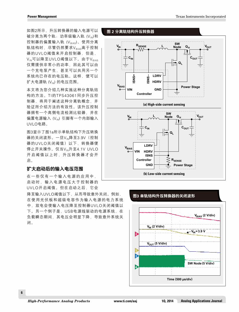
As shown in Figure 2, the input supply to the boost converter can be split into two rails: the power-stage input rail (VIN) and the controller’s bias input rail (VBIAS). In the split-rail configuration, although VBIAS is still required to be above the controller’s UVLO threshold to turn on the controller, VIN can go below the UVLO threshold. Since VBIAS needs to supply only a very small amount of power, it can be generated by a charge pump or even share another voltage rail already existing in the system. As a result, the voltage range of the power rail (VIN) can be extended.
This article will discuss several approaches to implementing the split-rail configuration. The TPS43061 synchronous boost controller from Texas Instruments (TI) will be used to elaborate on the split-rail concept and to validate the presented approaches. This boost controller has a high-side current-sense comparator and an internal input UVLO circuit at the bias-supply input (VIN) pin.
Figure 3 shows the turn-off waveforms of the boost converter in the single-rail config-uration shown in Figure 1a. The converter stops switching once VIN falls below 3.9 V, which is the controller’s UVLO turn-off threshold. The boost converter can be turned on only when VIN rises above the UVLO turn-on threshold of 4.1 V.
Extending input-voltage range after start-upIn some applications with only one input supply, the input-supply voltage is greater than the controller’s UVLO turn-on threshold at start-up. However, it might fall below the input UVLO threshold afterwards, leading to undesired shutdown. For example, in power systems using a photo-voltaic panel combined with a supercapacitor as an input supply, the input voltage may drop below the controller’s UVLO turn-off threshold due to discharge. Another exam-ple is a power system powered by a USB power cable where the voltage drops significantly during a load tran-sient, resulting in an unexpected system shutdown.
V (2 V/div)IN
V = 3.9 VIN
V (2 V/div)BIAS
V (5 V/div)OUT
SW Node (5 V/div)
Time (500 µs/div)
4
3
2
1
Figure 3. Turn-off waveforms of boost converter in single-rail configuration
VIN
ISN
S+
ISN
S–
GND
VOUTL QH
QL
CIN COUT
LDRV
Power Stage
HDRV
RSENSE
Controller
VIN
SWNode
VBIAS
Figure 2. Boost converters in split-rail configuration
(a) High-side current sensing
(b) Low-side current sensing
VBIAS
VIN
GND
VOUTL QH
QL
CIN COUT
LDRV
Power Stage
RSENSE
HDRV
ISNS
VIN
SWNode
Controller
图 2 分离轨结构升压转换器
图3 单轨结构升压转换器的关闭波形降至输入UVLO阈值以下,从而导致意外关闭。例如,
在使用光伏板和超级电容作为输入电源的电力系统
中,放电会使输入电压降至控制器UVLO关闭阈值以
下。另一个例子是,USB电源线驱动的电源系统,在
负载瞬态期间,其电压会明显下降,导致意外系统关
闭。
如图2所示,升压转换器的输入电源可以
被分离为两个轨:功率级输入轨 (VIN)和控制器的偏置输入轨 (VBIAS)。使用分离
轨结构时,尽管仍然要求VBIAS高于控制
器的UVLO阈值来开启控制器,但是,
VIN可以降至UVLO阈值以下。由于VBIAS
仅需提供非常小的功率,因此其可以由
一个充电泵产生,甚至可以共用另一个
系统内已存在的电压轨。这样,便可以
扩大电源轨 (VIN) 的电压范围。
本文将为您介绍几种实施这种分离轨结
构的方法。TI的TPS43061同步升压控
制器,将用于阐述这种分离轨概念,并
验证所介绍方法的有效性。该升压控制
器拥有一个高侧电流检测比较器,并在
偏置电源输入 (VIN) 引脚有一个内部输入
UVLO电路。
图3显示了图1a所示单轨结构下升压转换
器的关闭波形。一旦VIN降至3.9V(控制
器的UVLO关闭阈值)以下,转换器便
停止开关操作。仅当VIN升至4.1V UVLO开启阈值以上时,升压转换器才会开
启。
扩大启动后的输入电压范围
在一些仅有一个输入电源的应用中,
启动时,输入电源电压大于控制器的
UVLO开启阈值。但在启动之后,它会
Texas Instruments Incorporated
7
Analog Applications Journal 1Q, 2014 www.ti.com/aaj High-Performance Analog Products
Power Management
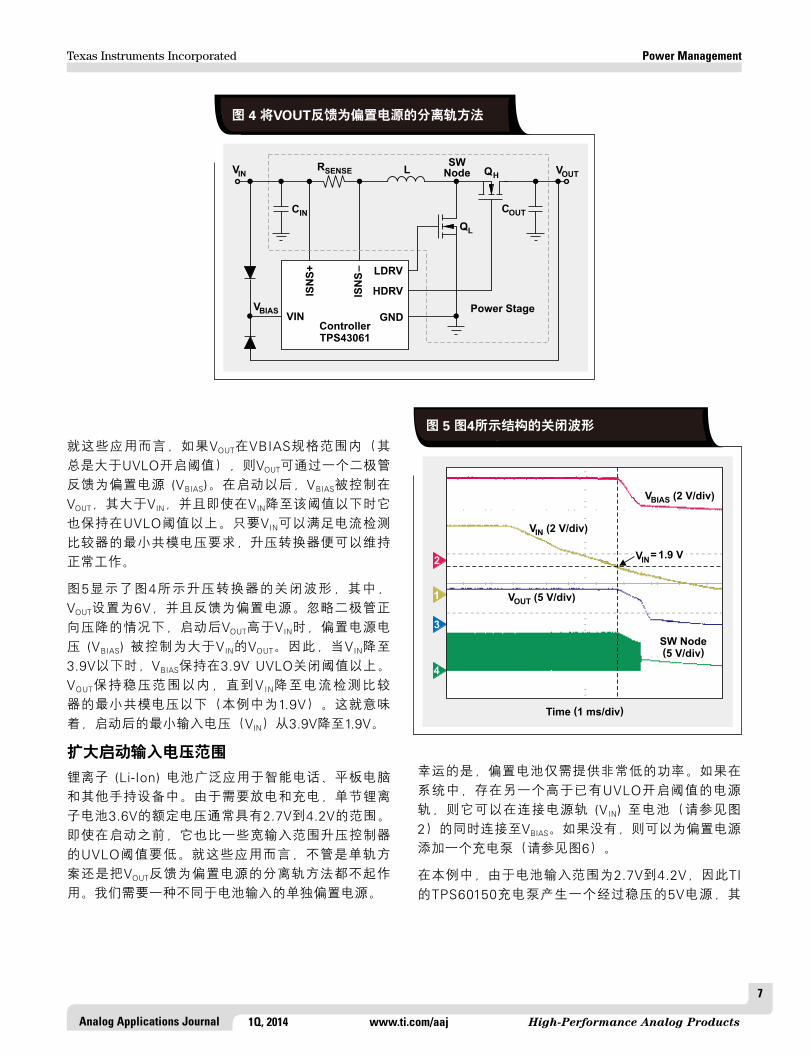
For these applications, if VOUT is within the VBIAS specifi-cation range, which is always higher than the UVLO turn-on threshold, VOUT can be fed back as the bias supply (VBIAS) via a diode (Figure 4). After start-up, VBIAS is clamped to VOUT rather than VIN and stays above the UVLO threshold even if VIN drops below this threshold. The boost converter can maintain normal operation as long as VIN can meet the current-sense comparator’s requirement for the minimum common-mode voltage.
Figure 5 shows the turn-off waveforms of the boost con-verter shown in Figure 4, where VOUT is set as 6 V and fed back as the bias supply. With diode’s forward voltage drop neglected, the bias-supply voltage (VBIAS) is clamped to VOUT rather than VIN when VOUT is higher than VIN after start-up. Hence, VBIAS stays above the 3.9-V UVLO turn-off threshold to avoid the undesired turn-off when VIN falls below 3.9 V. VOUT stays within regulation until VIN falls below the minimum common-mode voltage of the current-sense comparator, in this example 1.9 V. This means that the minimum input voltage (VIN) has been extended from 3.9 V to 1.9 V after start-up.
Extending the start-up input-voltage rangeLithium-Ion (Li-Ion) batteries are widely used in smart-phones, tablet PCs, and other handheld devices. The voltage of a single-cell Li-Ion battery rated at 3.6 V usually ranges from 2.7 V to 4.2 V due to discharge and charge. This is lower than the UVLO threshold of some wide-input-range boost controllers, even before start-up. For these applications, neither a single-rail scheme nor a
VBIASVIN
ISN
S+
ISN
S–
GND
VOUTL QH
QL
CIN COUT
LDRV
Power Stage
HDRV
RSENSEVIN
SWNode
ControllerTPS43061
Figure 4. Split-rail approach feeding VOUT back as bias supply
V (2 V/div)IN
V = 1.9 VIN
V (2 V/div)BIAS
V (5 V/div)OUT
SW Node(5 V/div)
Time (1 ms/div)
4
3
2
1
Figure 5. Turn-off waveforms of configuration shown in Figure 4
split-rail approach feeding VOUT back as the bias supply works. A separate bias supply different from the battery input is needed.
Fortunately, a bias supply needs to supply only very low power. If there is another supply rail above the UVLO turn-on threshold already available in the system, it can be connected to VBIAS while connecting the power rail (VIN)
图 5 图4所示结构的关闭波形
图 4 将VOUT反馈为偏置电源的分离轨方法
就这些应用而言,如果VOUT在VBIAS规格范围内(其
总是大于UVLO开启阈值),则VOUT可通过一个二极管
反馈为偏置电源 (VBIAS)。在启动以后,VBIAS被控制在
VOUT,其大于VIN,并且即使在VIN降至该阈值以下时它
也保持在UVLO阈值以上。只要VIN可以满足电流检测
比较器的最小共模电压要求,升压转换器便可以维持
正常工作。
图5显示了图4所示升压转换器的关闭波形,其中,
VOUT设置为6V,并且反馈为偏置电源。忽略二极管正
向压降的情况下,启动后VOUT高于VIN时,偏置电源电
压 (VBIAS) 被控制为大于VIN的VOUT。因此,当VIN降至
3.9V以下时,VBIAS保持在3.9V UVLO关闭阈值以上。
VOUT保持稳压范围以内,直到VIN降至电流检测比较
器的最小共模电压以下(本例中为1.9V)。这就意味
着,启动后的最小输入电压(VIN)从3.9V降至1.9V。
扩大启动输入电压范围
锂离子 (Li-Ion) 电池广泛应用于智能电话、平板电脑
和其他手持设备中。由于需要放电和充电,单节锂离
子电池3.6V的额定电压通常具有2.7V到4.2V的范围。
即使在启动之前,它也比一些宽输入范围升压控制器
的UVLO阈值要低。就这些应用而言,不管是单轨方
案还是把VOUT反馈为偏置电源的分离轨方法都不起作
用。我们需要一种不同于电池输入的单独偏置电源。
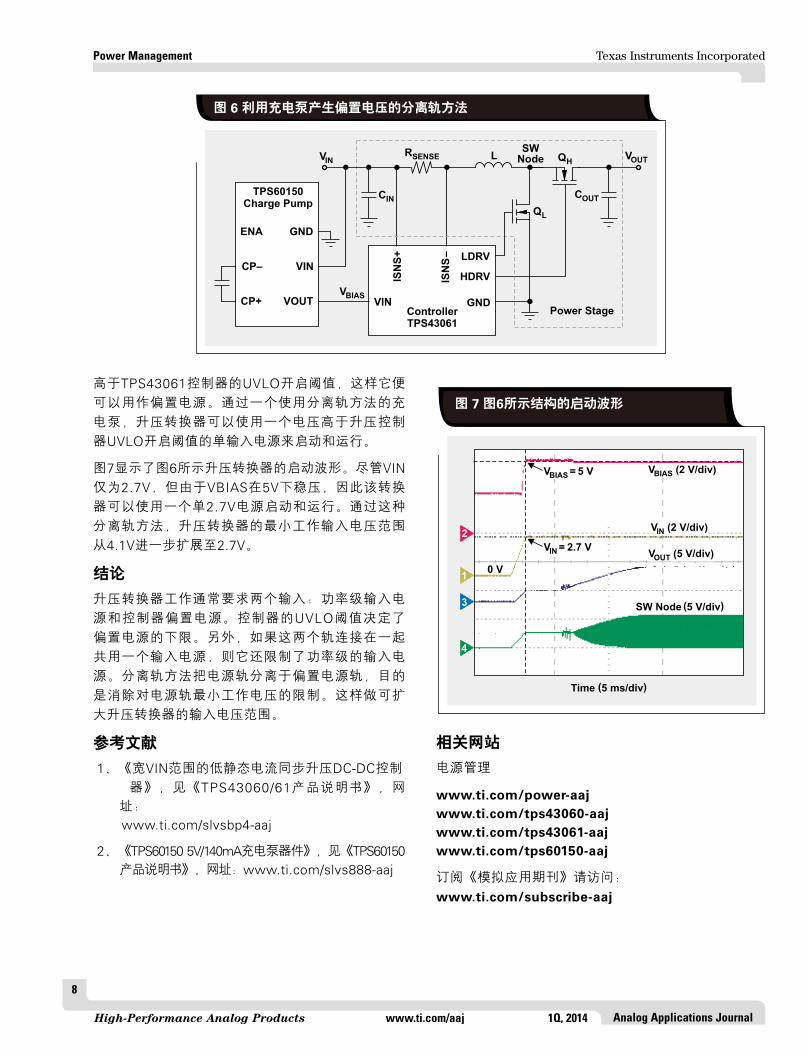
幸运的是,偏置电池仅需提供非常低的功率。如果在
系统中,存在另一个高于已有UVLO开启阈值的电源
轨,则它可以在连接电源轨 (VIN) 至电池(请参见图
2)的同时连接至VBIAS。如果没有,则可以为偏置电源
添加一个充电泵(请参见图6)。
在本例中,由于电池输入范围为2.7V到4.2V,因此TI的TPS60150充电泵产生一个经过稳压的5V电源,其
Texas Instruments Incorporated
8
Analog Applications JournalHigh-Performance Analog Products www.ti.com/aaj 1Q, 2014
Power Management
to the battery (Figure 2). If not, a charge pump can be added for a bias supply (Figure 6).
In this example, from the 2.7 V to 4.2 V of battery input, TI’s TPS60150 charge pump produces a regulated 5-V sup-ply, which is higher than the UVLO turn-on threshold of the TPS43061 controller, so it can be used as the bias sup-ply. Using a charge pump with the split-rail approach, the boost converter can start up and operate with a single input supply that is lower than the boost controller’s UVLO turn-on threshold .
Figure 7 shows the start-up waveforms of the boost con-verter shown in Figure 6. The converter can start up and operate with a single 2.7 V of supply since VBIAS is regu-lated at 5 V, although VIN is only 2.7 V. By using this split-rail approach, the boost converter’s minimum operating input voltage is extended from 4.1 V to 2.7 V.
ConclusionTwo inputs are usually required for a boost converter to operate: the input supply to the power stage and the bias supply to the controller. The controller’s UVLO threshold sets the low limit of the bias supply. It also places a con-straint on the input supply to the power stage, if these two rails are connected to share one input supply. Split-rail approaches separate the power rail from the bias supply rail to eliminate the constraint on the minimum operating voltage of the power rail. This extends the input-voltage range of boost converters.
References1. “Low quiescent current synchronous boost DC-DC con-
troller with wide VIN range,” TPS43060/61 Datasheet. Available: www.ti.com/slvsbp4-aaj
2. “TPS60150 5V/140mA charge pump device,” TPS60150 Datasheet. Available: www.ti.com/slvs888-aaj
VBIASVIN
ISN
S+
ISN
S–
GND
VOUTL QH
QL
CIN COUT
LDRV
Power Stage
HDRV
RSENSE
ControllerTPS43061
VIN
SWNode
GND
VIN
VOUT
ENA
CP–
CP+
TPS60150Charge Pump
Figure 6. Split-rail approach using charge pump to produce bias voltage
V = 2.7 VIN
Time (5 ms/div)
4
3
2
10 V
V = 5 VBIAS
V (2 V/div)IN
V (2 V/div)BIAS
V (5 V/div)OUT
SW Node (5 V/div)
Figure 7. Start-up waveforms of configuration shown in Figure 6
Related Web sitesPower Management:www.ti.com/power-aaj
www.ti.com/tps43060-aajwww.ti.com/tps43061-aajwww.ti.com/tps60150-aaj
Subscribe to the AAJ:www.ti.com/subscribe-aaj
图 6 利用充电泵产生偏置电压的分离轨方法
图 7 图6所示结构的启动波形
高于TPS43061控制器的UVLO开启阈值,这样它便
可以用作偏置电源。通过一个使用分离轨方法的充
电泵,升压转换器可以使用一个电压高于升压控制
器UVLO开启阈值的单输入电源来启动和运行。
图7显示了图6所示升压转换器的启动波形。尽管VIN仅为2.7V,但由于VBIAS在5V下稳压,因此该转换
器可以使用一个单2.7V电源启动和运行。通过这种
分离轨方法,升压转换器的最小工作输入电压范围
从4.1V进一步扩展至2.7V。
结论
升压转换器工作通常要求两个输入:功率级输入电
源和控制器偏置电源。控制器的UVLO阈值决定了
偏置电源的下限。另外,如果这两个轨连接在一起
共用一个输入电源,则它还限制了功率级的输入电
源。分离轨方法把电源轨分离于偏置电源轨,目的
是消除对电源轨最小工作电压的限制。这样做可扩
大升压转换器的输入电压范围。
参考文献
1、《宽VIN范围的低静态电流同步升压DC-DC控制
器》,见《TPS43060/61产品说明书》,网
址:
www.ti.com/slvsbp4-aaj
2、《TPS60150 5V/140mA充电泵器件》,见《TPS60150产品说明书》,网址:www.ti.com/slvs888-aaj
相关网站
电源管理
www.ti.com/power-aaj www.ti.com/tps43060-aaj www.ti.com/tps43061-aaj www.ti.com/tps60150-aaj
订阅《模拟应用期刊》请访问:
www.ti.com/subscribe-aaj

9
Analog Applications Journal
Texas Instruments Incorporated
1Q, 2014 www.ti.com/aaj High-Performance Analog Products
Low-cost flyback solutions for 10-mW standby power
For low-power AC/DC conversion, flyback topology remains the preferred choice due to its simplicity and low cost. Using a small number of external components, this topology can provide one or more outputs for a very wide input-voltage range. It is used in isolated and non-isolated forms to cover a broad range of applications, such as battery chargers in smartphones and tablets; auxiliary power supplies in TVs, desktop computers, and home appliances; AC adapters for portable computing, set-top boxes, and networking; and many more. Figure 1 shows the typical power levels in some of these applications. The wide-spread applicability and use of the flyback topology in high-volume consumer markets (estimated 2012 world-wide shipments for the markets shown in Figure 1 alone exceeded a few billion units) make it a perfect candidate for optimizing every possible performance specification, such as cost, efficiency, and standby power.
In most applications, flyback converters are stand-alone external power supplies in wall chargers/adapters. In some cases they are powering either a portion of larger equip-ment or providing standby power to maintain system func-tions like the user display and remote control when the equipment is not performing its primary function. In all cases, the standby-power consumption of the flyback
converter is being heavily scrutinized to minimize the overall power drain when it seems the converter is doing nothing. For example, a flyback power supply used in an AC wall charger may have a mass-production specification of less than 30 mW. If the actual supply consumes only 10 mW of standby power, the 20-mW difference can allow a higher margin for leaky circuit components such as input filters, capacitors, and bias components, reducing overall solution cost. Similarly, a flyback converter with low standby-power consumption can allow more system func-tions to be active in standby mode while keeping the end equipment’s total power consumption to a minimum.
The push towards green powerThere is an array of initiatives and directives in the power industry addressing efficiency and standby power that vary by end equipment, power level, and governing authority. In the U.S., these include the California Energy Commission and the Environmental Protection Agency’s ENERGY STAR®,1 and in Europe, the European Union’s Standby Initiative, to name a few. After a quick glance at many of these energy-conservation initiatives, it is clear that they all have a common theme—driving minimal power loss at light loads and no-load/standby. Many
Power Management
By Adnaan LokhandwalaProduct Manager
FeaturePhone
Smart-phone
Tablet Set-TopBox
HomeAppliance
TV DesktopComputer
20
15
10
5
Po
wer
Level (W
)
Battery Chargers/Adapters Auxiliary Power
Figure 1. Typical power levels for AC/DC flyback-converter designs
10mW待机功耗低成本反向解决方案作者:Adnaan Lokhandwala,德州仪器 (TI) 产品经理
图 1 AC/DC反向转换器设计的典型功率电平
就低功率AC/DC转换而言,反向拓扑因其结构简单
和成本低仍然是人们的首选。只需使用少量的外部组
件,这种拓扑便可提供一个或多个输出,实现非常宽
的输入电压范围。它能够以隔离和非隔离方式使用,
适用于大量应用,例如:智能电话和平板电脑的电池
充电器;电视机、桌面计算机和各种家用电器的辅助
电源;便携计算机、机顶盒和网络设备的AC适配器
等。图1显示了这些应用中一部分的典型功率电平。
消费类市场中对反向拓扑结构的大量采用及其广泛的
适用性(图1所示2012年世界市场估计出货量超过数
十亿件),让它成为对所有性能指标进行优化的一个
理想选择,例如:成本、效率和待机功耗等。
在大多数应用中,反向转换器都是墙上充电器 /适配
器的单独外部电源。在一些情况下,它们为更大型设
备的一部分供电,或者在设备不执行其主要功能时提
供待机功率,以维持一些系统功能,例如:用户显示
和远程控制等。在所有情况下,反向转换器的待机功
耗都被严格监控,目的是在转换器闲置时最小化总功
耗。例如,AC墙上充电器中使用的反激电源,其批
量生产型产品的待机功耗规格小于30mW。如果实际
电源的待机功耗仅为10mW,那么节省出来的20mW可以为漏电电路组件带来更大的余量,例如:输入滤
波器、电容和各种偏置组件,从而降低总解决方案成
本。同样,低待机功耗的反向转换器可以允许在待机
模式下运行更多的系统功能,并同时让终端设备总功
耗保持最小。
推动绿色电源发展
在电源行业,有关电源效率和待机功耗的发展计划和
规范有很多,但因终端设备、功率电平和管理部门不
同而各异。在美国,有加州能源委员会与环保局颁
布的“能源之星®”,欧盟有“待机功耗发展计划”
等,诸如此类。在大概了解这些节能计划之后,我们
可以清楚地知道,它们都有一个共同的主题—不断降
低轻负载和无负载/待机的功耗。世界许多地区还正在
推行一些针对外部电源待机功耗和轻负载工作效率的
强制和自愿规定。
在美国,加州能源委员会于2013年2月开始在本州实
施一项电池充电效率标准。另外,美国能源部正在最
终敲定一份草案,它将在世界范围内影响目前的电源
Texas Instruments Incorporated
10
Analog Applications JournalHigh-Performance Analog Products www.ti.com/aaj 1Q, 2014
Power Management
regions in the world are also introducing mandatory and voluntary limits for standby-power consumption and light-load operating efficiency of external power supplies.
In the U.S., the California Energy Commission adopted for its own state a battery-charging efficiency standard that became effective in February 2013. Additionally, the U.S. Department of Energy is finalizing a draft that will affect current regulations for power-supply efficiency worldwide. Similarly, the Joint Research Centre of the European Commission (EC) published the final draft of Version 5 of its Code of Conduct on Energy Efficiency of External Power Supplies in October 2013. These new voluntary specifications, which propose tightening of active-mode efficiency and no-load power consumption, are tougher to meet than the mandatory specifications of the EC’s current Ecodesign Directive.
To ensure that the external supply is efficient in the idle and standby modes of some applications, the EC has added an additional efficiency requirement at 10% load beyond the four-point active-mode average-efficiency requirement. The EC also has added an additional classification for mobile handheld battery-driven external supplies of less than 8 W that must limit no-load power consumption to less than 75 mW starting in 2014. Finally, the EC’s Ecodesign Directive for energy-related products, Lot 6, Tier 2 took effect in January 2013. This part of the directive limits total system standby-power consumption of household and office equipment to less than 0.5 W.
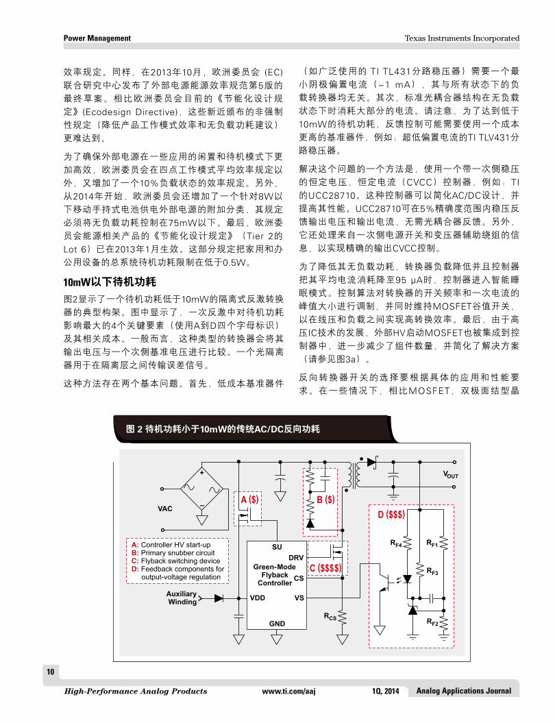
Less than 10 mW of standby-power consumptionThe typical architecture for an isolated flyback converter that consumes less than 10 mW of standby power is shown in Figure 2. Four key elements (labeled A through D) in a
flyback that contribute most to its standby-power loss are shown along with their relative cost. Traditionally, this type of converter compares its output voltage with a secondary-side reference. An optoisolator is used to transfer an error signal across the isolation barrier.
There are two fundamental issues with this approach. First, a low-cost reference like the widely used TL431 shunt regulator from Texas Instruments (TI) needs a mini-mum cathode bias current (~1 mA) independent of con-verter loading under all conditions. Second, the standard optocoupler configuration is such that it consumes the most current under no-load conditions. Note that in order to achieve standby-power consumption of less than 10 mW, a more expensive reference such as TI’s TLV431 shunt regulator with very low bias current may need to be used for feedback control.
One way to address these issues is to use a constant-voltage, constant-current (CVCC) controller with primary-side regulation, such as TI’s UCC28710. This type of con-troller can simplify and improve performance in AC/DC designs. The UCC28710 regulates the flyback output voltage and output current within 5% accuracy without optocoupler feedback. It also processes information from the primary power switch and transformer auxiliary wind-ing for precise output CVCC control.
To reduce its no-load consumption, the controller enters smart sleep modes as the converter load decreases and the controller reduces its average current consumption down to 95 µA. The control algorithm modulates the converter’s switching frequency and the primary current’s peak ampli-tude while maintaining MOSFET valley switching for high conversion efficiency across line and load. Finally, thanks to high-voltage IC technology, the external HV start-up
A:B:C:D:
Controller HV start-upPrimary snubber circuitFlyback switching deviceFeedback components foroutput-voltage regulation
VAC
VOUT
RF4 RF1
RF3
RF2
RCS
A ($)
C ($$$$)
D ($$$)
B ($)
+
–
AuxiliaryWinding
DRV
CS
VS
SU
VDD
GND
Green-ModeFlyback
Controller
Figure 2. Conventional AC/DC flyback consumes less than 10 mW of standby power图 2 待机功耗小于10mW的传统AC/DC反向功耗
效率规定。同样,在2013年10月,欧洲委员会 (EC) 联合研究中心发布了外部电源能源效率规范第5版的
最终草案。相比欧洲委员会目前的《节能化设计规
定》(Ecodesign Directive),这些新近颁布的非强制
性规定(降低产品工作模式效率和无负载功耗建议)
更难达到。
为了确保外部电源在一些应用的闲置和待机模式下更
加高效,欧洲委员会在四点工作模式平均效率规定以
外,又增加了一个10%负载状态的效率规定。另外,
从2014年开始,欧洲委员会还增加了一个针对8W以
下移动手持式电池供电外部电源的附加分类,其规定
必须将无负载功耗控制在75mW以下。最后,欧洲委
员会能源相关产品的《节能化设计规定》(Tier 2的
Lot 6)已在2013年1月生效。这部分规定把家用和办
公用设备的总系统待机功耗限制在低于0.5W。
10mW以下待机功耗
图2显示了一个待机功耗低于10mW的隔离式反激转换
器的典型构架。图中显示了,一次反激中对待机功耗
影响最大的4个关键要素(使用A到D四个字母标识)
及其相关成本。一般而言,这种类型的转换器会将其
输出电压与一个次侧基准电压进行比较。一个光隔离
器用于在隔离层之间传输误差信号。
这种方法存在两个基本问题。首先,低成本基准器件
(如广泛使用的 TI TL431分路稳压器)需要一个最
小阴极偏置电流(~1 mA),其与所有状态下的负
载转换器均无关。其次,标准光耦合器结构在无负载
状态下时消耗大部分的电流。请注意,为了达到低于
10mW的待机功耗,反馈控制可能需要使用一个成本
更高的基准器件,例如:超低偏置电流的TI TLV431分路稳压器。
解决这个问题的一个方法是,使用一个带一次侧稳压
的恒定电压、恒定电流(CVCC)控制器,例如:TI的UCC28710。这种控制器可以简化AC/DC设计,并
提高其性能。UCC28710可在5%精确度范围内稳压反
馈输出电压和输出电流,无需光耦合器反馈。另外,
它还处理来自一次侧电源开关和变压器辅助绕组的信
息,以实现精确的输出CVCC控制。
为了降低其无负载功耗,转换器负载降低并且控制器
把其平均电流消耗降至95 µA时,控制器进入智能睡
眠模式。控制算法对转换器的开关频率和一次电流的
峰值大小进行调制,并同时维持MOSFET谷值开关,
以在线压和负载之间实现高转换效率。最后,由于高
压IC技术的发展,外部HV启动MOSFET也被集成到控
制器中,进一步减少了组件数量,并简化了解决方案
(请参见图3a)。
反向转换器开关的选择要根据具体的应用和性能要
求。在一些情况下,相比MOSFET,双极面结型晶
Texas Instruments Incorporated
11
Analog Applications Journal 1Q, 2014 www.ti.com/aaj High-Performance Analog Products
Power Management
MOSFET is also integrated into the con-troller to further reduce component count and simplify the solution (Figure 3a).
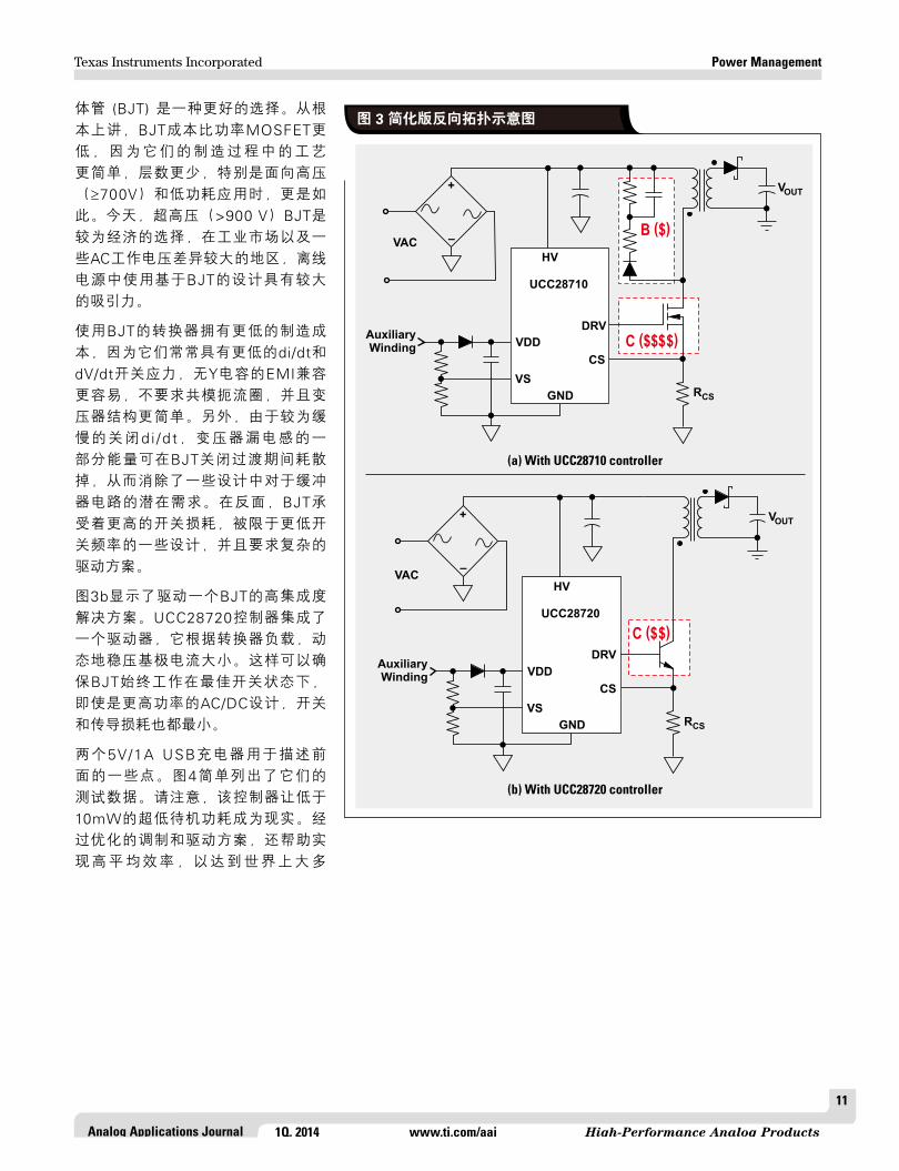
The choice of a flyback converter switch is very application-specific and performance-driven. In some situations, a bipolar junction transistor (BJT) can be a better choice than a MOSFET. Funda men-tally, BJTs cost less than power MOSFETs because their fabrication involves a sim-pler process with fewer layers, particularly for high-voltage (≥700-V) and low-power applications. BJTs with very high voltage (>900 V) are economical options today, making BJT-based designs attractive in off-line power supplies for the industrial market and in regions with widely varying AC utility voltages.
Converters with BJTs can have lower manufacturing cost because they normally have less di/dt and dV/dt switching stress, EMI compliance is easier with no Y capaci-tor, no common-mode choke is required, and transformer construction is simpler. Also, due to slow di/dt at turn-off, some energy in the transformer’s leakage induc-tance can be dissipated at the BJT turn- off transition, potentially eliminating snub-ber circuits in some designs. On the flip side, BJTs suffer from higher switching losses, are limited to designs with lower switching frequencies, and require a com-plex drive scheme.
A highly integrated solution for driving a BJT is shown in Figure 3b. The UCC28720 controller incorporates a driver that dynam-ically adjusts the base-current amplitude based on the converter load. This ensures that the BJT always operates in optimal switching conditions with minimal switch-ing and conduction losses even for higher-power AC/DC designs.
VAC
AuxiliaryWinding
VOUT
RCS
C ($$$$)
B ($)
+
–
DRV
CS
VS
HV
UCC28710
VDD
GND
Figure 3. Simplified flyback schematics
(a) With UCC28710 controller
(b) With UCC28720 controller
VAC
VOUT
RCS
C ($$)
+
–
AuxiliaryWinding
VS
HV
UCC28720
VDD
GND
DRV
CS
图 3 简化版反向拓扑示意图体管 (BJT) 是一种更好的选择。从根
本上讲,BJT成本比功率MOSFET更低,因为它们的制造过程中的工艺
更简单,层数更少,特别是面向高压
(≥700V)和低功耗应用时,更是如
此。今天,超高压(>900 V)BJT是较为经济的选择,在工业市场以及一
些AC工作电压差异较大的地区,离线
电源中使用基于BJT的设计具有较大
的吸引力。
使用BJT的转换器拥有更低的制造成
本,因为它们常常具有更低的di/dt和
dV/dt开关应力,无Y电容的EMI兼容
更容易,不要求共模扼流圈,并且变
压器结构更简单。另外,由于较为缓
慢的关闭d i /d t,变压器漏电感的一
部分能量可在BJT关闭过渡期间耗散
掉,从而消除了一些设计中对于缓冲
器电路的潜在需求。在反面,BJT承受着更高的开关损耗,被限于更低开
关频率的一些设计,并且要求复杂的
驱动方案。
图3b显示了驱动一个BJT的高集成度
解决方案。UCC28720控制器集成了
一个驱动器,它根据转换器负载,动
态地稳压基极电流大小。这样可以确
保BJT始终工作在最佳开关状态下,
即使是更高功率的AC/DC设计,开关
和传导损耗也都最小。
两个5V/1A USB充电器用于描述前
面的一些点。图4简单列出了它们的
测试数据。请注意,该控制器让低于
10mW的超低待机功耗成为现实。经
过优化的调制和驱动方案,还帮助实
现高平均效率,以达到世界上大多
Texas Instruments Incorporated
12
Analog Applications JournalHigh-Performance Analog Products www.ti.com/aaj 1Q, 2014
Power Management
Two 5-V/1-A USB chargers were designed to illustrate some of the preceding points. Their test data are summa-rized in Figure 4. Note that the controllers enable ultralow standby-power consumption of less than 10 mW. Opti mized modulation and drive schemes also facilitate achieving high average efficiency to meet the most stringent worldwide regulations. References 2 and 3 provide links to full test data and a bill of materials for these designs. Test data for a higher-power 5-V/1.5-A design is included in Figure 4 to illustrate that this BJT-based solution can provide an aver-age efficiency of 80+%.4
ConclusionThe simplicity and cost-effectiveness of the flyback topol-ogy have made it the preferred choice for the many low-power AC/DC designs powering consumer electronics. Power-supply designers are continuously challenged to achieve the same performance at lower cost or improved performance at the same cost. This article has touched on a few of these performance aspects and how th e cost of the power-supply solution can be addressed with the smart choice of a power-efficient controller. The UCC28710 and UCC28720 members of TI’s 700-V flyback-controller family enable cost-optimal designs with best-in-class standby power and efficiency for compliance with current and future industry standards.
References1. Adnaan Lokhandwala. (May 20, 2013). “The no-
load power crunch: 30 mW and beyond.” Power Systems Design [Online]. Available: www.powersystemsdesign.com
2. “Universal AC input [email protected] cube charger with <10mW no-load power,” Reference Design using UCC28710. Available: www.ti.com/pmp4344-aaj
3. “5V1A low standby power AC charger with low cost BJT solution,” Reference Design using UCC28720. Available: www.ti.com/pmp4373-aaj
4. “High efficiency [email protected] adapter using BJT solution,” Reference Design using UCC28720. Available: www.ti.com/pmp4372-aaj
Related Web sitesPower Management:www.ti.com/power-aaj
www.ti.com/tl431-aajwww.ti.com/tlv431-aajwww.ti.com/ucc28710-aajwww.ti.com/ucc28720-aaj
www.ti.com/adapterpower-aaj
Subscribe to the AAJ:www.ti.com/subscribe-aaj
115 V
MOSFET(5 V/1 A)
BJT(5 V/1 A)
BJT(5 V/1.5 A)
230 V 115 V 230 V 115 V 230 V
Sta
nd
by
Po
we
r( m
W)
Av
era
ge
Eff
icie
nc
y( %
)
20
15
10
5
0
88
84
80
76
72
Standby Power
Average Efficiency
22 x 21 x 20 mm 35.7 x 25.7 x 14 mm
43 x 28 x 16 mm
Figure 4. Summary of test data for AC/DC flyback designs with UCC287xx controllers图8 负载瞬态期间的集成线性稳压器
数严格的能耗规定。参考2和3给出了这些设计的完
整测试数据和一份材料清单。图4包括了一个高功率
5V/1.5A设计的测试数据,目的是说明这种BJT型解决
方案可以提供80+%的平均效率。4
结论
反向拓扑的简单性和高成本效益,让其成为许多驱动
消费类电子产品的低功耗AC/DC设计的首选。为了
以更低的成本达到相同的性能,或者在成本不变的情
况下实现更高的性能,电源设计人员面临众多的挑
战。本文只介绍了一部分这些性能,并说明了如何灵
活地选择高功效的控制器来解决电源解决方案的成本
问题。TI的700V反向控制器系列产品UCC28710和
UCC28720,拥有同级别中最低的待机功耗和最高的
效率,可实现最为经济的设计,能够达到目前和未来
的行业标准。
参考文献
1、《无负载功耗:30mWc以上》,作者:Adnaan Lokhandwala,2013年5月20日,见于《电源系统
设计》(在线版),网址:
www.powersystemsdesign.com
2、《无负载功耗小于10mW的通用AC输入[email protected]充电器》,见《使用UCC28710的参考设计》,
网址:www.ti.com/pmp4344-aaj
3、《低成本BJT解决方案的5V1A低待机电源AC充
电器》,见《使用UCC28720的参考设计》,网
址:www.ti.com/pmp4373-aaj
4、《使用B J T解决方案的高效率5 V @ 1. 5 A适配
器》,见《使用UCC28720的参考设计》,网
址:
www.ti.com/pmp4372-aaj
相关网站
电源管理:
www.ti.com/power-aaj www.ti.com/tl431-aaj www.ti.com/tlv431-aaj www.ti.com/ucc28710-aaj www.ti.com/ucc28720-aaj www.ti.com/adapterpower-aaj
订阅《模拟应用期刊》请访问:
www.ti.com/subscribe-aaj
13
Analog Applications Journal
Texas Instruments Incorporated
1Q, 2014 www.ti.com/aaj High-Performance Analog Products
Accurately measuring efficiency of ultralow-IQ devices
IntroductionWhile almost every power-supply engineer intimately knows and understands the lab setup for measuring efficiency, there are many important nuances that must be considered when measuring the efficiency of a device with ultralow quiescent current (IQ). For a device that consumes less than 1 µA, the circuit’s currents are very small and difficult to measure. These measurements may equate to calculated light-load efficiencies that are far lower than what is shown in the datasheet graphs and lower than what would be seen in the real application. This article reviews the basics of measuring efficiency, discusses common mistakes in mea-suring the light-load efficiency of ultralow-IQ devices, and demonstrates how to overcome them in order to get accu-rate efficiency measurements.
Basics of measuring efficiencyReference 1 details the best setup to accurately measure a device’s efficiency with a power-save or pulse-frequency-modulation (PFM) mode. This reference provides an excellent background to the topics covered in this article and should be read first. Generally, and especially in this article, efficiency is defined as
( ) OUT OUT OUT
IN IN IN
Power V I efficiency .
Power V I
×η = =
×
The following summarizes two key points made in Reference 1. The first is that any power-save mode draws relatively large bursts of current from the input supply. These bursts are an AC current from the input. Devices that always operate in continuous-conduction or pulse-width-modulation (PWM) mode draw DC currents from the input supply. Unlike the DC current drawn in PWM mode, the power-save mode’s bursts of current create an incorrect RMS-current reading in the input-current meter. Therefore, the proper test setup for measuring efficiency in power-save mode includes sufficient input capacitance after the input-current meter to smooth out the AC cur-rents drawn by the PFM mode in order to present a DC current to the current meter.
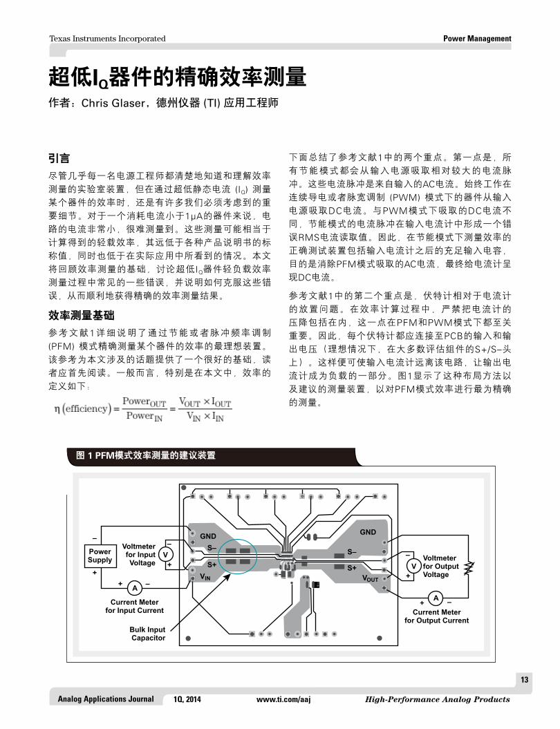
The second key point in Reference 1 regards the place-ment of the voltmeters relative to the current meters. It is critical in both PFM and PWM modes not to include the voltage drops across the current meters in the efficiency calculations. Therefore, each voltmeter should be con-nected to the input and output voltages on the PCB, ideally at the S+/S– header on most evaluation modules (EVMs). This places the input-current meter out of the circuit and the output-current meter as part of the load. These placements are shown in Figure 1 with the recom-mended setup for measuring PFM-mode efficiency with the best accuracy.
Power Management
By Chris GlaserApplications Engineer
Current Meterfor Input Current
Bulk InputCapacitor
Current Meterfor Output Current
Voltmeterfor Output Voltage
–
–
–
++
–+
+
PowerSupply V –
+V
AA
GND GND
S–S–
S+VIN VOUT
S+
Voltmeter for Input Voltage
Figure 1. Recommended setup for measuring PFM-mode efficiency图 1 PFM模式效率测量的建议装置
引言
尽管几乎每一名电源工程师都清楚地知道和理解效率
测量的实验室装置,但在通过超低静态电流 (IQ) 测量
某个器件的效率时,还是有许多我们必须考虑到的重
要细节。对于一个消耗电流小于1µA的器件来说,电
路的电流非常小,很难测量到。这些测量可能相当于
计算得到的轻载效率,其远低于各种产品说明书的标
称值,同时也低于在实际应用中所看到的情况。本文
将回顾效率测量的基础,讨论超低IQ器件轻负载效率
测量过程中常见的一些错误,并说明如何克服这些错
误,从而顺利地获得精确的效率测量结果。
效率测量基础
参考文献1详细说明了通过节能或者脉冲频率调制 (PFM) 模式精确测量某个器件的效率的最理想装置。
该参考为本文涉及的话题提供了一个很好的基础,读
者应首先阅读。一般而言,特别是在本文中,效率的
定义如下:
超低IQ器件的精确效率测量作者:Chris Glaser,德州仪器 (TI) 应用工程师
下面总结了参考文献1中的两个重点。第一点是,所
有节能模式都会从输入电源吸取相对较大的电流脉
冲。这些电流脉冲是来自输入的AC电流。始终工作在
连续导电或者脉宽调制 (PWM) 模式下的器件从输入
电源吸取DC电流。与PWM模式下吸取的DC电流不
同,节能模式的电流脉冲在输入电流计中形成一个错
误RMS电流读取值。因此,在节能模式下测量效率的
正确测试装置包括输入电流计之后的充足输入电容,
目的是消除PFM模式吸取的AC电流,最终给电流计呈
现DC电流。
参考文献1中的第二个重点是,伏特计相对于电流计
的放置问题。在效率计算过程中,严禁把电流计的
压降包括在内,这一点在PFM和PWM模式下都至关
重要。因此,每个伏特计都应连接至PCB的输入和输
出电压(理想情况下,在大多数评估组件的S+/S–头上)。这样便可使输入电流计远离该电路,让输出电
流计成为负载的一部分。图1显示了这种布局方法以
及建议的测量装置,以对PFM模式效率进行最为精确
的测量。
Texas Instruments Incorporated
14
Analog Applications JournalHigh-Performance Analog Products www.ti.com/aaj 1Q, 2014
Power Management
Setup issues in measuring efficiency of an ultralow-IQ deviceDevices with an ultralow IQ have special considerations for their efficiency-measurement setup. For simplicity, ultralow IQ can be approximated as less than roughly 10 µA of IQ. Below this level, the input current drawn by one or both voltmeters, as well as the leakage current of the additional input capacitor, can substantially affect the measured input current and thus the calculated light-load efficiency. Note that if higher-leakage equipment is used, these concerns also would be relevant for higher-IQ devices. Reference 2 explains IQ in detail.
Input resistance of the input voltmeterIn the test setup in Figure 1, the two voltmeters have some finite input resistance. For example, the standard handheld, battery-powered Fluke digital multimeter (DMM) has an input resistance of around 10 MΩ. While this certainly seems very large and unlikely to affect the efficiency measurement, calculating how much current it draws when it measures a very common 3.6-V input volt-age can be revealing. In this case, when 3.6 V is applied to the DMM’s terminals (across its resistance), 0.36 µA of current flows into the meter. This is effectively 360 nA of leakage current that is drawn directly from the input volt-age applied to the device and flows through the input- current meter. Just attaching the input voltmeter to the circuit increases the input current by 360 nA. If the mea-sured device has a 20-µA IQ, then this 360 nA is less than 2% of the input current and is not very significant. But, if a step-down converter like the Texas Instruments (TI) TPS62740 with its 360-nA IQ is being tested, then this extra current drawn by the voltmeter could be up to half of the input current. This results in quite a large differ-ence in efficiency.
Extra load current through the output voltmeterA voltmeter connected on the output behaves in the same way. It draws some extra (leakage) current not measured as part of the load’s current. This leakage current is not included in the numerator in the efficiency calculation. The output voltmeter creates an extra load, which draws an extra (and measured) input current. With this extra unmeasured load current creating an increased input current, the measured efficiency is lower than the actual efficiency.
High leakage current of the extra input capacitorFinally, the additional input capacitor used to smooth out the input current might have a sufficiently high leakage to draw substantial current from the input. For example,
some high-capacitance capacitors have maximum leakage currents in the hundreds of microamperes. This leakage may change over time, so it should be checked before any efficiency testing. This extra current, if too high, is sure to throw off the efficiency calculations.
Solutions to measurement-setup issuesThere are easy solutions to the three measurement-setup issues just described. The most important point, however, is simply to be aware that the setup used to take efficiency data can cause inaccuracies in the efficiency data collected. This is especially true at light loads, where the currents are very small and difficult to measure.
Overcoming the effects of the input voltmeter’s input resistanceThere are three methods of accounting for current leakage through the input voltmeter: (1) disconnecting the volt-meter, (2) connecting it in a different location, or (3) compensating for the current into it. The first and simplest method is to record the input voltage with the voltmeter connected as usual and then disconnect the voltmeter from the input terminals before recording the input current. This accurately measures the input voltage without increasing the input current. Minimal measurement inac cu racy is introduced by this method. What is not advisable is to read the input voltage from the display on the input supply (which typically is not calibrated) and use this value for the efficiency calculations. Rather, a high-quality, high- resolution voltmeter should be used to measure the input voltage at the EVM. This overcomes small voltage drops in wires and cabling between the input supply and the EVM.
The second method of accounting for the leakage current is to connect the input voltmeter in a different location. Specifically, the voltmeter’s positive lead can be connected to the input-current meter’s positive side, while the volt-meter’s ground lead remains connected to the same loca-tion as before (the S– header on the EVM). In this way, the input voltmeter does not draw any measured current and so does not affect the calculated efficiency. The down-side of this method is that the voltage drop across the input-current meter is not accounted for. At very light loads, however, such a drop is usually insignificant. To minimize this inaccuracy at heavier loads, the input volt-meter can be moved to its original location (after the input-current meter) once the measured input current is about 100 times greater than the leakage current into the voltmeter. This allows for a simple setup where the input voltmeter remains connected throughout testing and inac-curate measurement is minimized.
超低IQ器件效率测量的装置问题
超低IQ器件应特别考虑其效率测量装置。为了简单起
见,超低IQ可取近似值为约10 µA以下。低于这一水平
时,一个或者两个伏特计吸取的输入电流以及附加输
入电容的漏电流,会明显影响所测得的输入电流,从
而影响计算得到的轻负载效率。请注意,如果使用更
高漏电流的设备,则这些问题还会关系到更高IQ的器
件。参考文献2详细说明了IQ。
输入伏特计的输入电阻
在图1所示测试装置中,两个伏特计都有一些有限输
入电阻。例如,标准手持式电池供电型弗卢克 (Fluke) 数字万用表(DMM)具有约10MΩ的输入电阻。尽
管这看似非常大,并且似乎不可能影响效率测量,但
在对一个非常常见的3.6V输入电压进行测量时计算
它吸取的电流大小后,我们便可知道答案。在这种
情况下,当对DMM终端(电阻)施加3.6V电压时,
0.36µA电流流入该表。它是360 nA的漏电流,其直接
从运用于器件的输入电压吸取,并流经输入电流计。
把输入伏特计连接该电路,可增加输入电流360nA。
如果受测器件的IQ为20-µA,则这个360 nA小于2%输
入电流,不是非常明显。但是,如果测试的是360-nA IQ降压转换器(例如:TI TPS62740等),则伏特计
吸取的该额外电流会高达输入电流的一半。这会导致
非常大的效率测量差异。
输出伏特计的额外负载电流
在输出端连接的伏特计具有相同的表现。它吸取一些
未测作负载电流的额外(漏)电流。在效率计算过程
中,该漏电流并未包括在分数分子中。输出伏特计构
成一个额外负载,吸取额外(以及受测)输入电流。
由于这种额外未测负载电流形成高输入电流,因此测
得效率低于实际效率。
额外输入电容的高漏电流
最后,用于消除输入电流的附加输入电容,可能会有
足够高的漏电流,从而从输入吸取大量的电流。例
如,一些高电容电容的最大漏电流达到数百微安级
别。这种漏电流可能承时间而变化,因此在进行任何
效率测试以前都应对其进行检查。如果过高,这种额
外电流肯定会干扰效率计算。
测量装置问题的解决方案
上述3个测量装置问题,都有一些简单的解决方案。
但是,最重要的一点是,知道用于获得效率数据的装
置反而会引起效率数据的不准确。在轻负载状态下更
是如此,因为其电流非常小,很难测量。
克服输入伏特计输入电阻效应
处理输入伏特计电流泄露问题的方法有3种:(1)断
开伏特计;(2)在不同位置连接它;(3)对流入它
的电流进行补偿。第一种也是最简单的方法是,正常
连接伏特计,并通过它记录下输入电压,然后在记录
输入电流以前将其与输入端断开。这样,便可以在不
增加输入电流的情况下,准确地测量输入电压。这种
方法使用了最小测量误差。从输入电源显示器(通常
未经过校准)读取输入电压,然后把读取的值用于效
率计算,这种方法并不可取。相反,我们应该使用一
种高质量、高精度的伏特计来测量EVM的输入电压。
这样做可以克服输入电源和EVM之间线路和连接的小
压降。
解决漏电流问题的第二种方法是,在不同位置连接输
入伏特计。特别是,伏特计的正极引线可连接至输入
电流计的正极端,同时伏特计的接地引线仍然与之前
一样连接至相同位置(EVM上的S-头)。使用这种
方法,输入伏特计不吸取任何受测电流,因此也就不
影响效率计算。这种方法的缺点是,没有考虑到输入

Texas Instruments Incorporated
15
Analog Applications Journal 1Q, 2014 www.ti.com/aaj High-Performance Analog Products
Power Management
The third method of accounting for the leakage current into the input voltmeter is to measure the current through it with an additional current meter (Figure 2). The current through this new current meter is subtracted from the mea-sured input current. The result is used to compute the efficiency. This is the most accurate way of accounting for the leakage current into the input voltmeter. The computed efficiency is highly accurate because the input voltmeter remains connected where it should be throughout the entire testing. Furthermore, assuming that the input volt-age is not varied considerably throughout testing, the leak-age current also remains fairly constant. This fact allows for a single measurement of the leakage current to be made at a given input voltage and for this value to be used for all data points in the efficiency testing. In other words, it is not necessary to record the data of this extra multi-meter for all measurement points.
Overcoming the extra load current through the output voltmeterThe leakage current into the output voltmeter can be accounted for in the same three ways as for the input volt-meter. The first method (disconnecting the output volt-meter) can be used in exactly the same way—connecting the voltmeter as usual, reading the output voltage, then disconnecting it and reading the input current. The sec-ond method (connecting the voltmeter in a different loca-tion) is slightly different for the output voltage. In this method, the output voltmeter should be connected after the output current meter so that its current sums with the load’s current to give the total output current. Once the load current is about 100 times greater than the leakage
current into the output voltmeter, the voltmeter can be moved back to its usual location on the S+/S– header. The third method (compensating for the current drawn by the voltmeter) can be used in the same way as for the input voltmeter. Note that for this method the load current used to graph the efficiency data should be the sum of the cur-rent into the load and the leakage current into the output voltmeter. Not accounting for this may slightly shift the efficiency graph on the load-current axis.
Of course, the best way to eliminate errors from leakage currents into the voltmeters is to use voltmeters with extremely low leakage currents. For example, the effi-ciency data in the TPS62740 datasheet3 was taken with Agilent 34410A multimeters. Their 10-GΩ input-resistance setting was used for the voltage measurements, producing a negligible amount of leakage current with no effect on the calculated efficiency.
Minimizing leakage current from the extra input capacitorFinally, the leakage of the input capacitor is best mitigated by choosing a proper bulk input capacitor. X5R or X7R dielectric ceramic capacitors and their inherent low-leakage currents are recommended for measuring ultralow-power efficiency, as the ceramic technology used in these capaci-tors produces the lowest leakage currents. If the voltage is too high for a ceramic capacitor, then a low-leakage- current polymer or tantalum capacitor should be used. It is important to consult the datasheet of the chosen capaci-tor to determine if its leakage might cause measurement errors. It is also important to measure the leakage current of the exact capacitor used in the efficiency testing.
Voltmeter for Input Voltage
Current Meterfor Input Current
Current Meter for Input Voltmeter
Bulk InputCapacitor
–
–
–
+
+
+PowerSupply
V
A
– +A
GND GND
S–S–
S+VIN VOUT
S+
Current Meterfor Output Current
Voltmeter for Output Voltage
–+
–
+V
A
Figure 2. Efficiency-measurement setup to compensate for leakage into the input voltmeter
电流计的压降。但是,在非常轻的负载状态下,这种
压降通常并不明显。为了最小化更大负载下出现的这
种误差,一旦受测输入电流是伏特计漏电流的约100倍时,我们便可以把输入伏特计移至其初始位置(在
输入电流计之后)。这样便可实现一种简单的测量装
置,在整个测试过程中,其输入伏特计保持连接,并
且误差测量得到最小化。
处理输入伏特计漏电流的第三种方法是,使用一个附
加电流计测量流经它的电流(请参见图2)。用测得
输入电流减去流经这个新加电流计的电流。所得结果
用于计算效率。这是处理输入伏特计漏电流的最准确
方法。计算得到的效率高度准确,因为输入伏特计仍
然保持连接(应贯穿整个测试过程)。另外,假设在
整个测试过程,输入电压未明显变化,则漏电流也保
持非常恒定。这样,便可在给定输入电压情况下进行
单次漏电流测量,并且该值可用于效率测试的所有数
据点。换句话说,无需为所有测量点都记录该附加万
用表的数据。
克服输出伏特计的额外负载电流
使用与输入伏特计相同的这三种方法,也可以处理输
出伏特计的漏电流问题。第一种方法(断开输出伏特
计)的使用完全相同—正常连接伏特计,读取输出电
压,然后断开它,并读取输入电流。第二种方法(在
不同位置连接伏特计)对于输出电压稍有不同。使用
这种方法时,输出伏特计应在输出电流计之后连接,
这样它的电流加上负载电流,便是总输出电流。一
旦负载电流是输出伏特计漏电流的约100倍,则可把
伏特计移回其位于S+/S–头的正常位置。第三种方法
(对伏特计吸取电流进行补偿)的使用与输入伏特计
相同。注意,使用这种方法时,用于绘制效率数据图
的负载电流应为负载的电流与输出伏特计漏电流之
和。如若不考虑这一点,负载电流轴上的效率曲线图
可能会稍有偏差。
当然,消除伏特计漏电流所带来误差的最佳方法是
使用漏电流极低的伏特计。例如,TPS62740产品说
图 2 输入伏特计漏电流补偿的效率测量装置
Texas Instruments Incorporated
16
Analog Applications JournalHigh-Performance Analog Products www.ti.com/aaj 1Q, 2014
Power Management
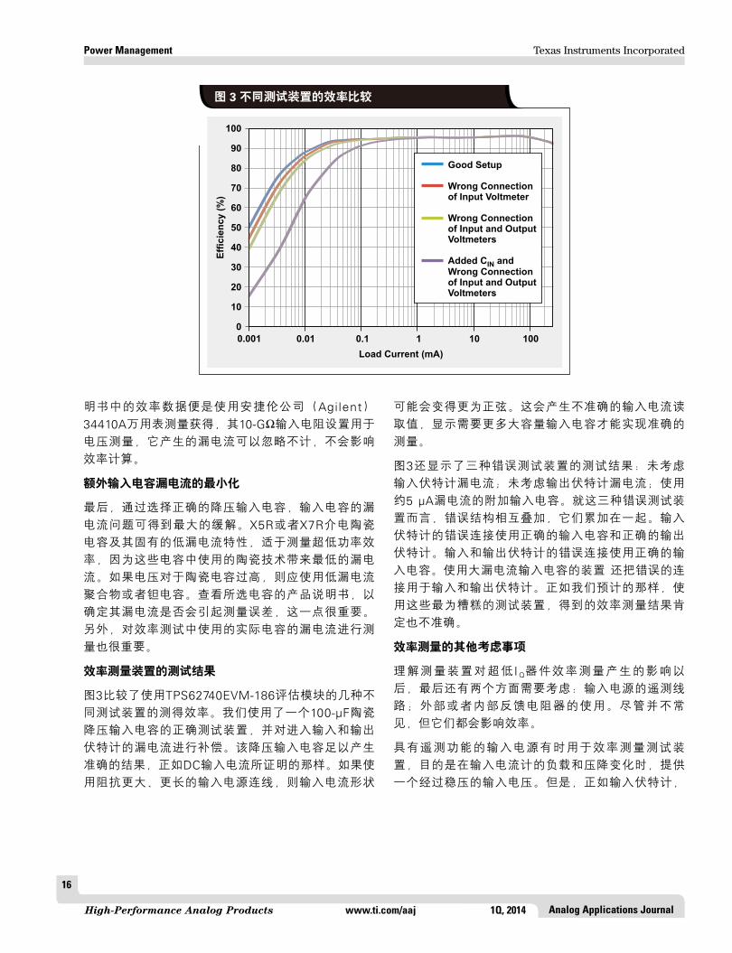
Test results of efficiency-measurement setupsFigure 3 compares the measured efficiency of several dif-ferent test setups that used the TPS62740EVM-186 evalu-ation module.4 A proper test setup with a 100-µF ceramic bulk input capacitor was used, with compensation for the leakage current into the input and output voltmeters. This bulk input capacitance was sufficient to produce accurate results, as was evidenced by a DC input current. If longer wires from the input supply with their larger impedance had been used instead, the input-current shape might have changed to be more sinusoidal. This would have produced an inaccurate input-current reading and shows that more bulk input capacitance would have been required for an accurate measurement.
Figure 3 also shows the test results of three improper test setups: the input voltmeter’s leakage not accounted for, the output voltmeter’s leakage not accounted for, and an extra input capacitor with about 5 µA of leakage. For the three improper test setups, the wrong configurations build on one another; they are additive. The wrong connection of input voltmeter used the correct input capacitor as well as the correct output voltmeter. The wrong connection of input and output voltmeters used the correct input capaci-tor. The setup using the leaky input capacitor also used the wrong connection for the input and output voltmeters. As expected, less accurate efficiency measurements were obtained with worse test setups.
100
90
80
70
60
50
40
30
20
10
0
0.001 0.01 0.1 1 10 100
Load Current (mA)
Eff
icie
nc
y (
%)
Good Setup
Wrong Connectionof Input Voltmeter
Wrong Connectionof Input and OutputVoltmeters
Added C andWrong Connectionof Input and OutputVoltmeters
IN
Figure 3. Efficiency comparison of different test setups
Other considerations in measuring efficiencyWith an understanding of the impact that measurement setups have on measuring an ultralow-IQ device’s efficiency, there are two final considerations that deserve a mention: the remote-sense lines on the input supply, and the use of external or internal feedback resistors. Though less com-monly seen, each of these has an impact on efficiency.
An input-power supply with remote-sense capability is sometimes used in efficiency-measurement test setups to provide a regulated input voltage as the load and voltage drop across the input-current meter change. However, just like the input voltmeter, these remote-sense lines draw current. In many instances, this current is relatively large—sometimes in the hundreds of microamperes. Needless to say, such high currents drawn by the test setup certainly affect the calculated efficiency and pro-duce erroneous results. Therefore, for best results, the remote-sense lines of the input supply should be con-nected before, not after, the input-current meter.
A final consideration in measuring the efficiency of ultralow-IQ devices is whether to use external or internal feedback resistors to set the output voltage. Most power supplies use two external resistors between the output voltage, FB pin, and ground to set the output voltage. This gives the user full flexibility to set the output voltage at any desired point. However, with external resistors and the highly sensitive external FB pin come more susceptibility
明书中的效率数据便是使用安捷伦公司(Agilent)
34410A万用表测量获得,其10-GΩ输入电阻设置用于
电压测量,它产生的漏电流可以忽略不计,不会影响
效率计算。
额外输入电容漏电流的最小化
最后,通过选择正确的降压输入电容,输入电容的漏
电流问题可得到最大的缓解。X5R或者X7R介电陶瓷
电容及其固有的低漏电流特性,适于测量超低功率效
率,因为这些电容中使用的陶瓷技术带来最低的漏电
流。如果电压对于陶瓷电容过高,则应使用低漏电流
聚合物或者钽电容。查看所选电容的产品说明书,以
确定其漏电流是否会引起测量误差,这一点很重要。
另外,对效率测试中使用的实际电容的漏电流进行测
量也很重要。
效率测量装置的测试结果
图3比较了使用TPS62740EVM-186评估模块的几种不
同测试装置的测得效率。我们使用了一个100-µF陶瓷
降压输入电容的正确测试装置,并对进入输入和输出
伏特计的漏电流进行补偿。该降压输入电容足以产生
准确的结果,正如DC输入电流所证明的那样。如果使
用阻抗更大、更长的输入电源连线,则输入电流形状
可能会变得更为正弦。这会产生不准确的输入电流读
取值,显示需要更多大容量输入电容才能实现准确的
测量。
图3还显示了三种错误测试装置的测试结果:未考虑
输入伏特计漏电流;未考虑输出伏特计漏电流;使用
约5 µA漏电流的附加输入电容。就这三种错误测试装
置而言,错误结构相互叠加,它们累加在一起。输入
伏特计的错误连接使用正确的输入电容和正确的输出
伏特计。输入和输出伏特计的错误连接使用正确的输
入电容。使用大漏电流输入电容的装置 还把错误的连
接用于输入和输出伏特计。正如我们预计的那样,使
用这些最为糟糕的测试装置,得到的效率测量结果肯
定也不准确。
效率测量的其他考虑事项
理解测量装置对超低 I Q器件效率测量产生的影响以
后,最后还有两个方面需要考虑:输入电源的遥测线
路;外部或者内部反馈电阻器的使用。尽管并不常
见,但它们都会影响效率。
具有遥测功能的输入电源有时用于效率测量测试装
置,目的是在输入电流计的负载和压降变化时,提供
一个经过稳压的输入电压。但是,正如输入伏特计,
图 3 不同测试装置的效率比较
Texas Instruments Incorporated
17
Analog Applications Journal 1Q, 2014 www.ti.com/aaj High-Performance Analog Products
Power Management
to noise. Any external noise seen at the FB pin is gained up, resulting in an incorrect output voltage. To avoid this, the two feedback resistors typically should have between 1 and 10 µA of current flowing in them to keep them robust against external noise sources. Since this current is not flowing to the load, it should be considered a loss that results in decreased efficiency.
To keep efficiency high, the FB pin and two resistors should be located inside the power supply to remove them from the variable and noisy external environment. In this way, a large resistance with minimal current flow is used for the feedback resistors, and efficiency is not significantly lowered. While internal feedback resistors fix the output voltage inside the power supply and prevent the user from having every possible output voltage available, a step-down converter like the TPS62740 overcomes this limitation. It has four digital input pins that allow the user to choose from among the most common output voltages ranging from 1.8 V to 3.3 V. As well, many other TI TPS62xxx devices internally set the output voltage to be either com-pletely fixed (as in the TPS62091) or adjustable via I2C (as in the TPS62360). These low-IQ devices are preferred because they do not lower the efficiency with external resistors but still allow sufficient user configurability.
ConclusionAccurately measuring the efficiency of ultralow-IQ devices is difficult because the currents in the circuit are very small. The basic efficiency-measurement test setup must be slightly altered to achieve accurate measurement
results that reflect the capability of the real circuit in the final application. Accounting for and/or eliminating the various leakage currents in the measurement equipment is the key to an accurate measurement.
References1. Jatan Naik, “Performing accurate PFM mode efficiency
measurements,” Application Report. Available: www.ti.com/slva236-aaj
2. Chris Glaser, “IQ: What it is, what it isn’t, and how to use it,” Analog Applications Journal (2Q, 2011). Available: www.ti.com/slyt412-aaj
3. “360nA IQ step down converter for low power applica-tions,” TPS62740 Datasheet. Available: www.ti.com/slvsb02-aaj
4. “TPS62740EVM-186 Evaluation Module,” User’s Guide. Available: www.ti.com/slvu949-aaj
Related Web sitesPower Management:www.ti.com/power-aaj
www.ti.com/tps62091-aajwww.ti.com/tps62360-aajwww.ti.com/tps62740-aaj
www.ti.com/tps62740evm-aajwww.ti.com/dcs-control-aaj
Subscribe to the AAJ:www.ti.com/subscribe-aaj
这些遥测线路会吸取电流。在许多情况下,这种电流
相对较大—有时达到数百微安。无需赘言,测试装置
吸取如此高的电流肯定会影响效率计算结果,从而得
到错误的结果。因此,为了获得最佳结果,应在输入
电流计“之前”(而非之后)连接输入电源的遥测线
路。
在超低IQ器件效率测量过程中,需要考虑的最后一点
是,使用外部还是内部反馈电阻器来设置输出电压。
大多数电源都在输出电压(FB引脚)和接地之间使用
两个外部电阻器来设置输出电压。这样便赋予用户完
全的灵活性,让其可以把输出电压设置在任何希望的
点。但是,使用外部电阻器和高敏感外部FB引脚,让
其更容易受到噪声的影响。FB引脚处的所有外部噪声
都获得了增益,从而带来错误的输出电压。为了避免
出现这种情况,一般应有1 µA和10 µA之间的电流流
入这两个反馈电阻器,以保持它们对于外部噪声源的
稳健性。由于该电流未流至负载,因此应把它看作是
一种带来效率降低的损耗。
为了保持高效率,FB引脚和两个电阻器应位于电源
内部,以让其远离变化、高噪声的外部环境。利用这
种方法,一种电流最小的大电阻用于反馈电阻器,所
以效率没有明显降低。尽管内部反馈电阻器设置电源
内部的输出电压,并防止用户对所有输出电压进行设
置,但是如TPS62740等降压转换器克服了这种局限
性。它拥有四个数字输入引脚,让用户能够从最为常
见的输出电压范围(1.8V到3.3V)进行选择。同样,
许多其他TI TPS62xxx器件使用内部方式设置输出电压
为完全固定(与TPS62091一样),或者可通过I2C稳
压(与TPS62360一样)。这些低IQ器件是首选,因为
它们不使用外部电阻器,不会降低效率,但仍然允许
充分的用户可结构性。
结论
准确测量超低IQ器件的效率很难,因为电路的电流非
常小。必须对基本效率测量测试装置进行稍微改动,
以获得准确的测量结果,以便能够反映最终应用中真
实电路的性能。考虑及(或)消除测量设备中的各种
漏电流是实现准确测量的关键。
参考文献
1、《如何进行准确PFM模式效率测量》,作者:
Jatan Naik,网址:www.ti.com/slva236-aaj
2、《IQ:什么是IQ,什么不是IQ,如何使用它》,作
者:Chris Glaser,见《模拟应用期刊》(2011年第2季度),网址:www.ti.com/slyt412-aaj
3、《低功耗应用的3 6 0 n A I Q降压转换器》,见
《TPS62740产品说明书》,网址:www.ti.com/slvsb02-aaj
4、《TPS62740EVM-186评估模件》,见《用户指
南》,网址:www.ti.com/slvu949-aaj
相关网站
电源管理:
www.ti.com/power-aaj www.ti.com/tps62091-aaj www.ti.com/tps62360-aaj www.ti.com/tps62740-aaj www.ti.com/tps62740evm-aaj www.ti.com/dcs-control-aaj 订阅《模拟应用期刊》请访问:
www.ti.com/subscribe-aaj

Analog Applications JournalHigh-Performance Analog Products www.ti.com/aaj 1Q, 2014
Texas Instruments Incorporated
18
When is the JESD204B interface the right choice?
IntroductionAnyone involved in high-speed data-capture designs that use an FPGA has probably heard the buzzword for the new JEDEC standard: JESD204B. Recently a lot of engineers have contacted Texas Instruments requesting information on the JESD204B interface, including how it works with an FPGA and how it will make their designs easier to exe-cute. So what is the JESD204B interface all about? This article discusses the evolution of the JESD204B standard and what it means to a systems design engineer.
What led to the JESD204B standard?About ten years ago, designers of high-speed data converters switched from using the traditional single-ended CMOS interface to using a differential LVDS interface because the latter enabled higher data rates. (The CMOS interface is limited to about 200 Mbps.) The LVDS interface also improved noise coupling on signal lines and power supplies. The drawback of this interface was higher power consumption at lower sam-pling speeds. This gave the CMOS interface a reason for existence, and it is still being used today.
But with the evolution of analog-to-digital converters (ADCs) requiring faster sampling rates and higher channel density, the industry was demanding a faster, more power-efficient digital interface than parallel LVDS. In order to overcome this challenge, a true serial interface called JESD204 was developed and approved by JEDEC in April 2006. The JESD204 interface is defined as a single-lane, high-speed serial link connect-ing single or multiple data converters to a digital logic device with data rates of up to 3.125 Gbps. It needs a common frame clock sent to the converter and the FPGA to synchronize the frames.
Supporting only one lane and one serial link, JESD204 was soon viewed as not quite as useful as initially hoped, so in April 2008 the standard was revised to JESD204A. JESD204A extended support for multiple aligned lanes and multipoint links, but the maximum speed was still limited to 3.125 Gbps. This drove the development in July 2011 of JESD204B, which promises to address several different system-design challenges. Besides drastically increasing the supported data rates from 3.125 Gbps to 12.5 Gbps, it also greatly simplifies multichannel synchronization by adding the deterministic latency feature.
What is the JESD204B standard?JESD204B supports interface speeds of up to 12.5 Gbps, uses a device clock instead of the previously used frame clock, and has three different subclasses. Subclass 0 is backward-compatible with JESD204A except with higher speeds, and it does not support deterministic latency. Furthermore, the SYNC signal has special timing require-ments for error reporting (Figure 1). Subclass 1 uses synchronization signal SYSREF to initiate and align the local multiframe clocks across devices (Figure 2). This
By Sureena GuptaWorldwide Analog Marketing
Data Converters
Tx Device
Rx Device
ClockSource
Frame Clock
Frame Clock
SYNC Data
Figure 1. JESD204B Subclass 0 interface
Tx Device
Rx Device
ClockSource
Device Clock
Device Clock
SYNC Data
SYSREF Clock
SYSREF Clock
Figure 2. JESD204B Subclass 1 interface
何时选择JESD204B接口?作者:Sureena Gupta,德州仪器 (TI) 全球模拟市场营销部门
图 1 JESD204B子类0接口
图 2 JESD204B子类1接口
引言
涉足使用FPGA的高速数据捕获设计的人可能都听
说过新JEDEC标准这个时髦术语:JESD204B。最
近,许多工程师联系 TI,要求获得JESD204B接口
的相关资料,包括它与FPGA如何工作,以及如何
让其设计更容易实现。那么,JESD204B到底是什
么呢?本文将讨论JESD204B标准的发展过程,以
及它对系统设计工程师的意义。
是什么导致了JESD204B标准的出现?
大约十年以前,高速数据转换器的设计师们从使用
传统单端CMOS接口,转向使用差动LVDS接口,
因为后者实现了更高的数据速率。(CMOS接口速
率被限制在约200Mbps。)LVDS接口还改善了信
号线路和电源的噪声耦合。这种接口的缺点是在低
采样速度下功耗更高。这便给了CMOS接口一个存
在的理由,直到今天人们仍然在使用。
但是,随着模数转换器 (ADC) 的发展,其要求更
快的采样速率和更高的通道密度,行业要求使用比
并行LVDS更快速、功效更高的数字接口。为了克
服这个挑战,2006年4月,JEDEC制订并批准了一
种真正的串行接口(称作JESD204)。JESD204接口被定义为一种单通道、高速串行链路,其使
用高达3.125 Gbps的数据速率把单个或者多个数
据转换器连接至数字逻辑器件。它需要向转换器和
FPGA发送一个公共帧时钟,以对帧进行同步。
由于仅支持一条通道和一条串行链路,因此
JESD204很快便被认为并不如之前希望的那样
有效。所以,在2 0 0 8年4月,该标准被修订为
JESD204A。JESD204A扩展了对多条对齐通道
和多点链路的支持,但是最大速度仍然被限定在
3.125 Gbps。这成了2011年7月订制JESD204B标
准的推动力,其旨在克服几种不同的系统设计问
题。除将支持数据速率从3.125 Gbps提高至12.5 Gbps以外,它还通过添加确定性延迟功能大大简
化了多通道同步。
什么是JESD204B标准?
JESD204B最高支持12.5 Gbps的接口速度,使用器件
时钟代替之前使用的帧时钟,并且拥有三个不同的子
类。除高速以外,子类0可向下兼容JESD204A,但它
并不支持确定性延迟。另外,SYNC信号具有特殊的错
误报告时序要求(请参见图1)。子类1使用同步信号
SYSREF来在各器件之间发起和对齐局部多帧时钟(请
参见图2)。它同步数据传输,并在数字链路之间实现
已知、确定性延迟。子类2使用SYNC信号,用于相同的
目的(请参见图3)。由于存在SYNC时序限制,因此子
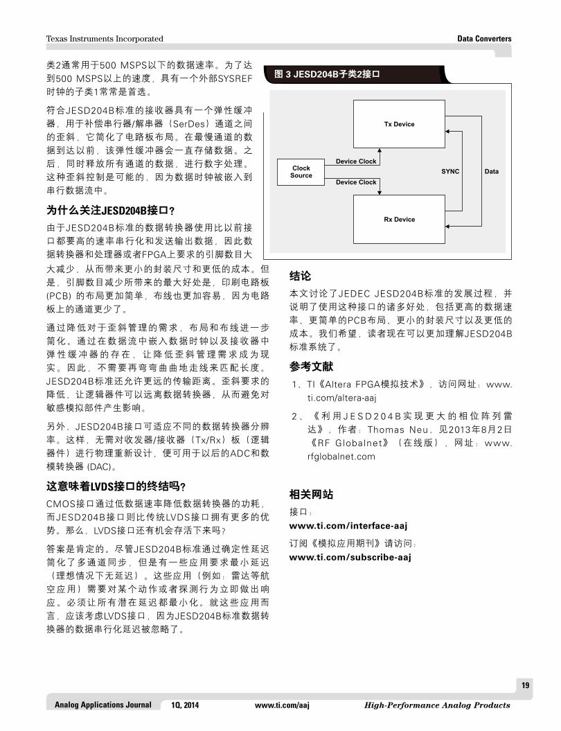
Texas Instruments Incorporated
19
Analog Applications Journal 1Q, 2014 www.ti.com/aaj High-Performance Analog Products
Data Converters
synchronizes data transmission and achieves a known, deterministic latency across the digital link. Subclass 2 uses the SYNC signal for that same purpose (Figure 3). Due to SYNC timing constraints, Subclass 2 typically is employed for data rates lower than 500 MSPS. For speeds higher than 500 MSPS, Subclass 1 with an external SYSREF clock is commonly preferred.
JESD204B-compliant receivers are outfitted with an elastic buffer that is used to compensate for skew across serializer/deserializer (SerDes) lanes, which simplifies board layout. This elastic buffer stores the data until the data from the slowest lane arrives. It then releases the data from all lanes simultaneously for digital proc-essing. This skew management is possible because the data clock is embedded in the serial data stream.
Why care about the JESD204B interface?Since JESD204B-compliant data converters serialize and transmit output data at a much higher rate than with previous interfaces, the number of pins required on the data converters as well as on processors or FPGAs is drastically reduced, translating to smaller package sizes and lower cost. However, the biggest benefits from the reduced pin count may be a much simpler layout on the printed circuit board (PCB) and easier routing because there are much fewer lanes on the board.
Layout and routing are further simplified by the reduced need for skew management, which is made possible by the data clock now being embedded in the data stream and the presence of the elastic buffer in the receiver. Hence, the need for trace squiggles to match lengths is eliminated. The JESD204B standard also allows longer transmission distances. Relaxed skew requirements enable logic devices to be placed much farther from data converters to avoid any impact on sensitive analog parts.
Additionally, the JESD204B interface is adaptable to different resolutions of data converters. This removes the need for physical redesign of transceiver/receiver (Tx/Rx) boards (logic devices) for future ADCs and digital-to- analog converters (DACs).
Does this mean the end for the LVDS interface?The CMOS interface provides lower power consumption for data converters with lower data rates, while the JESD204B interface offers a few benefits over the tradi-tional LVDS interface. So does the LVDS interface have any chance of survival?
The simple answer is yes. While the JESD204B standard has simplified multichannel synchronization by using
deterministic latency, there are applications that require minimal latency (and, in an ideal world, no latency). These applications (for example, aerospace applications like radar) need an immediate response to an action or detec-tion. Any possible delay must be minimized. For these applications, the LVDS interface should be considered, since the JESD204B-compliant data converter’s delay in serializing the data is omitted.
ConclusionThis article has discussed the evolution of the JEDEC JESD204B standard and has explained the many benefits of using this type of interface, including faster data rates, simplified PCB layout, smaller package sizes, and lower cost. It is hoped that the reader now understands the JESD204B-based system a little better.
References1. “Analog for Altera FPGAs,” Texas Instruments.
Available: www.ti.com/altera-aaj
2. Thomas Neu. (Aug. 2, 2013). “Enabling larger phased-array radars with JESD204B.” RF Globalnet [Online]. Available: www.rfglobalnet.com
Related Web sitesInterface:www.ti.com/interface-aaj
Subscribe to the AAJ:www.ti.com/subscribe-aaj
Tx Device
Rx Device
ClockSource
SYNC Data
Device Clock
Device Clock
Figure 3. JESD204B Subclass 2 interface类2通常用于500 MSPS以下的数据速率。为了达
到500 MSPS以上的速度,具有一个外部SYSREF时钟的子类1常常是首选。
符合JESD204B标准的接收器具有一个弹性缓冲
器,用于补偿串行器/解串器(SerDes)通道之间
的歪斜,它简化了电路板布局。在最慢通道的数
据到达以前,该弹性缓冲器会一直存储数据。之
后,同时释放所有通道的数据,进行数字处理。
这种歪斜控制是可能的,因为数据时钟被嵌入到
串行数据流中。
为什么关注JESD204B接口?
由于JESD204B标准的数据转换器使用比以前接
口都要高的速率串行化和发送输出数据,因此数
据转换器和处理器或者FPGA上要求的引脚数目大
大减少,从而带来更小的封装尺寸和更低的成本。但
是,引脚数目减少所带来的最大好处是,印刷电路板 (PCB) 的布局更加简单,布线也更加容易,因为电路
板上的通道更少了。
通过降低对于歪斜管理的需求,布局和布线进一步
简化。通过在数据流中嵌入数据时钟以及接收器中
弹性缓冲器的存在,让降低歪斜管理需求成为现
实。因此,不需要再弯弯曲曲地走线来匹配长度。
JESD204B标准还允许更远的传输距离。歪斜要求的
降低,让逻辑器件可以远离数据转换器,从而避免对
敏感模拟部件产生影响。
另外,JESD204B接口可适应不同的数据转换器分辨
率。这样,无需对收发器/接收器(Tx/Rx)板(逻辑
器件)进行物理重新设计,便可用于以后的ADC和数
模转换器 (DAC)。
这意味着LVDS接口的终结吗?
CMOS接口通过低数据速率降低数据转换器的功耗,
而JESD204B接口则比传统LVDS接口拥有更多的优
势。那么,LVDS接口还有机会存活下来吗?
答案是肯定的。尽管JESD204B标准通过确定性延迟
简化了多通道同步,但是有一些应用要求最小延迟
(理想情况下无延迟)。这些应用(例如:雷达等航
空应用)需要对某个动作或者探测行为立即做出响
应。必须让所有潜在延迟都最小化。就这些应用而
言,应该考虑LVDS接口,因为JESD204B标准数据转
换器的数据串行化延迟被忽略了。
结论
本文讨论了JEDEC JESD204B标准的发展过程,并
说明了使用这种接口的诸多好处,包括更高的数据速
率、更简单的PCB布局、更小的封装尺寸以及更低的
成本。我们希望,读者现在可以更加理解JESD204B标准系统了。
参考文献
1、TI《Altera FPGA模拟技术》,访问网址:www.ti.com/altera-aaj
2 、《利用 J E S D 2 0 4 B 实现更大的相位阵列雷
达》,作者:Thomas Neu,见2013年8月2日《RF Globalnet》(在线版),网址:www.rfglobalnet.com
相关网站
接口:
www.ti.com/interface-aaj
订阅《模拟应用期刊》请访问:
www.ti.com/subscribe-aaj
图 3 JESD204B子类2接口

Analog Applications JournalHigh-Performance Analog Products www.ti.com/aaj 1Q, 2014
Texas Instruments Incorporated
20
CAN bus, Ethernet, or FPD-Link: Which is best for automotive communications?
IntroductionIn 1915 Ford Motor Company introduced electric lights and an electric horn to its Model T automobile. Since then, the dependence on electrical and electronic systems in auto-mobiles has been steadily increasing. The initial systems tended to be local and independent. For example, a switch that controlled the headlights was connected directly to the battery. Today, however, these systems are all inter-connected. When a car’s headlights are turned on, the dashboard lighting, mirrors, and other systems may all adjust to the new conditions. For this to work properly, the various different systems must communicate with one another. As the automobile has evolved, so have the net-works used within it to make this communication possible. As autonomously driven vehicles continue to be developed, there will be an even greater demand for data transport within the vehicle and between vehicles. This article examines three automotive communications standards—the controller area network (CAN) bus, Ethernet, and Flat Panel Display Link (FPD-Link)—and explores which inter-face best suits which system.
CAN busThe CAN bus was initially developed by Robert Bosch GmbH in the 1980s. Today it is supported by several manufacturers of integrated circuits and subsystems and
is used in all modern automobiles. The CAN bus allows different controllers or processors on the bus to communi-cate with one another via messages that are passed on the bus. There is a method for prioritization so that lower- priority messages do not interfere with higher-priority messages. The CAN bus operates at speeds of less than 1 Mbps, and message lengths (CAN frames) are typically 50 to 100 bits in length.
Since a CAN bus can be shared by many different con-trollers, it is generally not very good for sending messages that might require updates more than approximately 100 times per second. Ideally it is suited for relaying much slower status updates from sensors to the engine-control unit. This includes applications such as communication about other mechanical systems (transmission, braking, cruise control, power steering, windows, door locks, and others) where the amount of data is limited and the band-widths involved tend to be relatively low.
Further reducing the overall transmission speed is the fact that automotive systems have become more compli-cated, with more sensors and processors being added to the network. Figure 1 shows a CAN bus being used for both door- and climate-control functions. Since each of these is a low-bandwidth application, there is little concern about one interfering with the other. However, if the same bus is also handling a higher-bandwidth, more critical function
By Mark SauerwaldApplications Engineer
Interface
CAN Bus
ClimateController
DoorController
Vent BaffleControl
FanControl
AirConditioning
Control
Door LocksWindowControl
MirrorControl
Figure 1. Portion of a CAN-bus implementation图1 部分CAN总线实施
引言
1915年,福特汽车公司把电灯和电子喇叭用于其T型汽车。自那时起,汽车对于电气和电子系统的依赖便
不断增加。初始系统往往都是局部和独立的,例如,
一个控制车头灯的开关直接连接至电池。但在今天,
这些系统都相互连接在一起。当车头灯开启时,仪表
盘照明、后视镜和其他系统可能都会转入新的工作状
态。为了实现这些功能,各种系统必须彼此相互通
信。随着汽车技术的发展,汽车拥有了许多网络,让
这种通信成为可能。由于自动驾驶汽车的不断发展,
对于汽车内部和汽车之间进行数据传输的需求日益增
长。本文为您介绍三种汽车通信标准—控制器局域网 (CAN)、以太网和平板显示链路 (FPD-Link),并探讨
每种接口最适合的系统。
CAN总线
CAN总线最初于20世纪80年代由Robe r t Bosch GmbH制订。今天,它得到许多集成电路和子系统制
造厂商的支持,并应用于所有现代汽车中。CAN总
线允许通过总线上传输的消息,让总线上的不同控
制器或者处理器进行相互通信。它使用一种优先次序
方法,这样低优先级的消息便不会干扰高优先级的
消息。CAN总线的传输速率小于1 Mbps,消息长度
(CAN帧)通常为50到100比特。
由于许多不同控制器可以共用一条CAN总线,因此
它一般不太适合发送要求每秒进行约100次以上更新
的消息。理想情况下,它适合于转播更缓慢的状态更
新,从传感器到引擎控制单元。它所包括的应用为与
其他机械系统相关的通信(变速器、制动、巡航定速
控制、动力转向、车窗、门锁等等),其数据量有
限,并且涉及带宽往往相对较低。
由于越来越多的传感器和处理器不断被加入到这个网
络中,总传输速度进一步降低,汽车系统变得更加复
杂。图1显示了用于实现车门和温度控制功能的CAN总线。由于所有这些都是低带宽应用,因此相互干扰
并不是一个大问题。但是,如果同一条总线还要处理
更高的带宽,如引擎控制等更重要的功能,则需要把
CAN总线、以太网还是FPD链路:哪一种最适合车载通信?作者:Mark Sauerwald,德州仪器 (TI) 应用工程师
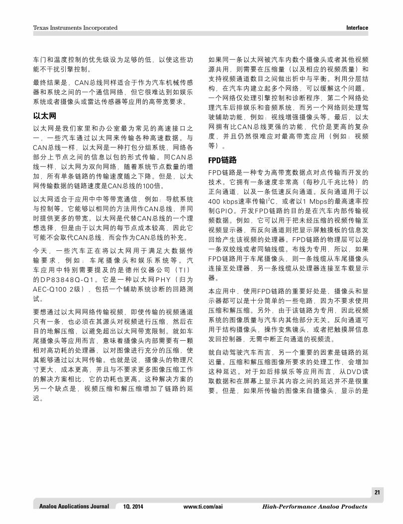
Texas Instruments Incorporated
21
Analog Applications Journal 1Q, 2014 www.ti.com/aaj High-Performance Analog Products
Interface
such as engine control, the priorities of door and climate control need to be set low enough so that these functions do not interfere with engine control.
The net result is that the CAN bus is well suited as a communications network between the mechanical sensors and systems within a car, but it is not readily extended to the higher-bandwidth requirements of applications such as entertainment systems or sensors for cameras or radar.
EthernetEthernet is one of the most common high-speed interfaces found in homes and offices, and there are some automo-biles where Ethernet is being used to transport a variety of high-speed data. Like the CAN bus, Ethernet is a pack-etized system, where information is transferred in packets between nodes on various parts of the network. Also like the CAN bus, Ethernet is bidirectional, and the speed possible on any individual link decreases as the number of nodes on the system increases. Still, Ethernet can transport data over a link 100 times faster than a CAN bus.
Ethernet is good for midbandwidth communications in applications such as navigation systems and control. It can be used in much the same way as a CAN bus while provid-ing much more bandwidth. Ethernet would be an ideal choice to replace the CAN bus, but since Ethernet’s cost per node is higher, it probably will not replace but rather will augment the CAN bus.
Some cars today are using Ethernet for data-intensive requirements such as backup cameras and entertainment systems. Of particular interest in automotive applications is the DP83848Q-Q1 from Texas Instruments (TI). This is an Ethernet PHY, screened to AEC-Q100 grade 2, and includes a loopback test mode for facilitating system diagnostics.
To transport video over an Ethernet network, even if there is only one video channel being transported, the video must be compressed at its source, then decom-pressed at the destination to avoid exceeding Ethernet bandwidth limitations. For an application such as a backup camera, this implies that there needs to be a relatively high-power processor in the camera to compress the image sufficiently to get it into the Ethernet network. This in turn means that the camera will be physically larger and more expensive and will have higher power dissipation than a solution that doesn’t require much image process-ing. Another disadvantage of this solution is that video compression and decompression add latency to the link.
If the same Ethernet network is shared by several cam-eras or other video sources in the car, there is a trade-off between the amount of compression (and corresponding video quality) and the number of video channels that can
be supported. This limitation could be mitigated by setting up multiple networks within the car in a hierarchical con-figuration. There might be one network that deals only with engine control and diagnostics, a second network that handles backseat entertainment and the audio sys-tem, and another network that handles driver-assist func-tions such as vision-enhancement cameras. In the end, Ethernet provides greater capacity than the CAN bus, at the expense of greater complexity, but still struggles to handle the highest-bandwidth applications such as video.
FPD-LinkFPD-Link is a technology developed for point-to-point transport of high-bandwidth data. It has one forward channel with a very high speed of several gigabits per second and a low-speed back channel. The back channel can be used to transport an I2C bus at 400 kbps or it can control GPIO lines at rates of up to 1 Mbps. FPD-Link was developed to transport video data within the car. For example, it can be used to send uncompressed video to a video display while the back channel sends information from a touch panel on the display screen back to the proc-essor generating the video. The physical layer for FPD-Link is either a twisted-pair or coaxial cable. The wiring is dedicated, so if FPD-Link is used for a backup camera, one cable goes from the backup camera to a processor, and a second cable goes from the processor to the display in the cabin.
The big advantage of using FPD-Link in this application is that both the camera and the display can be much sim-pler circuits, since compression and decompression are not required. Additionally, since the links are dedicated, the image quality of one video system is independent of what else is going on in the vehicle. The back channel can be used to configure a camera, operate a zoom lens, or send touch-screen information back to a controller with-out interrupting video flow on the forward channel.
For autonomously driven vehicles, another important factor will be the amount of latency in the link. The proc-essing required to compress and decompress an image adds to this latency. For an application such as backseat entertainment, a delay between reading the data from a DVD and its display on the screen is not important. However, if the image being transported is from a camera looking for pedestrians in the path of the vehicle, latency may have dire consequences.
FPD-Link is perfect for critical links where high band-width and low latency are the most important factors. Additionally, with the ability to support a back channel and power over a single twisted-pair or coaxial connection,
车门和温度控制的优先级设为足够的低,以使这些功
能不干扰引擎控制。
最终结果是,CAN总线同样适合于作为汽车机械传感
器和系统之间的一个通信网络,但它很难达到如娱乐
系统或者摄像头或雷达传感器等应用的高带宽要求。
以太网
以太网是我们家里和办公室最为常见的高速接口之
一,一些汽车通过以太网来传输各种高速数据。与
CAN总线一样,以太网是一种打包分组系统,网络各
部分上节点之间的信息以包的形式传输。同CAN总
线一样,以太网为双向网络,随着系统节点数量的增
加,所有单条链路的传输速度随之下降。但是,以太
网传输数据的链路速度是CAN总线的100倍。
以太网适合于应用中中等带宽通信,例如:导航系统
与控制等。它能够以相同的方法用作CAN总线,并同
时提供更多的带宽。以太网是代替CAN总线的一个理
想选择,但是由于以太网的每节点成本较高,因此它
可能不会取代CAN总线,而会作为CAN总线的补充。
今天,一些汽车正在将以太网用于满足大数据传
输要求,例如:车尾摄像头和娱乐系统等。汽
车应用中特别需要提及的是德州仪器公司(T I)的D P 8 3 8 4 8 Q - Q 1。它是一种以太网P H Y(归为
AEC-Q100 2级),包括一个辅助系统诊断的回路测
试。
要想通过以太网网络传输视频,即使传输的视频通道
只有一条,也必须在其源头对视频进行压缩,然后在
目的地解压缩,以避免超出以太网带宽限制。就如车
尾摄像头等应用而言,意味着摄像头内部需要有一颗
相对高功耗的处理器,以对图像进行充分的压缩,使
其能够通过以太网传输。也就是说,摄像头的物理尺
寸更大,成本更高,并且与不要求更多图像压缩工作
的解决方案相比,它的功耗也更高。这种解决方案的
另一个缺点是,视频压缩和解压缩增加了链路的延
迟。
如果同一条以太网被汽车内数个摄像头或者其他视频
源共用,则需要在压缩量(以及相应的视频质量)和
支持视频通道数目之间做出折中与平衡。利用分层结
构,在汽车内建立起多个网络,可以缓解这个问题。
一个网络仅处理引擎控制和诊断程序,第二个网络处
理汽车后排娱乐和音频系统,而另一个网络则处理驾
驶辅助功能,例如:视线增强摄像头等。最后,以太
网拥有比CAN总线更强的功能,代价是更高的复杂
度,并且仍然很难应对最高带宽应用(例如:视频
等)。
FPD链路
FPD链路是一种专为高带宽数据点对点传输而开发的
技术。它拥有一条速度非常高(每秒几千兆比特)的
正向通道,以及一条低速反向通道。反向通道用于以
400 kbps速率传输I2C,或者以1 Mbps的最高速率控
制GPIO。开发FPD链路的目的是在汽车内部传输视
频数据。例如,它可以用于把未经压缩的视频传输至
视频显示器,而反向通道则把显示屏触摸板的信息发
回给产生该视频的处理器。FPD链路的物理层可以是
一条双绞线或者同轴线缆。布线为专用,所以,如果
FPD链路用于车尾摄像头,则一条线缆从车尾摄像头
连接至处理器,另一条线缆从处理器连接至车载显示
器。
本应用中,使用FPD链路的重要好处是,摄像头和显
示器都可以是十分简单的一些电路,因为不要求使用
压缩和解压缩。另外,由于该链路为专用,因此视频
系统的图像质量与汽车内其他部分无关。反向通道可
用于结构摄像头,操作变焦镜头,或者把触摸屏信息
发回控制器,无需中断正向通道的视频流。
就自动驾驶汽车而言,另一个重要的因素是链路的延
迟量。压缩和解压缩图像所要求的处理工作,会增加
这种延迟。对于如后排娱乐等应用而言,从DVD读
取数据和在屏幕上显示其内容之间的延迟并不是很重
要。但是,如果所传输的图像来自摄像头,显示的是
Texas Instruments Incorporated
22
Analog Applications JournalHigh-Performance Analog Products www.ti.com/aaj 1Q, 2014
Interface
wiring can be simplified. Figure 2 shows an OMAP™ video processor connected to two different cameras, and a display with a single twisted-pair cable going to each peripheral. This twisted-pair cable supports camera video data and touch-screen/camera-setup data. It can also provide power for the display or camera. Since each link is dedicated to one peripheral, there is no risk of interference between the signals from the two cameras.
ConclusionSo which interface is best for automotive communications? They all are—but each for its own purpose. The CAN bus reigns supreme for low-speed control applications where cost is a driving factor. When bandwidth requirements move up, Ethernet can step in as an enhanced interface to support moderate bandwidth requirements. When the
highest bandwidth and lowest-latency link are required, such as for a surround-view camera system providing input to an autonomous vehicle pilot, then FPD-Link is ready to meet the challenge.
Related Web sitesInterface:www.ti.com/interface-aaj
www.ti.com/dp83848qq1-aajwww.ti.com/ds90ub913qq1-aajwww.ti.com/ds90ub914qq1-aajwww.ti.com/ds90ub925qq1-aajwww.ti.com/ds90ub926qq1-aaj
Subscribe to the AAJ:www.ti.com/subscribe-aaj
Displaywith
Touch Screen
OMAPProcessor
I C2
I C2
I C2
FSYNC
FSYNC
Serializer A Serializer C
Serializer B
DS90UB913Q DS90UB925Q
DS90UB913Q
DataPCLK
DataPCLK
CMOSImageSensor
CMOSImageSensor
Camera A
Camera B
FSIN
FSIN
GP
O
GP
O
GP
O
Deserializer A Deserializer C
Deserializer B
DS90UB914Q DS90UB926Q
DS90UB914Q
GP
IO
GP
IO
GP
IO
FSYNC FSYNC FSYNC
FSYNC
DataPCLK
DataPCLK
DataPCLK
DataPCLK
FSO
FSO
I C2
I C2
I C2
Figure 2. Using FPD-Link to connect dual cameras and display
公路上行人的情况,则这种延迟可能就会造成可
怕的后果。
当高带宽和低延迟是最为重要的考虑因素时,应
首选FPD链路来实现一些重要的连接。另外,由
于可以支持反向通道,并且能够通过单条双绞线
对或者同轴线连接来供电,因此布线更加简单。
图2显示了一个OMAPTM视频处理器,它连接两
个不同的摄像头和显示器,通过单条双绞线对线
缆连接外围设备。这种双绞线对线缆支持摄像头
视频数据和触摸屏/摄像头设置数据。它还为显示
器或者摄像头供电。由于每条链路专用于一个外
围设备,因此两个摄像头的信号之间不会出现干
扰。
结论
那么,哪种接口最适合于汽车通信呢?它们都适
合,但需根据具体的用途来确定。CAN总线在用
于那些要求不断降低成本的低速控制应用中占据统治地
位。当带宽要求提高时,以太网作为一种增强型接口,
可满足中等带宽要求。当要求最高带宽和最低延迟链路
时,例如:为自动驾驶程序提供周围环境情况的环视摄
像头系统,则FPD链路完全可以满足要求。
相关网站
接口:
www.ti.com/interface-aaj www.ti.com/dp83848qq1-aaj www.ti.com/ds90ub913qq1-aaj www.ti.com/ds90ub914qq1-aaj www.ti.com/ds90ub925qq1-aaj www.ti.com/ds90ub926qq1-aaj
订阅《模拟应用期刊》请访问:
www.ti.com/subscribe-aaj
图 2 使用FPD链路连接双摄像头和显示器

23
Analog Applications Journal
Texas Instruments Incorporated
1Q, 2014 www.ti.com/aaj High-Performance Analog Products
New-generation ESD-protection devices need no VCC connection
IntroductionAs digital and analog ICs grow increasingly sensitive to electrostatic-discharge (ESD) damage due to their shrink-ing process nodes, discrete ESD-protection diodes have become necessary to guarantee sufficient system-level ESD protection. In the past, the VCC connection was added to diodes to reduce their junction capacitance. With the advent of new diode technology, this is no longer required. This article explains the VCC connection’s neces-sity in the past and the advantages of not having to use it in the present.
ESD is the release of built-up static electricity when two objects of different electric potential come into contact. For example, on a dry winter day, up to 20 kV of ESD can build up simply from packing a printed cuircuit board (PCB) into a foam-lined box. To ensure that electronic end equipment is immune to everyday ESD events, dis-crete diodes with more robust ESD ratings than the stan-dard 2-kV human-body model (HBM) are often required. The ESD rating of discrete diodes is directly proportional to the area of the diode’s p-n junction; however, the bigger the junction, the larger is the parasitic capacitance. In order not to compromise a diode’s ESD rating, adding a VCC connection is one IC design technique that effectively decreases the diode’s parasitic capacitance, but at the risk of damaging any other device connected to VCC. However, recent improvements in process technologies have allowed diode designers to remove the VCC connection while still guaranteeing a high ESD rating with low capacitance.
Diode characteristicsA diode is the most basic semiconductor device. It is made from a p-type and an n-type junction and has two terminals: an anode at the p-type end and a cathode at the n-type end (Figure 1). When a large enough voltage is applied from the cathode to the anode (reverse biasing), the diode enters its breakdown region and, in theory, can conduct an infinite amount of current at zero resistance. A voltage applied in the other direction (forward biasing) causes the diode to enter its forward-conducting region. Figure 2 shows the IV curve of a basic
diode with the anode grounded and voltage swept across the cathode. While there are many types of diodes made for different applications, the topic under discussion is ultrafast-response diodes made for ESD-protection appli-cations. These diodes can respond to a high ESD voltage very quickly and clamp thousands of volts to just tens of volts in a matter of nanoseconds by shunting the ESD current to ground.
There are two contributing factors to a diode’s parasitic capacitance: junction capacitance (due to charge variation in the depletion layer) and diffusion capacitance (due to excess carriers in the quasi-neutral region). Junction capac-itance dominates in the reverse-biased region, which is the
Interface
By Roger LiangHigh Volume Linear
Anode Cathode
p-TypeMaterial
n-TypeMaterial
Figure 1. Construction of a diode
1.0
0.8
0.6
0.4
0.2
0
–0.2
–0.4
–0.6
–0.8
–1.0
–2 –1 0 1 2 3 4 5 6 7 8 9 10
Voltage (V)
Cu
rre
nt
( mA
)
ForwardVoltage
BreakdownVoltage
Forward
Bias
Reverse
Bias
Figure 2. Diode IV curve
图 1 二极管结构
图 2 二极管IV曲线
引言
由于其不断减少的处理节点,数字和模拟IC越来越容
易受到静电放电 (ESD) 的损坏,因此为了保证充分的
系统级ESD保护,离散式ESD保护二极管成为一种必
需组件。过去,我们把VCC连接添加至二极管,目的是
降低其结电容。随着新型二极管技术的出现,现在却
不再需要。本文将向您介绍过去为什么需要VCC连接,
并解释现在却不使用它的一些原因。
ESD是两个不同电势的物体接触时出现的静电释放
现象。例如,在天气干燥的冬天,在把印刷电路板 (PCB) 封装到填充有泡沫的箱子里时,最高可产生20 kV的ESD。为了确保电子终端设备不受日常ESD现象
的损害,通常要求使用离散式二极管,其拥有比标准
2kV人体模型 (HBM) 更稳健的ESD额定值。离散二极
管的ESD额定值直接与二极管的p-n结点面积成比例关
系;但是,结点越大,寄生电容就越大。为了不影响
二极管的ESD额定值,添加一个VCC连接是一种IC设计
方法,它可以有效降低二极管的寄生电容,但有可能
会损坏连接至VCC的所有其他器件。然而,工艺技术的
最新进展,让二极管设计人员不再需要VCC连接,并同
时能够保证低电容和高ESD额定值。
二极管特性
二极管是最为基本的半导体器件。它由
一个p型和一个n型结点组成,具有两
个端头:一个p型端的阳极和一个n型端的阴极(请参见图1)。当从阴极向
阴极(反向偏置)施加一个足够大的电
压时,二极管进入其击穿区域。理论上
讲,电阻为零时,它可以传导无限数量
的电流。使用另一个方向(正向偏置)
施加电压,会使二极管进入其正向导电
区域。图2显示了一个基本二极管的IV曲线,它的阴极接地,电压穿过阴极。尽
管针对不同应用有许多不同类型的二极
新一代ESD保护器件不再需要VCC连接作者:Roger Liang,德州仪器 (TI) 大容量线性部门
管,但这里要讨论的是ESD保护应用的超快速响应二
极管。这些二极管可以非常快速地对高ESD电压做出
响应,并通过分流ESD电流至接地,在几纳秒时间内
便可把数千伏电压降低至仅仅数十伏。
影响二极管寄生电容的因素有两个:结电容(由于过
渡层内的电荷变化)和扩散电容(由于中性区域内的
过剩载流子)。在反向偏置区域由结电容主导,其
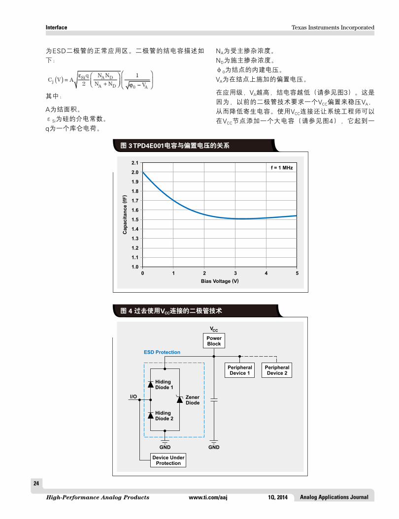
Texas Instruments Incorporated
24
Analog Applications JournalHigh-Performance Analog Products www.ti.com/aaj 1Q, 2014
Interface
usual application region for ESD diodes. The junction capacitance of a diode is characterized by
( ) Si A Dj
A D 0 A
q N N 1C V A ,
2 N N V
ε = + ϕ −
with the following definitions:
A is the area of the junction.εSi is the dielectric constant of silicon.q is one coulomb charge.NA is the acceptor doping concentration.
I/O
GND GND
HidingDiode 1
ZenerDiode
HidingDiode 2
VCC
PowerBlock
PeripheralDevice 1
PeripheralDevice 2
ESD Protection
Device UnderProtection
Figure 4. Older diode technology with VCC connection
2.1
2.0
1.9
1.8
1.7
1.6
1.5
1.4
1.3
1.2
1.1
1.0
0 1 3 52 4
Bias Voltage (V)
Cap
acit
an
ce
( fF
)
f = 1 MHz
Figure 3. TPD4E001 capacitance versus bias voltage
ND is the donor doping concentration.φ0 is the built-in voltage of the junction.VA is the bias voltage applied on the junction.
On the application level, the more VA is applied, the lower the junction capacitance will be (Figure 3). This is the reason why older diode technology required a VCC bias in order to adjust VA and bring down the parasitic capaci-tance. Having a VCC connection also allows a systems engi-neer to add a large capacitor at the VCC node (Figure 4), which serves as a charge reservoir to absorb some extra ESD energy, thus increasing ESD protection incrementally.
为ESD二极管的正常应用区。二极管的结电容描述如
下:
其中:
A为结面积。
εSi为硅的介电常数。
q为一个库仑电荷。
NA为受主掺杂浓度。
ND为施主掺杂浓度。
φ0为结点的内建电压。
VA为在结点上施加的偏置电压。
在应用级,VA越高,结电容越低(请参见图3)。这是
因为,以前的二极管技术要求一个VCC偏置来稳压VA,
从而降低寄生电容。使用VCC连接还让系统工程师可以
在VCC节点添加一个大电容(请参见图4),它起到一
图 3 TPD4E001电容与偏置电压的关系
图 4 过去使用VCC连接的二极管技术

Texas Instruments Incorporated
25
Analog Applications Journal 1Q, 2014 www.ti.com/aaj High-Performance Analog Products
Interface
Using high-speed diodes for ESD protectionTo design a low-capacitance diode structure with a high ESD rating, a three-diode approach often is used (see Figures 5 and 6), for three reasons:
1. A diode can withstand much more current in the forward-conducting region than in the reverse- breakdown region.
2. Hiding Diode 1 with the Zener diode protects against positive ESD strikes.
3. Hiding Diode 2 protects against negative ESD strikes.
Two smaller hiding diodes are connected in series with a larger Zener diode because the hiding diodes’ smaller capacitance effectively hides the Zener diode’s large capacitance due to the series structure. During a positive ESD event, Hiding Diode 1 enters its forward-conducting region. The Zener diode enters its reverse-breakdown region, creating a path for ESD current to be shunted to ground without entering the device under protection. The size of the larger Zener diode allows it to withstand the large amount of current flow in its break-down region. During a negative ESD event, Hiding Diode 2 enters its forward-conducting region and channels ESD energy directly to ground. During either event, the hiding diodes can handle the large amount of ESD current flow because they never break down and enter only the forward-conducting region.
Advantages of not using a VCC connectionDiode-fabrication technology has made great improvements over the past few years that have enabled a lower junction capacitance without sacrificing a high ESD rating. These improve-ments are:
I/O
GND
HidingDiode 1
ZenerDiode
HidingDiode 2
Device UnderProtection
Positive ESD
Figure 5. Discharge path of positive ESD strike
5-V Input
V = 3.3 VCC
I/O
GND
HidingDiode 1
ZenerDiode
HidingDiode 2
PowerBlock
PeripheralDevice 1
PeripheralDevice 2
Figure 7. Leakage path from I/O to VCC
I/O
GND
HidingDiode 1
ZenerDiode
HidingDiode 2
Device UnderProtection
Negative ESD
Figure 6. Discharge path of negative ESD strike
• Moving away from a lateral diode structure to a vertical diode structure
• Increased unit area ESD performance
• Less NA and ND doping to reach the same forward and breakdown voltages
These improvements mean a VCC connection is no longer required to bring down the junction capacitance to sup-port high-speed interfaces. Having no VCC connection gives the systems engineer the following three advantages.
1. No current leakage into internal power supplyIf a higher-voltage input signal is connected to the ESD diode I/O with a lower VCC level, signal current could leak through Hiding Diode 1 into the VCC and other devices con-nected on that node (Figure 7). This could damage either
个电荷库的作用,目的是吸收一些过多的ESD能量,
从而逐渐增加ESD保护。
把高速二极管用于ESD保护
为了设计出一种高ESD额定值、低电容的二极管结
构,通常使用三二级管方法(参见图5和6),原因有
三个:
1、相比在反向击穿区域,二极管在正向导电区域可
以承受更强的电流。
2、隐藏式 (hiding) 二极管1和齐纳二极管可抵制正
ESD电击。
3、隐藏式二极管2可抵制负ESD电击。
两个更小的“隐藏式”二极管与一个更大的
齐纳二极管串联。由于其串行结构,隐藏式
二极管的电容更小,可有效隐藏齐纳二极管
的大电容。在正ESD电击期间,隐藏式二极
管1进入其正向导电区域。齐纳二极管进入其
反向击穿区域,从而形成一条通路,让ESD电流被分流至接地,而不会进入受保护器件
内部。大齐纳二极管的大尺寸,让其能够在
击穿区域承受大电流。在负ESD电击期间,
隐藏式二极管2进入其正向导电区域,把ESD能量直接引导至接地。在上面任何一种电击
事件中,隐藏式二极管都可处理大量的ESD电流,因为它们绝对不会击穿,只会进入正
向导电区域。
不使用VCC连接的好处
过去几年,二极管制造技术取得了巨大的进
步,实现了更低的结电容,并且没有牺牲高ESD额定
值。这些进步包括:
• 从横向二极管结构变为纵向二极管结构
• 更高的单位面积ESD性能
• NA和ND掺杂更少,却可以达到相同的正向击穿电压
这些进步意味着,在降低结电容来支持高速接口时不
再需要使用VCC连接。不使用VCC连接,给系统工程师
带来如下三方面的好处:
1、没有泄露电流进入内部电源
如果一个高压输入信号通过低VCC电平连接ESD二极管
I/O,则信号电流可能会通过隐藏式二极管1泄露进入
图 5 正ESD电击的放电路径 图 6 负ESD电击的放电路径
图 7 I/O到VCC的漏电流路径

Texas Instruments Incorporated
26
Analog Applications JournalHigh-Performance Analog Products www.ti.com/aaj 1Q, 2014
Interface
the power supply or any device connected to it. If VCC is not connected to the ESD diode, there is no such worry.
2. No ESD damage to internal power supplyDuring a positive ESD strike, VCC is along the ESD current’s discharge path and experiences a voltage level that is one VF (~0.5 to 0.7 V) drop below the clamping voltage at the I/O. Although the power supply is very robust against ESD due to the shunt capacitor, this raised voltage level could very likely damage any device powered by the VCC (Figure 8). Again, if VCC is not connected to the ESD diode, there is no such worry.
3. No external capacitor necessaryESD-diode process development at Texas Instruments (TI) is focusing on strengthening the overall p-n structure so it can withstand more ESD voltage. With TI’s new generation of ESD-protection diodes rated as high as 30 kV, an extra capacitor can improve the overall ESD rating only marginally. Using one will generally reach a point of diminishing returns. Not having a capaci-tor reduces the bill of materials count, saves on cost, and allows more PCB space for other critical devices.
Examples of TI’s new-generation ESD-protection devicesTI’s TPD2E2U06 ESD-protection device is a noteworthy example of the improvements made in diode technology. Unlike its predecessor, the TPD2E001 does not require a VCC connection but maintains the same capacitance, clamps to a lower voltage, and increases the ESD rating threefold. (See Table 1.) Other similar ESD-protection devices from TI include the TPD4E1U06, TPD4E1U06, and TPD4E05U06.
ConclusionESD-protection diodes that don’t require a VCC connection bring many advantages to the table. No capacitor is needed on the VCC pin to boost the ESD rating; this reduces com-ponent count, simplifies layout, and lowers placement cost. Having no VCC connection also guarantees no leakage into the power supply and no ESD damage to any internal nodes that otherwise would be connected to the power supply via VCC.
Related Web sitesInterface:www.ti.com/interface-aaj
www.ti.com/tpd2e001-aajwww.ti.com/tpd2e2u06-aajwww.ti.com/tpd4e001-aajwww.ti.com/tpd4e05u06-aajwww.ti.com/tpd4e1u06-aaj
For more information about TI’s new-generation ESD-protection devices:www.ti.com/esd-aaj
Subscribe to the AAJ:www.ti.com/subscribe-aaj
Table 1. Specifications of TPD2E001 versus TPD2E2U06
SPECIFICATIONS TPD2E001 TPD2E2U06
VCC connection Recommended Not required
Contact ESD (kV) ±8 ±25
Air ESD (kV) ±15 ±30
CIN (pF)* 1.5 1.5
Clamping voltage (V)** 12 9.5
* Capacitance measured at f = 1 MHz, VBIAS = 2.5 V. ** Clamping voltage measured using TLP curve at 1 A, 100-ns pulse width.
Positive ESD
VCC
I/O
GND
HidingDiode 1
ZenerDiode
HidingDiode 2
PowerBlock
PeripheralDevice 1
PeripheralDevice 2
Figure 8. Positive ESD strike can damage VCC到VCC以及该节点上连接的其他器件内(图
7)。这可能会损坏连接它的电源或者器
件。如果VCC没有连接ESD二极管,则无需
有这方面的担心。
2、不会对内部电源造成ESD损坏
在正ESD电击期间,VCC沿着ESD电流的
放电路径,并且它的电压水平为I/O处箝位
电压以下一个VF(~0.5到0.7 V)。尽管由
于分流电容的使用,在面对ESD时电源已
经非常稳健,但这种升高的电压水平非常
可能会损坏由VCC驱动的器件(图8)。情
况一样,如果VCC不连接至ESD二极管,则
无需担心。
3、无需外部电容
德州仪器公司(TI)的ESD二极管工艺开
发重点加强整体p-n结构,以便让其能够承受更大的
ESD电压。由于TI的新一代ESD保护二极管拥有高达
30 kV的额定值,因此使用一个附加电容仅可提高少许
总ESD额定值。使用一个便会达到“收益递减”点。
不使用电容,可减少材料数目清单,节省成本,并为
其他重要器件留出更多的PCB空间。
TI新一代ESD保护器件例子
TI的TPD2E2U06 ESD保护器件便是二极管技术进步
的一个重要例子。与它的前辈不同,TPD2E001不要
求VCC连接,但保持相同的电容,电压更低,并且
ESD额定值增加了两倍。(参见表1)其他TI的类似
ESD保护器件还包括TPD4E1U06、TPD4E1U06和
TPD4E05U06。
表 1 TPD2E001和TPD2E2U06规范对比表
规范 TPD2E001 TPD2E2U06
VCC连接 推荐 不需要
接触放电 (kV) ±8 ±25
空气放电(kV) ±15 ±30
CIN (pF)* 1.5 1.5
钳位电压 (V)** 12 9.5
*f=1MHz时电容测量,VBIAS=2.5V
**1A、100ns 脉宽时使用 TLP 曲线进行钳位电压测量
结论
不要求VCC连接的ESD保护二极管带来了许多好处。
VCC引脚不需要电容来增加ESD额定值。它减少了组件
数目,简化了布局,并且降低了布局成本。不使用VCC
连接,还保证了没有漏电流进入到电源中,同时不会
对本应通过VCC连接至电源的内部节点造成ESD损坏。
相关网站
接口:
www.ti.com/interface-aaj www.ti.com/tpd2e001-aaj www.ti.com/tpd2e2u06-aaj www.ti.com/tpd4e001-aaj www.ti.com/tpd4e05u06-aaj www.ti.com/tpd4e1u06-aaj
TI新一代ESD保护器件的更多详情,请访问:
www.ti.com/esd-aaj
订阅《模拟应用期刊》,请访问:
www.ti.com/subscribe-aaj
图 8 正ESD电击会损坏VCC
27
Analog Applications Journal
Texas Instruments Incorporated
1Q, 2014 www.ti.com/aaj High-Performance Analog Products
Index of Articles
Index of Articles Title Issue Page Lit. No.
Data ConvertersWhen is the JESD204B interface the right choice? . . . . . . . . . . . . . . . . . . . . . . . . . . . . . . . . . . . . . .1Q, 2014 . . . . . . . . 18 SLYT559Grounding in mixed-signal systems demystified, Part 2 . . . . . . . . . . . . . . . . . . . . . . . . . . . . . . . . . .2Q, 2013 . . . . . . . . . 5 SLYT512Add a digitally controlled PGA with noise filter to an ADC . . . . . . . . . . . . . . . . . . . . . . . . . . . . . . .1Q, 2013 . . . . . . . . . 9 SLYT500Grounding in mixed-signal systems demystified, Part 1 . . . . . . . . . . . . . . . . . . . . . . . . . . . . . . . . . .1Q, 2013 . . . . . . . . . 5 SLYT499WEBENCH® tools and the photodetector’s stability . . . . . . . . . . . . . . . . . . . . . . . . . . . . . . . . . . . . .4Q, 2012 . . . . . . . . . 5 SLYT487How delta-sigma ADCs work, Part 2 . . . . . . . . . . . . . . . . . . . . . . . . . . . . . . . . . . . . . . . . . . . . . . . . . .4Q, 2011 . . . . . . . . . 5 SLYT438How delta-sigma ADCs work, Part 1 . . . . . . . . . . . . . . . . . . . . . . . . . . . . . . . . . . . . . . . . . . . . . . . . . .3Q, 2011 . . . . . . . . 13 SLYT423Clock jitter analyzed in the time domain, Part 3 . . . . . . . . . . . . . . . . . . . . . . . . . . . . . . . . . . . . . . . .3Q, 2011 . . . . . . . . . 5 SLYT422The IBIS model, Part 3: Using IBIS models to investigate signal-integrity issues. . . . . . . . . . . . . .2Q, 2011 . . . . . . . . . 5 SLYT413The IBIS model, Part 2: Determining the total quality of an IBIS model. . . . . . . . . . . . . . . . . . . . .1Q, 2011 . . . . . . . . . 5 SLYT400The IBIS model: A conduit into signal-integrity analysis, Part 1 . . . . . . . . . . . . . . . . . . . . . . . . . . .4Q, 2010 . . . . . . . . 11 SLYT390Clock jitter analyzed in the time domain, Part 2 . . . . . . . . . . . . . . . . . . . . . . . . . . . . . . . . . . . . . . . .4Q, 2010 . . . . . . . . . 5 SLYT389Clock jitter analyzed in the time domain, Part 1 . . . . . . . . . . . . . . . . . . . . . . . . . . . . . . . . . . . . . . . .3Q, 2010 . . . . . . . . . 5 SLYT379How digital filters affect analog audio-signal levels . . . . . . . . . . . . . . . . . . . . . . . . . . . . . . . . . . . . . .2Q, 2010 . . . . . . . . . 5 SLYT375How the voltage reference affects ADC performance, Part 3. . . . . . . . . . . . . . . . . . . . . . . . . . . . . .4Q, 2009 . . . . . . . . . 5 SLYT355How the voltage reference affects ADC performance, Part 2. . . . . . . . . . . . . . . . . . . . . . . . . . . . . .3Q, 2009 . . . . . . . . 13 SLYT339Impact of sampling-clock spurs on ADC performance . . . . . . . . . . . . . . . . . . . . . . . . . . . . . . . . . . .3Q, 2009 . . . . . . . . . 5 SLYT338How the voltage reference affects ADC performance, Part 1. . . . . . . . . . . . . . . . . . . . . . . . . . . . . .2Q, 2009 . . . . . . . . . 5 SLYT331Stop-band limitations of the Sallen-Key low-pass filter. . . . . . . . . . . . . . . . . . . . . . . . . . . . . . . . . . .4Q, 2008 . . . . . . . . . 5 SLYT306A DAC for all precision occasions . . . . . . . . . . . . . . . . . . . . . . . . . . . . . . . . . . . . . . . . . . . . . . . . . . . .3Q, 2008 . . . . . . . . . 5 SLYT300Understanding the pen-interrupt (PENIRQ) operation of touch-screen controllers . . . . . . . . . . .2Q, 2008 . . . . . . . . . 5 SLYT292Using a touch-screen controller’s auxiliary inputs . . . . . . . . . . . . . . . . . . . . . . . . . . . . . . . . . . . . . . .4Q, 2007 . . . . . . . . . 5 SLYT283Calibration in touch-screen systems . . . . . . . . . . . . . . . . . . . . . . . . . . . . . . . . . . . . . . . . . . . . . . . . . .3Q, 2007 . . . . . . . . . 5 SLYT277Conversion latency in delta-sigma converters . . . . . . . . . . . . . . . . . . . . . . . . . . . . . . . . . . . . . . . . . .2Q, 2007 . . . . . . . . . 5 SLYT264Clamp function of high-speed ADC THS1041 . . . . . . . . . . . . . . . . . . . . . . . . . . . . . . . . . . . . . . . . . .4Q, 2006 . . . . . . . . . 5 SLYT253Using the ADS8361 with the MSP430™ USI port . . . . . . . . . . . . . . . . . . . . . . . . . . . . . . . . . . . . . . .3Q, 2006 . . . . . . . . . 5 SLYT244Matching the noise performance of the operational amplifier to the ADC . . . . . . . . . . . . . . . . . . .2Q, 2006 . . . . . . . . . 5 SLYT237Understanding and comparing datasheets for high-speed ADCs . . . . . . . . . . . . . . . . . . . . . . . . . . .1Q, 2006 . . . . . . . . . 5 SLYT231Low-power, high-intercept interface to the ADS5424 14-bit, 105-MSPS converter for
undersampling applications . . . . . . . . . . . . . . . . . . . . . . . . . . . . . . . . . . . . . . . . . . . . . . . . . . . . . .4Q, 2005 . . . . . . . . 10 SLYT223Operating multiple oversampling data converters . . . . . . . . . . . . . . . . . . . . . . . . . . . . . . . . . . . . . . .4Q, 2005 . . . . . . . . . 5 SLYT222Simple DSP interface for ADS784x/834x ADCs . . . . . . . . . . . . . . . . . . . . . . . . . . . . . . . . . . . . . . . . .3Q, 2005 . . . . . . . . 10 SLYT210Using resistive touch screens for human/machine interface. . . . . . . . . . . . . . . . . . . . . . . . . . . . . . .3Q, 2005 . . . . . . . . . 5 SLYT209AImplementation of 12-bit delta-sigma DAC with MSC12xx controller . . . . . . . . . . . . . . . . . . . . . . .1Q, 2005 . . . . . . . . 27 SLYT076Clocking high-speed data converters . . . . . . . . . . . . . . . . . . . . . . . . . . . . . . . . . . . . . . . . . . . . . . . . .1Q, 2005 . . . . . . . . 20 SLYT07514-bit, 125-MSPS ADS5500 evaluation . . . . . . . . . . . . . . . . . . . . . . . . . . . . . . . . . . . . . . . . . . . . . . . .1Q, 2005 . . . . . . . . 13 SLYT074Supply voltage measurement and ADC PSRR improvement in MSC12xx devices . . . . . . . . . . . . .1Q, 2005 . . . . . . . . . 5 SLYT073Streamlining the mixed-signal path with the signal-chain-on-chip MSP430F169. . . . . . . . . . . . . .3Q, 2004 . . . . . . . . . 5 SLYT078ADS809 analog-to-digital converter with large input pulse signal . . . . . . . . . . . . . . . . . . . . . . . . . .1Q, 2004 . . . . . . . . . 8 SLYT083Two-channel, 500-kSPS operation of the ADS8361 . . . . . . . . . . . . . . . . . . . . . . . . . . . . . . . . . . . . . .1Q, 2004 . . . . . . . . . 5 SLYT082Evaluation criteria for ADSL analog front end. . . . . . . . . . . . . . . . . . . . . . . . . . . . . . . . . . . . . . . . . .4Q, 2003 . . . . . . . . 16 SLYT091Calculating noise figure and third-order intercept in ADCs . . . . . . . . . . . . . . . . . . . . . . . . . . . . . . .4Q, 2003 . . . . . . . . 11 SLYT090ADS82x ADC with non-uniform sampling clock . . . . . . . . . . . . . . . . . . . . . . . . . . . . . . . . . . . . . . . .4Q, 2003 . . . . . . . . . 5 SLYT089Interfacing op amps and analog-to-digital converters . . . . . . . . . . . . . . . . . . . . . . . . . . . . . . . . . . . .4Q, 2002 . . . . . . . . . 5 SLYT104Using direct data transfer to maximize data acquisition throughput. . . . . . . . . . . . . . . . . . . . . . . .3Q, 2002 . . . . . . . . 14 SLYT111MSC1210 debugging strategies for high-precision smart sensors . . . . . . . . . . . . . . . . . . . . . . . . . .3Q, 2002 . . . . . . . . . 7 SLYT110Adjusting the A/D voltage reference to provide gain. . . . . . . . . . . . . . . . . . . . . . . . . . . . . . . . . . . . .3Q, 2002 . . . . . . . . . 5 SLYT109Synchronizing non-FIFO variations of the THS1206 . . . . . . . . . . . . . . . . . . . . . . . . . . . . . . . . . . . . .2Q, 2002 . . . . . . . . 12 SLYT115SHDSL AFE1230 application . . . . . . . . . . . . . . . . . . . . . . . . . . . . . . . . . . . . . . . . . . . . . . . . . . . . . . . .2Q, 2002 . . . . . . . . . 5 SLYT114Intelligent sensor system maximizes battery life: Interfacing the MSP430F123 Flash
MCU, ADS7822, and TPS60311. . . . . . . . . . . . . . . . . . . . . . . . . . . . . . . . . . . . . . . . . . . . . . . . . . .1Q, 2002 . . . . . . . . . 5 SLYT123A/D and D/A conversion of PC graphics and component video signals, Part 2: Software
and control . . . . . . . . . . . . . . . . . . . . . . . . . . . . . . . . . . . . . . . . . . . . . . . . . . . . . . . . . . . . . . . . . . . .July 2001 . . . . . . . . . 5 SLYT129
Texas Instruments Incorporated
28
Analog Applications JournalHigh-Performance Analog Products www.ti.com/aaj 1Q, 2014
Index of Articles
Title Issue Page Lit. No.
Data Converters (Continued)A/D and D/A conversion of PC graphics and component video signals, Part 1: Hardware . . . . . .February 2001. . . . 11 SLYT138Using SPI synchronous communication with data converters — interfacing the
MSP430F149 and TLV5616 . . . . . . . . . . . . . . . . . . . . . . . . . . . . . . . . . . . . . . . . . . . . . . . . . . . . . .February 2001. . . . . 7 SLYT137Building a simple data acquisition system using the TMS320C31 DSP . . . . . . . . . . . . . . . . . . . . .February 2001. . . . . 1 SLYT136Using quad and octal ADCs in SPI mode . . . . . . . . . . . . . . . . . . . . . . . . . . . . . . . . . . . . . . . . . . . . . .November 2000. . . 15 SLYT150Hardware auto-identification and software auto-configuration for the
TLV320AIC10 DSP Codec — a “plug-and-play” algorithm . . . . . . . . . . . . . . . . . . . . . . . . . . . . .November 2000. . . . 8 SLYT149Smallest DSP-compatible ADC provides simplest DSP interface . . . . . . . . . . . . . . . . . . . . . . . . . . .November 2000. . . . 1 SLYT148Efficiently interfacing serial data converters to high-speed DSPs . . . . . . . . . . . . . . . . . . . . . . . . .August 2000 . . . . . 10 SLYT160Higher data throughput for DSP analog-to-digital converters . . . . . . . . . . . . . . . . . . . . . . . . . . . . .August 2000 . . . . . . 5 SLYT159New DSP development environment includes data converter plug-ins . . . . . . . . . . . . . . . . . . . . .August 2000 . . . . . . 1 SLYT158Introduction to phase-locked loop system modeling. . . . . . . . . . . . . . . . . . . . . . . . . . . . . . . . . . . . .May 2000 . . . . . . . . . 5 SLYT169The design and performance of a precision voltage reference circuit for 14-bit and
16-bit A-to-D and D-to-A converters . . . . . . . . . . . . . . . . . . . . . . . . . . . . . . . . . . . . . . . . . . . . . . .May 2000 . . . . . . . . . 1 SLYT168The operation of the SAR-ADC based on charge redistribution. . . . . . . . . . . . . . . . . . . . . . . . . . . .February 2000. . . . 10 SLYT176A methodology of interfacing serial A-to-D converters to DSPs . . . . . . . . . . . . . . . . . . . . . . . . . . .February 2000. . . . . 1 SLYT175Techniques for sampling high-speed graphics with lower-speed A/D converters . . . . . . . . . . . . . .November 1999. . . . 5 SLYT184Precision voltage references . . . . . . . . . . . . . . . . . . . . . . . . . . . . . . . . . . . . . . . . . . . . . . . . . . . . . . . .November 1999. . . . 1 SLYT183Evaluating operational amplifiers as input amplifiers for A-to-D converters . . . . . . . . . . . . . . . . .August 1999 . . . . . . 7 SLYT193Low-power data acquisition sub-system using the TI TLV1572 . . . . . . . . . . . . . . . . . . . . . . . . . . . .August 1999 . . . . . . 4 SLYT192Aspects of data acquisition system design . . . . . . . . . . . . . . . . . . . . . . . . . . . . . . . . . . . . . . . . . . . . .August 1999 . . . . . . 1 SLYT191
Power ManagementAccurately measuring efficiency of ultralow-IQ devices . . . . . . . . . . . . . . . . . . . . . . . . . . . . . . . . . .1Q, 2014 . . . . . . . . 13 SLYT558Low-cost flyback solutions for 10-mW standby power . . . . . . . . . . . . . . . . . . . . . . . . . . . . . . . . . . .1Q, 2014 . . . . . . . . . 9 SLYT557Split-rail approaches extend boost-converter input-voltage ranges. . . . . . . . . . . . . . . . . . . . . . . . .1Q, 2014 . . . . . . . . . 5 SLYT556Techniques for accurate PSRR measurements . . . . . . . . . . . . . . . . . . . . . . . . . . . . . . . . . . . . . . . . .4Q, 2013 . . . . . . . . 19 SLYT547Dynamic power management for faster, more efficient battery charging . . . . . . . . . . . . . . . . . . . .4Q, 2013 . . . . . . . . 15 SLYT546Low-cost solution for measuring input power and RMS current . . . . . . . . . . . . . . . . . . . . . . . . . . .4Q, 2013 . . . . . . . . 11 SLYT545Driving solenoid coils efficiently in switchgear applications. . . . . . . . . . . . . . . . . . . . . . . . . . . . . . .4Q, 2013 . . . . . . . . . 5 SLYT544Improved LiFePO4 cell balancing in battery-backup systems with an Impedance Track™
fuel gauge. . . . . . . . . . . . . . . . . . . . . . . . . . . . . . . . . . . . . . . . . . . . . . . . . . . . . . . . . . . . . . . . . . . . .3Q, 2013 . . . . . . . . 14 SLYT528Linear versus switching regulators in industrial applications with a 24-V bus . . . . . . . . . . . . . . . .3Q, 2013 . . . . . . . . . 9 SLYT527High-efficiency, low-ripple DCS-Control™ offers seamless PWM/power-save transitions . . . . . . .3Q, 2013 . . . . . . . . . 5 SLYT531Digital current balancing for an interleaved boost PFC . . . . . . . . . . . . . . . . . . . . . . . . . . . . . . . . . .2Q, 2013 . . . . . . . . 19 SLYT517Designing a negative boost converter from a standard positive buck converter . . . . . . . . . . . . . .2Q, 2013 . . . . . . . . 13 SLYT516Synchronous rectification boosts efficiency by reducing power loss . . . . . . . . . . . . . . . . . . . . . . . .2Q, 2013 . . . . . . . . . 9 SLYT515How to pick a linear regulator for noise-sensitive applications . . . . . . . . . . . . . . . . . . . . . . . . . . . .1Q, 2013 . . . . . . . . 25 SLYT50435-V, single-channel gate drivers for IGBT and MOSFET renewable-energy applications. . . . . . .1Q, 2013 . . . . . . . . 22 SLYT503Power MOSFET failures in mobile PMUs: Causes and design precautions . . . . . . . . . . . . . . . . . . .1Q, 2013 . . . . . . . . 17 SLYT502Design of a 60-A interleaved active-clamp forward converter . . . . . . . . . . . . . . . . . . . . . . . . . . . . .1Q, 2013 . . . . . . . . 13 SLYT501Simple open-circuit protection for boost converters in LED driver applications . . . . . . . . . . . . . .4Q, 2012 . . . . . . . . 21 SLYT490LDO noise examined in detail . . . . . . . . . . . . . . . . . . . . . . . . . . . . . . . . . . . . . . . . . . . . . . . . . . . . . . .4Q, 2012 . . . . . . . . 14 SLYT489Harnessing wasted energy in 4- to 20-mA current-loop systems . . . . . . . . . . . . . . . . . . . . . . . . . . .4Q, 2012 . . . . . . . . 10 SLYT488Designing a Qi-compliant receiver coil for wireless power systems, Part 1 . . . . . . . . . . . . . . . . . .3Q, 2012 . . . . . . . . . 8 SLYT479Easy solar-panel maximum-power-point tracking for pulsed-load applications . . . . . . . . . . . . . . .3Q, 2012 . . . . . . . . . 5 SLYT478Design considerations for a resistive feedback divider in a DC/DC converter . . . . . . . . . . . . . . . .2Q, 2012 . . . . . . . . 18 SLYT469Charging a three-cell nickel-based battery pack with a Li-Ion charger . . . . . . . . . . . . . . . . . . . . . .2Q, 2012 . . . . . . . . 14 SLYT468Remote sensing for power supplies. . . . . . . . . . . . . . . . . . . . . . . . . . . . . . . . . . . . . . . . . . . . . . . . . . .2Q, 2012 . . . . . . . . 12 SLYT467A solar-powered buck/boost battery charger . . . . . . . . . . . . . . . . . . . . . . . . . . . . . . . . . . . . . . . . . . .2Q, 2012 . . . . . . . . . 8 SLYT466Controlling switch-node ringing in synchronous buck converters . . . . . . . . . . . . . . . . . . . . . . . . . .2Q, 2012 . . . . . . . . . 5 SLYT465High-efficiency AC adapters for USB charging . . . . . . . . . . . . . . . . . . . . . . . . . . . . . . . . . . . . . . . . .1Q, 2012 . . . . . . . . 18 SLYT451Downslope compensation for buck converters when the duty cycle exceeds 50% . . . . . . . . . . . .1Q, 2012 . . . . . . . . 14 SLYT450Benefits of a multiphase buck converter . . . . . . . . . . . . . . . . . . . . . . . . . . . . . . . . . . . . . . . . . . . . . .1Q, 2012 . . . . . . . . . 8 SLYT449Turbo-boost charger supports CPU turbo mode . . . . . . . . . . . . . . . . . . . . . . . . . . . . . . . . . . . . . . . .1Q, 2012 . . . . . . . . . 5 SLYT448Solar lantern with dimming achieves 92% efficiency . . . . . . . . . . . . . . . . . . . . . . . . . . . . . . . . . . . .4Q, 2011 . . . . . . . . 12 SLYT440
Texas Instruments Incorporated
29
Analog Applications Journal 1Q, 2014 www.ti.com/aaj High-Performance Analog Products
Index of Articles
Title Issue Page Lit. No.
Power Management (Continued)Solar charging solution provides narrow-voltage DC/DC system bus for
multicell-battery applications . . . . . . . . . . . . . . . . . . . . . . . . . . . . . . . . . . . . . . . . . . . . . . . . . . . . .4Q, 2011 . . . . . . . . . 8 SLYT439A boost-topology battery charger powered from a solar panel. . . . . . . . . . . . . . . . . . . . . . . . . . . . .3Q, 2011 . . . . . . . . 17 SLYT424Challenges of designing high-frequency, high-input-voltage DC/DC converters. . . . . . . . . . . . . . .2Q, 2011 . . . . . . . . 28 SLYT415Backlighting the tablet PC . . . . . . . . . . . . . . . . . . . . . . . . . . . . . . . . . . . . . . . . . . . . . . . . . . . . . . . . . .2Q, 2011 . . . . . . . . 23 SLYT414IQ: What it is, what it isn’t, and how to use it . . . . . . . . . . . . . . . . . . . . . . . . . . . . . . . . . . . . . . . . . . .2Q, 2011 . . . . . . . . 18 SLYT412Benefits of a coupled-inductor SEPIC converter . . . . . . . . . . . . . . . . . . . . . . . . . . . . . . . . . . . . . . . .2Q, 2011 . . . . . . . . 14 SLYT411Implementation of microprocessor-controlled, wide-input-voltage, SMBus smart
battery charger . . . . . . . . . . . . . . . . . . . . . . . . . . . . . . . . . . . . . . . . . . . . . . . . . . . . . . . . . . . . . . . .2Q, 2011 . . . . . . . . 11 SLYT410Fine-tuning TI’s Impedance Track™ battery fuel gauge with LiFePO4 cells in
shallow-discharge applications . . . . . . . . . . . . . . . . . . . . . . . . . . . . . . . . . . . . . . . . . . . . . . . . . . . .1Q, 2011 . . . . . . . . 13 SLYT402An introduction to the Wireless Power Consortium standard and TI’s compliant solutions . . . . .1Q, 2011 . . . . . . . . 10 SLYT401Save power with a soft Zener clamp . . . . . . . . . . . . . . . . . . . . . . . . . . . . . . . . . . . . . . . . . . . . . . . . . .4Q, 2010 . . . . . . . . 19 SLYT392A low-cost, non-isolated AC/DC buck converter with no transformer. . . . . . . . . . . . . . . . . . . . . . .4Q, 2010 . . . . . . . . 16 SLYT391Computing power going “Platinum” . . . . . . . . . . . . . . . . . . . . . . . . . . . . . . . . . . . . . . . . . . . . . . . . . .3Q, 2010 . . . . . . . . 13 SLYT382Coupled inductors broaden DC/DC converter usage. . . . . . . . . . . . . . . . . . . . . . . . . . . . . . . . . . . . .3Q, 2010 . . . . . . . . 10 SLYT380Designing DC/DC converters based on ZETA topology. . . . . . . . . . . . . . . . . . . . . . . . . . . . . . . . . . .2Q, 2010 . . . . . . . . 16 SLYT372Discrete design of a low-cost isolated 3.3- to 5-V DC/DC converter . . . . . . . . . . . . . . . . . . . . . . . .2Q, 2010 . . . . . . . . 12 SLYT371Power-supply design for high-speed ADCs. . . . . . . . . . . . . . . . . . . . . . . . . . . . . . . . . . . . . . . . . . . . .1Q, 2010 . . . . . . . . 12 SLYT366Li-Ion battery-charger solutions for JEITA compliance . . . . . . . . . . . . . . . . . . . . . . . . . . . . . . . . . .1Q, 2010 . . . . . . . . . 8 SLYT365Fuel-gauging considerations in battery backup storage systems . . . . . . . . . . . . . . . . . . . . . . . . . . .1Q, 2010 . . . . . . . . . 5 SLYT364Efficiency of synchronous versus nonsynchronous buck converters. . . . . . . . . . . . . . . . . . . . . . . .4Q, 2009 . . . . . . . . 15 SLYT358Designing a multichemistry battery charger . . . . . . . . . . . . . . . . . . . . . . . . . . . . . . . . . . . . . . . . . . .4Q, 2009 . . . . . . . . 13 SLYT357Using power solutions to extend battery life in MSP430™ applications . . . . . . . . . . . . . . . . . . . . .4Q, 2009 . . . . . . . . 10 SLYT356Reducing radiated EMI in WLED drivers . . . . . . . . . . . . . . . . . . . . . . . . . . . . . . . . . . . . . . . . . . . . . .3Q, 2009 . . . . . . . . 17 SLYT340Selecting the right charge-management solution. . . . . . . . . . . . . . . . . . . . . . . . . . . . . . . . . . . . . . . .2Q, 2009 . . . . . . . . 18 SLYT334Designing a linear Li-Ion battery charger with power-path control . . . . . . . . . . . . . . . . . . . . . . . . .2Q, 2009 . . . . . . . . 12 SLYT333Taming linear-regulator inrush currents . . . . . . . . . . . . . . . . . . . . . . . . . . . . . . . . . . . . . . . . . . . . . . .2Q, 2009 . . . . . . . . . 9 SLYT332Using a portable-power boost converter in an isolated flyback application . . . . . . . . . . . . . . . . . .1Q, 2009 . . . . . . . . 19 SLYT323Cell balancing buys extra run time and battery life. . . . . . . . . . . . . . . . . . . . . . . . . . . . . . . . . . . . . .1Q, 2009 . . . . . . . . 14 SLYT322Improving battery safety, charging, and fuel gauging in portable media applications . . . . . . . . . .1Q, 2009 . . . . . . . . . 9 SLYT321Paralleling power modules for high-current applications . . . . . . . . . . . . . . . . . . . . . . . . . . . . . . . . .1Q, 2009 . . . . . . . . . 5 SLYT320Designing DC/DC converters based on SEPIC topology . . . . . . . . . . . . . . . . . . . . . . . . . . . . . . . . . .4Q, 2008 . . . . . . . . 18 SLYT309Compensating and measuring the control loop of a high-power LED driver . . . . . . . . . . . . . . . . .4Q, 2008 . . . . . . . . 14 SLYT308Getting the most battery life from portable systems. . . . . . . . . . . . . . . . . . . . . . . . . . . . . . . . . . . . .4Q, 2008 . . . . . . . . . 8 SLYT307New current-mode PWM controllers support boost, flyback, SEPIC, and
LED-driver applications . . . . . . . . . . . . . . . . . . . . . . . . . . . . . . . . . . . . . . . . . . . . . . . . . . . . . . . . .3Q, 2008 . . . . . . . . . 9 SLYT302Battery-charger front-end IC improves charging-system safety. . . . . . . . . . . . . . . . . . . . . . . . . . . .2Q, 2008 . . . . . . . . 14 SLYT294Understanding output voltage limitations of DC/DC buck converters . . . . . . . . . . . . . . . . . . . . . . .2Q, 2008 . . . . . . . . 11 SLYT293Using a buck converter in an inverting buck-boost topology . . . . . . . . . . . . . . . . . . . . . . . . . . . . . .4Q, 2007 . . . . . . . . 16 SLYT286Host-side gas-gauge-system design considerations for single-cell handheld applications . . . . . . .4Q, 2007 . . . . . . . . 12 SLYT285Driving a WLED does not always require 4 V . . . . . . . . . . . . . . . . . . . . . . . . . . . . . . . . . . . . . . . . . .4Q, 2007 . . . . . . . . . 9 SLYT284Simultaneous power-down sequencing with the TPS74x01 family of linear regulators . . . . . . . . .3Q, 2007 . . . . . . . . 20 SLYT281Get low-noise, low-ripple, high-PSRR power with the TPS717xx . . . . . . . . . . . . . . . . . . . . . . . . . .3Q, 2007 . . . . . . . . 17 SLYT280TPS6108x: A boost converter with extreme versatility. . . . . . . . . . . . . . . . . . . . . . . . . . . . . . . . . . .3Q, 2007 . . . . . . . . 14 SLYT279Power-management solutions for telecom systems improve performance, cost, and size. . . . . . .3Q, 2007 . . . . . . . . 10 SLYT278Current balancing in four-pair, high-power PoE applications. . . . . . . . . . . . . . . . . . . . . . . . . . . . . .2Q, 2007 . . . . . . . . 11 SLYT270Enhanced-safety, linear Li-Ion battery charger with thermal regulation and
input overvoltage protection . . . . . . . . . . . . . . . . . . . . . . . . . . . . . . . . . . . . . . . . . . . . . . . . . . . . .2Q, 2007 . . . . . . . . . 8 SLYT269Power management for processor core voltage requirements . . . . . . . . . . . . . . . . . . . . . . . . . . . . .1Q, 2007 . . . . . . . . 11 SLYT261LDO white-LED driver TPS7510x provides incredibly small solution size . . . . . . . . . . . . . . . . . . .1Q, 2007 . . . . . . . . . 9 SLYT260Selecting the correct IC for power-supply applications. . . . . . . . . . . . . . . . . . . . . . . . . . . . . . . . . . .1Q, 2007 . . . . . . . . . 5 SLYT259Fully integrated TPS6300x buck-boost converter extends Li-Ion battery life . . . . . . . . . . . . . . . .4Q, 2006 . . . . . . . . 15 SLYT256bq25012 single-chip, Li-Ion charger and dc/dc converter for Bluetooth® headsets. . . . . . . . . . . .4Q, 2006 . . . . . . . . 13 SLYT255A 3-A, 1.2-VOUT linear regulator with 80% efficiency and PLOST < 1 W . . . . . . . . . . . . . . . . . . . . . .4Q, 2006 . . . . . . . . 10 SLYT254Complete battery-pack design for one- or two-cell portable applications . . . . . . . . . . . . . . . . . . . .3Q, 2006 . . . . . . . . 14 SLYT248Single-chip bq2403x power-path manager charges battery while powering system. . . . . . . . . . . .3Q, 2006 . . . . . . . . 12 SLYT247
Texas Instruments Incorporated
30
Analog Applications JournalHigh-Performance Analog Products www.ti.com/aaj 1Q, 2014
Index of Articles
Title Issue Page Lit. No.
Power Management (Continued)TPS65552A powers portable photoflash. . . . . . . . . . . . . . . . . . . . . . . . . . . . . . . . . . . . . . . . . . . . . . .3Q, 2006 . . . . . . . . 10 SLYT246TPS61059 powers white-light LED as photoflash or movie light . . . . . . . . . . . . . . . . . . . . . . . . . . .3Q, 2006 . . . . . . . . . 8 SLYT245Powering today’s multi-rail FPGAs and DSPs, Part 2 . . . . . . . . . . . . . . . . . . . . . . . . . . . . . . . . . . . .2Q, 2006 . . . . . . . . 18 SLYT240Wide-input dc/dc modules offer maximum design flexibility . . . . . . . . . . . . . . . . . . . . . . . . . . . . . .2Q, 2006 . . . . . . . . 13 SLYT239TLC5940 PWM dimming provides superior color quality in LED video displays . . . . . . . . . . . . . .2Q, 2006 . . . . . . . . 10 SLYT238Practical considerations when designing a power supply with the TPS6211x . . . . . . . . . . . . . . . .1Q, 2006 . . . . . . . . 17 SLYT234TPS79918 RF LDO supports migration to StrataFlash® Embedded Memory (P30) . . . . . . . . . . .1Q, 2006 . . . . . . . . 14 SLYT233Powering today’s multi-rail FPGAs and DSPs, Part 1 . . . . . . . . . . . . . . . . . . . . . . . . . . . . . . . . . . . .1Q, 2006 . . . . . . . . . 9 SLYT232TLC5940 dot correction compensates for variations in LED brightness . . . . . . . . . . . . . . . . . . . . .4Q, 2005 . . . . . . . . 21 SLYT225Li-Ion switching charger integrates power FETs . . . . . . . . . . . . . . . . . . . . . . . . . . . . . . . . . . . . . . . .4Q, 2005 . . . . . . . . 19 SLYT224New power modules improve surface-mount manufacturability . . . . . . . . . . . . . . . . . . . . . . . . . . .3Q, 2005 . . . . . . . . 18 SLYT212Miniature solutions for voltage isolation. . . . . . . . . . . . . . . . . . . . . . . . . . . . . . . . . . . . . . . . . . . . . . .3Q, 2005 . . . . . . . . 13 SLYT211Understanding power supply ripple rejection in linear regulators . . . . . . . . . . . . . . . . . . . . . . . . . .2Q, 2005 . . . . . . . . . 8 SLYT202Understanding noise in linear regulators . . . . . . . . . . . . . . . . . . . . . . . . . . . . . . . . . . . . . . . . . . . . . .2Q, 2005 . . . . . . . . . 5 SLYT201A better bootstrap/bias supply circuit. . . . . . . . . . . . . . . . . . . . . . . . . . . . . . . . . . . . . . . . . . . . . . . . .1Q, 2005 . . . . . . . . 33 SLYT077Tips for successful power-up of today’s high-performance FPGAs . . . . . . . . . . . . . . . . . . . . . . . . .3Q, 2004 . . . . . . . . 11 SLYT079LED-driver considerations . . . . . . . . . . . . . . . . . . . . . . . . . . . . . . . . . . . . . . . . . . . . . . . . . . . . . . . . . .1Q, 2004 . . . . . . . . 14 SLYT084UCC28517 100-W PFC power converter with 12-V, 8-W bias supply, Part 2. . . . . . . . . . . . . . . . . .4Q, 2003 . . . . . . . . 21 SLYT092UCC28517 100-W PFC power converter with 12-V, 8-W bias supply, Part 1. . . . . . . . . . . . . . . . . .3Q, 2003 . . . . . . . . 13 SLYT097Soft-start circuits for LDO linear regulators. . . . . . . . . . . . . . . . . . . . . . . . . . . . . . . . . . . . . . . . . . . .3Q, 2003 . . . . . . . . 10 SLYT096Auto-Track™ voltage sequencing simplifies simultaneous power-up and power-down. . . . . . . . .3Q, 2003 . . . . . . . . . 5 SLYT095Using the TPS61042 white-light LED driver as a boost converter . . . . . . . . . . . . . . . . . . . . . . . . . .1Q, 2003 . . . . . . . . . 7 SLYT101Load-sharing techniques: Paralleling power modules with overcurrent protection . . . . . . . . . . . .1Q, 2003 . . . . . . . . . 5 SLYT100Understanding piezoelectric transformers in CCFL backlight applications. . . . . . . . . . . . . . . . . . .4Q, 2002 . . . . . . . . 18 SLYT107Power conservation options with dynamic voltage scaling in portable DSP designs . . . . . . . . . . .4Q, 2002 . . . . . . . . 12 SLYT106Using the UCC3580-1 controller for highly efficient 3.3-V/100-W isolated supply design . . . . . . .4Q, 2002 . . . . . . . . . 8 SLYT105Powering electronics from the USB port . . . . . . . . . . . . . . . . . . . . . . . . . . . . . . . . . . . . . . . . . . . . . .2Q, 2002 . . . . . . . . 28 SLYT118Optimizing the switching frequency of ADSL power supplies . . . . . . . . . . . . . . . . . . . . . . . . . . . . .2Q, 2002 . . . . . . . . 23 SLYT117SWIFT™ Designer power supply design program. . . . . . . . . . . . . . . . . . . . . . . . . . . . . . . . . . . . . . .2Q, 2002 . . . . . . . . 15 SLYT116Why use a wall adapter for ac input power? . . . . . . . . . . . . . . . . . . . . . . . . . . . . . . . . . . . . . . . . . . .1Q, 2002 . . . . . . . . 18 SLYT126Comparing magnetic and piezoelectric transformer approaches in CCFL applications . . . . . . . . .1Q, 2002 . . . . . . . . 12 SLYT125Power control design key to realizing InfiniBandSM benefits. . . . . . . . . . . . . . . . . . . . . . . . . . . . . . .1Q, 2002 . . . . . . . . 10 SLYT124Runtime power control for DSPs using the TPS62000 buck converter . . . . . . . . . . . . . . . . . . . . . .July 2001 . . . . . . . . 15 SLYT131Power supply solution for DDR bus termination . . . . . . . . . . . . . . . . . . . . . . . . . . . . . . . . . . . . . . . .July 2001 . . . . . . . . . 9 SLYT130–48-V/+48-V hot-swap applications . . . . . . . . . . . . . . . . . . . . . . . . . . . . . . . . . . . . . . . . . . . . . . . . . .February 2001. . . . 20 SLYT140Optimal design for an interleaved synchronous buck converter under high-slew-rate,
load-current transient conditions . . . . . . . . . . . . . . . . . . . . . . . . . . . . . . . . . . . . . . . . . . . . . . . . .February 2001. . . . 15 SLYT139Comparison of different power supplies for portable DSP solutions working from a
single-cell battery . . . . . . . . . . . . . . . . . . . . . . . . . . . . . . . . . . . . . . . . . . . . . . . . . . . . . . . . . . . . . .November 2000. . . 24 SLYT152Understanding the load-transient response of LDOs . . . . . . . . . . . . . . . . . . . . . . . . . . . . . . . . . . . .November 2000. . . 19 SLYT151Optimal output filter design for microprocessor or DSP power supply . . . . . . . . . . . . . . . . . . . . .August 2000 . . . . . 22 SLYT162Advantages of using PMOS-type low-dropout linear regulators in battery applications . . . . . . . .August 2000 . . . . . 16 SLYT161Low-cost, minimum-size solution for powering future-generation Celeron™-type
processors with peak currents up to 26 A. . . . . . . . . . . . . . . . . . . . . . . . . . . . . . . . . . . . . . . . . . .May 2000 . . . . . . . . 14 SLYT171Simple design of an ultra-low-ripple DC/DC boost converter with TPS60100 charge pump. . . . .May 2000 . . . . . . . . 11 SLYT170Powering Celeron-type microprocessors using TI’s TPS5210 and TPS5211 controllers . . . . . . . .February 2000. . . . 20 SLYT178Power supply solutions for TI DSPs using synchronous buck converters . . . . . . . . . . . . . . . . . . . .February 2000. . . . 12 SLYT177Understanding the stable range of equivalent series resistance of an LDO regulator . . . . . . . . . .November 1999. . . 14 SLYT187Synchronous buck regulator design using the TI TPS5211 high-frequency
hysteretic controller . . . . . . . . . . . . . . . . . . . . . . . . . . . . . . . . . . . . . . . . . . . . . . . . . . . . . . . . . . . .November 1999. . . 10 SLYT186TI TPS5602 for powering TI’s DSP . . . . . . . . . . . . . . . . . . . . . . . . . . . . . . . . . . . . . . . . . . . . . . . . . . .November 1999. . . . 8 SLYT185Migrating from the TI TL770x to the TI TLC770x. . . . . . . . . . . . . . . . . . . . . . . . . . . . . . . . . . . . . . .August 1999 . . . . . 14 SLYT196Extended output voltage adjustment (0 V to 3.5 V) using the TI TPS5210 . . . . . . . . . . . . . . . . . .August 1999 . . . . . 13 SLYT195Stability analysis of low-dropout linear regulators with a PMOS pass element. . . . . . . . . . . . . . . .August 1999 . . . . . 10 SLYT194
Texas Instruments Incorporated
31
Analog Applications Journal 1Q, 2014 www.ti.com/aaj High-Performance Analog Products
Index of Articles
Title Issue Page Lit. No.
InterfaceNew-generation ESD-protection devices need no VCC connection. . . . . . . . . . . . . . . . . . . . . . . . .1Q, 2014 . . . . . . . . 23 SLYT561CAN bus, Ethernet, or FPD-Link: Which is best for automotive communications? . . . . . . . . . . . .1Q, 2014 . . . . . . . . 20 SLYT560Correcting cross-wire faults in modern e-metering networks . . . . . . . . . . . . . . . . . . . . . . . . . . . . .4Q, 2013 . . . . . . . . 22 SLYT548Basics of debugging the controller area network (CAN) physical layer . . . . . . . . . . . . . . . . . . . . .3Q, 2013 . . . . . . . . 18 SLYT529RS-485 failsafe biasing: Old versus new transceivers . . . . . . . . . . . . . . . . . . . . . . . . . . . . . . . . . . . .2Q, 2013 . . . . . . . . 25 SLYT514Design considerations for system-level ESD circuit protection . . . . . . . . . . . . . . . . . . . . . . . . . . . .4Q, 2012 . . . . . . . . 28 SLYT492How to design an inexpensive HART transmitter . . . . . . . . . . . . . . . . . . . . . . . . . . . . . . . . . . . . . . .4Q, 2012 . . . . . . . . 24 SLYT491Data-rate independent half-duplex repeater design for RS-485. . . . . . . . . . . . . . . . . . . . . . . . . . . .3Q, 2012 . . . . . . . . 15 SLYT480Extending the SPI bus for long-distance communication . . . . . . . . . . . . . . . . . . . . . . . . . . . . . . . . .4Q, 2011 . . . . . . . . 16 SLYT441Industrial data-acquisition interfaces with digital isolators. . . . . . . . . . . . . . . . . . . . . . . . . . . . . . . .3Q, 2011 . . . . . . . . 24 SLYT426Isolated RS-485 transceivers support DMX512 stage lighting and special-effects applications . .3Q, 2011 . . . . . . . . 21 SLYT425Designing an isolated I2C Bus® interface by using digital isolators . . . . . . . . . . . . . . . . . . . . . . . . .1Q, 2011 . . . . . . . . 17 SLYT403Interfacing high-voltage applications to low-power controllers . . . . . . . . . . . . . . . . . . . . . . . . . . . .4Q, 2010 . . . . . . . . 20 SLYT393Magnetic-field immunity of digital capacitive isolators . . . . . . . . . . . . . . . . . . . . . . . . . . . . . . . . . . .3Q, 2010 . . . . . . . . 19 SLYT381Designing with digital isolators . . . . . . . . . . . . . . . . . . . . . . . . . . . . . . . . . . . . . . . . . . . . . . . . . . . . . .2Q, 2009 . . . . . . . . 21 SLYT335Message priority inversion on a CAN bus . . . . . . . . . . . . . . . . . . . . . . . . . . . . . . . . . . . . . . . . . . . . . .1Q, 2009 . . . . . . . . 25 SLYT325RS-485: Passive failsafe for an idle bus. . . . . . . . . . . . . . . . . . . . . . . . . . . . . . . . . . . . . . . . . . . . . . . .1Q, 2009 . . . . . . . . 22 SLYT324Cascading of input serializers boosts channel density for digital inputs . . . . . . . . . . . . . . . . . . . . .3Q, 2008 . . . . . . . . 16 SLYT301When good grounds turn bad—isolate!. . . . . . . . . . . . . . . . . . . . . . . . . . . . . . . . . . . . . . . . . . . . . . . .3Q, 2008 . . . . . . . . 11 SLYT298Enabling high-speed USB OTG functionality on TI DSPs . . . . . . . . . . . . . . . . . . . . . . . . . . . . . . . . .2Q, 2007 . . . . . . . . 18 SLYT271Detection of RS-485 signal loss . . . . . . . . . . . . . . . . . . . . . . . . . . . . . . . . . . . . . . . . . . . . . . . . . . . . . .4Q, 2006 . . . . . . . . 18 SLYT257Improved CAN network security with TI’s SN65HVD1050 transceiver . . . . . . . . . . . . . . . . . . . . . .3Q, 2006 . . . . . . . . 17 SLYT249Device spacing on RS-485 buses . . . . . . . . . . . . . . . . . . . . . . . . . . . . . . . . . . . . . . . . . . . . . . . . . . . . .2Q, 2006 . . . . . . . . 25 SLYT241Maximizing signal integrity with M-LVDS backplanes . . . . . . . . . . . . . . . . . . . . . . . . . . . . . . . . . . . .2Q, 2005 . . . . . . . . 11 SLYT203Failsafe in RS-485 data buses . . . . . . . . . . . . . . . . . . . . . . . . . . . . . . . . . . . . . . . . . . . . . . . . . . . . . . .3Q, 2004 . . . . . . . . 16 SLYT080The RS-485 unit load and maximum number of bus connections . . . . . . . . . . . . . . . . . . . . . . . . . .1Q, 2004 . . . . . . . . 21 SLYT086Estimating available application power for Power-over-Ethernet applications . . . . . . . . . . . . . . . .1Q, 2004 . . . . . . . . 18 SLYT085Power consumption of LVPECL and LVDS. . . . . . . . . . . . . . . . . . . . . . . . . . . . . . . . . . . . . . . . . . . . .1Q, 2002 . . . . . . . . 23 SLYT127The SN65LVDS33/34 as an ECL-to-LVTTL converter . . . . . . . . . . . . . . . . . . . . . . . . . . . . . . . . . . . .July 2001 . . . . . . . . 19 SLYT132The Active Fail-Safe feature of the SN65LVDS32A . . . . . . . . . . . . . . . . . . . . . . . . . . . . . . . . . . . . .November 2000. . . 35 SLYT154A statistical survey of common-mode noise . . . . . . . . . . . . . . . . . . . . . . . . . . . . . . . . . . . . . . . . . . .November 2000. . . 30 SLYT153Performance of LVDS with different cables . . . . . . . . . . . . . . . . . . . . . . . . . . . . . . . . . . . . . . . . . . .August 2000 . . . . . 30 SLYT163LVDS: The ribbon cable connection . . . . . . . . . . . . . . . . . . . . . . . . . . . . . . . . . . . . . . . . . . . . . . . . . .May 2000 . . . . . . . . 19 SLYT172LVDS receivers solve problems in non-LVDS applications . . . . . . . . . . . . . . . . . . . . . . . . . . . . . . . .February 2000. . . . 33 SLYT180Skew definition and jitter analysis. . . . . . . . . . . . . . . . . . . . . . . . . . . . . . . . . . . . . . . . . . . . . . . . . . . .February 2000. . . . 29 SLYT179Keep an eye on the LVDS input levels . . . . . . . . . . . . . . . . . . . . . . . . . . . . . . . . . . . . . . . . . . . . . . . .November 1999. . . 17 SLYT188TIA/EIA-568A Category 5 cables in low-voltage differential signaling (LVDS). . . . . . . . . . . . . . . .August 1999 . . . . . 16 SLYT197
AmplifiersDesigning active analog filters in minutes . . . . . . . . . . . . . . . . . . . . . . . . . . . . . . . . . . . . . . . . . . . . .4Q, 2013 . . . . . . . . 28 SLYT549Exploring anti-aliasing filters in signal conditioners for mixed-signal, multimodal
sensor conditioning . . . . . . . . . . . . . . . . . . . . . . . . . . . . . . . . . . . . . . . . . . . . . . . . . . . . . . . . . . . . .3Q, 2013 . . . . . . . . 25 SLYT530Using a fixed threshold in ultrasonic distance-ranging automotive applications . . . . . . . . . . . . . .3Q, 2012 . . . . . . . . 19 SLYT481Source resistance and noise considerations in amplifiers . . . . . . . . . . . . . . . . . . . . . . . . . . . . . . . . .2Q, 2012 . . . . . . . . 23 SLYT470Measuring op amp settling time by using sample-and-hold technique . . . . . . . . . . . . . . . . . . . . . .1Q, 2012 . . . . . . . . 21 SLYT452Converting single-ended video to differential video in single-supply systems . . . . . . . . . . . . . . . .3Q, 2011 . . . . . . . . 29 SLYT427Using single-supply fully differential amplifiers with negative input voltages to drive ADCs . . . .4Q, 2010 . . . . . . . . 26 SLYT394Operational amplifier gain stability, Part 3: AC gain-error analysis . . . . . . . . . . . . . . . . . . . . . . . . .3Q, 2010 . . . . . . . . 23 SLYT383Operational amplifier gain stability, Part 2: DC gain-error analysis . . . . . . . . . . . . . . . . . . . . . . . . .2Q, 2010 . . . . . . . . 24 SLYT374Precautions for connecting APA outputs to other devices . . . . . . . . . . . . . . . . . . . . . . . . . . . . . . . .2Q, 2010 . . . . . . . . 22 SLYT373Interfacing op amps to high-speed DACs, Part 3: Current-sourcing DACs simplified . . . . . . . . . .1Q, 2010 . . . . . . . . 32 SLYT368Signal conditioning for piezoelectric sensors . . . . . . . . . . . . . . . . . . . . . . . . . . . . . . . . . . . . . . . . . . .1Q, 2010 . . . . . . . . 24 SLYT369Operational amplifier gain stability, Part 1: General system analysis. . . . . . . . . . . . . . . . . . . . . . . .1Q, 2010 . . . . . . . . 20 SLYT367Interfacing op amps to high-speed DACs, Part 2: Current-sourcing DACs . . . . . . . . . . . . . . . . . . .4Q, 2009 . . . . . . . . 23 SLYT360Using fully differential op amps as attenuators, Part 3: Single-ended unipolar input signals . . . .4Q, 2009 . . . . . . . . 19 SLYT359Using the infinite-gain, MFB filter topology in fully differential active filters . . . . . . . . . . . . . . . . .3Q, 2009 . . . . . . . . 33 SLYT343Interfacing op amps to high-speed DACs, Part 1: Current-sinking DACs . . . . . . . . . . . . . . . . . . . .3Q, 2009 . . . . . . . . 24 SLYT342

Texas Instruments Incorporated
32
Analog Applications JournalHigh-Performance Analog Products www.ti.com/aaj 1Q, 2014
Index of Articles
Title Issue Page Lit. No.
Amplifiers: (Continued)Using fully differential op amps as attenuators, Part 2: Single-ended bipolar input signals . . . . .3Q, 2009 . . . . . . . . 21 SLYT341Using fully differential op amps as attenuators, Part 1: Differential bipolar input signals . . . . . . .2Q, 2009 . . . . . . . . 33 SLYT336Output impedance matching with fully differential operational amplifiers . . . . . . . . . . . . . . . . . . .1Q, 2009 . . . . . . . . 29 SLYT326A dual-polarity, bidirectional current-shunt monitor. . . . . . . . . . . . . . . . . . . . . . . . . . . . . . . . . . . . .4Q, 2008 . . . . . . . . 29 SLYT311Input impedance matching with fully differential amplifiers . . . . . . . . . . . . . . . . . . . . . . . . . . . . . .4Q, 2008 . . . . . . . . 24 SLYT310A new filter topology for analog high-pass filters . . . . . . . . . . . . . . . . . . . . . . . . . . . . . . . . . . . . . . .3Q, 2008 . . . . . . . . 18 SLYT299New zero-drift amplifier has an IQ of 17 µA . . . . . . . . . . . . . . . . . . . . . . . . . . . . . . . . . . . . . . . . . . . .2Q, 2007 . . . . . . . . 22 SLYT272Accurately measuring ADC driving-circuit settling time. . . . . . . . . . . . . . . . . . . . . . . . . . . . . . . . . .1Q, 2007 . . . . . . . . 14 SLYT262Low-cost current-shunt monitor IC revives moving-coil meter design . . . . . . . . . . . . . . . . . . . . . .2Q, 2006 . . . . . . . . 27 SLYT242High-speed notch filters . . . . . . . . . . . . . . . . . . . . . . . . . . . . . . . . . . . . . . . . . . . . . . . . . . . . . . . . . . . .1Q, 2006 . . . . . . . . 19 SLYT235Getting the most out of your instrumentation amplifier design . . . . . . . . . . . . . . . . . . . . . . . . . . . .4Q, 2005 . . . . . . . . 25 SLYT226So many amplifiers to choose from: Matching amplifiers to applications . . . . . . . . . . . . . . . . . . . .3Q, 2005 . . . . . . . . 24 SLYT213Auto-zero amplifiers ease the design of high-precision circuits . . . . . . . . . . . . . . . . . . . . . . . . . . . .2Q, 2005 . . . . . . . . 19 SLYT204Active filters using current-feedback amplifiers . . . . . . . . . . . . . . . . . . . . . . . . . . . . . . . . . . . . . . . .3Q, 2004 . . . . . . . . 21 SLYT081Integrated logarithmic amplifiers for industrial applications . . . . . . . . . . . . . . . . . . . . . . . . . . . . . .1Q, 2004 . . . . . . . . 28 SLYT088Op amp stability and input capacitance . . . . . . . . . . . . . . . . . . . . . . . . . . . . . . . . . . . . . . . . . . . . . . .1Q, 2004 . . . . . . . . 24 SLYT087Calculating noise figure in op amps . . . . . . . . . . . . . . . . . . . . . . . . . . . . . . . . . . . . . . . . . . . . . . . . . .4Q, 2003 . . . . . . . . 31 SLYT094Expanding the usability of current-feedback amplifiers . . . . . . . . . . . . . . . . . . . . . . . . . . . . . . . . . .3Q, 2003 . . . . . . . . 23 SLYT099Video switcher using high-speed op amps . . . . . . . . . . . . . . . . . . . . . . . . . . . . . . . . . . . . . . . . . . . . .3Q, 2003 . . . . . . . . 20 SLYT098Analyzing feedback loops containing secondary amplifiers . . . . . . . . . . . . . . . . . . . . . . . . . . . . . . .1Q, 2003 . . . . . . . . 14 SLYT103RF and IF amplifiers with op amps . . . . . . . . . . . . . . . . . . . . . . . . . . . . . . . . . . . . . . . . . . . . . . . . . . .1Q, 2003 . . . . . . . . . 9 SLYT102Active output impedance for ADSL line drivers . . . . . . . . . . . . . . . . . . . . . . . . . . . . . . . . . . . . . . . .4Q, 2002 . . . . . . . . 24 SLYT108FilterPro™ low-pass design tool . . . . . . . . . . . . . . . . . . . . . . . . . . . . . . . . . . . . . . . . . . . . . . . . . . . . .3Q, 2002 . . . . . . . . 24 SLYT113Using high-speed op amps for high-performance RF design, Part 2 . . . . . . . . . . . . . . . . . . . . . . . .3Q, 2002 . . . . . . . . 21 SLYT112Using high-speed op amps for high-performance RF design, Part 1 . . . . . . . . . . . . . . . . . . . . . . . .2Q, 2002 . . . . . . . . 46 SLYT121Worst-case design of op amp circuits . . . . . . . . . . . . . . . . . . . . . . . . . . . . . . . . . . . . . . . . . . . . . . . . .2Q, 2002 . . . . . . . . 42 SLYT120Fully differential amplifier design in high-speed data acquisition systems . . . . . . . . . . . . . . . . . . .2Q, 2002 . . . . . . . . 35 SLYT119Audio power amplifier measurements, Part 2 . . . . . . . . . . . . . . . . . . . . . . . . . . . . . . . . . . . . . . . . . .1Q, 2002 . . . . . . . . 26 SLYT128Audio power amplifier measurements . . . . . . . . . . . . . . . . . . . . . . . . . . . . . . . . . . . . . . . . . . . . . . . .July 2001 . . . . . . . . 40 SLYT135An audio circuit collection, Part 3. . . . . . . . . . . . . . . . . . . . . . . . . . . . . . . . . . . . . . . . . . . . . . . . . . . .July 2001 . . . . . . . . 34 SLYT134Designing for low distortion with high-speed op amps . . . . . . . . . . . . . . . . . . . . . . . . . . . . . . . . . . .July 2001 . . . . . . . . 25 SLYT133Frequency response errors in voltage feedback op amps . . . . . . . . . . . . . . . . . . . . . . . . . . . . . . . .February 2001. . . . 48 SLYT146An audio circuit collection, Part 2 . . . . . . . . . . . . . . . . . . . . . . . . . . . . . . . . . . . . . . . . . . . . . . . . . . .February 2001. . . . 41 SLYT145Pressure transducer-to-ADC application . . . . . . . . . . . . . . . . . . . . . . . . . . . . . . . . . . . . . . . . . . . . . .February 2001. . . . 38 SLYT144Fully differential amplifiers applications: Line termination, driving high-speed ADCs,
and differential transmission lines . . . . . . . . . . . . . . . . . . . . . . . . . . . . . . . . . . . . . . . . . . . . . . . .February 2001. . . . 32 SLYT143Notebook computer upgrade path for audio power amplifiers . . . . . . . . . . . . . . . . . . . . . . . . . . . .February 2001. . . . 27 SLYT1421.6- to 3.6-volt BTL speaker driver reference design . . . . . . . . . . . . . . . . . . . . . . . . . . . . . . . . . . . .February 2001. . . . 23 SLYT141Analysis of fully differential amplifiers . . . . . . . . . . . . . . . . . . . . . . . . . . . . . . . . . . . . . . . . . . . . . . . .November 2000. . . 48 SLYT157Thermistor temperature transducer-to-ADC application . . . . . . . . . . . . . . . . . . . . . . . . . . . . . . . . .November 2000. . . 44 SLYT156An audio circuit collection, Part 1 . . . . . . . . . . . . . . . . . . . . . . . . . . . . . . . . . . . . . . . . . . . . . . . . . . .November 2000. . . 39 SLYT155Reducing PCB design costs: From schematic capture to PCB layout . . . . . . . . . . . . . . . . . . . . . . .August 2000 . . . . . 48 SLYT167The PCB is a component of op amp design . . . . . . . . . . . . . . . . . . . . . . . . . . . . . . . . . . . . . . . . . . . .August 2000 . . . . . 42 SLYT166Fully differential amplifiers . . . . . . . . . . . . . . . . . . . . . . . . . . . . . . . . . . . . . . . . . . . . . . . . . . . . . . . . .August 2000 . . . . . 38 SLYT165Design of op amp sine wave oscillators . . . . . . . . . . . . . . . . . . . . . . . . . . . . . . . . . . . . . . . . . . . . . . .August 2000 . . . . . 33 SLYT164Using a decompensated op amp for improved performance . . . . . . . . . . . . . . . . . . . . . . . . . . . . . .May 2000 . . . . . . . . 26 SLYT174Sensor to ADC — analog interface design . . . . . . . . . . . . . . . . . . . . . . . . . . . . . . . . . . . . . . . . . . . . .May 2000 . . . . . . . . 22 SLYT173PCB layout for the TPA005D1x and TPA032D0x Class-D APAs. . . . . . . . . . . . . . . . . . . . . . . . . . . .February 2000. . . . 39 SLYT182Matching operational amplifier bandwidth with applications . . . . . . . . . . . . . . . . . . . . . . . . . . . . . .February 2000. . . . 36 SLYT181Reducing crosstalk of an op amp on a PCB . . . . . . . . . . . . . . . . . . . . . . . . . . . . . . . . . . . . . . . . . . . .November 1999. . . 23 SLYT190Single-supply op amp design . . . . . . . . . . . . . . . . . . . . . . . . . . . . . . . . . . . . . . . . . . . . . . . . . . . . . . . .November 1999. . . 20 SLYT189Power supply decoupling and audio signal filtering for the Class-D audio power amplifier . . . . .August 1999 . . . . . 24 SLYT199Reducing the output filter of a Class-D amplifier . . . . . . . . . . . . . . . . . . . . . . . . . . . . . . . . . . . . . . .August 1999 . . . . . 19 SLYT198
Texas Instruments Incorporated
33
Analog Applications Journal 1Q, 2014 www.ti.com/aaj High-Performance Analog Products
Index of Articles
Title Issue Page Lit. No.
Low-Power RFSelecting antennas for low-power wireless applications . . . . . . . . . . . . . . . . . . . . . . . . . . . . . . . . . .2Q, 2008 . . . . . . . . 20 SLYT296Using the CC2430 and TIMAC for low-power wireless sensor applications:
A power- consumption study . . . . . . . . . . . . . . . . . . . . . . . . . . . . . . . . . . . . . . . . . . . . . . . . . . . . .2Q, 2008 . . . . . . . . 17 SLYT295
General InterestIntroduction to capacitive touch-screen controllers . . . . . . . . . . . . . . . . . . . . . . . . . . . . . . . . . . . . .2Q, 2013 . . . . . . . . 29 SLYT513High-definition haptics: Feel the difference! . . . . . . . . . . . . . . . . . . . . . . . . . . . . . . . . . . . . . . . . . . .3Q, 2012 . . . . . . . . 29 SLYT483Applying acceleration and deceleration profiles to bipolar stepper motors . . . . . . . . . . . . . . . . . .3Q, 2012 . . . . . . . . 24 SLYT482Industrial flow meters/flow transmitters. . . . . . . . . . . . . . . . . . . . . . . . . . . . . . . . . . . . . . . . . . . . . . .2Q, 2012 . . . . . . . . 29 SLYT471Analog linearization of resistance temperature detectors. . . . . . . . . . . . . . . . . . . . . . . . . . . . . . . . .4Q, 2011 . . . . . . . . 21 SLYT442Spreadsheet modeling tool helps analyze power- and ground-plane voltage drops
to keep core voltages within tolerance . . . . . . . . . . . . . . . . . . . . . . . . . . . . . . . . . . . . . . . . . . . . .2Q, 2007 . . . . . . . . 29 SLYT273Analog design tools. . . . . . . . . . . . . . . . . . . . . . . . . . . . . . . . . . . . . . . . . . . . . . . . . . . . . . . . . . . . . . . .2Q, 2002 . . . . . . . . 50 SLYT122Synthesis and characterization of nickel manganite from different carboxylate
precursors for thermistor sensors . . . . . . . . . . . . . . . . . . . . . . . . . . . . . . . . . . . . . . . . . . . . . . . . .February 2001. . . . 52 SLYT147

德州仪器在线技术支持社区 www.deyisupport.com
中国产品信息中心 免费热线: 800-820-8682
TI新浪微博 e.weibo.com/tisemi
TPS92075 具有自适应基准的非隔离式、相位可调光、降压 PFC LED 驱动器
BQ24195 具有 5.1V 1A/2.1A 同步升压运行的由 I2C 控制的 2.5A/4.5A 单电池
LM3447 相位调光、初级侧电源调整的准谐振反激式控制器
LM34917 具有智能电流限制的超小型 33V、1.25A 恒准时降压开关稳压器
ADS1298 具有集成 ECG 前端的 8 通道 24 位模数转换器
SN65HVD82 针对要求严格的工业类应用的稳健耐用的驱动器和发送器
LM22670 具有同步或可调节开关频率的 3A SIMPLE SWITCHER、降压电压稳压器
ISO1050 电镀隔离的隔离式 CAN 收发器
热门产品
了解更多,请搜索以下产品型号:
TPS92075
WEBENCH® Designer
Enter your power supply requirements:
Vin V14.0Min
Power FPGA/μP Sensors
V22.0Max
Output V3.3Vout
A2.0Iout
Ambient Temp °C30
LED
Power ArchitectMultiple Loads
Start DesignSingle Output
WEBENCH® Designer
FPGA Power Processor Power
All
FPGA/μPPower Sensors LED
FPGA ArchitectMultiple Loads
μP ArchitectMultiple Loads
Actel
Altera
Lattice
Xilinx
All
Atmel
Freescale
TI
WEBENCH® 设计中心: 易于使用且可提供定制结果的设计工具。 www.ti.com.cn/webenchPowerLab™参考设计库, 包含了近千个适用于所有应用的参考设计。 www.ti.com.cn/powerlab电源在线培训课程 www.ti.com.cn/powertraining
开 始 设 计
从通讯、计算机、消费类电子到汽车、工业,从能源、医疗到安防、航
空航天,TI推出一系列创新、完整、独特的制胜解决方案,给您带来前
所未有的技术支持体验。http://www.ti.com.cn/ww/more/ 扫二维码 了解更多!
back cover-20130401.indd 1 2013-4-9 14:32:30
ZHCT251

重重要要声声明明
德州仪器(TI) 及其下属子公司有权根据 JESD46 最新标准, 对所提供的产品和服务进行更正、修改、增强、改进或其它更改, 并有权根据JESD48 最新标准中止提供任何产品和服务。客户在下订单前应获取最新的相关信息, 并验证这些信息是否完整且是最新的。所有产品的销售都遵循在订单确认时所提供的TI 销售条款与条件。
TI 保证其所销售的组件的性能符合产品销售时 TI 半导体产品销售条件与条款的适用规范。仅在 TI 保证的范围内,且 TI 认为 有必要时才会使用测试或其它质量控制技术。除非适用法律做出了硬性规定,否则没有必要对每种组件的所有参数进行测试。
TI 对应用帮助或客户产品设计不承担任何义务。客户应对其使用 TI 组件的产品和应用自行负责。为尽量减小与客户产品和应 用相关的风险,客户应提供充分的设计与操作安全措施。
TI 不对任何 TI 专利权、版权、屏蔽作品权或其它与使用了 TI 组件或服务的组合设备、机器或流程相关的 TI 知识产权中授予 的直接或隐含权限作出任何保证或解释。TI 所发布的与第三方产品或服务有关的信息,不能构成从 TI 获得使用这些产品或服 务的许可、授权、或认可。使用此类信息可能需要获得第三方的专利权或其它知识产权方面的许可,或是 TI 的专利权或其它 知识产权方面的许可。
对于 TI 的产品手册或数据表中 TI 信息的重要部分,仅在没有对内容进行任何篡改且带有相关授权、条件、限制和声明的情况 下才允许进行复制。TI 对此类篡改过的文件不承担任何责任或义务。复制第三方的信息可能需要服从额外的限制条件。
在转售 TI 组件或服务时,如果对该组件或服务参数的陈述与 TI 标明的参数相比存在差异或虚假成分,则会失去相关 TI 组件 或服务的所有明示或暗示授权,且这是不正当的、欺诈性商业行为。TI 对任何此类虚假陈述均不承担任何责任或义务。
客户认可并同意,尽管任何应用相关信息或支持仍可能由 TI 提供,但他们将独力负责满足与其产品及在其应用中使用 TI 产品 相关的所有法律、法规和安全相关要求。客户声明并同意,他们具备制定与实施安全措施所需的全部专业技术和知识,可预见 故障的危险后果、监测故障及其后果、降低有可能造成人身伤害的故障的发生机率并采取适当的补救措施。客户将全额赔偿因 在此类安全关键应用中使用任何 TI 组件而对 TI 及其代理造成的任何损失。
在某些场合中,为了推进安全相关应用有可能对 TI 组件进行特别的促销。TI 的目标是利用此类组件帮助客户设计和创立其特 有的可满足适用的功能安全性标准和要求的终端产品解决方案。尽管如此,此类组件仍然服从这些条款。
TI 组件未获得用于 FDA Class III(或类似的生命攸关医疗设备)的授权许可,除非各方授权官员已经达成了专门管控此类使 用的特别协议。
只有那些 TI 特别注明属于军用等级或“增强型塑料”的 TI 组件才是设计或专门用于军事/航空应用或环境的。购买者认可并同 意,对并非指定面向军事或航空航天用途的 TI 组件进行军事或航空航天方面的应用,其风险由客户单独承担,并且由客户独 力负责满足与此类使用相关的所有法律和法规要求。
TI 已明确指定符合 ISO/TS16949 要求的产品,这些产品主要用于汽车。在任何情况下,因使用非指定产品而无法达到 ISO/TS16949 要求,TI不承担任何责任。
产产品品 应应用用
数字音频 www.ti.com.cn/audio 通信与电信 www.ti.com.cn/telecom放大器和线性器件 www.ti.com.cn/amplifiers 计算机及周边 www.ti.com.cn/computer数据转换器 www.ti.com.cn/dataconverters 消费电子 www.ti.com/consumer-appsDLP® 产品 www.dlp.com 能源 www.ti.com/energyDSP - 数字信号处理器 www.ti.com.cn/dsp 工业应用 www.ti.com.cn/industrial时钟和计时器 www.ti.com.cn/clockandtimers 医疗电子 www.ti.com.cn/medical接口 www.ti.com.cn/interface 安防应用 www.ti.com.cn/security逻辑 www.ti.com.cn/logic 汽车电子 www.ti.com.cn/automotive电源管理 www.ti.com.cn/power 视频和影像 www.ti.com.cn/video微控制器 (MCU) www.ti.com.cn/microcontrollersRFID 系统 www.ti.com.cn/rfidsysOMAP应用处理器 www.ti.com/omap无线连通性 www.ti.com.cn/wirelessconnectivity 德州仪器在线技术支持社区 www.deyisupport.com
IMPORTANT NOTICE
邮寄地址: 上海市浦东新区世纪大道1568 号,中建大厦32 楼邮政编码: 200122Copyright © 2014, 德州仪器半导体技术(上海)有限公司