2007 - PC-Based Blood Pressure and Pulse Rate Monitoring ...
110
PC-BASED BLOOD PRESSURE AND PULSE RATE MONITORING SYSTEM By LAWRENCE VANDER SLOTT DISSERTATION Submitted to the Electrical & Electronics Engineering Programme in Partial Fulfillment of the Requirements for the Degree Bachelor of Engineering (Hons) (Electrical & Electronics Engineering) Universiti Teknologi Petronas Bandar Seri Iskandar 31750 Tronoh Perak Darul Ridzuan ©Copyright 2007 by Lawrence Vander Slott, 2007
-
Upload
khangminh22 -
Category
Documents
-
view
0 -
download
0
Transcript of 2007 - PC-Based Blood Pressure and Pulse Rate Monitoring ...

PC-BASED BLOOD PRESSURE AND PULSE RATE MONITORING SYSTEM
By
LAWRENCE VANDER SLOTT
DISSERTATION
Submitted to the Electrical & Electronics Engineering Programme
in Partial Fulfillment of the Requirements
for the Degree
Bachelor of Engineering (Hons)
(Electrical & Electronics Engineering)
Universiti Teknologi Petronas
Bandar Seri Iskandar
31750 Tronoh
Perak Darul Ridzuan
©Copyright 2007
by
Lawrence Vander Slott, 2007

CERTIFICATION OF APPROVAL
PC-BASED BLOOD PRESSURE AND PULSE RATE MONITORING SYSTEM
by
Lawrence Vander Slott
Approved:
A project dissertation submitted to theElectrical & Electronics Engineering Programme
Universiti Teknologi PETRONAS
inpartial fulfilment of therequirement for theBachelor ofEngineering (Hons)
(Electrical & Electronics Engineering)
Dr. Nazir Ahmpd^rian
Project Supervisor
UNIVERSITI TEKNOLOGI PETRONAS
TRONOH, PERAK
June 2007

CERTIFICATION OF ORIGINALITY
This is to certify that I am responsible for the work submitted in this project, that the
original work is my own except as specified in the references and acknowledgements,
and that the original work contained herein have not been undertaken or done by
unspecified sources or persons.
Lawrence Vander Slott

ACKNOWLEDGEMENTS
I wish to express my heartfelt thanks to my supervisor, Dr. Nazir Ahmed for his
valuable support and guidance throughout the Final Year Project. No forgetting the
whole FYP Committee who has helped and guided the students through this one year
FYP process.
My grateful thanks also goes out to the entire EE community including lecturers and
staff for their assistance in the labs during the conducting of this project. Not
forgetting Miss Siti Hawa for her invaluable experience and insightful assistance in
completing this project. Without all this help and assistance this Final Year Project
would never have taken of the air.
I am also gratefiil tomy fellow course mates who are never reluctant toshare in their
expertise be it circuit design or programming. Their assistance has been a very
valuable part in the progressofthis project.
Finally I would like to thanks all parties involved directly and indirectly in this Final
Year Project and I would like to express my gratitude to Universiti Teknologi
Petronas in developing me to be a well rounded engineer.
Thank you.

ABSTRACT
This report describes the application of the biomedical theory and communication
theory. This project "PC Based Blood Pressure and Pulse Rate Monitoring System" is
proposed as it can take the place of the conventional blood pressure monitoring
systems that are currently available in the market (example: the mercury tube blood
pressure monitors and electronic blood pressure monitors). The traditional method of
measuring blood pressure using the mercury tube and stethoscope requires an
individual who is skillful in order to getaccurate measurements. Theelectronic blood
pressure monitor makes this task much easier asa person only needs to place it onthe
arm and activate it. No expert personnel are needed. This project would be an update
of the electronic blood pressure monitor as it would be controlled by the Personal
Computer. The Personal Computer (PC) is chosen asthe base platform for this project
because the majority of people have PC's. A LabVIEW software interface will be
used to display the readings and control the blood pressure monitor. The readings are
sent to the PC fromthe blood pressure monitorunit via the PC SerialPort.

TABLE OF CONTENTS
ABSTRACT .
TABLE OF CONTENTS.
LIST OF FIGURES
LIST OF TABLES
CHAPTER 1:
CHAPTER 2:
CHAPTER 3:
CHAPTER 4:
INTRODUCTION
1.1 Project Background .
1.2 Project layout
13 Problem Statement
1.4 SignificanceofProject.
LITERATURE REVIEW
2.1 Measurement Concept
2.2 Oscillometric Measurement
SYSTEM DESIGN
3.1 Introduction
3.1. J BloodPressure Sensor Module.
3.1.1-aInflatable CuffandRubber Bulb
3.1.1-b Pressure Sensor
3.1.J-c Pre-Amplifier
3.1.2Analogto Digital Converter Module .
3.1.2-a Introduction to Analog to Digital Conversion
3.1.2-b P1C16F877A as Analog to Digital converter
3.1.2-b-i PIC16F877A Pin-Out Description
3.1.3 PC-Serial Port andGraphical UserInterface Module
3.1.3-a SerialPort
3.1.3-a-i Introduction
3.1.3-a-ii Serial Port Hardware Properties
3.1.3-b Graphical UserInterface .
3.1.4 Explanation on howsystem works
RESULTS AND DISCUSSION .
CONCLUSION & RECOMMENDATIONS
REFERENCES.
in
iv
1
1
1
2
3
4
4
5
7
7
8
10
13
13
13
14
15
15
15
16
18
20
22
34
35
111

LIST OF FIGURES
Figure 1: Project block diagram
Figure 2: Standard Blood PressureMeasurement Setup
Figure 3: 5 Phases ofKorotkoff Sounds
Figure 4: Oscillation of signal obtained from the inflatable cuff.
Figure 5: Project Dividedinto 3 Modules
Figure 6: MotorolaMPX50GP PressureSensor
Figure7: Motorola MPX50GP Pressure Sensor Dimensions
Figure 8: Uncompensated PressureSensorSchematic
Figure 9: Pin layoutof AD620
Figure 10: Blockdiagram for BloodPressure Sensor Module
Figure 11: PIC16F877A Connection Diagram
Figure 12: Internal Viewof MAX232 Chip
Figure 13: Pin LayoutofMAX232 Chip
Figure 14: DB-25 Serial Port
Figure 15: DB 9 Serial Port
Figure 16: DB 9 Male connector fitted on PC
Figure 17: DB 9 Female connector, found on plugto be connected to PC
Figure 18: Typical Oscillometric Method waveform; points of where pulses should
be measured are indicated.
Figure 19: Process Flow Diagram of how thesystem works
Figure 20: Pressure sensorand instrumentation amplifier module
Figure 21: Schematic Diagram ofADC
Figure22: PeakDetector.vi (Source: www.ni.com)
Figure 23: Voltage output versus pressure differential for the Motorola MPX50GP
Pressure Sensor
Figure 24: Sub-VIto convert the voltagevalue to mmHgpressure.
Figure 25:Front Panel showing Systolic Pressure, Diastolic Pressure andPulse Rate.
IV

LIST OF TABLES
Table 1: Pin Configuration
Table 2: PIC16F877A Pin-Out
Table 3: DB 9 Serial Port Pin Functions
Table4: Comparison ofVoltage values between Laboratory Power Supply and Hyper
Terminal
Table 5: Settings for VISA Serial
Table 6: Value ofvoltage obtained when testing 3 different subjects

CHAPTER 1
INTRODUCTION
1.1 Project Background
The PC-Based Blood Pressure and Pulse Rate Monitoring System utilizes the
personal computerto monitor blood pressureand pulse rate. The system is interfaced
to the PC through the serial port to monitor the blood pressure and pulse rate. The
pressure sensor senses these parameters and produces an analog voltage level that is
amplifiedand digitizedbeforethe computeris able to read it.
An interfacecircuit is designedin order to convert the analogvoltageproducedby the
pressure sensor to digital data using a PIC in order to allow the data to be read from
the serial port. The analog to digital converter will be connected to the personal
computer via the serial port.
The task of the personal computer is now to acquire the digital signals that are
obtained from the serial port. The programming language that is being used in this
project is LabVIEW.
1.2 Project Layout
Figure 1 shows the block diagram of the system. How the system works is the
inflatable cuff is first attached to a persons arm. It is then inflated to a level above the
systolic pressure so as to obstruct the movement of blood in the artery. The second
tube from the inflatable cuff is attached to the nozzle of the pressure sensor. As the
air is slowlyreleased from the inflatable cuff, the pressure sensor gives a differential
output voltage reading. Because the output of the pressure sensor is fairly small, it is
therefore amplified by an amplifier to increase it to a legible level for processing.
1

After that, the signal issent toan Analog toDigital Converter toenable the personal
computer toacquire the data via serial port (RS232) tobe processed and displayed on
the monitor the parameters of systolic pressure, diastolic pressure and pulse rate.
Pressure
Sensor
( InflatableV Cuff
Hand
Pump
Pre-AmplifierAnalog to
DigitalConverter
(ADC)
SystolicPressure
Diastolic
Pressure
Pulse
RateStart
PC
Figure1: Project block diagram
1.3 Problem Statement
ADC to
Serial Port
Interface
Monitor
Serial
Port
(RS232)
The idea of using a personal computer comes from the fact that most people own
computers nowadays and it would reduce the hassle of specially going to a medicalcenter to carry out blood pressure monitoring. The relevance of monitoring blood
pressure from home is because the very act ofgoing toa medical center can increase
blood pressure as it involves various activities such as driving or walking. Some
people also become nervous when they enter a medical center. This is called "WhiteCoat Syndrome". This means that blood pressure measured is unusually high in the

medical center but normal at other times [4]. The comforts of home where the mood
is relaxed wouldbe the idealplaceto monitor onesbloodpressure.
The design ofthe PC-Based Blood Pressure and Pulse Rate Monitoring System willalso be a more cost effective alternative to Digital Blood Pressure Monitors as the
product only involves buying ofthe necessary hardware components that will beinterfaced to the PC by serial port. The system will be controlled and readings
displayed using a programming language. As compared to a Digital Blood PressureMonitor, costs are lower. The Digital Blood Pressure Monitor contains a small
microprocessor that will carry out all the necessary calculations and readings. The
costs are also elevated due to engineering costs.
1.4 Significance of Project
Blood pressure is deemed to behigh when the Systolic pressure isorabove 140 mm
Hg and the Diastolic pressure is or above 90 mm Hg (140/90). When blood pressure
increases, there is an indication that the blood flow is blocked in some way. High
blood pressure has a direct link with the increase of risk for coronary heart disease
(will lead to a heart attack) and also stroke when presented with other risk factors.
Elevated blood pressure levels have also been known to cause kidney disease. Very
often people are unaware they are suffering from it until they start suffering the side
effects. This is one of the reasons why highbloodpressure is calledthe "silent killer"i
[10]. It isvery important for people above the age of 35 to get regular blood pressure
check ups.
If detected early, hypertension can often be reversed through diet, exercise, and
pharmaceuticals. This reduces the likelihood ofcatastrophic disease, hospitalization,
and death. The most ideal scenario is to haveeveryone owntheir ownpersonal blood
pressure monitor at home to keep track of blood pressure levels.

CHAPTER 2
LITERATURE REVIEW
2.1 Measurement Concept
A medical practitioner measures blood pressure by first pumping air into theinflatable arm cuff to a level that is above the systolic level so blood flow in the
artery will stop momentarily. He then uses his stethoscope and listens to themovement ofblood in the patients arm. At this pressure, he hears nothing as blood isunable to move. Pressure is then slowly released, and when it reaches a certain
pressure, blood begins to flow and the doctor will hear a"tapping" sound in time withthe heart beat. This is the systolic pressure. As the pressure is further released, the
"tapping" sound slowly fades away before becoming louder again and completelydisappearing. The pressure at which the sound disappears is the diastolic pressure.
The sounds heard while measuring blood pressure arecalled theKorotkoff sounds.
SyiioiicPnw-siir-:?
n WMI\ AAAAAAAAAft
Ii;i3aiio:i bulb
tt---'
Cuff !Brachial
Arterv
S le tboscope, — "l',-
Figure 2: Standard Blood Pressure Measurement Setup.Source: http./Avww.medphys.ucLacMk

.--1—
120
fSvstolk
pressure
A A
crisp blouing Silence
sound sound
110 IOC 90
Cuffpressure nunHg
1—
30
tDiastolic
pressure
Figure3: 5Phases ofKorotkoffSounds. Source: http://www.medphys.ucl.ac.uk
2.2 Oscillometric Measurement
The method to perform measurement for this system is by using the "Oscillometric"
method. The term "oscillometric" refers to any measurement of the oscillations
caused by the arterial pressure pulse. The air is pumped into the cuff to avalue above
the systolic pressure. The basic principle behind the Oscillometric Method is themeasurement of the amplitude ofthe change in pressure as the cuff is deflated from
the value above the systolic pressure. Amplitude suddenly grows larger as pulse
suddenly breaks through its obstruction. The pressure at this moment isvery close to
the systolic pressure. As the cuffpressure is further reduced, there is a great increase
in pulse amplitude where it reaches a maximum value and then would quickly
diminish. The diastolic pressure is taken when the peak starts to diminish. The
systolic blood pressure and diastolic blood pressure are obtained by identifying the
region where there is rapid increase then decrease in the amplitude ofthe pulses. Tosum up, the systolic pressure will be the pressure at which the pulsation starts to
occur, and the diastolic pressure will be the pressure when the pulses start to
disappear [1] [2}.

160150
160 150 140 130 120 110 100 90 80 70
Figure 4: Oscillation ofsignal obtainedfrom the inflatable cuff[2].

CHAPTER 3
SYSTEM DESIGN
3.1 Introduction
The overall design for the "PC Based Blood Pressure and Pulse Rate Monitoring
System"is broken up into 3 modules.
I. Module 1: Blood Pressure Sensor Module
Main hardware comprising of inflatable cuff, rubber bulb, pressure sensor and
instrumentation amplifier.
II. Module 2: Analog to Digital Converter Module
Consists of the PIC 16F877A which will be used as an Analog to Digital
Converterand is connectedto the serialport (RS232D-Type9 pin).
III. Module 3: Graphical User InterfaceModule
Consists of the Serial Port interface andthe programming language where the
readings that have been obtained from the pressure sensor will be displayed
on the monitor.
The system is broken up into several modules in order to simplify the order of the
system development work. Figure 5 shows the block diagram ofthe project divided
up into 3 modules.

Pressure
Sensor
Hand
Pump
Pre-
Amplitler
Inflatable
Cuff
Blood Pressure Sensor Module
Analog toDigital
Converter
(ADC)
ADC Module
Figure 5: Project Divided into 3 Modules
Serial Port
Personal
Computer(LabVIEW
Programming)
L
Graphical UserInterface Module

3.1.1 Blood Pressure Sensor Module
3.1.1-a Inflatable Cuff and Rubber Bulb
The inflatable cuff isused to restrict blood flow for blood pressure measurement. Thecuff is placed around the upper arm, around the height of the heart. The inflatablecuff is filled with air by using the rubber bulb attached to it. The cuff is filled with airuntil the artery is completely occluded. Air is then slowly released from the cuff viathe valve on the rubber bulb. The second tube on the inflatable cuff isattached tothe
pressure sensor.
3.1.1-b Pressure Sensor
The pressure sensor chosen for this project is a Motorola MPX50GP. This pressuresensor is a silicon piezoresistive pressure sensor that provides accurate and linear
voltage outputs that are proportional to the pressure applied. How this works is whenpressure is applied to the piezoresistive material, it either stretches or compresses.When the piezoresistive material becomes deformed, it generates electrical charges
with one face becoming negatively charged and the other face becoming positively
charged. The net charge q on a surface is proportional to the amount x by which thecharges have been displaced given by the equation q=bc =SF, where F is the
applied force, Ais a constant and S a constant termed the charge sensitivity. Thevoltage induced is proportional to the applied pressure [6]. Atube from the cuff isattached to the nozzle ofthe pressure sensor. This way, the changes inpressure inthe
cuffwill bedirectly proportional to theoutput voltage from thepressure sensor.
Figure 6:Motorola MPX50GP Pressure Sensor

CASE 344B-01ISSUE B
.\C7=-3:' Offi.S.mP.eAhDTCLEfyNCrNjFEES.'.J
YK3.1S1i catisoufs osaeeM ret.
m
MCffiS MWUETERS
HH tux mm MAX
A \K5 1.175 SJ35 29 B
•pn 17« SS.16
f 5.335 ,1X5 '75 Bli
liPl •u- a:'
F O.M 1W 122 IB
PSC 2.5S!SC
H 0.182 I1W 4.6: *s;
,1 0.514 1313 3K 34'
irfi •»»
B.2K O.SD 7 37 722
J.157 11«
P MS 1153 3 Si 424
n 0.153 3.1:3 385 434
SM SS5
s 02K 070 555 SB
V is-apw; Jil'SSC
STi'LsiC-RCIAO
Figure 7: Motorola MPX50GP Pressure Sensor Dimensions [6]
Figure 8: UncompensatedPressure Sensor Schematic [6]
PIN NUMBER
I Gnd 3 VS
2 +vout 4 "vout
Table 1: Pin Configuration
10

3.1.1-c Pre-Amplifier.
The pressure sensor that is being used produces avery low voltage (18mV to 60mV),so the signal needs to be amplified for legible readings. An instrumentation amplifieris the best type of amplifier to be used for signal processing application. An
instrumentation amplifier isa type ofdifferential amplifier that is specially designed
to have characteristics suitable for measurement and test equipment. Among the
characteristics are low DC offset, low noise, high open loop gain, and high input
impedance.
Instrumentation amplifiers can bemade using the traditional 2 or3 opamp design or
using a single dedicated designed amplifier. The amplifier chosen for the project is a
single dedicated IC chip from Analog Devices. The reason why a single dedicated IC
amplifier ischosen is because it gives a clean and low error signal which is important
for obtaining a proper value. The model chosen is the AD620 Instrumentation
Amplifier from Analog Devices. This amplifier is a high accuracy instrumentation
amplifier that requires only one external resistor to set gains of 1 to 10,000 [11]. G
here in this context refers to "gain" or the amplification value of the amplifier. The
term gain refers to the value of the output voltage/input voltage ratio. Gain does not
have any unit of measurement. Rq refers to the"gain resistor". This resistor isused to
determine the gain ofthe amplifierby the equation:
G-^*° +l
For a specific valueof Gain or G, the valueof the gainresistor can be determined by
the equation:
D 49.4KJft — ,—
G G-l
11

CONNECTION DIAGRAM
S-Lead Plastic Mini-DIP <N), Cerdip (Q)and SOIC (R) Packages
TOP VIEW
Figure 9:Pin layout ofAD620 [7]
S* ""N[ Pressure X
AW
DC
Output toA/D
Rg is usedto set gain for pre-amphfier
Figure 10: Block diagramforBloodPressure Sensor Module
12

3.1.2 Analog-to-Digital Converter Module
3.1.2-a Introduction to Analog to Digital Conversion
Real world signals outside the computer exist in an analog form. Acomputer is notable toread these analog values and must therefore be converted into digital orbinary
form mat consists of "0" and"1". An analog to Digital Converter (ADC) converts the
analog voltage value to a digital number. The output of an ADC is a quantizedrepresentation of the original analog signal. Quantization refers to the process ofapproximating a range ofvalues to a finite set ofvalues, or in other words to roundoffthe value. Quantization error isaninaccuracy that can occur asa result ofthis.
Resolutions define the number of possible analog to digital converter output states.
Foran 8 bit converter, there are a total of 256 possible states (0 to 255). The higher
the resolution an ADC has the less quantization error occurs because the range of
values are divided into smaller steps.
3.1.2-b PIC16F877A as Analog to Digital converter
The PIC16F877A is a powerful microcontroller that can be used for many purposes.
The PIC16F877A has a large program memory for storing written programs and it
can be cleared more than once. These features make it an ideal tool for system
development. The PIC also has an EEPROM data memory that is used for storing
data mat must not be lost if there is a sudden interruption of the supply. Other
features include RAM, free run timer and CPU. RAM is the data memory used during
execution of a program while the CPU plays an important role of coordinating work
ofother blocks an also executes the users program.
13

MCLWVs?RACvANO
RA1/AN1
RA3/ANaV^e=-
RAtfTCCKWCIOUT
RA5:AK4/SS-^20UTREQ/RD/AN5
R=tfiSRfAN6RE2«S/AN7
VEC
03C1/CLKI
OSC2-CLKO
RCG/TiOSO/T1CKIRC1.T10Sl'CCP2
RC2/CCP1
RCSfSCK/SCLRDOPSPO
RD1f=SP1
RB7/PGD
RB&°GC
3B5
RB4
RB3PGM
RB2
RB1
RBEMNT
VC&
vss
aD7rtsSD7
HospspeRD5.<PS?5
aD#PS?4
RC7/RX'DT
RC&TWCK3C5.-SDO
RCf3D!/S0A
RD3.(PS='3
RD2-PS=2
Figure 11: PIC16F877A Connection Diagram [5]
The microcontroller can perform a lot ofapplications and one of them is analog to
digital conversion. The ADC is used to convert analog data to digital data so it can befed into the computer. Several steps need to be taken in order to setup themicrocontroller as an ADC. First the I/O pins that will be used for the analog to
digital conversion need to be configured as analog inputs. The next step is to selectthechannels for conversion and themodules areconfigured andenabled. A delay for
acquisition time is provided after which the conversion is initiated. Once conversion
is completed, theoutput signal canberead.
3.1.2-b-i PIC16F877A Pin-Out Description
The PIC16F877A hasa total of40pins. There area few different configurations such
as PDIP (Plastic Dual In-line Package), TQFP (Thin Quad Flat Pack), MQFP (MetricQuad Flat Pack) and PLCC (Plastic Leaded Chip Carrier). For the project, the 40pin
PDIP versionwill be used. The table below showsthe descriptions of the pins for the
16F877A.
PIN NAME
OSC1/CLKIN 13
OSC2/CLKOUT 14
PIN NUMBER DESCRIPTION
Oscillator crystal or external clock
input
Oscillator crystal or clock output.
14

Connects to crystal or resonator in
crystal oscillator mode.
MCLR/VPP 1 Master Clear (Reset) input or
Programming voltage input. This pin
is an active low RESET to the device.
PORTA 2,3,4,5,6,7 PORT A is a bidirectional I/O port.
PORTB 33,34,35,36,37,38,39,
40
PORT B is a bidirectional I/O port.
PORT B can be software
programmed for internal weak pull-
up on all inputs
PORTC 15,16,17,18,23,24,25,
26
PORT C is a bidirectional I/O port.
PORTD 19,20,21,22,27,28,29,
30
PORT D is a bidirectional I/O port or
parallel slave portwhen interfacing to
a microprocessor bus.
PORTE 8, 9,10 PORT E is a bidirectional I/O port.
vss 12,31 Ground reference for logic and I/O
pins.
VDD 11,32 Positivesupply for logic and I/O pins.
Table 2: PIC16F877A Pin-Out [5j
3.1.2-cMAX232Chip
In orderfor data to be transmitted serially viathe serial port, it is necessary to be able
to communicate serially. The MAX232 is oneof the chipscontained in the family of
line drivers and receivers that is intended for protocol EIA/TIA-232E communication
interfaces. The MAX232 is especiallyusefulto be used in low poweredsystemsand
powerdissipationof less than 5uW can be achieved [12].
15
c>i%
L-r„
TTUCMGSJINPUTS)
10
ci+
19
Vet+5VTO+10V
W-_ VOLtftGEpOUBLERC2* tiWTO-lW V-C2- VOLTAGE WVEBTER
T1« ' JM+5V-
400kii-
J2fltt
Bin/^KlML M
•lt"£nucMOsOUTPUTS'A
!5kii
B2fflD__._.
1Skii
+10V
6 -iev
Ik C4
l RS-232(OUTPUTS
^J
13
RS-232
' INPUTS
Figure 12:Internal View ofMAX232Chip[12J
. ^C1+ 1 16 Vcc
V+ 2 1§]GNDG1- 3
C2+ 4
C2- 5
AAAA\AA
MAX232
m] Tioutl5] R1IN12J R10UT
v- [e_ 11 Tin
T20LU 7 10 T2||
R2mH ]]R2out
Figure 13: Pin LayoutofMAX232Chip[12]
3.1.3 PC-Serial Port Interface and Graphical User Interface Module
3.1.3-a Serial Port
3.1.3-a-i Introduction
Currently the most common used serial port for transmitting data and communication
interfaces is the RS-232. It is found on almost all desktop systems. The serial port is
harder to program compared to the parallel port but requires less hardware and
wiring, thus cost is significantly reduced. In order to carry out communication using
the serial port, only 3 data lines need to be used that is TxD (transmit data), RxD
(receive data) and Ground (common ground). Thereduced costmakes the serial port
an excellent and effective method for data transmission [11].
The RS-232 connection to be used is the D-type 9 pin (DB 9) which is the most
common. It was originally a 25 pin configuration (DB 25). But for simple standard
communications, only pins 1 through to 8 and pin 20 are important. Thus IBM
developed the D-type 9 pin configuration which is found on mostcomputer systems.
16

14o-
150-20--
frotective groundTransmit data (2)Transmit dataTransmitter clock (DCE)
30—ReceiveReceive data (2)Request to sendReceiver clock
to send
160-4Q--Request to;
17o-
180-50--Clear
19o-
200-
210-
220-
230-
Data set readyRequest to send (2)Siqnal ground
;aterminal readyta carrier detect
Signal quality detector' " pinttmg indicatorTest pinData signal rate detector
•Transmitter clock (DTE)-Data carrier detect (2)
-Clear to send (2)
8o—Data
go Test
Figure 14:DB25 Serial Port [11j
20- —Receive data
•Data carrier detect•Data set ready
Request to send30—Transmit data
Clear to send40— Data terminal ready
Ring indicator5C—|— Signal ground
-Protective ground
Figure 15:DB9 Serial Port [11]
Serial data communication has a number of advantages compared to parallel data
communication. The length of serial cables can be longer compared to parallel data
cables without significant signal loss. The serial port transmits "1"as -3 to -25 volts
and "0" as +3 to +25 volts. The parallel port transmits "0" as 0 volts and "1" as 5
volts. Thus the serial port has a maximum swing of 50 volts compared to the parallel
port which has a maximum swing of only 5 volts. Microcontrollers (such as the
PIC16F877A used in the project) have built in Serial Communication Interfaces
(SCI) that is used to communicate. The use ofserial communication greatly reduces
the pin count for microprocessor units. Only two pins are used for data
communication which is the TxD (Transmit Data) and RxD (Receive Data) pins
compared to the use of 8 pins foran 8 bitparallel communication method.
3.1.3-a-ii Serial Port Hardware Properties
There are two categories in which serial communication is split into, Data
Communication Equipment (DCE) and Data Terminal Equipment (DTE). Data
Communication Equipment refers to devices such as modems, adapters and plotters.
Data Terminal Equipment refers to equipment like a computers and data terminals.
17

The electrical specifications ofserial ports are contained in the Electronics IndustryAssociation (EIA) RS232 standard. The following are some ofthe parameters mat are
included:
• A"space" (logic 0) isbetween +3 volts and +25 volts.
• A"mark" (logic 1) isbetween -3 volts and -25 volts.
• The region between -3 volts and +3 volts is undefined.
• An open circuit voltage should never exceed 25 volts (in reference to GND).• Ashort circuit current should not exceed 500 mA. The driver should be able
to handle this without damage.
The serial port has two sizes which is the D-Type 25 pin connector and the D-Type 9pin connector which come in male configuration on the back of the PC. Theconnector that is being used in the project is the D-Type 9 pin. Below is the
description ofthe pins in the D-Type 9pin serial port:
Pin No. Pin Outs Function
1 DCD Data Carrierdetect (This line is active when
modem detects a carrier)
2 RXD Receive Data (Serial data input)
3 TXD Transmit Data (Serial data output)
4 DTR Data Terminal Ready
5 GND Signal ground
6 DSR Data ready state (UART establishes a link)
7 RTS Request to send (acknowledge to modem that
UART is ready to exchange data)
8 CTS Clear to send (modem is ready to exchange
data)
9 RI Ring Indicator (Becomes active when
modem detects ringing signal from PSTN)
Table 3: DB 9 Serial Port Pin Functions [11]
18

Figure 16: DB 9Male connectorfitted on PC [11]
Figure 17: DB 9Female connector, found on plug to be connected to PC [11]
Although there are many data pins on the serial port, all of them are only necessary ifcommunication between PC's or terminals need to take place involving continuous
data transfer. For simple data transfers that involve just inputs and outputs ofvoltage
values, only the said 3 pins; TxD, RxD and GND; are needed.
3.1.3-b Graphical User Interface
The graphical user interface is the main system that the user will use to control the PCBased Blood Pressure and Pulse Rate Monitoring System. The developed system will
display the Systolic and Diastolic blood pressure values as well as the pulse rate on
the monitor for easy viewing. The author has opted to use LabVIEW as it is the ideal
programming platform to be used for the project. LabVIEW will be used to read and
interpret the input signal as well as work as the graphical interface that will be used to
control the circuits. LabVIEW is a whole package as it does not need to be linked to
any other software.
19

3.1.4 Explanation on howsystem works
The arm cuff is fitted to the user and is pumped. The LabVIEW software is then run,and air is slowly released from the arm cuffusing the release valve. The voltage valuefix>m the pressure sensor is run through the instrumentation amplifier and isamplified. The signal is then sent to the ADC to be digitized. The signal will then besent to the PC via RS-232 to be processed by LabVIEW. In LabVIEW, the signal isconstantly monitored throughout the measurement process. As the cuff pressure isslowly released, the pulse would suddenly break out of its occlusion and would causepulsations. The pressure at which the pulsations start to occur is the Systolic Pressure.The DC component voltage value would then be measured at that point and it will beused to calculate the pressure value in mmHg based on aset ofcalculations involvingthe voltage gain and the slope ofthe pressure sensors voltage-pressure characteristics.After the Systolic Pressure measurement, the pulsations would reach a peak andslowly diminish. The point at which the peak starts to diminish is the DiastolicPressure. To be able to start measurements, acertain value of threshold voltage willbe set. The amplitude of oscillations further reduces as air is further released. Whenthe threshold voltage drops to below acertain value, it is monitored for atime intervalof 2 seconds, and ifit does not go above the value this would mean that it is belowthe threshold voltage value and the DC component signal can be measured accordingto the peak value using the same calculations as the Systolic Pressure. LabVIEWwould then proceed to measure the pulse rate. The pulse rate is measured at this pointbecause the oscillations are still strong and stable. LabVIEW would measure thenumber of peaks in the voltage value for atime interval of 5seconds. The number ofpeaks would then be converted for a reading of 1minute. All the values are thendisplayed on the monitor tobeviewed by the user.
20
Voltagevalue sampledand calculated for SystolicBlood Pressure
Voltage value sampled andcalculated for Diastolic Blood
Pressure
Tin* Number ofoscillations measured
for a time interval, converted topulse rate
Figure 18: Typical Oscillometric Methodwaveform; points ofwhere pulses shouldbe measured are indicated [1].
Pressure
Sensor (mV)(Motorola
MPX50GP)
Diastolic
Pressure
Measurement
Pulse Rate
Measurement
Analog-to-Digital
Converter
(PIC16F877A)
SystolicPressure
Measurement
Display readingson GUI
Figure 19: Process Flow Diagram ofhow the system works
Serial
Port
RS232
LabVIEW
Software
21

CHAPTER 4
RESULTS AND DISCUSSIONS
4.1 Results
4.1.1 Module 1: Blood Pressure Sensor Module
4.1.1-a Pressure Sensor and Instrumentation Amplifier.
The output of the Motorola MPX50GP pressure sensor gives a differential output in
mV value. In order to get the right value to enable proper sampling, thevoltage value
needs to be amplified. The pressure sensor is supplied with 3 Volts DC voltage and
GND.
The MPX50GP gives an output voltage reading of 18mV in idle condition where no
pressure is applied. This reading is rather small and needs to be amplified toachieve
legible readings. The value chosen for amplification is 100 to achieve readings
between the ranges ofapproximately 2V to 4V.
To test if the value of a 100 chosen for the project is appropriate, some calculations
are carried out using the equation below:
„ DC VoltagePr essure _ mmHg = ==— x oZ!> 1
6251 is the equation constant calculated from the slope ofthepressure sensor and the
kPa to mmHg conversion factor. (The calculations areshown in section 4.1.3-b).
22

Example: Using 125 mmHg as a base value
l25 ^DC.Voltage x625X100
DC _Voltage = 2.0V
From the calculations obtained, thegain value of 100 satisfies the criteria. So the gain
for the AD620instrumentation Amplifieris chosento be 100.
The Analog Devices AD620 Instrumentation Amplifier is given the task of
amplifying the signal. The Instrumentation Amplifier issupplied with +/- 5 Volts DC
voltages. The amplification value is determined by the Gain Resistor (Re). In order to
get the desired value, the equation below isused:
_ 49.4AO
0 G-l
Toobtain a gain of 100, the calculations below aredone:
_ 49AkQRn -
R,=G 99
7^498.90
100-1
49.4*Q
So in order to achieve a gain of at leastlOO, a resistance of 498.9Q needs to be
applied. The Rg value chosen for the Instrumentation Amplifier from testing ischosen tobe 500fi asit gives the voltage gain that we need. Through real time testing
using the Instrumentation Amplifier, the amplification value obtained isapproximately 121 times. This value is still tolerable.
23

Calculation ofvoltage with gain of 121
18 mVx 121-2.178 V
23 mVx 121= 2.783 V
Pressure
Sensor
Positive
Input
NegativeInput
Rg
r-WV—i500 Ohm
Outputto ADC
Figure 20: Pressure sensor and instrumentation amplifier module
4.1.2 Module 2: Analogto Digital ConverterModuleResults
Inorder for the PIC16F877A to beused asanADC, it needs to beprogrammed first.
The program used for the PIC is in appendix I. PIC CCompiler software is used tocompile and create the hex file. Microchip MPLAB software is then used todownload the program into the PIC16F877A using the programming board availablein the lab. The software will set all the I/O ports of the microcontroller to perform
analog to digital conversion corresponding to the program that has been designed.
Port ANO is used as the input for the amplified analog signal that is obtained from the
pressure sensor. The PIC is supplied with 5V nominal voltage and a 10MHz crystal
24

oscillator. The oscillator isused tosupply a clock tothe microcontroller inorder for it
to execute a program ofinstructions. The output for the ADC uses pin 25, which isthe RC6/TX pin. As the ADC would be using the Serial Port (RS 232) tocommunicate with the PC, it is necessary to use the MAX 232 chip in order for it to
function. This is because the Serial Port requires negative logic. The MAX 232 acts
as a converter for the right voltage logic value. The MAX 232 is supplied with 5Vnominal voltage and needs 4 external luF capacitors. The output from the MAX232chip is connected to pin 2 on the RS232 DB 9 connector which corresponds to"Receive Data" onthePC side. The circuit for the ADC converter isasbelow:
?>s
+
"P-W
-fiS
_C ill" 2
+
11
. "i_-' : -j—S •'--_]_tat- ! 5 -.-T
vss > IL 15
• ;jv
l-
~L~
jSlgnalO^pu! to RS23^ jRs.upm!
Figure 21:Schematic Diagram ofADC
Tests were carried outonthe ADC to ensure it fiinctions correctly. Tests were carried
out using Hyper Terminal Software available in Windows XP. Hyper Terminal is the
ideal platform to test the ADC converter. Hyper Terminal is setup by setting 9600baud rate, 8 data bits, No parity, 1 stop bitand Hardware flow control. The Com port
associated with the serial port needs to be setup also, which is Com 3 for the
computer that was used. Below are the results from testing the ADC with various
voltage inputs from 2V to5V with the digitized voltage reading shown on the Hyper
Terminal interface.
25

Laboratory Power Supply HyperTerminal Results
2.0 V 2.0034 V
2.5 V 2,5012 V
3.0 V 3.0107 V
3.5 V 3.5028 V
4.0 V 4.0019 V
4.5 V 4.5081 V
5.0 V 5.0000 V
Table 4: Comparison ofVoltage values between Laboratory Power Supply andHyper Terminal
From the results obtained, it can be seen that the Analog to Digital Converter is
working with fairly good accuracy and can be used for the project purposes. The
values obtained inHyper Terminal is rounded offto 4 decimal points.
As the method used is the Oscillometric method, the signal is sampled every 40
milliseconds inorder to getanaccurate reading. The resulting waveform is similar to
anoscillatory signal, where the spikes for the Systolic and Diastolic are visible.
26

4.1.4 Module 3: GraphicalUser Interface Module
4.1.4-a LabVIEW Programming
4.1.4-a-i Reading voltage from Serial Port
To sample the signal that has been sent from the ADC to the Serial Port, the VISA
virtual instrument is used. VISAin LabVIEW is a set of library functions that is used
to communicate with GPIB, serial, VXI, and computer-based instruments. The first
part isto accurately obtain the signal from the serial port and display it as awaveform
chart. To use LabVIEW VISA, it first needs to be configured for the specific input
source that isbeing used. For this project, the input isthe Serial Port. So VISA Serial
is used and it needs to be configured using the proper settings. Settings that need to
be done are:
Setting Name Configuration
VISA Resource The COM Port that the serial port uses
(example: COM 1,COM 2)
Baud Rate 9600
Data Bits 8
Parity No Parity
Stop Bits 1
Flow Control 0
Table 5: Settingsfor VISA Serial
It is important that the settings done inVISA Serial match the settings for theSerial
Port. Theabove stated configuration is used forthe project datatransfer. If anyvalues
do not match, LabVIEW will not detect the input signal.
27

The signal is then sent to the array function in order to get values in the proper order.The data values, in the case of this project the voltage values, are sorted into a row.
The values are the read and plotted ona graph using theGraph function.
4.1.4-a-ii Peak Detector VI
The main function thatwill be used in the LabVIEW Programming will be the Peak
Detector VI (virtual instrument) as the main scope of the project is to detect theamplitudes ofthe peaks ofthe oscillatory signal. The Peak Detector VI can be used todetect peaks or valleys, the amplitudes, widths of the signal, locations and alsonumber ofpeaks or valleys that are present in acertain period or time. For the project,for the Systolic Calculation, the Peak Detector will be set to a certain voltagethreshold and the peak that rises above the threshold will be evaluated. As forDiastolic Pressure measurement, the peaks below the threshold will be evaluated in
order to determine the pressure value. For Pulse Rate, the #found function on the
Peak Detector VI will be used to count the number of pulses that occurs in a time
intervaland it would be convertedto pulse rate per minute.
NI AALPro.lvlibrPeak Detector _vi
threshold rwidth —'
peaks/valleys —initialize IT)
end of data (T} -•
Finds the location, amplitude, and second derivative ofpeaks or valleys in the input signal.
T-*^
j?A*.
ttfound
LocationsAmplitudes
L,,, 2nd Derivativeserror
Figure 22: Peak Detector.vi (Source: www.ni.com)
28

4.1.4-b Determining the ThresholdVoltage for the Systolic Pressure
Inorder to determine the proper threshold voltage to besetfor the Peak Detector VI,
the voltage value was measured manually. How this was done was to attach the
pressure cuff to the pressure sensor and the instrumentation amplifier. The output
from the instrumentation amplifier is then hooked up to the oscilloscope in order to
see the changes in voltage value. As known from previous calculation and testing
using the pressure sensor, in idle state the voltage value obtained is approximately
2.178 Vamplified. The pressure cuff ispumped to obstruct the flow ofblood in the
artery. In order to measure, the air from the arm cuff is slowly released using therelease valve onthe hand pump. As the pulse breaks from the occlusion, the changes
in voltage value can be seen on the oscilloscope. The systolic pressure voltage value
can be seen and the value can be used for setting the threshold voltage. In order for
better accuracy, the system was tested on 3 different people in order to get a better
picture of thevalue of thethreshold voltage.
Subject Voltage
Person 1 2.35 Volts
Person 2 2.51 Volts
Person 3 2.44 Volts
Table 6: Value ofvoltage obtained when testing 3 different subjects
So, it can be seen that the value of voltage does not go below 2.3 Volts. So the
threshold voltage can be set to 2.3 Volts, where it will only measure peaks that are
above 2.3 volts for calculation.
29
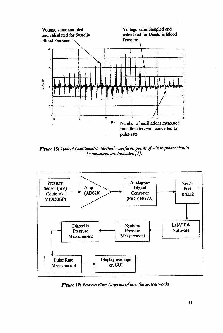
4.1.4-cCalculation for Systolic and DiastolicPressure
After the pulse has been sampled and the DC voltage value is obtained, the voltage
value would go through a few calculations in order to obtain the correct pressure
reading. In order to perform the calculations, the pressure-voltage slope value ofthepressure sensor needs to be obtained. This is done by taking 2points and calculating
the slope value.
4 | 520 30
PRESSUREDIFFERENTIAL
Figure 23: Voltage output versus pressure differentialfor the Motorola MPX50GPPressure Sensor[6],
Points at 10 kPa and 50 kPa are chosen to calculate the slope. At 10kPa, the voltage
value is 30 mV and for 50 kPa it is 78 mV.
Slope =7*mV-30mV=L2xlO-*V/kPa^ 50ifcPfl-10APa
As calculated earlier, the gain of the amplifier is approximately 121. Because the
output voltage versus the differential pressure slope is in mV, the voltage value needs
to be divided again bythe amplification value.
30

Voltage after amplificationSensor Voltage = ~ . ~ ,
_ Gam Value
Voltage after amplificationSensor_ Voltage = ~
After that, the voltage value is divided by the slope value in order to obtain the
pressure value in kPa.
Sensor VoltagekPa_ reading = - ~
kPa_reading-
Slope
Sensor^VoltageMxXO^VIkPa
To convertdie pressurefromkPa to mmHg,
kPa to mmHg^pressure =,J^^^=7.5006m mmHg/kPa~ ~ \0\325kPa
So the readings in mmHg will be:
mmHg_reading = kPa__reading x7.5006\68mmHg/kPa
Inorder to obtain a reading inmmHg, theconversion value isdivided bytheslope
7.5006mmmHg/kPa =625QMmmHg/v1.2xlO_3F/*Pfl
To get the final value in mmHg, the voltage value is multiplied with the value
obtained.
Sensor __ Voltage x6250.5 XmmHg IV- Pressure_mmHg
31

r^>—7^>
121 6251
bvstoiic pressure I
^123
Figure 24: Sub-VI toconvert the voltage value tommHgpressure.
4.1.4-d Determining Pulse Rate Measurement
The Pulse Rate is chosen to be determined right after the Diastolic Pressure
Measurement. The Pulse Rate is also determined using the Peak Detector.How this is
done is for a time interval of 5 seconds, the number of oscillation peaks found is
measured using the #found function. The numbers of peaks that are found are then
calculated for a one minute interval to get the pulse rate per minute value.
4.1.4-e User Interface
Theuser interface for the projectis to incorporate the readings ofSystolic Pressure,
DiastolicPressureand Pulse Rate measurements for easy viewing. It also acts as the
main interface betweenthe user and the computerin terms of startingand stopping
the program from running.
32

POTTNOOsdtatwn Chart
5~W%|COMl _w_l
4-H
SYSTOLIC PRESSURE -S3-I5 •
jo"~
DIASTOLIC PRESSURE1-fl
a-™PULSE RATE
OSCILLATIONS
1MM
Figure 25: Front Panel showing Systolic Pressure, Diastolic Pressure andPulseRate.
4.2 Discussion
The hardware of the system comprising of the Pressure Sensor, Instrumentation
Amplifier and the Analog-to-Digital Converter are working properly. However there
are problems with the LabVIEW software in terms of the manipulation and
processing of the signal. The system reads the signal well and the waveform can be
seen as it is displayed on the graphical user interface. The problems that are present
involve the processing to obtain the Systolic and Diastolic Pressure and also the Pulse
Rate.
33

CHAPTERS
CONCLUSION AND REC03VLMENDATIONS
The PC Based Blood Pressure and Pulse Rate Monitor is believed to be a very useful
device in order to assist people in carrying out measurement by themselves. It uses
the PC which is found in most households. This would encourage people to monitor
their health as it can be a hassle to go all the way to a medical practitioner for blood
pressure monitoring. The system is based on the oscillometric method. The
Oscillometric Method is the measurement of the amplitude of the change in pressure
as the cuff is deflated from the valueabove the systolic pressure. Amplitude suddenly
grows larger as pulse suddenly breaks through its obstruction. The pressure at this
moment is very close to the systolic pressure. As the cuffpressure is further reduced,
there is a great increase in pulse amplitude where it reaches a maximum value and
then would quickly diminish. The diastolic pressure is taken when the peak starts to
diminish. The systolic blood pressure and diastolic blood pressure are obtained by
identifying the region where there is rapid increase the decrease in the amplitude of
the pulses.
Recommendations that can be donefor the project is to havea properworking model.
The next student to take over this project should carry out some fine tuning and
maybe change or redesign certain aspects of the hardware, as the initial groundwork
has already been carried out. It is also recommended that a motorized pump be
incorporated into the system so as to make it a fully automatic system. On the
programming side of the project, the software can be changed to either Visual Basic
or C++, depending on the suitability.
34

References
[1] CS Chua and Siew Mun Hin, "Freescale Semiconductor Application NoteAN1571: Digital Blood Pressure Meter", Freescale Semiconductor, 2005.
[2] How Blood Pressure IsMeasured,
http://www.eheaithmd.com/Iibrary/highbp/HBP_measured.htmt.
[3] Memo Romero, Raul Figueroa, and Chad Madden (2000). Pressure-Sensing
Systems for Medical Devices.
www.freescale.CQm/fites/dsD/cioc/reports presentations/MDDI.pdf
[4] Barry Bittman, MD, "High Blood Pressure: anew twist on the white coatSyndrome ", 1998-1999. http://www.mind-body.org/hvpertension.htm
[5] PIC16F87XA Data Sheet, Microchip Technology Inc, 2003.
[6] Motorola MPX50 Series Data Sheet, Motorola Inc, 1997.
[7] Analog Devices AD620 Data Sheet, Analog Devices Inc, 2004.
[8] Jeffrey Travis, "LabVIEW for Everyone", Prentice-Hall, Upper Saddle River,New Jersey, USA, 2002.
[9] Jeffrey Y. Beyon, "LabVIEW Programming, Data Acquisition and Analysis",Prentice-Hail, Upper Saddle River, NewJersey, USA, 2001.
[10] National Institute on Aging, "High Blood Pressure", U.S. National Institutes ofHealth, USA, 2005. http://www.niapubiications.org/ageDages/hiblood.asp
[11] Interfacing the Serial / RS232 Porthttp://wearcam.onj/seatsaie/programs/wwvv.beyondlogic.org/serial/seriai.htm
[12] Max 232 Data Sheet, Texas Instruments Inc, 2004
35

[13] Portable Digital Blood Pressure Monitor
http://www.people.corneil.edu/pages/ws62/
36

APPENDIX A
PIC16F877A ANALOG TO DIGITAL CONVERTER PROGRAM
37

s^w
^^
^^
mH
^S
^^
^£s
mB
'!^
^^
^^
^^
^^
^^
^^
^^
^^
^^
^v^
^;s
's'^
ss^
^^
^^
^^
'
-*
Instr
Byt
esat
Po
rti
•fef
^-r^
^l^i
S*iS
-js;
SsS-
-!^i
!tW
icSe
l,S;
^S
^m
s^S
s-^
Bi?
^?
S^
^iS
g^
^^
^S
^^
^^
:^^
^^
^^
l^^
^!s
ss
Lab
VIE
WV
ISA
Ser
ial
VI
40

Wav
efo
rmC
hart
;*M
..i!
[thre
shol
d1
j^A
^
[Am
plitu
des
-•>
arfc
•^
arS
.•
«•P
eak
s
Det
ecti
ngpe
aks
usin
gP
eak
Det
ecto
r.V
I
41

e>#>
121
62
51
bysto
licpr
essu
rei t(/
l.23
Mat
hem
atic
alE
quat
ions
forS
ysto
lican
dD
iast
olic
Pres
sure
Cal
cula
tion
42

thre
shol
djim
mm
m
•I's
aras
ffiB
!
*P
eak
s
#fo
un
d
JI3
2
A^
iz!
Pul
seR
ate
co
nv
ert
tom
inu
tes
Usi
ngPe
akD
etec
tor.
VI
toob
tain
puls
era
te
43

APPENDIX C
DATASHEETS
44

MOTOROLASEMICONDUCTOR TECHNICAL DATA
50kPaUncompensatedSilicon Pressure Sensors
The MPX50 silicon piezoresistive pressure sensor provides a veryaccurate and linearvoltage output —directly proportional to the applied pressure. This standard, low cost,uncompensated sensor permits manufacturers to design and add their own externaltemperature compensating and signal conditioning networks. Compensation techniquesare simplified because of the predictability of Motorola's single element strain gaugedesign.
Features
• Low Cost
• Patented Silicon Shear Stress Strain Gauge Design
• Ratiometric to Supply Voltage
• Easy to Use Chip Carrier Package Options• 60 mV Span (Typ)
• Differential and Gauge Options
• ±0.25% (Max) Linearity
Application Examples• Air Movement Control
• Environmental Control Systems
• Level Indicators
• Leak Detection
• Medical Instrumentation
• Industrial Controls
• Pneumatic Control Systems
• Robotics
Figure 1 shows a schematic of the internal circuitry on the stand-alone pressuresensor chip.
PIN30+VS
(X) X-ducer
p,N1-2_
PIN 2
PIN 4
-o-Vout
Figure 1. Uncompensated Pressure Sensor Schematic
VOLTAGE OUTPUT versus APPLIED DIFFERENTIAL PRESSUREThe differential voltage outputofthe X-duceris directly proportional to the differential
pressure applied.The output voltage of the differential or gauge sensor increases with increasing
pressure applied to the pressure side (P1) relative to the vacuum side (P2). Similarly,output voltage increases as increasing vacuum is applied to the vacuum side (P2)relative to the pressure side (P1).
Senseon and X-ducer are trademarks of Motorola, Inc.
REV 5
©Motorola, Inc. 1997
Order Hh'js doetjmeitf
by MPX50/D
0 to 50 kPa (0-7.25 psi)60 mV FULL SCALE SPAN
(TYPICAL)
BASIC CHIP
CARRIER ELEMENT
CASE 344-15, STYLE 1
DIFFERENTIAL
PORT OPTION
CASE 344C-01, STYLE 1
NOTE: Pin 1 is the notched pin.
PIN NUMBER
1 Gnd 3 vs
2 +V0ut 4 -Vout
® MOTOROLA

SERIES
MAXIMUM RATINGS
Rating Symbol Value Unit
Overpressure(8) (P1 >P2) Pmax 200 kPa
Burst Pressure*8) (P1 >P2) Pburst 500 kPa
Storage Temperature Tstg -40 to +125 °C
Operating Temperature TA -40 to+125 °C
OPERATING CHARACTERISTICS (Vs=3.0Vdc, TA =25°C unless otherwise noted, P1 >P2)
Characteristic Symbol Mln Typ Max Unit
Pressure Ranged) pop 0 — 50 kPa
Supply Voltage*2) vs — 3.0 6.0 Vdc
Supply Current 'o — 6.0 —mAdc
Full Scale Span(3) Vfss 45 60 90 mV
OffeetW Voff 0 20 35 mV
Sensitivity AV/AP —1.2 — mV/kPa
Linearity!5) —-0.25 —
0.25 %vFss
Pressure Hysteresis*5) (0to50kPa) —
_ ±0.1 — %vFss
Temperature Hysteresis(5) (- 40°C to+125°C) — — ±0.5 — %vFss
Temperature Coefficient ofFull Scale Span*5) TCVpss -0.22 — -0.16 %vFSs/°c
Temperature Coefficient ofOffset*5) TCVoff — ±15 — nv/°c
Temperature CoefficientofResistance*5) TCR 0.21 —0.27 %2in/°C
Input Impedance Zin 400 — 550 £2
Output Impedance Zout 750 — 1800 Q
Response Time(6) (10% to90%) tR — 1.0 —ms
Warm-Up — — 20 — ms
Offset Stability^9) — — ±0.5 — %vFss
MECHANICAL CHARACTERISTICS
Characteristic Symbol Mln Typ Max Unit
Weight (BasicElementCase 344-15) —
_ 2.0 — Grams
Common Mode Line Pressure(7) — — — 690 kPa
NOTES:
1. 1.0 kPa (kiloPascal) equals 0.145 psi.2. Device isratiometricwithin this specified excitation range. Operating thedevice above thespecified excitation range may induce additional
error due to device self-heating.3. Full Scale Span (Vfss) isdefined asthe algebraic difference between the outputvoltageatfull rated pressureand the outputvoltage atthe
minimum rated pressure.4. Offset (Voff) isdefined as theoutput voltage at the minimum rated pressure.5. Accuracy(error budget) consists of the following:
• Linearity: Output deviation from a straight line relationship with pressure, using end point method, over the specifiedpressure range.
• Temperature Hysteresis: Output deviation at any temperature within theoperating temperature range, after thetemperature iscycled toand from theminimum ormaximum operating temperature points, with zero differential pressureapplied.Output deviation at anypressure within the specified range, when mispressure iscycled toandfrom theminimum or maximum rated pressure, at 25CC.Output deviation at full rated pressure overthetemperature rangeof0 to 85°C, relative to25°C.Output deviation with minimum rated pressure applied, over thetemperature range of0 to85°C, relativeto25°C.
Z|n deviation with minimum rated pressure applied, over the temperature range of-40°C to+125°C,relative to 25°C.
6. Response Time is defined asthe time for the incremental change in the output to go from 10% to 90% of its final value when subjected toa specified step change in pressure.
7. Common mode pressures beyond specified may result inleakage at thecase-to-leadinterface.8. Exposure beyond theselimits may causepermanent damage ordegradation tothedevice.9. Offset stability isthe product's output deviation when subjected to1000 hours ofPulsed Pressure, Temperature Cycling with Bias Test.
Pressure Hysteresis:
TcSpan:
TcOffset:
TCR:
Motorola Sensor Device Data

TEMPERATURE COMPENSATION
Figure 2 shows the typical output characteristics of theMPX50 series over temperature.
The X-ducer piezoresistive pressure sensor element is asemiconductor device which gives an electrical output signalproportional to the pressure applied to the device. This device uses a unique transverse voltage diffused semiconductor strain gauge which is sensitive to stresses produced in athin silicon diaphragm by the applied pressure.
Because this strain gauge is an integral part of the silicondiaphragm, there are no temperature effects due to differences in the thermal expansion of the strain gauge and thediaphragm, as are often encountered in bonded strain gaugepressure sensors. However, the properties of the straingauge itself are temperature dependent, requiring that thedevice be temperature compensated if it is to be used overan extensive temperature range.
Temperature compensation and offset calibration can beachieved rather simply with additional resistive components,
100
90
80
70
-s-60
£ 40
o
30
mpxwi „- -40°Q^
Vft =3Vdc
+ 25"C
P1>P2
+12 b"C
I
0 | 2 I3 4 I 5 I 6 r\
SPAN
RANGE
(TYP)
1OFFSET
(TYP)
20
10
PS) o"kPa 0 10 20 30 40
PRESSURE DIFFERENTIAL
50
Figure2. Output versus Pressure Differential
WIRE BOND
LEADFRAME
SILICONE
DIECOAT DIE
MPXSO SERIES
or by designing your system using the MPX2050 seriessensors.
Several approaches to external temperature compensation over both -40 to +125°C and 0 to +80°C ranges arepresented in Motorola Applications Note AN840.
LINEARITY
Linearity refers to how well a transducer's output followsthe equation: Vout= voff+ sensitivityx P over the operatingpressure range (see Figure 3). There are two basic methodsforcalculatingnonlinearity: (1) end point straight linefitor (2)a least squares best line fit. While a least squares fitgivesthe "best case" linearity error (lower numerical value), thecalculations required are burdensome.
Conversely, an end pointfitwill give the "worstcase" error(often more desirable in error budget calculations) and thecalculations are more straightforward for the user. Motorola'sspecified pressure sensor linearities are based on the endpoint straight line method measured at the midrangepressure.
STAINLESS STEEL
METALCOVER
EPOXY
CASE
RTVDIE
BOND
J_i i i L
SPAN
(VFSS)
OFFSET
(Voff)
0 MAX | PqPPRESSURE (kPA)
Figure 3. Linearity Specification Comparison
Figure 4. Cross-Sectional Diagram (not to scale)
Figure4 illustrates the differential or gauge configurationin the basic chip carrier (Case 344-15). A silicone ge! isolates the die surface and wire bonds from the environment,whileallowing the pressure signal to be transmitted to the silicon diaphragm.
The MPX50 series pressure sensor operating characteris
Motorola Sensor Device Data
tics and internal reliability and qualification tests are basedon use of dry air as the pressure media. Mediaother than dryair may have adverse effects on sensor performance andlong term reliability. Contact the factory for information regarding media compatibility in your application.

MPXSfJt SERIES
PRESSURE (P1VVACUUM (P2) SIDE IDENTIFICATION TABLE
Motorola designates the two sides of the pressure sensoras the Pressure (P1) side and the Vacuum (P2) side. ThePressure (P1) side is the side containing silicone gel whichisolates the die from the environment. The Motorola MPX
pressure sensor is designed to operate with positivedifferential pressure applied, P1 > P2.
The Pressure (P1) side may be identified by using thetable below:
Part Number Case Type Pressure (P1) Side Identifier
MPX50D 344-15 Stainless Steel Cap
MPX50DP 344C-01 Side with Part Marking
MPX50GP 344B-01 Side with Port Attached
MPX50GVP 344D-01 Stainless Steel Cap
MPX50GS 344E-01 Side with Port Attached
MPX50GVS 344A-01 Stainless Steel Cap
MPX50GSX 344F-01 Side with Port Attached
MPX50GVSX 344G-01 Stainless Steel Cap
ORDERING INFORMATION
MPX50 series pressure sensors are available in differential and gaugeelement package or with pressure port fittings which provide printed circuitconnections.
configurations. Devices are available with basicboard mounting ease and barbed hose pressure
Device Type Options Case Type
MPX Series
Order Number Device Marking
Basic Element Differential Case 344-15 MPX50D MPX50D
Ported Elements Differential Case344C-01 MPX50DP MPX50DP
Gauge Case344B-01 MPX50GP MPX50GP
Gauge Vacuum Case344D-01 MPX50GVP MPX50GVP
Gauge Stovepipe Case344E-01 MPX50GS MPX50D
Gauge Vacuum Stovepipe Case344A-01 MPX50GVS MPX50D
Gauge Anal Case344F-01 MPX50GSX MPX50D
Gauge Vacuum Axial Case344G-01 MPX50GVSX MPX50D
Motorola Sensor Device Data

PORT #2VACUUM
PRESSURE(P2)
SEATMG rjfZPLANED '
Motorola Sensor Device Data
PACKAGE DIMENSIONS
posmvEPRESSURE (PI)
& 0.136(0.005)® T A®
CASE 344-15
ISSUE W
posmvEPRESSURE
(PI)
PIN1
CASE 344A-01ISSUE B
NOTES:
1. DIMENSIONiNGANDTOLERANCINGPffiASMEY14.5M.1994.
2. CONTROLLING DIMENSION: INCH.
3. DIMENSION-A-IS INCLUSNE OF THE MOLD
STOP RING.MOLDSTOP RINGNOT TO EXCEED
16.00(0-630).
PININCHES IttJJKETERS
MIN MAX UN MAX
A aSBS 0.630 15.11 16.00
B 0514 0.534 13.06 13.56
C (L200 1X220 5,08 5.59
D 0,016 0.020 0.41 051
F 0.048 a064 152 1.63
G 0.100 BSC 2.54 BSC
J 0.014 0.016 0.36 0.40
L 0.696 0.725 17.65 1B.42
M 30° NOM W° JOM
N 0.475 °,4» 12.07 12.57
R M» 0,45Q 10.92 11.43
STYLE 1:PIN 1. GROUND
2.+OUTPUT3. ♦ SUPPLY4.-OUTPUT
NOTES:1. DIMENSIONING ANDTOLERANCING PER ANSI
Y14.5M 1982.2. CONTROLLING DIMENSION: INCH.
™M
mCHES MILLIMETERS
MM HAX M» HAX
A 0,690 0.720 17.53 1128
B 0.245 0.255 6.22 646
C 0.780 0.820 19.81 20.82
P 0.016 0.020 0.41 0.51
F ao48 0Q64 1.22 1.63
Q 0.10(1 BSC 2.54 BSC
J p.014 0.016 0.36 0.41
If 0.345 0.375 8.76 9.53
N 0.300 0.310 7.62 7.87
R 0.178 0.186 4.52 4.72
s 0220 0.240 5.59 6.10
V 0.182 0.104 4.62 4,83
STYLE 1:PIN 1. GROUND
Z*0UTPUT3. + SUPPLY4. -OUTPUT

SERIES
SEATING r^f-PLANE1—1-
nID
PACKAGE DIMENSIONS — CONTINUED
NOTES:1. DIMENSIONING AND TOLERANCING PER ANSI
Y14.5,1932.2. CONTROLLING DIMENSION: INCH.
Ml
MCHES MILLIMETERS
"W MAX MM MAX
A. 1.145 1r175 29.08 29.85
B 0.685 0.715 17.40 18.16
c 0.305 0.325 7.75 8.26
D 0.016 0.020 0.41 0.51
F 0.048 0.064 1.22 1.63
G am BSC 2.54 BSC
H 0.182 0.194 4.62 4.93
4 1014 0,016 0.36 0.41
K 0.695 0.725 17.65 18.42
L 0.290 p.300 7.37 7.62
N 0420 0440 10.67 11.18
P 0.153 0.159 189 4.04
Q 0.153 0,159 189 4.04
R Q.230 0.250 5.84 6.35
s 0.220 0.240 5.59 6.10
II 0.910 BSC 23.11 BSC
# 0.13(0.005)® T S © Q©STYLE 1:
PIN1. GROUND
2.+OUTPUT3. + SUPPLY4. -OUTPUT
CASE344B-01ISSUE B
& 0.13(0.005)® T S© Q©
CASE344C-01
ISSUE B
NOTES:1. DIMENSIONING ANDTOLERANCING PER ANSI
Y14.5M,1982.2. CONTROLLING DIMENSION: INCH.
PORTtflPOSITIVE PRESSURE(PI)
DM
HCHES MUMETERS
UN MAX MN MAX
A 1.145 1.175 29.08 29.85
B 0.665 0.715 17.40 16.16c 0.405 0435 10.29 11.05
D D.01E 0.020 041 0.51
F 0.048 0.064 1.22 1.63
G ai« BSC 254 BSC
H 0.182 0.194 4.62 4.93
i 0,014 0.016 Q.3B 0.41
K 0.695 0.725 1755 18.42
L 0290 0.300 7.37 7.62
N 0.420 0.440 10,67 11.18
P 0.153 0.159 3.89 4.04
q 0,153 0.159 3.89 4.64
R 0.063 0.083 1.60 2.11
S 0220 0.240 55S 8.10
II 0.91C BSC 23.1 BSC
V 0248 0278 6.30 7.06
w 0.310 0.330 7.87 0-38
bQd
STYLE1:PIN 1. GROUND
2. * OUTPUT3. * SUPPLY4.-OUTPUT
Motorola Sensor Device Data

PACKAGE DIMENSIONS — CONTINUED
1 'PLANE
PORT #2VACUUM
(P2)
**/ F^h$• 0 0.25(0.010)® T Q©
PLANE1 '
Motorola Sensor Device Data
# 0.13(0.005)® T S© Q©
CASE344D-01ISSUE B
PJN1
D4PL
& 0.13(0.005)® TB®
CASE344E-01ISSUE B
MPXSO SERIES
NOTES:1. DWENSJONINGANDTOLERANCING PER ANSI
Y14.5,1982.2. CONTROLLING DIMENSION: INCH.
DM
MCHES MILUMETERS
MM MAX ten MAX
A 1.145 1.175 29.08 29.85
B 0.685 0.715 17.40 18.16
C 0.305 p.325 7.75 8.26
D 0.016 0.020 041 0.51
F 0.046 0-064 1.22 1.63
S 0.100 BSC 254 BSC
H 0.182 0.194 4.62 4.93
J 0.014 0.016 0.36 0.41
K 0.695 0,725 17.65 1B42
I 0790 0.300 7.37 7,62N 0.420 0.440 10.67 11.18
P 0.153 WW 3.89 4.04
Q 0,153 0.15B 3.89 4.04
H 0230 0,250 5.84 6.35
9 0220 0.240 5.59 6.10
y 0.910 BSC 23.11 BSC
STYLE 1:PIN 1. GROUND
2.+OUTPUT3. + SUPPLY4.-OUTPUT
NOTES:1. DIMENSIONING ANDTOLERANCING PER ANSI
Y145M, 1982.2. CONTROLLING DIMENSION: INCH.
DM
INCHES MLLHETERS
MM P/U MM MAX
A 0.690 0.720 17.53 1628
B 0245 0255 6.22 6.48
C 0.780 0.820 19.81 2a62
O 0.016 0.020 0.41 0.51
F 0.048 Q.064 122 1.63
G Q.10C BSC 2.54 BSC
J 0.014 0.016 0.36 041
K 0.345 0.375 8.76 9.53
N 0.300 0.310 7.62 7.87
R 0.178 0.186 4.52 4.72
S 0220 0240 5.59 6.10
V 0.182 0.194 4.62 4.93
STYLE 1:PIN 1. GROUND
Z +OUTPUT3. + SUPPLY4.-OUTPUT

SERIES
PORT#1POSITIVEPRESSURE
(PI)
PORT #2VACUUM(P2>
PACKAGE DIMENSIONS — CONTINUED
& 0.13(0.005)® T P© Q©
CASE344F-01
ISSUE B
# 0.13(0.005)® T P© Q©
CASE344G-01ISSUE B
NOTES:1. DIMENSIONING ANDTOLERANCING PER
ANSIY14.5M, 1982.2. CONTROLLING DIMENSION: INCH.
DM
MCHES MILLIMETERS
MM MAX MM MAX
A 1.080 1.120 2743 2845
B 0.740 0.760 1850 19.30
C 0.630 0.6fj(l 16.00 16.51
P 0.016 0.020 0.41 0.51
E 0.160 0.180 4.06 457
F 0.048 0.064 122 1,630 0.100 BSC 2,54 BSC
4 0.014 0.016 0.36 0.41
K 0.220 0.240 559 6.10
N 0.070 0,080 1.78 £03
P 0.150 0.160 351 4.06
q 0.150 0.160 3.81 4.06
R 0.440 D.460 11.19 11.68
S 0.695 0.72S 17.65 1842
M 0540 0.660 21.34 21.84
V 0.182 0.194 4.62 4.92
STYLE 1:PIN 1. GROUND
2. V(+)OUT3. V SUPPLY4. V(-)OUT
NOTES:1. DIMENSIONING ANDTOLERANCING PER
ANSIY14.5M, 1962.2. CONTROLLING DIMENSION: INCH.
PW
MCHES MILLIMETERS
MM MAX MM MAX
A 1.080 1.120 27.43 2145
B 0.740 0.760 18.80 19.30
n 0.630 0.650 16.00 1651
0 0.0^6 0.020 041 0.51
E 0.160 0.160 4.06 4.57
F 0.048 0.064 122 1.63
a 0.100 BSC 2.54 ISC
i 1014 0.016 056 041
K 0.220 0.240 55S 6.10
N 0.070 0.080 1.78 203
P 0.150 0.160 3.81 4.06
q 0.150 0.160 3.61 4.06
R 0.440 0.460 11.18 1158
S 0.695 0.725 17.65 1842
II 0.840 0.660 21.34 2154
V 0.182 0.194 4.62 4.92
STYLE1:PJN1. GROUND
2. V(+)OUT3. VSUPPLY4. V(-)OUT
Motorola Sensor Device Data

"MPXSO SERIES
Motorola reservesthe right to makechangeswithout further notice to anyproducts herein. Motorola makesnowarranty, representation orguaranteeregardingthe suitability ofitsproducts foranyparticular purpose, nordoes Motorola assumeany liability arising outoftheapplication or use ofanyproduct orcircuit, andspecificallydisclaimsanyandall liability, including without limitation consequentialorincidentaldamages. Typical" parameterswhich may beprovided inMotoroladatesheets and/brspecificationscananddovaryindifferentapplfcationsandactualperformancemayvaryovertirne. All operatingparameters,M^mustbe validated foreach customerapplication bycustomer'stechnical experts. Motorola does notconveyany licenseunderitspatent rightsnorthe rightsofothers. Motorola productsare not designed, intended,or authorized for use as componentsin systems intendedfor surgicalimplant intothe body, or otherapplications intended tosupportorsustainlife, orforanyotherapplication inwhich thefailure oftheMotorola productcould createa situation wherepersonal injuryordeathmayoccur. Should BuyerpurchaseoruseMotorola productsforany suchuninter«ledorunauthorizedapplica1»n, Buyershall irelemnifVandhcW Motorolaand itsofficers, employees, subsidiaries, affiliates, and distributors harmless againstallclaims, costs,damages,and expenses,and reasonable attorney feesarising outof, directly or indirectly, anyclaim ofpersonal injury ordeathassociated with suchunintended or unauthorized use,evenifsuchclaim alleges thatMotorola was negligent regarding the design or manufacture of the part. Motorola and (gjare registered trademarks of Motorola, Inc. Motorola, Inc. isan EqualOpportunity/Affirmative Action Employer.
Motorola Sensor Device Data

MFX50 SERIES
Mfax is a trademark of Motorola, Inc.
How to reach us:
USA/EUROPE/Locations Not Listed: MotorolaLiterature Distribution; JAPAN: Nippon Motorola Ltd.; Tatsumi-SPD-JLDC,6F Setbu-^utsuryu-Center,P.O. Box 5405, Denver, Colorado 80217. 303-675-2140 or 1-600-441-2447 3-14-2 Tatsumi Koto-Ku, Tokyo135, Japan. 81-3-3521-8315
Mfax™: [email protected] - TOUCHTONE 602-244-6609 ASIA/PACIFIC: Motorola Semiconductor} H.K. Ltd.; 8B Tai PingIndustrial Park,- US &Canada ONLY 1-800-774-1848 51 Ting Kok Road, TaiPo, NT., Hong Kong. 852-26629298
INTERNET: http^/motorola.com/sps
9 MOTOROLA0 MPX50/D

• ANALOGDEVICES
MATURES
iasytouse
Gain set with one external resistor
(Gain range 1 to 10,000)
Wide power supply range (±2.3 V to ±18V)
Higher performance than 3 op amp IAdesignsAvailable in 8-lead DIPand SOIC packaging
Low power, 13 mA max supply current
Ixcellent dc performance (B grade)
50 |*Vmax, input offset voltage
0.6 uVTC max, input offset drift1.0 nA max. Input bias current
100 dB mln common-mode rejection ratio (G -10)
.ow noise
9 nV/VHz@1 kHz, input voltage noise0.28 LiVp-p noise (0.1 Hz to 10 Hz)
ixcellent ac specifications
120 kHz bandwidth (G -100)
15 us settling time to 0.01%
\PPUCATIONS
Veigh scales:CG and medical instrumentation
transducer interface
)ata acquisition systems
ndustrial process controls
lattery-powered and portable equipment
5 10SUPPlVCURRENTfmA)
Figure 2. ThreeOp Amp IA Designsvs.AD620
(ev.G••formation furnished by Analog Devices is beDevtd to be accurate and tenable,iowever, no responsiblity fa assumed by Analog Devkes for its us*, nor for anynntagcntontsof patents or othtr rights ofthird parties that may result from Its use.Specificationssubject to change without notice. Nolicense b granted by implicationnrotherwise under any patent or patent rights of Analog Devices. Trademarks andegistered trademarks are die property oftheir respective owners.
Low Cost Low Power
Instrumentation Amplifier
AD620
CONNECTION DIAGRAM
TOP VIEW
Figure 1.8-Lead PDIP (N), CERDIP (Q), andSOIC (R) Packages
PRODUCT DESCRIPTION
The AD620is a low cost, high accuracy instrumentationamplifier that requires onlyone externalresistorto set gainsof1 to 10.000. Furthermore, the AD620 features 8-lead SOIC and
DIPpackaging that is smaller than discrete designs and offerslower power (only 1.3mA max supply current), making it agoodfitforbattery-powered, portable (or remote) applications.
TheAD620, withitshighaccuracy of40ppmmaximumnonlinearity, lowoffsetvoltage of50 uVmax,and offsetdrift of0.6 uV/°Cmax, is ideal for use in precision data acquisitionsystems, such as weighscales and transducer interfaces.Furthermore,the lownoise,lowinputbiascurrent,and lowpowerof the AD620 makeit wellsuitedfor medicalapplications, suchas ECG and noninvasiveblood pressure monitors.
The lowinput biascurrent of 1.0nA max ismadepossible withthe use ofSuper6eta processing in the input stage. The AD620workswell as a preamplifier due to its lowinput voltage noiseof9nV/VHz at1kHz, 0.28 uV p-p inthe 0.1 Hz to10 Hz band,and 0.1 pA/VHz input current noise. Also, theAD620 iswellsuitedfor multiplexed applications with its settlingtime of 15(isto 0.01%, and its cost is low enough to enable designs with onein-amp per channel.
10k 100k 1M 10MSOURCE RESISTANCE (13
Figure 3. Total Voltage Noisevs.Source Resistance
One Technology Way, P.O. Box9106, Norwood, MA 02062-9106, U.S.A.Tel: 781.329.4700 www.analog.comFax:781326.8703 ©2004 Analog Devices, Inc All rights reserved.

D620
ABLE OF CONTENTSpecifications 3
absolute Maximum Ratings 5
ESD Caution 5
ypical Performance Characteristics 7
neory ofOperation 13
Gain Selection 16
Input andOutput Offset Voltage 16
Reference Terminal 16
REVISION HISTORY
2/04—Rev. F to Rev. G
Jpdated Format UniversalChange to Features.... 1
Change to Product Description 1
Changes toSpecifications 3
kdded Metallization Photograph 4
Replaced Figure 4-Figure 6 6
Replaced Figure 15 7
Replaced Figure 33 10
leplaced Figure 34andFigure 35 10
ieplaced Figure 37 10
Changes to Table 3 13
Changes to Figure 41 and Figure 42 14
Changes to Figure 43 15
Change to Figure 44 17
Dhanges to Input Protectionsection 15
Meted Figure 9 15
Changes to RFInterference section 15
idit to GroundReturnsfor Input Bias Currents section 17
\dded AD620CHIPS to Ordering Guide 19
Input Protection 16
RF Interference 16
Common-Mode Rejection 17
Grounding 17
GroundReturnsfor Input BiasCurrents 18
Outline Dimensions 19
Ordering Guide 20
7/03—Data Sheetchangedfrom REV. Eto REV. F
Edit to FEATURES 1
Changes toSPECIFICATIONS 2
Removed AD620CHIPS from ORDERING GUIDE 4
Removed METALLIZATION PHOTOGRAPH 4
Replaced TPCs 1-3 5
Replaced TPC12 6
Replaced TPC 30 9
Replaced TPCs 31 and32 10
Replaced Figure 4 10
Changes to Table 1 11
Changes to Figures 6and7 12
Changes to Figure 8 13
Edited INPUT PROTECTION section 13
Added newFigure 9 13
Changes to RFINTERFACE section 14
Edit to GROUND RETURNS FOR INPUT BIAS CURRENTS
section 15
Updated OUTLINE DIMENSIONS 16
Rev. G| Page 2 of 20

AD620
SPECIFICATIONS'ypical @25°C, Vs =±15 V, and Rl - 2kH, unless otherwise noted.able 1.
AD620A AD620B AD620S 1
•arameter Conditions Mln Typ Max Min Typ Max Min Typ Max Unit
iAIN G=1+(49.4IcO/Rg)
Gain Range 1 10,000 1 10,000 1 10,000
Gain Error2 Vout = ±10 V
G=1 0.03 0.10 0.01 0.02 0.03 0.10 %
G-10 0.15 0.30 0.10 0.15 0.15 0.30 %
G = 100 0.15 0.30 0.10 0.15 0.15 0.30 %
G = 1000 0.40 0.70 0.35 0.50 0.40 0.70 %
Nonlinearity Voor=-l0VtO+10V
G= 1-1000 RL=10kQ 10 40 10 40 10 40 ppm
G = 1-100 Ri = 2kQ 10 95 10 95 10 95 ppm
Gain vs. Temperature
G = 1 10 10 10 ppm/°C
Gain >12 -50 -50 -50 ppm/°C
/OLTAGE OFFSET (TotalRTI Error= Vos. +Voso/G)
Input Offset, Voh VS= ±5V
tO±15V
30 125 15 50 30 125 uV
Overtemperature Vs = ±5 V
tO±15V
185 85 225 uV
Average TC VS= ±5V
to ± 15 V
0.3 1.0 0.1 0.6 0.3 1.0 uV/°C
Output Offset,Voso VS= ±15V 400 1000 200 500 400 1000 Mv
Vs = ±5V 1500 750 1500 uV
Overtemperature Vs = ±5V
tO±15V
2000 1000 2000 uV
Average TC Vs = ±5VtO±15V
5.0 15 2.5 7.0 5.0 15 uWC
Offset Referred to the
Input vs.Supply (PSR) Vs = ±2.3V
to±18V
G = 1 80 100 80 100 80 100 dB
G=10 95 120 100 120 95 120 dB
G = 100 110 140 120 140 110 140 dB
G=1000 110 140 120 140 no 140 dB
INPUT CURRENT
Input BiasCurrent 0.5 2.0 0.5 1.0 0.5 2 nA
Overtemperature 2.5 1.5 4 nA
Average TC 3.0 3.0 8.0 pA/°C
Input Offset Current 03 1.0 0.3 0.5 0.3 1.0 nA_ A
Overtemperature 1.5 0.75 2.0 nA
Average TC 1.5 15 8.0 pA/°C
INPUT
Input ImpedanceDifferential 10||2 10H2 10t|2 GQ_pF
Common-Mode 10||2 10H2 10|12 GO_pF
Input Voltage Range3 VS= ±Z3V
to±5V
-Vs+1.9 +Vs-1.2 -Vs+1.9 +Vs-1-2 -Vs+1.9 +Vs-1.2 V
Overtemperature -Vs + 2.1 +Vs-1.3 -Vs + 2.1 +Vs-1.3 -Vs + 2.1 +Vs-U V
Vs=±5V -Vs+1.9 +Vs-1.4 -Vs + 1.9 +Vs-1.4 -Vs + 1.9 +VS-1.4 V
tO±18V
Overtemperature -Vs + 2.1 +VS-1.4 -Vs + 2.1 +Vs + 2.1 -Vs + 2.3 +VS-1.4 V
Rev.G|Page 3 of20

iD620
arameter
Common-Mode RejectionRatio DC to 60 Hz with
1 kO Source Imbalance
G=1
G = 10
G=100
G=1000
lUTPUT
Output Swing
Overtemperature
Overtemperature
Short Circuit Current
(YNAMIC RESPONSE
SmallSignal-3 dBBandwidthG=1
G=10
G = 100
G = 1000
Slew Rate
SettlingTimeto 0.01 % 10VStepG= 1-100
G = 1000
IOISE
Voltage Noise,1 kHz
Input, Voltage Noise, e^
Output, Voltage Noise,e™
RTI, 0.1 Hz to 10 Hz
G=1
G=10
G = 100-1000
Current Noise
0.1 Hz to 10 Hz
tEFERENCE INPUT
RlN
1,N
Voltage Range
Gain to Output
>OWER SUPPLY
Operating Range4Quiescent Current
Overtemperature
rEMPERATURE RANGE
For Specified Performance
Conditions Min
AD620A
Typ Max
Vcw= 0Vto±10V
73
93
110
110
RL=10kQ
Vs = ±2.3V
to±5V
Vs = +5V
to±18V
-Vs +1.1
-Vs+1.4
-Vs + 1.2
-Vs+1.6
0.75
90
110
130
130
±18
1000
800
120
12
1.2
15
150
+Vs-1.2
+VS-1.3
+Vs-1.4
+VS-1.5
Total RTI Noise =ffiZ)+(em IGf
f = 1kHz
Vim*,Vref = 0
Vs = ±2.3Vto±18V
9
72
3.0
0.55
0.28
100
10
13
100
20
50 60
-Vs+1.6 +Vs-1.6
1 ± 0.0001
±23 ±18
0.9 1.3
1.1 1.6
-40 to+85
SeeAnalog Devices military data sheetfor883B tested specificatfons.' Does not include effects of external resistor Re1One input grounded. G = 1.1Thisisdefinedas the samesupply range that isused to specifyPSR.
AD620B
Min Typ Max
80
100
120
120
-Vs+1-1
-Vs+1.4
-Vs+U
90
110
130
130
+Vs-1.2
+V5-13
+Vs-1.4
-Vs+1.6 +Vs-1.5
±18
0.75
1000
800
120
12
1.2
15
150
9
72
13
100
3.0 6.0
035 0.8
0.28 0.4
100
10
20
50 60
-Vs+1.6 +Vs-1.6
1± 0.0001
±23 ±18
0.9 13
1.1 1.6
-40 to +85
Rev.G | Page 4 of 20
AD620S1
Min Typ Max
73
93
110
110
-Vs + 1.1
-Vs + 1.6
-Vs+U
90
110
130
130
+Vs-12
+Vs-13
+Vs-1.4
-Vs + 2.3 +Vs-1.5
±18
0.75
±23
1000
800
120
12
1.2
15
150
9
72
13
100
3.0 6.0
0.55 0.8
0.28 0.4
100
10
±18
0.9 1.3
1.1 1.6
-55 to+125
Unit
dB
dB
dB
dB
V
V
V
mA
kHz
kHz
kHz
kHz
V/us
us
ps
nV/VHz
nVA/Hz
uVp-p
uVp-P
uVp-p
fAA/HzpAp-p
20 kfl
50 60 UA
-Vs + 1.6 +Vs-1.6 V
1 ± 0.0001
V
mA
mA
°C

AD620
iBSOLUTE MAXIMUM RATINGS
able 2.
arameter Rating
upply Voltage ±18V
ttemal Power Dissipation1 650 mW
iput Voltage (Common-Mode) ±VS
ifferential Input Voltage 25 V
utput Short-Circuit Duration Indefinite
torage Temperature Range (Q) -65°Cto+150°C
torage Temperature Range (N,R) -65°Cto+125°C
operatingTemperature Range
AD620(A,B) -40°Cto+85°C
AD620(S) -55gCto+125°C
ead Temperature Range
(Soldering 10 seconds) 300"c
Stresses above those listed under Absolute Maximum Ratingsmaycausepermanentdamageto the device. This is a stressratingonly;functionaloperation of the device at theseor anyother condition s above those indicated in the operational
sectionof this specification is not implied. Exposureto absolutemaximumratingconditionsfor extendedperiodsmayaffectdevicereliability.
Specification is for device in free ain8-Lead Plastic Package: 0« = 95gC8-Lead CERDIP Package: 6ja= 110°C8-LeadSOIC Package:6m= 155°C
SD CAUTION
SD(etectrostaticdischarge)sensitivedevice.Electrostatic charges as high as 4000Vreadilyaccumulate on theuman body and test equipment and can discharge without detection. Although this product featuresroprietary ESD protection circuitry,permanent damage may occur on devices subjected to high energylectrostaticdischarges.Therefore,proper ESD precautions are recommended to avoid performanceegradation or toss of functionality-
Rev.G | Page 5 of 20
WARNING!
^rPi^-

1D620
OUTPUT
d ud _F1 • •• •4.- in
„ 0.125 _(3-180)
le"J 11
-IN +IN
'FOR CHIP APPLICATIONS: THE PADS 1RG AND SRqMUST BECONNECTED IN PARALLELTO THEEXTERNAL GAIN REGISTER RQ.DONOTCONNECT THEMINSERIESTO Rq. FORUNITY GAIN APPLICATIONS WHERERq IS NOTREQUIRED, THEPADS1Rq MAY SIMPLYBE BONDED TOGETHER, AS WELLAS THEPADSSRq.
Figure 4. Metallization Photograph.Dimensions shown in inches and (mm).
Contactsales for latest dimensions.
Rev.G | Page 6 of 20
REFERENCE
~vs

YPICAL PERFORMANCE CHARACTERISTICSa> 25°C,Vs= ±15 V, Rl = 2 kO, unless otherwise noted.)
50
AMPL E= 36C
f=z
I 30Ul
2z
2a.
10
0
-80 -40 0 40
INPUT OFFSET VOLTAGE fcV)
80
Figure 5.TypicalDistribution ofInput Offset Voltage
so
40
30
20
10
• = 85
so
40
U. 30Oui
1£ 20
10
-1200 -600 0 600
INPUT BIAS CURRENT (pA)
1200
Figure6. TypicalDistribution ofInput Bias Current
AMPL • 85)
-400 -200 0 200
INPUTOFFSET CURRENT(pA)
400
Figure 7.TypicalDistribution ofInputOffsetCunent
AD620
2.0
1.S
1.0
0.5
0
-0.5
£ -1.0
-1.5
-2.0
ST"—••*^!l
zo
3.ill 1.5
i-i
§| 1.0u.
Oz
0.5
-75 -25 25 75
TEMPERATURE (X)125
Figure8. InputBiasCurrent vs.Temperabire
2 3
WARM-UP TIME (Minutes)
175
Figure 9.ChangeinInputOffset Voltage vs. Warm-Up Time
1000
l^»J 11 H l.W N = 1
rH1Jliiiii il: :
111J 1 .GA1it ^ 1
Nolo
f> H !ill!
!«o
— 5A ui 'iooAow> n — > ill]
li I 1 GAIN-10(1K> 3
1 1 L JBWUMIT
Hill III II110 100 1k
FREQUENCY(Hz)10k 100k
Figure 10. Voltage Noise Spectral Densityvs. Frequency (G=l-1000)
Rev.G| Page 7 of 20

ID620
1000
£ v ^UI
§1001-
23
10100010 100
FREQUENCY (Hz)
figure 77. Current NoiseSpectralDensity vs.Frequency
TtME(1SEC/DIV)
Figure l2.0.1Hzto 10HzRTI Voltage Noise(G= 1)
i—i—r i—i—r
J I L i i i i
TIMErtSEODrV)
figure 73.0.1 Hzto 10Hz RTI Voltage Noise (G - 1000)
Figure 14.0.1Hzto 10HzCurrentNoise,5pA/Div
I-10,000
fteo
FETINPUT
INtAMP^«S 1000s
'aD620A
TOTALDRIFTFRO 31
10k 100k 1M
SOURCE RESISTANCE (fl)10M1k
160
140
120
100
80
60
40
20
Figure 15. TotalDriftvs.Source Resistance
G
G*10Q
G» 10
IG-1
0.1 1 10 100 Ik 10k 100k 1M
FREQUENCY (Hz)
Figure 16. Typical CMR vs.Frequency. RTI. Zero to 1kOSource Imbalance
Rev.G | Page 8 of 20

180
160
120
100
80
60
N^G" 1000
-G»1«
\g= to
\G»140
200.1 10 100 Ik 10k 100k 1M{
FREQUENCY (Hz)
Figure 17. Positive PSR vs.Frequency, RTI(G=1 -1000)
180
160
140
120
2.100a.
a. m
60
40
20
"^Vgiiooo
V 1XJJ-100
X^fiBlO
\fi«10.1 1 10 100 Ik 10k 100k 1M &
FREQUENCY (Hz) 3
Figure 18. Negative PSR vs. Frequency, RTI (G= 1-1000)
1000
100
I•z
I
10
0.1100 1k 10k 100k
FREQUENCY (Hz)
Figure 19.Gainvs.Frequency
1M 10M
AD620
1
G>
•™r iTvrni ' "
10,100,1000
VI ' '3 • i
ti\•••\
^G«1 \i1wy f
i ' \
G-1000
I I HI -'! G • 100 -
II
35
30
|25>
I"5
01k 10k 100k
FREQUENCY (Hz)1M
+vs-o.o
a a
tat
if
-0.5
-1.0
-1.5
4
1
+1.5
+1.0
+0.5
-Vs+0.0
Figure20.large SignalFrequency Response
5 10 15
SUPPLY VOLTAGE ±Volts
Figure2 7.7nputVoltageRange vs.Supply Voltage, G= 7
+V9-0.0
-05
%l -1.0
is -1.5MS-
©8:
+1.5
SSI
3UI+1.0
ae +0.5
-V8+0.0
Ri.»iokn
R^IOkn
5 10 15
SUPPLY VOLTAGE i Volts
Figure22.Output Voltage Swing vs. Supply Voltage, G-10
20
20
Rev. G| Page 9of 20

1D620
30
20
10
VS =*16VG=10 r
/'?
100 1k
LOADRESISTANCE (ft)
Figure23. Output VoltageSwingvs.LoadResistance
10k
Figure24. Large SignalPulseResponseand Setding TimeG=7 (0.5 mV= 0.01%)
Figure25.SmallSignalResponse, G= 7,fli=2WiG= IQOpF
Figure 26.LargeSignalResponse andSettling Time, G- 10(0.5mV -0.01%)
Figure27. SmallSignalResponse, G=10,Ri=2kO,Ct-100pF
Figure 28.LargeSignalResponse andSettling Time, G=100 (0.5mV=0.01%)
Rev. G | Page 10of 20

20
15
10
Figure29.SmallSignalPulse Response, G=100,Ri=2kQrCt=100pF
AD620
/^TO 0.01%/'
TO 0.1%
S 10 15
OUTPUT STEP SEE (V)
Figure 32.Settling Time vs. StepSize(G = 1)
20
1000
Figure 30. LargeSignalResponseand SettlingTime,G= 1000 (asmV=0.01%)
Figure31.SmallSignalPulseResponse, G= 1000, Rl=2 kO., Ci= lOOpF
Rev. G| Page11of 20
1000:
Figure33.Settling Time to0.01% vs.Gain, fora 10VStep
Figure 34.Gain Nonlinearity, G= 7, ft = 70kQ (10pV= 1ppm)

ID620
Figure 35. GainNonlinearity, G= 100,Rl= 10kQ(100pV= lOppm)
Figure36. GainNonlinearity, G= 10O0tRL=10kQ(lmV=100ppm)
INPUT10V pi)
&iookn
J11kJ
lOkn
lkn fioon
G-1000
•«-9QJ49Ba |s.49kn
'ALL RESISTORS 1% TOLERANCE
figure 37.Settling Time TestCircuit
Rev.G] Page 12of 20

HEORY OF OPERATION
OUTPUT
Figure38. SimplifiedSchematicofAD620
he AD620 isa monolithic instrumentation amplifier based onmodification of theclassic threeop ampapproach. Absolutealue trimmingallows the userto programgainaccuratelyo 0.15% at G = 100) with onlyone resistor. Monolithicinstruction andlaserwafer trimmingallow the tightmatchingid tracking ofcircuitcomponents, thus ensuring thehighlevelfperformance inherent in this circuit
AD620
Theinputtransistors Ql andQ2provide a single differential-pair bipolarinput for highprecision(Figure38),yet offer lOxlower inputbias current thanks to Super6eta processing.Feedback through theQ1-A1-R1 loopandtheQ2-A2-R2 loopmaintainsconstantcollectorcurrent of the input devices QlandQ2,thereby impressing theinputvoltage across theexternalgain settingresistorRg. Thiscreatesa differential gain from theinputsto the A1/A2 outputsgiven byG= (Rl + R2)/Rg + 1.Theunity-gain subtracter, A3, removes anycommon-mode signal,yielding a single-ended output referred to theREF pinpotential
The value ofKg also determines the transconductance ofthe
preamp stage. AsRg is reducedfor largergains, thetransconductance increases asymptotically tothatoftheinputtransistors. Thishasthreeimportant advantages: (a)Open-loopgain isboosted forincreasing programmed gain, thusreducinggainrelated errors,(b)Thegain-bandwidth product(determined byCI and C2and the preamp transconductance)increases withprogrammed gain, thusoptimizing frequencyresponse, (c)Theinputvoltage noise is reduced to a value of9nV/VHz, determined mainly by the collector current and baseresistance of the input devices.
Theinternalgainresistors, Rl and R2, aretrimmedto anabsolute value of24.7kn, allowing the gainto beprogrammedaccurately with a singleexternalresistor.
The gain equation is then
49.4*QG = 1-1
49.4H3
G-l*g-
Make vs.Buy:a TypicalBridgeApplication ErrorBudgetTheAD620 offers improved performance over"homebrew"threeop ampIAdesigns, along withsmaller size, fewercomponents, and lOxlowersupplycurrent. In the typicalapplication, shown in Figure 39, a gain of100 is required toamplify a bridgeoutput of 20mV full-scale overthe industrialtemperature range of -40°C to +85°C.Table3 showshow tocalculate the effect various error sources have on circuit
accuracy.
Rev. G | Page 13of 20

ID620
Regardless of the system in whichit is beingused,the AD620irovides greater accuracyat low power and price. In simpleystems, absolute accuracy anddrifterrorsarebyfar themostigniflcant contributorsto error. In more complex systemsrith an uitelligent processor, an autogain/autozero cycle willemove allabsoluteaccuracyand drift errors, leaving onlytheesolution errorsofgain, nonlinearity, andnoise, thusallowingall 14-bitaccuracy.
Notethat for the homebrewcircuit, the OP07specifications forinput voltage offset and noise have been multiplied by V2. Thisis because a three op amp type in-amp has twoop ampsat itsinputs,bom contributingto the overall input error.
10V
PRECISION BRIDGETRANSDUCER s
>Rq C
49911 \ AD620AJ5—o
"v^Treference
ADS20A MONOLITHICINSTRUMENTATIONAMPLIFIER,6 "109
SUPPLYCURRENT»1.3mAMAX §
Figure 39.Make vs.Buy
-HOMEBREW ttt-AMP.Q ° 100•0.02% RESISTOR MATCH,JpmWC TRACKING-DISCRETE1* RESSTOR,100ppmF°C TRACKMQ
SUPPLY CURRENT. 1&M HAX
Table 3. Make vs. Buy Error Budget
irror Source AD620 Circuit Calculation "Homebrew" Circuit Calculation
Error, ppm
AD620
erfFull Scale
Homebrew
ABSOLUTE ACCURACY at TA = 25°C
iput OffsetVoltage,uVJutput Offset Voltage, uViput Offset Current, nA:MR,dB
125uW20mV
10<K>uV/100mV/20mV
2nAx350O/20mV
110dB(3.16ppm)x5W20mV
050uVxV2)/20mV((150uVx2)/10Q)/20mV
(6nAx350O.)/20mV
(0.02% Match x 5 V)/20 mV/100
Total Absolute Error
6,250
500
18
791
7,559
10,607
150
53
500
11,310
>RIFTT085°C
lain Drift,ppm/°Ciput Offset Voltage Drift,uV/°C
)utput OffsetVoltageDrift, uV/°C
(50 ppm +10 ppm) x60°C
1uV/°Cx60°C/20mV
15 uV/°C x 60°C/100 mV/20 mV
100 ppm/°C Trackx60°C{2S uWC x V2 x 60°Q/20 mV(2.5 uV/°C x 2 X 60°C)/100 mV/20 mV
Total Drift Error
3,600
3,000
450
7,050
6,000
10,607
150
16,757
lESOlimON
Jain Nonlinearity, ppm of FullScaleyp 0.1 Hzto 10 HzVoltage Noise, uVp-p
40 ppm
0.28uVp-p/20mV
40 ppm
(0.38 uV p-p xV2)/20mVTotal Resolution Error
40
14
54
40
27
67
Grand Total Error 14,663 28,134
i=l00,Vs = ±15V.
Mlerrors are min/max and referred to input)
Rev.G|Pagel4of20

AD620
Figure40.APressureMonitorCircuit thatOperates onaSVSingleSupply
'ressure Measurement
dthough useful in many bridge applications, suchasweighcales, the AD620 isespecially suitablefor higher resistanceressuresensorspoweredat lowervoltages wheresmallsizeand>w powerbecomemore significant.
igure40shows a 3 kfi pressure transducer bridge poweredrom 5 V. In sucha circuit, the bridge consumes only1.7mA.kdding the AD620 and a buffered voltage divider allows theignal to be conditionedforonly 3.8mA of total supplycurrent
mallsizeand lowcostmake the AD620 especially attractive foroltage output pressuretransducers. Sinceit delivers lownoisend drift, it willalsoserveapplications such as diagnosticoninvasive blood pressure measurement.
PAnENT/CIRCUlTPROTECTION/ISOLATION
Medical ECG
The low current noise of the AD620 allows its use in ECG
monitors(Figure 41)wherehigh sourceresistances of 1 Mfi orhigherare not uncommon.The AD620's lowpower, lowsupplyvoltage requirements, and space-saving 8-leadmini-DIPandSOICpackage offerings makeit an excellent choicefor battery-powered data recorders.
Furthermore, the low bias currents and low current noise,
coupledwith the lowvoltage noiseof the AD620, improvethedynamic range for better performance.
Thevalue ofcapacitor C1ischosen to maintain stability ofthe rightlegdriveloop. Propersafeguards, suchas isolation,mustbe added to this circuit to protect the patient frompossible harm.
+3V
Figure41. AMedicalECG MonitorCircuit
Rev. G | Page 15of 20

\D620
decision V-l Converter
Phe AD620, along with another opampandtwo resistors,nakes aprecision current source (Figure 42). The opamp>uffers the reference terminalto maintaingoodCMR. Thetutput voltage, Vx, of the AD620 appears across Rl, whichonvertsit to a current. This current, lessonlythe input biasurrent ofthe op amp, then flowsout to the load.
V|«*>
igure42.Precision Voltage-to-CurrentConverter(Operates on 1.8mA, ±3 V)
iAIN SELECTION
"he AD620's gainisresistor-programmed byRg, or morerecisely, bywhatever impedance appears between Pins1and 8.he AD620 isdesigned to offer accurate gains using 0.1%to 1%ssistors. Table 4 shows required values ofRg forvarious gains,lotethat for G = 1,the Rg pins are unconnected(Rg~ «•).Fornyarbitrarygain, Rg canbecalculated byusingtheformula:
R,49.4&Q
G-l
b mmimizegainerror,avoidhigh parasiticresistance in seriesrithRg;to minimize gain drift, Rgshould have a low TC—lesslan 10ppm/°C—for the best performance.
able 4. Required Values ofGain Resistors%Std Table Calculated 0.1% Std Table CalculatedalueofRcfQ) Gain Value of RG(n) Gain
9.9 k 1.990 49.3 k 2.002
2.4 k 4.984 12.4 k 4.984
49 k 9.998 5.49 k 9.998
61k 19.93 2.61k 19.93
00 k 50.40 1.01k 49.91
99 100.0 499 100.0
49 199.4 249 199.4
DO 495.0 98.8 501.0
9.9 991.0 49.3 1,003.0
INPUT AND OUTPUT OFFSET VOLTAGE
The low errors of the AD620 are attributed to two sources,inputandoutputerrors. Theoutputerror isdivided byGwhenreferred to the input In practice, the inputerrorsdominate athighgains, andtheoutput errors dominate atlowgains. Thetotal Vas for a givengain is calculated as
Total Error RTI = input error + (output error/G)
Total Error RTO - (input error xG) + output error
REFERENCE TERMINAL
The reference terminal potential defines thezero output voltageandisespecially useful when theloaddoes notshare a preciseground with the restof the system. It provides a directmeansofinjecting a precise offset to the output,withan allowable rangeof2 Vwithinthesupply voltages. Parasitic resistance shouldbekeptto a minimum foroptimumCMR.
INPUT PROTECTION
The AD620 features 400 fi of series thin film resistance at its
inputs andwill safely withstand inputoverloads ofup to ±15 Vor ±60mAfor several hours. Thisis true forallgains and poweronandof£which isparticularly important since thesignalsource andamplifier maybe powered separately. Forlongertime periods, the current should not exceed6 mA(ImS Vin/400 fi). For input overloads beyond thesupplies,clamping theinputs to the supplies (using a low leakage diodesuch asan FD333) will reduce therequired resistance, yieldinglower noise.
RF INTERFERENCE
All instrumentation amplifiers rectify small outofbandsignals.Thedisturbance mayappear asa small dcvoltage offsetHighfrequency signals canbefiltered with a low pass R-C networkplaced attheinput oftheinstrumentation amplifier. Figure 43demonstrates such a configuration. The filter limits theinputsignal according to the following relationship:
FilterEreqBIPP =2itR(2CD+Cc)
FilterFreq^ =2%RCr
where Co >I0Cc
Co affects thedifference signal. Ccaffects thecommon-modesignal. Anymismatchin Rx Ccwilldegradethe AD620'sCMRR. Toavoid inadvertendy reducing CMRR-bandwidthperformance, make surethatCc isat least onemagnitudesmaller than Cd. The effect ofmismatched Ccs is reduced with alargerCd:Cc ratio.
Rev.G | Page J6 of 20

+15V
o.1hf:
0-—W*
X X 10m F
RCq i 499n £ AD620
V
Figure43. Circuit to AttenuateRF interference
lOMMON-MODE REJECTION
istrumentation amplifiers, such as the AD620, offerhigh!MR, which isa measureof the changein output voltage whenoth inputsare changedby equalamounts.Thesespecificationsreusually given fora full-range inputvoltage change and aperilled source imbalance.
or optimal CMR, the referenceterminal should be tied to a>w impedancepoint and differences in capacitance anddistance should be kept to a minimum between the twolputs. In many applications,shielded cablesare used tolinimizenoise; for bestCMRoverfrequency, the shieldliould beproperly driven. Figure 44and Figure 45showactiveataguards that are configured to improve ac common-modeejections by"bootstrapping" the capacitances of input cableaields, thus minimizing the capacitance mismatch between thelputs.
AD620
-INPUT
rAD8«~'1won!
+ INPUT
Figure44.DifferentialShieldDriver
Vout
Figure45. Common-Mode ShieldDriver
GROUNDING
Since the AD620 output voltage is developed with respectto thepotentialon the reference terminal,it can solve manygrounding problems bysimply tyingthe REF pin to theappropriate"localground."
Toisolate lowlevel analog signals froma noisydigitalenvironmentmanydata-acquisition components haveseparateanalogand digitalground pins (Figure 46).It wouldbeconvenient to use a single ground line;however,currentthrough ground wiresand PC runs of the circuitcard can causehundredsof millivolts of error.Therefore, separategroundreturns should be provided to minimize the current flowfromthesensitive pointsto thesystem ground. These groundreturnsmust be tied togetherat somepoint, usuallybest at the ADCpackage shownin Figure46.
ANALOG P-S.
+1SV C -15V
AD574AADC
Figure46. BasicGroundingPractice
K DIGITAL>DATA
V OUTPUT
Rev. G | Page 17of 20

ID620
iROUND RETURNS FOR INPUT BIAS CURRENTS
nputbiascurrents are those currentsnecessaryto biastheiput transistorsofan amplifier. There mustbe a direct returniathfor thesecurrents.Therefore, whenamplifying "floating"[iput sources, suchas transformers or ac-coupled sources, therenustbe a dc path from eachinput to ground, as shownin'igure 47,Figure 48,and Figure 49. Refer to ADesigner's GuideoInstrumentation Amplifiers (freefrom AnalogDevices) fortioreinformation regarding in-amp applications.
OVoirr
igure47.Ground Returns forBiasCurrents withTransformer-CoupledInputs
♦-OVouT
Figure 48.Ground Returns forBias Currents withThermocouple Inputs
OVour
Figure49.Ground Returns forBias Currents withAC-Coupled Inputs
Rev. G| Page 18of20

1UTLINE DIMENSIONS04M (10.16)
PIN 1-"Jf Iji.
0.Z10
.160 (3.81)
.130(3.30),110(2.02)
0.022(0.66)O.Oie(OM)~m0.014(0.36)
0.013
\_SEATINGPLANE
-.0.005(0.13)
0.325(»,»)0.310 (T.S7)
0.300(7.62)
0.070(1.78)0.060(1.82)
0.045(1.14)
COMPLIANT TO JEOEC STANDARDS M8-001-BA
CONTROLUNQ DIMENSIONSARE IN INCHES;MILLIMETER DIMENSIONS(W PARENTHESES) ARE ROUNDE&OFFINCHEQUIVALENTSFORREFERENCEONLY ANDARE NOT APPROPRIATEFOR USE IN DESIGN.CORNER LEADS MAY BE CONFIGURED ASWHOLE OR HALF LEADS.
FigureSO8-LeadPlastic DualIn-Line Package [PDIP]
Narrow Body (N-8).Dimensionsshown in inchesand (millimeters)
0.005(0.13)MIN
-rr-
PIN1.
0.055(1JO)MAX
•** T0.310(7.87)
•1 40.220(6.68)
0.100 (2.64) BSC
0.406 (10.29) MAX
0.200(6.08
0.023 (0.58)0.014 (0.38) "** 0.070 (178)
1030(076)
• 0.320(8.13).H0280(7371
CONTROLUNGDIMENSIONS ARE IN INCHES;MILLIMETER DIMENSIONS(IN PARENTHESES) ARE ROUNDED-OFFINCH EQUIVALENTS FORREFERENCE ONLY AND ARE NOT APPROPRIATE FOR USE IN DESIGN
Figure51.8-LeadCeramicDualIn-Line Package[CERDIP] (Q-8)Dimensions shown in inches and(millimeters)
5.00(0.1968)4.90(0.1840)H n fl H
4.00(0.1874)3.60(0.14971
i I&20(0JZ44Q)5.60(0.2284)
H H » H *
1.27 (0.0600)BSC 1.79(0.0688}
0.25(0.0098) j ^1.35(0.0832)0.10(0.0040)1
AD620
OJO(0.0196)^T 0.26(0.0089)
^\ JL°-« (0.0201) TT* •*•**
PLANE 0.17(0,0067) 040(0.0157)
COMPLIANT TO JEDEC STANDARDS MS-012AACONTROLLING DIMENSIONSARE IN MILLIMETERS; INCHDIMENSIONS(INPARENTHESES) ARE ROUNDEDOFFMILLIMETER EQUIVALENTSFORREFERENCE ONLY AND ARE NOT APPROPRIATE FOR USE IN DESIGN
Figure52.8-LeadStandardSmallOutlinePackageISOK]
NarrowBody (R-8)Dimensionsshown in millimetersand (inches)
Rev. GJPage 19of 20

ID620
)RDERING GUIDE
lodel Temperature Range Package Option1lD620AN -40°Cto+85°C N-8
kD620AN2? -40°Cto+85°C N-8
,D620BN -40°Cto+85°C N-8
lD620BN2? -40°Cto+85°C N-8
,D620AR -40Xto+85°C R-8
.O620AR22 -40°Cto+85°C R-8
.D620AR-REEL -40°Cto4-85°C 13"REEL
.D620ARZ-REEL2 -40°Cto+85°C 13"REEL
,D620AR-REEL7 ^40*Cto+85°C 7" REEL
D620ARZ-REEL72 ~40°Cto+85°C 7"REEL
D620BR ^40°Cto+85°C R-8
D620BRZ2 -40°Cto+85°C R-8
D620BR-REEL -40°Cto+85°C 13" REEL
D620BRZ-RL2 -40°Cto+85°C 13"REEL
D620BR-REEL7 -40°Cto+8S°C 7"REEL
D620BRZ-R72 -40°Cto+85oC T REEL
D620ACHIPS -40°Cto-f-85°C Die Form
D520SQ/883B -55°Cto+125°C Q-8
M= Plastic DIP;Q= CERD1P; R= SOIC.E=Pb-freepart
2004 Analog Devices, Inc All rights reserved. Trademarksd registeredtrademarksarethe propertyof their respective owners.
C00775-0-12/04(6)
• ANALOGDEVICES
Rev.G | Page20 of 20
www. analog.com

$Microchip
PIC16F87XA
Data Sheet
28/40/44-Pin Enhanced Flash
Microcontrollers
©2003 Microchip Technology Inc. DS39582B

Note the following details of the code protection feature on Microchip devices:
Microchip productsmeet the specification contained intheirparticular Microchip DataSheet.
• Microchip believes that itsfamily ofproducts isone ofthe mostsecure families ofitskind on the market today, when used intheintended manner and under normal conditions.
There are dishonestand possibly illegal methods used to breach the code protection feature.All of these methods, to ourknowledge, requireusingthe Microchip productsina manneroutsidethe operatingspecifications containedin Microchip's DataSheets. Most likely, the person doing so is engaged in theft of intellectual property.
Microchip is willing to workwiththe customer who is concerned about the integrity of their code.
Neither Microchip norany othersemiconductor manufacturer can guarantee the securityoftheircode. Code protection does notmean that we are guaranteeing the product as "unbreakable."
Code protection is constantly evolving. Weat Microchip are committed to continuously improving the code protection features ofourproducts. Attempts to break microchip's code protection feature may be a violation ofthe Digital Millennium Copyright Act. Ifsuch actsallow unauthorized access to yoursoftwareor other copyrighted work, you may have a right to sue forreliefunder that Act.
Information contained in this publication regarding deviceapplications and the like is intended through suggestion onlyand may be superseded by updates. Itis your responsibility toensure that your application meets with your specifications.No representation or warranty is given and no liability isassumed by Microchip Technology Incorporated with respectto the accuracy or use of such information, or infringement ofpatents or other intellectual property rights arising from suchuse or otherwise. Use of Microchip's products as criticalcomponents in life support systems is not authorized exceptwith express written approval by Microchip. No licenses areconveyed, implicitly or otherwise, under any intellectualproperty rights.
DS39582B-page ii
DWC*rtMeatlon,me.USA
i§ LQ)[M!W
DNVMSCTho HtfhSftiiMM
Accredited by the RvA
ISO 9001 / QS-9000
REGISTERED FIRM
Trademarks
The Microchip name and logo, the Microchip logo, Accuron,dsPIC, KEELOQ, MPLAB, PIC, PICmicro, PICSTART,PRO MATE and PowerSmart are registered trademarks ofMicrochip Technology Incorporated in the U.S.A. and othercountries.
AmpLab, FifterLab, microID, MXDEV, MXLAB, PiCMASTER,SEEVALand The Embedded Control Solutions Company areregistered trademarks of Microchip Technology Incorporatedin the U.S.A.
Application Maestro, dsPICDEM, dsPlCDEM.net, ECAN,ECONOMONITOR, FanSense, FlexROM, fuzzyUB,In-Circuit Serial Programming, ICSP, ICEPIC, microPort,Migratabie Memory, MPASM, MPLIB, MPLINK, MPSfM,PICkit, PICDEM, PICDEM.net, PowerCaf, Powerlnfo,PowerMate, PowerTool, rfLAB, rfPIC, Select Mode,SmartSensor, SmartShunt, SmartTel and Total Endurance aretrademarks of Microchip Technology Incorporated in theU.S.A. and other countries.
Serialized Quick Turn Programming (SQTP) is a service markof Microchip Technology Incorporated in the U.SA
All other trademarks mentioned herein are property of theirrespective companies.
© 2003, Microchip Technology Incorporated, Printed in theU.S A, All Rights Reserved.
t% Printed cm recycled paper.
Microchipreceived QS-9000 qualitysystemcertificationfor its worldwideheadquarters,design and wafer fabricationfacilities inChandler and Tempo, Arizona in July 1999and Mountain View, California in March 2002.The Company'squalitysystem processes andprocedures are QS-9000 compliantforitsPICmicro* 8-WfMCUs,KeeLocPcode hoppingdevices, Serial EEPROMs, miooperiphemls,non-volatile memory and analog products. Inaddition, Microchips quality system for thedesign and manufacture ofdevelopmentsystems is ISO 9001 certified.
© 2003 Microchip Technology inc.

Microchip PIC16F87XA28/40/44-Pin Enhanced Flash Microcontrollers
Devices Included in this Data Sheet:
PIC16F873A
PIC16F874A
PIC16F876A
P1C16F877A
High-Performance RISC CPU:
• Only 35 single-word instructions to team• All single-cycle instructions except for program
branches, which are two-cycle
• Operating speed: DC- 20 MHz clock inputDC - 200 ns instruction cycle
• Upto 8Kx 14 words of Flash Program Memory,Upto 368 x 8 bytes of Data Memory (RAM),Up to 256 x 8 bytes of EEPROM Data Memory
• Pinout compatible to other 28-pin or 40/44-pinPIC16CXXX and PIC16FXXX microcontrollers
Peripheral Features:
• TimerO: 8-bit timer/counter with 8-bit prescaler
• Timerl: 16-bit timer/counter with prescaler,can be incremented during Sleep via externalcrystal/clock
• Timer2:8-bit timer/counter with 8-bit periodregister, prescaler and postscaler
• Two Capture, Compare, PWM modules
- Capture is 16-bit, max. resolution is 12.5 ns- Compare is 16-bit, max. resolution is 200 ns- PWM max. resolution is 10-bit
• Synchronous Serial Port (SSP) with SPt™(Master mode) and l2C™ (Master/Slave)
• Universal Synchronous Asynchronous ReceiverTransmitter (USART/SCi) with 9-bit addressdetection
• Parallel SlavePort(PSPJ - 8 bits wide withexternal RD, WR and CS controls (40/44-pin only)
• Brown-out detection circuitry forBrown-out Reset (BOR)
Analog Features:
• 10-bit, up to 8-channel Anaiog-to-DigitalConverter (A/D)
• Brown-out Reset (BOR)
• Analog Comparator module with:
- Two analog comparators
- Programmable on-chip voltage reference(Vref) module
- Programmable input multiplexing from deviceinputs and internal voltage reference
- Comparator outputs are externally accessible
Special Microcontroller Features:
• 100,000 erase/write cycle Enhanced Flashprogram memory typical
• 1,000,000 erase/write cycle Data EEPROMmemory typical
• Data EEPROM Retention > 40 years
• Self-reprogrammable under software control• in-Circuit Serial Programming™ (ICSP™)
via two pins
• Single-supply 5V In-Circuit Serial Programming
• Watchdog Timer (WDT)with its own on-chip RCoscillator for reliable operation
• Programmable code protection
• Power saving Sleep mode
• Selectable oscillator options
• In-Circuit Debug (ICD)via two pins
CMOS Technology:
• Low-power, high-speed Flash/EEPROMtechnology
• Fully static design
• Wide operating voltage range (2.0Vto 5.5V)• Commercial and Industrial temperature ranges
• Low-power consumption
Device
Program Memory Data
SRAM
(Bytes)
EEPROM
(Bytes)I/O
10-bit
A/D(ch)CCP
(PWM)
MSSP
USARTTimers
8/16-bitComparators
Bytes# Single Word
InstructionsSPI
Master
l2C
PIC16F873A 7.2K 4096 192 128 22 5 2 Yes Yes Yes 2/1 2
PIC16F874A 7.2K 4096 192 126 33 8 2 Yes Yes Yes 2/1 2
PIC16F876A 14.3K 8192 368 256 22 5 2 Yes Yes Yes 2/1 2
PIC16F877A 14.3K 8192 368 256 33 8 2 Yes Yes Yes 2/1 2
© 2003 Microchip Technology Inc. DS39582B-page 1

w
Mn Diagrams
23-Pin PDIP, SOIC, SSOP
MCLR/Vpp
RAO/ANO
RA1/AN1
RA2/AN2/VREF-/CVREF
RA3/AN3A/REF+
RA4/T0CKI/C1OUT
RA5/AN4/SS/C20UT
Vss
OSC1/CLK1
OSC2/CLKO
RC0/T1OSO/T1CKt
RC1/T10S1/CCP2
RC2/CCP1
RC3/SCK/SCL
44-Pin QFN
xaawtammoQ£ £5(05.0.0.0-150(OlBt«Nl-pWNuuoqqdSoudc fi 0: a oe a: 2 or a.
tmmim
88
DC QC
RC7/RWDT —^ 1« 33RD4/PSP4 ^— 2 32RD5/PSP5 —-» 3 31:RD6/PSP6 — 4 30RD7/PSP7 -«—-
VSS —~VDD *•
5 PIC16F874A |97 PIC16F877A 27
VDD * 8 26RBO/INT -—*• 9 25'
RB1 -~— 10 24RB2 *— 11 -..23Oint»OMOO)Q"N "
DS39582B-page 2
I IlllltUJSOS »UO g-SS
•«*££
RB7/PGD
RB6/PGC
RB5
RB4
R83/PGM
RB2
RB1
RBO/INT
VOD
VSS
RC7/RX/DT
RC6/TX/CK
RC5/SDO
RC4/SDI/SDA
28-Pin QFN z z >o o|£^ Q:PtQ&ffi S15 o: q: a: k
in nnRA2/AN2/Vref-/CVref —•-
X-ieo r- cd a> *r m ct \
11 211 -—-RB3/PGMRA3/AN3/VREF+ -—• 12 201 -—RB2
RA4/T0CKI/C1OUT —*• 'J PIC16F873A ]*|J PIC16F876A ™
-^-RB1
RA5/AN4/SS/C20UT •—*•
VSS —-
*-*- RBO/INT
VDD
OSC1/CLKI —«- 16 161 ^ VSS
OSC2/CLKO -— 17 15lI „,„,<=> *~ N O V J\ eOCB'-'-'i-r-T- /
—*• RC7/RX/DT
uutu"9 " eg wgj
OSC2/CLKO
OSCVCLKlVss
VssVdd
VDDRE2/CS/AN7
RE1/WR/AN6
RE0/RD/AN5
RA5/AN4/SS/C20UTRA4/T0CKI/C1OUT
fPllt £ O: a6 O
2*
£8
© 2003 Microchip Technology Inc.
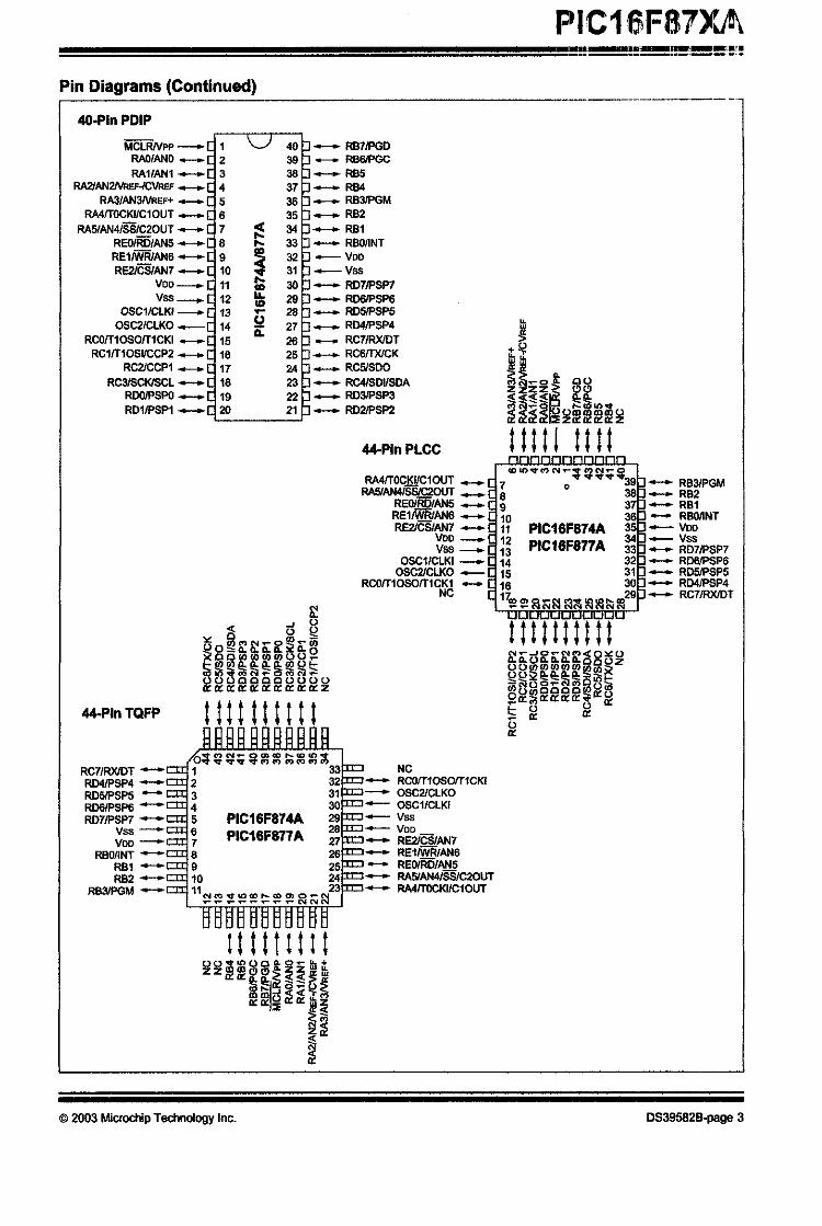
Pin Diagrams (Continued)
40-Pin PDIP
MCLR/VPPRAO/ANO
RA1/AN1RA2/AN2A/REF-/CVREF
RA3/AN3/VREF+
RA4/T0CKI/C1OUT
RA5/AN4/SS/C20UT
RE0/RD/AN5
RE1/WR/AN6
RE2/CS/AN7
VDD-
VSS.
OSC1/CLKI
OSC2/CLKO
RC0/T1OSO/T1CKI
RC1/T10SI/CCP2
RC2/CCP1
RC3/SCK/SCL
ROO/PSPO
RD1/PSP1
c 1 yj 40 3L" 2 39 3c 3 38 3
c 4 37 3
c 5 36 a
c 6 35 bc 7
r-
34 bc 8 33 bc 9 § 32 i
c 10 9 31 3c 11 OB 30 1c 12
U_(0 29 3
c 13 r-
0.
28 3
c 14 27 3c 15 26 3
c 16
17
25
24
b3
c 18 23 3c 19 22 3c 20 21 3
3 oloS££o:£i£P « m ft. a g^ ft. sg oOOOQDQQOO0:0:0:0:0:0:0:0:0:
00o:z
RB7/PGD
RB6/PGC
RB5
RB4
RB3/PGM
RB2
RB1
RBO/INT
VDD
VSS
RD7/PSP7
RD6/PSP6RD5/PSP5
RD4/PSP4
RC7/RX/DT
RCB/WCK
RC5/SD0
RC4/SDI/SDA
RD3/PSP3
RD2/PSP2
44-Pln PLCC
RA4/T0CKI/C1OUTRA5/AN4/SS/C20UT
RE0/RD/AN5RE1/WR/AN6
RE2/CS/AN7VDDVSS
0SC1/CLKI0SC2/CLK0
RC0/T1OSO/T1CK1NC
44-P.nTQFP \\\\\\\\\\
RC7/RX/DTRD4/PSP4
RD5/PSP5RD6/PSP6RD7/PSP7
Vss
VDDRBO/INT
RB1RB2
RB3/PGM
•6333 9\
PIC16F874A
PIC16F877A
3311=132 m-31 m-30HZ1-
291a-28 11=1-27IO-
26:°=1-25 n=)24 in-23 HU
fi-f T-x-r-i-NWI
UtttltUoojiijOQ S-2r ft izz
0:0:
CO h-lm or 5 <a: odS °='
© 2003 Microchip Technology Inc.
NGRC0/T1OSO/T1CKI
0SC2/CLK00SC1/CLKIVssVddRE2/CS/AN7
RE1/WR/AN6
RE0/RD/AN5RA5/AN4/SS/C20UT
RA4/T0CKI/C1OUT
•o a- QU
<<<<)£ ia.lOoooSajmolszo:Q:a:o:z
utti nilnnnnnnnnnnn
&
PIC16F874A
PIC16F877A
,29 3eesssisaKSBiS
RB3/PGMRB2RB1RBO/INTVDDVssRD7/PSP7RD6/PSP6RD5/PSP5RD4/PSP4RC7/RX/DT
UUUUUUUUUUU
twww£*-_l©^C'*CO<fWO
0.00,0.0.0.0002oorotptpcptoBmS
o£®ccccxu§ag% a. ao
DS39582B-page 3

1.0 DEVICE OVERVIEW
This document contains device specific informationabout the following devices:
• PIC16F873A
• PIC16F874A
• PIC16F876A
• PIC16F877A
PIC16F873A/876Adevices are available only in 28-pinpackages, white PIC16F874A/877A devices are available in 40-pin and 44-pin packages. All devices in thePIC16F87XA family share common architecture withthe following differences:
• The PIC16F873A and PIC16F874A have one-half
of the total on-chip memory of the PIC16F876Aand PIC16F877A
• The 28-pin devices have three I/O ports, while the40/44-pin devices have five
• The 28-pin devices have fourteen interrupts, whilethe 40/44-pin devices have fifteen
• The 28-pin devices have five A/D input channels,while the 40/44-pin devices have eight
• The Parallel Slave Port is implemented only onthe 40/44-pin devices
TABLE 1 -1: PIC16F87XA DEVICE FEATURES
The available features ara summarised in Table 1-1.
Block diagrams of the* PIC16F*;73A/876A andP1C16F874A/877A devices are provided in Figure 1-1and Figure 1-2, respectively. The pinouts for thesedevice families are listed in Table 1 -2 and Table 1 -3.
Additional information may be found m the PICmicro®Mid-Range Reference Manual (DS33023), which maybe obtained from your local Microchip Sales Representative or downloaded from the Microchip web site. TheReference Manual should be considered a complementary document to this data sheet and is highly recommended reading for a better understanding of the devicearchitecture and operation of the peripheral modules.
Key Features PIC16F873A PIC16F874A PIC16F876A PIC16F877A
Operating Frequency DC-20 MHz DC - 20 MHz DC-20 MHz DC - 20 MHz
Resets (and Delays) POR, BOR(PWRT, OST)
POR, BOR(PWRT, OST)
POR, BOR(PWRT, OST)
POR, BOR(PWRT, OST)
Flash Program Memory(14-bit words)
4K 4K 8K 8K
Data Memory (bytes) 192 192 368 368
EEPROM Data Memory (bytes) 128 128 256 256
Interrupts 14 15 14 15
I/O Ports Ports A, B, C PortsA,B,C,D,E Ports A, B, C PortsA,B,C,D,E
Timers 3 3 3 3
Capture/Compare/PWM modules 2 2 2 2
Serial Communications MSSP, USART MSSP, USART MSSP, USART MSSP, USART
Parallel Communications — PSP — PSP
10-bit Analog-to-Digital Module 5 input channels 8 input channels 5 input channels 8 input channels
Analog Comparators 2 2 2 2
Instruction Set 35 Instructions 35 Instructions 35 Instructions 35 Instructions
Packages 28-pin PDIP28-pin SOIC28-pin SSOP28-pin QFN
40-pin PDIP44-pin PLCC44-pin TQFP44-pin QFN
28-pin PDIP28-pin SOIC28-pin SSOP28-pin QFN
40-pin PDIP44-pin PLCC44-pin TQFP44-pin QFN
© 2003 Microchip Technology Inc. OS39562B-page 5

IGJRE1-1: PIC 16i:873A/876A BLOCK DIAGRAM
ProgramBus
RashProgramMemory
14/'
Instruction reg
%fc=£OSC1/CLKIOSC2/CLKO
TimerO
Data EEPROM
V
InstructionDecode& \C=^>
Control
TimingGeneration C=£
Timerf
II
CCP1.2
Direct Addr
I
RAMAddrW~?5~9/ AddrMUX\
SynchronousSerial Port
USART
PORTA
PORTB
Comparator
RAO/ANO
RA1/AN1
RA2/AN2/VREF-/CVREF
RA3/AN3A/REF+RA4/T0CKI/C1OUT
RA5/AN4/SS/C20UT
RBO/INT
R81
RB2
RB3/PGMRB4
RB5
RB6/PGC
RB7/PGD
RC0/T1OSO/nCKIRC1/T10SI/CCP2
RC2/CCP1
RC3/SCK/SCLRC4/SDI/SDA
RC5/SDORC6/TX/CKRC7/RX/DT
VoltageReference
Device Program Flash Data Memory Data EEPROM
PIC16F873A 4K words 192 Bytes 128 BytesPIC16F876A 8K words 368 Bytes 256 Bytes
Note 1: Higherorder bits are fromthe Status register.
DS39582B-page 6 © 2003 Microchip Technology Inc.

FIGURE 1-2: PIC16F874A/877A BLOCK DIAGRAM
Data Bus
Program 14 ,•Bus RAMAddr*1' & g
/ Addr MUX \
E3C=0OSC1/CLKIOSC2/CLKO
Timerf)
£InstructionDecode &
Control
TimingGeneration
c=o
C^>
Direct Addr 7/
Power-upTimer
OscillatorStart-up Timer
Power-onReset
WatchdogTimer
Brown-out
Reset
In-CircuitDebugger
Low-VoltageProgramming
MCLR Vdd, Vss
TimeM Timer2
I I
, „ Indirect8>f Addr
FSRreg <3=d
r=DH Status reg jp=
3,
B
, 8
\ MUX /
ALU /
£Wreg
10-bit A/D
II
PORTA
PORTD
• —*
* —«
> —*
• —m
• —»
• —»
PORTE
n
•NUBS
RAO/ANO
RA1/AN1
RA2/AN2/Vrei~/CVref
SA3/AN3/VREF+
RA4/T0CK1/C1OUT
RA5/AN4/SS/C20UT
RBO/INT
RB1
RB2
RB3/PGM
RB4
R85
RB6/PGCRB7/PGD
RC0/T1OSO/T1CKIRC1/T10SI/CCP2
RC2/CCP1
RC3/SCK/SCLRC4/SDI/SDA
RC5/SDO
RC6/TX/CK
RC7/RX/DT
RDO/PSPORD1/PSP1
RD2/PSP2
RD3/PSP3RD4/PSP4
RD57PSP5
RD6/PSP6
RD7/PSP7
'—H3 RE0/RD/AN5
•~HEI RE1/WWAN6•—{El RE2/CS/AN7
ParallelSlave Port
I
Data EEPROM CCP1.2Synchronous
Serial PortUSART Comparator
VoltageReference
Device Program Flash Data Memory Data EEPROM
PIC16F874A 4K words 192 Bytes 128 BytesPIC16F877A 8K words 368 Bytes 256 Bytes
Note 1: Higher orderbitsare from the Status register.
© 2003 Microchip TechnologyInc. DS39582B-page 7

P"C16F87XA
TAF>LE1--2: PHS16F87:)A/B76A PINOUT DESCRIPTION
Pin NamePDJP.SOIG,SSOF Pin#
QFN
Pin#
l/O/P
TypeBuffer
TypeDescription
OSG1/CLKI
0SC1
CLKI
9 6
1
I
ST/CMOS*3* Oscillator crystal or external dock input.Oscillator crystal input or external clock source input. STbuffer when configured in RC mode; otherwise CMOS.External clock source input. Always associated with pinfunction OSC1 (see OSC1/CLKI, OSC2/CLKO pins).
0SC2/CLK0
0SC2
CLKO
10 7
0
0
Oscillator crystal or clock output.Oscillator crystal output. Connects to crystal or resonatorin Crystal Oscillator mode.In RC mode, OSC2 pin outputs CLKO, which has 1/4 thefrequency of OSC1 and denotes the instruction cycle rate.
MCLRA/PP
MCLR
VPP
1 26
1
P
ST Master Clear (input) or programming voltage (output).Master Clear (Reset) input. This pin is an active low Resetto the device.
Programming voltage input.
PORTA is a bidirectional I/O port.
RAO/ANO
RAO
ANO
2 27
I/O
1
TTL
Digital I/O.Analog input 0.
RA1/AN1
RA1
AN1
3 28
I/O
1
TTL
Digital I/O.Analog input 1.
RA2/AN2/VREF-/
CVREF
RA2
AN2
VREF-
CVREF
4 1
I/O
1
i
0
TTL
Digital I/O.Analog input 2.A/D reference voltage (Low) input.Comparator Vref output.
RA3/AN3/VREF+
RA3
AN3
VREF+
5 2
I/O
1
1
TTL
Digital I/O.Analog input 3.A/D reference voltage (High) input.
RA4/TOCKI/C10UT
RA4
TOCKI
C10UT
6 3
I/O
1
0
ST
Digital I/O - Open-drain when configured as output.TimerOexternal clock input.Comparator 1 output.
RA5/AN4/SS/C20UT
RA5
AN4
SS
C20UT
7 4
I/O
1
1
0
TTL
Digital I/O.Analog input 4.SPI slave select input.Comparator 2 output.
Legend: I = input O = output I/O - input/output P = power— = Not used TTL = TTL input ST - Schmitt Trigger input
Note 1: This buffer is a Schmitt Trigger input when configured as the external interrupt2: This buffer is a Schmitt Trigger input when used in Serial Programming mode.3: This buffer is a Schmitt Trigger input when configured in RC Oscillator mode and a CMOS input otherwise.
DS39582B-page 8 © 2003 Microchip Technology Inc.

TABLE 1-2: PIC16F873A/876A PINOUT DESCRIPTION (CONTINUED)
Pin NamePDIP,SOIC,SSOPPin#
QFNPin#
l/O/P
TypeBuffer
TypeDescription
PORTB is a bidirectional I/O port. PORTB can be softwareprogrammed for internal weak pull-ups on all inputs.
RBO/INT 21 18 TTL/ST<1>RBO I/O Digital I/O.INT t External interrupt.
RB1 22 19 I/O TTL Digital I/O.
RB2 23 20 I/O TTL Digital I/O.
RB3/PGM 24 21 TTL
RB3 I/O Digital I/O.PGM I Low-voltage (single-supply) ICSP programming enable pin.
RB4 25 22 I/O TTL Digital I/O.
RB5 26 23 i/O TTL Digital I/O.
RB6/PGC 27 24 TTL/ST<2>RB6 I/O Digital I/O.PGC I In-circuit debugger and ICSP programming clock.
RB7/PGD 28 25 TTL/ST*2'RB7 I/O Digital I/O.PGD I/O In-circuit debugger and ICSP programming data.
PORTC is a bidirectional I/O port.RC0/T1OSO/T1CKI 11 8 ST
RCO I/O Digital I/O.T10SO 0 Timerl oscillator output.T1CKI I Timerl external clock input.
RC1/T10SI/CCP2 12 9 ST
RC1 I/O Digital I/O.T10SI I Timerl oscillator input.CCP2 I/O Capture2input, Compare2output, PWM2 output.
RC2/CCP1 13 10 ST
RC2 I/O Digital I/O.CCP1 I/O Capture1 input, Comparel output, PWM1 output
RC3/SCK/SCL 14 11 ST
RC3 f/O Digital I/O.SCK I/O Synchronous serial clock input/output for SPI mode.SCL I/O Synchronous serial clock input/output for v^C mode.
RC4/SDI/SDA 15 12 ST
RC4 I/O Digital I/O.SDI I SPI data in.SDA I/O ^C data I/O.
RC5/SDO 16 13 ST
RC5 I/O Digital I/O.SDO 0 SPI data out.
RC6/TX/CK 17 14 ST
RC6 I/O Digital I/O.TX 0 USART asynchronous transmit.CK I/O USART1 synchronous clock.
RC7/RX/DT 18 15 ST
RC7 I/O Digital I/O.RX ! USART asynchronous receive.DT I/O USART synchronous data.
VSS 8,19 5,6 P— Ground reference for logicand I/O pins.
VDD 20 17 p — Positive supply for logic and I/O pins.
Legend: I= input 0 =output I/O = input/output P = power—= Notused TTL • TTL input ST =SchmittTrigger input
Note 1: This buffer is a Schmitt Trigger input when configured as the external interrupt.2: Thisbuffer is a SchmittTrigger inputwhen used inSerial Programming mode.3: This buffer isa Schmitt Trigger input when configured in RC Oscillator mode anda CMOS input otherwise.
© 2003 Microchip Technology Inc. OS39582B-page 9

AH E 1 -3: PIC16F874A/877A PINOUT DESCRIPTION
Pin NamePDIP
Pin#
PLCC
F'in#
TQFP
Pin#
QFN
Pln#
i/O/P
TypeBuffer
TypeDescription
0SC1/CLKI
0SC1
CLKI
13 14 30 32
I
I
ST/CMOS*** Oscillator crystal or extemal clock input.Oscillator crystal input or extemal clock sourceinput. ST buffer when configured in RC mode;otherwise CMOS.
Extemal clock source input. Always associatedwith pin function OSC1 (see OSC1/CLKI,OSC2/CLKO pins).
OSC2/CLK0
0SC2
CLKO
14 15 31 33
0
0
Oscillator crystal or clock output.Oscillator crystal output.Connects to crystal or resonator in CrystalOscillator mode.
In RC mode, OSC2 pin outputs CLKO, whichhas 1/4 the frequency of OSC1 and denotes theinstruction cycle rate.
MCLRA/PP
MCLR
Vpp
1 2 18 18
I
P
ST Master Clear (input)or programming voltage (output).Master Clear (Reset) input. This pin is an activelow Reset to the device.
Programming voltage input
RAO/ANO
RAO
ANO
RA1/AN1
RA1
AN1
RA2/AN2/VREF-/CVREF
RA2
AN2
VREF-
CVREF
RA3/AN3A/REF+
RA3
AN3
VREF+
RA4/TOCKI/C10UT
RA4
TOCKI
C10UT
RA5/AN4/SS/C20UT
RA5
AN4
SSC20UT
2
3
4
5
6
7
3
4
5
6
7
8
19
20
21
22
23
24
19
20
21
22
23
24
I/O
I
I/O
I
I/O
I
I
0
I/O
I
I
I/O
I
0
I/O
I
I
o
TTL
TTL
TTL
TTL
ST
TTL
PORTAis a bidirectional I/O port.
Digital I/O.Analog input 0.
Digital I/O.Analog input 1.
Digital I/O.Analog input 2.A/Dreference voltage (Low)input.Comparator Vref output.
Digital I/O.Analog input 3.A/Dreference voltage (High)input.
Digital I/O- Open-drain when configured asoutput.TimerOextemal clock input.Comparator 1 output.
Digital I/O.Analog input 4.SPI slave select input.Comparator 2output. |
Legend:
Note 1
2
3
I = input O = output I/O— = Not used TTL = TTL input STThis buffer is a Schmitt Trigger input whenThis buffer is a Schmitt Trigger input whenThis buffer is a Schmitt Trigger input when
DS39582B-page 10
= input/output P *= power= Schmitt Trigger inputconfigured as the extemal interrupt.used in Serial Programming mode.configured in RC Oscillator mode and a CMOS input otherwise.
© 2003 Microchip Technology Inc.

TABLE 1-3: PIC16F874A/877A PINOUT DESCRIPTION (CONTINUED)
Pin NamePDIP
Pin#
PLCC
Pin#
TQFPPin#
QFN
Pin#
l/O/P
TypeBuffer
TypeDescriptii:
RBO/INT
RBO
INT
RB1
RB2
RB3/PGM
RB3
PGM
RB4
RB5
RB6/PGC
RB6
PGC
RB7/PGD
RB7
PGD
Legend:
Note 1
2
3
33
34
35
36
37
38
39
40
36
37
38
39
41
42
43
44
9
10
11
14
15
16
17
10
11
12
14
15
16
17
I/O
I
I/O
I/O
I/O
I
f/O
I/O
I/O
I/O
I/O
TTL/ST<1>
TTL
TTL
TTL
TTL
TTL
TTUST»
ttl/stW
PORTB is a bidirectional I/O port. PORTB can besoftware programmed for internal weak pull-upon allinputs.
Digital I/O.Extemal interrupt.
DigitalI/O.
Digital I/O.
Digital I/O.Low-voltage ICSP programming enable pin.
Digital i/O.
Digital I/O.
Digital I/O.In-circuit debugger and ICSP programmingdock.
Digital I/O.In-circuit debugger and ICSP programming data.
I - input 0 = output I/O— = Not used TTL = TTL input STThis buffer is a Schmitt Trigger input whenThis buffer is a Schmitt Trigger input whenThis bufferis a SchmittTrigger inputwhen
= input/output P * power= Schmitt Trigger input
configuredas the external interrupt.used in Serial Programmingmode.configured in RCOscillator mode and a CMOS inputotherwise.
© 2003 Microchip Technology Inc. DS39582B-page 11

PIC16F87XA
TABLE 1-3: PIC16F874A/877A PINOUT C)ESCRIPTION (CONTINUED)PDIP PLCC TQFP QFN l/O/P Buffer
Pin Namei?in# Pin# Pin# Pfnff Type Type
Description
PORTC is a bidirectional I/O port.
RC0/T1OSO/T1CKI 15 16 32 34 ST
RCO I/O Digital I/O.T10SO 0 Timerl oscillator output.T1CKI I Timerl extemal clock input.
RC1/T10SI/CCP2 16 18 35 35 ST
RC1 I/O Digital I/O.T10SI I Timerl oscillator input.CCP2 I/O Capture2 input Compare2 output PWM2 output.
RC2/CCP1 17 19 36 36 ST
RC2 I/O Digital I/O.CCP1 I/O Capturel input, Comparel output, PWM1 output.
RC3/SCK/SCL 18 20 37 37 ST
RC3 I/O DigitalI/O.SCK I/O Synchronous serial clock input/output for SPI
mode.
SCL I/O Synchronous serial clock input/output for l2Cmode.
RC4/SDI/SDA 23 25 42 42 ST
RC4 I/O Digital I/O.SDi i SPI data in.
SDA I/O I2C data I/O.
RC57SD0 24 26 43 43 ST
RC5 I/O Digital I/O.SDO 0 SPI data out.
RC6/TX/CK 25 27 44 44 ST
RC6 I/O Digital I/O.TX 0 USART asynchronous transmit.CK I/O USART1 synchronous clock.
RC7/RX/DT 26 29 1 1 ST
RC7 I/O Digital I/O.RX I USARTasynchronous receive.DT I/O USART synchronous data.
Legend: I = input O = output— = Not used TTL - TTL input
Note 1: This buffer is a Schmitt Trigger input2: This buffer is a Schmitt Trigger Input3: This buffer is a Schmitt Trigger input
DS39582B-page 12
I/O = input/output P = powerST = Schmitt Trigger input
when configured as the extemal interruptwhen used in Serial Programming mode.when configured in RC Oscillator mode and a CMOS input otherwise.
© 2003 Microchip Technology Inc.

TABLE 1-3: PK;16F8"r4A/877A PINOUT DESCR PTION (CONTINUED)
Pin NamePDIP
Pin#
PLCC
Pln#
TQFP
Pin#
QFN
Pin#
l/O/P
TypeBuffer
TypeDescription
PORTD is a bidirectional I/O port or Parallel SlavePort when interfacing to a microprocessor bus.
RDO/PSPO 19 21 38 38 ST/TTL<3>RDO I/O Digital I/O.PSPO I/O Parallel Slave Port data.
RD1/PSP1 20 22 39 39 st/ttl'3'RD1 I/O Digital I/O.PSP1 I/O Parallel Slave Port data.
RD2/PSP2 21 23 40 40 ST/TTL<3>RD2 I/O Digital I/O.PSP2 I/O Parallel Slave Port data.
RD3/PSP3 22 24 41 41 ST/TT|_(3)
RD3 I/O Digital I/O.PSP3 I/O Parallel Slave Port data.
RD4/PSP4 27 30 2 2 ST/TTL<3>RD4 I/O Digital I/O.PSP4 I/O Parallel Slave Port data.
RD5/PSP5 28 31 3 3 st/ttl*3>RD5 I/O Digital I/O.PSP5 I/O Parallel Slave Port data.
RD6/PSP6 29 32 4 4 ST/TTL<3>RD6 I/O Digital I/O.PSP6 I/O Parallel Slave Port data.
RD7/PSP7 30 33 5 5 st/ttl'3>RD7 I/O Digital I/O.PSP7 I/O Parallel Slave Port data.
PORTE is a bidirectional I/O port.
RE0/RD/AN5 8 9 25 25 st/ttl'3'REO I/O Digital I/O.RD I Read control for Parallel Slave Port.AN5 I Analog input 5.
RE1/WR/AN6 9 10 26 26 st/ttl'3'RE1 I/O Digital I/O.WR I Write control for Parallel Slave Port.AN6 I Analog input 6.
RE2/CS/AN7 10 11 27 27 ST/TTL<3>RE2 I/O Digital I/O.CS I Chip select control for Parallel Slave Port.AN7 I Analog input 7.
VSS 12,31 13,34 6,29 6,30,31
p — Ground reference for logic and I/O pins.
VDD 11,32 12,35 7,28 7,8,
28,29
p — Positive supply for logic and I/O pins.
NC — 1,17,
28,40
12,13,33,34
13 —— These pins are not internally connected. These pins
should be left unconnected.
Legend: I = input O = output— = Not used TTL = TTL input
Note 1: This buffer is a Schmitt Trigger input2: This buffer is a Schmitt Trigger input3: This buffer is a Schmitt Trigger input
© 2003 Microchip Technology Inc.
I/O = input/output P * powerST = Schmitt Trigger input
when configured as the extemal interrupt,when used in Serial Programming mode.when configured in RC Oscillator mode and a CMOS input otherwise.
DS39582B-page 13

11.0 ANALOG-TO-DIGITAL
CONVERTER (A/D) MODULE
The Analog-to-Digital (A/D)Converter module has fiveinputs for the 28-pin devices and eight for the 40/44-pindevices.
The conversion of an analog input signal results in acorresponding 10-bit digital number. The A/D modulehas high and low-voltage reference input that is software selectable to some combination of Vdd, Vss, RA2orRA3.
The A/D converter has a unique feature of being ableto operate while the device is in Sleep mode. Tooperate in Sleep, the A/D clock must be derived fromthe A/D's internal RC oscillator.
The A/D module has four registers. These registers ©re:
• A/D Result High Register (ADRESH)
• A/D Result Low Register (ADRESL)
• A/D Control Register 0 (ADCONO)
• A/D Control Register 1 (ADCON1)
The ADCONO register, shown in Register 11-1, controls the operation of the A/D module. The ADCON1register, shown in Register 11-2, configures the functions of the port pins. The port pins can be configuredas analog inputs (RA3 can also be the voltagereference) or as digital I/O.
Additional informationon using the A/Dmodule can befound in the PICmicro® Mid-Range MCU FamilyReference Manual (DS33023).
REGISTER 11-1: ADCONO REGISTER (ADDRESS 1Fh)RAV-0 R/W-0 R/W-0 R/W-0 R/W-0 R/W-0 U-0 RW-0
ADCS1 ADCSO CHS2 CHS1 CHSO GO/DONE L_ ADON
bit 7
bit 7-6 ADCS1 :ADCS0: A/D Conversion Clock Select bits (ADCONO bits in bold)
bitO
bit 5-3
bit 2
bit 1
bitO
ADCON1
<ADCS2>ADCONO
<ADCS1:ADCS0>Clock Conversion
0 00 Fosc/2
0 01 Fosc/8
0 10 F0SC/32
0 11 Frc (clock derived from the internal A/D RC oscillator)
1 00 FOSC/4
1 01 FOSC/16
1 10 FOSC/64
1 11 Frc (clock derived from the internal A/D RC oscillator)
CHS2:CHS0: Analog Channel Select bits000 = Channel 0 (ANO)001 = Channel 1 (AN1)010 = Channel 2 (AN2)011 = Channel 3 (AN3)100 = Channel 4 (AN4)101 = Channel 5 (AN5)110 = Channel 6 (AN6)ill = Channel 7 (AN7)
Note: The PIC16F873A/876A devices only implement A/D channels 0 through 4; theunimplemented selections are reserved. Do not select any unimplemented
^^^ channels with these devices.GO/DONE: A/D Conversion Status bit
When ADON = l:
l = A/D conversion in progress (setting this bit starts the A/Dconversion which is automaticallycleared by hardware when the A/D conversion is complete)
0 = A/D conversion not in progressUnimplemented: Read as 'o'
ADON: A/D On bit
1 = A/D converter module is powered upo = A/Dconverter module is shut-off and consumes no operating current
Legend:
R = Readable bit W - Writable bit U = Unimplemented bit, read as '0'
- n = Value at POR '1' = Bit is set '0' = Bit is cleared x = Bit is unknown
© 2003 Microchip Technology Inc. DS39582B-page 127

REGISTER 11-2: ADC0N1 REGISTER (ADDRESS 9Fh)
bit 7
bit 6
bit 5-4
bit 3-0
DS39582B-page 128
R/W-0 R/W-0 U-0 U-0 R/W-0 R/W-0 R/W-0 R/W-0
ADFM ADCS2 — •.— PCFG3 PCFG2 PCFG1 PCFGO
bit 7
ADFM: A/D Result Format Select bit
l = Right justified. Six(6) Most Significant bitsofADRESH are read as 'o'.o = Leftjustified. Six (6) Least Significant bits of ADRESL are read as 'o'.ADCS2: A/DConversion Clock Select bit (ADCON1 bits in shaded area and in bold)
bitO
ADCON1
<ADCS2>
ADCONO
<ADCS1:ADCS0>Clock Conversion
0 00 Fosc/2
0 01 Fosc/8
0 10 Fosc/32
0 11 Frc (clockderived fromthe internalA/D RCoscillator)1 00 FOSC/4
1 01 Fosc/16
i: 10 FOSC/64
i 11 Frc (clockderived fromthe internalA/D RC oscillator)
Unimplemented: Read as '0'
PCFG3:PCFG0: A/D Port Configuration Control bits
PCFG
<3:0>AN7 AN6 AN5 AN4 AN3 AN2 AN1 ANO VREF+ VREF- C/R
0000 A A A A A A A A VDD VSS 8/0
0001 A A A A VREF+ A A A AN3 Vss 7/1
0010 D D D A A A A A VDD vss 5/0
0011 D D D A VREF+ A A A AN3 Vss 4/1
0100 D D D D A D A A VDD vss 3/0
0101 D D D D VREF+ D A A AN3 vss 2/1
Ollx D D D D D D D D — — 0/0
1000 A A A A VREF+ VREF- A A AN3 AN2 6/2
1001 D D A A A A A A VDD VSS 6/0
1010 D D A A VREF+ A A A AN3 Vss 5/1
1011 D D A A VREF+ VREF- A A AN3 AN2 4/2
1100 D D D A VREF+ VREF- A A AN3 AN2 3/2
1101 D D D D VREF+ VREF- A A AN3 AN2 2/2
1110 D D D D D D D A VDD Vss 1/0
1111 D D D D VREF+ VREF- D A AN3 AN2 1/2
A = Analog inputC/R = # of analog
D = Digital I/Oinput channels/# of A/D voltage references
Legend:
R = Readable bit W = Writable bit U = Unimplemented bit, read as '0'
- n = Value at POR '1' = Bit is set '0' = Bit is cleared x = Bit is unknown
Note: On any device Reset, the port pins that are multiplexed with analog functions (ANx)are forced to be an analog input.
© 2003 Microchip Technology Inc.

The ADRESH:ADRESL registers contain the 10-bitresult of the A/D conversion. When the A/D conversion
is complete, the result is loaded into this A/D Resultregister pair, the GO/DONE bit (ADCON0<2>) is clearedand the A/D interrupt flag bit ADIF is set The blockdiagram of the A/D module is shown in Figure 11-1.
After the A/D module has been configured as desired,the selected channel must be acquired before the conversion is started. The analog input channels musthave their corresponding TRIS bits selected as inputs.
To determine sample time, see Section 11.1 "A/DAcquisition Requirements''. After this acquisitiontime has elapsed, the A/D conversion can be started.
To do an A/D Conversion, follow these steps:
1. Configure the A/D module:
- Configure analog pins/voltage reference anddigital I/O (ADCON1)
• Select A/D input channel (ADCONO)• Select A/D conversion clock (ADCONO)
• Turn on A/D module (ADCONO)
FIGURE 11-1: A/D BLOCK DIAGRAM
VAIN
(Input Voltage)
A/DConverter
VREF+
(ReferenceVoltage)
VREF"
(ReferenceVoltage)
Note 1: Not available on 28-pin devices.
© 2003 Microchip Technology Inc.
Vdd
OX.
iirr"PCFG3:PCFG0
iiir v»PCFG3:PCFG0
3.
4.
5.
6.
7.
Configure A/D interrupt (ifdesired):
• Clear ADIF bit
• SetADIEbit
• SetPEIEbit
• SetGIEbit
Wait the required acquisition time.
Start conversion:
• Set GO/DONE bit (ADCONO)
Wait for A/Dconversion to complete by either:• Polling for the GO/DONE bit to be cleared
(interrupts disabled); OR- Waiting for the A/D interrupt
Read A/D Result register pair(ADRESH.ADRESL), clear bit ADIF if required.
For the next conversion, go to step 1 or step 2as required. The A/D conversion time per bit isdefined as Tad.
CHS2:CHS0
V
V
V
u—o
V
111
no
101
100
on
10
001
00v*
^ RE2/AN7*1*
S? RE1/AN6<1>
X REQ/ANSM
X RA5/AN4
^? RA3/AN3A/REF+
S? RA2/AN2/VREF-
S
E
RA1/AN1
RAO/ANO
DS39582B-page 129
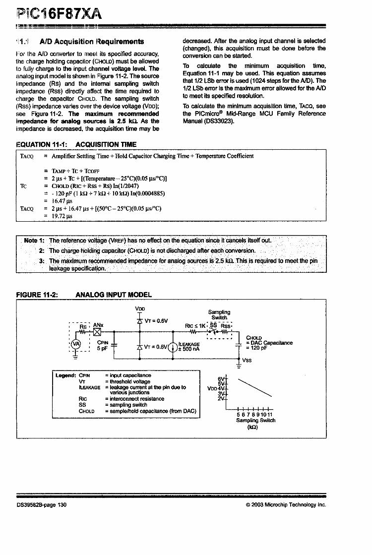
• '\: A/D Acquisition Requirements
For She A/D converter to meet its specified accuracy,the charge holding capacitor (Chold) must be allowedto fully charge to the input channel voltage level. Theanalog input model is shown in Figure 11-2. The sourceimpedance (Rs) and the internal sampling switchimpedance (Rss) directly affect the time required tocharge the capacitor Chold. The sampling switch(Rss) impedance varies over the device voltage (Vdd);see Figure 11-2. The maximum recommendedimpedance for analog sources is 2.5 ku As theimpedance is decreased, the acquisition time may be
decreased. After the analog input channel is selected(changed), this acquisition must be done before theconversion can be started.
To calculate the minimum acquisition time,Equation 11-1 may be used. This equation assumesthat 1/2 LSb error is used (1024 steps for the A/D). The1/2 LSb error is the maximum error allowed for the A/D
to meet its specified resolution.
To calculate the minimum acquisition time, Tacq, seethe PICmicro® Mid-Range MCU Family ReferenceManual (DS33023).
EQUATION 11-1: ACQUISITION TIME
Tacq = Amplifier Settling Time+ HoldCapacitor Charging Time+ Temperature Coefficient
= Tamp + Tc + Tcoff
= 2 US + TC + [(Temperature - 25°C)(0.05 us/°C)]TC = Chold (Rich- Rss + Rs)In(l/2047)
= -120pF(lkn + 7kiJ+10kS2)In(0.0004885)= 16.47 us
Tacq = 2 us + 16.47 us + [(50°C - 25°C)(0.05 us/°C)= 19.72 us
Note 1: The reference voltage (Vref) has no effect on the equation since rtcancels itself out.
2: The charge holding capacitor (Chold) is not discharged after each conversion.
3: The maximum recommended impedance for analog sources is 2.5 kit This is required to meet the pinleakage specification.
FIGURE 11-2: ANALOG INPUT MODEL
VDD
VT = 0.6V
SamplingSwitch
Ricsik-SS'rss;~-MV--i*^«-W:t--i
Chold-~ - DAC Capacitance— -120pF
fVA) ' CPIN _ _' 5pF
IVT
JlLEAKAGE±500nA=0.6VQ
Legend: Cpin - input capacitanceVT = threshold voltage(LEAKAGE = leakage cunent at the pin due to
various junctionsRlC = interconnect resistance
SS - sampling switchChold = sample/hold capacitance (from DAC)
DS395B2B-page 130
6V-5V--
VDD4V -3V--2V--
'Vss
I I I I I I I567891011Sampling Switch
(kfl)
© 2003 Microchip Technology Inc.

11.2 Selecting the A/D ConversionClock
The A/D conversion time per bit is defined as Tad. TheA/D conversion requires a minimum 12 Tad per 10-bitconversion. The source of the A/D conversion clock is
software selected. The seven possible options for Tadare:
• 2Tosc
• 4Tosc
• 8Tosc
• 16Tosc
• 32Tosc
• 64Tosc
• Internal A/D module RC oscillator (2-6 \i$)
For correct A/D conversions, the A/D conversion clock(Tad) must be selected to ensure a minimum Tad timeof 1.6 us.
Table 11-1 shows the resultant Tad times derived from
the device operating frequencies and the A/D clocksource selected.
11.3 Configuring Analog Port Pins
The ADCON1 and TRIS register:-! control the operationof the A/D port pins. The port pins that are desired asanalog inputs must have their corresponding TRIS bitsset (input). Ifthe TRIS bit is cleared (output), the digitaloutput level (Voh or Vol) will be converted.
The A/D operation is independent of the state of theCHS2:CHS0 bits and the TRIS bits.
Note 1: When reading the port register, any pinconfigured as an analog input channel willread as cleared (a low level). Pins configured as digital inputs will convert an analoginput. Analog levels on a digitally configured input will not affect the conversionaccuracy.
2: Analog levels on any pin that is defined asa digital input (including the AN7:AN0pins) may cause the input buffer to consume current that is out of the device
specifications.
TABLE 11 -1: Tad vs. MAXIMUM DEVICE OPERATING FREQUENCIES (STANDARD DEVICES (F))
AD Clock Source (Tad)Maximum Device Frequency
Operation ADCS2:ADCS1:ADCS0
2TOSC 000 1.25 MHz
4Tosc 100 2.5 MHz
8TOSC 001 5 MHz
16T0SC 101 10 MHz
32 Tosc 010 20 MHz
64Tosc 110 20 MHz
RC<1'2'3> xll (Note 1)
Note 1: The RC source has a typicalTad time of 4 us but can vary between 2-6 us.2: When the device frequencies are greater than 1 MHz, the RC A/D conversion clocksource is only
recommended for Sleep operation.
3: For extended voltage devices (LF), please refer to Section 17.0 "Electrical Characteristics".
© 2003 Microchip Technology Inc. DS39582B-page 131

II A/D Conversions
Clearing the GO/DONE bit during a conversion willabort the current conversion. The A/D Result registerpair will NOT be updated with the partially completedA/D conversion sample. That is, the ADRESH:ADRESLregisters will continue to contain the value of the lastcompleted conversion (or the last value written to theADRESH:ADRESL registers). Afterthe A/Dconversion
FIGURE 11-3: A/D CONVERSION TAD CYCLES
is aborted, the next acquisition on the selected channelis automatically started. The GO/DONE bit can then beset to start the conversion.
In Figure 11-3, after the GO bit is set, the first timesegment has a minimum ofTcYand a maximum of Tad.
Note: The GO/DONE bit should NOT be set in
the same instruction that turns on the A/D.
TCYtoTAD| TAD1 t TAD2 | TAD3 t TA04 | Tad5 l TAD6 | Tad7 | Tad8 ( TAD9 JAD10 TAD11t b9 b8 b7 b6 D5 b4 b3 b2 b1
Conversion starts
Holding capacitor is disconnected fromanalog input(typically 100 ns)
Set GO bit
11.4.1 A/D RESULT REGISTERS
The ADRESH:ADRESL register pair is the locationwhere the 10-bit A/D result is loaded at the completionof the A/Dconversion. This register pair is 16 bits wide.The A/D modulegives the flexibility to leftor rightjustifythe 10-bit result in the 16-bit result register. The A/D
FIGURE 11-4: A/D RESULT JUSTIFICATION
bO
ADRES is loaded
GO bit is cleared
ADIF bit is set
Holding capacitor is connected to analog input
Format Select bit (ADFM) controls this justification.Figure 11-4 shows the operation of the A/D resultjustification. The extra bits are loaded with 'o's. Whenan A/Dresult will not overwrite these locations (A/D disable), these registers may be used as two generalpurpose 8-bit registers.
10-bit Result
ADFM = 1
^K.
7 2107 0
0000 00 ;
ADRESH
V
ADRESL
10-bit Result
Right Justified
DS39582B-page 132
ADFM = o
0765
I 000000
Y V
ADRESH ADRESL
10-bit Result
Left Justified
© 2003 Microchip Technology inc.

11.5 A/D Operation During Sleep
The A/D module can operate during Sleep mode. Thisrequires that the A/D clock source be set to RC(ADCS1:ADCS0 = 11). When the RC clock source isselected, the A/D module waits one instruction cyclebefore starting the conversion. This allows the sleepinstruction to be executed which eliminates all digitalswitching noise from the conversion. When the conversion is completed, the GO/DONE bit willbe cleared andthe result loaded into the ADRES register. If the A/Dinterrupt is enabled, the device will wake-up fromSleep. Ifthe A/D interrupt is not enabled, the A/D module will then be tunned off, although the ADON bit willremain set.
When the A/D clock source is another clock option (notRC), a sleep instruction will cause the present conversion to be aborted and the A/D module to be turned off,though the ADON bit will remain set.
Turning off the A/D places the A/D module in its lowestcunent consumption state.
Note: For the A/.) module to operate in Sleep,the A/D clock source must be set to RC
(ADCS1:ADCS0 = 11). To allow the conversion to occur during Sleep, ensure thesleep instruction immediately follows theinstruction that sets the GO/DONE bit.
11.6 Effects of a Reset
A device Reset forces all registers to their Reset state.This forces the A/D module to be turned off and anyconversion is aborted. All A/D input pins are configuredas analog inputs.
The value that is in the ADRESH:ADRESL registers isnot modified for a Power-on Reset. The
ADRESH:ADRESL registers will contain unknown dataafter a Power-on Reset.
TABLE 11-2: REGISTERS/BITS ASSOCIATED WITH A/D
Address Name Bit 7 Bit6 Bit 5 Bit 4 Bit 3 Bit 2 Bitl BitOValue on
POR, BOR
Value on
MCLR.WDT
0Bh,8Bh,
10Bh,18BhINTCON GE PEIE TMROIE INTE RBIE TMROIF INTF RBIF 0000 OOOx 0000 OOOu
OCh PIR1 PSPIF*1' ADIF RCIF TXJF SSPIF CCP1IF TMR2IF TMR1IF 0000 0000 0000 0000
8Ch PIE1 PSPIE*1' ADIE RCIE TXIE SSPIE CCP1IE TMR2IE TMRUE 0000 0000 0000 0000
1Eh ADRESH A/DResult Register HighByte xxxx xxxx uuuu uuuu
9Eh ADRESL A/DResult Register LowByte xxxx xxxx uuuu uuuu
1Fh ADCONO ADCS1 ADCSO CHS2 CHS1 CHSO GO/DONE — . ADON 0000 00-0 0000 00-0
9Fh ADCON1 ADFM ADCS2 _ _ PCFG3 PCFG2 PCFG1 PCFGO 00-- 0000 00-- 0000
85h TRISA •_^—! - PORTAData Direction Register --11 1111 --11 1111
05h PORTA — — •- PORTAData Latch when written:PORTApins when read --Ox 0000 ~-0u 0000
89h<1> TRISE IBF OBF IBOV PSPMODE . _ PORTE Data Direction bits 0000 -111 0000 -111
09h<1> PORTE — — — — " — RE2 RE1 REO -XXX -uuu
Legend:Note 1:
x = unknown, u = unchanged, - = unimplemented, read as 'o'. Shaded cells are not used for A/Dconversion.These registers are not available on 28-pin devices.
© 2003 MicrochipTechnology Inc. DS39582B-page 133

9-4323; Rev 11; 2/03
11. 3~l VI+5V-Powered, Multichannel RS-232
Drivers/Receivers
.General Descriptionhe MAX220-MAX249 family of line drivers/receivers isitended for all EIA/T1A-232E and V.28/V.24 communica-ons interfaces, particularly applications where ±12V isot available.
hese parts are especially useful in battery-powered sys-3ms, since their low-power shutdown mode reducesower dissipation to less than 5uW. The MAX225,1AX233, MAX235, and MAX245/MAX246/MAX247 useo external components and are recommended for appli-ations where printed circuit board space is critical.
ApplicationsPortable Computers
Low-Power Modems
Interface Translation
Battery-powered RS-232 Systems
Multidrop RS-232 Networks
Features
Superior to Bipolar♦ Operate from Single +5V Power Supply
(+5V and +12V—MAX231/MAX239)
♦ Low-Power Receive Mode in Shutdown(MAX223/MAX242)
♦ Meet All E1A/TIA-232E and V.28 Specifications♦ Multiple Drivers and Receivers
4 3-State Driver and Receiver Outputs♦ Open-Line Detection (MAX243)
Ordering InformationPART TEMP RANGE PIN-PACKAGE
MAX220CPE 0°C to +70°C 16 Plastic DIP
MAX220CSE 0°C to +70°C 16 Narrow SO
MAX220CWE 0°Cto+70°C 16 Wide SO
MAX220C/D 0°C to +70°C Dice*
MAX220EPE -40DC to +85°C 16 Plastic DIP
MAX220ESE -40°Cto+85°C 16 Narrow SO
MAX220EWE -40°C to +85°C 16 Wide SO
MAX220EJE -40°Cto+85°C 16 CERDIP
MAX220MJE -55°Cto+125°C 16CERDIP
Ordering Information continued at end of data sheet*Contact factory for dice specifications.
Selection TablePower NO. of Nominal SHDN Rx
'art Supply RS-232 No. of Cap. Value & Three- Active in Data Ratelumber (V) Drivers/Hi ExLCaps (PF) State SHDN (kbps) Features/IAX220 +5 2/2 4 0.1 No — 120 Ultra-low-power, industry-standard pinout4AX222 +5 212 4 0.1 Yes — 200 Low-power shutdownHAX223 (MAX213) +5 4/5 4 1.0 (0.1) Yes • 120 MAX241 and receivers active in shutdown1AX225 +5 5/5 0 — Yes • 120 Available in SO1AX230(MAX200) +5 5/0 4 10(0.1) Yes — 120 5 drivers with shutdownAAX231 (MAX201) +5 and 2/2 2 1.0(0.1) No __ 120 Standard +5/+12V or battery supplies;
+7.5 to+13.2 same functions as MAX232AAX232 (MAX202) +5 2/2 4 1.0(0.1) No — 120(64) Industry standard/IAX232A +5 2/2 4 0.1 No — 200 Higher slew rate, small capsAAX233 (MAX203) +5 2/2 0 — No — 120 No external capsAAX233A +5 2/2 0 — No — 200 No external caps, hiah slew rateHAX234 (MAX204) +5 4/0 4 1.0(0.1) No _ 120 Replaces 14881AX235(MAX2Q5) +5 5/5 0 — Yes — 120 No external capsAAX236 (MAX206) +5 4/3 4 1.0(0.1) Yes — 120 Shutdown, three state1AX237(MAX2Q7) +5 5/3 4 1.0(0.1) No — 120 Complements IBMPC serial portAAX238(MAX208) +5 4/4 4 10 (0.1) No — 120 Replaces 1488 and 1489/IAX239 (MAX209) +5 and 3/5 2 1.0(0.1) No ~ 120 Standard +5/+12V or battery supplies;
+7.5 to+13.2 single-package solution for IBMPC serial port/IAX240 +5 5/5 4 1.0 Yes _ 120 DIPor flatpack packageflAX241(MAX211) +5 415 4 10(0.1) Yes — 120 Complete IBM PC serial port1AX242 +5 2/2 4 0.1 Yes • 200 Separate shutdown and enable1AX243 +5 2/2 4 0.1 No — 200 Open-line detection simplifies cablingUAX244 +5 8/10 4 1.0 No — 120 High slew rateHAX245 +5 8/10 0 — Yes • 120 High slew rate, int. caps, two shutdown modesHAX246 +5 8/10 0 „ Yes 1/ 120 High slew rate, int. caps, three shutdown modesAAX247 +5 8/9 0 — Yes • 120 High slew rate, int. caps, nine operating modes4AX248 +5 8/8 4 1.0 Yes • 120 High slew rate, selective half-chip enables/IAX249 +5 6/10 4 1.0 Yes • 120 Available in quad flatpack package
4iytXI>M Maxim Integrated Products 1
•orpricing, delivery,and ordering information, please contact Maxim/Dallas Direct!at1-888-629-4642, or visit Maxim's website at www.maxim-ic.com.
<0

i-5V-Powered, Multichannel RS-232Drivers/Receivers
ABSOLUTE MAXIMUM RATINGS—MAX220/222/232A/233A/242/243upply Voltage (VCc) -0.3V to +6Viput VoltagesT1N -0.3Vto (Vcc - 0.3V)RlN (Except MAX220) ±30VR)N(MAX220) ±25VTOUT (Except MAX220) (Note 1) ±15VToUT(MAX220) ±13,2Vlutput Voltagestout- .±15V
Rout -0.3Vto (VCc + 0.3V)river/Receiver Output Short Circuited to GND Continuousontinuous Power Dissipation (Ta = +70°C)16-Pin Plastic DIP (derate 10.53mWrC above +70°C}....842mW18-Pin Plastic DIP (derate 11.11mW/°C above +70°C)....889mW
20-Pin Plastic DIP (derate 8.00mW/°C above +70°C) ..440mW16-Pin Narrow SO (derate B.7QmWf°C above +70°C) ...696mW16-PinWide SO (derate 9.52mW/°Cabove +70°C) 762mW18-PinWide SO (derate 9.52mW/°Cabove +70°C) 762mW20-Pin Wide SO (derate 10.00mW/°C above +70°C)....800mW20-Pin SSOP (derate 8.00mW/°C above +70°C) 640mW16-Pin CERDIP(derate 10.00mW/°Cabove +70°C) 800mW18-PinCERDIP(derate 10.53mW/°Cabove +70°C) 842mW
Operating Temperature RangesMAX2__AC__, MAX2__C__ 0°Cto+70°CMAX2__AE__, MAX2__E__ -40°C to+85°CMAX2__AM__.MAX2__M.__ -55°Cto+125°C
Storage Temperature Range -65°C to+160°CLead Temperature (soldering, 10s) +300°C
lote 1: Input voltage measured withTout in high-impedance state, SHDNor Vcc = 0V.lote 2: For the MAX220, V+and V-can have a maximummagnitude of 7V, but their absolute difference cannot exceed 13V.tressesbeyondthose feted under"Absolute Maximum Ratings" maycause permanent damage to (ftedevice. Thesearestress ratings only, and functionalperation of thedeviceat theseoranyother conditions beyond those indicated intheoperational sectbns of thespecifications is notimplied. Exposure tobsoiute maximumratingconditions forextended periods may affect device reliability.
ILECTRICAL CHARACTERISTICS—MAX220/222/232A/233A/242/243/CC - +5V ±10%, C1-C4 = 0.1uF, MAX220, C1 = 0.047uF, C2-C4 = 0.33uF, TA = Tmin to TMAX, unless otherwise noted.)
PARAMETER CONDITIONS MIN TYP MAX UNITS
RS-232 TRANSMITTERS
Output Voltage Swing All transmitter outputs loaded with 3ki2 to GND ±5 ±8 V
Input Logic Threshold Low 1.4 0.8 V
Input Logic Threshold HighAlldevices except MAX220 2 1.4
VMAX220: Vcc = 5.0V 2,4
Logic Pull-Up/Input CurrentAllexcept MAX220, normal operation 5 40
MASHDN = 0V, MAX222/242, shutdown, MAX220 ±0.01 ±1
Output Leakage CurrentVcc = 5.5V, SHDN = 0V, V0UT= ±15V, MAX222/242 ±0.01 ±10
MAVcc = SHDN = 0V, Vout = ±15V ±0.01 ±10
Data Rate 200 116 kbps
Transmitter Output Resistance Vcc = v+ _ v- = ov, Vout = ±2V 300 10M Q
Output Short-Circuit Current Vout = ov ±7 ±22 mA
RS-232 RECEIVERS
RS-232 InputVoltage Operating Range ±30 V
RS-232 Input Threshold Low Vcc = 5VAli except MAX243 R2in 0.8 1.3
VMAX243 R2in (Note 2) -3
RS-232 Input Threshold High Vcc = 5VAN except MAX243 R2in 1.8 2.4
VMAX243 R2fN(Note 2) -0.5 -0.1
RS-232 Input HysteresisAll except MAX243. Vcc = 5V, no hysteresis in shdn. 0.2 0.5 1
VMAX243 1
RS-232 Input Resistance 3 5 7 kSl
TTL/CMOS Output Voltage Low l0UT ~ 3.2mA 0.2 0.4 V
TTL/CMOS Output Voltage High lOUT = -1 0mA 3.5 Vcc - 0.2 V
TTL/CMOS Output Short-Circuit CurrentSourcing Vout = GND -2 -10
mAShrinking Vout = Vcc 10 30
JIAAXXAA

+5V-Powered, Multichannel RS-232Drivers/Receivers
ELECTRICAL CHARACTERISTICS—MAX220/222/232A/233A/242/243 (continued)/CC = +5V ±10%, C1-C4 = 0.1uF, MAX220, C1 = 0.047uF, C2-C4 = 0.33uF, Ta = Tmin to Tmax, unless otherwise noted.)
PARAMETER CONDITIONS MIN TYP MAX UNITS
TTL/CMOS Output Leakage CurrentSHDN = Vcc or EN = Vcc (SHDN = OV for MAX222),ov < Vout < Vcc
±0.05 ±10 uA
EN Input Threshold Low MAX242 1.4 0.8 V
EN Input Threshold High MAX242 2.0 1.4 V
Operating Supply Voltage 4.5 5.5 V
No loadMAX220 0.5 2
mAVcc Supply Current (SHDN = Vcc), MAX222/232A/233A/242/243 4 10
Figures 5, 6, 11,19 3kn load
both inputs
MAX220 12
MAX222/232A/233A/242/243 15
MAX222/242
TA = +25°C 0.1 10
uAShutdown Supply CurrentTA = 0°C to +70°C 2 50
TA = -40°Cto+85°C 2 50
TA = -55°C to +125°C 35 100
SHDN Input Leakage Current MAX222/242 ±1 uA
SHDN Threshold Low MAX222/242 1.4 0.8 V
SHDN Threshold High MAX222/242 2.0 1.4 V
Transition Slew Rate
CL = 50pFto2500pF,Rl = 3kn to 7k«,Vcc=5V,TA-+25°C,measured from +3V
to-3Vor-3Vto+3V
MAX222/232A/233A/242/243 6 12 30
V/us
MAX220 1.5 3 30
tpHLTMAX222/232A/233A/242/243 1.3 3.5
us
Transmitter Propagation DelayTLLto RS-232 (Normal Operation),Figure 1
MAX220 4 10
tPLHTMAX222/232A/233A/242/243 1.5 3.5
MAX220 5 10
tPHLRMAX222/232A/233A/242/243 0.5 1
us
Receiver Propagation DelayRS-232 to TLL (Normal Operation),Figure 2
MAX220 0.6 3
tpLHRMAX222/232A/233A/242/243 0.6 1
MAX220 0.8 3
Receiver Propagation Delay tpHLS MAX242 0.5 10MS
RS-232 to TLL(Shutdown), Figure 2 tPLHS MAX242 2.5 10
Receiver-Output Enable Time, Figure 3 tER MAX242 125 500 ns
Receiver-Output Disable Time, Figure 3 tDR MAX242 160 500 ns
Transmitter-Output Enable Time(SHDN Goes High), Figure 4 tET
MAX222/242, 0.1 uF caps(includes charge-pump start-up)
250 ps
Transmitter-Output Disable Time(SHDN Goes Low), Figure 4 tDT MAX222/242,0.1pFcaps 600 ns
Transmitter + to - PropagationtPHLT - tPLHT
MAX222/232A/233A/242/243 300ns
Delay Difference (Normal Operation) MAX220 2000
Receiver + to - PropagationtPHLR - tpLHR
MAX222/232A/233A/242/243 100ns
Delay Difference (Normal Operation) MAX220 225
lote 3: MAX243 R2qut is guaranteed to be low when R2in is £ 0V or is floating.
A1>*XiyM

h5V-Powered, Multichannel RS-232Orivers/Receivers
Typical Operating Characteristics
10
8
6
4
2
0
-2
-4
•6
-8
-10
MAX220/MAX222/MAX232A/MAX233A/MAX242/MAX243
OUTPUT VOLTAGE fS. UUD CURRENT
NOLOAD ONTRANSMITTER OUTPUTS(EXCEPT MAX220.MAX233A)
I I IV-LOADED.NOLOAD0NV+-
0.V-
5 10 15 20
LOAD CURRENT (mA)
25
AVAILABLE OUTPUT CURREHT
VS. DATA RATE
10 20 30 40
DATA RATE (kbits/sec)
+10V
+5V+5V
OV
OV
-10V
MAX222/MAX242ON-THHE EXITING SHUTDOWN
n V+
Vtlr \ i i I
I ISHDN
-IfiFCAPS
V-0.1jiFCAPS
\ "V-—I—
500ns/div
wmxivm

+5V-Powered, Multichannel RS-232Drivers/Receivers
+3V
INPUTOV /
OUTPUT Uf==^EE
IPLHI tpHLT
-igure 1. Transmitter Propagation-Delay Timing
fixIN
8) TEST CIRCUIT
EN INPUT
RECEIVER
OUTPUTS
b) ENABLE TIMING
EN INPUT
VOH
RECEIVER
OUTPUTS
Vol
c) DISABLE TIMING
OV
RxOUT 1KQ**>>-9-AAAr-*—*- Vcc-2V
+3V
OUTPUT ENABLE TIME (tm)
+3.5V
EN
OUTPUT DISABLE TIME (Idr)
Voh-O-SV
VCC-2V
V0L + 05V
Figure3. Receiver-Output Enableand Disable Timing
JIAAXIJIA
+3V
0V--X- 50% - 50%XINPUT
OUTPUT
tPHLRtPHLS
—j—V-50% ~i—-)f-
'EXCEPT FOR R2ONTHE MAX243WHERE-OTIS USED.
Figure2. Receiver Propagation-Delay Timing
SHDN+3V
50%
GND
Vcc
tPLHRtpLHS
OUTPUT DISABLE TIME (tDT)
V+
V- -
8) TIMING DIAGRAM
1OH0 tJ>-'3kfi -^-50oF
D) TEST CIRCUIT
Figure4. Transmitter-Output Disable Timing
11

h5V-Powered, Multichannel RS-232Drivers/Receivers
Detailed Descriptionhe MAX220-MAX249 contain four sections: dual
harge-pump DC-DC voltage converters, RS-232 driers, RS-232 receivers, and receiver and transmitternable control inputs.
Dual Charge-Pump Voltage Converterhe MAX220-MAX249 have two internal charge-pumpsTat convert +5V to ±10V (unloaded) for RS-232 driverperation. The first converter uses capacitor C1 to dou-ile the +5V input to +10V on C3 at the V+ output. Theecond converter uses capacitor C2 to invert +10V to10V on C4 at the V-output.
^small amount of power may be drawn from the +10VV+) and -10V (V-) outputs to power external circuitrysee the Typical Operating Characteristics section),•xcept on the MAX225 and MAX245-MAX247, wherelese pins are not available. V+ and V-are not regulated,o the output voltage drops with increasing load current.)o not toad V+ and V- to a point that violates the mini-num ±5V EIA/TIA-232E driver output voltage whenourcing current from V+ and V- to external circuitry.
Vhen using the shutdown feature in the MAX222,MX225, MAX230, MAX235, MAX236, MAX240,/1AX241, and MAX245-MAX249, avoid using V+ and V-3 power external circuitry. When these parts are shutiown, V- falls to OV, and V+ falls to +5V. For applica-ions where a +10V external supply is applied to the V+)in (instead of using the internal charge pump to gen-;rate -MOV), the C1 capacitor must not be installed andhe SHDN pin must be tied to Vcc- This is because V+3 internally connected to Vcc in shutdown mode.
RS-232 Drivers"he typical driver output voltage swing is ±8V whenDaded with a nominal 5kQ RS-232 receiver and Vcc =-5V. Output swing is guaranteed to meet the EIA/TIA-?32E and V.28 specification, which calls for ±5V mini-num driver output levels under worst-case conditions.'hese include a minimum 3kD load, Vcc = +4.5V, andnaximum operating temperature. Unloaded driver out-)ut voltage ranges from (V+ -1.3V) to (V- +0.5V).
nput thresholds are both TTL and CMOS compatible,"he inputs of unused drivers can be left unconnected;ince 400kO input pull-up resistors to Vcc are built inexcept for the MAX220). The pull-up resistors force the>utputs of unused drivers low because all drivers invert,"he internal input pull-up resistors typically source 12uA,except in shutdown mode where the pull-ups are disabled. Driver outputs turn off and enter a high-imped-ince state—where leakage current is typicallynicroamperes (maximum 25uA)—when in shutdown
14
mode, in three-state mode, or when device power isremoved. Outputs can be driven to +15V. The power-supply current typically drops to 8uA in shutdown mode.The MAX220 does not have pull-up resistors to force theoutputs of the unused drivers low. Connect unusedinputs to GND or VcC-
The MAX239 has a receiver three-state control line, andthe MAX223, MAX225, MAX235, MAX236, MAX240,and MAX241 have both a receiver three-state control
line and a low-power shutdown control. Table 2 showsthe effects of the shutdown control and receiver three-state control on the receiver outputs.
The receiver TTL/CMOS outputs are in a high-impedance, three-state mode whenever the three-state enableline is high (for the MAX225/MAX235/MAX236/MAX239-MAX241), and are also high-impedance whenever theshutdown control line is high.
When in low-power shutdown mode, the driver outputsare turned off and their leakage current is less than 1uAwith the driver output pulled to ground. The driver outputleakage remains less than 1uA, even if the transmitteroutput is backdriven between OV and (Vcc + 6V). Below-0.5V, the transmitter is diode clamped to ground with1k£2 series impedance. The transmitter is also zenerclamped to approximately Vcc + 6V, with a seriesimpedance of 1kQ.
The driver output slew rate is limited to less than 30V/usas required by the EIA/TIA-232E and V.28 specifications. Typical slew rates are 24V/us unloaded and10V/us loaded with 3a and 2500pF.
RS-232 ReceiversEIAAT1A-232E and V.28 specifications define a voltagelevel greater than 3V as a logic 0, so all receivers invert.Input thresholds are set at 0.8V and 2.4V, so receiversrespond to TTL level inputs as well as EIA/TIA-232E andV.28 levels.
The receiver inputs withstand an input overvoltage upto ±25V and provide input terminating resistors with
Table 2. Three-State Control of Receivers
PART SHDN SHDN EN EN(R) RECEIVERS
MAX223—
Low
HighHigh
X
Low
High—
High ImpedanceActive
High Impedance
MAX225— — —
Low
HighHigh ImpedanceActive
MAX235
MAX236
MAX240
Low
Low
High— —
Low
HighX
High ImpedanceActive
High Impedance
yVMXIvVI

+5V-Powered, Multichannel RS-232Drivers/Receivers
lominal 5kfi values. The receivers implement Type 1iterpretation of the fault conditions of V.28 and;iA/T!A-232E.
he receiver input hysteresis is typically 0.5V with aluaranteed minimum of 0.2V. This produces clear out->ut transitions with slow-moving input signals, eveni/ith moderate amounts of noise and ringing. Theeceiver propagation delay is typically 600ns and isdependent of input swing direction.
Low-Power Receive Mode'he low-power receive-mode feature of the MAX223,/1AX242, and MAX245-MAX249 puts the IC into shut-Jown mode but still allows it to receive information. Thiss important for applications where systems are periodicity awakened to look for activity. Using low-powereceive mode, the system can still receive a signal thatvill activate it on command and prepare it for communication at faster data rates. This operation conservessystem power,
Negative Threshold—MAX243"he MAX243 is pin compatible with the MAX232A, differ-ng only in that RS-232 cable fault protection is removed>n one of the two receiver inputs. This means that controlines such as CTS and RTS can either be driven or leftloating without interrupting communication. Different;ables are not needed to interface with different pieces ofequipment.
"he input threshold of the receiver without cable fault)rotection is -0.8V rather than +1.4V. Its output goes)ositive only if the input is connected to a control linehat is actively driven negative. If not driven, it defaultso the 0 or "OK to send" state. Normally, the MAX243's>ther receiver (+1.4V threshold) is used for the data lineTD or RD), while the negative threshold receiver is con-lected to the control line (DTR, DTS, CTS, RTS, etc.).
3ther members of the RS-232 family implement the)ptional cable fault protection as specified by EIA/TIA->32E specifications. This means a receiver output goesligh whenever its input is driven negative, left floating,>r shorted to ground. The high output tells the serialcommunications IC to stop sending data. To avoid this,he control lines must either be driven or connectedvith jumpers to an appropriate positive voltage level.
MAXAJVi
Shutdown—MAX222-MAX242On the MAX222, MAX235, MAX236, MAX240, andMAX241, all receivers are disabled during shutdown.On the MAX223 and MAX242, two receivers continue tooperate in a reduced power mode when the chip is inshutdown. Under these conditions, the propagationdelay increases to about 2.5us for a high-to-low inputtransition. When in shutdown, the receiver acts as aCMOS inverter with no hysteresis. The MAX223 andMAX242 also have a receiver output enable input (ENfor the MAX242 and EN for the MAX223) that allowsreceiver output control independent of SHDN (SHDNfor MAX241). With all other devices, SHDN (SHDN forMAX241) also disables the receiver outputs.
The MAX225 provides five transmitters and fivereceivers, while the MAX245 provides ten receivers andeight transmitters. Both devices have separate receiverand transmitter-enable controls. The charge pumpsturn off and the devices shut down when a logic high isapplied to the ENT input. In this state, the supply current drops to less than 25uA and the receivers continueto operate in a low-power receive mode. Driver outputsenter a high-impedance state (three-state mode). Onthe MAX225, all five receivers are controlled by theENR input. On the MAX245, eight of the receiver outputs are controlled by the ENR input, while the remaining two receivers (RA5 and RB5) are always active.RA1-RA4 and RB1-RB4 are put in a three-state modewhen ENR is a logic high.
Receiver and Transmitter EnableControl inputs
The MAX225 and MAX245-MAX249 feature transmitter
and receiver enable controls.
The receivers have three modes of operation: full-speedreceive (normal active), three-state (disabled), and low-power receive (enabled receivers continue to functionat lower data rates). The receiver enable inputs controlthe full-speed receive and three-state modes. Thetransmitters have two modes of operation: full-speedtransmit (normal active) and three-state (disabled). Thetransmitter enable inputs also control the shutdownmode. The device enters shutdown mode when all
transmitters are disabled. Enabled receivers function inthe low-power receive mode when in shutdown.
15
t<0

h5V-Powered, Multichannel RS-232Drivers/Receivers
ables 1a-1d define the control states. The MAX244as no control pins and is not included in these tables.
he MAX246 has ten receivers and eight drivers withvo control pins, each controlling one side of theevice. A logic high at the A-side control input (ENA)auses the four A-side receivers and drivers to go intothree-state mode. Similarly, the B-side control input
ENB) causes the four B-side drivers and receivers too into a three-state mode. As in the MAX245, one A-ide and one B-side receiver (RA5 and RB5) remainctive at all times. The entire device is put into shut-own mode when both the A and B sides are disabledENA = ENB = +5V).
he MAX247 provides nine receivers and eight drivers/ith four control pins. The ENRA and ENRB receivernable inputs each control four receiver outputs. The;NTA and ENTB transmitter enable inputs each controlDur drivers, The ninth receiver (RB5) is always active,he device enters shutdown mode with a logic high onioth ENTA and ENTB.
he MAX248 provides eight receivers and eight drivers/ith four control pins. The ENRA and ENRB receiver•nable inputs each control four receiver outputs. The:NTA and ENTB transmitter enable inputs control fourIrivers each. This part does not have an always-activeaceiver. The device enters shutdown mode and trans-nitters go into a three-state mode with a logic high onioth ENTA and ENTB.
16
The MAX249 provides ten receivers and six drivers withfour control pins. The ENRA and ENRB receiver enableinputs each control five receiver outputs. The ENTAand ENTB transmitter enable inputs control three drivers each. There is no always-active receiver. Thedevice enters shutdown mode and transmitters go intoa three-state mode with a logic high on both ENTA andENTB. In shutdown mode, active receivers operate in alow-power receive mode at data rates up to20kbits/sec.
Applications InformationFigures 5 through 25 show pin configurations and typical operating circuits, in applications that are sensitiveto power-supply noise, Vcc should be decoupled toground with a capacitor of the same value as C1 andC2 connected as close as possible to the device.
JIAAXXAA

+5V-Powered, Multichannel RS-232Drivers/Receivers
TOPVIEW
DIP/SO
CAPACITANCE (nF)DEVICE CI C2 C3 C4 C5
MAX2ZS 4.7 4.7 10 10 4.7
MAX232 1.0 1.0 1.0 1.0 1.0MAX232A 0.1 0.1 0.1 0.1 0.1
4
C2^5
TTL/CMOSINPUTS
TTL/CMOS JOUTPUTS *
C5
+5V INPUT (a
* )kJT
16
0I+ +5VT0+10V v+Ct- VOLTAGE D0U8LER
C2+ +10VT0-10V v-C2- VOLTAGE INVERTER
+10V
6 -10V
C4
RS-232OUTPUTS
RS-232
INPUTS
-igure 5. MAX220/MAX232/MAX232A Pin Configuration and Typical Operating Circuit
TOPVIEW
T2out[8H2|n[?
DIP/SO
(N.OENfT18]SHDN C1+ [7
SSOP
(} ARE FOR MAX222 ONLY.PIN NUMBERS IN TYPICAL OPERATING CIRCUIT ARE FOR DIP/SO PACKAGES ONLY.
CI
5
C2^6
TTVCMOSINPUTS
TTL/CMOSOUTPUTS
cigure6. MAX222/MAX242 Pin Configurations and Typical OperatingCircuit
AAAXXAA
12
+5V NPUT C3 ALLCAPACIT0RS=0.1nFcsj^ ^rr
17
VCCC1+ +5VTO+10V v+CI- VOLTAGE D0UBLER
C2+ +10VTO-10V V-C2- VOLTAGE INVERTER
+5VT400knS(etCEFTMAX220)TIlN T |\_ T1QUT
>+5V
TO^^ (EXCEPT MAX220)
GNO ~
dr16
+10V
7 -10V
~3^C4
15.
RS-232OUTPUTS
RS-232INPUTS
17
i