2 digital circuit projects - The Cupola: Scholarship at ...
93
-
Upload
khangminh22 -
Category
Documents
-
view
4 -
download
0
Transcript of 2 digital circuit projects - The Cupola: Scholarship at ...

2 DIGITAL CIRCUIT PROJECTS
© Charles W. Kann III
277 E. Lincoln Ave.
Gettysburg, Pa
All rights reserved.
This book is licensed under the Creative Commons Attribution 4.0 License
This book is available for free download from:
http://chuckkann.com/books/DigitalCircuitProjects.

DIGITAL CIRCUIT PROJECTS 3
Table of Contents Chapter 1 Before you start ................................................................................................................12
1.1 Introduction ............................................................................................................................12
1.2 Computers and magic ..............................................................................................................12
1.3 Materials Needed ....................................................................................................................13
1.3.1 Logisim .............................................................................................................................13
1.3.2 Hardware .........................................................................................................................13
1.4 Some notes .............................................................................................................................15
1.5 Conclusion ..............................................................................................................................16
Chapter 2 Overview of a Central Processing Unit ................................................................................17
2.1 Introduction ............................................................................................................................17
2.2 A simple CPU ...........................................................................................................................17
2.3 Instructions in our CPU ............................................................................................................17
2.3.1 Creating the CPU...............................................................................................................19
2.4 Conclusion ..........................................................................................................................19
2.5 Exercises .............................................................................................................................20
Chapter 3 Getting started..................................................................................................................21
3.1 Introduction ............................................................................................................................21
3.2 Logisim circuit to turn on a light ...............................................................................................21
3.3 Implementing the switch circuit to turn on a light......................................................................22
3.3.1 The breadboard ................................................................................................................23
3.3.2 Stripping wires ..................................................................................................................24
3.3.3 Powering the Circuit..........................................................................................................26
3.3.4 Installing the switch ..........................................................................................................30
3.3.5 Completing the Circuit.......................................................................................................31
3.4 Debugging the circuit ...............................................................................................................32
3.5 Exercises .................................................................................................................................33
Chapter 4 Gates................................................................................................................................34
4.1 Introduction ............................................................................................................................34
4.2 Boolean logic and binary values................................................................................................34
4.3 Unary operations.....................................................................................................................34
4.4 Binary Operations....................................................................................................................35
4.5 Implementing the AND gate circuit ...........................................................................................36
4.5.1 ICs and the 7408 chip ........................................................................................................36
4.5.2 The datasheet...................................................................................................................37
4 DIGITAL CIRCUIT PROJECTS
4.5.3 Creating the AND circuit ....................................................................................................38
4.6 Exercises .................................................................................................................................39
Chapter 5 Associative Boolean operators ...........................................................................................41
5.1 Introduction ............................................................................................................................41
5.2 Modeling associative operations in Logisim ...............................................................................41
5.3 Implementing the circuit ..........................................................................................................42
5.3.1 Implementing the serial AND circuit ...................................................................................42
5.3.2 Implementing the parallel AND circuit ................................................................................44
5.4 Conclusion ..............................................................................................................................44
5.5 Exercises .................................................................................................................................44
Chapter 6 Adders..............................................................................................................................47
6.1 Introduction ............................................................................................................................47
6.2 Half adder ...............................................................................................................................47
6.2.1 Adding binary numbers .........................................................................................................47
6.2.2 Half adder circuit ..............................................................................................................48
6.2.3 Half adder implementation................................................................................................49
6.3 Full adder ................................................................................................................................50
6.3.1 Full adder circuit ...............................................................................................................51
6.3.2 Full adder implementation ................................................................................................52
6.4 2-bit adder circuit ....................................................................................................................54
6.5 Conclusion ..............................................................................................................................55
6.6 Exercises .................................................................................................................................55
Chapter 7 Decoders ..........................................................................................................................56
7.1 Introduction ............................................................................................................................56
7.2 Decoder circuit ........................................................................................................................56
7.3 2-to-4 decoder implementation................................................................................................57
7.4 Implementing a decoder using a single chip ..............................................................................59
7.4.1 The 74139 chip .................................................................................................................59
7.4.2 Implementing one 2-to-4 decoder using the 74139 chip ......................................................61
7.5 Conclusion ..............................................................................................................................62
7.6 Exercises .................................................................................................................................62
Chapter 8 Multiplexers......................................................................................................................63
8.1 Introduction ............................................................................................................................63
8.2 Circuit Diagram for a MUX........................................................................................................65
8.3 Implementing a MUX ...............................................................................................................67

DIGITAL CIRCUIT PROJECTS 5
8.4 74153 MUX chip ......................................................................................................................69
8.5 74153 circuit diagram ..............................................................................................................69
8.6 Implementing the 74153 circuit ................................................................................................70
8.7 Conclusion ..............................................................................................................................71
8.8 Exercises .................................................................................................................................71
Chapter 9 Memory basics - flip-flops and latches ................................................................................73
9.1 Introduction ............................................................................................................................73
9.2 Background material................................................................................................................73
9.2.1 State ................................................................................................................................73
9.2.2 Static and dynamic memory ..............................................................................................74
9.2.3 Square Wave ....................................................................................................................74
9.3 Latches ...................................................................................................................................74
9.3.1 D latch..............................................................................................................................75
9.3.2 Circuit diagram for a D latch ..............................................................................................76
9.3.3 Implementing the D latch ..................................................................................................77
9.3.4 D latch as a single IC chip ...................................................................................................79
9.3.5 Implementation of a D latch using a 7475 chip....................................................................80
9.3.6 Limitations of the D latch...................................................................................................80
9.4 Edge triggered flip-flop ............................................................................................................82
9.5 Conclusion ..............................................................................................................................84
9.6 Exercises .................................................................................................................................84
Chapter 10 Sequential circuits ...........................................................................................................85
10.1 Introduction ..........................................................................................................................85
10.2 Debouncing ...........................................................................................................................85
10.3 Implementing a state machine ...............................................................................................86
10.3.1 Mod 4 counter ................................................................................................................86
10.3.2 Implementation of a state transition diagram ...................................................................87
10.3.3 Hardware implementation of next state logic ...................................................................88
10.3.4 Read Only Memory .........................................................................................................89
10.3.5 Implementation of the Mod 4 counter .............................................................................90
10.4 Conclusion ............................................................................................................................93
10.5 Exercises ...............................................................................................................................93
6 DIGITAL CIRCUIT PROJECTS
Table of Figures
Figure 2-1: Instruction format ............................................................................................................18 Figure 2-2: Simple CPU ....................................................................................................................18
Figure 3-1: Logisim circuit to turn on light. ........................................................................................22 Figure 3-2: Typical breadboard..........................................................................................................23
Figure 3-3: Breadboard layout ...........................................................................................................24 Figure 3-4: Wire strippers .................................................................................................................25 Figure 3-5: A stripped wire ...............................................................................................................26
Figure 3-6: 7805 voltage regulator .....................................................................................................27 Figure 3-7: Powering the breadboard .................................................................................................27 Figure 3-8: LED .................................................................................................................................28
Figure 3-9: Installing capacitors.........................................................................................................29 Figure 3-10: Toggle switch................................................................................................................30
Figure 3-11: Completed circuit ..........................................................................................................31 Figure 3-12: Debugging the circuit .....................................................................................................32 Figure 4-1: Buffer and inverter gates..................................................................................................35
Figure 4-2: Buffer and inverter circuit in Logisim .................................................................................35 Figure 4-3 Truth table for AND and OR .............................................................................................35 Figure 4-4: AND, OR, and XOR gates...................................................................................................36
Figure 4-5: AND, OR, and XOR gate circuit ..........................................................................................36 Figure 4-6: 7408 chip, circle indicates top of chip. ...............................................................................37
Figure 4-7: 7408 chip, notch indicates top of chip. ..............................................................................37 Figure 4-8: 7408 pin configuration diagram ........................................................................................38 Figure 4-9: 7408 AND gate circuit ......................................................................................................39
Figure 5-1: Serial AND circuit .............................................................................................................41 Figure 5-2: Parallel AND circuit ..........................................................................................................42 Figure 5-3: 7408 pin configuration diagram ........................................................................................43
Figure 5-4: Serial AND implementation ..............................................................................................43 Figure 5-5: Parallel AND implementation ...........................................................................................44
Figure 6-1: ALU ...............................................................................................................................47 Figure 6-2: Half adder truth table .......................................................................................................48 Figure 6-3: Half adder circuit ............................................................................................................48
Figure 6-4: 7486 pin configuration diagram ........................................................................................49 Figure 6-5: Half adder implementation ...............................................................................................50
Figure 6-6: Addition problem showing a carry bit ...............................................................................51 Figure 6-7: Full adder truth table .......................................................................................................51 Figure 6-8: Full adder circuit .............................................................................................................52
Figure 6-9: Full adder implementation ...............................................................................................53 Figure 6-10: 2 bit full adder circuit .....................................................................................................54 Figure 7-1: Control lines for ALU ......................................................................................................56
Figure 7-2: Decoder used to set ALU control lines ..............................................................................56 Figure 7-3: Decoder circuit................................................................................................................57
Figure 7-4: 7404 pin configuration diagram ........................................................................................58 Figure 7-5: Decoder circuit................................................................................................................59 Figure 7-6: 74139 pin configuration diagram ......................................................................................60
Figure 7-7: 74139 decoder circuit ......................................................................................................61 Figure 8-1: Multiplexer as a memory selector .....................................................................................63

DIGITAL CIRCUIT PROJECTS 7
Figure 8-2: Truth table for a MUX .....................................................................................................64 Figure 8-3: 1-bit 4-to-1 MUX ............................................................................................................64
Figure 8-4: 4-to-2 MUX ....................................................................................................................64 Figure 8-5: Two 4-to-8 MUXes .........................................................................................................65 Figure 8-6: Schematic of a MUX .......................................................................................................66
Figure 8-7: Decoder used to implement a MUX ..................................................................................67 Figure 8-8: 4-to-1 MUX ....................................................................................................................68
Figure 8-9: 74153 circuit diagram ......................................................................................................69 Figure 8-10: 74153 pin configuration diagram ....................................................................................70 Figure 8-11: 74153 circuit .................................................................................................................71
Figure 9-1: Memory in a CPU ...........................................................................................................73 Figure 9-2: Square Wave...................................................................................................................74
Figure 9-3: D latch............................................................................................................................75 Figure 9-4: Characteristic truth-table for a D latch ..............................................................................75 Figure 9-5: D latch with enable bit .....................................................................................................76
Figure 9-6: Truth-table for a D latch with enable bit ............................................................................76 Figure 9-7: Circuit diagram for a D latch ............................................................................................76 Figure 9-8: Implementation of a D latch .............................................................................................77
Figure 9-9: 7475 pin configuration .....................................................................................................78 Figure 9-10: 7475 pin meanings.........................................................................................................79
Figure 9-11: : D latch using a 7475 chip .............................................................................................80 Figure 9-12: State transition with multiply operation ...........................................................................81 Figure 9-13: State transition with add operation ..................................................................................81
Figure 9-14: Two D latches to hold correct state .................................................................................82 Figure 9-15: Small time delay rising edge ...........................................................................................82 Figure 9-16: Edge trigger time in square wave ....................................................................................83
Figure 9-17: Illustrative example of flip-flop ......................................................................................83 Figure 9-18: Actual implementation of a D flip-flop............................................................................83
Figure 10-1: State diagram for a mod 4 counter ..................................................................................86 Figure 10-2: State transition table for a mod 4 counter .........................................................................87 Figure 10-3: Circuit overview for a state machine ...............................................................................87
Figure 10-4: Hardware implementation for a mod 4 counter ................................................................88 Figure 10-5: ROM implementation of a mod 4 counter ........................................................................89 Figure 10-6: Mux implementation of next state logic for a mod 4 counter .............................................90
Figure 10-7: 74153 pin layout diagram...............................................................................................91 Figure 10-8: 7474 pin layout .............................................................................................................91
Figure 10-9: Mod 4 counter ...............................................................................................................92

8 DIGITAL CIRCUIT PROJECTS
I Forward This text is designed provide an overview of the basic digital integrated circuits (ICs) that make
up the Central Processing Unit (CPU) of a computer. The coverage of the material is at a
sufficiently deep level that the text could be used as a supplemental text for a class in Computer
Organization, but the material should be easily understandable by a hobbyist who wants a better
understanding of how a computer works.
I.1 Why this book? This book is designed to address three issues. The first is that textbooks are far too expensive. I
understand the large amount of effort that goes into writing, editing, producing, and distributing
these books. The problem is the cost alone becomes an impediment to many people who wish to
learn the material. I view providing this book for free as my contribution to those who want to
learn this material. You can download this text for free from:
The second reason for this text is to provide a way to incorporate labs into classes in Computer
Organization, particularly online classes. As many colleges and universities moving more
classes online, there is a need to translate beneficial methodologies from face-to-face
environments to formats where they are useful in an online environment. One such instructional
methodology that is hard to translate is laboratory experiences. A class in Computer
Organization benefits immensely from labs that allow the students to create physical circuits.
Labs provide reinforcement for the material covered in class, and the labs represent a fun and
exciting way for students to interact with this material. This text is meant to provide a way to
incorporate labs into any class on Computer Organization, but especially online classes.
Finally this text book is written for hobbyists who want to better understand digital circuits and
how they work. It is designed for the complete novice, someone who has never seen a
breadboard or IC chip. In fact it is hoped that people who are afraid they could never get a
circuit to work, or understand what it does, will try the exercises in this book and find out just
how much talent they have when it comes to understanding and creating circuits.
I.2 Intended Audience The intended audience is central to what material is covered, the order in which it is covered, and
how it is covered. Thus understanding the intended audience will help the reader understand
how the book is oriented and how to use it.
This book is designed for two types of people. The first is hobbyists who want to understand
how a computer works, and would like to be able to build digital circuits using standard chips
they can easily buy online. The book is designed to describe and implement the major ICs used
in a CPU, and to give a rough idea of how they are used.
The second audience for this text is students who are taking a class in Computer Organization,
which is the study of how a CPU works, and the various issues in the design of computers. The
text is intended as a lab manual for a Computer Organization class, and in particular targeted at
students who are taking this class in an online environment.
Understanding the target audience for this book is important understand how it is written. First
the book is written to make understanding and implementing circuits as simple as possible for
novices who have little support in implementing these labs. The labs assume no institutional

DIGITAL CIRCUIT PROJECTS 9
infrastructure or support. No lab space or extra equipment should be needed, and students
should be able to complete these labs at home with only the equipment listed in chapter 1.
Second the book is written to address the interests and needs of both the hobbyist and CS
students. Both groups have similar but somewhat different levels of interests, and the text
attempts to address the needs of both groups.
How the text supports these two groups is explained in the next two sections.
I.3 Easy to understand circuit design and implementation One important characteristic of the target readers for this book is that they will have little or no
face-2-face support when implementing the components. Thus the book is written to help
maximize the chance for success in implementing the circuits in each chapter. To do this the
book does the following:
1) All parts that are needed for all circuits are listed, and can be easily obtained from a
number of online sources. There is no need to start a project and reach a point where
some extra part is needed.
2) An attempt was made to keep the kits as low cost as possible. This text is free for
download. When the text was written, a complete lab kit (without tools) could be ordered
as parts for $20-$25, with $5-$10 extra if wire strippers or pliers are not available. This is
a reasonable cost considering many textbooks today can sell for $100 or more.
3) Even simple steps, such as how to strip the wires, is covered.
4) An overview of each circuit is given, where the functioning of the circuit and how it is
used is explained. Detailed step-by-step instructions with photographs are included with
each lab so that the actual wiring of the circuit can be examined.
5) Extensive use is made of a powerful yet easy to use circuit design tool named Logisim.
Logisim allows the reader to interact with the circuits and components presented in each
chapter to understand how they work, and to modify these circuits to implement
enhanced functionality for the component.
I.4 Material covered in the text A hobbyist will be most interested in a general understand of what each digital component is,
and how it is used in a CPU. They are also interested in implementing successful projects which
are fun, while gaining some understanding of the material.
Students using this text as a lab manual are more interested in understanding the details of digital
circuits, in particular how to the circuits in their Computer Organization class, and often beyond.
Since the students will often be online, success in the projects is also a major goal. As is having
fun. Let's face it, actually implementing working, physical objects that turn light bulbs on should
be, and is, fun. There is no reason not to have fun while enhancing learning.
This book is designed to engage both types of readers. Chapters 2, 3 4, and 5 of the book are
designed to give the reader some basic understanding of Boolean algebra, how a CPU works, and
how to build a circuit on a breadboard. The material on Boolean algebra is not rigorous, and a
class in Computer Organization would need to supplement this material. The description of a
CPU needs to be greatly extended for a class in Computer Organization. But the material in this
10 DIGITAL CIRCUIT PROJECTS
text is sufficient for the reader to understand enough Boolean algebra to understand basic
circuits, and how they are used in a CPU.
Finally each subsequent chapter will cover one digital component. The chapter will contain an
overview of the component, and a brief description of how it can be used in a CPU. For
instructors who desire that students do more with the circuits than what is presented in the
chapter, exercises (both in Logisim and with the breadboards) are given at the end of each
chapter.
II Using this book in a class on Computer Organization The central question for professors looking to use this book is how the book can be applied to their classes. The following is an outline of how I use this text in a Computer Organization class.
In a class on Computer Organization I generally do not get into CPU data path until the eighth week of the semester. For the first seven weeks of the semester I cover background material. The first two weeks of the semester I cover a basic review of material that I find students often do not understand well. Boolean Algebra, binary mathematics (2's complement addition, subtraction, multiplication, and division), and floating point number format.
The next five weeks of the semester are spent covering assembly code. I find this is important for two reasons. First the students should know how their higher level programs are translated into programs which the computer can execute. It allows the students to see all data in a computer as just a binary number, and to understand concepts such as variables and pointers
to variables Second teaching assembly shows the translation by the assembler of the student's program into machine language, and the format of machine code. Understanding how a program is presented to the hardware is important to the understanding of how the CPU executes the program.
This leaves the last 5 weeks of a semester for actually studying the data path which defines the CPU.
In this type of semester I do not cover the digital components in this book as a single entity.
Chapters 1, 2, and 3 are assigned the first week, and each subsequent chapter assigned each subsequent week. A short overview of each circuit is provided in class, but the students are largely left on their own to do the problems associated with the circuit. By the eighth week, all of the circuits have been covered and the students are ready to begin studying the data path of the CPU. The digital circuits that have been covered forming the basis for the components in
the CPU. Many professors will want to supplement the digital circuits information in this text with information on Karnaugh Maps, Disjunctive and Conjunctive Normal forms, Boolean Algebra, and proofs such as the Universality of the NAND and NOR gates. I do not cover these in a single semester class in Computer Organization.
A sample 15 week schedule follows. Note that the assignments from this text are the second topic in each week. The first assignment each week represent material used in covering Computer Organization using a MIPS programming text.

DIGITAL CIRCUIT PROJECTS 11
Week Topic Circuit Assignment
1 1. Review: Boolean Algebra, Binary Arithmetic
2 1. Floating Point Numbers
2. Basic circuits
Due: Chapter 3: Exercise 1
Chapter 4: Exercises 3, 4A, 5, 6
3 1. Introduction to MIPS assembly: Hello World Program
2. Associative operators
Chapter 5: Exercises 1 & 2. Implement the circuit for one
type of gate only (your choice)
4 1. MIPS operators 2. Adders
Chapter 6: Exercises 2 & 3
5 1. Non-reentrant subprograms, accessing memory
2. Decoders
Chapter 7: Exercise 1
6 1. Program Control Structures (branches and loops)
2. Multiplexers
Chapter 8: Exercises 1, 2, 3 & 4
7 1. Reentrant subprograms and program stack 2. Latches and flip-flops
Chapter 9: Exercise 1
8 1. Arrays
2. State machines
Chapter 10: Exercises 2, 3, &4
9 1. Multiplication and Division circuits, Parallel Adders
10 1. MIPS data path
11 1. Pipelining
12 1. Pipelining (continued)
13 1. High performance memory or concurrency
14 1. I/O or other topics
15 Final

12 DIGITAL CIRCUIT PROJECTS
Chapter 1 Before you start
1.1 Introduction
This chapter provides an overview of the entire text, and what the reader can expect to learn. It
also provides a listing of all materials needed to implement the circuits covered in this text.
1.2 Computers and magic
While most would not admit it, people believe that computers actually obey the laws of magic.
Computers do such wild and miraculous things that somehow we all believe computers are not
really machines at all, but there is something very strange and magical which must go on inside
of a computer. Computers seem to do things which are beyond the physical laws of nature. And
the growth in the capability of the devices which we use every day, which are small and simple
to use yet so amazing in what they can do, reinforces this idea that computers are indeed magic.
In reality, we know computers are simply machines. The first machine ever designed that had all
the functionality of a modern computer, the analytical engine, was designed by Charles Babbage
in the 1850's. The analytical engine was to be purely mechanical and run on steam. While it
was never implemented, it is a perfectly workable design, and incorporates all the necessary
functionality of a modern computer.
The analytical engine shows that computers can be understood in purely mechanical terms. To
aid in understanding computers, this text will look at the heart of all computers, the Central
Processing Unit (CPU). The first step in understanding computer is to understand a CPU.
A CPU is entirely made up of wires and logic components called gates. These gates are very,
very tiny, and very, very fast, but they are just electronic circuits which perform simple
operations. The only operations these gates need to provide are the Boolean AND, OR, and NOT
functions, which will be explained in Chapter 4. More surprisingly, AND, OR and NOT
functions are more than what is needed. All of the logic in a computer can be implemented using
only one type of gate, the Not-AND, or NAND, gate. Thus a computer is simply a collection of
these wires and gates, and can be completely explained as a mechanical device using only one
type of computational element, the NAND gate. This really is almost as amazing as computers
being made of magic, but much more useful.
To simplify the CPU, collections of AND, OR and NOT gates are organized into digital
components (called Integrated Circuits, or ICs) which are used to build the CPU. These digital
ICs are called multiplexors, decoders, flip-flops (registers) and Arithmetic Logic Units (ALUs).
Some of these components, such as the ALU, are made up of other digital components, such as
adders, subtracters, comparators, and circuits to do other types of calculations. This book will
cover these digital ICs, explaining how they are used in a CPU, showing how these digital
components are made using simple gates, and actually implementing the circuits on a breadboard
using IC chips.
Once completing this book the reader should have a concept of what is a CPU, a good
understanding of the parts which make up a CPU, and a rudimentary concept of how a CPU
works to convert 1s and 0s into the amazing devices that are so central to our world.

DIGITAL CIRCUIT PROJECTS 13
1.3 Materials Needed
This section will outline the materials you will need for the rest of the book. There are two types
of materials you will need. The first will be a software program called Logisim, and the second
will be physical parts needed to implement the circuits on a breadboard.
1.3.1 Logisim
Logisim is a tool which is used to describe the circuits found in this book. Logisim is free and
easy to use, and can be found at http://ozark.hendrix.edu/~burch/logisim/. There is a download
link at that site, as well as tutorials and videos which can help you get started.
All circuits in this book are implemented in Logisim, and can be found at
http://www.chuckkann.com/books/DigitalCircuitProjects
1.3.2 Hardware
The following is a complete list of hardware that is needed to implement the basic circuits in the
text. It is broken down into 3 sections; chips, tools, and miscellaneous parts. For a complete list
of parts with part numbers from various retailers, please go to
www.chuckkann.com/books/DigitalCircuits/kits.html.
When buying the hardware, users will often have some of the needed material already on hand.
Things like wire stripper, needle-nose pliers, and a small flat-blade screw driver are common
items that many people will have readily available. Other items like wire or 9 volt batteries are
often available from other uses. If you already own some of the parts or equipment listed below,
there is no need to buy them again.
Chips
Except for the 7805 voltage regulator, all of the chips used in this text are standard 7400 series
chips. For more information about 7400 series logic chips, see
http://en.wikipedia.org/wiki/7400_series. A complete list of 7400 series chips can be found at
http://en.wikipedia.org/wiki/List_of_7400_series_integrated_circuits.
The chips in this series represent most of the logic components and Integrated Circuits (ICs) that
are needed to implement most digital logic applications. The numbering on chips is as follows:
74tttsssn
where
74: indicates the chip is a 7400 series chip
ttt: the type of logic used. In this text, the following are valid:
o blank - transitor-transitor logic (ttl)
o HC - high speed CMOS
o HCT - high speed CMOS, ttl compatible
sss: The type of chip. For example: o 7408 is a quad 2-input AND gate chip
o 7432 is a quad 2-input OR gate chip
n: Indicates the packaging of the chip. Only type n is used in this text.

14 DIGITAL CIRCUIT PROJECTS
For most of the 7400 series chips below, ttl, HC, and HCT chips can be considered
interchangeable in the circuits in this text1. So for a 7408 quad 2-input AND gate chip, the
following would all be valid:
7408N, 74HC08N, 74HCT08N
However the following chips could not be used:
7408D - Any chip designated D is a surface mounted chip, and will not work with the
breadboard. Other types of packaging might be encountered, and should be assumed not
to be compatible.
74LS08N - There are numerous technologies used to implement 7400 components. For
this text, only ttl, HC, and HCT types of chips are recommended. Some type of chips
(ACT, BCT, FCT, etc) would probably work, and others (LS, ALVC, etc) will definitely
not work. For readers interested in a more detailed discussion of the chip technology,
please refer to the Wikipedia page referenced above.
To simplify the process of obtaining the correct chips, a web site is maintained at
www.chuckkann.com/books/DigitalCircuits/kits.html. It lists a number of retailers who sell
these chips, and the retailers part numbers for each chip.
A complete list of chips used in this text follows.
7805 5V voltage regulator 1
7400 quad 2-input NAND gate 1
7402 quad 2-input NOR gate 1
7404 hex Inverter (OR gate) 1
7408 quad 2-input AND gate 2
7414 hex Schmitt Trigger Inverter (NOT gate) 1
7432 quad 2-input OR gate 1
7474 dual D positive edge triggered flip-flop 1
7486 quad 2-input XOR gate 1
74139 dual 2-line to 4-line decoder 1
74153 dual 4-to-1 Multiplexor 1
Important Note: In this text all chips will be referred to using their generic numbers. So while
the circuits in the text will generally use a 74HCT08N chip, the text will refer to the chip as a
7408 chip.
Tools A few tools are useful to implement the labs in this text. The wire strippers are the only required
tool, but needle nose pliers are very handy when doing wiring, and a flat blade screw driver
makes it much easier to pry chips from the board safely. These tools are often in toolboxes that
the reader might already have. If the reader does not have one or more of these tools, they
should be obtained.
1 The exception is the 7414 chip, which must use the ttl logic. HC and HCT chips are not substitutable.
DIGITAL CIRCUIT PROJECTS 15
wire stripper 1
needle nose pliers 1
small bladed screw driver 1
Miscellaneous
A number of miscellaneous parts are needed to implement the circuits in this text. The number
of type of these parts is limited specifically to keep the cost of the kits to a minimum.. For
example, the labs in the text use 4 colors of wire for clarity: red, black, yellow, and green. The
kits below only include black wire. The reader can obtain multiple colors of wire if they desire,
but the circuits can be implemented using a single color wire.
Be careful of substitutions. For example, a 400 point solderless breadboard is cheaper than the
830 point solderless breadboard which is recommended, and a thrifty reader might be tempted to
substitute the smaller board since it looks very similar. However several of the circuits in this
text will not fit on the 400 point version.
Wire, black 1 25 foot spool
830 point solderless breadboard 1
9V battery snap 1
9V battery 1
toggle switches 4
red LED 3
green LED 3
1k resister 1 package of 10
0.1µf capacitor 1 package of 10
0.22µf capacitor 1
mini push button switch (tactile button switch) 1
1.4 Some notes
There is a wiring convention used in this book which the reader should be aware of. This book
uses 4 colors of wires: red, black, yellow, and green. Red wires are wires which are always
expected to carry a positive voltage. Black wires are wires which are always expected to be
connected to ground. Yellow wires are wires running from the battery towards the output LED.
Green wires are wires which recycle backwards towards the battery (the use of green wires will
become clearer when the latch and counter circuits are implemented). The only reason these
colors were chosen is to enhance the readability of the circuits for the text. The standard material
for the lab kit only recommends purchasing black wire. The color of the wire is inconsequential
to the working of the circuit, though using only black wire means your circuits will appear
slightly different from the ones in the text, and be harder to read.
Be careful when doing the labs: The exercises in this book require the reader to strip wire and
to use simple logic chips. While a young person could do the exercises in this book, it is
intended for an adult audience or at least adult supervision. The parts are small, pointy and
sharp, and care should be used when handling them. Clipping and stripping wires can result in
small pieces of plastic and metal becoming airborne. The components used in these circuits can
become very hot, especially if installed backwards. While there is nothing inherently dangerous

16 DIGITAL CIRCUIT PROJECTS
in working with the circuits, care should be used. Safety glasses are recommended, and if any
chip or part of the circuit become hot, quickly remove the power by disconnecting the battery.
Do not touch any hot chips or other components, and wait for chips or other components to cool
before handling them.
1.5 Conclusion
Computers are machines. They are amazing machines, but they are still simply machines. This book will start to demystify computers by defining the basic components which make up a computation machine. It will do this by allowing the reader to develop the basic components which make up a computer, both virtually in software and physically in hardware.
DIGITAL CIRCUIT PROJECTS 17
Chapter 2 Overview of a Central Processing Unit
2.1 Introduction
This chapter creates a simple, virtual CPU which will be used to provide a context for all of the
subsequent digit components which will be created. This CPU will show how the digital
components are used in a CPU, to allow the user to understand not just the inputs and outputs of
the component, but the reason the component exists.
2.2 A simple CPU
For me, part of being able to understand a concept is being able to understand why it is
important. I always found mathematics hard because it seemed like there was a concerted effort
on the part of mathematicians to keep their work abstract. Once math became practical with
some real meaning it seemed it was no longer interesting to mathematicians, and demoted to use
by engineers. Being an engineer by trade and personality, this is when math started to make
sense and become interesting to me.
When writing this book, I found I had a need for the same closure when discussing ICs. If the
circuit has no practical use, I find it harder to understand how it is implemented. So this text will
provide a context for each IC to explain why each is useful, and how it can be applied to the
design of a CPU.
In order to do this, a very simple model of a CPU is created. It is not a very good CPU. It will
only have the ability to do a single thing: add, subtract, multiply, and divide two values which it
reads from memory. This CPU will not even be able to store the values back to memory
locations. But it will show the basic operations of a CPU, and will be used to describe why each
digital component is used.
2.3 Instructions in our CPU
Before designing the CPU, what the CPU can do needs to be defined. This is called an
Instruction Set Architecture (ISA). A language must also be designed to allow a programmer to
tell the CPU what to do. This is called an assembly language. A program to then translate from
assembly language to the bits a computer understands is created called an assembler.
The CPU in this text will have the ability to do one of four operations on two numbers. The
operations available to the CPU are add, subtract, multiply, and divide, and will be given the
mnemonic names ADD, SUB, MUL, and DIV. The CPU will have 4 memory locations which
can hold numbers. These 4 memory locations will be named R1, R2, R3, and R4.
To talk to the CPU, an instruction will be created which will specify the operation to perform,
and the source of the two numbers to be operated on. For example, consider the situation where
R1 = 4, R2 = 7, R3 = 5, and R4 = 1. To add 4+7 the following instruction would be used:
ADD R1, R2
In the same manner, subtracting 5-1 would be written:
SUB R3, R4
Having these instructions is useful for the programmer, but the computer does not understand
18 DIGITAL CIRCUIT PROJECTS
words, only the binary numbers 0 and 1. So these programmer instructions are translated (or
assembled) into numbers which the CPU can understand. The operations and memory locations
are represented by binary numbers (e.g. 002 is 010, 012 is 110, 102 is 210, and 112 is 310).
First each ADD, SUB, MUL, and DIV operation will be translated into a number: ADD=00 2,
SUB=012, MUL=102, DIV=112. Thus the four operations take up 2 bits.
The memory will be accessed by a location, and the location will have an address. There will be
4 memory locations named R1, R2, R3, and R4, so the address of each location in base 2 is:
R1=002, R2=012, R3=102, R4=112.
The language used to talk to the computer, called machine language, is a series of 1's and 0's
which represent the operation and the two memory locations to be used to retrieve the values.
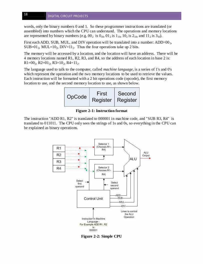
Each instruction will be formatted with a 2 bit operations code (opcode), the first memory
location to use, and the second memory location to use, as shown below.
Figure 2-1: Instruction format
The instruction "ADD R1, R2" is translated to 000001 in machine code, and "SUB R3, R4" is
translated to 011011. The CPU only sees the strings of 1s and 0s, so everything in the CPU can
be explained as binary operations.
Figure 2-2: Simple CPU
DIGITAL CIRCUIT PROJECTS 19
2.3.1 Creating the CPU
The Figure 2.2 is a schematic of our CPU. This schematic shows how the CPU would process a
simple machine language instruction such as ADD R1, R2.
This computer consists of 5 components. The first is the Control Unit (CU). The control unit is
responsible for taking a 6 bit instruction, the input string of 0s and 1s, and making it useful to the
rest of the CPU. For ADD R1, R2, the instruction is 0000012.
The first two bits coming into the CU are the opcode, in this case 00. This 00 is translated to
make one of the lines from the CU to the ALU become active, which tells the ALU which
operation to perform. In this case the 00 is translated so the ADD line is active.
The second component in the CPU is a bank of memory which can contain 4 values. The
memory locations are named R1, R2, R3, and R4. However these names are only mnemonics for
a programmer, the CPU knows these memory locations as the numbers 002, 012, 102, and 112.
The next two components in the CPU are the selectors. These selectors are connected to all four
values stored in the 4 memory locations. The CU takes the third and fourth bits from the
instruction, here 002, and places these two bits on the wire to the Selector 1. This selector uses
this input address to select the value contained in R1. The same thing is done for the fifth and
sixth bits in the instruction, which are sent to Selector 2 to select the value in R2. Be careful to
understand this correctly. There are two inputs to the selectors. The first input is 2 bits and
represent the address or name of the memory location to read. The value from memory to the
selected is a number, the value which is stored in the memory.
The last component in the CPU is called the Arithmetic Logic Unit (ALU). The ALU performs
the operation which is requested, such as addition, subtraction, etc. It takes two inputs from any
two of the memory locations, performs the operation, and produces the output.
This simple CPU might seem trivial, and it is. However it does contain all the major ICs which
are used in any CPU, and all of the ICs presented in this text. The CU will use a decoder to
decide which control line for an operation to send to the ALU. Each selector will be a MUX to
choose the correct ALU input value. The memory will be implemented as a collection of D flip-
flops. Finally one operation of the ALU will be shown by an adder. This context for each
component will be presented at the start of the chapter for that component.
2.4 Conclusion
The purpose of this book is to describe the major digital components which make up a CPU: a
decoder, multiplexer (MUX), flip-flop, and ALU (represented in the text by an adder). These
components can be used to make larger components, but together they are used to build a CPU.
To better understand how these components work, this book will provide a context of how these
digital components are used in the simple CPU in Figure 2.2. By providing this context, why
each of these components exist will be understood, and this will hopefully help readers
understand the design decisions made in creating each component.

20 DIGITAL CIRCUIT PROJECTS
2.5 Exercises
1. Write the instructions for the following operations in the simple CPU defined in this chapter.
a. ADD R3, R1
b. DIV R2, R4
c. MUL R4, R1
2. Translate the following machine code into assembly code. For example, 0000012 would be
ADD R1, R2.
a. 110110
b. 010001
c. 111110
3. Do you think the following instruction, "ADD R0, R0", is valid for the CPU described in
this chapter? Explain why or why not.
4. Describe the modifications which would have to be made to the CPU and the instructions to
add the following changes. Be sure to include hardware changes and changes to the
instruction format.
a. Increase the number of memory slots from 4 to 6
b. Add an instruction to compare to values for equality. For example, "EQ R1, R2"
would have an output of 1 if the two were equal, and 0 if they are different.
c. Add an instruction to compare two values for inequality. . For example, "NE R1,
R2" would have an output of 0 if the two were equal, and 1 if they are different.
d. Explain what how the CPU would be modified if all 3 of the above changes are made
together.

DIGITAL CIRCUIT PROJECTS 21
Chapter 3 Getting started
3.1 Introduction
There is an old adage, “A journey of 1000 miles begins with the first step”. The hardest part of
any project is getting started. I had taught Computer Organization for years but had always used
virtual circuits to describe the components presented in this text. That meant using pictures,
drawings, and eventually tools such as Logisim. Though I knew the circuits in this book, I was
afraid to actually touch the hardware. From my conversations with others, this is not an
uncommon feeling even among computer scientists. Like so many people in so much of life, I
was afraid of the beginning.
The beginning, when all the fears about the project are apparent. Do I really know enough to do
the project? Will it take a lot longer than I think? What happens if I hit a problem that I cannot
solve? Too often these fears take over, and useful projects just fail to get started. But once the
project is started, the unknowns become known and can be dealt with. The complexity becomes
manageable. Incremental progress can be achieved, and each success builds on the last. The
trick is to start very simple, and to allow the complexity to evolve. This is the approach of this
text.
This text starts as simply as possible. To begin studying circuits, the first step is to understand
that digital circuits take electricity into the circuit, and convert it to an output. In our case, the
input will always be a switch, and output will always a LED light. So the first project is a circuit
which has a switch which turns on a light.
3.2 Logisim circuit to turn on a light
In this text, all circuits are first created in Logisim to allow the reader to see the logic
implemented by the circuit. This is important for a number of reasons. First, it is much easier to
build the circuit in Logisim. No wires need to be cut and stripped, and there are no physical
problems like loose connections or other problems to debug. The circuit is virtual and it always
behaves as it is coded.
Second, Logisim will represent the circuit as a series of logic gates, which closely represent the
Boolean expressions used to create the circuit. When the circuit is implemented using the
breadboard and chips, and all the chips look the same so visualizing the circuit is difficult.
Logisim makes it easier to understand the circuit, and then to translate it into hardware.
Third, implementing the circuit requires as much concentration on the pin configurations on the
chips as the actual gates that are used to implement the logic. Using Logisim allows the reader
to understand the logic of the circuit without worrying about extraneous implementation details.
Fourth circuits in Logisim are easier to modify, so problems in implementing the circuit can be
more quickly addressed and fixed. Different types of designs for the circuits, inputs to the
circuits, etc., can be tried in a much more forgiving environment.
Finally the circuits which are implemented are more easily saved and shared using Logisim.
Most of the circuits in this book will have a Logisim implementation w hich can be downloaded
from http://chuckkann.com/books/DigitalCircuitProjects
22 DIGITAL CIRCUIT PROJECTS
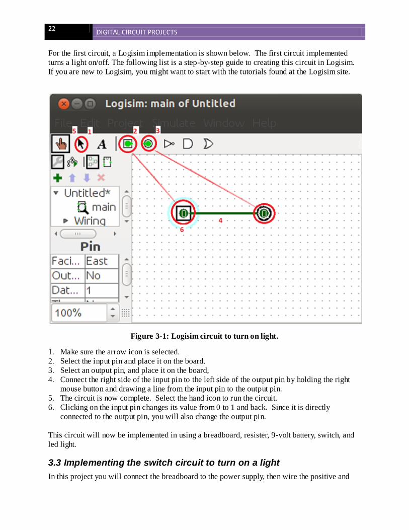
For the first circuit, a Logisim implementation is shown below. The first circuit implemented
turns a light on/off. The following list is a step-by-step guide to creating this circuit in Logisim.
If you are new to Logisim, you might want to start with the tutorials found at the Logisim site.
Figure 3-1: Logisim circuit to turn on light.
1. Make sure the arrow icon is selected.
2. Select the input pin and place it on the board.
3. Select an output pin, and place it on the board,
4. Connect the right side of the input pin to the left side of the output pin by holding the right
mouse button and drawing a line from the input pin to the output pin.
5. The circuit is now complete. Select the hand icon to run the circuit.
6. Clicking on the input pin changes its value from 0 to 1 and back. Since it is directly
connected to the output pin, you will also change the output pin.
This circuit will now be implemented in using a breadboard, resister, 9-volt battery, switch, and
led light.
3.3 Implementing the switch circuit to turn on a light
In this project you will connect the breadboard to the power supply, then wire the positive and
DIGITAL CIRCUIT PROJECTS 23
negative side strips. You will then put a switch on the board, and connect the switch to a led so
that the switch can turn the led on and off. This will complete the project.
3.3.1 The breadboard
This section describes the breadboard in your lab kits. For more information about breadboards
please see the following link:
http://en.wikipedia.org/wiki/Breadboard
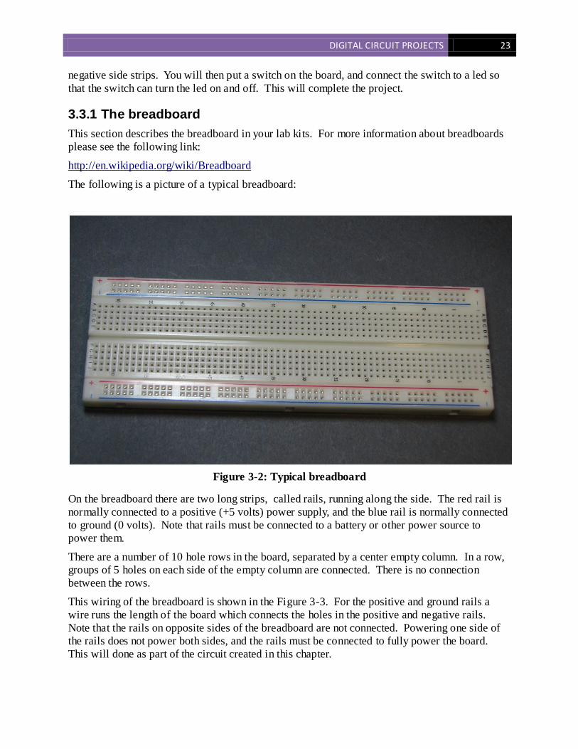
The following is a picture of a typical breadboard:
Figure 3-2: Typical breadboard
On the breadboard there are two long strips, called rails, running along the side. The red rail is
normally connected to a positive (+5 volts) power supply, and the blue rail is normally connected
to ground (0 volts). Note that rails must be connected to a battery or other power source to
power them.
There are a number of 10 hole rows in the board, separated by a center empty column. In a row,
groups of 5 holes on each side of the empty column are connected. There is no connection
between the rows.
This wiring of the breadboard is shown in the Figure 3-3. For the positive and ground rails a
wire runs the length of the board which connects the holes in the positive and negative rails.
Note that the rails on opposite sides of the breadboard are not connected. Powering one side of
the rails does not power both sides, and the rails must be connected to fully power the board.
This will done as part of the circuit created in this chapter.

24 DIGITAL CIRCUIT PROJECTS
Figure 3-3: Breadboard layout
This breadboard layout also shows that the groups of 5 holes in each row are also connected,
though the top and bottom groups of 5 holes are not. Normally the holes in these groups of 5 on
the two sides of the board will be kept separate. This will make sense when chips are installed
and used.
The groups of five holes are numbered 1 to 60 on each side of the breadboard. Each group of
five holes are wired together, so two wires which are placed in holes in the same group on a row
are connected. This will be used to wire the circuits.
3.3.2 Stripping wires
To make contact with the holes in the breadboard, the insulation must be removed from the ends
of the wires. To do this wire strippers will be used. Typical wire strippers are shown in the
following figure. Wire strippers are sharp and can easily cut the wire we are using here by
placing the wire in the lower part of the clippers (1), and closing them. However the notches in
the wire strippers are places where there is a predetermined distance between the two blades
which is just the size of the copper wire inside of our insulation. By placing the wire in the notch
labeled 22 AWG (or .60 mm) (2), the insulation is cut but the wire is not. Then by simpl y pulling
the wire from the strippers there is a clean end to the wire that no longer is insulated. This is
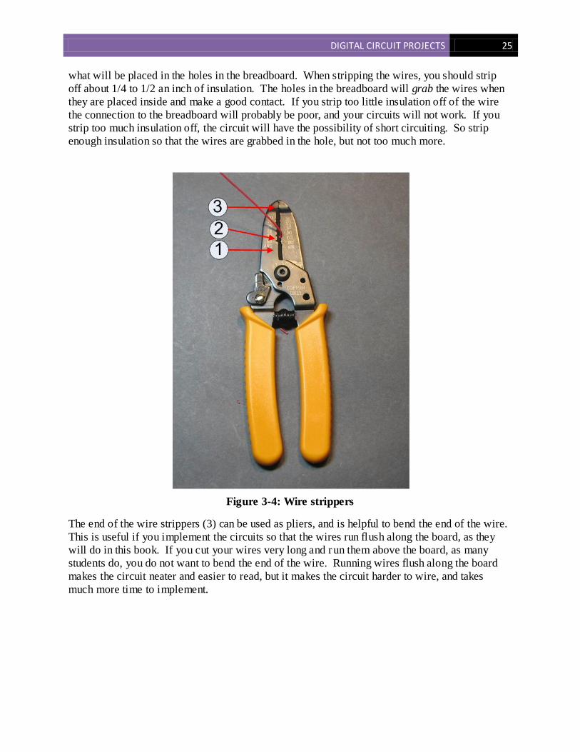
DIGITAL CIRCUIT PROJECTS 25
what will be placed in the holes in the breadboard. When stripping the wires, you should strip
off about 1/4 to 1/2 an inch of insulation. The holes in the breadboard will grab the wires when
they are placed inside and make a good contact. If you strip too little insulation off of the wire
the connection to the breadboard will probably be poor, and your circuits will not work. If you
strip too much insulation off, the circuit will have the possibility of short circuiting. So strip
enough insulation so that the wires are grabbed in the hole, but not too much more.
Figure 3-4: Wire strippers
The end of the wire strippers (3) can be used as pliers, and is helpful to bend the end of the wire.
This is useful if you implement the circuits so that the wires run flush along the board, as they
will do in this book. If you cut your wires very long and run them above the board, as many
students do, you do not want to bend the end of the wire. Running wires flush along the board
makes the circuit neater and easier to read, but it makes the circuit harder to wire, and takes
much more time to implement.
26 DIGITAL CIRCUIT PROJECTS
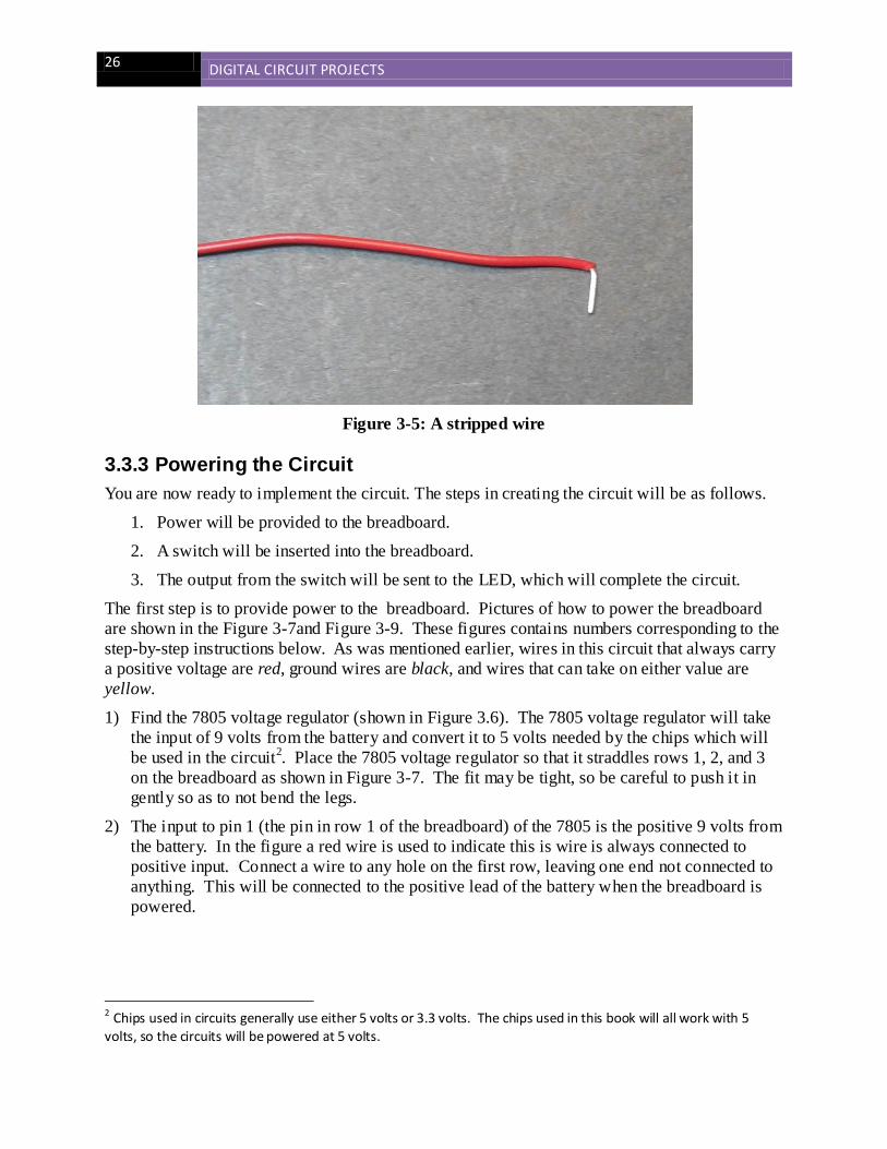
Figure 3-5: A stripped wire
3.3.3 Powering the Circuit
You are now ready to implement the circuit. The steps in creating the circuit will be as follows.
1. Power will be provided to the breadboard.
2. A switch will be inserted into the breadboard.
3. The output from the switch will be sent to the LED, which will complete the circuit.
The first step is to provide power to the breadboard. Pictures of how to power the breadboard
are shown in the Figure 3-7and Figure 3-9. These figures contains numbers corresponding to the
step-by-step instructions below. As was mentioned earlier, wires in this circuit that always carry
a positive voltage are red, ground wires are black, and wires that can take on either value are
yellow.
1) Find the 7805 voltage regulator (shown in Figure 3.6). The 7805 voltage regulator will take
the input of 9 volts from the battery and convert it to 5 volts needed by the chips which will
be used in the circuit2. Place the 7805 voltage regulator so that it straddles rows 1, 2, and 3
on the breadboard as shown in Figure 3-7. The fit may be tight, so be careful to push it in
gently so as to not bend the legs.
2) The input to pin 1 (the pin in row 1 of the breadboard) of the 7805 is the positive 9 volts from
the battery. In the figure a red wire is used to indicate this is wire is always connected to
positive input. Connect a wire to any hole on the first row, leaving one end not connected to
anything. This will be connected to the positive lead of the battery when the breadboard is
powered.
2 Chips used in circuits generally use either 5 volts or 3.3 volts. The chips used in this book will all work with 5 volts, so the circuits will be powered at 5 volts.
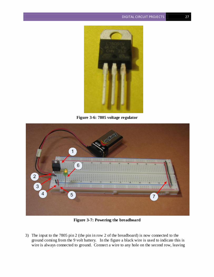
DIGITAL CIRCUIT PROJECTS 27
Figure 3-6: 7805 voltage regulator
Figure 3-7: Powering the breadboard
3) The input to the 7805 pin 2 (the pin in row 2 of the breadboard) is now connected to the
ground coming from the 9 volt battery. In the figure a black wire is used to indicate this is
wire is always connected to ground. Connect a wire to any hole on the second row, leaving

28 DIGITAL CIRCUIT PROJECTS
one end not connected to anything. This will be connected to the negative lead of the battery
when the breadboard is powered
4) Connect the ground rail of the breadboard to row 2. The ground rail is the blue column which
runs down the side of the board. Note that row 2 has three connection, the input ground from
the battery, the middle pin on the 7805 chip, and the output wire to the blue ground side rail.
5) The 5 volt output from the 7805 is the pin in row 3. To power the board, connect row 3 to
the positive rail of the breadboard. The positive rail is the red column which runs down the
side of the board.
6) The left half of the board is ready to be connected to the battery. Put a 9 volt battery in the
battery snap, and connect the leads from the battery to red and black wires from steps 3 and
4. (Be sure to connect positive wire to positive input, and negative wire to negative input!)
The board should now have power. This can be checked by placing an LED between the
positive and negative rails on the board. Note that the LED has two legs, and one is longer
than the other, as shown in Figure 3-8. Make sure to place the positive (long) leg in the
positive (red) rail, and the short leg in the ground (blue) rail. The light should come on. If it
does not, you have a debugging problem. Here are some things to try:
a) Make sure that the battery is connected correctly, positive to positive and negative to
negative. If it is not, your 7805 chip will quickly start to become hot. If this happens,
disconnect the battery and allow the chip to cool. When the chip is cool, reconnect the
battery correctly.
b) Make sure the LED is properly oriented. This simple mistakes often causes confusion,
and so when using an LED always make sure to orient it correctly.
c) Make sure the battery and the snap are ok by putting the LED directly into the 9 volt
battery clip. If the LED lights, move to step d.
d) Make sure that current is getting to the board correctly. Connect the battery to your
positive and negative leads (to power the board) and place the LED between rows 1 and 2
of the board to make sure that you have a good connection with the leads. If the LED
lights, move to step e.
e) Make sure you have current coming from the 7805 by connecting the LED between rows
3 and 2. If the LED does not light, something is wrong with the 7805. Check that you
have installed it correctly (not backwards for instance).
Figure 3-8: LED
DIGITAL CIRCUIT PROJECTS 29
7) The left half of the bread board should now have powered, but the right half is still not
connected. To connect the right half of the breadboard, go to the last row with the blue and
red rails. Run a wire from the left red rail (the outside left rail) to the right red rail (the inside
right rail) as shown in Figure 3.7. Do the same for the blue rail. This should power the rails
on the right side of the breadboard. You can test that both rails are now powered by using the
LED between the blue and red rails on the right side of the breadboard as in step 6 above.
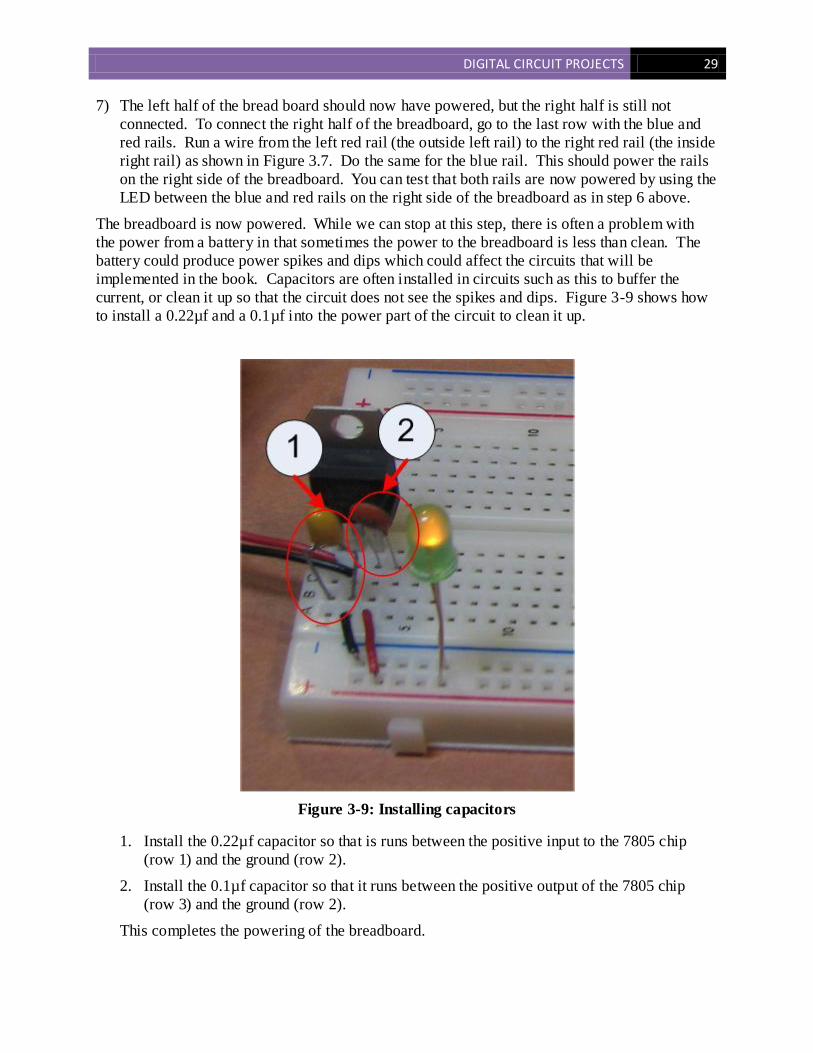
The breadboard is now powered. While we can stop at this step, there is often a problem with
the power from a battery in that sometimes the power to the breadboard is less than clean. The
battery could produce power spikes and dips which could affect the circuits that will be
implemented in the book. Capacitors are often installed in circuits such as this to buffer the
current, or clean it up so that the circuit does not see the spikes and dips. Figure 3-9 shows how
to install a 0.22µf and a 0.1µf into the power part of the circuit to clean it up.
Figure 3-9: Installing capacitors
1. Install the 0.22µf capacitor so that is runs between the positive input to the 7805 chip
(row 1) and the ground (row 2).
2. Install the 0.1µf capacitor so that it runs between the positive output of the 7805 chip
(row 3) and the ground (row 2).
This completes the powering of the breadboard.
30 DIGITAL CIRCUIT PROJECTS
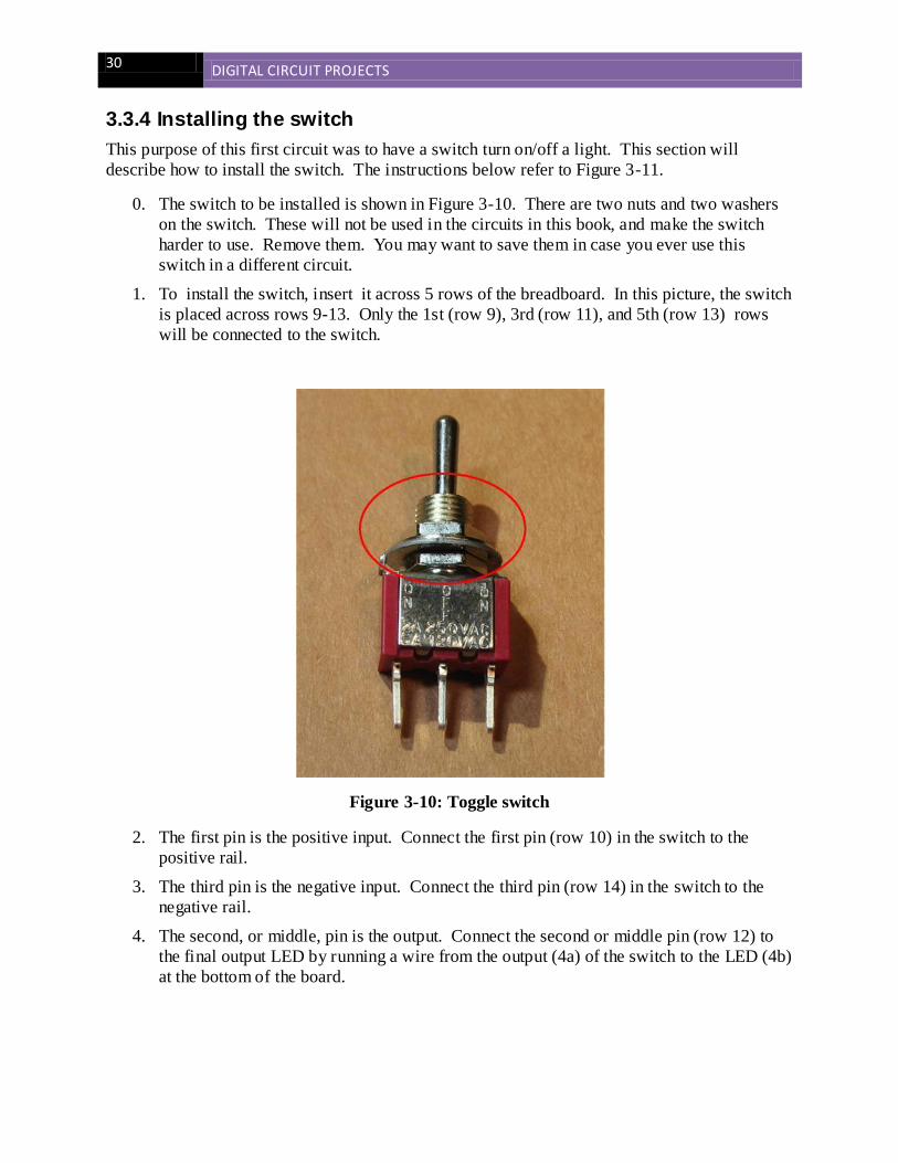
3.3.4 Installing the switch
This purpose of this first circuit was to have a switch turn on/off a light. This section will
describe how to install the switch. The instructions below refer to Figure 3-11.
0. The switch to be installed is shown in Figure 3-10. There are two nuts and two washers
on the switch. These will not be used in the circuits in this book, and make the switch
harder to use. Remove them. You may want to save them in case you ever use this
switch in a different circuit.
1. To install the switch, insert it across 5 rows of the breadboard. In this picture, the switch
is placed across rows 9-13. Only the 1st (row 9), 3rd (row 11), and 5th (row 13) rows
will be connected to the switch.
Figure 3-10: Toggle switch
2. The first pin is the positive input. Connect the first pin (row 10) in the switch to the
positive rail.
3. The third pin is the negative input. Connect the third pin (row 14) in the switch to the
negative rail.
4. The second, or middle, pin is the output. Connect the second or middle pin (row 12) to
the final output LED by running a wire from the output (4a) of the switch to the LED (4b)
at the bottom of the board.
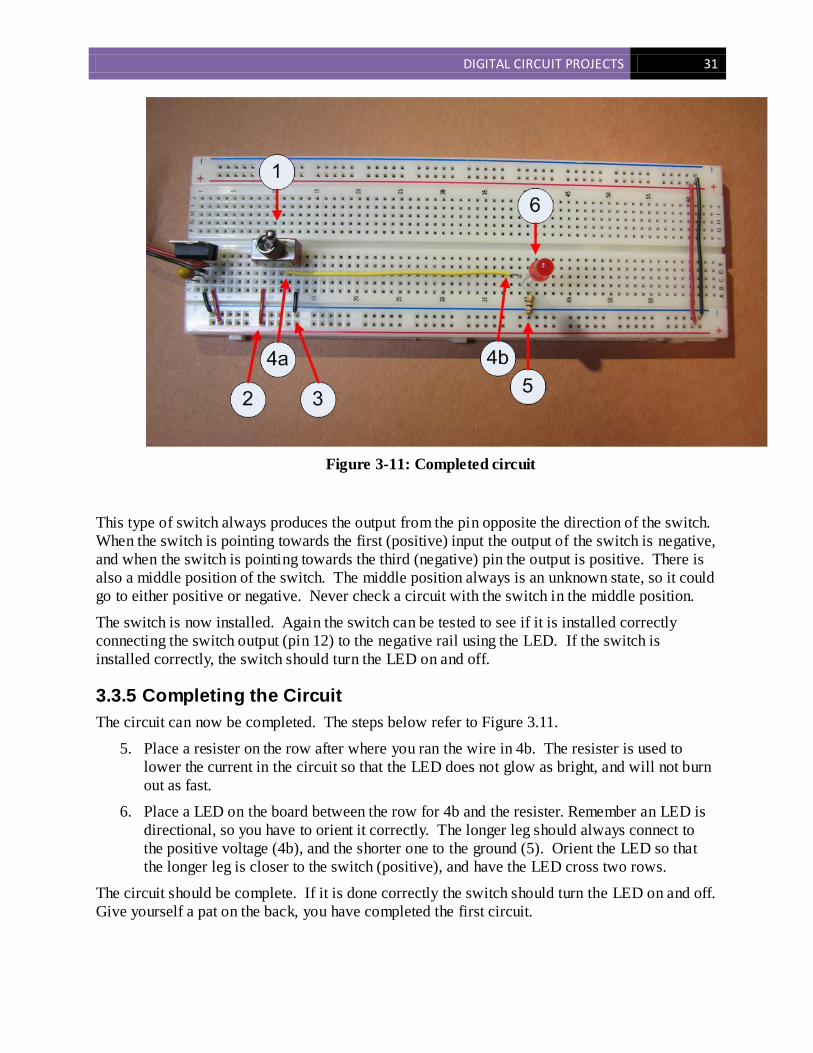
DIGITAL CIRCUIT PROJECTS 31
Figure 3-11: Completed circuit
This type of switch always produces the output from the pin opposite the direction of the switch.
When the switch is pointing towards the first (positive) input the output of the switch is negative,
and when the switch is pointing towards the third (negative) pin the output is positive. There is
also a middle position of the switch. The middle position always is an unknown state, so it could
go to either positive or negative. Never check a circuit with the switch in the middle position.
The switch is now installed. Again the switch can be tested to see if it is installed correctly
connecting the switch output (pin 12) to the negative rail using the LED. If the switch is
installed correctly, the switch should turn the LED on and off.
3.3.5 Completing the Circuit
The circuit can now be completed. The steps below refer to Figure 3.11.
5. Place a resister on the row after where you ran the wire in 4b. The resister is used to
lower the current in the circuit so that the LED does not glow as bright, and will not burn
out as fast.
6. Place a LED on the board between the row for 4b and the resister. Remember an LED is
directional, so you have to orient it correctly. The longer leg should always connect to
the positive voltage (4b), and the shorter one to the ground (5). Orient the LED so that
the longer leg is closer to the switch (positive), and have the LED cross two rows.
The circuit should be complete. If it is done correctly the switch should turn the LED on and off.
Give yourself a pat on the back, you have completed the first circuit.
32 DIGITAL CIRCUIT PROJECTS
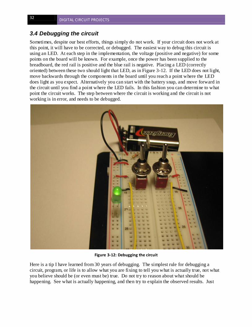
3.4 Debugging the circuit
Sometimes, despite our best efforts, things simply do not work. If your circuit does not work at
this point, it will have to be corrected, or debugged. The easiest way to debug this circuit is
using an LED. At each step in the implementation, the voltage (positive and negative) for some
points on the board will be known. For example, once the power has been supplied to the
breadboard, the red rail is positive and the blue rail is negative. Placing a LED (correctly
oriented) between these two should light that LED, as in Figure 3-12. If the LED does not light,
move backwards through the components in the board until you reach a point where the LED
does light as you expect. Alternatively you can start with the battery snap, and move forward in
the circuit until you find a point where the LED fails. In this fashion you can determine to what
point the circuit works. The step between where the circuit is working and the circuit is not
working is in error, and needs to be debugged.
Figure 3-12: Debugging the circuit
Here is a tip I have learned from 30 years of debugging. The simplest rule for debugging a
circuit, program, or life is to allow what you are fixing to tell you what is actually true, not what
you believe should be (or even must be) true. Do not try to reason about what should be
happening. See what is actually happening, and then try to explain the observed results. Just

DIGITAL CIRCUIT PROJECTS 33
verbalizing the problem can help3. When you get too upset, take a walk and get your mind off of
the problem.
But the key is to not assume you know what must be happening. Allowing the situation to tell
you the truth about what is happening is always more fruitful then trying to find faults in your
logic, especially if you believe that your (what turns out to be errant) logic has to be correct.
3.5 Exercises
1. Implement the circuit in Figure 3-11.
2. Modify the curcuit in Figure 3-11 by adding a second input switch and LED to the right
side of the breadboard.
3. Identify the following parts of the circuit, and give a short reason why they are used:
a. capacitor
b. resister
c. LED
4. What are the 3 positions of the toggle switch? Which one cannot be used?
5. Explain the configuration of a breadboard. What holes are connected? How is it
powered?
6. What components in the circuits implemented in this chapter are directional? How can
you determine if you have placed the component correctly?
3I like to tell the problem to a dog. Unlike a person, he will listen intently and not interrupt. And he appreciates the attention.
34 DIGITAL CIRCUIT PROJECTS
Chapter 4 Gates
4.1 Introduction
This chapter will present a simple explanation of Boolean (or binary) logic. The simple Boolean
operations NOT, AND, and OR will be explained, and how they are implemented in a circuit
diagram and in an IC chip will be explained.
4.2 Boolean logic and binary values
Now that we have a basic circuit to light an LED, we can start to implement Boolean logic in
our circuits. Boolean logic represents all data by two values, which is why it is sometimes
called binary logic. Often these two binary values are represented by the value true (T) or false
(F). However this is just one way to represent these values, and while it is the one
mathematicians use, it is often not convenient. For example, when we are talking about circuits
we often want to say if the switch is on (T) or off (F). We will know if the switch is on because
it produces a high voltage (T) or a low voltage (F). Finally these circuits can be used to
represent binary numbers, and in this case the values 1 (T) and 0 (F) are greatly preferred.
Depending on the context, each of these representation of binary values will be used at different
times in this text. However realize that they are just different ways to represent the same
information, and it is just convenience that will dictate which is used.
4.3 Unary operations
Boolean logic consists of a set of values (T and F) and the operations which can be performed
on the binary values. In this book, the three most important Boolean operations are AND, OR,
and NOT.
How a Boolean operation works is often shown (or characterized) using truth-tables. A truth-
table is a table which gives the input value for the operation, and the output values for that
operation. For example, there are only two unary operations. Unary operations are operations
which take only one input, the NULL operator and the NOT operator. An easy way to
characterize these functions is in a table where the input values of 0 and 1 are input, and the
output values from the function are given as 0 and 1.
A truth table is normally shown with the input values for a function on the left, and the name of
the function at the top of the column. The following truth table characterizes the NULL and
NOT operations. It shows what the outputs of the NULL and NOT operator are for an input
value of A.
Input Output
A NULL NOT
0 0 1
1 1 0

DIGITAL CIRCUIT PROJECTS 35
As this table shows, if the input value A is 0, the NULL gate will produce an output value of 0,
and the NOT operator will produce a value of 1 (the inverse). Likewise if the input value of A
is 1, the NULL operator will produce a value of 1, and the NOT operator will produce an output
value of 0. The NOT operator in this text will be written as a quote ('), so NOT-A will be A'.
Gates are the physical implementation of Boolean operators in a circuit. Since the NOT
operator always inverts the input value, the NOT gate is often referred to as an inverter, and is
represented by the triangle with a circle symbol in Figure 9 below. The NULL gate is usually
either absent, or implemented as a buffer. The symbol for the buffer is represented by the
triangle symbol in Figure 4-1 below.
Figure 4-1: Buffer and inverter gates
Figure 4-2 shows a circuit with the buffer and inverter in Logisim.
Figure 4-2: Buffer and inverter circuit in Logisim
4.4 Binary Operations
The other two important Boolean operators, AND and OR, are binary operators because they
take two inputs. The AND operator is true (1) it both of its inputs are true (1) (e.g. A and B are
both true); if either of its inputs are false (0) then the operator is false(0).
The OR operator is true (1) if either or both of its inputs are true (1) (e.g. either A and B is true,
or both are true); it is false (0) if both of its inputs are false (0). The following truth table
characterizes the output for the AND and OR functions behaves for the two inputs A and B.
Input Output
A B AND OR XOR
0 0 0 0 0
0 1 0 1 1
1 0 0 1 1
1 1 1 1 0
Figure 4-3 Truth table for AND and OR
In this text, the AND operator will be shown by the * symbol (A*B), and the OR operator by
the + symbol (A+B). The * is often dropped, as in algebra (e.g. A*B will be written AB).
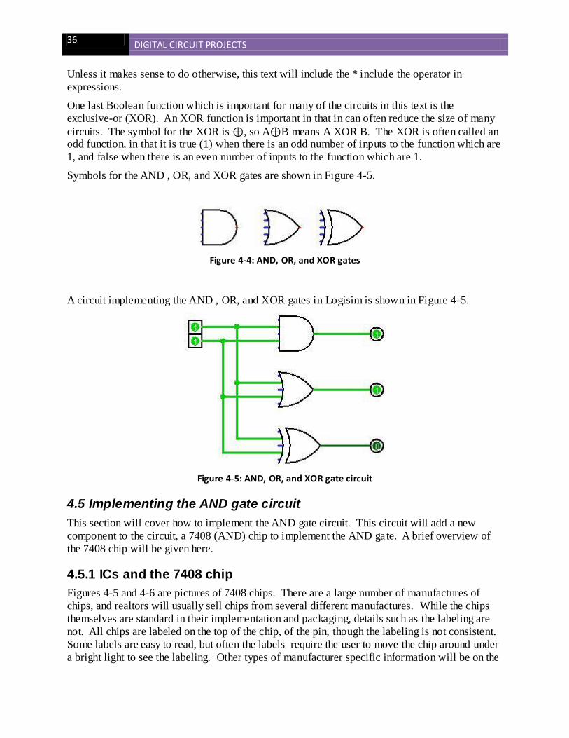
36 DIGITAL CIRCUIT PROJECTS
Unless it makes sense to do otherwise, this text will include the * include the operator in
expressions.
One last Boolean function which is important for many of the circuits in this text is the
exclusive-or (XOR). An XOR function is important in that in can often reduce the size of many
circuits. The symbol for the XOR is ⊕, so A⊕B means A XOR B. The XOR is often called an odd function, in that it is true (1) when there is an odd number of inputs to the function which are
1, and false when there is an even number of inputs to the function which are 1.
Symbols for the AND , OR, and XOR gates are shown in Figure 4-5.
Figure 4-4: AND, OR, and XOR gates
A circuit implementing the AND , OR, and XOR gates in Logisim is shown in Figure 4-5.
Figure 4-5: AND, OR, and XOR gate circuit
4.5 Implementing the AND gate circuit
This section will cover how to implement the AND gate circuit. This circuit will add a new
component to the circuit, a 7408 (AND) chip to implement the AND gate. A brief overview of
the 7408 chip will be given here.
4.5.1 ICs and the 7408 chip
Figures 4-5 and 4-6 are pictures of 7408 chips. There are a large number of manufactures of
chips, and realtors will usually sell chips from several different manufactures. While the chips
themselves are standard in their implementation and packaging, details such as the labeling are
not. All chips are labeled on the top of the chip, of the pin, though the labeling is not consistent.
Some labels are easy to read, but often the labels require the user to move the chip around under
a bright light to see the labeling. Other types of manufacturer specific information will be on the
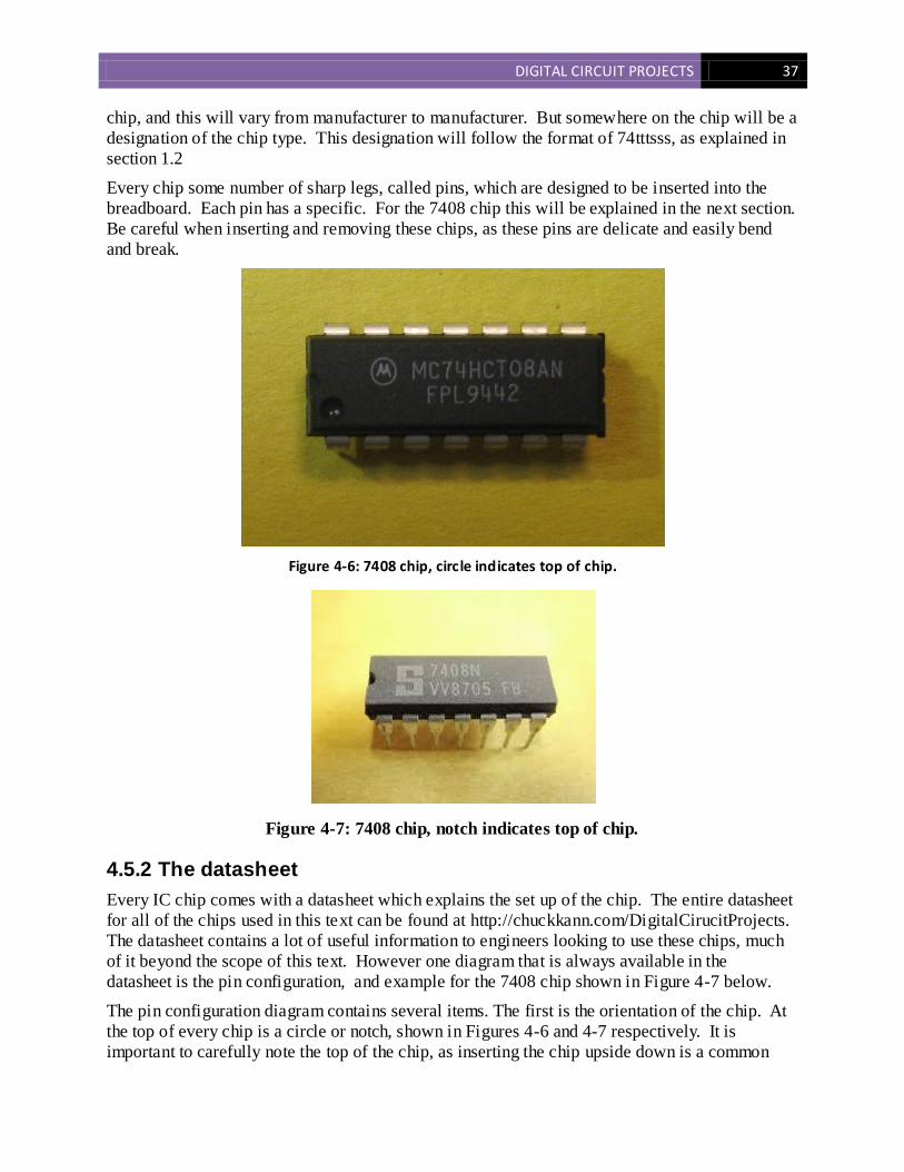
DIGITAL CIRCUIT PROJECTS 37
chip, and this will vary from manufacturer to manufacturer. But somewhere on the chip will be a
designation of the chip type. This designation will follow the format of 74tttsss, as explained in
section 1.2
Every chip some number of sharp legs, called pins, which are designed to be inserted into the
breadboard. Each pin has a specific. For the 7408 chip this will be explained in the next section.
Be careful when inserting and removing these chips, as these pins are delicate and easily bend
and break.
Figure 4-6: 7408 chip, circle indicates top of chip.
Figure 4-7: 7408 chip, notch indicates top of chip.
4.5.2 The datasheet
Every IC chip comes with a datasheet which explains the set up of the chip. The entire datasheet
for all of the chips used in this text can be found at http://chuckkann.com/DigitalCirucitProjects.
The datasheet contains a lot of useful information to engineers looking to use these chips, much
of it beyond the scope of this text. However one diagram that is always available in the
datasheet is the pin configuration, and example for the 7408 chip shown in Figure 4-7 below.
The pin configuration diagram contains several items. The first is the orientation of the chip. At
the top of every chip is a circle or notch, shown in Figures 4-6 and 4-7 respectively. It is
important to carefully note the top of the chip, as inserting the chip upside down is a common
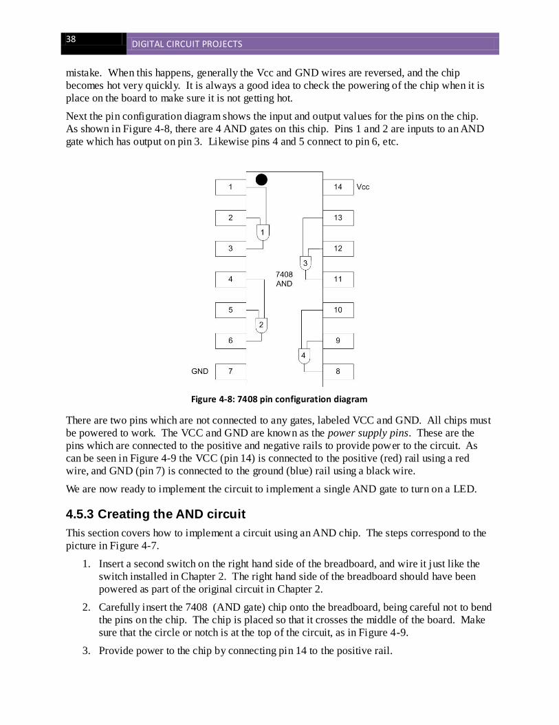
38 DIGITAL CIRCUIT PROJECTS
mistake. When this happens, generally the Vcc and GND wires are reversed, and the chip
becomes hot very quickly. It is always a good idea to check the powering of the chip when it is
place on the board to make sure it is not getting hot.
Next the pin configuration diagram shows the input and output values for the pins on the chip.
As shown in Figure 4-8, there are 4 AND gates on this chip. Pins 1 and 2 are inputs to an AND
gate which has output on pin 3. Likewise pins 4 and 5 connect to pin 6, etc.
Figure 4-8: 7408 pin configuration diagram
There are two pins which are not connected to any gates, labeled VCC and GND. All chips must
be powered to work. The VCC and GND are known as the power supply pins. These are the
pins which are connected to the positive and negative rails to provide power to the circuit. As
can be seen in Figure 4-9 the VCC (pin 14) is connected to the positive (red) rail using a red
wire, and GND (pin 7) is connected to the ground (blue) rail using a black wire.
We are now ready to implement the circuit to implement a single AND gate to turn on a LED.
4.5.3 Creating the AND circuit
This section covers how to implement a circuit using an AND chip. The steps correspond to the
picture in Figure 4-7.
1. Insert a second switch on the right hand side of the breadboard, and wire it just like the
switch installed in Chapter 2. The right hand side of the breadboard should have been
powered as part of the original circuit in Chapter 2.
2. Carefully insert the 7408 (AND gate) chip onto the breadboard, being careful not to bend
the pins on the chip. The chip is placed so that it crosses the middle of the board. Make
sure that the circle or notch is at the top of the circuit, as in Figure 4-9.
3. Provide power to the chip by connecting pin 14 to the positive rail.
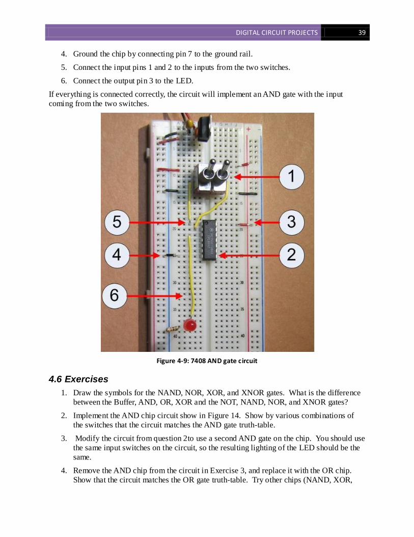
DIGITAL CIRCUIT PROJECTS 39
4. Ground the chip by connecting pin 7 to the ground rail.
5. Connect the input pins 1 and 2 to the inputs from the two switches.
6. Connect the output pin 3 to the LED.
If everything is connected correctly, the circuit will implement an AND gate with the input
coming from the two switches.
Figure 4-9: 7408 AND gate circuit
4.6 Exercises
1. Draw the symbols for the NAND, NOR, XOR, and XNOR gates. What is the difference
between the Buffer, AND, OR, XOR and the NOT, NAND, NOR, and XNOR gates?
2. Implement the AND chip circuit show in Figure 14. Show by various combinations of
the switches that the circuit matches the AND gate truth-table.
3. Modify the circuit from question 2to use a second AND gate on the chip. You should use
the same input switches on the circuit, so the resulting lighting of the LED should be the
same.
4. Remove the AND chip from the circuit in Exercise 3, and replace it with the OR chip.
Show that the circuit matches the OR gate truth-table. Try other chips (NAND, XOR,
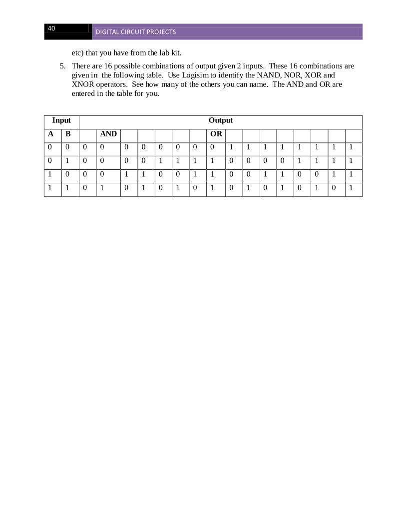
40 DIGITAL CIRCUIT PROJECTS
etc) that you have from the lab kit.
5. There are 16 possible combinations of output given 2 inputs. These 16 combinations are
given in the following table. Use Logisim to identify the NAND, NOR, XOR and
XNOR operators. See how many of the others you can name. The AND and OR are
entered in the table for you.
Input Output
A B AND OR
0 0 0 0 0 0 0 0 0 0 1 1 1 1 1 1 1 1
0 1 0 0 0 0 1 1 1 1 0 0 0 0 1 1 1 1
1 0 0 0 1 1 0 0 1 1 0 0 1 1 0 0 1 1
1 1 0 1 0 1 0 1 0 1 0 1 0 1 0 1 0 1

DIGITAL CIRCUIT PROJECTS 41
Chapter 5 Associative Boolean operators
5.1 Introduction
This chapter looks at which Boolean operators are associative. Associative operations allow
arbitrary groupings of the operations. For example, addition is associative. We can show this
with the following two equations, which are equal:
x = (2 + (3 + (4+5))) = 14
x = (2 + 3) + (4 + 5) = 14
However subtraction is not associate, as can be seen in the equations below:
x = (2 - (3 - (4 - 5))) = -2
x = ((2 - 3) - (4 - 5)) = 0
These examples show that subtraction is not associative, and while they do not prove that
addition is associative, they are illustrative that addition is associative at least for this example.
The proof that addition is associative is not really of interest in this text, and can easily be found
in an online search.
Like arithmetic operators, Boolean operators can also be associative, commutative, and
distributive. This chapter will create circuits which will demonstrate the associative property for
Boolean operators. The exercises at the end of the chapter allow the reader to further explore
these properties.
5.2 Modeling associative operations in Logisim
To demonstrate which Boolean operators are associative, the first step is to write equations for
each operator which implement two associative ways to implement an expression, and see if the
results are equivalent or not. A first equation for the AND operation could be the following:
(A * (B * (C*D))). In this equation, the results of the output from each AND gate serially feeds the inputs to the AND next gate, where it is matched with the next input. This is shown in
Figure 5-1 below:
Figure 5-1: Serial AND circuit
A second equation, (A * B) * (C * D), does the first two AND operations in parallel, and then
combines the results, as shown in Figure 5-2 below:
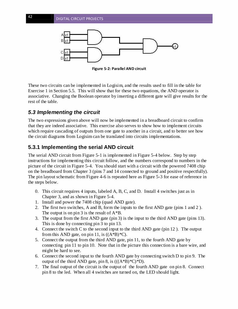
42 DIGITAL CIRCUIT PROJECTS
Figure 5-2: Parallel AND circuit
These two circuits can be implemented in Logisim, and the results used to fill in the table for
Exercise 1 in Section 5.5. This will show that for these two equations, the AND operator is
associative. Changing the Boolean operator by inserting a different gate will give results for the
rest of the table.
5.3 Implementing the circuit
The two expressions given above will now be implemented in a breadboard circuit to confirm
that they are indeed associative. This exercise also serves to show how to implement circuits
which require cascading of outputs from one gate to another in a circuit, and to better see how
the circuit diagrams from Logisim can be translated into circuits implementations.
5.3.1 Implementing the serial AND circuit
The serial AND circuit from Figure 5-1 is implemented in Figure 5-4 below. Step by step
instructions for implementing this circuit follow, and the numbers correspond to numbers in the
picture of the circuit in Figure 5-4. You should start with a circuit with the powered 7408 chip
on the breadboard from Chapter 3 (pins 7 and 14 connected to ground and positive respectfully).
The pin layout schematic from Figure 4-6 is repeated here as Figure 5-3 for ease of reference in
the steps below.
0. This circuit requires 4 inputs, labeled A, B, C, and D. Install 4 switches just as in
Chapter 3, and as shown in Figure 5-4.
1. Install and power the 7408 chip (quad AND gate).
2. The first two switches, A and B, form the inputs to the first AND gate (pins 1 and 2 ).
The output is on pin 3 is the result of A*B.
3. The output from the first AND gate (pin 3) is the input to the third AND gate (pins 13).
This is done by connecting pin 3 to pin 13.
4. Connect the switch C to the second input to the third AND gate (pin 12 ). The output
from this AND gate, on pin 11, is ((A*B)*C).
5. Connect the output from the third AND gate, pin 11, to the fourth AND gate by
connecting pin 11 to pin 10. Note that in the picture this connection is a bare wire, and
might be hard to see.
6. Connect the second input to the fourth AND gate by connecting switch D to pin 9. The
output of the third AND gate, pin 8, is (((A*B)*C)*D).
7. The final output of the circuit is the output of the fourth AND gate on pin 8. Connect
pin 8 to the led. When all 4 switches are turned on, the LED should light.
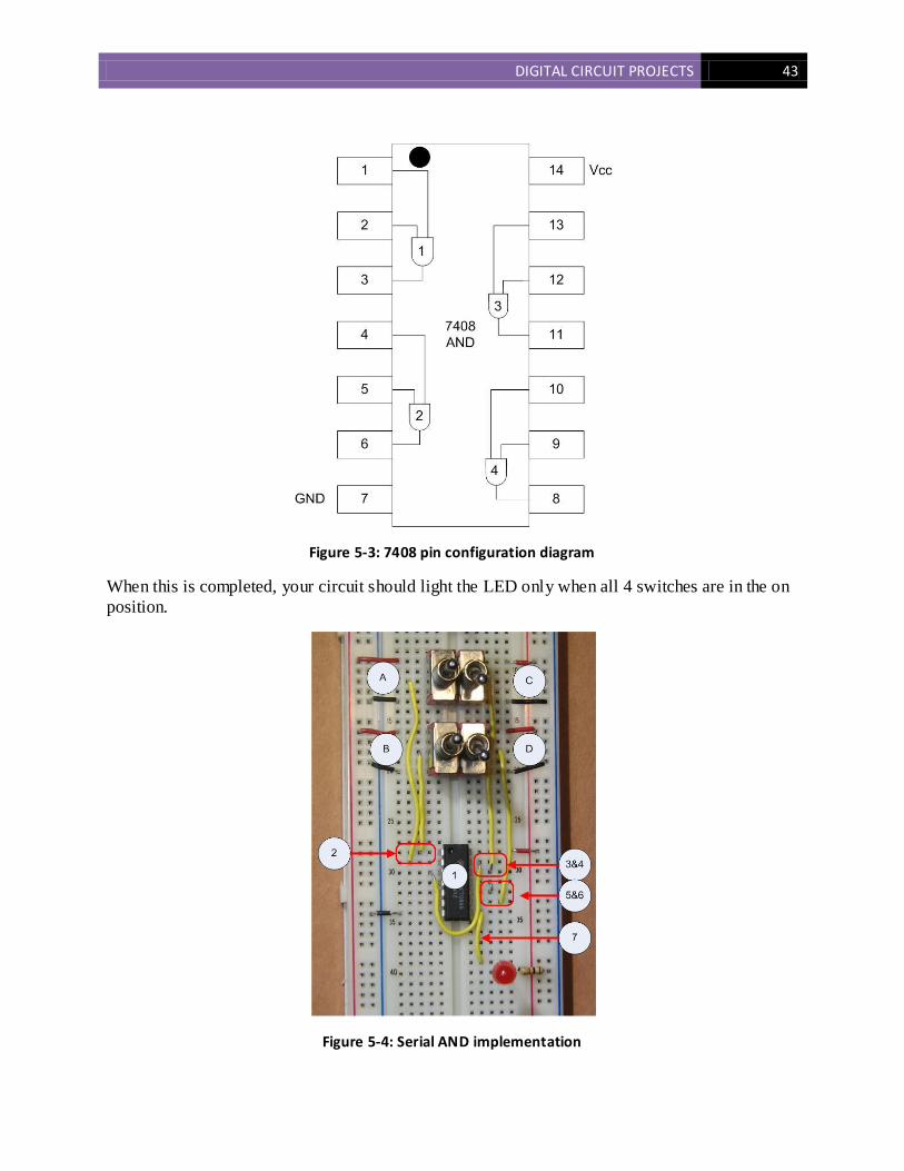
DIGITAL CIRCUIT PROJECTS 43
Figure 5-3: 7408 pin configuration diagram
When this is completed, your circuit should light the LED only when all 4 switches are in the on
position.
Figure 5-4: Serial AND implementation
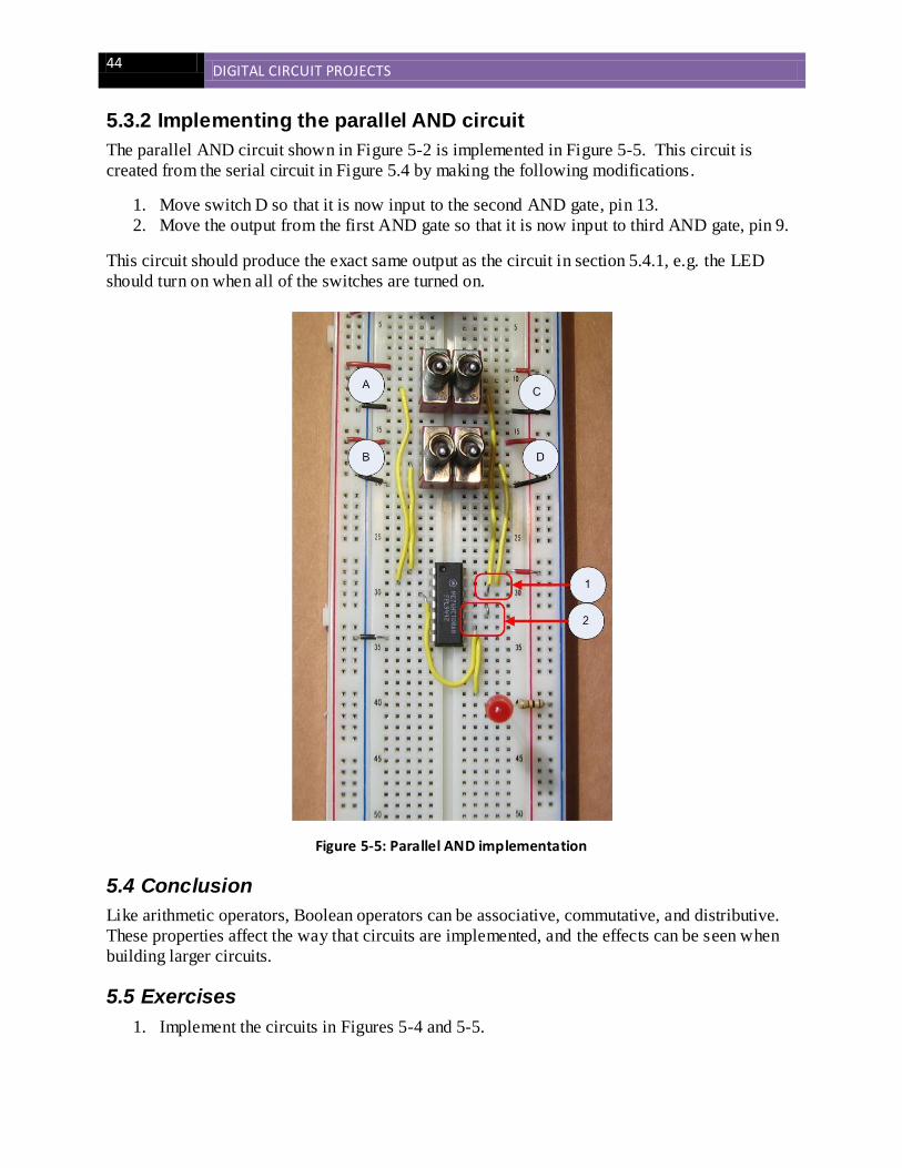
44 DIGITAL CIRCUIT PROJECTS
5.3.2 Implementing the parallel AND circuit
The parallel AND circuit shown in Figure 5-2 is implemented in Figure 5-5. This circuit is
created from the serial circuit in Figure 5.4 by making the following modifications.
1. Move switch D so that it is now input to the second AND gate, pin 13.
2. Move the output from the first AND gate so that it is now input to third AND gate, pin 9.
This circuit should produce the exact same output as the circuit in section 5.4.1, e.g. the LED
should turn on when all of the switches are turned on.
Figure 5-5: Parallel AND implementation
5.4 Conclusion
Like arithmetic operators, Boolean operators can be associative, commutative, and distributive.
These properties affect the way that circuits are implemented, and the effects can be seen when
building larger circuits.
5.5 Exercises
1. Implement the circuits in Figures 5-4 and 5-5.
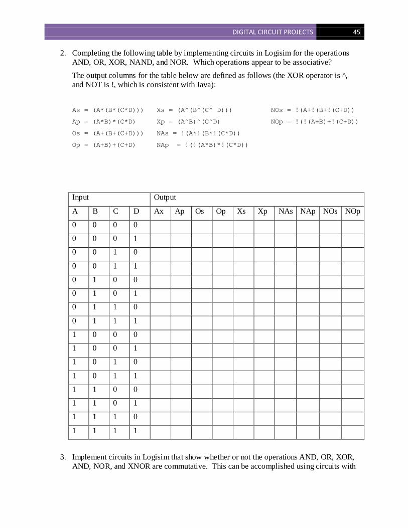
DIGITAL CIRCUIT PROJECTS 45
2. Completing the following table by implementing circuits in Logisim for the operations
AND, OR, XOR, NAND, and NOR. Which operations appear to be associative?
The output columns for the table below are defined as follows (the XOR operator is ,̂
and NOT is !, which is consistent with Java):
As = (A*(B*(C*D))) Xs = (A^(B^(C^ D))) NOs = !(A+!(B+!(C+D))
Ap = (A*B)*(C*D) Xp = (A^B)^(C^D) NOp = !(!(A+B)+!(C+D))
Os = (A+(B+(C+D))) NAs = !(A*!(B*!(C*D))
Op = (A+B)+(C+D) NAp = !(!(A*B)*!(C*D))
Input Output
A B C D Ax Ap Os Op Xs Xp NAs NAp NOs NOp
0 0 0 0
0 0 0 1
0 0 1 0
0 0 1 1
0 1 0 0
0 1 0 1
0 1 1 0
0 1 1 1
1 0 0 0
1 0 0 1
1 0 1 0
1 0 1 1
1 1 0 0
1 1 0 1
1 1 1 0
1 1 1 1
3. Implement circuits in Logisim that show whether or not the operations AND, OR, XOR,
AND, NOR, and XNOR are commutative. This can be accomplished using circuits with

46 DIGITAL CIRCUIT PROJECTS
only 3 inputs and 2 operations. Create a table similar to the one in problem 2. Which
operations appear to be commutative?
4. Implement two circuits showing the commutative property using your breadboard and
chips.
5. Implement circuits in Logisim that show whether or not the operations AND, OR, XOR,
AND, NOR, and XNOR are distributive. This can be accomplished using circuits with
only 3 inputs, but one version requires 2 operations and the other 3 operations. Create a
table similar to the one in problem 1, except with only 3 inputs, and complete it. Which
operations appear to be distributive? Implement the circuits using the breadboard.
6. Implement two circuits showing the distributive property using your breadboard and
chips.
7. Show, by creating the circuit in Logisim, that a 32-way parallel AND operation can be
implemented such that it only can be executed in 5*T time (where T is the time to do a
single AND operation). What does this exercise imply about the runtime growth of
associative operations when run in parallel? This question is for more advanced students,
and assumes some background in data structures and algorithms, but illustrates an
important point about parallelizing of associative operations.
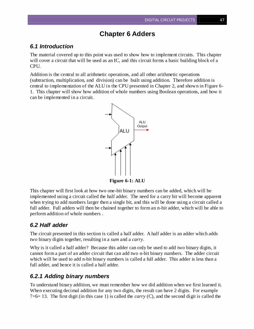
DIGITAL CIRCUIT PROJECTS 47
Chapter 6 Adders
6.1 Introduction
The material covered up to this point was used to show how to implement circuits. This chapter
will cover a circuit that will be used as an IC, and this circuit forms a basic building block of a
CPU.
Addition is the central to all arithmetic operations, and all other arithmetic operations
(subtraction, multiplication, and division) can be built using addition. Therefore addition is
central to implementation of the ALU in the CPU presented in Chapter 2, and shown in Figure 6-
1. This chapter will show how addition of whole numbers using Boolean operations, and how it
can be implemented in a circuit.
Figure 6-1: ALU
This chapter will first look at how two one-bit binary numbers can be added, which will be
implemented using a circuit called the half adder. The need for a carry bit will become apparent
when trying to add numbers larger then a single bit, and this will be done using a circuit called a
full adder. Full adders will then be chained together to form an n-bit adder, which will be able to
perform addition of whole numbers .
6.2 Half adder
The circuit presented in this section is called a half adder. A half adder is an adder which adds
two binary digits together, resulting in a sum and a carry.
Why is it called a half adder? Because this adder can only be used to add two binary digits, it
cannot form a part of an adder circuit that can add two n-bit binary numbers. The adder circuit
which will be used to add n-bit binary numbers is called a full adder. This adder is less than a
full adder, and hence it is called a half adder.
6.2.1 Adding binary numbers
To understand binary addition, we must remember how we did addition when we first learned it.
When executing decimal addition for any two digits, the result can have 2 digits. For example
7+6= 13. The first digit (in this case 1) is called the carry (C), and the second digit is called the
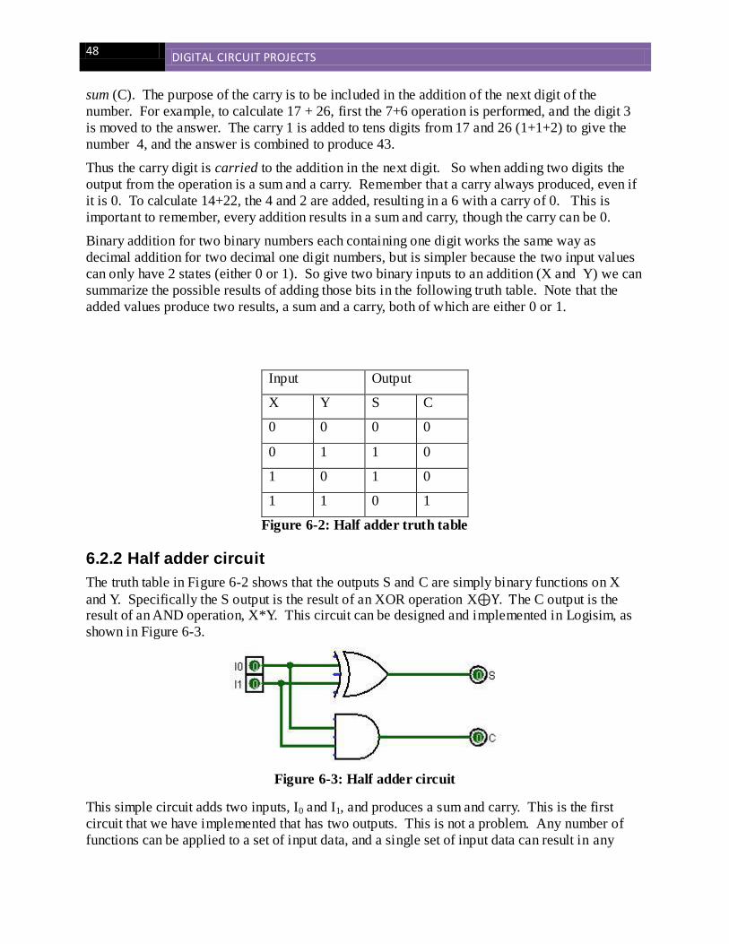
48 DIGITAL CIRCUIT PROJECTS
sum (C). The purpose of the carry is to be included in the addition of the next digit of the
number. For example, to calculate 17 + 26, first the 7+6 operation is performed, and the digit 3
is moved to the answer. The carry 1 is added to tens digits from 17 and 26 (1+1+2) to give the
number 4, and the answer is combined to produce 43.
Thus the carry digit is carried to the addition in the next digit. So when adding two digits the
output from the operation is a sum and a carry. Remember that a carry always produced, even if
it is 0. To calculate 14+22, the 4 and 2 are added, resulting in a 6 with a carry of 0. This is
important to remember, every addition results in a sum and carry, though the carry can be 0.
Binary addition for two binary numbers each containing one digit works the same way as
decimal addition for two decimal one digit numbers, but is simpler because the two input values
can only have 2 states (either 0 or 1). So give two binary inputs to an addition (X and Y) we can
summarize the possible results of adding those bits in the following truth table. Note that the
added values produce two results, a sum and a carry, both of which are either 0 or 1.
Input Output
X Y S C
0 0 0 0
0 1 1 0
1 0 1 0
1 1 0 1
Figure 6-2: Half adder truth table
6.2.2 Half adder circuit
The truth table in Figure 6-2 shows that the outputs S and C are simply binary functions on X
and Y. Specifically the S output is the result of an XOR operation X⊕Y. The C output is the result of an AND operation, X*Y. This circuit can be designed and implemented in Logisim, as
shown in Figure 6-3.
Figure 6-3: Half adder circuit
This simple circuit adds two inputs, I0 and I1, and produces a sum and carry. This is the first
circuit that we have implemented that has two outputs. This is not a problem. Any number of
functions can be applied to a set of input data, and a single set of input data can result in any
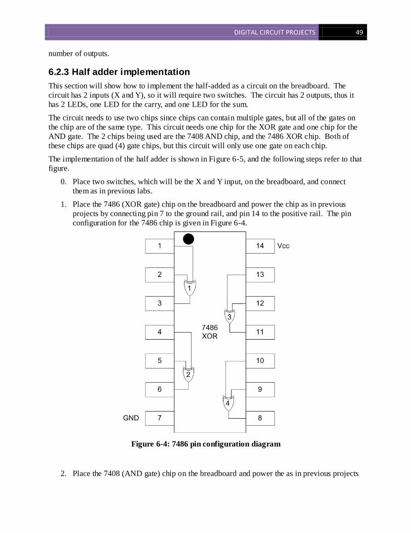
DIGITAL CIRCUIT PROJECTS 49
number of outputs.
6.2.3 Half adder implementation
This section will show how to implement the half-added as a circuit on the breadboard. The
circuit has 2 inputs (X and Y), so it will require two switches. The circuit has 2 outputs, thus it
has 2 LEDs, one LED for the carry, and one LED for the sum.
The circuit needs to use two chips since chips can contain multiple gates, but all of the gates on
the chip are of the same type. This circuit needs one chip for the XOR gate and one chip for the
AND gate. The 2 chips being used are the 7408 AND chip, and the 7486 XOR chip. Both of
these chips are quad (4) gate chips, but this circuit will only use one gate on each chip.
The implementation of the half adder is shown in Figure 6-5, and the following steps refer to that
figure.
0. Place two switches, which will be the X and Y input, on the breadboard, and connect
them as in previous labs.
1. Place the 7486 (XOR gate) chip on the breadboard and power the chip as in previous
projects by connecting pin 7 to the ground rail, and pin 14 to the positive rail. The pin
configuration for the 7486 chip is given in Figure 6-4.
Figure 6-4: 7486 pin configuration diagram
2. Place the 7408 (AND gate) chip on the breadboard and power the as in previous projects
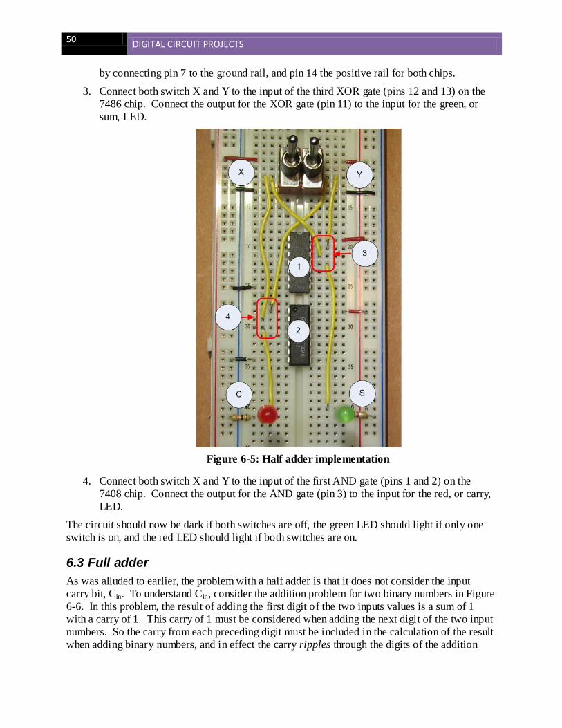
50 DIGITAL CIRCUIT PROJECTS
by connecting pin 7 to the ground rail, and pin 14 the positive rail for both chips.
3. Connect both switch X and Y to the input of the third XOR gate (pins 12 and 13) on the
7486 chip. Connect the output for the XOR gate (pin 11) to the input for the green, or
sum, LED.
Figure 6-5: Half adder implementation
4. Connect both switch X and Y to the input of the first AND gate (pins 1 and 2) on the
7408 chip. Connect the output for the AND gate (pin 3) to the input for the red, or carry,
LED.
The circuit should now be dark if both switches are off, the green LED should light if only one
switch is on, and the red LED should light if both switches are on.
6.3 Full adder
As was alluded to earlier, the problem with a half adder is that it does not consider the input
carry bit, Cin. To understand Cin, consider the addition problem for two binary numbers in Figure
6-6. In this problem, the result of adding the first digit of the two inputs values is a sum of 1
with a carry of 1. This carry of 1 must be considered when adding the next digit of the two input
numbers. So the carry from each preceding digit must be included in the calculation of the result
when adding binary numbers, and in effect the carry ripples through the digits of the addition
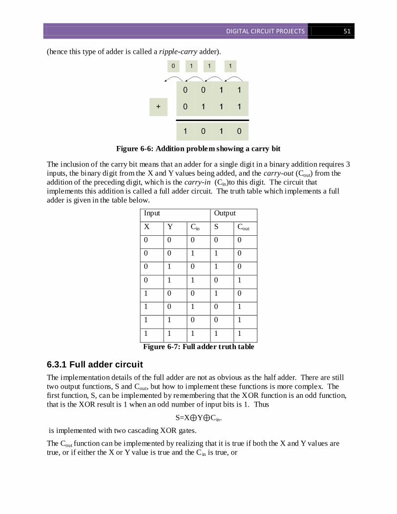
DIGITAL CIRCUIT PROJECTS 51
(hence this type of adder is called a ripple-carry adder).
Figure 6-6: Addition problem showing a carry bit
The inclusion of the carry bit means that an adder for a single digit in a binary addition requires 3
inputs, the binary digit from the X and Y values being added, and the carry-out (Cout) from the
addition of the preceding digit, which is the carry-in (Cin)to this digit. The circuit that
implements this addition is called a full adder circuit. The truth table which implements a full
adder is given in the table below.
Input Output
X Y Cin S Cout
0 0 0 0 0
0 0 1 1 0
0 1 0 1 0
0 1 1 0 1
1 0 0 1 0
1 0 1 0 1
1 1 0 0 1
1 1 1 1 1
Figure 6-7: Full adder truth table
6.3.1 Full adder circuit
The implementation details of the full adder are not as obvious as the half adder. There are still
two output functions, S and Cout, but how to implement these functions is more complex. The
first function, S, can be implemented by remembering that the XOR function is an odd function,
that is the XOR result is 1 when an odd number of input bits is 1. Thus
S=X⊕Y⊕Cin.
is implemented with two cascading XOR gates.
The Cout function can be implemented by realizing that it is true if both the X and Y values are
true, or if either the X or Y value is true and the C in is true, or

52 DIGITAL CIRCUIT PROJECTS
Cout = (X*Y) + ((X⊕Y)*Cin)
Using these two functions for C and S, the circuit for the full adder can be represented in
Logisim as the following diagram.
Figure 6-8: Full adder circuit
6.3.2 Full adder implementation
The implementation of the full adder is by far the most complex circuit we have implemented up
to this time. So while neatness when implementing a circuit always counts, it is now important
to be very careful to consider not only how the circuit is implemented, but what gates on the
chips to use and how to make the connections. A haphazard implementation of the circuit will
become very messy and hard to understand, implement, and debug.
1. Begin by installing and powering 3 switches. The first two switches will be the X and Y
values for the circuit, and the third switch will be the C in value to the circuit. Note the
order of the switches is different than for the half adder. This circuit is somewhat
complex, and so the placement of the switches is designed to keep the rest of the circuit
as simple as possible.
2. This circuit requires 3 types of gates, so 3 chips must be used. Install the 7486 (XOR)
chip on the board, and power it as before.
3. Install the 7408 (AND) chip on the board and power it.
4. Install the 7432 (OR) chip on the board and power it. It is suggested that these chips be
placed on the board in this order, as this is the order they will be accessed in the circuit.
Any other placement of the chips will require wires to be run both forward and backward
in this circuit, which will eventually be confusing.
5. Once the chips have been installed on the board, wire the XOR gates. Wire the X and Y
switches to pins 1 and 2 (first XOR gate) on the left side of the 7486 chip. The output of
the XOR gate will be on pin 3.
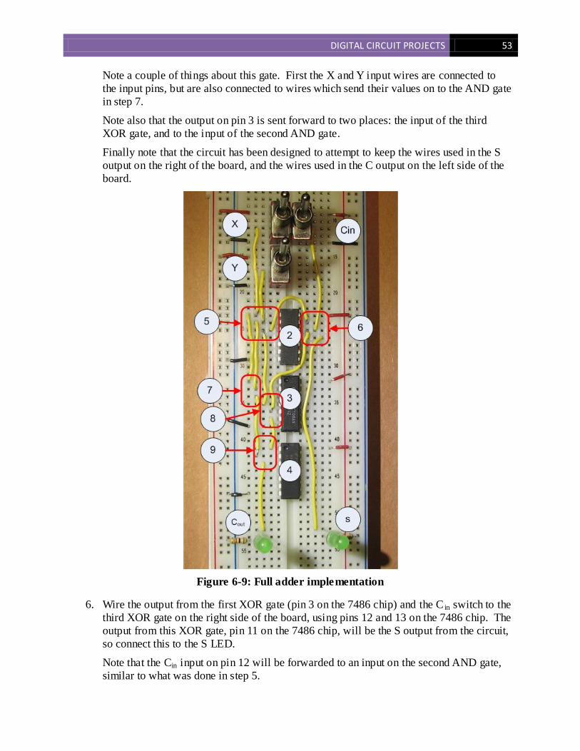
DIGITAL CIRCUIT PROJECTS 53
Note a couple of things about this gate. First the X and Y input wires are connected to
the input pins, but are also connected to wires which send their values on to the AND gate
in step 7.
Note also that the output on pin 3 is sent forward to two places: the input of the third
XOR gate, and to the input of the second AND gate.
Finally note that the circuit has been designed to attempt to keep the wires used in the S
output on the right of the board, and the wires used in the C output on the left side of the
board.
Figure 6-9: Full adder implementation
6. Wire the output from the first XOR gate (pin 3 on the 7486 chip) and the C in switch to the
third XOR gate on the right side of the board, using pins 12 and 13 on the 7486 chip. The
output from this XOR gate, pin 11 on the 7486 chip, will be the S output from the circuit,
so connect this to the S LED.
Note that the Cin input on pin 12 will be forwarded to an input on the second AND gate,
similar to what was done in step 5.
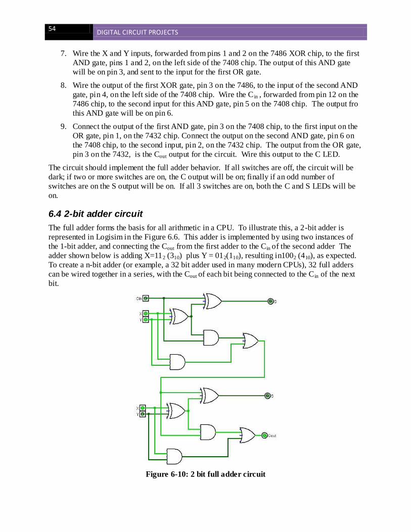
54 DIGITAL CIRCUIT PROJECTS
7. Wire the X and Y inputs, forwarded from pins 1 and 2 on the 7486 XOR chip, to the first
AND gate, pins 1 and 2, on the left side of the 7408 chip. The output of this AND gate
will be on pin 3, and sent to the input for the first OR gate.
8. Wire the output of the first XOR gate, pin 3 on the 7486, to the input of the second AND
gate, pin 4, on the left side of the 7408 chip. Wire the C in , forwarded from pin 12 on the
7486 chip, to the second input for this AND gate, pin 5 on the 7408 chip. The output fro
this AND gate will be on pin 6.
9. Connect the output of the first AND gate, pin 3 on the 7408 chip, to the first input on the
OR gate, pin 1, on the 7432 chip. Connect the output on the second AND gate, pin 6 on
the 7408 chip, to the second input, pin 2, on the 7432 chip. The output from the OR gate,
pin 3 on the 7432, is the Cout output for the circuit. Wire this output to the C LED.
The circuit should implement the full adder behavior. If all switches are off, the circuit will be
dark; if two or more switches are on, the C output will be on; finally if an odd number of
switches are on the S output will be on. If all 3 switches are on, both the C and S LEDs will be
on.
6.4 2-bit adder circuit
The full adder forms the basis for all arithmetic in a CPU. To illustrate this, a 2-bit adder is
represented in Logisim in the Figure 6.6. This adder is implemented by using two instances of
the 1-bit adder, and connecting the Cout from the first adder to the Cin of the second adder The
adder shown below is adding X=112 (310) plus Y = 012(110), resulting in1002 (410), as expected.
To create a n-bit adder (or example, a 32 bit adder used in many modern CPUs), 32 full adders
can be wired together in a series, with the Cout of each bit being connected to the C in of the next
bit.
Figure 6-10: 2 bit full adder circuit
DIGITAL CIRCUIT PROJECTS 55
6.5 Conclusion
The adder forms the basis for all of the arithmetic functions in the ALU. Subtraction,
multiplication, and division all are implemented using algorithms which are based on the adder.
The adder is therefore a stand in for all of the other types of functions performed by the ALU.
Despite the appearance that addition is more complex, it can be implemented as a Boolean
function consisting only of AND, OR, and XOR gates. These simple Boolean functions are
implemented in circuits called half adders and full adders. It is when these functions are chained
together so that the carry from each previous function is used in the next function that the adder
can add larger numbers.
The implementation of the full adder circuit is more complex than the other circuits which have
been looked at so far. It required 3 different chips, 2 outputs, and 5 gates that had to be
connected. This circuit required some degree of carefulness and forethought to implement and
debug it.
The adder was the first circuit implemented in this text that is a component, and it has been
encapsulated as an IC. The 7482 (2-bit binary full adder) and 7483 (4-bit binary full adder) IC
chips are implementations of this circuit.
6.6 Exercises
1. Implement the half adder circuit on the breadboard.
2. Implement the full adder circuit on the breadboard.
3. Using the 2-bit adder presented in the chapter as a model, implement a 4-bit adder in
Logisim. Implement an 8 bit adder.
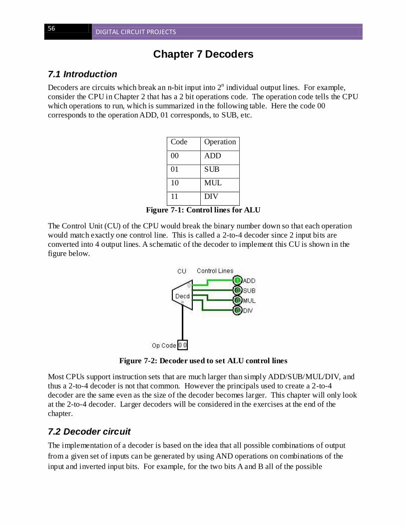
56 DIGITAL CIRCUIT PROJECTS
Chapter 7 Decoders
7.1 Introduction
Decoders are circuits which break an n-bit input into 2n individual output lines. For example,
consider the CPU in Chapter 2 that has a 2 bit operations code. The operation code tells the CPU
which operations to run, which is summarized in the following table. Here the code 00
corresponds to the operation ADD, 01 corresponds, to SUB, etc.
Code Operation
00 ADD
01 SUB
10 MUL
11 DIV
Figure 7-1: Control lines for ALU
The Control Unit (CU) of the CPU would break the binary number down so that each operation
would match exactly one control line. This is called a 2-to-4 decoder since 2 input bits are
converted into 4 output lines. A schematic of the decoder to implement this CU is shown in the
figure below.
Figure 7-2: Decoder used to set ALU control lines
Most CPUs support instruction sets that are much larger than simply ADD/SUB/MUL/DIV, and
thus a 2-to-4 decoder is not that common. However the principals used to create a 2-to-4
decoder are the same even as the size of the decoder becomes larger. This chapter will only look
at the 2-to-4 decoder. Larger decoders will be considered in the exercises at the end of the
chapter.
7.2 Decoder circuit
The implementation of a decoder is based on the idea that all possible combinations of output
from a given set of inputs can be generated by using AND operations on combinations of the
input and inverted input bits. For example, for the two bits A and B all of the possible
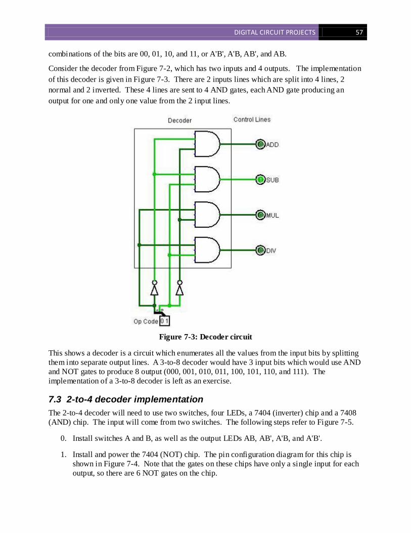
DIGITAL CIRCUIT PROJECTS 57
combinations of the bits are 00, 01, 10, and 11, or A'B', A'B, AB', and AB.
Consider the decoder from Figure 7-2, which has two inputs and 4 outputs. The implementation
of this decoder is given in Figure 7-3. There are 2 inputs lines which are split into 4 lines, 2
normal and 2 inverted. These 4 lines are sent to 4 AND gates, each AND gate producing an
output for one and only one value from the 2 input lines.
Figure 7-3: Decoder circuit
This shows a decoder is a circuit which enumerates all the values from the input bits by splitting
them into separate output lines. A 3-to-8 decoder would have 3 input bits which would use AND
and NOT gates to produce 8 output (000, 001, 010, 011, 100, 101, 110, and 111). The
implementation of a 3-to-8 decoder is left as an exercise.
7.3 2-to-4 decoder implementation
The 2-to-4 decoder will need to use two switches, four LEDs, a 7404 (inverter) chip and a 7408
(AND) chip. The input will come from two switches. The following steps refer to Figure 7-5.
0. Install switches A and B, as well as the output LEDs AB, AB', A'B, and A'B'.
1. Install and power the 7404 (NOT) chip. The pin configuration diagram for this chip is
shown in Figure 7-4. Note that the gates on these chips have only a single input for each
output, so there are 6 NOT gates on the chip.
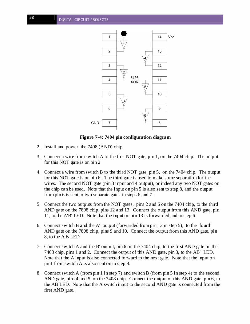
58 DIGITAL CIRCUIT PROJECTS
Figure 7-4: 7404 pin configuration diagram
2. Install and power the 7408 (AND) chip.
3. Connect a wire from switch A to the first NOT gate, pin 1, on the 7404 chip. The output
for this NOT gate is on pin 2
4. Connect a wire from switch B to the third NOT gate, pin 5, on the 7404 chip. The output
for this NOT gate is on pin 6. The third gate is used to make some separation for the
wires. The second NOT gate (pin 3 input and 4 output), or indeed any two NOT gates on
the chip can be used. Note that the input on pin 5 is also sent to step 8, and the output
from pin 6 is sent to two separate gates in steps 6 and 7.
5. Connect the two outputs from the NOT gates, pins 2 and 6 on the 7404 chip, to the third
AND gate on the 7808 chip, pins 12 and 13. Connect the output from this AND gate, pin
11, to the A'B' LED. Note that the input on pin 13 is forwarded and to step 6.
6. Connect switch B and the A' output (forwarded from pin 13 in step 5), to the fourth
AND gate on the 7808 chip, pins 9 and 10. Connect the output from this AND gate, pin
8, to the A'B LED.
7. Connect switch A and the B' output, pin 6 on the 7404 chip, to the first AND gate on the
7408 chip, pins 1 and 2. Connect the output of this AND gate, pin 3, to the AB' LED.
Note that the A input is also connected forward to the next gate. Note that the input on
pin1 from switch A is also sent on to step 8.
8. Connect switch A (from pin 1 in step 7) and switch B (from pin 5 in step 4) to the second
AND gate, pins 4 and 5, on the 7408 chip. Connect the output of this AND gate, pin 6, to
the AB LED. Note that the A switch input to the second AND gate is connected from the
first AND gate.
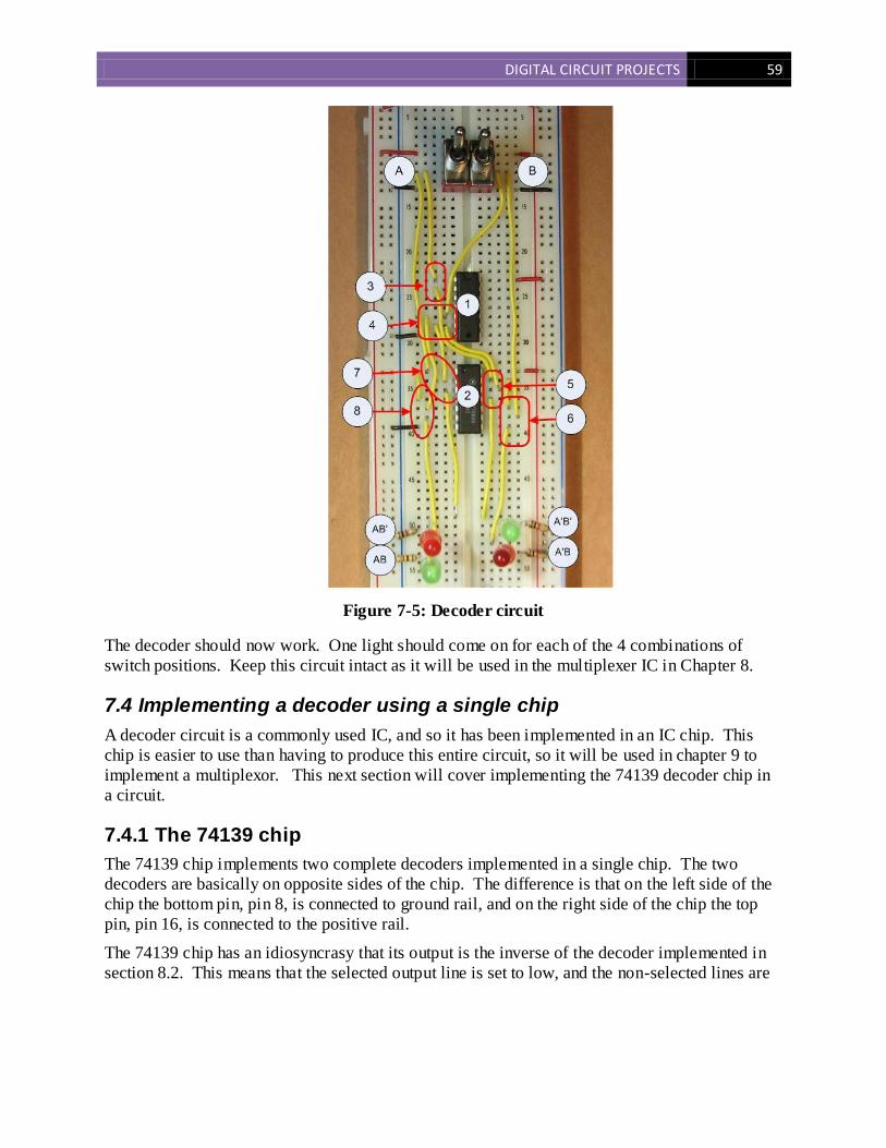
DIGITAL CIRCUIT PROJECTS 59
Figure 7-5: Decoder circuit
The decoder should now work. One light should come on for each of the 4 combinations of
switch positions. Keep this circuit intact as it will be used in the multiplexer IC in Chapter 8.
7.4 Implementing a decoder using a single chip
A decoder circuit is a commonly used IC, and so it has been implemented in an IC chip. This
chip is easier to use than having to produce this entire circuit, so it will be used in chapter 9 to
implement a multiplexor. This next section will cover implementing the 74139 decoder chip in
a circuit.
7.4.1 The 74139 chip
The 74139 chip implements two complete decoders implemented in a single chip. The two
decoders are basically on opposite sides of the chip. The difference is that on the left side of the
chip the bottom pin, pin 8, is connected to ground rail, and on the right side of the chip the top
pin, pin 16, is connected to the positive rail.
The 74139 chip has an idiosyncrasy that its output is the inverse of the decoder implemented in
section 8.2. This means that the selected output line is set to low, and the non-selected lines are
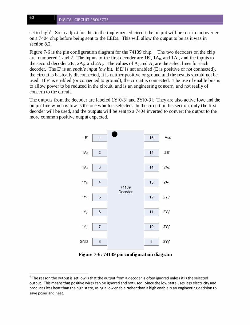
60 DIGITAL CIRCUIT PROJECTS
set to high4. So to adjust for this in the implemented circuit the output will be sent to an inverter
on a 7404 chip before being sent to the LEDs. This will allow the output to be as it was in
section 8.2.
Figure 7-6 is the pin configuration diagram for the 74139 chip. The two decoders on the chip
are numbered 1 and 2. The inputs to the first decoder are 1E', 1A0, and 1A1, and the inputs to
the second decoder 2E', 2A0, and 2A1. The values of A0 and A1 are the select lines for each
decoder. The E' is an enable input low bit. If E' is not enabled (E is positive or not connected),
the circuit is basically disconnected, it is neither positive or ground and the results should not be
used. If E' is enabled (or connected to ground), the circuit is connected. The use of enable bits is
to allow power to be reduced in the circuit, and is an engineering concern, and not really of
concern to the circuit.
The outputs from the decoder are labeled 1Y[0-3] and 2Y[0-3]. They are also active low, and the
output line which is low is the one which is selected. In the circuit in this section, only the first
decoder will be used, and the outputs will be sent to a 7404 inverted to convert the output to the
more common positive output expected.
Figure 7-6: 74139 pin configuration diagram
4 The reason the output is set low is that the output from a decoder is often ignored unless it is the selected output. This means that positive wires can be ignored and not used. Since the low state uses less electricity and produces less heat than the high state, using a low enable rather than a high enable is an engineering decision to save poser and heat.
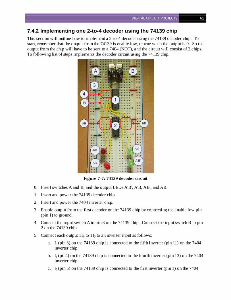
DIGITAL CIRCUIT PROJECTS 61
7.4.2 Implementing one 2-to-4 decoder using the 74139 chip
This section will outline how to implement a 2-to-4 decoder using the 74139 decoder chip. To
start, remember that the output from the 74139 is enable low, or true when the output is 0. So the
output from the chip will have to be sent to a 7404 (NOT), and the circuit will consist of 2 chips.
To following list of steps implements the decoder circuit using the 74139 chip.
Figure 7-7: 74139 decoder circuit
0. Insert switches A and B, and the output LEDs A'B', A'B, AB', and AB.
1. Insert and power the 74139 decoder chip.
2. Insert and power the 7404 inverter chip.
3. Enable output from the first decoder on the 74139 chip by connecting the enable low pin
(pin 1) to ground.
4. Connect the input switch A to pin 3 on the 74139 chip. Connect the input switch B to pin
2 on the 74139 chip.
5. Connect each output 1I0 to 1I3 to an inverter input as follows:
a. I0 (pin 3) on the 74139 chip is connected to the fifth inverter (pin 11) on the 7404
inverter chip.
b. I1 (pin4) on the 74139 chip is connected to the fourth inverter (pin 13) on the 7404
inverter chip.
c. I2 (pin 5) on the 74139 chip is connected to the first inverter (pin 1) on the 7404

62 DIGITAL CIRCUIT PROJECTS
inverter chip.
d. I3 (pin 6) on the 74139 chip is connected to the second inverter (pin 3) on the 7404
inverter chip.
6. Connect the inverter outputs to the correct LEDs:
a. Connect pin 10 on the 7404 inverter chip to the A'B' LED.
b. Connect pin 12 on the 7404 inverter chip to the A'B LED.
c. Connect pin 2 on the 7404 inverter chip to the AB' LED.
d. Connect pin 4 on the 7404 inverter chip to the AB LED.
This circuit should now behave like the circuit in section 7.3.
7.5 Conclusion
A decoder is an IC which splits an n-bit input value into 2n output lines. A decoder has many
uses, but the one presented here is translating a 2-bit input value into 4lines to allow the 4
different operations of the CPU. The decoder will also be used in the next chapter as part of the
multiplexer.
The decoder works by doing AND operations on all combinations of the input and inverted input
values, and then selecting the output using an OR operation on all of the inputs.
The decoder is a common circuit, so it has been encapsulated in a 74139 chip. The 74139
contains 2 decoders, and based on the binary input to each decoder, selects the correct output.
The 74139 chip is different in the enable and all output values are enable low, or selected when
the value is low. Therefore to get the behavior we want from the chip, the values must be sent to
an inverted (7404) chip to be used.
7.6 Exercises
1. Implement the 2-to-4 decoder using 7404 (NOT) an 7808 (AND) chips on your breadboard. 2. Implement the 2-to-4 decoder circuit with a 74139 chip on your breadboard. 3. Implement a 1-to-2 decoder in Logisim. Implement this circuit on your breadboard.
4. Implement a 3-to-8 decoder using NOT and AND gates in Logisim. Show that it is correct by showing it generates the same output as a 3-to-8 Decoder found in the Plexors menu of Logisim.
5. Implement a 3-to-8 decoder using two 2-to-4 decoders, and as many AND gates as you need. Compare the total number of AND gates in the circuit to the number of AND gates used to implement the 3-to-8 decoder with 2-input AND gates in question 4. Which circuit do you think
is faster. 6. Answer the following questions.
a. How many output lines would a 4 input decoder have? b. How many output lines would a 5 input decoder have? c. For an N-to-X decoder, specify X as a function of N (e.g. specify the number of output
lines as a function of the number of input lines for a decoder).
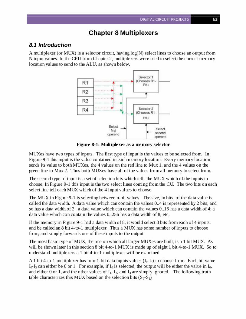
DIGITAL CIRCUIT PROJECTS 63
Chapter 8 Multiplexers
8.1 Introduction
A multiplexer (or MUX) is a selector circuit, having log(N) select lines to choose an output from
N input values. In the CPU from Chapter 2, multiplexers were used to select the correct memory
location values to send to the ALU, as shown below.
Figure 8-1: Multiplexer as a memory selector
MUXes have two types of inputs. The first type of input is the values to be selected from. In
Figure 9-1 this input is the value contained in each memory location. Every memory location
sends its value to both MUXes, the 4 values on the red line to Mux 1, and the 4 values on the
green line to Mux 2. Thus both MUXes have all of the values from all memory to select from.
The second type of input is a set of selection bits which tells the MUX which of the inputs to
choose. In Figure 9-1 this input is the two select lines coming from the CU. The two bits on each
select line tell each MUX which of the 4 input values to choose.
The MUX in Figure 9-1 is selecting between n-bit values. The size, in bits, of the data value is
called the data width. A data value which can contain the values 0..4 is represented by 2 bits, and
so has a data width of 2; a data value which can contain the values 0..16 has a data width of 4; a
data value which con contain the values 0..256 has a data width of 8; etc.
If the memory in Figure 9-1 had a data width of 8, it would select 8 bits from each of 4 inputs,
and be called an 8 bit 4-to-1 multiplexer. Thus a MUX has some number of inputs to choose
from, and simply forwards one of these inputs to the output.
The most basic type of MUX, the one on which all larger MUXes are built, is a 1 bit MUX. As
will be shown later in this section 8 bit 4-to-1 MUX is made up of eight 1 bit 4-to-1 MUX. So to
understand multiplexers a 1 bit 4-to-1 multiplexer will be examined.
A 1 bit 4-to-1 multiplexer has four 1-bit data inputs values (I0-I3) to choose from. Each bit value
I0-I3 can either be 0 or 1. For example, if I0 is selected, the output will be either the value in I0,
and either 0 or 1, and the other values of I1, I2, and I3 are simply ignored. The following truth
table characterizes this MUX based on the selection bits (S0-S1)
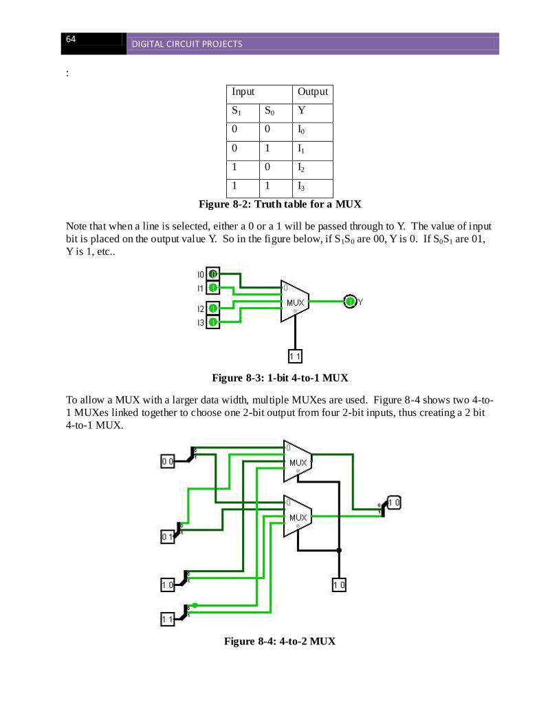
64 DIGITAL CIRCUIT PROJECTS
:
Input Output
S1 S0 Y
0 0 I0
0 1 I1
1 0 I2
1 1 I3
Figure 8-2: Truth table for a MUX
Note that when a line is selected, either a 0 or a 1 will be passed through to Y. The value of input
bit is placed on the output value Y. So in the figure below, if S1S0 are 00, Y is 0. If S0S1 are 01,
Y is 1, etc..
Figure 8-3: 1-bit 4-to-1 MUX
To allow a MUX with a larger data width, multiple MUXes are used. Figure 8-4 shows two 4-to-
1 MUXes linked together to choose one 2-bit output from four 2-bit inputs, thus creating a 2 bit
4-to-1 MUX.
Figure 8-4: 4-to-2 MUX
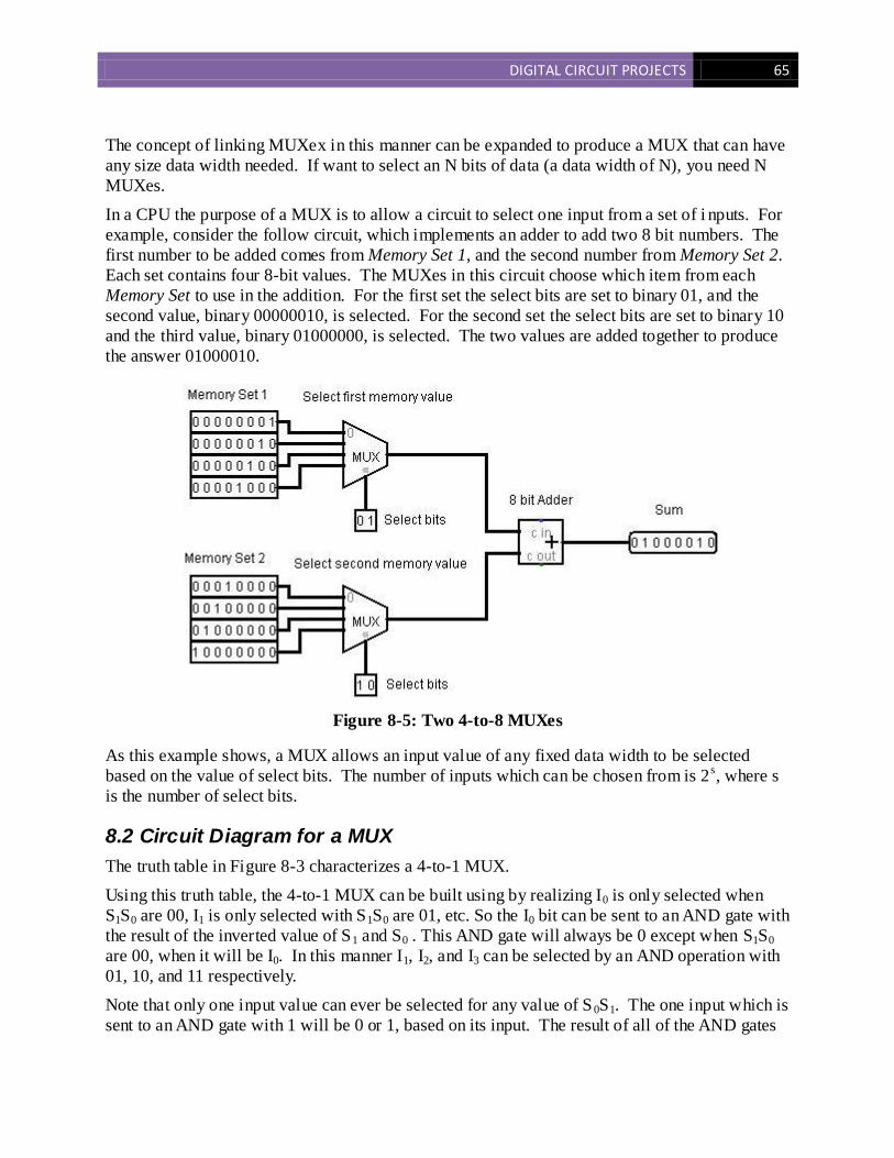
DIGITAL CIRCUIT PROJECTS 65
The concept of linking MUXex in this manner can be expanded to produce a MUX that can have
any size data width needed. If want to select an N bits of data (a data width of N), you need N
MUXes.
In a CPU the purpose of a MUX is to allow a circuit to select one input from a set of i nputs. For
example, consider the follow circuit, which implements an adder to add two 8 bit numbers. The
first number to be added comes from Memory Set 1, and the second number from Memory Set 2.
Each set contains four 8-bit values. The MUXes in this circuit choose which item from each
Memory Set to use in the addition. For the first set the select bits are set to binary 01, and the
second value, binary 00000010, is selected. For the second set the select bits are set to binary 10
and the third value, binary 01000000, is selected. The two values are added together to produce
the answer 01000010.
Figure 8-5: Two 4-to-8 MUXes
As this example shows, a MUX allows an input value of any fixed data width to be selected
based on the value of select bits. The number of inputs which can be chosen from is 2s, where s
is the number of select bits.
8.2 Circuit Diagram for a MUX
The truth table in Figure 8-3 characterizes a 4-to-1 MUX.
Using this truth table, the 4-to-1 MUX can be built using by realizing I0 is only selected when
S1S0 are 00, I1 is only selected with S1S0 are 01, etc. So the I0 bit can be sent to an AND gate with
the result of the inverted value of S1 and S0 . This AND gate will always be 0 except when S1S0
are 00, when it will be I0. In this manner I1, I2, and I3 can be selected by an AND operation with
01, 10, and 11 respectively.
Note that only one input value can ever be selected for any value of S 0S1. The one input which is
sent to an AND gate with 1 will be 0 or 1, based on its input. The result of all of the AND gates

66 DIGITAL CIRCUIT PROJECTS
are sent to a 4-way OR gate. Remembering 0 + X is always X, the result of the OR gate will
represent the one input selected. It can be 0 or 1, but it will be 0 or 1 based on the value of the
selected input.
The schematic of a MUX is given in the Figure 8-7.
Figure 8-6: Schematic of a MUX
An interesting thing about this circuit is that it a decoder is implemented as part of the
multiplexer circuit, as shown in the outlined part of Figure 8-6. This suggests another way to
implement the MUX using a decoder to select which input line to select. This is shown in Figure
8-7. We will make use of this in designing our implementation of a MUX.
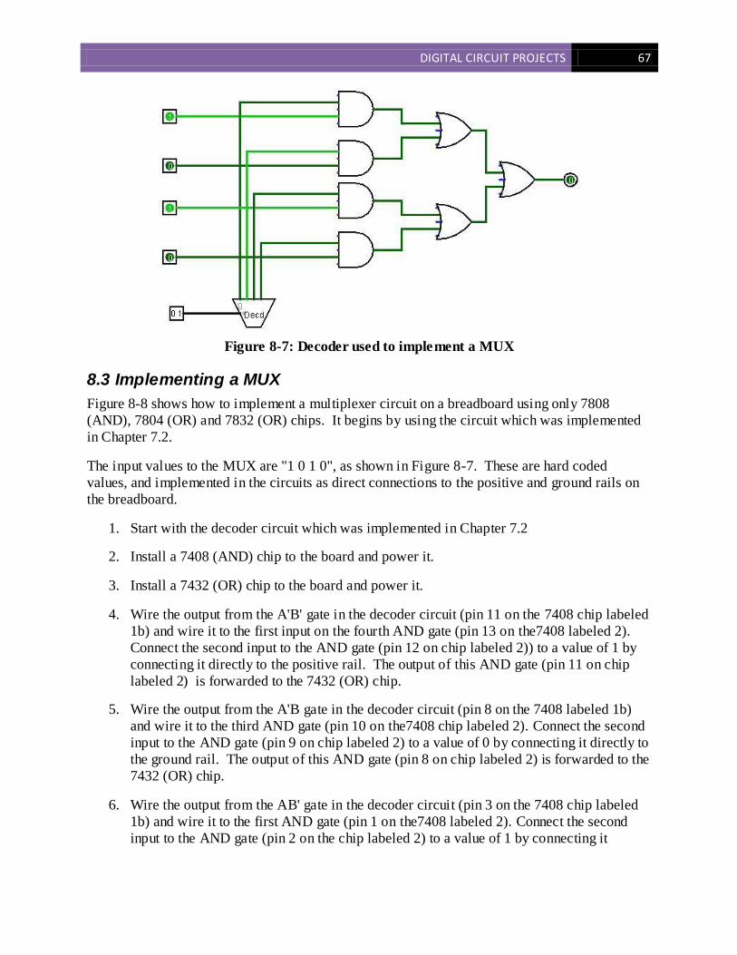
DIGITAL CIRCUIT PROJECTS 67
Figure 8-7: Decoder used to implement a MUX
8.3 Implementing a MUX
Figure 8-8 shows how to implement a multiplexer circuit on a breadboard using only 7808
(AND), 7804 (OR) and 7832 (OR) chips. It begins by using the circuit which was implemented
in Chapter 7.2.
The input values to the MUX are "1 0 1 0", as shown in Figure 8-7. These are hard coded
values, and implemented in the circuits as direct connections to the positive and ground rails on
the breadboard.
1. Start with the decoder circuit which was implemented in Chapter 7.2
2. Install a 7408 (AND) chip to the board and power it.
3. Install a 7432 (OR) chip to the board and power it.
4. Wire the output from the A'B' gate in the decoder circuit (pin 11 on the 7408 chip labeled
1b) and wire it to the first input on the fourth AND gate (pin 13 on the7408 labeled 2).
Connect the second input to the AND gate (pin 12 on chip labeled 2)) to a value of 1 by
connecting it directly to the positive rail. The output of this AND gate (pin 11 on chip
labeled 2) is forwarded to the 7432 (OR) chip.
5. Wire the output from the A'B gate in the decoder circuit (pin 8 on the 7408 labeled 1b)
and wire it to the third AND gate (pin 10 on the7408 chip labeled 2). Connect the second
input to the AND gate (pin 9 on chip labeled 2) to a value of 0 by connecting it directly to
the ground rail. The output of this AND gate (pin 8 on chip labeled 2) is forwarded to the
7432 (OR) chip.
6. Wire the output from the AB' gate in the decoder circuit (pin 3 on the 7408 chip labeled
1b) and wire it to the first AND gate (pin 1 on the7408 labeled 2). Connect the second
input to the AND gate (pin 2 on the chip labeled 2) to a value of 1 by connecting it
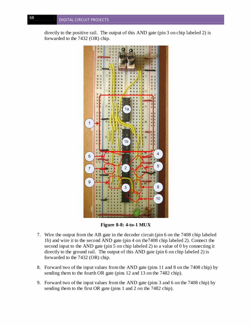
68 DIGITAL CIRCUIT PROJECTS
directly to the positive rail. The output of this AND gate (pin 3 on chip labeled 2) is
forwarded to the 7432 (OR) chip.
Figure 8-8: 4-to-1 MUX
7. Wire the output from the AB gate in the decoder circuit (pin 6 on the 7408 chip labeled
1b) and wire it to the second AND gate (pin 4 on the7408 chip labeled 2). Connect the
second input to the AND gate (pin 5 on chip labeled 2) to a value of 0 by connecting it
directly to the ground rail. The output of this AND gate (pin 6 on chip labeled 2) is
forwarded to the 7432 (OR) chip.
8. Forward two of the input values from the AND gate (pins 11 and 8 on the 7408 chip) by
sending them to the fourth OR gate (pins 12 and 13 on the 7482 chip).
9. Forward two of the input values from the AND gate (pins 3 and 6 on the 7408 chip) by
sending them to the first OR gate (pins 1 and 2 on the 7482 chip).
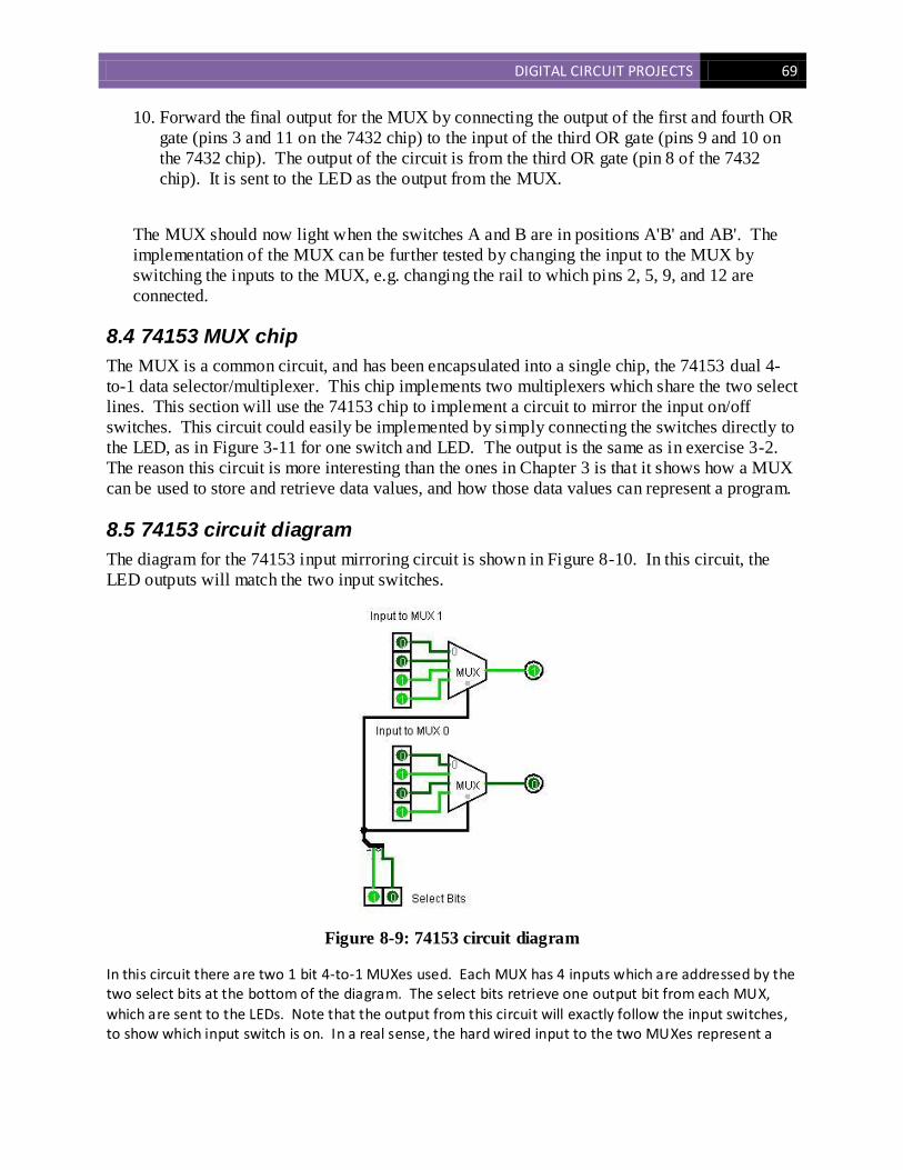
DIGITAL CIRCUIT PROJECTS 69
10. Forward the final output for the MUX by connecting the output of the first and fourth OR
gate (pins 3 and 11 on the 7432 chip) to the input of the third OR gate (pins 9 and 10 on
the 7432 chip). The output of the circuit is from the third OR gate (pin 8 of the 7432
chip). It is sent to the LED as the output from the MUX.
The MUX should now light when the switches A and B are in positions A'B' and AB'. The
implementation of the MUX can be further tested by changing the input to the MUX by
switching the inputs to the MUX, e.g. changing the rail to which pins 2, 5, 9, and 12 are
connected.
8.4 74153 MUX chip
The MUX is a common circuit, and has been encapsulated into a single chip, the 74153 dual 4-
to-1 data selector/multiplexer. This chip implements two multiplexers which share the two select
lines. This section will use the 74153 chip to implement a circuit to mirror the input on/off
switches. This circuit could easily be implemented by simply connecting the switches directly to
the LED, as in Figure 3-11 for one switch and LED. The output is the same as in exercise 3-2.
The reason this circuit is more interesting than the ones in Chapter 3 is that it shows how a MUX
can be used to store and retrieve data values, and how those data values can represent a program.
8.5 74153 circuit diagram
The diagram for the 74153 input mirroring circuit is shown in Figure 8-10. In this circuit, the
LED outputs will match the two input switches.
Figure 8-9: 74153 circuit diagram
In this circuit there are two 1 bit 4-to-1 MUXes used. Each MUX has 4 inputs which are addressed by the two select bits at the bottom of the diagram. The select bits retrieve one output bit from each MUX,
which are sent to the LEDs. Note that the output from this circuit will exactly follow the input switches, to show which input switch is on. In a real sense, the hard wired input to the two MUXes represent a
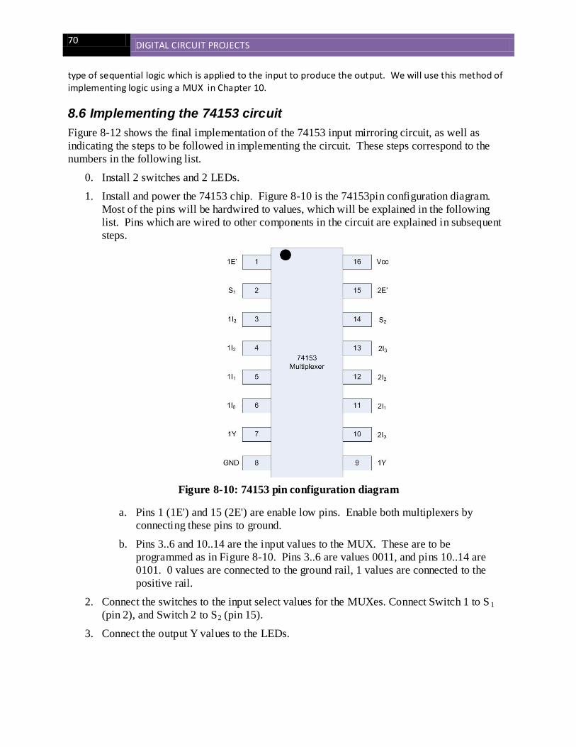
70 DIGITAL CIRCUIT PROJECTS
type of sequential logic which is applied to the input to produce the output. We will use this method of implementing logic using a MUX in Chapter 10.
8.6 Implementing the 74153 circuit
Figure 8-12 shows the final implementation of the 74153 input mirroring circuit, as well as
indicating the steps to be followed in implementing the circuit. These steps correspond to the
numbers in the following list.
0. Install 2 switches and 2 LEDs.
1. Install and power the 74153 chip. Figure 8-10 is the 74153pin configuration diagram.
Most of the pins will be hardwired to values, which will be explained in the following
list. Pins which are wired to other components in the circuit are explained in subsequent
steps.
Figure 8-10: 74153 pin configuration diagram
a. Pins 1 (1E') and 15 (2E') are enable low pins. Enable both multiplexers by
connecting these pins to ground.
b. Pins 3..6 and 10..14 are the input values to the MUX. These are to be
programmed as in Figure 8-10. Pins 3..6 are values 0011, and pins 10..14 are
0101. 0 values are connected to the ground rail, 1 values are connected to the
positive rail.
2. Connect the switches to the input select values for the MUXes. Connect Switch 1 to S 1
(pin 2), and Switch 2 to S2 (pin 15).
3. Connect the output Y values to the LEDs.
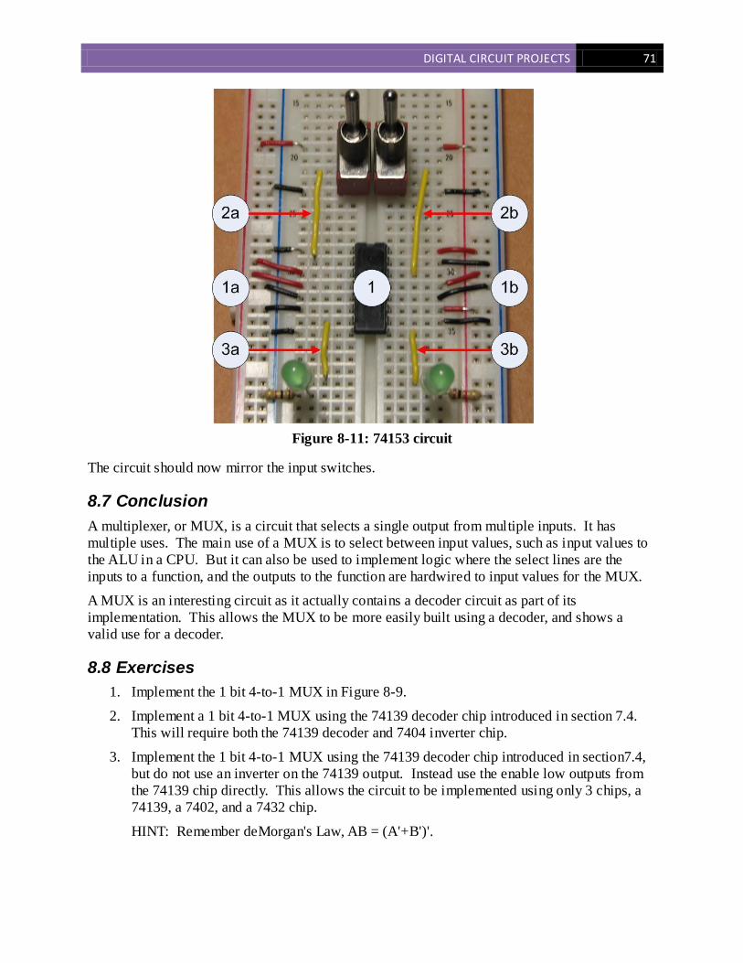
DIGITAL CIRCUIT PROJECTS 71
Figure 8-11: 74153 circuit
The circuit should now mirror the input switches.
8.7 Conclusion
A multiplexer, or MUX, is a circuit that selects a single output from multiple inputs. It has
multiple uses. The main use of a MUX is to select between input values, such as input values to
the ALU in a CPU. But it can also be used to implement logic where the select lines are the
inputs to a function, and the outputs to the function are hardwired to input values for the MUX.
A MUX is an interesting circuit as it actually contains a decoder circuit as part of its
implementation. This allows the MUX to be more easily built using a decoder, and shows a
valid use for a decoder.
8.8 Exercises
1. Implement the 1 bit 4-to-1 MUX in Figure 8-9.
2. Implement a 1 bit 4-to-1 MUX using the 74139 decoder chip introduced in section 7.4.
This will require both the 74139 decoder and 7404 inverter chip.
3. Implement the 1 bit 4-to-1 MUX using the 74139 decoder chip introduced in section7.4,
but do not use an inverter on the 74139 output. Instead use the enable low outputs from
the 74139 chip directly. This allows the circuit to be implemented using only 3 chips, a
74139, a 7402, and a 7432 chip.
HINT: Remember deMorgan's Law, AB = (A'+B')'.

72 DIGITAL CIRCUIT PROJECTS
4. Implement a 1 bit 4-to-1 MUX using the 74153 chip, as in section 8.3.
5. Explain how a 1 bit 4-to-1 MUX can calculate any binary Boolean function. Because
the MUX can calculate the result of any Boolean function, we call the MUX a univeral
operation.
6. In Logism implement an 8 bit 4-to-1 MUX using 8 4-to-1 MUXes.
7. In Logisim implement an 8-to-1 MUX using 2 4-to-1 MUXes and a 2-to-1 MUX.
8. In Logisim implement an 8-to-1 MUX using 4 2-to-1 MUXes and a 4-to-1 MUX.
9. In Logisim implement a circuit similar to the one in figure 8-10, but which produces
output which is the opposite of the input switch (e.g. the LEDs are 0 when the switch is 1,
and 1 when the switch is 0). Change the program in the breadboard to match this new
logic.
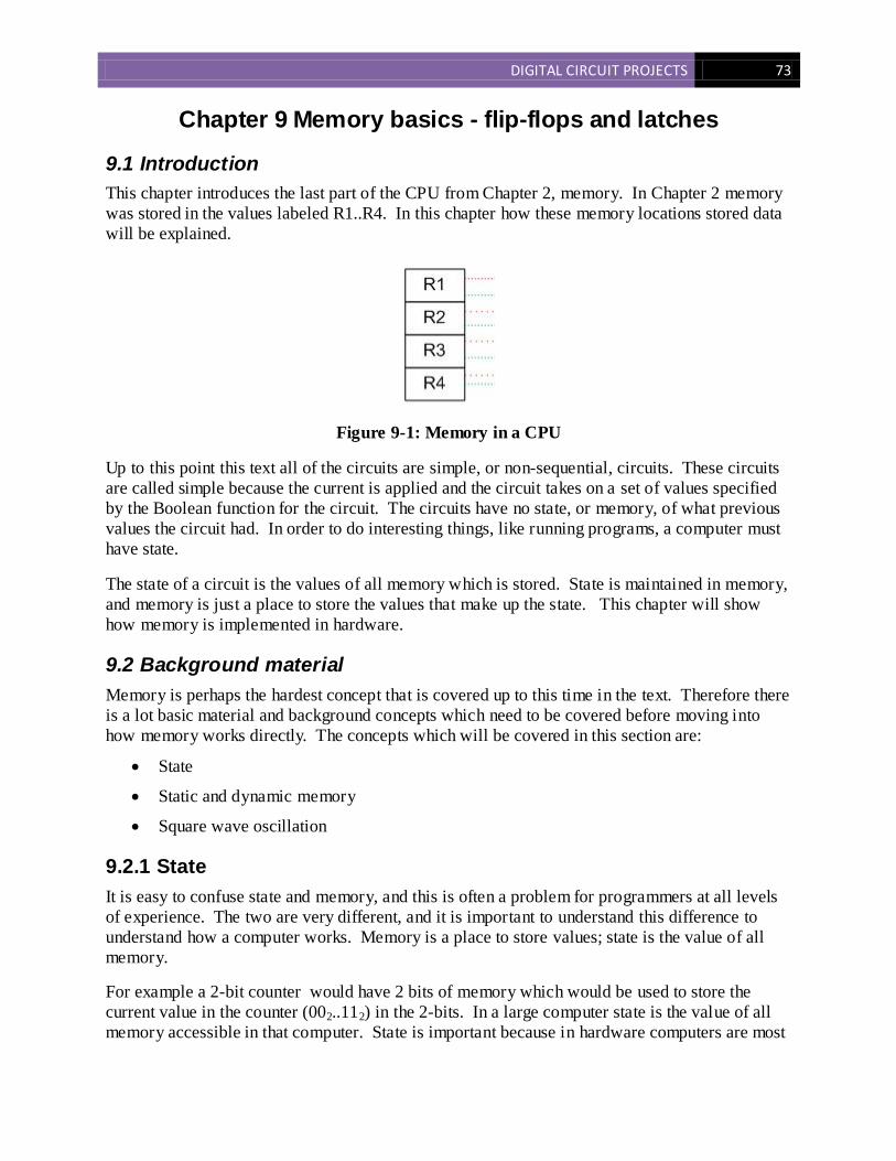
DIGITAL CIRCUIT PROJECTS 73
Chapter 9 Memory basics - flip-flops and latches
9.1 Introduction
This chapter introduces the last part of the CPU from Chapter 2, memory. In Chapter 2 memory
was stored in the values labeled R1..R4. In this chapter how these memory locations stored data
will be explained.
Figure 9-1: Memory in a CPU
Up to this point this text all of the circuits are simple, or non-sequential, circuits. These circuits
are called simple because the current is applied and the circuit takes on a set of values specified
by the Boolean function for the circuit. The circuits have no state, or memory, of what previous
values the circuit had. In order to do interesting things, like running programs, a computer must
have state.
The state of a circuit is the values of all memory which is stored. State is maintained in memory,
and memory is just a place to store the values that make up the state. This chapter will show
how memory is implemented in hardware.
9.2 Background material
Memory is perhaps the hardest concept that is covered up to this time in the text. Therefore there
is a lot basic material and background concepts which need to be covered before moving into
how memory works directly. The concepts which will be covered in this section are:
State
Static and dynamic memory
Square wave oscillation
9.2.1 State
It is easy to confuse state and memory, and this is often a problem for programmers at all levels
of experience. The two are very different, and it is important to understand this difference to
understand how a computer works. Memory is a place to store values; state is the value of all
memory.
For example a 2-bit counter would have 2 bits of memory which would be used to store the
current value in the counter (002..112) in the 2-bits. In a large computer state is the value of all
memory accessible in that computer. State is important because in hardware computers are most
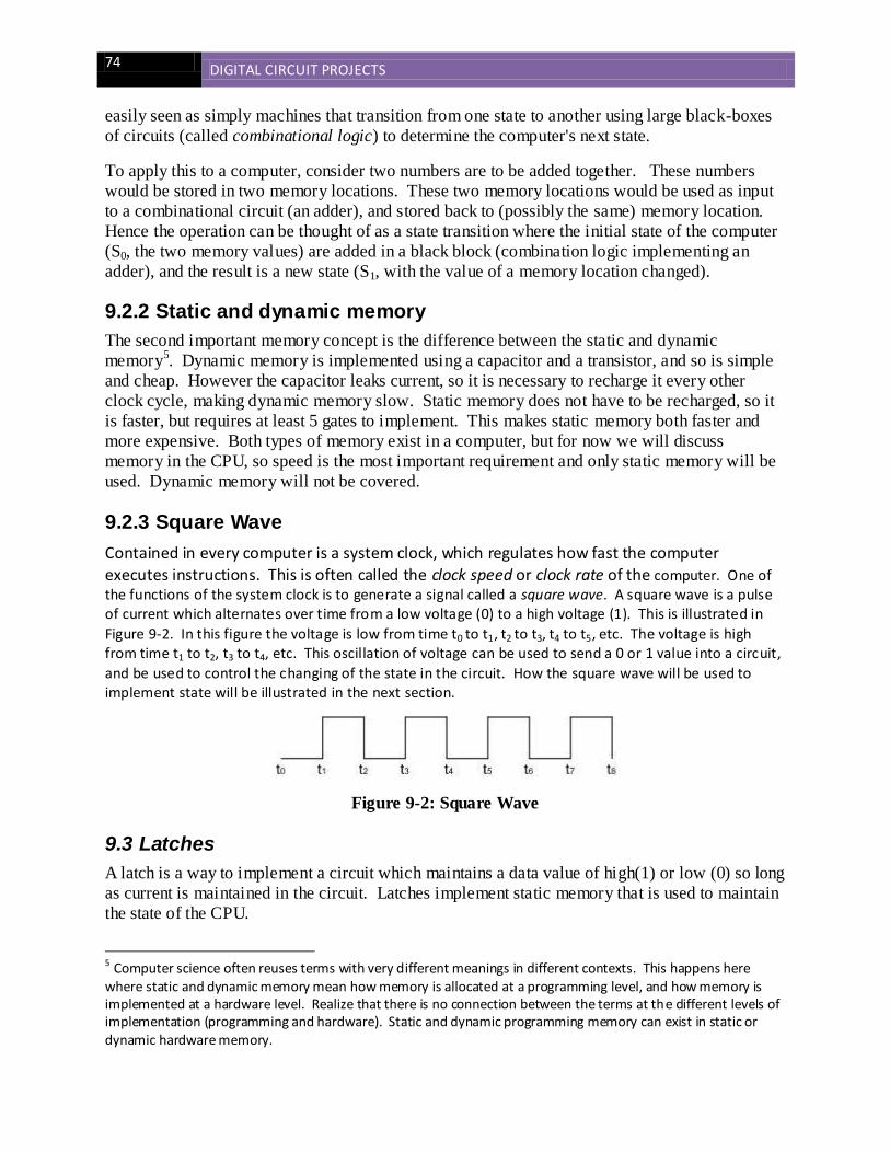
74 DIGITAL CIRCUIT PROJECTS
easily seen as simply machines that transition from one state to another using large black-boxes
of circuits (called combinational logic) to determine the computer's next state.
To apply this to a computer, consider two numbers are to be added together. These numbers
would be stored in two memory locations. These two memory locations would be used as input
to a combinational circuit (an adder), and stored back to (possibly the same) memory location.
Hence the operation can be thought of as a state transition where the initial state of the computer
(S0, the two memory values) are added in a black block (combination logic implementing an
adder), and the result is a new state (S1, with the value of a memory location changed).
9.2.2 Static and dynamic memory
The second important memory concept is the difference between the static and dynamic
memory5. Dynamic memory is implemented using a capacitor and a transistor, and so is simple
and cheap. However the capacitor leaks current, so it is necessary to recharge it every other
clock cycle, making dynamic memory slow. Static memory does not have to be recharged, so it
is faster, but requires at least 5 gates to implement. This makes static memory both faster and
more expensive. Both types of memory exist in a computer, but for now we will discuss
memory in the CPU, so speed is the most important requirement and only static memory will be
used. Dynamic memory will not be covered.
9.2.3 Square Wave
Contained in every computer is a system clock, which regulates how fast the computer
executes instructions. This is often called the clock speed or clock rate of the computer. One of the functions of the system clock is to generate a signal called a square wave. A square wave is a pulse of current which alternates over time from a low voltage (0) to a high voltage (1). This is illustrated in
Figure 9-2. In this figure the voltage is low from time t0 to t1, t2 to t3, t4 to t5, etc. The voltage is high from time t1 to t2, t3 to t4, etc. This oscillation of voltage can be used to send a 0 or 1 value into a circuit,
and be used to control the changing of the state in the circuit. How the square wave will be used to implement state will be illustrated in the next section.
Figure 9-2: Square Wave
9.3 Latches
A latch is a way to implement a circuit which maintains a data value of high(1) or low (0) so long
as current is maintained in the circuit. Latches implement static memory that is used to maintain
the state of the CPU.
5 Computer science often reuses terms with very different meanings in different contexts. This happens here where static and dynamic memory mean how memory is allocated at a programming level, and how memory is implemented at a hardware level. Realize that there is no connection between the terms at the different levels of implementation (programming and hardware). Static and dynamic programming memory can exist in static or dynamic hardware memory.
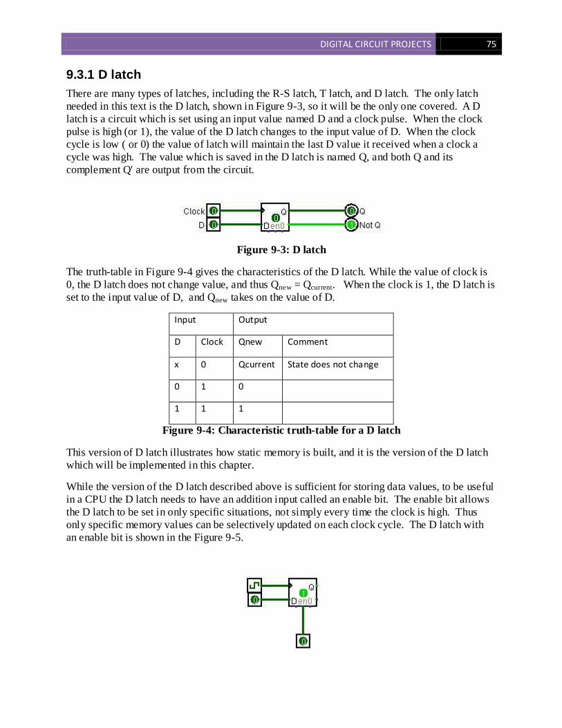
DIGITAL CIRCUIT PROJECTS 75
9.3.1 D latch
There are many types of latches, including the R-S latch, T latch, and D latch. The only latch
needed in this text is the D latch, shown in Figure 9-3, so it will be the only one covered. A D
latch is a circuit which is set using an input value named D and a clock pulse. When the clock
pulse is high (or 1), the value of the D latch changes to the input value of D. When the clock
cycle is low ( or 0) the value of latch will maintain the last D value it received when a clock a
cycle was high. The value which is saved in the D latch is named Q, and both Q and its
complement Q' are output from the circuit.
Figure 9-3: D latch
The truth-table in Figure 9-4 gives the characteristics of the D latch. While the value of clock is
0, the D latch does not change value, and thus Qnew = Qcurrent. When the clock is 1, the D latch is
set to the input value of D, and Qnew takes on the value of D.
Input Output
D Clock Qnew Comment
x 0 Qcurrent State does not change
0 1 0
1 1 1
Figure 9-4: Characteristic truth-table for a D latch
This version of D latch illustrates how static memory is built, and it is the version of the D latch
which will be implemented in this chapter.
While the version of the D latch described above is sufficient for storing data values, to be useful
in a CPU the D latch needs to have an addition input called an enable bit. The enable bit allows
the D latch to be set in only specific situations, not simply every time the clock is high. Thus
only specific memory values can be selectively updated on each clock cycle. The D latch with
an enable bit is shown in the Figure 9-5.
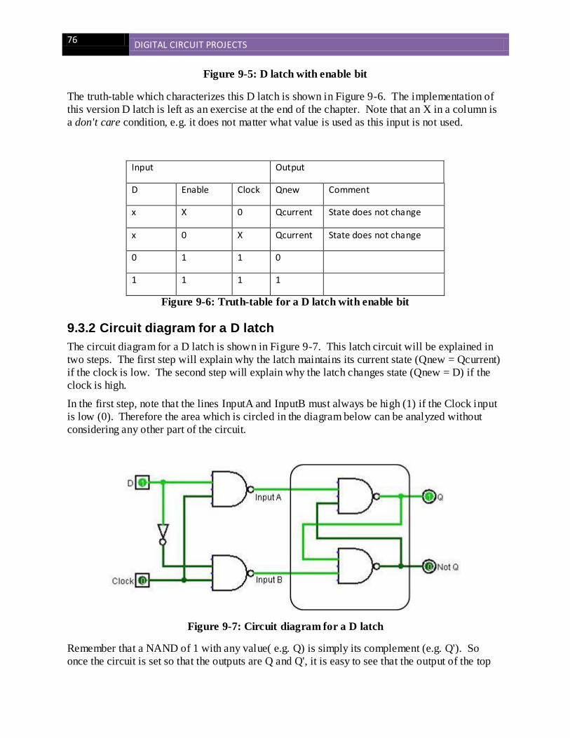
76 DIGITAL CIRCUIT PROJECTS
Figure 9-5: D latch with enable bit
The truth-table which characterizes this D latch is shown in Figure 9-6. The implementation of
this version D latch is left as an exercise at the end of the chapter. Note that an X in a column is
a don't care condition, e.g. it does not matter what value is used as this input is not used.
Input Output
D Enable Clock Qnew Comment
x X 0 Qcurrent State does not change
x 0 X Qcurrent State does not change
0 1 1 0
1 1 1 1
Figure 9-6: Truth-table for a D latch with enable bit
9.3.2 Circuit diagram for a D latch
The circuit diagram for a D latch is shown in Figure 9-7. This latch circuit will be explained in
two steps. The first step will explain why the latch maintains its current state (Qnew = Qcurrent)
if the clock is low. The second step will explain why the latch changes state (Qnew = D) if the
clock is high.
In the first step, note that the lines InputA and InputB must always be high (1) if the Clock input
is low (0). Therefore the area which is circled in the diagram below can be analyzed without
considering any other part of the circuit.
Figure 9-7: Circuit diagram for a D latch
Remember that a NAND of 1 with any value( e.g. Q) is simply its complement (e.g. Q'). So
once the circuit is set so that the outputs are Q and Q', it is easy to see that the output of the top

DIGITAL CIRCUIT PROJECTS 77
NAND gate is Q (e.g. (Q'*1)' = Q), and the output of the bottom NAND gate is Q' (e.g. (Q*1)' =
Q'). Thus if Q and Q' are loaded into the circuit and the clock is 0, the circuit will maintain the
values of Q and Q', and the latch keeps its current value.
Next the question is if the Clock line becomes high (1), how does it force the value of D into the
latch. To see this, note that if the Clock become 1, the InputA = D' and InputB = D must be true.
Thus one of the lines must be 0. Again consider the part of the circuit which has been circled.
The line which is 0 will force its output to be 1 (e.g. if Input-A = 1, Q = 1, or if Input-B = 0, Q' =
1). This will eventually force the output of the other NAND gate to 0, though it might take some
time to settle to this value. So long as the time needed for the circuit to settle is less than the
clock speed (the length of the clock pulse), the circuit will become stable with Q = D and Q'=D'.
So the result of the clock being high is that the latch will store in its state the value of Q = D and
Q' = D'.
Before the first clock pulse, the state of the latch is simply invalid, and the value of the latch
cannot be used until after it is set with the first clock pulse.
9.3.3 Implementing the D latch
Implementing the D latch will require 2 switches, one NOT gate (7404 chip) and 4 NAND gates
( 7400 chip), and 2 LEDs for Q and Q'. In this lab a clock is not used, and instead is simulated
by the second switch. Also in this diagram the two lines running from the output of the NAND
gates backwards to the input of the other NAND gate use green wire.
Figure 9-8: Implementation of a D latch
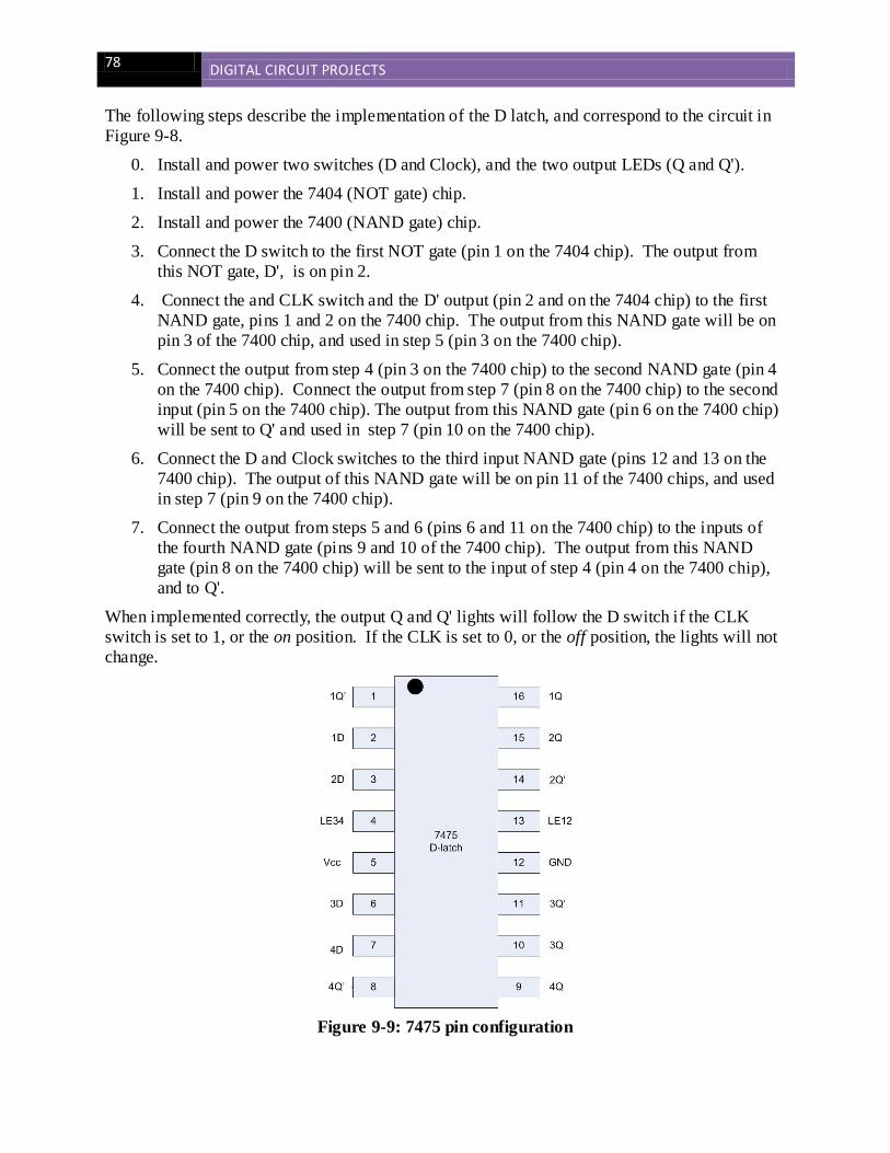
78 DIGITAL CIRCUIT PROJECTS
The following steps describe the implementation of the D latch, and correspond to the circuit in
Figure 9-8.
0. Install and power two switches (D and Clock), and the two output LEDs (Q and Q').
1. Install and power the 7404 (NOT gate) chip.
2. Install and power the 7400 (NAND gate) chip.
3. Connect the D switch to the first NOT gate (pin 1 on the 7404 chip). The output from
this NOT gate, D', is on pin 2.
4. Connect the and CLK switch and the D' output (pin 2 and on the 7404 chip) to the first
NAND gate, pins 1 and 2 on the 7400 chip. The output from this NAND gate will be on
pin 3 of the 7400 chip, and used in step 5 (pin 3 on the 7400 chip).
5. Connect the output from step 4 (pin 3 on the 7400 chip) to the second NAND gate (pin 4
on the 7400 chip). Connect the output from step 7 (pin 8 on the 7400 chip) to the second
input (pin 5 on the 7400 chip). The output from this NAND gate (pin 6 on the 7400 chip)
will be sent to Q' and used in step 7 (pin 10 on the 7400 chip).
6. Connect the D and Clock switches to the third input NAND gate (pins 12 and 13 on the
7400 chip). The output of this NAND gate will be on pin 11 of the 7400 chips, and used
in step 7 (pin 9 on the 7400 chip).
7. Connect the output from steps 5 and 6 (pins 6 and 11 on the 7400 chip) to the inputs of
the fourth NAND gate (pins 9 and 10 of the 7400 chip). The output from this NAND
gate (pin 8 on the 7400 chip) will be sent to the input of step 4 (pin 4 on the 7400 chip),
and to Q'.
When implemented correctly, the output Q and Q' lights will follow the D switch if the CLK
switch is set to 1, or the on position. If the CLK is set to 0, or the off position, the lights will not
change.
Figure 9-9: 7475 pin configuration

DIGITAL CIRCUIT PROJECTS 79
9.3.4 D latch as a single IC chip
The D latch is a common IC, and it has been implemented as a single chip, the 7475 chip. The
7475 chip is called 4-bit bistable latch because each chip has four 1-bit D latches. A D latch is
bistable because it has 2 stable states, 0 or 1.The circuit implemented here will use only one of
the D latches available on the 7475 chip.
The layout of the 7475 chip is somewhat complex. The pin configuration is given in Figure 9-9
and a table for the meaning of each pin in Figure 9-10. The implementation of the circuit in this
section will only use pins 1, 2, 5, 12, 13 and 16. The other pins will simply be left open, and not
discussed further.
Symbol Pin Description
1Q' 1 complementary latch output 1
1D 2 data input 1
2D 3 data input 2
LE34 4 latch enable input for latches 3 and 4 (active high)
Vcc 5 positive supply voltage
3D 6 data input 3
4D 7 7 data input 4
4Q' 8 complementary latch output 4
4Q 9 latch output 4
3Q 10 latch output 3
3Q' 11 complementary latch output 3
GND 12 Ground
LE12 13 latch enable input for latches 1 and 2 (active high)
2Q' 14 complementary latch output 2
2Q 15 15 latch output 2
1Q 16 15 latch output 1
Figure 9-10: 7475 pin meanings
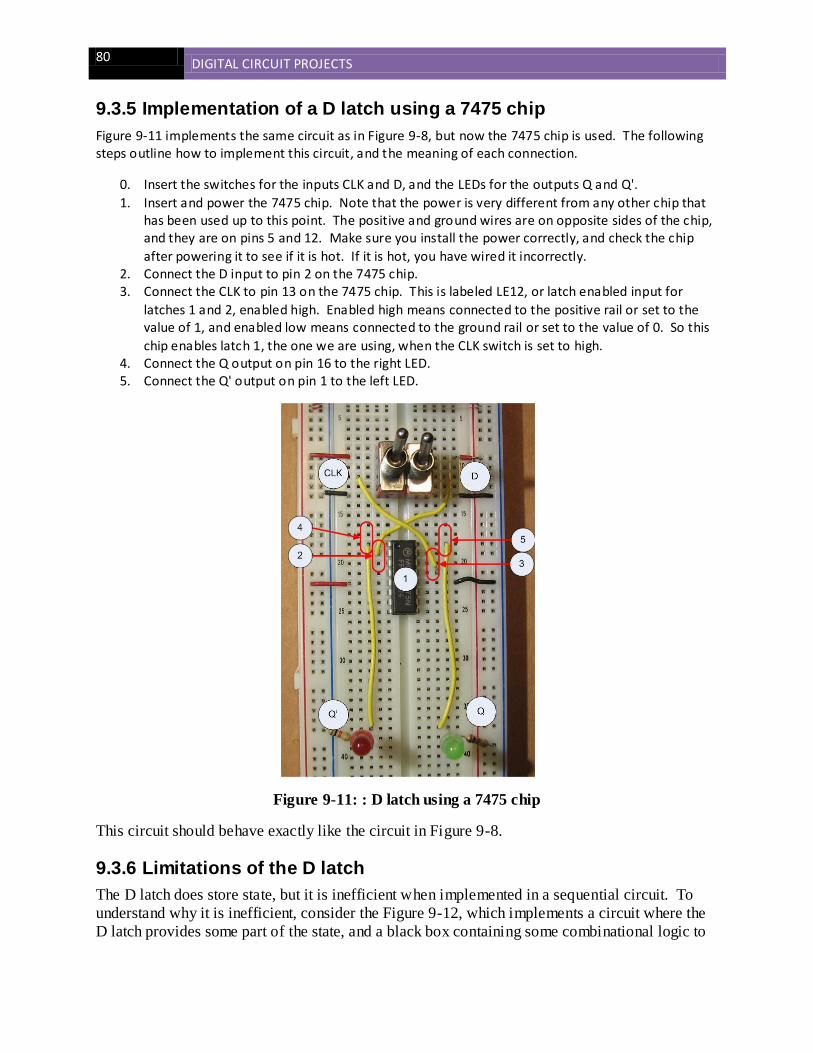
80 DIGITAL CIRCUIT PROJECTS
9.3.5 Implementation of a D latch using a 7475 chip
Figure 9-11 implements the same circuit as in Figure 9-8, but now the 7475 chip is used. The following steps outline how to implement this circuit, and the meaning of each connection.
0. Insert the switches for the inputs CLK and D, and the LEDs for the outputs Q and Q'.
1. Insert and power the 7475 chip. Note that the power is very different from any other chip that has been used up to this point. The positive and ground wires are on opposite sides of the chip, and they are on pins 5 and 12. Make sure you install the power correctly, and check the chip
after powering it to see if it is hot. If it is hot, you have wired it incorrectly. 2. Connect the D input to pin 2 on the 7475 chip. 3. Connect the CLK to pin 13 on the 7475 chip. This is labeled LE12, or latch enabled input for
latches 1 and 2, enabled high. Enabled high means connected to the positive rail or set to the value of 1, and enabled low means connected to the ground rail or set to the value of 0. So this
chip enables latch 1, the one we are using, when the CLK switch is set to high. 4. Connect the Q output on pin 16 to the right LED. 5. Connect the Q' output on pin 1 to the left LED.
Figure 9-11: : D latch using a 7475 chip
This circuit should behave exactly like the circuit in Figure 9-8.
9.3.6 Limitations of the D latch
The D latch does store state, but it is inefficient when implemented in a sequential circuit. To
understand why it is inefficient, consider the Figure 9-12, which implements a circuit where the
D latch provides some part of the state, and a black box containing some combinational logic to
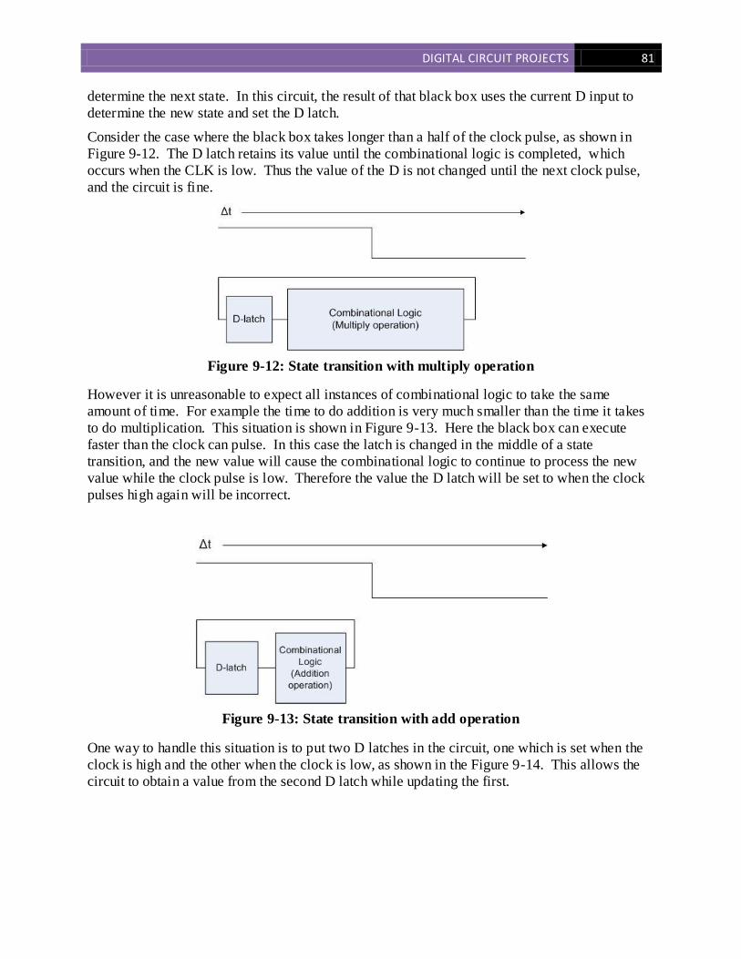
DIGITAL CIRCUIT PROJECTS 81
determine the next state. In this circuit, the result of that black box uses the current D input to
determine the new state and set the D latch.
Consider the case where the black box takes longer than a half of the clock pulse, as shown in
Figure 9-12. The D latch retains its value until the combinational logic is completed, which
occurs when the CLK is low. Thus the value of the D is not changed until the next clock pulse,
and the circuit is fine.
Figure 9-12: State transition with multiply operation
However it is unreasonable to expect all instances of combinational logic to take the same
amount of time. For example the time to do addition is very much smaller than the time it takes
to do multiplication. This situation is shown in Figure 9-13. Here the black box can execute
faster than the clock can pulse. In this case the latch is changed in the middle of a state
transition, and the new value will cause the combinational logic to continue to process the new
value while the clock pulse is low. Therefore the value the D latch will be set to when the clock
pulses high again will be incorrect.
Figure 9-13: State transition with add operation
One way to handle this situation is to put two D latches in the circuit, one which is set when the
clock is high and the other when the clock is low, as shown in the Figure 9-14. This allows the
circuit to obtain a value from the second D latch while updating the first.
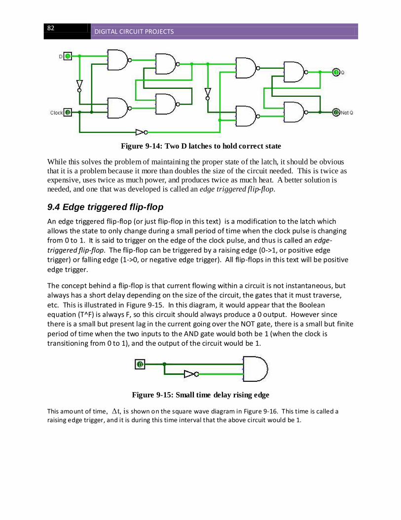
82 DIGITAL CIRCUIT PROJECTS
Figure 9-14: Two D latches to hold correct state
While this solves the problem of maintaining the proper state of the latch, it should be obvious
that it is a problem because it more than doubles the size of the circuit needed. This is twice as
expensive, uses twice as much power, and produces twice as much heat. A better solution is
needed, and one that was developed is called an edge triggered flip-flop.
9.4 Edge triggered flip-flop
An edge triggered flip-flop (or just flip-flop in this text) is a modification to the latch which allows the state to only change during a small period of time when the clock pulse is changing from 0 to 1. It is said to trigger on the edge of the clock pulse, and thus is called an edge-triggered flip-flop. The flip-flop can be triggered by a raising edge (0->1, or positive edge trigger) or falling edge (1->0, or negative edge trigger). All flip-flops in this text will be positive edge trigger.
The concept behind a flip-flop is that current flowing within a circuit is not instantaneous, but always has a short delay depending on the size of the circuit, the gates that it must traverse,
etc. This is illustrated in Figure 9-15. In this diagram, it would appear that the Boolean equation (T^F) is always F, so this circuit should always produce a 0 output. However since there is a small but present lag in the current going over the NOT gate, there is a small but finite
period of time when the two inputs to the AND gate would both be 1 (when the clock is transitioning from 0 to 1), and the output of the circuit would be 1.
Figure 9-15: Small time delay rising edge
This amount of time, Δt, is shown on the square wave diagram in Figure 9-16. This time is called a raising edge trigger, and it is during this time interval that the above circuit would be 1.
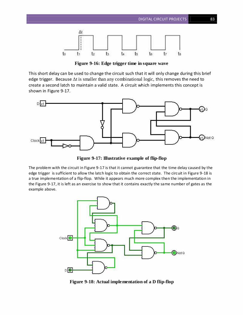
DIGITAL CIRCUIT PROJECTS 83
Figure 9-16: Edge trigger time in square wave
This short delay can be used to change the circuit such that it will only change during this brief edge trigger. Because Δt is smaller than any combinational logic, this removes the need to create a second latch to maintain a valid state. A circuit which implements this concept is shown in Figure 9-17.
Figure 9-17: Illustrative example of flip-flop
The problem with the circuit in Figure 9-17 is that it cannot guarantee that the time delay caused by the
edge trigger is sufficient to allow the latch logic to obtain the correct state. The circuit in Figure 9-18 is a true implementation of a flip-flop. While it appears much more complex then the implementation in
the Figure 9-17, it is left as an exercise to show that it contains exactly the same number of gates as the example above.
Figure 9-18: Actual implementation of a D flip-flop
84 DIGITAL CIRCUIT PROJECTS
Due to a problem known as debouncing, it is hard to illustrate a flip-flop in isolation as a circuit.
So this chapter will not implement a flip-flop. However a flip-flop will be used as part of the
circuits in chapter 10.
9.5 Conclusion
Circuits which have memory and can maintain a state are called sequential circuits. Simple, or
non-sequential, circuits are circuits which do not maintain a state using memory. Simple circuits
can calculate results based on inputs, but to compute a useful result a circuit must be able to
maintain a state.
This chapter introduced the concept of static ram, and how it is implemented using only NAND
and NOT gates. Static RAM maintains its state so long as current is supplied to the circuit, and
does not require a refresh cycle, making it faster than dynamic RAM. But static RAM is also
more complex than dynamic RAM, so static RAM is more expensive than dynamic RAM.
Static RAM was implemented using a D latch circuit. The problem with using a latch in a
circuit, that it requires two latches to be effective, was illustrated. The D flip-flop was then
introduced to solve the problem with a D latch.
9.6 Exercises
1. Implement the D latch from Figure 9-8 using a breadboard.
2. Implement the D latch to include an enable line using Logisim. The enable line will be
used to control when the D latch is set, so it is only set if the clock and enable line are
high.
3. Implement the circuit from problem 2 using a breadboard.
4. Implement the D latch to include a synchronous clear line using Logisim. A clear line
will set the value of the D latch to 0 on the next clock pulse.
5. Implement the circuit from problem 4 using a breadboard.
6. Implement a D flip-flop using the 7475 chip, as in figure 9-11.
7. Show that the circuits in Figure 9-17 and 9-18 have exactly the same number of gates.
DIGITAL CIRCUIT PROJECTS 85
Chapter 10 Sequential circuits
10.1 Introduction
Now that memory has been introduced it is possible to produce machines that change state. The
ability to change the state of the computer forms the basis to do calculations.
In this chapter a state machine will be presented. This machine will use memory, implemented
as latches or flip-flops, to define states. Events will be generated, in this case the pushing of a
button to simulate a clock pulse, which will allow the state machine to transition to a new state.
The relationship between the previous and successor states will be represented in a state
transition table, and the table used to encode a simple program into a multiplexer. The program
to be implemented is a simple mod 4, or 2-bit, up counter, which will count from 0..3.
10.2 Debouncing
Before beginning the discussion of sequential circuits, there is a problem which occurs when
trying to simulate the rising edge of a clock in the circuit. In all of the labs up to this point the
toggle switches appear to turn on and off cleanly. This is because the switches are used for to
represent a constant input to the circuit. The only state of interest is if the switch is 0 or 1. How
quickly or cleanly the switch changed from 0 to 1 or 1 to 0 did not matter.
In reality no switch ever makes a clean transition between 0 and 1. Switches cannot turn on/off
cleanly. All mechanical switches, when turned on or off, exhibit a period of time where the
switch oscillates between on/off before it settles into a steady value. This oscillation is generally
too fast for a human to notice, but the oscillations produce multiple square waves, and thus
multiple edge triggers. These edge triggers are slow enough for a latch or flip-flop to see
multiple phantom state changes instead of a single clean state change.
The lab in this chapter will demonstrate how a circuit can transition between defined states. This
requires that each time the switch is thrown only a single edge is ever seen as being produced.
The multiple edges being generated by the switch cause the circuit to behave incorrectly. So
something must be done to get only a single state change when a switch is thrown.
To handle these multiple phantom state changes, the circuits need to be debounced. A simple
way to think about debouncing is to realize that if multiple on/off signals are processed in a small
amount of time, they are in reality just noise coming from the switch, and the edges should be
combined into a single event.
Every type of switch, including the keys on the keyboard you type on, must be debounced. This
debouncing is generally handled in software which is designed to filter out the noise of the
switch. However the circuits we are looking at in this text do not implement a processor, so a
software solution is not possible.
To debounce the circuits in this chapter a hardware approach is used. This hardware approach
requires three parts be implemented in our circuit.
1. A small push button switch is substituted for our toggle switch. The push button
provides a much cleaner input than the toggle switch, and so it is easier to get a single
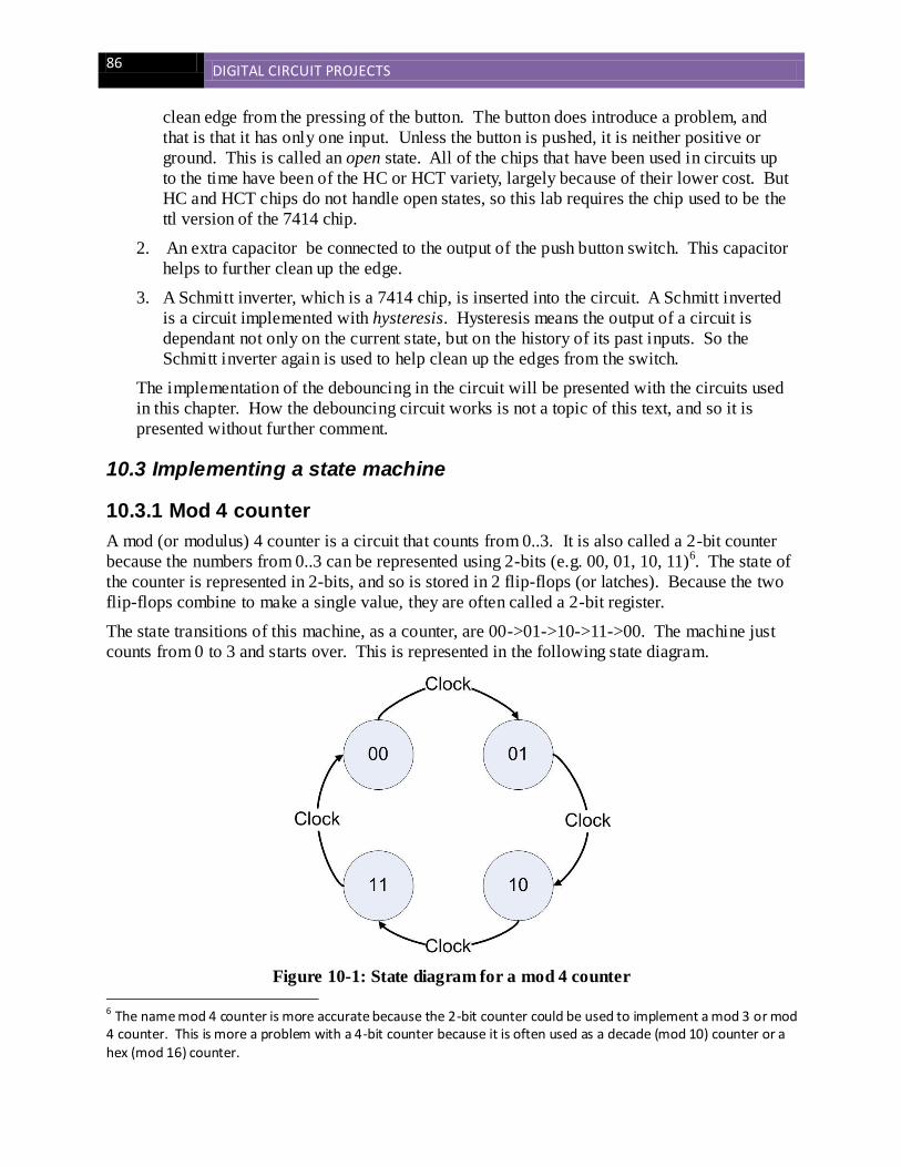
86 DIGITAL CIRCUIT PROJECTS
clean edge from the pressing of the button. The button does introduce a problem, and
that is that it has only one input. Unless the button is pushed, it is neither positive or
ground. This is called an open state. All of the chips that have been used in circuits up
to the time have been of the HC or HCT variety, largely because of their lower cost. But
HC and HCT chips do not handle open states, so this lab requires the chip used to be the
ttl version of the 7414 chip.
2. An extra capacitor be connected to the output of the push button switch. This capacitor
helps to further clean up the edge.
3. A Schmitt inverter, which is a 7414 chip, is inserted into the circuit. A Schmitt inverted
is a circuit implemented with hysteresis. Hysteresis means the output of a circuit is
dependant not only on the current state, but on the history of its past inputs. So the
Schmitt inverter again is used to help clean up the edges from the switch.
The implementation of the debouncing in the circuit will be presented with the circuits used
in this chapter. How the debouncing circuit works is not a topic of this text, and so it is
presented without further comment.
10.3 Implementing a state machine
10.3.1 Mod 4 counter
A mod (or modulus) 4 counter is a circuit that counts from 0..3. It is also called a 2-bit counter
because the numbers from 0..3 can be represented using 2-bits (e.g. 00, 01, 10, 11)6. The state of
the counter is represented in 2-bits, and so is stored in 2 flip-flops (or latches). Because the two
flip-flops combine to make a single value, they are often called a 2-bit register.
The state transitions of this machine, as a counter, are 00->01->10->11->00. The machine just
counts from 0 to 3 and starts over. This is represented in the following state diagram.
Figure 10-1: State diagram for a mod 4 counter
6 The name mod 4 counter is more accurate because the 2-bit counter could be used to implement a mod 3 or mod 4 counter. This is more a problem with a 4-bit counter because it is often used as a decade (mod 10) counter or a hex (mod 16) counter.
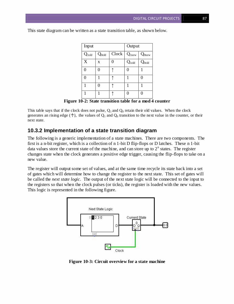
DIGITAL CIRCUIT PROJECTS 87
This state diagram can be written as a state transition table, as shown below.
Input Output
Q1old Q0old Clock Q1new Q0new
X x 0 Q1old Q0old
0 0 ↑ 0 1
0 1 ↑ 1 0
1 0 ↑ 1 1
1 1 ↑ 0 0
Figure 10-2: State transition table for a mod 4 counter
This table says that if the clock does not pulse, Q1 and Q0 retain their old values. When the clock
generates an rising edge (↑), the values of Q1 and Q0 transition to the next value in the counter, or their
next state.
10.3.2 Implementation of a state transition diagram
The following is a generic implementation of a state machines. There are two components. The
first is a n-bit register, which is a collection of n 1-bit D flip-flops or D latches. These n 1-bit
data values store the current state of the machine, and can store up to 2n states. The register
changes state when the clock generates a positive edge trigger, causing the flip-flops to take on a
new value.
The register will output some set of values, and at the same time recycle its state back into a set
of gates which will determine how to change the register to the next state. This set of gates will
be called the next state logic. The output of the next state logic will be connected to the input to
the registers so that when the clock pulses (or ticks), the register is loaded with the new values.
This logic is represented in the following figure.
Figure 10-3: Circuit overview for a state machine
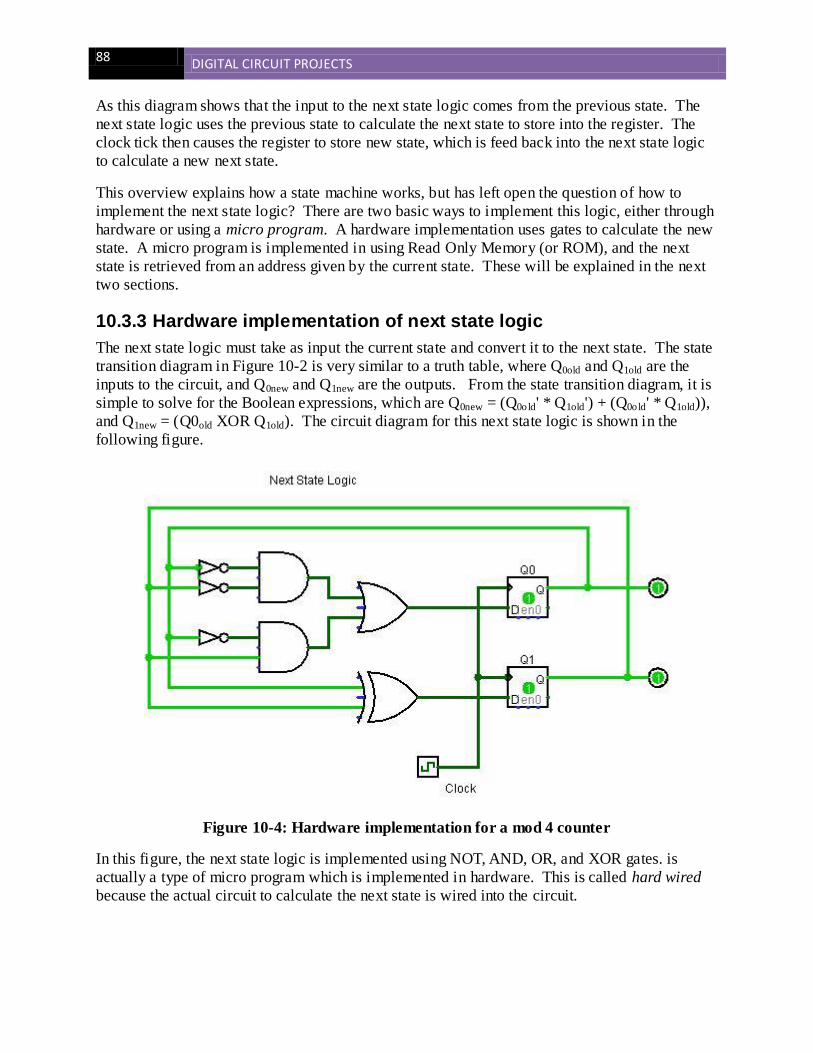
88 DIGITAL CIRCUIT PROJECTS
As this diagram shows that the input to the next state logic comes from the previous state. The
next state logic uses the previous state to calculate the next state to store into the register. The
clock tick then causes the register to store new state, which is feed back into the next state logic
to calculate a new next state.
This overview explains how a state machine works, but has left open the question of how to
implement the next state logic? There are two basic ways to implement this logic, either through
hardware or using a micro program. A hardware implementation uses gates to calculate the new
state. A micro program is implemented in using Read Only Memory (or ROM), and the next
state is retrieved from an address given by the current state. These will be explained in the next
two sections.
10.3.3 Hardware implementation of next state logic
The next state logic must take as input the current state and convert it to the next state. The state
transition diagram in Figure 10-2 is very similar to a truth table, where Q0old and Q1old are the
inputs to the circuit, and Q0new and Q1new are the outputs. From the state transition diagram, it is
simple to solve for the Boolean expressions, which are Q0new = (Q0old' * Q1old') + (Q0old' * Q1old)),
and Q1new = (Q0old XOR Q1old). The circuit diagram for this next state logic is shown in the
following figure.
Figure 10-4: Hardware implementation for a mod 4 counter
In this figure, the next state logic is implemented using NOT, AND, OR, and XOR gates. is
actually a type of micro program which is implemented in hardware. This is called hard wired
because the actual circuit to calculate the next state is wired into the circuit.
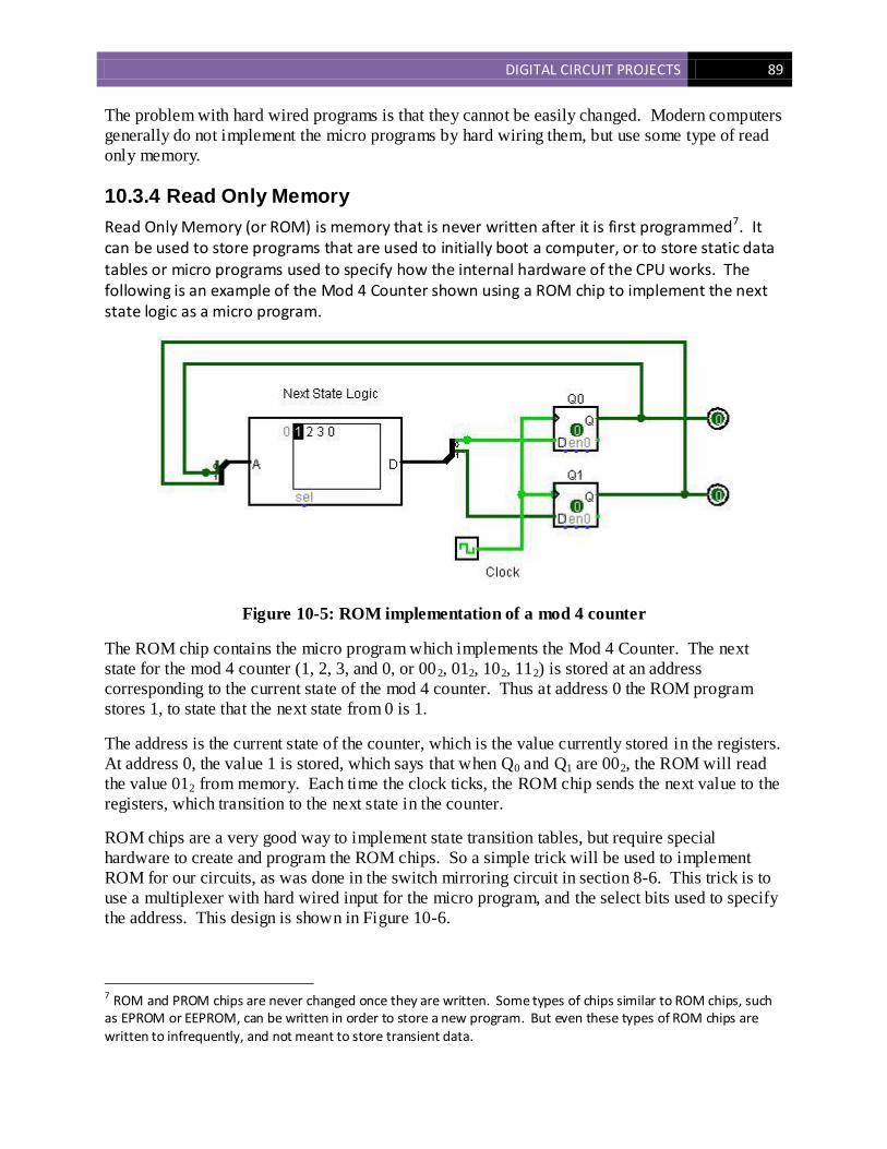
DIGITAL CIRCUIT PROJECTS 89
The problem with hard wired programs is that they cannot be easily changed. Modern computers
generally do not implement the micro programs by hard wiring them, but use some type of read
only memory.
10.3.4 Read Only Memory
Read Only Memory (or ROM) is memory that is never written after it is first programmed7. It can be used to store programs that are used to initially boot a computer, or to store static data
tables or micro programs used to specify how the internal hardware of the CPU works. The following is an example of the Mod 4 Counter shown using a ROM chip to implement the next state logic as a micro program.
Figure 10-5: ROM implementation of a mod 4 counter
The ROM chip contains the micro program which implements the Mod 4 Counter. The next
state for the mod 4 counter (1, 2, 3, and 0, or 002, 012, 102, 112) is stored at an address
corresponding to the current state of the mod 4 counter. Thus at address 0 the ROM program
stores 1, to state that the next state from 0 is 1.
The address is the current state of the counter, which is the value currently stored in the registers.
At address 0, the value 1 is stored, which says that when Q0 and Q1 are 002, the ROM will read
the value 012 from memory. Each time the clock ticks, the ROM chip sends the next value to the
registers, which transition to the next state in the counter.
ROM chips are a very good way to implement state transition tables, but require special
hardware to create and program the ROM chips. So a simple trick will be used to implement
ROM for our circuits, as was done in the switch mirroring circuit in section 8-6. This trick is to
use a multiplexer with hard wired input for the micro program, and the select bits used to specify
the address. This design is shown in Figure 10-6.
7 ROM and PROM chips are never changed once they are written. Some types of chips similar to ROM chips, such as EPROM or EEPROM, can be written in order to store a new program. But even these types of ROM chips are written to infrequently, and not meant to store transient data.
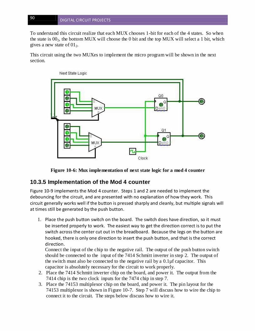
90 DIGITAL CIRCUIT PROJECTS
To understand this circuit realize that each MUX chooses 1-bit for each of the 4 states. So when
the state is 002, the bottom MUX will choose the 0 bit and the top MUX will select a 1 bit, which
gives a new state of 012.
This circuit using the two MUXes to implement the micro program will be shown in the next
section.
Figure 10-6: Mux implementation of next state logic for a mod 4 counter
10.3.5 Implementation of the Mod 4 counter
Figure 10-9 implements the Mod 4 counter. Steps 1 and 2 are needed to implement the debouncing for the circuit, and are presented with no explanation of how they work. This
circuit generally works well if the button is pressed sharply and cleanly, but multiple signals will at times still be generated by the push button.
1. Place the push button switch on the board. The switch does have direction, so it must be inserted properly to work. The easiest way to get the direction correct is to put the switch across the center cut out in the breadboard. Because the legs on the button are hooked, there is only one direction to insert the push button, and that is the correct direction. Connect the input of the chip to the negative rail. The output of the push button switch
should be connected to the input of the 7414 Schmitt inverter in step 2. The output of
the switch must also be connected to the negative rail by a 0.1µf capacitor. This
capacitor is absolutely necessary for the circuit to work properly.
2. Place the 7414 Schmitt inverter chip on the board, and power it. The output from the
7414 chip is the two clock inputs for the 7474 chip in step 7.
3. Place the 74153 multiplexor chip on the board, and power it. The pin layout for the
74153 multiplexor is shown in Figure 10-7. Step 7 will discuss how to wire the chip to
connect it to the circuit. The steps below discuss how to wire it.
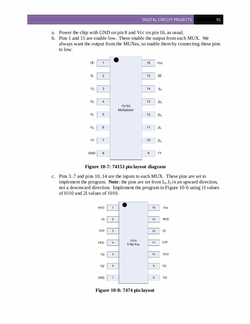
DIGITAL CIRCUIT PROJECTS 91
a. Power the chip with GND on pin 8 and Vcc on pin 16, as usual.
b. Pins 1 and 15 are enable low. These enable the output from each MUX. We
always want the output from the MUXes, so enable them by connecting these pins
to low.
Figure 10-7: 74153 pin layout diagram
c. Pins 3..7 and pins 10..14 are the inputs to each MUX. These pins are set to
implement the program. Note: the pins are set from I0..I3 in an upward direction,
not a downward direction. Implement the program in Figure 10-6 using 1I values
of 0110 and 2I values of 1010.
Figure 10-8: 7474 pin layout
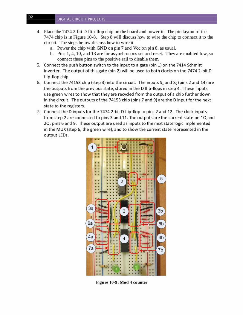
92 DIGITAL CIRCUIT PROJECTS
4. Place the 7474 2-bit D flip-flop chip on the board and power it. The pin layout of the
7474 chip is in Figure 10-8. Step 8 will discuss how to wire the chip to connect it to the
circuit. The steps below discuss how to wire it.
a. Power the chip with GND on pin 7 and Vcc on pin 8, as usual.
b. Pins 1, 4, 10, and 13 are for asynchronous set and reset. They are enabled low, so
connect these pins to the positive rail to disable them.
5. Connect the push button switch to the input to a gate (pin 1) on the 7414 Schmitt inverter. The output of this gate (pin 2) will be used to both clocks on the 7474 2-bit D
flip-flop chip. 6. Connect the 74153 chip (step 3) into the circuit. The inputs S1 and S0 (pins 2 and 14) are
the outputs from the previous state, stored in the D flip-flops in step 4. These inputs use green wires to show that they are recycled from the output of a chip further down in the circuit. The outputs of the 74153 chip (pins 7 and 9) are the D input for the next state to the registers.
7. Connect the D inputs for the 7474 2-bit D flip-flop to pins 2 and 12. The clock inputs
from step 2 are connected to pins 3 and 11. The outputs are the current state on 1Q and 2Q, pins 6 and 9. These output are used as inputs to the next state logic implemented
in the MUX (step 6, the green wire), and to show the current state represented in the output LEDs.
Figure 10-9: Mod 4 counter

DIGITAL CIRCUIT PROJECTS 93
When the push button switch is pressed, the LED lights should cycle through the states for 00-
>01->10->11->00.
10.4 Conclusion
State machines are simple calculation machines which use a state and next state logic to
implement simple algorithms such as counters. State machines are also a part of any larger
calculation machine such as a computer.
State machines can be implemented in hardware using some sort of memory to store a state, and
next state logic which allows the machine to advance from one state to another. The memory
used to store the state in this chapter was D flop-flops.
The next state logic was implemented in two ways in this chapter. The first was by a circuit
which implemented combinational logic to calculate the next state of the circuit. The second
way next state logic was implemented was using a ROM chip where the current state was used as
an address to the memory in the ROM chip which contained a value for the next state. Using a
ROM chip in this way was called micro-programming.
The chapter then continue by showing how a ROM chip could be simulated using a MUX with
hard wired values as inputs, and the select lines as addresses to the values to choose.
10.5 Exercises
1. Implement a Mod 4 up counter using the 74153 chip to implement the next state logic as
shown in section 10.3.
2. Implement the Mod 4 up counter using combinational logic to implement the next state
logic, as shown in Figure 10.4
3. Implement a Mod 4 down counter, or a counter which counts 11->10->01->00->11.
This counter will require that you modify the state diagram, state transition table, and
your program. For this problem submit the state diagram, state transition table, Logisim
diagram, and implemented circuit.
4. Implement the following up counters in Logisim:
a. Mod 6 counter
b. Mod 8 counter
c. Mod 10 (decade) counter.