
~ National
487
4<XXJ81
-
Upload
khangminh22 -
Category
Documents
-
view
0 -
download
0
Transcript of ~ National

4<XXJ81
~National ~Semiconductor

PROGRAMMABLE LOGIC DEVICES
DATABOOKAND DESIGN GUIDE
GAL
ECL PAL High Density MAPL
1993 Edition
PLO Design and Fabrication Ill Low Density GAL and PAL Devices f!m -Data Sheets and Application Notes (Im
High Density MAPL Family !!m -Data Sheets and Application Notes i;m
PLO Development Tools •
Appendices/Physical Dimensions . El

TRADEMARKS
Following is the most current list of National Semiconductor Corporation's trademarks and registered trademarks.
ABiCTM AbuseableTM AnadigTM APPSTM ASPECDM Auto-Chem DeflasherTM BCPTM Bl-FET™ Bl-FETll™ Bl-LINETM BIPLANTM BLCTM BLXTM BMACTM Brite-Lite TM BSI™ BSl-2™ CDDTM CIMTM CIMBUSTM CLASICTM COMBO® COMBO I™ COMBO 11™ COPSTM microcontrollers CRDTM DA4™ DENSPAKTM DIBTM DISCERNTM DISTILL™ DNA® DPVMTM E2CMOSTM ELSTAR™ Embedded System
Processor TM EPTM E-Z-LINK™
FACT™ FACT Quiet SeriesTM FAIRCAD™ Fairtech™ FAST® FASTrTM Flash™ GENIX™ GNXTM GTOTM HEX 3000TM HPCTM HyBal™ 13L® ICMTM Integral ISE™ lntelisplayTM lnter-LERICTM lnter-RICTM ISE™ ISE/06™ ISE/08™ ISE/16™ ISE32™ ISOPLANAR™ ISOPLANAR-ZTM LERIC™ LMCMOSTM M2CMOSTM MacrobusTM MacrocomponentTM MAPL™ MAXI-ROM® MicrobusTM data bus MICRO-DACTM µtalkerTM MicrotalkerTM MICROWIRETM
ABEL™ is a trademark of Data 1/0 Corporation. CUPL ® is a registered trademark of Logical Devices. Data 110® is a registered trademark of Data 110 Corporation. Epson® is a registered trademark of Epson America, Inc.
MICROWIRE/PLUSTM MOLE™ MPA™ MST™ Naked-8™ National® National Semiconductor® National Semiconductor
Corp.® NAX800TM Nitride PlusTM Nitride Plus OxideTM NML™ NOBUSTM NSC800TM NSCISETM NSX-16™ NS-XC-16™ NTERCOM™ NURAMTM OPAL™
. OXISSTM P2CMOSTM Perfect Watch™ PLAN TM PLANAR™ PLAYER™ Plus-2™ PolycraftTM Power + ControlTM POWERplanarTM QSTM QUAD3000TM QUIKLOOK™ RAT™ RICTM RTX16™ SCXTM
GAL® and UltraMOS® are registered trademarks of Lattice Semiconductor. Hercules® is a registered trademark of Hercules Computer Technology. HP® is a registered trademark of Hewlett-Packard Company. IBM®, PC-AT® and PC-XT® are registered trademarks of International Business Machines Corp. IFL™ is a trademark of Signetics Semiconductor. LaserjetTM is a trademark of Hewlett-Packard Company. Latch-Lock™ is a trademark of Lattice Semiconductor. MS-DOS® and Windows® are registered trademarks of Microsoft Corporation. PAL® is a registered trademark of and used under license from Advanced Micro Devices, Inc. PLDesigner™ is a trademark of Mine Incorporated. Sun® is a registered trademark of Sun Microsystems. UNIX® is a registered trademark of AT & T Bell Laboratories. VAX™ is a trademark of Digital Equipment Corporation. Viewlogic® is a registered trademark of Viewlogic Systems, Inc.
LIFE SUPPORT POLICY
SERIES/800TM Series 32000® Simple SwitcherTM SofChekTM SONICTM SPIRE™ Staggered Refresh™ STAR™ Starlink™ STARPLEXTM ST-NICTM SuperADM Super-Block™ SuperChipTM SuperScriptTM SYS32™ TapePak® TDSTM TeleGateTM The National Anthem® TLCTM TrapezoidalTM TRI-CODE™ TRI-POLY™ TRI-SAFE™ TRI-STATE® TROPICTM Tropic Pele'TM Tropic ReefTM TURBOTRANSCEIVERTM VIP™ VR32™ WATCHDOGTM XMOSTM XPUTM ZSTAR™ 883B/RETSTM 883S/RETS™
NATIONAL'S PRODUCTS ARE NOT AUTHORIZED FOR USE AS CRITICAL COMPONENTS IN LIFE SUPPORT DEVICES OR SYSTEMS WITHOUT THE EXPRESS WRITTEN APPROVAL OF THE PRESIDENT OF NATIONAL SEMICONDUCTOR CORPORATION. As used herein:
1. Life support devices or systems are devices or systems which, (a) are intended for surgical implant into the body, or (b) support or sustain life, and whose failure to perform, when properly used in accordance with instructions for use provided in the labeling, can be reasonably expected to result in a significant injury to the user.
2. A critical component is any component of a life support device or system whose failure to perform can be reasonably expected to cause the failure of the life support device or system, or to affect its safety or effectiveness.
NatlonalSemiconductorCorporation 2900 Semiconductor Drive, P.O. Box 58090, Santa Clara, California 95052-8090 1-800-272-9959 TWX (910) 339-9240
National does not assume any responsibility for use of any circuitry described, no circuit patent licenses are implied, and National reserves the right, at any time without notice, to change said circuitry or specifications.

Introduction
This Databook and Design Guide is your complete reference to all product and support information relating to National Semiconductor's programmable logic devices (PLDs) and development tools.
In our new 1992 issue, you will notice that we have expanded our EECMOS product line with the addition of many 11ew GAL® devices, including the new GAL Quiet SeriesTM family. We have also introduced a brand new family of higher-density EECMOS MAPL ™ (Multiple Array Programmable Logic) devices which specifically address the needs of complex state machine and bus interface applications.
To support all of our GAL, ECLPAL and MAPL devices, we have released OPAL™-a low cost, menu driven, open-architecture development package that is available for MSDOS®, Windows® 3.0 and Sun® workstation platforms.
·If you are in need of further information or assistance, please contact your local National Semiconductor sales representa-
. tive. A detailed list of National Semiconductor sales offices and representatives is given at the back of this book.
iii
S" -0 c. c n -s· ::I

Cl) c
~ ~National li D semiconductor c Cl) :::s -~ ProductStatus Definitions -u :::s "C 0
D:. Definition of Terms
Product Status
Formative or In Design
First Production
Full Production
Not In Production
Definition
This data sheet contains the design specifications for product development. Specifications may change in any manner without notice.
This data sheet contains preliminary data, and supplementary data will be published at a later date. National Semiconductor Corporation reserves the right to make changes at any time without notice in order to improve design and supply the best possible product.
This data sheet contains final specifications. National Semiconductor Corporation reserves the right to make changes at any time without notice in order to improve design and supply the best possible product.
This data sheet contains specifications on a product that has been discontinued by National Semiconductor Corporation. The data sheet is printed for reference information only.
National Semiconductor Corporation reserves the right to make changes without further notice to any products herein to improve reliability, function or design. National does not assume any liability arising out of the application or use of any product or circuit described herein; neither does it convey any license under its patent rights, nor the rights of others.
iv

Table of Contents Alphanumeric Index. . . . . . . . . . . . . . . . . . . . . . . . . . . . . . . . . . . . . . . . . . . . . . . . . . . . . . . . . . . vii PRODUCT LINE OVERVIEW Selection Tables ........................................................ ; . . . . ix Ordering Information .......................................................... · xi
Section 1 PLO Design and Fabrication Designing with Programmable Logic . . . . . . . . . . . . . . . . . . . . . . . . . . . . . . . . . . . . . . . . . . . . 1-3 Programmable Logic Design Methodology . . . . . . . . . . . . . . . . . . . . . . . . . . • . . . . . . . . . . . . 1-11 Fabrication of Programmable Logic . . . . . . . . . . . . . . . . . . . . . . . . . . . . . . . . . . . . . . . . . . . . . 1-21
Section 2 Low Density GAL and PAL Devices GAL AND PAL DATASHEETS GAL 16V8/ A 20-Pin Generic Array Logic Family. . . . . . . . . . . . . . . . . . . . . . . . . . . . . . . . . . . 2-3 GAL20V8/ A 24-Pin Generic Array Logic Family ................................ : . . 2-22 GAL 16V8QS 20-Pin Generic Array Logic Family . . . . . . . . . . . . . . . . . . . . . . . . . . . . . . . . . . 2-40 GAL20V8QS 24-Pin Generic Array Logic Family . . . . . . . . . . . . . . . . . . . . . . . . . . . . . . . . . . 2-59 GAL22V10 Generic Array Logic .............................................. : . 2-78 GAL20RA 1 O Generic Array Logic . . . . . . . . . . . . . . . . . . . . . . . . . . . . . . . . . . . . . . . . . . . . . . . 2-91 GAL6001 Generic Array Logic . . . . . . . . . . . . . . . . . . . . . . . . . . . . . . . . . . . . . . . . . . . . . . . . . . 2-102 EGL PAL10/10016P8 Combinatorial PAL ...................... ·................... 2-113 EGL PAL10/10016P8-3 3 ns Combinatorial PAL.................................. 2-122 EGL PAL10/10016PE8-3 3 ns Combinatorial PAL................................. 2-127 EGL PAL10/10016P4A Combinatorial PAL....................................... 2-132 EGL PAL10/10016P4-2 2 ns Combinatorial PAL ............................... ;.. 2-136 EGL PAL10/10016C4-2 2 ns Combinatorial PAL.................................. 2-141 GAL AND PAL APPLICATION EXAMPLES 1.0 Basic Gates............................................................ 2-146 2.0 Basic Flip-Flops . . . . . . . . . . . . . . . . . . . . . . . . . . . . . . . . . . . . . . . . . . . . . . . . . . . . . . . . 2-151 3.0 Quad 4-to-1 Multiplexer. . . . . . . . . . . . . . . . . . . . . . . . . . . . . . . . . . . . . . . . . . . . . . . . . . 2-156 4.0 Dual 8-to-1 Multiplexer . . . . . . . . . . . . . . . . . . . . . . . . . . . . . . . . . . . . . . . . . . . . . . . . . . 2-160 5.0 7-Bit Counter with Parallel-Load . . . . . . . . . . . . . . . . . . . . . . . . . . . . . . . . . . . . . . . . . . 2-165 6.0 10-Bit Up/Down Counter . .. .. .. . .. .. .. . . . . . . .. . .. . .. .. . .. . . . .. . .. .. .. .. . 2-169 7.0 8-Bit Barrel Shifter . . . . . . . . . . . . . . . . . . . . . . . . . . . . . . . . . . . . . . . . . . . . . . . . . . . . . . 2-177 8.0 Hexadecimal 7-Segment Display Encoder.................................. 2-181 9.0 Dual-Port RAM Controller ................................ ; . . . . . . . . . . . . . . . 2-187
10.0 CPU Board Random Control Logic .................. : . . . . . . . . . . . . . . . . . . . . . 2-196 GAL AND PAL APPLICATION NOTES AN-707 High Speed System Design Using Programmable GAL Devices.............. 2-198 AN-799 PAL to GAL Conversion................................................ 2-209 AN-667 A GAL6001-30L Zero Wait State Page Mode Memory System Interface
Between the DP8422A and the 68020 . . . . . . . . . . . . . . . . . . . . . . . . . . . . . . . . . . . . . . . . . 2-220 AN-669 A GAL Interface Between Static Random Access Memory (SAAM) and the
NSC Raster Graphics Processor (RGP, DP8500) . . . . . . . . . . . . . . . . . . . . . . . . . . . . . . . 2-230 AN-618 A GAL Interface for a 25 MHz and above No-Wait State DP8422A/80286
Burst Mode DRAM Memory System . . . . . . . . . . . . . . . . . . . . . . . . . . . . . . . . . . . . . . . . . . . 2-237 AN-535 A GAL Interface for a Dual Access DP8422A/68030/74F632 Error Detecting
and Correcting Memory System . . . . . . . . . . . . . . . . . . . . . . . . . . . . . . . . . . . . . . . . . . . . . . 2-246
Section 3 High Density MAPL Family MAPL DATASHEETS MAPL 128/MAPL 144 Multiple Array Programmable Logic . . . . . . . . . . . . . . . . . . . . . . . . . . 3-3 MAPL244 Multiple Array Programmable Logic (Preliminary) . . . . . . . . . . . . . . . . . . . . . . . . 3-15 MAPL268 Multiple Array Programmable Logic (Advanced Information). . . . . . . . . . . . . . . 3-31
v

Table of Contents (Continued)
Section 3 . High Density MAPL Family (Continued)
MAPL APPLICATION EXAMPLES 1.0 MAPL Register Control ................................................. . 2.0 4-Bit Counter .......................................................... . 3.0 3-Bit Up/Down Counter with 7-Segment Display Output ..................... . 4.0 15-Bit Up/Down Counter .......................... ; ..................... . 5.0 12-Bit LIA Shift Register ................................................. . 6.0 High Speed Frame Buffer Control ........................................ . 7.0 MAPL Divide Down Counter ............................................. . 8.0 Bus Transaction and DMA Controller .......... ·. ~ ........................... . 9.0 MAPL PC Interface Module for the FDDI MAC Layer Evaluation Board ......... .
10.0 PLUS405 to MAPL 128 Conversion ....................................... . MAPL APPLICATION NOTES
3-33 3-38 3-41 . 3-43 3-48
. 3-52 .3-60 3-67 3-78 3-85
AN-81 O Advanced° PLD Architectures .................. '.,. ........ : .............. ~ 3-87 AN-800 A Smart UART Design Implemented in a MAPL 128 . . . . . . . . . . . . . . . . . . . . . . . . 3-97 AN-801 State Machine Design ................................ ,. . . .. . .. .. . . .. . . . 3-105 AN-802 MAPL Demonstration Board .' ............... : . . . . . . . . . . . . . . . . . . . . . . . . . . . · 3-116
Section 4 PLO Development Tools . OPAL PLD Development Software . . . . . . . . . . . . . . . . . . . . . . . . .. .. . . . . . . . . . . . . . . .. . . . 4-3 3rd Party Software ............................ .- ........ ·. ... . . . . . . . . . . . . . . . . . . . . . . 4-15 PLD Programming and Testing .................................................. · 4:..17
Section 5 Appendices/Physical Dimensions Appendix A-Boolean Logic Review ......................... : . . . . . . . . . . . . . . . . .. 5-3
A.1 Basic Operators and Theorems ................... ; ... : . . . . . . . . . . . . . . . . . . . 5-3 A.2 Derivation of a Boolean Expression . . . . . . • . . . . . . . . . . . . . . . . . . . . . . . . . . . . . . . . . 5-4 A.3 Minimization ........................................................ ·" ... · 5-6 A.4 K-Map Method ................................................... ·....... 5-7 A.5 Sequential Circuit Elements . . . . . . . . . . . . . . . . . . . . . . . . . . . . . . . . . . . . . . . . . . . . . . 5-11 ·A.6 State Machine Fundamentals............................................. 5-12 A.7 Avoiding Logic Hazards .................................. ; .... ; ..... ,.... 5-14
Appendix B-Theory of PLD Testing . . . . . . . . . . . . . . . . . . . . . . . . . . . . . . . . . . . . • . . . . . . . 5;.16 B.1 Testing Methods ................................ ~ . . . . . . . . . . . . . . . . . . . . . . . 5-16 B.2 Test Generation Techniques .................................... ; . . . . . . . . 5-17 B.3 Response Evaluation Techniques . . . . . . . . . . . . . . . . . . . . . . . . . . . . . . . . . . . . . . .. . . 5-27
Physical Dimensions ......................................... ; . . . . . . . . . . . . . . . . 5-32 Bookshelf Distributors .
vi

Alpha-Numeric Index AN-535 A GAL Interface for a Dual Access DP8422A/68030/74F632 Error Detecting and
Correcting Memory System .........•................................................... 2-246 AN-618 A GAL Interface for a 25 MHz and above No-Wait State DP8422A/80286 Burst Mode
DRAM Memory System ................................................................ 2-237 AN-667 A GAL6001-30L Zero Wait State Page Mode Memory System Interface Between the
DP8422A and the 68020 ............................................................... 2-220 AN-669 A GAL Interface Between Static Random Access Memory (SAAM) and the NSC
Raster Graphics Processor (RGP, DP8500) ............................................... 2-230 AN-707 High Speed System Design Using Programmable GAL Devices ........................ 2-198 AN-799 PAL to GAL Conversion ........................................................... 2-209 AN-800 A Smart UART Design Implemented in a MAPL 128 .................................... 3-97 AN-801 State Machine Design ............................................................ 3-105 AN-802 MAPL Demonstration Board .......................... ; ............................ 3-116 AN-81 O Advanced PLO Architectures ....................................................... 3-87 GAL 16V8-7L 20-Pin Generic Array Logic Family ............................................... 2-3 GAL 16V8-1 OL 20-Pin Generic Array Logic Family .............................................. 2-3 GAL 16V8-20L 20-Pin Generic Array Logic Family .............................................. 2-3 GAL 16V8-25L 20-Pin Generic Array Logic Family .............................................. 2-3 GAL 16V8-25Q 20-Pin Generic Array Logic Family .............................................. 2-3 GAL 16V8A-12L 20-Pin Generic Array Logic Family ............................................. 2-3 GAL 16V8A-15L 20-Pin Generic Array Logic Family ............................................. 2-3 GAL 16V8QS-15L 20-Pin Generic Array Logic Family .......................................... 2-40 GAL 16V8QS-15Q 20-Pin Generic Array Logic Family .......................................... 2-40 GAL 16V8QS-20L 20-Pin Generic Array Logic Family .......................................... 2-40 GAL 16V8QS-25L 20-Pin Generic Array Logic Family .......................................... 2-40 GAL 16V8QS-25Q 20-Pin Generic Array Logic Family . ; ........................................ 2-40 GAL20RA10-15 Generic Array Logic ........................................................ 2-91 GAL20RA 10-20 Generic Array Logic ........................................................ 2-91 GAL20RA10-25 Generic Array Logic ........................................................ 2-91 GAL20V8-7L 24-Pin Generic Array Logic Family .............................................. 2-22 GAL20V8-1 OL 24-Pin Generic Array Logic Family ............................................. 2-22 GAL20V8-20L 24-Pin Generic Array Logic Family ............................................. 2-22 GAL20V8-25L 24-Pin Generic Array Logic Family ............................................. 2-22 GAL20V8-25Q 24-Pin Generic Array Logic Family ............................................. 2-22 GAL20V8A-12L 24-Pin Generic Array Logic Family ............................................ 2-22 GAL20V8A-15L 24-Pin Generic Array Logic Family ............................................ 2-22 GAL20V8QS-15L 24-Pin Generic Array Logic Family .......................................... 2-59 GAL20V8QS-15Q 24-Pin Generic Array Logic Family .......................................... 2-59 GAL20V8QS-20L 24-Pin Generic Array Logic Family .......................................... 2-59 GAL20V8QS-25L 24-Pin Generic Array Logic Family .......................................... 2-59 GAL20V8QS-25Q 24-Pin Generic Array Logic Family .......................................... 2-59 GAL22V10-15 Generic Array Logic ......................................................... 2-78 GAL22V10-20 Generic Array Logic ......................................................... 2-78 GAL22V10-25 Generic Array Logic ......................................................... 2-78 GAL22V10-30 Generic Array Logic ......................................................... 2-78 GAL6001 Generic Array Logic ............................................................. 2-102 MAPL 128-33 Multiple Array Programmable Logic .............................................. 3-3 MAPL 128-40 Multiple Array Programmable Logic .............................................. 3-3 MAPL 144-33 Multiple Array Programmable Logic (Preliminary) ................................... 3-3 MAPL 144-40 Multiple Array Programmable Logic (Preliminary) ................................... 3-3 MAPL 144-45 Multiple Array Programmable Logic (Preliminary) ................................... 3-3 MAPL244-33 Multiple Array Programmable Logic (Preliminary) ................................. 3-15
vii

Alpha-Numeric Index cconunued>
MAPL244-40 Multiple Array Programmable Logic (Preliminary) ............. ; .... ~ .............. 3-15 MAPL244-50 Multiple Array Programmable Logic (Preliminary) ............. · ..................... 3-15 MAPL268 Multiple Array Programmable Logic (Advanced Information) .... ~ ...................... 3-31 OPAL PLO Development Software ........................................................... 4-3 PAL 1016C4-2 ECL 2 ns Combinatorial PAL ................... ; .............................. 2-141 PAL1016P4-2 ECL 2 ns Combinatorial PAL .......................................•......... 2-136 PAL1016P4A ECL 4 ns Combinatorial PAL ......•.. ; ........................................ 2-132 PAL 1016P8 ECL Combinatorial PAL ........................................................ 2-113 PAL1016P8-3 ECL 3 ns Combinatorial PAL ................................................. 2-122 PAL 1016PE8-3 ECL 3 ns Combinatorial PAL ................................................ 2-127 PAL10016C4-2 ECL2 nsCombinatorial PAL ......................•..... ; ....... : ........... 2-141 PAL 10016P4-2 ECL 2 ns Combinatorial PAL ................................................ 2-136 PAL10016P4A ECL 4 ns Combinatorial PAL .........•................... ~ · .................. 2-132 PAL10016P8 ECL Combinatorial PAL .....•................................................ 2-113 PAL10016P8-3 ECL 3 ns Combinatorial PAL ................................................ 2-122 PAL 10016PE8-3 ECL 3 ns Combinatorial PAL ............................................... 2-127
viii

~National Semiconductor
Product Line Overview
1.0 Selection Tables The product selection tables which follow are organized by technology group (EEC MOS and ECL), then by "family", and finally by "series" within each family. The term "family" refers to a set of one or more "device types" which are variations on the same basic architecture. The term "device type" refers to a specific device architecture (regardless of performance characteristics). The term "series" refers to a particular speed/power version in which the devices of a PLO family are available. Thus as technology_ advancements provide for improved speed/power performance, a new series is added to selected product families.
TABLE I. Programmable Logic Product Selection Gulde
Family and Part tpo Ice Outputs Series Numbers
(max) (max)
Page (Note 1) Combinatorial Registered
EE CMOS
20-Pin Quiet Series GAL 16V8QS-15L 15 90 - 8 2-40 Generic GAL 16V8QS-15Q 15 55 - 8 2-40 Array GAL 16V8QS-20L 20 90 - 8 2-40 Logic GAL 16V8QS-25L 25 90 - B 2-40
GAL 16V8QS-25Q 25 55 - B 2-40
24-Pin Quiet Series GAL20V8QS-15L 15 90 - B 2-59 Generic GAL20V8QS-15Q 15 55 - B 2-59 Array GAL20V8QS-20L 20 90 - 8 2-59 Logic GAL20VBQS-25L 25 90 ·- B 2-59
GAL20VBQS-25Q 25 55 - B 2-59
20-Pin GAL16V8-7 7.5 115 - B 2-3 Generic GAL16V8-10 10 115 - B 2-3 Array GAL 16VBA-12 12 90 - B 2-3 Logic GAL 16VBA-15 15 90 - 8 2-3
GAL 16V8-20L 20 90 - B 2-3 GAL 16V8-25L 25 90 - B 2-3 GAL 16VB-25Q 25 55 - 8 2-3
24-Pin GAL20VB-7 7.5 115 - 8 2-22 Generic GAL20VB-10 10 115 - 8 2-22 Array GAL20VBA-12 12 90 - B 2-22 Logic GAL20VBA-15 15 90 - B 2-22
GAL20V8-20L 20 90 - B 2-22 GAL20VB-25L 25 90 - 8 2-22 GAL20VB-25Q 25 55 - 8 2-22 GAL22V10-15 15 130 - 10 2-78 GAL22V10-20 20 150 - 10 2-78 GAL22V10-25 25 130 - 10 2-78 GAL22V10-30 30 150 - 10 2-78 GAL20RA 10-15 15 100 - 10 2-91 GAL20RA 10-20 20 120 - 10 2-91 GAL20RA10-25 25 100 - 10 2-91 GAL6001-30L 30 150 - 10 2-102
Note 1: Maximum tpo for combinatorial outputs (commercial operating range). Denotes characteristic speed of family where product has all non-registered outputs.
ix
.,, ... 0 a. c (') -r-s· (I)
0 < (I)
< c;;· ==

;:: Cl) TABLE I. Programmable Logic Product Selection Gulde (Continued) -~ Cl)
Family and Part tpo Ice Outputs > (max) Page 0 Serles Numbers (max)
Cl) (Note 1) Combinatorial Registered
c ECLPAL ::i - Combinatorial PAL1016P8 6 -240 8 - 2-113 u
::I PAL10016P8 6 -240 8 - 2-113 "D PAL1016P8-3 3 -230 8 - 2-122 0 ... PAL10016P8-3 3 -230 8 - 2-122 D. PAL1016PE8-3 3 -230 8 - 2-127
PAL 10016PE8-3 3 -230 8 - 2-127 PAL1016P4A 4 -220 4 - 2-132 PAL10016P4A 4 -220 4 - 2-132 PAL 1016P4-2 2.5 -220 4 - 2-136 PAL 10016P4-2 2.5 '-220 4 - 2-136 PAL1016C4-2 2 -220 4 - 2·141 PAL10016C4-2 2 -220 4 - 2-.141
Note 1: Maximum tpo for combinatorial outputs (commercial operating range). Denotes characteristic speed of f~mily where product has all non-registered outputs.
Family and Part f(max)
Ice Outputs Page
Serles Numbers (max) Combinatorial Registered
HIGH DENSITY EECMOS
Multiple Array MAPL128-40 40 110 - 16 3-3 Programmable MAPL128-33 33 110 - 16 3-3 Logic MAPL144-45 45 125 - 24 3-3
MAPL144-40 40 125 - 24 .·3-3 MAPL144-33 33 125 - 24 3-3 MAPL244-50 50 180 8 24 3-15 MAPL244-40 40 180 8 24 3-15 MAPL244-33 33 180 ' 8 24 3-15
x

2.0 Ordering Information The ordering information diagram below defines the product-number nomenclature used throughout National's programmable logic product line. This nomenclature is based on that used by the original industry-standard PAL products, and are therefore very similar to the product numbers used by other PLO manufacturers. Refer to the corresponding "Ordering Information" diagrams in the individual product datasheets to determine the valid combinations of attributes describing actual PLO products.
.---------------Technology Family: GAL = Generic Array Logic (E2CMOS) PAL10 = 10kHECLPAL PAL100 = 100k ECL PAL MAPL = Multiple Array Programmable Logic
..-------------Number of Array Inputs (For MAPL Devices: 128 = Series 1, 28 pins
144 = Series 1, 44 pins 244 = Series 2, 44 pins)
..-----------Output Type: C = Complementary
RA = Registered Asynchronous V = Variable (GAL only) P = Programmable Polarity
.----------Number of Registered/Latched Outputs (or total outputs if non-registered)
.--------GAL Quiet Series Only
.------ Speed/Power Series: -7 = 7 ns -10 = 10 ns -15L = 15 ns, Half-power -15Q = 15 ns, Quarter-power - 20L = 20 ns, Half-power - 25L = 25 ns, Half-power -25Q = 25 ns, Quarter-power A-12 = 12 ns, Half-power A-15 = 15 ns, Half-power -33 = 33 MHz (MAPL) -40 = 40 MHz -45 = 45 MHz -50 = 50MHz
.---- Package Type: N = Plastic DIP J = Ceramic DIP V = Plastic Leaded Chip Carrier
W = Quad Cerpak (ECL only)
r Temperature Range: C = Commercial I = Industrial
'GAL16v0os15LNc
FIGURE 1-1. PLO Part-Number Nomenclature and Ordering Information
xi
"a 0 CL c n -r s· CD
0 < CD
< nr ~


Section 1
PLO Design and Fabrication
•

Section 1 Contents Designing with Programmable Logic . . . . . . . . . . . . . . . . . . . . . . . . . . . . . . . . . . . . . . . . . . . . . . . . . . 1-3 Programmable Logic Design Methodology . . . . . . . . . . . . . . . . . . . . . . . . . . . . . . . . . . . . . . . . . . . . . 1-11 Fabrication of Programmable Logic . . . . . . . . . . . . . . . . . . . . . . . . . . . . . . . . . . . . . . . . . . . . . . . . . . . 1-21
1-2

~National ~Semiconductor
Designing with Programmable Logic
Programmable logic has evolved over the last decade into a design tool permitting digital logic designs with a minimal number of packages and a· maximum of flexibility. The key to PLDs is the use of embedded programmable cells which allow logic components to be configured into specific designs in the field. This permits logic consolidation with quick implementation and equally quick design revision often without board layout changes.
While Programmable Logic Devices (PLDs) do not offer the density of standard VLSI or custom circuits, they are far more flexible than the former and more cost-efficient than the latter. They have found extensive. use in varied applications. They are both inexpensive and space-saving in replacing less efficient "glue logic", which was one of the more popular original uses of PLDs. But they are also capable of efficiently implementing complex functions and state machines.
1.0 Background to PLDs The use of programmable logic in digital design began with the diode matrix with aluminum fuses at the crosspoints in the early 1960's. This evolved into the PROM through the addition of a decoder at the inputs. The result was an addressable memory which could also be seen as a universal logic device with a fixed AND matrix (the decoder) feeding a programmable OR matrix (the diode array). A representative PROM circuit is shown in Figure 1(b) as implementing, for example, a simple set of equations given in Figure 1 (a). The disadvantage of a PROM used as a logic device derives from its universality. The number of product terms available is 2n, where n is the number of input variables. Each additional variable (input pin) doubles the size of the matrix. As a result, commercial PROMs offer limited input (i.e. address pins). This approach rapidly degrades performance due to the decode logic and the array dimensions required, and increases cost through inefficient use of silicon. Many logic applications require more inputs, but not the flexibility of a full decoder. ·
This dilemma was solved by introducing a second fuse matrix in place of the fixed decoder, allowing selection only of those product terms required by the design. This made much more efficient use of the programmable matrix. Like the PROM, it was made using fuses which could be configured in the field and was therefore called the Field Programmable Logic Array (FPLA or just PLA). The basic PLA architecture is shown in Figure 1(c). Unlike the PROM, the PLA can handle logic functions requiring more input variables with much less than 2n product terms.
1-3
However, the additional fuses of the second matrix imposes a longer delay than a hardwired decoder and introduces more circuit complexity. One solution was to hardwire the OR array and allow the user to program only the AND array. This arrangement is known as the Programmable Array Logic (PAL®) architecture shown in Figure 1(d). The introduction of the PAL device was the key which unlocked the potential of efficient programmable logic for designers. The PAL device could be made more cost-effectively than the PLA and could substitute flexibility in the OR array by being offered in a variety of basic configurations. Also, since the number of programmable arrays through which a logic signal needed to pass was reduced from two to one, device performance improved considerably.
Development of the initial PAL concept has fed to families of products in several technologies, offering a range of design building blocks, power requirements and performance.
The advantages of the one-time programmable (OTP) devices described above hinge on the ability to configure integrated circuits in the field. Once blown, the cells cannot be reconfigured. More cost savings would be available if PLDs could be reconfigured. This would permit device reuse and exhaustive factory testing for yet higher programming yield and improved reliability. Recent developments in semiconductor technology have made electrically erasable cells available for memory and logic products. Such reconfigurable cells have been used to make "Generic Array Logic" (GAL®) devices. Basic GAL devices offer not only all the logic configurations likely to be required but also allow modification of prototypes for development debug and also of systems in the field for reconfiguration or upgrade.
As systems become more complex, so too have PLDs. However, as the size of a GAL grows, its performance drops substantially. In order to achieve higher densities, while maintaining the performance of PALs, IC vendors have put multiple GAL matrices into one device to realize the density of one large GAL, while retaining the performance of a single GAL. National Semiconductor's MAPL devices take this concept one stage further. MAPL devices incorporate multiple PLA blocks that take advantage of the characteristics of the state machine applications they are designed for. State machines use only a portion of the total logic at any given time, so instead of making all of the PLA blocks active at one time, only the block with the current logic is made active. Thus, the multiple elements are not merely blocks, but pages that allow not only higher densities and high performance, but low power consumption as well.
c CD en ca· :::s s· cc :E :;::::;: :::r "'D ., 0 cc ., m 3 3 m C" CD' r-0 cc c;·
Ill

() ·e;, 0 ..J
C1> :c ca E E ca ... m 0 ... a.. .c -"i m c ·2 m ·u; C1> c
A
LOGIC EQUATIONS
F1 =A F2 =AB F3 =A+ B F4 =AB+ AB
{a) Desired Logic Functions
TL/L/9987-2
{c) PLA Architecture with Programmable AND & OR Arrays
FUSIBLE OR
HARD AND
·TL/L/9987-1
(b)PROM .Architecture with Fixed AND {Decoder) and · Programmable OR Array ·
A
HARD OR
FUSIBLE AND
r, TL/L/9987-3
{d) PAL Architecture with Programmable AND Array and Fixed OR-Gate Connections
FIGURE 1. Comparison of Programmable Logic Basic Architectures
1-4

2.0 Design Advantages Digital logic designers have always worked under constraints. Reduction of system size and cost demand efficient, compact designs. System reliability forces designers to compromise between evolving solutions and existing proven methods. Future revisions demand a degree of flexibility which must be anticipated. Yet the systems themselves increase in complexity, components sophistication req~ires ev~~ more sophisticated tools and conceiving the optimal design for so many parameters requires a range of skills wh.ich must constantly be developed.
PLDs do not solve all of these problems. But they do provide a method of dealing with some of the major issues in an effective way by providing a uniform methodology. This section discusses some of the major advantages available to designers through the use of PLDs.
SIMPLIFIED SYSTEM DESIGN
The se.mi-custom approach of PLDs allows the user to specify exactly the functions which will be implemented in the logic. This avoids the problem of interconnecting various SSI components to achieve the same result. At the same time, PLDs offer speed advantages through reduction of interco~nects. The methodology becomes one of writing the equations for the desired function with the help of the software tools and using such equations to configure the appropriate devices. This methodology accelerates both the conception and implementation of the design. Since the software tools available handle all the details regarding device configuration, the d.esigner is left free to focus on the design of the application itself. An additional benefit is that many of the changes which usually need to be incorporated in a design after implementation can often be accommodated by altering the PLD's internal configuration, thus avoiding rewiring of prototype and printed circuit boards.
INCREASED FUNCTIONAL DENSITY
Despite the development of LSI and VLSI devices which package an amazing amount of logic on a single chip,· system designers have still had to contend with the power, space and drive problems associated with a myriad of SSl/MSI packages used either for "glue" or for specific design requirements not available in off-the-shelf parts. Ordinarily, this wi!I decrease the functional density.
PLDs, however, offer a compact solution with high functionality and less waste in 1/0 and interconnect lines, so that functional density can approach that of custom logic without the associated engineering charges. On the other hand, the combination of several functions on a single chip reduces power as well as space and has the added benefit of boosting system performance through a reduction of interconnects.
3.0 Manufacturing Advantages While PLDs offer a number of advantages over SSl/MSI for the designer, there are a. number· of considerations which only become apparent when system volume production is examined. These include:
• Cost of Inventory
• Cost of Ownership
• Cost of Upgrades/Modifications
• Reliability
1-5
COST OF INVENTORY
A hidden cost associated with many designs is the inventory of parts required in order to sustain it in production. PLDs are able to reduce this cost by offering a substantial reduction in the number of different part types which are otherwise required to build a given system using standard logic parts. This is particularly true for GAL devices. Users may find that the inventory cost advantages of GAL devices tend to offset the slight difference in price of GAL over standard PAL devices.
COST OF OWNERSHIP
The cost of ownership of a particular part is more subtle than the simple price at which it is available on the market. In fact, the cost of ownership includes the cost of those devices which fail and which must be replaced. This cost increases dramatically as the discovery of failures occurs later in the production process.
The additional cost of a failed part at incoming inspection is relatively minor. However, PLDs must be programmed to the user's pattern before any meaningful functional testing can be done by the user. Therefore, the first detectable device failure for a PLO will be a programming failure detected during device verification on the programming equipment. This is the most frequent of all failure modes for PLDs. Electrically-erasable GAL and MAPL devices have a much higher factory testability and an inherently more reliable programming technology. This gives these advanced technology products a strong advantage at this early stage of production.
Once devices have been verified; functional testing can be performed while still loaded in the programming unit or on production IC testers. Otherwise, the device functionality is tested in-circuit. Both involve further production costs which contribute to cost of ownership, particularly if the device is already soldered in place.
Failures beyond this may occur at the. board or system level. This. sometimes occurs despite testing at previous stages and happens to standard non-programmable products as much as to PLDs. Most are detected in production, but are increasingly costly to correct.
The final location at which device failure over product lifetime can occur is in the field. Field failures are attributed primarily to device reliability. Since field failures have the highest associated cost, National Semiconductor performs extensive reliability testing on all PLO products, processes and packages. ·
CO~T OF UPGRADES AND MODIFICATIONS
Unlike standard SSl/MSI, PLDs offer some degree of flexibility in permitting alterations to a circuit which is already in production. At its simplest level, all PLDs permit some degree of reconfiguration within the existing printed circuit board and device pinout. Even if the original one-time-programmable (OTP) PLO cannot be reconfigured, subsequent production can alter the circuit by altering the fuse map without any other changes. Where the change is more dramatic, the use of a pin-compatible GAL device may still offer a change which requires no circuit board alterations. Field alterations are then limited to replacing a device and do not require the standard time-consuming cut-and-jumper approach.
c CD en
cE" ::I s·
(Q
:e ;::::;: ::I" "'O ... 0
(Q ... D> 3 3 D> tJ" Ci r-0
(Q c:;·
Ill

(,) ·c;, 0 -I Cl)
:a ca E E ca ... en e D. .c -'i en c '2 en ·u; Cl)
c
HIGHER RELIABILITY
The higher levels of integration associated with contemporary digital design have brought reliability and testability to the fore as issues in system design. Increased system and integrated circuit complexity have made it crucial that an acceptable design debug and system test methodology be included as part of the development process. PLDs help in this by being both flexible and versatile in design debug, particularly reconfigurable EECMOS devices.
It has also been shown that system reliability is a function of the number of components used and the pins and wiring necessary to interconnect them. The decreased package count over standard SSl/MSI devices through the use of PLDs therefore helps maximize system reliability.
Recent advances in PLO circuit design and processing technology have greatly improved the long-term reliability of both OTP and reprogrammable EECMOS products. Sophisticated test circuitry built into these products allows increased testability of on-chip circuit elements and programming cells to ensure long-term reliability.
4.0 Alternative Methodologies Since the introduction of LSI, there has ·been a growing "complexity gap" between high-density, high-functionality devices and the low-density device available to interconnect them or provide non-standard design alternatives. PLDs are emerging to bridge that gap.
STANDARD LSI
Advances in this area have been made at the cost of device flexibility and support software complexity. A hidden disadvantage has been the need to interface such devices into a given system, often resulting in a disproportionately high package count and power supply problems. PLDs can be used for package reduction of the inevitable "glue logic" around LSI applications. But also, frequently design requirements may be for a controller which doesn't require microprocessor complexity or cannot accept the slower microprocessor speeds. While standard LSI attempts to be a universal solution, the system under design may require a much simpler solution and/or special functions not provided in available LSI. PLDs can often provide a more appropriate, higher-performance, cost-effective and compact design in such cases.
STANDARD SSl/MSI
While having mounting competition from other design methodologies, SSl/MSI logic continues to be used in many designs where specialized functions are required in lower production volumes. PLDs offer a more effective means of implementing these functions in all but the most trivial examples because of their ability to reduce package count, increase performance, offer design support tools and simplify revisions and upgrades. Where systems require absolute minimum delays through short logic paths or standard logic functions, standard SSl/MSI devices are often an indispensable solution. However, in most other "glue logic" applications, the long-term efficiency and flexibility of PLDs tend to outweigh any initial parts cost savings derived from using SSl/MSI, especially when design revision is considered.
1-6
FULL CUSTOM
These provide an excellent solution to well-defined, low-tomedium complexity logic which is expected to be produced in very high volume. The risks involved in committing both the time and money mean it is seldom used in practice unless extreme performance/densitY is required or extreme high volume is expected .
SEMI-CUSTOM ASIC's
The success of this semi-custom approach depends on the efficiency of use of the gates available. This requires skillful partitioning of the logic and ·careful selection of the gate array. It has far less development time and cost associated with it than full custom, but fixed costs must still be considered, along with the difficulty of correcting any problem in the logic once committed to silicon.
Even though prototype development time· for gate arrays has been significantly reduced over the past few years, alomost any redesign requirements can imply mask revision and have a devastating effect on system introduction.
COMPLEX PLSs/FPGAs
These devices incorporate multiple arrays or logic blocks into one device. Both complex PLDs and Field Programmable Gate Arrays (FPGAs) are described here together since the distinction between the two is diminishing and since they address the same market. These devices provide the programmability of PAL and GAL devices with the densities of custom and semi-custom ASICs. While the part cost of these devices is greater than that of ASICs, they are much less expensive and much quicker to design with. Thus, as time to market continues to increase in importance, complex PLDs and FPGAs become more and more attractive. See the datasheet section of this databook for information about National Semiconductor's MAPL c~mplex PLDs.
5.0 PLO Architecture Overview This section describes some of the basic architectural features found in the various PAL-like devices (including the GAL devices). For more detailed descriptions of the architectures of specific devices, refer to the appropriate datasheet.
LOGIC ARRAY STRUCTURE
The PAL architecture is based on a single programmable AND-gate array with fixed OR-gate connections. The AND array consists of a number of "input lines" running in one dimension across a number of "product-term lines" running in the orthogonal dimension with programmable intercon~ nection cells at an intersections. For every input signal (logi~ cal input variable) applied to the array, a true and complement pair of input lines are provided.
A product term is satisfied (logically true) while all input lines connected to it (via programmable cells) are high. If neither the true nor complement of an array input is connected to a product line, then that array input represents a "don't care" value with respect to that product term.
In all PAL-based devices covered in this book, all product terms are dedicated to specific device outputs. The number of product terms allocated to each output logic function varies from device to device.

ADVANCED MACROCELL
GAL devices use additional programming cells to redirect their output logic paths to emulate a wide variety of TTL PAL architectures, plus other original configurations. These "architecture cells" select registered vs. combinatorial outputs, TRI-STATE® control signals, 1/0 feedback paths, and output polarity. The term "Output Logic Macrocell" (OLMC) is commonly used to describe such sophisticated peripheral logic which is user-configurable by means of programmable architecture switches. Figure 2 shows the complete logic schematic of a GAL OLMC. Fortunately, the logic paths and architecture switches are automatically configured by design development software according to the designer's familiar logic equations.
MAPL macrocells are even more advanced than GAL macrocells. The MAPL 1/0 macrocells incorporate both JK and DE flip-flops in hardware (Figure 3). This allows designs,
OLMC
especially state machines, to be implemented most efficiently. JK flip-flops can be used to effectively implement IFTHEN-ELSE statements in state machine language, and the ENABLE signal of the DE flip-flop can be used to "freeze" an output using a minimum number of product terms. GAL devices, having only a D flip-flop in hardware, must implement JK and DE flip-flops in software, substantially impacting performance.
MAPL2 devices also have input logic macrocells (ILMCs) (Figure 4). The ILMCs allow combinatorial, latched, registered, and double-registered inputs. Registered and latched inputs can be used to accommodate fast setup times and provide a synchronous interface to the rest of the system. The double-registered option performs these functions and greatly improves metastability.
f'rom Adjacent OLMC/PIN
r----------------------- ----~-~
PTDsn+O
PTDsn+1
PTDsn+2 AND PTDsn+3
ARRAY PTDsn+4
PTDsn+S
PTDsn+S
PTDsn+7
~--------------------To Adjacent OLMC
TL/L/9987-6
FIGURE 2. GAL Output Logic Macrocell (OLMC)
·1-7
c CD en ca· ::J s·
(Q
~ =:i: :::r ""D ... 0
(Q
DJ 3. 3 I» C" CD' ·r-0
(Q c:;·
•

u ·c;, 0
..;,J Cl)
:a as E E l! c:n 0 ... D.. .c -"i c:n c '2 c:n ·u; Cl) c
0
CLK
l/O (12-27)
(l)E OE TERM1 TERM2
s, 510
0 58 511
56
59
5 R Q
K 52
5
D
OLMC
1/0
TL/L/9987-7
FIGURE 3. MAPL244 FPLA OLMC
INIT TERM
513
TL/L/9987-8
FIGURE 4. MAPL244 ILMC
1-8

6.0 Programmable Logic from National National Semiconductor offers a broad range of products in the PLO field.
ECL PAL PRODUCTS A large range of the traditional PAL architectures are available in ECL for those system designers taking advantage of this technology. In very high speed applications where ECL is typically used, logic optimization becomes crucial and the delays involved in off-chip wiring become more pronounced as a fraction of the total delay. The SSl/MSI logic families available in ECL are not as robust as those in TTL and tend to consume larger system board areas in implementation. Both problems can be more effectively reduced through the use of ECL PLDs. Consolidating logic into PLDs moves local logic interconnections on-chip eliminating the associated wire delays. Also, by reducing board area consumed by the logic implemented in the PLO, remaining on-board logic becomes more compact thereby reducing the trace lengths of interconnections among surrounding logic. This adds to the speed advantage. Reducing required board area also allows the system designer to increase the amount of on-board logic. ·
EECMOS GAL PRODUCTS The CMOS technology offers advantages over standard TTL in some applications. Modern CMOS technologies require considerably less power with little speed penalty. The recent developments in electrically erasable CMOS devices (EECMOS) offer additional advantages in flexibility and testability. Using a cell which can be reprogrammed multiple times, a GAL device offers increased ease in system prototyping.
A GAL device also has a powerful feature in its reconfigurable output macrocells. This permits it to replace a variety of more conventional PAL devices, thus reducing inventory requirements. The intrinsic higher device reliability and ability to be fully tested in the factory with guaranteed yields of 100% can replace customer incoming device inspection.
EECMOS MAPL PRODUCTS National Semiconductor's new family of high density Multiple Array Programmable Logic (MAPL) devices solve the density limitations of standard PAL, GAL and PLA devices, without the development cost, effort and performance problems associated with FPGAs. The MAPL family is ideally suited to state machine designs and offers considerable performance advantages over other programmable logic solutions. MAPL devices can be configured to implement a superset of many current PLO architectures including:
- Field Programmable Logic Sequences (FPLS)
- Registered PAL/GAL devices
- Low density gate arrays/FPGAs
- Programmable microsequences/microcontrollers
- Registered PROMs
1-9
The MAPL family consists of two series, MAPL 1 and MAPL2. Both incorporate multiple Field Programmable Logic Arrays (FPLA) which are fully interconnected to resemble one large continuous FPLA. By internally partitioning the arrays in this manner, MAPL is able to achieve up to 45 MHz true system performance with the power consumption equal to that of just a single EECMOS GAL device.
PRE-PROGRAMMED PRODUCTS As the volume of system production increases and the confidence in the design solidifies, it may make economic sense to consider using one of the pre-programmed device programs from National. For production flows which require quantities of PLDs which cannot be programmed cost-effectively at the customer site, National Semiconductor offers a program which ships GAL devices already programmed to customers for immediate inclusion in the system.
This program avoids the manufacturing costs associated with device programming and related programming failures. It also considerably enhances device reliability due to the thorough factory test performed on functional devices be~ fore shipment using the customer's test patterns. Because of the resulting increase in product quality levels, further manufacturing costs may be saved by eliminating incoming component inspection.
7.0 Design Development Tools Design development with PLDs involves the use of a few tools which assist both in the design conception and implementation stages. Information is widely available describing in detail the usage, features, and issues involved in selecting and using these tools. Competition in the PLO support tools market has considerably reduced the investment necessary to acquire the appropriate hardware and software tools.
PROGRAMMING HARDWARE PLDs are typically configured on a piece of hardware known as a programmer. Most of today's programmers consist of a stand-alone box housing universal pin-driver electronics and control circuitry, connected to a computer software platform via a serial or parallel link. Device selection and programming control is executed from the computer. Most PLDs can be programmed in a single DIP socket mounted directly on the box. Adapters are often used for SMD devices.
The selection of programmers has widened in recent years, and now includes an extensive variety of both "universal", and device-specific programmers. Many manufacturers worldwide offer programmers, either as a stand-alone system, or as an add-in to an existing PC. Programmers are available in a wide variety of complexity, capabilty, and cost.
Most universal programmers are capable of programming a wide variety of PLO products when equipped with the necessary adapter or software cartridge/ diskette. Often the very latest PLO devices can be supported with an update available from the programmer manufacturer. Device-specific programmers are often available for new-technology, or high complexity devices (such as some FPGAs) which require unique, or complex support features not readily available on standard programmers.
c (D UJ ca· ::J s· cc :e ::;: :::r "'a ... 0 cc DJ 3 3 D> er CD' r-0 cc c;·
Ill

(.) ·c;, 0
...I Q)
::c ca E E e C» 0 .... a.. .c -"i C» c ·;: C» ·u; Q) c
The bulk of PLDs today are programmed by downloading a JEDEC file (generated from a PLD development software tool) into the programmer, then programming the device. The JEDEC file represents the fuse map for a specific PLD, and conforms to an industry-wide standard which ensures that files generated by virtually any software tool can be used to program PLDs an virtually any programmer .. ·
National maintains a program of evaluation and certification for programmers supporting NSC devices. All. "approved" programmers must meet stringent criteria designed to· ensure the highest quality programming results. National strongly recommends using only "approved" programmers for both e:ngineering and production.
For more detailed. information see Section 4.
DEVELOPMENT SOFTWARE
Software tools allow the PLD designer to use commonly available computers to enter PLD designs, compile and test the design, select appropriate PLD device types, and create the JEDEC file for downloading to a programmer: The soft~ ware allows designs to be entered in a variety of ways, including Boolean equations and high-level language, and may include advanced features such as automatic logic reduction and device independence. Virtually all software tools support most common PLDs, and some will also support less common types.
Development software packages are available from a variety of manufacturers worldwide, and offer a range of features, complexity, and cost.
NATIONAL SEMICONDUCTOR OPAL™ SOFTWARE
The OPAL software package is a comprehensive PLD (Programmable Logic Device) deveiopment design to.ol offered
1-10
by National Semiconductor. It supports state machine, truth table and Boolean equation entry, as well as optimization, verification and implementation in a wide variety of PLDs.
The OPAL software package consists of: a graphical shell environment, executable modules, a graphical simulation package, a device library file, examples and an overall dem-onstration of the software package. · _
OPAL is an open architecture language .. This means the software is moduiarized so that there is a standard interface format between modules. These standard interface formats allow the modules to communicate with 3rd party software, thereby letting the user use existing, familiar software tools in conjunction with .OPAL. While OPAL is a powerful standalone PLD developmenttool, it complements the user's existing tools (rather than superceding them) to form an even more powerful and flexible toolbox.
OTHER ASSEMBLERS/COMPILERS
High-level assemblers provide many automatic features that are not fe>und in other assemblers. They are usually device and manufacturer-independent and some tools may be usable with other software packages. While they are still capable of accepting Boolean equation data entry, they offer other input alternatives, such as gate-level graphics and higherlevel state machine descriptive language, and allow features such as set-definition and automated logic reduction. Several higher-level packages designed for use with all PLDs are generally available. Two of the most popular are CUPL® software from Logical Devices and ABEL® software from Data 1/0.
For more detailed information see Section 4.

~National· U Semiconductor
Programmable Logic Design Methodology
PLDs offer a number of design advantages to the designer. But in order to make use of these, the designer must apply a specific design methodology in order to maximize the effectiveness of the PLO tools available. This chapter outlines the steps by which this is done and illustrates their use by specific examples. Details of the use of the most important tools are given in Section 4. For more diverse examples without as much emphasis on methodology, refer to Applications examples Sections 2 and 3.
Design Development Process The design development process for PLDs proceeds in three main phases:
• Logic design
• Design implementation
• Design/Logic verification
Within each phase, an experienced designer will pass through a number of steps. While the process may appear involved at first, it is mostly a stylization of good design practices and efficient use of the PLO tools available to the designer.
Within the Logic Design phase, the steps involved are common procedure for any digital design engineer and can be tailored to suit the individual taste and design requirements. The main steps are:
• Define the system problem
• Generate a block diagram
• Implement the function logically
• Derive the Boolean equations describing the design
These are largely self-explanatory. For readers requiring some background information on logic design principles, refer to Appendix A.
Design Implementation consists largely of selecting and using the tools to translate the results of the first phase into a configure d PLO. It consists of steps:
• PLO family and device selection
• Partitioning the logic to fit the devices select.ad
• Equation entry
• Running development software and JEDEC file creation
• Platform and programmer configuration
• JEDEC file transfer
• Device programming
The preparation of software, platform and programmer need be done ony for the initial use of PLDs. Following that, the other functions are all straightforward operations often han-
1-11
died automatically by the PLO tools selected and not requiring involvement on the part of the designer.
Design verification is the final phase during which the correct programming of the device is checked, along with the generation of test procedures which verify that the device itself implements what was originally required. The steps in this phase are:
• Device programming verification
• Design test vector generation
• Device simulation
• Device functional test
• Design documentation
The effort involved in each depends both on the design complexity and the tools available. As with any other design, the verification phase can be too easily overlooked in the entire design process, but effort spent in judicious testing and adequate documentation is normally well spent.
Each of these steps is described in detail later in this section.
Logic Design This section gives a detailed account of the steps involved in generating the initial theoretical design, illustrated by reference to an example of a 6-bit bidirectional shift register.
DEFINING THE PROBLEM
As with any other design methodology, the first step involved is a clear definition of the problem to be solved. In the .case of the shift device, what is required is a device with the following characteristics:
• 6-bit wide right/left shift register
• Parallel input and output ports
• Clock input
• Control lines for mode selection
• Ability to be cascaded via two bidirectional serial ports
Additional criteria which might play a role in selection of the final solution are the need for low parts count, power and speed considerations, and the need to interface with or mop up other logic in the area. For the purpose of this example, assume these criteria impose no special constraints.
DESIGNING THE LOGIC
Based on the above criteria, the block diagram of the logic can be generated directly, as shown in Figure 1. The signal names are given to permit unambiguous reference to their function and any considerations of logic context within the system should be incorporated here.
"'C .... 0 cc .... m 3 3 m C" ii re cc c;· c (1) (/) ca· :::s ~ (1) -:::r 0 c. 0 0 cc '<

>. C) 0 0 "C 0 .c -a> :!: c C) ·c;; a> c u ·c, 0
...I a>
::ci ca E E f! C) 0 ...
D..
From the block diagram, the designer derives the detailed functional description of the intended behavioral concept. This may take a number of forms, depending on the application and the preference of the designer. One common method of expressing the detailed operation of a registered application such as this is a function table, which is shown in
PARALLEL DATA
INPUT
SHIFT RIGHT ___ _,
SHIFT LEFT-----
CLOCK
Figure 2 for reference. Another common method is the use of timing waveforms which are omitted for this example due to its simplicity. The target function is further defined by deriving a detailed logic schematic (as shown in Figure 3), combinatorial truth table, or direct expression in Boolean equations.
LIRO
05-0
RILO
SERIAL DATA
LEFT-IN RIGHT-OUT
SERIAL DATA
RIGHT-IN LEFT-OUT
PARALLEL ~1 DATA OUTPUT §t
TL/L/9988-1
FIGURE 1. Block Diagram Showing 3 Cascaded Shift Registers
Function SL SR RILO Os 04 03 02 01 Oo LIRO
Hold 0 0 z Os 04 03 02 01 Oo z Shift Right 0 1 RI RI 05 04 03 02 01 Oo Shift Left 1 0 05 04 03 02 01 Oo LI LI Parallel Load 1 1 z 05 04 03 D2 D1 Do z.
FIGURE 2. Functional Operation Table for Shifter Example
1-12

DERIVING BOOLEAN EQUATIONS
In order to provide a definition of the circuit which the design toots can handle, it is usually necessary to express the design in terms of Boolean equations. The fundamental transfer function of a PAL® device is the sum-of-products or, through DeMorgan inversion, product-of-sums form. Logic equations can be derived directly from the function table
shown in Figure 2, the logic schematic in Figure 3, or from the method of logic implementation preferred.
For any TRI-STATE output, including bidirectional 1/0 tines, additional equations may need to be specified to define the control functions of these lines. This is illustrated in the example of the 6-bit shift register.
TL/L/9988-2
FIGURE 3. Gate-Level Logic Schematic of Shifter
1-13
"O ., 0 cc DJ 3 3 D> C" (i r-0 cc c;· c (I) en c6' :::s ::::: (I) -::I" 0 c. 0 0 cc '<
Ill

>C) 0 0 "C 0 .c -CD :E c C) ·u; CD c u ·c;, 0
...I CD :E ca E E ca ... C) 0 ... D.
For the 6-bit shift register example, the equations are:
Oo ~ Oo. SR. SL +· 01 • SR. SL+ LIAO. SR. SL + Do• SR• SL
Qi~ Qi•SR•SL+Oi+1•SR•SL+Oi-1•SR•SL + Di • SR • SL, i = 1 ... 4
Os ~ Os• SR• SL + RILO •SR• SL + 04 •SR • SL + Ds •SR• SL
LIROouTPUT = Oo; LIROENABLE = SR • SL
RILOouTPUT = 05; RILOENABLE = SR. SL
The device logic requirements are now unambiguously defined in a form acceptable to PLO design tools.
LOGIC MINIMIZATION
It is generally good practice to minimize the logic equations to eliminate any extraneous variables or unnecessary redundant min-terms. Non-minimized logic does not interfere with proper device functionality. However, it may result in a design requiring more resources than available in a particular device which could otherwise accommodate the reduced equations. Also, logic redundancy could render some gates or nodes within the programmed device untestable.
On the other hand, intentional use of redundant terms may be a convenient method of avoiding logic hazards in combinatorial (unsynchronized) logic functions. For a more thorough discussion of logic minimization and avoiding hazards, refer to Appendix A.
Design Implementation Now that the basic theoretical design has been completed, the next stage is to transfer this des.ign into a physical device. This requires the selection of the device to be used and a number of tools with which the transfer is accomplished. Refer to Section 4 for a more detailed discussion of PLO tools and their use. The example of the 6-bit shift register is again used for the purpose of illustration of the principles.
SELECTING A DEVICE
Once the logic design is defined, a PLO needs to be found which can most efficiently accommodate the logic required.
The first criterion to consider is the family type required. PLDs come in a variety of technologies and speeds and offer a spectrum of possible categories from which the device is selected. If the design requires ECL compatibility, CMOS low-power or very high speed, this narrows the choice down to a device available in that category.
If the target logic is too complex to fit into any single PLO, then the design must be partitioned or select MAPL device. A decision which must be made at this point is between using more complex, expensive and slower parts, and the more traditional GAL devices. Partitioning criteria are heavily dependent on the goals of a specific design.
Once the family has been selected, the initial selection within the family is determined by examining the application's
1-14
block diagram, function table and logic equations. Based on these, the following parameters are established:
• Number of registered outputs required
• Number of combinatorial outputs required
• Number of inputs requi~ed • Clocking requirements
• Complexity of each logic equation (number of min-terms required)
For our 6-bit shift register, it can be seen that the requirements are:
• Six registered outputs (for the parallel-out lines)
• Two combinatorial bidirectional 1/0 lines (for the serial ports)
• Six parallel data inputs plus two mode control inputs
• Single master clock
• No more than four product terms per output function
Select the family which complies with the overall system requirements. Then select a device which furnishes all the requirements. For this example, the GAL 16V8 fulfills the requirement. Note that others like the GAL20V8 would also be capable of implementing the design, but would involve a 24-pin rather than a 20-pin part and higher power dissipation.
At this stage, the appropriateness of the device is also checked by examining its detailed block diagram. While most initial device selections, particularly for simpler designs, will be correct, difficulty can arise with a design, such as a priority encoder, which requires a large number of product terms. In such a case, while 110 requirements might suggest a particular PLO, it may not offer enough product terms to accommodate the design. For this design, the GAL 16V8 is selected.
DESIGN/EQUATION ENTRY
Before proceeding further, the software tools will need to be run on the computing platform selected. This normally involves installing an assembler such as National Semiconductor's OPAL software onto a PC in preparation for the entry of the programming information in the form described below. Refer to the individual software documentation for details.
The equations derived earlier must now be entered into the software tool selected. Higher-level packages provide a sophisticated user interface to do this. The OPAL assembler will accept a text file created with a common editor utility as an input file. Other packages have varying degrees of flexibility. The syntax requirements of the software package must be adhered to, although virtually all provide a parsing and evaluation feature with associated error messages to correct errors in the input file.
Using the example of the 6-bit Shift Register, the method of entering the data to the OPAL package involves first converting the equations derived earlier into OPAL syntax. This follows the original very closely and is shown in Figure 4.

Log file for 6shft.eqn Device: 16V8
Pin Label
l 2 3
title 6-bit cascadable shift register pattern 6shft revision C author Tarif Arabi company National Semiconductor corporation Date 8/30/92
~h~ln 6~hif~ GA~l6~8 5 6 7 8 9 lO
CLK SR DO Dl D2 D3 D4 D5 SL GND ; pin 11 12 13 14 15 16 17 18 19 20
/G RILO Q5 Q4 Q3 Q2 Ql QO LIRO VCC
equations
/QO := /QO * /SR * /SL + /Ql * SR * /SL + /LIRO * /SR * SL + /DO * SR * SL
/Ql := /Ql * /SR * /SL + /Q2 * SR * /SL + /QO * /SR * SL + /Dl * SR * SL
/Q2 := /Q2 * /SR * /SL + /Q3 * SR * /SL + /Ql * /SR * SL + /D2 * SR * SL
/Q3 := /Q3 * /SR * /SL + /Q4 * SR * /SL + /Q2 * /SR * SL + /D3 * SR * SL
/Q4 := /Q4 * /SR * /SL + /Q5 * SR * /SL + /Q3 * /SR * SL + /D4 * SR * SL
/Q5 := /Q5 * /SR * /SL + /RILO * SR * /SL + /Q4 * /SR * SL + /D5 * SR * SL
/LIRO = /QO LIRO.OE = SR * /SL /RILO = /Q5 RILO.OE = /SR * SL
TL/L/9988-4
FIGURE 4. OPAL™ Equation File for Shifter Example
Type
4 5 6
CLK SR DO Dl D2 D3 D4 D5 SL GND /G RILO Q5 Q4 Q3 Q2 Ql QO LIRO vcc
clock pin pos,corn input pas, corn input pas, com input pas, com input pas, corn input pos,com input pos,com input pos,com input ground pin enable pin
Chip Diagram (DIP)
7 8 9 10 11 12 13 14 15 16 17 18 19 20
neg, trst, com feedback (bidir) neg, reg feedback neg, reg feedback neg, reg feedback neg, reg feedback neg, reg feedback neg, reg feedback neg,trst,corn feedback(bidir) power pin
Device Utilization:
No of dedicated inputs used No of feedbacks used
Pin Label
19 18 17 16 15 14 13 12
LIRO.oe QO Ql Q2 Q3 Q4 Q5 RILO.oe
Total Terms
FIGURES
8/8 (100. 0%) 8/8 (100.0%)
Terms Usage
1/1 (100.0%) 4/8 (50.0%) 4/8 (50.0%) 4/8 (50.0%) 4/8 (50.0%) 4/8 (50.0%) 4/8 (50.0%) 1/1 (100.0%)
28/64 (43 .8%)
1-15
CLK Vee SR LIRO
DO ao 01 01
02 02
03 03
04
as TL/L/9988-8 SL RILO
GND 10 11 "G
TL/L/9988-9
TL/L/9988-10
"'tJ ... 0 cc ;; 3 3 D> C" iD r 0 cc r;· c CD (/) ca· :::::s
3: CD -:::s" 0 a. 0 0 cc '<

>en 0 0 "C 0 .c -G>
== c en ·u; G> c u ·c;, 0 -I G> ::c m E E cu ... en e a.
title 6-bit cascadable shift register pattern 6shft revision C author Tarif Arabi company National Semiconductor Corporation Date 8/30/92
* NOTE PINS CLK:l SR:2 00:3 01:4 02:5 03:6 04:7 05:8 SL:9 GND:lO* NOTE PINS /G:ll RILO:l2 Q5:13 Q4:14 Q3:15 Q2:16 Ql:l7 QO:l8 LIRO:l9* NOTE PINS VCC:20* QF2194*QP20*FO* LOOOO 01111111111111111111111111111011 11111110111111111111111111111111 000 0000000 0000 0 0 0 0 000000 0 000 0 000 000 00 0000000000 0 0 0 000000 0 0000000 000 000000000000 0 0 0 000000 0 0000000 000000000000000 0 00 0000 00 0 0000000 000 0 0 0000000000 0 00 0000 00 0 000 0 000 00000000000000000000000000000000* L0256 10111110111111111111111111111011 01111111111011111111111111111011 10101111111111111111111111110111 011110111111111111111111111101 l l 00 0000 00 0 0 0 0 0 000000 0 0 0 0 000 0000 0 0 0 0 0000 00 0 0 0 0 0 0 000000 00 0 0 00000 00 0 0 0 000 00 0 0 0 0 00 000000000 0 0 0 0 0 00 0 0 0 0000 0 00 0 0 0 000 00 0 000000 0 0 0 0 000 0 0 0 * L0512 10111111111011111111111111111011 01111111111111101111111111111011 101111101111111111111111111101 l l 01111111101111111111111111110111 0000 0 0 0 000 0 0000 0 00 00 00 0000 000 0 0 0 0000 00 0 0 0 000 000 0 00 0 0 0 0 0 00 0 000 0 0 0 0 000 00 00000000000 0 0 0 0 0 0 0 00 000 0 0 0 O 0 00 0 000 0 0 0 0 0 0 00000 0 00 O 000 0 00 O O O* L0768 10111111111111101111111111111011 01111111111111111110111111111011 10111111111011111111111111110111 01111111111110111111111111110111 0000 0000000000 00000 00000000 000 0 0 000 00 00000 0000 000000 0000 0 00000 00 000 0 000000 000 0 0 00000000 0 0 00000 0 0 000 00000000000 00 0 0 000000 000 000 0 O* Ll024 10111111111111111110111111111011 01111111111111111111111011111011 10111111111111101111111111110111 01111111111111111011111111110111 000 0 000000000000 0 0 0000 00 0 0000000 00000000 000000 0 0 0 0 000000 0 00000 0 0 000 00000 000000 0 0 0 0 000000 0 00000 0 0 00 000000 00 0 0 0 0000 0 00 00 0 0 0 0 000 000 * Ll280 10111111111111111111111011111011 01111111111111111111111111101011 10111111111111111110111111110111 01111111111111111111101111110111
000 0 0000000 0 0000 0000 0 0 0 0 0 0 0 0000 0 0000 000000000000 00 000 0 0 00 0 0 0000 0 0000 0 00000000000 00 000 0 0 0 0 0 0 000 00 0000 000000000000 0 0 0000 00 0 0 0 00 000* Ll536 10111111111111111111111111101011 01111111111111111111111111111010 10111111111111111111111011110111 01111111111111111111111110110111 00 0 000 0 0 00 0 000 000 00 0000000 0000 0 0 00000000 00 0 000 000 00 0 0000000000 0 0 00 0 0000 0 000000 0 00 0000000 0000 00 0 0 000000 0 0 000000 00 000000000 0 0 0 00 0 0 * Ll792 10111111111111111111111111110111 11111111111111111111111111101111 00 0 0000000 0 00000000 0 000 00 0 0 00000 000 0 000000 0 00 0000000 0 0000 0 000000 0 000 0 00000 000000 000 0 000 0 0 0000 000 0 000 0 00000 00 0 000 000 0 0 000 0 0000000 0 000 0 0000000 0 00 0 000 0 0 0 00 0 0000000 0 000 0 0 0000000000 0000 0 0 00 0 0000 000 * L2048 00000000* L2056 0000000000000000000000000000000000000000000000000000000000000000• L2120 10000001* L2128 110000001111000011110000111100001111000011110000111100 0 0110 00000 * L2192 01* C6826* •oooo 01111000011110000110 0 00 00 * L2192 01* C6826* •OOOO
TL/L/9988-5
TL/L/9988-6
FIGURE 5. JEDEC File for Shifter Example Produced by OPAL Software
1-16

COMPILATION-CREATING THE JEDEC FILE
At this stage, pin assignment is normally made, either manually or automatically by the software. OPAL offers an automatic assignment, which can then be edited manually, if desired.
Once the equation file has been entered and pin assignments resolved, the assembly is performed on the platform, the results of which are a JEDEC fuse map for down-loading to the programmer.
In order for the equations to be converted into a bit pattern from which the cells of a PLO can be systematically programmed, the initial equations must be converted into a form, known as the JEDEC file. The JEDEC file is an industry-wide standard accepted by all programming hardware. It consists of a formatted table indicating all of the cells (fuses) in the PLO to be programmed to implement the specified logic functions. This is done by a module within the software tool known as the assembler. Details of operation of the assembler varies from one package to another, but each provides syntax checking and an evaluation of whether the design can be implemented in the device chosen, as well as the JEDEC file itself, which is normally stored on disk ready for down-loading to a programmer.
The.actual form of the JEDEC file is usually of little interest to the system designer. Its only purpose is to provide a uniform interface between commercial PLO software and hardware tools and no real information for the designer is provided by its details. It may occasionally be useful as a debugging aid to isolate any problems occurring between equation entry and functional test.
PROGRAMMING HARDWARE PREPARATION
Before the cell data can be transferred, the programmer needs to be connected to the software platform and fitted with any socket adapters required to accommodate the blank sample device.
For the purpose of this example, a GAL 16V8 is being programmed with a Data 1/0 Model 29 programmer equipped
1-17
with Logic-Pack. In order to do this, connect the System 29 to the platform via an RS232C cable, according to the system documentation. Look up the GAL 16V8 on the device chart to determine and enter the family and pinout code.
DEVICE PROGRAMMING
This step involves transferring the prepared JEDEC file across a communication link from the platform to the hardware programmer. Each programmer differs slightly, but generally each requires that a number of prompts be answered with such information as file name, device type and manufacturer. Usually, a test is run at this time on the device by the programmer which ensures that the device is correctly oriented in the socket and is in fact blank and able to be programmed. The correctness of data transfer is verified by means of a checksum transmitted with the file.
For the purposes of our example, the System 29 provides all the prompts required to do this.
Now that all relevant information has been entered into the programmer, it is a matter of simply invoking the Program function.
This translates the JEDEC file into addresses, data patterns and programming pulses, which, when applied to the pins of the device in the socket, will configure the cells of the device in a pattern which will cause the device to operate in accordance with the original design. The implementation of the design in the PLO has now been completed.
Again, for the purposes of our example, the System 29 provides all the prompts required to do this.
Logic Verification Verification is required to ensure not only that the device has been configure d exactly as intended, but also that the programmer has functioned correctly and that the design performs as originally intended. Again, this takes the form of several steps.
.,, ... 0 cc DJ 3 3 m C' c:D re cc c;· c (I) tn ce· ::s 3:: (I) -::s" 0 a. 0 0 cc "<
•

>a C) 0 0 "C 0 .c -CD :E c C) ·u; CD c u ·s, 0 _J
CD JS co E E co .... C)
e a..
PATTERN VERIFICATION
This may be performed automatically by the programmer. If not, it is recommended that a manual verification run is performed while the device is still in the programmer to ensure that the pattern set in the device corresponds to that specified by the fuse map in the JEDEC file. This is a simple step which is done by the programmer itself.· The programmer reads the pattern directly from the PLO, similar to reading a PROM, and compares this directly with.the original JEDEC file still resident in the programmer. · · ·
TEST VECTOR GENERATION
Particularly with more complex designs, it is recommended that some consideration for a set of device exercises, generally known as test vectors, be given as early as the equation entry stage above. Some advanced software tools may provide automatic generation of test vectors from the equations as they are entered. Otherwise, vectors must be generated by hand. Even in the case of automatic test vector generation, some designers prefer to add. their. own additional vectors to verify application-specific operations.
For a design of the complexity of our 6-bit shift register, test vectors are easily generated by hand, as shown in Figure 7. In this case, a test such as walking ones and zeroes is probably sufficient to prove functionality of the device beyond reasonable doubt. For more complex designs, it may be helpful to employ fault-grading software to ensure adequate coverage of all design paths and gates by the test vectors.
DESIGN SIMULATION This optional step generates the device output vectors which allow verification of correct design operation. This can be done manually, or with the help of the simulator module of the software tool like OPAL software to predict the output configuration for.the device based on the original software model entered as Boolean equations.
Inputs Bidirectional
1/0
SL SR D5 D4 D3 D2 D1 Do LIRO RILO
1 1 0 0 0 0 0 0 1 1 0 0 1 1 1 1 1 1 1 1 1 0 1 1 1 1 1 1 1 L 1 0 1 1 1 1 1 1 0 L 1 0 1 1 1 1 1 1 0 L 1 0 1 1 1 1 1 1 0 L 1 0 1 1 1 1 1 1 0 L 1 0 1 1 1 1 1 1 0 H 1 0 1 1 1 1 1 1 0 L 1 1 1 1 1 1 1 1 0 0 0 0 0 0 0 0 0 0 0 0 0 1 0 0 0 0 0 0 H 0 0 1 0 0 0 0 0 0 H 1 0 1 0 0 0 0 0 0 H 1 0 1 0 0 0 0 0 0 H 1 0 1 0 0 0 0 0 0 H 1 0 1 0 0 0 0 0 0 L 1 0 1 0 0 0 0 0 0 H 1
Key: 0 = Apply Low Input, 1 = Apply High Input L = Expect Low Output, H = Expect High Output
The output vectors from the simulation must be examined to confirm that the model operates correctly. They also provide the output states, which must accompany the test vectors for functional testing of the device.
Beyond device-level simulation, additional software is becoming available to generate models of the programmed PLDs for use in system-level simulations. Such simulations are typically performed on CAD workstations and, more recently, personal computers.
DEVICE FUNCTIONAL TESTING
The device is evaluated fully for correct performance of the function desired. In the case of the 6~bit shift register, this would involve checking all the functions outlined in the func-tion table in Figure 2. ·
Varying from one software tool to another, the test vectors are entered (if not generated automatically) into the soft ware, which appends them in th_e proper format to the JEDEC file, as shown in. Figure 8. The test vector entry/gen~ eration typically follows the equation entry step, so that the combined JEDEC file is down-loaded to .the. programmer. Later, following device programming and pattern verification steps, the programmer performs the functional test on the PLO while still in the socket. The input vector waveforms are applied to the device pins while in the normal operational mode, and the device output signals are compared with the expected output vectors;
As a final step, most PLDs include a "security cell/fuse" which, when programmed, disables further programming and verifying. This prevents direct copying of the logic patterns resulting in proprietary custom circuits that are difficult to copy or reverse engineer.
Outputs Comments
05 04 03 02 01 Oo
L L L L L L Load all zeroes. L L L L L L Hold zeroes. L L L L L H Shift left single one, L L L L H L followed by zeroes. L L L H L L L L H L L L L H L L L L One shifts out of RILO, H L L L L L and vanishes. L L L L L L Load all ones. H H H H H H Hold ones. H H H H H H Shift right single zero, L H H H H H followed by ones. H L H H H H H H L H H H H H H L H H H H H H L H H H H H H L Zero shifts out of LIRO, H H H H H H and vanishes.
Note: The device is clocked after applyling each input vector. Outputs on the same line are strobed and compared after the clock.
FIGURE 7. Functional Test Pattern for 6-Bit Shift Register Example
1 ~18

GAL16V8 QF2194*QP20*FO* LOOOO 01111111111111111111111111111011 11111110111111111111111111111111* L0256 10111110111111111111111111111011 01111111111011111111111111111011 10101111111111111111111111110111 01111011111111111111111111110111* L0512 10111111111011111111111111111011 01111111111111101111111111111011 10111110111111111111111111110111 01111111101111111111111111110111* L0768 10111111111111101111111111111011 01111111111111111110111111111011 10111111111011111111111111110111 01111111111110111111111111110111* Ll024 10111111111111111110111111111011 01111111111111111111111011111011 10111111111111101111111111110111 01111111111111111011111111110111* Ll280 10111111111111111111111011111011 01111111111111111111111111101011 10111111111111111110111111110111 01111111111111111111101111110111*
, Ll536 10111111111111111111111111101011 01111111111111111111111111111010 10111111111111111111111011110111 01111111111111111111111110110111* Ll792 10111111111111111111111111110111 11111111111111111111111111101111* L2048 00000000* L2056 0000000000000000000000000000000000000000000000000000000000000000* L2120 10000001* L2128 1100000011110000111100001111000011110000111100001111000011000000* L2192 01* C6826* VOOOl OXXXXXXXXNOXXXXXXXXN* V0002 ClOOOOOOlNOlLLLLLLlN* V0003 COllllllONOlLLLLLLlN* V0004 COlllllllNOLLLLLLHlN* V0005 COlllllllNOLLLLLHLON* V0006 COlllllllNOLLLLHLLON* V0007 COlllllllNOLLLHLLLON* voooa COlllllllNOLLHLLLLON* V0009 COlllllllNOHHLLLLLON* VOOOlO COlllllllNOLLLLLLLON* VOOOll CllllllllNOOHHHHHHON* V00012 COOOOOOOONOOHHHHHHON* V00013 ClOOOOOOONOOLHHHHHHN* V00014 ClOOOOOOONOlHLHHHHHN* V00015 ClOOOOOOONOlHHLHHHHN* V00016 ClOOOOOOONOlHHHLHHHN* V00017 ClOOOOOOONOlHHHHLHHN* V00018 ClOOOOOOONOlHHHHHLLN* V00019 ClOOOOOOONOlHHHHHHHN* ¥0000
TL/L/9988-7
FIGURE 8. JEDEC File Combining Logic Array and.Test Vectors for 6-Blt Shifter Example
1-19
.,, ... 0 ca DJ 3 3 D) C" c;; r 0 ca 5" c CD en ~· :::s 3: CD -::I" 0 a. 0 0 ca "<
•

>en 0 0 "C 0 .c -cu
== c en ·u; cu c (.) ·c, 0 ..J cu :c as E E as ... en 0 ... D..
CLK ~
-
SR ~ v
3 .... > ~ ... ..,
4~ r-..,
5 .. > ...
6~ ll"'v
7 .. ~
v
8 ..... ~
9~ r' ....
SL
-
~ ... ~ 19
~ .. LIAO
......, .... - ' J..o
~ ...
J """ """ IQ J 10
' 7 ....
~~
"""
~ ~ """ """ ../ .....
a j
7 .... ,.. ' ....
~ """
~ """
j ... fC..
""" J:
, J..o
~ ~ J ... :>
' ... ..
~ - , i... i...
·~ ~ """
'l _....
~ ' Lt -
It: t: ~ ...
""" ··~ I'll . '
' ... ~ -J..o )41_ - 12
Iii
~ Ill
~ -v ....
RILO
TL/L/9988-3
FIGURE 9. GAL 16V8 Logic Diagram Showing Fuse Pattern of Shifter Example
1-20

~National D Semiconductor
Fabrication of Programmable Logic
PLO Technologies National Semiconductor is a broad-based supplier of programmable logic products. PLD's are offered in a wide range of circuit and programming technologies to address the diverse needs of most customer applications. PLD's can be seen as a stage of sophistication in the continuum from standard TTL logic to full-custom circuits. To provide the flexibility of configurable logic, PLD's make use of a number of circuit and programming technologies. These vary,· depending on the type of PLO.
ECL PAL DEVICES For ECL systems, high-speed PAL devices have been implemented with ECL I/Os using an oxide-isolated process known as OXISS. OXISS is a fully ion-implanted Schottky bipolar process with a 2 micron minimum feature size and two-layer metal interconnect. The ECL PAL products use the same Titanium-Tungsten lateral fuses as used in the original standard, Series-A and Series-B TTL PAL devices. The ECL PAL products are also available with both 10 KH and 100K compatibility.
Unprogrammed
More recent developments are based on National's ASPECT (Advanced Single-Poly Emitter-Coupled Technology) process. This is an oxide-isolated, self-aligned, contactless poly-emitter process which uses a single poly and two metal interconnect layers. The smaller geometries result in both lower gate power requirements and a higher device speed.
EECMOS TECHNOLOGY Electrically-Erasable CMOS offers many advantages as a technology for PLDs. Most importantly, it offers the ability to erase and reprogram devices. This allows lower part usage, particularly at the development and prototype stages, by allowing the same device to be re-used or revised. This extends into manufacturing because the technology allows 100% factory testability without encountering the cycling difficulties or windowed packages associated with UVbased devices. 100% programming and functional yields are possible. Under this technology GAL and MAPL devices are manufactured.
TL/L/9990-1
Programmed
FIGURE 1. Lateral Fuse Circuit
1-21
~ C" .... c;· D) -c;· ::s 0 -.,, .... 0
CQ .... D)
3 3 D) C" CD' r-0
CQ c;·

u ·s, .9 Cl)
:a cu E E e en e a. -0 c 0 :; u
·.::::: .c :.
The power requirements of such a technology are very low when compared to standard bipolar. The technology has developed to a point where performance is comparable to standard PLDs, if not to the higher-speed parts. The lowpower characteristics permit higher circuit density and higher reliability, which are particularly important in remote or power-conscious environments, such as in telecommunications.
The EECMOS technology is under further development to allow such devices to be programmed while in circuit, which will add even more to their flexibility and usefulness in manufacturing since they can be assembled in-circuit with all other components before being configured.
Quality and Factory Testing PRODUCT RELIABILITY National Semiconductor implements a reliability program for all ·of its integrated circuits. Reliability data is available for individual parts from the local sales office. It consists of:
• New product, package and process qualifications
• Existing product, package and process change qualifica-tions
• Existing product, package and process monitoring
Product qualification testing performed by National meets or exceeds MIL standard 883. For a more thorough discussion of product quality and reliability, refer to the National Semiconductor Reliability Handbook.
TEST CIRCUITRY All ECL PAL devices from National Semiconductor are fabricated with a number of test fuses and dedicated test circuitry as a part of the device. During final testing of each device, the functional paths, electrical integrity, cell programmability and the programming circuitry are all verified. The special test circuitry is accessed under non-operational modes during functional testing.
PRE-PROGRAMMED PLD FACTORY TEST As discussed earlier, National provides the service of providing devices already configured with fuse map configuration to customers in a fully-tested state. The procedure for doing this is shown in Figure 2.
1-22
BOXSTOCK
CUSTOMER PATTERN MARKING
FINAL TEST PROGRAM/ VERIFY
ARRAY 0 ROOM TEMP
FINAL TEST 0 ROOM TEMP
FINAL TEST C HOT TEMP
QA BUY-OFF 0 ROOM c!c HOT
SHIP PRODUCT
YES
ASSEMBLY
BURN-IN o 12s0 c
TUL/9990-7
FIGURE 2. Pre-Programmed PLD Final Test Flow
CUSTOMER HANDLING AND TEST Care must be taken to prevent static buildup when handling devices, particularly CMOS devices. Handling is the primary cause of device failures, and to minimize problems during production, the number of steps requiring device handling should be kept to a minimum.
The number of approaches to reliable handling and device test are limited for the end user of PLDs. For smaller production quantities, the programming hardware may be used or hand insertion and a simple functional test, though programmers have severe test limitations for high-speed or complex devices. As production quantities become larger, automatic handlers are available which can handle devices in volume, but these setups also are subject to the programmer test limitations as well as other protential problems. For more extensive manufacturing flows, programs are available for most of the common IC tester systems. These more complex systems offer reliable test capabilities, as well as device programming capabilities.

Section 2 Low Density GAL. and PAL Devices
Ell

Section 2 Contents GAL AND PAL DATASHEETS GAL 16V8/ A 20-Pin Generic Array Logic Family. . . . . . . . . . . . . . . . . . . . . . . . . . . . . . . . . . . . . . . . . 2-3 GAL20V8/ A 24-Pin Generic Array Logic Family. . . . . . . . . . . . . . . . . . . . . . . . . . . . . . . . . . . . . . . . . 2-22 GAL 16V8QS 20-Pin Generic Array Logic Family . . . . . . . . . . . . . . . . . . . . . . . . . . . . . . . . . . . . . . . . 2-40 GAL20V8QS 24-Pin Generic Array Logic Family . . . . . . . . . . . . . . . . . . . . . . . . . . . . . . . . . . . . . . . . 2-59 GAL22V10 Generic Array Logic . . . . . . . . . . . . . . . . . . . . . . . . . . . . . . . . . . . . . . . . . . . . . . . . . . . . . . 2-78 GAL20RA 1 O Generic Array Logic . . . . . . . . . . . . . . . . . . . . . . . . . . . . . . . . . . . . . . . . . . . . . . . . . . . . . 2-91 GAL6001 Generic Array Logic........................................................ 2-102 ECL PAL 10/10016P8 Combinatorial PAL.,............................................ 2-113 ECL PAL10/10016P8-3 3 ns Combinatorial PAL........................................ 2-122 ECL PAL 10/10016PE8-3 3 ns Combinatorial PAL....................................... 2-127 ECL PAL10/10016P4A Combinatorial PAL . . . . . . . .. . . . . . . . . . . . . . . .. . . .. . . . . . . . . . . . .. . . 2-132 ECL PAL10/10016P4-2 2 ns Combinatorial PAL........................................ 2-136 ECL PAL10/10016C4-2 2 ns Combinatorial PAL........................................ 2-141 GAL AND PAL APPLICATION EXAMPLES 1.0 Basic Gates. . . . . . . . . . . . . . . . . . . . . . . . . . . . . . . . . . . . . . . . . . . . . . . . . . . . . . . . . . . . . . . . . . 2-146 2.0 Basic Flip-Flops . . . . . . . . . . . . . . . . . . . . . . . . . . . . . . . . . . . . . . . . . . . . . . . . . . . . . . . . . . . . . . 2-151 3.0 Quad 4-to-1 Multiplexer. . . . . . . . . . . . . . . . . . . . . . . . . . . . . . . . . . . . . . . . . . . . . . . . . . . . . . . . 2-156 4.0 Dual 8-to-1 Multiplexer . . . . . . . . . . . . . . . . . . . . . . . . . . . . . . . . . . . . . . . . . . . . . . . . . . . . . . . . 2-160 5.0 7-Bit Counter with Parallel-Load . . . . . . . . . . . . . . . . . . . . . . . . . . . . . . . . . . . . . . . . . . . . . . . . 2-165 6.0 1 0-Bit Up/ Down Counter ..................................... ~ . . . . . . . . . . . . . . . . 2-169 7.0 8-Bit Barrel Shifter . . . . . . . . . . . . . . . . . . . . . . . . . . . . . . . . . . . . . . . . . . . . . . . . . . . . . . . . . . . . 2-177 8.0 Hexadecimal 7-Segment Display Encoder........................................ 2-181 9.0 Dual-Port RAM Controller...................................................... 2-187
10.0 CPU Board Random Control Logic . . . . . . . . . . . . . . . . . . . . . . . . . . . . . . . . . . . . . . . . . . . . . . 2-196 GAL AND PAL APPLICATION NOTES AN-707 High Speed System Design Using Programmable GAL Devices . . . . . . . . . . . . . . . . . . . 2-198 AN-799 PAL to GAL Conversion...................................................... 2-209 AN-667 A GAL6001-30L Zero Wait State Page Mode Memory System Interface Between the
DP8422A and the 68020 . . . . . . . . . . . . . . . . . . . . . . . . . . . . . . . . . . . . . . . . . . . . . . . . . . . . . . . . . . 2-220 AN-669 A GAL Interface Between Static Random Access Memory (SAAM) and the NSC
Raster Graphics Processor (RGP, DP8500).......................................... 2-230 AN-618 A GAL Interface for a 25 MHz and above No-Wait State DP8422A/80286 Burst Mode
DRAM Memory System . . . . . . . . . . . . . . . . . . . . . . . . . . . . . . . . . . . . . . . . . . . . . . . . . . . . . . . . . . . 2-237 AN-535 A GAL Interface for a Dual Access DP8422A/68030/7 4F632 Error Detecting and
Correcting Memory System . . . . . . . . . . . . . . . . . . . . . . . . . . . . . . . . . . . . . . . . . . . . . . . . . . . . . . . . 2-246
2-2

~National ~Semiconductor
GAL 16V8/ A 20-Pin Generic Array Logic Family
General Description The EE CMOS GAL® 16V8/ A devices are fabricated using electrically erasable floating gate technology. This programmable memory technology applied to array logic provides designers with reconfigurable logic and bipolar performance at significantly reduced power levels.
The 20-pin GAL 16V8 features 8 programmable Output Logic Macrocells (OLMCs) allowing each TRI-STATE® output to be configured by the user. Additionally, the GAL 16V8 is capable of emulating, in a functional/fuse map/parametric compatible device, all common 20-pin PAL® device architectures.
Programming is accomplished using readily available hardware and software tools. NSC guarantees a minimum 100 erase/write cycles.
Unique test circuitry and reprogrammable cells allow complete AC, DC, cell and functionality testing during manufacture. Therefore, NSC guarantees 100% field programmability and functionality of the GAL devices. In addition, electronic signature is available to provide positive device ID. Asecurity circuit is built-in, providing proprietary designs with copy protection.
PAL Replacement by Device Type
"Small "Registered "Medium PAL" Mode PAL" Mode PAL" Mode
10:112L~ 14L4 16L2 16R8 16R6 16R4 16L8 10H8 12H6 14H4 16H2 16RP8 16RP6 16RP4 16H8 10P8 12P6 14P4 16P2 16P8
2-3
Features • High performance EECMOS technology
- 7.5 ns maximum propagation delay -fcLK = 100 MHz - 5 ns maximum from clock input to data output - TIL compatible 24 mA outputs
• Reduced power - Low power = 115 mA Ice max, 75 mA Typ
• Electrically erasable cell technology - Reconfigurable logic - Reprogrammable cells -100% tested/guaranteed 100% yields - High speed electrical erasure ( < 50 ms) - 20 year data retention
• Eight output logic macrocells - Maximum flexibility for complex logic designs - Programmable output polarity - Also emulates 20-pin PAL devices with full
function/fuse map/parametric compatibility • Preload and power-up reset of all registers
- 100% functional testability • Fully supported by National OPAL™ and OPALjr
development software • Security cell prevents copying logic • Electronic signature for identification
Block Diagram-GAL 16V8
TL/L/11255-1
C) )> r ...... O> < Q) ....... )>

< ....... co > CD 'I"'"
..J < CJ
GAL 16V8-7 /-10
Absolute Maximum Ratings (Note 1)
If Military/Aerospace specified devices are required, Ambient Temperature please contact the National Semiconductor Sales with Power Applied - 65°C to + 125°C Office/Distributors for availability and specifications. Junction Temperature - 65°C to + 150°C Supply Voltage Vee -0.5Vto +7.0V Lead Temperature Input Voltage (Note 2) -2.5Vto Vee+ 1.ov (Soldering, 10 seconds) 2so0 c Off-State Output Voltage (Note 2) -:-2.5VtoVcc +1.0V ESD Tolerance > 2000V
Output Current ±100mA CzAP = 100 pF
Storage Temperature - 65°C to + 150°C RzAP = 1500!1 Test Method: Human Body Model Test Specification: NSC SOP-5-026 Rev. C
Recommended Operating Conditions •,•
SUPPLY VOLTAGE AND TEMPERATURE
Symbol Parameter Min Norn Max Units
Vee Supply Voltage 4.75 5 5.25 v
TA Operating Free-Air Temperature 0 25 75 ; oc Tc Operating Case Temperature oc
AC TIMING REQUIREMENTS
GAL16V8·7L GAL 16V8.,10L
Symbol Parameter COM COM ·Units
Min Max Min Max
tsu Set-Up Time 7 10 .ns
(Input or Feedback before Clock)
tH Hold Time (Input after Clock) 0 0 ns
tw Clock Pulse Width (High/Low) 5 8 ns
tcvCLE Clock Cycle Period (with Feedback) 12 17 ns
(Note 3)
fcLK Clock Frequency I With Feedback 83.3 '58.8 (Note 4) l Without Feedback 100 62.5 ·MHz
•
f1 Input Frequency (Note 5) 133.33 100
tpR Clock Valid after Power-Up 100 100 ns
Note 1: Absolute m.aximum ratings are those values beyond which the device may be permanently damaged. Proper operation is not guaranteed outside the specified recommended operating conditions. Note 2: Some device pins may be raised above these limits during programming and preload operations according to the applicable specification. Note 3: tcYCLE = tsu + tcLK Note 4: fcLK (with feedback) = <tcYCLE)-1
. fcLK (without feedback) = (2 tw)-1 Note 5: 11 = (tp0)-1
!
2-4

GAL 16V8·7 /·10 (Continued)
Electrical Characteristics over Recommended Operating Conditions
Symbol Parameter Conditions Min
V1H High Level Input Voltage 2.0
V1L Low Level Input Voltage -0.5
VoH High Level Output Voltage Vee= Min l loH = 3.2mA 2.4
VoL Low Level Output Voltage Vee= Min l loL = 24mA
lozH High Level Off State Vee = Max, Vo = Vcc(Max) Output Current
lozL Low Level Off State Vee = Max, Vo = GND Output Current
1, Maximum Input Current Vee= Max, Vr = Vcc(Max)
lrH High Level Input Current Vee= Max, Vr = Vcc(Max)
lrL Low Level Input Current Vee = Max, v, = GND
los* Output Short Circuit Current Vee = 5.0V, Vo = GND -30
Ice Supply Current f = 25 MHz,Vcc =Max
c, Input Capacitance Vee = 5.0V, v, = 2.0V
C110 110 Capacitance Vee = 5.0V, V110 = 2.0V
•one output at a time for a maximum duration of one second.
Switching Characteristics Over Recommended Operating conditions
GAL16V8-7
Symbol Parameter Conditions COM
Min Max
tpo Input or Feedback to S1 Closed, 7.5
Combinatorial Output CL= 50pF
tcLK Clock to Registered S1 Closed, 5
Output or Feedback CL= 50pF
tpzxG G .J, to Registered Active High: S1 Open, Output Enabled CL= 50 pF
6 Active Low: S1 Closed, CL= 50 pF
tpxzG G i to Registered From VoH: S1 Open, Output Disabled CL= 5pF
6 From VoL: S1 Closed, CL= 5pF
tpzxr Input to Combinatorial Active High: S1 Open, Output Enabled via CL= 50 pF
9 Product Term Active Low: S1 Closed,
CL= 50pF
tpxzr Input to Combinatorial From VoH: S1 Open, Output Disabled via CL= 5 pF
9 Product Term From VoL: S1 Closed,
CL= 5pF
tRESET Power-Up to Registered S1 Closed, 45
Output High CL= 50 pF
2-5
Typ Max
Vce+1
0.8
0.5
10
-10
10
10
-10
-150
75 115
5 8
5 8
GAL 16V8-10
COM
Min Max
10
7
10
10
10
10
45
Units
v v v v
µA
µA
µA
µA
µA
mA
mA
. pF
pF
Units
ns
ns
ns
ns
ns
ns
µs
Q )> r ..... en < Q) ...... )>
Ell

< ...... co > co .,.. _. < CJ
GAL 16V8A-12/-15
Absolute Maximum Ratings (Note 1>
If Military/Aerospace specified devices are required, Ambient Temperature please contact the National Semiconductor Sales with Power Applied -65°C to+ 125°C Office/Distributors for availability and specifications. Junction Temperature - 65°C to + 150°c Supply Voltage Vee -0.5Vto +7.0V Lead Temperature Input Voltage (Note 2) -2.5VtoVcc + 1.ov (Soldering, 10 seconds) 260°c
Off-State Output Voltage (Note 2) -2.5VtoVcc + 1.ov ESD Tolerance 1000V
Output Current ±100 mA CzAP = 100 pF
Storage Temperature -65°C to + 150°c RzAP = 15oon Test Method: Human Body Model Test Specification: NSC SOP-5-026 Rev. C
Recommended Operating Conditions SUPPLY VOLTAGE AND TEMPERATURE
Commercial Industrial Symbol Parameter Units
Min Norn Max Min Norn Max
Vee Supply Voltage 4.75 5 5.25 4.5 5 5.5 v
TA Operating Free-Air Temperature 0 25 75 -40 25 85 ·c
Tc Operating Case Temperature ·c
AC TIMING REQUIREMENTS
GAL 16V8A·12L GAL16V8A·15L
Symbol Parameter COM COM/IND Units
Min Max Min Max
tsu Set-Up Time 10 12 ns
(Input or Feedback before Clock)
tH Hold Time (Input after Clock) 0 0 ns
tw Clock Pulse Width (High/Low) 8 8 ns
tcvCLE Clock Cycle Period (with Feedback) 20 22 ns
(Note 3)
fcLK Clock Frequency l With Feedback 50 45.5 (Note4) l Without Feedback 62.5 62.5 MHz
f1 Input Frequency (Note 5) 83.3 66.6
tpR Clock Valid after Power-Up 100 100 ns
Note 1: Absolute maximum ratings are those values beyond which the device may be permanently damaged. Proper operation is not guaranteed outside the specified recommended operating conditions.
Note 2: Some device pins may be raised above these limits during programming and preload operations according to the applicable specification.
Note 3: tcvcLE = tsu + tcLK
Note 4: fcLK (with feedback) = (lcvcLE)-1 fcLK (without feedback) = (2 tw)-1
Note 5: f1 = (tp0)-1
2-6

C>
GAL 16V8A-12/-15 (Continued) l> r-..... O'>
Electrical Characteristics Over Recommended Operating conditions < Q) .......
Temperature l> Symbol Parameter Conditions
Range Min Typ Max Units
V1H High Level Input Voltage 2.0 Vee+1 v V1( Low Level Input Voltage -0.5 0.8 v VoH High Level Output Voltage Vee~ Min, loH = -3.2 mA 2.4 v Vol Low Level Output Voltage Vee= Min, loL = 24 mA 0.5 v lozH High Level Off State Vee = Max, Vo = Vec(Max)
10 µA Output Current
lozL Low Level Off State Vee = Max, Vo = GND -10 µA
Output Current
11 Maximum Input Current Vee= Max, V1 = Vcc(Max) 10 µA
l1H High Level Input Current Vee = Max, V1 = Vcc(Max) 10 µA
l1L Low Level Input Current Vee = Max, V1 = GND :_10 µA
los* Output Short Circuit Current Vee = 5.0V, Vo = GND -30 -150 mA
Ice Supply Current f = 25 MHz, Vee = Max COM 90 mA
IND 130 mA
C1 Input Capacitance Vee = 5.0V, V1 = 2.0V .. 8 pF
C110 110 Capacitance Vee= 5.0V, V110 = 2.0V 10 pF
•one output at a time for a maximum duration of one second.
Switching Characteristics Over Recommended Operating Conditions
GAL 16V8A-12L GAL 16V8A·15L
Symbol Parameter Conditions COM COM/IND Units
Min Max Min Max
tpo Input or Feedback to S1 Closed, 12 15. ns
Combinatorial Output CL= 50pF
teLK Clock to Register,ed s1 Closed, 10 10 ns
Output or Feedback CL= 50pF
tpzxG G .!. to Registered Active High: S1 Open,
Output Enabled CL= 50pF 10 15 ns
Active Low: S1 Closed,
CL= 50pF
tpxzG G j to Registered From VoH: S1 Open, Output Disabled CL= 5pF
10 15 ns From VoL: S1 Closed, CL= 5pF
tpzx1 Input to Combinatorial Active High: S1 Open,
Output Enabled via CL= 50pF 12 15 ns • Product Term Active Low: S 1 Closed,
CL= 50pF
tpxz1 Input to Combinatorial From VoH: S1 Open, Output Disabled via CL= 5pF
12 15 ns Product Term From VoL: S1 Closed,
CL= 5pF
tRESET Power-Up to Registered S1 Closed, 45 45 µs
Output High CL= 50 pF
2-7

er:: ...... co > co ..... ..J er::
"
GAL 16V8-20/-25
Absolute Maximum Ratings (Note 1>
If Military I Aerospace specified devices are required, Ambient Temperature please contact the National Semiconductor Sales with Power Applied -65°C to + 125°C Office/Distributors for availability and specifications. Junction Temperature -65°C to + 150°C Supply Voltage Vee -0.5Vto +7.0V Lead Temperature Input Voltage (Note 2) -2.5VtoVcc + 1.ov (Soldering, 10 seconds). 260°C
Off-State Output Voltage (Note 2) -2.5VtoVcc + 1.ov ESD Tolerance 1000V
Output Current ±100 mA CzAP = 100 pF
Storage Temperature -65°C to + 150°C .RzAP = 15000 Test Method: Human Body Model
· Test Specification: NSC SOP-5-026 Rey. C
Recommended Operating Conditions SUPPLY VOLTAGE AND TEMPERATURE
Symbol Parameter Commercial Industrial
Units Min Norn Max Min Norn Max
Vee Supply Voltage 4.75 5 5.25 4.5 5 5.5 v
TA Operating Free-Air Temperature 0 25 75 -40 25 85 oc Tc Operating Case Temperature oc
AC TIMING REQUIREMENTS
GAL 16V8·20L GAL 16V8·25L GAL 16V8·25Q
Symbol Parameter COM COM COM Units
Min Max Min Max Min Max
tsu Set-Up Time 15 15 15 ns
(Input or Feedback before Clock)
tH Hold Time (Input after Clock) 0 0 0 ns
tw Clock Pulse Width (High/Low) 12 12 12 ns
tcvCLE Clock Cycle Period (with Feedback) 27 27 27 ns
(Note 3)
fcLK Clock Frequency l With Feedback 37 37 37 (Note 4) 1 Without Feedback 41.66 41.66 41.66 MHz
f1 Input Frequency (Note 5) 50 50 50
tpR Clock Valid after Power-Up 100 100 100 ns
Note 1: Absolute maximum ratings are those values beyond which the device may be permanently damaged. Proper operation is not guaranteed outside the specified recommended operating conditions. Note 2: Some device pins may be raised above these limits during programming and preload operations according to the applicable specification.
Note 3: tcvcLE = tsu + lcLK Note 4: fcLK (with feedback) = (tcvcLE)-1
fcLK (without feedback) = (2 ty,)-1 Note 5: f1 = (tp0)-1
·-
2-8

G>
GAL 16V8-20/·25 (Continued) l> r ...... O>
Electrical Characteristics Over Recommended Operating Conditions < Q) .......
Temperature l> Symbol Parameter Conditions
Range Min Typ Max Units
V1H High Level Input Voltage 2.0 Vcc+1 v V1L Low Level Input Voltage -0.5 0.8 v VoH High Level Output Voltage Vee= Min, loH = -3.2 mA 2.4 v Vol Low Level Output Voltage Vee = Min, loL = 24 mA 0.5 v lozH High Level Off State Vee = Max, Vo = Vcc(Max)
10 µA Output Current
lozL Low Level Off State Vee = Max, Vo = GND -10 µA
Output Current
Maximum Input Current Vee= Max, V1 = Vcc(Max) 10 µA
l1H High Level Input Current Vee= Max, V1 = Vcc(Max) 10 µA
l1L Low Level Input Current Vee= Max, V1 = GND -10 µA
los* Output Short Circuit Current Vee = 5.0V, Vo = GND -30 -150 mA
Ice Supply Current f = 25 MHz, Vee = Max -20L, -25L 90 mA
-250 55 mA
C1 Input Capacitarice Vee = 5.0V, V1 = 2.0V 8 pF
C110 1/0 Capacitance Vee = 5.0V, V110 = 2.0V 8 pF
•one output at a time for a maximum duration of one second.
Switching Characteristics Over Recommended Operating Conditions
GAL 16V8·20L GAL 16V8-25L GAL 16V8-25Q
Symbol Parameter Conditions COM COM COM Units
Min Max Min Max Min Max
tpo Input or Feedback to S1 Closed, 20 25 25 ns
Combinatorial Output CL= 50 pF
tcLK Clock to Registered S1 Closed, 12 12 12 ns
Output or Feedback CL= 50 pF
tpzxG G J, to Registered Active High: S1 Open, Output Enabled CL= 50 pF
18 20 . 20 ns Active Low: S1 Closed, CL= 50pF
tpxzG G i to Registered From VoH: S1 Open, Output Disabled CL= 5 pF
18 20 20 ns From VoL: S1 Closed, CL= 5 pF
tpzx1. Input to Combinatorial . Active High: S1 Open, Output Enabled via CL= 50 pF
20 25 25 ns • Product Term Active Low: S1 Closed, CL= 50pF
tpxz1 Input to Combinatorial From VoH: S1 Open, Output Disabled via ·cl= 5pF
20 25 25 ns Product Term From VoL: S1 Closed,
CL= 5 pF
tRESET Power-Up to Registered S1 Closed, 45 45 45 J.LS
Output High CL= 50 pF
2-9

< ...... CC)
> CD .... ..J < CJ
AC Test Load
5V~~ , · R1
'""'' t' ~" TL/L/11255-2
Test Waveforms Setup and Hold
TIMING l------3V INPUT _______ +------ov
DATA-----""\.lll""....,....,Ll1----3V
INPUT OV
INPUT
IN-PHASE OUTPUT
TL/L/11255-3
Propagation Delay ----·-,-------3V
1------ov 1--+-..+-----VoH
(S 1 CLOSED) ---~1--"I •-----Vol
Notes:
CL includes probe and jig capacitance.
Vr = 1.5V.
1-----VoH . ___ ,,_,_ ___ ..;__Vol
Tl/l/11255-5
Test inputs have rise and fall times of 3 ns between 0.3V and 2.7V.
In the. examples above, the phase relationships between inputs and outputs have been chosen arbitrarily.
Switching Waveforms
CLOCK
REGISTERED OUTPUTS __ ...,_ _____ _,,,._ _____ ,,,
COM/IND
R1 = 200
R2 = 390
HIGH-LEVEL
Pulse Width
PULSE INPUT -----""I
LOW-LEVEL PULSE INPUT
Enable and Disable
TL/l/11255-4
ENABLE 3y_, r-------" ,---INPUT ov-'l'"-------""I''----
NORMALLY LOW z OUTPUT
(S 1 CLOSED) Vol -""-l----------.r-;;;==r; TL/L/11255-6
ANYINPUT---+-----------------------""",,.. ___ ""''.-------PROGRAMMED f'OR
TRI-STATE CONTROL---+------------------------1-----11-------
COMBINATORIAL ~~~~'m~~~~,-------------------"'i-------c: OUTPUTS ~~~~~~~~~,~-------------------"
TL/L/11255-7
2-10

Power-Up Reset Waveforms
CLOCK ViH~~~7'1~~~~~~~r--v.;:;;;-~-1t:~""'"'~~~~~ V1L~~tJi/.~~~~~~~~\...~~~~~~tJi/.~tJi/.~~~~
INTERNAL ~~""'"'""'"'""'""~~~~~nt'7'1nt''7\J REG.O~~~~tJi/.~~~~~~~~~~tJil,~...,;.;.;;;,;;....;,;.,;.;.;;~;._--
REGISTERED ~~nt'7'1""'7'1~7"7~~~~~nt'7'1nt'7JJ,.....------OUTPUTS ~~tJi/.~tJi/.~CL~~~~~~..QJ.~~YI
Input Schematic Input Translator/Buffer
l lNPUT~~G-.. J--. 1 ESD 1
: PROTECTION : ·-----·
TO INTERNAL CIRCUITRY
TL/L/11255-8
TL/L/11255-9
Ordering Information
....-------------·Generic Array Logic Family
.-----------Number of Array Inputs
.----------Type: V = Variable Architecture
....---------Number of Outputs
..---------12/-15 Only
.------Speed:
.. ....I...
GAL 16 V 8 A -7
-7: tpo = 7.5 ns -10: tpo = 10 ns -12: tpo = 12 ns -15: tpo = 15 ns -20: tpo = 20 ns -25: tpo ,,,,:, 25 ns
..----- L = Low Power Q = Quarter Power
Jr Package Type:
N = 20-Pin Plastic DIP V = 20-Lead Plastic Chip Carrier
Temperature Range: C = Commercial (0°C to + 75°C) I= Industrial (-40°Cto +85°C)
L N C
THE GAL16V8A-10L HAS BEEN RENAMED GAL16V8-10L. THERE WERE NO SPECIFICATION CHANGES ASSOCIATED WITH THIS NAME CHANGE.
2-11
G) l> r ...... en < m ....... l>
•

<C ...... GAL 16V8 Block Diagram-DIP Connections co
> co ,... ...I <C CJ
C, I [ 1 ] [20] Vee
[ 2] [ 19] 1/0
[ 3] [18] 1/0
[ 4] [17] 1/0
[ 5] [16] 1/0 AND
ARRAY [ 6] [15] 1/0
[ 7] [14] 1/0
[ 8] [ 13] 1/0
[ 9] [ 12] 1/0
GND [1 O] [ 11] G, I
1 [PLcc PIN ·NUMBERS J 1 TL/L/11255-10
FIGURE 1
2-12

Functional Description The GAL logic array consists of a programmable AND array with fixed OR-gate connections, similar to the bipolar PAL architecture. The logic array is organized as 16 complementary input lines crossing 64 "product term" lines with a programmable E2PROM cell at each intersection (2048 cells). Each programmable cell may establish a connection between an input line (true or complement phase of an array input signal) and a product term. A product term is satisfied (logically true) while all of the input lines "connected" to it are in the high logic state.
The 64 product terms are organized into eight output groups· with eight terms each. Seven or eight of the product terms in each output group feed into an OR-gate to produce each output logic function; one of the product terms may instead be used to control the associated TRI-STATE device output. The fundamental transfer function of each GAL output is the familiar Boolean sum-of-products. Design development software is available which accepts Boolean equations and converts them automatically into GAL programming patterns.
As shown in the GAL16VB Block Diagram (Figure 1), a total of eight output logic functions are available. Each of the AND/OR logic functions feeds into an "output logic macrocell" (OLMC). The eight OLMCs control the flow of input and output signals between the logic array and the device's 1/0 pins.
Under control of an OLMC, each output may be designated either registered or combinatorial (non-registered). In the registered output configuration, the logic function output
20-Lead PLCC Connection Diagram
passes through a D-type flip-flop triggered by the rising edge of the clock input. Additionally, the logic function's output polarity may be designated active-low or active-high (adjusted before the register, if present). OLMC options such as these are selected using a set of programmable architecture control cells. These architecture cells are normally configured automatically by the development software or programming hardware.
All of the possible 1/0 configurations of the GAL 16VB are classified into three basic modes: "Small-PAL" mode, "Registered-PAL" mode and "Medium-PAL" mode. These modes correspond to the architectures of the PAL families which the GAL 16VB can emulate. The modes determine the mixture of OLMC configurations which can be Selected for the device .. The OLMC Selection table (Table I) lists which functions can be selected on the device pin* 1 and pins* 11 through 19 for each of the three modes. The logic diagrams in Figure 3 illustrate these OLMC functions.
"OUTPUT" represents the always-active combinatorial output configuration available in the "Small-PAL" mode. "REGISTER" is the registered output with register feedback available in the "Registered-PAL" mode. "1/0" is the combinatorial bidirectional 1/0 available in "Registered-PAL" and "Medium-PAL" modes. "TRI-STATE" is the TRI-STATE combinatorial output function appearing on pins* 12 and 19 in the "Medium-PAL" mode. "INPUT" in Table I denotes an OLMC used as a dedicated input only. •Applies to both 20-pin DIP and 20-lead PLCC packages for GAL16V8.
20-PIN- 0 IT] lII §] ~ DIP PIN
NUMBERS
0 IT!] 1/0
m D!l. 1/0
0 20 - LEAD PLCC [ill 1/0 (TOP VIEW)
0 ~ 1/0
0 ~ 1/0
0E2:JE]@]@] Q
1c5 0 0
z: ".::::- ".::::-C> TL/L/11255-11
FIGURE2
2-13
C> )> r ..... O> < co ....... )>
Fii

c( ...... co > co .,... .;.J c( CJ
OLMC Selection Table TABLE I
"Small-PAL" Mode "Registered-PAL" Mode "Medium-PAL" Mode
TL/L/11255-12
INPUT
INPUT or OUTPUT* INPUT or OUTPUT* INPUT or OUTPUT*
.OUTPUT* OUTPUT*
INPUT or OUTPUT* INPUT or OUTPUT* INPUT or OUTPUT*
INPUT
•Active combinatorial output
••TRI-STATE combinatorial output
PAL Replacement Configurations
CLOCK INPUT
REGISTER or 1/0 TRI-STATE** REGISTER or 1/0. ; 1/0 REGISTER or 110 1/0 REGISTER or 1/0 1/0 REGISTER or 1/0 1/0 REGISTER or 1/0 1/0 REGISTER or 1/0 1/0 REGISTER or 1/0 TRI-STATE** ·
. OUPUT ENABLE (G) INPUT
TABLE II
'°Medlum·PAL;, "Small PAL" Mode "Registered-PAL" Mode Mode
GAL 16V8
TL/L/11255-13
EMULATED
PAL PRODUCTS
INPUT INPUT INPUT INPUT
OUTPUT° INPUT INPUT INPUT
OUTPUT" OUTPUT" INPUT INPUT
OUTPUT" OUTPUT" OUTPUT" INPUT
OUTPUT" OUTPUT" OUTPUT" OUTPUT"
OUTPUT• OUTPUT" OUTPUT" OUT PUP
OUTP.UT0 OUTPUT" OUTPUT" INPUT
OUTPUT" OUTPUT" INPUT INPUT
OUTPUT" INPUT INPUT INPUT
INPUT INPUT INPUT INPUT
10L8 12L6 14L4 16L2
10H8 12H6 14H4 16H2
10P8 12P6 14P4 16P2
•Active combinatorial output.
••.TRI-STATE combinatorial output.
2-14
CLOCK CLOCK. CLOCK INPUT
REGISTER 110 110 TRI-STATE ..
REGISTER REGISTER 110 110 REGISTER REGISTER REGISTER 110
REGISTER REGISTER REGISTER 110
REGISTER REGISTER REGISTER 110
REGISTER REGISTER REGISTER 110
REGISTER REGISTER 110 110
REGISTER 110 110 TRI-STATE ..
G G G INPUT
16R8 16R6 16R4 16L8
16RP8 16RP6 16RP4 16H8
16P8

OLMC Configurations
OUTPUT (Active Combinatorial Output)
AND Array
REGISTER (Registered Output)
AND Array
1/0 (Combinatorial Input/Output)
AND Array
Polarity
TRI-STATE (TRI-STATE Combinatorial Output)
AND Array
7
FIGURE3
2-15
TL/L/11255-14
TL/L/11255-15
TL/L/11255-16
TL/L/11255-17
C> )> r-...... O'> < ClO ...... )>

Functional Description (Continued)
In the "Small-PAL" and "Medium-PAL" modes (Table I), pins* 1 and 11 are always dedicated inputs. In the "Registered-PAL" mode, however, pin* 1 becomes the clock input controlling all OLMC registers, and pin* 11 becomes the output enable (G) input controlling the TRI-STATE outputs of all registered OLMCs. Within the "Small-PAL" and "Registered-PAL" modes in Table I, the functions of pins* 12 through 19 can be selected individually from either of the two functions listed. For example, in "Registered-PAL" mode, pins* 12 through 19 can each be designated as either a registered output or a combinatorial 1/0. The "Medium-PAL" mode represents a single fixed configuration used to emulate combinatorial medium PAL devices (16L8, 16H8, 16P8).
Table II lists the bipolar PAL products which the GAL16V8 can emulate, and the specific input/output configurations used. This is just a subset, however, of all the configurations provided in Table I.
All registers in a GAL device are reset to the low state upon power-up. The active-low outputs, in turn, assume high logic levels (if enabled) regardless of the selected output polarity. This may simplify sequential circuit design and test. To ensure successful power-up reset, Vee must rise monotonically until the specified operating voltage is attained. During power-up, the clock input should assume a valid, stable logic state as early as possible (within the specified time, tpR) to avoid interfering with the reset operation. The clock input should also remain stable until after the power-up reset operation is completed to allow the registers to capture the proper next state on the first high-going clock transition.
It should be noted that the switching of any input not logically connected to a product term or logic function has no effect on the associated output logic state. To minimize power consumption, however, unused inputs should be connected to a stable logic level such as ground or Vee (CMOS GAL inputs may be tied directly to the supply voltage without causing excessive loading conditions). •Applies to both 20-pin DIP and 20-lead PLCC packages for GAL 16V8.
Clock/Input Frequency Specifications The clock frequency (feLK) parameter listed in the Recommended Operating Conditions table specifies the maximum speed at which the GAL registers are guaranteed to operate. Clock frequency is defined differently for the two cases in which register feedback is used versus when it is not. In a data-path type application, when the logic functions fed into the registers are not dependent on register feedback from the previous cycle (i.e. based only on external inputs), the minimum required cycle period (feLK-1 without feedback) is defined as the greater of the minimum clock period Ctw high + tw low) and the minimum "data window" period (tsu + tH). This assumes optimal alignment between data inputs
2-16
and the clock input. In sequential logic applications such as state machines, the minimum required cycle period (teveLE = feLK-1 with feedback) is defined as teLK + tsu. This provides sufficient time for outputs from the registers to ·feed back through the logic array and set up on the inputs to the registers before the end of each cycle.
The input frequency (f1) parameter specifies the maximum rate at which each GAL input can be toggled and still produce valid logic transitions on each combinatorial output. The f1 specification is derived as the inverse of the combinatorial propagation delay (tpo).
Design Development Support A variety of software tools and programming equipment is available to support the development of designs using GAL products. Typical software packages accept Boolean logic equations to define desired functions. Most are available to run on personal computers and generate a JEDEC-compatible "cell-map" (analogous to a PAL "fuse-map"). The industry-standard JEDEC format ensures that the resulting cell-map file can be down-loaded into a variety of programming equipment. Many software packages and programming units support a large variety of programmable logic products as well. The OPAL software package from National Semiconductor supports all programmable logic products available from National and is fully JEDEC-compatible.
National strongly recommends using only approved programming hardware and software for developing GAL designs. Programming using unapproved equipment generally voids all guarantees. Approved programmers incorporate specialized programming algorithms that program the array and automatically configure the architecture cells. To ensure data retention and reliability, the programming algorithm also tracks the number of programming cycles to which each GAL device has been subjected since shipment, and stores this information automatically in the device.
The special GAL programming algorithm can also program a GAL device using a standard fuse-map developed for any of the emulated PAL products. PAL fuse-maps can be created by any JEDEC-compatible PAL development software or by loading the fuse pattern from an existing programmed PAL device into the programming unit (provided the PAL device has not been secured). However, to utilize the full flexibility of the GAL architecture, true GAL development software (such as OPAL software) is recommended.
Detailed logic diagrams showing all JEDEC cell-map addresses in the GAL logic array and OLMC are provided for direct map editing and diagnostic purposes (see "Programming Details"). For a list of current software and programming support tools available for these devices, please contact your local National sales representative or distributor. If detailed specifications of the GAL programming algorithm are needed, please contact the National Semiconductor Programmable Device Support department.

Security Cell A security cell is provided on all GAL 16V8 devices as a deterrent to unauthorized copying of the array configuration patterns. Once programmed, the circuitry enabling array access is disabled, preventing further programming or verification of the array. The security cell can be erased only in conjunction with the array during a bulk erase cycle, so the original configuration can never be examined once this cell is programmed.
Electronic Signature Each GAL device contains an electronic signature word consisting of 64 bits of reprogrammable memory. The electronic signature word can be programmed to contain any identification information desired by the user. Some uses include pattern identification labels, revision numbers, dates, inventory control information, etc. The data stored in the electronic signature word has no effect on the functionality of the device. The information is read out of the device using the normal program verification procedure provided by the programming equipment. The information may be accessed at any time independent of the state of the security cell. National's OPAL development software allows electronic signature data to be entered by the user and downloaded to the programming equipment.
Bulk Erase The programming equipment automatically performs a bulk erase operation prior to each programming operation. No special erase operation need be performed by the user. Bulk erase clears the logic array, architecture cells, security cell, and electronic signature information. The GAL device is thereby reverted back to its virgin state.
Latch-Up Protection GAL devices are designed with an on-chip charge pump to negatively bias the substrate. The negative bias is of sufficient magnitude to prevent input undershoots from causing the circuitry to latch. Additionally, outputs are designed with n-channel pullups instead of the traditional p-channel pullups to eliminate any possibility of SCR induced latching.
To insure that no undesired bias conditions occur with P+ diffusions, a Latch-Lock™ power-up circuitry has been developed. The .drain of all P channel devices normally connected to the device supply are now connected to an alternate supply that powers up after the device N-wells have been biased and the substrate has reached its negative clamp value. This prevents any hazardous bias conditions from developing in the power-up sequence. After power-up is complete, the Latch-Lock circuitry becomes dormant until a full power-down has occurred; this eliminates the chance of an unwanted P channel power-down during device operation.
2-17
Manufacturer Testing Because of EECMOS technology, GAL devices can be reprogrammed in milliseconds. This allows each device to be completely tested by the manufacturer using numerous logic array and architecture patterns prior to shipping. Every programmable cell and every logic path through every device is fully tested for programmability, functionality and performance to all AC and DC parameters. The customer can therefore expect 100%. programming and functional yield and 100% compliance of all GAL products to datasheet specifications.
The testing procedure perform·ed on all GAL devices by the manufacturer tests all aspects of device operation. Extensive testing of all programmable cells in the device include margin testing, internal verify, and program retention during high-temperature bake. All DC and AC parameters are tested at hot and cold temperatures using a variety of worst case logic and signal patterns. Functional tests include reprogramming each OLMC to all valid architectural configurations.
Register Preload The register preload feature allows OLMC registers to be directly loaded with any desired data pattern. It also allows the present state of OLMC registers to be examined regardless of TRI-ST ATE control conditions. This simplifies testing of devices after programming. A device may be put into any desired register state .at any point during the functional test sequence. The test sequence may then be resumed to verify proper next-state transitions. This allows complete verification of sequential logic circuits, including states that are normally impossible or difficult to reach. It may also shorten the overall test time significantly.
Register preload is not an operational mode and is not intended for board-level testing because elevated voltage levels must be applied to the device. The programming equipment normally provides the register preload capability as pa.rt of its functional test facility, Note that the testing of GAL devices after programming by the user may be considered unnecessary because all EECMOS GAL. products are completely tested by the manufacturer, guaranteeing 100% post-programming functional yield.
The register pre load algorithm is· described for those users who wish to test programmed GAL devices using test equipment other than approved GAL programming equipment. As shown in the Register Preload.Waveform in Figure 5, the preload sequence must not begin until the normal power-up reset operation has completed (after time tRESET>· The device is placed into preload mode by raising the "PRLD" input (pin* 11) to voltage V1ES· as specified in the Register Preload Specifications (Table Ill). •Applies to both 20-pin DIP and 20-lead PLCC Packages for GAL 16V8.
Ell

< ........ co > co ,.... ..J < "
Register Preload (Continued)
To preload the OLMC registers, a series of data bits are shifted into the device on the "SorN" input (pin* 9), one bit for each OLMC in which registered output has been selected. (Non-registered OLMCs are bypassed.) The shift sequence is clocked by the rising· edge of the "DeLK" input (pin* 1 ). The data stream is shifted in through the registered OLMC with the lowest corresponding pin number, and then "upward" through all remaining registered OLMCs in pinnumber ascending order. Therefore, the first data bit in the series is ultimately loaded into the registered OLMC with the highest corresponding pin number, as shown in Figure 4.
As the data series is shifted into the SorN input, the contents of all registers (in registered OLMCs) are shifted "upward" and out onto the "SoouT" output (pin* 12). Complete present-state information can be examined in this manner. Test fixtures can be devised to test several GAL devices in which the SoouT pin of each chip is connected to the SorN pin of the next, and all preload and present-state data can· be shifted around a single serial loop.
Note that when shifting register data into SorN or out of SoouT. VrLIVoL = register reset (0), and VrHIVoH = register set (1 ). These 0 and 1 register states are always inverted (active-low) on the normal output pins regardless of the selected output polarity (polarity affects logic function values before register inputs). •Applies to both 20-pin DIP and 20-lead PLCC Packages for GAL16V8.
Register Preload Specifications
0cLK 20
Yee
Soour .. PRLD
TL/L/11255-18
.. The Soour output buffer is an open drain output during preload. This pin should be terminated to Vee with a 10 k!l resistor:
FIGURE 4. Output Register Preload Plnout
TABLE Ill
Symbol Parameter Conditions Min
VrH Input Voltage (High) 2.40
VrL Input Voltage (Low) 0.00
VrES· Registered Preload Input Voltage 11.5
VoH Output Voltage (High) (Note 1)
Vol Output Voltage (Low) (Note 1) loL::;; 12 mA 0.00
lrH• l1L Input Current (Programming)
loH High Level Output Current (Note 1) VoH::;; Vee
tpwv Verify Pulse Width 1
to Pulse Sequence Delay 1
tRESET Register Reset Time from Valid Vee
Note 1: The SoouT output buffer is. an open drain output. This pin should be terminated to Vee with a 1 Ok resistor . . FIGURES
2-18
Typ Max Units
Vee v 0.50 v
12 12.5 v Vee v 0.50 v
±1 ±10 µA
10 µA
5 10 µs
5 10 µs
45 µs

Register Preload Waveforms
Vcc 90%
V:: ________ ~~ES~CT,,_. ...... ---------------------~~-------------'I Vcc~---
PRLD 10 90% ov
V1H"71:7t"""~~~t'7\Jr----~-----"'1r-----~----~ So1N V1L.Q~~~~~~1'---,.;.;..;., __ Jr~-...,;~..;_-....J
to V1H- - - - - - - - - - - - - - - -t~---1
0cLK V IL-----------"I Soo •• VoH
UT VoL-----------------.,,..1'------------J'-------§S-------"'''----....jl~~ TL/L/11255-19
.. The SoouT output buffer is an open drain output during preload. This pin should be terminated to Vee with a 10 kn resistor.
Programming Details Understanding the information in this section is not essential when using approved programming equipment and software for developing GAL designs. This is a more thorough disclosure of the GAL architecture provided for direct JEDEC cell-map editing and diagnostic purposes. This section alone, however, does not contain sufficient information to implement the GAL programming algorithm. If detailed specifications of the GAL programming algorithm are needed, please contact the National Semiconductor Programmable Device Support department.
As mentioned in the Functional Description, the OLMC is responsible for selecting input and/or output paths, registered vs. combinatorial outputs, active-high or low polarity, and common vs. locally-controlled TRI-STATE control. Additionally, the OLMCs select between alternate logic array input paths to maintain JEDEC cell-map compatibility with either "small-PAL" or "medium-PAL" logic arrays.
The various configurations of the OLMCs are controlled by a set of programmable "architecture" cells, separate from the logic-defining array cells. Each GAL device contains two "global" architecture cells, "SYN" and "ACO", which affect all OLMCs. Each of the device's eight OLMCs also contains two "local" cells, "AC1" and "XOR". The OLMC Logic Diagram in Figure 6 shows how the architecture cells select the different paths through the OLMC.
2-19
The SYN bit controls whether a device will have any registered outputs (SYN = 0) or will be purely combinatorial (SYN= 1 ). The SYN bit determines whether device pins• 1 and 11 are used as the clock and global TRI-STATE control inputs (SYN= 0) or whether they are ordinary inputs (SYN=1). The ACO bit selects between the "Small-PAL" mode and the "Medium/Registered-PAL" modes. The function of the AC1 bits depend on the state of the ACO bit. In "Small-PAL" mode (ACO=O), the AC1 bit in each OLMC determines whether the associated device pin is an output (AC1 = 0) or an input (AC1 = 1 ). In "Registered-PAL" mode (ACO= 1), the AC1 bit determines whether each OLMC is registered (AC1 =O) or combinatorial (AC1=1). In "Medium-PAL" mode (AC0=1), the AC1 bits in all OLMCs must be set to 1 (combinatorial). All of the valid architecture bit configurations are shown in the OLMC Architecture table (Table IV), which has the same familiar format used in the OLMC Selection table (Table I).
Independent of SYN, ACO and the AC1 bits, the XOR bit in each OLMC selects between active-low (XOR= 0) or activehigh (XOR= 1) output polarity. •Applies to both 20-pin DIP and 20-lead PLCC packages for GAL16V8.
C) )> r-.... O> < 0) ...... )>

<C ....... co > co ,... ...I <C CJ
OLMC Logic Diagram
AND ARRAY
PTDan+O
PTDan+ 1
PTDan+2
PTDan+3
PTDsn+4
PTDan+S
PTDan+6
PTDan+7
OLMC
ACO if pin• 13-18} SYN if pin• 12 or 19
AC1n
from Adjacent OLMC/P!N
·-------------------- ----~-----~ To Adjacent OLMC
TL/L/11255-20 , •Applies to both 20-pin DIP and 20-lead PLCC packages for GAL 16V8.
FIGURES
OLMC Architecture Programming TABLE IV
"Small-PAL" Mode "Registered-PAL" Mode "Medium-PAL" Mode
JEDEC JED EC JEDEC
Function Input
Function Input
Function· Input
Line #s Line #s Lines #s (Note 1) (Note _1) (Note 1)
Pin 1 INPUT INPUT 2,3 CLOCK CLOCK INPUT 2,3 ***Pin19 1/0 INPUT 6,7 REGISTER 1/0 2,3 TRI-STATE** ***Pin 18 1/0 INPUT 10,11 REGISTER 110 6,7 ***Pin17 1/0 INPUT 14,15 REGISTER 1/0 10, 11 ***Pin 16 OUTPUT* NC REGISTER 110 14,15 ***Pin15 OUTPUT* NC REGISTER 1/0 18,19 ***Pin 14 110 INPUT 18,19 REGISTER 1/0 22,23 ***Pin 13 1/0 INPUT 22,23 REGISTER 1/0 26,27 *** Pin 12 1/0 INPUT 26,27 REGISTER 1/0 30,13
Pin 11 INPUT INPUT 30,31 G G
AC1n = 0 AC1n = 1 AC1n = 0 AC1n = 1
SYN = 1, ACO = 0 SYN = 0, ACO = 1
All outputs are combinatorial At least one output is and always active. registered.
Note: Pin numbers above apply to both 20-pin DIP and 20-lead PLCC packages for GAL 16V8.
Note 1: All even and odd numbered JEDEC input line numbers correspond to true and complement array inputs, respectively.
•Active combinatorial output.
**TRI-STATE combinatorial output.
••• AC1n applies to these 110 pins only.
2-20
1/0 6,7 1/0 10,11 1/0 14,15 1/0 18,19 1/0 22,23 1/0 26,27
TRI-STATE** INPUT 30,31
AC1n = 1
SYN = 1, ACO = 1
All 110 pins are combinatorial.

GAL 16V8 Logic Diagram
.r-DIP PIN NUMBERS INPUT LINE NUMBERS
DIP PIN----..., NUMBERS Vee ~ T ~ r- PRODUCT LINE FIRST CELL NUMBERS
..(_20
1 0 2 4 6 8 10 12 14 1618 2022 2~~6 2~~0 ----r c ir 13579111315171921232 ... 212~31,.___l
00 32 OLMC ~ 6 4 9 6 ++++-+-+++-+-+-+-+-+-1-+-+-1-1-1-1""'4-.j....j-l-f..f-f-.._..-+-++-:Eo---l'-' XOR= 2 04 8
128 160 :E AC1=2120 19 192 224 PTD=2128 1..;
~ -z:1-J:I> -2135 !"""" 2 ,. . ..., ....,~ T
256 288 ~ OLMC 1-b 320 352 XOR=2049 384 416 ~ AC1=2121 I- 18 4: 8 480 ::; _.. ._l>PTD=2136 ~
3 ~ ~ :;143
512 544 Y OLMC 1-b 576 608 ::;,: XOR=2050 . 640 672 ~ AC1=2122 I- 17 7o4 736 . PTD=2144
4 .... ~ ~Ar--tl> -2151 ~ ........ ....,~ . 768 800 j; OLMC 1-b 832 864 XOR=2051 896928 ""2 AC1=21231- 16 960
992 _.. ._I> PTD=2152 I;.. 5 ~ ~ -2159
1024 1056,~-+-+---+..J-+-+-i-,1-1-1""'4-.j....j-l-f..f-f-.._.._,_,_..J-1-+-+-J-...,_ __ ,_, OLMC 1-b 1088 1120 ~ XOR=2052 11 ~~1184 ::;,: AC1=2124 I- 15 121 u1248 ....... ._l>PTD=2160 1..;,
""'~ r1-+- -2161 !"""" ....... ....,~ . 128(}1312 :;:: OLMC 1-b 1344 1376 y XOR=2053 14081440 AC1=2125 I- 14 14~21504 ::;,: ... ._l>PTD=2168 ~ ~ ~I-+- -2175 . - ""'..... ......
15~~ 1568 OLMC 1-b 160v 1632 ::;,: XOR=2054 16 ~!1696 ::;,: AC1=2126._ 13 172"1760 ....... ._ PTD=2176 ~
8 .... ~ r1---+-1> -2183 ... ..., ....,..... + 17921824 :;:: OLMC 1-b 18~~ 1888 ~ XOR=2055 192"1952 AC1=2127 I- 12 19842016 ~ PTD=2184~ -
~ ~I>
1-2191...-~)G
o 2 4 6 8 10 1214 1618 2oi2 242.E 283c 135791113151719212325272931 L..--....... ---11
10±
USER ELECTRONIC SIGNATURE WORD:
2056 2064 2072 2080 2088 2096 2104 2112 2119
BYTE 0 BYTE 1 BYTE 2 BYTE. 3 BYTE 4 BYTE 5 BYTE 6 BYTE 7
.t t MSB LSB
SYN=2192 AC0=2193
JEDEC Logic Array Cell Number = Product Line First Cell Number + Input Line Number
FIGURE 7
2-21
t t MSB LSB
TL/L/11255-21
C> )>
• _... en < Q) ....... )>

<( ........
~ ~National ~ D Semiconductor CJ
GAL20V8/ A 24-Pin Generic Array Logi~ Family
General Description The EECMOS GAL® 20V8/ A devices are fabricated using electrically erasable floating gate technology. This programmable memory technology applied to array logic provides designers with reconfigurable logic and bipolar performance at significantly reduced power levels.
The 24-pin GAL20V8 features 8 programmable Output Logic Macrocells (OLMCs) allowing each TRI-STATE® output to be configured by the user. Additionally, the GAL20V8 is capable of emulating, in a functional/fuse map/parametric compatible device, the most popular 24-pin PAL® device architectures. ·
Programming is accomplished using readily available hardware and software tools. NSC guarantees a minimum 100 erase/write cycles.
Unique test circuitry .and reprogrammable cells allow complete AC, DC, cell and functionality testing during manufacture. Therefore, NSC guarantees 100% field programmability of the GAL devices. In addition, electronic signature .is available to provide positive device ID. A security circuit is built-in, providing proprietary designs with copy protection.
PAL Replacement by Device Type.
"Small PAL" "Registered "Medium
PAL" Mode PAL" Mode
Mode
14L8 16L6 18L4 20L2 20R8 20R6 20R4 20L8 14HB 16H6 1BH4 20H2 20RPB 20RP6 20RP4 20HB 14PB 16P6 1BP4 20P2 20PB
Features. • High performance EECMOS technology
-7.5 ns maximum propagation delay :__fCLK = 100 MHz ·-- 5 ns maximum from clock input to data output - TIL compatible 24 mA outputs .
• Reduced power - Low power = 115 mA Ice max, 75 mA typ
• Electrically erasable cell technology - Reconfigurable logic - Reprogrammable cells -100% tested/guaranteed 100% yields ,...- High speed electrical erasure ( < 50 ms) - 20 year data retention
• Eight output logic macrocells - Maximum flexibility for complex logic.designs - Programmable output polarity - Also emulates 24-pin PAL devices with full functi-
on/fuse. map/parametric compatibility • Preload and power-up reset of al! registers
-100% functional testability • Fully supported by National OPALTM and OPALjr devel
opment software !I' Security cell prevents copying logic
Block Diagram-GAL20V8
TL/L/11256-1
2-22

GAL20V8·7/·10
Absolute Maximum Ratings (Note 1)
If Military/Aerospace specified devices are required, please contact the National Semiconductor Sales Office/Distributors for availability and specifications.
Ambient Temperature with Power Applied - 65°C to + 125•c
Junction Temperature
Lead Temperature (Soldering, 10 seconds)
- 65°C to + 15o•c Supply Voltage (Vee) -0.5V to + 7.0V
Input Voltage (Note 2) -2.5V to Vee + 1.0V
Off-State Output Voltage (Note 2) -2.5V to Vee+ 1.0V
Output Current
Storage Temperature
±100 mA
- 65°C to + 150°c
Recommended Operating Conditions SUPPLY VOLTAGE AND TEMPERATURE
Symbol Parameter
Vee Supply Voltage
TA Operating Free-Air Temperature
Tc Operating Case Temperature
AC TIMING REQUIREMENTS
Symbol Parameter
tsu Set-Up Time (Input or Feedback before Clock)
tH Hold Time (Input after Clock)
tw Clock Pulse Width (High/Low)
tcvcLE Clock Cycle Period (with Feedback) (Note 3)
fcLK Clock Frequency l With Feedback (Note 4) 1 Without Feedback
f1 Input Frequency (Note 5)
tpR Clock Valid after Power-Up
ESD Tolerance CzAP = 100 pF RzAP = 1500n Test Method: Human Body Model Test Specification: NSC SOP-5-028 Rev. C
Min Typ Max
4.75 5 5.25
0 25 75
GAL20V8-7L GAL20V8-10L
Min Max Min Max
7 10
0 0
5 8
12 17
83.3 58.8
100 62.5
133.3 100
100 100
260°c
>2000V
Units
v ·c
·c
Units
ns
ns
ns
ns
MHz
ns
Note 1: Absolute maximum ratings are those values beyond which the device may be permanently damaged. Proper operation is not guaranteed outside the specified recommended operating conditions.
Note 2: Some device pins may be raised above these limits during programming and preload operations according to the applicable specification.
Note 3: tcvCLE = tsu + tcLK
Note 4: fcLK (with feedback) = CtcvcLE)-1 fcLK (without feedback) = (2 tw)-1
Note 5: f1 = (tp0)-1
2-23
C> l> r I\) 0 < CX> ...... l>

er: ........ co GAL20V8-7 /-10 > 0 N Electrical Characteristics Over Recommended Operating conditions ..J er: CJ Symbol Parameter Conditions Min Typ Max Units
V1H High Level Input Voltage 2.0 Vee+ 1 v V1L Low Level Input Voltage -0.5 0.8 v VoH High Level Output Voltage Vee =.Min t loH = -3.2mA 2.4 v Vol Low Level Output Voltage Vee= Min loL = 24 mA 0.5 .v lozH High Level Off State Vee = Max, Vo = VedMax)
10 µA Output Current
lozL Low Level Off State Vee = Max, Vo = GND -10 µA
Output Current
Maximum Input Current Vee = Max, V1 = Vee (Max) 10 µA
l1H High Level Input Current Vee = Max, V1 = Vee (Max) 10 µA
l1L Low Level Input Current Vee = Max, v, = GND -10 µA
los* Output Short Circuit Current Vee = 5.0V, Vo = GND -30 -150 mA
Ice Supply Current f = 25 MHz, Vee = Max 75 115 mA
c, Input Capacitance Vee = 5.0V, v, = 2.0V 5 8 pF
C110 1/0 Capacitance Vee = 5.0V, V110 = 2.0V 5 8 pF
•one output at a time for a maximum duration of one second.
Switching Characteristics over Recommended Operating Conditions
Symbol Parameter Conditions GAL20V8-7 GAL20V8·10
Units Min Max . Min Max
tpo Input or Feedback to S1 Closed, CL = 50 pF 7.5 10 ns
Combinatorial Output
teLK Clock to Registered S1 Closed, CL= 50 pF 5 7 ns
Output or Feedback
tpzxG G ! to Registered Active High; S1 Open, Output Enabled CL~ 50 pF
6 10 ns Active Low; S1 Closed,
CL= 50 pF
tpxzG G j to Registered From VoH; S1 Open, Output Disabled CL= 5 pF
6 10 ns FromVm; S1 Closed, CL = 5 pF
tpzx1 Input to Combinatorial Active High; S1 Open, Output Enabled via CL= 50 pF
9 10 ns Product Term Active Low; S1 Closed,
CL= 50 pF
tpxz1 Input to Combinatorial From VoH; S1 Open, Output Disabled via CL= 5 pF
9 10 ns Product Term From Vm; S1 Closed,
CL= 5 pF
tRESET Power-Up to Registered S1 Closed, CL = 50 pF 45 45 µs
Output High
2-24

GAL20V8A-12/-15
Absolute Maximum Ratings (Note 1)
If Military/Aerospace specified devices are required, Ambient Temperature please contact the National Semiconductor Sales with Power Applied - 65°C to + 125°C Office/Distributors for availability and specifications. Junction Temperature - 65°C to + 150°C Supply Voltage (Vee) -0.5V to + 7.0V Lead Temperature Input Voltage (Note 2) -2.5VtoVee + 1.ov (Soldering, 1 o seconds) 260°C
Off-State Output Voltage (Note 2) -2.5VtoVee + 1.0V ESD Tolerance 1000V
Output Current ±100 mA CzAP = 100 pF
Storage Temperature -65°9 to + 150°C · RzAP = 15000 Test Method: Human Body Model Test Specification: NSC SOP-5-028 Rev. C
Recommended Operating Conditions SUPPLY VOLTAGE AND TEMPERATURE
Symbol Parameter Commercial Industrial
Units Min Typ Max :Min Typ Max
Vee Supply Voltage 4.75 5 5.25 4.5 5· 5.5 v
T/.. Operating Free-Air Temperature 0 25 75 -40 25 85 oc
AC TIMING REQUIREMENTS
GAL20VBA·12L GAL20VBA·15L
Symbol Parameter COM COM/IND Units
Min Max Min Max
tsu Set-Up Time 10 12 ns
(Input or Feedback before Clock)
tH Hold Time (Input after Clock) 0 0 ns
tw ·· Clock Pulse Width (High/Low) 8 8 ns
teveLE Clock Cycle Period 20 22 ns
(with Feedback) (Note 3)
feLK Clock Frequency T With Feedback 50 45.5 (Note4) [ Without Feedback 62.5 62.5 MHz
f1 Input Frequency (Note 5) 83.3 66.6
tpR Clock Valid after Power-Up 100 100 ns
Note 1: Absolute maximum ratings are those values beyond which the device may be permanently damaged. Proper operation is not guaranteed outside the specified recommended operating conditions.
Note 2: Some device pins may be raised above these limits during programming and preload operations according to the applicable specification.
Note 3: tcvcLE = tsu + lcLK
Note 4: fcLK (with feedback) = (lcvcLE)-1 fcLK (without feedback) = (2 lw)-1
Note 5: f1 = (tp0)-1
2-25
G) l> rN 0 < O> ....... l>
Ell

<C ....... co > 0 N _. <C
"
GAL20V8A-12/-15
Electrical Characteristics Over Recommended Operating Conditions
Symbol Parameter Conditions Temperature
Range
V1H High Level Input Voltage
V1L Low Level Input Voltage
VoH High Level Output Voltage Vee= Min I loH = -3.2 mA
VoL Low Level Output Voltage Vee= Min I loL = 24mA
lozH High Level Off State Vee = Max, Vo = Vee (Max) Output Current
lozL Low Level Off State Vee = Max, Vo = GND Output Current
1, Maximum Input Current Vee = Max, v, = Vee (Max)
l1H High Level Input Current Vee = Max, V1 = Vee (Max)
l1L Low Level Input Current Vee = Max, v, = GND
los* Output Short Circuit Current Vee = 5.0V, Vo = GND
Ice Supply Current f = 25 MHz, Vee= Max COM
IND
c, Input Capacitance Vee = 5.0V, v, = 2.0V
C11Q 1/0 Capacitance Vee= 5.0V, V110 = 2.0V
'One output at a time for a maximum duration of one second.
Switching Characteristics Over Recommended Operating Conditions
GAL20V8A· 12L
Symbol Parameter Conditions COM
Min Max
tpo Input or Feedback to S1 Closed, CL= 50 pF 12
Combinatorial Output
tcLK Clock to Registered S1 Closed, CL = 50 pF 10
Output or Feedback
tpzxG G .,J.. to Registered Active High; S1 Open, Output Enabled CL= 50pF
10 Active Low; S1 Closed, CL= 50pF
tpxzG G t to Registered From VoH; S1 Open, Output Disabled CL= 5 pF
10 From VoL; S1 Closed, CL = 5 pF
tpzx1 Input to Combinatorial Active High; S1 Open, Output Enabled via CL= 50pF
12 Product Term Active Low; S1 Closed,
CL= 50pF
tpxz1 Input to Combinatorial From VoH; S1 Open, Output Disabled via CL= 5pF
12 Product Term From Vol; S1 Closed,
CL= 5pF
tRESET Power-Up to Registered S1 Closed, CL= 50 pF 45
Output High
2-26
Min Typ Max Units
2.0 Vee+ 1 v -0.5 0.8 v 2.4 v
0.5 v
10 p.A
-10 p.A
10 p.A
10 p.A
-10 p.A
-30 -150 mA
90 mA
130 mA
8 pF
10 pF
GAL20V8A·15L
COM/IND Units
Min Max
15 ns
10 ns
15 ns
15 ns
15 ns
15 ns
45 p.S

GAL20V8-20/-25
Absolute Maximum Ratings (Note 1>
If Military/Aerospace specified devices are required, Ambient Temperature please contact the National Semiconductor Sales with Power Applied - 65°C to + 125°C Office/Distributors for availability and specifications. Junction Temperature - 65°C to + 150°C Supply Voltage (Vee) -0.5Vto +7.0V Lead Temperature Input Voltage (Note 2) -2.5VtoVee + 1.ov (Soldering, 10 seconds) 260°C
Off-State Output Voltage (Note 2) -2.5VtoVee + 1.ov ESD Tolerance 1000V
Output Current ±100mA CzAP = 100 pF
Storage Temperature - 65°C to + 150°C RzAP = 15000 Test Method: Human Body Model Test Specification: NSC SOP-5-028 Rav. C
Recommended Operating Conditions SUPPLY VOLTAGE AND TEMPERATURE
Symbol Parameter Commercial lndustrlal
Units Min Typ Max Min Typ Max
Vee Supply Voltage 4.75 5 5.25 4.5 5 5.5 v
TA Operating Free-Air Temperature 0 25 75 -40 25 85 oc
AC TIMING REQUIREMENTS
GAL20V8·20L GAL20V8·25L GAL20V8·25Q
Symbol Parameter COM COM COM Units
Min Max Min Max Min Min
tsu Set-Up Time 15 15 15 ns
(Input or Feedback before Clock)
tH Hold Time (Input after Clock) 0 0 0 ns
tw Clock Pulse Width (High/Low) 12 12 . 12 ns
tcveLE Clock Cycle Period 27 27 27 ns
(with Feedback) (Note 3)
feLK Clock Frequency 1 With Feedback 37 37 37 (Note 4) l Without Feedback 41.66 41.66 41.66 MHz
f1 Input Frequency (Note 5) 50 50 50
tpR Clock Valid after Power-Up 100 100 100 ns
Note 1: Absolute maximum ratings are those values beyond which the device may be permanently damaged. Proper operation is not guaranteed outside the specified recommended operating conditions.
Note 2: Some device pins may be raised above these limits during programming and preload operations according to the applicable specification.
Note 3: tcvcLE = tsu + tcLK
Note 4: fcLK (with feedback) = CtcvcLe>-1 fcLK (without feedback) = (2 tw)-1
Note 5: f1 = (tpo)~1
2-27
C> )> rN 0 < CD ....... )>

< ....... co > 0 N ...I < CJ
GAL20V8-20/-25
Electrical Characteristics Over Recommended Operating conditions
Symbol Parameter Conditions Temperature
Range
V1H High Level Input Voltage
V1L Low Level Input Voltage
VoH High Level Output Voltage Vee= Min J 10H = -3.2 mA
VoL Low Level Output Voltage Vee= Min J 10L = 24mA
lozH High Level Off State Vee =:' Max, Vo.= Vee (Max) Output Current
lozL Low Level Off State Vee = Max, Vo = GND Output Current
11 Maximum Input Current Vee = Max, V1 = Vee (Max)
l1H High Level Input Current Vee = Max, V1 = Vee (Max)
l1L Low Level Input Current Vee = Max, V1 = GND
las* Output Short Circuit Current Vee = 5.0V, Vo = GND
lee Supply Current f = 25 MHz, Vee = Max l -20L, -25L
1-250.
C1 Input Capacitance Vee= 5.0V, V1 =.2.0V
C110 1/0 Capacitance Vee = 5.0V, V110 = 2.0V ...
.. . •one output at a time for a maximum duration of one second .
Switching Characteristics Over Recommended Operating Conditions
GAL20V8·20L GAL20V8·25L
Symbol Parameter Conditions COM COM
. ~ . Min Max Min Max
tpo Input or Feedback to S1 Closed, CL = 50 pF 20 25
Combinatorial Output
teLK Clock to Registered S1 Closed, CL = 50 pF 12 12
Output or Feedback
tpzxG G. J.. to Registered Active High; s1 Open, Output Enabled ci_ = 50 pF
18 20 .. Active Low; S1 Closed, CL= 50 pF
tpxzG G t to Registered From VoH; S1 Open, Output Disabled CL= 5pF
18 20 FromVoL; S1 Closed, CL = 5 pF
tpzx1 Input to Combinatorial Active High; S1 Open, Output Enabled via CL= 50 pF
20 25 Product Term Active Low; S1 Closed,
CL= 50pF
tpxz1 Input to Combinatorial From VoH; S1 Open, Output Disabled via CL= 5 pF
20 25 Product Term From VoL; S1 Closed,
CL= 5 pF
tRESET Power-Up to Registered S1 Closed, CL= 50 pF 45 45
Output High
2-28
Min Typ Max Units
2.0 Vee+ 1 v -0.5 0.8 v 2.4 v
0.5 v
10 µ,A
-10 µ,A
10 µ,A
10 µ,A
-10 P,A
-30 .:...150 mA·
90 mA
55 mA
8 pF
10 pF
GAL20V8·25Q
COM Units
Min Max
25 ns
12 ns -
20 ns
20 ns
25 ns
25 ns
45 µ,s

AC Test Load
sv~=1i1 Al
0U1PUI
Jc, -::-A2
COM'L/IND R1 = 200 R2 = 390
TL/L/11256-2
Test Waveforms Setup and Hold
TIMING 1------3V
INPUT-------~------ov
DATA-----.... 1,..---.1----3V INPUT OV
TL/L/11256-3
Propagation Delay .----.~-------3V
Pulse Width HIGH-LEVEL
PULSE INPUT -----"I
LOW-LEVEL PULSE INPUT
ENABLE 3V
Enable and Disable
TL/L/11256-4
INPUT 1------ov
1--+---..+------VoH
INPUT ov-·1""-------"I, __ _
IN-PHASE OUTPUT
(S 1 CLOSED) -----1-11 1-----VoL
NORMALLY LOW OUTPUT
1-----VoH
·---"------Vol TL/L/11256-5
(S1 CLOSED) VoL-...i.....1·'--------r==;;;;;;;;;:
Notes: TL/L/11256-6 CL includes probe and jig capacitance.
VT= 1.5V;
Test inputs have rise and fall times of 3 ns between 0.3V and 2.7V.
In the example above, the phase relationships between inputs and outputs have been chosen arbitrarily.
Switching Waveforms
CLOCK
REGISTERED OUTPUTS ---+-------1-------1
ANYINPUT---+------------------------•·~----··~-------PROGRAMMED FOR
TRI-STATE CONTROL--+----------------------...,;r1,_ ___ __.rl'"-------
COMBINATORIAL ~~~~~~"'~j\fr------------------""'\li------.c: OUTPUTS ~~~~~~~~111\------------------.JI
Power-Up Reset Waveforms
CLOCK V1H"t?~7ti~~7t"7~~~~~it?W"--v:vAti:uino---r--------V1L~u.c.~~~~CJ.~~~le.:~'f'.--C~L~OC~K~S~IG~NA~L--I----------
REGISTERED "'71~~~7"~~~::"7"7"~~~::"7"7"~~~.lr.l~NT~E~RN~A:":"L"':R~E~Gl~ST~E~RS~OUTPUTS ~~ll.lCJ..liCJ~~~~~~~~~~l.JJ.~~ RESET TO LOGIC 0
2-29
TL/L/11256-7
TL/L/11256-8
C> )> r N c < co ........ )>
El

ct ....... co > 0 N ...J ct CJ
Input Schematic Input Translator/Buffer
I '"'"'I.._________:--£--: ~ : PROTECTION : ·-----·
Functional Description The GAL logic array consists of a programmable AND array with fixed OR-gate connections, similar to the bipolar PAL architecture. The logic array is organized as 20 complementary input lines crossing 64 "product term" lines with a programmable E2PROM cell at each intersection (2560 cells). Each programmable cell may establish a connection between an input line (true or complement phase of an array input signal) and a product term. A product term is satisfied (logically true) while all of the input lines "connected" to it are in the high logic state.
The 64 product terms are organized into eight output groups with eight terms each. Seven or eight of the product terms in each output group feed into an OR-gate to produce each output logic function; one of the product terms may instead be used to control the associated TRI-STATE device output. The fundamental transfer function of each GAL output is the familiar Boolean sum-of-products. Design development software is available which accepts Boolean equations and converts them automatically into GAL programming patterns.
As shown in the GAL20V8 Block Diagram (Figure 1), a total of eight output. logic functions are available .. Each of the AND/OR logic functions feeds into an "output logic macrocell" (OLMC). The eight OLMCs control the flow of input and output signals between the logic array and the device's 110 pins.
Under control of an OLMC, each output may be designated either registered or combinatorial (non-registered). In the registered output configuration, the logic function output passes through a D-type flip-flop triggered by the rising edge of the clock input. Additionally, the logic function's output polarity may be designated active-low or active-high (adjusted before the register, if present). OLMC options such as these are selected using a set of programmable architecture control cells. These architecture cells are normally configured automatically by the development software or programming hardware.
All of the possible 1/0 configurations of the GAL20V8 are classified into three basic modes: "Small-PAL" mode, "Registered-PAL" mode and "Medium-PAL" mode. These modes correspond to the architectures of the PAL families which the GAL20V8 can emulate. The modes determine the mixture of OLMC configurations which can be selected for the device. The OLMC Selection table (Table I) lists which functions can be selected on device pins• 1, 13 and 15 through 22 for each of the three modes. The logic diagrams in Figure 3 illustrate these OL~C functions. · · ·
2-30
TL/L/11256-9
"OUTPUT" represents the always-active combinatorial output configuration available in the "Small-PAL" mode. "REGISTER" is the registered output .with register feedback available in the "Registered-PAL" mode. "1/0" is the combinatorial bidirectional 1/0 available in "Registered-PAL" and "Medium-PAL" modes. "TRI-STATE" is the TRI-STATE combinatorial output function appearing on pins* 15 and 22 in the "Medium-PAL" mode. "INPUT" in Table I denotes an OLMC used as a dedicated input only.
In the "Small-PAL" and "Medium-PAL" modes (Table I), pins* 1 and 13 are always dedicated inputs. In the "Registered-PAL" mode, however, pin* 1 becomes the clock input controlling all OLMC registers, and pin* 13 becomes the output enable (G) input controlling the TRI-STATE outputs of all registered OLMCs. Within the "Small-PAL" and "Registered-PAL" modes in Table I, the functions of pins* 15 through 22 can be selected individually from either of the two functions listed. For example, in "Registered-PAL" mode, pins• 15 through 22 can each be designated as either a registered output or a combinatorial 1/0. The "Medium-PAL" mode represents a single fixed configuration used to emulate combinatorial medium PAL devices (20L8, 20H8, 20P8).
Table II lists the bipolar PAL products which the GAL20V8 can emulate, and the specific input/output configurations used. This is just a subset, however, of all the configurations provided in Table I.
All registers in a GAL device are reset to the low state upon power-up. The active-low outputs, in turn, assume high logic levels (if enabled) regardless of th.e selected output polarity. This may simplify sequential circuit design and test. To ensure successful power-up reset, Vee must rise monotonically until the specified operating voltage is attained. During power-up, the clock input should assume a valid, stable logic state as early as possible (within the specified time, tpR) to avoid interfering with the reset operation. The clock input should also remain stable until after the power-up reset operation is completed to allow the registers to capture the proper next state on the first high~going clock transition.
It should be noted that the switching of any input not logically connected to a product term or logic function has no effect on the associated output logic state. To minimize power consumption, however, unused inputs should be connected to a stable logic level such as ground or Vee (CMOS GAL inputs may be tied directly to the supply voltage without causing excessive loading conditions).
*Applies to 24-pin DIP packages for GAL20V8; refer to the 28-Jead PLCC Connection Diagram for conversion.

GAL20V8 Block Diagram-DIP Connections
C, I [2]
[3]
[4]
[5]
[6]
[7]
[9]
[ 1 o]
[ 11]
[ 12]
. I ( 13]
GND (14]
t
AND ARRAY
(PLCC PIN NUMBERS]
FIGURE 1
2-31
[28] Vee
[27]
[26 ] 1/0
[25] 1/0
[24] 1/0
[23] 1/0
[21] 1/0
[20] 1/0
[19] 1/0
[18] 1/0
[ 17]
[16] · G,I
t TL/L/11256-10
C) )> rN 0 < CD ....... )>
•

28-Lead PLCC Connection Diagram
0 ~ 1/0
0 §I 1/0
0 [!!) 1/0 28 - LEAD PLCC
NC , (TOP VIEW)
NC
[2] [!!] 1/0
m @] 1/0
m 19 ·~ 1/0
TL/L/11256-11
FIGURE2
Clock/Input Frequency Specifications The clock frequency (fcLK) parameter listed in the Recommended Operating Conditions table specifies the maximum speed at which the GAL registers are guaranteed to operate. Clock frequency. is defined differently for the two cases in which register feedback is used versus when it is not. In a data-path type application, when the logic functions fed into the registers are not dependent on register feedback from the previous cycle (i.e., based only on external inputs), the . minimum required cycle period (fcLK-1 without feedback) is defined as the greater of the minimum clock period (tw high + tw low) and the minimum "data window" period (tsu + tH>· This assumes optimal alignment between data inputs and the clock input. In sequential logic applications such as state machines, the minimum required cycle period (tcvCLE = fcLK-1 with feedback) is defined as tcLK + tsu. This provides sufficient time for outputs from the registers to feed back through the logic array and set up on the inputs to the registers before the end of each cycle.
The input frequency (f1) parameter specifies the maximum rate at which each GAL input can be toggled and still produce valid logic transitions on each combinatorial output. The f1 specification is derived as the inverse of the combinatorial propagation delay (tp0).
2-32
Design Development Support A variety of software tools and programming equipment is available to support the development of designs using GAL products. Typical software packages accept Boolean logic equations to define desired functions. Most are available to run on personal computers and generate a JEDEC-compatible "cell-map" (analogous to a PAL "fuse-map"). The industry-standard JEDEC format ensures that the resulting cell-map file can be down-loaded into a variety of programming equipment. Many software packages and programming units support a large variety of programmable logic products as well. The OPAL software package from National Semiconductor supports all programmable logic products available from National and is fully JEDEC-compatible.
National strongly recommends using only approved programming hardware and software for developing GAL designs. Programming using unapproved equipment generally voids all guarantees. Approved programmers incorporate specialized programming algorithms that program the array
· and automatically configure the architecture cells. To ensure data retention and reliability, the programming algorithm ·also tracks the number of programming cycles to which each GAL device has been subjected since shipment, and stores this information automatically in the device.

Design Development Support (Continued)
The special GAL programming algorithm can also program a GAL device using a standard fuse-map developed for any of the emulated PAL products. PAL fuse-maps can be created by any JEDEC-compatible PAL development software or by loading the fuse pattern from an existing programmed PAL device into the programming unit (provided the PAL device has not been secured). However, to utilize the full flexibility of the GAL architecture, true GAL development software (such as OPAL software) is recommended.
Detailed logic diagrams showing al.I JEDEC cell-map addresses in the GAL logic array ~nd OLMC are provided for direct map editing and diagnostic purposes (see "Programming Details"). For a list of current software and programming support tools available for these devices, please contact your local National sales representative or distributor. If detailed specifications of the GAL programming algorithm are needed, please contact the National Semiconductor Programmable Device Support department.
OLMC Selection Table
TL/L/11256-12
"Small-PAL" Mode
INPUT
INPUT or OUTPUT* INPUT or OUTPUT* INPUT or OUTPUT*
OUTPUT* OUTPUT*
INPUT or OUTPUT* INPUT or OUTPUT* INPUT or OUTPUT*
INPUT
•Active combinatorial output
••TRI-STATE.combinatorial output
TABLE I
"Registered-PAL" Mode
CLOCK
REGISTER or 110 REGISTER or 110 REGISTER or 110 REGISTER or 110 REGISTER or 110 REGISTER or 110 REGISTER or 1/0 REGISTER or 110
OUTPUT ENABLE (G)
"Medium-PAL" Mode
INPUT
TRI-STATE .. 110 1/0 110 110 110 110
TRI-STATE**
INPUT
Note: Pin numbers above apply to 24-pin DIP packages; refer to the 28-lead PCC Connection Diagram for conversion.
PAL Replacement Configurations
GAL20V8
GND
TL/L/11256-13
Emulated
PAL Products
"Small-PAL" Mode
INPUT INPUT INPUT
OUTPUT* INPUT INPUT
OUTPUT* OUTPUT* INPUT
OUTPUT* OUTPUT* OUTPUT*
OUTPUT* OUTPUT* OUTPUT*
OUTPUT* OUTPUT* OUTPUT*
OUTPUT* OUTPUT* OUTPUT*
OUTPUT* OUTPUT* INPUT
OUTPUT* INPUT INPUT
INPUT INPUT INPUT
14L8 16L6 18L4
14H8 16H6 18H4
14P8 16P6 18P4
• Active combinatorial output. ••TRI-STATE combinatorial output.
TABLE II
"Medium-PAL" "Registered-PAL" Mode
Mode
INPUT CLOCK CLOCK CLOCK INPUT
INPUT REGISTER 1/0 1/0 TRI-STATE**
INPUT REGISTER REGISTER 1/0 1/0
INPUT REGISTER REGISTER REGISTER 1/0
OUTPUT* REGISTER REGISTER REGISTER 1/0
OUTPUT* REGISTER REGISTER REGISTER 1/0
INPUT REGISTER REGISTER REGISTER 1/0
INPUT REGISTER REGISTER 1/0 1/0
INPUT REGISTER 1/0 1/0 TRI-STATE**
INPUT G G G INPUT
20L2 20R8 20R6 20R4 20L8
20H2 20RP8 20RP6 20RP4 20H8
20P2 20P8
Note: Pin numbers above apply to 24-pin DIP packages; refer to the 28-pin PCC Connection Diagram for conversion.
2-33

OLMC Configurations OUTPUT (Active Combinatorial Output)
Polarity
AND Array
8
>--------------~
TL/L/11256-14
REGISTER (Registered Output)
1/0 (Combinatorial Input/Output)
7
TLIL/11256-16
TRI-STATE (TRI-STATE Combinatorial Output)
AND Array
TL/L/11256-17
FIGURE3
2-34
TL/L/11256-15

Security Cell A security cell is provided on all GAL20V8 devices as a deterrent to unauthorized copying of the array configuration patterns. Once programmed, the circuitry enabling array access is disabled, preventing further programming or verification of the array. The security cell can be erased only in conjunction with the array during a bulk erase cycle, so the original configuration can never be examined once this cell is programmed.
Electronic Signature Each GAL device contains an electronic signature word consisting of 64 bits of reprogrammable memory. The electronic signature word can be programmed to contain any identification information desired by the user. Some uses include pattern identification labels, revision numbers, dates, inventory control information, etc. The data stored in the electronic signature word has no effect on the functionality of the device. The information is read out of the device using the normal program verification procedure provided by the programming equipment. The information may be accessed at any time independent of the state of the security cell. National's OPAL development software allows electronic signature data to be entered by the user and downloaded to the programming equipment.
Bulk Erase· The programming equipment automatically performs a bulk erase operation prior to each programming operation. No special erase operation need be performed by the user. Bulk erase clears the logic array, architecture cells, security cell, and electronic signature information. The GAL device is thereby reverted back to its virgin state.
Latch-Up Protection GAL devices are designed with an on-chip charge pump to negatively bias the substrate. The negative bias is of sufficient magnitude to prevent input undershoots from causing the circuitry to latch: Additionally, outputs are designed with n-channel pullups instead of the traditional p-channel pullups to eliminate any possibility of SCA induced latching.
To insure that no undesired bias conditions occur with P+ diffusions, a Latch-LockTM power-up circuitry has been developed. The drain of all P channel devices normally connected to the device supply are now connected to an alternate supply that powers up after the device N-wells have been biased and the substrate has reached its negative clamp value. This prevents any hazardous bias conditions from developing in the power-up sequence. After power-up is complete, the Latch-Lock circuitry becomes dormant until a full power-down has occurred; this eliminates the chance of an unwanted P channel power-down during device operation.
Manufacturer Testing Because of EECMOS technology, GAL devices can be reprogrammed in milliseconds. This allows each device to be completely tested by the manufacturer using numerous logic array and architecture patterns prior to shipping. Every programmable cell and every logic path through every de-
2-35
vice is fully tested for programmability, functionality and performance to all AC and DC parameters. The customer can therefore expect 100% programming and functional yield and 100% compliance of all GAL products to datasheet specifications.
The testing procedure performed on all GAL devices by the manufacturer tests all aspects of device operation. Extensive testing of all programmable cells in the device include margin testing, internal verify, and program retention during high-temperature bake. All DC and AC parameters are tested at hot and cold temperatures using a variety of worstcase logic and signal patterns. Functional tests include reprogramming each OLMC to all valid architectural configurations. · ·
Register Preload The register preload feature allows OLMC registers to be directly loaded with any desired data pattern. It also allows the present state of OLMC registers to be examined regardless of TAI-STATE control conditions. This simplifies testing of devices after programming. A device may be put into any desired register state at any point during the functional test sequence. The test sequence may then be resumed to verify proper next-state transitions. This allows complete verification of sequential logic circuits, including states that are normally impossible or difficult to reach. It may also shorten the overall test time significantly.
Register preload is not an operational mode and is not intended for board-level testing because elevated voltage levels must be applied to the device. The programming equipment normally provides the register preload capability as part of its functional test facility. Note that the testing of GAL devices after programming by the user may be considered unnecessary because all EECMOS GAL products are completely tested by the manufacturer, guaranteeing 100% post-programming functional yield.
The register preload algorithm is described for those users who wish to test programmed GAL devices using test equipment other than approved GAL programming equipment. As shown in the Register Preload Waveform in Figure 5, the preload sequence must not begin until the normal power-up reset operation has completed· (after time tRESET). The device is placed into preload mode by raising the "PALO" input (pin* 13) to voltage VrES· as specified in the Register Preload Specifications (Table Ill).
To preload the OLMC registers, a series of data bits are shifted into the device on the "SorN" input (pin* 11), one bit for each OLMC in which registered output has been selected. (Non-registered OLMCs are bypassed.) The shift sequence is clocked by the rising edge of the "DcLK" input (pin* 1). The data stream is shifted in through the registered OLMC with the lowest corresponding pin number, and then "upward" through all remaining registered OLMCs in pinnumber ascending order. Therefore, the first data bit in the series is ultimately loaded into the registered OLMC with the highest corresponding pin number, as shown in Figure 4. •Applies to 24-pin DIP packages for GAL20V8; refer to the 28-lead PLCC Connection Diagram for conversion.
ti

Register Preload (Continued)
As the data series is shifted into the SoiN input, the contents of all registers (in registered OLMCs) are shifted "upward" and out onto the "Soour" output (pin* 15). Complete present-state information can be examined in this manner. Test fixtures can be devised to test several GAL devices in which the' Soour pin of each chip is connected to the So1N pin of the next, and all preload . and present-state data can be shifted around a single ser.ial loop.
Note that when shifting register data into So1N or out of Soour. V1LIV0L = register reset (0), and V1HIVoH = · register set (1 ). These 0 and 1 register states are always inverted (active-low) on the normal output pins regardless of the selected output polarity (polarity affects logic function values before register inputs). •Applies to 24-pin DIP packages for GAL20V8; refer to the 28-lead PLCC Connection Diagram for conversion.
0cLK 1'
So1N-+-11----
12
Vee
24
Scour••
13 PRLD
TL/L/11256-18
**The Soour output buffer is an open drain output during preload .. This pin should be terminated to Vee with a 10 kn resistor.
FIGURE 4. Output Register Preload Pinout
.Register Preload Specifications TABLE Ill
Symbol Parameter Conditions Min Typ Max Units
V1H Input Voltage (High) 2.40 Vee .v V1L Input Voltage (Low) 0.00 0.50 v V1ES Register Preload Input Voltage 11.5 12 12.5 v VoH Output Voltage (High) (Note 1) Vee· v VoL Output Voltage (Low) (Note 1) loL ~ 12mA 0.00 0.50 v l1H. llL Input Current (Programming) ±1 ±.10 µA
loH. High Level Output Current (Note 1) VoH ~Vee 10 µA
tpwv Verify Pulse Width 1 5 10 µs
to Pulse Sequence Delay 1 5 10 µs
tRESET Register Reset Time from Valid Vee 45 µs
Note 1: The SooUT output buffer is an open drain output. This pin should be terminated to Vee with a 10k resistor.
Register Preload Waveforms
Vec~---Vcc . 90%
v:: ________ ~:_sa----------------------------------~ ..... ---------------..1 PRLD 10 90%
ov
V1H~~~~~""~Jr----""'."""~----"\IJ,..---~~----~ So1N YiL,,Qj~~~~~~J'----.;.;.;..;,. ____ ~.._--__;B;,;.IT;.,,.;.1 ____ _, BIT N
____ v_A_L_1o_o_A_TA __ __,)("'-____ v_A_L_1~n-D-AT_A ____ ...#,_ ____ --f __ ~ Scour•• VoH VoL------------
TL/L/11256-19
FIGURES *'The Soour output buffer is an open drain output during preload. This pin should be terminated to Vee with a 10 kn resistor.
2-36

OLMC Logic Diagram
PTDan+O
PTDan+ 1
PTDan+2
AND PTDan+3 ARRAY PTDan+4
PTDan+5
PTDan+6
PTDan+7
OLMC
ACO if pin• 16-21 SYN if pin• 15 or 22
AC1 0
from Adjacent OLMC/PIN
To Adjacent OLMC
•Applies to 24-pin DIP packages for GAL20V8; refer to the 28-lead PLCC Connection Diagram for conversion.
FIGURES
OLMC Architecture Programming TABLE IV
"Small-PAL" Mode "Registered-PAL" Mode
JED EC JEDEC
Function Input
Function Input
Line #s Line #s (Note 1) (Note 1)
Pin 1 INPUT INPUT 2,3 CLOCK CLOCK Pin23 INPUT INPUT 6, 7 INPUT INPUT 2,3
***Pin 22 110 INPUT 10, 11 REGISTER 1/0 6,7 ***Pin 21 110 INPUT 14, 15 REGISTER 1/0 10, 11 ***Pin 20 1/0 INPUT 18, 19 REGISTER 1/0 14, 15 ***Pin 19 OUTPUT* NC REGISTER 1/0 18, 19 ***Pin 18 OUTPUT* NC REGISTER 1/0 22,23 ***Pin 17 1/0 INPUT 22,23 REGISTER 1/0 26,27 ***Pin 16 1/0 INPUT 26,27 REGISTER 1/0 30,31 ***Pin 15 1/0 INPUT 30,31 REGISTER 110 34,35
Pin 14 INPUT INPUT 34, 35 INPUT INPUT 38,39 Pin 13 INPUT INPUT 38,39 G G
AC1n = 0 AC1n = 1 AC1n = 0 AC1n = 1
SYN = 1, ACO = 0 SYN = 0, ACO = 1
All outputs are combinatorial At least one output is and always active. registered.
Note: Pin numbers above apply to 24-pin DIP packages; refer to the 28-lead PLCC Connection Diagram for conversion.
Note 1: All even and odd numbered JEDEC input line numbers correspond to true and complement array inputs, respectively.
•Active combinatorial output. .. TRI-STATE combinatorial output.
... AC1n applies to these 1/0 pins only.
2-37
TL/ L/ 11256-20
"Medium-PAL" Mode
JEDEC
Function Input
Line #s (Note 1)
INPUT 2,3 INPUT 6, 7
TRI-STATE** 110 10, 11 1/0 14, 15 1/0 18, 19 1/0 22,23 1/0 26,27 1/0 30,31
TRI-STATE** INPUT 34,35 INPUT 38,39
AC1n = 1
SYN = 1, ACO = 1
All 1/0 pins are combinatorial.
G) )> rN 0 < Q) ....... )>
El

< ........ co > 0
"' ..J < CJ
GAL20V8 Logic Diagram _r- DIP PIN NUMBERS · f ~ ....--- PRODUCT LINE FIRST CELL NUMBERS
INPUT LINE NUMBERS
1 0 2 4 6 8 10 12 14 1618 2022 24.~6 28,~0 32,i,4 3~~8 ~ c ~
DIP PIN:------1 Vee .J' t ~24
1 3 5 7 9111315171921232_:>27~"1313.'1353_739 .
2 ~r--+ Ai--1 ,,.. ..... --"' ' """"""41_------23
00 40 =::::: OLMC ~ 80 120 ~ XOR=2560
160 200 ~ AC1 =2632 22 240 280 ~ PTD=2640 __ _..
3 ... ~ .• ~l-t=f -2647 ... ,,_ .......... ....:t..
320 360 OLMC r-b 400 440 :g XOR=2561 4so 520 _;:; AC1=2633 ~ 21 560 600 ::0 PTD=2648 i++--'
4 .... ~ ~t--# -2655 ~ ,,..,... ,.......,. I
640 680 =::::: OLMC t-b 720 760 ~ XOR=2562 800 840 § AC1=2634 r- 20 BBO 920 =::::: PTD=2656 i++--'
5 .... ~ A.1--# -2663 ~ ,,..,... ,.......,. I
9601oon: =::::: OLMC 10~~lOB~ ~ XOR=2563 t-b 112.,-116-n: AC1=2635t- 19 12 0C·124~ =::::: PTD=2664 i++--'
.... ~ "' ~1--..t:t -2671 ~ ~~ _ ...
128u132nu-+t-t-t-t-t-1-t-t-t-1-t-+++-t-++++-t-++.-.-+-t-+-l'""l-t-+-ll-f-iH-t-t-t-t--O-----il-I OLMC r-1360-140~ _;:; XOR=2564 b 144C>-148n: =:::::: AC1=2636 f- 18 1520-156~ ~ PT0=2672 "i....-t---
7 .... ~ ~1--+t -2679 ~ "';~ _... ~
160u164n ::;:t OLMC r-b 16BC>-172n: =:::::: XOR=2565 1760-180'* ~ AC1=2537r- 17 1840-188~ _;:; PTD=2680 rr
.... ~ •u _,-c:1-+t -2687 !+-~~ --... :..£
192u195n :g '. OLMC r-b ~~~~20~ ...;:;. XOR=2566 ·
215::_212]: ~ AC1=2638 f- 16 ~u2200- _;:; .A H PTD=2688 !+-~ A 1---t-11> -2695 ":~ --... :..£
224u228,n :g OLMC r-b ; 232"" ~ ...;:;. XOR=2567 240~236--"= 15 24B~244Q =:::::: AC 1 =2639 r-~u2520 ~ PT0=2696 ,.i.... __ _
e-+--+-++-+--_,..,.A..-.. ~ - 27 03 !+- G
14 10 ~ l~Fi~~ l A 11 ~ :L _______ 13
12---.= 0 2 4 6 8 10 1214 1618 202:.£ 2426 2830 3234 363-8 ....1.... 1 3 5 7 ·9 1113151719 2123 2527 29313335 3739 SYN
USER. ELECTRONIC SIGNATURE WORD:.
2568. 2576 2584 2592 2600. 2608 2616 2624 2631
BYTE 0 BYTE 1 BYTE 2 BYTE 3 BYTE 4 BYTE 5 BYTE 6 BYTE 7
t t .MSB LSB
SYN=2704 AC0=2705
t t MSB LSB
JEDEC Logic Array Cell Number = Product Line First Cell Number + Input Line Number
FIGURE 7
2-38
TL/L/11256-21

Programming Details Understanding the information in this section is not essential when using approved programming equipment and software for developing GAL designs. This is a more thorough disclosure of the GAL architecture provided for direct JEDEC cell-map editing and diagnostic purposes. This section alone, however, does not contain sufficient information to implement the GAL programming algorithm. If detailed specifications of the GAL programming algorithm are needed, please contact the National Semiconductor Programmable Device Support department.
As mentioned in the Functional Description, the OLMC is responsible for selecting input and/or output paths, registered vs. combinatorial outputs, active-high or low polarity, and common vs. locally-controlled TRI-STATE control. Ad-, ditionally, the OLMCs select between alternate logic array input paths to maintain JEDEC cell-map compatibility with either "small-PAL" or "medium-PAL" logic arrays.
The various configurations of the OLMCs are controlled by a set of programmable "architecture" cells, separate from the logic-defining array cells. Each GAL device contains two "global" architecture cells, "SYN" and "AGO", which affect all OLMCs. Each of the devices's eight OLMCs also contains two "local" cells, "AC1" and "XOR". The OLMC Logic Diagram in Figure 6 shows how the architecture cells select the different paths through the OLMC.
Ordering Information
The SYN bit controls whether a device will have any registered outputs (SYN = 0) or will be purely combinatorial (SYN = 1 ). The SYN bit determines whether device pins• 1 and 13 are used as the clock and global TRI-STATE control inputs (SYN = O) or whether they are ordinary inputs (SYN = 1 ). The ACO bit selects between the "Small-PAL" mode and the "Medium/Registered-PAL" modes. The function of the AC1. bits depend on the state of the ACO bit. In "SmallPAL" mode (ACO = 0), the AC1 bit in each OLMC determines whether the associated device pin is an output (AC1 = 0) or an· input (AC1 = 1 ). In "Registered-PAL" mode (ACO = 1 ), the AC1 bit determines whether each OLMC is registered (AC1 = 0) or combinatorial (AC1 = 1 ). In "Medium-PAL" mode (ACO = 1), the AC1 bits in all OLMCs must be set to 1 (combinatorial). All of the valid architecture bit · configurations are shown in the OLMC Architecture table (Table IV), which has the same familiar format used in the OLMC Selection table (Table I). ·
Independent of SYN, ACO and the AC1 bits, the XOR bit in each. OLMC ·selects between active-low (XOR = 0) or active~high (XOR =. 1) output polarity.
•Applies to 24-pin DIP packages for GAL20V8; refer to the 28-lead PLCC Connection Diagram for conversion.
..-----------------Generic Array Logic Family
..--------------Number of Array Inputs
.------------Output Type: V = Variable Architecture
.-----------Number of Outputs
....--------- -12/-15 Only
.-------Speed:
8
-7: tpo = 7.5 ns -10: tpo = 10 ns -12: tpo = 12 ns -15: tpo = 15 ns -20: tpo = 20 ns -25: tpo = 25 ns
.----L = Low Power
A :15 L
Q = Quarter Power
j Package Type:
N = 24-Pin Plastic DIP V = 28-Lead Plastic Chip Carrier
Temperature Range: C = Commercial (0°C to + 75°C) I= Industrial (-40°Cto +85°C)
N C
THE GAL20V8A-10L HAS BEEN RENAMED GAL20V8-10L. THERE WERE NO SPECIFICATION CHANGES ASSOCIATED WITH THIS NAME CHANGE.
2-39
C> )> rN 0 < co ........ )>

(/) 0 co > co ._ ...I <t: CJ
~National U Semiconductor
GAL 16V8QS 20-Pin Generic Array Logic Family General Description The EECMOS GAL® QSTM devices combine a high performance CMOS process with electrically erasable floating gate technology. This programmable memory technology applied to array logic provides designers with reconfigurable logic and bipolar performance at significantly reduced power levels. The GALQS family utilizes NSC Quiet Series technology to guarantee quiet output switching and improve dynamic threshold performance. GAL Quiet SeriesTM features GTQTM output control in addition to a split ground bus for superior performance. The 20-pin GAL 16V8QS features 8 programmable Output Logic Macrocells (OLMCs) allowing each TRI-STATE® output to be configured by the user. Additionally, the GAL 16V8QS is capable of emulating,· in a functional/fuse map/parametric compatible device, all common 20-pin PAL® device architectures.
Programming is accomplished using readily available hard~ ware and software tools. NSC guarantees a minimum 100 erase/write cycles. Unique test circuitry and reprogrammable cells allow complete AC, DC, cell and functionality testing during manufacture. Therefore, NSC guarantees 100% field programmability and functionality of the GAL devices. In addition, electronic signature is available to provide positive device ID. Asecurity circuit is built-in, providing proprietary designs with copy protection.
PAL Replacement by Device Type
"Small "Registered PAL" Mode PAL" Mode
10L8 12L6 14L4 16L2 16R8 16R6 16R4 10H812H614H416H216RP816RP616RP4 10P8 12P6 14P4 16P2
"Medium PAL" Mode
16L8 16H8 16P8
Features • High performance EECMOS technology
- 15 ns maximum propagation delay - fcLK = 62.5 MHz - 10 ns maximum from clock input to data output - TTL compatible 24 mA outputs - UltraMOS® Ill advanced CMOS technology
• Guaranteed simultaneous switching noise level and dynamic threshold performance
• Reduced groundbounce and undershoot • Reduced power
- Low power = 90 mA Ice max - Quarter power = 55 mA max Ice maX
• Electrically erasable cell technology - Reconfigurable logic - Reprogrammable cells - 100% tested/guaranteed 100% yields - High speed electrical erasure ( <50 ms) - 20 year data retention
• Eight output logic macrocells - Maximum flexibility for complex logic designs - Programmable output polarity -Also emulates 20-pin PAL devices with full
function/fuse map/parametric compatibility • Preload and power-up reset of all registers
- 100% functional testability • Fully supported by National OPAL™ and OPALjr
development software • Security cell prevents copying logic • Electronic signature for identification • Same JEDEC map as GAL 16V8
Block Diagram-GAL 16V8QS
TL/L/11145-1
2-40

GAL 16V8QS (·15L, ·15Q, -20L, ·25L, ·25Q) Commercial
Absolute Maximum Ratings (Note 1)
If Military I Aerospace specified devices are required, Ambient Temperature please contact. the National Semiconductor Sales with Power Applied · - 65°C to + 125•c Office/Distributors for availability and specifications. Junction Temperature -65°Cto +150°C Supply Voltage Vee -0.5Vto +7.0V Lead Temperature Input Voltage (Note 2) -2.5VtoVee +1.0V (Soldering, 10 seconds) 260°C
Off-State Output Voltage (Note 2) -2.5VtoVee +1.0V ESD Tolerance 1000V
Output Current ±100mA CzAP = 100 pF
Storage Temperature - 65°C to + 15o•c RzAP = 15oon Test Method: Human Body Model Test Specification: NSC SOP-5-026 Rev. C
Recommended Operating Conditions SUPPLY VOLTAGE AND TEMPERATURE
Symbol Parameter Commercial
Units Min Norn Max
Vee Supply Voltage 4.75 5 5.25 v TA Operating Free-Air Temperature. 0 25 75 ·c
Tc Operating Case Temperature ·c
AC TIMING REQUIREMENTS
GAL 16V8QS-15L GAL16V8QS-15Q GAL 16V8QS-20L GAL 16V8QS-25L/25Q
Symbol . Parameter COM COM COM COM Units
Min Max Min Max Min Max Min Max
tsu Set-Up Time 12 12 15 15 ns
(Input or Feedback before Clock)
tH. Hold Time (Input after Clock) 0 0 0 0 ns
tw Clock Pulse Width (High/Low) 8 8 12 12 ns
tcvCLE Clock Cycle Period (with Feedback) 22 22 27 27 ns
(Note3)
feLK Clock Frequency[With Feedback 45.5 45.5 37 37 (Note4) Jwithout Feedback 62.5 62.5 41.66 41.66 MHz
f1 Input Frequency (Note 5) 66.6 66.6 50 50
tpR Clock Valid after Power-Up 100 100 100 100 ns
Note 1: Absolute maximum ratings are those values beyond which the device may be permanently damaged. Proper operation is not guaranteed outside.the specified recommended operating conditions. Note 2: Some device pins may be raised above these limits during programming and preload operations according to the applicable specification. Note 3: tcvcLE = tsu + tcLK Note 4: fcLK (with feedback) = CtcvCLE)-1
fcLK (without feedback) = (2 tw)-1 Note 5: f1 = (tp0)-1
2-41
C> )> r-...... O> < co 0 (/)

GAL 16V8QS (-15L, -15Q, ·20L, -25L, ·25Q) Commercial (Continued)
Quiet Electrical Characteristics (Vee = 5.ov, Temp = 25°C> ''
Symbol Parameter Conditions Typ Max Units
VolP Quiet Output (Note6) 1.1 1.5 v
Maximum Dynamic Vol
VolV Quiet Output (Note6) -0.6 -1.2 v
Minimum Dynamic Vol
V1HD Maximum High Level (Note?) 1.9 2.2 v
Dynamic Input Voltage
V1lD Maximum Low Level (Note?) 1.2 0.8 v
Dynamic Input Voltage
Note 6: 7 outputs switching from high to low, one output at low. The width of the bounce at 50% amplitude Is S:3 ns.
Note 7: 7 outputs switching. Input-under-test switching: 3V to threshold <V1Lo) OV to threshold <ViHo) f = 1 MHz
Electrical Characteristics over Recommended Operating Conditions
Symbol Parameter Conditions Temperature
Min Typ Max Units Range
V1H High Level Input Voltage 2.0 Vcc+1 v V1l Low Level Input Voltage -0.5 0.8 v VoH High Level Output Voltage Vee = Min T loH = 3.2 mA COM 2.4 v Vol Low Level Output Voltage Vee = Min I lol = 24 mA COM 0.5 v lozH High Level Off State Vee = Max, Vo = Vcc(Max)
10 µA Output Current
lozl Low Level Off State Vee = Max, Vo = GND -10 µA
Output Current
11 Maximum Input Current Vee = Max, V1 = Vcc(Max) 10 µA
l1H High Level Input Current Vee= Max, V1 = Vcc(Max) 10 µA
l1l Low Level Input Current Vee= Max, V1 = GND -10 jJ.A
los• Output Short Circuit Current Vee = 5.0V, Vo = GND -30 -150 mA
Ice Suppl}t Current f = 25 MHz.Vee = Max 1-15L, -20L, -25L COM 90 mA
1-15Q,-25Q COM 55 mA
C1 Input Capacitance Vee = 5.0V, V1 = 2.0V 8 pF
C110 1/0 Capacitance Vee = 5.0V, V110 = 2.0V 10 pF
•one output at a time for a maximum duration of one second.
2-42

GAL 16V8QS (·15L, ·15Q, ·20L, ·25L, ·25Q) Commercial (Continued)
Switching Characteristics over Recommended Operating Conditions
GAL 16V8QS-15U·15Q GAL 16V8QS-20L GAL 16V8QS-25U25Q
Symbol Parameter CondlUona COM COM COM Unlta
Min Max Min Max Min Max
tpo Input or Feedback 51 Closed, to Combinatorial CL= 50pF 15 20 25 ns Output
tcLK Clock to 51 Closed, Registered Output CL= 50pF 10 12 12 . ns or Feedback
tpzxG ~ J, to Active High: 51 Open, Registered Output CL= 50pF
15 18 20 ns Enabled Active Low: 51 Closed,
CL= 50pF
tpxzG ~ f to From VoH: 51 Open, Registered Output .CL"'.' 5pF 15 18 20 ns Disabled From Vol: 51 Closed,
CL= 5pF
tpzx1 lriput fo Combina- Active High: 51 Open, torial Output CL=" 50pF
15 20 25 ns Enabled via Active Low: 51 Closed, Product Term CL= 50pF
tpxz1 Input to Combina- From VoH: 51 Open, torial Outpu1 CL= 5pF
15 20 25 ns Disabled via From Vol: 51 Closed, Product Term CL= 5pF
iRESET Power-Up 51 Closed, to Registered CL= 50pF 45 45 45 j.LS
Output High
fll
2-43

U> 0 Cl)
> co ...... ..J < CJ
GAL16V8QS (-20L, -25L,··25Q) Industrial·
Absolute Maximum Ratings·cNote 1> -
If . Military /Aerospace· ·specified .devices are required, please contact · the ·National· Semiconductor ·Sales Office/Distributors for.availability and specifications.
Ambient Temperature · with Power Applied - 65°C to + 125°C
Junction Temperature
Lead Temperature
-65°C to + 150°c SupplyVoltageVcc __ .. ... -0.5Vto +7.0V
Input Voltage (Note 2)
Off-State Output Voltage (Note 2)
.,-2.5VtoVcc +1.0V
-2.5VtoVcc +1.0V
±100 mA
-65°C to+ 15o•c
· Output Current
~torage Temperature
Recommended Operating Conditions SUPPLY VOLTAGE AND TEMPERATURE . . . .
Symbol Parameter
Vee Supply Voltage
TA Operating Free~Air Temperature
Tc Operating Case Temperature
AC TIMING REQUIREMENTS
(Soldering, 1 O seconds)
ESD Tolerance CzAP= 100 pF RzAP = 1500n Test Method: Human Body Model Test Specification: NSC SOP-5-026 Rev. C
Industrial
Min Nom Max
. 4.5 5 5.5
-40 ·.· 25 85
GAL 16V8QS-20L GAL 16V8QS-25L . GAL 16V8QS-25Q
Symbol. . Pa~ameter IND .. IND IND ;
Max Max : Min Max Min Min
tsu . ; Set-~pTime .... .. 15 I 20 20
(Input or Feedback before Clock)
tH Hold Time (Input after Clock) 0 0 0
tw Clock Pulse Width (High/Low) 12 15 15
tcvCLE Clock Cycle Period (with Feedback) 30 35 35
(Note 3)
fcLK Clock Frequency 1 With Feedback 33.3 28.5 28.5
(Note 4) l Without Feedback 41.66 33.3 33.3
f1 Input Frequency (Note 5) 50 40 40
tpR Clock Valid after Power-Up 100 100 100
2ao·c
1000V
Units
.V ..
·c
. ·c
Units
ns
ns
ns
ns
MHz
ns
Note 1: Absolute maximum ratings are those values beyond which the device may be permanently damaged. Proper operation is not guaranteed outside the specified recommended operating conditions.
Note 2: Some device pins may be raised above these limits during programming and preload operations according to the applicable specification.
Note 3: tcvcLE = tsu + !cLK
Note 4: fcLK (with feedback) = (tcvcLE)-1 fcLK (without feedback) = (2 ty,)-1
Note 5: f1 = (tp0)-1

GAL 16V8QS (-20L, ·25L, -25Q) Industrial (Continued)
Quiet Electrical Characteristics (Vee = 5.ov, Temp = 25°c)
Symbol Parameter Conditions Typ Max
VQLP Quiet Output (Note 6) 1.1 1.5
Maximum Dynamic VOL
VoLV Quiet Output (Note 6) -0.6 -1.2
Minimum Dynamic Vol
V1HD Maximum High Level (Note 7) 1.9 2.2
Dynamic Input Voltage
V1LD Maximum Low Level (Note7) 1.2 0.8
Dynamic Input Voltage
Note 6: 7 outputs switching from high to low, one output at low. The width of the bounce at 50% amplitude is :::3 ns.
Note 7: 7 outputs switching. Input-under-test switching: 3V to threshold MLO) OV to threshold MHo) f = 1 MHz
Electrical Characteristics Over Recommended Operating Conditions
Symbol Parameter Conditions Temperature
Min Typ Range
V1H High Level Input Voltage 2.0
V1L Low Level Input Voltage -0.5
VoH High Level Output Voltage Vee = Min J loH = -3.2 mA IND 2.4
VoL Low Level Output Voltage Vee= MinJ loL = 24mA IND
lozH High Level Off State Vee = Max, Vo = Vcc(Max) Output Current
lozL Low Level Off State Vee = Max, Vo = GND Output Current
11 Maximum Input Current Vee = Max, V1 = Vcc(Max) •
l1H High Level Input Current Vee= Max, V1 = Vcc(Max)
l1L Low Level Input Current Vee = Max, V1 = GND
las• Output Short Circuit Current Vee = 5.0V, Vo = GND -30
Ice Supply Current f = 25 MHz, l -20L/-25L IND Vee= Max 1-25Q IND
C1 Input Capacitance Vee = 5.0V, V1 = 2.0V
C110 1/0 Capacitance Vee = 5.0V, V11Q = 2.0V
•one output at a time for a maximum duration of one second.
2-45
Units
v
v
v
v
Max Units
Vcc+1 v
0.8 v
v
0.5 v
10 µA
-10 µA
10 µA
10 µA
-10 µA
-150 mA
90 mA
55 mA
8 pF
10 pF
C> l> r-...... O> < CX> 0 (/)

U') 0 co > U) ,.... ...I <C CJ
GAL 16V8QS (·20L, ·25L, ·25Q) Industrial (Continued)
Switching Characteristics Over Recommended Operating Conditions
GAL 16V8QS-20L GAL 16V8QS-25L GAL 16V8QS-25Q
Symbol Parameter Conditions IND IND IND
Min Max Min Max Min Max
tpo Input or Feedback S1 Closed, to Combinatorial CL= 50 pF 20 25 25 Output :
tcLK Clock to S1 Closed, Registered Output CL= 50 pF 15 15 15 or Feedback
tpzxG G J. to Active High: S1 Open, Registered Output CL,,;,, 50 pF
18 20 20 Enabled Active Low: S1 Closed,
CL= 50 pF
tpxzG Gt to From VoH: S1 Open, Registered Output CL= 5pF 18 20 20 Disabled From VOL: S1 Closed,
CL= 5 pF
tpzx1 Input to Combina- Active High: S1 Open, torial Output CL= 50pF 20 25 25 Enabled via Active Low: S1 Closed, Product Term CL= 50 pF
tpxz1 Input to Combina- From VoH: S1 Open, torial Output CL= 5pF 20 25 25 Disabled via From VoL: S1 Closed, Product Term CL= 5pF
tRESET Power-Up S1 Closed, to Registered CL= 50pF 45 45 45 Output High
"·
··- · ..
:
2-46
Units
ns
ns
ns
ns
ns
ns
µs

AC Test Load
Test Waveforms
5V~~Sl Rt
OUTPUT . • ..
TCL ":'R2
R1 = 200
R2 = 390
TL/L/11145-2
Quiet Output Noise Voltage Waveforms
~" ____________ ...,X~-------VoH auiiTI~~ ~ - . ------VoL
- re:..:..;:.;.;_ ~g~p o: V-------~
UNDER TEST __f\ - -~~ = = = = = = = = = = = = ~ ~~~P - ~ - - - - - - - - - - - - - - VoLV
Note A. VoHV and VoLP are measured with respect to ground reference.
Note B. Input pulses have· the following characteristics: f = 1 MHz, tr = 3 ns, t1 = 3 ns, skew < 150 ps.
Note C. Test load for Quiet output: CL = 50 pF, RL = 5000.
TL/L/11145-24
Setup and Hold Pulse Width
TIMING 1----------3V INPUT ___________ ~+~~~~~~ov
DATA ------1 .... --,1.----3V
INPUT OV
TL/L/11145-3
Propagation Delay
HIGH-LEVEL PULSE INPUT -------I
LOW-LEVEL PULSE INPUT
Enable and Disable
TL/L/11145-4
INPUT .---~..,....~~~~~~3V
1-------ov lr-""""'~•-t-~---YoH
ENABLE INPUT 3V~ Yr ENABLED Yr DISABLED ov
IN-PHASE OUTPUT
(S1 CLOSED)-----1-"I 1'-----VoL
Notes:
CL includes probe and jig capacitance.
Vr = 1.5V.
1-----VoH
·----r-=------VoL
TL/L/11145-5
Test inputs have rise and fall times of 5 ns between 0.3V and 2.7V.
In the examples above, the phase relationships between inputs and outputs have been chosen arbitrarily.
NORMALLY HIGH VoH OUTPUT
{S1 OPEN)
NORMALLY LOW OUTPUT
(St CLOSED) Val
TL/L/11145-6
2-47
G> )>
• ..... 0)
< co 0 (/)

ti)
~ Switching Waveforms co T""
...I ~ INPUTS {I, 1/0)
CLOCK
REGISTERED OUTPUTS __ ...._ _____ ,.,"'------1 ANYINPUT---+----------------------'""\.•~---"'•J,__ ____ __
PROGRAMMED FOR TRI-STATE CONTROL --...... ----------------------1----"'1,-------
COMBINATORIAL
OUTPUTS ~~~~~~~~111\.------------------JI
Power-Up Reset Waveforms
CLOCK VIH"rn:'7t':~Vt"'ff:?t7t'~~:"1\":~~7\IJ,_.-~~--:~7"~:'7t':'ff:?\'7't'~~':"/' VIL~;JL;~~~~~~~~~liff'-_:::;::~;::.::.::::::..,.~~~~;JL;~~~~~
REGISTERED ~~'1\1'1/t""/0~:"1\":"\"71~'1\1'\'7't'"/0~:"1\":"\"71:'7t':~~ir-------OUTPUTS ~~~QL~~~~~~QL~~~~~~~
Input Schematic
Input Translator/Buffer
I INM 11-------411.-J~ __ • r • • 1 ESD 1 y
: PROTECTION : ·-----·
TO INTERNAL CIRCUITRY
TL/L/11145-7
TL/L/11145-8
TL/L/11145-9
2-48

Ordering Information
.-----------'---Generic Array Logic Family
.-----------Number of Array Inputs
.----------Type: V = Variable Architecture
.----------Number of Outputs
.--------Quiet Series
.------- Speed: 15: tpo = 15 ns 20: tpo = 20 ns 25: tpo = 25 ns
· L = Low Power · _ · Q = Quarter Power --
Package Type: N = 20-Pin Plastic DIP .
V = 20-Lead Plastic Chip Carrier
Temperat~re Range: c = Commer~ial {0°C to + 75°C)
GAL 16 v 8 as 15 L N c '
GAL 16V8QS Block Diagram-DIP Connections
C, I
GND
' [ 1 ]
[ 2]
[ 3]
[ 4]
[ 5]
[ 6]
[ 7]
[ 8]
[ 9]
[ 10]
AND ARRAY
I = Industrial (-40°C to + 85°C)
[20]' Vee
[ 19] 1/0
(18] 1/0
[ 17] 1/0
[ 16] 1/0
[15] 1/0
[ 14] 1/0
[ 13] 1/0
[ 12] 1/0
[ 11] G, I
t J '--------[!Lee PIN NUMBER~ ______ _,
FIGURE 1
2-49
TL/L/11145-12
C> ):lo .-..... a> < CD 0 en

tn 0 CD
> co .... ..J er: "
Functional Description The GAL logic array consists of a programmable AND array with fixed OR-gate connections, similar to the bipolar PAL . architecture. The logic array is organized as 16 complementary input lines crossing 64 "product term" lines with a programmable E2PROM cell at each intersection (2048 cells). Each programmable cell may establish a connection . between an input line (true or complement phase of an array input signal) and a product term. A product term is satisfied (logically true) while all of the input lines "connected" to it are in the high logic state.
The 64 product terms are organized into eight output groups with eight terms each. Seven or eight of the product terms in each output group feed into an OR-gate. to produce each output logic function; one of the product terms may instead be used to control the associated TRI-STATE device output. The fundamental transfer function of each GAL output is the· familiar Boolean sum-of-products. Design development software is available which accepts Boolean equations and converts them automatically into GAL programming patterns.
As shown in the GAL16V8QS Block Diagram (Figure 1), a total of eight output logic functions are available. Each of the AND/OR logic functions feeds into an "output logic macrocell" (OLMC). The eight OLMCs control the flow of input and output signals between the logic array and the device's 1/0 pins.
Under control of an OLMC, each output may be designated either registered or combinatorial (non-registered). In the registered output configuration, the logic function output
20-Lead PLCC Connection Diagram
passes through a D-type flip-flop triggered by the rising edge of the clock input. Additionally, the logic function's output polarity may be designated active-low or active-high (adjusted before the register, if present).' OLMC options such
· as these are selected using a set of programmable architecture control cells. These architecture cells are normally configured automatically by the development software or programming hardware.
All of the possible 1/0 configurations of the GAL16V8QS are classified into three basic modes: "Small-PAL" mode, "Registered-PAL" mode and "Medium-PAL" mode. These modes correspond to the architectures of the PAL families which the GAL 16V8QS can emulate. The modes determine the mixture of OLMC configurations which can be selected for the device. The OLMC Selection table (Table I) lists which functions can be selected on the device pin• 1 and pins* 11 through 19 for each of the three modes. The logic diagrams in Figure 3 illustrate these OLMC functions.
"OUTPUT" represents the always-active combinatorial output configuration available in the "Small-PAL" mode. "REGISTER" is the registered output with register feedback available in the "Registered-PAL" mode. "1/0" is the combinatorial bidirectional 1/0 available in "Registered-PAL" and "Medium-PAL" modes .. "TRI-STATE" is the TRI-STATE combinatorial output function appearing on pins• 12 and 19 in the "Medium-PAL" mode. "INPUT" in Table I denotes an OLMC used as a dedicated input only. •Applies to both 20-pin DIP and 20-lead PLCC packages for GAL 16V80S.
20-PIN ~ ITJ 0 QJ §I~ DIP PIN
NUMBERS
0 [!!] 1/0
0 @] 1/0
0 20- LEAD PLCC ~ 1/0
(TOP VIEW)
1(2] ~ 1/0
0 E1 1/0
lil ~ ETI §1 @1 - c 0 0 z 1ci' ~ ~ <.:>
TL/L/11145-13
FIGURE2
2-50

OLMC Selection Table TABLE I
"Small·PAL" Mode "Registered-PAL" Mode "Medium-PAL" Mode
L Vee
--+
--+ --+ --+
--+ GNO --+
TL/L/11145-14
INPUT
INPUT or OUTPUP INPUT or OUTPUP INPUT or OUTPUP
OUTPUP OUTPUP
INPUT or OUTPUP INPUT or OUTPUP INPUT or OUTPUP
INPUT
•Active combinatorial output
••TRI-STATE combinatorial output
PAL Replacement Configurations
CLOCK INPUT
REGISTER or 110 TRI-STATE••
REGISTER or 1/0 1/0 REGISTER or 110 110 REGISTER or 1/0 110 REGISTER or 110 110 REGISTER or 110 110 REGISTER or 110 110 REGISTER or 1/0 TRI-STATE••
OUPUT ENABLE (G) INPUT
TABLE II
"Medlum·PAL" "Small PAL" Mode "Registered-PAL" Mode Mode
GNO
GAl.16V8QS
TL/L/11145-15
EMULATED
PAL PRODUCTS
INPUT INPUT INPUT INPUT
OUTPUT° INPUT INPUT INPUT
OUTPUT° OUTPUT° INPUT INPUT
OUTPUT° OUTPUT° OUTPUT° INPUT
OUTPUT° OUTPUT° OUTPUT° OUTPUT°
OUTPUT° OUTPUT° OUT PUP OUTPUT°
OUTPUT° OUTPUT° OUTPUT° INPUT
OUTPUT° OUTPUT° INPUT INPUT
OUTPUT° INPUT INPUT INPUT
INPUT INPUT INPUT INPUT
10LB 12L6 14L4 16L2
10HB 12H6 14H4 16H2
10P8 12P6 14P4 '16P2
•Active combinatorial output.
••TRI-STATE combinatorial output.
2·51
CLOCK CLOCK CLOCK INPUT
REGISTER 110 110 TRI-STATE••
REGISTER REGISTER 110 110 REGISTER REGISTER REGISTER 110 REGISTER REGISTER REGISTER 110
REGISTER REGISTER REGISTER 110 REGISTER REGISTER REGISTER 110
REGISTER REGISTER 110 110 REGISTER 110 110 TRI-STATE"•
G" G" 'G" INPUT
16RB 16R6 16R4 16LB
16RPB 16RP6 16RP4 16HB
16PB
G> ):lo .-..... en < Q)
0 (/)
Ell

(/)
~ OLMC Configurations (0 ~
..J <C OUTPUT (Active Combinatorial Output) CJ
AND Array
Polarity >-~+-~~~~--~
REGISTER (Registered Output)
AND Array
Polarity
c------------------..... G------1
1/0 (Combinatorial Input/Output)
TRI-STATE (TRl~STAT.E Combinatorial Output)
AND Array
FIGURE3
2-52
TL/L/11145-16
TL/L/11145-17
TL/L/11145-16
TL/L/11145-19

Functional Description (Continued)
In the "Small-PAL" and "Medium-PAL" modes (Table I), pins* 1 and 11 are always dedicated inputs. In the "Registered-PAL" mode, however, pin* 1 becomes the clock input controlling all OLMC registers, and pin* 11 becomes the output enable (G) input controlling the TRI-STATE outputs of all registered OLMCs. Within the "Small-PAL" and "Registered-PAL" modes in Table I, the functions of pins* 12 through 19 can be selected individually from either of the two functions listed. For example,. in "Registered-PAL" mode, pins* 12 through 19 can each be designated as either a registered output or a combinatorial 1/0. The "Medium-PAL" mode represents a single fixed configuration used to emulate combinatorial medium PAL devices (16L8, 16H8, 16P8).
Table II lists the bipolar PAL products which the GAL 16V8QS can emulate, and the specific input/ output configurations used. This is just a subset, however, of all the configurations provided in Table I.
All registers in a GAL device are reset to the low state upon power-up. The active-low outputs, in turn, assume high logic levels (if enabled) regardless of the selected output polarity. This may simplify sequential circuit design and test. To ensure successful power-up reset, Vee must rise monotonically until the specified operating voltage is attained. During power-up, the clock input should assume a valid, stable logic state as early as possible (within the specified time, tpR) to avoid interfering with the reset operation. The clock input should also remain stable until after the power-up reset operation is completed to allow the registers to capture the proper next state on the first high-going clock transition.
It should be noted that the switching of any input not logically connected to a product term or logic function has no effect on the associated output logic state. To minimize power consumption, however, unused inputs should be connected to a stable logic level such as ground or Vee (CMOS GAL inputs may be tied directly to the supply voltage without causing excessive loading conditions). •Applies to both 20-pin DIP and 20-lead PLCC packages for GAL 16V8QS.
Clock/Input Frequency Specifications The clock frequency (feLK) parameter listed in the Recommended Operating Conditions table specifies the maximum speed atwhich the GAL registers are guaranteed to operate. Clock frequency is defined differently for the two cases in which register feedback is used versus when it is not. In a data-path type application, when the logic functions fed into the registers are not dependent on register feedback from the previous cycle (i.e. based only on external inputs), the minimum required cycle period (feLK-1 without feedback) is defined as the greater of the minimum clock period (tw high + tw low) and the minimum "data window" period (tsu + tH). This assumes optimal alignment between data inputs and the clock input. In sequential logic applications such as
2-53
state machines, the minimum required cycle period (tcvcLE = feLK-1 with feedback) is defined as tcLK + tsu. This provides sufficient time for outputs from the registers to feed back through the logic array and set up on the inputs to the registers before the end of each cycle.
The input frequency (f1) parameter specifies the maximum rate at which each GAL input can be toggled and still produce valid logic transitions on each combinatorial output. The f1 specification is derived as the inverse of the combinatorial propagation delay (tpo).
Design Development Support A variety of software tools and programming equipment is available to support the development of designs using GAL products. Typical software packages accept Boolean logic equations to define desired functions. Most are available to run on personal computers and generate a JEDEC-compatible "cell-map" (analogous to a PAL "fuse-map"). The industry-standard JEDEC format ensures that the resulting cell-map file can be down-loaded into a variety of programming equipment. Many software packages and programming units support a large variety of programmable logic products as well. The OPAL software package from National Semiconductor supports all programmable logic products available from National and is fully JEDEC-compatible. OPAL software also provides automatic device selection based on the designer's Boolean logic equations.
National strongly recommends using only approved programming hardware and software for developing GAL designs. Programming using unapproved equipment generally voids all guarantees. Approved programmers incorporate specialized programming algorithms that program the array and automatically configure the architecture cells. To ensure data retention and reliability, the programming algorithm also tracks the number of programming cycles to which each GAL device has been subjected since shipment, and stores this information automatically in the device.
The special GAL programming algorithm can also program a GAL device using a standard fuse-map developed for any of the emulated PAL products. PAL fuse-maps can be created by any JEDEC-compatible PAL development software or by loading the fuse pattern from an existing programmed PAL device into the programming unit (provided the PAL device has not been .secured). However, to utilize the full flexibility of the GAL architecture, true GAL development software (such as OPAL software) is recommended.
Detailed logic diagrams showing all JEDEC cell-map addresses in the GAL logic array and OLMC are provided for direct map editing and diagnostic purposes (see "Programming Details"). For a list of current software and programming support tools available for these devices, please contact your local National sales representative or distributor. If detailed specifications of the GAL programming algorithm are needed, please contact the National Semiconductor Programmable Device Support department.
G> )> r-.... en < co 0 CJ)

Security Cell A security cell is provided on all GAL 16V8QS devices as a deterrent to unauthorized copying of the array configuration patterns. Once programmed, the circuitry enabling array access is disabled, preventing further programming or verification of the array. The security cell can be erased only in conjunction with the array during a bulk erase cycle, so the original configuration can never be examined once this cell is programmed.
Electronic Signature Each GAL device contains an electronic signature word consisting of 64 bits of reprogrammable memory. The electronic signature word can be programmed to contain any identification information desired by the user. Some uses include pattern identification labels, revision numbers dates, inventorY control information, etc. The data stored i~ the electronic signature word has no effect on the functionality of the. device. The information is read out of the device using the normal program verification procedure provided by the programming equipment. The information may be accessed at any time independent of the state of the security cell.. National's OPAL development software allows electronic signature data to be· entered by the user and downloaded to the programming equipment.
Bulk Erase The programming equipment automatically performs a bulk erase operation prior to each programming operation. No special erase operation need be performed by the user. Bulk erase clears the logic array, architecture cells, security cell, and electronic signature information. The GAL device is thereby reverted back to its virgin state.
Latch-Up Protection GAL devices are designed with an on-chip charge pump to negatively bias the substrate. The negative bias is of sufficient magnitude to prevent input undershoots from causing the circuitry to latch. Additionally, outputs are designed with n-channel pullups instead of the traditional p-channel pullups to eliminate any possibility of SCR induced latching.
To insure that no undesired bias conditions occur with P+ diffusions, a Latch-Lock™ power-up circuitry has been developed. The drain of all P channel devices normally connected to the device supply are now connected to an alternate supply that powers up after the device N-wells have been biased and. the substrate has reached its negative clamp value. This prevents any hazardous bias conditions from developing in the power-up sequence. After power-up is complete, the Latch-Lock circuitry becomes dormant until a full power-down has occurred; this eliminates the chance of an unwanted P channel power-down during device operation.
2-54
Manufacturer Testing Because of EECMOS technology, GAL devices can be reprogrammed in milliseconds. This allows each device to be completely tested by the manufacturer using numerous logic array and architecture patterns prior to shipping. Every programmable cell and every logic path through every device is fully tested for programmability, functionality and performance to all AC and. DC parameters. The customer can therefore expect 100% programming and functional yield and 100% compliance of all GAL products to datasheet specifications.
The testing procedure performed on all GAL devices by the manufacturer tests all aspects of· device operation. Extensive testing of all programmable cells in the device include margin testing, internal verify, and program retention during high-temperature bake. All DC and AC parameters are tested at hot and cold temperatures using a variety of worst case logic and signal patterns. Functional tests include reprogramming each OLMC to all valid architectural configurations.
Register Preload The register preload feature allows OLMC registers to be directly loaded with any desired data pattern. It also allows the present state of OLMC registers to be examined regard~ less of TRI-STATE control conditions. This simplifies testing of devices after programming. A device may be put into any desired register state at any point during the functional test sequence. The test sequence may then be resumed to verify proper next-state transitions. This allows complete verification of sequential logic· circuits, including states that are normally impossible or difficult to reach. It may also shorten the overall test time significantly.
Register preload is not an operational mode and is not intended for board-level testing because elevated voltage levels must be applied to the device. The programming equipment normally provides the register preload capability as part of its functional test facility. Note that the testing of GAL devices after programming by the user may be considered unnecessary because all EECMOS GAL products are completely tested by the manufacturer, guaranteeing 100% post-programming functional yield.
The register preload algorithm is described for those users who wish to test programmed GAL devices using test equipment other than approved GAL programming equipment. As shown in the Register Preload Waveform in Figure 5, the preload sequence must not begin until the normal power-up reset operation has completed (after time tRESET). The device is placed into preload mode by raising the "PRLD" input (pin* 11) to voltage V1ES· as specified in the Register Preload Specifications (Table Ill). ·

Register Preload (Continued)
To preload the OLMC registers, a series of data bits are shifted into the device on the "So1N" input (pin* 9), one bit for each OLMC in which registered output has been selected. (Non-registered OLMCs are bypassed.) The shift sequence is clocked by the rising edge of the "DeLK" input (pin* 1). The data stream is shifted in through the registered OLMC with the lowest corresponding pin number, and then "upward" through all remaining registered OLMCs in pinnumber ascending order. Therefore, the first data bit in the series is ultimately loaded into the registered OLMC with the highest corresponding pin number, as shown in Figure 4.
As the data series is shifted into the So1N input, the contents of all registers (in registered OLMCs) are shifted "upward" and out onto the "Scour" output (pin* 12). Complete present-state information can be examined in this manner. Test fixtures can be devised to test several GAL devices in which the Scour pin of each chip is connected to the So1N pin of the next, and all preload and present-state data can be shifted around a single serial loop.
Note that when shifting register data into SDIN or out of Scour. V1LIV0L = register reset (0), and V1HIVOH = register set (1 ). These 0 and 1 register states are always inverted (active-low) on the normal output pins regardless of the selected output polarity (polarity affects logic function values before register inputs). •Applies to both 20-pin DIP and 20-lead PLCC Packages for GAL 16VBQS.
Register Preload Specifications
20
501N ____ _, 5oour0
10 11 PRLD
TL/L/11145-20
.. The SoouT output buffer is an open drain output during preload. This pin should be terminated to Vee with a 10 kn resistor.
FIGURE 4. Output Register Preload Pinout
TABLE Ill
Symbol Parameter Conditions Min Typ Max Units
V1H Input Voltage (High) 2.40 Vee v V1L Input Voltage (Low) 0.00 0.50 v V1ES Registered Preload Input Voltage 14.5 15 15.5 v VoH Output Voltage (High) (Note 1) Vee v VoL Output Voltage (Low) (Note 1) loL::;; 12 mA 0.00 0.50 v l1H1 l1L Input Current (Programming) ±1 ±10 µA
loH High Level Output Current (Note 1) VoH::;; Vee 10 µA
tpwv Verify Pulse Width 1 5 10 µs
to Pulse Sequence Delay 1 5 10 µs
tRESEr Register Reset Time from Valid Vee 45 µs
Note 1: The Soour output buffer is an open drain output. This pin should be terminated to Vee with a 10k resistor.
2-55
G'> )> r-~
a> < CD 0 (/)

en 0 co > co .,.... ..J <C CJ
Register Preload Waveforms
Vcc 903 . Vcc~---
V::~ "~E~SE~T--------------------------------~'i----------------"""I PRLD ov~ 903
V1H~~'7t"l~~~t"7\lr------------"\.I-',_..----------~ SDIN BIT 1
V1L~~~~~~~l'-----..;;.;.;,~----Jl'..._ __ __;;;,;,,;_~--....J
to VIH - - - - - - - - - - - - - - - -+ .. -----1
DcLK V1L-----------------" I
VoH----------------------1.------------ -------~§.------- -------1-..,. SoouT.. VALID DATA
VoL------------------""1''--------" ____ _. •-----' -----1--TL/L/11145-21
**The SoouT output buffer is an open drain output during preload. This pin should be terminated to Vee with a 10 kn resistor ..
FIGURES
Programming Details Understanding the information in this section is not essential when using approved programming equipment and software for developing GAL designs. This is a more thorough disclosure of the GAL architecture provided for direct JEDEC cell-map editing and diagnostic purposes. This section alone, however, does not contain sufficient information to implement the GAL programming algorithm. If detailed specifications of the GAL programming algorithm are needed, please contact the National Semiconductor Programmable Device Support department.
As mentioned in the Functional Description, the OLMC is responsible for selecting input and/or output paths, registered vs. combinatorial outputs, active-high or low polarity, and common vs. locally-controlled TRI-STATE control. Additionally, the OLMCs select between alternate logic array input paths to maintain JEDEC cell-map compatibility with either "small-PAL" or "medium-PAL" logic arrays.·
The various configurations of the OLMCs are controlled by a set of programmable "architecture" cells, separate from the logic-defining array cells. Each GAL device contains two "global" architecture cells, "SYN" and "ACO", which affect all OLMCs. Each of the device's eight OLMCs also contains two "local" cells, "AC1" and "XOR". The OLMC Logic Diagram in Figure 6 shows how the architecture cells select the different paths through the OLMC.
2-56
The SYN bit controls whether a device will have any registered outputs (SYN = 0) or will be purely combinatorial (SYN= 1). The SYN bit determines whether device pins* 1 and 11 are used as the clock and global TRI-STATE control inputs (SYN= O) or whether they are ordinary inputs (SYN= 1 ). The ACO bit selects between the "Small-PAL" mode and the "Medium/Registered-PAL" modes. The function of the AC1 bits depend on the state of the ACO bit. In "Small-PAL" mode (ACO = 0), the AC1 bit in each OLMC determines whether the associated device pin is an output (AC1 =O) or an input (AC1=1). In "Registered-PAL" mode (ACO = 1 ), the AC1 bit determines whether each OLMC is registered (AC1 = 0) or combinatorial (AC1 = 1 ). In "Medium-PAL" mode (AC0=1), the AC1 bits in all OLMCs must be set to 1 (combinatorial). All of the valid architecture bit configurations are shown in the OLMC Architecture table (Table IV), which has the same familiar format used in the OLMC Selection table (Table I).
Independent of SYN, ACO and the AC1 bits, the XOR bit in each OLMC selects between active-low (XOR= 0) or activehigh (XOR= 1) output polarity. •Applies to both 20-pin DIP and 20-lead PLCC packages for GAL 16V8QS.

OLMC Logic Diagram rrom Adjacent OLMC/PIN
OLMC
r--~---------~---------- ------,
AND ARRAY
. PTDsn+O
PTDsn+1
PTDsn+2
PTDsn+3
PTDsn+S
PTDsn+6
PTDsn+7
ACO If pin• 13.-18} SYN If pin• 12 or 19
AC1n
~-------------------- ----------To Adjacent OLMC
•Applies to both 20-pin DIP and 20-lead PLCC packages for GAL 16V8QS.
FIGURES
OLMC Architecture Programming TABLE IV
"Small-PAL" Mode "Registered-PAL" Mode
JED EC JED EC
Function Input
Function Input
Line #s Line #s {Note 1)
~ {Note 1)
Pin 1 INPUT INPUT 2,3 CLOCK 'CLOCK ***Pin 19 110 INPUT 6,7 REGISTER. 1/0 2,3 ***Pin 18 1/0 INPUT 10,11 REGISTER 1/0 6,7 ***Pin 17 1/0 INPUT 14,15 REGISTER 1/0 10, 11 ***Pin 16 OUTPUT* NC REGISTER 1/0 14,15 ***Pin 15 OUTPUT* NC REGISTER 1/0 18,19 ***Pin 14 1/0 INPUT 18,19 REGISTER 1/0 22,23 ***Pin 13 1/0 INPUT 22,23 REGISTER 1/0 26,27 ***Pin 12 1/0 INPUT 26,27 REGISTER 1/0 30,13
Pin 11 INPUT INPUT 30,31 G G AC1n = 0 AC1n = 1 AC1n = 0 AC1n = 1
SYN = 1, ACO = 0 SYN = 0, ACO = 1
All outputs are combinatorial At least one output is and always active. registered.
Note: Pin numbers above apply to both 20-pin DIP and 20-lead PLCC packages for GAL16V8QS.
Note 1: All even and odd numbered JEDEC input line numbers correspond to true and complement array inputs, respectively.
•Active combinatorial output.
.. TRI-STATE combinatorial output.
••• AC1 n applies to these 1/0 pins only.
2-57
TL/L/11145-22
"Medium-PAL" Mode
JED EC
Function Input
Lines #s {Note 1)
INPUT 2,3 TRI-STATE**
1/0 6,7 1/0 10,11 1/0 14,15 1/0 18,19 1/0 22,23 1/0 26,27
TRI-STATE** INPUT 30,31
AC1n = 1
SYN = 1, ACO = 1
All 1/0 pins are combinatorial.
Q > .-...... Q)
< CX> 0 en
•

tn 0 co > co .... ...I c( CJ
GAL 16V8QS Logic Diagram r-- DIP PIN NUMBERS INPUT LINE
NUMBERS DIPPIN-----.
NUMBERS Vee ~ f - r- PRODUCT LINE FIRST CELL NUMBERS :i(,_20 1
~
0 2 4 6 8 10 1214 1618 2022 2426 2830 ----i c 1 3 5 7 9 11 13 15 17 19 21 23 25 27 29 31 ___i 1
64 96 ~ XOR=2048 00 32 :x OLMC ~
128 160 .;;. AC1=2120 19 192 224 ¢ PTD=2128 .
2 ~ H-++-<1-t-1-t-t~i-+-++-+-+++-+-+++-+++-<1-t-1-+-1--A.,....,~f-r:I> -2135 ~ r- ~- ~
256 288 OLMC 1-1-b
18 320 352 ~ XOR=2049 384 416 ~ AC1=2121 448 480 ~ PTD=2136 ---
3 ""~ . A ... t-r:I> -2143 14-4 r- ~- i
512 544 ...,. OLMC t-b 576 608 XOR=2050 640 672 ~ AC1 =2122 t- 17 704 736 ~ PTD=2144 ~
4 ""i ~ .... ._r:I> -2151 i~· r- ~"""' ::1
768 800 :ii: OLMC t-'b 832 864 XOR=2051 896 928 ~ AC1 =2123 t- 16 960 992 =5 PTD=2152 +i
5 ~ ~:..._t:jl> -2159
024-...-!..U..J..!.l-ULI..IU-l...U.JJ.U-l.U...JJ..U...U.U..J..UU-:::=:o----l-l-;:::oL~M~C~Hb 1088
1056 :.o XOR=2052 1152
1120 ~ AC1=2124 t- 15 12161184 ~ ... 1248 :;c; .... ~l>PTD=2160 ~
6 .... ~- ~~ -2167 _, ~
1280 1312 :::=: OLMC Hb 344 :::=: XOR=2053
14081376
AC1=2125 t- 14 1472
1440 ~ PTD=2168 7 ~504 A ... t-~I> -2175 ~ r- _., ~
536 5 8 OLMC Hb 1600
1 6 :::=: XOR=2054
1664 1632 .'.g AC! =2126 I- 13
17281696 ~
8 ...,~760 --'_....~I> PTD:i;~; ~ .. _ ~...... .A..
1792 1824 ...,. OLMC 1-b 856 1888 XOR=2055 9201952 ~ AC1=2127 1- 12 984 2016 ~ PTD=2184
9 :~ ~I>
1-2191 !r_~G
0 2 4 6 8 10 1214 1618 2022 2426 2830 1 3 5 7 9 11 1315 1719 2123 2527 29 31 ------11
10~
USER ELECTRONIC SIGNATURE WORD:
2056 2064 2072 2080 2088 2096 2104 2112 2119 I I
I BYTE 0 I BYTE 1 I I
I I
I I
I I
I I ~ BYTE 2 BYTE 3 BYTE 4 BYTE 5 I BYTE 6 ';YTE f I t t
MSB LSB MSB LSB
SYN=2192 AC0=2193
JEDEC Logic Array Cell Number = Product Line First Cell Number + Input Line Number
FIGURE7
2-58
TL/L/11145-23

~National D Semiconductor
GAL20V8QS 24-Pin Generic Array Logic Family
General Description The EECMOS GAL® QS™ devices combine a high performance CMOS process with electrically erasable floating gate technology. This programmable memory technology applied to array logic provides designers with reconfigurable logic and bipolar performance at significantly reduced power levels.
The GALQS family utilizes NSC Quiet Series technology to guarantee quiet output switching and improve dynamic threshold performance. GAL Quiet SeriesTM features GTOTM output control in addition to a split ground bus for superior performance.
The 24-pin GAL20V8QS features 8 programmable Output Logic Macrocells (OLMCs) allowing each TRI-ST ATE® output to be configured by the user. Additionally, the GAL20V8QS is capable of emulating, in a functional/fuse· map/parametric compatible device, the most popular 24-pin PAL® device architectures.
Programming is accomplished using readily available hardware and software tools. NSC guarantees a minimum 100 erase/write cycles.
Unique test circuitry and reprogrammable cells allow complete AC, DC, cell and functionality testing during manufacture. Therefore, NSC guarantees 100% field programmability of the GAL devices. In addition, electronic signature is available to provide positive device ID. A security circuit is built-in, providing proprietary designs with copy protection.
PAL Replacement by Device Type
"Small PAL" "Registered "Medium
PAL" Mode PAL" Mode
Mode
14L8 16L6 18L4 20L2 20R8 20R6 20R4 20L8 14H8 16H6 18H4 20H2 20RP8 20RP6 20RP4 20H8 14P8 16P6 18P4 20P2 20P8
Features • High performance EECMOS technology . · ~ 15 ns maximum propagation delay
- fcLK = 62.5 MHz ,' - 10 ns maximum from clock input to data output - TTL compatible 24 mA outputs - UltraMOS® Ill advanced CMOS technology
• Guaranteed simultaneous switching noise level and dynamic threshold performance
• Reduced Groundbounce and Undershoot • Reduced power
- Low power = 90 mA Ice max - Quarter power = 55 mA Ice max
• Electrically erasable cell technology - Reconfigurable logic - Reprogrammable cells -100% tested/guaranteed 100% yields - High speed electrical erasure ( <50 ms) - 20 year data retention
• Eight output logic macrocells - Maximum flexibility for complex logic designs - Programmable output polarity · - Also emulates 24-pin PAL devices with full functi-
on/fuse map/parametric compatibility • Preload and power-up reset of all registers
- 100% functional testability • Fully supported by National OPAL™ and OPALjr devel-
opment software · • Security cell prevents copying logic • Electronic signature for identification
Block Diagram-GAL20V8QS
TL/L/11144-1
2-59
G') l> r" I\,) 0 < m 0 tn
Ell

U'J 0 CC)
> 0 C\I ..J <I: CJ
GAL20V8QS (-15L, -15Q, -20L, -25L, -25Q) Commercial
Absolute Maximum Ratings (Note 1>
If Military/Aerospace specified devices are required, please contact the .. National Semiconductor Sales Office/Distributors f~r availability and specifications.
Supply Voltage (Vee) -0.5V to + 7.0V
Input Voltage (Note 2) -2.5V to Vee+ 1.0V
Off-State Output Voltage (Note 2)
Output Current
Storage Temperature
-2.5VtoVcc + 1.ov
±100mA
- 65°C to·.+ 15o•c
Recommended Operating Conditions SUPPLY VOLTAGE AND TEMPEFIATURE
Symbol Parameter
Vee · Supply Voltage
Operating Free-Air Ten:iperature
Tc Operating Case Temperature
AC TIMING REQUIREMENTS ·
Ambient Temperature _with Power Applied
Ju.n'ction Temperature
Lead Temperature (Soldering, 10 seconds)
ESD Tolerance CzAP = 100 pF
- 65°C to + 125•c
· ....:55•c to +150°c
260°c
1000V
RzAP =: 15000 . Test Method: Human Body Model Test Specification: NSC SOP~5.-028 _Rev. C
Commercial Units
Min Typ Max
4.75. 5 5.25 v
0 25 i
75 ·c
·c
GAL20V8QS-15L GAL20V8QS-15Q GAL20V8QS-20L GAL20V8QS-25L/25Q
Symbol Parameter COM COM COM COM Units
Min Max Min Max Min Max ·Min Max
tsu Set-Up Time (Input or 12 12 15 15 ns
Feedback before Clock) ·
tH Hold Time (Input after Clock) 0 0 0 0 ns
tw Clock Pulse Width (High/Low)· · 8 8 12 12 ns ,,
tcYCLE Clock Cycle Period '22 22 27 27 ns
(with Feedback) (Note 3)
fcLK Clock Frequency1With Feedback 45.5 45.5 37 37 (Note4) J Without Feedback 62.5 62.5 41.66 41.66 MHz
f1 Input Frequency (Note 5) 66.6 66.6 50 40
tpR Clock Valid after Power-Up 100 100 100 100 ns
Note 1: Absolute maximum ratings are those .values beyond which the device may be permanently damaged. Proper operation is not guaranteed outside the specified recommended operating conditions.
Note 2: Some.device pins may be raised above these limits during programming and preload operations according to the applicable specification.
Note 3: lcYCLE = tsu + lcLK i
Note 4: fcLK (with feedback) = (lcvcLE)-1 fcLK (without feedback) = (2 tw)-1
Note 5: f1 = (tp0)-1
2-60

GAL20V8QS (·15L, ·15Q, ·20L, ·25L, ·25Q) Commercial (Continued)
Quiet Electrical Characteristics (Vee = 5.ov, Temp = 25°C)
Symbol Parameter Conditions Typ Max Units
VolP Quiet Output (Note6) 1.1 1.5 v
Maximum Dynamic Vol
VolV Quiet Output (Note6) -0.6 -1.2 v
Minimum Dynamic Vol
V1HD Maximum High Level (Note7) 1.9 2.2 v
Dynamic Input Voltage
V1lD Maximum Low Level (Note7) 1.2 0.8 v
Dynamic Input Voltage
Note 6: 7 output switching from high to low, one output at low. The width of the bounce at 50% amplitude is s: 3 ns.
Note 7: 7 output switching. lnpuLunder_test switching: 3Y to threshold !ViLO). OV to threshold <V1Ho) f = 1 MHz
Electrical Characteristics over Recommended Operating conditions
Symbol Parameter Conditions Temperature
Min Typ Max Units Range
V1H High Level Input Voltage 2.0 Vee+ 1 v
V1l Low Level Input Voltage -0.5 0.8 v
VoH High Level Output Voltage Vee= Min J 10H = -3.2 mA COM 2.4 v
Vol Low Level Output Voltage Vee= Min J 1ol = 24mA COM 0.5 v
lozH High Level Off State Vee = Max, Vo = Vee (Max) 10 µA
Output Current
lozl Low Level Off State Vee = Max, Vo = GND -10 µA
Output Current
1, Maximum Input Current Vee = Max, v, = Vee (Max) 10 µA
l1H High Level Input Current Vee = Max, V1 = Vee (Max) 10 µA
l1l Low Level Input Current Vee = Max, v, = GND -10 µA
las• Output Short Circuit Current Vee = 5.0V, Vo = GND -30 -150 mA
Ice Supply Current f = 25 MHz, l -15L, -20L, -25L COM 90 mA
Vee= Max l -15Q, -25Q COM 55
c, Input Capacitance Vee = 5.0V, v, = 2.0V 5 8 pF
C110 1/0 Capacitance Vee = 5.0V, V110 = 2.0V 10 10 pF
•one output at a time for a maximum duration of one second.
2-61
G> l> rN 0 < CC> 0 en

en 0 co > 0 C'I ..J <C C!J
GAL20V8QS (-15L, -15Q, -20L, -25L, -25Q) Commercial (Continued)
Switching Characteristics Over Recommended Operating Conditions
GAL20V8QS·15L/·15Q GAL20V8QS-20L GAL20V8QS-25L/·25Q
Symbol Parameter Conditions COM COM COM
Min Max Min Max Min Max
tpo Input or Feedback to S1 Closed, CL = 50 pF 15 20 25
Combinatorial Output
tcLK Clock to Registered S1 Closed, CL= 50 pF 10 12 12
Output or Feedback
tpzxG G ! to Registered Active High; s1 Open, Output Enabled CL= 50 pF
15 18 20 Active Low; S1 Closed, CL= 50 pF \
tpxzG G t to Registered From VoH; S1 Open, Output Disabled CL= 5 pF
15 18 20 From VoL; S1 Closed, CL = 5 pF
tpzx1 Input to Combinatorial Output Active High; S1 Open, Enabled via Product Term CL= 50pF
15 20 25 Active Low; S1 Closed, CL= 50pF
tpxz1 · Input to Combinatorial Output From VoH; S1 Open, Disabled via ProductTerm CL= 5 pF
15 20 25 From VoL; S1 Closed, CL= 5 pF
tRESET Power-Up to Registered S1 Closed, CL = 50 pF 45 45 '45 Output High .
•,
2-62
Units
ns
ns
ns
ns
. ns
ns
µ.s

GAL20V8QS (-20L, -25L, -25Q) Industrial
Absolute Maximum Ratings (Note 1)
If Military/Aerospace specified devices are required, Ambient Temperature please contact the National Semiconductor Sales with Power Applied - 65°C to + 125°C Office/Distributors for availability and specifications. Junction Temperature - 65°C to + 150°c Supply Voltage (Yee) -0.5Vto +7.0V Lead Temperature Input Voltage (Note 2) -2.5VtoVcc + 1.ov (Soldering, 10 seconds) 260°c
Off-State Output Voltage (Note 2) -2.5VtoVcc + 1.ov ESD Tolerance 1000V
Output Current ±100 mA CzAP = 100 pF
Storage Temperature - 65°C to + 150°c RzAP = 1500!1 Test Method: Human Body Model Test Specification: NSC SOP-5-028 Rev. C
Recommended Operating Conditions SUPPLY VOLTAGE AND TEMPERATURE
Symbol Parameter Industrial
Units Min Typ Max
Vee Supply Voltage 4.5 5 5.5 v TA Operating Free-Air Temperature -40 25 85 ·c
Tc Operating Case Temperature ·c
AC TIMING REQUIREMENTS
GAL20V8QS-20L GAL20V8QS-25L GAL20V8QS-25Q
Symbol Parameter IND IND IND Units
Min Max Min Max Min Max
tsu Set-Up Time (Input or 15 20 20 ns
Feedback before Clock)
tH Hold Time (Input after Clock) 0 0 0 ns
tw Clock Pulse Width (High/Low) 12 15 15 ns
tcvCLE Clock Cycle Period 30 35 35 ns
(with Feedback) (Note 3)
fcLK Clock Frequency T With Feedback 33.3 28.5 28.5 (Note4) . f Without Feedback 41.66 33.3 33.3 MHz
f1 Input Frequency (Note 5) 50 40 40
tpR Clock Valid after Power-Up 100 100 100 ns
Note 1: Absolute maximum ratings are those values beyond which the device may be permanently damaged. Proper operation is not guaranteed outside the specified recommended operating conditions. Note 2: Some device pins may be raised above these limits during programming and preload operations according to the applicable specification. Note 3: tcvcLE = tsu + tcLK Note 4: fcLK (with feedback) = (lcvCLE)-1
fcLK (without feedback) = (2 tw)-1 Note 5: f1 = (tp0)-1
2-63
C> )> r N 0 < m 0 (/)
Ell

(/)
0 co > 0 N _J c( CJ
GAL20V8QS (·20L, ·25L, ·25Q) Industrial (Continued)
Quiet Electrical Characteristics CVcc = 5.ov. Temp = 25°C) ·
Symbol Parameter Conditions Typ Max
VolP Quiet Output (Note 6) '. 1.1 1.5
Maximum Dynamic Vol
'VolV Quiet Output (Note6) -0.6 -:-1.2
Minimum Dynamic Vol
VrHD Maximum High Level (Note?) 1.9 2.2
Dynamic Input Voltage
VrlD Maximum Low Level · (Note 7) 1.2 0.8
Dynamic Input Voltage
Note 6: 7 output switching from high to low, one output at low. The width of the bounce at 50% amplitude is ~ 3 ns.
Note 7: 7 output switching. lnpuLunder_test switching: 3V to threshold (V1Lo), OV to threshold <V1Ho) f = 1 MHz
Electrical Characteristics Over Recommended Operating Conditions
Symbol Parameter Conditions Temperature
Min Typ Range
VrH High Level Input Voltage 2.0
VrL Low Level Input Voltage -0.5
VoH High Level Output Voltage Vee= Min J loH = -'-3.2 mA IND 2.4
Vol Low Level Output Voltage Vee= Min J lol = 24mA IND
lozH High Level Off State Vee,= Max, Vo = Vee (Max) Output Current
lozL Low Level Off State Vee ::, Max, Vo = GND Output Current
Ir Maximum Input Current Vee = Max, v, = Vcc(Max)
lrH High Level Input Current Vee= Max, v, = Vcc(Max)
lrl Low Level Input Current Vee = Max, v, = GND
las• Output Short Circuit Current Vee = 5.0V, Vo = GND -30
Ice Supply Current f = 25 MHz, l -20L/-25L IND
Vee= Max J _25Q IND
c, Input Capacitance Vee = 5.0V, v, = 2.0V 5
C110 1/0 Capacitance Vee = 5.0V, V110 = 2.0V 8
•one output at a time for a maximum duration of one sec~nd.
2-64
Units
v
v
v
v
Max Units
Vee+ 1 v
0.8 v
v
0.5 v
10 µ.A
-10 µ.A
10 µ.A
10 µ.A
-'10 µ.A
-150 mA
90 mA
55
8 pF
10 pF

GAL20V8QS (-20L, -25L, -25Q) Industrial (Continued)
Switching Characteristics Over Recommended Operating Conditions
GAL20VBQS-20L GAL20VBQS-25L
Symbol Parameter Conditions IND IND
Min Max Min Max
tpo Input or Feedback to S1 Closed, CL= 50 pF 20 25
Combinatorial Output
tcLK Clock to Registered S1 Closed, CL = 50 pF 15 15
Output or Feedback
tpzxG G ..J.. to Registered Active High; S1 Open, Output Enabled CL= 50 pF
18 20 Active Low; S1 Closed, CL= 50pF
tpxzG G j to Registered From VoH; S1 Open, Output Disabled CL= 5 pF
18 20 From VoL; S1 Closed, CL= 5 pF
tpzx1 Input to Combinatorial Output Active High; S1 Open, Enabled via Product Term CL= 50 pF
20 25 Active Low; S1 Closed, CL= 50pF
tpxz1 Input to Combinatorial Output From VoH; S1 Open, Disabled via Product Term CL= 5 pF
20 25 From VoL; S1 Closed, CL= 5 pF
tRESET Power-Up to S1 Closed, CL= 50 pF 45 45
Registered Output High
2-65
GAL20VBQS-25Q
IND
Min Max
25
15
20
20
25
25
45
Units
ns
ns
ns
ns
ns
ns
ns
C) )> rN 0 < (X)
0 en
Ell

CJ) 0 co > 0 N ..J < CJ
AC Test Load
Test Waveforms
5V~T.i· S1 RI
OUTPUT
JCL ':'R2
TL/L/11144-2
R1 = 200 R2 = 390
Quiet Output Noise Voltage Waveforms
ACTIVE OUTPUTS
----voH
----voL
- ~VOHP QUIET · V. - - - - - - · ~g~V
OUTPUT UNDER TEST __f\ - -..::..=-..=.... - - - - - - - - - - -. - - · VoLP
- ~-------------·Vol
-------------------~~
Note A. VoHv and VoLP are measured with respect to ground reference.
Note B. Input pulses have the following characteristics: f = 1 MHz, tr = 3 ns, t1 = 3 ns, skew < 150 ps.
Note C. Test load for Quiet output: CL = 50 pF, AL = 500fi
TL/L/11144-24
Setup and Hold Pulse Width
TIMING •-------3V HIGH-LEVEL IN PUT _______ ,,+------av PULSE INPUT -----"I DATA ------1----.i .... ----3V
INPUT OV
TL/L/11144-3
LOW-LEVEL PULSE INPUT
TL/L/11144-4
INPUT
Propagation Delay -~-....,,..,.-------3V
1------ov 11'"-1"-~+-----VoH
ENABLE INPUT
Enable and Disable
3V~ VT ENABLED Vy DISABLED ov
IN-PHASE OUTPUT
{S1 CLOSED) ----+--1 1-----Vol
Notes: CL includes probe and jig capacitance.
Vr = 1.5V.
1-----VoH
·'"'--'"'-----Vol
TL/L/11144-5
Test inputs have rise and fall times of 5 ns between 0.3V and 2.7V.
NORMALLY HIGH VoH OUTPUT
{S1 OPEN) z
NORMALLY LOW z OUTPUT
(S1 CLOSED) Vol
In the example above, the phase relationships between inputs and outputs have been chosen arbitrarily.
2-66
TL/L/11144-6

Switching Waveforms
CLOCK
REGISTERED
OUTPUTS --....... -----""------•
ANYINPUT--....,.-----------------------. .• -----..,,...-----PROGRAl.ft.IED FOR
TRI-STATE CONTROL --...... ---------------------....J'l""----1------COl.IBINATORIAL
OUTPUTS /,,;:;J.~~~~~~~~------------------..JI
Power-Up Reset Waveforms
CLOCK V1H~~"/0\7\mt"1i~'7'?~7"~7\Lr--1viAALiir101--r-------V1L~~~Q/.~~~~°'~Q/.Yj'\......:c:;!;.L~OC!,K_;:SJ~GNl!,AL;_-+--------
REGISTERED ~~~rn~~~~rn~~~~~~rn~~.lr:l~NT~E~RN~A:':"'L"";R~EG::':l';:;ST~E~RS~OUTPUTS /,,J,J.~~Q/.~Ql.~~OL~Ql.~~~~Qt.~iLY) RESET TO LOGIC 0
Input Schematic· Input Translator/Buffer
I ~PITT 1----~--L. r • • 1 ESD 1 y
: PROTECTION : ·-----·
TO INTERNAL ----CIRCUITRY
TL/L/11144-7
TL/L/11144-8
TL/L/11144-9
2-67
G> > r N 0 < Q)
0 CJ)

(/) 0 co > 0 N -I <( CJ
Functional Description The GAL logic array consists of a programmable AND array with fixed OR-gate connections, similar to the bipolar PAL architecture. The logic array is organized as 20 complementary input lines crossing 64 "product term" lines with a programmable E2PROM cell at each intersection (2560 cells). Each programmable cell may establish a connection between an input line (true or complement phase of an array input signal) and a product term. A product term is satisfied (logically true) while all of the input lines "connected" to it are in the high logic state.
The 64 product terms are organized into eight output groups with eight terms each. Seven or eight of the product terms in each output group feed into an OR-gate to produce each output logic function; one of the product terms may instead be used to control the associated TRI-STATE device output. The fundamental transfer function of each GAL output is the familiar Boolean sum-of-products. Design development software is available which accepts Boolean equations and converts them automatically into GAL programming patterns.
As shown in the GAL20V8QS Block Diagram (Figure 1), a total of eight output logic functions are available. Each of the AND/OR logic functions feeds into an "output logic macrocell" (OLMC). The eight OLMCs control the flow of input and output signals between the logic array and the device's 1/0 pins.
Under control of an OLMC, each output may be designated either registered or combinatorial (non-registered). In the registered output configuration, the logic function output passes through a D-type flip-flop triggered by the rising edge of the clock input. Additionally, the logic function's output polarity may be designated active-low or active-high (adjusted before the register, if present). OLMC options such as these are selected using a set of programmable architecture control cells. These architecture cells are normally configured automatically by the development software or programming hardware.
All of the possible 1/0 configurations of the GAL20V8QS are classified into three basic modes: "Small-PAL" mode, "Registered-PAL" mode and "Medium-PAL" mode. These modes correspond to the architectures of the PAL families which the GAL20V8QS can emulate. The modes determine the mixture of OLMC configurations which can be. selected for the device. The OLMC Selection table (Table I) lists which functions can be selected on device pins• 1, 13 and 15 through 22 for each of the three modes. The logic diagrams in Figure 3 illustrate these OLMC functions.
2-68
"OUTPUT" represents the always-active combinatorial output configuration available in the "Small-PAL" mode. "REGISTER" is the registered output with register feedback available in the "Registered-PAL" mode. "1/0" is the combinatorial bidirectional 1/0 available in "Registered-PAL" and "Medium-PAL" modes. "TRI-STATE" is the TRI-STATE combinatorial output function appearing on pins* 15 and 22 in the "Medium-PAL" mode. "INPUT" in Table I denotes an OLMC used as a dedicated input only.
In the "Small-PAL" and "Medium-PAL" modes (Table I), pins* 1 and .13 are always dedicated inputs. In the "Registered-PAL" mode, however, pin* 1 becomes the clock input controlling all OLMC registers, and pin* 13 becomes the output enable (G) input controlling the TRI-STATE outputs of all registered OLMCs. Within the "Small-PAL" and "Registered-PAL" modes in Table I, the functions. of pins* 15 through 22 can be selected individually from either of the two functions listed. For example, in "Registered-PAL" mode, pins* 15 through 22 can each be designated as either a registered output or a combinatorial 1/0. The "Medi~ um-PAL" mode represents a single fixed configuration used to emulate combinatorial medium PAL devices (20L8, 20H8, 20P8).
Table II lists the bipolar PAL products which the GAL20V8QS can emulate, and the specific input/output configurations used. This is just a subset, however, of all the configurations provided in Table I.
All registers in a GAL device are reset to the low state upon power-up. The active-low outputs, in turn, assume high logic levels (if enabled) regardless of the selected output polarity. This may simplify sequential circuit design and test. To ensure successful power-up reset, Vee must rise monotonically until the specified operating voltage is attained. During power-up, the clock input should assume a valid, stable logic state as early as possible (within the specified time, tpR) to avoid interfering with the reset operation. The clock input should also remain stable until after the power-up reset operation is completed to allow the registers to capture the proper next state on the first high-going clock transition.
It should be noted that the switching of any input not logically connected to a product term or logic function has no effect on the associated output logic state. To minimize power consumption, however, unused inputs should be connected to a stable logic level such as ground or Vee (CMOS GAL inputs may be tied directly to the supply voltage without causing excessive loading conditions).
•Applies to 24-pin DIP packages for GAL20V8QS; refer to the 28-lead PLCC Connection Diagram for conversion.

GAL20V8QS Block Diagram-DIP Connections
e, I [ 2]
[ 3 J
[ 4 J
[ 5 J
[ 6 J
[ 7 J AND
ARRAY ._ _ _.r------~-
[ 9 J
[10 J
[ 11]
[ 12]
[13]
GND [14]
t (!Lee PIN NUMBER~
FIGURE 1
2-69
[28]
[27]
[26] 1/0
[25] 1/0
[24] 1/0
[23] 1/0
[21] 1/0
[20] ' 1/0
[19] 1/0
[ 18] 1/0
[ 17]
[16] G, I
r TL/L/11144-12
Q )> rN 0 < co 0 (/)

28-Lead PLCC Connection Diagram
24-PIN - 0 0 [!] NC ~ f231 rz21 DIP PIN i=.:J 1.==J
NUMBERS
0 ~ 1/0
10 §] 1/0
10 El 1/0 28 - LEAD PLCC
NC (TOP VIEW)
NC
0 ~ 1/0
1(!] ~ 1/0
10 ~ 1/0
1c5 0 '::::-
TL/L/11144-13
FIGURE2
Clock/Input Frequency Specifications The clock frequency (fcLK) parameter listed in the Recommended Operating Conditions table specifies the maximum speed at which the GAL registers are guaranteed to operate. Clock frequency is defined differently for the two cases in which register feedback is used versus when it is not. In a data-path type application, when the logic functions fed into the registers are not dependent on register feedback from the previous cycle (i.e., based only on external inputs), the minimum required cycle period (fcLK-1 without feedback) is defined as the greater of the minimum clock period (tw high + tw low) and the minimum "data window" period (tsu + tH). This assumes optimal alignment between data inputs and the clock input. In sequential logic applications such as state machines, the minimum required cycle period (tcvcLE = fcLK- 1 with feedback) is defined as tcLK + t8u. This provides sufficient time for outputs from the registers to feed back through the logic array and set up on the inputs to the registers before the end of each cycle.
The input frequency (f1) parameter specifies the maximum rate at which each GAL input can be toggled and still produce valid logic transitions on each combinatorial output. The f1 specification is derived as the inverse of the combinatorial propagation delay (tp0 ).
2-70
Design Development Support A variety of software tools and programming equipment is available to support the development of designs using GAL products. Typical software packages accept Boolean logic equations to define desired functions. Most are available to run on personal computers and generate a JEDEC-compatible "cell-map" (analogous to a PAL "fuse-map"). The industry-standard JEDEC format ensures that the resulting cell-map file can be down-loaded into a variety of programming equipment. Many software packages and programming units support a large variety of programmable logic products as well. The OPAL™ software package from National Semiconductor supports all programmable logic products available from National and is fully JEDEC-compatible. OPAL software also provides automatic device selection based on the designer's Boolean logic equations.
National strongly recommends using only approved programming hardware and software for developing GAL desi~ns. Programming using unapproved equipment generally voids all guarantees. Approved programmers incorporate specialized programming algorithms that program the array and automatically configure the architecture cells. To en~ure data retention and. reliability, the programming algorithm also tracks the number of programming cycles to which each GAL device has been subjected since shipment, and stores this information automatically in the device.

Design Development Support (Continued)
The special GAL programming algorithm can also program Detailed logic diagrams showing all JEDEC cell-map addresses in the GAL logic array and OLMC are provided for direct map editing and diagnostic purposes (see "Programming Details"). For a list of current software and programming support tools available for these devices, please contact your local National sales representative or distributor. If detailed specifications of the GAL programming algorithm are needed, please contact the National Semiconductor Programmable Device Support department.
a GAL device using a standard fuse-map developed for any of the emulated PAL products. PAL fuse-maps can be created by any JEDEC-compatible PAL development software or by loading the fuse pattern from an existing programmed PAL device into the programming unit (provided the PAL device has not been secured). However, to utilize the full flexibility of the GAL architecture, true GAL development software (such as OPAL software) is recommended.
OLMC Selection Table
"Small-PAL" Mode
INPUT
INPUT or OUTPUT* INPUT or OUTPUT* INPUT or OUTPUT*
GAL20V8QS OUTPUT* OUTPUT*
INPUT or OUTPUT* INPUT or OUTPUT* INPUT or OUTPUT*
INPUT
TL/L/11144-14 •Active combinatorial output
.. TRI-STATE combinatorial output
TABLE I
"Registered-PAL" Mode "Medium-PAL"
Mode
CLOCK INPUT
REGISTER or 1/0 TRI-STATE** REGISTER or 1/0 1/0 REGISTER or 1/0 1/0 REGISTER or 1/0 1/0 REGISTER or 1/0 1/0 REGISTER or 1/0 1/0 REGISTER or 1/0 1/0 REGISTER or 1/0 TRI-STATE**
OUTPUT ENABLE (G) INPUT
Note: Pin numbers above apply to 24-pin DIP packages; refer to the 28-lead PCC Connection Diagram for conversion.
PAL Replacement Configurations
GAL20V8QS
TL/L/11144-15
Emulated
PAL Products
"Small-PAL" Mode
INPUT INPUT INPUT
OUTPUT* INPUT INPUT
OUTPUT* OUTPUT* INPUT
OUTPUT* OUTPUT* OUTPUT*
OUTPUT* OUTPUT* OUTPUT*
OUTPUT* OUTPUT* OUTPUT*
OUTPUT* OUTPUT* OUTPUT*
OUTPUT* OUTPUT* INPUT
OUTPUT* INPUT INPUT
INPUT INPUT INPUT
14L8 16L6 18L4
14H8 16H6 18H4
14P8 16P6 18P4
• Active combinatorial output. **TRI-STATE combinatorial output.
TABLE II
"Medium-PAL" "Registered-PAL" Mode
Mode
INPUT CLOCK CLOCK CLOCK INPUT
INPUT REGISTER 1/0 1/0 TRI-STATE ..
INPUT REGISTER REGISTER 110 110
INPUT REGISTER REGISTER REGISTER 1/0
OUTPUT* REGISTER REGISTER REGISTER 1/0
OUTPUT* REGISTER REGISTER REGISTER 1/0
INPUT REGISTER REGISTER REGISTER 1/0
INPUT REGISTER REGISTER 1/0 1/0
INPUT REGISTER 1/0 1/0 TRI-STATE••
INPUT G G G INPUT
20L2 20R8 20R6 20R4 20L8
20H2 20RP8 20RP6 20RP4 20H8
20P2 20P8
Note: Pin numbers above apply to 24-pin DIP packages; refer to the 28-pin PCC Connection Diagram for conversion.
2·71
C> )> rN 0 < co 0 en
•

U)
~ OLMC Configurations ~ OUTPUT {Active Combinatorial Output) ...I <( CJ
AND Array
REGISTER {Registered Output)
AND Array
TL/L/11144-16
Polarity
c -------------------G ----
1/0 {Combinatorial Input/Output)
AND Array
TL/L/11144-18
TRI-STATE {TRI-STATE Combinatorial Output)
AND Array
TL/L/11144-19
FIGURE3
2-72
TL/L/11144-17

Security Cell A security cell is provided on all GAL20VBQS devices as a deterrent to unauthorized copying of the array configuration patterns. Once programmed, the circuitry enabling array access is disabled, preventing further programming or verification of the array. The security cell can be erased only in conjunction with the array during a bulk erase cycle, so the original configuration can never be examined once this cell is programmed.
Electronic Signature Each GAL device contains an electronic signature word consisting of 64 bits of reprogrammable memory. The electronic signature word can be programmed to contain any identification information desired by the user. Some uses include pattern identification labels, revision numbers, dates, inventory control information, etc. The data stored in the electronic signature word has no effect on the functionality of the device. The information is read out of the device using the normal program verification procedure provided by the programming equipment. The information may be accessed at any time independent of the state of the security cell. National's OPAL development software allows electronic signature data to be entered by the user and downloaded to the programming equipment.
Bulk Erase The programming equipment automatically performs a bulk erase operation prior to each programming operation. No special erase operation need be performed by the user. Bulk erase clears the logic array, architecture cells, security cell, and electronic signature information. The GAL device is thereby reverted back to its virgin state.
Latch-Up Protection GAL devices are designed with an on-chip charge pump to negatively bias the substrate. The negative bias is of sufficient magnitude to prevent input undershoots from causing the circuitry to latch. Additionally, outputs are designed with n-channel pullups instead of the traditional p-channel pullups to eliminate any possibility of SCR induced latching.
To insure that no undesired bias conditions occur with P+ diffusions, a Latch-Lock™ power-up circuitry has been developed. The drain of all P channel devices normally connected to the device supply are now connected to an alternate supply that powers up after the device N-wells have been biased and the substrate has reached its negative clamp value. This prevents any hazardous bias conditions from developing in the power-up sequence. After power-up is complete, the Latch-Lock circuitry becomes dormant until a full power-down has occurred; this eliminates the chance of an unwanted P channel power-down during device operation.
Manufacturer Testing Because of EECMOS technology, GAL devices can be reprogrammed in milliseconds. This allows each device to be completely tested by the manufacturer using numerous logic array and architecture patterns prior to shipping. Every programmable cell and every logic path through every de-
2-73
vice is fully tested for programmability, functionality and performance to all AC and DC parameters. The customer can therefore expect 100% programming and functional yield and 100% compliance of all GAL products to datasheet specifications.
The testing procedure performed on all GAL devices by the manufacturer tests all aspects of device operation. Extensive testing of all programmable cells in the device include margin testing, internal verify, and program retention during high-temperature bake. All DC and AC parameters are tested at hot and cold temperatures using a variety of worstcase logic and signal patterns. Functional tests include reprogramming each OLMC to all valid architectural configurations.
Register Preload The register preload feature allows OLMC registers to be directly loaded with any desired data pattern. It also allows the present state of OLMC registers to be examined regardless of TRI-STATE control conditions. This simplifies testing of devices after programming. A device may be put into any desired register state at any point during the functional test sequence. The test sequence may then be resumed to verify proper next-state transitions. This allows complete verification of sequential logic circuits, including states that are normally impossible or difficult to reach. It may also shorten the overall test time significantly.
Register preload is not an operational mode and is not intended for board-level testing because elevated voltage levels must be applied to the device. The programming equipment normally provides the register preload capability as part of its functional test facility. Note that the testing of GAL devices after programming by the user may be considered unnecessary because all EECMOS GAL products are completely tested by the manufacturer, guaranteeing 100% post-programming functional yield.
The register preload algorithm is described for those users who wish to test programmed GAL devices using test equipment other than approved GAL programming equipment. As shown in the Register Preload Waveform in Figure 5, the preload sequence must not begin until the normal power-up reset operation has completed (after time tRESET>· The device is placed into preload mode by raising the "PRLD" input (pin* 13) to voltage V1ES· as specified in the Register Preload Specifications (Table Ill).
To preload the OLMC registers, a series of data bits are shifted into the device on the "SorN" input (pin* 11 ), one bit for each OLMC in which registered output has been selected. (Non-registered OLMCs are bypassed.) .The shift sequence is clocked by the rising edge of the "DcLK" input (pin* 1 ). The data stream is shifted in through the registered OLMC with the lowest corresponding pin number, and then "upward" through all remaining registered OLMCs in pinnumber ascending order. Therefore, the first data bit in the series is ultimately loaded into the registered OLMC with the highest corresponding pin number, as shown in Figure 4. •Applies to 24·pin DIP packages for GAL20VBQS; refer to the 28-lead PLCC Connection Diagram for conversion.
G> l> rN 0 < co 0 (/)

"" 0 CIO > 0
"' ..J c( CJ
Register Preload (Continued)
As the data series is shifted into the SoiN input, the contents of all registers (in registered OLMCs) are shifted "upward" and out onto the "Soour" output (pin* 15). Complete present-state information can be examined in this manner. Test fixtures can b.e devised to test several GAL devices in which the Soour pin of each chip is connected to the SoiN pin of the next, and all preload and present-state data can be shifted around a single serial loop.
Note that w_hen shifting register data into So1N or out of Soour. V1LIV0L = register reset (0), and V1HIV0H = register set (1). These O and 1 register states are always inverted (active-low) on the normal output pins regardless of the selected output polarity (polarity affects logic function values before register inputs). *Applies to 24-pin DIP packages for GAL20V8QS; refer to the 28-lead PLCC Connection Diagram for conversion.
24
So1N __ 11 __ _
12 13 PRLD
TL/L/11144-20
.. The SoouT output buffer is an open drain output during preload. This pin should be terminated to Vee with a 10 kfi resistor.
FIGURE 4. Output Register Preload Plnout
Register Preload Specifications TABLE Ill
symbol Parameter Conditions Min Typ Max
V1H Input Voltage (High) 2.40 Vee
V1L Input Voltage (Low) 0.00 0.50
V1ES Register Preload Input Voltage 14.5 15 15.5
VoH Output Voltage (High) (Note 1) Vee
VoL Output Voltage (Low) (Note 1) loL ~ 12mA 0.00 0.50
l1H. l1L Input Current (Programming) . ±1 ±10
loH High Level Output Current (Note 1) VoH ~Vee 10
tpwv Verify Pulse Width 1 5 10
to Pulse Sequence Delay 1 5 10
tRESET · Register Reset Time from Valid Vee 45
Note 1: The SoouT output buffer is an open drain output. This pin should be terminated to Vee with a 10k resistor.
Register Preload Waveforms
Vcc 903 Vcc~----. ov
VIES_: -- - - -- - t:E .... _S~ET-----------------~l---------,1 PRLD 103 903 . . . ov
V1H~~7'V'\'7\'fu~'7\J~--"""':'---'\)J-----~--~ SDIN BIT 1
V1L.Llo~~~:.lL:~~l\---..;;.;.;,~--Jl'.._ _ __;~,;_-....J BIT N
to V1H- - -.- - - - - - - - - - - - .,,. ___ ,
DcLK V1L---------'I
S •• VoH-----------
DOUT VoL-------------____ v_A_L_1o_o_A_rA_~)C~ ___ v_A_L_1o:D_oA_T_A ____ ,_ ____ ..... __ _
Units
v v v v v
µA
µA
µs
µs
µs
TL/L/11144-21
FIGURES **The SoouT output buffer is an open drain output during preload. This pin should be terminated to Vee with a 10 kn resistor.
2-74

OLMC Logic Diagram from Adjacent
c OLMC/PIN OLMC ~ -----,
';dol TJ PTDan+O oo] .,,
7i1 t-i 1-i
~CO•ACI, I\
PTDan+1 -~ - l ~
~~ PTDan+2 -
AND PTDan+3 - """"'- j .. ARRAY PTDan+.4 - r=<: 1 ...
PTDan+S - r:( -
PTDan+6 - r-"\_ I .,, PTDan+7 -Fi\_
_J J
.... -..
.... ful JI:
~ 1..11 ~
r" ACO If pin• 16-21 I.I. SYN if pin• 15 or 22 r"
AC1n-i - '.A ... ..... To Adjacent
OLMC •Applies to 24-pin DIP packages for GAL20V8QS; refer to the 28-lead PLCC Connection Diagram for conversion.
FIGURE6
OLMC Architecture Programming TABLE IV
"Small-PAL" Mode "Registered-PAL" Mode
JEDEC JEDEC
Function Input
Function Input
Line #s Line #s . (Note 1) (Note 1)
Pin 1 INPUT INPUT 2,3 CLOCK CLOCK Pin23 INPUT INPUT 6, 7 INPUT INPUT 2,3
***Pin 22 110 INPUT 10, 11 REGISTER 1/0 6, 7 ***Pin 21 1/0 INPUT 14, 15 REGISTER 1/0 10, 11 ***Pin 20 1/0 INPUT 18, 19 REGISTER 1/0 14, 15 ***Pin 19 OUTPUT* NC REGISTER 1/0 18,19 ***Pin 18 OUTPUT*. NC REGISTER 1/0 22,23 ***Pin 17 1/0 INPUT 22,23 REGISTER 1/0 26,27 ***Pin 16 1/0 INPUT 26,27 REGISTER 1/0 30,31 ***Pin 15 1/0 INPUT 30,31 REGISTER 1/0 34,35
Pin 14 INPUT INPUT 34,35 INPUT INPUT 38,39 Pin 13 INPUT INPUT 38,39 G G
AC1n = 0 AC1n = 1 AC1n = 0 AC1n = 1
SYN = 1, ACO = 0 SYN = 0, ACO = 1
All outputs are combinatorial At least one output is and always active. registered.
Note: Pin numbers above apply to 24-pin DIP packages; refer to the 28-lead PLCC Connection Diagram for conversion. Note 1: All even and odd numbered JEDEC input line numbers correspond to true and complement array inputs, respectively.
•Active combinatorial output. .. TRI-STATE combinatorial output.
u•AC1n applies to these 1/0 pins only.
2-75
PIN I/On
c
TL/L/11144-22
"Medium-PAL" Mode
JEDEC
Function Input
Line #s (Note 1)
INPUT 2,3 INPUT 6, 7
TRI-STATE** 1/0 10, 11 1/0 14,15 1/0 18,19 1/0 22,23 1/0 26,27 1/0 30,31
TRI-STATE** INPUT 34,35 INPUT 38,39
AC1n = 1
SYN = 1, ACO = 1
All 1/0 pins are combinatorial.
Q l> rN 0 < m 0 (/)

U)
0 co > 0
"' ..J <C CJ
GAL20V8QS Logic Diagram r- DIP PIN NUMBERS INPUT LINE
NUMBERS DIP PIN :-----1
Yee~ ' ;;.c_24
' - r--- PRODUCT LINE FIRST CELL NUMBERS 1
1 3 5 7 9 1113151719 2123 2527 2931 3335 3739 o 2 4 6 8 10 1214 1618 2022 2426 2830 3234 3638 ~ c~
2~ ~ .... .........., 23 ... .....- _ _, -1------00 40 :;;; OLMC ~ 80 120 XOR=2560
160 200 :g AC1 =2632 22 240 280 _;:;: PTD=2640 ~
3 ""'~ A_........_::t -2647 I+-..- ....- ,...... i
320 360 ...... OLMC 1--b 400 440 ~ XOR=2561 480 520 _;:;: AC1 =2633 I- 21 560 600 .....,. PTD=2648 I!:
4 ~ ~ ~655 ,._,
~i~ ~~~ ~ xo~;~~62 'l:J 800 840 ~ AC1 =2634 ~ 20 880 920 _;:;: PTD=2656 14....--+---'
5 ... ~ ~1--t=r -2663 I+< ..-.....- ,,...,. I
960 _,., OLMC 1--1040 1 OOO .,;:;:: XOR-2563 b 1120 ~ ~~~ ~ AC1 =2635 I- 19 1200 _;:;: PTD=2664 I!:
.... 1240 ......... ~ -2671 ...-t r~ ~
~ ~~~ ~ ~~~ ~ xo~;~~64 1--b 1440 1480 _;:;: AC1=2636 I- 18 15201560 ~ PTD=2672 I!: 7~ ~ ""}_679,.-
1600 1640 :$:: OLMC 1--b 1680 1720 _;:;: XOR=2565 17601800 ~ AC1 =2637 I- 17 1840 1880 :;::: PTD=2680 t_.
8 ""'~ ~1---::J~ -2687 r · ... .....- _... ~
~~~~ 2040 ~ XOR=2566 16
1920 1960 :;;; OLMC . 1--b 2160
2120 :;::: AC1=2638 := ""' 2200 _.... PTD=2688 C::::
9 ~ At-f:t -2695 ......., .... .....- --~ ~
m~ 2280 ~ xo~:~~67 1--b 2400
2360 ~ AC1 =2639 I- 15 2480
2440 PTD=2696 ~
t.. 2520 ::: 10 ~ ~At-'= -2703 G
:- 11 _,,. I. A :~...:,_~_- 0 2 4 6 B 10 12" 1616 2022 2426 2630 3234 363~SYN I
....L. 1 3 5 7 9 11 1315 1719 2123 2527 2931 3335 3739
USER ELECTRONIC SIGNATURE WORD:
2568 2576 2584 2592 2600 2608 2616 2624 2631 I I I I I I I I I
I BYTE 0 I BYTE 1 I BYTE 2 I BYTE 3 I BYTE 4 I BYTE 5 I BYTE 6 I BYTE 7 I t t t t
MSB LSB
SYN=2704 AC0=2705
MSB LSB
JEDEC Logic Array Cell Number = Product Line First Cell Number + Input Line Number
FIGURE7
2-76
14
13
TL/L/11144-23

Programming Details Understanding the information in this section is not essential when using approved programming equipment and software for developing GAL designs. This is a more thorough disclosure of the GAL architecture provided for · direct JEDEC cell-map editing and diagnostic purposes. This section alone, however, does not contain sufficient information to implement the GAL programming algorithm. If detailed specifications of the GAL programming algorithm are needed, please contact the National Semiconductor Programmable Device Support department.
As mentioned in the Functional Description, the OLMC is responsible for selecting input and/or output paths, registered vs. combinatorial outputs, active-high or low polarity, and common vs. locally-controlled TRI-STATE control. Additionally, the OLMCs select between alternate logic array input paths to maintain JEDEC cell-map compatibility with eith.er "small-PAL" or "medium-PAL" logic arrays.
The various configurations of the OLMCs are controlled by a set of programmable "architecture" cells, separate from the logic-defining array cells. Each GAL device contains two "global" architecture cells, "SYN" and "ACO", which affect all OLMCs. Each of the devices's eight OLMCs also contains two "local" cells, "AC1" and "XOR". The OLMC Logic Diagram in Figure 6 shows how the architecture cells select the different paths through the OLMC.
2-77
The SYN bit controls whether a device will have any registered outputs (SYN = 0) or will be purely combinatorial (SYN = 1). The SYN bit determines whether device pins• 1 and 13 are used as the clock and global TRI-STATE control inputs (SYN = 0) or whether they are ordinary inputs (SYN = 1). The ACO bit selects between the "Small-PAL" mode and the "Medium/Registered-PAL" modes. The function of the AC1 bits depend on the state of the ACO bit. In "SmallPAL" mode (AGO = 0), the AC1 bit in each OLMC determines whether the associated device pin is an output (AC1 = O) or an input (AC1 = 1 ). In "Registered-PAL" mode (ACO = 1), the AC1 bit determines whether each OLMC is registered (AC1 = O) or combinatorial (AC1 = 1 ). In "Medium-PAL" mode (ACO = 1), the AC1 bits in all OLMCs must be set to 1 (combinatorial). All of the valid architecture bit configurations are shown in the OLMC Architecture table (Table IV), which has the same familiar format used in the OLMC Selection table (Table I).
Independent of SYN, ACO and the AC1 bits; the XOR bit in each OLMC selects between active-low (XOR = 0) or active-high (XOR = 1) output polarity.
•Applies to 24-pin DIP packages for GAL20V8QS; refer to the 28-lead PLCC Connection Diagram for conversion.
C> )> r N 0 < co 0 (/)
Ell

0 'I"'"
~ ~National ~ a Semiconductor CJ
GAL22V10, -·15, -20, -25, -30 Generic Array Logic General Description The NSC E2CMOS™ GAL® devices combine a high performance CMOS process with electrically erasable floating gate technology. This programmable memory technology applied to array logic provides designers with reconfigurable logic and bipolar performance at significantly reduced power levels.
The 24-pin GAL22V10 features 22 inputs, and 10 programmable Output. Logic Macro Cells (OLMCs) allowing each TRI-ST ATE® output to be configured by the user. The architecture of each output is user-programmable for registered or combinatorial operation, active high or low polarity, and as an input, output or bidirectional 1/0. This architecture features variable product term distribution, from 8 to 16 logical product terms to each output, as shown in the logic diagram. CMOS circuitry allows the GAL22V10 to consume just 90 mA typical Ice which represents a 50% saving in power when compared to its bipolar counterparts. Synchronous preset and asynchronous reset product terms have been added which are common to all output registers to enhance system operation. The GAL22V10 is directly compatible with the bipolar PAL22V10 in terms of functionality, fuse map, pinout, and electrical characteristics.
Programming is accomplished using industry standard available hardware and software tools. NSC guarantees a minimum 100 erase/write cycles.
Unique test circuitry and reprogrammable cells allow complete AC, DC, cell and functionality testing during manufacture. Therefore, NSC guarantees 100% field programmability of all GAL devices. In addition, electronic signature is available to provide positive device ID. A security circuit is built-in, providing proprietary designs with copy protection.
Ordering Information ~--------Generic Array Logic Family
.---------Number of Array Inputs
~------Output Type: V = Variable Architecture
~-----Number of Outputs
.----- Speed:
GAL 22 V 10 - 15 L N C
15: tpo = 15 ns (Com) 20: tpo = 20 ns (Ind) 25: tpo = 25 ns (Com) 30: tpo = 30 ns (Ind)
L =Low Power
Package Type: N = 24-Pin Plastic DIP V = 28-Lead Plastic Chip Carrier
Temperature Range: C = Commercial (0°C to + 75'C) I = Industrial (-40'C to + B5°C)
Features • High performance E2CMOS technology
- 15 ns maximum propagation delay - fmax = 45 MHz with feedback - TTL compatible 16 mA outputs - UltraMOS® Ill advanced CMOS technology - Internal pull-up resistor on all pins
• Electrically erasable cell technology - Reconfigurable logic - Reprogrammable cells -100% tested/guaranteed 100% yields - High speed electrical erasure ( < 50 ms) - 20 year data retention
• Ten output logic macrocells - Maximum Flexibility - Programmable output polarity - Maximum flexibility for complex logic designs - Full function/fuse map/parametric compatibility with
PAL22V10 devices ·
• Variable product term distribution - From 8 to 16 product terms per output data function
• Global synchronous preset and asynchronous reset • Preload and power-up reset of all registers
- 100% functional testability • Fully supported by National OPALTM and OPALjr
development software • Security cell prevents copying logic
Block Diagram-GAL22V10
TL/L/10406-2
2-78

Absolute Maximum Ratings (Note 1)
Supply Voltage (Vee) (Note 2) -0.5V to+ 7.0V Junction Temperature - 65°C to + 15o·c
Input Voltage (Note 2) -2.5VtoVcc +1.0V Lead Temperature
Off-State Output Voltage (Note 2) -2.5V to Vee + 1.ov (Soldering, 1 O seconds) 2so·c
Output Current ±100 mA ESD Tolerance
Storage Temperature - 65°C to + 15o·c CzAP = 100 pF 700V
RzAP = 1500!1 Ambient Temperature
Test Method: Human Body Model with Power Applied - 65°C to + 125·c
Test Specification: NSC SOP-5-028
Recommended Operating Conditions SUPPL V VOLTAGE AND TEMPERATURE
Symbol Parameter Commercial Industrial
Units Min Typ Max Min Typ Max
Vee Supply Voltage 4.75 5 5.25 4.5 5 5.5 v
TA Operating Free-Air Temperature 0 25 75 -40 25 85 ·c
AC TIMING REQUIREMENTS
GAL22V10·15L GAL22V10·20L GAL22V10·25L GAL22V10·30L
Symbol Parameter COM IND COM IND Units
Min Max Min Max Min Max Min Max
tsu Set-Up Time 12 15 15 25 ns
(Input or Feedback before Clock)
tH Hold Time (Input after Clock) 0 0 0 0 ns
tw Clock Pulse Width (High/Low) 8 10 15 20 ns
IAW Asynchronous Reset Input 15
Pulse Width 20 25 30 ns
tAR. Asynchronous Reset Recovery Time 15 20 25 30 ns
teveLE Clock Cycle Period (with Feedback) 22
(Note3) 27 30 45 ns
feLK Clock Frequency [ With Feedback 45.5 34.5 33.3 22.2
(Note4) · j Without Feedback 62.5 50 33.3 25 MHz
f1 Input Frequency (Note 5) 66.6 50.0 40.0 33.3
tpR Clock Valid after Power-Up 100 100 100 100 ns
Note 1: Absolute maximum ratings are those values beyond which the device may be permanently damaged. Proper operation is not guaranteed outside the specified recommended operating conditions.
Note 2: Some device pins may be raised above these limits during programming and preload operations according to the applicable specification.
Note 3: tcvcLE = tsu + lcLK Note 4: fcLK (with feedback) = (lcveLE)- 1
fcLK (without feedback) = (2 lw)- 1
Note 5: f1 = (tpo)- 1
2-79
G> )> r I\) I\)
< ..... 0
Ell

0 .... > C'I C'I ...I <C CJ
Electrical Characteristics Over Recommended Operating Conditions
Symbol Parameter Conditions Temperature
Range Min Typ
V1H High Level Input Voltage 2.0
V1L Low Level Input Voltage V55-0.5
VoH High Level Output Voltage Vee,,;, Min J loH = -3.2mA COM/IND 2.4
VoL Low Level Output Voltage Vee,;, Min ] loL = 16mA COM/IND
lozH High Level Off State Vee = Max, Vo = Vee (Max)
Output Current
lozL Low Level Off State Vee = Max, Vo = GND
Output Current
11 Maximum Input Current Vee = Max, V1 =Vee (Max) -150
l1H High Level Input Current Vee = Max, V1 = Vee (Max)
l1L Low Level Input Current Vee = Max, V1 = GND
los* Output Short Circuit Current Vee = 5.0V, Vo = GND -30
Ice Supply Current f = 25 MHz, Vee = Max COM 90
IND
C1 Input Capacitance Vee = 5.0V, V1 = 2.0V
C110 1/0 Capacitance Vee= 5.0V, V110 = 2.0V
'One output at a time for a maximum duration of one second.
Switching Characteristics Over Recommended Operating Condition~
GAL22V10-15L GAL22V10-20L GAL22V10-25L
Symbol Parameter Conditions COM IND COM
Min Max Min Max Min Max
tpo Input or Feedback to S1 Closed, CL = 50 pF 15 20 25
Combinatorial Output
tcLK Clock to Registered Output S1 Closed, CL = 50 pF
or Feedback 10 12 15
tpzx1 Input to Combinatorial Output Active High; S1 Open, CL = 50 pF 15 20 25
Enabled via Product Term Active Low; S1 Closed, CL = 50 pF
tpxz1 Input to Combinatorial Output From VoH; S1 Open, CL = 5 pF 15 20 25
Disabled via Product Term From VoL; S1 Closed, CL = 5 pF
tAP Asynchronous Reset
Input to Register 20 25 25
Output
tRESET Power-Up to Registered S1 Closed, CL = 50 pF 45 45 45
Output High
2-80
Max . Units
Vcc+1 v 0.8 v
v 0.5 v
10 p.A
-150 p.A
10 p.A
10 p.A
-150 p.A
-150 mA
130 mA
150 mA
8 pF
10 pF
GAL22V10-30L
IND Units
Min Max
30 ns
20 ns
25 ns
25 ns
30 ns
45 p.S

AC Test Load
5V~~I RI
OUIPUT
Jc, -=-Rz
Test Waveforms
Setup and Hold
TIMING 1------ 3V INPUT-------""'-+------ OV
DATA ___ ....;.;;.;...;;,o.1,~;....-.1,_-.. __ 3V
~m ~·
TL/L/10406-4
Propagation Delay
.--....,•-:------- 3V INPUT
IN-PHASE OUTPUT
,,,_ _____ ov
1--+-.. +----- VoH
(51 CLOSED) ------- 1 I'----- Vol
OUT OF PHASE _____ ,, 1----- VoH OUTPUT (51 CLOSED) ''-;......;.;r.!.-____ Vol
Notes:
CL includes probe and jig capacitance.
Vr = 1.5V.
Test inputs have rise and fall times of 3 ns 10%-90%.
TL/L/10406-6
In the examples above, the phase relationships between inputs and outputs have been chosen arbitrarily.
Switching Waveforms INPUT
CLOCK
INPUT USED FOR ASYNCHRONOUS/RESET
INPUT USED FOR TRI-STATE CONTROL
COMBINATORIAL OUTPUT
REGISTERED OUTPUT
2-81
COM'L/IND R1 = 300 R2 = 390
TL/L/10406-3
HIGH-LEVEL
Pulse Width
PULSE INPUT _____ ,
LOW-LEVEL PULSE INPUT
TL/L/10406-5
Enable and Disable
ENABLE3V~ INPUTov~
NORMAL~~~~~~ VoH ~ 0.5V
(S1 OPEN) Z
NORMALLY LOW OUTPUT
(S1 CLOSED) Vol
TL/L/10406-7
X VALID ENABLE
!=tpzx1--j
TL/L/10406-8
c:> )> rN N < ..... 0
•

0 ,.... ~ Power-Up Reset Waveforms ~ < CJ Vee ov----
Input/Output Schematics
INPUT
Input Translator/Buffer
Ice
!.)j\__l ·•
f3A
039
TO INTERNAL CIRCUITRY
Phased Output Turn-On Circuit
DATA
2-82
TL/L/10406-9
TL/L/10406-22
TL/L/10406-11

Functional Description The GAL22V1 O logic array consists of a programmable AND array with fixed OR-gate connections, similar to the traditional bipolar PAL architecture. The logic array is organized as 22 complementary input lines crossing 132 "product term" lines with a programmable E2PROM cell at each intersection (5808 cells). Each programmable cell may establish a connection between an input line (true or complement phase of an array input signal) and a product term. A product term is satisfied (logically true) while all of the input lines "connected" to it are in the high logic state.
Of the 132 product terms, 130 are distributed among ten "output logic macrocells" (OLMCs) with a varying number of terms allocated to each OLMC (as shown in Figure 1). The ten OLMCs control the flow of input and output signals between the logic array and the device's 1/0 pins. For a given OLMC, 8, 10, 12, 14 or 16 product terms feed into an ORgate to produce each output value. This varied distribution of product terms among outputs allows more optimum use of device resources. One additional product term in each of the ten OLMCs is used to control the associated TRISTATE device output. One global product term is used to control an asynchronous preset, and another global product term is used for a synchronous reset, and both are connected to all ten of the output registers.
The fundamental transfer function of each GAL22V1 O output is the familiar Boolean sum-of-products. Design development software is available which accepts Boolean equations and converts them automatically into GAL22V10 programming patterns.
Under control of an OLMC, each output may be designated either registered or combinatorial (non-registered). In the registered output configuration, the logic function output passes through a D-type flip-flop triggered by the rising edge of the clock input. Additionally, the logic function's output polarity may be designated active-low or active-high (adjusted after the register, if present). OLMC options such as these are selected using a set of programmable architecture control cells. These architecture cells are normally configured automatically by the development software or programming hardware.
The four possible 1/0 configurations of each GAL22V1 O OLMC are: registered-active low, registered-active high,
2-83
combinatorial-active low, and combinatorial-active high. These combinations are shown in Figure 3. The feedback paths are redirected with the register selection. The registered configurations include an internal feedback path taken directly from the register output. The combinatorial configurations include feedback from the 1/0 pin, thus allowing for bidirectional 1/0 or additional input channels.
All registers in a GAL22V1 O device are reset to the low state upon power-up. Outputs, in turn, assume either low or high logic levels (if enabled) depending on the selected output polarity. Power-up reset may simplify sequential circuit design and test. To ensure successful power-up reset, Vee must rise monotonically until the specified operating voltage is attained. During power-up, the clock input should be low as early as possible (within the specified time, tpR) to avoid interfering with the reset operation. The clock input should also remain stable until after the' power-up reset operation is completed to allow the registers to capture the proper next state on the first high-going clock transition.
It should be noted that the switching of any input not logically connected to a product term or logic function has no effect on the associated output logic state.
Programmable Preset and Reset The ten macrocell flip-flops share common programmable preset and reset control for easy system initialization. The Q
outputs of the register will go to the logic high state following a low-to-high transition of the clock input when the synchronous preset (SP) product term is asserted. The register will be forced to the logic low state independent of the clock when the asynchronous reset (AR) product term is asserted. Product term control allows preset and reset to be functions of any combination of device inputs and output feedback. The outputs will be high or low depending upon the polarity option chosen.
Note that preset and reset control the flip-flop, not the output. Thus, if active low polarity is selected, a synchronous preset would produce low-level outputs, and an asynchronous reset would produce high-level outputs (if enabled).
G> )> rN N < ..... 0
•

0 T""
> N N ...J < CJ
GAL22V10 Block Diagram-DIP Connections
C, I [2]
[ 3 J
[ 4]
[ 5 J
[ 6 J
[ 7 ]
AND ARRAY
[ 9 J
[10]
[ 11]
[12]
[13]
GND [14]
1 PLCC PIN NUMBERS
PCC Pin Numbers FIGURE 1
2-84
[28]
[27] 1/0
[26] 1/0
[25] 1/0
[24] 1/0
[23] 1/0
[21] 1/0
[20] 1/0
[19] 1/0·
[18] 1/0
[17] 1/0
[16]
I TL/L/10406-12

28-Lead PLCC Connection Diagram C,I Vee 1/0 1/0
24-PIN DIP-- 0 0 ITJ NC ~ §) §] PIN NUMBERS
4 3
[!TI 1/0
~ 1/0
~ 1/0 28 - LEAD PLCC
(TOP VIEW) NC
~ 1/0
l!21 1/0
~ 1/0
GND
FIGURE2
1/0 1/0 TL/L/10406-13
Clock/Input Frequency Specifications The clock frequency (fcLK) parameter listed in the Recommended Operating Conditions table specifies the maximum speed at which the GAL22V10 registers are guaranteed to operate. Clock frequency is defined differently for the two cases in which register feedback is used versus when it is not. In a data-path type application, when the logic functions fed into the registers are not dependent on register feedback from the previous cycle (i.e. based only on external inputs), the minimum required cycle period (fcLK-1 without feedback) is defined as the greater of the minimum clock period <tw high + tw low) and the minimum "data window" period (tsu + tH)· This assumes optimal alignment between data inputs and the clock input. In sequential logic applications such as state machines, the minimum required cycle period (tcvCLE = fcLK-1 with feedback) is defined as tcLK + tsu. This provides sufficient time for outputs ·from the registers to feed back through the logic array and set up on the inputs to the registers before the end of each cycle.
The input frequency (f1) parameter specifies the maximum rate at which each GAL22V10 input can be toggled and still produce valid logic transitions on each combinatorial output. The f1 specification is derived as the inverse of the combina-torial propagation delay (tpo). ·
Design Development Support A variety of software tools and programming equipment are available to support the development of designs using GAL22V10 products. Typical software packages, including National's OPAL software, accept Boolean logic equations to define desired functions. Most are available to run on personal computers and generate a JEDEC-compatible "cell-map" (analogous to a PAL "fuse-map"). The industrystandard JEDEC format ensures that the resulting cell-map
2-85
file can be down-loaded into industry standard programming equipment. Many software packages and programming units support a multitude of programmable logic products as well. The OPAL software package from National Semiconductor supports all programmable logic products available from National and is fully JEDEC-compatible. OPAL software also provides automatic device selection based on the designer's Boolean logic equations.
National strongly recommends using only approved programming hardware and software for developing GAL designs. Programming using unapproved equipment generally voids all guarantees. Approved programmers incorporate specialized programming algorithms that program the array and automatically configure the architecture cells. To ensure data. retention and reliability, the programming algorithm also tracks the number of programming cycles to which each GAL device has been subjected since shipment, and stores this information automatically in the device.
The GAL22V1 O can accept fuse-maps prepared for other PAL22V1 O devices. PAL22V1 O fuse-maps can be created by any JEDEC-compatible PAL development software or by loading the fuse pattern from an existing programmed PAL22V1 O device into the programming unit (provided the PAL device has not been secured).
Detailed logic diagrams showing all JEDEC cell-map addresses in the GAL22V10 logic array and OLMC are provided for direct map editing and diagnostic purposes. Figure 6 and Table II show details of the OLMC and the programmable architecture . cell combinations. Figure 7 shows the JEDEC logic diagram and details of all programmable cell locations. For a list of current software and programming support tools available for these devices, please contact your local National sales representative or distributor. If detailed specifications of the GAL22V10 programming algorithm are needed, please contact the National Semiconductor Programmable Device Support department.
G> l> rN N < ..... 0

OLMC Selection Table
AR
a
FIGURE 3·1. Registered/Active Low
AR
a
FIGURE 3·2. Registered/ Active High
S0 = 0 s, = 0
S0 = 1
s, = 0
So= 0 s, = 1
FIGURE 3-3. Combinatorial/ Active Low
S0 = 1 s, = 1
FIGURE 3·4. Comblnatorlal/ Active High
2-86
TL/L/10406-14
TL/L/10406-15
TL/L/10406-16
TL/L/10406-17

Security Cell A security cell is provided on all GAL22V1 O devices as a deterrent to unauthorized copying of the array configuration patterns. Once programmed, the circuitry enabling array access is disabled, preventing further programming or verification of the array. The security cell can be erased only in conjunction with the array during a bulk erase cycle, so the original configuration can never be examined once this cell is programmed.
Electronic Signature Each GAL device contains an electronic signature word consisting of 64 bits of reprogrammable memory. The electronic signature word can be programmed to contain any identification information desired by the user. Some uses include pattern identification labels, revision numbers, dates, inventory control information, etc. The data stored in the electronic signature word has no effect on the functionality of the device. The information is read out of the device using the normal program verification procedure provided by the programming equipment. The information may be accessed at any time independent of the state of the security cell. National's OPAL development software allows electronic signature data to be entered by the user and downloaded to the programming equipment.
Bulk Erase The programming equipment automatically performs a bulk erase operation prior to each programming operation. No special erase operation need be performed by the user. Bulk erase clears the logic array, architecture cells, security cell, and electronic signature information. The GAL device is thereby reverted back to its virgin state.
Latch-Up Protection GAL devices are designed with an on-chip charge pump to negatively bias the substrate. The negative bias is of sufficient magnitude to prevent input undershoots from causing the circuitry to latch. Additionally, outputs are designed with n-channel pullups instead of the traditional p-channel pullups to eliminate any possibility of SCA induced latching.
Manufacturer Testing Because of E2CMOS technology, GAL devices can be reprogrammed in milliseconds. This allows each device to be completely tested by the manufacturer using numerous logic array and architecture patterns prior to shipping. Every programmable cell and every logic path through every device is fully tested for programmability, functionality and performance to all AC and DC parameters. The customer can therefore expect 100% programming and functional yield and 100% compliance of all GAL products to datasheet specifications.
The testing procedure performed on all GAL devices by the manufacturer tests all aspects of device operation. Extensive testing of all programmable cells in the device include margin testing, internal verify, and program retention during
2-87
high-temperature bake. All DC and AC parameters are tested at hot and cold temperatures using a variety of worstcase logic and signal patterns. Functional tests include reprogramming each OLMC to all valid architectural configurations.
Register Preload The register preload feature allows OLMC registers to be directly loaded with any desired data pattern. It also allows the present state of OLMC registers to be examined regardless of TRI-STATE control conditions. This simplifies testing of devices after programming. A device may be put into any desired register state at any point during the functional test sequence. The test sequence may then be resumed to veri" fy proper next-state transitions. This allows complete verification of sequential logic circuits, including states that are normally impossible or difficult to reach. It may also shorten the overall test time significantly.
A typical functional test sequence would be to verify all possible state transitions for the device being tested. To verify these transitions requires the ability to set the state registers into an arbitrary "present state" value, and to set the device inputs to any arbitrary "present input" value. Once this is done, the state machine is then clocked into a new state, or "next state." The next state is then checked to validate the transition from the present state. In this way any state tran-sition can be checked. ·
Register preload is not an operational mode and is not intended for board-level testing because elevated voltage levels must be applied to the device. The programming equipment normally provides the register preload capability as part of its functional test facility. Note that the testing of GAL devices after programming by the user may be considered unnecessary because all E2CMOS GAL products are completely tested by the manufacturer, guaranteeing 100 % post-programming functional yield.
The register preload algorithm is described for those users who wish to test programmed GAL devices using test equipment other than approved GAL programming equipment. As shown in the register preload waveform in Figure 5, the preload sequence must not begin until the normal power-up reset operation has completed (after time tRESET>· The device is placed into preload mode by raising the "PRLD" input (pin 13*) to voltage V1ES· as specified in the register preload specifications (Table I).
To preload the OLMC registers, a series of data bits are shifted into the device on the "So1N" input (pin 11 *), one bit for each OLMC in which registered output has been selected. (Non-registered OLMCs are bypassed.) The shift sequence is clocked by the rising edge of the "DcLK" input
· (pin 1 *). The data stream is shifted in through the registered OLMC with the lowest corresponding pin number, and then "upward" through all remaining registered OLMCs in pinnumber ascending order. Therefore, the first data bit in the series is ultimately loaded into the registered OLMC with the highest corresponding pin number, as shown in Figure 4. •Applies to 24-pin DIP packages for GAL22V10; refer to the 28-lead PCC Connection Diagram for conversion. .

0 ,.... ~ Register Preload (Continued)
~ As the data series is shifted into the SoiN input, the contents <C of all registers (in registered OLMCs} are shifted "upward" CJ · and out onto the "Soour" output (pin 14 *). Complete pres-
ent-state information can be examined in this manner. Test fixtures can be devised to test several GAL devices in which the Soour pin of each chip is connected to the So1N pin of the next, and all preload and present-state data can be shifted around a single seri~I loop. ·
Note that when shifting register data into SoiN or out of Soour. V1LIV0L = register reset (0), and_V1HIV0H = register set (1 )~ These O and 1 register states are always inverted (active-low) ·on the normal output pins regardless of the selected. output polarity (polarity affects logic function. values before register inputs). *Applies to 24-pin DIP packages for GAL22V10; refer to.the 28-lead PCC Connection Diagram for conversion.
DeLK
So1N-+-1-.1 __ _,
12
24
SoouT ..
PRLD
TL/L/10406-18
.. The Sool.JT output buffer is an open drain output during preload. This pin should be terminated to Vee with a 10 k!l resistor.
FIGURE 4. Output Register Preload Plnout
Register Preload Specifications TABLE I
Symbol Parameter Conditions Min Typ Max
V1H Input Voltage (High) 2.40 Vee
V1L Input Voltage (Low) 0.00 0.50
V1ES Register Preload Input Voltage '14.5 15 15.5
VoH Output Voltage (High) (Note 1) · Vee
VoL Output Voltage (Low) (Note 1) loL::;;: 12 mA 0.00 0.50
hH, l1L Input Current (Programming) ±1 ±10
loH High Level Output Current (Note 1) VoH ~Vee 10 .
tpwv Verify Pulse Width' 1 5 10
to Pulse Sequence Delay 1 5 10
tRESET Register Reset Time fro111 Valid Vee 45
Note 1: The. Soour output buffer is an open drain output. This pin should _be terminated to V cc _with a 1 O,k resistor. .
Register.· Pre load Waveforms
.Vee _903 . Vee~----~ · : . ov
VIES.,.- - - - ·_ - - - t:E-SE-T----------------1· ~--------..1 PRLD ' 103 903
ov
v,H~"""~"m't'?C''1'\7\lr-----""'"'·lr------~ So1N v,L.LJJ.~~~f.::.l.~fl'..--.;;.;.;..;_ _ __J,1'---.;;,;Bl.;..T .;..1 --.J
DeLK V1L--------"I
VaH----------SoouT Vol----------
FIGURES
2-88
Units
v v v v v
µA
µA
µs
µs
µs
TL/L/10406-19

OLMC Logic Diagram
C, I
AND ARRAY
AR
•
n = 8, 10, 12, 14, or 16.
SP
S1
0 0 1 1
OLMC r-----------------------~
Output Enable
so,
s1 1
~-----------------------~
FIGURES
TABLE II
so Output Configuration
0 Registered/ Active Low
1 Registered/ Active High
0 Combinatorial/ Active Low 1 Combinatorial/ Active High
2-89
TL/L/10406-20
G> l> rN N < ..... 0
fll

0 ..... > "' "' ...I <t CJ
GAL22V10 Logic Diagram 'DP PIN NUMBERS PRODUCT LINE nRST cnL NUMBERS =E DIP I'll NUllBERS l 1-1'""""~-+-~~~~~~~~~~~~~~~~~~~~~~-t-~-. v~ J
-L-24
"" 132
23 220 308 395
484 572 560 7<48 22 '38
924 1012 1100 1188 1278 21 13'4 1452
1540 1828 1718 1804 1892 20 lteo 2068
2158 224' 23.U 2420 2il08 2598 19 2684 m2 28SO
29<48 2904 99 3038 30eG 3124 168 3212 3256 3300 18
3388 3432 3478 35'4 3608
3852 3698 3740 3828 3872 3918 4004 960
4092 40<48
4160 4
4298 4224
17
4358
"""" 4532 ruo 16 4708 4798
<4884 4972 5060 51<48 15 5238 5324
14
11~~--ti!::::::t:m:=t:lm=::tti::i:::t:m:=t:m=::m::i:::t:m:=t:1m=::m::i:::t:m:=i~n::==::sl-~~~~13
12~ 0 2 4 8
I 3 5 7 I 11 1315 1711 2113 2527 2tll 3335 3731 4143
USER El.ECIRONIC SIGNATURE WORD:
5828
JEDEC Logic Array Cell Numbers = Product Line First Cell Number + Input Line Numbers
FIGURE7
2-90
5891
TL/L/10406-21

~National U Semiconductor
GAL20RA10-15, -20, -25 Generic Array Logic General Description The NSC E2CMOS™ GAL® device combines a high performance CMOS process with electrically erasable floating gate technology. This programmable memory technology applied to array logic provides designers with reconfigurable logic and bipolar performance at significantly reduced power levels.
The GAL20RA 10 is made up of ten Output Logic Macro Cells (OLMC). Four programmable AND array outputs feed into the fixed OR-gate for each OLMC to generate the device's output functions. Four other AND array outputs are used for control functions in the OLMC. With a robust mixture of logic derived ·controlled functions and selectable. output data paths, the GAL20RA 1 o provides an ideal solution for registered random logic applications.
This device is housed in a 24-pin 300 mil DIP. A 28-pin PCC package is also available. It can be programmed by most PAL programmers.
Programming is accomplished using industry standard available hardware and software tools. NSC guarantees a minimum 100 erase/write cycles.
Unique test circuitry and reprogrammable cells allow complete AC, DC, cell and functionality testing during manufacture. Therefore, NSC guarantees 100% field programmability of the GAL devices. In addition, electronic signature is available to provide positive device ID. A security circuit is built-in, providing proprietary designs with copy protection.
Block Diagram-GAL20R10
Features • High performance E2CMOS technology
- 15 ns maximum propagation delay - fcLK = 45 MHz - 15 ns maximum from clock input to data output - TTL compatible 16 mA outputs - UltraMOS® Ill advanced CMOS technology
• Electrically erasable cell technology - Reconfigurable logic - Reprogrammable cells -100% tested/guaranteed 100% yields - High speed electrical erasure (<50 ms) - 20 year data retention
• 10 output logic macrocells - Maximum flexibility for complex logic designs - Programmable output polarity - Programmable asynchronous set and reset - Individually programmable clocks - Programmable and dedicated pin control of output
TRI-STATE® - Programmable Register bypass - TTL level Register preload
• Power-up reset for registered outputs • JEDEC-compatible programming equipment and devel
opment software available • Preload and power-up reset of all registers
- 100% functional testability . • Full supported development software
• Electronic signature for identification • Security fuse prevents direct copying of logic patterns . • JEDEC map identicle to Bipolar PAL versions • Fully supported by National OPAL™ and OPALjr devel
opment software
.... I 1-., I 1-., I I I-I I I"._ : I I I"._., I I ., .1/0 I I c., 1/0
~---.. ---: : : :-, • 110 M-!------t------+--.....1 I I I I I • 1/0
I I I I I j •llO ~-:.~:::::::________ I
1
I I •110 ~,--...;-- -------- : I : : : •llO ~,---- ------- --------• I I ...-.r-r-m1/0
~ , - - - - - - - - - - - - - - - - - - - • I I : '-+--9 1/0 ~,-- ------- ----------•I I: r--1/0 ~,--------- -----------• I I I
~ -------- ------------• I I ,------ --------------• I
•output macrocell shown is configured as an active high register output.
2-91
TL/L/10775-14
C> l> rN 0 :D l> .... 0

0 ,... < a: 0 N ..J < CJ
Absolute Maximum Ratings If Military/Aerospace specified devices are required, Ambient Temperature with please contact the National Semiconductor Sales Power Applied 65°c to + 125°C Office/Distributors for availablllty and specifications. Junction Temperature -65°Cto +150°c Supply Voltage (Vee) -0.5Vto +7.0V Lead Temperature (Soldering, 10 seconds) 260°c Input Voltage (Note 2) -2.5V to Vee + LOV ESD Tolerance 550V Off-State Output Voltage (Note 2) -2.5V to Vee + 1.ov CzAP = 100 pF
Output Current ±100 mA RzAP = 15000
Storage Temperature - 65°C to + 15o•c Test Method: Human Body Model
Test Specification: NSC SOP-5-028
Recommended Operating Conditions SUPPLY VOLTAGE AND TEMPERATURE
Commercial Industrial Symbol Parameter Units
Min Typ Max Min Typ Max
Vee Supply Voltage 4.75 5 5.25 4.5 5 5.5 v TA Operating Free-Air Temperature 0 25 75 -40 25 85 ·c
AC TIMING REQUIREMENTS
GAL20RA10-15 GAL20RA 10-20 GAL20RA 10-25
Symbol Parameter COM IND COM Units
Min Max Min Max Min Max
tsu Set-Up Time 7 10 15 ns
(Input or Feedback before Clock
tH Hold Time (Input after Clock) 0 0 0 ns
tw Clock Pulse Width (High/Low) 10 12 15 ns
teveLE Clock Cycle Period (with Feedback) 22 30 40 ns
(Note3)
feLi< Clock Frequency l With Feedback 45 33 25.0 MHz (Note4) J Without Feedback 50.0 41.7 33.3 MHz
f1 Input Frequency (Note 5) 66.7 50.0 40.0 MHz
tpR Clock Valid after Power-Up 100 100 100 ns
tRESET Power-Up to Register Output 45 45 45 µs
tARW Asynchronous Reset Pulse Width 15 20 25 ns
tAPW Asynchronous Preset Pulse Width 10 12 15 ns
tREe Asynchronous Reset/Preset 10 12 15 ns
Recovery Time
twp Preload Pulse Width 15 20 25 ns
tsuP Preload Setup Time 10 15 20 ns
tHp Preload Hold Time 10 15 20 ns
Note 1: Absolute maximum ratings are those values beyond which the device may be permanently damaged. Proper operation is not guaranteed outside specified recommended operating conditions.
Note 2: Some device pins may be raised above these limits during programming and preload operations according to the applicable specification.
Note 3: tcvcLE = tsu + tcLK
Note 4: tcLK (with feedback) = (tcYCLEl 1
tcLK (without feedback) = (2 tw) 1
Note 5: t1 = (tpo) 1
2-92

Electrical Characteristics Over Recommended Operating Conditions
Symbol Parameter Conditions Temperature
Min Range
V1H High Level Input Voltage 2.0
V1L Low Level Input Voltage -1.0
VoH High Level Output Voltage Vee= Min l 10H = -3.2 mA COM/IND 2.4
Vol Low Level Output Voltage Vee= Min l 10L = 8mA COM/IND
lozH High Level Off State Vee = Max, Vo = Vee Max Output Current
lozL Low Level Off State Vee = Max, Vo = GND Output Current
11 Maximum Input Current Vee = Max, V1 = Vee Max
l1H High Level Input Current Vee= Max, V1 =Vee Max
l1L Low Level Input Current Vee = Max, V1 = GND
las . Output Short Circuit Current Vee= 5.0V, Vo= GND -30
Ice· Supply Current f = 15 MHz, Vee= Max COM
IND
c, Input Capacitance Vee = 5.0V, v, = 2.0V
C110 1/0 Capacitance Vee = 5.0V, V110 = 2.0V •one output at a time for a maximum duration of one second
Switching Characteristics over Recommended Operating Conditions
GAL20RA10·15 GAL20RA 10·20
. Symbol Parameter Test
Conditions COM IND
Min Max Min Max
tpo Input or Feedback to· CL= 50pF, 15 20
Combinatorial Output S1 Closed
tcLK Clock Input to Registered CL= 50pF, 15 20
Output or Feedback S1 Closed
ts Asynchronous Set Input to 15 20
Registered Output Low
tR Asynchronous Reset Input to 15 20
Registered Output High
tpzxo G Pin Output Enabled CL= 50pF, Active High: S1 Open, 12 15 Active Low: 51 Closed
tpxzG G Pin Output Disabled CL= 5pF, From VoH: S1 Open, 12 15 From VoL: 51 Closed
tpzx1 Input to Output CL= 50pF, Enabled via Product Term Active High: 51 Open, 15 20
Active Low: 51 Closed
tpxz1 Input to Output CL= 5pF, Disabled via Product Term From VoH: 51 Open, 15 20
From Vol: S1 Closed
2-93
Typ Max
Vee+ 1
0.8
0.5
10
-10
10
10
-10
-150
100
120
8
10
GAL20RA 10·25
COM
Min Max
25
25
25
25
20
20
25
25
Units
v v v v
µA
µA
µA
µA
µA
mA
mA
mA
pF
pF
Units
ns
ns
ns
ns
ns
ns
ns
ns
Ci) l> r N 0 :D l> -. 0
Ell

0 ,... <t a: 0 N ...I <t CJ
Test Waveforms Set-Up and Hold Pulse Width
3V 3V CLOCK HIGH-LEVEL
ov PULSE INPUT ov 3V DATA
3V INPUT ov LOW-LEVEL PULSE INPUT ov TL/L/10775-18
TL/L/10775-20
Propagation Delay Enable and Disable
3V ~3V INPUT ENABLING INPUT E ov ov
IN-PHASE VoH' OUTPUT
(S1 CLOSED) Vol
OUT or PHASE VoH OUTPUT
(S1 CLOSED) Vol
TL/L/10775-19
Notes:
Vr = 1.5V
CL includes probe and jig capacitance.
In the examples above, the phase relationships between inputs and outputs have been chosen arbitrarily.
Power-Up Reset Waveforms
NORMALLY HIGH OUTPUT
YoH lpzH 'i>Hz
. (S1 OPEN)
NORt.IALL Y LOW OUTPUT
(S1 CLOSED) Vol
CLOCK VIH~~"'~~*'~""~~ru~Jr--vi:'lAML1no---t--~------V1L~~~Cj,j.~~OJ.~~~~~'l\.__;C~L~OC~K~S~IG~NA~L-"*"---------
REGISTERED ~~ru~~"'~~"'~~1'7~?\.~~ru~~V7i1N~T~E~RN~A:":"L-:R~E~Gl::;S;;TE~R::;S--OUTPUTS "' ,,,,,.,.,., '"' ... ''"' "' .,,,.,.,,.,,,., ""' . .,,," ••• RESET TO LOGIC 0 ·
2-94
0.5V
TL/L/10775-21
TL/L/10775-22

Switching Waveforms INPUT m...._ __ v_AL_ID_l_NP_U_T __ W$&
lsu-j-tii=!
INPUT USED AS CLOCK
INPUT USED FOR SET/RESET
INPUT USED FOR TRI-ST ATE CONTROL
_!::= tw---1--tw :::=J x~--AC-T-IV-E--x~--IN_A_CT-IV-E-~~
INACTIVE
---..1x VALID DISABLE x VALID ENABLE
~-tp-xz1---j--~''"I
--{ I )---COMBINATORIAL
OUTPUT
~j ~~~ ~~~ ~~~..,..,..,..,~-~~~~~~~~~-->~~~~~~~~~c:::
REGISTERED 1/0
PL
AC Test Load
l-1s/R=1 ____ 1 I
OUTPUT
SV~=lil R1
OUTPUT
JCL ":'R2
TL/L/10775-5
COM/IND R1 = 3000 R2 = 3900
PRELOAD INPUT
TL/L/10775-23
Ordering lnfo.rmation .-------------Generic Array Logic
~---------Number of Array Inputs
.----------Output Type RA = Register Asynchronous
.---------Number of Outputs
,.------Speed -15 = 15 ns -20 = 20 ns -25 = 25 ns
lr Pa~k~in2~~~i~ePlastic DIP
V = 28-Lead Plastic Chip Carrier
Temperature Range C = Commercial (0°C to + 75°C) I = Industrial (-40°C to + 85°C)
GAL 20 RA 10 -15 N C
2-95
G> )> .N 0 :a )> .... 0

0 ..... ~ GAL20RA10 Block Diagram-DIP Connections 0 N _. ~ PI [2]
I [s]
I [ s]
I [10]
I [ 12]
2-96
[ 25] 1/0
[ 20] 1/0
TL/L/10775-3

Functional Description The GAL20~A10 logic array consists of 20 complementary input lines and 80 product-term lines with an EE programmable cell at each intersection (3200 cell). The product terms are organized into ten groups of eight each. Four of the eight product terms in each group connect into an ORgate to produce the sum-of-products logic function. The remaining four product terms in each group are used for control functions in the "Output Logic Macro Cell" (OLMC).
As shown in the GAL20RA 10 Block Diagram a total of ten output logic functions are available. Under control of an OLMC each output may be designated either as a registered output configuration or combinatorial.
The logic function output passes through a D-type Flip-Flop triggered by the rising edge of the clock which is defined by one product-term line.
Two product-terms are designated to set or reset the output register and to define the output configuration (register or combinatorial).
Set Reset Output Mode
0 0 Register Mode · 0 1 Reset 1 0 Set 1 1 Combinatorial Mode
All architecture cells are normally configured automatically by the development software.
Connection Diagram 28-Lead PLCC
Ii 24-PIN r.l r7J r.1 DIP PIN_., L!J l!..J L!..J
NUt.lBERS
10 5
I IT] 6
I IT] 7
~ ~ ~
NC~~~
28-LEAD PLCC NC
(TOP VIEW)
i!IJ 9
i!IJ
PROGRAMMABLE SET AND RESET
[ill vo ffi:] 1/0
[!!1 vo NC
21 [ill vo fill 1/0
[ill vo
TL/LI 10775-4
In each OLMC cell, two product lines are dedicated to asynchronous set and reset. If the set product line is high, the register output becomes a logic "1 ", the output pin becomes a "O". If the reset product line is high, the register output becomes a logic "O", the output pin becomes a "1". The operation of the programmable set and reset overrides the clock.
INDIVIDUALLY PROGRAMMABLE REGISTER BYPASS
If both the set and reset product lines are high, the sum-of. products bypasses the register and appears immediately at the output, thus making the output combinatorial. This allows each output to be configured in the registered or combinatorial mode.
PROGRAMMABLE CLOCK
One of the product lines in each group is connected to the clock. This provides the user with the additional flexibility of a programmable clock, so each output can be clocked independently of all the others.
PROGRAMMABLE AND HARD-WIRED TRI-STATE OUT~ PUTS
The GAL20RA10 provides a product term dedicated to output control. There is also an output control pin (Pin 13). The output is enabled if both the output control pin is low and the output control product term is HIGH. If the output control pin is high a!I outputs will be disabled or if an output control product term is low, then that output will be disabled.
PROGRAMMABLE OUTPUT POLARITY
The outputs can be programmed either active-low or activehigh. This is represented by the exclusive-OR gates shown in the GAL20RA 1 O Logic Diagram. When the output polarity is unprogrammed the lower input to the exclusive-OR gate is high, so the output is active-high. Similarily, when the output polarity cell is 0, ·or a low impedance connection to GND, the output is active-low. The programmable output polarity features allows the user a high degree of flexibility when writing equations.
Output Register. Preload Register preload allows any arbitrary state to be loaded into the PAL output registers. This allows complete logic verification, including states that are impossible or impractical to reach. To use the preload feature, first disable the outputs by bringing OE high, and present the data at the output pins. A low-level on the preload pin (PL) will then load the data into the registers.
I I
TL/L/10775-24
POWER-UP RESET
The GAL20RA 1 O device resets all registers to a low state upon power-up (active-low outputs assume high logic levels if enabled). This may simplify sequential circuit design and test. During power-up, the clock input should assume a valid, stable logic state as early as possible to avoid interfering with the reset operation. The clock input should remain stable until after the power-up reset operation is completed to allow the registers to capture the proper next state on the first high-going transition.
2-97
G> > rN 0 :D > .... 0

0 ,.... <C a: 0 N ..J <C CJ
Clock/Input Frequency Specifications The clock frequency (fcLK) parameter listed in the Recommended Operating Conditions table specifies the maximum speed at which the GAL registers are guaranteed to operate. Clock frequency is defined differently for the.two .cases in which register feedback is used versus when it is not. In a data-path type application, when the logic functions feed into the registers are not dependent on register feedback from the previous cycle (i.e., based only on external inputs), the minimum required cycle period (fcLK-1 without feedback) is defined as the greater of the minimum "data window" period (tw high + tw low) and the minimum "data window" period (tsu + tH)· This assumes optimal alignment between data inputs and the clock input. In sequential logic applications such as state machines, the minimum required cycle period (tcvcLE = fcLK-1 with feedback) is defined as tcLK + tsu- This provides sufficient time for outputs from the registers to feed back through the logic array and set up on the inputs to the registers before the end of each cycle.
The input frequency (f1) parameter specifies the maximum rate at which each GAL input can be toggled and still produce valid logic transitions on each combinatorial output. The f1 specification is derived as the inverse of the combina- . torial propagation delay (tpo).
Design Development Support A variety of software tools and programming equipment is available to support the development of designs using GAL products. Typical software packages accept Boolean logic equations to define desired functions. Most are available to run on personal computers and generate a JEDEC-compatible "cell-map" (analogous to a PAL "fuse-map"). The industry-standard JEDEC format . ensures that the resulting cell-map file can be down-loaded into a variety of programming equipment. Many software packages and programming units support a large variety of programmable logic products as.well. The OPAL™ software package from National Semiconductor supports all programmable logic products available from National and is fully JEDEC-compatible. OPAL software also provides automatic device selection based on.the designer's Boolean logic equations.
National strongly recommends using only approved programming· hardware and software for developing GAL designs. Programming using unapproved equipment generally voids all guarantees. Approved programmers incorporate specialized programming algorithms that program the array and automatically configure the architecture cells. To ensure data retention and reliability, the programming algorithm also tracks the number . of programming cycles to which each GAL device has been subjected since shipment, and stores this information automatically in the device.
The special GAL programming algorithm can also program a GAL device using a standard fuse-map developed for any of the emulated PAL products. PAL fuse-maps can be created by any JEDEC-compatible PAL development softWare or by loading ·the fuse pattern from an existing programmed PAL device into the programming unit (provided the PAL device has not been secured). However, to utilize the full flexibility of the GAL architecture,· true GAL development software (such as OPAL software) is recommended.
Detailed logic diagrams showing all JEDEC cell-map addresses in the GAL logic array and OLMC are provided for
2-98
direct map editing and diagnostic purposes (see "Programming Details"). For a list of current software and programming support tools available for these devices, please contact your local National sales representative or distributor. If detailed specifications of the GAL programming algorithm are needed, please · contact the National Semiconductor Programmable Device Support department.
Security Cell A security cell is provided on all GAL20RA 10 devices as a deterrent to unauthorized copying of the array configuration patterns. Once programmed, the circuitry enabling array access is disabled, preventing further programming or verification of the array. The security cell can be erased only in conjunction with the array during a bulk erase cycle, so the original configuration can never be examined once this cell is programmed.
Electronic Signature Each GAL device contains an electronic signature word consisting of 64 bits of reprogrammable memory. The electronic signature word can be programmed to contain any identification information desired by the user. Some uses include pattern identification labels, revision numbers, dates, inventory control information, etc. The data stored in the electronic signature word has no effect on the functionality of the device. The information is read out of the device using the normal program verification procedure provided by the programming equipment. The information may be accessed at anytime independent of the state of the security cell. National's OPAL development software allows electronic signature data to be entered by the user and downloaded to the programming equipment.
Bulk Erase The programming equipment automatically performs a bulk erase operation prior to each programming operation. No special erase operation need be performed by the user. Bulk erase clears the logic array, architecture cells, security cell, and electronic signature information. The GAL device is thereby reverted back to its virgin state.
Latch~Up Protection GAL devices are designed with an on-chip charge pump to negatively bias the substrate. The negative bias is of sufficient magnitude to prevent input undershoots from causing the circuitry to latch. Additionally, outputs are designed with n-channel ·pull ups instead of the traditional p-channel pullups to eliminate any possibility of SCA induced latching.
To insure that no undesired bias conditions occur with P+ diffusions, a Latch-Lock™ power-up circuitry has been developed. The drain· of all P channel devices normally connected to the device supply are now connected to an alternate supply that powers up after the device N-wells have been biased and the substrate has reached its negative clamp value. This prevents any hazardous bias conditions from developing in the power~up sequence. After power-up is complete, the Latch-Lock circuitry becomes dormant until a full power-down has occurred; this eliminates the chance of an unwanted P channel power-down during device operation.

Manufacturer Testing Because of E2CMOS technology, GAL devices can be reprogrammed in milliseconds. This allows each device to be completely tested by the manufacturer using numerous logic array and . architecture patterns prior to shipping. Every programmable cell and every logic path through every device is fully tested for programmability, functionality and performance to all AC and DC parameters. The customer can therefore expect 100% programming and functional yield and 100% compliance ·of all GAL products to data sheet specifications.
OLMC Configurations Registered/ Active Low Combinatorial/ Active
Low
TL/L/10775-6
Registered/ Active High
TL/L/10775-12
TL/L/10775~7
Combinatorial/ Active High
TL/L/10775-13
2-99
The testing procedure performed on all GAL devices by the manufacturer tests all aspects of device operation. Extensive testing of all programmable cells in the device include margin testing, internal verify, and program retention during high-temperature bake. All DC and AC parameters are tested at hot and cold temperatures using a variety of worstcase logic and signal patterns. Functional test include reprogramming each OLMC to all valid architectural configurations.
Output Always Enabled
TL/L/10775-8
Hard-Wired
OE
~ TL/L/10775-10
Programmable
TL/L/10775-9
Combination of Programmable and
Hard-Wired
TL/L/10775-11
Q l> rN 0 J:J l> ..... 0

0 .,.. ~ Functional Description 0 !:I Typical Registered Logic Function Without Feedback
< CJ ' ' . ' .. . 4
~ ~ ...--
.tCi ""D OI-~ -
.. ~ "-;~~
i .:C: .r ..... _ -~
TL/L/10775-15
Typical Registered Logic Function With Feedback
4
~ _t-<1[)- ~ .io at--:1-C ~----
4 H~~ .... ... ~
~-L
-~ TL/L/10775-16
____....,,_ PARALLEL LOAD ji'[~ ...... ~~~~~~~~~~-.:L
LOGIC ARRAY
ENABLE CLOCK RESET SET
OLMC
r------- --------------- ---~--~~
Rr------------~ S I
I 1DPL
PL I I I I I I IQ
1-a...;.+-11---1 ~0-.....-11--- 1/0
------- --------------- -------~
T o<J -GLOBAL • G ENABLE
TL/L/10775-17
FIGURE 1. "RA" Output Logic Macrocell Logic Diagram
2-100

Logic Diagram-GAL20RA10 r DIP PIN NUMBERS
PRODUCT LINE FIRST INPUT LINE NUMBERS L_rusE NUMBERS l
DIP PIN NUMBERS -----.
7 1 3 5 7 '111315 1719 2123 2527 2931 3335 37311
0 o 2 ' e a 1 1 1 1 1 2 2 2 2 2 3 3 i 3 3 : i:' FD-, v~
.. ~ ~ii>; 'L_,.
:~: 1 ~1?.1~ .X>-J..------- 23
'" - ~ -------t~:r~~~~~:-~-+++H•l+t+H++1fff-H+1HtHittt+H++1+HHti~~7.11.,~,~~1?.1~ .x>-1J,__ _____
22
10
~~-~_ll_-_!fJ~f.ff+-4+f1ftt"Jft.r.a-~.J:++r.ti+t~+-4+rJ~~+t.!f+t1~-1:~S>-:_-..... ·r,;;;; .......... _,_):d.-1·~ ~.x~>-· "'11------- 21
-----I:1~~:mt:m~~m:ttm~mt:ttt:l:Utt:tt1~~~ f "::: I ~ J 10:0 :
60 E:t-""' ._ l 4~ 1040 L...-.
1080
::~ ::~~-+ltt-iH+l-ttil++H+H+HttH+tt-Hi+filii-l+tlH~C..A>-'i=lrri __ ,_)d.-1~ t~L .X->-1..------- 20 ~ -< f':: I J ~ -- ~
13201280 ~.... ., 4~ 1360 ~ L...-.
1400
::~:::-+ltt-iH+l-ttil++H++++Ht+H+tt-Hi+filii-l+tlH!C..A>-' r-1, .,L-=>r.-I =1?.1 "°' ~ .x->-J1..------- 19
~ ~
j~~l jm-+lf+l-il+tlH+l++++++tt++ltt-iH+IHiil++l+l-+++HlD-~-·r,;;: .......... _L/.d.-1r>j ~.x->-11>-------·. 18
-"~ ;.II f:: I ~ J
' ~~l-+lf+l-il+tlHiil++l+l-+tt++ltt-iH+IHiil++l+l-+++H!D-~-r=lc;;;:_L..-1~1?.1~~0--+------ 17
:::::::: ~~ -~ ------~-t~-~:_:~-tttt-tttH11t-1Hff-tttt-ttttt-ttt-ttt1t-1Hff-t111"A1.:J_......-" -1~ ~.X>-1>------- 1 &
l~~i~~l r ~~~~~.x->-1------- 15
------tf'"~ ~--ttttrffil+ttttiffttftt-irttl-ffil+tttttltHftt-::;o'J..11 - f:: L ~ r~.A'l.~->--++il++H+l+tlH+ll++H+l+HH+ll++H+~l4*H~O'.I.- ~ L___J
~m~m f ~~E~~.x->-11------- 1•
------t~h..~-f+fH#ffH++lfff-HflHttfi#ffH++l~•l+lf-:~7""1.ll - f:: L J ~~~~->--+++H+tt-Hi+filii-H+IH+tti+tt+tt++lf+l-i~l4K-J'-I-... ....._,
11
lo<J------- 13 12-i 1 3 5 7 9111151 192 232 272 313 353 39 o 2 'e 8 10 1214 u18 2022 2ue 2830 3234 3&38
TL/LI 10775-25
JEDEC Logic Array Cell Number = Product Line First Cell Number + Input Line Number.
2-101
C> )> r N 0 :a )> ..... 0
•

~National U Semiconductor
GAL6001® Generic Array Logic General Description Using a high performance E2CMOS™ technology, National Semiconductor has produced a next-generation program- · mable logic device, the GAL6001. Having an FPLA architecture, known for its superior flexibility in state-machine design, the GAL6001 offers the highest degree of functional integration, flexibility, and speed currently available· in a 24 pin, 300-mil package.
The GAL6001 has ten programmable Output Logic MacroCells (OLMC) and eight programmable "buried" State Logic MacroCells (SLMC). In addition, there are ten input Logic MacroCells (ILMC) and ten 1/0 Logic MacroCells (IOLMC). Two clock inputs are provided for independent control of the input and output macrocells. ·
Advanced features that simplify programming and reduce test time, coupled with E2CMOS reprogrammable cells, enable 100% AC, DC, programmability, and functionality testing of each GAL6001 during manufacture. This allows National to guarantee 100% performance to specifications. In addition, data retention of 20 years and a minimum of 100 erase/write cycles are guaranteed.
Programming is accomplished using standard hardware and software tools. In addition, an Electronic Signature word is available for storage of user specified data, and a security cell is provided to protect proprietary designs.
Block Diagram - GAL6001
Features • Electrically erasable cell technology
- Instantly reconfigurable logic - Instantly reprogrammable cells - Guaranteed 100% yields
• High performance E2CMOS technology · - Low power: 150 mA maximum
- High speed: 15 ns max. clock to output delay 25 ns max. setup time 30 ns max. propagation delay
• TTL compatible inputs and outputs • Unprecedented functional density
-::- 10 output logic macrocells - 8 state logic macrocells - 20 input and 1/0 logic macrocells
• High-level design flexibility - 78 x 64 x 36 FPLA architecture - Separate state register and input clock pins - Functionally supersets existing 24-pin PAL® and
IFL™ devices - Asynchronous clocking
• 24-pin, 300-mil DIP or 28-lead PLCC • High speed programming algorithm • 20-year data retention • Fully supported by National OPAL™ and OPALjr devel
opment software
TL/L/10561-1
2-102

Absolute Maximum Ratings Supply Voltage Vee -0.5to +7V Stresses above those listed under the "Absolute Maximum
Input Voltage Applied -0.5 to Vee + 1.ov Ratings" may cause permanent damage to the device.
Off-state Output Voltage Applied -0.5 to Vee+ 1.ov These are stress only ratings and functional operation of the device at these or at any other conditions above those indi-
Storage Temperature 0°C to + 125°C cated in the operational sections of this specification is not implied (while programming, follow the programming specifi-cations).
Recommended Operating Conditions SUPPLY VOLTAGE AND TEMPERATURE
Temperature Range
Symbol Parameter Commercial Units
Min Typ Max
Vee Supply Voltage 4.75 5 5.25 v
TA Ambient Temperture 0 75 oc Tc Case Temperature 0 75 oc
Capacitance (Note 1) CTA = 25°C, f = 1.0 MHz)
Symbol Parameter Test Conditions Maximum• Units
C1 Input Capacitance Vee = 5.0V, V1 = 2.0V 8 pF
Co Output Capacitance Vee= 5.0V, Vo= 2.0V 10 pF
CB Bidirectional Pin Cap Vee= 5.0V, Vs= 2.0V 10 pF
'Guaranteed but not 100% tested.
Switching Test Conditions Input Pulse Levels GNDto3.0V S1
Input Rise and Fall Times 5 ns (0.3V to 2. 7V) +sv4 o-, Input Timing Reference Levels 1.5V ~R1 Output Timing Reference Levels 1.5V
~
Output I Test Point
Output Load See Figure R2 = u-~· 3-state levels are measured 0.5V from steady-state active ~
level. R1 = 3000 ~
R2 = 3900 -= -TL/L/10561-2
GAL6001 Reset Timing Specifications Symbol Parameter Min Typ Max Units
tPR Reset Circuit Power-Up 100 ns
tRESET Register Reset Time from Valid Vee 45 µs
2-103

Electrical Characteristics over recommended operating conditions
Symbol Parameter Test Conditions
l1H1 l1L Input Leakage Current GND :5: V1N :5: Vee Max
lszH, lszL . Bidirectional Pin Leakage Current GND .:5: V1N :5: Vee Max
Ice Operating Power Supply Current F = 15 MHz
Vee= Vee Max
los Output Short Circuit (Note 1) Vee = 5.0V, VouT = GND
Vm Output Low Voltage Vee= loL = 16mA Vee Min
VoH O~tput High Voltage Vee= loH = -3.2 mA
Vee Min
V1H Input High Voltage
V1L Input Low Voltage
Note 1: One Output at a time for a maximum duratron of one second.
Temp Range
COM'L
COM
COM
Switching Characteristics over recommended operating conditions
Test Symbol Description
Condition1
tpd1 Combinatorial Input-to Combinatorial Output Note 1
tpd2 Feedback or 1/0 to Combinational Output Note 1
tcoc Output D/E Reg. OCLK f to Output Delay Note 1
tcot Output D Reg. Sum Term CLK t to Output Delay Note 1
tsu1 Setup Time, Input before Input Latch ICLK .! tsu2 Setup Time, Input before Input Reg. ICLK t tsu3 Setup Time, Input or Feedback before D/E Reg. OCLK t tsu4 Setup Time, Input or Feedback before D Reg. Sum Term CLK t tsu5 Setup Time, Input Reg. ICLK f before D/E Reg. OCLK f th1 Hold Time, Input after Input Latch ICLK .! th2 Hold Time, Input after Input Reg. ICLK t th3 Hold Time, Input or Feedback after D/E Reg. OCLK t th4 Hold Time, Input or Feedback after D Reg. Sum Term CLK f fmax · Maximum Clock Frequency, OCLK
ten Input or 1/0 to Output Enabled Note2
tdis Input or 1/0 to Output Disabled Note3
tar Input or 1/0 to Asynchronous Reg. Reset Note 1
Note 1: CL = 50 pF, S1 closed
Note 2: Active High: S1 open, CL = 50 pF Active low: 51 closed, CL = 50 pF
Note 3: Active High: 51 open, CL = 5 pF Active Low: 51 closed, CL = 5 pF
Differential Product Term (DPT) Switching Characteristics
Min Max Units
±10 µA
±10 µA
150 mA
-30 -150 mA
0.5 v
2.4 v
2.0 Vcc+1 v 0.8 v
-30 Units
Min Max
30 ns
30 ns
15 ns
35 ns
2.5 ns
2.5 ns
25 ns
7.5 ns
30 ns
5 ns
5 ns
-5 ns
12.5 ns
25 MHz
25 ns
25 ns
40 ns
The number of DPT that may switch in the same direction at the same time is limited to a maximum of 15.
The number of DPT for a given design is calculated by subtracting the total number of Product-Terms that are switching from a Logical HI to a Logical LO from those switching from a Logical LO to a Logical HI within a 5 ns period.
DPT= (P-Terms)LH"(P-Terms)HL
2-104

Switching Waveforms
TL/L/10561-16
INPUT or 1/0 FEEDBACK
ICLK(REGISTER)
OCLK
Registered Input
TL/L/10561-18 Latched Output
INPUT or \\\W 'f. l/O FEEDBACK ~i:: VALID INPUT ::::J'----------
l,,1-:r-~1 CLK (LATCH) \_ ____ !
TL/L/10561-17
Registered Output (Sum Term CLK)
INPUTor~ 1/0 FEEDBACK ~~~
tsu4 fii4
Sum Term CLK
REGISTERED OUTPUT
TL/L/10561-19
Input or 1/0 to Output Enable Disable .
INPUT or l/O FEEDBACK
OUTPUT
TL/L/10561-21
INPUT or 1/0 FEEDBACK
OCLK
REGISTERED
Registered Output
OUTPUT ~~~~~ .. ~~~~'"·-----
INPUT or 1/0 FEEDBACK
DRIVING AR
REGISTERED OUTPUT
TL/L/10561-20
Asynchronous Reset
~~\\\\~--TL/L/10561-22
C> > .... en 0 0 ......

28-Lead PLCC Connection Diagram 12 11 CLK/10 Vee B9 BB
24-PIN f:1 r:1 r.1 DIP PIN-+ ~ 12.J L2..J NC
NUMBERS ~~~
13IT] 5
14IT] 6
15 [I] 7
NC 28-LEAD PLCC
(TOP VIEW) 16 [I) 9
[ill B7
[ill B6
[!!] B5
NC
~m ~~
18 0 11 fill B2
19 110 GND OCLK BO B1
GAL6001 Block Diagram-DIP Connections
CLK/10 · [2] [28) Vee
11 [3) [27) B9
12 [4] [26) BB
13 [5] [25) B7
14 [6) [24) B6
15 [7] [23) B5
16 [9] [21) B4
17 [10) [20) B3
18 [11) [19) B2
19 [12) [18) B1
110 [13) [17) BO
GND OCLK
TL/L/10561-3
TL/L/10561-4
2-106

Input Logic MacroCell (ILMC) and 1/0 Logic MacroCell (IOLMC) The GAL6001 features two configurable input sections. The ILMC section corresponds to the dedicated input pins (2-11) and the IOLMC to the 1/0 pins (14-23). Each input section is configurable as a block for asynchronous, latched, or registered inputs. Pin 1 (ICLK) is used as an enable input for latched macrocells (transparent when high) and as a clock for registered macrocells (positive edge triggered).
Configurable input blocks can be used to advantage by system designers. Registered inputs are popular for synchronization and data merging. Transparent latches are useful when the input data is invalid outside a known time window. Direct inputs are used in systems where the input data is well ordered in time. With the GAL6001, external registers and latches are not necessary.
The various configurations of the input and 1/0 macrocells are controlled by programming four architecture control bits (INLATCH, INSYN, IOLATCH, and IOSYN) within the 68-bit architecture control word. The SYN bits determine whether the macrocells will have register/latch capability or will be strictly asynchronous. The LATCH bits select between latched and registered inputs.
The three valid macrocell configurations are shown in the macrocell equivalent diagrams on the following pages. The truth table associated with each diagram shows the values of the LATCH and SYN bits required to set the macrocell to the configuration shown.
Output Logic MacroCell (OLMC) and State Logic MacroCell (SLMC) The outputs of the OR array feed two groups of macrocells. One group of eight macrocells is buried; its outputs feed back directly into the AND array rather than to device pins. These cells are called the State Logic MacroCells (SLMC), as they are useful for building state machines. The second group of macrocells consists of 10 cells whose outputs, in addition to feeding back into the AND array, are available at the device pins. Cells in this group are known as Output Logic MacroCells (OLMC).
Like the ILMC and IOLMC discussed above, output and state logic macrocells are configured by programming specific bits in the architecture control word (CKS(i), OUTSYN(i), XORD(i), XORE(i)), but unlike the input macrocells which must be configured in blocks, these macrocells are configurable on a macrocell-by-macrocell basis. Throughout this datasheet, i = [14 ... 23] for OLMCs and i = (0 ... 7] for SLMCs.
2-107
State and Output Logic MacroCells may be set to one of three valid configurations: combinational, D-type registered with sum term (asynchronous) clock, or DIE-type registered. Output macrocells always have 1/0 capability, with directional control provided by the 10 output enable (OE) product terms. Additionally, the polarity of each OLMC output is selectable through the XORD(i) architecture bits. Polarity selection is not necessary for SLMCs, since both the true and complemented forms of their outputs are available in the AND array. Polarity of all "E" sum terms is selectable through the XORE(i) architecture control bits.
When CKS(i) = 1 and OUTSYN(i) = 0, macrocell "i" is set as "DIE-type registered". In this configuration, the register is clocked from the common OCLK and the register clock enable input is controlled by the associated "E" sum term. This configuration is useful for building counters and statemachines with state hold functions.
When CKS(i) = 0 and OUTSYN(i) = 0, macrocell "i" is set as "D-type registered with sum term clock". In this configuration, the register is enabled and its "E" sum term is routed directly to the clock input. This allows for the popular "asynchronous programmable clock" feature, selectable on a register-by-register basis.
When CKS(i) = 0 and OUTSYN(i) = 1, macrocell "i" is set as "combinatorial". Configuring a SLMC in this manner turns it into a complement array. Complement arrays are used to construct multi-level logic.
Registers in both the Output and State Logic MacroCells feature a RESET input. This active high input allows the registers to be simultaneously and asynchronously reset from a common signal. The source of this signal is the RESET product term. Registers reset to a logic zero, but since the output buffers invert, a logic one will be present at the device pins.
There are two possible feedback paths from each OLMC: one from before the output buffer (this is the normal path) and one from after the output buffer, through the IOLMCs. The second path is usable as a feedback only when the associated bi-directional pin is being used as an output; during input operations it becomes the input data path, turning the associated OLMC into an additional buried state macrocell.
The D/E registers used in this device offer the designer the ultimate in flexibility and utility. The DIE register construct can emulate RS-, JK-, and T-type registers with the same efficiency as a dedicated RS-, JK- or T-register.
The three valid macrocell configurations are shown in the macrocell equivalent diagrams on the following pages. The truth table associated with each diagram shows the bit value of CKS(i) and OUTSYN(i) required to set the macrocell to the configuration shown.

..... 0 0 CD ...I ct CJ
ILMC/IOLMCConfigurations
INPUT PINS 2-11 OR
1/0 PINS 14-23
INPUT PINS 2-11
ILMC/IOLMC Generic Block Diagram
ICLK _______________ ,.
ILLEGAL 01
LATCH SYN
TO AND
ARRAY
TL/L/10561-5
Registered Input
ICLK
---------------,.
OR --1---~ 10 1/0 PINS 14-23 10
LATCH SYN
0
TO AND ·
ARRAY
TL/L/10561-7
2-108
INPUT PINS 2-11
Asynchronous Input
ICLK
r---~---------------~ N.C.
OR ---T-------1--------;,..., I I Dl;:::
1/0 PINS 14-23
INPUT PINS 2-11 OR
1/0 PINS 14-23
10 TO
AND ARRAY
LATCH 1. SYN TL/L/10561-6
Latched Input
ICLK
r--- ---------------,.
10 TO AND
ARRAY
~-------------------TL/L/10561-8
LATCH SYN
0 0

OLMC/SLMC Configurations
FROM OR
ARRAY
OLMC/SLMC Block Diagram
RES a
r----------"" 1 XORo(I) OLMC I
l ~ >0-NL-Y~:--------t I I \.. ____ ;,. _____ J
XORc(I)
~
CKS(I)
OCU<
TO AND ARRAY
,-------------, l ~Cl) IOLMC : I I -+- --.. I I I I
: I : I I I I I I
I 1/0 : I I OLMC ONLY I , _____ J _______ ,
D/E Type Registered
RES a
TO AND ARRAY
,------------~, I OE I
: PT (I) IOLMC : I I r-------------------- -·- ' 1
I I I
D I I
FROM I OR :
ARRAY 1.
E :
FROM OR
ARRAY
I I I I I I I
I I I I I I rx~;D(1)- ---~~ci I I I I
------......... 1/0 : I I OLMC ONLY I
! ~ >0-NL-Y~:----------t I I \.. __________ J
XORc{I)
~
N.C.
, _____ J _______ ,
CKS(I)
OCU<
D·Type Registered with Sum Term Asynchronous Clock
RESa
Vee
TO AND ARRAY ,-------------,
: ~Cl) IOLMC : I I -+- --.. I I I I
: I : I I I I I .1
.-----......... ~ 1/0 : I . I OLMC ONLY I , _____ J _______ ,
CKS(I)
0
-----------~--------------------------OCLK
2-109
TL/L/10561-9
OUTSYN(I)
0
TL/L/ 10561-10
Ell OUTSYN(I)
.o
TL/L/10561-11

..... 0
g OLMC/SLMC Configurations (Continued) ..J <C CJ Combinatorial
TO AND ARRAY ,-------------,
RESET ! P~Cl) IOLMC : L I I
r-;.:::::.:::.::;----------r---------~ -r- --~ : I 1 XORo(l) OLMC 1 N.C. · : I : I I ~ ONLY I 1 I 1 I I I I I I
D I : >-........ ,~~~~~~~~~~~--............. vo : I 1 1 1 I OLMC ONLY 1
rROM I ~----------J , _____ J _______ , OR I
ARRAY :
E+N.C. I I I I I I N.C.
CKS(i) OUTSVN(i)
0
~-----------r--------------------------OCLK
Array Description The GAL6001 E2 reprogrammable array is subdivided into three smaller arrays: AND, OR and Architecture. These arrays are described in detail below.
AND ARRAY The AND array is organized as 78 input terms by 75 product term outputs. The 20 input and 110 logic macrocells, 8 SLMC feedbacks, 10 OLMC feedbacks, and ICLK comprise a total of 39 inputs to this array (each available in true and complemented forms). Product terms 0-63 serve as inputs to the OR array. Product term 64 is the RESET PT; it generates the RESET signal described in the earlier discussion of output and state logic macrocells. Product terms 65-7 4 are the output enable product terms; they control the output buffers, thus enabling device pins 14-23 to be bi-direction or TRI-ST ATE®.
OR ARRAY The OR array is organized as 64 inputs by 36 sum term outputs. Product terms 0-63 of the AND array serve as the inputs to this array. Of the 36 sum term outputs, 18 are data ("D") terms and 18 are enable/clock ("E") terms. These terms feed into the 10 OLM Cs and 8 SLM Cs, one "D" term and one "E" term to each.
ARCHITECTURE ARRAY The various configurations of the GAL6001 are enabled by programming cells within the architecture control word. This 68-bit word contains all of the chip configuration data. This data includes: XORD(i), XORE(i), CKS(i), OUTSYN(i), INLATCH, INSYN, IOLATCH, and IOSYN. The function of each of these bits has been previously explained.
Electronic Signature Word Every GAL6001 device contains an electronic signature word. The Electronic Signature word is a 72-bit user definable storage area, which can ·be used to store inventory control data, pattern revision numbers, manufacture date, etc. Signature data is always available to the user, regardless of the state of the security cell.
Security Cell A security cell is provided with every GAL6001 device as a deterrent to unauthorized copying of the· array patterns.
2-110
TL/L/10561-12
Once programmed, this cell prevents further read access to the AND, OR and architecture arrays. This cell can be erased only during a bulk erase cycle, so the original configuration can never be examined once this cell is programmed. Electronic Signature data is always available to the user, regardless of the state of this control cell.
Bulk Erase Before writing a new pattern into a previously programmed part, the old pattern must first be erased. This erasure is done automatically by the programming hardware as part of the programming cycle and takes only 50 ms.
Register Preload When testing state machine designs, all possible states and state transitions must be verified, not just those required during normal machine operations. This is because in system operation, certain events may occur that cause the logic to assume an illegal state: power-up, brown out, line voltage glitches, etc. To test a design for proper treatment of these conditions, a method must be provided to break the feedback paths and force any desired state (i.e., illegal) into the registers. Then the machine can be sequenced and the outputs tested for correct next state generation.
All of the registers in the GAL6001 can be preloaded, including the input, 1/0, and state registers. In addition, the contents of the state and output registers can be examined in a special diagnostics mode. Programming hardware takes care of all preload timing and voltage requirements.
Input Buffers GAL devices are designed with TTL level compatible input buffers. These buffers, with their characteristically high impedance, load driving logic much less than "traditional bipolar devices". This allows for a greater fan out from the driving logic.
GAL devices do not possess active pull-ups within their input structures. As a result, National recommends that all unused inputs and TRI-STATE 1/0 pins be connected to another active input, Vee. or GND. Doing this will tend to improve noise immunity and reduce Ice for the device.

Power-Up Reset Circuitry within the GAL6001 provides a reset signal to all registers during power-up. All internal registers will have their Q outputs set low after a specified time (tRESET). As a result, the state on the registered output pins (if they are enabled) will always be high on power-up, regardless of the programmed polarity of the output pins. This feature can greatly simplify state machine design by providing a known state on power-up. ·
The timing diagram for power-up is shown above. Because of the asynchronous nature of system power-up, the following conditions must be met to guarantee a valid power-up reset of the GAL6001. First, the Vee rise must be monotonic. Second, the clock inputs must become a proper TTL level within the specified time (tPR). The registers will reset within a maximum of tRESET time. As in normal system operation, avoid clocking the device until all input and feedback path setup times have been met. .
ICLK V1H ~'"°"~"""""'X""'ll-!""""~-,ro"""""'X"""'IJ,.....----------VALID CLOCK SIGNAL
OCLK VIL "'-1._._....,..._~~--..._.._.w,'"------------
INTERNAL REGISTER 0
FEEDBACK/EXTERNAL REGISTER 0
OUTPUT
Ordering Information
INTERNAL REGISTER RESET TO LOGIC 0
EXTERNAL REGISTER OUTPUT = LOGIC 1
TL/L/10561-13
The device number is used to form part of a simplified purchasing code where a package type and temperature range are defined as follows:
~-----------Generic Array Logic Family
.-----------Device Number
2-111
G> )> r-0'> 0 0 _.,

GAL6001 Logic Diagram
.__ _______ --113
TL/L/10561-15
2-112

~National D Semiconductor
PAL 10/10016P8 ECL Programmable Array Logic
General Description The PAL1016PB/10016P8 is the first member of an EGL programmable logic device family possessing common electrical characteristics, utilizing an easily accommodated programming procedure, and produced with National Semiconductor's advanced oxide-isolated process. This family includes combinatorial, and registered output devices.
These devices are fabricated using National's proven Ti-W (Titanium-Tungsten) fuse technology to allow fast, efficient, and reliable programming.
This family allows the designer to quickly implement the defined logic function by removing the fuses required to properly configure the internal gates and/or registers. Product terms with all fuses removed assume a logical high state. All devices in this series are provided with an output polarity fuse that, if removed, will permit any output to independently provide a logic low when the equation is satisfied. When these fuses are intact the outputs provide a logic true (most positive voltage level) in response to the input conditions d_efined by the applicable equation. All input and 1/0 pins have on-chip 50 kn pull-down resistors.
Ordering Information
Fuse symbols have been omitted from the logic diagrams to allow the designer use of the diagrams to create fuse maps representing the programmed device.
All devices in this family can be programmed using conventional programmers. After the device has been programmed and verified, an additional fuse may be removed to inhibit further verification or programming. This "security" feature can provide a proprietary circuit which cannot easily be duplicated.
Features • tpo = 6 ns max • Eight combinatorial outputs with programmable polarity • Programmable replacement for conventional EGL logic • Both 10KH and 100K 1/0 compatible versions • Simplifies prototyping and board layout • 24-pin thin DIP packages. · • Programmed on conventional TTL PLO programmers • Security fuse to prevent direct copying • Reliable titanium-tungsten fuses
.-------------- Programmable Array Logic Family
.----------EGL 1/0 Compatibility 10 = 10KH
100 = 100K
r-------- Number of Array Inputs
r------ Output Type
-16 p
P = Programmable Polarity
.....----- Number of Outputs
8 lr
Package J = 24-Pin Ceramic DIP
r Temperature Range C = Commercial:
o·c to + 75°C for 1 OKH o·c to + as·c for 1 OOK
J c
2-113
rn 0 r-a l> • ..... 0 ....... ..... 0 0 ..... O> -a CD

co a. co '9-
0 0 ......... 0 ..-_. ~ _. 0 w
Absolute Maximum Ratings If Military/Aerospace specified devices are required, Lead Temperature (Soldering, 10 seconds) 3oo·c please contact the National Semiconductor Sales ESD Tolerance 1000V Office/Distributors for avallablllty and specifications. CzAP = 100 pF Temperature Under Bias (Ambient) -55°C to + 125•c RzAP = 1500 n Storage Temperature Range -65°C to + 15o•c Test Method: Human Body Model
VEE Relative to Vee -7Vto +0.5V Test Specification: NSC SOP-5-028
Any Input Relative to Vee VEE to +0.5V
Recommended Operating Conditions Symbol Parameter Min Typ Max Units
VEE Supply Voltage 10kH -5.46 -5.2 -4.94 v 100k -4.73 -4.5 -4.27
RL Standard 10 kH/100k Load 50 n CL Standard 10 kH/100k Load 5 pF
TA Operating Ambient Temperature 10kH 0 +75 ·c 100k 0 +85
Electrical Characteristics Over Recommended Operating Conditions. Output Load= 50.0. to -2.ov.
Symbol Parameter Conditions TA Min Max Units
V1H . High Level Input Voltage Guaranteed input voltage o·c -1170 high for all inputs 10kH +25°C -1130
mV +75°C -1070
100k o•cto 85°C -1165 -880
V1L Low Level Input Voltage Guaranteed input voltage o·c -1480 low for all inputs 10kH +25°C -1480
mV +75°C -1450
100k o•cto 85°C -1810 -1475
VoH High Level Output Voltage V1N = V1H Max. or V1L Min. o·c -1020 -840 10 kH +25°C -980 -810
mV +75°C -920 -735
100k 0°Cto85°C -1025 -880
Vol Low Level Output Voltage V1N = V1H Max. or V1L Min. o·c -1950 -1630 10kH +25°C -1950 -1630
mV +75°C -1950 -1600
100k o•cto85°C -1810 -1620
l1H High Level Input Current V1N = V1H Max. 10 kH o·c
+75°C 220 µA
100k o·c to 85°C
l1L Low Level Input Current V1N = V1L Min. Except 1/0 Pins 10kH
o·c +75°C 0.5 µA
100k o·c to85°C
lee Supply Current Vee= Max. All inputs and 10kH o•cto 75•c -240 mA
outputs open 100k o·c to 85°C
Note: This product family has been designed to meet the specification in the test table after thermal equilibrium has been established. The circuit is in a test socket or mounted on a printed circuit board and transverse air fl<?r' greater than 500 linear fpm is maintained.
Dout
.::! ~± RL =so.a
CLSSpr (INCLUDING JIG AND STRAY CAPACITANCE) TL/L/6161-4
2-114

Switching Characteristics Over Recommended Operating Conditions; Output load: RL = 50n to -2.0V, CL= 5 pF to GND.
Symbol Parameter Test Conditions Min Typ Max Units
tpo Input to Output• 4 6 ns
tr Output Rise Time 0.5 1 2.5 ns
t1 Output Fall Time 0.5 1 2.5 ns
•Measure tpo at threshold points
Connection Diagram· Dual-In-Line Package
24 vee 23 I 22
110 21 110
0 20 0
veco 19 vcco 18
17 110
16
10 15
11 14
VEE 12 13
TL/L/6161-2
Top View
PAL Design The first step in designing a PAL device is the selection of the appropriate device to accommodate the logic equations. This is accomplished by partitioning the system into logic blocks with a defined number of inputs and outputs. Next, a device with an equal or greater 1/0 capability is selected to · · implement each logic block. The assignment of inputs and outputs to specific pins follows the device selection.
This device selection procedure is most easily accomplished with the use of computer software such as the OPAL™ package of programs by National Semiconductor Corporation, but can be done manually using the logic diagram and logic symbols provided in this document.
Specifying the Fuse Pattern Once a device with pinout is selected, the fuse pattern may be specified. The best procedure is the use of the PLAN, or a similar software package which will create the fuse pattern from the defined logic for the device and download the pattern to a programmer. Most common device programmers are provided with an RS-232 port which accesses the data provided in JEDEC or a selected HEX format.
2-115
Logic diagrams can be translated to PAL logic diagrams if desired. Fuses left intact are indicated on the logic diagram by an "X" at the intersection of the input line and the AND gate product line. A blown fuse is not marked. The PAL logic diagrams are provided with no fuse locations marked, allowing the designer to use the diagram to manually create a fuse map. Actually, the unprogrammed device is shipped with all Xs (fuses) intact. Each fuse node is identified by a product line number and an input line number.
Each device in the ECL PAL family has the capability for its output polarity to be user-determined. The selection of output polarity is logically determined by the equations and implemented, if an active low output is required, by removing the fuse representing the appropriate output.
National Masked Logic If a large number of devices with the same pattern are required, it may be more economical to consider mask programming. These mask-programmed devices will meet or exceed all of the performance specifications of the fuseprogrammed devices they replace.
To generate a mask-programmed device, National Semiconductor requires a set of logic equations, written in a format such as OPAL, plus test vectors which the user generates as acceptance criteria for the finished product.
m 0 r.,, > • ...... 0 ...... ...... 0 0 ...... en .,, CD
Ell

co a. <O ..... 0 0 ..... ........ 0 ..... -I ct a. -I 0 w
Logic Diagram PAL 1016P8/PAL 10016P8
INPUT LINE NUMBER-+0 2 4 6 8 10 12 14 16 18 20 22 24 26 28 30 1 3 5 7 9 11 13 15 17 19 21 23 25 27 29 31
1 ~ ~
2 ~ ...,-
PRODUCT LINE -+O 32 FIRST CELL NUMBER 64
96 128 160
192 224 3 ...
,2
2049 Yee '-,.... >-
4 !)<
>-.,....r .,...;-
>->->-~ ..... ~
512...,-576 544 640 608
704 672 736
2051 Yee '-,.... >-
L-o(J >->->->->->-.....
1024 10881056 11521120 12 1184 16
1248 2053 Yee
~ ~
>->-~ >-
>-~ .....
1536 1600 1568 1664 1632
1696 1728
1760
2055 Yee ~
8 !)<
>-.,....r >->->->-.....
~ ...,-
9 _)t -
10 _)t -
11 _)t -
JEDEC logic array cell number = product line first cell number + input line number.
2-116
... 23 ~ _ ... ~
22 ~
'""'_j t-;
Yee 2048 t-; - 21 p- -H H H ..... ' ....
1t..
256 288
320 352
384 416
448 480
Yee '""'_j 2050 ::>-- Do---12-p-H H b-1
768 800
832 864
896 928
960 992
'""'_j Yee 2052 H t-;
~ p-I-< H H ..... '
1280131 1344137:
14081440 1472
1504
~ Yee 2054
H - 17 """">-- -::>--H H ..... ' ~
1792 18 1 56
24 8
1888 1920 1952 1984 2016
::C .. 16 -
::C 15
~
::C 14
-iJ:..
13 ~
TL/L/6161-3

Programming Specification This specification defines the programming and verification procedure for the first programmable logic devices in Nationals generic ECL family. The internal fuse arrays consists of 64 product lines (8 for each output), each containing 32 fuse locations (1 for each of 16 inputs and its complement) for a total of 2048 array fuses. Eight additional fuses exist to allow changing the active output polarity.
ECLLOGIC
24 Yee 2 23 I
I 3 22 I
1/0 4 21 1/0
0 5 20 0
vcco 19 vcco
0 7 18 0
1/0 8 17 1/0
16
10 15
11 14
VEE 12 13
TL/L/6161-5
Each ECL device is programmed and verified as a 2048x1 TTL PROM. The connection diagrams in Figure 1 illustrate the difference between the logical ECL device and the PROGRAM MAB LE TTL device.
For a list of current software and programming support tools available for these devices, please contact your local National Semiconductor sales representative or distributor.
TIL PROGRAMMING
A 24 Yee A 2 23 A
A 3 22 A
0 4 21 0
0 5 20 0
Yce1 6 19 Yee2
0 7 18 0
0 8 17 0
A 9 16 VER
A 10 15 A
A 11 14 A
VEE 12 13 A
TL/L/6161-6
FIGURE 1. Connection Diagrams
2-117
m 0 r.,, )> r--. 0 ....... -. 0 0 -. O> .,, CIC)
•

ClO c.. (,C) ..... 0 0 ..... ...... 0 ..... ...J <C c.. ..J 0 w
Array Fuse Addressing
When programming or verifying a fuse location, the output (equation) is addressed by the 3 address pins 13, 14, and 15. The eight product lines, within the equation, are selected by the 3 address pins 9, 10, and 11. The fuse pair locations representing the logical inputs are selected by the 4 address pins 2, 3, 22, and 23, with the complementing fuse within the pair by the address pin 1. The programming address data is detailed in Tables 1-111.
Table I. Logic Output (Equation) Selection vs. Programming Address Inputs.
Output Address Pin Pin 15 14 13
21 0 0 0 4 0 0 1
20 0 1 0 5 0 1 1 18 1 0 0 7 1 0 1 17 1 1 0 8 1 1 1
Note that the sequence of outputs represent the physical, not numeric, order of logical outputs.
Table II. Product Line (within Equation, or Output) vs. Programming Address Inputs.
Product Address Pin Pin 11 10 9
0 0 0 0 1 0 0 1 2 0 1 0 3 0 1 1 4 1 0 0 5 1 0 1 6 1 1 0 7 1 1 1
2-118
Table Ill. Input Line Selection vs. Programming Address Inputs.
Input Address Pin Line 23 22 3 2 1
0 0 0 0 0 0 1 0 0 0 0 1 2 0 0 0 1 0 3 0 0 0 1 1 4 0 0 1 0 0 5 0 0 1 0 1 6 0 0 1 1 0 7 0 0 1 1 1 8 0 1 0 0 0 9 0 1 0 0 1 10 0 1 0 1 0 11 0 1 0 1 1 12 0 1 1 0 0 13 0 1 1 0 1 14 0 1 1 1 0 15 0 1 1 1 1 16 1 0 0 0 0 17 1 0 0' 0 1 18 1 0 0 1 0 19 1 0 0 1 1 20 1 0 1 0 0 21 1 0 1 0 1 22 1 0 1 1 0 23 1 0 1 1 1 24 1 1 0 0 0 25 1 1 0 0 1 26 1 1 0 1 0 27 1 1 0 1 1 28 1 1 1 0 0 29 1 1 1 0 1 30 1 1 1 1 0 31 1 1 1 1 1
Note pin 1 affects complementing fuse only.

Fuse Programming and Verification
The array and output polarity fuse programming waveform ·diagram is shown in Figure 2. The 8 output pins ON are used only to change the polarity of the selected device output and for removing the "security" fuse. Tables 4 and 5 define the voltage and timing requirements.
Programming Procedure 1. Power is applied to the device. VCC, VCC1, and VCC2
(pins 24, 6, and 19) go to VCC. (The voltage applied to pin 24 cannot precede the voltage applied to pin 6) The output pins (4, 5, 7, 8, 17, 18, 20, and 21), are open circuited, or held at a logic low level, while programming the array.
2. After TO, VCC1 (pin 6) can be raised from 5.0 to 10. 75V at a slew rate not to exceed 1 OV I µS, or not less than 1V/µs.
3. The 11 address inputs (pins 1-3, 9-11, 13-15, 22, and 23) will define the location of the array fuse to be opened or the applicable output pin will define the polarity fuse to be opened.
4. After VCC1 has been stable at 10.75V for period T1 and the address has been stable defining the applicable fuse location for period T2, VCC2 (pin 19) may slew from 5.0 to 10.75V at a slew rate of 1 to 10V/µS.
5. VCC2 must remain stable at 10.75V for the duration of the.programming pulse (TP) before returning to 5.0V.
6. With VCC1 at 10.75V and after VCC2 has been stable at 5.0V for the period T3, VER pin (16) may be sampled. If the fuse was properly opened, a logic low level will be observed. If the fuse did not open, steps 4 through 6 may be repeated up to 15 times.
7. If additional locations are to be addressed, steps 3 through 6 must be repeated for each fuse to be opened while observing the maximum power up time and duty cycle.
Fuse Verification
Fuse verification may be performed independent of programming. As seen in Figure 2, with · VCC1 at VCCP and VCC2 at VCC verification may occur within the defined timing constraints. (See Table V)
-----5 ms MAXIMUM 20% DUTY CYCLE------
t1 t4
0 ts
t2 t1 V1H
ON VIL VIL
POLARITY FUSE ADDRESSING
V1H
AN V1L
VER
Vol TL/L/6161-7
FIGURE 2. Array/Polarity Programming Diagram
2-119
m (') r""C l> r-..... 0 ....... ..... 0 0 ..... a> ""C CIO
fl

co D.. CD ,.. 0 0 ,.. ...... 0 ,.. ...I <C D.. ...I 0 LL.I
TABLE IV. DC Requirements
Symbol Description Min Norn Max Units
Vee Pin 24 Voltage While Programming or Verifying (Pin 4.75 5.00 5.25 v
19 Verifying) (Note 1)
Ice Pin 24 Current While Programming (Note 2) 200 300; mA
Veep Vcc11Vcc2 (Pins 6 and 19) Voltage While 10.50 10.75 11;00 v Programming (Note 3)
lcc1 Vcc1 (Pin 6) Current While Programming (Note 2) 300 450 mA
lcc2 VCC2 (Pin 19) Current While Programming (Note 2) 1o 25. mA
VIL Input LOW Level - If Left Open, Pins 4, 5, 7, 8, 17, 0 0.8 v 18, 20, and 21 are Held Low by Internal 50K Resistor
l1L Input LOW Current - Pins; -1.0 -1.5 mA 1-3, 9-11, 13-15, 22, and 23 VcclVcc11Vcc2 .=Max, V1N = 0.4V
· · 4, 5, 7, 8, 17, 18, 20, and 21 (Note 4) -0.25 -1.5 mA VcclVcc1IVcc2 =Max, V1N = o.av
V1H Input HIGH Level 2.20 Vee v l1H Input HIGH Current 90 300 µA
VcclVcc1 IVcc2 = Max, V1N = Vee Max Pins 1-3, 9-11, 13-15, 22, and 23
4, 5, 7, 8, 17, 18, 20, and 21 3 5 mA
VoL Output (Pin 16) LOW Level 0.8 v Vcc!Vcc11Vcc2 =Min, loL = 4 mA
VoH Output (Pin 16) HIGH Level 2.20 v Vcc!Vcc11Vcc2 =Max, loH = -0.6 mA
Note 1: While programming/verifying, power can be applied to the device for 5 mS maximum with a duty cycle of 20% maximum. Note 2: Current measurements are taken with Vee1Vee11Vee2 at maximu~ and with all device inputs and outputs open. Note 3: The difference between Vee and Veep must not exceed 6V.
Note 4: If V1N (ViL.) is less than 0.8 volts at pins 4, 5, 7, 8, 17, 18, 20, or 21, means must be provided to limit the current sourced by the device pins to 10 mA. Note 5: All programming and verification to be performed at 25'C ± s·c
TABLE V. Timing
Symbol Description Min Norn Max Units
TO Power-Up Before Raising Vcc1(Note1) 0 500 ns
T1 Vcc1 at Veep Before Raising Vcc2 400 500 ns
T2 Address Set-Up Time to Vcc2>Vccp 400 500 ns -:-
T3 VER Valid After Vcc2 at Vee (Note 2) 200 500 ns
T4 Vcc2 at Vee Before Lowering Vcc1 400 500 ns
T5 VER Valid After Raising Vcc1 (Note 2) 200 500 ns
T5b Address Set-Up Time to VER Val.id (Note 2) 200 500 ns
T6 VER Valid Hold Time From Address 0 ns
T7 Vcc2 at Vee Before Address Change 400 500 ns
TS VER Valid Hold Time From Vcc2 >Veep (Note 2) 0 100 ns
T9 Vcc1 at Vee Before Power Down 0 ns
TP Programming Pulse 10 10 30 µs Note 1: Observe the maximum power-up time or 5 ms and duty cycle of 20% for Vee/Vee11Vee2 during programming. Note 2: VER is valid when Vee2 = Vee and Vee1 = Veep.
2-120

Security Fuse Programming
The security fuse is opened using the same procedure as used for changing the output polarity, except all 8 outputs (pins 4, 5, 7, 8, 17, 18, 20, and 21) must be selected with the application of ViH· Verification is determined by the inability to further verify the array.
--5 mS MAXIMUM 20% DUTY CYCLE------
Yee
0 -tg
0
0
ALL OUTPUTS HIGH TO SELECT SECURITY FUSE
TL/L/6161-6
FIGURE 3. Security Fuse Programming Diagram
2-121
m (") r"tJ )>
• ...... 0 ...... ...... 0 0 ...... en "tJ CIC)

CW) I co a.
co 'I"'" 0 0 'I"'" ........ 0 'I"'" .... < a. .... 0 w
~National D Semiconductor
PAL 10/10016P8-3 3 ns ECL ASPECT™ Programmable Array Logic General Description The PAL10/10016P8-3 is a member of the National Semiconductor 28-pin high speed ECL PAL® family. This device utilizes National Semiconductor's ASPECT (Advanced Single Poly Emitter Coupled Technology) process with a newly developed tungsten fuse technology to provide the highestspeed user-programmable replacements for conventional ECL SSl-MSI logic with significant chip-count reduction. The JEDEC fuse-map format and programming algorithm of this device is compatible with those of all prior ECL PAL products from National.
Programmable logic devices provide convenient solutions for a wide variety of applications-specific functions, including random logic, custom decoders, state machines, etc. By programming fuse links to configure AND/OR gate connections, the system designer can implement custom logic as convenient sum-of-products Boolean functions. System prototyping and design iterations can be performed quickly using these off-the shelf products.
The PAL10/10016P8-3 logic array has a total of 16 complementary input pairs, 64 product terms and 8 programmable polarity output functions. Each output function is the ORsum of 8 product terms. Each product term is satisfied when all array inputs which are connected to it (via intact fuses) are in the correct state as defined by the equation for that
Connection Diagram
PLCCPlnOut
I NC Yee I I
1/0
Yec2
NC
0
1/0
TL/L/10714-6
product term. Each output function is provided with output polarity fuses. These fuses permit the designer to configure each output independently to produce either a logic high (by leaving the fuse intact) or a logic low (by programming the fuse) when the equation defining that output is satisfied.
Programming equipment and software make PAL design development quick and easy. Programming is accomplished using TTL voltage levels and is therefore supported by industry standard TTL PLO programmers. After programming and verifying the logic array, an additional security fuse may be programmed to prevent direct copying of proprietary logic designs.
Features • High speed: tpo = 3 ns max • Programmable replacement for ECL logic • Both 1 OOK and 10 KH 1/0 compatible versions • Eight output functions with programmable polarity • Improved programmability tungsten fuses • Security fuse to prevent direct copying • Programmed on conventional TTL PLO programmers • Fully supported by OPAL™ and OPALjr development
software • Commercial and Military ranges
Block Diagram PAL 10/10016P8-3
11
12
13
1/0 4
1/0 8
I 9
110
111 AND ARRAY
113
114
115
116
1/0 17
1/0 21
122
123
Do-4 1/0
Do-so
Do-1 0
Do-200
Do-211/0
TL/L/10714-1
2-122

Absolute Maximum Ratings If Miiitary/Aerospace specified devices are required, Output Current -50mA please contact the National Semiconductor Sales Lead Temperature (Soldering, 10 Seconds) 3oo·c Office/Distributors for avallablllty and specifications. ESD Tolerance 1000V Temperature under Bias -55°C to + 125°C CzAP = 100 pF Storage Temperature Range - 65°C to + 15o•c RzAP = 15000 VEE Relative to Vee -7Vto +0.5V Test Method: Human Body Model
Input Voltage VEeto +0.5V Test Specification: NSC SOP-5-028
Recommended Operating Conditions for commercial Range
Symbol Parameter Min Typ Max Units
VEE Supply Voltage 10KH -5.46 -5.2 -4.94 v
100K -4.80 -4.5 -4.20
T Operating Temperature (Note) 10KH 0 +75 ·c 100K 0 +85
Electrical Characteristics Over Recommended Operating Conditions Output Load = 500 to -2.ov
Symbol Parameter Conditions TA Min Max Units
VrH High Level Input Voltage Guaranteed Input Voltage 10KH
o·c -1170 -840 High for All Inputs +25°C -1130 -810
mV +15·c -1070 -735
100K o•cto +85°C -1165 -880
VrL Low Level Input Voltage Guaranteed Input Voltage o·c -1950 -1480 Low for All Inputs 10KH +25°c -1950 -1480
mV +15·c -1950 -1450
100K o•cto +85°C -1810 -1475
VoH High Level Output Voltage VrN = V1H Max or VrL Min o·c -1020 -840 10KH +25°c -980 -810
mV +75°C -920 -735
100K o•cto +85°C -1025 -880
VoL Low Level Output Voltage V1N = V1H Max or VrL Min o·c -1950 -1630 10KH +25°c -1950 -1630
mV +75°c -1950 -1600
100K o•cto +85°C -1810 -1620
lrH High Level Input Current VrN = VrH Max 10KH o·c
+15·c 220 p.A
100K o•cto +85°C
l1L Low Level Input Current VrN = VrLMin 10KH
o·c +15·c 0.5 p.A
100K o•cto +85°C
IEE Supply Current VEE= Min 10KH o•cto +75°C -230 mA
All Inputs and Outputs Open 100K o•cto +85°C
Note: Operating temperatures for circuits in J and N packages are specified as ambient temperatures (TA) with circuits in a test socket or mounted on a printed circuit board and transverse air flow greater than 500 linear fpm is maintained.
2-123
m 0 r.,, l> r-...A. Q ....... ...&. Q Q ...&. O> .,, m
I w

(f) I co
D.. CD 'I"'" 0 0 'I"'" ....... 0 'I"'" ..J <C D.. ..J 0 LI.I
Switching Characteristics Over Recommended Operating Conditions, Output load: AL = 50n to -2.0V, CL= 5 pF to GND
Symbol Parameter Measured Test Conditions
tpo Input to Output Measured at Threshold Points . (Note 1)
tr Output Rise Time Measured between
t1 Output Fall Time 20% and 60% Points
Note 1: All AC Measurements are to be made from Threshold Point.
V1H = Threshold + 400 mV V1L = Threshold - 400 mV
V1HMin + V1LMax Threshold = ·
2
Part Temp
10kH -55°C o•c
25·c 75°c
125·c
100k. All
V1NM1n
-1250 -1170 -1130 -1070 -1000
-1165
Timing Measurements
Connection Diagram
V1LMax Threshold V1H
-1480 -1365 -965 -1480 -1325 -925 -1480 -1300 -900 -1450 -1260 -860 -1420 -1210 -810
-1475 -1300 -900
Test Load
INPUT
OUTPUT
TL/L/10714-2
Dual-In-Line Package
24 vee 23 I 22
110 21 1/0
0 20 0
vcco 19 vcco 0 18
110 17 110
16 I
10 15
11 14
VEE 12 13
Top View
2-124
Commercial
Min Max
3.0
0.25 1.25
0.25 1.25
V1L
-1765 -1725 -1700 -1660 -1610
-1700
Dout
_:j c'i
TL/L/10714-4
Units.
ns
ns
ns
TL/L/10714-3

Functional Testing As with all field-programmable devices, the user of the ECL PAL devices provides the final manufacturing step. While National's PAL devices undergo extensive testing when they are manufactured, their logic function can be fully tested only after they have been programmed to the user's pattern.
To ensure that the programmed PAL devices will operate properly in your system, National Semiconductor (along with most other manufacturers of PAL devices) strongly recommends that devices be functionally tested before being installed in your system. Even though the number of post-programming functional failures is small, testing the logic function of the PAL devices before they reach system assembly will save board debugging and rework costs. For more information about the functional testing of PAL devices, please refer to National Semiconductor's Application Note #351 and the Programmable Logic Design Guide.
Ordering Information
Design Development Support A variety of software tools and programming hardware is available to support the development of designs using PAL products. Typical software packages accept Boolean logic equations to define desired functions. Most are available to run on personal computers and generate JEDEC-compatible "fuse maps". The industry-standard JEDEC format ensures that the. resulting fuse-map files can be downloaded into a large variety of programming equipment. Many software packages and programming units support a large variety of programmable logic products as well. The OPAL™ software package from National Semiconductor supports all programmable logic products available from National and is fully JEDEC-compatible. OPAL software also provides automatic device selection based on the designer's Boolean logic equations.
A detailed logic diagram showing all JEDEC fuse-map addresses for the PAL10/10016P8-3 is provided for direct map editing and diagnostic purposes. For a list of current software and programming support tools available for these devices, please contact your local National Semiconductor sales representative or distributor. If detailed specifications of the ECLPAL programming algorithm are needed, please contact the National Semiconductor Programmable Device Support Department.
,....--------------- Programmable Array Logic Family
.....------------ ECL 1/0 Compatibility: 10 "."' ECL 10KH
100 = ECL 100K
.-----------Number of Array Inputs
.....--------Output Type:
p
P = Programmable Polarity
.-------- Number of Outputs
-----Speed Version: -3 = ;3 ns tpo
..--- Packaging: N = 24-Pin Plastic DIP V =. 28-Pin PLCC
r Temperature Range: C = Commercial:
o·c to + 75°C for 1 OKH o·c to + a5°C for 1 ooK
N c
2-125
m 0 r-~ • ...... C) ....... ...... C) C) ...... O> .,, m
I w

C") I
~ Logic Diagram-PAL 1016P8-3/PAL 10016P8-3 CD ,.... g INPUT LINE NUMBER~O 2 4 6 8 10 12 14 16 18 20 22 24 26 28 30 ,.... ....... 0 ,.... ..J < a. ..J 0 LI.I
1 cr-v
2 ~
PRODUCT LINE ~o
FIRST CELL NUMBER 64 !~ 128 16 192 °
3 224 .. ~
2049 "', ,,,.... >-
4 - - r >-- r >->->-
.. t" '-
~ 512"' 576 544
640 608
704 672
736
20[~' ~ ~ ~ r
>->-"""
1024 10881056 11521120
12161184 1248
20[~ ~ 2--o(J § ~
>->-'-
1536 1600 1568
1664 1632 1728 1696
1760
2055 r ~ 8 -- >->->->->-.....
I~ v
9 ~
10 ~
~...,
11 ::t
v
1 3 5 7 9 11 13 15 17 19 21 23 25 27 29 31
2-126
~ 23 ~ ..,,.,.
-z 22 -..... ,... 2048 ..... ..... 21 ... ~ ... ... ..... .....
L.. .... X
256 288
320 352
384 416
448 480
..... 2050 ..... ..... ~ ... ... ..... ..... .....
L.;
768 800
832 864
896 928
960 992
..... 2052 ~ ~
~ ... ... ..... ..... ..... '-
12801312
13441376 1408
1472 1440 1504
,... 1 2054 ,_ ...... ·- 17 ...... .... P-,_ 1- "l
~ ... 1792 1824 1856
1888 1920 1952 1984
2016
~ 16
-..... ~ 15 ""i::
""'""" ~ 14 ""i:: -.....
""i:: 13 -v
TL/L/10714-5

~National U Semiconductor
PAL 10/10016PE8·3 (PLCC Only) 3 ns ECL ASPECT™ Programmable Array Logic
General Description The PAL10/10016PE8-3 is a member of the National Semiconductor 28-pin high speed ECL PAL® family. This device utilizes National Semiconductor's ASPECT (Advanced Single Poly Emitter Coupled Technology) process with a newly developed tungsten fuse technology to provide the highestspeed user-programmable replacements for conventional ECL SSl-MSI logic with significant chip-count reduction. The . JEDEC fuse-map format and programming algorithm of this device is compatible with those of all prior ECL PAL products from National.
Programmable logic devices provide convenient solutions for a wide variety of applications-specific functions, including random logic, custom decoders, state machines, etc.By programming fuse links to configure AND/OR gate connections, the system designer can implement custom logic as convenient sum-of-products Boolean functions. System prototyping and design iterations can be performed quickly using these off-the shelf products.
The PAL10/10016PE8-3 logic array has a total of 16 complementary input pairs, 64 product terms and 8 programmable polarity output functions. Each output function is the ORsum of 8 product terms. Each product term is satisifed when all array inputs which are connected to' it (via intact fuses) are in the correct state as defined by the equation for that
Ordering· Information .-----------Programmable Array Logic Family
.--------- ECL 1/0 Compatibility: 10 = ECL 10KH
100 = ECL 100K
.-------- Number of Array Inputs
.-------Output Type: PE = Expanded Programmable
Polarity (No 1/0 Pins/PLCC only)
.------ Number of Outputs
flr Speed Version: -3 = 3 ns !po
.
Packaging: V = 28-Pi.n PLCC
Temperature Range: C = Commercial:
o·c to + 75°C for 1 OKH o·c to + as·c for 1 ooK
PAL 100 16 PE 8 -3 V C
product term. Each output function is provided with output polarity fuses. These fuses permit th·e designer to configure each output independently to produce either a logic high (by leaving the fuse intact) or a logic low (by programming the fuse) when the equation defining that output is satisfied.
Programming equipment and software make PAL design development quick and easy. Programming is accomplished using TTL voltage levels and is therefore supported by industry standard conventional TTL PLO programmers. After programming and verifying the logic array, an additional security fuse may be programmed to prevent direct copying of proprietary logic designs.
Features • High speed: tpo = 3 ns max • Full 28-pin function (all pins used) • Programmable replacement for ECL logics • Both 1 OOK and 10 KH 1/0 compatible versions • Eight output functions with programmable polarity • Security fuse to prevent direct copying • Fully supported by OPAL™ and OPALjr development
software • High density-high performance 28-pin PLCC packag~ ·
Block Diagram
~o
~o .1 ~o
~o
AND D21-o Array
~o
~o
~o
TL/L/10712-1
2-127
m 0 r-"tJ )> r-..... 0 ...... ..... 0 0 ..... en "tJ m Q)
I w
Ell

CW) I
CC) w D.. co ...... 0 0 ...... ........ 0 ...... ..J <( D.. ..J 0 w
Absolute Maximum Ratings If Military/Aerospace specified devices are required, Output Current -50mA please contact the National Semiconductor Sales Lead Temperature Office/Distributors for availabllity and specifications. (Soldering, 10 Seconds) 1000V Temperature under Bias - ss·c to + 12s0 c ESD Tolerance Storage Temperature Range - 65°C to + 1 so·c CzAP = 100 pF VEE Relative to Vee -7Vto +0.5V RzAP = 1 soon .
Input Voltage VEE to +0.5V Test Method: Human Body Model Test Specification: NSC SOP-5028
Recommended Operating Conditions Symbol Parameter Min Typ Max ·units
VEE Supply Voltage 10KH -5.46 -5.2 -4.94 v
100K -4.80 -4.5 -4.20
T Operating Temperature (Note) 10KH 0 +75 ·c
100K 0 +85.
Electrical Characteristics over Recommended Operating Conditions output Load = son to -2.ov
Symbol Parameter Conditions TA Min Max Units
V1H High Level Input Voltage Guaranteed Input Voltage 10KH
o·c -1170 -840 High for All Outputs +2s0 c -1130 -810
mV ·+7s0 c :-1170 -735
100K o•cto +85°C -1165 -880
V1L Low Level Input Voltage Guaranteed Input Voltage o·c -1950 -1480 Low for All Inputs 10KH +25°c '-1950 .-1480
mV +1s·c -1950 -1450
100K o•cto +0s0 c -1810 -1475
VoH High Level Output Voltage V1N = V1H Max or V1L Min o·c -1020 -840 10KH +2s0 c -980 -810
mV +1s0 c -920 -735
100K o•cto +0s0 c -1025 -880
Vol Low Level Output Voltage V1N = V1H Max or V1L Min o·c -1950 -1630 10KH +2s0 c -1950 -1630
mV +1s0 c -1950 -1600
100K o•cto +85°C -1810 -1620
l1H High Level Input Current V1N = V1H Max 10KH o·c
+1s·c 220 µV
100K o•cto +85°C
l1L Low Level Input Current V1N = V1HMin 10KH
o·c +1s·c 0.5 µV
100K o•cto +85°C I
IEE Supply Current VEE= Min 10KH o·cto +75°C -230 mA
All Inputs and Outputs Open 100K o•cto +0s0 c
Note: Operating temperatures for circuits in PLCC packages are specified as ambient temperatures (TA) with circuits in a test socket or mounted on ~ printed circuit board and transverse air flow greater than 500 linear fpm is maintained.
2-128

Switching Characteristics Over Recommended Operating Conditions, Output load: RL = 500. to -2.0V, CL = 5 pF to GND
Symbol Parameter Measured Test Conditions Min
tpo Input to Output Measured at Threshold Points (Note 1)
tr Output Rise Time Measured between 0.25
t1 Output Fall Time 20% and 80% Points 0.25
Note 1: All AC Measurements are to be made from Threshold Point.
V1H = Threshold + 400 mV V1L = Threshold - 400 mV
V1HMin + V1LMax Threshold=
2
Part Temp V1NM1n V1LMax Threshold V1H V1L
10kH o·c -1170 -1480 -1325 -925 -1725 10kH 25'C -1130 -1480 -1300 -900 -1700 10kH 75'C -1070 -1450 -1260 -860 -1660
100k All -1165 -1475 -1300 -900 -1700
Timing Measurements Connection Diagram
V1H----.~ THRESHOLD V1L----'· -
INPUT
tp03 VoH_______ ... TH-R-ES_H_OL-D
OUTPUT Vol-------~ .
TL/L/10712-2
Test load
Dout
_::! ~± TL/L/10712-3
PLCC
0
0
Vcco 0
0
I
12
Top View
Max Units
3.0 ns
1.25 ns
1.25 ns
25 0
0
Vcco 0
0
TL/L/10712-4
Order Number PAL 1016PE8·3/PAL 10016PE8-3 See NS Package Number V28A
2-129
m 0 r-
~ r-..... 0 ....... ..... 0 0 ..... 0) ,, m CIC)
I w
Fl

Cf) I
co w D. CD ,,_ 0 0 ,,_ ....... 0 ,,_ _. ~ _. 0 w
Functional Testing As with all field-programmable devices, the user of the ECL PAL devices provides the firial manufacturing step. While National's PAL· devices undergo extensive testing when they are manufactured, their logic function can be fully tested only after they have been programmed to the user's pattern.
To ensure that the programmed PAL devices will operate properly in your system, National Semiconductor (along with most other manufacturers of PAL devices) strongly recommends that devices be functionally tested before being installed in your system. Even though the number of postprogramming functional failures is small, testing the logic function of the PAL devices before they reach system assembly will save board debugging and rework costs. For more information about the functional testing of PAL devices, please refer to National Semiconductor's Application Note #351 and the Programmable Logic Design Guide.
Design Development Support A variety of software tools and programming hardware .is available to support the development of designs using PAL products. Typical software packages accept Boolean logic equations to define desired functions. Most are available to run on personal computers and generate JEDEC-compatible "fuse maps". The industry-standard JEDEC format ensures that the resulting fuse-map files can be downloaded into a large variety of programming equipment. Many software packages and programming units support a large variety of programmable logic products as well. The OPAL software package from National Semiconductor supports all programmable logic products available from National and is fully JEDEC-compatible. OPAL software also provides automatic device selection based on the designer's Boolean logic equations.
A detailed logic diagram showing all JEDEC fuse-map addresses for the PAL10/10016PE8-3 is provided for direct map editing and diagnostic purposes. For a list of current software and programming support tools available for these devices, please contact your local National Semiconductor sales representative or distributor. If detailed specifications of the ECL PAL programming algorithm are needed, please contact the National Semiconductor Programmable Device Support Department.
2-130
Programming Most programmers listed below are able to directly program the 28-lead PLCC package. If programming from a DIP socket the following adapter wiring is required:
PLCC Pin DIP Pin 1 No Connect 2 1 3 2 4 3 5 4 6 5 7 6 8 7 9 8
10 No Connect 11 9 12 10
. 13 11 14 12 15 No Connect 16 13 17 14 18 15 19 16 20 No Connect 21 17 22 18 23 19 24 20 25 21 26 22 27 23 28 24
PLCC pins 1, 10, 15 and 20 are not connected to the DIP pins because these are the additional ECL inputs. If using such an adaptor, a 0.1 µF capacitor should be added from PLCC pin 23 to PLCC pin 14.

Logic Diagram-PAL 1016PE8-3/PAL 10016PE8-3 PLCC Pin Number
f "''' LI"' N'mb" -+• ' • • • " " " " " ~ n u ll M • 1 3 5 7 9 11 13 15 17 19 21 23 25 27 29 31
2
4
nrs
5
6
7
8
10
11
12
13
14
~ ~ "-.. ~
~ -Product Line__. 0
32 t Cell Number 6-4
128 96
160 192
22• 20-49 .....-
--o(] ... .-,_
>-I-...
512 576
54-4
6-40 608
70-4 672 736
2051 ~ ~ --o(] I-~
>-._>--
Vcco 102• 1056
_J 1088 1120 1152 118-4 1216 1248
2053
"""""" i->---o(] """ lo-
""">-""
1536 1568 1600 1632 1664 1696 1728
1760 2055 -
--o(] lo-
~ ~ I-...._
:::t "-:::t
~
:::t . ..,
--:L 0 v EE
~
< -v
~
p..; 1-
tc !3:
256 288 320 352
38-4 -416 ..a "80
~ ..>-~ ~ ~
768 BOO
832 86" 896 928 960
992
~
.....
~ )..<
12801312
13441376
14081.wl 14721504
'"').. ~
')-.... ')-
>-
1792182-4 18561888 1920
1952 198-42016
-"---~
"-~ c ~ c
<
l--c-4 ~
2 4 6 8 10 12 14 16 18 20 22 24 2 6 28 30
1 3 5 7 9 11 13 15 17 19 21 23 25 27 29 31
JEDEC logic array cell number = product line first cell number + input line number
2-131
2048
2050
2052
2054
PLCC Pin Number
Vee \ 9L__ 28
I>-
Do-
Vcco L._
Do-
Do-
27
26
25
24
23
22
21
20
19
18
17
16
15
TL/L/10712-5
m 0 • "'CJ )> .-..... 0 ....... ..... 0 0 ..... a> "'CJ m 0)
I w
Fl

~ ~
~ ~National g D Semiconductor ,.... ...... 0
~ PAL 10/10016P4A ~ 4 ns ECL Programmable Array Logic 0 U.I
General Description The PAL1016P4A and PAL10016P4A are members of the National Semiconductor ECL PAL® family. The PAL 10/ 10016P4A is a functional subset of the PAL10/10016P8 (6 ns tpd) and is compatible in pinout, JEDEC map format, and programming algorithm. The ECL PAL family utilizes National Semiconductor's advanced oxide-isolated process and proven Titanium-Tungsten (Ti-W) fuse technology to provide user-programmable logic to replace conventional ECL SSl/MSI gates and flip-flops. Typical chip count reduction gained by using PAL devices is greater than 4:1.
This family allows the systems engineer to customize his chip by opening fuse links to configure AND and OR gates to perform his desired logic function. Complex interconnections that previously required time-consuming layout are thus transferred from PC board to silicon where they can easily be modified during prototype checkout or production.
The PAL transfer function is the familiar sum-of-products implemented with a single array of fusible links. The PAL device incorporates a programmable AND array driving a fixed OR array. The AND term logic matrix incorporates 16 complementary inputs and 32 product terms. The 32 product terms are grouped into four OR functions with eight product terms each. All devices in this series are provided with output polarity fuses. These fuses permit the designer to configure each output independently to provide either a logic true (by leaving the fuse intact) or a logic false (by programming the fuse) when the equation defining that output is satisfied.
Product terms with all fuses programmed assume a logical high state, while product terms connected to both the true
Ordering Information
and complement of any input assume a logical low state. All product terms in an unprogrammed part are logically low.
Fuse symbols have been omitted from the logic diagrams to allow the designer use of the diagrams for logic editing.
These ECL PAL devices may be programmed on many PLO programmers. Programming is accomplished using TTL voltage levels. Once programmed and verified, an additional fuse may be programmed to disable further verification. This feature gives the user a proprietary circuit which is difficult to copy.
Features • High speed:
Combinatorial outputs tpd = 4 ns max
• Both 10 KH and 1 OOK 1/0 compatible versions • Four output functions; sixteen dedicated inputs • Individually programmable polarity for all logic outputs • Reliable titanium-tungsten fuses • Security fuse to prevent direct copying • Programmed on many PLO programmers • Fully Supported by OPAL™ and OPALjr Software • Packaging:
24-pin thin DIP (0.300") OPAL and OPALjr development software
Applications • Programmable replacement for ECL logic • Address or instruction decoding
The device number is used to form part of a simplified purchasing code where a package type and temperature range are defined as follows:
.---------------Programmable Array Logic Family .------------- ECL 1/0 Compatible
10 = 10kH 100 = 100k
..---------Number of Array Inputs .---------Output Type
P = Combinatorial with Programmable Polarity ..------ Number of Outputs
Sp~~~~~~~~= Standard Spee .. d (6 ns). A = High Speed (4 ns)
lr Pair:ig~eramic DIP
Temperature Range · c = o·c to + 75•c for 1 o kH . o•c to + as•c for 1 ook · ·
A J C PAL 1o 16 P 4
2-132

Absolute Maximum Ratings If Miiitary/Aerospace specified devices are required, Lead Temperature (Soldering, 10 seconds) 3oo·c please contact the National Semiconductor Sales ESD Tolerance 1000V Office/Distributors for avallablllty and specifications. CzAP = 100 pF Temperature Under Bias - ss·c to + 12s·c RzAP = 1500!1 Storage Temperature Range - 65°C to + 1 so·c Test Method: Human Body Model
VEE Relative to Vee -7Vto +0.5V Test Specification: NSC SOP-5-028
Any Input Relative to Vee VEEtO +0.5V
Recommended Operating Conditions Symbol Parameter Min Typ Max Units
VEE Supply Voltage 10 KH -5.46 -5.2 -4.94 v 100K -4.73 -4.5 -4.27
T Operating Temperature (Note) 10 KH 0 +75 ·c
100K 0 +85
DC Electrical Characteristics Over Rec~mmended Operating Conditions Output Load = 50!1 to - 2.0V
Symbol Parameter Conditions TA Min Max Units
V1H High Level Input Voltage Guaranteed Input Voltage o·c -1170 -840 High For All Inputs 10 KH +25°C -1130 -810
mV +1s·c -1070 -735
100K o•cto +85°C -1165 -880
V1L Low Level Input Voltage Guaranteed Input Voltage o·c -1950 -1480 Low For All Inputs 10 KH +2s0 c -1950 -1480
mV +1s·c -1950 -1450
100K o•cto +as·c -1810 -1475
VoH High Level Output Voltage V1N = V1H Max. or V1L Min. o·c -1020 -840 10 KH +2s0 c -980 -810
mV +1s·c -920 -735
100K o·cto +as·c -1025 -880
Vol Low Level Output Voltage V1N = V1H Max. or V1L Min. o·c -1950 -1630 10 KH +25°c -1950 -1630
mV +1s0 c -1950 -1600
100K o·c to +85°C -1810 -1620
l1H High Level Input Current V1N = V1H Max. 10 KH
o·c +1s·c 220 µA
. 100K o•cto +85°C
l1L Low Level Input Current V1N = V1L Min. 10KH
o·c +1s·c 0.5 µA
100K o·cto +as·c
IEE Supply Current VEE= Min. 10 KH o·cto +75°C -220 mA
All Inputs and Outputs Open 100K o•cto +85°C
Note: Operating temperatures for circuits in Dual-In-Line packages are specified as ambient temperatures (TA) with circuits in a test socket or mounted on a printed circuit board and transverse air flow greater than 500 linear !pm is maintained. Operating temperatures for circuits packaged in QUAD CERPAK are specified as case temperatures (Tc). All specifications apply after thermal equilibrium has been established.
2-133
'" 0 r-""CJ )>
• ...... 0 ....... ...... 0 0 ...... en "'CJ .a::i. )>
Ell

<C -.::t' ~ Switching Characteristics 0 Oyer Recommended Operating Conditions, Output load: AL = 500. to -2:0V, CL = 5 pF to GND
0 ,.... ....... 0 ,.... ..J <C D.. ..J 0 LL.I
Symbol Parameter Measured Test Conditions
tpo Input to Output Measured at threshold points (Note 1)
tr Output Rise Time Measured between
tt Output Fall Time 20% and 80% points
Note 1: All AC measurements are to be made from threshold point. V1H = Threshold + 400 mV
V1L = Threshold - 400 mV
Threshold = V1HMin : V1LMax
Part Temp V1HM1n V1LMax Threshold
10kH -55'C -1250 -1480 -1365
10kH o·c -1170 -1480 -1325
10kH 25'C -1130 -1480 -1300
10kH 75'C -1070 -1450 -1260
10kH 125'C -1000 -1420 -1210
100k All -1165 -1475 -1300
.Timing Measurements
V1H----t . =-THRESHOLD . . ' V1L----· -
V1H V1L
-965 -1765
-925 -1725
-900 -1700
-860 -1660
....:010 -1610
-900 -1700
INPUT
tpo3 VoH------- ------TH-R-ES-HOLD OUTPUT Vol-------~ .
TL/L/9138-7
Connection Diagram. Dual-In-Line Package
I 24 Vee 2 23 I
. I 3 22
I 4 ... 21
.0 5 20 0
Vcco 6 19 Vcco 0 7 18 0
I 8 17 I
9 16
10 15
11 14
VEE 12 13
Top View
2-134
Min Max Units
4 ns
0.5 2.5 ns
0.5 ·2:s ns
Output Load
Dout
-----rJ _,] • ~LIL/9'38-2
TLiL/9138-3

Logic Diagram PAL 1016P4A/PAL 10016P4A
INPUT LINE NUMBER-. o 2 4 6 8 10 12 14 16 18 20 22 24 26 28 30 Vee 24 1 3 5 7 9 11 13 15 17 19 21 23 25 27 29 31 --
1 .. 23 ~ ~ - _ ....
2 .. 2 ~
22 .., -....
3 .... .A 21 2 _A ..,
4 .... 2 ..,
Vee PRODUCT LINE 512 544
,..... 2050 I""'
FIRST CELL NUMBER 576 608 ~
~ ~
640 672 P-::>-704 736 ...>-1
Vee 2051 I-<
L--o(J ~ 768 800
H 832 864 Veeo 19 ~
~ 896 928 ---H H 960
992 ~ Vee
10241056 '>-1 Vee 2052
P- [)o-----1§. 6 Veeo 10881120 I")_ -- 11521184 ::>-
'""'>-12161248 D--t 2053 Vee ,...
12801312
1--o(J ~ >-I >-I 1344
1376 >-I >-I 14081440
i-.>-1 14721504 ~ .......
'I:. 17
""'. .... 8
2 J:: 16
-....
9 ... 15 2 _'I:. .., -
10 ~ 'I:.
14 -
11 .. 13 ~·
~ 12 v EE
TL/L/9138-4
JEDEC logic array cell number = product line first cell number + input line number
Functional Testing As with all field-programmable devices, the user of ~he ECL PAL devices provides the final manufacturing 'step. While National's PAL devices undergo extensive testing when they are manufactured, their logic function can be fully tested only after they have been programmed to the user's pattern.
To ensure that the programmed PAL devices will operate properly in your system, National Semiconductor (along with most other manufacturers of PAL devices) strongly recom-
mends that devices be functionally tested before being installed in your system. Even though the number of post-programming functional failures is small, testing the logic function of the PAL devices before they reach system assembly will save board debugging and rework costs. Refer to National Semiconductor's Application Note #351 and the Programmable Logic Design Guide for more information about
· the functional testing of PAL devices.
2-135
Please contact your local sales office for a list of current programming support tools for ECL PAL devices.
m 0 r-"'O )> r _,&,
0 ....... _,&,
0 0 _,&,
0)
-a ~ )>
•

N I ~ D.. <D ,... 0 0 ,... ........ 0 ,... ...I < D.. ...I 0 LLI
~National D Semiconductor
PAL 10/10016P4-2 (DIP Only) 2 ns ECL ASPECT™ Programmable Array Logic
General Description The PAL10/10016P4-2 is a member of the National Semiconductor 28-pin high speed ECL PAL® family. This device utilizes National Semiconductor's ASPECT (Advanced Single Poly Emitter Coupled Technology) process with a newly developed tungsten fuse technology to provide the highestspeed user-programmable replacements for conventional ECL SSl-MSI logic with significant chip-count reduction. The JEDEC fuse-map format and programming algorithm of this device is compatible with those of all prior ECL PAL products from National.
Programmable logic devices provide convenient solutions for a wide variety of application-specific functions, including random logic, custom decoders, state machines, etc .. By programming fuse links to configure AND/OR gate connections, the system designer can implement custom logic as convenient sum-of-products Boolean functions. System prototyping and design iterations can be performed quickly using these off-the-shelf products.
The PAL10/10016P4-2 logic array has a total of 16 complementary input pairs, 32 product terms and 4 programmable polarity output functions. Each output function is the ORsum of 8 product terms. Each product term is satisfied when all array inputs which are connected to it (via intact fuses) are in the correct state as defined by the equation for that
Block Diagram PAuo110016P4-2
VEE = 12, Vee= 24, Vcco (5, 7) = 6
Vcco (18, 20) = 19
Pinout applies to 24-pin DIP
11
12
13
14
18
19
110
111
I 13
114
I 15
I 16
I 17
I 21
I 22
I 23
AND ARRAY
8
product term. Each output function is provided with output polarity fuses. These fuses permit the designer to configure each output independently. to produce either a logic high (by leaving the fuse intact) or a logic low (by programming the fuse) when the ~quation defining that output is satisfied.
Programming equipment and software make PAL design development quick and easy. Programming is accomplished using TTL voltage levels and is therefore supported by industry standard TTL PLD programmers. After programming and verifying the logic array, an additional security fuse may be programmed to prevent direct copying of proprietary logic designs.
Features • Highest speed: tpo = · 2.5 ns max • Programmable replacement for ECL logic • Both 100K and 10 KH 1/0 compatible versions • Four output functions with programmable polarity • Improved programmability tungsten fuses • Security fuse to prevent direct copying • Programmed on conventional TTL PLD programmers • Fully Supported by OPALTM and OPALjr development
software .
• Commercial and Military ranges
~7 ~O/P
~18 ~O/P
~20 ~O/P
TL/L/10711-1
2-136

Absolute Maximum Ratings If Military/Aerospace specified devices are required, Output Current -50mA please contact the National Semiconductor Sales Lead Temperature (Soldering, 10 seconds) 3oo·c Office/Distributors for availability and specifications. ESD Tolerance 1000V Temperature Under Bias - 55•c to + 125•c CzAP = 100 pF Storage Temperature Range - 65°C to + 15o•c RzAP = 1500!l VEE Relative to Vee -7Vto +0.5V Test Method: Human Body Model
Input Voltage VEE to +0.5V Test Specification: NSC SOP-5-028
Recommended Operating Conditions tor commercial Range
Symbol Parameter Min Typ Max Units
VEE Supply Voltage 10KH -5.46 -5.2 -4.94 v 100K -4.80 -4.5 -4.20
T Operating Temperature (Note) 10KH 0 +75 ·c
100K 0 +85
Electrical Characteristics Over Recommended Operating conditions Output Load = 50!l to - 2.0V
Symbol Parameter Conditions TA Min Max Units
V1H High Level Input Voltage Guaranteed Input Voltage o·c -1170 -840 High For All Inputs 10 KH +25°C -1130 -810
mV +75°c -1070 -735
100K o•cto +85°C -1165 -880
V1L Low Level Input Voltage Guaranteed Input Voltage o·c -1950 -1480 Low For All Inputs 10 KH +25°C -1950 -1480
mV +75°c -1950 -1450
100K o·c to +85°C -1810 -1475
VoH High Level Output Voltage V1N = V1H Max. or V1L Min. o·c -1020 -840 10 KH +25°c -980 -810
mV +75°C -920 -735
100K o•cto +85°C -1025 -880
VoL Low Level Output Voltage V1N = V1H Max. or V1L Min. o·c -1950 -1630 10KH +25°c -1950 -1630
mV +75°c -1950 -1600
100K o•cto +85°C -1810 -1620
l1H High Level Input Current V1N = V1H Max. 10KH o•cto +75°c 220 µA
100K o·c to +85°C
l1L Low Level Input Current V1N = V1L Min. 10KH
o•cto +75°c 0.5 µA
100K o•cto +85°C
IEE Supply Current VEE= Min. 10KH o•cto +75°C -220 mA
All Inputs and Outputs Open 100K o·cto +85°C
Note: Operating temperatures for circuits in N and J packages are specified as ambient temperatures (TA) with circuits in a test socket or mounted on a printed circuit board and transverse air flow greater than 500 linear fpm is maintained.
2-137
rn 0 r-"tJ l> r-..... 0 ....... ..... 0 0 ..... a> "tJ .i:i.
I I\)
Ell

C\I I
"=I" D.. CD .... 0 0 .... ....... 0 .... ...I < D.. ...I 0 I.LI
Switching Characteristics Over Recommended Operating Conditions, Output load: RL = 500 to - 2.0V, CL = 5 pF to .GND
Symbol Parameter Measured Test Conditions Commercial
Units Min Max
tpo Input to Output Measured at Threshold Points (Note 1)
ns 2.5
tr Output Rise Time Measured between 0.25 1.25 ns
tt Output Fall Time 20% and 80% points 0.25 1.25 ns
Note 1: All AC Measurements are to be made from Threshold Point.
V1H = Threshold + 400 mV V1L =.Threshold - 400 mV
VIHMin + V1LMax Threshold=
2
Part Temp V1NM1n V1LMax Threshold V1H V1L
10kH :-55°C -1250 -1480 -1365 -965 -1765
10kH o·c -1170 -1480 -1325 -925 -1725
10kH 25·c -1130 -1480 -1300 -900 -1700
10kH 15·c -1070 -1450 -1260 -860 -1660
10kH 125·c -1000 -1420 -1210 -810 -1610
100k All -1165 -1475 -1300 -900 -1700
Timing Measurements Test Load
~::---""'t:=*OLD VoH------- -TH-R-ES-H-OL-D OUTPUT Vol
INPUT
TL/L/10711-2
Dout
_::! ~± TL/L/10711-3
Connection Diagram
Dual-In-Line Package
\.....) H1 24 ~Vee , __ 2
23 ~I
, ... 3 22 1-I
, ... 4 211-1
0-- 5 20 ~o
Vcco-- 6 19 ~Vcco
o ... 7 18 ~o
HB 17 H , ... 9 16 ~I
I- 10 15 1-I , __ 11 14 ~I
VEE-- 12 13 H
TL/L/10711-4
Top View
2-138

Functional Testing As with all field-programmable devices, the user of the EGL PAL devices provides the final manufacturing step. While National's PAL devices undergo extensive testing when they are manufactured, their logic function can be fully tested only after they have been programmed to the user's pattern.
To ensure that the programmed PAL devices will operate properly in your system, National Semiconductor (along with most other manufacturers of PAL devices) strongly recommends that devices be functionally tested before being installed in your system. Even though the number of post-programming functional failures is small, testing the logic function of the PAL devices before they reach system assembly will save board debugging and rework costs. For more information about the functional testing of PAL devices, please refer to National Semiconductor's Application Note #351 and the Programmable logic Design Guide.
Design Development Support A variety of software tools and programming hardware is available to support the development of designs using PAL
Ordering Information
products. Typical software packages accept Boolean logic equations to define desired functions. Most are available to run on personal computers and generate JEDEC-compatible "fuse maps". The industry-standard JEDEC format ensures that the resulting fuse-map files can be downloaded into a large variety of programming equipment. Many software packages and programming units support a large variety of programmable logic products as well. The OPAL software package from National Semiconductor supports all programmable logic products available from National and is fully JEDEC-compatible. OPAL software also provides automatic device selection based on the designer's Boolean logic equations.
A detailed logic diagram showing all JEDEC fuse-map addresses for the PAL10/10016P4-2 is provided for direct map editing and diagnostic purposes. For a list of current software and programming support tools available for these devices, please contact your local National Semiconductor sales representative or distributor. If detailed specifications of the EGL PAL programming algorithm are needed, please contact the National Se.miconductor Programmable Device Support Department.
---------------Programmable Array Logic Family
------------ EGL 1/0 Compatibility: 10 = EGL 10 KH 100 = EGL 100K
.-----------Number of Array Inputs
.---------Output Type:
......... 16 p
C =Complementary P = Programmable Polarity
.--------Number of Outputs
-----Speed Version: - 2 = 2.5 ns tpo .
4~ Ir. Packaging: . ·
N = 24-Pin Plastic DIP , *Note: For PLCC see PAL 10/10016C4-2 datasheet
r Temperature Range: C = Commercial:
0°c to + 75°C for 10 KH 0°C to + 85°C for 1 DOK
N C
2-139
m 0 r-"tJ l> r-....a. 0 ....... ...a. 0 0 ...a. en "tJ ~
N

N I
oi::I' D.. co ,.. 0 0 ,.. ....... 0 ,.. _. < D.. _. 0 LLI
Logic Diagram-PAL 1016P4-2/PAL 10016P4-2
INPUT LINE NUMBER -+ o 2 4 6 8 10 12 14 16 18 20 22 24 26 28 30 1 3 5 7 9 11 13 15 17 19 21 23 25 27 29 31 --
Vee 24
1 .. 23 ~ ~ ..,- ~,
2 .. ... 22 .2 1::
~,
3 ... .A 21 ~ ~ -4 .. ..2 ..,-
Vee 2050 PRODUCT LINE 512 f""" _]
544 H FIRST CELL NUMBER 576 H
~ 608 H 640 H
672 H
704 H 736 H .....
2051 Vee ,..., 768 H 800 2--.o(] H
H 832 Vcco 19 H 864 ~ 896 ---~ 928 ~ 960
992 '"- v ' 1024 1056
f""" _] cc 2052 H
6 Vcco 1088 1120
H [)o-----.!! H
-- 1152 1184 ::>-1216 1248
H t::>-i
2053 Vee LM
:~:~ 1312 ~ H H ~ ~ 1376 ~ 1408 1440 H ~ 1472
1504 ' - .,c: 17
-8 . ... 16 .;t. 1:: -
9 . 15 ~ .,c: ..,- -
10 . ... 14 ~- 1:: r-11 .. ... 13
~ ~ 12 v -EE
TL/L/10711-5
JEDEC logic array cell number = product line first cell number + input line number
2-140

~National . D Semiconductor
PAL 10/10016C4-2 (PLCC Only) 2 ns ECL ASPECT™ Programmable Array Logic
General Description The PAL10/10016C4-2 is a member of the National Semiconductor 28-pin high speed ECL PAL® family. This device utilizes National Semiconductor's ASPECT (Advanced Single Poly ECL Technology) Process with a newly developed tungsten fuse technology to provide the highest-speed userprogrammable replacements for conventional ECL SSl-MSI logic with significant chip-count reduction. The JEDEC fusemap format and programming algorithm of this device is compatible with those of all prior ECL PAL products from National.
Programmable logic devices provide convenient solutions for a wide variety of application-specific functions, including random logic, custom decoders, state machines, etc. By programming fuse links to configure AND/OR gate connections, the system designer can implement custom logic as convenient sum-of-products Boolean functions. System prototyping and design iterations can be performed quickly using these off-the-shelf products.
The PAL 10/10016C4-2 logic array has a total of 16 complementary input pairs, 32 product terms and 4 complementary output functions. Each output function is the OR-sum of 8 product terms. Each product term is satisfied when all array inputs which are connected to it (via intact fuses) are in the correct state. Complementary outputs eliminate the need
Ordering Information
for external inverters and allow for more convenient output OR-tying. They are also suitable for differential sensing for increased noise immunity. All input pins have on-chip 50 k!l. pull-down resistors.
Programming equipment and software make PAL design development quick and easy. Programming is accomplished using TTL voltage levels and is therefore supported by several conventional TTL PLO programming units. After programming and verifying the logic array, an additional security fuse may be programmed to prevent direct copying of proprietary logic designs.
Features • Highest speed: tpo = 2 ns max • Full 28-pin function . • Programmable replacement for ECL logic • Both 1 OOK and 10 KH 110 compatible versions • Four output functions with complementary outputs • Improved programmability tungsten fuses • Security fuse to prevent direct copying • Programmed on conventional TTL PLO programmers • Fully Supported by OPALTM and OPALjr development
software • High density-High performance 28-pin PLCC package
Block Diagram
~--------------Programmable Array Logic Family
~---------- ECL 1/0 Compatibility: PAL 10/10016C4·2
10 = ECL 10 KH 100 = ECL 1 OOK
~---------Number of Array Inputs
~-------.Output Type: C = Complementary P = Programmable Polarity
.--------Number of Outputs
.------Speed Version: -2 = 2.nstpo
Jr Packaging: V = 28-Pin PLCC
. *Note: For DIP see PAL10/10016
P4-2 datasheet.
Temperature Range: · C = Commercial: .
o·c to + 75°C for 1 o KH . o·c to + 85°C for 1 ooK
PAL 100 16 C 4 -2 V C
2-141
r----o ,__,,,.,,.--()
TL/L/10454-2
VEE = 14, Vee= 28, Veeo (5, 6, 8, 9) = 7
Veeo (21, 22, 24, 25) = 23
Pinout applies to 28-pin PLCC
rn 0 r--a )> r-...a. 0 ........ ..... 0 0 ..... CJ)
0 .i:i. I
N
Ell

N I ~ 0 (0 .... 0 0 .... ....... 0 .... -I < a.. -I 0 LLJ
Absolute Maximum Ratings If Military/Aerospace specified devices are required, Output Current -50mA please contact the National Semiconductor Sales Lead Temperature (Soldering, 10 seconds) · 3oo·c Office/Distributors for availability and specifications • ESD Tolerance 1000V Temperature Under Bias - 55°C to + 125°C CzAP = 100 pF Storage Temperature Range - 65°C to + 15o•c RzAP = 1500!!
VEE Relative to Vee -7Vto +0.5V Test Method: Human Body Model
Input Voltage VEE to +0.5V Test Specification: NSC SOP-5-028
Recommended Operating Conditions Symbol Parameter Min Typ Max Units
.
VEE Supply Voltage 10 KH -5.46 -5.2 -4.94 v 100K -4.80 -4.5 -4.20
T Operating Temperature (Note) 10 KH 0 +75 ·c 100K 0 +85
Electrical Characteristics Over Recommended Operating Conditions Output Load = 50!! to - 2.0V
Symbol Parameter Conditions TA Min Max Units
V1H High Level Input Voltage Guaranteed Input Voltage o·c -1170 -840 High For All Inputs 10 KH +25°C -:-1130 -810
mV +75°c -1070 -735
100K o•cto +85°C -1165 -880
V1L Low Level Input Voltage Guaranteed Input Voltage o·c -1950 -1480 Low For All Inputs 10 KH +25°C -1950 -1480
mV . ' +75°c -1950 ~1450
100K o•cto +85°C -1810 -1475
VoH High Level Output Voltage V1N = V1H Max. or V1L Min. o·c -1020 -840: 10 KH +25°c -980 -810
mV +75°c -920 -735
100K o•cto +85°C -1025 -880.
Vol Low Level Output Voltage V1N = V1H Max. or V1L Min. o·c -1950 -1630 10 KH +25°C -1950 -1630
mV I
+15·c -1950 -1600
100K o·c.to +85°C -1810 ,;_1620'
l1H·· High Level Input Current V1N = V1H.Max. 10 KH o•cto +15·c 220 µA
·100K o•cto +85°C
l1L Low Level Input Current V1N =. V1L Min. .10 KH
o•cto +75°c 0.5 µA
~
100K o·cto +85°C
IEE Supply Current ; VEE= Min. 10 KH o·c to t75°C
-220 mA All Inputs and Outputs Open 100K o•cto +85°C
Note: Operating temperatures for circuits in PLCC packages are specified as ambient temperatures (TA) with circuits in a test socket or mounted on a printed circuit board and transverse air flow greater than 500 linear fpm is maintained.
2-142

Switching Characteristics Over Recommended Operating Conditions, Output load: RL = 500 to - 2.0V, CL = 5 pF to GND
Symbol Parameter Measured Test Conditions
tpo Input to Output Measured at 50% points
. tr Output Rise Time Measured between
lt Output Fall Time 20% and 80% points
Timing Measurements
-0.9V tso;, INPUTS -1.1v----·C:-tp-o=i--.---
OUTPUTS ------~-so_r. __ TL/L/10454-3
Connection Diagram
PLCC
8 > -
Vcco 0
Top View
Vcco 0
6
Order Number PAL 1016C4·2/PAL 10016C4·2 See NS Package Number V28A
2-143
Min Max Units
2.0 ns
0.25 1.25 ns
0.25 1.25 ns
Test Load
Dout
_::! ~± TL/L/10454-4
TL/L/10454-5
m 0 r-"'CJ )> r-_., 0 ....... _., 0 0 _., O'> 0 .s:i.
I I\)

N I ~ 0 co ...... 0 0 ...... ...... 0 ...... -I < a. -I 0 w
Functional Testing As with all field-programmable devices, the user of the ECL PAL devices provides the final manufacturing step. While National's PAL devices undergo extensive testing when they are manufactured, their logic function can be fully tested only after they have been programmed to the user's pattern.
To ensure that the programmed PAL devices will operate properly in your system, National Semiconductor (along with most other manufacturers of PAL devices) strongly recommends that devices be functionally tested before being installed in your system. Even though the number of post-programming functional failures is small, testing the logic function of the PAL devices before they reach system assembly will save board debugging and rework costs. For more information about the functional testing of PAL devices, please refer to National Semiconductor's Application Note #351 and the Programmable logic Design Guide.
Design Development Support A variety of software tools and programming hardware is available to support the development of designs using PAL
2-144
products. Typical software packages accept ·Boolean logic equations to define desired functions. Most are available to run on personal computers and generate JEDEC-compatible "fuse maps". The industry-standard JED EC format ensures that the resulting fuse-map files can be downloaded into a large variety of programming equipment. Many software packages and programming units support a large variety of programmable logic products as well. The OPAL software package from National Semiconductor supports all programmable logic products available from National and is fully JEDEC-compatible. OPAL software also provides automatic device selection based on the designer's Boolean logic equations.
A detailed logic diagram showing all JEDEC fuse-map addresses for the PAL10/10016C4-2 is provided for direct map editing and diagnostic purposes. For a list of current software and programming support tools available for these devices, please contact your local National Semiconductor sales representative or distributor. If detailed specifications of the ECL PAL programming algorithm are needed, please contact the National Semiconductor Programmable Device Support Department. · · ·

Logic Diagram-PAL 1016C4-2/PAL 10016C4-2
PLCC PIN NUMBER l INPUT LINE NU •BER-+ o 2 4 6 s 1D 12 14 16 18 20 22 u " 2B lO
1 3 5 7 9 11 13 15 17 19 21 23 25 27 29 31
1 ~
2 ~ ...,.
3 ... ~
4 .. ~ ...,.
FIRST PRODUCT LINE~ 512
544 CELL NUMBER 576
640 608
672 704
736
5 ,.... >->-
6 y >->->->-H
Vcco ~ ......
1-...T 1024 1088 1056
1120 1152 1184
1216 1248
...., >-i
8 >-i
"" H >-i H
9 >-i >-i .....
10 ~. -
11 ... ~ ~
12 ~·· -...
.... __;i:: .,,
" -
,...... H ...... I"-' -y I"-' ...... ...... ...... ...
768 800 832
864 896 928
960 992
~ H H
~ H ...... ,.... ,.... ._
12801312 1344
1376 14081440 1472
1504
... " ~ ~ ~
_J:;: -....
" ~ .... _J:;: -
13 ~ r-& -
14 0 2 4 6 8 10 12 14 16 18 20 22 24 26 28 30
1 3 5 7 9 11 13 15 17 19 21 23 25 27 29 31
JEDEC logic array cell number = product line first cell number + input line number
2-145
PLCC PIN NUMBER
Vee i ~
27
26
25
24
Veco ~
22
21
20
19
18
17
16
15
TL/L/10454-6
m 0 r-"'tJ )> r-..... 0 ....... ..... 0 0 ..... 0)
0 .l=lo
I N

!en 'Q)
iii
I I
~National a Semiconductor
Application Examples*
1.0 Basic Gates This example demonstrates how fusable logic can implement the basic inverter, AND, OR, NAND, NOR and exclusive-OR functions. The PAL12H6 is selected in this example because it's architecture is simple and the implementation of the basic gates can be understood very easily. It is good to note that PAL 12H6 is an obsoleted device and can be replaced by GAL 16V8. The conversion to the GAL is shown in this example.
A---t>--B
TL/L/9991-1
FIGURE 1.1. Basic Gates
•Applications contained In this section are for illustration purposes only and National makes no representation or warranty that such applications will be suitable for the use specified without further testing or modification.
2-146

1.0 Basic Gates (Continued)
OPAL™ INPUT FILE
title Basic gate
pattern GATES revision A author Tarif Engineer company National Semi conductor Corporation
OPALTM JEDEC FILE
Date 11/28/1989
chip GATES PAL 12H6
pin 1 2 c D
pin 11 12 J K
equations
B = /A
E = C * D H = F + G
3 F 13
L = /I + /J + /K 0 = /M * /N R = p * /Q
+ IP * Q
end of GATES
PAL 12H6
4 G 14 R
title Basic gate pattern GATES revision A
5 M 15 0
author Tarif Engineer
6 7 8 N p Q
16 17 18 8
9 I 19 A
company National Semiconductor Corporation Date 11/28/1989
0 F0384 *OP20* F 0* LOOOO 111111101111111111111111 000000000000000000000000 000000000000000000000000 000000000000000000000000* L0096
010111111111111111111111 000000000000000000000000* L0144 111101111111111111111111
111111110111111111111111* L0192 111111111110101111111111 000000000000000000000000* L0240 111111111111110110111111 111111111111111001111111*
L0288 111111111111111111111011
111111111111111111111110 111111111111111111101111 000000000000000000000000*
C1BB9* 0000
2-147
10 GND 20 vcc
TL/L/9991-2
TL/L/9991-4
> "'C ~ c;· I» -o· :::s m >< I» 3
"'C CD' tn
•

U) CD
Basic Gates (Continued) a. 1.0 E
Document file ftS >< w Device: 12H6 c 0
:;:::; ftS
.!:? Pin Label Type a. c. < c com input
2 D com input 3 com input 4 G com input 5 M com input 6 N com input 7 p com input 8 Q com input 9 I com input 10 GND ground pin 11 J com input 12 K com input 13 L pos,com output 14 R pos,com output 15 0 pos,com output 16 H pos,com output 17 E pos,com output 18 B pos,com output 19 A com input 20 vcc power pin
TL/L/9991-6
Chip Diagram (DIP)
c 1 20 Vee D 2 19 A
3 18 B
G 4 17 E
t.f 5 16 H
N 6 15 0
p 7 14 R
Q 8 13
9 12 K
GND 10 11 J
TL/L/9991-35
2-148

1.0 Basic Gates (Continued)
Inputs (0-31) 1 3 5 7 13 17 21 25 27 29 31
0 2 4 6 8 12 16 20 24 26 28 30
c 1
~
D 2
~ ~ ~
9 8 __..... l.
""' ::i
1110 ~ ./ ::J8t :I_ --,
3 ...... ~ F --
1716 __..... ~ --
G 4
~
2524
_ .... _Jo<. -.,,
~ I e. M fl)
E
5 ...... ~ ..... _
~ 1S 3i
2 _ .... ~ --:J ,,
2 a. N 6
~-
4140 ....
..Jo< -.,,
7 ...... ~
p
__..... l. 4948 :Jo<: ::i ""' :Jo<: 5150 ~ J_
-- r
8
~ ~. -~
Q
9 ~ -X, .I -- -~ 1 3 5 7 9 13 17 21 25 27 2 9 31
0 2 4 6 12 16 20 24 26 28 30
FIGURE 1.2. PAL 12H6 Logic Diagram Showing Fuse Pattern of Basic Gates Example
2-149
19 A
18 B
17 E
16 H
15 0
14 R
13 L
12 K
11 J
TL/L/9991-30
)> "'C "E. c;· I» -a· ::s m >< I» 3
"'C Ci' (/)

,,, Cl>
"i5.. E <U >< w c 0
:;::; <U -~ "i5.. c. <
1.0 Basic Gates (Continued)
The previous basic gates example can be implemented using GAL 16V8 as the target device and the conversion can be done by using PAL2GAL utility offered by OPAL or OPALjr software.
PAL2GAL will generate a GAL JEDEC file that replace PAL 12H6 by GAL 16V8.
GAL JEDEC FILE
e GAL16V8 QF2194*QP20*FO* L0256 lllllllOllllllllllllllllllllllll* L0512 01011111111111111111111111111111* L0768 11110111111111111111111111111111 11111111011111111111111111111111* Ll024 11111111111110111011111111111111* Ll280 11111111111111111111011110111111 11111111111111111111101101111111* Ll536 11111111111111111111111111111011 11111111111111111111111111111110 11111111111111111111111111101111* L2048 01111110* L2056 oooooooooooooooooooooooooooooooooooooooboooooooooooooooooooooooo* L2120 10000001* L2128 0000000010000000100000001100000010000000110000001110000000000000* L2192 10* C2755* ¥0000
TL/L/9991-7
2-150

2.0 Basic Flip-Flops DESCRIPTION
Vee
20 In the Basic Gates application on the preceding pages, each 'gate' was directly connected to an output pin. Here, the output registers of the GAL 16VB are used. A simple RS latch, a T (Toggle) flip-flop, a D flip-flop, and a JK flip-flop are incorporated into a GAL 16VB (Figure 2.1). Each is shown with its truth table and defining equations in Figures 2.2-2.5. Note that all 3 flip-flops have synchronous preset (PR) and clear (CLR) inputs, while the RS latch does not. Also, the RS latch is not connected to the clock input; this was done to show the .versatility of the GAL 16VB-with a GAL device, the user is not locked in to a specific architecture.
CLK --+-------.
The CUPL design input file (Figure 2.6) and simulation file (Figure 2.7) are constructed by the designer. Each output must be given a distinct name, and any clocked circuit must be denoted with an appropriate extension (.D) in the logic equations. The simulation file is again provided for design verification.
This example has some subtle requirements that may not be apparent to the first-time user. When the RS latch is not being tested, it must remain in its latched state with the output levels specified, or with the variable N (not tested) specified instead. Also, when executing a preset or clear, remember that it will affect all flip-flops; even those not being tested will still respond. Finally, all output levels should be specified or marked with the variable N; the variable X, which indicates a 'don't care' condition, will not suffice.
s
R
TL/L/9991-9
PR
CLR
10
FIGURE 2.2. RS Latch
2-151
11 OE
TL/L/9991-8
FIGURE 2.1. Basic Flip-Flops Pinout
s R QN 0N+1 0N+1 Comments
0 0 0 1 1 Invalid
0 0 1 1 1
0 1 0 1 0 Set
0 1 1 1 0
1 0 0 0 1 Reset
1 0 1 0 1
1 1 0 0 1 Latch
1 1 1 1 0
l> "C "5!. n· D) -s· :l m >< D)
3 "C CD' en

tn Q)
c. E cu >< w c 0 :;: cu .2 c. c. <C
2.0 Basic Flip-Flops (Continued)
PR
I -T Q 1-- ON+1 = PR + (CLR. T. QN) +
(CLR. T. ON)
CLK-l> Q 1-- ON+ 1 = CLR + (PR • T •ON) + (PR • T • ON)
T CLR
TL/L/9991-10
FIGURE 2.3. T Flip-Flop
PR
I -o Q 1-- ON+1 = PR+ (CLR • D)
CLK-t> Q 1-- ON+1 = CLR + (PR• D)
--r CLR
TL/L/9991-11
FIGURE 2.4. D Flip-Flop
PR
J - J Q I- ON+1 =PR+ (CLR•K•QN) + (CLR•J•QN)
CLK ~t>
~K Q !--ON+ 1 = CLR + (PR• J •ON) + (PR• K • QN)
T CLR
TL/L/9991-12
FIGURE 2.5. JK Flip-Flop
2-152
PR CLR
1 1
1 0
0 1
0 0
0 0
0 0
0 0
PR CLR
1 1
1 0
0 1
0 0
0 0
0 0
0 0
PR CLR
1 1
1 0
0 1
0 0
0 0
0 0
0 0
0 0
0 0
0 0
0 0
T ON ON+1 ON+1 Comments
x x 1 1 Invalid
x x 1 0 Preset
x x 0 1 Clear
0 0 0 1 Hold
0 1 1 0
1 0 1 0 Toggle
1 1 0 1
DON 0N+1 0N+1 Comments
x x 1 1 Invalid
x x 1 0 Preset
x x 0 1 Clear
0 0 0 1 Reset
0 1 0 1
1 0 1 0 Set
1 1 1 0
J K QN ON+1 ON+1 Comments
xx x 1 1 Invalid
xx x 1 0 Preset
xx x 0 1 Clear
0 0 0 0 1 Hold
0 0 1 1 0
0 1 0 0 1 Reset
0 1 1 0 1
1 0 0 1 0 Set
1 0 1 1 0
1 1 0 1. 0
1 1 1 0 1 Toggle
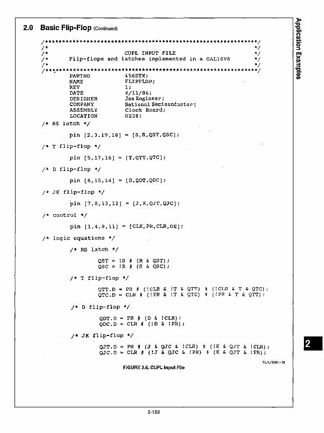
2.0 Basic Flip-Flop (Continued)
/**************************************************************/ I* */ /* CUPL INPUT FILE */ /* Flip-flops and latches implemented in a GAL16VB */ I* *I /**t***********************************************************/
PARTNO 456STX; NAME FLIPFLOP; REV 1; DATE 4/11/86; DESIGNER Joe Engineer; COMPANY National Semiconductor; ASSEMBLY Clock Board; LOCATION U238;
/* RS latch */
pin [2,3,19,18) [S,R,QST,QSC);
/* T flip-flop */
pin [5,17,16) [T,QTT,QTC);
I* D flip-flop */
pin [6,15,14) [D,QDT,QDC);
I* JK flip-flop */
pin [7,8,13,12) [J,K,QJT,QJC);
/* control */
pin (1,4,9,11) [CLK,PR,CLR,OEJ;
/* logic equations */
/* RS latch */
QST = !S # (R & QST); QSC = !R # (S & QSC);
/* T flip-flop */
QTT.D =PR# (!CLR & !T & QTT) QTC.D = CLR # (!PR & !T & QTC)
(!CLR & T & QTC); (!PR & T & QTT) ;
/* D flip-flop */
QDT.D =PR# (D & !CLR); QDC.D = CLR # (!D & !PR);
/* JK flip-flop */
QJT.D QJC.D
PR# (J & QJC & !CLR) # (!K & QJT & !CLR); CLR # (!J & QJC & !PR) # (K & QJT & !PR);
TL/L/9991-15
FIGURE 2.6. CUPL Input File
2-153
l> "'C "'5!. c:;· D> -c;· ::::J m >< D> 3
"'C CD' tn

(/) G)
a. E <U >< w c 0
:;::: <U
.!::! a. Q. <(
2.0 Basic Flip-Flops (Continued)
/****************************************************~*********/ I* *I I* CUPL SIMULATION FILE */ I* Flip-flops and latches implemented in a GAL16V8 *I I* *I /**************************************************************/
PARTNO 456STX: NAME FLIPFLOP: REV 1: DATE 4/11/86: DESIGNER Joe Engineer; COMPANY National Semiconductor; ASSEMBLY Clock Board: LOCATION U238;
/* The Order statement specifies the layout of the vector table. %n ~ n spaces inserted between variables. */
order: OE,%1,CLK,%2,S,R,%1,QST,QSC,%2,PR,%1,CLR,%2, T,%1,QTT,QTC,%2,D,%1,QDT,QDC,t2,J,K,%1,QJT,QJC;
vectors: I* RS-latch T-FF D-FF JK-FF *I /*OE CLK SR QSTQSC PR CLR T QTTQTC D QDTQDC JK QJTQJC *I
0 x 01 H L x x x X. x x x x xx x x I* set */ 0 x 10 L H x x x x x x x x xx x x I* reset */ 0 x 11 L H x x x x x x x x xx x x /* latch */ 0 x 10 L H x x x x ;x x x x xx x x I* reset */ 0 x 01 H L x x x x x x x x xx x x I* set */ 0 x 11 H L x x x x x x x x xx x x I* latch */
0 c 11 N N 1 0 x H L x N N xx N N /* preset */ 0 c 11 N N 0 1 x L H x N N xx N N I* clear */ 0 c 11 N N 0 0 0 L H x x x xx x x /* hold */ 0 c 11 N N 0 0 1 H L x x x xx x x /* toggle */ 0 c 11 N N 0 0 0 H L x x x xx x x I* hold *I 0 c 11 N N 0 0 1 L H x x x xx x x I* toggle */ 0 c 11 N N 0 0 1 H L x x x xx x x I* toggle */ 0 c 11 N N 1 0 x N N x H L xx N N I* preset */ 0 c 11 N N 0 1 x N N x L H xx N N I* clear */ 0 c 11 N N 0 0 x x x 0 L H xx x x 0 c 11 N N 0 0 x x x 1 H L xx x x /* test */ 0 c 11 N N 0 0 x x x 1 H L xx x x 0 c 11 N N 0 0 x x x 0 L H xx x x
0 c 11 N N 1 0 x N N x N N xx H L /* preset */ 0 c 11 N N 0 1 x N N x N ~ xx L H I* cl~ar */ 0 c 11 N N 0 0 x x x x x x 01 L H 0 c 11 N N 0 0 x x x x x x 00 L H /* hold */ 0 c 11 N N 0 0 x x x x x x 11 H L I* toggle */ 0 c 11 N N 0 0 x x x x x x 10 H L 0 c 11 N N 0 0 x x x x x x 00 H L I* hold */ 0 c 11 N N 0 0 x x x x x x 11 L H I* toggle */ 0 c 11 N N 0 0 x x x x x x 10 H L 0 c 11 N N 0 0 x x x x x x 01 L H
TL/L/9991-16
FIGURE 2.7. CUPL Simulation File
2-154

2.0 Basic Flip-Flops (Continued)
CLK 1
0123 ''17 111011 12131'13 11171111 20212223 2'2'2127 21213031 CK
0 r"""'
~ 1 i-2 b-< 3 ~
' ~
' &o OLMC I &o (19) 7 Ho< .... ~
.. 1'...H
r- -- ~ I
~ OLMCb I 10 11 12 13
~ (18) 1, 1, ....
3 .. .... ~ ~H .... _
r"""'_, ~ 11 17 ~~ 11 i OLMCµ II 20 21
~ (17) 22 23 ....
4 .. .... ~ ..CH --- ~
24 r"""' '
E Q 23 21 27
~ OLMCP 21 21
~ (16) 30 31 ....
PR
5 .. ;>,.. ~H ...--
r- -- ~ 32
~ o~cb 33 3' 33 31 37
~ (15) 31 31 .... ....
6 • .... ---t~ Z:H .... _ __ , ~
'° r-i-
~ •1
""' '2 '3 ~
" 9' e. OLMCP '3 ~ (14) " " ~ ....
7 .. .... ~ ..Ct-........ __ , ~
" r"""'
" i- Q 30 i-
,1 ""' '2 ~
OLMCP ,3 9'
" Ho< (13)
" ~ ....
8 .. ;>,.. -.<J-........
r"""'- ~ SI
i 0~b ,7 ,. " IO 11
~ (12) 62 63 .....
CLR 9
~· ~ 0123 ,,17 111011 12131'13 11171811 20212223 242,2127 21213031 OE
---4 FIGURE 2.8. GAL 16V8 Logic Diagram Showing Basic Flip-Flops Pattern
2-155
19 QST
18 QSC
17 QTT
19 QTC
15 QDT
14 QDC
13 QJT
12 QJC
11 OE
TL/L/9991-17
l> "C "5!. c:;· m -c;· :::J m )C m 3
"C (;' en
•

U) CJ)
Q. E ca ><
UJ c 0 ;:; cu -~ Q. Q.
<
3.0 Quad 4-to-1 Multiplexer DESCRIPTION
Widely used in computer and data communications circuits, multiplexers route one of several input banks to an output, based on the condition of select inputs. This particular version has 4 input banks, each 4-bits wide (Figure 3.1); therefore, two select lines are required to choose 1 of 4 inputs, as shown in the function table of Figure 3.2. Possible applications for our multiplexer include bus selection in a multibus computer environment, or data manipulation in an arithmetic/logic circuit.
With a total of 16 multiplexer inputs and two Select inputs, this design is well suited for the GAL20V8. The pinout chosen for this example is shown in Figure 3.3", actual pin placement of the multiplexer outputs is not critical since the versatility of the GAL20V8 allows the designer to choose that combination of output pins that best suits the board layout. The device was programmed using ABEL; the logic design input files are shown in Figure 3.4, with reduced equations shown in the document-generator file of Figure 3.5. The 'fuse' map is shown in Figure 3.6.
Ao • • A3
Bo
• • B3
INPUTS
Co
• • C3
Do
• • D3
SELECT s1 So
Aour
Bour
Cour
Dour
FIGURE 3.1. Block Diagram
} ouwurn
TL/L/9991-23
S1 So
0 0 0 1 1 0 1 1
2-156
AouT BouT CouT DouT
Ao Bo Co Do A1 B1 C1 01 A2 B2 C2 02 A3 B3 C3 03
FIGURE 3.2. Function Table
Ao 1 24 Vee
A1 2 23 s, A2 22 So
A3 4 21 Aour
Bo 5 20 Bour
B1 6 GAL20V8
19 Cour
B2 7 18 Dour
B3 8 17 D3
Co 9 16 D2
c, 10 15 D,
C2 11 14 Do
GND 12 13 C3
TL/L/9991-24
FIGURE 3.3. Pinout Diagram

3.0 Quad 4-to-1 Multiplexer (Continued)
module quad_4tol_mux·
title 'ABEL INPUT FILE Quad 4 to 1 Multiplexer in a GAL20V8 National Semiconductor
April 17, 1986 Joe Eng'
"device declaration
"location UB
"pin declaration
"inputs AO,Al,A2,AJ BO,Bl,B2,BJ co,c1,c2,cJ DO,Dl,02,DJ
"outputs
keyword device
pin 1,2,J,4; pin 5,6,7,B;
device code 'P20VBS';
pin 9,l0,11,lJ; pin 14,15,16,17;
Aout,Bout,Cout,Dout pin 21,20,19,18;
"control SO,Sl pin 22,2J;
equations
Aout ( ! Sl & !SO & AO) # (!Sl & SO & Al) # (Sl & !SO & A2) # (Sl & SO & AJ);
Bout = ( !Sl & !SO & BO) # (!Sl & SO & Bl) # (Sl & !SO & B2) # (Sl & SO & BJ);
Cout ,.. ( ! Sl & !SO & CO) # (!Sl & SO & Cl) # (Sl & !SO & C2) . #· (Sl & SO & CJ);
Dout = ( ! Sl & !SO & DO) # (!Sl & SO & 01) # (Sl & !SO & 02) # (Sl & SO & 03);
test_ vectors
([Sl,SO,AO,Al,A2,A3,BO,Bl,B2,B3,CO,Cl,C2,C3,DO,Dl,D2,D3) -> (Aout,Bout,cout,Dout])
II s s A A B B C C D D
II 1 0 0 1 2 ) 0 1 2 J Q 1 2 ) 0 1 2 J
outputs
A B C D
[0,0,1,0,0,0,0,1,0,0,0,0,l,0,0,0,0,1] -> [l,0,0,0); [0,1,1,0,0,0,0,1,0,0,0,0,l,O,O,O,O,l] -> [0,1,0,0]; [l,O,l,0,0,0,0,1,0,0,0,0,1,0,0,0,0,1] -> [O,O,l,O); [l,l,l,0,0,0,0,1,0,0,0,0,1,0,0,0,0,1] -> (O,O,O,l);
[0,0,1,1,1,0,l,1,0,1,l,0,1,l,0,1,1,l] -> (1,1,1,0]; [0,1,l,l,l,0,1,l,O,l,1,0,1,1,0,1,1,l] -> [1,1,0,l]; [1,0,l,l,l,O,l,1,0,1,1,0,1,l,O,l,l,l] -> [1,0,l,l); [1,1,1,1,1,0,1,l,O,l,l,0,1,1,0,l,l,l] -> (O,l,l,l];
FIGURE 3.4. ABEL Input File
2-157
" select "AO,BO,CO,DO "Al,Bl,Cl,Dl "A2,B2,C2,D2 11 A3,BJ,C3,D3
"AO,BO,CO,DO "Al,Bl,Cl,Dl "A2,B2,C2,D2 II AJ I BJ I CJ I DJ
TL/L/9991-25

U) CD Q. E cu >< w c 0 ;
.~ Q. c. <(
3.0 Quad 4-to-1 Multiplexer (Continued)
ABEL(tm) Version 1.19 Document Generator Quad 4 to 1 Multiplexer in a GAL20V8 April 17, 1986 National Semiconductor Joe Eng Equations for Module quad_4tol_mux
Device ue
Reduced Equations:
Aout - (AO & !SO & !Sl # Al & SO & !Sl # A2 & !SO & Sl # A3 & SO & Sl);
Bout - (BO & !SO & !Sl # Bl & SO & !Sl # 82 & !SO & Sl # 83 & SO & Sl);
Cout
Dout
(CO & !SO & !Sl # Cl & SO & !Sl # C2 & !SO & Sl #CJ & SO & Sl);
(DO & !SO & !Sl # Dl & SO & !Sl # 02 & !SO & Sl # 03 & SO & Sl);
' FIGURE 3.5. Reduced ABEL Equations
2-158
TLIL/9991-26

3.0 Quad 4-to-1 Multiplexer (Continued)
QP24• QF2706• LOOOO 0000000000000000000000000000000000000000 0000000000000000000000000000000000000000 0000000000000000000000000000000000000000 0000000000000000000000000000000000000000 0000000000000000000000000000000000000000 0000000000000000000000000000000000000000 0000000000000000000000000000000000000000 0000000000000000000000000000000000000000 11011110111011111111lllllllll11111111111 Ollllll0ll01lllllllllll1111111111lllllll lll1010lll101ll11111111111111111lllll111 llllllOlOlOlllllllllllllllllllllllllllll 0000000000000000000000000000000000000000 0000000000000000000000000000000000000000 0000000000000000000000000000000000000000 0000000000000000000000000000000000000000 lllllll01110011llllll11111llllllllllllll lllllllOllOlllllOlllllllllllllllllllllll llllllOllllOllllllllOlllllllllllllllllll llllllOlllOlllllllllllllOlllllllllllllll 0000000000000000000000000000000000000000 0000000000000000000000000000000000000000 0000000000000000000000000000000000000000 0000000000000000000000000000000000000000 lllllllOlllOllllllllllllllllOlllllllllll lllllllOllOlllllllllllllllllllllOlllllll llllllOllllOllllllllllllllllllllllllOlll 1111110111011111111111111111111111111101 0000000000000000000000000000000000000000 0000000000000000000000000000000000000000 0000000000000000000000000000000000000000 0000000000000000000000000000000000000000 1111111011101111111111111111111111011111 lllllll0110llllllllllllllllll101llllllll llllllOllllOllllllllllllllOlllllllllllll llllllOlllOlllllllllllOlllllllllllllllll 0000000000000000000000000000000000000000 0000000000000000000000000000000000000000 0000000000000000000000000000000000000000 0000000000000000000000000000000000000000• L2560 01111000• L2568 0000000000000000000000000000000000000000000000000000000000000000• L26l2 1• L2633 o• L26H o• L2635 o• L26l6 o• L26l7 l • L26l8 l * L26l9 l* L2640 llllllllllllllllllllllllllllllllllllllllllllllllllllllllllllllll• L2704 10• VOOOl 10000100001N00001LLLHOON* V0002 lOOOOlOOOOlNOOOOlLLHLlON• VOOOl lOOOOlOOOOlNOOOOlLHLLOlN* V0004 lOOOOlOOOOlNOOOOlHLLLllN* V0005 1110110ll01Nl0111LHHllOON• V0006 lllOllOllOlNlOlllHLHHlON• V0007 lllOllOllOlNlOlllHllU!OlN* voooe 11101101101NlOlllHHllL11N* C5127•
FIGURE 3.6. 'Fuse' Map
2-159
TUL/9991-27
l> "'C 1:!. c;· I» -5· :::s
'" >< I» 3
"'C Ci en

en Cl)
"i5.. E cu >< w c 0 :;:: cu .~ "i5.. Q.
<C
4.0 Dual 8-to-1 Multiplexer The Dual 8:1 Mux selects one of eight inputs, DO through D7, specified by three binary select inputs, A, B and C. The true data is output on Y when strobed by S. The circuit is implemented using a GAL22V10.
LOGIC SYMBOL
V cc A S 1Y 2Y 207 206 205 204 203
[24 23 22 21 2D 19 18 17 16 15 14 13
A B c s 1Y 2Y 207 206 205 204
...... 100 203 ........
101 102 103 104 105 106 107 200 201 202
1 2 3 4 5 6 7 8 9 10 11 112
100 101 102 103 104 105 106 107 200 201 202 GNO TUU9991-28
Plnout
FUNCTION TABLE
Inputs Output
Select Strobe y c B A s x x x H H L L L L DO L L H L D1 L H L L D2 L H H L D3 H L L L D4 H L H L DS H H L L D6 H H H L D7
2-160

4.0 Dual 8-to-1 Multiplexer (Continued)
LOGIC DIAGRAM Dual 8:1 Mux
23 22 21 20
2-161
24 --Vee
19 1Y
18 2Y
12 --.i TL/L/9991-29

(/) Cl)
"S. 4.0 Dual 8-to-1 Multiplexer (Continued) E cu OPAL™ INPUT FILE >< w c title Dual 8 to 1 multiplexer 0 pattern mux8tl ~ cu revision B .~ "S. author Tarif Engineer c. company NSC <C Date 1/8/92
chip mux8tl GAL22V10
lDO lDl 1D2 1D3 1D4 1D5 1D6 1D7 2DO 2Dl 2D2 GND
2D3 2D4 2D5 2D6 2D7 2Y ·lY s ·c B A vcc
equations
/lY ·/lDO * /C * /B * /A * /S + /lDO * /C * /B * A * /S + /lDO *. /C * B * /A * /S + /lDO *· /C * B * A * /S + /lDO * c * /B * /A * /S + /lDO * c * /B * A .* /S + /lDO * c * B * /A * /S + /lDO * c * B * A * /S
/2Y /2DO * /C * /B * /A * /S + /2Dl * /C * /B *· A * /S· + /2D2 * /C * B * /A * ./S + /2D3 * /C * B * A * /S + /2D4 * c * /B * /A * /S + /2D5 * c * /B * A * /S + /2D6 * c * B * /A * /S + /2D7 * c * B * A * /S
TL/L/9991-FO
2-162

4.0 Dual 8-to-1 Multiplexer (Continued)
OPAL™ JEDEC FILE
e GAL22Vl0 EQN2JED - Boolean Equations to JEDEC file assembler (Version V029) Copyright (c) National Semiconductor Corporation 1990,1991 Assembled from "C:\OPAL102\MUX8Tl.EQN". Date: 1-9-92
title Dual 8 to 1 multiplexer pattern mux8tl revision B author Tarif Engineer company NSC Date 1/8/92
* NOTE PINS lDO:l 101:2 1D2:3 103:4 1D4:5 105:6 106:7 107:8 200:9* NOTE PINS 201:10 202:11 GND:12 203:13 204:14 205:15 2D6:16 207:17* NOTE PINS 2Y:18 1Y:l9 S:20 C:21 B:22 A:23 VCC:24* QF5892*QP24*FO* L2156 11111111111111111111111111111111111111111111 10101110111011101111111111111111111111111111 10011110111011101111111111111111111111111111 10101101111011101111111111111111111111111111 10011101111011101111111111111111111111111111 10101110110111101111111111111111111111111111 10011110110111101111111111111111111111111111 10101101110111101111111111111111111111111111 10011101110111101111111111111111111111111111* L2904 11111111111111111111111111111111111111111111 11101110111011101111111111111111101111111111 11011110111011101111111111111111111110111111 11101101111011101111111111111111111111111011 11011101111011101111111111111111111111111110 11101110110111101111111111111111111111101111 11011110110111101111111111111111111011111111 11101101110111101111111111111110111111111111 11011101110111101111111111101111111111111111* L5808 01010101010101010101* L5828 0000000000000000000000000000000000000000000000000000000000000000* C551B* •oooo
TL/L/9991-F1
2-163
)> "C "'5!. c:;· I» -5· ::J m >< I» 3
"C Ci' en

U) Cl> Q. E
= w c 0 = ca -~ Q. CL c(
4.0 Dual 8-to-1 Multiplexer (Continued)
EQN2JED - Boolean Equations to JEDEC file assembler (Version V029) Copyright (c) National Semiconductor Corporation 1990,1991
Document file for C:\OPAL102\MUX8Tl.EQN Device: G22Vl0 ·
$LABELS 24 100 101··102 103 104 105 106 107 200 201 202 GNO 203 204 205 206 207 2Y lY S C B A VCC
Pin Label
1 100 2 101 3 102 4 103 5 104 6 105. 7 106 8 107 9 200 10 201 11 202 12 GNO 13 203 14 204 15 205 16 206 17 207 18 2Y 19 lY 20 s 21 c 22 B 23 A 24 vcc
Type
pos,com input unused unused unused unused unused· unused unused pos,com input pos,com input pos,com input ground pin pos,com input pos,com input pos,com input pos,com input pos,com input neg,trst,com output neg,trst,com output pos,com input pos,com input
· pas, com input pos,com input
·power pin
Chip Diagram (DIP)
100 24
101 2 23
102 3 22
103 4 21
104 5 20
105 6 19
106 7 18
107 8 17
200 9 16
201 10 15
202 11 14
GNO 12 13
2·164
Vee
A
B
c. s 1Y
2Y
207
206
205
204
203
TL/L/9991-F4
TL/L/9991-53

5.0 7-Bit Counter with Parallel Load DESCRIPTION In this example, a GAL20V8 implements a seven-bit counter with asynchronous carry-out and load functions. As illustrated in the block diagram (Figure 5. 1) and pinout diagram (Figure 5.2), the carry-in and carry-out pins make the counter fully cascadable to form larger counters. The CUPL design input files are shown in Figure 5.3, and simulation files in Figure 5.4. Note that the counter requires seven registers and one asynchronous output, taking full advantage of the generic architecture of the GAL20V8.
CLK--
LOAD--_..
CARRY IN--_..
CLEAR--_..
FIGURE 5.1. Block Diagram
OUTPUTS {Oo-05)
CARRY OUT
TL/L/9991-37
2-165
)> "'C "E. c:;· m -CLK 24 Vee s· :J
Do 2 23 CARRY IN m ><
D, 3 22 Oo m D2 4 21 o, 3
"'C D5 5 20 02 CD'
0 D4 6
GAL20V8 19 03
Ds 7 18 04
D5 8 17 Os
LOAD 9 16 05
CLEAR 10 15 CARRY OUT
11 14
GND 12 13 0£
TL/L/9991-38
FIGURE 5.2. Plnout Diagram

"' CD c.. E ca >< w c 0 ;:; ca -~ c.. a.
,<I:
5.0 7-Bit Counter with Parallel Load (Continued)
/**************************************************************/ I* . *I. /* CUPL INPUT FILE */ /* DESIGN INPUT FOR 7-BIT COUNTER */ I* . . . . . */ /**************************************************************/ /* ALLOWABLE TARGET DEVICE: GAL20V8 · */ /************************************************************~*/ PARTNO 7BITCNT ; NAME 7-BIT COUNTER REV 01 ; DATE 10/08/85 ; DESIGNER Joe Engineer; COMPANY National Semiconductor; ASSEMBLY JA-27 LOCATION U06
PIN 1 CLK I* CLOCK INPUT */ PIN 2 DO /* DAT AO INPUT */ PIN 3 Dl /* DAT Al INPUT */ PIN 4 02 /* DATA2 INPUT */ PIN 5 03 I* DATA3 INPUT */ PIN 6 04 /* DATA4 INPUT */ PIN 7 05 I* DATA5 INPUT *I PIN 8 06 I* DATA6 INPUT */ PIN 9 LO I* LOAD CONTROL */ PIN 10 CLEAR; I* ASYNCHRONOUS CARRY-IN */
PIN 13 !OE ; I* OUTPUT ENABLE */ PIN 15 CARRYOUT PIN 16 = Q6 I* COUNTER MSB */ PIN 17 Q5 PIN 18 Q4
PIN 19 Q3 PIN 20 Q2 PIN 21 Ql PIN 22 QO /* COUNTER LSB */ PIN 23 CARRYIN /* CARRY-IN FOR CASCADING */
TL/l/9991-39
FIGURE 5.3. CUPL Design Input Fife
2-166

l> 5.0 7-Bit Counter with Parallel Load (Continued)
"'O ~ c:;· D>
QO.D a (LO & DO I* LOAD DO *I -c;· # !LO & !QO & CARRY IN) & !CLEAR; I* TOGGLE *I :::::J
m >< D>
Ql.D = (LO & 01 /* LOAD Dl *I 3 # !LO& !Ql & QO & CARRYIN I* TOGGLE *I "'O
# !LO& Ql & !QO) & !CLEAR; I* HOLD *I CD" en
Q2.D = (LO & 02 I* LOAD 02 *I # !LO& !Q2 & Ql & QO & CARRYIN I* TOGGLE *I # !LO& Q2 & !Ql I* HOLD *I # !LO& Q2 & !QO) & !CLEAR; /* HOLD *I
Q3.D = (LO & 03 I* LOAD 03 *I # !LO& !Q3 & Q2 & Ql & QO & CARRY IN I* TOGGLE *I # !LO& QJ & !Q2 I* HOLD *I # !LO& Q3 & !Ql /* HOLD *I # !LO& QJ & !QO) & !CLEAR; /* HOLD *I
Q4.D = (LO & 04 I* LOAD 04 *I # !LO& !Q4& Q3 & Q2 & Ql & QO & CARRYIN /* TOGGLE *I # !LO& Q4 & !QJ I* HOLD *I # !LO& Q4 & !Q2 I* HOLD *I # !LO& Q4 & !Ql /* HOLD *I # !LO& Q4 & !QO) & !CLEAR;· I* HOLD *I
QS.D = (LO & 05 I* LOAD D5 */ # !LO& !Q5& Q4 & QJ & Q2 & Ql & QO
& CARRYIN /* TOGGLE *I # !LO& QS & !Q4 I* HOLD *I # !LO& QS & !QJ I* HOLD *I # !LO& QS & !Q2 /* HOLD */ # !LO& QS & !Ql /* HOLD *I # !LO& Q5 & !QO) & !CLEAR; I* HOLD *I
Q6.D = (LO & 06 I* LOAD 06 *I # !LO& !Q6& Q5 & Q4 & Q3 & Q2 & Ql & QO
& CARRYIN /* TOGGLE *I # !LO& Q6 & !QS I* HOLD *I # !LO& Q6 & !Q4 /* HOLD *I # !LO& Q6 & !QJ /* HOLD *! # !LO& Q6 & !Q2 I* HOLD *I # !LO& Q6 & !Ql I* HOLD *I # !LO& Q6 & !QO) & !CLEAR; I* HOLD *I
CARRYOUT = !LO & Q6 & QS & Q4 & Q3 & Q2 & Ql & QO & . CARRYIN; I* CARRY-OUT *I • TL/L/9991-40
FIGURE 5.3. CUPL Design Input File (Continued)
2-167

en Cl> 'i5. E
= I.LI c 0 ;:; cu -~ 'i5. a. <
5.0 7-Bit Counter with Parallel Load (Continued)
/**************************************************************/ /* *I /* CUPL INPUT FILE */ /* SIMULATION FOR 7-BIT COUNTER */ /* */ 1·····························································•1 /* ALLOWABLE TARGET DEVICE: GAL20V8 */ /**********************•···································~···; PARTNO 7BITCNT : NAME 7-BIT COUNTER REV 01 , DATE 10/08/85 : DESIGNER Joe Engineer; COMPANY National Semiconductor; ASSEMBLY JA-27 LOCATION U06 :
ORDER:
CLK, !OE, CLEAR, LO, CARRYIN, 06, 05, D4, DJ, D2, Dl, DO, Q6, Q5, Q4, QJ, Q2, Ql, QO, CARRYOUT;
VECTORS:
Smsg" Smsg" Smsg" $msg" $msg"
c ... c c c 0 11
•
L 0 LL I DDDDDDD QQQQQQQ U 11 •
KER D N 6543210 6543210 T 11 • ... 0 x x x xxxxxxx zzzzzzz x C 0 1 X X XXXXXXX LLLLLLL L C 0 0 1 X 1111111 HHHHHHH L C O 0 1 X 0000000 LLLLLLL L C 0 0 0 1 XXXXXXX LLLLLLH L C 0 0 0 1 XXXXXXX LLLLLHL L C 0 0 0 1 XXXXXXX LLLLLHH L C 0 0 0 1 XXXXXXX LLLLHLL L C 0 0 0 1 XXXXXXX LLLLHLH L C 0 0 0 1 XXXXXXX LLLLHHL L C 0 0 0 1 XXXXXXX LLLLHHH L C 0 0 0 1 XXXXXXX LLLHLLL L C O O O 1 XXXXXXX LLLHLLH L C 0 0 0 1 XXXXXXX LLLHLHL L C 0 0 0 1 XXXXXXX LLLHLHH L C 0 0 0 1 XXXXXXX LLLHHLL L C 0 0 0 1 XXXXXXX LLLHHLH L C 0 0 0 1 XXXXXXX LLLHHHL L C 0 0 0 1 XXXXXXX LLLHHHH L C 0 0 0 1 XXXXXXX LLHLLLL L C 0 0 0 1 XXXXXXX LLHLLLH L C 0 0 0 1 XXXXXXX LLHLLHL L C 0 0 0 1 XXXXXXX LLHLLHH L C 0 0 0 1 XXXXXXX LLHLHLL L C 0 0 0 1 XXXXXXX LLHLHLH L C 0 0 0 1 XXXXXXX LLHLHHL L C 0 0 0 1 XXXXXXX LLHLHHH L C O 0 0 1 XXXXXXX LLHHLLL L C 0 0 0 1 XXXXXXX LLHHLLH L C 0 0 0 1 XXXXXXX LLHHLHL L C 0 0 0 1 XXXXXXX LLHHLHH L C 0 0 0 1 XXXXXXX LLHHHLL L C 0 0 0 1 XXXXXXX LLHHHLH L C 0 0 0 1 XXXXXXX LLHHHHL L C 0 0 0 1 XXXXXXX LLHHHHH L C O 0 0 1 XXXXXXX LHLLLLL L C 0 0 0 1 XXXXXXX LHLLLLH L C 0 0 1 X 0111111 LHHHHHH L C 0 0 0 1 XXXXXXX HLLLLLL L C 0 0 0 1 XXXXXXX HLLLLLH L C 0 0 1 X 1111110 HHHHHHL L C 0 0 0 1 XXXXXXX HHHHHHH H C 0 0 0 1 XXXXXXX LLLLLLL L
/* TEST HI-Z */ /* TEST CLEAR */ /* LOAD ONES */ /* LOAD ZEROS */ /* COUNT=l */ /* COUNT=2 */ /* COUNT=J */ /* COUNT=4 */ /* COUNT=5 */ /* COUNT=6 */ /* COUNT=? */ /* COUNT=B */ . /* COUNT=9 */ /* COUNT=lO */ /* COUNT=ll */ /* COUNT=l2 */ /* COUNT=lJ */ /* COUNT=l4 */ /* COUNT=l5 */ /* COUNT=l6 */ /* COUNT=l7 */ /* COUNT=l8 */ /* COUNT=l9 */ /* COUNT=20 */ /* COUNT=21 */ /* COUNT=22 */ /* COUNT=23 */ /* COUNT .. 24 */ /* COUNTc25 */ /* COUNT=26 */ /* COUNT=27 */ /* COUNT=28 */ /* COUNT=29 */ /* COUNT=JO */ /* COUNT=Jl */ /* COUNT=32 */ /* COUNT=JJ */ /* LOAD=63 TO OBSERVE MSB TQGGLE */ /* COUNT=64, OBSERVE MSB */ /* COUNT=65, OBSERVE MSB */ /* LOAD=l26.TO OBSERVE CARRY*/ /* COUNT=l27, OBSERVE CARRY */ /* COUNT=O, OBSERVE CARRY */
FIGURE 5.4. CUPL Simulation File
2·168
TL/L/9991-50

6.0 10-Bit Up/Down Counter The ten-bit up/down counter can count up, count down, set all output to high, disable the output (high impedance), and load 2 LSB's, 2 MSB's and 6 middle bits high or low as a group. All operations are synchronous with the rising edge of the clock. SET overrides LOAD, COUNT and HOLD. LOAD overrides COUNT and HOLD.
C1N enable counting operation or hold it. COUNT Up or Down depend on UP signal.
All outputs are enabled when OE is low, otherwise HIGH-Z.
This circuit is implemented using a PAL20X10, with the' exclusive-or function the PAL20X10 facilitates design of counter and state sequences with minimum propagation delay. The PAL20X10 offers an efficient means of implementing counters. Normal PAL & PLA implementation would require addition terms for the XOR functions. Having 10 output the PAL20X10 supersets 20 and 24 medium PAL's in this specific application. On power up all registers are reset to sim-plify sequential circuit design. ·
LOGIC SYMBOL
DATA OUT
Vee QO Q1 Q2 Q3 Q4 Q5 Q6 Q7 QB Q9 UE
124 23 22 21 20 19 1B 17 16 15 14 13
QD Q1 Q2 Q3 Q4 Q5 Q6 Q7 QB Q9
!>CK ~ 10-BIT DE jo-J COUNTER
DO 01 02-07 DB 09 LO CNT UP SET C1N C) -c)- -c;r -Q
1 2 3 4 5 6 7 B 9 10 11 T12
cK , oo 01 02-01 oB og , m m UP sET CiN GNo
DATA IN
TL/L/9991-51
Plnout
FUNCTION TABLE
OE CK SET LD Cffi' CiN H x x x x x L t H x x x L t L L x x L t L H H x L t L H L H L t L H L L L t L H L L
2-169
UP 09-DO 09-QO
x x z x x H x D D x x a x x a L x Qplus1 H x Qminus 1
Operation
Hi-Z Set all HIGH LOADD HOLD HOLD Count UP Count ON
l> "'C "2. c:;· D» -c;· ::I m >< D» 3
"'C m en

"' cu 'ii 6.0 10-Bit Up/Down Counter (Continued) E = LOGIC DIAGRAM w c 0 ;::; cu -~ 'ii a. <(
SET ,:::.10-f:>o-ll++-~
2-170
TUL/9991-52

6.0 10-Bit Up/Down Counter (Continued)
OPAL™ INPUT FILE
title 10-BIT SYNCHRONOUS UP/OOIJN COUNTER
pattern COUNTER
revision A
author Tarif Engineer
company National Semiconductor Corporation Date 11/17/1989
chip COUNTER PAL20X10
pin 1 2 3 4 6 7 8
CLK 00 01 0207 /LO /CNT /UP SET pin 13 14 1S 16 17 18 19 20
/OE C9 ca C7 C6 cs C4 C3
equations
/CO := /CO*LD */SET
+ /LO* /SET* /DO S LO */Cl N* /SET* /CNT*UP
+ LO */Cl N* /SET* /CNT* /UP
/Cl := /C1*LD */SET
+ /LO* /SET* /01 S LO */CIN*/SET*/CNT*UP */CO
+ LO */CIN*/SET*/CNT*/UP* CO /C2 := /C2*LD */SET
+ /LO* /SET* /0207
9 08
21 C2
S LO */CIN*/SET*/CNT*UP */C1*/C0 + LO */CIN*/SET*/CNT*/UP* C1* CO
/C3 : = /C3*LD */SET
+ /LO* /SET* /0207
10
/CIN
22 C1
$ LO */CIN*/SET*/CNT*UP */C2*/C1*/C0
+ LO */CIN*/SET*/CNT*/UP* C2* C1* CO
/C4 := /C4*LD */SET + /LO*/SE.T*/0207
S LO */CIN*/SET*/CNT*UP */C3*/C2*/C1*/C0 + LO */CIN*/SET*/CNT*/UP* C3* C2* C1* CO
/CS := /C5*LD */SET
+ /LO* /SET* /0207
11
09
23 co
$ LO */CIN*/SET*/CNT*UP */C4~/C3*/C2*/C1*/Q0 + LO */CIN*/SET*/CNT*/UP* C4* Q3* Q2* Cl* CO
/Q6 : = /Q6*LD . */SET
+ /LO*/SET*/0207
12 GND
24 vcc
$ LO */CIN*/SET*/CNT*UP */CS*/C4*/C3*/C2*/C1*/QO
+ LO */CIN*/SET*/CNT*/UP* CS* C4* C3* C2* C1* CO
/C7 := /C7*LD */SET
+ /LO*/SET*/0207 S LO */CIN*tSET*/CNT*UP */C6*/CS*/C4*/C3*/C2*/C1*/QO
+ LO */CIN*/SET*/CNT*/UP* C6* CS* C4* C3* C2* C1* CO
/QB := /Q8*LD */SET
+ /LO* /SET* /08 S LO */CIN*/SET*/CNT*UP */C7*/Q6*/C5*/Q4*/C3*/C2*/C1*/C0
+ LO */CIN*/SET*/CNT*/UP* C7* C6* cs• C4* C3* C2* C1* QO
/Q9 : = /Q9*LD */SET
+ /LO*/SET*/09
S LO */CIN*/SET*/CNT*UP */C8*/C7*/C6*/CS*/Q4*/C3*/Q2*/Q1*/Q0
+ LO */CIN*/SET*/CNT*/UP* CS* C7* C6* CS* C4* C3* C2* C1* QO
2-171
l> "'C "2. c;· D> -c;· ::s m >< D> 3
"'C c;; en
TL/L/9991-FS

en cu Q. E cu >< w c 0 = -~ Q. a. c(
6.0 10-Bit Up/Down Counter (Continued)
OPAL™ JEDEC FILE
PAL20X10 title 10-BIT SYNCHRONOUS UP/DOIJN COUNTER pattern COUNTER revision A author Tarif Engineer company National Semiconductor Corporation Date 11/17/1989
Qf1600*0P24*FO* LOOOO .
1110111111111011111111111011111111111111 1011111111110111111111111011111111111111 1111111111111011011110111011111101111111 1111111111111011011101111011111101111111* L0160
1111111011111011111111111011111111111111 1111101111110111111111111011111111111111 111011111111101101111011101111110111111'1 1101111111111011011101111011111101111111* L0320
1111111111101011111111111011111111111111 1111111110110111111111111011111111111111 1110111011111011011110111011111101111111 1101110111111011011101111011111101111111* . L0480 1111111111111010111111111011111111111111 1111111110110111111111111011111111111111 1110111011101011011110111011111101111111 1101110111011011011101111011111101111111• L0640 1111111111111011111011111011111111111111 1111111110110111111111111011111111111111. 1110111011101010011110111011111101111111 1101110111011001011101111011111101111111• L0800 1111111111111011111111101011111111111111 1111111110110111111111111011111111111111 1110111011101010011010111011.111.101111111 1101110111011001010101111011111101111111• L0960 1111111111111011111111111010111111111111 1111111110110111111111111011111111111111 1110111011101010011010101011111101111111 1101110111011001010101011011111101111111• L1120 1111111111111011111111111011111011111111 1111111110110111111111111011111111111111 1110111011101010011010101010111101111111 1101110111011001010101011001111101111111•
L1280 1111111111111011111111111011111111101111 1111111111110111111111111011101111111111 1110111011101010011010101010111001111111 1101110111011001010101011001110101111111• L1440 1111111111111011111111111011111111111110 1111111111110111111111111011111111111011 1110111011101010011010101010111001101111 1101110111011001010101011001110101011111*
CA03E*
0000
2-172
TL/L/9991-F7

6.0 10-Bit Up/Down Counter (Continued)
The same design can be implemented in a GAL22V1 O by converting the Exclusive OR function to OR & AND functions which can be done manually by applying DeMorgan's Low (see appendix A) to the Exclusive OR function
F = A $ B " Xor relations "
Or the conversion can be done in an easier way by using OPAL feature. The software will automatically expand and minimize the equations. To get more information on the conversion procedure refer to PAL to GAL conversion note in this data book (APP Note # 799).
F = (A & /B) + (/A & B)" OR, AND relation" The following shows the final equations after converting and minimizing the previous design.
chip lOCOUNT GAL22V10
CLK LD ST UP CNT CIN D9 DB D2D7 Dl DO GND nc QO Q3 Q2 QB Q9 Q5 Q7 Q6 Q4 Ql vcc
equations
QO := LD * /ST * /CNT * /CIN * /QO + LD * /ST * CIN * QO + LD * /ST * CNT * QO + /LD * /ST * /DO
Ql .- /Ql * LD * /ST * UP * /CNT * /CIN * /QO + /Ql * LD * /ST * /UP * /CNT * /CIN * QO + Ql * LD * /ST * /UP * /QO + Ql * LD * /ST * UP * QO + /LD * /ST * /Dl + Ql * LD * /ST * CIN + Ql * LD * /ST * CNT
Q2 := Ql * LD * /ST * Q2 * /QO + LD * /ST * UP * Q2 * QO + /Ql * LD * /ST * /UP * Q2 + /Ql * LD * /ST * UP * /CNT * /CIN * /Q2 * /QO + Ql * LD * /ST * /UP * /CNT * /CIN * /Q2 * QO + /LD * /ST * /D2D7 + LD * /ST * CIN * Q2 + LD * /ST * CNT * Q2
Q3 := Ql * LD * /ST * Q3 * /QO + LD * /ST * /Q2 * Q3 * QO + /Ql * LD * /ST * /UP * Q3 + LD * /ST * UP * Q2 * QJ + /Ql * LD * /ST * UP * /CNT * /CIN * /Q2 * /Q3 * /QO + Ql * LD * /ST * /UP * /CNT * /CIN * Q2 * /Q3 * QO + /LD * /ST * /D2D7 + LD * /ST * CIN * Q3 + LD * /ST * CNT * Q3
Q4 := LD * Q4 * /ST * Q2 * /QO + /Ql * LD * Q4 * /ST * QO + Ql * LD * Q4 * /ST * UP + LD * Q4 * /ST * /Q2 * Q3 + LD * Q4 * /ST * /UP * /Q3 + /Ql * LD * /Q4 * /ST * UP * /CNT * /CIN * /Q2 * /Q3 * /QO + Ql * LD * /Q4 * /ST * /UP * /CNT * /CIN * Q2 * QJ * QO + /LO * /ST * /0207 + LD * Q4 * /ST * CIN + LD * Q4 * /ST * CNT
Q5 := LD * Q4 * /ST * Q5 * /QO + LD * /ST * Q5 * /Q3 * QO + /Ql * LO * /ST * /UP * Q5 + Ql * LO * /Q4 * /ST * Q5 + LD * /ST * Q5 * /Q2 * QJ + LO * /ST * UP * Q5 * Q2 + /Ql * LD * /Q4 * /ST * UP * /CNT * /Q5 * /CIN * /Q2 * /QJ * /QO + Ql * LD * Q4 * /ST * /UP * /CNT * /Q5 * /CIN * Q2 * QJ * QO + /LD * /ST * /D2D7 + LO * /ST * Q5 * CIN + LD * /ST * CNT * Q5
Q6 .- LD * /ST * Q6 * Q2 * /QO + LO * /ST * Q6 * /Q5 * QO + /Ql * LO * /ST * Q6 * Q5 + Ql * LO * /ST * Q6 * UP + LO * /ST * Q6 * /Q2 * QJ + LO * Q4 * /ST * Q6 * /Q3 + LO * /Q4 * /ST * Q6 * /UP + /Ql * LO * /Q4 * /ST * /Q6 * UP * /CNT * /Q5 * /CIN * /Q2 * /Q3
TL/L/9991-13
2-173
> "'C "2. c;· m -c;· ::s m >< m 3
"'C Ci' tn
fJI

(I) cu Q. E ca >< w c 0
;::: cu .2 Q. a. <(
6.0 10-Bit Up/Down Counter (Continued)
* /QO + Ql * LD * Q4 * /ST * /Q6 * /UP * /CNT * Q5 * /CIN * ~2 * Q3 * QO + /LD * /ST * /D2D7 + LD * /ST * Q6 * CIN + LD * /ST * Q6 * CNT
Q7 .- Ql * LD * /ST * Q7 * /QO + LD * /ST * Q7 * /Q2 * QO + /Ql * LD * /ST * /UP * Q7 + LD * /ST * /Q6 * Q7 * Q2 + LD * /ST * Q6 * Q7 * /Q3 + LD * /ST * Q7 * /Q5 * Q3 + LD * /Q4 * /ST * Q7 * Q5 + LD * Q4 * /ST * UP * Q7 + /Ql * LD * /Q4 * /ST * /Q6 * UP * /Q7 * /CNT * /Q5 * /CIN * /Q2
* /Q3 * /QO + Ql * LD * Q4 * /ST * Q6 * /UP * /Q7 * /CNT * Q5 * /CIN * Q2 * Q3
* QO + /LD * /ST * /D2D7 + LD * /ST * Q7 * CIN + LD * /ST * Q7 * CNT
Q8 .- LO * /ST * QB * Q2 * /QO + LD * /ST * /Q7 * QB * QO + /Ql * LD * /ST * QB * Q3 + Ql * LD * /ST * /Q5 * QB + LD * Q4 * /ST * QB * /Q2 + LD * /ST * Q7 * QB * /Q3 + LD * /Q4 * /ST * Q6 * QB + LD * /ST * UP * Q5 * QB + LD * /ST * /Q6 * /UP * QB + /Ql * LD * /Q4 * /ST * /Q6 * UP * /Q7 * /CNT * /Q5 * /CIN * /QB
* /Q2 * /Q3 * /QO + Ql * LD * Q4 * /ST * Q6 * /UP * Q7 * /CNT * Q5 * /CIN * /QB * Q2
* Q3 * QO + /LD * /ST * /DB + LD * /ST * CIN * QB + LD * /ST * CNT * Q8
Q9 := LD * /ST * Q9 * Q3 * /QO + LD * /Q4 * /ST * Q9 * QO + /Ql * LD * Q4 * /ST * Q9 + Ql * LD * /ST * Q9 * /QB + LD * /ST * Q9 * QB * /Q2 + LD * /ST * UP * Q9 * Q2 + LD * /ST * Q7 * Q9 * /Q3 + LD * /ST * Q6 * /Q5 * Q9 + LD * /ST * /Q7 * Q5 * Q9 + LD * /ST * /Q6 * /UP * Q9 + /Ql * LD * /Q4 * /ST *· /Q6 * UP * /Q7 * /CNT * /Q5 * /CIN * /Q9
* /QB * /Q2 * /Q3 * /QO + Ql * LD * Q4 * /ST * Q6 * /UP * Q7 * /CNT * Q5' * /CIN * /Q9 * QB
* Q2 * Q3 * QO + /LO * /ST * /D9 + LD * /ST * CIN * Q9 + LD * /ST * CNT * Q9
TL/L/9991-13
2-174

6.0 10-Bit Up/Down Counter (Continued)
GAL22V10
* QF5892*QP24*FO* L0044 11111111111111111111111111111111111111111111 11010111101101111011101111111111111111011111 11010111101110111011101111111111111111101111 11100111101110111111111111111111111111011111 11100111101101111111111111111111111111101111 11111011101111111111111111111111111110111111 11100111101111111111011111111111111111111111 11100111101111110111111111111111111111111111* L0440 11111111111111111111111111111111111111111111 11110110101111111111111111111110111111011111 11010110101111111111111111111111111111101111 11100110101101111111111111111111111111111111 11110110101111111111111111111101111011111111 11110110101110111111111111111111110111111111 11010101101101111011101111111101110111011111 11100101101110111011101111111110111011101111 11111011101111111111111111111111101111111111 11110110101111111111011111111111111111111111 11110110101111110111111111111111111111111111* L0924 11111111111111111111111111111111111111111111 11110111101011111111111111111110111111011111 11110111101011111101111111111111111111101111 11010111101011111110111111111111111111111111 11100111101001111111111111111111111111111111 11110111101011111111111111111101111011111111 11110110101011111111111111111111110111111111 11110101101010111111111111111111111111111111 11010101100101111001101111111101110111011111 11100110100110111010101111111110111011101111 11111011101111111111111111111111101111111111 11110111101011111111011111111111111111111111 11110111101011110111111111111111111111111111* L1496 11111111111111111111111111111111111111111111 11100111101111101111111111111111111111011111 11110111101111101111111111111101111111101111 11010111101110101111111111111111111111111111 11110111100111101111111111111110111111111111 11110111101011101111111111111111110111111111 11110111101111101101111111111111111011111111 11110101101111101110111111111111111111111111 11110110101101101111111111111111111111111111 11010101100101011001101111111101110111011111 11100110101010011010101111111110111011101111 11111011101111111111111111111111101111111111 11110111101111101111011111111111111111111111 11110111101111100111111111111111111111111111* L2156 11111111111111111111111111111111111111111111 11110110101111111110111111111111111111011111 11110111101111111110111111111111110111101111 11010111101110111110111111111111111111111111 11100101101111111110111111111111111111111111 11110111101111111110111111111101111011111111 11110111101101111110111111111110111111111111 1101010110110111100110111111110111011101i111 11100110101110111001101111111110111011101111 11111011101111111111111111111111101111111111 11110111101111111110011111111111111111111111 11110111101111110110111111111111111111111111*
2-175
TL/L/9991-18
)> "C "E. c;· D> -c;· ::s m >< m 3
"C c;; tn

6.0 10-Bit Up/Down Counter (Continued)
L2904 11111111111111111111111111111111111111111111 11110111101111111111111011111111111011011111 11110101101111111111111011111111111111101111 11010110101111111111111011111111111111111111 11100111101111111111111011011111111111111111 11110111101111111111111011101101111111111111 11110111101101111111111011111110111111111111 11110111101111101111111011111111110111111111 11110111101011111101111011111111111111111111 11110111101111011110111011111111111111111111 11110111100110111111111011111111111111111111 11010101100101011001100111011101110111011111 11100110101010101010100111101110111011101111 11111011101111111111111110111111111111111111 11110111101111111111011011111111111111111111 11110111101111110111111011111111111111111111* L3652 11111111111111111111111111111111111111111111 11110111101111111111111111101110111111011111 11110111101111011111111111101111111111101111 11010111101111111111111111101111111011111111 11100111101111111101111111101111111111111111 11110110101111111111111111101101111111111111 11110111101111101111111111101111110111111111 11110101101011111111111111101111111111111111 11110111101101111110111111101111111111111111 11110111100110111111111111101111111111111111 11010101100101011001101111011101110111011111 11100110101010101010101111011110111011101111 11111011101111111111111111111011111111111111 11110111101111111111011111101111111111111111 11110111101111110111111111101111111111111111* L4312 11111111111111111111111111111111111111111111 11100111101111111111111111111110111111011111 11110111101101111111111111111110111111101111 11010111101110111111111111111110111111111111 11010111101101111011101111111101111111011111 11100111101110111011101111111101111111101111 11111011101111111111111111111111101111111111 11110111101111111111011111111110111111111111 11110111101111110111111111111110111111111111* L4884 11111111111111111111111111111111111111111111 1110011110111111111111111111111111101101111i 11110111101111111111111111111101111011101111 11010111101110111111111111111111111011111111 11110111101101111111111111111110111011111111 11010111101101111011101111111101110111011111 11100111101110111011101111111110110111101111 11111011101111111111111111111111101111111111 11110111101111111111011111111111111011111111 11110111101111110111111111111111111011111111* L5368 11111111111111111111111111111111111111111111 11110111101111111011101111111111111111011111 11110111101111111111011111111111111111101111 11110111101111110111111111111111111111101111 11111011101111111111111111111111111111111011* L5808 10101010101010101010* L5828 . 0000000000000000000000000000000000000000000000000000000000000000* C2220* ¥0000
2-176
TUL/9991-21

7 .0 8-Bit Barrel Shifter DESCRIPTION
The barrel shifter (Figure 7.1) is a specialized shift register that rotates data a selectable number of bit positions out of the most-significant bit and back into the least-significant bit-thus the name. Typical applications of a barrel shifter are floating-point arithmetic and display rotation on a graphics terminal.
Since our barrel shifter has 8 data inputs and 8 registered outputs, as well as control signals, the GAL20V8 is the PLO of choice. The shift-select inputs (So, S1, S2) determine the number of positions shifted, as described in the function table of Figure 7.2. The block diagram is shown in Figure 7.3, and the pinout in Figure 7.4. The clock (CLK) input gates input data synchronously to the output registers, and the output enable (OE) allows TRI-STATE® buffering of the Q outputs. The one remaining input is used for a reset (RS) function.
The ABEL design input files shown in Figure 7.5 may appear tedious, but simply enumerate the eight different bit-shift possibilities for each output.
TL/L/9991-55
FIGURE 7.1. Barrel Shift Rotation
2-177
S2 S1 So 07 Os Os Q4 03 02
0 0 0 07 Ds 05 04' 03 D2· 0 0 1 Ds 05 04 03 D2 D1 0 1 0 05 04 03 D2 D1 Do 0 1 1 04 03 D2 D1 Do 07 1 0 0 03 D2 D1 Do 07 Ds 1 0 1 D2 D1 Do 07 Ds 05 1 1 0 D1 Do 07 Ds 05 04 1 1 1 Do 07 Ds 05 04 03
FIGURE 7.2. Function Table
CLK
RS
Do-07 BARREL SHIITTR
r SHIFT-CONTROL s INPUTS 1
. So
FIGURE 7.3. Block Diagram
P20V8R
CLK 24 Yee
S1 2 23 S2
So 3 22 07
0., 4 21 06
06 5 20 05
D5 6 19 04
D4 7 18 03
D3 8 17 02
D2 9 16 01
01 10 15 Oo
Do 11 14 RS
GND 12 13 OE
FIGURE 7.4. Plnout Diagram
01 Oo
D1 Do Do 07 07 Ds Ds 05 05 04 04 03 03 D2 D2 D1
OE
Oo-07
TL/L/9991-56
TL/L/9991-57
•

7 .0 . 8-Bit Barrel Shifter (Continued)
module: barrel_shifter_e;
title . 'ABEL INPUT FILE 8-bit Barrel Shifter iri a GAL20V8 National Semiconductor
'April 16, 1986 Joe Eng'
"devide declaration
"location U9
'"pin declaration
"inputs
.. keyword device
device' code 'P20V8R' ;
D7,D6,D5,D4,D3,D2,Dl,DO pin 4,5,6,7,8,9,10,11; CLK pin·l;
"outputs Q7,Q6,Q5,Q4,Q3,Q2,Ql,QO pin 22,21,20,19,18,17,16,15;
"control s2,s1,so RS OE
pin 23,2,3; pin 14; pin 13;
" selects 0-7 bit shift "resets.all outputs too " output enable
"constant declaration
Xa: .X.; c - .c.;
" simplify 'don't care' constant " simplify 'clock' constant
TL/L/9991-45
FIGURE 7.5. ABEL Input File
2-178

l>
8-Bit Barrel Shifter (Continued) "O
7.0 1:!. n· D>
equations -c;· ::I
QO .- !RS & ( ( ! S2 & !Sl & !SO & DO) # m >< ( ! S2 & !Sl & SO & D7) # D>
( ! S2 & Sl & !SO & D6) # 3 "O ( ! S2 & Sl & SO & D5). # CD'
(S2 & !Sl & !SO & D4) # en (S2 & !Sl & SO & D3) # (S2 & Sl & !SO & D2) #
(S2 & Sl & SO & Dl));
Ql := !RS & (( ! S2 & !Sl & !SO & Dl) # ( !S2 & !Sl & SO & DO) # ( ! S2 & Sl & !SO & 07) #
( ! S2 & Sl. & SO & 06) # (S2.& ! Sl & !SO & 05) #
(S2 & !Sl & SO & 04) # (S2 & Sl & !SO & 03) #
(S2 & Sl & SO & 02));
Q2 := .!RS & (( ! S2 & !Sl & !SO & 02) # ( !S2 & !Sl & SO & 01) # ( ! S2 & Sl & !SO & DO) #
( ! S2 & Sl & SO & 07) # (S2 & !Sl & !SO & D6) #
(S2 & !Sl & SO & 05) # (S2 & Sl & !SO & D4) #
(S2 & Sl & SO & D3)) ;
Q3 := !RS & (( ! S2 & !Sl & !SO & D3) # ( !S2 & !Sl & SO & D2) # ( !S2 & Sl & !SO & Dl) #
(!S2.& Sl & SO & DO) # (S2 & !Sl & !SO & D7) #
(S2 & 1s1·& so & 06) # (S2 & Sl & !SO & 05) #
(S2 & Sl & SO & 04));
Q4 := !RS & ((!S2 & !Sl & !SO & 04) # ( !S2 & !Sl & SO & 03) # ( !S2 & Sl & !SO & 02) #
( ! S2 & Sl & SO & 01) # (S2 & !Sl & !SO & DO) #
(S2 & !Sl & SO & D7) # (S2 & Sl & !SO & D6) #
(S2 & Sl & SO & 05)) ; TL/L/9991-46
FIGURE 7.5. ABEL Input File (Continued)
2-179

0 Cl)
C. 7.0 8-Bit Barrel Shifter (Continued) E cu >< w c 0 :; cu -~ Q. Q.
<
Q5 := !RS & ( ( 1 S2 & ! Sl & l SO & 05) # ( ! S2 & l Sl & SO & 04) # (!S2 & Sl & !SO & 03) #
( ! S2 & Sl & SO & 02) # . (S2 & !Sl & !SO & Dl) #
(S2 & 1 Sl & SO & DO) # (S2 & Sl & !SO & 07) #
(S2 & Sl & SO & 06)):
Q6 : :: !RS & (( !S2 & !Sl & !SO & 06) # ( ! S2 & ! Sl & SO & 05) # ( ! S2 & Sl & ! SO ' 04) #
( ! S2 & Si & SO & 03) # (S2 & .lSl & !SO ' 02) #
(S2 & 1 Sl & SO ' Dl) # (S2 & Sl. & !SO & DO) #
(S2 & Sl & SO & 07)) :
Q7 := !RS & ((!S2.& !Sl & !SO & D7) # ( ! S2 & 1 Sl & SO & D6) # (!S2&Sl&.!SO ' D5) #
( !S2 & Sl & SO & D4) # '(S2 & !Sl & !SO & D3) #
(S2 & !Sl & SO & 02) # (S2 & Sl & !SO & Dl) # (~2 & Sl & SO & DO));
test_vectors ([CLK,OE,RS,S2,Sl,SO,D7 •• DO] -> [Q7 •• QO])
" c "LORS SD D 11 K E S 2 1 0 7 6 5 4 3 2 1 0
Q Q 7 6 5 4 3 2 1 0
cc,o,1,x;x,x,x,x,x,x,x,x,x,x1 -> co,o,o,o,o,o,0,01: [C,0,0,0,0~0,0,0,0,0,1,l,l,11 -> [O,O,O,O,l,l,l,l1; cc,o,o,o,o,1,1i1,1,1;0,o,o,01 -> c1,1,1,o,o,o,o,11: cc,o,o,o,1,o,o,o,o,0~1,1,1,11 -> co,0,1,1,1,1,0,01: [C,O,O,O,l,1,1,1,l,1,0,0,0,0] -> [l,0,0,0,0,1,1,1]; [C,o,0,1,o,o;O,O,O,O,l,l,l,l] -> [lil,1,1,0,0,0,0); [C,O,O,l,0,1,1,1,l,l,O,O,O,O) -> [0,0,0,1,1,1,1,0); [C,O,O,l,l,O,O,O,O,Oil,l,1,11 -> [l,l,0,0,0,0,1,1); cc,o,o,1,1,1,1,1,1,1,0,o,o,01 -> co,1,1,1,1,0,0,01:
end barrel shifter 8
FIGURE 7.5. ABEL Input File (Continued)
2-180
set no shift shift 1
2 3 4 5 6 7
TL/L/9991-47

8.0 Hexadecimal 7-Segment Display Encoder The increasing use of microcomputers has led to an increased need to display numbers in hexadecimal format (0-9, A-F). Standard drivers for this function are not available, so most applications are forced to use several packages to decode each digit of the display. Since 6 to 12 digits are often being displayed, this approach can become very expensive. This example demonstrates how the hexadecimal display format can be both decoded and the LED indicators driven using a single GAL for each digit of the display.
FUNCTIONAL DESCRIPTION
A hex decoder/lamp driver accepts a four-bit hex digit, converts it to its corresponding seven-segment display code, and activates the appropriate segments on the display. These drivers can be used in both direct-drive and multiplexed display applications. A single GAL can provide both the basic decode/drive functions, and additional useful features as well.
GENERAL DESCRIPTION
Figure 8. 1 shows three digits of a display system that uses three GALs to implement the complete decoding and display-driving functions. The inputs to each section are a hex code on pins D0-D3, a ripple blanking signal, an intensity control signal, and a lamp test signal.
The hex codes are decoded to form the seven-segment patterns shown in Table 8.1. The input codes, digit represented, and segments driven are as follows:
TABLE 8.1. Function Description
Da D2 D1 Do Digit Segments
0 0 0 0 0 ABCDEF 0 0 0 1 1 BC 0 0 1 0 2 AB DEG 0 0 1 1 3 ABCDG 0 1 0 0 4 BCFG 0 1 0 1 5 ACDFG 0 1 1 0 6 ACDEFG 0 1 1 1 7 ABC 1 0 0 0 8 ABCDEFG 1 0 0 1 9 ABCDFG 1 0 1 0 A ABCEFG 1 0 1 1 B CD EFG 1 1 0 0 c ADEF 1 1 0 1 D BCDEG 1 1 1 0 E ADEFG 1 1 1 1 F AEFG
2-181
Ripple-blanking input RBI is used to suppress leading zeroes in the display. The signal is propagated from the most significant digit to the least significant digit. If the digit input is zero and RBI is low (indicating that the previous digit is also zero), all segments are left blank and this digit position's ripple-blanking output RBO is set low.
Intensity control signal IC controls the duty cycle of the display driver. When IC is high, all segment drivers are turned off. Pulsing this pin with a duty-cycled signal allows the adjustment of the display's apparent brightness.
Lamp test signal LT lets you check to see if all LED segments are energized.
GAL Device Implementation
The GAL 16V8 has both the required 1/0 pins and the drive current capability to perform as the complete display decoder-driver circuit with seven inputs and eight outputs. The logic equations for this circuit are shown in the listing. One GAL device drives each digit; they may be cascaded without limit. With minor changes, the same logical structure could be used with multiplexer logic to allow a single GAL device to decode and drive multiple digits.
)> "C "2. c:;· D> -c;· :::J m >< D> 3
"C (j) en
El

tn cu 'ii E as >< w c 0 ;: as -~ 'ii c. ct
8.0 Hexadecimal 7-Segment Display Encoder ccontinued)
I I ,_, DISPLAY! LEADING6 Vee
.:
.THREE STAGE HEXADECIM.AL DECODER /DRIVER .
I
BCD TO HEXADECIMAL DECODER/7SEGMENT DRIVER WITH RIPPLE BLANKING
ZEROS ~~~~~~--'-'-''-'-<
BLANK LEADING ":'" ZEROS
HEXADECIMAL INPUTS
INTENSITY ON
ONA LAMP TEST
OFF
TO NEXT STAGE
LED/LAMP DRIVER OUTPUTS
FIGURE 8.1. Hex Display Decoder-Driver Combinational Logic Diagram
2-182
TL/L/9991-64

8.0 Hexadecimal 7-Segment Display Encoder (Continued)
title 7-segment display encoder pattern ENC revision B author Tarif Arabi company National Semiconductor Corporation Date 8/30/92
~h~lnENi GAL16V8 2 3 4 5 6 7 8
/RBI DO Dl D2 D3 IC LT : pin 11 12 13 14 15 16 17
NC G /RBO F E D c
equations
/A /RBO * /DO * /D2 + /RBO * /DO * D3 + /RBO * Dl D2 + /RBO * Dl D2 /D3 + /RBO DO * D2 /D3 + /RBO /Dl * /D2 * D3 +
A.OE= /IC
/B /RBO /D2 * /D3 + /RBO /DO /D2 + /RBO * /DO /Dl * /D3 + /RBO DO Dl /D3 + /RBO DO /Dl /D3
B.OE= /IC
/C = /RBO DO * /Dl + /RBO DO * /D2 + /RBO /Dl * /D2 + /RBO D2 * /D3 + /RBO' * /D2 * D3 + LT
C.OE= /IC
/D = /RBO * /Dl * D3 + /RBO * /DO * /D2 * /D3 + /RBO * DO Dl * /D2 + /RBO * /DO Dl * D2 + /RBO * DO * /Dl *
D.OE= /IC
/E = /RBO * /DO * /D2 + /RBO * D2 * D3 + /RBO * /DO * Dl
D2
+ /RBO * Dl * D3 + LT E.OE= /IC
* /DO * /Dl * /D2 * D3
Dl D3 /DO D2
NC 18 B
LT
+ LT
+ LT
/F = /RBO + /RBO + /RBO + /RBO + /RBO * /Dl * D2 * /D3 + LT
F.OE= /IC
/G = /RBO * Dl * /D2 + /RBO * DO * D3 + /RBO * /D2 * D3 + /RBO * /DO * Dl + /RBO * /Dl * D2 * /D3 + LT
B.OE= /IC
RBO = /DO * /Dl * /D2 * /D3 * /RBI RBO.OE= VCC
2-183
9 NC 19 A
10 GND 20 vcc
TL/L/9991-G4

8.0 Hexadecimal 7-Segment·Display Encoder (Continued)
title 7-segment display encoder pattern ENC revision B author Tarif Arabi company National Semiconductor Corporation Date 8/30/92 .
NOTE PINS /RBI:l 00:2 01:3 02:4 03:5 IC:6 LT:7 NC:S NC:9 GNO:lO* NOTE PINS NC:ll G:l2 /RBO:l3 F:l4 E:lS 0:16 C:l7 B:lS A:l9 VCC:20* QF2194*QP20*FO* LOOOO l l 111111111111111011111111111111 10111111101111111111111111011111 10111111111101111111111111011111 11110111011111111111111111011 l l l 11110111011110111111111111011111 01111111011110111111111111011111 11111011101101111111111111011111 11111111111111111111011111111111 • L0256 11111111111111111011111111111111 11111111101110111111111111011111 10111111101111111111111111011 lll 10111011111110111111111111011111 01110111111110111111111111011111 0l111011111110111111111111011111 11111111111111111111011111111111 0 0 0 00 00 0 0 0 00 0 00 0 0 0 0 0 0 00 0 0 0 00 0 0 00. L0512 11111111111111111011111111111111 01111011111111111111111111011111 0111111110111111111111111101 llll 1111101110111111111111111101 llll 11111111011110111111111111011111 11111111101101111111111111011111 l l llllll ll ll lll l l ll lOl l lll lll 111 00 00 0 0 00 0 0 00 00 0 0 0 00 0 00 0 00 0000 0 00. L0768 l l l ll l ll l lll l ll 1101111111 l l l l l l l 11111011111101111111111111011111 10111111101110111111111111011111 01110111101111111111111111011111 10110111011111111111111111011111 01111011011111111111111111011111 11111111111111111111011111111 l ll 0 0 00 0 0 00 00 00 00 0 0 0 00 0 00 0 00 000 000 0. Ll024 111111111111111110111111111111 ll 10111111101111111111111111011111 11111111011101111111111111011111 l 0110111111111111111111111011111 11110111111101111111111111011111 11111111111111111111011111111111 0 0 00 0 000 0 00 0 00 0000 0 00 0 0000 0 0 0 0 0 0 0 0 00 0 0 00 000 0 00 0 0000 0 00 00000 0 000 0. Ll280 111111111111111110111111111111 l l 10111011111111111111111111011111 11111111101101111111111111011111 11110111111101111111111111011111
TL/L/9991-G6
2-184
10111111011111111111111111011111 11111011011110111111111111011111 11111111111111111111011111111111 00000000000000000000000000000000• Ll536 111111 l l lll ll lll ll l lllll l ll lllll 10011011101110111111111111111111 00000000000000000000000000000000 00000000000000000000000000000000 00000000000000000000000000000000 00000000000000000000000000000000 00000000000000000000000000000000 00000000000000000000000000000000• Ll792 11111111111111111111111111111111 11110111101111111111111111011111 Oll ll ll lllllOlllllll ll llllOllll l lll l l ll llOl lOlllllll llllllOll l ll lOl lOll llll lll lll lllll llllOlllll l ll l lOl lOll llOlllllllllll lOlllll l ll lll lllllll 11111110llllll lllll 0 00 0 00 0 0 0 0 0 00 0 000 0 0 0 0 0 0 0 0 00 000 0 0 * L2048 00000000* L2056 0000000000000000000000000000000000000000000000000000000000000000• L2120 11111111• L2128 1111111111111110111111101111111011111100111111101100000011111110• L2192 11• CCAAO* •OOOO
TL/L/9991-61

8.0 Hexadecimal 7-Segment Display Encoder (Continued)
Device: 16V8
Pin Label Type·
1 /RBI neg,com input 2 DO pos,com input 3 Dl pos,com input 4 D2 pos,com input 5 DJ pos,com input 6 IC pos,com input 7 LT pos,com input 8 NC unused 9 NC unused 10 GND ground pin 11 NC unused 12 G neg,trst,c~m output 13 /RBO neg,trst,com feedback 14 F neg,trst,com output 15 E neg,trst,com output 16 D neg,trst,com output 17 c neg,trst,com output 18 B neg,trst,com output 19 A neg,trst,com output 20 vcc power pin
Device Utilization:
No of dedicated inputs used No of dedicated outputs used
7/10 (70.0%) 2/2 (100. 0%) 5/6 (83.3%) 1/6 (16. 7%) :~ ~~ ~==~~:~~: ~~=~ as dedicated outputs
Pin
19 19 18 18 17 17 16 16 15 15 14 14 13 13 12 12
Label
A.oe A B.oe B C.oe c D.oe D E.oe E F.oe F RBO.oe RBO G.oe G
Total Terms
Chip Diagram (DIP)
RBI 1 20
DO 2 19
01 3 18
02 4 ·17
03 5 16
IC 6 15
LT 7 14
NC 8 13
NC 12
GNO 10 11
2-185
Vee A
B
c 0
E
RBO
G
NC
Terms Usage
1/1 6/7 1/1 6/7 1/1 5/7 1/1 5/7 1/1 4/7 1/1 5/7 1/1 1/7 1/1 6/7
(100.0%) (85.7%) (100.0%) (85.7%) (100.0%) (71.4%) (100.0%) (71.4%) (100.0%) (57.1%) (100.0%) (71.4%) (100.0%) (14.3%) (100.0%) (85.7%)
51/64 (79.7%)
TL/L/9991-60
TL/L/9991-62
)> "C "E. c;· D> -c;· :J m >< D> 3
"C Ci UJ

"' CD 'ii. E cu ><
I.LI c 0 ;: cu -~ 'ii. c. <.(
8.0 Hexadecimal 7-Segment Display Encoderccontinued) ·
-1 RBI
2
D1 3 -
4
5
6
~ ..,.
.... ~ ........
.... ""1.2 ... ~
~ .... ,,
... IC ---::If ... ~
7 ..... ~ ... ..,. LT
8 ">-NC
9 .... z ... ~ NC
l11J &Sil I 9 IG II 11n1•u 1111111• 1D11Ull 1US1UI UlUGJ1
D .... I I I
t"" . '
,.. I
,.. I t"" -I .... I
,.. .. ~ " " ,..
" ... "
... " t::
11 J: " II ... " ~ ID II
:~
' .
" .... II ... II
,.. Z1 E II
" ll ... II ... ...
II .... II
" " ... II II ... II II
.. r
" 41 0 .. IS .. "
.. .... .. SI SI 11 SI
" "
SI I"'" \I i::: " " t"" .. II II i1
QI l J t !ii .. I I 11Qll 1/11141\ ·111/11111 11JllU1J 141\1111 /llUIJf
:> ~-J
:J .J
~ -v ...
_:,
)-41 .A ~ ...
~ .A ~ ~
:>~ ~ -.... ...
iJ ::1 _.
.l J ./ .... =i
I
~ ...
J > ..... .A ~ -v ...
)--~.r .A
1'..r
FIGURE 8.2. GAL 16V8 Logic Diagram Showing Lamp Driver Pattern
2-186
19 A
18 B
17 c
16 D
15 E
14 F
13
12 G·
11 NC
TL/L/9991-72

9.0 Dual-Port RAM Controller DESCRIPTION
As an example of the speed and architectural flexibility of the GAL 16V8, a dual-port, dynamic-RAM controller capable of controlling four banks of DRAMs is. implemented. The design, whose block diagram is shown. in Figure 9.1 and state diagrams in Figures 9.2 and 9.3, requires two GAL 16V8 devices. The CUPL input listings for each device are shown in Figures 9.4 and 9.6, with respective simulation files shown in Figures 9.5 and 9.1.
The first device, the Controller, is primarily responsible for maintaining the state of the entire circuit. As shown by its state diagram in Figure 9.2, the Controller normally resides in the IDLE state. It can cycle to any of the states: RFGT (Refresh Grant), RQGTA (Request Grant A), or RQGT8 (Request Grant 8), depending on the inputs: REFRQ (Refresh Request), MROA (Memory Request A), or MRQ8 (Memory Request 8).
REFRQ has top priority, since the refresh cycle is of vital importance for DRAM memory retention. MRQA is arbitrarily chosen to have priority over MRQ8 to avoid bus contention with contiguous requests. Every REQUEST, whether a refresh request or a memory request, must receive an ACK (acknowledge) signal before the Controller will continue to cycle. Once an ACK is received, the Controller will either return to the IDLE state or perform a refresh (if REFRQ is present), and then return to the IDLE state. Cycling between RQGT A and RQGT8 is also possible.
The CUPL input file for the Controller, shown in Figure 9.4, distinguishes output declarations from intermediate variable definitions, which greatly reduce the complexity of declarations. 8K3;....8Ko are intermediate definitions decoded from address lines A17 and A15 to determine which bank
will be selected. RQGTAS, RQGT8S, and RFGTS are also intermediate definitions of Controller state paths. These are used to simplify the final outp_ut declarations.
Output declarations for RQGT A, RQGT8, and RFTG are formulated by simply documenting each set of input conditions that causes the Controller to enter each state. ACK is a signal asserted by inputs the Controller receives that acknowledge the end of a memory access.
The second GAL 16V8 device, called the Sequencer, is a state counter that asserts the control signals communicating with the DRAM section. Among these signals are: RAD (Row-Address-Data enable), CAD (Column-Address-Data enable), RAS (Row-Address Strobe), CAS (Column-Address Strobe), and ACK (Acknowledge). These signals are asserted when the Sequencer enters the proper state, as shown in the state diagram of Figure 9.3.
The CUPL input listing for the Sequencer is shown in Figure 9.6. Again, intermediate variable definitions are used to simplify output declarations. DSTa-DST1 are intermediate definitions that name the states . as decoded by the variables ST 2. ST 1. ST O· Notice that a grey-code scheme, which minimizes the number of product terms, was used for the counting operation.
Next, ST 2. ST 1 and ST o are declared by identifying which previous states will cause each next state. For example, to cycle from state 2 (DST 2) to state 3 (DST 3), variables ST 2 and ST 1 will be logic ones and variable ST o will be a logic zero upon reaching the new state. This can easily be extracted from the CUPL listing. Outputs RAD and CAD are also declared using the intermediate definitions D$T 8-
DST 1.
)> "'C "E. n· I» -s· ::s m >< D> 3
"'C CD' en
•

0 CL> 'ii. 9.0 Dual-Port RAM Controller (Continued) E as >< w c 0
:;:::;
-~ 'ii. Q.
<
SYSCLK -~ ~
ST2
ST1 ST0 GAL16V8
MRQA
MROe
REF'RQ -
· SYSCLK -=-
RQGTA
RQGT9
ROY --="
RFGT
WR GAL16V8 - ACK
RES -
~] !-===- . RAS1 3: TORAM
RAS3
~ RQGT9
RFGT
ACK
OE n
ST2
~ ST0
DIR
CAD
RAD
ACKREF' I-='-
WE I-=-
OE n
.L ...
'
t-+
FIGURE 9.1. Block Diagram
2-188
DATA 1+--.RAMoo LS373
G · OE
J l i;
~ LS240 J----+ RAMorN
OE
1
8 ~ ArAo-7'- F'240
J
~ 8
A15-As --7.t- F'240
'{
LS393 BL
F'240 ~ /
-:1 L-+
TL/L/9991-74

9.0 Dual-Port RAM Controller (Continued)
REFRQ
TL/L/9991-75
FIGURE 9.2. State Diagram for Controller Section
TL/L/9991-76
FIGURE 9.3. State Diagram for Sequencer Section
2-189
> "'C '2. c;· m -c;· ::s m >< m 3
"'C Ci' 0

"' Q)
Q. E cu >< w c 0
:;:::: cu .2 Q. c. ct
9.0 Dual-Port RAM Controller (Continued)
The two GAL 16V8-25 devices can be clocked at cycle times as fast as 35 ns (28.5 MHz), ample enough for the tight timings required to run a DRAM at its specified access times. The GAL 16V8's power-up reset feature comes in handy in this circuit, since no inputs were available for a reset term. To test the functionality of this circuit, the simulation facilities of CUPL were used.
It should be noted that although the Controller uses all eight registers in the device, the Sequencer requires seven registers and one combinational output. While the Controller could be implemented in a traditional PAL configuration (16R8), the Sequencer requires a nonstandard architecture which can only be implemented in a GAL 16V8 device. This is one of the biggest advantages of GAL devices-the flexibility of the architecture.
!***************************************************************/ /* */ /* CUPL INPUT FILE */ /* Design input for the controller section of the */ /* Dual Port DRAM Controller •/ I* *I /***************************************************************/ /* Allowable Target Device Types: GAL16V8 */ /***************************************************************/
/** Inputs
PIN 1 PIN [2,3] PIN [ 4 .• 6] PIN 7 PIN 8 PIN 9 PIN 11
/** Outputs
PIN 19 PIN 18 PIN 17 PIN 16 PIN 15 PIN 14 PIN 13 PIN 12
**/
PARTNO NAME DATE REV DESIGNER COMPANY ASSEMBLY LOCATION
CONTROLLER SECTION; DRAM CONTROLLER; 03/28/86 : 01 : Joe Engineer; National Semiconductor; ONE; UlO;
SYSCLK; [A16,Al7] [ST2,ST1,STO] MRQA ; .
= MRQB ; REFRQ !OE
**/
!RASO 1RAS1 1RAS2 !RAS3 !RQGTA : !RQGTB :
= !RFGT ACK :
FIGURE 9.4. Design Input File for Controller Section
2-190
TL/L/9991-77

9.0 Dual-Port RAM Controller (Continued)
/** Declarations and Intermediate Variable Definitions **/
BKO = (!Al7 & !Al6) # RFGT ; BKl = (!Al? & Al6) # RFGT ; BK2 = (Al7 & !Al6) # RFGT : BKJ = (Al7 & Al6) # RFGT :
RASEN = !ST2 & STl & !STO # ST2 & STl & !STO # !ST2 & STl & STO # !ST2 & !STl & STO # !ST2 & !STl & !STO
RASO.D = BKO & RAS EN RASl. D .. BKl & RAS EN RAS2.D = BK2 & RAS EN RASJ.D = BKJ & RAS EN
RQGTAS = RQGTA & !RQGTB & !RFGT
RQGTBS -= !RQGTA & RQGTB & !RFGT I·
RFGTS = !RQGTA & !RQGTB & RFGT
IDLE = !RQGTA & !RQGTB & !RFGT
RQGTA.D = (IDLE & MRQA & !REFRQ # RQGTAS & !ACK # RQGTBS & ACK & MRQA & !REFRQ # RFGTS & ACK & MRQA) & !(ACK & !MRQA & !MRQB & !REFRQ) ; .
RQGTB.D = (IDLE & !MRQA & !REFRQ & MRQB # RQGTBS & !ACK # RQGTAS & ACK & MRQB & !REFRQ # RFGTS & ACK & !MRQA & MRQB) & !(ACK & !MRQA & !MRQB & !REFRQ) ;
RFGT.D = (IDLE & REFRQ # RFGTS & !ACK # RQGTAS & ACK & REFRQ # RQGTBS & ACK & REFRQ) & !(ACK & !MRQA & !MRQB & !REFRQ)
ACK.D = ST2 & !STl & STO # !ST2 & STl & STO & RFGT :
FIGURE 9.4. Design Input File for Controller Section (Continued)
2-191
TUL/9991-78
):> "'O "2. c:;· D> -c;· :I m >< D> 3
"'O CD' UI
Fii

0 cu c. 9.0 Dual-Port RAM Controller (Continued) E «I 1·······························································1 >< w I* */ c /* CUPL SIMULATION FILE */ 0 I* Simulation input for the controller section of the *I ;:: ~ /* Dual Port DRAM Controller */ -~ I* *I c. /***************************************************************/ a. /* Allowable Target Device Types: GAL16V8 *I < /***************************************************************/
PARTNO CONTROLLER' SECTION; NAME DRAM CONTROLLER; DATE 03/28/86 ; REV 01 DESIGNER Joe Engineer; COMPANY National Semiconductor; ASSEMBLY ONE; LOCATION UlO;
ORDER: SYSCLK,%2,Al7,Al6,t2,ST2,STl,STO,t2,MRQA,MRQB,REFRQ,%2,!0E,t4, !RASO,!RAS1,!RAS2,!RASJ,%2,!RQGTA,!RQGTB,!RFGT,t2,ACK;
VECTORS: $msg" S ! ! II
$msg11 Y R 1111 RR! II
$msg 11 S MME RRRR QQR II
$msg11 c AA SSS RRF AAAA GGF A II
$msg 11 L 11 TTT QQR 0 ssss TTG C II
$msg 11 K 76 210 ABQ E 0123 ABT K II
$msg" ---------------------------------- II
0 00 101 000 0 xx xx xxx x c 00 101 000 0 HHHH xxx H c 00 111 000 0 HHHH HHH L c 00 111 000 0 HHHH HHH L c 00 111 100 0 HHHH LHH L c 00 010 100 0 LHHH LHH L c 00 110 100 0 LHHH LHH L c 00 011 100 0 LHHH LHH L c 00 001 100 0 LHHH LHH L c 00 000 100 0 LHHH LHH L c 00 100 100 0 HHHH LHH ·L c 00 101 110 0 HHHH LHH H c 00 111 110 0 HHHH HLH L c 11 111 010 0 HHHH HLH L c 11 111 010 0 HHHH HLH L c 11 010 010 0 HHHL HLH L c 11 110 010 0 HHHL HLH L c 11 011 010 0 HHHL HLH L c 11 001 010 0 HHHL HUI L c 11 000 000 0 HHHL HLH L c 11 100 101 0 HHHH HLH L c 11 101 101 0 HHHH HLH H c 00 111 101 0 HHHH HHL L c 00 111 101 0 HHHH HHL L c 11 010 000 0 LLLL HHL L c 11 110 000 0 LLLL HHL L c 11 011 000 0 LLLL HHL H c 11 001 000 0 LLLL HHH L c 11 000 000 0 HHHL HHH L c 11 100 101 0 HHHH HHL L c 11 101 101 0 HHHH HHL H c 00 111 101 0 HHHH LHH L c 00 111 101 0 HHHH LHH L
TL/L/9991-80
FIGURE 9.5. Simulation File for Controller Section
2-192

9.0 Dual-Port RAM Controller (Continued)
1·······························································1 I* *I /* ~ CUPL INPUT FILE */ /* Design input for the sequencer section for the */ /* Dual Port DRAM Controller */ /* *I 1·······························································1 /* Allowable Target Device Types: GAL16V8 •/
1·······························································1
/** Inputs
PIN l PIN [2,3] PIN 4 PIN 5 PIN 6 PIN 7 PIN 8 PIN 11 /** outputs
PIN 19 PIN 18 PIN 17 PIN 16 PIN 15 PIN 14 PIN.13 PIN 12
••/
PARTNO NAME DATE REV DESIGNER COMPANY ASSEMBLY· LOCATION
SYSCLK;
SEQUENCER SECTION; DRAM CONTROLLER; 03/28/86 : 01 ;· Joe Engineer; National Semiconductor; TWO; Ull;
= [ ! RQGTA I ! RQGTB] =- ROY ; = !RFGT = !WR ; = ACK ; ::a !RES ; = !OE **/
= ST2 = STl
STO = DIR :
!CAD ; = !RAD ; = !ACKREF = !WE :
FIGURE 9.6. Input File for Sequencer Section
2-193
TL/L/9991-81
l> "'O 1:!. c:;· D> -c:r ::I m >< m 3
"'O Ci' 0

9.0 Dual-Port RAM Controller (Continued)
/** Declarations and Intermediate Variable Definitions **/
DSTl = ST2 & STl & STO ; . DST2 !ST2 & STl & !STO ; DSTJ ST2 & STl & !STO ; DST4 !ST2 & STl & STO ; DST5 = !ST2 & !STl & STO. ; DST6 !ST2 & !STl & !STO ; DST?·= ST2 & !STl & !STO ; DST8 ST2 & !STl & STO :
.STCYC = ((RQGTA # RQGTB) &·ROY# RFGT) ;
ST2.D = (DST2 # DST6 # DST8 # DST7 # DST4 &·RFGT) #RES# DSTl & !STCYC
STLD
STO.D
DIR.D
CAD.D
RAD.D
DST2 # DSTJ # DST8 # DST4 & RFGT # DSTl # RES ;
(DSTJ # DST4 # DST7 # DST8) # RES # DSTl & !STCYC
WR & !DSTl :
DSTJ & !RFGT # DST4 & !RFGT # DST5 ;
(RQGTA # RQGTB) & ROY & (DSTl # DST2)
ACKREF = RFGT & ACK
WE.D = WR & (DST5 # DST6)
FIGURE 9.6. Input File for Sequencer Section (Continued)
2-194
TL/L/9991-82

9.0 Dual-Port RAM Controller (Continued)
1•······························································1 /* */ /* CUPL SIMULATION FILE */ /* Simulation File for the sequencer section of the */ /* Dual Port DRAM Controller */ I* *I /***************************************************************/ /* Allowable Target Device Types: GAL16V8 */ /***************************************************************/
ORDER:
PARTNO NAME DATE REV DESIGNER COMPANY ASSEMBLY LOCATION
SEQUENCER SECTION; DRAM CONTROLLER; 03/28/86 ; 01 ; Joe Engineer; National Semiconductor; TWO; Ull;
SYSCLK,%2,!RES,%2,!RQGTA,!RQGTB,!RFGT,%2,RDY,!WR,ACK,%2,!0E,%4, ST2,ST1,ST0,%2,DIR,%2,!CAD,!RAD,%2,!WE
VECTORS:
$num" s ! ! II i
$num" y RR! II ;
$num" s QQR ! ! " ; $num" c R GGF R!A SSS D CR II i
$num" L E TTG owe 0 TTT I AA w ": $num" K s ABT YRK E 210 R DD E II j
$num" -----------------------------------"; 0 0 111 010 0 xxx x xx x 0 0 111 010 0 xxx x xx x c 0 111 010 0 HHH L XH H c 1 011 010 0 HHH L HH H c 1 011 110 0 LHL L HL H c 1 011 110 0 HHL L HL H c 1 011 010 0 LHH L LH H c 1 011 010 0 LLH L LH H c 1 011 010 0 LLL L LH H c 1 011 010 0 HLL L HH H c 1 011 010 0 HLH L HH H c 1 011 010 0 HHH L HH H c 1 011 010 0 HHH L HH H c 1 011 010 0 HHH L HH H
FIGURE 9.7. Simulation Fiie for Sequencer Section
2-195
TL/L/9991-83

en CD a. 10.0 CPU Board Random Control Logic E ca >< PW D w DE r=D--cD MW c so 0
:;::: ca -~ a. a. PD cc ·NO
EN
EO C3
EA
El HA
SI SA SS
DO LA
TL/L/9991-84
FIGURE 10. CPU Control Logic
2-196

10.0 CPU Board Random Control Logic (Continued)
OPAL™ INPUT FILE title CPU CONTROL LOGIC pat"t;:e:i;-n CPU revision B author Tarif Engineer company NSC Date 1/8/92
chip.CPU GAL16V8
PD EN EO EA Sl SA El DO DE SO NC NO C3 HA SS LA MW PW
equations
MW /SO + PW * DE LA /SA * /DO SS Sl * PD * /SA
GND vcc
HA Sl * PD * /SA *EA * El
OPAL™ JEDEC FILE
e GAL16V8
C3 NO
PD * EO * EA PD * /EN
TL/L/9991-65
EQN2JED - Boolean Equations to JEDEC file assembler (Version V029) Copyright (c) National Semiconductor Corporation 1990,1991. Assembled from "C:\OPAL102\CPU.EQN". Date: 1-8-92
title CPU CONTROL LOGIC pattern CPU revision B author Tarif Engineer company NSC Date 1/8/92
* NOTE PINS PD:l EN:2 E0:3 EA:4 S1:5 SA:6 E1:7 D0:8 DE:9 GND:lO* NOTE PINS SO:ll NC:12 NO:l3 C3:14 HA:15 SS:16 LA:17 MW:l8 PW:l9* NOTE PINS VCC:20* QF2194*QP20*FO* L0256 11111111111111111111111111111110 11111101111111111111111111110111* L0512 11111111111111111011111110111111* L0768 11011111111101111011111111111111* L1024 11011111011101111011011111111111* Ll280 11010111011111111111111111111111* L1536 10011111111111111111111111111111* L2048 01111110* L2056 0000000000000000000000000000000000000000000000000000000000000000* L2120 10000000* L2128 0000000011000000100000001000000010000000100000001000000000000000* L2192 10* C1B40* •oooo
2-197
TL/L/9991-85

..... ....--~~~~~~~~~~~~~~~~~~~~~~~~~~~~~~~~~~~~~~~~~ 0 ..... z <(
High-Speed System Design Using Programmable Generic Array Logic (GAL®) Devices
TABLE OF CONTENTS
1.0 High Speed Consideration
2.0 Ground Bounce
Defining the Problem
Analyzing the Problem
Solution
3.0 Interfacing with TTL, CMOS and FACT Famlly
4.0 Decoupling Problem
5.0 Capacitive Load vs Propagation Delay
6.0 Terminating Transmission Line
7.0 High Speed Design Rules
1.0 HIGH SPEED CONSIDERATIONS
Today's system designer is faced with the problem of keeping ahead when addressing system performance and reliability. With the development of high speed, fast slew rate, TIL compatlble GAL devices, high speed system design is becoming more complicated and needs more attention and analysis.
This application note will describe the high speed design issues and possible solutions that can be used to eliminate them. The above items will be discussed and analyzed to give the user an understanding. of the problems involved and help in finding the best ·soiution.
Vee
TLiL/11019-1
FIGURE 1. GAL Output Structure
National Semiconductor Application Note 707 Tarif Arabi Senior Applications Engineer
2.0 GROUND BOUNCE
Defining the Problem
To understand the ground bounce problem we will analyze the output structure of the GAL device. The output of the GAL consists of two MOS transistors, acting as fast switches to give the desired output transition function going from high to low or low to high, or from TRI-STATE® (high impedance) to either high or low. Figure 1 shows the output structure of the GAL device, and Figure 2 shows the simplified models of the GAL device as it implements the various output functions. Figure 2a shows the output at logic LOW (GND), where lower transistor is ON and the upper transistor is OFF. Figure 2b shows the output at logic HIGH (Vee), where the lower transistor is OFF and the upper transistor is ON. Figure 2c shows the high impedance state (TRISTATE), where both transistors are OFF.
TL/L/11019-2
a. Low State
J TL/L/11019-3
b. High State
TL/L/11019-4
c. TRI-STATE (High-Impedance)
FIGURE2
2-198

The ground bounce problem starts when the output is switching from HIGH to LOW. In this case the lower transistor is turned from the "OFF" state to the "ON" state, causing high current to pass through the transistor and the ground lead.
Analyzing the Ground Bounce Problem
If we take the simple model for the current path, as shown in Figure 3 and put in the equations to realize the effect of this transition, then the current can be calculated as follows:
where
FIGURE3
I = CL • dV I dt :
TL/L/11019-5
CL =· CouT + C11'i1 + C1N2 + ... + C1NM (as shown in Figure 4)
Let us assume CL = 50 pF and dV I dt ~or fast edge GAL
devices = 1.5V /1 ns
Then I = 50 • 10-12 • (1.5/10-9) ~ 75 mA
The current will enter the low state loop and will cause a difference in voltage between the power supply ground and the device ground, Vgb· We can calculate this voltage:
l+Vgbl = 1-Vgbl = Lgb• ldl/dtl
where; Lgb = Lchp + Lbrd Lchp is 'the inductance of the ground lead inside the device
Lbrd is the inductance of the ground lead on the board
let us assume Lgb = 20 nH (for both the board and the device) and assume that the current will change from 0 mA to 75 mA or from 75 mA to O mA in 2 ns so dl/dt = 75 mA/ 2 ns.
2-199
Then Vgb = 20 • 10-9 • 75 • 10-3/2 • 10-9 = 750mV
.JC1n1
Jcout
;J;Cin2
FIGURE 4. Load Capacitance ·
2
TL/L/11019-6
The three waveforms shown in Figure 5 depict how the ground bounce is generated. The first waveform (Sa) shows the voltage (V) across the load as it is switched from a logic HIGH to a logic LOW.The second waveform (5b) shows the current that is generated as the load capacitor discharges (where I = CL dV/dt), and the third waveform (5c) shows the voltage that is. induced across the inductance in the ground lead. · Note: These models are included in· order to generate an understanding of
where ground bounce originates. To get accurate results many other factors must be taken into account which would result in some highly complex equations, and also the actual waveforms are dependant on where the measurements are taken.
When more outputs switch simultaneously the current going through the ground lead increases, causing a greater voltage drop· across the ground inductance, and generating higher ground bounce.
)> z I ......
0 ......

..... 0 .....
I z <C
~ dt -----
TL/L/11019-7
a
----··~-d-1 ~d-'.._ ______ _ dt dt
TL/L/11019-8
b
I-v,, TL/L/11019-9
c
FIGURE 5. Output Waveforms
The ground bounce in a GAL device might cause the following problem:
1. Glitch on the. quiet LOW output:'
When the output is quiet LOW (lower transistor is ON) the output voltage is referenced to the device ground, and any shift in the device ground will look like a shift in the output voltage as shown in Figure 6 . .If this output is driving another logic device this glitch might cause a false signal because the overshoot of the ground bounce (the positive pulse) might be considered as a HIGH signal at the input of the driven device.
2. False input:
The input buffers of the GAL device are also referenced to the same output ground, so a shift in the ground volt· age may change the input thresholds so as to cause a false transition. If this input is a clock, it might cause a new state in a GAL device operating in registers mode.
Vee Vee
-----1
-----1
3. Output oscillation:
Ground bounce can also disrupt the on-chip sense amplifier causing the outputs to oscillate temporarily.
4. System noise:
The overshoot and the undershoot that generated by the ground bounce are considered as a source of a noise in the system.
From the previous discussion we· can see that there are many factors that affect the amplitude of the ground bounce:
1. Number of outputs switching simultaneously: more outputs results in more ground bounce.
2. Type of output load: large capacitive loads generate more ground bounce than typical system traces.
3. Location of the output pin: outputs closer to the ground pin exhibit less ground bounce than those further away.
4. Board layout and power distribution: a good board design will result in less ground bounce, in the board that is designed intelligently the value of the power lead inductance is very small which reduces the ground bounce problem.
Solution
Now that the problem has been defined, we will discuss the methods for solving ground bounce induced phenomena. This can be further sub-divided into two parts: I-The Manufacturing Solution (over which the device designer has control), and II-The Board Design Solution (over which the system designer has control).
/-Manufacturing Solution
1. Slow the output buffer switching speed to reduce the edge rate (dl/dt) and so reduce ground bounce. Make the transition from HIGH to LOW slower by using a number of MOS transistors. Put a switching delay between each one so that the first one will open, then the second one, and so on, as shown in Figure 7a and 7b. This will help only if the board is designed correctly. In a poorly designed board, where Lbrd is greater than lchp· this solution will not make a difference.
Vee Output SwHchlng
VOH
~ -----1
Quiet Low Output (Low State)
-----1
GND TL/L/11019-10
FIGURES
2-200

2. Isolate the output ground from the ground of all other elements in the device by having a package with a split ground lead. Figures 8 and 9 show the difference between the regular ground lead and the split ground lead. This method will cancel the effect of the 0-chp • dl/dt) on the input, because the output current will only go in the dedicated output ground lead. The only effect on the in-
TUL/11019-11
a
FIGURE7
2-201
put will be the product of Lbrd • dl/dt. Careful board design will be the key issue in the ground bounce problem. Note that the ground split solution will not help in reducing the noise on the quiet LOW outputs, since they are sharing the same ground lead, as shown before in Figure 6. Also, note that the ground split solution is not effective in a PLCC package, since the ground lead is centered.
\ Vol --Yout Normal Operation
"-... ___ vOL_
V out Slowlng the Switching Speed
TL/L/11019-12
b
> z I ......
0 ......

....................................................... ' ' ' '
' ' ' ' .....................................................
TL/L/11019-13
FIGURE 8. Regular Ground Lead
' ' ' . ........................................................
TL/L/11019-14
FIGURE 9. Split Ground Lead
2-202

II-Board Design Solution
As we see from the previous discussion, an important factor of the ground bounce problem is a good system and board design. There are rules the system designer should follow to obtain high speed system and to minimize the problems of designing with next-generation logic. The following rules should be considered when designing with high speed GAL devices:
1. Ground planes and power planes are required, as shown in Figure 10. This implies a multi-layer board is also required. Use multi-layer boards with Vee and ground planes, with the device power pins soldered directly to the planes to insure the lowest ground and Vee line inductances possible.
SIGNAL
SIGNAL
POWER
GROUND
SIGNAL
SIGNAL
TL/L/11019-15
FIGURE 10. Typical Multilayer Printed Circuit Board ..
2. Devices driving the highest current should be as close as possible to the power entry point as shown in Figure 11.
Low-Current Devices
Medium-Current Devices
Highest-Current Devices .., I"'
TL/L/11019-16
FIGURE 11. Group HIGH Current Devices Near Power Entry Point
3. Use decoupling capacitor for every device, usually 0.1 mF should be adequate. These capacitors should be located as close to the ground pin as possible.
4. Do not use sockets or wirewrap boards to guarantee good connection in the board and reduce any possible impedance.
5. Do not exceed the manufacturer's limit in capacitive loading of the outputs.
6. Minimize the number of outputs switching simultaneously from high to low if possible.
2-203
7. Use a serial resistor Rs connected between the output and the load for the outputs that drive more current, to minimize the current during transitions, as shown in Figure 11. This resistor will affect the propagation delay of the GAL device. To calculate the extra delay, let us consider Rs ;= 1 on. The time constant of the loop is:
T = Rs • CL = 10 • 50 pF = 0.5 ns
This value is small compared to the propagation delay of the device. At the same time the series resistor will limit the switching current.
-----------,
Load
GAL Output
TL/L/11019-17
FIGURE12
3.0 INTERFACING WITH OTHER LOGIC FAMILIES:
An interfacing problem starts when the output logic level or the current requirements of the driver is different than the input logic levels or the current of the driven device. The most important parameters in this case are V1H. V1L l1v l1H for the driven device and VoH• VoL. loH. loL for the driver device. The design engineer will face the problem when the different logic families are not compatible. Modification of the circuit should be done to achieve compatibility. ·
I-Interfacing GAL Devices to the TTL Logic Famlly
An EECMOS GAL device can drive a TTL device wihout additional circuitry. This is because the GAL device specifications are fully compatible with those of TTL devices and vice versa.
II-Interfacing GAL Devices to the CMOS Logic Faml/y
The voltage levels of the two· families are not compatible. When interfacing the GAL as a driver to.a CMOS device, a problem arises because VoH Min for GAL = 2.4V, while V1H Min for CMOS = 4V. To solve this problem, a pull-up resistor RpL sh,ould be used as shown in Figure 13~ ·
l> z I ......
0 ......
Ell

Vee
CMOS Device
GAL Output
TL/L/11019-18
FIGURE 13 When the. output of the· GAL device goes LOW, the lower transistor at the output must sink the current I of the driven devices and the current of the pull-up resistor APL·
loL Max ~ IRPL + l1L (Load)
loL Max~ (Vee -· VoL Max)/ApL + n l1L (Load)
ApL ~ CVcc - VoL Max)/(loL Max - n l1L (Load)) as an example:
loL Max for GAL Device = 24 mA l1L for CMOS Device = 0.001 mA Number of Loads n = 5 Vol Max for GAL Device= 0.5V Vee= 4.8V · ApL Min = 4.8 - 0.5/24 - 0.005 = 10on
This defines the lower limit t.or the pull-up resistor.
Two factors affect the. upper limit of the pull-up resistor RpL: 1. Load high level input c~rrent. ·
2. Load input capacitance.
When the GAL output goes HIGH the l1H current of the load device must not cause a voltage drop across ApL such that V1H is violated so:
Vee- n • l1H. ApL ~ V1H Mi~ ApL :::;: Vee - V1H Min I n l1H
as an example
Vee= 4.8V ViH = 4V l1H :: ·o.001 mA n = 5
ApL Max = 160 kn
The other factor is that the input of the CMOS device will rise exponentially with a time constant equal to (RpL • CL):
V1H Min~ Vee [1 - e-(t/RpL•CLJJ
. RpL = t/k • CL
where k ~ -1n [(Vee - V1H)IVccJ =.= 1.8 ·
Maximum Input Rise or Fall Time for CMOS Device = 400 ns
so RpL Max = 400 ns/(1.8 • 50 pF) = 4.44 kn
(Assume the load capacitor is 50 pF)
Usually the rise time is the main factor for the highest value of APL·
2-204
Ill-Interfacing GAL Devices to the FACT™ Logic Family
The voltage levels of these two families are also incompatible. When interfacing the GAL as a driver to a FACT device, the problem arises because VoH Min for GAL = 2.4V while V1H Min for FACT = 3.5V so the same solution for interfac~ ing ·GAL devices to CMOS devices can use for interfacing GAL devices to the FACT family.
4.0 DECOUPLING REQUIREMENTS
GAL devices, like other high-drive, high-performance, logic families have special requirements for decoupling. and board layout. When the output of the GAL switches the device draws a substantial supply current, which will produce a current spike on the Vee and GND leads of the device.
A local decoupling capacitor is required to act as a low impedance supply for the driver chip during high current conditions. This will help maintain the voltage within acceptable limits and keep rise and fall times to a minimum. If the Vee drop is specified to be a maximum 0.1V then as shown in Figure 14 the value of the decoupling capacitor can be calculated as follows:
I= C,• dV/dT
If dt = 2 ns (rise or fall time) and I for the power supply = 0.8A
then C = 0.8 • 2 ns/0.1 = 0.016 mF
so select C ~ 0.047 mF
Decoupling capacitors need to be of the high k ceramic type with low equivalent series resistance (ESR). Capacitors using 5ZU dielectric have suitable properties and make a good choice for decoupling capacitors. They offer minimum cost and effective performance.
Vee Bus =1 Vee ______ .... ___ _
..L . ..L . ..L ! :.~!j-!- . l•OM
FIGURE 14
Powering GAL Devices and Connecting Unused Inputs
TL/L/11019-19
When GAL devices are powered-up the following steps should be followed to avoid damaging the devices:
1. Connect ground first
2. Connect V cc
3. Connect the input signal
When powering down, the reverse order of the above should be followed.
To avoid any noise and reduce power consumption the unused inputs should be tied to either Vee or ground.
5.0 CAPACITIVE LOADING EFFECTS ON PROPAGATION DELAY
One of the factors that affects the propagation delay {tpo) is the capacitive load CL. The additional delay caused by CL can be calculated if the short circuit current on the output is known.

Since the maximum current on the output is the short circuit current so as shown in Figure 15, the current can be calculated as: los = CL dV/dt
Vee
TL/L/11019-20
FIGURE 15
The propagation delay is measured to the 1.5V point of the output waveform:
dt = CL(1.5V)/los
This equation gives the general form of the additional propagation delay caused by changing the capacitive load from the specified load in data sheet. To calculate the propagation delay for a specific load capacitance (CL.), the following equation may be used
where tpor = tpo + 1.5 (CL - 50 pF)/los tpor = Total propagation delay
as an example:
tpo = Specified propagation delay for 50 pF load
CL = Actual load capacitance los = Short circuit current ·
tpo (50 pF) = 10 ns CL= 150 pF los = 80 mA tpor (150 pF) = 1 o + (1.5)(150 pF
- 50 pF)/80) = 10 ns + 1.9 ns = 11.9 ns
The above equations and the example are used here as a design aid, not as a guarantee.
6.0 TERMINATION FOR HIGH-SPEED GAL DEVICES
One common characteristic shared by high speed logic is that the output edge rates are very fast. As all other logic families, careful consideration must be made to determine if termination is necessary, and what is the best termination to be used. Any connection between two devices in a high speed design should be considered as a transmission line. That is because of the high ratio of rise time to the line propagation delay time. In order to obtain a pure signal, the line length must be very short compared to the signal rise time. Otherwise proper termination must be used.
Reflections on the transmission line are caused by discontinuity in line impedance, which is considered a major source of noise in high speed digital systems. Discontinuity can be caused by an input device, another circuit, a connector, or another transmission line.
The reflection coefficient (r) is the ratio of the voltage in the reflected wave to that in the incident wave
r = Vr/Vi
2-205
The signal that flows through the line at the discontinuity is V. The summation of the two waves (the incident and the reflected waves)
V =Vi+ Vr
The reflection coefficient is given by the relation:
r = (ZL - Zo)/(ZL + Zo)
where ZL is the Load impedance and Zo is the line impedance.
Reflection Diagram
Consider a basic transmission line as shown in Figure 16. The circuit has a source signal with impedance = Rs. a line impedance of Zo and the load impedance is RL.
rs= Rs - Zo Rs+ Zo
rl = RL - Zo RL + Zo
FIGURE 16
TL/L/11019-21
A reflection diagram is commonly used to dem.onstrate the reflection in the line where, as shown in Figure .17, the vertical axes are the time scales and the graph shows the signal going back and forth along the transmission line. We can see that after one line propagation delay (T), the input voltage (VsO) will reach the end of the transmission line and reflect back with the new voltage VR1 = r1 Vso. The output of the line (the load side) will see the value as (VL1 = Vso + VR1). This new voltage will act as an input to the line and after (2T) this voltage will reach the other end of the line and reflect again with a value of VR2 = r2 Vol which will change the voltage at the source side and reflect again going back and forth.
TI me TI me
Vs2 = Vso (1 + rL + rs rt)
V54 = Vso (1 + rL + rs rL + rs rl2 + rs2 rL2)
VL1 = Vso + rL Vso
VL3 = Vso (1 + rl + rs rL + rs rL 2) FIGURE 17
TL/L/11019-22
l> z ~ 0 ......

..... 0 .....
I z cc 4.8V
ovS
z0 = 50.ll.
rar End
RL = 250.ll.
TL/L/11019-23
12.5 - 50 rs= 12.5 + 50 = -o.6
250 - 50 rL =
250 +
50 = 0.6666
FIGURE 18
Let us consider a line, shown in Figure 18, as an example to calculate the· reflection. Assume the value Rs = 12.5 n, Zo = son and RL = 2son. The reflection coefficients at the ends are:
rs= Rs-Zo/Rs+Zo = -0.6
AL -Zo rL = --- = + 0.6666
RL+Zo
At the beginning the line is at OV. Then at time t = 0 the transmitter is turned on Vs = 4.BV. Let us consider the line propagation delay as T. The voltage at the near end will be:
VsZo Vso = --- = 4.8(50/62.5) = 4V
Rs+ Zo . .
A voltage wave Vso = 4V travels toward the far end which will be reflected at the far end at time t = T with reflection coefficient = rL giving the reflected wave VR1 as:
VR1 = Vso. rL = 4 • 0.6666 = 2.67
The load voltage (voltage at the far end) will be:
VL1 = 4 + 2.67 = 6.67V
The backward wave VR1 returns to the transmitter and reaches it at t = 2T where it reflects and generates a new forward wave
VR2 = VR1. rs= -1.6V
The new voltage at the transmitter is equal to the old value Vso plus the backward wave VR1 plus the outgoing forward wave VR2 · ·
Vs2 = Vso + VR1 + VR2 = 4 + 2.67 - 1.6 = 5.07V
rs= 0.6
Near OT 4.00V
2T 5.07V
4T 4.64V
6T 4.81V
TI me
12.5.ll. 50.ll.
This new forward wave will be reflected at t = 3T at the far end, and so on. The results are shown in the reflection diagram Figure 19.
Figure 20 shows the corresponding voltages observed at each end of the line. As we can see from both ends of the transmission line, the reflection happened each period of time J. If the transmission line is short with respect to the edge'rate of the incident signal, then reflections will have no effect on the quality of the incident signal. A good rule in this cause is that terminating the transmission line is necessary if the line delay exceeds one quarter the rise or fall time of the incident signal. For typical transmission lines in today's systems this translates to approximately six to eight inches (15 cm to 20 cm).
The main two effects of the unterminated transmission line are the overshoot and the undershoot of the transmitted signal as shown in Figure 16. The degree of the undershoot or the overshoot depends on the ratio of the edge speed to the propagation delay of the line.
It is important to. differentiate between the undershoot and overshoot generated by the driving device's output and that generated by reflected energy. Many times undershoot and overshoot is the result of reflected energy and not caused by the driving devices directly (ground bounce problem). Poor termination might cause undershoot and overshoot to exceed 2V.
rl = 0.6666
rar
6.66V 1T,
4.00V 3T
5.07V' ST
TI me
250.ll. TL/L/11019-24
FIGURE 19
2-206

Vs
7
6
5
Far End
r-------~ I
I .. _______ ..
Near End
3
2
0 1T 2T 3T 4T ST 6T 7T 8T 9T TL/L/11019-25
FIGURE20
There are several termination schemes which may be used on a transmission line. Figure21a shows four types of termination in addition to no termination. If the line is short, no termination may be necessary, and the ESD protection structures on the inputs of the GAL devices will clamp the undershoot.
1. Parallel Termination: Parallel termination is not generally recommended for CMOS devices due to the power consumption. The power consumption of parallel termination is a function of the resistor value and the duty cycle of the signal.
2. Series Termination: Series termination is most useful in high speed applications where most of the line loads are at the far end of the line. This type of termination is recommended for CMOS devices, as it offers the lowestpower consumption termination. Series termination di~ vides the line voltage in half. The reflection created at the end of the line doubles the voltage back up to the original value. Since the voltage swing along the line is one-half
2-207
of the driver output, this type of termination will reduce the amplitude of any crosstalk created on an adjacent line.
3. Thevenin Termination: Thevenin termination is also not generally recommended for CMOS devices due to power consumption. Thevenin termination is much like parallel termination except that it has a balanced effect on the output voltage. Lines terminated with a Thevenin termination should not be floated or TRI-ST ATEd otherwise the receivers along that line may oscillate.
4. AC Termination: AC termination works well for applications where the delay . caused by series terminations is unacceptable. In this type of termination the capacitor blocks any DC current path and help to reduce power consumption. This termination technique is· recommended for transmission lines driving distributed receivers.
Agure 21b shows the suggested termination values for the four types of above termination techniques.
l> z ..!.,. 0 ......
fJI

" 0
" I z cc r 1 No Termination
n r 1 Parallel Termination Series Termination
n Thevenin Termination
n AC Termination T
TL/L/11019-26
TERMINATION VALUES
Parallel: Resistor = Zo
Thevenin: Resistor = 2 x Zo
Series: Resistor = Zo - ·ZouT
AC: Resistor = Zo .
. Capacitor = C :2: ~~ Where: '. Zo is the line impedance
ZouT is th~· output driver impedance
tel is the line propagation delay FIGURE21
7.0 HIGH-SPEED PROGRAMMABLE LOGIC DESIGN RULES AND RECOMMENDATIONS
The following rules should be followed when designing with high speed digital logic:
1. In a high speed circuit, a multilayer PCB is required.
2. Separate ground planes and power planes are required.
3. Highest current devices should be placed as close as possible to the power entry point.
4. Use decoupling capacitors for every device in a highspeed circuit. The capacitor should be located as close to the ground pin as possible.
2-208
5. Minimize the number of outputs switching simultaneously from high to low.
6. Avoid discontinuity in ground plane and transmission lines and avoid sharp bends in the transmission line.
7. Do not exceed the manufacturer's limitation in the output capacitive load.
8. Use serial termination for high-speed outputs.
9. Terminate all high-speed signal lines.
10. Avoid using wirewrap boards and sockets.
11. Power pins should be soldered directly to the power planes.

PAL® to GAL® Conversion
TABLE OF CONTENTS
1.0 INTRODUCTION
2.0 CONVERSION PROCESS
3.0 TECHNICAL DIFFERENCES BETWEEN PAL AND GAL DEVICES
4.0 CONVERTING TO GAL22V10
5.0 CONVERTING AN XOR PAL TO A GAL22V10
6.0 PAL TO GAL CROSS REFERENCE
7.0 APPENDIX: OPALTM/OPALJr FLOWS
1.0 INTRODUCTION
Every day more designers are recognizing the advantages of EECMOS GAL devices over TIL PAL devices (PAL and GAL will henceforth imply TIL and EECMOS respectively). Some of the advantages are:
• GAL16V8, GAL20V8 and GAL22V10 replace most PAL devices -Reduced inventory, testing, etc.
• EECMOS technology -Reprogrammable, instant erase -100% factory tested means higher reliability, yield -Low power consumption
• GAL Quiet SeriesTM have guaranteed low noise specifi-cations
In most applications GAL devices can be used in place of PAL devices, however, a simple conversion process is necessary. Most people are aware of the advantages of GAL devices but are not fully aware of the subtle differences. This application note will try to explain the conversion process and highlight some of the impo,rtant differences be-. tween PAL and GAL devices.
National Semiconductor Application Note 799
2.0 CONVERSION PROCESS
A conversion process is needed to convert a PAL JEDEC file to a GAL JEDEC file. The difference in JEDEC files represents differences in device architecture. The conversion process can be accomplished using two simple methods.
• Cross programming method.
• Software conversion method
The cross programming method (Figure 1) is performed by the programmer itself. The designer selects this function from the programmer software menu and downloads the PAL JEDEC file to the programmer. which handles the conversion. Most programmer menus have an option for cross programming. Some software allow the user to choose from a list of source and target devices while others ask the user to specify a cross programming code (Data 1/0® calls this a RAL code) to determine the correct conversion algorithm. Either way, the user downloads the PAL JEDEC file to the programmer and the conversion is done by the programmer.
If a designer does not have the PAL design files on disk, most programmers are able to read a master PAL and convert this to a PAL JEDEC file (as long as the security bit is not set in the device). Once the JEDEC file information has been saved on disk, the conversion process proceeds as outlined above.
The software conversion method is also very simple. Most PLO design software including National Semiconductor's OPAL and OPALjr.PLD Design Software allow the software conversion of a PAL JEDEC file to a GAL JEDEC file.
Figures 2 and 3 show the software conversion method using OPAL or OPALjr. The PAL2GAL tool is selected from the "MODULES" menu (Figure.4) and the source and target JEDEC files are specified. l)pon hitting return, a GAL JEDEC file is created which can be downloaded to the programmer containing the GAL device. The new GAL JEDEC file uses the filename extension .GJD to differentiate it from the old PAL JEDEC file with extension .JED.
2-209
l> z .:.. co co
fJI

en ~ METHOD 1: CROSS PROGRAMMING :Z <(
Insert PAL master device into the programmer
Read design from PAL master device
Save JEDEC design file
' Select "Cross Programniing" from the programmer menu
Select correct conversion algorithm
Download PAL JEDEC file
Insert GAL target device into the programmer
Program and verify GAL device
Optional
These additional steps can be performed to retrieve a design from a PAL. If the designer still has the design on disk, these steps are not necessary.
Just follow these simple steps to convert a PAL design to a GAL design. Most programmers support cross programming.
FIGURE 1. The cross programming method
METHOD 2: SOFTWARE CONVERSION
Select "PAL2GAL" from the OPAL or OPALjr "MODULES" menu
Specify .the JEDEC file to be converted
Hit enter
Download the GAL JEDEC file
Insert GAL target device into the programmer
Program and verify GAL device
PAL to GAL· conversion using this method is even easier. OPAL and OPALjr are menu. driven to make tasks like PAL to GAL conversion a snap, Of course, the designer can still run the PAL2GAL module from DOS by typing:
PAL2GAL -d"PALdevice" "PALfile"
Remember that National Semiconductor offers OPALjr to our customers free of charge. Use lit.# 580153 when ordering OPALjr.
FIGURE 2. The software conversion method using OPAL or OPALjr
2-210
TL/L/11293-1
TL/L/11293-2

METHOD 2: SOFTWARE CONVERSION (Continued)
OPAL/OPALjr PAL to GAL Conversion Flow
Optional
PAL
GAL
TL/L/11293-3
FIGURE 3. PAL to GAL software flow using OPAL or OPALjr
OPAL/OPALjr PAL2GAL Menu
File Translate View Simulate Modules Help Info
--- PAL2GAL Input File [.jed]: --- Options
Output File [.gjd]: Specify Device: Specify UES:
[] TURN OFF diagnostic messages. [] Exclude vectors in GAL JEDEC file.
RUN Press < ESC > to cancel Enter input filename
F1 Help F2 Save File F3 Close File F10 Menu
FIGURE 4. PAL2GAL module menu from OPAL or OPALjr
2-211
TL/L/11293-4
)>o z
I ....... co co

en en "' I
z <C
3.0 TECHNICAL DIFFERENCES BETWEEN PAL AND GAL DEVICES
As PLDs have evolved, IC manufacturers have made subtle changes to newer PAL and GAL devices to make these devices more useful. While GAL devices can be used in place of PAL devices in most designs, the designer should be aware of some of the important differences between these two devices.
• Output Logic Macrocells (OLMCs)
• Floating inputs
• Power-up state
• Edge rates
• Reprogrammability
• Power Consumption
• User Electronic Signature (UES)
• Chec1<sum
20
2 GAL16V8 19
3 replaces 18
4 these PALs:
17
5 10H8 10P8 10L8 16
6 12H6 12P6 12L6 15 14H4 14P4 14L4
7 16H2 16P2 16L2 14
8 16H8 16P8 16L8
13 16R4 16RP4
9 16R6 16RP6 12 16R8 16RP8
10 11
TL/L/11293-5
3.1 Output Logic Macrocells {OLMCs}
PAL devices have many density and output variations. GAL devices, have standardized densities and configurable output structures. These output structures, called Output Logic Macrocells (OLMCs), can be programmed to emulate a variety of output types. Figures 6 and 7 show how OLMCs are configured as combinatorial and registered outputs.
OLMCs also have programmable output polarity. The output polarity can be programmed either active high or active low to emulate the output polarity of a specific PAL device or to meet the polarity requirements of the system.
24
2 23
3 GAL20V8 22
4 replaces
21 these PALs:
5 20
6 19 14H8 14P8 14L8
7 16H6 16P6 16L6 18
8 18H4 18P4 18L4 17 20H2 20P2 20L2
9 20H8 20P8 20L8 16 20R4 20RP4
10 20R6 20RP6 15
11 20R8 20RP8 14
12 13
TL/L/11293-6
FIGURE 5. How just two GAL devices replace most PAL devices
2-212

Polarity
TL/L/11293-7
FIGURE 6. Example OLMC In combinatorial configuration
Polarity
c----------------'G--------11
TL/L/11293-B
FIGURE 7. Example OLMC In registered configuration .
3.2 Floating Inputs
GAL and PAL devices have TTL compatible 1/0, however, GAL devices use CMOS input and output structures. Therefore, unused GAL inputs must be pulled up or down in order to function properly. In applications where a GAL device will replace a PAL device whose input(s) were left floating:
• Pull the unused inputs up or down with a 1 kn to 5 kn resistor, or
• Use a GAL22V10 device which has built-in pull-up resistors. GAL22V1 O devices are pin-for-pin compatible with GAL20V8 devices.
3.3 Power-Up
Some PAL devices have different power-up reset specifications from GAL devices. Since power-up reset is undefined for most PAL devices, converting to a GAL device is generally not a problem. NSC 24-pin medium B-PAL devices, however, reset to a low state. This may be a problem if power-up state is part of the design.
2-213
Additionally, test vectors are sometimes included to test the power-up reset state of the device. These vectors are usually at the start of the test vector file and must be changed to reflect the power-up reset specifications of the new device. Otherwise, the device may seem to fail mysteriously on the programmer as a result of incorrect power-up state test conditions.
3.4 Edge Rates
GAL devices tend to have faster edge rates than TTL PAL devices, which makes them more prone to noise. This can present a problem in some high speed systems. In noisecritical designs, the designer should consider GAL Quiet Series devices. GAL Quiet Series (GAL QS) devices have guaranteed low noise specifications assuring the designer that noise will be within guaranteed limits (four specifications guarantee simultaneous switching noise level and dynamic threshold performance). At the time of this printing, ten GAL OS devices are available from National Semiconductor.
)> z I .....
co co

GALQS tpo Ice Device (ns} (mA}
GAL 16V8QS-15Q 15 55 GAL20V8QS-15Q 15 55 GAL 16V8QS-15L 15 90 ., GAL20V8QS-15L 15 90 GAL 16V8QS-20L 20 90 GAL20V8QS-20L 20 90 GAL 16V8QS-25Q 25 55 GAL20V8QS-25Q 25 55 GAL 16V8QS-25L 25 '90 GAL20V8QS-25L 25 90
To help reduce noise, unused product terms can be dis- · abled in GAL devices. Disabling unused product terms .will help improve noise immunity. For more information on GAL QS devices and high-speed system design, see Application Note 707.
3.5 Reprogrammablllty
One of the greatest benefits of EECMOS GAL devices is reprogrammability. While.a minimum of 100 erase/write cycles is guaranteed, many thousands of. erase/write cycles may be realized. In addition, the erase cycle is alrnost instantaneous as compared with UV PAL . devices. These facts are well know.n to system designers, but .they. also have an impact on system reliability. Since GAL devices can be programmed and tested at the factory, National guarantees 100% field programmability and functionality.
2-214
Power-Up Reset Reference Chart
NSCDevlce Polarity Time
20-PinSmall STD x x A x x A2 x x
20-Pin Med STD x x A x x A2 x x B x x 82 ., x x D 1 1 µs 7 1 1 µs
24-PinSmall STD x x A x x
24-Pin Med A x x B 0 1 µs D 1 1 µs
24-PinXOR STD x x A 1 1 µs
24-Pin Pol. B 1 1 µs
PAL16RA8 1' 1 µs PAL20RA10 1 ·1 µs
GAL16V8 1 45µs GAL20V8 1 45µs GAL22V10 1 45µs
'GAL20RA10 1 ' 45jJ.s GAL6001 1 45µs
Note: x = Power-Up reset undefined.
FIGURE 8. Power-up reset condition.s

3.6 Power Consumption
Converting from a PAL to a GAL device will reduce power consumption by 50% to 75%.
PAL GAL
Med Med Yz Low Qtr 24-Pln 20-Pln Pwr Pwr Pwr
l icc (mA) 210 180 90 90 45
3.7 User Electronic Signature (UES)
GAL· devices contain a User Electronic Signature (UES) which contains 64-bits of user identification data. The designer may specify any relevant data up to 64-bits such as date, revision, and pattern codes. The UES may be specified in most PLO design software.
3.8 Checksum
The checksum of identically configured PAL and GAL devices will be different due to the extra programmable cells in GAL devices. This is important to remember since it could potentially cause confusion on the production floor. In addition, data in the UES will affect the checksum. This means. that two identical GAL devices may be functionally identical but may have different checksums due to different UES data. This, too, can cause confusion on the production floor. It is recommended that the user set the UES to zeros if it is not used. Most software will program the UES to zeros by default.
4.0 CONVERTING TO GAL22V10
A GAL22V10 will replace most PAL devices including PAL devices replaceable by a GAL20V8 (see Figure 9 ). In order to convert a PAL device to a GAL22V10, OPAL or OPALjr may be used. Start with the PAL JEDEC file and run the module called "JED2EQN" to convert the JEDEC file back to Boolean equations. Next, edit the .EON file and change the device name from PALxxxxx to GAL22V10, then recompile to a JEDEC file using the "EQN2JED" module. Now the new GAL JEDEC file can be downloaded to the programmer and the GAL22V10 (Figure 10).
Since a PAL22V10 JEDEC file is identical to that of a GAL · 22V10 except for the absence of UES, this recompilation is not needed. Programmer software contain two options for programming a GAL22V10. They are labeled "GAL22V1 O" and "GAL22V10 UES". Choose "GAL22V10" and prograrn the GAL22V10 using the PAL22V10 JEDEC file. OPAL 2.o· now supports automatic PAL to GAL22V10 conversion.
2-215
1. 24
2 23 GAL22V10
22 3 replaces 4 these PALs: 21
5 20
6 PAL22V10 19
7 PAL12L 10 18 PAL20L10 8 PAL20X4t 17
9 PAL20XBt 16
10 PAL20X10t 15
11 and PALs replace-
14 able by GAL20V8
12 13 t Replacement In 90% of designs.
TL/L/11293-9
FIGURE 9. GAL22V10 replaces large PAL devices
Optional
TL/L/11293-10
FIGURE 10. Converting from PAL to GAL22V10 using OPAL or OPALJr
)> z
I ....... co co

O> O> "':" z <C
5.0 CONVERTING AN XOR PAL TO A GAL22V10 National's OPAL software may be used to convert XOR PAL devices to a GAL22V10. First, the PAL JEDEC or EON file must be converted to the high level OPAL language using the "JED2EQN" and "EQN20PL" modules (Figure 11).
All XOR functions must then be described with the OPAL operator for XOR which is "$".
Example
f20.X1 /f19 & /f15 #/f22 & /f21 & f19 & /f15;
f20.X2 ·= f20 & f19 & /f15 #f15;
must be converted to:
f20 := (/f19 & /f15 #/f22 & /f21 & f19 & /f15)
$(f20 & f19 & /f15 #f15);
Note the use of parentheses. After all XOR functions are converted to the new format, the design should be recompiled to a JEDEC file. OPAL will expand the XOR functions to standard sum-of-products equation form during recompilation. ·For this reason, the Espresso minimization option should be chosen so that OPAL can attempt to shrink the design to fit in the GAL22VfO ..
Edit XOR Equations
EQN20PL
Espresso
XOR PAL GAL22V10
Optional TL/L/11293-11
FIGURE 11. Converting an XOR PAL to a GAL22V10 using OPAL
2-216

6.0 PAL TO GAL CROSS REFERENCE
PALNSID lee tpd (mA) (ns)
PAL10H8/A 90 35/25 PAL10L8/A 90 35/25 PAL12H6/A ' 90 35/25 PAL12L6/A 90 35/25 PAL14H4/A 90 35/25 PAL14L4/A 90 35/25 PAL16H2/A 90 35/25
PAL16L2/A 90 35/25 PAL16C1/A 90 35/25
PAL10H8A2 45 35 PAL10L8A2 45 35 PAL12H6A2 45 35
PAL12L6A2 45 35 PAL14H4A2 45 35 PAL14L4A2 45 35 PAL16H2A2 ' 45 35 PAL16L2A2 45 35 PAL16C1A2 45 35
PAL16L8/A 180 35/25
PAL16R4/A 180 35/25 PAL16R6/A 180 35/25 PAL16R8/A 180 35/25
PAL16L8A2 90 35 PAL16R4A2 90 35
PAL16R6A2 90 35 PAL16R8A2 90 35
PAL16L88 180 15
PAL16R48 180 15 PAL16R6B 180 15
PAL16R88 180 15
PAL16L882 90 25 PAL16R482 90 25
PAL16R682 . 90 25 PAL16R882 90 25
PAL16L8D 180 10
PAL16R4D 180 10 PAL16R6D 180 10
PAL16R8D 180 10
PAL16L8-7 180 7 PAL16R4-7 180 7
PAL16R6-7 180 7
PAL16R8-7 180 7
GALNSID Ice (mA)
GAL16V8-25L 90 GAL 16V8-25L 90 GAL 16V8-25L 90 GAL 16V8-25L 90 GAL 16V8-25L 90 GAL 16V8-25L 90 GAL 16V8-25L 90 GAL 16V8-25L 90 No Equivalent
GAL 16V8-25Q 55 GAL 16V8-25Q 55 GAL 16V8-25Q 55 GAL 16V8-25Q 55 GAL 16V8-25Q 55 GAL 16V8-25Q 55 GAL 16V8-25Q 55 GAL 16V8~25Q 55 No Equivalent
GAL 16V8-25L 90 GAL 16V8-25L 90 GAL 16V8-25L 90 GAL 16V8-25L 90
GAL 16V8-25L 90 GAL 16V8-25L 90 GAL 16V8-25L 90 GAL 16V8-25L 90.
GAL 16V8-15L 90 GAL16V8-15L 90 GAL 16V8-15L 90 GAL 16V8-15L 90
GAL 16V8-25L 90 GAL 16V8-25L 90 GAL 16V8-25L 90 GAL 16V8-25L 90
GAL 16V8-1 OL 115 GAL 16V8-1 OL 115 GAL 16V8-1 OL 115 GAL 16V8-1 OL 115
GAL16V8-7L 115 GAL16V8-7L 115 GAL16V8-7L 115 GAL16V8-7L 115
2-217
tpd (ns)
25 25 25 25 25
25 25 25.
25
25 25 25
25 25 25 25
25 25 25 25
25
25 25
25
15 15
15 15
25 25 25
25
10 10 10 10
7.5 7.5
7.5
7.5
GALQSNSID
GAL 16V8QS-25L GAL 16V8QS-25L
GAL 16V8QS-25L GAL 16V8QS-25L GAL 16V8QS-25L GAL 16V8QS-25L
GAL 16V8QS-25L GAL 16V8QS-25L
GAL 16V8QS-250 GAL 16V8QS-25Q
GAL 16V8QS-25Q GAL 16V8QS-25Q
GAL 16V8QS-25Q GAL 16V8QS-25Q
GAL 16V8QS-25Q
GAL 16V8QS-250
GAL 16V8QS-25L GAL 16V8QS-25L GAL 16V8QS-25L GAL 16V8QS-25L
GAL 16V8QS-25L
GAL 16V8QS-25L GAL 16V8QS-25L
GAL 16V8QS-25L
GAL 16V8QS-15L
GAL 16V8QS-15L GAL 16V8QS-15L
GAL 16V8QS-15L
GAL 16V8QS-25L GAL 16V8QS-25L GAL 16V8QS-25L
GAL 16V8QS-25L
l> z I .......
co co

O> O> .....
I
z ct
6.0 PAL TO GAL CROSS REFERENCE (Continued)
PALNSID Ice tpd GALNSID Ice (mA) (ns) (mA)
PAL14L8/A 100 40/25 GAL20V8-25L 90 PAL16L6/A 100 40/25 GAL20V8-25L 90 PAL18L4/A 100 40/25 GAL20V8-25L 90 PAL20L2/A 100 40/25 GAL20V8-25L. 90 PAL20C1/A 100 40/25 No Equivalent
PAL12L10/A 100 40/25 GAL22V10-25L 130 PAL20L10/A 165 50/30 GAL22V10-25L 130 PAL20X4/A 180 50/30 GAL22V10-25L 130 PAL20X8/A 180 50/30 GAL22V10-25L 130 PAL20X10/A 180 50/30 GAL22V10-25L 130
PAL20L8A 210 25 GAL20V8-25L 90 PAL20R4A 210 25 GAL20V8-25L 90 PAL20R6A 210 25 GAL20V8-25L 90 PAL20R8A 210 25 GAL20V8-25L 90
PAL20L8B 210 15 GAL20V8A-15L 90 PAL20R4B 210 15 GAL20V8A-15L 90 PAL20R6B 210 15 GAL20V8A-15L 90 PAL20R8B 210 15 GAL20V8A-15L 90
PAL20PBB 210 15 GAL20VBA-15L 90 PAL20RP4B 210 15 GAL20VBA-15L 90 PAL20RP68 210 15 GAL20VBA-15L 90 PAL20RP88 210 15 GAL20V8A-15L 90
PAL20L8D 210 10 GAL20V8-1 OL 115 PAL20R4D 210 10 GAL20V8-1 OL 115 PAL20R6D 210 10 GAL20V8-1 OL 115 PAL20RBD 210 10 GAL20V8-1 OL 115
PAL20L8-7 210 7 GAL20V8-7L 115 PAL20R4-7. 210 7 GAL20V8-7L 115 PAL20R6-7 210 7 GAL20V8-7L 115 PAL20RB-7 210 7 GAL20V8-7L 115
PAL16RA8 170 35 No Equivalent PAL20RA10 200 35 GAL20RA 10-25 100
0 GAL22V10 can replace 90% of designs for PAL20X4/20XB/20X10 by conversion using OPAL software.
2-218
tpd GALQSNSID (ns)
25 GAL20V8QS-25L 25 GAL20V8QS-25L
25 GAL20V8QS-25L 25 GAL20V8QS-25L
25 25 25* 25* 25*
25 GAL20V8QS-25L
25 GAL20V8QS-25L 25 GAL20V8QS-25L
25 GAL20V8QS-25L
15 GAL20V8QS-15L 15 GAL20V8QS-15L 15 GAL20V8QS-15L 15 GAL20V8QS-15L
15 GAL20VBQS-15L 15 GAL20V8QS-15L 15 GAL20V8QS-15L 15 GAL20V8QS-15L
10 10 10 10
7.5 7.5 7.5 7.5
25

7.0 APPENDIX: OPAL/OPALjr SOFTWARE FLOWS
EQN20PL
TRUTH TABLE
FITl.IAPL
JED2EQN
PAL2GAL
OPAL Software Flow.
BOOLEAN EQUATIONS
STATE l.IACHINE
OPALjr Software Flow
BOOLEAN EQUATIONS
CUSTOMER BOARD
PAL2GAL
FIGURE 12. OPAL and OPALjr software flows
2-219
TL/L/11293-12
TL/L/11293-13
l> z I .......
co co
Ell

...... co co
I z <
A GAL6001-30L Zero Wait State Page Mode Memory System Interface Between· The DP8422A and The 68020
1.0 INTRODUCTION This application note describes how the National Semiconductor GAL6001-30L can create a zero wait state page mode memory system interface between the DP8422A DRAM controller and the 68020 microprocessor operating at 16 MHz. It is assumed that the reader is already familiar with 68020 CPU, the DP8422A and GAL design using the GAL6001-30L.
2.0 DESCRIPTION OF DESIGN This design illustrates the use of the GAL6001 in conjunction with the DP8422A DRAM controller to provide a no-wait state page-mode memory system for a 68020 CPU running at 16 MHz. This application note assumes two 32-bit memory banks using 4 M-bit .DRAMs. This gives a 32 Mega-byte memory.
This memory design forces three wait states during out-ofpage accesses and zero wait states during in-page accesses using inexpensive 100 ns DRAMs. The theory behind this design is that the CPU will tend to have multiple accesses within some local area of memory (a page) before accessing some other area of memory (different page). The more accesses within a page of memory, the more efficient this memory design allows the CPU to become. The page size of a 4 M-bit DRAM is 2048 bits. The page size of one bank of memory (32 bits per bank) is 8192 bytes or 8 Kbytes.
It should be noticed that if the user wanted to use fast DRAMs (80 ns or less access times) he could get rid of one wait state during out-of-page accesses. This can be seen by subtracting one clock period (62.5 ns) from the calculated RAS access time (tRAC) and the CAS access time (tCAC), section IV numbers 5 and 6. This would result in the design forcing two wait states during out-of-page accesses, in-page accesses would still remain with zero wait states.
Figure 1 shows a block diagram of this design driving two banks of DRAM, each bank being 32 bits in width, giving a maximum memory capacity of up to 32 Mbytes (using 4 M-bit x 1 DRAMs). This memory design could easily be changed to four banks of 1 M-bit DRAMs since there are 12 bits that are compared internally, 10 bits of row address for 1 M-bit DRAMs and 2 bank bits.
The memory banks are interleaved on page boundries (2k double word boundaries). This means that the address bit (A13) is tied to the bank select input of the DP8422A (81). The bottom 11 bits (A2-12) constitute the column address
National Semiconductor Application Note 667
es (intra-page address) and the top 11 bits constitute the row addresses (page address) of the DRAMs.
Address bits AO and A 1 are used, along with the transfer size outputs (SIZO, 1 ), to produce the four byte select strobe inputs to the DP8422A, ECAS-(3:0). These byte select strobes,· ECAS- (3:0), enable the CAS- outputs which are used in byte reads and writes. The ECAS- output of the GAL6001 further shapes the CAS:- pulse to the DRAMs, cs - (3:0). ' .
The GAL6001-30 along with the DP8422A DRAM controller implement a page mode DRAM system. The GAL6001-30 latches the DRAM row and bank inputs (ROW0-10, 81) during each Chip Selected access. This page address is compared with each new Chip Selected address to determine whether the current access is within the same page of DRAM as the previous access. If the current access is within the same page a zero wait state access can be completed. If the current access is to another page of the DRAM the GAL6001-30 will end the current access by pulling AREQhigh; latch the new current page address in its internal registers; start the new access by pulling AREQ - back low again; and then pull DSACK - low once the current access has completed.
If AS- from the 68020 is high and a refresh is requested (AFRO- low) the GAL6001-30 will end the current page mode access by pulling AREQ- high. Then the GAL will allow the refresh to take place and start the next CPU DRAM access if one has been requested.
The logic shown in this application note forms a complete 68020 memory sub-system, no other logic is needed. This sub-system automatically takes care of:
A. arbitration between Port A and refreshing the DRAM;
. 8. the insertion of wait states to the processor (Port A and Port 8) when needed (i.e., if RAS- precharge is needed, refresh is happening during a memory access ... etc.);
C. performing byte writes and reads to the 32-bit double words in memory.
Memory system timing diagrams appear in Figures 2, 3, and 4. These figures are the result of simulating this design on an engineering workstation.
Also, throughout this application note the symbol " - " has been used to denote an active low signal. For example RAS- 0 refers to the active low RASO output of the DP8421A.
2-220

3.0 DP8422A PROGRAMMING MODE BITS
Programming Bits
RO= 0 R1=1
R2 = 1 R3 = 0
R4 = 0 R5 = 0 R6 = 0
R7 = 1 RB= 1
R9 = X
co= 0 C1=1 C2 = 0
C3 = X _C4 = 0 C5 = 0
C6 = 1
C7 = 1 ca= 1 C9 = 1
80 = 1 81=1 ECAS-0 = 1
Description
RAS- low two clocks, RAS -precharge of two clocks. If more RAS - precharge is desired the user should program three periods of RAS- precharge
DT ACK - 1 is chosen. DT ACK -follows the access RAS- low on the following rising clock edge No WAIT states during burst accesses
If WAITIN- = 0, add one clock to DTACK-. WAITIN- may be tied high or low in this application depending upon the number of wait states the user desires to insert into the access Select DT ACK - . Non-interleaved Mode
Select based upon the input "DELCLK" frequency. Example: if the input clock frequency is 16 MHz then choose CO, 1, 2 = 0, 1, O (divide by eight, this will give a frequency of 2 MHz).
RAS banks selected by "81". This mode allows two RAS- outputs to go low during an access, and allows byte writing in 16-bit words. Column address setup time of 0 ns. Row address hold time of 15 ns Delay CAS - during write accesses to one clock after RAS- transitions low Fall through latches. Access mode 1 Allow CAS - to be extended after RAS- transitions high. Also, allow the WE - output to be used as a refresh
·request (RFRQ-) output indicator.
0 = Program with low voltage level
1 = Program with high voltage level
X = Program with either high or low voltage level (don't care condition) ·
4.0 16 MHz 68020 TIMING CALCULATIONS FOR A SYSTEM WITH THREE WAIT STATES DURING NORMAL ACCESSES AND ZERO WAIT STATES DURING BURST ACCESSES
1. Maximum time to CS- valid:
30 ns (68020RC16 max time to valid address)
2-221
2. Minimum time to ADS- valid:
62.5 ns (one clock period at 16 MHz) + 4 ns (GAL6001-30 assumed min time output clock to
AREQ- valid) = 66.5 ns
3. Minimum CS- setup time to ADS- valid (DP8422A-25 needs a minimum of 5 ns):
66.5 ns (see #2 above) -30 ns (see # 1 above) = 36.5 ns
4. Minimum CS- setup time to CLOCK high (GAL6001-30 needs 25 ns input setup time to the output CLOCK for the AREQ- output):
62.5 ns (one clock) -30 ns (max time to address bit 31 valid, see #1 above) = 32.5 ns
5. Determining tRAC during a normal access (RAS - access time needed by the DRAM):
217.5 ns (three and one half clocks, (3 x 62.5) + 30 = 217.5 ns)
-15 (GAL6001-30 max CLK to AREQ- valid) -29 ns (ADS- to RAS- low max, DP8422A-25 #402) - 7 ns (7 4F245 max delay) -5 ns (68020 data setup time) = 161.5 ns Therefore the tRAC of the DRAM must be 161.5 ns or less.
6. Determining tCAC during a normal access (CAS - access time) 217.5 ns (three and one half clocks, (3 x 62.5) + 30 = 217.5 ns)
-15 (GAL6001-30 max CLK to AREQ- valid) -75 ns (ADS- to CAS- low max, DP8422A-25 #403a,
light load) -14 ns (7 4F32 CS - (3:0) drivers max delay driving
125 pF) - 7 ns (7 4F245 max delay) -5 ns (68020 data setup time) = 102.5 ns Therefore the tCAC and the column address access time of the DRAM must be 102.5 ns or less.
7. Maximum time to CS- (3:0) low during a page mode access:
62.5 ns (one clock at 16 MHz) + 30 ns (GAL6001-30 max time from clock to output,
ECAS-)
+ 14 ns (7 4F32 max time to CS - (3:0) valid) = 106.5 ns
8. Minimum time to DRAM column address strobes low [CS- (3:0)] during a page mode access:
62.5 ns (one clock at 16 MHz) + 8 ns (assumed GAL6001-30 min time from input to out
put, ECAS-) +4 ns (assumed 74F32 min time to CS-(3:0) valid) = 74.5 ns
l> z I
0) 0) ~

..... CD CD
:Z c(
9. Determining the minimum column address setup time to CS - (3:0) low (0 ns needed by the DRAMs) during burst mode accesses for zero wait states:
7 4.5 ns (see # 8 above, min time to CS- (3:0) valid) - 30 ns (max time to 68020 address valid) -35 ns (DP8422A-25 max time address in to out, #27) = 9.5 ns minimum
10. Determining the tCAC (CAS- access time) needed during burst mode accesses for zero wait states:
155 ns (two and one half clocks, (2 x 62.5) + 30 =
155 ns) -106.5 ns (max time to CS-(3:0), see #7 above) - 7 ns (7 4F245 max delay) -5 ns (68020 data setup time) = 36.5 ns
11. Determining the column address access time needed during burst mode accesses for zero wait states:
155 ns (two and one half clocks, (2 x 62.5) + 30 =
155 ns) - 30 ns (max time to 68020 address valid) - 35 ns (DP8422A-25 max time address in to out, # 27) - 7 ns (7 4F245 max delay) -5 ns (68020 data setup time) = 78 ns
12. Minimum DSACK - (Data transfer and Size ACKnowledge) setup time to clock low (68020 DSACK- input needs 5 ns, #47a) during page mode zero wait state accesses:
30 ns (one half clock period, S2 clock of 68020 clock cycle)
- 25 ns (GAL6001-30 input to outputs enabled, DSACK - output)
= 5 ns Note: Calculations can be performed for different frequencies, different logic
(ALS or CMOS ... etc.), and/or different combinations of wait states by substituting the appropriate values into the above equations.
5.0 68020 GAL6001-30 INPUT AND OUTPUT DESCRIPTIONS
Inputs:
ROW0-10 These are the row address inputs of the DRAMs and are also connected to the R0-10 inputs of the DP8422A-25. The
· GAL6001-30 latches these inputs along with the 81 input and compares this address with each new address during a Chip Selected DRAM access to determine whether the current access is within the same page of DRAM as the previous ac-cess.
2-222
81
RFRQ-
READ
DTACK-
AS-
cs-
CLK, ICLK
Outputs:
AREQ-
ECAS-
The bank input to the DP8422A-25, 81 input. This input determines which of the two ·DRAM banks the CPU is currently accessing in. The GAL6001-30 latches this input along with the ROW0-10 inputs and compares this address with each new address during a Chip Selected DRAM access to determine whether the current access is within the same page of DRAM as the previous access.
The ReFresh ReQuest input from the DP8422A DRAM controller.
The 68020 READ and write access indicator.
The DP8422A Data Transfer ACKnowledge indicator.
The 68020 address strobe, indicating that the CPU address is valid and a CPU access is in progress.
Chip Select for the memory system. It was assumed that the 68020 address bit 31 would be used for this indicator. When low it indicates that the 68020 is accessing the DRAM.
The 68020 system clock, 16 MHz in this application.
The DRAM Access REQuest. This signal is input to the DPS422A DRAM controller. It will remain low as long as all 68020 chip selected accesses remain within the current page. As soon as an access occurs that is not within the currently latched page address or a refresh request occurs AREQ- will be pulled high.
Enable CAS- is toggled during every access and is used to drive the CAS- inputs to the DRAMs, CS- (3:0). This input is delayed during write accesses to allow time for the data to become valid at the DRAM inputs before CAS- .transitions low. The READ input to the DRAMs is guaranteed to transition while ECAS- is high.
DSACK - The Data transfer and. Size ACKnowledge output goes to the 68020 to end the current access when low.
Internal Nodes:
LR0-10 These are the latched ROW0-10 addresses of the current page of DRAM. These addresses are clocked. by the falling edge of CS_AS_L-.
L81 This is the latched 81 address of the current page of DRAM.
CS_AS_L - This is a latched version of Chip Select and Address Strobe of the 68020. This signal toggles during each access and transitions low from the rising edge of S2 clock and high from the rising edge of S5 clock.

AS_D2-
RFRQD-
This is a delayed version of CS_AS_L - .
This is the DP8422A ReFresh ReQuest Delayed and Synchronized to the 68020 system clock.
6.0 68020 GAL6001-30 EQUATIONS WRITTEN IN NATIONAL SEMICONDUCTOR OPAL FORMAT
TITLE PATTERN REVISION AUTHOR COMPANY DATE
6B020/DP8422A DRAM PAGE DETECTOR FOR USE WITH NATIONAL GAL6001 PG_DETECT
CHIP
;PIN LIST
A RUSTY MEIER NATIONAL SEMICONDUCTOR DEC. 11, 19B9
PG_DETECT GAL6001
RO Rl R2 R3 R4 R5 RS R7 RFRQ- DTACK- AS- GND CLK RB R9 RlO Bl CS- ICLK DSACK- AREQ- ECAS- READ VCC
;BURIED NODE OUTPUTS LRO LRl LR2 LR3 LR4 LR5 LR6 LR7
;DUAL FEEDBACK NODE OUTPUTS LRB LR9 LRlO LBl cs_AS_L- AS_D2- NC NC NC RFRQD-
EQUATIONS
;GAL DUAL FEEDBACK NODES ************************************** ;NOTICE THAT THE CLOCKS (XXX.CLKF TERMS)
;ARE THE SAME AS •cs_AS_L- n INVERTED
LRB := RB LRB.CLKF = !CS- & !AS- & ICLK
# !CS_AS_L- & !AS-# !CS_AS_L- & !ICLK
LR9 := R9 LR9.CLKF = !CS- & !AS- & ICLK
# !CS_AS_L- & !AS-# !CS_AS_L- &: !ICLK
LRlO := RlO LRlO.CLKF = !CS- & !AS- & ICLK
# !CS_AS_L- & !AS-# !CS_AS_L- & !ICLK
LBl := Bl LBl.CLKF !CS- & !AS- &: ICLK
# !CS_AS_L- & !AS-
# !CS_AS_L- & !ICLK
!CS_AS_L- = !CS- & !AS- & ICLK # !CS_AS_L- & !AS-# !CS_AS_L- & !ICLK
!AS_D2- !CS- & !AS- &: !CS_AS_L- &: !ICLK # !CS- & !AS- & !AS_D2-# !CS- & !AS_D2- & !ICLK
!RFRQD- := !RFRQ-
;GAL OUTPUTS ************************************** DSACK- = CS-
# !CS- & RO & !LRO # !CS- & !RO & LRO # !CS- & Rl & !LRl # !CS- & !Rl & LRl # !CS- & R2 & !LR2 # !CS- & !R2 & LR2 # !CS- & R3 & !LR3
2-223
l> z I
O> O> ......
•

...... :8 # !CS- & !R3 &: LR3 Z # !CS - & R4 &: !LR4 <C # !CS- &: !R4 &: LR4
# !CS- & R5 &: !LR5 # !CS- & !R5 &: LR5 # !CS- &: R6 &: !LR6 # !CS- &: !R6 &: LR6 # !CS- &: R7 &: !LR7 # !CS- & !R7 &: LR7 # !CS- &: RS &: !LRS # !CS- & !RS &: LRS # !CS- & R9 &: !LR9 # !CS- &: !R9 &: LR9 # !CS- & RlO &: !LRlO # !CS- & !RlO & LRlO # !CS- &: Bl &: !LBl # !CS- &: !Bl &: LBl # DTACK-# DSACK - &: I CLK &: !AS_D2-# AS- &: !AS_D2-# AREQ-
DSACK- .TRST = !CS- &: !ASECAS- = CS-
# !CS- &: RO &: !LRO # !CS- & !RO & LRO # !CS- & Rl &: !LRl # !CS- &: !Rl &: LRl # !CS- &: R2 &: !LR2 # !CS- 8c !R2 8c LR2 # !CS- 8c R3 8c !LR3 # !CS- 8c !R3 8c LR3 # !CS- 8c R4 8c !LR4 # !CS- 8c !R4 8c LR4 # !CS- &: R5 8c !LR5 # !CS- 8c !R5 8c LR5 # !CS- 8c R6 8c !LR6 # !CS- &: !R6 8c LR6 # !CS- 8c R7 8c !LR7 # !CS- 8c !R7 8c LR7 # !CS- 8c RS 8c !LRS # !CS- &: !RS & LRS # !CS- 8c R9 8c !LR9 # !CS- 8c !R9 &: LR9 # !CS- 8c RlO 8c !LRlO # !CS- &: !RlO 8c LRlO # !CS- &: Bl &: !LBl # !CS- 8c !Bl 8c LBl #AS-# cs-# ECAS- 8c !ICLK 8c cs_AS_L# AREQ-# !READ 8c ECAS- &: AS_D2- 8c ICLK # !RFRQD- 8c cs_AS_L-
AREQ - ·- !CS- &: RO &: !LRO # !CS- 8c !RO &: LRO # !CS- &: Rl &: !LRl # !CS- 8c !Rl 8c LRl # !CS- &: R2 &: !LR2
2-224

l> # !CS- & !R2 & LR2 z
I
# !CS- & R3 & !LR3 O> O>
# !CS- & !R3 & LR3 ......,
# !CS- & R4 & !LR4 # !CS- & !R4 & LR4 # !CS- & R5 & !LR5 # !CS- & !R5 & LR5 # !CS- & R6 & !LR6 # !CS- & !R6 & LR6 # !CS- & R7 & !LR7 # !CS- & !R7 & LR7 # !CS- & RB & !LRB # ICS- & !RB & LRB # ICS- & R9 & !LR9 # !CS- & !R9 &: LR9 # !CS- & RlO & !LRlO # !CS- & !RlO & LRlO # !CS- & Bl & ILBl # !CS- & !Bl & LBl # !RFRQD- & cs_AS_L-# AREQ- & cs_AS_L-
;BURIED NODES**************************************· ; NOTICE THAT THE CLOCKS (xxx.CLKF TERMS) ARE THE ; SAME As • cs_As_L- • INVERTED
LRO :=RO. LRO.CLKF = !CS- & !AS- & ICLK
= !CS_AS_L- & !AS,..;
= tqs_AS:-L- & IICLK
LRl :=·Rl LRl.CLKF = !CS- & !AS-. & ICLK
# !CS..:AS_L- & !AS-# !CS..:AS_L- & !ICLK
LR2 := R2 LR2.CLKF = !CS- & !AS- &: ICLK
# !CS_AS_L- & !AS-# !CS_AS_L'"';' & !ICLK
LR3 := R3 LR3.CLKF = !CS- & !AS- & ICLK
# ICS_AS_L- & !AS-# !CS_AS_L- & !ICLK
LR4 := R4 LR4.CLKF = !CS- & !AS- & ICLK
# !CS_AS_L- & !AS-# ICS_AS_L- & !ICLK
LR5 := R5 LR5.CLKF !CS- & !AS- & ICLK
# !CS_AS_L- & !AS-# !CS_AS_L- & !ICLK
LR6 := R6 LR6.CLKF = !CS- & !AS- & ICLK
# !CS_AS_L- & !AS-# !CS_AS_L- & !ICLK
LR7 := R7 LR7.CLKF = !CS- & !AS- & ICLK
# !CS_AS_L- & !AS-# !CS_AS_L- & !ICLK
2-225

I\)
r\> I\) 0)
CLOCK GENERATOR
68020
ASN
R/WN
DSACKN
ADDRESS
SIZE0,1
DATA
AN·667
CLK 16MHz CLOCK CLK
DELCLK CLK CLK
ASN GAL6001-30L DP8422A PAGE DETECTOR WINN
READ AND ACCESS GENERATOR AREQN
ADS"'
AREQ..., DSACKN
DTACKN A31 cs .... DTACKN 2 BANKS A14-A24 ROW0-10 RFRQN Q OF 4M-BIT
RFRQ..., DRAMS
A13 =Bl ECASN RAS .... 0, 1 {32 BITS
PER BANK) RO-R9 RAS"'2,3
B1 CASN(3:0) 32 MEGA-BYTES
ECASN A0,1 co-cg
SIZE0,1 BO Byte Data Select 4 ECASN(3:0) Generation Logic
74F245 READ
DIR ASN
ENN cs ....
TRANSCEIVER 32 Data0-31 Data 0-31 32
TL/L/10771-4
FIGURE 1. A GAL6001 Interface to the 68020/DP8422A-25/DRAM Using Page Mode Accessing

)>
INITIAL ACCESS z
IN-PAGE IN-PAGE NON-CSN IN-PAGE I
WRITE ACCESS READ ACCESS ACCESS READ ACCESS m m
T1 T2 TWI TW2 TWl Tl Tl T2 Tl Tl ......
T2 Tl Tl T2 Tl Tl T2 Tl
CLK
CSN
ASN
CS_AS_LN
AS_D2N
AREQN
READ
DTACKN
DSACKN
ROW(IO:O)
COL(IO:O)
Bl
RASN(l:O)
CASN(l:O)
ECASN
CSN(l:O)
Q(IO:O)
RFRQN
RFIPN
DATA WRITE DATA READ DATA READ DATA
TL/L/10771-5
FIGURE 2. System Timing
fl
2-227

..... co co IN-PAGE· OUT-Of-PAGE READ ACCESS I z READ ACCESS <
T1 T2 T3 T1 T2 TW1 TW2 TW3 T3 Tl
CLK
cs ....
AS"'
CSJS_L ....
AS_D2 ....
AREQ ....
READ
DTACK ....
DSACK .... uuuuuuu
ROW(10:0) o• 200 201
COL(10:0) 2• 103 200
81
RAS .... (3:0) c
CAS .... (3:0)
ECAS ....
Cs....{3:0)
0(10:0) 255 103 200
Rf'RQ ....
Rf'IP ....
DATA READ DATA READ DATA TL/L/10771-6
FIGURE 3. System Timing
2-228

)> z
IN-PAGE READ ACCESS DURING REFRESH a, READ ACCESS O>
...... T1 T2 T3 T1 T2 TW1 TW2 TW3 TW4 TWS TW6 TW7 TWS T3
CLK
cs ....
AS ....
CS_AS_L ....
AS_D2 ....
AREQ ....
READ
DTACK ....
DSACK .... uuuuuuu uuuuuuuuuuu
ROW{10:0) 201
COL(10:0) 2• 201 202
81
RAS ... (3:0) c PRECHARGE REFRESH PRECHARGE c
CAS ... (3:0)
ECAS"'
Cs...{3:0)
0(10:0) 200 201 202
RFRO"' REFRESH REQUEST
RFIP"' REFRESH
DATA READ DATA READ DATA
TL/L/10771-7
FIGURE 4. System Timing
• 2-229

O> U) U)
I
z <
A GAL Interface between Static Random Access Memory (SRAM) and·the NSC Raster Graphics Processor (RGP, DP8500)
INTRODUCTION
This application note describes a GAL design that interfaces the· National Semiconductor RGP to Static RAM. This allows the RGP to be operated at up to 20 MHz with one wait state inserted during normal accesses. It is assumed that the reader is familiar with the National Semiconductor RGP, SAAM, and the basics of GAL design.
DESIGN DESCRIPTION
A block diagram of the RGP to SAAM interface is seen in Figure 1. The State Machine block (GAL interface) receives the control signals from the RGP (BS1, RD-, WR - , ALE), the SAAM chip select from the address decoding circuitry (CS-), and the Phase 2 clock (PHl2) to the RGP. The State Machine block outputs a READY signal back to the RGP to allow the insertion of wait states into RGP access cycles, drives the System Read (SYS_RD-) and System Write (SYS_WR-) outputs to control the SAAM, drives the ODIN - and DBE- signals to control the data transceivers, and drives the State Variables (A, B, C) that control the interface (see Figure 2).
The signal ALEL - shown in Figure 2 is an active low latched version of the RGP ALE output signal. This signal could be formed . by. using ALE. as an input to two cross coupled NOR gates. The inverted input DBE - could function as the reset input to the NOR ~ate latch.
Figure 3 shows a State Transition Diagram for the design. A State Table Diagram for the Design (Figure 4) was then drawn up from Figure 3. The State Table Diagram was used to draw up Karnaugh Maps for each State Variable and output of the design, these can be seen in Figures 5, 6 and 7. These equations were then put in ABEL format in Figure 8. Figures 9 and 10 show the timing during an RGP read and write access to the SAAM;
DESIGN TIMING ANALYSIS AT 20 MHz
1. Maximum time to valid address at SAAM inputs from PHl2 rising edge:
11 ns (ALE valid from PHl2 rising edge) + 23 ns (7 4ALS373 maximum propagation delay of enable to output valid) = 34 ns.
National Semiconductor Application Note 669
2. Maximum time to chip· select valid at SAAM input from PHl2 rising edge:
34 ns (see # 1 above) + 22 ns (maximum propaga-tion delay of 74ALS138) = 56 ns. ·
3. Minimum available time to perform an access of SAAM from rising edge PHl2 (during T1) to falling edge PHl2 (during T3):
150 ns (3 clocks) + 19 ns (minimum PHl2 high time) = 169 ns.
4. Determining the SAAM address access time needed in this design:
169 ns (available time, #3 above)
-34 ns (max time to valid address, see #1 above)
-10 ns (74ALS245 maximum delay time)
-5 ns (RGP Data setup time) = 120 ns access time, therefore the SAAM must have an address access time of 120 ns or less.
5. Determining the SAAM Chip Select access time needed in this design:
169 ns (available time, #3 above)
-56 ns (max time to valid Chip select, see #2 above)
-10 ns (74ALS245 maximum delay time)
-5 ns (RGP Data setup time) = 98 ns access time, therefore the SAAM· must have a Chip Select access time of 98 ns or less.
6. Determining the SAAM Output Enable (GAL SYS_RDoutput) access time needed in this design:
169 ns (available time, #3 above)
-100 ns (two clocks, rising edge of ~Hl2 during T1 until rising edge PHl2 during T2)
-10 ns (GAL 16V8A-10 maximum time from PHl2 rising clock edge until clocked output is valid)
-8 ns (GAL 16V8A-15 maximum time to SYS_RDoutput valid)
-10 ns (74ALS245 maximum delay time)
-5 ns (RGP Data setup time) = 36 ns access time, therefore the SAAM must have an Output Enable access time of 36 ns or less.
2-230

PHI 1 PHI 2
:=:I_
I RGP
<"
~ ~-
1
~ ·~
READY BS1
RO.-. WR-~
l ADDRESS DECODING
& LATCHES 74ALS373'S &
74ALS138
1'.
-y
1 --,..
:::: GAL 16V8
~ STATE MACHINE '-
SYS_Wi}.. I I SYS_ WR-(OH (WE-)
--.,.. SRAM_BUS CS-
SRAM .1'.
LATCHED ADDRESSES ) -y
..::~ I
[> ( DATA_BUS
" <J .... DBE-~
ODIN-......
SYSTEM ADDRESS/DATA BUS TL/L/10773-1 I
FIGURE 1. Block Diagram of Raster Graphics Processor {RGP) to Static Random Access Memory {SRAM) Interface
INPUTS
0ALEL---.. Bs1--.. cs---.. RO.-.__..
• ALEL IS A LATCHED VERSION Of' ALE
FIGURE 2. Synchronized State Machine Model
I ODIN-
ISYS_RO.-., I DBE-, I ODIN-, READY
I SYS_RO.-., I DBE-, I ODIN-
so
IDLE LOOP
ALE
I BS1 (NON-DRAWING)
I CS
000
TL/L/10773-2
SS 110
UNUSED STATE
FIGURE 3. State Transition Diagram for RGP/SRAM Interface Design
2-231
TL/L/10773-3
> z a, en co
•

O> co co :Z c(
Present State Inputs Next State Outputs
A B c ALEL- BS1 cs- RD- A B c DBE- ODIN- SYS_RD-
0 0 0 1 x x x 0 0 0 1 1 1 0 0 0 x 1 x x 0 0 0 1 1 1 0 0 0 x x 1 x 0 0 0 1 1 1 0 0 0 0 0 0 0 0 0 1 1 1 1 0 0 0 0 0 0 1 ' 1 ' 0 0 1 1 1
0 0 1 x x x x 0 1 1 1 0 1
0 1 0 x x x x 0 0 0 0 0 0
0 1 1 x x x x 0 1 0 0 0 0
1 0 0 x x x x 1 ·o 1 0 1 1
1 0 1 x x x x 1 1 1 0 1 1
1 1 0 x x x x 0 0 0 1 1 1
1 1 1 x x x x 0 0 0 0 1 1
FIGURE 4. State Table Diagram
*ASSUME: F = ALEL- # BS1 #CS- # (!ALEL- & IBS1 & !CS- & !RD-)
G = ALEL- # BS1 #CS- # (!ALEL- & IBS1 & !CS- & RD-)
• Assume using active low outputs, circle "O"s.
"TL/L/10773-4
TL/L/10773-5
TL/L/10773-6
IA:= F&IA
# IA&C
#B
Expanding this term out:
IA:= ALEL- &IA
# BS1 &IA
#CS-&IA
# IALEL- & IBS1 & !CS- & !RD- & IA
# IA&C
#B
. IB:= IC
#A&B
!C:= G&IA&!C
#B
Expanding this term out:
!C := ALEL- & IA& !C
# BS1 &IA&IC
#cs...: &IA&IC
# IALEL- &!BS1 &!CS- &RD- &IA&IC
#B
FIGURE 5. Using Karnaugh Maps To Generate GAL Equations
2-232
SYS_ WR- READY
1 0 1 0 1 0 1 0 1 0
1 0
1 0
1 1
0 0
0 1
1 0
1 0

BC A
0
BC
A
0
TL/L/10773-7
00 01 11 10
TL/L/10773-B
00 01 11 10
TL/L/10773-9
#B&C
# IA&B
#A&C
This term is not needed in this example because there never is a transition between states '011' and '111'.
IDDIN- = IA&C
# IA&B
ISYS_RD- = IA & B
FIGURE 6. Using Karnaugh Maps To Generate GAL Equations
11 10
TL/L/ 10773-10
TL/L/10773-11
ISYS_WR- = A & IB
!READY = IA & IB
#A&B
#IC
FIGURE 7. Using Karnaugh Maps To Generate GAL Equations
2-233
l> z a, en CD

O> CD CD z MODULE SRAM_INTERFACE
<I: TITLE 'SRAM_GAL, THIS GAL INTERFACES THE NATIONAL SEMICONDUCTOR RASTER GRAPHICS PROCESSOR TO A STATIC RANDOM ACCESS MEMORY'.
SRAM_GAL device 16V8 PHl_2 Pin 1; ALEL Pin 2; BS1 Pin 3; CS- Pin 4; RD- Pin 5; NC1 Pin 6; NC2 Pin 7; NC3 Pin 8; NC4 Pin 9; GND Pin 1 O; . NC5 Pin 11; READY Pin 12; SYS_RD- Pin 13; SYS_WR- Pin 14; A Pin 15; B Pin 16; C Pin 17; ODIN- Pin 18; DBE- Pin 19; Vee Pin20;
EQUATIONS
!A:
IB:
!C:
= ALEL- & !A
# BS1 & !A
#CS- & !A
# !ALEL- & IBS1 & !CS- & !RD- & !A
# !A&C
#B
= !C
#A&B
= ALEL- & !A & !C
# BS1 & !A & !C
#CS- & !A & !C
# !ALEL- & IBS1 & !CS- & RD- & IA & !C
#B
!DBE-
!ODIN-
= A&!B
#B&C # IA&B
#A&C
= !A&C
# !A&B
!SYS_RD- = IA & B
!SYS_WR- = A & !B
!READY = !A & !B
#A&B # IC
FIGURE 8. ABEL GAL Equations
2-234

T1
PHL1
PHL2
ALE
ADDRESS
BS(1-0)
RD""
WR""
cs ....
STATE_ so VARIABLES
SYS_RD"" {OEH
DDINN
READY
Notes: 20 MHz Operation: State machine changes state on rising edge of PHl-2. WAIT _DISABLE sampled by RGP on every falling edge of PHl-2 during T2. Data sampled by RGP on falling edge of PHl-2 during T3.
FIGURE 9. Non Draw SAAM Read Operation
2-235
so
TL/L/10773-12

O> co co z <C
T1 T2(W) T2 T3
PHU
PHL2
ALE
ADDRESS
BS (1-0) NON-DRAW, BS1 =O
RD,...
WR,...
cs ....
STATE_ VARIABLES so so
SYS_ WR,... {W[....}
DBE,...
READY
TL/L/10773-13
Notes: 20 MHz Operation: State machine changes on rising edge of PHl-2. Wait sampled on every falling edge of PHl-2 during T2.
FIGURE 10. Non Draw SRAM Write Operation
2-236

A GAL Interface for a 25 MHz and above No-Wait State DP8422A/80286 Burst Mode DRAM Memory System
I. INTRODUCTION
This application note describes a two GAL designs that interface the DP8422A to the 80286 CPU. The first design allows the 80286 to be operated at up to 40 MHz (80286-20) with one wait state inserted during normal accesses. The second design allows the 80286 to operate at up to 40 MHz (80286-20) with zero wait states inserted when operating the DRAMs in page mode. Design riumber two also makes use of the 74ALS6311 page detector to determine whether the 80286 current access is within the same page as the previous ·access. It is assumed that the· reader is familiar with the 80286, the DP8422A DRAM controller, the 74ALS6311 and the basics of GAL design.
II. DESCRIPTION OF DESIGN # 1, 80286 OPERATING AT UP TO 40 MHz WITH ONE WAIT STATED (80286-20)
The block diagram of this design is shown driving two banks of DRAM, each bank being 16 bits in width, giving a maximum memory capacity of up to 4 Mbytes (using 1 Mbit x 1 DRAMs). This memory could easily be expanded up to 32 Mbytes using four banks of 4 Mbit DRAMs.
The memory banks are interleaved on word (16-bit word) boundaries. This means that the address bit (A 1) is tied to the bank select input of the DP8422A (B1).
Address bit AO is used, along with Bus High Enable (BHE), to produce the two byte select ECAS- 0, 1 strobes. These byte select strobes (ECAS- 0, 1) enable the CAS - outputs which are used in byte reads and writes.
If the majority of accesses made by the 80286 are sequential, the 80286 can alternate memory banks, allowing one memory bank to be precharging (RAS·- precharge) while the other banks are being accessed. Each separate memory access to the same memory bank will require extra wait states to be inserted into the CPU access cycles to allow for the RAS - precharge time.
This application inserts 1 wait state in normal accesses of the 80286. The number of wait states can be adjusted through the WAITIN input of the DP8422A.
The logic shown in this application note forms a complete 80286 memory sub-system, no other logic is needed. This sub-system automatically takes care of:
A. Arbitration between Port A, Port B, and refreshing the DRAM;
B. The insertion of wait states to the processor (Port A and Port B) when needed (i.e., if RAS- precharge is needed, refresh is happening during a memory access, the other Port is currently doing an access ... etc);
National Semiconductor Application Note 618
C. Performing byte writes and reads to the 16-bit words in memory.
It is important that the 74ASOO NANO gates (U1) be in the same package so these delays (CLK-, S01) track each other.
By using the "output control" pins of some external latches (74AS373's), this application can easily be used in a dual access application. The addresses could be tri-stated through these latches, the write input (WIN - ), lock input (LOCK-), and ECAS-0-3 inputs must also be able to be tri-stated (a 74AS244 could be used for this purpose). By multiplexing the above inputs (through the use of the above parts and similar parts for Port B) the DP8422A can be used in a dual access application. If this design is used in a dual access application the tRAC and tCAC (required RAS and CAS access time requiied by the DRAM) will have to be recalculated since the time to RAS and CAS is longer for the dual access application (see TIMING section of this application note).
Also, throughout this application note the symbol '-.' has been used to denote and active low signal. For example RAS- 0 refers to the active low RASO output of the DP8421A.
Ill. DESCRIPTION OF DESIGN #2, 80286 OPERATING AT UP TO 40 MHz (80286-20) WITH ZERO WAIT STATES USING PAGE MODE DRAMs
This design is very similar with respect to design # 1 except for the following differences.
The memory banks are interleaved on page (1024 word) boundaries. This means that the address bit (A 11) is tied to the bank select input of the DP8421A (B1).
Address bit AO is used, along with Bus High Enable (BHE), to produce the two byte select ECAS- 0, 1 strobes. These byte select strobes (ECAS- 0, 1) are logically "ORed" with the DP8421A CAS- outputs to produce the byte selecting CAS- inputs to the DRAMs.
If the majority of accesses made by the 80286 are sequential and within a page, the 80286 in conjunction with the page detector (74ALS6311) allow zero wait state accessing. Each in-page memory access is completed using page mode (toggling the CAS - inputs).
As in design # 1 it is important that the 74ASOO NANO gates (U1) be in the same package so the delays (CLK-, S01) track each other.
2-237
l> z I
O> ..... co
Ell

co .... co
I
z c:(
IV. 80286DESIGNS#1 AND #2 PROGRAMMING MODE BITS
.· Programming Bits
RO= 0 R1=1
R2 = 0 R3 = 1
R4 = o·. ·
·R5·= 0
R6 = 0
R7 = 1
RB;.. 1 R9 = X
co= x C1 = X C2 = X C3 = X
C4=1 C5 = 0 C6 = 1
C7 = 1
CB;.. 1
cg= 1
80 = 1
81=1
ECAs:....o = 1
Description
RAS- low two clocks, RAS-precharge of two clocks. If more RAS- precharge is desired the user should program three periods of RAS - precharge.
DTACK-. % is chosen. OT ACK - follows the access RAS- low.
No WAIT states during burst accesses.
If WAITIN- =O, add one clock to DTACK-. WAITIN- maybe tied high or low in this application depending upon the number of wait states the user desires to insert into the access.
Select DTACK - .
Non-interleaved Mode.
Select based upon the input "DELCLK" frequency. Example: if the input clock frequency is 16 MHz then choose co, 1, 2 = 0, 1, 0 (divide by eight, this will give a frequency of 2 MHz).
RAS banks selected by "81". This mode allows two RAS -outputs to go low during an access, and allows byte writing in 16 bit words.
·Column address setup time of 0 ris.
Row address hold time of 15 ns. ·
Delay CAS-:-- during write accesses to one clock after RAS - transitions low.
Fall through latches.
Access mode 1.
Allow CAS- to be extended after RAS - transitions high. Also, allow the WE - output to be used as a refresh request (AFRO-) output indicator.
O = Program with low voltage level 1 = Program with high voltage level X = Program with either high or low voltage level (don't care condition)
2-238
V. 80286 TIMING CALCULATIONS FOR DESIGNS # 1 AND #2 AT 32 MHz (80286-16) WITH ONE WAIT STATE DURING NORMAL ACCESSES AND ZERO WAIT STATES IN PAGE MODE ACCESSES (DESIGN #2 ONLY). THE WAITIN- INPUT OF THE DP8422A SHOULD BE TIED LOW.
1. Minimum S01 high setup time to CLK - high:
31.25 ns (one clock period, 32 MHz) - 20 ns (maximum B0286 SO-, S 1 - delay, # 12a) - 1 ns (maximum skew between CLK- and SO-, S1 - since both gates are in the same package) = 10.25 ns.
2. Maximum address valid time (with respect to CLK - high during phase 1 in Ts):
62.5 ns (two clocks 32 MHz) - 31 ns (802B6 address valid delay from previous clock period, # 15) + 1 ns (minimum CLK- valid delay, 74ASOO) = -1.25 ns (be-fore CLK - high phase 1 Ts). · ·
3. Minimum address setup time to ADS- low (DPB421A-25 needs 14 ns, #404):
31.25 ns (one clock period)+ 1.25 ns (from #2 calculation above) + 2 ns (minimum ADS- valid delay from CLK - high, beginning of phase 2 in Ts) = 34.5 ns address setup.
4. Minimum CS setup time to ADS-. low (DP8421A-25 · needs 5 ns, #401): 34.5 ns (#3 above) - 10 ns (max
74ALS138 decoder) = 24.5 ns. ·
5. Determining tRAC during a normal access (RAS- access time needed by the DRAM):
156.25 ns (five clock (CLK) periods to do ·the access) -4.5 ns (max delay 7 4ASOO for CLK - ) - B ns - 29 ns (ADS- to RAS- low max, DPB421A-25 #402) - 7 ns (B0286 data setup time #B) - 7 ns (74F245 max delay) = 100.75 ns.
Therefore the tRAC of the DRAM must be 100. 75 ns or less.
6. Determining tCAC during a normal access (CAS - access time) and column address access time needed by the DRAM:
156.25 ns (five clock (CLK) periods to do the access) -4.5 ns (max delay 74ASOO for CLK-) - B ns (clocked output delay for ADS - from CLK - ) - B2 ns (ADS- to RAS- low max, DPB421A-25 #402) - 7 ns (B02B6 data setup time. #B) - 7 ns (74F245 max delay) = 47.75 ns.
Therefore the tCAC and the column address access time of the DRAM must be 47.75 ns or less.
7. Determining the column address setup time to CAS-0-3 low (0 ns needed by the DRAMs) during burst mode accesses for zero wait states (DESIGN #2 ONLY):
31.25 ns (phase 1 in Ts)+ 1.25 ns (#2 above, address valid with respect to CLK- beginning of phase 1 in Ts) + 2 ns (minimum 'D' speed GAL clocked output delay from CLK-, ECAS-0,1) + 2 ns (74AS32 min delay to CAS - 0-3 low) = 36.5 ns.
This gives 1.5 ns column. address setup time to CAS -0-3 low (36.5 ns - 35 ns 8421A-25 column address input to output valid, # 26).

I CLOCK
GENTR 5 82284
GCLK_.. ..._ CLK
80286 ~
CLK .... ,... so .... so ....
~ ,...
S01_.. s1 ....
,...
SRDY .... ~ SRDY ....
I CHIP SELECT 1 cs ......... DECODER 74ALS138 J AD, SHE"'__..
~ ~ .. ,... A22 A23 Ml/O ....
ADDRESS
DATA ~
A GAL WIN-
x GAL rnx .... v
Interfacing the 80286 to the 8421A
GAL16V8 DP8421A 8420CLK .... ............ q CLK
DECLK
WIN"' ...,.. WIN"'
ADS"' (AREQ .... ) ADS"' L: AREQ ....
i~ DTACK .... (DT12 .... ) DTACK"' I"'" a
RfRQ .... RfRQ .... RAS .... 0, 1
ECAS .... O, 1 A12-A21 __.. RAS .... 2,3
A11 :. RO-R9
81 cAs .... o, 1
A2-A11.,. CAS .... 2,3 .. C0-09
Lj BO
ECAs .... o ...... ECAS .... 0,2
ECAS .... 1 _.. ECAS .... 1,3 --,.
DIR
Eli TRANSCEIVER
2-239
A GAL WIN .... v __.. --,,
......
2 BANKS (UP TO
4 BANKS) OF 1M-BIT
DRAMS ( 16 BITS
PER BANK)
A!~
TL/F/10442.;.1
l> z I en
"""" CC>

co ..... co
I
z <C
8. Determining the tCAC (CAS- access time) needed during burst mode accesses for zero wait states (DESIGN #2 ONLY):
93. 75 ns (three clocks of CLK) - 4.5 ns (7 4ASOO max delay, CLK - ) - 8 ns (clocked output delay from CLK - , ECAS - 0, 1) - 10 ns (7 4AS32 max delay to CAS - 0-3 low) - 7 ns (80286 data setup time #8) - 7 ns (74F245 max delay) = 57.25 ns tCAC needed.
9. Determining the column address access time needed during burst mode accesses for zero wait states (DE- · SIGN #2 ONLY):
57.25 ns (#8 above, tCAC needed by the DRAM) + 1.5 ns ( # 7 above, column address setup time to CAS-0-3 low) = 58.75 ns.
1 O; Minimum SRDY - (Synchronous ReaDY) setup time to CLK low (80286 SRDY input needs 15 ns, # 11 ):
62.5 ns (two clock periods) - 4.5 ns (7 4ASOO max delay, CLK-) - 10 ns (combinational output max delay to SRDY - low) = 48 ns.
Note: Calculations can be performed for different frequencies, different logic (ALS or CMOS ... etc), and/or different combinations of wait states by substituting the appropriate values into the above equations.
VI. 80286 GAL INPUT AND OUTPUT DESCRIPTIONS FOR DESIGNS #1 AND #2
Inputs:
CLK
PCLK
S01
soWIN-
cs-
DT12-
AO
BHE
RFRQ
HSA-
OE
Outputs:
ECAS-0
ECAS-1
SRDY-
8420CLK-
ADS-
The inverted clock (CLK) of the 80286.
The half speed clock of the 80286, produced by the 82284.
The 80286 SO- 'NANDed' with S1 - .
The SO - output of the 80286.
The 80286 SO- input low latched throughout the access cycle.
The DRAM chip select generated from the 80286 addresses.
The DTACK- output of the 8421A.
The least significant address bit (low byte enable) from the 80286.
The high byte enable from the 80286.
The refresh request output from the 8421 A.
The High Speed Access output (comparison equal) from the 7 4ALS6311.
Output enable of the GAL®.
The low byte CAS - enable, this output also toggles during page mode accesses in design #2.
The high byte CAS - enable, this output also toggles during page mode accesses in design #2.
This is the ready input to the 80286, it is used to insert wait states into 80286 access cycles.
This is the CLOCK and DELCLK input to the 8421A. This clock runs at half of the 80286 CLK frequency.
This is the ADS- and AREQ- inputs to the 8421A. In design #2 this input stays low thru multiple accesses as long as the accesses are within a page.
2-240
NOACC- ··This GAL output is low at the end of an 80286 access and stays low until the next access starts.
LREQ- In Design #2 this output latches that an access request occurred (from the 80286) during an out-of-page access or refresh request during page mode accessing.
WIN- The latched SO- output from the 80286.
.ENX- The GAL output used to enable the data trans-ceivers.
80286 GAL EQUATIONS (DESIGN # 1)
1. Up to 40 MHz (80286-20)
GAL16V8 . CLK- PCLK S01 SO- CS- DT12- AO BHE- NC3 GND OE- ECAS-1 WIN- ENX- SRDY- ADS- NOACC-8420CLK - ECAS- 0 VCC
If (Vee) /ECAS-0 = 1cs-•so1•so-•/A0*8420CLK;READ
+/CS- */ADS- */DT12-* I A0*8420CLK- ;WRITE
+/ECAS-0*/ADS-
+ /ECAS- O* /SRDY-
lf (Vee) /ECAS-1 = /CS- •so1 •so-* /BHE - *8420CLK-
+!CS- */ADS- */DT12- *
;READ
/BHE- *8420CLK- ;WRITE
+/ECAS-1*/ADS
+IECAS-1*/SRDY-
/8420CLK- : = /PCLK
/NOACC- := /SRDY-*/ADS-
/ADS-
/SRDY-
/ENX-
/WIN-
+ /NOACC- * /PCLK
+ /NOACC- •cs-* I ADS
+ /NOACC- * /S01
:= /CS- *S01*PCLK
+/ADS- *SRDY-
:= /CS- */ADS- */DT12- *NOACC- * /PCLK
+ /SRDY- *I ADS- *NOACC
:= /CS- */ADS-
:= /SO- *S01
+/WIN- *NOACC
+ /WIN - * /PCLK
80286 PAGE MODE GAL EQUATIONS (DESIGN #2)
2. Up to 40 MHz (80286-20)
GAL16V8 CLK- PCLK S01 WIN- CS- DT12- RFRQ- HSAAO GND OE- BHE- ADS- LREQ- NOACC- 8420CLKECAS-1 ECAS- 0 SRDY- VCC
If (Vec)/SRDY- = /CS- */ADS-* /DT12- *NOACC- *8420CLK -
+ /SRDY- *I ADS- *NOACC
+ /SRDY - *I ADS- *8420CLK -

/ECAS-0 := /CS- •so1 •w1N- */AO*/HSA- *PCLK +/CS- •so1 •w1N- */AO*HSA- *ADS- *PCLK
+/CS-*/LREQ- */AO*/HSA- *WIN- *PCLK +/CS- */ADS- */SRDY- *NOACC- */AO*PCLK +/ECAS-0*/ADS- *NOACC-
/ECAS-1 := /CS- •so1 •w1N- */BHE- */HSA- *PCLK +/CS- *S01*WIN- */BHE- *HSA- *ADS- *PCLK +/CS- *LREQ- */BHE- */HSA- *WIN- *PCLK
+/CS- */ADS- */SRDY- *NOACC- */BHE- *PCLK + /ECAS-1 *I ADS- *NOACC-
/8420CLK- := /PCLK /NOACC- := /SRDY-*/ADS
+/NOACC-*/PCLK +/NOACc-•cs- */ADS+ /NOACC- • /S01
/LREO-:= 1cs-•so1•HSA-*/ADS+1cs-•so1•/RFRQ- */ADS+/LREQ- *ADS-
/ADS-: = cs-•so1*ADS-*RFRQ-•pcLK
+/LREQ- */HSA- *PCLK
+/ADS- *NOACC-+/ADS- */NOACC-*RFRQ-*/HSA-. +I ADS-• /NOACC- • /PCLK
2-241
;READ WITH ADS- LOW ;READ WITH ADS- HIGH ;READ DELAYED ACCCESS
;READ WITH .ADS- LOW ;READ WITH ADS- HIGH
;READ DELAYED ACCESS
,.. z
I O> .... CD
fll

co ..... co
I z <
80286/DP8421A Page Mode Timing (Design # 1)
r--- READ BANK 0 -r-- WRITE BANK I
I ~ I ~ I ~ I ~ I ~ I ~ Ts 'I Tc
REFRESH WITH PENDING READ BANK I ACCESS ---j ~ I ~ I ~ I ~ I ~ I ~ I
CLK
CPU SOI
ADDRESS
RFRO--
DTACKN ------(DT12N)
NOACC-.
ECASNQ, 1
DATA
TL/F 110442-2
2-242

80286
DATA
Interfacing 80286/8421A Using Page Mode Accessing (Design #2)
DP8421A 1---------...i CLK
DECLK
~;.;.......;;.;;.;.;..;...;.... ___ _.. ADSN
AR[QN
---------DTACKN
--------- RFRQN
RASN0,11t--------....
RASN2,3t--------.... .. --191 RO-R9 cAsNo,21--L;;..o_w_e_vr_E _ _.:--.... ECASNO
8420CLKN FROM GAL
HSAN
A11-A21 PAGE CLKEN
DETECTOR 74ALS6311
<>----IDIR GAL SRDYN EN
BO
2 BANKS (UP TO
4 BANKS) OF 1M-BIT
DRAMS (16 BITS
PER BANK)
._ _____ .. TRANSCEIVER ii-------------------• TL/F/10442-3
@At high frequencies (CLK > 32 MHz) the WIN- input may need to be sampled by a flip-flop (clocked by 8420CLK-) ·before being input to the GAL to meet the setup requirements of the GAL inputs. This would have the effect of delaying ECAS- 0, 1 becoming valid by one clock period (CLK-) during read accesses, this would not affect the performance of this interface.
2-243
l> z I
O> ...... CD

I\)
r\J "'"' "'"'
CLK
8420CLKN
CSN
CPU S01
ADSN
LR EON
WINN
ADDRESS
HSAN
RFRON
DTACKN (DT12N)
SRDYN
NOACCN
ECA$N0, 1
RASN0, 1
RASN2,3
CASN0-3
DATA
AN-618
80286/DP8421A Page Mode Timing (Design #2)
IN-PAGE ACCESSING I . . . . DlffERENT PAGE {SAME BANK)
~ ~ 1· ~ I ~ I ~ I ~ I ~ 1- Ts I, Ts Tc Tc Ts Tc Ts Tc
TUF/10442-4

I\)
r\l .i>-01
CLK
8420CLKN
CSN
CPU sot
AOS-.
LREQN
WINN
ADDRESS
HSAN
RFRQN
OTACKN (DTtH
SRDYN
NOACCN
ECAS---0, 1
RASN0, 1
RASN2,3
CASN0-3
DATA
Iii
·I I
80286/DP8421A Page Mode Timing (Design #2)
r-- OtrrERENT PAGE (OTHER BANK)
~ I ~ I ~ I ~ I ~ I ~ tlN-PAGE~ ACCESS
Tc s I Tc Ts Tc Tc
REFRESH WITH PENDING ACCESS
Ts Tc Tc Tc
TUF/10442-5
Si9·NV

Lt) (") Lt)
I z ct
A GAL Interface for a Dual Access DP8422A/68030/ 74F632 Error Detecting and Correcting Memory System I INTRODUCTION
This application note describes a 3 GAL design that interfaces two 68030 microprocessors, both synchronous to the same system clock, to a DP8422A DRAM controller and a 74F632 Error Detection and Correction (EDAC) chip. It is assumed that the reader is already familiar with the 68030 CPU, the DP8422A DRAM controller, the 74F632 EDAC, and the basics of GAL design. The National Semiconductor DP8402A EDAC chip can be used in place of the 7 4F632 though it is a slower device ..
This application note supports the following types of memory accesses:
1. Read accesses with 6 wait states inserted (8 clock periods total in the synchronous mode read access), any single bit errors are automatically co'rrected before sending the data to the CPU (EDAC unit in always correct mode/ error monitoring mode is also described);
2. Write accesses with 3 wait states inserted (5 clock periods total in the synchronous mode write access);
3. Byte write accesses with 7 wait states inserted (9 clock periods total in the synchronous mode byte write access);
4. Burst read accesses with 3 wait states in the burst portion of the access (4 clock periods total per synchronous mode burst read memory access);
5. Scrubbing during DRAM refreshes (6 clock periods total during the refresh if no errors, 8 clock periods total during the refresh if any errors), any single bit errors are corrected. The corrected word is then written back to the DRAM.
II DESCRIPTION OF 25 MHz DUAL ACCESS 68030 SYSTEM INTERFACED TO THE DP8422A AND THE 74F632
This design allows two 68030 microprocessors to access a common error corrected dynamic memory system. The error corrected memory system is implemented using the 74F632 EDAC chip in the always correct mode. Whichever 68030 accessed the memory last has a higher priority. Both 68030s are interfaced to the DRAM in the synchronous mode of operation (the accesses are terminated with the 68030 STEAM - input). This allows the DRAM system to support burst mode accesses.
During read accesses the data is always processed through the EDAC chip (always correct type of system). If a single bit error occurs during a read access this design guarantees correct data to the CPU, but does not write the corrected data back to the DRAM. Single bit soft errors in memory are only corrected (written back to memory) during scrubbing type refreshes. The· memory is scrubbed often enough that the probability of accumulating two soft errors in memory is very unlikely.
During read accesses the data is always processed through the 7 4F632 EDAC chip (i.e., the EDAC data buffers are enabled to provide the data to the CPU). The 7 4F632 is always put into latch and correct mode during read accesses, even though the data from the memory may be correct. This al-
National Semiconductor Application Note 535
lows CAS - to. be toggled early (before the CPU has sampled the data), during burst mode accesses, to start accessing the next word of the burst access.
This design drives two banks of DRAM, each bank being 39 bits in width (32 data bits plus 7 check bits) giving a maximum memory capacity of 32 Mbytes of error corrected memory (using 4 M-bit x 1 DRAMs). By choosing a different RAS- and CAS- configuration mode (see programming mode bits section of DP8422A data sheet) this application can support 4 banks of DRAM, giving a memory capacity of 64 Mbytes (using 4M-bit x 1 DRAMs, NOTE that when driving 64 Mbytes the timing calculations will have to be adjusted to the greater capacitive load).
The memory banks are interleaved on every four ·word (32-bit word) boundary. This means that the address bit (A4) is tied to the bank select input of the DP8422A (B1).
Address bits A3,2 are tied to the highest row arid column address inputs (R9, C9 for 1 Mbit DRAMs) to support burst accesses using nibble mode DRAMs. Nibble mode DRAMs must be used! The reason for this is that nibble mode DRAMs support address wrap-around during a .burst access. Address wrap-around is ·needed during an internal cache miss where the 68030 starts a burst memory access on a non-page boundary (i.e., the first of a 4 word burst may have the least significant address bits, "A3,A2" = 10). Given this condition, the CPU expects word 2, word 3, word 0, word 1. On incrementing from word 3 to word O the address bit A4 must not change (the nibble page must. remain the same). Nibble mode DRAMs support the address wrap-around feature. ·
Address bits A 1, AO are us~d tO produce the four byte select data strobes, used in byte reads and writes. If the majority of accesses made by the 68030 are sequential, the 68030 can be doing burst accesses most of the time. Each burst of four words can alternate memory banks (address bit A4 tied to DP8422A pin 81), allowing one memory bank to be precharging (RAS- precharge) while the other. bank is being accessed. This is a higher performance memory, system than a non-interleaved memory system (bank select on the higher address bits). Each separate memory access to the same memory bank will generally require extra wait states to be inserted into the CPU access cycles to allow for the RAS - precharge time.
The logic shown in this application note forms a. complete 68030 memory sub-system, no other logic is needed. This sub-system automatically takes care of:
A. arbitration between Port A, Port 8, and refreshing the DRAM;
8. the insertion of wait states to the processor (Port A and Port 8) when needed (i.e., if RAS- precharge is needed, refresh is happening during a memory access, the other Port is currently doing an access ... etc.);
2-246

C. performing byte writes and reads to the 32-bit words in memory;
D. normal and burst access operations.
By making use of the enable input on the 7 4AS244 buffer, this application allows dual access applications. The addresses and chip select are TRI-STATE® through this buffer, the write input (WIN-), lock input (LOCK-), and ECAS0-3 - inputs must also be able to be TRI-STATE (another 74AS244 could be used for this purpose). By multiplexing the above inputs (through the use of the above parts and similar parts for Port B) the DP8422A allows dual accessing to be performed.
Ill ANOTHER OPTION FOR A 68030 25 MHz DUAL AC· CESS EDAC DESIGN: THE EDAC ERROR MONITORING METHOD IN CONJUNCTION WITH THE 68030 ASYN· CHRONOUS LATE RETRY FEATURE
The 68030 dual access EDAC system design could use the error monitoring method in conjunction with the 68030 asynchronous late retry feature, instead of the always correct method (design shown in this application note). The error monitoring method can yield a slight improvement in system performance.
By using the error monitoring method of error correction single read accesses or the first read access during a burst access can be shortened by one clock period, allowing a synchronous read access to have only 5 wait states inserted, 7 clock periods total (compared to 6 wait states, 8 clock periods total when doing the always correct method). All other types of accesses (burst reads, byte writes, word writes, refresh scrubbing) will execute in the same number of clock cycles, and in the same manner as described in this application note.
Read accesses can save one wait state because the data from the DRAM memory is assumed to be correct in the error monitoring system design. Therefore the DRAM data is given directly to the CPU instead of running it through the EDAC chip as was done in the always correct method.
In order to do this design it is· required that the asynchronous late retry feature of the 68030 and registered transceivers (74F646) be employed.
The asynchronous late retry feature of the 68030 involves pulling the 68030 input signals "BEAR - and HALT-" both low before the falling clock edge of the last clock cycle of the access. Given that this is done the 68030 will suspend all bus activity until HALT - is brought high and then will retry the aborted bus cycle (unless that access is not currently needed by the CPU). This feature is useful for the case where an error is detected in the DRAM data. In this case BEAR - and HALT - are brought low until the data from the DRAM is corrected (by the EDAC chip) and written back to the DRAM. BEAR - and HALT - are then brough high to continue CPU processing.
2-247
Registered transceivers (7 4F646) are necessary during burst mode read accesses because CAS- transitions high before the CPU has sampled the DRAM data. The registered transceivers hold the data valid until the CPU samples it during these cases.
A read, read with a single bit error, and burst read access timing are shown at the end of this application note implementing the error monitoring method. The user can see how these access cycles differ from the always correct method access cycles.
IV 68030 25 MHz DUAL ACCESS DESIGN, PROGRAMMING MODE BITS
Programming Bits
RO= 1 R1=1
R2 = 1 R3 = 0
R4 = 0 RS= 0
R6 = 0
R7 = 1
RS= 1 R9 = X
co= x C1 = X C2 = X
C3 = X C4 = O C5 = 0 C6 = 1
C7 = 1
ca= 1
C9 = 1
BO= 1
Description
RAS - low four clocks, RAS,...; precharge of three clocks
DT ACK - 1 is chosen. DT ACK - low first rising CLK edge after access RAS- is low.
No WAIT states during burst accesses
If WAITIN- = o, add one clock to DTACK-. WAITIN- may be tied high or low in this application depending upon the number of wait states the user desires to insert into the access.
Select DT ACK -
Non-interleaved mode
Select based upon the input "DELCLK" frequency. Example: if the input clock frequency is 20 MHz then choose C0, 1,2 = 0,0,0 (divide by ten, this will give a frequency of 2 MHz). If DELCLK of the DP8422A is over 20 MHz do an initial divide by two externally and then run that output into the DELCLK input and choose the correct divider. ·
RAS- groups selected by "B1". This mode allows two RAS - outputs to go low during an access, and allows byte. writing in 32-bit words.
Column address setup time of 0 ns
Row address hold time of 15 ns
Delay CAS - during write accesses to one clock after RAS - transitions low
Fall-thru latches
B 1 = 1 Access mode 1
ECASO - = 0 Non-extend CASO = Program with low voltage level
1 = Program with high voltage level
X = Program with either high or low voltage level (don't care condition)
l> z
I <.n w <.n

in ('I) in
I z <
V 68030 25 MHz WORST CASE TIMING CALCULATIONS
The worst case access is an access from Port B. This occurs because the time to RAS- and CAS - low is longer for the Port B access than; a Port A access, a refresh with scrubbing access, or an access which has been delayed from starting (due to refresh, RAS- precharge time, or the other Port accessing memory).
A. Worst case time to RAS- low from the beginning of an access cycle:
40 ns (T1 clock period of 68030) + 10 ns (maximum combinational output delay to produce AREQB-) + 41 ns (DP8422A-25 parameter #102, AREQ- to RASdelay maximum) = 91 ns
B. Worst case time to CAS - low from the beginning of an access cycle:
40 ns + 1 O ns + 94 ns (DP8422A-25 parameter # 118a, ARE QB - to CAS - delay maximum) = 144 ns
C. Worst case time to DRAM data valid:
144 ns (from "B" above, maximum time to CAS-) + 50 ns (CAS- access time "tcAc" for a typical 100 ns DRA,M) = 194 ns
D. Worst case time to data valid on the EDAC data bus:
194 ns (from "C" above) + 7 ns (74AS244 maximum delay) = 201 ns
E. Worst case time until the error flags are valid from the 74F632:
201 ns (from "D" above) + 31 ns (74F632 maximum time to error flags valid) = 232 ns
F. Worst case time until corrected data is valid from the 74F632:
201 ns (from "D" above) + 28 ns (74F632 maximum time from data in to corrected data out) = 229 ns
G. Worst case time until corrected. data is available at the ,CPU:
229 ns (from "F" above) + 7 ns (74F245 maximum delay) = 236 ns
VI 68030 25 MHz DUAL ACCESS DESIGN, TIMING CAL· CULATIONS
1. Minimum ADS - low setup time to CLOCK - high for DT ACK - logic to work correctly (DP8422A-25 needs 25 ns, parameter #400b):
40 ns (one clock period) - 10 ns (combinational output maximum that produces AREO-, .ADS-) = 30 ns
2a. Minimum address setup time to ADS - low (DP8422A-25 needs 14 ns, parameter #404):
40 ns (one clock period) - 20 ns (assumed 68030 max time to address valid from CLK high) - 6.2 ns (74AS244 buffer delay max)+ 2.5 ns (minimum combinational output delay that produces AREQ-, ADS-) = 16.3 ns
2-248
2b. Minimum address setup time to CLK high (used in # 38 calculation below):
40 ns (one clock period) - 20 ns (assumed 68030 max time to address valid from CLK high) - 6.2 ns (7 4AS244 buffer delay max) = 13.8 ns
3a. Minimum CS - setup time to ADS- low (DP8422A-25 needs 5 ns, parameter #401):
16.3 ns (#2a) - 9 ns (max 74AS138 decoder) =
7.3 ns
3b. Minimum CS - setup time to CLK high (GAL equations need 0 ns):
13.8 ns (#2b) - 9 ns (max 74AS138 decoder) = 4.8 ns
4. Determining tRAC during a normal access. (RAS- access time needed by the DRAM):
200 ns (five and one-half clock periods to get data from the DRAM to the 7 4F632 data inputs) - 3 ns (7 4F632 data setup time to mode input SO high) + 2.5 ns (minimum combinational output delay for "SO") - 84 ns (from "A" of worst case times, from the beginning of the access to RAS- low) - 6.2 ns (7 4F244 DRAM buffer delay maximum) = 129.3 ns
Therefore the tRAC of the DRAM must be 129.3 ns or less.
5. Determining tcAC during a normal access (CAS- access time) and column address access time needed by the DRAM:
220 ns (five and one-half clock periods to get data from the DRAM to the 74F632 data inputs) - 3 ns (74F632 data setup time to mode input SO high) + 2.5 ns (minimum combinational output delay for "SO") - 138 ns (from "B" of worst case times, from the beginning of the access to CAS- low) - 6.2 ns (7 4F244 DRAM buffer delay maximum) = 75.3 ns
Therefore the tcAc of the DRAM must be 75.3 ns or less.
6. Determining the nibble mode access time needed during a burst access:
1 00 ns (two and one-half clock periods to do the burst) - 8 ns (clocked output delay maximum for ENCASoutput) - 27 ns (DP8422A-25 ECASn- to CASn -asserted maximum, parameter #14) - 3 .ns (74F632 data setup time to mode input SO high) + 2.5 ns (minimum combinational output delay for '"SO") - 6.2 · ns (7 4F244 DRAM buffer delay maximum) = 58.3 ns
Therefore the nibble mode access time of the DRAM must be 58.3 ns or less
7. Maximum time to DTACK1 - low (GAL 16V8 needs 10 ns setup to CLK):
40 ns (One clock) - 28 ns (DT ACK2- low from CLK high on DP8422A-25, parameter # 18) = 12 ns
8. Minimum STEAM - setup time to CLK (0 ns to CLK rising edge is needed by the 68030):
20 ns (one-half clock period) - 10 ns (combinational output maximum) = 10 ns
••Note: That calculations can be performed for different frequencies and/or different combinations of wait states by substituting the appropriate values into the above equations.

)>
VII GAL INPUT DESCRIPTIONS STERMA- This output is used to insert synchronous z BCLK System Clock wait states to the Port A 68030
u, w
CLK System Clock STERMB- This output is used to insert synchronous U1
CSA- Chip Select from Port A 68030 wait states to the Port B 68030
ASA- Address Strobe from Port A 68030 SERR- This output latches the fact that the 7 4F632 detected an error in the data it read from the
CSASA- Chip selected access request from Port A DRAM 68030
BEAR- This output latches that the 7 4F632 detected CSB- Chip Select from Port B 68030 a multiple bit error in the data it read from the ASB- -Address Strobe from Port B 68030 DRAM DTACK- Data Transfer ACKnowledge for Port B ac- WE- This output controls write enable to the
cesses DRAMs ATACKB- Transfer AC Knowledge for· Port B accesses IX 68030 25 MHz DUAL ACCESS EDAC SYSTEM DESIGN R Read/Write- (R/W-) indicator from the GAL EQUATIONS IN ABEL FORMAT
currently granted CPU DP1 device "GAL16V8"
CBREQ- Cache Burst REQuest indicator from the cur-rently granted CPU BCLK pin 1; vcc pin20;
WCBREQ- When low this signal indicates either a write CLK pin2; AREQ- pin 19;
access or a non-burst access CSASA- pin3; AREQB- pin 18;
RFIP- Indicates that a DRAM refresh is in progress CSB- · •· pin4; D1- pin 17;
RASO- RASO - output from the DP8422A DRAM ASB- pin 5; D2- pin 16;
controller DTACK- pin6; D3- pin 15;
WORD- Indicates a word access (32 bits) as opposed ATACKB- pin7; . ENCAS- pin 14;
to a byte or multi-byte access (less than 32 WCBREQ-· pin8; COUNT- pin 13;
bits) RFIP- pin9; RASO- pin 12;
GRANTS GRANTS output from the DP8422A DRAM GND pin 10; OE- pin 11;
controller, when high this output indicates EQUATIONS that Port B currently is granted to access the !AREQ- = ICSASA- & CLK DRAM # !AREQ- & !CSASA-
VIII GAL OUTPUT DESCRIPTIONS #IAREQ- _& !CLK;
AREQ- DRAM Access REQuest for Port A 68030 IAREQB- = !CSB - & !ASB- & CLK AREQB- DRAM Access REQuest for Port A 68030 #!AREQB- & !CSB- & !ASB-
COUNT- The enable for the shift register counter (out- # !AREQB- & !CLK;
puts D1-6-) !COUNT- = IAREQ'."'"' & !DTACK-- & ICSASA-D1-6- Shift register counter, these outputs are used #!AREQB- & IATACKB- & !ASB-
to drive the GAL control outputs in the proper #IRFIP,...., & !RASO,_,; sequence for each access (Port A, Port · 8,
!D1- := !AREQ,..; & !DTACK-refresh) and are clocked outputs : #!ATACKB- & !AREOB-:--
,,
ENCAS- This output, when low, enables the GAS- #!RFIP- & !RASO; outputs of the DP8422A DRAM controller and is a clocked output !D2- :ID1 - & D3- & !COUNT- ·"
EXRF- This output is used to EXtend the ReFresh #D3- & !AREQ- & !DTACK,.... & RFIP-;
cycle to allow an access from one of. the ID3- := !D2- & !COUNT-; banks of DRAM, if an error occurs (ERR -low) the refresh cycle is extended even long- !ENCAS- : = IWCBREQ;.., er to allow the corrected data to be written # D1-back to memory #!D2-
"
so- This output controls the SO mode input of the # D3-
74F632 # !RFIP-;
S1- This output controls the S1 mode input of the DP2 device "GAL16L8D" 74F632
TRAN_EN - This output is used to enable the data trans-BCLK pin 1; vcc pin20;
ceivers for the currently enabled Port (A or B) R pin2; EXRF- pin 19;
OEB- This output is used to drive the OEB0-3 -WORD- pin3; so' pin 18;
inputs of the 7 4F632 to provide byte output GRANTS pin4; S1 pin 17;
control of the latched corrected data RFIP- pin 5; TRAN_EN- pin 16;
OECB- This output controls when to enable the SERR- pin6; OEB- pin 15;
check bits out of the 7 4F632 D2- pin7; OECB- pin 14;
LEDBO- This output is used to latch the corrected D5- pin8; STERMA- pin 13;
data in the output latches of the 7 4F632 D6- pin9; STERMB- pin 12; GND pin 10; OE- pin 11;
2-249

EQUATIONS·
IEXRF- = IRFIP- & S1 & ID2- & D5- & D6- & SERR-
#IEXRF-·& IRFIP;.., & S1 & D5- & D6-#IRFIP- & !D5- & !SERR-;
!SO = IA & !WORD- & RFIP-# ID2- & D5-#. ISO & BCLK '
· # ID5- & IBCLK #ISO & !D5-# ISO- &I D6-# IS1 & !SERR- & IRFIP-;
IS1 = !A & !WORD- & RFIP# ID5- & IBCLK # IS1 & !D5-# IS1 & !D6- & IA & WORD# IS1 & ID6-- & IRFIP-# IS1 & !SERR- & !RFIP-;
ITRAN_EN- = A & ID5- & IBCLK & RFIP-# ITRAN_EN- & A & ID5- & D6- & RFIP# A & ID5- & ISTERMA- & RFIP-# A & ID5- & ISTERMB- & RFIP-# IA & !WORD- & IS1 & RFIP-# !A & WORD- & ID5- & !BCLK & RFIP;.., # ITRAN_EN- & IA & WORD- & ID5- &
RFIP- . #, ITRAN_EN - & IA & WORD- & ID6- &
RFIP-;
!OEB- =A & ID5- & IBCLK # !OEB- & A & ID5-# IRFIP- & !D5- & IBCLK & !SERR# !OEB- & IRFIP- & ID5- & !SERR# !OEB- & IRFIP- &·1D6- & !SERR# !A & WORD- & ID5- & !BCLK # IOEB- & IA & WORD- & ID5-# !OEB'~ & IA & WORD- & ID6-;
!OECB- = IA & !WORD- & RFIP- & IS1 # !RFIP- & ID5- & IBCLK & !SERR-# !OECB- & IRFIP":'"' & ID5- & !SERR-. # !OECB- & IRFIP- & ID6- & !SERR# !A & WORD- & !D5- & IBCLK # !OECB- & IA & WORD- & !D5-# !OECB- & IA & WORD- & ID6-;
ISTERMA- =A & RFIP- & ID5- & D6- &
IGRANTB- & IBCLK # !STERMA- & A & RFIP- & ID5- &
IGRANTB- & BCLK #IA & !WORD- & RFIP- & !D2- & D6- &
!GRANTS- & IBCLK # !STERMA- & !A & !WORD- & RFIP- &
!D2- & D6- IGRANTB & BCLK #IA & WORD- & RFIP- & ID5- & ID6- &
!GRANTS- & !BCLK # ISTERMA- & IA & WORD- & RFIP- & ID6 &
IGRANTB & BCLK;
2-250
ISTERMB- =A & RFIP- & ID5- & D6- & GRANTS- & IBCLK
# ISTERMB- & A & RFIP- & ID5- & GRANTS- & BCLK
#IA & !WORD- & RFIP- & ID2- & D6- & IGRANTB & !BCLK
# ISTERMB- & IA & IWORD- & RFIP- & ID2- & D6- GRANTS & BCLK
#IA & WORD- & RFIP- & ID5- & ID6- & GRANTS- & !BCLK
# ISTERMB- & IA & WORD-"& RFIP- & ID6 & GRANTS & BCLK;
DP3 device "PAL 16R4D"
BCLK pin 1; vcc CLK pin2; LEDBO-so;.., pin3; SERR-S1- pin4; WE-ERR- pin 5; D4-MERA- pin6; D5-COUNT- pin 7; D6-D2- pin8; BEAR-D3- pin9; OECB-GND pin 10; OE-
EQUATIONS
ILEDBO = ID2 - & ISO- & S1 - & ICLK #ILEDBO- & !D3- & ISO#ILEDBO- & ICLK
!SERR- = ID4- & SO- & S1- & !COUNT- & IERR- & CLK
# ISERR - & !COUNT-;
!BERA- = D4- & SO- & S1- & !COUNT- & !MERA- & CLK
#!BERA - & !COUNT-;
pin20; pin 19; pin 18; pin 17; pin 16; pin 15; pin 14; pin 13; pin 12; pin 11;
IWE- := IS1- & ID2- & D3- & !COUNT- & IOECB-;
ID4"".' := ID3- & !COUNT-;
ID5- := ID4- & !COUNT-;
ID6- := ID5- & !COUNT-;
Key: Reading PAL equations EXAMPLE EQUATIONS: IAREQ- = ICSASA- & CLK
# IAREQ- & ICSASA# !AREQ- & ICLK-
This example reads: the output "AREO-" will transition low given that one of the following conditions are valid; 1. the input "CSASA-" is low AND the input "CLK" is high,
OR 2. the output "AREQ-" is low AND the input "CSASA-"
is low, OR 3. the output "AREQ-" is low AND the input "CLK" is low.

L.
CLOCK GENERATOR
:I
I 3,.-_ AS.... cs.... R_fl{_ .... j_ Ah cs .... , PjJj_ .... 3..L j_
, CBREQ .... _J c: CB REON
,. CONTROL LOGIC
68030 i.... 2,,_ STREM ... CBACKN • 1 L STREM .... , CBACK .... • 2;· ...... 68030 ,..- ,
J J 1 l" BERR ....
, --,.. BERR .... 1-'4 . .....
PORT A ENABLE .... --~ ,...
ADS .... , 4 PORT B ENABLE ....
AREO"'.', AREQB .... , DATA STROBES cs .... , WE .... GRANTB ... , ENCAS .... ATACKB ... , ., DTACK ... , Rr1p ...
CLK DELCLK .,,.
DATA Jl I- DATA
...._STROBES Jl STROBES 4.... l'4 RMC ....
.,,. 4 ~ LOCK .... 4 "RMC ....
,, LOCK .... _.. DP8422A
J\ BUrrERS
J:...-,, A BUrrERS l/l
~l PORTA~ V PORTA J2 ~ ADDRESS 2-25 'I 74AS244 ROW, COLUMN ROW, COLUMN 74AS244 ADDRESS 2-25 v BANK ADDRESS JI r\_ BANK ADDRESS N" v ~
J l l BUrrER ENABLE ,,, ,,, MULTIPLEXED rROt.4 CONTROL I I
0 0 ADDRESS LOGIC ~ VI
< 00-10
D 0,(4 ":,~4 ~ '11 1
D A
., io: z. EN .... A
[ 1 1\ T rROt.4 WE .... ORAi.i t.IEt.IORY T A CONTROL ..... UP TO 4 BANKS or 39 BITS 5
J -.,,. A
WE .... (DATA+ CHECK BITS= 39) 39 BITS BUffERS 32
USING 41.4 X 1 ORAi.iS = or DATA+ 74AS244 32
B 641.4 BYTES or ERROR CHECKBITS B I CORRECTED DRAM -v I T L ;:s- DRAM T s DATA+ BurrERS s
1\ CHECKBITS
r I BIDIRECTIONAL INTO t.IEt.IORY IA
DATA+CHECK BITS
I TRANSCEIVER
J DATA rROt.4 CPU V
EDAC DATA 8c ~ ENABLES rROt.4 . CHECKBIT EDAC t.IODE, CONTROL LOGIC _'S" BUS :z_ LATCH AND
BUrrER
--~ CONTROL a J rROt.4 _h ...._ ~ CONTROL· . EN .... EDAC UNIT
....- " 1 LOGIC PORTA 74f632 ERROR M~ r ~ rLAGS _J TO CONTROL ] :z :z
>en 17 -.,,.-[ LOGIC "'o
Gi~ lPORT B 4_.v ;;o
R/W ....
L--1\ 4 V1-----J Jt
J 4 EN .... 74r245 DATA0-31 J 74r245 v l\f ~....----
TL/F/9729-1
Control logic in this system needs the following: 3 GAL® devices and some logic gates
'CBACK is tied low back to 68030
FIGURE 1. Block Diagram of Dual Access 68030 Error Detecting and Correcting (74F632) Memory System
2-251
)> z
I U1 (I,) c.n

II) CW) II)
I z cc
rROM GRANTED 68030
•11 wc:5RD is low then 32 bits are being accessed from the memory system.
If wmID is. high then less than 32 bits are being accessed from the memory system.
~--=---~C> TO 74r632
~~,:,:;,;,;;..... __ -C> TO DRAMs
XRr (COLINC of DP8422A)
t-:-::--:~;.;...----C> TO DP8422A
TL/F/9729-2
FIGURE 2. Control Logic for 68030 Dual Access EDAC Memory System
2·252

CLK
RAS ... {1:0)
RAS ... (3:2)
CAS ... {3:0)
ENCAS ...
OEB ... , OECB ...
SO,S1
LEDBO ... , TRAN_EN ...
CPU ADDRESS
EDAC DATABUS
T1 W1 W2 W3 W4 ws W6 T2 Tl Tl
ru ru ru rt-ru rt-rt-ru ~ ru J-t J
l_ _f
l 1
L _i-
L J L _r--l_ J 1 _r-
l_ J
L J
L r---' L I
\. J
~ 3 7
h_
\.1 J
~1 7 '- _L 1
~1 7~2 7
.x VALID
READ .X CORRECT I I I -1
I I I I READ ACCESS 1
TL/F/9729-3
FIGU.RE 3. 68030 EDAC Read Access Timing
2-253
l> z
I U1 w U1

I\)
"' 01
""'"
AN-535
TI m m ~ ~ ~ m n ~ ~ M n· ~ ~ M u ~ ~ M e CLK
ASA-
AREQ-
OTACK-
01-~ l. 02-8 03-
04-
L J IL J IL J fl J ~ rt J L J l_ J l_ J
Lf L.....L-..!rl 1- Lf L Lf -L
H l=L H l=L os- l os- LI I' I ltJ:i L+---1 STER MA- -4---I WE-
FIP-
RR- -~
OEB-,OECB ~I 7 ~j 7 ~1 '7 \: 1
SO,S1 +-.....,---..1 ~ LEOBO-,
TRAN_EN-\]2
CPU AOORESS +-~~-..._ __ _._~V~A~LID,......_ __ _._ __ __. ___ .._ __ ..._ __ _. __ __..._ __ .._ __ _,_ ______ __..._ __ .._ __ _,_ ________ .._ __ _
EDACDATABust£2]~[)f-------r-----r-----r---c::::::::::!i~r::::::J(:J:22~r:::>--<::::~u::::x:::]§!~!IJ--(:::::J~E!::::X::::~~crJ Previous Read Access-*<-----------------------------
TL/F/9729-4
FIGURE 4. 68030 EDAC Burst Read Access Timing

T2 T1 W1 W2 W3 CLK
ASA"'
AREO"'
DTACK"'
h-J ru rt-h-J rt-
Rf'IP"'
RAS"' (1 :0)
RAS"' (3:2)
CAS"' (3:0)
ENCAS"'
SO,S1
LEDBO"', TRAN_EN ...
CPU ADDRESS
~
11.
11
, 1--l
c
1
2
EDAC DATABUS
PREVIOUS REA ACCESS
D
CORRECT
l
_f
J
1 l
lJ
_f
_f
J ' _ffi
I ~
_x
I
l_
l
J L
J L
J
_J
l
~
\. 3
2
l
_L2
VALID
WRITE I I I
WORD WRITE
T2 I ~ r-w ru
_f
J
JI r
J
IL r L-r
i--_r
IL J
r
7 I
J
.J-I I
1
FIGURE 5. 68030 EDAC Word Write Access Timing
2-255
TL/F/9729-5
)> z u, w U1

CLK
ASA ...
AREQ;,.
DTACK ....
D1 ....
RAS ... (1:0)
RAS ... (3:2)
CAS .... (3:0}
ENCAS ....
ERR ...
OEB .... ,OECB ....
SO,S1
LEDBO .... , TRAN_EN ....
CPU ADDRESS
EDAC DATABUS
T1 W1 W2 W3 .w4 ws W6 W7 T2 Tl
ru rL ru rL ru rL ri-ru ru rL lo-
i--i J
-i J
L ~ r1 µ L
I J L J
µ- -i J L
µ -i J :t
L J
L J
L J
-i J
~ Ir IF ~- \.C c fT
~ ~n. I-r-
~ \.I 7 \. ~ ET
~ \.I v \. 2 J
_X VALID
~ J_ J_ J _L I I
!-" T T T READ ~ CORRECTED >--~ T T T T T J BYTE WRITE ACCESS 1
TUF/9729-6
FIGURE 6. 68030 EDAC Byte Write Access Timing
2-256

Tl Tl RF1 RF2 RF3 RF4 RFS RF6
CLKh-rt-~h-h-rl-J
D1 ..... µ L----....----+-------t-----....---....... ---t-_r---D2 ..... L J ~ D3 ..... u D4 ..... u l_
DS .....
D6 .....
STER MA .....
WE ....
RFIP ..... il RAS .... (1:0) II \. REFRESH NO ERRORS RAS .... (3:2) f
CAS ..... (3:0) i=r ~c
ENCAS .....
EXRF ..... L EXTENDjREf"RESH 1 ERR ....
QEB ..... ,OECB .....
SO,S1 \.1 _/
LEDBO ..... , TRAN_EN .... \.1 _/
CPU ADDRESS
EDAC DATABUS f----~r----+-----+~--+----C:JR~~~oC::::::::::::::> C:~co~RRmEc~r:::J+---~ -------DRAM REFRESHTWITH T T
SCRUBBING TL/F/9729-7
FIGURE 7. 68030 EDAC DRAM Refresh with Scrubbing
2-257
l> z u, w U1

AN-535
Tl II W1 n1 W2 '"' W3 n .... W4 n"t ws W6 nu W7 n1 wa nu W9 '"' W10 n IU W11 "'' T2 IL Tl II
RF1 RF2 RF3 RF4 RFS RF6 RF7 RF8 CLK ru ru rt.-ru ru ru ru ru ru ru ru ru ru ru rt.- 1---ru
AREQ .... L ~
DTACK"' l_ I--r D1 .... l_ _f : L r D2 .... L J L j IL J D3 .... L J L 1 L r D4 .... l 1 l_ _f r 1--DS .... l_ 1 D6 .... l_ _f
STER MA .... ~ ~ WE"' 'L j L J
~I RrlP"'
RAS"' (1:0)
RAS"' {3:2)
J
I\ REFRESH WITH SINGLE BIT ERROR _/
i---\ r I'-_/ \.
CAS"' {3:0) ~c _/ \.. 3 _/
ENCAS"' T
EXRF"' L EXTEND REFRESH 1
ERR"' L 1 OEB .... ,OECB"' ~2\._ _/ 1\2
SO,S1 \..1 7 ~
LEDBO .... , TRAN_EN .... ~1 7 \..2 _j_
CPU ADDRESS VALID
EDAC DATABUS _I I_ ~ I READ CORRECT WRITE ACCESS DATA
I I I T wR7rr. ACCESS
1 DURING D~M SCRUBBING
I I T T I
RrrRrC::l-I Wm.I C::INr:I r RIT rRRnR I
TL/F /9729-8
FIGURE 8. 68030 EDAC Write Access during Refresh Timing

CLK T2A WB1 WB2 WB3 WB4 WBS WB6 rL. WBS WB9 WB10 T2B Tl ru ru rw ru ru rw ru r---L ru r---L ru ru
AREQB"' ~. J
ATACKBN it r D1N _J -. .--D2N J l r u-L_ D3N h r l J
D4"' l r l r DSN l .--D6"' u-L_
STER MB"' l J
WEN h r
~I GRANTBN
RAS"' (1 :0)
r
RAS"' (3:2) N
CASN (3:0) 3 7 f'- 3 7
ENCASN
EXRf ....
ERR"'
OEB"', OECB"' 7 ,, 7
SO,S1 J \: 1 7 "" J"IT I I
LEDBO"', TRAN_EN..., 2 , ,, 7 \:2 7 -, DP8422A ADDRESS PORT A "Y POIIT B
EDAC DATABUS WRITE READ PORT B CORR B ~ T 1 T T 1 T T T T T T T
PORT B ACESS DURING PORT A ACCESS TL/F/9729-9
FIGURE 9. 68030 EDAC Port B Access during Port A Access
SES·N\1
II

BCLK
WE .... to DRAMs
TRAN_ EN
(CLOCK OF) CPBA \ 74F646 CPAB
E D A ERR FLAG .... c U OEB .... (3:0)
N I SO,S1 T
LEDBQ .... = DRAMBUFF _EN ....
DATA ON EDAC BUS
SERR .... , HALT ....
T1 W1 W2 W3 W4 W5 T2 T1 W1 W2 W3 W4 W5 T2 A1 A2 Tl
READ ACCESS {NO ERRORS) READ ACCESS (SINGLE BIT ERROR) WRITE BACK
TL/F/9729-10
FIGURE 10. 68030 EDAC Error Monitoring Method Using the Asynchronous Late Retry Feature of the 68030
2-260

T1 W1 W2 W3 W4 ws T2 BW1 BW2 BW3 T3 BW1 BW2 BW3 T4 Tl Tl
BCLK
ADS .... ,AREQ ....
WE"" to DRAMs
STERM ....
RASn""
CASn ....
TRAN_EN
(CLOCK OF) CPBA 74F646 CPAB
E OECB ....
D A ERR FLAc;.... c
u OEB .... (3:0)
N I SO,S1 READ CORR READ CORR CORR T
LEDBQ .... = DRAMBUFF _EN ....
DATA ON EDAC BUS
BERR .... , HALT .... READ WITH BURST BURST BURST
TL/F/9729-11
FIGURE 11. 68030 EDAC Error Monitoring Method Using the Asynchronous Late Retry Feature of the 68030
2-261
l> z
I U1 w U1


Section 3 High Density MAPL Family
: . .'·'
•

Section 3 Contents MAPL DATASHEETS MAPL 128/MAPL 144 Multiple Array Programmable Logic . . . . . . . . . . . . . . . . . . . . . . . . . . . . . . . . 3-3 MAPL244 Multiple Array Programmable Logic (Preliminary) . . . . . • . . . . . . . . . . . . . . . . . . . . . . . . 3-15 MAPL268 Multiple Array Programmable Logic (Advanced Information) . . . . . . . . . . . . . . . . . . . . 3-31 MAPL APPLICATION EXAMPLES 1.0 MAPL Register Control . . . . . . . . . . . . . . . . . . . . . . . . . . . . . . . . . . . . . . . . . . . . . . . . . . . . . . . . 3-33 2.0 4-Bit Counter. . . . . . . . . . . . . . . . . . . . . . . . . . . . . . . . . . . . . . . . . . . . . . . . . . . . . . . . . . . . . . . . . 3-38 3.0 3-Bit Up/Down Counter with 7-Segment Display Output. . . . . . . . . . . . . . . . . . . . . . . . . . . . 3-41 4.0 15-Bit Up/Down Counter . . . . . . . . . . . . . . . . . . . . . . . . . . . . . . . . . . . . . . . . . . . . . . . . . . . . . . 3-43 5.0 12-Bit LIA Shift Register. . . . . . . . . . . . . . . . . . . . . . . . . . . . . . . . . . . . . . . . . . . . . . . . . . . . . . . 3-48 6.0 High Speed Frame Buffer Control . . . . . . . . . . . . . . . . . . . . . . . . . . . . . . . . . . . . . . . . . . . . . . . 3-52 7 .0 MAPL Divide Down Counter . . . . . . . . . . . . . . . . . . . . . . . . . . . . . . . . . . . . . . . . . . . . . . . . . . . . 3-60 8.0 Bus Transaction and OMA Controller . . . . . . . . . . . . . . . . . . . . . . . . . . . . . . . . . . . . . . . . . . . . 3-67 9.0 MAPL PC Interface Module for the FDDI MAC Layer Evaluation Board............... 3-78
10.0 PLUS405 to MAPL 128 Conversion. . . . . . . . . . . . . . . . . . . . . . . . . . . . . . . . . . . . . . . . . . . . . . 3-85 MAPL APPLICATION NOTES AN-810 Advanced PLO Architectures . . . . . . . . . . . . . . . . . . . . . . . . . . . . . . . . . . . . . . . . . . . . . . . . . 3-87 AN-800 A Smart UART Design Implemented in a MAPL 128 . . . . . . . . . . . . . . . . . . . . . . . . . . . . . . 3-97 AN-801 State Machine Design . . . . . . . . . . . . . . . . . . . . . . . . . . . . . . . . . . . . . . . . . . . . . . . . . . . . . . . 3-105 AN-802 MAPL Demonstration Board . . . . . . . . . . . . . . . . . . . . . . . . . . . . . . . . . . . . . . . . . . . . . . . . . . 3-116
3-2

~National U Semiconductor
MAPL 128, MAPL 144 Multiple Array Programmable Logic
General Description The MAPL 128 and MAPL 144 are the first in a series of new higher density, electrically erasable CMOS (EECMOS) programmable logic devices based on a proprietary National Semiconductor programmable logic array architecture. The MAPL128 and MAPL144 products integrate multiple Field Programmable Logic Arrays (FPLAS), allowing for easy implementation of complex state machines, controllers, microinstruction sequencers, bus interfaces and general synchronous logic designs. The devices also allow for· easy and cost effective integration of multiple TTL counter, register and logic functions.
The MAPL ™ product family is supported by National Semiconductor's OPALTM (Open Programmable Architecture Language) software package and by other popular third-party PLO software packages such as ABEL ™-4, Viewlogic®, CUPL™, LOG/ic and PLDesignerTM. OPAL is an open environment design tool and is able to interface with these other software packages by means of the de-facto standard Berkeley PLA file format. OPAL also allows the designer to have full access to all of the intermediate files that are generated during the compilation process. Logic partitioning and utilization within a MAPL device may be done 100% automatically or manually using OPAL software. Automatic partitioning and device utilization can also be done using other third-party tools with the appropriate MAPL device fitter, available from the software vendor.
AND
OR
Programming of these devices is accomplished using readily available, industry standard, PLO programming equipment. NSC guarantees a minimum 100 erase/write cycles for all MAPL devices.
The MAPL 128 and MAPL 144 are available in 28-pin and 44-pin PLCC packages respectively. These packages conform to the JEDEC standard for power, ground and clock pin placements.
Features · • High density flexible PLA architecture • 33, 40 or 45 MHz system performance • Low power: lee = 11 O mA max • Electrically erasable CMOS technology:
- 100% functionally tested - Instantly reconfigurable logic - Minimum of 100 erase/write cycles
• 27 programmable macrocells with DE, JK, RS or T type registers
• Asynchronous preload, reset and power-up reset capability
• Replaces multiple PAL/PLA devices • Fully supported by National's OPAL, and popular third
party development software • Industry standard programmer support • Security cell prevents copying
Page Select
1/0 Feedback
Buried Feedback
CLK
FIGURE 1. MAPL 128 TL/L/11146-2
3-3
•

"'1::1' "'1::1' ...... ..J a. <I:
== ....... co N ...... ..J a. <I:
==
Functional and Architecture Description The MAPL 1 device architecture is functionally equivalent to a large continuous FPLA having a total of 128 product terms. In reality, the MAPL128 and MAPL144 each have eight individual FPLA planes or pages, consisting of both a programmable AND array as well as a programmable OR array, with the same 58 x 16 x 54 configuration. Each programmable AND array has a total of 58 true and complimentary inputs and 16 product terms which can be connected to any of the 54 sum terms in the programmable OR array.
Unlike PAL devices or complex PLD (CPLD) architectures based on PAL blocks, the product terms in an FPLA-based device can be shared among all outputs and macrocells since the OR array is programmable. Therefore, duplication of product terms for each output or state transition is not required.
The MAPL architecture provides 100% interconnectivity of the FPLA arrays. Any input can be routed to any output, via any one of the FPLA pages. There is no restriction on the number of product terms that can be connected to an output, no limiting switch matrix and no time consuming expander arrays to deal with as in the case of most PAL-based CPLDs.
Dynamic Logic Allocation {Paging) Since sequencer and state machine designs require the use of only a portion of the total available logic at any given time, the MAPL device logic is partitioned into pages. Only the current page is active at any time, the remaining pages being effectively deactivated. Three buried page macrocells are used to select which one of the eight pages is active. In addition, just like the other buried macrocells, these page macrocells can be used to store state bits. Pages are selected on-the-fly. As the output macrocells are clocked, so too are the page macrocells. This has the effect of pre-selecting the page where the next state logic can be found. It may be the same page or it may be a different one. By pipelining the next page in this manner no time delay is incurred in switching pages and so the paged architecture of the MAPL device appears transparent to the user. This method of allocating the logic within a MAPL device is
3-4
known as dynamic logic allocation or more simply paging. By using this technique, Internal propagation delays and power consumption are kept to a minimum. In fact the MAPL 1 series devices co~sume only as much power as a single standard EECMOS GAL device although they have several times the logic density.
To relieve the designer from having to fully understand the MAPL's paged architecture, a software fitter program (see development tools) is available. The fitter is responsible for automatically partitioning the logic and assigning the internal page bits and nodes, giving an immediate fit/no-fit result. Many other complex PLD fitters require the designer to design with device limitations in mind and to make repeated attempts to change and recompile the design to get it to fit into the target device.
TABLE II. MAPL 128/144 Pin Description
Product MAPL128 MAPL144
Power and GND Pins 2 8 Dedicated Clock 1 1 Dedicated Enable Cf 1 Setup Time Select Pin - 1 Dedicated Inputs Pins 9* 9 Dedicated Outputs Pins 4 12 110 Pins 12 12 Total Pins 28 44
Page Registers 3 3 Buried Registers 8 -Total Output Registers 16 24 Total Registers 27 27
Total AND Array Inputs 32 32 Total OR Array Outputs 54 54
Logic Transition Terms 128 128 Control Terms 4 4 Sum Terms 432 432 Total Product and Sum Terms 564 564
*Pin 24 is shared as I or OE

Connection Diagrams
10
1/04
1/03
1/02
1/01
1/00
12 13 14 eLK Vee 15 16
4 3 2 1 28 27 26
25
24
23
28 PIN PLCC 22
21
10 20
11 19
12 13 14 15 16 17 18
00 01 GND 02 03 1/05 1/06
FIGURE 2. MAPL 128 Plnout
17
18/0E
1/011
1/010
1/09
1/08
1/07
TL/L/11146-3
MAPL 128/ 144 Block Diagram
8 x 1 x 16 MUX
8 x 1 x 54 MUX
Page : Macrocells ~ __
04
GND
GND
05
06
07
1/04
1/03
Vee
Vee
1/02
10 11 12 13 14 CLK SP 15 16 17 18
6 5 4 3 2 1 u 43 42 41 40
39 "OE
38 Vee 37 Vee
10 36 08
11 35 09
12 44 PIN PLCe 3" 010
13 33 011
14 32 1/011
15 31 GND
16 30 GND
17 29 1/010
18 19 20 21 22 23 2" 25 26 27 28
1/011/00 00 01 02 031/051/06 1/071/081/09 . TUL/11146-4
FIGURE 3. MAPL144 Plnout
12
-----· :SH insat :
I
------{MAPL 144 ONLY) ·-· ----:.~.5! 04-011
t-r-~12--------'--t:><I 1/0 0 -1/0 11
TL/L/11146-1
3-5
3: )> .,, r-...... N CX> ........ 3: )> .,, r-...... .s:i. .s:i.

Logic Macrocell The MAPL products include a flexible user configurable macrocell structure. The same registered macrocell is utilized for 1/0, buried and output functions. Each macrocell can be configured as a true JK or DE type register. Both register types are implemented in hardware and do not require software transformations or additional product terms to implement the functions. All buried, page, 1/0 and output register macrocells are clocked on the rising edge of clock.
JK registers allow for implementation of RS and T registers. JK registers efficiently implement large state machines and counters. Programmable polarity is available on both J and K terms allowing "else" conditions to hold, set, reset or toggle registers which minimize the requirement for additional product terms.
The D type output allows easy implementation of data registers. This register type also maintains complete compatiblity with most PAL devices. As with the JK register, there is independent polarity control on both the D input term and
the clock enable term. When the enable register input, E, is low, the register contents are unchanged regardless of CLK and D inputs.
All macrocell types have user programmable global control features. The global term allows for asynchronous reset of all macrocells. This term asynchronously initializes all registers independent of present state, macrostate or inputs. The registers will hold the initialized data until the next valid enabled clock changes the data.
All output macrocells have flexible output enable control which allows for selection from up to three global output enable product terms or a dedicated output enable (OE) pin. The dedicated OE pin offers AC performance advantages in TRI-STATE® delays.
Each output register can be active low or active high. This allows 1/0 feedback or register output to be programmable active low or active high. This allows designs to have all registers type and both pin polarities.
1/0
CLK
TL/L/11146-6
Input/Output Macrocell
Page/Buried Macrocell
FIGURE 5. MAPL 128 Macrocells
3-6
CLK
TL/L/11146-7

Logic Macrocell (Continued)
Input/Output Macrocell
Output/Buried Macrocell
Page Macrocell
FIGURE 6. MAPL 144 Macrocells
3-7
CLK
1/0
CLK
TL/L/11146-9
CLK
TL/L/11146-10
TL/L/11146-11 •

DC Specifications Specifications are guaranteed over the recommended operating conditions only.
DC parameter description:
Vol: Voltage specification with 16 outputs held low and loaded at max loL level specified.
VoH: Voltage specification with 16 outputs held high and loaded at max lmi level specified.
V1H• V1L: Input high voltage rriin and input low voltage max specifications.
l1H1 l1L: Current specification for all input and 1/0 pins and include forcing voltage conditions.
los(lo):
Ice:
Current specifications sets a single output in a high state, forces zero volts (OV) and reads current. The specification disables the outputs not tested. The test is for a maximum duration of one second.
Current specification includes Vee. temp, frequency of operation, number of outputs active and output loading. Ice specified with open outputs, F(w/feedback) = 25 MHz.
The worst case power consumption calculation is dependent on external capacitive loads, frequency of operation and number of active inputs and outputs. ·
AC Specifications Specifications are guaranteed over the recommended oper~ ating conditions only. ·
3-8
AC parameter description:. ,
tsu: Data input or buried feedback to output or buried register input. Register set up time.
Output register clock to valid data output.
Clock period with feedback.
Data hold time for output register clock.
tpzx, tpxz: Input to product term output enable, output disable.
tozx, toxz: Dedicated OE pin input to output enable, output disable.
t1po: Propagation delay from pin input or buried register to initialization of register.
Recovery time from inactive input to valid rising edge of clock; minimum time from reset recovery input to clock rising edge.
Clock width high; minimum clock high to clock low.
Clock with low. Minimum clock low to clock high.
Fmax with buried feedback or input. Maximum clock frequency determined; having clock transition at buried register feedback, to any register, or input to any register. 1/(tsu)
Fmax with 1/0 feedback; maximum clock frequency determined; having clock transition at output register feedback, from output pin to any register input. 1 I (tsu + tco)
Fmax without feedback; maximum clock frequency with M register feedback or inputs. Maximum register toggle rate. Determined with minimum clock period. 1 /(tcH + tcu

Absolute Maximum Ratings (Note 1)
If Miiitary/Aerospace specified devices are required, Ambient Temperature please contact the National Semiconductor Sales with Power Applied - 65°C to + 125•c Office/Distributors for availability and specifications. Junction Temperature - 65°C to + 15o•c Supply Voltage (Vee) -0.5V to + 7.0V Lead Temperature Input Voltage (Note 2) -2.5VtoVcc +1.0V (Soldering, 1 O seconds) 2eo·c
Off-State Output Voltage (Note 2) -2.5VtoVcc + 1.ov ESD Tolerance 750V
Output Current ±100 mA CzAP = 100 pF
Storage Temperature - 65°C to + 15o•c RzAP = 150n
Test Method: Human Body Model
Test Specification: NSC SOP-5-028 REV.C
Recommended Operating Conditions SUPPLY VOLTAGE AND TEMPERATURE
Symbol Parameter Commercial Industrial
Units Min Typ Max Min Typ Max
Vee Supply Voltage 4.75 5 5.25 4.5 5 5.5 v
TA Operating Free-Air Temperature 0 25 75 -40 25 85 ·c
Electrical Characteristics Over Recommended Operating Conditions
Symbol Parameter Conditions Temperature
Min Typ Max Units Range
V1H High Level Input Voltage 2.0 Vcc+1 v
V1L Low Level Input Voltage -1.0 0.8 v
VoH High Level Output Voltage Vee= Min loH = -3.2mA COM/IND 2.4 v
VoL Low Level Output Voltage Vee= Min loL = 8 mA (128) COM/IND 0.5 v
loL = 12 mA (144)
lozH High Level Off State Vee = Max, Vo = Vee (Max) 10 µA
Output Current
lozL Low Level Off State Vee = Max, Vo = GND -10 µA Output Current
11 Maximum Input Current Vee = Max, V1 = Vee (Max) 10 µA
l1H High Level Input Current Vee = Max, V1 = Vee (Max) 10 µA
l1L Low Level Input Current Vee = Max, v, = GND -10 µA
los• Output Short Circuit Current Vee = 5.0V, Vo = GND -30 -160 mA
Ice Supply Current f = 25 MHz, 128 COM 110 mA
Vee= Max 144 COM 125 mA
IND 130 mA
c, Input Capacitance Vee= 5.0V, v, = 2.0V 10 pF
C110 1/0 Capacitance Vee = 5.0V, V110 = 2.0V 12 pF
•one output at a time for a maximum duration of one second.
Note 1: Absolute maximum ratings are those values beyond which the device may be permanently damaged. Proper operation is not guaranteed outside specified recommended operating conditions.
Note 2: Some device pins may be raised above these limits during programming and preload operations according to the applicable specification.
3-9

Switching Characteristics Over Recommended Operating Conditions (Note)
AC TIMING REQUIREMENTS
MAPL144-45 MAPL 128/144-40 MAPL 128/144-33
Symbol Parameter Conditions COM COM COM Units
Min Max Min Max Min Max
tsu Set-Up Time MAPL128 - 17 20 ns (Input or Feedback before Clock)
MAPL 144, Pin 44 Low3 15 15 18 ns
MAPL 144, Pin 44 High3 12 12 15 ns
tH Hold nme (Input after Clock) MAPL128 0 0 0 ns
MAPL 144, Pin 44 Low3 0 O· 0 ns
MAPL 144, Pin 44 High3 2 2 2 ns
tw Clock Pulse Width (High/Low) 8 8 8 ns
tcYCLE Clock Cycle Period (with 22 25' 30 ns Buried Feedback)
I~ with Buried Feedback1 45.5 40.0 33.3 MHz Clock
fMo2 Frequ~ncy
with 1/0 Feedback1 40.0 40.0 33.3 MHz '-i
fMT without Feedback 62.5 62.5 62.5 MHz
tpR Clock Valid after Power-Up 100 100 100 ns
tcLK2 Clock Input to Registered MAPL128 - 9 10 ns Output or Feedback
MAPL 144, Pin 44 Low3 10 11 12 ns
MAPL 144, Pin 44 High3 13 14 15 ns
tpzxG OE .! to Registered Active High; S1 Open, Output Enabled CL= 35pF
10 10 12 ns Active Low; S 1 Closed, CL= 35pF
tpxzG OE f to Registered From Vm; S1 Open, Output Disabled CL= 5pF
10 10 12 ns From VoH; S1 Closed, CL= 5pF
tpzx1 . Input to Output Enable Active High; 51 Open, via Product Term CL= 35pF
15 15 18 Active Low; S1 Closed,
ns
CL= 35pF
tpxz1 Input to Output Disabled From Vol; 51 Open, via Product Term CL= 5pF
.15 ·15 18 From VoH; S1 Closed,
ns
CL= 5pF
tRESET Power Up to Registered Output Low 51 Closed, CL = 35 pF 45 45 45 p.S
t1po Input Initialization to Output Reset 18 18 20 ns
t1Rc Input Initialization before Clock 12 15 20 ns
1 Actual measurements 2 S1 CLOSED, CL = 35 pF 3 The sp pin (44) is used to select tsultcLK Note: All MAPL144 specifications are Preliminary.
AC Test Load (All AC specifications are measured with half the outputs switching)
"~ . Rl
OUTPUT MAPL128 MAPL144 R1 = 620!l R1 = 400!l
JC' ":"R1 R2 = 620!l R1 = 4000
TL/L11146-23
3-10

Timing Diagrams
Buried Reg Buried Out Valid Buried Out Valid
CLOCK ------l....,,,___ ___ ~y~'---_ ---------..i~IM, "-' -~ ~ ~YCLE TL/L/11146-12
CLOCK
fMr=--1-~L + ~H
TL/L/11146-13 FIGURE 8. Internal Feedback Frequency FIGURE 9. Toggle Frequency
(I, 1/0) Valid
CLOCK
Register Output Output Valid
---------------------------'!'------------------ TL/L/11146-14
FIGURE 10. External Feedback
Any Input _._._._._._._._.__._._._._._._.._._._._._._.._1----------..1~-------------Programmed For Valid Enable Tri-State Control --------------...,..--------------,.-------------1----------..J' l'--------------
R~~i:;~~ _______ X ... ________ tp-xz_G_1,.----------tp-zx_G_1 ... ""----------->--------t-P-zx_• 1=:--1
TL/L/11146-15
FIGURE 11. Output Enable Timing
CLOCK
1,lfo ____ _
0,1/0
TL/L/11146-16
FIGURE 12. lnltlallzatlon Timing
Vee 903@ OV lpR
""' ~: xxxxxcxml "· Registered ~ESET • i
Outputs • -------• -----------------}~-----l Tristate \: Low
TL/L/11146-17
FIGURE 13. Power-Up Reset Timing
3-11

Design Technology Testability Electrically Erasable EECMOS technology allows the MAPL product family to be 100% AC, DC and functionally tested prior to shipment. Unlike one-time programmable devices, the actual array's true worst case patterns are programmed into the device and tested over temperature and voltage ratings. The specifications are guaranteed to be true worst case parameters, with fully loaded internal arrays and all (maximum available) outputs switching. The erasable cells allow for the device to be programmed and functionally tested, providing the highest programming yields and post-programming, functional yields, available in a user programmable device. National Semiconductor guarantees 100% field programmability of MAPL products.
Register Preload All macrocell registers have the ability to be preloaded and functionally tested. This capability allows the device to be forced into undefined or arbitrary states to greatly reduce the required number sequential test vectors. The device may be put into any desired register state at any point duri~g t.he functional test sequence. This allows complete verif1cat1on of sequential logic circuits including states that are not defined in the normal operational state sequence. The register preload is not an operational mode. It is available in certified programming equipment for test purposes. The regi~ter preload algorithm for the MAPL product family, is available separately from National Semiconductor.
Power-Up Reset Circuitry within the MAPL 1 devices provides a reset signal to all registers during power-up. All internal registers will have
Ordering Information
their Q outputs set low after a specified time (tRESET). As a result, the state on the registered output pins (if they are enabled) will always be low on power-up, regardless of the programmed polarity of the output pins. This feature can greatly simplify state machine design by providing a known state on power-up.
Due to the asynchronous nature of system power-up, the following conditions must be met to guarantee a valid power-up reset. First, the Vee rise must be monotonic. Second, the registers will reset within a maximum of tRESET time. As in normal system operation, avoid clocking the device until all input and feedback path setup times have been met.
Electronic Signature Each MAPL product contains 16 bytes of user reprogrammable memory known as the User Electronic Signature (UES). The UES may contain any identification information desired by the user. This information typically is associated with revision numbers, dates, inventory control information identification data and names. The information is read out of the device using the programming equipment's verification procedure. OPAL software allows representation of the UES data in HEX, binary or ASCII formats.
Design Security A security cell is provided on all MAPL products as a deterrent to copying the logic design. If the security cell is programmed, programming and verification of the array is disabled. Once the cell is programmed, only a "bulk erase" of the whole product will erase the security cell, thus the original design configuration can never be examined.
Multiple Array Programmable Logic
.-----------128 = Series 1, 28-Pin 144 = Series 1, 44-Pin
....----- Package Types: V = Plastic Leaded Chip Carrier (PLCC)
.------Temperature Range C = Commercial (0°C to + 75°C) I= Industrial (-40°Cto +85°C)
[
Speed: -45= 45 MHz with Feedback -40= 40 MHz with Feedback -33= 33.3 MHz with Feedback
-45
3-12

~ (,)
INCREMEltT NUMBER
PIN NUMBER \ 128 144 14224
v u ~
u
5 11 4 ~
J ~
2 u 0 ~
u ~
41 17 ~ ~
-a:.! -G:-! ~ -c -c ~ ~ ~ ~
11
20 22 24' 2! 21
JO J2 J4° Js Ji •o •! .. ,, ,, 5~ 52
s4 si 57
" 1i 18 80 12 ... 1! 81
100' 102 104'
1oi 108 110
111
II
12544 12432 10752 10640 8960 8848 7168 7056 5376
JEDEC CELL NUMBER = FIRST CELL NUMBER + INCREMENT NUMBER
TUU11146-20
FIGURE 16. MAPL128/144 Logic Diagram
171' ~ 1d\fW/8~ ~ 1d\f W

~ ~
5264 3584 3472 1792 1680 rtRST CELL NUWBER~oo
I I I I I I I I I I I I I I I lu I I I I I I I I I I I I I I I I~ I I I I I I I I I I I I I I I lu t l l l l l l l l l l l l l 1_ 1 J t l l l l l l 1 l l l l l l 1 ! t l l l l l l l l l l l l l l ! J O . P1 ENABLE 001 PO ENABLE 000
JEDEC CELL NUMBER = FIRST CELL NUMBER + INCREMENT NUMBER
20
!! 24
26 ~ 30
32 34 36 30
'° 42 « E .. ~ 52
54 56 57
SI
'i8 90 12 ... !! 98
'iOo' 'i02 104 iOi" ~ 110 111
14510 14452
14394 14336
rrm_
FIGURE 16. MAPL 128/144 Logic Diagram (Continued)
1/00 1/01 1/02 1/03 1/04 1/05 1/06 1/07 1/08 1/09 1/010 1/011 Bo" ii i2 83 84 85 Bi i7
ro
H11
I 2
~21
3
'
MAPL 128/MAPL 144
PIN NUMBERS (1H) CLK 1 OE 39 Yee 15, 16,37,38
CND 8, 9, 30, 31
--

~National U Semiconductor
PRELIMINARY
MAPL244 Multiple Array Programmable Logic
General Description The MAPL244 is a second generation device in a series of new higher density, electrically erasable CMOS (EECMOS) programmable logic devices based on a proprietary National Semiconductor programmable logic array architecture. The MAPL244 integrates multiple Field Programmable Logic Arrays (FPLA), allowing for easy implementation of complex state machines, controllers, microinstruction sequencers, bus interfaces and general synchronous logic designs. In addition to the MAPL 1xx devices the MAPL244 incorporates a separate PAL® block with combinatorial 110 to handle asynchronous and decode functions. The MAPL244 allows for easy and cost effective integration of complex subsystems consisting of synchronous and asynchronous elements.
The MAPL™ product family is supported by National Semiconductor's OPAL™ (Open Programmable Architecture Language) software package and by other popular third-party PLO software packages such as ABEL-4, CUPL, PLDesigner and Viewlogic®. OPAL is an open environment design tool and is able to interface with these other software packages by means of the de-facto standard Berkeley PLA file format. OPAL also allows the designer to have full access to all of the intermediate files that are generated during the compilation process. Logic partitioning and utilization within a MAPL device may be done 100% automatically or manually using OPAL software. Automatic partitioning and device utilization can also be done using other third-party tools with the appropriate MAPL device fitter, available from the software vendor.
Programming MAPL devices is accomplished using readily available, industry standard, PLO programming equipment. NSC guarantees a minimum 100 erase/write cycles for all MAPL devices.
AND
OR
FPLA CLK
The MAPL244 is available in a 44-pin PLCC package. It conforms to the JEDEC standard for power, ground and clock pin placements.
Features • High density flexible PLA and PAL architectures • High performance second generation MAPL architec
ture combining PAL and FPLA arrays - 15 ns maximum tpo - 50 MHz system performance
• Low power -180 mA max • 51 total macrocells
- 24 1/0 macrocells with DE, JK, RS or T-type registers
- 8 PAL macrocells (combinatorial or registered) - 3 Buried/Page control macrocells - 16 input macrocells with latched, registered or dou-
ble registered options • Multiple clocking and output enable options (synchro
nous and asynchronous) • Asynchronous preload, set, reset and power-up reset
capability • Internal and 1/0 feedback • Programmable setup and clock-to-output options • Replaces multiple PAL/GAL®/FPLA devices • 100% functionally tested reconfigurable EECMOS
technology • Fully supported by National's OPAL, and other popular
third-party development tools • Supported by industry standard programmers • Security cell prevents copying
32 l/O
AND
PAL CLK
TL/H/ 11324-1
FIGURE 1. MAPL244
3-15

-.:I' -.:I' ~ MAPL244 Block Diagram a. < ::e
1/0 0-31
OLMC 0-7 OLMC 28-31
PAGE BITS 0-2
32
16
18
8 x 1 x 54 MUX
. 48 Page :
Macrocells I
~-- ______ _.
·----- ---· I OLMC 8-31 t-t----... i---f)(I 1/0 8-31
76
1/0 0-7
OLMC 0-31
1/0 0-31
TL/H/11324-2
· FIGURE2
3-16

MAPL244 Functional Description The MAPL244 features an FPLA array similar to the MAPL 1 series devices and an additional PAL (programmable AND) and control array. There are eight individual pages. in the FPLA array, each now has a 64 x 16 x 54 configuration (64 input lines, 16 product terms and 54 output lines) giving a total of 128 product terms, feeding 27 macrocells. The PAL array has a 48 x 76 configuration (48 input lines and 76 product terms) which feed eight additional 1/0 logic macrocells (IOLMCs). There are a total of 35 IOLMCs in the MAPL244 (see Figure 2). The eight IOLMCs in the PAL array are individually configurable to provide registered or combinational outputs, with programmable polarity. Alternatively they may provide a buried feedback path and the 1/0 pins may be used as dedicated inputs. There is a choice of clocks, output enable and reset conditions. ·
The MAPL244 incorporates a flexible macrocell architecture that implements both DE-type and JK registers, with clock enables. This alleviates the need for software transformations or additional product terms to implement hold and toggle functions.
Unlike PAL devices, or complex PLO (CPLD) architectures based on PAL blocks, the product terms in the FPLA-based MAPL244 device can be shared among all outputs and macrocells since the OR array is user programmable. Therefore duplication of product terms for each output or state transition is not required. The multiple FPLA array within the MAPL244 provides 100% interconnectivity of the FPLA arrays. Any input can be routed to any output within the array. There is no restriction on the number of product terms that can be connected to an output, no limiting switch matrix and no time consuming expander arrays to deal with as in the case of most PAL-based CPLDs.
Dynamic Logic Allocation (Paging) Since sequencer and state machine designs require the use of only a portion of the total available logic at any given time, the FPLA array of the MAPL device is partitioned into pages. Only the current page is active at any time, the remaining pages being effectively deactivated. The additional
Available MAPL244 l/O
ILMC Pin
PAL array and control array of the MAPL244 are always active and available. Three buried page macrocells are used to select which one of the eight FPLA pages is active. In addition, just like the other buried macrocells, these page macrocells can be used to store state bits. Pages are enabled on-the-fly. As the output macrocells are clocked, so too are the page macrocells. This has the effect of pre-selecting the page where the next state logic can be found. It may be the same page or it may be a different one. By pipelining the next page in this manner no time delay is incurred in switching pages and so the paged architecture of the MAPL device appears transparent to the user. This method of allocating the logic within a MAPL device is known as dynamic logic allocation or more simply paging. By using this technique, internal propagation delays and power consumption are kept to a minimum. The MAPL 1 series devices consume only as much power as a single standard EECMOS GAL device, and the second generation MAPL244 device only takes as much power as a solitary 20-pin bipolar PAL device, although both MAPL series devices have several times the logic density of each respectively.
To relieve the designer from having to fully understand the MAPL's paged architecture, a software fitter program (see MAPL244 Development Tools) is available. The fitter is responsible for automatically partitioning the logic and assigning the internal page bits and nodes, giving an immediate fit/no-fit result.
Input Muxes Signals coming from package pins, buried feedback,. and ILMC's form the inputs to the PLA and PAL arrays. Since only a portion of these signals are needed as array inputs, 56 independent programmable multiplexers (40 2-to-1 and 16 3-to-1) are used to route selected signals to the inputs of the arrays. By making these multiplexers small and by providing many of them, great flexibility is achieved. For instance, most inputs are available to both the PLA and the PAL array simultaneously. Additionally, all 1/0 can be used as both inputs and buried feedback, allowing the designer to use 1/0 as inputs without sacrificing buried registers. The possible routing combinations are listed below.
Buried Input to
Output from Feedback to
1/00-7 NO PLAand PAL PAL PLAand PAL 1/0 8-11 NO PLAand PAL PLA PLA 1/012-19 YES* PLAand PAL· PLA PLA 11020-27 YES* PLAand PAL PLA PLA 1/0 28-31 NO PLAand PAL PLA PLAand PAL Page Registers 0-2 N/A N/A PLA PLAand PAL
•rhe 16 ILMC's are available to the PLA only.
3-17
•

Input Muxes (Continued)
It is important to again recognize that routing an input to the PLA doesn't preclude the routing of the same signal to the PAL, nor does routing buried feedback to one array preclude the routing of the feedback to the other array. In fact, it can be seen from the table that some I/Os allow all four combinations simultaneously.
While the designer can manually define how the signals are routed, device fitter software can automatically make these determinations based on the design information.
Control Array In addition to the PLA and PAL arrays, the MAPL2 devices contain a 70 x 20 control array. This array provides output enable and initialization control to the PLA output macrocells. The macrocells are grouped into three sets, with each set having two output enable signals one and three product terms. The macrocells can be individually configured to use either of these output enable signals, Vee. dedicated output enable pin, or their complements.
The control array also provides four initialization signals to the PLA output macrocells. One signal has three product terms, and the others have one product term. The macrocells can be individually configured to use these initialization signals and their complements to perform set and reset functions upon the macrocell registers.
The Input Logic Macrocells (ILMC's) have a one product term initialization signal and a one product term asynchronous clock signal. The ILMC initialization signal is separate from the output macrocell initialization signals so that the output and input macrocells can be initialized separately. The ILMC asynchronous clock signal allows the designer to asynchronously latch or buffer system data.
Note that the outputs of the page macrocells and their complements are also available in the control array to provide initialization and output enables based on state, since the page bits can also be used as state bits.
Input Logic Macrocell (ILMC) The MAPL2 devices provide 16 input logic macrocells that can each be configured as a latch, register, or double register. The latch and the first register can be clocked by the system clock pin, an input clock pin or its complement, or an asynchronous (product term) clock. The second register is clocked by the system clock pin. By using the ILMC, the designer is able to better accommodate the setup and hold times of the device and the surrounding environment, thereby improving metastability. For instance, a particular system may only guarantee data on a bus for 5 ns. Thus, a PLO with
3-18
a setup time > 5 ns will not read this data reliably. Using the ILMC, the data can be latched without violating the ILMC's setup time. Now that the data has been acquired, it needs to be available to the PLA at the same time as other forms of input (other inputs, buried feedback, etc.). To guarantee that all of these signals are available to the PLA at once, a designer may instead choose to use a double registered approach. This way, the first register can successfully acquire the system data, and the second register can provide the data to the PLA, synchronizing the data flow between the system and the IC. In either case, the ILMC can be useful in meeting the timing requirements of the application. ·
Note that the ILMC may also be bypassed if a buffered input is not required (see table under "Input Muxes").
Setup/Clock-to-Output Time. Selection MAPL2 devices allow the designer to choose from a pair of setup and clock to output times to best meet individual system requirements. This speed option is software programmable by selecting the option when running the MAPL2 device fitter (see the OPAL manual or the device fitter software manual).
Output Logic Macrocells (OLMC's) MAPL2 devices have three types of OLMC's: PLA, PAL, and page OLMC's. The PLA and page macrocells implement both DE and JK flip-flops in hardware with separate J/D and KIE product terms, allowing the designer to realize DE, JK, RS, T and D flip-flops with equal performance. DE and JK flip-flops are important in state machine design where the enable signal of a DE flip-flop allows the output to be held without multiple product terms, and where the JK flip-flops can be used to implement if-then-else statements or counters with a minimum number of product terms. The page OLMC's share this functionality with the PLA OLMC's since page macrocells can also be used as buried state bits.
The PAL OLMC is similar to a standard GAL macrocell and implements a D flip-flop in hardware. In addition, the PAL OLMC can be clocked by the system clock pin, a dedicated PAL clock pin, or an asynchronous (product term) clock. This clocking flexibility helps the designer synchronize the PAL with the PLA and the rest of the system. The register can be bypassed to implement combinatorial functions.
The PLA and the PAL OLMC's provide fixed, product term, and dedicated pin output enables (and their complements). In addition, these OLMC's can be initialized (set or reset) via a number of initialization product terms (see control array description).

FPLA Control Array (70 x 20)
32 INPUTS
COLO
OLMC (8-15)
Logic Macrocell
PLA Array Outputs
SYSCLK
s, S5
S3
So
OLMC (16-23)
R
Q
s6
OLMC (2-4-31)
Sz
FPLA OLMC (8-31)
3-19
S7
Sa
OLMC
1/0
OE OE TERM 1 TERM2
510
Sg
COL19
'--....---J TO ILMC
TL/H/11324-4
TL/H/11324-3 •

Logic Macrocell (Continued)
So
PLA Array Outputs
5t
SYSCLK
0
0
0
s
K
s D
R
a
Page/Burled Macrocell
3-20
0 0
0 0
0
S2
TL/H/11324-5

Logic Macrocell (Continued)
ASYNCHRONOUS CLOCK TERM (ACLK)
PCLK
SYSCLK
s >------4~0
.__ __ --to o
SYSCLK
1/0 (12-27)
R Q
PAL OLMC (0-7)
SIO
ILMC Diagram
3-21
0 0
OLMC
1/0
TL/H/11324-6
INIT TERt.4
Sl3
TL/H/11324-7
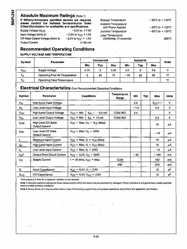
Absolute Maximum Ratings (Note 1>
If Miiitary/Aerospace specified devices are required, please contact the National Semiconductor Sales Office/Distributors for avallablllty and specifications.
Storage Temperature
Ambient Temperature with Power Applied
Supply Voltage (Vee) -0.5V to + 7.0V
Input Voltage (Note 2) -2.5V to V cc + 1.0V
Off-State Output Voltage (Note 2) -2.5V to Vee+ 1.0V
Junction Temperature
Lead Temperature (Soldering, 10 seconds)
Output Current ± 100 mA
Recommended Operating Conditions SUPPLY VOLTAGE AND TEMPERATURE
Symbol Parameter Commercial
Min Typ
Vee Supply Voltage 4.75 5
TA Operating Free-Air Temperature 0 25
Tc Operating Case Temperature
Max Min
5.25 4.5
75 -40
Electrical Characteristics Over Recommended Operating Conditions
Symbol Parameter Conditions Temperature
Range
V1H High Level Input Voltage
V1L Low Level Input Voltage
VoH High Level Output Voltage Vee= Min l 10H = -3.2 mA COM/IND
VoL Low Level Output Voltage Vee= Min J 10L = 12mA COM/IND
lozH High Level Off State Vee= Max, Vo= Vee (Max) Output Current
lozL Low Level Off State Vee = Max, Vo = GND Output Current
1, Maximum Input Current Vee = Max, v, = Vee (Max)
l1H High Level Input Current Vee = Max, v, = Vee (Max)
l1L Low Level Input Current Vee = Max, v, = GND
los• Output Short Circuit Current Vee = 5.0V, Vo = GND
Ice Supply Current f = 25 MHz, Vee = Max COM
IND
c, Input Capacitance Vee= 5.0V, v, = 2.0V
C110 1/0 Capacitance Vee= 5.0V, V110 = 2.0V
•one output at a time for a maximum duration of one second.
- 65°C to + 150°c
-65°C to + 125°C
-65°C to+ 150°c
2so0 c
Industrial Units
Typ Max
5 5.5 v 25 85 ·c
·c
Min Typ Max Units
2.0 Vcc+1 v -1.0 0.8 v 2.4 v
0.5 v
10 µA
-10 µA
10 µA
10 µA
-10 µA
-30 -160 mA
180 mA
200 mA
10 pF
12 pF
Note 1: Absolute maximum ratings are those values beyond which the device may be permanently damaged. Proper operation is not guaranteed outside specified recommended operating conditions.
Note 2: Some device pins may be raised above these limits during programming and preload operations according to the applicable specification.
3-22

Switching Characteristics Over Recommended Operating Conditions
AC TIMING REQUIREMENTS (FPLA ARRAY)
MAPL244·50 MAPL244-40 MAPL244·33
Symbol Parameter Conditions COM COM COM Units
Min Max Min Max Min Max
tsu Setup Time with Speed Option 12 14 17 (1/0 Pin or Feedback ns before Clock) without Speed Option 15 17 20
t1su ILMC Setup Time 5 6 8 ns (1/0 or OLMC before Clock
tcF Clock Input to Feedback S1 Closed 1with Speed Option 8 11 13 ns
CL = 35 Pj_without Speed Option 5 8 10
tH Hold Time (Input after Clock) 0 0 0 ns
tw Clock Pulse Width (High/Low) 6 6 8 ns
tcvCLE Clock Cycle Period (with 20 25 30 ns
OLMC Feedback)
I~ with OLMC Feedback* 50 40 33.3 MHz Clock
fMO Frequency with 1/0 Feedback* 45.5 40 33.3 MHz
1-fMT without Feedback 83.3 83.3 62.5 MHz
tpR Clock Valid after Power-Up 100 100 100 ns
tcLK Clock Input to 1/0 Pin S1 Closed, Jwith Speed Option 10 11 13 ns
CL = 35 P~without Speed Option 7 8 10
tpzxG OE ! to Registered Active High; S1 Open, Output Enabled CL= 35 pF
10 10 12 ns Active Low; S1 Closed, CL= 35 pF
tpxzG OE i to Registered From Vol; S1 Open, Output Disabled CL= 5 pF
10 10 12 ns From VoH; S1 Closed, CL= 5pF
tpzx1 Input to Output Enable Active High; S1 Open, via Product Term CL= 35 pF
15 15 18 Active Low; S1 Closed,
ns
CL= 35 pF
tpxz1 Input to Output Disabled From Vol; S1 Open, via Product Term CL= 5 pF
15 15 18 From VoH; S1 Closed,
ns
CL= 5pF
tRESET Power Up to Registered S1 Closed, CL= 35 pF 45 45 45 µ.s
Output Low
t1po Input Initialization 15 18 20 ns
to Output Reset
t1RC Input Initialization 10 12 15 ns
before Clock
•Actual measurements
AC Test Load
"~ Rt
OUTPUT .
R1 = 400fi R2 = 400fi
JC1 ":'R2
TL/H/11324-8
3-23

Switching Characteristics Over Recommended Operating Conditions (Continued)
AC TIMING REQUIREMENTS (PAL ARRAY) (Continued) ·'
MAPL244·50 MAPL244·40 MAPL244·33
Symbol Parameter Conditions COM COM COM Units
Min Max Min Max Min Max
tsuP Setup Time 10 12 15 ns (Input or Feedback before Clock)
tHP Hold Time (Input after Clock) 0 0 0 ns
tpop 1/0 or OLMC to CL= 35 pF 15 17 20 ns
Combinatorial Output S1 Closed
tcFP Clock Input to 5 8 10 ns
Feedback
twp Clock Pulse Width (High/Low) 6 6 8 ns
tcvCLEP Clock Cycle Period (with 15 20 25 ns.
Buried Feedback)
fMJP Input Frequency 66.6 58.8 50 MHz
fMBP with OLMC Feedback* 66.6 50 40 MHz
I~ Clock
with 1/0 Feedback* 52.6 47.6 40 MHz Frequency
fMTP without Feedback 83.3 83.3 62.5 MHz
tPRP ClockValid after Power-Up 100 100. 100 ns·
tcLKP Clock Input to 1/0 Pin S1 Closed, CL= 35 pF 9 9 10 ns
tpzxGP OE ! to Registered Active High; S1 Open, Output Enabled CL= 35 pF 10 10 12' ns
Active Low; S1 Closed, CL= 35 pF
tpxzGP OE t to Registered From Vol; S1 Open, Output Disabled CL= 5pF 10 10 .12 ns
From VoH; S1 Closed, CL= 5 pF
tpzx1P Input to Output Enable Active High; S1 Open, via Product Term CL= 35 pF
15 15 18 ns Active Low; S1 Closed, CL= 35 pF
tpxz1P Input to Output Disabled From Vol; S1 Open, via Product Term CL= 5pF
15 15 18 ns From VoH; S1 Closed, CL= 5 pF
tRESETP Power Up to Registered S1 Closed, CL = 35 pF 45 45 45 µs
Output Low
t1pop Input Initialization 20 20 20 ns
to Output Reset
t1RCP Input Initialization 20 20 20 ns
before Clock
•Actual measurements
AC Test Load
"~ . RI R1 = 4000
OUTPUT . R2 = 4000
Tc, R2
= -: TL/H/11324-9
3-24

Timing Diagrams
____ ,,,X" __ o_L_M_c_v_a1_id __ X" _____ o_L_Mc_va_H_d _____ X oLMc valid
f -....!.... t.llP -lpdp
CLOCK { \ f ---------' -----. 1"'8 = 'cv~LE = 'er 1 tsu
i..oo-----\ycle ·-
OUTPUT VALIO (PAL)
FIGURE 3. Internal Feedback Frequency
CLOCK
FIGURE 4. Toggle Frequency
CLOCK
IMr=--1-tcL + lcH
TL/H/11324-11
ti! \cLK tsu-----...i
TL/H/11324-10
TL/H/11324-12
FIGURE 5. Input Frequency Register Output --------------T'----ou_t_pu_t_v_a_lid __ _
TL/H/11324-13
FIGURE 6. External Feedback
Any Input ----------------------1,------~1.r------Programmed for
Tri-State Control --------------..... -------T'------'l"-------
R~~~~~ ----)(" ______ ~x_z_o~~~------~-z_x_o~-t:.._ ______ ...,ja-----~-z_x_1~-"I Valid Enable
TL/H/11324-14
FIGURE 7. Output Enable Timing
CLOCK
1,1/0 _____ ,,,
0, 1/0
TL/H/11324-15
FIGURE 8. lnitlallzatlon Timing
3-25

Timing Diagrams (Continued)
Yee '°"L '"" ~,'. xxxxx~ZXXXl . . '"
Registered •••• _ •• • t• ..... -~:ET·~-••• _. Outputs
. Tristate . . Low TL/H/11324-16
FIGURE 9. Power-Up Reset Timing
Design Technology Testability Electrically Erasable (EE)CMOS technology allows the MAPL product family to be 100% AC, DC and functionally tested prior to shipment. Unlike one-time programmable devices, the actual array's true worst case patterns are programmed into the device and tested over temperature and voltage ratings. The specifications are guaranteed to be true worst case parameters, with fully loaded internal arrays and all (maximum available) outputs switching. The erasable cells allow for the device to be programmed and functionally tested, providing the highest programming yields and postprogramming, functional yields, available in a user program~ mable device. National Semiconductor guarantees 100% field programmability of MAPL products.
Register Preload All macrocell registers have the ability to be preloaded and functionally tested. This capability allows the device to be · forced into undefined or arbitrary states to greatly reduce the required number of sequential test vectors. The device may be put into any desired register state at any point during the functional test sequence. This allows complete verification of sequential logic circuits including states that are not defined in the normal operational state sequence. The register preload is not an operational mode. It is available in certified programming equipment for test purposes. The register preload algorithm for the MAPL product family, is available separately from National Semiconductor.
Electronic Signature Each MAPL product contains 16 bytes of user reprogrammable memory known as the User Electronic Signature (UES). The UES may contain any identification information .
3-26
desired by the user. This information typically is associated with revision numbers, dates, inventory control information, identification data and names. The information is read out of the device using the programming equipment's verification procedure. OPAL software allows representation of the UES data in HEX, binary or ASCII formats.
Design Security A security cell is provided on all MAPL products as a deterrent to copying the logic design. If the security cell is programmed, programming and verification of the array is disabled. Once the cell is programmed, only a "bulk erase" of the whole product will erase the security cell, thus the original design configuration can never be examined.
Power-Up Reset Circuitry within the MAPL2 devices provides a reset signal to all registers during power-up. All internal registers will have their Q outputs set low after a specified time <tRESET). As a result, the state on the registered output pins (if they are enabled) will always be low on power-up, except the PAL OLMC's whose polarity control is after the register, in which case the state of the output pins will be high if active low is selected or low if active high is selected. This feature can greatly simplify state machine design by providing a known state on power-up.
Due to the asynchronous nature of system power-up, the following conditions must be met to guarantee a valid power-up reset. First, the Vee rise must be monotonic. Second, the registers will reset within a maximum of tRESET time. As in normal system operation, avoid clocking the device until all input and feedback path setup times have been met.

Ordering Information
~-------- Multiple Array Programmable Logic
.--------244 = Series 2, 44-Pin
.------Package Types: V = Plastic Leaded Chip Carrier (PLCC)
..---- Temperature Range C = Commercial (0°C to + 75°C) I = Industrial (-40°C to + 85°C)
[
SpeeC:50= 50 MHz with Feedback -40= 40 MHz with Feedback
· -33 = 33.3 MHz with Feedback
MAPL 244 V C -50
MAPL244 Connection Diagram
8 GND Vee
9 GND Vee
SYSCLK 10
1/0 3 11
1/0 2 44-PIN PLCC
1/0 1
1/0 0
15 Vee GND
16 Vee GND
PCLK 17
18 19 20 21 22 23 24 25 26 27 28
1/0 31 1/0 30 1/0 29 1/0 28 1/0 27 1/0 26 1/0. 25 1/0 24 1/0 23 1/0 22 1/0 21
3-27
39 ICLK
38
37
36 1/0 15
1/0 16
1/0 17
1/0 18
32 1/0 19
31
30
29 1/0 20
TL/H/11324-17

20104 19960 19288 18808 18520 l/O a-11 I
PO,P1,P2,NC 0
1/020-27 I I S0=20252 L
2x1x8
OLMC 0-7 0 S0=20259
1/0 12-19 1 1 S0=20260
2x 1 x8
~ S0=;0267
1/0 28-31 I
~I OLMC 28-31 0
20251
OE ©-{:;
IZI ~ ~ 1/0 7 1/0 6 1/0 5
OLMC 7 OLMC 6 OLMC 5
18232 17560 17080
~ ~ IZI 1/0 4 1/0 3 1/0 2
OLMC 4 OLMC 3 OLMC 2
16792
MAPL244
INCREMENT
16504
i:R
16551 47
s: )> .,, r-1\) ~ ~ .,, )> re.. m c m 0 3: D>
"'C
mm mrIT
1/0 1 1/0 0
OLMC 1 OLMC 0
TUH/11324-18

MAPL244 FPLA JEDEC Map
+1++++11+t++++-t++1+++-1+H1+t++++-1+t++++-1+H++++++11+t++++-1+t++++-H-1-~r----~~t++1+++-1+H++++++11+t++++-t++1+++-1+H++++++11+t++++-H+l+++ "' !-<"' +++ttti+tt+++ll+tt+++ttti+tt+++ll+tttt+l+tt+ttttti'+t++++ll+tt+++t++--t--iH I H-H+tt+++-l+H+++ttti+tt+++ll+tt+++-t+H+++l+H+tt+t+ll+t+
H H
+++tttir+tt+++ll+tt+++tt+t+tt+++t+tt+++l+H+tt+++l'+t+ttt-l+tt+++t++--t-~~~l+tt+++l+H+tt+++ll+tt+++l+tt+++ttti+tttttit+ttttt-Htt+t+ H~ ++++++1'++++++11++++++-1+H++++++11++++++-1+H++++++1'++++++11++++++-1+1--t--iH lwH-H++++++-1+H+++-1+H++++++1H-H+++-1++++++-1+H++++++11+t+
H~ +++ttt-1t+tt+++11-ttt+++tt+t+tt+++11-ttt+++1+H+tt+++1H-H+++11-ttt+++1+1--t-~H t+tt+++1+H+ttttt-1H-Httt-1-ttt+t+ttt-1+ttttt-1t+ttttt-tttt+t+
H
~ ~ +++++H++++++il+H+++++H+++++Hl+H+++++H+++++H++++++il+H+++1-H--+-~HgH-H++++++-1+H+++++H+++++H++++++1+H+++++H++++++1+++
~ H-++++++1H-H+++-1+H+++-1+H++++++-1+H+++1+H++++++1H-H+++-1++++++-1+1--t--iH I l++++++-l+H++++++ll++++++t++l+t+t++l+tt+++ll++++++H+l+++
+++ttti+tt+++ll+tt+++tt+t+tttttit+tt+++l+tt+t+tttii+t+tttit+tt+t+t+l--t-~~ +tt+++IH-H+++-l++++++t++t+++tttil+++tt+t++l+tt+++IH-H+++-1++++++-1+1--t--ij-< 1wt++1+++t++1++++++1t++1+++-t++t+++t++1++++++1H-H+++-1+H+++
Hal +++ttt-11+t++++11+tt+++1+H+tt+++11++++++-1+H++++++11+t++++11++++++1+1--t--iH 1~H-H+tt+++-1+H+++1+H+tt+++11+t++++-1++++++1+H++++tt-11+t+ Hw
+1++++11+t++++-1++++++1+H++++++1t++1+++-1++1++++++11+t++++-1+H+++-H-1--t---lH:H-H1+t++++-1+H+++1+H1+t++++1t++1+++-1+H+++1+H+++++H1+t+
+++ttti+tt+++ll+tt+++ttti+t++++lt+tt+t+l+H+t+tttii+t++t+t-t+t+++t++--t-~~
~ +tttttii+t++t+l+tt+++tt+t+t+tttil+tt+t+l+H+t+tttii+t++t+l+tt+t+t+l--t-~~l+tt+++l+H+t+tttit+tt+t+l+tt+++ttti+t+tttii+t++t+H-H+t+ ~
H;; ~ +++t++11+t++t+1-ttt+++1+H+++t++1t-ttt+++1+H++++++11+t++++-t-ttt+t+1+1--t--iH 1-1+tt+++1+H++++++1t++t+++t+tt+++ttt-1-tttttt-11+t++t+H-H+++
+l++++ll+t++++ll+H+++-t++1++++++11+H+++-t++1++++++1++++++1t++1+++-H-1--l---l~
+++ttt-11+t++t+1+tt+++tt+t+++tttit-tttttt-H+t+tttt1-11+t++t+t-ttt+t+1+1--t-~H +l++++ll+t++++lt++1+++-1+H++++++11+t++++-t++1++++++11+t++++-t++1+++-H-1--t---l~~H-Hl+t++++-1+H+++-1+H++++++11+t++++-1+H+++-1+H+++++Hi+t+
H~ +++tt+11+t++t+1-ttt+++1+H+ttt++1t-ttt+++1+H+ttt++11+t++++-t-ttt+++1+1--t--iH 1wt++1+++1+H+ttt++1t++t+++t+tt+t+ttt-1-tttt++11+t++t+t+tt+++
++++++1++++++1t++1+1+1+H++++++11+H+++-t++1++++++11+t++++-1+H+++-H-1--t---l~~t++1+++-1+H++++++11+H+++-1+H+++-1+H++++++1t++1+++-t++1+++H
+++ttti+tt+++ll+H+t+ttti+tttttit+ttttt-ttti+tttttit+tt+t+l+tt+t+t+l--t-~~ H
I~ H~H-H++++++-t++1+++-1+H1+t++++-1+H+++-t++1+++-1+H1+t++++11+t+
- +++-+++1++++++-1+H+++-1+H+++tttil+H+++-t++1++++++1++++++-1+H+++-1+1--t--i~ 1-H-H++++++-l+H+++-ttti++++++lt++t+t+t+H+++l+H+tt+++ll+t+
+l++++ll+t++++ll+H+++-t++1++++++11+H+++-t++1++++++11+t++++-1+H+++-H-1--l---l~
+++ttti+tt+++-t++t+++t+H+tttttit-t+t+++t+H+tt++HH+t+++-t-t+t+t+t+l--t--i~ l~l+tt+t+t+H+tt++Hl+H+t+t+H+++ttti+tt++HH+t+t+t+tt+++ H~ +1+1+H++++++11+H+++-H+1++++++1++++++-t++1+++-+++1++++++1++++++-H-1--l---l~~H-H++++++-H+1+++-1+H++++++1++++++-1+H+++-H+1++++++1+++
+<+++H-++++++i>++t+++H+f-++++++i>++++++H+f-++++++t>++++++i>++++++t++--+-~~
H +++ttti+tttttit+tt+++t+H+t+ttt-IH+ttt+H+l+t+ttti+tttttit+tt+t+t+l--t-~~
- ,____;:_4--+++++H+++++H++++++l+H+++++H++++++l+H+++++H+++++H++++++l++---~~ l = l-l+l+H+++++H++++++l+H+++++H+++++H++++++l+H+++l-H+
~ H-H-H++++t+t-ttt+++ttt-1+tt+++1t+tt+++H+t+++H+t+tt+++11+t+
+++-1+1-++H-l+++++H+++H-H+++I-+ ..... ~ H-H++++H-ll+H+++-t++l-1+'-.... .u+IH-H+++-l+H+++-t++l++++++ll+t+
+++-H-H+++11+t+++H+++1+H+++-1-+ ~ 1-H-1-++++++<>++++++<>++++++1-H-1-+++--<H +++-1+1-++H-l+++++H+++H-H+++I-+ a: ~ ~ H-Hl+t++H-ll+H+++-t++l+f ~ l+l-++++11+1-+++H+++H-H+++l+t+
a: H~ a: +++-t+t++++11+t+tt+t-tttl+H-tttt-t °" H w a: 1-H-1+++<>++++++<-+++++++-+++i-+++
+++11+1-++++1+++t++1+++H-H+++-1-+ C H :;: °" 1++++++11+t++++1+++H-H+++1-+++ +++-t+t++H-il+t++H-i+++H-H+++t-t z I-< H-H+tt+++-l+Htt+t++l+f a: l+tt+++ll+tt+H-i+t+t++t+++t-ttt +t+l+tt+H-i+ttt+H+t+t++t+++t-t "' ~ H-H+tttttil+tttt+l+H"i-1 0 l+tt+++ll+ttt+H+t+H+t+++t-ttt
IIT H LIII llI ]-< llil
3-29
•

5546 3776 3658 1888 1770
c.J (,, 0
JEDEC CELL NUMBER = rlRST CELL NUMBER + INCREMENT NUMBER
16084 18154
16224 16294
15664 15734
15804 15874
15244 15314
15384 15454
FIRSTCELLNUMBER~oo. 16364
16434 15944
18014 15524
15594 15104
15174
2 .. i • iO 'ii 14 ii ii 2o ... 24
ANDARRAYO~ ~
OR ARRAY 0
.!!...=:! u-=:t ,. 'ii ... 42 « .. ... ... ,,. !!
7' 7i 7i .. ~ ~ ..
" ... ii ii loO iOi' i04 105 108 'i1o' m m ill
117
t: CONTROL ARRAY -
H H ~OLMC22
3 OLMC 2'
1 ii" ii" _J PIM NUMBERS
!L2..!.. 3 !&.!... 2 ~ 1 !LQ...l! u !L2...ll 43 ~ 41 !L.2..!.! 40 ~ 36 ~ 35 .!L2..!.! 34 ~ 33 !&.!.! 32 ~ 29 !&!! 28 ~ 27 ~ 26 JLQ.1! 25. ~ 24 ~ 23 ~ 22 ~ 21 JL2.1! 20 ~ 19 .!L2.l! 18
L-1/0 8-31
OLMC 8-31
MAPL244
TL/H/11324-19
s:: l> ""O rN .s:a. .s:a. "Tl ""O rl> c.. rn c rn 0 s:: D)
"'C
9 a 5· c: CD s,

~National D Semiconductor
ADVANCE INFORMATION
MAPL268 Multiple Array Programmable Logic
General Description The MAPL268 is a second generation device in a series of new higher density, electrically erasable CMOS (EECMOS) programmable logic devices based on a proprietary National Semiconductor programmable logic array architecture. The MAPL268 integrates multiple Field Programmable Logic Arrays (FPLA), allowing for easy implementation of complex state machines, controllers, microinstruction sequencers, bus interfaces and general synchronous logic designs. Additionally the MAPL268 incorporates a separate PAL® block with 8 combinatorial/registered 1/0 and 8 combinatorial/registered outputs to handle asynchronous and decode functions. The MAPL268 allows for easy and cost effective integration of complex subsystems consisting of synchronous and asynchronous elements.
The MAPL ™ product family is supported by National Semiconductor's OPALTM (Open Programmable Architecture Language) software package and by other popular third-party PLO software packages such as ABEL-4, CUPL, PLDesigner and Viewlogic. OPAL is an open environment design tool and is able to interface with these other software packages by means of the de-facto standard Berkeley PLA file format. OPAL also allows the designer to have full access to all of the intermediate files that are generated during the compilation process. Logic partitioning and utilization within a MAPL device may be done 100% automatically or manually using OPAL software. Automatic partitioning and device utilization can also be done using other third-party tools with the appropriate MAPL device fitter, available from the software vendor. (Continued)
Block Diagram
Features • Extension of MAPL244 architecture • High density flexible FPLA and PAL architectures • High performance second generation MAPL
architecture combining PAL and FPLA arrays - 15 ns maximum T PD - 50 MHz system performance
• Low power • 59 total macrocells
- 24 1/0 macrocells with DE, JK, RS or T-type registers
-16 PAL macrocells (combinatorial or registered) - 3 Buried/Page control macrocells - 16 input macrocells with latched, registered or
double registered options • Multiple clocking and output enable options
(synchronous and asynchronous) • Asynchronous preload, set, reset and power-up reset
capability • Internal and 1/0 feedback • Programmable setup and clock-to-output options • Replaces multiple PAL/GAL/FPLA devices • 100% functionally tested reconfigurable EECMOS
technology • Fully supported by National's OPAL, and other popular
third-party development tools • Supported by industry standard programmers • Security cell prevents copying
MAPL268
12 Inputs
81/0 8 Outputs
AND CLK
16 1/0 8 Outputs
CLK PAL TL/L/11370-1
3-31
:: > "'CJ rN en co
•

co co !:I General Description (Continued)
~ Programming MAPL devices is accomplished using readily
The MAPL268 is available in a 68-pin PLCC package. It conforms to the JEDEC standard for power, ground and clock
::= available, industry standard, PLD programming equipment. pin placements. ·
NSC guarantees a minimum 100 erase/write cycles for all MAPL devices.
Product To/From Type
1/0 Macrocells FPLA DE/JK/RS/T PAL DI Combinatorial
Dedicated Outputs FPLA DE/JK/RS/T PAL DI Combinatorial
Buried/Page Macrocells FPLA DE/JK/RS/T Dedicated Inputs FPLA/PAL Input Logic Macrocells FPLA D/L/Double D/Comb.
3-32
MAPL244 MAPL268
24 16 8 8 0 8 0 8 3 3 0 12
16 16

~National D Semiconductor
MAPL TM Application Examples
1.0 MAPL Register Control The following application demonstrates the use of OPAL™ to control any single line in the output macrocell of the MAPL 128 and configure the output as either a JK or DE register. The example also shows how to drive the reset and the tri-state functions. From the 1/0 macrocell shown in Figure 1, the following signals can be controlled through the OPAL software:
• J input or D input
• K input or E input
• Reset input
• Output Enable
so
S2
51
This example uses the OPAL modules individually to generate the JEDEC map for programming the MAPL device:
OPL2PLA CONTROL 11 will generate PLA file FITMAPL CONTROL " will generate a MAPL PLA file PLA2EQN CONTROL 11 will generate equation file EQN2JED CONTROL 11 will generate JEDEC file
The example shows how easy it is to access any of the MAPL OLMC lines and goes step by step using OPAL software to generate desired function.
OE
00 01 10 11 5455
l/O
CLK
TL/L/11304-1
FIGURE 1. Input/Output Macrocell
3-33
3: l> .,, rl>
"tJ "2. n· D> -c;· ::I m >< D> 3
"tJ Ci" en
•

U) CD ii E ca >< w c 0 :; .!::! ii Q. < ..J D.. < ::E
The equations to implement the desired functions are defined as follows:
Begin Header Title MAPL I/O control signal Pattern control Revision A Author Tarif Arabi Date 10/15/90 End Header
Begin Definition Inputs Inl, In2, In3, In4, InS; feedbacks (JK) outl; outputs (DE) out2;
End Definition
Begin Equations
/outl.j = Inl * /In3 { J,K input control
outl.K outl.re outl.oe
+ In4; In2; Inl * InS; /InS;
Reset control Tristate control
out2.d = /In2 * In4 * outl; .{ D,E input control out2.re Inl* InS; { Reset control out2.oe = InS; { Tristate control
End Equations
Note that outl.j was defined in the above example as an active low signal. After compiling the entry file, the active low applying DeMorgan's Law will be:
/outl.j = Inl * /In3 + In4 will be equivalent to:
outl.j = /Inl * /In4 + In3 * /In4
Running "OPL2PLA CONTROL" will take CONTROL.OPL as the entry file and generate a PLA file called control.PLA :
#$ TOOL NSC opl2pla B.04 #$ TITLE MAPL control signal #$ TITLE #$ PINS 7 Inl In2 In3 In4 InS outl out2 #$ NODES 0
3-34
TL/L/11304-2

.i 6
.o 8
.type f
.phase 11111111
.ilb Inl In2 In3 In4 In5 outl
.ob out2.d out2.ce outl.j outl.k outl.re outl.oe out2.re out2.oe
o--o----10--1---1-----0--1-----0-1-1 1---1-----1---0---. e
--1-------1---------1--------1-----1----1------------1--------1 -1------
Running "FITMAPL CONTROL" will then take CONTROL.PLA as its entry file and fit the design into the MAPL128 by assigning pins and pages. The output file will be CONTROL.OUT:
#$ TOOL NSC #$ TITLE MAPL control signal #$ TITLE #$ DEVICE MAPL128 .i 9 .o 11 #$ PINS 7 In1:6 In2:5 In3:4 In4:3 In5:2 outl:lO out2:11 #$ NODES 3 pb2:39 pb1:38 pb0:37 .ilb Inl In2 In3 In4 In5 outl pb2 pbl pbO .ob out2.d out2.ce outl.j outl.k outl.re outl.oe out2.re
out2.oe pb2.reg pbl.reg pbO.reg .type f .phase 11111111111 .p 9 0--0--000 -~1-----000 --10--000 --1-----000 --0---000 -1------000 -0-1-1000 1-------000 -1----000 ---1----000 ----1---- -------1---1---1---- ------1--------0---- -----1-----1---1---- ----1------.e
3-35
TL/L/11304-3
3: )> "'tJ r )> "C "!:!. c:;· D> -s· :::s m >< D> 3
"C CD' en
•

"' Cl)
'iS.. E <U ><
LI.I c 0
; <U -~ 'iS.. c. <t ...I Q. <t ~
Running "PLA2EQN CONTROL.OUT" takes CONTROL.OUT as its input file and generates an equation file CONTROL.EQN :
MAPL control signal
;Translated from NSC formatted PLA file.
CHIP filename MAPL128
CLK In5 In4 In3 In2 Inl NC NC NC out2 outl NC NC GND NC NC NC NC NC NC NC NC NC NC NC NC NC VCC NC NC NC NC NC NC NC NC pbO pbl pb2
EQUATIONS
out2 := /In2 * In4 * outl *./pb2 * /pbl * /pbO out2.CE = /In3 * /pb2 * /pbl * /pbO outl.J .= /Inl * /In4 * /pb2 * /pbl * /pbO
+ In3 * /In4 * /pb2 * /pbl * /pbO outl.K = In2 * /pb2 * /pbl * /pbO outl.RE Inl * In5 outl.OE /InS out2.RE Inl * In5 out2.0E In5 pb2 := GND pbl := GND pbO := GND
Finally running "EQN2JED CONTROL" will take CONTROL.EQN as its input file and generate a Jedec map for the MAPL128 called CONTROL. JED :
MAPL128 EQN2JED -- Boolean Logic to JEDEC file assembler (Version 1.10) Copyright (R) National Semiconductor Corporation 1990 Assembled from "control. eqn". Date: 10-15-90
MAPL control signal
* QF14833*QP28*FO* LOOOO 1110110111111111110111111111111111111111111111111111111111 111111111111111111111111111111111111111111011111111111 1111101111111111111111111111111111111111111111111111111111 111111111111111111111111111111111111111111101111111111 1011111011111111111111111111111111111111111111111111111111
3-36
TL/L/11304-4

111111111111111111111111111111111111111111110111111111 1111011011111111111111111111111111111111111111111111111111 111111111111111111111111111111111111111111110111111111 1101111111111111111111111111111111111111111111111111111111 111111111111111111111111111111111111111111111011111111* L14336 0111111101111111111111111111111111111111111111111111111111* L14394 1111111110111111111111111111111111111111111111111111111111* L14452 1111111101111111111111111111111111111111111111111111111111* Ll4510 0000000000000000000000000000000000000000000000000000000000* Ll4568 111111111111111111111111111* L14595 000111111111111111111111111* L14622 000111111111111111111011111* L14649 111111111111111111111111* Ll4673 1111111111001111* L14689 1111111111101111* L14705 0000000000000000000000000000000000000000000000000000000000000000*
L14769 0000000000000000000000000000000000000000000000000000000000000000*
C67DF* ?0000
TL/L/11304-5
3-37

en Cl)
Q. E cu >< w c 0
;::: cu -~ :a. c. < ...J a. < :::ii:
2.0 A 4-Bit C~unter with Reset Using OPAL, a MAPL 128 can be implemented as a 4-bit counter with reset in three different ways. This application demonstrates different ways to enter the same design. '
Figure 2 is the entry file for 4-bit counter with reset implemented in a MAPL 128 using OPAL truth table entry only.
Figure 3 is the same design implemented in a MAPL 128 using OPAL Boolean equation entry only.
Figure 4 is the same design implemented in a MAPL 128 using OPAL state diagram entry only.
Note that any of the above entry files will give the same results. To get the JEDEC file run OPL2PLA, FITMAPL, PLA2EQN, and EQN2JED.
Begin Header Title Pattern Revision Author Date
4 bit counter 4count A
Tarif Arabi 10/15/90
Everything in the header block is copied directly into all the files that generated by OPAL as a comment field
End Header
BEGIN DEFINITION { Any thing surrounded by curly brackets is considered to be a
comment}
Device MAP1128;
INPUTS RESET;
feedbacks (JK,HOLD)
CNT4,CNT3iCNT2,CNT1; END DEFINITION
BEGIN truth TABLE ttin ttout
1 0 0 ---1 0 --11 0 -111
RESET,CNT4,CNT3,CNT2,CNT1; CNT4,CNT3,CNT2,CNT1;
0000 ---! --!--!--!---
END truth TABLE
{Define 4 I/O as a JK} {default to hold}
FIGURE 2. OPAL Truth Table
3-38
TL/L/11304-6

begin header 4 bit counter design using state diagram entry format only
end header
begin definition inputs
reset; statebits
cnt4,cnt3,cnt2,cntl; end definition
begin state_diagram
state zero : if reset !$ 0 then one else zero; state one : if reset !$ 0 then two else zero; state two : if reset 1$ 0 then three else zero; state three : if reset !$ 0 then four else zero; state four : if reset !$ 0 then five else zero; state five : if reset !$ 0 then six else zero; state six : if reset !$ 0 then seven else zero; state eight : if reset !$ 0 then nine else zero; state nine : if reset !$ 0 then ten else zero; state ten : if reset !$ 0 then eleven else zero; state eleven : if reset !$ 0 then twelve else zero; state twelve : if reset !$ 0 then thirteen else zero; state thirteen : if reset !$ 0 then fourteen else zero; state fourteen : if reset !$ 0 then fifteen else zero; state fifteen : goto zero;
end state_diagram
FIGURE 3. State Diagram Entry Format
3-39
TL/L/ 11304-7
3: :r> .,, r:r>
"C "5!. c;· D> -a· :J m >< D> 3
"C CD' tn
•

tn Cl)
a. E CG >< w c 0 = CG .2 a. a. < ..;J a.. < :E
begin header 4 bit counter design using boolean ,equations only
end header
begin Definition
inputs reset; feedbacks cnt4,cnt3,cnt2,cntl;
end Definition
begin Equations
cnt4 := /reset * /cnt4 * c~t3 * cnt2 * cntl + /reset * cnt4 * /cntl + /reset * cnt4 * /cnt3
/reset *.cnt4 * /cnt2; · cnt3 := /reset * /cnt3 * cnt2 * cntl
/reset * cnt3 * /cnt2 + /reset ~ cnt3 * /cntl;
cnt2 := /reset * /cnt2 * cntl + /reset * cnt2 * /.cntl;
cntl := /reset * /cntl;
end Equations
FIGURE 4. Boolean Equations
3-40
TL/L/11304-8

3.0 A 3-Bit Up-Down Counter with 7-Segment Display Output This application demonstrates the use of OPAL's state diagram entry format and set assignment to implement this design. The counter will reset to zero if rst is low, it will count:
• upward if up is high,
• downward if down is high,
• upward if both are high,
• hold value if both are low.
This application shows how to implement the above mentioned design using state diagram entry. This design can also be entered using the truth table format. ·
3_to_7.0PL
begin header Company Author Date Revision :
National Semiconductor Corp. Tarif Arabi 11/15/91 B
Description: A three-bit up-down counter with 7-segment display output.
end header
begin definition device mapll28; inputs up, down, rst;
7-segment display output} outputs a, b, c, d, e, f, g;
symbols to define state names and their values, statebits will be assigned automatically}
symbols zero=O, one=Abl, two=AblO, three=3, four=4, five=5, six=6, seven=?;
Sets are defined to group inputs and outputs} Sets out_disp= [a,b,c,d,e,f,g), ZERO= [1,1,l,l,1,l,O),
TWO [1,l,0,1,l,0,1), THREE= [1,l,1,1,0,0,1), FOUR [O,l,1,0,0,1,1), FIVE= [1,0,l,1,0,1,1), SIX [1,0,1,1,1,1,1), SEVEN= [1,l,1,0,0,0,0);
end definition
3-41
TL/L/11304-9
3: )> "tJ r)>
"C "2. c:;· D> -(5" :J m >< D> 3
"C CD' en

U) cu a E «S >< w c 0 :;:: «S .!::! a a. <C -I a. <C :E
begin state_diagram
state zero : out disp = ZERO; if /rst then zero else if up then one else if down then seven else zero;
state one : out_disp = [0,1,1,0,0,0,0];
if /rst then zero else if up then two else if down then zero else one;
state two : out disp = TWO; if /rst then zero else if up then three else if down then one else two;
state three : out disp = THREE; if /rst then zero else if up then four else if down then two else three;
else if down then three else four;
state five : out disp = FIVE; if /rst then zero else if up then six else if down then four else five;
state six : out disp = SIX; if /rst then zero else if up then seven else if down then five else six;
state seven : out disp = SEVEN; if /rst then zero else if up then zero else if down then six else seven;
etfd state:::.diagram
3-42
out 'O' to 7-segment display} reset counter } count upward } count downward hold }
set notation was used rather than a defined set to display 'L'}
TUL/11304-10

4.0 15-Bit Up/Down Counter This application demonstrates the use of the MAPL 128 in a state machine design to implement a 15-bit up/down counter with reset and hold. The JEDEC map for the MAPL 128 was generated using OPAL software.
This manual paging example shows how a designer can use OPAL to generate JEDEC maps for the MAPL products by completely specifying all pins and page data thereby eliminating the need to execute FITMAPL.
The design was simulated using the Verilog simulator. This application shows the implementation of the design in a truth table, while if the same design was entered using the
3-43
state diagram entry format, 32,768 states would appear in the entry file.
To implement the same design in a regular PAL or GAL device would take roughly four PAL 16R4's. In this application, 25% of the MAPL 128 was used to implement the 15-bit counter (2 pages out of 8).
To get the JEDEC file run the following modules:
• OPL2PLA 15UPDN
• PLA2EQN 15UPDN
• EQN2JED 15UPDN
:= )> "tJ r-l>
"'O '!:!. c;· D> -c;· :::s m >< D> 3
"'O c;; en
•

(I) Cl> Q. E co ><
LI.I c 0 ;:; co -~ Q. a. ct ..J a.. ct :El
·Entry file for a manual paging example 15bit up_ down counter. } .
Begin Header Title 15 bit up/down counter Pattern 15UPDN Revision D Author Tarif Arabi Date 12/10/90
Everything in the header command is copied directly into the jedec map as a comment field
End Header
BEGIN DEFINITION {
Any thing surrounded by curly brackets is considered to be a comment
Device MAPL128; Specify the device used
INPUTS Define 3 inputs
RESET=6, HOLD=5, UP_DOWN=4;
feedbacks (JK, HOLD, buried) {Define 3 buried register as count} {bits configured as JK with Hold default}
BCNT14=29,BCNT13=30,BCNT12=31;
feedbacks (JK,HOLD) {Define 11 I/O as a JK {default to hold
CNT11=11,CNT10=10,CNT9=9,CNT8=8,CNT7=7,CNT6=17,CNT5=18,CNT4=19, CNT3=20,CNT2=21,CNT1=22;
feedbacks (JK,TOGGLE) {Define one I/O as JK toggling}
CNT0=23;
OUTPUTS (JK, HOLD) }
{always with the clock }
{Define 3 outputs as JK so the total number
{of outputs will be 15. Observe that in the {truth table, they are driven by the buried
{feedback, which actually represents the count}
TL/L/11304-12
3-44

CNT14=12,CNT13=13,CNT12=15;
feedbacks (JK, HOLD, buried} {Define the 3 page bit labels } { ( 8 pages} by using these node numbers}
P2=39,Pl=38,P0=37;
END DEFINITION {
For this example we will use truth table entry to map the pages manualy and fit the design in the MALP128 }
BEGIN truth TABLE
{ Truth table inputs, outputs (ttin, ttout) }
ttin RESET, HOLD, UP_DOWN, BCNT14,BCNT13,BCNT12,
CNT11,CNT10,CNT9,CNT8,CNT7,CNT6,CNT5,CNT4,CNT3,CNT2,CNT1,CNT0, P2,Pl,PO;
ttout BCNT14,BCNT13,BCNT12,
CNT11,CNT10,CNT9,CNT8,CNT7,CNT6,CNT5,CNT4,CNT3,CNT2,CNT1,CNTO, P2,Pl,PO,CNT14,CNT13,CNT12;
{ Page Zero count up } 01- --------------- 000 ??????????????? 000 000 --------------1 000 -------------11 000 ------------111 000 -----------1111 000 ----------11111 000 ---------111111 000 --------1111111 000 -------11111111 000 ------111111111 000 -----1111111111 000 ----11111111111 000 ---111111111111 000 --1111111111111 000 -11111111111111 001 ---------------
000 -------------!- 000 000 ------------!-- 000 000 -----------!--- 000 000 ----------!---- 000 000 ---------!----- 000 000 --------!------ 000 000 -------!------- 000 000 ------!-------- 000 000 -----!--------- 000 000 ----!---------- 000 000 ---!----------- 000 000 --!------------ 000 000 -!------------- 000 000 !-------------- 000 000 --------------? 001
3-45
??? { ? = Hold --- { ! = Toggle
{- =Don't care}
--! -!-!--
TL/L/11304-13 •

"' Cl)
Q. E ca ><
I.LI c 0 ;: ca -~ Q. Q. <( -I D.. <(
==
{ Page One count down }
01- --------------- 001 ??????????????? 001 ??? 001 --------------0 001 -------------!- 001 001 -------"".'-----00 001 ------------!-- 001 001 ------------000 001 -----------!--- 001 001 -----------0000 001 ----------!---- 001 001 ----------00000 001 ---------!----- 001 001 ---------000000 001 --------!------ 001 001 --------0000000 001 -------!------- 001 001 -------00000000 001 ____ .:__!-------- 001 001 ------000000000 001 -----!--------- 001 001 -----0000000000 001 ----!---------- 001 001 ----00000000000 001 ---!----------- 001 001 ---000000000000 001 --!------------ 001 --! 001 --0000000000000 001 -!------------- 001 -!-001 -00000000000000 001 !-------------- 001 !--000 --------------- 001 --------------? 000
END truth TABLE
BEGIN equations
{This block is used to control the reset function in MAPL. } {Note that the 16 product terms in.the page were used for } {the counting and the reset function is implemented separatly }
BEGIN equations
[BCNT14, BCNT13, BCNT12,.CNT11, CNTlO, CNT9] .. RE=RESET; tCNT8,CNT7,CNT6,CNTS,CNT4] .RE=RESET; [CNT3, CNT2, CNTl I CNTO, P2, Pl, PO I CNT14 I CNTl,3, CNT12] • RE=RESET;.
END equations
TL/L/11304-14
3-46

270 -~~~~!!!fil!!!~~~~~~~~m!!~~~~~~~~~~~~~~~~~~ P1
PS 0 I
lllllllllllllllllllllllllllllll!. -~---J'.5Imrn11rn11n11n11rr111rn11rn11n11n11rr111rn11rn11n11n11rr111rn11rn11n11n11rn111rn11rn11n11n11rrmw11wu~11u11ll11w111~1 _____ 0~0~4~a ____ --11WJJ.LWUWW..U.:1.LLLJ::~. P4
PS
P6
·ns~iJ_ __________________________________________________________ ==~ -~0~1=r=: ______________________________________________________ -===~
-~1~1=r==---------------------------------------------------------------------------------....... ==~ P11
P10 pg
P8
P7
-~Z---1----------------;::============; _ i:_1~ - - ....---,'---------r====; - ':_1 ~ - - ---------=~
P20
.':.2! __
1SUPDN.LST
FIGURE 5. Timing Diagram
S30
P1
TL/L/11304-15
- i:_s - - - J~-anrr::=J!QK:==lIIIIIll[[[[[lil]imnirllIIIIIIIIIIIIIlIIIIIIIllIIIIIll[[[[[lil][[([(]IIIIIIII~~ . • ~ _ _ _ OOAC
P4 +--=--~---;:::::====::;----------======= PS
P6
·ns~iJ_ ____ ~------_.::..:__ _____________________________________________ ==== -~0~1=r==---~---------------------------------------------------------------------------....... ==== -~1~1=r=----~------------------------------------------------------------------------....... ====== P11
P10 pg
P8
P7
P17
P18 p1g
P20
P21
1SUPDN.LST TL/L/11304-16
FIGURE 6. Timing Diagram
3-47
•

(I) Cl)
"iS. E cu >< w c 0
:;:::
-~ "iS. c. ct ...I a. ct ::!:
P1
PS
270
Q 11:11111111111111111111111111111111111111111 P4
PS
P6
·P"29•ui
0
0093 llllllllllllllllllllllllllllllllllllllllllllllllllllllllllllllllllll
-~o~i----------------------------------------------------------------·p-31•ui -+-..:....------------------------------------------------------------P 11
P10
P9
PB
P7
P17
P18
P19
P20
P21
15UPDN.LST TL/L/11304-17
FIGURE 7. Timing Diagram
5.0 12-Bit L/R Shift Register with Loa.d simulator. In this example 40% of the MAPL128 was used This application demonstrates the use of the MAPL 128 in a
state machine design to implement a 12-bit shift register with reset and load. The design will shift right, shift left or load the 12-bit register. The JEDEC map for the MAPL 128 was generated using OPAL software.
. ,to implement the ·"12-bit" shift register (3 pages out of 8
This example shows how a designer can use OPAL to generate JEDEC maps for the MAPL products by completely specifying only the page data and using FITMAPL to generate the PIN list. The design was simulated using the Verilog .
3-48
pages). ·· ·
To get the JEDEC file run the following modules: • OPL2PLA 12 SHIFT ..
• FITMAPL 12 SHIFT
• PLA2EQN 12 SHIFT
. • EQN2JED 12 SHIFT

Entry file for a 12bit shift register - manual paging example. }
Begin Header
Title 12 bits shift right/left with load Pattern 12shift Revision C Author Tarif Arabi Date 12/10/90
Everything in the header command is copied directly into the jedec map as a comment field
End Header
BEGIN DEFINITION {
Any thing surrounded by curly brackets are considered to be a comment
Device MAPL128;
INPUTS { Define 5 inputs
RESET, HOLD, SH, LD, SHIN;
FEEDBACKS (DE,RST) {Define 12 I/O as DE register {default to reset
Sll,S10,S9,S8,S7,S6,SS,S4,S3,S2,Sl,SO;
FEEDBACKS (JK, HOLD, BURIED)
{Define the page labels because manual paging is used}
p2=39,p1=38,p0=37;
END DEFINITION
BEGIN TRUTH TABLE
ttin RESET, HOLD,SH,LD,SHIN,Sll,SlO,S9,S8,S7, S6,SS,S4,S3,S2,Sl,SO,p2,pl,p0;
ttout Sll,Sl0,S9,S8,S7,S6,S5,S4,S3,S2,Sl,SO,p2,pl,p0;
3-49
TL/L/11304-18
TL/L/11304-19

"' cu a. E <U >< w c 0 = cu -~ a. Q. < ...I a.:. < ==
Input
01000 00001 0000-0000-0000-0000-0000-0000-0000-0000-0000-0000-0000-0010-0001-
01---00101 0010-0010-0010-0010-0010-0010-0010-0010-0010-0·010-0010-0000-0001-
I/O Page
------------ 000
------------ 000 -----------1 000 ----------1- 000 ---------1-- 000 --------1--- 000 -------1---- 000 ------1----- 000 -----1------ 000 ----1------- 000 ---1-------- 000 --1--------- 000 -1---------- 000 ------------ 000 ------------ 000
------------ 001 ------------ 001 ----------1- 001 ---------1-- 001 --------1--- 001 -------1---- 001 ------1----- 001 -----1------ 001 ----1------- 001 ---1-------- 001 --1--------- 001 -1---------- 001 1----------- 001 ------------ 001 ------------ 001
Next I/0 Next page
???????????? 000 -----------1 000 {Shift left when SH = L} ----------1- 000 ---------1-- 000 --------1--- 000 -------1---- 000 ------1----- 000 -----1------ 000 ----1------- 000 ---1-------- 000 --1--------- 000 -1---------- 000 1----------- 000 ???????????? 001
------------ 010
???????????? 001 1----------- 001 {Shift right when SH = H} -----------1 001 ----------1- 001 ---------1-- 001 --------1--- 001 -------1---- 001 ------1----- 001 -----1-----'."" 001 ----1------- 001 ---1-------- 001 --1--------- 001 -1---------- 001 ???????????? 000 ------------ 010
TL/L/11304-20
3-50

01--- ------------ 010 ???????????? 010 0001- -----------1 010 -----------1 010 {Load 0001- ----------1- 010 ----------1- 010 0001- ---------1-- 010 ---------1-- 010 0001- --------1--- 010 --------1--- 010 0001- -------1---- 010 -------1---- 010 0001- ------1----- 010 ------1----- 010 0001- -----1------ 010 -----1------ 010 0001- ----1------- 010 ----1------- 010 0001- ---1-----·--- 010 ---1-------- 010 0001- --1--------- 010 --1--------- 010 0001- -1---------- 010 -1---------- 010 0001- 1----------- 010 1----------- 010 0000- ------------ 010 ???????????? 000 0010- ------------ 010 ???????????? 001
END TRUTH TABLE
{Disable the I/O when loading (LD = 1) {I/0 used as input to load the new value}
BEGIN equation
when
[Sll,Sl0,S9,S8,S7,S6,SS,S4,S3,S2,Sl,SO] .oe= /LD;
END equation
P1
P2
P3
P4
PS
P6
PS
P11
P10 pg
PS
P7
P17
P18
P19
P20
P21
P22
P23
12SHIFT.LST
FIGURE 8. Timing Diagram
3-51
LD H
TL/L/11304-21
TL/L/11304-22
3: )> "'O r)> "C 1!. c:;· D> -a· ::s m >< D> 3 "C CD' 0

U> CD 'i5. E ca >< w c 0 .. ca .!:! 'i5. c. < .... D. < ::!5
6.0 High Speed Frame Buffer Control INTRODUCTION
This application demonstrates how the MAPL family can integrate PAL, GAL, and discrete logic devices. Specifically, this application note describes the merging of a GAL20V8 and a counter into a MAPL 128 on the FDDI MAC Layer Evaluation Board with a reduction in power and board space. The integration of functions is done using OPAL software along with a multiple level logic partitioning algorithm. It is assumed that the reader is already familiar with the FDDI MAC Layer Evaluation Board and multiple level logic partitioning.
Framesize -+-e---.... TXACK----Txram-+-e--........
Pc_Address ( 12:0)
CINB
Description of Design
The block diagram in Figure 9 shows which devices and 1/0 signals are merged into one MAPL 128 device. The GAL portion of the initial design contains the upper five bits of the address which accesses the SAAM, along with some extra decode functions. The input control signals are received from the mode register (FRAMESIZE), the PC interface module (TXRAM), and the BMAC (TXACK). The design outputs a IRQEOFO signal back to the BMAC, and drives the MOREFRAMES signal for the transmit sequencer. Figure 10 shows where this block fits into the entire block diagram of the FDDI MAC Layer Evaluation Board .
...,_ ___ ...,__. Moreframes GAL
20VB 1-----+-... lrqeofO
Control
269
Counter
( 12:8)
(7:0)
TXACK
Static RAM
Bk x 8
-----------------· MAPL128
FIGURE 9. Block Diagram
3-52
TL/L/11304-23

The MAPL design also cuts down on a few 1/0 signals between the GAL and the counter. The three 1/0 signals that are integrated within the MAPL design are CINB, TXACK-, and TXRAM - . The CINB signal is the carry in bit from the 269 which triggers the GAL to count through the high order address bits. The signal TXACK is inverted through the GAL and then fed to the counter. TXRAM - is used as input to both blocks and thus can be integrated. So, not only can the MAPL reduce board space and power consumption, it can also eliminate some PCB routing.
pc_ Address
PCRST
Copy
PC Interface Logic
PC_ Data
CBus_Data
RX RAt.4
Bk x B
Figure 11 shows the implementation of the design in OPAL's high end .OPL file format. The .OPL file gives the designer freedom to choose state machine language, multilevel boolean equations, enhanced truth table functions, or any combination of the three to implement a design. For this specific design, it is easier to enter a truth table function for a 13-bit counter instead of a numerous amount of Boolean equations. Notice that in the .OPL file for this design, Boolean equations are used along with the truth table function for output enables. Actually, two functions were integrated into the .OPL file; namely the GAL control logic and the counter.
Bt.4AC
TX RAt.4
Bk x B
Board Registers ·
x I-
t.4APL128
Transmit Sequencer
TL/L/11304-24
FIGURE 10. FOOi MAC Board Block Diagram Data Path
3-53
3: l> -a .-l>
"C "2. r;· D> -s· :::J m >< D> 3
"C c;; en

en Q)
i5.. E
= w c 0
:;:::
-~ i5.. a. < ..J D.. < ::E
begin header transmit counter
·end header
begin defiriition
inputs• txram,txack,framesize,pcin; feedbacks (JK,HOLD) pc12,pcll,pc10,pc9,pc8,pc7,pc6,pc5,pc4,~c3,p62,pcl, cinb; feedbacks (JK,TOGGLE) pO; feedback's (JK, RST) more; outputs· (JK, RST) irqeofO,moreframes; outputs (JK,TOGGLE) pcO;
end definition
begin equation
[pc0,pcl,pc2,pc3,pc4,pc5,pc6,pc7,pc8,pc9,pcl0,pcll,pcl2].oe txram;
end equation
begin truth table
ttin txram,txack,framesize,pcl2,pcll,pcl0,pc9,pc8,pc7,pc6,pc5,pc4, pc3,pc2,pcl,p0,pcin,more,cinb;
ttout pc12,pcll,pc10,pc9,pc8,pc7,pc6,pc5,pc4,pc3,pc2,pcl,p0, pcO,more,moreframes,irqeofO,cinb;
FIGURE 11. Transmit Counter
3-54
TL/L/11304-25

0-- -------------1-0 ------------11---0 0-- -----------1---0 -----------1-----0 0-- ----------1----0 ----------1------0 0-- ---------1-----0 ---------1-------0 0-- --------1------0 --------1--------0 0-- -------1-------0 -------1---------0 0-- ------1--------0 ------1----------0 0-- -----1---------0 -----1-----------0 0-- ----1----------0 ----1------------0 0-- ---1-----------0 ---1-------------0 0-- --1------------0 --1--------------0 0-- -1-------------0 -1---------------0 0-- 1--------------0 1----------------0 0-- ---------------0 -----------------0 11- ------------0--0 -----------!--1110 11- -----------00--0 ----------!---1110 11- ----------000--0 ---------!----1110
. 11- ---------0000--0 --------!-----11.10 11- --------00000--0 -------!------1110 11- -------000000--0 ------!-------1110 11- ------0000000--0 -----!-----------0 11- -----00000000--0 ----!-----------11 11- ----000000000--0 ---!------------11 11- ---0000000000--0 --!-------------11 11- --00000000000--0 -!--------------11 11- -000000000000--0 !---------------11 1-- ----1---------11 --------------11-0 1-- ---1----------11 --------------11-0 1-- --1-----------11 --------------11-0 1-- -1------------11 --------------11-0 1-- 1-------------11 --------------11-0 11- --------------01 --------------11-0 -1- --------------10 --------------11-0 --1 1--------------1 ----------------10 --1 -1-------------1 ----------------10 --1 --1------------1 ----------------10 --1 ---1-----------1 ----------------10
----1----------1 ----------------10 ---------------0 ----------------10
-0- ---------------0 ----------------10
end truth table
FIGURE 11. Transmit Counter (Cqntinued)
3-55
TL/L/11304-26
s:: l> .,, rl>
"a "2. c:;· I» -c;· ::I m >C I» 3
"a CD' (I)
•

U) Q)
Q. E ca ><
LLI c 0 ;:::: ca -~ Q. a. er:
.;.J D. er: ==
The file in Figure 11 will not fit into the MAPL device due to partitioning problems. Refer to "Integrating Multiple Functions into a High Density PLO Using Efficient Mapping Algorithms" in the software section. Thus, the multiple level logic partitioning algorithm must be performed to allow the PLA file to be be partitioned. An XL T term is added to the .OPL file which is shown in Figure 12. Once the multiple level logic partitioning algorithm is performed, the MAPL fitter program will partition the logic and allocate it to "pages" in the device.
The output from the fitter program can then be used with the OPAL software to obtain an equations file as well as a JEDEC map. Using the JEDEC map and the OPALSIM simulator package, the design can be tested and verified. The OPALSIM output waveforms are illustrated in Figure 13 through Figure 15.
begin header transmit counter
end header
begin definition
inputs txram,txack,framesize,pcin;
feedbacks (JK,HOLD) pc12,pcll,pc10,pc9,pc8,pc7,pc6,pc5,pc4,pc3,pc2,pcl, cinb;
feedbacks (JK, RST) pg;
feedbacks (JK,TOGGLE) pO;
feedbacks (JK,RST) more;
outputs (JK,RST) irqeofO,moreframes;
outputs (JK,TOGGLE) . pcO;
end definition
begin equation
[pc0,pcl,pc2,pc3,pc4,pc5,pc6,pc7,pc8,pc9,pcl0,pcll, pc12] .oe = txram;
end equation
begin truth_table
ttin txram,txack,framesize,pc12,pcll,pcl0,pc9,pc8,pc7,pc6, pc5,pc4,pc3,pc2,pcl,p0,pcin,more,pg,cinb;
ttout pc12,pcll,pc10,pc9,pc8,pc7,pc6,pc5,pc4,pc3, pc2,pcl,p0,pc0,more,moreframes,irqeof0,pg,cinb;
FIGURE 12. TransmltCounterXLT
3-56
TL/L/11304-27

0-- -------------1-10 ------------11---10 0-- ----~-~----1---10 -----------1---~-10
0-- ----------1----10 ----------1------10 o-- --------~1----~10 ---------1-------10 o-- --------1------10 --------1-~------10 0-- -------1-------10 -------1---------10 0-- ------1--------10 ------1---~------10 0-- -----1---------10 ---~-1------~--~-10 o-- ----1----------10 ----1------------10 0-- ---1-----------10 -~-1----~~-------10 0-- --1------------10 --1~--~----------10 0-- -1-----~~----~-10 -1---------~~----10
0-- 1--------------10 1----------------10 0-- ---------------00 -----------------10 11- ------------0--00 -----------!--11100 11- -----------00--00 ----------!---11100 11- ----------000--00 ---------!----11100 11- ------~--0000-~oo ------~-!----~11100 11- --------00000~-oo -------!------11100 11- -------000000--00 ------!-------11100 11- ------0000000-~oo -----!-----------00 11- -----00000000--00 ----!-----------101 11-·~---000000000--00 ---!------------101 11- ---0000000000--00 --!-------------101 11- --00000000000--00 -!--------------101 11-.-000000000000--00 !---------------101 1-- ----1---------101 --------------11-00 1~- ---1----------101 --------------11-00· 1-- ~-1-----------101 --------------11-00 l~~ -1-----~------101 --------------11-00 1-- 1---~---------101 ----~~--------11~00
11- --------------001 --------------11~00 -1- --------------100 --------------11-00 --1 1--------------01 ----------------100 --1 -1-------------01 ----------------100 --1 --1------------01 ----------------100 --1 ---1-----------01 ----------------100
----1-------~~-0l ----------------100 ------------~--00 ----------------100
-o- --------------~oo --~-------------100
end truth table
FIGURE 12. Transmit Counter XLT (Continued)
3-57
TL/L/11304-28 •

fb Cl> a. E ca >< UJ c 0 :; -~ a. a. c( ...J Q. c( :E
$Transmit Counter (ver. 13) 0
CLK
I
• rxRAM- 1
TXACK ~------------------------.....;.----------------------. f!~M~~z ...... 1 ________________________________________________ __
I ------PC
:::::~ . i:s ___ -!:D<t::o::::...!:===-=============== CINB I
:~:::.,;::[)<-;::~o~~===;::::::===~;::::=====::;:::====== MOREFRAM 1
-'~°-!'.~~ _.____J-r---;:======;-------=====-_;..---------.,
I -----. ----.;.,-' ----.-...,
-----....1 I ------.,
_____ ..,.!
li~"ll"ll"ii"ll"fl"ll"ll"fl"ll"ll"ll"ll~IJ~IJ~il~il~ii~ilmlimilmlimlim_11n11n11n1n11n11n11n11n11n11n11n11nfiniinilniinil~il~il~ii~ii~ii~il~iim11milrTnJii t.IPLTCT 4.LST
FIGURE 13. Timing Diagram
$ TransmltCounter (ver. 13) 234
CLK
TX RAM
TXACK
PC
PS 0 x 2 x 0 CINB 0 x 1 x 0 PG 0 MOREFRAM
IRQEOFO
..!...
.!.
t.IPLTCT4.LST
FIGURE 14. Timing Diagram
3-58
TL/L/11304-29
TL/L/11304-30

$Transmit Counter (ver. 13) 4968
CLK _____ _,!
• !_X~A~ _ ..... -------TXACK
:~R~M}~z~ -;-------------------------------------------------------~
:€c:::~ 1FOF ><ITQE)--------------------·----...I
PS 1-,....---n0----~---------:,....------~ : ~~:: ~========~::==:::::;o====±======= PG -..... ~===============~-----------1--_;_ ______ __
: 1~o}€r~ :;~--------...!=====:;-----------! ·------. _____ ....! I ·------1 ·----...,
·----...I I -------.
·----....! liiiiililiillilllllilliillllliliiilliiliiiillilillliililllliililiillililliiliilililliiiilillllillili
MPLTCT4.LST
FIGURE 15. Timing Diagram TL/L/11304-31
SIGNAL DESCRIPTION
Inputs Outputs
FRAMESIZE
TXACK
TXRAM-
PC-ADD R ( 12: 0)
Determines the maximum size frame that may be transmitted.
O: 512 bytes
1: 8193 bytes
This is used by the MAPL design to determine the boundary crossing that signifies the end of a frame.
Transmit acknowledge output from the NSC FOOi BMAC (DP83261) indicates that the transmitter is ready for the next data byte.
Enables the MAPL design to address the Transmit RAM.
These are the address inputs to the MAPL design. The address lines can be loaded and then incremented to address the Transmit RAM.
3-59
MOREFRAMES MOREFRAMES is asserted whenever there are more 512 byte frames in the Tx_RAM to be transmitted.
IRQEOFO Request end of frame. Indicates that the data ready to be transmitted is the last data byte when asserted. Normally, this is the last byte of the INFO field of the frame.
ADDROUT(12:0) These are the latched PC_ADDR signals that address the Tx_RAM. The MAPL design takes the PC_ADDR, loads it, and then increments through the addresses until the Tx_RAM is empty.
s: > -a r-> "C '2. c;· D> -s· :J m >< D> 3
"C iD (I)

tn CD 'i5. E ca ><
LLl c 0 ;; ca
.!::! 'i5. c. < ..J Ill. < ::E
7.0 A MAPL Divide Down Counter with Specific Timing Control Options INTRODUCTION
This application note demonstrates the use of a MAPL 128 in a PC add-in FAX/modem card. The MAPL will be used to generate a repetitive 9.6 kHz clock output that can be advanced or delayed by the user.
DESCRIPTION OF DESIGN
Because of the MAPL 128's register intensive nature, four simple synchronous state machines can be integrated into one MAPL 128 device for this application. The function of the MAPL 128 is to divide an input clock of frequency 1.536 MHz down by 160 (8 state bits required) to achieve a repetitive output clock of frequency 9.6 kHz. Besides simply dividing an input clock, the MAPL 128 allows specific user programmable control. A user can choose to advance, (cause the output pulse to occur 4 clock cycles early), or delay, (cause the output pulse to occur 4 clock cycles late), the output through the use of two control bits named advance
and delay. For example, if a user wishes to advance the output, he would write the control bit advance and instead of a divide by 160 output, we have a divide by 156 output. In other words, the output occurs 4 x 1.536 MHz or 2.6 µs earlier than expected. This programmable feature is incorporated in two simple synchronous state machines that fit very well into the MAPL 128.
The motivation for using the MAPL 128 is twofold. Because the MAPL 128 replaces three PAL devices, it saves both board space and chip count.
Let's analyze the state machines that make up the MAPL 128 in more detail: We achieve the divide by 160 function by implementing a low counter divide of 16 and a high counter divide of 10. Notice the timing diagram of Figure 16 as every sixteenth MCLK, the H state changes and upon the transition of Hstate 9 ~ 0, the output pulse (Figure 17) is generated, producing a repetition of 9.6 kHz (1 /160 x 1.536 MHz).
$Transmit Counter (Ver. 13)
550
CLK
L
H
PS
PG
FSR
MAPL.LST TL/L/11304-32
FIGURE 16. Timing Diagram
3-60

$ Timing Generator of Output Clock
4395
CLK
L
H
PS
PG
FSR
l.IAPL.LST TL/L/11304-33
FIGURE 17. Timing Diagram
To advance the output, the user must write the control bit advance. Note the state diagram in Figure 18 to see how the advance input causes a skipping of four states, thus achieving the necessary four clock cycle advance. Note also in Figure 19 how a "cancel advance" signal is generated by the simple advance state machine. Cancel advance is necessary to clear the advance control bit written by the user. Without the cancel signal, the main counter state machine will keep skipping. Likewise, a user can realize a delaying of the output by writing the control bit delay. Note in Figure 20 how "delay" causes a repeat of the same state, eventually staying in the same state four extra clocks to net a result output four clock cycles later. See how the delay feature repeats the state four times before it issues the CANCELDEL pulse which clears the delay control bit written by the user and allows the main counter state machine to continue.
The implementation of this design in a .OPL file can be seen in Figure 21. Since there are a few state machines in this design, the truth table function proved to be the simplest solution. The first section of the truth table implements the
3-61
normal state transitions for the L states and the H states. This portion of the truth table also implements transitions from the normal state to advance or delay functions. The second portion of the truth table implements the advance function while the third portion implements the delay function.
SIGNAL DESCRIPTION
Inputs
MCLK
ADVANCE
DELAY
Outputs
FSA
Input clock of frequency 1.536 MHz.
User generated control bit used to cause output clock to occur 4 MCLKs earlier.
User generated control bit used to cause output clock to occur 4 MCLKs later.
Output clock of frequency 9.6 kHz.
CANCELADV Signal generated by MAPL to reset advance control bit.
CANCELDEL Signal generated by MAPL to reset delay control bit.
•

U) Cl)
a. e = ILi c 0 ;:::
-~ a. a. ct -I a. ct ::E
L States· Advance State Machine
t--+-+-+-a..,dvance
advance -----advance
J-+-~1-+-t--.
advance •Lstate0-9
canceLadv
FIGURE 18. Advance State Machine
3-62
TL/L/11304-34
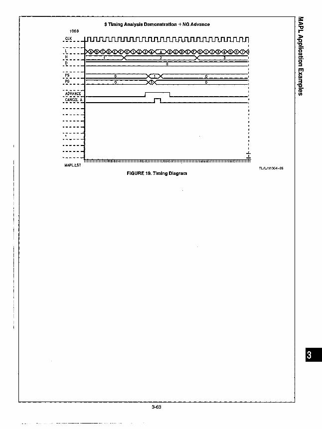
1060
CLK
L
H
D
PS
PG
$ Timing Analysis Demonstration +NG Advance
-j:::::::::::::=::o;:::::=:::::::=:=XJ:X~=============o=========== ---------------------><D<.._ ____________ __.o..__ __________ _
.J..
.!.
MAPL.LST
FIGURE 19. Timing Diagram
3-63
TL/L/11304-35
:s: )> "tJ r)>
"tJ "2. r;· m -s· ::J m >< D> 3
"tJ CD' 0
I •

L States Delay State Machine
delay
delay
delay
delay
delay
delay
delay
delay
delay
delay
delay
delay
delay
delay
delay
delay
TL/L/11304-36
FIGURE 20. Delay State Machine
3-64

Begin Header Divide Down Counter with Specific Timing Control Options
End Header
Begin Definition Inputs
rst, advance,· delay Feedbacks (JK, HOLD)
h3, h2, hl, hO, 13, 12, 11, 10, d2, dl, dO; Feedbacks (JK,RST)
aO; Feedbacks (JK,RST,BURIED)
gO, gl; · Outputs
cancel_adv, cancel_del, fsr End Definition
Begin Equation global.re rst;
End Equation
Begin Truth Table ttin advance, delay, h3, h2, hl,
dl, dO, gl, gO; ttout h3, h2, hl, hO, 13, 12, 11,
hO, 13,
10, aO, cancel adv, cancel _del, fsr, gl, gO;
-0-------- - ---00 -------!
12,
d2,
--000
11,
dl,
-0-------1 - ---00 ------!- - --000 -0------11 - ---00 -----!-- --000 -0-----111 - ---00 ----!--- --000 -0----1111 - ---00 ---!---- - --000 -000011111 - ---00 0010---- --000 -00-101111 - ---00 0?11---- - --000 -000111111 - ---00 0100---- - --000 -001001111 - ---00 0101---- - --000 -001011111 - ---00 0110---- - --000 -001111111 - ---00 1000---- --000 -010001111 - ---00 1001---- - --000 -010011111 - ---00 0000---- - --100 10----0--- - ---00 -------- - --011 10----100- - ---00 -------- - --011 01-------- - ---00 -------- - 000 ---10
FIGURE 21. Divide Down Counter
3-65
10, aO,
dO,
d2,
TL/L/11304-37
;: > .,, r>
"C 'E. c:;· D) -c;· ::s m >< D)
3 "C a; en
•

"' Cl)
Q. 10----0000 0 ---11 ----0110 1 1-000 E
cu 10----0001 0 ---11 ----0111 1 1-000 >< w 10----0010 0 ---11 ----1000 1 1-000 c 0 10----0011 0 ---11 ----1001 1 1-000 :;:: cu 10----0100 0 ---11 ----1010 1 1-000 -~ Q. 10----0101 0 ---11 ----1011 1 1-000 Q. cs: 10----0110 0 ---11 ----1100 1 1-000 ..J
10----0111 0 ---11 ----1101 1 1-000 a.. cs: 10----1000 0 ---11 ----1110 1 1-000 == 10----1001 0 ---11 ----1111 1 1-000
10----1010 0 ---11 ----1011 1 1-000 10----1011 0 ---11 - ... --1100 0 0-000 10----1100 0 ---11 ----1101 0 0-000 10----1101 0 ---11 ----1110 0 0-000 10----1110 0 ---11 ----1111 0 0-000 10----1111 0 ---11 ----0000 0 0-000
01-------- - 00010 -------- - 001 -0010 01-------- - 00110 -------- - 011 -0010 ' 01-------- - 01110 -------- - 000 -1000
End Truth Table TL/L/11304-38
FIGURE 21. Divide Down Counter (Continued)
3-66

8.0 Bus Transaction and OMA Controller This application demonstrates the use of the MAPL 128 for bus state machine control. In this design, the MAPL 128 provides bus access and OMA control for an 110 board on an asynchronous bus (Futurebus + ). Although the design is fairly simple, the resulting state machine demonstrates flexibility and power of the OPAL command language. Less than half of the product terms of the MAPL 128 are used in this example, so there is room for substantial increases in design sophistication.
The MAPL 128 state machine controls accesses from the system bus to the local DRAM, from the local CPU to the system bus, and block data transfers between local DRAM and the system bus. The OMA controller is a discrete design, programmed by the CPU and enabled by the state machine. It consists of four sub-blocks:
1. The local address counter is programmed by the CPU before each OMA operation with the start address of the data block in DRAM. This can be either the source or destination of the transfer, depending on whether a bus write or read has been programmed.
2. The bus address counter is also programmed by the local CPU with the start address of the data block on Futurebus. Once again, this is independent of the direction of data transfer.
3. The transfer counter determines the total size of the OMA transfer. This is programmed by the local CPU at the start of each transfer. The local CPU can read the contents of the counter in the event of an error or unexpected OMA termination condition. Because this is an asynchronous bus, this counter must be clocked asynchronously as the OMA transfer progresses, and could not be implemented in the MAPL 128.
4. The packet counter determines the number of words in each bus transaction, breaking up the OMA transfer into blocks that the bus can handle. The 8-bit counter allows packet sizes of up to 256 words (1 . Kbytes on a 32-bit bus) in a single bus transaction. This is programmed by the local CPU as necessary; the counter is automatically reloaded with the last programmed ,value before each bus transfer.
The MAPL 128 state machine takes requests from the system bus and generates accesses into local DRAM, takes requests from the CPU and generates accesses out to the system bus, and, after the CPU has loaded the appropriate OMA controller registers, generates accesses to both the DRAM and the system bus. It enables the address latches for each type of access. It monitors the transfer and packet counters, so that multiple packets are generated until all the data is transferred. The actual data transfer is controlled by a separate asynchronous state machine.
3-67
The state machine implemented by the MAPL 128 contains three "subroutines" for the three types of accesses supported. The MAPL 128 waits in the idle state until a request occurs. The state machine language uses the if/else syntax to prioritize simultaneous requests. BUS__AOOR_HIT is generated by the system bus address decoder, CPU_ AOOR_HIT is from the decoder on the local bus, and CPU_GO signals that the OMA has been programmed by the CPU. After a system bus request, the slave subroutine waits for a bus grant and free local bus before beginning the access and enabling data transfer. The machine supports locked transactions, which require that the local bus not be released between transfers. The master (CPU access) subroutine is almost identical to the slave subroutine. The specific signals monitored and generated by the MAPL 128 can be easily modified for any type of CPU or bus interface.
The OMA state machine first requests the system bus, then the local bus before performing accesses. It will continue to generate packets until all the data has been transferred and both counters are zero. (The packet counter gets reloaded when it reaches zero, until the transfer counter also reaches zero.)
The OMA subroutine waits for the CPU to signal, via an external 110 control register bit, that the OMA registers described above have been programmed and the transfer is ready to go. It requests first the system bus, then the local bus. Once both busses are available, it enables the addresses onto both the local and system busses and starts the asynchronous bus transfer state machine. With each data transfer, the transfer and packet counters are decremented. The state machine will give up the local and system busses between transfers in order to allow other devices access to them. Once the transfer counter reaches zero, the OMA operation is complete. The OMA state machine checks to ensure that the transfer has completed successfully, and interrupts the CPU.
This design was implemented using 0 flip-flops only. If PLA space had been an issue, JK flip-flops with a default of hold could have been used for the state bits. The final "else" statements in states with feedback include signals which are also held. These signals would need to be converted to DE or JK flip-flops, again with a default of hold, and all the positive and negative transitions need to be explicitly specified. By eliminating the product terms associated with final else statements, substantial space savings can often be realized.
3: l> "ti r l>
"'C "'5!. a·
D.> -a· :J m >< D.> 3
"'C Ci en
•

fl) Q)
Q. E ~
UJ c 0 :; ,g Q. a. <C ~ Q. <C :e
t.IAPL 128 Bus Transaction Control
State t.lachine
Bus 1/0 Board Block Diagram
System Bus
FIGURE 22. Bus 1/0 Board Block Diagram
FIGURE 23. Bus Control State Machine
3-68
ORAi.i Controller
TL/L/11304-39
TL/L/11304-40

bus_addr _hit= 0 cpu_addr _hit= 0
cpu_go = 0
bus_addr _hit= 0 cpu_addr _hit= O
bus_addr _hit= 1 cpu_go = 1
State idle:
(local_br:= 1)
bus_addr _hit= 0 cpu_addr _hit= 1
if bus_addr _hit then s_request with local_br := 1; endwith
else if cpu_addr_hit then m_request
with bus_br := 1; end with
else if cpu_go then Lbus_request '
with bus_br := 1; end with
else idle;
FIGURE 24. Bus Control State Machine (Idle State}
bus_addr _hit= 0 bus_lock = 0
bus_addr _hit= 0 bus_ lock= 1
(local_bgack := 1)
bus_end_tr = 1 bus_lock = 0
bus_end_tr = 0 {local_bgack := 1,
bus_as:=1)
FIGURE 25. Bus Control State Machine (Slave}
3-69
TL/L/11304-41
TL/L/11304-42

ti) CD a. E ca >< w c 0 = ca .2 a. a. ct ..J D. ct :e
cpu_addr _hit= O bus_lock =O
cpu_addr _hit= 0 bus_ lock= 1
(bus_bgack := 1)
{bus_bgack:=1, local_addr _len := 1,
bus_as := 1)
bus_end_tr = 1 bus_lock= 0
bus_end_tr = 0 {bus_bgack := 1,
bus_as := 1)
FIGURE 26. Bus Control State Machine (Master)
bus_addr _hit= 0 cpu_addr _hit= 0
cpu_go= 1 (bus_br := 1)
(bus_br := 1)
(bus_bgack := 1, {local_br := 1)
A: bus_enc!_tr = 1
packeLcounLzero = 0 xfer_counLzero = 0 {bus_br: = 1)
B: bus_end_tr = 1 packeLcounLzero = 0 xfer_counLzero = O (load_packeLcount = 1)
locaLbgack := 1, bus_addr _oen := 1,
locaLaddr _oen := 1,
bus_as := 1, locaLas := 1)
cpu_cir = 0 (cpu_int:=1)
bus_ end_ tr= 1 xfr _count_zero = 1
{cpu_int := 1)
. bus_end_tr = 1 (bus_,bgack :'= 1, locaLbgack := 1,
bus_as := 1, locaLas := 1)
FIGURE 27. Bus Control State Machine (OMA)
3-70
TLIL/11304-43
TL/L/11304-44

begin header
Synchronous Bus Control State Machine - Rev 0.1, Dave Hawley
end header
begin definition
Inputs:
CPU GO CPU CLR LOCAL BG LOCAL BUS FREE CPU ADDR HIT
PACKET COUNT ZERO - -XFER COUNT ZERO - -BUS ADDR HIT - -
BUS BG BUS END TR BUS LOCK BUS ERROR
Outputs:
CPU INT LOCAL BR LOCAL BGACK LOCAL AS BUS ADDR IEN - -
LOCAL ADDR OEN - -LOAD PACKET COUNT - -BUS BR BUS BGACK BUS AS LOCAL ADDR_IEN, BUS ADDR OEN - -DMA ERROR }
inputs
Signal from the CPU to begin DMA transfers Signal from the CPU to clear DMA interrupt Bus grant from local arbiter Bus free status on local bus Local decoder recognizes CPU access to system bus DMA data transfer counter equals zero DMA data transfer counter equals zero Bus decoder recognizes system access to DRAM System bus grant System bus end of data transfer System bus lock System bus transfer error
DMA complete interrupt signal to CPU Local bus request from DMA Local bus grant acknowledge Local bus address strobe Latch enable for system bus address to local bus Latch enable for DMA address to local bus Load packet transfer size counter System bus request System bus grant acknowledge System bus address strobe Latch enable for CPU address to system bus Latch enable for DMA address to system bus DMA transfer error
cpu_go, cpu_clr, local_bg, local_bus_free, cpu_addr_hit,
TL/L/11304-45
3-71
3: ):lo -a r)::io
"C '2. ~--c;· ::s m >< D> 3
"C Ci" 0
•
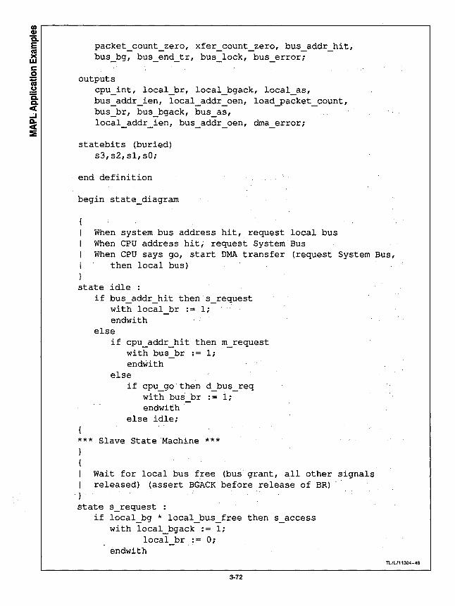
packet_count_zero, xfer_count_zero, bus_addr_hit/ bus_bg, bus_end_tr, bus_lock, bus_error;
outputs cpu_int, local_br, local_bgack, local_as, bus addr_ien, local_addr_oen, load_packet_count, bus_br, bus_bgack, bus_as, local_addr_ien, bus_addr_oen, dma_error;
statebits (buried) s3,s2,sl,s0;
end definition
begin state_diagram
When system bus address hit, request local bus When CPU address hit( request System Bus When CPU says go, start DMA transfer (request System Bus,
then local bus)
state idle if bus_addr_hit then s request
with local br := 1; endwith
else if cpu_addr_hit then m_request
with bus_br ·= 1; endwith
else if cpu_go then d_bus_req
with bu~ br := 1; endwith ·
else idle;
*** Slave State Machine *** }
{
I Wait for local bus free (bus grant, all other signals I released) (assert BGACK before release of BR) . :
. }
state s_request : if local_bg * local_bus_free then s access
with local_bgack := 1; local br := 0;
endwith
3-72
TL/U11304-46

else s_request with local br := 1; endwith;
Begin bus transaction (assert address enable before AS)
state s access : goto s_transfer
with local_bgack := 1; bus addr ien := 1; local as := 1;
endwith;
Can release the address enable inunediately (latched by DRAM controller)
When transaction complete, release AS If no lock, release local bus, otherwise enter locked state
state s transfer : case bus end tr * /bus_lock : idle;
bus end tr * bus lock : s locked - - - -with local_bgack :=-1; endwith;
/bus_end_tr : s_transfer with local_bgack := 1;
bus_addr_ien := 0; local as := 1;
endwith; endcase;
In locked state, wait for new address hit or lock release
state s locked : case bus addr hit : s access - -
with local_bgack := 1; endwith;
/bus_addr_hit * /bus_lock : idle; /bus_addr_hit * bus_lock : s_locked
with local_bgack := 1; endwith;
endcase;
*** Master State Machine ***
Wait for system bus grant
3-73
TL/L/11304-47
3: > "lJ r-> "C "'5!. c;· m -c;· ::s m >< m 3 "C ii en
Ell

en Q)
c.. E m ><
LI.I c 0 ; m .!::! c.. c. <I: ..J D. <I: ::E
I (assert BGACK before release of BR) }
state m_request if bus_bg then m_access
with bus_bgack := 1; bus_br .- O;
endwith else m_request
with bus br := 1; endwith;
Begin bus transaction (assert address enable before AS)
state m access : goto m_transfer
with bus_bgack := 1; local_addr_ien := 1; bus as := 1;
endwith;
Can release the address enable immediately When transaction complete, release AS If no lock, release System Bus, otherwise enter locked state
state m transfer : case bus end tr * /bus_lock : idle;
bus end tr * bus lock : m locked - - -with bus_bgack := 1; endwith;
/bus_end_tr : m_transfer with bus_bgack := 1;
local_addr_ien := 0; bus as := 1;
endwith; endcase;
In locked state, wait for new address hit or lock release
state m locked : case cpu_addr_hit : s_access
with bus_bgack := 1; endwith;
/cpu_addr_hit * /bus_lock /cpu_addr_hit * bus_lock
with bus_bgack := 1; endwith;
3-74
: idle; s locked
TL/L/11304-48

endcase;
*** OMA State Machine ***
Wait for System Bus grant, then request local bus (assert BGACK before release of BR)
state d_bus_req if bus_bg then d_local~req
with bus_bgack := 1; bus_br := O; local br := 1;
endwith else d_bus_req
with bus br := 1; endwith;
Wait for local bus free (bus grant, all other signals released) (assert BGACK before release of BR)
state d_local_req : if local_bg * local_bus_free then d access
with bus_bgack := 1; local_bgack := 1; local br := O;
endwith else d_local_req
with bus_bgack := 1; local br .- 1;
endwith;
Begin OMA transaction (assert address enables before AS)
state d access : goto d_transfer
with bus_bgack := 1; local_bgack := 1; bus_addr_oen := 1; local addr oen := 1; bus_as := 1; local as := 1;
endwith;
Can release the address enables immediately When transaction complete, release AS
TL/L/11304-49
3: )> .,, r)> "C "5!. c:;· I» -c;· ::s m >< I» 3 "C m "'
•

U) G)
'ii E ca >< w c 0
:;::: ca .!::! 'ii c. <C ..J a.. <C :::E
Interrupt CPU, reload packet counter, or re-request bus, depending on packet and transfer counter states
state d transfer case bus end tr * /bus_error * /packet_count_zero *
/xfer_count~zero d_bus_req
with bus br := 1; endwith;
bus_end_tr * /bus_error * packet_count_zero * /xfer_count_zero :
d_next_packet with load_packet_count := l; endwith;
bus_end_tr * /bus_error * packet_count zero * xf er count zero - -
d end dma with cpu_int := 1; endwith;
bus_end_tr * /bus_error * /packet~count_zero * xfer_count_zero
d end dma with cpu_int := 1;
dma error := 1; endwith;
/bus_end_tr : d transfer
endcase;
with bus_bgack := 1; local_bgack := 1; bus_addr_oen := O; local addr oen := O; bus_as := 1; local as .- 1;
endwith;
Transfer count <> 0, so reload packet counter and continue
state d_next_packet goto d_bus_req
with load_packet_count := 0; bus br := 1;
endwith;
Error or transfer count = 0 so interrupt CPU and wait for clear interrupt
3-76
TL/L/11304-50

state d end drna : case cpu clr * /cpu_go : idle;
cpu_clr * cpu_go : d_bus_req with bus_br ·- 1; endwith;
/cpu_clr * cpu_go : d end drna with cpu_int := 1;
drna error := 1; endwith;
/cpu_clr * /cpu_go : d end drna with cpu_int := 1; endwith;
endcase;
end state_diagram
270
PAGE
STATE
CLK
BUS.LST
FIGURE 28. Timing Diagram
3-77
TL/L/11304-51
TL/L/11304-52
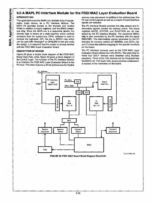
0 Cl> Ci. E ~
LLI c 0 ;:; cu
.!:! Ci. a. <C ...I D. <C :E
9.0 A MAPL PC Interface Module for the FDDI MAC Layer Evaluation Board INTRODUCTION This application uses the MAPL 144, Multiple Array Program-. mable Logic device, as a PC interface Module. The MAPL 144 provides access to the transmit and receive RAMs in addition to board registers, and the BMAC peripheral chip. Since the MAPL 144 is a sequential device, the decode logic is based on a state-machine which controls accesses from the system bus. OPAL software is used to compile the high-level .OPL file into a JEDEC map which can be used with Viewlogic® or OPALSIM to test and verify the design. It is assumed that the reader is already familiar with the FDDI MAC Layer Evaluation Board.
DESCRIPTION OF DESIGN Figure 29 gives a simple block diagram of the FDDI MAC Board Data Path, while Figure 30 gives a block diagram of the Control Logic. The function of the PC interface Module is to interface the FDDI MAC Layer Evaluation Board to the PC host. This block features a 20-bit address bus for flexible
PC_ Address
PCRST
PC Interface Logic
(l.4APL 144)
Receive Sequencer
Copy
PC_Data
CBus_Data
RX RAl.4
Bk x B
memory map placement. In addition to the address bus, five PC bus control signals as well as a couple of board interface signals are included.
The PC interface Module provides the chip selects and intermediate signals needed for memory select. The board registers MODE, STATUS, and FUNCTION are all controlled by the PC interface Module. The peripheral BMAC chip is also controlled by the PC interface with the signal BMACSEL. The intermediate signals generated by the PC interface for memory control are MEMSEL and ACK3. Figure 31 shows the address mapping for the specific functions on the board.
The . PC interface currently used on the FDDI MAC Layer Evaluation Board utilizes four GAL20VB's. The entry files for these four GAL® devices were obtained using Boolean equations. Three of the GAL devices can be integrated into the MAPL 144. The fourth GAL device provides combinatorial access of the memories on the board.
81.lAC
TX RAl.4
Bk x B
·Board Registers
x I-
Transmit Sequencer
TL/L/11304-53
FIGURE 29: FOOi MAC Board Block Diagram Data Path
3-78

When the Boolean equations for the three GAL devices are combined into one .CPL file, the logic will not compile into the device because of logic partitioning problems. In other words, it is unable to allocate logic to different pages when it is specified as being on one page. The PC interface was redesigned based on a state machine so as to split up the decode logic. Most of the decode logic in the Boolean equations was based on access feedback terms. These access feedback terms could be incorporated into a state machine. This access control state machine is illustrated in Figure 32. Now, each of the eight states can be placed on one page of the MAPL 144, thus partitioning the decode logic.
IOCHRDY
Incorporating the state machine into the .CPL file is now trivial. Figure 33 shows the final .CPL file for this design. Notice how the page bits are defined as state bits in the definition block. This allows the designer to free-up three pins for designs that are l/C limited. Figure 34 shows the output from the fitter. In this particular design, manual paging was done by using the page bits as state bits. This way, the designer has the freedom to partition the design the way he wants it to be partitioned.
SMRD .....
SMWD .....
MODESEL, ATTNENAB
AEN PCRST
INTB
Receive Sequencer
Copy I
REGS EL
.. 2 g
<.> x a::
Receive Status
BMACSEL
CBUSACK
STATUSSEL, ST ATUSSTB
RX RAM
Bk x B
MUX
Memory Interface
Transmit Status
RUN
BMAC
TX RAM
Bk x B
FIGURE 30. FDDI MAC Board Block Diagram Control Logic
3.79
Board Registers
.. .. c: ::I
8 ~
Transmit Sequencer
TL/L/11304-54
3: )> .,, r)>
"'C "2. (;" D> -o· ::::s m >< D> 3
"'C (6" 0
•

r.n CD Q. E tU )(
UJ c 0 :;; .2 Q. Q.
<C ..J a. <C
==
Signal Description
Inputs
SMWR
SMRD-
AEN
PCRST
CB USACK
INTB
CLK
Outputs
System write.
System read.
Address Enable.
PC Reset.
CBUS Acknowledge from BMAC peripheral.
Inverse Interrupt Signal.
System Clock.
ST A TU SS EL Output Enable for the STATUS Register.
STATUSSTB Chip Select for the STATUS Register.
MODESEL Chip Select for the MODE Register.
ATTNENAB Chip Select for the FUNCTION Register.
BMACSEL BMAC peripheral Chip Select.
RUN
MEMSEL
REGSEL
ACK3
INT
IOCHRDY
Reset all state machines. •,, ·. .
Accessing the board under a memory select. ·
Accessing the board under a register select.
Third state in the Access Control State Machine. Used for memory sel~cts.
Interrupt Control.
1/0 Channel Ready.
PC19 PC18 PC17 PC16 PC15 REGSEL MEMS EL RECEIVE TRANSMIT IOCHCTL ACK1 CBUSACCESS BMACSEL BOARDREG MODESEL ATTNENAB RUN
1 0 0
0 0
0
1
PC14 PC11 PC10
0
0 0 0 0 0 0
FIG~RE 31. PC Interface Logic Signal Description for MP144
TL/L/11304-55
FIGURE 32. PC Interface Access Control State Machine
3-80
PC9 PCS PC7 PC6
0 1 : 0
0 0 0

begin header pc interface (state machine)
end header
begin definition device MAPL144;
inputs aen,smwr,smrd, pc19,pc18,pc17,pcl6,pcl5,pcll,pcl0,pc9,pc8, pc7,pc6,pc5,pcrst,cbusack,intb;
outputs (JK,RST) statussel,modesel,attnenab,run,bmacsel,ack3,memsel, regsel,statusstb,int,iochrdy;
statebits (DE,RST,BURIED). pb2=47,pb1=46,pb0=45;
STATE NAME IDLE="b000,ACK1W="b001,ACK1R="bl00 1 ACK2W="b010, ACK2R="b101,ACK3W="b011,ACK3R="b110,ACK4RW="blll;
end definition
begin equation
int := /intb;
end equation
begin state_diagram state IDLE :
CASE /smrd*/aen*pc19*pcl8*/pcl7*pcl6
with /iochrdy := l; endwith; /smwr*/aen*pcl9*pcl8*/pcl7*pcl6
with /iochrdy := l; endwith; ENDCASE;
state ACKlW goto ACK2W with
ACKlR
ACKlW
modesel := /pcl5*/pcll*/pc10*pc9*pc8*/pc7*/pc6;
FIGURE 33. PC Interface .OPL File
3-81
TL/L/11304-56
3: l> "'tJ r-l>
"'C "E. 5· D> -cs· ::s m >< D> 3
"'C iD en
•

"' Q)
c. E ca >< w c 0 = ca -~ c. c. ct ...I a. ct :E
attnenab := /pc15*/pcll*/pc10*pc9*pc8*/pc7*pc6; statussel := (pc7*/pc6*/pc5*/pcl5*/pcll*/
pclO*pc9*pc8); statusstb := pc7*/pc6*/pc5; run := pc7*pc6*/pc15*/pcll*/pclO*pc9*pc8+pcrst; bmacsel := /pc15*/pcll*/pcl0*pc9*/pc8; regsel := /pclS; memsel := pclS; /iochrdy := 1;
endwith;
state ACKlR goto ACK2R with
modesel := /pc15*/pcll*/pclO*pc9*pc8*/pc7*/pc6; attnenab := /pc15*/pcll*/pclO*pc9*pc8*/pc7*pc6; statussel := (pc7*/pc6*/pc5*/pcl5*/pcll*/
pclO*pc9*pc8); statusstb := pc7*/pc6*/pc5;. run := pc7*pc6*/pcl5*/pcll*/pc10*pc9*pc8+pcrst; bmacsel := /pc15*/pcll*/pclO*pc9*/pc8; regsel := /pclS; memsel := pclS; /iochrdy := 1;
endwith;
state ACK2W goto ACK3W with
modes el ·= ?• . . , attnenab := ?; statussel := ?; statusstb : = ? ; run := ? ; bmacsel : = ? ; regsel := ?; memsel := ? ; ack3 := 1; /iochrdy := 1;
endwith;
FIGURE 33. PC Interface .OPL File (Continued)
3-82
TL/L/11304-57

state ACK2R : goto ACK3R with
modes el ·= ?• . . , attnenab := ?; statussel := ?; statusstb := ?; run := ?; bmacsel := ?; regsel := ?; memsel := ?; ack3 := 1; /iochrdy := 1;
endwith;
state ACK3W if (pc15+pcll+pc10+/pc9+pc8)+
(/pc15*/pcll*/pc10*pc9*/pc8*/cbusack) then ACK4RW else ACK3W with
modes el ·= ?• . . , attnenab := ?; statussel := ?; statusstb := ?; run := ? ; bmacsel := ?; regsel := ?; memsel := ?; ack3 := 1; /iochrdy := 1;
endwith;
FIGURE 33. PC Interface .OPL File (Continued)
3-83
TL/L/11304-58
3: )> ""C r)>
"C "'2. c;· m -s· ::s m >< m 3
"C CD' 0
•

en Cl)
Q. E cu >< w c 0 ; cu -~ Q. c. < ..J a.. < :::E
state ACK3R : if (pc15+pcll+pc10+/pc9+pc8)+
(/pc15*/pcll*/pc10*pc9*/pc8*/cbusack) then ACK4RW with
statussel ·= ?• . . , run := ?; bmacsel := ?; regsel := ?; memsel ·= ?;
endwith else ACK3R with
modes el ·= ?• . . , attnenab := ?; statussel := ?; statusstb := ?; run := ?; bmacsel := ?; regsel := ?; memsel := ? ; ack3 := 1; /iochrdy : = 1;
endwith;
state ACK4RW if /smrd then ACK4RW with
statussel := ?; run := ?; bmacsel : = ? ; regsel := ?; memsel := ? ;
endwith else if /smwr then ACK4RW else IDLE with statussel := 1; endwith;
end state_diagram
FIGURE 33. PC Interface .OPL File (Continued)
3-84
TL/L/11304-59

10.0 PLUS405 to MAPL TM 128 Conversion INTRODUCTION be dropped into the socket for evaluation. In some cases, a
Many state machine designers are familiar with Philips/Sig- couple of pins must be swapped. It should be noted that the
netics sequencers for state machine design and will appre- MAPL 128 has significantly more logic capacity than the oth-
ciate the density, low power, and speed of National Semi- er devices, allowing the designer to. not only replace the old
conductor's MAPL 128. The MAPL 128 in 28-pin PLCC has device, but improve (and add to) the design. In fact, upgrad-
the speed and density to tackle many existing and future ing to a MAPL 128 device will not only increase functionality,
designs including many current Signetics' sequencer de- but dramatically reduce power consumption. For example,
signs. In fact, in many cases the MAPL 128. is pin-for-pin the PLUS405 device consumes 225 mA, ·more than twice
compatible with these previous designs while offering the the power of MAPL 128 which consumes 110 mA, while the
designer higher speed, lower power, and more logic capaci- MAPL 128 has 40% more logic capacity than the PL05405.
ty. The following devices are available in 28-pin PLCC: National reduces power consumption by using EECMOS
GENERAL COMPARISON versus bipolar, and more importantly, by implementing a revolutionary paged architecture, giving MAPL devices low-
The MAPL 128 and the 28-pin Signetics sequencers have er power consumption an.d higher logic capacity without the very similar pinouts. Thus, the MAPL 128 device can usually usual speed reduction.
MAPL 128 Block Diagram
~ ::n
Inputs l8f- ::n ::n Page Select
..ll. I"< ll _I 1/0 ... L.. Feedback ... r"'" ... AND Buried ... Feedback
'"' L..
~ r<
27M=~ ~1/0 I. I.
I. OR ~ -~ - ;~Outputs ..
i" CLK
TL/L/11304-60
T T Prod tsu tcLK fMB Repl Mfgr Device In Out 1/0 Buried Ice
Terms (Note 1) (Note 1) (Note 1) (Note 2)
NSC MAPL128 9 4 12 8 128 110 17 9 40 -Sig PLUS405 (Note 3) 16 8 0 8 64 225 18 8 38.5 y
Sig PLUS105 (Note 3) 16 8 0 6 48 200 20 8 35.7 y
Sig PLC42VA 12 (Note 3) 8 2 10 10 64 120 50 17 13.3 N
Sig PLC415 (Note 3) 17 8 0 8 68 75 60 22 13.3 y
Sig PLS179 (Note 3) 8 4 8 0 48 210 55 20 13.3 N
Sig PLS168/ A (Note 3) 12 4 4 6 48 180 70 20 12.5 y
Sig PLS167/A (Note3) 14 4 2 6 48 180 70 20 12.5 y
Sig PLS105/ A (Note 3) 16 8 0 6 48 180 70 20 12.5 y
Note 1: Worst case speed: with buried feedback through complement array/page terms. Note 2: Pinout same as MAPL128. PLUS405 and PLC415 are replaceable if pin 4 is not used as clock. PLUS 168/ A are replaceable if pins 15 & 16 are used as outputs. PLUS105/A are replaceable if pin 16 is used as an output. PLUS105 and PLS105/A are pin for pin replaceable by MAPL 128. Note 3: Specifications are taken from fastest version of the device from the 1991 databook. Specifications are subject to change.
3-85
3: > "'tJ r-> "'C "2. c;· I» -a· :::s m >< I» 3
"'C CD' tn
•

U) Cl)
a. E ca ><
I.LI c 0 ;: ca .2 a. c. <( ...I a. <( ::E
PAGING VS COMPLEMENT ARRAY
National's paged architecture might appear similar to Signetics complement. array, but it is far different. Signetics feeds back one or two OR array output signals through a NOR gate directly back into the AND array. They call these feedback signal the complement array, which are used to more effectively ·use product terms in state machine designs. National feeds three signals and their complements into the AND array that not only can be used to perform a "complement array" function, but also to select one of eight pages. These page select signals are hard-wired so that one and only one page is active at a time. This reduces power consumption and increases device performance. At the time of compiling the design, "fitter" software automatically partitions the logic across the pages of the MAPL device and assigns page bits to each state. On each clock cycle the correct page is selected based on where the next logic state can be found. There is no time penalty for this paging operation therefore the paging is transparent to the user.
Most manufacturers claim best case speed of the device as the actual speed of the device, however, the device is usually much slower in the application. For example, the PLUS405-55 is touted as a 55 MHz device, however, sequential applications utilizing the complement array will only realize 38.5 MHz. National specifies speed of the MAPL family with paging and buried feedback, since this is the way the MAPL device is used in a sequential application. Therefore, a MAPL128VC-33 device is truly a 33 MHz device capable of running at 33 MHz (worst case) in the application.
TIMING
Given functional compatibility of the MAPL 128 to Signetics' sequencers, the designer still needs to make sure that the new device's timing specifications will allow it to run in the
3-86
system. In state machine design, tsu (setup time) and tcLK (time of clock to registered output), are very important. Careful attention should be paid to these parameters to be sure that a device will function properly in the application.
Device tsu tcLK fMB
MAPL128 17 9 40 20 10 33
PLUS405 18 8 38.5 22 12 29.4 25 15 25
PLO SOFTWARE COMPATIBILY
Both OPAL™ software from National and AMAZE software from Signetics allow state machine designs to be efficiently written in a state machine language. This language describes transition opreations with IF-THEN-ELSE and CASE statements. The syntax of these and other statements in OPAL and AMAZE are slightly different. If a design is described using ABELTM or CUPL™, the designer simply changes the device name and recompiles for the new device. If the design is described in AMAZE, then some simple modifications are needed to convert from AMAZE syntax to OPAL syntax. It should be noted that this manual conversion, although relatively simple, is necessary becase AMAZE is not an "open" software package like OPAL which allows designs to be freely communicated with third part software.
For more information on MAPL, OPAL, or the conversion process, please contact your nearest National Semiconductor Sales Representative.

Advanced PLO· Architectures
INTRODUCTION
The range of programmable logic devices can be divided into three broad architectural areas: PALs, PLAs, and FPGAs. Although designers probably wish there was a single architecture suitable for all applications, in reality each has its area of specialty. National Semiconductor's new MAPL™ family, for example, is a high-speed, PLA architecture ideal for state machine applications. Neither PALs nor FPGAs can provide the same performance and ease of use over a broad range of design complexity. This paper analyzes the application strengths and weaknesses of the latest PLO architectures, then focuses on the specific requirements of state machine design.
THE PAL® ARCHITECTURE
The basic PLO architecture is the PAL, with a programmable AND array and a fixed ' number of independent product terms per output {Figure 1). Although many refinements have been made to the output macrocells and distribution of productterms, the basic architecture remains the same. Its high speed, high fan-in, and moderate number of product terms per output make it ideal for the largest segments of the PLO market: random logic replacement and address decoding. Indeed, the GAL® 22V10 architecture is the most popular PLO today, and similar devices are available from a wide range of vendors.
The biggest advantage of the PAL architecture is its high speed; the biggest limitation is its relatively low density. Unfortunately, it is impossible to simply scale-up the PAL architecture without sacrificing performance and power. By examining characteristics of the target applications, however, manufacturers have been able to find an acceptable compromise. Since most random logic uses a small number of product terms, a device with a large number of 110 macrocells, each with only a few product terms, can. provide a much higher effective density. There are several partitionedPAL architectures on the market now which aim for the random logic replacement applications.
AND Array
Inputs
Dedicated OR Macrocells (8 Terms Typical)
TL/L/11296-1
FIGURE 1. The PAL architecture uses a programmable AND array and dedicated OR array for high speed
Implementation of random logic and decode functions.
National Semiconductor Application Note 810 David Hawley Staff Applications Engineer
Even random logic requires the occasional high-product term equation. Those architectures which solve this problem with the least disturbance to the output performance are generally the easiest to work with. If adding a product term to an equation changes the setup time of a signal by 10 ns, the performance of the entire system may have to be reduced. Folded NANO or expander arrays have this characteristic, and make a preliminary timing analysis of any design very difficult. Likewise, the interconnect between PAL arrays within a single chip can hide limitations until a final compilation of the design into the chip is attempted and design modification may cause unwanted pinout changes.
High-density PAL architectures have all made certain compromises in order to maintain performance. As long as the designer is aware of details of the architecture and how they relate to the characteristics of the application, they can be quite useful in reducing system part count. A software package which supports more than one manufacturer's device can be a useful evaluation tool. For raw speed and simplicity, however, standard PAL and GAL devices will always be at the leading edge.
THE PLA ARCHITECTURE
The PLA architecture differs from the PAL in that both the AND array and OR array are programmable {Figure 2). This means that all product terms are available to all outputs: several outputs can share the same product term, and each output can have a large number of product terms. As a result, the utilization of product terms in a PLA is generally much higher than in a PAL. The high fan-in and large number of product terms make PLAs ideal for state machine design, the third largest PLO application. Unfortunately, PLAs are generally much slower than PALs as well, since each signal must traverse two arrays. This means that designers have tended to avoid PLAs in speed-sensitive applications.
AND Array -----. Inputs
OR Array
Macrocells
TL/L/11296-2
FIGURE 2. The traditional PLA architecture, Ideal for state machines, uses two programmable arrays
for high density at the expense of speed.
3-87
l> z
I CIO .... Q
•

0 ,.... co z cs:
Other, non-PLA solutions to state machine design· have been attempted. These include various microcoded sequencers and pipelined arrays. However, they have sacrificed the basic simplicity of the sum-of-products architecture. Along with adding their own limitations, they lose some of the other benefits of a PLA. One of these is product term sharing, which allows PLA devices additional freedom in macrocell design. In a PAL, each macrocell input requires its own product terms, which impacts density, and therefore performance. In a PLA, an increase in the number of macrocell inputs does not require a corresponding increase in the number of product terms. Instead of only D flip-flops or latches, a PLA macrocell can be built with SR, JK, and DE flip-flops for additional design efficiency.
·The biggest advantage of the PLA architecture is its high density; the biggest limitation is its low speed. Once again, it is possible to examine the characteristics of the target application to find a way around the performance limitation. Although most state machines require a large number of product terms,· only a few of them are needed by the current state. In a paged-PLA architecture, a subset of the total array product terms are powered up at any given time. The power saved goes into making the device fast. National Semiconductor is the first manufacturer to provide an architectural solution to PLA state machine design.
THE FPGA ARCHITECTURE
FPGAs are the latest development in the area of programmable logic. Although the technology used to . implement them may vary, and manufacturers of high-density PALs and PLAs often mislabel their devices FPGAs, they are really quite easy to define. Instead of programmable AND or OR
arrays, they have an array of programmable logic cells, interconnected by a programmable wiring matrix (Figure 3). These logic cells have limited fan-in and fan-out, and the internal routing results in variable delays through the device. Their performance and efficiency tends to be highly application-dependent.
FPGAs are ideal for high-density logic replacement, where the performance of PLDs is not required. Because of the low fan-in, they are best where the complexity of each logic block in the design is small. Unlike PALs and PLAs, with close to full global interconnect, their 'limited routing resources make FPGAs better for designs with more local than globally routed signals. These characteristics lend themselves to the design of subsystems for which no custom silicon exists, and which would otherwise have to be built from discrete parts.
Unfortunately, it is difficult to know how well a design will match a particular FPGA architecture without a lot of design experience or a preliminary implementation. Due to the cost of FPGA design software, a large investment is often required before an estimate of efficiency, utilization, and system timing can be obtained. With respect to the main application areas of traditional PLDs, however, a few gross generalizations can be drawn. FPGAs work well for random logic replacement, if they can meet the propagation delay requirements of the design. They tend to be too slow and awkward for address decoding; the regular structu~e of a PAL is a much better match. And their performance degrades rapidly with the complexity of state machines, due to the high level of fan-in and interconnectivity that is typically required. A high-speed PLA architecture is much easier to work with.
TL/L/11296-3
FIGURE 3. FPGAs use interconnected logic cells to provide high Integration at the expense of deterministic performance. Efficiency Is application-dependent.
3-88

THE MAPL PLA ARCHITECTURE
The MAPL is targeted at high-speed state machine applications. This is a broad area which includes local and system bus interfaces, arbitration, timing control, micro sequencers, and almost any other type of synchronous (registered) logic design. All of these benefit from the full interconnect and consistent timing provided by a PLA architecture. The paged PLA architecture of the MAPL gives the user access to the largest, fastest, and lowest power EECMOS PLA on the market (Figure 4).
PAGE BITS
AND
OR
MACROCELLS OUTPUTS TL/L/11296-4
FIGURE 4. The MAPL paged PLA architecture allows Implementation of complex state machines without
sacrificing performance or power.
0
The MAPL array provides the user with 128 product terms. This is the largest PLA on the market, and allows unprecedented design complexity in a traditional architecture. The flexible output macrocells are designed to increase product term efficiency still further. It supports a 45 MHz true system clock rate, which is higher than most bipolar PLAs. The 8 ns · clock to output specification is the best of any high-density PLD. And the maximum device current, for any design, is specified at 110 mA at 25 MHz. All using standard electrically erasable CMOS GAL technology.
These remarkable figures are a result of the MAPL's patented paged architecture, which divides the 128 product terms into 8 pages. This paging is invisible to the user, as software fitters automatically assign state bits to enable pages. There is no timing penalty for switching pages. The architecture limits each state to a maximum of 16 product terms, but due to the optimized macrocell design, this limitation is rarely encountered. Paging powers up only the portion of the array needed by the current clock cycle. Since the array sense amplifiers can be shared among the pages, power can be devoted to device speed instead of device size. The benefit to the user is a PLA that provides 128 product terms to all outputs at 45 MHz (Figure 5). The MAPL is an architectural solution to state machine applications.
The MAPL PLA drives 27 registered macrocells, with two sum terms for each cell (Figure 6). These macrocelfs have been designed to enhance the overall device functionality
Inputs
TL/L/11296-5
FIGURE 5. Functionally, the MAPL appears to be a continuous 128-product term PLA.
TL/L/11296-6
FIGURE 6. The MAPL two-Input macrocell Includes programmable polarity and DE and JK flip-flops to allow selection of the optimum function of any application.
3-89
l> z
I 0) ..... 0
•

0
:C by minimizing product term usage. Both macrocell inputs z have programmable polarity, so that the positive or compli-~ mentary logic function can be chosen, whic.hever is most
efficient. Two hardwired flip-flop types can be selected, either DE (D with clock enable) or JK. This allows selection of the default (no product term active) condition of the output
· to be either set, reset, hold or toggle. This can have a significant impact on the number of product terms used in any state, depending on the type of structure present in the design. Additional PAL product terms are used to provide asynchronous register reset and a selection of four output enable functions to all signals.
Note that the array is fully registered, that is, no combinatorial outputs are available. However, for synchronous state machine applications, this is not a problem. In most designs, combinatorial and asynchronous functions are added to the periphery of the core state machine.
STATE MACHINE DESIGN TECHNIQUES
The low performance of traditional PLA architectures have forced most high-speed state machine designs to be implemented in PAL architecture devices. This requires designers to compromise their ideal design methodology, due to the limitations of the PAL architecture in these applications.
PALs and GALs are ideal for very simple state machines. They have short propagation delays, and these delays are
SLAVE INPUTS
GENERAL INPUTS
MASTER INPUTS
OMA INPUTS
GAL
SLAVE
consistent from one output to the next, regardless of whether one product term is used, or eight. This speed and simplicity make them the vehicle of choice for low-level design.
As design complexity increases, the limited number of product terms available to each output begins to squeeze the design. This problem occurs even in the new high-density partitioned PAL architectures. Solutions include breaking a single complex state machine into several smaller ones, or encoding inputs and decoding outputs in separate devices. The result is a design with worst-case delays through multiple devices, and signals with a wide range of timing values. Worse yet, because of the contortions necessary to fit the design into the product terms available, design modifications or enhancements are difficult to impossible. Equationlevel entry and a detailed knowledge of the device architecture are often required. Rather than providing a solution, PAL state machine design becomes a challenge.
An example of this is. a typical bus interface (Figure 7). Although the slave, master, and OMA bus operations logically form a single, large state machine, PAL product term limitations force the designer to break them up into three separate interconnected state machines. Some inputs and outputs are independent, but others are common to the entire design, and must be shared among mutiple inputs and outputs. The resulting network of feedbacks and decodes result in a complex design with inconsistent timing.
OUTPUTS
MASTER OUTPUTS
OMA OUTPUTS
MAPL SOLUTION:
SINGLE S.M. INCLUDING
DECODE
TL/L/11296-7
FIGURE 7. The MAPL frees the designer from the product term limitations of PAL architectures In state machine design, simplifying Implementation.
3-90

A PLA architecture, in· contrast, provides ample product terms to the user. This allows complex state machines to be implemented in a single device. All outputs have identical timing, and adding a product term or a state is no longer a major modification. Best of all, it is possible to design in software at the state machine level, with all the benefits that has for design maintenance and documentation.
The MAPL is the first device to solve the PLA performance problem without compromising functionality. A closer look at the characteristics of state machines themselves explains why.
A state machine, by definition, has only one state active at a time. During the clock cycle in which that state is active, only the equations necessary to determine the next state and outputs are being used. Out of the entire design, only the product terms needed by one state can be active. In a traditional PLA, sufficient power must be provided to drive all product terms, regardless of how many are used by the current state. The MAPL, by paging product terms, drives only 16 terms per clock cycle. It is extremely unusual for a single state to require more than 16 product terms. In fact, several states will usually fit onto a single page. This means that paging can be fully transparent to the user. The full state machine has access. to 128 product terms, while the device only needs to provide sufficient current to drive 16 product terms. As a result, the MAPL can be both big and fast.
The MAPL two-input macrocell also serves to increase the device's functionality. A signal which is normally set or reset, and only asserted in one or two states, is well-suited to a standard D flip-flop with polarity selection: A signal that changes state only occasionally, but is active over a large range of states, would require product terms in every one of these states. By using the MAPL's DE flip-flop, one product term can be used to turn the output on, and another to turn it off. Holding the output active uses no product terms. Counters can also require a large number of product terms
when implemented in D flip-flops. With the MAPL's JK flipflop, only a single term is needed for each bit of the counter. A 16-bit counter fits on a single page of the MAPL, leaving the remaining seven pages available for the rest of a state machine. Macrocell type selection decreases product term usage and increases the effective density of the MAPL.
In the bus interface example above, the MAPL would be able to implement the interface state machine directly, resulting in a simpler design and fewer chips, with consistent timing and no loss of system speed.
THE MAPL FAMILY National is developing two families of MAPL devices. The first, the MAPL 1 family, is focused only on the state machine portion of a design. The MAPL 128, in production, is a 28-pin device incorporating the 128-product term . MAPL paged array described above. It has 9 inputs, 4 dedicated outputs, 12 1/0, 8 buried feedbacks, and 3 page bits which can be used as state feedba.cks. One of the inputs can also be used as a fast output enable, along with the three dedicated product terms. All 27 macrocells can be asynchro~ nously reset. The MAPL 144 is a 44-pin device based on the same internal architecture, but the 8. buried feedbacks are also available as outputs. All run at a system clock rate of 45 MHz. . . . .
The MAPL2 family brings in additional functions that are needed in some applications. It is not uncommon for a state machine. to require that its inputs or outputs be combined with other high-speed signals, sometimes with specialized timing. The MAPL2 includes 8 PAL outputs with dynamic polarity control which can be used in conjunction with or independently of the MAPL array. Either registered or combinatorial outputs are available. The MAPL2 also has optional input latches on all signals to reduce setup times on critical signals, and double-buffering for synchronizing asynchronous inputs to avoid metastability.
TABLE I. MAPL Family
MAPL 128 144 244 268
Product
Package Size 28 44 44 68 Max Inputs 21 21 32 36 Max Outputs 16 24 32 40 Macrocells 27 27 35 43 Total 1/0 25 33 32 24 System Speed 40MHz 45MHz 50MHz 50MHz PLA Product Terms 128 128 128 128 PAL Product Terms 4 4 76 104 Max Power at 25 MHz 110 mA 125mA 180mA
3-91
> z I
CC> ..... 0

0 ,... co z <
PLO DESIGN SOFTWARE
In order to design effectively with any PLO, suitable design tools must be used. Because a designer's time is limited, it is important that they require little or no additional effort to learn. For the same reason, they must provide entry formats which suit the application at hand.
In the ideal world, a designer would only need to learn a single design environment. It takes time for new devices to be supported across all platforms, however, so there is a place for manufacturers to provide their own low-cost software to bridge the gap. National Semiconductor, for example, sells OPAL™ as a complete design package for PAL, GAL, and MAPL users. It provides boolean equation, truth table, and state machine language entry formats, and generates JEDEC maps and functional simulations for all National PLDs. A menu-driven shell environment makes it easy to use as a stand-alone tool, and the MAPL fitter automatically minimizes and compiles designs into the MAPL paged architecture. · .
For those that need to integrate the latest .in PLDs with their own tools, it is important to provide a bridge between software packages. National is one of the vendors supporting the use of Berkeley's Espresso PLA format. Rapidly becoming a standard for the transfer of logic design, it can be read or generated by a wide range of design tools. Combined with Data ·11o·s OPEN PLA device-specific "dot extensions," proprietary fitters, such as for the MAPL, can be used with third-party software. Indeed, National provides the MAPL fitter to all PLO softWare vendors, making it easy for thein to provide the latest support quickly and easily.
Having broad software support for a product is essential to users, who need to be able .to evaluate a wide range of devices for a particular application q·uickly. If a single state machine can be compiled into four, or five devices in a few minutes, a real evaluation of performance and functionality can take place. Therefore, manufacturer support for an OPEN PLA format provides real benefit to both users, who gain access to technology quickly, and to manufacturers, who present the lowest possible hurdle to use of their products.
BEGIN HEADER OPAL Traffic Signal C6ntrollcr,
END HEADER
BEGIN DEFINITION device MAPL128;
STATE MACHINE DESIGN EXAMPLES
A traffic light controller is a classic state machine design example. Here it is used to demonstrate characteristics of state machine language design and the Berkeley PLA format. National's OPAL syntax is used to describe the state machine; but the function should be fairly obvious to anyone with state machine language experience.
The version of the controller shown below has three inputs, aside from the clock. The "cir" signal is used to asynchronously reset the state machine, and the two "sensor" signals detect the presence of cars at the intersection. The size outputs of the design are the green, yellow, and red lights for each direction. Notice that the. characteristics of each output have been taken into account in the MAPL macrocell.selection. Both use a DE flip-flop, but the red and green lights, which are on or off throughout several states, hold their state as the default condition, while the yellow light, normally off, uses the reset state as its normal condition. Polarity selection at the input to the macrocells physi~ cally implements these defaults.
The state bits themselves are defined as JK flip-flops, with a default of toggle. This is because the state machine has a 2-bit counter embedded in it to control the maximum length of time any car can be kept waiting. As JK flip-flops implement efficient counters, this will minimize product term usage. These PLA outputs are buried within the MAPL, as they are not needed by any external logic. The "stateReg" set of symbols is defined in order that the asynchronous state reset function can be defined in a single equation below. The state values are defined in order to ensure that the 2-bit counters (states A1-A4 and B1-B4) follow a linear sequence. The remainder of the assignments, except for the Start state, are of little consequence ..
The equation block assigns the "cir" input to the asynchronous reset product term of the state bits. The other equations are merely definitions for variables used within the rest of the state machine.
The state machine consists of 13 states, two of which have branch conditions.The green and red lights must have each of their transitions explicitly defined, while the yellow lights only need to have their active conditions defined. The undefine state is reserved within the OPAL syntax. It is used to guarantee that the state machine returns to the Start state if any of the 3 undefined state bit encodings are encountered.
Hawley, NSC, 15 Aug 1991
inputs elk, clr, sensorA, sensorB; outputs (de, hold) greenA, red1'., greenB, redB; outputs (de, rst) yellowA, yellowB; statebits (buried, jk, toggle> s3, s2, sl, sO; set stateReg = [s3,s2,sl,sC1; state names Start=O, A0=3, A1=4, A2=5, A3=6, A4=7, A5=8,
- B0=9, B1=12, B2=13, B3=14, B4=15, B5=2; END DEFINITION
3-92
TL/L/11296-11

BEGIN EQUATION stateReg. ar=clr; turnedOn•l; turnedOff•O; On•l;
END EQUATION
BEGIN STATE_DIAGRAM state Start: goto AO with
greenA:•turnedOff; yellowA:s::On; redA:•turnedOn; greenB:=turnedOff: redB:•turnedOn; endwith;
state AO: goto Al. with greenA:•turnedOn: redA:•turnedOff; endwith;
state Al: if ( sensorA & !sensorB ) then Al else if (!sensorA & sensorB ) then AS with
greenA:•turnedOff; yellowA:•On; endwith
else if ( sensorA •• sensorB > then A2; state A2: goto A3; state A3: goto A4; state A4: goto AS with
greenA:=turnedOff; yellowA:=On; endwith:
state AS: goto BO with redA:=turnedOn; yellowB:=On; endwith;
state BO: goto Bl with greenB:•turnedOn; redB:=turnedOff; endwith;
state Bl: if (!sensorA & ser.sorB ) then Bl else if ( sensorA & !sensorE > then B5 with
greenB:•turnedOff; ycllcwB:=On; endwith
else if C sensorA •= s~ns~rB > then B2; state B2: goto B3; state B3: goto 84; state B4: goto BS with
greenB:•turnedOff; yellowB:=On: endwith;
state BS: goto AO with redB:-turnedOn; yellowA:-On; endwith:
state undefine: goto Start; END STATE_DIAGRAM
3-93
TUL/11296-9
):iii z
I CD ..... Q
•

0 ..... co :Z ~
This simple state machine also fits into a GAL 22V10 using D flip-flops. It would consume about one-third of the 22V10's product terms, and all 10 outputs. In the efficient PLA architecture of the MAPL, however, only 14 product terms are needed, less than one of the 8 pages of the device. Since the state bits can be buried, more 1/0 are free for additional functions as well. Even in this basic example, the advantages of the MAPL architecture for state machine design is evident.
The entire traffic signal controller can also be defined in the Berkeley PLA format shown below. This OPEN PLA format allows the same design to be transferred from one design tool package to another. National's OPAL software com~ piled the state machine above into a Berkeley PLA file, performed the minimization and page assignment required by the MAPL, and generated the revised PLA file shown below. This output can then be compiled into a JEDEC map for programming the MAPL 128.
The PLA file format is extremely compact. The lines begin- .. ning with "#$"are comments used by National's software
f $ TOOL NSC
for device or tool-specific information. The line beginning with ".i" defines the number of PLA inputs and the line beginning with ".o" defines the .number of PLA outputs. ''.ilb" defines the input label names, While ".ob" defines the output names. Notice that the software has automatically created the two macrocell inputs required by the MAPL DE or JK flip-flops, and defined the necessary polarity selections with the"-" suffix. The ".type" and ".phase" definitions·are,not used by the OPAL software. The ".p" line shows the total number of product terms in the design, including the 4 identical asynchronous reset terms at the bottom. The PLA map itself is in truth-table format, with each column defining an input or output in the order defined above. Each product term is represented by a single row. A "-" defines a "don't care" input, while " - " defines the same for outputs.
This is the format which allows software from different vendors to interchange PLO design information. Any software package which generates this file can be used as the design entry vehicle for the MAPL device. A PLO design tool with specific MAPL support, such as OPAL, can then perform the JEDEC map creation .required for programming.
1$ TITLE OPAL Traffic Signal Controller, D. Hawley, NSC, 15 Aug 1991 f $ TITLE f $ DEVICE MAPL128 .i 10 .o 26 4#$ PINS 10 clk:6 clr:5 sensc·rA:4 sensorB:3 greenA:l2 redA:l3 greenB:lS redB:l6 yellowA:ll yellowB:lO ts NODES 6 s3:37 s2:30 s1:31 s0:32 pb2:39 pb1:38 .ilb elk clr sensorA sensorB ~3 s2 sl sO pb2 pbl .ob s3.j s3.k s2.j s2.k sl.j sl.k sO.j sO.k greenA.d greenA.ce redA.d redA.ce greenB.d greenB.ce redB.d redB.ce yellowA.d yellowA.ceyellowB.d yellowB.ce- sO.ar sl.ar s2.ar s3.ar pb2.reg pbl.reg .type f .phase 11111111111111111111111~11 .p 18 --01 010000
100000 --10 110000 --oo --0-00 --11 --0-00
-1---1---1---1--.e
100100 111100 000000 00-000 -11-00 -00-00 011100 -10100 001100
11110000 00000000 11111100 00000011 00000011 00110000 11110000 00001100 00000011 00000011 00000011 11111100 00001111 00111111
01000000100000~000 001100000010000000 000001000010000000 00000000000000-0000 000000000000000000 000011010000000000 000001000010000000 OlllOlOOOOOOQOOOOO 000000111000000000 000000000000000000 000000000000000000 010000001000000000 000000000000000000 110100000000000000
---------------1---------------~ 1---
------------1-----
3-94
TL/L/11296-10

A second classic example demonstrates the abilities of the MAPL to a greater extent. The state machine described by the following diagram is for the control of a 3-floor lift. It responds to calls for service and displays the status of the lift. It has 1 O inputs, which include a call button for each floor, an "open" button inside the lift, and sensor inputs
which indicate the position of the lift and its doors. 13 outputs control the motor and doors, and drive a 7 -segment display and the up and down indicators. No manual state assignment was performed in this example, so the software created the 5 state bits automatically. The full state diagram is too long to present, but a sample is shown below.
TL/L/11296-8
state upfroml : disp:=one; up:=2call+3call; if C /arrive2 ) then upfroml with Umotor:=l; endwith else if ( 2call ) then open2 up else if ( 3call ) then upfrom2 with Umotor:==l; endwith else open2_up;
3-95
TL/L/11296-12
l> z c» ...a. Q
•

0 ...... co :2: ct
In this state example (uf1), the display decode is specified in the first line. An if-then-else syntax is used to describe the branch conditions, and the up motor is driven if the lift has not yet arrived at its destination. The remaining states are of similar complexity.
The OPAL software generates a log file which summarizes the total device utilization. This can be used to analyze the design, and to determine whether it might have fit in another type of device. In this example, the raw PLA file had 120 product terms. After minimization, the design occupied 70 product terms. In the paged architecture of the MAPL, however, a few terms needed to be duplicated. on more than one page, so a final total of 78 of the 128 product terms were actually consumed. This represents 60% of the terms available on the device. Notice that although some outputs require up to 32 product terms, the terms can be split
Device Utilization:
No of dedicated inputs used No of feedbacks used as dedicat.ed inputs No of dedicated outputs used
among multiple pages because only a few are used in each state. The sum of the individual output terms is less than the total because terms can be shared among multiple outputs in a PLA architecture.
No PAL could implement this state machine in a single device. Even the highest-density PAL architecture on the market cannot handle the intensive product term requirements of this design; partitioning would be required. Only a PLA architecture can provide an efficient implementation. This is generally true of any complex state machine design. Most importantly, every signal has the same timing relative to every other, impossible to achieve in a partitioned PAL or FPGA architecture. This design can run at a 45 MHz clock rate in the MAPL, and modification of the design will not affect the set-up, hold, or clock-to-output timing parameters of any signal. This knowledge provides the user with a solid base on which begin any design.
9/9 (100.0%) 1/12 (8.3%) 4/4 (100.0%)
No of feedbacks used as· dedicated outputs 9/12 (75.0%) No of buried feedbacks used 2/8 (25.0%) No of page bits used 3/3 (100.0%)
Pin Label Terms Usage --------------------------------------------------------21 down 9/128 (7. 0%) 20 up 8/128 (6.2%) 19 g 6/128 (4. 7%)
18 f 1/128 (0. 8%) 17 e 23/128 (18. 0%) 7 d 6/128 (4. 7%) 8 c 20/128 (15. 6%) 9 b 11/128 (8.6%) 10 a 6/128 (4. 7%)
12 Umotor .3/128 (2. 3%) 13 Dmotor 3/128 (2. 3%) 15 opendoor 3/128 (2. 3%) 16 closedoor 4/128 (3.1%) 29 statebit-01 5/128 (3. 9%) 33 statebit-05 32/128 (25.0%) 37 statebit-04 28/128 (21. 9%) 38 statebit-02 20/128 (15.6%) 39 statebit-03 25/128 (19.5,) --------------------------------------------------------Total
SUMMARY PAL architectures are ideal for high performance logic replacement. The new generation of high-density PAL architectures provide greater integration for applications with a limited number of product terms. State machine applications require a large number of shared product terms, and are best suited to PLA architectures. National's MAPL 128 is the first of a new family of paged-PLA devices which provide high performance for complex designs. FPGAs provide high levels of integration, but performance is extremely variable due to interconnect delays.
3-96
78/128 (60.9%)
TUL/11296-13
The best way to evaluate a technology is to compile a design onto a range of devices. Manufacturer support of open PLA formats guarantees that users have access to the latest devices within a consistent design framework. National Semiconductor provides access to MAPL devices through its own OPAL software and by working closely with PLO software vendors worldwide. In this way, state machines can be integrated as a part of a board design.

A Smart UART Design Implemented in a MAPL 128
A "smart" UART is often necessary to interface to a PC when designing a stand-alone circuit. This application note describes a UART design implemented in a MAPL 128 pro· grammable logic device. The state diagram, sample timing diagram, and OPAL TM entry language listing are included. This UART design utilizes 77% of the MAPL 128 device, al· lowing the designer the flexibility of changing or adding to the design.
The UART uses standard RS-232 signals-TxD, CTS, RxD, and OTA-and models a standard 8-bit UART running at 9600 baud. An integrated counter divides the clock by 16 from 153.6 kHz to 9.6 kHz. The UART design checks for parity and framing errors, sending a message back to the host if these occur, and incorporates an 8-bit interface to a bidirectional data bus.
RESET
- FROM PC
National Semiconductor Application Note 800 David O'Neal
The UART begins receiving when the serial in (SIN) signal goes low for more than half a bit width. The UART then samples the middle of each following bit to ensure stable data, toggling on each occurrence of data = 1 and holding on data = 0. After the eighth data bit, the UART compares the parity bit with the parity it has calculated. If these are not identical, a parity error has occurred. The SIN is sampled again to detect the stop bit. If SIN is low, a framing error has occurred. The UART sends a request back to the host and waits for more data if a parity or framing error has occurred, otherwise it raises the READY flag and holds the data on 10[0:7].
To transmit, the system controller pulls the LOAD signal high. After checking the host's OTA signal, the UART loads data into 10[0:7]. issues a start bit, and shifts the data seri· ally. The UART then issues a parity bit and a stop bit and returns to the idle state.
READY
MAPL128 UART
TO SYSTEt.4 CONTROLLER
1/0 BUS
TRANSCEIVER
ERROR_O ERROR-I
TL/L/11295-1
3.97
)> z
I O> 0 0
•

0 0 co :Z <I:
RST
TL/L/11295-2
3-98

4152 CLK
PAGE
10
RST
ERROR
SIN
PARITY
SEND
SOUT
READY
CTS
A:BADSEND.LST
4136 CLK
PAGE
RECEIVED A3 WITH BAD PARITY
$ UART
$ UART
SEND RESEND MESSAGE
10 ~-----o_3 _____ ><:::iI:)<:.._ __ A_3 ___ x~----------------"5----------------
RST
LOAD
ERROR
DTR
SIN
PARITY
SEND
IOMODE
SOUT
READY
CTS
A:UART.LST
RECEIVED A3 SEND 45
3-99
< ESC > TO EXIT
TL/L/11295-3
< ESC > TO EXIT
TL/L/11295-4
> z I
ex> 0 0
•

0 0 Cl)
I z <C
begin header This device is the serial interface controller for the serial port MAPL Eval board project. The UART section is clocked 16 times faster than the data communication rate, uses l stop bit and even parity. It is implemented on a MAPL128. end header begin definitions
device MAPL128;
inputs sin=6,dtr=S,error_i=2,load=25,rst=26;
feedbacks (JK,HOID) io7=23,io6=22,io5=21,io4=20,io3=19,io2=18,iol=l7,ioo=11;
feedback (JK, RST, BURIED) clear;
feedbacks (JK,HOID,BURIED) parity,send,iomode,count3,count2,countl;
feedbacks (JK, TOGGLE, BURIED) countO;
statebits (JK,HOID) sb3=7,sb2=8,sb1=9,sb0=10;
output (JK,HOLD) sout=12;
output (JK,HOLD) error_o=l5,ready=16,ctS:.13;
set count= [count3,count2,countl,countO); set io = [io7,io6,io5,io4,io3,io2,iol,ioo);
state names - IDLE=AhO,START=Ah7,PAR=Ah2,ERR=Ahl,STOP=Ah4,
BITO=AhB,BITl=Ah9,BIT2=AhA,BIT3=AhB,BIT4=AhC,BITS=AhD, BIT6=AhE,BIT7=AhF;
end definitions
begin equations
io.oe iomode; {allows you to tristate IO outputs with a variable.}
end equations
begin truth_table
ttin clear, count3, count2, countl, counto ,· send,sb3,sb2,sbl,sbo~ io7, .io6, ioS, io4, io3, io2, iol, ioO;
3-100
TL/L/11295-5

ttout count3,count2,countl,counto, sb3,sb2,sbl,sbO, io7,io6,io5,io4,io3,io2,iol,ioo;
1---- -------- 0001 0---1 -------- --!-0--11 -------- -!--
------------------------
{counter used as a clock {divider. It resets to {0001 to account for the }
0-111 - -------- !--- -------- {one clock needed to reset}
1 0111 .1------- 1000 1------- {this part of the truth } 1 0111 -1------ 1000 -1------ {table loads the IO } 1 0111 --1----- 1000 --1----- {variables using only 8 } 1 0111 ---1---- 1000 ---1---- (product tenns (since in} 1 0111 ----1--- 1000 ----1--- {the previous state they} 1 0111 -----1-- 1000 -----1-- {were all set to zero) . } 1 0111 ------1- 1000 ------1- {Nonnally with T ff's it} 1 0111 -------1 1000 -------1 {would take 16 product }
{tenns. }
end truth_table
begin state_diagram
state ALL : {set the reset conditions} if rst then IDLE with
send := O; iomode := 1; error o := o; sout := 1; ready := 1; cts := 1; endwith;
state IDLE : if /sin then START with
clear := 1; send := o; cts := O; endwith
else if load*dtr then START with send := 1; iomode := O; io := "hOO; cts := o; ready := O; endwith
else IDLE with iomode := 1; sout := 1; endwith;
{detect a start bit}
{begin a send cycle}
state START : case
{waiting to verify} {start bit}
/send*(count != "h8) : START;
{start bit verified}
{false start bit {return to IDLE}
/send*(count == "h8)*/sin*/clear BITO with clear := 1; ready := O; parity := O; endwith;
/send*(count == "hB)*sin*/clear .• IDLE with cts := 1; endwith;
3-101
TL/L/11295-6
)> z
I Q) 0 0
•

0 0 Cl)
I z <
{send out start bit}
endcase;
state BITO :
send BITO with clear := l; parity := O; sout := o; iomode := l; endwith;
if count!=Ahf then BITO else if /send then BITl with
· · ioO ·:= sin; parity.j = sin; parity.k = sin; endwith
else BITl with
state BITl :
sout := ioO; parity.j = ioO; parity.k = ioO; endwith;
if count!=Ahf then BITl else if /send then BIT2 with
iol := sin; parity.j = sin; parity.k = sin; endwith
else BIT2 with
state BIT2 :
sout := iol; parity. j = iol; parity.k = iol; endwith;
if count!=Ahf then BIT2 else if /send then BIT3 with
io2 := sin; parity. j = sin; parity~k = sin; endwith
else BIT3 with
state BIT3 :
sout := io2; parity. j = io2; parity.k = io2; endwith;
if count!=Ahf then BIT3 else if /send then BIT4 with
io3 := sin; parity.j = sin; parity.k = sin; endwith
else BIT4 with
state BIT4 :
sout := io3; parity.j = io3; parity.k = io3; endwith;
if count!=Ahf then BIT4 else if /send then BIT5 with
io4 := sin; parity. j = sin; parity.k = sin; endwith
else BIT5with sout := io4; parity .j = io4;
3-102
{states BITO - BIT? are} {identical. Wait until} {the counter reaches 15} {then receive input or } {send output. In either} {case, toggle parity } {bit if a one is sent } {or received. }
TL/L/11295-7

parity.k = io4: endwith:
state BIT5 : if count!=Ahf then BIT5 else if /send then BIT6 with
io5 := sin; parity.j = sin; parity.k = sin: endwith
else BIT6 with sout := io5; parity.j = io5: parity.k = io5: endwith;
state BIT6 : if count!=Ahf then BIT6 else if /send then BIT7 with
io6 := sin; parity.j = sin: parity.k = sin: endwith
else BIT7 with sout := io6; parity.j = io6: parity.k = io6; endwith;
state BIT7 : if count!=Ahf then BIT7 else if /send then PAR with
io7 := sin; parity.j = sin; parity.k = sin; endwith
else PAR with
state PAR : case
{error if parity} {does not match }
{continue if it does}
sout := io7; parity. j = io7; parity.k = io7; endwith;
count != Ahf : PAR;
(count == Ahf)*/send*(sin !=parity) error_o := l; endwith;
(count == Ahf)*/send*(sin ==parity)
{output parity on send} (count== Ahf)*send : STOP with iornode := l:
endcase;
state STOP : case
{error if no stop} {bit is detected }
{return to IDLE if } {there is a stop bit}
sout := parity; endwith;
count != Ahf : STOP;
(count== Ahf)*/send*/sin : ERR with error_o := l; endwith;
(count== Ahf)*/send*sin : IDLE with cts := l; ready := l; endwith;
3-103
l> z a, 0 0
ERR with
STOP;
• TL/L/11295-8

0 0 co :Z <
{return to IDLE with} {ready high if this } {was a normal send }
{return to IDLE with } {ready low if this } {was an error message} {being sent }
endcase;
state ERR :
(count== Ahf)*send*/error i cts := 1; -
IDLE with
sout := 1; ready := 1; endwith;
(count== Ahf)*send*error_i : IDLE with cts := 1; sout := 1; error_o := O; endwith;
if dtr then START with iomode := 1; io := Ahff;
{load error message (FF) in} {IO registers and send it } {to the host. }
send := 1; endwith else ERR;
end state_diagram
3-104
TL/L/11295-9

State Machine Design
Multiple Array Programmable Logic, or MAPL™ is National Semiconductor's new family of high density programmable logic devices. These PLDs are ideally suited for state machines, controllers, and synchronous logic applications. The purpose of this application note is to show how easy it is to implement state machines in MAPL devices. It is assumed that the reader is familiar with the MAPL128 data sheet, general principles of logic design, and has knowledge of PLO design.
• State machine fundamentals
• The state machine design process
•.State machine design using MAPL and OPAL™
. • The MAPL state machine architecture advantage
STATE MACHINE FUNDAMENTALS
Implementing a complex state machine with a MAPL device is much easier than with conventional programmable logic. To facilitate a MAPL implementation, an understanding of state machine design principles may be needed. This section and the next will review these principles. Once a design example is illustrated, the capabilities of MAPL will become more apparent.
National Semiconductor Application Note 801 Bill Carlson, Snr. Field Applications Engineer
State machines are used in nearly all digital systems. State machines often resolve timing dissimilarities between different devices and enable them to work together. They also perform the functions of complex counters and micro-instruction sequencers. A state machine is needed when a microprocessor interfaces to another large VLSI· device, such as a storage controller. State machines are also needed when an adapter board needs to gain access to the system bus, or when a CPU needs to interface to a complex memory architecture. In a slave mode or bus master mode transfer, state machines are used to translate the signals of a bus to those of a device the bus is accessing. In bus masters, state machines implement bus arbitration, the bus transfer protocol, and limiting bus tenure times upon being pre-empted. There are also serial protocols that need a complex state machine to do frame and address recognition, frame stripping, encoding/decoding and controlling the serializing and de-serializing of data.
State machines are based on sequential logic design where the inputs of the circuit along with the previous outputs determine what the next outputs will be. There are two different types of state machines, the Mealy and the Moore models as shown in Figure 1.
Moore State Machine Model
Next-state Combinational
Logic
Next-state Combinational
Logic
Tsu Tclk Tpd
Output Control Logic
Output is a function of state only
Mealy State Machine Model
Outputs
TL/L/11302-1
.. ------------------Outputs
.. ., ., .... C/I"'
J!
FIGURE 1
. 3-105
Output Control Logic
Outputs
TL/L/11302-2
)> z 0., 0 ......

T-o co In the Moore model, the outputs are only dependent upon Z the current state. In the Mealy model, by contrast, the out- Transition J Input K Input
< puts are dependent not only on the present state, but also · on the present inputs. Once a certain state is entered the state bits are fed back to the combinational logic· where output functions change asynchronously with respect to the clock. When an input changes, a corresponding output will change as well, even between clock periods. This is in contrast to the Moore model where an input change won't affect the output until the next clock cycle has occurred and a new state is entered. This application note will focus on the more common Moore type.
A state is defined as the current value of a group of state registers; each individual register value is called a·state bit. The outputs are decoded from the current state and are used to control the actual functions in the system. The nextstate logic is combinatorial in nature and combines the current state information with the inputs to form the logic needed to determine the next state. This logic can be represented by equations defining the inputs to the flip-flops in the state registers. These equations are dependent upon the reg~ster used, whether D/E, J/K, R/S, or T. The type of register chosen affects the complexity of this logic.
Each type of register has its advantages and disadvantages. In order to derive the equations for transitioning a register from one state to another, a transition table is needed for the type of register being implemented. These tables are somewhat different than the flip-flop truth tables as they are usually defined. The register transition tables define transitions only and assume a known current state to a known next state. Flip-flop truth tables on the other hand define Hold and Toggle functions as well as Set and Reset functions.
Transition D Input E Input
0--+ 0 - 0 0 --+ 1 1 1 1 --+ 0 0 1 1 --+ 1 - 0
Transition T Input
0--+ 0 0 0 --+ 1 1 1 --+ 0 1 1 --+ 1 0
CLK__J
0--+ 0 0 -0 --+ 1 1 -1 --+ 0 - 1 1 --+ 1 - 0
Transition S Input R Input
0--+ 0 0 -0 --+ 1 1 -1 --+ 0 - 1 1 --+ 1 - 0
Some PLDs have only one type of register, such as the D-type found in most PAL® and GAL® devices. Some PLDs, such as MAPL have all four types available for maximum flexibility. When a design is implemented using PLD software tools, they will often optimize the design based on the available register type. The JK type is the most flexible and can implement all needed functions such as Set, Reset, Hold, and Toggle. The hold function is useful because no further product terms are required to hold the newly transitioned state of a register. When state machine language is used in the software design tools, the JK type register can easily implement the "If-Then-Else" statement. The T-type register implements only the toggle function and requires a reset to bring it to a known state. An active input causes the output to toggle states and it defaults to a hold state. The T-type register is good in counter applications where only a few product terms can implement a very large counter. The RS register is a simpler version of the JK without the toggle function.
There are several timing parameters that affect the integration of the state machine into a system. Minimizing timing constraints of the input signals is an important factor. Figure 2 is a timing diagram based on the Moore model as illustrated in Figure 1.
Tsu is the set-up time required b.y the state registers of the input signals. It must be guaranteed that all inputs and current state feedback information be stable before a Tsu time period prior to the clock arriving to avoid any metastability problems. Th. is the time period that the data must be held valid after the clock edge has occurred. These parameters
....,...,...,..,,,_..._. t: Tsu~ tTh Inputs zzzzzzzzzzzx Valid ~zr""'1z-rzz7"'zr-z,...,zz~z.,...z,,...,zz..,.z..,..z.,..,z....,.zz..,..z~z,....,.zz-z-z-z-1z-z-z-z
~ Ou;~~!: ///////////////O//X State Bits (Hold for 3 Clks) X/////
i.:TPdj Output r---------------
Signals -----------------'X Valid Output Signals >e:: TL/L/11302-10
FIGURE2
3-106

must have specified maximum values that are as short as possible to guarantee that the inputs get properly latched into the register. T CLK is the clock to output delay of the state registers. The output logic decodes the current state information and forms the outputs to the system. T PD is the propagation delay of this logic to do this decoding function. For controlling the output functions, the T CLK and T PD parameters must be as short as possible as well. A very fast T CLK and T PD ensure that once a state is entered, the function being controlled by the. output control logic will be executed as soon as possible.
Determining the overall speed of a state machine is dependent on various timing parameters and implementations. The maximum clock rate is dependent in many cases on the kind of state feedback that is implemented. When buried registers are used in PLDs, the signals are fed back directly to the AND array and do not pass through a highly capacitive 1/0 pin that would excessively slow the signal down.
When signals are fed back through these pins the maximum clock rate is lowered by about 10%. With 1/0 feedback, the clock rate is dependent on two timing parameters, Tsu and T CLK· These two combine together to form the time period of the state information being clocked through the register (T CLK) followed by the time delay through the logic array Tsu). Thus the clock frequency is Fmax = 1/(Tsu + TcLK>· When there is no feedback at all, the set up times aren't an issue and the flip-flops can run much faster. However, in a state machine this clock rate is misleading because there will be feedback in the circuit. The MAPL 128, for example, has a clock rate of 62.5 MHz with no feedback and a 40 MHz speed using 1/0 feedback. The more typical situation is when the state bits are stored in the buried registers which allows the device to operate at a higher clock rate of 45.5 MHz like in MAPL 144. Many programmable logic devices, especially the newer, high density varieties, specify a maximum clock rate that the device will operate at without feedback. In a general logic replacement application, this . may be suitable but with the inherent feedback in state machines, it should be questioned if those devices were designed with this application in mind. The MAPL devices are specified with respect to this buried feedback. This parameter, as all others, should be viewed from the system perspective of the actual application. There is an architecture dependence on performance as well. In certain devices, having one too many product terms can halve the maximum clock frequency the device will run at. These architectures will be discussed later.
THE STATE MACHINE DESIGN PROCESS
The state machine design process follows a specific procedure and has been simplified greatly with today's powerful design tools.
1. Description of the sequential circuit
2. State Diagram
3. Solving asynchronous design and metastability prob-lems
4. State/transition tables
5. Minimization
6. Flip-flop determination and equation generation
7. PLO selection and programming
3-107
This process defines a procedure for implementing state machine designs. Describing the sequential circuit involves examining the timing diagrams, protocols, etc. that define the exact nature of the problem. The state diagram is the actual solution to the problem described in a flow-chart type manner. The state diagram is the heart of the state machine and its accuracy is crucial for the circuit to operate properly. Here, the proper inputs, control outputs, clock frequency, and state flow are chosen. The state diagram, although it shows the exact flow of the circuit as it steps through the various states, doesn't provide a structured format for describing each state and the conditions required to transition to the next state. The state transition table provides this structure and is derived from the state diagram. At this point, the design tools that support state machine language can be used to implement the logic straight from the state diagram or the state transition table. This makes for an easy transition to the actual implementation in the MAPL device. Traditionally, once the state diagram and state transition table were derived, the designer had to implement this information into simplified logic equations by way of Karnaugh maps, a manual process that was time consuming and only practically suitable for a small number of state bits and input signals. Equations may still be used to derive the output control functions, but today design software is able to take the information directly from the state diagram and state transition table and generate simplified equations in a common file format that different software tools can easily access and manipulate.
Once the state machine has been properly implemented in the PLO device, the output control equations are derived from the state diagram or the state tansition table. There are a few ways of doing this. One way is to use an external PLO with combinational logic or the PAL array that is internal to the MAPL2 family. This combinational logic would then decode the state information for each of the output functions. This is illustrated in the Mealy and Moore models as described above and in the MAPL2 family illustrated in Figure 3.
Another way to implement the output functions that . are common with PLDs, is to add extra state bits and have the state bits implement the actual output functions,· as shown in Figure 4.
This implementation assigns state bits that identically represent the needed output coding, hence the state bits become the output signals. By eliminating the output control logic; the T PD parameter is no longer a factor and faster state machine performance will result. The designer has to ensure that there are enough state bits and that they correspond to the needed outputs. If more outputs are needed than state bits available, duplicating next-state logic equations or increasing the number of state bits and assigning them to unused outputs in the PLO will ensure the right number of output control signals.
Figure 5 shows an example of a state diagram. A state diagram is usually based on a detailed timing analysis of the circuit being implemented; however, for this simple example the timing analysis will be skipped.
l> z
I ClO 0 ....

,... 0 co z ct
Next-state Combinational
Logic
Outputs
Simplified MAPL w/output GAL which decodes states for output functions. TL/L/11302-3
FIGURE3
. Next-state Combinational
Logic
Tsu
., .. ., .s .!!? (/) g>
0::
Tclk
----·Outputs
TL/L/11302-4
Output bits the same as state bits if possible
FIGURE4
The state diagram {Figure 5) is the core of the state machine circuit It defines the inputs, outputs and the conditions required to make a state transition. The diagram assumes a specific clock frequency to ensure· proper timing parameters are met. The time between state transitions is the period of this clock. Within each bubble, the state is coded in binary. Each binary bit corresponds to a state register. The name of the state may be included as well if desired for reference purposes. The various paths the state machine may take are indicated by the arrows. The transitions (arrows) are labeled by the input signal conditions needed to cause that transition and by the values the outputs will take after the transition (enclosed in parenthesis).
Once the sequential circuit has been described and completely defined in the state diagram, the state transition ta-
3-108
ble is derived to facilitate the PLO implementation. The table is essentially a modified truth table that extracts from the state diagram all of the state and input conditions required to make a transition and the output signal values based on the newly transitioned state. Every possible combination of signals is defined here. The table is created by starting with a state, usually a default or reset state, and examining what conditions cause a state transition. These conditions could be a change in an input signal value, or an unconditional transfer where there are no branches and the next state is transferred to regardless of input conditions. This process is then done for all the remaining states and the output signal values are defined for each of the new states. The state bits are the actual register outputs in the implemented design.

R=O
~=O, y=O)---_Output condition 'upon Input condition · arrival to next state required to
change or maintain state
R=O (x = 0, y= 0)
FIGURES
3-109
TL/L/11302-5
)> z 0, c .....

,... 0 a:>
I
z <C
Every state transition and input condition is listed. It should become quite apparent, when creating the state transition table, that its accuracy is entirely dependent upon that of the state diagram. The state transition table for this example is shown in Figure 6.
Current Inputs
Next Outputs
State State S2 S1 so R S2 S1 so x y
0 0 0 0 0 0 0 0 0 0 0 0 1 0 0 1 1 0 0 0 1 x 0 1 0 0 1 0 1 0 0 1 1 0 1 1 0 1 0 1 0 1 1 1 0 0 1 1 x 1 0 0 0 0 1 0 0 1 1 0 0 1 1 1 0 0 0 0 0 0 0 0 1 1 0 x 1 1 1 0 0 1 1 1 x 1 0 1 1 1 1 0 1 1 1 0 1 1 1 1 0 1 0 0 0 0 0 0
FIGURES
STATE MACHINE DESIGN USING MAPL AND OPAL
An important need of the designer is in implementing the next-state combinational logic and output control equations from the state diagram, or state transition table, as efficiently as possible. To meet this requirement, the MAPL architecture allows the use of common and well established hardware and software design tools. These include popular
EQN20PL
TRUTH TABLE
FITMAPL
JED2EQN
PAL2GAL
BOOLEAN EQUATIONS
third-party tools such as ABEL-4 and CUPL. National Semiconductor's own OPAL-Open Programming Architecture Language is a powerful, open software tool for designing with PAL and GAL devices, as well as the MAPL family. Figure 7 shows a flow chart of the design process using OPAL.
OPAL allows the designer to describe a design with Boolean equations, truth tables and state machine entry format. OPAL features pull-down menus, a text editor and an automatic fitter that are all easy to use. The OPAL source file is in the .OPL format. The OPL2PLA module compiles this .OPL file to the industry standard Berkeley .PLA format. The Berkeley .PLA format is an open standard format that different software tools can read and process. For example, a PLA file generated by ABEL-4 can also be read by OPAL. This allows designs to be transferred from one tool set to another, giving the designer the option to use tools that he is already familiar with. Espresso can be used to minimize the design and reduce any redundant logic. The traditional method of logic minimization using Karnaugh maps is replaced by Espresso, a public domain program from the University of California at Berkeley. Once minimized, the .PLA file is "fitted" to the MAPL device or compiled to a JEDEC file to program standard PLO devices. The fitter allows the designer to implement his design without a specific device in mind. Design tools equipped with various fitters give the designer different device options when the design is nearing completion. The MAPL fitter "FITMAPL" is available from third parties and is also included with OPAL. The next step is translating the fitted, minimized .PLA file to the .EON format via the PLA2EQN module. Arriving at the JEDEC map is obtained by running the EQN2JED module. Finally, the design can be simulated using the modules as described in
STATE MACHINE
TL/L/11302-14
FIGURE7
3-110
the OPAL flow chart. With OPAL, the modules can be executed individually, or the sequence can be automated using the translate command. This allows a quick analysis of the design as it is being implemented.
Other important features of OPAL are the PAL2GAL, JED2EQN and EQN20PL modules. The PAL2GAL module converts the JEDEC fuse map of a wide variety of bipolar PALs to the JEDEC fuse map required by GALs. GALs are growing in popularity due to their electrically erasable CMOS process, low power consumption, and macrocell flexibility that allow one GAL device to replace multiple PAL devices. Refer to the PAL to GAL conversion application note that describes this process in more detail. JED2EQN and EON20PL modules convert an arbitrary JEDEC file to the OPAL source format. This allows multiple PAL/GAL designs to be combined in a single MAPL device. Each GAL JEDEC file is converted to the OPAL language. The individual files are then merged in a single text file to be processed by OPAL and fitted to a single MAPL device.
THE MAPL STATE MACHINE ARCHITECTURE ADVANTAGE
The latest generation of PLDs today are able to integrate the logic functions that before would require several of the simpler 20 and 24 pin PLDs. However, these newest devices have significant limitations and may not meet all of the designers needs. Most complex PLDs are designed for general purpose logic replacement and often don't have the features needed for high speed, complex state machine design. FPGAs and many complex PLDs have focused on integration at the expense of overall system speed. Some integrate dozens of product terms throughout the chip, but each output cell may have access to only a few, a severe limitation in state machines where the total number of product terms and the number per output are both important. To increase the number of product terms per output some devices fold back buried arrays, adding logic levels and increasing delays. Programmable gate arrays, while offering flexibility also need to be routed and predetermined internal delays may be unkn.own. The increase in density also brings with it performance limitations due to longer and more capacitive routing channels.
For high performance state machine applications, the new MAPL family ·of programmable logic is designed to solve these problems. MAPL is designed specifically for implementing state machines. By focusing on a particular application, the device gives the designer important benefits. MAPL achieves these through the use of a proprietary State Machine Architecture that is optimized for state machine implementation.
3-111
FPLA ARRAY STRUCTURE
Programmable logic devices can be designed with either the PAL or the FPLA structure. While the PAL architecture is very popular for absorbing random logic, the Field Programmable Logic Array-FPLA is the best architecture where a large number of product terms are needed for each output function.
Both the PAL and the FPLA are composed of an "AND" array and an "OR" array. The "AND" array is essentially a large number of multiple input AND gates whose inputs come from external sources or internal feed back signals. This AND array is programmable. This means that each AND gate can have a programmable number of input variables from the array's pool of input sources. This programmable array gives flexibility to use only the inputs needed to define a particular function. The OR array consists of a large number of multi-input OR gates. The macrocells consist of various types of flip-flops (D/E, J/K, R/S, or T type) and/or combinational logic outputs. The macrocells may be buried; the outputs are fed back to the AND array and don't have a direct output to a pin. They can also be dedicated as an output or used as both an input and output.
The PAL has a fixed OR array whereas the FPLA has a programmable OR array. Each OR gate in a PAL has a fixed number of product term inputs. The FPLA has a programmable number of inputs to the OR gate. Not only does the FPLA have this programmable array, but the product terms defined in the AND array can be shared among the different functions. A product term used in output function F2, for example, can be shared by output F3. By sharing product terms, the FPLA is very efficient in logic utilization where product terms are needed by various macrocells within the device. In a PAL by contrast, output F3 would have to duplicate the product term used by output F2.
Since the FPLA shares product terms across the device, each product term is defined only once and each output has access to it. For example, MAPL has 128 total product terms and each output or buried macrocell has access to all of them. Because of this sharing of product terms, the state machine is best implemented in a FPLA architecture. In a state machine there are multiple state bits which use common product terms based on the current state and/or input conditions to cause transitions. This can be seen in the state transition table as defined in the previous example. In complex applications where dozens of product terms are shared by various state bits, the PAL structure would be prohibitively large if it were to integrate that many product terms because of the large amount of duplication that would occur. While the FPLA is more flexible, the propagation delay through the programmable . OR array increases and could cause set-up time constraints with external input signals. The sharing of product terms by the state bits and output functions means product term utilization is most efficient with the FPLA. A PAL array of the same 128 product term per output density as MAPL would be the equivalent of more than 4 GAL22V1 Os. ·
)> z
I m 0 ....
•

._ 0 co
I z <(
FPLA
A Programmable
....... i;::o----f+--~~--4---~;._- AND Array
PAL
A
F1 =A• /B+ B r2 =I A •e +A• /e F3=/A*B+A
F1
F2
F3
TL/L/11302-6
Programmable
....... i;::o----f+-'*-"*--+---;..-~-- AND Array
F1 =A */B+ B r2 =I A •e +A• /e F3=/A*B+A
f'1
F2
F3
TL/L/11302-7
FIGURES
MULTIPAGED ARCHITECTURE
Whereas most new architectures make compromises to fit a broad range of applications, the MAPL architecture is optimized for state machine applications. Figure 9 is a popular architecture that integrates multiple PAL blocks with routing resources.
While Figure 10 is a generalization, some important characteristics should be noted. The architectures have focused on a PAL architecture with a small, fixed number of product terms per macrocell array. If a macrocell array isn't large enough, to increase.the number of product terms for a particular function the signal paths must travel through multiple arrays to gather the required number of product terms. This brings with it performance degradations that are proportional to the number of arrays traversed. A path through two 15 ns arrays would increase the propagation delay to 30 ns or more if delays through the routing resources are included. A function that uses 16 or fewer product terms can operate full speed at 45 MHz, however, a function needing more
3-112
product terms must be implemented by two or more PAL blocks arranged serially. Thus, if 41 product terms are needed for a function, then three trips through the array are needed, decreasing the maximum clock rate by a factor of 3 to 15 MHz. The MAPL architecture, on the other hand, has the same high clock. rate regardless of the number of product .terms used. for a function, up to the maximum in the device. · · · · -
Not only is there a performance limitation with the architecture in Figure 9, but fitting the logic equations to the specific device can be excessively complex. When product terms are needed by one function from an adjacent PAL array, assigning signals to pins becomes very difficult and in some applications may be impossible. This may force the designer to use a larger, more expensive device, even though it's full 1/0 and logic capabilities are underutilized. MAPL, on the other hand is very flexible in its fitting process, allowing the designer to optimize pin assignment that would best suit the application.

102 Product Terms 6.4 MHz
16 Product Terms 45 MHz
Input
...._
.....-
...._ .....-
1/0 Cells ..---
,.,._
L ...._
["' ...._
L
'--
_j._ .... ...
j PAL Routing Array Resources
J
]
] ~
Input
Adding product terms for an output function by cascading multiple PAL arrays together. Note dramatic decrease in performance as additional logic levels are added.
FIGURE9
Programmable AND Array
Inputs _ _..
'V
1/0 &ells
[ --,.
PAL ..... J Array
L J
L ... .....
[ --y
..... ] L
..... ] ., --
r------------------------- t----------..; 1----~ Programmable
OR Array
r-+ Buried t-Registers
_.... l/O
~ Cells
128 Product Term FPLA
Input
4 1 Product Terms 15MHz
11.. ~
TL/L/11302-8
128 Product Terms 45 MHz
TL/L/11302-9
The MAPL128 Architecture. Each macrocell has access to all 128 product terms in th FPLA. Speed is constant irregardless of number of product terms per function.
FIGURE 10
3-113
> z I
CX> Q ....

.,.. 0 co :2: cs:
How is MAPL able to integrate this large number of product terms while maintaining a high clock rate and keeping power consumption down to a minimum? The answer is the multipaged architecture. MAPL's dynamic paging architecture allows an output function to use. all 128 available product terms without incurring a performance limitation. The paging mechanism also means power consumption is reduced to 110 mA, the same as a single GAL22V1 o while containing four times the density. This is critical in many of today's battery operated notebook computers and other power limited designs.
As shown in Figure 11 there are 8 separate FPLAs each with 16 product terms interconnected with a global interconnect bus. Each of these FPLAs is called a page, and at any point in time, there is only one active page while the other seven are deactivated. Due to the multi-paged FPLA architecture, each of the outputs and buried registers has access to all 128 product terms of which a maximum of 16 are available at any given point in time. How does this paging architecture increase the maximum clock rate and decrease the maximum current consumption? When a page is active, sense amps from the AND array drive the product terms into the OR array. These activated sense amps consume power and contribute a capacitive load to the OR array. When the sense amps are deactivated (tristated) their capacitive loading is minimized and won't slow down the product term bus. Also, these deactivated sense amps consume considerably less power than an activated one. By deactivating 7 of the 8 pages capacitive loading and power consumption is decreased significantly. Are there any limitations with this condition? The only limitation is that any one particular state cannot require more than 16 product terms. A state machine that does have this condition would be an extraordinarily rare condition and shouldn't be considered a limitation to the designer.
When an output function needs product terms in a page that currently isn't active, the page macrocells deselect the current page and multiplexes the needed page. This dynamic page switching takes advantage of a state machine charac-
Inputs
OR
teristic in which only the product terms associated with the current state are relevant at any given point. Product terms associated with other than the current state are not needed and are a don't care condition. This paging architecture gives each output function or state bit the resources of a large 128 product term FPLA while keeping only a small number of product terms active without slowing the maximum clock rate down~ General purpose PLDs must keep all product term arrays active which wastes power and decreases performance levels in medium to large state machine applications.
FLEXIBLE INPUT AND OUTPUT MACROCELLS
In state machine applications, having flexible input and output macrocells offer important advantages. Having DIE, J/K, R/S, or T types available enable large counters and sequencers to be integrated efficiently. In the MAPL2 series, the ILMCs (Input Logic MacroCells) are specifically designed for expanding the range of possible applications by enabling the device to capture a wide variety of asynchronous input signals.
Input signals and current state information logically combine to determine the next state. As mentioned previously these input signals must meet certain set-up and hold times for the registers. For MAPL, the Tsu = 17 ns while the T hid = 0 ns. If these requirements aren't met the signal is asynchronous to the main system clock. The ILMCs are designed to be used to solve this problem. When a metastability condition manifests itself, more than likely the register will hold the previous value without changing; however, there is the possibility of the output oscillating or being in a floating state. A very undesirable situation. The output is indeterminate, so guaranteeing that the set-up times of the state and 1/0 registers are met is critical.
If an input signal is asynchronous and is required to change states, the signal must be latched in a register and held until after the next clock cycle so the Tsu of the following cycle will be met. This method of latching the asynchronous input signal is implemented by the ILMCs of the MAPL2 family, as shown in Figure 12.
Page Select
1/0 feedback
Buried feedback
1/0
Outputs
CLK TL/L/11302-11
FIGURE 11
3-114

The ILMCs provide double buffering of 16 inputs coming from the input pins. Either single, double, or no buffering at all can be selected via the select mux. The ILMC registers may be preset via an intialization product term and the input data can be clocked by three selectable clock sources: the system clock, a separate input clock, and by a global product term shared by all ILMCs. The solution for metastability prevention is to synchronize the asynchronous signal by preventing it from appearing until after the system clock so it will have the proper Tsu for the following system clock.
Detailed ILMC
Diagram
·---------------------• Input --;1r----tH 02
lnclk I I I
·---------------------
This is done by first latching the signal in a register, probably using the input clock or global product term, and then isolating the latched output using a second buffer which is . clocked by the system clock. The first register must be isolated from the AND array because if it's output occurs too soon, the Tsu of the next clock cycle may still not be met. By clocking the second register by the system clock, it will be guaranteed that the Tsu of the following clock cycle will be met.
Programmable AND
Array
Programmable. OR .
Array
I-~.,_-+ Outputs Register
TL/L/11302-12
FIGURE 12
System CLK
Asynchronous
Input ---------
Input CLK _________ ...,._.
State Bit-------------------------< State Bit Output Register
FIGURE 13
3-115
TL/L/11302-13
:r> z 0, 0 .....
•

N 0 co z <
MAPL TM Demonstration Board
1.0 Introduction The goals of this project are to show the versatility and functionality of National Semiconductor's Multipaged Array of Programmable Logic, MAPL, as well as provide the customer with a design and testing tool. The MAPL products were, designed for high speed complex state machine applications. The MAPL demo board demonstrates the MAPL's high speed performance and verify the customer's MAPL designs in silicon. The demo board takes user.defined test vectors from an IBM® AT and inputs them to a programmed MAPL at 40 MHz and reads back the outputs. There are two MAPLs demonstrating key applications on this card: a PC bus interface for a plug in card, and a loadable 13-bit address counter.
2.0 Functional Description The MAPL demo board can store up to 8192 user defined test vectors with 16 input terms available for each. First; the user writes the number of test vectors to the circuit to initialize the address counter. Then the test vectors are loaded sequentially into the input RAM with a bulk write. When the write is done and a test command is given, the circuit steps through the test vectors, one per clock cycle, inputting them to the customer's programmed device at 40 MHz. Up to 16 outputs of the tested device are stored in the output RAM with each clock cycle. During the testing process, the CPU can check if the board is still testing with the status bit. Once testing is complete, the user can read the results from the output RAM.
3.0 Hardware Description The MAPL demo board is made up of four major components:
1. AT bus interface, a MAPL 128
2. Address generator, a MAPL 144
3. Clock and Memory controller, a PAL16L8
4. Device under test, either a MAPL 128 or MAPL 144
Figure 1 is a detailed block diagram.
3.1 AT BUS INTERFACE
This MAPL 128 device controls the modes and data flows on the demo board dependant upon the software instructions. It uses the standard AT bus interface protocol for a memory mapped device, i.e., SMWR, SMRD, AEN, AST, and the 20-bit address bus. The demo board occupies a 64K memory segment in the lowest 1 M of the address space, specifically 00000 to DFFFF. Within this segment, it is split up by the following modes:
DOOOO-D3FFF Input RAM on write, output RAM on read
D8000-DBFFF Address generator initialization
DCOOO-DFFFF Begin test on write, circuit status check on read
National Semiconductor Application Note 802 David O'Neal
The OPAL TM listing for the AT interface is listed as Figure 2. Following is a description of the AT bus interface modes.
3.1.1 Address Generator lnltlalization
This is the first mode necessary to set up the circuit. Here the user declares the first RAM address used. The AT interface device latches the data bus, then signals a load to the address generator with the AD_LA TCH signal. It then returns the IDLE state after ample loading time. Writing to any address between 8000 and BFFF will initialize the counter.
3.1.2 RAM Write Mode
A system write to any address between DOOOO and D3FFF will signal a MAPL demo board RAM write. The AT interface latches the data bus and sends out a WRITE_! flag to the Clock and Memory controller which in turn enables the input RAM. The AT interface then strobes the WE on the input RAM and advances the address generator to the next address. Then it returns to the IDLE state when the system write (SMWR) is unasserted.
3.1.3 Begin Testing and Status Check
By writing the address of the first test vector (on the data bus) to any address between DCOOO and DFFFF, the AT interface begins 40 MHz testing. It latches, the data bus and gives a load signal to the address generator (AD_LA TCH). It also outputs CLKSEL, signaling the Clock and Memory controller to start the 40 MHz clock, and TEST, to configure the input and output RAMs. The AT interface then waits until the address generator gives the DONE signal. During this time, the user can check the status bit to see if the demo board is ready to read the data back. If the CPU reads an address between DCOOO and DFFFF, the AT interface chip enables the STATUS output, which is equal to the TEST signal, and connected to bit 15 of the data bus.
3.1.4 RAM Read
After all the outputs of the programmed device are entered into the output RAM, the user can randomly access this data. The AT interface responds to a system read between DOOOO and D3000 by latching the lower 13 bits of the data bus to the output RAM and driving the data onto the data bus, just like any normal RAM access.
3.2 ADDRESS GENERATOR
This device generates the address for the input and output RAMs when loading and clocking through the test vectors. It is a 13-bit loadable count-down counter implemented in a MAPL 144. It loads a user defined address from the data bus when the AD_LATCH signal is high. Due to MAPL's limit of 16 active product terms per page, it takes two clock cycles to load the address. When AD_LA TCH goes low again, the device counts down to zero, one address per clock cycle. Upon reaching zero, it outputs a DONE flag to signal the AT interface and remains idle. There are 13 inputs for a total of SK addresses. The OPAL listing is included as Figure 3.
3-116

3.3 CLOCK AND MEMORY CONTROLLER
This PAL 16L8 device controls the clock timing and enables the memory chips with respect to the AT interface modes. It has two clock inputs, one system clock and one 40 MHz clock, and two clock enable lines, PULSE for the system clock and CLKSEL for the 40 MHz. The system clock is used during the address generator initialization to clock that device through the loading states and prepare it to count. The system clock is also used to decrement the address generator after each RAM write to prepare for the next write. The system clock is inverted to allow the AT interface outputs to settle before clocking. The 40 MHz clock is used in three different phases during the test mode. The first rising edge goes to the address generator to decrement the address. After 8 ns, the address is stable at the input RAM, and the data is stable at the tested device 12 ns later. The MAPL has a 15 ns setup time, thus the device under test needs to be clocked a total of 35 ns (8 + 12 + 15) after the address generator. By using a 16LBB with a nominal propagation time of 11 ns, we can feedback the signal once and generate a clock skewed by 11 ns per cycle, thus giving a rising edge to the customer's design 36 ns (11 + 25 ns clock period) after the address generator. 8 ns after the design is clocked, the data is ready to be written into the
STATUS -....-
l PCADD_OE
SMWR ADDR_OE
SMRD RST - ..
AEN AD_ LATCH
PCRST AT INTERfAa:E DONE
HARD_RST MAPL 128 WRITLI ...... --., TEST
PCA[14: 19] ..... READ_O -,,
f CLKSEL
,, + +
output RAM. With a 6.5 ns data setup time. The RAM's write enable can be strobed anywhere from 14.5 ns to 22 ns (address becomes invalid) after the design is clocked. Thus, feeding the design clock back twice, we have the 22 ns delay to strobe the write enable.
The Clock and Memory controller also signals the chip enable and output enable for both input and output RAM. The AT interface device puts out three mode signals, WRITE_I, READ_O, and TEST. On RAM write, the Clock and Memory controller enables the input RAM with disabled outputs; on RAM read, it enables the output RAM with the chip enable, output enable, and not write enabled. In the test mode, the input RAM is read enabled and the output RAM is write enabled. Figure 4 shows the OPAL listing.
4.0 Summary The result of this is not only a demonstration of how to use the MAPL products in a typical application, but the demo board also provides customers with a product to test their MAPL designs in silicon. All the device designs were created and simulated using National's OPAL, Open Programming Architecture Language, software. These files and timing diagrams are included.
.. ...... --.,
ADDRESS GENERATOR MAPL1·4'4
ADD~
+ ... ~
ADDRESS [0:12]
REG_G PULSE CLOCK AND MEMORY ~STCLK 40 ...... CONTROLLER MHz - ..
PAL 16L8 SYSCLK REG_OC !..t_ ~
ADDRESS J o-~
BUS 1 .....
RECEIVER 1""'111 PCA AD_IN[O: 12] DUTCLK 74LS541 [0:12]
- 'CB OE' cr 'WE -WE OE
+ ' + + + + -~ , 't..
~ ~ j+...J
[~ DATA BUS ..... INPUT ..... DEVICE UNDER TEST ..... OUTPUT ........ DATA BUS .....
LATCH ,.. RAM DATA IN ,, MAPL128 OR·
DATA OUT-,, RAM --,..- DRIVER --,..-
74LS374 MAPL 144 74LS541 PCD (0:15] (0:15] [0:15]
PCD
TL/L/11303-1
FIGURE 1. Block Diagram
3-117
)> z 0, 0 I\)
•

N Q co :Z ct
begin.header
This MAPL128 design is the PC interface for parallel add-in card based MAPL demo board. It is a generic bus manager for a memory mapped device.
end header
begin.definit~ons
device.mapl128:
inputs smwr,srnrd,aen,pcrst,hard rst, pcal9,pca18,pcal7,pcal6,Pcal5,:Pcal4, done; ·
feedbacks (DE,RST) test:
outputs (DE,'RST) reg_g,/reg_oc,ad_latch,/rst,/addr_oe, pulse,status,clksel,write_i,read_o, /we_i,/pcadd_oe;
end definitions
begin equations {reading.DCXXX at anytime will put the} {status bit on data[l5] and tell the } {cpu if the board is currently testing}
status.oe = /srnrd*/aen*pca19*pcal8*/pca17*pcal6*pcal5*pcal4; status := test;
end equations
begin state_diagram
state ALL : if /hard_rst + pcrst then IDLE with rst :=l; endwith;
state IDLE : CASE , /smwr*/aen*pcal9*pcal8*/pcal7*pcal6*/pcal5*/pcal4 : RAMWl
.with ~eg_g := l; · reg oc := l; {writing to ODOXXX will write } Write i := i': {the data bus to the· input RAM} /we i-:= O; {and increment the address } pulse := o; {counter. }
endwith;
/srnrd*/aen*pcal9*pcal8*/pcal7*pcal6*/pca15*/pcal4 : RAMRl with read o := 1;
/addr_oe := o: {reading oooxxx will put the /pcadd_oe := O; {contents of the output RAM }
endwith; {at address XXX on the data bus}
/smwr*/aen*pca19*pca18*/pcal7*pcal6*pcal5*/pcal4 : ADDWl with reg_g := l;
FIGURE2
3-118
TL/L/11303-2

reg oc := l; pulse := i: ad latch := l;
endwith7
(writing to ODBXXX will write} (the data bus to the address } (generator. }
/srnwr*/aen*pcal9*pcal8*/pcal7*pcal6*pcal5*pcal4 : TESTl with reg_g := 1:
reg_oc := l; (writing to ODCXXX will write ad latch := l; (the data bus to the address } test := o: (generator and begin test mode}
endwith; ENDCASE;
state RAMWl : if srnwr then IDLE with /we i := l;
pulse := i; write i := l; reg_oc := l; endwith
else RAMWl with /we i := l;
pulse := o; write i := l; reg_oc := l; endwith;
state RAMRl goto RAMR2 with read o := l;
/addr_oe := o; /pcadd oe .- O;
endwith; -
state RAMR2 : goto IDLE with
/addr oe := O; endwith;
state ADDWl : goto ADDW2 with reg_oc := l;
ad latch := l; pulse := l;
endwith;
state ADDW2 : goto ADDW3 with reg_oc := l;
ad latch := l; pulse := l;
endwith;
state ADDW3 : if srnwr then IDLE with reg_oc := l;
ad latch := O; pulse := l; endwith
else ADDW3 with reg_oc := l;
ad latch := O; pulse := O; endwith;
(RAM write: (1 - latch the data bus (2 - write enable the memory (3 - wait for srnwr to go low ( (to avoid double write) } (4 - increment addr generator}
{RAM read: } {l - disable addr.gen. {2 - enable PC address
address}
{3 - read enable output RAM { and data bus driver {4 - hold for 2 clocks
{Address write: } } {l - latch data bus
(2 - send ad latch to ( to read-address
addrgen}
(3 - strobe addrgen twice ( (two clocks to read) (4 - wait for srnwr to go low
} } } }
} } } }
FIGURE 2 (Continued)
3-119
TL/L/11303-3
l> z
I QO 0 N
•

N 0 co :Z <(
state TESTl : goto TEST2 with reg_oc := 1:
clksel := 1: ad latch := l; test := i:
endwith;
state TEST2 : goto TEST3 with ad latch := 1;
clksel := 1: test := l;
endwith;
state TEST3 : if done then IDLE else TEST3
end state_diagram
with clksel := l; test := l;
endwith;
FIGURE 2 (Continued)
3-120
{Test mode: } (1 - load address as above {2 - set addclk to fastclk (3 - assert test flag (4 - wait for done signal
TL/L/11303-4

begin header address generator for MAPL Demo Board This design is a loadable 13-bit countdown counter implemented on the MAPL144 device
end header
begin definitions
device MAPL144;
inputs rst,ad latch,addr oe, in12,in11,in10,in9,ina,in7,in6,in5,in4,in3,in2,in1,ino;
statebits (D,RST,BURIED) sb2,sbl,sbO;
feedbacks (JK,HOID) ad12,adll,adlO,ad9,ad8,ad7,ad6,ad5,ad4,ad3,ad2,adl,adO;
output (D,SET) done;
set count= (ad12,adll,adlO,ad9,ad8,ad7,ad6,ad5,ad4,ad3,ad2,adl,adO]; set ins= [in12,in11,in10,in9,ina,in7,in6,in5,in4,in3,in2,inl,ino);
end definitions
begin equation
count.oe = addr oe; done.oe = 1; -
end equation
begin truth_table
ttin rst,ad_latch, sb2,sbl,sbO, ad12,adll,adlO,ad9,ad8,ad7,ad6iad5,ad4,ad3,ad2,adl,adO, in12,inll,inlO,in9,ina,in7,in6,in5,in4,in3,in2,inl,inO;
ttout ad12,adll,adlO,ad9,ad8,ad7,ad6,ad5,ad4,ad3,ad2,adl,adO, sb2,sbl,sbO, done;
o- ------------- ------------- 0000000000000 000 10 000 ------------- ------------- 0000000000000 000 11 000 ------------- ------------- ????????????? 001
1- 001 ------------- 0------------ 0------------ 010 1- 001 ------------- 1------------ 1------------ 010 1- 001 ------------- -0----------- -0----------- 010 1- 001 ------------- -1----------- -1----------- 010 1- 001 ------------- --0---------- --0---------- 010 1- 001 ------------- --1---------- --1---------- 010 1- 001 ------------- ---0--------- ---0--------- 010 1- 001 ------------- ---1--------- ---1--------- 010
FIGURE3
3-121
1 {IDLE} 1 1
1 {IOAD_HI} 1 1 1 1 1 1 1
TL/L/11303-5
l> z
I (IC) 0 N
•

N 0 co
I z <
1- 001 ------------- ----0-------- ----0-------- 010 1 1- 001 ------------- --~-1-------- ----1-------- 010 1 1- 001 ------------- -----0------- -----0------- 010 1 1- 001 ------------- -----1------- -----1------- 010 1 1- 001 ------------- ------0------ ------0------ 010 1 1- 001 ------------- ------1------ ------1------ 010 1
1- 010 ------------- -------0----- -------0----- 011 1 (LOAD_I.O} 1- 010 ------------- -------1----- -------1----- 011 1 1- 010 ------------- --------0---- --------0---- 011 1 1- 010 ------------- --------1---- --------1---- 011 1 1- 010 ------------- ---------0--- ---------0--- 011 1 1- 010 ------------- ---------1--- ---------1--- 011 1 1- 010 ------------- ----------0-- ----------0-- 011 1 1- 010 ------------- ----------1-- ----------1-- 011 1 1- 010 ------------- -----------0- -----------0- 011 1 1- 010 ------------- -----------1- -----------1- 011 1 1- 010 ------------- ------------0 ------------0 011 1 1- 010 ------------- ------------1 ------------1 011 1
10 011 ------------- ------------- ????????????? 100 0 (WAIT} 11 011 ------------- ------------- ????????????? 011 0
11 .100 ------------- ------------- ????????????? 001 1 (COUNT} 10 100 ------------- ------------- ------------! 100 0 10 100 ------------0 ------------- -----------!- 100 0 10 100 -----------00 ------------- ----------!-- 100 0 10 100 ----------000 ------------- ---------!--- 100 0 10 100 ---------0000 ------------- --------!---- 100 0 10 100 --------00000 ------------- -------!----- 100 0 10 100 -------000000 ------------- ------!------ 100 0 10 100 ------0000000 ------------- -----!-...;. _____ 100 0 10 100 -----00000000 ------------- ----!-------- 100 0 10 100 ----000000000 ------------- ---!--------- 100 0 10 100 ---0000000000 ------------- --!---------- 100 0 10 100 --00000000000 ------------- -!----------- 100 0 10 100 -000000000000 ------------- !------------ 100 0 10 100 0000000000001 ------------- 0000000000000 111 0
-o 111 0000000000000 ------------- 0000000000000 000 .1 (END_COUNT} 11 111 ------------- ------------- ????????????? 001 1
end truth_table TL/L/11303-6
FIGURE 3 (Continued)
3-122

begin header
Clock and Memory controller for MAPL demo board
end header
begin definition
device 16L8;
inputs ad latch,done,clksel,pulse,fastclk,test,
· write_i,read_o,rst,sysclk;
outputs (com) /ce_o,/ce_i,/oe_i,/we_o,/oe_o;
feedbacks (com) /delay,/dutclk,/addclk;
end definition
begin equations
/addclk = pulse*/sysclk + /rst + (ad_latch+/done)*clksel*fastclk; dutclk = addclk + done + /test; delay = dutclk; we_o = delay*test;
ce_o = (test+ read_o)*/write_i; ce_i = (write_i + test)*/read_o; oe_i = /write_i * test * /read_o; oe_o = /write_i * /test * read_o;
end equations
FIGURE4
3-123
TL/L/11303-7
l> z
I m Q N
•

C\I 0 co
I z cs: CLK
SMWR
SMRD
PCA15
PCA14
PCRST
REG_G
REG_OC
cu WE_I
OU AD_LATCH
PULSE
ADDCLK
IN
AD
DONE
A:\MAPL_OEM.LST
2572 CLK
f'ASTCLK
SMWR
SMRD
PCA15
PCA14
CE_I
WE_I
OLI
CE_O
OE_O
AD_LATCH
WLO
DUTCLK
ADDCLK
IN
AD
DONE
STATUS
TEST
A:\MAPL_DEM.LST
INITIALIZE COUNTER
MAPL_OEM.CKT
$ MAPL_DEM.CKT --~~~~~~~~-.
Beginning of Test
3-124
< ESC > TO EXIT
RAM WRITE
TL/L/11303-8
< ESC > TO EXIT
TL/L/11303-9

2902 CLK
FASTCLK
SMWR
SMRD
PCA15
PCA14
cu WU OLI
CLO
OLO
AD_ LATCH
WE_O
DUTCLK
ADDCLK
IN
AD
DONE
STATUS
TEST
A:\MAPLDEM.LST
3336 CLK
FASTCLK
SMWR
SMRD
PCAIS
PCAl-4
cu WLI
OU CE_O
OE_O
AD_LATCH
$ MAPLDEM.CKT ...-~~~~~~~--
< ESC > TO EXIT
TL/L/11303-10
Testing
WE_O i=::;-~-;::::::::::;:---;::==:;-~;::::::;"~-;::==:;---;==::::;-~-;::::::;~-;:==:::;-~~"""."";====:!===========
DUTCLK
ADDCLK
IN
AD
DONE
STATUS
TEST
A:\MAPLDEM.LST < ESC> TO EXIT
TL/L/11303-11
End of Test
3-125
l> z a, 0 N
•

N 0 co
I 4800 z
< CLK
SMWR
SMRD
PCA15
PCA14
REG_G
REG_OC
CLO
WLO
OE_O
PULSE
ADDCLK
IN
AD
DONE
STATUS
REAO.:.O
ADDR_OE
CLK
SMWR
SMRD
PCA15
PCA14
REG_G
REG_OC
CLO
WLO
OLD
PULSE
ADDCLK
IN
AD
DONE
STATUS
READ_O
ADDR_OE
A:\MAPL_DEM.LST
STATUS CHECK
TESTING
STATUS CHECK
TESTING
$ MAPL.:.DEM.CKT
STATUS CHECK
3-126
STATUS CHECK .
READ RAt.t
TL/L/11303-12
< ESC > TO EXIT
READ RAM
TL/L/11303-13

Address Generator
RESET
PC Interface
RESET
3-127
TL/L/11303-14
TL/L/11303-15
l> z
I CD 0 N
•


Section 4 PLO Development Tools

Section 4 Contents OPAL PLO Development Software.................................................... 4-3 3rd Party Software . . . . . . . . . . . . . . . . . . . . . . . . . . . . . . . . . . . . . . . . . . . . . . . . . . . . . . . . . . . . . . . . . . 4-15 PLO Programming and Testing . . . . . . . . . . . . . . . . . . . . . . . . . . . . . . . . . . . . . . . . . . . . . . . . . . . . . . . 4-17
4~2

~National U Semiconductor
OPAL TM
Open Programmable Architecture Language PLO Development Software
General Description Features The OPAL software package is a comprehensive PLO (Programmable Logic Device) development design tool offered by National Semiconductor. It supports state machine, truth table and Boolean equation entry, as well as optimization, verification and implementation in a wide variety of PLDs.
• Supports all NSC MAPLTM/GAL®/ECL PAL® devices
The OPAL software package consists of: a graphical shell environment, executable modules, a graphical simulation package, a device library file, examples and an overall demonstration of the software package.
The example entry files contain circuit designs which are written in state machine, truth table and equation file formats. The entry fifes are used by the modules to create JEDEC maps, which contain the programming data for a target device. The designer can implement new designs by creating new entry files, or by borrowing from existing designs in a variety of file formats.
OPAL Software Diagram
• User friendly menu shelf • Multiple entry formats
• Device independent entry
• Minimization • Open design environment
• Logic simulation viewer • Extensive error checking • Automatic pinlist generation
• Full design documentation • PAL to GAL conversion • Demonstration of software package • Windows 3.0, Sun4 Support
OPAL Software Flow
EQN20PL
TRUTH TABLE
FITt.IAPL
JED2EQN
PAL2GAL
BOOLEAN EQUATll!NS
STATE MACHINE
FIGURE 1
4-3
TL/L/9989-1
"'D re c CD
~ 0 "C 3 CD ::J --f 0 0 u;
•

"' 0 ~ -c Cl)
·e c.. 0 Qi > Cl)
c c ..J a..
OPAL Software Chart
Software OPAL OPAL OPALjr Modules PC UNIX® PC
OPAL2PLA x x FITMAPL x x PLA2EON x x EQN2JED x x x JED2EQN x x x EQN20PL x x PAL2GAL x x x ESPRESSO x x JED2CKT x OPALsim x x OPAL view x SHELL x x
FIGURE3
OPALjr OPALjr is a subset of and is fully compatible with the complete high-level OPAL PLD development software. OPALjr contains five comprehensive OPAL demonstrations and is . available for use as equation entry PAL/GAL design software and OPAL demo. OPALjr allows the designer to go from Boolean equation design description to a JEDEC file and also includes the PAL2GAL module to upgrade JEDEC files from PAL to GAL format.
Hardware Requirements To run OPAL or OPALjr software you will need:
• IBM® PC-AT®, PC-XT® or compatible, with at least 350k RAM
• VGA, EGA, Hercules®, (CGA can be used without waveform viewer)
• MS-DOS® 2.1 or later
• Mouse supported
OPALJr Software Flow
BOOLEAN EQUATIONS
PAL2GAL
TL/L/9989-2
FIGURE2
4-4
Open Architecture OPAL is an open architecture language. This means the software is modularized so that there is a standard interface format between modules. These standard interface formats allow the modules to communicate with 3rd party software, thereby letting the user use existing, familiar software tools in conjunction with OPAL While OPAL is a powerful standalone PLD development tool, it complements the user's existing toots (rather than superceding them) to form an even more powerful and flexible toolbox'. The following three sections address these modules in more detail.
Functional Description User Interface: OPAL includes ·a user friendly menu driven shell with built-in help and debugging support. The shell allows the user to compile individual modules (Figure 4), or lets OPAL compile the design in one step (Figure 5). During compilation, many of the modules document compilation information and errors to a . LOG file. This is done so the designer can inspect and record the compilation process. Files can be edited with an on-board text editor or the external editor of choice.
OPL2PLA compiles an OPAL source file (.OPL) and produces an OPEN-PLA file as output. The OPAL source file can contain a mixture of state machine, truth table and Boolean equation definition blocks. The OPEN-PLA format (.PLA) is an industry standard allowing interface to 3rd party software toots.
PLA2EQN module translates an OPEN-PLA format file to a standard sum-of-products (SOP) Boolean equation file. The input PLA file can be:
1. The output of the OPL2PLA module.
2. The output of the ESPRESSO minimizer.
3. The output of the FITMAPL fitting module.
4. A PLA file from 3rd party software.
EQN2JED module converts basic sum-of-products Boolean equations to a device-specific JEDEC file. The JEDEC file contains all the necessary design details which can be downloaded to a device programmer for programming the target PLO. The JEDEC file is fully compatible with JEDEC standard 3B which is supported by industry standard programmers.

Functional Description (Continued)
File Translate View Simulate Modules Help Info
OPL2PLA ••• FITMAPL ••• PLA2EQN ... EQN2JED ••• JED2EQN ••• EQN20PL ••• JED2CKT ••• PAL2GAL. •• ESPRESSO •••
F1 Help F2 Save File F3 Close File F10 Menu TL/L/9989-3
FIGURE 4. OPAL Menu: OPAL Modules
File Translate View Simulate Modules Help Info
--- OPAL > JEDEC Input filename [.opl]: MyDealgn --- OPTIONS Output filename [.jed]: Log filename [.log]: Vector filename [.vec]: Device name : MAPL128
[] TURN OFF diagnostic messages. [] Minimize expressions for PAL. [x] Minimize expressions for PLA. [x] fit to a MAPL part. [] Automatic pin assignment. [x] Create circuit file from OPAL vectors. [x] Simulate design file.
RUN Press < ESC > to cancel Press return to execute
F1 Help F2 Save File F3 Close file F10 Menu TL/L/9989-4
FIGURE 5. OPAL Menu: OPAL Entry File to Simulation
JED2EQN module will disassemble a JEDEC file into the corresponding basic Boolean equations. This is useful when taking existing designs in JEDEC file format and modifying them and/or combining them with other designs. JED2EQN assigns meaningful labels to all the pins of the device. The labels used in the basic Boolean equations created by JED2EQN contain the pin number preceded by the type of signal. Observing labels makes it easy to determine if the pin is used as a dedicated input, combinatorial or registered output, and whether or not the output is used as feedback into the device.
EQN20PL module converts basic Boolean equations specified in EON format to an OPAL (.OPL) format file. EQN20PL is useful when modifying or combining existing design, since it allows the designer modify the design in the more powerful OPAL format as opposed to the simpler equation format.
4-5
PAL2GAL module converts a PAL JEDEC file into a GAL JEDEC file. PAL2GAL first checks to ensure that the PAL is replaceable by a supported GAL before it proceeds to do the conversion. PAL2GAL allows the user convert from fused, bipolar PAL devices to the more flexible and lower power CMOS GAL devic~s.
-a r c c (I)
< (I)
0 "C 3 (I) ::J -~ 0 ur
•

en 0 {!. -c Q)
E a. 0 'ii > Q) c c ..J a.
Functional Description (Continued)
FITMAPL fits a PLA file into any of National's MAPL devices. The process is accomplished by assigning pin/node numbers to the pin/node labels. FITMAPL optimizes the PLA file for the MAPL device. One MAPL device can replace multiple PAL/GAL devices and provide a higher performance, lower power solution.
ESPRESSO minimizes the logic in the input PLA file and produces an equivalent, though potentially smaller, PLA file as output. This is a slightly modified version of the publiclyavailable utility from the University of California at Berkeley.
JED2CKT module will translate a JEDEC file into the corre~ sponding macro file and circuit file that are required for simulation.
OPALslm/OPALvlew form an easy-to-use interactive simulation package (Figure 6). The designer is able to zoom, pan, and group waveforms interactively. This enables much more efficient debugging, saving hours of costly time. Additionally, the designer can print the waveforms to HP® LaserJet® and Epson® dot matrix printers while viewing these waveforms by pressing a single key.
CLK
RESET
OE
$ STAI
A Word About MAPL MAPL 128 and MAPL 144 from National Semiconductor are the first in a family of high density EECMOS PLDs optimized for state machine appi'ications. They use a paged PLA architecture to provide 128 product terms at a system speed of 45 MHz (with feedback). The OPAL PLD development software supports these devices as well as all other National PLDs. For more information on MAPL devices, consult the relative MAPL device datasheet.
AND
OR
PAGE SELECT
1/0 FEEDBACK
BURIED FEEDBACK
MACROCELLS
1/0
OUTPUTS
TL/L/9989-6
FIGURE 7. MAPL 128 Block Diagram
STATE
REG_HOLD
""'!"'"
~~.l.~.~~~-~-~~~-~-~-·c:ox::c:x:x:x:)::x::(:x::s::x::(:x::(:x::s::x1: ........................................... ... ···················-------------------------
TL/L/9989-5
FIGURE 6. OPAL Waveform Simulation
4-6

Application Example 1
Multiple GAL to MAPL Conversion
GAL 1 GAL 2 GAL 3
FITMAPL
TL/L/9989-7
Multiple GAL devices can be combined into a MAPL device using OPAL software. This example assumes the original GAL designs are contained in a JEDEC file. The procedure would be even simpler if the original GAL designs were written in Boolean equations, since this would save conversion from JEDEC file to equation file.
4-7
""C re c CD < CD 0
"tJ 3 CD ::I -';} 0 'iii
•

en 0 0 .... -c Cl)
E Q. 0 Qi > Cl)
c c ..J c..
Application Example 2 S 3bitcom $ JED2CKT - JEDEC File to DLSIM Circuit/Macro Translator (Version 1.00.806) $ Copyright (RI National Semiconductor Corporation 1990 $ Translated from 3bitcom.jed. Date: 3-7-91 S DEVICE GAL16V8
.LIB 3bitcom.mac
* Ul 3bitcom 2 a2 al aO nc compare nc b2 bl bO GND nc nc ~t nc + eq nc gt nc nc VCC
a2 INPUT 0 10 - LLLLLLLLLLLLLLLLLLLLLLLLLLLLLLLL a2 INPUT 320 10 - LLLLLLLLHHHHHHHHHHHHHHHHHHHHHHHH a2 INPUT 640 10 - HHHHHHHH al INPUT 0 10 - LLLLLLLLLLLLLLLLHHHHHHHHHHHHHHHH · al INPUT 320 10 - HHHHHHHHLLLLLLLLLLLLLLLLHHHHHHHH al INPUT 640 10 - HHHHHHHH aO INPUT 0 10 - LLLLLLLLHHHHHHHHLLLLLLLLLLLLLLLL aO INPUT 320 10 - HHHHHHHHLLLLLLLLHHHHHHHHLLLLLLLL aO INPUT 640 10 - HHHHHHHH compare INPUT 0 10 - HHHHHHHHHHHHHHHHHHHHHHHHLLLLLLLL compare INPUT 320 10 - HHHHHHHHHHHHHHHHHHHHHHHHHHHHHHHH compare INPUT 640 10 - HHHHHHHH b2 INPUT 0 10 - LLLLHHHHLLLLHHHHLLLLHHHHLLLLHHHH b2 INPUT b2 INPUT bl INPUT bl INPUT bl INPUT bO INPUT bO INPUT bO INPUT
.TIME 719
.END
320 10 640 10 0 10 -320 10 640 10 0 10 -320 10 640 10
A2
A1
- LLLLHHHHLLLLHHHHLLLLHHHHLLLLHHHH - LLLLHHHH LLHHLLHHLLHHLLHHLLHHLLHHLLHHLLHH - LLHHLLHHLLHHLLHHLLHHLLHHLLHHLLHH - LLHHLLHH LHLHLHLHLHLHLHLHLHLHLHLHLHLHLHLH - LHLHLHLHLHLHLHLHLHLHLHLHLHLHLHLH - LHLHLHLH
$ 3BITCOM
TL/L/9989-8
AO t""--1~~~~~~~""'"'.'"~~~~~~---~~~-:--~~~'"i===================
COMPARE
82 81 -r~:--~~~-;:::==========~ BO --~~:--~~;:::::==:::::
LT
EQ
GT
C:\OPAL \DEM0\3BITCOM .LST
....._ __ _.
< ESC > TO EXIT
TL/L/9989-9
This example is taken from the 381TBUS demonstration. This portion of the demonstration shows one of the many features of the interactive simulator, namely, the ability to arrange waveforms in a more meaningful organization by modifying the .CKT file. The modified portion appears here in larger text.
4-8

Application Example 2 (Continued)
S 3bitcom $ JED2CKT - JEDEC File to DLSIH Circuit/Macro Translator (Version 1.00.XXX) S Copyright (R) National Semiconductor Corporation 1990 S Translated from 3bitcom.jed. Date: 2-26-91 $ DEVICE GAL16V8
.LIB 3bitcom.mac
* Ul 3bitcom 2 a2 al aO nc compare nc b2 bl bO GND nc nc lt nc + eq nc gt nc nc VCC
a2 INPUT 0 10 - LLLLLLLLLLLLLLLLLLLLLLLLLLLLLLLL a2 INPUT 320 10 - LLLLLLLLHHHHHHHHHHHHHHHHHHHHHHHH a2 INPUT 640 10 - HHHHHHHH al INPUT 0 10 - LLLLLLLLLLLLLLLLHHHHHHHHHHHHHHHH al INPUT 320 10 - HHHHHHHHLLLLLLLLLLLLLLLLHHHHHHHH al INPUT 640 10 - HHHHHHHH aO INPUT 0 10 - LLLLLLLLHHHHHHHHLLLLLLLLLLLLLLLL ao INPUT 320 10 • HHHHHHHHLLLLLLLLHHHHHHHHLLLLLLLL aO INPUT 640 10 • HHHHHHHH compare INPUT 0 10 • HHHHHHHHHHHHHHHHHHHHHHHHLLLLLLLL compare INPUT 320 10 • HHHHHHHHHHHHHHHHHHHHHHHHHHHHHHHH compare INPUT 640 10 • HHHHHHHH b2 INPUT 0 10 • LLLLHHHHLLLLHHHHLLLLHHHHLLLLHHHH b2 INPUT 320 10 b2 INPUT 640 10 bl INPUT 0 10 -bl INPUT 320 10 bl INPUT 640 10 bO INPUT 0 10 -bO INPUT 320 10 bO INPUT 640 10 nc INPUT 0 - L
.TIME 719
.END
SETA
SETB
COMPARE
LT
EQ
GT
18
- LLLLHHHHLLLLHHHHLLLLHHHHLLLLHHHH - LLLLHHHH LLHHLLHHLLHHLLHHLLHHLLHHLLHHLLHH - LLHHLLHHLLHHLLHHLLHHLLHHLLHHLLHH • LLHHLLHH LHLHLHLHLHLHLHLHLHLHLHLHLHLHLHLH • LHLHLHLHLHLHLHLHLHLHLHLHLHLHLHLH - LHLHLHLH
$ 3BITCOt.I
C:\OPAL \DEt.10\3BITBUS .LST
4-9
TL/L/9989-10
< ESC > TO EXIT
TL/L/9989-11
"'tJ re c CD < CD 0
"tJ 3 CD ::J --i 0 0 u;

U)
0 0 1--c Cl> E a. 0
~ Cl> c c ..J a..
Application Example 3
Design Upgrade: PAL to GAL Conversion
with OPAL or OPALjr
PAL
TL/L/9989-12
This example shows the conversion from PAL to GAL. Note that this procedure may be accomplished with either OPAL or OPALjr software packages.
Application Example 4
Simple State Diagram: Two-Bit Counter with Reset
TL/L/9989-13
This simple example shows how easy it is to implement state machine designs using OPAL. The state machine description, written in OPAL, can be implemented with "if ... then ... else" statements or "case" statements as shown in the following pages.
4-10

Application Example 4 (Continued)
STATE MACHINE DESCRIPTION USING IF ••• THEN ... ELSE
begin header This is a two-bit up-down counter with four decoded outputs.
This counter will: count up if up is 1 and down is 0, count down if up is O and down is 1, and hold otherwise.
end header
clk,up, down, rst, /oe; ol, o2, o3, 04; sb2, sbl;
begin definition inputs outputs (com) state bits state_names set
zero=O, one=Abl, two=AblO, three=3; count = [sb2,sbl];
end definition
begin equation count.a = elk; count.oe = oe;
count_up and count_down are not defined in the definition block, so they are intermediate variables.
count_up = * /down; count_down = /up * down;
end equation
begin vector • vectors
end vector
4·11
""C re c CD < CD 0
"'C 3 CD :::J -~ 0 u;

en 0 ~ -c G> E CL 0 a; > G> c c ..J a..
Application Example 4 (Continued)
STATE MACHINE DESCRIPTION USING CASE STATEMENTS
begin header This design is a 2-bit up/down counter with reset using CASE statements. It is to fit into one GAL16V8. It also illustrates the use of intermediate variables UP, DN and HLD.
end header
begin definition device inputs state bits state_names output ( com set
end definition
begin equation even = /sbO; odd = sbO; UP = up • /down DN = /up • down ;
HLD = up !$ down end equation
begin vector • vectors
end vector
Gl6V8; clk=l,up=2,down=3,reset=4; sbl=l5, sb0=16; zero=O,one=l,two=2,three=3; even=l2,odd=l3; cnt:[sbl,sbO]
Since UP, DN and HLD is not defined in the definition block, they are treated as intermediate variables/pins. If up and down are both 0 or 1, counter will hold.
4-12

Application Example 4 (Continued)
Simulated Waveforms
13 S 2-COUNT CLK
COUNT ·:!:•:::o: :·:: :c: :·:: ): : :·:: ): : :·:: :o:: :-: : :c: :-:: ::: : 2 ::::: :-: : :c: :·:: ): : :-: ~: UP
DOWN
RST
/OE
01
02
03
04 rt
C:\OPAL \2-COUNT .LST < ESC > TO EXIT
TL/L/9969-14
This is the simulated waveform resulting from using either of the two previous OPAL input files.
4-13
.,, re c CD < CD 0
"C 3 CD ::s -';1 0 Cir
•

en 0 0 ..... -c Q)
E Q. 0 a; > Q)
c c ...I a.
Devices Supported MAPL DEVICES
MAPL128 MAPL144
GAL Devices
GAL16V8 GAL16VBA GAL22V10 GAL6001 ·
TTL PAL DEVICES
PAL10H8 PAL10L8 PAL14H4 PAL14L4 PAL16H2 PAL16L2 PAL16R4 PAL16R6 PAL16RP6 PAL16RP8 PAL20L2 PAL20L8 PAL20R8 PAL20RA10 PAL20X10 PAL20X4
ECL PAL DEVICES
PAL10/10016P8 PAL10/10016PE8 Pf\L10/10016C4 PAL10/10016RD8
Ordering Information NSC Part Number Description
MAPL:OPAL-PC OPAL PC version MAPL-OPAL-PCW OPAL PC Windows version MAPL-OPAL-SUN4 OPAL SUN-4/UNIX MAPL-OPAL-xxxx Future platforms
MAPL244 MAPL268
GAL20V8 GAL20VBA GAL20RA10
PAL12H6 PAL12L10 PAL12L6 PAL14L8 PAL16C1 PAL16C4 PAL16L6 PAL16L8 PAL16P8 PAL16R8 PAL1SRA8 PAL16RP4 PAL18L4 PAL20C1 PAL20L10 PAL20P8 PAL20R4 PAL20R6 PAL20RP4 PAL20RP6 PAL20RP8 PAL20X8
PAL10/10016P4A PAL10/10016M4A
NSC Part Number Description
MAPL 128VC-xx 28-pin PLCC -33,-40,-45 MHz MAPL144VC-xx 44-pin PLCC -33,-40,-45 MHz MAPL244VC-xx 44-pin PLCC -40, -45, -50 MHz MAPL268VC-xx Future device
4-14

3rd Party Software ABEL™ SOFTWARE
The ABEL package is an example of the second-generation PLD development tools which are usually referred to as high-level assemblers.
From an early version, which supported many PLD devices with logic reduction, simulation and generation of design documentation, it has become one of the standard software tools, capable of supporting a wide variety of PLDs, including PROMs. The most important feature which the most recent developments of ABEL software have added include:
• Revised simulation to support asynchronous devices and macrocells
• Syntax support of multiple-feedback paths
• Library of device-specific macros and functions
• JEDEC-to-ABEL conversion (for recovering undocument-ed designs)
ABEL software is available for platforms like the IBM/PC, VAXTM and others. The design can be entered using any standard text editor. Any combination of Boolean equations, truth tables or state diagrams can be used. The description falls into four main sections:
• Declarations section, where sets are defined
• Equations section, where Boolean equations are entered
• Truth Table section, where functional tables are entered
• Test Vector section, where the behavior during simula-tion is given
ABEL automatically performs logic reduction, simulation and conversion to a JEDEC file without requiring further intervention unless some error is encountered.
ATGEN SOFTWARE
ATGEN software automatically generates test vectors for CMOS, TTL, and ECL PLDs. The software generates effective tests for virtually all PLD designs including those that contain feedback, state machines, internal memory, and bidirectional 1/0.
CUPLTM SOFTWARE
The CUPL package is a high-level compiler similar to ABEL software, which provides a number of functions not normally found in a standard PLD assembler. The input syntax is based on the C programming language. The high-level PLD support language in CUPL software permits development of designs using a systems approach. To this end, several features are supplied, including:
• self-documenting syntax
• state machine input option
• macro substitution
• flexible format
• use of symbolic names
• bit-field capability
• pre-processor functions
• output polarity selection
The macro substitution allows for considerable reduction in the number of keystrokes required for data entry, particularly for more complex functions. The pre-processor function allows the source file to be written in a much more general-
4-15
ized manner up until the actual compilation by the main as sembler. This includes definition of the functions in state machine syntax and generalized arguments.
HITEST·PLD SOFTWARE
HITEST-PLD is an automatic test generation tool designed specifically to create high-fault coverage test waveforms,tor programmable logic devices (PLDs). HITEST-PLD produces high-quality test vectors that locate common manufacturing and customization defects in PLD components. HITESTPLD's automatic capabilities eliminate manual test development and significantly reduce overall PLD test development time.
LOG/ICTM SOFTWARE
LOG/iC is a PLD synthesis tool featuring all the high level design entry formats required for easy and efficient designs. LOG/iC's HYPERPLD concept allows the user to first enter, simulate and process and design, without a need to pinpoint a specific device.
The proprietary PLO optimizer used for logic reduction is an exact PLO optimizer that is fast enough to be applicable for large designs. So, the actual minimal number of product terms is found, ensuring the most cost-effective hardware design.
After the reduction process, LOG/iC's PLO Data Base may be used to select the best device for the application. This selection process is based on the results of the HYPERPLD optimization as well as on additional interactive parameters like speed, power consumption, packaging, etc.
LOG/iC supports the mainline PALs, GALs as well as ECL devices. The library of supported parts is updated regularly. There is also a LOG/iC-GATES compiler available which accepts the same PLO design files assuring an easy growth path to gate array designs.
LOG/iC is available on a number of hosts like IBM-PC, SUN3, SUN4, SUN386, APOLLO, HP-9000 and VAX workstations/mainframes. On all hosts, LOG/iC is operated through the same menu driven interface with online help available. An integrated communications program eases the device programmer operation and the downloading of JEDEC files.
OrCAD SOFTWARE
OrCAD Programmable Logic Design Tools is one part of a fully integrated system which operates under OrCAD/ESP. Other OrCAD tool sets include: Schematic Design Tools, Digital Simulation Design Tools and PC Board Layout Tools. Programmable Logic Design Tools allows multiple design entry formats, including schematic capture, logic simulation, test vector generation, PLA file generation and device fitting.
PGADesigner SOFTWARE
PGADesigner are universal logic synthesis packages allowing the user to design logic functions using PLDs and FPGAs. PGADesigner allows waveform, schematic and high-level language entry and permits these entry formats to be used in combination. PGADesigner also features logic simulation, automatic device selection and partitioning, and downloading of the JEDEC file to a Data 1/0 programmer.
~ re c C'D
~ 0 "C 3 C'D :::s -~ 0 0 'iii'
•

"' 0 ~ -c CD E CL 0 Ci) > CD c c ...I a..
PLD1ab90 SOFTWARE
PLD1ab90 features automatic test vector generation, ambiguous timing delay simulation, design-for-test analysis and feedback and automatic documentation. PLDlab90 allows the testing of multiple PLDs (clusters) as they might appear on a board.
PLDtest Plus SOFTWARE
PLDtest combines a testability of a device with fault grading and automatic test vector generation. PLDtest will analyze the circuitry and determine the number of faults, how many of those faults can be tested, and will automatically gerier~ ate test vectors to test those faults. '
VlewPLD SOFTWARE
ViewPLD is a comprehensive PLO development package offering multiple design entry formats, automatic partitioning, device fitting, VHDL model generation, logic simulation, waveform analysis and symbol/schematic· generation. Design entry is accomplished by ABEL input format or by importing JEDEC files. Viewdraw can be used to perform schematic capture, and the completed design can be automatically partitioned and minimized. Automatic device selection can be performed and device fitters are used to automatically make the design device specific. Logic simulation can be done either before or after the fitting stage using Viewwave and Viewsim/SD. A netlist and/or VHDL description can be generated for migrating designs to FPGAs and gate arrays.
For more inf~rmation on the abo.ve packages contact:
ABEL: Data 1/0 Corporation 10525 Willows Road NE P.O. Box 97046 Redmond, WA 98073-9746 (206) 881-6444 1-800-24 7 -5700
ATGEN: ACUGEN Software, Inc. 427-3 Amherst Street, Suite 391 Nashua, NH 03063 (603) 891-1995
CUPL:
Logical Devices, Inc.: 1201 NW 65th Place Ft. Lauderdale, Florida 33309 1-800-331-7766
4-16
HITEST-PLD GenRad 510 Cottonwood Drive Milpitas, CA .95035 (408) 432-1000 FAX: (408) 943-8240 or 432-1890
LOG/IC: 800 Airport Road Monterey, CA · 93940 (408) 373-7359 .
OrCAD: OrCAD 3175 NW Aloclek Drive Hillsboro, OR 97124-7135 Sales and Administration: (503) 690-9881 24-Hour Bulletin Board System: (503) 690-9791 FAX: (503) 690-9891
PGADesigner: Mine Incorporated 6755 Earl Drive Colorado Springs, CO 80918 (719) 590-1155 FAX: (719) 590-7330
PLDlab90: Informations- und Nachrichtentechnik iNt GmbH Bunsenstrasse 6 D-8033 Martinsried 089 857 66 67 FAX: 089 856 12 13
PLDtest Plus: Data 1/0 Corporation 10525 Willows Road NE P.O. Box 97046 Redmond, WA 98073-9746 (206) 881-6444 1-800-24 7 -5700
ViewPLD: Viewlogic Systems, Inc. 293 Boston Post Road W Marlboro, MA 01752 (508) 480-0881 1-800-422-4660 FAX: (508) 480-0882

PLO Programming and Testing Many programming and test issues exist today that were not issues a short time ago, due to the increased speed, density, and complexity of many of today's devices. Some of these issues include: inadequate hardware pin drivers that cause double clocking and glitches, poor Vee and ground planes that cause ground bounce, ESD sensitive CMOS devices, and improper use of test vectors.
PROGRAMMING The use of NSC-approved programming equipment will en-· sure a quality programmed device. Approved programmers have undergone extensive evaluation by NSC and must meet NSC's test criteria in a number of programming related areas. Use of non-certified programming equipment (such as IC testers with custom algorithms) may result in improperly programmed devices. National Semiconductor is continuously evaluating new programming equipment and handlers; please contact a National Semiconductor representative for the latest list of approved equipment.
QUALITY IN PROGRAMMING (QIP) CENTERS National Semiconductor has established a worldwide network of distributor QIP centers to guarantee the highest degree of quality and service for programming and testing of PLD's. The QIP centers are certified and approved by NSC after having met stringent requirements including; use of approved programming and test equipment, programming and handling procedures, personnel training and ESD protection.
Being locally situated, our QIP centers are able to meet all of your programming requirements, and guarantee the output quality. For more information contact your local National Semiconductor sales representative.
TESTING Many test installations that have been used successfully in the past are no longer adequate for testing today's PLDs. For example: PLO device programmers have routinely been
4-17
used as a functional tester for reliability and quality screening. This is no longer a valid use of programmers. Analysis has shown that most of today's programmers are incapable of reliably testing high-speed or complex PLDs because most programmers are not specifically designed to perform accurate testing. Doing so would mean having to use costly hardware which makes the programmer very expensive.
HANDLERS AND IC TESTERS When automatic device handlers are used, additional programming and test issues exist that the customer must be aware of. Some of these include: increased ESD environments, the inability of pick-and-place equipment to properly handle new packages and degraded program and test signals at the handler contacts. Automated environments should be carefully evaluated to ensure high quality programming/testing and high yields.
Even large commercial IC test systems are affected by these issues, especially when· device programming is part of an automatic flow. The programming algorithms implemented on these systems are usually highly customized and may violate the NSC programming specifications.
OPTIONS The end users of high-speed or complex PLDs, especially users of small quantities, may choose not to test these devices at all, relying on the quality of the devices and of the programmers used to program them. Many programmers reliably program devices, but do not reliably functionally test these same devices.
End users that use large volumes of a PLD must look beyond device programmers for reliable functional testing. Stand-alone test boxes or more complex IC testers must be used. ·
Whe.n using more complex setups perform multiple device insertions and device labeling, however, extra care must be taken to ensure that reliable, high-yield results are obtained.
"a r c c (I)
< (I)
0 "'C 3 (I) :::J -'cl 0 u;
•

tn 0 0 1--c G)
E a. 0 a; > G)
c c ..J a.
TABLE 1. Programmer Manufacturers Supporting National PLDs
Manufacturer Model Manufacturer
Advantech Dlgelec Taiwan: Shing-Tien City, Taipei PC-UPROG USA: West Hills, CA
886-2-9184567' (818) 887-3755, FAX: 886-2-9184566 FAX: (818) 887-3693
England: Dataman OMNIPR0-11 Germany: Munich 44-305-68066, 089-776-098, FAX: 44-305-64997 FAX: 089-725-9164
USA: sa.n Jose, CA GP Industrial (408) 293-6786, FAX: (408) 293-4697
England: Plymouth 0752-342961,
American Reliance AR9860 TELEX: 42513 SHARET G (818) 575-5110
ADVIN SAILOR-PAL USA: Sunnyvale, CA PILOT
HI-LO Systems Taiwan: Taipei
02-7640215, (408) 984-8600, FAX: 886-2-7566403 FAX: (408) 736-2503
USA: Tribal Microsystems AVAL Corporation PKW-3100 (415) 623-8860,
Ireland: Deansgrange, Co. PKW-5100 FAX: (415) 623-9925 Dublin 353-1-892136, FAX: 353-1-892070
Japan: Tokyo
Logical Devices USA: Ft. Lauderdale, FL
(305) 974-0975, FAX: (305) 974-8531
03-344-2001, FAX: 03-344-2007 Minato Electronics
USA: El Segundo, CA Electramotive
Japan: Yokohama 045-591-5611, FAX: 045-
(213) 722-9208, 591-5618
FAX: (213) 322-1716 USA: North Highlands, CA
BP Microsystems PLD-1100 USA: Houston, TX CP /PLD-1128
(916) 348-6066, FAX: (916) 348-0926
(713) 461-9430, SMSGmbH FAX: (713) 461-4713 Germany: Hergatz
Great Britain: Mutek, Ltd. 7522-5018,
2216-6501, FAX: 7522-8929
FAX: 2216-5083 USA: Redmond, WA 98052
Germany: API Electronik 8136-7092,
(206) 883-8447, FAX: (206) 883-8601
FAX: 8136-7398 Stag Microsystems France: Emulations England: Welwyn Garden City,
1-69-41-2801, Herts FAX: 1-60-19-2950 0707-332148,
Data 1/0 Corporation 298 FAX: 707-371503
USA: Redmond, WA 60H USA: Santa Clara, CA
(206) 881-6444, 2900 (408) 988-1118
FAX: (206) 882-1043 3900 Canada: Mississauga, Ontario
Canada: Mississauga, Ontario UNISITE (416) 890-2010
(416) 678-0761
Europe: Amsterdam + 31-0-20-6622866
System General Taiwan: Taipei
886-2-917-3005, Japan: Tokyo FAX: 886-2-911-1283
03-432-6991 USA: Milpitas, CA (408) 263-6667, FAX: (408) 262-9220
4-18
Model
860
AP100
ALL-03
TUP-300
PALPRO ALLPRO
1890A
SPRINT PLUS SPRINT EXPERT
ZL30A/B SYSTEM3000
SGUP = 85A TURPRO = 1

Section 5 Appendices/ Physical Dimensions
• I

Section 5 Contents Appendix A-Boolean Logic Review . . . . . . . . . . . . . . . . . . . . . . . . . . . . . . . . . . . . . . . . . . . . . . . . . . 5-3
A.1 Basic Operators and Theorems . . . . . . . . . . . . . . . . . . . . . . . . . . . . . . . . . . . . . . . . . . . . . . . . . 5-3 A.2 Derivation of a Boolean Expression . . . . . . . . . . . . . . . . . . . . . . . . . . . . . . . . . . . . . . . . . . . . . 5-4 A.3 Minimization. . . . . . . . . . . . . . . . . . . . . . . . . . . . . . . . . . . . . . . . . . . . . . . . . . . . . . . . . . . . . . . . . . 5-6 A.4 K-Map Method . . . . . . . . . . . . . . . . . . . . . . . . . . . . . . . . . . . . . . . . . . . . . . . . . . . . . . . . . . . . . . . 5-7 A.5 Sequential Circuit Elements . . . . . . . . . . . . . . . . . . . . . . . . . . . . . . . . . . . . . . . . . . . . . . . . . . . . 5-11 A.6 State Machine Fundamentals. . . . . . . . . . . . . . . . . . . . . . . . . . . . . . . . . . . . . . . . . . . . . . . . . . . 5-12 A.7 Avoiding Logic Hazards........................................................ 5-14
Appendix B-Theory of PLO Testing . . . . . . . . . . . . . . . . . . . . . . . . . . . . . . . . . . . . . . . . . . . . . . . . . . 5-16 B.1 Testing Methods .................... ~......................................... 5-16 B.2 Test Generation Techniques ..... ; . . . . . . . . . . . . . . . . . . . . . . . . . . . . . . . . . . . . . . . . . . . . . 5-17 B.3 Response Evaluation T ~chniques ..... : . . . . . . . . . . . . . . . . . . . . . . . . . . . . . . . . . . . . . . . . . 5-27
Physical Dimensions .......... : . . . . . . . . . . . . . . . . . . . . . . . . . . . . . . . . . . . . . . . . . . . . . . . . . . . . . 5-32 Bookshelf Distributors
5-2

~National ~Semiconductor
Appendix A Boolean Logic Review
A.1 Basic Operators and Theorems A gate is an electronic circuit which operates on one or more input signals to produce an output signal. There are three basic gates from which all other logic can be realized: AND, OR, and INVERTER gates. Figure A. 1.1 shows these three basic gates and their truth table.
:=o-F TL/L/9992-7
(A)AND Gate
:=o-F TL/L/9992-8
(B)OR Gate
A ---{>o---- F
TL/L/9992-9
(C) Inverter
Input
A B
0 0 0 1 1 0 1 1
Input
A B
0 0 0 1 1 0 1 1
Input
A
0
1
FIGURE A.1.1. Basic Gates
Output
F
0
0 0 1
Output
F
0
1 1
1
Output
F
1 0
To express the function of these gates by Boolean algebra, we need to define Boolean operators as follows:
Logical Equality
x Negate (Not, Invert, Complement)
+ OR (Sum)
• AND (Product)
Ell Exclusive OR
The function of an AND gate in Figure A.1. 1 can be expressed as:
F = A•B
The function of an OR gate and INVERTER can be expressed as:
F=A+B
and F =A
5-3
Boolean operators are logical operators, which are different from arithmetic operators. For example, + is logical addition, • is logical multiplication. We call such equations Boolean equations or logic equations.
A number of logic theorems and laws will be used to manipulate and red.uce logical equations. These theorems and laws are as follows: ·
Theorem 1 A + 0 = A
Theorem2 A•O =O
Theorem3 A+ 1 = 1
Theorem4 A•1 =A
Theorem 5 A+A =A
Theorem 6 A•A =A
Theorem 7 A+A = 1
Theorem a A•A =O
Theorem 9 ~ =A
Theorem 10 A+ A• B =A
Theorem 11 A• (A+ B) =A
Theorem 12 (A + B) • (A + C) = A + 8 • C
Theorem 13 A+ A• B =A+B
Commutative Law
A+B=B+A
A•B=B•A
Associative Law
A+B+C=~+~+C=A+~+C)
A • B • C = (A • B) • C = A • (B • C)
Distributive Law
A + (B • C • D) = (A + B) • (A + C) • (A + D)
A • (B + C + D) = A • B + A • C + A • D DeMorgan's Theorem
(A + B + C) = A • 8 • C (A • B • C) = A + B + C
The complement of any Boolean expression, or a part of any expression, may be found by means of DeMorgan's theorem. Two steps are used to form a complement in this theorem:
1. OR symbols are replaced with AND symbols or AND sym-bols with OR symbols.
2. Each of the terms in the expression is complemented.
DeMorgan's theorem is one of the most powerful tools for engineering applications. It is very useful for designing with programmable logic devices because it provides a quick and simple conversion method between PRODUCT-OFSUMS and SUM-OF-PRODUCTS expressions, which will be defined later.
m 0 0 Ci' I» :::s re cc c;· :0 (I)
< n;· ~

31: Cl> ·; Cl> a: CJ ·s, .9 c cu Cl> 0 0 m
A.2 Derivation of a Boolean Expression Any logic expression can be reduced to a two-level form and expressed as either a SUM-OF-PRODUCTS (SOP) or PRODUCT-OF-SUMS (POS). Before we define SOP or POS, we need to define "terms".
1. Product Term: A product term is a single variable or the logical product of several variables. The variable may or may not be complemented.
2. Sum Term: A sum term is a single variable or the sum of several variables. The variables may or may not be complemented.
3. Normal Term: A normal term is a product or sum term in which no variable appears more than once; ·
4. Mlnterm: A minterm is a product term containing· every variable once and only once (either true or complemented).
5. Maxterm: A maxterm is a sum term containing every vari-able once and only once (either true or complemented).
For example, the term A • B • C is a product term; A + B is a sum term; A is both a product term and a sum term; A + B • C is neither a product term nor a sum term; A + B is a sum term; A • B • C is a product term; B is both a sum term and a product term. We now define two most important forms:
1. SUM-OF-PRODUCTS Expression: A sum-of-products expression is a product term or several product terms logically added together.
2. PRODUCT-OF-SUMS Expression: A product-of-sums expression is a sum term or several sum terms logically multiplied together.
For example, the expression A • B + A • B is a sum-ofproducts expression; (A + B) • (A + B) is a product-ofsums expression.
One prime reason for using sum-of-products or product-ofsums expressions is their straightforward conversion to very simple gating networks. In their purest, simplest form they go into two-level networks, which are networks for which the longest path through which a signal must pass from input to output is two gates long.
When designing a logic circuit, the logic designer works from two sets of known values; the various states which the inputs to the logical network can take, and the desired outputs for each input condition. The logic expression is derived from these sets of values and the procedure is as follows:
1. Construct a table of the input and output values (Table A.2.1 left half).
2a. To derive a SUM-OF-PRODUCTS (SOP) expression:
A product term column is added listing the inputs A, B, and C according to their value in the input columns (Table A.2.1 ). Then the product terms from each row in which the output is a "1"- are collected.
Therefore:
F = A • B • C + A • B • C + A • B • C (Eq. A.2.1)
2b. To derive a PRODUCT-OF-SUMS (POS) expression:
A sum term column is added listing the inputs A, B, and C according to their complement value in the input columns (Table A.2.1). Then the sum terms from each row in which the output is "O" are collected.
Therefore:
F=~+B+q~+B+~~+B+q (A + B + C) (A + B + C) (Eq. A.2.2)
Figure A.2. 1 is the logic circuit derived from Eq A.2.1 Figure A.2.2 is derived from Eq. A.2.2.
Eq. A.2.1 Can be simplified as shown below:
F =A•B•C+A•B•C+A•B•C
= A • B (C + C) + A • B • C =A•B+A•B•C
= B (A+ A• C) = B (A+ C)
=A•B+B•C
Eq. A.2.2 can be simplified as shown:
F = (A + B .+ C) (A + B + C) (A + B + C) (A + B + C) (A + B + C)
= (A + B) (A + B) (A + C)
= B (A+ C) = A•B+B•C
TABLE A.2.1. Truth Table Eq. A.2.1 and Eq. A.2.2
Inputs Outputs Product Terms Sum Terms
A B c F
0 0 0 0 ABC A+B+C
0 ·O 1 0 ABC A+B+C
0 1 0 1 ABC A+B+C 0 1 1' 1 ABC A+B+C
1 0 0 0 ABC A+B+C
1 0 1 ·o ABC A+B+C
1 1 0 1 ABC A+B+C
1 1 ·1 1 ABC A+B+C
5-4

The two final expressions obtained are identical and can be implemented by the circuit shown in Figure A.2.3. This is much simpler than the circuits in Figures A.2. 1 and A.2.2. This simplified procedure is called minimization.
A
B
B
c
A----_,-, e-----c------1--' A-----r-, e-----t c------1.-"' A----_,-, e-----11 c ------1--'
FIGURE A.2.1. Logic Circuits of Eq. A.2.1
A-----111-.... e-----t c-----c-' A-----111-.... e-----t c-----c-'
~----...--...>--:--~~~~~~=:: A-----111-.... e------11 c-----c-'
FIGURE A.2.2. Logic Circuits of Eq. A.2.2
f'
f'
g D---r
FIGURE A.2.3. Simplified Logic Circuits
5-5
TL/L/9992-10
TL/L/9992-11
TL/L/9992-12
m 0 0 CD' m ::::s r-0 ca n· :D (I)
< n;· ==
Ill

~ ·:;: Q) a: (,) ·s, 0
...I c cu Q)
0 0 m
A.3 Minimization Logic circuits can be represented by logic expressions or so called logic equations. As discussed, we can minimize the logic circuit through logic equations minimization. For example, Figure A.3. 1 can be expressed by Eq. A.3.1.
F = (A • B • C + D) • (B + D) + A • C • (B + D) (Eq. A.3.1)
By using the theorems and laws mentioned in 3.1, we minimize Eq. A.3.1 as follows:
F A•B•C + B•D + A•B•C•D + D + A•C• B+A•C•D
A • B • C (1 + D) + D(B + 1) + A • C • B + A • . C • D Distributive Law
A • B • C + D + A • C • B + A • C • D Theory 3
A• B (C + C) + D (1 + A • C) Distributive Law
A• B + D
A--~t---f'-, B 1---z--~
The minimum SOP expression can now be implemented as the simple AND-OR logic circuits as shown in Figure A.3.2.
We can use Boolean Algebra to reduce the number of product terms. However, Karnaugh Mapping and the QuineMcCluskey method are two other powerful tools to minimize the logic equations. We'll discuss Karnaugh Mapping method in the next section.
c ">---r-... "--.Z--
TL/L/9992-13
FIGURE A.3.1. A Random Logic Circuit
TL/L/9992-14
FIGURE A.3.2. Minimized Logic Circuit
5-6

A.4 K-Map Method A Karnaugh map, hereafter called a K-map, is a graphical method for representing a Boolean function. It is similar to a truth table in that the K-map supplies the TRUE or FALSE value of a Boolean function for all possible combinations of its logical argument. There are many ways in which a K-map can be arranged. The most important considerations of the arrangement are:
1. There must be a unique location on the K-map for entering the TRUE/FALSE value of the function that corresponds to each combination of input variables.
2. The locations should be arranged so, with minimization mentioned in Section A.3, that they are readily apparent to the trained observer.
The second consideration implies that a successful K-mapping arrangement should point to groups of minterms or maxterms that can be combined into reduced forms. K-maps are also useful in expanding partially reduced expressions into standard forms prior to the minimization process.
The K-map is one of the most powerful tools at the hands of the logic designer. The power of the K-map does not lie in its application of any marvelous new theorems, but rather in its utilization of the remarkable ability of the human mind to perceive patterns in pictorial representations of data. This is not a new idea. Anytime we use a graph instead of a table of numerical data, we are utilizing the human ability to recognize complex patterns and relationships in a graphical representation far more rapidly and surely than in a tabular representation. A few examples of how to create a K-map follow.
First, consider a truth table for two variables. We list all four possible input combinations and the corresponding function values, i.e., the truth tables for AND and OR. (Figure A.4.1)
" 00 01 11 10
I
·~ ,ttj
TL/L/9992-15
TL/L/9992-17
(a)
(b)
A B A•B A B A+B
0 0 0 0 0 0 0 1 0 0 1 1 1 1 1 1 1 1 1 0 0 1 0 1
FIGURE A.4.1. Truth Tables for AND and OR
As an alternative approach, set up a diagram consisting of four small boxes, one for each combination of variables. Place a "1" in any box representing a combination of variables for which the function has the value 1. There is no logical objection to putting "O's" in the other boxes, but they are usually omitted for clarity.
The diagrams in Figure A.4.2(a) are perfectly valid K-maps, but it is more common to arrange the four boxes in a square, as shown in Figure A.4.2(b).
Since there must be one square for each input combination, there must be 2n squares in a K-map for n-variables. Whatever the number of variables, we may interpret the map in terms of a graphical form of the truth table (Figure A.4.3(a)) or in terms of union and intersection of areas (Figure A.4.3(b)). The K-maps for some other three-variable functions are shown in Figure A.4.4.
Particularly note the functions mapped in Figure A.4.3(a) and A.4.4(b). These are both minterms. Each is represented by one square, obviously, and each one of the eight squares corresponds to one of the eight minterms of three variables. This is the origin of the name minterm. A minterm is the form of Boolean function corresponding to the minimum possible area, other than 0, on a K-map. A maxterm, on the other hand, is the form of Boolean function corresponding to the maximum possible area, other than 1, on a K-map. Figure A.4.3(b) and A.4.4(c) are two examples.
A+B
~B 00 01 11 10
I TL/L/9992-16
A+B
BlliA 0 1 0 1
1 1 1
TL/L/9992-18
FIGURE A.4.2. K-Maps for AND and OR
5-7
m 0 0 a; m :::J re cc c:;· ::0 <D < c;;· :s
•

3:: Cl)
·:;: A.4 K-Map Method (Continued) Cl)
a: AB A B c A•B•C u c ·a, 0 ...I c ca Cl)
0 0 0 0
0 0 1 1
0 0 1 0 0 0 1 0
0
1
00 01 11 10
1
0 TL/L/9992-19 1 0 0 0 0 m 1
1
1
0 1 0 1 0 0 1 1 1
A
CEEEE A
B
(a)
TL/L/9992-20
TL/L/9992-22
A+ B + C = A+B+C (b)
A
CEEEE A
B
FIGURE A.4.3. K-Maps for 3-Varlable AND and OR
5-8
TL/L/9992-21
TL/L/9992-23

A
~ cCTIIJ
B
AC+AC (a)
A
~ c~
B
A+B+c (c)
AB c
0
1
TUL/9992-24
AB c
0
1
TL/l/9992-26
FIGURE A.4.4. Sample 3-Varlable K-Maps
5-9
00
00
1
01
ABC (b)
01
1
1
C +AB (d)
11
11
1
10
'1
10
1
TL/L/9992-25
TL/L/9992-27
m 0 0 Ci) D> :::J r-0 cc c;· :::0 (1)
< n;·
==

== Cl)
·:;: Cl)
a: (,) ·c;, 0
...I c co Cl)
0 0 m
A.4 K-Map Method (Continued)
Since each square on a K-map corresponds to a row in a truth table, it is appropriate to number the squares just as we numbered the row. These standard K-maps are shown in FigureA.4.5for two and three variables. Now, if a function is stated in the form of the minterm list, all we need to do is enter 1 's in the corresponding squares to produce the K-map.
BmAO 1 0 0 2
1 1 3
TL/L/9992-28
AB ' c 00 01 11 10
0 0 2 6 4
1 1 3 7 5
TL/L/9992-29
FIGURE A.4.5. K-Maps for Two and Three Variables
If a function is stated as a maxterm list, we can enter O's in the squares listed or 1 's in those not listed.
A map showing the O's of a function is a perfectly valid K-map, although it is more common to show the 1 's.
For example, the K-map of f(A, 8, C) = m(O, 2, 3, 7) is shown in Figure A.4.6 and the K-map of f(A, 8, C) = M(O, 1, 5, 6) is shown in Figure A.4.7 where m means minterm, M means maxterm.
AB c 00 01 11 10
0 1 1
1 1 1
TL/L/9992-30
FIGURE A.4.6. K-Map of M(O, 2, 3, 7)
AB AB c c 00 01 11 10 00 01 11 10
0 0 0 0 1 1
edges of the K-map, for instance, Figure A.4.B(a) and A.4.B(b} both have a pair of adjacent minterms.
(a) (b) FIGURE A.4.8. Adjacent Minterms on a K·Map
Consider this function
f(A, 8, C) = m(O, 1, 4, 6)
= AB c + A BC + AB c + ABC
which results on the K-map, on the pattern shown in Figure A.4.9.
TL/L/9992-33
FIGURE A.4.9. Minimization
Therefore, combine minterms 0 and 1, 4 and 6 to get a minimal expression:
f(A, B, C) = AB + AC
Figure A.4.10 shows some examples. Notice that it is permissible to include a minterm in several terms if it helps make the term shorter.
OR TL/L/9992-34
1 0 0 1 1 1
TL/L/9992-31 TL/L/9992-32
FIGURE A.4.7. K·Map of M(O, 1, 5, 6)
As shown, the K-map can be generated from the truth table on minterm expression or maxterm expression. For the remainder of this section, we will learn how to minimize the minterm expression by using the K-map.
The general principle of this minimization technique is "Any pair of n-variable minterms which are adjacent on a K-map may be combined into a single product term of n - 1 literals." The definition of "adjacent" should include opposite
TL/L/9992-35
FIGURE A.4.10. Minimization
5-10

A.4 K-Map Method (Continued)
Quite often, some of the possible combinations of input values never occur. In this case, we "don't care" what the function does if these input combinations appear. The K-map makes it easy to take advantage of these "don't care" conditions by letting the "don't care" minterms be 1 or 0, depending on which value results in a simpler expression. Figure A.4. 11 shows an example of the use of "don't cares" (redundancies) to simplify the terms.
AB CD
00 01 11 10
00 x : l x 1 J 01
11
10 I l 1 x 1 1 J TL/L/9992-36
FIGURE A.4.11. Minimization
When working with larger functions, the tabular reduction developed by Quine and modified by McCluskey is an alter-
DATA·---n---· an+ 1 =on
CLOCK ·---u · TL/L/9992-37
·---+n----· an+ 1 = (T•a + T•Q)n ----u TL/L/9992-38
·---oQ ---· an+ 1 = (S + R•S•a)n ·--- C R•S7"1
·--- R TL/L/9992-39
· ---oQ ---• an + 1 = (J •a + R •aJn
·--- c . ·--- K
TL/L/9992-40
native to the K-map method. The Quine-McCluskey minimization method involves simple, repetitive operations that compare each minterm that is present in a sum-of-minterms expression for a Boolean functions to all other minterms with which it may form a combinable grouping.
The reader can refer to "Introduction to Switching Theory and Logic Design" by Hill and Peterson to understand the Quine-McCluskey method.
A.5 Sequential Circuit Elements Usually the subject of logic design is subdivided into two types: sequential and combinational. A purely combinational logic subsystem has no memory. Its outputs are completely defined by its present inputs. The analysis and design of combinational logic is much easier. A sequential logic subsystem has memory and its outputs are functions of not only present inputs but the previous outputs. Circuits of multiplexer/selector, decoder/encoder, adder, and comparator are examples of combinational circuits. Shift register, counter, state machine, and memory controller are examples of sequential circuits.
on an+ 1
0 0 1 1
rn Qn + 1
0 Qn
1 (Q)n
R s Qn + 1
0 0 on 0 1 1
1 0 0 1 1 x
J K Qn + 1
0 0 Qn
0 1 0 1 0 1 1 1 (0)"
FIGURE A.5.1. Basic Flip-Flops
5-11
m 0 0 n; ll) ::s r-0
(Q c;· :c (D
< n;· ==
•

== Cl> ·:; Cl> a: (,) ·c;, .9 c m Cl> 0 0 m
Just as we have a logic gate as the basic combinational circuit element, we have a flip-flop as a basic sequential circuit element. A flip-flop is a memory device which can remember, or store, a binary bit of information. The-re are four basic flip-flop types: (1) D flip-flop, (2) T flip-flop, (3) RS flip-flop, and (4) JK flip-flop. Figure A.5.1 shows these elements and their truth table.
With the memory elements, the output does not change as a function of the inputs until the clock transition. Therefore, a superscript notation is used to indicate that the output during clock period n + 1 is a function of t_he inputs during the previous clock period n.
The D (delay) flip-flop means the input (D) is "stored" in the flip-flop when the clock occurs and will appear on the output (Q) during the next (n + 1) clock time. The D flip-flop is thus very much like a single-bit RAM. It is very useful for data storage and other special applications.
The other three types of flip-flops defined in Figure A.5.1 are also one-bit storage elements, but instead of simply storing the input, they change state in -response to the inputs by various logical rules. Since they hold their previous state in spite of the clock, unless an input goes true~ they often simplify the combinational logic functions required to control them in control applications.
The T (toggle) flip-flop, for example, stays in its previous state if the T input is false before the clock. If the T input is true, the output changes to the opposite state (toggle) on the clock. The T flip-flop is thus useful, for example, in binary counters where we want each bit to invert every time there is a carry from the lower order bits.
The R-S flip-flop sets after the S input is true and resets after the R input is true. Its output is undefined if both R and S are true. It is possible to define a Set Overrides Reset (SOR) or a Reset Overrides Set (ROS) flip-flop. It will set or reset respectively if both the R and the S inputs are true.
The J-K flip-flop sets after J is true and resets after K is true._lt is similar to an R-S flip-flop except that if J and Kare both true, the output changes to the opposite state (toggle). It can be used as a T flip-flop by tying the J and K inputs together.
Since the J-K flip-flop can essentially do the job of both the R-S and the T flip-flop, the R-S and the T flip-flops are seldom seen. The choice is between J-K flip-flops for small counters and control or D flip-flops for data storage applications. Actually the J-K flip-flo'p can even do the job of the D flip-flop with the addition of a single inverter, as shown in Figure A.5.2.
a o- ----
-- CLOCK
TL/L/9992-41
FIGURE A.5.2. Implement D Flip-Flop by Using J-K Another memory element type, called a latch, is often described on data sheets with a truth table like the one for the D flip-flop in Figure A.5.1. It is definitely not like a D flip-flop, however, because the output changes as soon as the clock goes high and does not "latch" until the clock falls (if the
5-12
input changes while the clock is high, the output follows it). Because of this characteristic, a latch is not usable in the synchronous logic.
A.6 State Machine Fundamentals The relationships among present-state variables, primary input variables, next-state (or excitation) variables, and primary output _variables that describe the behaviour of a sequential system can be specified in several ways. As an example, consider the simple sequential system that is shown in Figure A.6.1.
TL/L/9992-42
FIGURE A.6.1. A Typical Sequential Circuit
This system has two primary input variables, having four different combinations of values. There is one primary output variable and one state variable. It uses delay for memory. There are only two possible present states: y = 0 and y = 1. When combined with the four input combinations, these give eight different total present states. The values of the next-state variable, Y, and the primary output variable, F, must be specified for each total present state. The tabular arrangement shown in Table A.6.1 is a common method for presenting this information. This descriptive tool is called a state table.
Present State
y
0 1
1112
0, 1/0
1, 1/0
TABLE A.6.1. State Table
Next-State y
= 00 01 10 11 1112 = 0 1 0 1 0 1 1 1
G 1.111v1.011
0, 1/0
Output F
00 01 10 11
0 0 0 0 0 0 1 1
TL/L/9992-43
FIGURE A.6.2. State Diagram

A.6 State Machine Fundamentals (Continued)
A second method for describing the behavior of a sequen-tial system is the use of a state diagram. This method pres-ents a pictorial representation of the present-state/next-state sequences that apply to the sequential device. State changes are marked with directed arrows, with the primary input and output conditions that apply to each state transfer given beside the arrows. The state diagram for the system of Figure A.6.1 is shown in Figure A.6.2. A slash separates the input information from the output information.
State tables and state diagrams are essential tools in the analysis and design of sequential digital systems. The reader should be familiar with these two tools by reading the references listed in the end of this section.
Because a sequential system has feedback from its outputs to its input, certain types of instabilities and uncertainies can occur. When present, these conditions make the operation of circuit difficult or impossible to describe. They may even render the circuit useless, since its behavior may not be predictable or consistent. Several of these types of problems are listed below.
1. The input or output conditions of the system may be indeterminant. For example, the circuit in Figure A.6.3.
TL/L/9992-44
FIGURE A.6.3. Example of Hazard Circuit
11------r-........
2. The output condition of the system may be unstable, changing even though the external inputs do not change. Figure A.6.4 illustrates an example.
TL/L/9992-45
FIGURE A.6.4. Example of Unstable Circuit 3. The output condition of the system, even though stable,
may not be predictable depending upon the primary input conditions. Figure A.6.5 is an example.·
However, these problems mentioned above can be avoided by making certain restrictions in the way sequential systems are designed and used. For instance, the following are some restrictions:
1. Avoiding continuing instabilities (oscillations).
2. Allowing only fundamental-mode operation.
3. Allowing only pulse-mode operation.
-----------Fl 12 --+----r-........
--------~---r2
DELAY
f2 DELAY
TL/L/9992-46
FIGURE A.6.5. Example of Circuit with Unpredictable Output States
5-13
m 0 0 CD" I» :::J r 0 cc n· :0 CD < n;· ==

;:: Q) ·s: Q) a: (.) ·c;, 0 -I c <U Q)
0 0 m
A.7 Avoiding Logic Hazards The flexible alternative which PLDs provide to design with standard logic requires care in understanding criteria specific to the new design methodology. Care must be taken in understanding the capabilities of the part chosen and in following the design procedure described later in this chapter. But even careful adherence to the design flow will not avoid some of the more common errors, which are common in other design methodologies, as well as PLDs. This section outlines some of the more common anomalies and suggests how they might be avoided.
HAZARDS AND GLITCHES
Not all devices have the same propagation delay. A hazard may be caused by configuring a set of gates such that a change in the input signals can cause a spurious output signal or "glitch". In combinational circuits, the hazard will be prevented since the outputs are presumed to be a function of steady-state input signals and are not scanned until all transients have stabilized. However, in sequential circuits, particularly where the outputs of such a combinational circuit are used as inputs to a sequential circuit, glitches may occur.
STATIC AND DYNAMIC HAZARDS
Depending on the initial and final value of the output, there can be two classes of hazards. When these values are the same, extraneous output signals result from a static hazard. As an example, the circuit shown in Figure A. 7. 1 will exhibit an output glitch due to a static hazard when both inputs A and B are high and the control input is changed from high to low. In a perfect world, the output signal would not change, but the propagation delay of the logic gates (in this case the inverter) will cause a momentary low glitch on the otherwise high output, as shown.
A------11 X---4t----11
OUTPUT
TL/L/9992-1
FIGURE A.7.1. Circuit with Static Hazard
If the initial and final states of the output of a circuit are different, then an extraneous output results from a dynamic
5-14
hazard. As an example, this would be characterized by a circuit which moved through an intermediate state before settling in the final configurations, such as a 0-1-0-1 instead of a clean 0-1.
FUNCTION AND LOGIC HAZARDS
The causes of hazards are classed as either function or logic. Function hazards exist when logic is specified with a change in more than one input variable possible simultaneously. Figure A. 7.2 shows a truth table which illustrates this. The circuit is intended to move from stable state XYZ = 000 to stable state XYZ = 101. If the input variable X and Z do not change absolutely simultaneously, an output glitch due to a function hazard will occur. Assume both X and Z transition from 0 to 1 at about the same time, but not simultaneously. If X changes before Z, a momentary state of 100 will exist, giving a transient output of 0 until Z changes and the final output stabilizes at 1. If Z changes before X, the inputs are momentarily 001, which gives an output 0, which changes to 1 as X changes.
01 0
11 0 0
10 0 0
TL/L/9992-2
FIGURE A.7.2. Truth Table Illustrating a Function Hazard
Functional glitches can be avoided by assigning the state variables in such a manner that transitions between states require only one variable to change at a time.
Unequal delays which occur because of the detailed logic implementation are called logic hazards. These can exist even if only one variable at a time changes, as illustrated by Figure A. 7.3. This Karnaugh map displays a logic hazard in the Y input, which moves the circuit from the set XYZ to the set WYZ. Each group shown in FigureA.7.3 represents one product term that is an input to the circuit. In this example, it is an OR gate, and therefore at least one of the product terms must be 1 to give an output of 1. Due to circuit propagation delays, any real-world circuit will move out of the starting sets faster than it moves into the final sets. There is therefore the possibility of a brief interval when neither corresponding product is at 1.

wx yz 00011110
00 0 0 0 0
01 0 t-+'~:::±=i
11 0 1-+--+-'=I'~
10 0 0
y
0
0
1
wx z 0
1
1
0
(a)
00 01 11 1 0
0 0 0 0
o IG ?fl 0
0 0 11 D 0 0 0 0
(b)
TL/L/9992-3
TL/L/9992-4
FIGURE A.7.3 Karnaugh Map (K·Map) Used to Resolve a Function Hazard
A remedy for this is to ensure that any pair between which a transition may take place are in a single set. In other words, any 1-values which appear next to each other in the K-map must be contained within the same set, as shown in Figure A.7.3.
REMEDIES FOR MORE COMPLEX CIRCUITS
Once the number of terms exceeds two or three, K-maps become increasingly difficult to work with. A remedy for this can be found by adding additional terms to the original Boolean equations. From this, it can be determined whether a logic hazard exists by examining the modified equations. If a variable and its complement appear in separate product terms in the same equation and these product terms contain that are not mutually exclusive, a logic hazard exists. The hazard can be eliminated by generating a new product term to overlay each pair of product terms which pose a logic hazard. The new product term is selected from canonical product terms which differ only by the state of the variable causing the hazard.
Hazards can exist irrespective of the design methodology used. In manual design, generation and careful examination of K-maps, particularly multiple inputs for state change, can reveal potential hazards. Computer-aided design tools such as ABEL and CUPL are not completely hazard-free and a similar examination of their results may reveal hazards and require adjustment of minimization level and the addition of redundant terms, as for manual design.
As an example of hazard recognition and correction, consider the circuit shown in Figure A. 7.4. The Boolean equation describing this is:
XYZ + WYZ Examining the equation reveals a logic hazard because both Y and Y appear in separate product terms and inputs W and X are not mutually exclusive. The problem can be eliminated in two steps. Firstly, expand the expression to its canonical form, which gives:
WXYZ + WXYZ + WXYZ + WXYZ
5-15
Secondly, develop a new product term from those which overlay the original two and differ only by the state of the variable causing the hazard, in this case Y. This gives:
XYZ + WXZ(Y + Y) + WYZ = XYZ + WXZ + WYZ
In this case, the new product term WXZ overlays the original and is illustrated on the K-map of Figure A.7.3. Therefore, the addition of an AND gate and an input to the OR gate will result in elimination of the hazard, as shown in Figure A.7.4.
w x y z
(a) Logic Hazard Exists
w x y z
(b) No Logic Hazard
FIGURE A.7.4. Recognition and Correction of a Logic Hazard
References
OUTPUT
TL/L/9992-5
OUTPUT
TL/L/9992-6
Hill & Peterson, "Introduction to Switching Theory and Logical Design".
Kohavi, "Switching and Finite Automata Theory".
Rhyne, "Fundamentals of Digital Systems Designs".
Krieger, "Basic Switching Circuit Theory".
m 0 0 iD I» :J r-0 cc c:;· :0 (I)
< a;· :e
•

C) c
:;::; 0 (I) ..... c ..J D. -0
~ 0 Cl) .c .....
~National ~Semiconductor
Appendix B Theory of PLO Testing
B.1 Testing Methods There are many test methods for LSI circuits, each with its own way of generating and processing test data. These approaches can be divided into two broad categories-concurrent and exp/icit.2
In concurrent approaches, normal user-application input patterns serve as diagnostic patterns. Thus testing and normal computation proceed concurrently. In explicit approaches, on the other hand, special input patterns are applied as tests. Hence, normal computation and testing occur at different times.
CONCURRENT TESTING
Systems that are tested concurrently are designed such that all the information transferred among various parts of the system is coded with different types of error detecting codes. In addition, special circuits monitor this coded data continuously and signal detection of any fault.
Different coding techniques are required to suit the different types of information used inside LSI systems. For example m-out-of-n codes (n-bit patterns with exactly m 1 's and n - m O's) are suitable for coding control signals, while arithmetic codes are best suited for coding ALU operands.3
The monitoring circuits-checkers-are placed in various locations inside the systems so that they can detect most of the faults. A checker is sometimes designed in a way that enables it to detect a fault in its own circuitry as well as in the monitored data. Such a checker is called a self-checking checker.3
Hayes and McCluskey surveyed various concurrent testing methods that can be used with microprocessor-based LSI systems.2 Concurrent testing approaches provide the following advantages:
• Explicit testing expenses (e.g., for test equipment, down time, and test pattern generation) are eliminated during the. life of the system, since the data patterns used in normal operation serve as test patterns.
• The faults are detected instantaneously during the use of the LSI chip, hence the first faulty data pattern caused by a certain fault is detected. Thus, the user can rely on the correctness of his· output results within the degree of fault coverage provided by the error detection code used. In explicit approaches, on the other hand, nothing can be said about the correctness of the results until the chip is explicitly tested.
• Transient faults, which may occur during normal operation, are detected if they cause any faulty data pattern. These faults cannot be detected by any explicit testing method.
5-16
Unfortunately, the concurrent testing approach suffers from several problems that limit its usage in LSI testing:
• The application patterns may not exercise all the storage elements or all the internal connection lines. Defects may exist in places that are not exercised, and hence the faults these defects would produce will not be detected. Thus, the assumption that faults are detected as they occur, or at least before any other fault occurs, is no longer valid. Undetected faults will cause fault accumulation. As a result, the fault detection mechanism may fail because most error detection codes have a limited capability for detecting multiple faults.
• Using error detecting codes to code the information signals used in an LSI chip requires additional 1/0 pins. At least two extra pins are needed as error signal indicators~ (A single pin cannot be used, since such a pin stuck at the good value could go undetected). Because of constraints on pin count, however, such requirements cannot be fulfilled.
• Additional hardware circuitry is required to implement the checkers and to increase the width of the data carriers used for storing and transferring the coded information.
• Designing an LSI circuit for concurrent testing is a much more complicated task than designing a similar LSI circuit that will be tested explicitly.
• Concurrent approaches provide no control over critical voltage or timing parameters. Hence, devices cannot be tested under marginal timing and electrical conditions.
• The degree of fault coverage usually provided by concurrent methods is less than that provided by explicit methods.
The above-mentioned problems have limited the use of concurrent testing for most commercially available LSI circuits. However, as digital systems grow more complex and difficult to test, it becomes increasingly attractive to build test procedures into the UUT (unit under test) itself. We will not consider the concurrent approach further in this article. For a survey of work in concurrent testing, see Hayes and McCluskey.2
EXPLICIT TESTING
All explicit testing methods separate the testing process from normal operation. In general, an explicit testing process involves three steps:
• Generating the test patterns. The goal of this step is to produce those input patterns which will exercise the UUT under different modes of operation while trying to detect any existing fault.

• Applying tlie test patterns to the UUT. There are two ways to accomplish this step. The first is external testing-the use of special test equipment to apply the test patterns externally. The second is internal testing-the application of test patterns internally by forcing the UUT to execute a self-testing procedure.2 Obviously, the second method can only be used with systems that can execute programs (for example, with microprocessor-based systems). External testing gives better control over the test process and enables testing under different timing and electrical conditions. On the other hand, internal testing is easier to use because it does not need special test equipment or engineering skills.
• Evaluating the responses obtained from the UUT. This step is designed with one of two goals in mind. The . first is the detection of an erroneous, which indicates the existence of one or more faults (go/no-go testing). The other is the isolation of the fault, if one exists, in an easily replaceable module (fault location testing). Our interest in this article will be go/no-go testing, since fault location testing of LSI circuits sees only limited use.
Many explicit test methods have evolved in the last decade. They can be distinguished by the techniques used to generate the test patterns and to detect and evaluate the faulty responses (Figure B. 1. 1). In what follows, we concentrate on explicit testing and present in-depth discussions of the methods of test generation and response evaluation em~ ployed with explicit testing.
B.2 Test Generation Techniques The test generation process represents the most important part of any explicit testing method. Its main goal is to generate those test patterns that, when applied to the UUT, sensitize existing faults and propagate a faulty response to an observable output of the UUT. A test sequence is considered good if it can detect a high percentage of the possible UUT faults; it is considered good, in other words, if its degree of fault coverage is high.
MANUAL
Rigorous test generation should consist of three main activities:
• Selecting a good descriptive model, at a suitable level, for the system under consideration. Such a model should reflect the exact behavior of the system in all its possible modes of operation.
• Developing a fault model to define the types of faults that will be considered during test generation. In selecting a fault model, the percentage of possible faults covered by the model should be maximized, and the test costs associated with the use of the model should be minimized. The latter can be accomplished by keeping the complexity of the test generation low and the length of the tests short. Clearly these objectives contradict one another-a good fault model is usually found as a result of a trade-off between them. The nature of the fault model is usually influenced by the model used to describe the system.
• Generating tests to detect all the faults in the fault model. This part of test generation is the soul of the whole test process.· Designing a test sequence to detect a certain fault in a digital circuit usually involves two problems. First the fault must be excited; i.e., a certain test seque~ce must be applied that will force a faulty value to appear at the fault site if the fault exists. Second, the test must be made sensitive to the fault; i.e., the effect of the fault must propagate through the network to an observable output.
Rigorous test generation rests heavily on both accurate descriptive (system) models and accurate fault models.
Test generation for digital circuits is usually approached either at the gate-level or at the functional level. The classical approach of modeling digital circuits as a group of connected gates and flip-flops has been used extensively. Using this level of description, test designers introduced many types of fault models, such as the classical stuck-at model. They also assumed that such models could describe physical circuit failures in terms of logic. This assumption has sometimes restricted the number of physical failures that can be modeled, but it has also reduced the complexity of test generation since failures at the elementary level do not have to be considered.
TRANSITION COUNTING
SIGNATURE ANALYSIS
TL/L/9993-1
FIGURE 8.1.1. LSI Test Technology
5-17
-I :::r CD 0
-< 0 -"'CJ r c -I CD en -:;· cc

C) c
:.;::::
"' (I)
IC -I D.. -0
~ 0 (I) .c I-
Many algorithms have been developed for generating tests for a given fault in combinational networks.(1, 4, s, 6, 7) However, the complexity of these algorithms depends on the topology of the network; it can become very high for some circuits. Ibarra and Sahni have shown that the problem of generating tests to detect single stuck-at faults in a combinational circuit modeled at the gate level is an NP-complete problem.a Moreover, if the circuit is sequential, the problem can become even more difficult depending on the deepness of the circuit's sequential logic.
Thus, for LSI circuits having many thousands of gates, the gate level approach to the test generation problem is not very feasible. A new approach, the functional level, is needed.
Another important reason for considering faults at the functional level is the constraint imposed on LSI testing by a user environment-the test patterns have to be generated
5-18
without a knowledge of the implementation details of the chip at the gate level. The only source of information usually available is the typical IC catalog, which details the different modes of operation and describes the general architecture of the circuit. With such information, the test designer finds it easier to define the functional behavior of the circuit and to associate faults with the functions. He can partition the UUT into various modules such as registers, multiplexers, ALUs, HOMs, and RAMs. Each module can be treated as a "black box" performing a specified input/ output mapping. These modules can then be tested for functional fa17ures; explicit consideration of faults affecting the internal lines is not necessary. The example given below clarifies the idea.
Consider a simple one-out-of-four multiplexers such as the one shown in Figure 8.2.1. This multiplexer can be modeled at the gate level as shown in Figure 8.2.1(a}, or at the functional level as shown in Figure 8.2.1.(b}.

x y z w
Co
C1
u TL/L/9993-2
(a) Gate-Level Description
x y z w
C1 Co u 1-0UT·OF-4 MUX
0 0 x 0 1 y
u 1 0 z TL/L/9993-3
1 1 w (b) Functional-Level Description
FIGURE B.2.1. A One-Out-of-Four Multiplexer
A possible fault model for the gate-level description is the single stuck-at fault model. With this model, the fault list may contain faults such as the line labeled with f is stuck at 0, or the control line "Co" is stuck at 1.
At the functional level, the multiplexer is considered a black box with a well-defined function. Thus, a fault model for it may specify the following as possible faults: selection of wrong source, selection of no source, or presence of stuckat faults in the input lines or in the multiplexer output. With this model, the fault list may contain faults such as source "X" is selected instead of source "Y", or line "Z" is stuck at 1.
Ad hoc methods-which determine what faults are the most probable-are sometimes used to generate fault lists. But if no fault model is assumed, then the tests derived must be either exhaustive or a rather ad hoc check of the functionality of the system. Exhaustive tests are impossible for even small systems because of the enormous number of possible states, and superficial tests provide neither good coverage nor even an indication of what faults are covered.
Once the fault list has been defined, the next step is to find the test patterns required to detect the faults in the list. As previously mentioned, each fault first has to be excited so that an error signal will be generated somewhere in the UUT. Then this signal has to be sensitized at one of the observable outputs of the UUT. The three examples below describe how to excite and sensitize different types of faults in the types of modules usually encountered in LSI circuits.
Consider the gate-level description of the three-bit incrementer shown in Figure B.2.2.
5-19
Y1
TL/L/9993-4
FIGURE B.2.2. Gate-Level Description of Three-Bit lncrementer
The incrementer output, Y 2Y1 Yo is the binary sum of Ci and the three-bit binary number X2X1Xo, while Co is the carryout bit of the sum. Note that Xo(Y o) is the least significant bit of the incrementer input (output).
Assume we want to detect the fault "line f is stuck at O." To excite that fault we will force a 1 to appear on line f so that, if it is stuck at 0, a faulty value will be generated at the fault site. To accomplish this both Xo and Ci must be set to 1. To sensitize the faulty 0 at f, we have to set X1 to 1; this will propagate the fault to Y 2 independent of the value of x2. Note that if we set X1 to 0, the fault will be masked since the AND gate output will be 0, independent of the value at f. Note also that X2 was not specified in the above test. However, by setting X2 to 1, the fault will propagate to both Y 2 and Co, which makes the response evaluation task easier.
Consider a microprocessor RAM and assume we want to generate a test sequence to detect the fault "accessing
-I ::J" (1) 0
-< 0 -"D r-c -I (1) tn -s· cc
• I

CD c ;:; (/) a> I-C ..J 0.. -0 >-..... 0 a> .c I-
word i in the RAM results in accessing the word j instead." To excite such a fault, we will use the following sequence of instructions (assume a microprocessor with single-operand instructions):
Load the word 00 ... O into the accumulator.
Store the accumulator contents into memory address j.
Load the word 11 ... 1 into the accumulator.
Store the accumulator contents into memory address i.
If the fault exists, these instructions will force a 11 · . : . 1 word to be stored in memory address j instead of 00 ... O. To sensitize the fault, we need only read what is in memory address j, using the appropriate instructions. Note that the RAM and its fault have been considered at the functional level, since we did not specify how the RAM is implemented.
Consider the program counter (PC) of a microprocessor and assume we want to generate a test sequence that will detect any fault in the incrementing mode of this PC, i.e., any fault that makes the PC unable to be incremented from x to x + 1 for any address x. On.e way to excite this fault is to force .the PC to step through all the possible addresses. This can be easily done by initializing the PC to zero and then executing the no-operation instruction x + 1 times. As a result, the PC will contain an address different than x + 1. By executing another no-operation instruction, the wrong address can be observed at the address bus and the fault detected. In practice, such an exhaustive test sequence is very expensive, and more economical tests have to be used. Note that, as in the example immediately above, the problem and its solution have been considered at the functional level.
Four methods are currently used to generate test patterns for LSI circuits: manual test generation, algorithmic test generation, simulation-aided. test generation, and random test generation.
MANUAL TEST GENERATION
In manual test generation, the test designer carefully analyzes the UUT. This analysis can be done at the gate level, at the functional level or at a combination of the two. The analysis of the different parts of the UUT is intended to determine the specific patterns that will excite and sensitize each fault in the fault list.. At one time, the manual
. approach was widely used for medium- and small-scale digital circuits. Then, the formulation of the D-algorithm and. similar algorithms eliminated the need for analyzing each. circuit manually and provided an efficient means to generate the required test patterns.15 However, the arrival of LSI circuits and microprocessors required a shift back toward manual test generation techniques, because most of the algorithmic techniques used with SSI and MSI circuits were not suitable for LSI circuits.
Manual test generation tends to optimize the length of the test patterns and provides a relatively high degree of fault coverage. However, generating tests manually takes a considerable amount of effort and requires persons with special skills. Realizing that test generation has to be
5-20
done economically, test designers are now moving in the direction of automatic test generation.
One ·good example of manual test generation is the work done by Sridhar and Hayes,9 who generated test patterns for a simple bit-sliced microprocessor at the functional level.
A bit-sliced microprocessor is an array of n identical ICs called slices, each of which is a simple processor for operands of k bit length, where k is typically 2 or 4. The interconnections among the n slices are such that the entire array forms a processor for nkbit operands. The simplicity of the individual slices and the regularity of the interconnections make it feasible to use systematic methods for fault analysis and test generation.
Sridhar and Hayes considered a one-bit processor slice as a simplified model for the commercially available bit-sliced processors such as the Am2901.10 A slice can be modeled as a collection of modules interconnected in a known way. These modules are regarded as black boxes with well-defined input-output relationships. Examples of these functional modules are ALUs, multiplexers, and registers. Combinational modules are described by their truth tables, while sequential modules are defined by their state tables (or state diagrams).
The following fault categories were considered:
• For combinational modules, all possible faults that in. duce arbitrary changes in the truth table of the module, but that cannot convert it into a sequential circuit.
• For sequential modules, all possible faults that can cause arbitrary changes in the state table of the module without increasing the number of states.
Only one module was assumed to be faulty at any time.
To test for the faults allowed by the above-mentioned fault model, all possible input patterns must be applied to each combinational module (exhaustive testing), and a checking sequence11 to each sequential module. In addition, the responses of each module must be propagated to observable output lines. The tests required by the individual modules were easily generated manually-a direct consequence of the small operand size (k = 1). And because the slices were identical, the tests for one slice were easily extended to the whole array of slices. In fact, Sridhar and Hayes showed that an arbitrary number of simple interconnected slices could be tested with the same number of tests as that required for a single slice, as long as only one slice was faulty at one time. This property is called C-testability. Note that the use of carry-lookahead when connecting slices eliminates C-testability. Also note that slices with operand sizes equal to 2 or more usually are not C-testable.
The idea of modeling a digital system as a collection of interconnected functional modules can be used in modeling any LSI circuit. However, using exhaustive tests and checking sequences to test individual modules is feasible only for toy systems. Hence, the fault model proposed by Sridhar and . Hayes, though very powerful, is not directly applicable to LSI testing.

PATH SENSITIZATION AND THE D·ALGORITHM One OfJhe classical fault detection methods at the gate and flip·flop level is the D-algorithm1, s employing the path sensitii:atlon testing technique.4 The basic principle involved in path sensitization is relatively simple. For an input X; to detect a fault "lines is stuck at j, j = O, 1," the input X; must cause the signal s in the normal (fault~free) circuit to take the value J. This condition is necessary but not sufficient to detect the fault. The error signal must be propagated along some path from its site to an observable output. To generate a test to detect a stuck-at fault in a combinational circuit, the following path sensitization procedure must be followed: • Excitation~ The inputs must be specified so as to generate the appropriate value (O for stuck-at 1. and 1 for stuck-at
0) at the site of the fault.
5·21
-I ::J" CD 0
-< 0 -'1J r c -I CD tn -s· cc
I
II

CJ) c ;::
"' Cl> I-C ...J 0.. -0
~ 0 Cl> .c I-
ALGORITHMIC TEST GENERATION
In algorithmic test generation, the test designer devises a set of algorithms to generate the 1 's and O's needed to test the UUT. Algorithmic test techniques are much more economical than manual techniques. They also provide the test designer with a high level of flexibility. Thus, he can improve the fault coverage of the tests by replacing or modifying parts of the algorithms. Of course, this task is much simpler than modifying the 1 's and O's in a manually generated test sequence.
Techniques that use the gate-level description of the UUT, such as path sensitization4 and the D-algorithm,5 can no longer be used in testing complicated LSI circuits. Thus, the problem of generating meaningful sets of tests directly from the functional description of the UUT has become increasingly important. Relatively little work has been done on functional-level testing of LSI chips that are not memory elements. 9.12-17 Functional testing of memory chips is relatively simple because of the regularity of their design and also because their components can be easily controlled and observed from the outside. Various test generation algorithms have been developed to detect different types of faults in memories. 1,1a In the rest of ths section we will concentrate on the general problem of generating tests for irregular LSI chips, i.e., for LSI chips which are not strictly memory chips.
It is highly desirable to find an algorithm that can generate tests for any LSI circuit, or at least most LSI circuits. One good example of work in this area is the technique proposed by Thatte and Abraham for generating tests for microprocessors.12, 13 Another approach, pursued by the authors of this article, is a test generation procedure capable of handling general LSI circuits.15,16,17
THE THATTE·ABRAHAM TECHNIQUE
Microprocessors constitute a high percentage of today's LSI circuits. Thatte and Abraham12,13 approached the microprocessor test generation problem at the functional level.
5-22
• The test generation procedure they developed was based on:
• A functional description of the microprocessor at the register-transfer level. The model is defined in terms of data flow among storage units during the execution of an instruction. The functional behavior of a microprocessor is thus described by information about its instruction set and the functions performed by each i.nstruction.
• A fault model describing faults in the various functional parts of the UUT (e.g., the data transfer function, the data storage function, the instruction decoding and control function). This fault model describes .the faulty behavior of the UUT without knowing its implementation details.
The microprocessor is modeled by a graph. Each register in the microprocessor (including general-purpose registers and accumulator, stack, program counter, address buffer, and processor status word registers) is represented by a node of the graph. Instructions of the microprocessors are classified as being of transfer, data manipulation, or branch type. There exists a directed edge (labeled with an instruction) from one node to another if during an execution of the instruction data flow occurs from the register represented by the first node to that represented by the second. Examples of instruction representation are given in Figure 8.2.3.
Having described the function or the structure of the UUT, one needs an appropriate fault model in order to derive useful tests. The approach used by Thatte and Abraham is to partition the various functions of a microprocessor into five classes: the register decoding function, the instruction decoding and control function, the data storage function, the data transfer function, and the data manipulation function. Fault models are derived for each of these functions at a higher level and independently of the details of implementation for the microprocessor. The fault model is quite general. Tests are derived allowing any number of faults, but only in one function at a time; this restriction exists solely to cut down the complexity of test generation.

TL/L/9993-5
(a) ~ ~ 00 FIGURE B.2.3. Representations of Microprocessor lnstructlon-11,
(a) Transfer Instruction, R2 +-- R1; (b) Add Instruction, R3 +-- R1 + · R2; (c) 13, OR Instruction, R2 +-- R1 OR R2; (d) 14 Rotate Left Instruction
The fault model for the register decoding function allows any possible set of registers to be accessed instead of a particular register. (If the set is null then no register is accessed.) This fault model is thus very general and independent of the actual realization of the decoding mechanism.
For the instruction decoding and control function, the faulty behavior of the microprocessor is specified as follows. When instruction lj, is executed ·any one of the following can happen:
• Instead of instruction lj, some other instruction lk is executed. This fault is denoted by F(lj Ilk).
• In addition to instruction lj. some other instruction lk is activated. This fault is denoted by F(lj Iii + lk ).
• No instruction is executed. This fault is denoted by F(lj I 6).
Under this specification, any number of instructions can be faulty. ·
In the fault model for the data storage function, any cell in any data storage module is allowed to be stuck at 0 or 1. This can occur in any number of cells.
The fault model for the data transfer function includes the following types of faults:
• A line in a path used in the execution of an instruction is stuck at O or 1.
• Two lines of a path used in the instruction are coupled, i.e., they fail to carry different logic values.
Note that the second fault type cannot be modeled by single stuck-at faults. The transfer paths in this fault model are logical paths and thus will account for any failure in the actual physical paths.
Since there is a variefy of designs·for the ALU and other functional units such as increment or shift logic, no specific fault model is used for the data manipulation function. It is assumed t~at complete test sets can be derived for the functional units for a 'given fault model. ·
By carefully analyzing the logical behavior of the microprocessor according to the fault models presented above, Thatte and Abraham formulated a set of algorithms to generate the necessary test patterns. These algorithms step the m~croprocessor through a precisely defined set of instructions and addresses. Each algorithm was designed for detecting a particular class of faults, and theorems were proved which showed exactly the kind of faults detected by each algorithm. These algorithms employ the excitation and sensitization concepts previously described.
To gain insight into the problems involved in using the algorithms, Thatte investigated the testing of an eight-bit microprocessor from Hewlett-Packard.12 He generated the test patterns for the microprocessor by hand, using the algorithms. He found that 96 percent of the single stuck-at faults that could affect the microprocessor were detected by the
5-23
test sequence he generated. This figure indicates the validity of the technique.
THE ABADIR-REGHBATI TECHNIQUE Here we will briefly describe a test generation technique we developed for LSI circuits.15,16 We assume that the tests would ·be generated in a user environment in which the gate- and flip-flop-level details of the chip were not known.
We developed a module-level model for LSI circuits. This model bypasses the gate and flip-flop levels and directly describes blocks of logic (modules) according to their functions. Any LSI circuit can be modeled as a network of interconnected modules such as counters, registers, ALUs, ROMs, RAMs, multiplexers and decoders.. .
Each module in an LSI circuit was modeled as a black· box having a. number of functions defined by a set of binary decision diagrams (see box).19 This type of diagram, a functional description tool introduced by Akers in 1978, is a concise means for completely defining the logical operation of one or more digital functions in an implementation-free form. The information usually found in an IC catalog is sufficient .to derive the set of binary decision diagrams describing the functions performed by the different modules in a device. These diagrams-like truth tables and state tables-are amenable to extensive logical analysis. However; unlike truth tables and state tables-are amenable to extensive logical analysis. However, unlike truth tables and state tables, they do not have the unpleasant property of growing exponentially with the number of variables involved. Moreover, the diagrams can be stored and processed easily in a digital computer. An important feature of these diagrams is that they state exactly how the module will behave in every one of its operation modes. Such information can be extracted from the module's diagrams in the form of a set of experiments.15,20 Each of these experiments describes the behavior of the module in one of its modes of operation. The structure of these experiments makes them suitable for use in automatic test generation.
We also developed a functional-level fault model describing faulty behavior in the different modules of an LSI chip. This model is quite independent of the details of implementation and covers functional faults that alter the behavior of a module during one of its modes of operation. It also covers stuck-at faults affecting any input or output pin or any interconnection line in the chip.
Using the above-mentioned models, we proposed a functional test generation procedure based on path sensitization and D-algorithm.15 The procedure takes the module-level model of the LSI chip and the functional description of its modules as parameters and generates tests to detect faults in the fault model. The fault collapsing technique1 was used to reduce the length of the test sequence. As in the D-algorithm, the procedure employs three basic operations, name-
-I ::r CD 0 ~ 0 -"'D re -I CD
"' -s· cc

en c .. (I)
{!!. c ...I £L -0
~ 0 Cl) .c .....
ly implication, D-propagation, and line justification. However, these operations are performed on functional modules.
We also presented algorithmic solutions to the problems of performing these operations on functional modules.16 For each of the three operations, we gave an algorithm which takes the module's set of experiments and current state (i.e., the values assigned to the module inputs, outputs, and internal memory elements) as parameters and generates all the possible states of the module after performing the required operation.
We have also reported our efforts to develop test sequences based on our test generation procedure for typical LSI circuits.17 More specifically, we considered a one-bit microprocessor slice C that has all the basic features of the four-bit Am2901 microprocessor slice.10 The circuit C was modeled as a network of eight functional modules: an ALU, a latch register, an addressable register, and five multiplexers. The functions of the individual modules were described in terms of binary decision diagrams or equivalent sets of experiments. Test capable of detecting various faults 'COV·
ered by the fault model were then generated for the circuit C. We showed that if the fault collapsing technique is used, a significant reduction in the length of the final test sequence results.
The test generation effort was quite straightforward; indicating that the technique can be automated without much difficulty. Our study also shows that for a simplified version of the circuit C the length of the test sequence generated by our technique is very close to the length of the test sequence manually generated by Sridhar and Hayes9 for the same circuit. We also described techniques for modeling some of the features of.the Am2909 four-bit microprogram sequencer10 that are not covered by the circuit C.
The results of our case study were quite promising and showed that our technique is a viable and effective one for generating tests for LSI circuits. ·
SIMULATION-AIDED TEST GENERATION Logic simulation techniques have been used widely in the evaluation and verification of new digital circuits. However; an important application of logic simulation is to interpret the behavior of a circuit under a certain fault or faults. This is known as fault simulation. To clarify how this technique can be used to generate tests for LSI systems, we will first describe its use with SSl/MSl-type circuits.
To generate a fault simulator for an SSl/MSI circuit, the following information is needed.1
• the gate-level description of the circuit, written in a special language;
• the initial conditions of the memory elements; and
• a list of the faults to be simulated, including classical types of faults such as stuck-at faults and adjacent pin shorts.
5-24
The above is fed to a simulation package which generates the fault simulator of the circuit under test. The resulting simulator can simulate the behavior of the circuit under normal conditions as well as when any faults exist.
Now, by applying various input patterns (either generated by hand, by an algorithm, or at random) the simulator checks to see if the output response of the correct circuit differs from one of the responses of the faulty circuits. If it does, then this input pattern detects the fault which created the wrong output re~ponse; otherwise the input pattern is useless. If an input pattern is found to detect a certain fault, this fault is deleted from the fault list and the process continues until either the input patterns or the faults are finished. At the end, the faults remaining in the fault list are those which cannot be detected by the input patterns. This direclty measures the degree of fault coverage of the input patterns used.
Two examples of this type of logic simulator are LAMP-the Logic Analyzer for Maintenance Planning developed at Bell Laboratories,21 and the Testaid Ill fault simulator developed at the Hewlett-Packard Company.12 Both work primarily at the gate level and simulate stuck-at faults only. One of the main applications of such fault simulators is to determine the degree of fault coverage provided by a test sequence generated by any other test generation technique. ,
There are two key requirements that affect the success of any fault simulator:
• the existence of a software model for each primitive element of the circuit, and
• the existence of a good fault model for the UUT which can be used to generate a fault list covering most of the actual physical faults.
These two requirements have been met for SSl/MSI circuits, but they pose serious problems for LSI circuits. If it can be done at all, modeling LSI circuits at the gate level requires great effort. One part of the problem is the lack of detailed information about the internal structure of most LSI chips. The other is the time and memory required to simulate and LSI circuit containing thousands of gates. Another severe problem facing almost all LSI test generation techniques is the lack of good fault models at a level higher than the gate level.
The Abadir-Reghbati description model proposed in the previous section permits the test designer to bypass the gatelevel description and, using binary decision diagrams, to de, fine blocks of logic according to their functions. Thus, the simulation of complex LSI circuits can take place at a higher level, and this eliminates the large time and memory requirements. Furthermore, the Abadir-Reghbati fault model is quite efficient and is suitable for simulation purposes. In fact, the implication operation16 employed by the test generation procedure represents 'the main building block of any fault simulator. It must be noted that fault simulation techniques are very useful in optimizing the length of the test sequence generated by any test generation technique.

Binarycjecision diagrams are a means of defining the logical operation of digital functions.19They tell the user how to determine the output value of a digital function by examining the values of the inputs. Each node. in these diagrams is as~ociated with a binary variable, and there are two branches coming out from each node. The tight branch is the "1" .branch, while the left branch is the "O" branch. Depending on the value of the node variable, one of the two branches will be selected when the diagram is processed. To see how binary decision diagrams can be used, consider the half-adder shown in Figure B.2.4(a). Assume we are interested in defining a procedure to determine the value of C, given the binary values of X and Y.We can do this by looking at the value of X. If X = o, then C = o, and we are finished. If X = 1, we look at Y; If Y = 0, then C = 0, else C = 1, and in either case we. are finished: Figure B.2.4(b) shows a simple diagram of this procedure
7 . By entering the
diagram at the node indicated by the arrow labeled with C and then proceeding through the diagram following the appropriate branches until a O or 1 value Is reached, we can determine the value C.Figure 8.2.4(c) shows the.diagram representing the function S of the half -adder. ·
5-25
-t ::J" (I) 0
-< 0 -.,, .-0
~ ti) -3· cc

en c ~ {!. c ..J a. -0
~ 0 Q) .c I-
5-26

RANDOM TEST GENERATION
This method can be considered the simplest method for testing a device. A random number generator is used to simultaneously apply random input patterns both to the UUT and to a copy of it known to be fault-free. (This copy is called the golden unit.) The results obtained from the two units are compared, and if they do not match, a fault in the UUT is detected. This response evaluation technique is known as comparison testing; we will discuss it later. It is important to note that every time the UUT is tested, a new random test sequence is used.
The important question is how effective the random test is, or, in other words, what fault coverage a random test of given length provides. This question can be answered by employing a fault simulator to simulate the effect of random test patterns of various lengths. The results of such experiments on SSI and MSI circuits show that random test generation is most suitable for circuits without deep sequential logic.1,22,23 However, by combining random patterns with manually generated ones, test designers can obtain very good results.
The increased sequentiality of LSI circuits reduces the applicability of random testing. Again, combining manually generated test patterns with random ones improves the degree of fault coverage. However, two factors restrict the use of the random test generation technique:
• The dependency on the golden unit, which is assumed to be fault-free, weakens the level of confidence in the results.
• There is no accurate measure of how effective the test is, since all the data gathered about random tests are statistical data. Thus, the amount of fault coverage provided by a particular random test process is unpredictable.
B.3 Response Evaluation Techniques Different methods have been used to evaluate UUT responses to test patterns. We restrict our discussion to the case where the final goal is only to detect faults or, equivalently, to detect any wrong output response. There are two ways of achieving this goal-using a good response generator or using a compact testing technique.
GOOD RESPONSE GENERATION
This technique implements an ideal strategy: comparing UUT responses with good response patterns to detect any faulty response. Clearly, the key problems are how to obtain a good response and at what stage in the testing process that response will be generated. In current test systems, two approaches to solving these problems are taken-stored response testing and comparison testing.
STORED RESPONSE TESTING
In stored response testing, a one-shot operation generates the good response patterns at the end of the test generation stage. These patterns are stored in an auxiliary memory (usually a ROM). A flow diagram of the stored response testing technique is shown in Figure 8.3. 1.
Different methods can be used to obtain good responses of a circuit to a particular test sequence. One way is to do it manually by analyzing the UUT and the test patterns. This method is the most suitable if the test patterns were generated manually in the first place.
The method most widely used to obtain good responses from the UUT is to apply the test patterns either to a known good copy of the UUT-the golden unit-or to a softwaresimulated version of the UUT. Of course, if fault simulation techniques were used to generate the test patterns, the UUT's good responses can be obtained very easily as a partial product from the simulator.
ERROR SIGNAL
TL/L/9993-11
FIGURE B.3.1. Stored Response Testing
5-27
-I ::J" CD 0
-< 0 -"'D re ~ (/) -s·
CQ

CJ) c :;:
"' Q)
IC ~ a. -0
~ 0 Cl> .c I-
The use of a known good device depends on the availability of such a device. Hence, different techniques must be used for the user who wants to test his LSI system and for the designer who wants to test his prototype design. However, golden units are usually available once the device goes into production. Moreover, confidence in the correctness of the responses can be increased by using three or five good devices together to generate the good responses.
The major advantage of the stored response technique is that the good responses are generated only once for each test sequence, thus reducing the cost of the response evaluation step. However, the stored response technique suffers from vario.us· disadvantages:
• Any change in the test sequence requires the whole process to be repeated ..
• A very large memory is usually needed to store all the good responses to a reasonable test sequence, because both the length and the width of the responses are relatively large. As a result, the cost of testing equipment increases.
• The speed with which the test patterns can be applied to the UUT is limited by the access time of the memory used to store the good responses.
COMPARISON TESTING
Another way to evaluate the responses of the UUT during the testing. process is to apply the test patterns simultaneously to both the UUT and a golden unit and to compare their responses to detect any faulty response. The flow diagram of the comparison testing technique is shown in Figure 8.3.2 .. The use of comparison testing makes possible the testing of the UUT at different speeds under different electrical parameters, given that these parameters are within the operating limits of the golden unit, which is. assumed to be ideal.
Note that in comparison testing the golden unit is used to generate the good responses every time the UUT is tested. In stored response testing, on the other hand, the golden unit is used to generate the good responses only once.
TEST PATTERNS
UUT
GOLDEN UNIT
The disadvantages of depending on a golden unit are more serious here, however, since every explicit testing process requires one golden unit. This means that every tester must contain a golden copy of each ·LSI circuit tested ·by that tester.
One of the major advantages of comparison testing is that nothing has to be changed in the response evaluation stage if the test sequence is altered This makes comparison testing highly desirable if test patterns are generated randomly.
COMPACT TESTING
The major drawback of good response generation . techniques in general, and stored response testing in particular, is the huge amount of response data that must be analyzed and stored. Compact testing methods attempt to solve this by compressing the response data R into a more compact from J (R) from which most of the fault information in R can be derived. Thus, . because only the compact form of the good responses has to be stored, the need for large memory or expensive golden units is eliminated. An important property of the compression function f is that it can be implemented with simple circuitry. Thus, compact testing does not require much test equipment and is especially suited for field maintenance work. A general diagram of the compact testing technique is shown in Figure 8.3.3.
Several choices for the function f exist, such as "the number of 1 's in the sequence," "the number of 0 to 1 and 1 to 0 transitions in the. sequen.ce" (transition counting),24 or "the signature of the sequence" (signature analysis).25 For.each compression function f, there is a slight probability that a response R1 different from the fault-free response RO will be compressed to a form equal to f(RO), i.e., f(R1) = f(RO). Thus, the fault causing the UUT to produce R1 instead of RO will not be detected, even though it is covered by the test patterns.
The two compression functions that are the most widely accepted commercially are transition counting and signature analysis.
UUT RESPONSE
GOOD RESPONSE
ERROR SIGNAL
TL/L/9993-12
FIGURE B.3.2. Comparison Testing
5-28

TEST PATTERNS
ERROR SIGNAL
TL/L/9993-13
FIGURE B.3.3. Compact Testing TRANSITION COUNTING
In transition counting, the number of logical transitions (0 to 1 and vice versa) is computed at each output pin by simply running each output of the UUT into a special counter. Thus, the number of counters needed is equal to the number of output pins observed. For every m-bit output data stream (at one pin), an n-bit counter is required, where n = [log2m]. As in stored response testing, the transition counts of the good responses are obtained by applying the test sequence to a golden copy of the UUT and counting the number of transitions at each output pin. This latter information is used as a reference in any explicit testing process.
In the testing of an LSI circuit by means of transition counting, the input patterns can be applied to the UUT at a very high rate, since the response evaluation circuitry is very fast. Also, the size of the memory needed to store the transition counts of the good responses can be very small. For example, a transition counting test using 16 million patterns at a rate of 1 MHz will take 16 seconds, and the compressed stored response will occupy only K 24-bit words, where K is the number of output pins. This can be contrasted with the 16 million K-bit words of storage space needed if regular stored response testing is used.
The test patterns used in a transition counting test system must be designed such that their output responses maximize the fault coverage of the test.24 The example below shows how this can be done.
Consider the one-out-of-four multiplexer· shown in Figure 8.3.4. To check for multiple stuck-at faults in the multiplexer input lines, eight test patterns are required, as shown in Table 8.3.1. The sequence of applying these eight patterns to the multiplexer is not important if we want to evaluate the output responses one by one. However, this sequence will greatly affect the degree of fault coverage if transition counting is used. To illustrate this fact, consider the eight single stuck-at faults in the four input lines X1, X2, X3 and X4 (i.e, X1 stuck-at O, X1 stuck-at 1, X2 stuck-at O, and so on). Each of these faults will be detected by only one pattern among the eight test patterns. For example, the fault "X1 stuck-at O" will be detected by applying the first test pattern in Table 8.3.1, but the other seven test patterns will not detect this fault. Now, suppose we want to use transition counting to evaluate the output responses of the multiplexer. Applying the eight test patterns in the sequence shown in Table 8.3.1 (from top to bottom) will produce the output response 10101010 (from left to right), with a transition count of seven. Any possible combination of the eight faults described above will change the transition count to a number different from seven, and the fault will be detected. (Note that no more than four of the eight faults can occur at
5-29
X1 X2 X3 X4
So 1/4MUX
S1
y
TL/L/9993-14
So S1 y
0 0 X1
0 1 X2
1 0 X3
1 1 X4
FIGURE B.3.4. One-Out-of-Four Multiplexer
any one time.) Thus, the test sequence shown in Table 8.3.1 will det.ect all single and multiple stuck-at faults in the four input lines of the multiplexers.
Now, if we change the sequence of the test patterns to the one shown in Table 8.3.2., the fault coverage of the test will decrease considerable. The output responses of the sequence of Table 8.3.2 will be 11001100, with a transition count of three. As a result, six of the eight single stuck-at faults will not be detected, because the transition count of the six faulty responses will remain three. For example, the fault "X1 stuck-at 1" will change the output response to 11101100, which has a transition count of three. Hence, this fault will not be detected. Moreover, most of the multiple combinations of the eight faults will not change the transition count of the output, and hence they will not be detected either.
It is clear from the above example that the order of applying the test patterns to the UUT greatly affects the fault coverage of the test. When testing combinational circuits, the test designer is completely free to choose the order of test patterns. However, he cannot do the same with test patterns for sequential circuits. More seriously, because he is dealing with LSI circuits that probably have multiple output lines, he will find that a particular test sequence may give good results at some outputs and bad results at others. One way to solve these contradictions is to use simulation techniques to find the optimal test sequence. However, because of the limitations discussed here, transition counting cannot be recognized as a powerful compact LSI testing method.
-f ::::J" Cl)
0
-< 0 -"CJ r e ~ UI -s· cc

CJ) c :;: UI Cl)
IC ...I D. -0
~ 0 Cl) .c I-
So
0 0 0 0 1 1 1 1
So
0 0 0 0 1 1 1 1
TABLE B.3.1. The Eight Test Patterns Used for Testing the Multiplexer of Figure B.3.4
S1 X1 X2 X3 X4
0 1 0 0 0 0 0 1 1 1 1 0 1 0 0 1 1 0 1 1 0 0 0 1 0 0 1 1 0 1 1 0 0 0 1 1 1 1 1 0
TABLE B.3.2. A Different Sequence of the Eight Multiplexer Test Patterns
S1 X1 X2 X3 X4
0 1 0 0 0 1 0 1 0 0 0 0 1 1 1 1 1 0 1 1 0 0 0 1 0 1 0 0 0 1 0 1 1 0 1 1 1 1 1 0
SIGNATURE ANALYSIS
y
1 0 1 0 1 0 1 0
y
1 1 0 0 1 1 0 0
In 1977 Hewlett-Packard Corporation introduced a new compact testing technique called signature analysis, intended for testing LSI systems.25-28 In this method, each output response is passed through a 16-bit linear feedback shift register whose contents f (R), after the test patterns have been applied, are called the test signature. Figure B.3.5 shows an example of a linear feedback shift register used in signature analysis.
The signature provided by linear feedback shift registers can be regarded as a unique fingerprint-hence, test designers have extremely high confidence in these shift registers as tools· for catching errors. To better understand this confidence, let us examine the 16-bit Ii near feedback shift register shown in Figure B.3.5. Let us assume a data stream of length n is fed to the serial data input line (representing the output response to be evaluated). There are 2n possible combinations of data streams, and each one will be compressed to one of the 21 s possible signatures. Linear feedback shift registers have the property of equally distributing the different combinations of data streams over the different signatures.27 This property is illustrated by the following numeri~al examples.
• Assume n = 16. Then each data stream will be mapped to a distinctive signature (one-to-one mapping).
• Assume n = 17. Then exactly two data streams will be mapped to the same signature. Thus, for a particular data stream (the UUT good output response), there is only one other data stream (a faulty output response) that will have the same signature; i.e., only one fault response out of 211 -1 possible faults will not be detected.
• Assume n = 18. Then four different data streams will be mapped to the same signature. Hence,·only three faults out of 21a - 1 possible faults will not be detected.
We can generalize the results obtained above. For any response data stream of length n > 16, the probability of missing a faulty response when using a .16-bit signature analyzer is 27
2n - 16 - 1 · .
2n....,
1 :::::2-16,forn>>16.
Hence, the possibility of missing an error in the bit stream is very small (on the order of 0.002 percent). Note also that a great percentage of the faults will affect more than one output pin-hence the probability of not detecting these kind of faults is even lower.
~(_..._._I l_.__._I I .,......_JI ..___Ill ..........._I 11 ............ 1 I 1__._....J r~ "16-BIT SHIFT REGIST"'
SERIAL DATA INPUT
TL/L/9993-15
FIGURE B.3.5. The 16-Bit Linear Feedback Shift Register Used in Signature Analysis
5-30

Signature analysis provides a much higher level of confidence for detecting faulty output responses than that provided by transition counting. But, like transition counting, it requires only very simple hardware circuitry and a small amount of memory for storing the good signatures. As a result, the signatures of the output responses can be calculated even when the UUT is tested at its maximum speed. Unlike transition counting, the degree of fault coverage provided by signature analysis is not sensitive to the order of the test patterns. Thus, it is clear that signature analysis is the most attractive solution to the response evaluation problem.
The rapid growth of the complexity and performance of digital circuits presents a testing problem of increasing severity. Although many testing methods have worked well for SSI and MSI circuits, most of them are rapidly becoming obsolete. New techniques are required to cope with the vastly more complicated LSI circuits.
In general, testing techniques fall into the concurrent and explicit categories. In this article, we gave special attention to explicit testing techniques, especially those approaching the problem at the functional level. The explicit testing process can be partitioned into three steps: generating the test, applying the test to the UUT, and evaluating the UUT's re~ sponses. The various testing techniques are distinguished by the methods they' used to perform these three steps. Each of these techniques has certain strengths and weaknesses.
We have tried to emphasize the range of testing techniques available, and to highlight some of the milestones in the evolution of LSI testing. The details of an individual test method can be found in the source we have cited.
References 1. M.A. Breuer and A.D. Friedman, Diagnosis and Reliable
Design of Digital Systems, Computer Science Press, Washington, D.C., 1976.
2. J.P. Hayes and E.J. McCluskey, "Testing Considerations in Microprocessor-Based Design", Computer, Vol. 13, No.3, March 1980, pp. 17-26.
3. J. Wakerly, Error Detecting Codes, Self-Checking Circuits and Applications, American Elsevier, New York, 1978.
4. D.B. Armstrong, "On Finding a Nearly Minimal Set of Fault Detection Tests for Combinatorial Nets," IEEE Trans. Electronic Computers, Vol. EC-15, No. 2, Feb. 1966, pp. 63-73.
5. J.P. Roth, W.G. Bouricius, and P.R. Schneider, "Programmed Algorithms to Compute Tests to Detect and Distinguish Between Failures in Logic Circuits," IEEE Trans. E/ectronica Computers, Vol. EC-16, No. 5, October 1967, pp.567-580.
6. S.B. Akers, "Test Generation Techniques," Computer, Vol. 13, No. 3, March 1980, pp. 9-15.
7. E.I. Muehldorf and A.D. Savkar, "LSI Logic Testing-An Overview," IEEE Trans. Computers, Vol. C-30, No. 1, January 1981, pp. 1-17.
8. O.H. Ibarra and S.K. Sahni, "Polynomially Complete Fault Detection Problems," IEEE Trans. Computers, Vol. C-24, No. 3, March 1975, pp. 242-249.
9. T. Sridhar and J.P. Hayes, "Testing Bit-Sliced Microprocessors," Proc. 9th Int'/ Symp. Fault-Tolerant Computing, 1979, pp. 211-218.
10. The Am2900 Family Data Book, Advanced Micro Devices, Inc., 1979.
5-31
11. Z. Kohavi, Switching and Finite Automata Theory, McGraw-Hill, New York, 1970.
12. S.M. Thatte, "Test Generation for Microprocessors," PhD Thesis, University of Illinois, Urbana, 1979.
13. S.M. Thatte and J.A. Abraham, "Test Generation For Microprocessors," IEEE Trans. Computers, Vol. C-29, No. 6, June 1980, pp. 429-441.
14. M.A. Breuer and A.D. Friedman, "Functional Level Primitives in Test Generation," IEEE Trans. Computers, Vol. C-29, No. 3, March 1980, pp. 223-235.
15. M.S. Abadir and H.K. Reghbati, "Test Generation for LSI: A New Approach," Tech. Report 81-7, Dept. of Computational Science, University of Saskatchewan, Saskatoon, 1981.
16. M.S. Abadir and H.K. Reghbati, "Test Generation for LSI: Basic Operations," Tech. Report 81-8, Dept. of Computational Science, University of Saskatchewan, Saskatoon, 1981.
17. M.S. Abadir and H.K. Reghbati, "Test Generation for LSI: A Case Study," Tech. Report 81-9, Dept. of Computational Science, University of Saskatchewan, Saskatoon, 1981.
18. M.S. Abadir and H.K. Reghbati, "Functional Testing of Semiconductor Random Access Memories," Tech. Report 81-6, Dept. of Computational Science, University of Saskatchewan, Saskatoon, 1981.
19. S.B. Akers, "Binary Decision Diagram," IEEE Trans. Computers, Vol. C-27, No. 6, June 1978, pp. 509-516.
20. S.B. Akers, "Functional Testing with Binary Decision Diagram," Proc. 8th Int'/ Symp. Fault-Tolerant Computing, June 1978, pp. 82-92.
21. B.A Zimmer, "Test Techniques for Circuit Boards Containing Large Memories and Microprocessors," Proc. 1976 Semiconductor Test Symp., pp. 16-21.
22. P. Agrawal and V.D. Agrawal, "On Improving the Efficiency of Monte Carlo Test Generation," Proc. 5th Int'! Symp. Fault-Tolerant Computing, June 1975, pp. 205-209.
23. D. Bastin, E. Girard, J.C. Rault, and R. Tulloue, "Probabilistic Test Generation Methods," Proc. 3rd Int'/ Symp. Fault-Tolerant Computing, June 1973, p. 171.
24. J.P. Hayes, "Transition Count Testing of Combinational Logic Circuits," IEEE Trans. Computers, Vol. C-25, No. 6, June 1976, pp. 613-620.
25. "Signature Analysis," Hewlett Packard J., Vol. 28, No. 9, May 1977.
26. R. David, "Feedback Shift Register Testing," Proc. 8th Int'/ Symp. Fault-Tolerant Computing, June 1978.
27. H.J. Nadig, "Testing a Microprocessor Product Using Signature Analysis," Proc. 1978 Semiconductor Test Symp., pp. 159-169.
28. J.B. Peatman, Digital Hardware Design, McGraw-Hill, New York, 1980.
29. M. Garey and D. Johnson, Computers and Intractability: A Guide to the Theory of NP-Completeness, W.H. Free-man, San Francisco, 1978. ·
30. E. Horowitz and S. Sahni, Fundamentals of Computer Algorithms, Computer Science Press, Washington D.C., 1978.
-I :T (I) 0
-< 0 -"'CJ re -I (I) fl) -s· cc
•

en c 0 ·;; c CD E i5 ca ()
~National D semiconductor
·~ 24 Lead Ceramic Dual-In-Line Package {J) ~ NS Package Number J24F
1.025. RAD (D.135)
1.290 i--------(32.77) MAX
0.295 (7.493)MAX
0.060 ±0.005 ~TYP
~' (2.54 :!:0.254)--t TYP
20 Lead Molded Dual-In-Line Package {N) NS Package Number N20A
1.013-1.040 =:1 (25.73-26.42)
11 16 15 14 13 12 11 '
t 0.260 ±0.005
(6.604 ±0.127)
t;;;;:;t;:r;:;::;::;::p::;;:;:r::;::::;::::;:::::;:::;:::;:::;::::;::;:::;::;:::::;::l_l_
0.065 (1.651)
_!___ ........ T-.-'"T""'T'"..,......,........,...,.__,._,........_.._.. .......... ....,......,~
All dimensions are in inches (millimeters)
J24f{REVGI
0.032±0.005~ (0.813±0.127)
RAD
PIN N0.1 IDENT~
1
0.130 0.005 (3.302 0.127)
f 0.020
0.145-0.200 (3.683-5.080)
OPTION 2
0.009-0.01Jj (0.229-0.381) . TYP
0.060 ±0.005 (1.524±0.127)
. I 0.325 ~~:~~
I ~I 0.125-0.140 t-- 0.018±0.003 I- (3.175-3.556) (0.457 t0.076)
(0.508) MIN
',8.255 +1.016) ~ .·-0.381
N20AiREVG)
5-32

24 Lead Skinny Dual-In-Line Package (0.300" Centers Molded) (N) NS Package Number N24C
0.009-0.015 (0.229-0.381)
0.325 ~~:~~~ r8255 +1.016) ~ . -0.381
0.300 - 0. 320
I (7.~:,n· I
95°±5°
0.280 (7.112)
MIN
0.092 (2.337) (2 PLS)
0.065
0.062 (1.575)
RAD
i--J (1.651)
0.015±0.015 I (1.905±0.381) 1--
20 Lead Plastic Chip Carrier (V) NS Package Number V20A
0.005-0.015 (0.127-0.381)
0.080 18 (2.032) r: OIANOM
. .-=...-.-T"'---t-.._ PEDESTAL
14~~~~~~
4 SPACES AT 11_3 91 0.050 . - )Ir 0.226 (1.270) ,__ ____ (5.7401
0.310-0.330 (7.874-8.3821
(CONTACT DIMENSION)
NOM SQUARE
0.013-0.018
0.032-0.040 (0.813-1.016)
11"7.;.....:-..:, _ __.lj-j-.;--
0.385-0.395 (9.779-10.03)
SQUARE
0.165-0.180 (4.191-4.572)
5-33
0.040 (1.016)
TYP
f 0.260±0.005
(6.604±0.127)
!
0.130±0.005 (3.302±0.127)
0.125-0.145 . (3.175-3.556)
MIN
N24C(REVF)
0.045if jiT43j x45°
~ 15• VIEW A·A
V20A(REVJ) •

0 c -~ 28 Lead Plastic Chip Carrier (V) 5i NS Package Number V28A E c ca (,)
-~ .c a.
_r-------~L2!0~~:=~:~~f TYP-...+-1-.....- -1 11 1}o~~~:g:~:11 TYP*f=IC~~~l,\ m
44 Lead Plastic Chip Carrier (V) NS Package Number V44A
0.050 (1.Z70)
REF
0.526 (13.36)
NOM
G ~~o~~;~~: ~ (1.270=1Z.70)
0.230 (5.142)
DIANOM J (PEDESTAL) Ca
(1.143)
14.4 11•0 -11-0.050
(1.2701 REF
5-34
Y21A(REVH)
0.045 VIEWU.
''Lk§ rrc0.045
(1.143)

NOTES

~National ~Semiconductor Bookshelf of Technical Support Information National Semiconductor Corporation recognizes the need to keep you informed about the availability of current technical literature.
This bookshelf is a compilation of books that are currently available. The listing that follows shows the publication year and section contents for each book.
For datasheets on new products and devices still in production but not found in a databook, please contact the National Semiconductor Customer Support Center at 1-800-272-9959.
We are interested in your comments on our technical literature and your suggestions for improvement.
Please send them to:
Technical Communications Dept. M/S 16-300 2900 Semiconductor Drive P.O. Box 58090 Santa Clara, CA 95052-8090
ALS/AS LOGIC DATABOOK-1990 Introduction to Advanced Bipolar Logic• Advanced Low Power Schottky• Advanced Schottky
ASIC DESIGN MANUAL/GATE ARRAYS & STANDARD CELLS-1987 SSl/MSI Functions• Peripheral Functions • LSI/VLSI Functions• Design Guidelines • Packaging
CMOS LOGIC DATABOOK-1988 CMOS AC Switching Test Circuits and Timing Waveforms• CMOS Application Notes• MM54HC/MM74HC MM54HCT /MM7 4HCT • CD4XXX • MM54CXXX/MM7 4CXXX • Surface Mount
DATA ACQUISITION DATABOOK-1993 Data Acquisition Systems• Analog-to-Digital Converters • Digital-to-Analog Converters • Voltage References Temperature Sensors• Active Filters• Analog Switches/Multiplexers• Surface Mount
DATA ACQUISITION DATABOOK SUPPLEMENT-1992 New devices released since the printing of the 1989 Data Acquisition Linear Devices Databook.
DISCRETE SEMICONDUCTOR PRODUCTS DATABOOK-1989 Selection Guide and Cross Reference Guides • Diodes • Bipolar NPN Transistors Bipolar PNP Transistors• JFET Transistors • Surface Mount Products• Pro-Electron Series Consumer Series• Power Components• Transistor Datasheets • Process Characteristics
DRAM MANAGEMENT HANDBOOK-1991 Dynamic Memory Control • Error Detection and Correction • Microprocessor Applications for the DP8408A/09A/17/18/19/28/29 •Microprocessor Applications for the DP8420A/21A/22A Microprocessor Applications for the NS32CG821
EMBEDDED CONTROLLERS DATABOOK-1992 COP400 Family• COP800 Family• COPS Applications• HPC Family• HPC Applications MICROWIRE and MICROWIRE/PLUS Peripherals• Microcontroller Development Tools
FOOi DATABOOK-1991 FDDI Overview • DP83200 FDDI Chip Set • Development Support • Application Notes and System Briefs
F100K ECL LOGIC DATABOOK & DESIGN GUIDE-1992 Family Overview• 300 Series (Low-Power) Datasheets • 100 Series Datasheets • 11 C Datasheets Design Guide • Circuit Basics • Logic Design • Transmission Line Concepts • System Considerations Power Distribution and Thermal Considerations • Testing Techniques• 300 Series Package Qualification Quality Assurance and Reliability • Application Notes

FACT™ ADVANCED CMOS LOGIC DATABOOK-1990 Description and Family Characteristics • Ratings, Specifications and Waveforms Design Considerations• 54AC/74ACXXX • 54ACT/74ACTXXX •Quiet Series: 54ACQ/74ACQXXX Quiet Series: 54ACTQ/74ACTQXXX • 54FCT/74FCTXXX • FCTA: 54FCTXXXA/74FCTXXXA
FAST® ADVANCED SCHOTTKY TTL LOGIC DATABOOK-1990 Circuit Characteristics• Ratings, Specifications and Waveforms• Design Considerations• 54F/74FXXX
FAST® APPLICATIONS HANDBOOK-1990 Reprint of 1987 Falrchlld FAST Appllcatlons Handbook Contains application information on the FAST family: Introduction • Multiplexers• Decoders• Encoders Operators • FIFOs • Counters • TTL Small Scale Integration • Line Driving and System Design FAST Characteristics and Testing• Packaging Characteristics
HIGH-PERFORMANCE BUS INTERFACE DESIGNER'S GUIDE-1992 Futurebus+ /BTL Devices• BTL Transceiver Application Notes• Futurebus+ Application Notes High Performance TTL Bus Drivers• Pl-Bus• Futurebus+ /BTL Reference
IBM DATA COMMUNICATIONS HANDBOOK-1992 IBM Data Communications• Application Notes
INTERFACE: LINE DRIVERS AND RECEIVERS DATABOOK-1992 EIA-232 • EIA-422/ 423 • EIA-485 • Line Drivers • Receivers • Repeaters • Transceivers • Application Notes
LINEAR APPLICATIONS HANDBOOK-1991 The purpose of this handbook is to provide a fully indexed and cross-referenced collection of linear integrated circuit applications using both monolithic and hybrid circuits from National Semiconductor.
Individual application notes are normally written to explain the operation and use of one particular device or to detail various methods of accomplishing a given function. The organization of this handbook takes advantage of this innate coherence by keeping each application note intact, arranging them in numerical order, and providing a detailed Subject Index.
LINEAR APPLICATION SPECIFIC IC's DATABOOK-1993 Audio Circuits • Radio Circuits • Video Circuits • Display Drivers • Clock Drivers • Frequency Synthesis Special Automotive • Special Functions • Surface Mount
LOCAL AREA NETWORK DATABOOK-1992 Integrated Ethernet Network Interface Controller Products • Ethernet Physical Layer Transceivers Ethernet Repeater Interface Controller Products • Hardware and Software Support Products• FDDI Products• Glossary
LOW VOLTAGE DATABOOK-1992 This databook contains information on National's expanding portfolio of low and extended voltage products. Product datasheets included for: Low Voltage Logic (LVQ), Linear, EPROM, EEPROM, SAAM, Interface, ASIC, Embedded Controllers, Real Time Clocks, and Clock Generation and Support (CGS).
MASS STORAGE HANDBOOK-1989 Rigid Disk Pulse Detectors • Rigid Disk Data Separators/Synchronizers and ENDECs Rigid Disk Data Controller • SCSI Bus Interface Circuits • Floppy Disk Controllers • Disk Drive Interface Circuits Rigid Disk Preamplifiers and Servo Control Circuits • Rigid Disk Microcontroller Circuits • Disk Interface Design Guide
MEMORY DATABOOK-1992 CMOS EPROMs • CMOS EEPROMs • PROMs • Application Notes
OPERATIONAL AMPLIFIERS DATABOOK-1993 Operational Amplifiers• Buffers• Voltage Comparators • Instrumentation Amplifiers• Surface Mount

POWER IC's DATABOOK-1993 Linear Voltage Regulators • Low Dropout Voltage Regulators • Switching Voltage Regulators• Motion Control Peripheral Drivers • High Current Switches • Surface· Mount
PROGRAMMABLE LOGIC DEVICE DATABOOK AND DESIGN GUIDE-1993 Product Line Overview • Datasheets • Design Guide: Designing with PLDs • PLO Design Methodology PLO Design Development Tools • Fabrication of Programmable Logic• Application Examples
REAL TIME CLOCK HANDBOOK-1991 Real Time Clocks and Timer Clock Peripherals • Application Notes
RELIABILITY HANDBOOK-1987 Reliability and the Die• Internal Construction• Finished Package• MIL-STD-883 • MIL-M-38510 The Specification Development Process • Reliability and the Hybrid Device • VLSl/VHSIC Devices Radiation Environment • Electrostatic Discharge • Discrete Device • Standardization Quality Assurance and Reliability Engineering • Reliability and Documentation • Commercial Grade Device European Reliability Programs • Reliability and the Cost of Semiconductor Ownership Reliability Testing at National Semiconductor• The Total Military/Aerospace Standardization Program 883B/RETSTM Products• MILS/RETS™ Products• 883/RETS™ Hybrids• MIL-M-38510 Class B Products Radiation Hardened Technology• Wafer Fabrication • Semiconductor Assembly and Packaging Semiconductor Packages• Glossary of Terms• Key Government Agencies• AN/ Numbers and Acronyms Bibliography• MIL-M-38510 and DESC Drawing Cross Listing
TELECOMMUNICATIONS-1992 COMBO and SLIC Devices• ISDN • Digital Loop Devices• Analog Telephone Components• Software Application Notes

NATIONAL SEMICONDUCTOR CORPORATION DISTRIBUTORS ALABAMA Sunnyvale Norcross Tyngsboro
Huntsville Bell Industries Bell Industries Port Electronics Hamilton/ Avnet (408) 734-8570 (404) 662-0923 (508) 649-4860 (205) 637-7210 Hamilton/ Avnet Time Electronics Wakefield Pioneer Technology (408) 743-3300 (404) 366-0969 Zeus Components (205) 637-9300 Time Electronics ILLINOIS (617) 246-8200 Time Electronics (406) 734-9666 Addison Wilmington (205)721-1133 Torrance Pioneer Electronics Anthem Electronics
ARIZONA Time Electronics (708) 495-9660 (506) 657-5170
Chandler (213) 320-0860 Bensenville MICHIGAN Hamilton/ Avnet Tustin Hamilton/ Avnet Grand Rapids (602) 961-1211 Time Electronics (706) 660-7700 Pioneer Standard
Tempe (714) 669-0100 Elk Grove Village (616) 696-1600 Anthem Electronics Woodland Hills Bell Industries Grandville (602) 966-6600 Hamilton/ Avnet (706) 640·1910 Hamilton/ Avnet Bell Industries (616) 594-0404 Schaumburg (616) 243-8605 (602) 966-7600 Yorba Linda Anthem Electronics Livonia Time Electronics Zeus Components (706) 664-0200 Pioneer Standard (602) 967-2000 (714) 921·9000 Time Electronics (313) 525· 1600
CALIFORNIA COLORADO (706) 303·3000 Novi
AgoraHills Denver IN DIANA Hamilton/ Avnet
Bell Industries Bell Industries Carmel (313) 347-4720
(616) 706-2606 (303) 691·9010 Hamilton/ Avnet Wyoming Time Electronics Englewood (317) 644-9333 R. M. Electronics, Inc.
(616) 707-2690 Anthem Electronics Fort Wayne (616) 531-9300
Zeus Components (303) 790-4500 Bell Industries MINNESOTA (616) 669-3636 Hamilton/ Avnet (219) 423·3422 Eden Prairie
Burbank (303) 799·7600 Indianapolis Anthem Electronics Elmo Semiconductor Time Electronics Advent Electronics Inc. (612) 944-5454 (616) 766-7400 (303) 721·6662 (317) 672-4910 Pioneer Standard
Calabasas CONNECTICUT Bell Industries (612) 944-3355 FIX Electronics Danbury (317) 675·6200 Edina (616) 591·9220 Hamilton/ Avnet Pioneer Standard Time Electronics
Chatsworth (203) 743-6077 (317) 573·0660 (612) 943-2433 Anthem Electronics Shelton IOWA Minnetonka (616) 775-1333 Pioneer Standard Cedar Rapids Hamilton/ Avnet Time Electronics (203) 929·5600 Advent Electronics (612) 932-0600 (616) 996-7200 Waterbury (319) 363·0221 MISSOURI
Costa Mesa Anthem Electronics Hamilton/ Avnet Chesterfield Hamilton Electro Sales (203) 575-1575 (319) 362-4757 Hamilton/ Avnet (714) 641-4100 FLORIDA KANSAS (314) 537·1600
Cypress Altamonte Springs Lenexa St. Louis Bell Industries Bell Industries Hamilton/ Avnet Time Electronics (714) 695-7601 (407) 339-0076 (913) 666·8900 (314) 391-6444
Gardena Pioneer Technology Hamilton/Avnet MARYLAND NEW JERSEY
(407) 834-9090 (213) 516-8600 Zeus Components Columbia Cherry Hill
Irvine Anthem Electronics Hamilton/ Avnet
Anthem Electronics (407) 788-9100
(301) 995-6840 (609) 424-0100 Deerfield Beach Fairfield (714) 768-4444 Time Electronics Bell Industries Hamilton/ Avnet Rocklin (305)421·1997 (301) 964·3090
(201) 575-3390 Anthem Electronics Zeus Components (916) 624-9744
Pioneer Technology (301)997·1116 Pioneer Standard
Bell Industries (305) 426-8677
Gaithersburg (201) 575-3510 Fort Lauderdale Marl ton (916) 652-0414 Hamilton/ Avnet Pioneer Technology
Time Electronics Roseville (305) 767-6377 (301) 921·0660 (609) 596-6700 Hamilton/ Avnet Time Electronics MASSACHUSETTS Pine Brook (916) 925·2216 (305) 464-1778 Andover Anthem Electronics San Diego Orlando Bell Industries (201) 227-7960 Anthem Electronics Chip Supply (506) 474-8880
(619) 453-9005 (407) 298-7100 Beverly Wayne
Hamilton/ Avnet Time Electronics Time Electronics Sertech Laboratories (201) 765-8250 (619) 571-1900 (407) 841-6565 (508) 927-5620
Time Electronics St. Petersburg Lexington NEW MEXICO (619) 566-0129 Hamilton/ Avnet Pioneer Standard Albuquerque
San Jose (613) 572-4329 (617) 861-9200 Alliance Electronics Inc. Anthem Electronics Winter Park Norwood (505) 292-3360 (406)453-1200 Hamilton/ Avnet Gerber Electronics Bell Industries Pioneer Technology (407) 657-3300 (617) 769-6000 (505) 292·2700 (406) 954-9100 Peabody Hamilton/ Avnet Zeus Components GEORGIA
Hamilton/ Avnet (505) 345-0001 (406) 629-4769 Duluth
(508) 531-7430 Hamilton/ Avnet (404) 446-0611 Time Electronics
Pioneer Technology (508) 532·9900
(404) 623·1003

NATIONAL SEMICONDUCTOR CORPORATION DISTRIBUTORS (Continued)
NEW YORK Columbus Dallas Calgary Binghamton Time Electronics Hamilton/ Avnet Electro Sonic Inc.
Pioneer (614) 794-3301 (214) 308-8111 (403) 255-9550 (607) 722-9300 Dayton Pioneer Standard Semad Electronics
Buffalo Bell Industries (214) 386-7300 (403) 252-5664 Summit Electronics (513) 435-8660 Houston Zentronics (716) 887-2800 Bell Industries-Military Hamilton/ Avnet (403) 295-8838
Com mack (513) 434-8231 (713) 240-7733 Edmonton Anthem Electronics Hamilton/ Avnet Pioneer Standard Zentronics (516) 864-6600 (513) 439-6700 (713) 495-4700 (403) 468-9306
Fairport Pioneer Standard Richardson Markham Pioneer Standard (513) 236-9900 Anthem Electronics Samad Electronics Ltd. (716) 381-7070 Zeus Components (214) 238-7100 (416) 475-3922
Hauppauge (513) 293-6162 Time Electronics Richmond Hamilton/ Avnet Solon (214) 644-4644 Electro Sonic Inc. (516) 231-9444 Hamilton/ Avnet Zeus Components (604) 273-2911 Time Electronics (216) 349-5100 (214) 783-7010 Zentronics (516) 273-0100 OKLAHOMA UTAH (604) 273-5575
Port Chester Tulsa Midvale Saskatoon Zeus Components Hamilton/ Avnet Bell Industries Zentronics (914) 937-7400 (918) 664-0444 (801) 255-9611 (306) 955-2207
Rochester Pioneer Standard Salt Lake City Winnipeg Hamilton/ Avnet (918) 665-7840 Anthem Electronics Zentronics (716) 292-0730 Radio Inc. (801) 973-8555 (204) 694-1957 Summit Electronics (918) 587-9123 Hamilton/ Avnet EASTERN PROVINCES (716) 334-8110
OREGON (801) 972-2800 Mississauga Ronkonkoma
Beaverton West Valley Hamilton/ Avnet Zeus Components
Anthem Electronics Time Electronics (416) 795-3825 (516) 737-4500
(503) 643-1114 (801) 973-8494 Time Electronics Syracuse (416) 672-5300
Hamilton/ Avnet Hamilton/ Avnet WASHINGTON (503) 627-0201 Bothell Zentronics
(315) 437-2641 Time Electronics Lake Oswego Anthem Electronics (416) 564-9600'
(315) 432-0355 Bell Industries (206) 483-1700 Nepean
(503) 635-6500 Kirkland Hamilton/ Avnet Westbury
Hamilton/ Avnet Export Div. Portland Time Electronics (613) 226-1700
Time Electronics (206) 820-1525 Zentronics (516) 997-6868
(503) 684-3780 Redmond (613) 226-8840 Woodbury
Bell Industries Ottawa Pioneer Electronics PENNSYLVANIA Electro Sonic Inc. (516) 921-8700 Horsham (206) 867-5410
(613) 728-8333 Anthem Electronics Hamilton/ Avnet
NORTH CAROLINA (215) 443-5150 (206) 241-8555 Samad Electronics
Charlotte (613) 727-8325 Hamilton/ Avnet Pioneer Technology WISCONSIN Pointe Claire (704) 527-2485 (215) 674-4000' Brookfield Samad Electronics Pioneer Technology Mars Pioneer Electronics (514) 694-0860 (704) 527-8188 Hamilton/ Avnet (414) 784-3480 St. Laurent
Durham (412) 281-4150 Mequon Hamilton/ Avnet Pioneer Technology Pittsburgh Taylor Electric (514) 335-1000 (919) 544-5400 Pioneer (414) 241-4321 ' Zentronics
Morrisville (412) 782-2300 Waukesha (514) 737-9700 Pioneer Technology · TEXAS Bell Industries Willowdale (919) 460-1530 Austin (414) 547-8879 ElectroSonic Inc.
Raleigh Hamilton/ Avnet Hamilton/ Avnet (416) 494-1666 Hamilton/ Avnet (512) 837-8911 (414) 784-8205 Winnipeg (919) 878-0810 Minco Technology Labs. CANADA Electro Sonic Inc. Time Electronics (512) 834-2022 WESTERN PROVINCES (204) 783-3105 (919) 874-9650 Pioneer Standard Burnaby
OHIO (512) 835-4000 Hamilton/ Avnet
Cleveland Time Electronics (604) 420-4101
Pioneer (512) 346-7346 Samad Electronics
(216) 587-3600. (604) 420-9889 '

~National Semiconductor
Product Line Overview
1.0 Selection Tables The product selection tables which follow are organized by technology group (EEC MOS and ECL), then by "family", and finally by "series" within each family. The term "family" refers to a set of one or more "device types" which are variations on the same basic architecture. The term "device type" refers to a specific device architecture (regardless of performance characteristics). The term "series" refers to a particular speed/power version in which the devices of a PLO family are available. Thus as technology_ advancements provide for improved speed/power performance, a new series is added to selected product families.
TABLE I. Programmable Logic Product Selection Gulde
Family and Part tpo Ice Outputs Series Numbers
(max) (max)
Page (Note 1) Combinatorial Registered
EE CMOS
20-Pin Quiet Series GAL 16V8QS-15L 15 90 - 8 2-40 Generic GAL 16V8QS-15Q 15 55 - 8 2-40 Array GAL 16V8QS-20L 20 90 - 8 2-40 Logic GAL 16V8QS-25L 25 90 - B 2-40
GAL 16V8QS-25Q 25 55 - B 2-40
24-Pin Quiet Series GAL20V8QS-15L 15 90 - B 2-59 Generic GAL20V8QS-15Q 15 55 - B 2-59 Array GAL20V8QS-20L 20 90 - 8 2-59 Logic GAL20VBQS-25L 25 90 ·- B 2-59
GAL20VBQS-25Q 25 55 - B 2-59
20-Pin GAL16V8-7 7.5 115 - B 2-3 Generic GAL16V8-10 10 115 - B 2-3 Array GAL 16VBA-12 12 90 - B 2-3 Logic GAL 16VBA-15 15 90 - 8 2-3
GAL 16V8-20L 20 90 - B 2-3 GAL 16V8-25L 25 90 - B 2-3 GAL 16VB-25Q 25 55 - 8 2-3
24-Pin GAL20VB-7 7.5 115 - 8 2-22 Generic GAL20VB-10 10 115 - 8 2-22 Array GAL20VBA-12 12 90 - B 2-22 Logic GAL20VBA-15 15 90 - B 2-22
GAL20V8-20L 20 90 - B 2-22 GAL20VB-25L 25 90 - 8 2-22 GAL20VB-25Q 25 55 - 8 2-22 GAL22V10-15 15 130 - 10 2-78 GAL22V10-20 20 150 - 10 2-78 GAL22V10-25 25 130 - 10 2-78 GAL22V10-30 30 150 - 10 2-78 GAL20RA 10-15 15 100 - 10 2-91 GAL20RA 10-20 20 120 - 10 2-91 GAL20RA10-25 25 100 - 10 2-91 GAL6001-30L 30 150 - 10 2-102
Note 1: Maximum tpo for combinatorial outputs (commercial operating range). Denotes characteristic speed of family where product has all non-registered outputs.
ix
.,, ... 0 a. c (') -r-s· (I)
0 < (I)
< c;;· ==

Section 1
PLO Design and Fabrication
•

OLMC Logic Diagram rrom Adjacent OLMC/PIN
OLMC
r--~---------~---------- ------,
AND ARRAY
. PTDsn+O
PTDsn+1
PTDsn+2
PTDsn+3
PTDsn+S
PTDsn+6
PTDsn+7
ACO If pin• 13.-18} SYN If pin• 12 or 19
AC1n
~-------------------- ----------To Adjacent OLMC
•Applies to both 20-pin DIP and 20-lead PLCC packages for GAL 16V8QS.
FIGURES
OLMC Architecture Programming TABLE IV
"Small-PAL" Mode "Registered-PAL" Mode
JED EC JED EC
Function Input
Function Input
Line #s Line #s {Note 1)
~ {Note 1)
Pin 1 INPUT INPUT 2,3 CLOCK 'CLOCK ***Pin 19 110 INPUT 6,7 REGISTER. 1/0 2,3 ***Pin 18 1/0 INPUT 10,11 REGISTER 1/0 6,7 ***Pin 17 1/0 INPUT 14,15 REGISTER 1/0 10, 11 ***Pin 16 OUTPUT* NC REGISTER 1/0 14,15 ***Pin 15 OUTPUT* NC REGISTER 1/0 18,19 ***Pin 14 1/0 INPUT 18,19 REGISTER 1/0 22,23 ***Pin 13 1/0 INPUT 22,23 REGISTER 1/0 26,27 ***Pin 12 1/0 INPUT 26,27 REGISTER 1/0 30,13
Pin 11 INPUT INPUT 30,31 G G AC1n = 0 AC1n = 1 AC1n = 0 AC1n = 1
SYN = 1, ACO = 0 SYN = 0, ACO = 1
All outputs are combinatorial At least one output is and always active. registered.
Note: Pin numbers above apply to both 20-pin DIP and 20-lead PLCC packages for GAL16V8QS.
Note 1: All even and odd numbered JEDEC input line numbers correspond to true and complement array inputs, respectively.
•Active combinatorial output.
.. TRI-STATE combinatorial output.
••• AC1 n applies to these 1/0 pins only.
2-57
TL/L/11145-22
"Medium-PAL" Mode
JED EC
Function Input
Lines #s {Note 1)
INPUT 2,3 TRI-STATE**
1/0 6,7 1/0 10,11 1/0 14,15 1/0 18,19 1/0 22,23 1/0 26,27
TRI-STATE** INPUT 30,31
AC1n = 1
SYN = 1, ACO = 1
All 1/0 pins are combinatorial.
Q > .-...... Q)
< CX> 0 en
•

~National a Semiconductor
National Semiconductor Corporation 2900 Semiconductor Drive P 0 Box 58090 San ta Clara. CA 95052-8090
For sales. literature and technical support for North America. please contact the National Semiconductor Customer Support Center at 1-800-272-9959
SALES OFFICES
CANADA
National Semiconductor 5925 Airport Rd Suite 615 Mississauga Ontario l4V 1W1 Tel {416)678·2920 Fa)( (416) 678·2535
PUERTO RICO
National Semiconductor La Electronica Bldg Su1te312.RO •1 KM145 Rio P1ed1as Puerto Rico 00927 Tel r809l 758-9211 Fax 1809) 763-6959
INTERNATIONAL OFFICES
National Semiconductor (Australia) Pty, Ltd. 16 Business Park Dr Not11ng Hill. VIC 3168 Australia Tel (3) 558-9999 Fa< (31558-9998
National Semiconductor (Austral ia) Ply, Lid. Suite • 4. Level 5 3 Thomas Holt Drive Nortt1 Ryde NS W 2113 Sydney. Australia Tel t02J 887-4355 Telex AA27173
Fax t02l 805·0298
National Semiconductores Do Brazi l Ltda. Av Brig Faria Lima 1409 6 Andar Cep·O 1451 Paul1stano Sao Pauio_ SP Brazrl Tel (55111212-5066 Telex 391-1131931 NSBRBR Fax (55-111212-1181
National Semiconductor Bulgaria PC IS A Dondukov Bid 25, 3 Sol1a 1000 Bulgaria Tel (02) 88 01 16 Fax (02) 80 36 18
National Semiconductor (UK ) Lid. Valdemar.;gade 21 DK-4100 Ringsted Denmark Tel (57) 67 20 80 Fax (57) 67 20 82
1993 National Semiconductor
National Semiconductor (UK) Lid. Mekaanikonkatu 13 S~-00810 Hels1nk1 Finland Tel 358-0- 759-1855 Telex 126116 Fax 358-0- 759-1393
National Semiconductor France Centre d"Affaires ·La Bours1d1ere Sat1ment Champagne BP 90 Route Nat1onale 186 F-92357 Le Plessis Robinson Paris. France Tel (01) 40-94-88-88 Telex 631 065 Fax (01140-94-88-11
National Semiconductor GmbH D1eselstrasse 23 D-3004 lsernhagcn 2 Germany Tel (05-11) 72 34 49 Fax (05-11) 77 88 72
National Semiconductor GmbH Eschborner Landstrasse 130-132 D-6000 Frankfurt 90 Germany Tel (0-69178 91090 Fa' 10-691 78-95-38-3
National Semiconductor GmbH lndustrrestrasse 10 D-8080 Furstenfeldbruck Germany Tel (0-81-41) 103-0 Telex 527649 Fax (0-81-41) 10-35-06
National Semiconductor GmbH Untere Waldpl<3.tze 37 D-7000 Stuttgart 80 Germany Tel (07-11)68-65-11 Telex 7255993 Fa< 107-11168-65-260
National Semiconductor Hong Kong Ltd. 13th Floor. Straight Block Ocean Centre 5 Canton Rd Ts1mshatsu1. Kowloon Hong Kong Tel 1852) 737-1600 Telex 51292NSHKL Fa< (8521 736-9960
National Semiconductor (UK) Lid. Unit 2A Clonskeagh Square Clonskeagh Road Dublin 14 Ireland Tel (01 l 269-5344 Fax (01 l 283-0650
National Semiconductor SpA Strada 7. Pallazo R 13 1-20089 Rozzano-Milanof1or1 Italy Tel 1021 57500300 Telex 3526.!7 Fax (02J 57500400
National Semiconductor Japan Ltd. Sanse1do Bldg SF 4-15-3 N1sh1-sh1n1uku Sh1n1uku-ku Tokyo Japan 160 Tel (03) 3299- 7001 Fa< 10313299-7000
National Semiconductor (Far East) Lid. Korea Branch 13th Floor, Dai Han Life Insurance 63 Building 60_ Yo1do-dong. Youngdeungpo-ku Seoul Korea 150- 763 Tel (02) 784-8051 Telex 24942 NSRKLO Fax (021 784-8054
Electronica NSC de Mexico SA Juvent1no Rosas No 118-2 Col Guadalupe Inn Mexico 01020 D F Mexico Tel (525) 524-9402 Fax (5251 524-9342
National Semiconductor Benelux B.V. Flevolaan 4 Postbus 90 1380 AB Weesp The Netherlands Tel (02) 94 03 04 48 Fax (02) 94 03 04 30
National Semiconductor (UK) Lid. lsve1en 45 N-1390 Vollen Norway Tel (21 79-6500 Fax (2l 79-6040
TL/3708 RRD/RRD40M82/PM1ed 'n US A
National Semiconductor Asia Pacific Pte. Ltd. 200 Cantonment Road • 13-01 Southpo1n1 Singapore 0208 Singapore Tel (651225-2226 Telex NATSEMI RS 33877 Fa< 1651225-7080
National Semiconductor Calle A.,;iust1n de Foxa. 27 {9 DJ E-28036 Madrid Spain Tel (01) 7-33-29-58 Telex 46133 Fax {01) 7-33-80-18
National Semiconductor AB P 0 Box 1009 Grosshandlarvagen 7 S-12123 Johanneshov Sweden Tel 1081 7228050 Fax (08) 7229095
National Semiconductor Alte W1nterthurerstrasse 53 CH-8304 Wallisellen-ZUrich s-.,...1tzerland Tel 10118-30-27-27 Fa< (011 8-30-1 9-00
National Semiconductor (Far East) Lid. T a1wan Branch 9th Floor No 18 Sec 1. Chang An East Road Ta1pe1. Taiwan. AOC Tel (021521-3288 Fa> 102) 561-3054
National Semiconductor (UK) Ltd. The Maples. Kembrey Park Swindon. Wiltshire SN2 6UT United Kingdom Tel (07-93)61 4141 Telex· 444674 Fa, 107-931 52 21 80