
' 'M^, 20040713 020 - dtic.mil
13
REPORT DOCUMENTATION PAGE Form Approved OMB NO. 0704-0188 Public reporting burden for this collection of information is estimated to average 1 hour per response, including the time for reviewing instructions, searching existing data sources, gathering and maintaining Ihe data needed, and completing and reviewing the collection of information. Send comment regarding this burden estimates or any other aspect of this collection of Information, including suggestions for reducing this burden to Washington Headquarters Services. Directorate for information Operations and Repotls. 1215 Jefferson Davis Highway, Suite 1204, Arlington. VA 22202-4302. and to the Office of Management and Budget. Papenftfork Reduction Project (0704-0188), Washington, DC 20503. 1. AGENCY USE ONLY (Leave blank) 2. REPORT DATE 6/18/2004 3. REPORT TYPE AND DATES COVERED Final Report, 06/19/00 - 06/18/04 4. TITLE AND SUBTITLE Quantum Dot Intersubband Long-Wavelength Detector Arrays 6. AUTHOR(S) P. Bhattacharya 5. FUNDING NUMBERS DAAD19-00-1-0394 7. PERFORMING ORGANIZATION NAME(S) AND ADDRESS(ES) Solid State Electronics Laboratory Department of Electrical Engineering and Computer Science University of Michigan Ann Arbor, Ml 48109-2122 8. PERFORMING ORGANIZATION REPORT NUMBER 9. SPONSORING / MONITORING AGENCY NAMES(S) AND ADDRESS(ES) U. S. Army Research Office ATTN: AMSRL-RO-S (TR) P.O. Box 12211 Research Triangle Park, NC 27709-2211 10. SPONSORING / MONITORING AGENCY REPORT NUMBER MIHlMc^-EU 11. SUPPLEMENTARY NOTES The views, opinions and/or findings contained in this report are those of the author(s) and should not be construed as an official Department of the Army position, policy or decision, unless so designated by other documentation. 12a. DISTRIBUTION / AVAILABILITY STATEMENT Approved for public release; distribution unlimited. 12b. DISTRIBUTION CODE 13. ABSTRACT (Maximum 200 words) In(Ga,Al)As/(Ga,Al)As QDIPs are positioned to become an important technology in the field of IR detection, particularly for the type of high-temperature, low-cost, high-yield detector arrays required for the military and other highly sophisticated applications. This research has advanced the state-of-the-art in QDIP performance, demonstrating that it is reasonable to incorporate these devices into a FPA operating at 150 K for MWIR detection. For example, at this temperature of operation, Jjark ~ 10'^ A/cm , Rpeak ~ 0.2 - 0.3 A/W and D* ~ lO'^cm.Hz^'Vw. These improvements have been achieved by investigating several significant areas of QDIP operation to obtain a complete picture of the many different factors that affect detector performance: i) MBE growth of QDs for increased absorption of IR light, ii) design, fabrication, and characterization of state-of-the-art, discrete QDIPs operating at elevated temperatures, and iii) the characterization of small QDIP array properties. ^^sr 14. SUBJECT TERMS ' 'M^, 20040713 020 '^^Py 15. NUMBER IF PAGES 16. PRICE CODE 17. SECURITY CLASSIFICATION OR REPORT UNCLASSIFIED 18. SECURITY CLASSIFICATION OF THIS PAGE UNCLASSIFIED 19. SECURITY CLASSIFICATION OF ABSTRACT UNCLASSIFIED 20. LIMITATION OF ABSTRACT UL NSN 7540-01-280-5500 standard Form 298 (rev. 2-89) Prescribed by ANSI Std. 239-18 ooQ_i no
-
Upload
khangminh22 -
Category
Documents
-
view
0 -
download
0
Transcript of ' 'M^, 20040713 020 - dtic.mil

REPORT DOCUMENTATION PAGE Form Approved OMB NO. 0704-0188
Public reporting burden for this collection of information is estimated to average 1 hour per response, including the time for reviewing instructions, searching existing data sources, gathering and maintaining Ihe data needed, and completing and reviewing the collection of information. Send comment regarding this burden estimates or any other aspect of this collection of Information, including suggestions for reducing this burden to Washington Headquarters Services. Directorate for information Operations and Repotls. 1215 Jefferson Davis Highway, Suite 1204, Arlington. VA 22202-4302. and to the Office of Management and Budget. Papenftfork Reduction Project (0704-0188), Washington, DC 20503.
1. AGENCY USE ONLY (Leave blank) 2. REPORT DATE 6/18/2004
3. REPORT TYPE AND DATES COVERED Final Report, 06/19/00 - 06/18/04
4. TITLE AND SUBTITLE Quantum Dot Intersubband Long-Wavelength Detector Arrays
6. AUTHOR(S) P. Bhattacharya
5. FUNDING NUMBERS DAAD19-00-1-0394
7. PERFORMING ORGANIZATION NAME(S) AND ADDRESS(ES) Solid State Electronics Laboratory Department of Electrical Engineering and Computer Science University of Michigan Ann Arbor, Ml 48109-2122
8. PERFORMING ORGANIZATION REPORT NUMBER
9. SPONSORING / MONITORING AGENCY NAMES(S) AND ADDRESS(ES)
U. S. Army Research Office ATTN: AMSRL-RO-S (TR) P.O. Box 12211 Research Triangle Park, NC 27709-2211
10. SPONSORING / MONITORING AGENCY REPORT NUMBER
MIHlMc^-EU 11. SUPPLEMENTARY NOTES
The views, opinions and/or findings contained in this report are those of the author(s) and should not be construed as an official Department of the Army position, policy or decision, unless so designated by other documentation.
12a. DISTRIBUTION / AVAILABILITY STATEMENT
Approved for public release; distribution unlimited.
12b. DISTRIBUTION CODE
13. ABSTRACT (Maximum 200 words)
In(Ga,Al)As/(Ga,Al)As QDIPs are positioned to become an important technology in the field of IR detection, particularly for the type of high-temperature, low-cost, high-yield detector arrays required for the military and other highly sophisticated applications. This research has advanced the state-of-the-art in QDIP performance, demonstrating that it is reasonable to incorporate these devices into a FPA operating at 150 K for MWIR detection. For example, at this temperature of operation, Jjark ~ 10'^ A/cm , Rpeak ~ 0.2 - 0.3 A/W and D* ~ lO'^cm.Hz^'Vw. These improvements have been achieved by investigating several significant areas of QDIP operation to obtain a complete picture of the many different factors that affect detector performance: i) MBE growth of QDs for increased absorption of IR light, ii) design, fabrication, and characterization of state-of-the-art, discrete QDIPs operating at elevated temperatures, and iii) the characterization of small QDIP array properties.
^^sr
14. SUBJECT TERMS
'■'M^, 20040713 020 '^^Py 15. NUMBER IF PAGES
16. PRICE CODE
17. SECURITY CLASSIFICATION OR REPORT
UNCLASSIFIED
18. SECURITY CLASSIFICATION OF THIS PAGE
UNCLASSIFIED
19. SECURITY CLASSIFICATION OF ABSTRACT
UNCLASSIFIED
20. LIMITATION OF ABSTRACT
UL NSN 7540-01-280-5500 standard Form 298 (rev. 2-89)
Prescribed by ANSI Std. 239-18 ooQ_i no

Final Report
1. Title of Project: "Quantum Dot Intersubband Long-Wavelength Detector Arrays"
2. Grant Number: DAAD 19-00-1-0394
3. Period Covered by Report: 06/19/00-06/18/04
4. Name of Institution: University of Michigan, Ann Arbor
5. Principal Investigator: Pallab Bhattacharya
6. Scientific Progress and Accomplishments:
A. Motivation The overall objectives of this program were to design, fabricate, and characterize
multispectral, mid- (3-5 |j,m) and long-wavelength (8-20 |j.m) infrared (IR) focal plane arrays with quantum dot active regions. By using quantum dot infrared photodetectors (QDIPs) as the detector array in a focal plane array (FPA), the IR camera performance is expected to benefit from: i) multi-wavelength detection due to numerous parameters for tuning the bound-state energy spacing, ii) inherent sensitivity to surface-normal incident light due to the polarization selection rules for a quantum dot, iii) higher efficiency due to a large electron relaxation time from excited states due to the phonon bottleneck leading to, and iv) low dark current due to the 3-D quantum confinement of the electron wavefunction. Both the increased electron lifetime and the reduced dark current indicate that QDIPs should be able to provide high-temperature operation (> 120 K). Achieving operating temperatures in this range is very important because it can reduce both the cost and weight ofIR cameras by enabling the use of thermoelectric coolers as opposed to liquid-nitrogen dewars. Since beginning this work in 2000, this research has contributed to increasing the QDIP operating temperature from 40 K to 175 K for normal-incidence devices in the 3-5 fxm wavelength range, and we have been able to demonstrate excellent device characteristics in several different areas of QDIP performance.
In order to achieve the objectives of this program we investigated methods for the design, fabrication, and characterization of photoconductive and photovoltaic single devices and arrays with an operating temperature > 150 K, a specific detectivity (D*) > 10'° cmHz'^Vw, and a noise equivalent temperature difference (NEAT) ~ 10-20 mK under an ambient temperature of 300 K. Our approach consisted of the molecular beam epitaxial growth of vertical detector heterostructures with self-organized quantum dot active regions, the study of carrier dynamics in quantum dots, and the fabrication and characterization of single pixel devices and arrays with complementary theoretical analysis.
B. Molecular Beam Epitaxy (MBE) of Quantum Dots The advantages of QDIP device operation are derived from the zero-dimensional
size of the quantum dot. However, an array, or ensemble, of quantum dots is required for

the active region to efficiently absorb IR light. Since the electrical and optical properties are extremely dependent on the quantum dot size, the manner in which a quantum dot ensemble is realized is crucial to detector characteristics. Thus, for high performance devices: i) the lateral and vertical sizes of the quantum dots must be controlled to range from 4 nm to 20 nm and ii) quantum dot ensembles should have a large area density, low defect concentration, and large uniformity of quantum dot size and shape. However, the epitaxial growth mechanism for self-organized quantum dots, known as the Stranski- Krastanow growth mode, introduces random fluctuations in quantum dot size, material composition, and doping. The resultant inhomogeneously broadened linewidth (~ 50 meV) has a deleterious effect on QDIP performance. Subsequently, the quantum efficiency in these devices can be lower than what is predicted theoretically. An important result from this program has been the development of epitaxial growth techniques to improve the uniformity of self-organized quantum dots for increased IR absorption and state-of-the-art QDIP performance.
a. Laterally-coupled Quantum Dots One way to circumvent the uniformity issue is to induce lateral coupling of
quantum dots. Laterally-coupled quantum dots (LCQDs) nucleate with a nearest neighbor distance of approximately 10 nm in the plane perpendicular to the growth direction. This proximity results in the formation of minibands and a reduction in the ensemble linewidth, approaching the thermal broadening limit (~ 6 meV at 70 K). We have used various techniques to invoke lateral coupling, including reduced substrate temperatures during MBE, strain patterning of quantum dots either through vertically- coupled quantum dots or buried stressor quantum dots, and the incorporation of aluminum in the quantum dot or the surrounding barrier material. The buried stressor dot technique has resulted in an ensemble linewidth as narrow as 19 meV. In addition, by combining aluminum incorporation in either the quantum dot or the barrier with reduced substrate temperature during MBE growth, dense arrays of quantum dots were obtained. Such InAs/AlAs quantum dot ensembles grown at 490 °C were very dense and improved QDIP performance through the larger fill factor for increased IR absorption.
b. Large Quantum Dot Stacks IR detection requires a large absorption volume to efficiently convert photons to
electrons. Therefore, the small absorption region in QDIPs should be increased for better quantum efficiency. The most straightforward approach to increase the absorption region is to grow a large number of quantum dot layers in the detector active region. During the course of this program, we have determined the MBE growth technique for obtaining 70-layers of uncoupled quantum dot layers such that the resulting strain is incorporated coherently and the dislocation density in the heterostructure is minimal. The GaAs barrier region thickness required in InAs/GaAs quantum dots to minimize the effect of the strain field from one dot layer to the next was determined to be approximately 50 nm. This large GaAs barrier thickness is essential to obtaining large QD stacks for increased absorption of incident IR light. In addition, such barrier layers help reduce thermionic emission and tunneling contributions to the dark current, leading to state-of-the-art performance.

C. QDIP Design, Fabrication, and Characterization During the course of this program, we have also developed three different QDIP
heterostructure designs that have yielded state-of-the-art performance for various QDIP figures of merit: i) InAs/GaAs QDIPs featuring a single, Alo.sGaojAs current-blocking barrier, ii) InAs dot-in-a-well QDIPs featuring an AlAs/GaAs superlattice barrier, and iii) 70-layer, InAs/GaAs QDIPs. The performance for these device designs is summarized in Table I.
a. Alo.sGao. jAs Barrier QDIP QDIPs using vertical photoconduction geometries collect photocurrent through
the transport of carriers in the surface-normal direction. In such devices, AlxGai.xAs barriers can be included throughout the device heterostructure to block dark current generated by the thermionic- or field-assisted-tunneling emission of electrons from quantum dots. However, it is important to note that such current-blocking barriers also reduce photocurrent since identical transport paths exist for thermally- and photo-excited electrons. This heterostructure design, comprising repeated layers of InAs/GaAs quantum dots followed by a single Alo.3Gao.7As current-blocking barrier adjacent to the top contact layer, provided high detectivity at T = 100 K due to very low dark current in the device, as shown in Table I.
b. Superlattice Dot-in-a- Well QDIP The demonstration of large responsivity in QDIPs has been difficult due to the
trade-off between the generation of photocurrent and dark current, as mentioned in the case of the Alo.3Gao.7As barrier QDIP. While the calculated absorption coefficient is large for a single layer of InAs/GaAs quantum dots, the typical InAs/GaAs quantum dot surface density is ~ 5x10'° cm"'^ and the corresponding fill factor ranges from 25-28 %. As a result, the quantum efficiency of QDIPs tends to be low. Recently, some progress towards increasing the responsivity in QDIPs has been achieved by using a dot-in-a-well (DWELL) heterostructure, where better confinement of carriers is the main reason for improvement in device performance. A similar heterostructure, the superlattice (SL) DWELL QDIP, comprising InAs quantum dots embedded in an AlAs/GaAs SL barrier, has also been reported. This device differs from a typical DWELL QDIP in that the quantum wells are coupled such that minibands are formed in the conduction band of the device heterostructure. The creation of these minibands can significantly impact device operation, particularly in terms of increasing the quantum efficiency and gain for improved responsivity.
In the SL DWELL QDIPs studied during this program, a significant development of the heterostructure design resulted from the MBE techniques discussed earlier. The InAs quantum dots were grown directly on the AlAs barrier layers of the SL to approach laterally-coupled dots, resulting in the following advantages: i) the QD surface density and fill factor increase significantly, leading to more efficient absorption ofIR light, ii) The AlAs barrier provides increased carrier confinement in the vicinity of the undoped QDs, as in the case of DWELL QDIPs, iii) multiple bound-state-to-miniband transitions can occur from the QD ground and excited states, providing the possibility of multi- wavelength detection, iv) the absorption coefficient can increase as a result of better

wave/unction overlap between the quantum dots and the SL, and v) the presence of electronic minibands provides efficient carrier transport through the device.
c. 70-Layer InAs/GoAs QDIP As discussed earlier, large quantum dot stacks (70 layers) were grown by MBE in
an attempt to increase the absorption, and thereby the quantum efficiency, in QDIPs. Therefore, by including 70 quantum dot layers in the InAs/GaAs QDIP, the amount of absorbed IR light increases significantly, contributing to better detector performance. In addition, the 50 nm, GaAs barriers required for reducing dislocation propagation in the large quantum dot stack contribute to extremely low dark currents in the 70-layer QDIP, as shown in Table I.
d. Summary of State-of-the-Art QDIP Performance The extensive device characterization conducted in this program has been very
influential in understanding the device physics of QDIPs and developing techniques for improving QDIP performance. By investigating these different QDIP designs, performance benchmarks necessary for FPA fabrication have been realized. The best results for devices measured at the Army Research Laboratory (ARL) and the Jet Propulsion Laboratory (JPL) for the AlGaAs barrier QDIP, the SL DWELL QDIP, and the 70-layer QDIP are summarized in Table I.
The dark current and spectral responsivity measurements conducted at JPL have confirmed that the 70-layer QDIP heterostructure is suitable for incorporation into FPAs. Table II shows the required QDIP array performance for FPA fabrication at JPL using a (350x256) silicon read-out circuit manufactured by Indigo Systems Inc. for operation in the MWIR range. Of particular importance are the ROIC bias requirements (±2.0 V), charge well capacity (18x10* electrons), and operating temperature (> 80 K), which are quantities that significantly affect how well the QDIP array can be hybridized in order to make a FPA. By comparing the measured and estimated figures of merit for the 70-layer, InAs/GaAs QDIP characterized at ARL and JPL with the required performance parameters listed in Table II, this device design is suitable for FPA fabrication with an operating temperature as high as 150 K.
Table I. Summary of Figures of Merit in Different QDIP Designs
QDIP Design Operating
Temperature Operating
Bias Figure of
Merit Value
100 K 0.2 V
Jdark 6.17x10* A/cm^
Alo.3Gao.7As Tlconv 0.033 %
Barrier QDIP Rpeak 0.99 mAAV
D*peak 2.9x10' cmHz"^AV
15 nm SL DWELL QDIP
78 K -1.5 V Jdark 3.86 A/cm^
Tlconv 70%

Rpeak 2.5 AAV
D*peak 1.8x10^ cmHz^'^AV
175 K 2.0 V
Jdark 1.83x10-^ A/cm^
70-Iayer InAs/GaAs
Tlconv 3.2 %
QDIP (ARL) Rpeak 0.120 AAV
D*peak 4.15x10' cmHz"^AV
150 K 2.0 V
Jdark 5.80x10"^ A/cm^
70-layer InAs/GaAs
Rpeak 0.201 AAV
QDIP (JPL)
D*peak (estimated) 3.7x10" cmHz"^AV
NEAT (estimated)
50 mK
Table II. QDIP Array Performance Requirements for FPA Fabrication at NASA JPL
QDIP Array Figure of Merit at Operating Bias
Value
Dark Current Density -10"' A/cm^
Peak Responsivity - 0.100 AAV
Peak Specific Detectivity ~ lO" cmHz"^AV
NEAT -20mK
D. Achieving QDIP Focal Plane Arrays Given the state-of-the-art performance in discrete QDIP devices achieved in this
program, we also considered some of the issues related to fabricating and characterizing an array of QDIPs. Therefore, we have investigated the uniformity of small QDIP arrays and we have used an interconnected QDIP array in a raster-scan imaging technique to obtain in IR image using a quantum dot active region.
a. Uniformity Studies of InAs/GaAs QDIP Arrays An important factor in the success of a FPA is the pixel operability, which depends
greatly on the uniformity of the detector array. As a preliminary study to bridge the gap between discrete device performance and full-scale FPA fabrication, the uniformities of different quantities related to QDIP performance have been investigated. First, the uniformity of as-grown, InAs/GaAs QDs was investigated through PL and FTIR absorbance measurements. Second, dark current I-V curves were measured for several temperatures across (4x4) arrays of InAs/GaAs QDIPs with a single Alo.3Gao.7As barrier.

Subsequently, the non-uniformities (%) of dark current and activation energy were determined for the QDIP arrays. The non-uniformity is calculated by the ratio of the standard deviation to the average of a given quantity across the array, and lower non- uniformity percentages correspond to more consistent device characteristics across the array.
In order to determine how the spectral response characteristics might vary across a large-area, QDIP array, photoluminescence and Fourier transform IR absorbance measurements were conducted across a 2.54x10'* |im^ sample of 70-layer InAs/GaAs quantum dots. The surface area of the sample was approximately equal to that of a standard (320x256) silicon read-our circuit. These preliminary measurements, shown in Table III, indicate very low non-uniformity in the optical properties across the array, which is encouraging for FPA applications.
Table III. Non-uniformity of Optical Properties in 70-layer InAs/GaAs QDs
70-layer InAs/GaAs ODs
Non- uniformity (%)
PL Peak Wavelength 0.57
PLFWHM Linewidth
2.8
FTIR Absorbance Intensity
7.5
In addition, an individually-addressable, (4x4) QDIP array was fabricated for the dark current non-uniformity study. The pixel size was 50 |im in diameter and the pitch (measured from pixel center to pixel center) was 100 |J,m. For the dark current uniformity study, the non-uniformity in dark current across the array was determined as a function of bias voltage for several different temperatures. At the optimal bias point of 0.5 V (determined by signal-to-noise ratio measurements of the detector blackbody response) and a detector temperature of 100 K, the (4x4) array had 12.2 % non- uniformity in dark current. Large-area QWIP FPAs typically experience dark current non-uniformity from 10-20 %. Thus, while the InAs/GaAs QDIP array area is much smaller than that for a quantum well FPA, this study still signifies that the fabrication of large-area QDIP FPAs is feasible despite the random size fluctuations experienced by quantum dots.
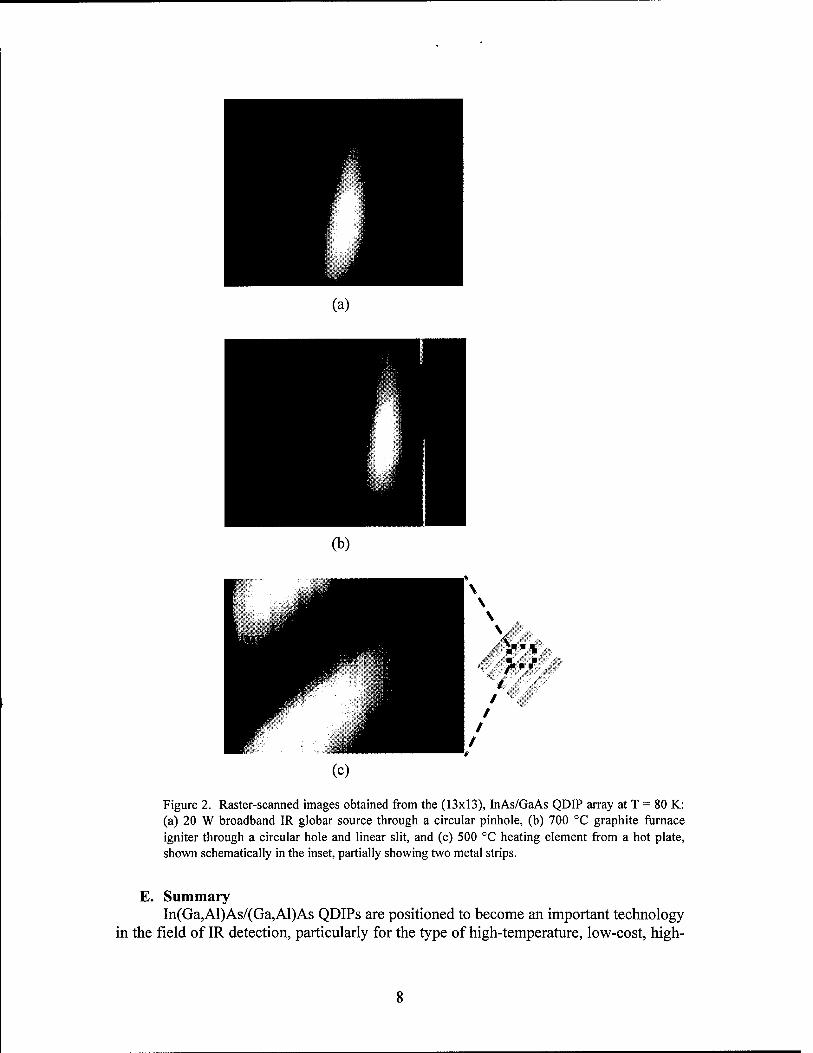
b. Raster-Scan Imaging using a (13x13) QDIP Array In an effort to demonstrate imaging using InAs/GaAs QDIPs, a raster-scan
imaging system was developed in which the field-of-view was scanned simultaneously in the X- and y-axes by a raster scan motion provided by two mirrors. An array of photocurrent/voltage values was compiled as the field-of-view array elements were scanned either by a small, interconnected detector array. In this way, IR imaging with InAs/GaAs QDIPs was demonstrated using a raster scanning technique. A small array was used in the imaging system because it permitted the collection of IR light more easily due to the larger optical area. In addition, the average photocurrent from the array was larger, and therefore, easier to distinguish from background noise. Standard photolithography and wet-etch processing were used to fabricate (9x9) and (13x13) non-

addressable (interconnected) arrays of QDIP pixels using as-grown, InAs/GaAs QDIP material. The pixel diameter was 40 |im, and the array pitch was 120 |im. An SEM image of an interconnected, (9x9) QDIP array is shown in Fig. 1. The entire array has a single top contact and a single bottom contact for all of the pixels, effectively behaving as a single detector with a very large optical area and generating a single photocurrent
S^,^:"-?^- ; ••
iM&?-^.S?:
S'
;, ..'.«:■
C. ^ '' "' -* SI mm Ml .::.'..■;■■.
:«i..ai«i:'.«i;<i.< S"«itt'iii'5''
S.'S.S.S'SJ
^■■^'j-'f'..
'«l;«i.«i «ic.«i<i oi'
-ci'iGi «i;'4B'tttm«i«<■ *;ii:i ..■•■'.,
L1..'.J-'A, ..^^ ..—y t..t#«A.>
Figure 1. Scanning electron microscopy image of a (9x9), interconnected, InAs/GaAs QDIP array. A similar, (13x13) InAs/GaAs QDIP array was used for raster-scan imaging.
The (13x13) QDIP array, with which the imaging experiments were conducted, was housed in a cryostat with a KRS-5 entrance window and held at a temperature of 80 K. The resolution of images obtained by this raster scan technique was determined by the incremental motion of the two scanning mirrors, as well as the integration time (time constant) of the lock-in amplifier. All of the objects imaged were placed directly in front of the XY mirror bracket, at 90 ° to the QDIP array and no more than 40 cm away from the mirror bracket entrance window. The images that were obtained are shown in Fig. 2. Figure 2(a) shows the image of a 20 W broadband IR globar source through a circular pinhole with a diameter of approximately 2 cm. Figure 2(b) is the image of a 700 °C furnace igniter shielded by an aluminum block with a 1 cm diameter circular pinhole and a linear slit. There is some distortion present because the computer program used to display the images treats each array element as a rectangle, whereas the image array is actually square. Figure 2(c) depicts the partial image, in this case limited by the field-of- view of the scanning mirrors, of the heating element of a hot plate at 500 °C. Portions of the heated strips (schematically shown in the inset) are seen as the bright regions. The width of each metal strip is 2 cm with a 1.5 cm space between strips. All three images were obtained at different distances from the QDIP array, thus size comparisons cannot be made from image to image. These results indicate that, with progressive improvement of device performance, QDIPs should be applicable to IR imaging FPAs.
(a)
(b)
Figure 2. Raster-scanned images obtained from the (13x13), InAs/GaAs QDIP array at T = 80 K: (a) 20 W broadband IR globar source through a circular pinhole, (b) 700 °C graphite furnace igniter through a circular hole and linear slit, and (c) 500 °C heating element from a hot plate, shown schematically in the inset, partially showing two metal strips.
E. Summary In(Ga,Al)As/(Ga,Al)As QDIPs are positioned to become an important technology
in the field of IR detection, particularly for the type of high-temperature, low-cost, high-

yield detector arrays required for the military and other highly sophisticated applications. This research has advanced the state-of-the-art in QDIP performance, demonstrating that it is reasonable to incorporate these devices into a FPA operating at 150 K for MWIR detection. These improvements have been achieved by investigating several significant areas of QDIP operation to obtain a complete picture of the many different factors that affect detector performance: i) MBE growth ofQDsfor increased absorption of IR light, ii) design, fabrication, and characterization of state-of-the-art, discrete QDIPs operating at elevated temperatures, and Hi) the characterization of small QDIP array properties.
7. Interactions with ARO and other DOD Personnel:
• Collaboration with Steve Kennerly at the Army Research Laboratory in order to characterize our QDIPs.
8. Technology Transfer/Initiatives:
• Collaboration with the Infrared Focal Planes and Photonics Technology Group at the NASA Jet Propulsion Laboratory for the fabrication of a QDIP FPA.
9. Report of Inventions: None.
10. Scientific Personnel (Honors/Awards/Degrees Received):
• Sanjay Krishna, Ph.D. in Applied Physics, 2001.
• P. Bhattacharya, Nick Holonyak, Jr. Award from the Optical Society of America, 2002.
• Pallab Bhattacharya, Quantum Devices Award from the International Symposium on Compound Semiconductors for Pioneering Contributions to MBE and Applications of III-V Heterostructure Electronic and Optoelectronic Devices, 2003.
• Adrienne D. Stiff-Roberts, Ph.D. in Applied Physics, 2004.
11. List of Manuscripts:
1. "High-detectivity, normal-incidence, mid-infrared (~ 4 |im) InAs/GaAs quantum-dot detector operating at 150 K", A. D. Stiff, S. Krishna, P. Bhattacharya, and S. Kennerly, Applied Physics Letters, 79, pp. 421-423, 2001.
2. "Normal-incidence, high-temperature, mid-infrared, InAs/GaAs vertical quantum-dot infrared photodetector", A. D. Stiff, S. Krishna, P.

Bhattacharya, and S. Kennerly, IEEE Journal of Quantum Electronics, 37, pp. 1412-1419,2001.
3. "Hot Dot Detectors: Infrared quantum dot intersubband photodetectors are a promising technology for multiwavelength IR detection," S. Krishna, A. D. Stiff-Roberts, J. D. Phillips, P. Bhattacharya, and S. W. Kennerly, IEEE Circuits &Devices Magazine, 18, pp. 14-24, 2002.
4. "Low-bias, high-temperature performance of a normal-incidence InAs/GaAs vertical quantum dot infrared photodetector with a current-blocking barrier," A. Stiff-Roberts, S. Krishna, P. Bhattacharya, and S. Kennerly, Journal of Vacuum Science & Technology B, 20, pp. 1185-1187, 2002.
5. "Raster-scan imaging with normal-incidence, mid-infrared InAs/GaAs quantum dot infrared photodetectors," A. D. Stiff-Roberts, S. Chakrabarti, S. Pradhan, B. Kochman, and P. Bhattacharya, Applied Physics Letters, 80, pp. 3265-3267, 2002.
6. "Quantum Dot Long-Wavelength Detectors," P. Bhattacharya, A. D. Stiff Roberts, S. Krishna, and S. Kennerly, Materials Research Society Symposium Proceedings, 692, pp. 109-116,2002.
7. "Quantum dot infrared detectors and sources," P. Bhattacharya, A. D. Stiff- Roberts, S. Krishna, and S. Kennerly, International Journal of High Speed Electronics and Systems, 12, pp. 969-994, 2002.
8. "High responsivity AlAs/InAs/GaAs superlattice quantum dot infrared photodetector," S. Chakrabarti, A. D. Stiff-Roberts, P. Bhattacharya, and S. W. Keimerly, Electronics Letters, accepted for publication, 2004.
9. "Contribution of field-assisted tunneling emission to dark current in InAs/GaAs quantum dot infrared photodetectors," A. D. Stiff-Roberts, X. H. Su, S. Chakrabarti, and P. Bhattacharya, IEEE Photonics Technology Letters, 16, pp. 867-869, 2004.
1 0. "High-temperature operation of InAs/GaAs quantum dot infrared photodetectors with large responsivity and detectivity," S. Chakrabarti, A. D. Stiff-Roberts, P. Bhattacharya, S. Gunapala, S. Bandara, S. B. Rafol, and S. W. Kennerly, IEEE Photonics Technology Letters, to be published, 2004.
11. "Quantum dot infrared photodetector," J. Phillips, A. D. Stiff-Roberts, and P. Bhattacharya, Encyclopedia on Nanoscience and Nanotechnology, 9, pp. 131-141,2004.
12. "Quantum dot opto-electronic devices," P. Bhattacharya, S. Ghosh, and A. D. Stiff-Roberts, Annual Review of Materials Research, in press, 2004.
10

13. "Heterostructures for achieving large responsivity in InAs/GaAs quantum dot infrared photodetectors," S. Chakrabarti, A. D. Stiff-Roberts, P. Bhattacharya, and S. Kennerly, Journal of Vacuum Science and Technology B, accepted for publication, April 2004.
14. "Novel quantum dot infrared photodetector design based on double-barrier resonant tunneling," X. H. Su, S. Chakrabarti. A. D. Stiff-Roberts, J. Singh, and P. Bhattacharya, submitted to Electronics Letters, April 2004.
12. Conferences:
1. "High-temperature operation of mid-infrared (k = 4-5 |xm) vertical and lateral InAs/GaAs/AlGaAs quantum dot infrared photodetectors", A. Stiff, S. Krishna, P. Bhattacharya, and S. Kermerly, Device Research Conference, Notre Dame, IN, June 2001.
2. "The carrier relaxation bottleneck in quantum dots and its importance in the realization of quantum dot intersubband detectors and lasers", P. Bhattacharya, S. Krishna, T. Norris, J. Urayama, J. Singh, P. J. McCann, and K. Namjou, ICMAT, Singapore, Japan, July 2001.
3. "Low-bias, high-temperature performance of a normal-incidence InAs/GaAs vertical quantum dot infrared photodetector with a current-blocking barrier", A. Stiff-Roberts, S. Krishna, P. Bhattacharya, and S. Kennerly, North American Conference on Molecular Beam Epitaxy, Providence, RI, October 2001.
4. "Quantum dot long-wavelength detectors", (INVITED), P. Bhattacharya, Materials Research Society Fall Meeting, Boston, MA, November 2001.
5. "Quantum Dot Infrared Photodetectors," (INVITED) P. Bhattacharya, A. Stiff-Roberts, S. Krishna, and S. Kennerly, International Society for Optical Engineering (SPIE) Photonics West Meeting, San Jose, CA, January 2002.
6. "Quantum Dot Inter-sublevel Transition-Based Devices," (INVITED) P. Bhattacharya, A. Stiff-Roberts, S. Chakrabarti, S. Kennerly, and S. Krishna, Nano-Optoelectronics Workshop, Berlin, Germany, July 2002.
7. "Carrier dynamics in self-organized In(Ga)As/Ga(Al)As quantum dots and their application to long-wavelength sources and detectors," (INVITED) P. Bhattacharya, 29"^ International Symposium on Compound Semiconductors, Lausanne, Switzerland, October 2002.
8. "Carrier Dynamics in Self-Organized Quantum Dots and Their Application to Infrared Detectors and Sources," P. Bhattacharya, American Physical Society Meeting, Austin, TX, March 2003.
11

9. "High-responsivity, polarization-sensitive, 70-layer InAs/GaAs quantum dot infrared photodetector," A. D. Stiff-Roberts, S. Chakrabarti, S. Kennerly, and P. Bhattacharya, Conference on Lasers and Electro-Optics, Baltimore, MD, June 2003.
10. "Heterostructures for Achieving Very Large Responsivity in InAs/GaAs Quantum Dot Infrared Photodetectors," S. Chakrabarti, A. D. Stiff-Roberts, P. Bhattacharya, and S. Kennerly, North American Conference on Molecular Beam Epitaxy, Keystone, CO, September 2003.
11. "Quantum Dot Infrared Photodetectors (QDIPs)," P. Bhattacharya, Army Research Office Infrared Physics Workshop, Ann Arbor, MI, September 2003.
12. "Tailoring of Quantum Dot Infrared Photodetector Performance with AlAs/GaAs Superlattice Barriers," A. D. Stiff-Roberts, S. Chakrabarti, P. Bhattacharya, and S. Keimerly, Lasers and Electro-Optics Society Meeting, Tucson, AZ, October 2003.
13. "Self-Organized Semiconductor Quantum Dots and Their Application to Optoelectronic Devices," P. Bhattacharya, Frontiers in Nanoscience and Nanotechnology, Ann Arbor, MI, November 2003.
12