具有立体声 ADC 和路由功能的 PCM9211 216kHz 数字音频 ...
133
具有 立体声 ADC 和路由功能的 PCM9211 216kHz 数字音频接口收发器 (DIX) 1 特性 • 集成了 DIX、ADC 和信号路由: – 异步操作(DIR、DIT、ADC) – PCM 数据多路复用和路由: • I 2 S、左平衡、右平衡 – 通用输入/输出引脚 • 数字音频接口接收器 (DIR): – 24 位,可支持 216kHz 的频率 – 50ps 超低抖动 –非 PCM 检测(IEC61937、DTS-CD/LD) – 12 个 S/PDIF 输入端口: • 2 个同轴 S/PDIF 输入 • 10 个光纤 S/PDIF 输入 • 数字音频接口发送器 (DIT): – 24 位,可支持 216kHz 的频率 – 24 位数据长度 – 48 位通道状态缓冲器 – 同步和异步操作 • 模数转换器 (ADC): – 24 位,可支持 96kHz 的频率 – 动态范围:101dB (f S = 96kHz) – 同步、异步操作 • 路由功能: – 输入:3 个 PCM、1 个 DIR、1 个 ADC – 输出:主输出、辅助输出、DIT – 多通道(8 通道)PCM 路由 • 其他功能特性: – 关断(引脚和寄存器控制) – PCM 端口采样频率计数器 – GPIO 和 GPO – 适用于外部晶振的 OSC (24.576MHz) – SPI、I 2 C 或硬件控制模式 • 电源: – 3.3V(2.9V 至 3.6V)DIX 全数字电源 – 5V(4.5V 至 5.5V)ADC 模拟电源 • 工作温度:–40°C 至 +85°C • 封装:48 管脚 LQFP 2 应用 • 家庭影院和 AVR 设备 • 电视和智能条形音箱 • 高性能声卡 3 说明 PCM9211 是一个完整的模拟和数字前端,适用于当今 的多媒体播放器、条形音箱和录音机。 PCM9211 集成了立体声 ADC、S/PDIF 收发器(具有 多达 12 个多路复用输入)和 3 个 PCM 输入,这些 PCM 输入支持对其他音频接收器进行多路复用且提供 到数字信号处理器的模拟和 S/PDIF 信号。 器件信息 (1) 器件型号 封装 封装尺寸(标称值) PCM9211 LQFP (48) 7.00mm × 7.00mm (1) 要了解所有可用封装,请参阅数据表末尾的封装选项附录。 BT Module PCM9211 x2 DSP OUT PCM DSP x6 IN IN LINE IN DSP PCM x3 GPIO/INT I2C x2 IN HDMI ARC S/PDIF S/PDIF S/PDIF 简化版应用示意图 PCM9211 ZHCSIM2D – JUNE 2010 – REVISED AUGUST 2021 本文档旨在为方便起见,提供有关 TI 产品中文版本的信息,以确认产品的概要。有关适用的官方英文版本的最新信息,请访问 www.ti.com,其内容始终优先。TI 不保证翻译的准确性和有效性。在实际设计之前,请务必参考最新版本的英文版本。 English Data Sheet: SBAS495
-
Upload
khangminh22 -
Category
Documents
-
view
1 -
download
0
Transcript of 具有立体声 ADC 和路由功能的 PCM9211 216kHz 数字音频 ...

具有立体声 ADC 和路由功能的 PCM9211 216kHz 数字音频接口收发器 (DIX)
1 特性
• 集成了 DIX、ADC 和信号路由:– 异步操作(DIR、DIT、ADC)– PCM 数据多路复用和路由:
• I2S、左平衡、右平衡
– 通用输入/输出引脚
• 数字音频接口接收器 (DIR):– 24 位,可支持 216kHz 的频率
– 50ps 超低抖动
– 非 PCM 检测(IEC61937、DTS-CD/LD)– 12 个 S/PDIF 输入端口:
• 2 个同轴 S/PDIF 输入
• 10 个光纤 S/PDIF 输入
• 数字音频接口发送器 (DIT):– 24 位,可支持 216kHz 的频率
– 24 位数据长度
– 48 位通道状态缓冲器
– 同步和异步操作• 模数转换器 (ADC):
– 24 位,可支持 96kHz 的频率
– 动态范围:101dB (fS = 96kHz)– 同步、异步操作
• 路由功能:– 输入:3 个 PCM、1 个 DIR、1 个 ADC– 输出:主输出、辅助输出、DIT– 多通道(8 通道)PCM 路由
• 其他功能特性:– 关断(引脚和寄存器控制)– PCM 端口采样频率计数器
– GPIO 和 GPO– 适用于外部晶振的 OSC (24.576MHz)– SPI、I2C 或硬件控制模式
• 电源:– 3.3V(2.9V 至 3.6V)DIX 全数字电源
– 5V(4.5V 至 5.5V)ADC 模拟电源
• 工作温度:–40°C 至 +85°C• 封装:48 管脚 LQFP
2 应用
• 家庭影院和 AVR 设备
• 电视和智能条形音箱• 高性能声卡
3 说明
PCM9211 是一个完整的模拟和数字前端,适用于当今
的多媒体播放器、条形音箱和录音机。
PCM9211 集成了立体声 ADC、S/PDIF 收发器(具有
多达 12 个多路复用输入)和 3 个 PCM 输入,这些
PCM 输入支持对其他音频接收器进行多路复用且提供
到数字信号处理器的模拟和 S/PDIF 信号。
器件信息(1)
器件型号 封装 封装尺寸(标称值)PCM9211 LQFP (48) 7.00mm × 7.00mm
(1) 要了解所有可用封装,请参阅数据表末尾的封装选项附录。
BT Module
PCM9211
x2
DSP
OUT
PCM
DSPx6
IN
IN
LINE
IN
DSP
PCM x3
GPIO/INT
I2C
x2
IN
HDMI
ARCS/PDIF
S/PDIF
S/PDIF
简化版应用示意图
PCM9211ZHCSIM2D – JUNE 2010 – REVISED AUGUST 2021
本文档旨在为方便起见,提供有关 TI 产品中文版本的信息,以确认产品的概要。有关适用的官方英文版本的最新信息,请访问
www.ti.com,其内容始终优先。TI 不保证翻译的准确性和有效性。在实际设计之前,请务必参考最新版本的英文版本。English Data Sheet: SBAS495

Table of Contents1 特性................................................................................... 12 应用................................................................................... 13 说明................................................................................... 14 Revision History.............................................................. 25 Pin Configuration and Functions...................................36 Specifications.................................................................. 5
6.1 Absolute Maximum Ratings........................................ 56.2 ESD Ratings............................................................... 56.3 Recommended Operating Conditions.........................66.4 Thermal Information....................................................66.5 Electrical Characteristics: General..............................66.6 Electrical Characteristics: Analog-to-Digital
Converter (ADC)............................................................86.7 Electrical Characteristics: Digital Audio I/F
Receiver (DIR)...............................................................96.8 Timing Requirements................................................106.9 Typical Characteristics: ADC.................................... 126.10 Typical Characteristics: ADC Internal Filter............ 136.11 Typical Characteristics: ADC Output Spectrum...... 14
7 Detailed Description......................................................167.1 Overview................................................................... 16
7.2 Functional Block Diagram......................................... 177.3 Feature Description...................................................187.4 Device Functional Modes..........................................537.5 Register Maps...........................................................61
8 Application and Implementation................................ 1198.1 Application Information............................................1198.2 Typical Application.................................................. 121
9 Power Supply Recommendations..............................12210 Layout.........................................................................123
10.1 Layout Guidelines................................................. 12310.2 Layout Example.................................................... 124
11 Device and Documentation Support........................12511.1 Documentation Support........................................ 12511.2 接收文档更新通知................................................. 12511.3 支持资源................................................................12511.4 Trademarks........................................................... 12511.5 Electrostatic Discharge Caution............................ 12511.6 术语表................................................................... 125
12 Mechanical, Packaging, and Orderable Information.................................................................. 125
4 Revision History注:以前版本的页码可能与当前版本的页码不同
Changes from Revision C (February 2020) to Revision D (August 2021) Page• 更新了整个文档中的表格、图和交叉参考的编号格式......................................................................................... 1• Changed AUTO Source Selector Cause Setting Register to match Register Map table..................................68
Changes from Revision B (August 2018) to Revision C (February 2020) Page• 删除了文档中的 HDMI 2.1 eARC 兼容特性........................................................................................................ 1• 添加了指向应用 部分的链接................................................................................................................................1• Changed bit 0 from RSV to MADLVL1 in bit register of INT1 Output Cause Mask Setting Register section... 73• Changed AUXIN2 bit setting from 100 to 101 in DIT Function Control Register 1/3 section............................94• Changed title of bit register from MPIO_C1, MPIO_C0 Output Flag Select Register to MPIO_C3, MPIO_C2
Output Flag Select Register in MPIO_C3, MPIO_C2 Output Flag Select Register section............................ 111• Changed title of bit register from MPIO_C1, MPIO_C0 Output Flag Select Register to MPO1, MPO0 Output
Flag Select Register in MPO1, MPO0 Function Assign Setting Register section...........................................112
PCM9211ZHCSIM2D – JUNE 2010 – REVISED AUGUST 2021 www.ti.com.cn
2 Submit Document Feedback Copyright © 2021 Texas Instruments Incorporated
Product Folder Links: PCM9211

5 Pin Configuration and Functions
48
VIN
R1
3M
PIO
_B
2
1ERROR/INT0 36 VDDRX
47
VIN
L1
4M
PIO
_B
3
2NPCM/INT1 35 RXIN1
46
VC
CA
D1
5M
PO
0
3MPIO_A0 34 RST
45
AG
ND
AD
16
MP
O1
4MPIO_A1 33 RXIN2
44
VC
OM
17
DO
UT
5MPIO_A2 32 RXIN3
43
FIL
T1
8L
RC
K
6MPIO_A3 31 RXIN4/ASCKI0
42
VC
C1
9B
CK
7MPIO_C0 30 RXIN5/ABCKI0
41
AG
ND
20
SC
KO
8MPIO_C1 29 RXIN6/ALRCKI0
40
XT
O2
1D
GN
D
9MPIO_C2 28 RXIN7/ADIN0
39
XT
I2
2D
VD
D
10MPIO_C3 27 MODE
38
GN
DR
X2
3M
DO
/AD
R0
11MPIO_B0 26 MS/ADR1
37
RX
IN0
24
MD
I/S
DA
12MPIO_B1 25 MC/SCL
Not to scale
图 5-1. PT Package, 48-Pin LQFP (Top View)
表 5-1. Pin FunctionsPIN
I/O 5-V TOLERANT DESCRIPTION
NO. NAME1 ERROR/INT0 O No DIR error detection output / interrupt 0 output
2 NPCM/INT1 O No DIR non-PCM detection output / interrupt 1 output
3 MPIO_A0 I/O Yes Multipurpose I/O, group A(1)
4 MPIO_A1 I/O Yes Multipurpose I/O, group A(1)
5 MPIO_A2 I/O Yes Multipurpose I/O, group A(1)
6 MPIO_A3 I/O Yes Multipurpose I/O, group A(1)
7 MPIO_C0 I/O Yes Multipurpose I/O, group C(1)
8 MPIO_C1 I/O Yes Multipurpose I/O, group C(1)
9 MPIO_C2 I/O Yes Multipurpose I/O, group C(1)
10 MPIO_C3 I/O Yes Multipurpose I/O, group C(1)
11 MPIO_B0 I/O Yes Multipurpose I/O, group B(1)
12 MPIO_B1 I/O Yes Multipurpose I/O, group B(1)
13 MPIO_B2 I/O Yes Multipurpose I/O, group B(1)
www.ti.com.cnPCM9211
ZHCSIM2D – JUNE 2010 – REVISED AUGUST 2021
Copyright © 2021 Texas Instruments Incorporated Submit Document Feedback 3
Product Folder Links: PCM9211

表 5-1. Pin Functions (continued)PIN
I/O 5-V TOLERANT DESCRIPTION
NO. NAME14 MPIO_B3 I/O Yes Multipurpose I/O, group B(1)
15 MPO0 O No Multipurpose output 0
16 MPO1 O No Multipurpose output 1
17 DOUT O No Main output port, serial digital audio data output
18 LRCK O No Main output port, LR clock output
19 BCK O No Main output port, bit clock output
20 SCKO O No Main output port, system clock output
21 DGND – – Ground, for digital
22 DVDD – – Power supply, 3.3 V (typ), for digital
23 MDO/ADR0 I/O Yes Software control I/F, SPI data output / I2C slave address setting 0(1)
24 MDI/SDA I/O Yes Software control I/F, SPI data input / I2C data input/output(1) (4)
25 MC/SCL I Yes Software control I/F, SPI clock input / I2C clock input(1)
26 MS/ADR1 I Yes Software control I/F, SPI chip select / I2C slave address setting 1(1)
27 MODE I No Control mode setting, (see the Serial Control Mode section, control mode pin setting)
28 RXIN7/ADIN0 I Yes Biphase signal, input 7 / AUXIN0, serial audio data input(1)
29 RXIN6/ALRCKI0 I Yes Biphase signal, input 6 / AUXIN0, LR clock input(1)
30 RXIN5/ABCKI0 I Yes Biphase signal, input 5 / AUXIN0, bit clock input(1)
31 RXIN4/ASCKI0 I Yes Biphase signal, input 4 / AUXIN0, system clock input(1)
32 RXIN3 I Yes Biphase signal, input 3(1)
33 RXIN2 I Yes Biphase signal, input 2(1)
34 RST I Yes Reset input, active low(1) (2)
35 RXIN1 I Yes Biphase signal, input 1, built-in coaxial amplifier
36 VDDRX – – Power supply, 3.3 V (typ.), for RXIN0 and RXIN1.
37 RXIN0 I Yes Biphase signal, input 0, built-in coaxial amplifier
38 GNDRX - - Ground, for RXIN
39 XTI I No Oscillation circuit input for crystal resonator or external XTI clock source input(3)
40 XTO O No Oscillation circuit output for crystal resonator
41 AGND – – Ground, for PLL analog
42 VCC – – Power supply, 3.3 V (typ), for PLL analog
43 FILT O No External PLL loop filter connection terminal; must connect recommended filter
44 VCOM O No ADC common voltage output; must connect external decoupling capacitor
45 AGNDAD – – Ground, for ADC analog
46 VCCAD – – Power supply, 5.0 V (typ), for ADC analog
47 VINL I No ADC analog voltage input, left channel
48 VINR I No ADC analog voltage input, right channel
(1) Schmitt trigger input.(2) Onboard pulldown resistor (50 kΩ, typical).(3) CMOS Schmitt trigger input.(4) Open-drain configuration in I2C mode.
PCM9211ZHCSIM2D – JUNE 2010 – REVISED AUGUST 2021 www.ti.com.cn
4 Submit Document Feedback Copyright © 2021 Texas Instruments Incorporated
Product Folder Links: PCM9211
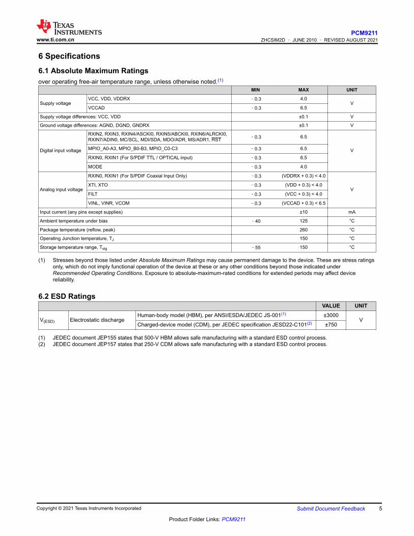
6 Specifications6.1 Absolute Maximum Ratingsover operating free-air temperature range, unless otherwise noted.(1)
MIN MAX UNIT
Supply voltageVCC, VDD, VDDRX –0.3 4.0
VVCCAD –0.3 6.5
Supply voltage differences: VCC, VDD ±0.1 V
Ground voltage differences: AGND, DGND, GNDRX ±0.1 V
Digital input voltage
RXIN2, RXIN3, RXIN4/ASCKI0, RXIN5/ABCKI0, RXIN6/ALRCKI0, RXIN7/ADIN0, MC/SCL, MDI/SDA, MDO/ADR, MS/ADR1, RST –0.3 6.5
VMPIO_A0-A3, MPIO_B0-B3, MPIO_C0-C3 –0.3 6.5
RXIN0, RXIN1 (For S/PDIF TTL / OPTICAL input) –0.3 6.5
MODE –0.3 4.0
Analog input voltage
RXIN0, RXIN1 (For S/PDIF Coaxial Input Only) –0.3 (VDDRX + 0.3) < 4.0
VXTI, XTO –0.3 (VDD + 0.3) < 4.0
FILT –0.3 (VCC + 0.3) < 4.0
VINL, VINR, VCOM –0.3 (VCCAD + 0.3) < 6.5
Input current (any pins except supplies) ±10 mA
Ambient temperature under bias –40 125 °C
Package temperature (reflow, peak) 260 °C
Operating Junction temperature, TJ 150 °C
Storage temperature range, Tstg –55 150 °C
(1) Stresses beyond those listed under Absolute Maximum Ratings may cause permanent damage to the device. These are stress ratings only, which do not imply functional operation of the device at these or any other conditions beyond those indicated under Recommended Operating Conditions. Exposure to absolute-maximum-rated conditions for extended periods may affect device reliability.
6.2 ESD RatingsVALUE UNIT
V(ESD) Electrostatic dischargeHuman-body model (HBM), per ANSI/ESDA/JEDEC JS-001(1) ±3000
VCharged-device model (CDM), per JEDEC specification JESD22-C101(2) ±750
(1) JEDEC document JEP155 states that 500-V HBM allows safe manufacturing with a standard ESD control process.(2) JEDEC document JEP157 states that 250-V CDM allows safe manufacturing with a standard ESD control process.
www.ti.com.cnPCM9211
ZHCSIM2D – JUNE 2010 – REVISED AUGUST 2021
Copyright © 2021 Texas Instruments Incorporated Submit Document Feedback 5
Product Folder Links: PCM9211

6.3 Recommended Operating Conditionsover operating free-air temperature range (unless otherwise noted)
MIN NOM MAX UNIT
DIR analog supply voltage, VCC 2.9 3.3 3.6 V
ALL digital supply voltage, VDD 2.9 3.3 3.6 V
ADC analog supply voltage, VCCAD 4.5 5.0 5.5 V
Coaxial amplifier supply voltage, VDDRX 2.9 3.3 3.6 V
Digital input interface level TTL-compatible
Digital input/output clock frequency
DIR, DIT, and Routing sampling frequency 7 216 kHz
DIR, DIT, and Routing system clock frequency 0.896 55.296 MHz
ADC sampling frequency 16 96 kHz
ADC system clock frequency 2.048 24.576 MHz
XTI input clock frequency 24.576 MHz
Analog input level VINL, VINR 3 VPP
Digital output load capacitance Except SCKO 20 pF
Digital output load capacitance SCKO 10 pF
MODE pin capacitance 10 pF
Operating free-air temperature –40 25 85 °C
6.4 Thermal Information
THERMAL METRIC(1)
PCM9211UNITPT (LQFP)
48 PINSRθJA Junction-to-ambient thermal resistance 64.5 °C/W
RθJC(top) Junction-to-case (top) thermal resistance 19.6 °C/W
RθJB Junction-to-board thermal resistance 60.1 °C/W
ψJT Junction-to-top characterization parameter 0.8 °C/W
ψJB Junction-to-board characterization parameter 29.7 °C/W
RθJC(bot) Junction-to-case (bottom) thermal resistance N/A °C/W
(1) For more information about traditional and new thermal metrics, see the Semiconductor and IC package thermal metrics application report.
6.5 Electrical Characteristics: GeneralAll specifications at TA = 25°C, VCC = VDD = VDDRX = 3.3 V, and VCCAD = 5 V, unless otherwise noted.
PARAMETER TEST CONDITIONS(1) MIN TYP MAX UNIT
DIGITAL I/O—DATA FORMAT
Audio data interface format I2S, left-justified, right-justified
Audio data word length 16, 24 Bits
Audio data format MSB first, twos complement
fS Sampling frequency
DIR 7 216
kHzDIT 7 216
Routing 7 216
ADC 16 96
DIGITAL I/O—INPUT LOGIC
VIH Input logic level, high(2) (3) 2.0 5.5 VDC
VIL Input logic level, low(2) (3) 0.8 VDC
VIH Input logic level, high (XTI pin)(4) 0.7 VCC VCC VDC
VIL Input logic level, low (XTI pin)(4) 0.3 VCC VDC
PCM9211ZHCSIM2D – JUNE 2010 – REVISED AUGUST 2021 www.ti.com.cn
6 Submit Document Feedback Copyright © 2021 Texas Instruments Incorporated
Product Folder Links: PCM9211

6.5 Electrical Characteristics: General (continued)All specifications at TA = 25°C, VCC = VDD = VDDRX = 3.3 V, and VCCAD = 5 V, unless otherwise noted.
PARAMETER TEST CONDITIONS(1) MIN TYP MAX UNIT
VIHInput logic level, high (RXIN0/1 pins)(5) 0.7 VDDRX VDDRX VDC
VILInput logic level, low (RXIN0/1 pins)(5) 0.3 VDDRX VDC
IIH Input logic current, high(2) (4) VIN = VDD or VCC ±10 μA
IIL Input logic current, low(2) (4) VIN = 0 V ±10 μA
IIH Input logic current, high ( RST pin)(3) VIN = VDD 65 100 μA
IIL Input logic current, low ( RST pin)(3) VIN = 0 V ±10 μA
IIHInput logic current, high (RXIN0/1 pins)(5) VIN = VDDRX 165 300 μA
IILInput logic current, low (RXIN0/1 pins)(5) VIN = 0 V –165 –300 μA
DIGITAL I/O—OUTPUT LOGIC
VOH Output logic level, high(6) IOUT = –4 mA 2.8 VDC
VOL Output logic level, low(6) IOUT = 4 mA 0.5 VDC
VOH Output logic level, high(7) IOUT = –4 mA 0.85 VCC VDC
VOL Output logic level, low(7) IOUT = 4 mA 0.15 VCC VDC
POWER-SUPPLY REQUIREMENTS
VCC Voltage range 2.9 3.3 3.6 VDC
VDD Voltage range 2.9 3.3 3.6 VDC
VCCAD Voltage range 4.5 5.0 5.5 VDC
VDDRX Voltage range 2.9 3.3 3.6 VDC
ICC Supply current
fS = 48 kHz / DIR, fS = 48 kHz / ADC, fS = 48 kHz / DIT 4.5mA
fS = 192 kHz / DIR, fS = 96 kHz / ADC, fS = 192 kHz / DIT 7 13
Full power down, RST = low 150 350 μA
IDD Supply current
fS = 48 kHz / DIR, fS = 48 kHz / ADC, fS = 48 kHz / DIT 12mA
fS = 192 kHz / DIR, fS = 96 kHz / ADC, fS = 192 kHz / DIT 26 38
Full power down, RST = low 150 350 μA
ICCAD Supply current
fS = 48 kHz / DIR, fS = 48 kHz / ADC, fS = 48 kHz / DIT 12mA
fS = 192 kHz / DIR, fS = 96 kHz / ADC, fS = 192 kHz / DIT 12
Full power down, RST = low 110 250 μA
IDDRX (8) Supply current
fS = 48 kHz / DIR, fS = 48 kHz / ADC, fS = 48 kHz / DIT 3.2mA
fS = 192 kHz / DIR, fS = 96 kHz / ADC, fS = 192 kHz / DIT 3.2 4.8
Full power down, RST = low 0 30 μA
Power dissipation
fS = 48 kHz / DIR, fS = 48 kHz / ADC, fS = 48 kHz / DIT 135
mWfS = 192 kHz / DIR, fS = 96 kHz / ADC, fS = 192 kHz / DIT 180
Full power down, RST = low 0.85
TEMPERATURE
Operating temperature –40 85 °C
RθJA Thermal resistance 100 °C/W
(1) PLL lock-up time varies with ERROR release wait time setting (Register 23h/ERRWT). Therefore, lock-up time in this table shows the value at ERRWT = 11 as the shortest time setting.
(2) Pins: MPIO_A0-A3, MPIO_B0-B3, MPIOC0-C3, RXIN2-RXIN7, MC/SCL, MDI/SDA, MDO/ADR0, MS/ADR1.(3) Pin: RST.(4) Pin: XTI.(5) Pins: RXIN0, RXIN1. Input impedance of RXIN0 and RXIN1 is 20 kΩ (typical). COAX amplifiers are powered on by Register 34h/
RX0DIS and RX1DIS = 0. At power down by Register 34h/RX0DIS and RX1DIS= 1 (default), RXIN0 and RXIN1 are internally tied high.
(6) Pins: MPIO_A0-A3, MPIO_B0-B3, MPIO_C0-C3, SCKO, BCK, LRCK, DOUT, MPO0-1, ERROR/INT0, NPCM/INT1.(7) Pin: XTO.(8) Two coaxial amplifiers are powered on by Register 34h/RX1DIS and Register 34h, RX0DIS.
www.ti.com.cnPCM9211
ZHCSIM2D – JUNE 2010 – REVISED AUGUST 2021
Copyright © 2021 Texas Instruments Incorporated Submit Document Feedback 7
Product Folder Links: PCM9211

6.6 Electrical Characteristics: Analog-to-Digital Converter (ADC)All specifications at TA = 25°C, VCC = VDD = VDDRX = 3.3 V, and VCCAD = 5 V, unless otherwise noted.
PARAMETER TEST CONDITIONS MIN TYP MAX UNITADC, CHARACTERISTICS
Resolution 16 24 Bits
fS Sampling frequency 16 96 kHz
Bit clock frequency 64fS 1.024 6.144 MHz
System clock frequency256fS 4.096 24.576
MHz512fS 8.192 24.576
ADC, ANALOG INPUTFull-scale input voltage VINL, VINR = 0 dB 0.6 VCCAD VPP
Center voltage 0.5 VCCAD V
Input Impedance 10 kΩ
Antialiasing filter response –3 dB 300 kHz
ADC, DC ACCURACYGain mismatch, channel to channel Full-scale input, VINL, VINR 2.0 ±8.0 % of FSR
Gain error Full-scale input, VINL, VINR ±2.0 ±8.0 % of FSR
Bipolar zero error HPF bypass, VINL, VINR ±0.5 ±2.0 % of FSR
ADC, DYNAMIC PERFORMANCE
THD+N VIN = –1 dBfS = 48 kHz –93 –85
dBfS = 96 kHz –93
Dynamic rangefS = 48 kHz, A-weighted 95 99
dBfS = 96 kHz, A-weighted 101
S/N ratiofS = 48 kHz, A-weighted 95 99
dBfS = 96 kHz, A-weighted 101
Channel separation(between L-ch and R-ch)
fS = 48 kHz 92 96dB
fS = 96 kHz 98
ADC, DIGITAL FILTER PERFORMANCEPassband 0.454 fS Hz
Stop band 0.583 fS Hz
Passband ripple < 0.454 fS ±0.05 dB
Stop band attenuation > 0.583 fS –65 dB
Group delay time 17.4 / fS sec
HPF frequency response –3 dB 0.019 fS/1000 Hz
ADC, COMMON VOLTAGE OUTPUTVCOM output voltage 0.5 VCCAD V
VCOM output impedance 7 12.5 18 kΩ
Allowable VCOM output source/sink current ±1 μA
PCM9211ZHCSIM2D – JUNE 2010 – REVISED AUGUST 2021 www.ti.com.cn
8 Submit Document Feedback Copyright © 2021 Texas Instruments Incorporated
Product Folder Links: PCM9211

6.7 Electrical Characteristics: Digital Audio I/F Receiver (DIR)All specifications at TA = 25°C, VCC = VDD = VDDRX = 3.3 V, and VCCAD = 5 V, unless otherwise noted.
PARAMETER TEST CONDITIONS MIN TYP MAX UNITDIR, COAXIAL INPUT AMPLIFIER (RXIN0 and RXIN1)
Input resistance 20 kΩ
Input voltage 0.15 VPP
Input hysteresis 50 mV
Input sampling frequency 7 216 kHz
DIR, BIPHASE SIGNAL INPUT and PLL
Input biphase sampling frequency rangeNormal mode 28 108
kHzWide mode 7 216
Input sampling frequency accuracy IEC60958-3 (2003-01) Level III (±12.5%)
Jitter tolerance IEC60958-3 (2003-01) IEC60958-3
PLL lock up time(1) From biphase signal detection to error out release (ERROR = L) 100 ms
DIR, RECOVERED CLOCK and DATASerial audio data width 16 24 Bits
System clock frequency
128fS 0.896 27.648
MHz256fS 1.792 55.296
512fS 3.584 55.296
Bit clock frequency 64fS 0.448 13.824 MHz
LR clock frequency fS 7 216 kHz
System clock jitter fS = 48 kHz, SCKO = 256fS, measured period jitter 50 100 ps, rms
System clock duty cycle 50% reference ±5% ±5%
DITOutput biphase sampling frequency 7 216 kHz
Input system clock frequency
128fS 0.896 27.648
MHz256fS 1.792 55.296
512fS 3.584 55.296
Input bit clock frequency 64fS 0.448 13.824 MHz
Input LR clock frequency fS 7 216 kHz
OSCILLATOR CIRCUIT, XTI and XMCKO CLOCKXTI source clock frequency 24.576 MHz
Frequency accuracy –100 100 ppm
XTI input clock duty cycle 45% 55%
XMCKO frequency 24.576 MHz
XMCKO output duty cycle 50% reference ±5% ±5%
PCM OUTPUT PORT (SCKO, BCK, LRCK, DOUT)System clock frequency 128fS / 256fS / 512fS 0.896 55.296 MHz
Bit clock output frequency 64fS 0.448 13.824 MHz
LR clock output frequency fS 7 216 kHz
ROUTINGSystem clock frequency 128fS / 256fS / 512fS 0.896 55.296 MHz
Bit clock output Frequency 64fS 0.448 13.824 MHz
LR clock output frequency fS 7 216 kHz
(1) PLL lock-up time varies with ERROR release wait time setting (Register 23h/ERRWT). Therefore, lock-up time in this table shows the value at ERRWT = 11 as the shortest time setting.
www.ti.com.cnPCM9211
ZHCSIM2D – JUNE 2010 – REVISED AUGUST 2021
Copyright © 2021 Texas Instruments Incorporated Submit Document Feedback 9
Product Folder Links: PCM9211

6.8 Timing RequirementsMIN NOM MAX UNIT
RST PIN DEVICE RESET REQUIREMENTS, 图 7-1
tRSTL RST pulse width ( RST pin = low) 1 µs
ADC SYSTEM CLOCK INPUT(1), 图 7-3
tSCY System clock cycle time 30 ns
tSCH System clock high time 0.4 tSCY ns
tSCL System clock low time 0.4 tSCY ns
System clock duty cycle 40% 60%
AUDIO DATA INTERFACE, SLAVE MODE(2), 图 7-5
tBCY BCK cycle time 75 ns
tBCH BCK high time 35 ns
tBCL BCK low time 35 ns
tLRS LRCK setup time to BCK rising edge 10 ns
tLRH LRCK hold time to BCK rising edge 10 ns
tDOD DOUT delay time from BCK falling edge 10 70 ns
AUDIO DATA INTERFACE, MASTER MODE(2), 图 7-6
tBCY BCK cycle time 1/64fStBCH BCK high time 0.4 tBCY 0.5 tBCY 0.6 tBCY
tBCL BCK low time 0.4 tBCY 0.5 tBCY 0.6 tBCY
tLRD LRCK delay time to BCK falling edge 0 30 ns
tDOD DOUT delay time from BCK falling edge 0 30 ns
LATENCY BETWEEN INPUT BIPHASE AND LRCKO/DOUT, 图 7-12
tLATE LRCKO/DOUT latency 4/fS s
DIR DECODED AUDIO DATA OUTPUT(3), 图 7-13
tSCY System clock pulse cycle time 18 ns
tCKLR Delay time of BCKO falling edge to LRCKO valid –10 10 ns
tBCY BCKO pulse cycle time 1/64fS s
tBCH BCKO pulse width high 60 ns
tBCL BCKO pulse width low 60 ns
tBCDO Delay time of BCKO falling edge to DOUT valid –10 10 ns
tR Rising time of all signals 5 ns
tF Falling time of all signals 5 ns
CONTROL INTERFACE REQUIREMENTS, FOUR WIRE SCI, 图 7-29
tMCY MC Pulse cycle time 100 ns
tMCL MC Low level time 40 ns
tMCH MC High level time 40 ns
tMHH MS High level time tMCY ns
tMSS MS Falling edge to MC rising edge 30 ns
tMSH MS Rising edge from MC rising edge for LSB 15 ns
tMDH MDI Hold time 15 ns
tMDS MDI Set-up time 15 ns
tMDD MDO Enable or delay time from MC falling edge 0 30 ns
tMDR MDO Disable time from MS rising edge 0 30 ns
PCM9211ZHCSIM2D – JUNE 2010 – REVISED AUGUST 2021 www.ti.com.cn
10 Submit Document Feedback Copyright © 2021 Texas Instruments Incorporated
Product Folder Links: PCM9211
6.8 Timing Requirements (continued)MIN NOM MAX UNIT
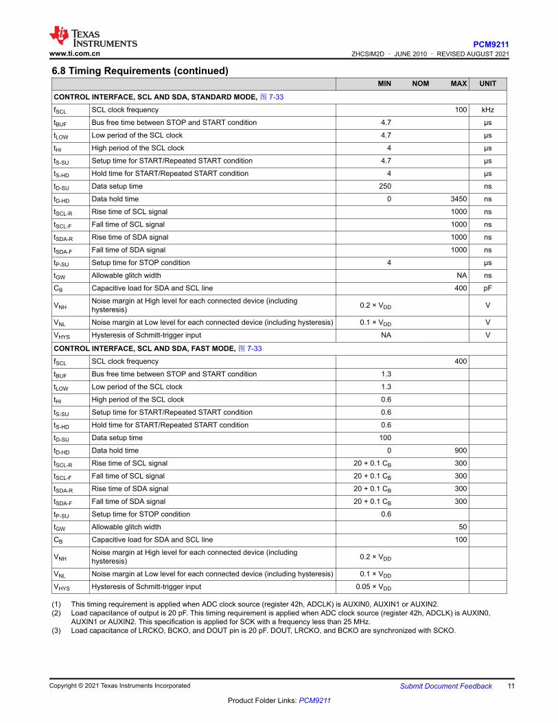
CONTROL INTERFACE, SCL AND SDA, STANDARD MODE, 图 7-33
fSCL SCL clock frequency 100 kHz
tBUF Bus free time between STOP and START condition 4.7 µs
tLOW Low period of the SCL clock 4.7 µs
tHI High period of the SCL clock 4 µs
tS-SU Setup time for START/Repeated START condition 4.7 µs
tS-HD Hold time for START/Repeated START condition 4 µs
tD-SU Data setup time 250 ns
tD-HD Data hold time 0 3450 ns
tSCL-R Rise time of SCL signal 1000 ns
tSCL-F Fall time of SCL signal 1000 ns
tSDA-R Rise time of SDA signal 1000 ns
tSDA-F Fall time of SDA signal 1000 ns
tP-SU Setup time for STOP condition 4 µs
tGW Allowable glitch width NA ns
CB Capacitive load for SDA and SCL line 400 pF
VNHNoise margin at High level for each connected device (including hysteresis) 0.2 × VDD V
VNL Noise margin at Low level for each connected device (including hysteresis) 0.1 × VDD V
VHYS Hysteresis of Schmitt-trigger input NA V
CONTROL INTERFACE, SCL AND SDA, FAST MODE, 图 7-33
fSCL SCL clock frequency 400
tBUF Bus free time between STOP and START condition 1.3
tLOW Low period of the SCL clock 1.3
tHI High period of the SCL clock 0.6
tS-SU Setup time for START/Repeated START condition 0.6
tS-HD Hold time for START/Repeated START condition 0.6
tD-SU Data setup time 100
tD-HD Data hold time 0 900
tSCL-R Rise time of SCL signal 20 + 0.1 CB 300
tSCL-F Fall time of SCL signal 20 + 0.1 CB 300
tSDA-R Rise time of SDA signal 20 + 0.1 CB 300
tSDA-F Fall time of SDA signal 20 + 0.1 CB 300
tP-SU Setup time for STOP condition 0.6
tGW Allowable glitch width 50
CB Capacitive load for SDA and SCL line 100
VNHNoise margin at High level for each connected device (including hysteresis) 0.2 × VDD
VNL Noise margin at Low level for each connected device (including hysteresis) 0.1 × VDD
VHYS Hysteresis of Schmitt-trigger input 0.05 × VDD
(1) This timing requirement is applied when ADC clock source (register 42h, ADCLK) is AUXIN0, AUXIN1 or AUXIN2.(2) Load capacitance of output is 20 pF. This timing requirement is applied when ADC clock source (register 42h, ADCLK) is AUXIN0,
AUXIN1 or AUXIN2. This specification is applied for SCK with a frequency less than 25 MHz.(3) Load capacitance of LRCKO, BCKO, and DOUT pin is 20 pF. DOUT, LRCKO, and BCKO are synchronized with SCKO.
www.ti.com.cnPCM9211
ZHCSIM2D – JUNE 2010 – REVISED AUGUST 2021
Copyright © 2021 Texas Instruments Incorporated Submit Document Feedback 11
Product Folder Links: PCM9211

6.9 Typical Characteristics: ADCAll specifications at TA = 25°C, VCCAD = 5 V, VDD = 3.3 V, fS = 48 kHz, SCK = 512fS, and 24-bit data, unless otherwise noted.
-25 0 25 50 75 100
T , Free-Air Temperature ( C)A °
-
-
-
-
-
-
88
90
92
94
96
98
100-
Tota
l H
arm
onic
Dis
tort
ion +
Nois
e (
dB
)
THD + N = 1 dB
图 6-1. Total Harmonic Distortion + Noise vs Temperature
-25 0 25 50 75 100
T , Free-Air Temperature ( C)A °
104
102
100
98
96
94
92
Dynam
ic R
ange a
nd
Sig
nal-to
-Nois
e R
atio (
dB
)
SNR
Dynamic Range
图 6-2. Dynamic Range and SNR vs Temperature
4.50 4.75 5.00 5.25
V , Supply Voltage (V)CC
-
-
-
-
-
-
88
90
92
94
96
98
100-
Tota
l H
arm
onic
Dis
tort
ion +
Nois
e (
dB
)
5.50
THD + N = 1 dB
图 6-3. Total Harmonic Distortion + Noise vs Supply Voltage
4.50 4.75 5.00 5.25
V , Supply Voltage (V)CC
5.50
104
102
100
98
96
94
92
Dynam
ic R
ange a
nd
Sig
nal-to
-Nois
e R
atio (
dB
)
SNR
Dynamic Range
图 6-4. Dynamic Range and SNR vs Supply Voltage
PCM9211ZHCSIM2D – JUNE 2010 – REVISED AUGUST 2021 www.ti.com.cn
12 Submit Document Feedback Copyright © 2021 Texas Instruments Incorporated
Product Folder Links: PCM9211
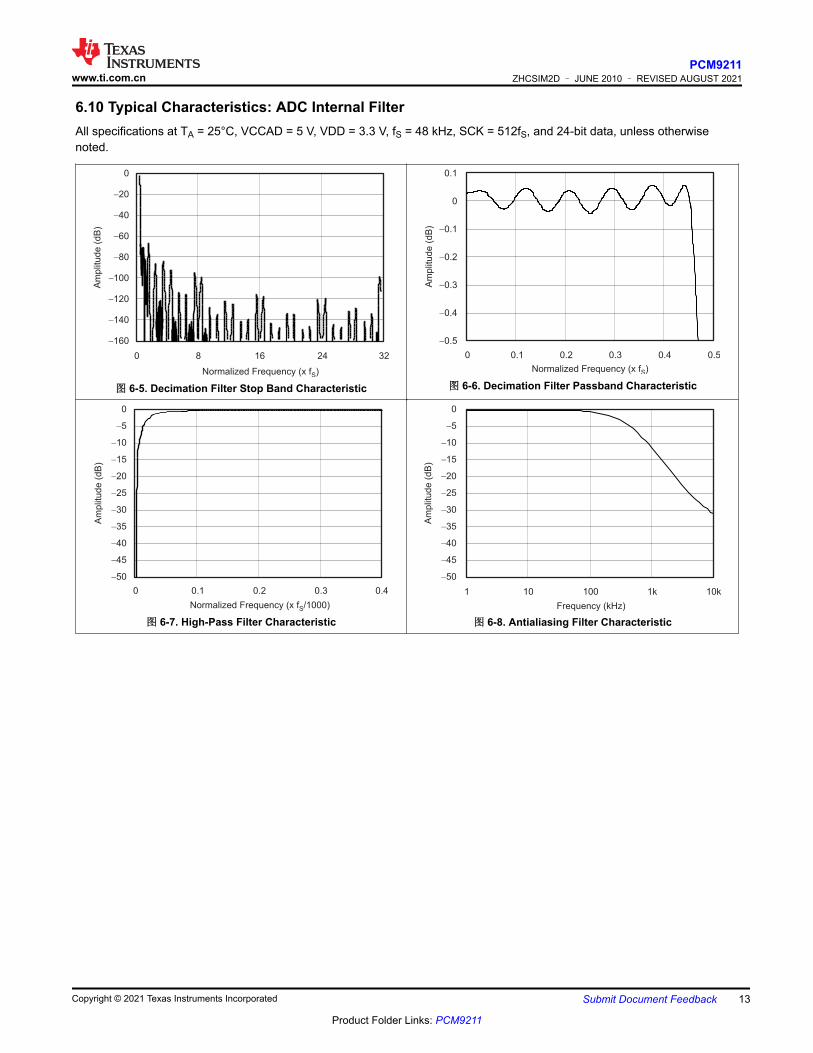
6.10 Typical Characteristics: ADC Internal FilterAll specifications at TA = 25°C, VCCAD = 5 V, VDD = 3.3 V, fS = 48 kHz, SCK = 512fS, and 24-bit data, unless otherwise noted.
Normalized Frequency (x fS)
0
20
40
60
80
100
120
140
160
-
-
-
-
-
-
-
-
0 8 16 24 32
Am
plit
ude (
dB
)
图 6-5. Decimation Filter Stop Band Characteristic
Normalized Frequency (x fS)
0.1
0
0.1
0.2
0.3
0.4
0.5
-
-
-
-
-
0 0.1 0.2 0.3 0.4 0.5
Am
plit
ude (
dB
)
图 6-6. Decimation Filter Passband Characteristic
0
5
10
15
20
25
30
35
40
45
50
-
-
-
-
-
-
-
-
-
-
Am
plit
ude (
dB
)
0 0.1 0.2 0.3 0.4
Normalized Frequency (x f /1000)S
图 6-7. High-Pass Filter Characteristic
0
5
10
15
20
25
30
35
40
45
50
-
-
-
-
-
-
-
-
-
-
Am
plit
ude (
dB
)
1 10 100 1k 10k
Frequency (kHz)
图 6-8. Antialiasing Filter Characteristic
www.ti.com.cnPCM9211
ZHCSIM2D – JUNE 2010 – REVISED AUGUST 2021
Copyright © 2021 Texas Instruments Incorporated Submit Document Feedback 13
Product Folder Links: PCM9211

6.11 Typical Characteristics: ADC Output SpectrumAll specifications at TA = 25°C, VCCAD = 5 V, VDD = 3.3 V, fS = 48 kHz, SCK = 512fS, and 24-bit data, unless otherwise noted.
0
20
40
60
80
100
120
140
-
-
-
-
-
-
-
Am
plit
ude (
dB
)
0 5 10 15 20
Frequency (kHz)
图 6-9. Output Spectrum
0 5 10 15 20
Frequency (kHz)
0
20
40
60
80
100
120
140
-
-
-
-
-
-
-
Am
plit
ude (
dB
)
–60 dB, N = 32,768
图 6-10. Output Spectrum
PCM9211ZHCSIM2D – JUNE 2010 – REVISED AUGUST 2021 www.ti.com.cn
14 Submit Document Feedback Copyright © 2021 Texas Instruments Incorporated
Product Folder Links: PCM9211

Parameter Measurement InformationAll Typical Characteristics for the devices are measured using the EVM and an Audio Precision SYS-2722 Audio Analyzer. 图 7-1 shows the PCM9211 parameter measurement circuit.
EDGE #DESIGN LEAD
PAGE INFO:TI FILENAME
DATE OF
DRAWN BY
SHEET
PCB REV
SCH REV
DRAWN BY:
OF:SHEET:
PCB REV:
SCH REV:
FILENAME:
DATE:
EDGE #:DESIGN LEAD: EDGE #DESIGN LEAD
PAGE INFO:TI FILENAME
DATE OF
DRAWN BY
SHEET
PCB REV
SCH REV
GND
J2
LEFT
RIGHT
Sh
ield
2
4
1
3
6
5 VINR
VINL
P71 2
3 4
5 6
7 8
TP13
White
C33
06030.1ufd/50V
C22
06030.1ufd/50V
75R22
RES,SMT,0603
RN3
87
65
43
21
0603x410K
RN2 12
34
56
78
0603x410K
RN1 12
34
56
78
0603x410K
P3
43
21
R21
06030.0
D40805
Yellow
R16
0603332
C19
06030.1ufd/50V
D50805
Yellow
R17
0603332
C20
06030.1ufd/50V
GND
GND
12
W5
12 W7
GND
GND
GND
GND
GND
GND
GND
GND
GND
+3.3V
GND
GND
GND
+3.3V
GND
GND
GND
GND
C37
060310pfd/100V
C36
060310pfd/100V
C41
08054700pfd/50V/2%R20
0603680
C35
060310ufd/6.3V
C34
06030.1ufd/50V
C44
060310ufd/6.3V
C42
060310ufd/6.3V
C45
06030.1ufd/50V
C43
06030.1ufd/50V
RESET~
WCLK
DOUT
BCLK
GND
W121
+5V
Y2
31
ABM1024.576 MHz Y2
4
2ABM1024.576 MHzGND
GND
C40
12060.068ufd/25V
GND
321
W13
SCLK
SCL
W14
1 2 3 MOSI
SDA
321
W12
GND
MISO
W15
1 2 3
SS~
C25
06030.1ufd/50V
20
19
18
17
16
15
14
13
12
1110
9
8
7
6
5
4
3
2
1
U9
PCF8574APWR
TSSOP20-PW
SCL
SDA
C39
060310ufd/6.3V
C38
06030.1ufd/50V
12 W4
1
2
3
4 5
6
7
8
U7
SN74LVC2G125DCTRSSOP8-DCT
GND
GND
+3.3V
MCLK
BCLK
WCLK
DIN
GND
GND
+3.3V
+3.3V
+3.3V
+3.3V+3.3V
+3.3V+3.3V
32
W8
1
R18
060310K
R19
060310K
GND
+3.3V
C21
06030.1ufd/50V
P41 2
3 4
5 6
7 8
P51 2
3 4
5 6
7 8
P61 2
3 4
5 6
7 8
1
2
3
J4
TORX147PL(F,T)
SHIELD
GND
Vcc
OUT
J5
RCA RA-FBlack
Sh
ield1
2
Signal
TP14White
SN74LVC1G04DBVR
U5
3
5 1
4
2
SOT23-DBV5
2
4
15
3
U6
SN74LVC1G04DBVRSOT23-DBV5
GND
SN74LVC244APWR
U820
19
18
17
16
15
14
13
12
1110
9
8
7
6
5
4
3
2
1
TSSOP20-PW
GND
+3.3V
C24
06030.1ufd/50V
+3.3V
GND
GND
W10
1 2 3
C26
06030.1ufd/50V
+3.3V
GND
2mm PIN HEADER
W11654321
GND
GND
GND
+3.3V
GND
+3.3V
GND
+3.3V
GND
+3.3V
U101
24
SN74LVC1G08DCKRSC70-DCK5
U111
24
SN74LVC1G08DCKRSC70-DCK5
U121
24
SN74LVC1G08DCKRSC70-DCK5
U131
24
SN74LVC1G08DCKRSC70-DCK5
U141
24
SN74LVC1G08DCKRSC70-DCK5
U151
24
SN74LVC1G08DCKRSC70-DCK5
5
3
SN74LVC1G08DCKR
U10
SC70-DCK5
Vcc
GND
U11
SN74LVC1G08DCKR
3
5
SC70-DCK5
Vcc
GND
U12
SN74LVC1G08DCKR
3
5
SC70-DCK5
Vcc
GND
U13
SN74LVC1G08DCKR
3
5
SC70-DCK5
Vcc
GND
U14
SN74LVC1G08DCKR
3
5
SC70-DCK5
Vcc
GND
U15
SN74LVC1G08DCKR
3
5
SC70-DCK5
Vcc
GND
C27
04020.1ufd/6.3V
C28
04020.1ufd/6.3V
C29
04020.1ufd/6.3V
C30
04020.1ufd/6.3V
C31
04020.1ufd/6.3V
C32
04020.1ufd/6.3V
C23
04020.1ufd/6.3V
1
2
3
J3
TOTX147PL
VCC
INPUT
GND
SHIELD
PCM9211PT
U4
48
47
46
45
44
43
42
41
40
39
38
37
36
35
34
33
32
31
30
29
28
27
26
25
24
23
22
21
20
19
18
17
16
15
14
13
12
11
10
9
8
7
6
5
4
3
2
1
LQFP48-PT
W6
21
+3.3V
10K0603
R23
GND
GND
12
W9
+3.3V
R24
060310K
GND
0603DNP
C17
C18
DNP0603
10K0603
R14
10K0603
R15
1 2W2
1 2W3
C15
10ufd/16V
AVE-A
+
AVE-A
10ufd/16V
C16
+
OPTICALMPO0-MPO1
MPIO CONNECTIONS
ERROR/NPCM& INT
FILTER COMPONENTSLOCATE CLOSE TO THE DEVICE UNDER TEST (DUT) U4
U4-PIN 26
U4-PIN 25
U4-PIN 24
U4-PIN 23
ANALOG LINE IN
PCM9211_USB_EVM_REVA SL
52
A
A
MAY 25, 2010
STEVE LEGGIO
AUDIO CODEC
PCM9211_USB_EVM_REVA
6516981
I2S/SPI SELECTION
COAX INPUTSRXIN0-RXIN1
OPTICAL INPUTSRXIN2-RXIN7
If C17 & C18 are placedas filter components,film type capacitoris recomended.
图 7-1. PCM9211 Parameter Measurement Circuit
www.ti.com.cnPCM9211
ZHCSIM2D – JUNE 2010 – REVISED AUGUST 2021
Copyright © 2021 Texas Instruments Incorporated Submit Document Feedback 15
Product Folder Links: PCM9211

7 Detailed Description7.1 OverviewThe PCM9211 is an analog and digital front-end device for any media player and recorder. It integrates a 216-kHz digital audio transceiver (DIX), a 96-kHz stereo ADC, and multiple PCM (I2S, left-justified, right-justified) interfaces. Additionally, the device integrates a router that allows any source (ADC, DIR, or PCM) to be routed to one of three outputs (2x PCM and DIT), thus significantly reducing the number of external components required to route sources to the core DSP.
Each audio interface of the PCM9211 (that is, the ADC, DIT, and DIR) can operate asynchronously at different sampling rates, allowing an analog source to be sampled at 96 kHz and to be switched over to an S/PDIF source driving encoded data at 48 kHz.
The PCM9211 also features a power down function that can be set using hardware pins and registers, ensuring that the system minimizes power consumption during standby.
7.1.1 Device Comparison
表 7-1. Device ComparisonPART NUMBER ADC PCM PORTS S/PDIF PORTS
PCM9211 Yes Up to 3 IN and Up to 3 OUT Up to 12 IN and Up to 2 OUT
DIX9211 No Up to 3 IN and Up to 3 OUT Up to 12 IN and Up to 2 OUT
PCM9211ZHCSIM2D – JUNE 2010 – REVISED AUGUST 2021 www.ti.com.cn
16 Submit Document Feedback Copyright © 2021 Texas Instruments Incorporated
Product Folder Links: PCM9211

7.2 Functional Block Diagram
Clock/ Data
Recovery
MPIO_A
SELECTOR
MPIO_C
SELECTOR
MPIO _B
SELECTOR
ADC
Com. Supply
MPO0/1
SELECTOR
MPO 0
MPO 1
MAIN
OUTPUT
SCKO
BCK
LRCK
DOUT
PORT
RXIN8
RXIN9
RXIN10
RXIN11
DITOUT
AUTO
DIR
ADC
AUXIN0
AUXIN1
AUXIN2
AUTO
DIR
ADC
AUXIN0
AUXIN1
AUXIN2
AUTO
DIR
ADC
AUXIN0
AUXIN1
DIT
Lock:DIR
Unlock:ADC
AUXIN 2
AUXOUT
OSC
Divider
XMCKO
Divider
XMCKO
DITOUT
RECOUT0
RECOUT1
AUXIN 0
AUXIN1
ADC Standalone
ADC Mode
Control
Function
Control
REGISTER
POWER SUPPLY
MC /SCL
MDI /SDA
MDO /ADR0
MS/ADR1
FILT
PLL
DIR
Lock Detection
ERROR /INT0
NPCM /INT1
ADC Clock
(SCK /BCK/LRCK)
(To MPIO _A & MPO0/1)
ADC
MODE
DIR CS
(48-bit)
DIT CS
(48-bit)DIR Interrupt
GPIO/GPO
Data
MPIO_A
MPIO_B
MPIO_C
MPO0
MPO1
Divider( to MPIO_A)
Secondary BCK/ LRCK
Selector
RECOUT0
RECOUT1
SBCK /SLRCK
DOUT
RXIN7
SCKO/ BCK/LRCK
RXIN 0
RXIN 1
RXIN 2
RXIN 4/ASCKI0
RXIN 3
RXIN 5/ABCKI0
RXIN 6/ALRCKI 0
RXIN 7/ADIN0 RXIN7
RXIN6
RXIN5
RXIN4
RXIN3
RXIN2
RXIN1
RXIN0
MPIO_A0
MPIO_A1
MPIO_A2
MPIO_A3
VINL
VINR
VCOM
MPIO _C0
MPIO _C1
MPIO _C2
MPIO _C3
XTI
XTO
AGND VDDRX GNDRX DVDDVCCAD AGNDAD DGNDVCC
ADC
ANALOG
DIR
ANALOGALL
DIR
ANALOG
SPI/I CINTERFACE
2
Resetand Mode
Set
All Portf CalculatorS
DIRf CalculatorS
DIRP and PC D
EXTRA DIR FUNCTIONS
f CalculatorS
ERROR DETECTION
Non-PCM DETECTION
Flags
DTS-CD/LD Detection
Validity Flag
User Data
Channel Status Data
BFRAME Detection
Interrupt System
MPIO_B3
MPIO_B2
MPIO_B1
MPIO_B0
RST
www.ti.com.cnPCM9211
ZHCSIM2D – JUNE 2010 – REVISED AUGUST 2021
Copyright © 2021 Texas Instruments Incorporated Submit Document Feedback 17
Product Folder Links: PCM9211

7.3 Feature Description7.3.1 Digital Audio Interface Receiver (DIR)
Up to 12 single-ended S/PDIF input pins are available on the PCM9211 DIR module. Two of the 12 S/PDIF inputs integrate coaxial amplifiers; the other inputs are designed to be directly connected to CMOS sources (up to 5 V), or standard S/PDIF optical modules.
The DIR module outputs the first 48 bits of channel status data from each frame into specific registers that can be read via the control interface. In addition, the DIR can detect non-PCM data (such as compressed multi-channel data) by looking at channel status bits, burst preambles and DTS-CD/LD. When the DIR detects non-PCM audio data, its status can be configured to the NPCM pin (pin 2). Control of pin 2 (NPCM or INT1) is set by register 2Bh.
When the DIR encounters an error (for example, when it loses a lock), an error signal can be configured and sent to the ERROR pin (pin 1). Control of pin 1 (ERROR or Int0) is set by Register 20h. Preamble data PC and PD (typically used to transmit format information such as Digital Theater Sound, or DTS, or AC-3™ data) can be read from registers Register 3Ah through Register 3Dh. For more information, see the audio data standard IEC61937.
The PCM9211 has two interrupt pins (INT0 and INT1) that are shared with other functions (NPCM and ERROR). The interrupt pins, when configured, can be used for operations such as interrupt transmissions to the DSP (for example, instructing the DSP where the start of the frame is, etc.). Eight different factors can drive the interrupt. For more details, see Register 2Ch and Register 2Dh. The interrupt source can also be stored in a register to be read by a DSP, if required.
When switching from one source to the DIR and vice-versa, additional circuitry in the DIR helps continuity between the crystal clock source and an internal phase-locked loop (PLL). During a clock source switch, a clock transition signal can be output that can then be used by the processor to respond accordingly (such as temporarily muting the output).
An integrated sample rate calculator in the DIR can read and detect both the incoming data rate of the S/PDIF input as well as the sample rate information bits that are within the channel status data.
The PCM9211 has an internal clock divider that changes its system clock (SCK) output rate in order to maintain synchronization between the incoming clock and the receiver (based on the autodetector of the incoming data rate). For example, if the user switches from a 96-kHz source to a 48-kHz source, the divider automatically detects the switch and changes the clock dividing ratio to make sure that the subsequent DSP continues to receive the same system clock.
The PCM9211 also has two output ports for the DIR output. The primary output is available from the Main Port and/or MPIO_B; the secondary port is available through MPIO_A. The dividing ratio of BCK and LRCK for the primary output is defined by the DIR. The dividing ratio for the second output (normally taken from MPIO_A) is defined by Register 32h and Register 33h.
When the PLL is locked, the secondary clock source automatically selects the PLL clock (256fS). Otherwise, the XTI clock source is selected. Register 32h should be used for dividing in the lock status (that is, the PLL source). When unlocked, Register 33h should be used (the XTI source).
The PCM9211 has two RECOUT signals that can be routed to the MPO port. The respective sources can be drawn from one of the 12 S/PDIF inputs, or the DIT module.
Channel status, user data, and valid audio data from the S/PDIF stream can be found in various registers or routed to MPIO pins. In addition, the block start signal can be routed to an I/O pin, so that any postprocessing DSP can be informed of the start of a frame for decoding data and so forth.
The DIR module in the PCM9211 complies with these digital audio I/F standards:
• S/PDIF• IEC60958 (formerly IEC958)• JEITA CPR-1205 (formerly EIAJ CP-1201/340)• AES3
PCM9211ZHCSIM2D – JUNE 2010 – REVISED AUGUST 2021 www.ti.com.cn
18 Submit Document Feedback Copyright © 2021 Texas Instruments Incorporated
Product Folder Links: PCM9211

• EBU Tech 3250 (also known as AES/EBU)
In addition, the DIR Module within the PCM9211 also meets and exceeds jitter tolerance specifications defined by IEC60958-3 for sampling frequencies between 28 kHz and 216 kHz.
7.3.2 Digital Audio Interface Transmitter (DIT)
The DIT (S/PDIF transmitter) is a relatively simple module. The DIT integrated in the PCM9211 is able to transmit control status and user bits in the data stream, as well as standard 24-bit audio. Channel status, user data, and Audio Valid bits in the stream are configured on incoming MPIO pins.
The DIT complies with the following audio standards:
• S/PDIF• IEC60958 (formerly IEC958)• JEITA CPR-1205 (formerly EIAJ CP-1201/340)• AES3• EBU Tech 3250 (also known as AES/EBU)
7.3.3 Analog-to-Digital Converter (ADC)
The integrated ADC within the PCM9211 is capable of supporting 24-bit data from 16 kHz up to 96 kHz. The signal-to-noise ratio (SNR) of the ADC module at 96 kHz is 101 dB.
The PCM9211 contains integrated front-end buffer amplifiers for the ADC, thereby reducing the need for external amplifiers. The ADC also has several digital features, including digital volume control (adjustable from –100 dB to 20 dB in 0.5-dB steps), digital mute, and the ability to phase-invert the digital output.
Additionally, interrupts can be generated based on the ADC inputs being larger than user-defined threshold levels.
In standalone mode, the ADC can be either a clock master or a clock slave.
7.3.4 Auxiliary PCM Audio Input and Output (I/O)
There are up to 3x digital auxiliary (AUX) inputs and one AUX output on the PCM9211. These I/Os are multiplexed and shared with RXIN4 through RXIN7, MPIOB, and MPIOC. Each input and output supports a four-wire digital audio interface that is similar to the I2S protocol. Each I/O can support SCK (system clock), BCK (bit clock), LRCK (left/right clock, or word clock) and data transmissions. The audio format supported through the Aux I/O can be configured for I2S, 24-bit left-justified (LJ), 24-bit right-justified (RJ), and 16-bit RJ output.
The AUX inputs are designed to be driven in Clock Slave mode. The Aux Output can only operate in Master mode. The system clock can be run from 128fS, 256fS, and 512fS. However, the ADC cannot run from 128fS.
7.3.5 Routing
All 3x AUXIN data and clocks, in addition to data and clocks from the ADC and DIR modules, are routed to three output ports. The Main Output Port and Aux Output Port (that can be output through MPIO_B) are both PCM outputs capable of I2S, RJ, and LJ. The DIT output is an S/PDIF signal output.
All three outputs have individual multiplexers that can select between the AUXINs, DIR, or ADC.
7.3.6 Control Interface
The PCM9211 can be controlled by either SPI or I2C (up to a 400-kHz I2C bus). However, on startup, the device goes into a default routing mode. Details of this mode are discussed in the Serial Control Mode section. For certain applications, the default configuration may be suitable, and therefore does not require external programming.
www.ti.com.cnPCM9211
ZHCSIM2D – JUNE 2010 – REVISED AUGUST 2021
Copyright © 2021 Texas Instruments Incorporated Submit Document Feedback 19
Product Folder Links: PCM9211

7.3.7 Multipurpose I/O
The PCM9211 includes 12 MPIO (Multi-Purpose Inputs/Outputs) and two MPO (Multi-Purpose Output) pins. These MPIO/MPO pins can be easily set to different configurations through registers to allow different routing and provide data outputs based on the specific application.
The 12 MPIO pins are divided into three groups (A, B, and C); each group has four pins (MPIO_Ax, MPIO_Bx, and MPIO_Cx).
For example, to access all 12 S/PDIF inputs, the MPIO_Ax pins can be configured to support S/PDIF RXIN8 and RXIN11. However, if the application requires an additional I2S input, then the MPIO_Ax pins can be configured for an Aux In instead of RXIN8 and RXIN11.
7.3.8 PCM9211 Module Descriptions7.3.8.1 Power Supply
The PCM9211 has four power-supply pins and four ground pins. All ground pins (AGND, AGNDAD, DGND, and GNDRX) must be connected as closely as possible to the PCM9211. The PCM9211 DVDD and DGND pins are power-supply pins that support all the onboard digital circuitry for the PCM9211. DVDD should be connected to a 3.3-V supply. DVDD drives the internal power-on reset circuit, making it a startup requirement.
VCC and AGND are analog power-supply power pins that support the DIR analog supply rails.
VDDAD and AGNDAD are dedicated power-supply pins for the onboard ADC. VDDAD should be connected to a 5.0-V power rail.
VDDRX is a dedicated power supply for the coaxial input amplifiers on pins RXIN0 and RXIN1. It should be connected to a 3.3-V pin. The relative GND pin for this supply is GNDRX. If the coaxial amplifiers are not used (for example, the application only uses optical inputs), then no power supply is required for the VDDRX.
If the onboard ADC is not used (such as when the application uses an external ADC) then no power supply is required for the VCCAD pin. This option means that a 5-V rail is not required when the internal ADC is not used. In such situations, VCCAD should be connected to AGND OR AGNDAD.
Because VCC (3.3 V) is an analog supply (used as part of the power supply for the DIR PLL), make sure that minimum noise and ripple are present. 0.1-μF ceramic capacitors and 10-μF electrolytic capacitors should be used to decouple each supply pin to the respective relative GND (for example, to decouple VCCAD and AGNDAD).
7.3.8.2 Power-Down Function
The PCM9211 has a power-down function that is controlled by the external RST pin or a power control register.
When the RST pin is held at GND, the PCM9211 powers down.
When the device is powered down (that is, RST = GND), all register values are cleared and reset to the respective default values. By default, all modules are powered on except for the coaxial amplifier.
The other option for powering down the device is to use the Power Control Register (Register 40h). The Power Control Register allows selective power down of the DIR, ADC, DIT, Coax Amp, and Oscillator circuit without resetting other registers to the respective default modes.
The advantage of using the registers to power down individual modules of the PCM9211 is that the registers retain the respective settings rather than resetting to default.
PCM9211ZHCSIM2D – JUNE 2010 – REVISED AUGUST 2021 www.ti.com.cn
20 Submit Document Feedback Copyright © 2021 Texas Instruments Incorporated
Product Folder Links: PCM9211

7.3.8.3 System Reset
The PCM9211 has two sources for reset: the internal power-on reset circuit (hereafter called POR) and the external reset circuit. See 图 7-4 for an illustration of the timing sequence during an internal power-on reset event. Initialization (reset) is done automatically when VDD exceeds 2.2 V (typ).
When only the onboard POR is to be used, the RST pin should be connected to VDD directly. An external pull-up resistor should not be used, because the RST pin has an internal pull-down resistor (typ 50 kΩ). If an external resistor is used, then the reset is not released. The reset sequence is shown in 图 7-1. The Timing Requirements table lists the timing requirements to reset the device using the RST pin.
RST
MODE
VDD
Tied to V or DGNDDD
V = 2.2 V typDD
V = 3.3 V typDD0 V
tRSTL
图 7-1. Required System Reset Timing
The condition of each output pins during the device reset is shown in 表 7-2.
表 7-2. Output Pin Condition During ResetCLASSIFICATION PIN NAME AT RST = L(1)
Main output port
SCKO L
BCK L
LRCK L
DOUT L
Flag and statusERROR/INT0 H
NPCM/INT1 L
MPIOs and MPOs
MPIO_A0 through MPIO_A3 Hi-Z
MPIO_B0 through MPIO_B3 Hi-Z
MPIO_C0 through MPIO_C3 Hi-Z
MPO0, MPO1 L
Serial I/FMDI/SDA Hi-Z
MDO/ADR0 Hi-Z
Oscillation circuit XTO Output
Common supply for ADC VCOM Output
Coax input RXIN0, RXIN1 H
(1) L = low, H = high, Hi-Z = high impedance.
www.ti.com.cnPCM9211
ZHCSIM2D – JUNE 2010 – REVISED AUGUST 2021
Copyright © 2021 Texas Instruments Incorporated Submit Document Feedback 21
Product Folder Links: PCM9211

7.3.8.4 PCM Audio Interface Format
Each of the modules in the PCM9211 (DIR, DIT, ADC, Aux I/Os) supports these four interface formats:
• 24-bit I2S format• 24-bits Left-Justified format• 24-bit Right-Justified format• 16-bit Right-Justified format
32-bit interfaces are supported for the paths from AUXIN0/1/2 to MainPort/AUXOUT.
All formats are provided twos complement, MSB first. They are selectable through SPI-/I2C-accessible registers. The specific control registers are:
• DIR: RXFMT[2:0]• ADC: ADFMT[1:0]• DIT: TXFMT[1:0]
图 7-2 shows these formats.
Right-channelLeft-channel
22 23 24321
MSB LSB
22 23 24321
MSB LS B
LRCK
DATA IN
BCK
DATA OUT 22 23 24321
MSB LSB
22 23 24321
MSB LSB
24 22 23 24321 22 23 24321
24 22 23 24321
MSB LSB
22 23 24321
MSB LSB
MSB LSB MSB LSB
122 23 24321
MSB LSB
22 23 24321
MSB LSB
122 23 24321
MSB LSB
22 23 24321
MSB LSB
LRCK
DATA IN
BCK
DATA OUT
MSB First, 24-bit Left Justified
LRCK
DATA IN
BCK
DATA OUT
MSB First, 24-bit Right Justified
16 14 15 16321
MSB LSB
14 15 16321
MSB LSB
16 14 15 16321
MSB LSB
14 15 16321
MSB LSB
LRCK
DATA IN
BCK
DATA OUT
MSB First, 16-bit Right Justified
Right-channelLeft-channel
Right-channelLeft-channel
Right-channelLeft-channel
MSB First, 24-bit I S2
图 7-2. Audio Data Input/Output Format
PCM9211ZHCSIM2D – JUNE 2010 – REVISED AUGUST 2021 www.ti.com.cn
22 Submit Document Feedback Copyright © 2021 Texas Instruments Incorporated
Product Folder Links: PCM9211

7.3.8.5 ADC Details7.3.8.5.1 System Clock
The system clock for the ADC of the PCM9211 must be either 256fS or 512fS, where fS is the audio sampling rate for the ADC (16 kHz to 96 kHz).
表 7-3 lists the typical system clock frequencies fSCK for common audio sampling rates. 图 7-3 shows the timing requirements for the system clock inputs. The Timing Requirements table the timing requirements.
表 7-3. ADC Clock RequirementsSAMPLING
FREQUENCYBIT CLOCK FREQUENCY SYSTEM CLOCK FREQUENCY
64fS 256fS 512fS
16 kHz 1.024 MHz 4.0960 MHz 8.1920 MHz
32 kHz 2.048 MHz 8.1920 MHz 16.3840 MHz
44.1 kHz 2.8224 MHz 11.2896 MHz 22.5792 MHz
48 kHz 3.072 MHz 12.2880 MHz 24.5760 MHz
88.2 kHz 5.6448 MHz 22.5792 MHz See (1)
96 kHz 6.144 MHz 24.5760 MHz See (1)
(1) This system clock frequency is not supported for the given sampling clock frequency
System Clock(SCK)
"L"
"H"
0.8 V
2 V
tSCL
tSCH
tSCY
图 7-3. ADC System Clock Input Timing
7.3.8.5.2 ADC: Clock Source Configuration
A number of clock sources for the ADC are provided. Clock source selection is done using the ADCLK[2:0] register (Register 42h). In most applications, the onboard clock (XTI) is used, but using another clock source (such as a DIR recovered clock or AUXIN clock) is also possible. The ADC can only be used in a slave mode unless it is set to run in standalone mode.
1. Driving the ADC From an XTI (External) Clock
The dividing ratio for the incoming clock (XTI) is set by using the registers XSCK[1:0], XBCL[1:0], and XLRCL[1:0] (Register 31h). These registers provide the ability to drive the device up to 192 kHz; however, the integrated ADC sample rate is only supported in the range of 16 kHz to 96 kHz.
Keep this limitation in mind when setting the registers.2. Driving the ADC From the DIR Clock
The ADC maximum specified sampling frequency is 96 kHz. The maximum supported frequency of the DIR is 216 kHz. Therefore, special care must be taken when driving the ADC clock from the DIR receiver clock.
Driving the ADC clock from the DIR is done by setting Register 42h/ADCLK-001. An ADC clock limiter is set in Register 42h/ADFSLMT. This limiter only functions when the DIR is selected as the clock source.
If the DIR receives data that are over 96 kHz and generates a clock for the ADC that exceeds its specifications, then the ADC is forced into a power-down state. If the limiter is not set, the ADC will run beyond its specified limits and generate erroneous data.
www.ti.com.cnPCM9211
ZHCSIM2D – JUNE 2010 – REVISED AUGUST 2021
Copyright © 2021 Texas Instruments Incorporated Submit Document Feedback 23
Product Folder Links: PCM9211

7.3.8.5.3 ADC: Standalone Operation
This configuration allows separate use of the ADC from the rest of the device. In this configuration, PCM data (SCK, BCK, LRCK, and Data) are routed directly out to MPIO_C.
This mode is the only state where the ADC can act as the master (set in register ADIFMD). In master mode, the ADC can output SCK clocks at 256fS or 512fS.
During normal ADC operation, the system clock (SCK) is sourced within the PCM9211 (that is, either the DIR SCK, or the oscillator circuit SCK). By running the ADC in Master mode, the ADC can operate from an external SCK source (such as a DSP or PLL circuit), and provide BCK and LRCK to the rest of the PCM9211 circuitry and external components.
To configure the ADC for standalone operation, set MPCSEL[2:0] to 001. ADIFMD should also be set to 010 or 100.
7.3.8.5.4 Additional ADC Functions
The onboard ADC has some additional functions. Control of these functions is done using several registers (Register 40h through Register 49h).
Each ADC channel has a digital attenuator function. The level of attenuation can be set from 20 dB to –100 dB in 0.5-dB steps, and also set to infinite attenuation (mute). By default, the digital gain/attenuation is moved 0.5-dB steps closer from its current level to its new setting only when the sampled output crosses zero (zero crossing). Changing gain or attenuation at zero crossing points in the audio minimizes zipper noise.
If zero crossing is disabled, then the gain steps ±0.5 dB towards its target every 8/fS. Zero crossing detection is modified using the ADZCDD register. If zero crossing is not detected for 512/fS (for example, if there is a significant dc bias on the signal), then the level change is done on every samples (1/fS) until zero crossing is detected again.
If updated volume change instructions are received during a volume change, they will be ignored until the current change is complete.
The attenuation level for each channel can be set individually using the following formula:
Attenuation Level (dB) = 0.5 (AT1x[7:0]DEC – 215), where AT1x[7:0]DEC = 0 through 255
For ADATTL[7:0]DEC = 0 through 14, attenuation is set to infinite attenuation (mute).
For ADATTR[7:0]DEC = 0 through 14, attenuation is set to infinite attenuation (mute).
7.3.8.5.5 ADC: Power Down and Power Up
If synchronization is maintained among SCKI, BCK, and LRCK, the DOUT from the ADC is enabled and a fade-in begins tADCDLY1 = 2048/fS after the internal reset is released. DOUT then starts to output data corresponding to VINL and VINR after tADCDLY2 = 1936/fS from the start of fade-in. If synchronization is not maintained, the internal reset is not released, and the ADC is held in reset. After resynchronization, the ADC begins its fade-in operation after internal initialization and an initial delay. During fade-in (tADCDLY1 + tADCDLY2) and fade-out (tADCDLY2), SCKI, BCK, and LRCK must be provided. 图 7-4 illustrates the ADC output sequence at power up and power down.
PCM9211ZHCSIM2D – JUNE 2010 – REVISED AUGUST 2021 www.ti.com.cn
24 Submit Document Feedback Copyright © 2021 Texas Instruments Incorporated
Product Folder Links: PCM9211
2048/f minS
ADDIS
Synchronous Clocks Synchronous Clocks
SCK
BCK
LRCK
tADCDLY2
power down
1024 SCKIx
InternalReset
Normal Operation Normal Operation
DOUT ZERO
tADCDLY1
2048/fS
tADCDLY2
1936/fS 1936/f
S
Fade Out Fade In
图 7-4. ADC Output At Power Up And Power Down
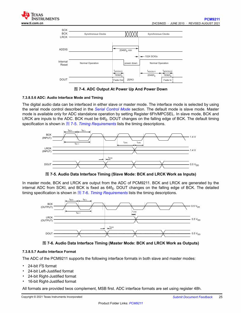
7.3.8.5.6 ADC: Audio Interface Mode and Timing
The digital audio data can be interfaced in either slave or master mode. The interface mode is selected by using the serial mode control described in the Serial Control Mode section. The default mode is slave mode. Master mode is available only for ADC standalone operation by setting Register 6Fh/MPCSEL. In slave mode, BCK and LRCK are inputs to the ADC. BCK must be 64fS. DOUT changes on the falling edge of BCK. The default timing specification is shown in 图 7-5. Timing Requirements lists the timing descriptions.
DOUT 0.5 VDD
1.4 VLRCK
(INPUT)
BCK
(INPUT) 1.4 V
tBCH tBC L
tBC YtLRH
tDOD
tLRS
图 7-5. Audio Data Interface Timing (Slave Mode: BCK and LRCK Work as Inputs)
In master mode, BCK and LRCK are output from the ADC of PCM9211. BCK and LRCK are generated by the internal ADC from SCKI, and BCK is fixed as 64fS. DOUT changes on the falling edge of BCK. The detailed timing specification is shown in 图 7-6. Timing Requirements lists the timing descriptions.
DOUT
LRCK
(OUTPUT)
BCK
(OUTPUT) 0.5 VDD
tBCH tBC L
tBC Yt LRD
tDOD
0.5 VDD
0.5 VDD
图 7-6. Audio Data Interface Timing (Master Mode: BCK and LRCK Work as Outputs)
7.3.8.5.7 Audio Interface Format
The ADC of the PCM9211 supports the following interface formats in both slave and master modes:
• 24-bit I2S format• 24-bit Left-Justified format• 24-bit Right-Justified format• 16-bit Right-Justified format
All formats are provided twos complement, MSB first. ADC interface formats are set using register 48h.
www.ti.com.cnPCM9211
ZHCSIM2D – JUNE 2010 – REVISED AUGUST 2021
Copyright © 2021 Texas Instruments Incorporated Submit Document Feedback 25
Product Folder Links: PCM9211

7.3.8.5.8 ADC and Synchronization with Other Clocks
The PCM9211 operates under the system clock (SCKI) and the audio sampling clock (LRCK). The PCM9211 does not require a specific phase relationship between audio interface clocks (LRCK, BCK) and the system clock (SCKI), but does require the synchronization in the frequency of LRCK, BCK and SCKI. This requirement allows SCKI to be provided elsewhere than from LRCK and BCK.
LRCK and BCK require synchronization at all times.
If the relationship between SCKI and LRCK changes more than ±6 BCKs as a result of jitter, a frequency change, and so forth, the internal operation of the ADC stops within 2/fS, and the digital output will be ZERO codes until resynchronization between SCKI and LRCK and BCK is completed. Real data begin to be generated a period of tADCDLY3 later.
Changes or drift less than ±5 BCKs do not cause any issues with the device. 图 7-7 shows the ADC digital output when synchronization is lost.
The ADC output, DOUT, maintains its previous state if the system clock stops.
ADCDOUT
tADCDLY3
32/f SUndefined data
NormalZERONormal
synchronousAsynchronoussynchronousSTATE of
SYNCHRONIZATION
within 2 /fS
图 7-7. ADC Output for Lost Synchronization
7.3.8.5.9 Setting the ADC Sampling Frequency with XTI as Clock Source
Register 31h holds the bytes that control the dividers used to bring the high-speed, 24.567-MHz clock down to SCK, BCK, and LRCK as used by the ADC.
Note
While the registers allow operation beyond 96 kHz, the ADC itself does not.
7.3.8.5.10 Analog Inputs to the ADC
The ADC module of the PCM9211 has two independent input channels: VINL and VINR. These are single-ended, unbalanced inputs, each capable of 0.6 VCC VPP input with 10-kΩ input resistance (typ). The ADC also integrates a buffering operational amplifier and a low-pass filter.
7.3.8.5.11 VCOM Output
One unbuffered common voltage output pin, VCOM (pin 44) is brought out for decoupling purposes. This pin is internally biased to a dc voltage level of 0.5 VCCAD (nominal), and is used as internal reference voltage for the ADC. This pin may be used to bias external circuitry (such as an ADC driver op amp), but the load impedance must be high enough because the output impedance of this pin is typically 12.5 kΩ.
7.3.8.5.12 Oversampling Rate
The oversampling rate of the PCM9211 ADC is fixed at 64fS.
7.3.8.5.13 External ADC Mode
To use an external ADC instead of the integrated ADC, the PCM9211 supports External ADC Mode. This option enables a connection with an external, 192-kHz capable ADC via the MPIO_B ports. The external ADC must be a clock slave to the PCM9211. The clock source for the external ADC can be selected using Register 42h/ADCLK (the same register that controls the clock source for the internal ADC).
PCM9211ZHCSIM2D – JUNE 2010 – REVISED AUGUST 2021 www.ti.com.cn
26 Submit Document Feedback Copyright © 2021 Texas Instruments Incorporated
Product Folder Links: PCM9211

To lower power consumption in the PCM9211, the onboard ADC can be set to power-down state using Register 40h/ADDIS.
To use the external ADC mode, Register 6Fh/MPBSEL must be set to '101' (External Slave ADC Input). Then, each MPIO_B port is assigned for MPIO_B0 = EASCKO (output), MPIO_B1 = EABCKO (output), MPIO_B2 = EALRCKO (output), and MPIO_B3 = EADIN (input). The MPIO_B pins should be connected according to this configuration:
• MPIO_B0 to ADC system clock input• MPIO_B1 to ADC bit clock input• MPIO_B2 to ADC LR clock input• MPIO_B3 to ADC data output
www.ti.com.cnPCM9211
ZHCSIM2D – JUNE 2010 – REVISED AUGUST 2021
Copyright © 2021 Texas Instruments Incorporated Submit Document Feedback 27
Product Folder Links: PCM9211

7.3.8.5.14 ADC Level Detect and Interrupt
The PCM9211 has the ability to monitor audio inputs, which can be used to trigger interrupt outputs on port INT1. The ADC has a level monitor that can be set so that INT1 can be triggered whenever a specific level (referenced to 0dBFS) is crossed. A block diagram for this function is shown in 图 7-8.
ADC Core
24
MainPort/MPIO
Matrix
DIR Core
SPI/I2C
ERROR
NPCM
EMPH
DTSCD
CSRNW
PCRNW
FSCHG
7
8
MainPort/
MPIOs
ERROR
NPCM2
ERROR/INT0
NPCM/INT1
Level
DetectorINT
REG
ERROR/
NPCM
ADDTLV[1:0]
图 7-8. Block Diagram for ADC Level Detection
Operation of the level detect circuitry is shown in 图 7-9. The ADC level detect is flagged when either ADC channel goes high. The flag is cleared when Register 2Dh is read.
VINL
VINR
SPI/I C2
Register 2Dh_B0
NPCM/INT1 pin
LVL DET Flag
Read Register 2Dh
图 7-9. Operation of the ADC Level Detect Circuitry
The trigger threshold for the ADC can be configured at four different levels below full scale using the ADLVLTH[1:0] bits in Register 2Eh. The output is post-ADC volume control, allowing finer gain steps to be configured by changing the ADC volume control.
In a typical application, this level change is done as the system moves into standby, and reset back to 0dB attenuation when the system wakes up.
The output of this comparator circuit can be ORed along with the INT1 interrupt that is sourced. When the INT1 interrupt is flagged, then the INT1 output register can be read by the host controller.
PCM9211ZHCSIM2D – JUNE 2010 – REVISED AUGUST 2021 www.ti.com.cn
28 Submit Document Feedback Copyright © 2021 Texas Instruments Incorporated
Product Folder Links: PCM9211

7.3.8.5.15 Real World Application
By using both the S/PDIF lock status on INT0 and the analog level detect output on INT1, a system controller can place the rest of the system to sleep (such as the Class D amplifier stage, etc). Upon S/PDIF lock, or an ADC input that is above the preset threshold, the controller can wake up and wake up the rest of the system.
In most implementations, it is suggested that as the system goes into standby, only INT1 be used for the ADC level detect function. (that is, mask all other INT1 sources). In addition, it is recommended that this function be implemented one second after startup, in order to allow the internal high-pass filter to settle.
Using such a system allows auto-shutdown, provided that the source moves into its own standby mode (for example, a TV or a set-top box).
7.3.8.6 Digital Audio Interface Receiver (Rxin0 To Rxin11)7.3.8.6.1 Input Details for Pins Rxin0 through Rxin11
Up to 12 single-ended S/PDIF input pins are available. Two of the S/PDIF input pins integrate coaxial amplifiers. The other 10 pins are designed to be directly connected to CMOS sources or standard S/PDIF optical modules. Each of the inputs can tolerate 5-V inputs.
The DIR module in the PCM9211 complies with these Digital Audio I/F standards:
• S/PDIF• IEC60958 (formerly IEC958)• JEITA CPR-1205 (formerly EIAJ CP-1201/340)• AES3• EBU Tech 3250 (also known as AES/EBU)
In addition, the DIR module within the PCM9211 also meets and exceeds jitter tolerance limits as specified by IEC60958-3 for sampling frequencies between 28 kHz and 216 kHz.
Each of the physical connections used for these standards (optical, differential, and single-ended) have different signal levels. Take care to make sure that each of the RXIN pins is not overdriven or underdriven, such as driving a coaxial 0.2-VPP signal into a CMOS 3.3-V input.
RXIN0 and RXIN1 integrate coaxial input amplifiers. This architecture means that they can be directly connected to either coaxial input (or RCA/Phono) S/PDIF sources. They can accept a minimum of 0.2VPP. They can also be connected to maximum 5-V TTL sources, such as optical receivers.
Note
Consideration should be made for electrostatic discharge, or ESD, on the input connectors.
RXIN2 to RXIN11 are 5-V tolerant TTL level inputs. These inputs are typically used as connections to optical receiver modules (known as TOSLINK™ connectors).
RXIN8 through RXIN11 are also part of the MPIO_A (Multipurpose Input/Output A) group. These I/O pins can either be set as S/PDIF inputs, or reassigned to other functions (see the MPIO Description section). To configure MPIO_A as S/PDIF inputs, set Register MPASEL[1:0] to 00.
Typically, no additional components are required to connect an optical receiver to any RXIN pin. However, consideration should be given to the output characteristics of the specific receiver modules used, especially if there is a long printed circuit board (PCB) trace between the receiver and the PCM9211 itself.
For differential inputs (such as the AES/EBU standard), differential to single-ended circuitry is required.
7.3.8.6.2 PLL Clock Source (Built-In PLL and VCO) Details
The PCM9211 an has on-chip PLL (including a voltage-controlled oscillator, or VCO) for recovering the clock from the S/PDIF input signal.
The VCO-derived clock is identified as the PLL clock source.
www.ti.com.cnPCM9211
ZHCSIM2D – JUNE 2010 – REVISED AUGUST 2021
Copyright © 2021 Texas Instruments Incorporated Submit Document Feedback 29
Product Folder Links: PCM9211

When locked, the onboard PLL generates a system clock that synchronizes with the input biphase signal. When unlocked, the PLL generates its own free-run clock (from the VCO).
The generated system clocks from the PLL can be set to fixed multiples of the input S/PDIF frequency. Register 30h/PSCK[2:0] can configure the output clock to 128fS, 256fS or 512fS.
The PCM9211 also has an automatic default output rate that is calculated based on the incoming S/PDIF frequency. This calculation and rate are controlled by Register 30h/PSCKAUTO. In its default mode, the SCK dividing ratio is configured according to these parameters:
• 512fS: 54 kHz and below.• 256fS: 54 kHz to 108 kHz• 128fS: 108 kHz and above (or unlocked)
PSCKAUTO takes priority over any settings in PSCK[2:0]. PSCK[2:0] only becomes relevant in the system when the PSCKAUTO Register is set to 0.
The PCM9211 can decode S/PDIF input signals between sampling frequencies of 7 kHz and 216 kHz for all PSCK[2:0] settings. The relationship between the output clock (SCKO, BCKO, LRCKO) at the PLL source and PSCK[2:0] selection is shown in 表 7-4.
表 7-4. SCKO, BCKO and LRCKO Frequency Set by PSCK[2:0]OUTPUT CLOCK AT PLL SOURCE PSCK[2:0] SETTING
SCKO BCKO LRCKO PSCK2 PSCK1 PSCK0128fS 64fS fS 0 0 0
256fS 64fS fS 0 1 0
512fS (1) 64fS fS 1 0 0
(1) 512fS SCK is only supported at 108 kHz or lower sampling frequency of incoming biphase signal.
In PLL mode, the output clocks (SCKO, BCKO, LRCKO) are generated from the PLL source clock.
The relationship between the sampling frequencies (fS) of the input S/PDIF signal and the frequency of LRCKO, BCKO, and SCKO are shown in 表 7-5.
表 7-5. Output Clock Frequency at PLL Lock StateLRCK BCK SCK(1)
fS 64fS 128fS 256fS 512fS
8 kHz 0.512 MHz 1.024MHz 2.048 MHz 4.096 MHz
11.025 kHz 0.7056 MHz 1.4112 MHz 2.8224 MHz 5.6448 MHz
12 kHz 0.768 MHz 1.536 MHz 3.072 MHz 6.144 MHz
16 kHz 1.024 MHz 2.048 MHz 4.096 MHz 8.192 MHz
22.05 kHz 1.4112 MHz 2.8224 MHz 5.6448 MHz 11.2896 MHz
24 kHz 1.536 MHz 3.072 MHz 6.144 MHz 12.288 MHz
32 kHz 2.048 MHz 4.096 MHz 8.192 MHz 16.384 MHz
44.1 kHz 2.8224 MHz 5.6448 MHz 11.2896 MHz 22.5792 MHz
48 kHz 3.072 MHz 6.144 MHz 12.288 MHz 24.576 MHz
64 kHz 4.096 MHz 8.192 MHz 16.384 MHz 32.768 MHz
88.2 kHz 5.6448 MHz 11.2896 MHz 22.5792 MHz 45.1584 MHz
96 kHz 6.144 MHz 12.288 MHz 24.576 MHz 49.152 MHz
128 kHz 8.192 MHz 16.384 MHz 32.768 MHz N/A
176.4 kHz 11.2896 MHz 22.5792 MHz 45.1584 MHz N/A
192 kHz 12.288 MHz 24.576 MHz 49.152 MHz N/A
(1) Depending on PSCK[2:0] setting.
PCM9211ZHCSIM2D – JUNE 2010 – REVISED AUGUST 2021 www.ti.com.cn
30 Submit Document Feedback Copyright © 2021 Texas Instruments Incorporated
Product Folder Links: PCM9211

7.3.8.6.3 DIR and PLL Loop Filter Details
The PCM9211 incorporates a PLL for generating clocks synchronized with the input biphase signal (S/PDIF). The onboard PLL requires an external loop filter. The components and configuration shown in 图 7-10 and 表 7-6 are recommended for optimal performance, with these considerations:
• The resistor and capacitors that configure the filter should be located and routed as close as possible to the PCM9211. The external loop filter must be placed on the FILT pins.
• The GND node of the external loop filter must be directly connected with AGND pin of the PCM9211; it must be not combined with other signals.
图 7-10 shows the configuration of the external loop filter and the connection with the PCM9211.
C2
C1R1
FILT AGND DGND
Charge
PumpVCO
PCM9211
PLL Section
图 7-10. Loop Filter Connection
The recommended value of loop filter components is shown in 表 7-6.
表 7-6. Recommended Value of Loop Filter ComponentsREF. NO. RECOMMENDED VALUE TYPE TOLERANCE
R1 680 Ω Metal film or carbon ≤ 5%
C1 0.068 µF Film or ceramic (CH or C0G) ≤ 5%
C2 0.0047 µF Film or ceramic (CH or C0G) ≤ 5%
7.3.8.6.4 External (XTI) Clocks, Oscillators, and Supporting Circuitry
An external clock source (CMOS or crystal/resonator) is known as the XTI source. The XTI source can be either a CMOS logic source, or a crystal resonator (internal circuitry in the PCM9211 can start the crystal resonating). Whichever clock source is used, it must be 24.576 MHz.
The PCM9211 uses the XTI source as a reference clock in order to calculate the sampling frequency of the incoming S/PDIF stream. It is also used as the clock source in XTI clock source mode.
When using a resonator as an XTI source, the following points should be considered:
• The 24.576-MHz resonator should be connected between the XTI and XTO pins• The resonator should be a fundamental mode type• A crystal or ceramic resonator can be used as the XTI source• The values of the load capacitors CL1 and CL2 and the current limiting resistor Rd all depend on the
characteristics of the resonator• No external feedback resistor between the XTI and XTO pins is required, because the resistor is integrated
into the device• No loads other than the resonator should be used on the XTO pin
When using an external oscillation circuit with a CMOS output, the following points should be considered:
• Always supply a 24.576-MHz clock on the XTI pin
www.ti.com.cnPCM9211
ZHCSIM2D – JUNE 2010 – REVISED AUGUST 2021
Copyright © 2021 Texas Instruments Incorporated Submit Document Feedback 31
Product Folder Links: PCM9211
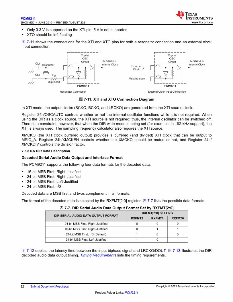
• Only 3.3 V is supported on the XTI pin; 5 V is not supported• XTO should be left floating
图 7-11 shows the connections for the XTI and XTO pins for both a resonator connection and an external clock input connection.
XTI
XTO
Crystal
OSC
Circuit 24.576 MHz
Internal ClockExternal
Clock
Must be open
PCM9211
RD
CL1
CL2
XTI
XTO
Crystal
OSC
Circuit 24.576 MHz
Internal Clock
(Optional)
Resonator
PCM9211
Resonator Connection External Clock Input Connection
图 7-11. XTI and XTO Connection Diagram
In XTI mode, the output clocks (SCKO, BCKO, and LRCKO) are generated from the XTI source clock.
Register 24h/OSCAUTO controls whether or not the internal oscillator functions while it is not required. When using the DIR as a clock source, the XTI source is not required; thus, the internal oscillator can be switched off. There is a constraint, however, that when the DIR wide mode is being set (for example, in 192-kHz support), the XTI is always used. The sampling frequency calculator also requires the XTI source.
XMCKO (the XTI clock buffered output) provides a buffered (and divided) XTI clock that can be output to MPIO_A. Register 24h/XMCKEN controls whether the XMCKO should be muted or not, and Register 24h/XMCKDIV controls the division factor.
7.3.8.6.5 DIR Data Description
Decoded Serial Audio Data Output and Interface Format
The PCM9211 supports the following four data formats for the decoded data:
• 16-bit MSB First, Right-Justified• 24-bit MSB First, Right-Justified• 24-bit MSB First, Left-Justified• 24-bit MSB First, I2S
Decoded data are MSB first and twos complement in all formats.
The format of the decoded data is selected by the RXFMT[2:0] register. 表 7-7 lists the possible data formats.
表 7-7. DIR Serial Audio Data Output Format Set by RXFMT[2:0]
DIR SERIAL AUDIO DATA OUTPUT FORMATRXFMT[2:0] SETTING
RXFMT2 RXFMT1 RXFMT024-bit MSB First, Right-Justified 0 0 0
16-bit MSB First, Right-Justified 0 1 1
24-bit MSB First, I2S (Default) 1 0 0
24-bit MSB First, Left-Justified 1 0 1
图 7-12 depicts the latency time between the input biphase signal and LRCKO/DOUT. 图 7-13 illustrates the DIR decoded audio data output timing. Timing Requirements lists the timing requirements.
PCM9211ZHCSIM2D – JUNE 2010 – REVISED AUGUST 2021 www.ti.com.cn
32 Submit Document Feedback Copyright © 2021 Texas Instruments Incorporated
Product Folder Links: PCM9211

B 0L
0L
W 0R
0R
M 1L
1L
W 1R
1R
tLATE
17±1BCK
Biphase Signal (IN)
BFRAME (OUT)
LRCK (OUT)
(I S)2
LRCK (OUT)
(All except I S)2
DATA (OUT)
图 7-12. Latency Time Between Input Biphase and LRCKO/DOUT
BCKO
(OUT)
LRCKO(OUT)
DOUT(OUT)
SCKO(OUT)
tSCY
tBCH tBCL
tBCY tBCDO
tCKLR
V /2DD
V /2DD
V /2DD
V /2DD
图 7-13. DIR Decoded Audio Data Output Timing
7.3.8.6.6 Channel Status Data, User Data, and Validity Flag
The PCM9211 can output decoded channel status data, user data, and a validity flag synchronized with audio data from the input S/PDIF signal. These signals can be transmitted from any of the three MPIOs (MPIO_A, MPIO_B, or MPIO_C). To assign this function to the MPIOs, see the MPIO Description section.
Each type of output data has own dedicated output pin:
• Channel status data (C) are output through MPIOs assigned as COUT.• User data (U) are output through MPIOs assigned as UOUT.• Validity flag (V) is output through MPIOs assigned as VOUT• Data (left and right) are identified as DOUT.
C, U, and V output data are synchronized with the recovered LRCKO (left-right clock output) from the S/PDIF input signal.
The polarity of the recovered LRCKO from the S/PDIF input depends on the Register 2Fh/RXFMT[2:0] setting.
The beginning of each S/PDIF frame (BFRAME) is provided as one of the outputs on the MPIO. It can be used to indicate the start of the frame to the decoding DSP. If the DIR decodes a start-of-frame preamble on the decoded data, then it sets BFRAME high for 8xLRCK periods to signify the start of the frame.
LRCKO can be used as a reference clock for each of the data outputs, BFRAME, DOUT, COUT, UOUT, and VOUT. The relationship between each output is shown in 图 7-14.
Numbers 0 to 191 of DOUT, COUT, UOUT, and VOUT in 图 7-14 indicate the frame number of the input biphase signal.
www.ti.com.cnPCM9211
ZHCSIM2D – JUNE 2010 – REVISED AUGUST 2021
Copyright © 2021 Texas Instruments Incorporated Submit Document Feedback 33
Product Folder Links: PCM9211

17±1BCK
0L 0R191R 1L 1R 2L 2R 3L
C0L C0RC191R C1L C1R C2L C2R
U0L U0RU191R U1L U1R U2L U2R
RECOVERED
LRCKO (I S)2
RECOVERED
LRCKO (All except I S)2
BFRAME
DOUT
COUT
VOUT
图 7-14. LRCKO, DOUT, BFRAME, COUT, UOUT, and VOUT Output Timing
The RXVDLY Register in Register 22h controls when the VOUT pin goes high (either immediately, or at the start of the sample/frame). 图 7-15 shows these timing sequences.
L(n) L(n+1)R(n) R(n+1) L(n+2) R(n+2)
V-bit = 1
17 BCLK
DOUT
VOUT
(RXVDLY = 1)
VOUT
(RXVDLY = 0)
图 7-15. RXVDLY and VOUT Timing
7.3.8.6.7 DIR: Parity Error Processing
Error detection and processing for parity errors behave in the following manner:
• For PCM data, when an error is detected (for example, a parity error), then the data from the previous sample are repeated. This sequence is shown in 图 7-16, where sample Ln+1 is repeated because the incoming data (Ln+2) had an error.
• For non-PCM data, the data are output as is with no changes. (Non-PCM data implies data which has Channel Status bit 1 = 1.)
图 7-16 shows the processing for parity error occurrence.
Internal LOCK
Ln
LRCKO (I 2S)
MUTE (Low)
ERROR
DOUT
Parity errorInterpolation processing by previous data
Internal LOCK
LRCKO (I 2S)
ERROR
DOUT
Parity error
[FOR PCM SIGNAL]
[FOR NON-PCM SIGNAL ]
Rn Ln+1 Rn+1 Ln+1 Rn+2 Rn+3Ln+3
LnMUTE (Low) Rn Ln+1 Rn+1 Ln+2 Rn+2 Rn+3Ln+3
图 7-16. Processing for Parity Error Occurrence
PCM9211ZHCSIM2D – JUNE 2010 – REVISED AUGUST 2021 www.ti.com.cn
34 Submit Document Feedback Copyright © 2021 Texas Instruments Incorporated
Product Folder Links: PCM9211
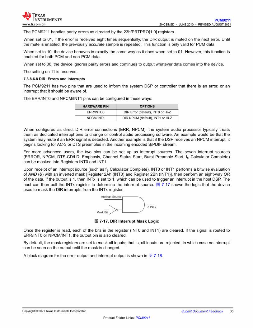
The PCM9211 handles parity errors as directed by the 23h/PRTPRO[1:0] registers.
When set to 01, if the error is received eight times sequentially, the DIR output is muted on the next error. Until the mute is enabled, the previously accurate sample is repeated. This function is only valid for PCM data.
When set to 10, the device behaves in exactly the same way as it does when set to 01. However, this function is enabled for both PCM and non-PCM data.
When set to 00, the device ignores parity errors and continues to output whatever data comes into the device.
The setting on 11 is reserved.
7.3.8.6.8 DIR: Errors and Interrupts
The PCM9211 has two pins that are used to inform the system DSP or controller that there is an error, or an interrupt that it should be aware of.
The ERR/INT0 and NPCM/INT1 pins can be configured in these ways:
HARDWARE PIN OPTIONSERR/INTO0 DIR Error (default), INT0 or Hi-Z
NPCM/INT1 DIR NPCM (default), INT1 or Hi-Z
When configured as direct DIR error connections (ERR, NPCM), the system audio processor typically treats them as dedicated interrupt pins to change or control audio processing software. An example would be that the system may mute if an ERR signal is detected. Another example is that if the DSP receives an NPCM interrupt, it begins looking for AC-3 or DTS preambles in the incoming encoded S/PDIF stream.
For more advanced users, the two pins can be set up as interrupt sources. The seven interrupt sources (ERROR, NPCM, DTS-CD/LD, Emphasis, Channel Status Start, Burst Preamble Start, fS Calculator Complete) can be masked into Registers INT0 and INT1.
Upon receipt of an interrupt source (such as fS Calculator Complete), INT0 or INT1 performs a bitwise evaluation of AND (&) with an inverted mask [Register 2Ah (INT0) and Register 2Bh (INT1)], then perform an eight-way OR of the data. If the output is 1, then INTx is set to 1, which can be used to trigger an interrupt in the host DSP. The host can then poll the INTx register to determine the interrupt source. 图 7-17 shows the logic that the device uses to mask the DIR interrupts from the INTx register.
Interrupt Source
Mask Bit
To INTx
图 7-17. DIR Interrupt Mask Logic
Once the register is read, each of the bits in the register (INT0 and INT1) are cleared. If the signal is routed to ERR/INT0 or NPCM/INT1, the output pin is also cleared.
By default, the mask registers are set to mask all inputs; that is, all inputs are rejected, in which case no interrupt can be seen on the output until the mask is changed.
A block diagram for the error output and interrupt output is shown in 图 7-18.
www.ti.com.cnPCM9211
ZHCSIM2D – JUNE 2010 – REVISED AUGUST 2021
Copyright © 2021 Texas Instruments Incorporated Submit Document Feedback 35
Product Folder Links: PCM9211

DIR
Re
gis
ter
2A
h/2
Bh
Re
gis
ter
2C
h/2
Dh
Re
gis
ter
20
h
Re
gis
ter
20
h
Re
gis
ter
28
hR
eg
iste
r 2
0h
Re
gis
ter
20
hR
eg
iste
r 2
0h
Re
gis
ter
2E
h
Re
gis
ter
2E
h
Re
gis
ter
6B
h
INT
0P
INT
1P
ER
RC
ON
NP
CM
SE
L
NP
CM
P
NP
CM
HZ
ER
RS
EL
ER
RH
Z
MO
PS
RC
INT0/1
Mask
INT0/1
Register
Em
ph
asis
DT
S-C
D/L
D
Ch
an
ne
l S
tatu
s
Bu
rst
Pre
am
ble
f Calculator
CompleteS
‘1’
NPCM/INT1
External Pin
ERR/INT0
External Pin
Hi-Z
Hi-Z
图 7-18. Error Output and Interrupt Output Block Diagram
There are several allowable error sources from the DIR:
• Change of incoming S/PDIF sample frequency (Register 25h / EFSCHG)• Out-of-range incoming S/PDIF signal (Register 25h / EFSLMT)• Non-PCM data (Register 25h / ENPCM)• Data invalid flag is the stream (Validity bit = 1) (Register 25h / EVALID)• Parity error (Register 25h / EPARITY)• PLL unlock (default) (Register 25h / EUNLOCK)
The error sources can be selected using Register 25h.
There are also several interrupts within the device that can be masked:
• Error in DIR (this error is selectable from the list above in Register 25h)• When the device detects non-PCM data• When the Emphasis flag in the channel status of the incoming data has been set• When DTS-CD data have been detected by the device• When the Channel Status (CS) is updated• When Burst Preamble (PC) is updated• When the sampling frequency is changed.• When the analog input crosses the Analog Input Detect level (available only on INT1).
Each interrupt source can be masked by Register 2Ah (INT0) and Register 2Bh (INT1).
PCM9211ZHCSIM2D – JUNE 2010 – REVISED AUGUST 2021 www.ti.com.cn
36 Submit Document Feedback Copyright © 2021 Texas Instruments Incorporated
Product Folder Links: PCM9211

7.3.8.6.9 DIR: Sampling Frequency Calculator for Incoming S/PDIF Inputs
The PCM9211 has two integrated sampling frequency calculators. The first calculator is always connected to the output of the DIR. It calculates the actual sampling frequency of the incoming S/PDIF signal. The result can be read from a register, or output through the MPIO pins. Note that this process is not the same as reading the Channel Status value for the sample rate that the transmitting equipment may be sending.
To use this function, a 24.576-MHz clock source must be supplied to the XTI pin. The 24.576-MHz clock is used as a reference clock to calculate the incoming S/PDIF sampling frequency. If the XTI pin is connected to DGND, the function is disabled and the calculation is not performed. If there is an error in the XTI clock frequency, the calculation result and range will be incorrect.
The result is decoded into 4-bit data and stored in Register 39h/SFSOUT[3:0]; the MPIO pins are then assigned to the SFSOUT[3:0] function.
The data in the SFSOUT[3:0] register (and available as a signal for the MPIO section) are the calculated sampling frequency based on the incoming S/PDIF stream, and not what is reported in Channel Status bits 24 to 27. If the PLL becomes unlocked, or attempts to run out of range, SFSOUT[3:0] = '0000' is output, and indicates abnormal operation.
If the XTI source clock is not supplied before the PCM9211 powers up, SFSOUT [3:0] outputs '0000'. If the XTI source clock is stopped, the fS calculator holds its most recent calculated result. Once the XTI source clock is restored, the fS calculator resumes operation.
Register 39h/SFSST indicates the calculator status. Before reading SFSOUT[3:0], it is recommended that the user verify that the SFSST status is 0.
The relationship between SFSOUT[3:0] outputs and the range of sampling frequency fS is shown in 表 7-8.
表 7-8. Calculated Biphase Sampling Frequency Output
NOMINAL fSACTUAL SAMPLINGFREQUENCY RANGE
CALCULATED SAMPLING FREQUENCY OUTPUT(1)
SFSOUT3 SFSOUT2 SFSOUT1 SFSOUT0Out of range Out of range 0 0 0 0
8 kHz 7.84 kHz to 8.16 kHz 0 0 0 1
11.025 kHz 10.8045 kHz to 11.2455 kHz 0 0 1 0
12 kHz 11.76 kHz to 12.24 kHz 0 0 1 1
16 kHz 15.68 kHz to 16.32 kHz 0 1 0 0
22.05 kHz 21.609 kHz to 22.491 kHz 0 1 0 1
24 kHz 23.52 kHz to 24.48 kHz 0 1 1 0
32 kHz 31.36 kHz to 32.64 kHz 0 1 1 1
44.1 kHz 43.218 kHz to 44.982 kHz 1 0 0 0
48 kHz 47.04 kHz to 48.96 kHz 1 0 0 1
64 kHz 62.72 kHz to 65.28 kHz 1 0 1 0
88.2 kHz 86.436 kHz to 89.964 kHz 1 0 1 1
96 kHz 94.08 kHz to 97.92 kHz 1 1 0 0
128 kHz 125.44 kHz to 130.56 kHz 1 1 0 1
176.4 kHz 172.872 kHz to 179.928 kHz 1 1 1 0
192 kHz 188.16 kHz to 195.84 kHz 1 1 1 1
(1) The flag SFSOUT[3:0] is output from the register and MPIOs are assigned as SFSOUT[3:0].0 or 1 indicates the register output data. The symbol 'H' or 'L' refers to the MPIO output electrical signal.
www.ti.com.cnPCM9211
ZHCSIM2D – JUNE 2010 – REVISED AUGUST 2021
Copyright © 2021 Texas Instruments Incorporated Submit Document Feedback 37
Product Folder Links: PCM9211

The Biphase Sampling Frequency Calculator is also used for restricting the type of data that can be received.
1. If Register 27h/MSK128 is set to 1, the PCM9211 does not accept 128-kHz sampling frequency data2. If Register 27h/MSK64 is set to 1, the PCM9211 does not accept 64-kHz sampling frequency data.3. If Register 27h/NOMLMT is set to 1, the PCM9211 only accepts the nominal audio sampling frequency within
±2%.The nominal audio sampling frequencies are 8 kHz, 11.025 kHz, 12 kHz, 16 kHz, 22.05 kHz, 24 kHz,32 kHz, 44.1 kHz, 48 kHz, 64 kHz, 88.2 kHz, 96 kHz, 128 kHz, 176.4 kHz, and 192 kHz.
4. For Register 27h/HILMT[1:0] and Register 27h/LOLMT[1:0]: These registers are used for setting a higher or lower limit to the acceptable sampling frequency.
Register 21h/RXFSRNG is used for global control of the acceptable sampling frequencies. If normal mode is selected, the range of acceptable sampling frequency is restricted from 28 kHz to 108 kHz. If wide mode is selected, the range is from 7 kHz to 216 kHz.
7.3.8.6.10 DIR: Audio Port Sampling Frequency Calculator
The second sampling frequency calculator can be used to calculate the sampling frequency of DIR, ADC, AUXIN0, AUXIN1, AUXIN2, Main Output Port, AUX Output Port, and DIT Input. 图 7-19 illustrates the sampling frequency calculator sources.
ADC
DIT
000
001
010
011
100
101
110
111
Audio Port
Sampling Frequency
Calculator
PFSTGT[2:0]
DIR (default)
AUXIN0
AUXIN1
AUXIN2
Main Output Port
AUX Output Port
图 7-19. Sampling Frequency Calculator Sources
The calculated sampling frequency fS is decoded to 4-bit data and stored in the PFSOUT[3:0] register. The input source of this counter is selectable from AUXIN0, AUXIN1, AUXIN2, DIR, ADC, Main Output Port, AUX Output Port, and DIT by using the Register 37h/PFSTGT[3:0].
To use this function, a 24.576-MHz clock source must be supplied to the XTI pin. The 24.576-MHz clock is used as a reference clock. If the XTI pin is connected to DGND, the calculation is not performed. If there is an error in the XTI clock frequency, the calculation result and range will be incorrect.
Register 38h/PFSST indicates the calculator status. It is recommended that PFSST is checked (for complete status) before reading PFSOUT[3:0].
PCM9211ZHCSIM2D – JUNE 2010 – REVISED AUGUST 2021 www.ti.com.cn
38 Submit Document Feedback Copyright © 2021 Texas Instruments Incorporated
Product Folder Links: PCM9211

7.3.8.6.11 Output Register Construction
The output 8-bit register is subdivided into three sections. The first four bits show the decoded result. The next three bits signify the source; the final bit signifies the calculator status (finished or not).
The lock range of the counter (to the specified fS given in 表 7-9) are any clock rate within ±2%. The relation between the nominal fS and actual measured fS range is shown in 表 7-9.
表 7-9. Calculated Port Sampling Frequency Output
NOMINAL fSACTUAL SAMPLING
FREQUENCY RANGE (MIN)CALCULATED SAMPLING FREQUENCY OUTPUT
PFSOUT3 PFSOUT2 PFSOUT1 PFSOUT0Out of range Out of range 0 0 0 0
8 kHz 7.84 kHz to 8.16 kHz 0 0 0 1
11.025 kHz 10.8045 kHz to 11.2455 kHz 0 0 1 0
12 kHz 11.76 kHz to 12.24 kHz 0 0 1 1
16 kHz 15.68 kHz to 16.32 kHz 0 1 0 0
22.05 kHz 21.609 kHz to 22.491 kHz 0 1 0 1
24 kHz 23.52 kHz to 24.48 kHz 0 1 1 0
32 kHz 31.36 kHz to 32.64 kHz 0 1 1 1
44.1 kHz 43.218 kHz to 44.982 kHz 1 0 0 0
48 kHz 47.04 kHz to 48.96 kHz 1 0 0 1
64 kHz 62.72 kHz to 65.28 kHz 1 0 1 0
88.2 kHz 86.436 kHz to 89.964 kHz 1 0 1 1
96 kHz 94.08 kHz to 97.92 kHz 1 1 0 0
128 kHz 125.44 kHz to 130.56 kHz 1 1 0 1
176.4 kHz 172.872 kHz to 179.928 kHz 1 1 1 0
192 kHz 188.16 kHz to 195.84 kHz 1 1 1 1
7.3.8.6.12 DIR: Auto Source Selector for Main Output and AUX Output
The AUTO source selector is an automatic system that selects the DIR or ADC output based on specific DIR conditions set by Register 26h. The AUTO source selector is integrated in both the Main Port and the AUX output separately.
The typical behavior for the AUTO source selector is shown in 图 7-20. This example is the default register setting for Register 26h. In this case, only Register 26h/AUNLOCK is selected.
www.ti.com.cnPCM9211
ZHCSIM2D – JUNE 2010 – REVISED AUGUST 2021
Copyright © 2021 Texas Instruments Incorporated Submit Document Feedback 39
Product Folder Links: PCM9211
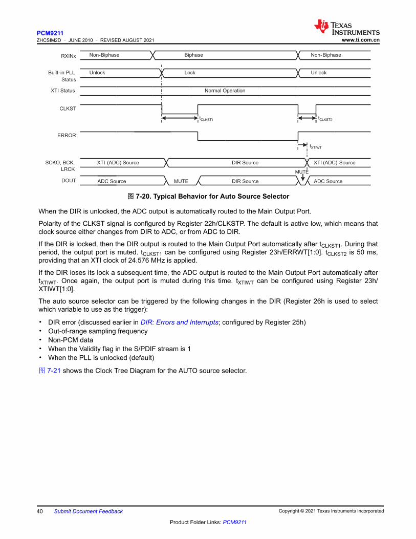
RXINx
Built-in PLL
Status
XTI Status
ERROR
SCKO, BCK,
LRCK
CLKST
Non-Biphase Biphase Non-Biphase
Unlock Lock Unlock
Normal Operation
XTI (ADC) Source DIR Source XTI (ADC) Source
ADC Source MUTE DIR Source ADC SourceDOUT
MUTE
tCLKST2
tCLKST1
tXTIWT
图 7-20. Typical Behavior for Auto Source Selector
When the DIR is unlocked, the ADC output is automatically routed to the Main Output Port.
Polarity of the CLKST signal is configured by Register 22h/CLKSTP. The default is active low, which means that clock source either changes from DIR to ADC, or from ADC to DIR.
If the DIR is locked, then the DIR output is routed to the Main Output Port automatically after tCLKST1. During that period, the output port is muted. tCLKST1 can be configured using Register 23h/ERRWT[1:0]. tCLKST2 is 50 ms, providing that an XTI clock of 24.576 MHz is applied.
If the DIR loses its lock a subsequent time, the ADC output is routed to the Main Output Port automatically after tXTIWT. Once again, the output port is muted during this time. tXTIWT can be configured using Register 23h/XTIWT[1:0].
The auto source selector can be triggered by the following changes in the DIR (Register 26h is used to select which variable to use as the trigger):
• DIR error (discussed earlier in DIR: Errors and Interrupts; configured by Register 25h)• Out-of-range sampling frequency• Non-PCM data• When the Validity flag in the S/PDIF stream is 1• When the PLL is unlocked (default)
图 7-21 shows the Clock Tree Diagram for the AUTO source selector.
PCM9211ZHCSIM2D – JUNE 2010 – REVISED AUGUST 2021 www.ti.com.cn
40 Submit Document Feedback Copyright © 2021 Texas Instruments Incorporated
Product Folder Links: PCM9211

SCK/BCK/LRCK/DOUT
DIR
AUTO selector
OSC
ADC
REG.42 h /ADCLK
REG.26h/AERROR
SCK/BCK/LRCK
Divider
ERROR defined by REG.25h
REG.42h/ADCKOUT
SCK/BCK/LRCK
REG.40h/ADDIS
SCK/BCK/LRCK
AUTO select signal defined by
REG.25h excluding AERROR.
REG.26h/ACKSL REG.6Bh/MOSSRC&MOPSRC
Main Port
AUXINx
AUXINx
图 7-21. Clock Tree Diagram for Auto Source Selector
7.3.8.6.13 Non-PCM Data Detection
The PCM9211 can also detect Non-PCM data (AC-3, DTS-CD, and so forth) using one of these two methods:
1. Channel Status Bit 1 is 1.
If Register 28h/CSBIT is set to 1, this function is enabled. Register 39h/SCSBIT1 always indicates Channel Status Bit 1 status even if CSBIT1 is disabled.
2. A Burst Preamble (PA/PB) is found in the S/PDIF stream.
If Register 28h/PAPB or Register 28h/DTSCD is set to 1, this function is enabled. If DTS-CD detection is active, it uses DTSCD, and can also be set in Register 29h/DTS16, 29h/DTS14, and Register 29h/DTSPRD[1:0].
If the PCM9211 detects a Burst Preamble when Non-PCM detection is enabled, an error signal and BPSYNC signal are generated. The BPSYNC signal can be monitored through MPIO_A/MPIO_B/MPIO_C. For more details, see the MPIO Description section of this document. The error signal can be monitored from either the ERR_INT0 pin or the NPCM_INT1 pin.
7.3.8.6.14 PC/PD Monitor
The PCM9211 has a PC and PD buffer for monitoring the latest PC or PD. Registers 3Ah and 3Bh are assigned for the PC buffer; Registers 3Ch and 3Dh are assigned for the PDbuffer.
The following sequence is an example of reading PC/PD buffers. This example is based on using the INT0 function.
1. Set Register 2Ah/MPCRNW0 to 0.2. Check that Register 2Ch/OPCRNW0 is 1.3. Read the PC and PD buffers.
7.3.8.7 Digital Audio Interface Transmitter7.3.8.7.1 Overview
The PCM9211 has an onboard Digital Audio Interface Transmitter (DIT) that transmits S/PDIF data from 7 kHz to 216 kHz, up to 24-bit audio data. The first 48 bits of the channel status buffer are programmable. The source for the DIT is selectable from the built-in routing function of the PCM9211 as well as the dedicated inputs assigned to the MPIOs.
7.3.8.7.2 Selection of DIT Input Source
Selection of the DIT audio and clock sources is done using the Registers 60h/TXSSRC[2:0] and 60h/TXPSRC[2:0]. The system clock source for the DIT is selected using the Register 60h/TXSSRC[2:0]. The PCM audio data source for the DIT (BCK. LRCK, and Data) is selected using the Register 60h/TXPSRC[2:0].
www.ti.com.cnPCM9211
ZHCSIM2D – JUNE 2010 – REVISED AUGUST 2021
Copyright © 2021 Texas Instruments Incorporated Submit Document Feedback 41
Product Folder Links: PCM9211

The DIT can also be operated in a standalone mode. In standalone mode, the data source is provided through MPIO_C. See the Standalone Operation section for more details.
7.3.8.7.3 DIT Output Biphase
The S/PDIF-encoded signal generated by the DIT module is available through the MPO0 and MPO1 pins. The MPO selection registers (Register 78h/MPOxSEL[3:0]) can be set to '1101' to determine the DIT output through one of these two pins.
In addition to the standard MPOx pins, the DIT output can also be multiplexed to the RECOUT pin, or back into the DIR. An example of where this multiplexing might occur is in a jitter cleaner application. The DIR in the PCM9211 has excellent jitter reduction. Data can be brought in from an auxiliary source, transmitted through the DIT internally, then routed to the DIR. This process, in turn, cleans the clocks and provides a stable, well-clocked PCM source. This feature is especially useful for jittery sources, such as HDMI.
7.3.8.7.4 Audio Data and Clock
The DIT can accept a 128fS, 256fS, or 512fS system clock. The clock ratio selection is set by using the Register TXSCK[2:0]. A 216-kHz sampling frequency is supported by using the 128fS or 256fS system clock ratio. A 108-kHz sampling frequency can be supported up to a 512fS clock ratio.
I2S, 24-bit left-justified, 24-bit right-justified, and 16-bit right-justified serial audio interface formats can be used. Only slave mode is supported. 表 7-10 shows the relationship between typical audio sampling frequencies and the respective BCK and SCK frequencies
表 7-10. Typical Audio Sampling, BCK, and SCK FrequenciesLRCK BCK SCK
fS 64fS 128fS 256fS 512fS
8 kHz 0.512 MHz 1.024MHz 2.048 MHz 4.096 MHz
11.025 kHz 0.7056 MHz 1.4112 MHz 2.8224 MHz 5.6448 MHz
12 kHz 0.768 MHz 1.536 MHz 3.072 MHz 6.144 MHz
16 kHz 1.024 MHz 2.048 MHz 4.096 MHz 8.192 MHz
22.05 kHz 1.4112 MHz 2.8224 MHz 5.6448 MHz 11.2896 MHz
24 kHz 1.536 MHz 3.072 MHz 6.144 MHz 12.288 MHz
32 kHz 2.048 MHz 4.096 MHz 8.192 MHz 16.384 MHz
44.1 kHz 2.8224 MHz 5.6448 MHz 11.2896 MHz 22.5792 MHz
48 kHz 3.072 MHz 6.144 MHz 12.288 MHz 24.576 MHz
64 kHz 4.096 MHz 8.192 MHz 16.384 MHz 32.768 MHz
88.2 kHz 5.6448 MHz 11.2896 MHz 22.5792 MHz 45.1584 MHz
96 kHz 6.144 MHz 12.288 MHz 24.576 MHz 49.152 MHz
128 kHz 8.192 MHz 16.384 MHz 32.768 MHz N/A
176.4 kHz 11.2896 MHz 22.5792 MHz 45.1584 MHz N/A
192 kHz 12.288 MHz 24.576 MHz 49.152 MHz N/A
7.3.8.7.5 Data Mute Function
The PCM9211 has the ability to mute the audio data on its DIT output. This option is set using Register 62h/TXDMUT. During a mute state (TXDMUT = 1), the biphase stream continues to flow, but all audio data are zeroed.
The channel status data and validity flag are not zeroed. Mute is done at the LRCK edge for both L-ch and R-ch data at the same time.
7.3.8.7.6 Channel Status Data
The DIT has the ability to transmit channel status (CS) data for the first 48 bits of the 128-bit stream. These 48 bits cover the standards for both S/PDIF and AES/EBU. These bits are set in Registers TXCS0 through TXCS47. These values are used on both the Left and Right channels of the output stream.
PCM9211ZHCSIM2D – JUNE 2010 – REVISED AUGUST 2021 www.ti.com.cn
42 Submit Document Feedback Copyright © 2021 Texas Instruments Incorporated
Product Folder Links: PCM9211

Upon reset, these registers are all 0 by default.
7.3.8.7.7 User Data
This DIT does not have the ability to transmit custom user data (known as "U Bits" in the stream).
7.3.8.7.8 Validity Flag
Setting the valid flag is possible in the DIT by using Register 62h/TXVFLG. The same value is used for both left and right channels.
7.3.8.7.9 Standalone Operation
Standalone operation for the DIT module is provided by supplying external clocks and data (SCK, BCK, LRCK, and Data). In standalone mode, the audio and clock data must be brought into the device through MPIO_C. To enable standalone mode, set Register 6Fh/MPCSEL[2:0] to '101'. This configuration then bypasses the standard DIT connections through the device and connects them directly to MPIO_C.
Channel Status and Validity flags continue to be sourced from the same registers as they would during normal DIT operation.
7.3.8.8 MPIO Description7.3.8.8.1 Overview
The PCM9211 offers significant flexibility through its MPIO pins. Depending on the system partitioning of the specific end product, the pins can be reconfigured to offer various I/Os that complement the design.
There are 14 flexible pins: 12 are Input/Output pins, and two pins that are output only.
The 12 multi-purpose I/O (MPIO) pins are grouped into three banks, each with four pins: MPIO_A, MPIO_B, and MPIO_C.
The two multi-purpose outputs (MPO) pins are assigned as MPO0 and MPO1.
www.ti.com.cnPCM9211
ZHCSIM2D – JUNE 2010 – REVISED AUGUST 2021
Copyright © 2021 Texas Instruments Incorporated Submit Document Feedback 43
Product Folder Links: PCM9211

7.3.8.8.2 Assignable Signals for MPIO Pins
The PCM9211 has the following signals that can be brought out to MPIOs. Not all MPIOs are equal; be sure to review subsequent sections in this document to see which signals can be brought out to which MPIO. The possible signals are summarized in 表 7-11.
表 7-11. Allowable MPIO SignalsMODULE ALLOWABLE SIGNALS
DIR
Extended biphase input pins for DIR: RXIN8/RXIN9/RXIN10/RXIN11
DIR Flags Output: The details of each signal are described in the Channel Status Data, User Data, and Validity Flag section.
DIR Interrupt Output: INT0 and INT1
DIR, B frame, serial output of channel status, user data, validity flag
DIR, decoded result of sampling frequency calculated by built-in fS counter
Auxiliary I/O
AUXIN0, external serial audio data input (SCK/BCK/LRCK/Data)
AUXIN1, external serial audio data input (SCK/BCK/LRCK/Data)
AUXIN2, external serial audio data input (SCK/BCK/LRCK/Data)
AUXOUT, external serial audio data output (SCK/BCK/LRCK/Data)
ADC Serial audio data output for ADC Standalone Operation
DIT Serial audio data input for DIT Standalone Operation
Application-Specific
AVR Application1: Clock Transition Output, Validity Output, XTI buffered Output, Interrupt Output
AVR Application2: Secondary BCK/LRCK Output, XTI buffered Output, Interrupt Output
Digital Logic SpecificGPIO (General Purpose I/O), Logical high or low I/O, selectable I/O
direction for each pin
Hi-Z status, selectable for each pin
7.3.8.8.3 How to Assign Functions to MPIO
Both MPO0 and MPO1 have a function assignment register. The output of MPO0 can be selected using the MPO0SEL[3:0] register; in the same way, the output of MPO1 can be selected using the MPO1SEL[3:0] register. Selecting the biphase source can be done using Register 35h/RO0SEL and Register 36h/RO1SEL. Muting the MPO can be done using Registers MPO0MUT and MPO1MUT.
7.3.8.8.4 Selection of Output Source
The PCM9211 also has a routing function for serial digital audio clocks and data. This function routes between all input sources (DIR, ADC, AUXIN0, AUXIN1, AUXIN2) and Main Out, AUXOUT, and DIT. The selection for Main Out and AUXOUT is set with these registers:
• Main Out: Registers 6Bh, MOSSRC[2:0], and MOPSRC[2:0]• AUXOUT: Register 6Ch, AOSSRC[2:0], and AOPSC[2:0]
Muting Main Out and AUXOUT is done using Register 6Ah. Hi-Z control for Main Out is set with Register 6Dh.
7.3.8.8.5 Assignable Signals to MPO Pins
Both MPO pins have the same function. The following signals can be routed to the MPOs:
• DIR flags output (details of signals are described in the Channel Status Data, User Data, and Validity Flag section)
• DIR Interrupt Output: INT0 and INT1• B frame, serial output of channel status, user data and validity flag of DIR• GPO (general-purpose output), Hi-Z / Logical high or low• DIT biphase Output• XTI buffered Output
PCM9211ZHCSIM2D – JUNE 2010 – REVISED AUGUST 2021 www.ti.com.cn
44 Submit Document Feedback Copyright © 2021 Texas Instruments Incorporated
Product Folder Links: PCM9211

• RECOUT0 or RECOUT1, two independent multiplexers, are provided
To use the limited pins of the PCM9211 economically, the DIR flag outputs and the GPIO are used at same time within the number of MPIO pins assigned to DIR flags or to GPIO functions. DIR flags or GPIO can be selected for each MPIO zone by using Registers MPASEL[1:0], MPBSEL[2:0], and MPCSEL[2:0]
Note
To identify the pins in each MPIO group, the convention * represents 0 to 3.
When DIR flags are required on hardware pins, users should select the desired signals with Registers MPA*FLG, MPB*FLG, and MPC*FLG.
When GPIOs are required, set the I/O direction with GIOA*DIR, GIOB*DIR, and GIOC*DIR registers. When a GPO (general-purpose output) function is required, set the output data with Registers GPOA*, GPOB*, and GPOC*. When a GPI (general-purpose input) function is required, the status of the pins with an assigned GPI function is stored in the GPIA*, GPIB*, and GPIC* registers (these registers are read-only).
7.3.8.8.6 MPIO and MPO Assignments
The I/O function of the MPIOs and MPOs are assigned by Registers MPASEL[1:0], MPBSEL[2:0], MPCSEL[2:0], MPO0SEL[3:0], and MPO1SEL[3:0]. The available functions are shown in 表 7-12 through 表 7-16.
表 7-12. MPIO Group A (Pin: MPIO_A0 – MPIO_A3)MPASEL[1:0] DIRECTION MPIO GROUP A FUNCTION
00 IN Biphase input (RXIN8/RXIN9/RXIN10/RXIN11)
01 OUT AVR Application 1 (CLKST, VOUT, XMCKO, INT0) (default)(1)
10 OUT AVR Application 2 (SBCK, SLRCK, XMCKO, INT0)
11 IN/ OUT DIR Flags output or GPIOs
(1) MPIO_A0 to MPIO_A3 are set to Hi-Z by the MPA0HZ to MPA3HZ registers as default.
表 7-13. MPIO Group B (Pin: MPIO_B0 – MPIO_B3)MPBSEL[2:0] DIRECTION MPIO GROUP B FUNCTION
000 IN AUXIN2, ASCKI2/ABCKI2/ALRCKI2/ADIN2 (default)
001 OUT AUXOUT, ASCKO/ABCKO/ALRCKO/ADOUT
010 OUT Sampling frequency calculated result output, SFSOUT[3:0]
011 IN/OUT DIR Flags Output or GPIO
100 OUT DIR BCUV_Output (BFRAME/COUT/UOUT/VOUT)
101 IN/OUT External slave ADC input (EASCKO/EABCKO/EALRCKO/EADIN)
110 N/A Reserved
111 N/A Reserved
表 7-14. MPIO Group C (Pin: MPIO_C0 – MPIO_C3)MPCSEL[2:0] DIRECTION MPIO GROUP C FUNCTION
000 IN AUXIN1 (ASCKI1/ABCKI1/ALRCKI1/ADIN1) (default)
001 IN/OUT ADC Standalone, clock, and data (ADSCK/ADBCK/ADLRCK/ADDOUT)
010 OUT Sampling frequency calculated result output, SFSOUT[3:0]
011 IN/OUT DIR Flags output or GPIO
100 OUT DIR BCUV output (BFRAME/COUT/UOUT/VOUT)
101 IN DIT Standalone, clock, and data (TXSCK/TXBCK/TXLRCK/TXDIN)
110 N/A Reserved
111 N/A Reserved
www.ti.com.cnPCM9211
ZHCSIM2D – JUNE 2010 – REVISED AUGUST 2021
Copyright © 2021 Texas Instruments Incorporated Submit Document Feedback 45
Product Folder Links: PCM9211

表 7-15. MPO0 PinMPO0SEL[3:0] DIRECTION MPO0 FUNCTION
0000 OUT Hi-Z
0001 OUT GPO0, Output data = Logic high level
0010 OUT GPO0, Output data = Logic low level
0011 OUT VOUT
0100 OUT INT0
0101 OUT INT1
0110 OUT CLKST
0111 OUT EMPH
1000 OUT BPSYNC
1001 OUT DTSCD
1010 OUT PARITY
1011 OUT LOCK
1100 OUT XMCKO
1101 OUT TXOUT (default)
1110 OUT RECOUT0
1111 OUT RECOUT1
表 7-16. MPO1 PinMPO1SEL[3:0] DIRECTION MPO1 FUNCTION
0000 OUT Hi-Z
0001 OUT GPO1, Output data = Logic high level
0010 OUT GPO1, Output data = Logic low level
0011 OUT VOUT (default)
0100 OUT INT0
0101 OUT INT1
0110 OUT CLKST
0111 OUT EMPH
1000 OUT BPSYNC
1001 OUT DTSCD
1010 OUT PARITY
1011 OUT LOCK
1100 OUT XMCKO
1101 OUT TXOUT
1110 OUT RECOUT0
1111 OUT RECOUT1
PCM9211ZHCSIM2D – JUNE 2010 – REVISED AUGUST 2021 www.ti.com.cn
46 Submit Document Feedback Copyright © 2021 Texas Instruments Incorporated
Product Folder Links: PCM9211

7.3.8.8.7 MPIO Description
Description for Signal Name Assigned to MPIO
表 7-17 through 表 7-25 list the details of where each of the internal PCM9211 signals can be routed to. For instance, DIR LOCK can be output to any of the MPIO and MPO pins, while SBCK (Secondary Clock Output) can only be brought out through MPIO_A0.
表 7-17. DIR Flags OutputSIGNAL NAME MPIO GROUP / PIN DESCRIPTION
CLKST All MPIOs, MPO0/1 Clock transient status signal output
INT0 All MPIOs, MPO0/1 Interrupt system 0, Interrupt event detection output
INT1 All MPIOs, MPO0/1 Interrupt system 1, Interrupt event detection output
EMPH All MPIOs, MPO0/1 Channel status, emphasis detection output
BPSYNC All MPIOs, MPO0/1 Burst preamble sync signal output
DTSCD All MPIOs, MPO0/1 DTS-CD/LD detection output
PARITY All MPIOs, MPO0/1 Biphase parity error detection output
LOCK All MPIOs, MPO0/1 PLL lock detection output
表 7-18. DIR B Frame, Channel Status, User Data, Validity Flag OutputSIGNAL NAME MPIO GROUP / PIN DESCRIPTION
BFRAME All MPIOs, MPO0/1 B frame output
COUT All MPIOs Channel status data
UOUT All MPIOs User data
VOUT All MPIOs Validity flag
表 7-19. DIR Calculated Sampling Frequency OutputSIGNAL NAME MPIO GROUP / PIN DESCRIPTION
SFSOUT0 All MPIOs Calculated fS, decoded output, bit0
SFSOUT1 All MPIOs Calculated fS, decoded output, bit1
SFSOUT2 All MPIOs Calculated fS, decoded output, bit2
SFSOUT3 All MPIOs Calculated fS, decoded output, bit3
表 7-20. Biphase InputSIGNAL NAME MPIO GROUP / PIN DESCRIPTION
RXIN8 MPIO_A0 Biphase signal input 8
RXIN9 MPIO_A1 Biphase signal input 9
RXIN10 MPIO_A2 Biphase signal input 10
RXIN11 MPIO_A3 Biphase signal input 11
表 7-21. Biphase OutputSIGNAL NAME MPIO GROUP / PIN DESCRIPTION
RECOUT0 MPO0/1 Independent biphase selector 0, output0
RECOUT1 MPO0/1 Independent biphase selector 1, output1
TXOUT MPO0/1 Built-in DIT, biphase output
表 7-22. AUX Clocks OutputSIGNAL NAME MPIO GROUP / PIN DESCRIPTION
SBCK MPIO_A0 Secondary bit clock output
SLRCK MPIO_A1 Secondary LR clock output
XMCKO MPIO_A2, MPO0/1 XTI pin input clock buffered output
www.ti.com.cnPCM9211
ZHCSIM2D – JUNE 2010 – REVISED AUGUST 2021
Copyright © 2021 Texas Instruments Incorporated Submit Document Feedback 47
Product Folder Links: PCM9211

表 7-23. Audio Clock and Data I/OSIGNAL NAME MPIO GROUP / PIN DESCRIPTION
ASCKI1 MPIO_C0 AUXIN1, system clock input
ABCKI1 MPIO_C1 AUXIN1, bit clock input
ALRCKI1 MPIO_C2 AUXIN1, LR clock input
ADIN1 MPIO_C3 AUXIN1, data input
ASCKI2 MPIO_B0 AUXIN2, system clock input
ABCKI2 MPIO_B1 AUXIN2, bit clock input
ALRCKI2 MPIO_B2 AUXIN2, LR clock input
ADIN2 MPIO_B3 AUXIN2, data input
ASCKO MPIO_B0 AUXOUT, system clock output
ABCKO MPIO_B1 AUXOUT, bit clock output
ALRCKO MPIO_B2 AUXOUT, LR clock output
ADOUT MPIO_B3 AUXOUT, data output
EASCKO MPIO_B0 External Slave ADC Input, system clock output
EABCKO MPIO_B1 External Slave ADC Input, bit clock output
EALRCKO MPIO_B2 External Slave ADC Input, LR clock output
EADIN MPIO_B3 External Slave ADC Input, data input
TXSCK MPIO_C0 DIT Standalone, system clock input
TXBCK MPIO_C1 DIT Standalone, bit clock input
TXLRCK MPIO_C2 DIT Standalone, LR clock input
TXDIN MPIO_C3 DIT Standalone, data input
ADSCK MPIO_C0 ADC Standalone, system clock input
ADBCK MPIO_C1 ADC Standalone, bit clock input/output
ADLRCK MPIO_C2 ADC Standalone, LR clock input/output
ADDOUT MPIO_C3 ADC Standalone, data output
表 7-24. GPIO (General-Purpose Input/Output)SIGNAL NAME MPIO GROUP / PIN DESCRIPTION
GPIA0 MPIO_A0 General-purpose input
GPIA1 MPIO_A1 General-purpose input
GPIA2 MPIO_A2 General-purpose input
GPIA3 MPIO_A3 General-purpose input
GPOA0 MPIO_A0 General-purpose output
GPOA1 MPIO_A1 General-purpose output
GPOA2 MPIO_A2 General-purpose output
GPOA3 MPIO_A3 General-purpose output
GPIB0 MPIO_B0 General-purpose input
GPIB1 MPIO_B1 General-purpose input
GPIB2 MPIO_B2 General-purpose input
GPIB3 MPIO_B3 General-purpose input
GPOB0 MPIO_B0 General-purpose output
GPOB1 MPIO_B1 General-purpose output
GPOB2 MPIO_B2 General-purpose output
GPOB3 MPIO_B3 General-purpose output
GPIC0 MPIO_C0 General-purpose input
GPIC1 MPIO_C1 General-purpose input
GPIC2 MPIO_C2 General-purpose input
PCM9211ZHCSIM2D – JUNE 2010 – REVISED AUGUST 2021 www.ti.com.cn
48 Submit Document Feedback Copyright © 2021 Texas Instruments Incorporated
Product Folder Links: PCM9211

表 7-24. GPIO (General-Purpose Input/Output) (continued)SIGNAL NAME MPIO GROUP / PIN DESCRIPTION
GPIC3 MPIO_C3 General-purpose input
GPOC0 MPIO_C0 General-purpose output
GPOC1 MPIO_C1 General-purpose output
GPOC2 MPIO_C2 General-purpose output
GPOC3 MPIO_C3 General-purpose output
表 7-25. GPO (General-Purpose Output)SIGNAL NAME MPIO GROUP / PIN DESCRIPTION
GPO0 MPO0 General-purpose output
GPO1 MPO1 General-purpose output
7.3.8.8.8 MPIO And MPO Assignment: Pin Assignment Details
Each MPIO group has four pins. 表 7-26 through 表 7-28 describe the signals assigned to each group.
表 7-26. MPIO Group A
MPASEL[1:0]ASSIGNED PIN FUNCTION
MPIO_A0 MPIO_A1 MPIO_A2 MPIO_A300 RXIN8 RXIN9 RXIN10 RXIN11
01 (Default) CLKST VOUT XMCKO INT0
10 SBCK SLRCK XMCKO INT0
11 DIR Flag / GPIO(1) DIR Flag / GPIO(1) DIR Flag / GPIO (1) DIR Flag / GPIO(1)
(1) This function, DIR Flag Output or GPIO, is set for each pin by Registers MPA0FLG, MPA1FLG, MPA2FLG, and MPA3FLG.
表 7-27. MPIO Group B
MPBSEL[1:0]ASSIGNED PIN FUNCTION
MPIO_B0 MPIO_B1 MPIO_B2 MPIO_B3000 (Default) ASCKI2 ABCKI2 ALRCKI2 ADIN2
001 ASCKO ABCKO ALRCKO ADOUT
010 SFSOUT3 SFSOUT2 SFSOUT1 SFSOUT0
011 DIR Flag / GPIO(1) DIR Flag / GPIO (1) DIR Flag / GPIO(1) DIR Flag / GPIO(1)
100 BFRAME COUT UOUT VOUT
101 EASCKO EABCKO EALRCKO EADIN
110 Reserved Reserved Reserved Reserved
111 Test Mode Test Mode Test Mode Test Mode
(1) This function, DIR Flag Output or GPIO, is set for each pin by Registers MPB0FLG, MPB1FLG, MPB2FLG, and MPB3FLG.
www.ti.com.cnPCM9211
ZHCSIM2D – JUNE 2010 – REVISED AUGUST 2021
Copyright © 2021 Texas Instruments Incorporated Submit Document Feedback 49
Product Folder Links: PCM9211

表 7-28. MPIO Group C
MPCSEL[1:0]ASSIGNED PIN FUNCTION
MPIO_C0 MPIO_C1 MPIO_C2 MPIO_C3000 (Default) ASCKI1 ABCKI1 ALRCKI1 ADIN1
001 ADSCK ADBCK ADLRCK ADDOUT
010 SFSOUT3 SFSOUT2 SFSOUT1 SFSOUT0
011 DIR Flag / GPIO(1) DIR Flag / GPIO (1) DIR Flag / GPIO(1) DIR Flag / GPIO(1)
100 BFRAME COUT UOUT VOUT
101 TXSCK TXBCK TXLRCK TXDIN
110 Reserved Reserved Reserved Reserved
111 Reserved Reserved Reserved Reserved
(1) This function, DIR Flag Output or GPIO, is set for each pin by Registers MPC0FLG, MPC1FLG, MPC2FLG, and MPC3FLG.
7.3.8.9 Default Routing Function (After Reset)
The default routing paths are shown in 图 7-22. MPIO_A0-A3 are selected by CLKST, VOUT, XMCKO, and INT0. Note that by default, MPIO_A0-A3 pins are Hi-Zas set by Registers MPA0HZ, MPA1HZ, MPA2HZ, and MPA3HZ.
PCM9211ZHCSIM2D – JUNE 2010 – REVISED AUGUST 2021 www.ti.com.cn
50 Submit Document Feedback Copyright © 2021 Texas Instruments Incorporated
Product Folder Links: PCM9211

EXTRA DIR FUNCTIONS
ERROR DETECTION
Non-PCM DETECTION
fs Calculator
Flags
DTS-CD/LD Detection
Validity Flag
User Data
Channel Status Data
BFRAME Detection
Interrupt System
AUXIN 0
RXIN 0
RXIN 1
RXIN 2
RXIN 3
RXIN 4 / ASCKI0
RXIN 5 / ABCKI0
RXIN 6 / ALRCKI0
RXIN 7 / ADIN0
MPIO_A0 (CLKST)
MPIO_A1 (VOUT)
MPIO_A2 (XMCKO)
MPIO_A3 (INTO)
These pins are Hi-Z
at default
MPIO_A
SELECTOR
AUTO
ADC
AUXIN0
AUXIN1
DIR
AUXOUT
AUXIN2
MPIO_B
SELECTOR
MPIO_B0(ASCKI2)
MPIO_B1(ASCKI2)
MPIO_B2(ALRCKI2)
MPIO_B3(ADIN2)
ERROR/INT0 (ERROR)
NPCM/INT 1 (NPCM)
Secondary BCK/LRCK
Divider
Selector
RXIN 0
RXIN 1
RXIN 2
RXIN 3
RXIN 4
RXIN 5
RXIN 6
RXIN 7
ADC
RXIN 8
RXIN 9
RXIN 10
RXIN 11
DITOUT
RXIN 7
MAIN
OUTPUT
PORT
DIT
MPC0/1
SELECTOR
AUTO
DIR
ADC
AUXIN0
AUXIN1
AUXIN2
AUTO
DIR
ADC
AUXIN0
AUXIN1
AUXIN2
DOUT
SCKC/BCK/LRCK
RECOUT0
RECOUT1
RECOUT0
RECOUT1
DITOUT
SCKC
BCK
LRCK
DOUT
ADC Mode
Control
MPIO_C
SELECTOR
Com. Supply
ADC
Clock/Data
Recovery
Lock Detection
MPO 0 (TXOUT)
MPO 1 (VOUT)
SBCK/SLRCK
(to MPIO_A)
MPIO_A
MPIO_B
MPIO_C
MPO0
MPO1
ADC Standalone
MPIO_C (TXSCK)
MPIO_C1 (TXSCK)
MPIO_C2 (TXLRCK)
MPIO_C3 (TXDIN)AUXIN1
OSC
Divider
XMCKO
Divider
ADC Clock
(SCK/BCK/LRCK)
XMCKO
(To MPIO_A & MPO0/1)
PLL
FILT
DIR
Lock DIR
Unlock ADC
XTI
XTO
VINL
VINR
Function
Control
GPIO/GPO
Data
DIR CS
(48-bit)
DIT CS
(48-bit)
DIR CS
PC and PO
DIR Interrupt
DIR
fs Calculator
All Port
fs Calculator
REGISTER
图 7-22. Default Routing Block Diagram
By default, the ADC starts up as a clock slave to the crystal that is connected to the PCM9211. The DIR receives data on RXIN2. When the DIR is unlocked, the ADC has priority, and uses the Main port. When the DIR is locked, data from the MAIN PORT are DIR data.
www.ti.com.cnPCM9211
ZHCSIM2D – JUNE 2010 – REVISED AUGUST 2021
Copyright © 2021 Texas Instruments Incorporated Submit Document Feedback 51
Product Folder Links: PCM9211

7.3.8.10 Multichannel PCM Routing Function7.3.8.10.1 Overview
The PCM9211 has a multi-channel PCM routing function (maximum of eight channels) that can route multi-channel PCM signals easily. This function is enabled by using all the MPIOs.
MPIO_A and MPIO_C are assigned as multi-channel PCM input ports and clock transition outputs (CLKST).
MPIO_B and the Main audio port are assigned as multi-channel PCM output ports. For some applications, these multi-channel PCM output ports have five data pins. The DOUT pin and the MDOUT pin share the same data.
A detailed block diagram is shown in 图 7-23.
RXIN0
RXIN1
RXIN2
RXIN4/ASCKI0
RXIN3
RXIN5/ABCKI0
RXIN6/ALRCKI 0
RXIN7/ADIN0
Clock/ Data
Recovery
MPIO_A
SELECTOR
MPIO _A0 (MSCKI)
MPIO _A1 (MBCKI)
MPIO _A2 (MLRCKI)
MPIO _A3 (MDIN0)
MPIO_C
SELECTOR
MPIO _C0(CLKST)
MPIO _C1(MDIN1)
MPIO _C2(MDIN2)
MPIO _C3(MDIN3)
MPIO _B
SELECTOR
MPIO_B0 (MDOUT 0)
MPIO_B1 (MDOUT 1)
MPIO_B2 (MDOUT 2)
MPIO_B3 (MDOUT 3)
ADC
VINL
VINR
Com. SupplyVCOM
MPO0/1
SELECTOR
MPO 0
MPO 1
MAIN
OUTPUT
SCKO
BCK
LRCK
DOUTPORT
RXIN7
RXIN6
RXIN5
RXIN4
RXIN3
RXIN2
RXIN1
RXIN0
DITOUT
AUTO
DIR
ADC
AUXIN0
AUXIN1
AUXIN2
AUTO
DIR
ADC
AUXIN0
AUXIN1
AUXIN2
AUTO
DIR
ADC
AUXIN0
AUXIN1
DIT
Lock:DIR
Unlock:ADC
AUXIN 2
AUXOUT
DITOUT
RECOUT0
RECOUT1
AUXIN 0
AUXIN1
ADC Standalone
ADC ModeControl
FILT
PLL
DIR
Lock Detection
ADC
RECOUT0
RECOUT1
图 7-23. Multichannel PCM Routing Block Diagram
7.3.8.10.2 Initial Setting
To use the multi-channel function, set Register MCHR to 1. In the multi-channel function, the assigned MPIO function for Registers MPASEL[1:0], MPBSEL[2:0], and MPCSEL[2:0], are invalid; in other words, Register MCHR has greater priority than Registers MPASEL[1:0], MPBSLE[2:0], and MPCSEL[2:0].
Note
In multi-channel PCM mode, Register MCHR (20h) and Register MPAxHz (6Eh) must be set to 0 in order to get the outputs from the main port.
PCM9211ZHCSIM2D – JUNE 2010 – REVISED AUGUST 2021 www.ti.com.cn
52 Submit Document Feedback Copyright © 2021 Texas Instruments Incorporated
Product Folder Links: PCM9211

7.3.8.10.3 Output Source Selection
The output source for Multi-Channel PCM Output (the Main output port and MPIO_B) is selected by a register. 表 7-29 describes the relationship between the output source and the register (MCHRSRC) setting.
表 7-29. Multichannel PCM Output Source and Register SettingMULTI-CHANNEL MODE
OUTPUT SOURCE SELECTMCHRSRC
00 or 10 01 or 11CLOCK SOURCE MAIN OUT (1) MULTI-CH INPUT
DOUT MAIN OUT (1) MDIN0
MDOUT0 MAIN OUT (1) MDIN0
MDOUT1 Logic low MDIN1
MDOUT2 Logic low MDIN2
MDOUT3 Logic low MDIN3
(1) The Main OUT data source is discussed in the Digital Audio Interface Receiver (Rxin0 To Rxin11) section of this data sheet. It can either be the DIR recovered clock and data, or the ADC DATA and the ADC clock source.
7.4 Device Functional Modes7.4.1 DSD Input Mode
The PCM9211 can also be used to suppress the jitter of the DSCKI signals, typically generated by an HDMI receiver. DSD signals (DBCKI, DSDRI, DSDLI) are routed to the Main Port as DBCKO, DSDRO, and DSDLO, respectively.
The DIT works with DSCKI for SCK, DBCKI for BCK, internally-created LRCK, DBCKI divided by 64, and 0 data for DIN.
MOLRMTEN (Register 6Ah) can be used to mute/unmute DSDRO from the LRCK port. When MOLRMTEN is set to 1, mute/unmute of DSDRO from LRCK is available by MODMUT = 1/0.
表 7-30 summarizes the DSD input mode configuration. 图 7-24 illustrates the DSD format.
表 7-30. DSD Input Mode SummarySIGNAL NAME MPIO GROUP / PIN DESCRIPTION
DSCKI MPIO_C0 or MPIO_B0 SCK input (256fS)
DBCKI MPIO_C1 or MPIO_B1 DBCK input for DSD format (64fS)
DSDRI MPIO_C2 or MPIO_B2 R-channel DSD data input for DSD format
DSDLI MPIO_C3 or MPIO_B3 L-channel DSD data input for DSD format
DSCKO SCKO SCK output generated by DIR from DIT output
DBCKO BCK DBCK output for DSD format (the same signal as DBCKI)
DSDRO LRCK R-channel DSD data output for DSD format (the same signal as DSDRI)
DSDLO DOUT L-channel DSD data output for DSD format(the same signal as DSDLI)
321
321
646362
646362
321
321
DBCK
DSDRI
DSDLI
图 7-24. DSD Format
www.ti.com.cnPCM9211
ZHCSIM2D – JUNE 2010 – REVISED AUGUST 2021
Copyright © 2021 Texas Instruments Incorporated Submit Document Feedback 53
Product Folder Links: PCM9211

7.4.1.1 Typical Register Settings
表 7-31 and 表 7-32 show the typical register settings for DSD format.
表 7-31. DSD Inputs From MPIO_CX PortsREGISTER SETTINGS DESCRIPTIONS
34h = CFh RXSEL = TXOUT
61h = 14h TXDSD = Enable
6Bh = 14h MOSSRC = DIRMOPSRC = AUXIN1
表 7-32. DSD Inputs From MPIO_BX PortsREGISTER SETTINGS DESCRIPTIONS
34h = CFh RXSEL = TXOUT
60h = 55h TXSSRC = AUXIN2TXPSRC = AUXIN2
61h = 14h TXDSD = Enable
6Bh = 14h MOSSRC = DIRMOPSRC = AUXIN1
图 7-25 shows a block diagram of DSD Input Mode (this illustration includes an example of DSD input = MPIO_Cx pins).
PCM9211ZHCSIM2D – JUNE 2010 – REVISED AUGUST 2021 www.ti.com.cn
54 Submit Document Feedback Copyright © 2021 Texas Instruments Incorporated
Product Folder Links: PCM9211

Clock/ Data
Recovery
MPIO_A
SELECTOR
MPIO_C
SELECTOR
MPIO _B
SELECTOR
MPIO_B0
MPIO_B1
MPIO_B2
MPIO_B3
ADC
Com. Supply
MPO0/1
SELECTOR
MPO 0
MPO 1
MAIN
OUTPUT
SCKO (DSCKO)
BCK (DBCKO )
LRCK (DSDRO )
DOUT (DSDLO)
PORT
RXIN8
RXIN9
RXIN10
RXIN11
DITOUT
AUTO
DIR
ADC
AUXIN0
AUXIN1
AUXIN2
AUTO
DIR
ADC
AUXIN0
AUXIN1
AUXIN2
AUTO
DIR
ADC
AUXIN0
AUXIN1
DIT
Lock:DIR
Unlock:ADC
AUXIN 2
AUXOUT
DITOUT
RECOUT0
RECOUT1
AUXIN 0
AUXIN1
ADC Standalone
ADC Mode
Control
FILT
PLL
DIR
Lock Detection
ADC
RECOUT0
RECOUT1
DOUT
RXIN7
SCKO from DIR
BCK from AUXIN 1
LRCK from AUXIN 1
RXIN 0
RXIN 1
RXIN 2
RXIN 4/ASCKI0
RXIN 3
RXIN 5/ABCKI0
RXIN 6/ALRCKI 0
RXIN 7/ADIN0 RXIN7
RXIN6
RXIN5
RXIN4
RXIN3
RXIN2
RXIN1
RXIN0
MPIO_A0
MPIO_A1
MPIO_A2
MPIO_A3
VINL
VINR
VCOM
MPIO _C0(DSCKI)
MPIO _C1(DBCKI)
MPIO _C2(DSDRI)
MPIO _C3(DSDLI )
Blue lines are through-paths for DBCKI, DSDRI, and DSDLI. Red lines are DSCKO generation paths.
图 7-25. DSD Input Mode Block Diagram
www.ti.com.cnPCM9211
ZHCSIM2D – JUNE 2010 – REVISED AUGUST 2021
Copyright © 2021 Texas Instruments Incorporated Submit Document Feedback 55
Product Folder Links: PCM9211

7.4.2 Serial Control Mode
The PCM9211 supports two types of control interface, which are set using the MODE pin (pin 27), as defined in 表 7-33.
表 7-33. Mode Control Interface TypesMODE MODE CONTROL INTERFACE
Tied to DGND Two-wire (I2C) serial control
Tied to VDD Four-wire (SPI) serial control
The input state of the MODE pin is only sampled during a power-on reset or external reset event. Therefore, any change after device power on or external reset is ignored.
表 7-34 shows the pin assignments based on the control interface selected.
表 7-34. Pin Assignments for SPI And I2C Control Interfaces
PINDEFINITION
SPI MODE I2C MODE23 MDO ADR0
24 MDI SDA
25 MC SCL
26 MS ADR1
7.4.3 Four-Wire (SPI) Serial Control
The PCM9211 includes an SPI-compatible serial port, which operates asynchronously to the audio serial interface. The control interface consists of these data sources: MDI/SDA, MS/ADR1, MC/SCL, and MDO/ADR0.
• MDI is the serial data input to program the mode control registers. In other applications, this source may be known as MOSI.
• MDO is the serial data output to read back register settings and some flags. In other applications, this source may be known as MISO.
• MC is the serial bit clock to shift the data into the control port. In other applications, this clock may be known as SCK.
• MS is the select input to enable the mode control port. In other applications, this control may be known as an active-low Chip Select ( CS).
7.4.3.1 Control Data Word Format
All single write/read operations via the serial control port use 16-bit data words. 图 7-26 shows the control data word format. The first bit is for read/write control, where 0 indicates a write operation and 1 shows a read operation. The next seven bits, labeled ADR[6:0], set the register address for the write/read operation. The least significant eight bits, D[7:0] on MDI or MDO, contain the data to be written to (or read from) the register specified by ADR[6:0].
R/W ADR 6 ADR 5 ADR 4 ADR 3 ADR 2 ADR 1 ADR 0 D7 D6 D5 D4 D3 D2 D1 D0
Register Address Register Data
MSB LSB
图 7-26. Control Data Word Format for MDI
PCM9211ZHCSIM2D – JUNE 2010 – REVISED AUGUST 2021 www.ti.com.cn
56 Submit Document Feedback Copyright © 2021 Texas Instruments Incorporated
Product Folder Links: PCM9211
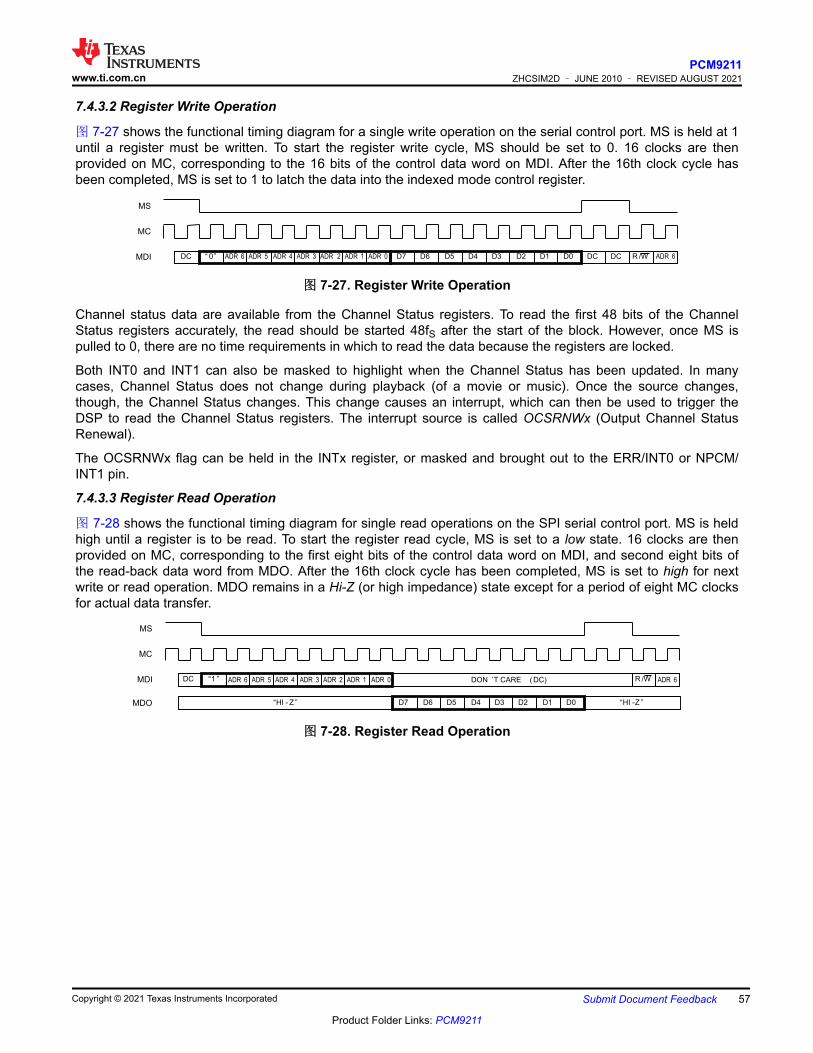
7.4.3.2 Register Write Operation
图 7-27 shows the functional timing diagram for a single write operation on the serial control port. MS is held at 1 until a register must be written. To start the register write cycle, MS should be set to 0. 16 clocks are then provided on MC, corresponding to the 16 bits of the control data word on MDI. After the 16th clock cycle has been completed, MS is set to 1 to latch the data into the indexed mode control register.
MS
MC
MDI ADR 6 ADR 5 ADR 4 ADR 3 ADR 2 ADR 1 ADR 0 D7 D6 D5 D4 D3 D2 D1 D0 DC DC R /W ADR 6DC “ 0”
图 7-27. Register Write Operation
Channel status data are available from the Channel Status registers. To read the first 48 bits of the Channel Status registers accurately, the read should be started 48fS after the start of the block. However, once MS is pulled to 0, there are no time requirements in which to read the data because the registers are locked.
Both INT0 and INT1 can also be masked to highlight when the Channel Status has been updated. In many cases, Channel Status does not change during playback (of a movie or music). Once the source changes, though, the Channel Status changes. This change causes an interrupt, which can then be used to trigger the DSP to read the Channel Status registers. The interrupt source is called OCSRNWx (Output Channel Status Renewal).
The OCSRNWx flag can be held in the INTx register, or masked and brought out to the ERR/INT0 or NPCM/INT1 pin.
7.4.3.3 Register Read Operation
图 7-28 shows the functional timing diagram for single read operations on the SPI serial control port. MS is held high until a register is to be read. To start the register read cycle, MS is set to a low state. 16 clocks are then provided on MC, corresponding to the first eight bits of the control data word on MDI, and second eight bits of the read-back data word from MDO. After the 16th clock cycle has been completed, MS is set to high for next write or read operation. MDO remains in a Hi-Z (or high impedance) state except for a period of eight MC clocks for actual data transfer.
MS
MC
MDI ADR 6 ADR 5 ADR 4 ADR 3 ADR 2 ADR 1 DON ’T CARE ( DC)ADR 0 R /W ADR 6DC “1 ”
MDO D7 D6 D5 D4 D3 D2 D1 D0“HI - Z ” “HI -Z ”
图 7-28. Register Read Operation
www.ti.com.cnPCM9211
ZHCSIM2D – JUNE 2010 – REVISED AUGUST 2021
Copyright © 2021 Texas Instruments Incorporated Submit Document Feedback 57
Product Folder Links: PCM9211

7.4.3.4 Control Interface Timing Requirements
图 7-29 shows a detailed timing diagram for the four-wire serial control interface. These timing parameters are critical for proper control port operation. Timing Requirements lists the timing requirements.
tM S S
LSB (D0)MDI
MC
MS
tMDHtMDS
t MS HtMCH tMCL
tMCY
1.4 V
1.4 V
1.4 V
MDO 0.5*VDD
tMD D
t MHH
t MDR
LSB (D0 )MSB (D7)
MSB (R/W)
Hi -Z Hi -Z
tM DD
ADR0
图 7-29. Control Interface Timing Requirements
7.4.4 Two-Wire (I2C) Serial Control
The PCM9211 also supports the I2C serial bus and data transmission protocol. It can be configured for fast mode as a slave device.
7.4.4.1 Slave Address
MSB LSB
1 0 0 0 0 ADR1 ADR0 R/ W
The PCM9211 has seven bits for its own slave address. The first five bits (MSB) of the slave address are factory-preset to '10000'. The next two bits of the address byte are selectable bits that can be set by MDO/ADR0 and MS/ADR1. A maximum of four PCM9211s can be connected on the same bus at one time. Each PCM9211 responds when it receives its own slave address.
PCM9211ZHCSIM2D – JUNE 2010 – REVISED AUGUST 2021 www.ti.com.cn
58 Submit Document Feedback Copyright © 2021 Texas Instruments Incorporated
Product Folder Links: PCM9211

7.4.4.2 Packet Protocol
A master device must control the packet protocol, which consists of a start condition, slave address with read/write bit, data if a write procedure is desired, or an acknowledgment if read and stop conditions exist. The PCM9211 supports both slave receiver and transmitter functions. Details of the DATA pulse for both write and read operations are described in 图 7-30.
9
SDA
SCLSt
Startcondition
1–7 8 1–8 9 1– 8 9 9 Sp
Stopcondition
Slave address R/W ACK DATA ACK DATA ACK ACK
R/W: Read o peration if 1; otherwise, write operationACK: Acknowledgement of a byte if 0, n ot Acknowledgement of a bite if 1
DATA: 8 b its ( byte) , Details are described in write and read operation .
图 7-30. I2C Packet Protocol
7.4.4.3 Write Operation
The PCM9211 can only function as an I2C slave. A master can write to any PCM9211 registers using either single or multiple accesses. The master sends a PCM9211 slave address with a write bit, a register address, and the data. When undefined registers are accessed, the PCM9211 does not send an acknowledgment. 图 7-30 illustrates the write operation. The register address and the write data are 8-bit, MSB-first format.
图 7-30. Framework for Write OperationTransmitter M M M S M S M S M S S M
Data Type St slaveaddress W ACK reg
address ACK writedata 1 ACK write
data 2 ACK ACK Sp
M: Master Device, S: Slave Device, St: Start Condition, W: Write, ACK: Acknowledge, Sp: Stop Condition
7.4.4.4 Read Operation
A master can read the PCM9211 registers. The value of the register address is stored in an indirect index register in advance. The master sends the PCM9211 slave address with a read bit after storing the register address. The PCM9211 then transfers the data to which the index register points. 图 7-31 shows the read operation.
图 7-31. Framework for Read OperationTransmitter M M M S M S M M M S S M M
Data Type St slaveaddress W ACK reg
address ACK Sr slaveaddress R ACK read
data NACK Sp
M: Master Device, S: Slave Device, St: Start Condition, Sr: Repeated Start Condition, W: Write, R: Read,ACK: Acknowledge, NACK: Not Acknowledge, Sp: Stop Condition
The slave address after the repeated start condition must be the same as the previous slave address.
www.ti.com.cnPCM9211
ZHCSIM2D – JUNE 2010 – REVISED AUGUST 2021
Copyright © 2021 Texas Instruments Incorporated Submit Document Feedback 59
Product Folder Links: PCM9211

7.4.4.5 Timing Diagram
图 7-33 shows the detailed timing diagram for SCL and SDA. Timing Requirements lists the timing requirements.
SDA
SCL
Start Repeated Start Stop
tBUF tD-SU
tD-HD
tLOW
tSCL-F
tS-HD tHI tS-SU
tSCL-R tS-HD
tSDA-R
tSDA-F
tP-SU
tGW
图 7-33. Control Interface Timing
PCM9211ZHCSIM2D – JUNE 2010 – REVISED AUGUST 2021 www.ti.com.cn
60 Submit Document Feedback Copyright © 2021 Texas Instruments Incorporated
Product Folder Links: PCM9211

7.5 Register Maps表 7-35 shows the PCM9211 register map that lists all the registers available in this device.
表 7-35. Register MapADR REGISTER DESCRIPTION R/W B7 B6 B5 B4 B3 B2 B1 B0
20h ERROR Output Condition and Shared Port Settings R/W RSV ERRCON MCHR RSV ERRHZ ERRSEL NPCMHZ NPCMSEL
21h DIR Initial Settings 1/3 R/W RSV RSV RSV RXFSRNG RSV RSV RSV RSV
22h DIR Initial Settings 2/3 R/W RSV CLKSTCON RSV CLKSTP RSV RSV RSV RXVDLY
23h DIR Initial Settings 3/3 R/W RSV RSV XTIWT1 XTIWT0 PRTPRO1 PRTPRO0 ERRWT1 ERRWT0
24h Oscillation Circuit Control R/W OSCAUTO RSV RSV XMCKEN XMCKDIV1 XMCKDIV0 RSV RSV
25h ERROR Cause Setting R/W RSV RSV EFSCHG EFSLMT ENPCM EVALID EPARITY EUNLOCK
26h AUTO Source Selector Cause Setting R/W ACKSL AERROR RSV AFSLMT ANPCM AVALID RSV AUNLOCK
27h DIR Acceptable fS Range Setting and Mask R/W MSK128 MSK64 RSV NOMLMT HILMT1 HILMT0 LOLMT1 LOLMT0
28h Non-PCM Definition Setting R/W RSV RSV CS1BPLS NPCMP RSV DTSCD PAPB CSBIT1
29h DTS CD/LD Detection Setting R/W RSV RSV RSV RSV DTS16 DTS14 DTSPRD1 DTSPRD0
2Ah INT0 Output Cause Mask Setting R/W MERROR0 MNPCM0 MEMPHF0 MDTSCD0 MCSRNW0 MPCRNW0 MFSCHG0 RSV
2Bh INT1 Output Cause Mask Setting R/W MERROR1 MNPCM1 MEMPHF1 MDTSCD1 MCSRNW1 MPCRNW1 MFSCHG1 MADLVL1
2Ch INT0 Output Register R OERROR0 ONPCM0 OEMPHF0 ODTSCD0 OCSRNW0 OPCRNW0 OFSCHG0 RSV
2Dh INT1 Output Register R OERROR1 ONPCM1 OEMPHF1 ODTSCD1 OCSRNW1 OPCRNW1 OFSCHG1 OADLVL1
2Eh INT0, INT1 Output Polarity Setting R/W RSV INT1P RSV ADLVLTH1 ADLVLTH0 INT0P RSV RSV
2Fh DIR Output Data Format R/W RSV RSV RSV RSV RSV RXFMT2 RXFMT1 RXFMT0
30h DIR Recovered System Clock Ratio Setting R/W RSV RSV RSV PSCKAUTO RSV PSCK2 PSCK1 PSCK0
31h XTI Source Clock Frequency Setting R/W RSV RSV XSCK1 XSCK0 XBCK1 XBCK0 XLRCK1 XLRCK0
32h DIR Source, Sec. Bit/LR Clock Frequency Setting R/W RSV PSBCK2 PSBCK1 PSBCK0 RSV PSLRCK2 PSLRCK1 PSLRCK0
33h XTI Source, Sec. Bit/LR Clock Frequency Setting R/W RSV XSBCK2 XSBCK1 XSBCK0 RSV XSLRCK2 XSLRCK1 XSLRCK0
34h DIR Input Biphase Source Select, Coax Amp. Control R/W RX0DIS RX1DIS RSV RSV RXSEL3 RXSEL2 RXSEL1 RXSEL0
35h RECOUT0 Output Biphase Source Select R/W RSV RSV RSV MPO0MUT RO0SEL3 RO0SEL2 RO0SEL1 RO0SEL0
36h RECOUT1 Output Biphase Source Select R/W RSV RSV RSV MPO1MUT RO1SEL3 RO1SEL2 RO1SEL1 RO1SEL0
37h Port fS Calculator Measurement Target Setting R/W RSV RSV RSV RSV RSV PFSTGT2 PFSTGT1 PFSTGT0
38h Port fS Calculator Result Output R PFSST PFSPO2 PFSPO1 PFSPO0 PFSOUT3 PFSOUT2 PFSOUT1 PFSOUT0
39h Incoming Biphase Information and Calculated fS Output R SFSST SCSBIT1 RSV RSV SFSOUT3 SFSOUT2 SFSOUT1 SFSOUT0
3Ah PC Buffer Byte0 (Burst Preamble PC Output Register) R PC7 PC6 PC5 PC4 PC3 PC2 PC1 PC0
3Bh PC Buffer Byte1 (Burst Preamble PC Output Register) R PC15 PC14 PC13 PC12 PC11 PC10 PC9 PC8
3Ch PD Buffer Byte0 (Burst Preamble PD Output Register) R PD7 PD6 PD5 PD4 PD3 PD2 PD1 PD0
3Dh PD Buffer Byte1 (Burst Preamble PD Output Register) R PD15 PD14 PD13 PD12 PD11 PD10 PD9 PD8
40h System Reset Control R/W MRST SRST ADDIS RXDIS RSV RSV TXDIS XODIS
42h ADC Function Control 1/3 R/W RSV RSV ADCKOUT ADDTRX7 ADFSLMT ADCLK2 ADCLK1 ADCLK0
46h ADC L-ch, digital ATT control R/W ADATTL7 ADATTL6 ADATTL5 ADATTL4 ADATTL3 ADATTL2 ADATTL1 ADATTL0
47h ADC R-ch, digital ATT control R/W ADATTR7 ADATTR6 ADATTR5 ADATTR4 ADATTR3 ADATTR2 ADATTR1 ADATTR0
48h ADC Function Control 2/3 R/W RSV ADIFMD2 ADIFMD1 ADIFMD0 RSV RSV ADFMT1 ADFMT0
49h ADC Function Control 3/3 R/W RSV RSV RSV ADZCDD ADBYP ADPHSE ADMUTR ADMUTL
5Ah DIR Channel Status Data Buffer 1/6 R RXCS7 RXCS6 RXCS5 RXCS4 RXCS3 RXCS2 RXCS1 RXCS0
5Bh DIR Channel Status Data Buffer 2/6 R RXCS15 RXCS14 RXCS13 RXCS12 RXCS11 RXCS10 RXCS9 RXCS8
5Ch DIR Channel Status Data Buffer 3/6 R RXCS23 RXCS22 RXCS21 RXCS20 RXCS19 RXCS18 RXCS17 RXCS16
5Dh DIR Channel Status Data Buffer 4/6 R RXCS31 RXCS30 RXCS29 RXCS28 EXCS27 RXCS26 RXCS25 RXCS24
5Eh DIR Channel Status Data Buffer 5/6 R RXCS39 RXCS38 RXCS37 RXCS36 RXCS35 RXCS34 RXCS33 RXCS32
5Fh DIR Channel Status Data Buffer 6/6 R RXCS47 RXCS46 RXCS45 RXCS44 RXCS43 RXCS42 RXCS41 RXCS40
60h DIT Function Control 1/3 R/W RSV TXSSRC2 TXSSRC1 TXSSRC0 RSV TXPSRC2 TXPSRC1 TXPSRC0
61h DIT Function Control 2/3 R/W RSV TXSCK2 TXSCK1 TXSCK0 RSV RSV TXFMT1 TXFMT0
62h DIT Function Control 3/3 R/W RSV RSV TXDMUT RSV TXVFLG RSV RSV RSV
63h DIT Channel Status Data Buffer 1/6 R/W TXCS7 TXCS6 TXCS5 TXCS4 TXCS3 TXCS2 TXCS1 TXCS0
64h DIT Channel Status Data Buffer 2/6 R/W TXCS15 TXCS14 TXCS13 TXCS12 TXCS11 TXCS10 TXCS9 TXCS8
65h DIT Channel Status Data Buffer 3/6 R/W TXCS23 TXCS22 TXCS21 TXCS20 TXCS19 TXCS18 TXCS17 TXCS16
66h DIT Channel Status Data Buffer 4/6 R/W TXCS31 TXCS30 TXCS29 TXCS28 TXCS27 TXCS26 TXCS25 TXCS24
67h DIT Channel Status Data Buffer 5/6 R/W TXCS39 TXCS38 TXCS37 TXCS36 TXCS35 TXCS34 TXCS33 TXCS32
www.ti.com.cnPCM9211
ZHCSIM2D – JUNE 2010 – REVISED AUGUST 2021
Copyright © 2021 Texas Instruments Incorporated Submit Document Feedback 61
Product Folder Links: PCM9211

表 7-35. Register Map (continued)ADR REGISTER DESCRIPTION R/W B7 B6 B5 B4 B3 B2 B1 B0
68h DIT Channel Status Data Buffer 6/6 R/W TXCS47 TXCS46 TXCS45 TXCS44 TXCS43 TXCS42 TXCS41 TXCS40
6Ah Main Output and AUXOUT Port Data Mute Control R/W AOMUTAS MOMUTAS RSV RSV AOLRMTEN AODMUT MOLRMTEN MODMUT
6Bh Main Output Port, Output Source Setting R/W RSV MOSSRC2 MOSSRC1 MOSSRC0 RSV MOPSRC2 MOPSRC1 MOPSRC0
6Ch AUX Output Port, Output Source Setting R/W RSV AOSSRC2 AOSSRC1 AOSSRC0 RSV AOPSRC2 AOPSRC1 AOPSRC0
6Dh MPIO_B & Main Output Port Hi-Z Control R/W MPB3HZ MPB2HZ MPB1HZ MPB0HZ SCKOHZ BCKHZ LRCKHZ DOUTHZ
6Eh MPIO_C and MPIO_A Hi-Z Control R/W MPC3HZ MPC2HZ MPC1HZ MPC0HZ MPA3HZ MPA2HZ MPA1HZ MPA0HZ
6Fh MPIO_A, MPIO_B, MPIO_C Group Function Assign R/W MPASEL1 MPASEL0 MPBSEL2 MPBSEL1 MPBSEL0 MPCSEL2 MPCSEL1 MPCSEL0
70h MPIO_A, Flags/GPIO Assign Setting R/W RSV RSV MCHSRC1 MCHSRC0 MPA3SEL MPA2SEL MPA1SEL MPA0SEL
71h MPIO_B, MPIO_C, Flags/GPIO Assign Setting R/W MPB3SEL MPB2SEL MPB1SEL MPB0SEL MPC3SEL MPC2SEL MPC1SEL MPC0SEL
72h MPIO_A1, MPIO_A0 Output Flag Select R/W MPA1FLG3 MPA1FLG2 MPA1FLG1 MPA1FLG0 MPA0FLG3 MPA0FLG2 MPA0FLG1 MPA0FLG0
73h MPIO_A3, MPIO_A2 Output Flag Select R/W MPA3FLG3 MPA3FLG2 MPA3FLG1 MPA3FLG0 MPA2FLG3 MPA2FLG2 MPA2FLG1 MPA2FLG0
74h MPIO_B1, MPIO_B0 Output Flag Select R/W MPB1FLG3 MPB1FLG2 MPB1FLG1 MPB1FLG0 MPB0FLG3 MPB0FLG2 MPB0FLG1 MPB0FLG0
75h MPIO_B3, MPIO_B2 Output Flag Select R/W MPB3FLG3 MPB3FLG2 MPB3FLG1 MPB3FLG0 MPB2FLG3 MPB2FLG2 MPB2FLG1 MPB2FLG0
76h MPIO_C1, MPIO_C0 Output Flag Select R/W MPC1FLG3 MPC1FLG2 MPC1FLG1 MPC1FLG0 MPC0FLG3 MPC0FLG2 MPC0FLG1 MPC0FLG0
77h MPIO_C3, MPIO_C2 Output Flag Select R/W MPC3FLG3 MPC3FLG2 MPC3FLG1 MPC3FLG0 MPC2FLG3 MPC2FLG2 MPC2FLG1 MPB2FLG0
78h MPO1, MPO0 Function Assign Setting R/W MPO1SEL3 MPO1SEL2 MPO1SEL1 MPO1SEL0 MPO0SEL3 MPO0SEL2 MPO0SEL1 MPO0SEL0
79h GPIO I/O Direction control for MPIO_A, MPIO_B R/W GIOB3DIR GIOB2DIR GIOB1DIR GIOB0DIR GIOA3DIR GIOA2DIR GIOA1DIR GIOA0DIR
7Ah GPIO I/O Direction control for MPIO_C R/W RSV RSV RSV RSV GIOC3DIR GIOC2DIR GIOC1DIR GIOC0DIR
7Bh GPIO Output Data Setting for MPIO_A, MPIO_B R/W GPOB3 GPOB2 GPOB1 GPOB0 GPOA3 GPOA2 GPOA1 GPOA0
7Ch GPIO Output Data Setting for MPIO_C R/W RSV RSV RSV RSV GPOC3 GPOC2 GPOC1 GPOC0
7Dh GPIO Input Data Register for MPIO_A, MPIO_B R GPIB3 GPIB2 GPIB1 GPIB0 GPIA3 GPIA2 GPIA1 GPIA0
7Eh GPIO Input Data Register for MPIO_C R RSV RSV RSV RSV GPIC3 GPIC2 GPIC1 GPIC0
Note
Blank spaces are provided to aid in development. Record your register settings for future reference.
PCM9211ZHCSIM2D – JUNE 2010 – REVISED AUGUST 2021 www.ti.com.cn
62 Submit Document Feedback Copyright © 2021 Texas Instruments Incorporated
Product Folder Links: PCM9211

7.5.1 Error Output Condition and Shared Port Settings Register (address = 20h) [reset = 00000000]
图 7-33. Error Output Condition and Shared Port Settings Register7 6 5 4 3 2 1 0
RSV ERRCON MCHR RSV ERRHZ ERRSEL NPCMHZ NPCMSEL
R/W-0h R/W-0h R/W-0h R/W-0h R/W-0h R/W-0h R/W-0h R/W-0h
LEGEND: R/W = Read/Write; R = Read only; -n = value after reset
ERRCON: ERROR Output Condition Setting0: ERROR pin output is always DIR status (default)1: ERROR output depends on source control MOPSRC[2:0]
DIR/AUTO: Output DIR statusExcept DIR: ERROR outputs high (error status).
MCHR: MPIO/Multi-Channel PCM Routing Select0: All MPIOs are controlled by MPASEL[1:0], MPBSEL[1:0], MPCSEL[2:0] (Default)1: All MPIOs are assigned for Multichannel PCM Routing I/O.
ERRHZ: ERROR/INT0 Port Output Hi-Z Control0: Output (default)1: Hi-Z
ERRSEL: ERROR/INT0 Port Output Source Select0: ERROR (default)1: INT0
NOTE: ERRSEL must be 0 when Register 26h/AERROR = 1 or Register 42h/ADFSLMT = 1, or if the signal CLKST is used.NPCMHZ: NPCM/INT1 Port Output Hi-Z Control
0: Output (default)1: Hi-Z
NPCMSEL: NPCM/INT1 Port Output Source Select0: NPCM (default)1: INT1
7.5.2 DIR Initial Settings Register 1/3 (address: 21h) [reset = 00000000]
图 7-34. DIR Initial Settings Register 1/37 6 5 4 3 2 1 0
RSV RSV RSV RXFSRNG RSV RSV RSV RSV
R/W-0h R/W-0h R/W-0h R/W-0h R/W-0h R/W-0h R/W-0h R/W-0h
LEGEND: R/W = Read/Write; R = Read only; -n = value after reset
RXFSRNG: DIR Receivable Incoming Biphase Sampling Frequency Range Setting0: Wide mode (7 kHz to 216 kHz) (default)1: Normal mode (28 kHz to 108 kHz)
www.ti.com.cnPCM9211
ZHCSIM2D – JUNE 2010 – REVISED AUGUST 2021
Copyright © 2021 Texas Instruments Incorporated Submit Document Feedback 63
Product Folder Links: PCM9211

7.5.3 DIR Initial Settings Register 2/3 (address: 22h) [reset = 00000001]
图 7-35. DIR Initial Settings Register 2/37 6 5 4 3 2 1 0
RSV CLKSTCON RSV CLKSTP RSV RSV RSV RXVDLY
R/W-0h R/W-0h R/W-0h R/W-0h R/W-0h R/W-0h R/W-0h R/W-1h
LEGEND: R/W = Read/Write; R = Read only; -n = value after reset
CLKSTCON: CLKST Output Condition Setting0: Only PLL Lock status change (default)1: All events where the Main port output clock condition changes, as well as these cases:
1. MOSSRC/MOPSRC register is updated to ADC, AUXIN0, AUXIN1, or AUXIN22. DIR and ADC are switched by DIR status when MOSSRC = 000(AUTO) and MOPSRC = 000(AUTO)3. Main port sampling frequency changes when PFSTGT = 101(Main output port)
NOTES:CLKST never outputs when updating MOSSRC and MOPSRC to AUTO or DIR.OSCAUTO must be 0 when CLKST is used because CLKST is generated by frequency counting of built-in oscillator circuit.To output CLKST, MOSSRC and MOPSRC are set simultaneously.
CLKSTP: CLKST Polarity Setting0: Active low (default)1: Active high
RXVDLY: VOUT Delay Setting0: VOUT is active immediately after validity flag is detected1: VOUT is active after synchronization with DOUT data (default)
PCM9211ZHCSIM2D – JUNE 2010 – REVISED AUGUST 2021 www.ti.com.cn
64 Submit Document Feedback Copyright © 2021 Texas Instruments Incorporated
Product Folder Links: PCM9211

7.5.4 DIR Initial Settings Register 3/3 (address: 23h) [reset = 00000100]
图 7-36. DIR Initial Settings Register 3/37 6 5 4 3 2 1 0
RSV RSV XTIWT1 XTIWT0 PRTPRO1 PRTPRO0 ERRWT1 ERRWT0
R/W-0h R/W-0h R/W-0h R/W-0h R/W-0h R/W-1h R/W-0h R/W-0h
LEGEND: R/W = Read/Write; R = Read only; -n = value after reset
XTIWT[1:0]: Crystal OSC, Oscillation Start-up Wait Time Setting00: 25 ms01: 50 ms10: 100 ms11: 200 ms
XTIWT is counted by the PLL generated clock.These are the resulting values when the PLL is running with a free-run clock because of no S/PDIF input.After these delay times, the Main Port source changes from DIR to ADC when DIR is unlocked.
PRTPRO[1:0]: Process for Parity Error Detection00: No process
01: For PCM data only, an 8x continuous parity error is replaced by previous data and muted after ninth parity error at EPARITY = 1 (default)
10: For PCM and non-PCM data, an 8x continuous parity error is replaced by previous data and muted after ninth parity error at EPARITY = 1
11: Reserved (The definition of Non-PCM depends on the Non-PCM Definition Setting Register)Validity flag, user bit, channel status, Non-PCM and DTS-CD detection should be refreshed by waiting more than 192/fS without any parity error.
ERRWT[1:0]: ERROR Release Wait Time Setting00: ERROR Release after 48 counts of preamble B (Default), 192 ms at fS = 48 kHz01: ERROR Release after 12 counts of preamble B10: ERROR Release after six counts of preamble B11: ERROR Release after three counts of preamble B
These counts are only available when DIR is unlocked or DIR sampling frequency is changed or exceeds limits defined by DIR Acceptable fS Range Setting and Mask registers.CLKST also uses ERRWT to release.
www.ti.com.cnPCM9211
ZHCSIM2D – JUNE 2010 – REVISED AUGUST 2021
Copyright © 2021 Texas Instruments Incorporated Submit Document Feedback 65
Product Folder Links: PCM9211

7.5.5 Oscillation Circuit Control Register (address: 24h) [reset = 00000000]
图 7-37. Oscillation Circuit Control Register7 6 5 4 3 2 1 0
OSCAUTO RSV RSV XMCKEN XMCKDIV1 XMCKDIV0 RSV RSV
R/W-0h R/W-0h R/W-0h R/W-0h R/W-0h R/W-0h R/W-0h R/W-0h
LEGEND: R/W = Read/Write; R = Read only; -n = value after reset
OSCAUTO: Oscillation Circuit Automatic Operation Control0: Built-in oscillator circuit always operates (default)1: Built-in oscillator circuit is stopped during lock state of DIR but is active when DIR locks and CLKST is active
NOTES:The XODIS command has more priority than this OSCAUTO register.If XODIS is set to power down, the XTI source is not output.
XMCKENX: MCKO (XTI Clock Buffered Output) Output Enable Control0: MUTE (Logic low level) (default)1: Output
XMCKDIV[1:0]: XMCKO (XTI Clock Buffered Output) Output Clock Dividing Ratio00: XTI/1 (24.576 MHz) (default)01: XTI/2 (12.288 MHz)10: XTI/4 (6.144 MHz)11: XTI/8 (3.072 MHz)
PCM9211ZHCSIM2D – JUNE 2010 – REVISED AUGUST 2021 www.ti.com.cn
66 Submit Document Feedback Copyright © 2021 Texas Instruments Incorporated
Product Folder Links: PCM9211

7.5.6 Error Cause Setting Register (address = 25h) [reset = 00000001]
The following ERROR Cause Setting registers are independent of the AUTO Source Selector Cause Setting register (26h).
图 7-38. Error Cause Setting Register7 6 5 4 3 2 1 0
RSV RSV EFSCHG EFSLMT ENPCM EVALID EPARITY EUNLOCK
R/W-0h R/W-0h R/W-0h R/W-0h R/W-0h R/W-0h R/W-0h R/W-1h
LEGEND: R/W = Read/Write; R = Read only; -n = value after reset
EFSCHG: DIR Sampling Frequency Change0: Not selected (default)1: Selected
EFSLMT: DIR Limiting Acceptable Sampling Frequency0: Not selected (default)1: Selected
The definition of receivable sampling frequency range depends on the fS Limit Setting Register.ENPCM: Non-PCM
0: Not selected (default)1: Selected
The definition of non-PCM depends on the Non-PCM Definition Setting Register.EVALID: Validity Flag
0: Not selected (default)1: Selected
EPARITY: Parity Error0: Not selected (default)1: Selected
EUNLOCK: PLL Lock Error0: Not selected1: Selected (default)
This register is used for setting the ERROR output factor.The required factors of ERROR set to 1 are selected based on OR logic.
www.ti.com.cnPCM9211
ZHCSIM2D – JUNE 2010 – REVISED AUGUST 2021
Copyright © 2021 Texas Instruments Incorporated Submit Document Feedback 67
Product Folder Links: PCM9211

7.5.7 AUTO Source Selector Cause Setting Register (address = 26h) [reset = 00000001]
图 7-39. AUTO Source Selector Cause Setting Register7 6 5 4 3 2 1 0
ACKSL AERROR RSV AFSLMT ANPCM AVALID RSV AUNLOCK
R/W-0h R/W-0h R/W-0h R/W-0h R/W-0h R/W-0h R/W-0h R/W-1h
LEGEND: R/W = Read/Write; R = Read only; -n = value after reset
The AUTO source selector is an automatic selector that outputs DIR or ADC output based on the following register settings. The following AUTO Source Selector Cause Setting registers are independent of the ERROR Cause Setting register (25h).ACKSL: ADC Output Clock Select
0: ADC clock selected by the ADCLK[2:0] register (42h) (default)1: XTI clock
AERROR: ERROR0: Not selected (default)1: Selected
ERROR condition is defined by the ERROR Cause Setting register (25h).AFSLMT: Limiting Acceptable Sampling Frequency
0: Not selected (default)1: Selected
The definition of receivable sampling frequency range depends on the fS Limit Setting register.ANPCM: Non-PCM
0: Not selected (default)1: Selected
The definition of non-PCM depends on the Non-PCM Definition Setting register.AVALID: Validity Flag
0: Not selected (default)1: Selected
AUNLOCK: PLL Lock Error0: Not selected1: Selected (default)
PCM9211ZHCSIM2D – JUNE 2010 – REVISED AUGUST 2021 www.ti.com.cn
68 Submit Document Feedback Copyright © 2021 Texas Instruments Incorporated
Product Folder Links: PCM9211

7.5.8 DIR Acceptable fS Range Setting and Mask Register (address: 27h) [reset = 00000000]
图 7-40. DIR Acceptable fS Range Setting and Mask Register7 6 5 4 3 2 1 0
MSK128 MSK64 RSV NOMLMT HILMT1 HILMT0 LOLMT1 LOLMT0
R/W-0h R/W-0h R/W-0h R/W-0h R/W-0h R/W-0h R/W-0h R/W-0h
LEGEND: R/W = Read/Write; R = Read only; -n = value after reset
MSK128: Mask for fS = 128 kHz0: No mask (default)1: Mask
PCM9211 does not receive 128-kHz sampling frequency.This register setting is effective with NOMLMT = 1.
MSK64: Mask for fS = 64 kHz0: No mask (default)1: Mask
PCM9211 does not receive 64-kHz sampling frequency.This register setting is effective with NOMLMT = 1.
NOMLMT: Receive Nominal Audio fS within ±2%0: No limit (default)1: Limit
PCM9211 receives the nominal audio sampling frequencies within ±2%.The nominal audio sampling frequencies are: 8 kHz, 11.025 kHz, 12 kHz, 16 kHz, 22.05 kHz, 24 kHz, 32 kHz, 44.1 kHz, 48 kHz, 64 kHz, 88.2 kHz, 96 kHz, 128 kHz, 176.4 kHz, 192 kHz
HILMT[1:0]: Acceptable fS Higher Limit Setting00: No limit (default)01: fS = 54 kHz10: fS = 108 kHz11: fS = 216 kHz
LOLMT[1:0]: Acceptable fS Lower Limit Setting00: No limit (default)01: fS = 7 kHz10: fS = 14 kHz11: fS = 28 kHz
www.ti.com.cnPCM9211
ZHCSIM2D – JUNE 2010 – REVISED AUGUST 2021
Copyright © 2021 Texas Instruments Incorporated Submit Document Feedback 69
Product Folder Links: PCM9211

7.5.9 Non-PCM Definition Register (address = 28h) [reset = 00000011]
图 7-41. Non-PCM Definition Register7 6 5 4 3 2 1 0
RSV RSV CS1BPLS NPCMP RSV DTSCD PAPB CSBIT1
R/W-0h R/W-0h R/W-0h R/W-0h R/W-0h R/W-0h R/W-1h R/W-1h
LEGEND: R/W = Read/Write; R = Read only; -n = value after reset
CS1BPLS: CSBIT1 Detection Signal Select0: Hold value (default)1: Pulse
NPCMP: NPCM Pin Output Polarity0: Active high (default)1: Active low
DTSCD: DTS CD/LD Detection0: Unselected (default)1: Selected
PAPB: Burst Preamble PA and PB Detection0: Unselected1: Selected (default)
CSBIT1: Channel Status Bit1 = 1 Detection0: Unselected1: Selected (default)
This register is used to set the definition of non-PCM data. The NPCM pin output and NPCM register flag output follow this definition.
There are three types of non-PCM factors to be selected, based on OR logic.
Note
The DTSCD register (29h) must be 1 (that is, selected) in order to output the DTSCD flag from the MPIO, MPO, and INT pins as DIR Flag outputs.
PCM9211ZHCSIM2D – JUNE 2010 – REVISED AUGUST 2021 www.ti.com.cn
70 Submit Document Feedback Copyright © 2021 Texas Instruments Incorporated
Product Folder Links: PCM9211

7.5.10 DTS-CD/LD Sync Word and Period Detection Setting Register (address: 29h) [reset = 00001100]
图 7-42. DTS-CD/LD Sync Word and Period Detection Setting Register7 6 5 4 3 2 1 0
RSV RSV RSV RSV DTS16 DTS14 DTSPRD1 DTSPRD0
R/W-0h R/W-0h R/W-0h R/W-0h R/W-1h R/W-1h R/W-0h R/W-0h
LEGEND: R/W = Read/Write; R = Read only; -n = value after reset
DTS16: DTS-CD/LD 16-bit Sync Word Detection0: Unselected1: Selected (default)
DTS14: DTS-CD/LD 14-bit Sync Word Detection0: Unselected1: Selected (default)
DTSPRD[1:0]: DTS-CD/LD Sync Word Detection Period00: No period, detect one sync word (default)01: One period10: Two periods11: Four periods
Note
The DTSCD register (register 28h) must be 1 (that is, selected) in order to output the DTSCD flag from the MPIO, MPO, and INT pins as DIR Flag outputs.
www.ti.com.cnPCM9211
ZHCSIM2D – JUNE 2010 – REVISED AUGUST 2021
Copyright © 2021 Texas Instruments Incorporated Submit Document Feedback 71
Product Folder Links: PCM9211

7.5.11 INT0 Output Cause Mask Setting Register (Address: 2Ah) [reset = 11111111]
图 7-43. INT0 Output Cause Mask Setting Register7 6 5 4 3 2 1 0
MERROR0 MNPCM0 MEMPHF0 MDTSCD0 MCSRNW0 MPCRNW0 MFSCHG0 RSV
R/W-1h R/W-1h R/W-1h R/W-1h R/W-1h R/W-1h R/W-1h R/W-1h
LEGEND: R/W = Read/Write; R = Read only; -n = value after reset
MERROR0: ERROR Port Output Status0: Not masked1: Masked (default)
MNPCM0: NPCM Port Output Status0: Not masked1: Masked (default)
This register setting follows the register setting of non-PCM data identification.MEMPHF0: Emphasis Flag in Channel Status
0: Not masked1: Masked (default)
MDTSCD0: DTS-CD/LD Sync Detection0: Not masked1: Masked (default)
This detection condition depends on the register setting for DTS-CD/LD detection conditions.MCSRNW0: Channel Status Data of Beginning 48-bit Renewal
0: Not masked1: Masked (default)
MPCRNW0: Burst Preamble PC Renewal0: Not masked1: Masked (default)
MFSCHG0: Renewal Flag of fS Calculator Result0: Not masked1: Masked (default)
PCM9211ZHCSIM2D – JUNE 2010 – REVISED AUGUST 2021 www.ti.com.cn
72 Submit Document Feedback Copyright © 2021 Texas Instruments Incorporated
Product Folder Links: PCM9211

7.5.12 INT1 Output Cause Mask Setting Register (Address: 2Bh) [reset = 11111111]
图 7-44. INT1 Output Cause Mask Setting Register7 6 5 4 3 2 1 0
MERROR1 MNPCM1 MEMPHF1 MDTSCD1 MCSRNW1 MPCRNW1 MFSCHG1 MADLVL1
R/W-1h R/W-1h R/W-1h R/W-1h R/W-1h R/W-1h R/W-1h R/W-1h
LEGEND: R/W = Read/Write; R = Read only; -n = value after reset
MERROR1: ERROR Port Output Status0: Not masked1: Masked (default)
MNPCM1: NPCM Port Output Status0: Not masked1: Masked (default)
This register setting follows the register setting of non-PCM data identification.MEMPHF1: Emphasis Flag in Channel Status
0: Not masked1: Masked (default)
MDTSCD1: DTS-CD/LD Sync Detection0: Not masked1: Masked (default)
This detection condition depends on the register setting for DTS-CD/LD detection conditions.MCSRNW1: Channel Status Data of Beginning 48-bit Renewal
0: Not masked1: Masked (default)
MPCRNW1: Burst Preamble PC Renewal0: Not masked1: Masked (default)
MFSCHG1: Renewal Flag of fS Calculator Result0: Not masked1: Masked (default)
MADLVL1: ADC Input Level Detection Status0: Not masked1: Masked (default)
www.ti.com.cnPCM9211
ZHCSIM2D – JUNE 2010 – REVISED AUGUST 2021
Copyright © 2021 Texas Instruments Incorporated Submit Document Feedback 73
Product Folder Links: PCM9211

7.5.13 INT0 Output Register (address = 2Ch) [reset = N/A]
图 7-45. INT0 Output Register7 6 5 4 3 2 1 0
OERROR0 ONPCM0 OEMPHF0 ODTSCD0 OCSRNW0 OPCRNW0 OFSCHG0 RSV
R-N/A R-N/A R-N/A R-N/A R-N/A R-N/A R-N/A R-0h
LEGEND: R/W = Read/Write; R = Read only; -n = value after reset
OERROR0: ERROR Port Output Status0: No ERROR1: Detect ERROR
This register setting follows the register setting of the ERROR factor.ONPCM0: NPCM Port Output Status
0: PCM data1: Non-PCM data
This register setting follows the register setting of non-PCM data identification.OEMPHF0: Emphasis Flag in Channel Status
0: No emphasis1: Emphasis
ODTSCD0: DTS-CD/LD Detection0: No DTS-CD/LD1: DTS-CD/LD
This register setting follows the register setting for DTS-CD/LD detection conditions.OCSRNW0: Channel Status Data of Beginning 48-bit Renewal
0: Not detect renewal1: Detect renewal
OPCRNW0: Burst Preamble PC Renewal0: Not detect renewal1: Detect renewal
OFSCHG0: Renewal Flag of fS Calculator Result0: Not detect renewal1: Detect renewal
When this register is read, the INT0 output is cleared.
PCM9211ZHCSIM2D – JUNE 2010 – REVISED AUGUST 2021 www.ti.com.cn
74 Submit Document Feedback Copyright © 2021 Texas Instruments Incorporated
Product Folder Links: PCM9211

7.5.14 INT1 Output Register (address = 2Dh) [reset = N/A]
图 7-46. INT1 Output Register7 6 5 4 3 2 1 0
OERROR1 ONPCM1 OEMPHF1 ODTSCD1 OCSRNW1 OPCRNW1 OFSCHG1 OADLVL1
R-N/A R-N/A R-N/A R-N/A R-N/A R-N/A R-N/A R-N/A
LEGEND: R/W = Read/Write; R = Read only; -n = value after reset
OERROR1: ERROR Port Output Status0: No ERROR1: Detect ERROR
This register setting follows the register setting of the ERROR factor.ONPCM1: NPCM Port Output Status
0: PCM data1: Non-PCM data
This register setting follows the register setting of non-PCM data identification.OEMPHF1: Emphasis Flag in Channel Status
0: No emphasis1: Emphasis
ODTSCD1: DTS-CD/LD Detection0: No DTS-CD/LD1: DTS-CD/LD
This register setting follows the register setting for DTS-CD/LD detection conditions.OCSRNW1: Channel Status Data of Beginning 48-bit Renewal
0: Not detect renewal1: Detect renewal
OPCRNW1:Burst Preamble PC Renewal0: Not detect renewal1: Detect renewal
OFSCHG1: Renewal Flag of fS Calculator Result0: Not detect renewal1: Detect renewal
OADLVL1: ADC Input Level Detection Status0: Not detect the defined threshold input level1: Detect the defined threshold input level
NOTE: The threshold input level is defined by Register 2Eh, ADLVLTH[1:0].
When this register is read, the INT1 output is cleared.
www.ti.com.cnPCM9211
ZHCSIM2D – JUNE 2010 – REVISED AUGUST 2021
Copyright © 2021 Texas Instruments Incorporated Submit Document Feedback 75
Product Folder Links: PCM9211

7.5.15 INT0, INT1 Output Polarity Setting Register (address = 2Eh) [reset = 00000000]
图 7-47. INT0, INT1 Output Polarity Setting Register7 6 5 4 3 2 1 0
RSV INT1P RSV ADLVLTH1 ADLVLTH0 INT0P RSV RSV
R/W-0h R/W-0h R/W-0h R/W-0h R/W-0h R/W-0h R/W-0h R/W-0h
LEGEND: R/W = Read/Write; R = Read only; -n = value after reset
INT1P: INT1 Port, Polarity Setting0: Negative logic (default)1: Positive logic
ADLVLTH[1:0]: ADC Input Level Detection Threshold for INT100: –12dB
01: –24dB
10: –36dB
11: –48dBINT0P: INT0 Port, Polarity Setting
0: Negative logic (default)1: Positive logic
When the INT0 or INT1 Information Register is read, Register INT0 or INT1 port output is cleared.
7.5.16 DIR Output Data Format Register (address = 2Fh) [reset = 00000100]
图 7-48. DIR Output Data Format Register7 6 5 4 3 2 1 0
RSV RSV RSV RSV RSV RXFMT2 RXFMT1 RXFMT0
R/W-0h R/W-0h R/W-0h R/W-0h R/W-0h R/W-1h R/W-0h R/W-0h
LEGEND: R/W = Read/Write; R = Read only; -n = value after reset
RXFMT[2:0]: DIR Output Data Format Setting000: 24-bit MSB first, right-justified001: Reserved010: Reserved011: 16-bit MSB first, right-justified100: 24-bit MSB first, I2S (default)101: 24-bit MSB first, left-justified110: Reserved111: Reserved
PCM9211ZHCSIM2D – JUNE 2010 – REVISED AUGUST 2021 www.ti.com.cn
76 Submit Document Feedback Copyright © 2021 Texas Instruments Incorporated
Product Folder Links: PCM9211
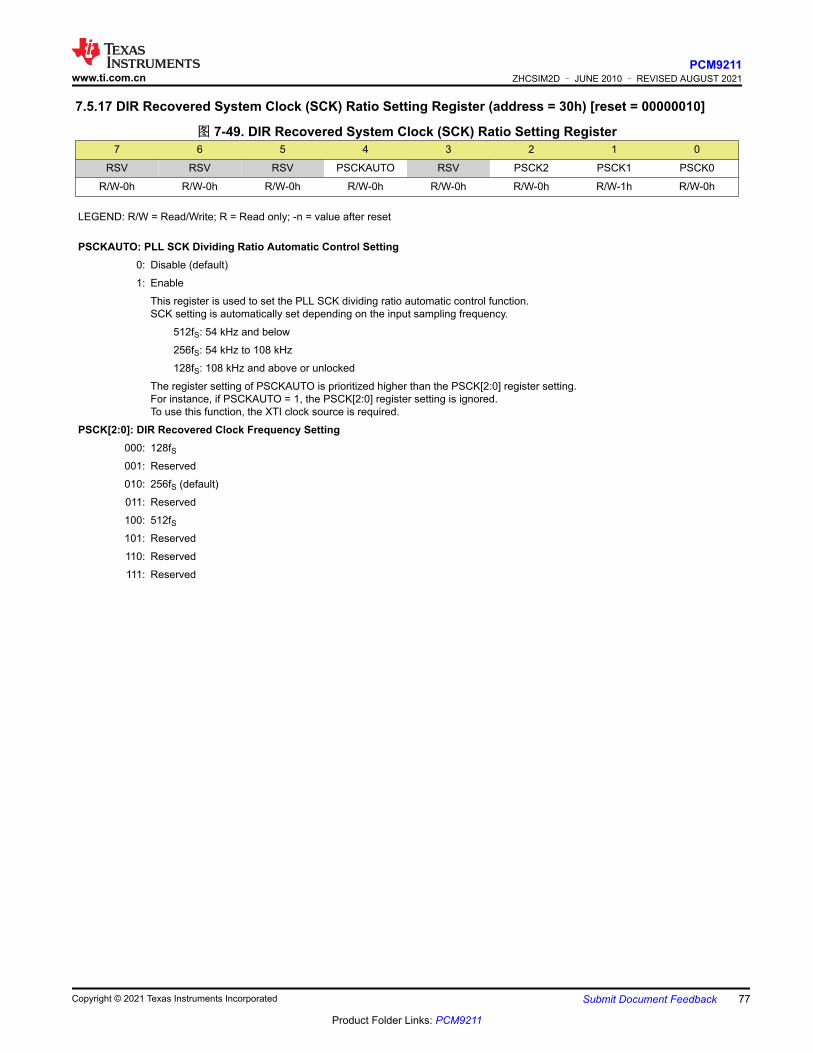
7.5.17 DIR Recovered System Clock (SCK) Ratio Setting Register (address = 30h) [reset = 00000010]
图 7-49. DIR Recovered System Clock (SCK) Ratio Setting Register7 6 5 4 3 2 1 0
RSV RSV RSV PSCKAUTO RSV PSCK2 PSCK1 PSCK0
R/W-0h R/W-0h R/W-0h R/W-0h R/W-0h R/W-0h R/W-1h R/W-0h
LEGEND: R/W = Read/Write; R = Read only; -n = value after reset
PSCKAUTO: PLL SCK Dividing Ratio Automatic Control Setting0: Disable (default)1: Enable
This register is used to set the PLL SCK dividing ratio automatic control function.SCK setting is automatically set depending on the input sampling frequency.
512fS: 54 kHz and below256fS: 54 kHz to 108 kHz128fS: 108 kHz and above or unlocked
The register setting of PSCKAUTO is prioritized higher than the PSCK[2:0] register setting.For instance, if PSCKAUTO = 1, the PSCK[2:0] register setting is ignored.To use this function, the XTI clock source is required.
PSCK[2:0]: DIR Recovered Clock Frequency Setting000: 128fS001: Reserved010: 256fS (default)011: Reserved100: 512fS101: Reserved110: Reserved111: Reserved
www.ti.com.cnPCM9211
ZHCSIM2D – JUNE 2010 – REVISED AUGUST 2021
Copyright © 2021 Texas Instruments Incorporated Submit Document Feedback 77
Product Folder Links: PCM9211

7.5.18 XTI Source, Clock (SCK, BCK, LRCK) Frequency Setting Register (address = 31h)[reset = 00011010]
图 7-50. XTI Source, Clock (SCK, BCK, LRCK) Frequency Setting Register7 6 5 4 3 2 1 0
RSV RSV XSCK1 XSCK0 XBCK1 XBCK0 XLRCK1 XLRCK0
R/W-0h R/W-0h R/W-0h R/W-1h R/W-1h R/W-0h R/W-1h R/W-0h
LEGEND: R/W = Read/Write; R = Read only; -n = value after reset
XSCK[1:0]: XTI Clock Source Frequency Setting00: XTI/1 (24.576 MHz)01: XTI/2 (12.288 MHz) (default)10: XTI/4 (6.144 MHz)11: XTI/8 (3.072 MHz)
XBCK[1:0]: XTI Clock Source BCK Frequency Setting00: XTI/2 (12.288 MHz)01: XTI/4 (6.144 MHz)10: XTI/8 (3.072 MHz) (default)11: XTI/16 (1.536 MHz)
XLRCK[1:0]: XTI Clock Source LRCK Frequency Setting00: XTI/128 (192 kHz)01: XTI/256 (96 kHz)10: XTI/512 (48 kHz) (default)11: XTI/1024 (24 kHz)
Note
The XTI clock source frequency is allowed to be set over the maximum limit of the ADC allowable clock frequency. However, setting the XTI clock source frequency at such a level is not recommended and may cause the device to exceed its stated operating and performance limits.
PCM9211ZHCSIM2D – JUNE 2010 – REVISED AUGUST 2021 www.ti.com.cn
78 Submit Document Feedback Copyright © 2021 Texas Instruments Incorporated
Product Folder Links: PCM9211

7.5.19 DIR Source, Secondary Bit/LR Clock (SBCK/SLRCK) Frequency Setting Register (address = 32h) [reset = 00100010]
图 7-51. DIR Source, Secondary Bit/LR Clock (SBCK/SLRCK) Frequency Setting Register7 6 5 4 3 2 1 0
RSV PSBCK2 PSBCK1 PSBCK0 RSV PSLRCK2 PSLRCK1 PSLRCK0
R/W-0h R/W-0h R/W-1h R/W-0h R/W-0h R/W-0h R/W-1h R/W-0h
LEGEND: R/W = Read/Write; R = Read only; -n = value after reset
PSBCK[2:0]: DIR Clock Source, Secondary BCK (SBCK) Frequency Setting000: 16fS (BCK/4)001: 32fS (BCK/2)010: 64fS (1x BCK) (default)011: 128fS (2x BCK)100: 256fS (4x BCK)101: Reserved110: Reserved111: Reserved
PSLRCK[2:0]: DIR Clock Source, Secondary LRCK (SLRCK) Frequency Setting000: fS/4 (LRCK/4)001: fS/2 (LRCK/2)010: fS (1x LRCK) (default)011: 2fS (2x LRCK)100: 4fS (4x LRCK)101: Reserved110: Reserved111: Reserved
www.ti.com.cnPCM9211
ZHCSIM2D – JUNE 2010 – REVISED AUGUST 2021
Copyright © 2021 Texas Instruments Incorporated Submit Document Feedback 79
Product Folder Links: PCM9211

7.5.20 XTI Source, Secondary Bit/LR Clock (SBCK/SLRCK) Frequency Setting Register (address = 33h) [reset = 00100010]
图 7-52. DIR Source, Secondary Bit/LR Clock (SBCK/SLRCK) Frequency Setting Register7 6 5 4 3 2 1 0
RSV XSBCK2 XSBCK1 XSBCK0 RSV XSLRCK2 XSLRCK1 XSLRCK0
R/W-0h R/W-0h R/W-1h R/W-0h R/W-0h R/W-0h R/W-1h R/W-0h
LEGEND: R/W = Read/Write; R = Read only; -n = value after reset
XSBCK[2:0]: XTI Clock Source, Secondary BCK (SBCK) Frequency Setting000: XTI/2 (12.288 MHz)001: XTI/4 (6.144 MHz)010: XTI/8 (3.072 MHz) (default)011: XTI/16 (1.536 MHz)100: XTI/32 (0.768 MHz)101: Reserved110: Reserved111: Reserved
XSLRCK[2:0]: XTI Clock Source, Secondary LRCK (SLRCK) Frequency Setting000: XTI/128 (192 kHz)001: XTI/256 (96 kHz)010: XTI/512 (48 kHz) (default)011: XTI/1024 (24 kHz)100: XTI/2048 (12 kHz)101: Reserved110: Reserved111: Reserved
PCM9211ZHCSIM2D – JUNE 2010 – REVISED AUGUST 2021 www.ti.com.cn
80 Submit Document Feedback Copyright © 2021 Texas Instruments Incorporated
Product Folder Links: PCM9211

7.5.21 DIR Input Biphase Source Select, Coax Amplifier Control Register (address = 34h)[reset = 11000010]
图 7-53. DIR Input Biphase Source Select, Coax Amplifier Control Register7 6 5 4 3 2 1 0
RX0DIS RX1DIS RSV RSV RXSEL3 RXSEL2 RXSEL1 RXSEL0
R/W-1h R/W-1h R/W-0h R/W-0h R/W-0h R/W-0h R/W-1h R/W-0h
LEGEND: R/W = Read/Write; R = Read only; -n = value after reset
RX0DIS: Power Down for RXIN0 Coaxial Amplifier0: Normal operation1: Power down (default)
RX1DIS: Power Down for RXIN1 Coaxial Amplifier0: Normal operation1: Power down (default)
RXSEL[3:0]: DIR Input Biphase Signal Source Select0000: RXIN00001: RXIN10010: RXIN2 (default)0011: RXIN30100: RXIN40101: RXIN50110: RXIN60111: RXIN71000: RXIN81001: RXIN91010: RXIN101011: RXIN111100: Reserved1101: Reserved1110: Reserved1111: TXOUT (internal DIT output)
Note
RX0DIS or RX1DIS must be set to 0, even when an S/PDIF, TTL, or OPTICAL input is provided into RXIN0 or RXIN1, without use of the built-in COAX amplifier.
www.ti.com.cnPCM9211
ZHCSIM2D – JUNE 2010 – REVISED AUGUST 2021
Copyright © 2021 Texas Instruments Incorporated Submit Document Feedback 81
Product Folder Links: PCM9211

7.5.22 RECOUT0 Output Biphase Source Settings Register (address = 35h) [reset = 00000010]
图 7-54. RECOUT0 Output Biphase Source Settings Register7 6 5 4 3 2 1 0
RSV RSV RSV MPO0MUT RO0SEL3 RO0SEL2 RO0SEL1 RO0SEL0
R/W-0h R/W-0h R/W-0h R/W-0h R/W-0h R/W-0h R/W-1h R/W-0h
LEGEND: R/W = Read/Write; R = Read only; -n = value after reset
RO0SEL0[3:0]: RECOUT0 Output Biphase Source Select0000: RXIN00001: RXIN10010: RXIN2 (default)0011: RXIN30100: RXIN40101: RXIN50110: RXIN60111: RXIN71000: RXIN81001: RXIN91010: RXIN101011: RXIN111100: Reserved1101: Reserved1110: Reserved1111: TXOUT (internal DIT output)
MPO0MUT: MPO0 Mute Control0: Output (default)1: MUTE (Logic low level)
PCM9211ZHCSIM2D – JUNE 2010 – REVISED AUGUST 2021 www.ti.com.cn
82 Submit Document Feedback Copyright © 2021 Texas Instruments Incorporated
Product Folder Links: PCM9211

7.5.23 RECOUT1 Output Biphase Source Settings Register (address = 36h) [reset = 00000010]
图 7-55. RECOUT1 Output Biphase Source Settings Register7 6 5 4 3 2 1 0
RSV RSV RSV MPO1MUT RO1SEL3 RO1SEL2 RO1SEL1 RO1SEL0
R/W-0h R/W-0h R/W-0h R/W-0h R/W-0h R/W-0h R/W-1h R/W-0h
LEGEND: R/W = Read/Write; R = Read only; -n = value after reset
RO1SEL0[3:0]: RECOUT1 Output Biphase Source Select0000: RXIN00001: RXIN10010: RXIN2 (default)0011: RXIN30100: RXIN40101: RXIN50110: RXIN60111: RXIN71000: RXIN81001: RXIN91010: RXIN101011: RXIN111100: Reserved1101: Reserved1110: Reserved1111: TXOUT (internal DIT output)
MPO1MUT: MPO1 Mute Control0: Output (default)1: MUTE (Logic low level)
www.ti.com.cnPCM9211
ZHCSIM2D – JUNE 2010 – REVISED AUGUST 2021
Copyright © 2021 Texas Instruments Incorporated Submit Document Feedback 83
Product Folder Links: PCM9211

7.5.24 Port Sampling Frequency Calculator Measurement Target Setting Register (address = 37h)[reset = 00000000]
图 7-56. RECOUT1 Output Biphase Source Settings Register7 6 5 4 3 2 1 0
RSV RSV RSV RSV RSV PFSTGT2 PFSTGT1 PFSTGT0
R/W-0h R/W-0h R/W-0h R/W-0h R/W-0h R/W-0h R/W-0h R/W-0h
LEGEND: R/W = Read/Write; R = Read only; -n = value after reset
PFSTGT[2:0]: Port fS Calculator, Target Port Setting000: DIR (default)001: ADC010: AUXIN0011: AUXIN1100: AUXIN2101: Main output port110: AUX output port111: DIT
PCM9211ZHCSIM2D – JUNE 2010 – REVISED AUGUST 2021 www.ti.com.cn
84 Submit Document Feedback Copyright © 2021 Texas Instruments Incorporated
Product Folder Links: PCM9211

7.5.25 Port Sampling Frequency Calculator Result Output Register (address = 38h) [reset = N/A]
图 7-57. Port Sampling Frequency Calculator Result Output Register7 6 5 4 3 2 1 0
PFSST PFSPO2 PFSPO1 PFSPO0 PFSOUT3 PFSOUT2 PFSOUT1 PFSOUT0
R-N/A R-N/A R-N/A R-N/A R-N/A R-N/A R-N/A R-N/A
LEGEND: R/W = Read/Write; R = Read only; -n = value after reset
PFSST: Port Sampling Frequency Calculate Status0: Calculated1: Calculating
PFSPO[2:0]: Calculated Port Information000: DIR001: ADC010: AUXIN0011: AUXIN1100: AUXIN2101: Main output port110: AUX output port111: DIT
PFSOUT[3:0]: Calculated Sampling Frequency0000: Out of range0001: 8 kHz0010: 11.025 kHz0011: 12 kHz0100: 16 kHz0101: 22.05 kHz0110: 24 kHz0111: 32 kHz1000: 44.1 kHz1001: 48 kHz1010: 64 kHz1011: 88.2 kHz1100: 96 kHz1101: 128 kHz1110: 176.4 kHz1111: 192 kHz
Note
PFSST, PFSPO, and PFSOUT always output the status when these registers are read.
The other registers do not have clear functions when these are read. To enable these registers, DIR must be powered on. For example, (Register 40h/RXDIS = 0) PFSST indicates Calculating and PFSOUT indicates the previous value when no source comes to the port that is selected by Register 37h/PFSTGT.
www.ti.com.cnPCM9211
ZHCSIM2D – JUNE 2010 – REVISED AUGUST 2021
Copyright © 2021 Texas Instruments Incorporated Submit Document Feedback 85
Product Folder Links: PCM9211

7.5.26 Incoming Biphase Information and Sampling Frequency Register (address = 39h) [reset = N/A]
图 7-58. Port Sampling Frequency Calculator Result Output Register7 6 5 4 3 2 1 0
SFSST SCSBIT1 RSV RSV SESOUT3 SESOUT2 SESOUT1 SESOUT0
R-N/A R-N/A R-N/A R-N/A R-N/A R-N/A R-N/A R-N/A
LEGEND: R/W = Read/Write; R = Read only; -n = value after reset
SFSST: Incoming Biphase Signal, Sampling Frequency Calculate Status0: SFSOUT[3:0] Output is calculated1: In the process of calculating or unlocked
SCSBIT1: Detected Channel Status Bit1 Flag0: CS Bit1 = 0 (Audio data)1: CS Bit1 = 1 (Non-audio data)
SFSOUT[3:0]: Incoming Biphase Signal, Actual Sampling Frequency0000: Out of range0001: 8 kHz0010: 11.025 kHz0011: 12 kHz0100: 16 kHz0101: 22.05 kHz0110: 24 kHz0111: 32 kHz1000: 44.1 kHz1001: 48 kHz1010: 64 kHz1011: 88.2 kHz1100: 96 kHz1101: 128 kHz1110: 176.4 kHz1111: 192 kHz
Note
When SFSST becomes 1 (that is, in the process of calculating or unlocked), SFSOUT holds the previous data. SFSST and SFSOUT always output the status when these registers are read. The other registers do not have clear functions when these are read. To enable these registers, DIR must be powered on (register 40h/RXDIS = 0).
PCM9211ZHCSIM2D – JUNE 2010 – REVISED AUGUST 2021 www.ti.com.cn
86 Submit Document Feedback Copyright © 2021 Texas Instruments Incorporated
Product Folder Links: PCM9211
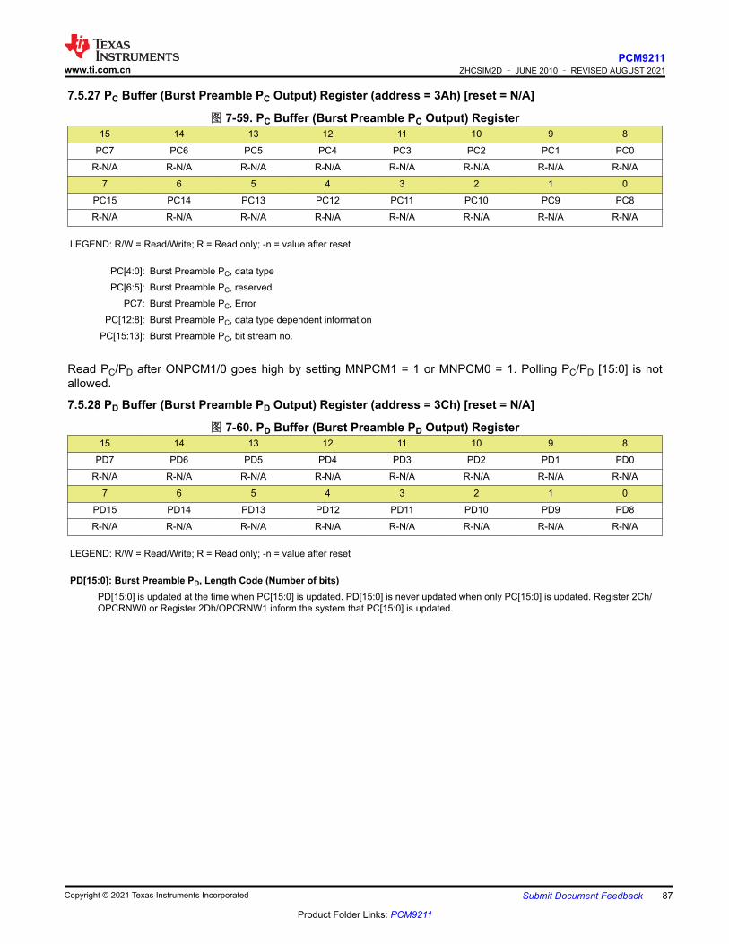
7.5.27 PC Buffer (Burst Preamble PC Output) Register (address = 3Ah) [reset = N/A]
图 7-59. PC Buffer (Burst Preamble PC Output) Register15 14 13 12 11 10 9 8
PC7 PC6 PC5 PC4 PC3 PC2 PC1 PC0
R-N/A R-N/A R-N/A R-N/A R-N/A R-N/A R-N/A R-N/A
7 6 5 4 3 2 1 0
PC15 PC14 PC13 PC12 PC11 PC10 PC9 PC8
R-N/A R-N/A R-N/A R-N/A R-N/A R-N/A R-N/A R-N/A
LEGEND: R/W = Read/Write; R = Read only; -n = value after reset
PC[4:0]: Burst Preamble PC, data typePC[6:5]: Burst Preamble PC, reserved
PC7: Burst Preamble PC, ErrorPC[12:8]: Burst Preamble PC, data type dependent information
PC[15:13]: Burst Preamble PC, bit stream no.
Read PC/PD after ONPCM1/0 goes high by setting MNPCM1 = 1 or MNPCM0 = 1. Polling PC/PD [15:0] is not allowed.
7.5.28 PD Buffer (Burst Preamble PD Output) Register (address = 3Ch) [reset = N/A]
图 7-60. PD Buffer (Burst Preamble PD Output) Register15 14 13 12 11 10 9 8
PD7 PD6 PD5 PD4 PD3 PD2 PD1 PD0
R-N/A R-N/A R-N/A R-N/A R-N/A R-N/A R-N/A R-N/A
7 6 5 4 3 2 1 0
PD15 PD14 PD13 PD12 PD11 PD10 PD9 PD8
R-N/A R-N/A R-N/A R-N/A R-N/A R-N/A R-N/A R-N/A
LEGEND: R/W = Read/Write; R = Read only; -n = value after reset
PD[15:0]: Burst Preamble PD, Length Code (Number of bits)PD[15:0] is updated at the time when PC[15:0] is updated. PD[15:0] is never updated when only PC[15:0] is updated. Register 2Ch/OPCRNW0 or Register 2Dh/OPCRNW1 inform the system that PC[15:0] is updated.
www.ti.com.cnPCM9211
ZHCSIM2D – JUNE 2010 – REVISED AUGUST 2021
Copyright © 2021 Texas Instruments Incorporated Submit Document Feedback 87
Product Folder Links: PCM9211

7.5.29 System Reset Control Register (address = 40h) [reset = 11000000]
图 7-61. System Reset Control Register7 6 5 4 3 2 1 0
MRST SRST ADDIS RXDIS RSV RSV TXDIS XODIS
R/W-1h R/W-1h R/W-0h R/W-0h R/W-0h R/W-0h R/W-0h R/W-0h
LEGEND: R/W = Read/Write; R = Read only; -n = value after reset
MRST: Mode Control Register Reset for All Functions0: Set default value1: Normal operation (default)
SRST: System Reset for ADC0: Reset1: Normal operation (default)
To return the MRST, SRST bit to 0 is not necessary because the MRST, SRST bit is automatically set to 1.ADDIS: Power Down for ADC
0: Normal operation (default)1: Power down
SCK must be provided to disable ADC by ADDIS = 1.RXDIS: Power Down for DIR
0: Normal operation (default)1: Power down
TXDIS: Power Down for DIT0: Normal operation (default)1: Power down
XODIS: Power Down for OSC0: Normal operation (default)1: Power down
XODIS is superior to OSCAUTO.
PCM9211ZHCSIM2D – JUNE 2010 – REVISED AUGUST 2021 www.ti.com.cn
88 Submit Document Feedback Copyright © 2021 Texas Instruments Incorporated
Product Folder Links: PCM9211

7.5.30 ADC Function Control Register 1/3 (address = 42h) [reset = 00000010]
图 7-62. ADC Function Control Register 1/37 6 5 4 3 2 1 0
RSV RSV ADCKOUT ADDTRX7 ADFSLMT ADCLK2 ADCLK1 ADCLK0
R/W-0h R/W-0h R/W-0h R/W-0h R/W-0h R/W-0h R/W-1h R/W-0h
LEGEND: R/W = Read/Write; R = Read only; -n = value after reset
ADCKOUT: ADC Clock (SCK, BCK, LRCK) Output Select at ADC Power-Down0: Output enable even at ADDIS = 1 (default)1: Output disable at ADDIS = 0
ADDTRX7: ADC Output Data Select to Main Port, DOUT Pin0: DOUT = ADC DOUT (default)1: DOUT = RXIN7 (ADIN0)
This register can select an external ADC data from RXIN7 (ADIN0) to Main Port DOUT pin when an external ADC is used.ADFSLMT: ADC Sampling Frequency Limiter for DIR Clock Source
0: Disable (default)1: Enable
When ADFSLMT = 1, ADCLK[2:0] = 001(ADC clock is DIR output clock) and DIR locks at frequency from 14 kHz to 111 kHz, the ADC is forced into power down.
ADCLK[2:0]: ADC Clock Source (SCK/BCK/LRCK) Select000: AUTO (DIR or XTI)001: DIR010: XTI (default)011: AUXIN0100: AUXIN1100: AUXIN2110: Reserved111: Reserved
The ADC clock source must be normally set to XTI source with fixed frequency (the clocks at the XTI source select are generated by the SCK/BCK/LRCK dividers). Its frequency is set by the register of XSCK[1:0], XBCK[1:0], and XLRCK[1:0].).
www.ti.com.cnPCM9211
ZHCSIM2D – JUNE 2010 – REVISED AUGUST 2021
Copyright © 2021 Texas Instruments Incorporated Submit Document Feedback 89
Product Folder Links: PCM9211

7.5.31 ADC L-Ch, Digital ATT Control Register (address = 46h) [reset = 11010111]
图 7-63. ADC L-Ch, Digital ATT Control Register7 6 5 4 3 2 1 0
ADATTL7 ADATTL6 ADATTL5 ADATTL4 ADATTL3 ADATTL2 ADATTL1 ADATTL0
R/W-1h R/W-1h R/W-0h R/W-1h R/W-0h R/W-1h R/W-1h R/W-1h
LEGEND: R/W = Read/Write; R = Read only; -n = value after reset
ADATTL[7:0]: ADC L-Ch, Digital ATT Setting1111 1111: +20.0 dB1111 1110: +19.5 dB
1101 0111: 0 dB (default)
1101 0110: –0.5 dB
0000 1111: –100 dBOthers: Mute
7.5.32 ADC R-Ch, Digital ATT Control Register (address = 47h) [reset = 11010111]
图 7-64. ADC L-Ch, Digital ATT Control Register7 6 5 4 3 2 1 0
ADATTR7 ADATTR6 ADATTR5 ADATTR4 ADATTR3 ADATTR2 ADATTR1 ADATTR0
R/W-1h R/W-1h R/W-0h R/W-1h R/W-0h R/W-1h R/W-1h R/W-1h
LEGEND: R/W = Read/Write; R = Read only; -n = value after reset
ADATTR[7:0]: ADC R-Ch, Digital ATT Setting1111 1111: +20.0 dB1111 1110: +19.5 dB
1101 0111: 0 dB (default)
1101 0110: –0.5 dB
0000 1111: –100 dBOthers: Mute
PCM9211ZHCSIM2D – JUNE 2010 – REVISED AUGUST 2021 www.ti.com.cn
90 Submit Document Feedback Copyright © 2021 Texas Instruments Incorporated
Product Folder Links: PCM9211

7.5.33 ADC Function Control Register 2/3 (address = 48h) [reset = 00000000]
图 7-65. ADC Function Control Register 2/37 6 5 4 3 2 1 0
RSV ADIFMD2 ADIFMD1 ADIFMD0 RSV RSV ADFMT1 ADFMT0
R/W-0h R/W-0h R/W-0h R/W-0h R/W-0h R/W-0h R/W-1h R/W-0h
LEGEND: R/W = Read/Write; R = Read only; -n = value after reset
ADIFMD[2:0]: ADC Interface Mode Setting000: Slave mode (default)001: Reserved010: Master mode, 512fS011: Reserved100: Master mode, 256fS101: Reserved110: Reserved111: Reserved
Master mode settings are available only in ADC standalone mode (MPCSEL[2:0] = '001').ADFMT[1:0]: ADC Audio I/F Format Setting
00: 24-bit I2S (default)01: 24-bit left-justified10: 24-bit right-justified11: 16-bit right-justified
www.ti.com.cnPCM9211
ZHCSIM2D – JUNE 2010 – REVISED AUGUST 2021
Copyright © 2021 Texas Instruments Incorporated Submit Document Feedback 91
Product Folder Links: PCM9211

7.5.34 ADC Function Control Register 3/3 (address = 49h) [reset = 00000000]
图 7-66. ADC Function Control Register 3/37 6 5 4 3 2 1 0
RSV RSV RSV ADZCDD ADBYP ADPHSE ADMUTR ADMUTL
R/W-0h R/W-0h R/W-0h R/W-0h R/W-0h R/W-0h R/W-1h R/W-0h
LEGEND: R/W = Read/Write; R = Read only; -n = value after reset
ADZCDD: Zero-Crossing Detection Disable for Digital Attenuation0: Enable (default)1: Disable.
ADBYP: High-Pass Filter Bypass Control0: Normal output, HPF enable (default)1: Bypassed output, HPF disenable
ADPHSE: Input Phase Select0: Normal input (default)1: Invert Input
ADMUTR: Soft Mute Control, R-Ch0: Mute disabled (default)1: Mute enabled
ADMUTL: Soft Mute Control, L-Ch0: Mute disabled (default)1: Mute enabled
The mute bits, ADMUTL and ADMUTR, are used to enable or disenable the soft mute function for the corresponding ADC outputs, DOUT.
PCM9211ZHCSIM2D – JUNE 2010 – REVISED AUGUST 2021 www.ti.com.cn
92 Submit Document Feedback Copyright © 2021 Texas Instruments Incorporated
Product Folder Links: PCM9211

7.5.35 DIR Channel Status Data Buffer Register (address = 5Ah) [reset = 00000000]
图 7-67. DIR Channel Status Data Buffer Register47 46 45 44 43 42 41 40
RXCS7 RXCS6 RXCS5 RXCS4 RXCS3 RXCS2 RXCS1 RXCS0
CS Bit7 CS Bit6 CS Bit5 CS Bit4 CS Bit3 CS Bit2 CS Bit1 CS Bit0
R R R R R R R R
39 38 37 36 35 34 33 32
RXCS15 RXCS14 RXCS13 RXCS12 RXCS11 RXCS10 RXCS9 RXCS8
CS Bit15 CS Bit14 CS Bit13 CS Bit12 CS Bit11 CS Bit10 CS Bit9 CS Bit8
R R R R R R R R
31 30 29 28 27 26 25 24
RXCS23 RXCS22 RXCS21 RXCS20 RXCS19 RXCS18 RXCS17 RXCS16
CS Bit23 CS Bit22 CS Bit21 CS Bit20 CS Bit19 CS Bit18 CS Bit17 CS Bit16
R R R R R R R R
23 22 21 20 19 18 17 16
RXCS31 RXCS30 RXCS29 RXCS28 RXCS27 RXCS26 RXCS25 RXCS24
CS Bit31 CS Bit30 CS Bit29 CS Bit28 CS Bit27 CS Bit26 CS Bit25 CS Bit24X
R R R R R R R R
15 14 13 12 11 10 9 8
RXCS39 RXCS38 RXCS37 RXCS36 RXCS35 RXCS34 RXCS33 RXCS32
CS Bit39 CS Bit38 CS Bit37 CS Bit36 CS Bit35 CS Bit34 CS Bit33 CS Bit32
R R R R R R R R
7 6 5 4 3 2 1 0
RXCS47 RXCS46 RXCS45 RXCS44 RXCS43 RXCS42 RXCS41 RXCS40
CS Bit47 CS Bit46 CS Bit45 CS Bit44 CS Bit43 CS Bit42 CS Bit41 CS Bit40
R R R R R R R R
LEGEND: R/W = Read/Write; R = Read only; -n = value after reset
RXCS0: Use of channel status blockRXCS1: Linear PCM informationRXCS2: Copyright information
RXCS5 – RXCS3: Additional format information
RXCS7– RXCS6: Channel status mode
RXCS15 – RXCS8: Category code
RXCS19 – RXCS16: Source number
RXCS23 – RXCS20: Channel number
RXCS27 – RXCS24: Sampling frequency
RXCS29 – RXCS28: Clock accuracy
RXCS31 – RXCS30: Not defined
RXCS32: Maximum audio sample word length
RXCS35 – RXCS33: Sample word length
RXCS39 – RXCS36: Original sampling frequency
RXCS47 – RXCS40: Not defined
xx of RXCSxx represents the serial number of the channel status data. L-channel data of the channel status is stored in this register. Its default value is not specified. Therefore, wait until the ERROR/INT0 port goes low and 192 samples pass to read RXCS. RXCS is cleared when DIR unlocks and an L-ch parity error is detected.
www.ti.com.cnPCM9211
ZHCSIM2D – JUNE 2010 – REVISED AUGUST 2021
Copyright © 2021 Texas Instruments Incorporated Submit Document Feedback 93
Product Folder Links: PCM9211

7.5.36 DIT Function Control Register 1/3 (address = 60h) [reset = 01000100]
图 7-68. DIT Function Control Register 1/37 6 5 4 3 2 1 0
RSV TXSSRC2 TXSSRC1 TXSSRC0 RSV TXPSRC2 TXPSRC1 TXPSRC0
R/W-0h R/W-1h R/W-0h R/W-0h R/W-0h R/W-1h R/W-0h R/W-0h
LEGEND: R/W = Read/Write; R = Read only; -n = value after reset
TXSSRC[2:0]: DIT System Clock Source Select000: DIR/ADC Automatic (DIR lock = DIR, DIR unlock = ADC)001: DIR010: ADC011: AUXIN0100: AUXIN1 (default)101: AUXIN2110: Reserved111: Reserved
TXPSRC[2:0]: DIT Bit Clock, LR Clock, Data Source Select000: DIR/ADC Automatic (DIR lock = DIR, DIR unlock = ADC)001: DIR010: ADC011: AUXIN0100: AUXIN1 (default)101: AUXIN2110: Reserved111: Reserved
PCM9211ZHCSIM2D – JUNE 2010 – REVISED AUGUST 2021 www.ti.com.cn
94 Submit Document Feedback Copyright © 2021 Texas Instruments Incorporated
Product Folder Links: PCM9211

7.5.37 DIT Function Control Register 2/3 (address = 61h) [reset = 00010000]
图 7-69. DIT Function Control Register 2/37 6 5 4 3 2 1 0
RSV TXSCK2 TXSCK1 TXSCK0 RSV TXDSD TXFMT1 TXFMT0
R/W-0h R/W-0h R/W-0h R/W-1h R/W-0h R/W-0h R/W-0h R/W-0h
LEGEND: R/W = Read/Write; R = Read only; -n = value after reset
TXSCK[2:0]: DIT System Clock Control000: 128fS001: 256fS (default)010: 512fS011: Reserved100: Controlled by DIR system clock rate100: Controlled by DIR system clock rate110: Controlled by DIR system clock rate111: Controlled by DIR system clock rate
TXDSD: DIT DSD Input Enable0: DSD input disable (default)1: DSD input enable
Note
When TXDSD is set to 1, the DIT LR clock is generated by the Bit Clock divided by 64. The DIT source data are forced to all 0s. Provide the DSD source to MPIO_B0 for the system clock (256fS), MPIO_B1 for the DSD bit clock (64fS), MPIO_B2 for L-ch data, and MPIO_B3 for R-ch data.
This function is useful when it is desired to suppress system clock jitter by using the path that is DIT to DIR. Jitter of the system clock generated by DIR is also reduced if the jitter is high frequency.
TXFMT[1:0]:DIT Audio I/F Format Setting00: 24-bit I2S (default)01: 24-bit left-justified10: 24-bit right-justified11: 16-bit right-justified
www.ti.com.cnPCM9211
ZHCSIM2D – JUNE 2010 – REVISED AUGUST 2021
Copyright © 2021 Texas Instruments Incorporated Submit Document Feedback 95
Product Folder Links: PCM9211

7.5.38 DIT Function Control Register 3/3 (address = 62h) [reset = 00000000]
图 7-70. DIT Function Control Register 3/37 6 5 4 3 2 1 0
RSV RSV TXDMUT RSV TXVFLG RSV RSV RSV
R/W-0h R/W-0h R/W-0h R/W-0h R/W-0h R/W-0h R/W-0h R/W-0h
LEGEND: R/W = Read/Write; R = Read only; -n = value after reset
TXDMUT: DIT Output Audio Data Mute Control0: No mute (default)1: Audio data on biphase signal is Mute (zero data)
TXVFLG: DIT Output Validity Flag Control0: V = 0, Valid (default)1: V = 1, Invalid
PCM9211ZHCSIM2D – JUNE 2010 – REVISED AUGUST 2021 www.ti.com.cn
96 Submit Document Feedback Copyright © 2021 Texas Instruments Incorporated
Product Folder Links: PCM9211

7.5.39 DIT Channel Status Data Buffer Register (address = 63h) [reset = 00000000]
图 7-71. DIT Channel Status Data Buffer Register47 46 45 44 43 42 41 40
TXCS7 TXCS6 TXCS5 TXCS4 TXCS3 TXCS2 TXCS1 TXCS0
CS Bit7 CS Bit6 CS Bit5 CS Bit4 CS Bit3 CS Bit2 CS Bit1 CS Bit0
R/W R/W R/W R/W R/W R/W R/W R/W
39 38 37 36 35 34 33 32
TXCS15 TXCS14 TXCS13 TXCS12 TXCS11 TXCS10 TXCS9 TXCS8
CS Bit15 CS Bit14 CS Bit13 CS Bit12 CS Bit11 CS Bit10 CS Bit9 CS Bit8
R/W R/W R/W R/W R/W R/W R/W R/W
31 30 29 28 27 26 25 24
TXCS23 TXCS22 TXCS21 TXCS20 TXCS19 TXCS18 TXCS17 TXCS16
CS Bit23 CS Bit22 CS Bit21 CS Bit20 CS Bit19 CS Bit18 CS Bit17 CS Bit16
R/W R/W R/W R/W R/W R/W R/W R/W
23 22 21 20 19 18 17 16
TXCS31 TXCS30 TXCS29 TXCS28 TXCS27 TXCS26 TXCS25 TXCS24
CS Bit31 CS Bit30 CS Bit29 CS Bit28 CS Bit27 CS Bit26 CS Bit25 CS Bit24X
R/W R/W R/W R/W R/W R/W R/W R/W
15 14 13 12 11 10 9 8
TXCS39 TXCS38 TXCS37 TXCS36 TXCS35 TXCS34 TXCS33 TXCS32
CS Bit39 CS Bit38 CS Bit37 CS Bit36 CS Bit35 CS Bit34 CS Bit33 CS Bit32
R/W R/W R/W R/W R/W R/W R/W R/W
7 6 5 4 3 2 1 0
TXCS47 TXCS46 TXCS45 TXCS44 TXCS43 TXCS42 TXCS41 TXCS40
CS Bit47 CS Bit46 CS Bit45 CS Bit44 CS Bit43 CS Bit42 CS Bit41 CS Bit40
R/W R/W R/W R/W R/W R/W R/W R/W
LEGEND: R/W = Read/Write; R = Read only; -n = value after reset
TXCS0: Use of channel status block.TXCS1: Linear PCM information.TXCS2: Copyright information.
TXCS5 – TXCS3: Additional format information.
TXCS7 – TXCS6: Channel status mode.
TXCS15 – TXCS8: Category code.
TXCS19 – TXCS16: Source number.
TXCS23 – TXCS20: Channel number.
TXCS27 – TXCS24: Sampling frequency.
TXCS29 - TXCS28: Clock accuracy.
TXCS31 – TXCS30: Not defined.
TXCS32: Maximum audio sample word length.
TXCS35 – TXCS33: Sample word length.
TXCS39 – TXCS36: Original sampling frequency.
TXCS47 – TXCS40: Not defined.
The data in this register are used for both channels (L-ch and R-ch). When these register data are used for the DIT channel status data, a channel status data of bit 48 or later is all 0. All initial values of this register are all 0.
www.ti.com.cnPCM9211
ZHCSIM2D – JUNE 2010 – REVISED AUGUST 2021
Copyright © 2021 Texas Instruments Incorporated Submit Document Feedback 97
Product Folder Links: PCM9211

7.5.40 Main Output and AUXOUT Port Control Register (address = 6A) [reset = 00000000]
图 7-72. Main Output and AUXOUT Port Control Register7 6 5 4 3 2 1 0
AOMUTAS MOMUTAS RSV RSV AOLRMTEN AODMUT MOLRMTEN MODMUT
R/W-0h R/W-0h R/W-0h R/W-0h R/W-0h R/W-0h R/W-0h R/W-0h
LEGEND: R/W = Read/Write; R = Read only; -n = value after reset
AOMUTAS: AUX Output Port, Mute Synchronization Select (MPIO_B2 and MPIO_B3)0: AODMUT works with synchronization with LRCK edge. (default)1: AODMUT works without synchronization with LRCK edge
MOMUTAS: Main Output Port, Mute Synchronization Select (LRCK and DOUT)0: MODMUT works with synchronization with LRCK edge. (default)1: MODMUT works without synchronization with LRCK edge
AOLRMTEN: AODMUT Signal Select (MPIO_B2)0: Only DOUT (default)1: Both of LRCK and DOUT
AODMUT: AUX Output Port, Data Mute Control0: Output (default)1: Mute (the affected signals are selected by Register 6Ah, AOLRMTEN)
MOLRMTEN : MODMUT signal select0: Only DOUT (default)1: Both LRCK and DOUT
MODMUT: Main Output Port, DOUT Mute Control0: Output (default)1: Mute (the affected signals are selected by Register 6Ah, MOLRMTEN)
Data mutes are done in synchronization with a LRCK edge.
PCM9211ZHCSIM2D – JUNE 2010 – REVISED AUGUST 2021 www.ti.com.cn
98 Submit Document Feedback Copyright © 2021 Texas Instruments Incorporated
Product Folder Links: PCM9211

7.5.41 Main Output Port (SCKO/BCK/LRCK/DOUT) Source Setting Register (address = 6Bh)[reset = 00000000]
图 7-73. Main Output Port (SCKO/BCK/LRCK/DOUT) Source Setting Register7 6 5 4 3 2 1 0
RSV MOSSRC2 MOSSRC1 MOSSRC0 RSV MOPSRC2 MOPSRC1 MOPSRC0
R/W-0h R/W-0h R/W-0h R/W-0h R/W-0h R/W-0h R/W-0h R/W-0h
LEGEND: R/W = Read/Write; R = Read only; -n = value after reset
MOSSRC[2:0]: Main Output Port, SCK Source Control000: DIR/ADC Automatic (DIR lock:DIR, DIR unlock:ADC) (default)001: DIR010: ADC011: AUXIN0100: AUXIN1101: AUXIN2110: Reserved111: Reserved
MOPSRC[2:0]: Main Output Port, BCK/LRCK/DATA Source Control000: DIR/ADC Automatic (DIR lock:DIR, DIR unlock:ADC) (default)001: DIR010: ADC011: AUXIN0100: AUXIN1101: AUXIN2110: Reserved111: Reserved
This source control register is divided into two parts (MOSSRC and MOPSRC). This architecture allows some additional functionality such as jitter cleaning. To clean the clock jitter of the HDMI receiver output, the HDMI receiver S/PDIF output is connected with the PCM9211 S/PDIF input, and the HDMI receiver I2S outputs (BCK/LRCK/DATA) are connected with the PCM9211 PCM input port.
www.ti.com.cnPCM9211
ZHCSIM2D – JUNE 2010 – REVISED AUGUST 2021
Copyright © 2021 Texas Instruments Incorporated Submit Document Feedback 99
Product Folder Links: PCM9211

7.5.42 AUX Output Port (AUXSCKO/AUXBCKO/AUXLRCKO/AUXDOUT) Source Setting Register(address = 6Ch) [reset = 00000000]
图 7-74. AUX Output Port (SCKO/BCK/LRCK/DOUT) Source Setting Register7 6 5 4 3 2 1 0
RSV AOSSRC2 AOSSRC1 AOSSRC0 RSV AOPSRC2 AOPSRC1 AOPSRC0
R/W-0h R/W-0h R/W-0h R/W-0h R/W-0h R/W-0h R/W-0h R/W-0h
LEGEND: R/W = Read/Write; R = Read only; -n = value after reset
AOSSRC[2:0]: AUX Output Port, SCK Source Control000: DIR/ADC automatic (DIR lock:DIR, DIR unlock:ADC) (default)001: DIR010: ADC011: AUXIN0100: AUXIN1101: Reserved110: Reserved111: Reserved
AOPSRC[2:0]: AUX Output Port, BCK/LRCK/DATA Source Control000: DIR/ADC automatic (DIR lock:DIR, DIR unlock:ADC) (default)001: DIR010: ADC011: AUXIN0100: AUXIN1101: Reserved110: Reserved111: Reserved
This source control register is divided into two parts (MOSSRC and MOPSRC). This design allows some additional functionality such as jitter cleaning. To clean the clock jitter of the HDMI receiver output, the HDMI receiver S/PDIF output is connected to the PCM9211 S/PDIF input, and the HDMI receiver I2S outputs (BCK/LRCK/DATA) are connected with the PCM9211 PCM input port.
PCM9211ZHCSIM2D – JUNE 2010 – REVISED AUGUST 2021 www.ti.com.cn
100 Submit Document Feedback Copyright © 2021 Texas Instruments Incorporated
Product Folder Links: PCM9211

7.5.43 MPIO_B and Main Output Port Hi-Z Control Register (address = 6Dh) [reset = 00000000]
图 7-75. MPIO_B and Main Output Port Hi-Z Control Register7 6 5 4 3 2 1 0
MPB3HZ MPB2HZ MPB1HZ MPB0HZ SCKOHZ BCKHZ LRCKHZ DOUTHZ
R/W-0h R/W-0h R/W-0h R/W-0h R/W-0h R/W-0h R/W-0h R/W-0h
LEGEND: R/W = Read/Write; R = Read only; -n = value after reset
MPB3HZ: MPIO_B3, Hi-Z Control0: Defined by Group Function Assign register, 6Fh/MPBSEL. (default)1: Hi-Z
MPB2HZ: MPIO_B2, Hi-Z Control0: Defined by Group Function Assign register, 6Fh/MPBSEL. (default)1: Hi-Z
MPB1HZ: MPIO_B1, Hi-Z Control0: Defined by Group Function Assign register, 6Fh/MPBSEL. (default)1: Hi-Z
MPB0HZ: MPIO_B0, Hi-Z Control0: Defined by Group Function Assign register, 6Fh/MPBSEL. (default)1: Hi-Z
SCKOHZ: Main Output Port, SCKO Hi-Z Control0: Output (default)1: Hi-Z
BCKHZ: Main Output Port, BCKO Hi-Z Control0: Output (default)1: Hi-Z
LRCKHZ: Main Output Port, LRCKO Hi-Z Control0: Output (default)1: Hi-Z
DOUTHZ: Main Output Port, DOUT Hi-Z Control0: Output (default)1: Hi-Z
www.ti.com.cnPCM9211
ZHCSIM2D – JUNE 2010 – REVISED AUGUST 2021
Copyright © 2021 Texas Instruments Incorporated Submit Document Feedback 101
Product Folder Links: PCM9211
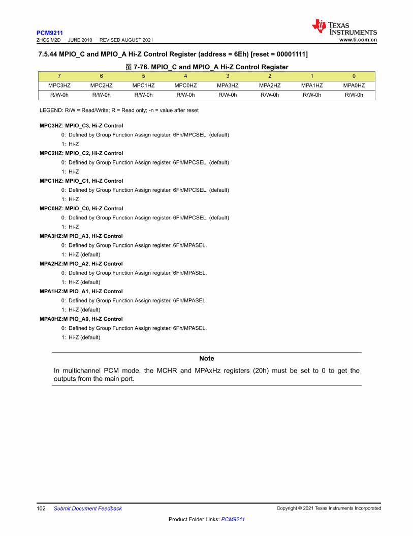
7.5.44 MPIO_C and MPIO_A Hi-Z Control Register (address = 6Eh) [reset = 00001111]
图 7-76. MPIO_C and MPIO_A Hi-Z Control Register7 6 5 4 3 2 1 0
MPC3HZ MPC2HZ MPC1HZ MPC0HZ MPA3HZ MPA2HZ MPA1HZ MPA0HZ
R/W-0h R/W-0h R/W-0h R/W-0h R/W-0h R/W-0h R/W-0h R/W-0h
LEGEND: R/W = Read/Write; R = Read only; -n = value after reset
MPC3HZ: MPIO_C3, Hi-Z Control0: Defined by Group Function Assign register, 6Fh/MPCSEL. (default)1: Hi-Z
MPC2HZ: MPIO_C2, Hi-Z Control0: Defined by Group Function Assign register, 6Fh/MPCSEL. (default)1: Hi-Z
MPC1HZ: MPIO_C1, Hi-Z Control0: Defined by Group Function Assign register, 6Fh/MPCSEL. (default)1: Hi-Z
MPC0HZ: MPIO_C0, Hi-Z Control0: Defined by Group Function Assign register, 6Fh/MPCSEL. (default)1: Hi-Z
MPA3HZ:M PIO_A3, Hi-Z Control0: Defined by Group Function Assign register, 6Fh/MPASEL.1: Hi-Z (default)
MPA2HZ:M PIO_A2, Hi-Z Control0: Defined by Group Function Assign register, 6Fh/MPASEL.1: Hi-Z (default)
MPA1HZ:M PIO_A1, Hi-Z Control0: Defined by Group Function Assign register, 6Fh/MPASEL.1: Hi-Z (default)
MPA0HZ:M PIO_A0, Hi-Z Control0: Defined by Group Function Assign register, 6Fh/MPASEL.1: Hi-Z (default)
Note
In multichannel PCM mode, the MCHR and MPAxHz registers (20h) must be set to 0 to get the outputs from the main port.
PCM9211ZHCSIM2D – JUNE 2010 – REVISED AUGUST 2021 www.ti.com.cn
102 Submit Document Feedback Copyright © 2021 Texas Instruments Incorporated
Product Folder Links: PCM9211

7.5.45 MPIO_A, MPIO_B, MPIO_C Group Function Assign Register (address = 6Fh) [reset = 01000000]
图 7-77. MPIO_A, MPIO_B, MPIO_C Group Function Assign Register7 6 5 4 3 2 1 0
MPASEL1 MPASEL0 MPBSEL2 MPBSEL1 MPBSEL0 MPCSEL2 MPCSEL1 MPCSEL0
R/W-0h R/W-1h R/W-0h R/W-0h R/W-0h R/W-0h R/W-0h R/W-0h
LEGEND: R/W = Read/Write; R = Read only; -n = value after reset
MPASEL[1:0]: MPIO_A Group Function Assign Setting00: Biphase Input Extension (RXIN8 to RXIN11)01: CLKST Output, VOUT Output, XMCKO Output, INT0 Output (default)10: Secondary BCK/LRCK Output, XMCKO Output, INT0 Output11: DIR Flags Output or GPIO (Selected by MPA3SEL, MPA2SEL, MPA1SEL, MPA0SEL)
MPBSEL[2:0]: MPIO_B Group Function Assign Setting000: AUXIN2 (default)001: AUXOUT010: Sampling Frequency Calculated Result: FSOUT[3:0]011: DIR Flags Output or GPIO (Selected by MPB3SEL, MPB2SEL, MPB1SEL, MPB0SEL)100: DIR BCUV OUT, BFRAME/VOUT/UOUT/COUT101: External Slave ADC Input (Clocks: Out, Data: In, EASCKO/EABCKO/EALRCKO/EADIN)110: Reserved111: Test Mode
MPCSEL[2:0]: MPIO_C Group Function Assign Setting000: AUXIN1 (default)001: ADC Standalone Operation, Clock, and Data I/O, ADSCK/ADBCK/ADLRCK/ADDOUT010: Sampling Frequency Calculated Result: FSOUT[3:0]011: DIR Flags Output or GPIO (Selected by MPC3SEL, MPC2SEL, MPC1SEL, MPC0SEL)100: DIR BCUV OUT, BFRAME/VOUT/UOUT/COUT101: DIT Standalone Operation, Clock, and Data I/O, TXSCK/TXBCK/TXLRCK/TXDIN110: Reserved111: Reserved
www.ti.com.cnPCM9211
ZHCSIM2D – JUNE 2010 – REVISED AUGUST 2021
Copyright © 2021 Texas Instruments Incorporated Submit Document Feedback 103
Product Folder Links: PCM9211

7.5.46 MPIO_A Flags or GPIO Assign Setting Register (address = 70h) [reset = 00000000]
图 7-78. MPIO_A Flags or GPIO Assign Setting Register7 6 5 4 3 2 1 0
RSV RSV MCHRSRC1 MCHRSRC0 MPA3SEL MPA2SEL MPA1SEL MPA0SEL
R/W-0h R/W-0h R/W-0h R/W-0h R/W-0h R/W-0h R/W-0h R/W-0h
LEGEND: R/W = Read/Write; R = Read only; -n = value after reset
MCHRSRC: AUX Output Port, SCK Source Control00: See 表 7-29, Multi-Channel PCM Routing (default)
01: See 表 7-29, Multi-Channel PCM Routing
10: See 表 7-29, Multi-Channel PCM Routing
11: See 表 7-29, Multi-Channel PCM RoutingMPA3SEL: MPIO_A3 Pin Function, DIR Flags or GPIO Select
0: DIR Flags, set by MPA3FLG[3:0] (default)1: GPIO, set by GIOA3DIR/GPOA3/GPIA3
MPA2SEL: MPIO_A2 Pin Function, DIR Flags or GPIO Select0: DIR Flags, set by MPA2FLG[3:0] (default)1: GPIO, set by GIOA2DIR/GPOA2/GPIA2
MPA1SEL: MPIO_A1 Pin Function, DIR Flags or GPIO Select0: DIR Flags, set by MPA1FLG[3:0] (default)1: GPIO, set by GIOA1DIR/GPOA1/GPIA1
MPA0SEL: MPIO_A0 Pin Function, DIR Flags or GPIO Select0: DIR Flags, set by MPA0FLG[3:0] (default)1: GPIO, set by GIOA0DIR/GPOA0/GPIA0
PCM9211ZHCSIM2D – JUNE 2010 – REVISED AUGUST 2021 www.ti.com.cn
104 Submit Document Feedback Copyright © 2021 Texas Instruments Incorporated
Product Folder Links: PCM9211

7.5.47 MPIO_B, MPIO_C Flags or GPIO Assign Setting Register (address = 71h) [reset = 00000000]
图 7-79. MPIO_B, MPIO_C Flags or GPIO Assign Setting Register7 6 5 4 3 2 1 0
MPB3SEL MPB2SEL MPB1SEL MPB0SEL MPC3SEL MPC2SEL MPC1SEL MPC0SEL
R/W-0h R/W-0h R/W-0h R/W-0h R/W-0h R/W-0h R/W-0h R/W-0h
LEGEND: R/W = Read/Write; R = Read only; -n = value after reset
MPB3SEL: MPIO_B3 Pin Function, DIR Flags or GPIO Select0: DIR Flags, set by MPB3FLG[3:0] (default)1: GPIO, set by GIOB3DIR/GPOB3/GPIB3
MPB2SEL: MPIO_B2 Pin Function, DIR Flags or GPIO Select0: DIR Flags, set by MPB2FLG[3:0] (default)1: GPIO, set by GIOB2DIR/GPOB2/GPIB2
MPB1SEL: MPIO_B1 Pin Function, DIR Flags or GPIO Select0: DIR Flags, set by MPB1FLG[3:0] (default)1: GPIO, set by GIOB1DIR/GPOB1/GPIB1
MPB0SEL: MPIO_B0 Pin Function, DIR Flags or GPIO Select0: DIR Flags, set by MPB0FLG[3:0] (default)1: GPIO, set by GIOB0DIR/GPOB0/GPIB0
MPC3SEL: MPIO_C3 Pin Function, DIR Flags or GPIO Select0: DIR Flags, set by MPC3FLG[3:0] (default)1: GPIO, set by GIOC3DIR/GPOC3/GPIC3
MPC2SEL: MPIO_C2 Pin Function, DIR Flags or GPIO Select0: DIR Flags, set by MPC2FLG[3:0] (default)1: GPIO, set by GIOC2DIR/GPOC2/GPIC2
MPC1SEL: MPIO_C1 Pin Function, DIR Flags or GPIO Select0: DIR Flags, set by MPC1FLG[3:0] (default)1: GPIO, set by GIOC1DIR/GPOC1/GPIC1
MPC0SEL: MPIO_C0 Pin Function, DIR Flags or GPIO Select0: DIR Flags, set by MPC0FLG[3:0] (default)1: GPIO, set by GIOC0DIR/GPOC0/GPIC0
www.ti.com.cnPCM9211
ZHCSIM2D – JUNE 2010 – REVISED AUGUST 2021
Copyright © 2021 Texas Instruments Incorporated Submit Document Feedback 105
Product Folder Links: PCM9211

7.5.48 MPIO_A1, MPIO_A0 Output Flag Select Register (address = 72h) [reset = 00000000]
图 7-80. MPIO_B, MPIO_C Flags or GPIO Assign Setting Register7 6 5 4 3 2 1 0
MPA1FLG3 MPA1FLG2 MPA1FLG1 MPA1FLG0 MPA0FLG3 MPA0FLG2 MPA0FLG1 MPA0FLG0
R/W-0h R/W-0h R/W-0h R/W-0h R/W-0h R/W-0h R/W-0h R/W-0h
LEGEND: R/W = Read/Write; R = Read only; -n = value after reset
MPA1FLG[3:0]: MPIO_A1 Pin, Flag Select0000: CLKST (default)
0001: EMPH
0010: BPSYNC
0011: DTSCD
0100: PARITY
0101: LOCK
0110: VOUT
0111: UOUT
1000: COUT
1001: BFRAME
1010: FSOUT0
1011: FSOUT1
1100: FSOUT2
1101: FSOUT3
1110: INT0
1111: INT1
MPA0FLG[3:0]: MPIO_A0 Pin, Flag Select0000: CLKST (default)
0001: EMPH
0010: BPSYNC
0011: DTSCD
0100: PARITY
0101: LOCK
0110: VOUT
0111: UOUT
1000: COUT
1001: BFRAME
1010: FSOUT0
1011: FSOUT1
1100: FSOUT2
1101: FSOUT3
1110: INT0
1111: INT1
These register settings are effective only at MPASEL[1:0] = 11, MPA3SEL = 0, and MPA2SEL = 0.
PCM9211ZHCSIM2D – JUNE 2010 – REVISED AUGUST 2021 www.ti.com.cn
106 Submit Document Feedback Copyright © 2021 Texas Instruments Incorporated
Product Folder Links: PCM9211
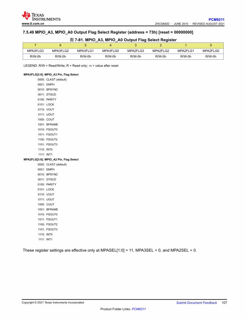
7.5.49 MPIO_A3, MPIO_A0 Output Flag Select Register (address = 73h) [reset = 00000000]
图 7-81. MPIO_A3, MPIO_A0 Output Flag Select Register7 6 5 4 3 2 1 0
MPA3FLG3 MPA3FLG2 MPA3FLG1 MPA3FLG0 MPA2FLG3 MPA2FLG2 MPA2FLG1 MPA2FLG0
R/W-0h R/W-0h R/W-0h R/W-0h R/W-0h R/W-0h R/W-0h R/W-0h
LEGEND: R/W = Read/Write; R = Read only; -n = value after reset
MPA3FLG[3:0]: MPIO_A3 Pin, Flag Select0000: CLKST (default)
0001: EMPH
0010: BPSYNC
0011: DTSCD
0100: PARITY
0101: LOCK
0110: VOUT
0111: UOUT
1000: COUT
1001: BFRAME
1010: FSOUT0
1011: FSOUT1
1100: FSOUT2
1101: FSOUT3
1110: INT0
1111: INT1
MPA2FLG[3:0]: MPIO_A2 Pin, Flag Select0000: CLKST (default)
0001: EMPH
0010: BPSYNC
0011: DTSCD
0100: PARITY
0101: LOCK
0110: VOUT
0111: UOUT
1000: COUT
1001: BFRAME
1010: FSOUT0
1011: FSOUT1
1100: FSOUT2
1101: FSOUT3
1110: INT0
1111: INT1
These register settings are effective only at MPASEL[1:0] = 11, MPA3SEL = 0, and MPA2SEL = 0.
www.ti.com.cnPCM9211
ZHCSIM2D – JUNE 2010 – REVISED AUGUST 2021
Copyright © 2021 Texas Instruments Incorporated Submit Document Feedback 107
Product Folder Links: PCM9211

7.5.50 MPIO_B1, MPIO_B0 Output Flag Select Register (address = 74h) [reset = 00000000]
图 7-82. MPIO_B1, MPIO_B0 Output Flag Select Register7 6 5 4 3 2 1 0
MPB1FLG3 MPB1FLG2 MPB1FLG1 MPB1FLG0 MPB0FLG3 MPB0FLG2 MPB0FLG1 MPB0FLG0
R/W-0h R/W-0h R/W-0h R/W-0h R/W-0h R/W-0h R/W-0h R/W-0h
LEGEND: R/W = Read/Write; R = Read only; -n = value after reset
MPB1FLG[3:0]: MPIO_B1 Pin, Flag Select0000: CLKST (default)
0001: EMPH
0010: BPSYNC
0011: DTSCD
0100: PARITY
0101: LOCK
0110: VOUT
0111: UOUT
1000: COUT
1001: BFRAME
1010: FSOUT0
1011: FSOUT1
1100: FSOUT2
1101: FSOUT3
1110: INT0
1111: INT1
MPB0FLG[3:0]: MPIO_B0 Pin, Flag Select0000: CLKST (default)
0001: EMPH
0010: BPSYNC
0011: DTSCD
0100: PARITY
0101: LOCK
0110: VOUT
0111: UOUT
1000: COUT
1001: BFRAME
1010: FSOUT0
1011: FSOUT1
1100: FSOUT2
1101: FSOUT3
1110: INT0
1111: INT1
These register settings are effective only at MPBSEL[2:0] = 011, MPB1SEL = 0, and MPB0SEL = 0.
PCM9211ZHCSIM2D – JUNE 2010 – REVISED AUGUST 2021 www.ti.com.cn
108 Submit Document Feedback Copyright © 2021 Texas Instruments Incorporated
Product Folder Links: PCM9211

7.5.51 MPIO_B3, MPIO_B2 Output Flag Select Register (address = 75h) [reset = 00000000]
图 7-83. MPIO_B3, MPIO_B2 Output Flag Select Register7 6 5 4 3 2 1 0
MPB3FLG3 MPB3FLG2 MPB3FLG1 MPB3FLG0 MPB2FLG3 MPB2FLG2 MPB2FLG1 MPB2FLG0
R/W-0h R/W-0h R/W-0h R/W-0h R/W-0h R/W-0h R/W-0h R/W-0h
LEGEND: R/W = Read/Write; R = Read only; -n = value after reset
MPB3FLG[3:0]: MPIO_B3 Pin, Flag Select0000: CLKST (default)
0001: EMPH
0010: BPSYNC
0011: DTSCD
0100: PARITY
0101: LOCK
0110: VOUT
0111: UOUT
1000: COUT
1001: BFRAME
1010: FSOUT0
1011: FSOUT1
1100: FSOUT2
1101: FSOUT3
1110: INT0
1111: INT1
MPB2FLG[3:0]: MPIO_B2 Pin, Flag Select0000: CLKST (default)
0001: EMPH
0010: BPSYNC
0011: DTSCD
0100: PARITY
0101: LOCK
0110: VOUT
0111: UOUT
1000: COUT
1001: BFRAME
1010: FSOUT0
1011: FSOUT1
1100: FSOUT2
1101: FSOUT3
1110: INT0
1111: INT1
These register settings are effective only at MPBSEL[2:0] = 011, MPB3SEL = 0, and MPB2SEL = 0.
www.ti.com.cnPCM9211
ZHCSIM2D – JUNE 2010 – REVISED AUGUST 2021
Copyright © 2021 Texas Instruments Incorporated Submit Document Feedback 109
Product Folder Links: PCM9211

7.5.52 MPIO_C1, MPIO_C0 Output Flag Select Register (address = 76h) [reset = 00000000]
图 7-84. MPIO_C1, MPIO_C0 Output Flag Select Register7 6 5 4 3 2 1 0
MPC1FLG3 MPC1FLG2 MPC1FLG1 MPC1FLG0 MPC0FLG3 MPC0FLG2 MPC0FLG1 MPC0FLG0
R/W-0h R/W-0h R/W-0h R/W-0h R/W-0h R/W-0h R/W-0h R/W-0h
LEGEND: R/W = Read/Write; R = Read only; -n = value after reset
MPC1FLG[3:0]: MPIO_C1 Pin, Flag Select0000: CLKST (default)
0001: EMPH
0010: BPSYNC
0011: DTSCD
0100: PARITY
0101: LOCK
0110: VOUT
0111: UOUT
1000: COUT
1001: BFRAME
1010: FSOUT0
1011: FSOUT1
1100: FSOUT2
1101: FSOUT3
1110: INT0
1111: INT1
MPC0FLG[3:0]: MPIO_C0 Pin, Flag Select0000: CLKST (default)
0001: EMPH
0010: BPSYNC
0011: DTSCD
0100: PARITY
0101: LOCK
0110: VOUT
0111: UOUT
1000: COUT
1001: BFRAME
1010: FSOUT0
1011: FSOUT1
1100: FSOUT2
1101: FSOUT3
1110: INT0
1111: INT1
These register settings are effective only at MPCSEL[2:0] = 011, MPC1SEL = 0, and MPC0SEL = 0.
PCM9211ZHCSIM2D – JUNE 2010 – REVISED AUGUST 2021 www.ti.com.cn
110 Submit Document Feedback Copyright © 2021 Texas Instruments Incorporated
Product Folder Links: PCM9211

7.5.53 MPIO_C3, MPIO_C2 Output Flag Select Register (address = 77h) [reset = 00000000]
图 7-85. MPIO_C3, MPIO_C2 Output Flag Select Register7 6 5 4 3 2 1 0
MPC3FLG3 MPC3FLG2 MPC3FLG1 MPC3FLG0 MPC2FLG3 MPC2FLG2 MPC2FLG1 MPC2FLG0
R/W-0h R/W-0h R/W-0h R/W-0h R/W-0h R/W-0h R/W-0h R/W-0h
LEGEND: R/W = Read/Write; R = Read only; -n = value after reset
MPC3FLG[3:0]: MPIO_C3 Pin, Flag Select0000: CLKST (default)
0001: EMPH
0010: BPSYNC
0011: DTSCD
0100: PARITY
0101: LOCK
0110: VOUT
0111: UOUT
1000: COUT
1001: BFRAME
1010: FSOUT0
1011: FSOUT1
1100: FSOUT2
1101: FSOUT3
1110: INT0
1111: INT1
MPC2FLG[3:0]: MPIO_C2 Pin, Flag Select0000: CLKST (default)
0001: EMPH
0010: BPSYNC
0011: DTSCD
0100: PARITY
0101: LOCK
0110: VOUT
0111: UOUT
1000: COUT
1001: BFRAME
1010: FSOUT0
1011: FSOUT1
1100: FSOUT2
1101: FSOUT3
1110: INT0
1111: INT1
These register settings are effective only at MPCSEL[2:0] = 011, MPC3SEL = 0, and MPC2SEL = 0.
www.ti.com.cnPCM9211
ZHCSIM2D – JUNE 2010 – REVISED AUGUST 2021
Copyright © 2021 Texas Instruments Incorporated Submit Document Feedback 111
Product Folder Links: PCM9211

7.5.54 MPO1, MPO0 Function Assign Setting Register (address = 78h) [reset = 00111101]
图 7-86. MPO1, MPO0 Output Flag Select Register7 6 5 4 3 2 1 0
MPO1SEL3 MPO1SEL2 MPO1SEL1 MPO1SEL0 MPO0SEL3 MPO0SEL2 MPO0SEL1 MPO0SEL0
R/W-0h R/W-0h R/W-1h R/W-1h R/W-1h R/W-1h R/W-0h R/W-1h
LEGEND: R/W = Read/Write; R = Read only; -n = value after reset
MPO1SEL[3:0]: MPO1 Pin, Output Control0000: Hi-Z
0001: GPO, Output data = High level
0010: GPO, Output data = Low level
0011: VOUT (default)
0100: INT0
0101: INT1
0110: CLKST
0111: EMPH
1000: BPSYNC
1001: DTSCD
1010: PARITY
1011: LOCK
1100: XMCKO
1101: TXOUT
1110: RECOUT0
1111: RECOUT1
MPO0SEL[3:0]: MPO0 Pin, Output Control0000: Hi-Z
0001: GPO, Output data = High level
0010: GPO, Output data = Low level
0011: VOUT
0100: INT0
0101: INT1
0110: CLKST
0111: EMPH
1000: BPSYNC
1001: DTSCD
1010: PARITY
1011: LOCK
1100: XMCKO
1101: TXOUT (default)
1110: RECOUT0
1111: RECOUT1
PCM9211ZHCSIM2D – JUNE 2010 – REVISED AUGUST 2021 www.ti.com.cn
112 Submit Document Feedback Copyright © 2021 Texas Instruments Incorporated
Product Folder Links: PCM9211

7.5.55 GPIO I/O Direction Control for MPIO_A, MPIO_B Register (address = 79h) [reset = 00000000]
图 7-87. GPIO I/O Direction Control for MPIO_A, MPIO_B Register7 6 5 4 3 2 1 0
GIOB3DIR GIOB2DIR GIOB1DIR GIOB0DIR GIOA3DIR GIOA2DIR GIOA1DIR GIOA0DIR
R/W-0h R/W-0h R/W-0h R/W-0h R/W-0h R/W-0h R/W-0h R/W-0h
LEGEND: R/W = Read/Write; R = Read only; -n = value after reset
GIOB3DIR: MPIO_B3 Pin, GPIO I/O Direction Control0: Input (default)1: Output
GIOB2DIR: MPIO_B2 Pin, GPIO I/O Direction Control0: Input (default)1: Output
GIOB1DIR: MPIO_B1 Pin, GPIO I/O Direction Control0: Input (default)1: Output
GIOB0DIR: MPIO_B0 Pin, GPIO I/O Direction Control0: Input (default)1: Output
GIOA3DIR: MPIO_A3 Pin Function, GPIO I/O Direction Control0: Input (default)1: Output
GIOA2DIR: MPIO_A2 Pin Function, GPIO I/O Direction Control0: Input (default)1: Output
GIOA`DIR: MPIO_A1 Pin Function, GPIO I/O Direction Control0: Input (default)1: Output
GIOA0DIR: MPIO_A0 Pin Function, GPIO I/O Direction Control0: Input (default)1: Output
These registers are effective only at MPIO_A and MPIO_B assigned as GPIO. I/O direction setting is available by pin.
www.ti.com.cnPCM9211
ZHCSIM2D – JUNE 2010 – REVISED AUGUST 2021
Copyright © 2021 Texas Instruments Incorporated Submit Document Feedback 113
Product Folder Links: PCM9211
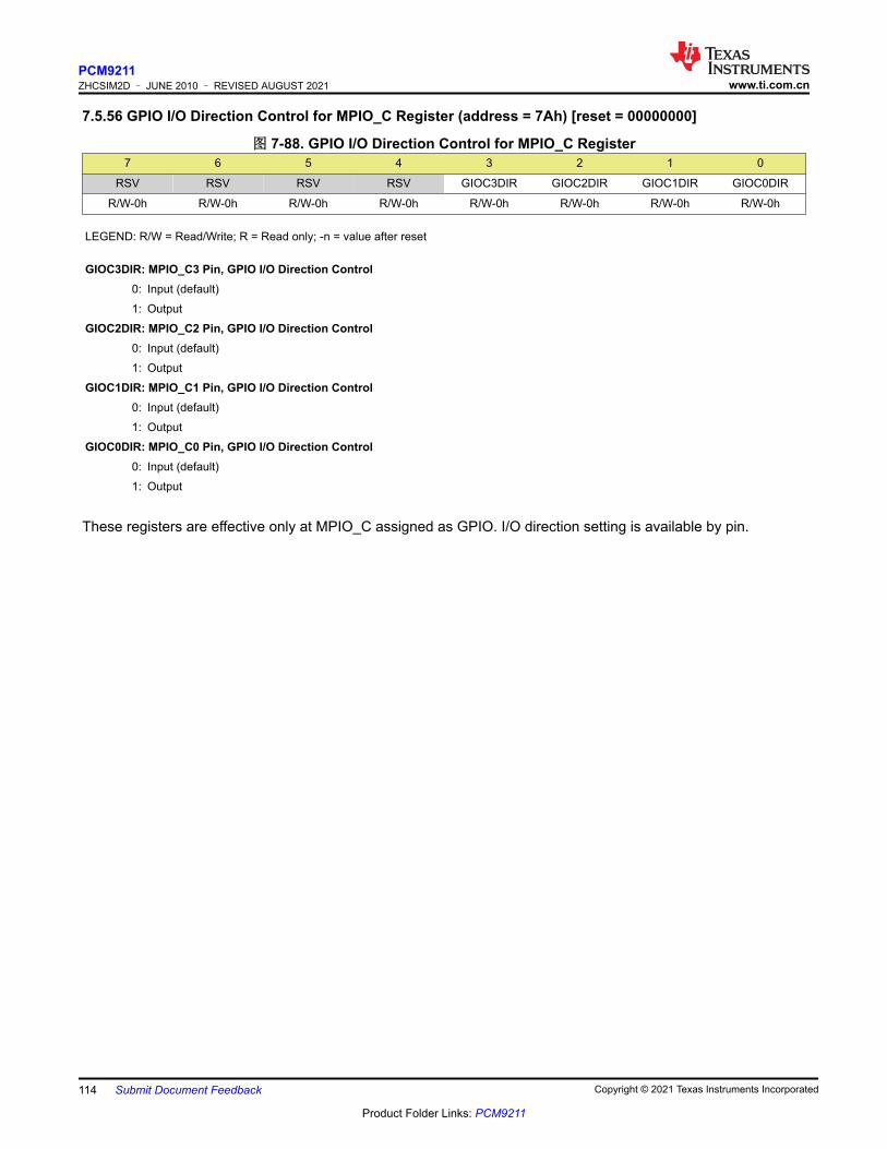
7.5.56 GPIO I/O Direction Control for MPIO_C Register (address = 7Ah) [reset = 00000000]
图 7-88. GPIO I/O Direction Control for MPIO_C Register7 6 5 4 3 2 1 0
RSV RSV RSV RSV GIOC3DIR GIOC2DIR GIOC1DIR GIOC0DIR
R/W-0h R/W-0h R/W-0h R/W-0h R/W-0h R/W-0h R/W-0h R/W-0h
LEGEND: R/W = Read/Write; R = Read only; -n = value after reset
GIOC3DIR: MPIO_C3 Pin, GPIO I/O Direction Control0: Input (default)1: Output
GIOC2DIR: MPIO_C2 Pin, GPIO I/O Direction Control0: Input (default)1: Output
GIOC1DIR: MPIO_C1 Pin, GPIO I/O Direction Control0: Input (default)1: Output
GIOC0DIR: MPIO_C0 Pin, GPIO I/O Direction Control0: Input (default)1: Output
These registers are effective only at MPIO_C assigned as GPIO. I/O direction setting is available by pin.
PCM9211ZHCSIM2D – JUNE 2010 – REVISED AUGUST 2021 www.ti.com.cn
114 Submit Document Feedback Copyright © 2021 Texas Instruments Incorporated
Product Folder Links: PCM9211

7.5.57 GPIO Output Data Setting for MPIO_A, MPIO_B Register (address = 7Bh) [reset = 00000000]
图 7-89. GPIO Output Data Setting for MPIO_A, MPIO_B Register7 6 5 4 3 2 1 0
GPOB3 GPOB2 GPOB1 GPOB1 GPOA3 GPOA2 GPOA1 GPOA0
R/W-0h R/W-0h R/W-0h R/W-0h R/W-0h R/W-0h R/W-0h R/W-0h
LEGEND: R/W = Read/Write; R = Read only; -n = value after reset
GPOB3: MPIO_B3 Pin, GPIO Output Data Setting0: Output low level (default)1: Output high level
GPOB2: MPIO_B2 Pin, GPIO Output Data Setting0: Output low level (default)1: Output high level
GPOB1: MPIO_B1 Pin, GPIO Output Data Setting0: Output low level (default)1: Output high level
GPOB0: MPIO_B0 Pin, GPIO Output Data Setting0: Output low level (default)1: Output high level
GPOA3: MPIO_A3 Pin, GPIO Output Data Setting0: Output low level (default)1: Output high level
GPOA2: MPIO_A2 Pin, GPIO Output Data Setting0: Output low level (default)1: Output high level
GPOA1: MPIO_A1 Pin, GPIO Output Data Setting0: Output low level (default)1: Output high level
GPOA0: MPIO_A0 Pin, GPIO Output Data Setting0: Output low level (default)1: Output high level
These registers are effective only as GPIOs are assigned to output.
www.ti.com.cnPCM9211
ZHCSIM2D – JUNE 2010 – REVISED AUGUST 2021
Copyright © 2021 Texas Instruments Incorporated Submit Document Feedback 115
Product Folder Links: PCM9211

7.5.58 GPIO Output Data Setting for MPIO_C Register (address = 7Ch) [reset = 00000000]
图 7-90. GPIO I/O Direction Control for MPIO_C Register7 6 5 4 3 2 1 0
RSV RSV RSV RSV GPOC3 GPOC2 GPOC1 GPOC0
R/W-0h R/W-0h R/W-0h R/W-0h R/W-0h R/W-0h R/W-0h R/W-0h
LEGEND: R/W = Read/Write; R = Read only; -n = value after reset
GPOC3: MPIO_C3 Pin, GPIO Output Data Setting0: Output low level (default)1: Output high level
GPOC2: MPIO_C2 Pin, GPIO Output Data Setting0: Output low level (default)1: Output high level
GPOC1: MPIO_C1 Pin, GPIO Output Data Setting0: Output low level (default)1: Output high level
GPOC0: MPIO_C0 Pin, GPIO Output Data Setting0: Output low level (default)1: Output high level
These registers are effective only as GPIOs are assigned to output.
PCM9211ZHCSIM2D – JUNE 2010 – REVISED AUGUST 2021 www.ti.com.cn
116 Submit Document Feedback Copyright © 2021 Texas Instruments Incorporated
Product Folder Links: PCM9211

7.5.59 GPIO Input Data Register for MPIO_A, MPIO_B Register (address = 7Dh) [reset = N/A]
图 7-91. GPIO Input Data Register for MPIO_A, MPIO_B Register7 6 5 4 3 2 1 0
GPIB3 GPIB2 GPIB1 GPIB1 GPIA3 GPIA2 GPIA1 GPIA0
N/A N/A N/A N/A N/A N/A N/A N/A
LEGEND: R/W = Read/Write; R = Read only; -n = value after reset
GPIB3: MPIO_B3 Pin, GPIO Input Data0: Detect low level1: Detect high level
GPIB2: MPIO_B2 Pin, GPIO Input Data0: Detect low level1: Detect high level
GPIB1: MPIO_B1 Pin, GPIO Input Data0: Detect low level1: Detect high level
GPIB0: MPIO_B0 Pin, GPIO Input Data0: Detect low level1: Detect high level
GPIA3: MPIO_A3 Pin, GPIO Input Data0: Detect low level1: Detect high level
GPIA2: MPIO_A2 Pin, GPIO Input Data0: Detect low level1: Detect high level
GPIA1: MPIO_A1 Pin, GPIO Input Data0: Detect low level1: Detect high level
GPIA0: MPIO_A0 Pin, GPIO Input Data0: Detect low level1: Detect high level
www.ti.com.cnPCM9211
ZHCSIM2D – JUNE 2010 – REVISED AUGUST 2021
Copyright © 2021 Texas Instruments Incorporated Submit Document Feedback 117
Product Folder Links: PCM9211

7.5.60 GPIO Input Data Register for MPIO_C Register (address = 7Eh) [reset = N/A]
图 7-92. GPIO Input Data Register for MPIO_C Register7 6 5 4 3 2 1 0
RSV RSV RSV RSV GPIC3 GPIC2 GPIC1 GPIC0
N/A N/A N/A N/A N/A N/A N/A N/A
LEGEND: R/W = Read/Write; R = Read only; -n = value after reset
GPIC3: MPIO_C3 Pin, GPIO Input Data0: Detect low level1: Detect high level
GPIC2: MPIO_C2 Pin, GPIO Input Data0: Detect low level1: Detect high level
GPIC1: MPIO_C1 Pin, GPIO Input Data0: Detect low level1: Detect high level
GPIC0: MPIO_C0 Pin, GPIO Input Data0: Detect low level1: Detect high level
PCM9211ZHCSIM2D – JUNE 2010 – REVISED AUGUST 2021 www.ti.com.cn
118 Submit Document Feedback Copyright © 2021 Texas Instruments Incorporated
Product Folder Links: PCM9211

8 Application and ImplementationNote
以下应用部分中的信息不属于 TI 器件规格的范围,TI 不担保其准确性和完整性。TI 的客 户应负责确定
器件是否适用于其应用。客户应验证并测试其设计,以确保系统功能。
8.1 Application Information8.1.1 Typical Circuit Connection
图 8-1 shows a typical circuit connection.
ERROR/INT0
NPCM/ INT1
MPIO_A0
MPIO_A1
MPIO_A2
MPIO_A3
MPIO_C0
MPIO_C1
MPIO_C2
MPIO_C3
MPIO_B0
MPIO_B1
1
2
3
4
5
6
7
8
9
10
11
12
MP
IO_
B2
MP
IO_
B3
MP
O0
MP
O1
DO
UT
LR
CK
BC
K
SC
KO
DG
ND
DV
DD
MD
O/A
DR
0
MD
I/S
DA
VDDRX
RXIN1
RXIN2
RXIN3
RXIN4/ASCKIO
RXIN5/ABCKIO
RXIN6/ALRCKIO
RXIN7/ADIN0
MODE
MS/ADR1
MC/SCL
36
35
34
33
32
31
30
29
28
27
26
25
VIN
R
VIN
L
VC
CA
D
AG
ND
AD
VC
OM
FIL
T
VC
C
AG
ND
XT
O
XT
I
GN
DR
X
RX
IN0
48 47 46 45 44 43 42 41 40 39 38 37
13 14 15 16 17 18 19 20 21 22 23 24
C1
Analog Input
C2C3
+5 V
C4 R1
C5
C6
C7
+3.3 V
X1
C9
C8
C12
C11
C10
R4
R3
+3.3V
COAX Input0 V 0 V 0 V
COAX Input
OpticalInputs
orPCM
Audio
I/ F
0 V or 3.3 V
Serial
ControlI/ F
Serial
ControlI/F
C13
0 V +3.3 V
PCM
AudioI/F
MPOx
AssignedFunctions
MPIO_B
AssignedFunctions
MPIO_A
AssignedFunctions
MPIO_C
AssignedFunctions
MPIO_B
AssignedFunctions
InterruptionFlag
Functions
R2
RST
图 8-1. Typical Circuit Connection
www.ti.com.cnPCM9211
ZHCSIM2D – JUNE 2010 – REVISED AUGUST 2021
Copyright © 2021 Texas Instruments Incorporated Submit Document Feedback 119
Product Folder Links: PCM9211
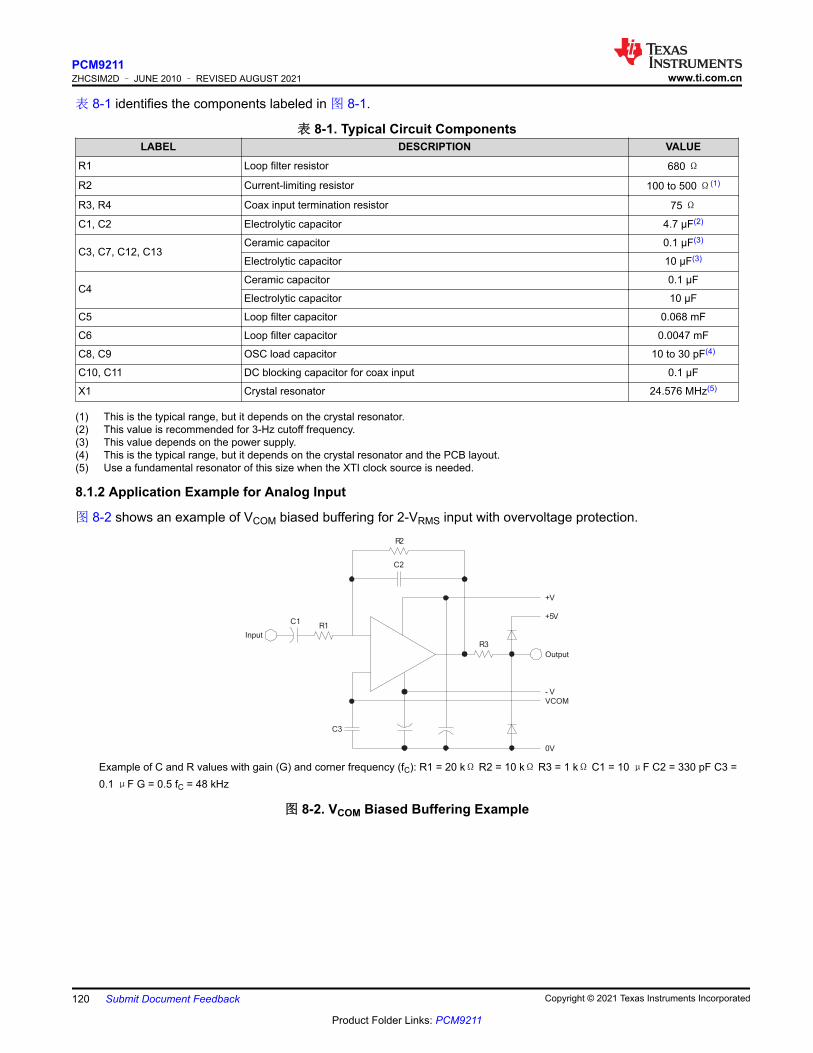
表 8-1 identifies the components labeled in 图 8-1.
表 8-1. Typical Circuit ComponentsLABEL DESCRIPTION VALUE
R1 Loop filter resistor 680 Ω
R2 Current-limiting resistor 100 to 500 Ω(1)
R3, R4 Coax input termination resistor 75 Ω
C1, C2 Electrolytic capacitor 4.7 µF(2)
C3, C7, C12, C13Ceramic capacitor 0.1 µF(3)
Electrolytic capacitor 10 µF(3)
C4Ceramic capacitor 0.1 µF
Electrolytic capacitor 10 µF
C5 Loop filter capacitor 0.068 mF
C6 Loop filter capacitor 0.0047 mF
C8, C9 OSC load capacitor 10 to 30 pF(4)
C10, C11 DC blocking capacitor for coax input 0.1 µF
X1 Crystal resonator 24.576 MHz(5)
(1) This is the typical range, but it depends on the crystal resonator.(2) This value is recommended for 3-Hz cutoff frequency.(3) This value depends on the power supply.(4) This is the typical range, but it depends on the crystal resonator and the PCB layout.(5) Use a fundamental resonator of this size when the XTI clock source is needed.
8.1.2 Application Example for Analog Input
图 8-2 shows an example of VCOM biased buffering for 2-VRMS input with overvoltage protection.
C2
R1
Input
C1
R2
R3
C3
Output
- V
VCOM
+V
0V
+5V
Example of C and R values with gain (G) and corner frequency (fC): R1 = 20 kΩ R2 = 10 kΩ R3 = 1 kΩ C1 = 10 μF C2 = 330 pF C3 = 0.1 μF G = 0.5 fC = 48 kHz
图 8-2. VCOM Biased Buffering Example
PCM9211ZHCSIM2D – JUNE 2010 – REVISED AUGUST 2021 www.ti.com.cn
120 Submit Document Feedback Copyright © 2021 Texas Instruments Incorporated
Product Folder Links: PCM9211

8.2 Typical Application
BT Module
PCM9211
x2
DSP
OUT
PCM
DSPx6
IN
IN
LINE
IN
DSP
PCM x3
GPIO/INT
I2C
x2
IN
HDMI
ARCS/PDIF
S/PDIF
S/PDIF
图 8-3. Typical Application Schematic
8.2.1 Design Requirements
For this design example, use the parameters listed in 表 8-2 as the input parameters.
表 8-2. Design ParametersDESIGN PARAMETER EXAMPLE VALUE
Audio Input PCM, COAX S/PDIF, Optical S/PDIF, 2 ch Single Ended Analog
Audio Output PCM, S/PDIF
Control Host I2C
8.2.2 Detailed Design Procedure8.2.2.1 S/PDIF Ports
The PCM9211 has total of 12 single ended S/PDIF inputs and 2 of these S/PDIF inputs have built in COAX amplifiers. These S/PDIF inputs are MUXed to one DIR. MPIO_A provides 4 of the 12 S/PDIF inputs, but can also be configured to be an additional I2S input for other applications.
There are two S/PDIF outputs available in the MPO port; MPO0 and MPO1 output can be selected independently. The MPO pins are also able to output DIR flag information, interrupt flags, or to repeat S/PDIF signals selected for the RECOUT0 or RECOUT1 paths.
In this application there are 8 total S/PDIF inputs available (2 with integrated COAX amplifiers) due to RXIN4- RXIN7 being used for a PCM input on AUXIN0.
8.2.2.2 PCM Ports
The PCM9211 can have up to 3 PCM inputs at one time or up to 3 PCM outputs at one time. Each PCM port can be configured top select the data output on the pins, and some such as MPIO_B can be either an input or an output. MPIO_C can be the PCM output for the ADC or a PCM input. In this application the Main Output Port, MPIO_B and MPIO_C are PCM outputs, while AUXIN0 (RXIN4 –RXIN7) is utilized as a PCM input.
8.2.2.3 ADC Operation
In this application, the ADC is operating in standalone mode. This means that the ADC is acting as a master and outputting PCM data on the MPIO_C port.
8.2.2.4 GPIO/Interrupts
The Error/Int0 and NPCM/Int1 pins can be programmed to output flags for various internal flags masked or unmasked in the registers. This can include DIR flags, ADC flags, or port flags.
www.ti.com.cnPCM9211
ZHCSIM2D – JUNE 2010 – REVISED AUGUST 2021
Copyright © 2021 Texas Instruments Incorporated Submit Document Feedback 121
Product Folder Links: PCM9211

8.2.3 Application Curve
0
20
40
60
80
100
120
140
-
-
-
-
-
-
-
Am
plit
ude (
dB
)
0 5 10 15 20
Frequency (kHz)
–1 dB, N = 32,768图 8-4. Output Spectrum
9 Power Supply RecommendationsThe PCM9211 requires 3.3-V nominal rails and a 5-V nominal rail. At least one 3.3-V supply is needed for VCC, VDD, and VDDRX. For best performance, separate 3.3-V rails are recommended for each power pin. A 5-V supply is needed for the VCCAD rail that supplies the ADC circuitry. Place the decoupling capacitors for the power supplies close to the device terminals.
PCM9211ZHCSIM2D – JUNE 2010 – REVISED AUGUST 2021 www.ti.com.cn
122 Submit Document Feedback Copyright © 2021 Texas Instruments Incorporated
Product Folder Links: PCM9211

10 Layout10.1 Layout GuidelinesIt is strongly recommend to use one ground plane for the PCM9211 as the internal ground partitions are not connected. While using one ground plane, it is best to make sure that analog and digital circuitry be sufficiently partitioned on the PCB so that analog and digital return currents do not cross.• Decoupling caps should be placed as close to power pins as possible (VCC, VDD, VDDRX, VCCAD).• 24.576-MHz crystal should be placed as close to XTI and XTO pins as possible, the resistor value is
generally between 100 Ω to 500 Ω depending on crystal; and load capacitors are generally between 10 pF to 30 pF, depending on crystal.
• Further guidelines can be found in 图 10-1.
www.ti.com.cnPCM9211
ZHCSIM2D – JUNE 2010 – REVISED AUGUST 2021
Copyright © 2021 Texas Instruments Incorporated Submit Document Feedback 123
Product Folder Links: PCM9211

10.2 Layout Example
Top Layer Ground Pour and PowerPad Top Layer Signal Traces Pad to top layer ground pour
PCM9211
Impedance Matching and
DC Blocking Capacitor
for COAX Input
1
2
3
4
5
6
7
8
9
10
11
12
13 14 15 16 17 18 19 20 21 22 23 24
25
26
27
28
29
30
31
32
33
34
35
36
373839404142434445464748
+3.3 V
+5 V
10 μF
+
10 μF
+
Analog
Inputs680 Ω
4.7 μF
0.068 mF
+3.3 V
0.1 μF
0.1 μF
10 μF
10 μF 24.576
MHz 0.1 μF
75 Ω
COAX
Input
75 Ω
COAX
Input
0.1 μF
+3.3 V
0.1 μF 10 μF
10 μF
VDDRX
RX
IN0
RXIN1
RST
RXIN2
RXIN3
RXIN4,ASCKIO
RXIN5,ABCKIO
RXIN6,ALRCKIO
RXIN7,ADIN0
MODE
MS,ADR1
MC,SCL
GN
DR
X
XT
I
XT
O
AG
ND
VC
C
FIL
T
VC
OM
AG
ND
AD
VC
CA
D
VIN
L
VIN
R
ERROR,INT0
NPCM,INT1
MPIO_A0
MPIO_A1
MPIO_A2
MPIO_A3
MPIO_C0
MPIO_C1
MPIO_C2
MPIO_C3
MPIO_B0
MPIO_B1
MP
IO_
B2
MP
IO_
B3
MP
O0
MP
O1
DO
UT
LR
CK
BC
K
SC
KO
DG
ND
DV
DD
MD
O,A
DR
0
MD
I,S
DA
Interruption
Flag
Functions
MPIO_A
Assigned
Functions
MPIO_C
Assigned
Functions
MPIO_B
Assigned
Functions
MPIO_B
Assigned
Functions
MPIOx
Assigned
Functions
PCM
AUDIO
Interface
Serial
Control
Interface
Serial
Control
Interface
Optical Inputs
Or PCM Audio
Interface
0.1 μF
Place a top-layer ground pour as shielding around the PCM9211, and connect,
the top layer to the lower main PCB ground plane using multiple vias.
For resistor and capacitor values of the crystaloscillator circuit, see the section,and the data sheet for the crystal oscillator.
Layout Guidelines
Electrolytic DC Blocking Capacitors
for Best Performance Over Temperature
图 10-1. Layout Example
PCM9211ZHCSIM2D – JUNE 2010 – REVISED AUGUST 2021 www.ti.com.cn
124 Submit Document Feedback Copyright © 2021 Texas Instruments Incorporated
Product Folder Links: PCM9211

11 Device and Documentation Support11.1 Documentation Support11.1.1 Related Documentation
For related documentation see the following:• Texas Instruments, PCM9211EVM: PCM9211 Evaluation Module with CodecControl Software user's guide• Texas Instruments, PCM9211EVM Record and Playback via USB Interface application report• Texas Instruments, PurePath™ Console Motherboard user's guide
11.2 接收文档更新通知
要接收文档更新通知,请导航至 ti.com 上的器件产品文件夹。点击订阅更新 进行注册,即可每周接收产品信息更
改摘要。有关更改的详细信息,请查看任何已修订文档中包含的修订历史记录。
11.3 支持资源
TI E2E™ 支持论坛是工程师的重要参考资料,可直接从专家获得快速、经过验证的解答和设计帮助。搜索现有解
答或提出自己的问题可获得所需的快速设计帮助。
链接的内容由各个贡献者“按原样”提供。这些内容并不构成 TI 技术规范,并且不一定反映 TI 的观点;请参阅
TI 的《使用条款》。
11.4 TrademarksAC-3™ is a trademark of Dolby Laboratories.TOSLINK™ is a trademark of Toshiba Corp.PurePath™ and TI E2E™ are trademarks of Texas Instruments.所有商标均为其各自所有者的财产。
11.5 Electrostatic Discharge CautionThis integrated circuit can be damaged by ESD. Texas Instruments recommends that all integrated circuits be handled with appropriate precautions. Failure to observe proper handling and installation procedures can cause damage.ESD damage can range from subtle performance degradation to complete device failure. Precision integrated circuits may be more susceptible to damage because very small parametric changes could cause the device not to meet its published specifications.
11.6 术语表
TI 术语表 本术语表列出并解释了术语、首字母缩略词和定义。
12 Mechanical, Packaging, and Orderable InformationThe following pages include mechanical, packaging, and orderable information. This information is the most current data available for the designated devices. This data is subject to change without notice and revision of this document. For browser-based versions of this data sheet, refer to the left-hand navigation.
www.ti.com.cnPCM9211
ZHCSIM2D – JUNE 2010 – REVISED AUGUST 2021
Copyright © 2021 Texas Instruments Incorporated Submit Document Feedback 125
Product Folder Links: PCM9211

重要声明和免责声明TI 提供技术和可靠性数据(包括数据表)、设计资源(包括参考设计)、应用或其他设计建议、网络工具、安全信息和其他资源,不保证没
有瑕疵且不做出任何明示或暗示的担保,包括但不限于对适销性、某特定用途方面的适用性或不侵犯任何第三方知识产权的暗示担保。
这些资源可供使用 TI 产品进行设计的熟练开发人员使用。您将自行承担以下全部责任:(1) 针对您的应用选择合适的 TI 产品,(2) 设计、验
证并测试您的应用,(3) 确保您的应用满足相应标准以及任何其他安全、安保或其他要求。这些资源如有变更,恕不另行通知。TI 授权您仅可
将这些资源用于研发本资源所述的 TI 产品的应用。严禁对这些资源进行其他复制或展示。您无权使用任何其他 TI 知识产权或任何第三方知
识产权。您应全额赔偿因在这些资源的使用中对 TI 及其代表造成的任何索赔、损害、成本、损失和债务,TI 对此概不负责。
TI 提供的产品受 TI 的销售条款 (https:www.ti.com/legal/termsofsale.html) 或 ti.com 上其他适用条款/TI 产品随附的其他适用条款的约束。TI 提供这些资源并不会扩展或以其他方式更改 TI 针对 TI 产品发布的适用的担保或担保免责声明。重要声明
邮寄地址:Texas Instruments, Post Office Box 655303, Dallas, Texas 75265Copyright © 2021,德州仪器 (TI) 公司

PACKAGE OPTION ADDENDUM
www.ti.com 24-Aug-2021
Addendum-Page 1
PACKAGING INFORMATION
Orderable Device Status(1)
Package Type PackageDrawing
Pins PackageQty
Eco Plan(2)
Lead finish/Ball material
(6)
MSL Peak Temp(3)
Op Temp (°C) Device Marking(4/5)
Samples
PCM9211PT ACTIVE LQFP PT 48 250 RoHS & Green NIPDAU Level-1-260C-UNLIM -40 to 85 PCM9211
PCM9211PTR ACTIVE LQFP PT 48 1000 RoHS & Green NIPDAU Level-1-260C-UNLIM -40 to 85 PCM9211
(1) The marketing status values are defined as follows:ACTIVE: Product device recommended for new designs.LIFEBUY: TI has announced that the device will be discontinued, and a lifetime-buy period is in effect.NRND: Not recommended for new designs. Device is in production to support existing customers, but TI does not recommend using this part in a new design.PREVIEW: Device has been announced but is not in production. Samples may or may not be available.OBSOLETE: TI has discontinued the production of the device.
(2) RoHS: TI defines "RoHS" to mean semiconductor products that are compliant with the current EU RoHS requirements for all 10 RoHS substances, including the requirement that RoHS substancedo not exceed 0.1% by weight in homogeneous materials. Where designed to be soldered at high temperatures, "RoHS" products are suitable for use in specified lead-free processes. TI mayreference these types of products as "Pb-Free".RoHS Exempt: TI defines "RoHS Exempt" to mean products that contain lead but are compliant with EU RoHS pursuant to a specific EU RoHS exemption.Green: TI defines "Green" to mean the content of Chlorine (Cl) and Bromine (Br) based flame retardants meet JS709B low halogen requirements of <=1000ppm threshold. Antimony trioxide basedflame retardants must also meet the <=1000ppm threshold requirement.
(3) MSL, Peak Temp. - The Moisture Sensitivity Level rating according to the JEDEC industry standard classifications, and peak solder temperature.
(4) There may be additional marking, which relates to the logo, the lot trace code information, or the environmental category on the device.
(5) Multiple Device Markings will be inside parentheses. Only one Device Marking contained in parentheses and separated by a "~" will appear on a device. If a line is indented then it is a continuationof the previous line and the two combined represent the entire Device Marking for that device.
(6) Lead finish/Ball material - Orderable Devices may have multiple material finish options. Finish options are separated by a vertical ruled line. Lead finish/Ball material values may wrap to twolines if the finish value exceeds the maximum column width.
Important Information and Disclaimer:The information provided on this page represents TI's knowledge and belief as of the date that it is provided. TI bases its knowledge and belief on informationprovided by third parties, and makes no representation or warranty as to the accuracy of such information. Efforts are underway to better integrate information from third parties. TI has taken andcontinues to take reasonable steps to provide representative and accurate information but may not have conducted destructive testing or chemical analysis on incoming materials and chemicals.TI and TI suppliers consider certain information to be proprietary, and thus CAS numbers and other limited information may not be available for release.
In no event shall TI's liability arising out of such information exceed the total purchase price of the TI part(s) at issue in this document sold by TI to Customer on an annual basis.

PACKAGE OPTION ADDENDUM
www.ti.com 24-Aug-2021
Addendum-Page 2

TRAY
Chamfer on Tray corner indicates Pin 1 orientation of packed units.
*All dimensions are nominal
Device PackageName
PackageType
Pins SPQ Unit arraymatrix
Maxtemperature
(°C)
L (mm) W(mm)
K0(µm)
P1(mm)
CL(mm)
CW(mm)
PCM9211PT PT LQFP 48 250 10 x 25 150 315 135.9 7620 12.2 11.1 11.25
PACKAGE MATERIALS INFORMATION
www.ti.com 4-Jan-2022
Pack Materials-Page 1

www.ti.com
PACKAGE OUTLINE
0.25GAGE PLANE
0 -7
7.26.8
7.26.8
9.28.8
4X 5.5
44X 0.5
9.28.8
48X 0.270.17
1.6 MAX
0.5 MIN
1.451.35
0.750.45
LQFP - 1.6 mm max heightPT0048A LOW PROFILE QUAD FLATPACK
4215159/A 12/2021
0.1 C
NOTES: 1. All linear dimensions are in millimeters. Any dimensions in parenthesis are for reference only. Dimensioning and tolerancing per ASME Y14.5M. 2. This drawing is subject to change without notice.3. Reference JEDEC registration MS-026.4. This may also be a thermally enhanced plastic package with leads conected to the die pads.
0.08 C A B
SEATING PLANE
SEE DETAIL A
A15.000DETAIL A
SCALE 2.000
A
B
C

www.ti.com
EXAMPLE BOARD LAYOUT
0.05 MAXALLAROUND
0.05 MINALL AROUND
(8.2)
(8.2)
48X (1.6)
48X (0.3)
44X (0.5)
(R0.05) TYP
LQFP - 1.6 mm max heightPT0048A LOW PROFILE QUAD FLATPACK
4215159/A 12/2021
NOTES: (continued) 5. Publication IPC-7351 may have alternate designs. 6. Solder mask tolerances between and around signal pads can vary based on board fabrication site.
LAND PATTERN EXAMPLEEXPOSED METAL SHOWN
SCALE 10.000
PKG SYMM
PKGSYMM
1
12
13 24
25
36
3748 SEE SOLDER MASKDETAILS
EXPOSED METAL
METAL EDGESOLDER MASKOPENING
NON SOLDER MASKDEFINED
SOLDER MASK DETAILS
EXPOSED METAL
SOLDER MASKOPENING
METAL UNDERSOLDER MASK
SOLDER MASKDEFINED

www.ti.com
EXAMPLE STENCIL DESIGN
(8.2)
(8.2)
48X (1.6)
48X (0.3)
44X (0.5)
(R0.05) TYP
LQFP - 1.6 mm max heightPT0048A LOW PROFILE QUAD FLATPACK
4215159/A 12/2021
NOTES: (continued) 7. Laser cutting apertures with trapezoidal walls and rounded corners may offer better paste release. IPC-7525 may have alternate design recommendations. 8. Board assembly site may have different recommendations for stencil design.
SOLDER PASTE EXAMPLEBASED ON 0.1 mm THICK STENCIL
SCALE: 10X
PKG SYMM
PKGSYMM
1
12
13 24
25
36
3748

重要声明和免责声明TI“按原样”提供技术和可靠性数据(包括数据表)、设计资源(包括参考设计)、应用或其他设计建议、网络工具、安全信息和其他资源,不保证没有瑕疵且不做出任何明示或暗示的担保,包括但不限于对适销性、某特定用途方面的适用性或不侵犯任何第三方知识产权的暗示担保。这些资源可供使用 TI 产品进行设计的熟练开发人员使用。您将自行承担以下全部责任:(1) 针对您的应用选择合适的 TI 产品,(2) 设计、验证并测试您的应用,(3) 确保您的应用满足相应标准以及任何其他功能安全、信息安全、监管或其他要求。这些资源如有变更,恕不另行通知。TI 授权您仅可将这些资源用于研发本资源所述的 TI 产品的应用。严禁对这些资源进行其他复制或展示。您无权使用任何其他 TI 知识产权或任何第三方知识产权。您应全额赔偿因在这些资源的使用中对 TI 及其代表造成的任何索赔、损害、成本、损失和债务,TI 对此概不负责。TI 提供的产品受 TI 的销售条款或 ti.com 上其他适用条款/TI 产品随附的其他适用条款的约束。TI 提供这些资源并不会扩展或以其他方式更改 TI 针对 TI 产品发布的适用的担保或担保免责声明。TI 反对并拒绝您可能提出的任何其他或不同的条款。IMPORTANT NOTICE
邮寄地址:Texas Instruments, Post Office Box 655303, Dallas, Texas 75265Copyright © 2022,德州仪器 (TI) 公司