UCC28704 具有一次侧稳压(PSR) 功能的高效离线CV 和CC 反 ...
45
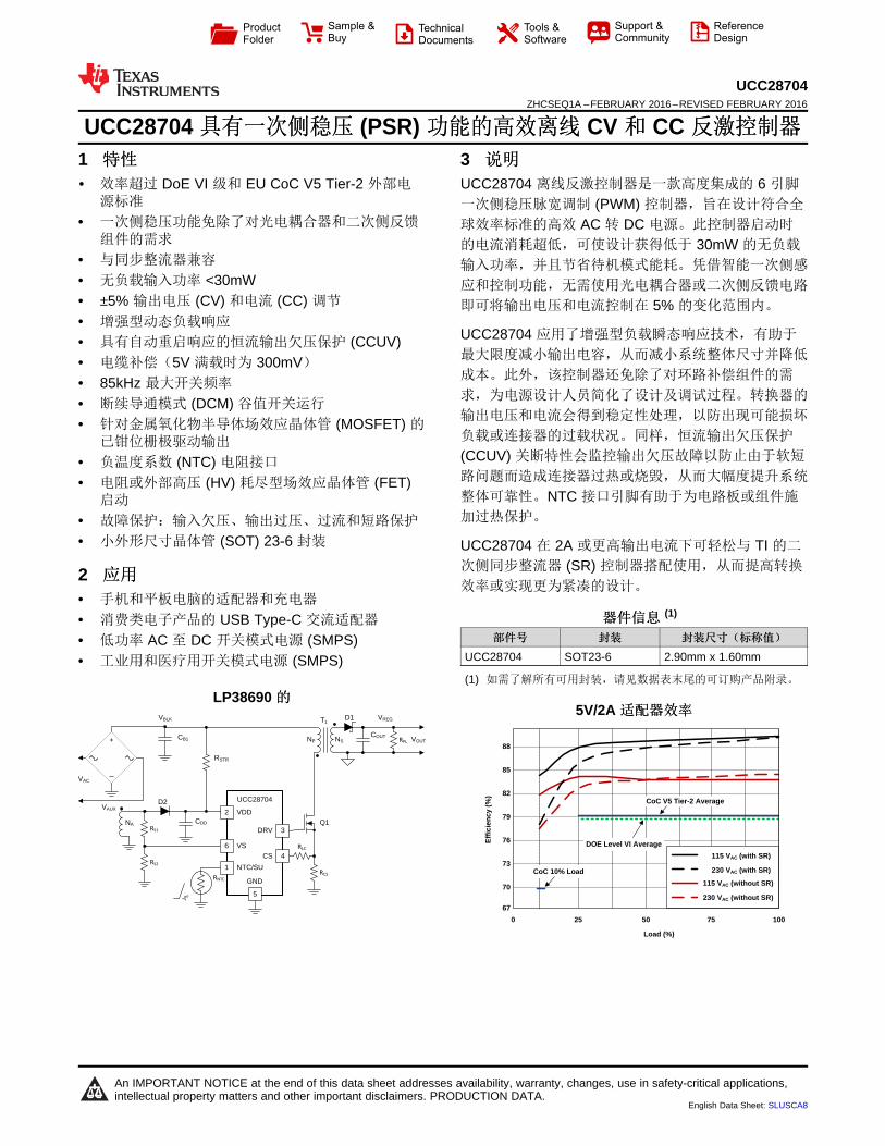
0 25 50 75 100 CoC V5 Tier-2 Average DOE Level VI Average CoC 10% Load Efficiency (%) Load (%) 67 70 73 76 79 82 85 88 115 VAC (with SR) 230 VAC (with SR) 115 VAC (without SR) 230 VAC (without SR) 2 CDD RSTR 6 1 3 4 5 GND NTC/SU VS VDD DRV CS RS2 RS1 RNTC RLC RCS CB1 + COUT RPL D2 Q1 D1 VAUX NA VAC VOUT VREG VBLK UCC28704 -t° NP NS T1 Product Folder Sample & Buy Technical Documents Tools & Software Support & Community Reference Design An IMPORTANT NOTICE at the end of this data sheet addresses availability, warranty, changes, use in safety-critical applications, intellectual property matters and other important disclaimers. PRODUCTION DATA. English Data Sheet: SLUSCA8 UCC28704 ZHCSEQ1A – FEBRUARY 2016 – REVISED FEBRUARY 2016 UCC28704 具有一次侧稳压 (PSR) 功能的高效离线 CV 和 CC 反激控制器 1 1 特性 1• 效率超过 DoE VI 级和 EU CoC V5 Tier-2 外部电 源标准 • 一次侧稳压功能免除了对光电耦合器和二次侧反馈 组件的需求 • 与同步整流器兼容 • 无负载输入功率 <30mW • ±5% 输出电压 (CV) 和电流 (CC) 调节 • 增强型动态负载响应 • 具有自动重启响应的恒流输出欠压保护 (CCUV) • 电缆补偿(5V 满载时为 300mV) • 85kHz 最大开关频率 • 断续导通模式 (DCM) 谷值开关运行 • 针对金属氧化物半导体场效应晶体管 (MOSFET) 的 已钳位栅极驱动输出 • 负温度系数 (NTC) 电阻接口 • 电阻或外部高压 (HV) 耗尽型场效应晶体管 (FET) 启动 • 故障保护:输入欠压、输出过压、过流和短路保护 • 小外形尺寸晶体管 (SOT) 23-6 封装 2 应用 • 手机和平板电脑的适配器和充电器 • 消费类电子产品的 USB Type-C 交流适配器 • 低功率 AC 至 DC 开关模式电源 (SMPS) • 工业用和医疗用开关模式电源 (SMPS) 3 说明 UCC28704 离线反激控制器是一款高度集成的 6 引脚 一次侧稳压脉宽调制 (PWM) 控制器,旨在设计符合全 球效率标准的高效 AC 转 DC 电源。此控制器启动时 的电流消耗超低,可使设计获得低于 30mW 的无负载 输入功率,并且节省待机模式能耗。凭借智能一次侧感 应和控制功能,无需使用光电耦合器或二次侧反馈电路 即可将输出电压和电流控制在 5% 的变化范围内。 UCC28704 应用了增强型负载瞬态响应技术,有助于 最大限度减小输出电容,从而减小系统整体尺寸并降低 成本。此外,该控制器还免除了对环路补偿组件的需 求,为电源设计人员简化了设计及调试过程。转换器的 输出电压和电流会得到稳定性处理,以防出现可能损坏 负载或连接器的过载状况。同样,恒流输出欠压保护 (CCUV) 关断特性会监控输出欠压故障以防止由于软短 路问题而造成连接器过热或烧毁,从而大幅度提升系统 整体可靠性。NTC 接口引脚有助于为电路板或组件施 加过热保护。 UCC28704 在 2A 或更高输出电流下可轻松与 TI 的二 次侧同步整流器 (SR) 控制器搭配使用,从而提高转换 效率或实现更为紧凑的设计。 器件信息 (1) 部件号 封装 封装尺寸(标称值) UCC28704 SOT23-6 2.90mm x 1.60mm (1) 如需了解所有可用封装,请见数据表末尾的可订购产品附录。 LP38690 的 5V/2A 适配器效率
-
Upload
khangminh22 -
Category
Documents
-
view
0 -
download
0
Transcript of UCC28704 具有一次侧稳压(PSR) 功能的高效离线CV 和CC 反 ...
0 25 50 75 100
CoC V5 Tier-2 Average
DOE Level VI Average
CoC 10% Load
Eff
icie
ncy
(%
)
Load (%)
67
70
73
76
79
82
85
88
115 VAC (with SR)
230 VAC (with SR)
115 VAC (without SR)
230 VAC (without SR)
2CDD
RSTR
6
1
3
4
5
GND
NTC/SU
VS
VDD
DRV
CSRS2
RS1
RNTC
RLC
RCS
CB1+COUT
RPL
D2
Q1
D1
VAUX
NA
VAC
VOUT
VREGVBLK
UCC28704
-t°
NP NS
T1
Product
Folder
Sample &Buy
Technical
Documents
Tools &
Software
Support &Community
ReferenceDesign
An IMPORTANT NOTICE at the end of this data sheet addresses availability, warranty, changes, use in safety-critical applications,intellectual property matters and other important disclaimers. PRODUCTION DATA.
English Data Sheet: SLUSCA8
UCC28704ZHCSEQ1A –FEBRUARY 2016–REVISED FEBRUARY 2016
UCC28704 具具有有一一次次侧侧稳稳压压 (PSR) 功功能能的的高高效效离离线线 CV 和和 CC 反反激激控控制制器器
1
1 特特性性
1• 效率超过 DoE VI 级和 EU CoC V5 Tier-2 外部电源标准
• 一次侧稳压功能免除了对光电耦合器和二次侧反馈组件的需求
• 与同步整流器兼容
• 无负载输入功率 <30mW• ±5% 输出电压 (CV) 和电流 (CC) 调节
• 增强型动态负载响应
• 具有自动重启响应的恒流输出欠压保护 (CCUV)• 电缆补偿(5V 满载时为 300mV)• 85kHz 最大开关频率
• 断续导通模式 (DCM) 谷值开关运行
• 针对金属氧化物半导体场效应晶体管 (MOSFET) 的已钳位栅极驱动输出
• 负温度系数 (NTC) 电阻接口
• 电阻或外部高压 (HV) 耗尽型场效应晶体管 (FET)启动
• 故障保护:输入欠压、输出过压、过流和短路保护
• 小外形尺寸晶体管 (SOT) 23-6 封装
2 应应用用
• 手机和平板电脑的适配器和充电器
• 消费类电子产品的 USB Type-C 交流适配器
• 低功率 AC 至 DC 开关模式电源 (SMPS)• 工业用和医疗用开关模式电源 (SMPS)
3 说说明明
UCC28704 离线反激控制器是一款高度集成的 6 引脚
一次侧稳压脉宽调制 (PWM) 控制器,旨在设计符合全
球效率标准的高效 AC 转 DC 电源。此控制器启动时
的电流消耗超低,可使设计获得低于 30mW 的无负载
输入功率,并且节省待机模式能耗。凭借智能一次侧感
应和控制功能,无需使用光电耦合器或二次侧反馈电路
即可将输出电压和电流控制在 5% 的变化范围内。
UCC28704 应用了增强型负载瞬态响应技术,有助于
最大限度减小输出电容,从而减小系统整体尺寸并降低
成本。此外,该控制器还免除了对环路补偿组件的需
求,为电源设计人员简化了设计及调试过程。转换器的
输出电压和电流会得到稳定性处理,以防出现可能损坏
负载或连接器的过载状况。同样,恒流输出欠压保护
(CCUV) 关断特性会监控输出欠压故障以防止由于软短
路问题而造成连接器过热或烧毁,从而大幅度提升系统
整体可靠性。NTC 接口引脚有助于为电路板或组件施
加过热保护。
UCC28704 在 2A 或更高输出电流下可轻松与 TI 的二
次侧同步整流器 (SR) 控制器搭配使用,从而提高转换
效率或实现更为紧凑的设计。
器器件件信信息息 (1)
部部件件号号 封封装装 封封装装尺尺寸寸((标标称称值值))
UCC28704 SOT23-6 2.90mm x 1.60mm
(1) 如需了解所有可用封装,请见数据表末尾的可订购产品附录。
LP38690 的的5V/2A 适适配配器器效效率率
2
UCC28704ZHCSEQ1A –FEBRUARY 2016–REVISED FEBRUARY 2016 www.ti.com.cn
Copyright © 2016, Texas Instruments Incorporated
目目录录
1 特特性性.......................................................................... 12 应应用用.......................................................................... 13 说说明明.......................................................................... 14 修修订订历历史史记记录录 ........................................................... 25 Pin Configuration and Functions ......................... 36 Specifications......................................................... 4
6.1 Absolute Maximum Ratings ...................................... 46.2 ESD Ratings ............................................................ 46.3 Recommended Operating Conditions....................... 46.4 Thermal Information .................................................. 56.5 Electrical Characteristics........................................... 56.6 Typical Characteristics .............................................. 7
7 Detailed Description .............................................. 97.1 Overview ................................................................... 97.2 Functional Block Diagram ......................................... 97.3 Feature Description................................................. 107.4 Device Functional Modes........................................ 24
8 Applications and Implementation ...................... 258.1 Application Information............................................ 258.2 Typical Application .................................................. 258.3 Do's and Don'ts....................................................... 33
9 Power Supply Recommendations ...................... 3410 Layout................................................................... 34
10.1 Layout Guidelines ................................................. 3410.2 Layout Example .................................................... 35
11 器器件件和和文文档档支支持持 ..................................................... 3611.1 器件支持 ................................................................ 3611.2 文档支持 ................................................................ 3911.3 社区资源 ................................................................ 3911.4 商标 ....................................................................... 3911.5 静电放电警告......................................................... 3911.6 Glossary ................................................................ 39
12 机机械械、、封封装装和和可可订订购购信信息息....................................... 39
4 修修订订历历史史记记录录
日日期期 修修订订版版本本 注注释释
2016 年2 月 A 首次发布。
1
2
3
6
5
4
VDD
DRV
VS
GND
CS
NTC/SU
3
UCC28704www.ti.com.cn ZHCSEQ1A –FEBRUARY 2016–REVISED FEBRUARY 2016
Copyright © 2016, Texas Instruments Incorporated
(1)
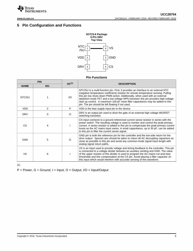
5 Pin Configuration and Functions
SOT23-6 Package6-Pin DBVTop View
Pin FunctionsPIN
I/O (1) DESCRIPTIONNAME NO.
NTC/SU 1 I/O
NTC/SU is a multi-function pin. First, it provides an interface to an external NTC(negative temperature coefficient) resistor for remote temperature sensing. Pullingthis pin low shuts down PWM action. Additionally, when used with an externaldepletion-mode FET and a low-voltage NPN transistor this pin provides high-voltagestart up control. A maximum 100-pF noise filter capacitance may be added to thispin. The pin should be left floating if not used.
VDD 2 P VDD is the bias supply input pin to the device.
DRV 3 O DRV is an output pin used to drive the gate of an external high voltage MOSFETswitching transistor.
CS 4 I
CS input connects to a ground referenced current sense resistor in series with thepower switch. The resulting voltage is used to monitor and control the peak-primarycurrent. A series resistor is added to this pin to compensate the peak-primary currentlevels as the AC mains input varies. A small capacitance, up to 30 pF, can be addedto this pin to filter the current sense signal.
GND 5 G
GND pin is both the reference pin for the controller and the low-side return for thedrive output. Special care should be taken to return all AC decoupling capacitors asclose as possible to this pin and avoid any common-mode signal trace length withanalog signal return paths.
VS 6 I
VS is an input used to provide voltage and timing feedback to the controller. This pinis connected to a voltage divider between an auxiliary winding and GND. The valueof the upper resistor of this divider is used to program the AC-mains run-and-stopthresholds and line compensation at the CS pin. Avoid placing a filter capacitor onthis input which would interfere with accurate sensing of this waveform.
P = Power, G = Ground, I = Input, O = Output, I/O = Input/Output
4
UCC28704ZHCSEQ1A –FEBRUARY 2016–REVISED FEBRUARY 2016 www.ti.com.cn
Copyright © 2016, Texas Instruments Incorporated
(1) Stresses beyond those listed under Absolute Maximum Ratings may cause permanent damage to the device. These are stress ratingsonly, which do not imply functional operation of the device at these or any other conditions beyond those indicated under RecommendedOperating Conditions. Exposure to absolute-maximum-rated conditions for extended periods may affect device reliability.
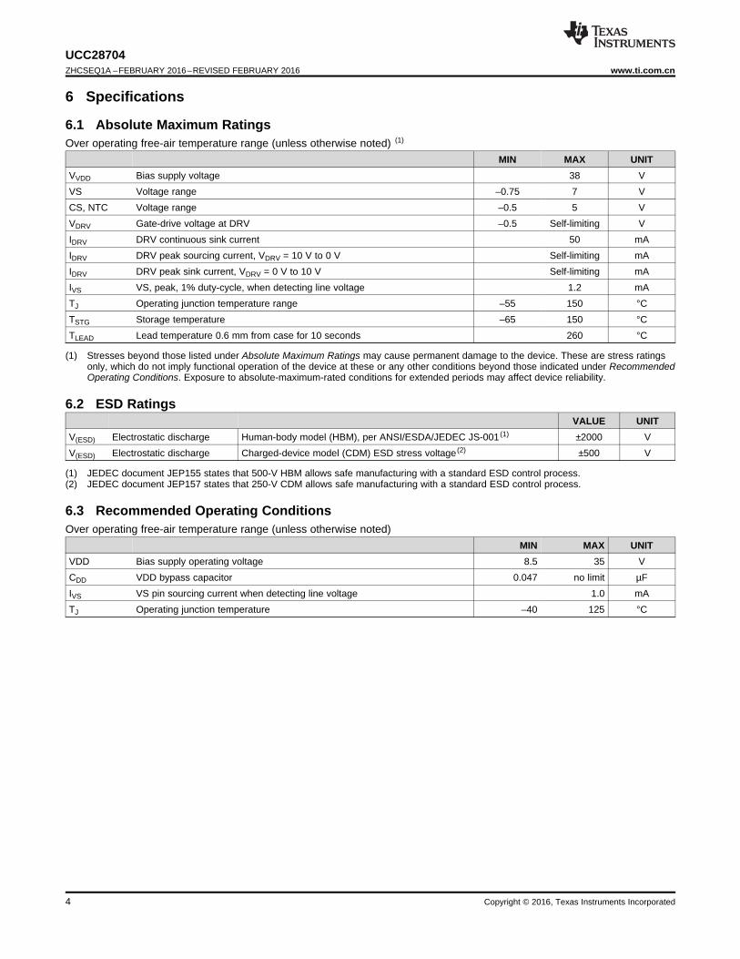
6 Specifications
6.1 Absolute Maximum RatingsOver operating free-air temperature range (unless otherwise noted) (1)
MIN MAX UNITVVDD Bias supply voltage 38 VVS Voltage range –0.75 7 VCS, NTC Voltage range –0.5 5 VVDRV Gate-drive voltage at DRV –0.5 Self-limiting VIDRV DRV continuous sink current 50 mAIDRV DRV peak sourcing current, VDRV = 10 V to 0 V Self-limiting mAIDRV DRV peak sink current, VDRV = 0 V to 10 V Self-limiting mAIVS VS, peak, 1% duty-cycle, when detecting line voltage 1.2 mATJ Operating junction temperature range –55 150 °CTSTG Storage temperature –65 150 °CTLEAD Lead temperature 0.6 mm from case for 10 seconds 260 °C
(1) JEDEC document JEP155 states that 500-V HBM allows safe manufacturing with a standard ESD control process.(2) JEDEC document JEP157 states that 250-V CDM allows safe manufacturing with a standard ESD control process.
6.2 ESD RatingsVALUE UNIT
V(ESD) Electrostatic discharge Human-body model (HBM), per ANSI/ESDA/JEDEC JS-001 (1) ±2000 VV(ESD) Electrostatic discharge Charged-device model (CDM) ESD stress voltage (2) ±500 V
6.3 Recommended Operating ConditionsOver operating free-air temperature range (unless otherwise noted)
MIN MAX UNITVDD Bias supply operating voltage 8.5 35 VCDD VDD bypass capacitor 0.047 no limit µFIVS VS pin sourcing current when detecting line voltage 1.0 mATJ Operating junction temperature –40 125 °C

5
UCC28704www.ti.com.cn ZHCSEQ1A –FEBRUARY 2016–REVISED FEBRUARY 2016
Copyright © 2016, Texas Instruments Incorporated
(1) The junction-to-ambient thermal resistance under natural convection is obtained in a simulation on a JEDEC-standard, high-K board, asspecified in JESD51-7, in an environment described in JESD51-2a.
(2) The junction-to-case (top) thermal resistance is obtained by simulating a cold plate test on the package top. No specific JEDEC-standard test exists, but a close description can be found in the ANSI SEMI standard G30-88.
(3) The junction-to-board thermal resistance is obtained by simulating in an environment with a ring cold plate fixture to control the PCBtemperature, as described in JESD51-8.
(4) The junction-to-top characterization parameter, ψJT, estimates the junction temperature of a device in a real system and is extractedfrom the simulation data obtaining θJA, using a procedure described in JESD51-2a (sections 6 and 7).
(5) The junction-to-board characterization parameter, ψJB, estimates the junction temperature of a device in a real system and is extractedfrom the simulation data obtaining θJA, using a procedure described in JESD51-2a (sections 6 and 7).
6.4 Thermal Information
THERMAL METRICUCC28704
UNITDBV6 PINS
θJA Junction-to-ambient thermal resistance (1) 150 °C/WθJCtop Junction-to-case (top) thermal resistance (2) 55 °C/WθJB Junction-to-board thermal resistance (3) 60 °C/WψJT Junction-to-top characterization parameter (4) 3 °C/WψJB Junction-to-board characterization parameter (5) 55 °C/W
(1) The regulation level and OV threshold at VS decrease with increasing temperature by 1 mV/. This compensation over temperature isincluded to reduce the variances in power supply output regulation over-voltage detection with respect to the external output rectifier.
(2) These threshold voltages represent average levels. This device automatically varies the current sense threshold to improve EMIperformance.
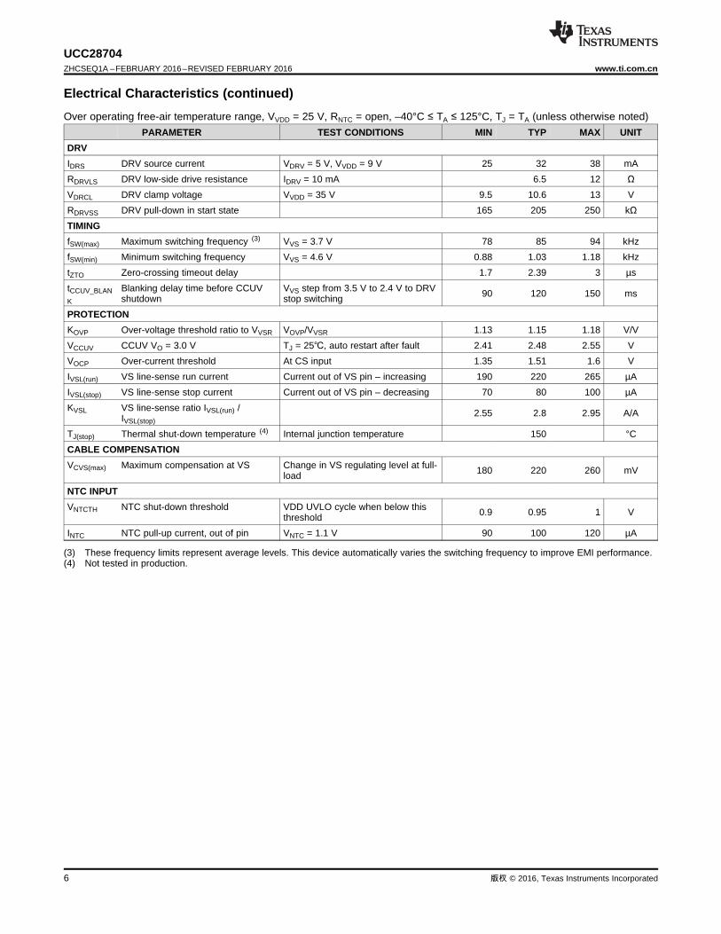
6.5 Electrical CharacteristicsOver operating free-air temperature range, VVDD = 25 V, RNTC = open, –40°C ≤ TA ≤ 125°C, TJ = TA (unless otherwise noted)
PARAMETER TEST CONDITIONS MIN TYP MAX UNITBIAS SUPPLY INPUTIRUN Supply current, run IDRV = 0, run state 1.65 2.3 2.65 mAIWAIT Supply current, wait IDRV = 0, VVDD = 20 V, wait state 40 70 100 µAISTART Supply current, start IDRV = 0, VVDD = 17 V, start state 1.5 2.5 µAIFAULT Supply current, fault IDRV = 0, fault state 1.7 2.2 2.8 mAUNDER-VOLTAGE LOCKOUTVVDD(on) VDD turn-on threshold VVDD low to high 17.5 21 23 VVVDD(off) VDD turn-off threshold VVDD high to low 7.3 7.7 8.15 VVS INPUTVVSR Regulating level (1) Measured at no-load condition, TJ =
25°C 4.02 4.06 4.1 V
VVSNC Negative clamp level IVS = –300 µA 190 250 325 mVIVSB Input bias current VVS = 4 V –0.25 0 0.25 µACS INPUTVCST(max) Max CS threshold voltage (2) VVS = 3.70 V 720 750 784 mVVCST(min) Min CS threshold voltage (2) VVS = 4.35 V 170 187.5 210 mVKAM AM control ratio VCST(max) / VCST(min) 3.55 4 4.4 V/VVCCR Constant-current regulating level 345 356 369 mVKLC Line compensating current
ratio, IVSLS /(current out of CS pin)
IVSLS = –300 µA 23 25 29 A/A
TCSLEB Leading-edge blanking time DRV output duration, VCS = 1 V 170 255 340 ns
6
UCC28704ZHCSEQ1A –FEBRUARY 2016–REVISED FEBRUARY 2016 www.ti.com.cn
版权 © 2016, Texas Instruments Incorporated
Electrical Characteristics (continued)Over operating free-air temperature range, VVDD = 25 V, RNTC = open, –40°C ≤ TA ≤ 125°C, TJ = TA (unless otherwise noted)
PARAMETER TEST CONDITIONS MIN TYP MAX UNIT
(3) These frequency limits represent average levels. This device automatically varies the switching frequency to improve EMI performance.(4) Not tested in production.
DRVIDRS DRV source current VDRV = 5 V, VVDD = 9 V 25 32 38 mARDRVLS DRV low-side drive resistance IDRV = 10 mA 6.5 12 ΩVDRCL DRV clamp voltage VVDD = 35 V 9.5 10.6 13 VRDRVSS DRV pull-down in start state 165 205 250 kΩTIMINGfSW(max) Maximum switching frequency (3) VVS = 3.7 V 78 85 94 kHzfSW(min) Minimum switching frequency VVS = 4.6 V 0.88 1.03 1.18 kHztZTO Zero-crossing timeout delay 1.7 2.39 3 µstCCUV_BLANK
Blanking delay time before CCUVshutdown
VVS step from 3.5 V to 2.4 V to DRVstop switching 90 120 150 ms
PROTECTIONKOVP Over-voltage threshold ratio to VVSR VOVP/VVSR 1.13 1.15 1.18 V/VVCCUV CCUV VO = 3.0 V TJ = 25, auto restart after fault 2.41 2.48 2.55 VVOCP Over-current threshold At CS input 1.35 1.51 1.6 VIVSL(run) VS line-sense run current Current out of VS pin – increasing 190 220 265 µAIVSL(stop) VS line-sense stop current Current out of VS pin – decreasing 70 80 100 µAKVSL VS line-sense ratio IVSL(run) /
IVSL(stop)2.55 2.8 2.95 A/A
TJ(stop) Thermal shut-down temperature (4) Internal junction temperature 150 °CCABLE COMPENSATIONVCVS(max) Maximum compensation at VS Change in VS regulating level at full-
load 180 220 260 mV
NTC INPUTVNTCTH NTC shut-down threshold VDD UVLO cycle when below this
threshold 0.9 0.95 1 V
INTC NTC pull-up current, out of pin VNTC = 1.1 V 90 100 120 µA
TJ - Temperature (qC)
VC
ST
(min
) - M
inim
um C
S T
hres
hold
Vol
tage
(m
V)
-50 -25 0 25 50 75 100 125 150191.5
191.7
191.9
192.1
192.3
192.5
192.7
192.9
D005TJ - Temperature (qC)
VC
CR -
Con
stan
t Cur
rent
Reg
ulat
ion
Leve
l (m
V)
-50 -25 0 25 50 75 100 125 150345
350
355
360
365
D006
TJ - Temperature (qC)
VV
SR -
VS
Reg
ulat
ion
Vol
tage
(V
)
-50 -25 0 25 50 75 100 125 1503.95
3.98
4.00
4.03
4.05
4.08
4.10
4.12
D003 TJ - Temperature (qC)
VS
Lin
e S
ense
Cur
rent
(P
A)
-50 -25 0 25 50 75 100 125 15050
75
100
125
150
175
200
225
250
275
300
D004
IVSL, Run
IVSL, Stop
VDD - Bias Supply Voltage (V)
I VD
D -
Bia
s S
uppl
y C
urre
nt (
mA
)
0 5 10 15 20 25 30 35 401x10-6
1x10⁻⁵
1x10⁻⁴
1x10⁻³
1x10⁻²
1x10⁻¹
1x100
1x101
5x101
D001
Run State
Wait State
Start State
pVDD Turn-Off nVDD Turn-On
TJ - Temperature (qC)
I VD
D -
Bia
s S
uppl
y C
urre
nt (P
A)
-50 -25 0 25 50 75 100 125 1501x10-1
1x100
1x101
1x10²
1x10³
1x10⁴
1x10⁵
D002
IRUN, VDD = 25V
IWAIT, VDD = 20V
ISTART, VDD = 17V
7
UCC28704www.ti.com.cn ZHCSEQ1A –FEBRUARY 2016–REVISED FEBRUARY 2016
版权 © 2016, Texas Instruments Incorporated
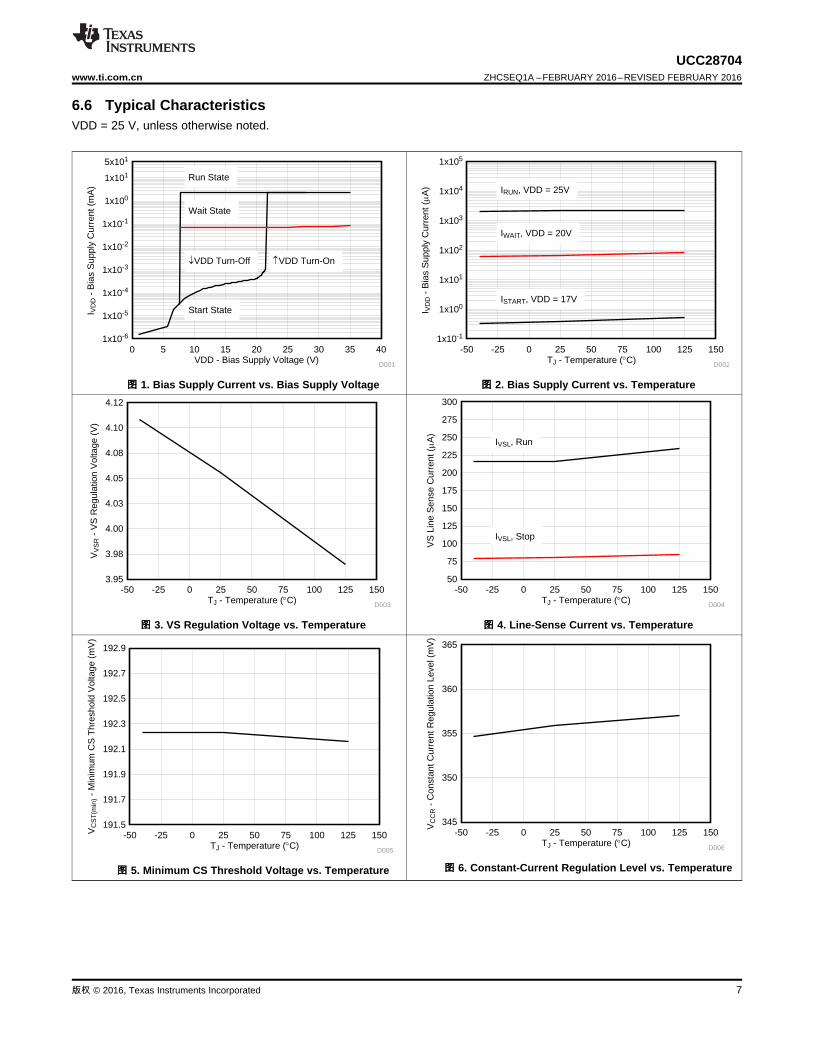
6.6 Typical CharacteristicsVDD = 25 V, unless otherwise noted.
图图 1. Bias Supply Current vs. Bias Supply Voltage 图图 2. Bias Supply Current vs. Temperature
图图 3. VS Regulation Voltage vs. Temperature 图图 4. Line-Sense Current vs. Temperature
图图 5. Minimum CS Threshold Voltage vs. Temperature 图图 6. Constant-Current Regulation Level vs. Temperature
TJ - Temperature (qC)
VC
CU
V -
Con
stan
t Cur
rent
UV
Thr
esho
ld (
V)
-50 -25 0 25 50 75 100 125 1502.35
2.4
2.45
2.5
2.55
2.6
D011
TJ - Temperature (qC)
VN
TC
TH -
NT
C S
hutd
own
Thr
esho
ld V
olta
ge (
V)
-50 -25 0 25 50 75 100 125 1500.946
0.947
0.948
0.949
0.95
0.951
0.952
D009TJ - Temperature (qC)
I NT
C -
NT
C P
ull-u
p C
urre
nt (P
A)
-50 -25 0 25 50 75 100 125 150103
104
105
106
107
108
D010
TJ - Temperature (qC)
f SW
(min
) - M
inim
um S
witc
hing
Fre
quen
cy (
kHz)
-50 -25 0 25 50 75 100 125 1500.98
0.99
1.00
1.01
1.02
1.03
1.04
1.05
D007 TJ - Temperature (qC)
I DR
S -
DR
V S
ourc
e C
urre
nt (
mA
)
-50 -25 0 25 50 75 100 125 15030.0
30.5
31.0
31.5
32.0
32.5
33.0
33.5
D008
8
UCC28704ZHCSEQ1A –FEBRUARY 2016–REVISED FEBRUARY 2016 www.ti.com.cn
版权 © 2016, Texas Instruments Incorporated
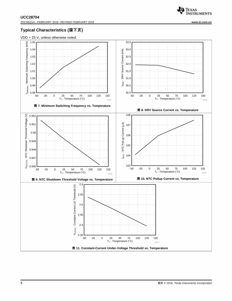
Typical Characteristics (接接下下页页)VDD = 25 V, unless otherwise noted.
图图 7. Minimum Switching Frequency vs. Temperature图图 8. DRV Source Current vs. Temperature
图图 9. NTC Shutdown Threshold Voltage vs. Temperature 图图 10. NTC Pullup Current vs. Temperature
图图 11. Constant-Current Under-Voltage Threshold vs. Temperature
30 mA
S Q
QR
Sampler
+E/A
4.06 V + VCVS
Power and Fault Managment
UVLO21 V/7.7 V
Zero Crossing Detect
Control Law
LEB
1/fSWVCST
Secondary Timing Detect
Current Regulation and Cable compensation
VCST
VDD
Line Sense IVSLS / KLC
VSS
VCVS
OV FAULT
IVSLS
10 V
Line Fault
IVSLS
2.2 V / 0.8 V
1.5 VOC
Fault
OTP FAULT
Line FAULT
OC FAULT
VSS /1.10Minimum fSW
4.06 V
1 kHzS Q
QR
VNTCTH
INTC
10 k:
200 k:
Bias
4 kHz
VSS /1.15
4.06 V
2.48 V
CCUV FAULT
CCUV FAULT
VCL
120 ms Delay
VDD
VDD
GND
VS 6
5
2
1
3
4 CS
DRV
NTC/SU
9
UCC28704www.ti.com.cn ZHCSEQ1A –FEBRUARY 2016–REVISED FEBRUARY 2016
版权 © 2016, Texas Instruments Incorporated
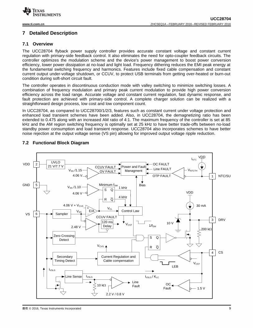
7 Detailed Description
7.1 OverviewThe UCC28704 flyback power supply controller provides accurate constant voltage and constant currentregulation with primary-side feedback control. It also eliminates the need for opto-coupler feedback circuits. Thecontroller optimizes the modulation scheme and the device's power management to boost power conversionefficiency, lower power dissipation at no-load and light load. Frequency dithering reduces the EMI peak energy atthe fundamental switching frequency and harmonics. Features include fixed cable compensation and constantcurrent output under-voltage shutdown, or CCUV, to protect USB terminals from getting over-heated or burn-outcondition during soft-short circuit fault.
The controller operates in discontinuous conduction mode with valley switching to minimize switching losses. Acombination of frequency modulation and primary peak current modulation to provide high power conversionefficiency across the load range. Accurate voltage and constant current regulation, fast dynamic response, andfault protection are achieved with primary-side control. A complete charger solution can be realized with astraightforward design process, low cost and low component count.
In UCC28704, as compared to UCC28700/1/2/3, features such as constant current under voltage protection andenhanced load transient schemes have been added. Also, in UCC28704, the demagnetizing ratio has beenextended to 0.475 along with an increased AM ratio of 4:1. The maximum frequency of the controller is set at 85kHz and the AM region switching frequency is optimally set at 25 kHz to have better trade-offs between no-loadstandby power consumption and load transient response. UCC28704 also incorporates schemes to have betternoise rejection at the output voltage sense (VS pin) allowing for improved output voltage ripple reduction.
7.2 Functional Block Diagram
S1 VSRS2
AS OCV F VSR
R VR
N (V V ) V
u
u
IN(run) BULK(run)
S1PA VSL(run) PA VSL(run)
2 V VR
N I N I
u
|u u
10
UCC28704ZHCSEQ1A –FEBRUARY 2016–REVISED FEBRUARY 2016 www.ti.com.cn
版权 © 2016, Texas Instruments Incorporated
7.3 Feature Description
7.3.1 Detailed Pin Description
7.3.1.1 VDD (Device Bias Voltage Supply)
The VDD pin is typically powered from a rectified auxiliary transformer winding, the same winding that is used tocapture the output voltage level. A bypass capacitor, with minimum value 0.047 μF, on the VDD pin is used forinitially biasing the device to start-up along with a resistive or active source of start-up charging current. UVLOstart / stop levels of 21 V / 7.7 V accommodate lower values of VDD capacitance that in turns keeps the start-upcurrent low, which for resistive start-up has an impact on both stand-by power and power-on delay. A high, 35-V,maximum operating level on VDD alleviates concerns with leakage energy charging of VDD and gives addedflexibility to when varying power supply output voltage must be supported.
7.3.1.2 GND (Ground)This is an external return pin, and provides the reference point for both external signal and the gate drive of thedevice. The VDD bypass capacitor should be placed close to this pin. Critical component GND connections fromthe VS, CS and NTC pins should have dedicated and short paths to this pin.
7.3.1.3 VS (Voltage-Sense)The VS pin is connected to a resistor divider from the auxiliary winding to ground. The output-voltage feedbackinformation is sampled at the end of the transformer secondary current demagnetization time to provide anaccurate representation of the output voltage. Timing information to achieve valley-switching and to control theduty cycle of the secondary transformer current is determined by the waveform on the VS pin. The VS input is acritical signal and will generally be with relatively high impedance. To avoid unpredictable behavior avoid placinga filter capacitor on this pin and keep the total PCB area tied to VS at a minimum.
The VS pin also senses the bulk capacitor input voltage to provide for ac-input run and stop thresholds, and tocompensate the current-sense threshold across the AC-input range. This information is sensed by monitoring thecurrent pulled out of the VS pin during the MOSFET on-time. During this time the voltage on the VS pin isclamped to about 250mV below GND. As a result, the current out of the pin is determined by the upper VSdivider resistor, the auxiliary to primary turns-ratio and the bulk input voltage level. For the AC-input run/stopfunction, the run threshold on VS is IVSL(run) (typical 220 µA) and the stop threshold is IVSL(stop) (typical 80 µA).The values for the auxiliary voltage divider upper-resistor RS1 and lower-resistor RS2 can be determined by theequations below.
where• NPA is the transformer primary-to-auxiliary turns ratio,• VIN(run) is the AC rms voltage to enable turn-on of the flyback converter (run),• VBULK(run) is the DC bulk voltage to enable turn-on of the flyback converter (run),• IVSL(run) is the run-threshold for the current pulled out of the VS pin during the primary MOSFET on-time. (see
the Electrical Characteristics table). (1)
where• VOCV is the converter regulated output voltage,• VF is the output rectifier forward voltage drop at near-zero current,• NAS is the transformer auxiliary to secondary turns ratio,• RS1 is the VS divider high-side resistance,• VVSR is the CV regulating level at the VS input (see the Electrical Characteristics table). (2)
This pin is also used to sense the output constant current under voltage (CCUV) level, used to shut down theconverter in the case of a soft-short circuit at its output. Refer to Constant Current Under-Voltage Protection forfurther information.
LC S1 CS D GATE _ OFF PALC
P
K R R (t t ) NR
L
u u u u
CCR PSCS XFMR
OCC
V NR
2 I
u u K
u
11
UCC28704www.ti.com.cn ZHCSEQ1A –FEBRUARY 2016–REVISED FEBRUARY 2016
版权 © 2016, Texas Instruments Incorporated
Feature Description (接接下下页页)7.3.1.4 DRV (Gate Drive)The DRV pin is connected to the MOSFET gate pin, usually through a series resistor. The DRV provides a gatedrive signal which is clamped to 10.5-V internally. During turn-on the driver applies a typical 30-mA currentsource out of the DRV pin. When the DRV voltage rises to above 9 V the output current is reduced to about 100µA. This current brings the DRV voltage to the 10.5-V clamp level, or to VDD, whichever is less. The 30-mAcurrent provides adequate turn-on speed while automatically limiting noise generated at turn-on by the MOSFETdrain dv/dt and by the leading edge turn-on current spike. The gate drive turn-off current is internally limited toabout 400 mA when DRV is above about 4 V. At lower DRV voltages the current will reduce, eventually beinglimited by the low-side on resistance, RDS(on). The drain turn-on and turn-off dv/dt can be further impacted byadding external resistor in series with DRV pin. The drain current resonances can be damped with a small seriesgate resistor, generally less than a 1 Ω.
7.3.1.5 CS (Current Sense)The current sense pin is connected through a series resistor (RLC) to the current-sense resistor (RCS). Thecontroller varies the internal current sense threshold between 0.188 V and 0.75 V, setting a correspondingcontrol range for the peak-primary winding current to a 4-to-1 range. The series resistor RLC provides an inputvoltage feed-forward function. The voltage drop across this resistor reduces primary-side peak current as the linevoltage increases, compensating for the increased di/dt and delays in the MOSFET turn-off. There is an internalleading-edge blanking time of 255 ns to eliminate sensitivity to the MOSFET turn-on leading edge current spike.If additional blanking time is needed, a small bypass capacitor, up to 30 pF, can be placed on between CS pinand GND pin. The value of RCS is determined by the target output current in constant current (CC) regulation.The values of RCS and RLC can be determined by the equations below. The term ηXFMR is intended to account forthe energy stored in the transformer but not delivered to the secondary. This includes transformer core andcopper losses, bias power, and primary leakage inductance losses.
Example: With a transformer core and copper losses of 3%, leakage inductance caused power losses 2%, andbias power to output power ratio of 0.5%. The transformer power transfer efficiency is estimated as ηXFMR =100% - 3% - 2% - 0.5% = 94.5%
where• VCCR is a current regulation constant (see the Electrical Characteristics table),• NPS is the transformer primary-to-secondary turns ratio (a typical turns-ratio of 12 to 15 is recommended for 5-
V output),• IOCC is the target output current in constant-current regulation,• ηXFMR is the transformer efficiency. (3)
where• RS1 is the VS pin high-side resistor value,• RCS is the current-sense resistor value,• tD is the current-sense delay (typical 50 ns) plus MOSFET turn-off delay,• tGATE_OFF is the primary-side main MOSFET turn-off time,• NPA is the transformer primary-to-auxiliary turns-ratio,• LP is the transformer primary inductance,• KLC is a current-scaling constant (see the Electrical Characteristics table). (4)
(VOUT + VF + ISRS) NA / NS
- (VBLK) NA / NP
0 V
VS Sample
Aux Winding
RS1
RS2
VSDiscriminator and
Sampler
(VOUT + VF + ISRS) x NA / NS
Timing
ControlLaw
-Minimum
PeriodAnd Peak Primary Current
GD
Primary Winding
Bulk Voltage -VBLK
RCS
SecondaryWinding
COUT RLOAD
VOUT
CS
DRV
Zero Crossings
VCL
+ VF -IS
Q1
12
UCC28704ZHCSEQ1A –FEBRUARY 2016–REVISED FEBRUARY 2016 www.ti.com.cn
版权 © 2016, Texas Instruments Incorporated
Feature Description (接接下下页页)7.3.1.6 NTC/SU (NTC Thermistor Shutdown and External Start Up Control)The UCC28704 uses an external NTC resistor tied to the NTC/SU pin to program a thermal shutdowntemperature for the power supply. The NTC/SU shutdown threshold is 0.95 V with an internal 105-µA currentsource which results in a 9.05-kΩ thermistor shutdown threshold. A small capacitor with value not greater than100 pF can be used on this pin for any noise reduction purposes. The capacitor with its value greater than 100pF can cause a false over-temperature protection response. The NTC/SU pin should be left floating if not used.
The NTC/SU pin can be used to control an external depletion-mode FET to enable active high-voltage start up,Refer to Initial Power-On with A Depletion-Mode FET for more detail.
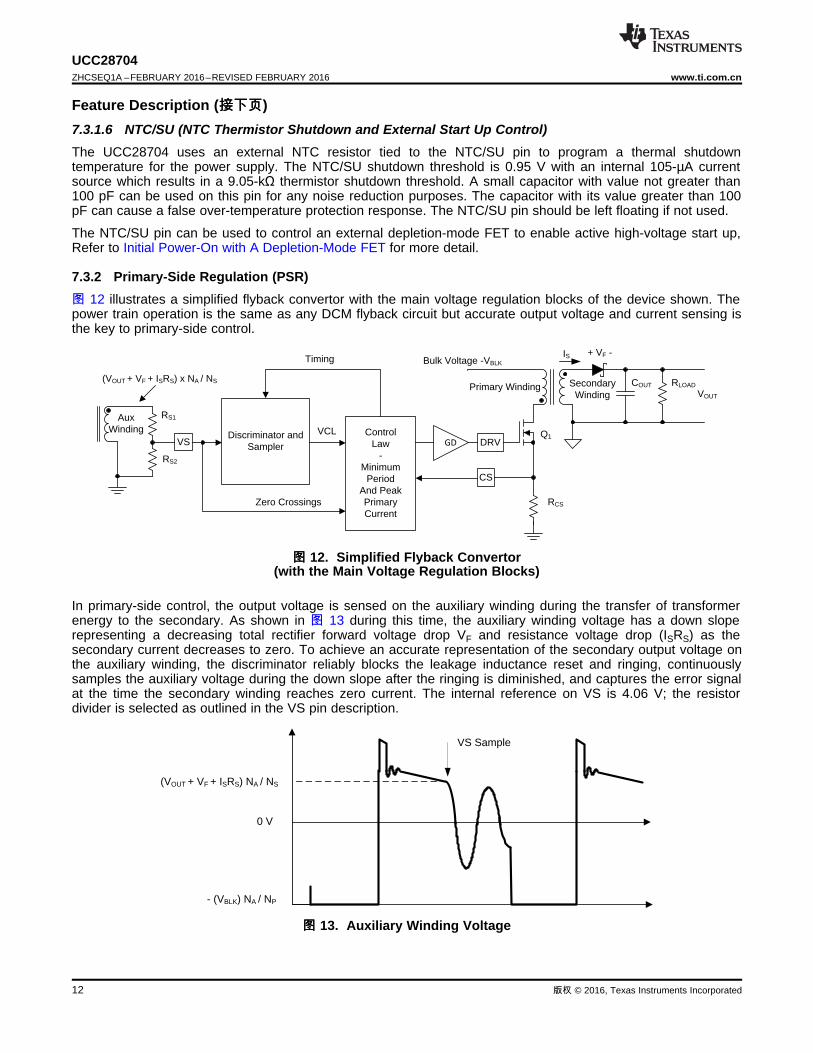
7.3.2 Primary-Side Regulation (PSR)图 12 illustrates a simplified flyback convertor with the main voltage regulation blocks of the device shown. Thepower train operation is the same as any DCM flyback circuit but accurate output voltage and current sensing isthe key to primary-side control.
图图 12. Simplified Flyback Convertor(with the Main Voltage Regulation Blocks)
In primary-side control, the output voltage is sensed on the auxiliary winding during the transfer of transformerenergy to the secondary. As shown in 图 13 during this time, the auxiliary winding voltage has a down sloperepresenting a decreasing total rectifier forward voltage drop VF and resistance voltage drop (ISRS) as thesecondary current decreases to zero. To achieve an accurate representation of the secondary output voltage onthe auxiliary winding, the discriminator reliably blocks the leakage inductance reset and ringing, continuouslysamples the auxiliary voltage during the down slope after the ringing is diminished, and captures the error signalat the time the secondary winding reaches zero current. The internal reference on VS is 4.06 V; the resistordivider is selected as outlined in the VS pin description.
图图 13. Auxiliary Winding Voltage
0 V
VS ring p-p(scaled)
tDM_BLANK
tLK_RESET
tDMAG
tSW
Entering Wait StateIPP < IPP(max)
RS2/(RS1+RS2)
13
UCC28704www.ti.com.cn ZHCSEQ1A –FEBRUARY 2016–REVISED FEBRUARY 2016
版权 © 2016, Texas Instruments Incorporated
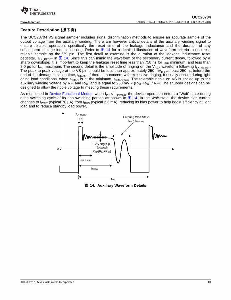
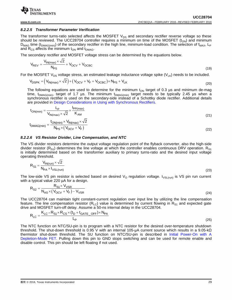
Feature Description (接接下下页页)The UCC28704 VS signal sampler includes signal discrimination methods to ensure an accurate sample of theoutput voltage from the auxiliary winding. There are however critical details of the auxiliary winding signal toensure reliable operation, specifically the reset time of the leakage inductance and the duration of anysubsequent leakage inductance ring. Refer to 图 14 for a detailed illustration of waveform criteria to ensure areliable sample on the VS pin. The first detail to examine is the duration of the leakage inductance resetpedestal, TLK_RESET in 图 14. Since this can mimic the waveform of the secondary current decay, followed by asharp downslope, it is important to keep the leakage reset time less than 750 ns for IPRI minimum, and less than3.0 µs for IPRI maximum. The second detail is the amplitude of ringing on the VAUX waveform following tLK_RESET.The peak-to-peak voltage at the VS pin should be less than approximately 250 mVp-p at least 250 ns before theend of the demagnetization time, tDMAG. If there is a concern with excessive ringing, it usually occurs during lightor no load conditions, when tDMAG is at the minimum, tDMAG(min). The tolerable ripple on VS is scaled up to theauxiliary winding voltage by RS1 and RS2, and is equal to 250 mV × (RS1+RS2) / RS2. The snubber designs can bedesigned to allow the ripple voltage to meeting these requirements.
As mentioned in Device Functional Modes, when IPP < IPP(max), the device operation enters a “Wait” state duringeach switching cycle of its non-switching portion as shown in 图 14. In the Wait state, the device bias currentchanges to IWAIT (typical 70 µA) from IRUN (typical 2.3 mA), reducing its bias power to help boost efficiency at lightload and to reduce standby load power.
图图 14. Auxiliary Waveform Details
OOUT OCV
OCC
IV V (1 0.06 )
I u u
OCCOUT
OCV MAX
IC 100
V ft u
u
14
UCC28704ZHCSEQ1A –FEBRUARY 2016–REVISED FEBRUARY 2016 www.ti.com.cn
版权 © 2016, Texas Instruments Incorporated
Feature Description (接接下下页页)7.3.3 Primary-Side Constant Voltage (CV) RegulationDuring voltage regulation (CV mode), the controller operates in frequency modulation mode and peak currentamplitude modulation mode as illustrated in 图 15 below. The UCC28704 incorporates internal voltage-loopcompensation circuits so that external compensation is not necessary, provided that the value of COUT is highenough. The following equation determines a minimum value of COUT necessary to maintain a phase margin ofabout 40 degrees over the full-load range,
(5)
The internal operating frequency limits of the device are fSW(max) and fSW(min), typically 85 kHz and 1 kHz,respectively. The choice of transformer primary inductance and primary-peak current sets the maximumoperating frequency of the converter, which must be equal to or lower than fSW(max). Conversely, the choice ofmaximum target operating frequency and primary-peak current determines the transformer primary-inductancevalue. The actual minimum switching frequency for any particular converter depends on several factors, includingminimum loading level, leakage inductance losses, switch-node capacitance losses, other switching andconduction losses, and bias-supply requirements. In any case, the minimum steady-state frequency of theconverter must always exceed fSW(min) or the output voltage may rise to the over-voltage protection level (OVP)and the controller responds as described in Fault Protection.
To achieve a regulated output voltage in the CV mode operation, energy balance has to be maintained. As theUCC28704 has a minimum switching frequency typical 1 kHz, together with the energy per switching cycledetermined by converter parameters, such as the transformer primary inductance Lp and the selected RCSresistor, the converter has a minimum input power. A proper pre-load needs to be selected to ensure that thisminimum energy is balanced during the no-load condition. The selection of the line compensation resistor value(RLC) connected to the CS pin can impact the energy per switching cycle based on low-line and high-lineconditions. Typical Application section provides a design example to show how to implement theseconsiderations.
In the CV mode operation, the cable compensation is in effect. The cable compensation is to adjust the outputvoltage at board-end to be higher than the no-load setup point, noted as VOCV, then to compensate the voltagedrop due to the cable resistance through which the load current IO is flowing. The UCC28704 cablecompensation is fixed at 6% of VOCV at full load, and the board-end output voltage is described by 公式 6:
(6)
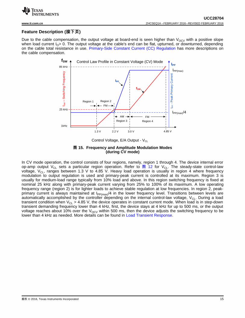
Control Voltage, E/A Output - VCL
Control Law Profile in Constant Voltage (CV) ModefSW
I PP -
Pea
k P
rimar
y C
urre
nt
2.2 V1.3 V
IPP(max)
85 kHz
fSW
IPP
25 kHz
AM
FM
FM
4.85 V
Region 4Region 3
Region 2Region 1
3.0 V
1kHz
IPP(max)/4
IPPf S
W ±
Sw
itchi
ng F
requ
ency
15
UCC28704www.ti.com.cn ZHCSEQ1A –FEBRUARY 2016–REVISED FEBRUARY 2016
版权 © 2016, Texas Instruments Incorporated
Feature Description (接接下下页页)Due to the cable compensation, the output voltage at board-end is seen higher than VOCV with a positive slopewhen load current IO> 0. The output voltage at the cable's end can be flat, upturned, or downturned, dependingon the cable total resistance in use. Primary-Side Constant Current (CC) Regulation has more descriptions onthe cable compensation.
图图 15. Frequency and Amplitude Modulation Modes(during CV mode)
In CV mode operation, the control consists of four regions, namely, region 1 through 4. The device internal errorop-amp output VCL sets a particular region operation. Refer to 图 12 for VCL. The steady-state control-lawvoltage, VCL, ranges between 1.3 V to 4.85 V. Heavy load operation is usually in region 4 where frequencymodulation to output regulation is used and primary-peak current is controlled at its maximum. Region 3 isusually for medium-load range typically from 10% load and above. In this region switching frequency is fixed atnominal 25 kHz along with primary-peak current varying from 25% to 100% of its maximum. A low operatingfrequency range (region 2) is for lighter loads to achieve stable regulation at low frequencies. In region 2, peak-primary current is always maintained at IPP(max)/4 in the lower frequency level. Transitions between levels areautomatically accomplished by the controller depending on the internal control-law voltage, VCL. During a loadtransient condition when VCL > 4.85 V, the device operates in constant current mode. When load is in step-downtransient demanding frequency lower than 4 kHz, first, the device stays at 4 kHz for up to 500 ms, or the outputvoltage reaches about 10% over the VOCV within 500 ms, then the device adjusts the switching frequency to belower than 4 kHz as needed. More details can be found in Load Transient Response.
0 IOCC
Out
put V
olta
ge V
O
Output Current IO
VOCV
Fixed Cable Compensation
Vo at Cable-End
VOCV x (1+ 0.06 x IO/IOCC)
Vo (Board-End) =
VO_CCUV atBoard-End
VO_CCUV atCable-End
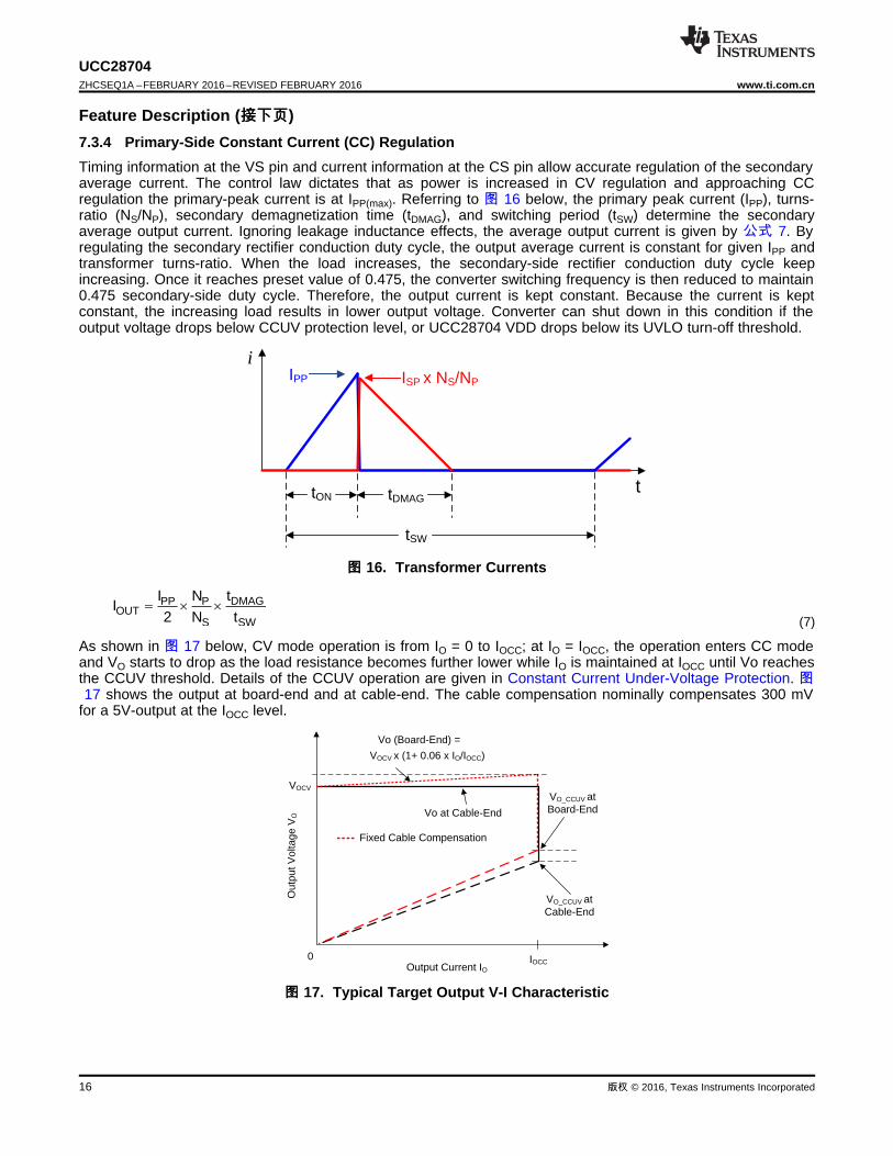
DMAGPP POUT
S SW
tI NI
2 N t u u
tON tDMAG
tSW
IPP ISP x NS/NP
t
i
16
UCC28704ZHCSEQ1A –FEBRUARY 2016–REVISED FEBRUARY 2016 www.ti.com.cn
版权 © 2016, Texas Instruments Incorporated
Feature Description (接接下下页页)7.3.4 Primary-Side Constant Current (CC) RegulationTiming information at the VS pin and current information at the CS pin allow accurate regulation of the secondaryaverage current. The control law dictates that as power is increased in CV regulation and approaching CCregulation the primary-peak current is at IPP(max). Referring to 图 16 below, the primary peak current (IPP), turns-ratio (NS/NP), secondary demagnetization time (tDMAG), and switching period (tSW) determine the secondaryaverage output current. Ignoring leakage inductance effects, the average output current is given by 公式 7. Byregulating the secondary rectifier conduction duty cycle, the output average current is constant for given IPP andtransformer turns-ratio. When the load increases, the secondary-side rectifier conduction duty cycle keepincreasing. Once it reaches preset value of 0.475, the converter switching frequency is then reduced to maintain0.475 secondary-side duty cycle. Therefore, the output current is kept constant. Because the current is keptconstant, the increasing load results in lower output voltage. Converter can shut down in this condition if theoutput voltage drops below CCUV protection level, or UCC28704 VDD drops below its UVLO turn-off threshold.
图图 16. Transformer Currents
(7)
As shown in 图 17 below, CV mode operation is from IO = 0 to IOCC; at IO = IOCC, the operation enters CC modeand VO starts to drop as the load resistance becomes further lower while IO is maintained at IOCC until Vo reachesthe CCUV threshold. Details of the CCUV operation are given in Constant Current Under-Voltage Protection. 图17 shows the output at board-end and at cable-end. The cable compensation nominally compensates 300 mV
for a 5V-output at the IOCC level.
图图 17. Typical Target Output V-I Characteristic
VDS
VDRV
t
0 V
0 V
17
UCC28704www.ti.com.cn ZHCSEQ1A –FEBRUARY 2016–REVISED FEBRUARY 2016
版权 © 2016, Texas Instruments Incorporated
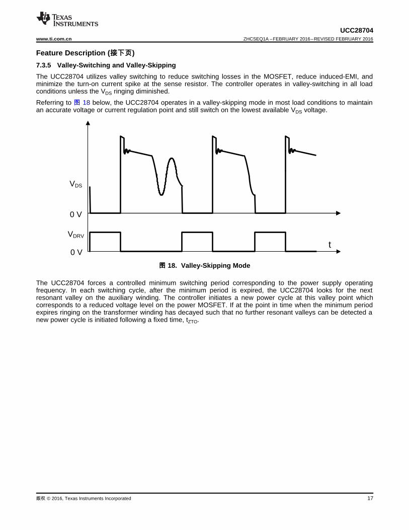
Feature Description (接接下下页页)7.3.5 Valley-Switching and Valley-SkippingThe UCC28704 utilizes valley switching to reduce switching losses in the MOSFET, reduce induced-EMI, andminimize the turn-on current spike at the sense resistor. The controller operates in valley-switching in all loadconditions unless the VDS ringing diminished.
Referring to 图 18 below, the UCC28704 operates in a valley-skipping mode in most load conditions to maintainan accurate voltage or current regulation point and still switch on the lowest available VDS voltage.
图图 18. Valley-Skipping Mode
The UCC28704 forces a controlled minimum switching period corresponding to the power supply operatingfrequency. In each switching cycle, after the minimum period is expired, the UCC28704 looks for the nextresonant valley on the auxiliary winding. The controller initiates a new power cycle at this valley point whichcorresponds to a reduced voltage level on the power MOSFET. If at the point in time when the minimum periodexpires ringing on the transformer winding has decayed such that no further resonant valleys can be detected anew power cycle is initiated following a fixed time, tZTO.
2CDD
RSTR
6
1
3
4
5
GND
NTC/SU
VS
VDD
DRV
CSRS2
RS1
RNTC
RLC
RCS
CB1+COUT
RPL
D2
Q1
D1
VAUX
NA
VAC
VOUT
VREGVBLK
UCC28704
-t°
CB2 NP NS
T1
18
UCC28704ZHCSEQ1A –FEBRUARY 2016–REVISED FEBRUARY 2016 www.ti.com.cn
版权 © 2016, Texas Instruments Incorporated
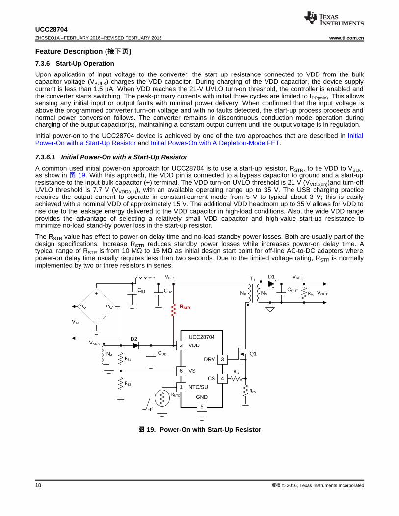
Feature Description (接接下下页页)7.3.6 Start-Up OperationUpon application of input voltage to the converter, the start up resistance connected to VDD from the bulkcapacitor voltage (VBULK) charges the VDD capacitor. During charging of the VDD capacitor, the device supplycurrent is less than 1.5 µA. When VDD reaches the 21-V UVLO turn-on threshold, the controller is enabled andthe converter starts switching. The peak-primary currents with initial three cycles are limited to IPP(min). This allowssensing any initial input or output faults with minimal power delivery. When confirmed that the input voltage isabove the programmed converter turn-on voltage and with no faults detected, the start-up process proceeds andnormal power conversion follows. The converter remains in discontinuous conduction mode operation duringcharging of the output capacitor(s), maintaining a constant output current until the output voltage is in regulation.
Initial power-on to the UCC28704 device is achieved by one of the two approaches that are described in InitialPower-On with a Start-Up Resistor and Initial Power-On with A Depletion-Mode FET.
7.3.6.1 Initial Power-On with a Start-Up ResistorA common used initial power-on approach for UCC28704 is to use a start-up resistor, RSTR, to tie VDD to VBLK,as show in 图 19. With this approach, the VDD pin is connected to a bypass capacitor to ground and a start-upresistance to the input bulk capacitor (+) terminal. The VDD turn-on UVLO threshold is 21 V (VVDD(on))and turn-offUVLO threshold is 7.7 V (VVDD(off)), with an available operating range up to 35 V. The USB charging practicerequires the output current to operate in constant-current mode from 5 V to typical about 3 V; this is easilyachieved with a nominal VDD of approximately 15 V. The additional VDD headroom up to 35 V allows for VDD torise due to the leakage energy delivered to the VDD capacitor in high-load conditions. Also, the wide VDD rangeprovides the advantage of selecting a relatively small VDD capacitor and high-value start-up resistance tominimize no-load stand-by power loss in the start-up resistor.
The RSTR value has effect to power-on delay time and no-load standby power losses. Both are usually part of thedesign specifications. Increase RSTR reduces standby power losses while increases power-on delay time. Atypical range of RSTR is from 10 MΩ to 15 MΩ as initial design start point for off-line AC-to-DC adapters wherepower-on delay time usually requires less than two seconds. Due to the limited voltage rating, RSTR is normallyimplemented by two or three resistors in series.
图图 19. Power-On with Start-Up Resistor
2CDD
RLIM
6
1
3
4
5
GND
NTC/SU
VS
VDD
DRV
CSRS2
RS1
RNTC
RLC
RCS
CB1+COUT
RPL
D2
Q1
D1
VAUX
NA
VAC
VOUT
VREGVBLK
UCC28704
-t°
CB2 NP NS
RST3
RST2
CST
RST1
QST1
T1
QST2
19
UCC28704www.ti.com.cn ZHCSEQ1A –FEBRUARY 2016–REVISED FEBRUARY 2016
版权 © 2016, Texas Instruments Incorporated
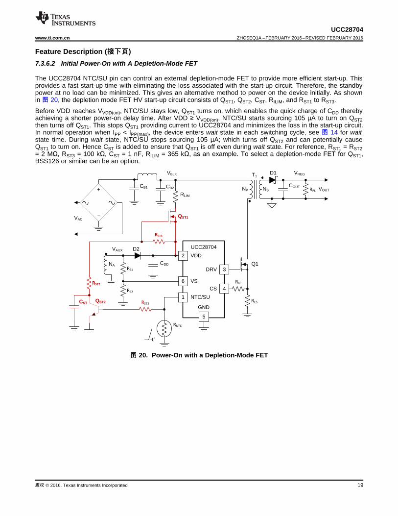
Feature Description (接接下下页页)7.3.6.2 Initial Power-On with A Depletion-Mode FET
The UCC28704 NTC/SU pin can control an external depletion-mode FET to provide more efficient start-up. Thisprovides a fast start-up time with eliminating the loss associated with the start-up circuit. Therefore, the standbypower at no load can be minimized. This gives an alternative method to power on the device initially. As shownin 图 20, the depletion mode FET HV start-up circuit consists of QST1, QST2, CST, RILIM, and RST1 to RST3.
Before VDD reaches VVDD(on), NTC/SU stays low, QST1 turns on, which enables the quick charge of CDD therebyachieving a shorter power-on delay time. After VDD ≥ VVDD(on), NTC/SU starts sourcing 105 µA to turn on QST2then turns off QST1. This stops QST1 providing current to UCC28704 and minimizes the loss in the start-up circuit.In normal operation when IPP < IPP(max), the device enters wait state in each switching cycle, see 图 14 for waitstate time. During wait state, NTC/SU stops sourcing 105 µA; which turns off QST2 and can potentially causeQST1 to turn on. Hence CST is added to ensure that QST1 is off even during wait state. For reference, RST1 = RST2= 2 MΩ, RST3 = 100 kΩ, CST = 1 nF, RILIM = 365 kΩ, as an example. To select a depletion-mode FET for QST1,BSS126 or similar can be an option.
图图 20. Power-On with a Depletion-Mode FET
20
UCC28704ZHCSEQ1A –FEBRUARY 2016–REVISED FEBRUARY 2016 www.ti.com.cn
版权 © 2016, Texas Instruments Incorporated
Feature Description (接接下下页页)7.3.7 Fault ProtectionThere is comprehensive fault protection incorporated into the UCC28704. Protection functions include:• Output Over-Voltage• Input Under-Voltage• Primary Over-Current Fault• CS Pin Open Fault• CS Pin Short-to-GND Fault• VS Pin Fault• External NTC Over-Temperature• Device Internal Over-Temperature• Constant Current Under Voltage Output Shutdown (CCUV) for Soft-Short Protection
Output Over-Voltage: The output over-voltage function is determined by the voltage feedback on the VS pin. Ifthe voltage sample on VS exceeds 4.67 V, 115% of the nominal regulating level, for three consecutive switchingcycles an OV fault is asserted. Once asserted the device stops switching, initiating a UVLO reset and re-startfault cycle. During the fault, the VDD bias current remains at the run current level, discharging the VDD pin to theUVLO turn-off threshold, VVDD(off). After that, the device returns to the start state, VDD now charging to VVDD(on)where switching is initiated. The UVLO sequence repeats as long as the fault condition persists.
Input Under-Voltage: The line input run and stop thresholds are determined by current information at the VS pinduring the MOSFET on-time. While the VS pin is clamped close to GND during the MOSFET on-time, the currentthrough RS1, out of the VS pin, is monitored to determine a sample of the bulk capacitor voltage. A wideseparation of run and stop thresholds allows clean start-up and shut-down of the power supply with the linevoltage. From the start state, the sensed VS current, IVSL, must exceed the run current threshold, IVSL(run) (typical220 µA), within the first three cycles after switching starts as VDD reaches VVDD(on). If it does not, then switchingstops and the UVLO reset and re-start fault cycle is initiated. Once running, IVSL must drop below the stop level,IVSL(stop) (typically 80 µA), for three consecutive cycles to initiate the fault response.
Primary Over-Current: The UCC28704 always operates with cycle-by-cycle primary-peak current control. Thenormal operating range of the CS pin is 0.75 V to 0.188 V. If the voltage on CS exceeds the 1.5-V over-currentlevel, any time after the internal leading edge blanking time and before the end of the transformerdemagnetization, for three consecutive cycles the device shuts down and the UVLO reset and re-start fault cyclebegins.
CS Pin Open: The CS pin has a 2-µA minimum pull-up that brings the CS pin above the 1.5-V OC fault level ifthe CS pin is open. This causes the primary over-current fault after three cycles.
CS Pin Short to GND: On the first, and only the first cycle at start-up, the device checks to verify that theVCST(min) threshold is reached at the CS pin within 4 µs of DRV going high. If the CS voltage fails to reach thislevel then the device terminates the current cycle and immediately enters the UVLO reset and re-start faultsequence.
VS Pin: Protection is included in the event of component failures on the VS pin. If the high-side VS dividerresistor opens the controller stops switching. VDD collapses to its VVDD(off) threshold, a start-up attempt followswith a single DRV on-time when VDD reaches VVDD(on). The UVLO cycle will repeat. If the low-side VS dividerresistor is open then an output over-voltage fault occurs.
NTC Over-Temperature: UCC28704 uses the NTC/SU pin to program thermal shutdown threshold with anexternal NTC thermistor on this pin. The NTC shutdown threshold is 0.95 V with an internal 105-µA currentsource which results in a 9.05-kΩ thermistor shutdown threshold. If the NTC/SU pin voltage is below 0.95 V atthe end of the secondary current demagnetization time for three consecutive cycles switching stops and theUVLO reset and re-start fault sequence is initiated.
Device Internal OTP: The internal over-temperature protection threshold is 150°C. If the junction temperature ofthe device reaches this threshold the device initiates the UVLO reset and re-start fault cycle. If the temperature isstill high at the end of the UVLO cycle, the protection cycle repeats.
Constant Current Under-Voltage: Output shutdown (CCUV) for soft-short protection. Constant Current Under-Voltage Protection provides detailed description for this fault and fault response.
1.0
5.0
4.0
3.0
2.0
0IOCC
Out
put V
olta
ge (
V)
Output Current (A)
4.75 V
5.25 V
+/-5%
3.0 V
2.7 V
Board-EndCable-End
21
UCC28704www.ti.com.cn ZHCSEQ1A –FEBRUARY 2016–REVISED FEBRUARY 2016
版权 © 2016, Texas Instruments Incorporated
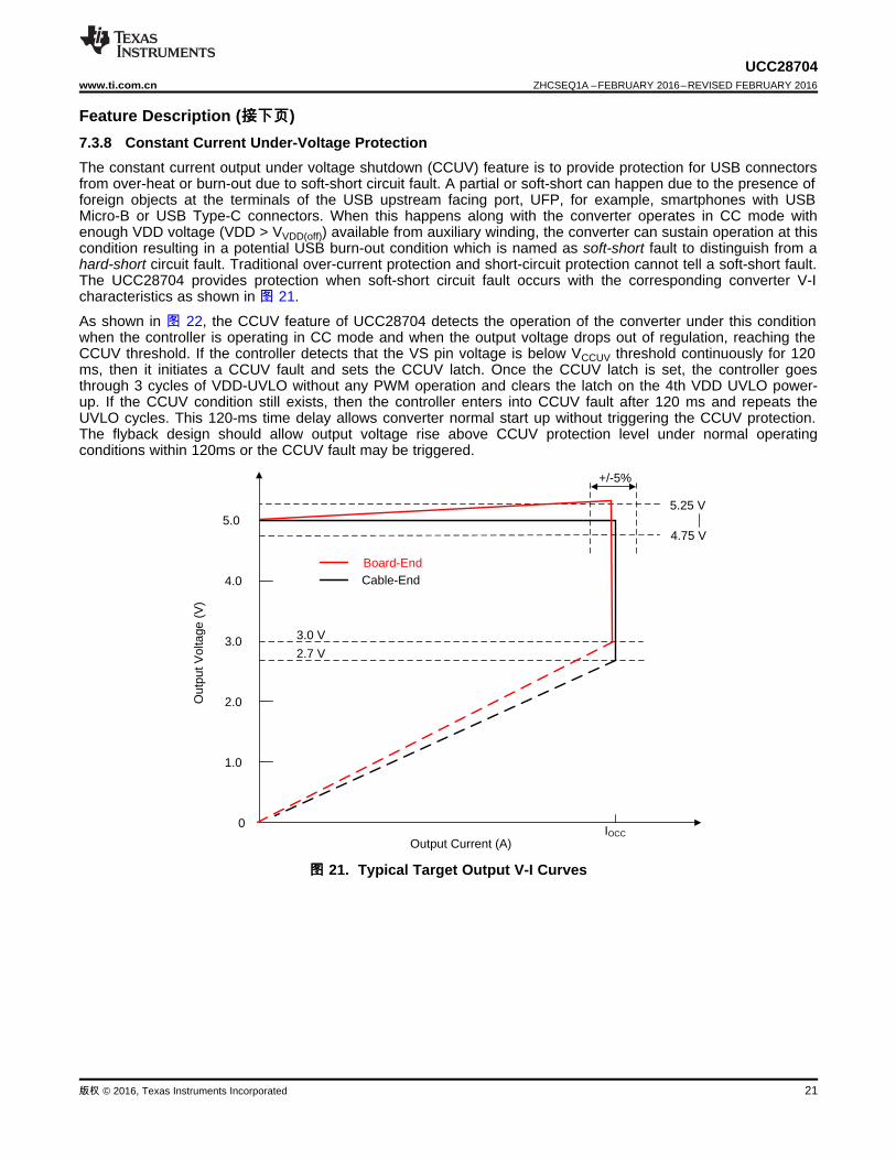
Feature Description (接接下下页页)7.3.8 Constant Current Under-Voltage ProtectionThe constant current output under voltage shutdown (CCUV) feature is to provide protection for USB connectorsfrom over-heat or burn-out due to soft-short circuit fault. A partial or soft-short can happen due to the presence offoreign objects at the terminals of the USB upstream facing port, UFP, for example, smartphones with USBMicro-B or USB Type-C connectors. When this happens along with the converter operates in CC mode withenough VDD voltage (VDD > VVDD(off)) available from auxiliary winding, the converter can sustain operation at thiscondition resulting in a potential USB burn-out condition which is named as soft-short fault to distinguish from ahard-short circuit fault. Traditional over-current protection and short-circuit protection cannot tell a soft-short fault.The UCC28704 provides protection when soft-short circuit fault occurs with the corresponding converter V-Icharacteristics as shown in 图 21.
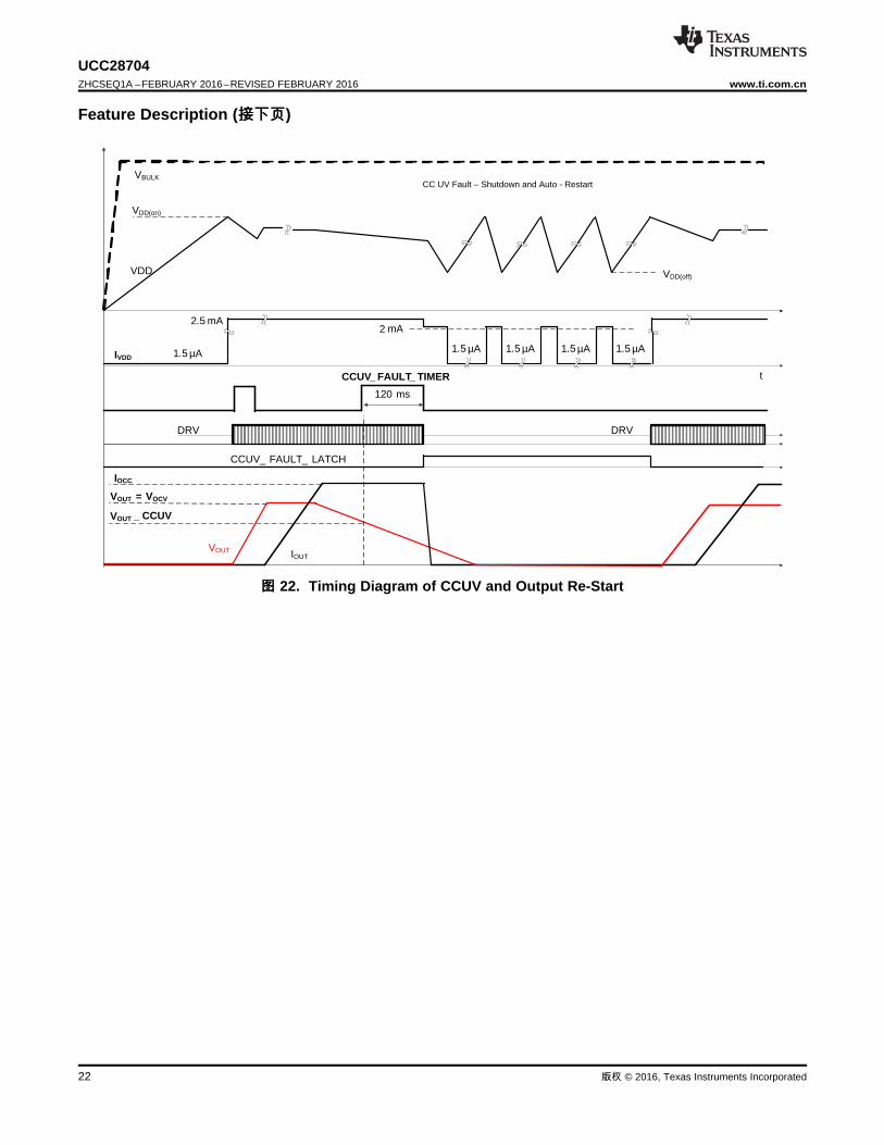
As shown in 图 22, the CCUV feature of UCC28704 detects the operation of the converter under this conditionwhen the controller is operating in CC mode and when the output voltage drops out of regulation, reaching theCCUV threshold. If the controller detects that the VS pin voltage is below VCCUV threshold continuously for 120ms, then it initiates a CCUV fault and sets the CCUV latch. Once the CCUV latch is set, the controller goesthrough 3 cycles of VDD-UVLO without any PWM operation and clears the latch on the 4th VDD UVLO power-up. If the CCUV condition still exists, then the controller enters into CCUV fault after 120 ms and repeats theUVLO cycles. This 120-ms time delay allows converter normal start up without triggering the CCUV protection.The flyback design should allow output voltage rise above CCUV protection level under normal operatingconditions within 120ms or the CCUV fault may be triggered.
图图 21. Typical Target Output V-I Curves
VDD
IVDD
DRV
120 ms
VOUT
IOCC
xxxxxxxxxxxxxxxx
IOUT
CCUV_ FAULT_ LATCH
VBULK
DRV
xxxxxxxxxx
VOUT = VOCV
_ CCUV
t
VDD(on)
VDD(off)
2 mA
.1 5 µA .1 5 µA .1 5 µA .1 5 µA.1 5 µA
CCUV_ FAULT_ TIMER
2.5 mA
CC UV Fault ± Shutdown and Auto - Restart
VOUT
22
UCC28704ZHCSEQ1A –FEBRUARY 2016–REVISED FEBRUARY 2016 www.ti.com.cn
版权 © 2016, Texas Instruments Incorporated
Feature Description (接接下下页页)
图图 22. Timing Diagram of CCUV and Output Re-Start

Transient response from standby Periodic Transient Response
fSW
fSW(min)
fSW(standby)
fSW(min) = 4 kHz fSW(min) = 4 kHz
fSW(min) = 1 kHz
fSW(standby)
IOUT
VOUT
VOUT(nom)
VOUT(nom) x 1.1
VOUT Recovers to nom Level, fSW(min) < fSW(standby)
Load = 0, 4 kHz > fSW(standby)
Standby Zero Load Steady State
Periodic Load StepsStandby Zero Load
Steady State
OUT(step)OUT
OUT SW(s tandby)
IV
C f'
u
23
UCC28704www.ti.com.cn ZHCSEQ1A –FEBRUARY 2016–REVISED FEBRUARY 2016
版权 © 2016, Texas Instruments Incorporated
Feature Description (接接下下页页)7.3.9 Load Transient ResponseThe UCC28704 can provide excellent transient performance for most load steps. However the response of PSRcontroller is always limited by the operating frequency of the converter, since the controller only samples or readsthe output voltage once every switching cycle. At zero external load, or standby, the operating frequency is setby any preload together with the bias power needed. This frequency, fSW(standby), sets a maximum incrementalresponse delay. The preload can always be adjusted, at the expense of standby power, to increase the standbyfrequency. The actual response delay depends on the relative timing of the load step within the switching cycle.Thus for a given load step, IOUT(step), the output deviation can be as large as:
(8)
In the case of repeating load transients the situation is aggravated. Whenever the load steps from a modestcurrent level to zero, there is a period of time when there is a slight over-shoot in the output voltage and thecontrol loop saturates and force the converter operating at to its minimum switching frequency, fSW(min), or 1 kHzregardless what preload setting is. If the next positive load step occurs during this time the output deviation willbe larger, remembering that fSW(standby) must be > fSW(min).
A special transient response algorithm in this controller dynamically adjusts the minimum controlled switchingfrequency, such that during a mid to high current level condition the loop's minimum switching frequency is raisedto fSW(lim), typically 4 kHz. This raised minimum switching frequency is maintained following a load step-downchange until the output voltage rises momentarily to 10% above its normal regulating level or has stayed aboveits normal regulating level for 500 ms. During this time the response to a load step-up change benefits from thedecreased response delay afforded by the 4-kHz switching frequency. This is illustrated in 图 23. ApplicationCurves provides test results and further description in regarding to this technique.
注注In applications where standby power is not critical the minimum operating frequency of theloop can be kept higher than 4 kHz. In these cases controller will continuously maintain a4-kHz minimum frequency.
图图 23. Dynamic Load Response
24
UCC28704ZHCSEQ1A –FEBRUARY 2016–REVISED FEBRUARY 2016 www.ti.com.cn
版权 © 2016, Texas Instruments Incorporated
7.4 Device Functional ModesThe UCC28704 operates in different modes according to input voltage, VDD voltage, and output load conditions:• At start-up, when VDD is less than the turn-on threshold, VVDD(on) , the device is simply waiting for VDD to
reach this threshold while the VDD capacitor is getting charged.• When VDD exceeds VVDD(on), the device starts switching to deliver power to the converter output. The initial 3
switching cycles control the primary-peak current to IPP(min). This allows sensing any initial input or outputfaults with minimal power delivery. When confirmed with input voltage above predetermined level and no faultconditions, start up process proceeds and normal power conversion follows. The converter will remain indiscontinuous current mode operation during charging of the output capacitor(s), maintaining a constantoutput current until the output voltage reaches its regulation point.– CV mode means that the converter keeps the output voltage constant. When the load current is less than
the current limit level, the converter operates in CV mode to keep the output voltage at the regulation levelover the entire load and input line ranges.
– CC mode means that the converter keeps the output current constant. When the output voltage is belowthe regulation level, the converter operates in CC mode to limit the output current.
– In CC mode, when the output voltage starts to drop below regulation and if it reaches below the CCUVthreshold VCCUV, sensed at the VS pin, the controller declares a CCUV fault and disables PWM. Thecontroller initiates a shutdown-restart operation. This protection mode helps avoid USB terminals fromgetting over-heated and thereby preventing a burn-out condition, which is also called soft-short protection.Detailed description is in Constant Current Under-Voltage Protection.
• When operating in CV mode where IPP reaches IPP(max), the UCC28704 operates continuously in the run state.In this state, the VDD bias current is always at IRUN plus the average gate-drive current.
• When operating in CV mode where IPP is less than IPP(max), the UCC28704 operates in the wait state betweenswitching cycles and in the run state during a switching cycle. In the wait state, the VDD bias current isreduced to IWAIT after demagnetizing time of each switching cycle to improve efficiency at light loads. Thishelps reduce light-load power losses, particularly for achieving higher efficiency at 10% and 25% loadconditions.
• When a dynamic load change occurs in CV mode, the UCC28704 provides an enhanced transient responseto reduce load step caused VOUT dip in periodic load change operation. Detailed description is in LoadTransient Response.
• The device operation can be stopped by the events listed below:– If VDD drops below the VVDD(off) threshold, the device stops switching, its bias current consumption is
lowered to ISTART until VDD rises above the VVDD(on) threshold. The device then resumes switching.– If a fault condition is detected, the device stops switching and its bias current consumption becomes
IFAULT. This current level discharges VDD to VVDD(off) where the bias current changes from IFAULT to ISTARTuntil VDD rises above the VVDD(on) threshold.
– By pulling down NTC/SU pin to below VNTCTH, the device responds similar to that of an NTC fault whereinPWM is disabled and converter is shutdown. On releasing the pull-down on NTC, normal operation intoCV mode will be restored.
• If a fault condition persists, the operation sequence described above in repeats until the fault condition or theinput voltage is removed. Refer to Fault Protection for fault conditions and post-fault operation.
2CDD
RSTR
6
1
3
4
5
GND
NTC/SU
VS
VDD
DRV
CSRS2
RS1
RNTC
RLC
RCS
CB1+COUT
RPL
D2
Q1
D1
VAUX
NA
VAC
VOUT
VREGVBLK
UCC28704
-t°
NP NS
T1
25
UCC28704www.ti.com.cn ZHCSEQ1A –FEBRUARY 2016–REVISED FEBRUARY 2016
版权 © 2016, Texas Instruments Incorporated
8 Applications and Implementation
注注Information in the following applications sections is not part of the TI componentspecification, and TI does not warrant its accuracy or completeness. TI’s customers areresponsible for determining suitability of components for their purposes. Customers shouldvalidate and test their design implementation to confirm system functionality.
8.1 Application InformationThe UCC28704 device is a PSR controller optimized for isolated-flyback AC-to-DC single-output supplyapplications, typically in the range from 5 W to 25 W, providing constant-voltage (CV) mode control and constantcurrent (CC) mode control for precise output regulation; and to help meet USB-compliant adaptors and chargerrequirements as well as help meeting DOE Level VI or CoC V5 Tier 2 efficiency performance. The device usesthe information obtained from auxiliary winding sensing (VS) to control the output voltage without requiringoptocoupler/TL431 feedback circuitry. Not requiring optocoupler feedback reduces the component count andmakes the design more cost effective.
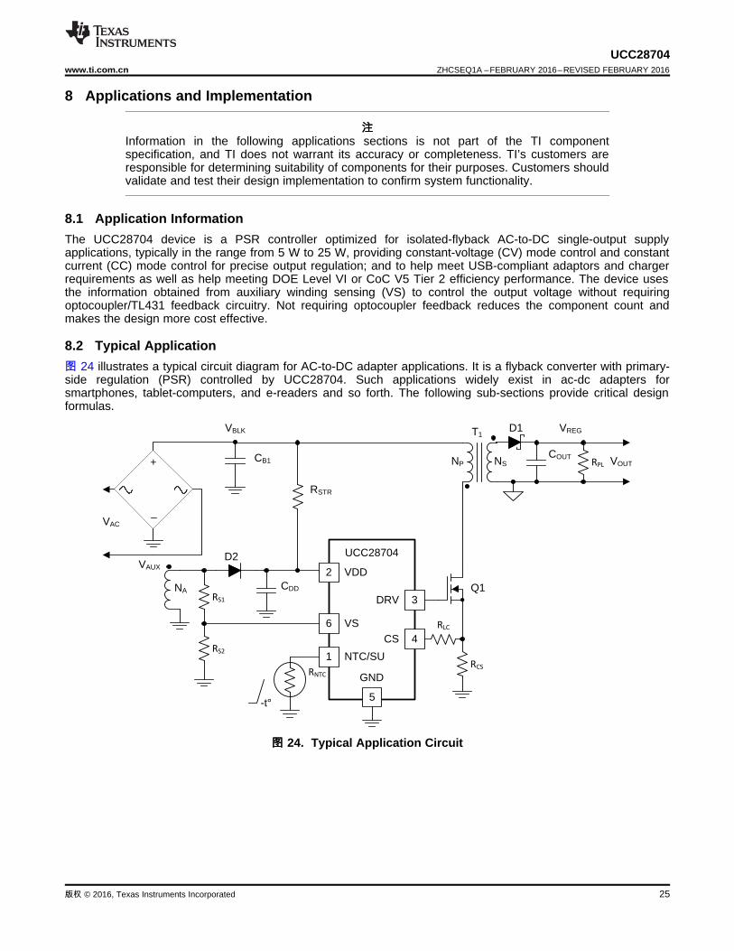
8.2 Typical Application图 24 illustrates a typical circuit diagram for AC-to-DC adapter applications. It is a flyback converter with primary-side regulation (PSR) controlled by UCC28704. Such applications widely exist in ac-dc adapters forsmartphones, tablet-computers, and e-readers and so forth. The following sub-sections provide critical designformulas.
图图 24. Typical Application Circuit
26
UCC28704ZHCSEQ1A –FEBRUARY 2016–REVISED FEBRUARY 2016 www.ti.com.cn
版权 © 2016, Texas Instruments Incorporated
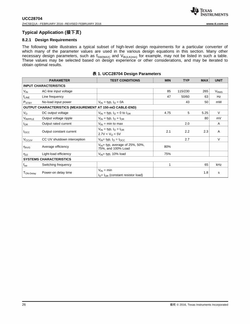
Typical Application (接接下下页页)8.2.1 Design RequirementsThe following table illustrates a typical subset of high-level design requirements for a particular converter ofwhich many of the parameter values are used in the various design equations in this section. Many othernecessary design parameters, such as fSW(MAX) and VBULK(min) for example, may not be listed in such a table.These values may be selected based on design experience or other considerations, and may be iterated toobtain optimal results.
表表 1. UCC28704 Design ParametersPARAMETER TEST CONDITIONS MIN TYP MAX UNIT
INPUT CHARACTERISTICSVIN AC-line input voltage 85 115/230 265 VRMS
fLINE Line frequency 47 50/60 63 HzPSTBY No-load input power VIN = typ, IO = 0A 43 50 mWOUTPUT CHARACTERISTICS (MEASUREMENT AT 150-mΩ CABLE-END)VO DC output voltage VIN = typ, IO = 0 to IOR 4.75 5 5.25 VVRIPPLE Output voltage ripple VIN = typ, IO = IOR 80 mVIOR Output rated current VIN = min to max 2.0 A
IOCC Output constant currentVIN = typ, IO > IOR
2.7V < VO < 5V2.1 2.2 2.3 A
VCCUV CC UV shutdown interception VIN= typ, IO = IOCC 2.7 V
ηAVG Average efficiency VIN= typ, average of 25%, 50%,75%, and 100% Load 80%
η10 Light-load efficiency VIN= typ, 10% load 75%SYSTEMS CHARACTERISTICSfsw Switching frequency 1 65 kHz
TON-Delay Power-on delay timeVIN = minIO= IOR (constant resistor load)
1.8 s

BULK(min)IN
IN(min)BULK 2 2
IN(min) BULK(min) LINE
V1P 0.5 arcsin
2 VC
2V V f
§ ·§ ·¨ ¸¨ ¸u u
¨ ¸S¨ ¸u© ¹© ¹ u
OCV OCCIN
V IP
u
K
IN(min)
STRDD(on) DD
STARTSTR
2 VR
V CI
t
u
u
OUT OCCRUN
OCCDD
DD(on),min DD(off),max
C VI 1.0mA
ICV V
u u
27
UCC28704www.ti.com.cn ZHCSEQ1A –FEBRUARY 2016–REVISED FEBRUARY 2016
版权 © 2016, Texas Instruments Incorporated
8.2.2 Detailed Design ProcedureThis procedure outlines the steps to design a constant-voltage, constant-current flyback converter using theUCC28704 controller. Please refer to the 图 24 for circuit details and section 器件命名规则 for variable definitionsused in the applications equations below.
8.2.2.1 VDD Capacitance, CDD
The capacitance on VDD needs to supply the device operating current until the output of the converter reachesthe target minimum operating voltage. At this time the auxiliary winding can sustain the voltage to theUCC28704. The total output current available to the load and to charge the output capacitors is the constant-current regulation target. The equation below assumes the output current of the flyback is available to charge theoutput capacitance until the minimum output voltage VOCC is achieved. The gate-drive current depends onparticular MOSFET to be used. If with an estimated 1.0 mA of gate-drive current, CDD is determined by 公式 9.
(9)
8.2.2.2 VDD Start-Up Resistance, RSTR
Once the VDD capacitance is known, the start-up resistance from VBULK to achieve the power-on delay time(tSTR) target can be determined.
(10)
8.2.2.3 Input Bulk Capacitance and Minimum Bulk VoltageDetermine the minimum voltage on the input capacitance, CB1 and CB2 total, in order to determine the maximumNp to Ns turns ratio of the transformer. The input power of the converter based on target full-load efficiency,minimum input rms voltage, and minimum AC input frequency are used to determine the input capacitancerequirement.
Maximum input power is determined based on VOCV, IOCC, and the full-load efficiency target. An initial estimate of84% can be assumed for the full-load efficiency for a 5-V/2-A design.
(11)
公式 12 provides an accurate solution for input capacitance based on a target minimum bulk capacitor voltage.To target a given input capacitance value, iterate the minimum capacitor voltage to achieve the targetcapacitance.
(12)
DD(off) FAAS
OCC F
V VN
V V
OCV F OCBC OCCP 2
XFMR PP(max) MAX
2 V V V IL
I f
u u
K u u
CST(max)PP(max)
CS
VI
R
CCR PSCS XFMR
OCC
V NR
2 I
u u K
u
MAX BULK(min)
PS(max)MAGCC OCV F OCBC
D VN
D V V V
u
u
RMAX MAX MAGCC
tD 1 f D
2§ ·
u ¨ ¸© ¹
28
UCC28704ZHCSEQ1A –FEBRUARY 2016–REVISED FEBRUARY 2016 www.ti.com.cn
版权 © 2016, Texas Instruments Incorporated
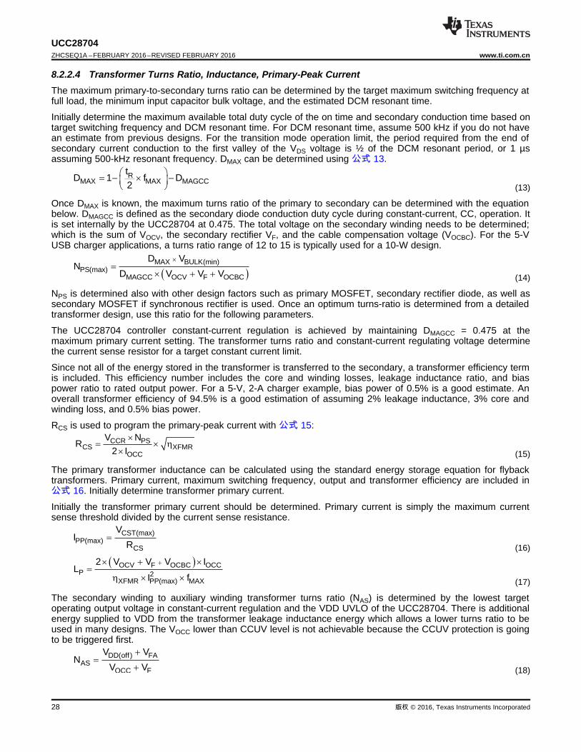
8.2.2.4 Transformer Turns Ratio, Inductance, Primary-Peak CurrentThe maximum primary-to-secondary turns ratio can be determined by the target maximum switching frequency atfull load, the minimum input capacitor bulk voltage, and the estimated DCM resonant time.
Initially determine the maximum available total duty cycle of the on time and secondary conduction time based ontarget switching frequency and DCM resonant time. For DCM resonant time, assume 500 kHz if you do not havean estimate from previous designs. For the transition mode operation limit, the period required from the end ofsecondary current conduction to the first valley of the VDS voltage is ½ of the DCM resonant period, or 1 µsassuming 500-kHz resonant frequency. DMAX can be determined using 公式 13.
(13)
Once DMAX is known, the maximum turns ratio of the primary to secondary can be determined with the equationbelow. DMAGCC is defined as the secondary diode conduction duty cycle during constant-current, CC, operation. Itis set internally by the UCC28704 at 0.475. The total voltage on the secondary winding needs to be determined;which is the sum of VOCV, the secondary rectifier VF, and the cable compensation voltage (VOCBC). For the 5-VUSB charger applications, a turns ratio range of 12 to 15 is typically used for a 10-W design.
(14)
NPS is determined also with other design factors such as primary MOSFET, secondary rectifier diode, as well assecondary MOSFET if synchronous rectifier is used. Once an optimum turns-ratio is determined from a detailedtransformer design, use this ratio for the following parameters.
The UCC28704 controller constant-current regulation is achieved by maintaining DMAGCC = 0.475 at themaximum primary current setting. The transformer turns ratio and constant-current regulating voltage determinethe current sense resistor for a target constant current limit.
Since not all of the energy stored in the transformer is transferred to the secondary, a transformer efficiency termis included. This efficiency number includes the core and winding losses, leakage inductance ratio, and biaspower ratio to rated output power. For a 5-V, 2-A charger example, bias power of 0.5% is a good estimate. Anoverall transformer efficiency of 94.5% is a good estimation of assuming 2% leakage inductance, 3% core andwinding loss, and 0.5% bias power.
RCS is used to program the primary-peak current with 公式 15:
(15)
The primary transformer inductance can be calculated using the standard energy storage equation for flybacktransformers. Primary current, maximum switching frequency, output and transformer efficiency are included in公式 16. Initially determine transformer primary current.
Initially the transformer primary current should be determined. Primary current is simply the maximum currentsense threshold divided by the current sense resistance.
(16)
(17)
The secondary winding to auxiliary winding transformer turns ratio (NAS) is determined by the lowest targetoperating output voltage in constant-current regulation and the VDD UVLO of the UCC28704. There is additionalenergy supplied to VDD from the transformer leakage inductance energy which allows a lower turns ratio to beused in many designs. The VOCC lower than CCUV level is not achievable because the CCUV protection is goingto be triggered first.
(18)
LC S1 CS D GATE _ OFF PALC
P
K R R (t t ) NR
L
u u u u
S1 VSR
S2AS OCV F VSR
R VR
N V V Vu
u
IN(run)
S1PA VSL(run)
V 2R
N I
u
u
ON(min) IN(max)
DMAG(min)PS OCV F
t V 2t
N V V
u u
u
PP(max)PON(min)
AMIN(max)
ILt
KV 2 u
u
DSPK IN(max) OCV F OCBC PS LKV V 2 V V V N V u u
IN(max)
REV OCV OCBCPS
V 2V V V
N
u
29
UCC28704www.ti.com.cn ZHCSEQ1A –FEBRUARY 2016–REVISED FEBRUARY 2016
版权 © 2016, Texas Instruments Incorporated
8.2.2.5 Transformer Parameter VerificationThe transformer turns-ratio selected affects the MOSFET VDS and secondary rectifier reverse voltage so theseshould be reviewed. The UCC28704 controller requires a minimum on time of the MOSFET (tON) and minimumDMAG time (tDMAG(min)) of the secondary rectifier in the high line, minimum-load condition. The selection of fMAX, LPand RCS affects the minimum tON and tDMAG.
The secondary rectifier and MOSFET voltage stress can be determined by the equations below.
(19)
For the MOSFET VDS voltage stress, an estimated leakage inductance voltage spike (VLK) needs to be included.
(20)
The following equations are used to determine for the minimum tON target of 0.3 µs and minimum de-magtime, tDMAG(min), target of 1.7 µs. The minimum tDMAG(min) target needs to be typically 2.45 µs when asynchronous rectifier is used on the secondary-side instead of a Schottky diode rectifier. Additional detailsare provided in Design Considerations in Using with Synchronous Rectifiers.
(21)
(22)
8.2.2.6 VS Resistor Divider, Line Compensation, and NTCThe VS divider resistors determine the output voltage regulation point of the flyback converter, also the high-sidedivider resistor (RS1) determines the line voltage at which the controller enables continuous DRV operation. RS1is initially determined based on the transformer auxiliary to primary turns-ratio and the desired input voltageoperating threshold.
(23)
The low-side VS pin resistor is selected based on desired VO regulation voltage. IVSL(run) is VS pin run currentwith a typical value 220 µA for a design.
(24)
The UCC28704 can maintain tight constant-current regulation over input line by utilizing the line compensationfeature. The line compensation resistor (RLC) value is determined by current flowing in RS1 and expected gatedrive and MOSFET turn-off delay. Assume a 50-ns internal delay in the UCC28704.
(25)
The NTC function on NTC/SU-pin is to program with a NTC resistor for the desired over-temperature shutdownthreshold. The shut-down threshold is 0.95 V with an internal 105-μA current source which results in a 9.05-kΩthermistor shut-down threshold. The SU function on NTC/SU-pin is described in Initial Power-On with ADepletion-Mode FET. Pulling down this pin to GND stops switching and can be used for remote enable anddisable control. This pin should be left floating if not used.
RIPPLE RIPPLE_R RIPPLE_CV 0.81 V 1.15 V 10mV u u
2P PP(max)
OUTOCV CBC RIPPLE _ C
L I 1C
4 (V V ) V
u
u
u
ESR RIPPLE_RPP(max) PS
1R V
I N u
u
TRANSW(min)
OUTO
1I 50 s
fC
V
§ · P¨ ¸¨ ¸
© ¹ '
SB SB _ CONV RSTR SNBRP P P P
2BULK DD
RSTRSTR
(V V )P
R
2OCV
PLSB _ CONV
VR
P 2.1mW
OUT MINSB _ CONV 2
AM MAX
P fP
K f
u#Ku u
30
UCC28704ZHCSEQ1A –FEBRUARY 2016–REVISED FEBRUARY 2016 www.ti.com.cn
版权 © 2016, Texas Instruments Incorporated
8.2.2.7 Standby Power EstimateAssuming no-load standby power is a critical design parameter, determine the estimated no-load power basedon target converter maximum switching frequency and output power rating. The following equation estimates thestand-by power of the converter.
(26)
For a typical USB charger application, the bias power during no-load is approximately 2.1 mW. This is based on21-V VDD and 100-µA bias current. The output preload resistor can be estimated by VOCV and the difference inthe converter stand-by power and the bias power. The equation for output preload resistance accounts for biaspower estimated at 2.1 mW. Preload resistor value is estimated in 公式 27 :
(27)
Typical start-up resistance values for RSTR range from 10 MΩ to 15 MΩ to achieve less than 2-s start-up time.The capacitor bulk voltage for the loss estimation is the highest voltage for the stand-by power measurement,typically 325 VDC.
(28)
For the total stand-by power estimation add an estimated 2.5 mW for snubber loss to the start-up resistance andconverter stand-by power loss.
(29)
8.2.2.8 Output CapacitanceThe output capacitance value is typically determined by the transient response requirement from no-load. Forexample, in some USB charger applications there is a requirement to maintain a minimum VO of 4.1 V with aload-step transient of 0 mA to 500 mA . 公式 30 assumes that the switching frequency can be at the UCC28704minimum of fSW(min).
(30)
公式 5 should be observed together with 公式 30 for stability consideration when determine COUT.
Another consideration of the output capacitor(s) is the ripple voltage requirement. The output capacitors and theirtotal ESR are the main factors to determine the output voltage ripple. 公式 31 provides a formula to determinerequired ESR value RESR, and 公式 31 provides a formula to determine required capacitance. The total outputripple is the sum of these two parts with scale factors and 10mV to consider other noise as shown in 公式 33,
(31)
(32)
(33)
Example: if require VRIPPLE = 70 mV, assume 0.81 × VRIPPLE_R = 1.15 × VRIPPLE_C = 30 mV, then RESR = 4.05mΩ, and COUT = 643 µF, with assumption of LP = 700 µH, IPP(max) = 0.713 A, NPS = 13, VOCV = 5 V, VCBC = 0.3 V.
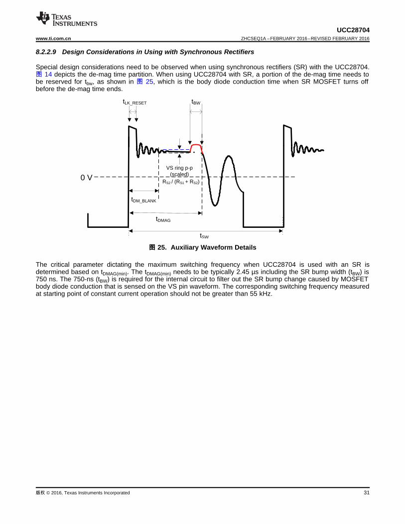
0 VVS ring p-p
(scaled)
tDM_BLANK
tLK_RESET
tDMAG
tSW
RS2 / (RS1 + RS2)
tBW
31
UCC28704www.ti.com.cn ZHCSEQ1A –FEBRUARY 2016–REVISED FEBRUARY 2016
版权 © 2016, Texas Instruments Incorporated
8.2.2.9 Design Considerations in Using with Synchronous Rectifiers
Special design considerations need to be observed when using synchronous rectifiers (SR) with the UCC28704.图 14 depicts the de-mag time partition. When using UCC28704 with SR, a portion of the de-mag time needs tobe reserved for tbw, as shown in 图 25, which is the body diode conduction time when SR MOSFET turns offbefore the de-mag time ends.
图图 25. Auxiliary Waveform Details
The critical parameter dictating the maximum switching frequency when UCC28704 is used with an SR isdetermined based on tDMAG(min). The tDMAG(min) needs to be typically 2.45 µs including the SR bump width (tBW) is750 ns. The 750-ns (tBW) is required for the internal circuit to filter out the SR bump change caused by MOSFETbody diode conduction that is sensed on the VS pin waveform. The corresponding switching frequency measuredat starting point of constant current operation should not be greater than 55 kHz.
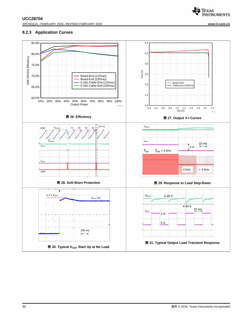
VOCV (V)1.1 x VOCV
200 ms
VOUT
IOUT
0 A
2 A
4.44 V
5.45 V
10 ms
VOUT
IOUT
fsw fsw > 4 kHz
4 kHz < 4 kHz
2 A10 ms
VDD
VOUT
IOUT
DRV
VDD(on)
VDD(off)
(1) (2) (3) (4)120 ms
Iout (A)
Vou
t (V
)
0.0 0.2 0.5 0.8 1.0 1.2 1.5 1.8 2.0 2.20.0
1.0
2.0
3.0
4.0
5.0
6.0
D027
Board-EndCable-End (150m:)
Output Power
10W
(5V
/2A
) E
ffici
ency
10% 20% 30% 40% 50% 60% 70% 80% 90% 100%60.0%
65.0%
70.0%
75.0%
80.0%
85.0%
D026
Board-End (115Vac)Board-End (230Vac)0.15: Cable-End (115Vac)0.15: Cable-End (230Vac)
32
UCC28704ZHCSEQ1A –FEBRUARY 2016–REVISED FEBRUARY 2016 www.ti.com.cn
版权 © 2016, Texas Instruments Incorporated
8.2.3 Application Curves
图图 26. Efficiency 图图 27. Output V-I Curves
图图 28. Soft-Short Protection 图图 29. Response to Load Step-Down
图图 30. Typical VOUT Start Up at No Load图图 31. Typical Output Load Transient Response
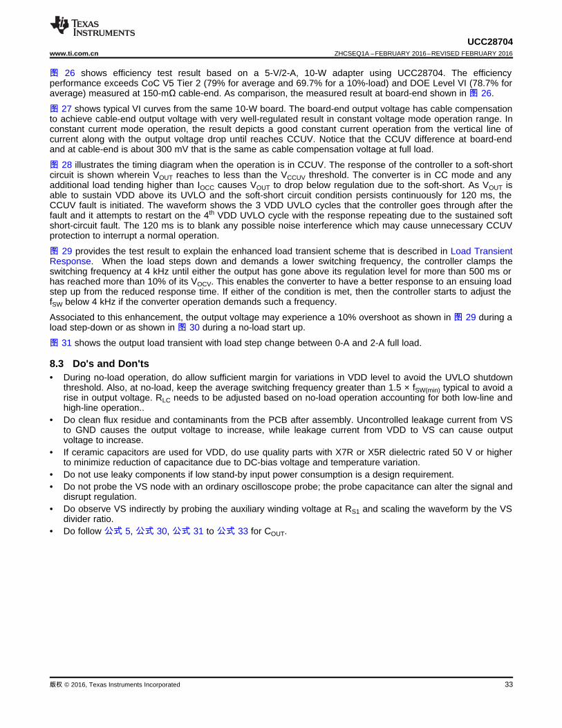
33
UCC28704www.ti.com.cn ZHCSEQ1A –FEBRUARY 2016–REVISED FEBRUARY 2016
版权 © 2016, Texas Instruments Incorporated
图 26 shows efficiency test result based on a 5-V/2-A, 10-W adapter using UCC28704. The efficiencyperformance exceeds CoC V5 Tier 2 (79% for average and 69.7% for a 10%-load) and DOE Level VI (78.7% foraverage) measured at 150-mΩ cable-end. As comparison, the measured result at board-end shown in 图 26.
图 27 shows typical VI curves from the same 10-W board. The board-end output voltage has cable compensationto achieve cable-end output voltage with very well-regulated result in constant voltage mode operation range. Inconstant current mode operation, the result depicts a good constant current operation from the vertical line ofcurrent along with the output voltage drop until reaches CCUV. Notice that the CCUV difference at board-endand at cable-end is about 300 mV that is the same as cable compensation voltage at full load.
图 28 illustrates the timing diagram when the operation is in CCUV. The response of the controller to a soft-shortcircuit is shown wherein VOUT reaches to less than the VCCUV threshold. The converter is in CC mode and anyadditional load tending higher than IOCC causes VOUT to drop below regulation due to the soft-short. As VOUT isable to sustain VDD above its UVLO and the soft-short circuit condition persists continuously for 120 ms, theCCUV fault is initiated. The waveform shows the 3 VDD UVLO cycles that the controller goes through after thefault and it attempts to restart on the 4th VDD UVLO cycle with the response repeating due to the sustained softshort-circuit fault. The 120 ms is to blank any possible noise interference which may cause unnecessary CCUVprotection to interrupt a normal operation.
图 29 provides the test result to explain the enhanced load transient scheme that is described in Load TransientResponse. When the load steps down and demands a lower switching frequency, the controller clamps theswitching frequency at 4 kHz until either the output has gone above its regulation level for more than 500 ms orhas reached more than 10% of its VOCV. This enables the converter to have a better response to an ensuing loadstep up from the reduced response time. If either of the condition is met, then the controller starts to adjust thefSW below 4 kHz if the converter operation demands such a frequency.
Associated to this enhancement, the output voltage may experience a 10% overshoot as shown in 图 29 during aload step-down or as shown in 图 30 during a no-load start up.
图 31 shows the output load transient with load step change between 0-A and 2-A full load.
8.3 Do's and Don'ts• During no-load operation, do allow sufficient margin for variations in VDD level to avoid the UVLO shutdown
threshold. Also, at no-load, keep the average switching frequency greater than 1.5 × fSW(min) typical to avoid arise in output voltage. RLC needs to be adjusted based on no-load operation accounting for both low-line andhigh-line operation..
• Do clean flux residue and contaminants from the PCB after assembly. Uncontrolled leakage current from VSto GND causes the output voltage to increase, while leakage current from VDD to VS can cause outputvoltage to increase.
• If ceramic capacitors are used for VDD, do use quality parts with X7R or X5R dielectric rated 50 V or higherto minimize reduction of capacitance due to DC-bias voltage and temperature variation.
• Do not use leaky components if low stand-by input power consumption is a design requirement.• Do not probe the VS node with an ordinary oscilloscope probe; the probe capacitance can alter the signal and
disrupt regulation.• Do observe VS indirectly by probing the auxiliary winding voltage at RS1 and scaling the waveform by the VS
divider ratio.• Do follow 公式 5, 公式 30, 公式 31 to 公式 33 for COUT.
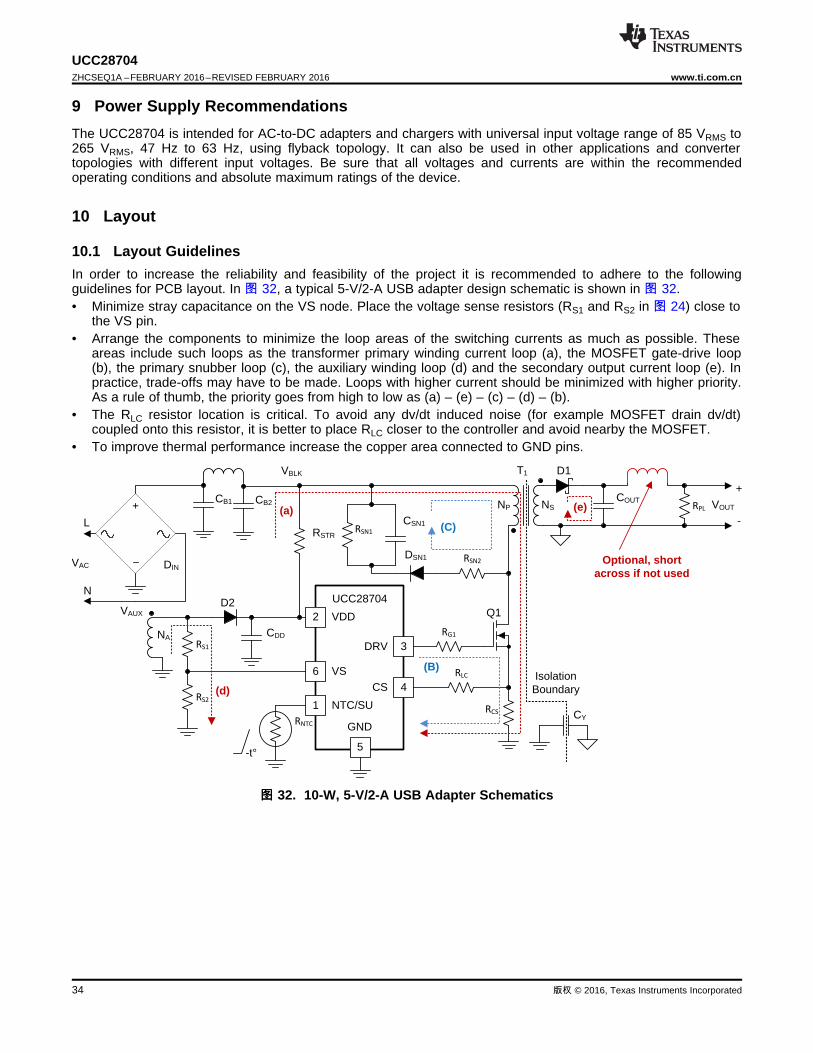
2CDD
RSTR
6
1
3
4
5
GND
NTC/SU
VS
VDD
DRV
CSRS2
RS1
RNTC
RLC
RCS
CB1+COUT
RPL
D2Q1
D1
VAUX
NA
VAC
VOUT
Optional, short across if not used
VBLK
UCC28704
-t°
CB2 NP NS
T1
RSN2
RSN1
CSN1
DSN1
RG1
CY
+
-L
N
DIN
Isolation Boundary
(e)(a)(C)
(B)
(d)
34
UCC28704ZHCSEQ1A –FEBRUARY 2016–REVISED FEBRUARY 2016 www.ti.com.cn
版权 © 2016, Texas Instruments Incorporated
9 Power Supply RecommendationsThe UCC28704 is intended for AC-to-DC adapters and chargers with universal input voltage range of 85 VRMS to265 VRMS, 47 Hz to 63 Hz, using flyback topology. It can also be used in other applications and convertertopologies with different input voltages. Be sure that all voltages and currents are within the recommendedoperating conditions and absolute maximum ratings of the device.
10 Layout
10.1 Layout GuidelinesIn order to increase the reliability and feasibility of the project it is recommended to adhere to the followingguidelines for PCB layout. In 图 32, a typical 5-V/2-A USB adapter design schematic is shown in 图 32.• Minimize stray capacitance on the VS node. Place the voltage sense resistors (RS1 and RS2 in 图 24) close to
the VS pin.• Arrange the components to minimize the loop areas of the switching currents as much as possible. These
areas include such loops as the transformer primary winding current loop (a), the MOSFET gate-drive loop(b), the primary snubber loop (c), the auxiliary winding loop (d) and the secondary output current loop (e). Inpractice, trade-offs may have to be made. Loops with higher current should be minimized with higher priority.As a rule of thumb, the priority goes from high to low as (a) – (e) – (c) – (d) – (b).
• The RLC resistor location is critical. To avoid any dv/dt induced noise (for example MOSFET drain dv/dt)coupled onto this resistor, it is better to place RLC closer to the controller and avoid nearby the MOSFET.
• To improve thermal performance increase the copper area connected to GND pins.
图图 32. 10-W, 5-V/2-A USB Adapter Schematics
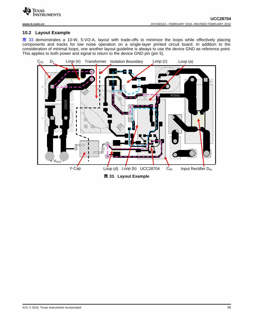
Y-Cap
CO1
CB2
Loop (a)
Loop (b)Loop (d)
Loop (c)Loop (e)
+ VOUT -
TransformerD1
Input Rectifier DINUCC28704
Isolation Boundary
35
UCC28704www.ti.com.cn ZHCSEQ1A –FEBRUARY 2016–REVISED FEBRUARY 2016
版权 © 2016, Texas Instruments Incorporated
10.2 Layout Example图 33 demonstrates a 10-W, 5-V/2-A, layout with trade-offs to minimize the loops while effectively placingcomponents and tracks for low noise operation on a single-layer printed circuit board. In addition to theconsideration of minimal loops, one another layout guideline is always to use the device GND as reference point.This applies to both power and signal to return to the device GND pin (pin 5).
图图 33. Layout Example
36
UCC28704ZHCSEQ1A –FEBRUARY 2016–REVISED FEBRUARY 2016 www.ti.com.cn
版权 © 2016, Texas Instruments Incorporated
11 器器件件和和文文档档支支持持
11.1 器器件件支支持持
11.1.1 器器件件命命名名规规则则
11.1.1.1 电电容容术术语语((以以法法拉拉为为单单位位))
CBULK CB1 和 CB2 的总输入电容。
CDD VDD 引脚所需的最小电容。
COUT 所需的最小输出电容。
11.1.1.2 占占空空比比术术语语
DMAGCC CC 中二次侧二极管导通占空比,0.475。
DMAX 最大 MOSFET 导通时间占空比。
11.1.1.3 频频率率术术语语((以以赫赫兹兹为为单单位位))
fLINE 最低线路频率。
fMAX 转换器的最高目标满载开关频率。
fMIN 转换器的最低开关频率,在器件 fSW(min)限值基础上增加 15% 的裕度。
fSW(lim) 负载减小后的瞬态开关频率
FSW(min) 最低开关频率(见Electrical Characteristics表)
fSW(max) 最大开关频率(见Electrical Characteristics表)
fSW(standby) 轻负载条件下负载变化之前的开关频率
11.1.1.4 电电流流术术语语((以以安安培培为为单单位位))
IOCC 转换器输出恒流目标。
IOR 转换器额定输出电流。
IPP(max) 变压器一次侧最大电流。
ISTART 启动偏置电源电流(见Electrical Characteristics表)。
ITRAN 所需的正负载阶跃电流。
IVSL(run) VS 引脚运行电流(见Electrical Characteristics表)。
IWAIT 等待状态期间的 VDD 偏置电流。(见Electrical Characteristics表)。
11.1.1.5 电电流流和和电电压压调调节节术术语语
KAM 一次侧峰峰值电流比(见Electrical Characteristics表)。
KCo 稳定性因子为 100,用于计算 COUT。
KLC 电流调节常量(见Electrical Characteristics表)。
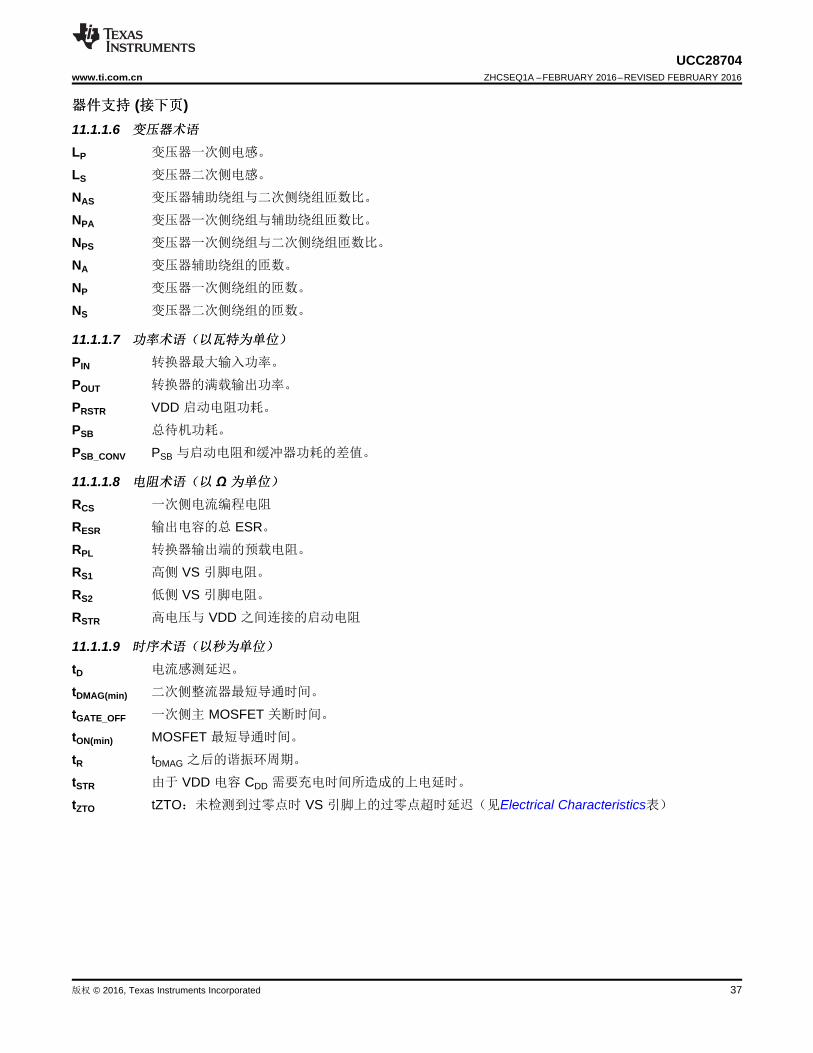
37
UCC28704www.ti.com.cn ZHCSEQ1A –FEBRUARY 2016–REVISED FEBRUARY 2016
版权 © 2016, Texas Instruments Incorporated
器器件件支支持持 (接接下下页页)11.1.1.6 变变压压器器术术语语
LP 变压器一次侧电感。
LS 变压器二次侧电感。
NAS 变压器辅助绕组与二次侧绕组匝数比。
NPA 变压器一次侧绕组与辅助绕组匝数比。
NPS 变压器一次侧绕组与二次侧绕组匝数比。
NA 变压器辅助绕组的匝数。
NP 变压器一次侧绕组的匝数。
NS 变压器二次侧绕组的匝数。
11.1.1.7 功功率率术术语语((以以瓦瓦特特为为单单位位))
PIN 转换器最大输入功率。
POUT 转换器的满载输出功率。
PRSTR VDD 启动电阻功耗。
PSB 总待机功耗。
PSB_CONV PSB 与启动电阻和缓冲器功耗的差值。
11.1.1.8 电电阻阻术术语语((以以 Ω 为为单单位位))
RCS 一次侧电流编程电阻
RESR 输出电容的总 ESR。
RPL 转换器输出端的预载电阻。
RS1 高侧 VS 引脚电阻。
RS2 低侧 VS 引脚电阻。
RSTR 高电压与 VDD 之间连接的启动电阻
11.1.1.9 时时序序术术语语((以以秒秒为为单单位位))
tD 电流感测延迟。
tDMAG(min) 二次侧整流器最短导通时间。
tGATE_OFF 一次侧主 MOSFET 关断时间。
tON(min) MOSFET 最短导通时间。
tR tDMAG 之后的谐振环周期。
tSTR 由于 VDD 电容 CDD 需要充电时间所造成的上电延时。
tZTO tZTO:未检测到过零点时 VS 引脚上的过零点超时延迟(见Electrical Characteristics表)
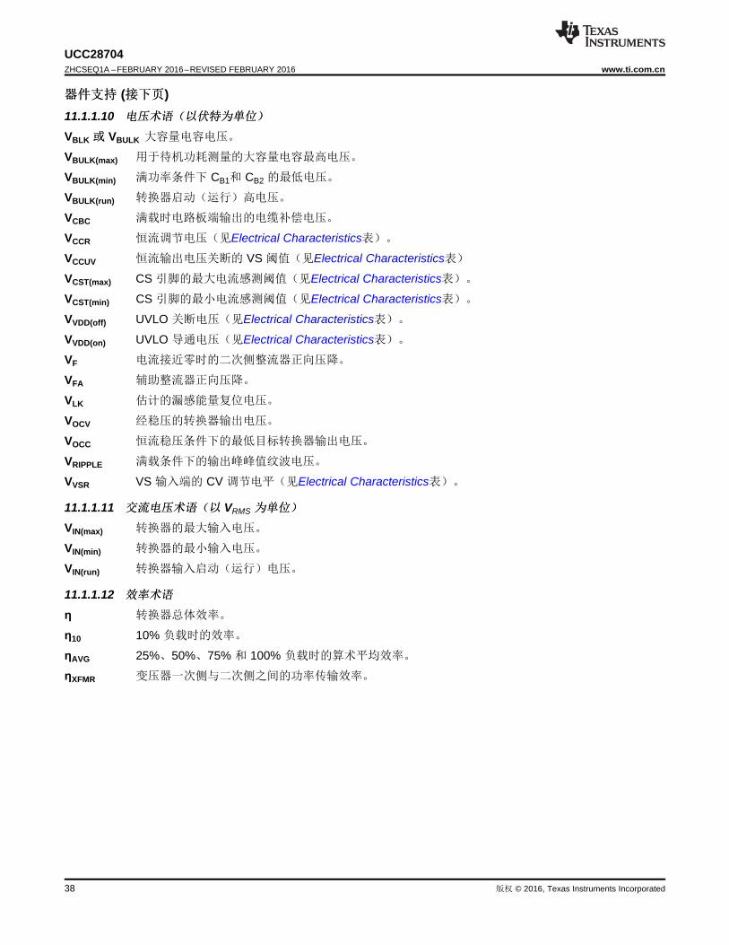
38
UCC28704ZHCSEQ1A –FEBRUARY 2016–REVISED FEBRUARY 2016 www.ti.com.cn
版权 © 2016, Texas Instruments Incorporated
器器件件支支持持 (接接下下页页)11.1.1.10 电电压压术术语语((以以伏伏特特为为单单位位))
VBLK 或或 VBULK 大容量电容电压。
VBULK(max) 用于待机功耗测量的大容量电容最高电压。
VBULK(min) 满功率条件下 CB1和 CB2 的最低电压。
VBULK(run) 转换器启动(运行)高电压。
VCBC 满载时电路板端输出的电缆补偿电压。
VCCR 恒流调节电压(见Electrical Characteristics表)。
VCCUV 恒流输出电压关断的 VS 阈值(见Electrical Characteristics表)
VCST(max) CS 引脚的最大电流感测阈值(见Electrical Characteristics表)。
VCST(min) CS 引脚的最小电流感测阈值(见Electrical Characteristics表)。
VVDD(off) UVLO 关断电压(见Electrical Characteristics表)。
VVDD(on) UVLO 导通电压(见Electrical Characteristics表)。
VF 电流接近零时的二次侧整流器正向压降。
VFA 辅助整流器正向压降。
VLK 估计的漏感能量复位电压。
VOCV 经稳压的转换器输出电压。
VOCC 恒流稳压条件下的最低目标转换器输出电压。
VRIPPLE 满载条件下的输出峰峰值纹波电压。
VVSR VS 输入端的 CV 调节电平(见Electrical Characteristics表)。
11.1.1.11 交交流流电电压压术术语语((以以 VRMS 为为单单位位))
VIN(max) 转换器的最大输入电压。
VIN(min) 转换器的最小输入电压。
VIN(run) 转换器输入启动(运行)电压。
11.1.1.12 效效率率术术语语
η 转换器总体效率。
η10 10% 负载时的效率。
ηAVG 25%、50%、75% 和 100% 负载时的算术平均效率。
ηXFMR 变压器一次侧与二次侧之间的功率传输效率。

39
UCC28704www.ti.com.cn ZHCSEQ1A –FEBRUARY 2016–REVISED FEBRUARY 2016
版权 © 2016, Texas Instruments Incorporated
11.2 文文档档支支持持
11.2.1 相相关关文文档档
相关文档如下:
《使用 UCC28704-1EVM-724,评估模块》,SLUUBF1
11.3 社社区区资资源源
The following links connect to TI community resources. Linked contents are provided "AS IS" by the respectivecontributors. They do not constitute TI specifications and do not necessarily reflect TI's views; see TI's Terms ofUse.
TI E2E™ Online Community TI's Engineer-to-Engineer (E2E) Community. Created to foster collaborationamong engineers. At e2e.ti.com, you can ask questions, share knowledge, explore ideas and helpsolve problems with fellow engineers.
Design Support TI's Design Support Quickly find helpful E2E forums along with design support tools andcontact information for technical support.
11.4 商商标标
E2E is a trademark of Texas Instruments.
11.5 静静电电放放电电警警告告
这些装置包含有限的内置 ESD 保护。 存储或装卸时,应将导线一起截短或将装置放置于导电泡棉中,以防止 MOS 门极遭受静电损伤。
11.6 GlossarySLYZ022 — TI Glossary.
This glossary lists and explains terms, acronyms, and definitions.
12 机机械械、、封封装装和和可可订订购购信信息息
以下页中包括机械、封装和可订购信息。这些信息是针对指定器件可提供的最新数据。这些数据会在无通知且不对本文档进行修订的情况下发生改变。欲获得该数据表的浏览器版本,请查阅左侧的导航栏。
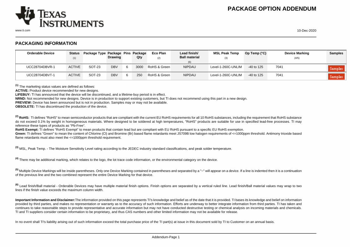
PACKAGE OPTION ADDENDUM
www.ti.com 10-Dec-2020
Addendum-Page 1
PACKAGING INFORMATION
Orderable Device Status(1)
Package Type PackageDrawing
Pins PackageQty
Eco Plan(2)
Lead finish/Ball material
(6)
MSL Peak Temp(3)
Op Temp (°C) Device Marking(4/5)
Samples
UCC28704DBVR-1 ACTIVE SOT-23 DBV 6 3000 RoHS & Green NIPDAU Level-1-260C-UNLIM -40 to 125 7041
UCC28704DBVT-1 ACTIVE SOT-23 DBV 6 250 RoHS & Green NIPDAU Level-1-260C-UNLIM -40 to 125 7041
(1) The marketing status values are defined as follows:ACTIVE: Product device recommended for new designs.LIFEBUY: TI has announced that the device will be discontinued, and a lifetime-buy period is in effect.NRND: Not recommended for new designs. Device is in production to support existing customers, but TI does not recommend using this part in a new design.PREVIEW: Device has been announced but is not in production. Samples may or may not be available.OBSOLETE: TI has discontinued the production of the device.
(2) RoHS: TI defines "RoHS" to mean semiconductor products that are compliant with the current EU RoHS requirements for all 10 RoHS substances, including the requirement that RoHS substancedo not exceed 0.1% by weight in homogeneous materials. Where designed to be soldered at high temperatures, "RoHS" products are suitable for use in specified lead-free processes. TI mayreference these types of products as "Pb-Free".RoHS Exempt: TI defines "RoHS Exempt" to mean products that contain lead but are compliant with EU RoHS pursuant to a specific EU RoHS exemption.Green: TI defines "Green" to mean the content of Chlorine (Cl) and Bromine (Br) based flame retardants meet JS709B low halogen requirements of <=1000ppm threshold. Antimony trioxide basedflame retardants must also meet the <=1000ppm threshold requirement.
(3) MSL, Peak Temp. - The Moisture Sensitivity Level rating according to the JEDEC industry standard classifications, and peak solder temperature.
(4) There may be additional marking, which relates to the logo, the lot trace code information, or the environmental category on the device.
(5) Multiple Device Markings will be inside parentheses. Only one Device Marking contained in parentheses and separated by a "~" will appear on a device. If a line is indented then it is a continuationof the previous line and the two combined represent the entire Device Marking for that device.
(6) Lead finish/Ball material - Orderable Devices may have multiple material finish options. Finish options are separated by a vertical ruled line. Lead finish/Ball material values may wrap to twolines if the finish value exceeds the maximum column width.
Important Information and Disclaimer:The information provided on this page represents TI's knowledge and belief as of the date that it is provided. TI bases its knowledge and belief on informationprovided by third parties, and makes no representation or warranty as to the accuracy of such information. Efforts are underway to better integrate information from third parties. TI has taken andcontinues to take reasonable steps to provide representative and accurate information but may not have conducted destructive testing or chemical analysis on incoming materials and chemicals.TI and TI suppliers consider certain information to be proprietary, and thus CAS numbers and other limited information may not be available for release.
In no event shall TI's liability arising out of such information exceed the total purchase price of the TI part(s) at issue in this document sold by TI to Customer on an annual basis.
PACKAGE OPTION ADDENDUM
www.ti.com 10-Dec-2020
Addendum-Page 2
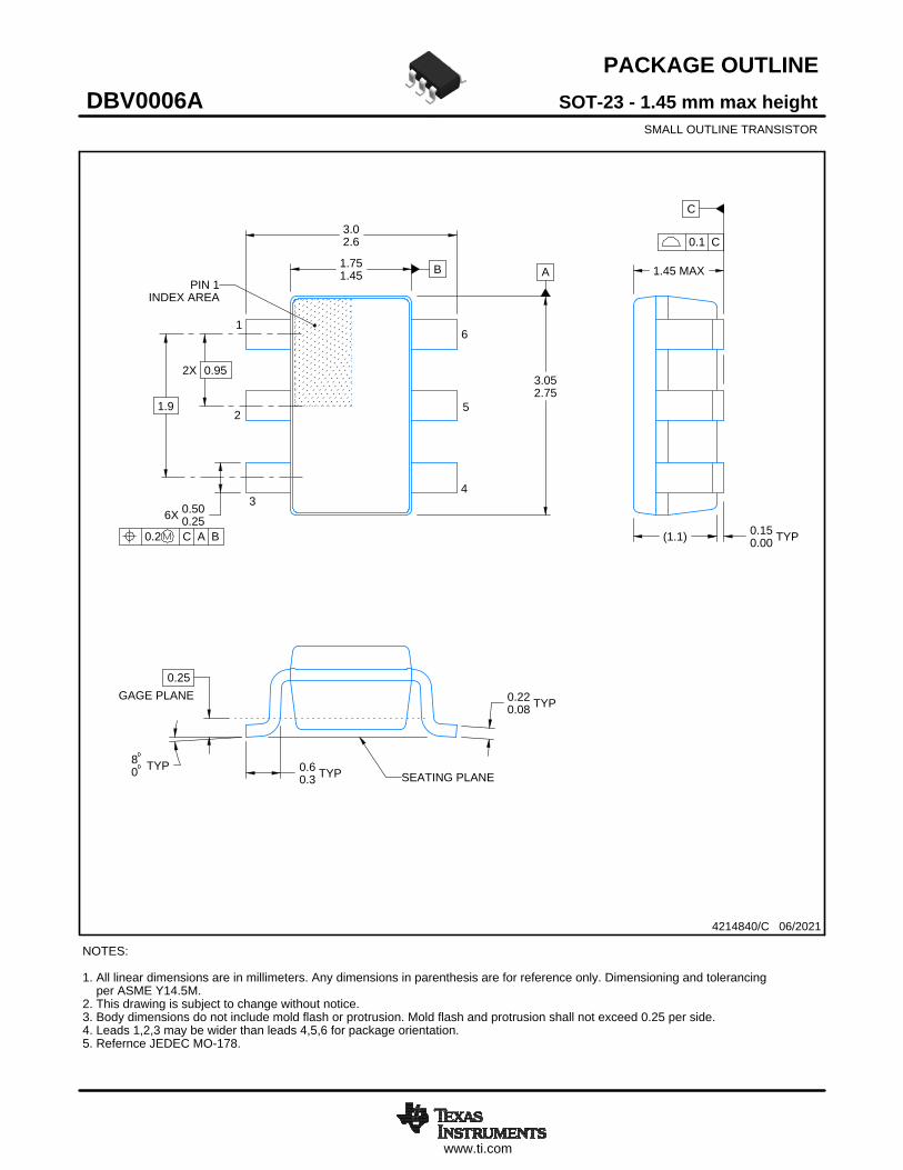
www.ti.com
PACKAGE OUTLINE
C
0.220.08 TYP
0.25
3.02.6
2X 0.95
1.45 MAX
0.150.00 TYP
6X 0.500.25
0.60.3 TYP
80 TYP
1.9
A
3.052.75
B1.751.45
(1.1)
SOT-23 - 1.45 mm max heightDBV0006ASMALL OUTLINE TRANSISTOR
4214840/C 06/2021
NOTES: 1. All linear dimensions are in millimeters. Any dimensions in parenthesis are for reference only. Dimensioning and tolerancing per ASME Y14.5M.2. This drawing is subject to change without notice.3. Body dimensions do not include mold flash or protrusion. Mold flash and protrusion shall not exceed 0.25 per side.4. Leads 1,2,3 may be wider than leads 4,5,6 for package orientation.5. Refernce JEDEC MO-178.
0.2 C A B
1
34
52
INDEX AREAPIN 1
6
GAGE PLANE
SEATING PLANE
0.1 C
SCALE 4.000
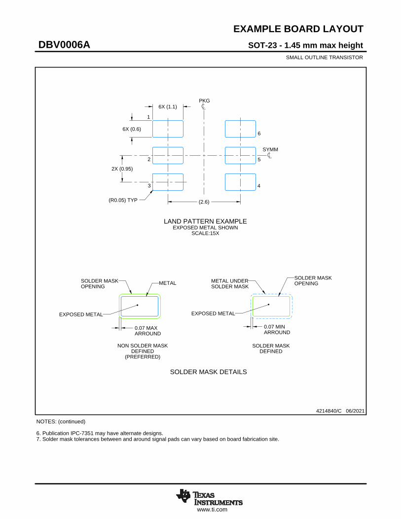
www.ti.com
EXAMPLE BOARD LAYOUT
0.07 MAXARROUND
0.07 MINARROUND
6X (1.1)
6X (0.6)
(2.6)
2X (0.95)
(R0.05) TYP
4214840/C 06/2021
SOT-23 - 1.45 mm max heightDBV0006ASMALL OUTLINE TRANSISTOR
NOTES: (continued) 6. Publication IPC-7351 may have alternate designs. 7. Solder mask tolerances between and around signal pads can vary based on board fabrication site.
SYMM
LAND PATTERN EXAMPLEEXPOSED METAL SHOWN
SCALE:15X
PKG
1
3 4
52
6
SOLDER MASKOPENINGMETAL UNDER
SOLDER MASK
SOLDER MASKDEFINED
EXPOSED METAL
METALSOLDER MASKOPENING
NON SOLDER MASKDEFINED
(PREFERRED)
SOLDER MASK DETAILS
EXPOSED METAL
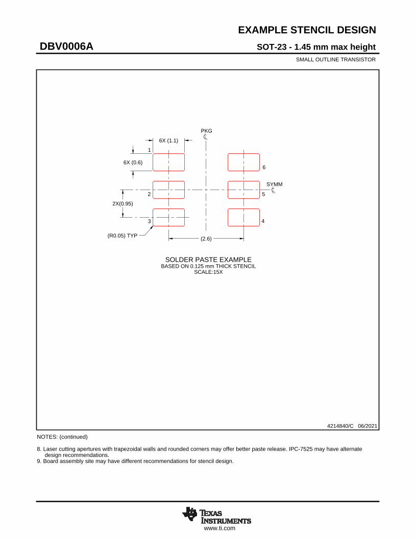
www.ti.com
EXAMPLE STENCIL DESIGN
(2.6)
2X(0.95)
6X (1.1)
6X (0.6)
(R0.05) TYP
SOT-23 - 1.45 mm max heightDBV0006ASMALL OUTLINE TRANSISTOR
4214840/C 06/2021
NOTES: (continued) 8. Laser cutting apertures with trapezoidal walls and rounded corners may offer better paste release. IPC-7525 may have alternate design recommendations. 9. Board assembly site may have different recommendations for stencil design.
SOLDER PASTE EXAMPLEBASED ON 0.125 mm THICK STENCIL
SCALE:15X
SYMM
PKG
1
3 4
52
6
重要声明和免责声明TI 提供技术和可靠性数据(包括数据表)、设计资源(包括参考设计)、应用或其他设计建议、网络工具、安全信息和其他资源,不保证没有瑕疵且不做出任何明示或暗示的担保,包括但不限于对适销性、某特定用途方面的适用性或不侵犯任何第三方知识产权的暗示担保。这些资源可供使用 TI 产品进行设计的熟练开发人员使用。您将自行承担以下全部责任:(1) 针对您的应用选择合适的 TI 产品,(2) 设计、验证并测试您的应用,(3) 确保您的应用满足相应标准以及任何其他安全、安保或其他要求。这些资源如有变更,恕不另行通知。TI 授权您仅可将这些资源用于研发本资源所述的 TI 产品的应用。严禁对这些资源进行其他复制或展示。您无权使用任何其他 TI 知识产权或任何第三方知识产权。您应全额赔偿因在这些资源的使用中对 TI 及其代表造成的任何索赔、损害、成本、损失和债务,TI 对此概不负责。TI 提供的产品受 TI 的销售条款 (https:www.ti.com.cn/zh-cn/legal/termsofsale.html) 或 ti.com.cn 上其他适用条款/TI 产品随附的其他适用条款的约束。TI 提供这些资源并不会扩展或以其他方式更改 TI 针对 TI 产品发布的适用的担保或担保免责声明。IMPORTANT NOTICE
邮寄地址:上海市浦东新区世纪大道 1568 号中建大厦 32 楼,邮政编码:200122Copyright © 2021 德州仪器半导体技术(上海)有限公司


![反覆緊張局勢的後果研究 [A Study on the Consequences of Repeated Tensions]](https://static.fdokumen.com/doc/165x107/631ec3d256cbbb475005b7ff/-a-study-on-the-consequences-of-repeated-tensions.jpg)