Jobsheet Praktikum 1 - Teknik Elektro – UM
166
Transcript of Jobsheet Praktikum 1 - Teknik Elektro – UM

1
Lab Teknik Digital
Jobsheet Praktikum
REGISTER
A. Tujuan Kegiatan Praktikum 1-4 :
Setelah mempraktekkan Topik ini, anda diharapkan dapat :
1. Mengetahui fungsi dan prinsip kerja register.
2. Menerapkan register SISO, PISO, SIPO dan PIPO dalam rangkaian
elektronika digital.
3. Mengetahui operasi dan aplikasi ring shift counter dan Johnson shift
counter.
4. Mengetahui konsep three-state (logika 3-keadaan) pada komponen
elektronika digital.
B. Dasar Teori Kegiatan Praktikum 1-4
Register merupakan komponen elektronika digital yang berfungsi untuk
menyimpan secara sementara sekumpulan bit. Bit data yang dioperasikan dalam
sistem digital kadang-kadang perlu disimpan, dipindahkan, atau digeser ke kiri atau
ke kanan satu posisi atau lebih. Register geser dapat menangani perpindahan bit
data paralel dan serial, serta dapat digunakan untuk mengonversi dari paralel ke
serial dan serial ke paralel.
Ada 4 macam register geser, yaitu:
1. Serial-In, Serial-Out (SISO)
2. Serial-In, Parallel-Out (SIPO)
3. Parallel-In, Serial-Out (PISO)
4. Parallel-In Parallel-Out (PIPO)
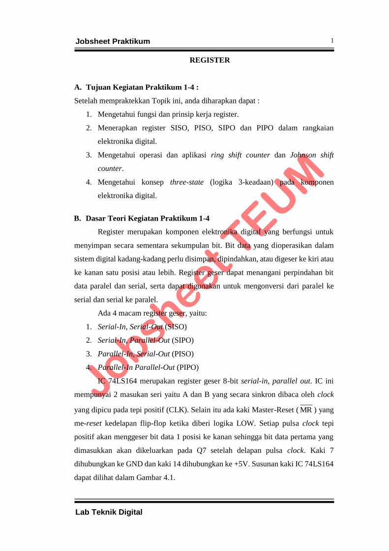
IC 74LS164 merupakan register geser 8-bit serial-in, parallel out. IC ini
mempunyai 2 masukan seri yaitu A dan B yang secara sinkron dibaca oleh clock
yang dipicu pada tepi positif (CLK). Selain itu ada kaki Master-Reset ( MR ) yang
me-reset kedelapan flip-flop ketika diberi logika LOW. Setiap pulsa clock tepi
positif akan menggeser bit data 1 posisi ke kanan sehingga bit data pertama yang
dimasukkan akan dikeluarkan pada Q7 setelah delapan pulsa clock. Kaki 7
dihubungkan ke GND dan kaki 14 dihubungkan ke +5V. Susunan kaki IC 74LS164
dapat dilihat dalam Gambar 4.1.
2
Lab Teknik Digital
Jobsheet Praktikum
Gambar 1.1 Susunan Kaki IC 74LS164
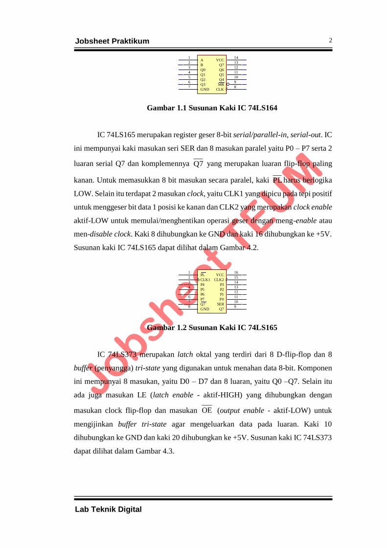
IC 74LS165 merupakan register geser 8-bit serial/parallel-in, serial-out. IC
ini mempunyai kaki masukan seri SER dan 8 masukan paralel yaitu P0 – P7 serta 2
luaran serial Q7 dan komplemennya Q7 yang merupakan luaran flip-flop paling
kanan. Untuk memasukkan 8 bit masukan secara paralel, kaki PL harus berlogika
LOW. Selain itu terdapat 2 masukan clock, yaitu CLK1 yang dipicu pada tepi positif
untuk menggeser bit data 1 posisi ke kanan dan CLK2 yang merupakan clock enable
aktif-LOW untuk memulai/menghentikan operasi geser dengan meng-enable atau
men-disable clock. Kaki 8 dihubungkan ke GND dan kaki 16 dihubungkan ke +5V.
Susunan kaki IC 74LS165 dapat dilihat dalam Gambar 4.2.
Gambar 1.2 Susunan Kaki IC 74LS165
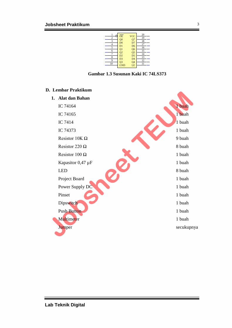
IC 74LS373 merupakan latch oktal yang terdiri dari 8 D-flip-flop dan 8
buffer (penyangga) tri-state yang digunakan untuk menahan data 8-bit. Komponen
ini mempunyai 8 masukan, yaitu D0 – D7 dan 8 luaran, yaitu Q0 –Q7. Selain itu
ada juga masukan LE (latch enable - aktif-HIGH) yang dihubungkan dengan
masukan clock flip-flop dan masukan OE (output enable - aktif-LOW) untuk
mengijinkan buffer tri-state agar mengeluarkan data pada luaran. Kaki 10
dihubungkan ke GND dan kaki 20 dihubungkan ke +5V. Susunan kaki IC 74LS373
dapat dilihat dalam Gambar 4.3.
A1
B2
Q03
Q14
Q25
Q36
Q410
Q511
Q612
Q713
CLK8
MR9
VCC14
GND7
74LS164
SER10
P011
P112
P213
P314
P43
P54
P65
P76
CLK12
CLK215
PL1
Q79
Q77
VCC16
GND8
74LS165
3
Lab Teknik Digital
Jobsheet Praktikum
Gambar 1.3 Susunan Kaki IC 74LS373
D. Lembar Praktikum
1. Alat dan Bahan
IC 74164 1 buah
IC 74165 1 buah
IC 7414 1 buah
IC 74373 1 buah
Resistor 10K Ω 9 buah
Resistor 220 Ω 8 buah
Resistor 100 Ω 1 buah
Kapasitor 0,47 µF 1 buah
LED 8 buah
Project Board 1 buah
Power Supply DC 1 buah
Pinset 1 buah
Dipswitch 1 buah
Push Button 1 buah
Multimeter 1 buah
Jumper secukupnya
D03
Q02
D14
Q15
D27
Q26
D38
Q39
D413
Q412
D514
Q515
D617
Q616
D718
Q719
OE1
LE11
VCC20
GND10
PIN74373
4
Lab Teknik Digital
Jobsheet Praktikum
2. Kesehatan dan Keselamatan kerja
(a) Periksalah kelengkapan alat dan bahan sebelum digunakan.
(b) Pelajari dan pahami petunjuk praktikum pada lembar kegiatan
praktikum.
(c) Pastikan tegangan keluaran catu daya sesuai yang dibutuhkan.
(d) Sebelum catu daya dihidupkan hubungi dosen pendamping untuk
mengecek kebenaran rangkaian.
(e) Yakinkan tempat anda aman dari sengatan listrik.
(f) Hati-hati dalam penggunaan peralatan praktikum !
5
Lab Teknik Digital
Jobsheet Praktikum
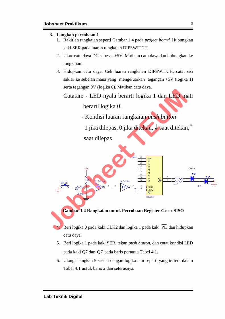
3. Langkah percobaan 1
1. Rakitlah rangkaian seperti Gambar 1.4 pada project board. Hubungkan
kaki SER pada luaran rangkaian DIPSWITCH.
2. Ukur catu daya DC sebesar +5V. Matikan catu daya dan hubungkan ke
rangkaian.
3. Hidupkan catu daya. Cek luaran rangkaian DIPSWITCH, catat sisi
saklar ke sebelah mana yang mengeluarkan tegangan +5V (logika 1)
serta tegangan 0V (logika 0). Matikan catu daya.
Catatan: - LED nyala berarti logika 1 dan LED mati
berarti logika 0.
- Kondisi luaran rangkaian push button:
1 jika dilepas, 0 jika ditekan, saat ditekan,
saat dilepas
Gambar 1.4 Rangkaian untuk Percobaan Register Geser SISO
4. Beri logika 0 pada kaki CLK2 dan logika 1 pada kaki PL dan hidupkan
catu daya.
5. Beri logika 1 pada kaki SER, tekan push button, dan catat kondisi LED
pada kaki Q7 dan Q7 pada baris pertama Tabel 4.1.
6. Ulangi langkah 5 sesuai dengan logika lain seperti yang tertera dalam
Tabel 4.1 untuk baris 2 dan seterusnya.
SER10
P011
P112
P213
P314
P43
P54
P65
P76
CLK12
CLK215
PL1
Q79
Q77
74LS165
3 4
B 74LS14
1 2
A 74LS1410k
100
0,47uF
SW-PB
+5V
1
0
Input
220LED
Output
6
Lab Teknik Digital
Jobsheet Praktikum
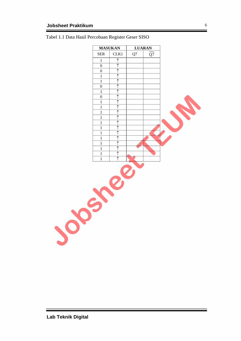
Tabel 1.1 Data Hasil Percobaan Register Geser SISO
MASUKAN LUARAN
SER CLK1 Q7 Q7
1
0
0
1
1
0
1
0
1
1
1
1
1
1
1
1
1
1
1
1
7
Lab Teknik Digital
Jobsheet Praktikum
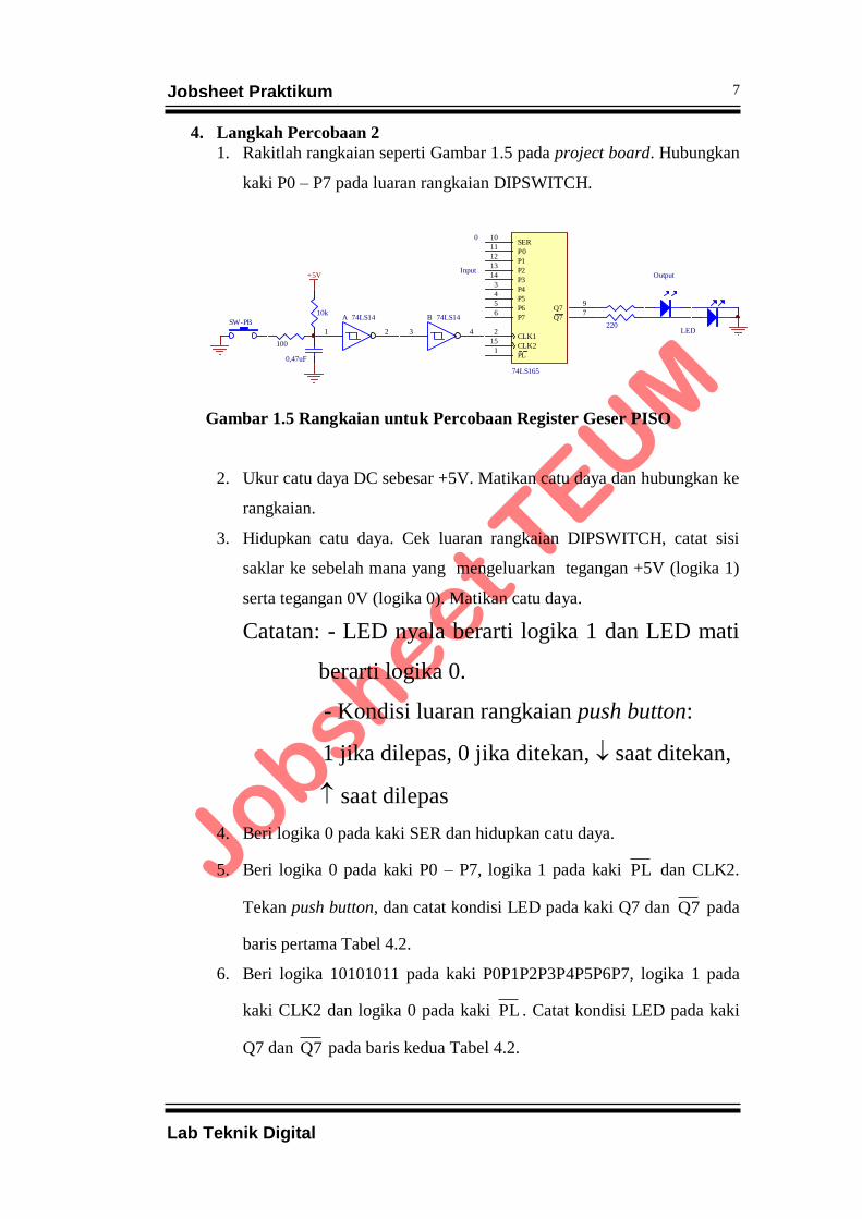
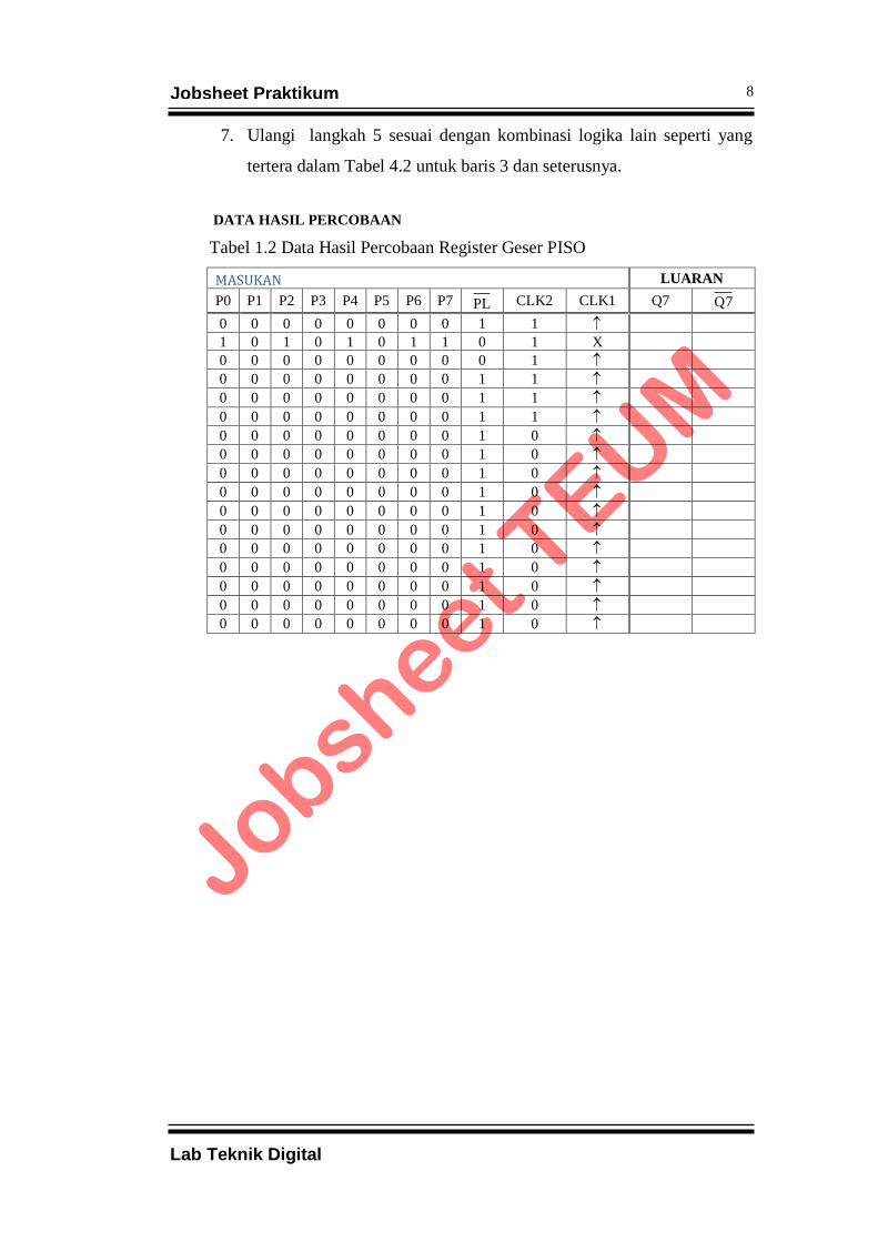
4. Langkah Percobaan 2
1. Rakitlah rangkaian seperti Gambar 1.5 pada project board. Hubungkan
kaki P0 – P7 pada luaran rangkaian DIPSWITCH.
Gambar 1.5 Rangkaian untuk Percobaan Register Geser PISO
2. Ukur catu daya DC sebesar +5V. Matikan catu daya dan hubungkan ke
rangkaian.
3. Hidupkan catu daya. Cek luaran rangkaian DIPSWITCH, catat sisi
saklar ke sebelah mana yang mengeluarkan tegangan +5V (logika 1)
serta tegangan 0V (logika 0). Matikan catu daya.
Catatan: - LED nyala berarti logika 1 dan LED mati
berarti logika 0.
- Kondisi luaran rangkaian push button:
1 jika dilepas, 0 jika ditekan, saat ditekan,
saat dilepas
4. Beri logika 0 pada kaki SER dan hidupkan catu daya.
5. Beri logika 0 pada kaki P0 – P7, logika 1 pada kaki PL dan CLK2.
Tekan push button, dan catat kondisi LED pada kaki Q7 dan Q7 pada
baris pertama Tabel 4.2.
6. Beri logika 10101011 pada kaki P0P1P2P3P4P5P6P7, logika 1 pada
kaki CLK2 dan logika 0 pada kaki PL . Catat kondisi LED pada kaki
Q7 dan Q7 pada baris kedua Tabel 4.2.
220LED
SER10
P011
P112
P213
P314
P43
P54
P65
P76
CLK12
CLK215
PL1
Q79
Q77
74LS165
3 4
B 74LS14
1 2
A 74LS1410k
100
0,47uF
SW-PB
+5V
0
InputOutput
8
Lab Teknik Digital
Jobsheet Praktikum
7. Ulangi langkah 5 sesuai dengan kombinasi logika lain seperti yang
tertera dalam Tabel 4.2 untuk baris 3 dan seterusnya.
DATA HASIL PERCOBAAN
Tabel 1.2 Data Hasil Percobaan Register Geser PISO
MASUKAN LUARAN
P0 P1 P2 P3 P4 P5 P6 P7 PL CLK2 CLK1 Q7 Q7
0 0 0 0 0 0 0 0 1 1
1 0 1 0 1 0 1 1 0 1 X
0 0 0 0 0 0 0 0 0 1
0 0 0 0 0 0 0 0 1 1
0 0 0 0 0 0 0 0 1 1
0 0 0 0 0 0 0 0 1 1
0 0 0 0 0 0 0 0 1 0
0 0 0 0 0 0 0 0 1 0
0 0 0 0 0 0 0 0 1 0
0 0 0 0 0 0 0 0 1 0
0 0 0 0 0 0 0 0 1 0
0 0 0 0 0 0 0 0 1 0
0 0 0 0 0 0 0 0 1 0
0 0 0 0 0 0 0 0 1 0
0 0 0 0 0 0 0 0 1 0
0 0 0 0 0 0 0 0 1 0
0 0 0 0 0 0 0 0 1 0
9
Lab Teknik Digital
Jobsheet Praktikum
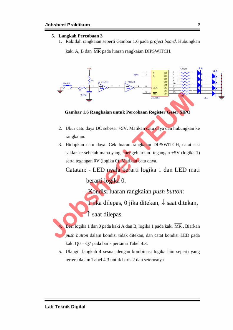
5. Langkah Percobaan 3
1. Rakitlah rangkaian seperti Gambar 1.6 pada project board. Hubungkan
kaki A, B dan MR pada luaran rangkaian DIPSWITCH.
Gambar 1.6 Rangkaian untuk Percobaan Register Geser SIPO
2. Ukur catu daya DC sebesar +5V. Matikan catu daya dan hubungkan ke
rangkaian.
3. Hidupkan catu daya. Cek luaran rangkaian DIPSWITCH, catat sisi
saklar ke sebelah mana yang mengeluarkan tegangan +5V (logika 1)
serta tegangan 0V (logika 0). Matikan catu daya.
Catatan: - LED nyala berarti logika 1 dan LED mati
berarti logika 0.
- Kondisi luaran rangkaian push button:
1 jika dilepas, 0 jika ditekan, saat ditekan,
saat dilepas
4. Beri logika 1 dan 0 pada kaki A dan B, logika 1 pada kaki MR . Biarkan
push button dalam kondisi tidak ditekan, dan catat kondisi LED pada
kaki Q0 – Q7 pada baris pertama Tabel 4.3.
5. Ulangi langkah 4 sesuai dengan kombinasi logika lain seperti yang
tertera dalam Tabel 4.3 untuk baris 2 dan seterusnya.
A1
B2
Q03
Q14
Q25
Q36
Q410
Q511
Q612
Q713
CLK8
MR9
74LS164
Input
3 4
B 74LS14
1 2
A 74LS1410k
100
0,47uF
SW-PB
+5V
220LED
Output
10
Lab Teknik Digital
Jobsheet Praktikum
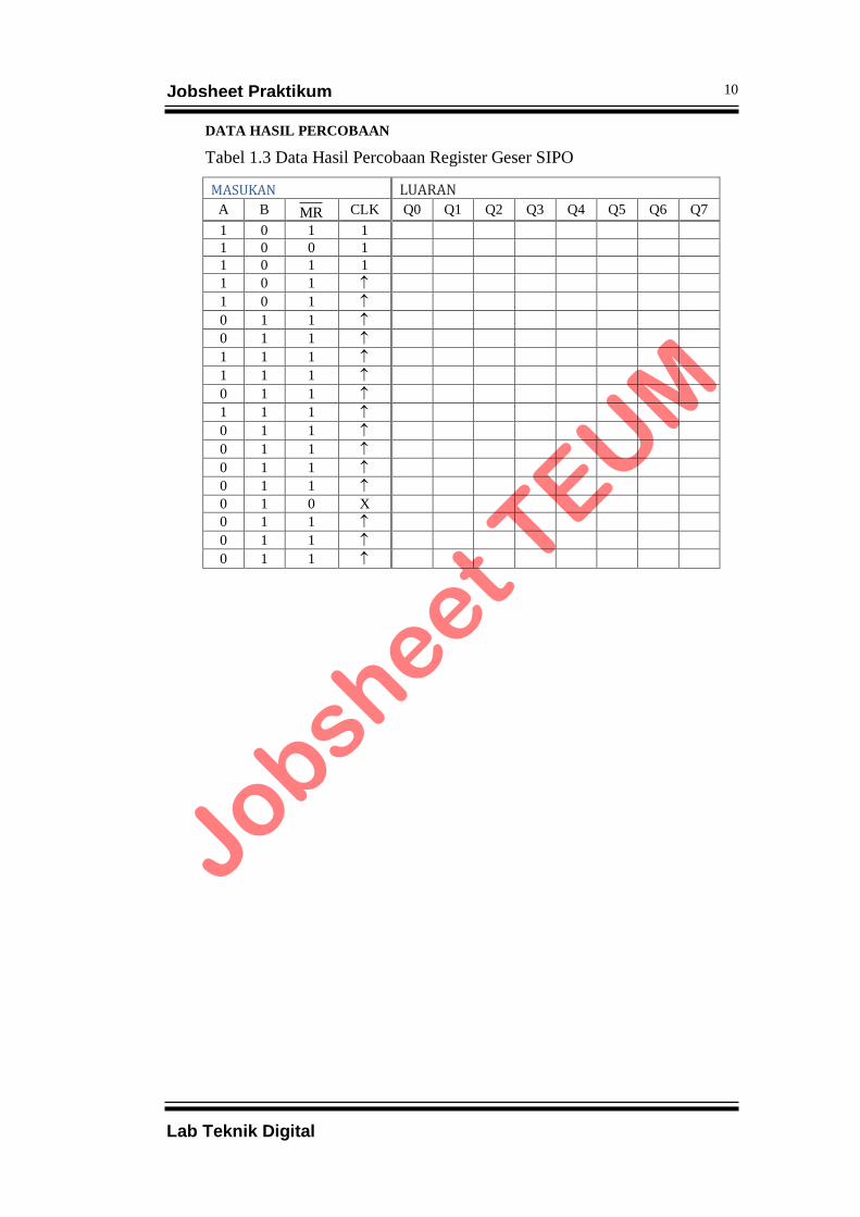
DATA HASIL PERCOBAAN
Tabel 1.3 Data Hasil Percobaan Register Geser SIPO
MASUKAN LUARAN
A B MR CLK Q0 Q1 Q2 Q3 Q4 Q5 Q6 Q7
1 0 1 1
1 0 0 1
1 0 1 1
1 0 1
1 0 1
0 1 1
0 1 1
1 1 1
1 1 1
0 1 1
1 1 1
0 1 1
0 1 1
0 1 1
0 1 1
0 1 0 X
0 1 1
0 1 1
0 1 1
11
Lab Teknik Digital
Jobsheet Praktikum
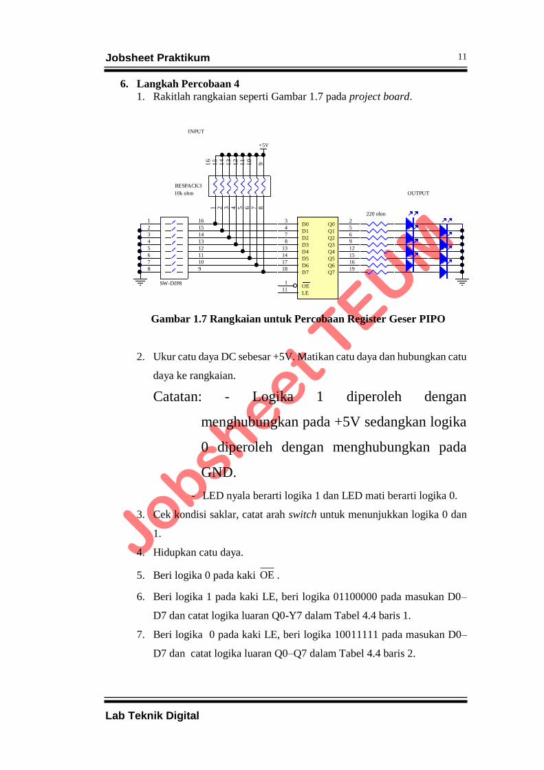
6. Langkah Percobaan 4
1. Rakitlah rangkaian seperti Gambar 1.7 pada project board.
Gambar 1.7 Rangkaian untuk Percobaan Register Geser PIPO
2. Ukur catu daya DC sebesar +5V. Matikan catu daya dan hubungkan catu
daya ke rangkaian.
Catatan: - Logika 1 diperoleh dengan
menghubungkan pada +5V sedangkan logika
0 diperoleh dengan menghubungkan pada
GND.
- LED nyala berarti logika 1 dan LED mati berarti logika 0.
3. Cek kondisi saklar, catat arah switch untuk menunjukkan logika 0 dan
1.
4. Hidupkan catu daya.
5. Beri logika 0 pada kaki OE .
6. Beri logika 1 pada kaki LE, beri logika 01100000 pada masukan D0–
D7 dan catat logika luaran Q0-Y7 dalam Tabel 4.4 baris 1.
7. Beri logika 0 pada kaki LE, beri logika 10011111 pada masukan D0–
D7 dan catat logika luaran Q0–Q7 dalam Tabel 4.4 baris 2.
1
2
3
4
5
6
7
8
16
15
14
13
12
11
10
9
SW-DIP8
1 2 3 4 5 6 7 8
16
15
14
13
12
11
10
9
RESPACK3
D03
Q02
D14
Q15
D27
Q26
D38
Q39
D413
Q412
D514
Q515
D617
Q616
D718
Q719
OE1
LE11
74LS373
+5V
220 ohm
INPUT
OUTPUT10k ohm
12
Lab Teknik Digital
Jobsheet Praktikum
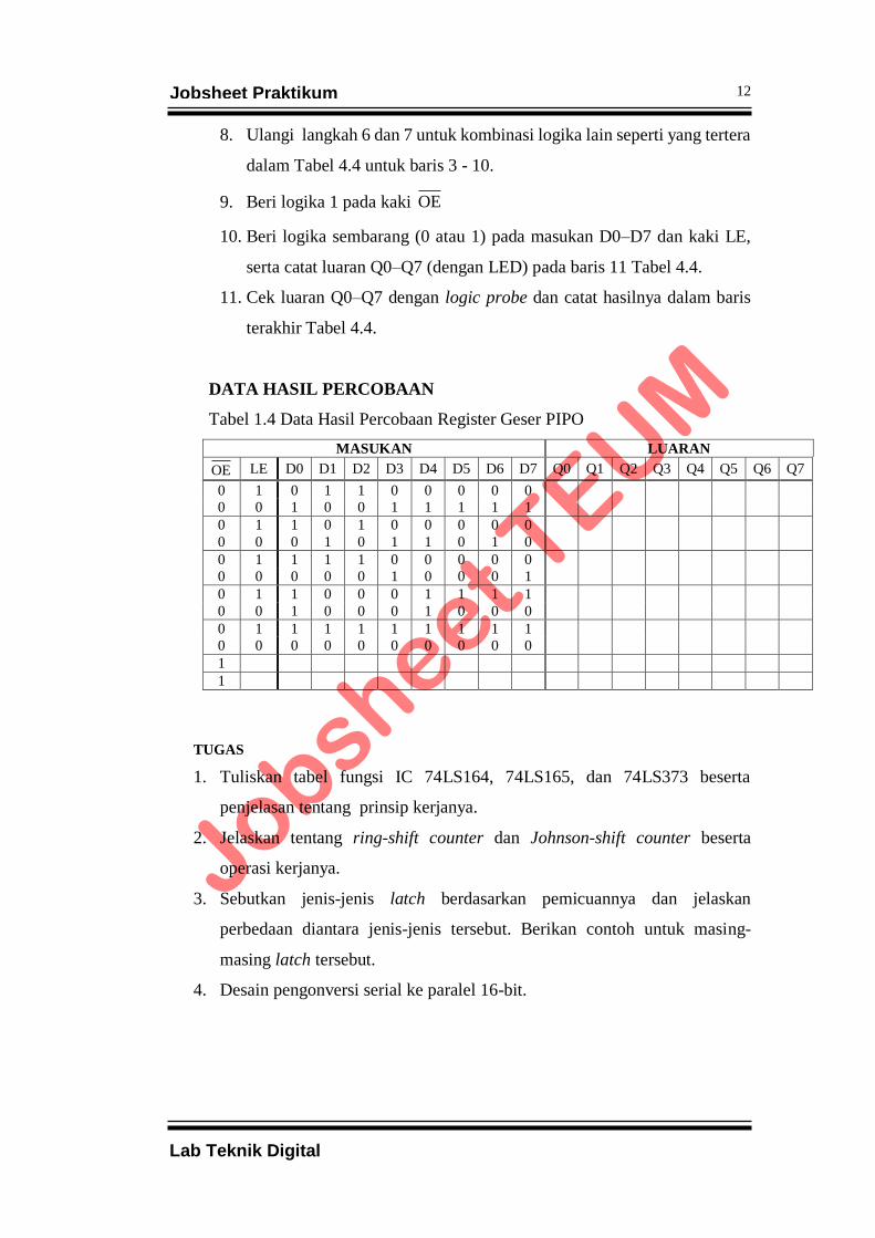
8. Ulangi langkah 6 dan 7 untuk kombinasi logika lain seperti yang tertera
dalam Tabel 4.4 untuk baris 3 - 10.
9. Beri logika 1 pada kaki OE
10. Beri logika sembarang (0 atau 1) pada masukan D0–D7 dan kaki LE,
serta catat luaran Q0–Q7 (dengan LED) pada baris 11 Tabel 4.4.
11. Cek luaran Q0–Q7 dengan logic probe dan catat hasilnya dalam baris
terakhir Tabel 4.4.
DATA HASIL PERCOBAAN
Tabel 1.4 Data Hasil Percobaan Register Geser PIPO
MASUKAN LUARAN
OE LE D0 D1 D2 D3 D4 D5 D6 D7 Q0 Q1 Q2 Q3 Q4 Q5 Q6 Q7
0 1 0 1 1 0 0 0 0 0
0 0 1 0 0 1 1 1 1 1
0 1 1 0 1 0 0 0 0 0
0 0 0 1 0 1 1 0 1 0
0 1 1 1 1 0 0 0 0 0
0 0 0 0 0 1 0 0 0 1
0 1 1 0 0 0 1 1 1 1
0 0 1 0 0 0 1 0 0 0
0 1 1 1 1 1 1 1 1 1
0 0 0 0 0 0 0 0 0 0
1
1
TUGAS
1. Tuliskan tabel fungsi IC 74LS164, 74LS165, dan 74LS373 beserta
penjelasan tentang prinsip kerjanya.
2. Jelaskan tentang ring-shift counter dan Johnson-shift counter beserta
operasi kerjanya.
3. Sebutkan jenis-jenis latch berdasarkan pemicuannya dan jelaskan
perbedaan diantara jenis-jenis tersebut. Berikan contoh untuk masing-
masing latch tersebut.
4. Desain pengonversi serial ke paralel 16-bit.

13
Lab Teknik Digital
Jobsheet Praktikum
Analisa
_______________________________________________________________________________
_______________________________________________________________________________
_______________________________________________________________________________
_______________________________________________________________________________
_______________________________________________________________________________
_______________________________________________________________________________
_______________________________________________________________________________
_______________________________________________________________________________
_______________________________________________________________________________
_______________________________________________________________________________
_______________________________________________________________________________
_______________________________________________________________________________
_______________________________________________________________________________
_______________________________________________________________________________
_______________________________________________________________________________
_______________________________________________________________________________
_______________________________________________________________________________
_______________________________________________________________________________
_______________________________________________________________________________
_______________________________________________________________________________
_______________________________________________________________________________
_______________________________________________________________________________
_______________________________________________________________________________
_______________________________________________________________________________
_______________________________________________________________________________
_______________________________________________________________________________
_______________________________________________________________________________
_______________________________________________________________________________
_______________________________________________________________________________
_______________________________________________________________________________
_______________________________________________________________________________
_______________________________________________________________________________
_______________________________________________________________________________
_______________________________________________________________________________
_______________________________________________________________________________
_______________________________________________________________________________
_______________________________________________________________________________
_______________________________________________________________________________

14
Lab Teknik Digital
Jobsheet Praktikum
Kesimpulan
_______________________________________________________________________________
_______________________________________________________________________________
_______________________________________________________________________________
_______________________________________________________________________________
_______________________________________________________________________________
_______________________________________________________________________________
_______________________________________________________________________________
_______________________________________________________________________________
_______________________________________________________________________________
_______________________________________________________________________________
_______________________________________________________________________________
_______________________________________________________________________________
_______________________________________________________________________________
_______________________________________________________________________________
_______________________________________________________________________________
_______________________________________________________________________________
_______________________________________________________________________________
_______________________________________________________________________________
_______________________________________________________________________________
_______________________________________________________________________________
_______________________________________________________________________________
_______________________________________________________________________________
_______________________________________________________________________________
_______________________________________________________________________________
_______________________________________________________________________________
_______________________________________________________________________________
_______________________________________________________________________________
_______________________________________________________________________________
_______________________________________________________________________________
_______________________________________________________________________________
_______________________________________________________________________________
_______________________________________________________________________________
_______________________________________________________________________________
_______________________________________________________________________________
_______________________________________________________________________________
_______________________________________________________________________________
_______________________________________________________________________________
_______________________________________________________________________________

1
Lab Teknik Digital
Jobsheet Praktikum
ADC-DAC
A. Tujuan Kegiatan Praktikum 5-6 :
Setelah mempraktekkan Topik ini, anda diharapkan dapat :
1. Mengetahui prinsip kerja ADC dan DAC.
2. Mengetahui toleransi kesalahan ADC dan ketelitian DAC.
3. Memahami spesifikasi ADC dan DAC yang diberikan oleh data book.
4. Mengaplikasikan ADC dan DAC dalam rangkaian elektronika digital.
B. Dasar Teori Kegiatan Praktikum 5-6
Analog-to-Digital Converter (ADC) merupakan peranti yang mengubah
besaran kontinyu (suhu, tekanan, intensitas cahaya, dan lain-lain) menjadi besaran
diskrit (digital). ADC0808 adalah peranti CMOS monolitik dengan konverter
analog-ke-digital 8-bit, multiplekser 8-kanal dan logika kontrol yang kompatibel
dengan mikroprosesor. ADC ini mempunyai toleransi kesalahan ½ LSB serta
dapat mengonversi dalam waktu 100 s dengan luaran yang ditahan oleh buffer
tri-state.
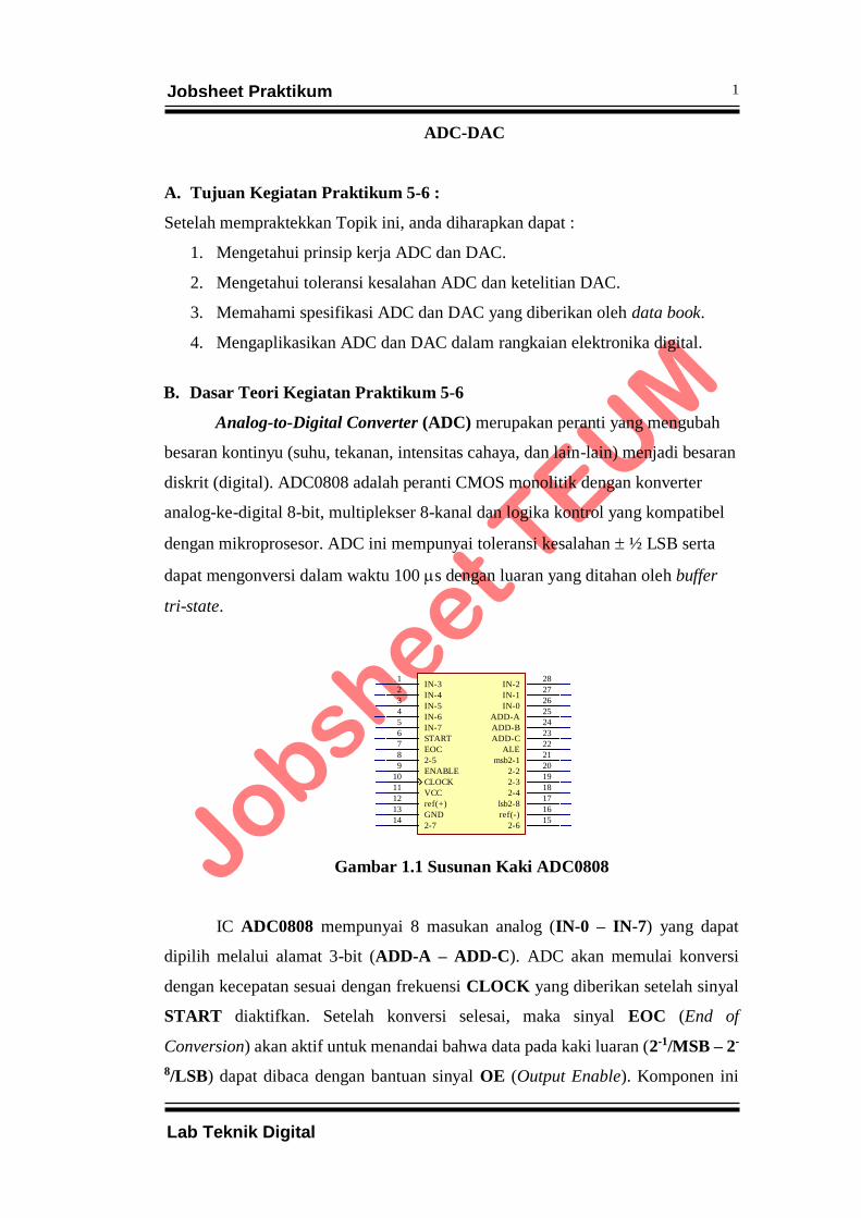
Gambar 1.1 Susunan Kaki ADC0808
IC ADC0808 mempunyai 8 masukan analog (IN-0 – IN-7) yang dapat
dipilih melalui alamat 3-bit (ADD-A – ADD-C). ADC akan memulai konversi
dengan kecepatan sesuai dengan frekuensi CLOCK yang diberikan setelah sinyal
START diaktifkan. Setelah konversi selesai, maka sinyal EOC (End of
Conversion) akan aktif untuk menandai bahwa data pada kaki luaran (2-1/MSB – 2-
8/LSB) dapat dibaca dengan bantuan sinyal OE (Output Enable). Komponen ini
GND13
VCC11
IN-026
msb2-121
2-220
IN-127
2-319
2-418
IN-228
2-58
2-615
IN-31
2-714
lsb2-817
IN-42
EOC7
IN-53
ADD-A25
IN-64
ADD-B24
ADD-C23
IN-75
ALE22
ref(-)16
ENABLE9
START6
ref(+)12
CLOCK10
ADC0808
2
Lab Teknik Digital
Jobsheet Praktikum
mempunyai 2 kaki untuk tegangan referensi yaitu ref(+) dan ref(-). Sedangkan kaki
13 dihubungkan ke GND dan kaki 11 dihubungkan ke VCC. Susunan kaki IC
ADC0808 dapat dilihat dalam Gambar 5.1.
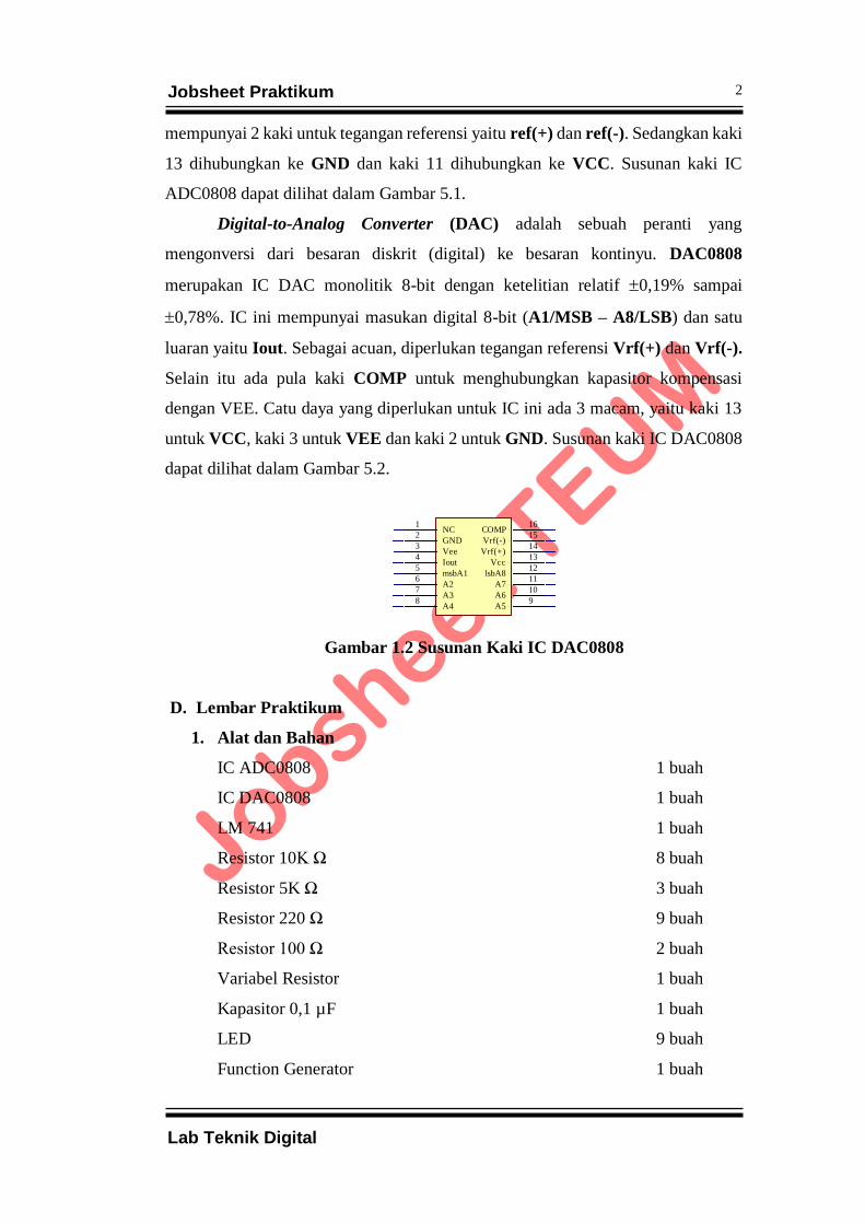
Digital-to-Analog Converter (DAC) adalah sebuah peranti yang
mengonversi dari besaran diskrit (digital) ke besaran kontinyu. DAC0808
merupakan IC DAC monolitik 8-bit dengan ketelitian relatif 0,19% sampai
0,78%. IC ini mempunyai masukan digital 8-bit (A1/MSB – A8/LSB) dan satu
luaran yaitu Iout. Sebagai acuan, diperlukan tegangan referensi Vrf(+) dan Vrf(-).
Selain itu ada pula kaki COMP untuk menghubungkan kapasitor kompensasi
dengan VEE. Catu daya yang diperlukan untuk IC ini ada 3 macam, yaitu kaki 13
untuk VCC, kaki 3 untuk VEE dan kaki 2 untuk GND. Susunan kaki IC DAC0808
dapat dilihat dalam Gambar 5.2.
Gambar 1.2 Susunan Kaki IC DAC0808
D. Lembar Praktikum
1. Alat dan Bahan
IC ADC0808 1 buah
IC DAC0808 1 buah
LM 741 1 buah
Resistor 10K Ω 8 buah
Resistor 5K Ω 3 buah
Resistor 220 Ω 9 buah
Resistor 100 Ω 2 buah
Variabel Resistor 1 buah
Kapasitor 0,1 µF 1 buah
LED 9 buah
Function Generator 1 buah
GND2
Vcc13
Iout4
msbA15
Vrf(-)15
A26
A37
Vrf(+)14
A48
A59
A610
COMP16
A711
lsbA812
Vee3
NC1
DAC0808
3
Lab Teknik Digital
Jobsheet Praktikum
Multimeter Digital 1 buah
Power Supply DC ±15VDC (simetris) 1 buah
Power Supply DC (non simetris) 1 buah
Project Board 1 buah
Push Button 2 buah
Dipswitch 1 buah
Pinset 1 buah
Jumper secukupnya
2. Kesehatan dan Keselamatan kerja
(a) Periksalah kelengkapan alat dan bahan sebelum digunakan.
(b) Pelajari dan pahami petunjuk praktikum pada lembar kegiatan
praktikum.
(c) Pastikan tegangan keluaran catu daya sesuai yang dibutuhkan.
(d) Sebelum catu daya dihidupkan hubungi dosen pendamping untuk
mengecek kebenaran rangkaian.
(e) Yakinkan tempat anda aman dari sengatan listrik.
(f) Hati-hati dalam penggunaan peralatan praktikum !
4
Lab Teknik Digital
Jobsheet Praktikum
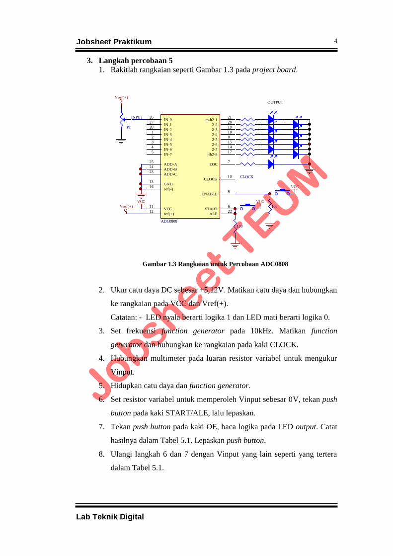
3. Langkah percobaan 5
1. Rakitlah rangkaian seperti Gambar 1.3 pada project board.
Gambar 1.3 Rangkaian untuk Percobaan ADC0808
2. Ukur catu daya DC sebesar +5,12V. Matikan catu daya dan hubungkan
ke rangkaian pada VCC dan Vref(+).
Catatan: - LED nyala berarti logika 1 dan LED mati berarti logika 0.
3. Set frekuensi function generator pada 10kHz. Matikan function
generator dan hubungkan ke rangkaian pada kaki CLOCK.
4. Hubungkan multimeter pada luaran resistor variabel untuk mengukur
Vinput.
5. Hidupkan catu daya dan function generator.
6. Set resistor variabel untuk memperoleh Vinput sebesar 0V, tekan push
button pada kaki START/ALE, lalu lepaskan.
7. Tekan push button pada kaki OE, baca logika pada LED output. Catat
hasilnya dalam Tabel 5.1. Lepaskan push button.
8. Ulangi langkah 6 dan 7 dengan Vinput yang lain seperti yang tertera
dalam Tabel 5.1.
GND13
VCC11
IN-026
msb2-121
2-220
IN-127
2-319
2-418
IN-228
2-58
2-615
IN-31
2-714
lsb2-817
IN-42
EOC7
IN-53
ADD-A25
IN-64
ADD-B24
ADD-C23
IN-75
ALE22
ref(-)16
ENABLE9
START6
ref(+)12
CLOCK10
ADC0808
INPUT
VCC
OUTPUT
CLOCK
100
100
VCC
VCC
P1
Vref(+)
Vref(+)
5
Lab Teknik Digital
Jobsheet Praktikum
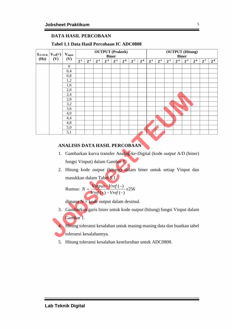
DATA HASIL PERCOBAAN
Tabel 1.1 Data Hasil Percobaan IC ADC0808
fCLOCK
(Hz)
Vref(+)
(V)
Vinput
(V)
OUTPUT (Praktek)
Biner
OUTPUT (Hitung)
Biner
2-1 2-2 2-3 2-4 2-5 2-6 2-7 2-8 2-1 2-2 2-3 2-4 2-5 2-6 2-7 2-8
0
0,4
0,8
1,2
1,6
2,0
2,4
2,8
3,2
3,6
4,0
4,4
4,8
5,0
5,1
ANALISIS DATA HASIL PERCOBAAN
1. Gambarkan kurva transfer Analog-ke-Digital (kode output A/D (biner)
fungsi Vinput) dalam Gambar 1.
2. Hitung kode output (hitung) dalam biner untuk setiap Vinput dan
masukkan dalam Tabel 5.1.
Rumus: 256)()(
)(x
VrefVref
VrefVinputN
dimana N = kode output dalam desimal.
3. Gambarkan garis linier untuk kode output (hitung) fungsi Vinput dalam
Gambar 1.
4. Hitung toleransi kesalahan untuk masing-masing data dan buatkan tabel
toleransi kesalahannya.
5. Hitung toleransi kesalahan keseluruhan untuk ADC0808.
6
Lab Teknik Digital
Jobsheet Praktikum
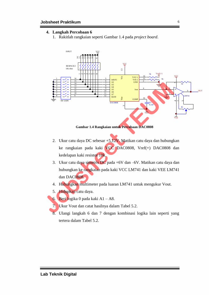
4. Langkah Percobaan 6
1. Rakitlah rangkaian seperti Gambar 1.4 pada project board.
Gambar 1.4 Rangkaian untuk Percobaan DAC0808
2. Ukur catu daya DC sebesar +5,12V. Matikan catu daya dan hubungkan
ke rangkaian pada kaki VCC DAC0808, Vref(+) DAC0808 dan
kedelapan kaki resistor 10k.
3. Ukur catu daya simetris DC pada +6V dan –6V. Matikan catu daya dan
hubungkan ke rangkaian pada kaki VCC LM741 dan kaki VEE LM741
dan DAC0808.
4. Hubungkan multimeter pada luaran LM741 untuk mengukur Vout.
5. Hidupkan catu daya.
6. Beri logika 0 pada kaki A1 – A8.
7. Ukur Vout dan catat hasilnya dalam Tabel 5.2.
8. Ulangi langkah 6 dan 7 dengan kombinasi logika lain seperti yang
tertera dalam Tabel 5.2.
GND2
Vcc
13
Iout4
msbA15
Vrf(-)15
A26
A37
Vrf(+)14
A48
A59
A610
COMP16
A711
lsbA812
Vee
3
DAC0808
VCC
5k
5k
C10,1uF
VEE
Vref(+)
VCC
5k
P2
VEE
OUT
1
2
3
4
5
6
7
8
16
15
14
13
12
11
10
9
SW-DIP8
1 2 3 4 5 6 7 8
16
15
14
13
12
11
10
9
RESPACK3
VCCINPUT
10k ohm
3
2
6
1 5
74
LM741
7
Lab Teknik Digital
Jobsheet Praktikum
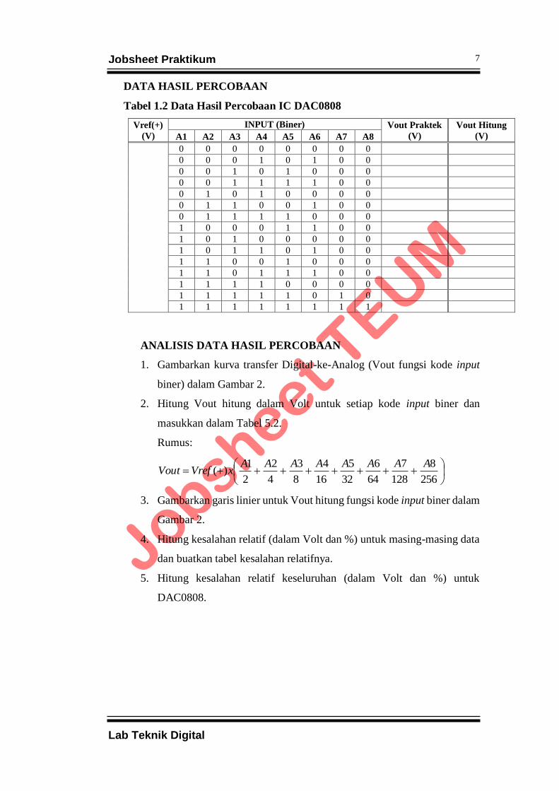
DATA HASIL PERCOBAAN
Tabel 1.2 Data Hasil Percobaan IC DAC0808
Vref(+)
(V)
INPUT (Biner) Vout Praktek
(V)
Vout Hitung
(V) A1 A2 A3 A4 A5 A6 A7 A8
0 0 0 0 0 0 0 0
0 0 0 1 0 1 0 0
0 0 1 0 1 0 0 0
0 0 1 1 1 1 0 0
0 1 0 1 0 0 0 0
0 1 1 0 0 1 0 0
0 1 1 1 1 0 0 0
1 0 0 0 1 1 0 0
1 0 1 0 0 0 0 0
1 0 1 1 0 1 0 0
1 1 0 0 1 0 0 0
1 1 0 1 1 1 0 0
1 1 1 1 0 0 0 0
1 1 1 1 1 0 1 0
1 1 1 1 1 1 1 1
ANALISIS DATA HASIL PERCOBAAN
1. Gambarkan kurva transfer Digital-ke-Analog (Vout fungsi kode input
biner) dalam Gambar 2.
2. Hitung Vout hitung dalam Volt untuk setiap kode input biner dan
masukkan dalam Tabel 5.2.
Rumus:
256
8
128
7
64
6
32
5
16
4
8
3
4
2
2
1)(
AAAAAAAAxVrefVout
3. Gambarkan garis linier untuk Vout hitung fungsi kode input biner dalam
Gambar 2.
4. Hitung kesalahan relatif (dalam Volt dan %) untuk masing-masing data
dan buatkan tabel kesalahan relatifnya.
5. Hitung kesalahan relatif keseluruhan (dalam Volt dan %) untuk
DAC0808.

8
Lab Teknik Digital
Jobsheet Praktikum
TUGAS
1. Rancang rangkaian pengubah analog ke digital dengan IC ADC0804
dan berikan penjelasannya
2. Apakah fungsi op-amp dalam rangkaian DAC?
3. Jika Iref (arus referensi) diganti menjadi 1,5 mA, apa pengaruhnya
terhadap Iout dan Vout?

9
Lab Teknik Digital
Jobsheet Praktikum
Analisa
_______________________________________________________________________________
_______________________________________________________________________________
_______________________________________________________________________________
_______________________________________________________________________________
_______________________________________________________________________________
_______________________________________________________________________________
_______________________________________________________________________________
_______________________________________________________________________________
_______________________________________________________________________________
_______________________________________________________________________________
_______________________________________________________________________________
_______________________________________________________________________________
_______________________________________________________________________________
_______________________________________________________________________________
_______________________________________________________________________________
_______________________________________________________________________________
_______________________________________________________________________________
_______________________________________________________________________________
_______________________________________________________________________________
_______________________________________________________________________________
_______________________________________________________________________________
_______________________________________________________________________________
_______________________________________________________________________________
_______________________________________________________________________________
_______________________________________________________________________________
_______________________________________________________________________________
_______________________________________________________________________________
_______________________________________________________________________________
_______________________________________________________________________________
_______________________________________________________________________________
_______________________________________________________________________________
_______________________________________________________________________________
_______________________________________________________________________________
_______________________________________________________________________________
_______________________________________________________________________________
_______________________________________________________________________________
_______________________________________________________________________________
_______________________________________________________________________________

10
Lab Teknik Digital
Jobsheet Praktikum
Kesimpulan
_______________________________________________________________________________
_______________________________________________________________________________
_______________________________________________________________________________
_______________________________________________________________________________
_______________________________________________________________________________
_______________________________________________________________________________
_______________________________________________________________________________
_______________________________________________________________________________
_______________________________________________________________________________
_______________________________________________________________________________
_______________________________________________________________________________
_______________________________________________________________________________
_______________________________________________________________________________
_______________________________________________________________________________
_______________________________________________________________________________
_______________________________________________________________________________
_______________________________________________________________________________
_______________________________________________________________________________
_______________________________________________________________________________
_______________________________________________________________________________
_______________________________________________________________________________
_______________________________________________________________________________
_______________________________________________________________________________
_______________________________________________________________________________
_______________________________________________________________________________
_______________________________________________________________________________
_______________________________________________________________________________
_______________________________________________________________________________
_______________________________________________________________________________
_______________________________________________________________________________
_______________________________________________________________________________
_______________________________________________________________________________
_______________________________________________________________________________
_______________________________________________________________________________
_______________________________________________________________________________
_______________________________________________________________________________
_______________________________________________________________________________
_______________________________________________________________________________

1
Lab Teknik Digital
Jobsheet Praktikum
MEMORI
A. Tujuan Kegiatan Praktikum 7 :
Setelah mempraktekkan Topik ini, anda diharapkan dapat :
1. Mengetahui prinsip kerja penulisan dan pembacaan data dalam memori.
2. Mengetahui dan memahami pengalamatan memori dan pendekodean
memori sebagai komponen elektronika digital.
B. Dasar Teori Kegiatan Praktikum 7
Dalam sistem digital, memori digunakan untuk menyimpan data/informasi
secara sementara atau permanen. Secara umum memori terbagi menjadi dua, yaitu
RAM: Random Access Memory dan ROM: Read Only Memory. RAM dapat ditulisi
dan dibaca secara acak, sedangkan ROM hanya dapat dibaca setelah ditulis datanya.
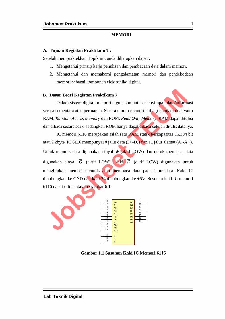
IC memori 6116 merupakan salah satu RAM statik berkapasitas 16.384 bit
atau 2 kbyte. IC 6116 mempunyai 8 jalur data (D0-D7) dan 11 jalur alamat (A0-A10).
Untuk menulis data digunakan sinyal W (aktif LOW) dan untuk membaca data
digunakan sinyal G (aktif LOW). Kaki E (aktif LOW) digunakan untuk
mengijinkan memori menulis atau membaca data pada jalur data. Kaki 12
dihubungkan ke GND dan kaki 24 dihubungkan ke +5V. Susunan kaki IC memori
6116 dapat dilihat dalam Gambar 6.1.
Gambar 1.1 Susunan Kaki IC Memori 6116
A08
A17
A26
A35
A44
A53
A62
A71
A823
A922
A1019
E18
G20
W21
D09
D110
D211
D313
D414
D515
D616
D717
6116
2
Lab Teknik Digital
Jobsheet Praktikum
D. Lembar Praktikum
1. Alat dan Bahan
IC 6116 1 buah
IC 74245 1 buah
IC 74373 1 buah
Respack 10K Ω 2 buah
Resistor 10K Ω 2 buah
Resistor 220 Ω 8 buah
LED 8 buah
Push Button 2 buah
Dipwitch 8-bit 2 buah
Multimeter Digital 1 buah
Power Supply DC 1 buah
Project Board 1 buah
Pinset 1 buah
Jumper secukupnya
2. Kesehatan dan Keselamatan kerja
(a) Periksalah kelengkapan alat dan bahan sebelum digunakan.
(b) Pelajari dan pahami petunjuk praktikum pada lembar kegiatan
praktikum.
(c) Pastikan tegangan keluaran catu daya sesuai yang dibutuhkan.
(d) Sebelum catu daya dihidupkan hubungi dosen pendamping untuk
mengecek kebenaran rangkaian.
(e) Yakinkan tempat anda aman dari sengatan listrik.
(f) Hati-hati dalam penggunaan peralatan praktikum !
3
Lab Teknik Digital
Jobsheet Praktikum
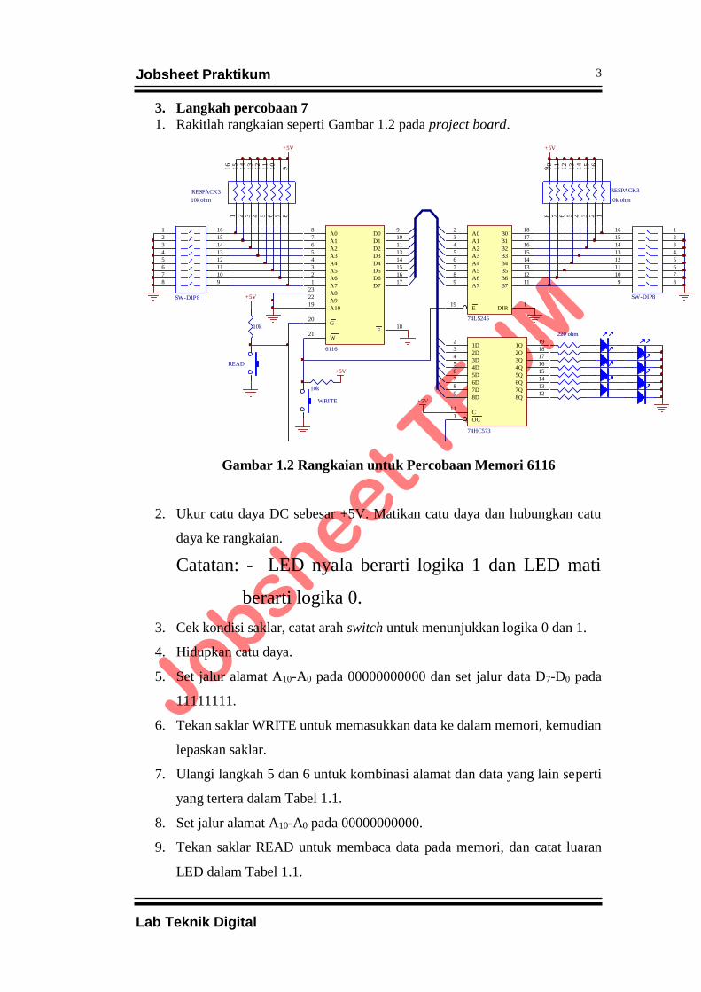
3. Langkah percobaan 7
1. Rakitlah rangkaian seperti Gambar 1.2 pada project board.
Gambar 1.2 Rangkaian untuk Percobaan Memori 6116
2. Ukur catu daya DC sebesar +5V. Matikan catu daya dan hubungkan catu
daya ke rangkaian.
Catatan: - LED nyala berarti logika 1 dan LED mati
berarti logika 0.
3. Cek kondisi saklar, catat arah switch untuk menunjukkan logika 0 dan 1.
4. Hidupkan catu daya.
5. Set jalur alamat A10-A0 pada 00000000000 dan set jalur data D7-D0 pada
11111111.
6. Tekan saklar WRITE untuk memasukkan data ke dalam memori, kemudian
lepaskan saklar.
7. Ulangi langkah 5 dan 6 untuk kombinasi alamat dan data yang lain seperti
yang tertera dalam Tabel 1.1.
8. Set jalur alamat A10-A0 pada 00000000000.
9. Tekan saklar READ untuk membaca data pada memori, dan catat luaran
LED dalam Tabel 1.1.
1
2
3
4
5
6
7
8
16
15
14
13
12
11
10
9
SW-DIP8
1 2 3 4 5 6 7 8
16
15
14
13
12
11
10
9
RESPACK3
+5V
10k ohm
220 ohm
A08
A17
A26
A35
A44
A53
A62
A71
A823
A922
A1019
E18
G20
W21
D09
D110
D211
D313
D414
D515
D616
D717
6116
A02
A13
A24
A35
A46
A57
A68
A79
B018
B117
B216
B315
B414
B513
B612
B711
E19
DIR1
74LS245
1
2
3
4
5
6
7
8
16
15
14
13
12
11
10
9
SW-DIP8
12345678
16
15
14
13
12
11
10
9
RESPACK3
+5V
10k ohm
+5V
10k
10k
+5V
+5V
WRITE
READ
OC1
C11
1D2
2D3
3D4
4D5
5D6
6D7
7D8
8D9
1Q19
2Q18
3Q17
4Q16
5Q15
6Q14
7Q13
8Q12
74HC573
4
Lab Teknik Digital
Jobsheet Praktikum
10. Ulangi langkah 8 dan 9 untuk kombinasi alamat yang lain seperti yang
tertera dalam Tabel 1.1.
DATA HASIL PERCOBAAN
Tabel 1.1 Data Hasil Percobaan IC Memori 6116
MASUKAN LUARAN
ALAMAT DATA DATA
A10 A9 A8 A7 A6 A5 A4 A3 A2 A1 A0 D7 D6 D5 D4 D3 D2 D1 D0 D7 D6 D5 D4 D3 D2 D1 D0
0 0 0 0 0 0 0 0 0 0 0 1 1 1 1 1 1 1 1
0 0 0 0 0 0 0 0 0 0 1 1 1 1 1 1 1 1 0
0 0 0 0 0 0 0 0 0 1 0 1 1 1 1 1 1 0 0
0 0 0 0 0 0 0 0 0 1 1 1 1 1 1 1 0 0 0
0 0 0 0 0 0 0 0 1 0 0 1 1 1 1 0 0 0 0
0 0 0 0 0 0 0 0 1 1 1 1 1 1 0 0 0 0 0
0 0 0 1 1 0 0 1 0 0 0 1 1 0 0 0 0 0 0
0 0 0 1 1 0 0 1 0 0 1 1 0 0 0 0 0 0 0
0 0 0 1 1 0 0 1 0 1 0 0 0 0 0 0 0 0 0
0 0 0 1 1 0 0 1 0 1 1 1 0 0 0 0 0 0 1
0 0 0 1 1 0 0 1 1 0 0 1 1 0 0 0 0 1 1
0 0 0 1 1 0 0 1 1 0 1 1 1 1 0 0 1 1 1
TUGAS
1. Gambarkan blok diagram dan tabel kebenaran IC memori 6116.
2. * Kelompok 1
Susunlah sistem memori 4 kbyte dengan EPROM 1 kbyte. Buatlah
pengalamatan (pendekodean) untuk setiap memori tersebut sehingga
tidak ada alamat yang saling bertumpukan serta berilah penjelasan.
* Kelompok 2
Susunlah sistem memori 16 kbyte dengan EPROM 4 kbyte. Buatlah
pengalamatan (pendekodean) untuk setiap memori tersebut sehingga
tidak ada alamat yang saling bertumpukan serta berilah penjelasan.
* Kelompok 3
Susunlah sistem memori 32 kbyte dengan RAM statik 8 kbyte. Buatlah
pengalamatan (pendekodean) untuk setiap memori tersebut sehingga
tidak ada alamat yang saling bertumpukan serta berilah penjelasan.
5
Lab Teknik Digital
Jobsheet Praktikum
* Kelompok 4
Susunlah sistem memori 64 kbyte dengan EPROM 16 kbyte. Buatlah
pengalamatan (pendekodean) untuk setiap memori tersebut sehingga
tidak ada alamat yang saling bertumpukan serta berilah penjelasan.
* Kelompok 5
Susunlah sistem memori 64 kbyte dengan RAM statik 32 kbyte. Buatlah
pengalamatan (pendekodean) untuk setiap memori tersebut sehingga
tidak ada alamat yang saling bertumpukan serta berilah penjelasan.
* Kelompok 6
Susunlah sistem memori 16 kbyte dengan RAM statik 2 kbyte. Buatlah
pengalamatan (pendekodean) untuk setiap memori tersebut sehingga
tidak ada alamat yang saling bertumpukan serta berilah penjelasan.
Catatan: - Nama RAM/EPROM dapat dipilih sendiri asalkan kapasitasnya
sesuai.
- Range alamat ditentukan sendiri (dalam range 0000H –
FFFFH).

6
Lab Teknik Digital
Jobsheet Praktikum
Analisa
_______________________________________________________________________________
_______________________________________________________________________________
_______________________________________________________________________________
_______________________________________________________________________________
_______________________________________________________________________________
_______________________________________________________________________________
_______________________________________________________________________________
_______________________________________________________________________________
_______________________________________________________________________________
_______________________________________________________________________________
_______________________________________________________________________________
_______________________________________________________________________________
_______________________________________________________________________________
_______________________________________________________________________________
_______________________________________________________________________________
_______________________________________________________________________________
_______________________________________________________________________________
_______________________________________________________________________________
_______________________________________________________________________________
_______________________________________________________________________________
_______________________________________________________________________________
_______________________________________________________________________________
_______________________________________________________________________________
_______________________________________________________________________________
_______________________________________________________________________________
_______________________________________________________________________________
_______________________________________________________________________________
_______________________________________________________________________________
_______________________________________________________________________________
_______________________________________________________________________________
_______________________________________________________________________________
_______________________________________________________________________________
_______________________________________________________________________________
_______________________________________________________________________________
_______________________________________________________________________________
_______________________________________________________________________________
_______________________________________________________________________________
_______________________________________________________________________________

7
Lab Teknik Digital
Jobsheet Praktikum
Kesimpulan
_______________________________________________________________________________
_______________________________________________________________________________
_______________________________________________________________________________
_______________________________________________________________________________
_______________________________________________________________________________
_______________________________________________________________________________
_______________________________________________________________________________
_______________________________________________________________________________
_______________________________________________________________________________
_______________________________________________________________________________
_______________________________________________________________________________
_______________________________________________________________________________
_______________________________________________________________________________
_______________________________________________________________________________
_______________________________________________________________________________
_______________________________________________________________________________
_______________________________________________________________________________
_______________________________________________________________________________
_______________________________________________________________________________
_______________________________________________________________________________
_______________________________________________________________________________
_______________________________________________________________________________
_______________________________________________________________________________
_______________________________________________________________________________
_______________________________________________________________________________
_______________________________________________________________________________
_______________________________________________________________________________
_______________________________________________________________________________
_______________________________________________________________________________
_______________________________________________________________________________
_______________________________________________________________________________
_______________________________________________________________________________
_______________________________________________________________________________
_______________________________________________________________________________
_______________________________________________________________________________
_______________________________________________________________________________
_______________________________________________________________________________
_______________________________________________________________________________
1
Lab Teknik Digital
Jobsheet Praktikum
MULTIVIBRATOR
A. Tujuan Kegiatan Praktikum 8-9 :
Setelah mempraktekkan Topik ini, anda diharapkan dapat :
1. Memahami macam-macam dan prinsip kerja multivibrator.
2. Merancang timer/clock dan delay (aplikasi multivibrator) sesuai keperluan.
B. Dasar Teori Kegiatan Praktikum 8-9
Rangkaian multivibrator merupakan rangkaian yang digunakan untuk
keperluan pewaktuan (timing) rangkaian elektronika. Multivibrator merupakan
rangkaian yang berubah antara dua level digital secara kontinyu, berbasis “free
running” atau berdasar permintaan dari sumber pemicu eksternal.
Pada dasarnya ada 3 jenis multivibrator, yaitu:
1. Bistabil : multivibrator yang dipicu ke salah satu dari 2 kondisi
digital oleh sumber eksternal, dan berada dalam kondisi
tersebut sampai dipicu ke kondisi sebaliknya.
2. Astabil : osilator free running yang berkondisi antara 2 level
digital pada frekuensi dan siklus kerja tertentu.
3. Monostabil : dikenal sebagai one-shot, memberikan pulsa luaran
tunggal pada lebar waktu tertentu ketika dipicu dari
sumber eksternal.
Multivibrator dapat dibangun dari gerbang logika dasar, IC khusus yang
dirancang untuk aplikasi pewaktuan (IC 555, IC 74121 atau 74123) ataupun osilator
kristal. IC 555 adalah IC timer yang sangat populer dan banyak fungsinya. IC ini
merupakan peranti yang kestabilannya tinggi untuk membangkitkan waktu tunda
yang akurat (one-shot) atau osilator. Kaki tambahan digunakan untuk memicu atau
me-reset jika diinginkan. Pada mode operasi waktu tunda, waktu tersebut dikontrol
oleh satu resistor eksternal dan kapasitor. Untuk operasi astabil sebagai osilator,
frekuensi free running dan siklus kerja dikontrol dengan dua kapasitor eksternal
dan satu kapasitor. Rangkaian tersebut dapat dipicu atau di-reset pada tepi turun.
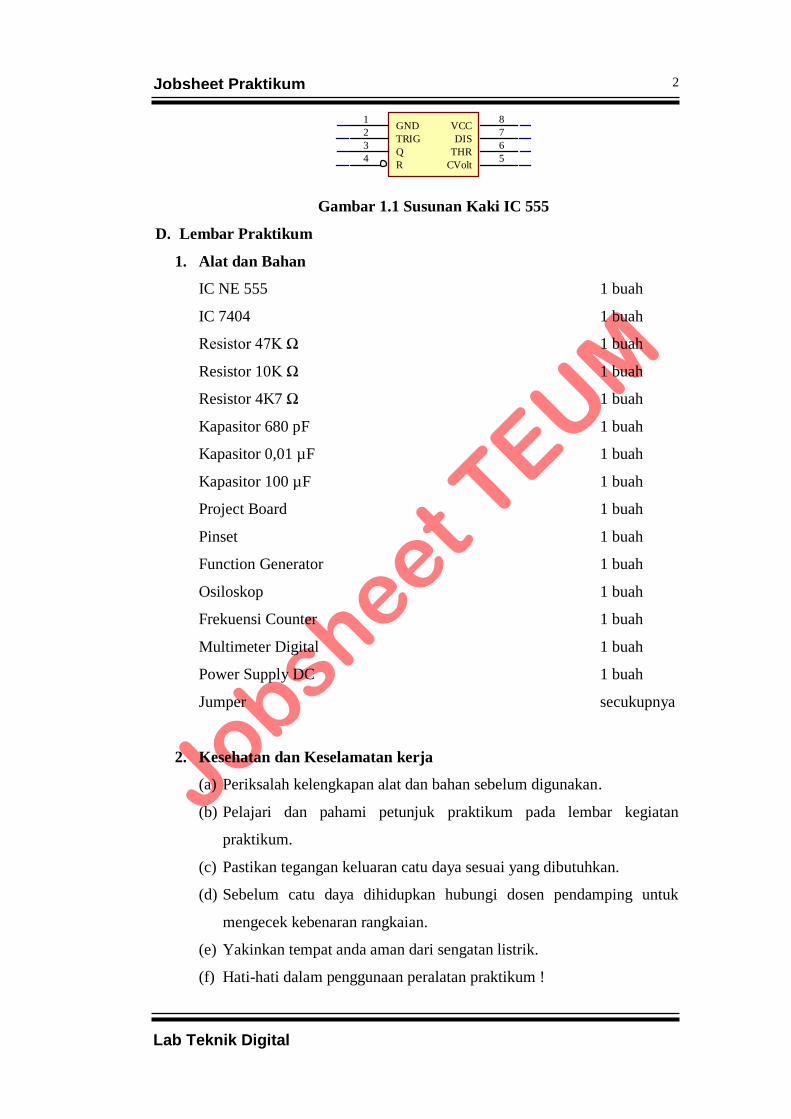
Susunan kaki IC 555 dapat dilihat dalam Gambar 1.1.
2
Lab Teknik Digital
Jobsheet Praktikum
Gambar 1.1 Susunan Kaki IC 555
D. Lembar Praktikum
1. Alat dan Bahan
IC NE 555 1 buah
IC 7404 1 buah
Resistor 47K Ω 1 buah
Resistor 10K Ω 1 buah
Resistor 4K7 Ω 1 buah
Kapasitor 680 pF 1 buah
Kapasitor 0,01 µF 1 buah
Kapasitor 100 µF 1 buah
Project Board 1 buah
Pinset 1 buah
Function Generator 1 buah
Osiloskop 1 buah
Frekuensi Counter 1 buah
Multimeter Digital 1 buah
Power Supply DC 1 buah
Jumper secukupnya
2. Kesehatan dan Keselamatan kerja
(a) Periksalah kelengkapan alat dan bahan sebelum digunakan.
(b) Pelajari dan pahami petunjuk praktikum pada lembar kegiatan
praktikum.
(c) Pastikan tegangan keluaran catu daya sesuai yang dibutuhkan.
(d) Sebelum catu daya dihidupkan hubungi dosen pendamping untuk
mengecek kebenaran rangkaian.
(e) Yakinkan tempat anda aman dari sengatan listrik.
(f) Hati-hati dalam penggunaan peralatan praktikum !
TRIG2
Q3
R4
CVolt5
THR6
DIS7
VCC8
GND1
555
3
Lab Teknik Digital
Jobsheet Praktikum
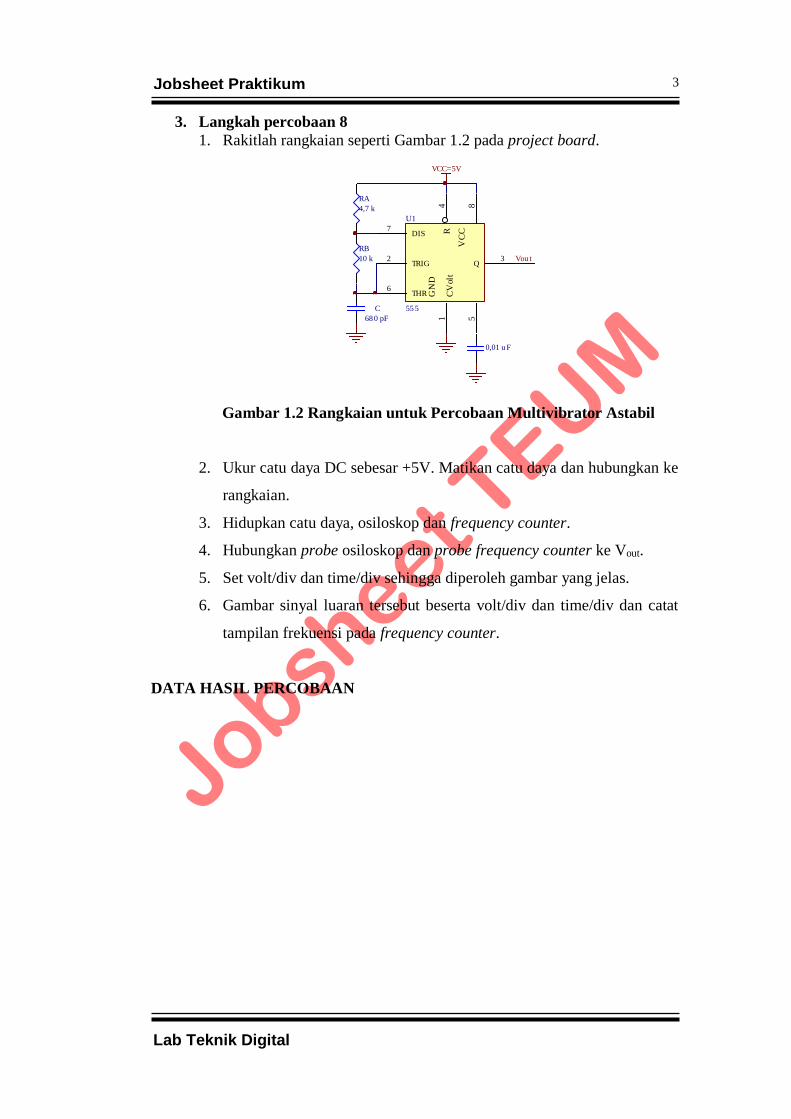
3. Langkah percobaan 8
1. Rakitlah rangkaian seperti Gambar 1.2 pada project board.
Gambar 1.2 Rangkaian untuk Percobaan Multivibrator Astabil
2. Ukur catu daya DC sebesar +5V. Matikan catu daya dan hubungkan ke
rangkaian.
3. Hidupkan catu daya, osiloskop dan frequency counter.
4. Hubungkan probe osiloskop dan probe frequency counter ke Vout.
5. Set volt/div dan time/div sehingga diperoleh gambar yang jelas.
6. Gambar sinyal luaran tersebut beserta volt/div dan time/div dan catat
tampilan frekuensi pada frequency counter.
DATA HASIL PERCOBAAN
TRIG2
Q3
R4
CV
olt
5
THR6
DIS7
VC
C8
GN
D1
U1
55 5
RB
10 k
RA
4,7 k
C
68 0 pF
0,01 u F
VCC=5V
Vou t
4
Lab Teknik Digital
Jobsheet Praktikum
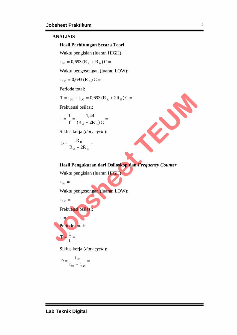
ANALISIS
Hasil Perhitungan Secara Teori
Waktu pengisian (luaran HIGH):
C )R(R 0,693t BAHI
Waktu pengosongan (luaran LOW):
C )(R 0,693t BLO
Periode total:
C )2R(R 0,693ttT BALOHI
Frekuensi osilasi:
C )2R(R
1,44
T
1f
BA
Siklus kerja (duty cycle):
BA
B
2RR
RD
Hasil Pengukuran dari Osiloskop dan Frequency Counter
Waktu pengisian (luaran HIGH):
HIt
Waktu pengosongan (luaran LOW):
LOt
Frekuensi osilasi:
f
Periode total:
f
1T
Siklus kerja (duty cycle):
LOHI
HI
tt
tD

5
Lab Teknik Digital
Jobsheet Praktikum
Tugas:
1. Menggunakan 555 rancang multivibrator astabil yang berosilasi pada 50
kHz dengan siklus kerja 60%. Ambil nilai C = 0,0022 F.
2. Berikan contoh salah satu aplikasi multivibrator astabil dalam rangkaian
elektronika digital.
6
Lab Teknik Digital
Jobsheet Praktikum
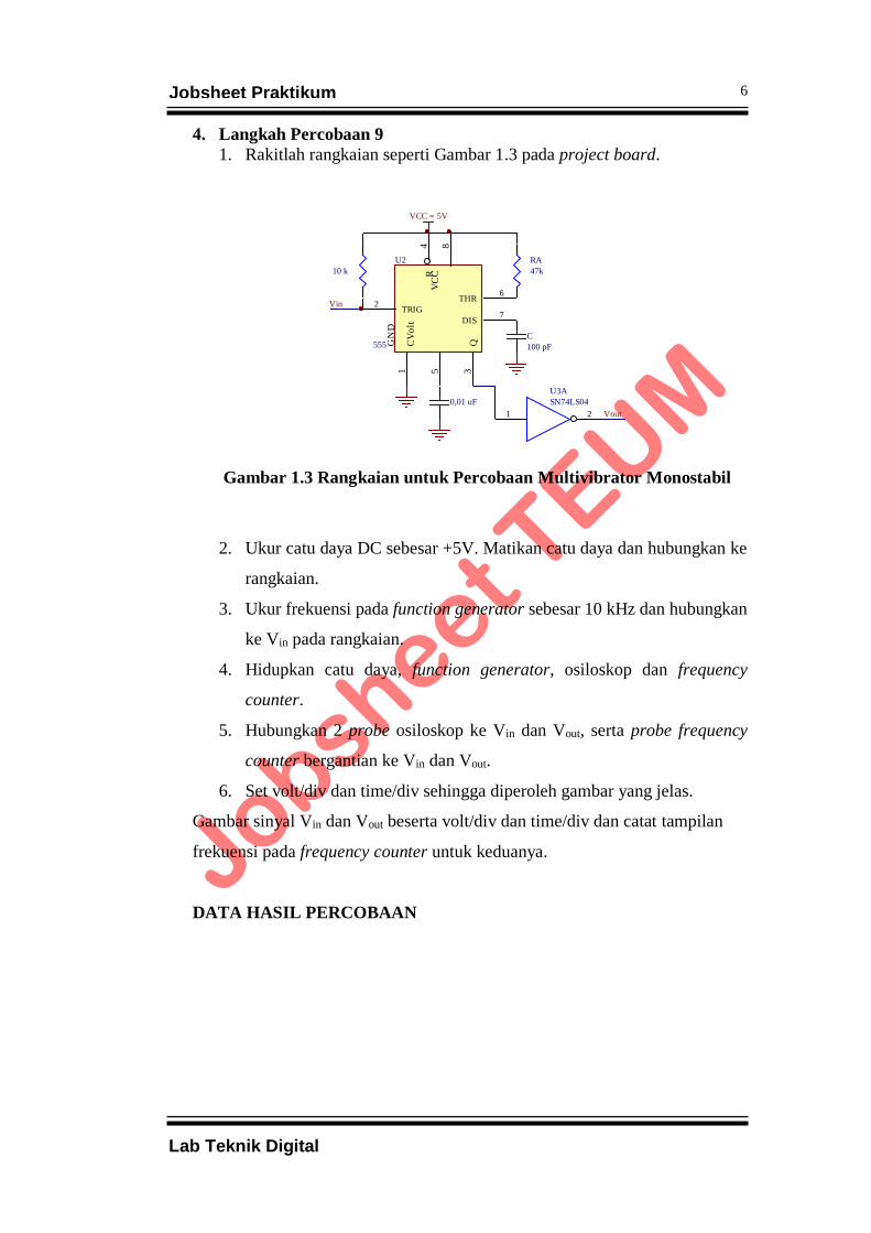
4. Langkah Percobaan 9
1. Rakitlah rangkaian seperti Gambar 1.3 pada project board.
Gambar 1.3 Rangkaian untuk Percobaan Multivibrator Monostabil
2. Ukur catu daya DC sebesar +5V. Matikan catu daya dan hubungkan ke
rangkaian.
3. Ukur frekuensi pada function generator sebesar 10 kHz dan hubungkan
ke Vin pada rangkaian.
4. Hidupkan catu daya, function generator, osiloskop dan frequency
counter.
5. Hubungkan 2 probe osiloskop ke Vin dan Vout, serta probe frequency
counter bergantian ke Vin dan Vout.
6. Set volt/div dan time/div sehingga diperoleh gambar yang jelas.
Gambar sinyal Vin dan Vout beserta volt/div dan time/div dan catat tampilan
frekuensi pada frequency counter untuk keduanya.
DATA HASIL PERCOBAAN
TRIG2
Q3
R4
CV
olt
5
THR6
DIS7
VC
C8
GN
D1
U2
555C
100 pF
0,01 uF
10 k
VCC = 5V
RA
47k
1 2
U3A
SN74LS04
Vin
Vout
7
Lab Teknik Digital
Jobsheet Praktikum
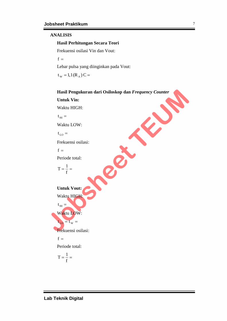
ANALISIS
Hasil Perhitungan Secara Teori
Frekuensi osilasi Vin dan Vout:
f
Lebar pulsa yang diinginkan pada Vout:
C )(R ,11t AW
Hasil Pengukuran dari Osiloskop dan Frequency Counter
Untuk Vin:
Waktu HIGH:
HIt
Waktu LOW:
LOt
Frekuensi osilasi:
f
Periode total:
f
1T
Untuk Vout:
Waktu HIGH:
HIt
Waktu LOW:
WLO tt
Frekuensi osilasi:
f
Periode total:
f
1T

8
Lab Teknik Digital
Jobsheet Praktikum
Tabel 1.1 Perbandingan Hasil Perhitungan dengan Pengukuran
Vin Vout
Teori (Perhitungan) Praktek (Pengukuran) Teori (Perhitungan) Praktek (Pengukuran)
tHI
tLO (tW)
T
f
TUGAS
1. Rancang rangkaian one-shot dengan IC 555 agar mengeluarkan sinyal
dengan waktu HIGH 10 s setiap periode 60 s. Asumsikan Vin
mempunyai waktu LOW selama 1 s setiap periode 60 s dan Vcc yang
digunakan sebesar 5V. Gambarkan bentuk gelombang Vin dan Vout
untuk rangkaian tersebut.
2. Rancanglah multivibrator monostabil dengan IC 74121 yang
mengonversi gelombang kotak 100 kHz, siklus kerja 30% menjadi
gelombang kotak 100 kHz, siklus kerja 50%.
3. Beri contoh aplikasi multivibrator monostabil dalam rangkaian
elektronika digital.

9
Lab Teknik Digital
Jobsheet Praktikum
Data Hasil Percobaan
_______________________________________________________________________________
_______________________________________________________________________________
_______________________________________________________________________________
_______________________________________________________________________________
_______________________________________________________________________________
_______________________________________________________________________________
_______________________________________________________________________________
_______________________________________________________________________________
_______________________________________________________________________________
_______________________________________________________________________________
_______________________________________________________________________________
_______________________________________________________________________________
_______________________________________________________________________________
_______________________________________________________________________________
_______________________________________________________________________________
_______________________________________________________________________________
_______________________________________________________________________________
_______________________________________________________________________________
_______________________________________________________________________________
_______________________________________________________________________________
_______________________________________________________________________________
_______________________________________________________________________________
_______________________________________________________________________________
_______________________________________________________________________________
_______________________________________________________________________________
_______________________________________________________________________________
_______________________________________________________________________________
_______________________________________________________________________________
_______________________________________________________________________________
_______________________________________________________________________________
_______________________________________________________________________________
_______________________________________________________________________________
_______________________________________________________________________________
_______________________________________________________________________________
_______________________________________________________________________________
_______________________________________________________________________________
_______________________________________________________________________________
_______________________________________________________________________________

10
Lab Teknik Digital
Jobsheet Praktikum
Analisa
_______________________________________________________________________________
_______________________________________________________________________________
_______________________________________________________________________________
_______________________________________________________________________________
_______________________________________________________________________________
_______________________________________________________________________________
_______________________________________________________________________________
_______________________________________________________________________________
_______________________________________________________________________________
_______________________________________________________________________________
_______________________________________________________________________________
_______________________________________________________________________________
_______________________________________________________________________________
_______________________________________________________________________________
_______________________________________________________________________________
_______________________________________________________________________________
_______________________________________________________________________________
_______________________________________________________________________________
_______________________________________________________________________________
_______________________________________________________________________________
_______________________________________________________________________________
_______________________________________________________________________________
_______________________________________________________________________________
_______________________________________________________________________________
_______________________________________________________________________________
_______________________________________________________________________________
_______________________________________________________________________________
_______________________________________________________________________________
_______________________________________________________________________________
_______________________________________________________________________________
_______________________________________________________________________________
_______________________________________________________________________________
_______________________________________________________________________________
_______________________________________________________________________________
_______________________________________________________________________________
_______________________________________________________________________________
_______________________________________________________________________________
_______________________________________________________________________________

11
Lab Teknik Digital
Jobsheet Praktikum
Kesimpulan
_______________________________________________________________________________
_______________________________________________________________________________
_______________________________________________________________________________
_______________________________________________________________________________
_______________________________________________________________________________
_______________________________________________________________________________
_______________________________________________________________________________
_______________________________________________________________________________
_______________________________________________________________________________
_______________________________________________________________________________
_______________________________________________________________________________
_______________________________________________________________________________
_______________________________________________________________________________
_______________________________________________________________________________
_______________________________________________________________________________
_______________________________________________________________________________
_______________________________________________________________________________
_______________________________________________________________________________
_______________________________________________________________________________
_______________________________________________________________________________
_______________________________________________________________________________
_______________________________________________________________________________
_______________________________________________________________________________
_______________________________________________________________________________
_______________________________________________________________________________
_______________________________________________________________________________
_______________________________________________________________________________
_______________________________________________________________________________
_______________________________________________________________________________
_______________________________________________________________________________
_______________________________________________________________________________
_______________________________________________________________________________
_______________________________________________________________________________
_______________________________________________________________________________
_______________________________________________________________________________
_______________________________________________________________________________
_______________________________________________________________________________
_______________________________________________________________________________
SDLS029C − DECEMBER 1983 − REVISED JANUARY 2004
1POST OFFICE BOX 655303 • DALLAS, TEXAS 75265
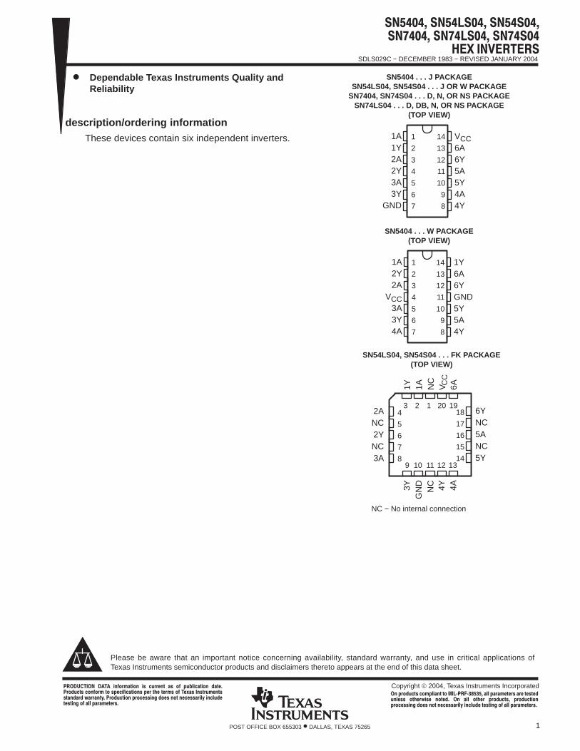
Dependable Texas Instruments Quality andReliability
description/ordering informationThese devices contain six independent inverters.
Copyright 2004, Texas Instruments Incorporated
Please be aware that an important notice concerning availability, standard warranty, and use in critical applications ofTexas Instruments semiconductor products and disclaimers thereto appears at the end of this data sheet.
1
2
3
4
5
6
7
14
13
12
11
10
9
8
1A1Y2A2Y3A3Y
GND
VCC6A6Y5A5Y4A4Y
SN5404 . . . J PACKAGESN54LS04, SN54S04 . . . J OR W PACKAGE
SN7404, SN74S04 . . . D, N, OR NS PACKAGESN74LS04 . . . D, DB, N, OR NS PACKAGE
(TOP VIEW)
1
2
3
4
5
6
7
14
13
12
11
10
9
8
1A2Y2A
VCC3A3Y4A
1Y6A6YGND5Y5A4Y
SN5404 . . . W PACKAGE(TOP VIEW)
3 2 1 20 19
9 10 11 12 13
4
5
6
7
8
18
17
16
15
14
6YNC5ANC5Y
2ANC2YNC3A
SN54LS04, SN54S04 . . . FK PACKAGE(TOP VIEW)
1Y 1A NC
4Y 4A6A
3YG
ND
NC
NC − No internal connection
V CC
!" #!$% &"'&! #" #" (" " ") !"&& *+' &! #", &" ""%+ %!&"", %% #""'
#&! #% -./.010 %% #"" " ""&!%" ("*" "&' %% (" #&! #&!#", &" ""%+ %!&" ", %% #""'
SDLS029C − DECEMBER 1983 − REVISED JANUARY 2004
2 POST OFFICE BOX 655303 • DALLAS, TEXAS 75265
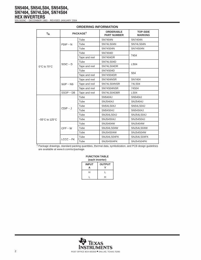
ORDERING INFORMATION
TA PACKAGE † ORDERABLEPART NUMBER
TOP-SIDEMARKING
Tube SN7404N SN7404N
PDIP − N Tube SN74LS04N SN74LS04NPDIP − N
Tube SN74S04N SN74S04N
Tube SN7404D7404
Tape and reel SN7404DR7404
SOIC − DTube SN74LS04D
LS040°C to 70°C
SOIC − DTape and reel SN74LS04DR
LS040 C to 70 C
Tube SN74S04DS04
Tape and reel SN74S04DRS04
Tape and reel SN7404NSR SN7404
SOP − NS Tape and reel SN74LS04NSR 74LS04SOP − NS
Tape and reel SN74S04NSR 74S04
SSOP − DB Tape and reel SN74LS04DBR LS04
Tube SN5404J SN5404J
Tube SNJ5404J SNJ5404J
CDIP − JTube SN54LS04J SN54LS04J
CDIP − JTube SN54S04J SN54S04J
Tube SNJ54LS04J SNJ54LS04J
−55°C to 125°C Tube SNJ54S04J SNJ54S04J−55 C to 125 C
Tube SNJ5404W SNJ5404W
CFP − W Tube SNJ54LS04W SNJ54LS04WCFP − W
Tube SNJ54S04W SNJ54S04W
LCCC − FKTube SNJ54LS04FK SNJ54LS04FK
LCCC − FKTube SNJ54S04FK SNJ54S04FK
† Package drawings, standard packing quantities, thermal data, symbolization, and PCB design guidelinesare available at www.ti.com/sc/package.
FUNCTION TABLE(each inverter)
INPUTA
OUTPUTY
H L
L H
SDLS029C − DECEMBER 1983 − REVISED JANUARY 2004
3POST OFFICE BOX 655303 • DALLAS, TEXAS 75265
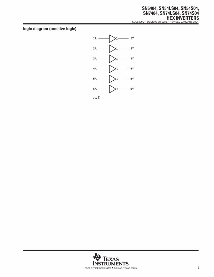
logic diagram (positive logic)
1A
2A
3A
4A
5A
6A
1Y
2Y
3Y
4Y
5Y
6Y
Y = A
SDLS029C − DECEMBER 1983 − REVISED JANUARY 2004
4 POST OFFICE BOX 655303 • DALLAS, TEXAS 75265
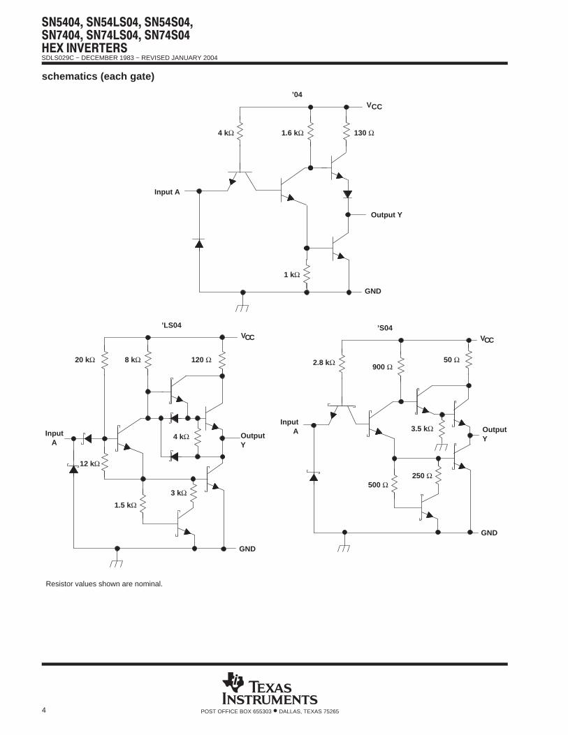
schematics (each gate)
Input A
VCC
Output Y
GND
130 Ω
1 kΩ
1.6 kΩ
’04
4 kΩ
InputA
VCC
OutputY
GND
20 kΩ 120 Ω
’LS04
8 kΩ
12 kΩ
1.5 kΩ
3 kΩ
4 kΩ
InputA
VCC
Outpu tY
GND
2.8 kΩ900 Ω
’S04
50 Ω
3.5 kΩ
250 Ω500 Ω
Resistor values shown are nominal.
SDLS029C − DECEMBER 1983 − REVISED JANUARY 2004
5POST OFFICE BOX 655303 • DALLAS, TEXAS 75265
absolute maximum ratings over operating free-air temperature range (unless otherwise noted) †
Supply voltage, VCC (see Note 1) 7 V. . . . . . . . . . . . . . . . . . . . . . . . . . . . . . . . . . . . . . . . . . . . . . . . . . . . . . . . . . . . . Input voltage, VI: ’04, ’S04 5.5 V. . . . . . . . . . . . . . . . . . . . . . . . . . . . . . . . . . . . . . . . . . . . . . . . . . . . . . . . . . . . . . . .
’LS04 7 V. . . . . . . . . . . . . . . . . . . . . . . . . . . . . . . . . . . . . . . . . . . . . . . . . . . . . . . . . . . . . . . . . . . . . Package thermal impedance, θJA (see Note 2): D package 86°C/W. . . . . . . . . . . . . . . . . . . . . . . . . . . . . . . . . . .
DB package 96°C/W. . . . . . . . . . . . . . . . . . . . . . . . . . . . . . . . . N package 80°C/W. . . . . . . . . . . . . . . . . . . . . . . . . . . . . . . . . . . NS package 76°C/W. . . . . . . . . . . . . . . . . . . . . . . . . . . . . . . . .
Storage temperature range, Tstg −65°C to 150°C. . . . . . . . . . . . . . . . . . . . . . . . . . . . . . . . . . . . . . . . . . . . . . . . . . . † Stresses beyond those listed under “absolute maximum ratings” may cause permanent damage to the device. This are stress ratings only, and
functional operation of the device at these or any other conditions beyond those indicated under “recommended operating conditions” is notimplied. Exposure to absolute-maximum-rated conditions for extended periods may affect device reliability.
NOTES: 1. Voltage values are with respect to network ground terminal.2. The package thermal impedance is calculated in accordance with JESD 51-7.
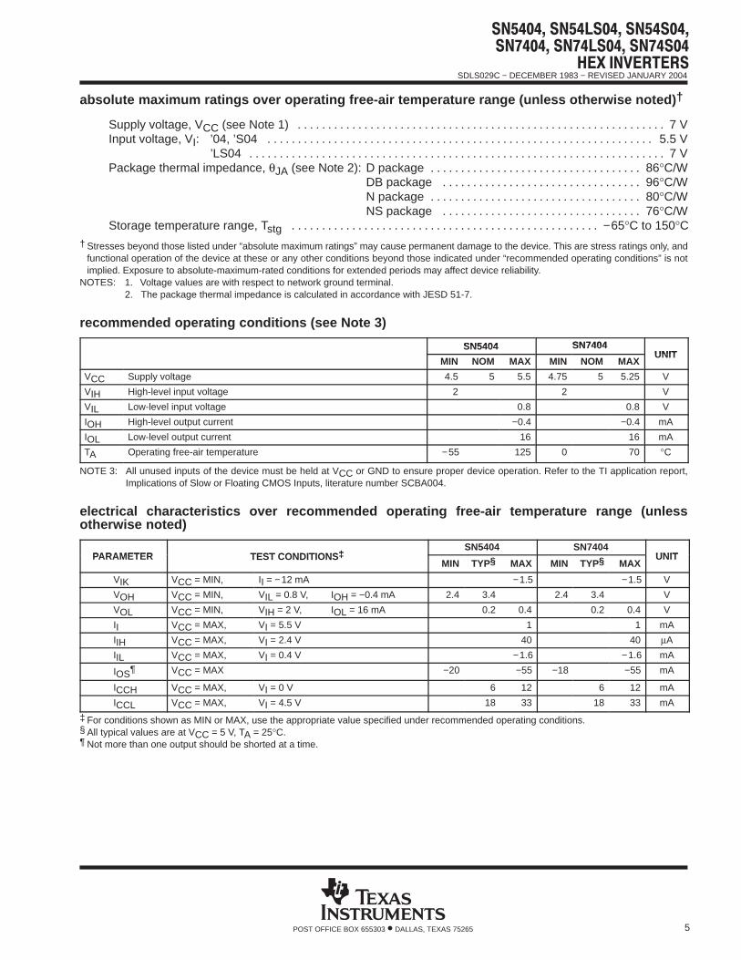
recommended operating conditions (see Note 3)
SN5404 SN7404SN5404 SN7404UNIT
MIN NOM MAX MIN NOM MAXUNIT
VCC Supply voltage 4.5 5 5.5 4.75 5 5.25 V
VIH High-level input voltage 2 2 V
VIL Low-level input voltage 0.8 0.8 V
IOH High-level output current −0.4 −0.4 mA
IOL Low-level output current 16 16 mA
TA Operating free-air temperature −55 125 0 70 °C
NOTE 3: All unused inputs of the device must be held at VCC or GND to ensure proper device operation. Refer to the TI application report,Implications of Slow or Floating CMOS Inputs, literature number SCBA004.
electrical characteristics over recommended operating free-air temperature range (unlessotherwise noted)
PARAMETER TEST CONDITIONS‡SN5404 SN7404
UNITPARAMETER TEST CONDITIONS‡MIN TYP§ MAX MIN TYP§ MAX
UNIT
VIK VCC = MIN, II = −12 mA −1.5 −1.5 V
VOH VCC = MIN, VIL = 0.8 V, IOH = −0.4 mA 2.4 3.4 2.4 3.4 V
VOL VCC = MIN, VIH = 2 V, IOL = 16 mA 0.2 0.4 0.2 0.4 V
II VCC = MAX, VI = 5.5 V 1 1 mA
IIH VCC = MAX, VI = 2.4 V 40 40 µA
IIL VCC = MAX, VI = 0.4 V −1.6 −1.6 mA
IOS¶ VCC = MAX −20 −55 −18 −55 mA
ICCH VCC = MAX, VI = 0 V 6 12 6 12 mA
ICCL VCC = MAX, VI = 4.5 V 18 33 18 33 mA
‡ For conditions shown as MIN or MAX, use the appropriate value specified under recommended operating conditions.§ All typical values are at VCC = 5 V, TA = 25°C.¶ Not more than one output should be shorted at a time.
SDLS029C − DECEMBER 1983 − REVISED JANUARY 2004
6 POST OFFICE BOX 655303 • DALLAS, TEXAS 75265
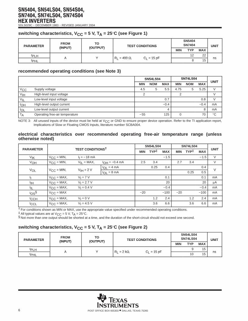
switching characteristics, V CC = 5 V, TA = 25°C (see Figure 1)
PARAMETERFROM
(INPUT)TO
(OUTPUT) TEST CONDITIONS
SN5404SN7404 UNITPARAMETER (INPUT) (OUTPUT) TEST CONDITIONS
MIN TYP MAXUNIT
tPLHA Y RL = 400 Ω, CL = 15 pF
12 22ns
tPHLA Y RL = 400 Ω, CL = 15 pF
8 15ns
recommended operating conditions (see Note 3)
SN54LS04 SN74LS04SN54LS04 SN74LS04UNIT
MIN NOM MAX MIN NOM MAXUNIT
VCC Supply voltage 4.5 5 5.5 4.75 5 5.25 V
VIH High-level input voltage 2 2 V
VIL Low-level input voltage 0.7 0.8 V
IOH High-level output current −0.4 −0.4 mA
IOL Low-level output current 4 8 mA
TA Operating free-air temperature −55 125 0 70 °C
NOTE 3: All unused inputs of the device must be held at VCC or GND to ensure proper device operation. Refer to the TI application report,Implications of Slow or Floating CMOS Inputs, literature number SCBA004.
electrical characteristics over recommended operating free-air temperature range (unlessotherwise noted)
PARAMETER TEST CONDITIONS†SN54LS04 SN74LS04
UNITPARAMETER TEST CONDITIONS†MIN TYP‡ MAX MIN TYP‡ MAX
UNIT
VIK VCC = MIN, II = −18 mA −1.5 −1.5 V
VOH VCC = MIN, VIL = MAX, IOH = −0.4 mA 2.5 3.4 2.7 3.4 V
VOL VCC = MIN, VIH = 2 VIOL = 4 mA 0.25 0.4 0.4
VVOL VCC = MIN, VIH = 2 VIOL = 8 mA 0.25 0.5
V
II VCC = MAX, VI = 7 V 0.1 0.1 mA
IIH VCC = MAX, VI = 2.7 V 20 20 µA
IIL VCC = MAX, VI = 0.4 V −0.4 −0.4 mA
IOS§ VCC = MAX −20 −100 −20 −100 mA
ICCH VCC = MAX, VI = 0 V 1.2 2.4 1.2 2.4 mA
ICCL VCC = MAX, VI = 4.5 V 3.6 6.6 3.6 6.6 mA
† For conditions shown as MIN or MAX, use the appropriate value specified under recommended operating conditions.‡ All typical values are at VCC = 5 V, TA = 25°C.§ Not more than one output should be shorted at a time, and the duration of the short-circuit should not exceed one second.
switching characteristics, V CC = 5 V, TA = 25°C (see Figure 2)
PARAMETERFROM
(INPUT)TO
(OUTPUT) TEST CONDITIONS
SN54LS04SN74LS04 UNITPARAMETER (INPUT) (OUTPUT) TEST CONDITIONS
MIN TYP MAXUNIT
tPLHA Y RL = 2 kΩ, CL = 15 pF
9 15ns
tPHLA Y RL = 2 kΩ, CL = 15 pF
10 15ns
SDLS029C − DECEMBER 1983 − REVISED JANUARY 2004
7POST OFFICE BOX 655303 • DALLAS, TEXAS 75265
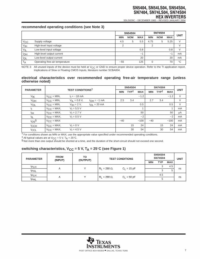
recommended operating conditions (see Note 3)
SN54S04 SN74S04SN54S04 SN74S04UNIT
MIN NOM MAX MIN NOM MAXUNIT
VCC Supply voltage 4.5 5 5.5 4.75 5 5.25 V
VIH High-level input voltage 2 2 V
VIL Low-level input voltage 0.8 0.8 V
IOH High-level output current −1 −1 mA
IOL Low-level output current 20 20 mA
TA Operating free-air temperature −55 125 0 70 °C
NOTE 3: All unused inputs of the device must be held at VCC or GND to ensure proper device operation. Refer to the TI application report,Implications of Slow or Floating CMOS Inputs, literature number SCBA004.
electrical characteristics over recommended operating free-air temperature range (unlessotherwise noted)
PARAMETER TEST CONDITIONS†SN54S04 SN74S04
UNITPARAMETER TEST CONDITIONS†MIN TYP‡ MAX MIN TYP‡ MAX
UNIT
VIK VCC = MIN, II = −18 mA −1.2 −1.2 V
VOH VCC = MIN, VIL = 0.8 V, IOH = −1 mA 2.5 3.4 2.7 3.4 V
VOL VCC = MIN, VIH = 2 V, IOL = 20 mA 0.5 0.5 V
II VCC = MAX, VI = 5.5 V 1 1 mA
IIH VCC = MAX, VI = 2.7 V 50 50 µA
IIL VCC = MAX, VI = 0.5 V −2 −2 mA
IOS§ VCC = MAX −40 −100 −40 −100 mA
ICCH VCC = MAX, VI = 0 V 15 24 15 24 mA
ICCL VCC = MAX, VI = 4.5 V 30 54 30 54 mA
† For conditions shown as MIN or MAX, use the appropriate value specified under recommended operating conditions.‡ All typical values are at VCC = 5 V, TA = 25°C.§ Not more than one output should be shorted at a time, and the duration of the short-circuit should not exceed one second.
switching characteristics, V CC = 5 V, TA = 25°C (see Figure 1)
PARAMETERFROM
(INPUT)TO
(OUTPUT) TEST CONDITIONS
SN54S04SN74S04 UNITPARAMETER (INPUT) (OUTPUT) TEST CONDITIONS
MIN TYP MAXUNIT
tPLHA Y RL = 280 Ω, CL = 15 pF
3 4.5ns
tPHLA Y RL = 280 Ω, CL = 15 pF
3 5ns
tPLHA Y RL = 280 Ω, CL = 50 pF
4.5ns
tPHLA Y RL = 280 Ω, CL = 50 pF
5ns
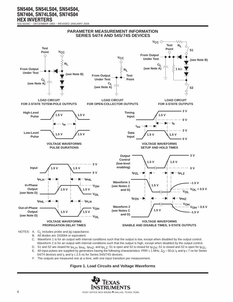
SDLS029C − DECEMBER 1983 − REVISED JANUARY 2004
8 POST OFFICE BOX 655303 • DALLAS, TEXAS 75265
PARAMETER MEASUREMENT INFORMATIONSERIES 54/74 AND 54S/74S DEVICES
tPHL tPLH
tPLH tPHL
LOAD CIRCUITFOR 3-STATE OUTPUTS
High-LevelPulse
Low-LevelPulse
VOLTAGE WAVEFORMSPULSE DURATIONS
Input
Out-of-PhaseOutput
(see Note D)
3 V
0 V
VOL
VOH
VOH
VOL
In-PhaseOutput
(see Note D)
VOLTAGE WAVEFORMSPROPAGATION DELAY TIMES
VCC
RL
Test Point
From OutputUnder Test
CL(see Note A)
LOAD CIRCUITFOR OPEN-COLLECTOR OUTPUTS
LOAD CIRCUITFOR 2-STATE TOTEM-POLE OUTPUTS
(see Note B)
VCC
RLFrom Output
Under Test
CL(see Note A)
TestPoint
(see Note B )
VCCRL
From OutputUnder Test
CL(see Note A)
TestPoint
1 kΩ
NOTES: A. CL includes probe and jig capacitance.B. All diodes are 1N3064 or equivalent.C. Waveform 1 is for an output with internal conditions such that the output is low, except when disabled by the output control.
Waveform 2 is for an output with internal conditions such that the output is high, except when disabled by the output control.D. S1 and S2 are closed for tPLH, tPHL, tPHZ, and tPLZ; S1 is open and S2 is closed for tPZH; S1 is closed and S2 is open for tPZL.E. All input pulses are supplied by generators having the following characteristics: PRR ≤ 1 MHz, ZO ≈ 50 Ω; tr and tf ≤ 7 ns for Series
54/74 devices and tr and tf ≤ 2.5 ns for Series 54S/74S devices.F. The outputs are measured one at a time, with one input transition per measurement.
S1
S2
tPHZ
tPLZtPZL
tPZH
3 V
3 V
0 V
0 V
thtsu
VOLTAGE WAVEFORMSSETUP AND HOLD TIMES
TimingInput
DataInput
3 V
0 V
OutputControl
(low-levelenabling)
Waveform 1(see Notes C
and D)
Waveform 2(see Notes C
and D)≈1.5 V
VOH − 0.5 V
VOL + 0.5 V
≈1.5 V
VOLTAGE WAVEFORMSENABLE AND DISABLE TIMES, 3-STATE OUTPUTS
1.5 V 1.5 V
1.5 V 1.5 V
1.5 V
1.5 V 1.5 V
1.5 V 1.5 V
1.5 V
1.5 V
tw
1.5 V 1.5 V
1.5 V 1.5 V
1.5 V 1.5 V
VOH
VOL
Figure 1. Load Circuits and Voltage Waveforms
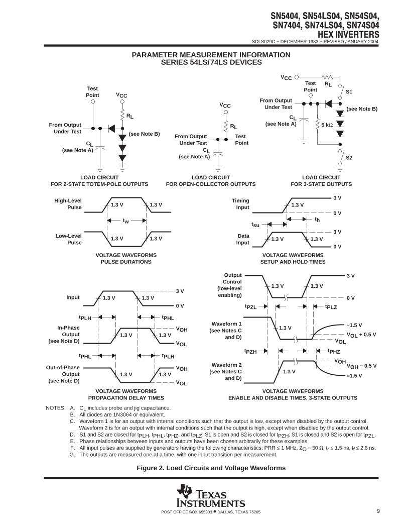
SDLS029C − DECEMBER 1983 − REVISED JANUARY 2004
9POST OFFICE BOX 655303 • DALLAS, TEXAS 75265
PARAMETER MEASUREMENT INFORMATIONSERIES 54LS/74LS DEVICES
tPHL tPLH
tPLH tPHL
LOAD CIRCUITFOR 3-STATE OUTPUTS
High-LevelPulse
Low-LevelPulse
VOLTAGE WAVEFORMSPULSE DURATIONS
Input
Out-of-PhaseOutput
(see Note D)
3 V
0 V
VOL
VOH
VOH
VOL
In-PhaseOutput
(see Note D)
VOLTAGE WAVEFORMSPROPAGATION DELAY TIMES
VCC
RL
Test Point
From OutputUnder Test
CL(see Note A)
LOAD CIRCUITFOR OPEN-COLLECTOR OUTPUTS
LOAD CIRCUITFOR 2-STATE TOTEM-POLE OUTPUTS
(see Note B)
VCC
RLFrom Output
Under Test
CL(see Note A)
TestPoint
(see Note B )
VCCRL
From OutputUnder Test
CL(see Note A)
TestPoint
5 kΩ
NOTES: A. CL includes probe and jig capacitance.B. All diodes are 1N3064 or equivalent.C. Waveform 1 is for an output with internal conditions such that the output is low, except when disabled by the output control.
Waveform 2 is for an output with internal conditions such that the output is high, except when disabled by the output control.D. S1 and S2 are closed for tPLH, tPHL, tPHZ, and tPLZ; S1 is open and S2 is closed for tPZH; S1 is closed and S2 is open for tPZL.E. Phase relationships between inputs and outputs have been chosen arbitrarily for these examples.F. All input pulses are supplied by generators having the following characteristics: PRR ≤ 1 MHz, ZO ≈ 50 Ω, tr ≤ 1.5 ns, tf ≤ 2.6 ns.G. The outputs are measured one at a time, with one input transition per measurement.
S1
S2
tPHZ
tPLZtPZL
tPZH
3 V
3 V
0 V
0 V
thtsu
VOLTAGE WAVEFORMSSETUP AND HOLD TIMES
TimingInput
DataInput
3 V
0 V
OutputControl
(low-levelenabling)
Waveform 1(see Notes C
and D)
Waveform 2(see Notes C
and D) ≈1.5 V
VOH − 0.5 V
VOL + 0.5 V
≈1.5 V
VOLTAGE WAVEFORMSENABLE AND DISABLE TIMES, 3-STATE OUTPUTS
1.3 V 1.3 V
1.3 V 1.3 V
1.3 V
1.3 V 1.3 V
1.3 V 1.3 V
1.3 V
1.3 V
tw
1.3 V 1.3 V
1.3 V 1.3 V
1.3 V 1.3 V
VOL
VOH
Figure 2. Load Circuits and Voltage Waveforms
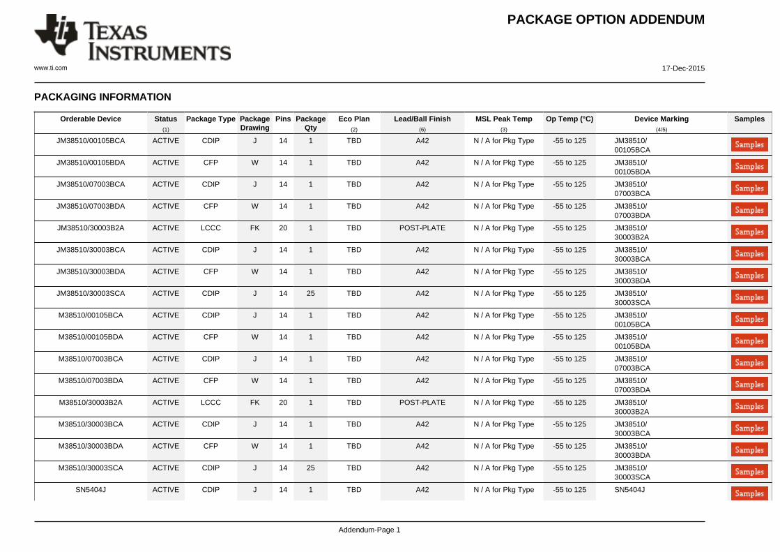
PACKAGE OPTION ADDENDUM
www.ti.com 17-Dec-2015
Addendum-Page 1
PACKAGING INFORMATION
Orderable Device Status(1)
Package Type PackageDrawing
Pins PackageQty
Eco Plan(2)
Lead/Ball Finish(6)
MSL Peak Temp(3)
Op Temp (°C) Device Marking(4/5)
Samples
JM38510/00105BCA ACTIVE CDIP J 14 1 TBD A42 N / A for Pkg Type -55 to 125 JM38510/00105BCA
JM38510/00105BDA ACTIVE CFP W 14 1 TBD A42 N / A for Pkg Type -55 to 125 JM38510/00105BDA
JM38510/07003BCA ACTIVE CDIP J 14 1 TBD A42 N / A for Pkg Type -55 to 125 JM38510/07003BCA
JM38510/07003BDA ACTIVE CFP W 14 1 TBD A42 N / A for Pkg Type -55 to 125 JM38510/07003BDA
JM38510/30003B2A ACTIVE LCCC FK 20 1 TBD POST-PLATE N / A for Pkg Type -55 to 125 JM38510/30003B2A
JM38510/30003BCA ACTIVE CDIP J 14 1 TBD A42 N / A for Pkg Type -55 to 125 JM38510/30003BCA
JM38510/30003BDA ACTIVE CFP W 14 1 TBD A42 N / A for Pkg Type -55 to 125 JM38510/30003BDA
JM38510/30003SCA ACTIVE CDIP J 14 25 TBD A42 N / A for Pkg Type -55 to 125 JM38510/30003SCA
M38510/00105BCA ACTIVE CDIP J 14 1 TBD A42 N / A for Pkg Type -55 to 125 JM38510/00105BCA
M38510/00105BDA ACTIVE CFP W 14 1 TBD A42 N / A for Pkg Type -55 to 125 JM38510/00105BDA
M38510/07003BCA ACTIVE CDIP J 14 1 TBD A42 N / A for Pkg Type -55 to 125 JM38510/07003BCA
M38510/07003BDA ACTIVE CFP W 14 1 TBD A42 N / A for Pkg Type -55 to 125 JM38510/07003BDA
M38510/30003B2A ACTIVE LCCC FK 20 1 TBD POST-PLATE N / A for Pkg Type -55 to 125 JM38510/30003B2A
M38510/30003BCA ACTIVE CDIP J 14 1 TBD A42 N / A for Pkg Type -55 to 125 JM38510/30003BCA
M38510/30003BDA ACTIVE CFP W 14 1 TBD A42 N / A for Pkg Type -55 to 125 JM38510/30003BDA
M38510/30003SCA ACTIVE CDIP J 14 25 TBD A42 N / A for Pkg Type -55 to 125 JM38510/30003SCA
SN5404J ACTIVE CDIP J 14 1 TBD A42 N / A for Pkg Type -55 to 125 SN5404J
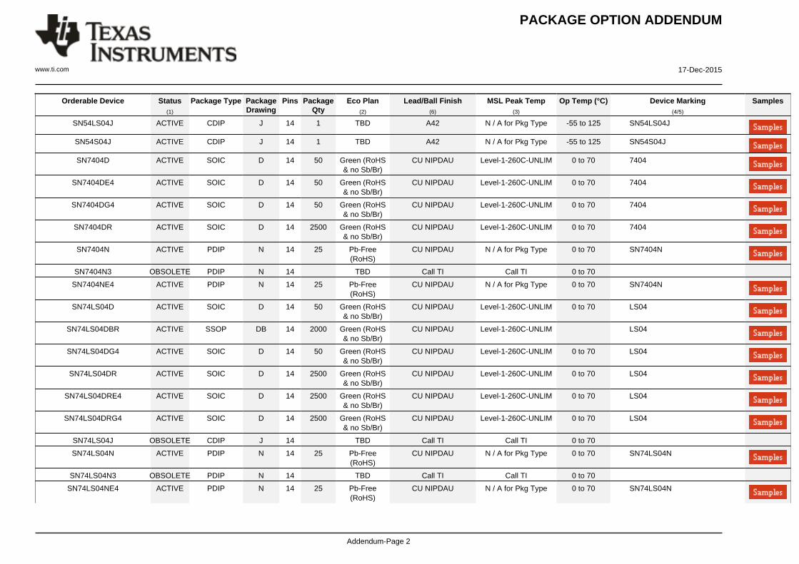
PACKAGE OPTION ADDENDUM
www.ti.com 17-Dec-2015
Addendum-Page 2
Orderable Device Status(1)
Package Type PackageDrawing
Pins PackageQty
Eco Plan(2)
Lead/Ball Finish(6)
MSL Peak Temp(3)
Op Temp (°C) Device Marking(4/5)
Samples
SN54LS04J ACTIVE CDIP J 14 1 TBD A42 N / A for Pkg Type -55 to 125 SN54LS04J
SN54S04J ACTIVE CDIP J 14 1 TBD A42 N / A for Pkg Type -55 to 125 SN54S04J
SN7404D ACTIVE SOIC D 14 50 Green (RoHS& no Sb/Br)
CU NIPDAU Level-1-260C-UNLIM 0 to 70 7404
SN7404DE4 ACTIVE SOIC D 14 50 Green (RoHS& no Sb/Br)
CU NIPDAU Level-1-260C-UNLIM 0 to 70 7404
SN7404DG4 ACTIVE SOIC D 14 50 Green (RoHS& no Sb/Br)
CU NIPDAU Level-1-260C-UNLIM 0 to 70 7404
SN7404DR ACTIVE SOIC D 14 2500 Green (RoHS& no Sb/Br)
CU NIPDAU Level-1-260C-UNLIM 0 to 70 7404
SN7404N ACTIVE PDIP N 14 25 Pb-Free(RoHS)
CU NIPDAU N / A for Pkg Type 0 to 70 SN7404N
SN7404N3 OBSOLETE PDIP N 14 TBD Call TI Call TI 0 to 70
SN7404NE4 ACTIVE PDIP N 14 25 Pb-Free(RoHS)
CU NIPDAU N / A for Pkg Type 0 to 70 SN7404N
SN74LS04D ACTIVE SOIC D 14 50 Green (RoHS& no Sb/Br)
CU NIPDAU Level-1-260C-UNLIM 0 to 70 LS04
SN74LS04DBR ACTIVE SSOP DB 14 2000 Green (RoHS& no Sb/Br)
CU NIPDAU Level-1-260C-UNLIM LS04
SN74LS04DG4 ACTIVE SOIC D 14 50 Green (RoHS& no Sb/Br)
CU NIPDAU Level-1-260C-UNLIM 0 to 70 LS04
SN74LS04DR ACTIVE SOIC D 14 2500 Green (RoHS& no Sb/Br)
CU NIPDAU Level-1-260C-UNLIM 0 to 70 LS04
SN74LS04DRE4 ACTIVE SOIC D 14 2500 Green (RoHS& no Sb/Br)
CU NIPDAU Level-1-260C-UNLIM 0 to 70 LS04
SN74LS04DRG4 ACTIVE SOIC D 14 2500 Green (RoHS& no Sb/Br)
CU NIPDAU Level-1-260C-UNLIM 0 to 70 LS04
SN74LS04J OBSOLETE CDIP J 14 TBD Call TI Call TI 0 to 70
SN74LS04N ACTIVE PDIP N 14 25 Pb-Free(RoHS)
CU NIPDAU N / A for Pkg Type 0 to 70 SN74LS04N
SN74LS04N3 OBSOLETE PDIP N 14 TBD Call TI Call TI 0 to 70
SN74LS04NE4 ACTIVE PDIP N 14 25 Pb-Free(RoHS)
CU NIPDAU N / A for Pkg Type 0 to 70 SN74LS04N
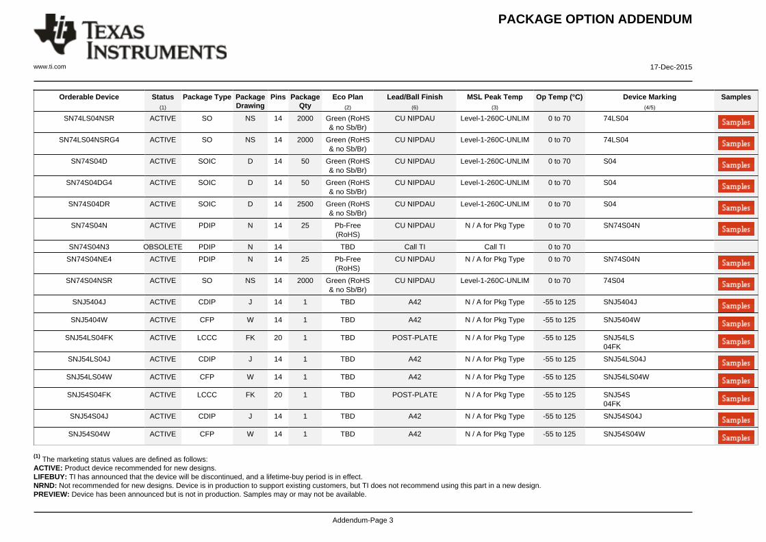
PACKAGE OPTION ADDENDUM
www.ti.com 17-Dec-2015
Addendum-Page 3
Orderable Device Status(1)
Package Type PackageDrawing
Pins PackageQty
Eco Plan(2)
Lead/Ball Finish(6)
MSL Peak Temp(3)
Op Temp (°C) Device Marking(4/5)
Samples
SN74LS04NSR ACTIVE SO NS 14 2000 Green (RoHS& no Sb/Br)
CU NIPDAU Level-1-260C-UNLIM 0 to 70 74LS04
SN74LS04NSRG4 ACTIVE SO NS 14 2000 Green (RoHS& no Sb/Br)
CU NIPDAU Level-1-260C-UNLIM 0 to 70 74LS04
SN74S04D ACTIVE SOIC D 14 50 Green (RoHS& no Sb/Br)
CU NIPDAU Level-1-260C-UNLIM 0 to 70 S04
SN74S04DG4 ACTIVE SOIC D 14 50 Green (RoHS& no Sb/Br)
CU NIPDAU Level-1-260C-UNLIM 0 to 70 S04
SN74S04DR ACTIVE SOIC D 14 2500 Green (RoHS& no Sb/Br)
CU NIPDAU Level-1-260C-UNLIM 0 to 70 S04
SN74S04N ACTIVE PDIP N 14 25 Pb-Free(RoHS)
CU NIPDAU N / A for Pkg Type 0 to 70 SN74S04N
SN74S04N3 OBSOLETE PDIP N 14 TBD Call TI Call TI 0 to 70
SN74S04NE4 ACTIVE PDIP N 14 25 Pb-Free(RoHS)
CU NIPDAU N / A for Pkg Type 0 to 70 SN74S04N
SN74S04NSR ACTIVE SO NS 14 2000 Green (RoHS& no Sb/Br)
CU NIPDAU Level-1-260C-UNLIM 0 to 70 74S04
SNJ5404J ACTIVE CDIP J 14 1 TBD A42 N / A for Pkg Type -55 to 125 SNJ5404J
SNJ5404W ACTIVE CFP W 14 1 TBD A42 N / A for Pkg Type -55 to 125 SNJ5404W
SNJ54LS04FK ACTIVE LCCC FK 20 1 TBD POST-PLATE N / A for Pkg Type -55 to 125 SNJ54LS04FK
SNJ54LS04J ACTIVE CDIP J 14 1 TBD A42 N / A for Pkg Type -55 to 125 SNJ54LS04J
SNJ54LS04W ACTIVE CFP W 14 1 TBD A42 N / A for Pkg Type -55 to 125 SNJ54LS04W
SNJ54S04FK ACTIVE LCCC FK 20 1 TBD POST-PLATE N / A for Pkg Type -55 to 125 SNJ54S04FK
SNJ54S04J ACTIVE CDIP J 14 1 TBD A42 N / A for Pkg Type -55 to 125 SNJ54S04J
SNJ54S04W ACTIVE CFP W 14 1 TBD A42 N / A for Pkg Type -55 to 125 SNJ54S04W
(1) The marketing status values are defined as follows:ACTIVE: Product device recommended for new designs.LIFEBUY: TI has announced that the device will be discontinued, and a lifetime-buy period is in effect.NRND: Not recommended for new designs. Device is in production to support existing customers, but TI does not recommend using this part in a new design.PREVIEW: Device has been announced but is not in production. Samples may or may not be available.
PACKAGE OPTION ADDENDUM
www.ti.com 17-Dec-2015
Addendum-Page 4
OBSOLETE: TI has discontinued the production of the device.
(2) Eco Plan - The planned eco-friendly classification: Pb-Free (RoHS), Pb-Free (RoHS Exempt), or Green (RoHS & no Sb/Br) - please check http://www.ti.com/productcontent for the latest availabilityinformation and additional product content details.TBD: The Pb-Free/Green conversion plan has not been defined.Pb-Free (RoHS): TI's terms "Lead-Free" or "Pb-Free" mean semiconductor products that are compatible with the current RoHS requirements for all 6 substances, including the requirement thatlead not exceed 0.1% by weight in homogeneous materials. Where designed to be soldered at high temperatures, TI Pb-Free products are suitable for use in specified lead-free processes.Pb-Free (RoHS Exempt): This component has a RoHS exemption for either 1) lead-based flip-chip solder bumps used between the die and package, or 2) lead-based die adhesive used betweenthe die and leadframe. The component is otherwise considered Pb-Free (RoHS compatible) as defined above.Green (RoHS & no Sb/Br): TI defines "Green" to mean Pb-Free (RoHS compatible), and free of Bromine (Br) and Antimony (Sb) based flame retardants (Br or Sb do not exceed 0.1% by weightin homogeneous material)
(3) MSL, Peak Temp. - The Moisture Sensitivity Level rating according to the JEDEC industry standard classifications, and peak solder temperature.
(4) There may be additional marking, which relates to the logo, the lot trace code information, or the environmental category on the device.
(5) Multiple Device Markings will be inside parentheses. Only one Device Marking contained in parentheses and separated by a "~" will appear on a device. If a line is indented then it is a continuationof the previous line and the two combined represent the entire Device Marking for that device.
(6) Lead/Ball Finish - Orderable Devices may have multiple material finish options. Finish options are separated by a vertical ruled line. Lead/Ball Finish values may wrap to two lines if the finishvalue exceeds the maximum column width.
Important Information and Disclaimer:The information provided on this page represents TI's knowledge and belief as of the date that it is provided. TI bases its knowledge and belief on informationprovided by third parties, and makes no representation or warranty as to the accuracy of such information. Efforts are underway to better integrate information from third parties. TI has taken andcontinues to take reasonable steps to provide representative and accurate information but may not have conducted destructive testing or chemical analysis on incoming materials and chemicals.TI and TI suppliers consider certain information to be proprietary, and thus CAS numbers and other limited information may not be available for release.
In no event shall TI's liability arising out of such information exceed the total purchase price of the TI part(s) at issue in this document sold by TI to Customer on an annual basis.
OTHER QUALIFIED VERSIONS OF SN5404, SN54LS04, SN54LS04-SP, SN54S04, SN7404, SN74LS04, SN74S04 :
• Catalog: SN7404, SN74LS04, SN54LS04, SN74S04
• Military: SN5404, SN54LS04, SN54S04
• Space: SN54LS04-SP
NOTE: Qualified Version Definitions:
PACKAGE OPTION ADDENDUM
www.ti.com 17-Dec-2015
Addendum-Page 5
• Catalog - TI's standard catalog product
• Military - QML certified for Military and Defense Applications
• Space - Radiation tolerant, ceramic packaging and qualified for use in Space-based application
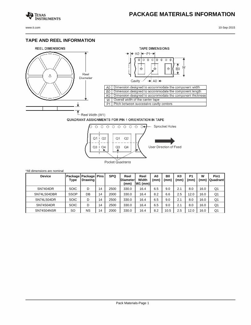
TAPE AND REEL INFORMATION
*All dimensions are nominal
Device PackageType
PackageDrawing
Pins SPQ ReelDiameter
(mm)
ReelWidth
W1 (mm)
A0(mm)
B0(mm)
K0(mm)
P1(mm)
W(mm)
Pin1Quadrant
SN7404DR SOIC D 14 2500 330.0 16.4 6.5 9.0 2.1 8.0 16.0 Q1
SN74LS04DBR SSOP DB 14 2000 330.0 16.4 8.2 6.6 2.5 12.0 16.0 Q1
SN74LS04DR SOIC D 14 2500 330.0 16.4 6.5 9.0 2.1 8.0 16.0 Q1
SN74S04DR SOIC D 14 2500 330.0 16.4 6.5 9.0 2.1 8.0 16.0 Q1
SN74S04NSR SO NS 14 2000 330.0 16.4 8.2 10.5 2.5 12.0 16.0 Q1
PACKAGE MATERIALS INFORMATION
www.ti.com 10-Sep-2015
Pack Materials-Page 1
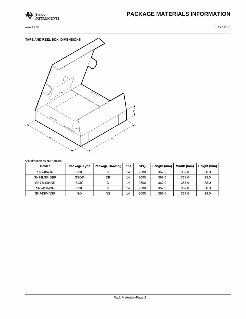
*All dimensions are nominal
Device Package Type Package Drawing Pins SPQ Length (mm) Width (mm) Height (mm)
SN7404DR SOIC D 14 2500 367.0 367.0 38.0
SN74LS04DBR SSOP DB 14 2000 367.0 367.0 38.0
SN74LS04DR SOIC D 14 2500 367.0 367.0 38.0
SN74S04DR SOIC D 14 2500 367.0 367.0 38.0
SN74S04NSR SO NS 14 2000 367.0 367.0 38.0
PACKAGE MATERIALS INFORMATION
www.ti.com 10-Sep-2015
Pack Materials-Page 2
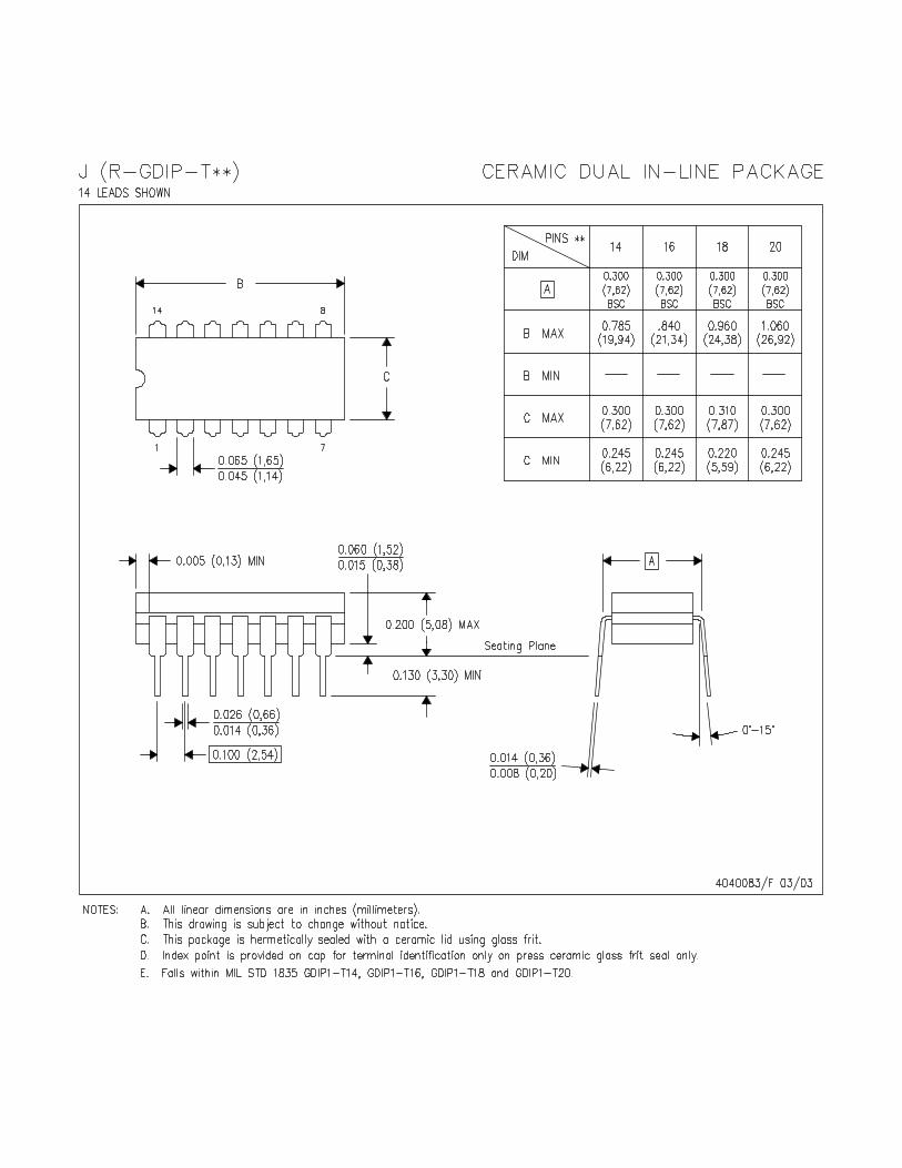
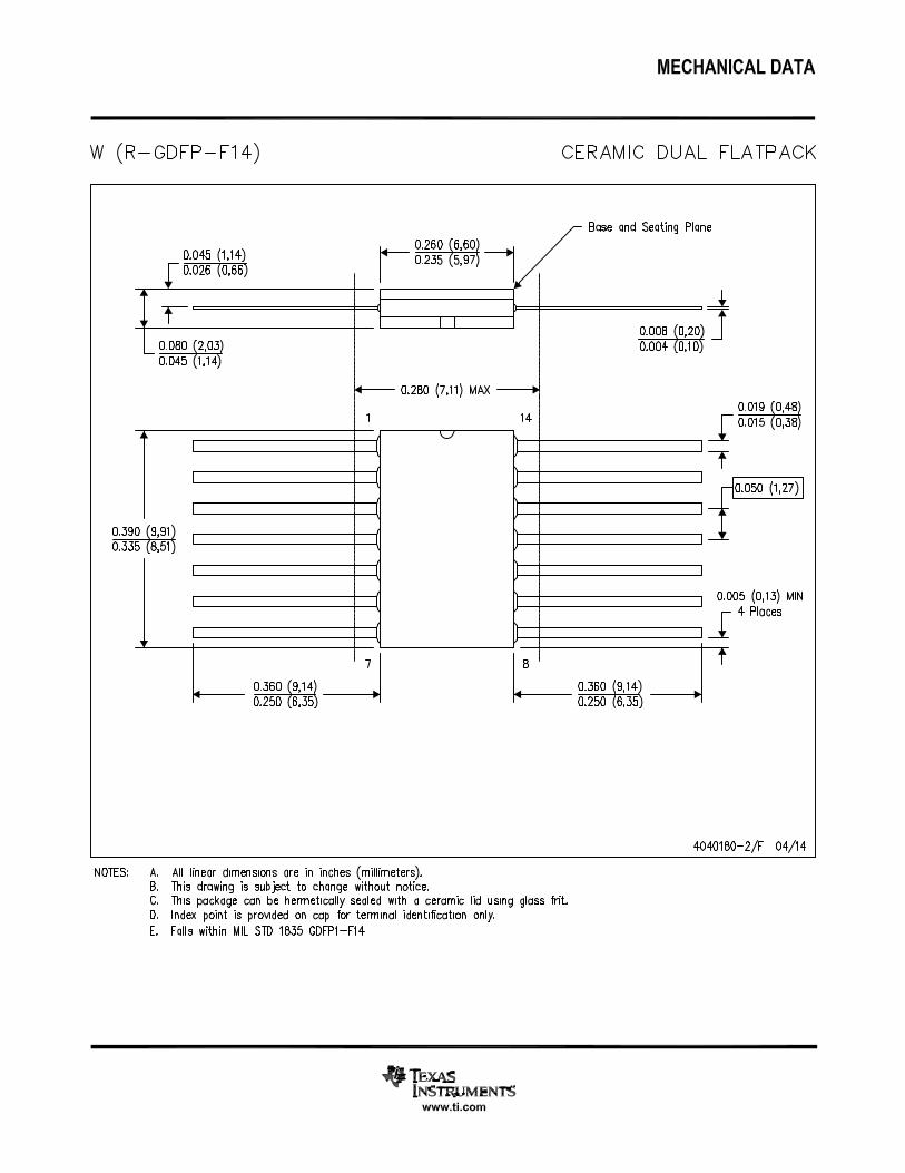
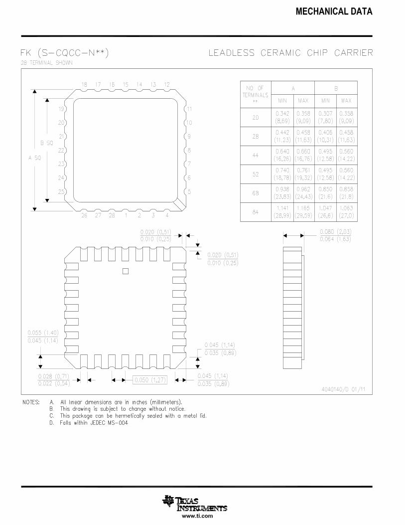
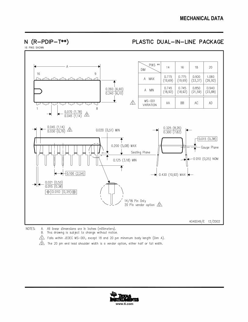
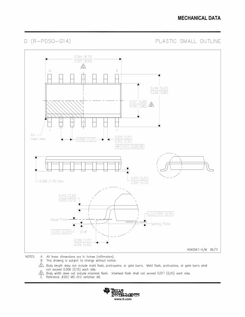
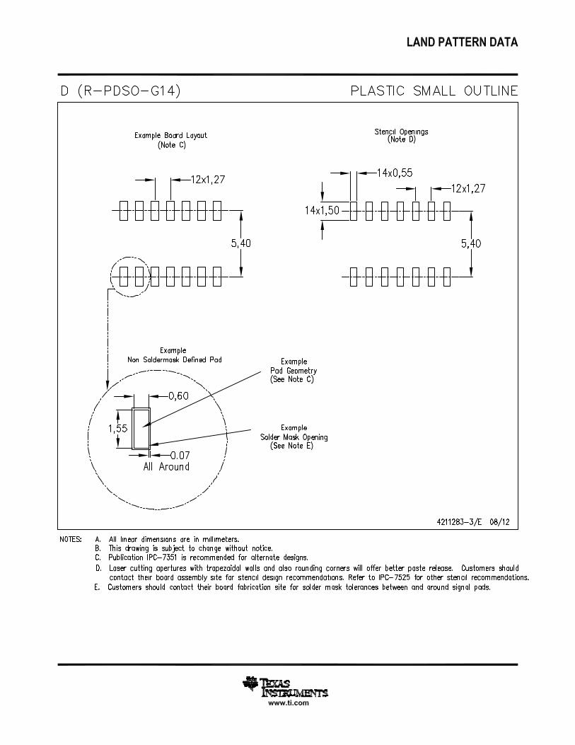
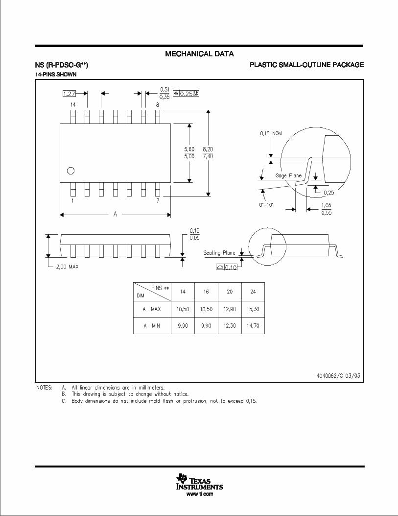
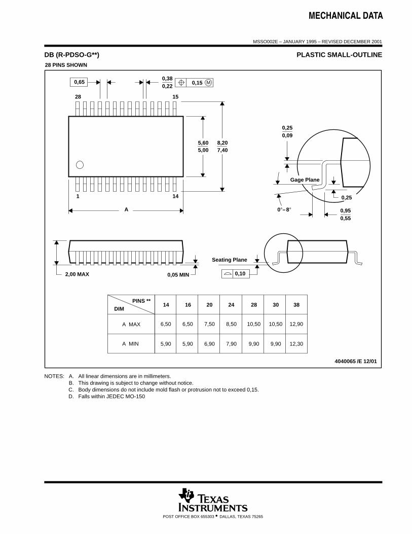
MECHANICAL DATA
MSSO002E – JANUARY 1995 – REVISED DECEMBER 2001
POST OFFICE BOX 655303 • DALLAS, TEXAS 75265
DB (R-PDSO-G**) PLASTIC SMALL-OUTLINE
4040065 /E 12/01
28 PINS SHOWN
Gage Plane
8,207,40
0,550,95
0,25
38
12,90
12,30
28
10,50
24
8,50
Seating Plane
9,907,90
30
10,50
9,90
0,38
5,605,00
15
0,22
14
A
28
1
2016
6,506,50
14
0,05 MIN
5,905,90
DIM
A MAX
A MIN
PINS **
2,00 MAX
6,90
7,50
0,65 M0,15
0°–8°
0,10
0,090,25
NOTES: A. All linear dimensions are in millimeters.B. This drawing is subject to change without notice.C. Body dimensions do not include mold flash or protrusion not to exceed 0,15.D. Falls within JEDEC MO-150

IMPORTANT NOTICE
Texas Instruments Incorporated and its subsidiaries (TI) reserve the right to make corrections, enhancements, improvements and otherchanges to its semiconductor products and services per JESD46, latest issue, and to discontinue any product or service per JESD48, latestissue. Buyers should obtain the latest relevant information before placing orders and should verify that such information is current andcomplete. All semiconductor products (also referred to herein as “components”) are sold subject to TI’s terms and conditions of salesupplied at the time of order acknowledgment.TI warrants performance of its components to the specifications applicable at the time of sale, in accordance with the warranty in TI’s termsand conditions of sale of semiconductor products. Testing and other quality control techniques are used to the extent TI deems necessaryto support this warranty. Except where mandated by applicable law, testing of all parameters of each component is not necessarilyperformed.TI assumes no liability for applications assistance or the design of Buyers’ products. Buyers are responsible for their products andapplications using TI components. To minimize the risks associated with Buyers’ products and applications, Buyers should provideadequate design and operating safeguards.TI does not warrant or represent that any license, either express or implied, is granted under any patent right, copyright, mask work right, orother intellectual property right relating to any combination, machine, or process in which TI components or services are used. Informationpublished by TI regarding third-party products or services does not constitute a license to use such products or services or a warranty orendorsement thereof. Use of such information may require a license from a third party under the patents or other intellectual property of thethird party, or a license from TI under the patents or other intellectual property of TI.Reproduction of significant portions of TI information in TI data books or data sheets is permissible only if reproduction is without alterationand is accompanied by all associated warranties, conditions, limitations, and notices. TI is not responsible or liable for such altereddocumentation. Information of third parties may be subject to additional restrictions.Resale of TI components or services with statements different from or beyond the parameters stated by TI for that component or servicevoids all express and any implied warranties for the associated TI component or service and is an unfair and deceptive business practice.TI is not responsible or liable for any such statements.Buyer acknowledges and agrees that it is solely responsible for compliance with all legal, regulatory and safety-related requirementsconcerning its products, and any use of TI components in its applications, notwithstanding any applications-related information or supportthat may be provided by TI. Buyer represents and agrees that it has all the necessary expertise to create and implement safeguards whichanticipate dangerous consequences of failures, monitor failures and their consequences, lessen the likelihood of failures that might causeharm and take appropriate remedial actions. Buyer will fully indemnify TI and its representatives against any damages arising out of the useof any TI components in safety-critical applications.In some cases, TI components may be promoted specifically to facilitate safety-related applications. With such components, TI’s goal is tohelp enable customers to design and create their own end-product solutions that meet applicable functional safety standards andrequirements. Nonetheless, such components are subject to these terms.No TI components are authorized for use in FDA Class III (or similar life-critical medical equipment) unless authorized officers of the partieshave executed a special agreement specifically governing such use.Only those TI components which TI has specifically designated as military grade or “enhanced plastic” are designed and intended for use inmilitary/aerospace applications or environments. Buyer acknowledges and agrees that any military or aerospace use of TI componentswhich have not been so designated is solely at the Buyer's risk, and that Buyer is solely responsible for compliance with all legal andregulatory requirements in connection with such use.TI has specifically designated certain components as meeting ISO/TS16949 requirements, mainly for automotive use. In any case of use ofnon-designated products, TI will not be responsible for any failure to meet ISO/TS16949.
Products ApplicationsAudio www.ti.com/audio Automotive and Transportation www.ti.com/automotiveAmplifiers amplifier.ti.com Communications and Telecom www.ti.com/communicationsData Converters dataconverter.ti.com Computers and Peripherals www.ti.com/computersDLP® Products www.dlp.com Consumer Electronics www.ti.com/consumer-appsDSP dsp.ti.com Energy and Lighting www.ti.com/energyClocks and Timers www.ti.com/clocks Industrial www.ti.com/industrialInterface interface.ti.com Medical www.ti.com/medicalLogic logic.ti.com Security www.ti.com/securityPower Mgmt power.ti.com Space, Avionics and Defense www.ti.com/space-avionics-defenseMicrocontrollers microcontroller.ti.com Video and Imaging www.ti.com/videoRFID www.ti-rfid.comOMAP Applications Processors www.ti.com/omap TI E2E Community e2e.ti.comWireless Connectivity www.ti.com/wirelessconnectivity
Mailing Address: Texas Instruments, Post Office Box 655303, Dallas, Texas 75265Copyright © 2015, Texas Instruments Incorporated
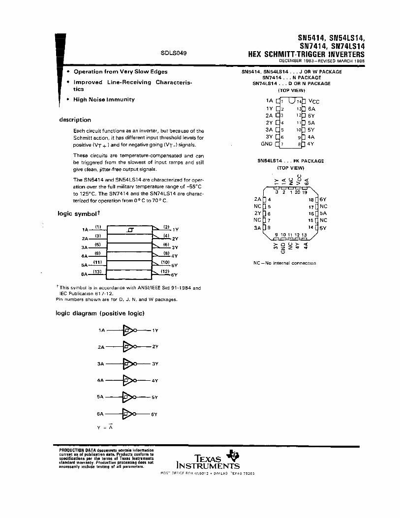
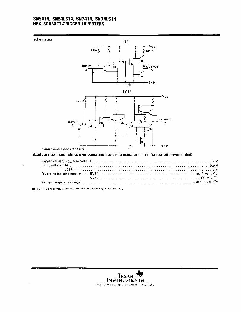

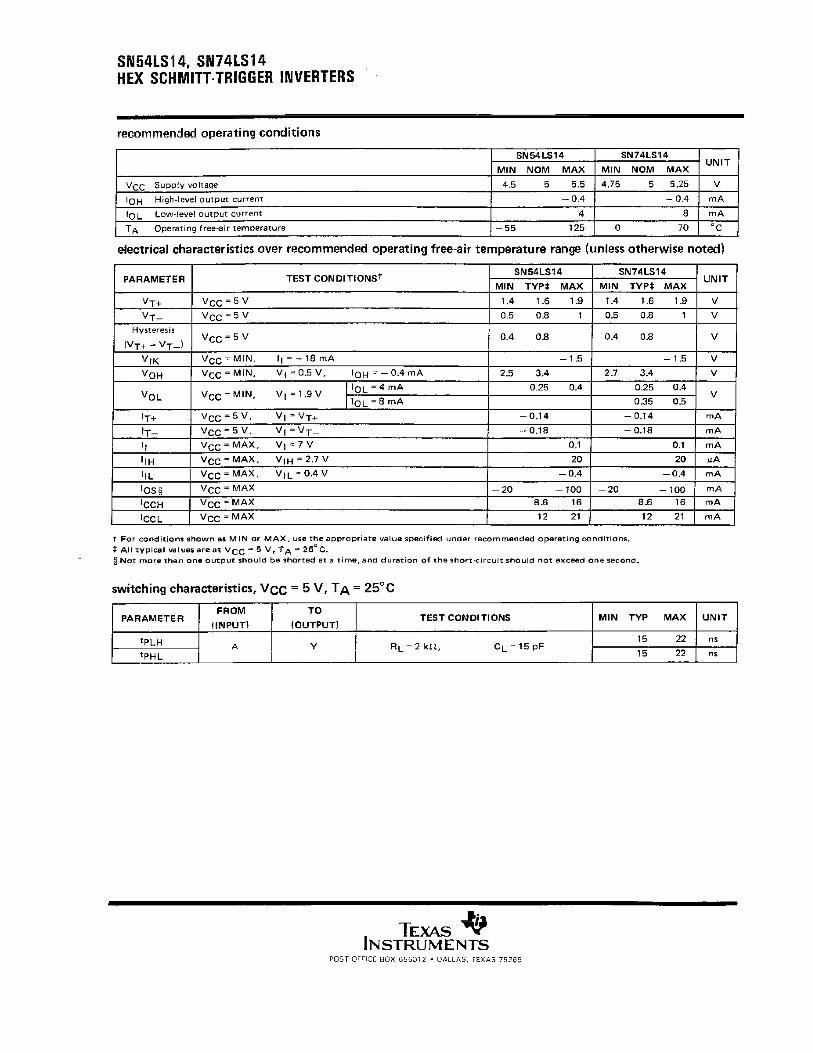
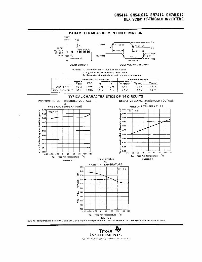
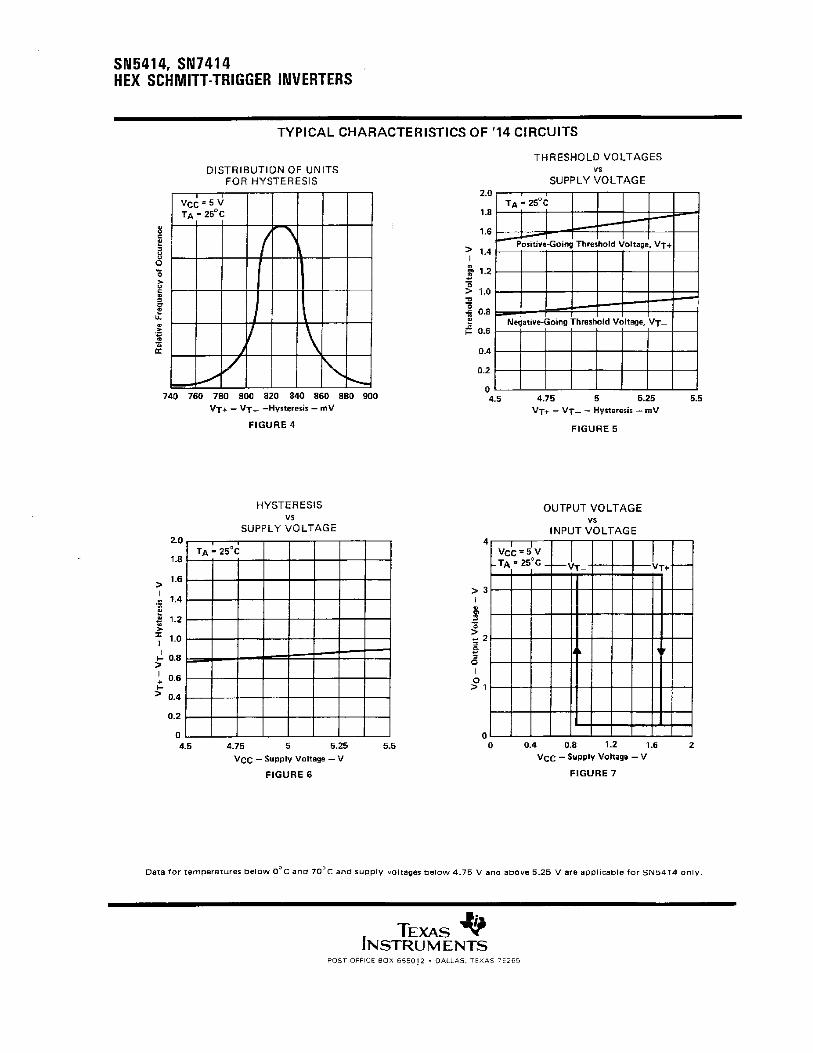
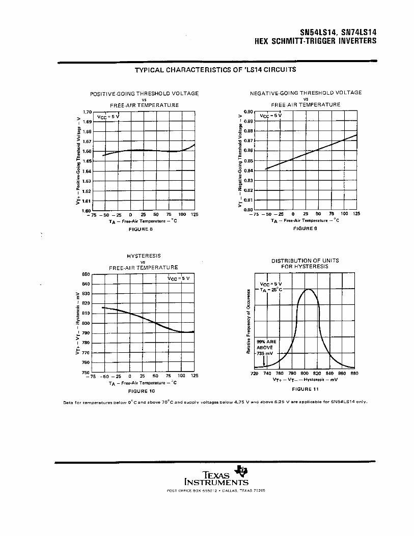
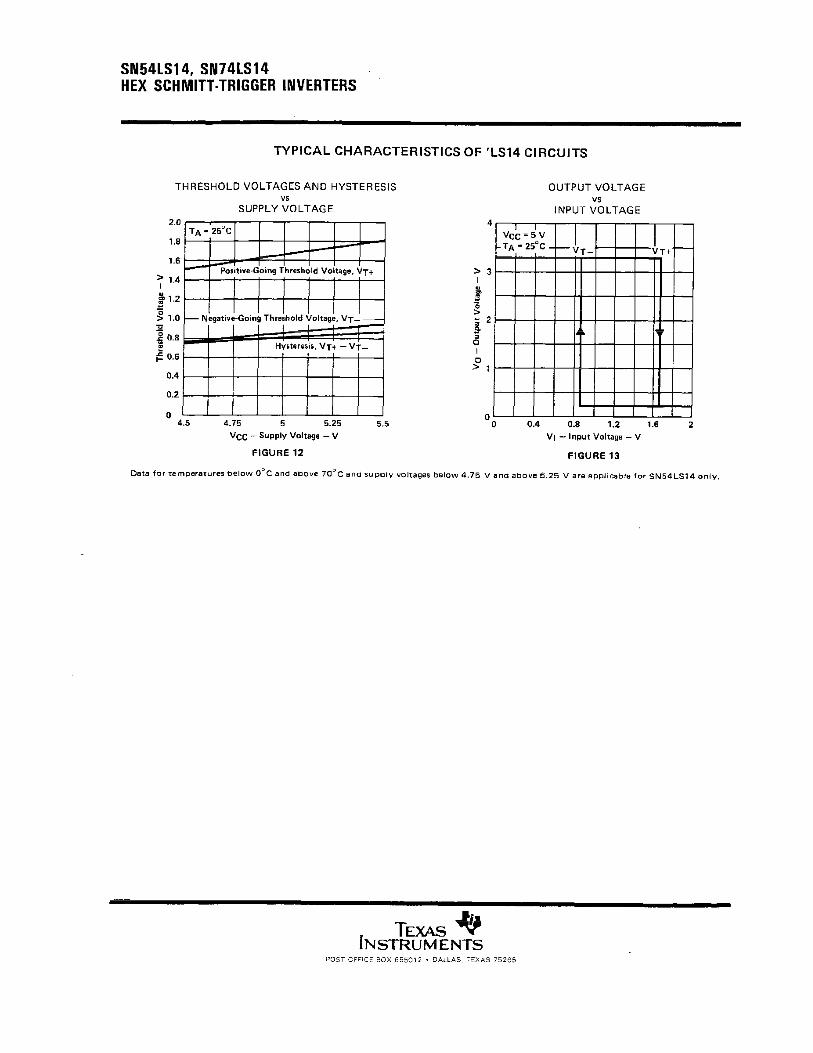
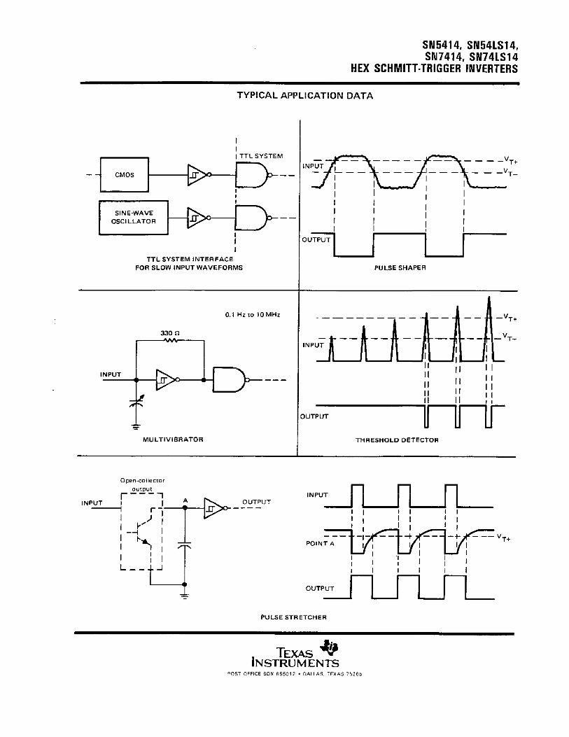
IMPORTANT NOTICE
Texas Instruments and its subsidiaries (TI) reserve the right to make changes to their products or to discontinueany product or service without notice, and advise customers to obtain the latest version of relevant informationto verify, before placing orders, that information being relied on is current and complete. All products are soldsubject to the terms and conditions of sale supplied at the time of order acknowledgement, including thosepertaining to warranty, patent infringement, and limitation of liability.
TI warrants performance of its semiconductor products to the specifications applicable at the time of sale inaccordance with TI’s standard warranty. Testing and other quality control techniques are utilized to the extentTI deems necessary to support this warranty. Specific testing of all parameters of each device is not necessarilyperformed, except those mandated by government requirements.
CERTAIN APPLICATIONS USING SEMICONDUCTOR PRODUCTS MAY INVOLVE POTENTIAL RISKS OFDEATH, PERSONAL INJURY, OR SEVERE PROPERTY OR ENVIRONMENTAL DAMAGE (“CRITICALAPPLICATIONS”). TI SEMICONDUCTOR PRODUCTS ARE NOT DESIGNED, AUTHORIZED, ORWARRANTED TO BE SUITABLE FOR USE IN LIFE-SUPPORT DEVICES OR SYSTEMS OR OTHERCRITICAL APPLICATIONS. INCLUSION OF TI PRODUCTS IN SUCH APPLICATIONS IS UNDERSTOOD TOBE FULLY AT THE CUSTOMER’S RISK.
In order to minimize risks associated with the customer’s applications, adequate design and operatingsafeguards must be provided by the customer to minimize inherent or procedural hazards.
TI assumes no liability for applications assistance or customer product design. TI does not warrant or representthat any license, either express or implied, is granted under any patent right, copyright, mask work right, or otherintellectual property right of TI covering or relating to any combination, machine, or process in which suchsemiconductor products or services might be or are used. TI’s publication of information regarding any thirdparty’s products or services does not constitute TI’s approval, warranty or endorsement thereof.
Copyright 1998, Texas Instruments Incorporated
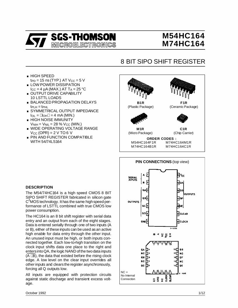
M54HC164M74HC164
October 1992
8 BIT SIPO SHIFT REGISTER
B1R(Plastic Package)
ORDER CODES :M54HC164F1R M74HC164M1RM74HC164B1R M74HC164C1R
F1R(Ceramic Package)
M1R(Micro Package)
C1R(Chip Carrier)
PIN CONNECTIONS (top view)
NC =No InternalConnection
.HIGH SPEEDtPD = 15 ns (TYP.) AT VCC = 5 V.LOW POWER DISSIPATIONICC = 4 µA (MAX.) AT TA = 25 °C.OUTPUT DRIVE CAPABILITY10 LSTTL LOADS.BALANCED PROPAGATION DELAYStPLH = tPHL.SYMMETRICAL OUTPUT IMPEDANCEIOL = IOH = 4 mA (MIN.).HIGH NOISE IMMUNITYVNIH = VNIL = 28 % VCC (MIN.).WIDE OPERATING VOLTAGE RANGEVCC (OPR) = 2 V TO 6 V.PIN AND FUNCTION COMPATIBLEWITH 54/74LS164
DESCRIPTIONThe M54/74HC164 is a high speed CMOS 8 BITSIPO SHIFT REGISTER fabricated in silicon gateC2MOS technology. It has the same highspeed per-formance of LSTTL combined with true CMOS lowpower consumption.
The HC164 is an 8 bit shift register with serial dataentry and an output from each of the eight stages.Data is entered serially through one of two inputs (Aor B), either of these inputs can be used as an activehigh enable for data entry through the other input.An unused input must be high, or both inputs con-nected together. Each low-to-high transition on theclock input shifts data one place to the right andentersintoQA, the logic NAND of the twodata inputs(A ⋅ B), the data that existed before the rising clockedge. A low level on the clear input overrides allother inputs and clears the register asynchronously,forcing all Q outputs low.
All inputs are equipped with protection circuitsagainst static discharge and transient excess volt-age.
1/12
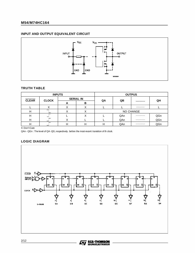
INPUT AND OUTPUT EQUIVALENT CIRCUIT
TRUTH TABLE
INPUTS OUTPUS
CLEAR CLOCKSERIAL IN
QA QB ............ QHA B
L X X X L L ............ L
H X X NO CHANGE
H L X L QAn ............ QGn
H X L L QAn ............ QGn
H H H H QAn ............ QGnX: Don’t CareQAn - QGn : The level of QA -QG, respectively. before the most-recent transition of th clock.
LOGIC DIAGRAM
M54/M74HC164
2/12
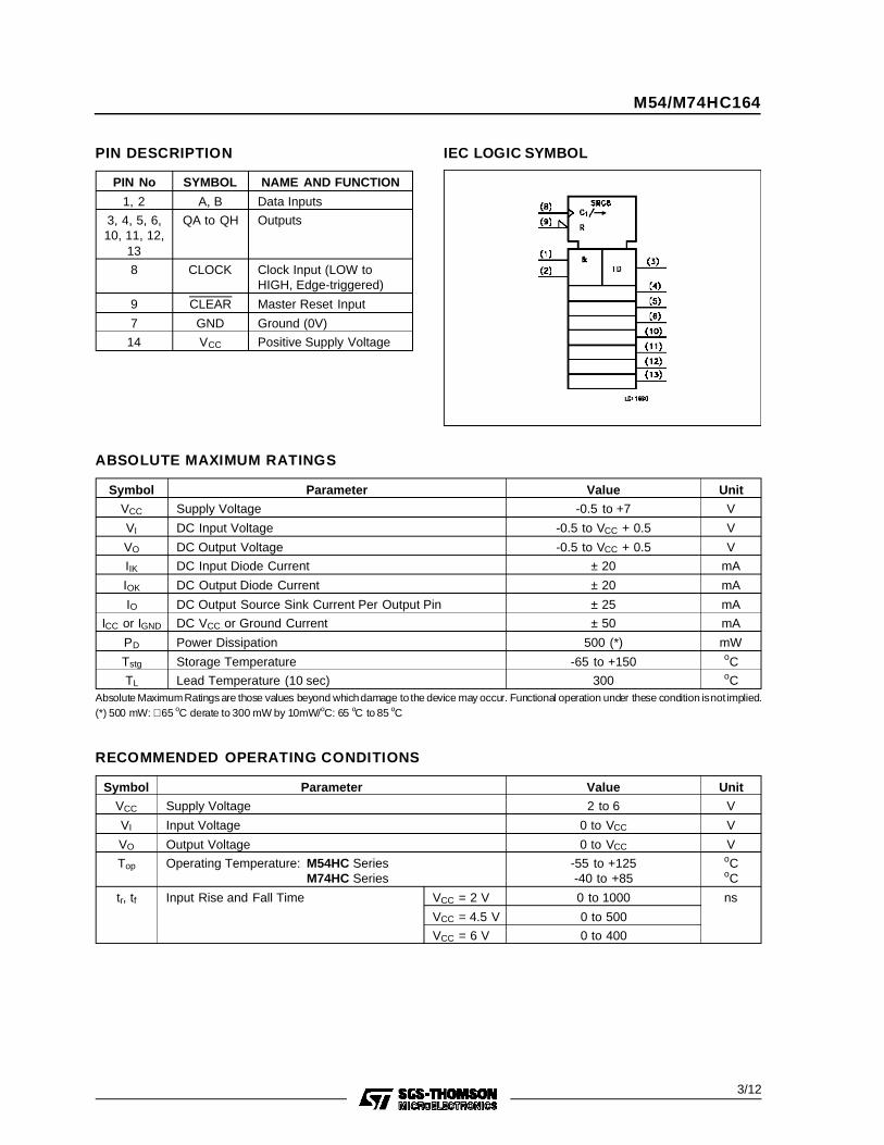
PIN DESCRIPTION
PIN No SYMBOL NAME AND FUNCTION
1, 2 A, B Data Inputs
3, 4, 5, 6,10, 11, 12,
13
QA to QH Outputs
8 CLOCK Clock Input (LOW toHIGH, Edge-triggered)
9 CLEAR Master Reset Input
7 GND Ground (0V)
14 VCC Positive Supply Voltage
IEC LOGIC SYMBOL
ABSOLUTE MAXIMUM RATINGS
Symbol Parameter Value Unit
VCC Supply Voltage -0.5 to +7 V
VI DC Input Voltage -0.5 to VCC + 0.5 V
VO DC Output Voltage -0.5 to VCC + 0.5 V
IIK DC Input Diode Current ± 20 mA
IOK DC Output Diode Current ± 20 mA
IO DC Output Source Sink Current Per Output Pin ± 25 mA
ICC or IGND DC VCC or Ground Current ± 50 mA
PD Power Dissipation 500 (*) mW
Tstg Storage Temperature -65 to +150 oC
TL Lead Temperature (10 sec) 300 oCAbsolute MaximumRatings are those values beyond whichdamage to the device may occur. Functional operation under these condition isnot implied.(*) 500 mW: ≅ 65 oC derate to 300 mW by 10mW/oC: 65 oC to 85 oC
RECOMMENDED OPERATING CONDITIONS
Symbol Parameter Value Unit
VCC Supply Voltage 2 to 6 V
VI Input Voltage 0 to VCC V
VO Output Voltage 0 to VCC V
Top Operating Temperature: M54HC SeriesM74HC Series
-55 to +125-40 to +85
oCoC
tr, tf Input Rise and Fall Time VCC = 2 V 0 to 1000 ns
VCC = 4.5 V 0 to 500
VCC = 6 V 0 to 400
M54/M74HC164
3/12
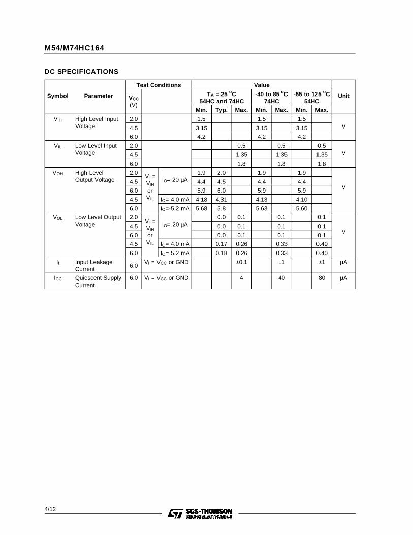
DC SPECIFICATIONS
Symbol Parameter
Test Conditions Value
UnitVCC
(V)
TA = 25 oC54HC and 74HC
-40 to 85 oC74HC
-55 to 125 oC54HC
Min. Typ. Max. Min. Max. Min. Max.
VIH High Level InputVoltage
2.0 1.5 1.5 1.5V4.5 3.15 3.15 3.15
6.0 4.2 4.2 4.2
VIL Low Level InputVoltage
2.0 0.5 0.5 0.5V4.5 1.35 1.35 1.35
6.0 1.8 1.8 1.8
VOH High LevelOutput Voltage
2.0VI =VIH
orVIL
IO=-20 µA1.9 2.0 1.9 1.9
V4.5 4.4 4.5 4.4 4.4
6.0 5.9 6.0 5.9 5.9
4.5 IO=-4.0 mA 4.18 4.31 4.13 4.10
6.0 IO=-5.2 mA 5.68 5.8 5.63 5.60
VOL Low Level OutputVoltage
2.0VI =VIH
orVIL
IO= 20 µA0.0 0.1 0.1 0.1
V4.5 0.0 0.1 0.1 0.1
6.0 0.0 0.1 0.1 0.1
4.5 IO= 4.0 mA 0.17 0.26 0.33 0.40
6.0 IO= 5.2 mA 0.18 0.26 0.33 0.40
II Input LeakageCurrent
6.0VI = VCC or GND ±0.1 ±1 ±1 µA
ICC Quiescent SupplyCurrent
6.0 VI = VCC or GND 4 40 80 µA
M54/M74HC164
4/12
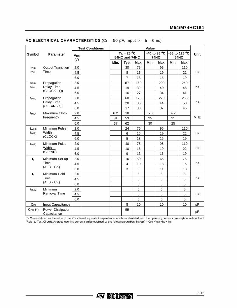
AC ELECTRICAL CHARACTERISTICS (CL = 50 pF, Input tr = tf = 6 ns)
Symbol Parameter
Test Conditions Value
UnitVCC
(V)
TA = 25 oC54HC and 74HC
-40 to 85 oC74HC
-55 to 125 oC54HC
Min. Typ. Max. Min. Max. Min. Max.tTLH
tTHL
Output TransitionTime
2.0 30 75 95 110ns4.5 8 15 19 22
6.0 7 13 16 19
tPLH
tPHL
PropagationDelay Time(CLOCK - Q)
2.0 57 160 200 240ns4.5 19 32 40 48
6.0 16 27 34 41
tPHL PropagationDelay Time(CLEAR - Q)
2.0 60 175 220 265ns4.5 20 35 44 53
6.0 17 30 37 45
fMAX Maximum ClockFrequency
2.0 6.2 18 5.0 4.2MHz4.5 31 53 25 21
6.0 37 62 30 25
tW(H)
tW(L)
Minimum PulseWidth(CLOCK)
2.0 24 75 95 110ns4.5 6 15 19 22
6.0 5 13 16 19
tW(L) Minimum PulseWidth(CLEAR)
2.0 40 75 95 110ns4.5 10 15 19 22
6.0 9 13 16 19
ts Minimum Set-upTime(A, B - CK)
2.0 16 50 65 75ns4.5 4 10 13 15
6.0 3 9 11 13
th Minimum HoldTime(A, B - CK)
2.0 5 5 5ns4.5 5 5 5
6.0 5 5 5
tREM MinimumRemoval Time
2.0 5 5 5ns4.5 5 5 5
6.0 5 5 5
CIN Input Capacitance 5 10 10 10 pF
CPD (*) Power DissipationCapacitance
99pF
(*) CPD is defined as the value of the IC’s internal equivalent capacitance which is calculated from the operating current consumption without load.(Refer to Test Circuit). Average operting current can be obtained by the followingequation. ICC(opr) = CPD • VCC • fIN + ICC
M54/M74HC164
5/12
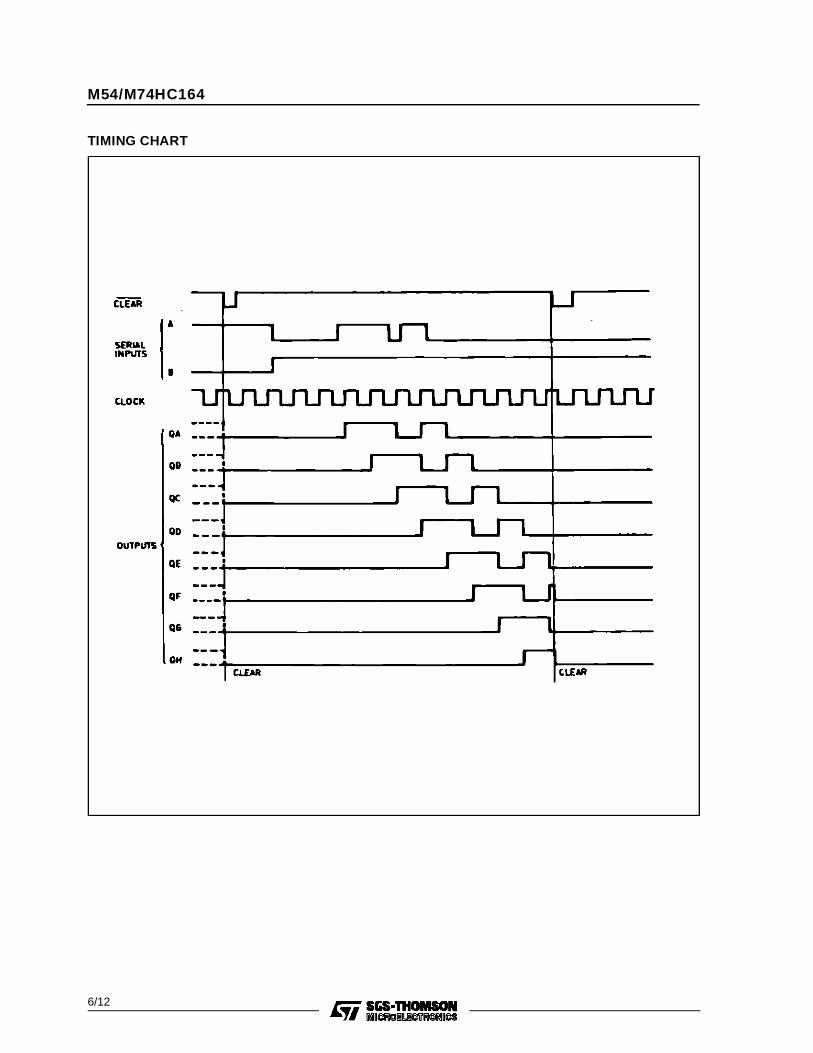
TIMING CHART
M54/M74HC164
6/12
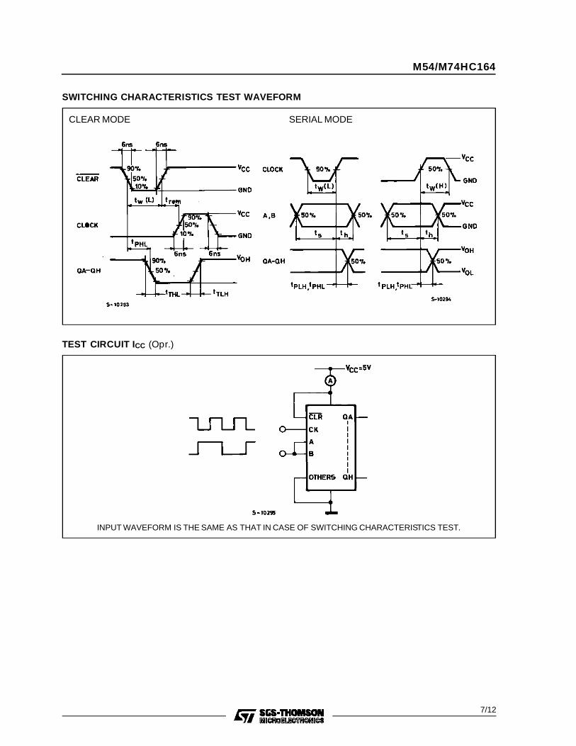
SWITCHING CHARACTERISTICS TEST WAVEFORM
TEST CIRCUIT ICC (Opr.)
INPUT WAVEFORM IS THE SAME AS THAT IN CASE OF SWITCHING CHARACTERISTICS TEST.
CLEAR MODE SERIAL MODE
M54/M74HC164
7/12
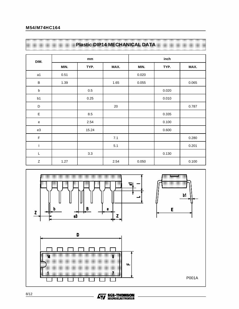
Plastic DIP14 MECHANICAL DATA
DIM.mm inch
MIN. TYP. MAX. MIN. TYP. MAX.
a1 0.51 0.020
B 1.39 1.65 0.055 0.065
b 0.5 0.020
b1 0.25 0.010
D 20 0.787
E 8.5 0.335
e 2.54 0.100
e3 15.24 0.600
F 7.1 0.280
I 5.1 0.201
L 3.3 0.130
Z 1.27 2.54 0.050 0.100
P001A
M54/M74HC164
8/12
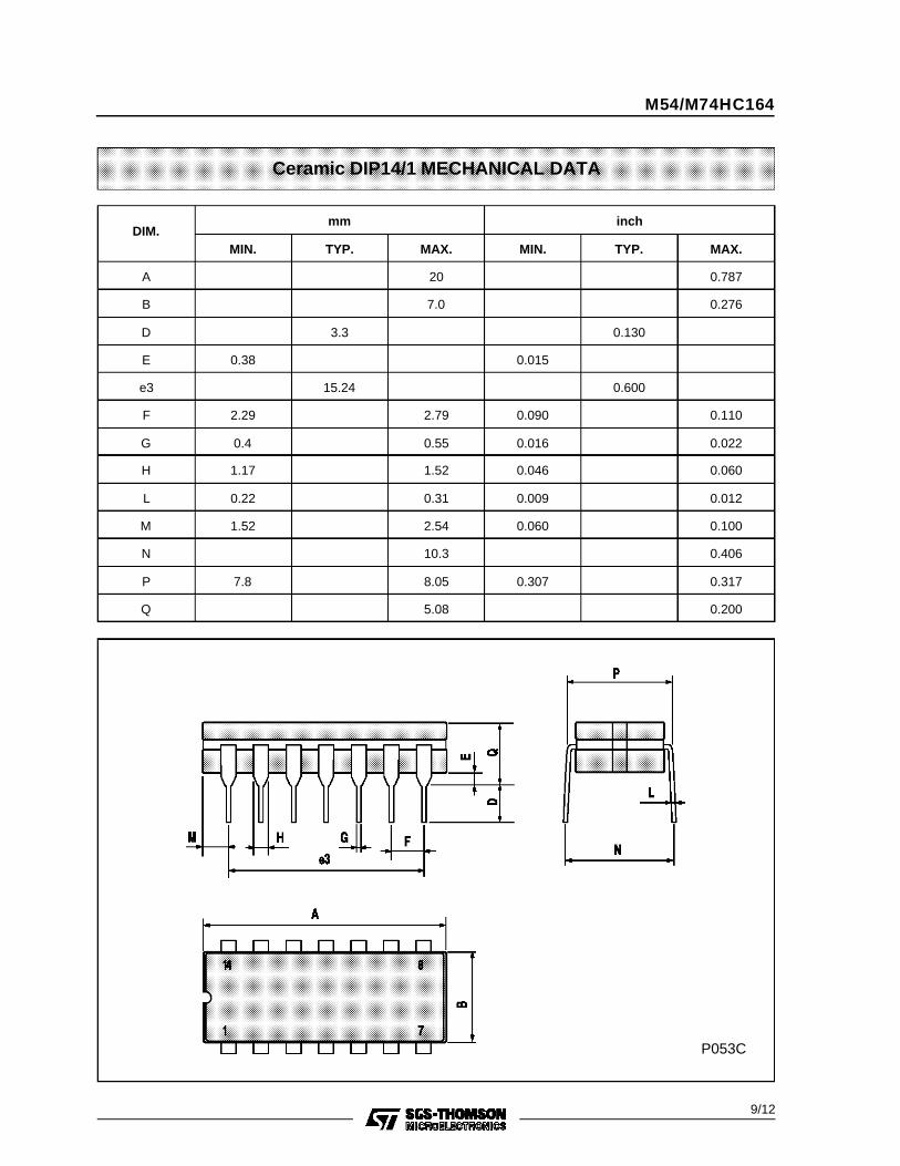
Ceramic DIP14/1 MECHANICAL DATA
DIM.mm inch
MIN. TYP. MAX. MIN. TYP. MAX.
A 20 0.787
B 7.0 0.276
D 3.3 0.130
E 0.38 0.015
e3 15.24 0.600
F 2.29 2.79 0.090 0.110
G 0.4 0.55 0.016 0.022
H 1.17 1.52 0.046 0.060
L 0.22 0.31 0.009 0.012
M 1.52 2.54 0.060 0.100
N 10.3 0.406
P 7.8 8.05 0.307 0.317
Q 5.08 0.200
P053C
M54/M74HC164
9/12
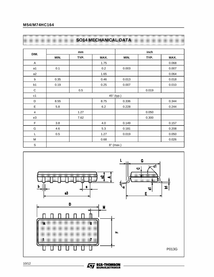
SO14 MECHANICAL DATA
DIM.mm inch
MIN. TYP. MAX. MIN. TYP. MAX.
A 1.75 0.068
a1 0.1 0.2 0.003 0.007
a2 1.65 0.064
b 0.35 0.46 0.013 0.018
b1 0.19 0.25 0.007 0.010
C 0.5 0.019
c1 45° (typ.)
D 8.55 8.75 0.336 0.344
E 5.8 6.2 0.228 0.244
e 1.27 0.050
e3 7.62 0.300
F 3.8 4.0 0.149 0.157
G 4.6 5.3 0.181 0.208
L 0.5 1.27 0.019 0.050
M 0.68 0.026
S 8° (max.)
P013G
M54/M74HC164
10/12
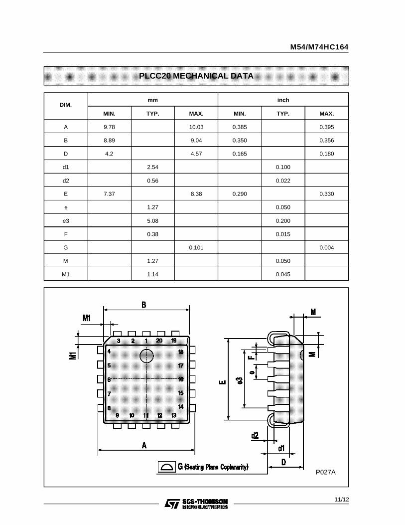
PLCC20 MECHANICAL DATA
DIM.mm inch
MIN. TYP. MAX. MIN. TYP. MAX.
A 9.78 10.03 0.385 0.395
B 8.89 9.04 0.350 0.356
D 4.2 4.57 0.165 0.180
d1 2.54 0.100
d2 0.56 0.022
E 7.37 8.38 0.290 0.330
e 1.27 0.050
e3 5.08 0.200
F 0.38 0.015
G 0.101 0.004
M 1.27 0.050
M1 1.14 0.045
P027A
M54/M74HC164
11/12
Information furnished is believed to be accurate and reliable. However, SGS-THOMSON Microelectronics assumes no responsability for theconsequences of use of such information nor for any infringement of patents or other rights of third parties which may results from its use. Nolicense is granted by implication or otherwise under any patent or patent rights of SGS-THOMSON Microelectronics. Specificationsmentionedin this publication are subject to change without notice. This publication supersedes and replaces all information previously supplied.SGS-THOMSON Microelectronicsproducts are not authorized foruse ascritical components in life support devices or systems without expresswritten approval of SGS-THOMSON Microelectonics.
1994 SGS-THOMSON Microelectronics - All Rights Reserved
SGS-THOMSON Microelectronics GROUP OF COMPANIESAustralia - Brazil - France - Germany - Hong Kong - Italy - Japan - Korea - Malaysia - Malta - Morocco - The Netherlands -
Singapore - Spain - Sweden - Switzerland - Taiwan - Thailand - United Kingdom - U.S.A
M54/M74HC164
12/12
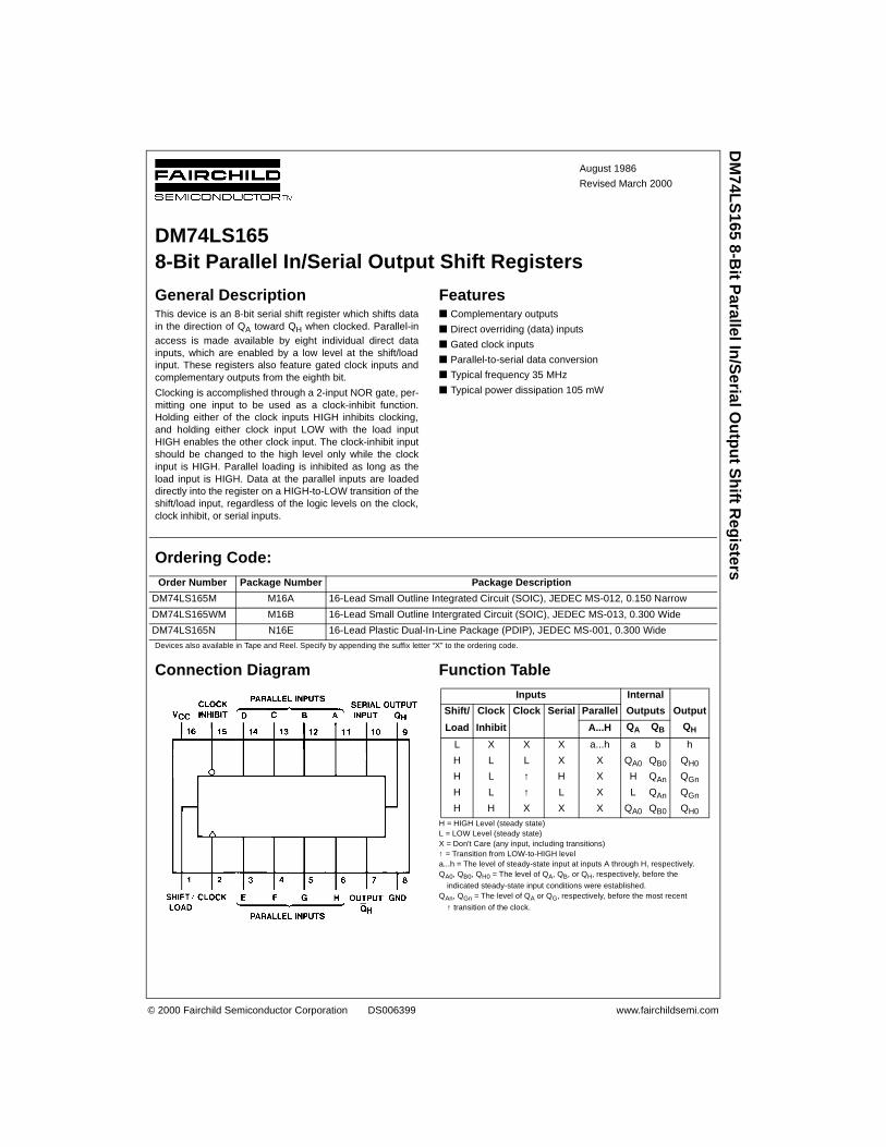
© 2000 Fairchild Semiconductor Corporation DS006399 www.fairchildsemi.com
August 1986
Revised March 2000
DM
74LS
165 8-Bit P
arallel In/S
erial Ou
tpu
t Sh
ift Reg
isters
DM74LS1658-Bit Parallel In/Serial Output Shift Registers
General DescriptionThis device is an 8-bit serial shift register which shifts datain the direction of QA toward QH when clocked. Parallel-inaccess is made available by eight individual direct datainputs, which are enabled by a low level at the shift/loadinput. These registers also feature gated clock inputs andcomplementary outputs from the eighth bit.
Clocking is accomplished through a 2-input NOR gate, per-mitting one input to be used as a clock-inhibit function.Holding either of the clock inputs HIGH inhibits clocking,and holding either clock input LOW with the load inputHIGH enables the other clock input. The clock-inhibit inputshould be changed to the high level only while the clockinput is HIGH. Parallel loading is inhibited as long as theload input is HIGH. Data at the parallel inputs are loadeddirectly into the register on a HIGH-to-LOW transition of theshift/load input, regardless of the logic levels on the clock,clock inhibit, or serial inputs.
Features Complementary outputs
Direct overriding (data) inputs
Gated clock inputs
Parallel-to-serial data conversion
Typical frequency 35 MHz
Typical power dissipation 105 mW
Ordering Code:
Devices also available in Tape and Reel. Specify by appending the suffix letter “X” to the ordering code.
Connection Diagram Function Table
H = HIGH Level (steady state)L = LOW Level (steady state)X = Don't Care (any input, including transitions)↑ = Transition from LOW-to-HIGH levela...h = The level of steady-state input at inputs A through H, respectively.QA0, QB0, QH0 = The level of QA, QB, or QH, respectively, before the
indicated steady-state input conditions were established.QAn, QGn = The level of QA or QG, respectively, before the most recent
↑ transition of the clock.
Order Number Package Number Package Description
DM74LS165M M16A 16-Lead Small Outline Integrated Circuit (SOIC), JEDEC MS-012, 0.150 Narrow
DM74LS165WM M16B 16-Lead Small Outline Intergrated Circuit (SOIC), JEDEC MS-013, 0.300 Wide
DM74LS165N N16E 16-Lead Plastic Dual-In-Line Package (PDIP), JEDEC MS-001, 0.300 Wide
Inputs Internal
Shift/ Clock Clock Serial Parallel Outputs Output
Load Inhibit A...H QA QB QH
L X X X a...h a b h
H L L X X QA0 QB0 QH0
H L ↑ H X H QAn QGn
H L ↑ L X L QAn QGn
H H X X X QA0 QB0 QH0
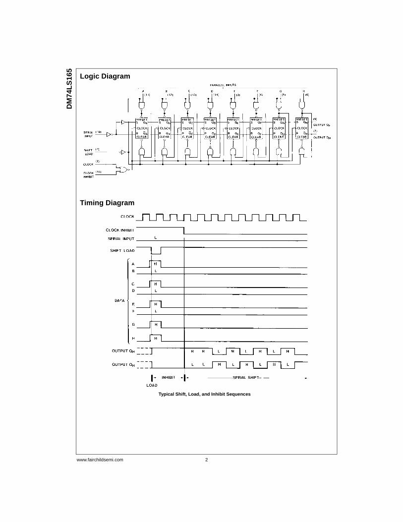
www.fairchildsemi.com 2
DM
74L
S16
5Logic Diagram
Timing Diagram
Typical Shift, Load, and Inhibit Sequences
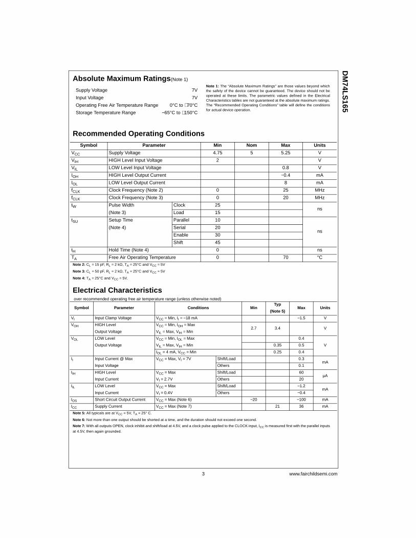
3 www.fairchildsemi.com
DM
74LS
165Absolute Maximum Ratings(Note 1)
Note 1: The “Absolute Maximum Ratings” are those values beyond whichthe safety of the device cannot be guaranteed. The device should not beoperated at these limits. The parametric values defined in the ElectricalCharacteristics tables are not guaranteed at the absolute maximum ratings.The “Recommended Operating Conditions” table will define the conditionsfor actual device operation.
Recommended Operating Conditions
Note 2: CL = 15 pF, RL = 2 kΩ, TA = 25°C and VCC = 5V
Note 3: CL = 50 pF, RL = 2 kΩ, TA = 25°C and VCC = 5V
Note 4: TA = 25°C and VCC = 5V.
Electrical Characteristics over recommended operating free air temperature range (unless otherwise noted)
Note 5: All typicals are at VCC = 5V, TA = 25° C.
Note 6: Not more than one output should be shorted at a time, and the duration should not exceed one second.
Note 7: With all outputs OPEN, clock inhibit and shift/load at 4.5V, and a clock pulse applied to the CLOCK input, ICC is measured first with the parallel inputs
at 4.5V, then again grounded.
Supply Voltage 7V
Input Voltage 7V
Operating Free Air Temperature Range 0°C to +70°C
Storage Temperature Range −65°C to +150°C
Symbol Parameter Min Nom Max Units
VCC Supply Voltage 4.75 5 5.25 V
VIH HIGH Level Input Voltage 2 V
VIL LOW Level Input Voltage 0.8 V
IOH HIGH Level Output Current −0.4 mA
IOL LOW Level Output Current 8 mA
fCLK Clock Frequency (Note 2) 0 25 MHz
fCLK Clock Frequency (Note 3) 0 20 MHz
tW Pulse Width Clock 25ns
(Note 3) Load 15
tSU Setup Time Parallel 10
(Note 4) Serial 20ns
Enable 30
Shift 45
tH Hold Time (Note 4) 0 ns
TA Free Air Operating Temperature 0 70 °C
Symbol Parameter Conditions MinTyp
Max Units(Note 5)
VI Input Clamp Voltage VCC = Min, II = −18 mA −1.5 V
VOH HIGH Level VCC = Min, IOH = Max2.7 3.4 V
Output Voltage VIL = Max, VIH = Min
VOL LOW Level VCC = Min, IOL = Max 0.4
Output Voltage VIL = Max, VIH = Min 0.35 0.5 V
IOL = 4 mA, VCC = Min 0.25 0.4
II Input Current @ Max VCC = Max, VI = 7V Shift/Load 0.3mA
Input Voltage Others 0.1
IIH HIGH Level VCC = Max Shift/Load 60µA
Input Current VI = 2.7V Others 20
IIL LOW Level VCC = Max Shift/Load −1.2mA
Input Current VI = 0.4V Others −0.4
IOS Short Circuit Output Current VCC = Max (Note 6) −20 −100 mA
ICC Supply Current VCC = Max (Note 7) 21 36 mA
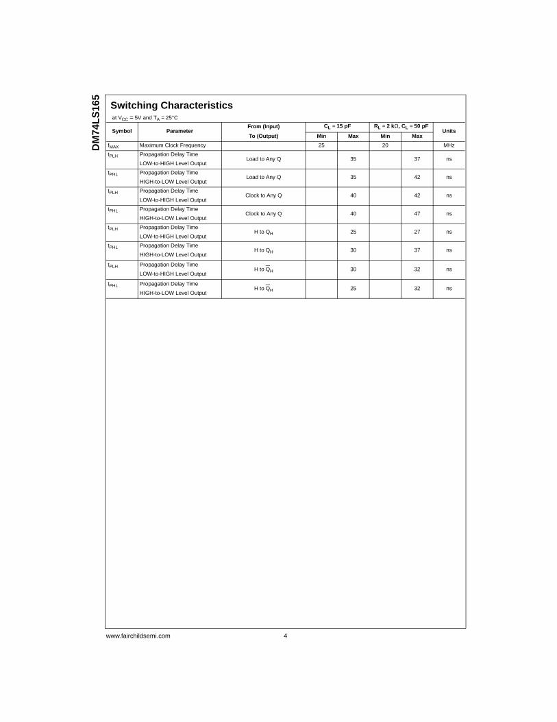
www.fairchildsemi.com 4
DM
74L
S16
5Switching Characteristics at VCC = 5V and TA = 25°C
Symbol ParameterFrom (Input) CL = 15 pF RL = 2 kΩ, CL = 50 pF
UnitsTo (Output) Min Max Min Max
fMAX Maximum Clock Frequency 25 20 MHz
tPLH Propagation Delay TimeLoad to Any Q 35 37 ns
LOW-to-HIGH Level Output
tPHL Propagation Delay TimeLoad to Any Q 35 42 ns
HIGH-to-LOW Level Output
tPLH Propagation Delay TimeClock to Any Q 40 42 ns
LOW-to-HIGH Level Output
tPHL Propagation Delay TimeClock to Any Q 40 47 ns
HIGH-to-LOW Level Output
tPLH Propagation Delay TimeH to QH 25 27 ns
LOW-to-HIGH Level Output
tPHL Propagation Delay TimeH to QH 30 37 ns
HIGH-to-LOW Level Output
tPLH Propagation Delay TimeH to QH 30 32 ns
LOW-to-HIGH Level Output
tPHL Propagation Delay TimeH to QH 25 32 ns
HIGH-to-LOW Level Output
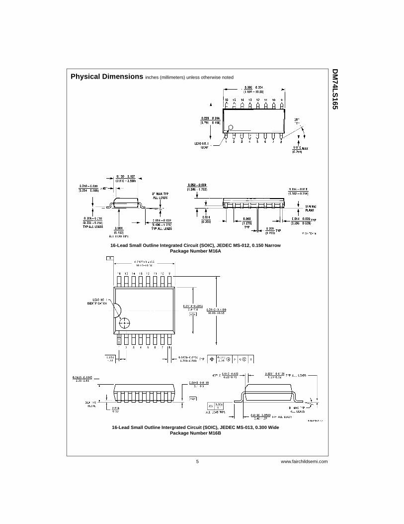
5 www.fairchildsemi.com
DM
74LS
165Physical Dimensions inches (millimeters) unless otherwise noted
16-Lead Small Outline Integrated Circuit (SOIC), JEDEC MS-012, 0.150 NarrowPackage Number M16A
16-Lead Small Outline Intergrated Circuit (SOIC), JEDEC MS-013, 0.300 WidePackage Number M16B
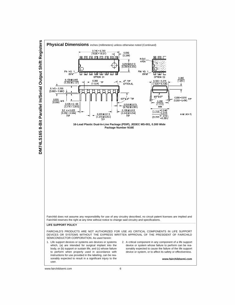
www.fairchildsemi.com 6
DM
74L
S16
5 8-
Bit
Par
alle
l In
/Ser
ial O
utp
ut
Sh
ift
Reg
iste
rs Physical Dimensions inches (millimeters) unless otherwise noted (Continued)
16-Lead Plastic Dual-In-Line Package (PDIP), JEDEC MS-001, 0.300 WidePackage Number N16E
Fairchild does not assume any responsibility for use of any circuitry described, no circuit patent licenses are implied andFairchild reserves the right at any time without notice to change said circuitry and specifications.
LIFE SUPPORT POLICY
FAIRCHILD’S PRODUCTS ARE NOT AUTHORIZED FOR USE AS CRITICAL COMPONENTS IN LIFE SUPPORTDEVICES OR SYSTEMS WITHOUT THE EXPRESS WRITTEN APPROVAL OF THE PRESIDENT OF FAIRCHILDSEMICONDUCTOR CORPORATION. As used herein:
1. Life support devices or systems are devices or systemswhich, (a) are intended for surgical implant into thebody, or (b) support or sustain life, and (c) whose failureto perform when properly used in accordance withinstructions for use provided in the labeling, can be rea-sonably expected to result in a significant injury to theuser.
2. A critical component in any component of a life supportdevice or system whose failure to perform can be rea-sonably expected to cause the failure of the life supportdevice or system, or to affect its safety or effectiveness.
www.fairchildsemi.com
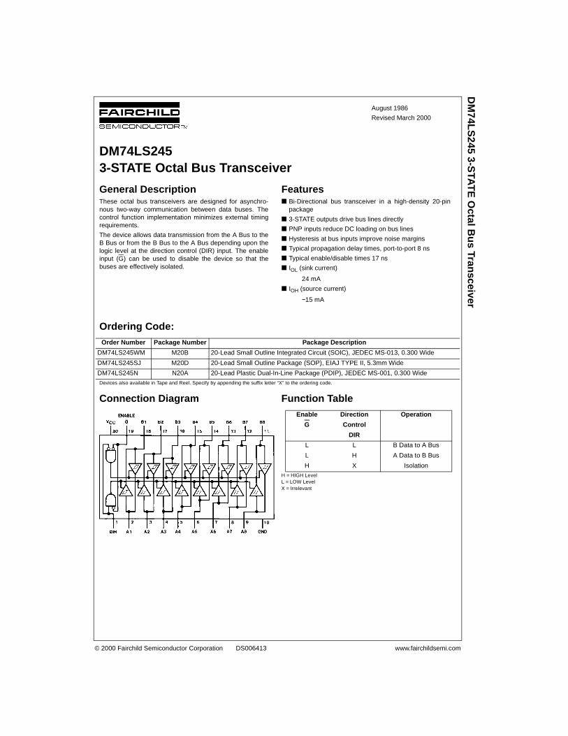
© 2000 Fairchild Semiconductor Corporation DS006413 www.fairchildsemi.com
August 1986
Revised March 2000
DM
74LS
245 3-STA
TE
Octal B
us Tran
sceiver
DM74LS2453-STATE Octal Bus Transceiver
General DescriptionThese octal bus transceivers are designed for asynchro-nous two-way communication between data buses. Thecontrol function implementation minimizes external timingrequirements.
The device allows data transmission from the A Bus to theB Bus or from the B Bus to the A Bus depending upon thelogic level at the direction control (DIR) input. The enableinput (G) can be used to disable the device so that thebuses are effectively isolated.
Features Bi-Directional bus transceiver in a high-density 20-pin
package
3-STATE outputs drive bus lines directly
PNP inputs reduce DC loading on bus lines
Hysteresis at bus inputs improve noise margins
Typical propagation delay times, port-to-port 8 ns
Typical enable/disable times 17 ns
IOL (sink current)
24 mA
IOH (source current)
−15 mA
Ordering Code:
Devices also available in Tape and Reel. Specify by appending the suffix letter “X” to the ordering code.
Connection Diagram Function Table
H = HIGH LevelL = LOW LevelX = Irrelevant
Order Number Package Number Package Description
DM74LS245WM M20B 20-Lead Small Outline Integrated Circuit (SOIC), JEDEC MS-013, 0.300 Wide
DM74LS245SJ M20D 20-Lead Small Outline Package (SOP), EIAJ TYPE II, 5.3mm Wide
DM74LS245N N20A 20-Lead Plastic Dual-In-Line Package (PDIP), JEDEC MS-001, 0.300 Wide
Enable Direction Operation
G Control
DIR
L L B Data to A Bus
L H A Data to B Bus
H X Isolation
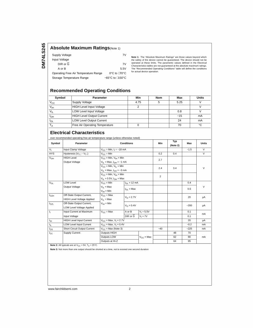
www.fairchildsemi.com 2
DM
74L
S24
5Absolute Maximum Ratings(Note 1)
Note 1: The “Absolute Maximum Ratings” are those values beyond whichthe safety of the device cannot be guaranteed. The device should not beoperated at these limits. The parametric values defined in the ElectricalCharacteristics tables are not guaranteed at the absolute maximum ratings.The “Recommended Operating Conditions” table will define the conditionsfor actual device operation.
Recommended Operating Conditions
Electrical Characteristics over recommended operating free air temperature range (unless otherwise noted)
Note 2: All typicals are at VCC = 5V, TA = 25°C.
Note 3: Not more than one output should be shorted at a time, not to exceed one second duration
Supply Voltage 7V
Input Voltage
DIR or G 7V
A or B 5.5V
Operating Free Air Temperature Range 0°C to +70°C
Storage Temperature Range −65°C to +150°C
Symbol Parameter Min Nom Max Units
VCC Supply Voltage 4.75 5 5.25 V
VIH HIGH Level Input Voltage 2 V
VIL LOW Level Input Voltage 0.8 V
IOH HIGH Level Output Current −15 mA
IOL LOW Level Output Current 24 mA
TA Free Air Operating Temperature 0 70 °C
Symbol Parameter Conditions MinTyp
Max Units(Note 2)
VI Input Clamp Voltage VCC = Min, II = −18 mA −1.5 V
HYS Hysteresis (VT+ − VT−) VCC = Min 0.2 0.4 V
VOH HIGH Level VCC = Min, VIH = Min2.7
Output Voltage VIL = Max, IOH = −1 mA
VCC = Min, VIL = Min2.4 3.4 V
VIL = Max, IOH = −3 mA
VCC = Min, VIH = Min2
VIL = 0.5V, IOH = Max
VOL LOW Level VCC = Min IOL = 12 mA 0.4
Output Voltage VIL = MaxIOL = Max 0.5
V
VIH = Min
IOZH Off-State Output Current, VCC = MaxVO = 2.7V 20 µA
HIGH Level Voltage Applied VIL = Max
IOZL Off-State Output Current, VIH = MinVO = 0.4V −200 µA
LOW Level Voltage Applied
II Input Current at Maximum VCC = Max A or B VI = 5.5V 0.1mA
Input Voltage DIR or G VI = 7V 0.1
IIH HIGH Level Input Current VCC = Max, VI = 2.7V 20 µA
IIL LOW Level Input Current VCC = Max, VI = 0.4V −0.2 mA
IOS Short Circuit Output Current VCC = Max (Note 3) −40 −225 mA
ICC Supply Current Outputs HIGH
VCC = Max
48 70
Outputs LOW 62 90 mA
Outputs at Hi-Z 64 95
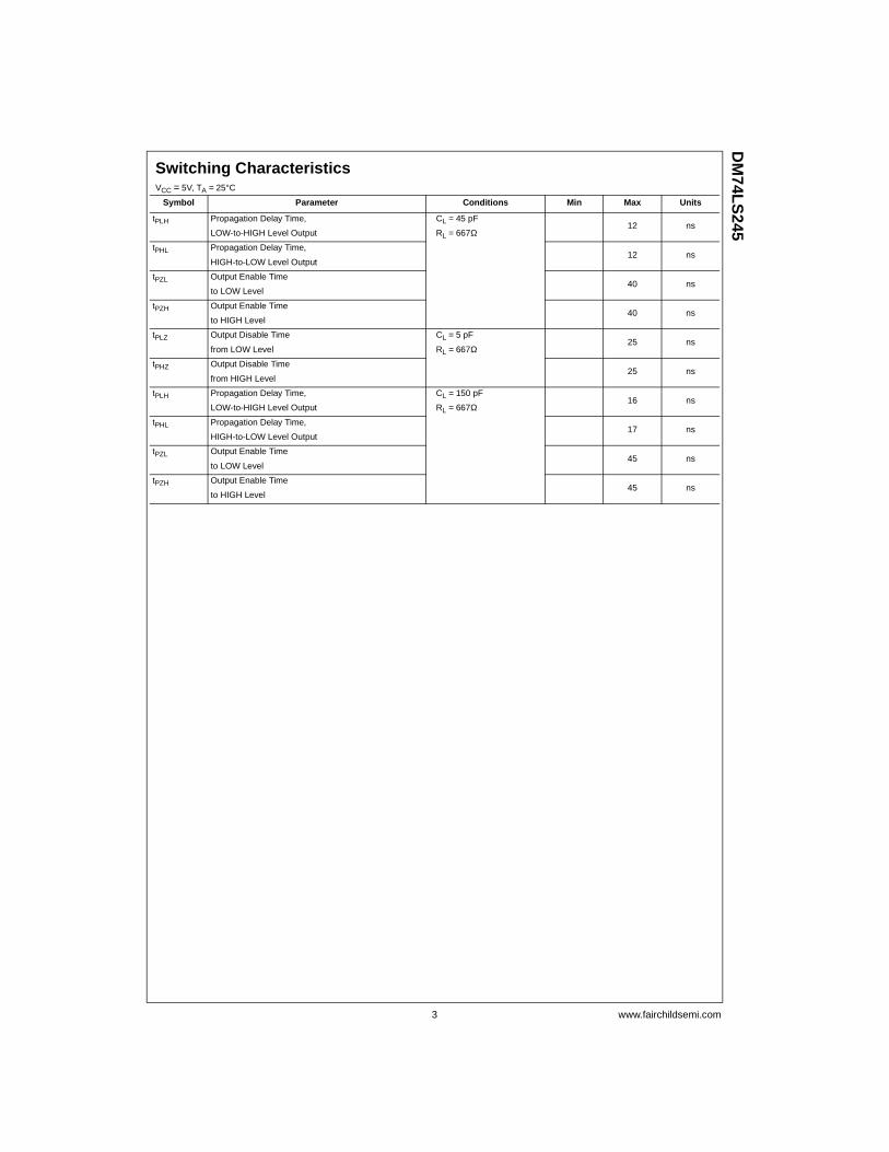
3 www.fairchildsemi.com
DM
74LS
245Switching Characteristics VCC = 5V, TA = 25°C
Symbol Parameter Conditions Min Max Units
tPLH Propagation Delay Time, CL = 45 pF12 ns
LOW-to-HIGH Level Output RL = 667Ω
tPHL Propagation Delay Time, 12 ns
HIGH-to-LOW Level Output
tPZL Output Enable Time 40 ns
to LOW Level
tPZH Output Enable Time 40 ns
to HIGH Level
tPLZ Output Disable Time CL = 5 pF25 ns
from LOW Level RL = 667Ω
tPHZ Output Disable Time 25 ns
from HIGH Level
tPLH Propagation Delay Time, CL = 150 pF16 ns
LOW-to-HIGH Level Output RL = 667Ω
tPHL Propagation Delay Time, 17 ns
HIGH-to-LOW Level Output
tPZL Output Enable Time 45 ns
to LOW Level
tPZH Output Enable Time45 ns
to HIGH Level
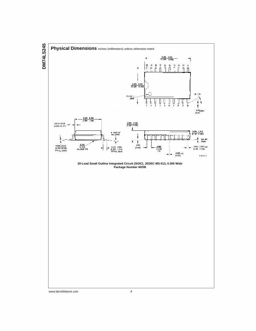
www.fairchildsemi.com 4
DM
74L
S24
5Physical Dimensions inches (millimeters) unless otherwise noted
20-Lead Small Outline Integrated Circuit (SOIC), JEDEC MS-013, 0.300 WidePackage Number M20B
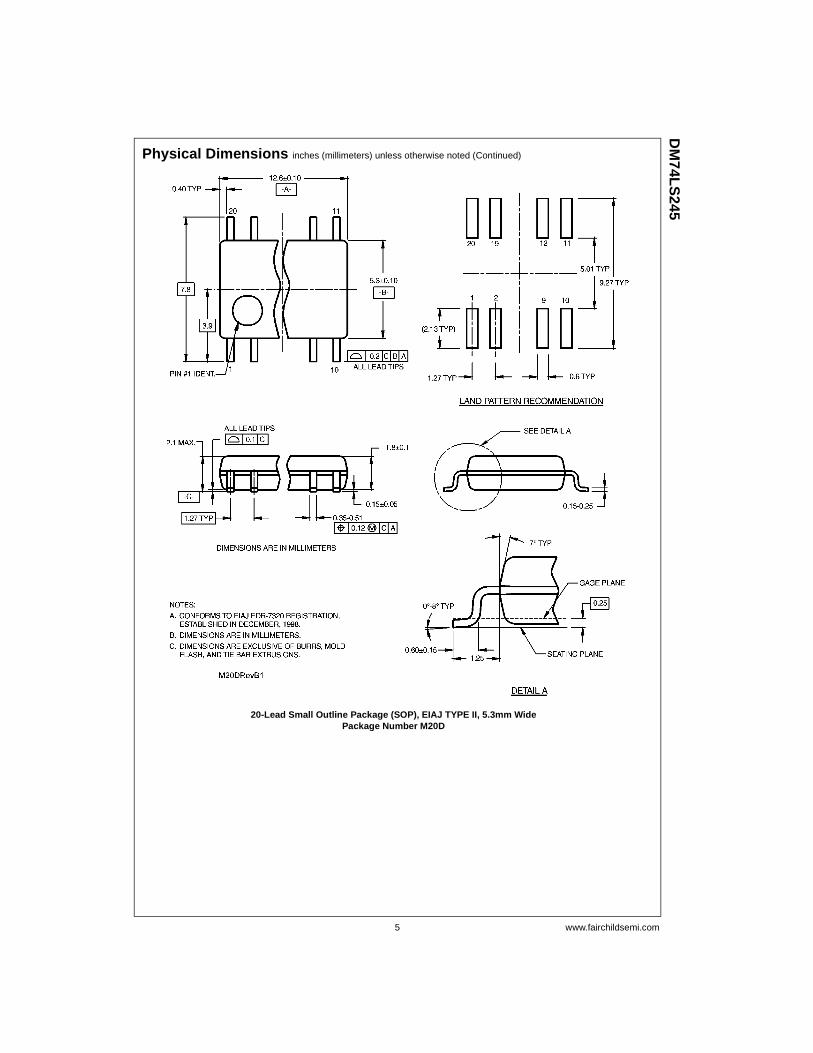
5 www.fairchildsemi.com
DM
74LS
245Physical Dimensions inches (millimeters) unless otherwise noted (Continued)
20-Lead Small Outline Package (SOP), EIAJ TYPE II, 5.3mm WidePackage Number M20D
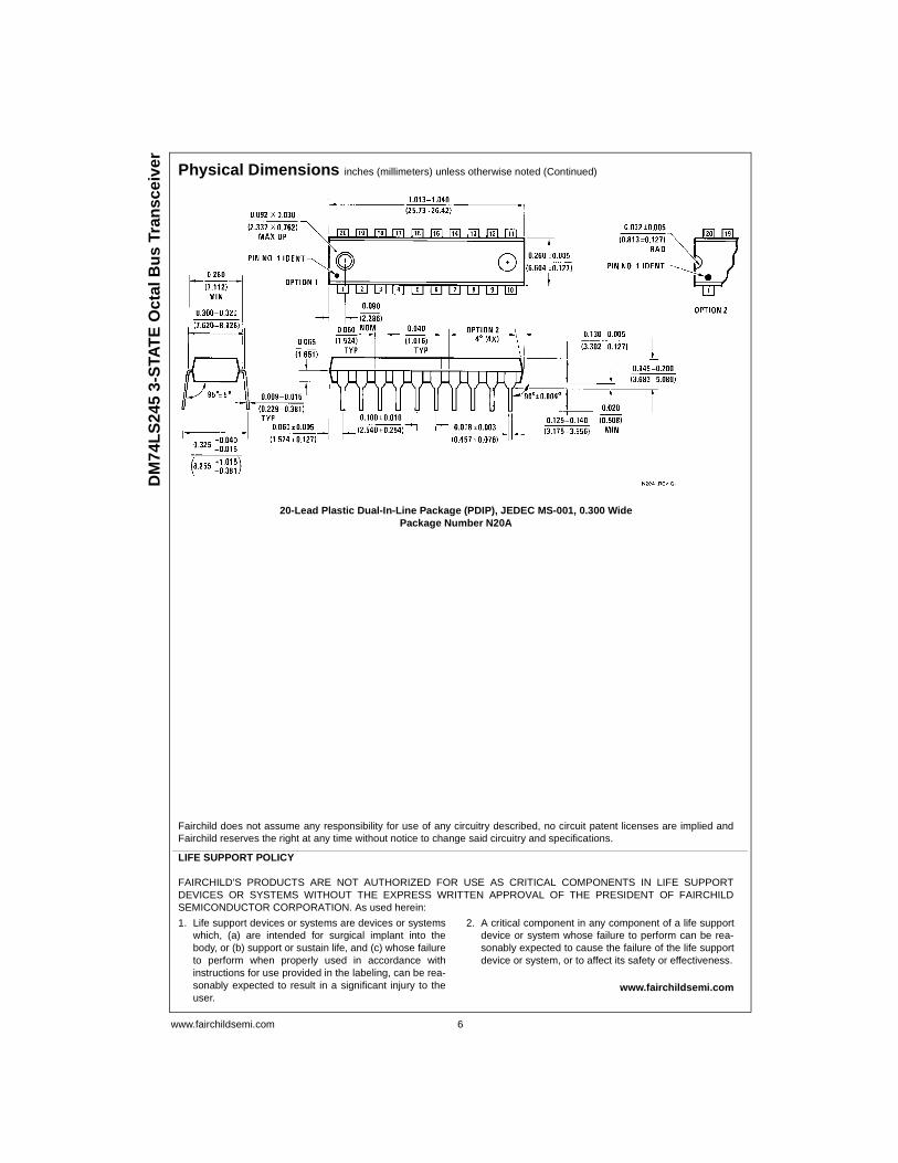
www.fairchildsemi.com 6
DM
74L
S24
5 3-
STA
TE
Oct
al B
us
Tran
scei
ver
Physical Dimensions inches (millimeters) unless otherwise noted (Continued)
20-Lead Plastic Dual-In-Line Package (PDIP), JEDEC MS-001, 0.300 WidePackage Number N20A
Fairchild does not assume any responsibility for use of any circuitry described, no circuit patent licenses are implied andFairchild reserves the right at any time without notice to change said circuitry and specifications.
LIFE SUPPORT POLICY
FAIRCHILD’S PRODUCTS ARE NOT AUTHORIZED FOR USE AS CRITICAL COMPONENTS IN LIFE SUPPORTDEVICES OR SYSTEMS WITHOUT THE EXPRESS WRITTEN APPROVAL OF THE PRESIDENT OF FAIRCHILDSEMICONDUCTOR CORPORATION. As used herein:
1. Life support devices or systems are devices or systemswhich, (a) are intended for surgical implant into thebody, or (b) support or sustain life, and (c) whose failureto perform when properly used in accordance withinstructions for use provided in the labeling, can be rea-sonably expected to result in a significant injury to theuser.
2. A critical component in any component of a life supportdevice or system whose failure to perform can be rea-sonably expected to cause the failure of the life supportdevice or system, or to affect its safety or effectiveness.
www.fairchildsemi.com
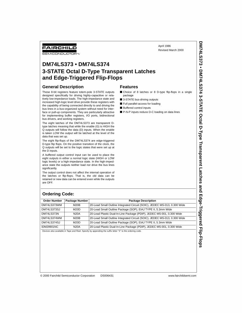
© 2000 Fairchild Semiconductor Corporation DS006431 www.fairchildsemi.com
April 1986
Revised March 2000
DM
74LS
373 • DM
74LS374 3-S
TAT
E O
ctal D-Type Transparent Latches and E
dge-Triggered Flip-F
lops
DM74LS373 • DM74LS3743-STATE Octal D-Type Transparent Latches and Edge-Triggered Flip-Flops
General DescriptionThese 8-bit registers feature totem-pole 3-STATE outputsdesigned specifically for driving highly-capacitive or rela-tively low-impedance loads. The high-impedance state andincreased high-logic level drive provide these registers withthe capability of being connected directly to and driving thebus lines in a bus-organized system without need for inter-face or pull-up components. They are particularly attractivefor implementing buffer registers, I/O ports, bidirectionalbus drivers, and working registers.
The eight latches of the DM74LS373 are transparent D-type latches meaning that while the enable (G) is HIGH theQ outputs will follow the data (D) inputs. When the enableis taken LOW the output will be latched at the level of thedata that was set up.
The eight flip-flops of the DM74LS374 are edge-triggeredD-type flip flops. On the positive transition of the clock, theQ outputs will be set to the logic states that were set up atthe D inputs.
A buffered output control input can be used to place theeight outputs in either a normal logic state (HIGH or LOWlogic levels) or a high-impedance state. In the high-imped-ance state the outputs neither load nor drive the bus linessignificantly.
The output control does not affect the internal operation ofthe latches or flip-flops. That is, the old data can beretained or new data can be entered even while the outputsare OFF.
Features Choice of 8 latches or 8 D-type flip-flops in a single
package
3-STATE bus-driving outputs
Full parallel-access for loading
Buffered control inputs
P-N-P inputs reduce D-C loading on data lines
Ordering Code:
Devices also available in Tape and Reel. Specify by appending the suffix letter “X” to the ordering code.
Order Number Package Number Package Description
DM74LS373WM M20B 20-Lead Small Outline Integrated Circuit (SOIC), JEDEC MS-013, 0.300 Wide
DM74LS373SJ M20D 20-Lead Small Outline Package (SOP), EIAJ TYPE II, 5.3mm Wide
DM74LS373N N20A 20-Lead Plastic Dual-In-Line Package (PDIP), JEDEC MS-001, 0.300 Wide
DM74LS374WM M20B 20-Lead Small Outline Integrated Circuit (SOIC), JEDEC MS-013, 0.300 Wide
DM74LS374SJ M20D 20-Lead Small Outline Package (SOP), EIAJ TYPE II, 5.3mm Wide
IDM29901NC N20A 20-Lead Plastic Dual-In-Line Package (PDIP), JEDEC MS-001, 0.300 Wide
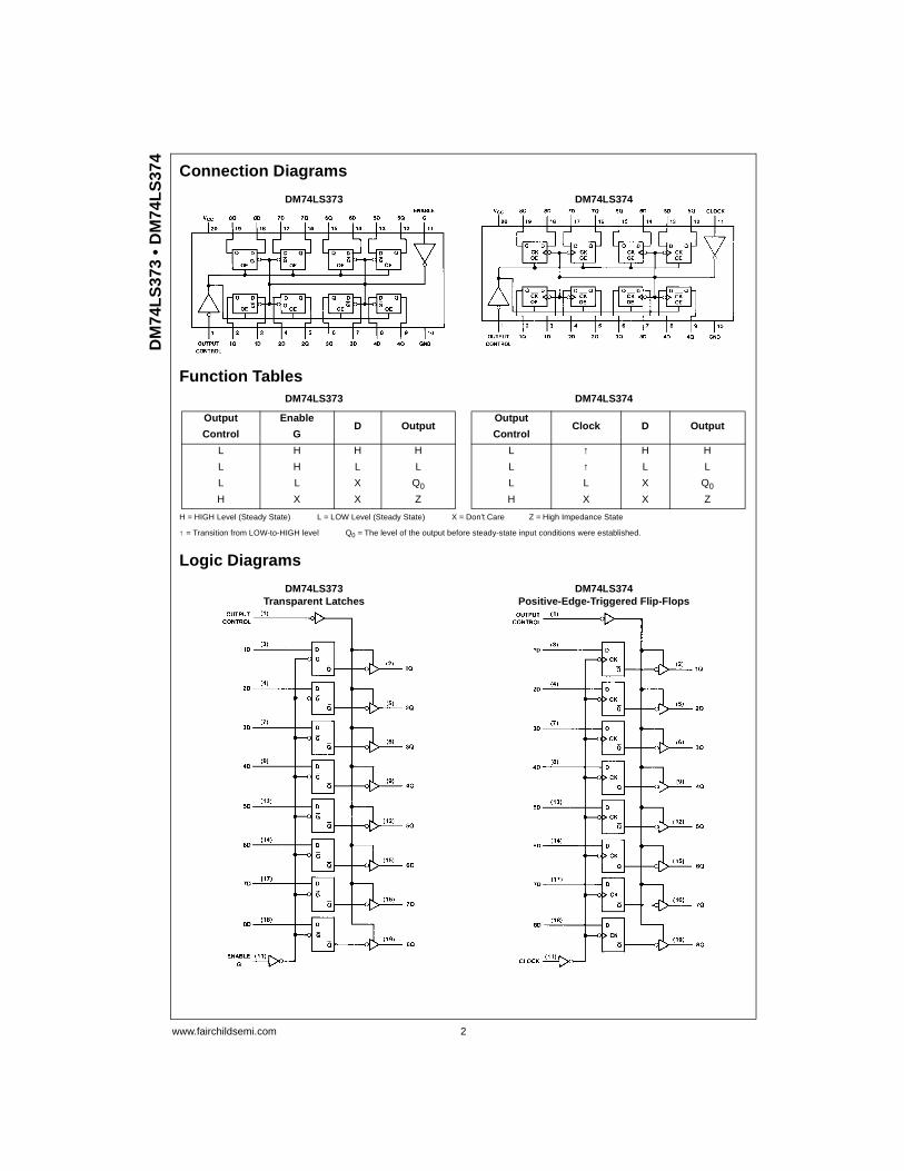
www.fairchildsemi.com 2
DM
74L
S37
3 •
DM
74LS
374
Connection Diagrams
DM74LS373 DM74LS374
Function TablesDM74LS373 DM74LS374
H = HIGH Level (Steady State) L = LOW Level (Steady State) X = Don’t Care Z = High Impedance State
↑ = Transition from LOW-to-HIGH level Q0 = The level of the output before steady-state input conditions were established.
Logic Diagrams
DM74LS373Transparent Latches
DM74LS374Positive-Edge-Triggered Flip-Flops
Output EnableD Output
Control G
L H H H
L H L L
L L X Q0
H X X Z
OutputClock D Output
Control
L ↑ H H
L ↑ L L
L L X Q0
H X X Z
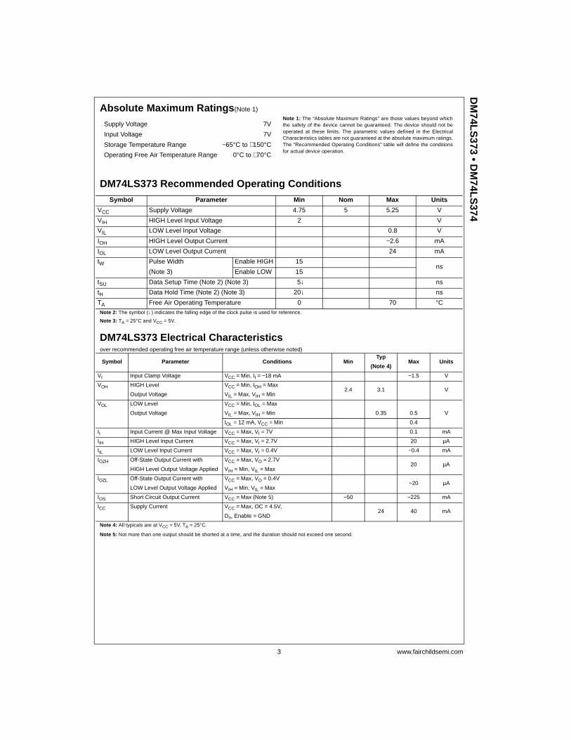
3 www.fairchildsemi.com
DM
74LS
373 • DM
74LS374
Absolute Maximum Ratings(Note 1)Note 1: The “Absolute Maximum Ratings” are those values beyond whichthe safety of the device cannot be guaranteed. The device should not beoperated at these limits. The parametric values defined in the ElectricalCharacteristics tables are not guaranteed at the absolute maximum ratings.The “Recommended Operating Conditions” table will define the conditionsfor actual device operation.
DM74LS373 Recommended Operating Conditions
Note 2: The symbol (↓) indicates the falling edge of the clock pulse is used for reference.
Note 3: TA = 25°C and VCC = 5V.
DM74LS373 Electrical Characteristicsover recommended operating free air temperature range (unless otherwise noted)
Note 4: All typicals are at VCC = 5V, TA = 25°C.
Note 5: Not more than one output should be shorted at a time, and the duration should not exceed one second.
Supply Voltage 7V
Input Voltage 7V
Storage Temperature Range −65°C to +150°C
Operating Free Air Temperature Range 0°C to +70°C
Symbol Parameter Min Nom Max Units
VCC Supply Voltage 4.75 5 5.25 V
VIH HIGH Level Input Voltage 2 V
VIL LOW Level Input Voltage 0.8 V
IOH HIGH Level Output Current −2.6 mA
IOL LOW Level Output Current 24 mA
tW Pulse Width Enable HIGH 15ns
(Note 3) Enable LOW 15
tSU Data Setup Time (Note 2) (Note 3) 5↓ ns
tH Data Hold Time (Note 2) (Note 3) 20↓ ns
TA Free Air Operating Temperature 0 70 °C
Symbol Parameter Conditions MinTyp
Max Units(Note 4)
VI Input Clamp Voltage VCC = Min, II = −18 mA −1.5 V
VOH HIGH Level VCC = Min, IOH = Max2.4 3.1 V
Output Voltage VIL = Max, VIH = Min
VOL LOW Level VCC = Min, IOL = Max
Output Voltage VIL = Max, VIH = Min 0.35 0.5 V
IOL = 12 mA, VCC = Min 0.4
II Input Current @ Max Input Voltage VCC = Max, VI = 7V 0.1 mA
IIH HIGH Level Input Current VCC = Max, VI = 2.7V 20 µA
IIL LOW Level Input Current VCC = Max, VI = 0.4V −0.4 mA
IOZH Off-State Output Current with VCC = Max, VO = 2.7V20 µA
HIGH Level Output Voltage Applied VIH = Min, VIL = Max
IOZL Off-State Output Current with VCC = Max, VO = 0.4V−20 µA
LOW Level Output Voltage Applied VIH = Min, VIL = Max
IOS Short Circuit Output Current VCC = Max (Note 5) −50 −225 mA
ICC Supply Current VCC = Max, OC = 4.5V,24 40 mA
Dn, Enable = GND
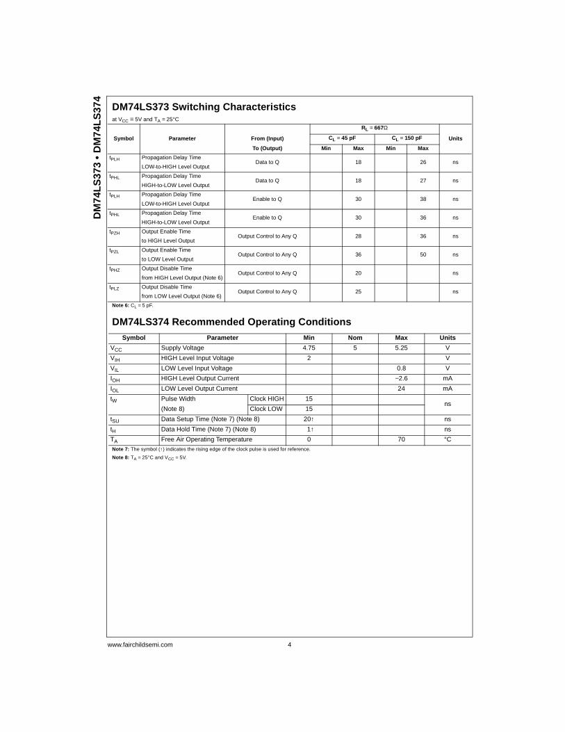
www.fairchildsemi.com 4
DM
74L
S37
3 •
DM
74LS
374
DM74LS373 Switching Characteristics at VCC = 5V and TA = 25°C
Note 6: CL = 5 pF.
DM74LS374 Recommended Operating Conditions
Note 7: The symbol (↑) indicates the rising edge of the clock pulse is used for reference.
Note 8: TA = 25°C and VCC = 5V.
RL = 667Ω
Symbol Parameter From (Input) CL = 45 pF CL = 150 pF Units
To (Output) Min Max Min Max
tPLH Propagation Delay TimeData to Q 18 26 ns
LOW-to-HIGH Level Output
tPHL Propagation Delay TimeData to Q 18 27 ns
HIGH-to-LOW Level Output
tPLH Propagation Delay TimeEnable to Q 30 38 ns
LOW-to-HIGH Level Output
tPHL Propagation Delay TimeEnable to Q 30 36 ns
HIGH-to-LOW Level Output
tPZH Output Enable TimeOutput Control to Any Q 28 36 ns
to HIGH Level Output
tPZL Output Enable Time Output Control to Any Q 36 50 ns
to LOW Level Output
tPHZ Output Disable TimeOutput Control to Any Q 20 ns
from HIGH Level Output (Note 6)
tPLZ Output Disable TimeOutput Control to Any Q 25 ns
from LOW Level Output (Note 6)
Symbol Parameter Min Nom Max Units
VCC Supply Voltage 4.75 5 5.25 V
VIH HIGH Level Input Voltage 2 V
VIL LOW Level Input Voltage 0.8 V
IOH HIGH Level Output Current −2.6 mA
IOL LOW Level Output Current 24 mA
tW Pulse Width Clock HIGH 15ns
(Note 8) Clock LOW 15
tSU Data Setup Time (Note 7) (Note 8) 20↑ ns
tH Data Hold Time (Note 7) (Note 8) 1↑ ns
TA Free Air Operating Temperature 0 70 °C
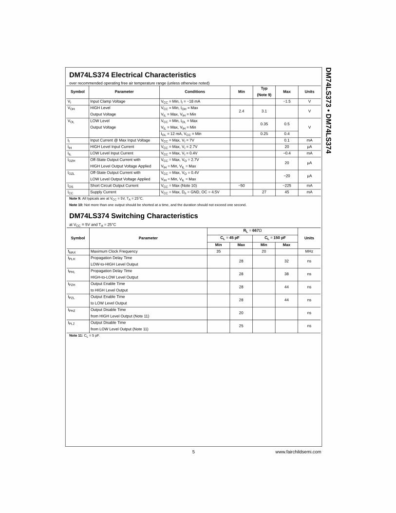
5 www.fairchildsemi.com
DM
74LS
373 • DM
74LS374
DM74LS374 Electrical Characteristicsover recommended operating free air temperature range (unless otherwise noted)
Note 9: All typicals are at VCC = 5V, TA = 25°C.
Note 10: Not more than one output should be shorted at a time, and the duration should not exceed one second.
DM74LS374 Switching Characteristics at VCC = 5V and TA = 25°C
Note 11: CL = 5 pF.
Symbol Parameter Conditions MinTyp
Max Units(Note 9)
VI Input Clamp Voltage VCC = Min, II = −18 mA −1.5 V
VOH HIGH Level VCC = Min, IOH = Max2.4 3.1 V
Output Voltage VIL = Max, VIH = Min
VOL LOW Level VCC = Min, IOL = Max0.35 0.5
VOutput Voltage VIL = Max, VIH = Min
IOL = 12 mA, VCC = Min 0.25 0.4
II Input Current @ Max Input Voltage VCC = Max, VI = 7V 0.1 mA
IIH HIGH Level Input Current VCC = Max, VI = 2.7V 20 µA
IIL LOW Level Input Current VCC = Max, VI = 0.4V −0.4 mA
IOZH Off-State Output Current with VCC = Max, VO = 2.7V20 µA
HIGH Level Output Voltage Applied VIH = Min, VIL = Max
IOZL Off-State Output Current with VCC = Max, VO = 0.4V−20 µA
LOW Level Output Voltage Applied VIH = Min, VIL = Max
IOS Short Circuit Output Current VCC = Max (Note 10) −50 −225 mA
ICC Supply Current VCC = Max, Dn = GND, OC = 4.5V 27 45 mA
RL = 667Ω
Symbol Parameter CL = 45 pF CL = 150 pF Units
Min Max Min Max
fMAX Maximum Clock Frequency 35 20 MHz
tPLH Propagation Delay Time28 32 ns
LOW-to-HIGH Level Output
tPHL Propagation Delay Time28 38 ns
HIGH-to-LOW Level Output
tPZH Output Enable Time28 44 ns
to HIGH Level Output
tPZL Output Enable Time28 44 ns
to LOW Level Output
tPHZ Output Disable Time20 ns
from HIGH Level Output (Note 11)
tPLZ Output Disable Time25 ns
from LOW Level Output (Note 11)
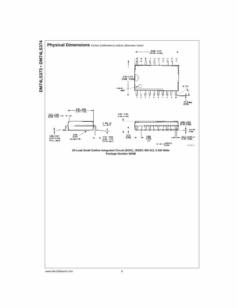
www.fairchildsemi.com 6
DM
74L
S37
3 •
DM
74LS
374
Physical Dimensions inches (millimeters) unless otherwise noted
20-Lead Small Outline Integrated Circuit (SOIC), JEDEC MS-013, 0.300 WidePackage Number M20B
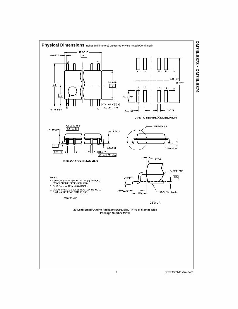
7 www.fairchildsemi.com
DM
74LS
373 • DM
74LS374
Physical Dimensions inches (millimeters) unless otherwise noted (Continued)
20-Lead Small Outline Package (SOP), EIAJ TYPE II, 5.3mm WidePackage Number M20D
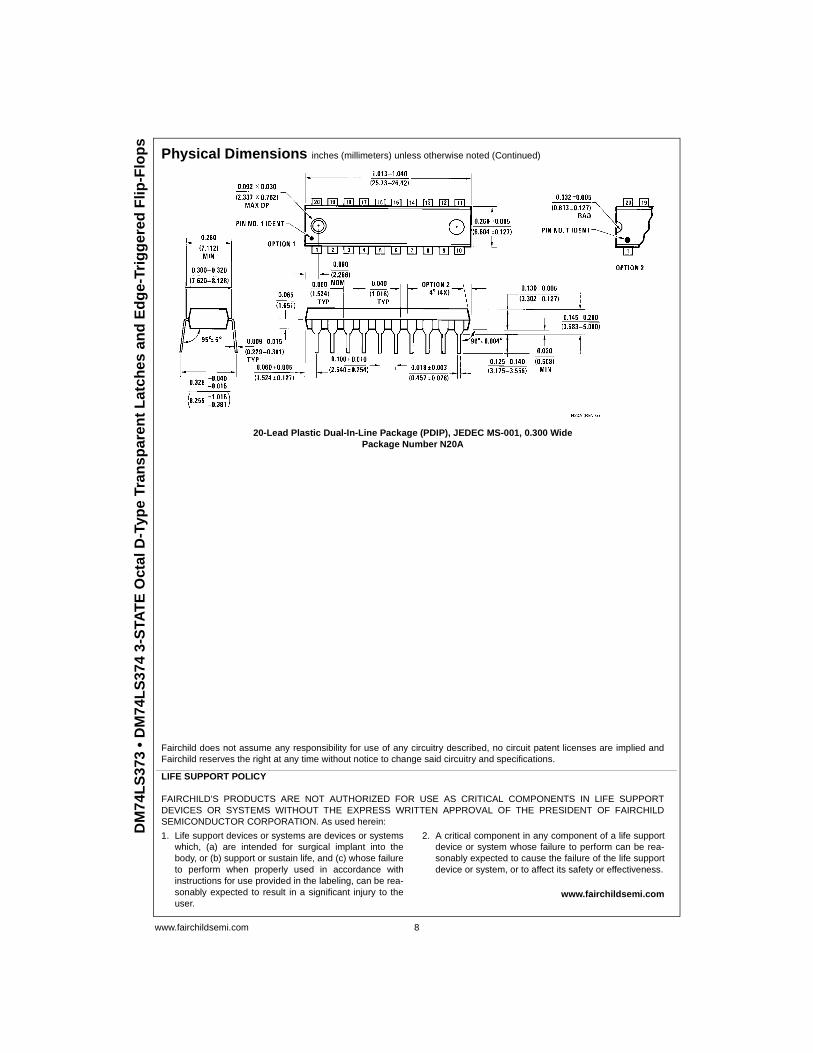
www.fairchildsemi.com 8
DM
74L
S37
3 •
DM
74LS
374
3-S
TAT
E O
ctal
D-T
ype
Tran
spar
ent L
atch
es a
nd E
dge-
Trig
gere
d F
lip-F
lops
Physical Dimensions inches (millimeters) unless otherwise noted (Continued)
20-Lead Plastic Dual-In-Line Package (PDIP), JEDEC MS-001, 0.300 WidePackage Number N20A
Fairchild does not assume any responsibility for use of any circuitry described, no circuit patent licenses are implied andFairchild reserves the right at any time without notice to change said circuitry and specifications.
LIFE SUPPORT POLICY
FAIRCHILD’S PRODUCTS ARE NOT AUTHORIZED FOR USE AS CRITICAL COMPONENTS IN LIFE SUPPORTDEVICES OR SYSTEMS WITHOUT THE EXPRESS WRITTEN APPROVAL OF THE PRESIDENT OF FAIRCHILDSEMICONDUCTOR CORPORATION. As used herein:
1. Life support devices or systems are devices or systemswhich, (a) are intended for surgical implant into thebody, or (b) support or sustain life, and (c) whose failureto perform when properly used in accordance withinstructions for use provided in the labeling, can be rea-sonably expected to result in a significant injury to theuser.
2. A critical component in any component of a life supportdevice or system whose failure to perform can be rea-sonably expected to cause the failure of the life supportdevice or system, or to affect its safety or effectiveness.
www.fairchildsemi.com
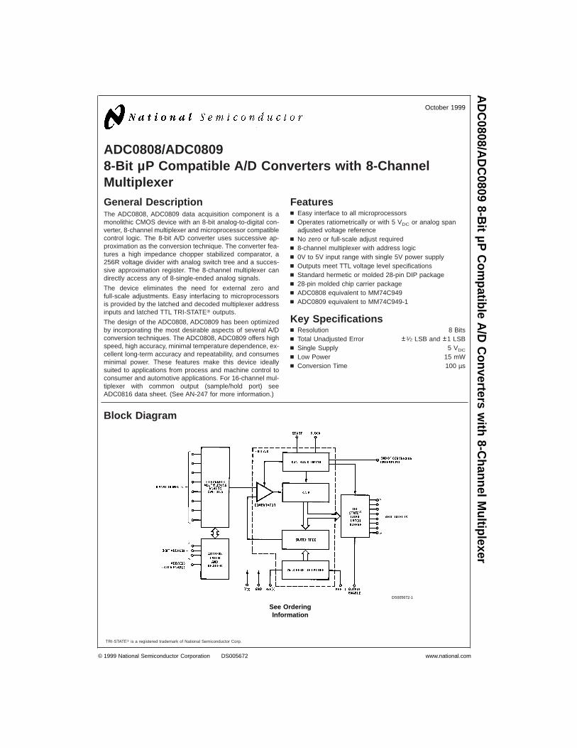
ADC0808/ADC08098-Bit µP Compatible A/D Converters with 8-ChannelMultiplexerGeneral DescriptionThe ADC0808, ADC0809 data acquisition component is amonolithic CMOS device with an 8-bit analog-to-digital con-verter, 8-channel multiplexer and microprocessor compatiblecontrol logic. The 8-bit A/D converter uses successive ap-proximation as the conversion technique. The converter fea-tures a high impedance chopper stabilized comparator, a256R voltage divider with analog switch tree and a succes-sive approximation register. The 8-channel multiplexer candirectly access any of 8-single-ended analog signals.
The device eliminates the need for external zero andfull-scale adjustments. Easy interfacing to microprocessorsis provided by the latched and decoded multiplexer addressinputs and latched TTL TRI-STATE® outputs.
The design of the ADC0808, ADC0809 has been optimizedby incorporating the most desirable aspects of several A/Dconversion techniques. The ADC0808, ADC0809 offers highspeed, high accuracy, minimal temperature dependence, ex-cellent long-term accuracy and repeatability, and consumesminimal power. These features make this device ideallysuited to applications from process and machine control toconsumer and automotive applications. For 16-channel mul-tiplexer with common output (sample/hold port) seeADC0816 data sheet. (See AN-247 for more information.)
Featuresn Easy interface to all microprocessorsn Operates ratiometrically or with 5 VDC or analog span
adjusted voltage referencen No zero or full-scale adjust requiredn 8-channel multiplexer with address logicn 0V to 5V input range with single 5V power supplyn Outputs meet TTL voltage level specificationsn Standard hermetic or molded 28-pin DIP packagen 28-pin molded chip carrier packagen ADC0808 equivalent to MM74C949n ADC0809 equivalent to MM74C949-1
Key Specificationsn Resolution 8 Bitsn Total Unadjusted Error ±1⁄2 LSB and ±1 LSBn Single Supply 5 VDC
n Low Power 15 mWn Conversion Time 100 µs
Block Diagram
TRI-STATE® is a registered trademark of National Semiconductor Corp.
DS005672-1
See OrderingInformation
October 1999
AD
C0808/A
DC
08098-B
itµPC
ompatible
A/D
Converters
with
8-ChannelM
ultiplexer
© 1999 National Semiconductor Corporation DS005672 www.national.com
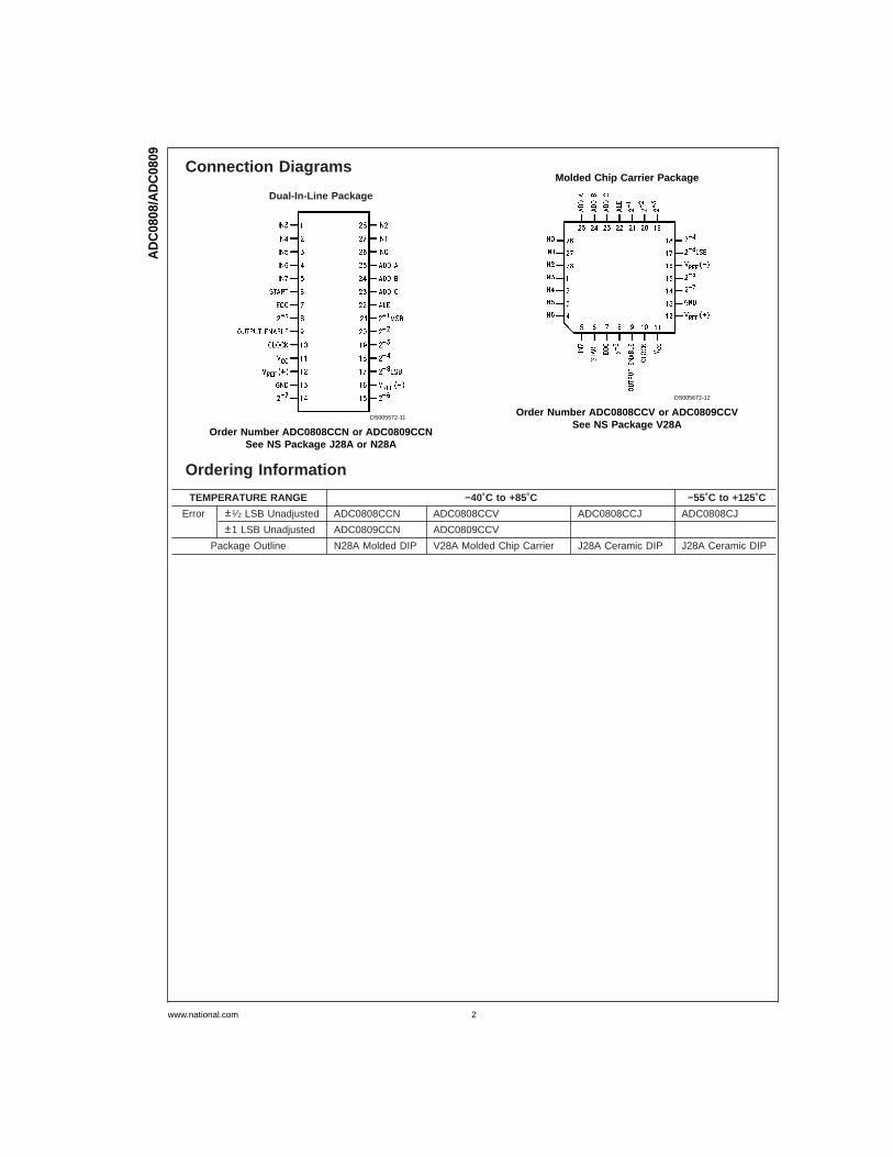
Connection Diagrams
Ordering Information
TEMPERATURE RANGE −40˚C to +85˚C −55˚C to +125˚C
Error ±1⁄2 LSB Unadjusted ADC0808CCN ADC0808CCV ADC0808CCJ ADC0808CJ
±1 LSB Unadjusted ADC0809CCN ADC0809CCV
Package Outline N28A Molded DIP V28A Molded Chip Carrier J28A Ceramic DIP J28A Ceramic DIP
Dual-In-Line Package
DS005672-11
Order Number ADC0808CCN or ADC0809CCNSee NS Package J28A or N28A
Molded Chip Carrier Package
DS005672-12
Order Number ADC0808CCV or ADC0809CCVSee NS Package V28A
AD
C08
08/A
DC
0809
www.national.com 2
Absolute Maximum Ratings (Notes 2, 1)
If Military/Aerospace specified devices are required,please contact the National Semiconductor Sales Office/Distributors for availability and specifications.
Supply Voltage (VCC) (Note 3) 6.5VVoltage at Any Pin −0.3V to (VCC+0.3V)
Except Control InputsVoltage at Control Inputs −0.3V to +15V
(START, OE, CLOCK, ALE, ADD A, ADD B, ADD C)Storage Temperature Range −65˚C to +150˚CPackage Dissipation at TA=25˚C 875 mWLead Temp. (Soldering, 10 seconds)
Dual-In-Line Package (plastic) 260˚C
Dual-In-Line Package (ceramic) 300˚CMolded Chip Carrier Package
Vapor Phase (60 seconds) 215˚CInfrared (15 seconds) 220˚C
ESD Susceptibility (Note 8) 400V
Operating Conditions (Notes 1, 2)
Temperature Range (Note 1) TMIN≤TA≤TMAX
ADC0808CCN,ADC0809CCN −40˚C≤TA≤+85˚CADC0808CCV, ADC0809CCV −40˚C ≤ TA ≤ +85˚C
Range of VCC (Note 1) 4.5 VDC to 6.0 VDC
Electrical CharacteristicsConverter Specifications: VCC=5 VDC=VREF+, VREF(−)=GND, TMIN≤TA≤TMAX and fCLK=640 kHz unless otherwise stated.
Symbol Parameter Conditions Min Typ Max Units
ADC0808
Total Unadjusted Error 25˚C ±1⁄2 LSB
(Note 5) TMIN to TMAX ±3⁄4 LSB
ADC0809
Total Unadjusted Error 0˚C to 70˚C ±1 LSB
(Note 5) TMIN to TMAX ±11⁄4 LSB
Input Resistance From Ref(+) to Ref(−) 1.0 2.5 kΩAnalog Input Voltage Range (Note 4) V(+) or V(−) GND−0.10 VCC+0.10 VDC
VREF(+) Voltage, Top of Ladder Measured at Ref(+) VCC VCC+0.1 V
Voltage, Center of Ladder VCC/2-0.1 VCC/2 VCC/2+0.1 V
VREF(−) Voltage, Bottom of Ladder Measured at Ref(−) −0.1 0 V
IIN Comparator Input Current fc=640 kHz, (Note 6) −2 ±0.5 2 µA
Electrical CharacteristicsDigital Levels and DC Specifications: ADC0808CCN, ADC0808CCV, ADC0809CCN and ADC0809CCV, 4.75≤VCC≤5.25V,−40˚C≤TA≤+85˚C unless otherwise noted
Symbol Parameter Conditions Min Typ Max Units
ANALOG MULTIPLEXER
IOFF(+) OFF Channel Leakage Current VCC=5V, VIN=5V,
TA=25˚C 10 200 nA
TMIN to TMAX 1.0 µA
IOFF(−) OFF Channel Leakage Current VCC=5V, VIN=0,
TA=25˚C −200 −10 nA
TMIN to TMAX −1.0 µA
CONTROL INPUTS
VIN(1) Logical “1” Input Voltage VCC−1.5 V
VIN(0) Logical “0” Input Voltage 1.5 V
IIN(1) Logical “1” Input Current VIN=15V 1.0 µA
(The Control Inputs)
IIN(0) Logical “0” Input Current VIN=0 −1.0 µA
(The Control Inputs)
ICC Supply Current fCLK=640 kHz 0.3 3.0 mA
AD
C0808/A
DC
0809
www.national.com3
Electrical Characteristics (Continued)
Digital Levels and DC Specifications: ADC0808CCN, ADC0808CCV, ADC0809CCN and ADC0809CCV, 4.75≤VCC≤5.25V,−40˚C≤TA≤+85˚C unless otherwise noted
Symbol Parameter Conditions Min Typ Max Units
DATA OUTPUTS AND EOC (INTERRUPT)
VOUT(1) Logical “1” Output Voltage VCC = 4.75VIOUT = −360µAIOUT = −10µA
2.44.5
V(min)V(min)
VOUT(0) Logical “0” Output Voltage IO=1.6 mA 0.45 V
VOUT(0) Logical “0” Output Voltage EOC IO=1.2 mA 0.45 V
IOUT TRI-STATE Output Current VO=5V 3 µA
VO=0 −3 µA
Electrical CharacteristicsTiming Specifications VCC=VREF(+)=5V, VREF(−)=GND, tr=tf=20 ns and TA=25˚C unless otherwise noted.
Symbol Parameter Conditions MIn Typ Max Units
tWS Minimum Start Pulse Width (Figure 5) 100 200 ns
tWALE Minimum ALE Pulse Width (Figure 5) 100 200 ns
ts Minimum Address Set-Up Time (Figure 5) 25 50 ns
tH Minimum Address Hold Time (Figure 5) 25 50 ns
tD Analog MUX Delay Time RS=0Ω (Figure 5) 1 2.5 µs
From ALE
tH1, tH0 OE Control to Q Logic State CL=50 pF, RL=10k (Figure 8) 125 250 ns
t1H, t0H OE Control to Hi-Z CL=10 pF, RL=10k (Figure 8) 125 250 ns
tc Conversion Time fc=640 kHz, (Figure 5) (Note 7) 90 100 116 µs
fc Clock Frequency 10 640 1280 kHz
tEOC EOC Delay Time (Figure 5) 0 8+2 µS Clock
Periods
CIN Input Capacitance At Control Inputs 10 15 pF
COUT TRI-STATE Output At TRI-STATE Outputs 10 15 pF
Capacitance
Note 1: Absolute Maximum Ratings indicate limits beyond which damage to the device may occur. DC and AC electrical specifications do not apply when operatingthe device beyond its specified operating conditions.
Note 2: All voltages are measured with respect to GND, unless othewise specified.
Note 3: A zener diode exists, internally, from VCC to GND and has a typical breakdown voltage of 7 VDC.
Note 4: Two on-chip diodes are tied to each analog input which will forward conduct for analog input voltages one diode drop below ground or one diode drop greaterthan the VCCn supply. The spec allows 100 mV forward bias of either diode. This means that as long as the analog VIN does not exceed the supply voltage by morethan 100 mV, the output code will be correct. To achieve an absolute 0VDC to 5VDC input voltage range will therefore require a minimum supply voltage of 4.900 VDCover temperature variations, initial tolerance and loading.
Note 5: Total unadjusted error includes offset, full-scale, linearity, and multiplexer errors. See Figure 3. None of these A/Ds requires a zero or full-scale adjust. How-ever, if an all zero code is desired for an analog input other than 0.0V, or if a narrow full-scale span exists (for example: 0.5V to 4.5V full-scale) the reference voltagescan be adjusted to achieve this. See Figure 13.
Note 6: Comparator input current is a bias current into or out of the chopper stabilized comparator. The bias current varies directly with clock frequency and has littletemperature dependence (Figure 6). See paragraph 4.0.
Note 7: The outputs of the data register are updated one clock cycle before the rising edge of EOC.
Note 8: Human body model, 100 pF discharged through a 1.5 kΩ resistor.
AD
C08
08/A
DC
0809
www.national.com 4
Functional DescriptionMultiplexer. The device contains an 8-channel single-endedanalog signal multiplexer. A particular input channel is se-lected by using the address decoder. Table 1 shows the inputstates for the address lines to select any channel. The ad-dress is latched into the decoder on the low-to-high transitionof the address latch enable signal.
TABLE 1.
SELECTED ADDRESS LINE
ANALOGCHANNEL
C B A
IN0 L L L
IN1 L L H
IN2 L H L
IN3 L H H
IN4 H L L
IN5 H L H
IN6 H H L
IN7 H H H
CONVERTER CHARACTERISTICS
The Converter
The heart of this single chip data acquisition system is its8-bit analog-to-digital converter. The converter is designed togive fast, accurate, and repeatable conversions over a widerange of temperatures. The converter is partitioned into 3major sections: the 256R ladder network, the successive ap-proximation register, and the comparator. The converter’sdigital outputs are positive true.
The 256R ladder network approach (Figure 1) was chosenover the conventional R/2R ladder because of its inherentmonotonicity, which guarantees no missing digital codes.Monotonicity is particularly important in closed loop feedbackcontrol systems. A non-monotonic relationship can cause os-cillations that will be catastrophic for the system. Additionally,the 256R network does not cause load variations on the ref-erence voltage.
The bottom resistor and the top resistor of the ladder net-work in Figure 1 are not the same value as the remainder ofthe network. The difference in these resistors causes theoutput characteristic to be symmetrical with the zero andfull-scale points of the transfer curve. The first output transi-tion occurs when the analog signal has reached +1⁄2 LSBand succeeding output transitions occur every 1 LSB later upto full-scale.
The successive approximation register (SAR) performs 8 it-erations to approximate the input voltage. For any SAR typeconverter, n-iterations are required for an n-bit converter.Figure 2 shows a typical example of a 3-bit converter. In theADC0808, ADC0809, the approximation technique is ex-tended to 8 bits using the 256R network.
The A/D converter’s successive approximation register(SAR) is reset on the positive edge of the start conversion(SC) pulse. The conversion is begun on the falling edge ofthe start conversion pulse. A conversion in process will be in-terrupted by receipt of a new start conversion pulse. Con-tinuous conversion may be accomplished by tying theend-of-conversion (EOC) output to the SC input. If used inthis mode, an external start conversion pulse should be ap-plied after power up. End-of-conversion will go low between0 and 8 clock pulses after the rising edge of start conversion.
The most important section of the A/D converter is the com-parator. It is this section which is responsible for the ultimateaccuracy of the entire converter. It is also the comparatordrift which has the greatest influence on the repeatability ofthe device. A chopper-stabilized comparator provides themost effective method of satisfying all the converter require-ments.
The chopper-stabilized comparator converts the DC inputsignal into an AC signal. This signal is then fed through ahigh gain AC amplifier and has the DC level restored. Thistechnique limits the drift component of the amplifier since thedrift is a DC component which is not passed by the AC am-plifier. This makes the entire A/D converter extremely insen-sitive to temperature, long term drift and input offset errors.
Figure 4 shows a typical error curve for the ADC0808 asmeasured using the procedures outlined in AN-179.
AD
C0808/A
DC
0809
www.national.com5
Functional Description (Continued)
DS005672-2
FIGURE 1. Resistor Ladder and Switch Tree
DS005672-13
FIGURE 2. 3-Bit A/D Transfer CurveDS005672-14
FIGURE 3. 3-Bit A/D Absolute Accuracy Curve
DS005672-15
FIGURE 4. Typical Error Curve
AD
C08
08/A
DC
0809
www.national.com 6
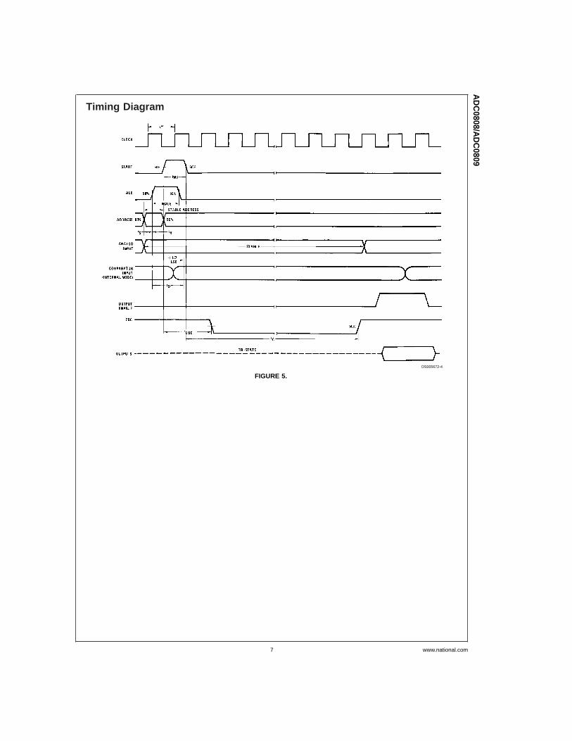
Timing Diagram
DS005672-4
FIGURE 5.
AD
C0808/A
DC
0809
www.national.com7
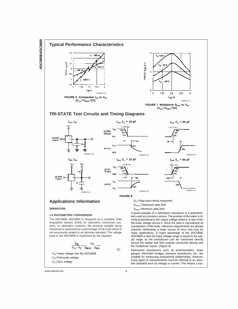
Typical Performance Characteristics
TRI-STATE Test Circuits and Timing Diagrams
Applications Information
OPERATION
1.0 RATIOMETRIC CONVERSION
The ADC0808, ADC0809 is designed as a complete DataAcquisition System (DAS) for ratiometric conversion sys-tems. In ratiometric systems, the physical variable beingmeasured is expressed as a percentage of full-scale which isnot necessarily related to an absolute standard. The voltageinput to the ADC0808 is expressed by the equation
(1)
VIN=Input voltage into the ADC0808
Vfs=Full-scale voltage
VZ=Zero voltage
DX=Data point being measured
DMAX=Maximum data limit
DMIN=Minimum data limit
A good example of a ratiometric transducer is a potentiom-eter used as a position sensor. The position of the wiper is di-rectly proportional to the output voltage which is a ratio of thefull-scale voltage across it. Since the data is represented asa proportion of full-scale, reference requirements are greatlyreduced, eliminating a large source of error and cost formany applications. A major advantage of the ADC0808,ADC0809 is that the input voltage range is equal to the sup-ply range so the transducers can be connected directlyacross the supply and their outputs connected directly intothe multiplexer inputs, (Figure 9).
Ratiometric transducers such as potentiometers, straingauges, thermistor bridges, pressure transducers, etc., aresuitable for measuring proportional relationships; however,many types of measurements must be referred to an abso-lute standard such as voltage or current. This means a sys-
DS005672-16
FIGURE 6. Comparator I IN vs VIN
(VCC=VREF=5V) DS005672-17
FIGURE 7. Multiplexer R ON vs VIN
(VCC=VREF=5V)
t1H, tH1
DS005672-18
t1H, CL = 10 pF
DS005672-19
tH1, CL = 50 pF
DS005672-20
t0H, tH0
DS005672-21
t0H, CL = 10 pF
DS005672-22
tH0, CL = 50 pF
DS005672-23
FIGURE 8.
AD
C08
08/A
DC
0809
www.national.com 8
Applications Information (Continued)
tem reference must be used which relates the full-scale volt-age to the standard volt. For example, if VCC=VREF=5.12V,then the full-scale range is divided into 256 standard steps.The smallest standard step is 1 LSB which is then 20 mV.
2.0 RESISTOR LADDER LIMITATIONS
The voltages from the resistor ladder are compared to theselected into 8 times in a conversion. These voltages arecoupled to the comparator via an analog switch tree which isreferenced to the supply. The voltages at the top, center andbottom of the ladder must be controlled to maintain properoperation.
The top of the ladder, Ref(+), should not be more positivethan the supply, and the bottom of the ladder, Ref(−), shouldnot be more negative than ground. The center of the laddervoltage must also be near the center of the supply becausethe analog switch tree changes from N-channel switches toP-channel switches. These limitations are automatically sat-isfied in ratiometric systems and can be easily met in groundreferenced systems.
Figure 10 shows a ground referenced system with a sepa-rate supply and reference. In this system, the supply must betrimmed to match the reference voltage. For instance, if a5.12V is used, the supply should be adjusted to the samevoltage within 0.1V.
The ADC0808 needs less than a milliamp of supply currentso developing the supply from the reference is readily ac-complished. In Figure 11 a ground referenced system isshown which generates the supply from the reference. Thebuffer shown can be an op amp of sufficient drive to supplythe milliamp of supply current and the desired bus drive, or ifa capacitive bus is driven by the outputs a large capacitor willsupply the transient supply current as seen in Figure 12. TheLM301 is overcompensated to insure stability when loadedby the 10 µF output capacitor.
The top and bottom ladder voltages cannot exceed VCC andground, respectively, but they can be symmetrically less thanVCC and greater than ground. The center of the ladder volt-age should always be near the center of the supply. The sen-sitivity of the converter can be increased, (i.e., size of theLSB steps decreased) by using a symmetrical reference sys-tem. In Figure 13, a 2.5V reference is symmetrically cen-tered about VCC/2 since the same current flows in identicalresistors. This system with a 2.5V reference allows the LSBbit to be half the size of a 5V reference system.
DS005672-7
FIGURE 9. Ratiometric Conversion System
AD
C0808/A
DC
0809
www.national.com9
Applications Information (Continued)
DS005672-24
FIGURE 10. Ground ReferencedConversion System Using Trimmed Supply
DS005672-25
FIGURE 11. Ground Referenced Conversion System withReference Generating V CC Supply
AD
C08
08/A
DC
0809
www.national.com 10
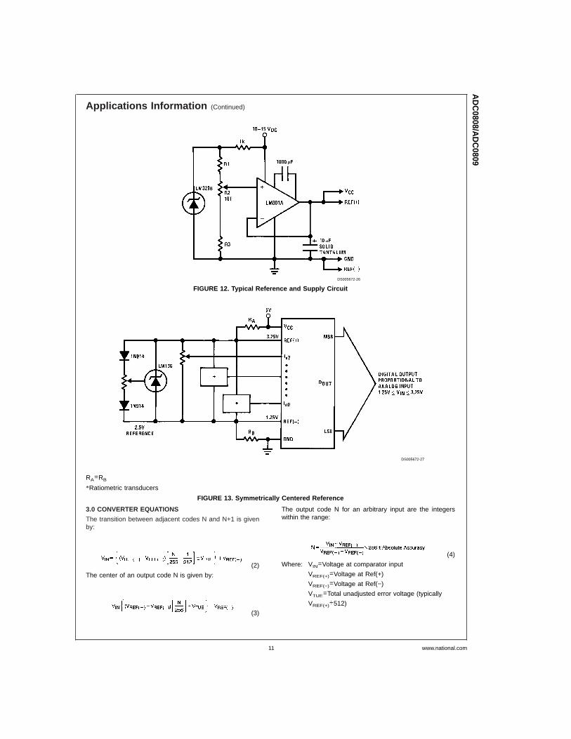
Applications Information (Continued)
3.0 CONVERTER EQUATIONS
The transition between adjacent codes N and N+1 is givenby:
(2)
The center of an output code N is given by:
(3)
The output code N for an arbitrary input are the integerswithin the range:
(4)
Where: VIN=Voltage at comparator input
VREF(+)=Voltage at Ref(+)
VREF(−)=Voltage at Ref(−)
VTUE=Total unadjusted error voltage (typically
VREF(+)÷512)
DS005672-26
FIGURE 12. Typical Reference and Supply Circuit
DS005672-27
RA=RB
*Ratiometric transducers
FIGURE 13. Symmetrically Centered Reference
AD
C0808/A
DC
0809
www.national.com11
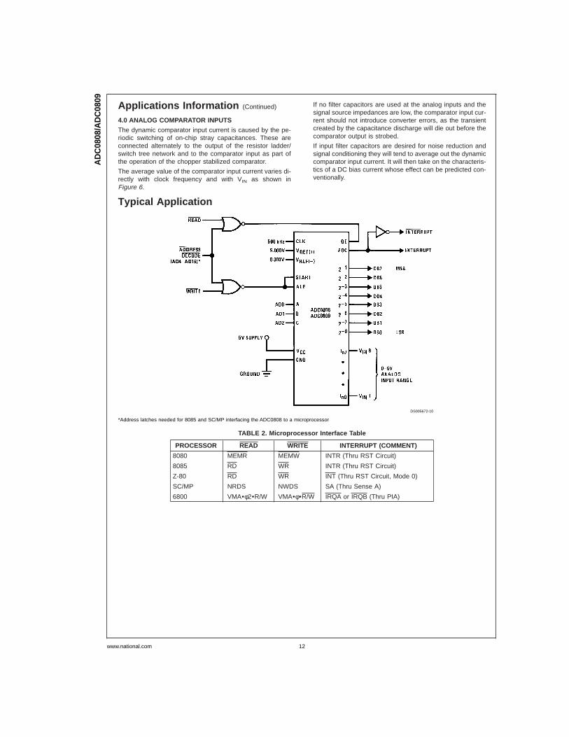
Applications Information (Continued)
4.0 ANALOG COMPARATOR INPUTS
The dynamic comparator input current is caused by the pe-riodic switching of on-chip stray capacitances. These areconnected alternately to the output of the resistor ladder/switch tree network and to the comparator input as part ofthe operation of the chopper stabilized comparator.
The average value of the comparator input current varies di-rectly with clock frequency and with VIN as shown inFigure 6.
If no filter capacitors are used at the analog inputs and thesignal source impedances are low, the comparator input cur-rent should not introduce converter errors, as the transientcreated by the capacitance discharge will die out before thecomparator output is strobed.
If input filter capacitors are desired for noise reduction andsignal conditioning they will tend to average out the dynamiccomparator input current. It will then take on the characteris-tics of a DC bias current whose effect can be predicted con-ventionally.
Typical Application
TABLE 2. Microprocessor Interface Table
PROCESSOR READ WRITE INTERRUPT (COMMENT)
8080 MEMR MEMW INTR (Thru RST Circuit)
8085 RD WR INTR (Thru RST Circuit)
Z-80 RD WR INT (Thru RST Circuit, Mode 0)
SC/MP NRDS NWDS SA (Thru Sense A)
6800 VMA•φ2•R/W VMA•φ•R/W IRQA or IRQB (Thru PIA)
DS005672-10
*Address latches needed for 8085 and SC/MP interfacing the ADC0808 to a microprocessor
AD
C08
08/A
DC
0809
www.national.com 12
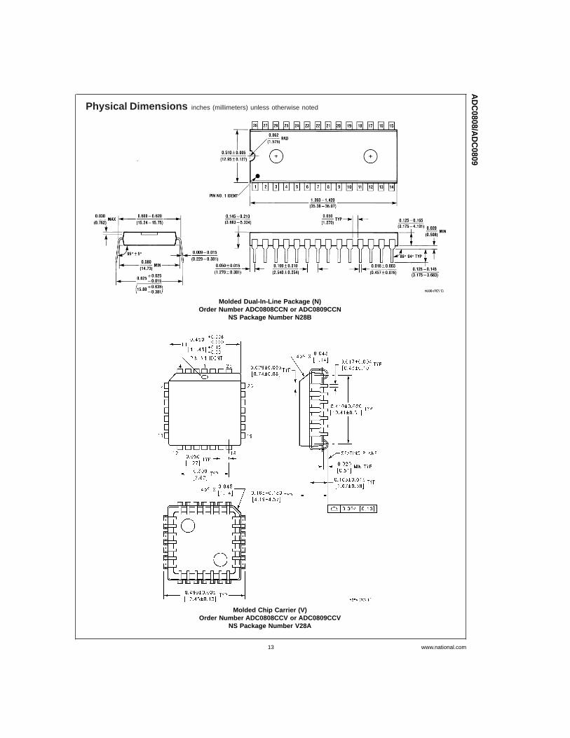
Physical Dimensions inches (millimeters) unless otherwise noted
Molded Dual-In-Line Package (N)Order Number ADC0808CCN or ADC0809CCN
NS Package Number N28B
Molded Chip Carrier (V)Order Number ADC0808CCV or ADC0809CCV
NS Package Number V28A
AD
C0808/A
DC
0809
www.national.com13
Notes
LIFE SUPPORT POLICY
NATIONAL’S PRODUCTS ARE NOT AUTHORIZED FOR USE AS CRITICAL COMPONENTS IN LIFE SUPPORTDEVICES OR SYSTEMS WITHOUT THE EXPRESS WRITTEN APPROVAL OF THE PRESIDENT AND GENERALCOUNSEL OF NATIONAL SEMICONDUCTOR CORPORATION. As used herein:
1. Life support devices or systems are devices orsystems which, (a) are intended for surgical implantinto the body, or (b) support or sustain life, andwhose failure to perform when properly used inaccordance with instructions for use provided in thelabeling, can be reasonably expected to result in asignificant injury to the user.
2. A critical component is any component of a lifesupport device or system whose failure to performcan be reasonably expected to cause the failure ofthe life support device or system, or to affect itssafety or effectiveness.
National SemiconductorCorporationAmericasTel: 1-800-272-9959Fax: 1-800-737-7018Email: [email protected]
National SemiconductorEurope
Fax: +49 (0) 1 80-530 85 86Email: [email protected]
Deutsch Tel: +49 (0) 1 80-530 85 85English Tel: +49 (0) 1 80-532 78 32Français Tel: +49 (0) 1 80-532 93 58Italiano Tel: +49 (0) 1 80-534 16 80
National SemiconductorAsia Pacific CustomerResponse GroupTel: 65-2544466Fax: 65-2504466Email: [email protected]
National SemiconductorJapan Ltd.Tel: 81-3-5639-7560Fax: 81-3-5639-7507
www.national.com
AD
C08
08/A
DC
0809
8-B
itµP
Com
patib
leA
/DC
onve
rters
with
8-C
hann
elM
ultip
lexe
r
National does not assume any responsibility for use of any circuitry described, no circuit patent licenses are implied and National reserves the right at any time without notice to change said circuitry and specifications.
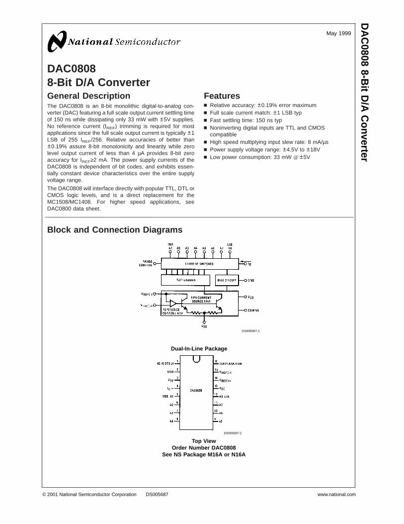
DAC08088-Bit D/A ConverterGeneral DescriptionThe DAC0808 is an 8-bit monolithic digital-to-analog con-verter (DAC) featuring a full scale output current settling timeof 150 ns while dissipating only 33 mW with ±5V supplies.No reference current (IREF) trimming is required for mostapplications since the full scale output current is typically ±1LSB of 255 IREF/256. Relative accuracies of better than±0.19% assure 8-bit monotonicity and linearity while zerolevel output current of less than 4 µA provides 8-bit zeroaccuracy for IREF≥2 mA. The power supply currents of theDAC0808 is independent of bit codes, and exhibits essen-tially constant device characteristics over the entire supplyvoltage range.
The DAC0808 will interface directly with popular TTL, DTL orCMOS logic levels, and is a direct replacement for theMC1508/MC1408. For higher speed applications, seeDAC0800 data sheet.
Featuresn Relative accuracy: ±0.19% error maximumn Full scale current match: ±1 LSB typn Fast settling time: 150 ns typn Noninverting digital inputs are TTL and CMOS
compatiblen High speed multiplying input slew rate: 8 mA/µsn Power supply voltage range: ±4.5V to ±18Vn Low power consumption: 33 mW @ ±5V
Block and Connection Diagrams
DS005687-1
Dual-In-Line Package
DS005687-2
Top ViewOrder Number DAC0808
See NS Package M16A or N16A
May 1999D
AC
08088-B
itD/A
Converter
© 2001 National Semiconductor Corporation DS005687 www.national.com
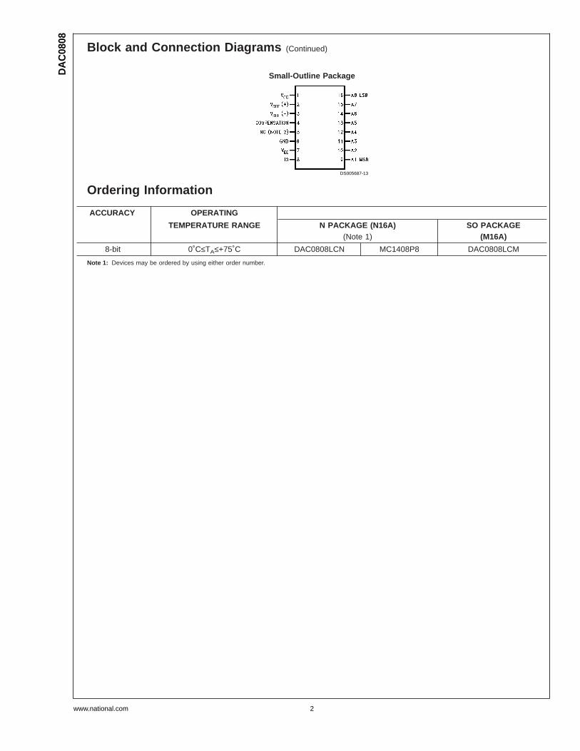
Block and Connection Diagrams (Continued)
Ordering Information
ACCURACY OPERATING
TEMPERATURE RANGE N PACKAGE (N16A)(Note 1)
SO PACKAGE(M16A)
8-bit 0˚C≤TA≤+75˚C DAC0808LCN MC1408P8 DAC0808LCM
Note 1: Devices may be ordered by using either order number.
Small-Outline Package
DS005687-13
DA
C08
08
www.national.com 2
Absolute Maximum Ratings (Note 2)
If Military/Aerospace specified devices are required,please contact the National Semiconductor Sales Office/Distributors for availability and specifications.
Power Supply VoltageVCC +18 VDC
VEE −18 VDC
Digital Input Voltage, V5–V12 −10 VDC to +18 VDC
Applied Output Voltage, VO −11 VDC to +18 VDC
Reference Current, I14 5 mAReference Amplifier Inputs, V14, V15 VCC, VEE
Power Dissipation (Note 4) 1000 mWESD Susceptibility (Note 5) TBD
Storage Temperature Range −65˚C to +150˚CLead Temp. (Soldering, 10 seconds)
Dual-In-Line Package (Plastic) 260˚CDual-In-Line Package (Ceramic) 300˚CSurface Mount Package
Vapor Phase (60 seconds) 215˚CInfrared (15 seconds) 220˚C
Operating RatingsTemperature Range TMIN ≤ TA ≤ TMAX
DAC0808 0 ≤TA ≤ +75˚C
Electrical Characteristics(VCC = 5V, VEE = −15 VDC, VREF/R14 = 2 mA, and all digital inputs at high logic level unless otherwise noted.)
Symbol Parameter Conditions Min Typ Max Units
Er Relative Accuracy (Error Relative (Figure 4) %
to Full Scale IO)
DAC0808LC (LM1408-8) ±0.19 %
Settling Time to Within 1⁄2 LSB TA=25˚C (Note 7), 150 ns
(Includes tPLH) (Figure 5)
tPLH, tPHL Propagation Delay Time TA = 25˚C, (Figure 5) 30 100 ns
TCIO Output Full Scale Current Drift ±20 ppm/˚C
MSB Digital Input Logic Levels (Figure 3)
VIH High Level, Logic “1” 2 VDC
VIL Low Level, Logic “0” 0.8 VDC
MSB Digital Input Current (Figure 3)
High Level VIH = 5V 0 0.040 mA
Low Level VIL = 0.8V −0.003 −0.8 mA
I15 Reference Input Bias Current (Figure 3) −1 −3 µA
Output Current Range (Figure 3)
VEE = −5V 0 2.0 2.1 mA
VEE = −15V, TA = 25˚C 0 2.0 4.2 mA
IO Output Current VREF = 2.000V,
R14 = 1000Ω,
(Figure 3) 1.9 1.99 2.1 mA
Output Current, All Bits Low (Figure 3) 0 4 µA
Output Voltage Compliance (Note 3) Er ≤ 0.19%, TA = 25˚C
VEE=−5V, IREF=1 mA −0.55, +0.4 VDC
VEE Below −10V −5.0, +0.4 VDC
SRIREF Reference Current Slew Rate (Figure 6) 4 8 mA/µs
Output Current Power Supply −5V ≤ VEE ≤ −16.5V 0.05 2.7 µA/V
Sensitivity
Power Supply Current (All Bits (Figure 3)
Low)
ICC 2.3 22 mA
IEE −4.3 −13 mA
Power Supply Voltage Range TA = 25˚C, (Figure 3)
VCC 4.5 5.0 5.5 VDC
VEE −4.5 −15 −16.5 VDC
Power Dissipation
DA
C0808
www.national.com3
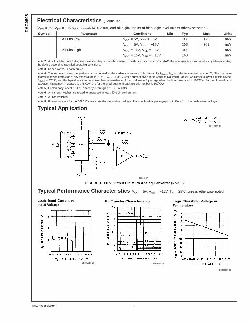
Electrical Characteristics (Continued)
(VCC = 5V, VEE = −15 VDC, VREF/R14 = 2 mA, and all digital inputs at high logic level unless otherwise noted.)
Symbol Parameter Conditions Min Typ Max Units
All Bits Low VCC = 5V, VEE = −5V 33 170 mW
VCC = 5V, VEE = −15V 106 305 mW
All Bits High VCC = 15V, VEE = −5V 90 mW
VCC = 15V, VEE = −15V 160 mW
Note 2: Absolute Maximum Ratings indicate limits beyond which damage to the device may occur. DC and AC electrical specifications do not apply when operatingthe device beyond its specified operating conditions.
Note 3: Range control is not required.
Note 4: The maximum power dissipation must be derated at elevated temperatures and is dictated by TJMAX, θJA, and the ambient temperature, TA. The maximumallowable power dissipation at any temperature is PD = (TJMAX − TA)/θJA or the number given in the Absolute Maixmum Ratings, whichever is lower. For this device,TJMAX = 125˚C, and the typical junction-to-ambient thermal resistance of the dual-in-line J package when the board mounted is 100˚C/W. For the dual-in-line Npackage, this number increases to 175˚C/W and for the small outline M package this number is 100˚C/W.
Note 5: Human body model, 100 pF discharged through a 1.5 kΩ resistor.
Note 6: All current switches are tested to guarantee at least 50% of rated current.
Note 7: All bits switched.
Note 8: Pin-out numbers for the DAL080X represent the dual-in-line package. The small outline package pinout differs from the dual-in-line package.
Typical Application
Typical Performance Characteristics VCC = 5V, VEE = −15V, TA = 25˚C, unless otherwise noted
DS005687-3
DS005687-23
FIGURE 1. +10V Output Digital to Analog Converter (Note 8)
Logic Input Current vsInput Voltage
DS005687-14
Bit Transfer Characteristics
DS005687-15
Logic Threshold Voltage vsTemperature
DS005687-16
DA
C08
08
www.national.com 4
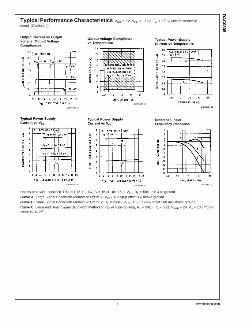
Typical Performance Characteristics VCC = 5V, VEE = −15V, TA = 25˚C, unless otherwisenoted (Continued)
Unless otherwise specified: R14 = R15 = 1 kΩ, C = 15 pF, pin 16 to VEE; RL = 50Ω, pin 4 to ground.
Curve A: Large Signal Bandwidth Method of Figure 7, VREF = 2 Vp-p offset 1V above ground.
Curve B: Small Signal Bandwidth Method of Figure 7, RL = 250Ω, VREF = 50 mVp-p offset 200 mV above ground.
Curve C: Large and Small Signal Bandwidth Method of Figure 9 (no op amp, RL = 50Ω), RS = 50Ω, VREF = 2V, VS = 100 mVp-pcentered at 0V.
Output Current vs OutputVoltage (Output VoltageCompliance)
DS005687-17
Output Voltage Compliancevs Temperature
DS005687-18
Typical Power SupplyCurrent vs Temperature
DS005687-19
Typical Power SupplyCurrent vs V EE
DS005687-20
Typical Power SupplyCurrent vs V CC
DS005687-21
Reference InputFrequency Response
DS005687-22
DA
C0808
www.national.com5
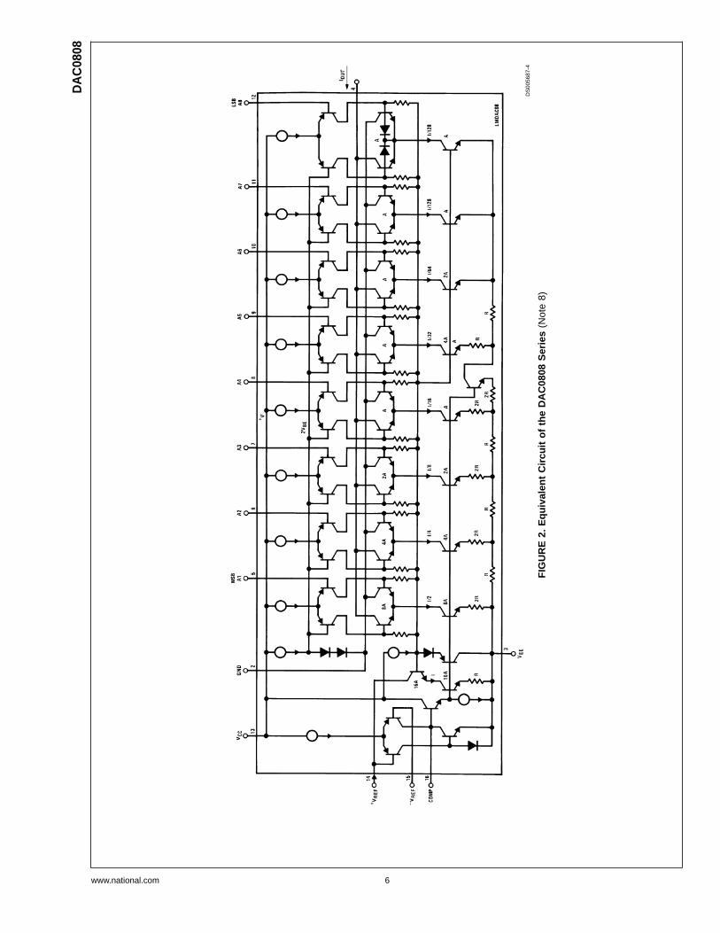
DS
0056
87-4
FIG
UR
E2.
Equ
ival
ent
Circ
uit
ofth
eD
AC
0808
Ser
ies
(Not
e8)
DA
C08
08
www.national.com 6
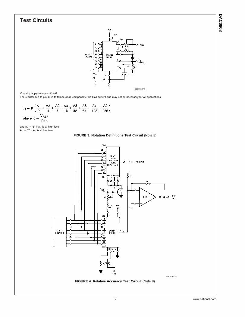
Test Circuits
DS005687-6
VI and I1 apply to inputs A1–A8.The resistor tied to pin 15 is to temperature compensate the bias current and may not be necessary for all applications.
and AN = “1” if AN is at high levelAN = “0” if AN is at low level
FIGURE 3. Notation Definitions Test Circuit (Note 8)
DS005687-7
FIGURE 4. Relative Accuracy Test Circuit (Note 8)
DA
C0808
www.national.com7
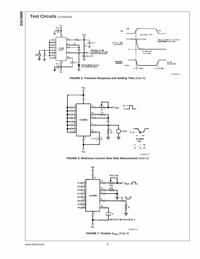
Test Circuits (Continued)
DS005687-8
FIGURE 5. Transient Response and Settling Time (Note 8)
DS005687-9
FIGURE 6. Reference Current Slew Rate Measurement (Note 8)
DS005687-10
FIGURE 7. Positive V REF (Note 8)
DA
C08
08
www.national.com 8
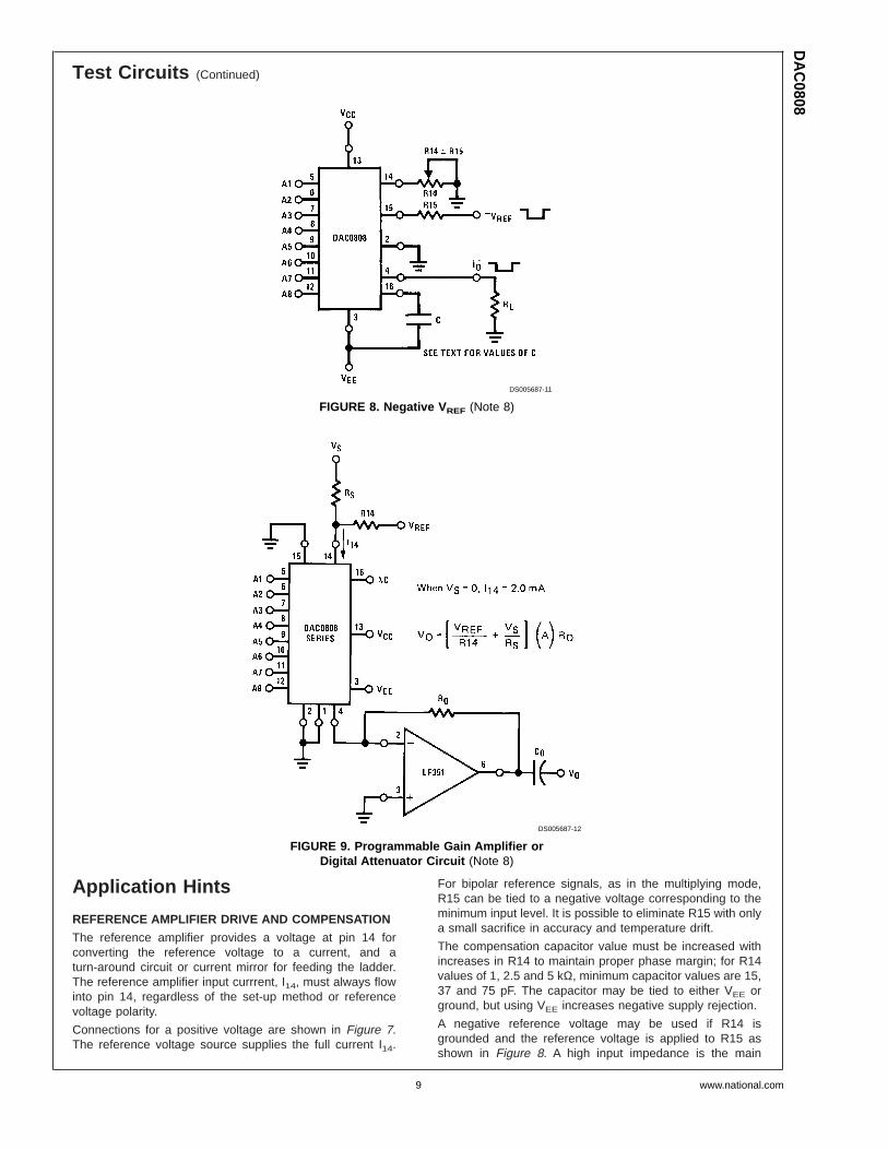
Test Circuits (Continued)
Application Hints
REFERENCE AMPLIFIER DRIVE AND COMPENSATION
The reference amplifier provides a voltage at pin 14 forconverting the reference voltage to a current, and aturn-around circuit or current mirror for feeding the ladder.The reference amplifier input currrent, I14, must always flowinto pin 14, regardless of the set-up method or referencevoltage polarity.
Connections for a positive voltage are shown in Figure 7.The reference voltage source supplies the full current I14.
For bipolar reference signals, as in the multiplying mode,R15 can be tied to a negative voltage corresponding to theminimum input level. It is possible to eliminate R15 with onlya small sacrifice in accuracy and temperature drift.
The compensation capacitor value must be increased withincreases in R14 to maintain proper phase margin; for R14values of 1, 2.5 and 5 kΩ, minimum capacitor values are 15,37 and 75 pF. The capacitor may be tied to either VEE orground, but using VEE increases negative supply rejection.
A negative reference voltage may be used if R14 isgrounded and the reference voltage is applied to R15 asshown in Figure 8. A high input impedance is the main
DS005687-11
FIGURE 8. Negative V REF (Note 8)
DS005687-12
FIGURE 9. Programmable Gain Amplifier orDigital Attenuator Circuit (Note 8)
DA
C0808
www.national.com9
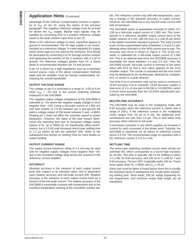
Application Hints (Continued)
advantage of this method. Compensation involves a capaci-tor to VEE on pin 16, using the values of the previousparagraph. The negative reference voltage must be at least4V above the VEE supply. Bipolar input signals may behandled by connecting R14 to a positive reference voltageequal to the peak positive input level at pin 15.
When a DC reference voltage is used, capacitive bypass toground is recommended. The 5V logic supply is not recom-mended as a reference voltage. If a well regulated 5V supplywhich drives logic is to be used as the reference, R14 shouldbe decoupled by connecting it to 5V through another resistorand bypassing the junction of the 2 resistors with 0.1 µF toground. For reference voltages greater than 5V, a clampdiode is recommended between pin 14 and ground.
If pin 14 is driven by a high impedance such as a transistorcurrent source, none of the above compensation methodsapply and the amplifier must be heavily compensated, de-creasing the overall bandwidth.
OUTPUT VOLTAGE RANGE
The voltage on pin 4 is restricted to a range of −0.55 to 0.4Vwhen VEE = −5V due to the current switching methodsemployed in the DAC0808.
The negative output voltage compliance of the DAC0808 isextended to −5V where the negative supply voltage is morenegative than −10V. Using a full-scale current of 1.992 mAand load resistor of 2.5 kΩ between pin 4 and ground willyield a voltage output of 256 levels between 0 and −4.980V.Floating pin 1 does not affect the converter speed or powerdissipation. However, the value of the load resistor deter-mines the switching time due to increased voltage swing.Values of RL up to 500Ω do not significantly affect perfor-mance, but a 2.5 kΩ load increases worst-case settling timeto 1.2 µs (when all bits are switched ON). Refer to thesubsequent text section on Settling Time for more details onoutput loading.
OUTPUT CURRENT RANGE
The output current maximum rating of 4.2 mA may be usedonly for negative supply voltages more negative than −8V,due to the increased voltage drop across the resistors in thereference current amplifier.
ACCURACY
Absolute accuracy is the measure of each output currentlevel with respect to its intended value, and is dependentupon relative accuracy and full-scale current drift. Relativeaccuracy is the measure of each output current level as afraction of the full-scale current. The relative accuracy of theDAC0808 is essentially constant with temperature due to theexcellent temperature tracking of the monolithic resistor lad-
der. The reference current may drift with temperature, caus-ing a change in the absolute accuracy of output current.However, the DAC0808 has a very low full-scale current driftwith temperature.
The DAC0808 series is guaranteed accurate to within ±1⁄2LSB at a full-scale output current of 1.992 mA. This corre-sponds to a reference amplifier output current drive to theladder network of 2 mA, with the loss of 1 LSB (8 µA) whichis the ladder remainder shunted to ground. The input currentto pin 14 has a guaranteed value of between 1.9 and 2.1 mA,allowing some mismatch in the NPN current source pair. Theaccuracy test circuit is shown in Figure 4. The 12-bit con-verter is calibrated for a full-scale output current of 1.992mA. This is an optional step since the DAC0808 accuracy isessentially the same between 1.5 and 2.5 mA. Then theDAC0808 circuits’ full-scale current is trimmed to the samevalue with R14 so that a zero value appears at the erroramplifier output. The counter is activated and the error bandmay be displayed on an oscilloscope, detected by compara-tors, or stored in a peak detector.
Two 8-bit D-to-A converters may not be used to construct a16-bit accuracy D-to-A converter. 16-bit accuracy implies atotal error of ±1⁄2 of one part in 65,536 or ±0.00076%, whichis much more accurate than the ±0.019% specification pro-vided by the DAC0808.
MULTIPLYING ACCURACY
The DAC0808 may be used in the multiplying mode with8-bit accuracy when the reference current is varied over arange of 256:1. If the reference current in the multiplyingmode ranges from 16 µA to 4 mA, the additional errorcontributions are less than 1.6 µA. This is well within 8-bitaccuracy when referred to full-scale.
A monotonic converter is one which supplies an increase incurrent for each increment in the binary word. Typically, theDAC0808 is monotonic for all values of reference currentabove 0.5 mA. The recommended range for operation with aDC reference current is 0.5 to 4 mA.
SETTLING TIME
The worst-case switching condition occurs when all bits areswitched ON, which corresponds to a low-to-high transitionfor all bits. This time is typically 150 ns for settling to within±1⁄2 LSB, for 8-bit accuracy, and 100 ns to 1⁄2 LSB for 7 and6-bit accuracy. The turn OFF is typically under 100 ns. Thesetimes apply when RL ≤ 500Ω and CO ≤ 25 pF.
Extra care must be taken in board layout since this is usuallythe dominant factor in satisfactory test results when measur-ing settling time. Short leads, 100 µF supply bypassing forlow frequencies, and minimum scope lead length are allmandatory.
DA
C08
08
www.national.com 10
Physical Dimensions inches (millimeters) unless otherwise noted
Small Outline PackageOrder Number DAC0808LCMNS Package Number M16A
Dual-In-Line PackageOrder Number DAC0808
NS Package Number N16A
DA
C0808
www.national.com11
Notes
LIFE SUPPORT POLICY
NATIONAL’S PRODUCTS ARE NOT AUTHORIZED FOR USE AS CRITICAL COMPONENTS IN LIFE SUPPORTDEVICES OR SYSTEMS WITHOUT THE EXPRESS WRITTEN APPROVAL OF THE PRESIDENT AND GENERALCOUNSEL OF NATIONAL SEMICONDUCTOR CORPORATION. As used herein:
1. Life support devices or systems are devices orsystems which, (a) are intended for surgical implantinto the body, or (b) support or sustain life, andwhose failure to perform when properly used inaccordance with instructions for use provided in thelabeling, can be reasonably expected to result in asignificant injury to the user.
2. A critical component is any component of a lifesupport device or system whose failure to performcan be reasonably expected to cause the failure ofthe life support device or system, or to affect itssafety or effectiveness.
National SemiconductorCorporationAmericasEmail: [email protected]
National SemiconductorEurope
Fax: +49 (0) 180-530 85 86Email: [email protected]
Deutsch Tel: +49 (0) 69 9508 6208English Tel: +44 (0) 870 24 0 2171Français Tel: +33 (0) 1 41 91 8790
National SemiconductorAsia Pacific CustomerResponse GroupTel: 65-2544466Fax: 65-2504466Email: [email protected]
National SemiconductorJapan Ltd.Tel: 81-3-5639-7560Fax: 81-3-5639-7507
www.national.com
DA
C08
088-
Bit
D/A
Con
verte
r
National does not assume any responsibility for use of any circuitry described, no circuit patent licenses are implied and National reserves the right at any time without notice to change said circuitry and specifications.
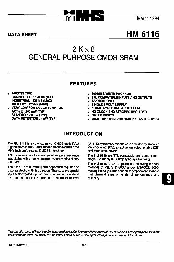
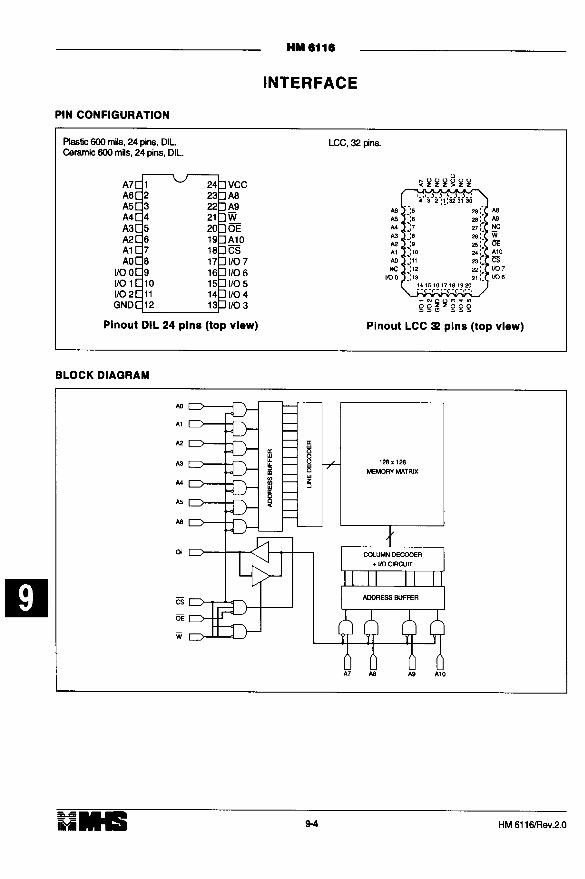
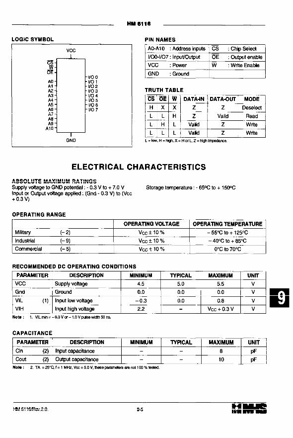
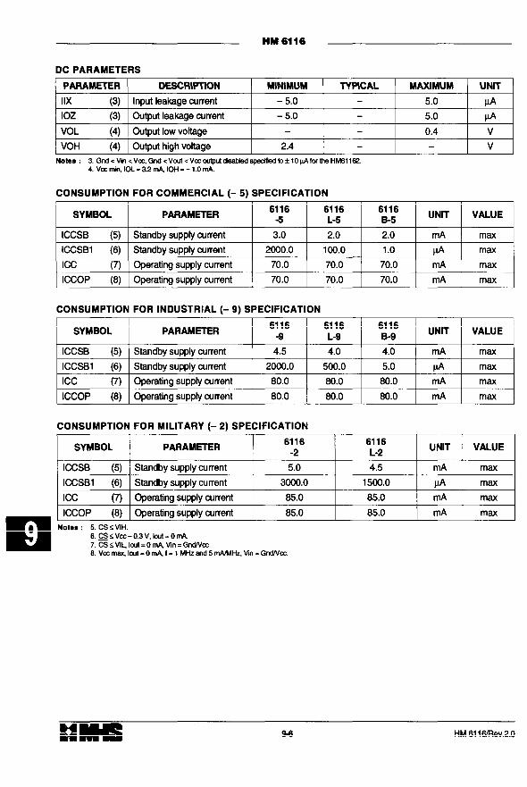
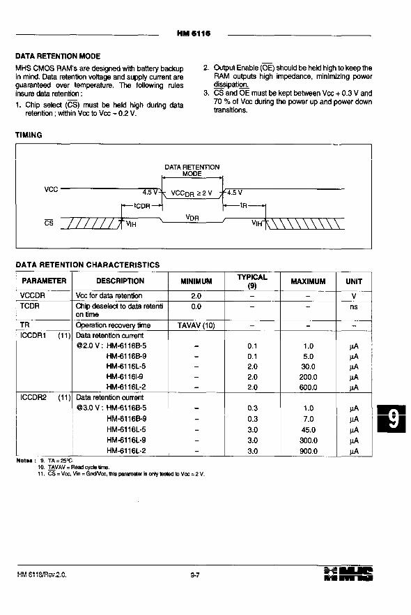
This datasheet has been downloaded from:
www.DatasheetCatalog.com
Datasheets for electronic components.
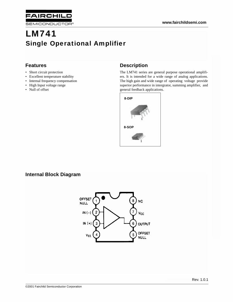
©2001 Fairchild Semiconductor Corporation
www.fairchildsemi.com
Rev. 1.0.1
Features• Short circuit protection• Excellent temperature stability• Internal frequency compensation• High Input voltage range• Null of offset
DescriptionThe LM741 series are general purpose operational amplifi-ers. It is intended for a wide range of analog applications.The high gain and wide range of operating voltage providesuperior performance in intergrator, summing amplifier, andgeneral feedback applications.
8-DIP
1
8-SOP
1
Internal Block Diagram
LM741Single Operational Amplifier
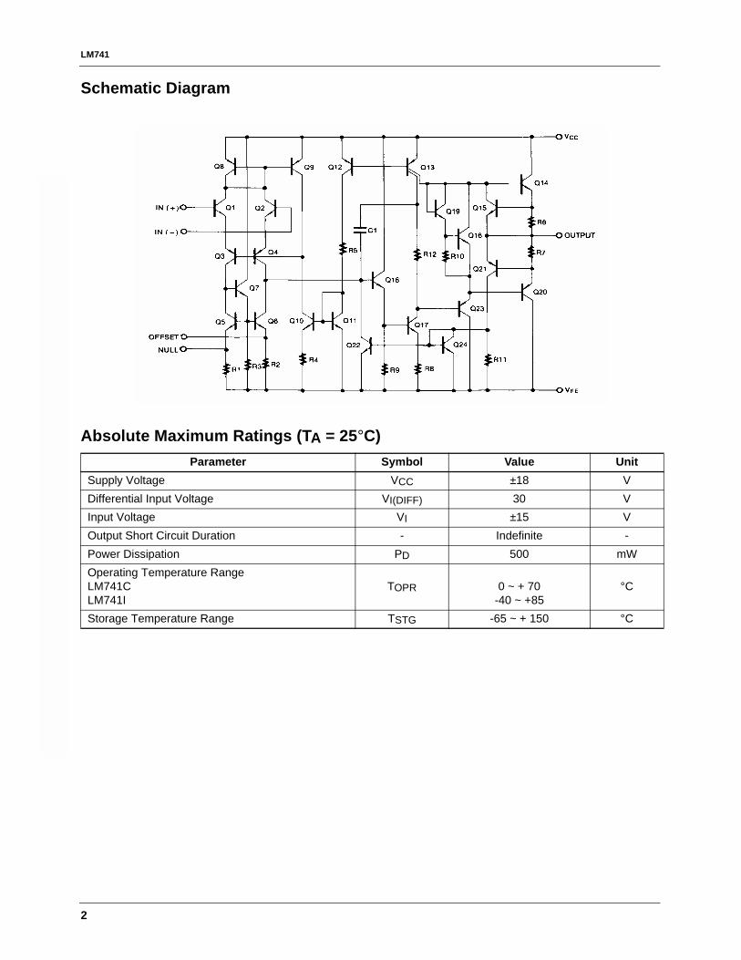
LM741
2
Schematic Diagram
Absolute Maximum Ratings (TA = 25°C)Parameter Symbol Value Unit
Supply Voltage VCC ±18 VDifferential Input Voltage VI(DIFF) 30 VInput Voltage VI ±15 VOutput Short Circuit Duration - Indefinite -Power Dissipation PD 500 mWOperating Temperature RangeLM741CLM741I
TOPR 0 ~ + 70-40 ~ +85
°C
Storage Temperature Range TSTG -65 ~ + 150 °C
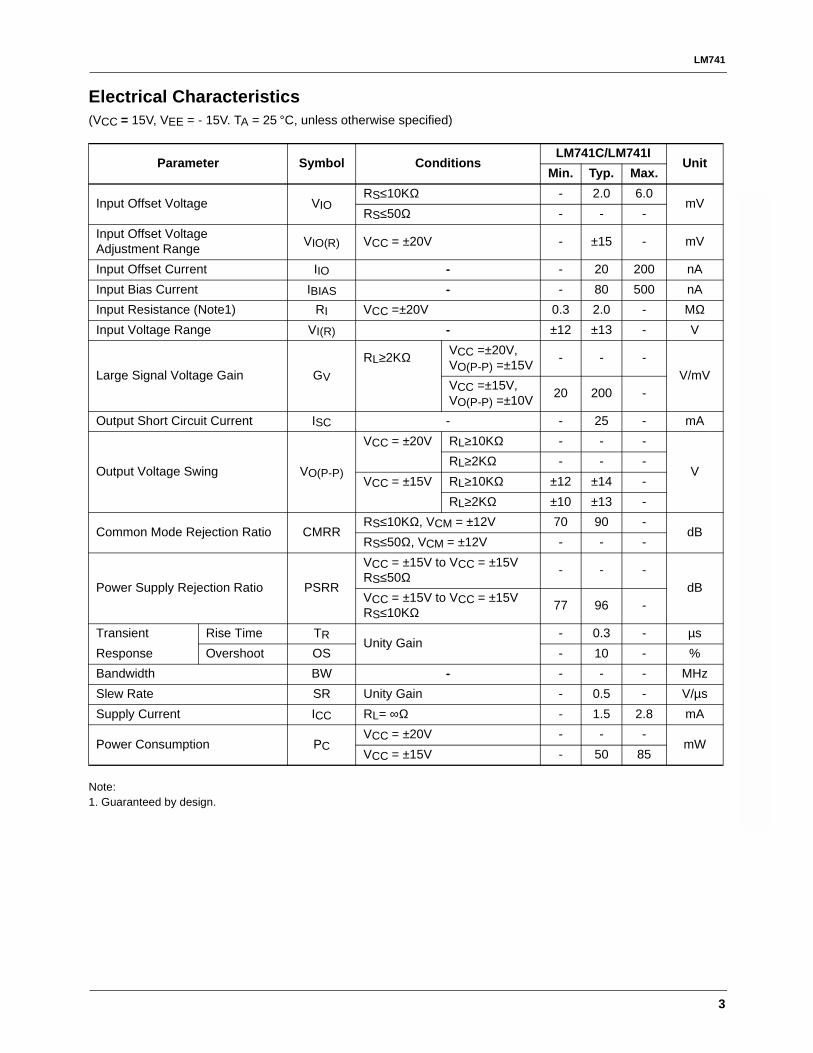
LM741
3
Electrical Characteristics(VCC = 15V, VEE = - 15V. TA = 25 °C, unless otherwise specified)
Note:1. Guaranteed by design.
Parameter Symbol ConditionsLM741C/LM741I
UnitMin. Typ. Max.
Input Offset Voltage VIORS≤10KΩ - 2.0 6.0
mVRS≤50Ω - - -
Input Offset VoltageAdjustment Range VIO(R) VCC = ±20V - ±15 - mV
Input Offset Current IIO - - 20 200 nAInput Bias Current IBIAS - - 80 500 nAInput Resistance (Note1) RI VCC =±20V 0.3 2.0 - MΩInput Voltage Range VI(R) - ±12 ±13 - V
Large Signal Voltage Gain GVRL≥2KΩ VCC =±20V,
VO(P-P) =±15V - - -V/mV
VCC =±15V,VO(P-P) =±10V 20 200 -
Output Short Circuit Current ISC - - 25 - mA
Output Voltage Swing VO(P-P)
VCC = ±20V RL≥10KΩ - - -
VRL≥2KΩ - - -
VCC = ±15V RL≥10KΩ ±12 ±14 -RL≥2KΩ ±10 ±13 -
Common Mode Rejection Ratio CMRRRS≤10KΩ, VCM = ±12V 70 90 -
dBRS≤50Ω, VCM = ±12V - - -
Power Supply Rejection Ratio PSRR
VCC = ±15V to VCC = ±15VRS≤50Ω - - -
dBVCC = ±15V to VCC = ±15VRS≤10KΩ 77 96 -
Transient Rise Time TRUnity Gain
- 0.3 - µsResponse Overshoot OS - 10 - %Bandwidth BW - - - - MHzSlew Rate SR Unity Gain - 0.5 - V/µsSupply Current ICC RL= ∞Ω - 1.5 2.8 mA
Power Consumption PCVCC = ±20V - - -
mWVCC = ±15V - 50 85
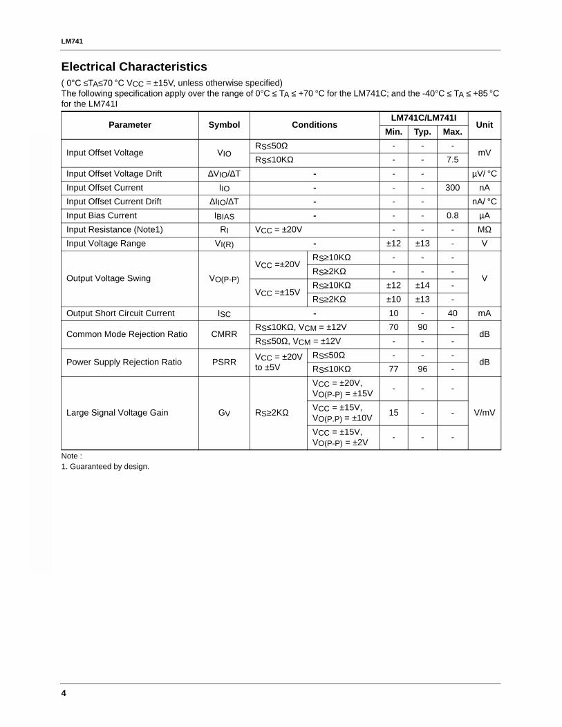
LM741
4
Electrical Characteristics( 0°C ≤TA≤70 °C VCC = ±15V, unless otherwise specified)The following specification apply over the range of 0°C ≤ TA ≤ +70 °C for the LM741C; and the -40°C ≤ TA ≤ +85 °C for the LM741I
Note :1. Guaranteed by design.
Parameter Symbol ConditionsLM741C/LM741I
UnitMin. Typ. Max.
Input Offset Voltage VIORS≤50Ω - - -
mVRS≤10KΩ - - 7.5
Input Offset Voltage Drift ∆VIO/∆T - - - µV/ °CInput Offset Current IIO - - - 300 nAInput Offset Current Drift ∆IIO/∆T - - - nA/ °CInput Bias Current IBIAS - - - 0.8 µAInput Resistance (Note1) RI VCC = ±20V - - - MΩInput Voltage Range VI(R) - ±12 ±13 - V
Output Voltage Swing VO(P-P)
VCC =±20VRS≥10KΩ - - -
VRS≥2KΩ - - -
VCC =±15VRS≥10KΩ ±12 ±14 -RS≥2KΩ ±10 ±13 -
Output Short Circuit Current ISC - 10 - 40 mA
Common Mode Rejection Ratio CMRRRS≤10KΩ, VCM = ±12V 70 90 -
dBRS≤50Ω, VCM = ±12V - - -
Power Supply Rejection Ratio PSRR VCC = ±20V to ±5V
RS≤50Ω - - -dB
RS≤10KΩ 77 96 -
Large Signal Voltage Gain GV RS≥2KΩ
VCC = ±20V,VO(P-P) = ±15V - - -
V/mVVCC = ±15V,VO(P.P) = ±10V 15 - -
VCC = ±15V,VO(P-P) = ±2V - - -
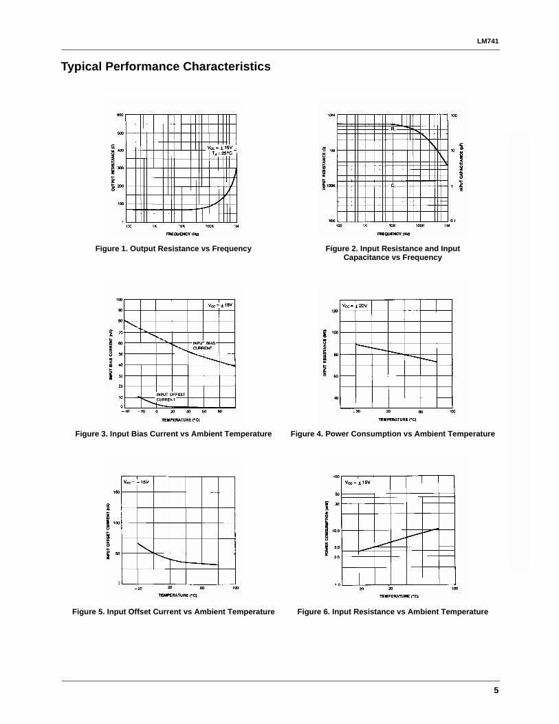
LM741
5
Typical Performance Characteristics
Figure 1. Output Resistance vs Frequency Figure 2. Input Resistance and Input Capacitance vs Frequency
Figure 3. Input Bias Current vs Ambient Temperature Figure 4. Power Consumption vs Ambient Temperature
Figure 5. Input Offset Current vs Ambient Temperature Figure 6. Input Resistance vs Ambient Temperature
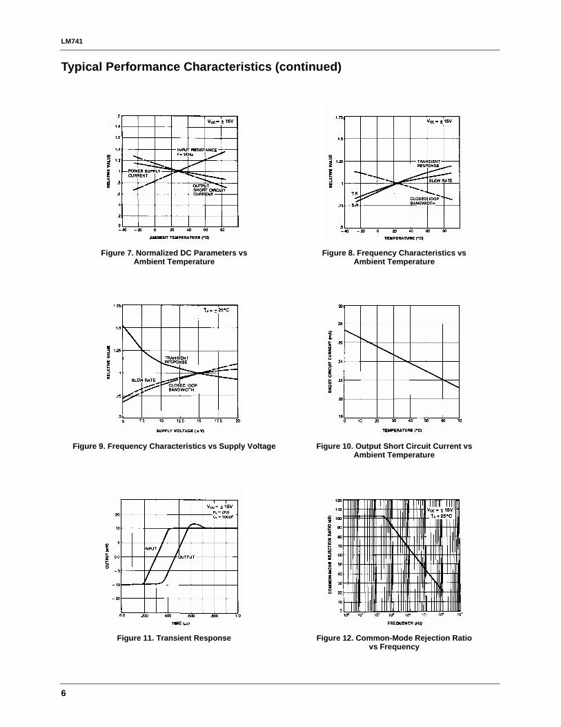
LM741
6
Typical Performance Characteristics (continued)
Figure 7. Normalized DC Parameters vs Ambient Temperature
Figure 8. Frequency Characteristics vs Ambient Temperature
Figure 9. Frequency Characteristics vs Supply Voltage Figure 10. Output Short Circuit Current vs Ambient Temperature
Figure 11. Transient Response Figure 12. Common-Mode Rejection Ratiovs Frequency
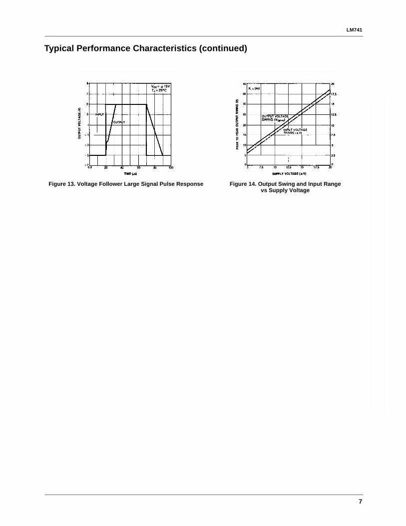
LM741
7
Typical Performance Characteristics (continued)
Figure 13. Voltage Follower Large Signal Pulse Response Figure 14. Output Swing and Input Range vs Supply Voltage
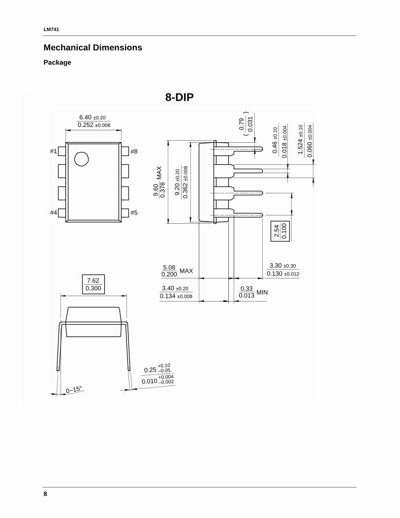
LM741
8
Mechanical DimensionsPackage
6.40 ±0.20
3.30 ±0.30
0.130 ±0.012
3.40 ±0.20
0.134 ±0.008
#1
#4 #5
#8
0.252 ±0.008
9.20
±0.
20
0.79
2.54
0.10
0
0.03
1(
)
0.46
±0.
10
0.01
8 ±0
.004
0.06
0 ±0
.004
1.52
4 ±0
.10
0.36
2 ±0
.008
9.60
0.37
8M
AX
5.080.200
0.330.013
7.62
0~15°
0.300
MAX
MIN
0.25+0.10–0.05
0.010+0.004–0.002
8-DIP
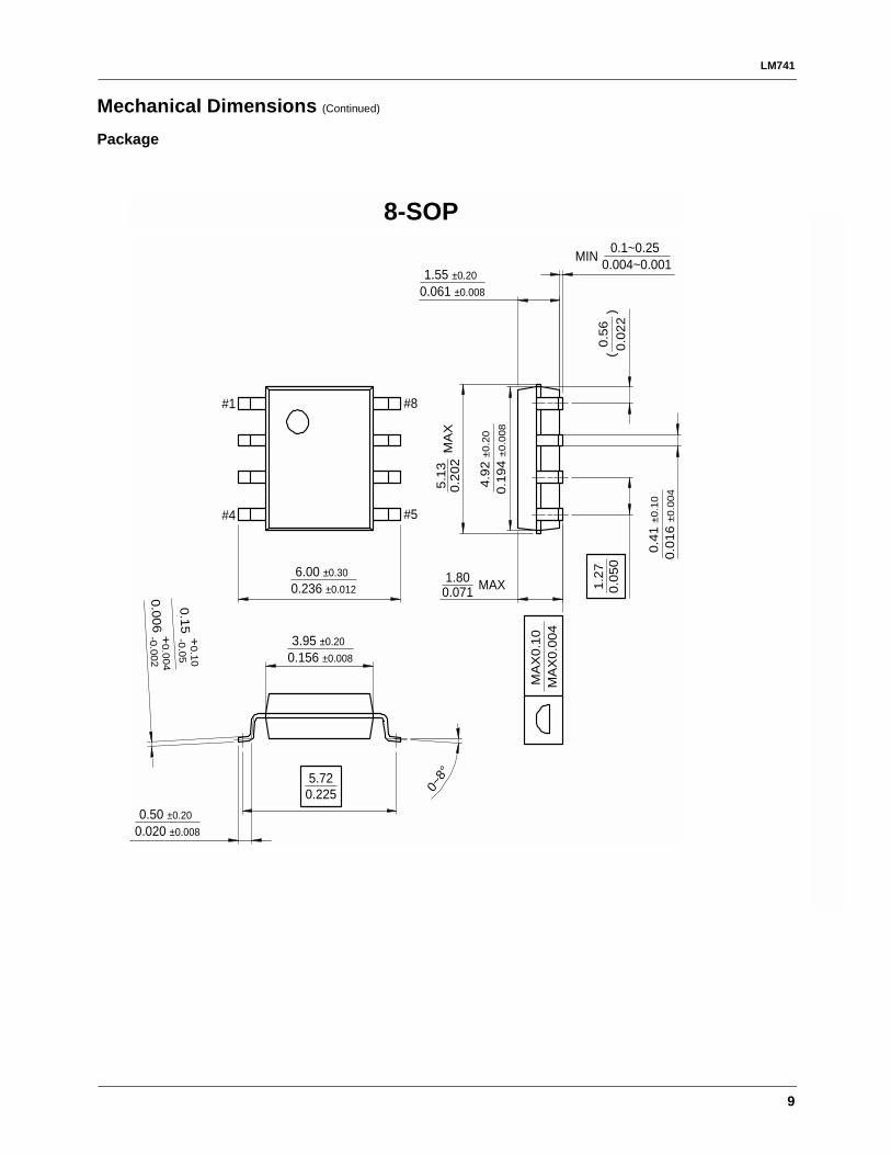
LM741
9
Mechanical Dimensions (Continued)
Package
4.9
2 ±
0.2
0
0.1
94
±0.0
08
0.4
1 ±
0.1
0
0.0
16
±0.0
04
1.2
70
.05
0
5.720.225
1.55 ±0.20
0.061 ±0.008
0.1~0.250.004~0.001
6.00 ±0.30
0.236 ±0.012
3.95 ±0.20
0.156 ±0.008
0.50 ±0.20
0.020 ±0.008
5.1
30
.20
2M
AX
#1
#4 #5
0~8°
#8
0.5
60
.02
2(
)
1.800.071
MA
X0
.10
MA
X0
.00
4
MAX
MIN
+0.1
0-0
.05
0.1
5
+0.0
04
-0.0
02
0.0
06
8-SOP
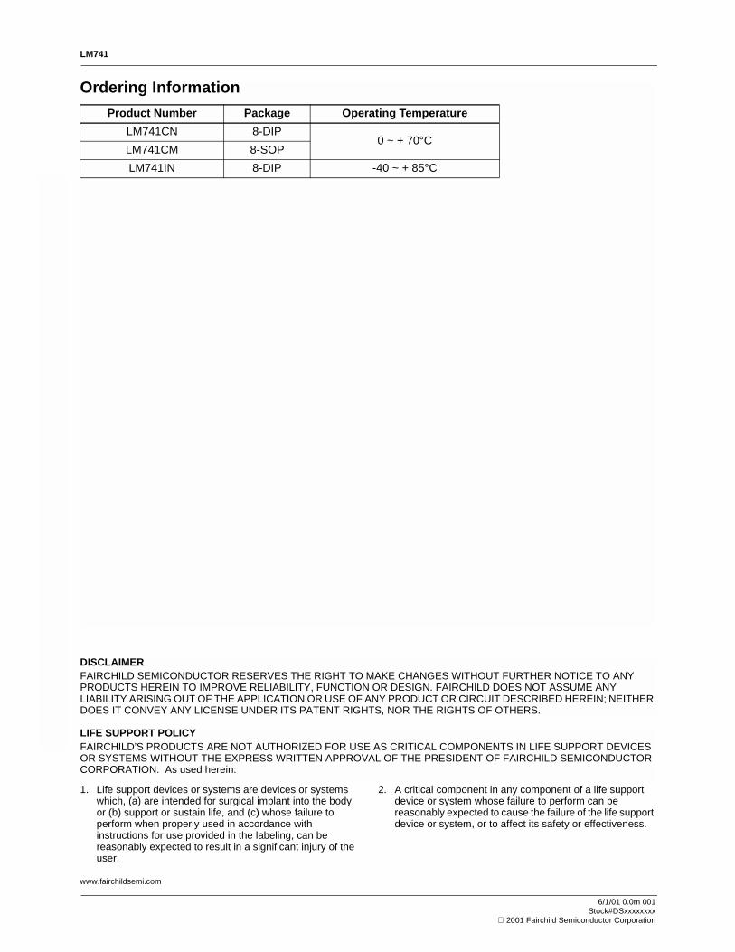
LM741
6/1/01 0.0m 001Stock#DSxxxxxxxx
2001 Fairchild Semiconductor Corporation
LIFE SUPPORT POLICY FAIRCHILD’S PRODUCTS ARE NOT AUTHORIZED FOR USE AS CRITICAL COMPONENTS IN LIFE SUPPORT DEVICES OR SYSTEMS WITHOUT THE EXPRESS WRITTEN APPROVAL OF THE PRESIDENT OF FAIRCHILD SEMICONDUCTOR CORPORATION. As used herein:
1. Life support devices or systems are devices or systems which, (a) are intended for surgical implant into the body, or (b) support or sustain life, and (c) whose failure to perform when properly used in accordance with instructions for use provided in the labeling, can be reasonably expected to result in a significant injury of the user.
2. A critical component in any component of a life support device or system whose failure to perform can be reasonably expected to cause the failure of the life support device or system, or to affect its safety or effectiveness.
www.fairchildsemi.com
DISCLAIMER FAIRCHILD SEMICONDUCTOR RESERVES THE RIGHT TO MAKE CHANGES WITHOUT FURTHER NOTICE TO ANY PRODUCTS HEREIN TO IMPROVE RELIABILITY, FUNCTION OR DESIGN. FAIRCHILD DOES NOT ASSUME ANY LIABILITY ARISING OUT OF THE APPLICATION OR USE OF ANY PRODUCT OR CIRCUIT DESCRIBED HEREIN; NEITHER DOES IT CONVEY ANY LICENSE UNDER ITS PATENT RIGHTS, NOR THE RIGHTS OF OTHERS.
Ordering InformationProduct Number Package Operating Temperature
LM741CN 8-DIP0 ~ + 70°C
LM741CM 8-SOPLM741IN 8-DIP -40 ~ + 85°C
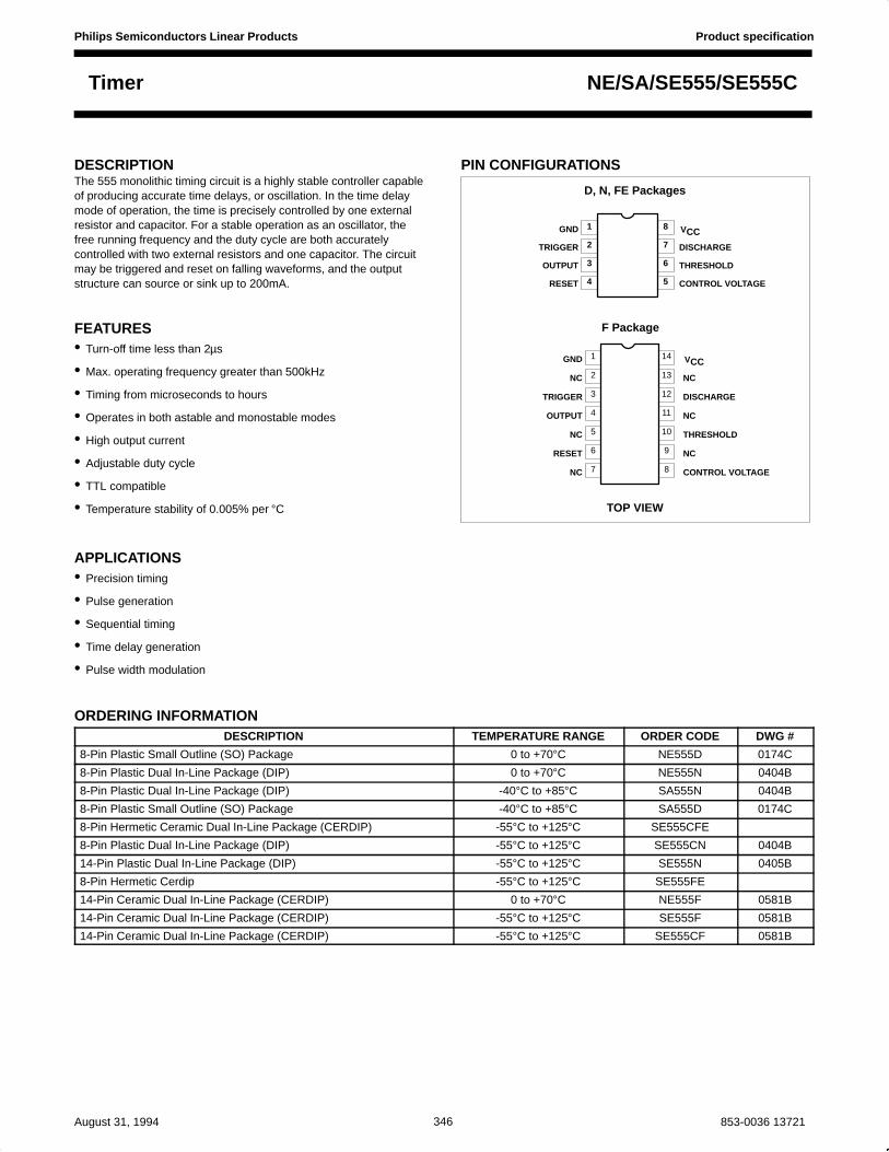
Philips Semiconductors Linear Products Product specification
NE/SA/SE555/SE555CTimer
346August 31, 1994 853-0036 13721
DESCRIPTIONThe 555 monolithic timing circuit is a highly stable controller capableof producing accurate time delays, or oscillation. In the time delaymode of operation, the time is precisely controlled by one externalresistor and capacitor. For a stable operation as an oscillator, thefree running frequency and the duty cycle are both accuratelycontrolled with two external resistors and one capacitor. The circuitmay be triggered and reset on falling waveforms, and the outputstructure can source or sink up to 200mA.
FEATURES• Turn-off time less than 2µs
• Max. operating frequency greater than 500kHz
• Timing from microseconds to hours
• Operates in both astable and monostable modes
• High output current
• Adjustable duty cycle
• TTL compatible
• Temperature stability of 0.005% per °C
APPLICATIONS• Precision timing
• Pulse generation
• Sequential timing
• Time delay generation
• Pulse width modulation
PIN CONFIGURATIONS
1
2
3
4 5
6
7
8
1
2
3
4
5
6
7 8
14
13
12
11
10
9
GND
TRIGGER
OUTPUT
RESET
GND
NC
TRIGGER
OUTPUT
NC
RESET
NC
DISCHARGE
THRESHOLD
CONTROL VOLTAGE
NC
DISCHARGE
NC
THRESHOLD
NC
CONTROL VOLTAGE
VCC
VCC
D, N, FE Packages
TOP VIEW
F Package
ORDERING INFORMATIONDESCRIPTION TEMPERATURE RANGE ORDER CODE DWG #
8-Pin Plastic Small Outline (SO) Package 0 to +70°C NE555D 0174C
8-Pin Plastic Dual In-Line Package (DIP) 0 to +70°C NE555N 0404B
8-Pin Plastic Dual In-Line Package (DIP) -40°C to +85°C SA555N 0404B
8-Pin Plastic Small Outline (SO) Package -40°C to +85°C SA555D 0174C
8-Pin Hermetic Ceramic Dual In-Line Package (CERDIP) -55°C to +125°C SE555CFE
8-Pin Plastic Dual In-Line Package (DIP) -55°C to +125°C SE555CN 0404B
14-Pin Plastic Dual In-Line Package (DIP) -55°C to +125°C SE555N 0405B
8-Pin Hermetic Cerdip -55°C to +125°C SE555FE
14-Pin Ceramic Dual In-Line Package (CERDIP) 0 to +70°C NE555F 0581B
14-Pin Ceramic Dual In-Line Package (CERDIP) -55°C to +125°C SE555F 0581B
14-Pin Ceramic Dual In-Line Package (CERDIP) -55°C to +125°C SE555CF 0581B
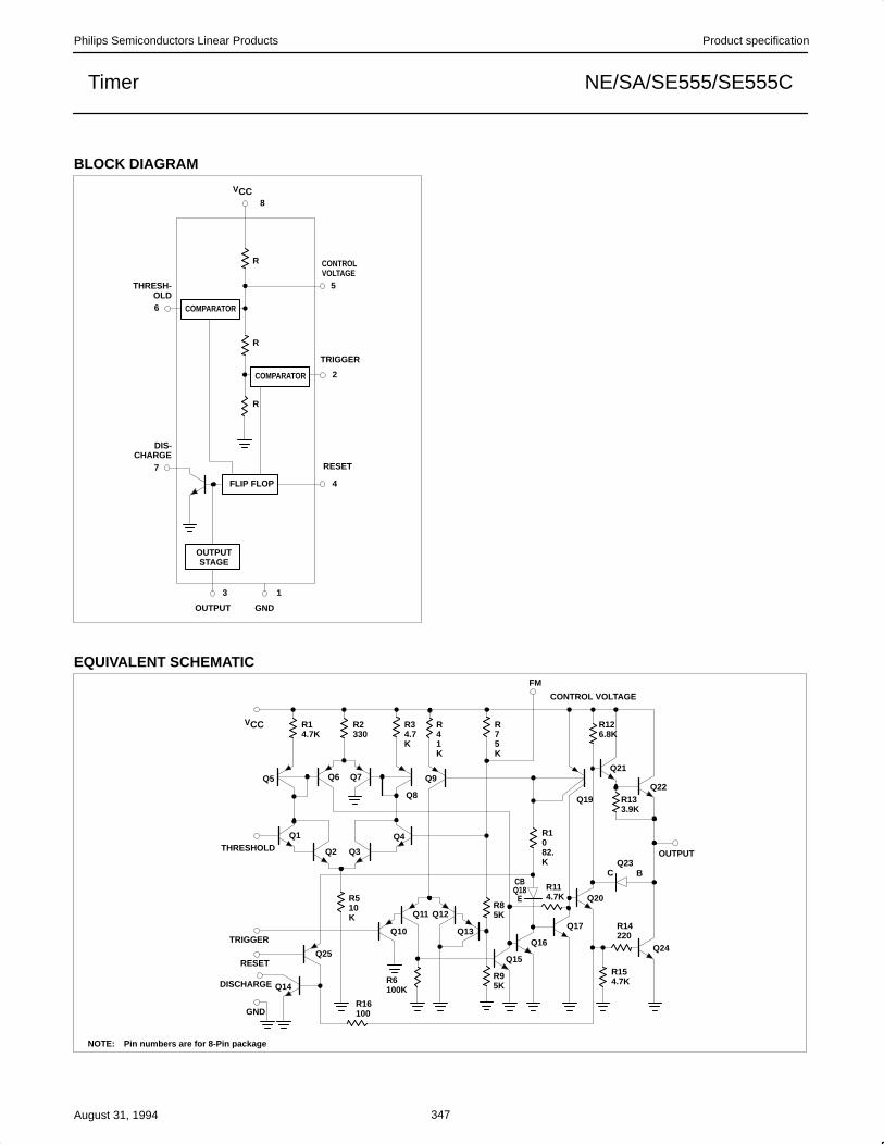
Philips Semiconductors Linear Products Product specification
NE/SA/SE555/SE555CTimer
August 31, 1994 347
BLOCK DIAGRAM
COMPARATOR
COMPARATOR
FLIP FLOP
OUTPUTSTAGE
THRESH-OLD
VCC
6
7
3 1
4
2
5
8
R
R
R CONTROLVOLTAGE
TRIGGER
RESET
DIS-CHARGE
OUTPUT GND
EQUIVALENT SCHEMATIC
NOTE: Pin numbers are for 8-Pin package
CONTROL VOLTAGE
FM
VCC R14.7K
R2330
R34.7K
R41K
R75K
R126.8K
Q21Q9
Q8
Q7Q6Q5
Q1
Q2 Q3
Q4
Q19Q22
R133.9K
OUTPUTQ23
C B
R1082.K
R510K
Q10
Q11 Q12
Q13
Q20R114.7K
CBQ18
ER85K
Q17
Q16
Q15
R6100K
R16100
Q14
Q25
R95K
R154.7K
Q24
R14220
THRESHOLD
TRIGGER
RESET
DISCHARGE
GND
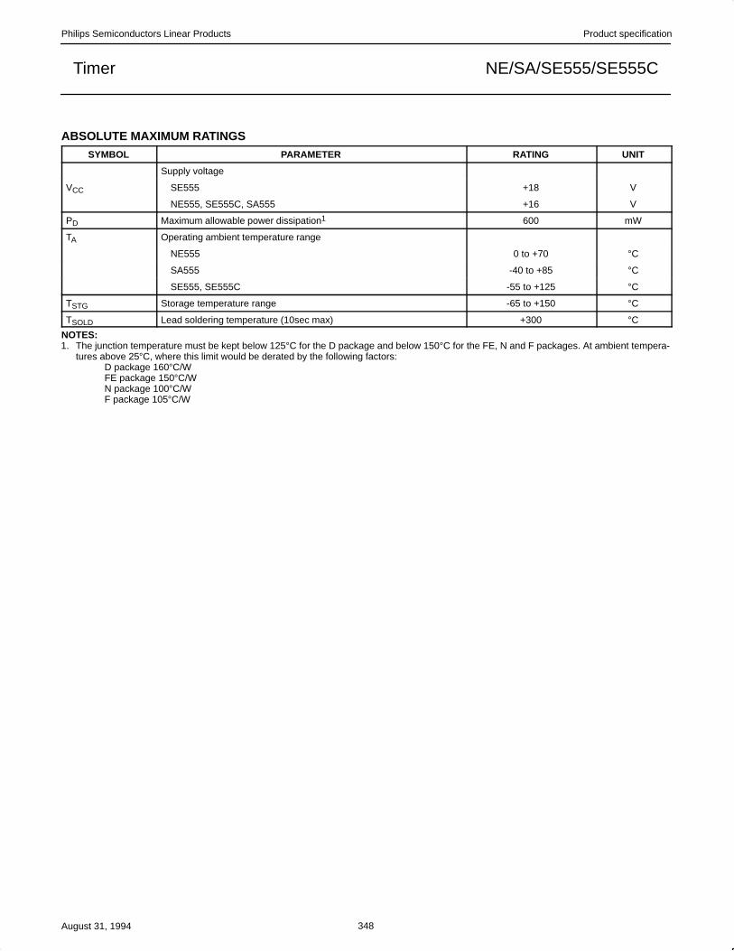
Philips Semiconductors Linear Products Product specification
NE/SA/SE555/SE555CTimer
August 31, 1994 348
ABSOLUTE MAXIMUM RATINGSSYMBOL PARAMETER RATING UNIT
Supply voltage
VCC SE555 +18 V
NE555, SE555C, SA555 +16 V
PD Maximum allowable power dissipation1 600 mW
TA Operating ambient temperature range
NE555 0 to +70 °C
SA555 -40 to +85 °C
SE555, SE555C -55 to +125 °C
TSTG Storage temperature range -65 to +150 °C
TSOLD Lead soldering temperature (10sec max) +300 °CNOTES:1. The junction temperature must be kept below 125°C for the D package and below 150°C for the FE, N and F packages. At ambient tempera-
tures above 25°C, where this limit would be derated by the following factors:D package 160°C/WFE package 150°C/WN package 100°C/WF package 105°C/W
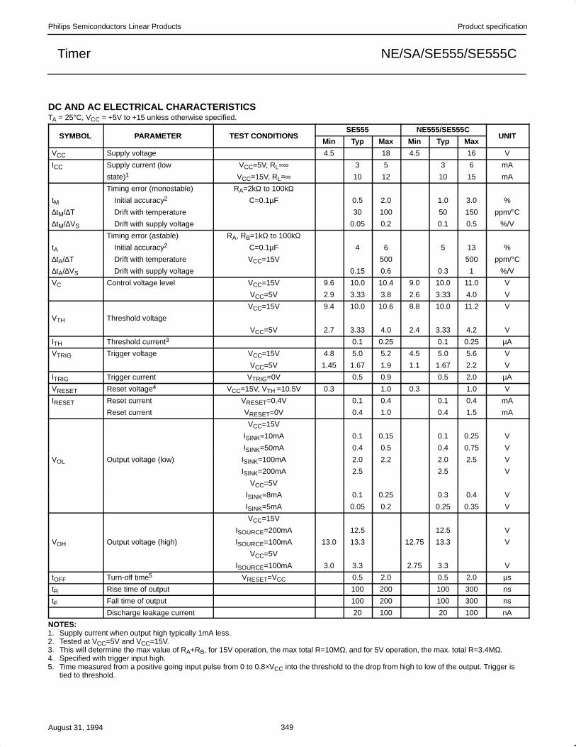
Philips Semiconductors Linear Products Product specification
NE/SA/SE555/SE555CTimer
August 31, 1994 349
DC AND AC ELECTRICAL CHARACTERISTICSTA = 25°C, VCC = +5V to +15 unless otherwise specified.
SYMBOL PARAMETER TEST CONDITIONSSE555 NE555/SE555C
UNITSYMBOL PARAMETER TEST CONDITIONSMin Typ Max Min Typ Max
UNIT
VCC Supply voltage 4.5 18 4.5 16 V
ICC Supply current (low VCC=5V, RL=∞ 3 5 3 6 mA
state)1 VCC=15V, RL=∞ 10 12 10 15 mA
Timing error (monostable) RA=2kΩ to 100kΩtM Initial accuracy2 C=0.1µF 0.5 2.0 1.0 3.0 %
∆tM/∆T Drift with temperature 30 100 50 150 ppm/°C∆tM/∆VS Drift with supply voltage 0.05 0.2 0.1 0.5 %/V
Timing error (astable) RA, RB=1kΩ to 100kΩtA Initial accuracy2 C=0.1µF 4 6 5 13 %
∆tA/∆T Drift with temperature VCC=15V 500 500 ppm/°C∆tA/∆VS Drift with supply voltage 0.15 0.6 0.3 1 %/V
VC Control voltage level VCC=15V 9.6 10.0 10.4 9.0 10.0 11.0 V
VCC=5V 2.9 3.33 3.8 2.6 3.33 4.0 V
VCC=15V 9.4 10.0 10.6 8.8 10.0 11.2 V
VTH Threshold voltage
VCC=5V 2.7 3.33 4.0 2.4 3.33 4.2 V
ITH Threshold current3 0.1 0.25 0.1 0.25 µA
VTRIG Trigger voltage VCC=15V 4.8 5.0 5.2 4.5 5.0 5.6 V
VCC=5V 1.45 1.67 1.9 1.1 1.67 2.2 V
ITRIG Trigger current VTRIG=0V 0.5 0.9 0.5 2.0 µA
VRESET Reset voltage4 VCC=15V, VTH =10.5V 0.3 1.0 0.3 1.0 V
IRESET Reset current VRESET=0.4V 0.1 0.4 0.1 0.4 mA
Reset current VRESET=0V 0.4 1.0 0.4 1.5 mA
VCC=15V
ISINK=10mA 0.1 0.15 0.1 0.25 V
ISINK=50mA 0.4 0.5 0.4 0.75 V
VOL Output voltage (low) ISINK=100mA 2.0 2.2 2.0 2.5 V
ISINK=200mA 2.5 2.5 V
VCC=5V
ISINK=8mA 0.1 0.25 0.3 0.4 V
ISINK=5mA 0.05 0.2 0.25 0.35 V
VCC=15V
ISOURCE=200mA 12.5 12.5 V
VOH Output voltage (high) ISOURCE=100mA 13.0 13.3 12.75 13.3 V
VCC=5V
ISOURCE=100mA 3.0 3.3 2.75 3.3 V
tOFF Turn-off time5 VRESET=VCC 0.5 2.0 0.5 2.0 µs
tR Rise time of output 100 200 100 300 ns
tF Fall time of output 100 200 100 300 ns
Discharge leakage current 20 100 20 100 nA
NOTES:1. Supply current when output high typically 1mA less.2. Tested at VCC=5V and VCC=15V.3. This will determine the max value of RA+RB, for 15V operation, the max total R=10MΩ, and for 5V operation, the max. total R=3.4MΩ.4. Specified with trigger input high.5. Time measured from a positive going input pulse from 0 to 0.8×VCC into the threshold to the drop from high to low of the output. Trigger is
tied to threshold.
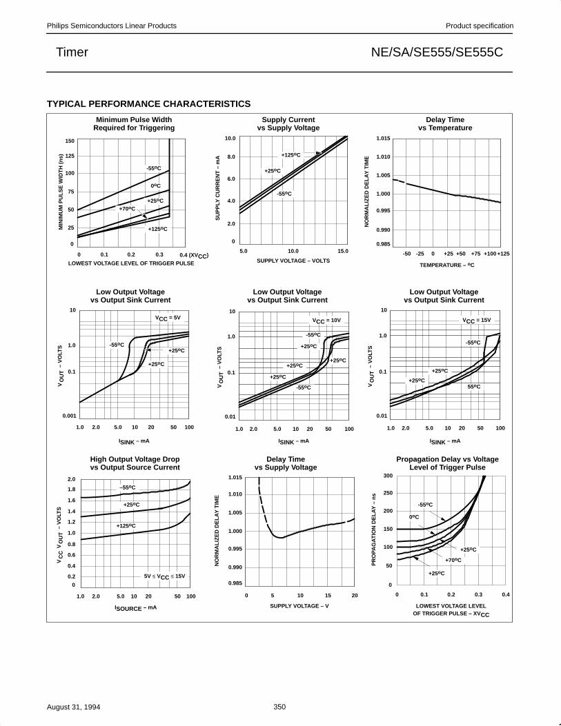
Philips Semiconductors Linear Products Product specification
NE/SA/SE555/SE555CTimer
August 31, 1994 350
TYPICAL PERFORMANCE CHARACTERISTICS
Minimum Pulse WidthRequired for Triggering
Supply Currentvs Supply Voltage
Low Output Voltagevs Output Sink Current
Low Output Voltagevs Output Sink Current
Low Output Voltagevs Output Sink Current
Delay Timevs Temperature
Delay Timevs Supply Voltage
Propagation Delay vs VoltageLevel of Trigger Pulse
High Output Voltage Dropvs Output Source Current
MIN
IMU
M P
ULS
E W
IDT
H (
ns)
LOWEST VOLTAGE LEVEL OF TRIGGER PULSE
150
125
100
75
50
25
0
0 0.1 0.2 0.3 0.4 (XVCC)
-55oC
0oC
+25oC+70oC
+125oC
10.0
8.0
6.0
4.0
2.0
0
5.0 10.0 15.0
SUPPLY VOLTAGE – VOLTS
SU
PP
LY C
UR
RE
NT
– m
A
1.015
1.010
1.005
1.000
0.995
0.990
0.985
-50 -25 0 +25 +50 +75 +100 +125
NO
RM
ALI
ZE
D D
ELA
Y T
IME
TEMPERATURE – oC
10
1.0
0.1
0.001
1.0 2.0 5.0 10 20 50 100
10
1.0
0.1
0.01
1.0 2.0 5.0 10 20 50 100
10
1.0
0.1
0.01
1.0 2.0 5.0 10 20 50 100
1.0 2.0 5.0 10 20 50 100
2.0
1.8
1.6
1.4
1.2
1.0
0.8
0.6
0.4
0.2
0
1.015
1.010
1.005
1.000
0.995
0.990
0.985
0 5 10 15 20 0 0.1 0.2 0.3 0.4
300
250
200
150
100
50
0
V
– V
OLT
SO
UT
V
– V
OLT
SO
UT
V
– V
OLT
SO
UT
V
– V
OLT
SO
UT
V C
C
NO
RM
ALI
ZE
D D
ELA
Y T
IME
PR
OP
AG
AT
ION
DE
LAY
– n
s
ISINK – mA ISINK – mA ISINK – mA
ISOURCE – mA SUPPLY VOLTAGE – V LOWEST VOLTAGE LEVELOF TRIGGER PULSE – XVCC
+125oC
+25oC
-55oC
VCC = 5V VCC = 10V VCC = 15V
-55oC
+25oC
+25oC
-55oC
+25oC
+25oC+25oC
+25oC
-55oC
-55oC
55oC
+25oC
+25oC
–55oC
+25oC
+125oC
5V ≤ VCC ≤ 15V
-55oC
0oC
+25oC
+70oC
+25oC
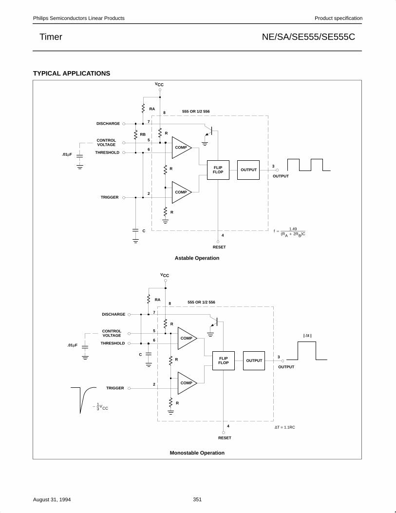
Philips Semiconductors Linear Products Product specification
NE/SA/SE555/SE555CTimer
August 31, 1994 351
TYPICAL APPLICATIONS
OUTPUTFLIPFLOP
COMP
COMP
f 1.49(RA 2RB)C
555 OR 1/2 556
DISCHARGE
CONTROLVOLTAGE
THRESHOLD
TRIGGER
RESET
OUTPUT
R
R
C
RB
RA
R
5
6
2
4
3
8
7
.01µF
VCC
OUTPUTFLIPFLOP
COMP
COMP
555 OR 1/2 556
DISCHARGE
CONTROLVOLTAGE
THRESHOLD
TRIGGER
RESET
OUTPUT
R
R
RA
R
5
6
2
4
3
8
7
.01µF
VCC
∆T = 1.1RC
C
13
VCC
| ∆t |
Astable Operation
Monostable Operation
Philips Semiconductors Linear Products Product specification
NE/SA/SE555/SE555CTimer
August 31, 1994 352
TYPICAL APPLICATIONS
DURATION OF TRIGGER PULSE AS SEEN BY THE TIMER
VCC VCC
10k
2 555
.001µF
NOTE: All resistor values are in Ω
Figure 1. AC Coupling of the Trigger Pulse
1
SWITCH GROUNDEDAT THIS POINT
OVOLTS
1/3 VCC
VCC
Trigger Pulse Width Requirements and TimeDelaysDue to the nature of the trigger circuitry, the timer will trigger on thenegative going edge of the input pulse. For the device to time outproperly, it is necessary that the trigger voltage level be returned tosome voltage greater than one third of the supply before the time outperiod. This can be achieved by making either the trigger pulsesufficiently short or by AC coupling into the trigger. By AC couplingthe trigger, see Figure 1, a short negative going pulse is achievedwhen the trigger signal goes to ground. AC coupling is mostfrequently used in conjunction with a switch or a signal that goes toground which initiates the timing cycle. Should the trigger be heldlow, without AC coupling, for a longer duration than the timing cyclethe output will remain in a high state for the duration of the lowtrigger signal, without regard to the threshold comparator state. Thisis due to the predominance of Q15 on the base of Q16, controllingthe state of the bi-stable flip-flop. When the trigger signal thenreturns to a high level, the output will fall immediately. Thus, theoutput signal will follow the trigger signal in this case.
Another consideration is the “turn-off time”. This is the measurementof the amount of time required after the threshold reaches 2/3 VCCto turn the output low. To explain further, Q1 at the threshold inputturns on after reaching 2/3 VCC, which then turns on Q5, which turnson Q6. Current from Q6 turns on Q16 which turns Q17 off. Thisallows current from Q19 to turn on Q20 and Q24 to given an outputlow. These steps cause the 2µs max. delay as stated in the datasheet.
Also, a delay comparable to the turn-off time is the trigger releasetime. When the trigger is low, Q10 is on and turns on Q11 which turnson Q15. Q15 turns off Q16 and allows Q17 to turn on. This turns offcurrent to Q20 and Q24, which results in output high. When thetrigger is released, Q10 and Q11 shut off, Q15 turns off, Q16 turns onand the circuit then follows the same path and time delay explainedas “turn off time”. This trigger release time is very important indesigning the trigger pulse width so as not to interfere with theoutput signal as explained previously.