1 Pertemuan 1 Introduksi VLSI Matakuliah: H0362/Very Large Scale Integrated Circuits Tahun: 2005...
13
1 Pertemuan 1 Introduksi VLSI Matakuliah : H0362/Very Large Scale Integrated Circuits Tahun : 2005 Versi : versi/01
-
Upload
shyann-leek -
Category
Documents
-
view
226 -
download
2
Transcript of 1 Pertemuan 1 Introduksi VLSI Matakuliah: H0362/Very Large Scale Integrated Circuits Tahun: 2005...
1
Pertemuan 1
Introduksi VLSI
Matakuliah : H0362/Very Large Scale Integrated Circuits
Tahun : 2005
Versi : versi/01

2
Learning Outcomes
Pada akhir pertemuan ini, diharapkan mahasiswa akan dapat mengidentifikasi perihal yang berkaitan dengan proses teknologi VLSI.

3
Course Outline
No Silabus Pertemuan
1 Introduksi teknologi VLSI 1
2 Karakteristik kelistrikan dan logik gerbang CMOS
2, 3
3 Karakteristik switching gerbang CMOS 7,8
4 Introduksi proses fabrikasi teknologi VLSI 4, 5
5 Prinsip dasar Physical Design teknologi VLSI 6
6 Introduksi Verilog HDL 9
7 Rangkaian spesial gerbang VLSI 11, 12, 13
8 Konsep keandalan dan pengujian komponen VLSI
10
H0362 – Very Large Scale Integrated Circuits
4
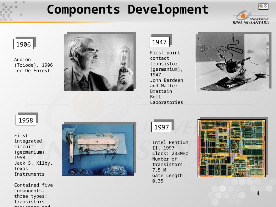
First point contact transistor (germanium), 1947John Bardeen and Walter BrattainBell Laboratories
Audion (Triode), 1906Lee De Forest
1906190619471947
1958195819971997
First integrated circuit (germanium), 1958Jack S. Kilby, Texas Instruments
Contained five components, three types:transistors resistors and capacitors
Intel Pentium II, 1997Clock: 233MHzNumber of transistors: 7.5 MGate Length: 0.35
Components Development
5
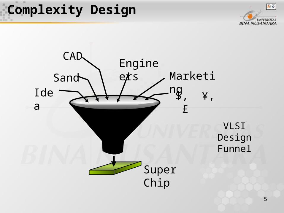
VLSIDesignFunnel
IdeaSand
CADEngineers Marketin
g$, ¥, £
Super Chip
Complexity Design

6
Complexity Design
System Specification
Abstract high-level modelVHDL, Verilog HDL
Logic synthesis
Circuit design
Physical design
Manufacturing
Finished VLSI chip
Top design level
Bottom design level
Initial concept
System designand verification
Logic designand verification
CMOS designand verification
Silicon logic designand verification
Mass productiontesting, and packaging
Marketing
Design hierarchy

7
System Specification
System
Functional Module
Gate
Circuit
Device SG
D
+
Leve
l o
f A
bstr
action
Low
High Design hierarchy
Complexity Design

8
Design flowexample
Instruction set Basic component
Architectural modelRTL and Behavioral
HDL
Blok diagram
Test instruction
Logicaldescription
Functionality
Component level Ports and connections
Electronic logic circuits Electrical behavior
Silicon logic Silicon behavior
Design complete
Complexity Design

9
104
105
106
107
108
1985 1990 1995 2000
0.25 M
1.2 M
3.1 M5.5 M
9 M21 M
42 M
110 M
Year
Num
ber
of
tran
sist
ors
Basic Concepts
Moore’s Law:The number of transistors ona chip would double aboutevery 18 months.

10
Trends in transistor count
(From: http://www.intel.com)
Number of transistors doubles every 2.3 years(acceleration over the last 4 years: 1.5 years)
42 M transistors
2.25 K transistors
Increase: ~20K
11
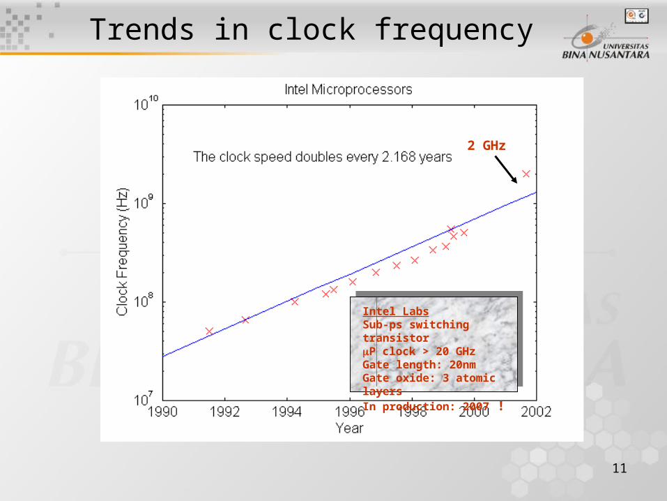
Trends in clock frequency
2 GHz
Intel LabsSub-ps switching transistorP clock > 20 GHzGate length: 20nmGate oxide: 3 atomic layersIn production: 2007 !

12
Trends in feature size
0.13 m inproduction
Intel LabsSub-ps switching transistorP clock > 20 GHzGate length: 20nmGate oxide: 3 atomic layersIn production: 2007 !

13
RESUME
• Sejarah perkembangan komponen electronik.
• Kompleksitas disain dalam VLSI.
• Hukum Moore.
• Trend teknologi.