


Bahasa
Halaman
Hukum


PROCEEDINGS A WAVE S
of the I R E D and ELECTRONSThe Institute of Radio Engineers
INCORPORATED
THREADLESS SEWING MACHINEELECTRONIC TECHNIQUE ENABLES THE PRODUCTION OF SEAMLESS FABRIC JOINTS
MARCH, 1946Volume 34 Number 3
Published in Two Sections
Section I-Proceedings of theI.R.E. Section
Reflex-Klystron Oscillators
Transmission of F -M Wave
R -C Parallel -T Network Analysis
Modulation -Frequency Feedback
Low -Pass Filter
Matrix Algebra
Section II-Waves and ElectronsSection
Induction Heating in Tube Manufacture
Fine Wires in Tube Industry
Three -Beam Microoscillograph
Television Synchronizing Generators
Negative Voltage Feedback
Fractional -Mu Oscillator
of the Theory, Practice, and Applications ofREPORTSElectronics and Electrical Communication
Radio Communication Sound Broadcasting Television Marine and Aerial Guidance Tubes Radio -Frequency Measurements Engineering Education Electron Optics Sound and Picture Electrical Recording and Reproduction Power and Manufacturing Applications of Radio -and -Electronic Technique Industrial Electronic Control and Processes Medical Electrical Research and Applications
... . .1111
ii U 1 !IMak 1-114.41
4stm, Ihintel:F. s
1:72- . .
MINI14111P"IIP
10111iiii 1V,'"Illiiiiumillinmemumr gummy, Annummeinu:militi
, 1111111IP '111IP11.
1:1
.11. MEOW.'=NM Ma..11 1111111 I; naltii
E MI I M rINIM I1111111111101111 ;Stf INjarl
I. _ 111111111111Figlillir
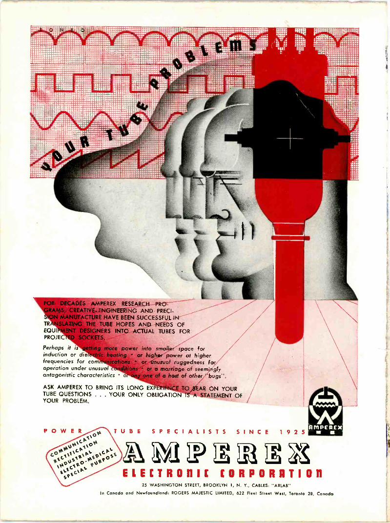
FOR DECADES AMPEREX RESEARCH-PRCMS, CREATIVE ENGINEERING AND PRECI-
MANUFACTURE HAVE BEEN SUCCESSFUL INTRANSLATING THE TUBE HOPES AND NEEDS OFEQUI T DESIGNERS INTO ACTUAL TUBES FOR ,---PROJEC SOCKETS.
Perhaps it is ing more power into smaller space forinduction or die ctric heating or higher power at higherfrequencies for communications or unusual ruggedness foroperation under unusual Cbaditions or a marriage of seem' glyantagonistic characteristics or arl, one of a host of other bugs".
ASK AMPEREX TO BRING ITS LONG EXPERIENCE TO BEAR ON YOURTUBE QUESTIONS . . . YOUR ONLY OBLIGATION IS A STATEMENT OFYOUR PROBLEM.
POWER 00 SPECIALISTS SINCE 19 25
MANo0
N 1DC'°.StEC'S 0 tt't V °It ..,1:0) 9.0 " ,,? N.)9'% s-- ct
StOr'il ELECTRONIC CORPORATION
25 WASHINGTON STREET, BROOKLYN 1, N. Y., CABLES: "ARIAS"
In Canada and Newfoundland: ROGERS MAJESTIC LIMITED, 622 Fleet Street West, Toronto 2B, Canada
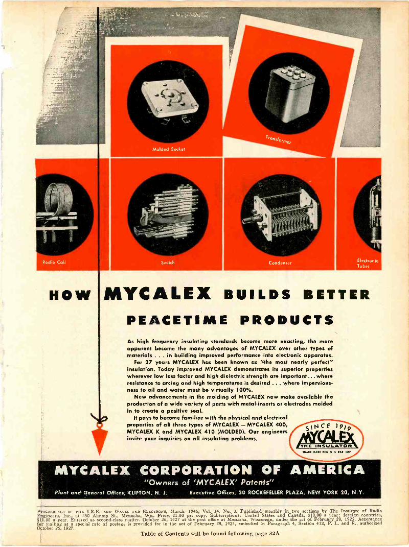
HOW MYCALEX BUILDS BETTERPEACETIME PRODUCTSAs high frequency insulating standards become more exacting, the moreapparent become the many advantages of MYCALEX over other types ofmaterials . . . in building improved performance into electronic apparatus.
For 27 years MYCALEX has been known as "the most nearly perfect"insulation. Today improved MYCALEX demonstrates its superior propertieswherever low loss factor and high dielectric strength are important... whereresistance to arcing and high temperatures is desired ... where impervious-ness to oil and water must be virtually 100%.
New advancements in the molding of MYCALEX now make availcble theproduction of a wide variety of parts with metal inserts or electrodes moldedin to create a positive seal.
It pays to become familiar with the physical and electricalproperties of all three types of MYCALEX - MYCALEX 400, SIN CE 19MYCALEX K and MYCALEX 410 (MOLDED). Our engineersinvite your inquiries on all insulating problems.
THE INSULATORTIRADE MAIM 'MG Y S PAT OPT
MYCALEX CORPORATION OF AMERICA"Owners of 'MYCALEX' Patents"
Plant and General Offices, CLIFTON, N. J. Executive Offices, 30 ROCKEFELLER PLAZA, NEW YORK 20, N.Y.
PROCEEDINGS OF THE I.R.E. AND WAVES AND ELECTRONS, March, 1946, Vol. 34, No. 3. Published monthly in two sections by The Institute of RadioEngineers, Inc., at 450 Ahnaip St., Menasha, Wis. Price, $1.00 per copy. Subscriptions: United States and Canada, $10.00 a year; foreign countries,$11.00 a year. Entered as second-class matter. October 26, 1927 at the post office at Menasha, Wisconsin, under the act of February 28, 1925. Acceptancefor mailing at a special rate of postage is provided for in the act of February 28, 1925, embodied in Paragraph 4, Section 412, P. L. and R., authorizedOctober 26, 1927.
Table of Contents will be found following page 32A
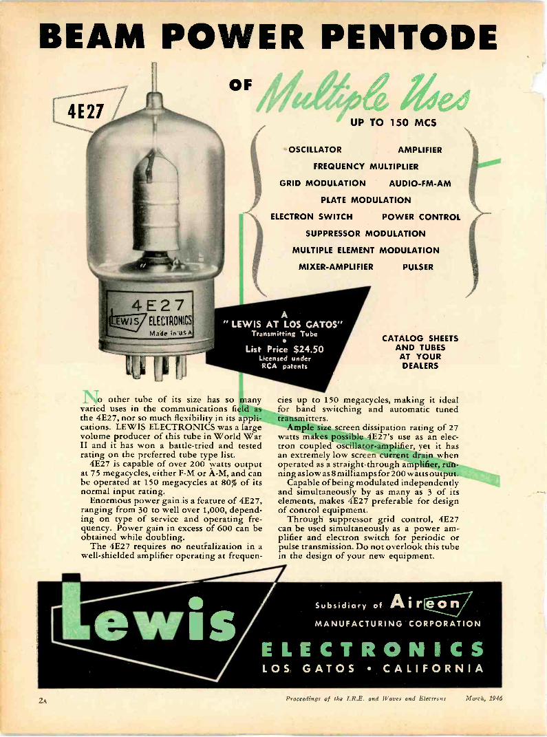
BEAM POWER PENTODE
4E27ELECTRONICS
Made in USA
No other tube of its size has so manyvaried uses in the communications field asthe 4E27, nor so much flexibility in its appli-cations. LEWIS ELECTRONICS was a largevolume producer of this tube in World WarII and it has won a battle -tried and testedrating on the preferred tube type list.
4E27 is capable of over 200 watts outputat 75 megacycles, either F -M or A -M, and canbe operated at 150 megacycles at 80% of itsnormal input rating.
Enormous power gain is a feature of 4E27,ranging from 30 to well over 1,000, depend-ing on type of service and operating fre-quency. Power gain in excess of 600 can beobtained while doubling.
The 4E27 requires no neutralization in awell -shielded amplifier operating at frequen-
OF
UP TO 150 MCS
OSCILLATOR AMPLIFIER
FREQUENCY MULTIPLIER
GRID MODULATION AUDIO -FM -AM
PLATE MODULATION
ELECTRON SWITCH POWER CONTROL
SUPPRESSOR MODULATION
MULTIPLE ELEMENT MODULATION
MIXER -AMPLIFIER PULSER
A" LEWIS AT LOS GATOS"
Transmitting Tube
List Price $24.50Licensed underRCA patents
ELECTRONICS
CATALOG SHEETSAND TUBESAT YOURDEALERS
cies up to 150 megacycles, making it idealfor band switching and automatic tunedtransmitters.
Ample size screen dissipation rating of 27watts makes possible 4E27's use as an elec-tron coupled oscillator -amplifier, yet it hasan extremely low screen current drain whenoperated as a straight -through amplifier, run-ning as low as 8 milliamps for 200 watts output.
Capable of being modulated independentlyand simultaneously by as many as 3 of itselements, makes 4E27 preferable for designof control equipment.
Through suppressor grid control, 4E27can be used simultaneously as a power am-plifier and electron switch for periodic orpulse transmission. Do not overlook this tubein the design of your new equipment.
Subsidiary of Air eonMANUFACTURING CORPORATION
LOS GATOS CALIFORNIA
2A Proceedings of the I.R.E. and Waves and Electrons March, 1946
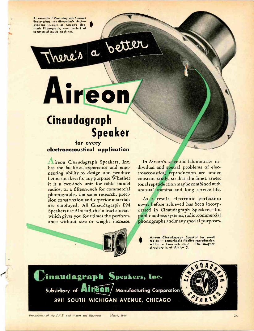
An example of Cinaudagraph Speaker
speaker of Aireon'sEngineering-the fifteen -inch electro-dynamicElec-tronic Phonograph, most perfect ofcommercial music machines.
AireonCinaudagraph
Speakerfor every
electroaccoustical application
ireon Cinaudagraph Speakers, Inc.has the facilities, experience and engi-neering ability to design and producebetter speakers for any purpose.Whetherit is a two-inch unit for table modelradios, or a fifteen -inch for commercialphonographs, the same research, preci-sion construction and superior materialsare employed. All Cinaudagraph PMSpeakers use Alnico 5, themiracle metal"which gives you four times the perform-ance without size or weight increase.
In Aireon's scientific laboratories in-dividual and special problems of elec-troaccoustical. reproduction are underconstant study, so that the finest, truesttonal reproduction may be combined withunusual stamina and long service life.
As a result, electronic perfectionnever before achieved has been incorp-orated in Cinaudagraph Speakers-forpublic address systems, radio, commercialphonographs and many special purposes.
Aireon Cinaudagraph Speaker for smallradios - remarkable fidelity reproductionwithin a two-inch cone. The magnetstructure is of Alnico 5.
Cinaudagraph Speakers, Inc.
Subsidiary of Aireon Manufacturing Corporation
4au,
Ca
11
AP tilAi.A Kt3911 SOUTH MICHIGAN AVENUE, CHICAGO
Proceedings of the I.R.E. and Waves and Electrons March, 1946
.,,._ ----'-'""7.1kZ1NOt2,----.---.., ,.-, ,. -,.. '!°' , - ' . ' - -
,
''',,---,-.1141rt;C"46114-"SillikaAft",3C'i' .,,l''''Silittc.,,'. _._-.7 rt.`2-srzs..
. ..._
- ,I.,,,-,..,----".4.4111---- ',i.tt.e.,,...:,ctic..14.
'i.z'stv.;-im..,,,,-..,;:z--...---
,
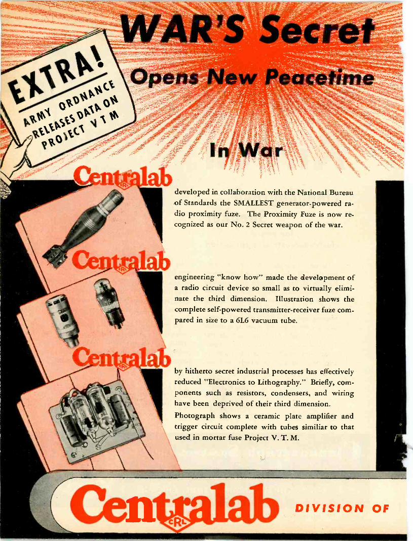
developed in collaboration with the National Bureauof Standards the SMALLEST generator -powered ra-dio proximity fuze. The Proximity Fuze is now re-cognized as our No. 2 Secret weapon of the war.
engineering "know how" made the development ofa radio circuit device so small as to virtually elimi-nate the third dimension. Illustration shows thecomplete self -powered transmitter -receiver fuze com-pared in size to a 6L6 vacuum tube.
by hitherto secret industrial processes has effectivelyreduced "Electronics to Lithography." Briefly, com-ponents such as resistors, condensers, and wiringhave been deprived of their third dimension.
Photograph shows a ceramic plate amplifier andtrigger circuit complete with tubes similiar to thatused in mortar fuse Project V. T. M.
DIVISION OF

- ,Oltlefttiffilta
ttr t"'"3:`!.....,..
2(71)-"441420014FAmmix...,, *ftwitv,poi
Se.,..,,.. .. no.. ...
.... ,......,.."...7.-;"iPletferP''9,:...:......"".'... *3fgLAWOIP"....,..*'
mor* ..z.,...K. ...--:::,..--
....,.41.":.4,0*.r...j. ....,......' .......,...t,41C........ ...qt...-. .._ ...4... , ..,...... t....:4,470:....."..''47., ,....... , A..."."'- ....1:".1V"... 4c,S.,'".''.'I''".'"''.*. "..:::Ca..7.,'....;r40041504*'...-.- -ere,,,,1r16.41P.
--...-.n. - 1 A W ' 1.....11( ;Q4'10' ilt
At
4.116,Mr vewirt.1.:w0''. 11144.0
,
.24.'4-4; -4; ,
Air--
-r-re;,,fr.sk
4"4". ,CAtakerwio.f,e' :4` .
.144ze*,,Oist'A
*' '
-0 n. _
''-=7F.41.c..c.vz '',,zw.K ',-t:+:,
introduces this new technique to the electronic in-dustry. New applications of electronics to everydayliving are made possible by this revolutionary development.
al)envisions personal radios the size of a package ofcigarettes . . . made possible through the applicationof this new technique . . . a pocket -sized personalwalkie-talkie . . . a hearing aid, complete with bat-teries, no larger than a wallet.
abis proud of the engineering "know how"that made possible this contribution tothe science of electronics. Centralab'slaboratories are a constant reservoir ofscientific research and development infields of interest to the electronic engineer.
GLOBE -UNION INC., MILWAUKEE
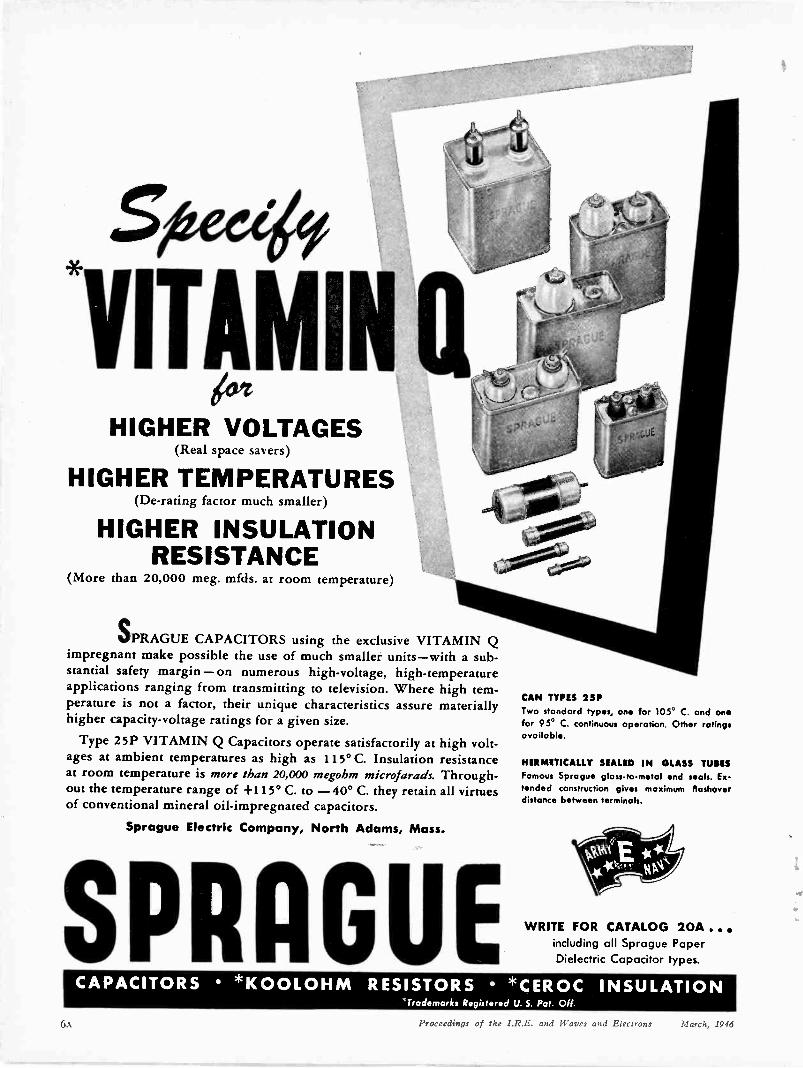
*VITki4NIN aHIGHER VOLTAGES
(Real space savers)
HIGHER TEMPERATURES(De -rating factor much smaller)
HIGHER INSULATIONRESISTANCE
(More than 20,000 meg. mfds. at room temperature)
SPRAGUE CAPACITORS using the exclusive VITAMIN Qimpregnant make possible the use of much smaller units-with a sub-stantial safety margin - on numerous high -voltage, high -temperatureapplications ranging from transmitting to television. Where high tem-perature is not a factor, their unique characteristics assure materiallyhigher capacity -voltage ratings for a given size.
Type 25P VITAMIN Q Capacitors operate satisfactorily at high volt-ages at ambient temperatures as high as 115° C. Insulation resistanceat room temperature is more than 20,000 megohm microjarads. Through-out the temperature range of +115° C. to -40° C. they retain all virtuesof conventional mineral oil -impregnated capacitors.
Sprague Electric Company, North Adams, Mass.
SPRAGUE
CAN TYPES 25PTwo standard types, one for 105° C. and onfor 95° C. continuous operation. Other ratingsavailable.
HERMETICALLY SEALED IN GLASS TURESFamous Sprague glass -to -metal end seals. Ex-tended construction gives maximum flashoverdistance between terminals.
WRITE FOR CATALOG 20A . e eincluding all Sprague PaperDielectric Capacitor types.
CAPACITORS *KOOLOHM RESISTORS *CEROC INSULATION*Trademarks Rgistred U. S. Pal. Off.
6A Proceedings of the I.R.E. and Waves and Electrons March, 1946
ti
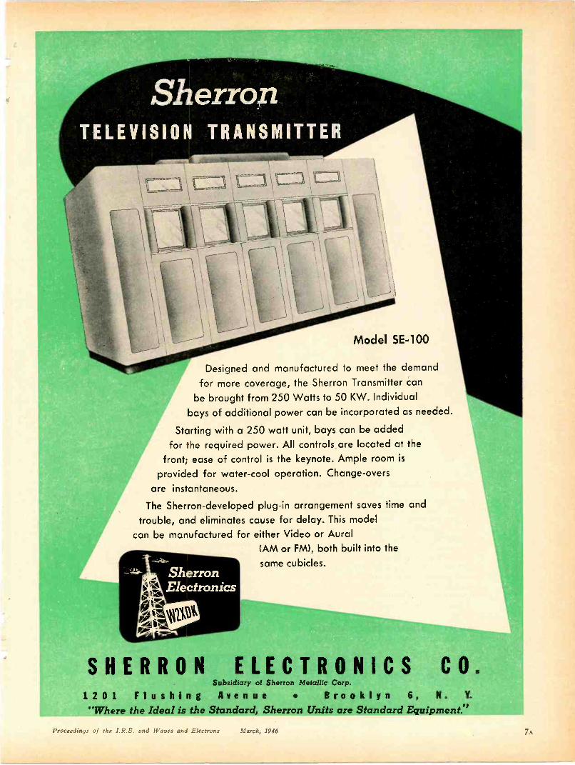
SherronTELEVISION TRANSMITTER
Model SE -100
Designed and manufactured to meet the demandfor more coverage, the Sherron Transmitter can
be brought from 250 Watts to 50 KW. Individualbays of additional power can be incorporated as needed.
Starting with a 250 watt unit, bays can be addedfor the required power. All controls are located at the
front; ease of control is the keynote. Ample room isprovided for water-cool operation. Change-overs
are instantaneous.
The Sherron-developed plug-in arrangement saves time andtrouble, and eliminates cause for delay. This model
can be manufactured for either Video or Aural(AM or FM), both built into thesame cubicles.
SHERRON ELECTRONICS CO.Subsidiary of Sherron Metallic Corp.
1201 Flushing Avenue Brooklyn 6, N. Y.
"Where the Ideal is the Standard, Sherron Units are Standard Equipment."
Proceedings z;ie I.R.E. and Wax es aria Elect, oris Larch, 1946

Time -proved Design! Widest Range of Sizes!You get these advantages: (1) Ohmite experience withcountless rheostat applications. (2) Service -provedOhmite features that assure permanently smooth, closecontrol. (3) Extensive range of sizes and types for easy,economical selection of the best unit for everyapplication.
There are ten wattage sizes ranging from 25 to 1000watts-from 194" diameter to 12" diameter-in uni-form or tapered winding-in single or tandem units-in regular or special designs. Stock models from 25 to500 watts, in many resistance values.
Consult Ohmite engineers on your rheostat controlproblem.
OHMITE MANUFACTURING COMPANY4861 FLOURNOY STREET, CHICAGO 44, U.S.A.
Ve Rola cad
Send for Catalogand EngineeringManual No. 40Write on companyletterhead for thishelpful guide in theselection and ap-plication of rheo-stats, resistors, tapswitches, chokesand attenuators.
HAUTERHEOSTATS RESISTORS TAP SWITCHES CHOKES ATTENUATORS
Proceedings of the 1.K.[. and Iraves and Electrons March, 1946
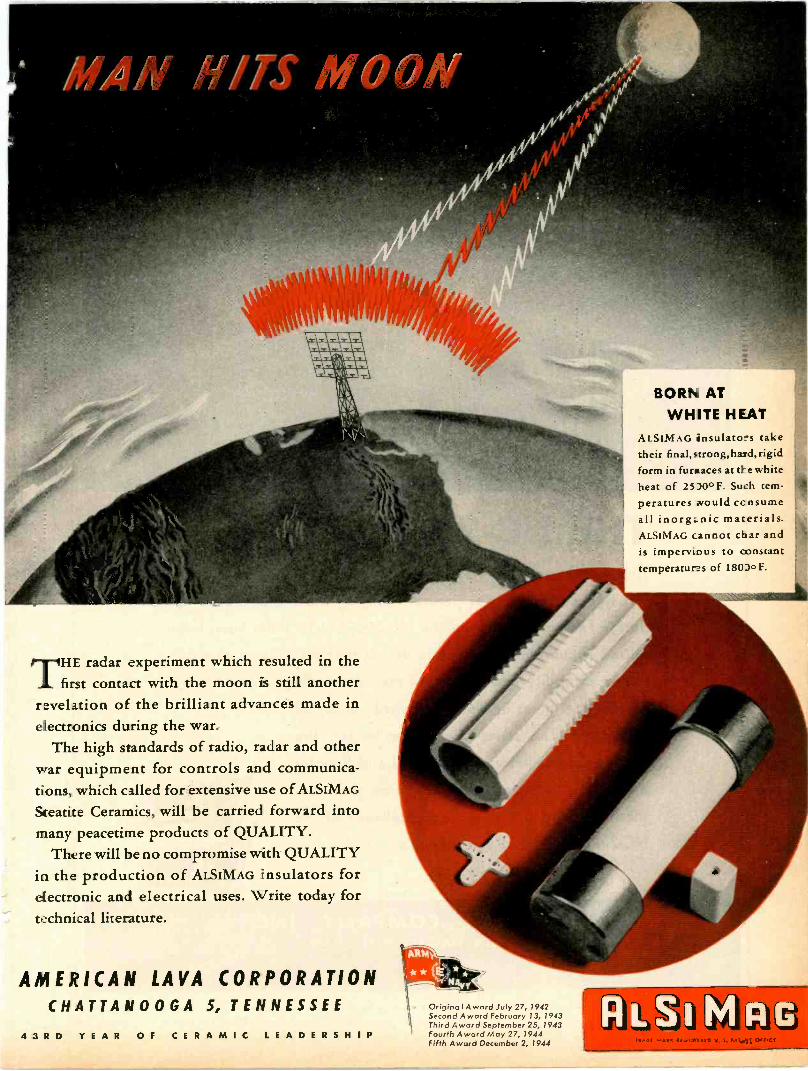
THE radar experiment which resulted in thefirst contact with the moon is still another
revelation of the brilliant advances made inelectronics during the war.
The high standards of radio, radar and otherwar equipment for controls and communica-tions, which called for extensive use of ALSIMAGSteatite Ceramics, will be carried forward intomany peacetime products of QUALITY.
There will be no compromise with QUALITYin the production of ALSIMAG insulators forelectronic and electrical uses. Write today fortechnical literature.
AMERICAN LAVA CORPORATIONCHATTANOOGA 5, TENNESSEE OriginalAward July 27, 1942
Second Award February 13, 1943Third Award September 25, 1943Fourth Award May 27, 1944Fifth Award December 2, 1944
BORN ATWHITE HEAT
ALS[MAG insulato:s taketheir final,strong,haid, rigidform in fureaces at ti- e whiteheat of 25)00F. Such tem-peratures would ccnsumeall inorgLnic materials.ALSIMAG cannot char andis impervious to constanttemperatures of 18030F.
Fi LSI MAG43RD YEAR OF CERAMIC LEADERSHIP

THE NC -2-40CThis superb new receiver reflects National's intensive receiver
research during the war period. Many of the NC-2-40C's basic
design features stem from the NC -200, but to them have been
added circuit and construction details that set it apart as a per-
former. Stability and sensitivity are outstanding. A wide range
crystal filter gives optimum selectivity under all
conditions. The series -valve noise limiter, the
AVC, beat oscillator, tone control and S-meter
are among the many auxiliary circuits that con-
tribute toward the all-around excellence of the
NC -2-40C. See it at your dealer's.
NATIONAL COMPANY, INC.MALDEN, MASSACHUSETTS, U.S.A.
10A Proceedings of the I.R.E. and Waves and Electrons March, 1946

We ole91040.0o
DaviOsVtvie100
C001,1Eto adstitioo
to tile 250watt
ttatteroitter,
V; tolitssee
ooteitt stock.,
5 kvi'sloe
reaalsbottl/
l'hesoves13
* &tettV,Ieetric
iso is also
to looaoctioo.estero
tasolass
iostoat\inc.
branchin,vItase
shittiog,
oltsseotoototiot,
sod,so-
teooscooviiitg
ectoilooeot
to
cosovieteyoov
toten
9
ORDER
YOURS
NOW!
yotiveboilato%
a oewstatioo--ov
loo
waotto Warove los resent
ooe--cooact
yoovGvaybav
vefeseotative
toy &tiltsoi %Vas
aod
estecofNectric,
Altik and
tvaosttterstoday.
i'"ceedi n -s ofthe I.R.E. and Waves and Electrons March, 1996
FEB.
SYLVANIA NEWSCIRCUIT ENGINEERING EDITION
Published by- SYLV kNIA ELECTRIC PEODUCTS INC., Emporium. Pa. 1946
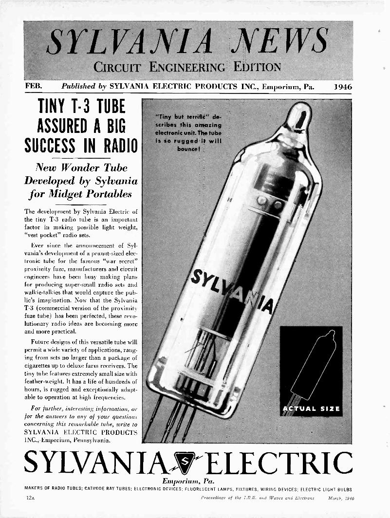
TINY T-3 TUBE
ASSURED A BIG
SUCCESS IN RADIO
New Wonder TubeDeveloped by Sylvaniafor Midget Portables
The development by Sylvania Electric ofthe tiny T-3 radio tube is an importantfactor in making possible light weight,"vest pocket" radio sets.
Ever since the announcement of Syl-vania's development of a peanut -sized elec-tronic tube for the famous "war secret"proximity fuze, manufacturers and circuitengineers have been busy making plansfor producing super -small radio sets andwalkie-talkies that would capture the pub-lic's imagination. Now that the SylvaniaT-3 (commercial version of the proximityfuze tube) has been perfected, these revo-lutionary radio ideas are becoming moreand more practical.
Future designs of this versatile tube willpermit a wide variety of applications, rang-ing from sets no larger than a package ofcigarettes up to deluxe farm receivers. Thetiny tube features extremely small size withfeather -weight. It has a life of'hundreds ofhours, is rugged and exceptionally adapt-able to operation at high frequencies.
For further, interesting information, orfor the answers to any of your questionsconcerning this remarkable tube, write toSYLVANIA ELECTRIC PRODUCTSINC.,,Emporium, Pennsylvania.
"Tiny but terrific" de-scribes this amazingelectronic unit. The tubeis so rugged it will
bounce!
SYLVANIA ELECTRICEmporium, Pa.
MAKERS OF RADIO TUBES; CATHODE RAY TUBES; ELECTRONIC DEVICES; FLUORESCENT LAMPS, FIXTURES. WIRING DEVICES; ELECTRIC LIGHT BULBS
I2A Proceedings of the ;.R.E. and Waves and Electrons March, 1946
S SWtS
IXle0\t'itrockeo
0-0001
VIC1Peot
NISk:0\:e01:Nctkoolocktoo
IcoostocOtets
tepteseot
ctosestop-
ptoocttto t
oenci vespoOs-f
4:wive\
ttoONtbeos:t00:.:p\loeeol\cs.:00,co,i\oto
fie
ye to(Towd\stott%
t\ons'00,0
St\locoostA
sttVataog
coa,)41,%c.isc,
vmea,co
ioctOc.
copo6ty,
v4eno*/
ofitelttNes:
Vs
:14E;rov\ets
bee
doctoo:;:o00,og
al
\rocoedtote
aecsiety.
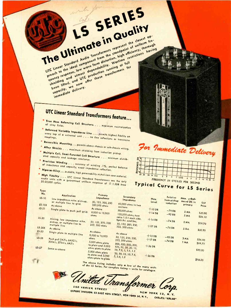
UTC Linear Standard Transformers feature... True Hum
Balancing Coil Structure.of stray fields. . . maximum neutralization
BalancedVariable Impedance
Line ... permits highestfidelity on
every tap of a universal unit.couplings. . . no line reflections
or transverseReversible Mounting ... permits above
chassis or sub -chassis wiring.Alloy Shields. maximum shielding
from induction pickup.Multiple Coil, Semi -Toroidal Coil Structure. . . minimum distrib-
uted capacity and leakage reactance.Precision Winding
. . . accuracy of winding .1%, perfect balanceof inductance and capacity;
exact impedance reflection. Hiperm-Alloy... a stable, high permeabilit
High Fidelity y nickel -iron core material.. . UTC Linear Standard
Transformersare the only
audio units with a guaranteeduniform response
of20.20,000 cycles. ±- 1.5DB from
TypeNo.
LS -10
LS -10X
LS -21
LS -30
LS -30X
LS -50
ApplicationLow impedance
mike, pick-up,or multiple line to grid.As above
Single plate to push pull grid,
Mixing, low impedancemike,pickup, or multiple line tomultiple line 333, 500 ohms
As above
Single plate to multiple line
PrimaryImpedance
50, 125, 200, 250333,500 ohms
As above
8,000 to 15,000ohms
1S.55 Push pull 2A3's, 6A5G's,300A's, 275A's, 6A3's
£5.57 Some as above
50, 125, 200, 250
As above
8,000 to 15,000ohms
5,000 ohms plateto Plate and 3,000ohms plate to plate5,000 ohms plateto plate and 3,000ohms plate to plate
5741ilr Tototededre Vetiver"411111111111111111111MMMIUMMEN$2111111111111111111111111.1111111111M1111Mni
2 imuiamoinummunnotrinN-4 11111111111111111111111111111111111111111111
20 50 70 100 2 3 5 7 1000 2 3 5 7 10 15 00 30FREQUENCY IN CYCLESPER SECONDTypical Curve for LS Series
SecondaryImpedance
60,000 ohms in twosections
50,000 ohms
135,000 ohms; turnratio 1.5:1 each side.Split Pri. and Sec.50, 125, 200, 250,333, 500 ohms
As above
50, 125, 200, 250,333, 500 ohms
500, 333, 250, 200,125, 50, 30, 20, 15,10, 7.5, 5, 2.5, 1.230, 20, 15, 10, 7.5,5, 2.5, 1.2
Max.Level
+15 D13
+14 08
+14 D8
+17 DB
+15138+17 DB
+36 DB
+36 D8
The above listingincludes only a few of the many unitsof the LS Series. For complete listing - write for catalogue.
150 VARICK STREETEXPORT DIVISION:
13 EAST 40thSTREET, NEW YORK 16,
NEW YORK 13, N. YN. Y., CABLES: "ARLAB"
Relative Max. unbal-hum-pickupanted DC inreduction primary
-74 DB-92 DB
-74 DB
-74 DB
-92 DB-74 DB
5 MA
5 MA
0 MA
5 MA
3 MA1 MA
ListPrice
$20.90
$26.10
$19.70
$20.90
$26.10
$19.70
$23.20
$16.25
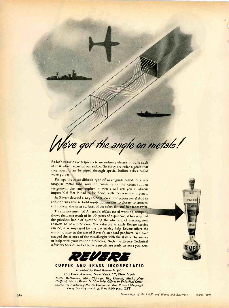
Radar's miracle eye responds to no ordinary electric impulse suchas that which actuates our radios. So fussy are radar signals thatthey must often be piped through special hollow tubes calledwave guides.
Perhaps the most difficult type of wave guide called for a rec-tangular metal tube with no curvature in the corners . . . anassignment that any worker in metals will tell you is almostimpossible! Yet it had tq be done, with top wartime urgency.
So Revere devised a way to dd4t, on a production basis! And inaddition was able to hold inside climensions to closest tolerances,and to keep the inner surfaces of the tubes flat and free from twist.
This achievement of America's oldest metal -working companyshows that, as a result of its 144 years of experience it has acquiredthe priceless habit of questioning the obvious, of creating newanswers to new problems. Yet valuable as such Revere servicecan be, it is surpassed by the day-to-day help Revere offers theradio industry in the use of Revere's standard products. We havemerged the science of the metallurgist with the skill of the artisanto help with your routine problems. Both the Revere TechnicalAdvisory Service and all Revere metals are ready to serve you now.
~ORSCOPPER AND BRASS INCORPORATED
Founded by Paul Revere in 1801230 Park Avenue, New York 17, New York
Mills: Baltimore, Md.; Chicago, Ill.; Detroit, Mich.; NewBedford, Mass.; Rome, N. Y.-Sales Offices in Principal Cities.Listen to Exploring the Unknown on the Mutual Network
every Sunday evening, 9 to 9:30 p.m., EST.
14A Proceeding: of the I.R.E. and Waves and Electrons March, 1946
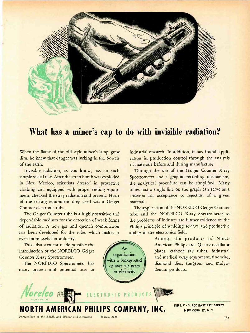
What has a miner's cap to do with invisible radiation?
When the flame of the old style miner's lamp grewdim, he knew that danger was lurking in the bowelsof the earth.
Invisible radiation, as you know, has no suchsimple visual test. After the atom bomb was explodedin New Mexico, scientists dressed in protectiveclothing and equipped with proper testing equip-ment, checked the stray radiation still present. Heartof the testing equipment they used was a GeigerCounter electronic tube.
The Geiger Counter tube is a highly sensitive anddependable medium for the detection of weak formsof radiation. A new gas and quench combinationhas been developed for the tube, whicheven more useful in industry.
This advancement made possible theintroduction of the NORELCO GeigerCounter X-ray Spectrometer.
The NORELCO Spectrometer hasmany present and potential uses in
ittg. J. S. Pat CH.
makes it
industrial research. In addition, it has found appli-cation in production control through the analysisof materials before and during manufacture.
Through the use of the Geiger Counter X-raySpectrometer and a graphic recording mechanism,the analytical procedure can be simplified. Manytimes just a single line on the graph can serve as a
or rejection of a given
Anorganization
with a backgroundof over 50 years
in electricity
ELECTRONIC PRODUCTS
criterion for acceptancematerial.
The application of the NORELCO Geiger Countertube and the NORELCO X-ray Spectrometer tothe problems of industry are further evidence of thePhilips principle of wedding science and productiveability in the electronics field.
Among the products of NorthAmerican Philips are: Quartz oscillatorplates, cathode ray tubes, industrialand medical x-ray equipment, fine wire,diamond dies, tungsten and molyb-denum products.
NORTH AMERICAN PHILIPS COMPANY, INC.DEPT. F - 3 ,100 EAST 42"D STREET
NEW YORK 17, N. Y.
Proceedings of the I.R.E. and Waves and Electrons March, 1946 15A
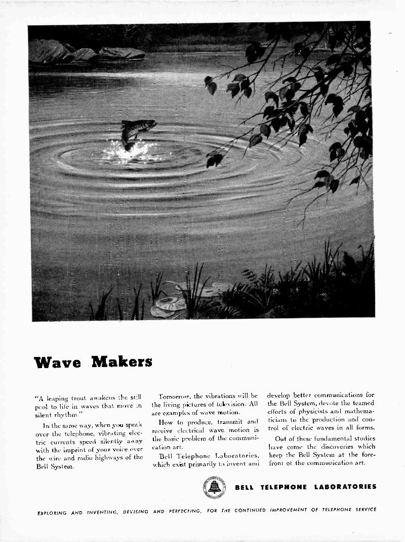
Wave Makers
'"A leaping trout awakens the stillpool to life in waves that move insilent rhythm."
In the same way, when you speakover the telephone, vibrating elec-tric currents speed silently awaywith the imprint of your voice overthe wire and radio highways of theBell System.
Tomorrow, the vibrations will bethe living pictures of television. Allare examples of wave motion.
How to produce, transmit andreceive electrical wave motion isthe basic problem of the communi-cation art.
Bell Telephone Laboratories,which exist primarily to invent and
develop better communications forthe Bell System, devote the teamedefforts of physicists and mathema-ticians to the production and con-trol of electric waves in all forms.
Out of these fundamental studieshave come the discoveries whichkeep the Bell System at the fore-front of the communication art.
BELL TELEPHONE LABORATORIES
EXPLORING AND INVENTING, DEVISING AND PERFECTING, FOR T-IE CONTINUED IMPROVEMENT OF TELEPHONE SERVICE
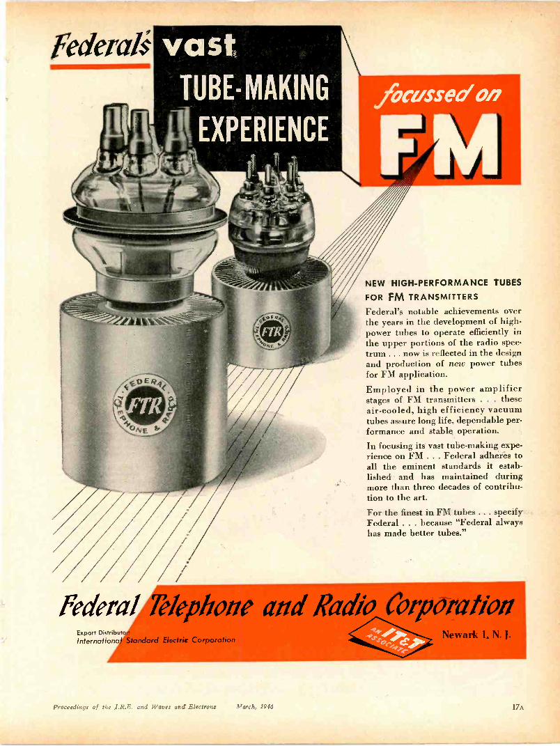
federals
NEW HIGH-PERFORMANCE TUBES
FOR FM TRANSMITTERS
Federal's notable achievements overthe years in the development of high -power tubes to operate efficiently inthe upper portions of the radio spec-trum . .. now is reflected in the designand production of new power tubesfor FM application.
Employed in the power amplifierstages of FM transmitters . . . theseair-cooled, high efficiency vacuumtubes assure long life, dependable per-formance and stable operation.In focusing its vast tube -making expe-rience on FM . . . Federal adheres toall the eminent standards it estab-lished and has maintained duringmore than three decades of contribu-tion to the art.For the finest in FM tubes . . . specifyFederal . . . because "Federal alwayshas made better tubes."
11 41
Federal ?elephone and Radio CotporatioaGr414 Newark 1 N. I
g'sJd7
Export Distributor:International Standard Electric Corporation
Proceedings of the and Waves and Electrons March 1946
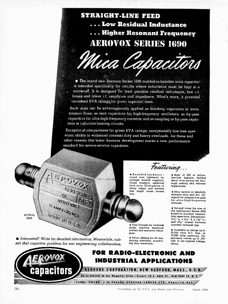
ACTUAL
STRAIGHT-LINE FEED. . . Low Residual Inductance. .. Higher Resonant FrequencyAEROVOX SERIES 1690
7/ler4Aa° aar#1,46 The brand new Aerovox Series 1690 molded-in-bakelite mica capacitor
is intended specifically for circuits where inductance must be kept at aminimum. It is designed for least possible residual inductance, low r.f.losses and lower r.f. resistance and impedance. What's more, it providesincreased KVA ratings for given capacitor sizes.
Such -.mils can be advantageously applied as blocking capacitors in trans-mission lines; as tank capacitors for high -frequency oscillators; as by-passcapacitcrs for ultra -high -frequency currents; and as coupling or by-pass capac-itors in induction -heating circuits.
Exceptional compactness for given KVA ratings; exceptionally -low -loss oper-ation; ability to withstand constant duty and heavy overloads- for these andother reasons this latest Aerovox development marks a new performancestandard for severe -service capacitors.
I
10300
MSS
SIZE 1):,t1I
Rounded hardware-round nuts tightened byspanner wrench supplied;round washers; sphericallock nuts. Elimination ofsharp edges and cornersthat might cause coronaloss.
Fine threads for terminalstuds, insuring maximumcontact and minimum resistance.
Interested? Write for detailed information. Meanwhile, sub-mit that capacitor problem for our engineering collaboration.
FOR RADIO -ELECTRONIC ANDINDUSTRIAL APPLICATIONS
AEROVOX CORPORATION, NEW BEDFORD, MASS., U.S.A.SALES DFFIccs IN ALL PRINCIPAL CITIES Export: 13 E. Oath ST., NEW YORK 16, N. Y.
Cable: 'ARLAB' In Canada: AER OYU( CANADA LTD., HAMILTON, ONT.,/
Prreeedings of the I.R.E. and Waves and Electrons March, 1996
Body of XM or yellowlow -loss bakelite moldedabout mica section for thor-ough sealing and extremeruggedness.
Mica section of carefullyselected mica and foil. De-signed for straight-line pathfor ultra -high -frequencycurrents.
Silver plating for all con-ducting members, minimiz-ing skin resistance.
Several times the size ofthe well-known Series 1650bakelite-molded transmit-ting capacitors. Dimensions:23/s" w. x 21/s" d. x 11/2" h.,and 43/4" overall between.rounded terminal tips.
Available in ratings up to20,000 volts D.C. Test, or10,000 volts operating. Ca-pacitance values up to .001mfd. at the highest voltagerating.
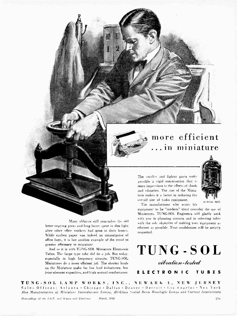
Many oldsters still remember the oldletter copying press and long hours spent in dim lightafter other office workers had gone to their homes.While carbon paper was indeed an emancipator ofoffice boys, it is but another example of the trend togreater efficiency in miniature
And so it is with TUNG-SOL Miniature ElectronicTubes. The large type tube did do a job. But today,especially in high frequency circuits, TUNG-SOLMiniatures do a more efficient job The shorter leadson the Miniature make for low lead inductance, lowinter -element capacities, and high mutual conductance.
more efficient... in miniature
The smaller and lighter parts makepossible a rigid construction that is
more impervious to the effects of shockand vibration. The size of the Minia-ture makes it a factor in reducing theoverall size of radio equipment.
The manufacturer who wants hisequipment to be "modern" must consider the use ofMiniatures. TUNG-SOL Engineers will gladly workwith you in planning circuits and in selecting tubeswith the sole objective of making your equipment asefficient as possible. Your confidences will be strictlyrespected.
ACTUAL. SIZE
TUNG-SOLviktallow-leafed
ELECTRONIC TUBESTUNG-SOL LAMP WORKS, INC., NEWARK I, NEW JERSEYSales Offices: Atlanta Chicago Dallas Denver Detroit Los Angeles New YorkAlso Manufacturers of Miniature Incandescent Lamps, All -Glass Sealed Beam Headlight Lamps and Current Intermittors
Proceedings of the I.R.E. and Waves and Electrons March, 1946 19A
t Tam]
-44.1t
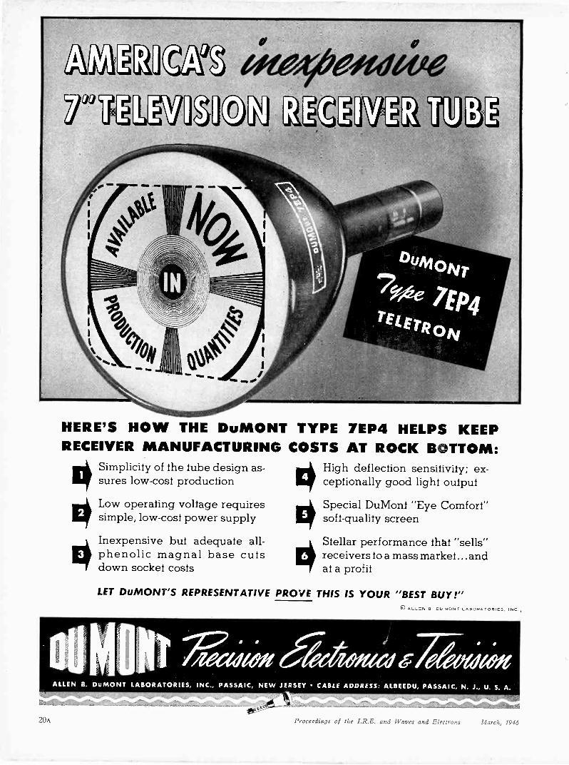
HERE'S HOW THE DuMONT TYPE 7EP4 HELPS KEEPRECEIVER MANUFACTURING COSTS AT ROCK BOTTOM:
e;toOteimapie(31 rA(LCM
Simplicity of the tube design as-sures low-cost production
Low operating voltage requiressimple, low-cost power supply
Inexpensive but adequate all -
phenolic magnal base cutsdown socket costs
High deflection sensitivity; ex-ceptionally good light output
Special DuMont "Eye Comfort"soft -quality screen
Stellar performance that "sells"receivers to a mass market ...andat a profit
LET DuMONT'S REPRESENTATIVE PROVE THIS IS YOUR "BEST BUY!"0 ALLEN B DU MONT LABORATORIES. INC. ,
a d twee Te dewto tALLEN B. DUMONT LABORATORIES, INC., PASSAIC, NEW JERSEY CABLE ADDRESS: ALBEEDU, PASSAIC, N. J., U. S. A.
Proceedings of the I.R.E. and Waves and Electrons March, 1946

with this basically new
These new ideas in FM circuits designed byWestinghouse bring you important advantagesnever before available in FM transmitters
Modulation, for example, is a simple, straight-forward diole type . . . noncritical, non -micro -phonic, no -trick tubes (see drawing above). Theeffective resistance of the tubes is a function ofplate current in the modulator -control tube.
Thus, the master oscillator tank circuit is fre-quency -modulated due to resistance variationin response 70 audio signals applied to modulator -control input circuit. And the frequency -modu-lated master oscillator operates at only 1/9th theF.C.C. assigned center -frequency.
There are other important benefits in the newWestinghouse design. Frequency is held withoutusing critically -tuned elements or moving partsand nowhere does frequency stability dependupon a tuned circuit.
WestinghousePLANTS IN 25 CITIES ... OFFICES EVERYWHERE
These new improvements are born of intensivewartime radar experience and actual operation offive FM stations . . . a background unmatchedby any other transmitter manufacturer. Ask yournearest Westinghouse office today to give you allthe facts, and look at Westinghouse before youbuy! Westinghouse Electric Corporation, P. 0.Box 868, Pittsbugh 30, Pa. J-081.58
a,7"(aziProceedinos of the I.R.E. and Waves and Electrons March, 1946 21A
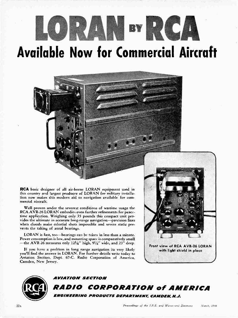
LORAN BY RCAAvailable Now for Commercial Aircraft
erv.
..0`.s
RCA basic designer of all air -borne LORAN equipment used inthis country and largest producer of LORAN for military installa-tion now makes this modern aid to navigation available for com-mercial aircraft.
Well proven under the severest conditions of wartime usage theRCA AVR-26 LORAN embodies even further refinements for peace-time application. Weighing only 35 pounds this compact unit pro-vides the ultimate in accurate long-range navigation-precision fixeswhen clouds make celestial shots impossible and severe static pre-vents the taking of aural bearings.
LORAN is fast, too-bearings can be taken in less than a minute.Power consumption is low, and mounting space is comparatively small-the AVR-26 measures only 121/4" high, Ws" wide, and 23" deep.
If you have a problem in long range navigation its very likelyyou'll find the answer in LORAN. For further details write today toAviation Section, Dept. 67-C. Radio Corporation of America,Camden, New Jersey.
AVIATION SECTION
Fron- view of RCA AVR-26 LORANwith Ight shield in place
RADIO CORPORATION of AMERICAENO/NEER/NG PRODUCTS DEPARTMENT, CAMDEN, N.J.
Proceedings of the I.R.E. and Waves and Electrons March, 1946
you solve them
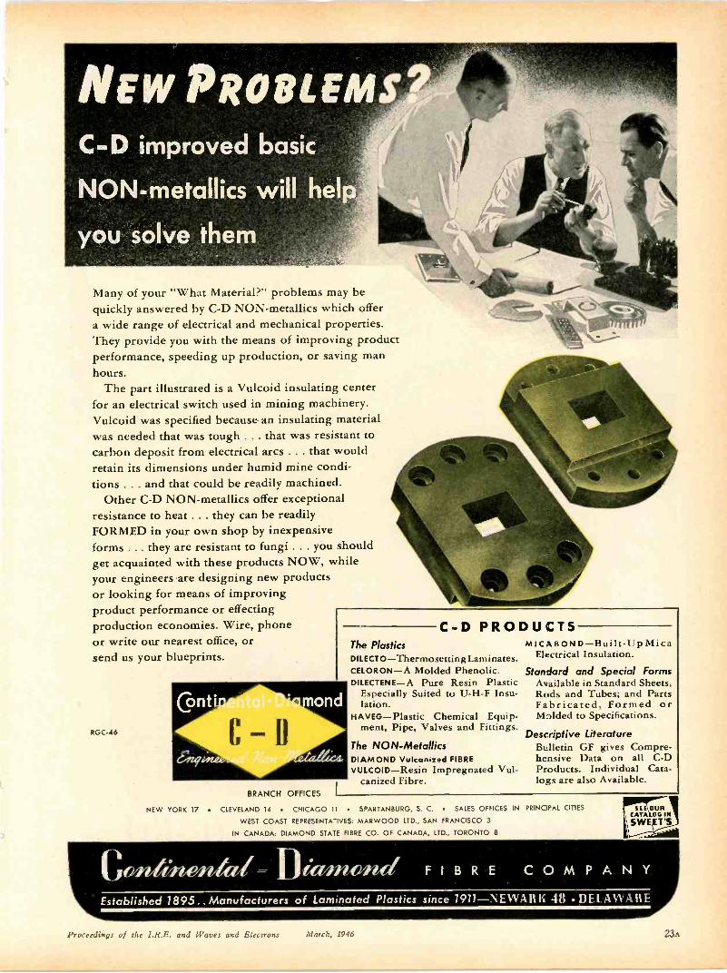
Many of your "What Material?" problems may bequickly answered by C -D NON-metallics which offera wide range of electrical and mechanical properties.They provide you with the means of improving productperformance, speeding up production, or saving manhours.
The part illustrated is a Vulcoid insulating centerfor an electrical switch used in mining machinery.Vulcoid was specified because an insulating materialwas needed that was tough .. . that was resistant tocarbon deposit from electrical arcs ... that wouldretain its dimensions under humid mine condi-tions . .. and that could be readily machined.
Other C -D NON-metallics offer exceptionalresistance to heat . . . they can be readilyFORMED in your own shop by inexpensiveforms ... they are resistant to fungi . .. you shouldget acquainted with these products NOW, whileyour engineers .are designing new productsor looking for means of improvingproduct performance or effectingproduction economies. Wire, phoneor write our nearest office, orsend us your blueprints.
RGC-46
NEW YORK
BRANCH OFFICES
The PlasticsDILECTO -ThermosettingLaminates.CELORON-A Molded Phenolic.DILECTENE-A Pure Resin Plastic
Especially Suited to U -H -F Insu-lation.
HAVEG-Plastic Chemical Equip-ment, Pipe, Valves and Fittings.
The NON-MetallicsDIAMOND Vulcanized FIBREVULCOID-Resin Impregnated Vul-
canized Fibre.
C -D PRODUCTSMICABOND -Built -Up Mica
Electrical Insulation.
Standard and Special FormsAvailable in Standard Sheets,Rods and Tubes; and PartsFabricated, Formed orMolded to Specifications.
Descriptive LiteratureBulletin GF gives Compre-hensive Data on all C -DProducts. Individual Cata-logs are also Available.
17 CLEVELAND 14 CHICAGO 11 SPARTANBURG, S. C. SALES OFFICES IN
WEST COAST REPRESENTATIVES: MARWOOD LTD., SAN FRANCISCO 3
IN CANADA: DIAMOND STATE FIBRE CO. OF CANADA, LTD., TORONTO 8
ColTibleipted= Elitmaiwid
PRINCIPAL CITIES SE OURCATALOG INSWEET'S
FIBRE COMPANYEstablished 1895.. Manufacturers of Laminated Plastics since 7911-NEWAR 48 DEL. AWARE
Proceedings of the I.R.E. and Waves and Electrons March, 1946 23A
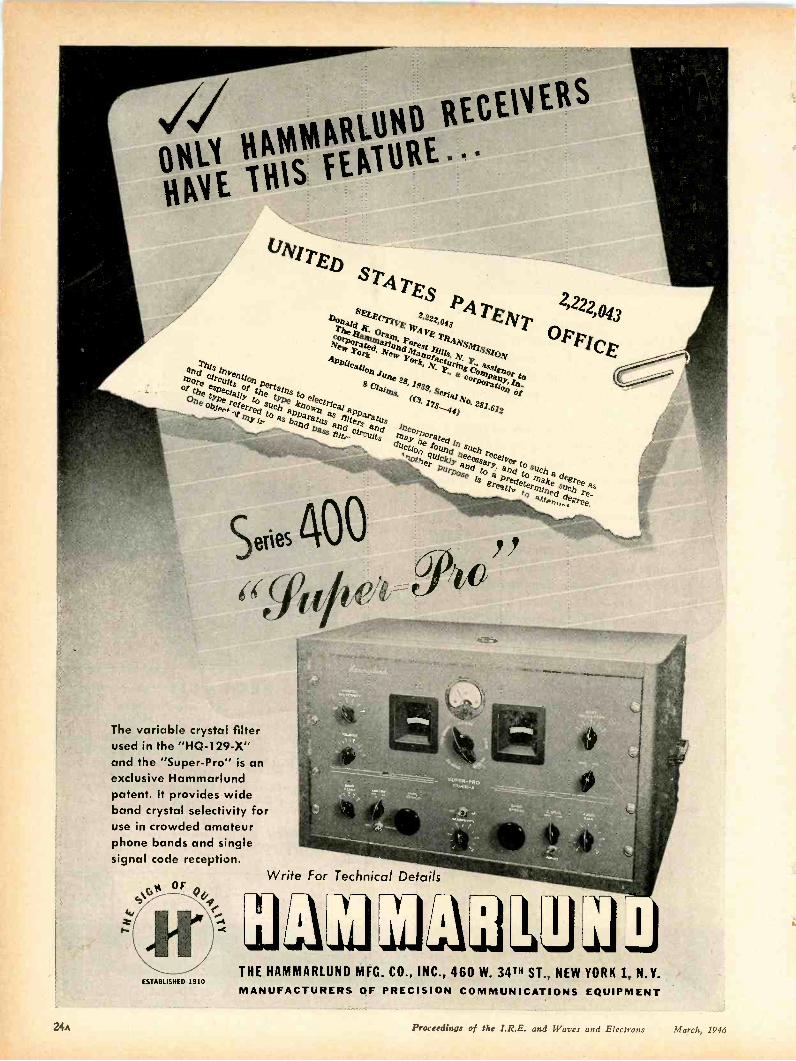
se,es 400
The variable crystal filterused in the "HQ -129-X"and the "Super -Pro" is anexclusive Hammarlundpatent. It provides wideband crystal selectivity foruse in crowded amateurphone bands and singlesignal code reception.
cok OF
44.
IESTABLISHED 1910
Write For Technical Details
9
2SIALLIJTHE HAMMARLUND MFG. CO., INC., 460 W. 34TH ST., NEW YORK 1, N.Y.MANUFACTURERS OF PRECISION COMMUNICATIONS EQUIPMENT
24A Proceedings of the and Waves and Electrons March, 1946
" "
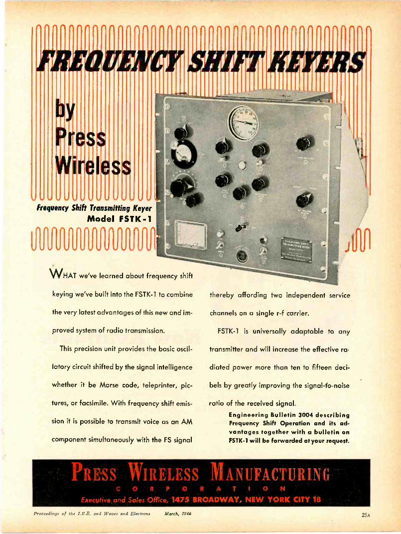
v 4.J lJ <J vfrequency Shift Transmlting Keyer
et , A AModel FSTK -1
A et , A e* et A et e't
%.0 v 4.1 4.4 v v %.14.1
WHAT we've learned about frequency shift
keying we've built into the FSTK-1 to combine thereby affording two independent service
the very latest advantages of this new and im- channels on a single r -f carrier.
proved system of radio transmission. FSTK-1 is universally adaptable to any
This precision unit provides the basic oscil- transmitter and will increase the effective ra.
latory circuit shifted by the signal intelligence diated power more than ten to fifteen deci-
whether it be Morse code, teleprinter, pic- bets by greatly improving the signal-to-noise
tures, or facsimile. With frequency shift emis- ratio of the received signal.
sion it is possible to transmit voice as an AM
component simultaneously with the FS signal
Engineering Bulletin 3004 describingFrequency Shift Operation and its ad-vantages together with a bulletin onFSTK-1 will be forwarded at your request.
PRESS WIRELESS MANUFACTURINGP 0Ft A T ION
' 175 BROADWAY, NEW YORK CITY 18
Proceedings of the I.R.E. and Waves and Electrons March, 1946
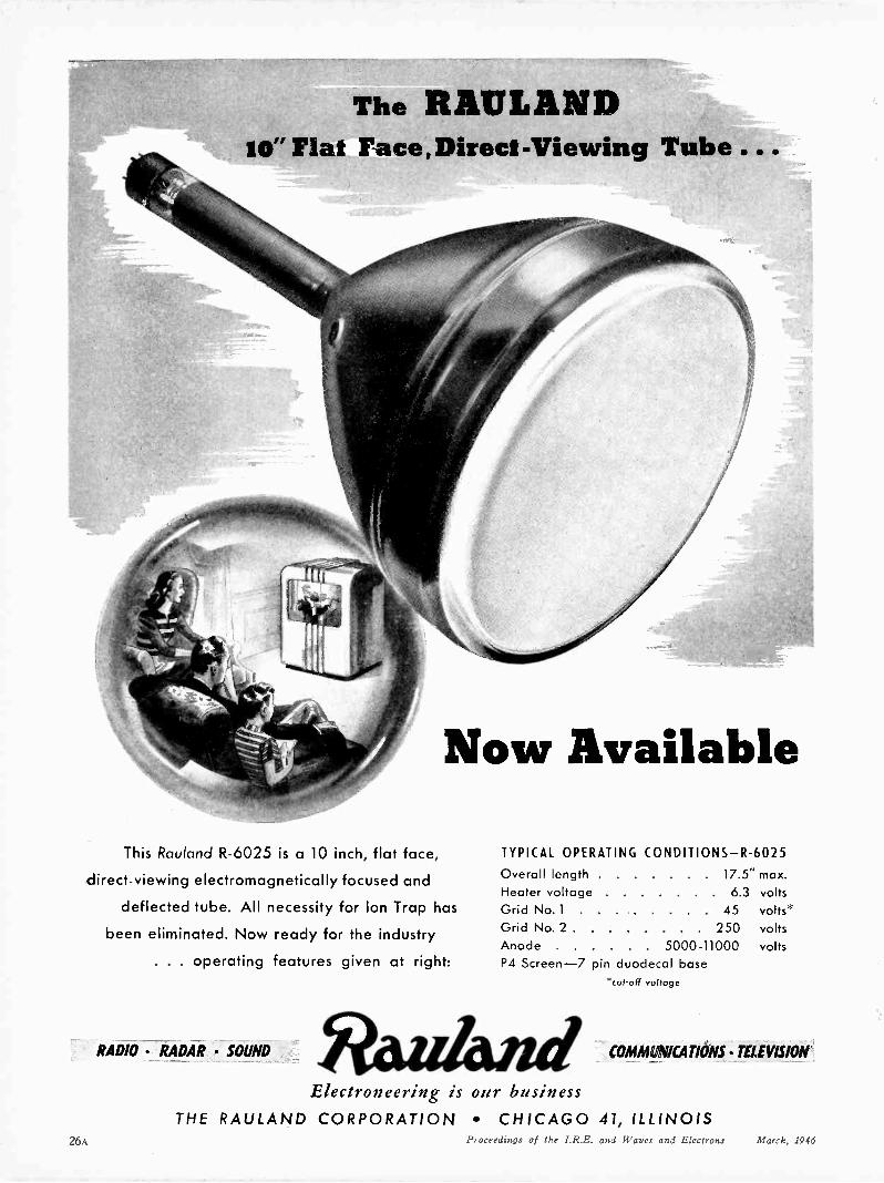
The RAULANDFlat Face,Direct-Viewing Tube
Now Available
This Rauland R-6025 is a 10 inch, flat face,
direct -viewing electromagnetically focused and
deflected tube. All necessity for Ion Trap has
been eliminated. Now ready for the industry
. . . operating features given at right:
RADIO RADAR SOUND
Anode
TYPICAL OPERATING CONDITIONS-R-6025
Overall length 17 5" max.Heater voltage 6.3 voltsGrid No. 1 . ... . 45 volts*Grid No 2 250 volts
5000-11000 voltsP4 Screen -7 pin duodecal base
*cut-off voltage
COMMUNICATIONS TELEVISION
Electroneering is our businessTHE RAULAND CORPORATION CHICAGO 41, ILLINOIS
26:A Proceedings of the I.R.E. and Waves and Electrons March, 1946
avoid damagefrom "in -the -package"
moisture
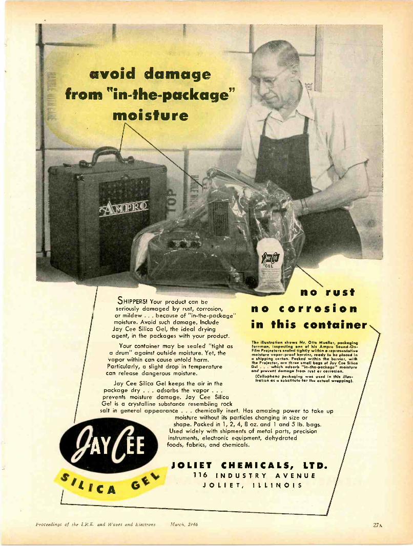
SHIPPERS! Your product can beseriously damaged by rust, corrosion,or mildew ... because of "in -the -package"moisture. Avoid such damage. Include
Jay Cee Silica Gel, the ideal dryingagent, in the packages with your product.
Your container may be sealed "tight asa drum" against outside moisture. Yet, thevapor within can cause untold harm.Particularly, a slight drop in temperaturecan release dangerous moisture.
Jay Cee Silica Gel keeps the air in thepackage dry . . . adsorbs the vapor . . .
prevents moisture damage. Jay Cee SilicaGel is a crystalline substance resembling rocksalt in general appearance . . . chemically inert. Has amazing power to
moisture without its particles changing in size orshape. Packed in 1, 2, 4, 8 oz. and 1 and 5 lb. bags.
Used widely with shipments of metal parts, precisioninstruments, electronic equipment, dehydratedfoods, fabrics, and chemicals.
no rustno corrosionin this containerThe illustration shows Mr. Otto Mueller, packagingforeman, inspecting one of his Ampro Sound -On -Film Projectors sealed lightly within a representativemoisture vapor -proof barrier, ready to be placed ina shipping carton. Packed within the barrier, withthe Projector, are three small bags of Jay Cs* SilicaGel . . . which adsorb "in -the -package" moistureand prevent damage from rust or corrosion.
(Cellophane packaging was used in this illus-tration as a substitute for the actual wrapping).
take up
JOLIET CHEMICALS, LTD.116 INDUSTRY AVENUE
JOLIET, ILLINOIS
Proceedings of the I.R.E. and Waves and Electrons March, 1946
\ \\ \
LABORATORY INSTRUMENTS FOR SPEED AND ACCURACY
\ _ \ ---c...
....4k:\
TAILOR - MADE WAVES
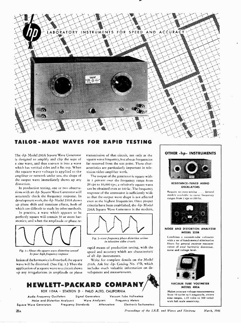
The -bp- Model 210A Square Wave Generatoris designed to amplify and clip the tops ofa sine wave, and thus convert it into a wavewhich has vertical sides and a flat top. Whenthe square wave voltage is applied to theamplifier or network under test, the shape ofthe output wave immediately shows up anydistortion.
In production testing, one or two observa-tions with an -hp- Square Wave Generator willaccurately check the frequency response. Indevelopment work, the -hp- Model 210A showsup phase shift and transient effects, both ofwhich are difficult to study by other methods.
In practice, a wave which appears to beperfectly square will contain 30 or more har-monics; and when the amplitude or phase re -
Fig. 1-Shows the square wave distortion causedby poor high frequency response
lation of the harmonics is disturbed, the squarewave will be distorted. (See Fig. 1.) Thus theapplication of a square wave to a circuit showsup any irregularities in amplitude or phase
FOR RAPID TESTING
transmission of that circuit, not only at thesquare wave frequency, but also at frequenciesfar removed from the test point. These char-acteristics are particularly important in tele-vision video amplifier work.
The output of the generator is square with-in 1 percent over the frequency range from20 cps to 10,000 cps; a relatively square wavecan be obtained even at 100 kc. The frequencyresponse of the attenuator is sufficiently wideso that the output wave shape is not affectedeven at the highest frequencies. Once propercriteria have been established, the -hp- Model210A Square Wave Generator is the modern,
Fig. 2-Low frequency phase distortion seriousin television video circuits
rapid means of production testing, with thespeed and accuracy which are characteristicof all -hp- instruments.
Write for complete details on the Model210A. Ask for -hp- Catalog No. 17B, whichincludes much valuable information on de-velopment and measurements.
HEWLETT-PACKARD COMPANYBOX I I 34A STATION D PALO ALTO, CALIFORNIA
Audio Frequency Oscillators Signal Generators Vacuum Tube Voltmeters
Noise and Distortion Analyzers Wave Analyzers Frequency Meters
Square Wave Generators Frequency Standards Attenuators Electronic Tachometers
\- \.'\\ *1'
\\
\
OTHER -hp- INSTRUMENTS
RESISTANCE -TUNED AUDIOOSCILLATORS
Require no zero setting . . Severalmodels available to cover frequencyranges trans 2 cps to 200 kc.
NOISE AND DISTORTION ANALYZERMODEL 3256
Combines a vacuum -tube voltmeterwith a set of fundamental eliminationfilters for general purpose measure-ments of total harmonic distortion,noise and voltage level.
VACUUM TUBE VOLTMETERMODEL 400A
Makes accurate voltage measurementsfrom 10 cycles to 1 megacycle, coversnine ranges, (.03 volts to 300 volts)with full scale sensitivity.
28A Proceedings of the I.R.E. and Waves and Electrons March, 194,',
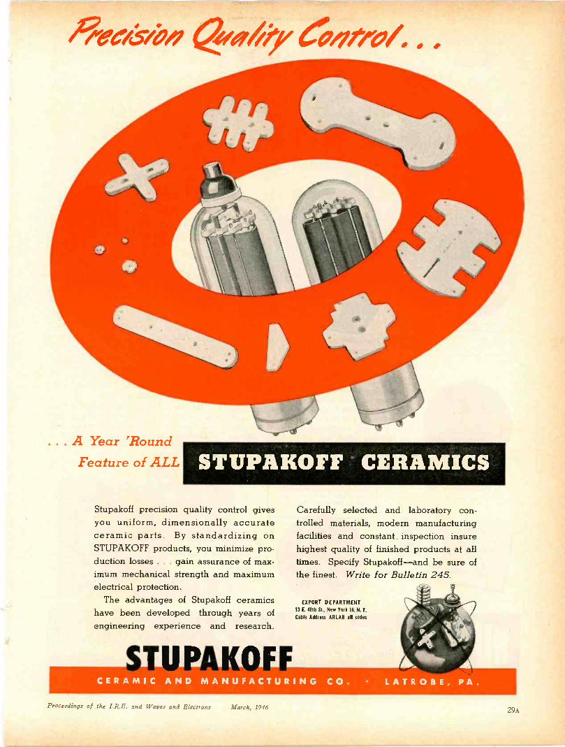
8-e94-4's efefry 64teeel
. . . A Year 'RoundFeature of ALL STUPAKOFF CERAMICS
Stupakoff precision quality control givesyou uniform, dimensionally accurateceramic parts. By standardizing onSTUPAKOFF products, you minimize pro-duction losses . . . gain assurance of max-imum mechanical strength and maximumelectrical protection.
The advantages of Stupakoff ceramicshave been developed through years ofengineering experience and research.
Carefully selected and laboratory con-trolled materials, modern manufacturingfacilities and constant, inspection insurehighest quality of finished products at alltimes. Specify Stupakoff-and be sure ofthe finest. Write for Bulletin 245.
EXPORT DEPARTMENT13 E. 40th St., New Terk 16, N.Y.
Cable Address ARLAII all ales
Proceedings of the I.R.E. and Waves and Electrons March, 1946 29A
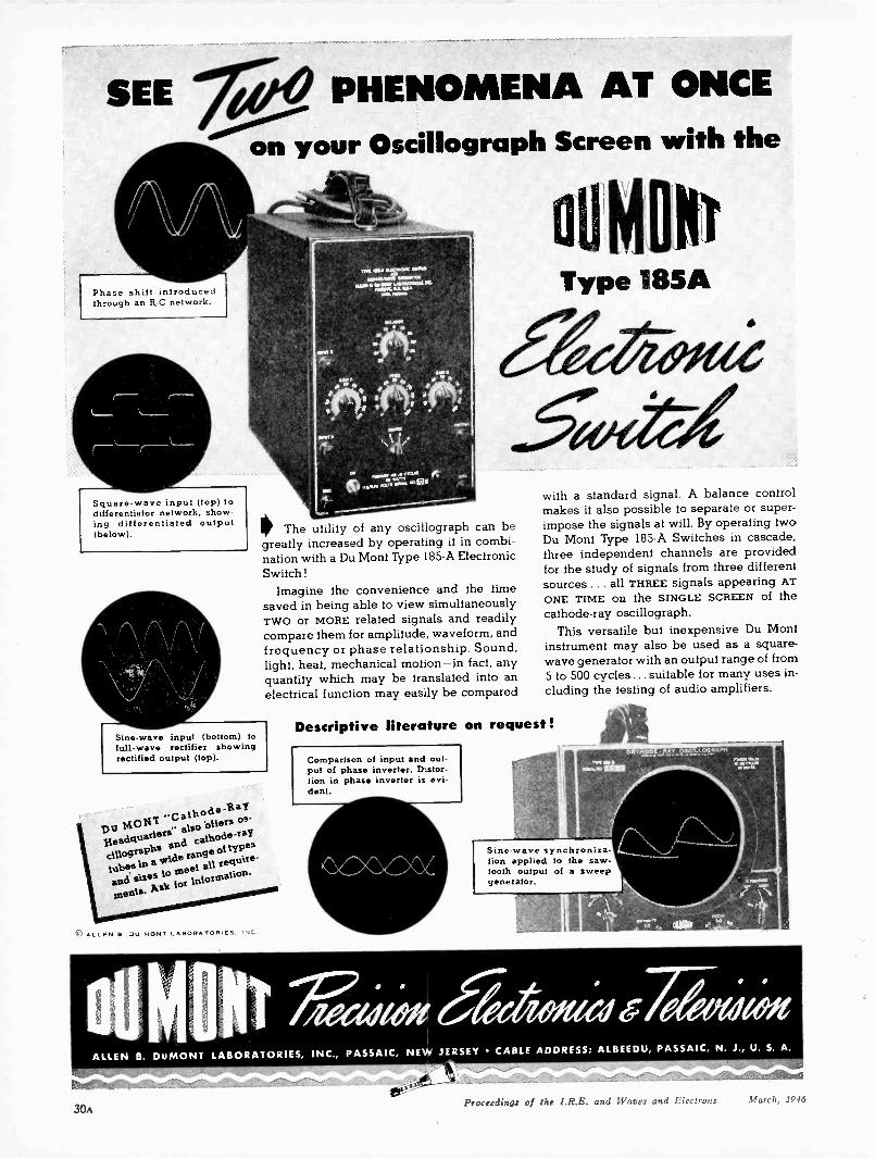
with a standard signal. A balance controlmakes it also possible to separate or super-impose the signals at will. By operating twoDu Mont Type 185-A Switches in cascade,three independent channels are providedfor the study of signals from three differentsources ... all THREE signals appearing ATONE TIME on the SINGLE SCREEN of thecathode-ray oscillograph.
This versatile but inexpensive Du Montinstrument may also be used as a square -wave generator with an output range of from5 to 500 cycles ... suitable for many uses in-cluding the testing of audio amplifiers.
Descriptive literature on request!
Comparison of input and out-put of phase inverter. Distor-tion in phase inverter is evi-dent.
SEE 71.1.19 PHENOMENA AT ONCE
on your Oscillograph Screen with the
Phase shift introducedthrough an R -C network.
Square -wave input (top) toditterenliator network, show-ing differentiated output(below).
aM OPType 185A
aezzotee
5eilleliwg. vats W...
10 The utility of any oscillograph can begreatly increased by operating it in combi-nation with a Du Mont Type 185-A ElectronicSwitch!
Imagine the convenience and the timesaved in being able to view simultaneouslyTwo or MORE related signals and readilycompare them for amplitude, waveform, andfrequency or phase relationship. Sound,light, heat, mechanical motion-in fact, anyquantity which may be translated into anelectrical function may easily be compared
Sine -wave input (bottom) tofull -wave rectifier showingrectified output (top).
Du 140141"Cathode
-Ray
Headquatters"also ones os-
cillographsand cathode-ray
tubes in a widerange oftypes
and sizesto
all sequite-
ments.Ask tor intotmation.
11,3 311A ,1,11, ,':
Sine -wave synchroniza-tion applied to the saw -tooth output of a sweepgenerator.
tr
ALLEN B. DuMONT LABORATORIES, INC., PASSAIC, NEW JERSEY CABLEw.
ADDRESS: ALBEEDU, PASSAIC, N..1., U. S. A.
30AProceedings of the I.R.E. and Waves and Electrons March, 1946
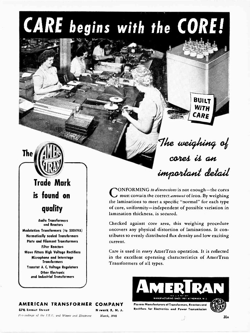
CARE begins with the CORE!
The
Trade Mark
is found on
quality
Audio Transformersand Reactors
Modulation Tiansformers (to SOOKVA)
Hermetically sealed Transformers
Plate and Filament Transformers
Filter Reactors
Wave Filters High Voltage Rectifiers
Microphone and InterstageTransformers
Transtat A. C. Voltage Regulators
Other Electronicand Industrial Transformers
lite weirthalf.4,4 aot
isfro/daid detailCONFORMING to dimensions is not enough-the cores
must contain the correct amount of iron. By weighingthe laminations to meet a specific "normal" for each typeof core, uniformity-independent of possible variation inlamination thickness, is secured.
Checked against core area, this weighing procedureuncovers any physical distortion of laminations. It con-tributes to evenly distributed flux density and low excitingcurrent.
Care is used in every AmerTran operation. It is reflectedin the excellent operating characteristics of AmerTranTransformers of all types.
AMERICAN TRANSFORMER COMPANYfat, Emmet StreetProceedings of the I.R.E. and Waves and Electrons
N twark 3, N. J.March, 1946
AMERTRANMANUFACTURING SINCE 1901 AT NEWARK, N 1
Pioneer Manufacturers of Transformers, Reactors andRectifiers for Electronics and Power Transmission
314
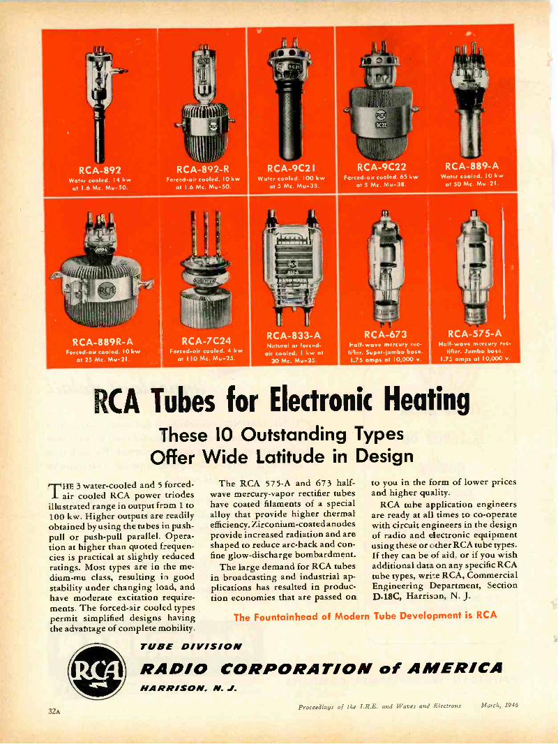
RCA -892Water cooled. 14 kw
at 1.6 Mc. Mu -SO.
RCA -889R -AForced -air cooled. 10 kw
at 25 Mc. Mu -21.
RCALV12-RForced -air cooled. 10 kw
at 1.6 Mc. Mu -50.
RCA -7C24Forced -air cooled. 4 kw
at 110 Mc. Mu -25.
RCA -9C21Water cooled. 100 kw
at 5 Mc. Mu. --38.
RCA -833-ANatural or forced -air cooled. I kw at
30 Mc. Mu -35.
RCA -9C22Fcrced-air cooled. 65 kw
at 5 Mc. Mu= 38.
RCA -889-AWater cooled. 10 kw
at 50 Mc. Mu 21.
RCA -673 RCA -575-A1-alf-wave mercury rec-tiler. Super -jumbo base.1.75 amps at 10,000 v.
Half -wave mercury rec-tifier. Jumbo base.
1.75 amps at 10,000 v.
RCA Tubes for Electronic HeatingThese 10 Outstanding Types
Offer Wide Latitude in Design1-1 HE 3 water-cooled and 5 forced -
air' cooled RCA power triodesillustrated range in output from 1 to100 kw. Higher outputs are readilyobtained by using the tubes in push-pull or push-pull parallel. Opera-tion at higher than quoted frequen-cies is practical at slightly reducedratings. Most types are in the me-dium -mu class, resulting in goodstability under changing load, andhave moderate excitation require-ments. The forced -air cooled typespermit simplified designs havingthe advantage of complete mobility.
The RCA 575-A and 673 half -wave mercury-vapor rectifier tubeshave coated filaments of a specialalloy that provide higher thermalefficiency. Zirconium -coated anodesprovide increased radiation and areshaped to reduce arc -back and con-fine glow -discharge bombardment.
The large demand for RCA tubesin broadcasting and industrial ap-plications has resulted in produc-tion economies that are passed on
to you in the form of lower pricesand higher quality.
RCA tube application engineersare ready at all times to co-operatewith circuit engineers in the designof radio and electronic equipmentusing these or other RCA tube types.If they can be of aid. or if you wishadditional data on any specific RCAtube types, write RCA, CommercialEngineering Department, SectionD -18C, Harrison, N. J.
The Fountainhead of Modern Tube Development is RCA
TUBE D/V/S/ON
RADIO CORPORATION of AMERICAHARRISON, N. J.
32AProceedings of the I.R.E. and Waves and Electrons March, 1946
BOARD OFDIRECTORS, 1946
Frederick B. LlewellynPresident
Edmond M. DeloraineVice -President
William C. WhiteTreasurer
Haraden PrattSecretary
Alfred N. GoldsmithEditor
Hubert M. TurnerSenior Past PresidentWilliam L. Everitt
Junior Past President1944-1946
Raymond F. GuyLawrence C. F. Horle
1945-1947Stuart L. Bailey
Keith HenneyBenjamin E. Shackelford
1946-1948Walter R. G. BakerVirgil M. GrahamDonald B. Sinclair
1946
Ralph A. HackbuschFrederick R. LackGeorge T. Royden
William 0. SwinyardWilbur L. Webb
Edward M. Webster
Harold R. ZeamansGeneral Counsel
George W. BaileyExecutive Secretary
William H. CrewAssistant Secretary
BOARD OF EDITORS
Alfred N. GoldsmithChairman
PAPERS COMMITTEE
Frederick B. LlewellynChairman
PAPERSPROCUREMENT
COMMITTEEDorman D. IsraelGeneral Chairman
Edward T. DickeyVice General Chairman
PROCEEDINGS A WAVES
of the I.R.E. D and ELECTRONS
Published Monthly in two sections by
The Institute of Radio Engineers, Inc.
VOLUME 34 March, 1946 NUMBER 3
SECTION I-PROCEEDINGS OF THE I.R.E. SECTION
Continuing Service F H. R. Pounsett 96 P
Reflex-Klystron Oscillators ... Edward Leonard Ginzton and Arthur E. Harrison 97 P
The Transmission of a Frequency -Modulated Wave Through a NetworkWalter J. Frantz 114 P
Analysis of a Resistance -Capacitance Parallel -T Network and ApplicationsA E. Hastings 126 P
The Application of Modulation -Frequency Feedback to Signal DetectorsGeoffrey Builder 130 P
The Ideal Low -Pass Filter in the form of a Dispersionless Lag LineMarcel J. E. Golay 138 P
Applications of Matrix Algebra to Filter Theory Paul I. Richards 145 P
Discussion on "Electron Transit Time in Time -Varying Fields," by Arthur B.Bronwell L. A. Ware, H. B. Phillips, and Arthur B. Bronwell 151 P
Contributors to the PROCEEDINGS OF THE I.R.E. SECTION 152 P
Advertising Index 86 A
SECTION II-WAVES AND ELECTRONS SECTION FOLLOWS AFTER PAGE 152 P.
EDITORIAL DEPARTMENTAlfred N. Goldsmith
EditorHelen M. Stote
Publications ManagerWinifred CarriereAssistant Editor
William C. CoppAdvertising Manager
Ray D. RettenmeyerTechnical Editor
Lillian PetranekAssistant Advertising Manager
Responsibility for the contents of papers published in the PROCEEDINGS OF THE I.R.E. and WAVESAND ELECTRONS rests upon the authors.
Statements made in papers are not binding on the Institute or its members.
Changes of address (with advance notice of fifteen days) and communications regarding subscriptions and pay-ments should be mailed to the Secretary of the Institute, at 450 Ahnaip St., Menasha, Wisconsin or 330 West 42ndStreet, New York 18, N. Y. All rights of republication, including translation into foreign languages, are reserved bythe Institute. Abstracts of papers, with mention of their source, may be printed. Requests for republication privilegesshould be addressed to The Institute of Radio Engineers.
Copyright, 1996. by The Institute of Radio Engineers, Inc.
The Chairmen of the Sections of the Institute have been invited to expressto the membership, in such editorial form as they may desire, views which theybelieve will be contributory to the future of the engineering profession. Thought-ful analyses and forward -looking discussions of this nature have been received.There follows, accordingly, a statement from the Chairman of the TorontoSection of the Institute.
The Editor
Continuing ServiceF. H. R. POUNSETT
Due credit has been reflected on our membership for its technical effort during the war. However,we must avoid becoming too embroiled in the present confusion of reconversion of facilities, men, andminds, and missing opportunities for further service: a service which, if properly performed, will beof lasting benefit to our industry, our Institute, and incidentally ourselves.
It is well, at a turning point like this, to look back at the fundamental concepts of our charter.What are the objects of our Institute? As stated in the Constitution; "Its aims shall include the ad-vancement of the theory and practice of radio, and allied branches of engineering and of the relatedarts and sciences, their application to human needs, and the maintenance of a high professional stand-ing among its members."
Headquarters, backed by the splendid response to the Building -Fund Campaign, and the recentlyacquired executive assistance, is taking care of the general realigning of our affairs to cope with presentconditions of expansion and broadening of interest. The Sections must, in turn, organize to serve theirparticular areas as required by local conditions and plan to make The Institute of Radio Engineersof maximum benefit to the membership and the community. The avenues along which the TorontoSection has been extending its activities during the past eighteen months are briefly outlined here inthe hope that they may be of interest or possibly of benefit to members elsewhere.Education
Meetings are arranged to acquaint members and guests not only with the interesting war develop-ments but also with the industrially useful phases of wartime developments with which many havelost touch during the past six years because of the pressure of their particular jobs.
Many members can exert considerable influence towards adjusting the curricula of engineeringschools and rehabilitation schools in line with the present requirements of industry. Surplus test equip-ment and prototypes from war plants can be well directed to the laboratories of these schools.Rehabilitation
Returned Service technical personnel, not necessarily members, are invited to Section meetings.Group contact, as well as personal counseling can be helpful to these men, especially those who werenot in technical work before the war but, because of their war experience, are now seriously consider-ing continuing it as a vocation. Many members are serving on advisory councils of rehabilitationschools which offer electronic courses.Canadian Radio Technical Planning Board
This needs no elucidation. Several members have taken an active part on the various panels andcommittees as representatives of the I.R.E., particularly recommended by the Section.Regional Organization
Our Section executive has played an active part in organizing the Canadian Council of the I.R.E.The Regional Scheme, recently proposed at Headquarters will offer all Sectionsa similar opportunityto co-operate with others in their territories to their mutual advantage.The Profession
Members have been encouraged to upgrade their membership wherever possible. They have alsobeen encouraged to join the Provincial Association of Professional Engineers (the registering body).
By intermembership in the Provincial Association and the active participation of the Section withthe Canadian Council of the I.R.E. in the formation of the Canadian Council of Professional En-gineers and Scientists (CCPES), the relationship of the employee engineer to his employer and toorganized labor with regard to collective bargaining has been beneficially clarified on a Dominion -wide basis.
96 P Proceedings of the I.R.E. and Waves and Electrons March

Reflex-Klystron Oscillators*EDWARD LEONARD GINZTONt, ASSOCIATE, I.R.E., AND
ARTHUR E. HARRISONt, SENIOR MEMBER, I.R.E.
Summary-A comprehensive analysis of reflex klystrons is de-veloped by considering the electrons as particles acted upon byforces which modify their motion. The analysis is similar to earlierexplanations of electron bunching in a field -free drift space and pre-dicts a similar current distribution when bunching takes place in areflecting field. The effect of the bunched electron beam is treatedqualitatively by considering the effect of the beam admittance upon asimple equivalent circuit. A quantitative mathematical analysis basedupon oscillator theory is also derived and the results are presented ina series of universal curves which are used to explain the operatingcharacteristics of these tubes. Power output, efficiency, starting cur-rent, electronic tuning, and modulation properties are discussed.Some general remarks on reflex -oscillator design considerations arealso included.
INTRODUCTION
REFLEX-klystron oscillators are an importantmember of an extensive family of velocity -modu-lation tubes invented independently by R. H.
Varian and W. W. Hansen at Stanford University,W. C. Hahn and G. F. Metcalf at Schenectady, and0. Heil in Germany. Velocity -modulation tubes are nowquite generally known as klystrons, and perform thesame functions at frequencies in the microwave regionthat triodes and pentodes do at lower frequencies. Themechanism of energy conversion is different, but analo-gies between klystrons and the electrical circuits usedwith conventional tubes are often useful. Klystrons withone or more resonators are used as oscillators, and multi -resonator klystrons often replace conventional vacuumtubes for other applications.
A reflex klystron utilizes a single resonator, and ob-tains feedback by reflecting the electron beam so that itpasses through the resonator a second time. This typeof oscillator was described briefly by Hahn and Metcalf,'and has been discussed in greater detail in otherpapers.2-4 The operation of these tubes can be explainedby a ballistic or kinematic analysis; i.e., the electronsmay be considered as particles which follow Newton'slaws of motion. An understanding of the application ofsuch a kinematic analysis to the principles of operationof the ordinary two -resonator klystron will be assumed.These principles have been presented in papers by
* Decimal classification: R355.9. Original manuscript received bythe Institute, August 3, 1945.
f Sperry Gyroscope Company, Inc., Garden City, Long Island,N. Y.
W. C. Hahn and G. F. Metcalf, "Velocity -modulated tubes,"PROC. I.R.E., vol. 27, pp. 106-117; February, 1939.
A. E. Harrison, "Klystron Technical Manual," Sperry Gyro-scope Company, Inc., Great Neck, Long Island, New York, 1944.
A. E. Harrison, "Kinematics of reflection oscillators," Jour.A ppl. Phys., vol. 15, pp. 709-711; October, 1944.
' J. R. Pierce, "Reflex oscillators," PROC. I.R.E., vol. 33, pp. 112-118; February, 1945.
Varian' and Webster," and a similar analysis will bedeveloped for the reflex-klystron oscillator.
The analysis has been subdivided into two parts. Thefirst section derives the transit -time relationships for thereflex type of klystron from the laws of motion. Thenthese relations are expanded to explain electron bunch-ing, and the similarity between reflection -field bunchingand bunching in a field -free drift space is shown. Asecond section applies these relationships to a derivationof the efficiency, power output, and electronic tuning ofa reflex-klystron oscillator. The dependence of thesecharacteristics on the beam current, beam voltage, re-flector voltage, load, and other klystron design factorswill be shown.
OPERATING PRINCIPLES OF A REFLEX KLYSTRON
A simplified drawing of a reflex klystron is shown inFig. 1. The tube is a figure of revolution about the axisAA. The cathode surface K provides a source of elec-
A
REFLECTORELECTRODE
COAXIALOUTPUTTERMINAL
FLEXIBLEDIAPHRAGM
CATHODE 'K
so
TUNING RINGS
ANODE PLANEFOCUSING ELECTRODE LCONTROL GRID '0"
HEATER 'F'
A
Fig. 1-Cross-section view of a reflex klystron.
trons when it is indirectly heated by F. The electronsare accelerated by the voltage Eo, which is known as thebeam voltage, or as the acceleration voltage because itdetermines the velocity which the electrons have ac-quired when they reach the anode plane. The emissioncurrent is controlled by the voltage E2 which is appliedto the grid G. The cylindrical portion of the control -gridstructure acts as a focusing element and gives a col-limated beam which continues along the axis of thetube past the anode plane. In many klystron designs,the grid is not used and this electrode is only a focusing
6 R. H. Varian and S. F. Varian, "A high -frequency oscillatorand amplifier," Jour. A ppl. Phys., vol. 10, pp. 321-327; May, 1.939.
6 D. L. Webster, "Cathode-ray bunching," Jour. A ppl. Phys.,vol. 10, pp. 501-508; July, 1939.
D. L. Webster, "The theory of klystron oscillations," Jour. A ppl.Phys., vol. 10, pp. 864-872; December. 1939.
1946 Proceedings of the I.R.E. and Waves and Electrons 97 P
98 P Proceedings of the I.R.E. and Waves and Electrons March
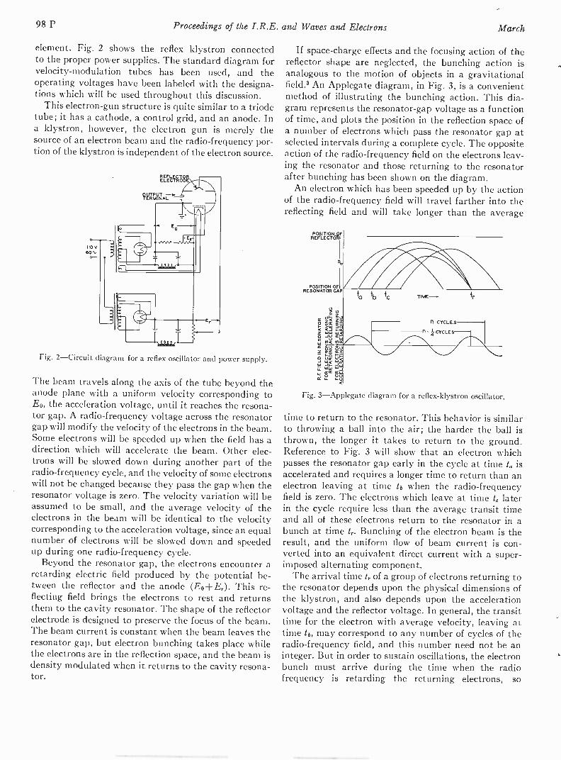
element. Fig. 2 shows the reflex klystron connectedto the proper power supplies. The standard diagram forvelocity -modulation tubes has been used, and theoperating voltages have been labeled with the designa-tions which will be used throughout this discussion.
This electron -gun structure is quite similar to a triodetube; it has a cathode, a control grid, and an anode. Ina klystron, however, the electron gun is merely thesource of an electron beam and the radio -frequency por-tion of the klystron is independent of the electron source.
REFLECTORELECTRODE
110 V60 A.
Fig. 2-Circuit diagram for a reflex oscillator and power supply.
The beam travels along the axis of the tube beyond theanode plane with a uniform velocity corresponding toEo, the acceleration voltage, until it reaches the resona-tor gap. A radio -frequency voltage across the resonatorgap will modify the velocity of the electrons in the beam.Some electrons will be speeded up when the field has adirection which will accelerate the beam. Other elec-trons will be slowed down during another part of theradio -frequency cycle, and the velocity of some electronswill npt be changed because they pass the gap when theresonator voltage is zero. The velocity variation will beassumed to be small, and the average velocity of theelectrons in the beam will be identical to the velocitycorresponding to the acceleration voltage, since an equalnumber of electrons will be slowed down and speededup during one radio -frequency cycle.
Beyond the resonator gap, the electrons encounter aretarding electric field produced by the potential be-tween the reflector and the anode (E0 --F E,). This re-flecting field brings the electrons to rest and returnsthem to the cavity resonator. The shape of the reflectorelectrode is designed to preserve the focus of the beam.The beam current is constant when the beam leaves theresonator gap, but electron bunching takes place whilethe electrons are in the reflection space, and the beam isdensity modulated when it returns to the cavity resona-tor.
If space -charge effects and the focusing action of thereflector shape are neglected, the bunching action isanalogous to the motion of objects in a gravitationalfield.' An Applegate diagram, in Fig. 3, is a convenientmethod of illustrating the bunching action. This dia-gram represents the resonator -gap voltage as a functionof time, and plots the position in the reflection space ofa number of electrons which pass the resonator gap atselected intervals during a complete cycle. The oppositeaction of the radio -frequency field on the electrons leav-ing the resonator and those returning to the resonatorafter bunching has been shown on the diagram.
An electron which has been speeded up by the actionof the radio -frequency field will travel farther into thereflecting field and will take longer than the average
PM-% r
POSITION OFRESONATOR GAP
tb TIME ---
!1 CYCLES
fl 4cra..Es
Fig. 3-Applegate diagram for a reflex-klystron oscillator.
time to return to the resonator. This behavior is similarto throwing a ball into the air; the harder the ball isthrown, the longer it takes to return to the ground.Reference to Fig. 3 will show that an electron whichpasses the resonator gap early in the cycle at time to isaccelerated and requires a longer time to return than anelectron leaving at time tb when the radio -frequencyfield is zero. The electrons which leave at time t, laterin the cycle require less than the average transit timeand all of these electrons return to the resonator in abunch at time tr. Bunching of the electron beam is theresult, and the uniform flow of beam current is con-verted into an equivalent direct current with a super-imposed alternating component.
The arrival time I, of a group of electrons returning tothe resonator depends upon the physical dimensions ofthe klystron, and also depends upon the accelerationvoltage and the reflector voltage. In general, the transittime for the electron with average velocity, leaving attime tb, may correspond to any number of cycles of theradio -frequency field, and this number need not be aninteger. But in order to sustain oscillations, the electronbunch must arrive during the time when the radiofrequency is retarding the returning electrons, so

1946 Ginzton and Harrison: Reflex-Klystron Oscillators 99 P
that the electron velocity is reduced and some of thekinetic energy of the electrons is transferred into electro-magnetic energy in the cavity -resonator field.
The electron which is to become the center of thebunch leaves at the time tb when the radio -frequencyvoltage is zero and changing from acceleration to de-celeration. At an integral number of cycles later, theradio -frequency voltage will again be zero, but for thereturning electron, the field will be changing from de-celeration to acceleration. This time is indicated by ncycles in Fig. 3. Since a maximum retarding field is re-quired for maximum energy transfer from the bunchedelectron beam, the transit time for an electron whichenters the reflecting field with average velocity must cor-respond to one -quarter cycle less than an integral num-ber of cycles. This transit -time requirement may beverified by inspection of Fig. 3.
Most of the electrons are collected by the metal wallsof the tube after they have given up energy to the reso-nator field. Other electrons may have been lost by inter-ception by the grid structures. A few electrons maysurvive these chances of getting collected and will bedecelerated near the cathode surface, then reacceleratedwith the newly emitted electrons. Upon re-entering thereflection space, these electrons will behave differentlyfrom the electrons which are going through the round-trip cycle for the first time. These electrons which makemultiple transits may produce undesirable effects, butin most cases the effect of these electrons may be neg-lected. More important factors, such as space -chargedebunching forces, will be neglected in order to simplifythe analysis. This theory is not intended for designingklystrons, but to help in understanding many of the phe-nomena which occur.
TRANSIT -TIME RELATIONSHIPS IN THEREFLECTION SPACE
It was mentioned previously that the electrons whichpass the resonator gap when the radio -frequency voltageis zero enter the reflecting field without any change invelocity, and are defined as electrons with averagevelocity. Electrons which pass the resonator gap at atime tb (see Fig. 3) when the radio -frequency field ischanging from accleration to deceleration, become thecenter of the bunch. The electrons in the bunch havedifferent velocities, and these velocities are continuallychanging during the time the electrons are in the re-flection space; however, it is convenient to consider thatthe bunch moves as a unit along a path determined bythe electron which is to become the center of the bunch.Note that the lines in Fig. 3 representing electrons leav-ing at times ta, tb, and tc appear to converge about thecenter of the bunch.
A brief review of electron ballistics will derive theequations which are useful in determining the relation-ships between the transit time and the tube -design
parameters. The calculation of the transit time fromthe tube voltages and the reflector -electrode spacingwill not be accurate because the effect of the nonuniformfield and the effect of space charge have been neglected.Although the effects of space charge are quite impor-tant, the assumption simplifies the analysis consider-ably, and the result is quite useful.
In the derivations which follow, the terminology willbe defined as it is introduced. In addition, a glossary ofsymbols is included in an appendix. The average elec-tron velocity vo is determined by the acceleration volt-age Eo, and the relation may be obtained from the factthat the kinetic energy gained by an electron of mass mand charge e is equal to the potential energy which ac-celerates the electron. This relation may be stated
1/2(mvo2) = Eoe. (1)
Equation (1) is then rewritten in the form
/2evo = Eo.
Other laws of motion of particles may be used to de-termine the transit time. If the deceleration is denotedby a, then the position of a particle as a function of timeis given by
(2)
s = vot - 1/2(a12). (3)
When t is equal to the average transit time To the elec-tron has returned to the resonator, the electron velocityis again vo, but in the opposite direction, and s is equalto zero; i.e.,
0 = voTo - 1/2(aTo2). (4)
There are two solutions to (4). To equal to zero cor-responds to an electron which has not traversed the re-flection space, and is disregarded. The other solution is
2voTo = - (5)a
The deceleration a may be evaluated from the familiarequation for the force acting on a particle. This force isgiven by the product of the charge on the electron andthe gradient of the potential between the anode and thereflector electrode. If the reflector field is assumed to beuniform, the gradient is simply the sum of the voltageson the reflector electrode divided by so, the reflectorspacing. Therefore,
Eo +F = ma (6)
So
Substitution of (6) and (2) in (5) gives
m2vo V2e- EoTo = = 4so (7)
e Eo + Er Eo + Erm So
for the average transit time.
100 P Proceedings of the I.R.E. and Waves and Electrons March
It is usually more convenient to express the transittime in terms of a number of oscillation cycles ratherthan as a time interval. This equivalent number ofcycles will be designated N, and is defined by
N = fTo (8)
where f is the frequency of oscillation. Equation (7) maytherefore be written
0
O
V2tne- Eo
N = 4fsoEo ± Er
4
N=2-1---'"
N=3-1
4
N=41
N=51
0 2 A A .8 11
ACCELERATION VOLTAGE
Fig. 4-Family of curves showing voltage modes in areflex oscillator.
(9)
If oscillation is to be at maximum strength, the num-ber of cycles during the transit time in the reflectionspace must satisfy the relation mentioned in the discus-sion of Fig. 3; i.e.,
N = n - 1/4 (10)
where n is any integer greater than zero. Oscillation atthe same frequency will occur for a number of values ofN, and each value of N may be provided by the properchoice of the acceleration voltage and the reflector volt-age. A series of curves showing the reflector voltagerequired to give constant frequency for any value of ac-celeration voltage is shown in Fig. 4. Each curverepresents a different value of N. The value of N maybe estimated from the frequency, reflector spacing, andvoltages involved. These transit times are an importantfactor in the behavior of reflex klystrons, and the impor-tance of transit time will be discussed in greater detailin the sections which follow. In practice, transit timecorresponding to values of N between 11 and 101 cyclesare typical.
ELECTRON -BUNCHING RELATIONSHIPS
It is obvious that electron bunching must occur in areflex klystron because the velocity variation introducedby the resonator voltage produces a variation of thetransit times of electrons which pass the resonator gapat different times during a cycle. This variation of
transit time may be expected from (5), which may berewritten in terms of a varying velocity instead of theaverage velocity, and becomes
2vT = - (11)a
when T and v are varying quantities. The current dis-tribution in the bunched beam is similar to the bunchingin a two -resonator klystron, but the manner in whichthe electrons become grouped is different and there is aphase difference of 180 degrees between the two types ofbunching.
These differences between reflection -field bunchingand field -free bunching are introduced because thetransit time is proportional to the electron velocity in areflex klystron; while the transit time in the field -freedrift space between the resonators in a two -resonatorklystron is inversely proportional to the velocity. As aresult, the electron bunch in a reflex klystron is formedaround the electron which passed the resonator gapwhen the radio -frequency voltage was changing fromacceleration to decleration. In contrast, the bunch in atwo -resonator klystron forms around the electron whichpassed the input resonator gap when the radio -frequencyfield was changing from deceleration to acceleration.'
The existence of a field -free, bunching space in addi-tion to the reflection space requires a modification ofthis analysis. A discussion of this effect is given in anumber of references1-3 and will not be repeated here.
An analysis of the bunching process in a reflex klys-tron may be made, following the method used byWebster6 for the two -resonator type of klystron. Negli-gible transit time across the resonator gap will be as-sumed in the preliminary analysis, and the factors whichmust be modified when this assumption is invalid will bediscussed in a later section.
The electrons approach the resonator gap with aver-age velocity vo, which is determined by the accelerationvoltage Eo as shown in (2). The velocity of the electronswill be modified by the radio -frequency voltage at theresonator gap, and after passing the gap the velocitywill be
v = \/E0 w11E1 sin (12)
where E1 is the peak value of the radio -frequency volt-age at the resonator gap, w is the angular frequency andequal to 2z -f, and t1 is the time required for an electron topass the resonator gap. The transit time of an electronwill be given by (11), and may be rewritten in a formsimilar to (7).
4/ my-eEo
E1T = 4so 1 - sin WI. (13)
Eo ± ET Eo
1946 Ginzton and Harrison: Reflex-Klystron Oscillators 101 P
Equation (7) may be substituted in (13) to give
E1T = To V 1 - sin cal.
Eo(13a)
When the ratio of E1/Eo is small, an approximate formof (13a) may be used
E1T= To (1+ - sin coti)
2E0(14)
Returning electrons will arrive at the resonator gapat a time t2, which will be the sum of the transit time(T) and the departure time (t1).
E1t2 = 11 + To (1 + sin co11).
2E0
which may be rewritten
dt2 = d11(1 x cos w11) (18c)
The quantity x is known as the bunching parameter,and is defined by
E1x = rN - Eo
(19)
Other expressions for the bunching parameter may beobtained by substitution in (19), but these expressionswill not be similar to the other equations for the bunch-ing parameter when bunching occurs in a field -free
(15) drift space.Substituting (18c) in (17) gives
The number of electrons which return to the resonatorduring a time interval d12 will be equal to the product ofthe instantaneous beam current in the reverse direction
-X.1.04
-X 1.00
AVERAGE CURRENT
1^-141',3 (n +34 )1g
ARRIVAL TIME t2
( n + %) 24;
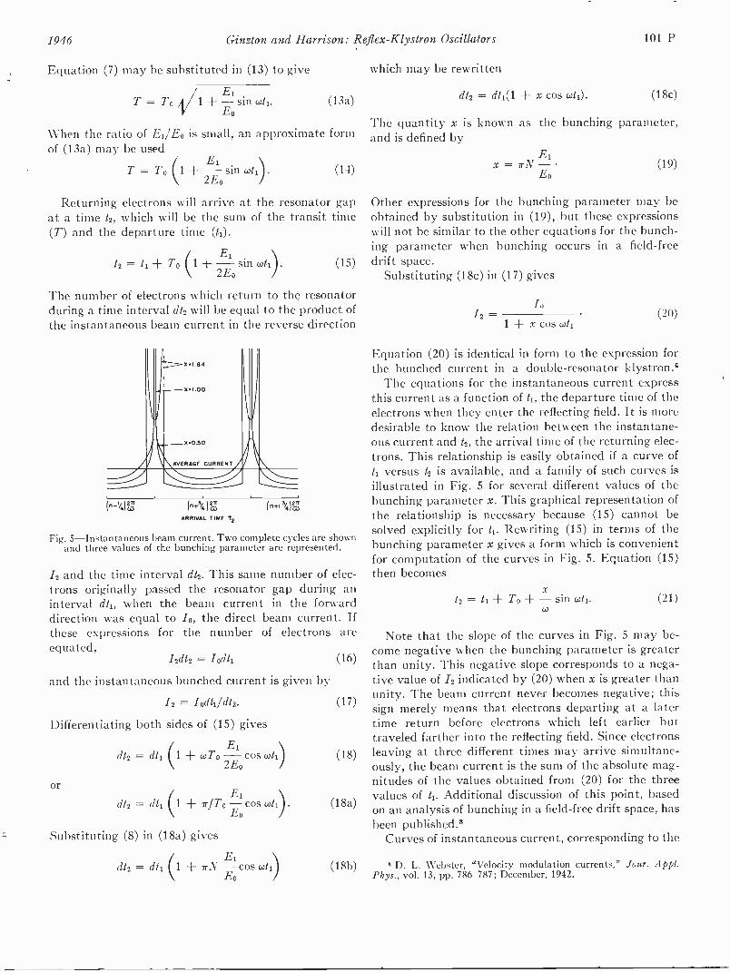
Fig. 5-Instantaneous beam current. Two complete cycles are shownand three values of the bunching parameter are represented.
12 and the time interval d12. This same number of elec-trons originally passed the resonator gap during aninterval dt1, when the beam current in the forwarddirection was equal to /0, the direct beam current. Ifthese expressions for the number of electrons areequated,
12d12 = 10d11
and the instantaneous bunched current is given
/2 = /0dt1/dt2.
Differentiating both sides of (15) gives
dt2 = d11 (1 + coT 0 - cos w11)2E0
orE1
dt2 = dt1 (1 + rfT0 - cos C011)E0
Substituting (8) in (18a) gives
E1dt2 = c111 (1 rN - cos coti)
Eo
(16)
by
(17)
/012 = (20)
1 x cos wti
Equation (20) is identical in form to the expression forthe bunched current in a double -resonator klystron.'
The equations for the instantaneous current expressthis current as a function of ti, the departure time of theelectrons when they enter the reflecting field. It is moredesirable to know the relation between the instantane-ous current and 12, the arrival time of the returning elec-trons. This relationship is easily obtained if a curve of11 versus 12 is available, and a family of such curves isillustrated in Fig. 5 for several different values of thebunching parameter x. This graphical representation ofthe relationship is necessary because (15) cannot besolved explicitly for 11. Rewriting (15) in terms of thebunching parameter x gives a form which is convenientfor computation of the curves in Fig. 5. Equation (15)then becomes
X
12 = 11 + TO - sin cal.w
(21)
Note that the slope of the curves in Fig. 5 may be-come negative when the bunching parameter is greaterthan unity. This negative slope corresponds to a nega-tive value of /2 indicated by (20) when x is greater thanunity. The beam current never becomes negative; thissign merely means that electrons departing at a latertime return before electrons which left earlier buttraveled farther into the reflecting field. Since electronsleaving at three different times may arrive simultane-ously, the beam current is the sum of the absolute mag-nitudes of the values obtained from (20) for the threevalues of 11. Additional discussion of this point, basedon an analysis of bunching in a field -free drift space, hasbeen published.'
Curves of instantaneous current, corresponding to the
(18b) 8 D. L. Webster, "Velocity modulation currents," Jour. Appi.Phys., vol. 13, pp. 786-787; December, 1942.
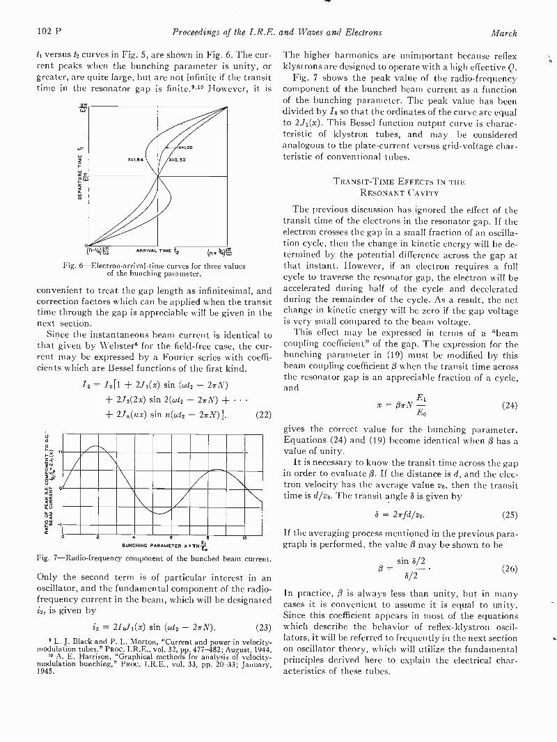
102 P Proceedings of the I.R.E. and Waves and Electrons March
/1 versus t2 curves in Fig. 5, are shown in Fig. 6. The cur-rent peaks when the bunching parameter is unity, orgreater, are quite large, but are not infinite if the transittime in the resonator gap is finite." However, it is
2
O
. ...
2,AARRIVAL. TIME t2
Fig. 6-Electron-arrival-time curves for three valuesof the bunching parameter.
convenient to treat the gap length as infinitesimal, andcorrection factors which can be applied when the transittime through the gap is appreciable will be given in thenext section.
Since the instantaneous beam current is identical tothat given by Webster6 for the field -free case, the cur-rent may be expressed by a Fourier series with coeffi-cients which are Bessel functions of the first kind.
/2 = /0[1 + 2./1(x) sin (0.42 - 2rN)
2J2(2x) sin 2(w12 - 2rN) + 2J(nx) sin n(0)/2 - 2rN)]. (22)
2 4 Q B 10
BUNCHING PARAMETER X ="ITN110
Fig. 7-Radio-frequency component of the bunched beam current.
Only the second term is of particular interest in anoscillator, and the fundamental component of the radio -
frequency current in the beam, which will be designatedi2, is given by
i2 = 2/0./1(x) sin (cot2 - 2rN). (23)
9 L. J. Black and P. L. Morton, "Current and power in velocity -modulation tubes," PROC. I.R.E., vol. 32, pp. 477-482; August, 1944.
'0 A. E. Harrison, "Graphical methods for analysis of velocity -modulation bunching," PROC. I.R.E., vol. 33, pp. 20-33; January,1945.
The higher harmonics are unimportant because reflexklystrons are designed to operate with a high effective Q.
Fig. 7 shows the peak value of the radio -frequencycomponent of the bunched beam current as a functionof the bunching parameter. The peak value has beendivided by /0 so that the ordinates of the curve are equalto 2Ji(x). This Bessel function output curve is charac-teristic of klystron tubes, and may be consideredanalogous to the plate -current versus grid -voltage char-teristic of conventional tubes.
TRANSIT -TIME EFFECTS IN THERESONANT CAVITY
The previous discussion has ignored the effect of thetransit time of the electrons in the resonator gap. If theelectron crosses the gap in a small fraction of an oscilla-tion cycle, then the change in kinetic energy will be de-termined by the potential difference across the gap atthat instant. However, if an electron requires a fullcycle to traverse the resonator gap, the electron will beaccelerated during half of the cycle and deceleratedduring the remainder of the cycle. As a result, the netchange in kinetic energy will be zero if the gap voltageis very small compared to the beam voltage.
This effect may be expressed in terms of a "beamcoupling coefficient" of the gap. The expression for thebunching parameter in (19) must be modified by thisbeam coupling coefficient (3 when the transit time acrossthe resonator gap is an appreciable fraction of a cycle,and
x = 1371-N -E1Eo
(24)
gives the correct value for the bunching parameter.Equations (24) and (19) become identical when )3 has avalue of unity.
It is necessary to know the transit time across the gapin order to evaluate O. If the distance is d, and the elec-tron velocity has the average value vo, then the transittime is d/vo. The transit angle (5 is given by
= 27rfd/vo. (25)
If the averaging process mentioned in the previous para-graph is performed, the value [3 may be shown to be
sin (5/2=
B/2(26)
In practice, is always less than unity, but in manycases it is convenient to assume it is equal to unity.Since this coefficient appears in most of the equationswhich describe the behavior of reflex-klystron oscil-lators, it will be referred to frequently in the next sectionon oscillator theory, which will utilize the fundamentalprinciples derived here to explain the electrical char-acteristics of these tubes.
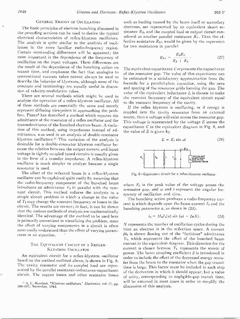
1946 Ginzton and Harrison: Reflex-Klystron Oscillators 103 P
GENERAL THEORY OF OSCILLATORS
The basic principles of electron bunching discussed inthe preceding sections can be used to derive the typicalelectrical characteristics of reflex-klystron oscillators.The analysis is quite similar to the analysis of oscil-lators in the more familiar radio -frequency region.Certain outstanding differences will be apparent; themost important is the dependence of the frequency ofoscillation on the input voltages. These differences arethe result of the dependence of the bunching action ontransit time, and emphasize the fact that analogies toconventional vacuum tubes cannot always be used todescribe the behavior of klystrons, although some of theconcepts and terminology are equally useful in discus-sion of velocity -modulation tubes.
There are several methods which might be used toanalyze the operation of a reflex-klystron oscillator. Allof these methods are essentially the same and merelyrepresent differing viewpoints in approaching the prob-lem. Pierce4 has described a method which equates theadmittance of the resonator of a reflex oscillator and thetransadmittance of the bunched electron beam. A varia-tion of this method, using impedances instead of ad-mittances, was used in an analysis of double -resonatorklystron oscillators." This variation of the analysis isdesirable for a double -resonator klystron oscillator be-cause the relation between the output current and inputvoltage in tightly coupled tuned circuits is usually givenin the form of a transfer impedance. A reflex-klystronoscillator is much simpler to analyze because a singleresonator is used.
The effect of the reflected beam in a reflex-klystronoscillator can be explained quite easily by assuming thatthe radio -frequency component of the bunched beamintroduces an admittance Y2 in parallel with the reso-nant circuit. This method reduces the analysis to asimple circuit problem in which a change in the valueof Y2 may change the resonant frequency or losses in thecircuit. The results are correct; in fact, it can be shownthat the various methods of analysis are mathematicallyidentical. The advantage of the method to be used hereis primarily convenient in visualizing the problem, sincethe effect of varying components in a circuit is oftenmore easily understood than the effect of varying param-eters in an equation.
THE EQUIVALENT CIRCUIT OF A REFLEX-KLYSTRON OSCILLATOR
An equivalent circuit for a reflex-klystron oscillatorbased on the method outlined above, is shown in Fig. 8.The cavity resonator and its coupled load are repre-sented by the parallel resistance -inductance -capacitancecircuit. The copper losses and other resonator losses
" A. E. Harrison, "Klystron oscillators," Electronics, vol. 17, pp.100-107; November, 1944.
such as loading caused by the beam itself or secondaryelectrons, are represented by an equivalent shunt re-sistance Rs, and the coupled load or output circuit con-sidered as another parallel resistance RL. Then the ef-fective resistance RSL would be given by the expressionfor two resistances in parallel
RSL =RSRL
Rs RL(27)
The equivalent capacitance C represents the capacitanceof the resonator gap. The value of this capacitance canbe estimated to a satisfactory approximation from theformula for a parallel -plate capacitor, using the areaand spacing of the resonator grids forming the gap. Thevalue of the equivalent inductance L is chosen to makethe resonant frequency of the equivalent circuit equalto the resonant frequency of the cavity.
If the reflex klystron is oscillating, or if energy iscoupled into the cavity resonator from an externalsource, then a voltage will exist across the resonator gap.This voltage is represented by the voltage E across thecapacitance C in the equivalent diagram in Fig. 8, andthe value of E is given by
E = El sin wt
EQUIVALENTADMITTANCEDUE TO THEBUNCHED REAM
Fig. 8-Equivalent circuit for a reflex-klystron oscillator.
(28)
where EI is the peak value of the voltage across theresonator gap, and (.4 and t represent the angular fre-quency of oscillation and time.
The bunching action produces a radio -frequency cur-rent i2 which depends upon the beam current /2 and thebunching parameter x, as shown in (23).
i2 = 215J,(x) sin (cot - 2rN). (23)
N represents the number of oscillation cycles during thetime an electron is in the reflection space. A current13i, is shown flowing out of the "fictitious" admittanceY2, which represents the effect of the bunched beamcurrent in the equivalent diagram. This direction for thecurrent is chosen because Y2 represents the source ofpower. The beam coupling coefficient 3 is introduced inorder to include the effect of the decreased energy trans-fer from the beam to the resonator when the gap transittime is large. This factor must be included in each stepof the derivation in which it should appear; but a valueof unity, corresponding to negligible -gap transit time,will be assumed in most cases in order to simplify thediscussion of this analysis.

104 P Proceedings of the I.R.E. and Waves and Electrons March
Admittances are used in this discussion because ad-mittances can be added when considering parallel cir-cuits. Equation (27), expressed in the form of the sumof two conductances (the real part of an admittance),would be written
1 1 1
=RsL Rs RL
(29)
The total admittance of the resonator Ys wouldthe susceptance terms for the inductance andtance as well as the conductance terms in (29).
Ys =1 1 j
jwC.Rs RL wL
includecapaci-
(30)
This form will be quite convenient in the analysis of areflex oscillator because real and imaginary terms maybe considered separately.
An evaluation of the admittance Y2 which is added tothe resonator admittance may be obtained from thefact that a voltage E must cause a current 012 to flow.The magnitude of Y2 will be determined by the ratio ofthe peak value of 012 and the peak voltage El.
213/0Ji(x)Y2 = (31)
E1
The phase of 17.2 is determined by the transit time in thereflection field. If the transit time corresponds to (n-4)cycles, where n is an integer, then the electrons in thebunch will be retarded, and the beam will transferenergy to the radio -frequency field in the resonator.This relation was explained in the discussion of Fig. 3.Under these conditions 11.2 will be a pure negative con-ductance. A transit time of (n+1) cycles corresponds toa transfer of energy from the radio -frequency field to theelectron beam, and in this case 172 is a positive conduct-ance; i.e., the beam represents an additional loss in thecircuit.
Other values of transit time cause Y2 to be complexsince the radio -frequency component of the bunchedbeam current will not be in phase with the resonatorvoltage. The phase angle of 12 will be represented by 4,and 4) will be considered zero when the transit time inthe reflection field corresponds to (n -I) cycles. Theexpression for i2 in (23) may be rewritten
i2 = 2/0./i(x) sin [cot - 2r(n - 1/4) - 0] (32)
Comparison of (23) and (32) shows that the phaseangle 4 is defined by
= 2rN - 27(n - 1/4). (33)
N may have any value and is determined by the transittime in the reflection space, but n is always an integer.If the transit time is correct for maximum output, thenthe phase angle c is zero, and N is given by (10).
N = n - 1/4. (10)
Decreasing either the acceleration voltage or the re-flector voltage increases the transit time in the reflectionspace and increases the angle ck.
It will be convenient to express 12 in the vector forminstead of the sinusoidal form in (32).
i2 = 2/0./1(x) [cos ¢ -j sin 0]. (34)
Since Y2 is a negative admittance when 4 is equal tozero, as defined in the discussion following (31), thecomplex admittance is
- /3i2 213/0/1(x)Y2 = [ cos CI) j sin (id. (35)
E1 E1
Both components of the admittance are plotted in Fig.9. The conductance, which is the real term in (35), isshown as a solid line, and the susceptance is a dash line.The vertical scale in Fig. 9 is purely arbitrary, since/0, J1(x) and El are unspecified.
CONDUCTANCECOMPONENT
REGION OF SUSCEPTANCE/0SGILL AT ION,_,,COMPONENT
%AMITY CONDUCTANCE .11-"31..
PHASE ANGLE -^
Fig. 9-Conductance and susceptance components ofthe beam admittance.
A qualitative analysis of a reflex oscillator may beobtained from inspection of Fig. 9. As the phase angleis increased from a negative value toward zero, theconductance changes from a positive value, indicating aloss, to a negative value representing a source of power.Oscillation will occur when the negative conductance isequal in magnitude to the conductance of the cavity;i.e., when the source of power is just sufficient to supplythe losses in the resonator and the load. The magnitudeof the circuit conductance is indicated by the horizontaldotted line in Fig. 9. The shaded portion shows the re-gion in which oscillation will occur.
When 4) is equal to zero, corresponding to the transittime for maximum output, the beam susceptance is zeroand the tube will oscillate at the natural frequency ofthe cavity resonator. Note that the equivalent capaci-tance of the resonator corresponds to a positive suscep-tance in (30). Increasing the phase angle until 4) ispositive introduces an additional positive susceptancein parallel with C, and the frequency of oscillation be-comes less than the natural frequency of the resonator.A negative susceptance might be considered a negativecapacitance which decreases the effect of C, or it mightbe viewed as an inductance in parallel with L. Eitherviewpoint indicates that the resonant frequency of thesystem will be increased when 4) is negative.
The value of this analysis can be demonstrated byexperimental verification of the theory. If the beam cur-rent is kept quite small so that oscillation does not
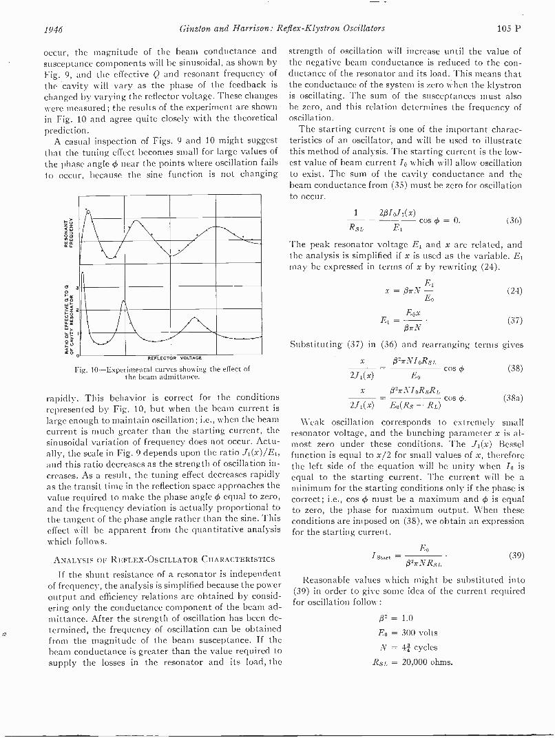
1946 Ginzton and Harrison: Reflex-Klystron Oscillators 105 P
occur, the magnitude of the beam conductance andsusceptance components will be sinusoidal, as shown byFig. 9, and the effective Q and resonant frequency ofthe cavity will vary as the phase of the feedback ischanged by varying the reflector voltage. These changeswere measured; the results of the experiment are shownin Fig. 10 and agree quite closely with the theoreticalprediction.
A casual inspection of Figs. 9 and 10 might suggestthat the tuning effect becomes small for large values ofthe phase angle ct. near the points where oscillation failsto occur, because the sine function is not changing
REFLECTOR VOLTAGE
Fig. 10-Experimental curves showing the effect ofthe beam admittance.
rapidly. This behavior is correct for the conditionsrepresented by Fig. 10, but when the beam current islarge enough to maintain oscillation; i.e., when the beamcurrent is much greater than the starting current, thesinusoidal variation of frequency does not occur. Actu-ally, the scale in Fig. 9 depends upon the ratio Ji(x)/Ei,and this ratio decreases as the strength of oscillation in-creases. As a result, the tuning effect decreases rapidlyas the transit time in the reflection space approaches thevalue required to make the phase angle ck equal to zero,and the frequency deviation is actually proportional tothe tangent of the phase angle rather than the sine. Thiseffect will be apparent from the quantitative analysiswhich follows.
ANALYSIS OF REFLEX -OSCILLATOR CHARACTERISTICS
If the shunt resistance of a resonator is independentof frequency, the analysis is simplified because the poweroutput and efficiency relations are obtained by consid-ering only the conductance component of the beam ad-mittance. After the strength of oscillation has been de-termined, the frequency of oscillation can be obtainedfrom the magnitude of the beam susceptance. If thebeam conductance is greater than the value required tosupply the losses in the resonator and its load, the
strength of oscillation will increase until the value ofthe negative beam conductance is reduced to the con-ductance of the resonator and its load. This means thatthe conductance of the system is zero when the klystronis oscillating. The sum of the susceptances must alsobe zero, and this relation determines the frequency ofoscillation.
The starting current is one of the important charac-teristics of an oscillator, and will be used to illustratethis method of analysis. The starting current is the low-est value of beam current /0 which will allow oscillationto exist. The sum of the cavity conductance and thebeam conductance from (35) must be zero for oscillationto occur.
1 2/3/0./1(x)cos cp = 0.
RSL El(36)
The peak resonator voltage E1 and x are related, andthe analysis is simplified if x is used as the variable. E1may be expressed in terms of x by rewriting (24).
E1x = 137N - (24)
Eo
EoxEl =
137rN
Substituting (37) in (36) and rearranging terms gives
x 13N-NioRsLcos (38)
2J1(x) Eo
x 13271VIoRsRL
2J1(x) Eo(Rs RL)
Weak oscillation corresponds to extremely smallresonator voltage, and the bunching parameter x is al-most zero under these conditions. The Ji(x) Besselfunction is equal to x/2 for small values of x, thereforethe left side of the equation will be unity when /0 isequal to the starting current. The current will be aminimum for the starting conditions only if the phase iscorrect; i.e., cos 4) must be a maximum and 4, is equalto zero, the phase for maximum output. When theseconditions are imposed on (38), we obtain an expressionfor the starting current.
(37)
'Start =E0
cos cp. (38a)
(39)
Reasonable values which might be substituted into(39) in order to give some idea of the current requiredfor oscillation follow:
02 = 1.0
Eo = 300 volts
N = 41 cycles
RsL = 20,000 ohms.
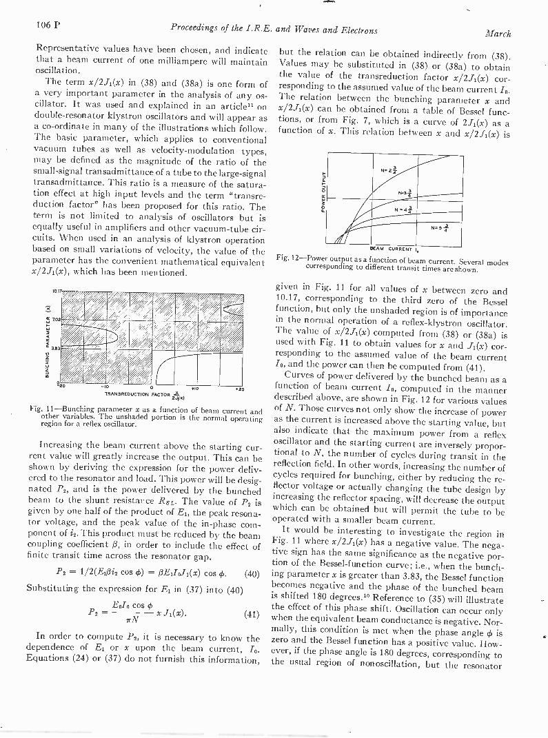
106 P Proceedings of the I.R.E. and Waves and Electrons March
Representative values have been chosen, and indicatethat a beam current of one milliampere will maintainoscillation.
The term x/24(x) in (38) and (38a) is one form ofa very important parameter in the analysis of any os-cillator. It was used and explained in an article" ondouble -resonator klystron oscillators and will appear asa co-ordinate in many of the illustrations which follow.The basic parameter, which applies to conventionalvacuum tubes as well as velocity -modulation types,may be defined as the magnitude of the ratio of thesmall -signal transadmittance of a tube to the large -signaltransadmittance. This ratio is a measure of the satura-tion effect at high input levels and the term "transre-duction factor" has been proposed for this ratio. Theterm is not limited to analysis of oscillators but isequally useful in amplifiers and other vacuum -tube cir-cuits. When used in an analysis of klystron operationbased on small variations of velocity, the value of theparameter has the convenient mathematical equivalentx/23.1(x), which has been mentioned.
10,17 , P IWZA,
42
N-10 0
TRANSREDUCTION FACTOR -212 4X)
+10 .20
Fig. 11-Bunching parameter x as a function of beam current andother variables. The unshaded portion is the normal operatingregion for a reflex oscillator.
Increasing the beam current above the starting cur-rent value will greatly increase the output. This can beshown by deriving the expression for the power deliv-ered to the resonator and load. This power will be desig-nated P2, and is the power delivered by the bunchedbeam to the shunt resistance RSL. The value of P2 isgiven by one half of the product of El, the peak resona-tor voltage, and the peak value of the in -phase com-ponent of i2. This product must be reduced by the beamcoupling coefficient )3, in order to include the effect offinite transit time across the resonator gap.
P2 = 1/ 2(E1(3i2 cos 4,) = 13E110.71(X) cos 4,. (40)
Substituting the expression for E1 in (37) into (40)
Ea.° cos 4)P2 =
rNX Jj(X). (41)
In order to compute P2, it is necessary to know thedependence of E1 or x upon the beam current, /o.Equations (24) or (37) do not furnish this information,
but the relation can be obtained indirectly from (38).Values may be substituted in (38) or (38a) to obtainthe value of the transreduction factor x/2Ji(x) cor-responding to the assumed value of the beam current /0.The relation between the bunching parameter x andx/2J1(x) can be obtained from a table of Bessel func-tions, or from Fig. 7, which is a curve of 2J1(x) as afunction of x. This relation between x and x/23 -1(x) is
BEAM CURRENT
Fig. 12-Power output as a function of beam current. Several modescorresponding to different transit times are shown.
given in Fig. 11 for all values of x between zero and10.17, corresponding to the third zero of the Besselfunction, but only the unshaded region is of importancein the normal operation of a reflex-klystron oscillator.The value of x/2J1(x) computed from (38) or (38a) isused with Fig. 11 to obtain values for x and J1(x) cor-responding to the assumed value of the beam current/0, and the power can then be computed from (41).
Curves of power delivered by the bunched beam as afunction of beam current /0, computed in the mannerdescribed above, are shown in Fig. 12 for various valuesof N. Those curves not only show the increase of poweras the current is increased above the starting value, butalso indicate that the maximum power from a reflexoscillator and the starting current are inversely propor-tional to N, the number of cycles during transit in thereflection field. In other words, increasing the number ofcycles required for bunching, either by reducing the re-flector voltage or actually changing the tube design byincreasing the reflector spacing, will decrease the outputwhich can be obtained but will permit the tube to beoperated with a smaller beam current.
It would be interesting to investigate the region inFig. 11 where x/2.Ii(x) has a negative value. The nega-tive sign has the same significance as the negative por-tion of the Bessel-function curve; i.e., when the bunch-ing parameter x is greater than 3.83, the Bessel functionbecomes negative and the phase of the bunched beamis shifted 180 degrees." Reference to (35) will illustratethe effect of this phase shift. Oscillation can occur onlywhen the equivalent beam conductance is negative. Nor-mally, this condition is met when the phase angle 4, iszero and the Bessel function has a positive value. How-ever, if the phase angle is 180 degrees, corresponding tothe usual region of nonoscillation, but the resonator
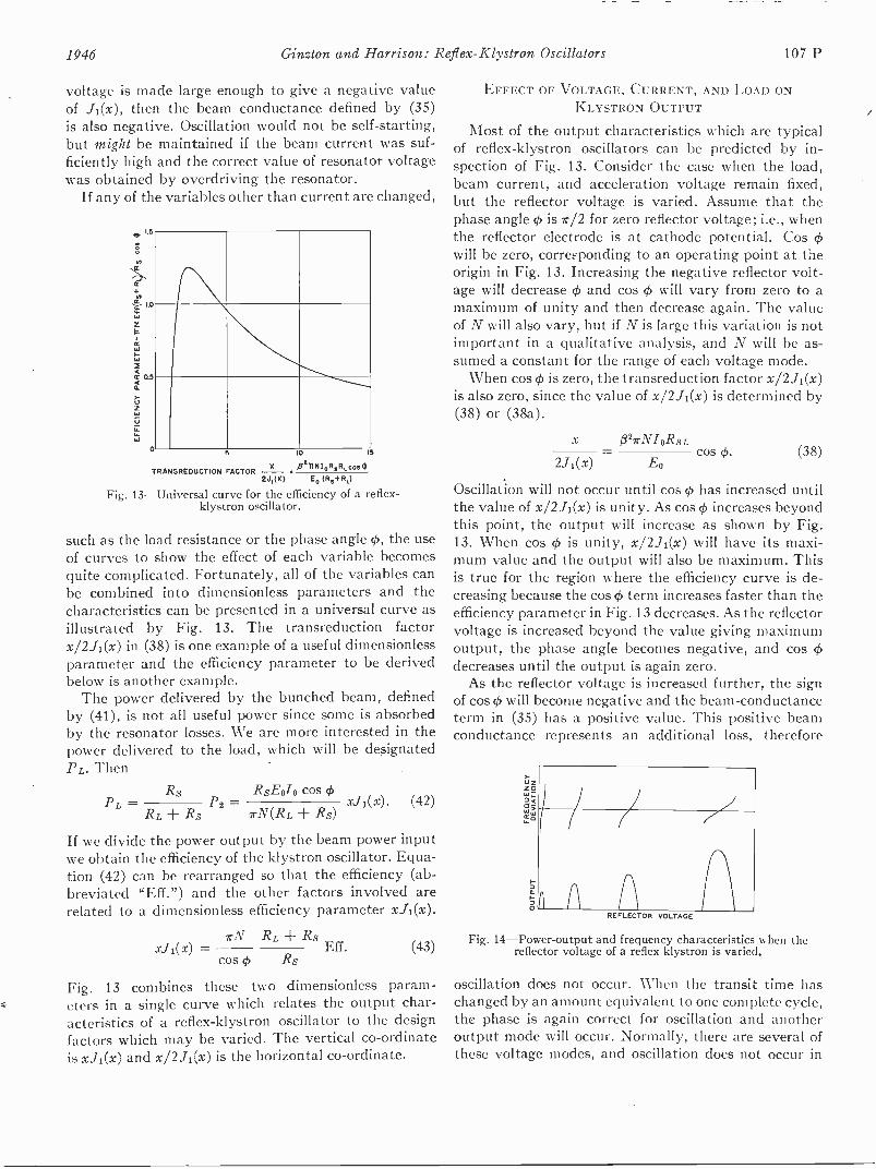
1946 Ginzton and Harrison: Reflex-Klystron Oscillators 107 P
voltage is made large enough to give a negative valueof ./1(x), then the beam conductance defined by (35)is also negative. Oscillation would not be self-starting,but might be maintained if the beam current was suf-ficiently high and the correct value of resonator voltagewas obtained by overdriving the resonator.
If any of the variables other than current are changed,
s
0
s
0 5 I0 II
TRANSREDUCTION FACTORX fitTINI.R.R,cos
2J,(X) E0 021+RO
Fig. 13-Universal curve for the efficiency of a reflex-klystron oscillator.
such as the load resistance or the phase angle 4,, the useof curves to show the effect of each variable becomesquite complicated. Fortunately, all of the variables canbe combined into dimensionless parameters and thecharacteristics can be presented in a universal curve asillustrated by Fig. 13. The transreduction factorx/2J1(x) in (38) is one example of a useful dimensionlessparameter and the efficiency parameter to be derivedbelow is another example.
The power delivered by the bunched beam, definedby (41), is not all useful power since some is absorbedby the resonator losses. We are more interested in thepower delivered to the load, which will be designated
L. Then
RS RSE0/0 cos 41FL = P2 = xJi(x). (42)
RL, ± Rs rN(RL + Rs)
If we divide the power output by the beam power inputwe obtain the efficiency of the klystron oscillator. Equa-tion (42) can be rearranged so that the efficiency (ab-breviated "Eff.") and the other factors involved arerelated to a dimensionless efficiency parameter xJi(x).
7rN RL ± RsxJi(x) = Eff.
cos 4, Rs
Fig. 13 combines these two dimensionless param-eters in a single curve which relates the output char-acteristics of a reflex-klystron oscillator to the designfactors which may be varied. The vertical co-ordinateis xJi(x) and x/2.11(x) is the horizontal co-ordinate.
(43)
EFFECT OF VOLTAGE, CURRENT, AND LOAD ONKLYSTRON OUTPUT
Most of the output characteristics which are typicalof reflex-klystron oscillators can be predicted by in-spection of Fig. 13. Consider the case when the load,beam current, and acceleration voltage remain fixed,but the reflector voltage is varied. Assume that thephase angle 4, is it/2 for zero reflector voltage; i.e., whenthe reflector electrode is at cathode potential. Cos 4,will be zero, corresponding to an operating point at theorigin in Fig. 13. Increasing the negative reflector volt-age will decrease 4) and cos 4 will vary from zero to amaximum of unity and then decrease again. The valueof N will also vary, but if N is large this variation is notimportant in a qualitative analysis, and N will be as-sumed a constant for the range of each voltage mode.
When cos 4) is zero, the transreduction factor x/2.11(x)is also zero, since the value of x/2.i1(x) is determined by(38) or (38a).
X 132Z N oR S Lcos cp. (38)
2J1(x) E0
Oscillation will not occur until cos 4) has increased untilthe value of x/2,71(x) is unity. As cos 4 increases beyondthis point, the output will increase as shown by Fig.13. When cos 4) is unity, x/2./1(x) will have its maxi-mum value and the output will also be maximum. Thisis true for the region where the efficiency curve is de-creasing because the cos 4) term increases faster than theefficiency parameter in Fig. 13 decreases. As the reflectorvoltage is increased beyond the value giving maximumoutput, the phase angle becomes negative, and cos 4decreases until the output is again zero.
As the reflector voltage is increased further, the signof cos 4, will become negative and the beam -conductanceterm in (35) has a positive value. This positive beamconductance represents an additional loss, therefore
UZZ 0t'i=
QW
0REFLECTOR VOLTAGE
Fig. 14-Power-output and frequency characteristics when thereflector voltage of a reflex klystron is varied.
oscillation does not occur. When the transit time haschanged by an amount equivalent to one complete cycle,the phase is again correct for oscillation and anotheroutput mode will occur. Normally, there are several ofthese voltage modes, and oscillation does not occur in
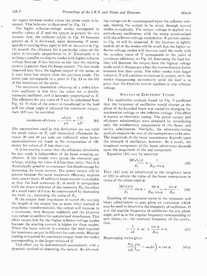
108 P Proceedings of the I.R.E. and Waves and Electrons March
the region between modes where the phase angle is in-correct. This behavior is illustrated by Fig. 14.
The higher reflector -voltage modes correspond tosmaller values of N and the output is greater for tworeasons: first, the ordinate x..11.(x) in Fig. 13 becomesgreater as N is decreased, since decreasing N corre-sponds to moving from right to left on the curve in Fig.13; second, the efficiency for a particular value on thecurve is inversely proportional to N. Eventually it isno longer possible to observe modes with higher reflectorvoltage because N has become so low that the startingcurrent is greater than the beam current. The last modeobserved may have the highest output of the series, orit may have less output than the previous mode. Thelatter case corresponds to a point in Fig. 13 to the leftof the maximum of the curve.
The maximum theoretical efficiency of a reflex-klys-tron oscillator is less than the value for a double-
resonator oscillator, and is inversely proportional to N.The efficiency for any value of N can be calculated fromFig. 13. If most of the power is transferred to the loadand the phase angle is adjusted for maximum output,then (43) may be rewritten
x./i(x) 1.25maximum efficiency =,
irN rN(44)
The assumptions used in this derivation are not validfor small values of N, and theoretical efficiencies be-tween 20 and 30 per cent are indicated when betterapproximations are made in the computation of effi-ciency for values of N less than two.
It is interesting to note that the efficiency obtainablefor any mode is independent of the beam coupling co-efficient. If the transit time across the resonator gapis large, making the value of Q less than unity, then it istheoretically possible to overcome this disadvantage byincreasing the beam current. The power output will begreater because the same maximum efficiency requiresmore power input. If sufficient beam current is availableso that the load resistance RL is small in comparisonwith the shunt resistance of the resonator Rs, the effectof a small value of (3 may be counteracted by decreasingthe load; i.e., increasing the value of RL.
If the output load impedance is varied (by varyingthe length of the output line or some other method ofimpedance transformation), the output will increase toa maximum, then decrease suddenly and the klystronmay refuse to oscillate for certain load impedances. Thiseffect occurs first for the higher reflector -voltage modesbecause the starting current is higher for these modes.When the beam current is constant the load requiredfor maximum output is different for each mode. Heavierloading is required for maximum output from the modescorresponding to the larger values of N.
This effect can be demonstrated conveniently with adynamic method of observing the output. An alternat-
ing voltage can be superimposed upon the reflector volt-age, causing the output to be swept through severalmodes periodically. The output voltage is applied to acathode-ray oscilloscope with the sweep synchronizedwith the reflector -voltage modulation. A pattern similarto Fig. 14 will be observed. If the klystron is lightlyloaded, all of the modes will be small, but the higher re-flector -voltage modes will increase until the mode withthe smallest value of N corresponds to the point ofmaximum efficiency on Fig. 13. Increasing the load fur-ther will decrease the output from the highest voltagemode until it disappears when the transreduction factorbecomes less than unity. The other modes with largervalues of N will continue to increase in output, with themodes disappearing successively until the load is sogreat that the klystron cannot oscillate at any reflectorvoltage.
ANALYSIS OF ELECTRONIC TUNING
The qualitative analysis based on Fig. 9 predictedthat the frequency of oscillation would change as thephase of the bunched beam was varied by changing theacceleration voltage or the reflector voltage. This effectis known as electronic tuning. The power output andefficiency relationships were obtained by consideringonly the conductance components of the beam andcavity admittances. Similarly, the electronic -tuninganalysis requires the sum of the susceptances to be zero.The magnitude of the beam susceptance depends uponthe strength of oscillation, however. As a result, theimaginary component of the beam admittance dependsupon the magnitude of the real component.
Equation (36) may be rewritten
2(3/0./i(x) 1
(45)E1 RsL cos 4,
Then (45) may be substituted in the imaginary termof (35) to obtain the value of the beam susceptance interms of the phase angle 4.
213/0J1(x) sin ¢ tansin 4, = (46)
El RSL cos 4, RSL
Equating all susceptance terms in the resonator andbeam admittances to zero gives an expression whichmay be used to determine the frequency of oscillation. Ifw is the angular frequency of oscillation for any phaseangle, and coo is the angular frequency corresponding tozero phase; i.e., the resonant frequency of the cavity,then
1
wCwL
Rearranging terms gives
Rsz,
cooL
tan ct,= 0.
RSL(47)
ww0LC) = tan cp. (47a)
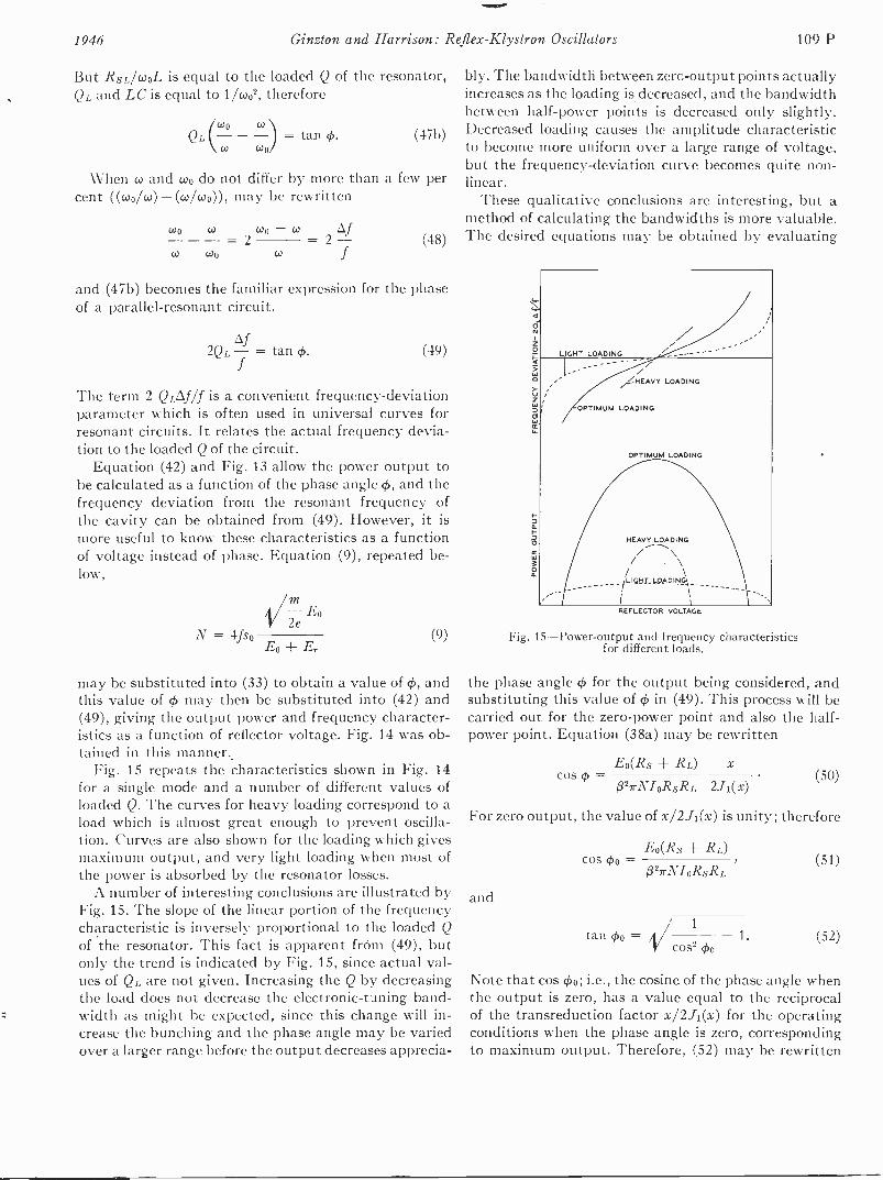
1946 Ginzton and Harrison: Reflex-Klystron Oscillators 109 P
But RsL/cooL is equal to the loaded Q of the resonator,QL and LC is equal to 1/co02, therefore
o
Qco w(- - = tan 4) .
co coo
(47b)
When co and coo do not differ by more than a few percent ((coo/co) - (co/coo)), may be rewritten
wo
w coo
wo-w Af= 2 = 2 -cof (48)
and (47b) becomes the familiar expression for the phaseof a parallel -resonant circuit.
Af2QL -= tan 4,. (49)
The term 2 QL.Aflf is a convenient frequency -deviationparameter which is often used in universal curves forresonant circuits. It relates the actual frequency devia-tion to the loaded Q of the circuit.
Equation (42) and Fig. 13 allow the power output tobe calculated as a function of the phase angle 0, and thefrequency deviation from the resonant frequency ofthe cavity can be obtained from (49). However, it ismore useful to know these characteristics as a functionof voltage instead of phase. Equation (9), repeated be-low,
N = 4fsom-2e
Eo
Eo+Er(9)
may be substituted into (33) to obtain a value of 4,, andthis value of 4, may then be substituted into (42) and(49), giving the output power and frequency character-istics as a function of reflector voltage. Fig. 14 was ob-tained in this manner.,
Fig. 15 repeats the characteristics shown in Fig. 14for a single mode and a number of different values ofloaded Q. The curves for heavy loading correspond to aload which is almost great enough to prevent oscilla-tion. Curves are also shown for the loading which givesmaximum output, and very light loading when most ofthe power is absorbed by the resonator losses.
A number of interesting conclusions are illustrated byFig. 15. The slope of the linear portion of the frequencycharacteristic is inversely proportional to the loaded Qof the resonator. This fact is apparent from (49), butonly the trend is indicated by Fig. 15, since actual val-ues of QL are not given. Increasing the Q by decreasingthe load does not decrease the electronic -tuning band-width as might be expected, since this change will in-crease the bunching and the phase angle may be variedover a larger range before the output decreases apprecia-
bly. The bandwidth between zerc-output points actuallyincreases as the loading is decreased, and the bandwidthbetween half -power points is decreased only slightly.Decreased loading causes the amplitude characteristicto become more uniform over a large range of voltage,but the frequency -deviation curve becomes quite non-linear.
These qualitative conclusions are interesting, but amethod of calculating the bandwidths is more valuable.The desired equations may be obtained by evaluating
0N
z
0
IGHT LOADING
...-41EAVY LOADING
PTIMUM LOADING
OPTIMUM LOADING
HEAVY LOADING------./ \/
, \/ \
/LIGHT LOADING_ __
iREFLECTOR VOLTAGE
Fig. 15-Power-output and frequency characteristicsfor different loads.
the phase angle 4, for the output being considered, andsubstituting this value of 4) in (49). This process will becarried out for the zero -power point and also the half -power point. Equation (38a) may be rewritten
Eo(Rs RL) xcos 4) = (50)
/3271-N/oRsRL 2./1(x)
For zero output, the value of x/2./1(x) is unity; therefore
and
cos cboEo(Rs RL)
0271 -NI oRsRL
tan cko =1
1.icos2 cbo
(51)
(52)
Note that cos 00; i.e., the cosine of the phase angle whenthe output is zero, has a value equal to the reciprocalof the transreduction factor x/2J1(x) for the operatingconditions when the phase angle is zero, correspondingto maximum output. Therefore, (52) may be rewritten
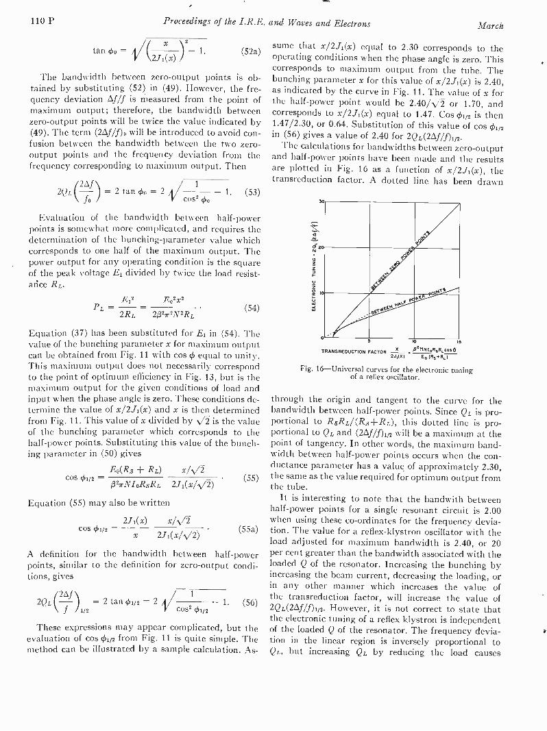
110 P Proceedings of the I.R.E. and Waves and Electrons March
tan 4)0 = /1/(:(x)
2
1. (52a)
The bandwidth between zero -output points is ob-tained by substituting (52) in (49). However, the fre-quency deviation Af/f is measured from the point ofmaximum output; therefore, the bandwidth betweenzero -output points will be twice the value indicated by(49). The term (20f/f)0 will be introduced to avoid con-fusion between the bandwidth between the two zero-
output points and the frequency deviation from thefrequency corresponding to maximum output. Then
2QL = 2 tan 44, = 2 4/ 1cost q501. (53)
Evaluation of the bandwidth between half -powerpoints is somewhat more complicated, and requires thedetermination of the bunching -parameter value whichcorresponds to one half of the maximum output. Thepower output for any operating condition is the squareof the peak voltage E1 divided by twice the load resist-arice RL.
E12 E02x2Pt =
2RL 2(322r2N2RL(54)
Equation (37) has been substituted for E1 in (54). Thevalue of the bunching parameter x for maximum outputcan be obtained from Fig. 11 with cos 4) equal to unity.This maximum output does not necessarily correspondto the point of optimum efficiency in Fig. 13, but is themaximum output for the given conditions of load andinput when the phase angle is zero. These conditions de-termine the value of x/2J1(x) and x is then determinedfrom Fig. 11. This value of x divided by N is the valueof the bunching parameter which corresponds to thehalf -power points. Substituting this value of the bunch-ing parameter in (50) gives
Eo(Rs
13271-NIoRsRLcos 4,1/2 -
Equation (55) may also be written
2./1(x) x/N/2
x 2.1.1(x/0)
A definition for the bandwidth between half -powerpoints, similar to the definition for zero -output condi-tions, gives
cos 441/2 =
x/02J1(x/1/2)
(55)
2QL1/2
= 2 tan 4)1/2 = 2/ 1
'V cost 01,2
(55a)
1. (56)
These expressions may appear complicated, but theevaluation of cos 01/2 from Fig. 11 is quite simple. Themethod can be illustrated by a sample calculation. As-
sume that x/2J1(x) equal to 2.30 corresponds to theoperating conditions when the phase angle is zero. Thiscorresponds to maximum output from the tube. Thebunching parameter x for this value of x/2J1(x) is 2.40,as indicated by the curve in Fig. 11. The value of x forthe half -power point would be 2.40N2 or 1.70, andcorresponds to x/2J1(x) equal to 1.47. Cos Om is then1.47/2.30, or 0.64. Substitution of this value of cos 4)1/2in (56) gives a value of 2.40 for 2QL(20f/f)1/2.
The calculations for bandwidths between zero -outputand half -power points have been made and the resultsare plotted in Fig. 16 as a function of x/2J1(x), thetransreduction factor. A dotted line has been drawn
30
07.20
43
z
U
10 1415PO
sc,
5 10 15
TRANSREDUCTION FACTORX /3t1INI.R.R..cos
2J,(X) E. (Its+III0
Fig. 16-Universal curves for the electronic tuningof a reflex oscillator.
through the origin and tangent to the curve for thebandwidth between half -power points. Since QL is pro-portional to RsRLARs-ERL), this dotted line is pro-portional to QL and (26tUni/2 will be a maximum at thepoint of tangency. In other words, the maximum band-width between half -power points occurs when the con-ductance parameter has a value of approximately 2.30,the same as the value required for optimum output fromthe tube.
It is interesting to note that the bandwith betweenhalf -power points for a single resonant circuit is 2.00when using these co-ordinates for the frequency devia-tion. The value for a reflex-klystron oscillator with theload adjusted for maximum bandwidth is 2.40, or 20per cent greater than the bandwidth associated with theloaded Q of the resonator. Increasing the bunching byincreasing the beam current, decreasing the loading, orin any other manner which increases the value ofthe transreduction factor, will increase the value of2QL(20f/f)1/2. However, it is not correct to state thatthe electronic tuning of a reflex klystron is independentof the loaded Q of the resonator. The frequency devia-tion in the linear region is inversely proportional toQL, but increasing QL by reducing the load causes
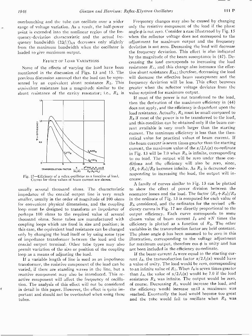
1946 Ginzton and Harrison: Reflex-Klystron Oscillators 111 P
overbunching and the tube can oscillate over a widerrange of voltage variation. As a result, the half -powerpoint is extended into the nonlinear region of the fre-quency -deviation characteristic and the actual fre-quency bandwidth (24/f)1/2 decreases only slightlyfrom the maximum bandwidth when the oscillator isloaded to give maximum output.
EFFECT OF LOAD VARIATIONS
Some of the effects of varying the load have beenmentioned in the discussion of Figs. 13 and 15. Theprevious discussion assumed that the load can be repre-sented by an equivalent shunt resistance RL. Thisequivalent resistance has a magnitude similar to theshunt resistance of the cavity resonator; i.e., RL is
.0
n
.713 le=2013
=ins5 10 IS
TRANSREOUCTION FACTORX ,821iNI.R.Rocts
2J,(X) E, Ois+RO
Fig. 17-Efficiency of a reflex oscillator as a function of load.Curves for three values of beam current are shown.
usually several thousand ohms. The characteristicimpedance of the coaxial output line is very muchsmaller, usually in the order of magnitude of 100 ohmsfor convenient physical dimensions, and the couplingloop must be designed to transform an impedance ofperhaps 100 ohms to the required value of severalthousand ohms. Some tubes are manufactured withcoupling loops which are fixed in size and position; inthis case, the equivalent load resistance can be changedonly by changing the load itself or by using some typeof impedance transformer between the load and thecoaxial output terminal. Other tube types may alsopermit variation of the size or position of the couplingloop as a means of adjusting the load.
If a variable length of line is used as an impedancetransformer, the resistive component of the load can bevaried, if there are standing waves in the line, but areactive component may also be introduced. This re-active component will affect the frequency of oscilla-tion. The analysis of this effect will not be consideredin detail in this paper. However, the effect is quite im-portant and should not be overlooked when using thesetubes.
Frequency changes may also be caused by changingonly the resistive component of the load if the phaseangle is not zero. Consider a case illustrated by Fig. 15when the reflector voltage does not correspond to theadjustment for maximum output and the frequencydeviation is not zero. Decreasing the load will decreasethe frequency deviation. This effect is also indicatedby the magnitude of the beam susceptance in (47). De-creasing the load corresponds to increasing the loadresistance RL, and this change also increases the effec-tive shunt resistance RRL; therefore, decreasing the loadwill decrease the effective beam susceptance and thefrequency deviation will be less. This effect becomesgreater when the reflector voltage deviates from thevalue required for maximum output.
If most of the power is not transferred to the load,then the derivation of the maximum efficiency in (44)does not apply, and the efficiency is dependent upon theload resistance. Actually, RL must be small compared toRs if most of the power is to be transferred to the load,and this condition can be obtained only if the beam cur-rent available is very much larger than the startingcurrent. The maximum efficiency is less than the theo-retical value for practical values of beam current. Ifthe beam current is seven times greater than the startingcurrent, the maximum value of the x/2./i(x) co-ordinatein Fig. 13 will be 7.0 when RL is infinite, correspondingto no load. The output will be zero under these con-ditions and the efficiency will also be zero, since,(RL-ERs)/Rs becomes infinite. As RL is decreased cor-responding to increasing the load, the output will in-crease.
A family of curves similar to Fig. 13 can be plottedto show the effect of power division between theresonator losses and the load. The factor (RL+Rs)/Rsin the ordinate of Fig. 13 is computed for each value ofRL considered, and the ordinates for the revised effi-ciency curves in Fig. 17 are directly proportional to theoutput efficiency. Each curve corresponds to somechosen value of beam current /0 and 7rN times theefficiency is plotted as a function of RL. The othervariables in the transreduction factor are held constant.The phase angle ck has been assumed to be zero in thisillustration, corresponding to the voltage adjustmentfor maximum output, therefore cos q is unity and hasnot been included in the efficiency co-ordinate.
If the beam current /0 were equal to the starting cur-rent /s, the transreduction factor x/2./1(x) would havea value of unity. The load would be zero, correspondingto an infinite value of RL. When /0 is seven times greaterthan Is, the value of x/2.7.1(x) would be 7.0 if the loadresistance RL was infinite. The output would be zero,of course. Decreasing RL would increase the load, andthe efficiency would increase until a maximum wasreached. Eventually the load would become too greatand the tube would fail to oscillate when RL was
112 P Proceedings of the I.R.E. and Waves and Electrons March
reduced until x/2.11(x) had a value of unity. Similarcurves are shown for values of /0 twelve and twentytimes greater than the starting current. Note that theactual efficiency is only 90 per cent of the theoreticalefficiency when the beam current is twenty times greaterthan the starting current.
Fig. 17 may also be used to compare the efficienciesfor different values of N when the beam current re-mains constant. These conditions can be met by chang-ing the reflector voltage. Consider that the curve inFig. 17 for seven times the starting current correspondsto a value of N equal to 21 cycles, and the curve for12 times the starting current corresponds to the samebeam current but a value of 44 cycles for N. Thenthe actual efficiency for optimum loading would be0.87/2.757r or 10.1 per cent for N equal to 21 cycles,and 1.01/4.75r or 6.8 per cent for N equal to 41 cycles.Although the loading required for maximum output isless for the mode with the shorter transit time, andtherefore a larger proportion of the total power isdissipated in the resonator losses, the improved con-version efficiency for the shorter transit time allows theoutput efficiency to be greater.
REFLEX-KLYSTRON DESIGN CONSIDERATIONS
Most of the previous discussion has been used topredict or explain the electrical characteristics of re-flex-klystron oscillators when operating voltages, cur-rent, and loading were the only variables. It is inter-esting to consider the effect of varying the design of thetube itself, although it is necessary to remember thatthe relation between the lumped constants used in theequivalent circuit and the physical dimensions of thecavity resonator is not clearly defined. However, con-sidering the effect of changing these constants can bequite useful in a qualitative analysis of the factors whichare important in the design of klystrons.
Reference to the equivalent circuit in Fig. 8 will indi-cate that increasing the ratio of the small -signal beamadmittance to the circuit capacitance will increase theamount of electronic tuning. This ratio may be increasedby increasing the beam current /0, increasing the transittime in the reflection space (increasing the value of N),or by decreasing the circuit capacitance. Decreasing thecapacitance by increasing the resonator -gap spacingmay not be satisfactory because the transit time acrossthe gap may become excessive. This change would re-duce the beam coupling coefficient, which has the sameeffect as reducing the beam current. Therefore we willonly consider reducing the capacitance by decreasingthe area of the resonator gap.
Either increasing the beam current without changingthe capacitance, or reducing the area of the gap withoutchanging the current, corresponds to increasing thecurrent density. Therefore the problem of increasingthe electronic tuning in a klystron design becomes a
problem of increasing the current density. This con-clusion assumes that N is already large and that addi-tional transit time in the reflection space will not in-crease N appreciably.
It is equally interesting to analyze the factors affect-ing electronic tuning from the viewpoint that increasedelectron bunching permits heavier loading of the oscil-lator, and therefore increases the electronic tuning be-cause the loaded Q has been reduced. Reference toFigs. 11 and 13 will emphasize the fact that the bunch-ing parameter x has a value of 2.40 when the oscillatoris adjusted for maximum output. If the beam currentis increased, with no design change in the resonator, theresonator voltage E1 will be increased and the value ofthe bunching parameter will increase. The magnitude ofE1 is determined by the radio -frequency current i2 andthe loaded shunt resistance RsL.
E1 = 2/oRsL./1(x). (57)
Since E1 must be constant if x remains constant, anincrease in /0 must be accompanied by a decrease in theloaded shunt resistance RSL. Therefore the increasedbeam current permits the oscillator to be operated witha greater load, and reducing the Q of the loaded circuitincreases the electronic tuning.
The effect of decreasing the capacitance may also berelated to the loaded Q of the resonator. One of therelations giving the Q of a circuit is
RsRLQL = ("JCRs', = coC (58)
Rs ± RL
The unloaded Q of the circuit will be
Q = coCRs,
therefore (58) may be rewritten
QL = Q Rs ±RL
(59)
(60)
Decreasing the circuit capacitance by reducing theresonator -gap area without changing the gap spacingdoes not change the unloaded Q appreciably, but doesincrease the shunt resistance Rs. This change will notaffect the loaded shunt resistance RSL, since RL isusually much smaller than Rs; therefore, the oscillatorwill operate with the same degree of bunching if thebeam current and the load resistance RL are unchangedHowever, (60) indicates that the loaded Q will decreasewhen the shunt resistance is increased, and the elec-tronic tuning will be increased.
Note that the changes discussed in all of the pre-ceding paragraphs correspond to increasing the curentdensity in the electron beam. The various explanationsof the electronic tuning are merely different ways oflooking at the problem.
1946 Ginzton and Harrison: Reflex-Klystron Oscillators 113 P
The design of an efficient, high -power reflex-klystronoscillator would require a different approach. The im-portant design factor would be the transit time in thereflection space, therefore N must be small. As pointedout in the discussion of (44), the analysis is not validfor small values of N, but the trend is indicated cor-rectly. Decreasing N increases the starting current, andif the beam current is already as large as permitted bya practical design, then the load required for optimumoutput cannot be very great and the electronic tuningwill be small. It is also apparent that the theoreticalefficiency will not be attained if a large part of the totalpower goes into the resonator losses. In spite of thisfactor, however, the efficiency will be greater than thatof a reflex klystron designed for a larger value of N. Ifit were possible to increase the beam current sufficientlyso that most of the power could be transferred to theload, then the klystron would have as much electronictuning as a design with a larger value of N and smallerbeam current.
ACKNOWLEDGMENT
The presentation of reflex -oscillator characteristicswith universal curves, and the form of these curves,were suggested in an unpublished report by D. R.Hamilton. Credit is also due G. E. Hackley for some ofthe experimental work which verified the theory.
APPENDIX I
GLOSSARY OF SYMBOLS
Eo =beam voltage or acceleration voltage.Er =reflector voltage (voltage between cathode and
reflector electrode).Eo =control -grid voltage.E =instantaneous value of radio -frequency voltage
across resonator gap.E1 =peak value of radio -frequency voltage across
resonator gap./0 =average beam current (value of direct current)./start= minimum value of beam current required to
maintain oscillation/2 =instantaneous value of bunched beam current.i2 =fundamental component of radio -frequency cur-
rent in the bunched beam.c/7 =phase angle of bunched beam current.v = velocity of an electron.vo =average velocity of an electron (corresponds to
Eo).s =distance measured from resonator gap.so =spacing between resonator gap and reflector elec-
trode.F =retarding force due to reflecting field.
a =deceleration caused by retarding force F.e =charge of an electron.m = mass of an electron.t =time.ti =departure time when an electron leaves the reso-
nator gap.t2 =arrival time when an electron returns to the
resonator.T = transit time in the reflection field.To = transit time in the reflection field of an electron
with average velocity vo.N =number of oscillation cycles during transit of the
reflection space.f = frequency of oscillation.co = 271-f.
coo = 27r times the resonant frequency of the cavity.
x = bunching parameter equal to 137rNE-0.
.1. =Bessel function of first kind and nth order.J1 =Bessel function of first kind and first order.d =spacing of resonator gap.
= transit angle across the resonator gap.
sin 6/2=moudlation coefficient equal to
6/2
Rs =shunt resistance of the cavity resonator.RL =equivalent load resistance.Rsr, = loaded shunt resistance of the cavity resonator.L =equivalent inductance of the cavity resonator.C =equivalent capacitance of resonator gap.Q =unloaded Q of the cavity resonator.QL =loaded Q of the cavity resonator.Y8 = total admittance of the cavity resonator.112 = equivalent admittance due to the bunched beam.P2 =power delivered to the resonator and load.FL =power delivered to the load.Eff. =efficiency (ratio of radio -frequency output power
to beam -power input).x/2J1(x) =transreduction factor (magnitude of the
ratio of small -signal transadmittanceto large -signal transadmittance).
x./1 (x) =universal efficiency parameter for reflexklystrons.
=frequency deviation from resonant fre-quency of the cavity.
bandwidth between zero -power -outputpoints.
2QL(20fif)7/7= bandwidth between half -power points(frequently called electronic -tuningbandwidth).
2Q LAM
2Q L(2Af /Do
The Transmission of a Frequency -ModulatedWave Through a Network*
WALTER J. FRANTZt, ASSOCIATE, I.R.E.
Summary-A practical method for calculating the effect of a four -terminal network upon a frequency -modulated wave being trans-mitted through it is developed and demonstrated. The form of thesolution is simple enough to be applied by anyone familiar with elec-tric circuits. No knowledge of calculus or higher mathematics is re-quired; nor is the solution restricted in any way, being equally accu-rate and practical for large and small values of modulation index, andfor any physical network.
In order to determine whether or not a particular network prob-lem involving a frequency -modulated input wave may be analyzedfrom the "instantaneous frequency" viewpoint, a test, or validitycondition, has been developed. This test quickly classifies the prob-lem either as one for which only a complete, straightforward analysisdetermines the response, or as one for which a quasi -steady stateexists. The quasi -steady state is a condition under which the ampli-tude-instantaneous-input-frequency envelope and the phase-shift-instantaneous-input-frequency envelope of the output wave approachclosely enough to the steady-state-amplification-frequency andphase-shift-frequency characteristics of the network.
INTRODUCTION
ITH THE increasing use of a frequency -modu-lated wave for circuit alignment and test, spec-trum analysis, altitude or time -delay measure-
ment, and the transmission of intelligence, there arisesthe need for a practical and dependable method of cal-culating the response of a network to a frequency -modulated input wave.
Suppose that it is desired to picture accurately thesteady-state amplification-frequency characteristic ofa tuned one -megacycle amplifier with an effective Q of100. The layout of Fig. 1 is often used for visual circuittest and alignment in the communications industry.
'NEE,64-ner.eAroe
SUSPECT1 Nf r NORR
AA000ZATIAILiVOLTAGE
GENERATOR
OSCILLOSCOPE
Fig. 1-Block layout of a visual network test and alignment position.
Since the modulating voltage is applied also to thehorizontal plates of the oscilloscope, the horizontal axisis linear in instantaneous frequency of the input fre-quency -modulated wave. In Fig. 2, (a) is the oscillogramobtained when the frequency -modulated signal gen-erator is operating at a center frequency of one mega-cycle, a total sweep width of 50 kilocycles, and a modu-
* Decimal classification: R414 X R140. Original manuscript re-ceived by the Institute, May 28, 1945; revised manuscript received,October 23, 1945.
RCA Laboratories, Princeton, N. J.
lating frequency of 100 cycles per second; the amplifica-tion-frequency characteristic of the amplifier has beenfairly well pictured. If the modulating frequency is in-creased to 1000 cycles per second, the pattern (b) de-parts considerably from the steady-state amplification-frequency characteristic of the network. The twotraces are the frequency upsweep and the downsweep.The upsweep trace leans to the right and the down -
sweep trace leans to the left. In Fig. 2, (c) is the oscillo-gram obtained for a total sweep width of 150 kilocyclesand a modulating frequency of 333 cycles per second,while (d) is the oscillogram obtained for a total sweepwidth of 150 kilocycles and a modulating frequency of1000 cycles per second.
These oscillograms will be referred to quantitativelylater in the article. They are presented here only topersuade those unfamiliar with the problem that it isreal, important, and frequently encountered. The prob-lem is probably given the most attention by the de-signers of high -quality frequency -modulated transmit-ters and receivers.
It is the purpose of this paper devise a simple test bywhich one may determine whether or not the effects ofa network upon a frequency -modulated wave beingtransmitted through it differ appreciably from thesteady-state amplification-frequency and phase -shift-frequency characteristics of the network, and, if so,to offer a general and practical method of calculatingthese effects as a function of either time or instantaneousinput frequency.
THE RESPONSE -ENVELOPE EQUATION
The following procedure is a rigorous and generalmethod of obtaining the output -voltage envelope for anetwork driven by a frequency -modulated wave:
1. Measure or calculate the steady-state amplifica-tion-frequency and phase-shift-frequency character-istics of the network in question.
2. Express the frequency -modulated input wave interms of its steady-state spectrum of sinusoidal side fre-quencies.
3. Pass the individual side frequencies through thenetwork, altering the amplitude and phase of each ac-cording to the steady-state amplification and phasecharacteristics of the network at the particular fre-quency of the side frequency.
4. Plot the sum of the altered side frequencies pointby point to obtain the output wave as a function of time.
5. Draw a smooth curve through the carrier -voltagepeaks to obtain the response envelope of the outputvoltage.
114 P Proceedings of the I.R.E. and Waves and Electrons March, 1946
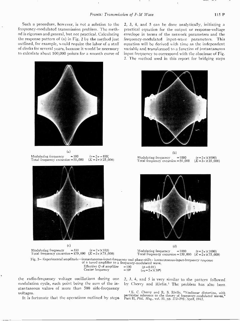
Frantz: Transmission of F -M Wave 115 P
Such a procedure, however, is not a solution to thefrequency -modulated transmission problem. The meth-od is rigorous and general, but not practical. Calculatingthe response pattern of (a) in Fig. 2 by the method justoutlined, for example, would require the labor of a staffof clerks for several years, because it would be necessaryto calculate about 100,000 points for a smooth curve of
(a)
Modulating frequency =100 (v =2r = 100)Total frequency excursion =50,000 (K =2 r X25,000)
(c)
Modulating frequency =333 (v=2 r X333)Total frequency excursion =150,000 (K =2 r X75,000)
2, 3, 4, and 5 can be done analytically, initiating apractical equation for the output or response -voltageenvelope in terms of the network parameters and thefrequency -modulated input -wave parameters. Thisequation will be derived with time as the independentvariable and transformed to a function of instantaneousinput frequency to correspond with the abscissae of Fig.2. The method used in this report for bridging steps
(b)
Modulating frequency =1000 (v=27 X1000)Total frequency excursion = 50,000 (K= 2 r X 25,000)
(d)
Modulating frequency =1000 (v=2rX1000)Total frequency excursion =150,000 (K =2 r X75,000)
Fig. 2-Experimental amplitude-instantaneous-input-frequency and phase-shift-instantaneous-input-frequency responseof a tuned amplifier to a frequency -modulated wave.
Effective Q of amplifier =100 (p =0.01)Center frequency =106 (wo=2rX106)
the radio -frequency voltage oscillations during onemodulation cycle, each point being the sum of the in-stantaneous values of more than 500 side -frequencyvoltages.
It is fortunate that the operations outlined by steps
2, 3, 4, and 5 is very similar to the pattern followedby Cherry and Rivlin.1 The problem has also been
I E. C. Cherry and R. S. Rivlin, "Nonlinear distortion, withparticular reference to the theory of frequency -modulated waves,"Part II, Phil. Mag., vol. 33, pp. 272-293; April, 1942.
116 P Proceedings of the I.R.E. and Waves and Electrons March
considered by Kulp, who developed a solution which ispractical when the modulation index of the frequency -modulated input wave is sma11.2
First a unit frequency -modulated wave is defined. Theequations derived in this paper are based upon unitmagnitude of the input signal.
coo = 27 X the center frequency
K = 27r X the frequency deviation
v = 27r X the modulating frequency
KInf = -= the modulation index
= coo K cos vt = 27r
X the instantaneous input frequency.
It has been shown that3
ein = sin (coot + mf sin vt)
= Jo(mf) sin coot
00
+ E (J2,i(n1) { sinn=1
- sin Iwo - (2n - 1)v]t}
[coo + (2n - 1)v]t
+ J2.(m1) { sin [coo + 2nv]t + sin [coo - 2nv]t} ). (6)
The series (6) is absolutely convergent, allowing theconvenience of a partial summation with any desiredaccuracy.
ein Jo(mf) sin coot
E (J2._,(ni1) { sinn=1
- sin Iwo - (2n - 1)v]t}
[coo + (2n - 1)v]t
J2.(m1) I sin [coo + 2nv]t + sin [coo - 2nv[tI). (7)
The choice of N depends upon m1 and the accuracy re-quired of the analysis. The choice of N is not ordinarilydifficult, because the Bessel coefficients of the series be-come negligible rather abruptly for a given argumentas the order is increased beyond a certain value. Forexample, J (10,000)'s are relatively important up ton =10,000 and slightly above, but are insignificant be-yond n =10,050.
For pure sinusoidal input of angular velocity co to alinear network, the output wave can differ from the in-put wave only in amplitude and phase. By the rules ofalgebraic steady-state circuit analysis Emit can be ex-pressed in general as the product of Ein and a complexfunction of co. (See Appendix.)
2 M. Kulp, "Spektra und Klirrfaktoren frequenz- und ampli-tudenmodulierter Schwingungen," Part II, Elek. Nach. Tech., vol. 19,pp. 96-109; June, 1942.
3 John R. Carson, "Notes on the theory of modulation," PROC.I.R.E., vol. 10, pp. 57-64; February, 1922
Eout = Einf(w) (8)
where
amplitude of EuutI f(w) I =
and where
amplitude of Ei.
imaginary If(co)arc tangent = angular phase [.E.,c1
real [f(co)]
(9)
- angular phase [Ein] (10)
The f(co) is a dimensionless transfer -voltage ratio. If/out were used instead of Eout, f(co) would be the transferadmittance.
The next step is to approximate f(co) by a finiteFourier series about coo in a period Cl equal to or greaterthan the interval containing the side -frequency voltageof (7). From (7) it is obvious that this interval extendsfrom (coo-2Nv) to (coo +2Nv), a total width of 4Nv.
f(co) E (Am cos (co - coolm -o
rm+ B, sin
2(tocoo)]). (11)
The notation -A-.; used in (11) means "approximatelyequals only in the interval (coo - 2Nv) <w < (coo+2Nv)."It is sufficient that the partial sum represent the func-tion only in the interval (coo - 2Nv) <co 5 (co0+2Nv) sinceN has previously been chosen large enough that onlyrelatively insignificant side frequencies of the frequency -modulated input voltage lie outside that interval. Thechoice of M depends upon the accuracy with which it isdesired to approximate f(co) and the nature of f(co).
The reason for expressing f(co) as a series approxima-tion is to make the method general. If an analytical solu-tion to steps 2, 3, 4, and 5 can be obtained for the termsof the series approximation, the problem is then solvedfor any f(co), since any physical network characteristiccan be approximated by such a finite series as (11). TheFourier series was chosen in preference to other seriesapproximations because the analytical solution to steps2, 3, 4, and 5 is not difficult for sinusoidal network terms,because engineering personnel are most familiar with theuse of the Fourier series, and because the Fourier series,being periodic, is well behaved and known everywhereoutside the interval of approximation. The power andreal exponential series were avoided because such seriesincrease without bound outside the chosen interval asthe argument becomes large. Although N has beenchosen large enough so that the side frequencies out-side the interval (coo-2Nv) co (coo+2Nv) are smallenough to be neglected in comparison with the ampli-tude of the side frequencies within the interval, theproducts of the side frequencies and the value of the

1946 Frantz: Transmission of F -M Wave 117 P
series outside the interval of approximation might notbe negligible in comparison with the products of the sidefrequencies and the series approximation within the in-terval.
The 44,'s and of (11) are the complex Fouriercoefficients defined by the following integrals.
1 wo+012
coA0 = f(w)dft 6,0-11/2
2 wo+f2/2
(12)
A m>c, = - f(w) cos (13)(w - coo)idco
11 .o-0/2 O
2 r coo-Fa/2B, f(w) sin
J0 wo-11/2
(14)(co - wo)]dw.2
These integrals can seldom be evaluated analytically,because either the f(w) is known only numerically, or,if known analytically, the integrals are too difficult tohandle. Numerical methods of obtaining the values ofthe integrals are nearly always preferable. These meth-ods have been organized well enough so that, for exam-ple, a 24 -point numerical analysis of a function takesonly a few hours.'
Bridging steps 3, 4, and 5 analytically yields the fol-lowing general equation for the output frequency -modu-lated voltage envelope. (See Appendix.)
The amplitude and phase shift of Eout can be plottedas a function of time by calculating the magnitude andphase of (15) for several equally spaced values of t be-tween vt = 0 and vt=27. As a function of instantaneousinput frequency the amplitude and phase shift of Ecuitcan be determined by calculating the magnitude andphase of (15) for several equally spaced values of 6 be-tween (6 -coo) = -K and (e.:,--coo) =K. As a function ofinstantaneous input frequency Eout has two values, onecorresponding to the frequency downsweep and one cor-responding to the frequency upsweep. The sign of theimaginary part of D,(6) is negative for the downsweepof frequency and positive for the upsweep. (See Appen-dix.)
It should be noted that Eout (15) is unusual in that itdescribes the amplitude and phase of a frequency -modu-lated oscillation. The arc tangent of the quotient of theimaginary and real parts of E,,t, is equal to the deviationbetween the instantaneous angular phase of the outputwave and the instantaneous angular phase of the fre-quency -modulated input wave. When using (15) to com-pute points for a response envelope it must be remem-bered that Dm, Am, and B. are complex quantities, andthat the summation is a complex summation. The mag-nitude of E.t is the absolute value of the complex sum-mation rather than the sum of the absolute values ofDm(Am cos %Pm- Bm sin vim).
M
Eout{ = 1 E Dm(Am COS 1,1/m B, sin 11/7)m.0
(15)THE VALIDITY CONDITION UPON THE "INSTANTANEOUS -
FREQUENCY" METHOD OF ANALYSIS
It is not surprising that the response of the networksof a final working frequency -modulation design can
where Dm and 4/, are calculated as functions of either usually be justified from the "instantaneous -frequency"time t or instantaneous angular input velocity 6 as fol- premise. A quasi -steady state usually results from care-lows (see Appendix):
D,,,(t)= cos [- sin vt (1- cos27mv
ful design for a practical application; the quasi -steadystate is often necessary. When the "instantaneous -frequency" method of analyzing the effect of a network
S2 )27mv
v
\upon a frequency -modulated wave is valid (that is,when a quasi -steady state exists) the response envelope
the
#,(t) =
-j sin-rli
cos
sin (1v
27mv
(16)
(17)
cosSt )
approaches steady-state amplification-frequencyand phase -shift --frequency characteristics of the net-work. At any instant of time the frequency -modulatedoutput wave deviates from the frequency -modulatedvt sin
St _I
[-input wave in amplitude and phase in a manner nodifferent from that of a steady-state output wave whose
2= cosr/K2 (6- w°) (1 COS27mv \ 1 constant frequency is equal to the instantaneous fre-
quency of the frequency -modulated wave. Letting thequasi -steady-state response envelope EoI,,(6) approach
V
2rmvN/K2- (4)-(00jsin[2 COS (18) f(w), equation (11),
mr
(1)
4'm(6) =(40 2irmv
(19)E °Lai (6) f(w) E (Am costk,' B, sin ik,') (20)
m=0sinV
whereJ. B. Scarborough, "Numerical Mathematical Analysis," Johns
Hopkins University Press, Baltimore, Md., 1930, chap. 17, pp.388-404.
6 R. P. G. Denman, "Thirty-six and seventy-two ordinate sched-
27rm -= wo). (21)
ules for general harmonic analysis," Electronics, vol. 15, pp. 44-47;September, 1942. Corrections by F. W. Grover, Electronics. vol. 16,pp. 214-215; April, 1943. Equation (20) is equivalent to (15) it D,->1 and
118 P Proceedings of the I.R.E. and Waves and Electrons March
tk,-4,'. The discrepancy between the angles 4/, and,1/,1 is given by
2irm 6 - coo 27rmv- = (6 wo) sin
For small discrepancies this becomes
6 - wo (2r= \ 3Ittni 1 -
6v )
(22)
(23)
The maximum discrepancy between IP.' and 4.4 occursat the ends of the sweep where A -coo =K, the maximumfrequency deviation.
4,1 _ K (27rmv
6v \ SZ)3
maximum. (24)
The discrepancy between Dm and 1 is given by
27mvD.-1= cosr / (6- w°)2 (1 cos
±; sin ["2-(v6
-wo)2 (1 cos 2"nv _1.
For small discrepancies this becomes
N/K2 - (a) - coo)2 27rmv
- )
(25)
(26)
This discrepancy is maximum at the center of the fre-quency sweep A -coo =0, where the time rate of changeof frequency is maximum. Neglecting the factor +j,this maximum discrepancy becomes
2KvDm - 1 maximum2 SI
(27)
The discrepancy given by (24) is nearly always negligi-ble if the discrepancy given by (27) is negligible. There-fore, if the discrepancy given by (27) for a particularproblem is small enough to be considered negligible, thevalidity condition upon the "instantaneous -frequency"method of analysis has been fulfilled. One can establishquantitative ideas about how small the value of (27)must be to be considered negligible by studying theexamples in the next section. Most engineers have al-ready established their own personal landmarks con-cerning the allowable distortion of the terms of a Fourierapproximation to a nonsinusoidal function. Fortunately,(27) gives the phase discrepancy of the terms of theFourier approximation as proportional to m2, so only theshortest period terms (m = M) need usually be con-sidered. The terms for m less than M are distorted muchless than the Mth.
A practical procedure which has proven quite satis-factory for using (27) follows. First, decide how far themagnitude of the response envelope can differ from thenetwork characteristic in its most hard -to -follow regionbefore a quasi -steady state ceases to exist. This mag-nitude may vary from one tenth of one per cent of thepeak value of the network characteristic to 50 per centof the peak, depending entirely upon the requirementsand specifications of the equipment being designed. Mis then determined such that the sum of the absolutevalues of all the coefficients of the Fourier approxima-tion beyond the Mth terms is equal to or less than theallowable difference decided upon. It should be pointedout that the sum of the absolute values of the coefficientsof the Fourier approximation always converges (and al-ways converges quite rapidly beyond a certain coeffi-cient) since there can be no discontinuities in the func-tion or its derivatives for a physical network character-istic. How to avoid creating extrinsic discontinuities atthe ends of the period of the approximation will be dis-cussed in the example in the next section.
Thirdly, the phase displacement of this Mth term ofthe approximation is investigated by (27). A quasi -steady state is assumed to exist if the discrepancy isless than one third radian or about 20 degrees. This sortof procedure is quite similar to common video -fre-quency -amplifier design practice. Amplifiers for non -
sinusoidal waves are commonly designed to be downless than three decibels, that is, to have less than 45degrees phase shift, at the frequency of the last sig-nificant harmonic of the signal to be amplified. Thatdesign criterion is somewhat less conservative than theallowable 20 degrees phase shift assumed here for thelast significant harmonic of the network characteristic.
The procedure outlined above is, of course, not fool-proof. It is certainly feasible to imagine a Fourier ap-proximation of functions for which the above procedurewould not insure the desired fidelity of the output, en-velope. Such functions, however, are seldom, if ever,encountered in physical networks.
STEP-BY-STEP PROCEDURE FOR TESTING THE VALIDITYOF THE "INSTANTANEOUS -FREQUENCY"
METHOD OF ANALYSIS
The steps necessary for determining whether or not aquasi -steady state exists are organized and demon-strated in this section. The test is applied to the prob-lems which, when tried experimentally, yielded (a) and(b) in Fig. 2.
A. Investigate the spectrum of the frequency -modu-lated wave applied to the network, deciding how widea frequency band need be considered in order to includeall the nonnegligible side frequencies of the wave.
Example: The frequency -modulated wave applied toa tuned amplifier to produce (b) in Fig. 2 experimentallyis described by the following parameters, which are re-peated here for convenience:
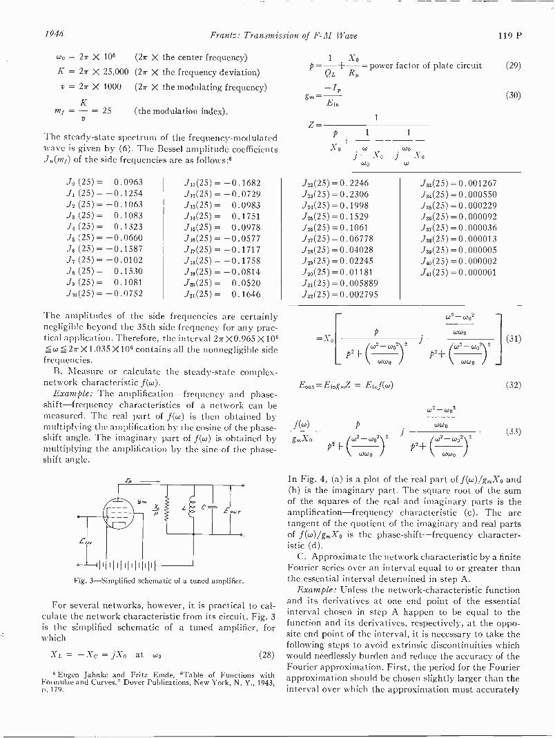
1946 Frantz: Transmission of F -M Wave 119 P
coo = 27r X 106 (27r X the center frequency) 1 X0factorK = 27r X 25,000 (27r X the frequency deviation) (29)p=
{2L-power of plate circuit
Ap
v = 27r X 1000 (27r X the modulating frequency) - 1p(30)gm =
EinK= -= 25 (the modulation index).1
The steady-state spectrum of the frequency -modulatedwave is given by (6). The Bessel amplitude coefficients.1,i(mi) of the side frequencies are as follows:6
z-1
Xo+ CO oX0 j-XoCOO
Jo (25) = 0.0963 111(25) = -0.1682 J22(25) = 0.2246 133(25) =0.001267J1 (25)= -0.1254 .112(25)= -0.0729 123(25) = 0.2306 134(25) = 0.000550
(25)= -0.1063 J13(25)= 0.0983 124(25) =0.1998 135(25) = 0.000229.13 (25) = 0.1083 114(25)= 0.1751 125(25) =0.1529 136(25) = 0.000092J4 (25) = 0.1323 J15(25)= 0.0978 126(25) =0.1061 137(25)=0.000036
(25) = -0.0660 J36(25)= -0.0577 127(25)=0.06778 138(25) =0.000013Ja (25)= -0.1587 117(25) = -0.1717 128(25) =0.04028 130(25)=0.000005J7 (25)= -0.0102 J18(25)= -0.1758 120(25) =0.02245 40(25) =0.000002Js (25)= 0.1530 110(25)= -0.0814 130(25) =0.01181 J41(25) =0.000001ig (25) = 0.1081 J20(25) = 0.0520 131(25)=0.005889J10(25) = -0.0752 121(25) = 0.1646 132(25) =0.002795
The amplitudes of the side frequencies are certainlynegligible beyond the 35th side frequency for any prac-tical application. Therefore, the interval 2ir X0.965 X106
27r X1.035 X106 contains all the nonnegligible sidefrequencies.
B. Measure or calculate the steady-state complex-
network characteristic f(co).Example: The amplification -frequency and phase -
shift -frequency characteristics of a network can bemeasured. The real part of f(co) is then obtained bymultiplying the amplification by the cosine of the phase -
shift angle. The imaginary part of f(co) is obtained bymultiplying the amplification by the sine of the phase-shift angle.
Forculateis thewhich
111 11111111 111
Fig. 3 -Simplified schematic of a tuned amplifier.
several networks, however, it is practical to cal -
the network characteristic from its circuit. Fig. 3simplified schematic of a tuned amplifier, for
XL = - Xc = jXo at coo (28)
Eugen Jahnke and Fritz Emde, "Table of Functions withFormulae and Curves," Dover Publications, New York, N. Y., 1943,
. 179.
w2_,.,02
p[p2+
COW 0
p2+ -WC40
(31)n1
wco o
Eout=EingniZ = Einflco)
gmXo p2+2
WO2
cow o
p2+WW1) cow o
(32)
(33)
In Fig. 4, (a) is a plot of the real part of f(co)/g,X0 and(b) is the imaginary part. The square root of the sumof the squares of the real and imaginary parts is theamplification -frequency characteristic (c). The arctangent of the quotient of the imaginary and real partsof f(co)/g,X0 is the phase -shift -frequency character-istic (d).
C. Approximate the network characteristic by a finiteFourier series over an interval equal to or greater thanthe essential interval determined in step A.
Example: Unless the network -characteristic functionand its derivatives at one end point of the essentialinterval chosen in step A happen to be equal to thefunction and its derivatives, respectively, at the oppo-site end point of the interval, it is necessary to take thefollowing steps to avoid extrinsic discontinuities whichwould needlessly burden and reduce the accuracy of theFourier approximation. First, the period for the Fourierapproximation should be chosen slightly larger than theinterval over which the approximation must accurately
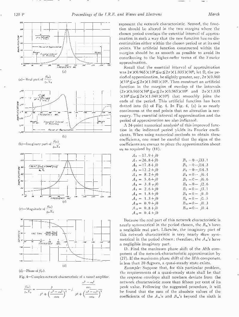
120 P Proceedings of the I.R.E. and Waves and Electrons March
/10
/00
090
tttt
60
40
/0
0
P
of AppeormoeloomPr.-ioe/
A50,6,Esarmiool Infireral
of fleevoary
Morgto
.96 ..97 .90
f(w)(a) -Real part of
ji0
g,X0
99 500 /0/FREQUENCY MC.
(a)
101 103 /04 105
j40
94 97 90 3SFREQUENCY MC.
V40I-soon/rod Inforror/
of Retwroey
00 ROI 01 /.03 04 405
More/.
(b)
(b) -Imaginary part of f (w)
O
WU
/00
00
$0
40
LO
0
/REAL' [re o] 4. IMfeffe451. X.
9 .96 97 98 .99 /00FREQUENCY MC
(c)
(c) -Magnitude of -f(-.)
90
60
4701/41
1/41
90
60
-90
10e 101 /04 10$
- ARC TAMIMAG.[fl to9
REAL [f(W)
L__ I I5 .96 .97
FREQUENCY98 59
MC./ LO/ 101 /03 I 105
(d)
(d) -Phase of f(w).
Fig. 4 -Complex -network characteristic of a tuned amplifier.co2 wo2
f(w)
g.X0p2
represent the network characteristic. Second, the func-tion should be altered in the two margins where thechosen period overlaps the essential interval of approx-imation in such a way that the new function has no dis-continuities either within the chosen period or at its endpoints. The artificial function constructed within themargins should be as smooth as possible to avoid itscontributing to the higher -order terms of the Fourierapproximation.
Recall that the essential interval of approximationwas 271- X0.965 X 106 <w < 27r X1.035 X106; let E2, the pe-riod of approximation, be slightly greater, say, 27r X 0.960X 106 <w27r X 1.040 X106. Then construct an artificialfunction in the margins of overlap of the intervals(27rX0.960 X106:5co 5_271-X0.965 X106 and 27rX1.035X 106-50.) :5_ 27rX1.040 X106) that smoothly joins theends of the period. This artificial function has beendotted into (b) of Fig. 4. In Fig. 4, (a) is so nearlycontinuous at the end points that no alteration is nec-essary. The essential interval of approximation and theperiod of approximation are also indicated.
A 24 -point numerical analysis4 of this improved func-tion in the indicated period yields its Fourier coeffi-cients. When using numerical methods to obtain thesecoefficients, one must be careful that the signs of thecoefficients are correct to place the approximation aboutcoo as required by (11).
Ao =17.9±j0A1 =26.8-1-j0 B1 = 0 -j33.1A2 =17.8+j0 B2 =0-j14.3A3 =12.2-1-j0 B3 =0-j14.5A4 = 8.2+j0 B4 =0- j6.4A5 = 5.6+j0 B6 =0- j6.6A6 = 3.8±j0 Bo =0- j2.6A7 = 2.6-1-j0 B7 = 0 - j3.1A8 = 1.8+j0 B8 =0- j1.0A9 = 1.3 + j0 B9 =0- jl . 5A10= O. 9 d -j0 B10=0- j0.3A11= 0 . 8 + j0 B11=0- j0.4Al2 = 0.4-1-j0
Because the real part of this network characteristic isnearly symmetrical in the period chosen, the Bm's havea negligible real part. Likewise, the imaginary part ofthis network characteristic is very nearly skew sym-metrical in the period chosen; therefore, the Am's havea negligible imaginary part.
D. Find the maximum phase shift of the Mth com-ponent of the network -characteristic approximation by(27). If the maximum phase shift of the Mth componentis less than 20 degrees, a quasi -steady state exists.
Example: Suppose that, for this particular problem,the requirements of a quasi -steady state shall be thatthe response envelope shall nowhere deviate from thenetwork characteristic more than fifteen per cent of itspeak value. Following the suggested procedure, it willbe found that the sum of the absolute values of thecoefficients of the Am's and Bm's beyond the sixth is
1946 Frantz: Transmission of F -M Wave 121 P
about 14 per cent of the peak magnitude of the function.Therefore, the terms corresponding to m = M= 6 arethe last significant terms of the series.
The problem solved experimentally in (b) of Fig. 2will now be tested analytically for a quasi -steady state.The parameters K and v have been given, SZ was chosenin step C, and the largest significant value of m(M= 6)has been chosen in the preceding paragraph.
Kv (27rm
2
2r X 25,000 X 2r X 1000 ( 2r X 6 r(27)
2 2r X 80,000)
-, 2.8 radians or 160 degrees.
This large phase discrepancy for m = 6 indicates that aquasi -steady state does not exist, and that the distor-tion is quite large. This conclusion is confirmed by (b)in Fig. 2.
The series obtained in step C is also adequate for theproblem solved experimentally in (a) of Fig. 2, becausethe spectrum is even more closely confined. Substitutingthe parameters for (a) of Fig. 2 into (27),
the static -network response characteristic is obviouslyeverywhere less than 15 per cent of the peak.
STEP-BY-STEP PROCEDURE FOR CALCULATING THE
RESPONSE OF A NETWORK TO A FREQUENCY -
MODULATED WAVE
The necessary steps for evaluating (15) as a functionof either t or fv are organized and demonstrated in thissection. The amplitude -instantaneous -input -frequencyresponse and phase - shift - instantaneous - input -fre-quency response of a tuned amplifier will be calculatedusing the same parameters that were used experimen-tally to obtain (b) of Fig. 2.I. Perform steps A, B, and C of the validity -test pro-cedure.II (a). Prepare work sheets similar to Table I for severalequally spaced values of (43 -coo) between zero and K.
Example: There should be work sheets for enoughpoints to determine smooth curves of the amplitude -instantaneous - input - frequency and phase -shift - in-stantaneous -input -frequency response. Work sheets for(43-wo)=27rX2000, 271-X4000, 27rX6000, , 27r
X24,000 were prepared for the example; Table I is thework sheet for (6 -wo) =27r X6000.
TABLE 1
SAMPLE WORK SHEET FOR CALCULATING E.ut
III IV V VI VII VIII IX X
B.
XI
B, sin (V)
XII
(XI) cos (IV)
XIII
j(XI) sin (IV)mPhaseof D.
(degrees)
1,1,.
(degrees)A. A, cos (V) (VII) cos (IV) j(VII) sin
(IV)
0 0 0 17.9 +j0 17.9-1-j0 17.9+j01 4.3 27.0 26.8±j0 23.9 +j0 23.9-1-j0 0+j1.8 0 -j33.1 0 -j14.9 0 -j14.9 1.1+j02 17.1 53.8 17.8+j0 10.5-1-j0 10.0±j0 0 +j3.1 0 -j14.3 0 -j11.5 0 -j11.1 3.4 +j03 38.4 80.3 12.2-1-j0 2.1+j0 1.6±j0 0+j1.3 0 -j14.5 0 -j14.3 0 -j11.2 8.9-1-j04 68 106 8.2+j0 -2.3 -HO -0.9+j0 0 -j2.1 0- j6.4 0- j6.1 0- j2.3 5.7-1-j05 106 132 5.6+j0 -3.7+j0 1.0+j0 0 -j3.6 0-j6.6 0-j4.9 0+ j1.3 4.7+j°6 152 156 3.8+j0 -3.5 ±j0 3.1+j0 0 -j1.6 0- j2.6 0- j1.1 0+ j1.0 0.5±j07 205 180 2.6-1-j0 -2.6 +j0 2.4+j0 0 -FP .1 0- j3.1 0+ j0 0+ j0 0 +j08 266 202 1.8+j0 -1.7 ±j0 0.1+j0 0±j1.7 0- j1.0 0+ j0.4 0+ j0 0.4+j09 333 223 1.3-1-j0 -1.0 -Fj0 -0.9+j0 0+j0.5 0- j1.5 0+ j1.0 0+ j0.9 0.5+j0
10 407 243 0.9 +j0 -0.4-+0 -0.3-+0 0 -j0.3 0- j0.3 0+ j0.3 0+ j0.2 -0.2-1-j011 487 262 0.8+j0 -0.1-1-j0 0.1 +j0 0 -j0.1 0- j0.4 0+ j0.4 0- j0.3 -0.3+j012 572 278 0.4 +j0 0.1 +j0 -0.1-+0 0 -j0.1
;') - coo = 2 v- X6000 TOTALS 57.9+j0 0 ±j1 .7 0 -j36.4 24.7-1-j0or vc =
' Q= (57.9 ±i0) ± (0 4-j1 . 7) ± (0 -j36.4) ± (24.7 ±j0) =82.6 -j34.7 =89.5/ -22.8 degreesR= (57.9+j0) -(0-1-j1.7) ± (0 -j36.4) -(24.7±j0) =33.2 -j38.1 =50.5/ -48.9 degreesS= (57.9 ±j0) ± (0 +j1.7) - (0 -j36.4) -(24.7 ±j0) = 33.2 +j38.1 =50.5/ 48.9 degreesT= (57.9 +j0) -(0-1-j1.7) - (0 -j36.4) (24.7 ±j0) = 82.6 ±j34.7 = 89.5/ 22.8 degrees
2r X 25,000 X2rX 100 ( 2r X6 2
1,-=,2 2r X80,000
=--- 0.28 radian or 16 degrees.
Since the phase discrepancy for this Mth term is lessthan 20 degrees, a quasi -steady state (such as postu-lated) may be assumed to exist. In Fig. 2, (a) bears outthis conclusion nicely; the discrepancy between (a) and
II (t). Prepare work sheets similar to Table I for severalequally spaced values of vt between zero and 7r/2 (90degrees).
III. Into column III enter the orders of the Fouriercoefficients obtained in step C.
This column is the same for all the work sheets.
IV (a). Into column IV enter the value of
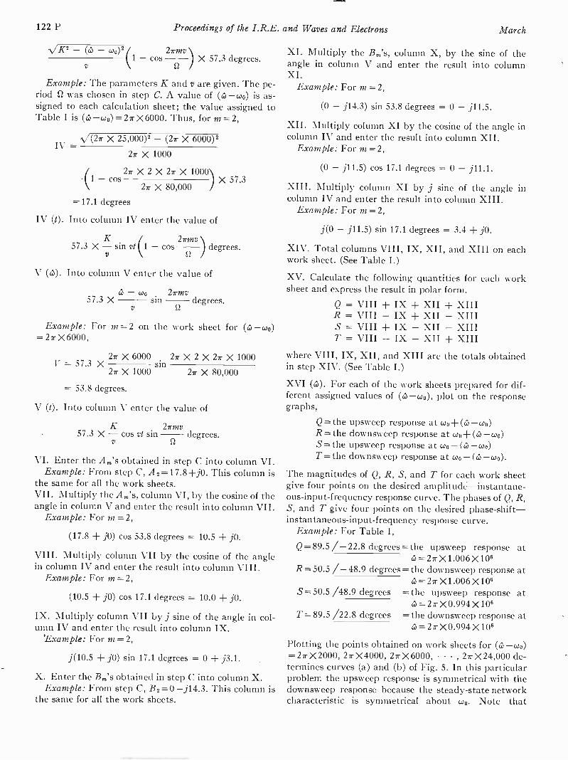
122 P Proceedings of the I.R.E. and Waves and Electrons March
/K2- (6 - wo) 27rmv(1cos
\X 57.3 degrees.
St
Example: The parameters K and v are given. The pe-riod Sl was chosen in step C. A value of (ea -coo) is as-signed to each calculation sheet; the value assigned toTable I is (Co -coo) =27 X6000. Thus, for m =2,
IV =027 X 25,000)2 - (27r X 6000)2
27 X 1000
.(1 -27 X 2 X 27 X
cos X 57.327 X 80,000
=17.1 degrees
IV (1). Into column IV enter the value of
/K
57.3 X - sin vt (1 - cos degrees.v
V (Co). Into column V enter the value of
- coo57.3 X
27 mvsin degrees.
12
Example: For m = 2 on the work sheet for (a) -coo)=27rX6000,
27 X 6000 27 X 2 XV = 57.3 X sin
27 X 1000 27 X 80,000
27 X 1000
= 53.8 degrees.
V (t) . Into column V enter the value of
K 27g-mv57.3 X - cos vt sin degrees.
12
VI. Enter the Am's obtained in step C into column VI.Example: From step C, A 2 =17.8+j0. This column is
the same for all the work sheets.VII. Multiply the Am's, column VI, by the cosine of theangle in column V and enter the result into column VII.
Example: For m=2,
(17.8 + j0) cos 53.8 degrees = 10.5 + j0.
VIII. Multiply column VII by the cosine of the anglein column IV and enter the result into column VIII.
Example: For m = 2,
(10.5 + j0) cos 17.1 degrees = 10.0 + j0.
IX. Multiply column VII by j sine of the angle in col-umn IV and enter the result into column IX.
'Example: For m = 2,
j(10.5 + j0) sin 17.1 degrees = 0 + j3.1.
X. Enter the .Bm's obtained in step C into column X.Example: From step C, B2=0 -j14.3. This column is
the same for all the work sheets.
XI. Multiply the /3,'s, column X, by the sine of theangle in column V and enter the result into columnXI.
Example: For m = 2,
(0 - j14.3) sin 53.8 degrees = 0 - j11.5.
XII. Multiply column XI by the cosine of the angle incolumn IV and enter the result into column XII.
Example: For m =2,
(0 - j11.5) cos 17.1 degrees = 0 - j11.1.
XIII. Multiply column XI by j sine of the angle incolumn IV and enter the result into column XIII.
Example: For m = 2,
j(0 - j11.5) sin 17.1 degrees = 3.4 + j0.
XIV. Total columns VIII, IX, XII, and XIII on eachwork sheet. (See Table I.)
XV. Calculate the following quantities for each worksheet and express the result in polar form.
Q = VIII ± IX ± XII ± XIIIR = VIII - IX + XII - XIIIS = VIII ± IX - XII - XIIIT = VIII - IX - XII + XIII
where VIII, IX, XII, and XIII are the totals obtainedin step XIV. (See Table I.)
XVI (6). For each of the work sheets prepared for dif-ferent assigned values of (6 -coo), plot on the responsegraphs,
Q= the upsweep response at coo+ (co* -coo)R= the downsweep response at coo+ (6 -coo)S= the upsweep response at coo- (c'Zi -coo)T= the downsweep response at coo- (07 -coo).
The magnitudes of Q, R, S, and T for each work sheetgive four points on the desired amplitude -instantane-ous -input -frequency response curve. The phases of Q, R,S, and T give four points on the desired phase -shift-instantaneous -input -frequency response curve.
Example: For Table I,
Q = 89.5 /- 22.8 degrees = the upsweep response at6=27X1.006 X106
R=50.5 /- 48.9 degrees= the downsweep response at= 27 X1.006 X106
S= 50.5 /48.9 degrees = the upsweep response at= 27 X 0.994 X 106
T=89.5 /22.8 degrees = the downsweep response at= 27 X 0.994 X106
Plotting the points obtained on work sheets for (6)-(00)=27X2000, 27X4000, 27X6000, , 2rX24,000 de-termines curves (a) and (b) of Fig. 5. In this particularproblem the upsweep response is symmetrical with thedownsweep response because the steady-state networkcharacteristic is symmetrical about coo. Note that

1946 Frantz: Transmission of F -M Wave 123 P
curve (a) of Fig. 5, the calculated amplitude-instan-taneous-input-frequency response, agrees very closelywith (b) of Fig. 2, the experimental amplitude-instan-taneous-input-frequency response. The reader may beinterested in comparing the results of the calculationwith the results obtained by Roder on a very similarproblem, which he solved by the aid of a differentialanalyzer. His response curve was plotted as a function oftime.'
MO
/00
O60
40
20
0
---- [:-1
.., .......
.97 9B .99 /00 lex /02 /03INSTANTANEOUS INPUT FREQUENCY MC.
(a)E out(a)-Amplitude of --g)Co
I/O
60
41tt 30to
30
-60
-90
-/20
PHASE [E.,.1
INSTANTANEOUS.97 98 .99
INPUT/00 /0/
FREQUENCY102 /03
MC.
(b)(b)-Phase of Erna.
Fig. 5-Calculated amplitude-instantaneous-input-frequencyand phase-shift-instantaneous-input-frequency response of a tunedamplifier to a frequency -modulated wave.
Effective Q of amplifier =100 (p =0.01)Center frequency =106 (coo = 27r X 106)Modulating frequency =1000 (v=2x-X1000)Total frequency excursion =50 , 000 (K = 2r X25 ,000)
XVI (1). For each of the work sheets prepared for dif-ferent assigned values of vt, plot on the response graphs.
Q = the response at 2r -vtR = the response at vtS= the response at rd-vtT = the response at it-vt.
The magnitudes of Q, R, S, and T for each work sheetgive four points on the desired amplitude-time re-sponse curve. The phases of Q, R, S, and T give fourpoints on the desired phase-shift-time-response curve.
7 Hans Roder, "Effects of tuned circuits upon a frequency -modulated signal," PROC. I.R.E., vol. 25, pp. 1617-1648; December,1937.
APPENDIX
If a steady-state driving voltage ef6" is applied to theinput terminals of a linear network, it can be shown thatthe steady-state solution for the voltage at the outputterminals' is of the form R(w)ei["+°(')]. R(w) is the ratioof the peak amplitudes of the output and input voltages,and 0(w) is the phase difference. Abbreviating es"' as E10+and R(co)eim±e(w)] as E.,i6+, it follows that
Eout+ = Ein+R(w)eo('). (34)
Furthermore, if a steady-state driving voltage e-"'" isapplied to the input terminals of the same linear net-work, it can be shown that the voltage at the outputterminals is of the form R(co)c-ii"÷"(01, where R and 0are equal to R and 0 of (34). Setting e-i" as E1 andR(w)e-i["+°(')] as Eouti it follows that
Eout- = Ein-R(w)E-i°('). (35)
Therefore, if a steady-state driving voltage sin wt is ap-plied to the input terminals of the network, the outputvoltage can be determined as follows:
,i.t -Ein = sin cot =
By (34) and (35),
R(co)Ei[wg-"(w)] - R(co)e-i["+"(01Eout
2j
= R(w) sin
2j
[cot + 0(co) ].
(36)
(37)
R(co)fie(w) is now defined as the complex network char-acteristic, f(co). It can be seen from (36) and (37) that
Eoutt = Einf(w) (8)
where
Aco)amplitude of .E.ut
amplitude of Eir,
and where
[f(imaginary conarc tan = angular phase [E..t[real [f(w)]
- angular phase [Ein].
(9)
(10)
The notation = 1 in (8) means "equals by conven-tion," because the right- and left-hand members of theequation are not mathematically equivalent exceptwhen 0(co)= nr.
Note also from (34) and (35) that
and
Emit+ = Ein+f(w) (38)
Eout- = Ein-f*(co) (39)
" H. Pender and S. Warren, "Electric Circuits and Fields," Mc-Graw-Hill Book Company, New York, N. Y., 1943, pp. 161-163.
124 P Proceedings of the I.R.E. and Waves and Electrons March
where f*(w) = the complex conjugate of f(w). (40)
The = signs of (38) and (39) indicate exact mathe-matical equivalence. Only the = } sign of (8) is re-stricted.
Equation (7), which expresses the input frequency -modulation voltage as a spectrum of steady-state sidefrequencies, is repeated here for convenience.
ein = Jo(mf) sin coot
in [coo + (2n - 1)v]t+ E( J._,(m,) sn=1
- sin [wo - (2n - 1)01
J2n(mf) sin [coo + 2nv]t + sin [coo - 2nv]t}). (7)
[Am2
M 2N
2jet = E E(Ei (0,0-1-i/v) t-Fkmitvi ± El ((w0+vv) t- kmvv])
B,(,i[co,o+not+kmny] - eiuwo+not-kmnvi)
2jAm*
2
B.*
2j
The Bessel coefficients are combined with the exponen-tials by the use of the relation,
(Ei(-(to-F7v)1+kinnvi 1[-(oio+nv) t-km7v1)
(ei-u,,,o+not+km,m - ,i-E(.04-not-kmno)1. (49)
Since J(z)-= (-1)n..Ln(z), equation (7) can be com-pressed as follows:
2N
2N
EJ(ni,,)0 Sin 8,
n= -2N
ein = E ..r,(tro sin (wo nv)t. (41) which is accurate because the J,7(mf)'s below n= -2N77=-2N and above n= ----2N are negligible by the definition of N.
Changing sin (coo-Fnv)t to exponential form, M2jeout E A.
sin (vt+kmv)1(fik.,01-1-mi
2N m=0 2
2jein = E .1,,(ini)[e(.0+not - c1(.0+no t]. (42) Ell4.001+m/ sin (vt-kmv)])77=-2N
The steady-state output oscillation corresponding toeach steady-state oscillation of the frequency -modulatedinput spectrum is given by (38) and (39).
Ennt+ [for Ein+ = Ei('°+nv) t] = 6/('04-nv) y(coo nv) ( 43 )
and
Bm(j[ci0t-Fmf sin (vti-kmv)]
2jE;[.0 -1-,n., sin (vt-kmv)])
A .*
2
(,j[--,01-1- mi. sin (-vt+kmv)]
+ j-coot- mf sin (-vt-kmv)])
Ennt,- [for Ein- = E i(wo+nv)] = ("+")t f * (coo+ nv) (44) B.*(Ei[-wtit-l-mf sin (-v k my)]
Equation (11) gives the values of f(coo+nv) and 2j
f*(0)0+no.
f(wo + nv) E (Am cos kmnv + B. sin kmnv) (45)
and
7740
ci[-Loa-Erni sin (-v k mv)]) (50)
Expanding sin (vt+kmv) and factoring the exponentials,M Am
2jeout = 2_,,
(E1 (wot+ "if sin vt cos k mv))(j mf cos vt sin kmv
M m=0 2
f*(wo + ,iv) E (A.* cos kmnv Bm* sin kmnv) (46)1,1=0
where
27rk = (47)
The output -voltage equation can now be written from(42), (43), and (44).
M 2N
2jeout= E E J(nif) [eim+no t(A. cos kmnv+ B. sin kmnv)m=-0 77.=-2N
- (w°+") t (A m* cos krmiv+B,* sin kmnv)]. (48)
Changing cos kmnv and sin krirqv to exponential form,
E-imf cos vt sin kniv)
B,(,1(.0e+mf sin vt cos kmv))(ejmf cos vt sin kmv
2jcinif cos V g sin kmv)
Am*
2
(E- j (wo t+ mi. sin vt cos k mv))(,1 mi cos vt sin kmv
Mi. cos V t sin kmv)
Bm*
2j(E- (w0t± mf sin vt cos k mv)) (ti mf cos vt sin kmv
1- E--:/inf cos V g sin kmv) (51)
1946 Frantz: Transmission of F -M Wave 125 P
Factoring eti(iot+nif sin vt cos k my) and changing
exponentials to trigonometric form,the other Then
2jeout = ,;(wowmf sin vopEio -,iciost+mf sin vopc-io (58)
2jeout = E [Am cos (mi. cosm=0
vt sin kmv)fi"/ sin vt(cos kmv-1)ei(,01-fmj sin vt)
+ B. sin (mi. cos vt sin kmv)Eimi sin vt(cos k mv-1) El (wo mj sin vt)
- Am* cos (nif cos vt sin kmv)E-ing sin vt(cos k mv-1)e-i(woi+Mf sin vt)
- B.* sin (m1 cos vt sin kinv)E- jmf sin vt(cos k )(coo t- - mi sin vt)] (52)AlM
2jeont = coist+inf sin o E D,,,[A, cos +Bm
where
sin IGni] - -/(0,0t-Fmf sin vt)E D ,* [A .* cos tk, + Bm* sin 1/.,] (53)m=0
eout, = j (toot- I- mf sin vt-F¢) ,-1(coot-Fnif sin tit -1-0)] (59)
Dm(t) = cos [Kv
2 V71-M
1sin vt cosSt )
-j sin 27rmv- (16) eons = P sin (coo t + mf sin vt + 4,) (60)[- sin vt (1 cosv )iK 27rnzv
and where Ik,(1) = (17) The output -voltage -envelope equation, therefore, writ-ten in conventional form is
- cos vt sin
It is easy to derive D,(6) and 1,14,2(6) from (16) and (17)by starting with (5), which relates a, and t.
(:os = coo + K cos vt (5)
- WOcos vt = (54)
K
± K2 - (6') - (002sin vt =
K
Substituting for sin vt in (16),
Dm(w) = cos(67 -WO 2
V
27rmv1-Cos
)
= E D,[An, cos + B. sin 1,tim]. (15)Tn=0
(55) The notation { = } again means "equals by conven-tion"; the amplitude of the envelope is the absolutevalue of the complex summation, and the angular phasedifference between the output and input frequency -modulated waves is equal to the phase of the complexsummation.
+j sin ["2- (v6 -(4°)2 (1 COS27rmv
(18)SZ )_1
Substituting for cos vt in (17),
=- wo 277-mv
sin (19)v S2
Equation (53) can be changed from exponential form tosinusoidal form as follows:
Let P =M= 0
and
D,[A,,, cos 1,G, + B. sin lit m]
= arc tan
(56)
ACKNOWLEDGMENT
The author wishes to express his appreciation for themany suggestions and constructive criticisms of thispaper in the draft stage offered by members of the TestEngineering Section of RCA Victor, and to the depart-ment management, who supplied laboratory and cleri-cal facilities; Mr. L. C. Smith suggested that this mate-rial be prepared for publication, and supervised thework. Mr. M. S. Corrington of the Advanced Develop-ment Section recommended changes that strengthenedthe text, suggested identities which greatly simplifiedthe appendix, and cited additional pertinent references.
imaginary { E D, [A, cos ¢m + B, sin IY,
real cos + B, sin ]}m=0
(57)
Analysis of a Resistance -Capacitance Parallel -TNetwork and Applications*
A. E. HASTINGSt, ASSOCIATE, I.R.E.
Summary-A resistance -capacitance parallel -T network is ana-lyzed to find the conditions for a null in output and the transfer char-acteristic. Its use in the return circuit of a feedback amplifier is con-sidered, and the bandwidth of the resulting tuned amplifier is found.The requirements for stability of the amplifier and for its use as anoscillator are discussed.
INTRODUCTION
NETWORKS which have the property of null bal-ance at one frequency are well known. The Wienbridge is such a network of the four -terminal
type, using only resistance and capacitance as elements.A three -terminal equivalent has recently come intouse.L2 This form has the advantage of a common inputand output terminal and does not require a special trans-former in many applications.
With such a network in the inverse feedback circuitof an amplifier, there results a tuned amplifier with anumber of advantages, particularly at audio frequen-cies. A number of applications of this amplifier to thedesign of instruments have been made.3-6 The purpose of
R,
Cj
R2
C2
Fig. 1-Parallel-T network with general R's and C's.
* Decimal classification: R140 X R363.1. Original manuscript re-ceived by the Institute, May 3, 1945; revised manuscript received,August 31, 1945.
t Naval Research Laboratory, Washington, D. C.1 W. N. Tuttle, "Bridged -T and parallel -T null circuits for meas-
urements at radio frequencies," PRoc. I.R.E., vol. 28, pp. 23-30;January, 1940.
2 Mathematics Tables Project, "Characteristics of Resistance-Capacitance Electrical Networks," 50 Church St., New York, N. Y.,1942.
3 H. H. Scott, "A new type of selective circuit and some applica-tions," PROC. I.R.E., vol. 26, pp. 226-236; February, 1938.
4 L. A. Meacham, "The bridge -stabilized oscillator," PROC. I.R.E.,vol. 26, pp. 1278-1295; October, 1938.
6 H. H. Scott, "An analyzer for sub -audible frequencies," Jour.Acous. Soc. Amer., vol. 13, pp. 360-362; April, 1942.
W. G. Shepherd and R. 0. Wise, "Variable -frequency bridge-type frequency -stabilized oscillators," PROC. I.R.E., vol. 31, pp.256-269; June, 1943.
this work is to analyze in some detail the null networkand its use in a tuned amplifier.
CONDITIONS FOR A NULL
A three -terminal parallel -T network which containsonly resistive and capacitive elements is shown in Fig.1. In this illustration, e is the input voltage with angularvelocity co, and it is desired to find the conditions for anull in output voltage e'. The impedance across e' isassumed throughout this analysis to be infinite, a con-dition which can in most cases be closely approximated.Four independent circuit equations can be written.These are
e - ii(Ri j) ± ia( i ) = OW. -,r3 COC3
e + i2 iR3 - - i3(R3) = 0W 1
e -i11--)+COC3
i3 (R2 -
e' i2(R3) - i3 (R3 -COC3
WC2
=0
=0
(1)
If e' =0, for a null, these reduce to a set of four linearhomogeneous equations with four variables, e, ii, i2, andi3. The necessary and sufficient condition that the vari-ables shall have values other than zero is that the de-terminant of the coefficients shall be zero. This gives theconditions on the R's and C's and on co for a null. Ex-panding this determinant and equating to zero givesthe equation
R IR21234002C2C3
1+ j = 0cooVIC2C3
R3 R3 R2R3 RiR3.1
coous wou3/`
wo2
where coo is the value of co for a null. Equating both realand imaginary parts of this equation to zero, these con-ditions are obtained:
Ci+C2WO2=
RiR2C1C2C3and (RI-i-R2)(Ci-FC2)R3-RiR2C3 = O.
If the T's are made symmetrical, RI=R2=R and= C2 = C, and the conditions for a null become
and
1
V2n RC(2)
126 P Proceedings of the I.R.E. and Waves and Electrons March, 1946
Hastings: R -C Parallel-71Network Analysis 127 P
R3 C3= =n
R 4C(3)
where n is a positive number which can be chosen arbi-trarily to obtain certain desired characteristics. Thenetwork then appears as in Fig. 2.
R
4>2C
nR
C C
Fig. 2-Network as used in the tuned amplifier.
The null conditions also hold for any impedanceacross e', since when e' is zero the current distributionis not affected by whatever value of impedance is usedin shunt.
TRANSFER CHARACTERISTIC
The transfer characteristic of the network in Fig. 2,with infinite impedance across e', will now be found.This is the ratio of e' to e as a function of frequency.The set of equations (1) represents this circuit ifR1=R2 =R= Ro/n and C1= C2= C= C3/4n. Makingthese substitutions and solving for the voltage ratio, thetransfer characteristic is found to be
e' 4n2a3-2na-1-j(- 2na2+ 1)- =e 4n2a3- 6na - 2a j( - 8n2a2- 6na2+ 1)
(4)
where a =coRC. Let the frequency of the applied voltagee be restricted to small variations about the null fre-quency given by
Then
= wo =1
Jo2/r 2/1-RCN/2n
f = fo(1±fi
where Aflfo<<1, and
Oa = 2rfRC = 2rRCf0(/1 =
f o
1 ( +Af\..\/2n Jo )
Substituting this value of a in (4) and making approxi-mations for Af small,
AN/2n=j (3)
fo(2n + 1)
This indicates that, at a frequency near that for anull, the phase of the output voltage e' is shifted 90degrees from that of the input voltage e, its amplitudeis proportional to the frequency deviation from that ofthe null, and its phase changes discontinuously by 180degrees as the frequency passes through that of the null.For certain applications it is desired that /3 change asrapidly as possible with frequency about the null point,or that the slope of the 1/31 versus Af curve be as greatas possible. This slope is
dl 01 N/2ns = =
d(Af) (2n + 1)fo
Now n is still arbitrary, and if the slope is made a maxi-mum by varying n so that ds/dn=0, n is found to beFor this value, in (4) becomes
0 = a' - 5a + j(- 5a2 + 1)
+ j( a2 + 1)
For Of small as in (5)
(6)
USE IN THE FEEDBACK CIRCUIT OF AN AMPLIFIER
The use of a parallel -T network in a vacuum -tube cir-cuit to obtain a tuned amplifier will be discussed. Sup-pose the output of an amplifier with a flat gain -frequencycharacteristic is returned to the input in such a way
e
Fig. 3-Arrangement of feedback in the tuned amplifier.
that the amplifier is highly degenerative at any inputfrequency. A null network inserted in the return circuitwill leave the degeneration unchanged at all frequenciesexcept those near the null frequency of the network. Atthe null frequency the amplifier has no degenerationand operates with maximum gain. Such an arrangementis shown in Fig. 3, where the output of the null network
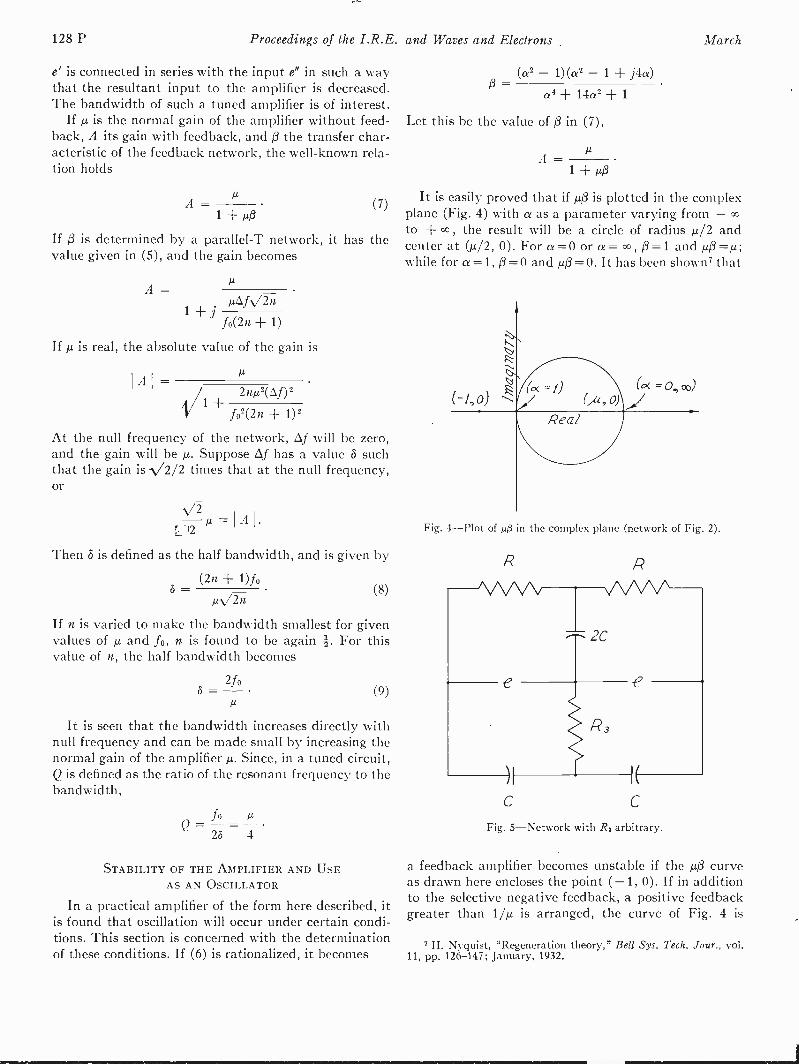
128 P Proceedings of the I.R.E. and Waves and Electrons March
e' is connected in series with the input e" in such a waythat the resultant input to the amplifier is decreased.The bandwidth of such a tuned amplifier is of interest.
If A is the normal gain of the amplifier without feed-back, A its gain with feedback, and 3 the transfer char-acteristic of the feedback network, the well-known rela-tion holds
A=1 + AtO
(7)
If 0 is determined by a parallel -T network, it has thevalue given in (5), and the gain becomes
A -
fo(2n + 1)
Ifµ is real, the absolute value of the gain is
I A -
1 +
/.4
2,11,2(AD 2
fo2(2n + 1)2
At the null frequency of the network, of will be zero,and the gain will be µ. Suppose Af has a value 3 suchthat the gain is -0/2 times that at the null frequency,or
-12
Then 3 is defined as the half bandwidth, and is given by
- (2n+ 1)foµN/2n
If n is varied to make the bandwidth smallest for givenvalues of kt and fo, n is found to be again I. For thisvalue of n, the half bandwidth becomes
2fo
la
(8)
(9)
It is seen that the bandwidth increases directly withnull frequency and can be made small by increasing thenormal gain of the amplifier ,u. Since, in a tuned circuit,Q is defined as the ratio of the resonant frequency to thebandwidth,
,foQ = = -
23 4
STABILITY OF THE AMPLIFIER AND USEAS AN OSCILLATOR
In a practical amplifier of the form here described, itis found that oscillation will occur under certain condi-tions. This section is concerned with the determinationof these conditions. If (6) is rationalized, it becomes
(a2=
- 1)(a2 - 1 -I- j4a)a4 14a2 + 1
Let this be the value of 0 in (7),
A =1 +
It is easily proved that if u0 is plotted in the complexplane (Fig. 4) with a as a parameter varying from -00to + cc, the result will be a circle of radius u/2 andcenter at (u/2, 0). For a =0 or a= cc, 0 =1 and /10 =,u;while for a 1, /3 =0 and ,u0 = 0. It has been shown' that
plane (network of Fig. 2).
)1
C
1(
C
Fig. 5-Network with R3 arbitrary.
a feedback amplifier becomes unstable if the i.40 curveas drawn here encloses the point (-1, 0). If in additionto the selective negative feedback, a positive feedbackgreater than 1/j.t is arranged, the curve of Fig. 4 is
T H. Nyquist, "Regeneration theory," Bell Sys. Tech. Jour., vol.11, pp. 126-147; January, 1932.
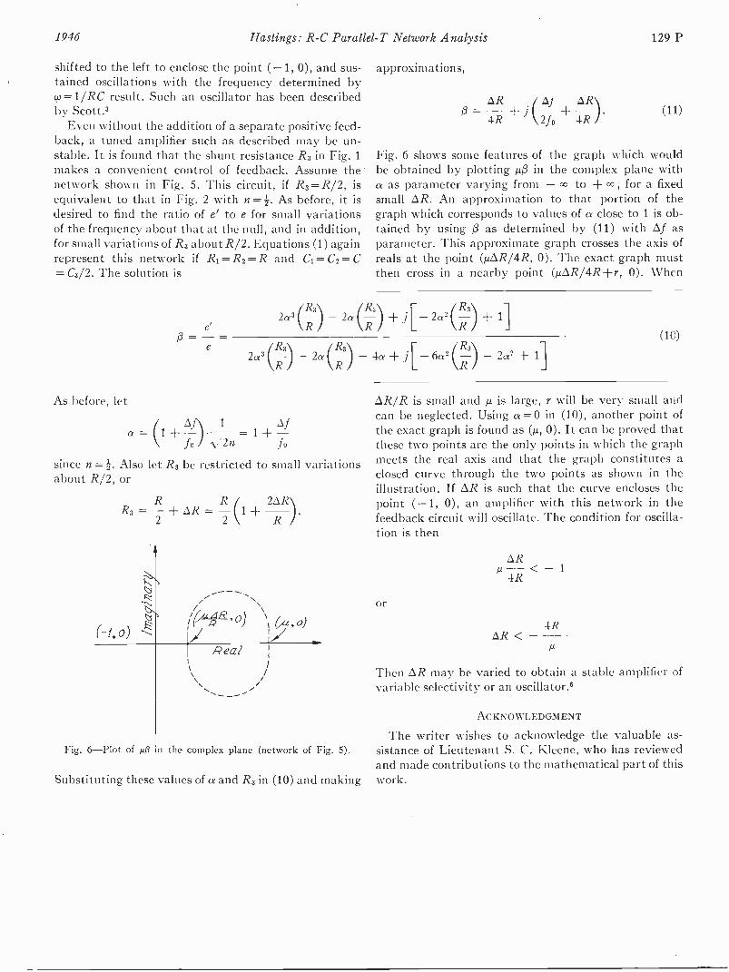
1946 Hastings: R -C Parallel -T Network Analysis 129 P
shifted to the left to enclose the point (-1, 0), and sus-tained oscillations with the frequency determined bycp =1/RC result. Such an oscillator has been describedby Scott.'
Even without the addition of a separate positive feed-back, a tuned amplifier such as described may be un-stable. It is found that the shunt resistance R3 in Fig. 1makes a convenient control of feedback. Assume thenetwork shown in Fig. 5. This circuit, if R3=R/2, isequivalent to that in Fig. 2 with n = 2. As before, it isdesired to find the ratio of e' to e for small variationsof the frequency about that at the null, and in addition,for small variations of R3 about R/2. Equations (1) againrepresent this network if R1= R2 =R and Ci = C2 = C= C3/2. The solution is
e'
e0 = =
approximations,
AR Aj AR0 =
4R+
4R) (11)
Fig. 6 shows some features of the graph which wouldbe obtained by plotting /213 in the complex plane witha as parameter varying from -co to + CO for a fixedsmall OR. An approximation to that portion of thegraph which corresponds to values of a close to 1 is ob-tained by using f3 as determined by (11) with Of asparameter. This approximate graph crosses the axis ofreals at the point (yAR/4R, 0). The exact graph mustthen cross in a nearby point (u0R/4R+r, 0). When
2a3 - 2aCI + j [- 2a2 + 1]
R3 R3 R32a3 - 2a (-) - 4a + j [- 6a2 (-) - 2a2 + 1]
As before, let
(1 1
1+of
fo \/2n JO
since n = 1. Also let R3 be restricted to small variationsabout R/2, or
R RR3=
2- AR=
2 R- 1+
Fig. 6-Plot of kii3 in the complex plane (network of Fig. 5).
Substituting these values of a and R3 in (10) and making
(10)
iR/R is small and ,f.t is large, r will be very small andcan be neglected. Using a =0 in (10), another point ofthe exact graph is found as (2, 0). It can be proved thatthese two points are the only points in which the graphmeets the real axis and that the graph constitutes aclosed curve through the two points as shown in theillustration. If OR is such that the curve encloses thepoint ( -1, 0), an amplifier with this network in thefeedback circuit will oscillate. The condition for oscilla-tion is then
or
AR4R< - 1
AR < -4R
Then OR may be varied to obtain a stable amplifier ofvariable selectivity or an oscillator.'
ACKNOWLEDGMENT
The writer wishes to acknowledge the valuable as-sistance of Lieutenant S. C. Kleene, who has reviewedand made contributions to the mathematical part of thiswork.

The Application of Modulation -Frequency Feedbackto Signal Detectors*
GEOFFREY BUILDERt, FELLOW, I.R.E.
Summary-Positive modulation -frequency feedback to the loadcircuit of a signal detector may be adjusted to make the effectivemodulation -frequency admittance of the load circuit equal to its di-rect -current conductance, thus eliminating peak clipping and improv-ing the efficiency of detection. Conversely, negative feedback to thedetector tends to increase peak clipping. Incidental effects in theamplifier from which the positive feedback voltage is derived maycorrespond to positive or negative, voltage or current, feedback de-pending on the general circuit arrangement. Design formulas andsome simple equivalent circuits are given and the major design con-siderations are outlined. Typical examples include a detector ar-rangement which provides automatic -volume -control voltages andhas a high input impedance and a very low output impedance, as wellas Varrell's arrangement which is in agreement with the design pro-cedure outlined in this paper. Attention is also drawn to the greatcare necessary in the design of detector -amplifier circuits, usingmultipurpose valves (vacuum tubes), to avoid distortion due to in-cidental negative modulation -frequency feedback to the detector.
I. INTRODUCTION
IT IS well known that the modulation -frequency out-put of signal detectors may be seriously distorted by"peak clipping" if the detector load -circuit admit-
tance is not uniform; i.e., if its admittance to modulationfrequencies differs from its direct -current conductance.It has been stated' that quite small amounts of peakclipping may cause objectionable distortion. The causeand nature of peak clipping have been fully discussedand analyzed by Wheeler' and are now well known todesigners. Although Wheeler deals only with diode de-tectors, similar effects may occur in other types ofdetectors, and may also occur in audio -frequency am-plifiers.
As a basis for discussion, the simplified equivalentcircuit of Fig. 1 will be used to represent a diode de-tector. The diode is fed from a carrier -frequency source
Fig. 1-An equivalent circuit for diode detectors.
of electromotive force Ec and of internal conductance G.The detector load circuit comprises a carrier -frequencyby-pass capacitor C in parallel with the uniform con-ductance Go of a diode leak resistor and in parallel with
* Decimal classification: R134 X R362.2. Original manuscript re-ceived by the Institute, August 6, 1945.
f Merino House, 57 York Street, Sydney, Australia.1 A. J. Heins van der Venn, "Distortionless detection" (Discus-
sion), Jour. I.E.E. (London), Part III, vol. 89, pp. 175-176; Septem-ber, 1942.
1 Harold A. Wheeler, "Design formulas for diode detectors,"PROC. I.R.E., vol. 26, pp. 745-781; June, 1938.
a modulation -frequency load of conductance G. A ca-pacitor Cm serves to prevent flow of direct currentthrough the modulation -frequency load G5, and will beassumed throughout to have negligible impedance atmodulation frequencies. Neglecting the modulation -frequency admittance of the capacitor C, the totalmodulation -frequency admittance G. of the load circuitis given by
G. = Go + G. (1)
while its direct -current conductance is Go.The effect of nonuniformity in the load circuit can
then be summarized, in terms of the equivalent circuitof Fig. 1, as follows:
(a) Peak ClippingPeak clipping occurs when the depth of inward modu-
lation exceeds an amount corresponding to a modulationfactor
(K5).55 = Go(2Gm + GO/G.(2Go GO (2)
This peak clipping takes the form of clipping of the in-ward peaks of the detected modulation -frequency wave,and also results in corresponding distortion of the en-velope of the modulated carrier -frequency signal E.'applied to the detector and thus causes distortion in themodulation -frequency output of any other detector orsignal rectifier fed from the same carrier -frequencysource. An automatic -volume -control voltage derivedfrom the detector output would also be affected by achange in mean direct -current voltage output at highmodulation depths, leading to an undesirable variationof the automatic -volume -control voltage with modula-tion.
(b) EfficiencyThe addition to the load circuit of the modulation -
frequency conductance G results in a reduction in themodulation -frequency output voltage, at all depths ofmodulation, in comparison with the output voltage thatwould be obtained if the load circuit has a uniform con-ductance of the value Go. The carrier -frequency voltageE0' applied to the diode and the output voltage E' aremodulated to a depth K.' which is less than the depthof modulation K. of the carrier -frequency signal E, byan amount given by
Km' = K,(2Go-f- Gi)/(2Gm + (3)
as compared with
Km' = K., When Gm = 0. (4)
Although the peak -clipping effect is the more importantand has received correspondingly greater attention, thereduction in detector efficiency expressed by (3), andcorresponding losses incurred in keeping the value of Gohigh to reduce peak clipping, should not be overlooked.
130 P Proceedings of the I.R.E. and Waves and Electrons March, 1946
Builder: Modulation -Frequency Feedback 131 P
II. METHODS OF ELIMINATING OR REDUCING THEEFFECTS OF NONUNIFORMITY OF THE LOAD-
CIRCUIT ADMITTANCE
Many design methods and devices, aimed at reducingor eliminating the effects of nonuniformity in the ad-mittance of the detector load circuit, have been de-scribed from time to time, and are briefly summarizedin this section.
(a) Equalization of the Direct -Current and Modulation -
Frequency Conductances of the Load Circuit
It is obviously preferable to eliminate the effects ofnonuniformity by making the load circuit uniform, orso nearly uniform as to make the effects of nonuniform-ity negligible for any particular purpose.
Wheeler2,3 has described the use of modulation -fre-quency choke coils to reduce the modulation -frequencyconductance of the load circuit, but the method does notseem to have been widely used, at least at low modula-tion frequencies, owing to the practical design and costfactors involved.
Wheeler' has also shown that, for many practical pur-poses, careful design of the load circuit, and particularlythe correct selection of the diode leak conductance Go,can be used to keep the load conductance fairly uniformand thus to reduce peak -clipping effects to an acceptabledegree. His methods are widely used, and provide a sim-ple and satisfactory attack on the problem for manypurposes.
The simplest device, and one that is very satisfactoryin the limited number of cases to which it is applicable,is the direct connection of the detector output to theinput control grid of the modulation -frequency signalamplifier. An obvious disadvantage of the device is theapplication to the control grid of the direct rectifiedcarrier voltage. Although in a limited number of specialcases this may be used to provide automatic -volume -control action in the amplifier valve, it is usually aserious limitation. One method of overcoming this diffi-culty, proposed by Varrell,4 is to utilize direct -currentfeedback, without modulation -frequency feedback, inthe cathode circuit of the amplifier, to maintain the gridbias substantially constant irrespective of variations inthe carrier level applied to the detector.
The success of these methods is limited when an ad-ditional modulation -frequency load is applied to the de-tector for automatic -volume -control or other purposes,or when an automatic -volume -control rectifier is alsoconnected across the same carrier -frequency source fromwhich the signal detector is fed.
(b) Positive Diode Bias
The application of a positive bias to the diode is wellknown and has been discussed by Wheeler,' Sturley,5
3 Harold A. Wheeler, "Peak detector"; United States Patent1,951,685, March 20, 1934; British Patent 398,882, April 1, 1931.
4 H. E. Varrell, "Distortionless detection," Wireless World, vol.45, pp. 94-96; August 3, 1939.
6 K. R. Sturley, "The diode detector with positive bias," WirelessWorld, vol. 44, pp. 220-223; March 9. 1939.
The Marconi Review,' Cocking,' and others. The op-timum value of the bias voltage depends on the carrier -voltage level as well as on the relative values of the loadconductances. A wide variety of circuits has thereforebeen devised to provide a diode bias controlled by thecarrier -signal level, and some of the circuit arrange-ments used are quite complex; but it is not clear to whatextent these have been used. An investigation by Wil-liamss raises considerable doubt as to the over-all im-provement in distortion to be achieved by these methods.
(c) The Reflex DetectorThe reflex or "infinite -impedance" detector ascribed
by Weedon9 to the R.C.A. Licencee Laboratories ismentioned here because it seems likely to have beendevised to meet some of the limitations of diode detec-tors, because it is frequently described as a negative -feedback device, and because it may also be regarded asdiffering essentially from the diode detector only insofaras a separate electrode, with negative bias, is used forsignal injection. It has the advantages of a very highinput impedance, independent of its load circuit, andof the existence of a small amount of standing anodecurrent which tends to reduce peak clipping. Disad-vantages, which have considerably restricted its use, arethat it is not itself suitable as a source of automatic-
volume -control voltages, and that the usefulness of itshigh input impedance is somewhat limited if a normalautomatic -volume -control diode rectifier is fed from thesame carrier -frequency channel. A further practicaldifficulty is that the carrier -input level must be fairlyclosely controlled to prevent the input grid from draw-ing current, while maintaining a level high enough toensure effectively linear detection. The detector hasbeen described and discussed in detail by Healy andRoss," Chauvierre," and others.
Reference is often made to the reflex detector as adevice utilizing negative feedback. While it is true thatits configuration resembles that of an amplifier of the"cathode -follower" type, and while it may perhaps beregarded as a development from an anode -bend detec-tor with the addition of negative current feedback, ex-cessive emphasis on the negative -feedback aspect doesnot seem wholly desirable in that it tends to hide theessential similarity of the reflex and diode detectors andfails to draw attention to the difference in operatingconditions between the reflex detector and the cathode -follower type of amplifier. The matter is of courselargely one of definition and perhaps also of personalpreference, but there seems no reason why the corre-sponding aspect of the diode detector itself should not
6 "The reduction of diode -detector distortion by positive bias,"Marconi Rev., no. 73, pp. 10-12; April-June, 1939.
7 W. T. Cocking, "The diode detector," Wireless World, vol. 42,pp. 74-76; January 27, 1938; pp. 103-105; February 3, 1938.
8 F. C. Williams, "The properties of a resonant circuit loaded bya complex diode rectifier," Wireless Eng., vol. 15, pp. 600-611; No-vember, 1938.
9 W. N. Weeden, "New detector circuit," Wireless World, vol. 40,pp. 6-8; January 1, 1937.
18 C. P. Healy and H. A. Ross, "The linear reflex detector,"A.W.A. Tech. Rev., vol. 3, pp. 1-6; July, 1937.
11 M. Chauvierre, "Distortion in diode detection," L'Onde Elec-trigue, vol 17, p. 321; June, 1938.
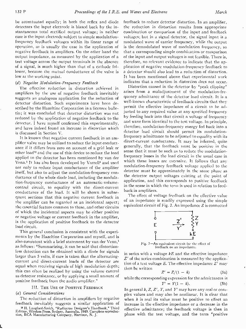
132 P Proceedings of the I.R.E. and Waves and Electrons March
be accentuated equally; in both the reflex and diodedetectors the input electrode is biased back by the in-stantaneous total rectified output voltage ; in neithercase is the input electrode subject to simple modulation -frequency feedback voltages within its linear range ofoperation, as is usually the case in the application ofnegative feedback in amplifiers. On the other hand theoutput impedance, as measured by the application of atest voltage across the output terminals in the absenceof a signal, is much higher than that of a cathode fol-lower, because the mutual conductance of the valve islow at the working point.(d) Negative Modulation -Frequency Feedback
The effective reduction in distortion achieved inamplifiers by the use of negative feedback inevitablysuggests an analogous application for the reduction ofdetector distortion. Such experiments have been de-scribed by the Hazeltine Corporation in a licensee bulle-tin ; it was concluded that detector distortion was notreduced by the application of negative feedback to thedetector. I have myself confirmed this experimentally,and have indeed found an increase in distortion whichis discussed in Section V.
It is known that negative current feedback in an am-plifier valve may be utilized to reduce the input conduct-ance if it differs from zero on account of a grid leak orother load12 and the use of this device to reduce the loadapplied to the detector has been mentioned by van derVenn.' It has also been developednot only to reduce input conductance of the amplifieritself, but also to adjust the modulation -frequency con-ductance of the whole diode load, including the modula-tion -frequency conductance of an automatic -volume -
control circuit, to equality with the direct -currentconductance of the load. It will be shown in subse-quent sections that this negative current feedback inthe amplifier can be regarded as an incidental aspect;the essential feature common to these, and other circuitsof which the incidental aspects may be either positiveor negative voltage or current feedback in the amplifier,is the application of positive feedback to the detectorload circuit.
This general conclusion is consistent with the experi-ments by the Hazeltine Corporation and myself, and isalso consistent with a brief statement by van der Venn,'as follows: "Summarizing, it can be said that distortion -less detection can be obtained with a diode for signalslarger than 5 volts, if care is taken that the alternating -current and direct -current loads of the detector areequal when receiving signals of high modulation depth;this can often be realized by using the volume controlas detector resistance, or by applying a small amount ofpositive feedback from the audio amplifier."
III. THE USE OF POSITIVE FEEDBACK(a) General Considerations
The reduction of distortion in amplifiers by negativefeedback inevitably suggests a similar application of
" H. Langford -Smith, "Radiotron Designer's Handbook," ThirdEdition, Wireless Press, Sydney, Australia, 1940. Complete reproduc-tion, RCA Manufacturing Company, Harrison, N. J.
feedback to reduce detector distortion. In an amplifier,the reduction in distortion results from appropriatecombination or comparison of the input and feedbackvoltages; but in a signal detector, the signal input is amodulated wave of carrier frequency, while the outputis the demodulated wave of modulation frequency, sothat a corresponding simple combination or comparisonof the input and output voltages is not feasible. There is,therefore, no relevant evidence to indicate that the ap-plication of negative modulation -frequency feedback toa detector should also lead to a reduction of distortion.It has been mentioned above that experimental workindicates that a reduction in distortion does not occur.
Distortion caused in the detector by "peak clipping"arises from a maladjustment of the modulation -fre-quency admittance of the detector load circuit. It is awell-known characteristic of feedback circuits that theypermit the effective impedance of a circuit to be ad-justed to any required value at any specified frequencyby feeding back into that circuit a voltage of frequencyand wave form identical to the test voltage. In principle,therefore, modulation -frequency energy fed back into adetector load circuit should permit its modulation -frequency admittance to be adjusted to equality with itsdirect -current conductance. It may be inferred, quitegenerally, that the feedback must be positive in thesense that it must be such as to reduce the modulation -frequency losses in the load circuit in the usual case inwhich these losses are excessive. It follows that anymodulation -frequency feedback voltage applied to thedetector must be approximately in the same phase asthe detector output voltages existing at the point ofapplication, and this corresponds to positive feedbackin the sense in which the term is used in relation to feed-back in amplifiers.
The effect of voltage feedback on the effective valueof an impedance is readily expressed using the simpleequivalent circuit of Fig. 2. An impedance Z is connected
Fig. 2-An equivalent circuit for the effect offeedback on an impedance.
in series with a voltage kE and the effective impedanceZ' of the series combination is measured by the applica-tion of a test voltage E. The effective impedance Z' maythen be written
Z' = Z/(1 - k) (5a)
while the corresponding expression for the admittances isY' = Y(1 - k). (5b)
In general k, Z, Z', Y, and Y' may have any real or com-plex values and may also be nonlinear. It is clear thatwhen k is real its value must be positive to effect anincrease in the effective impedance or a decrease in theeffective admittance; the feedback voltage is then inphase with the test voltage, and the term "positive
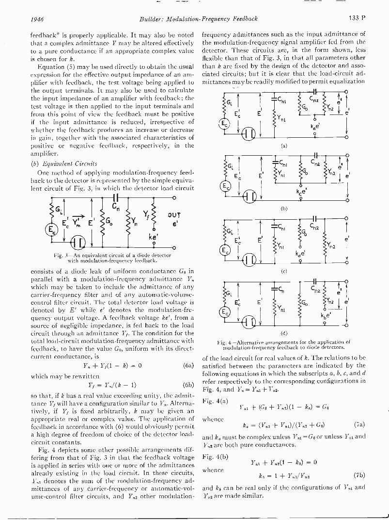
1946 Builder: Modulation -Frequency Feedback 133 P
feedback" is properly applicable. It may also be notedthat a complex admittance Y may be altered effectivelyto a pure conductance if an appropriate complex valueis chosen for k.
Equation (5) may be used directly to obtain the usualexpression for the effective output impedance of an am-plifier with feedback, the test voltage being applied tothe output terminals. It may also be used to calculatethe input impedance of an amplifier with feedback; thetest voltage is then applied to the input terminals andfrom this point of view the feedback must be positiveif the input admittance is reduced, irrespective ofwhether the feedback produces an increase or decreasein gain, together with the associated characteristics ofpositive or negative feedback, respectively, in theamplifier.
(b) Equivalent CircuitsOne method of applying modulation -frequency feed-
back to the detector is represented by the simple equiva-lent circuit of Fig. 3, in which the detector load circuit
Fig. 3-An equivalent circuit of a diode detectorwith modulation -frequency feedback.
consists of a diode leak of uniform conductance Go inparallel with a modulation -frequency admittance Y.which may be taken to include the admittance of anycarrier -frequency filter and of any automatic -volume -control filter circuit. The total detector load voltage isdenoted by E' while e' denotes the modulation -fre-quency output voltage. A feedback voltage ke' , from asource of negligible impedance, is fed back to the loadcircuit through an admittance Yf. . The condition for thetotal load -circuit modulation -frequency admittance withfeedback, to have the value Go, uniform with its direct -current conductance, is
Y. + Y,(1 - = 0 (6a)
which may be rewritten171= 17,./(k - 1) (6b)
so that, if k has a real value exceeding unity, the admit-tance Yf will have a configuration similar to Y. Alterna-tively, if 171 is fixed arbitrarily, k may be given anappropriate real or complex value. The application offeedback in accordance with (6) would obviously permita high degree of freedom of choice of the detector load -circuit constants.
Fig. 4 depicts some other possible arrangements dif-fering from that of Fig. 3 in that the feedback voltageis applied in series with one or more of the admittancesalready existing in the load circuit. In these circuits,Y,1 denotes the sum of the modulation -frequency ad-mittances of any carrier -frequency or automatic -vol-ume -control filter circuits, and Yn2 other modulation -
frequency admittances such as the input admittance ofthe modulation -frequency signal amplifier fed from thedetector. These circuits are, in the form shown, lessflexible than that of Fig. 3, in that all parameters otherthan k are fixed by the design of the detector and asso-ciated circuits; but it is clear that the load -circuit ad-mittances may be readily modified to permit equalization
(a)
(d)
Fig. 4-Alternative arrangements for the application ofmodulation -frequency feedback to diode detectors.
of the load circuit for real values of k. The relations to besatisfied between the parameters are indicated by thefollowing equations in which the subscripts a, b, c, and drefer respectively to the corresponding configurations inFig. 4, and Y. = Y.1+ Y.2.
Fig. 4(a)
whence
Y,,1 + (Go + Y.2)(1 - ka) = Go
ka = (17.2 + Y.1)/(17.2 + Go) (7a)
and ka must be complex unless Yni = Go or unless Y.1 andY,2 are both pure conductances.
Fig. 4(b)
whenceY.1 + Y.2(1 - kb) = 0
kb = 1 + Y.1/17.2 (7b)
and kb can be real only if the configurations of Yni andI7.2 are made similar.
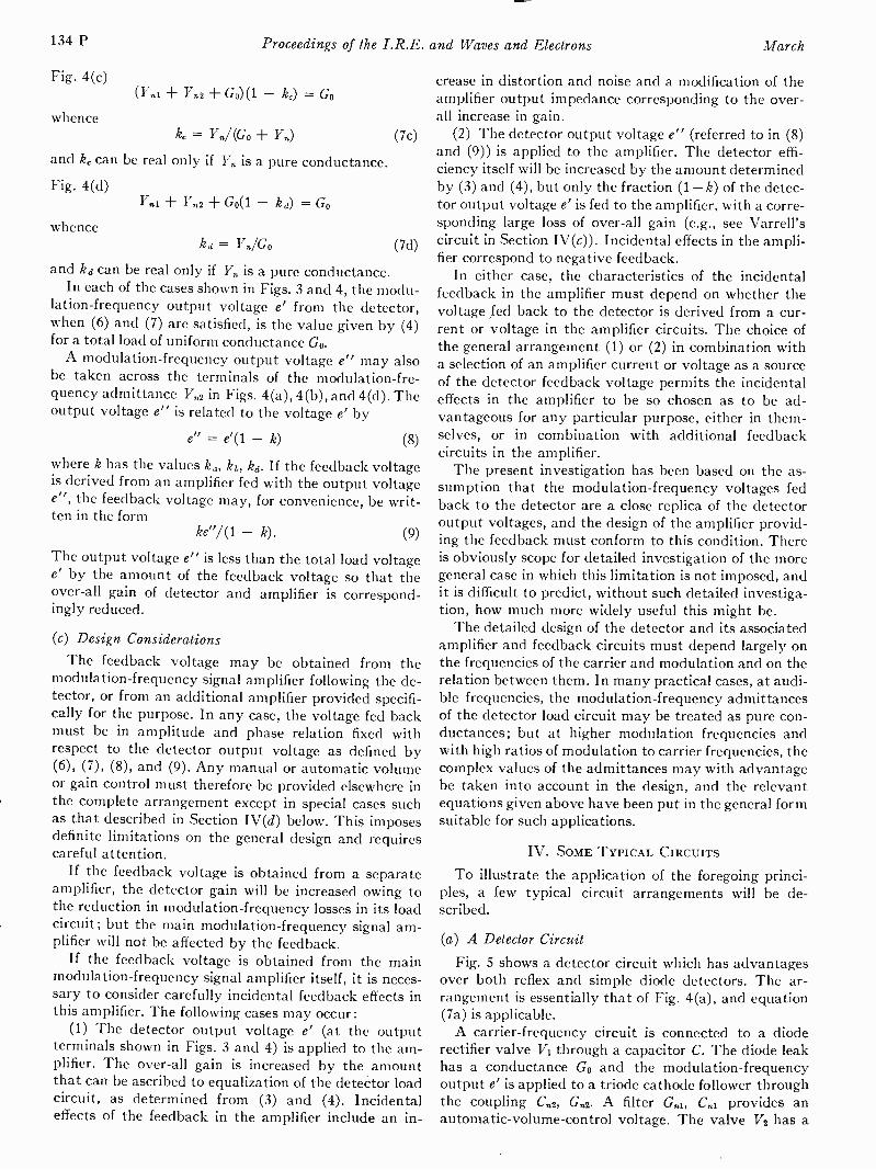
134 P
Fig. 4(c)
whence
and k, can be real only if 17,, is a pure conductance.
Fig. 4(d)
whence
Proceedings of the I.R.E. and Waves and Electrons March
(17n1 + Yn2 + Go) (1 - 14) = Go
kc = Y./(Go F.) (7c)
+ Yn2 + GO(1 kd) = GO
kd = Y./Go (7d)
and kd can be real only if 17 is a pure conductance.In each of the cases shown in Figs. 3 and 4, the modu-
lation -frequency output voltage e' from the detector,when (6) and (7) are satisfied, is the value given by (4)for a total load of uniform conductance Go.
A modulation -frequency output voltage e" may alsobe taken across the terminals of the modulation -fre-quency admittance 17.2 in Figs. 4(a), 4(b), and 4(d). Theoutput voltage e" is related to the voltage e' by
e" = e'(1 - k) (8)
where k has the values ka, kb, kd. If the feedback voltageis derived from an amplifier fed with the output voltagee", the feedback voltage may, for convenience, be writ-ten in the form
ke"/(1 - k). (9)
The output voltage e" is less than the total load voltagee' by the amount of the feedback voltage so that theover-all gain of detector and amplifier is correspond-ingly reduced.
(c) Design Considerations
The feedback voltage may be obtained from themodulation -frequency signal amplifier following the de-tector, or from an additional amplifier provided specifi-cally for the purpose. In any case, the voltage fed backmust be in amplitude and phase relation fixed withrespect to the detector output voltage as defined by(6), (7), (8), and (9). Any manual or automatic volumeor gain control must therefore be provided elsewhere inthe complete arrangement except in special cases suchas that described in Section IV(d) below. This imposesdefinite limitations on the general design and requirescareful attention.
If the feedback voltage is obtained from a separateamplifier, the detector gain will be increased owing tothe reduction in modulation -frequency losses in its loadcircuit; but the main modulation -frequency signal am-plifier will not be affected by the feedback.
If the feedback voltage is obtained from the mainmodulation -frequency signal amplifier itself, it is neces-sary to consider carefully incidental feedback effects inthis amplifier. The following cases may occur:
(1) The detector output voltage e' (at the outputterminals shown in Figs. 3 and 4) is applied to the am-plifier. The over-all gain is increased by the amountthat can be ascribed to equalization of the detector loadcircuit, as determined from (3) and (4). Incidentaleffects of the feedback in the amplifier include an in-
crease in distortion and noise and a modification of theamplifier output impedance corresponding to the over-all increase in gain.
(2) The detector output voltage e" (referred to in (8)and (9)) is applied to the amplifier. The detector effi-ciency itself will be increased by the amount determinedby (3) and (4), but only the fraction (1-k) of the detec-tor output voltage e' is fed to the amplifier, with a corre-sponding large loss of over-all gain (e.g., see Varrell'scircuit in Section IV(c)). Incidental effects in the ampli-fier correspond to negative feedback.
In either case, the characteristics of the incidentalfeedback in the amplifier must depend on whether thevoltage fed back to the detector is derived from a cur-rent or voltage in the amplifier circuits. The choice ofthe general arrangement (1) or (2) in combination witha selection of an amplifier current or voltage as a sourceof the detector feedback voltage permits the incidentaleffects in the amplifier to be so chosen as to be ad-vantageous for any particular purpose, either in them-selves, or in combination with additional feedbackcircuits in the amplifier.
The present investigation has been based on the as-sumption that the modulation -frequency voltages fedback to the detector are a close replica of the detectoroutput voltages, and the design of the amplifier provid-ing the feedback must conform to this condition. Thereis obviously scope for detailed investigation of the moregeneral case in which this limitation is not imposed, andit is difficult to predict, without such detailed investiga-tion, how much more widely useful this might be.
The detailed design of the detector and its associatedamplifier and feedback circuits must depend largely onthe frequencies of the carrier and modulation and on therelation between them. In many practical cases, at audi-ble frequencies, the modulation -frequency admittancesof the detector load circuit may be treated as pure con-ductances; but at higher modulation frequencies andwith high ratios of modulation to carrier frequencies, thecomplex values of the admittances may with advantagebe taken into account in the design, and the relevantequations given above have been put in the general formsuitable for such applications.
IV. SOME TYPICAL CIRCUITS
To illustrate the application of the foregoing princi-ples, a few typical circuit arrangements will be de-scribed.
(a) A Detector Circuit
Fig. 5 shows a detector circuit which has advantagesover both reflex and simple diode detectors. The ar-rangement is essentially that of Fig. 4(a), and equation(7a) is applicable.
A carrier -frequency circuit is connected to a dioderectifier valve V1 through a capacitor C. The diode leakhas a conductance Go and the modulation -frequencyoutput e' is applied to a triode cathode follower throughthe coupling C,,2, Gn2. A filter G.1, C.1 provides anautomatic -volume -control voltage. The valve V2 has a
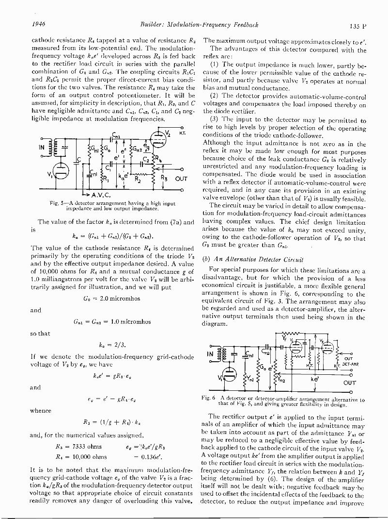
1946 Builder: Modulation -Frequency Feedback 135 P
cathode resistance R4 tapped at a value of resistance R3measured from its low -potential end. The modulation -frequency voltage kae' developed across R3 is fed backto the rectifier load circuit in series with the parallelcombination of Go and Ga2. The coupling circuits RIC'and R2C2 permit the proper direct -current bias condi-tions for the two valves. The resistance R4 may take theform of an output control potentiometer. It will beassumed, for simplicity in description, that RI, R2, and Chave negligible admittance and C.1, Cn2, C1, and C2 neg-ligible impedance at modulation frequencies.
Fig. 5-A detector arrangement having a high inputimpedance and low output impedance.
The value of the factor ka is determined from (7a) andis
ka = (Gal + G2)/(Go + G.2).
The value of the cathode resistance R4 is determinedprimarily by the operating conditions of the triode V2and by the effective output impedance desired. A valueof 10,000 ohms for R4 and a mutual conductance g of1.0 milliangstrom per volt for the valve V2 will be arbi-trarily assigned for illustration, and we will put
Go = 2.0 micromhos
and
G1 = G2 = 1.0 micromhos
so that
ka = 2/3.
If we denote the modulation -frequency grid -cathodevoltage of V2 by e, we have
kae' = gR3. eg
and
e = e' - gR4. e,
whence
R3 = (1/g + R4) ka
and, for the numerical values assigned,
R3 = 7333 ohms
R4 = 10,000 ohms
e, =:!kae7gRs
= 0.136e'.
It is to be noted that the maximum modulation -fre-quency grid -cathode voltage e, of the valve V2 is a frac-tion ka/gR3 of the modulation -frequency detector outputvoltage so that appropriate choice of circuit constantsreadily removes any danger of overloading this valve.
The maximum output voltage approximates closely to e'.The advantages of this detector compared with the
reflex are:(1) The output impedance is much lower, partly be-
cause of the lower permissible value of the cathode re-sistor, and partly because valve V2 operates at normalbias and mutual conductance.
(2) The detector provides automatic -volume -controlvoltages and compensates the load imposed thereby onthe diode rectifier.
(3) The input to the detector may be permitted torise to high levels by proper selection of the operatingconditions of the triode cathode -follower.Although the input admittance is not zero as in thereflex it may be made low enough for most purposesbecause choice of the leak conductance Go is relativelyunrestricted and any modulation -frequency loading iscompensated. The diode would be used in associationwith a reflex detector if automatic -volume -control wererequired, and in any case its provision in an existingvalve envelope (other than that of V2) is usually feasible.
The circuit may be varied in detail to allow compensa-tion for modulation -frequency load -circuit admittanceshaving complex values. The chief design limitationarises because the value of lea may not exceed unity,owing to the cathode -follower operation of V2, so thatGo must be greater than Gal.
(b) An Alternative Detector Circuit
For special purposes for which these limitations are adisadvantage, but for which the provision of a lesseconomical circuit is justifiable, a more flexible generalarrangement is shown in Fig. 6, corresponding to theequivalent circuit of Fig. 3. The arrangement may alsobe regarded and used as a detector -amplifier, the alter-native output terminals then used being shown in thediagram.
NOUT
H.T. DET-AHP0O
OUT
0Fig. 6-A detector or detector -amplifier arrangement alternative to
that of Fig. 5, and giving greater flexibility in design.
The rectifier output e' is applied to the input termi-nals of an amplifier of which the input admittance maybe taken into account as part of the admittance Y.1 ormay be reduced to a negligible effective value by feed-back applied to the cathode circuit of the input valve V2.A voltage output ke' from the amplifier output is appliedto the rectifier load circuit in series with the modulation-
frequency admittance VI, the relation between k and I ifbeing determined by (6). The design of the amplifieritself will not be dealt with; negative feedback maybeused to offset the incidental effects of the feedback to thedetector, to reduce the output impedance and improve
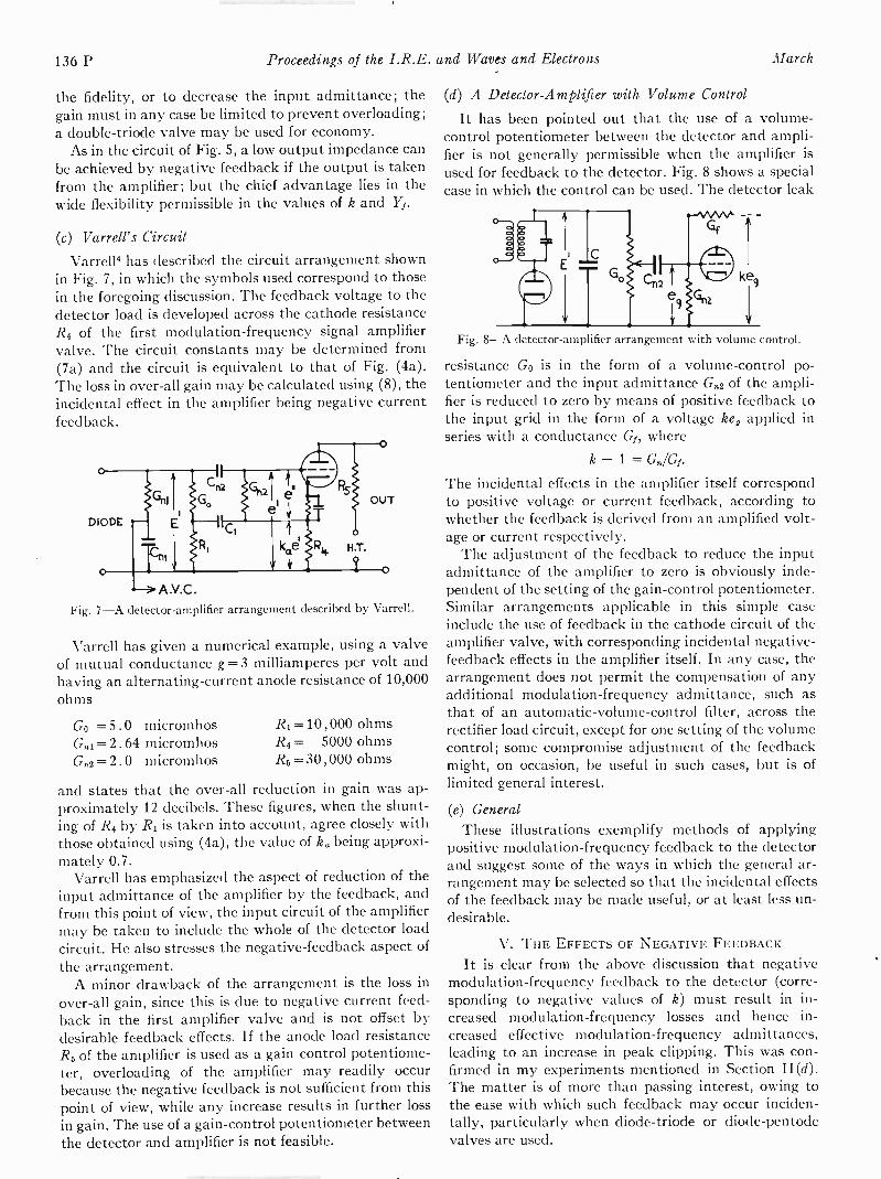
136 P Proceedings of the I.R.E. and Waves and Electrons March
the fidelity, or to decrease the input admittance; thegain must in any case be limited to prevent overloading;a double -triode valve may be used for economy.
As in the circuit of Fig. 5, a low output impedance canbe achieved by negative feedback if the output is takenfrom the amplifier; but the chief advantage lies in thewide flexibility permissible in the values of k and V1.
(c) Varrell's Circuit
Varre114 has described the circuit arrangement shownin Fig. 7, in which the symbols used correspond to thosein the foregoing discussion. The feedback voltage to thedetector load is developed across the cathode resistanceR4 of the first modulation -frequency signal amplifiervalve. The circuit constants may be determined from(7a) and the circuit is equivalent to that of Fig. (4a).The loss in over-all gain may be calculated using (8), theincidental effect in the amplifier being negative currentfeedback.
Fig. 7-A detector -amplifier arrangement described by Varrell.
Varrell has given a numerical example, using a valveof mutual conductance g= 3 milliamperes per volt andhaving an alternating -current anode resistance of 10,000ohms
Go =5 . 0 micromhosGni = 2.64 micromhosGn2= 2 .0 micromhos
Ri =10,000 ohmsR4 = 5000 ohmsR5 = 30 , 000 ohms
and states that the over-all reduction in gain was ap-proximately 12 decibels. These figures, when the shunt-ing of R4 by R1 is taken into account, agree closely withthose obtained using (4a), the value of ka being approxi-mately 0.7.
Varrell has emphasized the aspect of reduction of theinput admittance of the amplifier by the feedback, andfrom this point of view, the input circuit of the amplifiermay be taken to include the whole of the detector loadcircuit. He also stresses the negative -feedback aspect ofthe arrangement.
A minor drawback of the arrangement is the loss inover-all gain, since this is due to negative current feed-back in the first amplifier valve and is not offset bydesirable feedback effects. If the anode load resistanceR6 of the amplifier is used as a gain control potentiome-ter, overloading of the amplifier may readily occurbecause the negative feedback is not sufficient from thispoint of view, while any increase results in further lossin gain. The use of a gain -control potentiometer betweenthe detector and amplifier is not feasible.
(d) A Detector -Amplifier with Volume Control
It has been pointed out that the use of a volume -control potentiometer between the detector and ampli-fier is not generally permissible when the amplifier isused for feedback to the detector. Fig. 8 shows a specialcase in which the control can be used. The detector leak
Fig. 8-A detector -amp ifier arrangement with volume control.
resistance Go is in the form of a volume -control po-tentiometer and the input admittance G.2 of the ampli-fier is reduced to zero by means of positive feedback tothe input grid in the form of a voltage keg applied inseries with a conductance G1, where
k - 1 = G./Gf.The incidental effects in the amplifier itself correspondto positive voltage or current feedback, according towhether the feedback is derived from an amplified volt-age or current respectively.
The adjustment of the feedback to reduce the inputadmittance of the amplifier to zero is obviously inde-pendent of the setting of the gain -control potentiometer.Similar arrangements applicable in this simple caseinclude the use of feedback in the cathode circuit of theamplifier valve, with corresponding incidental negative -feedback effects in the amplifier itself. In any case, thearrangement does not permit the compensation of anyadditional modulation -frequency admittance, such asthat of an automatic -volume -control filter, across therectifier load circuit, except for one setting of the volumecontrol; some compromise adjustment of the feedbackmight, on occasion, be useful in such cases, but is oflimited general interest.
(e) GeneralThese illustrations exemplify methods of applying
positive modulation -frequency feedback to the detectorand suggest some of the ways in which the general ar-rangement may be selected so that the incidental effectsof the feedback may be made useful, or at least less un-desirable.
V. THE EFFECTS OF NEGATIVE FEEDBACK
It is clear from the above discussion that negativemodulation -frequency feedback to the detector (corre-sponding to negative values of k) must result in in-creased modulation -frequency losses and hence in-creased effective modulation -frequency admittances,leading to an increase in peak clipping. This was con-firmed in my experiments mentioned in Section II (d).The matter is of more than passing interest, owing tothe ease with which such feedback may occur inciden-tally, particularly when diode -triode or diode -pentodevalves are used.
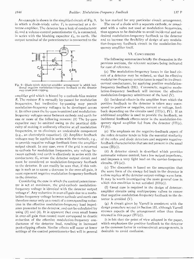
1946 Builder: Modulation -Frequency Feedback 137 P
An example is shown in the simplified circuit of Fig. 9,in which a diode -triode valve V1 is connected as a de-tector -amplifier. The detector has a leak of conductanceGo and a volume -control potentiometer G. is connected,in series with the blocking capacitor C., to earth. Theoutput terminal of the potentiometer is connected to the
Fig. 9-Diode-triode detector -amplifier arrangement in which inci-dental negative modulation -frequency feedback to the detectormay cause peak clipping.
amplifier grid which is biased by a cathode -bias resistorR. The resistor R is normally by-passed for modulationfrequencies, but ineffective by-passing may permitmodulation -frequency voltages to be developed acrossit. In other cases the by-pass is omitted and modulation -
frequency voltages occur between cathode and earth forone or more of the following reasons: (1) The by-passcapacitor may be omitted owing to the practical diffi-culty of making it uniformly effective at all modulationfrequencies, or to eliminate an undesirable component(e.g., an electrolytic capacitor). (2) Amplifier feedbackvoltages may be applied in series with the cathode, e.g.,to provide negative voltage feedback from the amplifieroutput circuit. In any case, even if the grid is returnedto cathode for modulation frequencies, any voltage be-tween cathode and earth is effectively in series with theconductance Gn across the detector output circuit andmust be considered as modulation -frequency feedbackto the detector. It can readily be seen that, if this volt-age is such as to cause a decrease in the over-all gain, itmust represent negative modulation -frequency feedbackto the detector.
Considering the case in which the control potentiome-ter is set at maximum, the grid -cathode modulation -frequency voltage is identical with the detector outputvoltage e'. Any reduction in over-all gain due to a modu-lation -frequency voltage between cathode and earth cantherefore occur only as a result of a corresponding reduc-tion in the effective modulation -frequency load imped-ance presented to the detector, and can be calculated byusing (3) and (4). It is apparent that even small lossesin over-all gain thus caused must correspond to drasticreduction of the effective modulation -frequency con-ductance of the detector load, resulting in increasedpeak -clipping effects. Similar effects will occur at lowersettings of the control potentiometer but will in general
be less marked for any particular circuit arrangement.The use of a diode with a separate cathode, or associ-
ated with a valve not used at modulation frequencies,thus appears to be desirable to avoid incidental and un-desired modulation -frequency feedback to the detectorand to increase the flexibility of design of any modula-tion -frequency feedback circuit in the modulation -fre-quency amplifier itself.
VI. CONCLUSIONS
The following summarizes briefly the discussion in theprevious sections, the relevant sections being indicatedfor ease of reference.
(a) The modulation -frequency losses in the load cir-cuit of a detector may be reduced, so that its effectivemodulation -frequency conductance is equal to its direct-
current conductance, by applying positive modulation -
frequency feedback (III). Conversely, negative modu-lation -frequency feedback will increase the effectivemodulation -frequency admittance of the load (V).
(b) Incidental effects in the amplifier from which thepositive feedback to the detector is taken may corre-spond to positive or negative, current or voltage, feed-back depending on the circuits used (III(c), IV). If anadditional amplifier is used to provide the feedback, noincidental feedback effects occur in the modulation -fre-quency signal amplifier fed from the detector (III(c),IV(b)).
(c) The emphasis on the negative -feedback aspect ofthe reflex detector tends to hide the essential similarityof the reflex and diode detectors and suggests negative-
feedback characteristics that are not present in the usualsense (II (c)).
(d) A detector circuit is described which providesautomatic volume control, has a low output impedance,and imposes a very light load on the carrier -frequencycircuits. (IV(a)).
(e) The discussion is based on the assumption thatthe wave form of the energy fed back to the detector isa close replica of the detector output -voltage wave form.It may be worth investigating the more general case inwhich this condition is not satisfied (III(c)).
(f) Great care is required in the design of detector -
amplifier circuits using multipurpose valves to ensurethat negative modulation -frequency feedback to the de-tector is avoided (V).
(g) A circuit given by Varrell is consistent with thedesign procedure set out in Section III, although Varrellstresses aspects of the arrangement other than thosestressed in this paper (IV(c)).
It is felt that the point of view adopted in the paper,which emphasizes the positive feedback to the detectoras the common factor in various circuit arrangements, isdesirable to avoid confusion.
The Ideal Low -Pass Filter in the form of a
Dispersionless Lag Line*MARCEL J.
Summary-Some theoretical and practical aspects of the designof the ideal low-pass filter in the form of a dispersionless lag line areconsidered. It is shown, in particular, that an artificial line made upof series inductances and shunt capacitances, with 18 per cent aidingmutual inductance between adjacent coils and 8 per cent shuntcapacitance between alternate tie points, forms, for many purposes,a sufficiently good approximation of a dispersionless lag line. Themathematical study of the function f(n) =for (1 -cos 0/02) cos nybdo,which is of pertinent interest in lag -line theory, is given in an ap-pendix.
THE IDEAL low-pass filter, which is defined as afilter having linear phase characteristics and noattenuation up to the cutoff frequency, and infi-
nite attenuation beyond, forms a useful mathematicalconcept in the theory of communication, as well as achallenge to the engineer to design as close an approxi-mation to the ideal as possible.
Inasmuch as any delay networks with linear phasecharacteristics, and, in particular, the lag line, are, es-sentially, ideal low-pass filters, the theory presentedherein will be concerned with the lag -line type of con-struction. This construction offers the advantage, overother types of delay networks, of having a multiplicityof tie points from which variously delayed but otherwiseidentical signals can be derived.
The original basic lag line was composed of equal se-ries inductances and shunt capacitances. This arrange-ment offered good frequency cutoff, but poor phase char-acteristics. A notable improvement in the phase charac-teristics of lag lines was contributed by Pierce,' whodiscovered that a certain amount of negative (aiding)mutual inductance, between adjacent sections, unavoid-able when the coils are coaxially mounted to yield asimple construction, actually is beneficial.' The consid-eration of mutual inductance between adjacent sectionsleads naturally to the consideration of mutual induct-ance between alternate and more distant sections, andan investigation of this possibility indicated that suit-able design values for these various parameters yieldedincreasingly more linear phase characteristics. Un-fortunately, the practical coaxial construction yieldsthe wrong sign for the mutual inductance betweenalternate sections, when the connections are so made as
Decimal classification: R386. Original manuscript receivedby the Institute, March 15, 1945; revised manuscript received, Sep-tember 5, 1945.
t Signal Corps Engineering Laboratories, Bradley Beach, N. J.1 G. W. Pierce, "Artificial electric lines," Proc. Amer. Acad. Arts
and Sci., vol. 57, pp. 195-212; 1921.2 The utilization of such a lag line in a special bridge network for
the purpose of obtaining any desired impulse response, and, in par-ticular, the impulse response of an ideal low-pass filter, has been de-scribed by M. Levy, in "The impulse response of electrical networks,with special reference to the use of artificial lines in network design,"Jour. I.E.E. (London), Part III, pp. 153-164; December, 1943.
E. GOLAYt
to yield the correct value between adjacent sections.This situation could be circumvented by the device ofproviding special small additional coils designed to yieldthe mutual inductances of the correct sign and magni-tude between alternate and more distant sections, butthe resulting construction becomes unwieldy, besidesintroducing troublesomely large capacitances wherethey may not be wanted. This consideration led to theinvestigation of the effect of shunt capacitances acrossone or more coils, and the more general theory thusevolved yielded eventually such simple "recipes" forlag -line construction as the requirement of 18 per centmutual inductance between coaxially mounted adjacentcoils and of small capacitors between alternate tiepoints, the capacitance of these capacitorg being 8 percent of the capacitance of the line -to -ground capacitors.
For a simplified basic theory of the ideal lag line weneed only consider a recurrent assembly of series induct-ances L with mutual inductance a1L, a2L, etc., betweenadjacent, alternate, and more distant sections, and ca-pacitances C to ground (Fig. 1). The inductances and
Fig. 1-Schematic diagram of lag line with mutual inductances.
capacitances are assumed to have infinite Q and zeropower factor, respectively. Kirchhoff equations for thenth junction and the nth loop can be written
in - in 1-1
Vn Vn+1
= jwCvn
= iCar, [in+1 - al( in +(1)
- a2(in-1 2n+3) - . . . 1. (2)
The recurrent character of the network permitswrite, generally
vn
Vn+1 - in+1 in
in+1 - = eis6.
us to
(3)
Substitution in (1) and (2) of all i's and v's by their ex-pressions in terms of in and vn, multiplication of (1) and(2), member by member, and division by invn, yields
2(1-cos 0) = w2LC(1-2ai cos -2a2 cos 20- ).(4)
The requirement of no attenuation below cutoff andof no phase distortion may be expressed by the conditionthat cp be real and proportional to w
k4,2 = ,2.LE(5)
138 P Proceedings of the I.R.E. and Waves and Electrons March, 1946
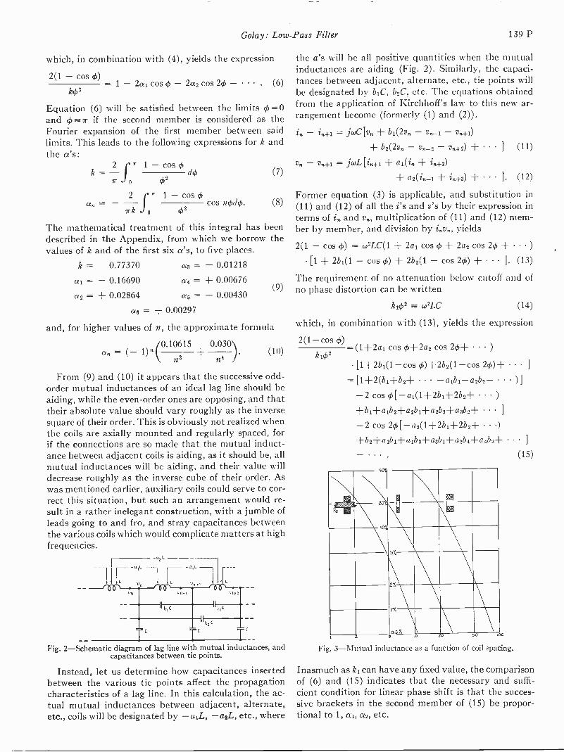
Golay: Low -Pass Filter 139 P
which, in combination with (4), yields the expression
2(1 - cos 4,)= 1 - 2a1 cos ¢ - 2a2 cos 24, - . (6)
Equation (6) will be satisfied between the limits 4, = 0and 4, --.2r if the second member is considered as theFourier expansion of the first member between saidlimits. This leads to the following expressions for k andthe a's:
(14)2 r 1 - cos 4.7 J
2 r 1 - cosan = - cos Odck.irk
The mathematical treatment of this integral hasdescribed in the Appendix, from which we borrow thevalues of k and of the first six a's, to five places.
(7)
k = 0.77370
al = - 0.16690a2 = + 0.02864
a> = - 0.01218a4 = + 0.00676ao = - 0.00430
(8)
been
(9)
ao = + 0.00297
and, for higher values of n, the approximate formula
/0.10615 0.030\(10)an = (- 1)n
n2 n4 )From (9) and (10) it appears that the successive odd -
order mutual inductances of an ideal lag line should beaiding, while the even -order ones are opposing, and thattheir absolute value should vary roughly as the inversesquare of their order. This is obviously not realized whenthe coils are axially mounted and regularly spaced, forif the connections are so made that the mutual induct-ance between adjacent coils is aiding, as it should be, allmutual inductances will be aiding, and their value willdecrease roughly as the inverse cube of their order. Aswas mentioned earlier, auxiliary coils could serve to cor-rect this situation, but such an arrangement would re-sult in a rather inelegant construction, with a jumble ofleads going to and fro, and stray capacitances betweenthe various coils which would complicate matters at highfrequencies.
L-L vn
in L71+1 v
il
i.n.1
62 C
1' TFig. 2-Schematic diagram of lag line with mutual inductances, and
capacitances between tie points.
Instead, let us determine how capacitances insertedbetween the various tie points affect the propagationcharacteristics of a lag line. In this calculation, the ac-tual mutual inductances between adjacent, alternate,etc., coils will be designated by -a1L, -a2L, etc., where
the a's will be all positive quantities when the mutualinductances are aiding (Fig. 2). Similarly, the capaci-tances between adjacent, alternate, etc., tie points willbe designated by biC, b2C, etc. The equations obtainedfrom the application of Kirchhoff's law to this new ar-rangement become (formerly (1) and (2)).
in - in+). = jo)C[vn bi(2vn - vn--1 - vn+,)
b2(2v - vn_2 - 744+2) +
= jwL [in+1 al(in in+2)
a2( in-1 + in+3) +
Vn+1
(11)
]. (12)
Former equation (3) is applicable, and substitution in(11) and (12) of all the i's and v's by their expression interms of in and v,,, multiplication of (11) and (12) mem-ber by member, and division by inv, yields
2(1 - cos 4)) = w2LC(1 2a1 cos 4, + 2a2 cos 20 + )
[1 + 2b1(1 - cos 4) 2b2(1 - cos 20) + j. (13)
The requirement of no attenuation below cutoff and ofno phase distortion can be written
144i2 = co'LC (14)
which, in combination with (13), yields the expression
2(1-cos 4>)-(1±2ai cos 0+2a2 cos 20+ )
k02 [1+2b1(1-cos (0+2b2(1-cos 24)+
= [1+2(b1 -1-b2+ - -a2b2- )]
-2 cos 4[-ai(1-1-2b1+2b2+ )
+bi+aib24-a2bi+a2b34-a3b2-1- ]
-2 cos 24,[-a2(1+2b1+2b2+ .)
-1-b2-1-aibri-aib3-l-a3b1±a2b4-1-a4b2+ . .]
(15)
Fig 3-Mutual inductance as a function of coil spacing.
Inasmuch as ki can have any fixed value, the comparisonof (6) and (15) indicates that the necessary and suffi-cient condition for linear phase shift is that the succes-sive brackets in the second member of (15) be propor-tional to 1, al, a2, etc.

140 P Proceedings of the I.R.E. and Waves and Electrons March
The b's can be chosen at will, but little choice is avail-able for the a's when the practical coaxial constructionis adopted, in which the mutual inductance betweenadjacent coils determines, substantially, all others. Thethree curves of Fig. 3 are plots, on doubly logarithmicpaper, of the mutual inductance as a function of the dis-tance, for the two different shapes of air -core coils illus-trated, as well as for coils mounted on a common ironcore of permeability 22. If the fuller air -core coils areused, and the spacing is adjusted for 18 per cent mutualinductance between adjacent sections, the mutual in-ductance between alternate, etc., sections can be veri-fied to be 4.0 per cent, 1.4 per cent, 0.6 per cent, 0.3 percent, etc., which gives the a's. If capacitance betweenalternate tie points only is used, so that b2= 8 per centand all other b's vanish, it can be verified that the suc-cessive brackets of the last member of (15) are propor-tional to
1, - 0.168, 0.029, - 0.002, - 0.003, - 0.002, etc.,
and can be compared with the required values for the a's
1, - 0.167, 0.029, - 0.012, 0.007, - 0.004.
If flatter coils are used, the slightly higher mutual in-ductances between far sections would yield more nega-tive values for the 4th and 5th brackets, therebyimproving the agreement of the 4th bracket with thetheoretical value. The agreement of the 5th bracketwould be slightly worsened, but this could be correctedwith a little capacitance between every tie point and the4th next, so as to yield a value for b4 which will permitagreement of the 5th bracket with the required value.Thus if the coils are spaced for 18.2 per cent mutualinductance between adjacent sections, the other mutualinductance derived from the center curve of Fig. 3 willbe: 5.2 per cent, 2.1 per cent, 1.05 per cent, 0.6 per cent,0.4 per cent, etc. Assuming now for b2 and b4 the valuesof 9.6 per cent and 1.6 per cent respectively, the succes-sive brackets of (15) will be proportional to
1, - 0.167, 0.028, - 0.004, 0.007, - 0.002, etc.,
thereby yielding an appreciably better agreement withthe theoretical values than the figures based on thecurve for compact coils. Such an arrangement would ap-pear to be of especial value in radio -frequency lag linesof many sections, for at such frequencies flat coils yieldas good a Q as the more compactly shaped ones.
The curve of Fig. 3 representing the mutual induct-ance versus spacing of compact coils having a commoniron core has approximately the same slope as the curveobtained for the same coils without the iron core, andoffers, therefore, no possibility of a better agreement ofthe 4th bracket with the required value.
Preliminary measurements have indicated that if thecoils are flanked with discs of magnetic material, in addi-tion to the central magnetic core, the successive mutualswill decrease even less rapidly than in the case offlat air -core coils, thereby offering the possibility ofeven better phase characteristics. However, this case
cannot be represented rigorously by a single curve, be-cause a variation of the spacing between coils causes achange in their magnetic circuit.
It might be thought that placing the coils in closerproximity than is needed for approximately 18 per centmutual inductance between adjacent coils, so as to in-crease the mutual inductance between every coil and the3rd next, would yield a better agreement for the 4thbracket, but, as it turns out, the large capacitancesneeded across the coils and between alternate tie pointsyield values for the cross terms aib2, and alb, which offsetthe increase obtained for a3.
REFLECTING TERMINATION
Reflections with approximately the same small dis-tortions that occur along a line of the design describedabove, can be obtained by a proper adjustment of thecircuit constants at the end of the line. These adjust-ments are derived from the consideration of a virtualimage of the line beyond its terminated end, in whichpositive or negative image pulses are propagated.
Vrtt V V V V
"T 4 -
Fig. 4-Schematic diagram of lag line and its electrical image aboutthe last tie point.
Fig. 4 illustrates the end of a lag line and its mirrorimage about its last tie point. The pulses in the imageline are assumed to be the positive image of the pulsesin the real line, and will become, therefore, the reflectionwithout change of phase of the pulses in the real line ifcertain conditions are met. These conditions are that thevoltages induced in the coils of the real line owing totheir mutual inductance with the coils of the image linebe actually induced as the result of a modificationof the real line, and that the currents delivered by thevarious tie points of the image line to the various tiepoints of the real line be actually generated within thereal line. If the line in question is assumed to have-18 per cent and -4 per cent mutual inductance be-tween adjacent and alternate coils, respectively, and8 per cent shunt capacitance between alternate tiepoints, it will be readily seen that the absence of ashunt capacitance between points A and A' will call forno modification of the real line, inasmuch as A and A'are always at the same potential by virtue of the as-sumption made. Conversely, the absence of a mutualinductance between the last coil of the real line and itsimage will require that a voltage having the value-0.18 jcoLin+i be otherwise generated within the lastcoil of the real line, and this is accomplished by reducingthe value of the inductance of this last coil to 0.82L.Likewise, the absence of mutual inductance between thelast coil of the real line and the second coil of the image
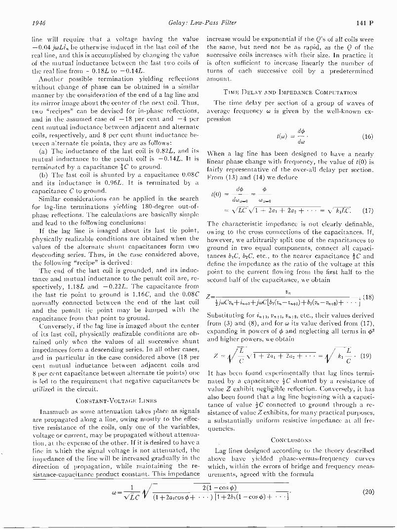
1946 Golay: Low -Pass Filter 141 P
line will require that a voltage having the value-0.04 jcoLin be otherwise induced in the last coil of thereal line, and this is accomplished by changing the valueof the mutual inductance between the last two coils ofthe real line from -0.18L to -0.14L.
Another possible termination yielding reflectionswithout change of phase can be obtained in a similarmanner by the consideration of the end of a lag line andits mirror image about the center of the next coil. Thus,two "recipes" can be devised for in -phase reflections,and in the assumed case of -18 per cent and -4 percent mutual inductance between adjacent and alternatecoils, respectively, and 8 per cent shunt inductance be-tween alternate tie points, they are as follows:
(a) The inductance of the last coil is 0.82L, and itsmutual inductance to the penult coil is -0.14L. It isterminated by a capacitance iC to ground.
(b) The last coil is shunted by a capacitance 0.08Cand its inductance is 0.96L. It is terminated by acapacitance C to ground.
Similar considerations can be applied in the searchfor lag -line terminations yielding 180 -degree out -of -phase reflections. The calculations are basically simpleand lead to the following conclusions:
If the lag line is imaged about its last tie point,physically realizable conditions are obtained when thevalues of the alternate shunt capacitances form twodescending series. Thus, in the case considered above,the following "recipe" is derived:
The end of the last coil is grounded, and its induc-tance and mutual inductance to the penult coil are, re-spectively, 1.18L and -0.22L. The capacitance fromthe last tie point to ground is 1.16C, and the 0.08Cnormally connected between the end of the last coiland the penult tie point may be lumped with thecapacitance from that point to ground.
Conversely, if the lag line is imaged about the centerof its last coil, physically realizable conditions are ob-tained only when the values of all successive shuntimpedances form a descending series. In all other cases,and in particular in the case considered above (18 percent mutual inductance between adjacent coils and8 per cent capacitance between alternate tie points) oneis led to the requirement that negative capacitances beutilized in the circuit.
CONSTANT -VOLTAGE LINES
Inasmuch as some attenuation takes place as signalsare propagated along a line, owing mostly to the effec-tive resistance of the coils, only one of the variables,voltage or current, may be propagated without attenua-tion, at the expense of the other. If it is desired to have aline in which the signal voltage is not attenuated, theimpedance of the line will be increased gradually in thedirection of propagation, while maintaining the re-sistance -capacitance product constant. This impedance
increase would be exponential if the Q's of all coils werethe same, but need not be as rapid, as the Q of thesuccessive coils increases with their size. In practice itis often sufficient to increase linearly the number ofturns of each successive coil by a predeterminedamount.
TIME DELAY AND IMPEDANCE COMPUTATION
The time delay per section of a group of waves ofaverage frequency w is given by the well-known ex-pression
t(w) =d4)
dco(16)
When a lag line has been designed to have a nearlylinear phase change with frequency, the value of 1(0) isfairly representative of the over-all delay per section.From (13) and (14) we deduce
t(0) -d4
dcow-o cow -o
= N/ LC + 2a, Jr- 2a2 + = .\/ kiLC. (17)
The characteristic impedance is not clearly definable,owing to the cross connections of the capacitances. If,however, we arbitrarily split one of the capacitances toground in two equal components, connect all capaci-tances biC, b2C, etc., to the nearer capacitance IC anddefine the impedance as the ratio of the voltage at thispoint to the current flowing from the first half to thesecond half of the capacitance, we obtain
v,'Z- (18)jwCv H-jcoC [bi (vn b2(vn-vn+2)+ . . ]
Substituting for in+1, v+1, Vn+2, etc., their values derivedfrom (3) and (8), and for w its value derived from (17),expanding in powers of ¢ and neglecting all terms in 02and higher powers, we obtain
/CL
Z = A/ - 2a1 2a2 = ki - (19)
It has been found experimentally that lag lines termi-nated by a capacitance IC shunted by a resistance ofvalue Z exhibit negligible reflection. Conversely, it hasalso been found that a lag line beginning with a capaci-tance of value IC connected to ground through a re-sistance of value Z exhibits, for many practical purposes,a substantially uniform resistive impedance at all fre-quencies.
CONCLUSIONS
Lag lines designed according to the theory describedabove have yielded phase -versus -frequency curveswhich, within the errors of bridge and frequency meas-urements, agreed with the formula
1 / 2(1 -cos 4,)w VLC (1 -1-2alcos 0+ ) +2b1(1 -cos 4)) -I- 1
(20)
142 P Proceedings of the I.R.E. and Waves and Electrons March
In designing lag lines for high frequencies and low im-pedances, it was found necessary to take into accountthe shunted capacitance of the coils, which contributesto the factor bl, and which was compensated by makinga1 and consequently b2 correspondingly larger. The limitto the application of the lag -line theory is met when thecombination of high cutoff frequency, high impedance,and high coil capacitance yield values for b1 which canjust be compensated by placing the coils at an optimumproximity, beyond which the increased capacitance be-tween the coils causes an effective increase in b1 whichis no more compensated by the increase in a1.
APPENDIX
POWER -SERIES DEVELOPMENT OF THE FUNCTION
From
f(n) = 1 - cos la4,2
cos nOdcp
1-cos4'f(n) = f0 4,2
cos niOdcp (21)
we derive, after two differentiations under the integralsign
1 sin (n - 1)2rf"(n) = -J
(1 - cos 0) cos n0d4) =2 n - 1
1 sin (n + 1)r sin nr2 n + 1 (22)
If we define F(n) as the second integral of (sin nr)/n,f(n) may be written
f(n) = 2F(n - 1) + 1F(n + 1) - F(n). (23)
The circumstance that the second member of (23) is asecond difference justifies the indetermination of thelower integral limits of F(n). The Taylor expansion ofF(n -1) and F(n+1) yields for f(n)
1 1
!
p,,(n)4Fly
(n) .
2!f(n)
1 sin nr 1 nr \"2! 4! n ) (24)
If its expansion in series is substituted for sin nor in theseries above, the (2/ -2)nd derivative of the (l+m)thexpanded term of the lth term in (24) will be the termexplicitly written out in the new summation obtainedfor f(n) in (25)
n2 m(n) = E
(2m)!
1)1+;,÷1 (2/ + 2m - 2)!R.214 -2m-1 (25)
z-i (21)!(21 + 2m - 1)!
The absolute value of every term of the double seriesabove is smaller than the corresponding term in the
double series
n I 2m oo r21+2 m-2
mmo
V E(2m)! /..1 (2/ - 2)!
= r cosh r cosh I ni r (26)
therefore the expansion of f(n) given in (25) is abso-lutely convergent for all values of n.
The value of f(0), which will be designated by Ko isequal to the partial sum corresponding to m =0 in (25)
7 73 r5f(0) = KO =
2! 3.4! 5.6!. (27)
This series is not reducible to a simpler form, whereasall other partial series, corresponding to higher valuesof m, are.
For their reduction, use will be made of the identicalrelation
(21+2m- 2) ! 2m-1
E i)p+, (2m- 2) !(21+2m- 1)!(21)!= (2m -P -1)!(2/+p) I (28)
which can be verified by observing that both sides arepolynomials in 2/ of order 2m -2 having the same co-efficient for the highest power of 21 and the same roots,all of which are single. The identity of the roots can bederived from the circumstance that the pth term of thesummation is identifiable with the coefficient of x2'n-P-1in the expression
(2m - 2)!(1 - x)21±2m-i
which vanishes for x =1 when 2/ is an integer greaterthan 1 -2m, and all terms of which are included in thesummation when 2/ is a negative integer, for these con-ditions define also the values of 2/ for which the poly-nomial in the first member of (28) vanishes.
The substitution of the second member of (28) for itsequivalent expression in (25) yields for f(n)
co
(11) = Ko+ E (-1)-.-1 (2m -1)2m
[2m-1 (-70-P (- 1) /71-21-1-P 1
(29)p...1 (2m -p-1)! (21+p)!+
(2m-1)!
ir2m-1n2 m
in which the summations have been extended to all in-tegral values of 1 for which 21 is a root of the polynomialof (28), which adds only vanishing terms to the summa-tions, as well as to the value 1=0, the term thus addedto the summations being subsequently subtracted withinthe brackets.
The partial summations with respect to 1 can be iden-tified with sin (p -1)7r/2 and vanish for odd values of p.Equation (29) therefore can be rewritten, setting p = 2q
00 (_l)mF2m-1n2mf(n) = f(0) E
msl (2m - 1)2mm_i E (- 1p -F1
72.2(2n3 - 2q - 1)! (2m - 1)!]
1
= Ko 12.n2m (30)
1946
where7
Q1 =2
73Q2 =
3.4 3.4.3!
7 73 1r5
Q. =5.6 5.6.3! 5.6.5!
71" era R.5 77Q4
7.8 7.8.3! 7.8.5! 7.8.7!
Golay: Low -Pass Filler 143 P
(31)
The series defined by (30) is absolutely convergent forall values of n, as it was formed by reshuffling the termsof the absolutely convergent series of (25).
The application of the (symbolic) binomial theoremto the successive derivatives of (24) yields
f(n) = A sin n7 + B cos nr. (32)
The explicit expression of the contribution to A of theterm containing the (2/ -2)nd derivative of sin fir inthe (m +/ -1)st term of (24) yields for A the sum
When
00 00
A=E1...1
(- 1)1-"721-2(2m + 2/ - 4)!
(2m + 2/ - 2)!(21 - 2)!n2"4-'(33)
I n I z 1 (34)
the absolute value of the individual terms of this sumis equal to or smaller than the corresponding term in thesum 0. 002/-2
E E - loge 2 cosh r (35)m=1 /-1 (2m - 1)2m(2/ - 2)!
and the series defined by (33) is therefore absolutelyconvergent in the region defined by (34).
The partial summations of (33) for any one value of 1over all values of m have a logarithmic character. Forinstance, the partial sum corresponding to 1=1 is equalto
1 1 1 1
1.2 n 3.4 TO ± = -1 log. (1 +
n)n+i (1 - - n1)n
2(36)
The divergent character of the sum above for all abso-lute values of n below unity indicates that the doubleseries defining A is not absolutely convergent outsidethe region defined by (34).
The partial summations of (33) for any one value ofm over all values of 1 have a circular character andyield more convenient expressions for f(n).
To effect this summation, use is made of the identicalrelation
(2/ + 2m - 4)!(21 - 2)!
2m-1 (2m - 2)!(2m + 2/ - 2)!(2m - p - 1)1(2/ + p - 1)1
= E 1)-Fv, (37)
which can be verified by observing that both sides arepolynomials in 21 of order 2m -2 having the same co-efficient for the term 2/2m-2 and the same roots, all ofwhich are single. The equality of the roots can be de-rived from the circumstance that the pth term of thesecond member is identifiable with the coefficient ofx2m-p-1 in the expression
(2m - 2)!(1 - x)2m4-21-3[2m - 1 + (2/ - 1)x]
which vanishes for x=1 when 21 is greater than 3 -2m,and all terms of which are included in the second mem-ber of (17) when 21-2 is a negative integer, these condi-tions for 2/ being also the conditions under which thefirst member of (37) vanishes.
Substituting the second member of (37) for the ratio(2m +2/ -4)!/(21-2)! in (33) yields
A=(2m - 2)! 2m-1 OPP
n2m-1 7P+1(2m - p - 1)!
(-z-2-. (2/ + p - 1)!
(38)
in which the summation has been extended to allvalues of 21 which are even roots of the polynomial(2m +2/ -4)!/(21-2)!, as identically vanishing quan-tities only are added to the summation by this exten-sion. Any one of the partial summations with respectto 1 can be identified with -sin pr/2, except whenp = 2m -1, in which case the first term of the expansionof sin (m -1/2)7= (-1)"' cos 7 is missing and must besubtracted separately. Setting p = 2q -1, the expressionfinally obtained for A is
A=
ro
(2m - 2) ! 2q - 1n2m-1 4-i 72q(2M - 2q)!q= 1
(- 1)m+1
Rm
2m -72m
(39)
n2m-1
where
2R1
w2
1 12R2
.2 .4
(40)1 36 240R3= - - - -
7672 .4
R41 90 1800 10,080
72 74 76 78
etc.
An entirely similar procedure would yield, for B, thedouble infinite series, absolutely convergent when1n1 Z 1
144 P Proceedings of the I.R.E. and Waves and Electrons
=
where
Si = -
S2 = -
S3 =
S4 =
B=_1)1,21-1(21,1+ 21_2)!
E En2m(2m+21)!(21-1)!
=m=1
(2nt 1) 2m ( p+Ip
2mfOrP+1= E (2m-1)!
L
E".
n2m qml
S.n2m
4
7r
(_ 01,21+p
(21+p)!
(-1)q2q 1
(2m -2q)! .2q+1 r2m-F1
wherefrom f(0) can be calculated with convenience.Its value to seven places is
f(0) = Ko = 1.2153173. (45)
Other convenient relations may be similarly derived forthe first few integral values of n. The formula
1(n) = (-$.- (46)
tn=1 n2"'
(41) permits the ready calculation of f(n) for higher integralvalues of n.
In certain problems of dispersionless energy propaga-tion through recurrent electrical or mechanical networksthe quantities
6- 48 2k = - Ko = 0.77370 (47)7r5-
10 240 1440 and73
14
7r5
840
71-7
15120 80640
(42) f(n)(48)an =
Ko73 21-5 w7 ir9
where n represents a natural number, are of practicaletc. interest. The first six values of an are, to five places,
(- 1)q2q (2m) !sm = (2m - 1)!gE,=.1
(2m - 2q) 72q+'( 1)m
7r2m+1
The first six values of S. are, to eight places
Sl = 0.12900614
S2 = 0.03665655
S3 = 0.01502696
S4 = 0.00752223
S5 = 0.00427285
S6 = 0.00265136.
Another general relation is of use in computing thevalue of f(n) when n assumes integral values. The appli-cation of Fourier's expansion theorem to (1) yields
1 - cos (1)= f(0) 2f(1) cos cp 2f(2) cos 2gb +
-7 (t) 7. (43)
If, for instance, the values 0, 7/3, 27r/3, and ir are sub-stituted in (43), and the four relations thus obtained aregiven the weights 1, 2, 2 and 1 and added, we obtain
7r
(1 71-+-)= 6/(0)+14(6)+14(12)-F 2 ir2
= 6f(0)+12 [T6( 1-F-4--F.H- 1 1
s2 1 1(1+++1296 16 81 )+
w2 sz w4= 6f(0) +12 +
36 6 1296 90) (44)
al = - 0.16690az = + 0.02864a3 = - 0.01218
a4 = + 0.00676a5 = - 0.00430 (49)
ao = + 0.00297.
For higher values of n we derive from (45), (46), and(48), the very approximate expression
an = (- 1)nn2
0.10615n4 (50)
It must be noted that for real values of n, f(n) can beexpressed by the formula
21(n) = - - cos nr - nSi(nmr)
+ 1)Si(n 1)7r
+ - 1)Si(n - 1)7r (51)
which was pointed out to the writer by Dr. A. N. Lowan.f(n) could therefore be calculated in terms of known(that is, extensively tabulated) functions. It is thoughtthat the developments presented above have somemathematical interest because f(n) can be expressed byconvergent series in the inverse powers of n, whereas,to the writer's knowledge, divergent series only areavailable for the development of the primary functionSi(n) in inverse powers of n. The same remarks applyto the similar function defined by the integral
(1)
cos nq5dq5.
Applications of Matrix Algebra to Filter Theory*PAUL I. RICHARDSt, ASSOCIATE, I.R.E.
Summary-After a brief introduction to matrix notation, methodsare presented for the derivation of design equations for filter sectionswith special attention to symmetrical types. Finally, insertion andmismatch loss formulas, obtainable directly from the matrices, aregiven.
I. INTRODUCTION
/MATRICES are useful in circuit theory becausecircuit equations (even in transient analysis)are always linear. The matrix method was de-
veloped as a means of handling linear equations andalmost all of its use occurs in this connection. One ad-vantage of using matrices lies in the fact that there is adefinite "turn -the -crank" procedure for most problems.Thus, no time is lost searching out blind alleys andtrick methods, as is so often tempting if not necessaryin the usual simultaneous -equations method. In addi-tion, matrix notation is brief ; it requires a minimumamount of lead pencil to express a given set of relations.This last fact becomes of greater and greater importanceas the circuits become more complicated.
II. ELEMENTARY DEFINITIONS
We must first draw the distinction between a matrixand a determinant. The two look very much alike onpaper. A determinant, however, is a single number;the various elements displayed in the expression for thedeterminant are always to be combined in a certainfashion, and, when this process is carried out, the singlenumber found is then the value of the determinant. Amatrix is not a single number; it has no "value." On thecontrary, it is a list of numbers-no more, no less. Theindividual elements are no more to be combined to asingle value than are the names in a telephone book. It iscustomary to respresent matrices symbolically in thefollowing form:
A=
all
a21
and
a12 aima22 " as.,
an2 anm
or II aiill (1)
where the first subscript indicates the row and thesecond, the column. If m = n, the matrix is called asquare matrix. All of the following theory remains validif a nonsquare matrix is thought of as being a squarematrix with zeros in the missing rows or columns. It iswise, however, to become accustomed to handling non -square matrices since they are much briefer than thecorresponding square forms.
We next define operations on matrices. The first sixoperations defined are very simple; the operation inquestion is merely applied to each term of the matrix
* Decimal classification: R143. Original manuscript received bythe Institute, August 13, 1945; revised manuscript received, Novem-ber 9, 1945.
t 49 Washington Avenue, Cambridge 40, Mass.
(or to corresponding terms if there is more than onematrix involved). They areC = K71 (K = an ordinary number) if ci; = Kai;
= * (conjugate) if ci; = ai;*
.= ;f + W if ci; = aij bij
_ d dai; (2)C = -A if ci =
dx dx
= f Adx if cii =
Matrix multiplication is more complicated. At thisstage, one can see no reason for defining it in the strangefashion to follow. The reason is the same as that formany other complicated definitions (e.g., curl of avector; dot product of vectors, which is a special case ofmatrix products); namely, the concept later turns outto be extremely useful. Matrix multiplication is definedas follows:
C = AB if = E aikbki. (3)
Note that A must have as many columns as TB hasrows; otherwise, the expression is meaningless. Second,in general:
ABABA. (4)
Equation (4) is the only point at which matrix algebradiffers from ordinary algebra; it is, therefore, the pointwhere caution must be observed in handling matrixexpressions. The content of definition (3) is best remem-bered by the following diagram :
all a12 ain, b11 . . . bik
aln anm bmi bmk
The arrows indicate that we take a row in A, multiplyeach term by the corresponding term in a column of T3,and add the results. This number is then placed in theposition in C where the particular row of 7f and columnof ./3 would intersect if A and 13 were laid on top of eachother. Anticipating later notation, we have as examples(capital letters indicate ordinary numbers)
A B
C D
A
C
A' B'
C' D'
AA' +BC' AB' +BD'
A'C+C'D DD'd-B/CB E AE+BI
D I CE+DI
(5)
March, 1946 Proceedings of the I.R.E. and Waves and Electrons 145 P

146 P Proceedings of the I.R.E. and Waves and Electrons March
The operation represented in (5) is the one which re-quires the most practice in learning to use the matrixmethods. Once this is mastered, the rest of the conceptsare relatively simple.
There is a matrix, usually denoted by 7, which be-haves like the number 1 in ordinary algebra; it is
7=
1 0 0 00 1 0 00 0 1 0 0
where Sii= /I if i=i10 if i/j. (6)
0
0 1
This matrix has the property that for all A"
IA = Al = A. (7)
In view of this property, if there is a matrix A-' suchthat
AA-' = 7(= 71-'7)
then a4-1 is called the inverse of A. Only those matriceswhose determinants are not zero have inverses. Wheninverses exist, they are unique. For a two -by -two matrix(only), the inverse is obtained simply by (a) inter-changing the diagonal terms (i =j); (b) changing thesign of the off -diagonal terms (ij); (c) dividing eachelement by the determinant of the original matrix.
Thus
A BC D
1
AD -BCD -B
-C A(AD- BC0). (8)
Inverses are extremely useful in manipulating matrixexpressions. As a simple example, if we represent(withobvious definitions) equations (9) and (10) by Ti= GT2then, if G has an inverse, premultiplication by gives
= G-1GT2= /T2= T2, or
E2
12
A BC D
-1X
71(8a)
III. USE OF MATRICES IN CIRCUIT THEORY
A number of the problems of circuit theory are veryeasily handled by matrix methods. Some of these are (a)finding networks equivalent to a given network; (b)analyzing transient behavior of complicated networks;(c) analyzing alternating -current machinery, especiallyin unstable conditions ("hunting"); (d) elimination ofvarious dependent currents and voltages; and (e) find-ing driving -point impedances of complicated (e.g., non -planar) networks. These problems are treated by Pipes,'2Guillemin,3 and Kron.' We shall consider only the ap-
L. A. Pipes, "Matrices in engineering," Elec. Eng, vol. 56, pp.1177-1190; September, 1937. This paper gives basic matrix theory invery brief, easily understandable form. In addition, several applica-tions are discussed.
2 L. A. Pipes, "Matrix theory of four -terminal networks," Phil.Mag., vol. 30, pp.370-395; November, 1940. A large number of useful
plications of the matrix method to filter design; i.e., tofour -terminal networks.
IV. FOUR -TERMINAL NETWORKS
In any linear four -terminal network, there is, bydefinition, a linear relation between the input currentand voltage and output current and voltage (Fig. 1).
E1 = AE2-1- B12
= CE2 DI2.
1
Fig. 1-Conventions employed in this paper.
This may be placed in matrix form as follows:
(9)
A B E2
C D X (10)12
The reader should check, by multiplying out thematrices, that (10) is really equivalent to (9). Noticethat the essential properties of the equations are de-termined by the coefficients A, B, C, D; matrix algebraachieves its brevity by dealing only with these co-efficients. It is thus unnecessary to write out repeatedlyeither the "+" and " = " signs of (9) or the variablesE1, I,, E2, I. The values of A, B, C, D, for severalsimple circuits are given in Table I. The reader shouldcheck a few of these so that he will understand the con-nection between this method of notation and the usualcircuit equations.
Thus far, we have merely translated language of thetype (9) into that of the type (10), and it might seemthat we have gained little. The advantages appear, how-ever, when we begin to interconnect various networks.The only connection which we shall employ in thispaper is that of cascade. A large collection of formulasfor this2 and other types of connection' has already beengiven.
In the case of cascade of several networks, the rule isthat the over-all matrix of the new network is merely thematrix product of the matrices for the individual networkstaken in the order of connection. This rule is easily provedby setting up the relations (10) for each network andperforming appropriate substitutions according to the
formulas are summarized and a full discussion of input impedancesand iterative -termination parameters is included.3 E. A. Guillemin, "Communication Networks," vol. II, JohnWiley and Sons, New York, N. Y., 1935, p. 140. A basic discussion of
four -terminal networks is given with proofs of the propagation func-tion and characteristic impedance formulas for both image and itera-tive termination. Also, a section on finding equivalent circuits is in-cluded.Gabriel Kron, "Tensor Analysis," "Tensor Analysis of Net-works," and "Application of Tensors to Rotating Electrical Machin-ery." These works are written from a geometric point of view to agreat extent, and contain techniques of a much more general char-acter than any of the others listed here.
6 In footnote reference 4 there appears to be an error in theformula for C in the case of parallel connection. The numeratorshould read AP-FAID +BC' +IP C-2.
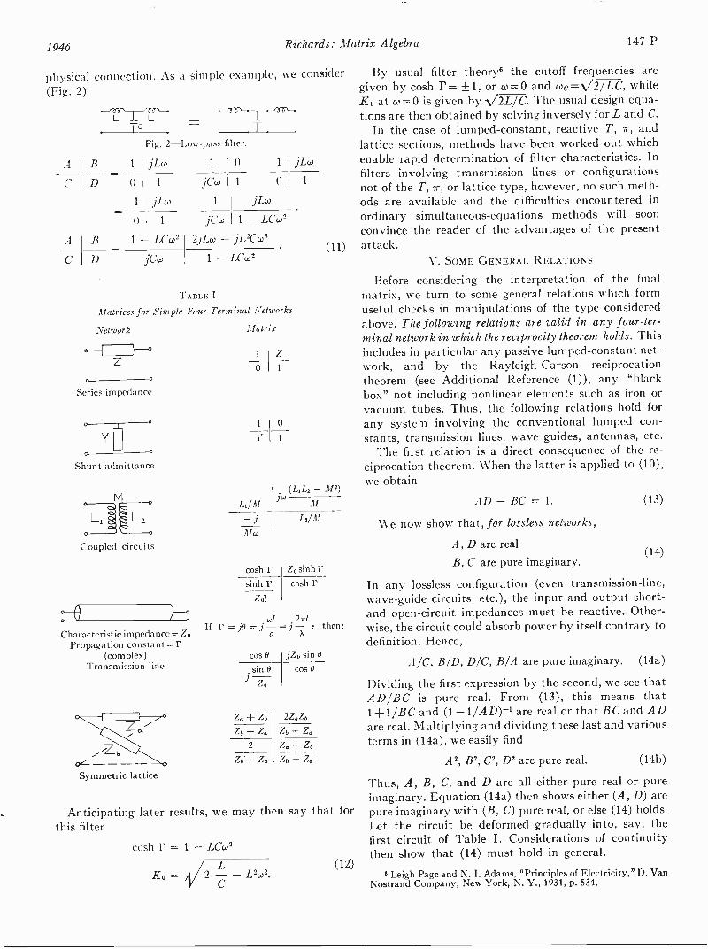
1946 Richards: Matrix Algebra 147 P
physical connection. As a simple example, we(Fig. 2)
A
--nr,--/-inr_.
(11)
Tc T
B
Fig. 2-Low-pass filter.
1 j1.6) 1 0 1 jLw
C
A
D
B
0 1
1 1..11,0)
jCco
'1 0
I iLw
1
0 1
1 - LCw2
jCw 1 - LCw2
2.11,0) - jL2Cw3
C D jCce 1 - LCw2
TABLE I
Matrices for Simple Four -Terminal Networks
Network Matrix
}-°
0 0
Series impedance
Shunt admittance
M
L1
0
Coupled circuits
0Characteristic impedance = Zo
Propagation constant =I'(complex)
Transmission line
21.- -Symmetric lattice
consider By usual filter theory° the cutoff frequencies aregiven by cosh t = ± 1, or co = 0 and coc=V2/LC, whileKo at w = 0 is given by 1/2L/C. The usual design equa-tions are then obtained by solving inversely for L and C.
In the case of lumped -constant, reactive T, 7r, andlattice sections, methods have been worked out whichenable rapid determination of filter characteristics. Infilters involving transmission lines or configurationsnot of the T, 7r, or lattice type, however, no such meth-ods are available and the difficulties encountered inordinary simultaneous -equations methods will soonconvince the reader of the advantages of the presentattack.
V. SOME GENERAL RELATIONS
Before considering the interpretation of the finalmatrix, we turn to some general relations which formuseful checks in manipulations of the type consideredabove. The following relations are valid in any four -ter-minal network in which the reciprocity theorem holds. This
1 Z includes in particular any passive lumped -constant net -0 1 work, and by the Rayleigh -Carson reciprocation
theorem (see Additional Reference (1)), any "blackbox" not including nonlinear elements such as iron orvacuum tubes. Thus, the following relations hold for
1 0 any system involving the conventional lumped con-y 1 stants, transmission lines, wave guides, antennas, etc.
The first relation is a direct consequence of the re-ciprocation theorem. When the latter is applied to (10),we obtain
L,/M-.1Mw
(1.1L2 - M2)./0
Lz/M
cosh I' I Zo sinh
sinh r cosh I'
Zol
wl .2r1If r=j0=j-=i-x- 1 then:
cos 0 jZo sin 0
sin 0.1
Zo
cos 0
Za + Zb 2Z.Zb
Zb Z. Zb
2 Z. Zb
Zb. - Z. Zb-Z,,
Anticipating later results, we may then say that forthis filter
cosh r = 1 - LCw2(12)
Ko = - L20.
AD-BCC 1.We now show that, for lossless networks,
A, D are real
B, C are pure imaginary.
In any lossless configuration (even transmission -line,wave -guide circuits, etc.), the input and output short -and open -circuit impedances must be reactive. Other-wise, the circuit could absorb power by itself contrary todefinition. Hence,
A/C, BID, D/C, B/A are pure imaginary. (14a)
Dividing the first expression by the second, we see thatAD/BC is pure real. From (13), this means that1-}-1/BC and (1 -1/AD)-1 are real or that BC and ADare real. Multiplying and dividing these last and variousterms in (14a), we easily find
A2, B2, C2, D2 are pure real. (14b)
Thus, A, B, C, and D are all either pure real or pureimaginary. Equation (14a) then shows either (A, D) arepure imaginary with (B, C) pure real, or else (14) holds.Let the circuit be deformed gradually into, say, thefirst circuit of Table I. Considerations of continuitythen show that (14) must hold in general.
6 Leigh Page and N. I. Adams, "Principles of Electricity," D. VanNostrand Company, New York, N. Y., 1931, p. 534.
(13)
(14)
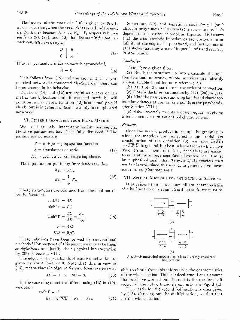
148 P Proceedings of the I.R.E. and Waves and Electrons March
The inverse of the matrix in (10) is given by (8). Ifwe consider that, when the network is turned end for end,E1, Il, E2, /2 become E2, 12, E1, -.11 respectively, wesee from (8), (8a), and (13) that the matrix for the net-work connected inversely is
D
C
B
A(15)
Thus, in particular, if the network is symmetrical,
A = D. (16)
This follows from (15) and the fact that, if a sym-metrical network is connected "backwards," there canbe no change in its behavior.
Relations (14) and (16) are useful as checks on thematrix multiplication and, if watched carefully, willpoint out many errors. Relation (13) is an equally validcheck, but is in general difficult to apply in complicatednetworks.
VI. FILTER PARAMETERS FROM FINAL MATRIX
We consider only image -termination parameters.Iterative parameters have been fully discussed.2'3 Theparameters we use are
= a + j,9 = propagation function
= transformation ratio (17)
Km = geometric mean image impedance.
The input and output image impedances are then
K,1 = ckKm
1 (18)1(12 = - Km.
These parameters are obtained from the final matrixby the formulas
cosh2 r = AD
sinh2 r = BC
BC Z.tarth2 r = -= - (19)AD Zoc
= A /D
K.2 = B/C.These relations have been proved by conventional
methods.3 For purposes of this paper, we may take themas definitions and justify their physical interpretationby (29) of Section VIII.
The edges of the pass bands of reactive networks aregiven by cosh2 r= 1 or 0. Note that this, in view of(13), means that the edges of the pass bands are given by
AD = 0 or BC = O. (20)
In the case of symmetrical filters, using (16) in (19),we obtain
cosh I' = A
Ko = i/B/C = K,1 = K12. (21)
Sometimes (20), and sometimes cosh F = +1 (or 0also, for unsymmetrical networks) is easier to use. Thisdepends on the particular problem. Equation (20) showsthat the characteristic impedances are always zero orinfinite at the edges of a pass band, and further, use of(13) shows that they are real in pass bands and reactivein stop bands.
Conclusion
To analyze a given filter:(a) Break the structure up into a cascade of simple
four -terminal networks, whose matrices are alreadyknown. (Table I and footnote reference 2.)
(b) Multiply the matrices in the order of connection.(c) Obtain the filter parameters by (19), (20), or (21).(d) Find the pass bands and stop bands and character-
istic impedances at appropriate points in the pass bands.(See Section VIII.)
(e) Solve inversely to obtain design equations givingfilter elements in terms of desired characteristics.
Remarks
Once the matrix product is set up, the grouping inwhich the matrices are multiplied is immaterial. Onconsideration of the definition (3), we have A(BC)=(AT3)c. In general, it is best to leave factors which have0's or 1's as elements until last, since these are easiestto multiply into more complicated expressions. It mustbe emphasized again that the order of the matrices mustnot be changed, since this would, in general, give incor-rect results. (Compare (4).)
VII. SPECIAL METHODS FOR SYMMETRICAL SECTIONS
It is evident that if we know all the characteristicsof a half section of a symmetrical network, we must be
q3C D
-s--4-
(a)
c A
DIB A BC A C D
(b)
Fig. 3-Symmetrical network split into inversely connectedhalf sections.
able to obtain from this information the characteristicsof the whole section. This is indeed true. Let us assumethat we have worked out the matrix for the first halfsection of the network and its expression is Fig. 3 (a).
The matrix for the second half section is then givenby (15). Carrying out the multiplication, we find thatfor the whole section
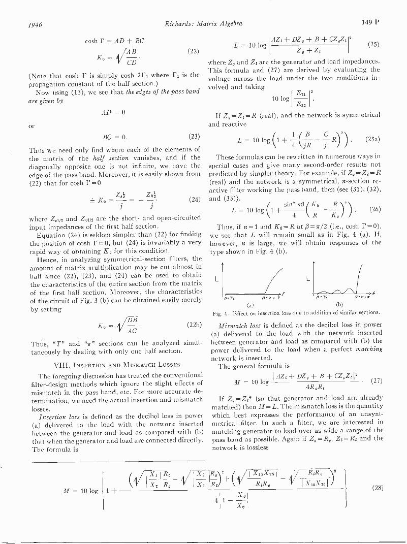
1946 Richards: Matrix Algebra 149 P
cosh r = AD + BCVAB
K0 = -CD
(22)
(Note that coshr is simply cosh 21'1 where r, is thepropagation constant of the half section.)
Now using (13), we see that the edges of the pass bandare given by
AD = 0
or
BC = 0. (23)
Thus we need only find where each of the elements ofthe matrix of the half section vanishes, and if thediagonally opposite one is not infinite, we have theedge of the pass band. Moreover, it is easily shown from(22) that for cosh r = o
Zsi Zo+ Ko = = - (24)
.1 .1
where Z.112 and Z0112 are the short- and open -circuitedinput impedances of the first half section.
Equation (24) is seldom simpler than (22) for findingthe position of cosh r =0, but (24) is invariably a veryrapid way of obtaining Ko for this condition.
Hence, in analyzing symmetrical -section filters, theamount of matrix multiplication may be cut almost inhalf since (22), (23), and (24) can be used to obtainthe characteristics of the entire section from the matrixof the first half section. Moreover, the characteristicsof the circuit of Fig. 3 (b) can be obtained easily merelyby setting
A/DBKo
AC(22b)
Thus, "T" and "r" sections can be analyzed simul-taneously by dealing with only one half section.
VIII. INSERTION AND MISMATCH LOSSES
The foregoing discussion has treated the conventionalfilter -design methods which ignore the slight effects ofmismatch in the pass band, etc. For more accurate de-termination, we need the actual insertion and mismatchlosses.
Insertion loss is defined as the decibel loss in power(a) delivered to the load with the network insertedbetween the generator and load as compared with (b)that when the generator and load are connected directly.The formula is
M = 10 logX2
AZ1+ DZ, B + CZ ,Z1
Z+Ziwhere Z, and Z1 are the generator and load impedances.This formula and (27) are derived by evaluating thevoltage across the load under the two conditions in-volved and taking
L = 10 log
10 logE21
E22
If Z,=Zi=R (real), and the network is symmetricaland reactive
2
2
(25)
L = 10 log (4
y.12
(25a)j j
These formulas can be rewritten in numerous ways inspecial cases and give many second -order results notpredicted by simpler theory. For example, if Zo,--Z1.-- R(real) and the network is a symmetrical, n -section re-active filter working the pass band, then (see (31), (32),and (33)).
2sm nift KoL = 10 log (1 +
R y(26)
4 \ R Kol IThus, if n=1 and Ko= R at 3=7r/2 (i.e., cosh r =0),
we see that L will remain small as in Fig. 4 (a). If,however, n is large, we will obtain responses of thetype shown in Fig. 4 (b).
L
p 13-o it
(a) (b)
Fig. 4-Effect on insertion loss due to addition of similar sections.
Mismatch loss is defined as the decibel loss in power(a) delivered to the load with the network insertedbetween generator and load as compared with (b) thepower delivered to the load when a perfect matchingnetwork is inserted.
The general formula is1 AZI DZ, B + CZ ,Z112
M = 10 log (27)4R,Ri
If Z, = Z1* (so that generator and load are alreadymatched) then 'M= L. The mismatch loss is the quantitywhich best expresses the performance of an unsym-metrical filter. In such a filter, we are interested inmatching generator to load over as wide a range of thepass band as possible. Again if Zg = Rg, Zi= Ri and thenetwork is lossless
X2 R0)2+ IX1SX2S I / RIRX1 R1 RIR, I X ioX2o1
4Xs-Xo
(28)
150 P Proceedings of the I.R.E. and Waves and Electrons March
where subscripts 1 and 2 refer to input and output; Sand 0 to short-circuit and open -circuit conditions; also
X1 X13 X10= =X2 X23 X20
XS Xis X25and -= -= - Xo Xio X20
This formula shdws that, whenever Xis= Xio(i = 1 or 2)and 1X11 R, 1 X21 RI, we have M= 00 or infiniteinsertion loss despite the behavior of a. In particular, thisfrequently occurs if a shunt element becomes resonantor a series element antiresonant. These considerationsare of importance in the choice of various filter types.As an example, the filter section shown in Fig. 5 (a) has'an "attenuation" (a) curve as in Fig. 5 (b) whereas theforegoing considerations show that the actual insertionloss of a number of such sections terminated in resistiveloads would be of the general form of the dotted curve.
.eM
(a) (b)Fig. 5-Difference of behavior of insertion loss and
attenuation functions.
From (27) it is easily shown that if A and D haveonly small imaginary parts and B and C small realparts, then the change in M will be small. (Use thefact that, for any complex la±b1Thus small losses cause only slight differences in filterbehavior.
Finally, if X9= 0, Xi= 0, and the network is reactive,M can be written
M=10 log {(1,
R/ 1 ireA2
Rg 101V R1)(I Km1
1
2 1 sinh2 r I
VR,R I Km I 4
+4(1 + 1 cosh= r +1 sinh2 r I )} .
This involved formula is interesting in that each ofits terms gives us information on filter design. The lastterm, it will be seen, is equal to 1 throughout the pass-band and cosh2a in the stopband. Thus, if the otherterms were not present, M would be zero throughoutthe passband and approximately 20 log (ea/0) inthe stopband. This explains why conventional "first-order" theory works so well.
Secondly, we shall see that in filter design we shouldmake
7 W. P. Mason and R. A. Sykes, "The use of coaxial and balancedtransmission lines in filters and wide -band transformers for high radiofrequencies," Bell Sys. Tech. Jour., vol. 16, pp. 275-302; 1937.
cosh2 r1
4
(29)
Km = VR,Ri when or near AD = 0
= /1/17.Ri
when or near BC = 0.(30)
This is contrary to usual practice which makes
Km = OK, = R,1
Kr2 = - = R14)
somewhere in the middle of the passband. This latterrequirement means that both parts of (30) are satisfiedat one point and consequently that neither is satisfiedat any other point. We have seen, however, that idealfilter behavior depends on keeping the first two termssmall. Thus we want the coefficient of sin2(3 to be zerowhen (or near) sin2(3=1, and similarly the coefficientof cos2/3 small when cos23=1. These conditions giveprecisely (30). The behavior of the coefficients whensin 13 or cos (3=0 is immaterial.
In order to show that the parameters r, Km asdefined by (19) for a single section, are immediatelyextensible to a cascade of any number of sections, wenote that if (19) is solved inversely for A, B, C, D, andthe sign properly chosen in extracting the square roots,then the matrix may be written
(1) cosh r Km sinh
sinh r
Km
1- cosh r4)
(31)
(Note that the ambiguity of sign in extracting thesquare roots makes no difference in (29).)
If an odd number n of such sections is connected incascade in the manner for image termination, thenmultiplying the matrices gives
c() cosh nr Km sinh nrsinh nr
Km
1- cosh nr4)
(32)
If an even number 2n is so connected, the structure,of course, becomes symmetrical with characteristic im-pedance Kr1=0K, and indeed matrix multiplicationgives
cosh 2nr cpK, sinh 2nrsinh 2nr
oK,cosh 2nr
(33)
Additional References(1) J. R. Carson, "A generalization of the reciprocation theorem,"
Bell Sys. Tech. Jour., vol. 3, pp. 393-399; July, 1924. This pa-per contains a proof of the Rayleigh -Carson reciprocation the-orem.
(2) R. S. Burrington and C. C. Torrence, "Higher Mathematics,"Matrix Algebra, chap. 6, Part A, Electric Circuits: pp. 403-416.
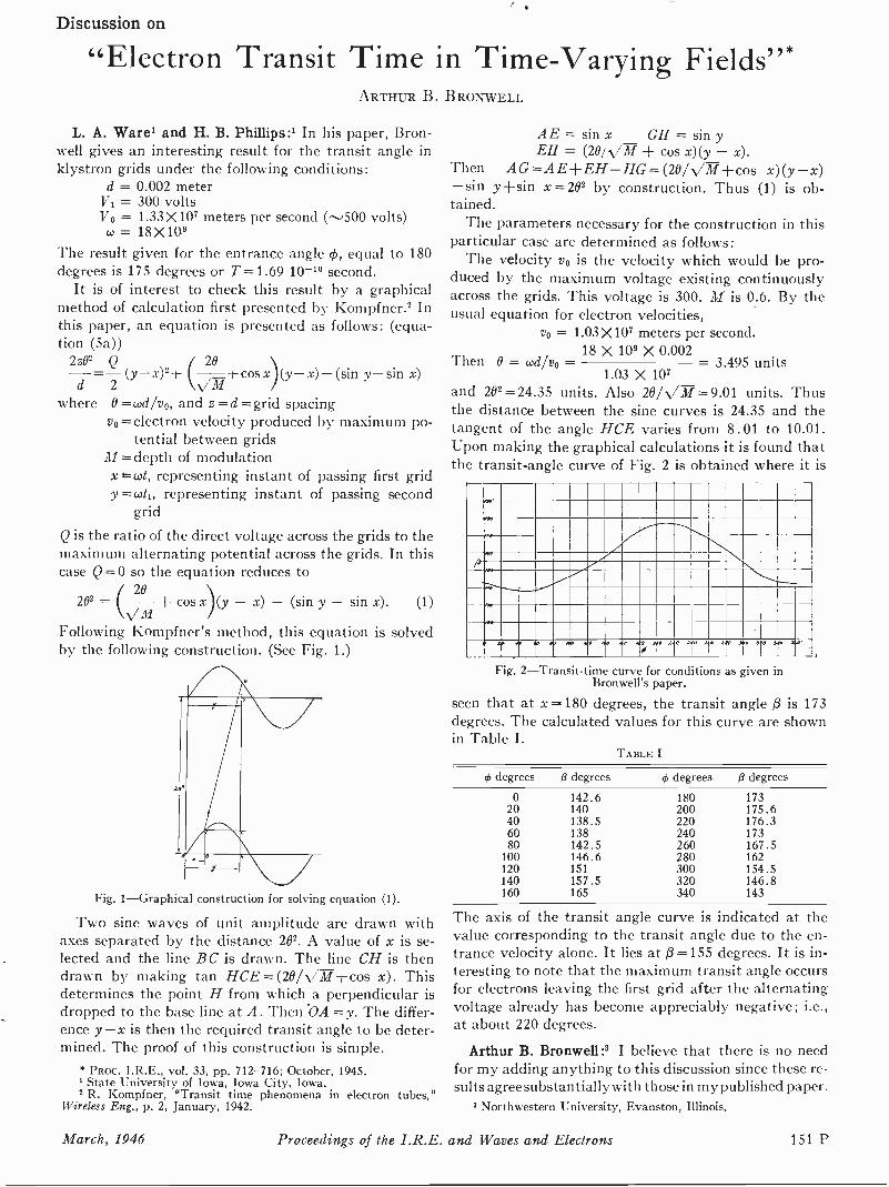
Discussion on
"Electron Transit Time in Time -Varying Fields"ARTHUR B. BRONWELL
L. A. Ware' and H. B. Phillips:' In his paper, Bron-well gives an interesting result for the transit angle inklystron grids under the following conditions:
d = 0.002 meterV1 = 300 voltsVo = 1.33 X10⁷ meters per second 0500 volts)w = 18X109
The result given for the entrance angle t, equal to 180degrees is 175 degrees or T=1.69 10-10 second.
It is of interest to check this result by a graphicalmethod of calculation first presented by Kompfner.2 Inthis paper, an equation is presented as follows: (equa-tion (5a))
2z02 Q
d=-
2(y-x)2+ +cos x (y-x) - (sin y- sin x)
where 0 =wd/vo, and z =d =grid spacingvo = electron velocity produced by maximum po-
tential between gridsM= depth of modulationxx.cot, representing instant of passing first gridy =coti, representing instant of passing second
grid
Q is the ratio of the direct voltage across the grids to themaximum alternating potential across the grids. In thiscase Q =0 so the equation reduces to
20+ cos x)(y - x) - (sin y - sin x). (1)
\-VMFollowing Kompfner's method, this equation is solvedby the following construction. (See Fig. 1.)
Fig. 1-Graphical construction for solving equation (1).
Two sine waves of unit amplitude are drawn withaxes separated by the distance 202. A value of x is se-lected and the line BC is drawn. The line CH is thendrawn by making tan HCE = (20/N/M±cos x). Thisdetermines the point H from which a perpendicular isdropped to the base line at A. Then OA =y. The differ-ence y-x is then the required transit angle to be deter-mined. The proof of this construction is simple.
* PROC. I.R.E., vol. 33, pp. 712-716; October, 1945.'State University of Iowa, Iowa City, Iowa.2 R. Kompfner, "Transit time phenomena in electron tubes,"
Wireless Eng., p. 2, January, 1942.
AE = sin x GH = sin yEH = (201VM + cos x)(y - x).
Then AG =AE+ EH -HG = (20 / -VH +cos x)(y-x)-sin y+sin x =202 by construction. Thus (1) is ob-tained.
The parameters necessary for the construction in thisparticular case are determined as follows:
The velocity vo is the velocity which would be pro-duced by the maximum voltage existing continuouslyacross the grids. This voltage is 300. M is 0.6. By theusual equation for electron velocities,
vo = 1.03 X10⁷ meters per second.18 X 109 X 0.002
Then 0 = cod/vo = - 3.495 units1.03 X 107
and 202=24.35 units. Also 20/VM =9.01 units. Thusthe distance between the sine curves is 24.35 and thetangent of the angle HCE varies from 8.01 to 10.01.Upon making the graphical calculations it is found thatthe transit -angle curve of Fig. 2 is obtained where it is
p
00.
AN
OAP
Age
0 A. de I7 410 0 A A 0 AP A 3.
Fig. 2-Transit-time curve for cond'tions as given inBronwell's paper.
seen that at x=,180 degrees, the transit angle is 173degrees. The calculated values for this curve are shownin Table I.
TABLE I
ye. degrees 13 degrees < degrees 13 degrees
0 142.6 180 17320 140 200 175.640 138.5 220 176.360 138 240 17380 142.5 260 167.5
100 146.6 280 162120 151 300 154.5140 157.5 320 146.8160 165 340 143
The axis of the transit angle curve is indicated at thevalue corresponding to the transit angle due to the en-trance velocity alone. It lies at =155 degrees. It is in-teresting to note that the maximum transit angle occursfor electrons leaving the first grid after the alternatingvoltage already has become appreciably negative; i.e.,at about 220 degrees.
Arthur B. Bronwelle I believe that there is no needfor my adding anything to this discussion since these re-sults agree substantially with those in my published paper.
3 Northwestern University, Evanston, Illinois.
March, 1946 Proceedings of the I.R.E. and Waves and Electrons 151 P
Contributors to Proceedings of the I.R.E. Section
WALTER J. FRANTZ
Walter J. Frantz (S'42-A'45) was bornon April 23, 1921, at Swayzee, Indiana. In1942 he received the B.S. degree in electricalengineering from Purdue University. Aftergraduation Mr. Frantz was employed bythe test and measuring equipment sectionof the RCA Victor Division at Camden,New Jersey. During 1945 he transferred tothe RCA Laboratories at Princeton, NewJersey, to continue work on radio circuitsand systems. Mr. Frantz is a member ofEta Kappa Nu and Tau Beta Pi.
Edward Leonard Ginzton (S'39-A'40)was born on December 27, 1915, in Russia.He received the B.S. degree in 1936 andthe M.S. degree in 1937 from the Universityof California; the E.E. degree in 1938 andthe Ph.D. degree in 1940 from Stanford Uni-versity. From 1937 to 1939 Dr. Ginzton wasan assistant in teaching and research atStanford University and during 1939 and1940 a research assistant in physics there.In 1940 he joined the Sperry GyroscopeCompany, Inc., and is now a researchengineer in charge of tube and microwaveresearch and development. He is a memberof Sigma Xi.
Marcel J. E. Golay was born on May 3,1902, in Switzerland. He received the
A. E. HASTINGS
EDWARD LEONARD GINZTON
Baccalaureat Scientifique from the Gymnasede Neuchatel in 1920, the licenciate inelectrical engineering from the Federal In-stitute of Technology at Zurich in 1924, andthe Ph.D. in physics from the University ofChicago in 1930.
From 1924 to 1928 Dr. Golay was asso-ciated with the Bell Telephone Laboratoriesengaged in work on telephone cables. In1930 and 1931 he worked on automatictelephone systems for the Automatic Elec-tric Company, and since 1931 he has beenconnected with the Signal Corps Labora-tories, Bradley Beach, New Jersey, work-ing on subaqueous acoustics, terrestrialsound ranging, heat detection, radio relays,and electronic controls.
Arthur E. Harrison (A'41-SM'45) wasborn on January 20, 1908, at San LuisObispo, California. He received the B.S. de-gree in electrical engineering from the Uni-versity of California in 1936. From 1936 to1939 he was a teaching Fellow at the Cali-fornia Institute of Technology, and receivedthe M.S. degree in 1937 and the Ph.D. de-gree in 1940. He did research work for thedepartment of mechanical engineering at theUniversity of California in 1940. Mr. Harri-son joined the klystron laboratory of the
PAUL I. RICHARDS
MARCEL J. E. GOLAY
Sperry Gyroscope Company at San Carlos,California, in May, 1940, and is now locatedat the Sperry Research Laboratories in Gar-den City, Long Island, New York. He is amember of Sigma Xi, Tau Beta Pi, and EtaKappa Nu.
A. E. Hastings (A'42) received the B.S.degree in electrical engineering in 1934 andthe Ph.D. degree in physics in 1938 fromBrown University. Since 1938 he has beenassociated with the Naval Research Labo-ratory in the development of radar andclosely allied devices.
Paul I. Richards (A'45) was born atOrono, Maine, on February 8, 1923. Hestudied physics and electronics at HarvardUniversity from 1940 to 1943. In 1943, heleft became a research associate at the radioresearch laboratory, Harvard University.His work was concerned primarily with thetheory and design of distributed -constantfilter circuits. Mr. Richards is now studyingfor his Ph.D. degree in physics at HarvardUniversity. He is a member of Phi BetaKappa.
For a biographical sketch of GeoffreyBuilder, see Contributors to Waves andElectrons Section, page 147 W, this issue.
ARTHUR E. HARRISON
152 P Proceedings of the I.R.E. and Waves and Electrons March, 1946
PROCEEDINGS A WAVES
of the I.R.E. D and ELECTRONS
Published Monthlyby
The Institute of Radio Engineers, Inc.
March, 1946
SECTION II-WAVES AND ELECTRONS SECTION
George R. Town-Chairman, Rochester Section 108 WWhen Radio Engineer is "Big Boss" Orestes H. Caldwell 109 WInduction Heating in Radio Electron -Tube Manufacture Edwin E. Spitzer 110 WFine Wires in the Electron -Tube Industry George A. Espersen 116 WA Three -Beam Oscillograph for Recording at Frequencies up to 10,000 Megacycles...
Gordon M. Lee 121 WSynchronizing Generators for Electronic Television A Rufus Applegarth 128 WThe Effect of Negative Voltage Feedback on Power -Supply Hum in Audio -Frequency
Amplifiers Geoffrey Builder 140 WHigh -Voltage Rectified Power Supply Using Fractional -Mu Radio -Frequency Oscillator
Robert L. Freeman and R. C. Hergenrother 145 WContributors to WAVES AND ELECTRONS SECTION 147 W
Institute News and Radio NotesOutstanding Events of 1946 Winter Technical Meeting 149 W
Board of Directors 154 W I.R.E. People 155 WExecutive Committee 155 W Sections 159 W
Books"Pulsed Linear Networks," by Ernest Frank Reviewed by Albert Preisman 159 W"Table of Arc Sin X," Prepared by The Mathematical Tables Project, Arnold N.
Lowan, Project Director, and a Technical Staff of Six PersonsReviewed by John R. Whinnery 160 W
Section Meetings 36 A Positions Open 54 AMembership 40 A Positions Wanted 56 A
Advertising Index 86 A
SECTION I-PROCEEDINGS OF THE I.R.E. SECTION CONTENTS ON PAGE 95 P
EDITORIAL DEPARTMENTAlfred N. Goldsmith
EditorHelen M. Stote Ray D. Rettenmeyer
Publications Manager Technical EditorWinifred CarriereAssistant Editor
William C. Copp Lillian PetranekAdvertising Manager Assistant Advertising Manager
Responsibility for the contents of papers published in the PROCEEDINGS OF THE I.R.E. and WAVESAND ELECTRONS rests upon the authors.
Statements made in papers are not binding on the Institute or its members.
George R. TownChairman-Rochester Section
George R. Town was born on May 26, 1905, in Poult-ney, Vermont. He received the degree of E.E. fromRensselaer Polytechnic Institute in 1926, and the de-gree of D.Eng. from the same institution in 1929.
From 1929 until 1933 he was an engineer in the re-search laboratory at Leeds and Northrup Company.For seven months in 1933 he was a development engi-neer for Arma Engineering Company. From 1933 to1936 he was an instructor at Rensselaer PolytechnicInstitute serving one year as instructor in mathematics,and two years as instructor in electrical engineering.
In 1936 Dr. Town joined the engineering division ofStromberg-Carlson Company. He has worked succes-sively as an engineer in the research department, as en-gineer -in -charge of the television laboratory, as assist-ant director of research, and in his present position asmanager of engineering and research. In April, 1945, hewas elected assistant secretary of the Company. He has
served on various panels and committees of the NationalTelevision System Committee and of the Radio Tech-nical Planning Board, being chairman of one of theTelevision Standards Committees of the latter organ-ization. He is, at present, chairman of the Frequency -Modulation Systems Committee of the Radio Manu-facturers Association, and secretary of the RMATelevision Systems Committee.
He was secretary of the Rochester Section from 1942to 1944, and has served as chairman for the RochesterSection since 1944. He is chairman of the I.R.E. Com-mittee on Organizational Research, and is a member ofthe I.R.E. Committee on Education. He is vice-chair-man of the Rochester Section of the American Instituteof Electrical Engineers.
Dr. Town joined the Institute of Radio Engineers asan Associate in 1937 and transferred to Senior Membergrade in 1944.
108 W Proceedings of the I.R.E. and Waves and Electrons March

.1.
Contributing substantially to the advancement of the radio -and -electronicfield are the various periodicals which present the methods and advances inthat field. Their Editors are a group of leaders of thought in the field. Guesteditorials from the pens of these Editors have been requested, and it is ac-cordingly possible to present below an analytical and stimulating discussionfrom the Editor of Electronic Industries, who is himself a Fellow of The Insti-tute of Radio Engineers and a former Federal Radio Commissioner.
The Editor
When Radio Engineer is "Big Boss"ORESTES H. CALDWELL
Radio engineers can be proud of the industrial wealth they have created and continue tocreate.
Last year, for example, some four -billion -dollars' worth of radio equipment and service-four-thousand-million dollars-was produced based on the technical discoveries and designscreated by the members of The Institute of Radio Engineers ,and their fellow engineers. Foreach of the voting members of the I.R.E., this was nearly one and one-half million dollars perman. And all of this billions of dollars of actual wealth per year was created literally "out ofthin air" by radio engineers and radio inventors.
Radio engineers have now had a taste of big -scale industrial production. Radio engineershave seen themselves playing a part in big -business operations. They have observed that theirknowledge and their efforts are at the center of businesses which collect hard round dollars inthe millions.
But from now on, we should insist, radio engineers must not be satisfied to be merely em-ployees and staff aides in the huge industries they have created.
Radio engineers should themselves take business and industrial leadership. It is time for theradio engineer to be the "big boss" of his own concern and shape its general policies. Instead ofavoiding and evading business responsibility in order to keep close to the design room and slide -rule, radio engineers should prepare to reach out themselves for the top management positions,for independent proprietorships, for public service in fitting radio into broader usefulness tohumanity.
All too often, some skillful lawyer, clever salesman, or quick -minded accountant is chosen tofill the top place in a radio organization, a post which would have been far better served by atrained radio -minded man having the broad grasp necessary to relate our radio art to generalbusiness problems.
Radio engineers are perfectionists. And so they like to keep close to their technical work,improving detail parts into the highest possible efficiency.
But even from this aspect of perfectionism alone, radio men will admit that fullest perfectionin radio cannot come unless the radio engineer has the greatest freedom in which to work. Andthis means that there must be radio engineers at the top who can give sympathetic encourage-ment to radio engineers throughout the organization.
Radio engineers have created a whole galaxy of great industries-industries tremendous inpublic service, industries imagination -defying in technical achievement, and industries nowastronomic in dollar volume!
Let us look forward to the day when radio -electronic industries are officered by radio men,from top executive posts on down to the design rooms and production departments. This isabsolutely necessary, for the good of the radio industries and the public they serve. Let radiomen accept and even seek out these responsibilities of management and direction. And let ussee that the radio man collects in full, for himself and his family, his share of the wealth he isproducing.
1946 Proceedings of the I.R.E. and Waves and Electrons 109 W
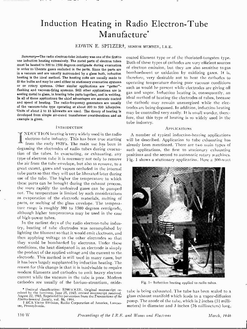
Induction Heating in Radio Electron -TubeManufacture*
EDWIN E. SPITZERt, SENIOR MEMBER, I.R.E.
Summary-The radio electron -tube industry was one of the first touse induction heating extensively. The metal parts of electron tubesmust be heated to 500 to 1500 degrees centigrade during evacuationin order to liberate gases occluded in the parts. Since the parts arein a vacuum and are usually surrounded by a glass bulb, inductionheating is the ideal method. The heating coils are usually made tofit the bulbs and may be used either on stationary evacuation systemsor on rotary systems. Other similar applications are "getter" -flashing and vacuum -firing systems. Still other applications are insealing metal to glass, in brazing tube parts together, and in welding.In all of these applications the chief advantages are accurate controland speed of heating. The radio -frequency generators are usuallyof the vacuum -tube type operating at about 200 to 500 kilocycles.Units of about 2 to 15 kilowatts are used. The theory of heating isdeveloped from simple air -cored transformer considerations and anexample is given.
INTRODUCTION
NDUCTION heating is very widely used in the radioelectron -tube industry. This has been true startingfrom the early 1920's. The main use has been in
degassing the electrodes of radio tubes during evacua-tion of the tubes. In evacuating, or exhausting, anytype of electron tube it is necessary not only to removethe air from the tube envelope, but also to remove, to agreat extent, gases and vapors occluded in the internaltube parts so that they will not be liberated later duringuse of the tube. The higher the temperature to whichthese parts can be brought during the exhaust process,the more rapidly the undesired gases can be pumpedout. The temperature is limited by such considerationsas evaporation of the electrode materials, melting ofparts, or melting of the glass envelope. The tempera-ture range is roughly 500 to 1500 degrees centigrade,although higher temperatures may be used in the caseof high -power tubes.
In the earliest days of the radio electron -tube indus-try, heating of tube electrodes was accomplished bylighting the filament so that it would emit electrons, andthen applying voltage to the other electrodes so thatthey would be bombarded by electrons. Under theseconditions, the heat dissipated in an electrode is simplythe product of the applied voltage and the current to theelectrode. This method is still used in many cases, butit has been largely supplanted by induction heating. Thereason for this change is that it is inadvisable to requiremodern filaments and cathodes to emit heavy electroncurrent while the vacuum in the tube is poor. Moderncathodes are usually of the barium -strontium, oxide-
* Decimal classification: R590 X R331. Original manuscript re-ceived by the Institute, June 25, 1945; revised manuscript received,August 22, 1945. Reprinted by permission from the Transactions of theElectrochemical Society, vol. 86, 1944.
t RCA Victor Division, Radio Corporation of America, Lancas-ter, Pennsylvania.
coated filament type or of the thoriated-tungsten type.Both of these types of cathodes are very efficient sourcesof electron emission, but they are also sensitive to gasbombardment or oxidation by oxidizing gases. It is,therefore, very desirable not to heat the cathodes tooperating temperature during poor vacuum conditionssuch as would be present while electrodes are giving offgas and vapor. Induction heating is, consequently, anideal method of heating the electrodes of tubes, becausethe cathode may remain unenergized while the elec-trodes are being degassed. In addition, induction heatingmay be controlled very easily. It is small wonder, there-fore, that this type of heating is so widely used in thetube industry.
APPLICATIONS
A number of typical induction -heating applicationswill be described. Application to tube exhausting hasalready been mentioned. There are two main types ofsuch applications, the first to stationary exhaustingpositions and the second to automatic rotary machines.Fig. 1 shows a stationary application. Here a 500 -watt
Fig. 1-Induction heating applied to radio tubes.
tube is being exhausted. The tube has been sealed to aglass exhaust manifold which leads to a vapor -diffusionpump. The anode of the tube, which is 2 inches (51 milli-meters) in diameter and 3 inches (76 millimeters) long,
110 W Proceedings of the I.R.E. and Waves and Electrons March, 1946

Spitzer: Induction Heating in Tube Manufacture 111 W
and made of tantalum sheet, is being heated to about1300 degrees centigrade by the multiple -turn heatingcoil or inductor. The inductor is made of standard 0.25 -inch (2.5 -millimeter) copper tubing and carries a cur -
Fig. 2-Automatic rotary exhausting machine.
rent of about 150 amperes at about 300 kilocycles. Thiscurrent is generated by an 8 -kilowatt radio -frequencygenerator, which will be described later. The radio -fre-quency current is controlled by changing of voltage taps
Fig. 3-Induction-heating position on rotary exhausting machine.
on the high -voltage -supply transformer and by variationof the filament voltage of the oscillator tubes in the gen-erator.
Fig. 2 shows an automatic rotary exhausting machine.The exhaust tubing of the tubes is inserted into a rubberexhaust opening and connected by means of manifoldsand a rotary valve to diffusion and mechanical pumps.The rotary table carrying the tubes turns at intervalswhich may be 0.1 to 3 minutes long. To the rear of themachine, the carbon anodes of the tubes may be seenheated to incandescence by high -frequency inductors.
Just before the rotary table indexes, the inductors areraised up high enough to clear the tubes. Due to thisarrangement, it is not necessary to have the inductorsrotate. The radio -frequency generator may be seen inthe left background; the heavily insulated leads carryingthe current to the machine are in clear view. Severalinductors are usually connected in series in order toutilize fully the capabilities of the generator.
Fig. 3 shows a closer view of the machine in Fig. 2.Fig. 4 shows a typical inductor held over a tube. Theinductors shown in these two figures are made of flat-tened 0.5 -inch (51 -millimeter) diameter copper tubingthrough which cooling water is circulated. Inductor
Fig. 4-Typical inductor and radio tube.
currents of 50 to 150 amperes are used; temperatures of700 to 1200 degrees centigrade are commonly producedin the electrodes of the tubes being exhausted. The in-ductors are designed to be readily interchangeable bythe use of standard pipe couplings. In this way, induc-tors of varying diameter and construction to suit thejob at hand may be installed.
Fig. 5 shows an application of induction heating tovacuum firing. It is often desirable to heat tube parts tohigh temperature in good vacuum prior to assembly ofthe tubes. Occluded gases can be removed in this mannerand it is also possible to remove vaporizable contaminat-ing materials. In the particular case shown in Fig. 5,small tube parts are being vacuum -fired. Since theseparts have very poor coupling to the inductor, they areplaced in a box made of tantalum sheet. The inductioncurrents heat the box which in turn heats the parts by
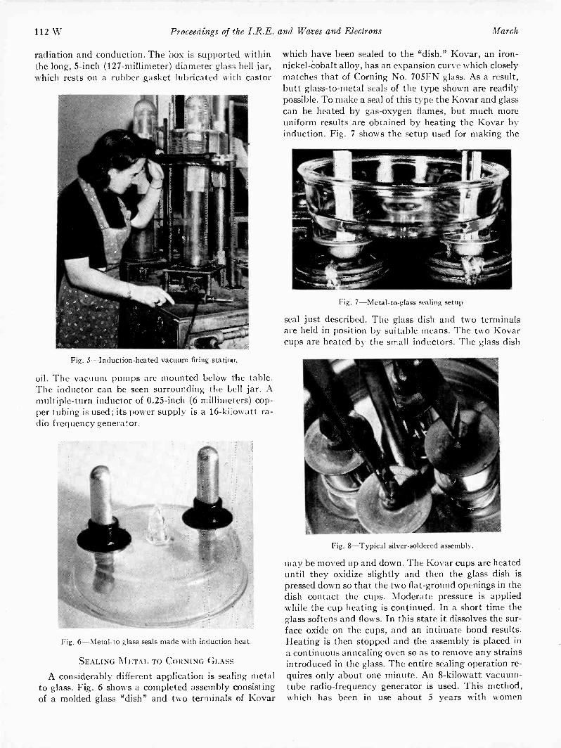
112 W Proceedings of the I.R.E. and Waves and Electrons March
radiation and conduction. The box is supported within which have been sealed to the "dish." Kovar, an iron -the long, 5 -inch (127 -millimeter) diameter glass bell jar, nickel -Cobalt alloy, has an expansion curve which closelywhich rests on a rubber ,gasket lubricated with castor matches that of Corning No. 705FN glass. As a result,
butt glass -to -metal seals of the type shown are readilypossible. To make a seal of this type the Kovar and glasscan be heated by gas -oxygen flames, but much moreuniform results are obtained by heating the Kovar byinduction. Fig. 7 shows the setup used for making the
Fig. 5-Induction-heated vacuum firing station.
oil. The vacuum pumps are mounted below the table.The inductor can be seen surrounding the bell jar. Amultiple -turn inductor of 0.25 -inch (6 millimeters) cop-per tubing is used; its power supply is a 16 -kilowatt ra-dio frequency generator.
Fig. 6-Metal-to-glass seals made with induction heat.
SEALING METAL TO CORNING GLASS
Fig. 7-Metal-to-glass sealing setup
seal just described. The glass dish and two terminalsare held in position by suitable means. The two Kovarcups are heated by the small inductors. The glass dish
Fig. 8-Typical silver -soldered assembly.
may be moved up and down. The Kovar cups are heateduntil they oxidize slightly and then the glass dish ispressed down so that the two flat -ground openings in thedish contact the cups. Moderate pressure is appliedwhile the cup heating is continued. In a short time theglass softens and flows. In this state it dissolves the sur-face oxide on the cups, and an intimate bond results.Heating is then stopped and the assembly is placed ina continuous annealing oven so as to remove any strainsintroduced in the glass. The entire sealing operation re -
A considerably different application is sealing metal quires only about one minute. An 8 -kilowatt vacuum -to glass. Fig. 6 shows a completed assembly consisting tube radio -frequency generator is used. This method,of a molded glass "dish" and two terminals of Kovar which has been in use about 5 years with women
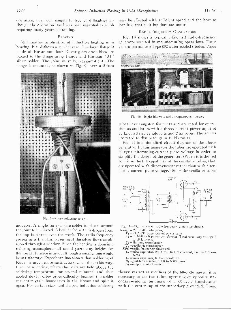
1946 Spitzer: Induction Heating in Tube Manufacture 113 W
operators, has been singularly free of difficulties al-though the operation itself was once regarded as a jobrequiring many years of training.
BRAZING
Still another application of induction heating is inbrazing. Fig. 8 shows a typical case. The large flange ismade of Kovar and four Kovar glass assemblies arebrazed to the flange using Handy and Harman "BT"silver solder. The joint must be vacuum -tight. Theflange is mounted, as shown in Fig. 9, over a 5 -turn
Fig. 9-Silver-,01(1cring setup.
inductor. A single turn of wire solder is placed aroundthe joint to be brazed. A bell jar fed with hydrogen fromthe top is placed over the work. The radio -frequencygenerator is then turned on until the silver flows as ob-served through a window. Since the heating is done in areducing atmosphere, all metal parts stay bright. An8 -kilowatt furnace is used, although a smaller one wouldbe satisfactory. Experience has shown that soldering ofKovar is much more satisfactory when done this way.Furnace soldering, where the parts are held above thesoldering temperature for several minutes, and thencooled slowly, often gives difficulty because the soldercan enter grain boundaries in the Kovar and split itopen. For certain sizes and shapes, induction soldering
may be effected with sufficient speed and the heat solocalized that splitting does not occur.
RADIO -FREQUENCY GENERATORS
Fig. 10 shows a typical 8 -kilowatt radio -frequencygenerator as used in manufacturing operations. Thesegenerators use two Type 892 water-cooled triodes. These
Fig. 10-Eight-kilowatt radio -frequency generator.
tubes have tungsten filaments and are rated for opera-tion as oscillators with a direct -current power input of30 kilowatts at 15 kilovolts and 2 amperes. The anodesare rated to dissipate up to 10 kilowatts.
Fig. 11 is a simplified circuit diagram of the abovegenerator. In this generator the tubes are operated with60 -cycle alternating -current plate voltage in order tosimplify the design of the generator. (When it is desiredto utilize the full capability of the oscillator tubes, theyare operated with direct -current rather than with alter-nating -current plate voltage.) Since the oscillator tubes
MAGNETICCONTACTOR HEATING
COIL)
Fig. 11-Eight-kilowatt radio -frequency generator circuit.Range =250 to 400 kilocycles.
VI- RCA -892 water-cooled power tubeT1=12.5 -kilovolt power transformer. Total secondary voltage 7
to 18 kilovoltsTy 3= filament transformer
1.7',= feedback transformerRFC = radio -frequency choke coil
CI =mica capacitor, 0.014 to 0.021 microfarad, 140 to 210 am-peres
Cy =mic.a capacitor, 0.004 microfaradR1=grid-bias resistor, 1000 to 6000 ohmsSi =output control switch
themselves -act as rectifiers of the 60 -cycle power, it isnecessary to use two tubes, operating on opposite sec-ondary -winding terminals of a 60 -cycle transformerwith the center tap of the secondary grounded. Thus,
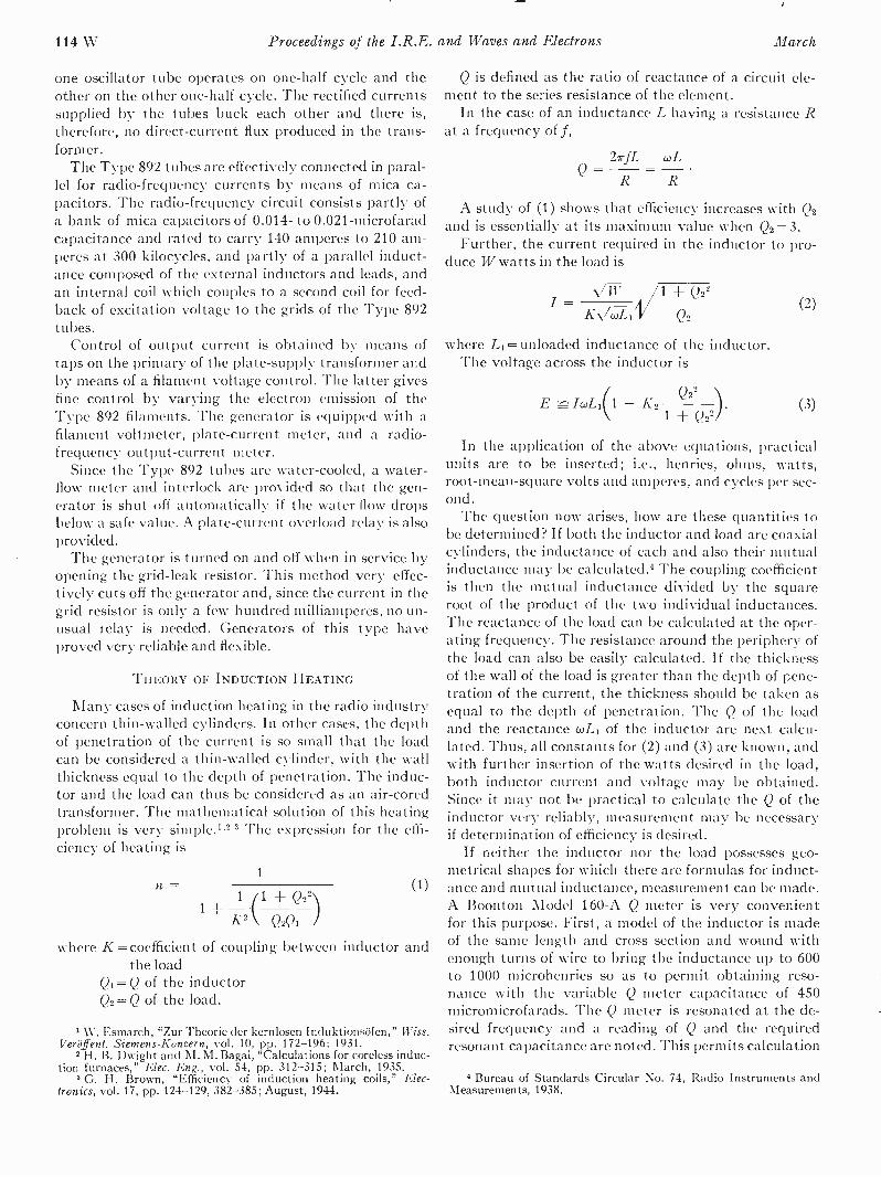
114 W Proceedings of the I.R.E. and Waves and Electrons March
one oscillator tube operates on one-half cycle and theother on the other one-half cycle. The rectified currentssupplied by the tubes buck each other and there is,therefore, no direct -current flux produced in the trans-former.
The Type 892 tubes are effectively connected in paral-lel for radio -frequency currents by means of mica ca-pacitors. The radio -frequency circuit consists partly ofa bank of mica capacitors of 0.014- to 0.021-microfaradcapacitance and rated to carry 140 amperes to 210 am-peres at 300 kilocycles, and partly of a parallel induct-ance composed of the external inductors and leads, andan internal coil which couples to a second coil for feed-back of excitation voltage to the grids of the Type 892tubes.
Control of output current is obtained by means oftaps on the primary of the plate -supply transformer andby means of a filament voltage control. The latter givesfine control by varying the electron emission of theType 892 filaments. The generator is equipped with afilament voltmeter, plate -current meter, and a radio -frequency output -current meter.
Since the Type 892 tubes are water-cooled, a water -flow meter and interlock are provided so that the gen-erator is shut off automatically if the water flow dropsbelow a safe value. A plate -current overload relay is alsoprovided.
The generator is turned on and off when in service byopening the grid -leak resistor. This method very effec-tively cuts off the generator and, since the current in thegrid resistor is only a few hundred milliamperes, no un-usual relay is needed. Generators of this type haveproved very reliable and flexible.
THEORY OF INDUCTION HEATING
Many cases of induction heating in the radio industryconcern thin -walled cylinders. In other cases, the depthof penetration of the current is so small that the loadcan be considered a thin -walled cylinder, with the wallthickness equal to the depth of penetration. The induc-tor and the load can thus be considered as an air -coredtransformer. The mathematical solution of this heatingproblem is very simple.1,2,3 The expression for the effi-ciency of heating is
n=1
1+1 1 + Q22)
K21\ Q2Q1 /I
where K= coefficient of coupling between inductor andthe load
=Q of the inductorQ2 = Q of the load.
(1)
1 W. Esmarch, "Zur Theorie der kernlosen InduktionsOfen," Wiss.Veroffent. Siemens-Konzern, vol. 10, pp. 172-196; 1931.
2 H. B. Dwight and M. M. Bagai, "Calculations for coreless induc-tion furnaces," Elec. Eng., vol. 54, pp. 312-315; March, 1935.
8 G. H. Brown, "Efficiency of induction heating coils," Elec-tronics, vol. 17, pp. 124-129, 382-385; August, 1944.
Q is defined as the ratio of reactance of a circuit ele-ment to the series resistance of the element.
In the case of an inductance L having a resistance Rat a frequency of f,
2irfL co",Q=
R R
A study of (1) shows that efficiency increases with Q2and is essentially at its maximum value when Q2= 3.
Further, the current required in the inductor to pro-duce W watts in the load is
,./W 4/1 + Q22I- KN/coLi V Q2
where L1= unloaded inductance of the inductor.The voltage across the inductor is
E IcoLi(1 - K2 Q22 ).1 + Q22
(2)
(3)
In the application of the above equations, practicalunits are to be inserted; i.e., henries, ohms, watts,root -mean -square volts and amperes, and cycles per sec-ond.
The question now arises, how are these quantities tobe determined? If both the inductor and load are coaxialcylinders, the inductance of each and also their mutualinductance may be calculated.4 The coupling coefficientis then the mutual inductance divided by the squareroot of the product of the two individual inductances.The reactance of the load can be calculated at the oper-ating frequency. The resistance around the periphery ofthe load can also be easily calculated. If the thicknessof the wall of the load is greater than the depth of pene-tration of the current, the thickness should be taken asequal to the depth of penetration. The Q of the loadand the reactance wL1 of the inductor are next calcu-lated. Thus, all constants for (2) and (3) are known, andwith further insertion of the watts desired in the load,both inductor current and voltage may be obtained.Since it may not be practical to calculate the Q of theinductor very reliably, measurement may be necessaryif determination of efficiency is desired.
If neither the inductor nor the load possesses geo-metrical shapes for which there are formulas for induct-ance and mutual inductance, measurement can be made.A Boonton Model 160-A Q meter is very convenientfor this purpose. First, a model of the inductor is madeof the same length and cross section and wound withenough turns of wire to bring the inductance up to 600to 1000 microhenries so as to permit obtaining reso-nance with the variable Q meter capacitance of 450micromicrofarads. The Q meter is resonated at the de-sired frequency and a reading of Q and the requiredresonant capacitance are noted. This permits calculation
Bureau of Standards Circular No. 74, Radio Instruments andMeasurements, 1938.
1946 Spitzer: Induction Heating in Tube Manufacture 115 W
of LM, WLM, and RM, where the subscript M refers to themodel. The load is then inserted. (If the load is magneticat room temperature, but not at the desired tempera-ture, an identical load of nonmagnetic metal should beused.) The Q meter is reresonated and the new values ofQ and capacitance are noted. Again LM', coLm', and Rm'are calculated. The original values are subtracted givingAcoLm and ARm. The theory shows that
,AwLm Qm 2
= K' (4)olLm 1 Qm 2
and that
=AcoLm
ARM(5)
Equation (5) gives QM which is inserted in (4). Equation(4) can be solved for the coupling coefficient K. Know-ing the resistivity of the actual load at the desired tem-perature and the resistivity of the load used during thetest above, we find that the true Q of the load is
Q2 = Q3fpm
P2
(6)
where pm is the model load resistivity and p2 the actualload resistivity. Equation (6) assumes that the depth ofpenetration is less than about one fifth of the radius ofthe load. Finally, the measured WLM must be reduced bythe ratio of the square of the inductor turns to the squareof the model turns, so as to get the true inductor react-ance wLi. All values are then known for (2) and (3).
Both of the above methods have been used with goodresults. One example will be given. The load and induc-tor were those shown in Fig. 4. A model of the inductorwas made by winding 91 turns on a coil form. The modelhad the same length as the inductor, but the diameterwas 3.75 inches (95 millimeters) instead of 3.5 inches(89 millimeters). This requires a later correction in K.The model connected to a Boonton Q meter, gave at300 kilocycles a Q of 180 and a resonant capacitance of272 micromicrofarads. By a second measurement at600 kilocycles, it was found that the model had 7 micro-microfarads stray capacitance. Therefore the correctedcapacitance was 279 micromicrofarads. From the usualformula connecting L, C, and f, the inductance of themodel was 1010 microhenries and its reactance was 1905ohms at 300 kilocycles. Thus the model had a resistanceof 1905/180 =10.6 ohms.
Next, the anode of Type 813 tube was inserted in themodel and it was found that at 300 kilocycles the Q was29 and the resonant capacitance was 286 micromicro-farads. Repeating the calculations above the new modelreactance was 1810 ohms and the new resistance was1810/29 = 62.4 ohms. The change in reactance was, thus,1905 -1810 = 95 ohms, and the change in resistance was62.4 -10.6 = 51.8 ohms. Applying (5) we find that
95Q.If = =
51.81.83.
In this case, since an actual anode and not a model wasused, QM = Q2. However, the anode was not at operatingtemperature, so the correction of (6) is still necessary.The ratio of hot -to -cold resistance in this case was 0.85.Therefore the hot
Q2 = 1.83 /1/ 1
0.85= 1.99.
Applying (4), we obtain
95 1.832= 10
1905 1 + 1.832
From this equationK = 0.25.
This value needs revision, due to the fact that the in-ductor model had too large a diameter. As an approxi-mation, K is inversely proportional to diameter. Thusthe corrected K became
3.750.25 X = 0.268.
3.5
The reactance of the model inductor was then re-duced by the square of the number of turns in order toget the reactance coL1 of the actual inductor, which had4.5 turns. We obtain
4.5wLl = 1905 X (
91= 4.63 ohms.
The power required in the anode was calculated byassuming that the temperature was 1100 degrees centi-grade and the radiation coefficient was 0.8, and by allow-ing 5 per cent for end effects. This gave 1200 watts.
Now applying (2) and (3), we obtain
and
1 1200(1 + 1.992)/ - = 95 amperes0.268 4.63 X 1.99
E = 95 X 4.63(1 - 0.2682 - -1.992
= 415 volts.1 + 1.99'
Actual measurements on an exhausting machine gaveI = 87 amperes, E = 365 volts at a frequency of 308 kilo-cycles and with an anode temperature of 1100 degreescentigrade. This comparison shows that satisfactory re-sults can be obtained by this method.
Additional References(1) T. P. Kinn, "R -F generator characteristics for induction heat-
ing," Radio-Elec. Eng., vol. 4, pp. 20-22, 28 -30; January, 1945.(2) R. M. Baker and C. J. Madsen, "High -frequency induction
heating of conductors and nonconductors," Elec. Eng., vol. 64,p. 64; February, 1945.
(3) F. W. Curtis, "High -Frequency Induction Heating," McGraw-Hill Book Company, New York, N. Y., 1944.
Fine Wires in the Electron -Tube Industry*GEORGE A. ESPERSENt, ASSOCIATE, I.R.E.
Summary-This article discusses primarily the application of finewires in the electron -tube industry. Some fundamental basic prop-erties which confront the wire manufacturer are briefly discussed.Design formulas, including a nomograph, are given for electron-tube filaments. The use of platings of gold, platinum, and zirconium onmetals of the refractory group have assisted in the reduction of gridemission. A unique method of utilizing zirconium, both to acceleratethe vacuum exhaust process and to serve as a continuous "getter,""is described. A novel method of securing a uniform rate of evapora-tion of thin films of metals is discussed.
METHODS OF SPECIFYING CHARACTERISTICS
FINE WIRES such as nickel, nickel alloys, tung-sten, thoriated tungsten, molybdenum, and tan-talum have been used by the electron -tube
industry from the date of its inception. The practicesset up for manufacturing incandescent -lamp filamentswere readily applied to filaments, heaters, and grids forelectron tubes. Through a period of years, variousstandards for wire quality and characteristics have beenestablished independently by individual electron -tubemanufacturing companies. These standards in mostcases are practically identical, with minor deviationsoccurring where certain other fabricating processes areto be considered.
The basic properties which have been considered are:(1) finish; (2) weight; (3) diameter; (4) elongation;(5) tensile strength; (6) straightness; (7) electrical re-sistance; (8) chemical composition; (9) brittleness.
The finish of a wire may vary from a clean, shinysurface to a dark matt surface. Manufacturing specifica-tions may also include such statements as freedom fromkinks, waves, cracks, slivers, seams, burrs, roughness,soap drawing compounds, oil, foreign matter, andoxides.
The weight of the fine wires is usually expressed inmilligrams per 200 millimeters. Tolerances on weightusually vary from plus or minus 2 per cent for filamentsto plus or minus 4 per cent for grid wires, these valuesdepending upon the degree of control required to main-tain the specified characteristic tolerances.
The diameter of the wire is usually specified as anominal value for fine wires, and it can readily be com-puted by using either of the following formulas:
D = K,VW
W = K2D2
(1)
(2)
* Decimal classification: R331 XR282.1. Original manuscript re-ceived by the Institute, June 22, 1945; revised manuscript received,October 10, 1945.
t North American Philips Company, Inc., Dobbs Ferry, N. Y.
where D= the mean diameter of the wire in milsW= the weight of the wire in milligrams
per 200 millimeters of lengthK1 and K2= constants depending upon the den-
sities of the wire.Table I indicates values for K1 and K2 for the ma-
terials named.TABLE I
Material K1 K2
Molybdenum 0.989 1.022Tungsten 0.717 1.950Tantalum 0.771 1.682Thoriated Tungsten 0.725 1.903Nickel 1.055 0.898Magno Nickel 1.064 0.883
The diameter of a wire is usually checked by the wiremanufacturer for any out -of -round tendencies, whichusually indicate excessive die wear and serve as awarning to change defective dies. Lack of uniformdiameter may cause localized bright spots, if the wireis used as a filament, which would tend to shorten itsuseful life; if utilized as a grid, no detrimental effectsshould be observed providing the specified weighttolerance is maintained.
Out -of -roundness is usually expressed as a percentageequal to
A -BA
X 100
where A =the maximum diameter of the cross section ininches, and
B = the minimum diameter of the cross section ininches.
The elongation of fine wires is usually specified if thismaterial is to be used for grid material, in particular forgrids requiring stretching of the laterals to maintain aspecified shape. Typical values of elongation range from17 to 22 per cent.
The straightness is usually specified for grid lateralmaterial and tungsten heaters of the spiral type. Thisquality indicates the relative freedom from strain re-sulting from proper annealing of the wire. No standardmethod of testing this characteristic has been estab-lished in the electron -tube industry.' The usual crudetest is to suspend a three-foot length at the ends in ahorizontal plane approximately twenty inches apart andobserve that the sample assumes the shape of a catenaryfree from bulges or irregular rises or twists.
Brittleness tests are specified for tungsten wire, whichis used either as direct or indirect heaters. Stringent
'See "American Society for Testing Materials Standards Hand-book," 1944, p. 1794.
116 W Proceedings of the I.R.E. and Waves and Electrons March, 1946
Espersen: Fine Wires in Tube Industry 117 W
vibration testing of tubes has made such tests impera-tive. Manufacturers of electron tubes differ only indetail as to how this quality is measured. The usualprocedure consists of supporting one end horizontally byclamping and bending the wire downward to a specifiedangle at which value the specimen shall not break orshow a tendency towards splitting.
Electrical -resistance and chemical -composition testsare usually established only as additional tests. Theseproperties have usually been well adhered to by mostwire manufacturers, since it is very difficult to have anyundue quantities of volatile impurities at the tempera-tures at which wires of the refractory group are sintered.Manufacturers who make alloys consisting of two ormore metals of the refractory group conduct thoroughtests on electrical conductivity as well as the chemicalcomposition. In cases where the heaters or filaments areformed in the shape of coils, either inductive, noninduc-tive, flat pancake, or spiral, nonsag material is usuallyspecified.
It is clear that if the tube engineer puts such rigidquality requirements on his wires, the wire manufac-
- 60-50- 40 -100
- 30
-- 20
-8- 6
-.4
- .2
r8 p100S
cl 6 --/-4 4'
-
10,0008
6
43
2
10008
6
43
-80
60
--- 50
-40
2--10
4
4 3o 2
AI
108
3 ti
1.8.6.4.3.2
.1
2
-.5
turers can supply a satisfactory product only if they areequipped with up-to-date wire -drawing and wire -platingmachinery.
In addition, a scientific control system, using the lat-est apparatus handled by a skilled staff to check thefinished product is necessary. These features can be pro-vided only by wire manufacturers in intimate contactwith the electron -tube manufacturers.
Fine wires employed as a base metal for emitters usu-ally consist of pure nickel, aluminum nickel, cobaltnickel, silicon nickel, tungsten, thoriated tungsten, andnickel -plated tungsten. Wires containing nickel are basemetals for oxide -coated filaments of the alkaline earthgroup, usually barium, strontium, and calcium. Tung-sten wires have been utilized either as a base metal forindirectly heated cathode -type tubes or as a directemitter for high -power water-cooled copper -anode tubes.Thoriated-tungsten wire has been successfully employedas a direct emitter for power -transmitter tubes wherethe maximum plate dissipation does not exceed 1000watts or the maximum plate voltage does not exceed4000 volts. Nickel -plated tungsten wires having
- 2
3
4
56
8
10
Fig. 1 -Nomograph for design of tungsten filaments. (See footnote reference 2.)
toto
.15
.20
.25
.60
.80
1100
1200
1300
1400
1500
1600
1700so
18001.
a)
2000 4tU
2200 fis
0.
2400
2600
2800
3000
3200
3400
118 W Proceedings of the I.R.E. and Waves and Electrons March
diameters of less than 0.001 inch are suitable as a basemetal for oxide -coated filaments of the alkaline earthgroup on minature and hearing -aid -type tubes.
DESIGN FUNDAMENTALS
The following formula is generally employed by elec-tron -tube engineers in the design of filaments. (Endlosses are not considered.)
2pLhdRh =
Wh
where Rh= heater resistance at operating temperatureexpressed in ohms
p= specific resistance in ohms at the operatingdiameter
d = density of the heater material in milli-grams per cubic centimeter
Wh = heater -wire weight in milligrams per 200 mil-limeters of length
Lh= heater -wire length in millimeters.Fig. 1 takes into consideration the correction factor
for end losses due to conduction to the leads to whichthe filament is welded and the contact with the filamenttension hook.2
GRID EMISSION
Grids on most receiving tubes and a number of trans-mitting types use lateral wires having diameters of lessthan 0.010 inch. The most common materials being usedare manganese -nickel, nickel -chromium -iron alloys, tan-talum, molybdenum, molybdenum -iron alloys, zirco-nium -clad molybdenum, platinum -clad molybdenum,and gold-plated molybdenum.
To reduce grid emission, manganese -nickel materialhas been utilized on most receiving -type tubes whilezirconium -clad molybdenum, platinum -clad molybde-num, and gold-plated molybdenum have been used onmost transmitter -type tubes.
To date, a controversy still exists as to whether plati-num -clad molybdenum is superior to gold-plated molyb-denum for the prevention of grid emission. Bothmaterials are being used successfully, and data shouldbe available in the near future as to which displayssuperior qualities. However, the use of platinum isrecommended when either the degassing or operatingtemperature during processing is above or dangerouslyclose to the melting point of gold. The gold-plating ofmolybdenum wire in a continuous process to provide awell -adherent nonporous coating offers certain fabricat-ing difficulties which have now been overcome.
To date, it has been virtually impossible for the wiremanufacturer to obtain the same results with platingof platinum as with gold, hence we must resort to amechanical cladding process to produce platinum -clad
2 W. E. Forsythe and A. G. Worthing, "The properties of tung-sten and the characteristics of tungsten lamps," Astrophys. Jour., vol.61, pp. 146-185; 1925.
molybdenum. From the stand of the wire manufacturer,plating is a simpler process than applying a platinumtube to a molybdenum core prior to the drawing opera-tion.
The application of grid -emission inhibiting wires hasfound usage in grids (Fig. 2) of close -spaced triodes,pentodes, and velocity -modulated tubes where spacingsfrom the cathode to the grid may range from 0.004 inchto 0.015 inch. The relative merits of zirconium -cladmolybdenum for the prevention of grid emission hasbeen explored on a number of medium -power high -fre-quency pentodes.
Fig. 2-Grid assemblies of various designs.
Electron -tube manufacturers who specialize in min-iature or acorn -type tubes have usually had difficultieswith molybdenum wire on grids due to heavy oxidationresulting from the heat generated during the sealingoperations. Where possible, inert gases have been intro-duced into the envelope to reduce the degree of oxida-tion, but this method has not been entirely satisfactory.Molybdenum oxide on the grid laterals has a tendencyto poison the emitting cathode, particularly if it con-sists of the alkaline earth type. Gold and silver platingof the molybdenum wire, prior to grid making, hasoffered considerable relief in reducing the degree ofoxidation. Platinum and zirconium cladding have alsobeen highly successful in this respect.
GETTER WIRES OF ZIRCONIUM
The use of fine zirconium wire as a getter material hashad numerous applications in X-ray tubes where thebarium getter has proven to be unsatisfactory due to itshigher vapor pressure at the operating temperature ofthe tube. Zirconium has the peculiar property of absorp-tion of hydrogen at temperatures ranging from 300 to400 degrees centigrade, and absorption of all other gases(excepting rare gases) at temperatures ranging from1000 to 1600 degrees centigrade.
Zirconium wire which is unsupported is not suffi-ciently strong to maintain its preformed shape at a
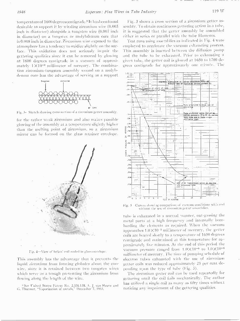
1946 Espersen: Fine Wires in Tube Industry 119 W
tern perature of 1600 degreescentigrade.a It hasbeen founddesirable to support it by winding zirconium wire (0.005inch in diameter) alongside a tungsten wire (0.007 inchin diameter) on a tungsten or molybdenum core thatis 0.008 inch in diameter. Zirconium wire exposed to theatmosphere has a tendency to oxidize slightly on the sur-face. This oxidation does not seriously impair thegettering qualities since it can be removed by glowingat 1600 degrees centigrade in a vacuum of approxi-mately 1 X10⁻⁶ millimeter of mercury. The combina-tion zirconium -tungsten assembly wound on a molyb-denum core has the advantage of serving as a support
Tungsten Zirconium
No Core
Fig. 3-Sketch showing cross section of a zirconium getter assembly.
for the rather weak zirconium and also makes possibleglowing of the assembly at a temperature slightly higherthan the melting point of zirconium, so a zirconiummirror can be formed on the glass retainer envelope.
Fig. 4-View of helical coil sealed in glass envelope.
This assembly has the advantage that it prevents theliquid zirconium from forming globules about the corewire, since it is retained between two tungsten wireswhich serve as a trough preventing the zirconium fromflowing along the length of the wire.
See United States Patent No. 2,336,138.:\. J. van Hoorn andG. Thurmer, "Vaporization of metals," December 7, 1943.
Fig. 3 shows a cross section of a zirconium getter as-sembly. To obtain continuous gettering action in a tube,it is suggested that the getter assembly be assembledeither in series or parallel with the tube filaments.
Test runs using assemblies as indicated in Fig. 4 wereemployed to accelerate the vacuum exhausting process.This assembly is inserted between the diffusion pumpand the tube to be exhausted. Prior to exhausting agiven tube, the getter coil is glowed at 1650 to 1700 de-grees centigrade for approximately one minute. The
1.0
.8
.c
.8
4
6IISTECTt
RITESCOMDIRISON OF
r aiACLU CONDITIONS WITH efie=WOKEN -GETTER .ASSENDLIPS
.8
.00
.06
06
.04
.02
;4.01
.000
.00e
1
.006
.001
.006-
009
.001
PreSsure et 'ebesChendnent
t oof tube
0 1 2 3 4 5 6 6 10
Tia IN MINUTES
Tube processed2-1-reon Imo
TutmLniocessed 'usime SireQPiumgetter amsambly Sig 3) Sin marten
browmit), Otisdiffusion puns
deent p ior to sealingN.
1416Fig. 5-Curves showing comparison of vacuum conditions with and
without the use of zirconium getter assemblies.
tube is exhausted in a normal manner, out -gassing themetal parts at a high frequency and internally bom-barding the elements as required. When the vacuumapproaches 1.0 X10⁻³ millimeter of mercury, the gettercoils are heated slowly to a temperature of 1650 degreescentigrade and maintained at this temperature for ap-proximately five minutes. At the end of this period thevacuum pressure ranged from 1.0 X10⁻⁶ to 1.0 X10⁻⁶millimeter of mercury. The time of pumping schedule ofelectron tubes exhausted with the use of zirconiumgetter coils was reduced approximately 25 per cent de-pending upon the type of tube (Fig. 5).
The zirconium getter coil can be used repeatedly forgettering until the coil fails mechanically. The authorhas utilized a single coil as many as fifty times withoutnoticing any impairment of the gettering qualities.
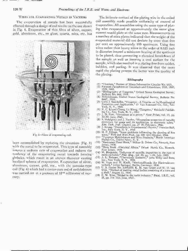
120 W Proceedings of the I.R.E. and Waves and Electrons
WIRES FOR EVAPORATING METALS IN VACUUMS
The evaporation of metals has been successfullyeffected through a design of coil similar to the one shownin Fig. 6. Evaporation of thin films of silver, copper,gold, aluminum, etc., on glass, quartz, mica, etc. has
Fig. 6-View of evaporating coil.
been accomplished by replacing the zirconium (Fig. 3)with the metal to be evaporated. This type of assemblyinsures a uniform rate of evaporation and reduces thetendency of the evaporating metal towards formingglobules, which result in an uneven diameter causinglocalized spheres of evaporation. Evaporation of silver,aluminum, copper, gold, etc., with the pancake -typecoil (Fig. 6) which had a center -core rod of molybdenumwas carried out at a pressure of 10-3 millimeter of mer-cury.
The intimate contact of the plating wire in the coiledcoil assembly made possible uniformity of control ofevaporation. All assemblies using the same type of plat-ing wire evaporated at approximately the same glowcurrent would plate at the same rate. Measurements ona number of mica plates indicated that the weight of theevaporated material did not deviate by more than fiveper cent on approximately 100 specimens. Using finewires rather than heavy wires in the order of 0.025 inchin diameter insured a minimum heating of the specimento be plated, thus preventing a chemical breakdown ofthe sample as well as insuring a cool surface for thesample, which also resulted in a plating free from oxides,bubbles, and peeling. It was observed that the morerapid the plating process the better was the quality ofthe plating.
Bibliography
(1) "Thorium," Bureau of Mines Information Circular No. 6321.(2) Fansteel Pamphlets on Tantalum and Columbium, 1935, 1937,
1939, 1942.(3) "Bibliography of Tungsten," United States Geological Survey,
Bulletin No. 666, 1919.(4) Molybdenum, United States Geological Survey, Bulletin No.
846C, 1933.(5) Colin J Smithelles, "Tungsten-A Treatise on Its Metallurgical
Properties and Application," D Van Nostrand Co., Inc., NewYork, N. Y., 1926
(6) K. C. Li and Chung Yu Wang, "Tungsten," Reinhold Publish-ing Co., New York, N. Y., 1943
(7) J. D. Fast, "Zirconium as a getter," Foote Prints, vol. 13, pp.22-30; June, 1940.
(8) S. Hukagawa and J. Nambo, "Absorption properties of metalliczirconium for gases and its application to electronic tubes,"Elec. Tech. Jour. (Japan), pp. 27-30; February, 1941.
(9) J. Strong, "Procedures in Experimental Physics," Prentice Hall,Inc., New York, N. Y., 1944
(10) H. P. Edinga, "Some problems influencing the drawing of finewires," Wire and Wire Prod., pp. 650-653; October, 1944.
(11) "Tungsten Molybdenum and Wire Products," North AmericanPhilips Co., Dobbs Ferry, N. Y.
(12) "Resistance Hand Book," Wilbur B. Driver Co., Newark, NewJersey, 1938.
(13) "Data Book-Electrical Alloys," Driver Harris Co., Newark,New Jersey, 1939.
(14) M. Benjamin, "Influence of metallic impurities in the core ofoxide cathodes," Phil. Mag., vol. 20, pp. 1-24; July, 1935.
(15) A. L. Reiman, "Thermionic Emission," John Wiley and Sons,Inc., New York, N. Y., 1934.
(16) W. Espe and M. Knoll, "Werkstoffkunde der Hockvakuum-technik," Julius Springer, Berlin, Germany, 1936.
(17) U. S. Patent No. 2,050,820, K. M. van Gessel and W. D. vanWijk, "Method of making metal bodies consisting of a core anda shell," August 11, 1936.
(18) E. M. Wise, "Nickel in the radio industry," PROC. I.R.E., vol.25, pp. 714-753; June, 1937.
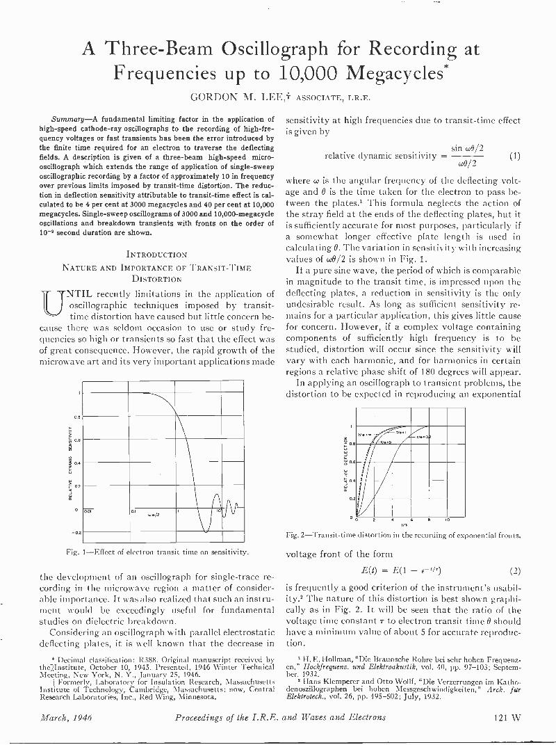
A Three -Beam Oscillograph for Recording atFrequencies up to 10,000 Megacycles*
GORDON M. LEE,t ASSOCIATE, I.R.E.
Summary-A fundamental limiting factor in the application ofhigh-speed cathode-ray oscillographs to the recording of high -fre-quency voltages or fast transients has been the error introduced bythe finite time required for an electron to traverse the deflectingfields. A description is given of a three -beam high-speed micro-oscillograph which extends the range of application of single -sweeposcillographic recording by a factor of approximately 10 in frequencyover previous limits imposed by transit -time distortion. The reduc-tion in deflection sensitivity attributable to transit -time effect is cal-culated to be 4 per cent at 3000 megacycles and 40 per cent at 10,000megacycles. Single -sweep oscillograms of 3000 and 10,000 -megacycleoscillations and breakdown transients with fronts on the order of10-9 second duration are shown.
INTRODUCTION
NATURE AND IMPORTANCE OF TRANSIT -TIMEDISTORTION
UNTIL recently limitations in the application ofoscillographic techniques imposed by transit -time distortion have caused but little concern be-
cause there was seldom occasion to use or study fre-quencies so high or transients so fast that the effect wasof great consequence. However, the rapid growth of themicrowave art and its very important applications made
0.8
0.4
-0.2
001 0.14,4/2
10
Fig. 1-Effect of electron transit time on sensitivity.
the development of an oscillograph for single -trace re-cording in the microwave region a matter of consider-able importance. It was also realized that such an instru-ment would be exceedingly useful for fundamentalstudies on dielectric breakdown.
Considering an oscillograph with parallel electrostaticdeflecting plates, it is well known that the decrease in
* Decimal classification: R388. Original manuscript received bythe),Institute, October 10, 1945. Presented, 1946 Winter TechnicalMeeting, New York, N. Y., January 25, 1946.
t Formerly, Laboratory for Insulation Research, MassachusettsInstitute of Technology, Cambridge, Massachusetts; now, CentralResearch Laboratories, Inc., Red Wing, Minnesota.
sensitivity at high frequencies due to transit -time effectis given by
sin w0/2relative dynamic sensitivity - (1)
coo/2
where w is the angular frequency of the deflecting volt-age and 0 is the time taken for the electron to pass be-tween the plates.' This formula neglects the action ofthe stray field at the ends of the deflecting plates, but itis sufficiently accurate for most purposes, particularly ifa somewhat longer effective plate length is used incalculating 0. The variation in sensitivity with increasingvalues of w0/2 is shown in Fig. 1.
If a pure sine wave, the period of which is comparablein magnitude to the transit time, is impressed upon thedeflecting plates, a reduction in sensitivity is the onlyundesirable result. As long as sufficient sensitivity re-mains for a particular application, this gives little causefor concern. However, if a complex voltage containingcomponents of sufficiently high frequency is to bestudied, distortion will occur since the sensitivity willvary with each harmonic, and for harmonics in certainregions a relative phase shift of 180 degrees will appear.
In applying an oscillograph to transient problems, thedistortion to be expected in reproducing an exponential
W6
0.2
O0 4 6
1/0
Fig. 2-Transit-time distortion in the recording of exponential fronts.
T/.0
voltage front of the form
E(1) = E(1 - E-tir) (2)
is frequently a good criterion of the instrument's usabil-ity.' The nature of this distortion is best shown graphi-cally as in Fig. 2. It will be seen that the ratio of thevoltage time constant T to electron transit time 0 shouldhave a minimum value of about 5 for accurate reproduc-tion.
I H. E. Holtman, "Die Braunsche Rohre bei sehr hohen Frequenz-en," Hochfrequenz. and Elektroakustik, vol. 40, pp. 97-103; Septem-ber, 1932.
2 Hans Klemperer and Otto Wollf, "Die Verzerrungen im Katho-denoszillographen bei hohen Messgeschwindigkeiten," Arch. furElektrotech., vol. 26, pp. 495-502; July, 1932.
March, 1946 Proceedings of the I.R.E. and Waves and Electrons 121 W
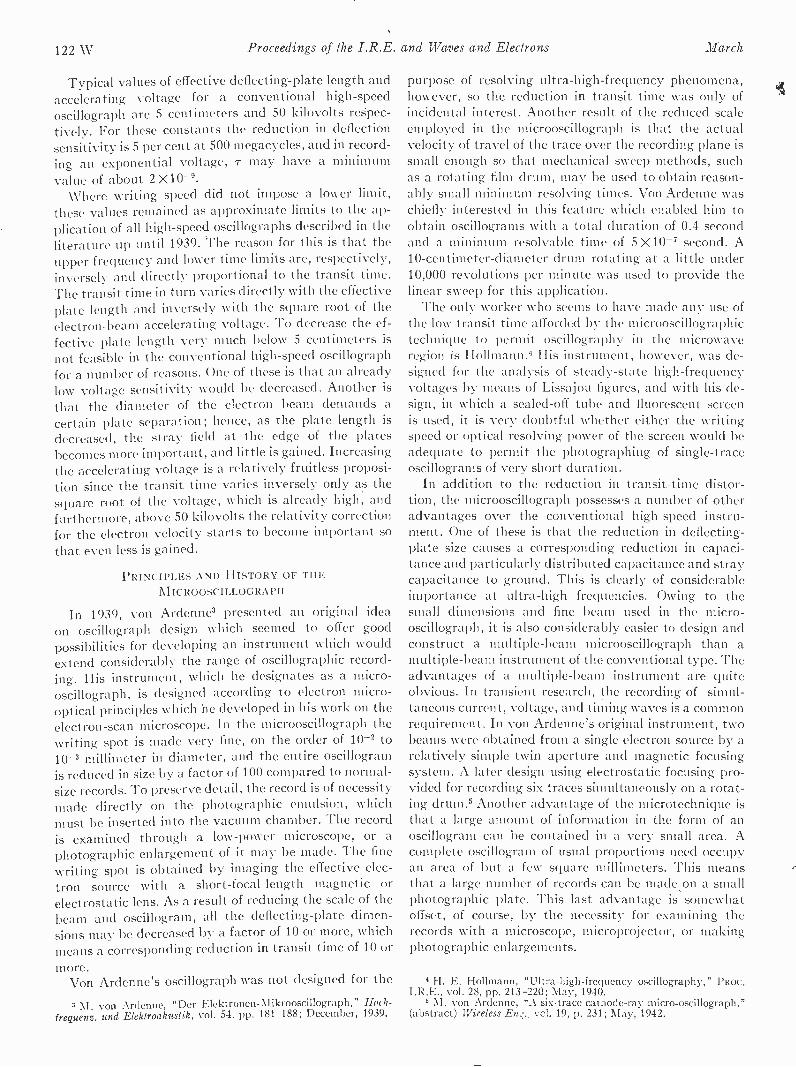
122 W Proceedings of the I.R.E. and Waves and Electrons March
Typical values of effective deflecting -plate length andaccelerating voltage for a conventional high-speedoscillograph are 5 centimeters and 50 kilovolts respec-tively. For these constants the reduction in deflectionsensitivity is 5 per cent at 500 megacycles, and in record-ing an exponential voltage, r may have a minimumvalue of about 2 X10⁻⁹.
Where writing speed did not impose a lower limit,these values remained as approximate limits to the ap-plication of all high-speed oscillographs described in theliterature up until 1939. The reason for this is that theupper frequency and lower time limits are, respectively,inversely and directly proportional to the transit time.The transit time in turn varies directly with the effectiveplate length and inversely with the square root of theelectron -beam accelerating voltage. To decrease the ef-fective plate length very much below 5 centimeters isnot feasible in the conventional high-speed oscillographfor a number of reasons. One of these is that an alreadylow voltage sensitivity would be decreased. Another is
that the diameter of the electron beam demands acertain plate separation; hence, as the plate length isdecreased, the stray field at the edge of the platesbecomes more important, and little is gained. Increasingthe accelerating voltage is a relatively fruitless proposi-tion since the transit time varies inversely only as thesquare root of the voltage, which is already high, andfurthermore, above 50 kilovolts the relativity correctionfor the electron velocity starts to become important sothat even less is gained.
PRINCIPLES AND HISTORY OF THEM ICROOSCILLOGRAPH
In 1939, von Ardenne3 presented an original ideaon oscillograph design which seemed to offer goodpossibilities for developing an instrument which wouldextend considerably the range of oscillographic record-ing. His instrument, which he designates as a micro-oscillograph, is designed according to electron micro -optical principles which he developed in his work on theelectron -scan microscope. In the microoscillograph thewriting spot is made very fine, on the order of 10-2 to10-3 millimeter in diameter, and the entire oscillogramis reduced in size by a factor of 100 compared to normal -size records. To preserve detail, the record is of necessitymade directly on the photographic emulsion, whichmust be inserted into the vacuum chamber. The recordis examined through a low -power microscope, or aphotographic enlargement of it may be made. The finewriting spot is obtained by imaging the effective elec-tron source with a short-focal -length magnetic orelectrostatic lens. As a result of reducing the scale of thebeam and oscillogram, all the deflecting-plate dimen-sions may be decreased by a factor of 10 or more, whichmeans a corresponding reduction in transit time of 10 ormore.
Von Ardenne's oscillograph was not designed for the
3 M. von Ardenne, "Der Elektronen-Mikrooscillograph," Hoch-frequenz. and Elektroakuslik, vol. 54, pp. 181-188; December, 1939.
purpose of resolving ultra -high -frequency phenomena,however, so the reduction in transit time was only ofincidental interest. Another result of the reduced scaleemployed in the microoscillograph is that the actualvelocity of travel of the trace over the recording plane issmall enough so that mechanical sweep methods, suchas a rotating film drum, may be used to obtain reason-ably small minimum resolving times. Von Ardenne waschiefly interested in this feature which enabled him toobtain oscillograms with a total duration of 0.4 secondand a minimum resolvable time of 5 X10⁻⁷ second. A10 -centimeter -diameter drum rotating at a little under10,000 revolutions per minute was used to provide thelinear sweep for this application.
The only worker who seems to have made any use ofthe low transit time afforded by the microoscillographictechnique to permit oscillography in the microwaveregion is Hollmann.4 His instrument, however, was de-signed for the analysis of steady-state high -frequencyvoltages by means of Lissajou figures, and with his de-sign, in which a sealed -off tube and fluorescent screenis used, it is very doubtful whether either the writingspeed or optical resolving power of the screen would beadequate to permit the photographing of single -traceoscillograms of very short duration.
In addition to the reduction in transit -time distor-tion, the microoscillograph possesses a number of otheradvantages over the conventional high-speed instru-ment. One of these is that the reduction in deflecting -plate size causes a corresponding reduction in capaci-tance and particularly distributed capacitance and straycapacitance to ground. This is clearly of considerableimportance at ultra -high frequencies. Owing to thesmall dimensions and fine beam used in the micro-oscillograph, it is also considerably easier to design andconstruct a multiple -beam microoscillograph than amultiple -beam instrument of the conventional type. Theadvantages of a multiple -beam instrument are quiteobvious. In transient research, the recording of simul-taneous current, voltage, and timing waves is a commonrequirement. In von Ardenne's original instrument, twobeams were obtained from a single electron source by arelatively simple twin aperture and magnetic focusingsystem. A later design using electrostatic focusing pro-vided for recording six traces simultaneously on a rotat-ing drum.' Another advantage of the microtechnique isthat a large amount of information in the form of anoscillogram can be contained in a very small area. Acomplete oscillogram of usual proportions need occupyan area of but a few square millimeters. This meansthat a large number of records can be made on a smallphotographic plate. This last advantage is somewhatoffset, of course, by the necessity for examining therecords with a microscope, microprojector, or makingphotographic enlargements.
4 H. E. Hollmann, "Ultra -high -frequency oscillography," PROC.I.R.E., vol. 28, pp. 213-220; May, 1940.
6 M. von Ardenne, "A six trace cathode-ray micro-oscillograph,"(abstract) Wireless vel. 19, p. 231; May, 1942.
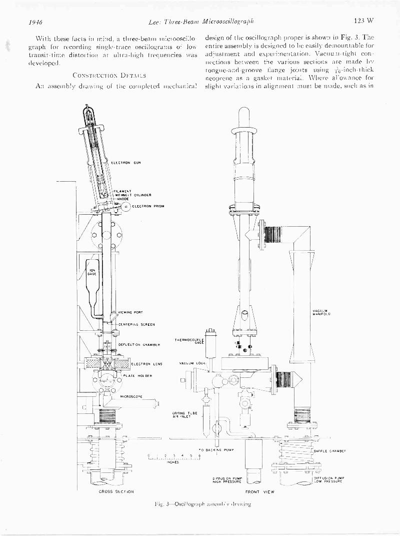
1946 Lee: Three -Beam Microoscillograph 123 W
With these facts in mind, a three -beam microoscillo-graph for recording single -trace oscillograms of lowtransit -time distortion at ultra -high frequencies wasdeveloped.
CONSTRUCTION DETAILS
An assembly drawing of the completed mechanical
le\
FILAMENTWEHNELT CYLINDER
04.0ANODE
ELECTRON GUN
ELECTRON PRISM
VIEWING PORT
CENTERING SCREEN
DEFLECTION CHAMBER
ELECTRON LENS
PLATE HOLDER
MICROSCOPE
CROSS SECTION
THERMOCOUPLE
VACUUM LOCK
DRYING TUBEAIR INLET
design of the oscillograph proper is shown in Fig. 3. Theentire assembly is designed to be easily demountable foradjustment and experimentation. Vacuum -tight con-nections between the various sections are made bytongue -and -groove flange joints using -,--inch-thickneoprene as a gasket material. Where allowance farslight variations in alignment must be made, such as in
int
TO BACKING PUMP
0 I 2 3 4 5 6L. I 1 I..1,JINCHES
VACUUMMANIFOLD
BAFFLE CHAMBEII
DIFFUSION PUMP DIFFUSION PUMPHIGH PRESSURE LOW PRESSURE
FRONT VIEW
Fig. 3-Oscillograph assembly drawing.
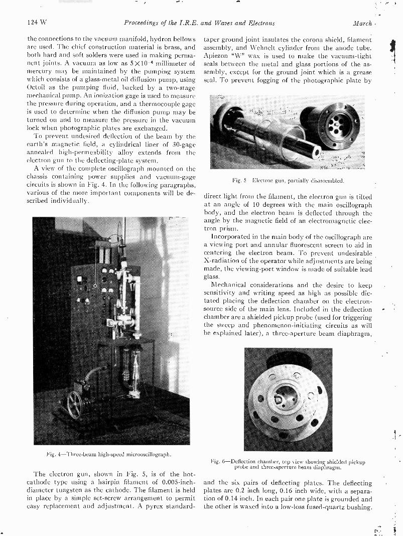
124 W Proceedings of the I.R.E. and Waves and Electrons March
the connections to the vacuum manifold, hydron bellowsare used. The chief construction material is brass, andboth hard and soft solders were used in making perma-nent joints. A vacuum as low as 5 X10⁻⁶ millimeter ofmercury may be maintained by the pumping systemwhich consists of a glass -metal oil diffusion pump, usingOctoil as the pumping fluid, backed by a two -stagemechanical pump. An ionization gage is used to measurethe pressure during operation, and a thermocouple gageis used to determine when the diffusion pump may beturned on and to measure the pressure in the vacuumlock when photographic plates are exchanged.
To prevent undesired deflection of the beam by theearth's magnetic field, a cylindrical liner of 30 -gageannealed high -permeability alloy extends from theelectron gun to the deflecting -plate system.
A view of the complete oscillograph mounted on thechassis containing power supplies and vacuum -gagecircuits is shown in Fig. 4. In the following paragraphs,various of the more important components will be de-scribed individually.
Fig. 4-Three-beam high-speed microoscillograph.
The electron gun, shown in Fig. 5, is of the hot -cathode type using a hairpin filament of 0.005 -inch -diameter tungsten as the cathode. The filament is heldin place by a simple set -screw arrangement to permiteasy replacement and adjustment. A pyrex standard -
taper ground joint insulates the corona shield, filamentassembly, and Wehnelt cylinder from the anode tube.Apiezon "W" wax is used to make the vacuum -tightseals between the metal and glass portions of the as-sembly, except for the ground joint which is a greaseseal. To prevent fogging of the photographic plate by
Fig. 5-Electron gun, partially disassembled.
direct light from the filament, the electron gun is tiltedat an angle of 10 degrees with the main oscillographbody, and the electron beam is deflected through theangle by the magnetic field of an electromagnetic elec-tron prism.
Incorporated in the main body of the oscillograph area viewing port and annular fluorescent screen to aid incentering the electron beam. To prevent undesirableX-radiation of the operator while adjustments are beingmade, the viewing -port window is made of suitable leadglass.
Mechanical considerations and the desire to keepsensitivity and writing speed as high as possible dic-tated placing the deflection chamber on the electron -
source side of the main lens. Included in the deflectionchamber are a shielded pickup probe (used for triggeringthe sweep and phenomenon -initiating circuits as willbe explained later), a three -aperture beam diaphragm,
Fig. 6-Deflection chamber, top view showing shielded pickupprobe and three -aperture beam diaphragm.
and the six pairs of deflecting plates. The deflectingplates are 0.2 inch long, 0.16 inch wide, with a separa-tion of 0.14 inch. In each pair one plate is grounded andthe other is waxed into a low -loss fused -quartz bushing.
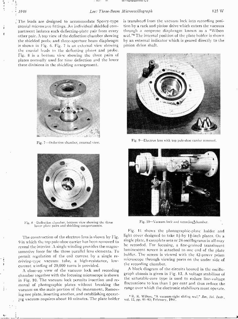
Lee: Three -Beam Microoscillograph 125 W
The leads are designed to accommodate Sperry -typecoaxial microwave fittings. An individual shielded com-partment isolates each deflecting -plate pair from everyother pair. A top view of the deflection chamber showingthe shielded probe and three -aperture beam diaphragmis shown in Fig. 6. Fig. 7 is an external view showingthe coaxial leads to the deflecting plates and probe.Fig. 8 is a bottom view showing the three pairs ofplates normally used for time deflection and the lowerthree divisions in the shielding arrangement.
Fig. 7-Deflection chamber, external view.
Fig. 8-Deflection chamber, bottom view showing the threelower plate pairs and shielding compartments.
The construction of the electron lens is shown by Fig.9 in which the top pole -shoe carrier has been removed toreveal the interior. A single winding provides the magne-tomotive force for the three parallel lens elements. Topermit regulation of the coil current by a single re-ceiving -type vacuum tube, a high -resistance, low -
current winding of 20,000 turns is provided.A close-up view of the vacuum lock and recording
chamber together with the focusing microscope is shownin Fig. 10. The vacuum lock permits insertion and re-moval of photographic plates without breaking thevacuum on the main portion of the instrument. Remov-ing one plate, inserting another, and establishing operat-ing vacuum requires about 10 minutes. The plate holder
is translated from the vacuum lock into recording posi-tion by a rack and pinion drive which enters the vacuumthrough a neoprene diaphragm known as a "Wilsonseal."' The internal position of the plate holder is shownby an external indicator which is geared directly to thepinion drive shaft.
Fig. 9-Electron lens with top pole -shoe carrier removed.
Fig. 10-Vacuum lock and recordinglchamber.
Fig. 11 shows the photographic -plate holder andlight cover designed to take 11 -by 18 -inch plates. On asingle plate, 8 complete sets or 24 oscillograms in all maybe recorded. For focusing, a fine-grained translucentluminescent screen is attached to one end of the plateholder. The screen is viewed with the 42 -power prismmicroscope through viewing ports on the under side ofthe recording chamber.
A block diagram of the circuits housed in the oscillo -
graph chassis is given in Fig. 12. A voltage stabilizer ofthe saturable -core type is used to reduce line -voltagefluctuations to less than 1 per cent and thus reduce therange over which the electronic stabilizers must operate.
6 R. R. Wilson, "A vacuum -tight sliding seal," Rev. Sci. Instr.,vol. 12, pp. 91-93; February, 1941.
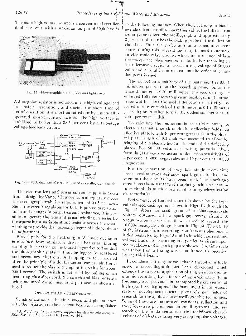
126 W Proceedings of the I. and Waves and Electrons March
The main high -voltage source is a conventional rectifier- in the following manner. When the electron -gun bias isdoubler circuit, with a maximum output of 50,000 volts. I switched from cutoff to operating value, the full electron
beam passes down the oscillograph and approximately2 per cent of it strikes the pickup probe in the deflectionchamber. Thus the probe acts as a constant -currentsource during this interval and may be used to actuatean electronic relay circuit, which in turn may initiatethe sweep, the phenomenon, or both. For recording inthe microwave region an accelerating voltage of 50,000volts and a total beam current on the order of 5 mil-liamperes is used.
Fig. 11-Photographic plate holder and light cover.
A 5-megohm resistor is included in the high -voltage leadas a safety precaution, and during the short time ofactual operation, it is short-circuited out by a manually -operated short-circuiting switch. The high voltage isstabilized to better than 0.05 per cent by a two -stagevoltage -feedback circuit.
115V.
PVi IAMCF;
SAT.COREREG.
THERMGAGE
IONGAGE
FIL.
SUPPLY
50 Kv.
RE CT.
FILTER
FIL.
REG.CURRENTSUPPLY
FEEDBACKREG.
-I LENS
PRISM
Fig. 12-Block diagram of circuits housed in oscillograph chassis.
The electron lens and prism current supply is takenfrom a design by Vance.' It more than adequately meetsthe oscillograph stability requirement of 0.05 per cent.Since the circuit regulates for both input -voltage varia-tions and changes in output -circuit resistance, it is pos-sible to operate the lens and prism winding in series byincorporating a variable shunt resistor across the prismwinding to provide the necessary degree of independencein adjustment.
Bias supply for the electron -gun Wehnelt cyclinderis obtained from miniature dry -cell batteries. Duringstandby the electron gun is biased beyond cutoff so thatthe photographic plate will not be fogged by scatteredand secondary electrons. A tripping switch modeledafter the principle of a double -action camera shutter isused to reduce the bias to the operating value for about0.001 second. The switch is actuated by pulling on aninsulating glass -fiber cord, the switch and bias batteriesbeing mounted on an insulated platform as shown inFig. 4.
OPERATION AND PERFORMANCE
Synchronization of the time sweep and phenomenonwith the initiation of the electron beam is accomplished
7 A. W. Vance, "Stable power supplies for electron microscopes,"RCA Rev., vol. 5, pp. 293-300; January, 1941.
The deflection sensitivity of the instrument is 0.001millimeter per volt on the recording plane. Since thetrace diameter is 0.01 millimeter, the records may beenlarged 100 diameters to give an oscillogram of normaltrace width. Thus the useful deflection sensitivity, re-ferred to a trace width of 1 millimeter, is 0.1 millimeterper volt; or in other terms, the deflection factor is 10volts per trace width.
To calculate the reduction in sensitivity owing toelectron transit time through the deflecting fields, aneffective plate length 40 per cent greater than the physi-cal plate length of 0.2 inch was assumed to allow forfringing of the electric field at the ends of the deflectingplates. For 50,000 volts accelerating potential then,formula ( 1 ) gives a reduction in deflection sensitivity of4 per cent at 3000 megacycles and 40 per cent at 10,000megacycles.
For the generation of very fast single-sweep timebases, resistance -capacitance spark-gap circuits, andvacuum -tube circuits have been used. The spark-gapcircuit has the advantage of simplicity, while a vacuum -tube circuit is much more reliable in synchronizationcharacteristics.
Performance of the instrument is shown by the typi-cal enlarged oscillograms shown in Figs. 13 through 16.Fig. 13 shows an oscillogram of a 3000 -megacyclevoltage obtained with a spark-gap sweep circuit. Avacuum -tube sweep circuit was used to record the10,000-megacyCle voltage shown in Fig. 14. The utilityof the instrument in recording simultaneous phenomenais demonstrated by Figs. 15 and 16 in which current andvoltage transients occurring in a particular circuit uponthe breakdown of a spark gap are shown. The time scalewas taken from a timing wave simultaneously recordedby the third beam.
In conclusion it may be said that a three -beam high-speed microoscillograph has been developed whichextends the range of application of single-sweep oscillo-graphic recording by a factor of approximately 10 infrequency over previous limits imposed by conventionalhigh-speed oscillographs. The instrument in its presentstate of development opens up entirely new fields ofresearch for the application of oscillographic techniques.Some of these are microwave transients, reflection andtraveling -wave phenomena on small systems, and re-search on the fundamental electric -breakdown charac-teristics of dielectrics using very steep impulse voltages.
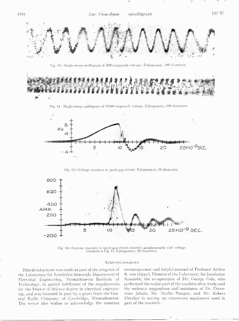
1946 Lee: Three -Beam ooscillograph 127 W
Fig. 13 -Single -sweep oscillogram of 3000 -megacycle voltage. Enlargement, 100 diameters.
Fig. 14-Single-sweep oscillogram of 10,000 -megacycle voltage. Enlargement, 100 diameters.
800
600
400AMP.
200
-200
Fig. 15-Voltage transient in spark -gap circuit. Enlargement, 50 diameters.
5 10I
20 2.5x10⁻⁹ SEC.
Fig. 16-Current transient in spark -gap circuit recorded simultaneously with voltagetransient in Fig. 15. Enlargement, 50 diameters.
ACKNOWLEDGMENT
This development was made as part of the program ofthe Laboratory for Insulation Research, Department ofElectrical Engineering, Massachusetts Institute ofTechnology, in partial fulfillment of the requirementsfor the Doctor of Science degree in electrical engineer-ing, and was financed in part by a grant from the Gen-eral Radio Company, of Cambridge, MassachusettsThe writer also wishes to acknowledge the constant
encouragement and helpful counsel of Professor ArthurR. von Hippel, Director of the Laboratory for InsulationResearch; the co-operation of Mr. George Gale, whoperformed the major part of the machine shop work; andthe welcome suggestions and assistance of Dr. Deme-trius Jelatis, Mr. Merlin Haugen, and Mr. RobertFletcher in setting up microwave equipment used inpart of the research.
Synchronizing Generators for Electronic Television*A. RUFUS APPLEGAI flit, ASSOCIATE, I.R.E.
Summary-The system of electronic circuits employed to gener-ate the complex wave forms required as a base for television picturetransmission is described. It comprises four principal sections whichare: (1) source of accurately timed pulses; (2) frequency -dividerchain; (3) components -generating circuits; and (4) signal -synthesiscircuits. The various means for accomplishing these functions isbriefly discussed, and illustrated by circuits which have been usedsuccessfully for such purposes in practical applications.
I. INTRODUCTION
has been written about the general subjectof television. There are available several goodtexts which discuss the general requirements of
television systems, but which do not delve into theproblems involved in generating the modern electronic -
television synchronizing signal. The subject matter ofthis paper includes a discussion of the problems con-cerning the design of synchronizing generators and alsosome detailed circuits to illustrate the discussion.
The synchronizing generator is the heart of any elec-tronic -television system. It provides the many com-ponent synchronizing and pedestal signals to which thepicture signal, having been generated and amplifiedelsewhere, is added to form the complete compositevideo signal. This video signal is then modulated upon asuitable carrier for radio -television transmission. Thebasic components of a television synchronizing gener-ator are illustrated in Fig. 1. It is necessarily a complexassembly of electronic devices, interlocked in such away as to produce a stable composite signal which mustconform to the standards set by the Federal Communi-cations Commission (see Fig. 2).
The Federal Communications Commission standardsspecify an interlaced scan. The timing of the verticalscan must be precisely related to that of the horizontalscan, if accurate interlacing is to be obtained. Not onlymust the horizontal and vertical scanning frequenciesbe harmonically related, but precisely controlled in rela-tive phase position as well. For example, a shift in thetiming of the vertical scan by an interval equal to onehalf of a horizontal line will completely destroy theinterlace. Furthermore, the maintenance of a satisfac-tory interlace (defined as one in which the unbalancebetween adjacent line spacing is no greater than 40 to60 per cent) requires that timing precision be held to0.1 line, or to one part in 5250 in a 525 -line system. Suchnarrow tolerance restrictions in the timing betweenhorizontal and vertical scanning frequencies precludemost of the simple harmonic -generating systems usedsuccessfully for other purposes.
* Decimal classification: R583. Original manuscript receivedby the Institute, July 2, 1945.
t 5722 Greene Street, Philadelphia 44, Pa.
The design of electronic synchronizing generatorsgenerally includes a high -frequency master oscillatorfrom which the various signal components are derivedby frequency -divider systems and wave -shaping cir-cuits. It is desirable to have the 60 -cycle vertical -scanning frequency synchronous with the 60 -cyclepower system of the local utility, to eliminate the slowvertical drift imparted to any hum pattern whichmight originate anywhere in the over-all televisionsystem.
SOURCE OF
CONTROLLED
PULSED
COMPCNENTS
GENERATING
CIRCUI TS
FREOUENCv
Div iDER
CHAIN
SIGNAL
SYNTHESIS
CIRCUITS
A f C
OUTPUT
INE
Fig. 1-Block diagram of synchronizing generatorshowing principal components.
Television standards for some years have included aline structure specifically chosen to facilitate frequency -divider design. The frequency -division ratio to relatethe vertical scan to the second harmonic of the hori-zontal scan is equal to the number of lines. Thus, foreasy frequency -divider design, the number of lines mustbe a number capable of being broken into several smallprime factors. For example, 343 could be factored into7 X 7 X 7. Likewise, 441 can be factored into 3 X 3 X 7 X 7,and 525 into 3 X5 X5 X7. Future standards undoubt-edly will be chosen to factor similarly. The illustrativecircuits described herein are designed for the 525 -linestandard, but, by suitable modification, could be madeto function on any standard likely to be adopted forsome time to come.
' II. THE FREQUENCY -DIVIDER CHAIN
As pointed out above, the system of circuits called thefrequency -divider chain which links the vertical-scan-ning frequency to the second harmonic of the hori-zontal -scanning frequency forms a vital part of thesynchronizing generator. Various circuits can be usedfor the several links of the chain, including multivibra-tors, blocking -tube oscillators, and counters.
The multivibrator comprises two resistance -coupledamplifier stages in cascade, with the output of thesecond stage fed directly back to the input of the firststage, to form an oscillator (see Fig. 3a).(The frequencyof oscillation is determined primarily by the time
128 W Proceedings of the I.R.E. and Waves and Electrons March, 1946

Applegarth: Television Synctronizing Generators 129 W
constants of the coupling networks, but depends also on ' The resonant stabilizer is shock excited by the pulsethe tube characteristics, power-su_p\ply voltages, and the of 'grid current that flows through it during the positive -amplitude of the driving signal.) The multivibrator 1, grid portion of each cycle. The voltage that appearsoffers a versatile means for generating oscillations of across the stabilizer is a damped transient oscillation
BOTTOM OF PICTURE
4.00 H MAX.
\
04 H
.5H -40- .43H
EQUALIZINGPULSE INTERVAL
3.2H
VERT. SYNC.PULSE INTERVAL
3H
1St- HORIZONTAL SYNC. PULSES
h
EQUALIZINGPULSE INTERVAL
VERTICAL BLANKING .075V ± 005V
.004H MAX.
-90%
- -101
A2H .08H-4-07H i.01H
tO1H
DETAIL BETWEEN D -D DETAIL BETWEEN E- E
3H
E
.02 H MIN.FRONT PORC
1 HMAX.
E
08H
18HMAX.
TOP OF PICTURE
DETAIL OF SECTION C- C
Fig. 2-Federal Communications Commission's standard television signal.
rectangular wave form, but its stability is inadequatefor its use as a frequency divider for factors greaterthan about 3:1.
The blocking -tube oscillator represents a distinct im-provement in stability over the multivibrator (seeFig. 3b). This improvement comes primarily from thesubstitution of a transformer of inherently stable char-acteristics for one of the tubes of the multivibrator. Thistype of oscillator, although more stable, is also subjectto frequency dependence upon tube characteristics,power -supply voltage variations, and the amplitude ofthe driving signal used to synchronize it.
A resonant stabilizer comprising a parallel -connectedtuned circuit can be inserted in series with the oscillatorgrid circuit to increase greatly its frequency stability.This will cause it to divide by a factor primarily deter-mined by the tuning of the resonant circuit, and to afar lesser degree by unwanted variables (see Fig. 4).
.14 H MIN.REMAINDEROF PEDESTAL
whose period is determined by the tuning of the reso-nant stabilizer. This transient voltage, which is re-peated each time a pulse of oscillator -grid currentflows, is added to the exponential capacitor -dischargevoltage, and to the train of driving pulses to form thecomposite oscillator -grid signal. Thus, by tuning the sta-bilizer to the proper frequency (about one and one-half times the desired oscillator frequency) the transientoscillation will elevate the desired driving pulse sub-stantially above its neighbors, and thereby insure syn-chronization of the blocking -tube oscillator on the de-sired driving pulse, despite the usual variations in tubecharacteristics, power -supply voltages, and the ampli-tude of the driving pulses.
The stabilizing effect increases as the amplitude of thedamped transient signal is increased, up to the pointwhere this transient signal becomes strong enough tofire the blocking -tube oscillator without the aid of the
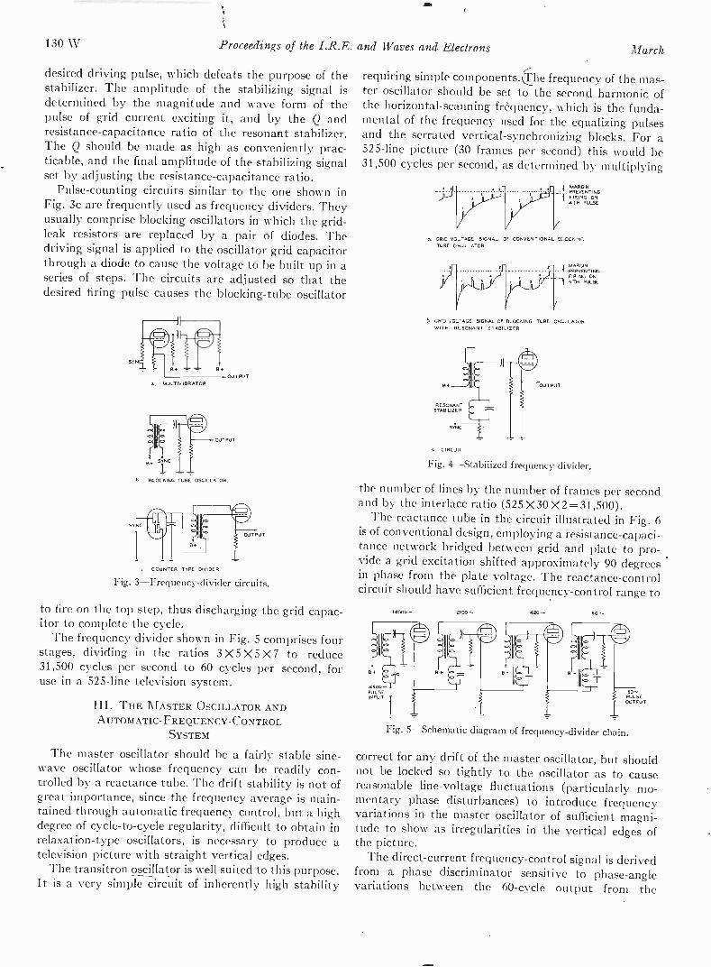
130 W Proceedings of the I.R.E. and Waves and Electrons March
desired driving pulse, which defeats the purpose of thestabilizer. The amplitude of the stabilizing signal isdetermined by the magnitude and wave form of thepulse of grid current exciting it, and by the Q andresistance -capacitance ratio of the resonant stabilizer.The Q should be made as high as conveniently prac-ticable, and the final amplitude of the stabilizing signalset by adjusting the resistance -capacitance ratio.
Pulse -counting circuits similar to the one shown inFig. 3c are frequently used as frequency dividers. Theyusually comprise blocking oscillators in which the grid -
leak resistors are replaced by a pair of diodes. Thedriving signal is applied to the oscillator grid capacitorthrough a diode to cause the voltage to be built up in aseries of steps. The circuits are adjusted so that thedesired firing pulse causes the blocking -tube oscillator
SY
a. MULTIVIBRATOR
OUTPUT
B. SYNC
-A
6 BLOCKING TUBE OSCILLATOR.
COUNTER TYPE DIVIDER
Fig. 3-Frequency-divider circuits.
to fire on the top step, thus discharging the grid capac-itor to complete the cycle.
The frequency divider shown in Fig. 5 comprises fourstages, dividing in the ratios 3 X5 X5 X7 to reduce31,500 cycles per second to 60 cycles per second, foruse in a 525 -line television system.
III. THE MASTER OSCILLATOR ANDAUTOMATIC -FREQUENCY -CONTROL
SYSTEM
The master oscillator should be a fairly stable sine-
wave oscillator whose frequency can be readily con-trolled by a reactance tube. The drift stability is not ofgreat importance, since the frequency average is main-tained through automatic frequency control, but a highdegree of cycle -to -cycle regularity, difficult to obtain inrelaxation -type oscillators, is necessary to produce atelevision picture with straight vertical edges.
The transitron oscillator is well suited to this purpose.It is a very simple circuit of inherently high stability
requiring simple components. The frequency of the mas-ter oscillator should be set to the second harmonic ofthe horizontal -scanning frequency, which is the funda-mental of the frequency used for the equalizing pulsesand the serrated vertical -synchronizing blocks. For a525 -line picture (30 frames per second) this would be31,500 cycles per second, as determined by multiplying
MARGIN-PREVENTING
I. FIRING ON4TH PULSE
A. GRID VOLTAGE SIGNAL OF CONVENTIONAL BLOCKINGTUBE OSCILLATOR.
5 GRID VOLTAGE SIGNAL OF BLOCKING TUBE OSCILLATORWITH RESONANT STABILIZER
c CIRCUIT
Fig. 4-Stabilized frequency divider.
the number of lines by the number of frames per secondand by the interlace ratio (525 X30 X2 =31,500).
The reactance tube in the circuit illustrated in Fig. 6is of conventional design, employing a resistance -capaci-tance network bridged between grid and plate to pro-vide a grid excitation shifted approximately 90 degreesin phase from the plate voltage. The reactance -controlcircuit should have sufficient frequency -control range to
BY
31500 --PULSEINPUT
10500 - 2100- 420 60 --
60 --PULSEOUTPUT
Fig. 5-Schematic diagram of frequency -divider chain.
correct for any drift of the master oscillator, but shouldnot be locked so tightly to the oscillator as to causereasonable line -voltage fluctuations (particularly mo-mentary phase disturbances) to introduce frequencyvariations in the master oscillator of sufficient magni-tude to show as irregularities in the vertical edges ofthe picture.
The direct -current frequency -control signal is derivedfrom a phase discriminator sensitive to phase -anglevariations between the 60 -cycle output from the
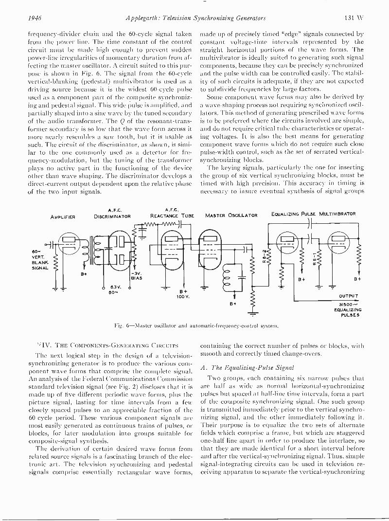
1946 Applegarth: Television Synchronizing Generators 131 W
frequency -divider chain and the 60 -cycle signal takenfrom the power line. The time constant of the controlcircuit must be made high enough to prevent suddenpower -line irregularities of momentary duration from af-fecting the master oscillator. A circuit suited to this pur-pose is shown in Fig. 6. The signal from the 60 -cyclevertical -blanking (pedestal) multivibrator is used as adriving source because it is the widest 60 -cycle pulseused as a component part of the composite synchroniz-ing and pedestal signal. This wide pulse is amplified, andpartially shaped into a sine wave by the tuned secondaryof the audio transformer. The Q of the resonant -trans-former secondary is so low that the wave form across itmore nearly resembles a saw tooth, but it is usable assuch. The circuit of the discriminator, as shown, is simi-lar to the one commonly used as a detector for fre-quency -modulation, but the tuning of the transformerplays no active part in the functioning of the deviceother than wave shaping. The discriminator develops adirect -current output dependent upon the relative phaseof the two input signals.
AMPLIFIER
oHBO-VERT.BLANKSIGNAL
A .F C.
DISCRIMINATOR
00-
A F.C.REACTANCE TUBE
H
B+100 V.
made up of precisely timed "edge" signals connected byconstant voltage -time intervals represented by thestraight horizontal portions of the wave forms. Themultivibrator is ideally suited to generating such signalcomponents, because they can be precisely synchronizedand the pulse width can be controlled easily. The stabil-ity of such circuits is adequate, if they are not expectedto subdivide frequencies by large factors.
Some component wave forms may also be derived bya wave -shaping process not requiring synchronized oscil-lators. This method of generating prescribed wave formsis to be preferred where the circuits involved are simple,and do not require critical tube characteristics or operat-ing voltages. It is also the best means for generatingcomponent wave forms which do not require such closepulse -width control, such as the set of serrated vertical -synchronizing blocks.
The keying signals, particularly the one for insertingthe group of six vertical synchronizing blocks, must betimed with high precision. This accuracy in timing isnecessary to insure eventual synthesis of signal groups
MASTER OSCILLATOR
B+
EQUALIZING PULSE MULTIVIBRATOR
Fig. 6-Master oscillator and automatic -frequency -control system.
IV. THE COMPONENTS -GENERATING CIRCUITS
The next logical step in the design of a television -synchronizing generator is to produce the various com-ponent wave forms that comprise the complete signal.An analysis of the Federal Communications Commissionstandard television signal (see Fig. 2) discloses that it ismade up of five different periodic wave forms, plus thepicture signal, lasting for time intervals from a fewclosely spaced pulses to an appreciable fraction of the60 -cycle period. These various component signals aremost easily generated as continuous trains of pulses, orblocks, for later modulation into groups suitable forcomposite -signal synthesis.
The derivation of certain desired wave forms fromrelated source signals is a fascinating branch of the elec-tronic art. The television synchronizing and pedestalsignals comprise essentially rectangular wave forms,
B+
OUTPUT
31900^'EQUALIZING
PULSES
containing the correct number of pulses or blocks, withsmooth and correctly timed change-overs.
A. The Equalizing -Pulse Signal
Two groups, each containing six narrow pulses thatare half as wide as normal horizontal -synchronizingpulses but spaced at half-line time intervals, form a partof the composite synchronizing signal. One such groupis transmitted immediately prior to the vertical synchro-nizing signal, and the other immediately following it.Their purpose is to equalize the two sets of alternatefields which comprise a frame, but which are staggeredone-half line apart in order to produce the interlace, sothat they are made identical for a short interval beforeand after the vertical -synchronizing signal. Thus, simplesignal -integrating circuits can be used in television re-ceiving apparatus to separate the vertical -synchronizing
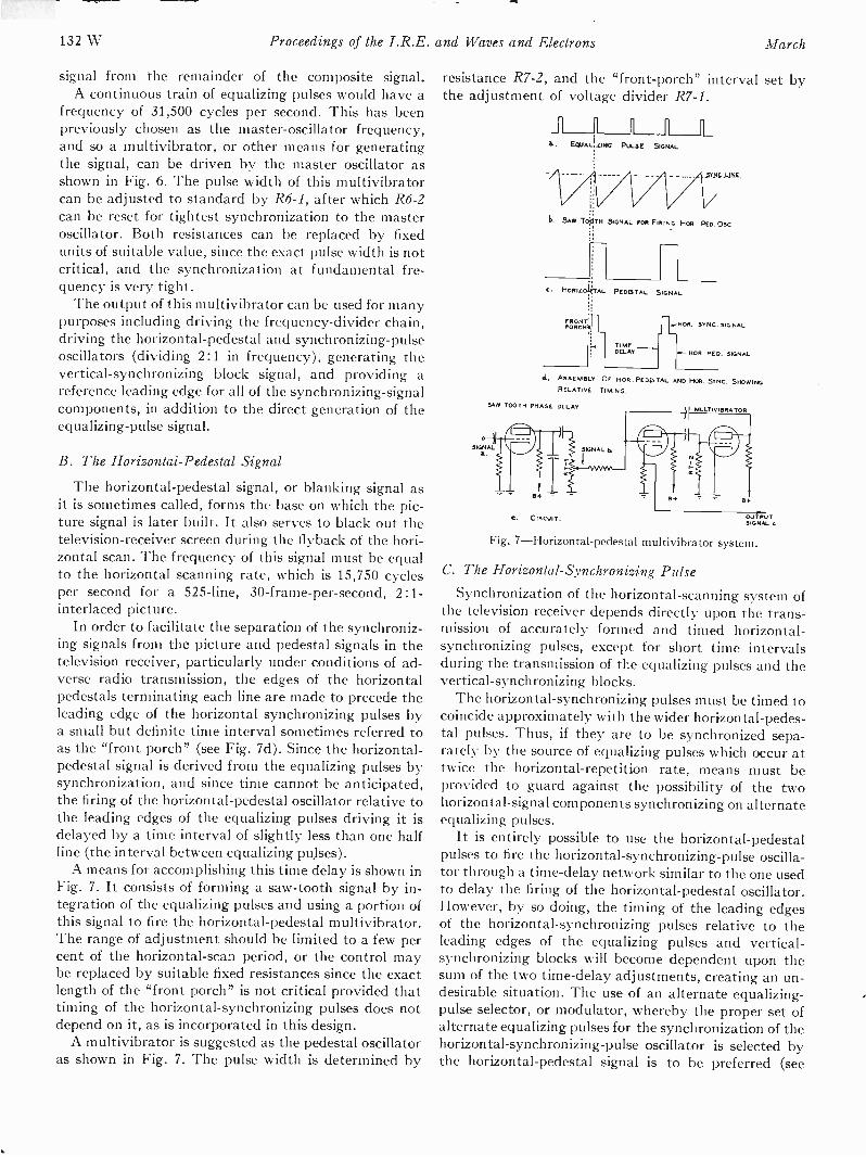
132 W Proceedings of the I.R.E. and Waves and Electrons March
signal from the remainder of the composite signal.A continuous train of equalizing pulses would have a
frequency of 31,500 cycles per second. This has beenpreviously chosen as the master -oscillator frequency,and so a multivibrator, or other means for generatingthe signal, can be driven by the master oscillator asshown in Fig. 6. The pulse width of this multivibratorcan be adjusted to standard by R6-1, after which R6-2can be reset for tightest synchronization to the masteroscillator. Both resistances can be replaced by fixedunits of suitable value, since the exact pulse width is notcritical, and the synchronization at fundamental fre-quency is very tight.
The output of this multivibrator can be used for manypurposes including driving the frequency -divider chain,driving the horizontal -pedestal and synchronizing -pulseoscillators (dividing 2:1 in frequency), generating thevertical -synchronizing block signal, and providing areference leading edge for all of the synchronizing -signalcomponents, in addition to the direct generation of theequalizing -pulse signal.
B. The Horizontal -Pedestal Signal
The horizontal -pedestal signal, or blanking signal asit is sometimes called, forms the base on which the pic-ture signal is later built. It also serves to black out thetelevision -receiver screen during the flyback of the hori-zontal scan. The frequency of this signal must be equalto the horizontal scanning rate, which is 15,750 cyclesper second for a 525 -line, 30 -frame -per -second, 2:1 -interlaced picture.
In order to facilitate the separation of the synchroniz-ing signals from the picture and pedestal signals in thetelevision receiver, particularly under conditions of ad-verse radio transmission, the edges of the horizontalpedestals terminating each line are made to precede theleading edge of the horizontal synchronizing pulses bya small but definite time interval sometimes referred toas the "front porch" (see Fig. 7d). Since the horizontal -pedestal signal is derived from the equalizing pulses bysynchronization, and since time cannot be anticipated,the firing of the horizontal -pedestal oscillator relative tothe leading edges of the equalizing pulses driving it isdelayed by a time interval of slightly less than one halfline (the interval between equalizing pulses).
A means for accomplishing this time delay is shown inFig. 7. It consists of forming a saw -tooth signal by in-tegration of the equalizing pulses and using a portion ofthis signal to fire the horizontal -pedestal multivibrator.The range of adjustment should be limited to a few percent of the horizontal -scan period, or the control maybe replaced by suitable fixed resistances since the exactlength of the "front porch" is not critical provided thattiming of the horizontal -synchronizing pulses does notdepend on it, as is incorporated in this design.
A multivibrator is suggested as the pedestal oscillatoras shown in Fig. 7. The pulse width is determined by
resistance R7-2, and the "front -porch" interval set bythe adjustment of voltage divider R7-1.
i. EQUAL IZIPEG PULSE SIGNAL
I. SAW TOOTH SIGNAL FOR FIRING HOR. PED OsC
C. HORIZO AL PEDISTAL SIGNAL.
FRONTPORCH)i_
DELAY
}HOR. SYNC. SIG NAL
HOR. PE D. SIGNAL
I. ASSEMBLY OF HOR PEKSTAL AND HOR. SYNC. SHOWINGRELATIVE TIMING.
SAW TOOTH PHASE DEL AY
I . CIRCUIT.
RIULT IVIORA TOR
Fig. 7-Horizontal-pedestal multivibrator system.
C. The Horizontal -Synchronizing Pulse
Synchronization of the horizontal -scanning system ofthe television receiver depends directly upon the trans-mission of accurately formed and timed horizontal-
synchronizing pulses, except for short time intervalsduring the transmission of the equalizing pulses and thevertical -synchronizing blocks.
The horizontal -synchronizing pulses must be timed tocoincide approximately with the wider horizontal -pedes-tal pulses. Thus, if they are to be synchronized sepa-rately by the source of equalizing pulses which occur attwice the horizontal -repetition rate, means must beprovided to guard against the possibility of the twohorizontal -signal components synchronizing on alternateequalizing pulses.
It is entirely possible to use the horizontal -pedestalpulses to fire the horizontal -synchronizing -pulse oscilla-tor through a time -delay network similar to the one usedto delay the firing of the horizontal -pedestal oscillator.However, by so doing, the timing of the leading edgesof the horizontal -synchronizing pulses relative to theleading edges of the equalizing pulses and vertical -
synchronizing blocks will become dependent upon thesum of the two time -delay adjustments, creating an un-desirable situation. The use of an alternate equalizing-
pulse selector, or modulator, whereby the proper set ofalternate equalizing pulses for the synchronization of thehorizontal -synchronizing -pulse oscillator is selected bythe horizontal -pedestal signal is to be preferred (see
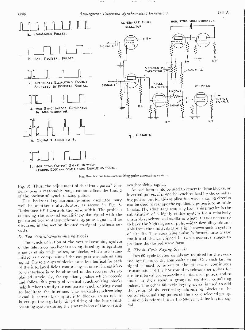
1946 A pplegarth: Television Synchronizing Generators 133 W
b.. EQUALIZING PULSES.
SIGNAL b.
b. HOR. PEDESTAL PULSES.
b
b
C. ALTERNATE EQUALIZING PULSES
SELECTED BY PEDESTAL SIGNAL. SIGNAL a.
4.. NOR SYNC. PULSES GENERATEDBY MULTIVIBRATOR.
A
e. SIGNAL C ADDED TO d.
et -
f. HOR. SYNC. OUTPUT SIGNAL IN WHICH
LEADING EDGE a a. COMES FROM EQUALIZING PULSE.
ALTERNATE PULSESELECTOR
0+
DIFFERENTIATICAPACITOR
0+
CIRCUITS.
PHASEINVERTER
HOR. SYNC. MULTIVIBRA7OR
SIGNALc
SIGNALe
B+
Fig. 8-Horizontal-synchronizing-pulse generating system.
Fig. 8). Thus, the adjustment of the "front -porch" timedelay over a reasonable range cannot affect the timingof the horizontal -synchronizing pulses.
The horizontal -synchronizing -pulse oscillator maywell be another multivibrator, as shown in Fig. 8.
Resistance R8-1 controls the pulse width. The problemof mixing the selected equalizing -pulse signal with thegenerated horizontal -synchronizing -pulse signal will bediscussed in the section devoted to signal -synthesis cir-cuits.D. The Vertical -Synchronizing Blocks
The synchronization of the vertical -scanning systemof the television receiver is accomplished by integratinga series of six wide pulses, or blocks, which are trans-mitted as a component of the composite synchronizingsignal. These groups of blocks must be identical for eachof the interlaced fields comprising a frame if a satisfac-tory interlace is to be obtained in the receiver. As ex-plained previously, the equalizing pulses which precedeand follow this group of vertical -synchronizing blockshelp further to unify the composite synchronizing signal
to facilitate the interlace. The vertical -synchronizingsignal is serrated, or split, into blocks, so as not tointerrupt the regularly timed firing of the horizontal -scanning system during the transmission of the vertical -
B+ +
SIGNAL a.
CLIPPER
OUTPUTSIGNAL f.
B+
synchronizing signal.An oscillator could be used to generate these blocks, or
inverted pulses, if properly synchronized by the equaliz-ing pulses, but for this application wave-shaping circuitscan be used to reshape the equalizing pulses into suitableblocks. The advantage resulting from this practice is thesubstitution of a highly stable system for a relativelyunstable synchronized oscillator where it is not necessaryto have the high degree of pulse -width flexibility obtain-able from the multivibrator. Fig. 9 shows such a systemof circuits. The equalizing pulse is formed into a sawtooth and thence clipped in two successive stages toproduce the desired wave form.
E. The 60 -Cycle Keying SignalsTwo 60 -cycle keying signals are required for the even-
tual synthesis of the composite signal. One such keying
signal is used to interrupt the otherwise continuoustransmission of the horizontal -synchronizing pulses for
a time interval corresponding to nine such pulses, and toinsert in their stead a group of eighteen equalizingpulses. The other 60 -cycle keying signal is used to addthe group of six vertical -synchronizing blocks to thecenter six equalizing pulses of the above selected group.This one is referred to as the 60 -cycle, 3 -line keying sig-
nal.

134 W Proceedings of the I.R.E. and Waves and Electrons March
The final 60 -cycle, blocking -tube oscillator of the fre-quency -divider chain can be used as the 60 -cycle 9 -line
b.. EQUALIZING PULSES.
1b. SAW TOOTH SIGNAL AT INPUT TO SECOND STAGE,
e. CLIPPED AND AMPLIFIED SIGNAL AT INPUT TO THIRD STAGE.
A. VERT. SYNC. BLOCKS AT OUTPUT OF THIRD STAGE (POLARITY REVERSED)
SIGNAL b
5+ 5+
SIGNAL C
5+
OUTPUTSIGNAL 411,
e CIRCUITS
Fig. 9-Shaping circuits for generating thevertical -synchronizing blocks.
a.. TRANSIENT VOLTAGE ACROSS TUNED CIRCUIT.
b. PULSE VOLTAGE ACROSS CATHODE LOAD RESISTOR
C. DIFFERENTIATED EQUALIZING PULSES
E.79 SELECTED PULSE
a. COMPOSITE SIGNAL it. 4- b +c
4 5
a-
TUNING. ONLY 5 EQUALIZING PULSES.
4 5
PULSES.TUNING. 7 EQUALIZING
DIFFERENTIATING
keying signal, if it is designed to produce a pulse ofthe proper width.
The 60 -cycle 3 -line keying signal must be more pre-cisely controlled. It can be either a properly designedmultivibrator or a simple blocking -tube oscillator, orcan be derived from the 60 -cycle 9 -line keying signalby suitable wave -shaping circuits. Experience has shownthat the blocking -tube oscillator provides a satisfactorysolution to the problem.
The timing of the leading edge of the 60 -cycle 3 -linekeying signal is very critical and must be held withinthe time interval represented by the width of an equaliz-ing pulse. The most certain means for accomplishingthis degree of precision is to fire the oscillator generatingthe 60 -cycle 3 -line signal from the leading edge of aparticular equalizing pulse. Synchronization on theleading edge can be obtained readily by electrical differ-entiation of the equalizing pulse prior to its use for thesynchronization of the 60 -cycle 3 -line oscillator. Themore difficult problem is to insure synchronization onthe particularly chosen equalizing pulse out of the 525which are generated during each 60 -cycle period.
A means for obtaining the required timing precisionwith proven stability is shown in Fig. 10. The 60 -cycle9 -line keying signal, which is used to time the keying
I 2 3 4 5
1. CORRECT TUNING OF RESONANT CIRCUIT.6 EQUALIZING PULSES.
I Z 3
2.INCORRECT
2 3
Lr3. INCORRECT
e. EFFECT OF RESONANT CIRCUIT TUNING ON COMPLETED
COMPOSITE SYNCHRONIZING SIGNAL.
EQUALIZING PULSE 'CAPACITORt SIGNAL c.
17
60 CYCLE SIGNAL a..9 LINEKEYINGSIGNAL
B+ SIGNAL 6.
f. CIRCUIT.
Fig. 10-Details of precision time -delay system.
OUTPUTSIGNAL d.
1946 Applegarth: Television Synchronizing Generators 135 W
of the equalizing -pulse group, is also used to drive apulse of current through a resonant circuit, causing it todevelop two trains of damped sinusoidal oscillations,one following each pulse edge. The resonant circuit istuned so that the second half cycle of the damped oscil-lations following the excitation produced by the leadingedge of the 60 -cycle, 9 -line signal can serve as a ped-estal to elevate the seventh equalizing pulse followingthe leading edge of the 60 -cycle 9 -line signal. The useof the second half cycle for pulse selection results in again in pulse selectivity of about three times, as com-pared to the use of the first half cycle. This improve-ment results from the obvious fact that the frequencyto which the resonant circuit must be tuned is threetimes as great when the desired time interval is threequarters of a cycle as compared to one -quarter cycle(peak of the transient).
The second half cycle of a highly damped transientoscillation is considerably reduced in amplitude as com-pared to the first half cycle. Thus, if the polarity of thetransient signal is chosen to cause the second half cycleof the initial damped oscillation excited by the leadingedge of 60 -cycle, 9 -line pulse to reinforce the desiredequalizing pulse, the first half cycle of the second trainof damped oscillations excited by the trailing edge ofthe 60 -cycle, 9 -line pulse will be greater in amplitudethan the desired reinforcement signal, and will probablycause erroneous synchronization. The resistance compo-nent of the inductor forming part of the tuned circuitadds a voltage component of the same wave form as the60 -cycle 9 -line pulse, which further accentuates theundesired reinforcement. Both of these factors can beovercome by mixing with the transient oscillations anddifferentiated equalizing pulses a third component com-prising a 60 -cycle, 9 -line pulse of proper polarity toelevate the initial transient relative to the second one(see Fig. 10). The result of adding the three compo-nents is to produce a very precise synchronizing signalfor the 60 -cycle 3 -line oscillator, accurate to about onepart in 25,000, without requiring any critical circuits.The tuning of the resonant circuit is the only adjust-ment, and its tolerance is about +10 per cent in reso-nant frequency.
F. The Vertical Blanking SignalThe vertical -blanking signal corresponds in the verti-
cal -scanning system to the horizontal pedestal. It issometimes called the vertical -pedestal signal, and itserves to black out the television -receiver screen duringthe vertical flyback, but does not serve as a base uponwhich to build the picture signal, as does the horizontalpedestal.
The timing of this signal is not of great importanceso long as it comes within a line or two of its specifiedphase relative to the vertical -synchronizing signal. It isa wide pulse, and therefore a multivibrator is suggested.The frequency should be 60 cycles per second, and sim-
ple synchronization from the leading edge of the 60 -cycle,9 -line keying signal will suffice. The output signalfrom this oscillator is also used to drive the discrimina-tor for the automatic frequency control of the masteroscillator (see Fig. 6).
G. Conclusions
It seems advisable at this point to tabulate the vari-ous signals (Table I) that have been generated, beforeproceeding with the synthesis of these signal compo-nents into the composite television signal.
TABLE I
Signal Fre- Wave formquency Timing Source
Master oscillator 31,500 sine wave
Equalizing pulse 31,500 narrow pulseHorizontal -synchronizing 15,750 medium pulse
pulse
Vertical synchronizing blocks 31,500 wide blockHorizontal pedestal 15,750 wide pulse
Vertical blanking60 -cycle, 9 -line keying60 -cycle, 3 -line keying
power line through auto-matic -frequency -controlsystem
master oscillatorequalizing pulses selected
by horizontal -pedestalmodulator
equalizing pulsesequalizing pulses (de-
layed)60 wide pulse 60 -cycle, 9 -line keying60 medium pulse frequency -divider chain60 narrow pulse 60 -cycle, 9 -line keying
(delayed)
V. SIGNAL -SYNTHESIS CIRCUITS
The synthesis of the composite television signal fromthe various components generated (Section IV) is donein several successive stages.
In a television synchronizing generator, uniform andprecisely regular timing of the leading edges of the threecomponents used to synchronize the horizontal -scanningsystem at successive time intervals is essential to thereproduction of a picture with straight vertical edgesand tight horizontal synchronization. For example, ifthe leading edges of the equalizing pulses or the vertical -synchronizing blocks are delayed by but a microsecondrelative to the uniform regularity of the horizontal -synchronizing pulses, a "tear" or horizontal displace-ment of several of the lines at the top of the picturemay appear due to the transient disturbance set up inthe receiver horizontal -scanning system. Thus, unusualprecautions must be taken to insure leading -edge regu-larity between the various horizontal -synchronizingcomponents.
It is, of course, possible to use adjustable delay cir-cuits between the master timing signal and each of thethree horizontal -synchronizing components, which canbe individually adjusted to provide uniform timing.Such an arrangement would be subject to the variationsin timing that might arise from nonuniform drifting ofthe time -delay circuits and to the component -generat-ing circuits derived therefrom.
A more stable system not requiring any such criticaladjustments for obtaining the exact timing of the lead-ing edges of these various components has been success-fully used. In this system, the leading edges of onereference timing signal are used directly for all compo-nents, and the various trailing edges corresponding to
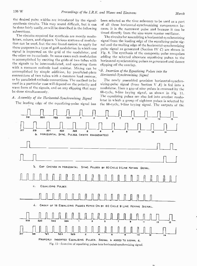
136 W Proceedings of the I.R.E. and Waves and Electrons March
the desired pulse widths are introduced by the signal -synthesis circuits. This may sound difficult, but it canbe done fairly easily, as will be described in the followingsubsections.
The circuits required for synthesis are mostly modu-lators, mixers, and clippers. Various systems of modula-tion can be used, but the one found easiest to apply forthese purposes is a type of grid modulation in which onesignal is impressed on the grid of the modulator, andthe other on its cathode. In some cases such modulationis accomplished by exciting the grids of two tubes withthe signals to be intermodulated, and operating themwith a common cathode load resistor. Mixing can beaccomplished by simple addition, by paralleled -plateconnections of two tubes with a common load resistor,or by paralleled -cathode connections. The method to beused in a particular case will depend on the polarity andwave form of the signals, and on any clipping that maybe done simultaneously.
A. Assembly of the Horizontal -Synchronizing SignalThe leading edge of the equalizing -pulse signal has
518 520 522 524 1 3
been selected as the time reference to be used as a partof all three horizontal -synchronizing components be-cause it is the narrowest pulse and because it can betimed directly from the sine -wave master oscillator.
The circuits for assembling a horizontal -synchronizingsignal from the leading edge of the equalizing -pulse sig-nal and the trailing edge of the horizontal-synchronizingpulse signal as generated (Section IV C) are shown inFig. 8. The synthesis of the composite pulse comprisesadding the selected alternate equalizing pulses to thehorizontal -synchronizing pulses as generated and thenceclipping off the overlap.
43. Insertion of the Equalizing Pulses into theHorizontal -Synchronizing Signal
The newly assembled precision horizontal -synchro-nizing -pulse signal (from Section V A) is fed into amodulator. Here a gap of nine pulses is removed by the60 -cycle, 9 -line keying signal, as shown in Fig. 11.The equalizing pulses are also fed into another modu-lator in which a group of eighteen pulses is selected bythe 60 -cycle, 9 -line keying signal. The outputs of the
5
517 519 521 523 525 2 4 66.. HORIZONTAL SYNC. PULSES. (WIDTH EXAGGERATED)
7 9 11
8 10
13 15
12 14
k). GAP OPENED IN HORIZONTAL SYNC. PULSES BY 60 CYCLE 9 LINE KEYING SIGNAL.
c EQUALIZING PULSES
r
ct. GROUP OF 18 EQUALIZING PULSES KEYED ON BY 60 CYCLE 9 LINE KEYING SIGNAL.
518 520 522 524
517 519 521 52 3 525
3 5 7
6 10
PROPERLY INSERTED EQUALIZING PULSES. SIGNAL b ADDED TO SIGNAL d.Fig. 11-Insertion of equalizing pulses into horizontal -synchronizing signal.
13 15
12 14
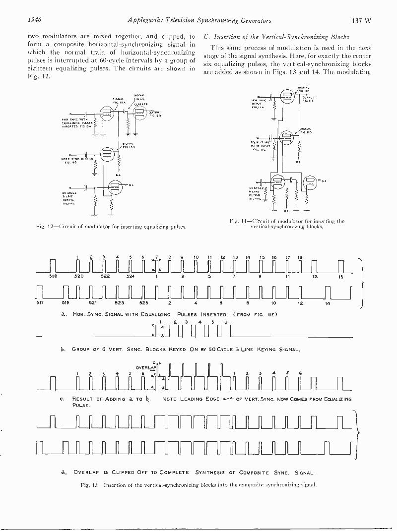
1946 Applegarth: Television Synchronizing Generators 137 W
two modulators are mixed together, and clipped, toform a composite horizontal -synchronizing signal inwhich the normal train of horizontal -synchronizingpulses is interrupted at 60 -cycle intervals by a group ofeighteen equalizing pulses. The circuits are shown inFig. 12.
SIGNALFIG ISA
SIGNAL1G. l3C
CLIPPER
OUTPUTrIG.13D
NOR. SYNC. MTNEQUALIZING PULSESINSERTED. FIG.13A
VERT. SYNC. BLOCKSFIG. 9D
6+
60 CYCLE3 LINEKEYINGSIGNAL
SIGNALFIG. 13 6
Fig. 12-Circuit of modulator for inserting equalizing pulses.
4 5 6 7
C. Insertion of the Vertical -Synchronizing Blocks
This same process of modulation is used in the nextstage of the signal synthesis. Here, for exactly the centersix equalizing pulses, the vertical -synchronizing blocksare added as shown in Figs. 13 and 14. The modulating
9 10 11
a 6
518 520 522 524 1 3
517 519 521 523 525 2 4
NOR
INPUTFIG.II A
EQUALIZINGPULSE INPUT
FIG. 11C
SO CYCLE9 LINEKEYINGSIGNAL
SIGNALFIG. I I B
OUT PUTFIG IIE
GNALFIG.110
Fig. 14-Circuit of modulator for inserting thevertical -synchronizing blocks.
12 13
5 7
6
14
8 10
a. HOR. SYNC. SIGNAL WITH EQUALIZING PULSES INSERTED. C FROM
1 2 3 4 5 5c -a -
C
FIG. 11E)
13 IS
12 14
b. GROUP OF 6 VERT. SYNC. BLOCKS KEYED ON BY 60 CYCLE 3 LINE KEYING SIGNAL.
2
OVERLAP3 4 5 6
C. RESULT OF ADDING a. TO b.PULSE.
fl I
6
6
NOTE LEADING EDGE
Z 3 4 5
0--°- OF VERT. SYNC. NOW COMES FROM EQUALIZING
51, OVERLAP IS CLIPPED OFF TO COMPLETE SYNTHESIS OF COMPOSITE SYNC. SIGNAL.
Fig. 13-Insertion of the vertical -synchronizing blocks into the composite synchronizing signal.
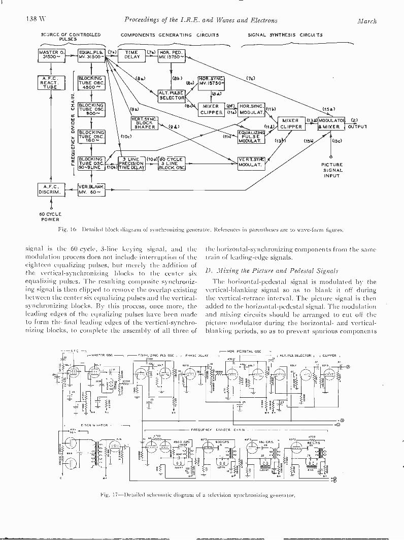
138 W Proceedings of the I.R.E. and Waves and Electrons March
SOURCE OF CONTROLLEDPULSES
MASTER 0. EQUAL .P L (7s)31500,-, MV. 31500".
1
A. F.0 .REACT.TUBE
A .F.0 .DISC IM.
U
COMPONENTS GENERATING CIRCUITS
BLOCKINGTUBE OBC.
4500
BLOCKINGTUBE OSC.
900^.
o. TUBE 05C2 180",
cc
BLOCKING1, TUBE OSC.
60-.9 LINE
060 CYCLEPOWER
IVER.BLANK.MV. 60 -*
TIMEDELAY
C7b)
86.)
(9 a)
VERT.SY NC .BLOCK
SHAPER (91)
HOR. PED.MV. 15750
(8b )(Be)
ALT. PU.SSELECTOR
(101)
3 LINEPRECISIONTIME
(B
(ioal dO CYCLE3 LINE
BLOCK OSC
HOR.SYNC.MV.15750.'
IBA)
MIXERCLIPPER
(11
SIGNAL SYNTHESIS CIRCUITS
(7c)
(BO HOR.SYNC.
(110 MODULAT.
EO,UALIZIPULSE
MODULAT.
VE RTSYttMODULAT.
MIXERCLIPPER
(151)
(131)
(13 (151)
MODULATO
&MIXER
(15c)
0
PICTURESIGNALINPUT
Fig. 16-Detailed block diagram of synchronizing generator. References in parentheses are to wave -form figures.
signal is the 60 -cycle, 3 -line keying signal, and themodulation process does not include interruption of theeighteen equalizing pulses, but merely the addition ofthe vertical -synchronizing blocks to the center sixequalizing pulses. The resulting composite synchroniz-ing signal is then clipped to remove the overlap existingbetween the center six equalizing pulses and the vertical -
synchronizing blocks. By this process, once more, theleading edges of the equalizing pulses have been madeto form the final leading edges of the vertical -synchro-nizing blocks, to complete the assembly of all three of
A.F. C -
MASTER OSC ,-- EQUALIZINGloo
as
DISCRIMINATOR
es 01
(a)OUTPUT
the horizontal -synchronizing components from the sametrain of leading -edge signals.
D. Mixing the Picture and Pedestal Signals
The horizontal -pedestal signal is modulated by thevertical -blanking signal so as to blank it off duringthe vertical -retrace interval. The picture signal is thenadded to the horizontal -pedestal signal. The modulationand mixing circuits should be arranged to cut off thepicture modulator during the horizontal- and vertical -
blanking periods, so as to prevent spurious components
HOR. PEDESTAL OSCPI.5 OSC PHASE DELAY
asrs
00
01
FREQUENCY DIVIDER CHAIN
.F5
r -ALT. PLS.SELECTOR CUPPER
01831.7 I 53 5
esrs
Fig. 17-Detailed schematic diagram of a television synchronizing generator.
4700
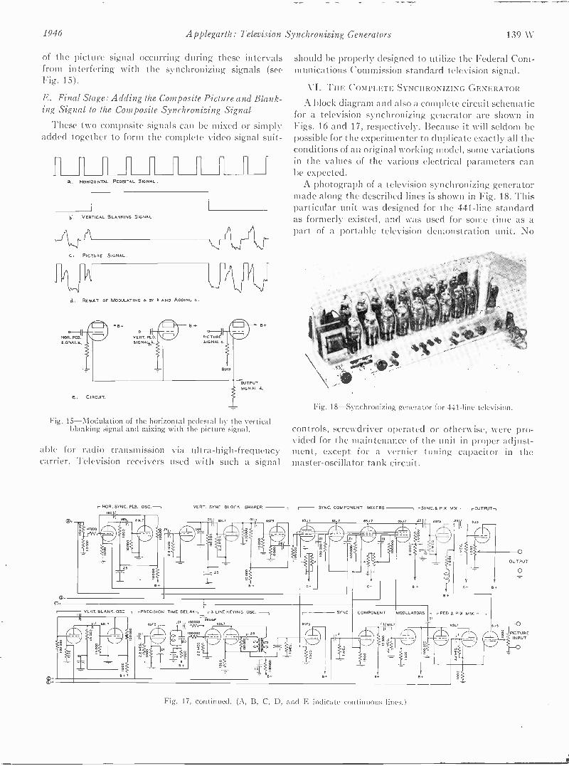
1946 A pplegarth: Television Synchronizing Generators 139 W
of the picture signal occurring during these intervalsfrom interfering with the synchronizing signals (seeFig. 15).
E. Final Stage: Adding the Composite Picture and Blank-ing Signal to the Composite Synchronizing Signal
These two composite signals can be mixed or simplyadded together to form the complete video signal suit -
a.. HORIZONTAL PEDDTAL SIGNAL.
VERTICAL BLANKING SIGNAL.
C. PICTURE SIGNAL.
f
NOR. PED.SIGNAL A.
A
RESULT OF MODULATING A BY b AND ADDING C.
VENT. PED.SIG NALn6.
+o----1
PICTURESIGNAL.
BIAS
OUTPUTSIGNAL G.
G. CIRCUIT.
Fig. 15-Modulation of the horizontal pedestal by the verticalblanking signal and mixing with the picture signal.
able for radio transmission via ultra -high -frequencycarrier. Television receivers used with such a signal
HON. SYNC. PLS. OSC.-1 VERT. SYNC. BLOCK SHAPER
should be properly designed to utilize the Federal Com-munications Commission standard television signal.
VI. THE COMPLETE SYNCHRONIZING GENERATOR
A block diagram and also a complete circuit schematicfor a television synchronizing generator are shown inFigs. 16 and 17, respectively. Because it will seldom bepossible for the experimenter to duplicate exactly all theconditions of an original working model, some variationsin the values of the various electrical parameters canbe expected.
A photograph of a television synchronizing generatormade along the described lines is shown in Fig. 18. Thisparticular unit was designed for the 441 -line standardas formerly existed, and was used for some time as apart of a portable television demonstration unit. No
Fig. 18-Synchronizing generator for 4 -11 -line tcluvi,ion.
controls, screwdriver operated or otherwise, were pro-vided for the maintenance of the unit in proper adjust-ment, except for a vernier tuning capacitor in themaster -oscillator tank circuit.
SYNC. COMPONENT MIXERS r.SYNC.S. PIX. MIX.- rOUTPUT,
OUTPUT
VERT BLANK. OSC. rPR ECISI ON TIME DELAY,
PICTUREINPUT
Fig. 17, continued. (A, B, C, D, and E indicate continuous lines.)

The Effect of Negative Voltage Feedback on Power -Supply Hum in Audio -Frequency Amplifiers*
GEOFFREY BUILDERt, FELLOW, I.R.E.
Summary-Some confusion exists regarding the effect of nega-tive voltage feedback on the signal -to -hum ratio in the output of anaudio -frequency amplifier. This appears to be due to lack of care ininterpretation of the negative -feedback equations and to the applica-tion of these equations to circuit arrangements which do not conformto the conditions implied in their formulation. Various cases are dis-cussed to illustrate the proper interpretation and application of theequations. The conclusions to be derived from these discussions maybe summarized briefly as follows:
(1) Where the negative voltage feedback circuits satisfy the rele-vant conditions implied in the formulation of equations for simplenegative feedback, the signal -to -hum ratio, for constant signal out-put, is improved by the gain -reduction factor (1 -OM).
(2) This improvement must be interpreted in relation to the com-plex value of the factor (1-13M) and its variation with frequency, inrelation to the frequencies of the signal and hum voltages.
(3) Failure to achieve the improvement in signal -to -hum ratiothus predicted may be due to the feedback voltage including voltageother than the fraction g of the output voltage required for simplenegative feedback. A further specific analysis is then necessary todetermine the effect of the feedback on the signal -to -hum ratio.
(4) In general, hum balancing within the amplifier is independentof the feedback only when the conditions for simple negative feed-back are satisfied.
(5) Although, without feedback, it is legitimate to calculate thehum output voltage due to the high-tension hum voltage e by consid-ering simple potential division of this voltage between the load im-pedance and the valve anode resistance Ro, this procedure is notgenerally valid when applied to an amplifier with feedback if theeffective value of the anode impedance Zo' of the valve is taken tobe Ro/(1 - IA. This arises because Zo' is the effective value of thevalve impedance as viewed from the amplifier output terminals andis not necessarily significant when potential division of the voltage eis considered. It has, however, been shown in Section III(c) that,when the feedback voltage is proportional to (e--eo), the effect of thefeedback on the hum output due toe is identical with that obtained onthe basis of simple potential division, using the effective value Zo'.
I. INTRODUCTION
NEGATIVE voltage feedback is commonly ap-plied to audio -frequency amplifiers in radio re-ceivers and similar equipment for reduction of
nonlinear distortion and frequency discrimination in theamplifier itself or in its load circuit. The theory of nega-tive feedback suggests that hum and other noise voltagesintroduced by the amplifier and its associated circuitsshould also be reduced. There is, however, some confu-sion as to what improvement in signal -to -hum ratiomay, in fact, be expected from the application of nega-tive feedback. This appears to arise from two maincauses; lack of care in interpretation of the significanceof the negative -feedback equations, and application ofthese equations to circuit arrangements which do notconform to the conditions implied.
* Decimal classification: R363.2 X R263. Original manuscript re-ceived by the Institute, June 18, 1945.
t Merino House, 57 York Street, Sydney, Australia.
It is the object of the following discussion to clarifythese points. The second of them arises from the factthat there is in common use" a number of negative -feedback circuits that do not conform to the conditionsimplied in the negative -feedback equations formulatedby Black.' The term "simple negative feedback" will beused to distinguish circuit arrangements conforming toBlack's implied condition that the feedback voltageshould be a definite fraction of the output voltage andshould not include any other voltages. For simplicity,attention is restricted to the use of negative voltagefeedback, and the discussion is illustrated by circuit ar-rangements typical of its application; but it is obviousthat similar considerations might arise in the applicationof other types of feedback.
The symbols and abbreviations used in the text aresummarized below for convenient reference:M = voltage gain of an amplifier or valve (vacuum
tube), measured between the input and outputterminals.
M,= voltage gain from the screen grid to anode of apentode valve.
= amplification factor of the amplifier or valve be-tween input and output terminals.
=amplification factor of a pentode valve, from screengrid to anode.
= that fraction of the output voltage fed back to theinput circuit of the amplifier.
R. =alternating -current anode resistance of the outputvalve of an amplifier.
Za = output impedance of the amplifier.Z = load impedance into which the amplifier works.e =hum voltage across the output of the high-tension
rectifier filter supplying the amplifier.ei =an equivalent hum voltage referred to the input
terminals of the amplifier and arising from sourceswithin the amplifier from which the hum is inde-pendent of the signal level.
eo = output hum voltage developed across the amplifieroutput circuit.
eo' = corresponding output hum voltage when simpleI Laboratory staff of Amalgamated Wireless Valve Company,
"Negative feedback in R -C amplifiers," Wirless World, vol. 43, pp.437-438; November 17, 1938.
2 Amalgamated Wireless Valve Company, "Inverse feedback,"Radio Rev. Australia, vol. 5, p. 64; March, 1937.
3 G. Robert Mezger, "Feedback amplifier for C.R. oscilloscopes,"Electronics, vol. 17, pp. 126-131, 254; April, 1944.
F. Langford -Smith, "Radiotron Designer's Handbook," WirelessPress, Sydney, Australia, 1940, pp. 40-45. Complete reproduction,RCA Manufacturing Company, Harrison, N. J.
6 F. Langford -Smith, "The relationship between the power outputstage and the loudspeaker," Proc. World Radio Convention, Sydney,Australia, 1938.
6 H. S. Black, "Stabilized feedback amplifiers," Bell. Sys. Tech.Jour., vol. 13, pp. 1-19; January, 1934.
140 W Proceedings of the I.R.E. and Waves and Electrons March, 1946
Builder: Negative Voltage Feedback 141 W
negative voltage feedback is applied to the ampli-fier.
eo" =corresponding output hum voltage when feedback,other than simple negative feedback, is applied tothe amplifier.
In each case, the suffixes t and p are used for amplifiershaving the output valve connected as a triode or pen-tode, respectively.
The amplification factory is defined by
(dea/deg) for is constant
where ea is the anode voltage of the output valve, eg thepotential of the input control grid, and is the anode cur-rent of the output valve. For a single valve µ is real andnegative, in agreement with the actual physical valueof the amplification factor. In any case, the sign of µ isconsistent with that of M, and in the case of a singlevalve, corresponds to the change of phase of 180 degrees(for resistive load) between input and output voltages.
II. SIMPLE NEGATIVE VOLTAGE FEEDBACK
The general theory and equations of simple negativevoltage feedback are well known; but, for clarity, thoseequations relevant to the discussion will be set outbriefly in convenient form. In deriving these equationsit is implied that the feedback voltage is derived from,and is directly proportional to, the voltage developedacross the amplifier output terminals.
If the voltage gain of an amplifier without feedbackis M, and if a fraction 13 of the voltage across the outputcircuit is fed back to the amplifier input in series withthe signal voltage, the gain becomes
M' = M/(1 - (3M) (1)
and the quantity (1 -OM) is conveniently referred to asthe gain -reduction factor. The gain M is related to theamplification factor µ of the amplifier, the load Z, andthe anode resistance R, of the output valve, by
M = µ'Z/(Z Re). (2)
The effect of the feedback on the output impedance ofthe amplifier is to reduce it, from the anode resistanceRa of the output valve, to a value Zs' (which will ingeneral have a complex value) given by
Za' = R./(1 - )31.4). (3)
It is to be noted that IL is always greater than M, andt.ay be much greater when a pentode valve is used, so
that the output impedance is reduced by a factor corre-spondingly greater than the gain -reduction factor.
It can be shown readily that distortion, hum, andnoise voltages generated in the amplifier and its associ-ated circuits and developed across the output circuit arealso reduced by the gain -reduction factor (1 -OM).When, as is usually the case, the signal input voltage isincreased by the factor (1 -13M) to maintain the signaloutput at the same level as without feedback, one might
expect an improvement in the signal -to -hum and signal -to -distortion ratios across the output circuit by thefactor (1 -OM), insofar as the hum or distortion origi-nates within the amplifier.
These equations are valid for all real and complexvalues of the parameters µ, M, 0, and Z, and the valueof the gain reduction factor (1 -#111) is generally com-plex and dependent on frequency even for a single -valveamplifier; some of the advantages of negative feedbackare in fact due to this.
It is obvious that great care is required to ascertainthe exact significance of "an improvement in signal -to -hum ratio by the gain -reduction factor (1 -OM)." Ananalysis can readily be made for any specific case, and itis clear that the reduction of signal -to -hum ratio mustdepend on the relative frequencies of the signal and humvoltages; only when the frequencies are identical will thegain -reduction factor be the same for both. It is notunusual to refer to an amplifier having negative feed-back giving a gain reduction stated in decibels; thereference is usually to the numerical value of the gain -reduction factor at the center of the transmitted bandand the gain -reduction factor at the hum frequency maybe very much less, and may even in some cases be lessthan unity.
Proper application of the theory thus permits a cor-rect assessment of the improvement to be expected insignal -to -hum ratio from the use of negative voltagefeedback. Failure to achieve this in practice may be dueto the use of feedback circuits that fail to satisfy theconditions implied. One departure from these conditionsoccurs when the voltage fed back includes voltages otherthan the fraction of the amplifier output voltage. Inpractice, this probably occurs most often if the outputvalve of the amplifier is transformer -coupled to the loadand is series fed, and if the feedback voltage is takenfrom between anode and cathode of the output valve;the voltage fed back then includes some fraction of anyhum voltage in the high-tension supply to the outputvalve."
III. AMPLIFIER WITH TRANSFORMER COUPLINGTO THE LOAD
Transformer coupling is sometimes used for voltageamplification but is chiefly of interest in radio -receiverdesign for coupling the amplifier power output to a load.For illustration, an amplifier using a series -fed outputvalve transformer -coupled to the load, and operated un-der class A conditions, will be considered.
Such an amplifier may use either a pentode or triodeoutput valve. For immediate comparison of the twotypes it is convenient to consider the same pentode (orbeam -power) amplifier valve connected as a triode orpentode. Denoting its anode resistance as a pentode byR, and as a triode by Rat, we have the approximaterelation
Rap = As Rat (4)
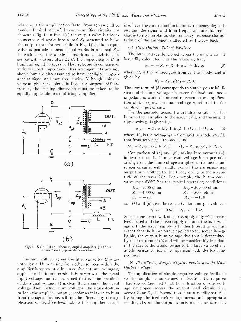
142 W Proceedings of the LR.E. and Waves and Electrons March
where µ, is the amplification factor from screen grid toanode. Typical series -fed power -amplifier circuits areshown in Fig. 1. In Fig. 1(a) the output valve is triode -connected and works into a load Zt presented to it bythe output transformer, while in Fig. 1(b), the outputvalve is pentode -connected and works into a load Zp.In each case, the anode is fed from a high-tensionsource with output filter L, C; the impedance of C tohum and signal voltages will be neglected in comparisonwith the load impedance. Bias arrangements are notshown but are also assumed to have negligible imped-ance at signal and hum frequencies. Although a single -valve amplifier is depicted in Fig. 1 for purposes of illus-tration, the ensuing discussion must be taken to beequally applicable to a multistage amplifier.
P
(a)
(D)Fig. 1-Series-fed transformer -coupled amplifier (a) triode
connection (b) pentode connection.
The hum voltage across the filter capacitor C is de-noted by e. Hum arising from other sources within theamplifier is represented by an equivalent hum voltage e,applied to the input terminals in series with the signalinput voltage, and it is assumed that ei is independentof the signal voltage. It is clear that, should the signalvoltage itself include hum voltages, the signal -to -humratio in the amplifier output, insofar as it is due to humfrom the signal source, will not be affected by the ap-plication of negative feedback to the amplifier except
insofar as the gain -reduction factor is frequency -depend-ent and the signal and hum frequencies are different;that is to say, insofar as the frequency -response charac-teristic of the amplifier is affected by the feedback.
(a) Hum Output Without Feedback
The hum voltage developed across the output circuitis readily calculated. For the triode we have
eot = - Ze e/(Zt + Rat) + Mt e, (5)
where Mt is the voltage gain from grid to anode, and isgiven by
Mt = Z t Rat)The first term of (5) corresponds to simple potential di-vision of the hum voltage e between the load and anodeimpedances, while the second represents the amplifica-tion of the equivalent hum voltage ei referred to theamplifier input circuit.
For the pentode, account must also be taken of thehum voltage e applied to the screen grid, and the outputripple voltage is given by
eop = -Zp-e/(Z± Rap) M. e M p ei (6)
where M is the voltage gain from grid to anode and M,that from screen grid to anode, and
M, = Z,/.1,/(Z,+ Rap) M. = Zpaus/(Zp+ Rap).
Comparison of (5) and (6), taking into account (4),indicates that the hum output voltage for a pentode,arising from the hum voltage e applied to its anode andscreen circuits, will usually exceed the correspondingoutput hum voltage for the triode owing to the magni-tude of the term .1118e. For example, the beam -powervalve type 6V6G has the typical operating conditions.
Rat= 2500 ohms Rap= 50 ,000 ohmsZt =4000 ohms Z, =5000 ohms/28 = -20 M, = -1.8
and (5) and (6) give the respective hum output voltages
eot = - 0.6e eop = -1.7e.
Such a comparison will, of course, apply only when seriesfeed is used and the screen supply includes the hum volt-age e. If the screen supply is further filtered to such anextent that the hum voltage applied to the screen is neg-ligible, the output hum voltage due to e is determinedby the first term of (6) and will be considerably less thanin the case of the triode, owing to the large value of theanode resistance Rap in comparison with the load im-pedance.
(b) The Effect of Simple Negative Feedback on the HumOutput Voltage
The application of simple negative voltage feedbackto the amplifier, as defined in Section II, requiresthat the voltage fed back be a fraction of the volt-age developed across the output load circuit; i.e.,across Zt or Z. This condition is most readily satisfiedby taking the feedback voltage across an appropriatewinding AB on the output transformer as indicated in

1946 Builder: Negative Voltage Feedback 143 W
Fig. 1. When this is done, the hum output voltage isreduced by the factor (1-,13M). We then have, for thetriode and pentode connections, respectively,
eo,' = e01/(1 - (7)
eo,' = eop/(1 - 03/12,). (8)
These expressions cannot be formulated in terms of thereduction in effective output impedance Z.' of the am-plifier because the voltage e is not included in the feed-back and the effective output impedance Z.' is notapplicable to such a calculation; i.e., it is not the effec-tive impedance as viewed from the terminals of the volt-age e.
It is obvious that, in this case, the reduction in thehum output voltages occurs equally for hum from thevarious sources and any hum balancing within the am-plifier will not be affected by the feedback. However, ifthe output transformer feeds a moving -coil loudspeakerof which the field coil is used for smoothing the rectifiedhigh-tension supply to the amplifier, the speaker mayhave a hum -balancing coil wound over the field coil andconnected in series with the voice coil. In general, a humvoltage will then be produced across the transformersecondary and reduction of this voltage by the feedbackmay require compensation by adjustment of the hum -balancing coil.
(c) The Effect of Other Feedback Circuits on the HumOutput
It is a common, and undoubtedly convenient, prac-tice to utilize a feedback voltage other than that re-quired for simple negative feedback as specified inSection II above. Among the most common of such mod-ified circuits is that in which the feedback voltage isobtained by potential division from the anode -cathodevoltage of the output amplifier; i.e., the voltage betweenpoints P and E in Figs. 1(a) and 1(b). This arrangementdeparts from the simple feedback circuit in that thefeedback voltage is a fraction, not of the output loadvoltage, but of the output voltage plus the hum voltagee across the capacitor C. It is not, therefore, to be ex-pected that the modification of the hum output voltageindicated by the theory of simple feedback will occur.
If the output valve is triode -connected, the effect ofthis feedback circuit will be to change the output humvoltage from its value eo, without feedback (equation(5)), to a value eat" given by
eo," = -Zte/(Zi+Zat') Mi'ei (9)
where
Z.,' = R.,/(1 - 13/.4,).
M' = M,/(1 - 13/1/,)
and for large amounts of feedback this approximates to
eot" = - e Mt'-ei (10)
indicating that, owing to the reduction in the effective
output impedance of the amplifier by the feedback,practically the whole of the hum voltage e is developedacross the load; but that hum voltages represented by eiare reduced by the gain -reduction factor. It happens inthis case, because the feedback voltage is proportionalto (e+eo), that the effect of the feedback on the hum dueto e can be expressed in terms of the change in effectiveoutput impedance of the amplifier.
If the output valve is pentode connected, the effectof this feedback arrangement will be to change the humvoltage output from its value e, without feedback, asgiven in (6), to a value eop" given by
eo" = -Zp-e/(Zp+ Zap') + Ma'e+ 111,'-ei (11)
whereZap' = Rap/(1 - 0/./p)
M.' = M8/(1 - OMp)
Mp' = Mp/(1 13Mp).
Without feedback, the first term of (11) is small butincreases to the limiting value -e for large values of feed-back, as in the case of the triode. The hum arising in thescreen and input circuits is decreased by the gain -reduc-tion factor.
(d) Hum BalancingFor either connection of the output valve, the net
result of the feedback on the total output hum de-pends on the relative phases and amplitudes of thevarious hum voltages. Equations (5), (6), (9), and(11) state the conditions necessary for reduction of theoutput hum voltage to zero by any process of hum -bal-ancing within the amplifier such as those described7'8 inthe literature. It is to be noted that any such balancegenerally depends on the degree and nature of the feed-back, but that when the conditions for simple negativefeedback are satisfied, the balance is independent of thefeedback, as indicated by the form of (7) and (8).
IV. OTHER AMPLIFIERS
In amplifiers having an output circuit other than theseries -fed transformer arrangement discussed in relationto Fig. 1, the output voltage is usually identical with theanode -to -cathode voltage of the output valve, and therelevant conditions for simple negative feedback aresatisfied by almost any convenient circuit arrangement.This applies, for example, to a parallel -fed transformer -coupled output circuit, or to a resistance- or choke -coupled voltage amplifier. Simplified circuits corre-sponding to these cases are shown in Figs. 2(a) and 2(b)and can be used to represent a wide range of practicalcases.
In Fig. 2 the high-tension supply is fed to the ampli-fier anode through an impedance Z1 which may be a
Wen -Yuan Pan, "Circuit for neutralizing low -frequency regen-eration and power -supply hum," PROC. I.R.E., vol. 30, pp. 411-412;September, 1942.
8 K. B. Gonser, "A method of neutralizing hum and feedbackcaused by variations in the plate supply," PROC. I.R.E., vol. 26, pp.442-449; April, 1938.
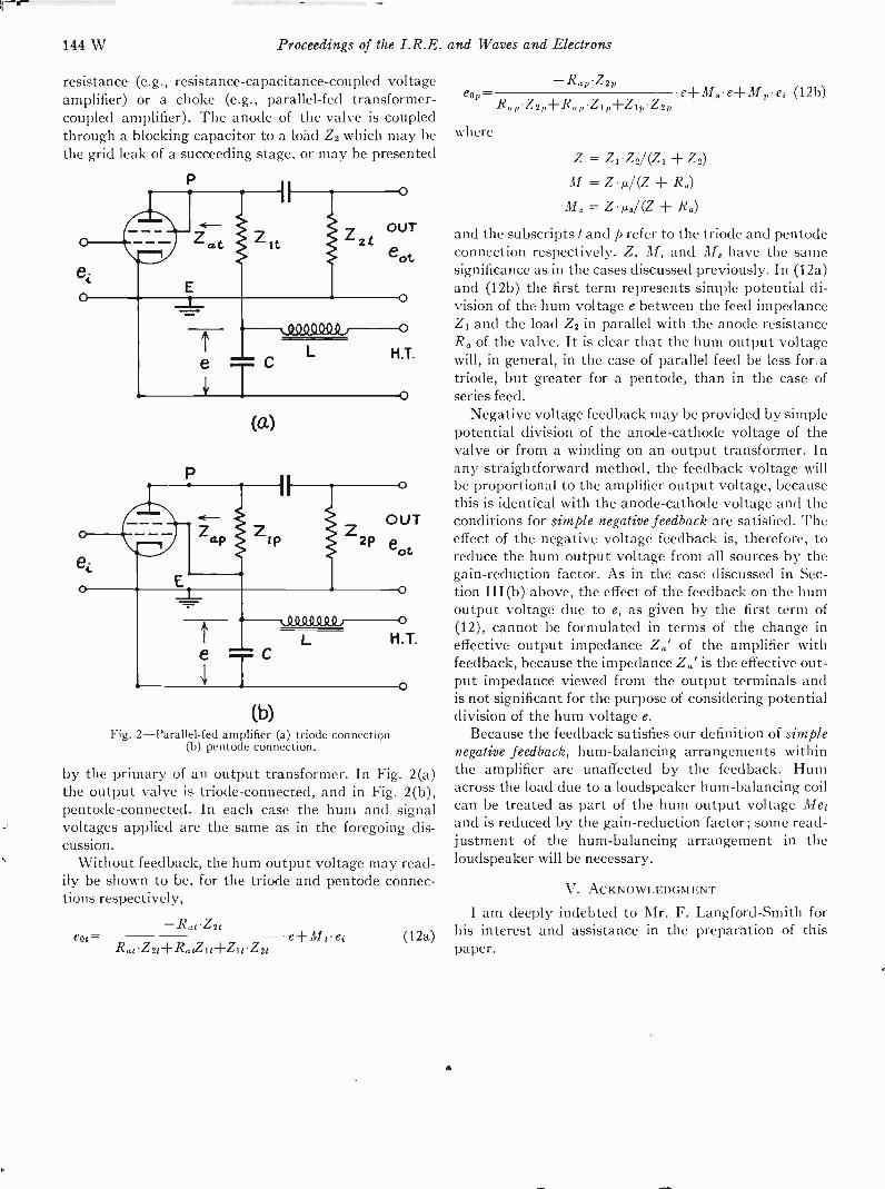
144 W Proceedings of the I.R.E. and Waves and Electrons
resistance (e.g., resistance -capacitance -coupled voltageamplifier) or a choke (e.g., parallel -fed transformer -coupled amplifier). The anode of the valve is coupledthrough a blocking capacitor to a load Z2 which may bethe grid leak of a succeeding stage, or may be presented
P
(a)
(b)Fig. 2-Parallel-fed amplifier (a) triode connection
(b) pentode connection.
by the primary of an output transformer. In Fig. 2(a)the output valve is triode -connected, and in Fig. 2(b),pentode -connected. In each case the hum and signalvoltages applied are the same as in the foregoing dis-cussion.
Without feedback, the hum output voltage may read-ily be shown to be, for the triode and pentode connec-tions respectively,
eot=-R.t.Z2t
R.tZ2t+RatZlt+Zit.Z2ted-Aft-ei (12a)
-RapZ2pe0p= ed-Me+Mp et (12b)
RapZ2p+Rap.Zip+ZI9*Z2p
where
Z = ZiZ2/(Zi± Z2)M = Z OZ ± R.)
= Z pal (Z + Ra)
and the subscripts t and p refer to the triode and pentodeconnection respectively. Z, M, and M. have the samesignificance as in the cases discussed previously. In (12a)and (12b) the first term represents simple potential di-vision of the hum voltage e between the feed impedanceZ1 and the load Z2 in parallel with the anode resistanceR. of the valve. It is clear that the hum output voltagewill, in general, in the case of parallel feed be less for.atriode, but greater for a pentode, than in the case ofseries feed.
Negative voltage feedback may be provided by simplepotential division of the anode -cathode voltage of thevalve or from a winding on an output transformer. Inany straightforward method, the feedback voltage willbe proportional to the amplifier output voltage, becausethis is identical with the anode -cathode voltage and theconditions for simple negative feedback are satisfied. Theeffect of the negative voltage feedback is, therefore, toreduce the hum output voltage from all sources by thegain -reduction factor. As in the case discussed in Sec-tion III(b) above, the effect of the feedback on the humoutput voltage due to e, as given by the first term of(12), cannot be formulated in terms of the change ineffective output impedance Za' of the amplifier withfeedback, because the impedance Z.' is the effective out-put impedance viewed from the output terminals andis not significant for the purpose of considering potentialdivision of the hum voltage e.
Because the feedback satisfies our definition of simplenegative feedback, hum -balancing arrangements withinthe amplifier are unaffected by the feedback. Humacross the load due to a loudspeaker hum -balancing coilcan be treated as part of the hum output voltage Meiand is reduced by the gain -reduction factor; some read-justment of the hum -balancing arrangement in theloudspeaker will be necessary.
V. ACKNOWLEDGMENT
I am deeply indebted to Mr. F. Langford -Smith forhis interest and assistance in the preparation of thispaper.
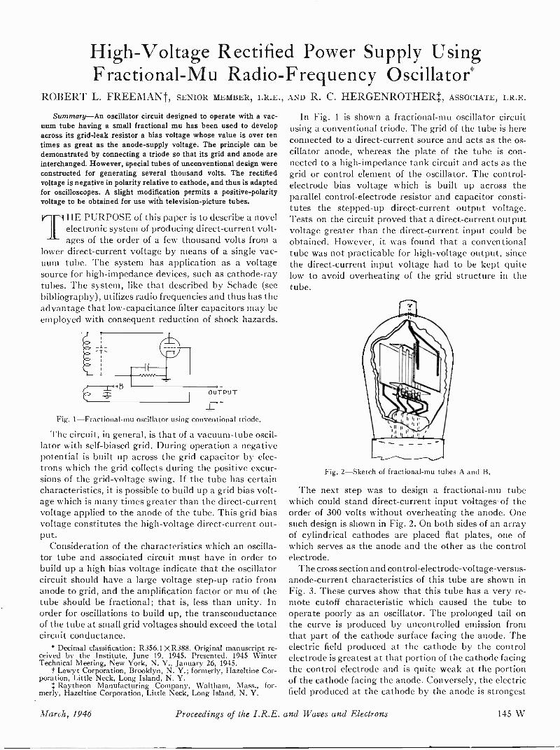
High -Voltage Rectified Power Supply UsingFractional -Mu Radio -Frequency Oscillator*
ROBERT L. FREEMANt, SENIOR MEMBER, I.R.E., AND R. C. HERGENROTHERT, ASSOCIATE, I.R.E.
Summary-An oscillator circuit designed to operate with a vac-uum tube having a small fractional mu has been used to developacross its grid -leak resistor a bias voltage whose value is over tentimes as great as the anode -supply voltage. The principle can bedemonstrated by connecting a triode so that its grid and anode areinterchanged. However, special tubes of unconventional design wereconstructed for generating several thousand volts. The rectifiedvoltage is negative in polarity relative to cathode, and thus is adaptedfor oscilloscopes. A slight modification permits a positive -polarityvoltage to be obtained for use with television -picture tubes.
THE PURPOSE of this paper is to describe a novelelectronic system of producing direct -current volt-ages of the order of a few thousand volts from a
lower direct -current voltage by means of a single vac-uum tube. The system has application as a voltagesource for high -impedance devices, such as cathode-raytubes. The system, like that described by Schade (seebibliography), utilizes radio frequencies and thus has theadvantage that low -capacitance filter capacitors may beemployed with consequent reduction of shock hazards.
OUTPUT
Fig. 1-Fractional-mu oscillator using conventional triode.
The circuit, in general, is that of a vacuum -tube oscil-lator with self -biased grid. During operation a negativepotential is built up across the grid capacitor by elec-trons which the grid collects during the positive excur-sions of the grid -voltage swing. If the tube has certaincharacteristics, it is possible to build up a grid bias volt-age which is many times greater than the direct -currentvoltage applied to the anode of the tube. This grid biasvoltage constitutes the high -voltage direct -current out-put.
Consideration of the characteristics which an oscilla-tor tube and associated circuit must have in order tobuild up a high bias voltage indicate that the oscillatorcircuit should have a large voltage step-up ratio fromanode to grid, and the amplification factor or mu of thetube should be fractional; that is, less than unity. Inorder for oscillations to build up, the transconductanceof the tube at small grid voltages should exceed the totalcircuit conductance.
* Decimal classification: R356.1 X R388. Original manuscript re-ceived by the Institute, June 19, 1945. Presented, 1945 WinterTechnical Meeting, New York, N. Y., January 26, 1945.
t Lewyt Corporation, Brooklyn, N. Y.; formerly, Hazeltine Cor-poration, Little Neck, Long Island, N. Y.
Raytheon Manufacturing Company, Waltham, Mass., for-merly, Hazeltine Corporation, Little Neck, Long Island, N. Y.
In Fig. 1 is shown a fractional -mu oscillator circuitusing a conventional triode. The grid of the tube is hereconnected to a direct -current source and acts as the os-cillator anode, whereas the plate of the tube is con-nected to a high -impedance tank circuit and acts as thegrid or control element of the oscillator. The control -electrode bias voltage which is built up across theparallel control -electrode resistor and capacitor consti-tutes the stepped -up direct -current output voltage.Tests on the circuit proved that a direct -current outputvoltage greater than the direct -current input could beobtained. However, it was found that a conventionaltube was not practicable for high -voltage output, sincethe direct -current input voltage had to be kept quitelow to avoid overheating of the grid structure in thetube.
Fig. 2-Sketch of fractional -mu tubes A and B.
The next step was to design a fractional -mu tubewhich could stand direct -current input voltages- of theorder of 300 volts without overheating the anode. Onesuch design is shown in Fig. 2. On both sides of an arrayof cylindrical cathodes are placed flat plates, one ofwhich serves as the anode and the other as the controlelectrode.
The cross section and control -electrode -voltage -versus -anode -current characteristics of this tube are shown inFig. 3. These curves show that this tube has a very re-mote cutoff characteristic which caused the tube tooperate poorly as an oscillator. The prolonged tail onthe curve is produced by uncontrolled emission fromthat part of the cathode surface facing the anode. Theelectric field produced at the cathode by the controlelectrode is greatest at that portion of the cathode facingthe control electrode and is quite weak at the portionof the cathode facing the anode. Conversely, the electricfield produced at the cathode by the anode is strongest
March, 1946 Proceedings of the I.R.E. and Waves and Electrons 145 W
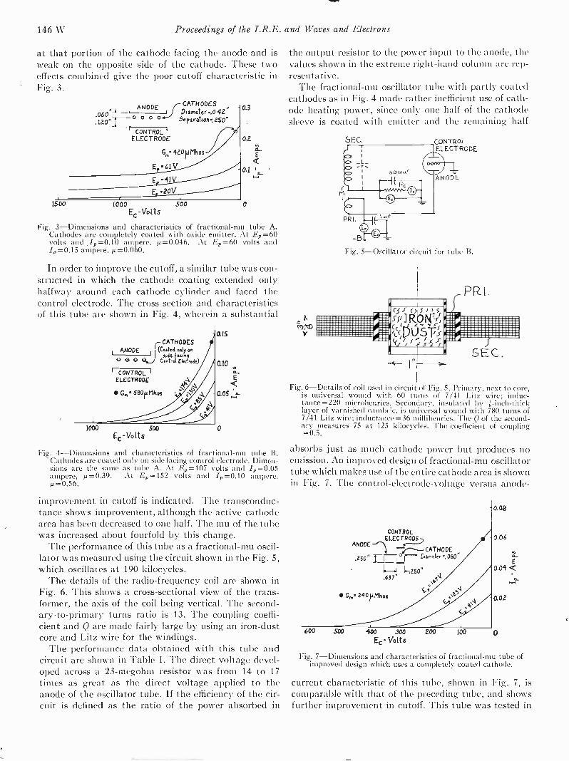
146 W Proceedings of the I.R.E. and Waves and Electrons
ANODE
at that portion of the cathode facing the anode and isweak on the opposite side of the cathode. These twoeffects combined give the poor cutoff characteristic inFig. 3.
:01260,4i o o
CONTROLELECTRODE
CATHODESDiameter 42
5eparatton...250"
G: 420 fAMkos
E. -61V
1500 1000 SOD
EE -Volts
Fig. 3-Dimensions and characteristics of fractional -mu tube A.Cathodes are completely coated with oxide emitter. At E5=60volts and /p =0.10 ampere, IA =0.046. At Ep =60 volts and4=0.15 ampere, /2=0.060.
0.3
0.2
In order to improve the cutoff, a similar tube was con-structed in which the cathode coating extended onlyhalfway around each cathode cylinder and faced thecontrol electrode. The cross section and characteristicsof this tube are shown in Fig. 4, wherein a substantial
r- CATHODES
ANODE I(Coated only on
'lee facing0 0 0 0,/ Control Eloctreeie)
CONTROLELECTRODE
Gm 580t4Mhos
1000 SOO
Ec-Volts
Fig. 4-Dimensions and characteristics of fractional -mu tube B.Cathodes are coated only on side facing control electrode. Dimen-sions are the same as tube A. At E, =107 volts and /2, =0.05ampere, µ=0.39. At Ep = 152 volts and /p =0.10 ampere,m=0.56.
0.15
0.100E
0.05
improvement in cutoff is indicated. The transconduc-tance shows improvement, although the active cathodearea has been decreased to one half. The mu of the tubewas increased about fourfold by this change.
The performance of this tube as a fractional -mu oscil-lator was measured using the circuit shown in the Fig. 5,which oscillates at 190 kilocycles.
The details of the radio -frequency coil are shown inFig. 6. This shows a cross-sectional view of the trans-former, the axis of the coil being vertical. The second-ary -to -primary turns ratio is 13. The coupling coeffi-cient and Q are made fairly large by using an iron -dustcore and Litz wire for the windings.
The performance data obtained with this tube andcircuit are shown in Table I. The direct voltage devel-oped across a 23-megohm resistor was from 14 to 17times as great as the direct voltage applied to theanode of the oscillator tube. If the efficiency of the cir-cuit is defined as the ratio of the power absorbed in
the output resistor to the power input to the anode, thevalues shown in the extreme right-hand column are rep-resentative.
The fractional -mu oscillator tube with partly coatedcathodes as in Fig. 4 made rather inefficient use of cath-ode heating power, since only one half of the cathodesleeve is coated with emitter and the remaining half
lr
SEC,. CONTROLELECTRODE
Fig. 5-Oscillator circuit for tube B.
PRI.
Sfei ROW?: 0D°r-Cs .1" Cy 5 S I
SEC.
Fig. 6-Details of coil used in circuit of Fig. 5. Primary, next to core,is universal wound with 60 turns of 7/41 Litz wire; induc-tance =220 microhenries. Secondary, insulated by I -inch -thicklayer of varnished cambric, is universal wound with 780 turns of7/41 Litz wire; inductance =36 millihenries. The Q of the second-ary measures 75 at 125 kilocycles. The coefficient of coupling= 0.5.
absorbs just as much cathode power but produces noemission. An improved design of fractional -mu oscillatortube which makes use of the entire cathode area is shownin Fig. 7. The control -electrode -voltage versus anode -
0.08
CONTROLELECTRODES
CATHODE
0.06ANODE
e50"t IDovneter . 06o"
0.04
.437"
Gm- 340 rp11106cz
600 500 400 300 200 100
Ec - Vol ts
0.02
Fig. 7-Dimensions and characteristics of fractional -mu tube ofimproved design which uses a completely coated cathode.
current characteristic of this tube, shown in Fig. 7, iscomparable with that of the preceding tube, and showsfurther improvement in cutoff. This tube was tested in
TABLE IPERFORMANCE AF TUBE 13 IN CIRCUIT OF FIG. 5.
En EoVolts Volts
10la
Milli- Milli- R,Megohms E°/Ea E,1,/Ea..
amperes amperes
220 3160 14.7 0.134 23.6 14.4 0.13312 4900 21.5 0.208 23.6 15.7 0.152362 5900 25.5 0.250 23.6 16.3 0.16490 8400 35.2 0.355 23.6 17.2 0.171300 4540 25.0 0.360 12.6 12.0 0.217485 7750 43.0 0.617 12.6 12.6 0.228
the circuit of Fig. 4 and gave substantially the sameperformance as the previous tube.
The output voltage developed across the control -electrode resistor and capacitor has considerable saw -tooth component. Increasing the time constant will re-duce this component to some extent, but a time con-stant will ultimately be reached where the oscillator willintermittently block. Thus, an additional resistance -capacitance filter is used preferably between the control -electrode resistor and the utilization device.
The potential derived is negative with respect to chas-sis and is thus of correct polarity for cathode-ray tubesused as oscilloscopes. In such applications the secondanode and deflector plates are usually at chasis potentialand the cathode at a large negative potential.
In television receivers it is most convenient to applya large positive potential to the second anode whilemaintaining the cathode and grid near chasis potential.This permits simplified coupling between the last videostage and the cathode -ray -tube grid. It is possible,however, to connect the picture tube so that its cathode
and grid are highly negative. However, a high -voltagecapacitor and .a direct -current reinsertion diode are nec-essary to couple the last video stage to the cathode -ray -tube grid.
If the cathode-ray tube is to be operated with its gridand cathode near chassis potential, the fractional -muoscillator can be operated with the chassis connection atthe negative -potential end of the grid resistor insteadof at the cathode end. A separate low -wattage powersupply operating above chassis potential can be used tosupply the anode voltage and heater voltage for thefractional -mu tube. This supply will fluctuate in poten-tial above chassis by an amount equal to the ripplepresent across the grid resistor, and thus the auxiliarypower supply preferably should be shielded.
ACKNOWLEDGMENT
It is to be acknowledged that an associate of the au-thors, A. H. Reesor Smith, made the proposal of using afractional -mu oscillator to generate high voltages.
(1)
Bibliography
F. E. Terman, "The inverted vacuum tube, a voltage -reducingpower amplifier," PRoc. I.R.E., vol. 16, pp. 447-461; April,1928.
(2) 0. H. Schade, "Radio -frequency -operated high -voltage suppliesfor cathode-ray tubes," PROC. I.R.E., vol. 31, pp. 158-163;April, 1943. (Also U. S. Patent No. 2,374,781, May 1, 1945).U. S. Patent No. 2,300,451, A. H. R. Smith, November 3,1942, "High -voltage power -supply system."U. S. Patent No. 2,324,776, R. C. Hergenrother, July 20, 1943,"Vacuum tube."
(3)
(4)
Contributors to Waves and Electrons SectionA. Rufus Applegarth, Jr., (A'36) was
born at Patchogue, New York, on February1, 1913. He received the S.B. and S.M. de-grees from the Massachusetts Institute ofTechnology in 1936, after which he became
A. RUFUS APPLEGARTII, JR.
associated with the Philco Radio and Tele-vision Corporation as a television develop-ment engineer. He joined the RCAManufacturing Company in 1939 to engagein the design of aviation -radio receivers andairborne radar equipment. Shortly after theoutbreak of the war with Japan, he wascalled to active duty with the Signal Corps,and sent to the aircraft radio laboratory,Wright Field, Dayton, Ohio, where he wasassigned to the radar division. He is nowvice-president of the Aeronautical Corpora-tion, Camden, New Jersey.
Geoffrey Builder (A'32-F'41) was bornat Cue, Western Australia, on June 21, 1906.He received the B.Sc. degree from the Uni-versity of Western Australia in 1928, andthe Ph.D. degree from London Universityin 1933. From 1928 to 1930 he was an ob-server at the Walheroo, Western Australia,Magnetic Observatory of the Carnegie In-stitution of Washington. During 1931 and1932 he was engaged in research work in
radio physics at the University of London,and during 1933 and 1934 was a researchphysicist of the Australian Radio ResearchBoard. From 1934 to 1941 he was in chargeof the research and development laboratories
GEOFFREY BUILDER
March, 1946 Proceedings of the I.R.E. and Waves and Electrons 147 W
148 W Proceedings of the I.R.E. and Waves and Electrons
EDWIN E. SPITZER
of Amalgamated Wireless (Australasia), Ltd.Since 1941 he has been a consulting en-gineer.
Dr. Builder is a Fellow of the Institute ofPhysics, London, a Fellow of the Institutionof Radio Engineers (Australia), and an As-sociate member of the Institution of Engi-neers (Australia).
George A. Espersen (A'34) was born atJersey City, New Jersey, on May 17, 1906.He received the B.S. degree in physics in1931 from New York University. From 1932to 1939 Mr. Espersen was employed byHygrade Sylvania Corporation as a develop-ment engineer engaged in the developmentand production of receiving type tubes. Hewas tube -development engineer for NationalUnion Radio Corporation in 1939 and 1940.
From 1940 to 1942 Mr. Espersen was en-gaged in research and development of ultra-high -frequency tubes in the research labora-tories of the Sperry Gyroscope Company.Since 1942 he has been a development engi-neer with the North American Philips Com-pany at Dobbs Ferry, New York.
Mr. Espersen is a member of the Ameri-can Physical Society.
Edwin E. Spitzer (A'28-M '38-SM '43)was born at Fitchburg, Massachusetts, on
GEORGE A. ESPERSEN
February 22, 1905. He received the B.S. andM.S. degrees in electrical engineering fromthe Massachusetts Institute of Technologyin 1927. Mr. Spitzer was associated with theresearch laboratory and the vacuum -tubeengineering department of the General Elec-tric Company from 1927 to 1933. From 1933to date he has been head of the power -tubedivision of the engineering department,RCA -Victor Division of the Radio Corpora-tion of America, Harrison, New Jersey, andsince 1943 located at Lancaster, Pennsyl-vania.
Gordon M. Lee (A'45) was born onJanuary 3, 1917, at Minneapolis, Minnesota.He received the B.E.E. degree from theUniversity of Minnesota in 1938. For thefollowing year he was employed as a researchand teaching assistant in electrical engineer-ing at the University of Missouri and re-ceived the M.S. degree in electrical engineer-ing from that school in 1939. From 1939 to1945 he was associated with the Laboratoryfor Insulation Research at the Massachu-setts Institute of Technology, receiving the
GORDON M. LEE
D.Sc. degree in electrical engineering fromM.I.T. in 1944.
In 1945 he became one of the technicaldirectors of the newly organized CentralResearch Laboratories, Inc., of Red Wing,Minnesota, an organization devoted toconsultation, research, development, andlimited production in the fields of chemistry,physics, and electrical engineering.
Dr. Lee is a member of the AmericanInstitute of Electrical Engineers, the Ameri-can Physical Society, Sigma Xi, Tau BetaPi, and Eta Kappa Nu.
Robert L. Freeman (S'32-A'33-SM'45)was born on February 1, 1909, at Cleveland,Ohio. He received the A.B. degree in 1931,the E.E. degree in 1933, and the Ph.D. de-gree in electrical engineering in 1934 fromStanford University. He was engaged in re-ceiver development with the Crosley RadioCorporation from 1934 until 1937. During1937 he was transmitter engineer for Farns-worth Television, Inc. From September,1937, to August, 1945, he was employed byHazeltine Corporation as senior engineerand as consulting engineer. In August, 1945,
ROBERT L. FREEMAN
he was employed by Lewyt Corporation aschief engineer.
Dr. Freeman is a member of Sigma Xiand a Fellow of the Radio Club of America.
R. C. Hergenrother (A'37) was born onSeptember 5, 1903, in Chemnitz, Germany.He received the A.B. degree from CornellUniversity in 1925. During 1925 and 1926he was employed in vacuum -tube develop-ment work at Westinghouse Lamp Com-pany in Bloomfield, New Jersey. He went tothe Pennsylvania State College in 1927 as aninstructor in physics and there received theM.S. degree in 1928. He received the Ph.D.degree from California Institute of Technol-ogy in 1931.
Dr. Hergenrother held a RockefellerFoundation Research Fellowship in physicsat Washington University, St. Louis,Missouri, from 1932 to 1934. From 1934 to1935 he was employed by the FarnsworthTelevision Laboratories of Philadelphia,Pennsylvania, on research and developmentwork on television tubes. From 1935 untilrecently he worked for the Hazeltine Corporation on electron -tube research and de-velopment. He has now joined the, com-munications division of the RaytheonManufacturing Company in Waltham, Mas-sachusetts.
He is a member of the American PhysicalSociety, Sigma Xi, and Sigma Pi Sigma.
R. C. HERGENROTHER
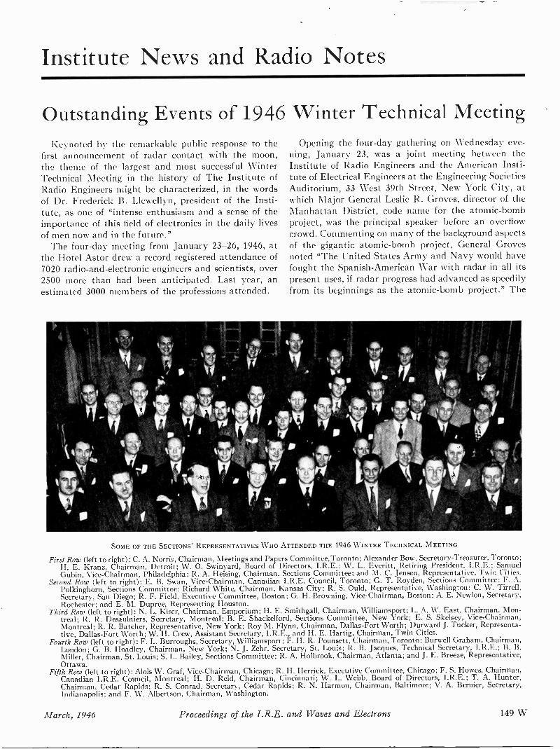
Institute News and Radio Notes
Outstanding Events of 1946 Winter Technical MeetingKeynoted by the remarkable public response to the
first announcement of radar contact with the moon,the theme of the largest and most successful WinterTechnical Meeting in the history of The Institute ofRadio Engineers might be characterized, in the wordsof Dr. Frederick B. Llewellyn, president of the Insti-tute, as one of "intense enthusiasm and a sense of theimportance of this field of electronics in the daily livesof men now and in the future."
The four -day meeting from January 23-26, 1946, atthe Hotel Astor drew a record registered attendance of7020 radio -and -electronic engineers and scientists, over2500 more than had been anticipated. Last year, anestimated 3000 members of the professions attended.
Opening the four -day gathering on Wednesday eve-ning, January 23, was a joint meeting between theInstitute of Radio Engineers and the American Insti-tute of Electrical Engineers at the Engineering SocietiesAuditorium, 33 West 39th Street, New York City, atwhich Major General Leslie R. Groves, director of theManhattan District, code name for the atomic -bombproject, was the principal speaker before an overflowcrowd. Commenting on many of the background aspectsof the gigantic atomic -bomb project, General Grovesnoted "The United States Army and Navy would havefought the Spanish-American War with radar in all itspresent uses, if radar progress had advanced as speedilyfrom its beginnings as the atomic -bomb project." The
SOME OF THE SECTIONS' REPRESENTATIVES WHO ATTENDED THE 1946 WINTER TECHNICAL MEETING
First Row (left to right): C. A. Norris, Chairman, Meetings and Papers Committee,Toronto; Alexander Bow, Secretary -Treasurer, Toronto;H. E. Kranz, Chairman, Detroit; W. 0. Swinyard, Board of Directors, I.R.E.; W. L. Everitt, Retiring President, I.R.E.; SamuelGubin, Vice -Chairman, Philadelphia; R. A. Heising, Chairman, Sections Committee; and M. C. Jensen, Representative, Twin Cities.
Second Row (left to right): E. B. Swan, Vice -Chairman, Canadian I.R.E. Council, Toronto; G. T. Royden, Sections Committee; F. A.Polkinghorn, Sections Committee; Richard White, Chairman, Kansas City; R. S. Ould, Representative, Washington; C. W. Tirrell,Secretary, San Diego; R. F. Field, Executive Committee, Boston; G. H. Browning, Vice -Chairman, Boston; A. E. Newlon, Secretary,Rochester; and E. M. Dupree, Representing Houston.
Third Row (left to right): N. L. Kiser, Chairman, Emporium; H. E. Smithgall, Chairman, Williamsport; L. A. W. East, Chairman, Mon-treal; R. R. Desaulniers, Secretary, Montreal; B. E. Shackelford, Sections Committee, New York; E. S. Skelsey, Vice -Chairman,Montreal; R. R. Batcher, Representative, New York; Roy M. Flynn, Chairman, Dallas -Fort Worth; Durward J. Tucker, Representa-tive, Dallas -Fort Worth; W. H. Crew, Assistant Secretary, I.R.E., and H. E. Hartig, Chairman, Twin Cities.
Fourth Row (left to right): F. L. Burroughs, Secretary, Williamsport; F. H. R. Pounsett, Chairman, Toronto; Burwell Graham, Chairman,London; G. B. Hoadley, Chairman, New York; N. J. Zehr, Secretary, St. Louis; R. B. Jacques, Technical Secretary, I.R.E.; B. B.Miller, Chairman, St. Louis; S. L. Bailey, Sections Committee; R. A. Holbrook, Chairman, Atlanta; and J. E. Breeze, Representative,Ottawa.
Fifth Row (left to right): Alois W. Graf, Vice -Chairman, Chicago; R. H. Herrick, Executive Committee, Chicago; F. S. Howes, Chairman,Canadian I.R.E. Council, Montreal; H. D. Reid, Chairman, Cincinnati; W. L. Webb, Board of Directors, I.R.E.; T. A. Hunter,Chairman, Cedar Rapids; R. S. Conrad, Secretary, Cedar Rapids; R. N. Harmon, Chairman, Baltimore; V. A. Bernier, Secretary,Indianapolis; and F. W. Albertson, Chairman, Washington.
March, 1946 Proceedings of the I.R.E. and Waves and Electrons 149 W
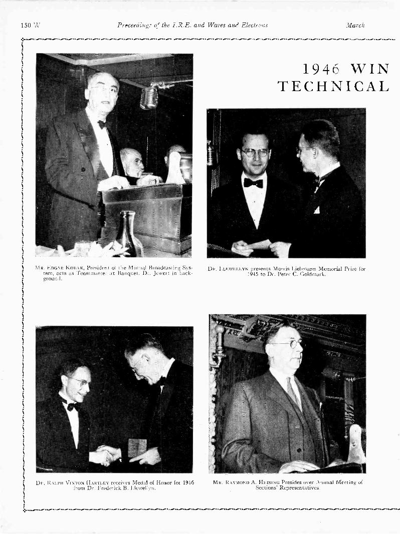
15 0 Prececang: o! the I.R.E. and Waves an Electrons March
-- a...e---- yr, --
MR. EDGAR KODAK, President of the Mutual Broadcasting Sys -tern, acts as Toastmaster at Banquet. Dr. Jewett in back-ground.
DR. RALPH VINTON HARTLEY receives Medal of 110110r for 1946from Dr. Frederick B. Llewellyn.
1946 WINTECHNICAL
DR. LLEWELLYN presents Morris Liebmann Memorial Prize for1945 to Dr. Peter C. Goldmark.
MR. RAYMOND A. HEISING Presides over Annual Meeting ofSections' Representatives
- ..--, -- -- -. , -......,. .-. -ow,. a -- b 4.- -a- o- A...ow, F. -ad.- *us., --, ..

1946 Institute News and Radio Notes 151 W
...o- I, ..o- ...- -o- ...- _- _.-,...- _- /0..,/,/-18^.16./..C11.,.../.610.11,4 .../0../ . _- -- _am- - _do, .../-.11:p
TER I.R.E.MEETING
DR. LLEWELLYN presents Certificate of Fellowship to Dr. JuliusA. Stratton who made Speech of Acceptance for all recipients!o! ...Fellow Award.
MR. LEWIS M. CLEMENT, Vice -President in Charge of Researchand Engineering, The Crosley Corporation, is Master ofCeremonies at President's Luncheon. Dr. Everitt in back-ground.
Ds. FRANK B. JEWETT, Predent of the National Academy ofSciences, is Guest Speaker at Banquet.
DR. WILLIAM L. EVERITT, Retiring President of the I.R.E.,Presents Gavel to Dr. Frederick B. Llewellyn, President for1946, at Annual Meeting.
1.-- 0.-
152 W Waves and Electrons March
title of the General's talk was "Some Electrical, En-gineering, and General Aspects of the Atomic -BombProject."
Presenting a panoramic view of the new world ofelectronics, a major assembly of radio engineering equip-ment was shown. One hundred and seventy exhibits ofnew devices by 135 companies included everything fromlatest developments in radio receivers to the latest fre-quency -modulation and television transmitters, froma preproduction model of a camera for the photo-graphic recording of patterns which may appear on acathode -ray -oscilloscope screen to "packaged antennas,"easy to erect 30 -foot antenna towers and 150 -footmasts.
Radars and radar devices for peacetime use, ampli-tude- and frequency -modulation radio, television,sound recording, communications, photography, va-cuum tubes, magnetic recording, remote -control de-vices, testing devices, time- and heat -control devices,rectifiers and converters, electronic navigation anddirection -finding instruments, and X-ray equipmentwere a few of the many categories of electronic equip-ment featured in the exhibit.
Under radar were a number of superior designs ofsignal generators, wave guides, and other componentsof radars displayed for the first time together withexamples of some of the newest radars for peacetime use.
In the radio field, one of the newer developments wasa new supersensitive loop antenna for receivers. Oc-cupying a section of an entire stage on the main exhibitfloor was a radiotelegraph printer system in actual op-eration and a transmitting and receiving facsimile cir-cuit at work. One feature of particular interest to broad-cast engineers was a device shown in actual operationknown as a "frequency watchman" which insured syn-chronized frequency control in frequency -modulationtransmitters.
In television, a new television pickup and transmissionsystem containing an extremely compact televisioncamera weighing 40 pounds was included among thelatest developments.
In sound recording, new phonograph pickups, re-cording turntables, transcription playback units forradio and other professional uses highlighted improvedmodels of home and studio recording. Also on exhibitwas a highly developed model of a new magnetic re-corder.
In communications, mobile radiotelephone equipmentof the type suggested for installation in vehicles op-erating within urban areas was among the new equip-ment shown.
One of the features in vacuum tubes was a 2,000,000 -volt X-ray tube in an insulating column consisting of180 metal -to -glass seals which has a precision control ofthe electron beam making possible a focal spot as smallas one hundredth of an inch.
Other displays of unusual interest were a remote -control system which remotely tunes radio equipment
in aircraft; extremely high vacuum pumps; pulse timersfor automatic control equipment; a new type of voltagestabilizer for photographic purposes; dual remote -con-trol automatic direction finders, and a new type currentconverter for automobile radios.
The third major feature of the Meeting was the An-nual Banquet held Thursday evening, January 24, atwhich Dr. Frank B. Jewett, president of the NationalAcademy of Sciences, was the principal speaker. Dr.Jewett declared on his talk before the 2000 membersand their guests present, that our Nation's fundamentalscientific resources were dangerously depleted. "Wedrew heavily on our scientific resources in this war,"Dr. Jewett said, "and must get back again as soon aspossible to serious researches in fundamental sciences.We must remember that our success in applied scienceadds very little to the source of all science which is fun-damental research, and indeed the amazing success ofsuch programs as the atomic -bomb project and theradar program draw heavily upon fundamental scienceand mobilize the brains and resources of our best menon a limited number of projects to the detriment ofother equally vital fields."
At the Banquet also, two special awards and fifteenFellowships were presented. The Institute Medal ofHonor was awarded to Ralph Vinton Lyon Hartley,engineer of Bell Telephone Laboratories "for his earlywork on oscillating circuits employing triode tubes andlikewise for his early recognition and clear expositionof the fundamental relationship between the totalamount of information which may be transmitted overa transmission system of limited bandwidth and thetime required." Dr. Peter C. Goldmark, engineer of theColumbia Broadcasting System, was the recipient ofthe Morris Liebmann Memorial Prize, "for his con-tributions to the development of television systems, par-ticularly in the field of color." Fellowships were awardedto the following engineers: Gregory Breit, Henri G.Busignies, Howard A. Chinn, Thomas Lydwell Eckers-ley, Walter C. Evans, Clarence W. Hansell, HaroldLester Kirke, Elmer D. McArthur, Harold S. Osborne,Ronald J. Rockwell, Arthur L. Samuel, Joseph Slepian,Julius A. Stratton, William 0. Swinyard, and Merle A.Tuve.
The fourth major feature of the Meeting was thePresident's Luncheon, honoring the incoming president,Dr. Frederick B. Llewellyn. The principal speaker wasPaul Porter, then chairman of the Federal Communica-tions Commission, who told 1000 luncheon guests thatthe radio industry has three main and immediate assign-ments: the construction of an entirely new system ofaural broadcasting-frequency modulation-completewith thousands of transmitters, millions of receivers, anda nationwide network; the construction of a nationwidesystem of television, and the construction of scores ofradio systems for a wide variety of uses to promotesafety and efficiency.
Mr. Porter stressed the need for continued support
1946 Institute News and Radio Notes 153 W
of the Federal Government in the realm of pure scien-tific research. "No one knows better than the radio en-gineer the frontiers that still remain to be conquered inthe field of communications," he asserted. "These aretasks of such magnitude and of such general benefit tothe entire field that no one company can or should beexpected to undertake them. They are proper concernsof the Federal Government. It is plain that we shallhave no alternative in this matter. Either research intopure science is to be aided by the Federal Governmentor much of it will simply be left undone."
At the cocktail party, which was held in the GrandBallroom of the Hotel Astor on January 25, over 1700members of the Institute and friends attended.
The women's activities were participated in by 171guests who registered. On Thursday, January 24, 89women were taken for a trip through the Cathedral ofSt. John the Divine; luncheon was served at Stoddard'sRestaurant; and a tour of Riverside Church was pro-vided. On Friday, January 25, 107 women were theguests of the I.R.E. and were conducted to the Museumof Costume Art, Sloane's House of Years, and thePublic Library. Luncheon was served at the Town HallClub where Mr. E. Stanley Turnbull had his pictureson display and painted a portrait of one of the womenguests. Later in the afternoon, the group was taken toRadio City for a television tour.
Finally, the major features of every annual meeting-the reading of scientific papers and the sessionssymposia on the latest electronic developments-tookon particular significance this year with a record numberof 87 papers in 16 categories of subjects, many hithertorestricted by military security. The subjects of the ses-sions were: Military Applications of Electronics; Fre-quency Modulation and Standard Broadcasting; NewCircuit Developments; Television; Radio NavigationAids; Vacuum Tubes; Microwave Vacuum Tubes; An-tennas; Radar; Microwave Techniques; Crystal Recti-fiers; Industrial Electronics; Communications Systemsand Relay Links; Radio Propagation; Broadcast Re-ceivers; and Quartz Crystals.
One of the important papers of these sessions was re-corded and played before a special meeting of theBritish Institution of Electrical Engineers in London,while its author, J. A. Pierce of the Radiation Labora-tory of the Massachusetts Institute of Technology was
delivering the paper in person at the meeting in NewYork. The subject was loran, a radar system that holdsgreat promise for peacetime application and the titleof the paper was "An Introduction to Hyperbolic Navi-gation." In his talk, Mr. Pierce outlined the possi-bilities of ships and planes automatically navigatingstraight to their destinations half a world away in anykind of weather; pilotless aircraft being controlled andguided from a great distance with unheard-of accuracyand large areas of the earth's surface being surveyedand charted in far less time than is required by conven-tional methods through development of loran.
Among other interesting facts which emerged fromthe many outstanding papers presented was the factthat more than 2,500,000 tons of Japanese shipping hadbeen sunk during the war through the use of sonar, asupersonic device mounted on the hulls of submarinesand surface vessels of many types. This informationcame from a paper entitled: "Navy Radio and Elec-tronics in World War II," by Commodore J. B. Dow ofthe Navy's Bureau of Ships. Successful invasion of theultra -high frequencies by high -power, high -definition,full -color television was described in a paper by Dr.Peter C. Goldmark of Columbia Broadcasting System,entitled "Television in the Ultra -High Frequencies."In a paper on "Metal -Lens Antennas", by W. E. Kockof the Bell Telephone Laboratories, new lens antennasmade of thin metal strips which resemble venetianblinds were discussed and demonstrated and their usein the future in radio -relay links pointed out.
A Naval radar -directed bomb known under the codename of the "Bat" originated and sponsored by CaptainDundas P. Tucker of the Naval Bureau of Ordinancewas described in a paper entitled "Radar Aspects ofNaval Fire Control" before the session on Radar. TheBat was a flying bomb with a small fire -control type offully automatic radar placed in its nose which guidedthe bomb to its assigned target. "Here," CaptainTucker pointed out, "was a robot 'suicide pilot' farbetter than his Japanese counterpart."
In a paper entitled "From Wiring to Plumbing"E. M. Purcell of the Radiation Laboratory of Massa-chusetts Institute of Technology told why engineersmust be familiar with plumbers' techniques, in order toput together wave guides, which are metal pipes usedfor the transmission of ultra -high -frequency radio waves.
PROCEEDINGS OF THE I.R.E. AND WAVES AND ELECTRONS
From month to month, it is hoped more clearly to differentiate the nature of the contents of thePROCEEDINGS OF THE I.R.E. Section from those of WAVES AND ELECTRONS Section, and to develop inthe latter Section an increasingly distinctive character. In the meantime, the Board of Editors willbe grateful for any comments, criticisms, or suggestions relative to WAVES AND ELECTRONS Section.Only through the accumulation of viewpoints, and careful consideration of such proposals, can nor-mal progress and improvement be anticipated.
154 W Proceedings of the I.R.E. and Waves and Electrons March
Board of DirectorsJanuary 9 Meeting: At the final meeting
of the 1945 Board of Directors, which washeld on January 9, 1946, the following werepresent: F. B. Llewellyn, president-elect(guest); G. W. Bailey, executive secretary;S. L. Bailey, W. R. G. Baker, Alfred N.Goldsmith, editor; V. M. Graham, R. F.Guy, Keith Henney, B. E. Shackelford,D. B. Sinclair, and W. C. White.
Approval of Executive Committee Ac-tions: The actions of the Executive Commit-tee taken at its December 5, 1945, meetingwere unanimously approved.
January 9 Meeting: At the annual meet-ing of the Board of Directors for 1946, thefollowing were present: F. B. Llewellyn,president; G. W. Bailey, executive secretary;S. L. Bailey, W. R. G. Baker, Alfred N.Goldsmith, editor; V. M. Graham, R. F.Guy, Keith Henney, L. C. F. Horle, B. E.Shackelford, D. B. Sinclair, and W. C.White.
1946 Budget: After a careful considera-tion of the various items of the budget, theBoard adopted the recommendation of theExecutive Committee that the Budget, aspresented, be approved.
Appointments and Committees: The fol-lowing appointments were unanimously ap-proved:
SECRETARY
Haraden Pratt
TREASURER
William C. \Vhite
EDITOR
Alfred N. Goldsmith
APPOINTED DIRECTORS -1946
R. A. HackbuschF. R. LackG. T. Royden
W. 0. SwinyardW. L. WebbE. M. Webster
TECHNICAL SECRETARY
Robert Blair Jacques
GENERAL COUNSEL
Harold R. Zeamans
CommitteesThe following members were appointed.
AWARDS
E. W. Engstrom, ChairmanRalph Bown W. B. LodgeD. E. Harnett G. T. RoydenKeith Henney W. C. White
CONSTITUTION AND LAWS
R. F. Guy, ChairmanG. W. Bailey L. C. F. HorleI. S. Coggeshall B. E. ShackelfordR. A. Heising F. E. Terman
H. R. Zeamans
EXECUTIVE
S. L. Bailey R. F. GuyKeith Henney
NOMINATIONS
S. L. Bailey, ChairmanE. J. Content D. D. IsraelBeverly Dudley R. C. PoulterW. L. Everitt P. F. Siling
W. C. White
TELLERS
Trevor Clark, ChairmanH. A. Chinn W. G. MoranH. M. Lewis J. E. Shepherd
WAR MEDALS
(Subcommittee of Awards Committee)Ralph Bown, Chairman
F. S. Barton G. F. MetcalfJ. B. DowL. A. DuBridgeMelville EasthamE. W. EngstromW. L. EverittJ. W. McRae
J. A. StrattonA. H. TaylorF. E. TermanM. A. TuveA. F. Van DyckW. C. White
RTPB REPRESENTATIVE
D. B. SinclairAlfred N. Goldsmith (alternate)
Building -Fund: B. E. Shackelford, chair-man of the I.R.E. Building -Fund Commit-tee, reported that the amount subscribed todate is $625,545.77.
Code of Ethics: The recommendationsthat the functions of the Code of EthicsCommittee be combined with the Commit-tee on Professional Recognition and that themembership of the first -named committeebe discharged with thanks and that therecords of the first -named committee be for-warded to the chairman of the Committeeon Professional Recognition was unani-mously approved.
Office -Quarters: The Executive Secretaryread a report of the Office -Quarters Com-mittee, and a letter from General CounselZeamans, reporting the acquisition of thenew I.R.E. Building at Fifth Avenue and79th Street, New York, N. Y.
Constitution and BylawsArticle II, Sec. 9: It was approved that
the following wording be adopted for Ar-ticle II, Sec. 9, and the amendment as modi-fied be submitted to the membership:
"Sec. 9-Graduation from a radio orelectrical course of a school of recognizedstanding shall be accepted as equivalentto two years experience in radio or alliedfields. Full-time graduate work, or part-time graduate work with teaching in ra-dio or allied courses in a school ofrecognized standing, shall be accepted asequivalent to professional experience, fora period not exceeding one year."Article V: Unanimous approval was
given to the proposed ConstitutionalAmendment to change the title of Article Vfrom "Officers" to "Officers and Directors,"to be submitted to the membership.
Article V, Sec. 5: It was unanimously ap-proved that the following wording beadopted for Article V, Sec. 5, and theamendment as modified be submitted to themembership:
"Sec. 5-No Officer nor Director shallreceive, directly or indirectly, any salary,traveling expense, compensation, oremolument from the Institute, unlessauthorized by the Board of Directors, orby the Bylaws."Article VI. Sec. 7: The following wording
was approved for adoption for Article VI,Sec. 7, and the amendment as modified sub-mitted to the membership:
"Sec. 7-All committees shall be ap-pointed by the Board of Directors or in
such manner as the Board may desig-nate."Bylaw Section 22: The recommendation
of the Constitution and Laws Committeethat Bylaw Section 22 be eliminated wasunanimously approved.
Bylaw Section 46: Unanimous approvalwas given to the following wording to beadopted for Bylaw Section 46:
"Sec. 46-The standing committees,each of which shall normally consist offive or more persons, shall include the fol-lowing:
AdmissionsAppointmentsAwardsBoard of EditorsConstitution and LawsEducationExecutive Committee
of the Board of Di-rectors
InvestmentsMembershipNominationsPapers ProcurementPapers ReviewPublic RelationsSectionsTellers
Annual ReviewAntennasCircuitsElect roacousticsElectron TubesFacsimileFrequency ModulationHandbookIndustrial ElectronicsMedical ElectronicsRadio ReceiversRadio TransmittersRadio Wave Propaga-
tion and UtilizationRailroad and Vehicu-
lar CommunicationResearchStandardsSymbolsTelevision
"On matters which are reasonably de-scribed by the committee names, thesecommittees shall be advisory to theBoard of Directors or the ExecutiveCommittee, whichever appoints themand directs their activities."The terms of appointments of the Ad-missions, Awards, Board of Editors,Constitution and Laws, Education, In-vestments, Membership, Nominations,Papers Procurement, Papers Review,Public Relations, Sections, and TellersCommittees shall start with the first dayof the month following appointment andcontinue until the date the succeedingterms of appointments take effect. TheBoard may specifically advance or delaythe terminating date of any committeeand the starting date of a succeedingcommittee. Appointments shall be madeto the following committees: AnnualReview, Antennas, Circuits, Electro-acoustics, Electron Tubes, Facsimile,Frequency Modulation, Handbook, In-dustrial Electronics, Medical Electron-ics, Radio Receivers, Radio Transmit-ters, Radio Wave Propagation andUtilization, Railroad and VehicularCommunication, Research, Standards,Symbols, and Television, each year be-tween January first and May first andthe terms of appointment shall be fromMay first of the year when the appoint-ments are made until April thirtieth ofthe following year. Additional appoint-ments may be made to fill vacancies or tocare for special cases as the need arises,with the term of the appointment ex-piring April thirtieth."Bylaw Section 49: Approval was given to
the following wording to be adopted for By-law Section 49:
"Sec. 49-The Appointments Committeeshall be appointed by the Board of Di-rectors at its regular November meeting.
1946 Institute News and Radio Notes 155 W
Its membership shall be chosen from thecontinuing and newly elected membersof the Board of Directors. At least four-teen days before the next annual meetingof the Board of Directors, the Appoint-ments Committee shall mail to the mem-bers of the new Board of Directors, a listof candidates for the Offices of Secretary,Treasurer, Editor, and Appointed Di-rectors, and Chairmen and members ofthe Awards, Constitution and Laws,Executive, Investments, Nominations,and Tellers Committees."Bylaw Section 53: It was unanimously
approved that Bylaw Section 53 be changedto read as follows:
"Sec. 53-The President is authorized toappoint teachers of science or engineeringwho are Institute members as InstituteRepresentatives. Each such InstituteRepresentative is charged with promot-ing the welfare of the Institute at hisschool, particularly in matters relatingto Student membership."Bylaw Section 54 --It was unanimously
approved that the following wording beadopted for Bylaw Section 54:
"Sec. 54-The Board of Directors mayappoint or direct the appointment ofrepresentatives of the Institute on jointcommittees, boards, and other local,national, and international bodies."
Awards: It was approved that all awardsin the future shall be made by the Board,upon the recommendation of the AwardsCommittee, and the Board shall reserve theright to make such changes and additions asit deems desirable.
Morris Liebmann Memorial Fund: Onrecommendation of Mr. Heising, Treasurer,and the Board, Executive Secretary Bailey,wrote to Mr. Emil J. Simon, donor of theMorris Liebmann Memorial Fund, request-ing his approval of a set of modified termswith reference to the Award as follows:
"First-That the award be made to thatmember of the Institute, who, in theopinion of the Board or its appointedcommittee, shall have made the mostimportant contribution to the radio artduring the preceding calendar year, butthat the Board may deviate from theseterms when, in its opinion, there aresuitable and sufficient reasons, and whenit believes the spirit of the award willstill be properly satisfied.
I.R.E. People
"Second-That the fund may be in-vested in such securities as the Invest-ments Committee of the Institute ofRadio Engineers elects, including bothstocks and bonds."Third-That the Committee on theaward may be either a special Commit-tee or the regular Committee of theInstitute on other awards."Fourth-That the Board in its discre-tion may estimate the proper amount ofan annual award giving effect to possiblefluctuations in income so as to have theamount of the award substantially thesame for each year in the future, and paysuch sum annually, accumulation of anyexcess to be finally paid out by changein annual award."Fifth-The time of the award may bevaried by the Board in charge provided itis once for each year."
Mr. Simon replied that he was agreeable tomodifying the terms of the Award as out-lined above.
SectionsColumbus: Approval was given to the
recommendation of the Executive Commit-tee that the petition of Columbus membersfor the formation of a Columbus Section beapproved.
Executive CommitteeJanuary 9 Meeting: The Executive Com-
mittee Meeting, held on January 9, 1946,was attended by F. B. Llewellyn, president-elect (guest); G. W. Bailey, executive secre-tary; S. L. Bailey, W. L. Barrow, W. H.Crew, assistant secretary; Alfred N. Gold-smith, editor; and R. A. Heising, treasurer.
Membership: Approval was given to the360 applications for membership in the In-stitute as listed on page 42A in the February,1946, issue of the PROCEEDINGS OF TI1EI.R.E. and WAvEs AND ELECTRONS. Theseapplications are as follows:
For Transfer to Senior Member Grade 14
For Admission to Senior Member Grade 12
For Transfer to Member Grade 71
For Admission to Member Grade 81For Admission to Associate Grade 131
For Admission to Student Grade 51
Total 360
Fifth Avenue at 79th Street: Mr. Heis-ing, chairman of the Office -Quarters Com-mittee, reported that the final purchase ofthe property at Fifth Avenue at 79th Street,New York, N. Y. had been consummatedon December 28, 1945, that the architect ismaking up drawings, copies of which werenot available as yet, and that the planswould have to be presented to the Depart-ment of Housing.
Office -Quarters Committee: The Office -Quarters Committee for the year 1946 willconsist of R. A. Heising, chairman; F. B.Llewellyn, Haraden Pratt, Alfred N. Gold-smith, and George \V. Bailey.
Papers Procurement Committee: TheEditorial Department, on behalf of the Pa-pers Procurement Committee, some timeago sent out a letter from Dorman D. Israeland E. T. Dickey to all Group and SubgroupChairmen of the Papers Procurement Com-mittee furnishing information which wassecured from the postcard survey on prom-ised papers. Thus, it was made possible foreach Group chairman to secure papers sys-tematically from the survey made on thepostcards.
AppointmentsThe following appointments were unani-
mously approved:Mr. R. F. Guy to serve as Mr. A in
charge of technical committees.Mr. S. L. Bailey to serve as Mr. B in
charge of Sections' activities.Mr. Keith Henney to serve as Mr. C in
charge of certain standing committeesas Admissions, Membership, and Public Re-lations.
FACSIMILE COMMITTEE
Pierre MertzTechnical Secretary: Executive Secre-
tary Bailey announced that, in accordancewith authorization by the Executive Com-mittee and the Board of Directors, RobertBlair Jacques had been engaged as the newtechnical secretary to take office on Febru-ary 1, 1946.
American Standards Association: TheExecutive Committee authorized the pay-ment of $500 membership fees to the ASAStandards Council, subject to the approvalof the 1946 Budget.
C. P. SWEENEYC. P. Sweeney has returned to the Na-
tional Broadcasting Company's engineeringdepartment as a member of the technicalstaff of the television transmitter in theEmpire State Building in New York afterservice with the United States Navy as aLieutenant Commander.
Mr. Sweeney joined NBC in 1939 as de-velopment laboratory engineer and wascalled to the Navy as a Lieutenant (s.g.)in 1941. He served as radio officer and radiomateriel officer at Casablanca before return-
ing to the United States to head the majorshore section of the electronic field servicegroup at the Naval Reserve Laboratory,Washington, D. C. In 1944, Mr. Sweeneywas transferred to the Radio EngineeringPlanning Board of the Commander -in -Chiefof the Pacific Fleet, serving as executiveofficer with the group which designed andsupervised installation of Radio Guam. Hecompleted his naval service in 1945 as anelectronic ship superintendent at MareIsland, California.
J. B. SCHAEFERJ. B. Schaefer (A'37-SM'45) has been
appointed plant manager of the New YorkTransformer Company. He will direct engi-neering and manufacturing activities at theAlpha, New Jersey, plant and have charge ofreconversion.
Mr. Schaefer formerly was associatedwith the Sperry Gyroscope Company asengineering manager. He was responsible forseveral of Sperry's most important warprojects and acted as transformer consultantfor the company.
156 W Proceedings of the I.R.E. and Waves and Electrons March
VERNON B. BAGNALL
VERNON B. BAGNALL
Vernon B. Bagnall (A'30-M '40-SM '43)has returned to the long -lines department ofthe American Telephone and TelegraphCompany as division plant superintendentfor the territories of Maryland, Virginia,West Virginia, and District of Columbia,after four years in the United States SignalCorps.
Colonel Bagnall received his B.S. degreein electrical engineering at the University ofWisconsin in 1927 and the M.S. from NewYork University in 1933. He joined the long -lines department in 1927 as technical em-ployee in Chicago, Illinois, after which hewas transferred to New York as radio engi-neer and circuit -layout engineer.
In 1942, he entered the Signal Corps asCaptain and was assigned Officer in Charge,Radio Branch, Plant Division. In 1943,Colonel Bagnall was appointed Chief, Com-munications Engineering Branch, ArmyCommunications Service, Office of the ChiefSignal Officer, with responsibility for theover-all engineering of the world-wide radioand wire network established by ACS. Heparticipated in making practicable the use ofteletypewriters on radio circuits whichformed the basis of the Army's telegraphcommunications system. He supervised theengineering of the communications arrange-ments for the Anglo-American and Big -
BEVERLY F. FREDENDALL
Three conferences at Quebec, Cairo -Teheran, Malta -Yalta, and Potsdam, andalso supervised the installation and opera-tion of facilities at the Pottsdam and firstQuebec conferences.
Colonel Bagnall made two other trips tothe European theater, the first in connectionwith planning communications for the in-vasion of Europe, and the second in con-nection with rehabilitation and establish-ment of communications in France followingthe Allied Armies' push through that coun-try. He also participated in an engineeringsurvey of communications on the Air Trans-port Command's South Atlantic air -ferryroute to establish radioteletype facilitieswhich would expedite the movement of air-craft. Colonel Bagnall was awarded theBronze Star and the Legion of Merit for hisservices.
RAY H. DE PASQUALE
RAY H. DE PASQUALE
Ray H. de Pasquale (A'43) has beenappointed vice-president and general man-ager of the recently organized Press WirelessManufacturing Corporation of New York.Mr. Pasquale formerly was director ofmanufacturing for Press Wireless, Inc.
BEVERLY F. FREDENDALL
Beverly F. Fredendall (A'29) is nowassociated with Frederick Hart and Com-pany, Inc., specializing in the design andmanufacture of recording equipment. Mr.Fredendall previously was with the NationalBroadcasting Company for sixteen years inoperation and design of audio and videobroadcast systems including the field of re-cording. Until recently, he was located at theNBC midwest headquarters in Chicago.
WALTER S. LEMMON
Walter S. Lemmon (SM'45) has beennamed a vice-president of Globe Wireless,Ltd. Globe has acquired from Interna-tional Business Machines Corporation itsinterest in the radio -type developments ofWalter S. Lemmon and Associates.
ADOLPH B. CHAMBERLAIN
ADOLPH B. CHAMBERLAIN
Adolph B. Chamberlain (A'27-M'30-F'42) was commissioned a Captain (SE3)Tin the United States Naval Reserve inJuly, 1945. Captain Chamberlain has beenactive in radio work since 1920, and hasserved on general and technical committeesof the I.R.E. He is a past chairman of theRochester and Buffalo Sections. On Decem-ber 24, 1945, he resumed his position aschief engineer of the Columbia BroadcastingSystem.
HOWARD S. FRAZIER
Howard S. Frazier (A'27-M'43-SM'43)has announced the formation of a radiomanagement consulting practice, with officesin Washington, D. C.
Mr. Frazier entered the amateur radiofield in 1919, and in 1922, engaged in themanufacture and sale of radio parts and thecustom building of broadcast receivers. From1925 to 1932, he was located in Philadelphia,Pennsylvania, as control operator of WCAU,chief engineer of WABQ, partner and chiefengineer of WPSW, and chief engineer of\VPEN and WRAX. He was also chief engi-neer of WOAX, Trenton, New Jersey, andWOAB, New York City. In 1933, he becamechief engineer of the General BroadcastingSystem and two years later was consulting
HOWARD S. FRAZIER
1946 Institute News and Radio Notes 1.c
ROYAL V. HOWARD
broadcast engineer practicing before theFederal Communications Commission. In1937, Mr. Frazier became president andgeneral manager of WSNJ, Bridgeton, NewJersey. As sales engineer for the RadioCorporation of America in 1942, he was incharge of United States Navy contracts, andlater that year, he was named director ofengineering of the National Association ofBroadcasters.
Mr. Frazier is vice-chairman of the RadioTechnical Planning Board and chairman ofits Panel 4 on Standard Broadcasting. He ischairman of the Radio Manufacturers As-sociation's Subcommittee on Satellite Am-plitude -Modulated Broadcast Transmitters,acting director of engineering and secretaryof the Executive Engineering Committee ofNAB, alternate representative of RTPB onthe Radio Propagation Executive Council,and a member of H. V. Kaltenborn's"Twenty -Year Club." He has recently beenelected vice-president of Freeland andOlschner Products, Inc., of New Orleans,Louisiana, in charge of sales and finance. Mr.Frazier served as a member of the I.R.E.Winter Technical Meeting Committee andis a member of the I.R.E. Papers Commit-tee.
ALLAN A. KEES
UNIVERSAL RESEARCHLABORATORIES
Royal V. Howard (M'41-SM'43) hasbeen named director of the Universal Re-search Laboratories in San Francisco, Cali-fornia, established for the performance ofradio engineering consultant work. His as-sociates are F. Richard Brace (A'36-M'44),Allan A. Kees (M'44), Alfred E. Towne(A'30), and Melvin P. Klein (A'43).
Mr. Howard, one of the early workers inshort-wave and aircraft communications,has been engaged in the radio field for thepast twenty years. During the last twelveyears of this period, he was director of engi-neering for KSFO, KWID, KWIX, andKPAS. He returned from Europe early in1945 where he headed a special scientificstaff and directed the Operational AnalystStaff at United States Army Headquartersfor one year. Mr. Howard is vice-presidentof engineering of both the Associated Broad-casters, Inc., and the Universal BroadcastingCompany, and is chairman of the San Fran-cisco Section of the I.R.E. for 1946.
A graduate of the United States NavalAcademy, Mr. Brace studied radio at theUniversity of California and the RadioInstitute of California. After a period of ac-tive duty with the Navy, he became chiefof engineering plans of the AssociatedBroadcasters, Inc., and is in charge of direc-tional -antenna design and engineering plansat the Laboratories.
Mr. Kees, engineering expert and studioconstruction specialist for the Laboratories,attended Shanghai American School andSt. John's University, Shanghai, China. Heserved with the United States Navy for fiveyears specializing in Naval radio and under-water sound. Mr. Kees performed radio re-search and was chief engineer of a prominentbroadcast station for seven years beforejoining KSFO where he is chief of audiofacilities.
Mr. Towne received the B.S. degreee inelectrical engineering from the CaliforniaInstitute of Technology. Before becomingchief of transmitter facilities for KSFO,KWID, and KWIX in 1937, he served astest engineer for the Radio Corporation of
MELVIN P. KLEIN
F. RICHARD BRACE
America and General Electric Company, andas radio test and design engineer in SanFrancisco. Besides design, Mr. Townehandles transmitter and antenna field engi-neering for the Laboratories.
Mr. Klein received his electrical engi-neering training at Denver University, Uni-versity of Colorado, and the University ofCalifornia. He was associated with the Air-craft Radio Laboratory in Denver, and wasconsulting engineer for the Air TransportCommand in Alaska. In San Francisco, hewas affiliated with the Office of War In-formation, after which he became engaged inbroadcast consultant work in Washington,D. C. Mr. Klein served with the Office ofScientific Research and Development asscientific consultant in radar in the south-west Pacific area.
CARMAN RANDOLPH RUNYAN, JR.
Carman Randolph Runyan, Jr., (A'18)was recently awarded the Armstrong Medalof The Radio Club of America for outstand-ing contributions to the radio art. The cita-tion stresses his development of the multi -spark synchronous -gap transmitter, thecrystal -controlled frequency -modulated tele-graph system, the single -signal radiotele-graph receiver, and the 100 -megacyclefrequency -modulated broadcast transmitter.
ALFRED E. TOWNE
158 W Proceedings of the I.R.E. and Waves and Electrons March
LEONARD F. CRAMER
LEONARD F. CRAMER
Allen B. DuMont (M 30-F'31), presi-dent of the Allen B. Du Mont Laboratories,Inc., Passaic, New Jersey, recently an-nounced the appointment of Leonard F.Cramer (A'44) as director of the newly es-tablished television -broadcast division. Mr.Cramer has been the vice-president and adirector of the Company since 1942.
NORMAN S. KORNETZ
Norman S. Kornetz (A'39) has recentlybeen appointed project engineer in charge ofWestinghouse television -receiver develop-ment. He will have charge of all Westing-house home television -receiver development,with emphasis on receiving units to be usedin flight tests of stratovision.
AUSTEN M. CURTIS
Austen M. Curtis (M'13-SM'43), mem-ber of the transmission research staff of BellTelephone Laboratories, died in SouthOrange, New Jersey, on December 22, 1945,Mr. Curtis was born in Brooklyn, New York,in 1890.
Leaving Heffley Institute in 1907, heshipped as wireless operator for the UnitedWireless Company. Three years later, hebecame chief operator and installer for theradio systems of a Brazilian shipping com-pany, and in 1912 had charge of radio op-erations on an exploring expedition for theBrazilian Department of Agriculture. Mr.Curtis joined the Western Electric engineer-ing department in 1913 engaging in tele-phone instruments study and the radioresearch that took him to Paris for thetransatlantic tests of 1915. It was he wholistened at the Eiffel Tower radio receiverwhen spoken words were first transmittedacross the Atlantic.
A member of the Army Signal Corps inWorld War I, he became a Captain in theDivision of Research and Inspection inParis. Returning to Western Electric's re -
Born in Boston, Massachusetts, Mr.Kornetz was graduated from MassachusettsInstitute of Technology in 1935 with a B.S.degree in electrical engineering. He re-mained at M.I.T. during the next threeyears serving with the Division of IndustrialCo-operation. In 1938, he joined the Ameri-can Television Corporation of New YorkCity. Later that year, Mr. Kornetz went toBuffalo to become a member of the staff ofthe Colonial Radio Corporation where hewas located until he joined the U. S. SignalCorps in September, 1942. Mr. Kornetz hasrecently returned to this country fromIndia where, as a captain with the 3105thSignal Service Battalion, he was in chargeof all administrative radio communicationsin the Calcutta area.
L. W. CHUBB ANDEDWIN H. COLPITTS
L. W. Chubb (M'21 -F'40) was electedvice-chairman of The Engineering Founda-tion, and Edwin H. Colpitts (A'14 -F'26) wasre-elected director at the annual meeting ofthat organization held on October 18, 1945.Dr. Chubb is director of the WestinghouseElectric Company's research laboratories,and Dr. Colpitts formerly held the positionof director of the Bell Telephone Labora-tories.
The Engineering Foundation was estab-lished in 1913 for "the furtherance of re-search in science and engineering and for theadvancement in any other manner of theprofession of engineering and the good ofmankind."
AUSTEN M. CURTIS
searcy department after the war, Mr. Curtisdeveloped systems for telegraph communica-tion over submarine cable, with particularemphasis on his work in recording oscillo-graphs. He was responsible for the develop-ment of echo suppressors and volume lim-iters, and engaged in the study of contact
NORMAN S. KORNETZ
G. ROBERT NIEZGER
G. Robert Mezger (A'37) has rejoinedthe Allen B. DuMont Laboratories, Inc.,Passaic, New Jersey, as manager of instru-ment sales after four and one-half years inthe United States Navy.
Commander Mezger first joined theDuMont engineering department in 1936following his graduation from RensselaerPolytechnic Institute with a degree in elec-trical engineering. His first Naval assign-ment in 1941 was with the electronics sectionof the David Taylor Model Basin, Washing-ton, D. C., where he was concerned with thedevelopment of electrical equipment forstudies in stress, strain, and vibration prob-lems on ships. In 1944, Commander Mezgerattended the Navy's preradar and radarschools, after which he was appointed to thestaff of the Electronics Maintenance Schoolat Pearl Harbor.
phenomena which occupied his attentionuntil his death. During World War II, Mr.Curtis made important contributions tosecret scientific projects undertaken by BellTelephone Laboratories for the UnitedStates Government.
LEROY C. ANDERSON
Sergeant Leroy C. Anderson (A'39) losthis life when the ship on which he was beingtransported. from the Philippine Islandswas torpedoed and sunk on October 24, 1944.Sergeant Anderson was born April 2, 1918,and he was graduated from Burlington HighSchool, Burlington, Wisconsin, in 1936, andlater from a radio and television school inChicago. At the time of his induction intothe Armed Forces, Sergeant Anderson wasemployed at the Burlington Mills. InFebruary, 1942, General Douglas Mac-Arthur awarded Sergeant Anderson theDistinguished Service Cross for extraordi-nary heroism in action, he being the firstselectee to be so honored.
0
1946 Institute News and Radio Notes 159 W
ChairmanR. A. Holbrook146 Lawrenceville Rd.Decatur, Ga.
R. N. Harmon1920 South Rd.Mt. Washington, Baltimore 9,
Md.
C. C. HarrisTropical Radio Telegraph CoBox 584, Hingham, Mass.
A. DiMarcoCarabobo 105Buenos Aires, Argentina
J. M. Van Baalen282 Orchard Dr.Buffalo 17, N. Y.
T. A HunterCollins Radio Co.855-35 St., N.E.Cedar Rapids, Iowa
Cullen Moore327 Potomac Ave.Lombard, Ill.
J. D. ReidBox 67Cincinnati 31, Ohio
R. A. Fox2478 Queenston Rd.Cleveland Heights 18, Ohio
R. C. Higgy2032 Indianola Ave.Columbus, Ohio
H. W. SundiusSouthern New England Tele-
phone Co.New Haven, Conn.R. M. FlynnStation KRLDDallas 1, Texas
L. B. Hallman3 Crescent Blvd.Southern HillsDayton, Ohio
H. E. KranzInternational Detrola Corp1501 Beard Ave.Detroit 9, Mich.N. L. KiserSylvania Electric Products,
Inc.Emporium, Pa.H. I. MetzCivil Aeronautics AuthorityExperimental StationIndianapolis, Ind.E. M. DupreeStar Electric and Engineering
Co.613 Fannin St,Houston, Texas
R. N. White4800 Jefferson St.Kansas City, Mo.
SECTIONS
ATLANTAMarch 15
BALTIMOREMarch 26
BOSTONMarch 22
BUENOS AIRES
BUFFALO -NIAGARAMarch 20
CEDAR RAPIDSMarch 20
CHICAGOMarch 15
CINCINNATIApril 16
CLEVELANDMarch 28
Magnetic Recording, PhysicalAspects and Recent
DevelopmentsOtto Kernei
COLUMBUSApril 12
CONNECTICUT VALLEYMarch 14Bridgeport
Offensive Aspects of Radar
DALLAS -FT. WORTHApril 12
DAYTONApril 25
Dayton Engineers ClubPresentation of Local Papers
Annual MeetingElection of Officers
DETROITMarch 15
EMPORIUM
INDIANAPOLIS
HOUSTON
KANSAS CITY
SecretaryI. M. Miles554-14 St., N.W.Atlanta, Ga.
F. W. Fischer714 S. Beechfield Ave.Baltimore, Md.
A. G. BousquetGeneral Radio Co.275 Massachusetts Ave.Cambridge 39, Mass.
H. KrahenbuhlTransradio InternacionalSan Martin 379Buenos Aires, Argentina
H. W. Staderman264 Loring Ave.Buffalo, N. Y.
R. S. ConradCollins Radio Co.855-35 St, N.E.Cedar Rapids, Iowa
D. G. Haines4000 W. North Ave.Chicago 39, III.
P. J. Konkle5524 Hamilton Ave.Cincinnati 24, Ohio
Walter Widlar1299 Bonnieview Ave.Lakewood 7, Ohio
Warren Bauer376 Crestview Rd.Columbus 2, Ohio
L. A. Reilly989 Roosevelt Ave.Springfield, Mass.
J. G. RountreeBox 5238Dallas 2, Texas
Joseph General411 E. Bruce Ave.Dayton 5, Ohio
A. FriedenthalWJRFisher BuildingDetroit 2, Mich.D. J. KnowlesSylvania Electric Products,
Inc.Emporium, Pa.
V. A. Bernier5211 E. 10Indianapolis, Ind.
Mrs. G. L. Curtis6003 El MonteMission, Kansas
BooksPulsed Linear Networks, byErnest Frank
Published (1945) by McGraw-Hill BookCo., Inc., 330 W. 42 St., New York 18,N. Y. 260 pages+7-page index+vii pages.179 illustrations. 51X81 inches. Price, $3.00.
The scope of this book is the analysis bymeans of the classical method of the tran-sient response of various forms of networksto a rectangular pulse. The networks are ofthe series resistance -capacitance, resistance -inductance, and resistance -inductance -capac-itance type, as well as some special series -parallel combinations of the above param-eters. The author very carefully emphasizesthat other methods of solution, such asLaplacian transforms, will be necessary inmore involved networks, but he intends us-ing the classical method only, and to applyit to those circuits that are simple enough tobe amenable to its application.
It might, therefore, be expected that theutility of this book (which is a first edition)will be limited accordingly, but actuallyquite a number of practical and useful cir-cuits are treated, and the author covers thescope of his book quite thoroughly. In-deed, the first reaction is that he covers ittoo thoroughly, and that the first part of thebook dealing with series networks, could becondensed into possibly three chapters in-stead of five.
However, the information contained inthese five chapters is quite worthwhile forthe busy design engineer who wants a sum-mary of the results. The curves furnishedserve this purpose, and since they areplotted in generalized co-ordinates involv-ing the ratio of pulse width to time constant,they apply to all circuits of the type con-sidered.
Thus, although the book is planned es-sentially for undergraduates in their junioror senior year, it will he found of value bythe practicing engineer, particularly if heis a little rusty in his knowledge of elemen-tary transient analysis. This is particularlytrue of the latter part of the book dealingwith the series -parallel combinations ofresistance, inductance, and capacitance.
It is here that some rather interestingequivalent series circuits are presented,and the method employed is that of trans-forming the differential equations for thevarious meshes into a single differentialequation that suggests the equivalent seriescircuit. In some cases Thevenin's theorem isemployed for the purpose, and thus morethan one series equivalent can be found.This latter half is probably the more im-portant part of the book, and makes thereader feel that if the first part had beencondensed (since it is available in scores ofother textbooks) more space would havebeen available for further examples ofequivalent circuits and practical applica-tions.
In line with this, the discussion of powerand energy relations in the resistance -capacitance and resistance -inductance single -energy circuits seems to be somewhat un-necessary since no additional practical in-formation is obtained that is not alreadycontained in the current and voltage rela-
160 W Proceedings of the I.R.E. and Waves and Electrons
tions. The material appears more of aca-demic interest, and could be summarized.
The book is very clearly written and iseasy to follow. However, this is in consider-able measure due to the simple networksstudied and to the avoidance of some of themore complicated circuits actually in use.While many of the latter may be classifiedmaterial, there are many circuits used intelevision, for example, that could be dis-cussed profitably and the book would gainconsiderably in utility by the inclusion ofsuch material. In short, while the authorcovers the scope of his book, it seems un-fortunate that he did not expand its scope toinclude many useful and important circuitsthat are employed today. Incidentally, theclassical method would appear particularlysuited to the analysis of that type of non-linear circuit involving switching actions,such as that of a unilateral circuit element.An example is given in Chapter IX in theform of a diode stage.
Nevertheless the book is quite worth-while. and will be of value to many engi-neers engaged in pulse technique. Theillustrations and diagrams are well done,and as stated previously, the style is clearand simple. In addition, a systematic modeof presentation is followed throughout.
ALBERT PREISMANCapitol Radio Engineering Institute
Washington, D. C.
Table of Arc Sin XPrepared by the Mathematical Tables
Project, Arnold N. Lowan, Project Direc-tor, and a Technical Staff of six persons,together with five Supervisory and EditingAssistants, and Conducted under the Spon-sorship of the National Bureau of Standards,Lyman J. Briggs, Director, and OfficialSponsor of the Project.
Published (1945) by Columbia Univer-sity Press, 2960 Broadway, New York,N. Y. 124 pages ±xix pages. 74 X10 inches.Price, $3.50.
The tables of fundamental mathematicalfunctions prepared by The MathematicalTables Project under the direction of Dr.Lowan are well known to workers in appliedmathematics; this latest volume will befound a welcome addition to the series. Themain body of the tables in this volume givesvalues of arc sin X in radians to twelvedecimal places, with intervals between suc-cessive arguments of 0.0001 from zero to0.9890 and intervals of 0.00001 from0.98900 to unity. In order to make the fullaccuracy of the table available when inter-polation is necessary, special interpolationaids are included. Second central differencesare listed in the main table for values of theargument from zero to 0.99900, second andfourth differences from 0.99900 to 0.99950,and a thirteen -place auxiliary table of aspecial function for greater accuracy in therange from 0.99950 to unity. Correspondingcoefficients for the interpolation formulasare also tabulated in auxiliary tables, as aremultiples of r/2, and conversion tables be-tween radians, degrees, and decimal frac-tions, and degrees, minutes, and seconds.
JOHN R. WHINNERYGeneral Electric Co.Schenectady, N. Y.
ChairmanB. S. GrahamSparton of Canada, Ltd.London, Ont., Canada
Frederick IrelandGeneral Radio Co.1000 N. Seward St.Hollywood, Calif.P. B. Laeser9410 Harding Rd.Milwaukee, Wis.L. A. W. EastCanadian Pacific Railway204 Hospital St.Montreal, Que., CanadaG. B. Hoadley85 Livingston St.Brooklyn, N. Y.
W. A. Steel298 Sherwood Dr.Ottawa, Ont., CanadaD. B. SmithPhilco CorporationPhiladelphia 34, Pa.J. A. Hutcheson852 N. Meadowcroft Ave.Pittsburgh 16, Pa.
C. W. LundRt. 4, Box 858Portland, Ore.G. R. TownStromberg-Carlson Co.Rochester 3, N. Y.B. B. Miller2356A Lawrence St.St. Louis 10, Mo.David Kalbfell941 RosecransSan Diego, Calif.
R. V. HowardMark Hopkins HotelSan Francisco, Calif.E. H. Smith823 E. 78 St.Seattle 5, Wash.F. H. R. PounsettResearch Enterprises, Ltd.Leaside, Ont., CanadaH. E. HartigUniversity of MinnesotaMinneapolis, Minn.F. W. AlbertsonRoom 1111, Munsey Bldg.Washington 4, D. C.
Harry SmithgallSylvania Electric Products,
Inc.Plant No. 1Williamsport, Pa.
N. F. SchlaackBell Telephone Laboratories463 West St.New York 14, N. Y.W. C. JohnsonPrinceton UniversityPrinceton, N. J.H. E. Ellithorn417 Parkovash Ave.South Bend 17, Ind.
LONDON, ONTARIOMarch 15
Los ANGELESMarch 19
MILWAUKEE
MONTREAL, QUEBECMarch 21
NEW YORKApril 3
OTTAWA, ONTARIOMarch 21
PHILADELPHIAApril 4
PITTSBURGHApril 8
"New Frequency -ModulationTransmitters"L. 0. Krause
General Electric CompanySchenectady, N. Y.
PORTLAND
ROCHESTERApril 18
ST. LOUISMarch 28March 20
SAN DIEGOApril 2
SAN FRANCISCO
SEATTLEMarch 14
TORONTO, ONTARIO
TWIN CITIES
WASHINGTONApril 8
WILLIAMSPORTMarch 6April 3
SUBSECTIONSMONMOUTH
(New York Subsection)
PRINCETON(Philadelphia Subsection)
SOUTH BEND(Chicago Subsection)
March 21
SecretaryC. H. LangfordLangford Radio Co.246 Dundas St.London, Ont., CanadaWalter Kenworth1427 Lafayette St.San Gabriel, Calif.
E. L. Cordes3304 N. Oakland Ave.Milwaukee, Wis.R. R. DesaulniersCanadian Marconi Co.Box 1690 (Place D'Armes)Montreal 1, Que., CanadaJ. T. CimorelliRCA Victor Div.415 S. Fifth St.Harrison, N. J.L. F. Millett33 Regent St.Ottawa, Ont., CanadaP. M. CraigPhilco CorporationPhiladelphia 34, Pa.C. W. Gilbert52 Hathaway Ct.Pittsburgh 21, Pa.
L. C. White3236 N.E. 63 Ave.Portland 13, Ore.A. E. NewlonStromberg-Carlson Co.Rochester 3, N. Y.N. J. Zehr1538 Bradford Ave.St. Louis 14, Mo.Clyde TirrellU. S. Navy Radio and Sound
LaboratorySan Diego 52, Calif.Lester Reukema2319 Oregon St.Berkeley, Calif.W. R. HillUniversity of WashingtonSeattle 5, Wash.Alexander Bow137 Oxford St.Guelph, Ont., CanadaM. R. Ludwig315 E. 24 St.Minneapolis, Minn.G. P. AdairFederal Communications
CommissionWashington 4, D. C.F. L. Burroughs2030 Reed St.Williamsport 39, Pa.
C. D. Samuelson5 Russel Ave.Fort Monmouth, N. J.
J. G. BarryPrinceton UniversityPrinceton, N. J.J. E. WillsonWHOT, St. Joseph and Mon-
roe Sts.South Bend, Ind.
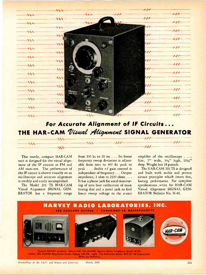
-AAA,
-AAA/
-
-
\Ws- -
For Accurate Alignment of IF Circuits...THE HAR-CAM Vididete fiet:9toteat SIGNAL GENERATOR
This sturdy, compact HAR-CAMunit is designed for the visual align-ment of the IF circuits in FM andAM receivers. The performance ofthe IF circuit is shown visually on anoscilloscope and accurate alignmentis swiftly and easily accomplished.
The Model 205 TS HAR-CAMVisual Alignment SIGNAL GEN-ERATOR has a frequency range
from 100 kc to 20 me . . . Its linearfrequency sweep deviation is ad just -able from zero to 900 kc peak topeak . . . Stable r -f gain control isindependent of frequency . . . Outputimpedance, 1 ohm to 2500 ohms . . .
It has a phone jack for aural monitor-ing of zero beat calibration of maintuning dial and a panel jack to feedlinear sweep voltage to the x-axis
amplifier of the oscilloscope . . .Size, 7" wide, 9M" high, 10M"deep. Weight but 18 pounds.
The H AR -CAM 205 TS is designedand built with stable and provencircuit principles which insure fine,lasting performance. For completespecifications .write for HAR-CAMVisual Alignment SIGNAL GEN-ERATOR Bulletin No. H-40.
p
Typical HARVEY products: Above left: The HARVEY Marine Radio Telephone Model M-25;center: The HARVEY Regulated Power Supply 106 PA; right: The HAR-CAM Model MFT-25 FM Transmitter.
. _Wei.. far Roasting_
Proceedings of the I.R.E. and Waves and Electrons March, 1946 33A
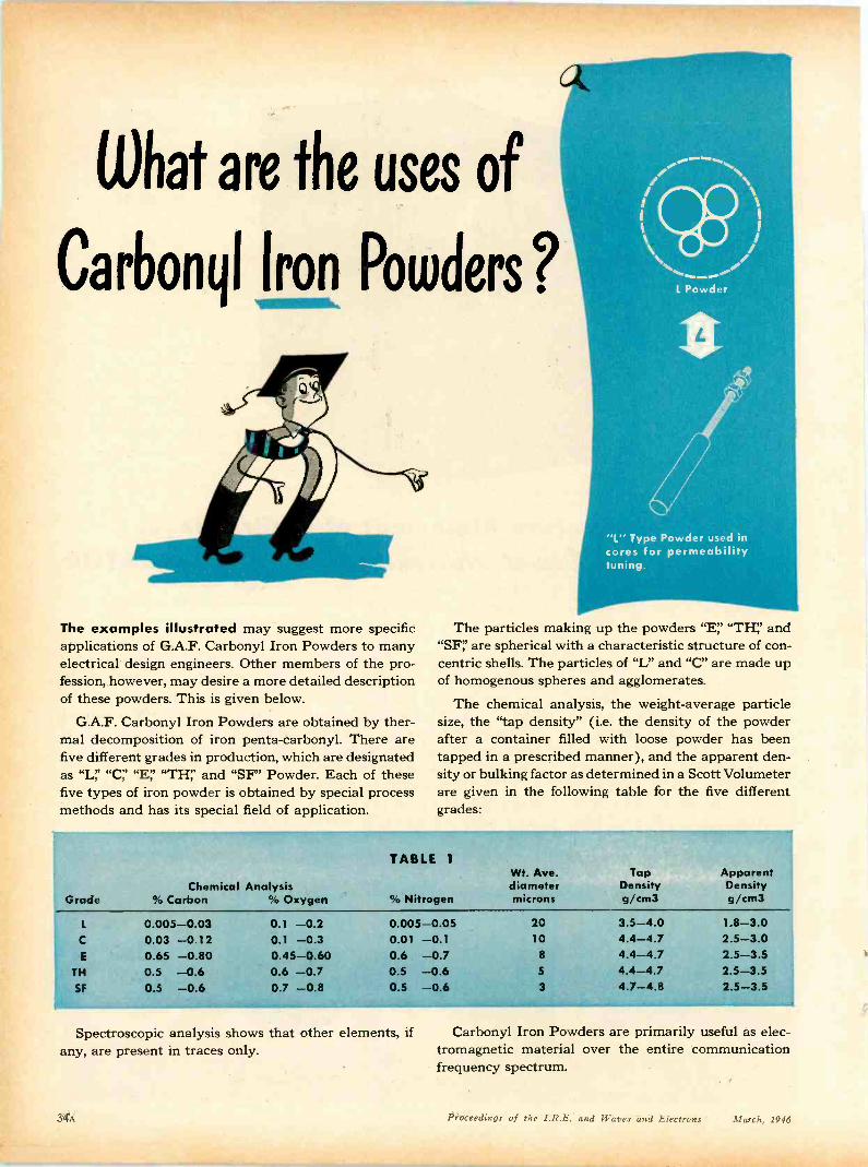
What are the uses of
Carbonyl Iron Powders?
The examples illustrated may suggest more specificapplications of G.A.F. Carbonyl Iron Powders to manyelectrical design engineers. Other members of the pro-fession, however, may desire a more detailed descriptionof these powders. This is given below.
G.A.F. Carbonyl Iron Powders are obtained by ther-mal decomposition of iron penta-carbonyl. There arefive different grades in production, which are designatedas "L',' "C:' "E',' "TH;' and "SF" Powder. Each of thesefive types of iron powder is obtained by special processmethods and has its special field of application.
"L" Type Powder used incores for permeabilitytuning.
The particles making up the powders "E',' "TH;' and"SF;' are spherical with a characteristic structure of con-centric shells. The particles of "L" and "C" are made upof homogenous spheres and agglomerates.
The chemical analysis, the weight -average particlesize, the "tap density" (i.e. the density of the powderafter a container filled with loose powder has beentapped in a prescribed manner), and the apparent den-sity or bulking factor as determined in a Scott Volumeterare given in the following table for the five differentgrades:
GradeChemical Analysis
co Carbon % Oxygen
TABLE 1
% Nitrogen
Wt. Ave.diametermicrons
TapDensityg/cm3
ApparentDensityg/cm3
L 0.005-0.03 0.1 -0.2 0.005-0.05 20 3.5-4.0 1.8-3.0C 0.03 -0.12 0.1 -0.3 0.01 -0.1 10 4.4-4.7 2.5-3.0E 0.65 -0.80 0.45-0.60 0.6 -0.7 8 4.4-4.7 2.5-3.5
TH 0.5 -0.6 0.6 -0.7 0.5 -0.6 5 4.4-4.7 2.5-3.5SF 0.5 -0.6 0.7 0.5 -0.6 3 4.7-4.8 2.5-3.5
Spectroscopic analysis shows that other elements, ifany, are present in traces only.
Carbonyl Iron Powders are primarily useful as elec-tromagnetic material over the entire communicationfrequency spectrum.
34A Proceedings of the I.R.E. and Waves and Electrons March, 1946

CARBONYL IRON POWDERS AND SOME OF THEIR PRESENT USES
The different grades of CARBONYL IRON POWDERS as seen it the microscope....WM.., .............. ............... ''''"'-'"'"".
/I // ft..
/% .
I I I I Or`e0 I I Ctrb I/ 1 I 1
a! I I/ X /
/ /IX // / // / /
..... .0.... ... .. .., ...., .... - ...C Powder E Powder SF Powder
II
"C" Type Powder forE -cores in filter coils.
II
For antenna coils, "E"Type Powder used incores.
TH Powder
II
"TH" Type Powder is em-ployed for cup shields incoils.
One use of "SF" TypePowder is in high fre-quency choke cores (withcenled-in leads).
Table 2 below gives relative Q values (quality fac-tors) and effective permeabilities for the different gradesof carbonyl iron powder. The values given in the tableare derived from measurements on straight cylindricalcores placed in simple solenoidal coils. Although the
CarbonylIron Grade
EffectivePermeability at
1 kc
data were not obtained at optimum conditions, the Qvalues as expressed in percentage of the best core givean indication of the useful frequency ranges for the dif-ferent powder grades.
"L" and "C" powders are also used as powder metal-
TABLE 2Relative Quality Factor at
10 kc 150 kc 200 kc 1 Mc 100 Mc
C
E
TH
SF
4.163.653.092.972.17
100 96 90 4394 100 98 72 3
81 94 103 97 3081 93 98 100 5462 71 73 84 100
(Note: The actually measured 0 values can be obtained by multiplying the rows respective y with: 0.78, 1.09, 1.25, 2.63, and 1.62.)
lurgical material because of their low sintering tempera-tures, high tensile strengths, and other very desirablequalities. (Sintering begins below 500° C and tensilestrengths reach 150,000 psi.)
Further information can be obtained from the Spe-cial Products Sales Dept., General Aniline & Film Cor-poration, 270 Park Ave., New York 17, N. Y.
CARBONYL /RON POWDERSProceedings of the I.R.E. and Waves and Electrons March, 1946
35A

/
What you should know about theSHURE G/44:- Phonograph Pickup
What is the,,aider,,The "Glider" Pickup is a lightweight, low massTone Arm with the new Shure Lever -Type Crystalpicku,?
2-* Cartridge.
How is low The arm is aluminum. It uses no counterweights ormass achieved? springs. It has a needle force of only 1Y ounces.
The Crystal is driven by a lever which improves theWhat is meant transmission of needle chuck torque into the Crystal.by Lever -Type This results in higher output and greater lateral
Cartridge? needle point compliance. It absorbs full impact ofsudden jars to the Cartridge or needle, minimizingCrystal strain or breakage.
What is its The various types range from 1.6 volts to overoutput voltage? 3 volts.
High needle point compliance affords faithful track-What ing which results in clearer, fuller tone qualities.
are its playing Lightness means longer record life. The "Glider" isqualities? less susceptible to floor vibrations, improves playing
of warped records and is especially suitable for Viny-lite records.
MODEL 93A-$5.50 LISTImmediately Available at Shure Distributors Everywhere
Patented by Shure Brothers. Licensed under the Patents of the Brush Development Company
SHURE BROTHERSDesigners and Manufacturers of Microphones and Acoustic Devices
225 West Huron Street, Chicago 10, IllinoisSHURECable Address: SHUREMICRO
ATLANTA
"Some Notes on Units and Measure-ment Scales Used in Communication Engi-neering," by N. B. Fowler, AmericanTelephone and Telegraph Service; Novem-ber 9, 1945.
"Recent Developments in Sonar," byFrank Lowance, Georgia Institute of Tech-nology; November 30, 1945.
"Atomic Energy," by J. H. Howey,Georgia Institute of Technology; Decem-ber 28, 1945.
BOSTON
"Microwave Sources for Radar," byA. G. Hill, Massachusetts Institute ofTechnology; January 4, 1946.
"An Introduction to Loran," by J. A.Pierce, Harvard University; January 18,1946.
BUFFALO -NIAGARA
"Very -High -Frequency Aircraft RadioEquipment," by R. E. Frazier, J. Chand-ler, M. C. Scott, and J. C. Pontius,Colonial Radio Corporation; January 16,1946.
CHICAGO
"Some Aspects of Acoustic -Horn The-ory," by Vincent Salmon, Jensen RadioManufacturing Company; December 21,1945.
"The Technics of Postwar Television,"by A. B. DuMont, Allen B. DuMont Labo-ratories; January 10, 1946.
CINCINNATI
7411 "Microwave Television -Relay Net-works," by H. B. Francher, General Elec-tric Company; December 18, 1945.
Election of Officers; December 18,1945.
"Quality in Sound," by J. D. Reid, TheCrosley Corporation; January 15, 1946.
"The Electronic Organ," by J. F. Jor-dan, The Baldwin Company; January 15,1946.
CLEVELAND
"Short -Wave Diathermy Apparatusand Frequency -Control Possibilities,"C. K. Gieringer, Liebel-Flarsheim Com-pany; January 24, 1946.
CONNECTICUT VALLEY
"Record Embossing," by LincolnThompson, Soundscriber Corporation; Oc-tober 18, 1945.
"Klystrons," by A. E. Harrison, SperryGyroscope Company; December 13, 1945.
"Microwave Relay Systems," by H. B.Fancher, General Electric Company; Jan-uary 8, 1946.
DALLAS -FT. WORTH
"VHF Field Intensity Survey-Sum-mer 1945," by J. G. Rountree, FederalCommunications Commission; January 17,1946.
Election of Officers; January 17, 1946.(Continued on page 38A)
Proceedings of the I R.E. and Waves and Electrons March, 1946

KEEP THINGS
WITSOMOTORSfieS0
ALLIANCE MOTORS are mode with centerless ground precision
shafts; large, self -aligning, graphite bronze oilless-type bearings;
and with adequate mounting facilities to incorporate them in any
device. Shaded pole induction type motors for A.C. voltage from
24 to 250, and frequencies of 40, 50 or 60 cycles have starting
torques from one-half ounce inches at 10 watts, to two ounce inches
at 36 watt input. Split phase resistor type, enclosed reversible
control motors for intermittent duty, with or without integral gear
reduction ore made for 60 cycles, 24 or 117 volts. Typical weights
run from less than 13 ounces to more than two and one-half pounds.
HERE ARE JUST A FEW PLACES!Electronic and electric controls, time, pressure, temperature, pres-
sure and humidity controls, remote actuation controls, radio tuning
and turntable drives, coin operated dispensers, fans, valves, blow-
ers, door openers, signals, motion displays, projectors and spe-
cialized uses.
MINIATUREMOTORS
TKEEPEM MOVINGHAT
With Alliance Powr-Pakt miniature electric motors you
can put power right where you need it! Electronic con-
trols and electro-mechanical devices will work faster,
you cut down manual effort and increase automatic
operation.
Furnished in quantity, with operating variations to
meet the demands of specific jobs, Alliance Motors are
built for any standard voltage or frequency. You can
fit them in small places because they're small! Ratings
run from less than 1 -300th on up to 1 -20th H.P. You can
use them for continuous or intermittent duty-for starting,
stopping, reversing, and for smooth, steady driving.
Remember, there's probably an Alliance motor already
designed and ready to go to work for you!
WHEN YOU DESIGN KEEP Ce111/10MOTORS IN MIND
ALLIANCE MANUFACTURING COMPANY ALLIANCE, OHIOALLIANCE TOOL AND MOTOR, LTD., TORONTO 14, CANADA
Proceedings of the I.R.E. and Waves and Electrons March, 1946
38\
"The whole is equal to the sum of all itsparts"-Elementary? Of course-as simple and unchanging as allgreat principles. This axiom is a fundamental manufacturingcreed at Stancor. We know the established excellence of StancorTransformers is vitally dependent upon the perfection of eachsuccessive manufacturing step-from engineering considerationsof individual specifications-through coil -winding, laminating,assembling, finishing, testing-and, finally, to careful packingfor shipment.
All individual manufacturing operations have one commondenominator - QUALITY - uncompromising, changelessQUALITY that continues to prove -"IN TRANSFORMERS,STANCOR GIVES MORE."
STANCORSTANDARD TRANSFORMER CORPORATION1500 NORTH HALSTED STREE- CHICAGO 22, ILLINOIS
(Continued from page 36A)
DAYTON
"Electronic Aspects of the Geiger -Mueller Counter Tube and Spectrometer,"by D. H. Reynolds and J. W. Heyd, Mon-santo Chemical Company; January 16,1946.
DETROIT
"New Things to Come," by H. S.Walker, The Detroit Edison Company;January 18, 1946.
EMPORIUM
"Notes on a Trip to England," byM. G. Hasselman, Sylvania Electric Prod-ucts; January 14, 1946.
"The Principles of Cathode -Ray -TubeOperation," by W. A. Dickinson, SylvaniaElectric Products; January 14, 1946.
INDIANAPOLIS
"Development of Voltage Regulators,"by C. H. Humes, Solar Electric Company;November 23, 1945.
"The New Radio -Frequency IgnitionSystem," by A. C. Wall, P. R. MalloryCompany; November 23, 1945.
"New Frequency -Control System," byJ. R. Boykin, Westinghouse Electric Cor-poration; December 28, 1945.
MONTREAL
"Radar in World War II," by K. R.Patrick, RCA Victor Company; December12, 1945.
PHILADELPHIA
"Television -Receiver Testing in Pro-duction," by J. A. Bauer, RCA VictorDivision; January 11, 1946.
PITTSBURGH
"Magnetic -Tape Recording," by L. A.Umbach, Carnegie Institute of Technol-ology; January 14, 1946.
"Working with Microwaves," by R. G.Plaisted and S. A. Leiner, University ofPittsburgh, January 14, 1946.
PORTLAND
"Civil Aeronautics AdministrationRadio Range, As Used for Air Naviga-tion," by W. A. Cutting, Portland Inter-state Airways Communications; Decem-ber 21, 1945.
Election of Officers; December 21,1945.
ROCHESTER
"Transmutation of the Elements," byK. K. Darrow, Bell Telephone Labora-tories; January 10, 1946.
SAN DIEGO
"The Phasitron as Used in FrequencyModulation," by C. G. Pierce, GeheralElectric Company; January 4, 1946.
Election of Officers; January 4, 1946.
SEATTLE
"Atomic Bombs and the Hanford Proj-ect," by F. T. Matthais, Hanford Engi-neer Works; December 17, 1945.
Election of Officers; December 17,1945.
(Continued on page 40d4)
Proceedings of the I.R.E. and Waves and Electrons March, 1946
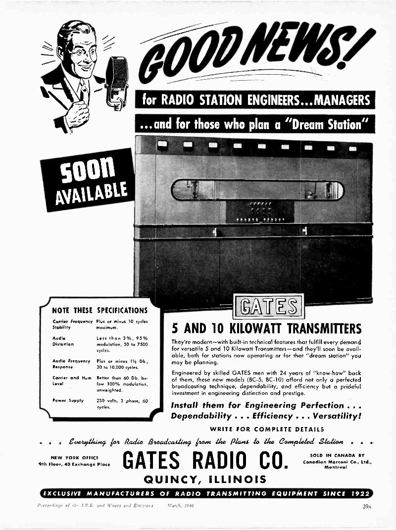
iltraff:/for RADIO STATION ENGINEERS...MANAGERS
...and for those who plan a "Dream Station"
NOTE THESE SPECIFICATIONS
Carrier FrequencyStability
AudioDistortion
Plus or minus 10 cyclesmaximum.
less than 3%, 95%modulation, 50 to 7500cycles.
Audio Frequency Plus or minus 11/2 Db.,Response 30 to 10,000 cycles.
Carrier and HumLevel
Better than 60 Db. be-low 100% modulation,unweighted.
Power Supply 230 volts, 3 phase, 60cycles.
rrrrr.
5 AND 10 KILOWATT TRANSMITTERSThey're modern-with built-in technical features that fulfill every demandfor versatile 5 and 10 Kilowatt Transmitters-and they'll soon be avail-able, both for stations now operating or for that "dream station" youmay be planning.
Engineered by skilled GATES men with 24 years of "know-how" backof them, these new models (BC -5, BC -10) afford not or ly a perfectedbroadcasting technique, dependability, and efficiency but a pridefulinvestment in engineering distinction and prestige.
Install them for Engineering Perfection ...Dependability . . . Efficiency ... Versatility!
WRITE FOR COMPLETE DETAILS
. eaeiuttlia, As4 Radio thoodea41i#19. kroon the Plaos to the Costpleted Statio4: . .
NEW YORK OFFICE9th Floor, 40 Exchange Place GATES RADIO CO.
QUINCY, ILLINOIS
SOLD IN CANADA BYCanadian Marconi Co., Ltd.,
Montreal
EXCLUSIVE MANUFACTURERS OF RADIO TRANSMITTING EQUIPMENT SINCE 1922
39A
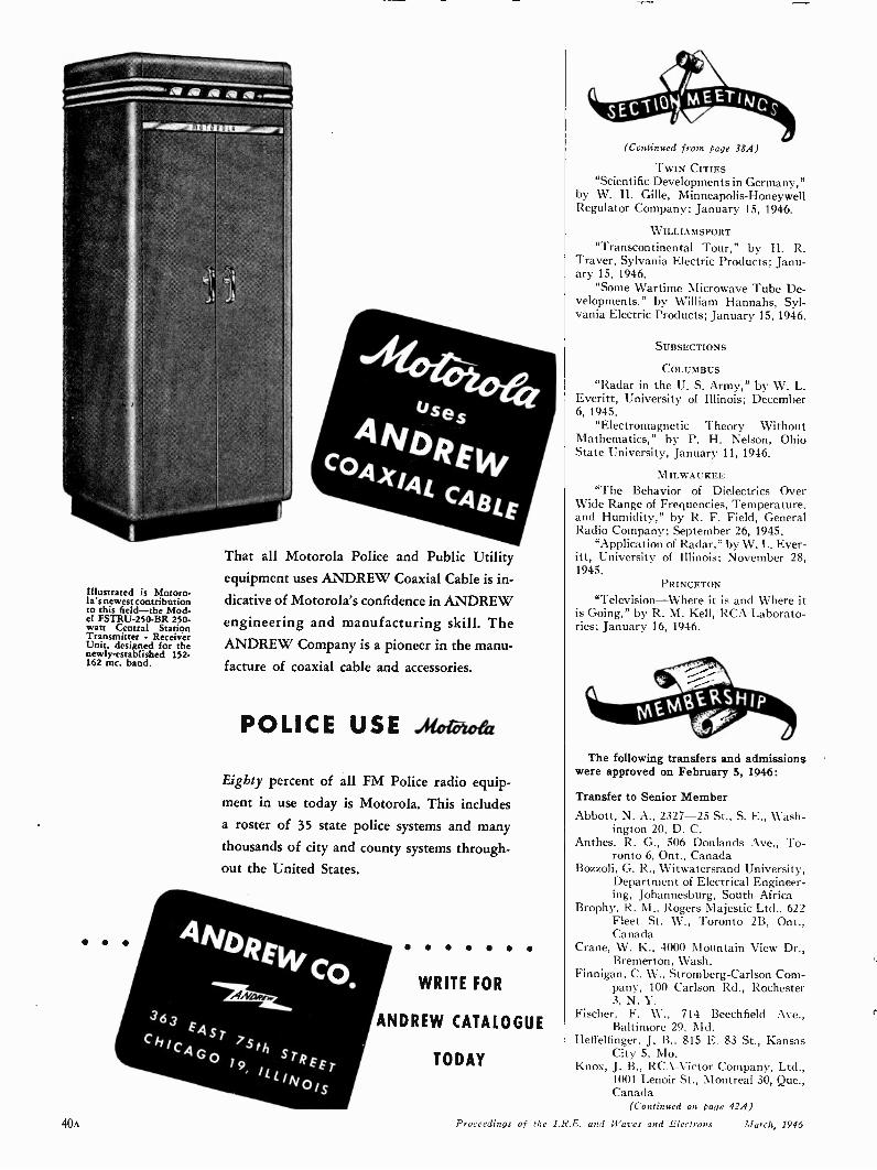
Illustrated is Motoro-la's newest contributionto this field-the Mod-el FSTRU-250-BR 250 -watt Central StationTransmitter - ReceiverUnit, designed for thenewly -established 152-162 mc. band.
40A
That all Motorola Police and Public Utilityequipment uses Cable is in-
dicative of Motorola's confidence in ANDREW
engineering and manufacturing skill. TheANDREW Company is a pioneer in the manu-
facture of coaxial cable and accessories.
POLICE USE di/01%04z
Eighty percent of all FM Police radio equip-ment in use today is Motorola. This includesa roster of 35 state police systems and manythousands of city and county systems through-out the United States.
0 OOOOO
WRITE FOR
ANDREW CATALOGUE
TODAY
Proceedings of
(Continued from page 38A)
TWIN CITIES"Scientific Developments in Germany,"
by W. H. Gille, Minneapolis -HoneywellRegulator Company; January 15, 1946.
WILLIAMSPORT
"Transcontinental Tour," by H. R.Traver, Sylvania Electric Products; Janu-ary 15, 1946.
"Some Wartime Microwave Tube De-velopments," by William Hannahs, Syl-vania Electric Products; January 15, 1946.
SUBSECTIONS
COLUMBUS
"Radar in the U. S. Army," by W. L.Everitt, University of Illinois; December6, 1945.
"Electromagnetic Theory WithoutMathematics," by P. H. Nelson, OhioState University, January 11, 1946.
MILWAUKEE
"The Behavior of Dielectrics OverWide Range of Frequencies, Temperature,and Humidity," by R. F. Field, GeneralRadio Company; September 26, 1945.
"Application of Radar," by W. L. Ever-itt, University of Illinois; November 28,1945.
PRINCETON
"Television-Where it is and Where itis Going," by R. M. Kell, RCA Laborato-ries; January 16, 1946.
The following transfers and admissionswere approved on February 5, 1946:
Transfer to Senior MemberAbbott, N. A., 2327-25 St., S. E., Wash-
ington 20, D. C.Anthes, R. G., 506 Donlands Ave., To-
ronto 6, Ont., CanadaBozzoli, G. R., Witwatersrand University,
Department of Electrical Engineer-ing, Johannesburg, South Africa
Brophy, R. M., Rogers Majestic Ltd., 622Fleet St. W., Toronto 2B, Ont.,Canada
Crane, W. K., 4000 Mountain View Dr.,Bremerton, Wash.
Finnigan, C. W., Stromberg-Carlson Com-pany, 100 Carlson Rd., Rochester3, N. Y.
Fischer, F. W., 714 Beechfield Ave.,Baltimore 29, Md.
Heffelfinger, J. B., 815 E. 83 St., KansasCity 5, Mo.
Knox, J. B., RCA -Victor Company, Ltd.,1001 Lenoir St., Montreal 30, Que.,Canada
(Continued on page 42A)
the I.R.E. and Waves and Electrons March, 1946
EVERYTHING Fl OM ONESOURC-
A complete insulation servicefrom one source gives time-saving advantages t 3 you.
AlACALLANFIBERGLAS
NATIONALLY RECOGNIZEDPRODUCTS
The highest quality productsmade to rigid specificationsguarantee you top notch per-formance of your product.
THE IMC NGINEE
The mo ern march of business demands the atten-tion of experts Your present staff, unless familiarwith the expe services of the IMC organization, willwelcome the -service which is available in theperson of the IMC engineer.
When you buy ElectricalInsulation you should getMaterials Plus Service ...
The IMC engineer is, in effect, traveling companionto IMC products. He is ready at all times to ...
1. Assist you in the selection of the best insulat-ing material for the job.
2. Familiarize you with their proper application.3. Suggest ways to eliminate waste.4. Increase your production.
His is .'experience at work" to insure insulation thatapproaches perfection. It is due in largethe wholehearted co-operation of IMC engineers thatIMC materials are favorably known and so widely used.
TAILOR-MADE TO YOURNEEDS
If you desire, we have the fa cilities to fabricate parts toyour specifications.
IMC PRODUCTS: Macallen Mica Products-Vortex Varnished Clothand Tapes-Varslot Combination Slot Insulation-Varnished Silk and
Paper-Fiberglas Electrical Insulation-Manning Insulating Papers andPr, ssboards-Dow Corning Silicones-Dien.: Varnished Tubings
and Saturated Sleevings of Cotton and Fiberglas-National Hard Fibreand Fishpaper-Phenolito Bakelite-Adhesive Tapes-Asbestos
Woven Tapes and Sleevings-Cotton Tapes, Webbings, and Sleevings'edigree Insulating Varnishes-Wedgie Brand Wood Wedges.
Re; -esentatives in:
MILWAUKEE 2: 312 East Wisconsin AvenueDETROIT 2: 11341 Woodward AvenueMINNEAPOLIS 3: 1208 Harmon PlacePEORIA 5: 101 Hein. CourtArsi other cities
"KNOW HOW" ENGINEERS...STRATEGICALLY LOCATED
Throughout the MiddlewestIMC engineers call regu artyand will give special service inemergencies.
IOW
PROMPT SHIPMENT FROMCOMPLETE STOCKS
Products are quickly on theway to you by truck, freight,mail, or express.
INSULATIONMANUFACTURERS CORPORATION
4%.e.c17R (94
C:IeVSU6:iiA°T.
*CHICAGO 6565 W. Washing-ton Blvd.
*CLEVE LAND 141005 Leader Bldg.

A
M
YOU PLANNING
TO GIVE
RE LISTENERS
SETTERRECEPTION ?
If you're planning to addload to your output, youcan take a load off yourshoulders by turning yourantenna problem over toBlaw-Knox.
Unequalled experience inthis field-backed bythousands of successfulinstallations ranging insize up to 1000 feet-means that you can relyon Blaw-Knox for full re-sponsibility in the fabri-cation and erection ofcomplete antenna systems.
BLAW-KNOX DIVISIONof Blaw-Knox Company
2037 FARMERS BANK BUILDING
ITTSBURGH, ENNSYLVANIA
BLAW-KNOXVERTICAL RADIATORS
(Continued from page 404)
Lund, C. W., 8417 N.E. Columbia Bot-tom Rd., RFD 4, Box 858, Port-land 11, Ore.
Mathes, R. E., 15 Fairhill Rd., Westfield,N. J.
Pettit, J. M., Airborne Instruments Labor-atory, Inc., 160 Old Country Rd.,Mineola, L. I., N. Y.
Reid, J. D., Box 67, Mt. Healthy, OhioSkelton, T. H., Australian War Supplies,
1700 Massachusetts Ave., N.W.,Washington 6, D. C.
Sledge, 0. D., 546 Oakwood St., S. E.,Washington 20, D. C.
Admission to Senior Member
Darwin, F. A., 8 Ashby Ave., Alexandria,Va.
Havens, B. L., Watson Scientific Comput-ing Laboratories, 612 W. 116 St.,New York, N. Y.
Koehler, J. F., 620 E. Leland St., ChevyChase 15, Md.
McNally, I. L., 1365 Kennedy St., N.W.,Washington 11, D. C.
Mode, D. E., Lehigh University, Bethle-hem, Pa.
Roberts, J. M., 318 Bogert Ave., Ridge-wood, N. J.
Rogers, J. R., 8 Garden Court, Cambridge38, Mass.
Watson -Watt, R., 287 Sheen Lane, Lon-don S.W. 14, England
Transfer to MemberBeranek, J. A., Columbia Broadcasting
System, Inc., Hollywood, Calif.Bloomenthal, S., 914 Carmen Ave., Chi-
cago 40, Ill.Byrne, M. E., 523-6 Ave., Lewiston,
IdahoCervenka, F. J., Civil Aeronautics Ad-
ministration, 608 S. Dearborn St.,Chicago, Ill.
Chew, T. M., 3004 Gainesville St., S.E.,Washington 20, D. C.
Cooke, L. G., 1595 Greenwich St., SanFrancisco 20, Calif.
Cowles, L. G., Box 425, Bellaire, TexasDeutsch, K. T., U. S. Bureau of Reclama-
tion, Customhouse, Denver 2, Colo.Garcia, S. C., U. S. Maritime Service,
Hoffman Island, Staten Island 1,N. Y.
Granger, J. V., 387 Harvard St., Cam-bridge 38, Mass.
Haeger, J. R., 283 N.W. 59 Terrace, Mi-ami 38, Fla.
Hollingsworth, L. M., 36 Highland Ave.,Cambridge 39, Mass.
Hudson, P. K., Electrical Engineering De-partment, University of Idaho,Moscow, Idaho
Israel, J. 0., 463 West St., New York 14,N. Y.
MacKenzie, N. F., Radio Corporation ofAmerica, Harrison, N. J.
McCann, F. H., 6924 N.E. 23 St., Port-land 11, Ore.
(Continued on page 44A)
Proceedings cf the I.R.E. and Waves and Electrons March, 1946
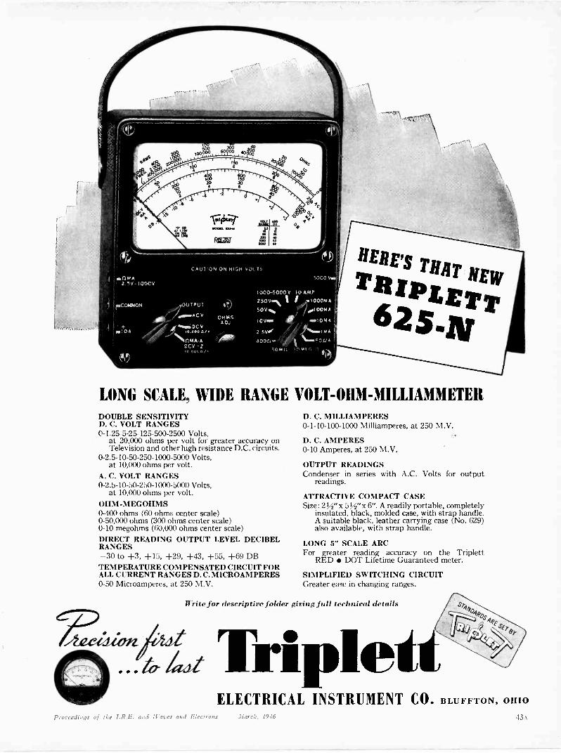
2.5V-t000V
CAUTION ON HIGH VOL.
OHMSAO.
ve
I
l5000
1000-5000 V 10 AMP
2505 i i ./.1000,4 A50V% ; /0100NA tI C5mor 0 ' Awl OM A I,
50/ ,/ 441..IMA I
-00f,.. ' ,.. I ItIA..,-3IJ A !
50001C: FO NIG
LONG SCALE, WIDE RANGE VOLT-OHM-MILLIAMMETERDOUBLE SENSITIVITYD. C. VOLT RANGES0-1.25-5-25-125-500-2500 Volts,
at 20,000 ohms per volt for greater accuracy onTelevision and other high resistance D.C. circuits.
0-2.5-10-50-250-1000-5000 Volts,at 10,000 ohms per volt.
A. C. VOLT RANGES0-2.5-10-50-250-1000-5000 Volts,
at 10,000 ohms per volt.OHM-MEGOHMS0-400 ohms (60 ohms center scale)0-50,000 ohms (300 ohms center scale)0-10 megohms (60,000 ohms center scale)DIRECT READING OUTPUT LEVEL DECIBELRANGES-30 to +3, +15, +29, +43, +55, +69 DBTEMPERATURE COMPENSATED CIRCUIT FORALL CURRENT RANGES D.C. MICROAMPERES0-50 Microamperes, at 250 M.V.
D. C. MILLIAMPERES0-1-10-100-1000 Milliamperes, at 250 M.V.
D. C. AMPERES0-10 Amperes, at 250 M.V.
OUTPUT READINGSCondenser in series with A.C. Volts for output
readings.
ATTRACTIVE COMPACT CASESize: 2 x 5M" x 6". A readily portable, completely
insulated, black, molded case, with strap handle.A suitable black, leather carrying case (No. 629)also available, with strap handle.
LONG 5" SCALE ARCFor greater reading accuracy on the Triplett
RED DOT Lifetime Guaranteed meter.
SIMPLIFIED SWITCHING CIRCUITGreater ease in changing ranges.
Write for descriptive folder giving full technical details
TriplettELECTRICAL INSTRUMENT CO. BLUFFTON, OHIO
Proceedings of the I.R.L. and Il az es and Electrons March, 1946 43 \
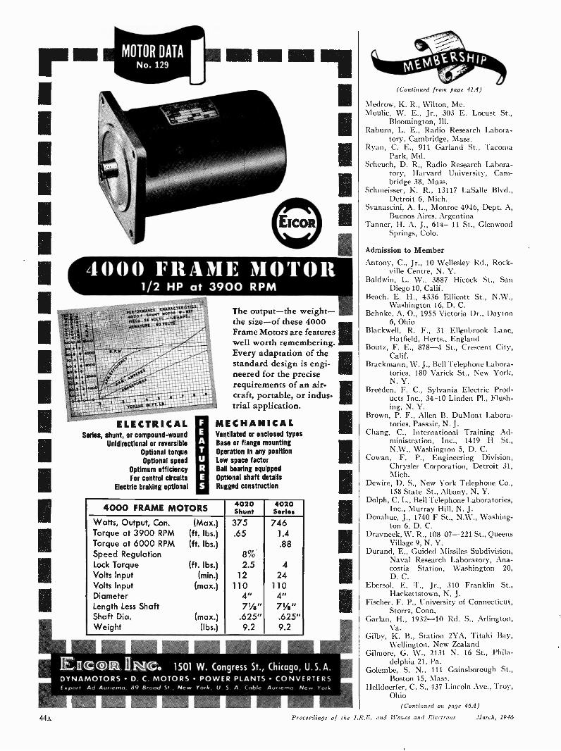
4000 FRAME MOTOR1/2 HP at 3900 RPM
.7.11 t
so .02.4.
?Ill; DO 11,14 A:0C.%,1110. 1 twit.. 5
PItt.03A rOLIS - 1.11 Ws.
APIAATUIlt - 40 TOL%
ELECTRICALSeries, shunt, or compound -wound
Unidirectional or reversibleOptional torqueOptional speed
Optimum efficiencyFor control circuits
Electric braking optional
The output-the weight-the size-of these 4000Frame Motors are featureswell worth remembering.Every adaptation of thestandard design is engi-neered for the preciserequirements of an air-craft, portable, or indus-trial application.
MECHANICALVentilated or enclosed typesBase or flange mountingOperation in any positionLow space factorBall bearing equippedOptional shaft detailsRugged construction
4000 FRAME MOTORS 4020 4o20Shunt
Series
Watts, Output, Con. (Max.) 375 746Torque at 3900 RPM (ft. lbs.) .65 1.4Torque at 6000 RPM (ft. lbs.) .88Speed Regulation 8`..-c
Lock Torque (ft. lbs.) 2.5 4Volts Input (min.) 12 24Volts Input (max.) 110 110Diameter 4" 4"Length Less Shaft 71/4" 71/4"Shaft Dia. (max.) .625" .625"Weight (lbs.) 9.2 9.2
Ii CONit INV* 1501 W. Congress St., Chicago, U.S. A.DYNAMOTORS D. C. MOTORS POWER PLANTS CONVERTERSf moor, Ad Aurlemo, 89 Brood Sr., New Ynrk, U. S Coble At.r.errso New Yorl.
(Continued from page 42A)
Medrow, K. R., Wilton, Me.Moulic, W. E., Jr., 303 E. Locust St.,
Bloomington, Ill.Raburn, L. E., Radio Research Labora-
tory, Cambridge, Mass.Ryan, C. E., 911 Garland St., Tacoma
Park, Md.Scheuch, D. R., Radio Research Labora-
tory, Harvard University, Cam-bridge 38, Mass.
Schmeisser, K. R., 13117 LaSalle Blvd.,Detroit 6, Mich.
Svanascini, A. L., Monroe 4946, Dept. A,Buenos Aires, Argentina
Tanner, H. A. J., 614-11 St., GlenwoodSprings, Colo.
Admission to Member
Antony, C., Jr., 10 Wellesley Rd., Rock-ville Centre, N. Y.
Baldwin, L. W., 3887 Hicock St., SanDiego 10, Calif.
Beach, E. H., 4336 Ellicott St., N.W.,Washington 16, D. C.
Behnke, A. 0., 1955 Victoria Dr., Dayton6, Ohio
Blackwell, R. F., 31 Ellfnbrook Lane,Hatfield, Herts., England
Boutz, F. E., 878-4 St., Crescent City,Calif.
Brackmann, W. J., Bell Telephone Labora-tories, 180 Varick St., New York,N. Y.
Breeden, F. C., Sylvania Electric Prod-ucts Inc., 34-10 Linden Pl., Flush-ing, N. Y.
Brown, P. F., Allen B. DuMont Labora-tories, Passaic, N. J.
Chang, C., International Training Ad-ministration, Inc., 1419 H St.,N.W., Washington 5, D. C.
Cowan, F. P., Engineering Division,Chrysler Corporation, Detroit 31,Mich.
Dewire, D. S., New York Telephone Co.,158 State St., Albany, N. Y.
Dolph, C. L., Bell Telephone Laboratories,Inc., Murray Hill, N. J.
Donahue, J., 1740 F St., N.W., Washing-ton 6, D. C.
Dravneek, W. R., 108-07-221 St., QueensVillage 9, N. Y.
Durand, E., Guided Missiles Subdivision,Naval Research Laboratory, Ana-costia Station, Washington 20,D. C.
Ebersol, E. T., Jr., 310 Franklin St.,Hackettstown, N. J.
Fischer, F. P., University of Connecticut,Storrs, Conn.
Garlan, H., 1932-10 Rd. S., Arlington,Va.
Gilby, K. B., Station 2YA, Titahi Bay,Wellington, New Zealand
Gilmore, G. W., 2131 N. 16 St., Phila-delphia 21, Pa.
Golembe, S. N., 111 Gainsborough St.,Boston 15, Mass.
Helldoerfer, C. S., 437 Lincoln Ave., Troy,Ohio
(Continued on page 46A)
Proceedings of the I.R.E. and Waves and Electrons March, 1946
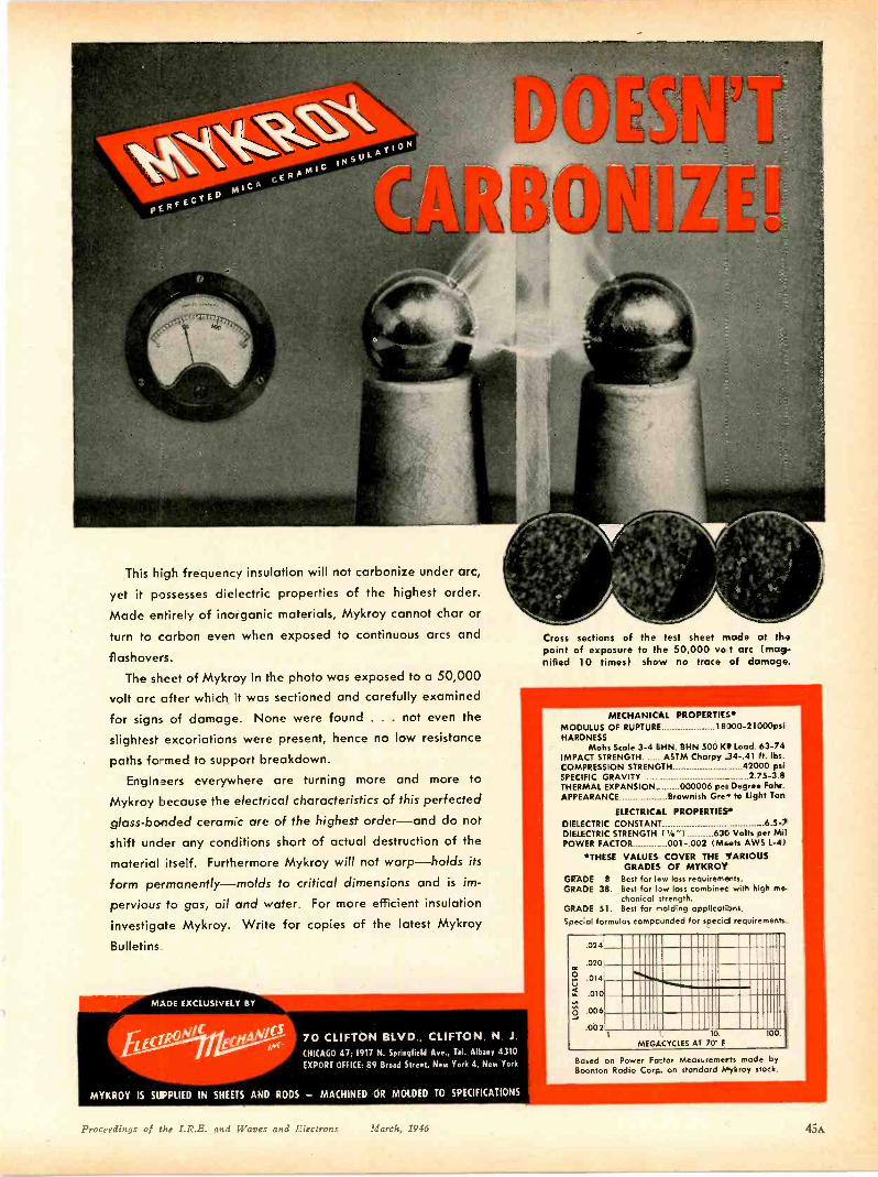
This high frequency insulation will not carbonize under arc,
yet it possesses dielectric
Made entirely of inorganic
turn to carbon even when
flashovers.
The sheet of Mykroy in the photo was exposed to a 50,000
volt arc after which it was sectioned and carefully examined
for signs of damage. None were found . . . not even the
slightest excoriations were present, hence no low resistance
paths fo-med to support breakdown.Engineers everywhere are turning more and more to
Mykroy because the electrical characteristics of this perfected
glass -bonded ceramic are of the highest order-and do notshift under any conditions short of actual destruction of the
material itself. Furthermore Mykroy will not warp-holds itsform permanently-molds to critical dimensions and is im-
pervious to gas, oil and water. For more efficient insulation
investigate Mykroy. Write for copies of the latest Mykroy
Bulletins
MADE EXCLUSIVELY BY
properties of the highest order.materials, Mykroy cannot char or
exposed to continuous arcs and
70 CLIFTON BLVD., CLIFTON, N. J.CHICAGO 47; 1917 N. Springfield Ave., Tel. Albany 4310EXPORT OFFICE: 89 Broad Street, New York 4, New York
MYKROY IS SUPPLIED IN SHEETS AND RODS - MACHINED OR MOLDED TO SPECIFICATIONS
Cross sections of the test sheet made at thepoint of exposure to the 50,000 vo t arc (mag-nified 10 times) show no trace of damage.
MECHANICAL PROPERTIES*MODULUS OF RUPTURE 18 )00-21000p'HARDNESS
Mohs Scale 3-4 IHN. BHN 500 KS Load. 63-74IMPACT STRENGTH ASTM Charpy .34-.41 ft. lbs.COMPRESSION STRENGTH 42000 psiSPECIFIC GRAVITY 2.75-3.8THERMAL EXPANSION_ 000006 per Degree Fahr.APPEARANCE Brownish Gre-, to Light Ton
ELECTRICAL PROPERTIES*DIELECTRIC CONSTANT 6.5-7DIELECTRIC STRENGTH I'/."1 63C Volts per MilPOWER FACTOR 001-.002 I Meets AWS L-41
*THESE VALUES COVER THE VARIOUSGRADES OF MYKROY
GRADE 8 Best for lew loss requirements.GRADE 38. Best for I3W loss combinec with high me-
chanical strength.GRADE 51. Best for molding applications.Special formulas compcunded for specid requirements.
024
.020
014
010
006
0021 0.
MEGACYCLES AT 70' F100
Based on Power Factor Measuremerts mode byBoonton Radio Corp. on standard Mykroy rock.
Proceedings of the I.R.E. and Waves and Electrons March, 1946 45A
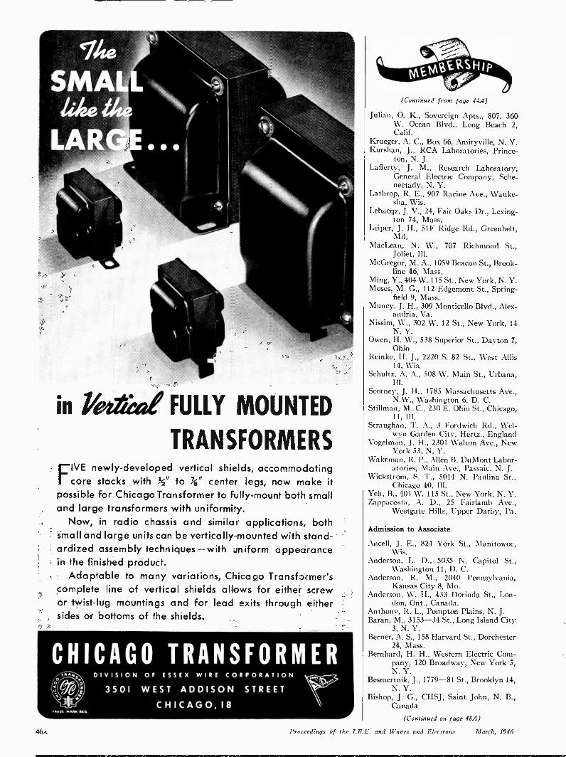
in Pertical FULLY MOUNTED
TRANSFORMERSFIVE newly -developed vertical shields, accommodatingcore stacks with Vr to %" center legs, now make it
possible for Chicago Transformer to Fully -mount both smalland large transformers with uniformity.
Now, in radio chassis and similar applications, bothsmall and large units can be vertically -mounted with stand-ardized assembly techniques-with :uniform appearancein the finished product.
Adaptable to many variations, Chicago Transformer'scomplete line of vertical shields allows for either screwor twist -lug mountings and for lead exits through eithersides or bottoms of the shields.
CHICAGO TRANSFORMERDIVISION OF ESSEX WIRE CORPORATION
3501 WEST ADDISON STREETCHICAGO, 18
T11115g M1611N MC6.
46A Proceedings of
(Continued from page 44A)
Julian, 0. K., Sovereign Apts., 807, 360W. Ocean Blvd., Long Beach 2,Calif.
Krueger, A. C., Box 66, Amityville, N. Y.Kurshan, J., RCA Laboratories, Prince-
ton, N. J.Lafferty, J. M., Research Laboratory,
General Electric Company, Sche-nectady, N. Y.
Lathrop, R. E., 907 Racine Ave., Wauke-sha, Wis.
Lebacqz, J. V., 24, Fair Oaks Dr., Lexing-ton 74, Mass.
Leiper, J. H., 51F Ridge Rd., Greenbelt,Md.
MacLean, N. W., 707 Richmond St.,Joliet, Ill.
McGregor, M. A., 1059 Beacon St., Brook-line 46, Mass.
Ming, Y., 404 W. 115 St., New York, N. Y.Moses, M. G., 112 Edgemont St., Spring-
field 9, Mass.Muncy, J. H., 309 Monticello Blvd., Alex-
andria, Va.Nissim, W., 302 W. 12 St., New York, 14
N. Y.Owen, H. W., 538 Superior St., Dayton 7,
OhioReinke, H. J., 2220 S. 82 St., West Allis
14, Wis.Schultz, A. A., 508 W. Main St., Urbana,
Ill.Scotney, J. H., 1785 Massachusetts Ave.,
N.W., Washington 6, D. C.Stillman, M. C., 230 E. Ohio St., Chicago,
11, Ill.Straughan, T. A., 3 Fordwich Rd., Wel-
wyn Garden City, Hertz., EnglandVogelman, J. H., 2301 Walton Ave., New
York 53, N. Y.Wakeman, R. P., Allen B. DuMont Labor-
atories, Main Ave., Passaic, N. J.Wickstrom, S. T., 5014 N. Paulina St.,
Chicago 40, III.Yeh, B., 404 W. 115 St., New York, N. Y.Zappacosta, A. D., 25 Fairlamb Ave.,
Westgate Hills, Upper Darby, Pa.
Admission to Associate
Ancell, J. E., 824 York St., Manitowoc,Wis.
Anderson, L. D., 5035 N. Capitol St.,Washington 11, D. C.
Anderson, R. M., 2040 Pennsylvania,Kansas City 8, Mo.
Anderson, W. H., 433 Dorinda St., Lon-don, Ont., Canada.
Anthony, R. L., Pompton Plains, N. J.Baran, M., 3153-34 St., Long Island City
3, N. Y.Berner, A. S., 158 Harvard St., Dorchester
24, Mass.Bernhard, H. H., Western Electric Com-
pany, 120 Broadway, New York 5,N. Y.
Besmertnik, J., 1779-81 St., Brooklyn 14,N. Y.
Bishop, J. G., CHSJ, Saint John, N. B.,Canada
(Continued on page 48A)
the I.R.E. and Waves and Electrons March, 1946
Flight engineered forperformance and dependability
"replaced cathode bias resistor 'reference No. 508' with a400 ohm 2 watt resistor."
. . . an excerpt from a typical Bendix Radio FlightEngineers report. A report that means the installedBendix Radio Communication or Navigation Systemwill meet the equipment user's field operation expec-tations-laboratory performance and dependabilityunder all conditions.
But-this is only one phase of Bendix Flight Engi-neering Service. Previous to the equipment's purchasehighly skilled Bendix engineers make a comprehen-sive field survey that is intended to aid in planning theinstallation to the user's satisfaction. This survey pro-vides Bendix with equipment modification data andaids in the creative engineering of any new designproducts needed for this installation.
Planned for the user, Bendix Radio Flight EngineeringService enables him to realize the greatest possiblereturn from his investment-to relieve his mind ofworries over proper circuit protection, undesiredlock -up of electrical control circuits, radio compassbearing errors, calibration of indicators, etc.In addition, Bendix Radio provides a Field Engi-
neering Service that insures the equipment user of thissame initial performance and dependability through-out the life of the installation.
Developed by Bendix Radio-these Flight EngineeringServices are some of the reasons why thousands ofusers have made Bendix Radio equipment "Standardfor the Aviation Industry."
BENDIX RADIO DIVISION, BALTIMORE 4, MARYLAND
4111-11PRODUCT OF
Precision411P /
Equipment AP
AVIATION CORPORATION
BENDIX RADIO )CG. 1.
Proceedings of the I.R.E. and Waves and Electrons March, 1946 47A
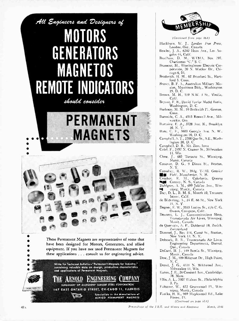
AU Eoteicoteved eua Ve4tryterd ej
MOTORS
GENERATORS
MAGNETOS
REMOTE INDICATORS
L
PERMANENT
MAGNETS
These Permanent Magnets are representative of some thathave been designed for Motors, Generators, and alliedequipment. If you have not used Permanent Magnets forthese applications . . . consult us for engineering advice.
Write for Technical Bulletin -"Permanert Magnets for Industry,"containing valuable data on design, production characteristicsand applications of Permanent Magnets.
THE ARNOLD ENGINEERING COMPANYSUBSIDIARY OF ALLEGHENY LUDLUM STEEL CORPORATION
147 EAST ONTARIO STREET, CH-CAGO 11, ILLINOISSpecialists in the Manufacture ofALNICO PERMANENT MAGNETS
(Continued from page 46A)
Blackburn, W. J., London Free Press,London, Ont., Canada
Bowler, J. A., 6242 Haas Ave., Los An-geles 44, Calif.
Bradham, D. M., WTMA, Box 297,Charleston "C," S. C.
Brasseur, M., Westinghouse Electric Cor-poration, 20 N. Wacker Dr., Chi-cago 6, Ill.
Broderick, H. M., 62 Branford St., Hart-ford 5, Conn.
Brown, B. F. A., Australian Military Mis-sion, Munitions Bldg., Washington25, D. C.
Brown, M. H., 119 N.W. 3 St., Visalia,Calif.
Bryant, F. B., David Taylor Model Basin,Washington, D. C.
Burleson, M. M., 10 Beckwith Pl., Groton,Conn.
Burnside, C. A., 4515 Roswell Ave., Mil-waukie, Ore.
Burtaine, E. A., 3728 Ave. K., Brooklyn10, N. Y.
Buse, C. F., 3603 Georgia Ave. N. W.,Washington 10, D. C.
Campbell, A. T., 2700 Que St., S.E., Wash-ington 20, D. C.
Campbell, D. B., Mt. Zion, IowaCatel, F., 2497 N. Cramer St., Milwaukee
11, Wis.Close, J., 685 Toronto St., Winnipeg,
Manit, CanadaConover, D. G., 9 Dinan St., Beacon,
N. Y.Cronshey, R. W., Bldg. T-143, GrenierEll Field, Manchester, N. H.Crooker, R. M., Caledonia, Queens
County, N. S., CanadaDahlgren, A. M., 699 Jubilee Ave., Win-n nipeg, Manit., CanadaDay, D. L., R. M. S., Month 10, Treasure
Island, Calif.de Bilderling, A., 24 E. 66 St., New York
21, N. Y.Degner, E. W., 2035 Lucien St., c/o C. G.
Owens, Compton, Calif.Dennett, L. J., Communications Shop,
Transcanada Air Lines, Winnipeg,Manit., Canada
de Quervain, A. P., Doldertal 18, Zurich,Zwitzerland
Dimond, J., Box 114, Canal St., Station,New York 13, N. Y.
Dobesch, R. R., Transcanada Air Lines,Engineering Department, Dorval,Que., Canada
Dollard, H. J., 149 Scotia St., Winnipeg,Manit., Canada
Dow, J. M., 109 Hilicrest Dr., High Point,N. C.
Doyel, J. G., 4331 N. Wildwood Ave.,Milwaukee 11, Wis.
Eaton, J. E., 26 Concord Ave., Cambridge,38, Mass.
Ellis, A. L., 2007 Walnut St., Philadelphia3, Pa.
Falconer, W., 622 Greenwood Pl., Win-nipeg, Manit., Canada
Faulks, H. R., 969 Maplewood Rd., LakeForest, Ill.
(Continued on page 52A)
48k Proceedings of the I.R.E. and Waves and Electrons March, 1946

r
L
Callite kulgrid* wire and strand
I
for electronic and electrical applications
Callite developed Kulgrid to meet the needs for a stranded wire thatdoes not oxidize nor flake under the high temperatures of beading,stem -making, sealing -in and exhaust operations. Kulgrid is a com-posite wire having an inner core of copper alloy bonded to a nickelsleeve. It has 70% of copper's conductivity, plus all of nickel's strengthand resistance to oxidation. Kulgrid is widely used for lead-in wires,welds and grid supports in electron tubes.
sleeve of nickel
KULGRID LEADS INA TYPICAL STEM.
copper core,
FEATURES OF C -TKULGRID*
WIRE
1. Does not be-come brittle;
2. Strands staywelded, remainflexible, offerlower resist-ance;
3. No oxide flakes in the tubepress because of nickel sleeve;
4. Not nickel -plated but "clad"-both copper core and nickelsleeve drown down together;
5. Welds readily to itself and tonickel, copperclad, tungsten,molybdenum, and other relatedmetols
(*Kulgrid is covered by U.S. and foreign oatents.)
J
Because of its special characteristics, Kulgrid isgaining popularity as a connector from terminalsto heating elements in electrical appliances. Wewill be glad to discuss applications of Kulgrid andfurnish samples. Callite Tungsten Corporation,544 Thirty-ninth Street, Union City, New Jersey.Branch offices: Chicago, Cleveland.
KULGRID AND OTHER "CLAD" WIRES
also fine alloy wiresin aluminum, phos-phor bronze, siliconbronze, commercialbronze, stainlesssteel, silver, nickelsilver, monel, brassesand special alloys.Precision diametersdown to .002" orsmaller.
Proceedings of the I.R.E. and Waves and Electrons March, 1946 49A
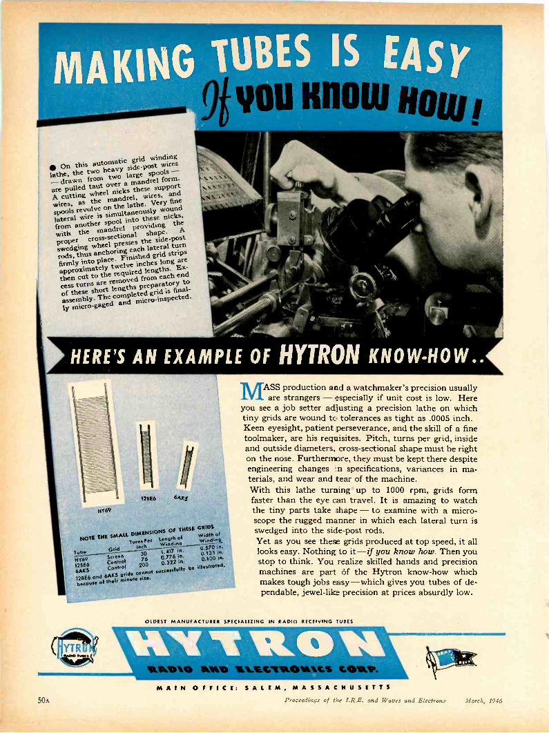
On this automatic grid winding
lathe, the two heavy side -post wires
- drawn from two large spools -
are pulled taut over a mandrel form.
A cutting wheel nicks these supandwires, as the mandrel, wires,
spools revolve on the lathe. Very fine
lateral wire is simultaneouslywound
from anotherspool into these nicks,
with the mandrel providing the
proper cross-sectionalshape. A
swedging wheel presses the side -post
rods, thus anchoring each lateral turn
firmly into place. Finished grid strips
approximatelytwelve inches long are
then cut to the requiredlengths. Ex-
cess turns are removed preparatoryach end
of these short lengthsto
completed grid is final -assembly. The comp
cro-inspected.ly micro -gaged and mi
12BE6 6AK.5
H169
NOTE THE SMALL DIMENSIONSOF THESE
Turns PerLength of
TubeGrid
Inches ing
HT69 Screen30 1.417 in.
12BE6Control 76 0.776 in.
OAKSControl 200 0.322 in.
12BE6 and 6AK5grids cannot
successfully be
because of their minute size.
rttYT
ligaS litt4:00 WCIE.g.NROWttS cow,.
GRIDSWidth ofWinding0.570 in.0.135 in.0.100 in.
illustrated.
MASS production and a watchmaker's precision usuallyare strangers - -especially if unit cost is low. Here
you see a job setter adjusting a precision lathe on whichtiny grids are wound to tolerances as tight as .0005 inch.Keen eyesight, patient perseverance, and the skill of a finetoolmaker, are his requisites. Pitch, turns per grid, insideand outside diameters, cross-sectional shape must be righton the nose. Furthermore, they must be kept there despiteengineering changes n specifications, variances in ma-terials, and wear and tear of the machine.With this lathe turning up to 1000 rpm, grids formfaster than the eye can travel. It is amazing to watchthe tiny parts take shape - to examine with a micro-scope the rugged manner in which each lateral turn isswedged into the side -post rods.Yet as you see these grids produced at top speed, it alllooks easy. Nothing to it-if you know how. Then youstop to think. You realize skilled hands and precisionmachines are part of the Hytron know-how whichmakes tough jobs easy-which gives you tubes of de-pendable, jewel-like precision at prices absurdly low.
OLDEST MANUFACTURER SPECIALIZING IN RADIO RECEIVING TUBES
50A
MAIN OFFICE: SALEM, MASSACHUSETTSProceedings of the I.R.E. and Waves and Electrons March, 1946
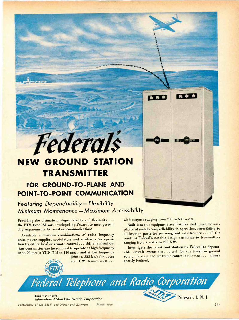
NEW GROUND STATIONTRANSMITTER
FOR GROUND -TO -PLANE ANDPOINT-TO-POINT COMMUNICATIONFeaturing Dependability - FlexibilityMinimum Maintenance - Maximum Accessibility
Providing the ultimate in dependability and flexibility . . .
the FTR type 184 was developed by Federal to meet presentday requirements for aviation communications.
Available in various combinations of radio frequencyunits, power supplies, modulators and auxiliaries for opera-tion by either local or remote control . . . this advanced de-sign transmitter can be supplied to operate at high frequency(2 to 20 mcs.); VHF (108 to 140 mcs,) and at low frequency
(200 to '525 kc.) for voiceand CW transmission . . .E
FTROp
O
0 0 0 0
111111111.1111111111111110111111111,
with outputs ranging from 200 to 500 watts.Built into this equipment are features that make for sim-
plicity of installation, reliability in operation, accessibility toall interior parts for servicing and maintenance . . . all theresult of Federal's notable design technique in transmittersranging from 2 watts to 200 KW.
Investigate this latest contribution by Federal to depend-able aircraft operations . . . and for the finest in groundcommunication and air traffic control equipment . . . alwaysspecify Federal.
Federal Telephone and Radio CotporatiomExport Distributor:International Standard Electric Corporation
Proceedings of the and Waves and Electrons March, 1996
Newark 1, N. J.
51h

SENSITIVE
R -F VOLTMETER
and
Wide Band Amplifier
MODEL 304
RANGE-.001 to 100 volts
FREQUENCY -30 c.p.s. to 5.5 Megacyles, + 0.5 DB
INPUT IMPEDANCE -1 Megohm shunted by 9 mmfds.
Probe method of connection provides true indicationof voltages at point of origin. Logarithmic outputmeter yields simplicity and accuracy of readings asdemonstrated by our voltmeter line for over ten years.Illuminated scale is further aid to observation.
A -C output connector and change -over switch affordsseparate wide -band amplifier capable of many uses.Example: extends useful range of ordinary oscillo-scopes to beyond 5 megacycles.
Send for Bulletin for further description
13.ALLANTI1E LABORATORIES, INC.BOONTON, NEW JERSEY, U. S. A.
(Continued from page 48A)
Fite, A. S., Jr., 7 W. Afton Ave., Yardley,Pa.
Friedman, B., 161 Monroe St., New York2, N. Y.
Gaddis, L. L., 4708-30 St., S., Arlington,Va.
Gavriel, S. N., 195 Cross St., Lowell,Mass.
Gilbert, J. N., 2805 Ontario St., Knoxville15, Tenn.
Gill, H. C., 495 Dundas St., London, Ont.,Canada
Glagow, G., St. Walburg, Sask., CanadaGraff, B. J., Jr., 376 W. 10 St., San Pedro,
Calif.Greer, P. A., Box 175, Fairforest, S. C.Guthrie, R. L., Aeradio Station, Blenheim,
New ZealandHackley, G. E., 109-14 St., Garden City,
L. I., N. Y.Hahn, N. G., 236 E. Sunset Court, Madi-
son 5, Wis.Hall, T. W., 30 Fulham Ave., Winnipeg,
Manit., CanadaHallick, F. J., 3 Government Rd. W.,
Kirkland Lake, Ont., CanadaHamme, R. J., 6524 Woodland Ave.,
Philadelphia 43, Pa.Hannum, E. W., 549 South Dr., Miami
Springs, Fla.Harold, M., 9 E. 193 St., Bronx, N. Y.Harvey, S. A., Box 219, Anchorage, AlaskaHarz, E. W., 127 E. 3 St., Lansdale, Pa.Hawes, A. R., 220 Lexington Ave., Cam-
bridge 38, Mass.Hawley, F. S., 1215 Jackson St., Toledo 2,
OhioHayden, L. C., 9463 T.S.U., Sig. C,
R.P.U. Det., Box 462, Herndon,Va.
Heinrich, R. E., 686 Hamlet St., Colum-bus 8, Ohio
Hendry, A. J., 3211-24 Ave. S., Min-neapolis 6, Minn.
Hodgkinson, T. E., 2YA Titahi Bay, Wel-lington, New Zealand
Horton, J. R., WBIR, 406 W. Church St.,Knoxville, Tenn.
Hovey, D. P., 45-Second St., HamdenConn.
Howe, J. S., 3354 S. Hamilton Ave., Chi-cago 8, Ill.
Hubbard, V. Y., c/o Chiu, 304 W. 11St., New York 14, N. Y.
Hyder, H. R., III, 301 E. 44 St., NewYork 17, N. Y.
James, E., Box 148, Tonagnoxie, Kan. .
James, M. B., 3403-28 St. W., Seattle 99,Wash.
Jeffery, A. D., Chez-Nous, Green St.,Hazlemere, High Wycombe, Eng-land
Jones, H. H., 62, Worcester St., Stour -bridge, Worcs., England
Jones, R. J., 2939 N. Cramer St., Mil-waukee 11, Wis.
Karlskind, D. B., 60 Alfred Drowne Rd.,West Barrington, R. I.
Kinnear, H. E., 1176 Dominion St., Win-nipeg, Manit., Canada
(Continued on page 58A)
52. Proceeding: of the I.R.E. and Waves and Electrons March, 1946
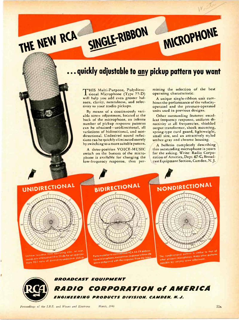
wok,01IF
. . quickly adjustable to any pickup pattern you want
Pr HIS Multi -Purpose, Polydirec-I tional Microphone (Type 77-D)
will help you add even greater bal-ance, clarity, naturalness, and selec-tivity to your studio pickups.
By means of a continuously vari-able screw adjustment, located at theback of the microphone, an infinitenumber of pickup response patternscan be obtained-unidirectional, allvariations of bidirectional, and non -directional. Undesired sound reflec-tions can be quickly eliminated merelyby switching to a more suitable pattern.
A three -position VOICE -MUSICswitch on the bottom of the micro-phone is available for changing thelow -frequency response, thus per -
UNIDIRECTIONAL
Uniform responsefrom operating
side. At rear,
sounds oreottenuoted 14 to 20 db for on approxi-
mate 10:1 ratio of desired -to-undesired pickup.
BIDIRECTIONAL
mitting the selection of the bestoperating characteristic.
A unique single -ribbon unit com-bines the performance of the velocity -operated and the pressure -operatedunits used in previous designs.
Other outstanding features: excel-.lent frequency response, uniform di-rectivity at all frequencies, shieldedoutput transformer, shock mounting,spring -type cord guard, lightweight,small size, and an attractively styledumber -gray and chrome housing.
A bulletin completely describinithis outstanding microphone is yoursfor the asking. Write: Radio Corpo-ration of America, Dept. 67-C, Broad -
\,,,.cast Equipment Section, Camden, N. J. )1
180
Pattern similorto conventional
RCA 44-BX bidirec-
tional microphone,except reor
response is three db
down compared with the responsefrom the front.
BROADCAST EQUIPMENT
NONDIRECTIONAL
Thenondirectionol pattern
A similar to that of
other pressure microphones.Many other patterns
possible by varying screw adjustment.
RAD/0 CORPORATION of AMERICAENGINEER/NO PRODUCTS DIVISION, CAMDEN, N. J.
Proceedings of the I.R.E. and IVaves and Electrons March, 1946
The following positions of interest toI.R.E. members have been reported asopen. Apply in writing, addressing replyto company mentioned or to Box No. ....
The Institute reserves the right to refuse anyannouncement without giving a reason forthe refusal.
PROCEEDINGS of the I.R.E.330 West 42nd Street, New York 18. N.Y.
SENIOR ENGINEER
Newly formed organization for manu-facture of radio receiver sets requires ex-perienced man to assume charge of pro-duction and general development. Must beable to lay out, set up, and properly equipmodern assembly line. New plant in NewYork area. Excellent opportunity forpermanent connection. All inquiriestreated confidential. Box 409.
RADIO AND ELECTRONICS ENGINEER
Manufacturer established since 1921 haspermanent opening for engineer capableof designing circuits and thoroughlyfamiliar with designing of condensers,sockets, jacks, plugs, etc. more from elec-trical than mechanical angle. Box 410.
RADIO SPEAKER ENGINEER
Position for a present chief engineer orassistant with confidence backed by ex-perience in design and economical produc-tion of radio speakers. Outstanding op-portunity to establish yourself as impor-tant member of our company. Salary andbonus. Eventual participation in companystock after proof of performance. Massa-chusetts location. Interview arranged atour expense. Write full details of ex-perience, past and present positions, earn-ings etc. to enable us to accurately judgeyou. Replies held confidential. Our menknow of this ad. Box 411.
ENGINEERSSeniors for design work onradio receivers, audio am-plifiers, television
Men with substantial commercial
experience wanted, preferably
those having Degrees in Electrical
or Communications Engineering.
Also Mechanical Engineer with
knowledge of radio set design to
supervise drafting and specifica-
tions. Write, giving details of ex-
perience and salary expected, to:
FREED RADIO CORP.
Makers of the famous.Freed-Eisemann Radio -
Phonograph
200 Hudson Street, New York 13,N.Y.
DESIGN ENGINEER
To design and develop production testequipment and fixture used to check R.F.coils and condensers. Knowledge and ex-perience on design of electronic test equip-ment essential and some radar experiencedesirable. Salary open. Location Newark.Box 412.
ASSISTANT CHIEF ENGINEER
Prominent Eastern radio set manufac-turer requires assistant chief engineer totake complete charge of laboratory. Mustbe thoroughly competent in AM and FMreceiver design ; also television; and pos-sess executive ability. Excellent salary andgood future. Write complete qualifica-tions and background. Box 408.
WANTEDGeneral Foreman For Tube Development ShopPosition now open in Engineering Department of RCA's Lancaster Plant. Workinvolves supervision of personnel engaged in developmental fabrication of all typesof Cathode Ray, Transmitting, Gas and Phototubes.
Applicants with previous background of tube manufacturing or engineering experi-ence preferred.
Apply in person or in writing to Personnel Department-RCA, Camden.
Salary dependent upon training and experience. Opportunities for advancement.
TECHNICAL EDITOR
Skilled in servicing electronic equip-ment, to assist in writing and editing arti-cles about radio repairing. Radio Mainte-nance Magazine, 295 Broadway, NewYork 7, N.Y.
SALES ENGINEER
Graduate electrical engineer to applyand sell small fractional horsepower mo-tors to industry. Work direct from salesoffice of established manufacturer inRochester, N.Y. Manufacturer's repre-sentatives not considered. State fully edu-cation, experience, age, and salary ex-pected. Box 322, Rochester 2, N.Y.
RADIO ENGINEERS
For design and development of homeradio receivers. Can use men with ex-perience in design laboratories on com-munications and entertainment receivingsets. Call or write Mr. Frank A. Hinners,Vice President in Charge of Engineering,Air King Products, 1523 63rd St., Brook-lyn 19, N.Y.
APPLIED PHYSICISTS, COMMUNICATIONAND ELECTRONICS ENGINEERS
Research minded with good theoreticalbackground to engage in research in aero-nautical science, advanced degrees pre-ferred. Salary commensurate with qualifi-cations. Address replies to Cornell Aero-nautical Laboratory, Personnel Office, Box56, Buffalo 5, N.Y. Replies will be held instrict confidence.
ACOUSTICAL ENGINEER
Primarily in the field of architecturalacoustics, who is qualified to determine theacoustical properties of broadcasting andrecording studios and to develop newmethods and equipment for the measure-ment of these characteristics. A workingknowledge of the acoustical problems as-sociated with microphones and loud-speakers is also necessary.
Applications and requests for inter-views should be made in writing to W. B.Lodge, Director of Engineering, ColumbiaBroadcasting System, Inc., New York 22,N.Y.
CHIEF MANAGING ENGINEER ANDRESEARCH ENGINEERS
Chief Managing Engineer to take fullcharge of a division of a large manufac-turing organization. Must have extensiveexperience in communications field, withsubstantial background in electronics andmicro -wave research and product develop-ment. Salary $12,000 to $15,000.
Research Engineers with thorough experi-ence in electronics, and micro -wave de-velopment. Salary $5,000 to $6,000.
Write qualifications to Boyd King, 10Rockefeller Plaza, New York 20, N.Y.
54A Proceedings of the I.R.E. and Waves and Electrons March, 1946
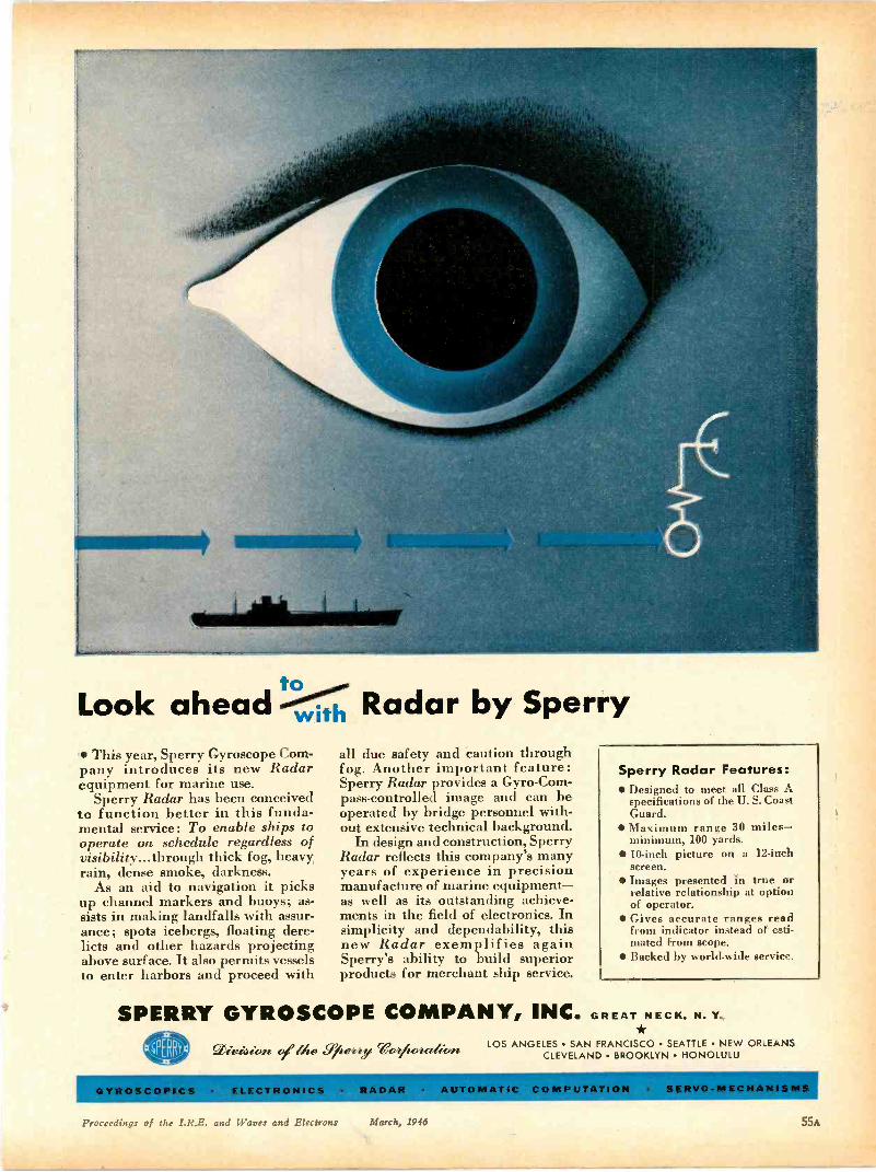
toLook ahead -1,ith Radar by Sperry This year, Sperry Gyroscope Com-pany introduces its new Radarequipment for marine use.
Sperry Radar has been conceivedto function better in this funda-mental service: To enable ships tooperate on schedule regardless ofvisibility...through thick fog, heavy,rain, dense smoke, darkness.
As an aid to navigation it picksup channel markers and buoys; as-sists in making landfalls with assur-ance; spots icebergs, floating dere-licts and other hazards projectingabove surface. It also permits vesselsto enter harbors and proceed with
all due safety and caution throughfog. Another important feature:Sperry Radar provides a Gyro -Com-pass -controlled image and can beoperated by bridge personnel with-out extensive technical background.
In design and construction, SperryRadar reflects this company's manyyears of experience in precisionmanufacture of marine equipment-as well as its outstanding achieve-ments in the field of electronics. Insimplicity and dependability, thisnew Radar exemplifies againSperry's ability to build superiorproducts for merchant ship service.
SPERRY GYROSCOPE COMPANY, INC.9401a451, ?ME eg5/84744, VO4Aflialf:OPt
Sperry Radar Features: Designed to meet all Class A
specifications of the U. S. CoastGuard.
Maximum range 30 miles-minimum, 100 yards.
10 -inch picture on a 12-incilscreen.
Images presented in true orrelative relationship at optionof operator.
Gives accurate ranges readfrom indicator instead of esti-mated from scope.
Backed by world-wide servic
GREAT NECK, N. Y.
LOS ANGELES SAN FRANCISCO SEATTLE NEWCLEVELAND BROOKLYN HONOLULU
OR -ERNS
Proceedings of the and Waves and Electrons March, 1946 55A
DUREZ
COATED
CAPACITORS
lAugeOiM-Int"mumum
1 I 1.11M1MM\11$
STAND-OFF CONDENSERS
CERAMICCAPACITORS
WIRE WOUNDRESISTORS
qampi!!!!!!!!!!!meenli!!!!!!!!1
CHOKE COILS
ELECTRICAL REACTANCECORPORATION
FR ANK LINVILLE, N.Y.
Positions WantedBy Armed Forces
Veterans
In order to give a reasonably equal op-portunity to all applicants, and to avoidovercrowding of the correspondingcolumn, the following rules have beenadopted
The Institute publishes free of chargenotices of positions wanted by I.R.E. mem-bers who are now in the Service or havereceived an honorable discharge within aperiod of one year. Such notices should nothave more than five lines. They may beinserted only after a lapse of one month ormore following a previous insertion, andthe maximum number of insertions isthree per year. The Institute necessarilyreserves the right to decline any announce-ment without assignment of reason.
RADIO ENGINEER
BSEE Purdue University. Age 26. Mar-ried. Four years experience design, de-velopment, production, test and installa-tion of electronic and microwave equip-ment. Box 6W.
EXECUTIVE ASSISTANT
M.I.T. trained electronics -radar officer,AAF, 26 years old, married. BA, MS de-grees Industrial Management. Experi-enced in supervision Loran, GCA, micro-wave equipment; also public accounting,budgets, costs. Available March. Box 7W.
ELECTRONICS TECHNICIAN
Age 25, married. Desires electronics re-search position preferably in Los Angelesarea. BS; First Phone license; experiencein broadcast, radar, and teaching. Authorarticles in RADIO and QST. E. M. Mc-Cormick, 3455 Lemon St., Riverside, Calif.
BROADCAST AND COMMUNICATIONSENGINEER
Pre-war resident in Middle East nowserving Royal Air Force and employed byForces Broadcasting Service (M.E.) insearch of congenial, responsible positionanywhere in world beginning winter 1946-47. Familiar aircraft radio installationsand conventional equipment. Offers toBM/ZC6, London W.C.1, England.
TECHNICIAN
Maintenance and repair, receiving andtransmitting equipment. Eleven years ex-perience. Discharged Chief Petty OfficerNavy, available immediately, work any-where. Carl Morris, P.O. 1094, Lexington,Ky.
POSITION WITH STATION
Young man, age 35, married, desiresposition with station contemplating expan-sion. Licensed since 1931. Nine years attransmitter before entering Navy. Ex-perienced installation and maintenancetransmitter and studio equipment. Navalexperience in materiel, VHF and FM. LosAngeles preferred. Box 1W.
Complete Your Filesof the
Proceedings of the I.R.E.Some back issues available
Each issue is priced at $1.00 butmembers of I.R.E. are given a25% discount and accreditedpublic and college libraries a50% discount. The followingissues are offered subject toprior sale.
1913-1915 Volumes 1-3Quarterly
1913 Vol. 1 January (a reprint)
1916-1926 Volumes 4-14Bimonthly
1917 Vol. 5
1918 Vol. 61919 Vol. 71920 Vol. 8
1921 Vol. 91922 Vol. 101923 Vol. 11
1924 Vol. 12
1925 Vol. 13
1926 Vol. 14
April, June, August,OctoberNoneDecemberApril, June, August,October, DecemberAll 6 issuesAll 6 issuesFebruary, April, June,August, DecemberAugust, October, De-cemberApril, June, August,October, DecemberAll 6 issues
1927-1938 Volumes 15-26Monthly
1927 Vol. 15 April, May, June, Oc-tober, December
1928 Vol. 16 February to December,inc.
1929 Vol. 17 April, May, June, No-vember
1930 Vol. 18 January, April to De-cember, inc.
1931 Vol. 19 All 12 issues1932 Vol. 20 January, March to De-
cember, inc.1933 Vol. 21 All 12 issues1934 Vol. 22 All 12 issues1935 Vol. 23 All 12 issues1936 Vol. 24 January to April, inc.,
June1937 Vol. 25 February to December,
inc.1938 Vol. 26 All 12 issues
1939-1945 Volumes 27-33Monthly
New Format-Large Size1939 Vol. 27 All 12 issues1940 Vol. 28 All 12 issues1941 Vol. 29 All 12 issues1942 Vol. 30 January, February, Ap-
ril, October to Dec.,inc.
1943 Vol. 31 February to December,inc.
1944 Vol. 32 January, February,July to December, inc.
1945 Vol. 33 All issuesRemittance should accompany
your order.Please do not send cash except by
registered mail
THE INSTITUTE OFRADIO ENGINEERS, INC.
330 West 42nd Street,New York 18, N.Y.
56A Proceedings of the I.R.E. and Waves and Electrons March, 1946

Presto Cutting Needles
in a "Trouble -Proof" Container
at to eztim coa
FOR YOUR CONVENIENCE! PrestoSapphire Recording Needles now come toyou in a new package, designed for utmostneedle protection in shipping and handling.
DRESTO Cutting Needles
'1" arepacked in a Distrib-
utor's Carton of six. Each
needle container is individ-
ually boxed with mailing
bag. Order a dozen. Keep
6 in use -6 in transit.
NEW! A transparent lucite con-tainer keeps Presto Cutting Needlessafe. Nothing can harm the precisionground point and cutting edges.
TIGHT! This ingenious chuckholds the needle tight-no chance ofdamage to the point in shipment.
EASY! Just slip used needles (safein their containers) into this handymailing bag and send them off toPresto for resharpening.
FREE! To Presto -equipped re-cording studios: a convenient rackholding six Presto Cutting Needles,with special "point -control" chartrecording number of hours each
needle is used.
RECORDING CORPORATION
242 W. 55th St., New York 19, N.Y.
WALTER P. DOWNS, LTD., in Canada
WORLD'S LARGEST MANUFACTURER OF INSTANTA-
NEOUS SOUND RECORDING EQUIPMENT AND DISCS
Proceedings of the I.R.E. and Waves and Electrons March, 1996 57A
ilROADENING the field of Crys-
tal Pickup Cartridge applications, Astatic has designed
Models L-73 and L-74 Cartridges to obtain all the ad-
vantages of crystal reproduction at higher operating
temperatures. These two cartridges, in Astatic's new
series, employ the new PN Crystal elements for applica-
tions not satisfactorily filled by the lower operatingtemperature limitation of Rochelle Salts Crystals. PN
Crystal elements, while having only one -tenth the in-
ternal capacitance of Rochelle Salts Crystal elements, do
not change capacitance with temperature. The safeoperating temperature for crystal cartridges has been
stepped up from 120° F. to 150° F., with the use of this
new war -born -and -developed Piezo active material.
These cartridges, while representing an im-portant contribution for certain applications,cannot be used as replacements for StandardRochelle Salts Crystal Cartridges unless the in-put circuit is changed and the amplifier gainadjusted to take care of the PN characteristic.
CORPORATIONCONNEAUT, OHIO
IN CANADA: CANADIAN ASTATIC LTD., TORONTO, ONTARIO
(Continued from page 52A)
Kleinberger, R. C., 20 Cushman Rd.,White Plains, N. Y.
Kroeger, F. B., 3827 Millsbrae Ave., Cin-cinnati 9, Ohio
Lagasse, J. E. M., 234 Winchester St.,St. James, Manit., Canada
Leinmond, C. Q., Box 349, YMCA,Schenectady 5, N. Y.
Lerner, S., 469 Burrows Ave., Winnipeg,Manit., Canada
Luno, P., 235; Egerton St., London, Ont.,Canada
Martin, J. G., Calle del Barco No. 31,Madrid, Spain
Masson, F. Y., 340 Cleveland St., Orange,N. J.
McBride, J. D., CFOR, Orillia, Ont.,Canada
McCarthy, J. E., Box 382, Barnesville,Minn.
McCauley, A. R., Suydam Lane, Bayport,L. I., N. Y.
McClelland, A. B., 1189 CommonwealthAve., Allston 34, Mass.
McDonald, D. J., Bell Telephone Com-pany of Canada, Beaver Hall Bldg.,Montreal 1, Que., Canada
McIntire, G. \V., Box 663, Hagerstown,Md.
McKie, W. M., 77 Hallam St., Toronto,Ont., Canada
Malan, D. G., Box 8718 Johannesburg,South Africa
Meinema, H., 216 N. Harvey St., OakPark, Ill.
Mestery, S., 294 Fountain St., Winnipeg,Manit., Canada
Michael, F. R., 2125 St. James Pl., Phila-delphia 3, Pa.
Miller, B. J., National Bureau of Stand-ards, Washington 8, D. C.
Miller, L. H., 663 Yale St., Akron 11, OhioMiller, T. W., 184 Truman Ave., Yonkers
2, N. Y.Mills, G. J., 405 Winchester St., St. James,
Winnipeg, Manit., CanadaMitchell, W. J., Jr., 1815 S. 55 St., Phila-
delphia 43, Pa.Mojamdar, V. G., M.27, Railway Quart-
ers, Hubli, IndiaMullaney, F. C., 1328-A Seminary St.,
Key West, Fla.Murphy, J. L., 5810 Adeline St., Oakland,
Calif.Murray, H. J., Jr., 425 W. 118 St., New
York 27, N. Y.Myers, S. F., 247 Western Ave., Albany,
N. Y.Nauman, P. W., 4221-48 St., San Diego
5, Calif.Neck, H., Schartenrain 11, Wettingen,
SwitzerlandNilsson, B. N. A., Sandelsgatan 271, Stock-
holm, SwedenNolke, F.H., A.P.O. 757 c/o Postmaster,
New York, N. Y.Oldfield, R., 1 Plimsoll St., Sans Souci,
N.S.W., AustraliaOlson, D. C., 3005--39 Ave., S.W., Se-
attle 6, Wash.(Continued on Page 60A)
58A Proceedings of She I R.E. and Waves and Electrons March, 1946
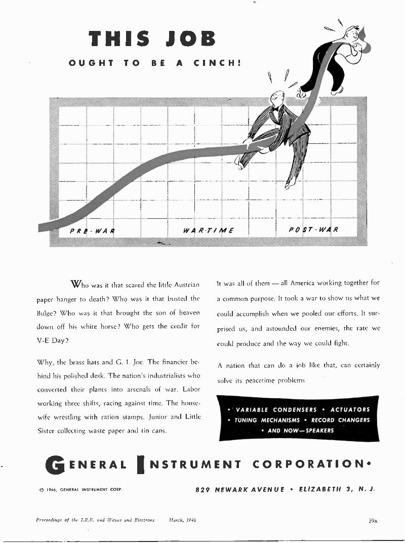
THIS JOBOUGHT TO BE A CINCH!
Who was it that scared the little Austrian
paper hanger to death? Who was it that busted the
Bulge? Who was it that brought the son of heaven
down off his white horse? Who gets the credit for
V -E Day?
Why, the brass hats and G. I. Joe. The financier be-
hind his polished desk. The nation's industrialists who
converted their plants into arsenals of war. Labor
working three shifts, racing against time. The house-
wife wrestling with ration stamps. Junior and Little
Sister collecting waste paper and tin cans.
It was all of them - all America working together for
a common purpose. It took a war to show us what we
could accomplish when we pooled our efforts. It sur-
prised us, and astounded our enemies, the rate we
could produce and the way we could fight.
A nation that can do a job like that, can certainly
solve its peacetime problems.
VARIABLE CONDENSERS ACTUATORS
TUNING MECHANISMS RECORD CHANGERS
AND NOW -SPEAKERS
GENERAL NSTRUMENT CORPORATION*
ID 1946, GENERAL INSTRUMENT CORP. 829 NEWARK AVENUE ELIZABETH 3, N. J,
Proceedings of the I.R.E. and Waves and Electrons March, 1916 59A
WILEY BOOKSIN COMMUNICATIONS -ELECTRONICS
These books will furnish the authoritative information necessaryto keep abreast of present-day scientific progress in Communi-cations-Electronics. Look over the important titles listed below.Then make your selection and order from the coupon today.
ELECTRON OPTICSand the ELECTRON MICROSCOPE
(1946)
By V. K. ZWORYKIN, G. A. MORTON, E. G. RAMBERG,J. HILLIER, A. W. VANCE
747 Pages $10.00
The new comprehensive guide to the electron microscope in all its phases. It isdesigned to aid the electron microscopist in understanding his instrument and inusing it to greatest advantage, and to present the practical and theoretical knowl-edge which must form the basis for further progress in electron microscope design.
HIGH VACUUM TECHNIQUE-Second EditionBy J. YARWOOD(1946) 140 Pages $2.75
Presents the theoretical and technical dataessential for an understanding of highvacuum work, including latest developmentsin apparatus, important individual processes, andfacts regarding the properties and uses of ma-terials encountered in all types of vacuum work.
PRINCIPLES OF INDUSTRIALPROCESS CONTROLBy DONALD P. ECKMAN(1945) 237 Pages $3.50A thorough and comprehensive treatment ofthe principles governing automatic control,emphasizing the basic principles necessary forindustrial instrumentation. Includes present-dayinformation on measuring characteristics of con-trollers, process load changes, multiple con-trol systems.
PRINCIPLES OF RADIO-Fifth EditionBy KEITH HENNEY(1945) 534 Pages $3.50Offers a working knowledge of the basicprinciples of radio communications. Starts withthe fundamental principles of electricity, andgradually develops the subject of radio practice.Thoroughly revised to include recent develop.ments and future methods.
FIELDS AND WAVESIN MODERN RADIOBy SIMON RAMO and JOHN R. WHINNERY(1944) 503 Pages. $5.00
An authoritative coverage of this field, requir-ing only a basic knowledge of elementary calculusand physics. Gives a rigorous account of thetechnique of applying field and wave theory tothe solution of modern radio problems.
HYPER AND ULTRA -HIGHFREQUENCY ENGINEERINGBy ROBERT I. SARBACHER andWILLIAM A. EDSON(1943) 644 Pages $5.50A practical treatment of an important new branch
JOHN WILEY & SONS, Inc., 440 Fo
of communications engineering, requiring nospecial advanced knowledge. Of value to the be-ginner, as well as to those having some fa-miliarity with the subject.
FUNDAMENTALS OF ELECTRIC WAVESBy HUGH H. SKILLING(1942) 186 Pages $2.75Discusses the principles of wave action as appliedto engineering practice, with particular emphasison the basic ideas of Maxwell's equations and re-peated use in simple examples; also on physicalconcepts and mathematical rigor.
APPLIED ELECTRONICSBy the ELECTRICAL ENGINEERING STAFF,Massachusetts Institute of Technology(1943) 772 Pages $6.50Provides a thorough understanding of the charac-teristics, ratings, and applicability of electronicdevices. Gives a working knowledge of the phy-sical phenomena involved in electronic conduc-tions plus its applications common to variousbranches of engineering.
PRINCIPLES OF ELECTRONICSBy ROYCE G. KLOEFFLER(1942) 175 Pages $2.50Tells clearly and simply the story of electrontheory and the operation of the electron tube.Beginning with the discovery of the electron andthe forces of attraction and repulsion of chargedparticles, the entire action taking place in elec-tronic devices is carefully explained.
HIGH FREQUENCY THERMIONIC TUBESBy A. F. HARVEY(1943) 244 Pages $3.00Gives the details of these important tubes anddescribes the experimental work that has been donewith them. Presents a thoroughly comprehensiveaccount of the properties of thermionic tubes atvery high frequencies and their relation to thoseof the associated electric circuits.
TIME BASES-(Scanning Generators)By 0. S. PUCKLE(1943) 204 Pages $2.75Covers the subject from both the design andthe development points of view; assembles moretime bases circuits than have heretofore beenavailable in one volume.
urth Ave., New York 16, N. Y.
On Approval CouponJOHN WILEY & SONS, INC.440 Fourth Ave.. New York 16, N.Y.Please send me on ten days' approval the books I have checked in this advertisement (or Iam attaching to this coupon a separate list of the books desired). At the end of that time, ifI decide to keep the books I will remit indicated price plus postage; otherwise I will re-turn the books postpaid. IRE -3-46
NameAddressCity and StateEmployed by
Approval offer not valid outside U.S. and Canada.
(Continued from page 58A)
Owen, R., 2 Circle Gordonston, Savannah,Ga.
Pace, T. L., 7 Div., Shop 863, USNAS,North Island, San Diego, Calif.
Padberg, L. R., Jr., 3705 Riviera Dr., SanDiego 9, Calif.
Palmisano, R. J., 1291 Durand Dr. N.E.,Atlanta, Ga.
Palmquist, C. A., 19 S. Broadway, Tarry-town, N. Y.
Parsons, C. B., C. B. Parsons and Com-pany, 119 Belmont Ave. N., Se-attle 2, Wash.
Parvex M., J., Teresa Vial 1370 (Corn-muna de San Miguel) Santiago,Chile
Payton, F. S., Ste. 11, River and OsborneApts., Winnipeg, Manit., Canada
Peters, G. A., 6 Ainslie St., Ashton Gate,Bristol 3, England
Petersen, P. B., 23 John St., Red Bank,N. J.
Pierce, J. F., 716 East End Avenue, Pitts-burgh 21, Pa.
Pierson, J. 60 E. 42 St., New York 17,N. Y.
Pillai, K. M. R., Divisional Engineer Tele-graphs, Dacca, India
Prugh, T. A., 552-18 St., S., Arlington,Va.
Quinn, J. M., 435 Breck St., Scranton, Pa.Rao, J., di. Raibahadur Dr. J. Rao, P. 0.
Chandnichowk, Cuttack, Orissa,India
Ramsell, J. L., Jr., 54 Undercliff Rd.,Millburn, N. J.
Reed, R. B., 518 S. 8 St., Ponca City,Okla.
Reguera Fernandez, J. J., Nicaro NickelCo., Nicaro, Oriente, Cuba
Rich, F. N., 315 W. 98 St., New York,N. Y.
Richardson, C. M., 69 Dale St., Waltham,Mass.
Robinson, C. S., Jr., 302 Passaic Ave.,Spring Lake, N. J.
Rokosz, A. J., 7 Bradford Rd., ValleyStream, L. I., N. Y.
Romero, R. F., 60 River Road, Cos Cob,Conn.
Ronson, H. T., Box 66, Matawan, N. J.Rossetti, A., 767 Milwaukee Ave., Chi-
cago 22, Ill.Rossetti, J., 767 Milwaukee Ave., Chicago
22, Ill.Schechter, C. W., Scenic Dr. RFD 2,
Muskegon, Mich.Schmidt, B. F., 3014 Nichols Ave., Wash-
ington 20, D. C.Scholes, W. R., 6917 N. 19 St., Phila-
delphia 26, Pa.Schulte, G. J., 1119 E. Indiana Ave.,
South Bend 14, Ind.Schupbach, R., Mellingerstrasse 35,
Baden, SwitzerlandSchwalbe, J. H., 2728 Kings Highway,
Brooklyn, N. Y.Scott, D. A., 108 Ocean Ave., Monmouth
Beach, N. J.Shary, R. F., 306 E. 207 St., Bronx 67,
N. Y.(Continued on page 62A)
60A Proceedings of the I.R.E. and Waves and Electrons March, 1946
V
KU- 672 627676 \ /N.
N \ % /N. \ l /
WL-2050/
WL- N.% /632A N % /
% /-. NN /
NO MATTER WHATELECTRONIC TUBESYOU NEED FORRESISTANCE WELDING
WESTINGHOUSECalf 457K:2 /Ea&
All of these standard Westinghouse tubes are carriedin your local Westinghouse distributor's stock.
For descriptive data on any of these tubes, write yournearest Vi'estinghouse office or Electronic Tube SalesDepartment, Westinghouse Electric Corporptilin,Bloomfield, N. J.
WL- WL-651/656 652/657
mn,655/658
WestinghouseProceedings of the I.R.E. and Waves and Electrons March, 1946 61A
/Nair/mapON THE TROUBLESHOOTER'S CHECK LIST
/1/149 PROUD OF Ir.
J -B -T Instrument Type Rotary Selector Switchesare available in 20 position SS -20 and 14 position.SS -14 models, one to six decks, non -shorting stand-ard, and shorting on special order.
. for these are the instrument and tester makers own switches, designed anddeveloped to meet the need for trouble -free, dependable performance in hardservice.
They are extensively used in high quality test equipment, portable instru-ments, in inspection set-ups, and experimental circuits.
Now, because of quantity production, they are in a price range which makesit sensible to consider them for many other electronic applications. And theyare available for immediate delivery. Your jobber probably has them instock by now.
ADVANTAGES:
RUGGED
COMPACT
VERSATILE
Rigid. 3 -post deck suspension; double -grip con-tacts, silver to silver; ball bearing indexing withberyllium copper spring; lugs staked for extrastrength.
14 or 20 positions in same space generally requiredfor 12 positions. Often eliminates need for otherswitches or extra decks.
Many variations. such as multiple circuits perdeck; four -pole, double -throw band selectors:unusual contact arrangements; non-standard stopand panel locators are being supplied on sub-stantial quantity runs.
J -B -T INSTRUMENTS, INC.423 CHAPEL STREET NEW HAVEN 8, CONNECTICUT
Membership(Continued from page 60A)
Sheer, S., 1150 Grand Concourse, Bronx56, N. Y.
Sillman, D., Hazeltine Electronics Cor-poration, 58-25 Little Neck Pkwy.,Little Neck, L. I., N. Y.
Simister, R. M., 179 Renefrew St., Win-nipeg, Manit., Canada
Simonson, H. E., 30 Powers Ave., SanFrancisco, Calif.
Smith, E. D. W., 986 Garfield St., Win-nipeg, Manit., Canada
Smith, F. J., 698 Banning St., Winnipeg,Manit., Canada
Smith, J. E., 13374 Cedar Rd., ClevelandHeights 18, Ohio
Solar, J. J., Nueva York 54, Oficina 1,Santiago, Chile
Southall, A. A., Lloyds Bank, Ltd., Lom-bard St., London, England
Steinman, B., W., 150 W. 21St., New York11, N. Y.
Stone, E. J., 260 Eldred St., Battle Creek,Mich.
Storey, A. E., 27 Portland Ave., Baldwin,L. I., N. Y.
Stratton, H. E.,Jr., 427 S. Garden St.,Visalia, if.
Szumal, L. J., Philco Engineering, C andTioga Sts., Philadelphia, Pa.
Theofil, D. V., 1109 Prospect St., AnnArbor, Mich.
Thomas, R. D., Agnes Apts., Agnes andEllice Ave., Winnipeg, Manit.,Canada
Thomson, W. E., 2810 Erie St, S. E.,Washington 20, D. C.
Tison, J. B., 4616 Virginia Ave., Tampa,Fla.
Townsend, J. W., Box 271, Davis, Calif.Turkish, M. C. 9771 French Rd., Detroit
13, Mich.Viles, F. M., Jr., 1929-26 Ave., Oakland
1, Calif.Weber, P. H., 452 Winchester St., St.
James, Manit., CanadaWeeks, I. B., Box 654, Dickinson, N. D.Weinstein, D. C., 1414 St. Marks Ave.,
Brooklyn 33, N. Y.Weiss, H. R., 5222-A Von Phul St., St.
Louis 7, Mo.Welch, E., RFD 1, Lock Haven, Pa.Werthen, H. L. 0., Rindogatan 11',
Stockholm, SwedenWilliams, J., Canadian General Electric,
265 Notre Dame Ave., Winnipeg,Manit., Canada
Wilson, R., 337 Walsgrave Rd., Coventry,Wachs., England
Winnik, E., 255 Machray Ave., Winnipeg,Manit., Canada
Winter, H. L., Gore Bay, Ont., CanadaWolfe, I. P., 224 Main St., Poughkeepsie,
N. Y.Wolff, M., 2902 N. Sawyer Ave., Chicago
18, Ill.Wolfson, N., 1375 Ocean Ave., Brooklyn
30, N. Y.Yorke, C. J., 24 Rattle St., London, Ont.,
CanadaWorobec, W. N., Bellevue, Alta., CanadaYu, Y. Y., Central Broadcasting Admini-
stration, Chungking, ChinaZender, J. F., 567 Arlington St., Win-
nipeg, Manit., Canada
62A Proceedings of the I.R.E. and Waves and Electrons March, 1946

4
OfA11 Radio
Manufacturers-Electronic at the
who exhibited
WIER
ECNNICA1MEEIING
HotelAstor,
New York
(who use metalcabinets,
chassis,housings,
etc)
CUSIOMERS i
Of.ARE
OR? tal PRODUCISCO.
tic
MAYWE SERVE
YOU,TOO?
KAR METAL PRODUCTS CO., INC.117 -30th Street. Brooklyn 32. N. Y.
Wea&trz Vie:Amen an <rhea'e/f4talProceedings of the I.R.E. and Waves and Electrons March, 1946
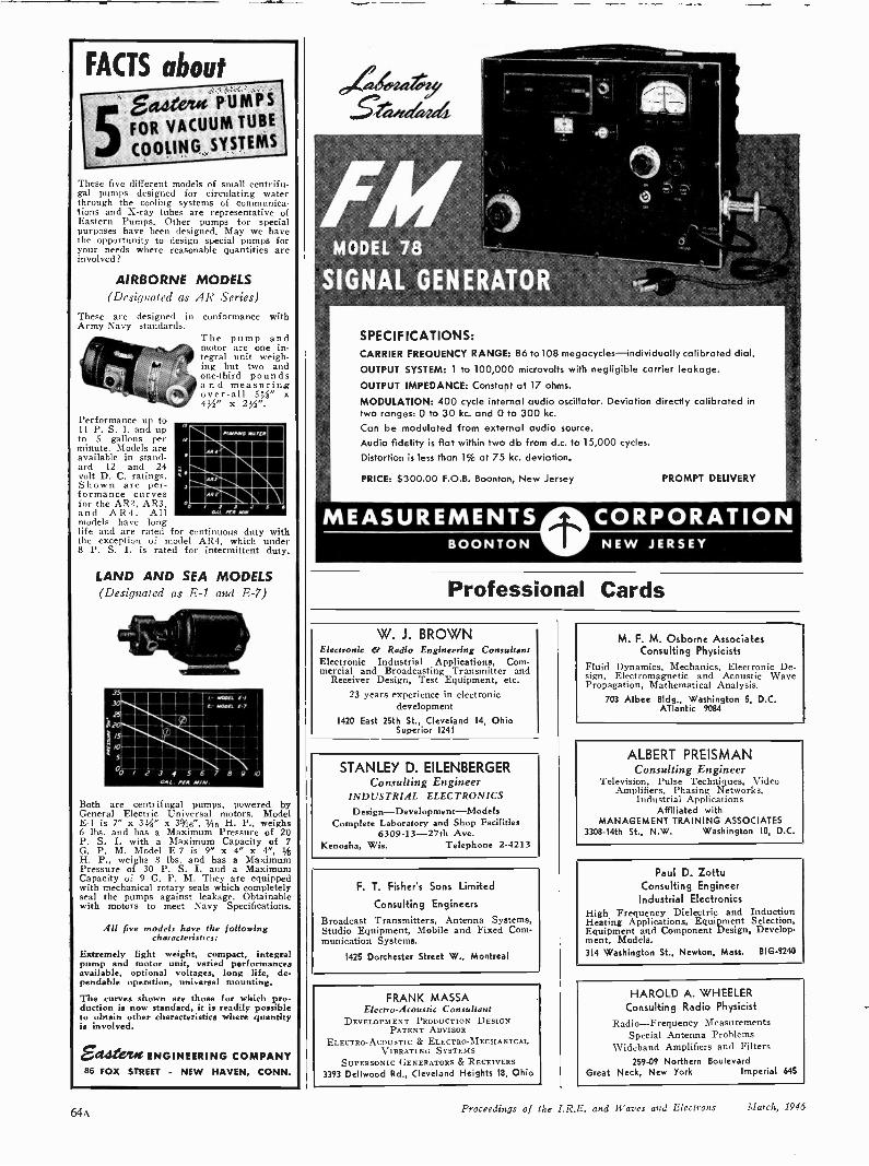
FACTS about
5EaAtreita PUMPSFOR VACUUM TUBE
COOLING SYSTEMS
These five different models of small centrifu-gal pumps designed for circulating waterthrough the cooling systems of communica-tions and X-ray tubes are representative ofEastern Pumps. Other pumps for specialpurposes have been designed. May we havethe opportunity to design special pumps foryour needs where reasonable quantities areinvolved?
AIRBORNE MODELS(Designated as AR Series)
These are designed in conformance withArmy -Navy standards.
Performance up to11 P. S. I. and upto 5 gallons perminute. Models areavailable in stand-ard 12 and 24volt D. C. ratings.Shown are per-formance curvesfor the AR2, AR3,and AR4. Allmodels have longlife and are rated for continuous duty withthe exception of model AR4, which under8 P. S. I. is rated for intermittent duty.
The pump andmotor are one in-tegral unit weigh-ing but two andone-third poundsand measuringover-all 5%" x4%" x 254".
PAC KR MW
LAND AND SEA MODELS(Designated as E-1 and E-7)
Both are centrifugal pumps, powered byGeneral Electric Universal motors. ModelE-1 is 7" x 33-i" x 3Ehe, H. P., weighs(, lbs. and has a Maximum Pressure of 20P. S. I. with a Maximum Capacity of 7G. P. M. Model E-7 is 9" x 4" x 4", 1As
II. P., weighs 8 lbs. and has a MaximumPressure of 30 P. S. I. and a MaximumCapacity of 9 G. P. M. They are equippedwith mechanical rotary seals which completelyseal the pumps against leakage. Obtainablewith motors to meet Navy Specifications.
All five models have the followingcharacteristics:
Extremely light weight, compact, integralpump and motor unit, varied performancesavailable, optional voltages, long life, de-pendable operation, universal mounting.The curves shown are those for which pro-duction is now standard, it is readily possibleto obtain other characteristics where quantityis involved.
ECUte,EM ENGINEERING COMPANY86 FOX STREET - NEW HAVEN, CONN.
MODEL 78
SIGNAL GENERATOR
SPECIFICATIONS:CARRIER FREQUENCY RANGE: 86 to 108 megacycles-individually calibrated dial.OUTPUT SYSTEM: 1 to 100,000 microvolts with negligible carrier leakage.OUTPUT IMPEDANCE: Constant at 17 ohms.
MODULATION: 400 cycle internal audio oscillator. Deviation directly calibrated intwo ranges: 0 to 30 kc. and 0 to 300 kc.Can be modulated from external audio source.Audio fidelity is flat within two db from d.c. to 15,000 cycles.Distortion is less than 1% at 75 kc. deviation.
PRICE: $300.00 F.O.B. Boonton, New Jersey PROMPT DELIVERY
MEASUREMENTS CORPORATIONBOONTON V NEW JERSEY
Professional Cards
W. J. BROWNElectronic & Radio Engineering ConsultantElectronic Industrial Applications, Com-mercial and Broadcasting Transmitter and
Receiver Design, Test Equipment, etc.23 years experience in electronic
development1420 East 25th St., Cleveland 14, Ohio
Superior 1241
STANLEY D. EILENBERGERConsulting Engineer
INDUSTRIAL ELECTRONICSDesign-Development-Models
Complete Laboratory and Shop Facilities6309 -13 -27th Ave.
Kenosha, Wis. Telephone 2-4213
F. T. Fisher's Sons Limited
Consulting Engineers
Broadcast Transmitters, Antenna Systems,Studio Equipment, Mobile and Fixed Com-munication Systems.
1425 Dorchester Street W., Montreal
FRANK MASSAElectro- Acoustic Consultant
DEVELOPMENT PRODUCTION DESIGNPATENT ADVISOR
ELECTRO-ACOUSTIC & ELECTRO-MECIIANICALVIBRATING SYSTEMS
SUPERSONIC GENERATORS & RECEIVERS3393 Dellwood Rd., Cleveland Heights IS, Ohio
M. F. M. Osborne AssociatesConsulting Physicists
Fluid Dynamics, Mechanics, Electronic De-sign, Electromagnetic and Acoustic WavePropagation, Mathematical Analysis.
703 Albee Bldg., Washington 5, D.C.ATlantic 9084
ALBERT PREISMANConsulting Engineer
Television, Pulse Techniques, VideoAmplifiers, Phasing Networks,
Industrial ApplicationsAffiliated with
MANAGEMENT TRAINING ASSOCIATES3308 -14th St., N.W. Washington 10, D.C.
Paul D. ZottuConsulting EngineerIndustrial Electronics
High Frequency Dielectric and InductionHeating Applications, Equipment Selection,Equipment and Component Design, Develop-ment, Models.314 Washington St., Newton, Mass. BIG -9240
HAROLD A. WHEELERConsulting Radio Physicist
Radio-Frequency MeasurementsSpecial Antenna Problems
Wideband Amplifiers and Filters259-09 Northern Boulevard
Great Neck, New York Imperial 645
64:\ Proceedings of the I.R.E. and Waves and Electrons March, 1946
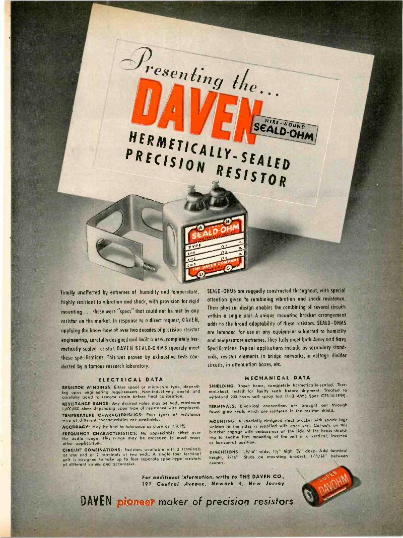
TYPE',Toe
Totally unaffected by extremes of humidity and temperature,
highly resistant to vibration and shock, with provision br rigid
mounting ... these were "specs" that could not be met by any
resistor an the market. In response to a direct request, DAVE N,
applying the know-how of over two decades of precision resistor
engireering, carefully designed and built a new, completely her-
metically -sealed resistor. DAY EN S E AL D-0 H M S squarely meet
these spaifications. This was proven by exhaustive teits con-
ducted by a famous research laboratory.
ELECTRICAL DATARESISTOR WINDINGS: Either spool or mica -card type, depend-ing upon engineering requirements. Non -inductively wound andcarefully aged to remove strain before final calibration.RESISTANCE RANGE: Any desired value may be had: maximum1,600000 ohms depending upon type of resistance wire employed.
TEMPERATURE CHARACTERISTICS: Four types of resistancewire of different characteristics are available.ACCURACY: May be had to tolerance as close as 10.1%.
FREQUENCY CHARACTERISTICS: No appreciable effect overthe lud o range. This range may be exceeded to meet manyother applications.CIRCUIT COMBINATIONS: Resistors available with 2 terminalsat one end or 2 terminals at two ends. A single tour terminalunit is cesigned to take up to four separate spool.type resistorsof different values and accuracies.
SEALD-OHMS are ruggedly constructed throughout, with special
attention given to combining vibration and shock resistance.
Their physical design enables the combining of several circuits
within a single unit. A unique mounting bracket arrangement
adds to the broad adaptability of these resistors. SEALD - OHMS
are intended for use in any equipment subjected to humidity
and temperature extremes. They fully meet both Army and Navy
Specifications. Typical applications include as secondary stand-
ards, resistor elements in bridge networks, in voltage divider
circuits, in attenuation boxes, etc.
MECHANICAL DATASHIELDING: Drawn brass, completely hermetically -sealed. Ther-mal -shock tested for faulty seals before shipment. Treated towithstand 200 hours salt spray test (f-13 AWS Spec C7S.16-1944).
TERMINALS: Electrical connections are brought out throughfused glass seals which ore soldered in the resistor shield.
MOUNTING: A specially designed steel bracket with spode lugswelded to the sides is supplied with each unit. Cut-outs on thisbracket engage with embossings on the side of the brass shield-ing to enable fi-m mounting of the unit in a vertical, invertedor horizontal position.
DIMENSIONS: 19/16" wide, 11/2" high, 7/8" deep. Add terminalheight, 9/16" studs on mounting bracket, 1-11/16" between
centers.
For additional nformation, write to THE DAVEN CO.,191 Central Avenue. Newark 4, New Jersey
maker of precision resistors
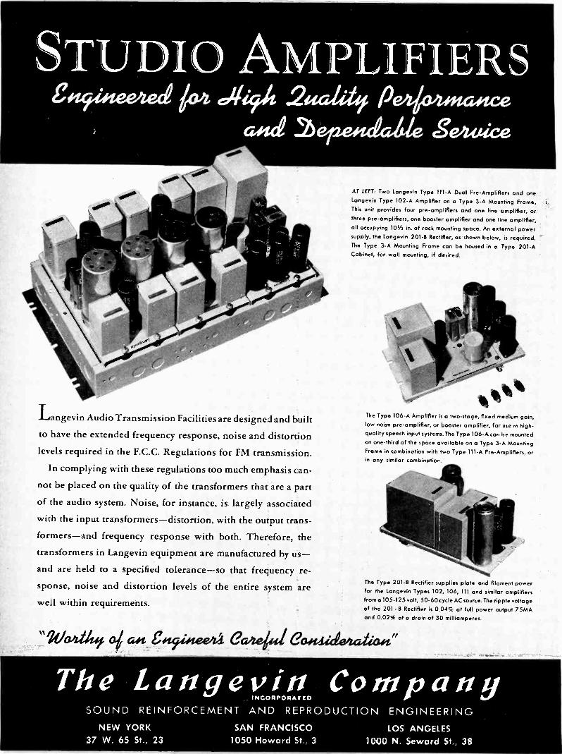
STUDIO AMPLIFIERS104, 444, .2ualikt
2.T.encialAle gWtaice,
Langevin Audio Transmission Facilities are designed and built
to have the extended frequency response, noise and distortion
levels required in the F.C.C. Regulations for FM transmission.
In complying with these regulations too much emphasis can-
not be placed on the quality of the transformers that are a part
of :he audio system. Noise, for instance, is largely associated
with the input transformers-distortion, with the output trans-
formers-and frequency response with both. Therefore, thetransformers in Langevin equipment are manufactured by us-and are held to a specified tolerance-so that frequency re-
sponse, noise and distortion levels of the entire system arewell within requirements.
It
AT LEFT: Two Langevin Type 111-A Dual Pre -Amplifiers and oneLangevin Type 102-A Amplifier on a Type 3-A Mounting Frame.This unit provides four pre -amplifiers and one line amplifier, orthree pre -amplifiers, one booster amplifier and one line amplifier,all occupying 101/2 in. of rack mounting space. An external power
supply, the Langevin 201-B Rectifier, as shown below, is required.The Type 3-A Mounting Frame can be housed in a Type 201-ACabinet, for wall mounting, if desired.
The Type 106-A Amplifier is a two -stage, fixed medium gain,
low noise pre -amplifier, or booster amplifier, for use in high -quality speech input systems. The Type 106-A can be mounted
on one-third of the space available on a Type 3-A MountingFrame in combination with two Type 111-A Pre -Amplifiers, orin any similar combination.
The Type 201-B Rectifier supplies plate and filament powerfor the Langevin Types 102, 106, 111 and similar amplifiersfrom a 105.125 volt, 50-60 cycle AC source. The ripple voltage
of the 201 - B Rectifier is 0.04% at full power output 75MAand 0.02% at a drain of 30 milliamperes.
e.finewth. ea 44.1 e0.4.4492.4:."
The Langevin CompanyINCORPORATED
SOUND REINFORCEMENT AND REPRODUCTION ENGINEERINGNEW YORK SAN FRANCISCO LOS ANGELES
37 W. 65 St., 23 1050 Howard St., 3 1000 N. Seward St 38
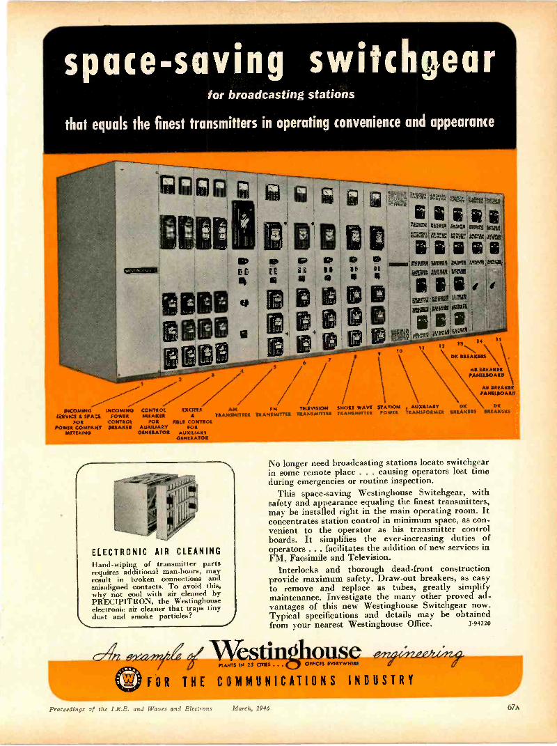
space -saving switchgearfor broadcasting stations
that equals the finest transmitters in operating convenience and appearance
U
DICO/AING INCOMING CONTROL EXCITER AMSERVICE 4 SPA= POWER DREAKER A TRANSIMITIR
FOR CONTROL FOR !FULD CONTROLPOWER COMPANY CREAM AUXILIARY FOR
ALETERINO GENERATOR AUXKIARYGENERATOR
E EE
aCe Ce mum MP! (491111 .1S7r11 tvr+P4
CCID DO DO belle IMP myII 4 gi 111 Slid
seu awl ;4-4,4OW PAW Mini
0"1 awasuivi
111 ati,Itret MiT; KAI1.171' CMIC f C.Mt, a 7-$1 AVZ
1/ a
10 11 12 13 14 16
DK SNEAKERS
AR DREAMPANELTIOARD
FM TELEVISION SHORT WAVE STATION AUXILIARY DK
TRANSMITTER TRANSMITTER TRANSMITTER POWER TRANSFORMER BREAKERS
Al IREAKERPANELEIOARD
12KBREAKERS
ELECTRONIC AIR CLEANINGHand -wiping of transmitter partsrequires additional man-hours, mayresult in broken connections andmisaligned contacts. To avoid this,why not cool with air cleaned byPRECIPITRON, the Westinghouseelectronic air cleaner that traps tinydust and smoke particles?
No longer need broadcasting stations locate switchgearin some remote place . . . causing operators lost timeduring emergencies or routine inspection.
This space -saving Westinghouse Switchgear, withsafety and appearance equaling the finest transmitters,may be installed right in the main operating room. Itconcentrates station control in minimum space, as con-venient to the operator as his transmitter controlboards. It simplifies the ever-increasing duties ofoperators . . . facilitates the addition of new services inFM, Facsimile and Television.
Interlocks and thorough dead -front constructionprovide maximum safety. Draw -out breakers, as easyto remove and replace as tubes, greatly simplifymaintenance. Investigate the many other proved ad-vantages of this new Westinghouse Switchgear now.Typical specifications and details may be obtainedfrom your nearest Westinghouse Office. J-94720
Westin housePLANTS IN 23 CITIES . . OFFICES EVERYWHERE
FOR THE COMMUNICATIONS INDUSTRY
Pro 67A
Remler Appointedas Agent for
R.F.C.
. . to handle and sell gov-ernment owned electronicequipment released forcivilian use.
Write for Bulletin Z-1
listing a wide variety ofequipment covering entireelectronic field.
Remler Co., Ltd. 2101 Bryant St.San Francisco 11, Calif.
REMLERSINCE 1918
Communications Electronics
Try "The house thatSERVICE built!" Our stocksare big-our deliveries, ex-tra -fast.
We've been at it since 1925-and we know how!
. L. IDA1_11%. ISA .Wholesale Distributors
RADIO -ELECTRONIC SUPPLIES 8 PARTS17 Union Square
NEW YORK 3, N. Y.Phones: ALgonquin 4-8112-3-4-5-6-7
Newsand New Products
New Series of MidgetSensitive Relays
Kurman Electric Company, 35-1837th Street, Long Island City 1, N. Y. announces a new line of midget relays, series13, featuring .035 -watt sensitivity in acompact 1 ounce -unit.
This relay is designed for low currentoperation under conditions where spaceand weight are limited. A balanced arma-ture construction assures stability at highspeed operation in all positions. It isclaimed that the coil will safely stand 1
watt without overheating.The contacts are single -pole, double -
throw and are rated to carry I. amp. 110volts A.C. non -inductive load. The approx-imate dimensions of the relay are 1 ,' long,
wide and 1' high overall.A coil may be selected for any D.C.
input voltage between .04 and 40 volts.Additional information may be had fromthe manufacturer, by requesting bulletin1346.
Sylvania Acquires WabashWill Operate Wabash Company
as Independent SubsidiaryWalter E. Poor, (Associate IRE A'29),
President of Sylvania Electric Products,Inc., has announced that the WabashAppliance Corporation, one of the largestindependent manufacturers of photoflashand incandescent lamps, would merge withthe Wabash Photolamp Corporation andBirdseye Electric Corporation to become awholly -owned but independently operatedSylvania subsidiary. A. M. Parker remainsas president and general manager ofWabash with headquarters at Brooklyn,N. Y. Sales staffs, sales policies, productbrands and distribution outlets remain un-changed.
The Brooklyn plant will continue man-ufacture of photolamps, incandescentlamps, reflector lamps and infra -red heatlamps, with augmented production of lightconditioning and other standard lightbulbs. Additional factory units planned
(Continued on page 78)
EBY#60
SPEAKERCONNECTORS
SAVE APPROXIMATELY 25% IN ASSEMBLY TIME
Only 2 parts to Female Assembly:1. The bakelite casting.2. Eby patented snap -lock contacts.
Here's assembly speed! It's as simple as this:Attach contact to wire and push into cavity.Contact automatically locks in place.(Casting and contacts supplied unassembled./
Male Assembly - nickel -plated brass prongs.Bakelite casting - Standard arrangement for3, 4, and 5 prongs. Other arrangements tospecifications.
Wrie today for samples and prices.
Eby #60 Male and Female Speaker ConnectorsAre the Standard of the Industry
IF IT'S IN A CIRCUIT
... EBY COMPONENTS
AND SERVICES WILL
HELP YOU DO IT BETTER
HUGH H.
EBYINCORPORATED18 W. CHELTEN BLDG.
PHILA., PENNA.
68A Proceedings of the I.R.E. and Waves and Electrons March, 1946
*I0111 WO ni01111
**1161071,111111;"1:11.71.11;1. Silk
"IOC 11111.1.01.$
10%
*Ilit:EIS OW 111111.11S
Is a ot
* * Edited by Milton B. Sleeper * *
FREEwith your subscription to FMand TELEVISION MagazineFM and TELEVISION Magazine is
the business journal of the post-warradio industry. It is devoted exclu-sively to the two principal fields ofradio progress, development, andexpansion.
Now in its 6th year of publication,It has the well -deserved reputation ofbeing "The Complete and Authori-tative Source of Information on Fre-quency Modulation and Television.
Articles on FM cover the business,engineering, and operating aspects ofbroadcasting and communications,and the design, manufacture, andmerchandising of home receivers.plus analysis of FCC actions.
Television articles cover current de-velopments in equipment. installa-tions, methods, and techniques.Space devoted to television is beingincreased with the progress of the art.
Because the tremendous post-warradio expansion is concentrated inthese two fields. FM and TELEVISIONis essential reading for everyone con-nected with this industry. SubscribeNOW and get a FREE copy of the FMRadio Handbook.
The Most ImportantRADIO BOOKpublished in thelast 10 years-,
The StandardHandbook of
F M RADIOfor everyone engaged
in the Radio IndustryHere is the first and only book on post-
war FM broadcasting, home receivers, andcommunications. Edited by recognizedauthorities and written by engineers whoare specialists in their respective fields, thisStandard Handbook of FM Radio is a com-plete source of information for every en-gineer, executive, merchandiser, and tech-nician connected with the radio industry.It is a large book, 834 by 11N ins, hand-somely printed and beautifully illus-trated.
PARTIAL LIST OF CHAPTERS.
1. Background of Frequency Modulation.2. FM THEORY: Explained by originalcharts and diagrams, rather than math-ematics.3. FM BROADCASTING: All post-war prac-tice. covering transmitters, studios, STlinks, antennas, satellites, measurements.FCC standards, rules, and allocations.4. FM COMMUNICATIONS-Municipal andstate police systems. latest transmitters andreceivers, railroad installations, selectivecalling systems, antennas and directive ar-rays. relays, and FCC rules.5. FM HOME RECEIVERS-Post-war de-signs. schematics, installation notes, an-tennas. servicing, testing, alignment.6. FM FOR AMATEURS-Design of trans-mitters and receivers for amateur communi-cations.7. REFERENCE DATA-Allocations, propa-gation. antenna liability insurance, tubes,and directories of consulting engineers andattorneys, broadcast stations, emergencystations, manufacturers.
Treatment of these subjects coverstheory, design, planning, installation, op-eration, and maintenance of FM broad-cast stations, home receivers, and com-munications systems. Each subject istreated fully, and detailed with specialdrawings, large photographs.
This very complete data is on post-wardesigns and design practice, making theFM Handbook up-to-the-minute in everyrespect.
Broadcasters and communications ex-perts who have seen advanced proofs de-clare this the most practical, useful bookever published for everyone in the radioindustry. GET YOUR COPY AT ONCE!
$4.00in lifetime
librarypaperbound
binding edition .50
Order your FREE COPY NOW
FM andTELEVISION Magazine511 Fifth Avenue, New York 17, N. Y.
I Enter my[3 renewal 3 yrs.$6.00subscription for 1 yr. $3.00new
Add $1.00 per year foreign postage; 50c Canada: Isend me ABSOLUTELY FREE a copy of the newFM RADIO HANDBOOK "paper bound addition"
I Name
Street
City & Zone
My official position is:
Company
NOTE: If you want your FM RADIO HANDBOOKin the lifetime library binding, add $2.50 to the sub-
scription prices above. A
State
Proceedings of the I.R.E. and Waves and Electrons March, 1946 69A
PERFECTIONA fine-cut diamond is perfection in beauty andformation. But to you as a transformer -user,perfection lies in performance, day In, dayout, under the exacting conditions of yourparticular application.
Finest engineering talent and most com-plete electronic laboratories are ready toconsult with and help you with your problem-and to design and produce the transformerthat will give you perfection in performance.
"SPECIALIZED
ENGINEERS"
3223-9 W. ARMITAGE AVENUE
JUST PUBLISHEDThe Most Indispensable Reference in Radio -Electronics
Electronic Engineering Master Index
Cloth71/2" 5 101/2"
320 pages
A master compilation of over 15,000 titles of textsand articles selected for their value to the research en-gineer, this INDEX covers the years 1925.1945 andenables you to survey twenty years of research litera-ture on any subject in a matter of minutes!
Vitally Needed in Every Laboratory and Library
COMPLETE IN ONE VOLUME
PART I
January 1925 toDecember 1934
PART II
January 1935 toJune 1945
PARTIAL LIST OF PERIODICALS INDEXEDBell Laboratories RecordBell System Technical
JournalCommunicationsElectrical CommunicationElectronics
Electronic IndustriesJournal of I.E.E.
General Electric ReviewJournal of Applied
Physics
Proceedings I.R.E.Transactions of A.I.E.E.Radio NewsR.C.A. Review
Wireless Engineer
A $500 Reference Library in One Volume for $17.50Descriptive circular on request.
ELECTRONICS RESEARCH PUBLISHING COMPANY2 West 46th Street New York 19, N.Y.
Bindersfor the Proceedings
Protect your file
of copies against
damage and loss
Binders are available for those whodesire to protect their copies of thePROCEEDINGS with stiff covers. Eachbinder will accommodate the twelvemonthly issues published during theyear. These binders are of blue Span-ish grain fabricoid with gold letteringand will serve either as temporarytransfers or as permanent binders.They are so constructed that each indi-vidual copy of the PROCEEDINGS will lieflat when the pages are turned. Copiescan be removed from the binder in afew seconds and are not damaged bytheir insertion.
Available for both the old, smallsize PROCEEDINGS or the new, largesize (1939 to date).
Price: $2.50either size (specify which)
Postpaid to all countries
You may have a volume number oryour name stamped in gold for 50cents additional.
Remittance should accompanyyour order
THE INSTITUTE OFRADIO ENGINEERS, INC.
330 West 42nd Street,New York, N.Y.
70A Proceedings of the I.R.E. and Waves and Electrons March, 1946
no 1011111 -FORM DISTORTION
NOT THISWITH
SECO AUTOMATICVOLTAGE REGULATORS
IN designing electrical apparatus, theengineer not only specifies a definite operatingvoltage but also assumes that the wave -formof the specified voltage will be a sine wave.If these two factors are not considered, the
efficiency and utility of the equipment is drastically reduced if not completely eliminated. Althoughthe SECO automatic voltage regulator can not manufacture a sine wave, it will maintain a constantoutput voltage without -wave-for:n distortion regardless of variations in input voltage or outputload current.
Such desired performance is cbtained ay combining an electronic detector circuit with a motor -driven variable auto -transformer. There is no dependency on saturation of core material forregulating acti an. In direct contrast, the variable auto: -transformer together with its auxiliarytransformer are designed tc operate far below the saturation point assuring the zero wave -formcharacteristic.
This feature, plus mary other 3ecided advan:ages, has prompted the exclusive use of SECO regu-lators for countless appLcations. An investigation may prove it ideal for your particular requirement.
Send for Bulletins E R
SUPERIOR ELECTRIC COMPANY783 LAUREL STREET, BRISTOL, CONNECTICUTSTOCKED BY LEADING DISTRIBUTORS IN THE UNITED STATES AND CANADAProceedings of the and Waves and Elertrons March, 1946
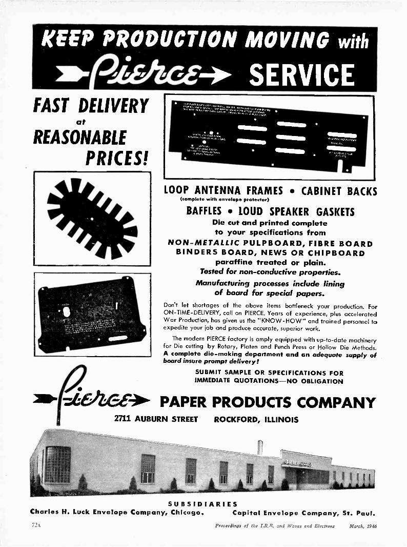
KEEP PRODUCTION MOVING with
ithzEi+ SERVICEFAST DELIVERY
REASONABLE
PRICES!IVI/CIVA,
CC.
lallnaggb
01111.1111111
MW/1111m 11111.11.11a 71,141,1 reeo
41.11111111,
LOOP ANTENNA FRAMES CABINET BACKS(complete with envelope protector)
BAFFLES LOUD SPEAKER GASKETSDie cut and printed completeto your specifications from
NON-METALLIC PULPBOARD, FIBRE BOARDBINDERS BOARD, NEWS OR CHIPBOARD
paraffine treated or plain.Tested for non-conductive properties.
Manufacturing processes include liningof board for special papers.
Don't let shortages of the above items bottleneck your production. ForON -TIME -DELIVERY, call on PIERCE. Years of experience, plus acceleratedWar Production, has given us the "KNOW-HOW" and trained personnel toexpedite your job and produce accurate, superior work.
The modern PIERCE factory is amply equipped with up-to-date machineryfor Die cutting by Rotary, Platen and Punch Press or Hollow Die Methods.A complete die -making department and an adequate supply ofboard insure prompt delivery!
SUBMIT SAMPLE OR SPECIFICATIONS FORIMMEDIATE QUOTATIONS-NO OBLIGATION
am- 7001Ce- PAPER PRODUCTS COMPANY2711 AUBURN STREET ROCKFORD, ILLINOIS
SUBSIDIARIESCharles H. Luck Envelope Company, Chicago. Capital Envelope Company, St. Paul.
Proceedings of the I.R.E. and Waves and Electrons March, 1946
PHASE SHIFT MODULATORS
FOR FM BROADCASTING
Before the war, REL was the only manufacturer of FM broadcast transmitters whoadvocated the use of the Phase -Shift method of producing Frequency Modulation. REL transmittershave always employed this method because of the very high order of stability and the low distortioncharacteristics that are inherent in the system.
111 t is with considerable pride, therefore, that we now find our judgment confirmedthrough the introduction to the art of crystal controlled, phase -shift arrangements that have beenengineered by other manufacturers. It is certain that their decision to adopt the basic principle of theArmstrong Modulator will be helpful to the FM industry as a whole.
We do not believe that the circuitry employed to produce a phase -shift is as importantas the recognition that the Phase Shift principle is the best. We do contend, however, that the per-formance and reliability of the dual channel Modulator by REL cannot be surpassed, and we predictthat the operating data on all systems that will soon become available to the industry will establishthis fact.
RELbuilt the first commercial Phase -Shift Modulator in 1938 and has built a substantialquantity of them during the last eight years. The experience gained over these years makes it possiblefor REL to offer the most advanced designs and insures the highest quality of performance andreliability.
PACIFIC CONorman B. Neely Er7422 Melrose AvenuHollywood 46, Calif
PIONEER MANL
Iina
MICHIGANLuffy & Co., Inc.Ind River Ave., W.Mich.
YING ARMSTRONG
Proceedings of the I.R.E. and Waves and ElecP 73A
ofea.ogs
11
1170111STON Process
Dire ...So line itCan he seen only
under high
We cancan draw wire assmall as
1 of an inch100,0001 in diameter
. . . available in Platinumand some other Metals
.00001" is less than 1/30 thediameter of the smallest wiredie commercially available.Yet our Wollaston Processwire (drawn in a silver jacket)closely meets your specifica-tions for diameter, resistanceand other characteristics.
This organization specializesin wire and ribbon of smallerthan commercial sizes andcloser than commercial toler-ances. Write for List of Products.
SIGMUND COHN & CO.
SINCE 1901
44 GOLD STREET NEW YORK 7
74A
AttentionAssociate
Members!
Many Associate Members can
qualify for higher membership
grades and should certainly do
so. Members are urged to keep
membership grade up in pace
with their present development.
An Associate over 24 years of
age who is occupied as a radio
engineer or scientist, and is in
this active practice three years
may qualify for Member Grade.
An Associate who has taught
college radio or allied subjects
may qualify.
Some may possibly qualify for
Senior Grade. But transfers can
be made only upon your appli-
cation. For fuller details request
transfer application -form in
writing or by using the coupon
below.
OREMAIT
AntennasAre Available
I
For All
Mobile
Installations
Premax Antennas andMountings are standard
equipment for numerous
municipalities, public utili-
ties and specal services. They
have been proven to be able
to take the hard usage ofrough roads and still bring in
the signals sharp and clear.
Available in "whip" types or
special tubular metal Anten-
nas, in either fixed or col-
lapsible styles.
Write for complete detailsand prices on the type of An-
tenna equipment you re-
quire.
Division Chisholm -Ryder Co., Inc.
4613 Highland Ave, Niagara Falls, N.Y.
'.E. and Waves and Electrons March, 1946
METAL ASSEMBLIES AND COMPONENTSFOR
ELECTRONIC AND MECHANICAL DEVICES
ENGINEERING
DEVELOPING
FABRICATING
ELECTRO-FORMING
PLATING
FINISHING
B ERNARD R ICE'S S ONSI N C O R P OR A T ED
MANUFACTURERS OF QUALITY METAL PRODUCTS SINCE 1867
OFFICE: 325 FIFTH AVENUE, NEW YORK 16, N.Y.WORKS: 139-145 NORTH TENTH STREET, BROOKLYN 11, N.Y.

4f SPECIALISTS INSPECIAL CRYSTALS
SPACE SAVING
FREQUENCY STABILITY
Especially suitable for applications forclose frequency tolerance . . . VHF ser-
vices - police, aircraft, railway com-munications, etc. . . . works on 6.3v at1 amp. . . . temp control within 3°C.
. . . operates at 60`C. . . . frequency
control of x.005%0 ... frequency range3MC to 14MC . fits octal socket .
Write Dept. I.R. for comprehensiveCatalog, "Selectronic Crystals."
LABORATORIES INC.29 ALLYN ST., HARTFORD, 3, CONN., PHONE 1-3215
THE MOST
WIDELY ACCEPTED PRECISION
RESISTOR IN THE WORLD!
MEPCO"TRU-TOLERANCE';
MEPCO. TRU-TOLERANCE" -
SiNDING POST TYPES
/6 PageGET YOURS
Contents: TRU TOLERANCE WOUND RESISTORS
PRECISION RESISTORS
PEW TERMINAt TYPES
C
I.F. and R.F. TRANSFORMERS and CHOKES TRIMMER CONDENSERS
LOOP ANTENNAE ELECTRONIC EQUIPMENT
MADISON ELECTRICAL PRODUCTS CORPORATION76 Main St., Madison, N. J,
I'd like a copy of your new catalog
I NAME TITLE
I COMPANY
I ADDRESS
"BAND HOPPERS"
TURRETS
ANTENNA COILS
From amateurradio types
to units for
broadcast,r -f heating and other elec-
tronic uses,B W offers a complete
line of AIR INDUCTORSand assenl-
blies for practicallyevery require
ment.Same
sendto your specifications
on request,or send details
of your
applicationfor recommendation
based
on standardPi & Vc/ Inductor
type.
BARKER &WI LLIAMSON"Inductor Headquarters "
Dept. IR-36 235 Fairfield AvenueUpper Darby, Penna.
76A Proceedings of the I.R.E. and Waves and Electrons March, 1946

...JOHNSON
COMPONENTS PICKED
FOR USE IN AIRLINE
TRANSMITTER I
The new Wilcox 99A, medium power, trans-mitter designed primarily for airline fixed com-munication service, is provided with features in-cluding four removable radio frequency channelsin the low, high and very high frequency ranges.
Shown above is one of ther.f. channels with Johnsoncomponents highlighted ...Type D dual condensers inthe antenna tuning and finalamplifier stages, Type Fcondenser in the r.f. ampli-fier, cone insulators andthru-panel insulators withjack connections. None visi-ble in the photograph areJohnson 211 and 237 tubesockets, lead-in bushingsand panel bearings.
The use of Johnson compo-nents in the Wilcox 99A isfurther proof of the relia-
WILCOX 99ATRANSMITTER
bility of Johnson products. In a transmitter of thistype, designed for flexible and trouble -free serv-ice, components must meet the highest standardsof quality and adaptability.The adaptability of Johnson products results ingreat savings to Johnson customers by minimizingthe need for specially designed components. Forexample, the Type D dual condensers used in theassembly shown above are standard models re-duced in overall size and supplied with specialmounting brackets to meet chassis design. Thestandard Type D used in the final amplifier hasbeen furnished with dual sections of differentcapacitances, thus eliminating the need for aspecial condenser.
Whether you are working on a "ham rig," elec-tronic heating equipment, commercial transmitteror any other radio electronic device, you will besure of top performance with components byJohnson. Send us your special problems and wewill first try to adapt our standard products tomeet your special requirements.
R. F. CAPACITORS AND INDUCTORS TUBE SOCKETS INSULATORSCONNECTORS PILOT LIGHTS HARDWARE ITEMS
WRITE FOR SPECIFIC INFORMATIONOR GENERAL PRODUCTS CATALOG 968A
E. F. JOHNSON COMPANY WASECA MINNESOTAProceedings of Lhe 1.k.E. and IVaves and Electrons March, 1946
77

Try C.T.C.'s NewIF SLUG TUNED INDUCTOR COIL
With a frequency range from I.1 megacycle to 60 megacycles anda slug tuning range from 1.5.1 in frequency, this tiny, compact LS 3is ideal for many applications.
Be sure to specify the inductance or capacitance and frequencyrequired when ordering the LS. 3.
Write for C.T.C. Catalog No. 100.
CAMBRIDGE THERMIONIC CORPORATION456 Concord Avenue Cambridge 38, Mass.
PATTERSON PHOSPHORS ARE AVAILABLE
IN A WIDE RANGE OF
1. Colors
1. Grain Siz
3. Brilliance
4. Types of Excitation
3. Afterglow
6. Special Blends
PATTERSON
PattersonPhosphors
for Contrast...Brilliance... Detail
in TelevisionImages
PATTERSON PHOSPHORS are de-signed for maximum luminescence withminimum input energy. Quality phos-phors for television, radar, oscilloscopesand other electronic instruments areavailable from Patterson Screen Divi-sion of E. I. du Pont de Nemours & Co.(Inc.), Towanda, Pa. Manufacturers,experimental laboratories and schoolsare invited to write us outlining theirrequirements.
LUMINESCENT CHEMICALSBETTER THINGS FOR BETTER LIVING ... THROUGH CHEMISTRY
78A
News and New Products(Continued from Page 68)
for installation at the Brooklyn plantduring the next few months will step upphotoflash production to more than doublethat of the highest pre-war year. Mr.Parker predicted that sales throughout theindustry during 1946 would shatter all pre-vious records, with consumption of60,000,000 flash bulbs.
With acquisition of Wabash and thatof Colonial Radio last year, Sylvaniahas taken its position as a producerin the incandescent lamp, fluorescentlighting, radio tube and photoflash fields,with factories in Massachusetts, Pennsyl-vania, New York and Illinois, in additionto the Brooklyn plant being acquired.Don G. Mitchell, Vice -President in chargeof Sales, Sylvania Electric Products, Inc.,places light conditioning and flourescentlighting at the head of his company's en-larged program for 1946.
Type 706 Thermocouple -Ionization Gauge Control
Manufactured by The National Re-search Corp., 100 Brookline Ave., Boston15, Mass.
Type 706 Thermocouple -IonizationGauge Control is a unit which incorporatescircuits for use with any standard ioniza-tion gauge, complete with power supply.It is claimed that using National ResearchCorporation Type 507 Ionization Gauge,which is standard equipment with thecontrol. the range of vacuum measure-ment from 1 mm. to 2X10⁻⁷ mm. of mer-cury is covered. The Thermocouple Gaugehandles pressures from 1 mm. to 10-1 mm.of mercury. The sensitivity of the Ioniza-tion Gauge may be doubled by doublingthe grid current. Readings of the Ioniza-tion Gauge range are spread by a multi-plying switch to indicate full scale meterdeflection for 5, 1, 0.1 or 0.01 micronswhen used with Type 507 IonizationGauge.
Features include a production -testedThermocouple Gauge circuit and an Ioni-zation Gauge circuit with outgassing pro-vision, interlocking relay for protection,zero set and zero adjust controls for am-plifier balancing.
The cabinet is finished in gray wrinklepaint with black and chrome trim and isruggedly constructedso that the panel andchassis may be removed from the box andinserted as a unit in a larger control panel.
Carboloy Contacts in Tele-graph Relays Reportedto Outlast Former Types
It is claimed that electrical contactsmade of Carboloy cemented carbide are
(Continued on page 82)
Proceedings of the I.R.E. and Waves and Electrons March, 1946
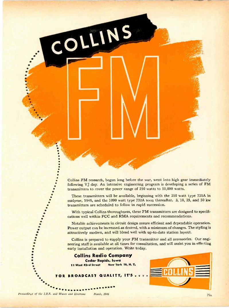
Collins FM research, begun long before the war, went into high gear immediatelyfollowing VJ day. An intensive engineering program is developing a series of FMtransmitters to cover the power range of 250 watts to 50,000 watts.
These transmitters will be available, beginning with the 250 watt type 731A inmidyear, 1946, and the 1000 watt type 732A soon thereafter. 3, 10, 25, and 50 kwtransmitters are scheduled to follow in rapid succession.
With typical Collins thoroughness, these FM transmitters are designed to specifi-cations well within FCC and RMA requirements and recommendations.
Notable achievements in circuit design assure efficient and dependable operation.Power output can be increased as desired, with a minimum of changes. The styling isattractively modern, and will blend well with up-to-date station layout.
Collins is prepared to supply your FM transmitter and all accessories. Our engi-neering staff is available at all times for consultation, and will assist you in effectingearly installation and operation. Write today.
Collins Radio CompanyCedar Rapids, Iowa
11 West 42nd Street New York 18, N. Y.
FOR BROADCAST QUALITY, IT'S . . . . Proceedings of the I.R.E. and Waves and Electrons March, 1946 79A
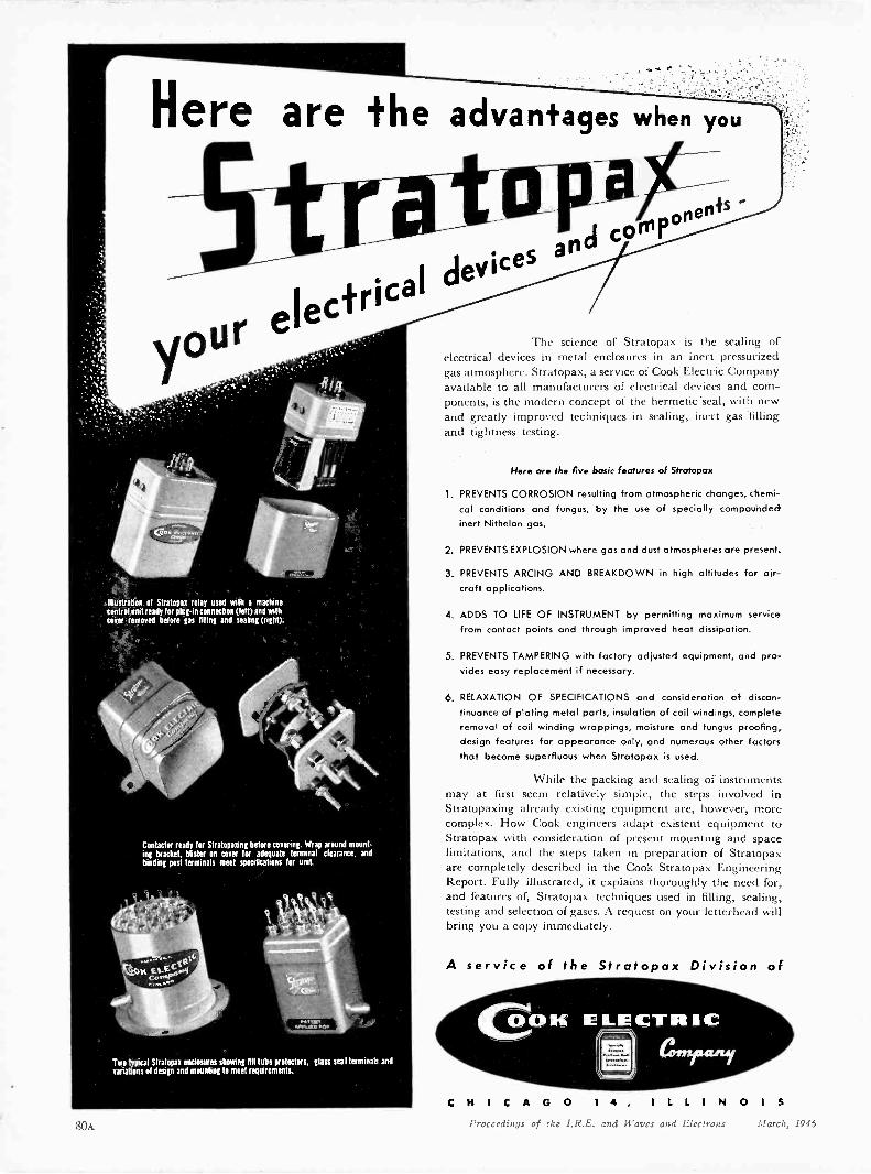
Here are the advantages when you
Illustration of Stratopax relay used with a machinecontrol unit ready for plug-in connection (left) and withcover removed before gas filling and sealing (right).
Contactor ready for Stratoparing before covering. Wrap around mount-ing bracket, blister on cover for adequate terminal clearance, andbinding post terminals meet specifications for unit.
Two typical Stratopas enclosures showing fill tube protectors, glass seal terminals andvariations of design and mounting to meet requirements.
The science of Stratopax is the sealing ofelectrical devices in metal enclosures in an inert pressurizedgas atmosphere. Stratopax, a service of Cook Electric Companyavailable to all manufacturers of electrical devices and com-ponents, is the modern concept of the hermetic 'seal, with newand greatly improved techniques in sealing, inert gas fillingand tightness testing.
Here are the five basic features of Stratopax
1. PREVENTS CORROSION resulting from atmospheric changes, chemi-cal conditions and fungus, by the use of specially compoundedinert Nithelon gas.
2. PREVENTS EXPLOSION where gas and dust atmospheres are present.
3. PREVENTS ARCING AND BREAKDOWN in high altitudes for air-craft applications.
4. ADDS TO LIFE OF INSTRUMENT by permitting maximum servicefrom contact points and through improved heat dissipation.
5. PREVENTS TAMPERING with factory adjusted equipment, and pro-vides easy replacement if necessary.
6. RELAXATION OF SPECIFICATIONS and consideration of discon-tinuance of plating metal parts, insulation of coil windings, completeremoval of coil winding wrappings, moisture and fungus proofing,design features for appearance only, and numerous other factorsthat become superfluous when Stratopax is used.
While the packing and sealing of instrumentsmay at first seem relatively simple, the steps involved inStratopaxing already existing equipment are, however, morecomplex. How Cook engineers adapt existent equipment toStratopax with consideration of present mounting and spacelimitations, and the steps taken in preparation of Stratopaxare completely described in the Cook Stratopax EngineeringReport. Fully illustrated, it explains thoroughly the need for,and features of, Stratopax techniques used in filling, sealing,testing and selection of gases. A request on your letterhead willbring you a copy immediately.
A service of the Stratopax Division of
CHICAGO 14, ILLINOIS80A Proceedings of the I.R.E. and Waves and Electrons March, 1946
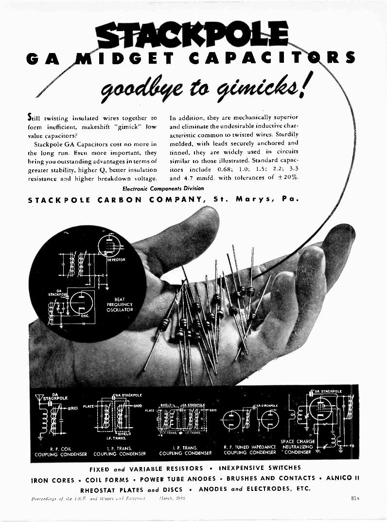
GA IDGET CAPACITORSpodies a 9
Still twisting insulated wires together toform inefficient, makeshift "gimick" lowvalue capacitors?
Stackpole GA Capacitors cost no more inthe long run. Even more important, theybring you outstanding advantages in terms ofgreater stability, higher Q, better insulationresistance and higher breakdown voltage.
In addition, they are mechanically superiorand eliminate the undesirable inductive char-acteristic common to twisted wires. Sturdilymolded, with leads securely anchored andtinned, they are widely used in circuitssimilar to those illustrated. Standard capac-itors include 0.68; 1.0; 1.5; 2.2; 3.3
and 4.7 mmfd. with tolerances of ± 20%.Electronic Components Division
STACKPOLE CARBON COMPANY, St. Marys, Pa.
GASTACKPOLE
GASTACKPOLE
GRIDPLATE
91
DETECTOR
BEATFREQUENCYOSCILLATOR
GA STACKPOLE
L-- -JSHIELD
I.F. TRANS.
GRIDPLATE
R. F. COIL I. F. TRANS.
COUPLING CONDENSER COUPLING CONDENSER
I LP TRANS I.F. TRANS.
I. F. TRANS.COUPLING CONDENSER
EGA STACKPOLE
STAGN POLE
SPACE CHARGER. F. TUNED IMPEDANCE NEUTRALIZING
COUPLING CONDENSER CONDENSER
FIXED and VARIABLE RESISTORS INEXPENSIVE SWITCHES
IRON CORES COIL FORMS POWER TUBE ANODES BRUSHES AND CONTACTS ALNICO II
RHEOSTAT PLATES and DISCS ANODES and ELECTRODES, ETC.Procecdings of the LR.L. and It uz'es and LieLlridis .11ar,h, 1910
Pin
RESISTORSAND
BALLASTS
* Troubled by fluctuating linevoltage? Just include a Claro-
stat Automatic Line Voltage Reg-ulator in your assembly-or as anaccessory plugged in between con-necting cord and outlet. At 110volts the resistance is low. Voltagedrop is negligible. But as line volt-age increases, the resistance buildsup so as to maintain uniform andsafe voltage to your assembly.Clarostat also makes voltage -drop-ping resistors, such as for adapting110 -volt equipment to 220 -voltpower lines (particularly for exporttrade). Made either for built-in ap-plications, or as convenient plug-inaccessories.
* Submit that problem ...If it has to do with resistors, controlsor resistance devices, send it to us forengineering collaboration. Engineeringcatalog on request.
CLAROSTAT MFG. CO., Inc. 285.1 N.6to St., Brooklyn, N.Y.
News and New Products(Continued from pays 78)
giving materially better service in modernhigh speed, low amperage telegraph trans-mission operations than did other metalsin the past.
Although relays with pure platinumand with the platinum -iridium alloy con-tacts worked effectively in the early daysof telegraph transmission, the develop-ment of modern highly automatic tele-graph transmission equipment created acritical problem in the matter of electricalcontacts. The higher speeds at which themodern apparatus functions creates atendency for the conventional metal con-tacts to fuse and oxidize.
It is stated that carboloy contactswhich have been attached by brazing tothe marking and spacing contacts and thearmature are self-cleaning. That is, ma-terial which becomes loosened througharcing, drops away from the carbide in-stead of fusing to the opposite contact asoccurs on contacts made of conventionalmetals.
Meeting of Board of Direc-tors of Radio Parts &Electronic Equipment
Shows, Inc.The Board is composed of the following
men, reading left to right. Kenneth C.Prince, General Manager, Show Corpora-tion; J. J. Kahn, Standard TransformerCorporation, Director; H. W. Clough,Belden Manufacturing Company, Presi-
dent; John W. Van Allen, General Coun-sel, Radio Manufacturers Association;Bond Geddes, Executive Secretary, RadioManufacturers Association; Leslie F.Muter, The Muter Company, Director;R. P. Almy, Sylvania Electronic Products,Director; Sam Poncher, Newark ElectricCompany, Director; J. A. Berman, ShureBrothers, Director; Charles Golenpaul,Aerovox Corporation; Director; W. O.Schoning, Lukko Sales Company, Direc-
HIGH ACCURACYIn Measuring:
CAPACITANCE-RESISTANCE-INDUCTANCE STORAGE FACTOR (C)) OF COILS DISSIPATION FACTOR OF CONDENSERS
MODEL 200-A IMPEDANCE BRIDGE is a port-able, self contained instrument of highest qualityused extensively by the Army, Navy, and manymanufacturers.
The range of measurement for capacitance is 1
micro microfarad to 100 microfarads; for resistance,1 milliohm to 1 megohm; for inductance. 1 micro -henry to 100 henrys. The accuracy on the main decadeIs 1% for capacitance or resistance measurements and2% for inductance tests.Reading obtained from 6 inch direct reading dials.All controls and connections plainly marked andconveniently located on the panel. 35 -page bookgives methods for many types of measurements.
IMMEDIATE DELIVERIESOur factory is in a position to make fast deliverieson Model 200-A and other products including pre-cision mica condensers, binding poets, several typesof AWS rheostat -potentiometers and decade and lowcapacity switches.
Brown Engineering Co.4635 S. E. Hawthorne Blvd. Portland 15, Oregon
wrro 114Ese.s.T
When any leading manufac-turer brings out a new prod-uct, you're sure to find it atNewark-as fast as the prod-uct is available. Standarditems, too, are always part ofthe giant stocks of bothNewark stores.
BIG NEW CATALOG!Newark's new catalog will in-clude everything for radio andelectronics, and by writing forit now, you will also be
placed on the list of thosewho receive Newark's famousbargain lists each month.Write today, addressing Dept.IR of nearest Newark branch.
Newark lifililf. Company
115-111 W. 4515 St.0 323 W Maths/MU
(Adolph Gross)(Sam Poncher)
Chicago 6New York 19
82. Proceedings of the I.R.E. and Waves and Electrons March; 1946
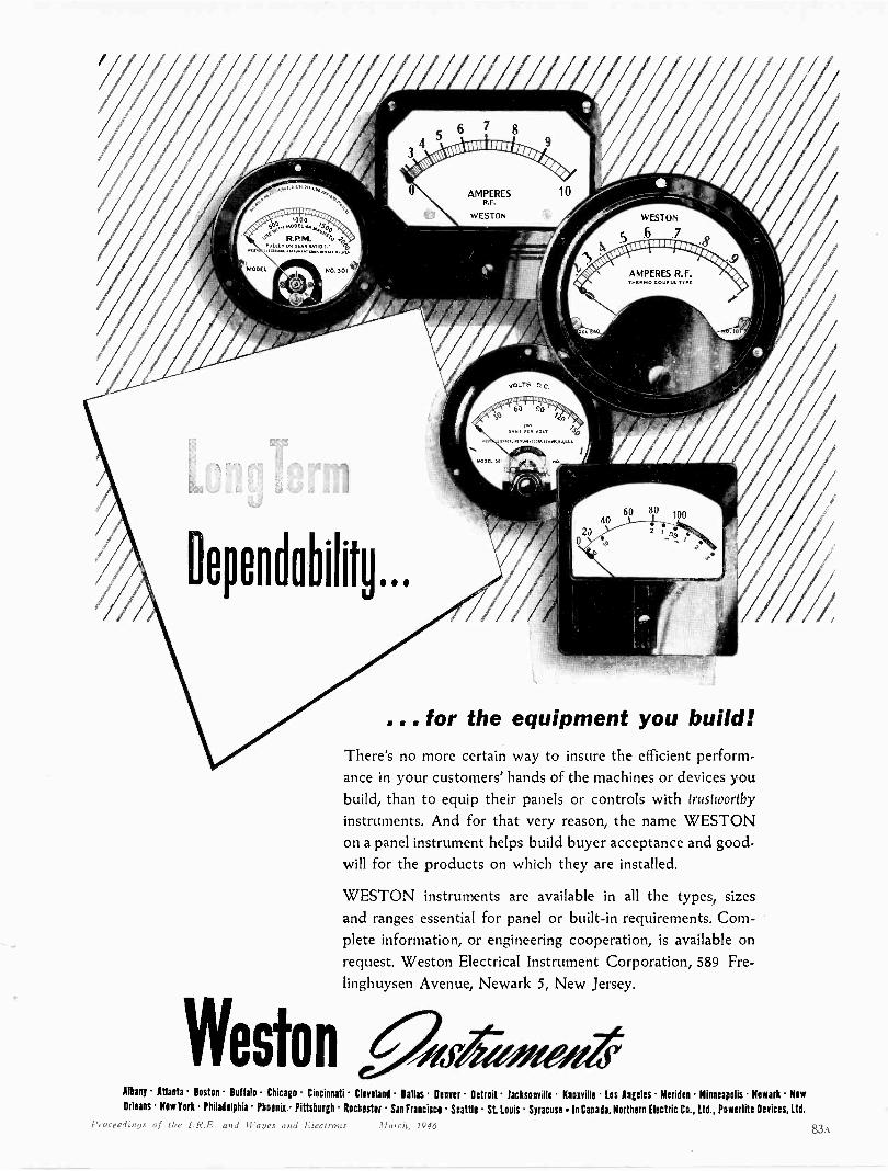
Weston
WESTON
s .6 .7ts,
AMPERES R.F.
... for the equipment you build!There's no more certain way to insure the efficient perform-ance in your customers' hands of the machines or devices youbuild, than to equip their panels or controls with trustworthyinstruments. And for that very reason, the name WESTONon a panel instrument helps build buyer acceptance and good-will for the products on which they are installed.
WESTON instruments are available in all the types, sizesand ranges essential for panel or built-in requirements. Com-plete information, or engineering cooperation, is available onrequest. Weston Electrical Instrument Corporation, 589 Fre-linghuysen Avenue, Newark 5, New Jersey.
Albany Atlanta Boston Buffalo - Chicago Cincinnati Cleveland Dallas Denver Detroit Jacksonville Knoxville Los Angeles Meriden Minneapolis Newark NewOrleans New York Philadelphia Phoenix Pittsburgh Rochester San Francisco Seattle St. Louis Syracuse In Canada. Northern Electric Co., ltd., Powerlite Devices, Ltd.
the I.R.L. and It ill 'Jet
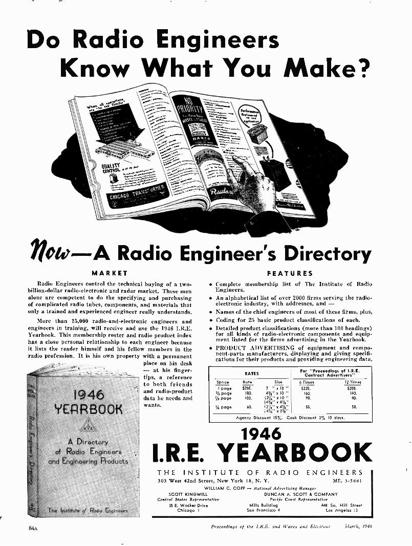
Do Radio EngineersKnow What You Make?
lick-A Radio Engineer's DirectoryMARKET
Radio Engineers control the technical buying of a two -
billion -dollar radio -electronic and radar market. These menalone are competent to do the specifying and purchasingof complicated radio tubes, components, and materials thatonly a trained and experienced engineer really understands.
More than 15,000 radio -and -electronic engineers andengineers in training, will receive and use the 1946 I.R.E.Yearbook. This membership roster and radio product indexhas a close personal relationship to each engineer becauseit lists the reader himself and his fellow members in theradio profession. It is his own property
1946YEARBOOti
A Directoryof Radio Engineers
and Engineering Products
he Institute 91 Rode Engineers
with a permanentplace on his desk- at his finger-tips, a referenceto both friendsand radio -productdata he needs andwants.
FEATURES Complete membership list of The Institute of Radio
Engineers. An alphabetical list of over 2000 firms serving the radio -
electronic industry, with addresses, and - Names of the chief engineers of most of these firms, plus, Coding for 25 basic product classifications of each. Detailed product classifications (more than 100 headings)
for all kinds of radio -electronic components and equip-ment listed for the firms advertising in the Yearbook.
PRODUCT ADVERTISING of equipment and compo-nent -parts manufacturers, displaying and giving specifi-cations for their products and providing engineering data.
RATESFor "Proceedings of I.R.E.
Contract Advertisers"Space Rate Size 6 Times 12 Times
I page $250. 7 " x 10 " $225. $200.
2/3 page 180. 4%" x 10 " 160. 140.
V3 page 100. (21/4" x 10 " 90. 80.
14% x 41/4"
I/o page 60. (21/4" x 4%" 55. 50.
14%" x 2%"
Agency Discount 15%. Cash Discount 2% 10 days.
I.R.E. YEARBOOKTHE INSTITUTE OF RADIO ENGINEERS303 West 42nd Street, New York 18, N. Y. ME. 3-5661
WILLIAM C. COPP - National Advertising ManagerSCOTT KINGWILL DUNCAN A. SCOTT & COMPANY
Central States Representative Pacific Coast Representative35 E. Wacker Drive Mills Building 448 So. Hill Street
Chicago I San Francisco 4 Los Angeles 13
g 1 \Proceedings of the I.R.E. and Waves and Electrons March, 1946
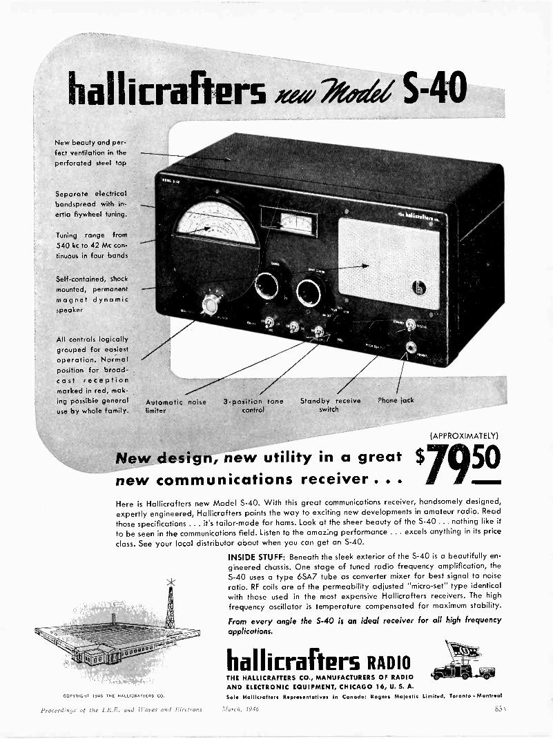
hallicrafters iemaeosw 5-40New beauty and per-fect ventilation in theperforated steel top
Separate electricalbandspread with in-ertia flywheel tuning.
Tuning range from
540 kc to 42 Mc con-tinuous in four bands
Self-contained, shockmounted, permanentmagnet dynamicspeaker
All controls logicallygrouped for easiestoperation. Normalposition for broad-cast receptionmarked in red, mak-ing possible generaluse by whole family. limiter
Automatic noise 3 -position tonecontrol
Standby receiveswitch
Phone jack
(APPROXIMATELY)
New design, new utility in a great $ 50new communications receiver .
Here is Hallicrafters new Model S-40. With this great communications receiver, handsomely designed,expertly engineered, Hallicrafters points the way to exciting new developments in amateur radio. Readthose specifications ... it's tailor-made for hams. Look at the sheer beauty of the S-40 ... nothing like itto be seen in the communications field. Listen to the amazing performance ... excels anything in its priceclass. See your local distributor about when you can get an 5-40.
INSIDE STUFF: Beneath the sleek exterior of the S-40 is a beautifully en-gineered chassis. One stage of tuned radio frequency amplification, the5-40 uses a type 6SA7 tube as converter mixer for best signal to noiseratio. RF coils are of the permeability adjusted "micro -set" type identicalwith those used in the most expensive Hallicrafters receivers. The highfrequency oscillator is temperature compensated for maximum stability.
From every angle the S-40 is an ideal receiver for all high frequencyapplications.
COPYRIGHT 1945 THE HALLICRAFTERS CO.
Proceedings of the I.R.E. and Waves and Electrons
hallicrafters RADIOTHE HALLICRAFTERS CO., MANUFACTURERS OF RADIOAND ELECTRONIC EQUIPMENT, CHICAGO 16, U. S. A.Sole Hallicrafters Representatives in Canada: Rogers Majestic Limited, Toronto - Montreal
March, 1946
ADVERTISER'S INDEXSection Meetings 36A Eastern Engineering Co. 64A Measurements Corp. 64AMembership 40A Hugh H. Eby, Inc. 68A Mycalex Corporation of Amer-Positions Open 54A Eicor, Inc. 44A ica I A
Positions Wanted 56A Stanley D. Eilenberger 64A
Eitel-McCullough, Inc. 88A National Company, Inc. 10A
Electrical Reactance 56A Newark Electric Co., Inc. 82AAerovox Corp. I 8A Electronic Engineering Co. 70A North American Philips Co., Inc. 15A
Aireon Mfg. Corp. 2A & 3A Electronic Mechanics, Inc. 45AAlliance Mfg. Co. 37A Electronics Research Publishing Ohmite Mfg. Co. 8AAmerican Lava Corp. 9A Co. 70A M. F. M. Osborne Associates 64AAmerican Transformer Co. 31 A
Amperex Electronic Corporation Federal Tel. & Radio Corp. 17A, 5 I A Pierce Paper Products Company 72ACover II
F. T. Fisher's Sons 64A Albert Preisman 64AAndrew Co. 40A F M & Television 69A Premax Products 74AArnold Engineering Co. 48A
Freed Radio Corp. 54A Press Wireless 25AThe Astatic Corp. 58A
Presto Recording 57A
Gates Radio Co. 39AGeneral Aniline & Film Corp. Radio Corp. of America
Ballantine Labs., Inc. 52A34A & 35A 22A, 32A, 53A, 54A, 87A
Barker & Williamson 76AGeneral Instruments Corp. 59A Radio Engineering Labs., Inc. 73A
Bell Telephone Laboratories I 6AGeneral Radio Co. Cover IV The Rauland Corp. 26A
Bendix Aviation Corp. 47A
42ARemler Co., Ltd. ,
Revere Copper & Brass Inc.
68A
14AW. J. Brown 64A Hallicrafters Company 85A
Bernard Rice's Sons, Inc. 75ABrown Engineering 82A Hammarlund Mfg. Company,
Inc. 24A
Harvey Radio Laboratories, Sherron Electronics Co. 7A
Inc. 33A Shure Bros. 36ACallite Tungsten Corp. 49A Hewlett-Packard Company . 28A Sperry Gyroscope Co., Inc. 55ACambridge Thermionic Corp. . 78A Hytron Radio & Electronics Sprague Electric Company 6ACentra la b 4A & 5A Corp. 50A Stackpole Carbon Co 8 I AChicago Transformer Corp. 46A Standard Transformer Corp. 38ACinaudagraph Speakers, Inc. 3A
Insulation Manufacturers Corp. 4 I AStupakoff Ceramic & Mfg. Co. 29A
Clarostat Mfg. Co., Inc. 82AInternational Tel. & Tel. Corp. Superior Electric Co. 71A
.Sigmund Cohn & Co. 74A17A, 51A Sylvania Electric Products Inc. I 2A
Collins Radio Co. 79A
Continental -Diamond Fibre Triplett Electrical Instrument Co. 43ACompany 23A J. B. T. Instruments 62A Tung -Sol Lamp Works, Inc. I 9A
Cook Electric Co. 80A E. F. Johnson Co. 77A
Cornell-Dubilier Electric Corp. Joliet Chemicals, Ltd 27A United Transformer Corporation I 3ACover III
Crystal Research Laboratories, Karp Metal Products Co., Inc. 63AInc. 76A
Western Electric Company
Westinghouse Electric Corp.
IIA
The Langevin Company, Inc. . . 66A21 A, 61 A, 67A
Weston Electrical Inst. Corp... 83ALewis Electronics 2AH. L. Dalis, Inc. 68A
Daven Company 65A Harold A. Wheeler 64AAllen B. DuMont Labs., Inc. 20A, 30A Madison Electrical Products John Wiley & Sons, Inc. 60AE. I. DuPont De Nemours & Co., Corp. 76A
Inc. 78A Frank Massa 64A Paul D. Zottu 64A
l're,ecdin!ts o f the 1.k.T. Ind trai-es and life, trans 11 at., h, 1940
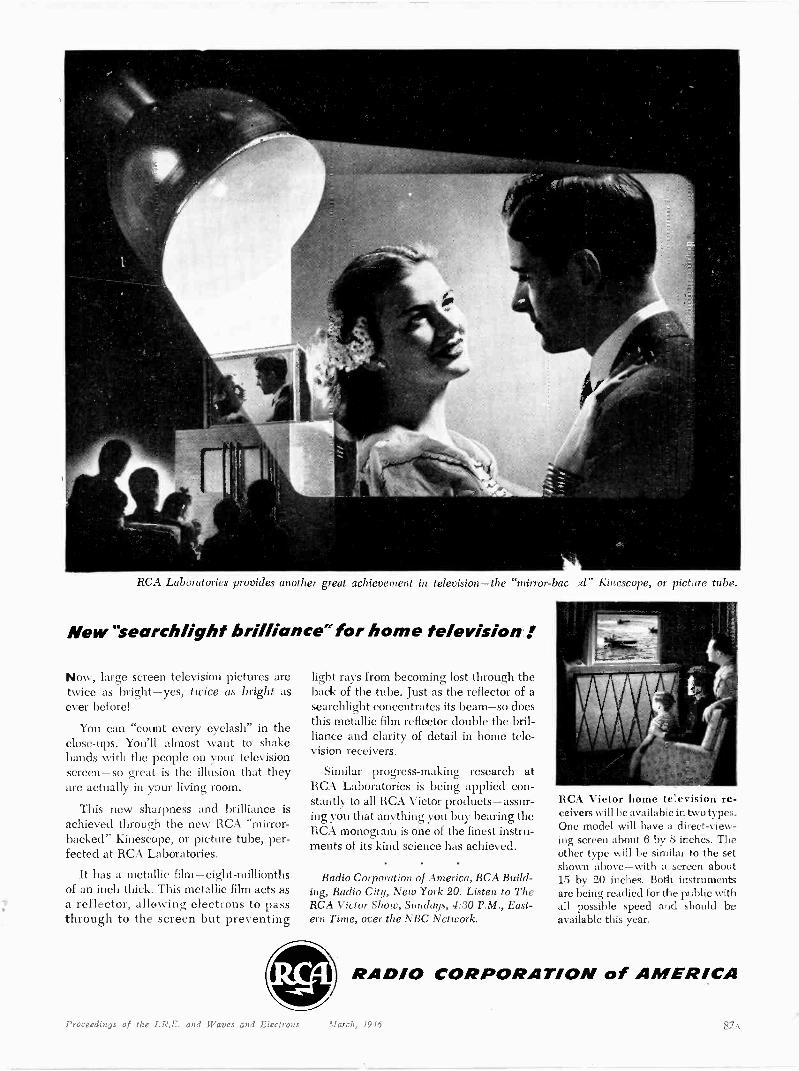
RCA Laboratories provides another great achievement in television-the "mirror-bac id" Kinescope, or picture tube.
New "searchlight brilliance" for home television
Now, large screen television pictures aretwice as bright -yes, twice as bright asever before!
You can "count every eyelash" in theclose-ups. You'll almost want to shakehands with the people on your televisionscreen-so great is the illusion that theyare actually in your living room.
This new sharpness and brilliance isachieved through the new RCA "mirror -backed" Kinescope, or picture tube, per-fected at RCA Laboratories.
It has a metallic film -eight -millionthsof an inch thick. This metallic film acts asa reflector, allowing electrons to passthrough to the screen but preventing
light rays from becoming lost through theback of the tube. Just as the reflector of asearchlight concentrates its beam-so doesthis metallic film reflector double the bril-liance and clarity of detail in home tele-vision receivers.
Similar progress -making research atRCA Laboratories is being applied con-stantly to all RCA Victor products-assur-ing you that anything you buy bearing theRCA monogram is one of the finest instru-ments of its kind science has achieved.
Radio Corporation of America, RCA Build-ing, Radio City, New York 20. Listen to TheRCA Victor Show, Sundays, 4:30 P.M., East-ern Time, over the NBC Network.
RCA Victor home television re-ceivers will be available in two types.One model will have a direct -view-ing screen about 6 by 8 inches. Theother type will be similar to the setshown above-with a screen about15 by 20 inches. Both instrumentsare being readied for the public withall possible speed and should beavailable this year.
RADIO CORPORATION of AMERICA
Proceedings of the I.R.E. and Waves and Electrons March, 1946
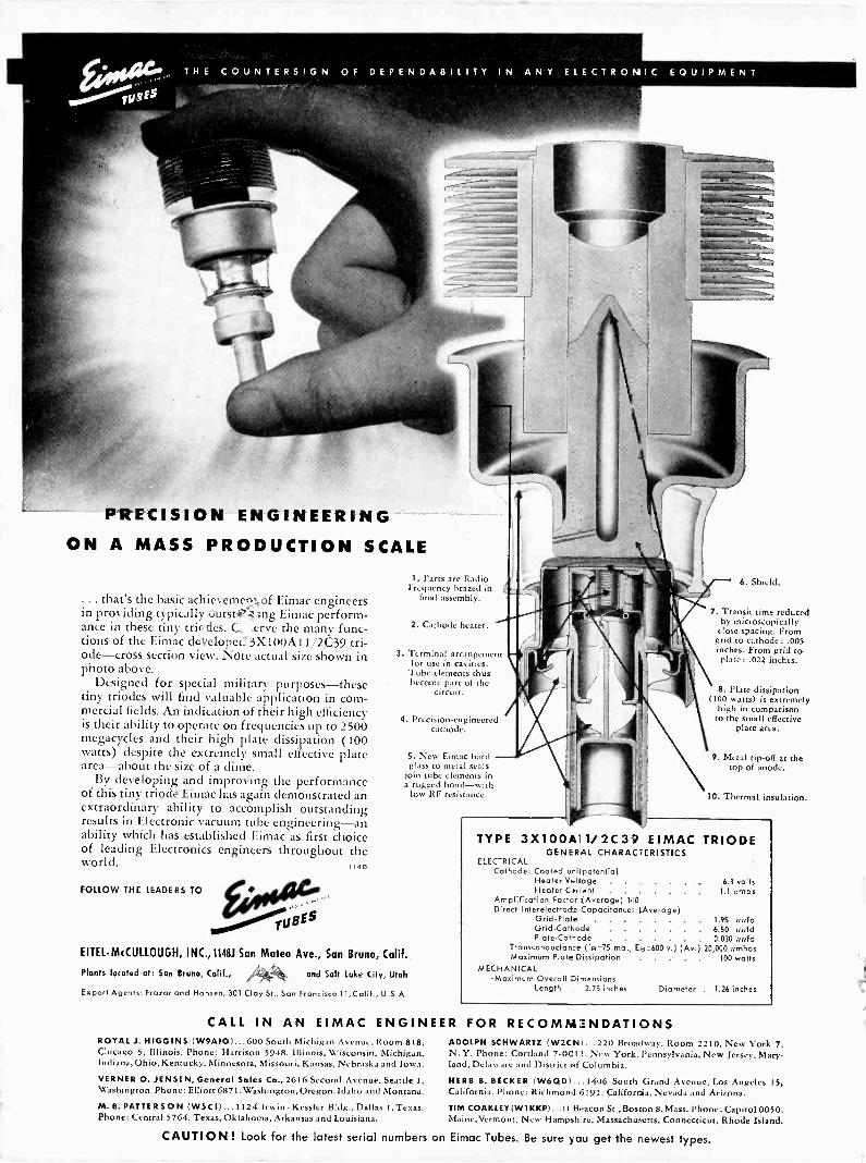
T H E COUNTERSIGN OF DEPFNDABILITY IN ANY ELECTRONIC EQUIPMENT
PRECISION ENGINEERINGON A MASS PRODUCTION SCALE
... that's the basic achievement of Eimac engineersin providing typically outstri"-: ;ng Eimac perform-ance in these tiny tric-des. C. .erve the many func-tions of the Eimac developeC3X100A11/2C39 tri-ode-cross section view. Note actual size shown inphoto above.
Designed for special military purposes-thesetiny triodes will find valuable application in com-mercial fields. An indication of their high efficiencyis their ability to operate on frequencies up to 2500megacycles and their high plate dissipation (100watts) despite the extremely small effective platearea-about the size of a dime.
By developing and improving the performanceof this tiny triode Eimac has again demonstrated anextraordinary ability to accomplish outstandingresults in Electronic vacuum tube engineering-anability which has established Eimac as first choiceof leading Electronics engineers throughout theworld. 1146
FOLLOW THE LEADERS TO
2000000°.°711BES
1. Parts are RadioFrequency brazed in
final assembly.
2. Cathode heater.
3. Terminal arrangemenfor use in cavities.
Tube elements thusbecome part of the
circuit.
4. Precision -engineeredcathode.
5. New Eimac hardglass to metal seals
join tube elements ina rugged bond-with
low RF resistance.
EITEL-McCULLOUGH, INC.,11481 San Mateo Ave., San Bruno, Calif.
Plants located at: San Bruno, Calif., / tr. and Salt Lake City, Utah
Export Agents: Frazer and Hansen, 301 Clay St., Son Francisco 11, Calif., U.S.A.
6. Shield.
7. Transit time reducedby microscopically
close spacing. Fromgrid to cathode: .005inches. From grid toplate: .022 inches.
8. Plate dissipation(100 watts) is extremely
high in comparisonto the small effective
plate area.
9. Metal tip-off at thetop of anode.
10. Thermal insulation.
TYPE 3X100/11-1 1/2C39 EIMAC TRIODEGENERAL CHARACTERISTICS
ELECTRICALCathode: Coated unitpotential
Heater VoltageHeater Cyr ent
Amplification Factor (Average) 1110Direct InterelectrodeCapacitance: (Average)
Grid -Plate 1.95 uufdGrid -Cathode 6.50 uufdPlate -Cathode 0.030 uufd
Transconductance (ier.75 ma., Eez600 v.) (Av.) 20,000 umhosMaximum Plate Dissipation 100 watts
MECHANICAL-Maximum Overall Dimensions
Length 2.75 inches Diameter . 1.26 inches
6 3 volts1.1 amps
CALL IN AN EIMAC ENGINEER FOR RECOMMENDATIONSROYAL J. HIGGINS (W9A10)...600 South Michigan Avenue, Room 818,Chicago 5, Illinois. Phone: Harrison 5948. Illinois, Wisconsin, Michigan,Indiana, Ohio. Kentucky, Minnesota, Missouri, Kansas, Nebraska and Iowa.
VERNER 0. JENSEN, General Sales Co., 2616 Second Avenue, Seattle 1,Washington. Phone: Elliott 6871. Washington, Oregon, Idaho and Montana.
M. B. PATTE R ON ( WS C I) ... 1124 Irwin - Kessler Bldg., Dallas I, Texas.Phone: Central 5764. Texas, Oklahoma, Arkansas and Louisiana.
ADOLPH SCHWARTZ (W2C N (... 220 Broadway, Room 2210, New York 7,N.Y. Phone: Cortland 7-0011. New York, Pennsylvania, New Jersey, Mary-land, Delaware and District of Columbia.
HERB B. BECKER (W6QD) 1406 South Grand Avenue. Los Angeles 15,California. ('hone: Richmond 6191. California, Nevada and Arizona.
TIM COAKLEY (W1KKP)...11 Beacon St., Boston 8,Mass. Phone: Capitol 0050.Maine,Vermont, New Hampshire, Massachusetts, Connecticut, Rhode Island.
CAUTION! Look for the latest serial numbers on Eimac Tubes. Be sure you get the newest types.
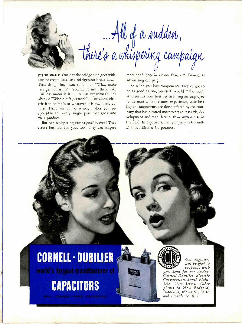
as
IT'S SO SIMPLE. One day the bridge club goes with-out ice cream because a refrigerator broke down.First thing they want to know: "What makerefrigerator is it?" You don't hear them ask:"Whose motor is it . . . whose capacitors ?" It'salways: "Whose refrigerator ?" ... or whose elec-tric iron or radio or whatever it is you manufac-ture. That, without question, makes you re-sponsible for every single part that goes intoyour product.
But ban whispering campaigns? Never! Theycreate business for you, too. They can inspire
CORNELL - DUBILIER
CAPACITORS
4cal
0
more confidence in a name than a million dollaradvertising campaign.
So when you buy components, they've got tobe as good as you, yourself, would make them.And just as your best bet in hiring an employeeis the man with the most experience, your bestbuy in components are those offered by the com-pany that has devoted more years to research, de-velopment and manufacture than anyone else inthe field. In capacitors, that company is Cornell-Dubilier Electric Corporation.
Our engineerswill be glad tocooperate with
you. Send for our catalog.Cornell-Dubilier ElectricCorporation. South Plain-field, New Jersey. Otherplants in New Bedford,Brookline, Worcester, Mass.and Providence, R. I.
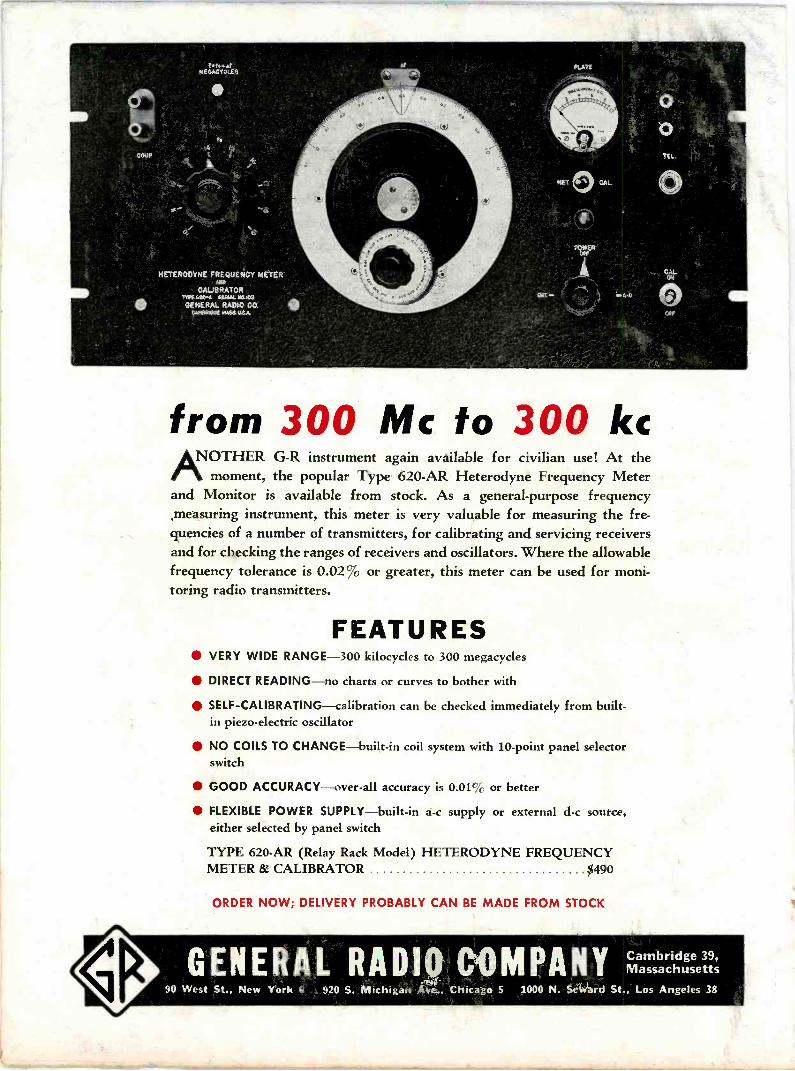
tot000tMEGACYCLES
HETERODYNE FREQUENCY METERnw
CALIBRATORTYPE 620-A WOK 1110.103
GENERAL RADIO CO.CAMMiDat WAS USA
PLATE
Kt0 CAL.
TEL.
CALON
0OFF
from 300 Mc to 300 kcANOTHER G -R instrument again available for civilian use! At the
moment, the popular Type 620 -AR Heterodyne Frequency Meterand Monitor is available from stock. As a general-purpose frequency.measuring instrument, this meter is very valuable for measuring the fre-quencies of a number of transmitters, for calibrating and servicing receiversand for checking the ranges of receivers and oscillators. Where the allowablefrequency tolerance is 0.02% or greater, this meter can be used for moni-toring radio transmitters.
FEATURES VERY WIDE RANGE -300 kilocycles to 300 megacycles
DIRECT READING-no charts or curves to bother with
SELF-CALIBRATING-calibration can be checked immediately from built-in piezo-electric oscillator
NO COILS TO CHANGE-built-in coil system with 10 -point panel selectorswitch
GOOD ACCURACY-over-all accuracy is 0.01% or better
FLEXIBLE POWER SUPPLY-built-in a -c supply or external d -c source,either selected by panel switch
TYPE 620 -AR (Relay Rack Model) HETERODYNE FREQUENCYMETER & CALIBRATOR $490
ORDER NOW; DELIVERY PROBABLY CAN BE MADE FROM STOCK
GENERAL RADIO COMPANY Cambridge 39,Massachusetts
90 West St., New York 6 920 S. Michigan Ave.. Chicago 5 1000 N. Seward St., Los Angeles 38
Copyright © 2022 FDOKUMEN

