


Bahasa
Halaman
Hukum


Product
Folder
Sample &Buy
Technical
Documents
Tools &
Software
Support &Community
An IMPORTANT NOTICE at the end of this data sheet addresses availability, warranty, changes, use in safety-critical applications,intellectual property matters and other important disclaimers. PRODUCTION DATA.
TMS570LC4357SPNS195C –FEBRUARY 2014–REVISED JUNE 2016
TMS570LC4357 Hercules™ Microcontroller Based on the ARM® Cortex®-R Core
1 Device Overview
1
1.1 Features1
• High-Performance Automotive-GradeMicrocontroller for Safety-Critical Applications– Dual-Core Lockstep CPUs With ECC-Protected
Caches– ECC on Flash and RAM Interfaces– Built-In Self-Test (BIST) for CPU, High-End
Timers, and On-Chip RAMs– Error Signaling Module (ESM) With Error Pin– Voltage and Clock Monitoring
• ARM® Cortex® - R5F 32-Bit RISC CPU– 1.66 DMIPS/MHz With 8-Stage Pipeline– FPU With Single- and Double-Precision– 16-Region Memory Protection Unit (MPU)– 32KB of Instruction and 32KB of Data Caches
With ECC– Open Architecture With Third-Party Support
• Operating Conditions– Up to 300-MHz CPU Clock– Core Supply Voltage (VCC): 1.14 to 1.32 V– I/O Supply Voltage (VCCIO): 3.0 to 3.6 V
• Integrated Memory– 4MB of Program Flash With ECC– 512KB of RAM With ECC– 128KB of Data Flash for Emulated EEPROM
With ECC• 16-Bit External Memory Interface (EMIF)• Hercules™ Common Platform Architecture
– Consistent Memory Map Across Family– Real-Time Interrupt (RTI) Timer (OS Timer)– Two 128-Channel Vectored Interrupt Modules
(VIMs) With ECC Protection on Vector Table• VIM1 and VIM2 in Safety Lockstep Mode
– Two 2-Channel Cyclic Redundancy Checker(CRC) Modules
• Direct Memory Access (DMA) Controller– 32 Channels and 48 Peripheral Requests– ECC Protection for Control Packet RAM– DMA Accesses Protected by Dedicated MPU
• Frequency-Modulated Phase-Locked Loop(FMPLL) With Built-In Slip Detector
• Separate Nonmodulating PLL• IEEE 1149.1 JTAG, Boundary Scan, and ARM
CoreSight™ Components• Advanced JTAG Security Module (AJSM)• Trace and Calibration Capabilities
– ETM™, RTP, DMM, POM
• Multiple Communication Interfaces– 10/100 Mbps Ethernet MAC (EMAC)
• IEEE 802.3 Compliant (3.3-V I/O Only)• Supports MII, RMII, and MDIO
– FlexRay Controller With 2 Channels• 8KB of Message RAM With ECC Protection• Dedicated FlexRay Transfer Unit (FTU)
– Four CAN Controller (DCAN) Modules• 64 Mailboxes, Each With ECC Protection• Compliant to CAN Protocol Version 2.0B
– Two Inter-Integrated Circuit (I2C) Modules– Five Multibuffered Serial Peripheral Interface
(MibSPI) Modules• MibSPI1: 256 Words With ECC Protection• Other MibSPIs: 128 Words With ECC
Protection– Four UART (SCI) Interfaces, Two With Local
Interconnect Network (LIN 2.1) InterfaceSupport
• Two Next Generation High-End Timer (N2HET)Modules– 32 Programmable Channels Each– 256-Word Instruction RAM With Parity– Hardware Angle Generator for Each N2HET– Dedicated High-End Timer Transfer Unit (HTU)
for Each N2HET• Two 12-Bit Multibuffered Analog-to-Digital
Converter (MibADC) Modules– MibADC1: 32 Channels Plus Control for up to
1024 Off-Chip Channels– MibADC2: 25 Channels– 16 Shared Channels– 64 Result Buffers Each With Parity Protection
• Enhanced Timing Peripherals– 7 Enhanced Pulse Width Modulator (ePWM)
Modules– 6 Enhanced Capture (eCAP) Modules– 2 Enhanced Quadrature Encoder Pulse (eQEP)
Modules• Three On-Die Temperature Sensors• Up to 145 Pins Available for General-Purpose I/O
(GPIO)• 16 Dedicated GPIO Pins With External Interrupt
Capability• Packages
– 337-Ball Grid Array (ZWT) [Green]

2
TMS570LC4357SPNS195C –FEBRUARY 2014–REVISED JUNE 2016 www.ti.com
Submit Documentation FeedbackProduct Folder Links: TMS570LC4357
Device Overview Copyright © 2014–2016, Texas Instruments Incorporated
1.2 Applications• Braking Systems (Antilock Brake Systems and
Electronic Stability Control)• Electric Power Steering (EPS)• HEV and EV Inverter Systems• Battery-Management Systems
• Active Driver Assistance Systems• Aerospace and Avionics• Railway Communications• Off-road Vehicles

3
TMS570LC4357www.ti.com SPNS195C –FEBRUARY 2014–REVISED JUNE 2016
Submit Documentation FeedbackProduct Folder Links: TMS570LC4357
Device OverviewCopyright © 2014–2016, Texas Instruments Incorporated
1.3 DescriptionThe TMS570LC4357 device is part of the Hercules TMS570 series of high-performance automotive-gradeARM® Cortex®-R-based MCUs. Comprehensive documentation, tools, and software are available toassist in the development of ISO 26262 and IEC 61508 functional safety applications. Start evaluatingtoday with the Hercules TMS570LC43x LaunchPad Development Kit. The TMS570LC4357 device has on-chip diagnostic features including: dual CPUs in lockstep, Built-In Self-Test (BIST) logic for CPU, theN2HET coprocessors, and for on-chip SRAMs; ECC protection on the L1 caches, L2 flash, and SRAMmemories. The device also supports ECC or parity protection on peripheral memories and loopbackcapability on peripheral I/Os.
The TMS570LC4357 device integrates two ARM Cortex-R5F floating-point CPUs, operating in lockstep,which offer an efficient 1.66 DMIPS/MHz, and can run up to 300 MHz providing up to 498 DMIPS. Thedevice supports the big-endian [BE32] format.
The TMS570LC4357 device has 4MB of integrated flash and 512KB of data RAM with single-bit errorcorrection and double-bit error detection. The flash memory on this device is a nonvolatile, electricallyerasable and programmable memory, implemented with a 64-bit-wide data bus interface. The flashoperates on a 3.3-V supply input (the same level as the I/O supply) for all read, program, and eraseoperations. The SRAM supports read and write accesses in byte, halfword, and word modes.
The TMS570LC4357 device features peripherals for real-time control-based applications, including twoNext Generation High-End Timer (N2HET) timing coprocessors with up to 64 total I/O terminals.
The N2HET is an advanced intelligent timer that provides sophisticated timing functions for real-timeapplications. The timer is software-controlled, with a specialized timer micromachine and an attached I/Oport. The N2HET can be used for pulse-width-modulated outputs, capture or compare inputs, or GPIO.The N2HET is especially well suited for applications requiring multiple sensor information or driveactuators with complex and accurate time pulses. The High-End Timer Transfer Unit (HTU) can performDMA-type transactions to transfer N2HET data to or from main memory. A Memory Protection Unit (MPU)is built into the HTU.
The Enhanced Pulse Width Modulator (ePWM) module can generate complex pulse width waveforms withminimal CPU overhead or intervention. The ePWM is easy to use and supports both high-side and low-side PWM and deadband generation. With integrated trip zone protection and synchronization with the on-chip MibADC, the ePWM is ideal for digital motor control applications.
The Enhanced Capture (eCAP) module is essential in systems where the accurately timed capture ofexternal events is important. The eCAP can also be used to monitor the ePWM outputs or for simple PWMgeneration when not needed for capture applications.
The Enhanced Quadrature Encoder Pulse (eQEP) module directly interfaces with a linear or rotaryincremental encoder to get position, direction, and speed information from a rotating machine as used inhigh-performance motion and position-control systems.
The device has two 12-bit-resolution MibADCs with 41 total channels and 64 words of parity-protectedbuffer RAM. The MibADC channels can be converted individually or by group for special conversionsequences. Sixteen channels are shared between the two MibADCs. Each MibADC supports threeseparate groupings. Each sequence can be converted once when triggered or configured for continuousconversion mode. The MibADC has a 10-bit mode for use when compatibility with older devices or fasterconversion time is desired. One of the channels in MibADC1 and two of the channels in MibADC2 can beused to convert temperature measurements from the three on-chip temperature sensors.
The device has multiple communication interfaces: Five MibSPIs; four UART (SCI) interfaces, two with LINsupport; four CANs; two I2C modules;one Ethernet Controller; and one FlexRay controller. The SPIprovides a convenient method of serial interaction for high-speed communications between similar shift-register type devices. The LIN supports the Local Interconnect standard (LIN 2.1) and can be used as aUART in full-duplex mode using the standard Non-Return-to-Zero (NRZ) format. The DCAN supports theCAN 2.0B protocol standard and uses a serial, multimaster communication protocol that efficientlysupports distributed real-time control with robust communication rates of up to 1 Mbps. The DCAN is ideal
4
TMS570LC4357SPNS195C –FEBRUARY 2014–REVISED JUNE 2016 www.ti.com
Submit Documentation FeedbackProduct Folder Links: TMS570LC4357
Device Overview Copyright © 2014–2016, Texas Instruments Incorporated
for applications operating in noisy and harsh environments (for example, automotive and industrial fields)that require reliable serial communication or multiplexed wiring. The FlexRay controller uses a dual-channel serial, fixed time base multimaster communication protocol with communication rates of 10 Mbpsper channel. A FlexRay Transfer Unit (FTU) enables autonomous transfers of FlexRay data to and frommain CPU memory. HTU transfers are protected by a dedicated, built-in MPU. The Ethernet modulesupports MII, RMII, and Management Data I/O (MDIO) interfaces. The I2C module is a multimastercommunication module providing an interface between the microcontroller and an I2C-compatible devicethrough the I2C serial bus. The I2C module supports speeds of 100 and 400 kbps.
The Frequency-Modulated Phase-Locked Loop (FMPLL) clock module multiplies the external frequencyreference to a higher frequency for internal use. The Global Clock Module (GCM) manages the mappingbetween the available clock sources and the internal device clock domains.
The device also has two External Clock Prescaler (ECP) modules. When enabled, the ECPs output acontinuous external clock on the ECLK1 and ECLK2 balls. The ECLK frequency is a user-programmableratio of the peripheral interface clock (VCLK) frequency. This low-frequency output can be monitoredexternally as an indicator of the device operating frequency.
The Direct Memory Access (DMA) controller has 32 channels, 48 peripheral requests, and ECC protectionon its memory. An MPU is built into the DMA to protect memory against erroneous transfers.
The Error Signaling Module (ESM) monitors on-chip device errors and determines whether an interrupt orexternal Error pin/ball (nERROR) is triggered when a fault is detected. The nERROR signal can bemonitored externally as an indicator of a fault condition in the microcontroller.
The External Memory Interface (EMIF) provides a memory extension to asynchronous and synchronousmemories or other slave devices.
A Parameter Overlay Module (POM) is included to enhance the debugging capabilities of application code.The POM can reroute flash accesses to internal RAM or to the EMIF, thus avoiding the reprogrammingsteps necessary for parameter updates in flash. This capability is particularly helpful during real-timesystem calibration cycles.
Several interfaces are implemented to enhance the debugging capabilities of application code. In additionto the built-in ARM Cortex-R5F CoreSight debug features, the Embedded Cross Trigger (ECT) supportsthe interaction and synchronization of multiple triggering events within the SoC. An External TraceMacrocell (ETM) provides instruction and data trace of program execution. For instrumentation purposes,a RAM Trace Port (RTP) module is implemented to support high-speed tracing of RAM and peripheralaccesses by the CPU or any other master. A Data Modification Module (DMM) gives the ability to writeexternal data into the device memory. Both the RTP and DMM have no or minimal impact on the programexecution time of the application code.
With integrated safety features and a wide choice of communication and control peripherals, theTMS570LC4357 device is an ideal solution for high-performance real-time control applications with safety-critical requirements.
(1) For more information on these devices, see Section 10, Mechanical Packaging and OrderableInformation.
Device Information (1)
PART NUMBER PACKAGE BODY SIZETMS570LC4357ZWT NFBGA (337) 16.00 mm × 16.00 mm

HTU1 FTU HTU2
Peripheral Interconnect Subsystem
CRC
1,2
PCR2 PCR3
EMAC Slaves
DCAN1
DCAN2
DCAN3
LIN1/
SCI1
MibSPI4
MDIO
MIIMibSPI1
CAN1_RX
CAN1_TX
CAN2_RX
CAN2_TX
CAN3_RX
CAN3_TX
MIBSPI1_CLK
MIBSPI1_SIMO[1:0]
MIBSPI1_SOMI[1:0]
MIBSPI1_nCS[5:0]MIBSPI1_nENA
MibSPI2
MIBSPI2_CLK
MIBSPI2_SIMO
MIBSPI2_SOMI
MIBSPI2_nCS[1:0]MIBSPI2_nENA
MibSPI3
MIBSPI3_CLK
MIBSPI3_SIMO
MIBSPI3_SOMI
MIBSPI3_nCS[5:0]
MIBSPI3_nENA
MIBSPI4_CLK
MIBSPI4_SIMO
MIBSPI4_SOMI
MIBSPI4_nCS[5:0]
MIBSPI4_nENA
MibSPI5
MIBSPI5_SIMO[3:0]
MIBSPI5_SOMI[3:0]
MIBSPI5_nCS[5:0]
MIBSPI5_nENA
LIN1_RX
LIN1_TX
IOMM
PMM
Lockstep
VIMs
RTI
DCC1
DMA
MDCLK
MDIO
MII_RXD[3:0]
MII_RXERMII_TXD[3:0]MII_TXEN
MII_TXCLK
MII_RXCLKMII_CRSMII_RXDVMII_COL
EMIF
EMIF_CLKEMIF_CKEEMIF_nCS[4:2]
EMIF_nCS[0]
EMIF_ADDR[21:0]
EMIF_BA[1:0]EMIF_DATA[15:0]
EMIF_nDQM[1:0]EMIF_nOEEMIF_nWEEMIF_nRASEMIF_nCAS
EMIF_nRW
EMIF_nWAIT
SYSnPORRST
nRST
ECLK[2:1]
ESM
eQEP
1,2
eQEPxA
eQEPxB
eQEPxS
eQEPxI
eCAP
1..6eCAP[6:1]
ePWM
1..7
nTZ[3:1]
SYNCO
SYNCI
ePWMxA
ePWMxB
N2HET1 FlexRayGION2HET2
FR
AY
_R
X1
FR
AY
_TX
1
FR
AY
_T
XE
N1
FR
AY
_R
X2
FR
AY
_TX
2
FR
AY
_T
XE
N2
GIO
B[7
:0]
GIO
A[7
:0]
N2H
ET1[3
1:0
]
N2H
ET
1_PIN
_nD
IS
N2H
ET
2_P
IN_n
DIS
MibADC1 MibADC2
VS
SA
D
VC
CA
D
AD
RE
FH
I
AD
RE
FLO
NMPU
EMAC
# 2
# 3
# 4
#6
#1always on
Core/RAM Core
#5
Color Legend forPower Domains
DCAN4CAN4_RX
CAN4_TX
PCR1
LIN2/
SCI2
LIN2_RX
LIN2_TX
SCI3SCI3_RX
SCI3_TX
SCI4SCI4_RX
SCI4_TX
I2C1I2C1_SDA
I2C1_SCL
I2C2I2C2_SDA
I2C2_SCL
EMIF
Slave
CPU Interconnect Subsystem
Dual Cortex -R5F
CPUs in lockstep
32KB Icache
& Dcache w /
ECC
POM
4MB Flash
&128KB
Flash forEEPROMEmulation
w/ ECC
512KB
SRAM
w/
ECC
NMPU
NMPU
STC1
EPC
SCM
SYS
DCC2
STC2
DMMDAP
CCM-
R5F
RTP
nTR
ST
TM
ST
CK
RTC
KTD
ITD
O
DM
MnE
NA
DM
MS
YN
CD
MM
CLK
DM
MD
AT
A[1
5:0]
TPIU
RTP
nE
NA
RTP
SY
NC
RT
PC
LK
RT
PD
AT
A[1
5:0
]
ETM
DA
TA
[31:
0]
]E
TM
TR
AC
EC
TL
ET
MTR
AC
EC
LK
ET
MTR
AC
EC
LK
IN
MIBSPI5_CLK
N2H
ET
2[3
1:0]
AD
1IN
[15:8
]/
AD
2IN
[15:8
] AD
2E
VT
AD
1IN
[23:1
6]/
AD
2IN
[7:0
]AD
1IN
[7:0
]A
D1E
VT
AD
1E
XT
_S
EL
[4:0
]
AD
1E
XT
_E
NA
_
AD
2IN
[24:1
6]
AD
1IN
[31:2
4]
nERROR
uS
CU
Copyright © 2016, Texas Instruments Incorporated
5
TMS570LC4357www.ti.com SPNS195C –FEBRUARY 2014–REVISED JUNE 2016
Submit Documentation FeedbackProduct Folder Links: TMS570LC4357
Device OverviewCopyright © 2014–2016, Texas Instruments Incorporated
1.4 Functional Block DiagramFigure 1-1 shows the functional block diagram of the device.
Figure 1-1. Functional Block Diagram

6
TMS570LC4357SPNS195C –FEBRUARY 2014–REVISED JUNE 2016 www.ti.com
Submit Documentation FeedbackProduct Folder Links: TMS570LC4357
Table of Contents Copyright © 2014–2016, Texas Instruments Incorporated
Table of Contents1 Device Overview ......................................... 1
1.1 Features .............................................. 11.2 Applications........................................... 21.3 Description............................................ 31.4 Functional Block Diagram ............................ 5
2 Revision History ......................................... 73 Device Comparison ..................................... 84 Terminal Configuration and Functions.............. 9
4.1 ZWT BGA Package Ball-Map (337 Terminal GridArray) ................................................. 9
4.2 Terminal Functions .................................. 105 Specifications .......................................... 55
5.1 Absolute Maximum Ratings ......................... 555.2 ESD Ratings ........................................ 555.3 Power-On Hours (POH)............................. 555.4 Device Recommended Operating Conditions....... 565.5 Switching Characteristics over Recommended
Operating Conditions for Clock Domains ........... 575.6 Wait States Required - L2 Memories ............... 575.7 Power Consumption Summary...................... 595.8 Input/Output Electrical Characteristics Over
Recommended Operating Conditions............... 605.9 Thermal Resistance Characteristics for the BGA
Package (ZWT) ..................................... 615.10 Timing and Switching Characteristics ............... 61
6 System Information and ElectricalSpecifications ........................................... 646.1 Device Power Domains ............................. 646.2 Voltage Monitor Characteristics ..................... 656.3 Power Sequencing and Power-On Reset ........... 666.4 Warm Reset (nRST)................................. 686.5 ARM Cortex-R5F CPU Information ................. 696.6 Clocks ............................................... 766.7 Clock Monitoring .................................... 876.8 Glitch Filters ......................................... 896.9 Device Memory Map ................................ 906.10 Flash Memory...................................... 1016.11 L2RAMW (Level 2 RAM Interface Module) ........ 1046.12 ECC / Parity Protection for Accesses to Peripheral
RAMs .............................................. 104
6.13 On-Chip SRAM Initialization and Testing .......... 1056.14 External Memory Interface (EMIF)................. 1096.15 Vectored Interrupt Manager........................ 1176.16 ECC Error Event Monitoring and Profiling ......... 1216.17 DMA Controller..................................... 1236.18 Real-Time Interrupt Module........................ 1276.19 Error Signaling Module............................. 1296.20 Reset / Abort / Error Sources...................... 1346.21 Digital Windowed Watchdog....................... 1386.22 Debug Subsystem ................................. 139
7 Peripheral Information and ElectricalSpecifications ......................................... 1567.1 Enhanced Translator PWM Modules (ePWM) ..... 1567.2 Enhanced Capture Modules (eCAP)............... 1617.3 Enhanced Quadrature Encoder (eQEP) ........... 1647.4 12-bit Multibuffered Analog-to-Digital Converter
(MibADC)........................................... 1667.5 General-Purpose Input/Output ..................... 1797.6 Enhanced High-End Timer (N2HET) .............. 1807.7 FlexRay Interface .................................. 1857.8 Controller Area Network (DCAN) .................. 1877.9 Local Interconnect Network Interface (LIN)........ 1887.10 Serial Communication Interface (SCI) ............. 1897.11 Inter-Integrated Circuit (I2C) ....................... 1907.12 Multibuffered / Standard Serial Peripheral
Interface............................................ 1937.13 Ethernet Media Access Controller ................. 207
8 Applications, Implementation, and Layout ...... 2118.1 TI Design or Reference Design.................... 211
9 Device and Documentation Support .............. 2129.1 Device Support..................................... 2129.2 Documentation Support............................ 2149.3 Trademarks ........................................ 2149.4 Electrostatic Discharge Caution ................... 2149.5 Glossary............................................ 2149.6 Device Identification................................ 2159.7 Module Certifications............................... 217
10 Mechanical Data ...................................... 22310.1 Packaging Information ............................. 223

7
TMS570LC4357www.ti.com SPNS195C –FEBRUARY 2014–REVISED JUNE 2016
Submit Documentation FeedbackProduct Folder Links: TMS570LC4357
Revision HistoryCopyright © 2014–2016, Texas Instruments Incorporated
2 Revision HistoryThis data manual revision history highlights the technical changes made to the SPNS195B device-specificdata manual to make it an SPNS195C revision. These devices are now in the Production Data (PD) stageof development.
Changes from January 31, 2016 to June 25, 2016 (from B Revision (January 2016) to C Revision) Page
• Global: Updated/Changed the product status from Product Preview to Production Data. .................................. 1• Table 6-13 (LPO Specifications): Updated/Changed LPO - HF oscillator, Untrimmed frequency TYP value from
"9.6" to "9" MHz ..................................................................................................................... 78• Section 6.9.3 (Special Consideration for CPU Access Errors Resulting in Imprecise Aborts): Add missing
subsection ............................................................................................................................ 96• Section 6.14.1 (External Memory Interface (EMIF), Features): Updated/Changed the EMIF asynchronous
memory maximum addressable size from "32KB" to "16MB" each ......................................................... 109• Section 6.14 (External Memory Interface (EMIF)): Added 32-bit access note using a 16-bit EMIF interface. ........ 109• Added "Commonly caused by ..." statement for clarification................................................................. 131• Table 6-56 (ETMTRACECLK Timing): Restructured timing table formatting to standards............................... 149• Table 7-7, (eCAPx Clock Enable Control): Updated/Changed "ePWM" to "eCAP" in the MODULE INSTANCE
column............................................................................................................................... 162• Table 7-11, (eQEPx Clock Enable Control): Updated/Changed "ePWM" to "eQEP" in the MODULE INSTANCE
column............................................................................................................................... 164• Table 7-16 (MibADC1 Event Trigger Selection): Added lead-in paragraph referencing the able ....................... 166• (MibADC1 Event Trigger Hookup): NOTE: Added new paragraph ......................................................... 168• Table 7-17 (MibADC2 Event Trigger Selection): Added lead-in paragraph referencing the able ....................... 168• Section 7.4.2.3 (Controlling ADC1 and ADC2 Event Trigger Options Using SOC Output from ePWM Modules):
Updated/Changed the names of the four ePWM signals that event trigger the ADC .................................... 170• Table 7-22 (MibADC Operating Characteristics Over 3.0 V to 3.6 V Operating Conditions): Updated/Changed
the 10- and 12-bit mode formulas to be superscript power of 2 values .................................................... 175• Table 7-23 (MibADC Operating Characteristics Over 3.6 V to 5.25 V Operating Conditions): Updated/Changed
the 10- and 12-bit mode formulas to be superscript power of 2 values .................................................... 175

8
TMS570LC4357SPNS195C –FEBRUARY 2014–REVISED JUNE 2016 www.ti.com
Submit Documentation FeedbackProduct Folder Links: TMS570LC4357
Device Comparison Copyright © 2014–2016, Texas Instruments Incorporated
(1) For additional device variants, see www.ti.com/tms570.(2) This table reflects the maximum configuration for each peripheral. Some functions are multiplexed and not all pins are available at the
same time.(3) Superset device(4) Total number of pins that can be used as general-purpose input or output when not used as part of a peripheral.
3 Device Comparison
Table 3-1 lists the features of the TMS570LC4357 devices.
Table 3-1. TMS570LC4357 Device Comparison (1) (2)
FEATURES DEVICES
Generic Part Number TMS570LC4357ZWT (3) TMS570LS3137ZWT (3) TMS570LS3135ZWT TMS570LS1227ZWT (3)
Package 337 BGA 337 BGA 337 BGA 337 BGA
CPU ARM Cortex-R5F ARM Cortex-R4F ARM Cortex-R4F ARM Cortex-R4F
Frequency (MHz) 300 180 180 180
Cache (KB) 32 I32 D – – –
Flash (KB) 4096 3072 3072 1280
RAM (KB) 512 256 256 192
Data Flash [EEPROM] (KB) 128 64 64 64
EMAC 10/100 10/100 – 10/100
FlexRay 2-ch 2-ch 2-ch 2-ch
CAN 4 3 3 3
MibADC12-bit (Ch) 2 (41ch) 2 (24ch) 2 (24ch) 2 (24ch)
N2HET (Ch) 2 (64) 2 (44) 2 (44) 2 (44)
ePWM Channels 14 – – 14
eCAP Channels 6 – – 6
eQEP Channels 2 – – 2
MibSPI (CS) 5 (4 x 6 + 2) 3 (6 + 6 + 4) 3 (6 + 6 + 4) 3 (6 + 6 + 4)
SPI (CS) – 2 (2 + 1) 2 (2 + 1) 2 (2 + 1)
SCI (LIN) 4 (2 with LIN) 2 (1 with LIN) 2 (1 with LIN) 2 (1 with LIN)
I2C 2 1 1 1
GPIO (INT) (4) 168 (with 16 interrupt capable) 144 (with 16 interrupt capable) 144 (with 16 interrupt capable) 101 (with 16 interrupt capable)
EMIF 16-bit data 16-bit data 16-bit data 16-bit data
ETM (Trace) 32-bit 32-bit 32-bit –
RTP/DMM 16/16 16/16 16/16 –
OperatingTemperature –40ºC to 125ºC –40ºC to 125ºC –40ºC to 125ºC –40ºC to 125ºC
Core Supply (V) 1.14 V – 1.32 V 1.14 V – 1.32 V 1.14 V – 1.32 V 1.14 V – 1.32 V
I/O Supply (V) 3.0 V – 3.6 V 3.0 V – 3.6 V 3.0 V – 3.6 V 3.0 V – 3.6 V

A B C D E F G H J K L M N P R T U V W
19 VSS VSS TMSN2HET1
[10]MIBSPI5NCS[0]
MIBSPI1SIMO[0]
MIBSPI1NENA
MIBSPI5CLK
MIBSPI5SIMO[0]
N2HET1[28]
DMM_DATA[0]
DCAN3RX AD1EVTAD1IN[15]
/AD2IN[15]
AD1IN[22]/
AD2IN[06]
AD1IN[06]
AD1IN[11]/
AD2IN[11]AD2IN[24] VSSAD 19
18 VSS TCK TDO nTRSTN2HET1
[08]MIBSPI1
CLKMIBSPI1SOMI[0]
MIBSPI5NENA
MIBSPI5SOMI[0]
N2HET1[0]
DMM_DATA[1]
DCAN3TX AD1IN[24]AD1IN[08]
/AD2IN[08]
AD1IN[14]/
AD2IN[14]
AD1IN[13]/
AD2IN[13]
AD1IN[04]
AD1IN[02]
AD2IN[24] 18
17 TDI nRSTEMIF_
ADDR[21]EMIF_nWE
MIBSPI5SOMI[1]
DMM_CLK
MIBSPI5SIMO[3]
MIBSPI5SIMO[2]
N2HET1[31]
EMIF_nCS[3]
EMIF_nCS[2]
EMIF_nCS[4]
EMIF_nCS[0]
AD1IN[25]AD1IN
[05]AD1IN
[03]
AD1IN[10]/
AD2IN[10]
AD1IN[01]
AD1IN[09]/
AD2IN[09]17
16 RTCKFRAY
TXEN1EMIF_
ADDR[20]EMIF_BA[1]
MIBSPI5SIMO[1]
DMM_nENA
MIBSPI5SOMI[3]
MIBSPI5SOMI[2]
DMM_SYNC
N2HET2[08]
N2HET2[09]
N2HET2[10]
N2HET2[11]
AD1IN[26]AD1IN[23]
/AD2IN[07]
AD1IN[12]/
AD2IN[12]
AD1IN[19]/
AD2IN[03]ADREFLO VSSAD 16
15 FRAYRX1 FRAYTX1EMIF_
ADDR[19]EMIF_
ADDR[18]ETM
DATA[06]ETM
DATA[05]ETM
DATA[04]ETM
DATA[03]ETM
DATA[02]
ETMDATA[16] /
EMIF_DATA[0]
ETMDATA[17] /
EMIF_DATA[1]
ETMDATA[18] /
EMIF_DATA[2]
ETMDATA[19] /
EMIF_DATA[3]
AD1IN[27] AD1IN[28]AD1IN[21]
/AD2IN[05]
AD1IN[20]/
AD2IN[04]ADREFHI VCCAD 15
14N2HET1
[26]nERROR
EMIF_ADDR[17]
EMIF_ADDR[16]
ETMDATA[07]
VCCIO VCCIO VCCIO VCC VCC VCCIO VCCIO VCCIO VCCIO AD1IN[29] AD1IN[30]AD1IN[18]
/AD2IN[02]
AD1IN[07]
AD1IN[0]
14
13N2HET1
[17]N2HET1
[19]EMIF_
ADDR[15]N2HET2
[04]
ETMDATA[12] /EMIF_BA[
0]
VCCIO VCCIOETM
DATA[01]AD1IN[31]
AD1IN[17]/
AD2IN[01]
AD1IN[16]/
AD2IN[0]AD2IN[16] 13
12 ECLKN2HET1
[04]EMIF_
ADDR[14]N2HET2
[05]
ETMDATA[13] /EMIF_nOE
VCCIO VSS VSS VCC VSS VSS VCCIOETM
DATA[0]MIBSPI5NCS[3]
AD2IN[19] AD2IN[18] AD2IN[17] 12
11N2HET1
[14]N2HET1
[30]EMIF_
ADDR[13]N2HET2
[06]
ETMDATA[14] /
EMIF_nDQM[1]
VCCIO VSS VSS VSS VSS VSS VCCPLLETM
TRACECTL
AD2IN[20] AD2IN[21] AD2IN[22] AD2IN[23] 11
10 DCAN1TX DCAN1RXEMIF_
ADDR[12]ePWM1B
ETMDATA[15] /
EMIF_nDQM[0]
VCC VCC VSS VSS VSS VCC VCCETM
TRACECLKOUT
AD2EVTMIBSPI1NCS[4]
MIBSPI3NCS[0]
GIOB[3] 10
9N2HET1
[27]FRAY
TXEN2EMIF_
ADDR[11]ePWM1A
ETMDATA[08] /
EMIF_ADDR[5]
VCC VSS VSS VSS VSS VSS VCCIOETM
TRACECLKIN
MDCLKMIBSPI1NCS[5]
MIBSPI3CLK
MIBSPI3NENA
9
8 FRAYRX2 FRAYTX2EMIF_
ADDR[10]N2HET2[1]
ETMDATA[09] /
EMIF_ADDR[4]
VCCP VSS VSS VCC VSS VSS VCCIO
ETMDATA[31] /
EMIF_DATA[15]
N2HET2[23]
MII_TXD[0]
MIBSPI3SOMI
MIBSPI3SIMO
8
7 LIN1RX LIN1TXEMIF_
ADDR[9]N2HET2
[2]
ETMDATA[10] /
EMIF_ADDR[3]
VCCIO VCCIO
ETMDATA[30] /
EMIF_DATA[14]
N2HET2[22]
MII_TX_CLK
N2HET1[09]
nPORRST 7
6 GIOA[4]MIBSPI5NCS[1]
EMIF_ADDR[8]
N2HET2[0]
ETMDATA[11] /
EMIF_ADDR[2]
VCCIO VCCIO VCCIO VCCIO VCC VCC VCCIO VCCIO VCCIO
ETMDATA[29] /
EMIF_DATA[13]
N2HET2[21]
MII_RX_DV
N2HET1[05]
MIBSPI5NCS[2]
6
5 GIOA[0] GIOA[5]EMIF_
ADDR[7]EMIF_
ADDR[1]
ETMDATA[20] /
EMIF_DATA[4]
ETMDATA[21] /
EMIF_DATA[5]
ETMDATA[22] /
EMIF_DATA[6]
FLTP2 FLTP1
ETMDATA[23] /
EMIF_DATA[7]
ETMDATA[24] /
EMIF_DATA[8]
ETMDATA[25] /
EMIF_DATA[9]
ETMDATA[26] /
EMIF_DATA[10]
ETMDATA[27] /
EMIF_DATA[11]
ETMDATA[28] /
EMIF_DATA[12]
N2HET2[20]
MII_RX_ER
MIBSPI3NCS[1]
N2HET1[02]
5
4N2HET1
[16]N2HET1
[12]EMIF_
ADDR[6]EMIF_
ADDR[0]MII_TXEN MDIO
MII_TXD[3]
N2HET1[21]
N2HET1[23]
N2HET2[15]
N2HET2[16]
N2HET2[17]
N2HET2[18]
N2HET2[19]
EMIF_nCAS
MII_RXCLK
MII_RXD[0]
MII_CRS MII_COL 4
3N2HET1
[29]N2HET1
[22]MIBSPI3NCS[3]
N2HET2[12]
N2HET1[11]
MIBSPI1NCS[1]
MIBSPI1NCS[2]
GIOA[6]MIBSPI1NCS[3]
EMIF_CLK
EMIF_CKE
N2HET1[25]
N2HET2[7]
EMIF_nWAIT
EMIF_nRAS
MII_RXD[1]
MII_RXD[2]
MII_RXD[3]
N2HET1[06]
3
2 VSSMIBSPI3NCS[2]
GIOA[1]N2HET2
[13]N2HET2
[3]GIOB[2] GIOB[5] DCAN2TX GIOB[6] GIOB[1]
KELVIN_GND
GIOB[0]N2HET1
[13]N2HET1
[20]MIBSPI1NCS[0]
MII_TXD[2]
TESTN2HET1
[1]VSS 2
1 VSS VSS GIOA[2]N2HET2
[14]GIOA[3] GIOB[7] GIOB[4] DCAN2RX
N2HET1[18]
OSCIN OSCOUT GIOA[7]N2HET1
[15]N2HET1
[24]MII_TXD
[1]N2HET1
[7]NHET1
[03]VSS VSS 1
A B C D E F G H J K L M N P R T U V W
9
TMS570LC4357www.ti.com SPNS195C –FEBRUARY 2014–REVISED JUNE 2016
Submit Documentation FeedbackProduct Folder Links: TMS570LC4357
Terminal Configuration and FunctionsCopyright © 2014–2016, Texas Instruments Incorporated
4 Terminal Configuration and Functions
4.1 ZWT BGA Package Ball-Map (337 Terminal Grid Array)
Figure 4-1. ZWT Package Pinout. Top View
Note: Balls can have multiplexed functions. See Section 4.2.2 for detailed information.

10
TMS570LC4357SPNS195C –FEBRUARY 2014–REVISED JUNE 2016 www.ti.com
Submit Documentation FeedbackProduct Folder Links: TMS570LC4357
Terminal Configuration and Functions Copyright © 2014–2016, Texas Instruments Incorporated
4.2 Terminal FunctionsTable 4-1 through Table 4-27 identify the external signal names, the associated terminal numbers alongwith the mechanical package designator, the terminal type (Input, Output, I/O, Power, or Ground), whetherthe terminal has any internal pullup/pulldown, whether the terminal can be configured as a GIO, and afunctional terminal description. The first signal name listed is the primary function for that terminal. Thesignal name in Bold is the function being described. For information on how to select between differentmultiplexed functions, see the Section 4.2.2, Multiplexing of this data manual along with the I/OMultiplexing Module (IOMM) chapter in the Technical Reference Manual (TRM) (SPNU563).
NOTEIn the Terminal Functions tables below, the "Default Pull State" is the state of the pull appliedto the terminal while nPORRST is low and immediately after nPORRST goes High. Thedefault pull direction may change when software configures the pin for an alternate function.The "Pull Type" is the type of pull asserted when the signal name in bold is enabled for thegiven terminal by the IOMM control registers.
All I/O signals except nRST are configured as inputs while nPORRST is low and immediatelyafter nPORRST goes High. While nPORRST is low, the input buffers are disabled, and theoutput buffers are disabled with the default pulls enabled.
All output-only signals have the output buffer disabled and the default pull enabled whilenPORRST is low, and are configured as outputs with the pulls disabled immediately afternPORRST goes High.

Copyright © 2014–2016, Texas Instruments Incorporated Terminal Configuration and FunctionsSubmit Documentation Feedback
Product Folder Links: TMS570LC4357
11
TMS570LC4357www.ti.com SPNS195C –FEBRUARY 2014–REVISED JUNE 2016
4.2.1 ZWT Package
4.2.1.1 Multibuffered Analog-to-Digital Converters (MibADC)
Table 4-1. ZWT Multibuffered Analog-to-Digital Converters (MibADC1, MibADC2)TERMINAL
SIGNALTYPE
DEFAULTPULL STATE PULL TYPE
OUTPUTBUFFERDRIVE
STRENGTHDESCRIPTION
SIGNAL NAME 337ZWT
AD1EVT/MII_RX_ER/RMII_RX_ER/nTZ1_1 N19 I/O Pulldown Programmable, 20 µA 2mA ZD ADC1 event trigger input, or GIO
AD1IN[0] W14 Input - - - ADC1 Input
AD1IN[1] V17 Input - - - ADC1 Input
AD1IN[2] V18 Input - - - ADC1 Input
AD1IN[3] T17 Input - - - ADC1 Input
AD1IN[4] U18 Input - - - ADC1 Input
AD1IN[5] R17 Input - - - ADC1 Input
AD1IN[6] T19 Input - - - ADC1 Input
AD1IN[7] V14 Input - - - ADC1 Input
AD1IN[8]/AD2IN[8] P18 Input - - - ADC1/ADC2 shared Input
AD1IN[9]/AD2IN[9] W17 Input - - - ADC1/ADC2 shared Input
AD1IN[10]/AD2IN[10] U17 Input - - - ADC1/ADC2 shared Input
AD1IN[11]/AD2IN[11] U19 Input - - - ADC1/ADC2 shared Input
AD1IN[12]/AD2IN[12] T16 Input - - - ADC1/ADC2 shared Input
AD1IN[13]/AD2IN[13] T18 Input - - - ADC1/ADC2 shared Input
AD1IN[14]/AD2IN[14] R18 Input - - - ADC1/ADC2 shared Input
AD1IN[15]/AD2IN[15] P19 Input - - - ADC1/ADC2 shared Input
AD1IN[16]/AD2IN[0] V13 Input - - - ADC1/ADC2 shared Input
AD1IN[17]/AD2IN[1] U13 Input - - - ADC1/ADC2 shared Input
AD1IN[18]/AD2IN[2] U14 Input - - - ADC1/ADC2 shared Input
AD1IN[19]/AD2IN[3] U16 Input - - - ADC1/ADC2 shared Input
AD1IN[20]/AD2IN[4] U15 Input - - - ADC1/ADC2 shared Input
AD1IN[21]/AD2IN[5] T15 Input - - - ADC1/ADC2 shared Input
AD1IN[22]/AD2IN[6] R19 Input - - - ADC1/ADC2 shared Input
AD1IN[23]/AD2IN[7] R16 Input - - - ADC1/ADC2 shared Input
AD1IN[24] N18 Input - - - ADC1 Input

Copyright © 2014–2016, Texas Instruments IncorporatedTerminal Configuration and FunctionsSubmit Documentation Feedback
Product Folder Links: TMS570LC4357
12
TMS570LC4357SPNS195C –FEBRUARY 2014–REVISED JUNE 2016 www.ti.com
Table 4-1. ZWT Multibuffered Analog-to-Digital Converters (MibADC1, MibADC2) (continued)TERMINAL
SIGNALTYPE
DEFAULTPULL STATE PULL TYPE
OUTPUTBUFFERDRIVE
STRENGTHDESCRIPTION
SIGNAL NAME 337ZWT
AD1IN[25] P17 Input - - - ADC1 Input
AD1IN[26] P16 Input - - - ADC1 Input
AD1IN[27] P15 Input - - - ADC1 Input
AD1IN[28] R15 Input - - - ADC1 Input
AD1IN[29] R14 Input - - - ADC1 Input
AD1IN[30] T14 Input - - - ADC1 Input
AD1IN[31] T13 Input - - - ADC1 Input(1)
AD2EVT T10I/O Pulldown Programmable, 20 µA 2mA ZD ADC2 event trigger input, or GIO
MIBSPI3NCS[0]/AD2EVT/eQEP1I V10(2)
AD2IN[16] W13 Input - - - ADC2 Input
AD2IN[17] W12 Input - - - ADC2 Input
AD2IN[18] V12 Input - - - ADC2 Input
AD2IN[19] U12 Input - - - ADC2 Input
AD2IN[20] T11 Input - - - ADC2 Input
AD2IN[21] U11 Input - - - ADC2 Input
AD2IN[22] V11 Input - - - ADC2 Input
AD2IN[23] W11 Input - - - ADC2 Input
AD2IN[24] V19Input - - - ADC2 Input
AD2IN[24] W18
ADREFHI V15(3) Input - - - ADC high reference supply
ADREFLO V16(3) Input - - - ADC low reference supply
MIBSPI3SOMI/AD1EXT_ENA/ECAP2 V8Output Pullup 20 µA 2mA ZD External Mux ENA
MIBSPI5SOMI[3]/DMM_DATA[15]/I2C2_SCL/AD1EXT_ENA G16
MIBSPI3SIMO/AD1EXT_SEL[0]/ECAP3 W8Output Pullup 20 µA 2mA ZD External Mux Select 0
MIBSPI5SIMO[1]/DMM_DATA[9]/AD1EXT_SEL[0] E16
MIBSPI3CLK/AD1EXT_SEL[1]/eQEP1A V9Output Pullup 20 µA 2mA ZD External Mux Select 1
MIBSPI5SIMO[2]/DMM_DATA[10]/AD1EXT_SEL[1] H17
MIBSPI5SIMO[3]/DMM_DATA[11]/I2C2_SDA/AD1EXT_SEL[2] G17 Output Pullup 20 µA 2mA ZD External Mux Select 2
MIBSPI5SOMI[1]/DMM_DATA[13]/AD1EXT_SEL[3] E17 Output Pullup 20 µA 2mA ZD External Mux Select 3
MIBSPI5SOMI[2]/DMM_DATA[14]/AD1EXT_SEL[4] H16 Output Pullup 20 µA 2mA ZD External Mux Select 4

Copyright © 2014–2016, Texas Instruments Incorporated Terminal Configuration and FunctionsSubmit Documentation Feedback
Product Folder Links: TMS570LC4357
13
TMS570LC4357www.ti.com SPNS195C –FEBRUARY 2014–REVISED JUNE 2016
Table 4-1. ZWT Multibuffered Analog-to-Digital Converters (MibADC1, MibADC2) (continued)TERMINAL
SIGNALTYPE
DEFAULTPULL STATE PULL TYPE
OUTPUTBUFFERDRIVE
STRENGTHDESCRIPTION
SIGNAL NAME 337ZWT
VCCAD W15(3) Input - - - Operating supply for ADC
VSSAD W16(3) Input - - - ADC supply ground
VSSAD W19(3) Input - - - ADC supply ground
(1) This ADC channel is also multiplexed with an internal temperature sensor.(2) This is the secondary terminal at which the signal is also available. See Section 4.2.2.2 for more detail on how to select between the available terminals for input functionality.(3) The ADREFHI, ADREFLO, VCCAD, and VSSAD connections are common for both ADC cores.

Copyright © 2014–2016, Texas Instruments IncorporatedTerminal Configuration and FunctionsSubmit Documentation Feedback
Product Folder Links: TMS570LC4357
14
TMS570LC4357SPNS195C –FEBRUARY 2014–REVISED JUNE 2016 www.ti.com
4.2.1.2 Enhanced High-End Timer Modules (N2HET)
Table 4-2. ZWT Enhanced High-End Timer Modules (N2HET)
TerminalSignalType
Default PullState Pull Type
OutputBufferDrive
StrengthDescription
Signal Name 337ZWT
N2HET1[0]/MIBSPI4CLK/ePWM2B K18 I/O Pulldown Programmable,20 µA 2 mA ZD N2HET1 time input capture or
output compare, or GIO
N2HET1[1]/MIBSPI4NENA/N2HET2[8]/eQEP2A V2 I/O Pulldown Programmable,20 µA 2 mA ZD N2HET1 time input capture or
output compare, or GIO
N2HET1[2]/MIBSPI4SIMO/ePWM3A W5 I/O Pulldown Programmable,20 µA 2 mA ZD N2HET1 time input capture or
output compare, or GIO
N2HET1[3]/MIBSPI4NCS[0]/N2HET2[10]/eQEP2B U1 I/O Pulldown Programmable,20 µA 2mA ZD N2HET1 time input capture or
output compare, or GIO
N2HET1[4]/MIBSPI4NCS[1]/ePWM4B B12 I/O Pulldown Programmable,20 µA 2mA ZD N2HET1 time input capture or
output compare, or GIO
N2HET1[5]/MIBSPI4SOMI/N2HET2[12]/ePWM3B V6 I/O Pulldown Programmable,20 µA 2mA ZD N2HET1 time input capture or
output compare, or GIO
N2HET1[6]/SCI3RX/ePWM5A W3 I/O Pulldown Programmable,20 µA 2mA ZD N2HET1 time input capture or
output compare, or GIO
N2HET1[7]/MIBSPI4NCS[2]/N2HET2[14]/ePWM7B T1 I/O Pulldown Programmable,20 µA 2mA ZD N2HET1 time input capture or
output compare, or GIO
N2HET1[8]/MIBSPI1SIMO[1]/MII_TXD[3] E18 I/O Pulldown Programmable,20 µA 8mA N2HET1 time input capture or
output compare, or GIO
N2HET1[9]/MIBSPI4NCS[3]/N2HET2[16]/ePWM7A V7 I/O Pulldown Programmable,20 µA 2mA ZD N2HET1 time input capture or
output compare, or GIO
N2HET1[10]/MIBSPI4NCS[4]/MII_TX_CLK/nTZ1_3 D19 I/O Pulldown Programmable,20 µA 2mA ZD N2HET1 time input capture or
output compare, or GIO
N2HET1[11]/MIBSPI3NCS[4]/N2HET2[18]/ePWM1SYNCO E3 I/O Pulldown Programmable,20 µA 2mA ZD N2HET1 time input capture or
output compare, or GIO
N2HET1[12]/MIBSPI4NCS[5]/MII_CRS/RMII_CRS_DV B4 I/O Pulldown Programmable,20 µA 2mA ZD N2HET1 time input capture or
output compare, or GIO
N2HET1[13]/SCI3TX/N2HET2[20]/ePWM5B N2 I/O Pulldown Programmable,20 µA 2mA ZD N2HET1 time input capture or
output compare, or GIO
N2HET1[14] A11 I/O Pulldown Programmable,20 µA 2mA ZD N2HET1 time input capture or
output compare, or GIO
N2HET1[15]/MIBSPI1NCS[4]/N2HET2[22]/ECAP1 N1 I/O Pulldown Programmable,20 µA 2mA ZD N2HET1 time input capture or
output compare, or GIO
N2HET1[16]/ePWM1SYNCI/ePWM1SYNCO A4 I/O Pulldown Programmable,20 µA 2mA ZD N2HET1 time input capture or
output compare, or GIO

Copyright © 2014–2016, Texas Instruments Incorporated Terminal Configuration and FunctionsSubmit Documentation Feedback
Product Folder Links: TMS570LC4357
15
TMS570LC4357www.ti.com SPNS195C –FEBRUARY 2014–REVISED JUNE 2016
Table 4-2. ZWT Enhanced High-End Timer Modules (N2HET) (continued)Terminal
SignalType
Default PullState Pull Type
OutputBufferDrive
StrengthDescription
Signal Name 337ZWT
N2HET1[17]/EMIF_nOE/SCI4RX A13I/O Pulldown Programmable,
20 µA 2mA ZD N2HET1 time input capture oroutput compare, or GIOMIBSPI1NCS[1]/MII_COL/N2HET1[17]/eQEP1S F3(1)
N2HET1[18]/EMIF_RNW/ePWM6A J1 I/O Pulldown Programmable,20 µA 2mA ZD N2HET1 time input capture or
output compare, or GION2HET1[19]/EMIF_nDQM[0]/SCI4TX B13
I/O Pulldown Programmable,20 µA 2m A ZD N2HET1 time input capture or
output compare, or GIOMIBSPI1NCS[2]/MDIO/N2HET1[19] G3(1)
N2HET1[20]/EMIF_nDQM[1]/ePWM6B P2 I/O Pulldown Programmable,20 µA 2mA ZD N2HET1 time input capture or
output compare, or GION2HET1[21]/EMIF_nDQM[2] H4
I/O Pulldown Programmable,20 µA 2mA ZD N2HET1 time input capture or
output compare, or GIOMIBSPI1NCS[3]/N2HET1[21]/nTZ1_3 J3(1)
N2HET1[22]/EMIF_nDQM[3] B3 I/O Pulldown Programmable,20 µA 2mA ZD N2HET1 time input capture or
output compare, or GION2HET1[23]/EMIF_BA[0] J4
I/O Pulldown Programmable,20 µA 2mA ZD N2HET1 time input capture or
output compare, or GIOMIBSPI1NENA/MII_RXD[2]/N2HET1[23]/ECAP4 G19(1)
N2HET1[24]/MIBSPI1NCS[5]/MII_RXD[0]/RMII_RXD[0] P1 I/O Pulldown Programmable,20 µA 2mA ZD N2HET1 time input capture or
output compare, or GION2HET1[25] M3
I/O Pulldown Programmable,20 µA 2mA ZD N2HET1 time input capture or
output compare, or GIOMIBSPI3NCS[1]/MDCLK/N2HET1[25] V5(1)
N2HET1[26]/MII_RXD[1]/RMII_RXD[1] A14 I/O Pulldown Programmable,20 µA 2mA ZD N2HET1 time input capture or
output compare, or GION2HET1[27] A9
I/O Pulldown Programmable,20 µA 2mA ZD N2HET1 time input capture or
output compare, or GIOMIBSPI3NCS[2]/I2C1_SDA/N2HET1[27]/nTZ1_2 B2(1)
N2HET1[28]/MII_RXCLK/RMII_REFCLK K19 I/O Pulldown Programmable,20 µA 2mA ZD N2HET1 time input capture or
output compare, or GION2HET1[29] A3
I/O Pulldown Programmable,20 µA 2mA ZD N2HET1 time input capture or
output compare, or GIOMIBSPI3NCS[3]/I2C1_SCL/N2HET1[29]/nTZ1_1 C3(1)
N2HET1[30]/MII_RX_DV/eQEP2S B11 I/O Pulldown Programmable,20 µA 2mA ZD N2HET1 time input capture or
output compare, or GION2HET1[31] J17
I/O Pulldown Programmable,20 µA 2mA ZD N2HET1 time input capture or
output compare, or GIOMIBSPI3NENA/MIBSPI3NCS[5]/N2HET1[31]/eQEP1B W9(1)N2HET2[0] D6
I/O Pulldown Programmable,20 µA 2mA ZD N2HET2 time input capture or
output compare, or GIOGIOA[2]/N2HET2[0]/eQEP2I C1(1)N2HET2[1]/N2HET1_NDIS D8
I/O Pulldown Programmable,20 µA 2mA ZD N2HET2 time input capture or
output compare, or GIOEMIF_ADDR[0]/N2HET2[1] D4(1)

Copyright © 2014–2016, Texas Instruments IncorporatedTerminal Configuration and FunctionsSubmit Documentation Feedback
Product Folder Links: TMS570LC4357
16
TMS570LC4357SPNS195C –FEBRUARY 2014–REVISED JUNE 2016 www.ti.com
Table 4-2. ZWT Enhanced High-End Timer Modules (N2HET) (continued)Terminal
SignalType
Default PullState Pull Type
OutputBufferDrive
StrengthDescription
Signal Name 337ZWT
N2HET2[2]/N2HET2_NDIS D7I/O Pulldown Programmable,
20 µA 2mA ZD N2HET2 time input capture oroutput compare, or GIOGIOA[3]/N2HET2[2] E1(1)
N2HET2[3]/MIBSPI2CLK E2I/O Pulldown Programmable,
20 µA 2mA ZD N2HET2 time input capture oroutput compare, or GIOEMIF_ADDR[1]/N2HET2[3] D5(1)
N2HET2[4] D13I/O Pulldown Programmable,
20 µA 2mA ZD N2HET2 time input capture oroutput compare, or GIOGIOA[6]/N2HET2[4]/ePWM1B H3(1)
N2HET2[5] D12I/O Pulldown Programmable,
20 µA 2mA ZD N2HET2 time input capture oroutput compare, or GIOEMIF_BA[1]/N2HET2[5] D16(1)
N2HET2[6] D11I/O Pulldown Programmable,
20 µA 2mA ZD N2HET2 time input capture oroutput compare, or GIOGIOA[7]/N2HET2[6]/ePWM2A M1(1)
N2HET2[7]/MIBSPI2NCS[0] N3I/O Pulldown Programmable,
20 µA 2mA ZD N2HET2 time input capture oroutput compare, or GIOEMIF_nCS[0]/RTP_DATA[15]/N2HET2[7] N17(1)
N2HET2[8] K16I/O Pulldown Programmable,
20 µA 2mA ZD N2HET2 time input capture oroutput compare, or GION2HET1[1]/MIBSPI4NENA/N2HET2[8]/eQEP2A V2(1)
N2HET2[9] L16I/O Pulldown Programmable,
20 µA 2mA ZD N2HET2 time input capture oroutput compare, or GIOEMIF_nCS[3]/RTP_DATA[14]/N2HET2[9] K17(1)
N2HET2[10] M16I/O Pulldown Programmable,
20 µA 2mA ZD N2HET2 time input capture oroutput compare, or GION2HET1[3]/MIBSPI4NCS[0]/N2HET2[10]/eQEP2B U1(1)
N2HET2[11] N16I/O Pulldown Programmable,
20 µA 2mA ZD N2HET2 time input capture oroutput compare, or GIOEMIF_ADDR[6]/RTP_DATA[13]/N2HET2[11] C4(1)
N2HET2[12]/MIBSPI2NENA/MIBSPI2NCS[1] D3I/O Pulldown Programmable,
20 µA 2mA ZD N2HET2 time input capture oroutput compare, or GION2HET1[5]/MIBSPI4SOMI/N2HET2[12]/ePWM3B V6(1)
N2HET2[13]/MIBSPI2SOMI D2I/O Pulldown Programmable,
20 µA 2mA ZD N2HET2 time input capture oroutput compare, or GIOEMIF_ADDR[7]/RTP_DATA[12]/N2HET2[13] C5(1)
N2HET2[14]/MIBSPI2SIMO D1I/O Pulldown Programmable,
20 µA 2mA ZD N2HET2 time input capture oroutput compare, or GION2HET1[7]/MIBSPI4NCS[2]/N2HET2[14]/ePWM7B T1(1)
N2HET2[15] K4I/O Pulldown Programmable,
20 µA 2mA ZD N2HET2 time input capture oroutput compare, or GIOEMIF_ADDR[8]/RTP_DATA[11]/N2HET2[15] C6(1)
N2HET2[16] L4I/O Pulldown Programmable,
20 µA 2mA ZD N2HET2 time input capture oroutput compare, or GION2HET1[9]/MIBSPI4NCS[3]/N2HET2[16]/ePWM7A V7(1)
N2HET2[17] M4 I/O Pulldown Programmable,20 µA 2mA ZD N2HET2 time input capture or
output compare, or GIO

Copyright © 2014–2016, Texas Instruments Incorporated Terminal Configuration and FunctionsSubmit Documentation Feedback
Product Folder Links: TMS570LC4357
17
TMS570LC4357www.ti.com SPNS195C –FEBRUARY 2014–REVISED JUNE 2016
Table 4-2. ZWT Enhanced High-End Timer Modules (N2HET) (continued)Terminal
SignalType
Default PullState Pull Type
OutputBufferDrive
StrengthDescription
Signal Name 337ZWT
N2HET2[18] N4I/O Pulldown Programmable,
20 µA 2mA ZD N2HET2 time input capture oroutput compare, or GION2HET1[11]/MIBSPI3NCS[4]/N2HET2[18]/ePWM1SYNCO E3(1)
N2HET2[19]/LIN2RX P4 I/O Pulldown Programmable,20 µA 2mA ZD N2HET2 time input capture or
output compare, or GION2HET2[20]/LIN2TX T5
I/O Pulldown Programmable,20 µA 2mA ZD N2HET2 time input capture or
output compare, or GION2HET1[13]/SCI3TX/N2HET2[20]/ePWM5B N2(1)
N2HET2[21] T6 I/O Pulldown Programmable,20 µA 2mA ZD N2HET2 time input capture or
output compare, or GION2HET2[22] T7
I/O Pulldown Programmable,20 µA 2mA ZD N2HET2 time input capture or
output compare, or GION2HET1[15]/MIBSPI1NCS[4]/N2HET2[22]/ECAP1 N1(1)
N2HET2[23] T8 I/O Pulldown Programmable,20 µA 2mA ZD N2HET2 time input capture or
output compare, or GIO
ETMDATA[24]/EMIF_DATA[8]/N2HET2[24]/MIBSPI5NCS[4] L5 I/O Pulldown Programmable,20 µA 2mA ZD N2HET2 time input capture or
output compare, or GIO
ETMDATA[25]/EMIF_DATA[9]/N2HET2[25]/MIBSPI5NCS[5] M5 I/O Pulldown Programmable,20 µA 2mA ZD N2HET2 time input capture or
output compare, or GIO
ETMDATA[26]/EMIF_DATA[10]/N2HET2[26] N5 I/O Pulldown Programmable,20 µA 2mA ZD N2HET2 time input capture or
output compare, or GIO
ETMDATA[27]/EMIF_DATA[11]/N2HET2[27] P5 I/O Pulldown Programmable,20 µA 2mA ZD N2HET2 time input capture or
output compare, or GIO
ETMDATA[28]/EMIF_DATA[12]/N2HET2[28]/GIOA[0] R5 I/O Pulldown Programmable,20 µA 2mA ZD N2HET2 time input capture or
output compare, or GIO
ETMDATA[29]/EMIF_DATA[13]/N2HET2[29]/GIOA[1] R6 I/O Pulldown Programmable,20 µA 2mA ZD N2HET2 time input capture or
output compare, or GIO
ETMDATA[30]/EMIF_DATA[14]/N2HET2[30]/GIOA[3] R7 I/O Pulldown Programmable,20 µA 2mA ZD N2HET2 time input capture or
output compare, or GIO
ETMDATA[31]/EMIF_DATA[15]/N2HET2[31]/GIOA[4] R8 I/O Pulldown Programmable,20 µA 2mA ZD N2HET2 time input capture or
output compare, or GION2HET2[1]/N2HET1_NDIS D8 Input Pulldown Fixed, 20 µA 2mA ZD N2HET1 DisableN2HET2[2]/N2HET2_NDIS D7 Input Pulldown Fixed, 20 µA 2mA ZD N2HET2 Disable
(1) This is the secondary terminal at which the signal is also available. See Section 4.2.2.2 for more detail on how to select between the available terminals for input functionality.

Copyright © 2014–2016, Texas Instruments IncorporatedTerminal Configuration and FunctionsSubmit Documentation Feedback
Product Folder Links: TMS570LC4357
18
TMS570LC4357SPNS195C –FEBRUARY 2014–REVISED JUNE 2016 www.ti.com
4.2.1.3 RAM Trace Port (RTP)
Table 4-3. ZWT RAM Trace Port (RTP)Terminal
Signal Type Default PullState Pull Type Output Buffer
Drive Strength DescriptionSignal Name 337
ZWT
EMIF_ADDR[21]/RTP_CLK C17 I/O Pulldown Programmable, 20 µA 8mA RTP packet clock, or GIO
EMIF_ADDR[18]/RTP_DATA[0] D15 I/O Pulldown Programmable, 20 µA 8mA RTP packet data, or GIO
EMIF_ADDR[17]/RTP_DATA[1] C14 I/O Pulldown Programmable, 20 µA 8mA RTP packet data, or GIO
EMIF_ADDR[16]/RTP_DATA[2] D14 I/O Pulldown Programmable, 20 µA 8mA RTP packet data, or GIO
EMIF_ADDR[15]/RTP_DATA[3] C13 I/O Pulldown Programmable, 20 µA 8mA RTP packet data, or GIO
EMIF_ADDR[14]/RTP_DATA[4] C12 I/O Pulldown Programmable, 20 µA 8mA RTP packet data, or GIO
EMIF_ADDR[13]/RTP_DATA[5] C11 I/O Pulldown Programmable, 20 µA 8mA RTP packet data, or GIO
EMIF_ADDR[12]/RTP_DATA[6] C10 I/O Pulldown Programmable, 20 µA 8mA RTP packet data, or GIO
EMIF_nCS[4]/RTP_DATA[7]/GIOB[5] M17 I/O Pulldown Programmable, 20 µA 8mA RTP packet data, or GIO
EMIF_ADDR[11]/RTP_DATA[8] C9 I/O Pulldown Programmable, 20 µA 8mA RTP packet data, or GIO
EMIF_ADDR[10]/RTP_DATA[9] C8 I/O Pulldown Programmable, 20 µA 8mA RTP packet data, or GIO
EMIF_ADDR[9]/RTP_DATA[10] C7 I/O Pulldown Programmable, 20 µA 8mA RTP packet data, or GIO
EMIF_ADDR[8]/RTP_DATA[11]/N2HET2[15] C6 I/O Pulldown Programmable, 20 µA 8mA RTP packet data, or GIO
EMIF_ADDR[7]/RTP_DATA[12]/N2HET2[13] C5 I/O Pulldown Programmable, 20 µA 8mA RTP packet data, or GIO
EMIF_ADDR[6]/RTP_DATA[13]/N2HET2[11] C4 I/O Pulldown Programmable, 20 µA 8mA RTP packet data, or GIO
EMIF_nCS[3]/RTP_DATA[14]/N2HET2[9] K17 I/O Pulldown Programmable, 20 µA 8mA RTP packet data, or GIO
EMIF_nCS[0]/RTP_DATA[15]/N2HET2[7] N17 I/O Pulldown Programmable, 20 µA 8mA RTP packet data, or GIO
EMIF_ADDR[19]/RTP_nENA C15 I/O Pullup Programmable, 20 µA 8mA RTP packet handshake, or GIO
EMIF_ADDR[20]/RTP_nSYNC C16 I/O Pullup Programmable, 20 µA 8mA RTP synchronization, or GIO
(1) This is the secondary terminal at which the signal is also available. See Section 4.2.2.2 for more detail on how to select between the available terminals for input functionality.

Copyright © 2014–2016, Texas Instruments Incorporated Terminal Configuration and FunctionsSubmit Documentation Feedback
Product Folder Links: TMS570LC4357
19
TMS570LC4357www.ti.com SPNS195C –FEBRUARY 2014–REVISED JUNE 2016
4.2.1.4 Enhanced Capture Modules (eCAP)
Table 4-4. ZWT Enhanced Capture Modules (eCAP)
TerminalSignalType
Default PullState Pull Type
OutputBufferDrive
StrengthDescription
Signal Name 337ZWT
N2HET1[15]/MIBSPI1NCS[4]/N2HET2[22]/ECAP1 N1 I/O Pullup Fixed, 20 µA 8mA Enhanced Capture Module 1 I/OMIBSPI3SOMI/AD1EXT_ENA/ECAP2 V8 I/O Pullup Fixed, 20 µA 8mA Enhanced Capture Module 2 I/OMIBSPI3SIMO/AD1EXT_SEL[0]/ECAP3 W8 I/O Pullup Fixed, 20 µA 8mA Enhanced Capture Module 3 I/OMIBSPI1NENA/MII_RXD[2]/N2HET1[23]/ECAP4 G19 I/O Pullup Fixed, 20 µA 8mA Enhanced Capture Module 4 I/OMIBSPI5NENA/DMM_DATA[7]/MII_RXD[3]/ECAP5 H18 I/O Pullup Fixed, 20 µA 8mA Enhanced Capture Module 5 I/OMIBSPI1NCS[0]/MIBSPI1SOMI[1]/MII_TXD[2]/ECAP6 R2 I/O Pullup Fixed, 20 µA 8mA Enhanced Capture Module 6 I/O

Copyright © 2014–2016, Texas Instruments IncorporatedTerminal Configuration and FunctionsSubmit Documentation Feedback
Product Folder Links: TMS570LC4357
20
TMS570LC4357SPNS195C –FEBRUARY 2014–REVISED JUNE 2016 www.ti.com
4.2.1.5 Enhanced Quadrature Encoder Pulse Modules (eQEP)
Table 4-5. ZWT Enhanced Quadrature Encoder Pulse Modules (eQEP)(1)
TerminalSignalType
Default PullState Pull Type
OutputBufferDrive
StrengthDescription
Signal Name 337ZWT
MIBSPI3CLK/AD1EXT_SEL[1]/eQEP1A V9 Input Pullup Fixed, 20 µA - Enhanced QEP1 Input AMIBSPI3NENA/MIBSPI3NCS[5]/N2HET1[31]/eQEP1B W9 Input Pullup Fixed, 20 µA - Enhanced QEP1 Input BMIBSPI3NCS[0]/AD2EVT/eQEP1I V10 I/O Pullup Fixed, 20 µA 8mA Enhanced QEP1 IndexMIBSPI1NCS[1]/MII_COL/N2HET1[17]/eQEP1S F3 I/O Pullup Fixed, 20 µA 8mA Enhanced QEP1 StrobeN2HET1[1]/MIBSPI4NENA/N2HET2[8]/eQEP2A V2 Input Pullup Fixed, 20 µA - Enhanced QEP2 Input AN2HET1[3]/MIBSPI4NCS[0]/N2HET2[10]/eQEP2B U1 Input Pullup Fixed, 20 µA - Enhanced QEP2 Input BGIOA[2]/N2HET2[0]/eQEP2I C1 I/O Pullup Fixed, 20 µA 8mA Enhanced QEP2 IndexN2HET1[30]/MII_RX_DV/eQEP2S B11 I/O Pullup Fixed, 20 µA 8mA Enhanced QEP2 Strobe
(1) These signals are double-synchronized and then optionally filtered with a 6-cycle VCLK4-based counter.

21
TMS570LC4357www.ti.com SPNS195C –FEBRUARY 2014–REVISED JUNE 2016
Submit Documentation FeedbackProduct Folder Links: TMS570LC4357
Terminal Configuration and FunctionsCopyright © 2014–2016, Texas Instruments Incorporated
4.2.1.6 Enhanced Pulse-Width Modulator Modules (ePWM)
Table 4-6. ZWT Enhanced Pulse-Width Modulator Modules (ePWM)
TERMINALSIGNAL
TYPEDEFAULT
PULLSTATE
PULLTYPE
OUTPUTBUFFERDRIVE
STRENGTHDESCRIPTION
SIGNAL NAME 337ZWT
ePWM1A D9Output – – 8 mA Enhanced PWM1 Output A
GIOA[5]/EXTCLKIN1/ePWM1A B5(1)
ePWM1B D10Output – – 8 mA Enhanced PWM1 Output B
GIOA[6]/N2HET2[4]/ePWM1B H3(1)
N2HET1[16]/ePWM1SYNCI/ePWM1SYNCO A4 Input Pulldown Fixed,20 µA – External ePWM Sync Pulse
InputN2HET1[11]/MIBSPI3NCS[4]/N2HET2[18]/ePWM1SYNCO E3
Output Pulldown 20 µA 2mA ZD External ePWM Sync PulseOutput
N2HET1[16]/ePWM1SYNCI/ePWM1SYNCO A4(1)
GIOA[7]/N2HET2[6]/ePWM2A M1 Output Pulldown 20 µA 8 mA Enhanced PWM2 Output AN2HET1[0]/MIBSPI4CLK/ePWM2B K18 Output Pulldown 20 µA 8 mA Enhanced PWM2 Output BN2HET1[2]/MIBSPI4SIMO/ePWM3A W5 Output Pulldown 20 µA 8 mA Enhanced PWM3 Output AN2HET1[5]/MIBSPI4SOMI/N2HET2[12]/ePWM3B V6 Output Pulldown 20 µA 8 mA Enhanced PWM3 Output BMIBSPI5NCS[0]/DMM_DATA[5]/ePWM4A E19 Output Pulldown 20 µA 8 mA Enhanced PWM4 Output AN2HET1[4]/MIBSPI4NCS[1]/ePWM4B B12 Output Pulldown 20 µA 8 mA Enhanced PWM4 Output BN2HET1[6]/SCI3RX/ePWM5A W3 Output Pulldown 20 µA 8 mA Enhanced PWM5 Output AN2HET1[13]/SCI3TX/N2HET2[20]/ePWM5B N2 Output Pulldown 20 µA 8 mA Enhanced PWM5 Output BN2HET1[18]/EMIF_RNW/ePWM6A J1 Output – – 8 mA Enhanced PWM6 Output AN2HET1[20]/EMIF_nDQM[1]/ePWM6B P2 Output – – 8 mA Enhanced PWM6 Output BN2HET1[9]/MIBSPI4NCS[3]/N2HET2[16]/ePWM7A V7 Output – – 8 mA Enhanced PWM7 Output AN2HET1[7]/MIBSPI4NCS[2]/N2HET2[14]/ePWM7B T1 Output – – 8 mA Enhanced PWM7 Output BAD1EVT/MII_RX_ER/RMII_RX_ER/nTZ1_1 N19
Input Pulldown Fixed,20 µA – Trip Zone 1 Input 1
MIBSPI3NCS[3]/I2C1_SCL/N2HET1[29]/nTZ1_1 C3(1)
GIOB[7]/nTZ1_2 F1Input Pulldown Fixed,
20 µA – Trip Zone 1 Input 2MIBSPI3NCS[2]/I2C1_SDA/N2HET1[27]/nTZ1_2 B2(1)
MIBSPI1NCS[3]/N2HET1[21]/nTZ1_3 J3Input Pullup Fixed,
20 µA – Trip Zone 1 Input 3N2HET1[10]/MIBSPI4NCS[4]/MII_TX_CLK/nTZ1_3 D19(1)
(1) This is the secondary terminal at which the signal is also available. See Section 4.2.2.2 for more detail on how to select between theavailable terminals for input functionality.

22
TMS570LC4357SPNS195C –FEBRUARY 2014–REVISED JUNE 2016 www.ti.com
Submit Documentation FeedbackProduct Folder Links: TMS570LC4357
Terminal Configuration and Functions Copyright © 2014–2016, Texas Instruments Incorporated
4.2.1.7 Data Modification Module (DMM)

Copyright © 2014–2016, Texas Instruments Incorporated Terminal Configuration and FunctionsSubmit Documentation Feedback
Product Folder Links: TMS570LC4357
23
TMS570LC4357www.ti.com SPNS195C –FEBRUARY 2014–REVISED JUNE 2016
Table 4-7. ZWT Data Modification Module (DMM)Terminal
Signal Type Default PullState Pull Type
Output BufferDrive
StrengthDescription
Signal Name 337ZWT
DMM_CLK F17 I/O Pullup Programmable, 20 µA 2mA ZD DMM clock, or GIO
DMM_DATA[0] L19 I/O Pullup Programmable, 20 µA 2mA ZD DMM data, or GIO
DMM_DATA[1] L18 I/O Pullup Programmable, 20 µA 2mA ZD DMM data, or GIO
MIBSPI5NCS[2]/DMM_DATA[2] W6 I/O Pullup Programmable, 20 µA 2mA ZD DMM data, or GIO
MIBSPI5NCS[3]/DMM_DATA[3] T12 I/O Pullup Programmable, 20 µA 2mA ZD DMM data, or GIO
MIBSPI5CLK/DMM_DATA[4]/MII_TXEN/RMII_TXEN H19 I/O Pullup Programmable, 20 µA 2mA ZD DMM data, or GIO
MIBSPI5NCS[0]/DMM_DATA[5]/ePWM4A E19 I/O Pullup Programmable, 20 µA 2mA ZD DMM data, or GIO
MIBSPI5NCS[1]/DMM_DATA[6] B6 I/O Pullup Programmable, 20 µA 2mA ZD DMM data, or GIO
MIBSPI5NENA/DMM_DATA[7]/MII_RXD[3]/ECAP5 H18 I/O Pullup Programmable, 20 µA 2mA ZD DMM data, or GIO
MIBSPI5SIMO[0]/DMM_DATA[8]/MII_TXD[1]/RMII_TXD[1] J19 I/O Pullup Programmable, 20 µA 2mA ZD DMM data, or GIO
MIBSPI5SIMO[1]/DMM_DATA[9]/AD1EXT_SEL[0] E16 I/O Pullup Programmable, 20 µA 2mA ZD DMM data, or GIO
MIBSPI5SIMO[2]/DMM_DATA[10]/AD1EXT_SEL[1] H17 I/O Pullup Programmable, 20 µA 2mA ZD DMM data, or GIO
MIBSPI5SIMO[3]/DMM_DATA[11]/I2C2_SDA/AD1EXT_SEL[2] G17 I/O Pullup Programmable, 20 µA 2mA ZD DMM data, or GIO
MIBSPI5SOMI[0]/DMM_DATA[12]/MII_TXD[0]/RMII_TXD[0] J18 I/O Pullup Programmable, 20 µA 2mA ZD DMM data, or GIO
MIBSPI5SOMI[1]/DMM_DATA[13]/AD1EXT_SEL[3] E17 I/O Pullup Programmable, 20 µA 2mA ZD DMM data, or GIO
MIBSPI5SOMI[2]/DMM_DATA[14]/AD1EXT_SEL[4] H16 I/O Pullup Programmable, 20 µA 2mA ZD DMM data, or GIO
MIBSPI5SOMI[3]/DMM_DATA[15]/I2C2_SCL/AD1EXT_ENA G16 I/O Pullup Programmable, 20 µA 2mA ZD DMM data, or GIO
DMM_nENA F16 I/O Pullup Programmable, 20 µA 2mA ZD DMM handshake, or GIO
DMM_SYNC J16 I/O Pullup Programmable, 20 µA 2mA ZD DMM synchronization, or GIO

Copyright © 2014–2016, Texas Instruments IncorporatedTerminal Configuration and FunctionsSubmit Documentation Feedback
Product Folder Links: TMS570LC4357
24
TMS570LC4357SPNS195C –FEBRUARY 2014–REVISED JUNE 2016 www.ti.com
4.2.1.8 General-Purpose Input / Output (GIO)
Table 4-8. ZWT General-Purpose Input / Output (GIO)Terminal
Signal Type Default PullState Pull Type
Output BufferDrive
StrengthDescription
Signal Name 337ZWT
GIOA[0] A5 I/O Pulldown Programmable, 20 µA 2mA ZD General-purpose I/O, external interrupt capable
ETMDATA[28]/EMIF_DATA[12]/N2HET2[28]/GIOA[0] R5(1)
GIOA[1] C2 I/O Pulldown Programmable, 20 µA 2mA ZD General-purpose I/O, external interrupt capable
ETMDATA[29]/EMIF_DATA[13]/N2HET2[29]/GIOA[1] R6(1)
GIOA[2]/N2HET2[0]/eQEP2I C1 I/O Pulldown Programmable, 20 µA 2mA ZD General-purpose I/O, external interrupt capable
FRAYTX1/GIOA[2] B15(1)
GIOA[3]/N2HET2[2] E1 I/O Pulldown Programmable, 20 µA 2mA ZD General-purpose I/O, external interrupt capable
ETMDATA[30]/EMIF_DATA[14]/N2HET2[30]/GIOA[3] R7(1)
GIOA[4] A6 I/O Pulldown Programmable, 20 µA 2mA ZD General-purpose I/O, external interrupt capable
ETMDATA[31]/EMIF_DATA[15]/N2HET2[31]/GIOA[4] R8(1)
GIOA[5]/EXTCLKIN1/ePWM1A B5 I/O Pulldown Programmable, 20 µA 2mA ZD General-purpose I/O, external interrupt capable
ETMTRACECLKIN/EXTCLKIN2/GIOA[5] R9(1)
GIOA[6]/N2HET2[4]/ePWM1B H3 I/O Pulldown Programmable, 20 µA 2mA ZD General-purpose I/O, external interrupt capable
ETMTRACECLKOUT/GIOA[6] R10(1)
GIOA[7]/N2HET2[6]/ePWM2A M1 I/O Pulldown Programmable, 20 µA 2mA ZD General-purpose I/O, external interrupt capable
ETMTRACECTL/GIOA[7] R11(1)
GIOB[0] M2 I/O Pulldown Programmable, 20 µA 2mA ZD General-purpose I/O, external interrupt capable
FRAYTX2/GIOB[0] B8(1)
GIOB[1] K2 I/O Pulldown Programmable, 20 µA 2mA ZD General-purpose I/O, external interrupt capable
FRAYTXEN1/GIOB[1] B16(1)
GIOB[2]/DCAN4TX F2 I/O Pulldown Programmable, 20 µA 2mA ZD General-purpose I/O, external interrupt capable
FRAYTXEN2/GIOB[2] B9(1)
GIOB[3]/DCAN4RX W10 I/O Pulldown Programmable, 20 µA 2mA ZD General-purpose I/O, external interrupt capable
EMIF_nCAS/GIOB[3] R4(1)
GIOB[4] G1 I/O Pulldown Programmable, 20 µA 2mA ZD General-purpose I/O, external interrupt capable
EMIF_nCS[2]/GIOB[4] L17(1)
GIOB[5] G2 I/O Pulldown Programmable, 20 µA 2mA ZD General-purpose I/O, external interrupt capable
EMIF_nCS[4]/RTP_DATA[7]/GIOB[5] M17(1)

Copyright © 2014–2016, Texas Instruments Incorporated Terminal Configuration and FunctionsSubmit Documentation Feedback
Product Folder Links: TMS570LC4357
25
TMS570LC4357www.ti.com SPNS195C –FEBRUARY 2014–REVISED JUNE 2016
Table 4-8. ZWT General-Purpose Input / Output (GIO) (continued)Terminal
Signal Type Default PullState Pull Type
Output BufferDrive
StrengthDescription
Signal Name 337ZWT
GIOB[6]/nERROR J2 I/O Pulldown Programmable, 20 µA 2mA ZD General-purpose I/O, external interrupt capable
EMIF_nRAS/GIOB[6] R3(1)
GIOB[7]/nTZ1_2 F1 I/O Pulldown Programmable, 20 µA 2mA ZD General-purpose I/O, external interrupt capable
EMIF_nWAIT/GIOB[7] P3(1)
(1) This is the secondary terminal at which the signal is also available. See Section 4.2.2.2 for more detail on how to select between the available terminals for input functionality.

Copyright © 2014–2016, Texas Instruments IncorporatedTerminal Configuration and FunctionsSubmit Documentation Feedback
Product Folder Links: TMS570LC4357
26
TMS570LC4357SPNS195C –FEBRUARY 2014–REVISED JUNE 2016 www.ti.com
4.2.1.9 FlexRay Interface Controller (FlexRay)
Table 4-9. FlexRay Interface Controller (FlexRay)
TerminalSignalType
Default PullState Pull Type
OutputBufferDrive
StrengthDescription
Signal Name 337ZWT
FRAYRX1 A15 Input Pullup Fixed, 100 µA – FlexRay data receive (channel 1)FRAYRX2 A8 Input Pullup Fixed, 100 µA – FlexRay data receive (channel 2)FRAYTX1/GIOA[2] B15 Output Pulldown 20 µA 8mA FlexRay data transmit (channel 1)FRAYTX2/GIOB[0] B8 Output Pulldown 20 µA 8mA FlexRay data transmit (channel 2)FRAYTXEN1/GIOB[1] B16 Output Pulldown 20 µA 8mA FlexRay transmit enable (channel 1)FRAYTXEN2/GIOB[2] B9 Output Pulldown 20 µA 8mA FlexRay transmit enable (channel 2)

Copyright © 2014–2016, Texas Instruments Incorporated Terminal Configuration and FunctionsSubmit Documentation Feedback
Product Folder Links: TMS570LC4357
27
TMS570LC4357www.ti.com SPNS195C –FEBRUARY 2014–REVISED JUNE 2016
4.2.1.10 Controller Area Network Controllers (DCAN)
Table 4-10. ZWT Controller Area Network Controllers (DCAN)
TerminalSignalType
Default PullState Pull Type
OutputBufferDrive
StrengthDescription
Signal Name 337ZWT
DCAN1RX B10 I/O Pullup Programmable,20 µA
2mA ZD CAN1 receive, or GIO
DCAN1TX A10 I/O Pullup Programmable,20 µA
2mA ZD CAN1 transmit, or GIO
DCAN2RX H1 I/O Pullup Programmable,20 µA
2mA ZD CAN2 receive, or GIO
DCAN2TX H2 I/O Pullup Programmable,20 µA
2mA ZD CAN2 transmit, or GIO
DCAN3RX M19 I/O Pullup Programmable,20 µA
2mA ZD CAN3 receive, or GIO
DCAN3TX M18 I/O Pullup Programmable,20 µA
2mA ZD CAN3 transmit, or GIO
GIOB[3]/DCAN4RX W10 I/O Pulldown Programmable,20 µA
2mA ZD CAN4 receive, or GIO
GIOB[2]/DCAN4TX F2 I/O Pulldown Programmable,20 µA
2mA ZD CAN4 transmit, or GIO

Copyright © 2014–2016, Texas Instruments IncorporatedTerminal Configuration and FunctionsSubmit Documentation Feedback
Product Folder Links: TMS570LC4357
28
TMS570LC4357SPNS195C –FEBRUARY 2014–REVISED JUNE 2016 www.ti.com
4.2.1.11 Local Interconnect Network Interface Module (LIN)
Table 4-11. ZWT Local Interconnect Network Interface Module (LIN)
TerminalSignalType
Default PullState Pull Type
OutputBufferDrive
StrengthDescription
Signal Name 337ZWT
LIN1RX A7 I/O Pullup Programmable,20 µA
2mA ZD LIN receive, or GIO
LIN1TX B7 I/O Pullup Programmable,20 µA
2mA ZD LIN transmit, or GIO
N2HET2[19]/LIN2RX P4 I/O Pulldown Programmable,20 µA
2mA ZD LIN receive, or GIO
N2HET2[20]/LIN2TX T5 I/O Pulldown Programmable,20 µA
2mA ZD LIN transmit, or GIO

Copyright © 2014–2016, Texas Instruments Incorporated Terminal Configuration and FunctionsSubmit Documentation Feedback
Product Folder Links: TMS570LC4357
29
TMS570LC4357www.ti.com SPNS195C –FEBRUARY 2014–REVISED JUNE 2016
4.2.1.12 Standard Serial Communication Interface (SCI)
Table 4-12. ZWT Standard Serial Communication Interface (SCI)
TerminalSignalType
Default PullState Pull Type
OutputBufferDrive
StrengthDescription
Signal Name 337ZWT
N2HET1[6]/SCI3RX/ePWM5A W3 I/O Pulldown Programmable,20 µA
2mA ZD SCI receive, or GIO
N2HET1[13]/SCI3TX/N2HET2[20]/ePWM5B N2 I/O Pulldown Programmable,20 µA
2mA ZD SCI transmit, or GIO
N2HET1[17]/EMIF_nOE/SCI4RX A13 I/O Pulldown Programmable,20 µA
2mA ZD SCI receive, or GIO
N2HET1[19]/EMIF_nDQM[0]/SCI4TX B13 I/O Pulldown Programmable,20 µA
2mA ZD SCI transmit, or GIO

Copyright © 2014–2016, Texas Instruments IncorporatedTerminal Configuration and FunctionsSubmit Documentation Feedback
Product Folder Links: TMS570LC4357
30
TMS570LC4357SPNS195C –FEBRUARY 2014–REVISED JUNE 2016 www.ti.com
4.2.1.13 Inter-Integrated Circuit Interface Module (I2C)
Table 4-13. ZWT Inter-Integrated Circuit Interface Module (I2C)
TerminalSignalType
Default PullState Pull Type
OutputBufferDrive
StrengthDescription
Signal Name 337ZWT
MIBSPI3NCS[3]/I2C1_SCL/N2HET1[29]/nTZ1_1 C3 I/O Pullup Programmable,20 µA
2mA ZD I2C serial clock, or GIO
MIBSPI3NCS[2]/I2C1_SDA/N2HET1[27]/nTZ1_2 B2 I/O Pullup Programmable, 20uA 2mA ZD I2C serial data, or GIOMIBSPI5SOMI[3]/DMM_DATA[15]/I2C2_SCL/AD1EXT_ENA G16 I/O Pullup Programmable, 20uA 2mA ZD I2C serial clock, or GIOMIBSPI5SIMO[3]/DMM_DATA[11]/I2C2_SDA/AD1EXT_SEL[2] G17 I/O Pullup Programmable, 20uA 2mA ZD I2C serial data, or GIO

Copyright © 2014–2016, Texas Instruments Incorporated Terminal Configuration and FunctionsSubmit Documentation Feedback
Product Folder Links: TMS570LC4357
31
TMS570LC4357www.ti.com SPNS195C –FEBRUARY 2014–REVISED JUNE 2016
4.2.1.14 Multibuffered Serial Peripheral Interface Modules (MibSPI)
Table 4-14. ZWT Multibuffered Serial Peripheral Interface Modules (MibSPI)Terminal
Signal Type Default PullState Pull Type Output Buffer
Drive Strength DescriptionSignal Name 337
ZWT
MIBSPI1CLK F18 I/O Pullup Programmable, 20 µA 8mA MibSPI1 clock, or GIO
MIBSPI1NCS[0]/MIBSPI1SOMI[1]/MII_TXD[2]/ECAP6 R2 I/O Pullup Programmable, 20 >µA 8mA MibSPI1 chip select, or GIO
MIBSPI1NCS[1]/MII_COL/N2HET1[17]/eQEP1S F3 I/O Pullup Programmable, 20 µA 2mA ZD MibSPI1 chip select, or GIO
MIBSPI1NCS[2]/MDIO /N2HET1[19] G3 I/O Pullup Programmable, 20 µA 2mA ZD MibSPI1 chip select, or GIO
MIBSPI1NCS[3]/N2HET1[21]/nTZ1_3 J3 I/O Pullup Programmable, 20 µA 2mA ZD MibSPI1 chip select, or GIO
MIBSPI1NCS[4] U10 I/O Pullup Programmable, 20 µA 2mA ZD MibSPI1 chip select, or GIO
N2HET1[15]/MIBSPI1NCS[4]/N2HET2[22]/ECAP1 N1(1)
MIBSPI1NCS[5] U9 I/O Pullup Programmable, 20 µA 2mA ZD MibSPI1 chip select, or GIO
N2HET1[24]/MIBSPI1NCS[5]/MII_RXD[0]/RMII_RXD[0] P1(1)
MIBSPI1NENA/MII_RXD[2]/N2HET1[23]/ECAP4 G19 I/O Pullup Programmable, 20 µA 2mA ZD MibSPI1 enable, or GIO
MIBSPI1SIMO[0] F19 I/O Pullup Programmable, 20 µA 8mA MibSPI1 slave-in master-out, or GIO
N2HET1[8]/MIBSPI1SIMO[1]/MII_TXD[3] E18 I/O Pulldown Programmable, 20 µA 8mA MibSPI1 slave-in master-out, or GIO
MIBSPI1SOMI[0] G18 I/O Pullup Programmable, 20 µA 8mA MibSPI1 slave-out master-in, or GIO
MIBSPI1NCS[0]/MIBSPI1SOMI[1]/MII_TXD[2]/ECAP6 R2 I/O Pullup Programmable, 20 µA 8mA MibSPI1 slave-out master-in, or GIO
N2HET2[3]/MIBSPI2CLK E2 I/O Pulldown Programmable, 20 µA 8mA MibSPI2 clock, or GIO
N2HET2[7]/MIBSPI2NCS[0] N3 I/O Pulldown Programmable, 20 µA 2mA ZD MibSPI2 chip select, or GIO
N2HET2[12]/MIBSPI2NENA/MIBSPI2NCS[1] D3 I/O Pulldown Programmable, 20 µA 2mA ZD MibSPI2 chip select, or GIO
N2HET2[12]/MIBSPI2NENA/MIBSPI2NCS[1] D3 I/O Pulldown Programmable, 20 µA 2mA ZD MibSPI2 enable, or GIO
N2HET2[14]/MIBSPI2SIMO D1 I/O Pulldown Programmable, 20 µA 8mA MibSPI2 slave-in master-out, or GIO
N2HET2[13]/MIBSPI2SOMI D2 I/O Pulldown Programmable, 20 µA 8mA MibSPI2 slave-out master-in, or GIO
MIBSPI3CLK/AD1EXT_SEL[1]/eQEP1A V9 I/O Pullup Programmable, 20 µA 8mA MibSPI3 clock, or GIO
MIBSPI3NCS[0]/AD2EVT/eQEP1I V10 I/O Pullup Programmable, 20 µA 2mA ZD MibSPI3 chip select, or GIO
MIBSPI3NCS[1]/MDCLK/N2HET1[25] V5 I/O Pullup Programmable, 20 µA 2mA ZD MibSPI3 chip select, or GIO
MIBSPI3NCS[2]/I2C1_SDA/N2HET1[27] /nTZ1_2 B2 I/O Pullup Programmable, 20 µA 2mA ZD MibSPI3 chip select, or GIO
MIBSPI3NCS[3]/I2C1_SCL/N2HET1[29] /nTZ1_1 C3 I/O Pullup Programmable, 20 µA 2mA ZD MibSPI3 chip select, or GIO
N2HET1[11]/MIBSPI3NCS[4]/N2HET2[18]/ePWM1SYNCO E3 I/O Pulldown Programmable, 20 µA 2mA ZD MibSPI3 chip select, or GIO
MIBSPI3NENA/MIBSPI3NCS[5]/N2HET1[31]/eQEP1B W9 I/O Pullup Programmable, 20 µA 2mA ZD MibSPI3 chip select, or GIO
MIBSPI3NENA/MIBSPI3NCS[5]/N2HET1[31]/eQEP1B W9 I/O Pullup Programmable, 20 µA 2mA ZD MibSPI3 enable, or GIO
MIBSPI3SIMO/AD1EXT_SEL[0]/ECAP3 W8 I/O Pullup Programmable, 20 µA 8mA MibSPI3 slave-in master-out, or GIO
MIBSPI3SOMI/AD1EXT_ENA/ECAP2 V8 I/O Pullup Programmable, 20 µA 8mA MibSPI3 slave-out master-in, or GIO
N2HET1[0]/MIBSPI4CLK/ePWM2B K18 I/O Pulldown Programmable, 20 µA 8mA MibSPI4 clock, or GIO
N2HET1[3]/MIBSPI4NCS[0]/N2HET2[10]/eQEP2B U1 I/O Pulldown Programmable, 20 µA 2mA ZD MibSPI4 chip select, or GIO

Copyright © 2014–2016, Texas Instruments IncorporatedTerminal Configuration and FunctionsSubmit Documentation Feedback
Product Folder Links: TMS570LC4357
32
TMS570LC4357SPNS195C –FEBRUARY 2014–REVISED JUNE 2016 www.ti.com
Table 4-14. ZWT Multibuffered Serial Peripheral Interface Modules (MibSPI) (continued)Terminal
Signal Type Default PullState Pull Type Output Buffer
Drive Strength DescriptionSignal Name 337
ZWT
N2HET1[4]/MIBSPI4NCS[1]/ePWM4B B12 I/O Pulldown Programmable, 20 µA 2mA ZD MibSPI4 chip select, or GIO
N2HET1[7]/MIBSPI4NCS[2]/N2HET2[14]/ePWM7B T1 I/O Pulldown Programmable, 20 µA 2mA ZD MibSPI4 chip select, or GIO
N2HET1[9]/MIBSPI4NCS[3]/N2HET2[16]/ePWM7A V7 I/O Pulldown Programmable, 20 µA 2mA ZD MibSPI4 chip select, or GIO
N2HET1[10]/MIBSPI4NCS[4]/MII_TX_CLK/nTZ1_3 D19 I/O Pulldown Programmable, 20 µA 2mA ZD MibSPI4 chip select, or GIO
N2HET1[12]/MIBSPI4NCS[5]/MII_CRS/RMII_CRS_DV B4 I/O Pulldown Programmable, 20 µA 4mA MibSPI4 chip select, or GIO
N2HET1[1]/MIBSPI4NENA/N2HET2[8]/eQEP2A V2 I/O Pulldown Programmable, 20 µA 8mA MibSPI4 enable, or GIO
N2HET1[2]/MIBSPI4SIMO/ePWM3A W5 I/O Pulldown Programmable, 20 µA 8mA MibSPI4 slave-in master-out, or GIO
N2HET1[5]/MIBSPI4SOMI/N2HET2[12]/ePWM3B V6 I/O Pulldown Programmable, 20 µA 8mA MibSPI4 slave-out master-in, or GIO
MIBSPI5CLK/DMM_DATA[4]/MII_TXEN/RMII_TXEN H19 I/O Pullup Programmable, 20 µA 8mA MibSPI5 clock, or GIO
MIBSPI5NCS[0]/DMM_DATA[5]/ePWM4A E19 I/O Pullup Programmable, 20 µA 2mA ZD MibSPI5 chip select, or GIO
MIBSPI5NCS[1]/DMM_DATA[6] B6 I/O Pullup Programmable, 20 µA 2mA ZD MibSPI5 chip select, or GIO
MIBSPI5NCS[2]/DMM_DATA[2] W6 I/O Pullup Programmable, 20 µA 2mA ZD MibSPI5 chip select, or GIO
MIBSPI5NCS[3]/DMM_DATA[3] T12 I/O Pullup Programmable, 20 µA 2mA ZD MibSPI5 chip select, or GIO
ETMDATA[24]/EMIF_DATA[8]/N2HET2[24]/MIBSPI5NCS[4] L5 I/O Pullup Programmable, 20 µA 2mA ZD MibSPI5 chip select, or GIO
ETMDATA[25]/EMIF_DATA[9]/N2HET2[25]/MIBSPI5NCS[5] M5 I/O Pullup Programmable, 20 µA 2mA ZD MibSPI5 chip select, or GIO
MIBSPI5NENA/DMM_DATA[7] /MII_RXD[3]/ECAP5 H18 I/O Pullup Programmable, 20 µA 2mA ZD MibSPI5 enable, or GIO
MIBSPI5SIMO[0]/DMM_DATA[8]/MII_TXD[1]/RMII_TXD[1] J19 I/O Pullup Programmable, 20 µA 8mA MibSPI5 slave-in master-out, or GIO
MIBSPI5SIMO[1]/DMM_DATA[9]/AD1EXT_SEL[0] E16 I/O Pullup Programmable, 20 µA 8mA MibSPI5 slave-in master-out, or GIO
MIBSPI5SIMO[2]/DMM_DATA[10]/AD1EXT_SEL[1] H17 I/O Pullup Programmable, 20 µA 8mA MibSPI5 slave-in master-out, or GIO
MIBSPI5SIMO[3]/DMM_DATA[11]/I2C2_SDA/AD1EXT_SEL[2] G17 I/O Pullup Programmable, 20 µA 8mA MibSPI5 slave-in master-out, or GIO
MIBSPI5SOMI[0]/DMM_DATA[12]/MII_TXD[0]/RMII_TXD[0] J18 I/O Pullup Programmable, 20 µA 8mA MibSPI5 slave-out master-in, or GIO
MIBSPI5SOMI[1]/DMM_DATA[13]/AD1EXT_SEL[3] E17 I/O Pullup Programmable, 20 µA 8mA MibSPI5 slave-out master-in, or GIO
MIBSPI5SOMI[2]/DMM_DATA[14]/AD1EXT_SEL[4] H16 I/O Pullup Programmable, 20 µA 8mA MibSPI5 slave-out master-in, or GIO
MIBSPI5SOMI[3]/DMM_DATA[15]/I2C2_SCL/AD1EXT_ENA G16 I/O Pullup Programmable, 20 µA 8mA MibSPI5 slave-out master-in, or GIO
(1) This is the secondary terminal at which the signal is also available. See Section 4.2.2.2 for more detail on how to select between the available terminals for input functionality.

Copyright © 2014–2016, Texas Instruments Incorporated Terminal Configuration and FunctionsSubmit Documentation Feedback
Product Folder Links: TMS570LC4357
33
TMS570LC4357www.ti.com SPNS195C –FEBRUARY 2014–REVISED JUNE 2016
4.2.1.15 Ethernet Controller
Table 4-15. ZWT Ethernet Controller: MDIO Interface
TerminalSignalType
Default PullState Pull Type
OutputBufferDrive
StrengthDescription
Signal Name 337ZWT
MDCLK T9 Output - - 8mA Serial clock outputMIBSPI3NCS[1]/MDCLK/N2HET1[25] V5(1)MDIO F4 I/O Pulldown Fixed, 20 µA 8mA Serial data input/outputMIBSPI1NCS[2]/MDIO/N2HET1[19] G3(1)
(1) This is the secondary terminal at which the signal is also available. See Section 4.2.2.2 for more detail on how to select between the available terminals for input functionality.
Table 4-16. ZWT Ethernet Controller: Reduced Media Independent Interface (RMII)
TerminalSignalType
Default PullState Pull Type
OutputBufferDrive
StrengthDescription
Signal Name 337ZWT
N2HET1[12]/MIBSPI4NCS[5]/MII_CRS/RMII_CRS_DV B4 Input Pulldown Fixed, 20 µA - RMII carrier sense and datavalid
N2HET1[28]/MII_RXCLK/RMII_REFCLK K19 Input Pulldown Fixed, 20 µA 8mA EMII synchronous referenceclock for receive, transmit andcontrol interface
AD1EVT/MII_RX_ER/RMII_RX_ER/nTZ1_1 N19 Input Pulldown Fixed, 20 µA - RMII receive errorN2HET1[24]/MIBSPI1NCS[5]/MII_RXD[0]/RMII_RXD[0] P1 Input Pulldown Fixed, 20 µA - RMII receive dataN2HET1[26]/MII_RXD[1]/RMII_RXD[1] A14 Input Pulldown Fixed, 20 µA - RMII receive dataMIBSPI5SOMI[0]/DMM_DATA[12]/MII_TXD[0]/RMII_TXD[0] J18 Output Pullup 20 µA 8mA RMII transmit dataMIBSPI5SIMO[0]/DMM_DATA[8]/MII_TXD[1]/RMII_TXD[1] J19 Output Pullup 20 µA 8mA RMII transmit dataMIBSPI5CLK/DMM_DATA[4]/MII_TXEN/RMII_TXEN H19 Output Pullup 20 µA 8mA RMII transmit enable

Copyright © 2014–2016, Texas Instruments IncorporatedTerminal Configuration and FunctionsSubmit Documentation Feedback
Product Folder Links: TMS570LC4357
34
TMS570LC4357SPNS195C –FEBRUARY 2014–REVISED JUNE 2016 www.ti.com
Table 4-17. ZWT Ethernet Controller: Media Independent Interface (MII)
TerminalSignalType
Default PullState Pull Type
OutputBufferDrive
StrengthDescription
Signal Name 337ZWT
MII_COL W4 Input Pullup Fixed, 20 µA - Collision detectMIBSPI1NCS[1]/MII_COL/N2HET1[17]/eQEP1S F3(1)MII_CRS V4 Input Pulldown Fixed, 20 µA - Carrier sense and receive validN2HET1[12]/MIBSPI4NCS[5]/MII_CRS/RMII_CRS_DV B4(1)MII_RX_DV U6 Input Pulldown Fixed, 20 µA - Received data validN2HET1[30]/MII_RX_DV/eQEP2S B11(1)MII_RX_ER U5 Input Pulldown Fixed, 20 µA - Receive errorAD1EVT/MII_RX_ER/RMII_RX_ER/nTZ1_1 N19(1)MII_RXCLK T4 Input Pulldown Fixed, 20 µA - Receive clockN2HET1[28]/MII_RXCLK/RMII_REFCLK K19(1)MII_RXD[0] U4 Input Pulldown Fixed, 20 µA - Receive dataN2HET1[24]/MIBSPI1NCS[5]/MII_RXD[0]/RMII_RXD[0] P1(1)MII_RXD[1] T3 Input Pulldown Fixed, 20 µA - Receive dataN2HET1[26]/MII_RXD[1]/RMII_RXD[1] A14(1)MII_RXD[2] U3 Input Pulldown Fixed, 20 µA - Receive dataMIBSPI1NENA/MII_RXD[2]/N2HET1[23]/ECAP4 G19(1)MII_RXD[3] V3 Input Pulldown Fixed, 20 µA - Receive dataMIBSPI5NENA/DMM_DATA[7]/MII_RXD[3]/ECAP5 H18(1)MII_TX_CLK U7 Input Pulldown Fixed, 20 µA - Transmit clockN2HET1[10]/MIBSPI4NCS[4]/MII_TX_CLK/nTZ1_3 D19(1)MII_TXD[0] U8 Output - - 8mA Transmit dataMIBSPI5SOMI[0]/DMM_DATA[12]/MII_TXD[0]/RMII_TXD[0] J18(1)MII_TXD[1] R1 Output - - 8mA Transmit dataMIBSPI5SIMO[0]/DMM_DATA[8]/MII_TXD[1]/RMII_TXD[1] J19(1)MII_TXD[2] T2 Output - - 8mA Transmit dataMIBSPI1NCS[0]/MIBSPI1SOMI[1]/MII_TXD[2]/ECAP6 R2(1)MII_TXD[3] G4 Output - - 8mA Transmit dataN2HET1[8]/MIBSPI1SIMO[1]/MII_TXD[3] E18(1)

Copyright © 2014–2016, Texas Instruments Incorporated Terminal Configuration and FunctionsSubmit Documentation Feedback
Product Folder Links: TMS570LC4357
35
TMS570LC4357www.ti.com SPNS195C –FEBRUARY 2014–REVISED JUNE 2016
Table 4-17. ZWT Ethernet Controller: Media Independent Interface (MII) (continued)Terminal
SignalType
Default PullState Pull Type
OutputBufferDrive
StrengthDescription
Signal Name 337ZWT
MII_TXEN E4 Output - - 8mA Transmit enableMIBSPI5CLK/DMM_DATA[4]/MII_TXEN/RMII_TXEN H19(1)
(1) This is the secondary terminal at which the signal is also available. See Section 4.2.2.2 for more detail on how to select between the available terminals for input functionality.

Copyright © 2014–2016, Texas Instruments IncorporatedTerminal Configuration and FunctionsSubmit Documentation Feedback
Product Folder Links: TMS570LC4357
36
TMS570LC4357SPNS195C –FEBRUARY 2014–REVISED JUNE 2016 www.ti.com
4.2.1.16 External Memory Interface (EMIF)
Table 4-18. External Memory Interface (EMIF)(2)
TerminalSignalType
Default PullState Pull Type
OutputBufferDrive
StrengthDescription
Signal Name 337ZWT
EMIF_ADDR[0]/N2HET2[1] D4 Output Pulldown 20 µA 8mA EMIF addressEMIF_ADDR[1]/N2HET2[3] D5 Output Pulldown 20 µA 8mA EMIF addressETMDATA[11]/EMIF_ADDR[2] E6 Output - - 8mA EMIF addressETMDATA[10]/EMIF_ADDR[3] E7 Output - - 8mA EMIF addressETMDATA[9]/EMIF_ADDR[4] E8 Output - - 8mA EMIF addressETMDATA[8]/EMIF_ADDR[5] E9 Output - - 8mA EMIF addressEMIF_ADDR[6]/RTP_DATA[13]/N2HET2[11] C4 Output Pulldown 20 µA 8mA EMIF addressEMIF_ADDR[7]/RTP_DATA[12]/N2HET2[13] C5 Output Pulldown 20 µA 8mA EMIF addressEMIF_ADDR[8]/RTP_DATA[11]/N2HET2[15] C6 Output Pulldown 20 µA 8mA EMIF addressEMIF_ADDR[9]/RTP_DATA[10] C7 Output Pulldown 20 µA 8mA EMIF addressEMIF_ADDR[10]/RTP_DATA[9] C8 Output Pulldown 20 µA 8mA EMIF addressEMIF_ADDR[11]/RTP_DATA[8] C9 Output Pulldown 20 µA 8mA EMIF addressEMIF_ADDR[12]/RTP_DATA[6] C10 Output Pulldown 20 µA 8mA EMIF addressEMIF_ADDR[13]/RTP_DATA[5] C11 Output Pulldown 20 µA 8mA EMIF addressEMIF_ADDR[14]/RTP_DATA[4] C12 Output Pulldown 20 µA 8mA EMIF addressEMIF_ADDR[15]/RTP_DATA[3] C13 Output Pulldown 20 µA 8mA EMIF addressEMIF_ADDR[16]/RTP_DATA[2] D14 Output Pulldown 20 µA 8mA EMIF addressEMIF_ADDR[17]/RTP_DATA[1] C14 Output Pulldown 20 µA 8mA EMIF addressEMIF_ADDR[18]/RTP_DATA[0] D15 Output Pulldown 20 µA 8mA EMIF addressEMIF_ADDR[19]/RTP_nENA C15 Output Pullup 20 µA 8mA EMIF addressEMIF_ADDR[20]/RTP_nSYNC C16 Output Pullup 20 µA 8mA EMIF addressEMIF_ADDR[21]/RTP_CLK C17 Output Pulldown 20 µA 8mA EMIF addressETMDATA[12]/EMIF_BA[0] E13 Output Pulldown 20 µA 8mA EMIF bank address or address
lineN2HET1[23]/EMIF_BA[0] J4(1)EMIF_BA[1]/N2HET2[5] D16 Output Pulldown 20 µA 8mA EMIF bank address or address
line

Copyright © 2014–2016, Texas Instruments Incorporated Terminal Configuration and FunctionsSubmit Documentation Feedback
Product Folder Links: TMS570LC4357
37
TMS570LC4357www.ti.com SPNS195C –FEBRUARY 2014–REVISED JUNE 2016
Table 4-18. External Memory Interface (EMIF)(2) (continued)Terminal
SignalType
Default PullState Pull Type
OutputBufferDrive
StrengthDescription
Signal Name 337ZWT
EMIF_CKE L3 Output - - 8mA EMIF clock enableEMIF_CLK/ECLK2 K3 Output Pulldown 20 µA 8mA EMIF clockETMDATA[16]/EMIF_DATA[0] K15 I/O Pulldown Fixed, 20 µA 8mA EMIF dataETMDATA[17]/EMIF_DATA[1] L15 I/O Pulldown Fixed, 20 µA 8mA EMIF dataETMDATA[18]/EMIF_DATA[2] M15 I/O Pulldown Fixed, 20 µA 8mA EMIF dataETMDATA[19]/EMIF_DATA[3] N15 I/O Pulldown Fixed, 20 µA 8mA EMIF dataETMDATA[20]/EMIF_DATA[4] E5 I/O Pulldown Fixed, 20 µA 8mA EMIF dataETMDATA[21]/EMIF_DATA[5] F5 I/O Pulldown Fixed, 20 µA 8mA EMIF dataETMDATA[22]/EMIF_DATA[6] G5 I/O Pulldown Fixed, 20 µA 8mA EMIF dataETMDATA[23]/EMIF_DATA[7] K5 I/O Pulldown Fixed, 20 µA 8mA EMIF dataETMDATA[24]/EMIF_DATA[8]/N2HET2[24]/MIBSPI5NCS[4] L5 I/O Pulldown Fixed, 20 µA 8mA EMIF dataETMDATA[25]/EMIF_DATA[9]/N2HET2[25]/MIBSPI5NCS[5] M5 I/O Pulldown Fixed, 20 µA 8mA EMIF dataETMDATA[26]/EMIF_DATA[10]/N2HET2[26] N5 I/O Pulldown Fixed, 20 µA 8mA EMIF dataETMDATA[27]/EMIF_DATA[11]/N2HET2[27] P5 I/O Pulldown Fixed, 20 µA 8mA EMIF dataETMDATA[28]/EMIF_DATA[12]/N2HET2[28]/GIOA[0] R5 I/O Pulldown Fixed, 20 µA 8mA EMIF dataETMDATA[29]/EMIF_DATA[13]/N2HET2[29]/GIOA[1] R6 I/O Pulldown Fixed, 20 µA 8mA EMIF dataETMDATA[30]/EMIF_DATA[14]/N2HET2[30]/GIOA[3] R7 I/O Pulldown Fixed, 20 µA 8mA EMIF dataETMDATA[31]/EMIF_DATA[15]/N2HET2[31]/GIOA[4] R8 I/O Pulldown Fixed, 20 µA 8mA EMIF dataEMIF_nCAS/GIOB[3] R4 Output Pulldown 20 µA 8mA EMIF column address strobeEMIF_nCS[0]/RTP_DATA[15]/N2HET2[7] N17 Output Pulldown 20 µA 8mA EMIF chip select, synchronousEMIF_nCS[2]/GIOB[4] L17 Output Pulldown 20 µA 8mA EMIF chip select, asynchronousEMIF_nCS[3]/RTP_DATA[14]/N2HET2[9] K17 Output Pulldown 20 µA 8mA EMIF chip select, asynchronousEMIF_nCS[4]/RTP_DATA[7]/GIOB[5] M17 Output Pulldown 20 µA 8mA EMIF chip select, asynchronousETMDATA[15]/EMIF_nDQM[0] E10 Output Pulldown 20 µA 8mA EMIF byte enableN2HET1[19]/EMIF_nDQM[0]/SCI4TX B13(1)ETMDATA[14]/EMIF_nDQM[1] E11 Output Pulldown 20 µA 8mA EMIF byte enableN2HET1[20]/EMIF_nDQM[1]/ePWM6B P2(1)N2HET1[21]/EMIF_nDQM[2] H4 Output Pulldown 20 µA 8mA EMIF byte enableN2HET1[22]/EMIF_nDQM[3] B3 Output Pulldown 20 µA 8mA EMIF byte enable

Copyright © 2014–2016, Texas Instruments IncorporatedTerminal Configuration and FunctionsSubmit Documentation Feedback
Product Folder Links: TMS570LC4357
38
TMS570LC4357SPNS195C –FEBRUARY 2014–REVISED JUNE 2016 www.ti.com
Table 4-18. External Memory Interface (EMIF)(2) (continued)Terminal
SignalType
Default PullState Pull Type
OutputBufferDrive
StrengthDescription
Signal Name 337ZWT
ETMDATA[13]/EMIF_nOE E12 Output Pulldown 20 µA 8mA EMIF output enableN2HET1[17]/EMIF_nOE/SCI4RX A13(1)EMIF_nRAS/GIOB[6] R3 Output Pulldown 20 µA 8mA EMIF row address strobeEMIF_nWAIT/GIOB[7] P3 Input Pullup Fixed, 20 µA - EMIF waitEMIF_nWE/EMIF_RNW D17 Output - - 8mA EMIF write enableEMIF_nWE/EMIF_RNW D17 Output - - 8mA EMIF read-not-writeN2HET1[18]/EMIF_RNW/ePWM6A J1(1)
(1) This is the secondary terminal at which the signal is also available. See Section 4.2.2.2 for more detail on how to select between the available terminals for input functionality.(2) By default, the EMIF interface pins are the primary pins before configurating the IOMM (IO Muxing Module). The output buffers of these pins are forced to tri-state until enabled by setting
PINMMR174[8] = 0 and PINMMR174[9] = 1.”

Copyright © 2014–2016, Texas Instruments Incorporated Terminal Configuration and FunctionsSubmit Documentation Feedback
Product Folder Links: TMS570LC4357
39
TMS570LC4357www.ti.com SPNS195C –FEBRUARY 2014–REVISED JUNE 2016
4.2.1.17 Embedded Trace Macrocell Interface for Cortex-R5F (ETM-R5)
Table 4-19. ZWT Embedded Trace Macrocell Interface for Cortex-R5F (ETM-R5)
TerminalSignalType
Default PullState Pull Type
OutputBufferDrive
StrengthDescription
Signal Name 337ZWT
ETMDATA[0] R12 Output Pulldown 20 µA 8mA ETM dataETMDATA[1] R13 Output Pulldown 20 µA 8mA ETM dataETMDATA[2] J15 Output Pulldown 20 µA 8mA ETM dataETMDATA[3] H15 Output Pulldown 20 µA 8mA ETM dataETMDATA[4] G15 Output Pulldown 20 µA 8mA ETM dataETMDATA[5] F15 Output Pulldown 20 µA 8mA ETM dataETMDATA[6] E15 Output Pulldown 20 µA 8mA ETM dataETMDATA[7] E14 Output Pulldown 20 µA 8mA ETM dataETMDATA[8]/EMIF_ADDR[5] E9 Output Pulldown 20 µA 8mA ETM dataETMDATA[9]/EMIF_ADDR[4] E8 Output Pulldown 20 µA 8mA ETM dataETMDATA[10]/EMIF_ADDR[3] E7 Output Pulldown 20 µA 8mA ETM dataETMDATA[11]/EMIF_ADDR[2] E6 Output Pulldown 20 µA 8mA ETM dataETMDATA[12]/EMIF_BA[0] E13 Output Pulldown 20 µA 8mA ETM dataETMDATA[13]/EMIF_nOE E12 Output Pulldown 20 µA 8mA ETM dataETMDATA[14]/EMIF_nDQM[1] E11 Output Pulldown 20 µA 8mA ETM dataETMDATA[15]/EMIF_nDQM[0] E10 Output Pulldown 20 µA 8mA ETM dataETMDATA[16]/EMIF_DATA[0] K15 Output Pulldown 20 µA 8mA ETM dataETMDATA[17]/EMIF_DATA[1] L15 Output Pulldown 20 µA 8mA ETM dataETMDATA[18]/EMIF_DATA[2] M15 Output Pulldown 20 µA 8mA ETM dataETMDATA[19]/EMIF_DATA[3] N15 Output Pulldown 20 µA 8mA ETM dataETMDATA[20]/EMIF_DATA[4] E5 Output Pulldown 20 µA 8mA ETM dataETMDATA[21]/EMIF_DATA[5] F5 Output Pulldown 20 µA 8mA ETM dataETMDATA[22]/EMIF_DATA[6] G5 Output Pulldown 20 µA 8mA ETM dataETMDATA[23]/EMIF_DATA[7] K5 Output Pulldown 20 µA 8mA ETM dataETMDATA[24]/EMIF_DATA[8]/N2HET2[24]/MIBSPI5NCS[4] L5 Output Pulldown 20 µA 8mA ETM dataETMDATA[25]/EMIF_DATA[9]/N2HET2[25]/MIBSPI5NCS[5] M5 Output Pulldown 20 µA 8mA ETM dataETMDATA[26]/EMIF_DATA[10]/N2HET2[26] N5 Output Pulldown 20 µA 8mA ETM dataETMDATA[27]/EMIF_DATA[11]/N2HET2[27] P5 Output Pulldown 20 µA 8mA ETM dataETMDATA[28]/EMIF_DATA[12]/N2HET2[28]/GIOA[0] R5 Output Pulldown 20 µA 8mA ETM data

Copyright © 2014–2016, Texas Instruments IncorporatedTerminal Configuration and FunctionsSubmit Documentation Feedback
Product Folder Links: TMS570LC4357
40
TMS570LC4357SPNS195C –FEBRUARY 2014–REVISED JUNE 2016 www.ti.com
Table 4-19. ZWT Embedded Trace Macrocell Interface for Cortex-R5F (ETM-R5) (continued)Terminal
SignalType
Default PullState Pull Type
OutputBufferDrive
StrengthDescription
Signal Name 337ZWT
ETMDATA[29]/EMIF_DATA[13]/N2HET2[29]/GIOA[1] R6 Output Pulldown 20 µA 8mA ETM dataETMDATA[30]/EMIF_DATA[14]/N2HET2[30]/GIOA[3] R7 Output Pulldown 20 µA 8mA ETM dataETMDATA[31]/EMIF_DATA[15]/N2HET2[31]/GIOA[4] R8 Output Pulldown 20 µA 8mA ETM dataETMTRACECLKIN/EXTCLKIN2/GIOA[5] R9 Input Pullup Fixed, 20 µA - ETM trace clock inputETMTRACECLKOUT/GIOA[6] R10 Output Pulldown 20 µA 8mA ETM trace clock outputETMTRACECTL/GIOA[7] R11 Output Pulldown 20 µA 8mA ETM trace control

Copyright © 2014–2016, Texas Instruments Incorporated Terminal Configuration and FunctionsSubmit Documentation Feedback
Product Folder Links: TMS570LC4357
41
TMS570LC4357www.ti.com SPNS195C –FEBRUARY 2014–REVISED JUNE 2016
4.2.1.18 System Module Interface
Table 4-20. ZWT System Module Interface
TerminalSignalType
Default PullState Pull Type
OutputBufferDrive
StrengthDescription
Signal Name 337ZWT
nERROR B14 Output Pulldown 20 µA 8mA ESM error (And of Error 1 andError 2)
GIOB[6]/nERROR J2 Output Pulldown 20 µA 8mA ESM error 1nPORRST W7 Input Pulldown 100 µA - Power-on reset, cold resetnRST B17 I/O Pullup 100 µA 4mA System reset, warm reset
4.2.1.19 Clock Inputs and Outputs
Table 4-21. ZWT Clock Inputs and OutputsTerminal
Signal Type Default PullState Pull Type Output Buffer
Drive Strength DescriptionSignal Name 337
ZWT
ECLK1 A12 I/O Pulldown Programmable, 20 µA 2mA ZD/8mA External clock output, or GIO
EMIF_CLK/ECLK2 K3 I/O Pulldown Programmable, 20 µA 2mA ZD/8mA External clock output, or GIO
GIOA[5]/EXTCLKIN1/ePWM1A B5 Input Pulldown Fixed, 20 µA - External clock input
ETMTRACECLKIN/EXTCLKIN2/GIOA[5] R9 Input Pullup Fixed, 20 µA - External clock input # 2
KELVIN_GND L2 Input - - - Kelvin ground for oscillator
OSCIN K1 Input - - - From external crystal/resonator, orexternal clock input
OSCOUT L1 Output - - - To external crystal/resonator

Copyright © 2014–2016, Texas Instruments IncorporatedTerminal Configuration and FunctionsSubmit Documentation Feedback
Product Folder Links: TMS570LC4357
42
TMS570LC4357SPNS195C –FEBRUARY 2014–REVISED JUNE 2016 www.ti.com
4.2.1.20 Test and Debug Modules Interface
Table 4-22. ZWT Test and Debug Modules InterfaceTERMINAL
SIGNALTYPE
DEFAULTPULL STATE PULL TYPE
OUTPUTBUFFERDRIVE
STRENGTHDESCRIPTION
SIGNAL NAME 337ZWT
nTRST D18 Input Pulldown 100 µA - JTAG test hardware reset
TCK B18 Input Pulldown Fixed, 100 µA - JTAG test clock
TDI A17 Input Pullup Fixed, 100 µA - JTAG test data in
TDO C18 Output Pulldown Fixed, 100 µA 8mA JTAG test data out
TEST U2 Input Pulldown Fixed, 100 µA -Test mode enable. This terminalmust be connected to ground directlyor through a pulldown resistor.
TMS C19 Input Pullup Fixed, 100 µA - JTAG test mode select
RTCK A16 Output - - 8mA JTAG return test clock
4.2.1.21 Flash Supply and Test Pads
Table 4-23. ZWT Flash Supply and Test PadsTERMINAL
SIGNALTYPE
DEFAULTPULL STATE PULL TYPE
OUTPUTBUFFERDRIVE
STRENGTHDESCRIPTION
SIGNAL NAME 337ZWT
VCCP F8 3.3-V Power – – – Flash pump supply
FLTP1 J5 Input – – – Flash test pads. These terminals arereserved for TI use only. For properoperation these terminals mustconnect only to a test pad or not beconnected at all [no connect (NC)].
FLTP2 H5 Input – – –

Copyright © 2014–2016, Texas Instruments Incorporated Terminal Configuration and FunctionsSubmit Documentation Feedback
Product Folder Links: TMS570LC4357
43
TMS570LC4357www.ti.com SPNS195C –FEBRUARY 2014–REVISED JUNE 2016
4.2.1.22 Supply for Core Logic: 1.2-V Nominal
Table 4-24. ZWT Supply for Core Logic: 1.2-V Nominal
TerminalSignalType
Default PullState Pull Type
OutputBufferDrive
StrengthDescription
Signal Name 337ZWT
VCC P10 1.2-VPower
- - - Core supplyVCC L6 - - - Core supplyVCC K6 - - - Core supplyVCC F9 - - - Core supplyVCC F10 - - - Core supplyVCC J14 - - - Core supplyVCC K14 - - - Core supplyVCC M10 - - - Core supplyVCC K8 - - - Core supplyVCC H10 - - - Core supplyVCC K12 - - - Core supply

Copyright © 2014–2016, Texas Instruments IncorporatedTerminal Configuration and FunctionsSubmit Documentation Feedback
Product Folder Links: TMS570LC4357
44
TMS570LC4357SPNS195C –FEBRUARY 2014–REVISED JUNE 2016 www.ti.com
4.2.1.23 Supply for I/O Cells: 3.3-V Nominal
Table 4-25. ZWT Supply for I/O Cells: 3.3-V Nominal
TerminalSignalType
Default PullState Pull Type
OutputBufferDrive
StrengthDescription
Signal Name 337ZWT
VCCIO F11 3.3-VPower
– – – Operating supply for I/OsVCCIO F12 – – – Operating supply for I/OsVCCIO F13 – – – Operating supply for I/OsVCCIO F14 – – – Operating supply for I/OsVCCIO G14 – – – Operating supply for I/OsVCCIO H14 – – – Operating supply for I/OsVCCIO L14 – – – Operating supply for I/OsVCCIO M14 – – – Operating supply for I/OsVCCIO N14 – – – Operating supply for I/OsVCCIO P14 – – – Operating supply for I/OsVCCIO P13 – – – Operating supply for I/OsVCCIO P12 – – – Operating supply for I/OsVCCIO P9 – – – Operating supply for I/OsVCCIO P8 – – – Operating supply for I/OsVCCIO P7 – – – Operating supply for I/OsVCCIO P6 – – – Operating supply for I/OsVCCIO N6 – – – Operating supply for I/OsVCCIO M6 – – – Operating supply for I/OsVCCIO J6 – – – Operating supply for I/OsVCCIO H6 – – – Operating supply for I/OsVCCIO G6 – – – Operating supply for I/OsVCCIO F6 – – – Operating supply for I/OsVCCIO F7 – – – Operating supply for I/Os

Copyright © 2014–2016, Texas Instruments Incorporated Terminal Configuration and FunctionsSubmit Documentation Feedback
Product Folder Links: TMS570LC4357
45
TMS570LC4357www.ti.com SPNS195C –FEBRUARY 2014–REVISED JUNE 2016
4.2.1.24 Ground Reference for All Supplies Except VCCAD
Table 4-26. ZWT Ground Reference for All Supplies Except VCCAD
TERMINAL SIGNALTYPE
DEFAULTPULL
STATEPULL TYPE OUTPUT BUFFER
DRIVE STRENGTH DESCRIPTIONSIGNAL NAME 337 ZWT
VSS W1
Ground
– – – Ground referenceVSS V1 – – – Ground referenceVSS W2 – – – Ground referenceVSS B1 – – – Ground referenceVSS A1 – – – Ground referenceVSS A2 – – – Ground referenceVSS A18 – – – Ground referenceVSS A19 – – – Ground referenceVSS B19 – – – Ground referenceVSS M8 – – – Ground referenceVSS M9 – – – Ground referenceVSS M11 – – – Ground referenceVSS M12 – – – Ground referenceVSS L8 – – – Ground referenceVSS L9 – – – Ground referenceVSS L10 – – – Ground referenceVSS L11 – – – Ground referenceVSS L12 – – – Ground referenceVSS K9 – – – Ground referenceVSS K10 – – – Ground referenceVSS K11 – – – Ground referenceVSS J8 – – – Ground referenceVSS J9 – – – Ground referenceVSS J10 – – – Ground referenceVSS J11 – – – Ground referenceVSS J12 – – – Ground referenceVSS H8 – – – Ground referenceVSS H9 – – – Ground referenceVSS H11 – – – Ground referenceVSS H12 – – – Ground reference

Copyright © 2014–2016, Texas Instruments IncorporatedTerminal Configuration and FunctionsSubmit Documentation Feedback
Product Folder Links: TMS570LC4357
46
TMS570LC4357SPNS195C –FEBRUARY 2014–REVISED JUNE 2016 www.ti.com
4.2.1.25 Other Supplies
Table 4-27. Other Supplies
TERMINALSIGNAL
TYPEDEFAULT
PULLSTATE
PULL TYPEOUTPUTBUFFERDRIVE
STRENGTHDESCRIPTION
SIGNAL NAME 337ZWT
Supply for PLL: 1.2-V nominal
VCCPLL P11 1.2-VPower – – – Core supply for PLL's

Copyright © 2014–2016, Texas Instruments Incorporated Terminal Configuration and FunctionsSubmit Documentation Feedback
Product Folder Links: TMS570LC4357
47
TMS570LC4357www.ti.com SPNS195C –FEBRUARY 2014–REVISED JUNE 2016
4.2.2 MultiplexingThis microcontroller has several interfaces and uses extensive multiplexing to bring out the functions as required by the target application. Themultiplexing is mostly on the output signals. A few inputs are also multiplexed to allow the same input signal to be driven in from an alternativeterminal. For more information on multiplexing, refer to the IOMM chapter of the device specific technical reference manual.
4.2.2.1 Output Multiplexing
Table 4-28. Output MultiplexingAddress
Offset337ZWTBALL
DEFAULTFUNCTION
SelectBit
AlternateFunction 1
SelectBit
AlternateFunction 2
SelectBit
AlternateFunction 3
SelectBit
AlternateFunction 4
SelectBit
AlternateFunction 5
SelectBit
0x110 N19 AD1EVT 0[0] MII_RX_ER 0[2] RMII_RX_ER 0[3] nTZ1_1 0[5]
D4 EMIF_ADDR[0] 0[8] N2HET2[1] 0[10]
D5 EMIF_ADDR[1] 0[16] N2HET2[3] 0[18]
C4 EMIF_ADDR[6] 0[24] RTP_DATA[13] 0[25] N2HET2[11] 0[26]
0x114 C5 EMIF_ADDR[7] 1[0] RTP_DATA[12] 1[1] N2HET2[13] 1[2]
C6 EMIF_ADDR[8] 1[8] RTP_DATA[11] 1[9] N2HET2[15] 1[10]
C7 EMIF_ADDR[9] 1[16] RTP_DATA[10] 1[17]
C8 EMIF_ADDR[10] 1[24] RTP_DATA[9] 1[25]
0x118 C9 EMIF_ADDR[11] 2[0] RTP_DATA[8] 2[1]
C10 EMIF_ADDR[12] 2[8] RTP_DATA[6] 2[9]
C11 EMIF_ADDR[13] 2[16] RTP_DATA[5] 2[17]
C12 EMIF_ADDR[14] 2[24] RTP_DATA[4] 2[25]
0x11C C13 EMIF_ADDR[15] 3[0] RTP_DATA[3] 3[1]
D14 EMIF_ADDR[16] 3[8] RTP_DATA[2] 3[9]
C14 EMIF_ADDR[17] 3[16] RTP_DATA[1] 3[17]
D15 EMIF_ADDR[18] 3[24] RTP_DATA[0] 3[25]
0x120 C15 EMIF_ADDR[19] 4[0] RTP_nENA 4[1]
C16 EMIF_ADDR[20] 4[8] RTP_nSYNC 4[9]
C17 EMIF_ADDR[21] 4[16] RTP_CLK 4[17]
0x124-
0x12C
Reserved
0x130 PINMMR8[23:0] are reserved
D16 EMIF_BA[1] 8[24] 8[25] N2HET2[5] 8[26]
0x134 K3 RESERVED 9[0] EMIF_CLK 9[1] ECLK2 9[2]
R4 EMIF_nCAS 9[8] GIOB[3] 9[10]
N17 EMIF_nCS[0] 9[16] RTP_DATA[15] 9[17] N2HET2[7] 9[18]
L17 EMIF_nCS[2] 9[24] GIOB[4] 9[26]

Copyright © 2014–2016, Texas Instruments IncorporatedTerminal Configuration and FunctionsSubmit Documentation Feedback
Product Folder Links: TMS570LC4357
48
TMS570LC4357SPNS195C –FEBRUARY 2014–REVISED JUNE 2016 www.ti.com
Table 4-28. Output Multiplexing (continued)Address
Offset337ZWTBALL
DEFAULTFUNCTION
SelectBit
AlternateFunction 1
SelectBit
AlternateFunction 2
SelectBit
AlternateFunction 3
SelectBit
AlternateFunction 4
SelectBit
AlternateFunction 5
SelectBit
0x138 K17 EMIF_nCS[3] 10[0] RTP_DATA[14] 10[1] N2HET2[9] 10[2]
M17 EMIF_nCSl[4] 10[8] RTP_DATA[7] 10[9] GIOB[5] 10[10]
R3 EMIF_nRAS 10[16] GIOB[6] 10[18]
P3 EMIF_nWAIT 10[24] GIOB[7] 10[26]
0x13C D17 EMIF_nWE 11[0] EMIF_RNW 11[1]
E9 ETMDATA[8] 11[8] EMIF_ADDR[5] 11[9]
E8 ETMDATA[9] 11[16] EMIF_ADDR[4] 11[17]
E7 ETMDATA[10] 11[24] EMIF_ADDR[3] 11[25]
0x140 E6 ETMDATA[11] 12[0] EMIF_ADDR[2] 12[1]
E13 ETMDATA[12] 12[8] EMIF_BA[0] 12[9]
E12 ETMDATA[13] 12[16] EMIF_nOE 12[17]
E11 ETMDATA[14] 12[24] EMIF_nDQM[1] 12[25]
0x144 E10 ETMDATA[15] 13[0] EMIF_nDQM[0] 13[1]
K15 ETMDATA[16] 13[8] EMIF_DATA[0] 13[9]
L15 ETMDATA[17] 13[16] EMIF_DATA[1] 13[17]
M15 ETMDATA[18] 13[24] EMIF_DATA[2] 13[25]
0x148 N15 ETMDATA[19] 14[0] EMIF_DATA[3] 14[1]
E5 ETMDATA[20] 14[8] EMIF_DATA[4] 14[9]
F5 ETMDATA[21] 14[16] EMIF_DATA[5] 14[17]
G5 ETMDATA[22] 14[24] EMIF_DATA[6] 14[25]
0x14C K5 ETMDATA[23] 15[0] EMIF_DATA[7] 15[1]
L5 ETMDATA[24] 15[8] EMIF_DATA[8] 15[9] N2HET2[24] 15[10] MIBSPI5NCS[4] 15[11]
M5 ETMDATA[25] 15[16] EMIF_DATA[9] 15[17] N2HET2[25] 15[18] MIBSPI5NCS[5] 15[19]
N5 ETMDATA[26] 15[24] EMIF_DATA[10] 15[25] N2HET2[26] 15[26]
0x150 P5 ETMDATA[27] 16[0] EMIF_DATA[11] 16[1] N2HET2[27] 16[2]
R5 ETMDATA[28] 16[8] EMIF_DATA[12] 16[9] N2HET2[28] 16[10] GIOA[0] 16[11]
R6 ETMDATA[29] 16[16] EMIF_DATA[13] 16[17] N2HET2[29] 16[18] GIOA[1] 16[19]
R7 ETMDATA[30] 16[24] EMIF_DATA[14] 16[25] N2HET2[30] 16[26] GIOA[3] 16[27]
0x154 R8 ETMDATA[31] 17[0] EMIF_DATA[15] 17[1] N2HET2[31] 17[2] GIOA[4] 17[3]
R9 ETMTRACECLKIN 17[8] EXTCLKIN2 17[9] GIOA[5] 17[11]
R10 ETMTRACECLKOUT 17[16] GIOA[6] 17[19]
R11 ETMTRACECTL 17[24] GIOA[7] 17[27]

Copyright © 2014–2016, Texas Instruments Incorporated Terminal Configuration and FunctionsSubmit Documentation Feedback
Product Folder Links: TMS570LC4357
49
TMS570LC4357www.ti.com SPNS195C –FEBRUARY 2014–REVISED JUNE 2016
Table 4-28. Output Multiplexing (continued)Address
Offset337ZWTBALL
DEFAULTFUNCTION
SelectBit
AlternateFunction 1
SelectBit
AlternateFunction 2
SelectBit
AlternateFunction 3
SelectBit
AlternateFunction 4
SelectBit
AlternateFunction 5
SelectBit
0x158 B15 FRAYTX1 18[0] GIOA[2] 18[3]
B8 FRAYTX2 18[8] GIOB[0] 18[11]
B16 FRAYTXEN1 18[16] GIOB[1] 18[19]
B9 FRAYTXEN2 18[24] GIOB[2] 18[27]
0x15C C1 GIOA[2] 19[0] N2HET2[0] 19[2] eQEP2I 19[5]
E1 GIOA[3] 19[8] N2HET2[2] 19[10]
B5 GIOA[5] 19[16] EXTCLKIN1 19[19] ePWM1A 19[21]
H3 GIOA[6] 19[24] N2HET2[4] 19[26] ePWM1B 19[29]
0x160 M1 GIOA[7] 20[0] N2HET2[6] 20[2] ePWM2A 20[5]
F2 GIOB[2] 20[8] DCAN4TX 20[11]
W10 GIOB[3] 20[16] DCAN4RX 20[19]
J2 GIOB[6] 20[24] nERROR 20[25]
0x164 F1 GIOB[7] 21[0] RESERVED 21[1] nTZ1_2 21[5]
R2 MIBSPI1NCS[0] 21[8] MIBSPI1SOMI[1] 21[9] MII_TXD[2] 21[10] ECAP6 21[13]
F3 MIBSPI1NCS[1] 21[16] MII_COL 21[18] N2HET1[17] 21[19] eQEP1S 21[21]
G3 MIBSPI1NCS[2] 21[24] MDIO 21[26] N2HET1[19] 21[27]
0x168 J3 MIBSPI1NCS[3] 22[0] N2HET1[21] 22[3] nTZ1_3 22[5]
G19 MIBSPI1NENA 22[8] MII_RXD[2] 22[10] N2HET1[23] 22[11] ECAP4 22[13]
V9 MIBSPI3CLK 22[16] AD1EXT_SEL[1] 22[17] eQEP1A 22[21]
V10 MIBSPI3NCS[0] 22[24] AD2EVT 22[25] eQEP1I 22[29]
0x16C V5 MIBSPI3NCS[1] 23[0] MDCLK 23[2] N2HET1[25] 23[3]
B2 MIBSPI3NCS[2] 23[8] I2C1_SDA 23[9] N2HET1[27] 23[11] nTZ1_2 23[13]
C3 MIBSPI3NCS[3] 23[16] I2C1_SCL 23[17] N2HET1[29] 23[19] nTZ1_1 23[21]
W9 MIBSPI3NENA 23[24] MIBSPI3NCS[5] 23[25] N2HET1[31] 23[27] eQEP1B 23[29]
0x170 W8 MIBSPI3SIMO 24[0] AD1EXT_SEL[0] 24[1] ECAP3 24[5]
V8 MIBSPI3SOMI 24[8] AD1EXT_ENA 24[9] ECAP2 24[13]
H19 MIBSPI5CLK 24[16] DMM_DATA[4] 24[17] MII_TXEN 24[18] RMII_TXEN 24[19]
E19 MIBSPI5NCS[0] 24[24] DMM_DATA[5] 24[25] ePWM4A 24[29]
0x174 B6 MIBSPI5NCS[1] 25[0] DMM_DATA[6] 25[1]
W6 MIBSPI5NCS[2] 25[8] DMM_DATA[2] 25[9]
T12 MIBSPI5NCS[3] 25[16] DMM_DATA[3] 25[17]
H18 MIBSPI5NENA 25[24] DMM_DATA[7] 25[25] MII_RXD[3] 25[26] ECAP5 25[29]

Copyright © 2014–2016, Texas Instruments IncorporatedTerminal Configuration and FunctionsSubmit Documentation Feedback
Product Folder Links: TMS570LC4357
50
TMS570LC4357SPNS195C –FEBRUARY 2014–REVISED JUNE 2016 www.ti.com
Table 4-28. Output Multiplexing (continued)Address
Offset337ZWTBALL
DEFAULTFUNCTION
SelectBit
AlternateFunction 1
SelectBit
AlternateFunction 2
SelectBit
AlternateFunction 3
SelectBit
AlternateFunction 4
SelectBit
AlternateFunction 5
SelectBit
0x178 J19 MIBSPI5SIMO[0] 26[0] DMM_DATA[8] 26[1] MII_TXD[1] 26[2] RMII_TXD[1] 26[3]
E16 MIBSPI5SIMO[1] 26[8] DMM_DATA[9] 26[9] AD1EXT_SEL[0] 26[12]
H17 MIBSPI5SIMO[2] 26[16] DMM_DATA[10] 26[17] AD1EXT_SEL[1] 26[20]
G17 MIBSPI5SIMO[3] 26[24] DMM_DATA[11] 26[25] I2C2_SDA 26[26] AD1EXT_SEL[2] 26[28]
0x17C J18 MIBSPI5SOMI[0] 27[0] DMM_DATA[12] 27[1] MII_TXD[0] 27[2] RMII_TXD[0] 27[3]
E17 MIBSPI5SOMI[1] 27[8] DMM_DATA[13] 27[9] AD1EXT_SEL[3] 27[12]
H16 MIBSPI5SOMI[2] 27[16] DMM_DATA[14] 27[17] AD1EXT_SEL[4] 27[20]
G16 MIBSPI5SOMI[3] 27[24] DMM_DATA[15] 27[25] I2C2_SCL 27[26] AD1EXT_ENA 27[28]
0x180 K18 N2HET1[0] 28[0] MIBSPI4CLK 28[1] ePWM2B 28[5]
V2 N2HET1[1] 28[8] MIBSPI4NENA 28[9] N2HET2[8] 28[11] eQEP2A 28[13]
W5 N2HET1[2] 28[16] MIBSPI4SIMO 28[17] ePWM3A 28[21]
U1 N2HET1[3] 28[24] MIBSPI4NCS[0] 28[25] N2HET2[10] 28[27] eQEP2B 28[29]
0x184 B12 N2HET1[4] 29[0] MIBSPI4NCS[1] 29[1] ePWM4B 29[5]
V6 N2HET1[5] 29[8] MIBSPI4SOMI 29[9] N2HET2[12] 29[11] ePWM3B 29[13]
W3 N2HET1[6] 29[16] SCI3RX 29[17] ePWM5A 29[21]
T1 N2HET1[7] 29[24] MIBSPI4NCS[2] 29[25] N2HET2[14] 29[27] ePWM7B 29[29]
0x188 E18 N2HET1[8] 30[0] MIBSPI1SIMO[1] 30[1] MII_TXD[3] 30[2]
V7 N2HET1[9] 30[8] MIBSPI4NCS[3] 30[9] N2HET2[16] 30[11] ePWM7A 30[13]
D19 N2HET1[10] 30[16] MIBSPI4NCS[4] 30[17] MII_TX_CLK 30[18] RESERVED 30[19] nTZ1_3 30[21]
E3 N2HET1[11] 30[24] MIBSPI3NCS[4] 30[25] N2HET2[18] 30[27] ePWM1SYNCO 30[29]
0x18C B4 N2HET1[12] 31[0] MIBSPI4NCS[5] 31[1] MII_CRS 31[2] RMII_CRS_DV 31[3]
N2 N2HET1[13] 31[8] SCI3TX 31[9] N2HET2[20] 31[11] ePWM5B 31[13]
N1 N2HET1[15] 31[16] MIBSPI1NCS[4] 31[17] N2HET2[22] 31[19] ECAP1 31[21]
A4 N2HET1[16] 31[24] ePWM1SYNCI 31[27] ePWM1SYNCO 31[29]
0x190 A13 N2HET1[17] 32[0] EMIF_nOE 32[1] SCI4RX 32[2]
J1 N2HET1[18] 32[8] EMIF_RNW 32[9] ePWM6A 32[13]
B13 N2HET1[19] 32[16] EMIF_nDQM[0] 32[17] SCI4TX 32[18]
P2 N2HET1[20] 32[24] EMIF_nDQM[1] 32[25] ePWM6B 32[29]
0x194 H4 N2HET1[21] 33[0] EMIF_nDQM[2] 33[1]
B3 N2HET1[22] 33[8] EMIF_nDQM[3] 33[9]
J4 N2HET1[23] 33[16] EMIF_BA[0] 33[17]
P1 N2HET1[24] 33[24] MIBSPI1NCS[5] 33[25] MII_RXD[0] 33[26] RMII_RXD[0] 33[27]

Copyright © 2014–2016, Texas Instruments Incorporated Terminal Configuration and FunctionsSubmit Documentation Feedback
Product Folder Links: TMS570LC4357
51
TMS570LC4357www.ti.com SPNS195C –FEBRUARY 2014–REVISED JUNE 2016
Table 4-28. Output Multiplexing (continued)Address
Offset337ZWTBALL
DEFAULTFUNCTION
SelectBit
AlternateFunction 1
SelectBit
AlternateFunction 2
SelectBit
AlternateFunction 3
SelectBit
AlternateFunction 4
SelectBit
AlternateFunction 5
SelectBit
0x198 A14 N2HET1[26] 34[0] MII_RXD[1] 34[2] RMII_RXD[1] 34[3]
K19 N2HET1[28] 34[8] MII_RXCLK 34[10] RMII_REFCLK 34[11] RESERVED 34[12]
B11 N2HET1[30] 34[16] MII_RX_DV 34[18] eQEP2S 34[21]
D8 N2HET2[1] 34[24] N2HET1_NDIS 34[25]
0x19C D7 N2HET2[2] 35[0] N2HET2_NDIS 35[1]
D3 N2HET2[12] 35[8] MIBSPI2NENA 35[12] MIBSPI2NCS[1] 35[13]
D2 N2HET2[13] 35[16] MIBSPI2SOMI 35[20]
D1 N2HET2[14] 35[24] MIBSPI2SIMO 35[28]
0x1A0 P4 N2HET2[19] 36[0] LIN2RX 36[1]
T5 N2HET2[20] 36[8] LIN2TX 36[9]
T4 MII_RXCLK 36[16] RESERVED 36[20]
U7 MII_TX_CLK 36[24] RESERVED 36[28]
0x1A4 E2 N2HET2[3] 37[0] MIBSPI2CLK 37[4]
N3 N2HET2[7] 37[8] MIBSPI2NCS[0] 37[12]

52
TMS570LC4357SPNS195C –FEBRUARY 2014–REVISED JUNE 2016 www.ti.com
Submit Documentation FeedbackProduct Folder Links: TMS570LC4357
Terminal Configuration and Functions Copyright © 2014–2016, Texas Instruments Incorporated
4.2.2.1.1 Notes on Output Multiplexing
Table 4-28 lists the output signal multiplexing and control signals for selecting the desired functionality foreach pad.• The pads default to the signal defined by the "Default Function" in Table 4-28.• The CTRL x columns in Table 4-28 contain a value of type x[y] which indicates the control register PINMMRx, bit
y. It indicates the multiplexing control register and the bit that must be set in order to select the correspondingfunctionality to be output on any particular pad.– For example, consider the multiplexing on pin H3 for the 337-ZWT package:
337ZWTBALL
DEFAULTFUNCTION CTRL1 OPTION 2 CTRL2 OPTION 3 CTRL3 OPTION 4 CTRL4 OPTION 5 CTRL5 OPTION 6 CTRL6
H3 GIOA[6] 19[24] N2HET2[4] 19[26] ePWM1B 19[29]
– When GIOA[6] is configured as an output pin in the GIO module control register, then the programmed outputlevel appears on pin H3 by default. The PINMMR19[24] is set by default to indicate that the GIOA[6] signal isselected to be output.
– If the application must output the N2HET2[4] signal on pin H3, it must clear PINMMR19[24] and setPINMMR19[26].
– Note that the pin is connected as input to both the GIO and N2HET2 modules. That is, there is no inputmultiplexing on this pin.
• The base address of the IOMM module starts at 0xFFFF_1C00. The Output mux control registers with the firstregister PINMMR0 starts at the offset address 0x110 within the IOMM module.

53
TMS570LC4357www.ti.com SPNS195C –FEBRUARY 2014–REVISED JUNE 2016
Submit Documentation FeedbackProduct Folder Links: TMS570LC4357
Terminal Configuration and FunctionsCopyright © 2014–2016, Texas Instruments Incorporated
4.2.2.2 Input Multiplexing
Some signals are connected to more than one terminals, so that the inputs for these signals can comefrom either of these terminals. A multiplexor is implemented to let the application choose the terminal thatwill be used for providing the input signal from among the available options. The input path selection isdone based on two bits in the PINMMR control registers as listed in Table 4-29.
Table 4-29. Input Multiplexing
AddressOffset
Signal Name Default Terminal Terminal 1 InputMultiplex Control
Alternate Terminal Terminal 2 InputMultiplex Control
250h AD2EVT T10 PINMMR80[0] V10 PINMMR80[1]25Ch GIOA[0] A5 PINMMR83[24] R5 PINMMR83[25]260h GIOA[1] C2 PINMMR84[0] R6 PINMMR84[1]
GIOA[2] C1 PINMMR84[8] B15 PINMMR84[9]GIOA[3] E1 PINMMR84[16] R7 PINMMR84[17]GIOA[4] A6 PINMMR84[24] R8 PINMMR84[25]
264h GIOA[5] B5 PINMMR85[0] R9 PINMMR85[1]GIOA[6] H3 PINMMR85[8] R10 PINMMR85[9]GIOA[7] M1 PINMMR85[16] R11 PINMMR85[17]GIOB[0] M2 PINMMR85[24] B8 PINMMR85[25]
268h GIOB[1] K2 PINMMR86[0] B16 PINMMR86[1]GIOB[2] F2 PINMMR86[8] B9 PINMMR86[9]GIOB[3] W10 PINMMR86[16] R4 PINMMR86[17]GIOB[4] G1 PINMMR86[24] L17 PINMMR86[25]
26Ch GIOB[5] G2 PINMMR87[0] M17 PINMMR87[1]GIOB[6] J2 PINMMR87[8] R3 PINMMR87[9]GIOB[7] F1 PINMMR87[16] P3 PINMMR87[17]MDIO F4 PINMMR87[24] G3 PINMMR87[25]
270h MIBSPI1NCS[4] U10 PINMMR88[0] N1 PINMMR88[1]MIBSPI1NCS[5] U9 PINMMR88[8] P1 PINMMR88[9]
274h MII_COL W4 PINMMR89[16] F3 PINMMR89[17]MII_CRS V4 PINMMR89[24] B4 PINMMR89[25]
278h MII_RX_DV U6 PINMMR90[0] B11 PINMMR90[1]MII_RX_ER U5 PINMMR90[8] N19 PINMMR90[9]MII_RXCLK T4 PINMMR90[16] K19 PINMMR90[17]MII_RXD[0] U4 PINMMR90[24] P1 PINMMR90[25]
27Ch MII_RXD[1] T3 PINMMR91[0] A14 PINMMR91[1]MII_RXD[2] U3 PINMMR91[8] G19 PINMMR91[9]MII_RXD[3] V3 PINMMR91[16] H18 PINMMR91[17]MII_TX_CLK U7 PINMMR91[24] D19 PINMMR91[25]
280h N2HET1[17] A13 PINMMR92[0] F3 PINMMR92[1]N2HET1[19] B13 PINMMR92[8] G3 PINMMR92[9]N2HET1[21] H4 PINMMR92[16] J3 PINMMR92[17]N2HET1[23] J4 PINMMR92[24] G19 PINMMR92[25]
284h N2HET1[25] M3 PINMMR93[0] V5 PINMMR93[1]N2HET1[27] A9 PINMMR93[8] B2 PINMMR93[9]N2HET1[29] A3 PINMMR93[16] C3 PINMMR93[17]N2HET1[31] J17 PINMMR93[24] W9 PINMMR93[25]

54
TMS570LC4357SPNS195C –FEBRUARY 2014–REVISED JUNE 2016 www.ti.com
Submit Documentation FeedbackProduct Folder Links: TMS570LC4357
Terminal Configuration and Functions Copyright © 2014–2016, Texas Instruments Incorporated
Table 4-29. Input Multiplexing (continued)AddressOffset
Signal Name Default Terminal Terminal 1 InputMultiplex Control
Alternate Terminal Terminal 2 InputMultiplex Control
288h N2HET2[0] D6 PINMMR94[0] C1 PINMMR94[1]N2HET2[1] D8 PINMMR94[8] D4 PINMMR94[9]N2HET2[2] D7 PINMMR94[16] E1 PINMMR94[17]N2HET2[3] E2 PINMMR94[24] D5 PINMMR94[25]
28Ch N2HET2[4] D13 PINMMR95[0] H3 PINMMR95[1]N2HET2[5] D12 PINMMR95[8] D16 PINMMR95[9]N2HET2[6] D11 PINMMR95[16] M1 PINMMR95[17]N2HET2[7] N3 PINMMR95[24] N17 PINMMR95[25]
290h N2HET2[8] K16 PINMMR96[0] V2 PINMMR96[1]N2HET2[9] L16 PINMMR96[8] K17 PINMMR96[9]N2HET2[10] M16 PINMMR96[16] U1 PINMMR96[17]N2HET2[11] N16 PINMMR96[24] C4 PINMMR96[25]
294h N2HET2[12] D3 PINMMR97[0] V6 PINMMR97[1]N2HET2[13] D2 PINMMR97[8] C5 PINMMR97[9]N2HET2[14] D1 PINMMR97[16] T1 PINMMR97[17]N2HET2[15] K4 PINMMR97[24] C6 PINMMR97[25]
298h N2HET2[16] L4 PINMMR98[0] V7 PINMMR98[1]N2HET2[18] N4 PINMMR98[8] E3 PINMMR98[9]N2HET2[20] T5 PINMMR98[16] N2 PINMMR98[17]N2HET2[22] T7 PINMMR98[24] N1 PINMMR98[25]
29Ch nTZ1_1 N19 PINMMR99[0] C3 PINMMR99[1]nTZ1_2 F1 PINMMR99[8] B2 PINMMR99[9]nTZ1_3 J3 PINMMR99[16] D19 PINMMR99[17]
4.2.2.2.1 Notes on Input Multiplexing• The Terminal x Input Multiplex Control column in Table 4-29 lists the multiplexing control register and the bit that
must be set in order to select the terminal for providing the input signal to the system. For example, N2HET2[22]can appears on two different terminals at terminal number T7 and N1. By default PINMMR98[24] is set andPINMMR98[25] is cleared to select T7 for providing N2HET2[22] to the system. If the application chooses to useN1 for providing N2HET2[22] then PINMMR98[24] must be cleared and PINMMR98[25] must be set.
• Base address of the IOMM module starts at 0xFFFF_1C00. Input mux control registers with the first registerPINMMR80 starts at the offset address 0x250 within the IOMM module.
4.2.2.2.2 General Rules for Multiplexing Control Registers• The PINMMR control registers can only be written in privileged mode. A write in a nonprivileged mode will
generate an error response.• If the application writes all 9’s to any PINMMR control register, then the default functions are selected for the
affected pads.• Each byte in a PINMMR control register is used to select the functionality for a given pad. If the application sets
more than one bit within a byte for any pad, then the default function is selected for this pad.• Several bits in the PINMMR control registers are reserved and are not used to enable any functions. If the
application sets only these bits and clears the other bits, then the default functions are selected for the affectedpads.

55
TMS570LC4357www.ti.com SPNS195C –FEBRUARY 2014–REVISED JUNE 2016
Submit Documentation FeedbackProduct Folder Links: TMS570LC4357
SpecificationsCopyright © 2014–2016, Texas Instruments Incorporated
(1) Stresses beyond those listed under Absolute Maximum Ratings may cause permanent damage to the device. These are stress ratingsonly, and functional operation of the device at these or any other conditions beyond those indicated under Recommended OperatingConditions is not implied. Exposure to absolute-maximum-rated conditions for extended periods may affect device reliability.
(2) Maximum-rated conditions for extended periods may affect device reliability. All voltage values are with respect to their associatedgrounds.
5 Specifications
5.1 Absolute Maximum Ratings (1)
Over Operating Free-Air Temperature RangeMIN MAX UNIT
Supply voltageVCC
(2) –0.3 1.43VVCCIO, VCCP
(2) –0.3 4.6VCCAD –0.3 6.25
Input voltageAll input pins, with exception of ADC pins –0.3 4.6
VADC input pins –0.3 6.25
Input clamp current:
IIK (VI < 0 or VI > VCCIO)All pins, except AD1IN[31:0] and AD2IN[24:0] –20 20
mAIIK (VI < 0 or VI > VCCAD)AD1IN[31:0] and AD2IN[24:0] –10 10
Total –40 40Operating free-air temperature (TA) –40 125 °COperating junction temperature (TJ) –40 150 °CStorage temperature (Tstg) –65 150 °C
(1) AEC Q100-002D indicates HBM stressing is done in accordance with the ANSI/ESDA/JEDEC JS-001-2011 specification.
5.2 ESD RatingsMIN MAX UNIT
VESDElectrostatic discharge (ESD)performance:
Human Body Model (HBM), per AEC Q100-002D (1) –2 2 kV
Charged Device Model (CDM), per AECQ100-011
All pins except cornerballs –500 500 V
Corner balls –750 750 V
(1) POH represent device operation under the specified nominal conditions continuously for the duration of the calculated lifetime.
5.3 Power-On Hours (POH)POH is a function of voltage and temperature. Usage at higher voltages and temperatures will result in areduction in POH to achieve the same reliability performance. The POH information in Table 5-1 isprovided solely for convenience and does not extend or modify the warranty provided under TI’s standardterms and conditions for TI Semiconductor Products. To avoid significant device degradation, the devicePOH must be limited to those listed in Table 5-1. To convert to equivalent POH for a specific temperatureprofile, see the Calculating Equivalent Power-on-Hours for Hercules Safety MCUs Application Report(SPNA207).
Table 5-1. Power-On Hours Limits
NOMINAL VCC VOLTAGE (V) JUNCTIONTEMPERATURE (TJ) LIFETIME POH (1)
1.2 V 105 ºC 100K

56
TMS570LC4357SPNS195C –FEBRUARY 2014–REVISED JUNE 2016 www.ti.com
Submit Documentation FeedbackProduct Folder Links: TMS570LC4357
Specifications Copyright © 2014–2016, Texas Instruments Incorporated
(1) All voltages are with respect to VSS, except VCCAD, which is with respect to VSSAD.
5.4 Device Recommended Operating Conditions (1)
MIN NOM MAX UNITVCC Digital logic supply voltage (Core) 1.14 1.2 1.32 VVCCPLL PLL supply voltage 1.14 1.2 1.32 VVCCIO Digital logic supply voltage (I/O) 3 3.3 3.6 VVCCAD MibADC supply voltage 3 5.25 VVCCP Flash pump supply voltage 3 3.3 3.6 VVSS Digital logic supply ground 0 VVSSAD MibADC supply ground –0.1 0.1 VVADREFHI Analog-to-Digital (A-to-D) high-voltage reference source VSSAD VCCAD VVADREFLO A-to-D low-voltage reference source VSSAD VCCAD VTA Operating free-air temperature –40 125 °CTJ Operating junction temperature –40 150 °C

57
TMS570LC4357www.ti.com SPNS195C –FEBRUARY 2014–REVISED JUNE 2016
Submit Documentation FeedbackProduct Folder Links: TMS570LC4357
SpecificationsCopyright © 2014–2016, Texas Instruments Incorporated
5.5 Switching Characteristics over Recommended Operating Conditions for Clock Domains
Table 5-2. Clock Domain Timing Specifications
PARAMETER TESTCONDITIONS MIN MAX UNIT
fOSC OSC - oscillator clock frequency using an external crystal 5 20 MHzfGCLK1 GCLK - R5F CPU clock frequency 300 MHzfGCLK2 GCLK - R5F CPU clock frequency 300 MHzfHCLK HCLK - System clock frequency 150 MHzfVCLK VCLK - Primary peripheral clock frequency 110 MHzfVCLK2 VCLK2 - Secondary peripheral clock frequency 110 MHzfVCLK3 VCLK3 - Secondary peripheral clock frequency 150 MHzfVCLKA1 VCLKA1 - Primary asynchronous peripheral clock frequency 110 MHzfVCLKA2 VCLKA2 - Secondary asynchronous peripheral clock frequency 110 MHzfVCLKA4 VCLKA4 - Secondary asynchronous peripheral clock frequency 110 MHzfRTICLK1 RTICLK1 - clock frequency fVCLK MHzfPROG/ERASE System clock frequency - flash programming/erase fHCLK MHzfECLK1 External Clock 1 110 MHzfECLK2 External Clock 2 110 MHzfETMCLKOUT ETM trace clock output 55 MHzfETMCLKIN ETM trace clock input 110 MHzfEXTCLKIN1 External input clock 1 110 MHzfEXTCLKIN2 External input clock 2 110 MHz
Table 5-2 lists the maximum frequency of the CPU (GLKx), the level-2 memory (HCLK) and the peripheralclocks (VCLKx). It is not always possible to run each clock at its maximum frequency as GCLK must be anintegral multiple of HCLK and HCLK must be an integral multiple of VCLKx. Depending on the system, theoptimum performance may be obtained by maximizing either the CPU frequency, the level-two RAMinterface, the level-two flash interface, or the peripherals.
5.6 Wait States Required - L2 MemoriesWait states are cycles the CPU must wait in order to retrieve data from the memories which have accesstimes longer than a CPU clock. Memory wrapper, SCR interconnect and the CPU itself may introduceadditional cycles of latency due to logic pipelining and synchronization. Therefore, the total latency cyclesas seen by the CPU can be more than the number of wait states to cover the memory access time.
Figure 5-1 shows only the number of programmable wait states needed for L2 flash memory at differentfrequencies. The number of wait states is correlated to HCLK frequency. The clock ratio between CPUclock (GCLKx) and HCLK can vary. Therefore, the total number of wait states in terms of GCLKx can beobtained by taking the programmed wait states multiplied by the clock ratio.
There is no user programmable wait state for L2 SRAM access. L2 SRAM is clocked by HCLK and islimited to maximum 150 MHz.

Data WaitstatesRAM
RWAIT SettingFlash (Main Memory)
HCLK = 0MHz
HCLK = 0MHz
90MHz45MHz
0 1 3
0
135MHz
2
EWAIT SettingHCLK = 0MHz
1 64
150MHz
150MHz
150MHz
EEPROM Flash (BUS2)7
60MHz 90MHz 120MHz45MHz
2
75MHz
3 8
135MHz105MHz
5
58
TMS570LC4357SPNS195C –FEBRUARY 2014–REVISED JUNE 2016 www.ti.com
Submit Documentation FeedbackProduct Folder Links: TMS570LC4357
Specifications Copyright © 2014–2016, Texas Instruments Incorporated
Figure 5-1. Wait States Scheme
L2 flash is clocked by HCLK and is limited to maximum 150 MHz. The L2 flash can support zero data waitstate up to 45 MHz.

59
TMS570LC4357www.ti.com SPNS195C –FEBRUARY 2014–REVISED JUNE 2016
Submit Documentation FeedbackProduct Folder Links: TMS570LC4357
SpecificationsCopyright © 2014–2016, Texas Instruments Incorporated
(1) The typical value is the average current for the nominal process corner and junction temperature of 25ºC.(2) The maximum ICC, value can be derated
• linearly with voltage• by 1.8 mA/MHz for lower GCLK frequency when fGCLK= 2 * fHCLK= 4 * fVCLK• for lower junction temperature by the equation below where TJK is the junction temperature in Kelvin and the result is in milliamperes.
405 - 0.2 e0.018 TJK
(3) The maximum ICC, value can be derated• linearly with voltage• by 3.2 mA/MHz for lower GCLK frequency• for lower junction temperature by the equation below where TJK is the junction temperature in Kelvin and the result is in milliamperes.
405 - 0.2 e0.018 TJK
(4) LBIST and PBIST currents are for a short duration, typically less than 10 ms. They are usually ignored for thermal calculations for thedevice and the voltage regulator.
5.7 Power Consumption SummaryOver Recommended Operating Conditions
PARAMETER TEST CONDITIONS MIN TYP (1) MAX UNIT
ICC
VCC digital supply and PLL current(operating mode)
fGCLK = 300 MHz,fHCLK = 150 MHz,fVCLK = 75 MHz,fVCLK2 = 75 MHz,fVCLK3 = 150 MHz
510 990 (2) mA
VCC digital supply and PLL current(LBIST mode, or PBIST mode)
LBIST clock rate = 75 MHz880 1375
(3) (4)
mAPBIST ROM clock frequency = 75 MHzICCIO VCCIO digital supply current (operating mode) No DC load, VCCmax 15 mA
ICCAD VCCAD supply current (operating mode)Single ADC operational, VCCADmax 15 mASingle ADC power down, VCCADmax 5 µABoth ADCs operational, VCCADmax 30 mA
ICCREFHI
ADREFHI supply current (operating mode)Single ADC operational, ADREFHImax 5 mABoth ADCs operational, ADREFHImax 10 mA
ICCP VCCP pump supply current
Read operation of two banks in parallel,VCCPmax
70 mA
Read from two banks and program orerase another bank, VCCPmax
93 mA

60
TMS570LC4357SPNS195C –FEBRUARY 2014–REVISED JUNE 2016 www.ti.com
Submit Documentation FeedbackProduct Folder Links: TMS570LC4357
Specifications Copyright © 2014–2016, Texas Instruments Incorporated
(1) Source currents (out of the device) are negative while sink currents (into the device) are positive.(2) This does not apply to the nPORRST pin.
5.8 Input/Output Electrical Characteristics Over Recommended Operating Conditions (1)
PARAMETER TEST CONDITIONS MIN TYP MAX UNIT
Vhys Input hysteresis
All inputs (exceptFRAYRX1,FRAYRX2)
180 mV
FRAYRX1, FRAYRX2 100 mV
VIL Low-level input voltage
All inputs (2) (exceptFRAYRX1,FRAYRX2)
–0.3 0.8 V
FRAYRX1, FRAYRX2 0.4 * VCCIO V
VIH High-level input voltage
All inputs (2) (exceptFRAYRX1,FRAYRX2)
2 VCCIO + 0.3 V
FRAYRX1, FRAYRX2 0.6 * VCCIO V
VOL Low-level output voltageIOL = IOLmax 0.2 * VCCIO
VIOL = 50 µA, standardoutput mode 0.2
VOH High-level output voltageIOH = IOHmax 0.8 * VCCIO
VIOH = 50 µA, standardoutput mode VCCIO – 0.3
IIC Input clamp current (I/O pins) VI < VSSIO – 0.3 or VI> VCCIO + 0.3 –3.5 3.5 mA
II Input current (I/O pins)
IIH Pulldown 20 µA VI = VCCIO 5 40
µAIIH Pulldown 100 µA VI = VCCIO 40 195IIL Pullup 20 µA VI = VSS -40 –5IIL Pullup 100 µA VI = VSS –195 –40All other pins No pullup or pulldown –1 1
IOL Low-level output current
Pins with outputbuffers of 8 mA drivestrength
VOLmax8
mAPins with outputbuffers of 4 mA drivestrength
4
Pins with outputbuffers of 2 mA drivestrength
2
IOH High-level output current
Pins with outputbuffers of 8 mA drivestrength
VOLmin–8
mAPins with outputbuffers of 4 mA drivestrength
–4
Pins with outputbuffers of 2 mA drivestrength
–2
CI Input capacitance 2 pFCO Output capacitance 3 pF

VCCIO
0.6*VCCIO
0.4*VCCIO
0
Input
tpw
0.6*VCCIO
0.4*VCCIO
VCCIO
V IHVIH
VIL0
Input
tpw
V IL
61
TMS570LC4357www.ti.com SPNS195C –FEBRUARY 2014–REVISED JUNE 2016
Submit Documentation FeedbackProduct Folder Links: TMS570LC4357
SpecificationsCopyright © 2014–2016, Texas Instruments Incorporated
(1) For more information about traditional and new thermal metrics, see the Semiconductor and IC Package Thermal Metrics applicationreport SPRA953
5.9 Thermal Resistance Characteristics for the BGA Package (ZWT)Over operating free-air temperature range (unless otherwise noted) (1)
°C / W
RΘJA Junction-to-free air thermal resistance, still air (includes 5×5 thermal via cluster in 2s2p PCB connected to 1st ground plane) 14.3
RΘJB Junction-to-board thermal resistance (includes 5×5 thermal via cluster in 2s2p PCB connected to 1st ground plane) 5.49
RΘJC Junction-to-case thermal resistance (2s0p PCB) 5.02
ΨJT Junction-to-package top, still air (includes 5×5 thermal via cluster in 2s2p PCB connected to 1st ground plane) 0.29
ΨJB Junction-to-board, still air (includes 5×5 thermal via cluster in 2s2p PCB connected to 1st ground plane) 6.41
(1) tc(VCLK) = peripheral VBUS clock cycle time = 1 / f(VCLK)(2) The timing shown above is only valid for pin used in general-purpose input mode.
5.10 Timing and Switching Characteristics
5.10.1 Input Timings
Figure 5-2. TTL-Level Inputs
Table 5-3. Timing Requirements for Inputs (1)
MIN MAX UNITtpw Input minimum pulse width tc(VCLK) + 10 (2) nstin_slew Time for input signal to go from VIL to VIH or from VIH to VIL 1 ns
(1) tc(VCLKA2) = sample clock cycle time for FlexRay = 1 / f(VCLKA2)
Figure 5-3. FlexRay Inputs
Table 5-4. Timing Requirements for FlexRay Inputs (1)
MIN MAX UNIT
tpw Input minimum pulse width to meet the FlexRay sampling requirement tc(VCLKA2) +2.5 ns

62
TMS570LC4357SPNS195C –FEBRUARY 2014–REVISED JUNE 2016 www.ti.com
Submit Documentation FeedbackProduct Folder Links: TMS570LC4357
Specifications Copyright © 2014–2016, Texas Instruments Incorporated
5.10.2 Output Timings
Table 5-5. Switching Characteristics for Output Timings versus Load Capacitance (CL)
PARAMETER MIN MAX UNIT
Rise time, tr
8 mA low EMI pins
CL = 15 pF 2.5
nsCL = 50 pF 4CL = 100 pF 7.2CL = 150 pF 12.5
Fall time, tf
CL = 15 pF 2.5
nsCL = 50 pF 4CL = 100 pF 7.2CL = 150 pF 12.5
Rise time, tr
4 mA low EMI pins
CL = 15 pF 5.6
nsCL = 50 pF 10.4CL = 100 pF 16.8CL = 150 pF 23.2
Fall time, tf
CL = 15 pF 5.6
nsCL= 50 pF 10.4CL = 100 pF 16.8CL = 150 pF 23.2
Rise time, tr
2 mA-z low EMI pins
CL = 15 pF 8
nsCL = 50 pF 15CL = 100 pF 23CL = 150 pF 33
Fall time, tf
CL = 15 pF 8
nsCL = 50 pF 15CL = 100 pF 23CL = 150 pF 33
Rise time, tr
Selectable 8mA / 2mA-z pins
8 mA mode
CL = 15 pF 2.5
nsCL = 50 pF 4CL = 100 pF 7.2CL = 150 pF 12.5
Fall time, tf
CL = 15 pF 2.5
nsCL = 50 pF 4CL = 100 pF 7.2CL = 150 pF 12.5
Rise time, tr
2 mA-z mode
CL = 15 pF 8
nsCL = 50 pF 15CL = 100 pF 23CL = 150 pF 33
Fall time, tf
CL = 15 pF 8
nsCL = 50 pF 15CL = 100 pF 23CL = 150 pF 33

tftr
VCCIOVOH VOH
VOL VOL0
Output
63
TMS570LC4357www.ti.com SPNS195C –FEBRUARY 2014–REVISED JUNE 2016
Submit Documentation FeedbackProduct Folder Links: TMS570LC4357
SpecificationsCopyright © 2014–2016, Texas Instruments Incorporated
(1) This specification does not account for any output buffer drive strength differences or any external capacitive loading differences. Checkfor output buffer drive strength information on each signal.
Figure 5-4. CMOS-Level Outputs
Table 5-6. Timing Requirements for Outputs (1)
MIN MAX UNIT
td(parallel_out)
Delay between low to high, or high to low transition of general-purpose output signalsthat can be configured by an application in parallel, for example, all signals in aGIOA port, or all N2HET1 signals, and so forth.
6 ns

64
TMS570LC4357SPNS195C –FEBRUARY 2014–REVISED JUNE 2016 www.ti.com
Submit Documentation FeedbackProduct Folder Links: TMS570LC4357
System Information and Electrical Specifications Copyright © 2014–2016, Texas Instruments Incorporated
6 System Information and Electrical Specifications
6.1 Device Power DomainsThe device core logic is split up into multiple virtual power domains to optimize the power for a givenapplication use case.
This device has six logic power domains: PD1, PD2, PD3, PD4, PD5, and PD6. PD1 is a domain whichcannot turn off of its clocks at once through the Power-Management Module (PMM). However, individualclock domain operating in PD1 can be individually enabled or disabled through the SYS.CDDIS register.Each of the other power domains can be turned ON, IDLE or OFF as per the application requirementthrough the PMM module.
In this device, a power domain can operate in one of the three possible power states: ON, IDLE and OFF.ON state is the normal operating state where clocks are actively running in the power domain. Whenclocks are turned off, the dynamic current is removed from the power domain. In this device, both theIDLE and OFF states have the same power characteristic. When put into either the IDLE or the OFF state,only clocks are turned off from the power domain. Leakage current from the power domain still remains.Note that putting a power domain in the OFF state will not remove any leakage current in this device. Inchanging the power domain states, the user must poll the system status register to check the completionof the transition. From a programmer model perspective, all three power states are available from thePMM module.
The actual management of the power domains and the hand-shaking mechanism is managed by thePMM. Refer to the Power Management Module (PMM) chapter of the device technical reference manualfor more details.

65
TMS570LC4357www.ti.com SPNS195C –FEBRUARY 2014–REVISED JUNE 2016
Submit Documentation FeedbackProduct Folder Links: TMS570LC4357
System Information and Electrical SpecificationsCopyright © 2014–2016, Texas Instruments Incorporated
6.2 Voltage Monitor CharacteristicsA voltage monitor is implemented on this device. The purpose of this voltage monitor is to eliminate therequirement for a specific sequence when powering up the core and I/O voltage supplies.
6.2.1 Important Considerations• The voltage monitor does not eliminate the need of a voltage supervisor circuit to ensure that the device is held in
reset when the voltage supplies are out of range.• The voltage monitor only monitors the core supply (VCC) and the I/O supply (VCCIO). The other supplies are not
monitored by the VMON. For example, if the VCCAD or VCCP are supplied from a source different from that forVCCIO, then there is no internal voltage monitor for the VCCAD and VCCP supplies.
6.2.2 Voltage Monitor OperationThe voltage monitor generates the Power Good MCU signal (PGMCU) as well as the I/Os Power Good IOsignal (PGIO) on the device. During power-up or power-down, the PGMCU and PGIO are driven low whenthe core or I/O supplies are lower than the specified minimum monitoring thresholds. The PGIO andPGMCU being low isolates the core logic as well as the I/O controls during power up or power down of thesupplies. This allows the core and I/O supplies to be powered up or down in any order.
When the voltage monitor detects a low voltage on the I/O supply, it will assert a power-on reset. Whenthe voltage monitor detects an out-of-range voltage on the core supply, it asynchronously makes all outputpins high impedance, and asserts a power-on reset. The I/O supply must be above the threshold formonitoring the core supply. The voltage monitor is disabled when the device enters a low power mode.
The VMON also incorporates a glitch filter for the nPORRST input. Refer to Section 6.3.3.1 for the timinginformation on this glitch filter.
Table 6-1. Voltage Monitoring Specifications
PARAMETER MIN TYP MAX UNIT
VMON
Voltagemonitoringthresholds
VCC low - VCC level below this threshold is detected as too low. 0.75 0.9 1.13VVCC high - VCC level above this threshold is detected as too high. 1.40 1.7 2.1
VCCIO low - VCCIO level below this threshold is detected as too low. 1.85 2.4 2.99
6.2.3 Supply FilteringThe VMON has the capability to filter glitches on the VCC and VCCIO supplies.
Table 6-2 lists the characteristics of the supply filtering. Glitches in the supply larger than the maximumspecification cannot be filtered.
Table 6-2. VMON Supply Glitch Filtering Capability
PARAMETER MIN MAX UNITWidth of glitch on VCC that can be filtered 250 1000 nsWidth of glitch on VCCIO that can be filtered 250 1000 ns

66
TMS570LC4357SPNS195C –FEBRUARY 2014–REVISED JUNE 2016 www.ti.com
Submit Documentation FeedbackProduct Folder Links: TMS570LC4357
System Information and Electrical Specifications Copyright © 2014–2016, Texas Instruments Incorporated
6.3 Power Sequencing and Power-On Reset
6.3.1 Power-Up SequenceThere is no timing dependency between the ramp of the VCCIO and the VCC supply voltage. The power-up sequence starts with the I/O voltage rising above the minimum I/O supply threshold, (for more details,see Table 6-3), core voltage rising above the minimum core supply threshold and the release of power-onreset. The high-frequency oscillator will start up first and its amplitude will grow to an acceptable level. Theoscillator start-up time is dependent on the type of oscillator and is provided by the oscillator vendor. Thedifferent supplies to the device can be powered up in any order.
The device goes through the following sequential phases during power up.
Table 6-3. Power-Up Phases
Oscillator start-up and validity check 1024 oscillator cycleseFuse autoload 3650 oscillator cycles
Flash pump power-up 250 oscillator cyclesFlash bank power-up 1460 oscillator cycles
Total 6384 oscillator cycles
The CPU reset is released at the end of the above sequence and fetches the first instruction from address0x00000000.

3.3 V
1.2 V
VCC (1.2 V)
VCCIO / VCCP (3.3 V)
8
6
3
7
6
9
VCCPORH
VCCIOPORL
VIL(PORRST)
VCCIOPORH
7
VCCIOPORH
VCCIOPORL
VCCPORL
VCC
nPORRST
VCCIO / VCCP
VCCPORH
VCCPORL
VILVILVIL VILVIL(PORRST)
67
TMS570LC4357www.ti.com SPNS195C –FEBRUARY 2014–REVISED JUNE 2016
Submit Documentation FeedbackProduct Folder Links: TMS570LC4357
System Information and Electrical SpecificationsCopyright © 2014–2016, Texas Instruments Incorporated
6.3.2 Power-Down SequenceThe different supplies to the device can be powered down in any order.
6.3.3 Power-On Reset: nPORRSTThis is the power-on reset. This reset must be asserted by an external circuitry whenever the I/O or coresupplies are outside the specified recommended range. This signal has a glitch filter on it. It also has aninternal pulldown.
6.3.3.1 nPORRST Electrical and Timing Requirements
Table 6-4. Electrical Requirements for nPORRST
NO. MIN MAX UNITVCCPORL VCC low supply level when nPORRST must be active during power up 0.5 V
VCCPORHVCC high supply level when nPORRST must remain active duringpower up and become active during power down 1.14 V
VCCIOPORLVCCIO / VCCP low supply level when nPORRST must be active duringpower up 1.1 V
VCCIOPORHVCCIO / VCCP high supply level when nPORRST must remain activeduring power up and become active during power down 3.0 V
VIL(PORRST)Low-level input voltage of nPORRST VCCIO > 2.5 V 0.2 * VCCIO VLow-level input voltage of nPORRST VCCIO < 2.5 V 0.5
3 tsu(PORRST)Setup time, nPORRST active before VCCIO and VCCP > VCCIOPORLduring power up 0 ms
6 th(PORRST) Hold time, nPORRST active after VCC > VCCPORH 1 ms
7 tsu(PORRST)Setup time, nPORRST active before VCC < VCCPORH during powerdown 2 µs
8 th(PORRST) Hold time, nPORRST active after VCCIO and VCCP > VCCIOPORH 1 ms9 th(PORRST) Hold time, nPORRST active after VCC < VCCPORL 0 ms
tf(nPORRST)
Filter time nPORRST terminal; pulses less than MIN will be filtered out,pulses greater than MAX will generate a reset. Pulses greater thanMIN but less than MAX may or may not generate a reset.
475 2000 ns
A. Figure 6-1 shows that there is no timing dependency between the ramp of the VCCIO and the VCC supply voltages.
Figure 6-1. nPORRST Timing Diagram(A)

68
TMS570LC4357SPNS195C –FEBRUARY 2014–REVISED JUNE 2016 www.ti.com
Submit Documentation FeedbackProduct Folder Links: TMS570LC4357
System Information and Electrical Specifications Copyright © 2014–2016, Texas Instruments Incorporated
6.4 Warm Reset (nRST)This is a bidirectional reset signal. The internal circuitry drives the signal low on detecting any device resetcondition. An external circuit can assert a device reset by forcing the signal low. On this terminal, theoutput buffer is implemented as an open drain (drives low only). To ensure an external reset is notarbitrarily generated, TI recommends that an external pullup resistor is connected to this terminal.
This terminal has a glitch filter. It also has an internal pullup
6.4.1 Causes of Warm Reset
Table 6-5. Causes of Warm Reset
DEVICE EVENT SYSTEM STATUS FLAGPower-Up Reset Exception Status Register, bit 15Oscillator fail Global Status Register, bit 0PLL slip Global Status Register, bits 8 and 9Watchdog exception Exception Status Register, bit 13Debugger reset Exception Status Register, bit 11CPU Reset (driven by the CPU STC) Exception Status Register, bit 5Software Reset Exception Status Register, bit 4External Reset Exception Status Register, bit 3
(1) Specified values do not include rise/fall times. For rise and fall timings, see Table 5-5.
6.4.2 nRST Timing Requirements
Table 6-6. nRST Timing Requirements (1)
MIN MAX UNIT
tv(RST)Valid time, nRST active after nPORRST inactive 5032tc(OSC) nsValid time, nRST active (all other System reset conditions) 32tc(VCLK)
tf(nRST)Filter time nRST terminal; pulses less than MIN will be filteredout, pulses greater than MAX will generate a reset 475 2000 ns

69
TMS570LC4357www.ti.com SPNS195C –FEBRUARY 2014–REVISED JUNE 2016
Submit Documentation FeedbackProduct Folder Links: TMS570LC4357
System Information and Electrical SpecificationsCopyright © 2014–2016, Texas Instruments Incorporated
6.5 ARM Cortex-R5F CPU Information
6.5.1 Summary of ARM Cortex-R5F CPU FeaturesThe features of the ARM Cortex-R5F CPU include:• An integer unit with integral Embedded ICE-RT logic.• High-speed Advanced Microprocessor Bus Architecture (AMBA) Advanced eXtensible Interfaces (AXI)
for Level two (L2) master and slave interfaces.• Floating-Point Coprocessor• Dynamic branch prediction with a global history buffer, and a 4-entry return stack• Low interrupt latency.• Nonmaskable interrupt.• Harvard Level one (L1) memory system with:
– 32KB of instruction cache and 32KB of data cache implemented. Both Instruction and data cachehave ECC support.
– ARMv7-R architecture Memory Protection Unit (MPU) with 16 regions• Dual core logic for fault detection in safety-critical applications.• L2 memory interface:
– Single 64-bit master AXI interface– 64-bit slave AXI interface to cache memories– 32-bit AXI_Peri ports to support low latency peripheral ports
• Debug interface to a CoreSight Debug Access Port (DAP).• Performance Monitoring Unit (PMU).• Vectored Interrupt Controller (VIC) port.• AXI accelerator coherency port (ACP) supporting IO coherency with write-through cacheable regions• Ability to generate ECC on L2 data buses and parity of all control channels• Both CPU cores in lock-step• Eight hardware breakpoints• Eight watchpoints
6.5.2 Dual Core ImplementationThe device has two Cortex-R5F cores, where the output signals of both CPUs are compared in the CCM-R5F unit. To avoid common mode impacts the signals of the CPUs to be compared are delayed by twoclock cycles as shown in Figure 6-2.

CPU Bus Compare
PD Inactivity
Monitor
VIM Bus Compare
Checker CPU
Inactivity Monitor
CPU1
(Main CPU)
CPU2
(Checker
CPU)
2 cycle delay
VIM1 VIM2
2 cycle delay
Inputs to CPU1
cpu2clk
cpu1clkOutputs from CPU1 to
the system
Outputs from CPU2 to
the system
Safe values (values
that will force the
�Z��l����Wh[��}µ��µ���
to inactive states)
CCM-R5F
Compare errorsESM
PDx PDy
70
TMS570LC4357SPNS195C –FEBRUARY 2014–REVISED JUNE 2016 www.ti.com
Submit Documentation FeedbackProduct Folder Links: TMS570LC4357
System Information and Electrical Specifications Copyright © 2014–2016, Texas Instruments Incorporated
Figure 6-2. Dual Core Implementation
6.5.3 Duplicate Clock Tree After GCLKThe CPU clock domain is split into two clock trees, one for each CPU, with the clock of the second CPUrunning at the same frequency and in phase to the clock of CPU1. See Figure 6-2.
6.5.4 ARM Cortex-R5F CPU Compare Module (CCM) for SafetyCCM-R5F has two major functions. One is to compare the outputs of two Cortex-R5F processor cores andthe VIM modules. The second function is inactivity monitoring, to detect any faulted transaction initiated bythe checker core.
6.5.4.1 Signal Compare Operating Modes
The CCM-R5F module run in one of four operating modes - active compare lockstep, self-test, errorforcing, and self-test error forcing mode. To select an operating mode, a dedicated key must be written tothe key register. CPU compare block and VIM compare block have separate key registers to select theiroperating modes. Status registers are also separate for these blocks.
6.5.4.1.1 Active Compare Lockstep Mode
In this mode the output signals of both CPUs and both VIMs are compared, and a difference in the outputsis indicated by the compare_error terminal. For more details about CPU and VIM lockstep comparison,refer to the device technical reference manual.

71
TMS570LC4357www.ti.com SPNS195C –FEBRUARY 2014–REVISED JUNE 2016
Submit Documentation FeedbackProduct Folder Links: TMS570LC4357
System Information and Electrical SpecificationsCopyright © 2014–2016, Texas Instruments Incorporated
CCM-R5F also produces a signal to ESM GP1.92 to indicate its current status whether it is out of lockstepor is in self-test mode. This ensures that any lock step fault is reported to the CPU.
6.5.4.1.2 Self-Test Mode
In self-test mode the CCM-R5F is checked for faults, by applying internally generated, series of testpatterns to look for any hardware faults inside the module. During self-test the compare error signal isdeactivated. If a fault on the CCM-R5F module is detected, an error is shown on the selftest_error pin.
6.5.4.1.3 Error Forcing Mode
In error forcing mode a test pattern is applied to the CPU and VIM related inputs of the compare logic toforce an error at the compare error signal of the compare unit. Error forcing mode is done separately forVIM signal compare block and CPU signal compare block. For each block, this mode is enabled by writingthe key in corresponding block’s key register.
6.5.4.1.4 Self-Test Error Forcing Mode
In self-test error forcing mode an error is forced at the self-test error signal. The compare block is stillrunning in lockstep mode and the key is switched to lockstep after one clock cycle.
Table 6-7. CPU Compare Self-Test Cycles
MODE NUMBER OF GCLK CYCLESSelf-Test Mode 4947Self-Test Error Forcing Mode 1Error Forcing Mode 1
Table 6-8. VIM Compare Self-Test Cycles
MODE NUMBER OF VCLK CYCLESSelf-Test Mode 151Self-Test Error Forcing Mode 1Error Forcing Mode 1
6.5.4.2 Bus Inactivity Monitor
CCM-R5F also monitors the inputs to the interconnect coming from the checker Cortex-R5F core. Theinput signals to the interconnect are compared against their default clamped values. The checker coremust not generate any bus transaction to the interconnect system as all bus transactions are carried outthrough the main CPU core. If any signal value is different from its clamped value, an error signal isgenerated. The error response in case of a detected transaction is sent to ESM.
In addition to bus monitoring the checker CPU core, the CCM-R5F will also monitor several other criticalsignals from other masters residing in other power domains. This is to ensure an inadvertent bustransaction from an unused power domain can be detected. To enable detection of unwanted transactionfrom an unused master, the power domain in which the master to be monitored will need to be configuredin OFF power state through the PMM module.
6.5.4.3 CPU Registers Initialization
To avoid an erroneous CCM-R5F compare error, the application software must ensure that the CPUregisters of both CPUs are initialized with the same values before the registers are used, includingfunction calls where the register values are pushed onto the stack.
Example routine for CPU register initialization:

.text
.state32
.global __clearRegisters_
.asmfunc__clearRegisters_:
mov r0, lrmov r1, #0x0000mov r2, #0x0000mov r3, #0x0000mov r4, #0x0000mov r5, #0x0000mov r6, #0x0000mov r7, #0x0000mov r8, #0x0000mov r9, #0x0000mov r10, #0x0000mov r11, #0x0000mov r12, #0x0000mov r1, #0x11 ; FIQ Mode = 10001msr cpsr, r1msr spsr, r1mov lr, r0mov r8, #0x0000 ; Registers R8 to R12 are also
banked in FIQ modemov r9, #0x0000mov r10, #0x0000mov r11, #0x0000mov r12, #0x0000mov r1, #0x13 ; SVC Mode = 10011msr cpsr, r1msr spsr, r1mov lr, r0mov r1, #0x17 ; ABT Mode = 10111msr cpsr, r13msr spsr, r13mov lr, r0mov r1, #0x12 ; IRQ Mode = 10010msr cpsr, r13msr spsr, r13mov lr, r0mov r1, #0x1B ; UDEF Mode = 11011msr cpsr, r13msr spsr, r13mov lr, r0mov r1, #0xDF ; System Mode = 11011111msr cpsr, r13msr spsr, r13
; Floating Point Co-Processor Initialization. FPU needs to be enabled first.
mrc p15, #0x00, r2, c1, c0, #0x02orr r2, r2, #0xF00000mcr p15, #0x00, r2, c1, c0, #0x02mov r2, #0x40000000fmxr fpexc, r2
fmdrr d0, r1, r1fmdrr d1, r1, r1fmdrr d2, r1, r1fmdrr d3, r1, r1fmdrr d4, r1, r1fmdrr d5, r1, r1fmdrr d6, r1, r1fmdrr d7, r1, r1fmdrr d8, r1, r1fmdrr d9, r1, r1fmdrr d10, r1, r1fmdrr d11, r1, r1fmdrr d12, r1, r1fmdrr d13, r1, r1fmdrr d14, r1, r1fmdrr d15, r1, r1bl $+4bl $+4bl $+4bl $+4bx r0
.endasmfunc
72
TMS570LC4357SPNS195C –FEBRUARY 2014–REVISED JUNE 2016 www.ti.com
Submit Documentation FeedbackProduct Folder Links: TMS570LC4357
System Information and Electrical Specifications Copyright © 2014–2016, Texas Instruments Incorporated

73
TMS570LC4357www.ti.com SPNS195C –FEBRUARY 2014–REVISED JUNE 2016
Submit Documentation FeedbackProduct Folder Links: TMS570LC4357
System Information and Electrical SpecificationsCopyright © 2014–2016, Texas Instruments Incorporated
6.5.5 CPU Self-TestThe CPU STC (Self-Test Controller) is used to test the two Cortex-R5F CPU Cores using theDeterministic Logic BIST Controller as the test engine.
The main features of the self-test controller are:• Ability to divide the complete test run into independent test intervals• Capable of running the complete test as well as running few intervals at a time• Ability to continue from the last executed interval (test set) as well as ability to restart from the
beginning (First test set)• Complete isolation of the self-tested CPU core from rest of the system during the self-test run• Ability to capture the Failure interval number• Time-out counter for the CPU self-test run as a fail-safe feature
6.5.5.1 Application Sequence for CPU Self-Test1. Configure clock domain frequencies.2. Select number of test intervals to be run.3. Configure the time-out period for the self-test run.4. Enable self-test.5. Wait for CPU reset.6. In the reset handler, read CPU self-test status to identify any failures.7. Retrieve CPU state if required.
For more information see the device technical reference manual.
6.5.5.2 CPU Self-Test Clock Configuration
The maximum clock rate for the self-test is 110 MHz. The STCCLK is divided down from the CPU clock.This divider is configured by the STCCLKDIV register at address 0xFFFFE644.
For more information see the device-specific Technical Reference Manual.
6.5.5.3 CPU Self-Test Coverage
The self-test, if enabled, is automatically applied to the entire processor group. Self-test will only startwhen nCLKSTOPPEDm is asserted which indicates the CPU cores and the ACP interface are inquiescent state. While the processor group is in self-test, other masters can still function normallyincluding accesses to the system memory such as the L2 SRAM. Because uSCU is part of the processorgroup under self-test, the cache coherency checking will be bypassed.
When the self-test is completed, reset is asserted to all logic subjected to self-test. After self-test iscomplete, software must invalidate the cache accordingly.
The default value of the CPU LBIST clock prescaler is’ divide-by-1’. A prescalar in the STC module can beused to configure the CPU LBIST frequency with respect to the CPU GCLK frequency.
Table 6-9 lists the CPU test coverage achieved for each self-test interval. It also lists the cumulative testcycles. The test time can be calculated by multiplying the number of test cycles with the STC clock period.

74
TMS570LC4357SPNS195C –FEBRUARY 2014–REVISED JUNE 2016 www.ti.com
Submit Documentation FeedbackProduct Folder Links: TMS570LC4357
System Information and Electrical Specifications Copyright © 2014–2016, Texas Instruments Incorporated
Table 6-9. CPU Self-Test Coverage
INTERVALS TEST COVERAGE, % TEST CYCLES0 0 01 56.85 16292 64.19 32583 68.76 48874 71.99 65165 75 81456 76.61 97747 78.08 114038 79.2 130329 80.18 1466110 81.03 1629011 81.9 1791912 82.58 1954813 83.24 2117714 83.73 2280615 84.15 2443516 84.52 2606417 84.9 2769318 85.26 2932219 85.68 3095120 86.05 3258021 86.4 3420922 86.68 3583823 86.94 3746724 87.21 3909625 87.48 4072526 87.74 4235427 87.98 4398328 88.18 4561229 88.38 4724130 88.56 4887031 88.75 5049932 88.93 5212833 89.1 5375734 89.23 5538635 89.41 5701536 89.55 5864437 89.7 6027338 89.83 6190239 89.96 6353140 90.1 65160

75
TMS570LC4357www.ti.com SPNS195C –FEBRUARY 2014–REVISED JUNE 2016
Submit Documentation FeedbackProduct Folder Links: TMS570LC4357
System Information and Electrical SpecificationsCopyright © 2014–2016, Texas Instruments Incorporated
6.5.6 N2HET STC / LBIST Self-Test CoverageLogic BIST self-test capability for N2HETs is available in this device. The STC2 can be configured toperform self-test for both N2HETs at the same time or one at the time. The default value of the N2HETLBIST clock prescaler is divide-by-1. However, the maximum clock rate for the N2HET STC / LBIST isVCLK/2. N2HET STC test should not be executed concurrently with CPU STC test.
Table 6-10. N2HET Self-Test Coverage
INTERVALS TEST COVERAGE, % TEST CYCLES0 0 01 70.01 13652 77.89 27303 81.73 40954 84.11 54605 86.05 68256 87.78 81907 88.96 95558 89.95 109209 90.63 12285

OSCIN OSCOUT
C1
(see Note A)
C2
Crystal
(a)
OSCIN OSCOUT
(b)
External
(toggling 0 V to 3.3 V)Clock Signal
Note A: The values of C1 and C2 should be provided by the resonator/crystal vendor.
Kelvin_GND
Note B: Kelvin_GND should not be connected to any other GND.
(see Note B)
76
TMS570LC4357SPNS195C –FEBRUARY 2014–REVISED JUNE 2016 www.ti.com
Submit Documentation FeedbackProduct Folder Links: TMS570LC4357
System Information and Electrical Specifications Copyright © 2014–2016, Texas Instruments Incorporated
6.6 Clocks
6.6.1 Clock SourcesTable 6-11 lists the available clock sources on the device. Each clock source can be enabled or disabledusing the CSDISx registers in the system module. The clock source number in the table corresponds tothe control bit in the CSDISx register for that clock source.
Table 6-11 also lists the default state of each clock source.
Table 6-11. Available Clock Sources
CLOCKSOURCE NO. NAME DESCRIPTION DEFAULT STATE
0 OSCIN Main Oscillator Enabled1 PLL1 Output From PLL1 Disabled2 Reserved Reserved Disabled3 EXTCLKIN1 External Clock Input 1 Disabled4 CLK80K Low-Frequency Output of Internal Reference Oscillator Enabled5 CLK10M High-Frequency Output of Internal Reference Oscillator Enabled6 PLL2 Output From PLL2 Disabled7 EXTCLKIN2 External Clock Input 2 Disabled
6.6.1.1 Main Oscillator
The oscillator is enabled by connecting the appropriate fundamental resonator/crystal and load capacitorsacross the external OSCIN and OSCOUT pins as shown in Figure 6-3. The oscillator is a single-stageinverter held in bias by an integrated bias resistor. This resistor is disabled during leakage testmeasurement and low power modes.
NOTETI strongly encourages each customer to submit samples of the device to theresonator/crystal vendors for validation. The vendors are equipped to determine which loadcapacitors will best tune their resonator/crystal to the microcontroller device for optimumstart-up and operation over temperature and voltage extremes.
An external oscillator source can be used by connecting a 3.3-V clock signal to the OSCIN terminal andleaving the OSCOUT terminal unconnected (open) as shown in Figure 6-3.
Figure 6-3. Recommended Crystal/Clock Connection

77
TMS570LC4357www.ti.com SPNS195C –FEBRUARY 2014–REVISED JUNE 2016
Submit Documentation FeedbackProduct Folder Links: TMS570LC4357
System Information and Electrical SpecificationsCopyright © 2014–2016, Texas Instruments Incorporated
6.6.1.1.1 Timing Requirements for Main Oscillator
Table 6-12. Timing Requirements for Main Oscillator
MIN NOM MAX UNITtc(OSC) Cycle time, OSCIN (when using a sine-wave input) 50 200 nstc(OSC_SQR) Cycle time, OSCIN, (when input to the OSCIN is a square wave) 50 200 nstw(OSCIL) Pulse duration, OSCIN low (when input to the OSCIN is a square wave) 15 nstw(OSCIH) Pulse duration, OSCIN high (when input to the OSCIN is a square wave) 15 ns

BIAS_EN
Low-PowerOscillator
LFEN
LF_TRIM
HFEN
HF_TRIM
LFLPO
HFLPO
HFLPO_VALID
nPORRST
78
TMS570LC4357SPNS195C –FEBRUARY 2014–REVISED JUNE 2016 www.ti.com
Submit Documentation FeedbackProduct Folder Links: TMS570LC4357
System Information and Electrical Specifications Copyright © 2014–2016, Texas Instruments Incorporated
6.6.1.2 Low-Power Oscillator
The Low-Power Oscillator (LPO) is comprised of two oscillators — HF LPO and LF LPO, in a singlemacro.
6.6.1.2.1 Features
The main features of the LPO are:• Supplies a clock at extremely low power to reduce power consumption. This is connected as clock
source 4 of the Global Clock Module (GCM).• Supplies a high-frequency clock for nontiming-critical systems. This is connected as clock source 5 of
the GCM.• Provides a comparison clock for the crystal oscillator failure detection circuit.
Figure 6-4. LPO Block Diagram
Figure 6-4 shows a block diagram of the internal reference oscillator. This is a low-power oscillator (LPO)and provides two clock sources: one nominally 80 kHz and one nominally 10 MHz.
6.6.1.2.2 LPO Electrical and Timing Specifications
Table 6-13. LPO Specifications
PARAMETER MIN TYP MAX UNIT
Clock detection
Oscillator fail frequency - lower threshold, using untrimmedLPO output 1.375 2.4 4.875 MHz
Oscillator fail frequency - higher threshold, using untrimmedLPO output 22 38.4 78 MHz
LPO - HF oscillator
Untrimmed frequency 5.5 9 19.5 MHzTrimmed frequency 8.0 9.6 11.0 MHzStart-up time from STANDBY (LPO BIAS_EN high for at least900 µs) 10 µs
Cold start-up time 900 µs
LPO - LF oscillator
Untrimmed frequency 36 85 180 kHzStart-up time from STANDBY (LPO BIAS_EN high for at least900 µs) 100 µs
Cold start-up time 2000 µs

/NR
/1 to /64
OSCIN
PLL
INTCLK /OD
/1 to /8
VCOCLK /R
/1 to /32
post_ODCLK
/NF
/1 to /256
PLLCLK
/NR2
/1 to /64
OSCIN
PLL#2
INTCLK2 /OD2
/1 to /8
VCOCLK2 /R2
/1 to /32
post_ODCLK2
/NF2
/1 to /256
PLL2CLK
fPLLCLK = (fOSCIN / NR) * NF / (OD * R)
fPLL2CLK = (fOSCIN / NR2) * NF2 / (OD2 * R2)
79
TMS570LC4357www.ti.com SPNS195C –FEBRUARY 2014–REVISED JUNE 2016
Submit Documentation FeedbackProduct Folder Links: TMS570LC4357
System Information and Electrical SpecificationsCopyright © 2014–2016, Texas Instruments Incorporated
6.6.1.3 Phase-Locked Loop (PLL) Clock Modules
The PLL is used to multiply the input frequency to some higher frequency.
The main features of the PLL are:• Frequency modulation can be optionally superimposed on the synthesized frequency of PLL1. The
frequency modulation capability of PLL2 is permanently disabled.• Configurable frequency multipliers and dividers• Built-in PLL Slip monitoring circuit• Option to reset the device on a PLL slip detection
6.6.1.3.1 Block Diagram
Figure 6-5 shows a high-level block diagram of the two PLL macros on this microcontroller. PLLCTL1 andPLLCTL2 are used to configure the multiplier and dividers for the PLL1. PLLCTL3 is used to configure themultiplier and dividers for PLL2.
Figure 6-5. ZWT PLLx Block Diagram
6.6.1.3.2 PLL Timing Specifications
Table 6-14. PLL Timing Specifications
PARAMETER MIN MAX UNITfINTCLK PLL1 Reference Clock frequency 1 20 MHzfpost_ODCLK Post-ODCLK – PLL1 Post-divider input clock frequency 400 MHzfVCOCLK VCOCLK – PLL1 Output Divider (OD) input clock frequency 550 MHzfINTCLK2 PLL2 Reference Clock frequency 1 20 MHzfpost_ODCLK2 Post-ODCLK – PLL2 Post-divider input clock frequency 400 MHzfVCOCLK2 VCOCLK – PLL2 Output Divider (OD) input clock frequency 550 MHz

80
TMS570LC4357SPNS195C –FEBRUARY 2014–REVISED JUNE 2016 www.ti.com
Submit Documentation FeedbackProduct Folder Links: TMS570LC4357
System Information and Electrical Specifications Copyright © 2014–2016, Texas Instruments Incorporated
6.6.1.4 External Clock Inputs
The device supports up to two external clock inputs. This clock input must be a square-wave input.Table 6-15 specifies the electrical and timing requirements for these clock inputs.
Table 6-15. External Clock Timing and Electrical Specifications
PARAMETER MIN MAX UNITfEXTCLKx External clock input frequency 80 MHztw(EXTCLKIN)H EXTCLK high-pulse duration 6 nstw(EXTCLKIN)L EXTCLK low-pulse duration 6 nsviL(EXTCLKIN) Low-level input voltage –0.3 0.8 VviH(EXTCLKIN) High-level input voltage 2 VCCIO + 0.3 V

81
TMS570LC4357www.ti.com SPNS195C –FEBRUARY 2014–REVISED JUNE 2016
Submit Documentation FeedbackProduct Folder Links: TMS570LC4357
System Information and Electrical SpecificationsCopyright © 2014–2016, Texas Instruments Incorporated
6.6.2 Clock Domains
6.6.2.1 Clock Domain Descriptions
Table 6-16 lists the device clock domains and their default clock sources. Table 6-16 also lists the systemmodule control register that is used to select an available clock source for each clock domain.
Table 6-16. Clock Domain Descriptions
CLOCK DOMAIN CLOCK DISABLE BIT DEFAULTSOURCE
SOURCE SELECTIONREGISTER SPECIAL CONSIDERATIONS
GCLK1 SYS.CDDIS.0 OSCIN SYS.GHVSRC[3:0]
• This the main clock from which HCLK isdivided down
• In phase with HCLK• Is disabled separately from HCLK through
the CDDISx registers bit 0• Can be divided-by-1 up to 8 when running
CPU self-test (LBIST) using the CLKDIVfield of the STCCLKDIV register ataddress 0xFFFFE108
GCLK2 SYS.CDDIS.0 OSCIN SYS.GHVSRC[3:0]
• Always the same frequency as GCLK1• 2 cycles delayed from GCLK1• Is disabled along with GCLK1• Gets divided by the same divider setting
as that for GCLK1 when running CPU self-test (LBIST)
HCLK SYS.CDDIS.1 OSCIN SYS.GHVSRC[3:0]
• Divided from GCLK1 throughHCLKCNTLregister
• Allowable clock ratio from 1:1 to 4:1• Is disabled through the CDDISx registers
bit 1
VCLK SYS.CDDIS.2 OSCIN SYS.GHVSRC[3:0]
• Divided down from HCLK throughCLKCNTL register
• Can be HCLK/1, HCLK/2,... or HCLK/16• Is disabled separately from HCLK through
the CDDISx registers bit 2• HCLK:VCLK2:VCLK must be integer ratios
of each other
VCLK2 SYS.CDDIS.3 OSCIN SYS.GHVSRC[3:0]
• Divided down from HCLK• Can be HCLK/1, HCLK/2,... or HCLK/16• Frequency must be an integer multiple of
VCLK frequency• Is disabled separately from HCLK through
the CDDISx registers bit 3
VCLK3 SYS.CDDIS.8 OSCIN SYS.GHVSRC[3:0]
• Divided down from HCLK• Can be HCLK/1, HCLK/2,... or HCLK/16• Is disabled separately from HCLK through
the CDDISx registers bit 8
VCLKA1 SYS.CDDIS.4 VCLK SYS.VCLKASRC[3:0]• Defaults to VCLK as the source• Is disabled through the CDDISx registers
bit 4
VCLKA2 SYS.CDDIS.5 VCLK SYS.VCLKASRC[3:0]• Defaults to VCLK as the source• Is disabled through the CDDISx registers
bit 5
VCLKA4 SYS.CDDIS.11 VCLK SYS.VCLKACON1[19:16]• Defaults to VCLK as the source• Is disabled through the CDDISx registers
bit 11

82
TMS570LC4357SPNS195C –FEBRUARY 2014–REVISED JUNE 2016 www.ti.com
Submit Documentation FeedbackProduct Folder Links: TMS570LC4357
System Information and Electrical Specifications Copyright © 2014–2016, Texas Instruments Incorporated
Table 6-16. Clock Domain Descriptions (continued)
CLOCK DOMAIN CLOCK DISABLE BIT DEFAULTSOURCE
SOURCE SELECTIONREGISTER SPECIAL CONSIDERATIONS
VCLKA4_DIVR SYS.VCLKACON1.20 VCLK SYS.VCLKACON1[19:16]
• Divided down from VCLKA4 using theVCLKA4R field of the VCLKACON1register
• Frequency can be VCLKA4/1,VCLKA4/2, ..., or VCLKA4/8
• Default frequency is VCLKA4/2• Is disabled separately through the
VCLKA4_DIV_CDDIS bit in theVCLKACON1 register, if the VCLKA4 isnot already disabled
RTICLK1 SYS.CDDIS.6 VCLK SYS.RCLKSRC[3:0]
• Defaults to VCLK as the source• If a clock source other than VCLK is
selected for RTICLK1, then the RTICLK1frequency must be less than or equal toVCLK/3
• Application can ensure this byprogramming the RTI1DIV field of theRCLKSRC register, if necessary
• Is disabled through the CDDISx registersbit 6

HCLK1 (to SYSTEM)
GCLK, GCLK2 (to CPU, CCM)
GCM
VCLK (VCLK to peripherals on PCR3)
RTICLK1 (to RTI1, DWWD)
/1, 2, 4, or 8
VCLK
OSCIN
Low Power
Oscillator 10MHz
80kHz
FMzPLL
1
0
4
5
/1..64 X1..256 /1..8 /1..32
6
PLL # 2
*
VCLK
/1,2,..1024
Phase_seg2
CAN Baud Rate
Phase_seg1
VCLKA1
/1,2,..256
SPIx,MibSPIx
/2,3..224
LIN, SCI
SPI LIN / SCI
/1,2..32
MibADCx
ADCLK
/1,2..65536
External Clock
ECLK
VCLK2
N2HETx
HRP/1..64
LRP/20..25
Loop
Resolution ClockHigh
Baud Rate Baud Rate
N2HETxTU
VCLK2
Ethernet
VCLKA4_DIVR
(SSPLL)
(SSPLL)
/1..64 X1..256 /1..8 /1..32 *
EXTCLKIN1
EXTCLKIN2
3
7 VCLKA1 (to DCANx)
CLKSRC(7:0)
VCLK
VCLK3
EMIF
VCLK3 (to EMIF, , ePWMx,and eQEPx)
eCAPxEthernet
/1..16
VCLK_s (VCLK to system modules)
* the frequency at this node must notexceed the maximum HCLK specifiation.
/1,2..256
I2C
I2C baudrate
VCLKA2 (to FlexRay and FTU)
/1,2,..4
VCLKA2
GTUC1,2
NTU[1]
NTU[0]
NTU[2]
NTU[3]
RTI
Macro Tick
Start of cycle
PLL#2 output
EXTCLKIN1
VCLKA2
Prop_seg
DCANx
FlexRayBaudRate
FlexRayTU
FlexRay
VCLK2 (to N2HETx and HTUx)
VCLKA4_DIVR_EMAC (to Ethernet,as alternate for MIIXCLK and/orMIIRXCLK) VCLKA4 is left open.
CLKSRC(7:0)
VCLK
CLKSRC(7:0)
VCLK
CLKSRC(7:0)
/1..16
/1..16
/1..16
/1..4
83
TMS570LC4357www.ti.com SPNS195C –FEBRUARY 2014–REVISED JUNE 2016
Submit Documentation FeedbackProduct Folder Links: TMS570LC4357
System Information and Electrical SpecificationsCopyright © 2014–2016, Texas Instruments Incorporated
6.6.2.2 Mapping of Clock Domains to Device Modules
Each clock domain has a dedicated functionality as shown in Figure 6-6.
Figure 6-6. Device Clock Domains

VCLKA4_SRC
0134567
VCLK
VCLKA4 (left open)
/DIVR
PLL2 post_ODCLK/8
PLL2 post_ODCLK/16
VCLKA4_DIVR_EMAC(to EMAC)
84
TMS570LC4357SPNS195C –FEBRUARY 2014–REVISED JUNE 2016 www.ti.com
Submit Documentation FeedbackProduct Folder Links: TMS570LC4357
System Information and Electrical Specifications Copyright © 2014–2016, Texas Instruments Incorporated
6.6.3 Special Clock Source Selection Scheme for VCLKA4_DIVR_EMACSome applications may need to use both the FlexRay and the Ethernet interfaces. The FlexRay controllerrequires the VCLKA2 frequency to be 80 MHz, while the MII interface requires VCLKA4_DIVR_EMAC tobe 25 MHz and the RMII requires VCLKA4_DIVR_EAMC to be 50 MHz.
These different frequencies are supported by adding special dedicated clock source selection options forthe VCLKA4_DIVR_EMAC clock domain. This logic is shown in Figure 6-7.
Figure 6-7. VCLKA4_DIVR Source Selection Options
The PLL2 post_ODCLK is brought out as a separate output from the PLL wrapper module. There are twoadditional dividers implemented at the device-level to divide this PLL2 post_ODCLK by 8 and by 16.
As shown in Figure 6-7, the VCLKA4_SRC configured through the system module VCLKACON1 controlregister is used to determine the clock source for the VCLKA4 and VCLKA4_DIVR. An additionalmultiplexor is implemented to select between the VCLKA4_DIVR and the two additional clock sources –PLL2 post_ODCLK/8 and post_ODCLK/16.
Table 6-17 lists the VCLKA4_DIVR_EMAC clock source selections.
Table 6-17. VCLKA4_DIVR_EMAC Clock Source Selection
VCLKA4_SRC FROM VCLKACON1[19–16] CLOCK SOURCE FOR VCLKA4_DIVR_EMAC0x0 OSCIN / VCLKA4R0x1 PLL1CLK / VCLKA4R0x2 Reserved0x3 EXTCLKIN1 / VCLKA4R0x4 LF LPO / VCLKA4R0x5 HF LPO / VCLKA4R0x6 PLL2CLK / VCLKA4R0x7 EXTCLKIN2 / VCLKA4R
0x8–0xD VCLK0xE PLL2 post_ODCLK/80xF PLL2 post_ODCLK/16

85
TMS570LC4357www.ti.com SPNS195C –FEBRUARY 2014–REVISED JUNE 2016
Submit Documentation FeedbackProduct Folder Links: TMS570LC4357
System Information and Electrical SpecificationsCopyright © 2014–2016, Texas Instruments Incorporated
6.6.4 Clock Test ModeThe TMS570 platform architecture defines a special mode that allows various clock signals to be selectedand output on the ECLK1 terminal and N2HET1[12] device outputs. This special mode, Clock Test Mode,is very useful for debugging purposes and can be configured through the CLKTEST register in the systemmodule. See Table 6-18 and Table 6-19 for the CLKTEST bits value and signal selection.
Table 6-18. Clock Test Mode Options for Signals on ECLK1
SEL_ECP_PIN = CLKTEST[4-0] SIGNAL ON ECLK100000 Oscillator Clock00001 PLL1 Clock Output00010 Reserved00011 EXTCLKIN100100 Low-Frequency Low-Power Oscillator (LFLPO) Clock [CLK80K]00101 High-Frequency Low-Power Oscillator (HFLPO) Clock [CLK10M]00110 PLL2 Clock Output00111 EXTCLKIN201000 GCLK101001 RTI1 Base01010 Reserved01011 VCLKA101100 VCLKA201101 Reserved01110 VCLKA4_DIVR01111 Flash HD Pump Oscillator10000 Reserved10001 HCLK10010 VCLK10011 VCLK210100 VCLK310101 Reserved10110 Reserved10111 EMAC Clock Output11000 Reserved11001 Reserved11010 Reserved11011 Reserved11100 Reserved11101 Reserved11110 Reserved11111 Reserved

86
TMS570LC4357SPNS195C –FEBRUARY 2014–REVISED JUNE 2016 www.ti.com
Submit Documentation FeedbackProduct Folder Links: TMS570LC4357
System Information and Electrical Specifications Copyright © 2014–2016, Texas Instruments Incorporated
Table 6-19. Clock Test Mode Options for Signals on N2HET1[12]
SEL_GIO_PIN = CLKTEST[11-8] SIGNAL ON N2HET1[12]0000 Oscillator Valid Status0001 PLL1 Valid Status0010 Reserved0011 Reserved0100 Reserved0101 HFLPO Clock Output Valid Status [CLK10M]0110 PLL2 Valid Status0111 Reserved1000 LFLPO Clock Output Valid Status [CLK80K]1001 Oscillator Valid status1010 Oscillator Valid status1011 Oscillator Valid status1100 Oscillator Valid status1101 Reserved1110 VCLKA41111 Oscillator Valid status

f[MHz]1.375 4.875 22 78
faillower
thresholdpass
upperthreshold
fail
87
TMS570LC4357www.ti.com SPNS195C –FEBRUARY 2014–REVISED JUNE 2016
Submit Documentation FeedbackProduct Folder Links: TMS570LC4357
System Information and Electrical SpecificationsCopyright © 2014–2016, Texas Instruments Incorporated
6.7 Clock MonitoringThe LPO Clock Detect (LPOCLKDET) module consists of a clock monitor (CLKDET) and an internal LPO.
The LPO provides two different clock sources – a low frequency (CLK80K) and a high frequency(CLK10M).
The CLKDET is a supervisor circuit for an externally supplied clock signal (OSCIN). In case the OSCINfrequency falls out of a frequency window, the CLKDET flags this condition in the global status register(GLBSTAT bit 0: OSC FAIL) and switches all clock domains sourced by OSCIN to the CLK10M clock (limpmode clock).
The valid OSCIN frequency range is defined as: fCLK10M / 4 < fOSCIN < fCLK10M * 4.
6.7.1 Clock Monitor Timings
Figure 6-8. LPO and Clock Detection, Untrimmed CLK10M
6.7.2 External Clock (ECLK) Output FunctionalityThe ECLK1/ECLK2 terminal can be configured to output a prescaled clock signal indicative of an internaldevice clock. This output can be externally monitored as a safety diagnostic.
6.7.3 Dual Clock ComparatorsThe Dual Clock Comparator (DCC) module determines the accuracy of selectable clock sources bycounting the pulses of two independent clock sources (counter 0 and counter 1). If one clock is out ofspec, an error signal is generated. For example, the DCC1 can be configured to use CLK10M as thereference clock (for counter 0) and VCLK as the "clock under test" (for counter 1). This configurationallows the DCC1 to monitor the PLL output clock when VCLK is using the PLL output as its source.
An additional use of this module is to measure the frequency of a selectable clock source. For example,the reference clock is connected to Counter 0 and the signal to be measured is connected to Counter 1.Counter 0 is programmed with a start value of known time duration (measurement time) from thereference clock. Counter 1 is programmed with a maximum start value. Start both counter simultaneously.When Counter 0 decrements to zero, both counter will stop and an error signal is generated if Counter 1does not reach zero. The frequency of the input signals can be calculated from the count value of Counter1 and the measurement time.
6.7.3.1 Features• Takes two different clock sources as input to two independent counter blocks.• One of the clock sources is the known-good, or reference clock; the second clock source is the "clock under test."• Each counter block is programmable with initial, or seed values.• The counter blocks start counting down from their seed values at the same time; a mismatch from the expected
frequency for the clock under test generates an error signal which is used to interrupt the CPU.

88
TMS570LC4357SPNS195C –FEBRUARY 2014–REVISED JUNE 2016 www.ti.com
Submit Documentation FeedbackProduct Folder Links: TMS570LC4357
System Information and Electrical Specifications Copyright © 2014–2016, Texas Instruments Incorporated
6.7.3.2 Mapping of DCC Clock Source Inputs
Table 6-20. DCC1 Counter 0 Clock Sources
CLOCK SOURCE[3:0] CLOCK NAMEOthers Oscillator (OSCIN)
0x5 High-frequency LPO0xA Test clock (TCK)
Table 6-21. DCC1 Counter 1 Clock Sources
KEY[3:0] CLOCK SOURCE[3:0] CLOCK NAMEOthers – N2HET1[31]
0x0 Main PLL free-running clockoutput
0x1 PLL #2 free-running clock output0x2 Low-frequency LPO
0xA 0x3 High-frequency LPO0x4 Reserved0x5 EXTCLKIN10x6 EXTCLKIN20x7 Reserved
0x8 - 0xF VCLK
Table 6-22. DCC2 Counter 0 Clock Sources
CLOCK SOURCE[3:0] CLOCK NAMEOthers Oscillator (OSCIN)
0xA Test clock (TCK)
Table 6-23. DCC2 Counter 1 Clock Sources
KEY[3:0] CLOCK SOURCE[3:0] CLOCK NAMEOthers – N2HET2[0]
0xA
0x1 PLL2_post_ODCLK/80x2 PLL2_post_ODCLK/16
0x3 - 0x7 Reserved0x8 - 0xF VCLK
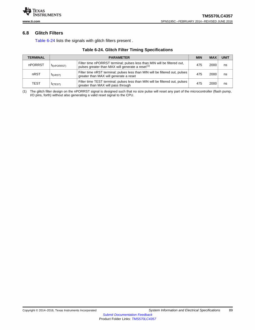
89
TMS570LC4357www.ti.com SPNS195C –FEBRUARY 2014–REVISED JUNE 2016
Submit Documentation FeedbackProduct Folder Links: TMS570LC4357
System Information and Electrical SpecificationsCopyright © 2014–2016, Texas Instruments Incorporated
(1) The glitch filter design on the nPORRST signal is designed such that no size pulse will reset any part of the microcontroller (flash pump,I/O pins, forth) without also generating a valid reset signal to the CPU.
6.8 Glitch FiltersTable 6-24 lists the signals with glitch filters present .
Table 6-24. Glitch Filter Timing Specifications
TERMINAL PARAMETER MIN MAX UNIT
nPORRST tf(nPORRST)Filter time nPORRST terminal; pulses less than MIN will be filtered out,pulses greater than MAX will generate a reset (1) 475 2000 ns
nRST tf(nRST)Filter time nRST terminal; pulses less than MIN will be filtered out, pulsesgreater than MAX will generate a reset 475 2000 ns
TEST tf(TEST)Filter time TEST terminal; pulses less than MIN will be filtered out, pulsesgreater than MAX will pass through 475 2000 ns

Flash (4MB)
RAM (512KB)
0x00000000
0x003FFFFF
0x08000000
0x0807FFFF
CRC10xFE000000
0xFEFFFFFF
SYSTEM Peripherals - Frame 10xFFFFFFFF
RAM - ECC0x08400000
0x0847FFFF
RESERVED
RESERVED
RESERVED
0xF0000000
EMIF (16MB * 3)
0x60000000
0x6FFFFFFF
CS2
RESERVED
CS3
RESERVED
CS4
Peripherals - Frame 20xFC000000
0xFCFFFFFF
EMIF (128MB)
0x80000000
0x87FFFFFF
CS0
RESERVED
reserved
Async RAM
SDRAM
0x64000000
0x68000000
0x6C000000
Flash
(Flash ECC, OTP and EEPROM accesses)
0xF047FFFF
Peripherals - Frame 3
0xFFF800000xFFF7FFFF
0xFF000000
0xFB000000
0xFBFFFFFFCRC2
RESERVED
R5F Cache0x30000000
0x33FFFFFF
RESERVED
RESERVED0x34000000
0x37FFFFFF
90
TMS570LC4357SPNS195C –FEBRUARY 2014–REVISED JUNE 2016 www.ti.com
Submit Documentation FeedbackProduct Folder Links: TMS570LC4357
System Information and Electrical Specifications Copyright © 2014–2016, Texas Instruments Incorporated
6.9 Device Memory Map
6.9.1 Memory Map DiagramFigure 6-9 shows the device memory map.
Figure 6-9. Memory Map

91
TMS570LC4357www.ti.com SPNS195C –FEBRUARY 2014–REVISED JUNE 2016
Submit Documentation FeedbackProduct Folder Links: TMS570LC4357
System Information and Electrical SpecificationsCopyright © 2014–2016, Texas Instruments Incorporated
6.9.2 Memory Map Table
Table 6-25. Module Registers / Memories Memory Map
TARGET NAME MEMORYSELECT
ADDRESS RANGEFRAME
SIZEACTUAL
SIZE
RESPONSE FORACCESS TO
UNIMPLEMENTEDLOCATIONS IN
FRAMESTART END
Level 2 Memories
Level 2 Flash Data Space 0x0000_0000 0x003F_FFFF 4MB 4MB Abort
Level 2 RAM 0x0800_0000 0x083F_FFFF 4MB 512KB Abort
Level 2 RAM ECC 0x0840_0000 0x087F_FFFF 4MB 512KB
Accelerator Coherency Port
Accelerator Coherency Port 0x0800_0000 0x087F_FFFF 8MB 512KB Abort
Level 1 Cache Memories
Cortex-R5F Data CacheMemory 0x3000_0000 0x30FF_FFFF 16MB 32KB Abort
Cortex-R5F Instruction CacheMemory 0x3100_0000 0x31FF_FFFF 16MB 32KB
External Memory Accesses
EMIF Chip Select 2(asynchronous) 0x6000_0000 0x63FF_FFFF 64MB 16MB Access to
"Reserved" spacewill generate AbortEMIF Chip Select 3
(asynchronous) 0x6400_0000 0x67FF_FFFF 64MB 16MB
EMIF Chip Select 4(asynchronous) 0x6800_0000 0x6BFF_FFFF 64MB 16MB
EMIF Chip Select 0(synchronous) 0x8000_0000 0x87FF_FFFF 128MB 128MB
Flash OTP, ECC, EEPROM Bank
Customer OTP, Bank0 0xF000_0000 0xF000_1FFF 8KB 4KB Abort
Customer OTP, Bank1 0xF000_2000 0xF000_3FFF 8KB 4KB
Customer OTP, EEPROMBank 0xF000_E000 0xF000_FFFF 8KB 1KB
Customer OTP-ECC, Bank0 0xF004_0000 0xF004_03FF 1KB 512B
Customer OTP-ECC, Bank1 0xF004_0400 0xF004_07FF 1KB 512B
Customer OTP-ECC,EEPROM Bank 0xF004_1C00 0xF004_1FFF 1KB 128B
TI OTP, Bank0 0xF008_0000 0xF008_1FFF 8KB 4KB
TI OTP, Bank1 0xF008_2000 0xF008_3FFF 8KB 4KB
TI OTP, EEPROM Bank 0xF008_E000 0xF008_FFFF 8KB 1KB
TI OTP-ECC, Bank0 0xF00C_0000 0xF00C_03FF 1KB 512B
TI OTP-ECC, Bank1 0xF00C_0400 0xF00C_07FF 1KB 512B Abort
TI OTP-ECC, EEPROM Bank 0xF00C_1C00 0xF00C_1FFF 1KB 128B
EEPROM Bank-ECC 0xF010_0000 0xF01F_FFFF 1MB 16KB
EEPROM Bank 0xF020_0000 0xF03F_FFFF 2MB 128KB
Flash Data Space ECC 0xF040_0000 0xF05F_FFFF 2MB 512KB
Interconnect SDC MMR
Interconnect SDC MMR 0xFA00_0000 0xFAFF_FFFF 16MB 16MB
Registers/Memories under PCR2 (Peripheral Segment 2)
CPPI Memory Slave (EthernetRAM) PCS[41] 0xFC52_0000 0xFC52_1FFF 8KB 8KB Abort
CPGMAC Slave (EthernetSlave) PS[30]-PS[31] 0xFCF7_8000 0xFCF7_87FF 2KB 2KB No Error
CPGMACSS Wrapper(Ethernet Wrapper) PS[29] 0xFCF7_8800 0xFCF7_88FF 256B 256B No Error
Ethernet MDIO Interface PS[29] 0xFCF7_8900 0xFCF7_89FF 256B 256B No Error

92
TMS570LC4357SPNS195C –FEBRUARY 2014–REVISED JUNE 2016 www.ti.com
Submit Documentation FeedbackProduct Folder Links: TMS570LC4357
System Information and Electrical Specifications Copyright © 2014–2016, Texas Instruments Incorporated
Table 6-25. Module Registers / Memories Memory Map (continued)
TARGET NAME MEMORYSELECT
ADDRESS RANGEFRAME
SIZEACTUAL
SIZE
RESPONSE FORACCESS TO
UNIMPLEMENTEDLOCATIONS IN
FRAMESTART END
ePWM1
PS[28]
0xFCF7_8C00 0xFCF7_8CFF 256B 256B Abort
ePWM2 0xFCF7_8D00 0xFCF7_8DFF 256B 256B Abort
ePWM3 0xFCF7_8E00 0xFCF7_8EFF 256B 256B Abort
ePWM4 0xFCF7_8F00 0xFCF7_8FFF 256B 256B Abort
ePWM5
PS[27]
0xFCF7_9000 0xFCF7_90FF 256B 256B Abort
ePWM6 0xFCF7_9100 0xFCF7_91FF 256B 256B Abort
ePWM7 0xFCF7_9200 0xFCF7_92FF 256B 256B Abort
eCAP1 0xFCF7_9300 0xFCF7_93FF 256B 256B Abort
eCAP2
PS[26]
0xFCF7_9400 0xFCF7_94FF 256B 256B Abort
eCAP3 0xFCF7_9500 0xFCF7_95FF 256B 256B Abort
eCAP4 0xFCF7_9600 0xFCF7_96FF 256B 256B Abort
eCAP5 0xFCF7_9700 0xFCF7_97FF 256B 256B Abort
eCAP6
PS[25]
0xFCF7_9800 0xFCF7_98FF 256B 256B Abort
eQEP1 0xFCF7_9900 0xFCF7_99FF 256B 256B Abort
eQEP2 0xFCF7_9A00 0xFCF7_9AFF 256B 256B Abort
PCR2 registers PPSE[4]–PPSE[5] 0xFCFF_1000 0xFCFF_17FF 2KB 2KB Reads return zeros,writes have no effect
NMPU (EMAC) PPSE[6] 0xFCFF_1800 0xFCFF_18FF 512B 512B Abort
EMIF Registers PPS[2] 0xFCFF_E800 0xFCFF_E8FF 256B 256B Abort
Cyclic Redundancy Checker (CRC) Module Register Frame
CRC10xFE00_0000 0xFEFF_FFFF 16MB 512KB
Accesses above0xFE000200
generate abort.
CRC20xFB00_0000 0xFBFF_FFFF 16MB 512KB
Accesses above0xFB000200
generate abort.

93
TMS570LC4357www.ti.com SPNS195C –FEBRUARY 2014–REVISED JUNE 2016
Submit Documentation FeedbackProduct Folder Links: TMS570LC4357
System Information and Electrical SpecificationsCopyright © 2014–2016, Texas Instruments Incorporated
Table 6-25. Module Registers / Memories Memory Map (continued)
TARGET NAME MEMORYSELECT
ADDRESS RANGEFRAME
SIZEACTUAL
SIZE
RESPONSE FORACCESS TO
UNIMPLEMENTEDLOCATIONS IN
FRAMESTART END
Memories under User PCR3 (Peripheral Segment 3)
MIBSPI5 RAM PCS[5] 0xFF0A_0000 0xFF0B_FFFF 128KB 2KB Abort for accessesabove 2KB
MIBSPI4 RAM PCS[3] 0xFF06_0000 0xFF07_FFFF 128KB 2KB Abort for accessesabove 2KB
MIBSPI3 RAM PCS[6] 0xFF0C_0000 0xFF0D_FFFF 128KB 2KB Abort for accessesabove 2KB
MIBSPI2 RAM PCS[4] 0xFF08_0000 0xFF09_FFFF 128KB 2KB Abort for accessesabove 2KB
MIBSPI1 RAM PCS[7] 0xFF0E_0000 0xFF0F_FFFF 128KB 4KB Abort for accessesabove 4KB
DCAN4 RAMPCS[12] 0xFF18_0000 0xFF19_FFFF 128KB 8KB
Abort generated foraccesses beyond
offset 0x2000
DCAN3 RAMPCS[13] 0xFF1A_0000 0xFF1B_FFFF 128KB 8KB
Abort generated foraccesses beyond
offset 0x2000
DCAN2 RAMPCS[14] 0xFF1C_0000 0xFF1D_FFFF 128KB 8KB
Abort generated foraccesses beyond
offset 0x2000
DCAN1 RAMPCS[15] 0xFF1E_0000 0xFF1F_FFFF 128KB 8KB
Abort generated foraccesses beyond
offset 0x2000.
MIBADC2 RAM
PCS[29] 0xFF3A_0000 0xFF3B_FFFF 128KB 8KB
Wrap around foraccesses to
unimplementedaddress offsets
lower than 0x1FFF.
MIBADC1 RAM
PCS[31] 0xFF3E_0000 0xFF3F_FFFF 128KB
8KB
Wrap around foraccesses to
unimplementedaddress offsets
lower than 0x1FFF.
MIBADC1 Look-UP Table
384 bytes
Look-Up Table forADC1 wrapper.
Starts at addressoffset 0x2000 andends at address
offset 0x217F. Wraparound for accesses
between offsets0x0180 and 0x3FFF.Abort generation for
accesses beyondoffset 0x4000.
NHET2 RAM
PCS[34] 0xFF44_0000 0xFF45_FFFF 128KB 16KB
Wrap around foraccesses to
unimplementedaddress offsets
lower than 0x3FFF.Abort generated foraccesses beyond
0x3FFF.
NHET1 RAM
PCS[35] 0xFF46_0000 0xFF47_FFFF 128KB 16KB
Wrap around foraccesses to
unimplementedaddress offsets
lower than 0x3FFF.Abort generated foraccesses beyond
0x3FFF.
HET TU2 RAM PCS[38] 0xFF4C_0000 0xFF4D_FFFF 128KB 1KB Abort
HET TU1 RAM PCS[39] 0xFF4E_0000 0xFF4F_FFFF 128KB 1KB Abort
FlexRay TU RAM PCS[40] 0xFF50_0000 0xFF51_FFFF 128KB 1KB Abort

94
TMS570LC4357SPNS195C –FEBRUARY 2014–REVISED JUNE 2016 www.ti.com
Submit Documentation FeedbackProduct Folder Links: TMS570LC4357
System Information and Electrical Specifications Copyright © 2014–2016, Texas Instruments Incorporated
Table 6-25. Module Registers / Memories Memory Map (continued)
TARGET NAME MEMORYSELECT
ADDRESS RANGEFRAME
SIZEACTUAL
SIZE
RESPONSE FORACCESS TO
UNIMPLEMENTEDLOCATIONS IN
FRAMESTART END
CoreSight Debug Components
CoreSight Debug ROM CSCS[0] 0xFFA0_0000 0xFFA0_0FFF 4KB 4KB Reads return zeros,writes have no effect
Cortex-R5F Debug CSCS[1] 0xFFA0_1000 0xFFA0_1FFF 4KB 4KB Reads return zeros,writes have no effect
ETM-R5 CSCS[2] 0xFFA0_2000 0xFFA0_2FFF 4KB 4KB Reads return zeros,writes have no effect
CoreSight TPIU CSCS[3] 0xFFA0_3000 0xFFA0_3FFF 4KB 4KB Reads return zeros,writes have no effect
POM CSCS[4] 0xFFA0_4000 0xFFA0_4FFF 4KB 4KB Reads return zeros,writes have no effect
CTI1 CSCS[7] 0xFFA0_7000 0xFFA0_7FFF 4KB 4KB Reads return zeros,writes have no effect
CTI3 CSCS[9] 0xFFA0_9000 0xFFA0_9FFF 4KB 4KB Reads return zeros,writes have no effect
CTI4 CSCS[10] 0xFFA0_A000 0xFFA0_AFFF 4KB 4KB Reads return zeros,writes have no effect
CSTF CSCS[11] 0xFFA0_B000 0xFFA0_BFFF 4KB 4KB Reads return zeros,writes have no effect
Registers under PCR3 (Peripheral Segment 3)
PCR3 registers PS[31:30] 0xFFF7_8000 0xFFF7_87FF 2KB 2KB Reads return zeros,writes have no effect
FTU PS[23] 0xFFF7_A000 0xFFF7_A1FF 512B 512B Reads return zeros,writes have no effect
HTU1 PS[22] 0xFFF7_A400 0xFFF7_A4FF 256B 256B Abort
HTU2 PS[22] 0xFFF7_A500 0xFFF7_A5FF 256B 256B Abort
NHET1 PS[17] 0xFFF7_B800 0xFFF7_B8FF 256B 256B Reads return zeros,writes have no effect
NHET2 PS[17] 0xFFF7_B900 0xFFF7_B9FF 256B 256B Reads return zeros,writes have no effect
GIO PS[16] 0xFFF7_BC00 0xFFF7_BCFF 256B 256B Reads return zeros,writes have no effect
MIBADC1 PS[15] 0xFFF7_C000 0xFFF7_C1FF 512B 512B Reads return zeros,writes have no effect
MIBADC2 PS[15] 0xFFF7_C200 0xFFF7_C3FF 512B 512B Reads return zeros,writes have no effect
FlexRay PS[12]+PS[13] 0xFFF7_C800 0xFFF7_CFFF 2KB 2KB Reads return zeros,writes have no effect
I2C1 PS[10] 0xFFF7_D400 0xFFF7_D4FF 256B 256B Reads return zeros,writes have no effect
I2C2 PS[10] 0xFFF7_D500 0xFFF7_D5FF 256B 256B Reads return zeros,writes have no effect
DCAN1 PS[8] 0xFFF7_DC00 0xFFF7_DDFF 512B 512B Reads return zeros,writes have no effect
DCAN2 PS[8] 0xFFF7_DE00 0xFFF7_DFFF 512B 512B Reads return zeros,writes have no effect
DCAN3 PS[7] 0xFFF7_E000 0xFFF7_E1FF 512B 512B Reads return zeros,writes have no effect
DCAN4 PS[7] 0xFFF7_E200 0xFFF7_E3FF 512B 512B Reads return zeros,writes have no effect
LIN1 PS[6] 0xFFF7_E400 0xFFF7_E4FF 256B 256B Reads return zeros,writes have no effect
SCI3 PS[6] 0xFFF7_E500 0xFFF7_E5FF 256B 256B Reads return zeros,writes have no effect
LIN2 PS[6] 0xFFF7_E600 0xFFF7_E6FF 256B 256B Reads return zeros,writes have no effect
SCI4 PS[6] 0xFFF7_E700 0xFFF7_E7FF 256B 256B Reads return zeros,writes have no effect

95
TMS570LC4357www.ti.com SPNS195C –FEBRUARY 2014–REVISED JUNE 2016
Submit Documentation FeedbackProduct Folder Links: TMS570LC4357
System Information and Electrical SpecificationsCopyright © 2014–2016, Texas Instruments Incorporated
Table 6-25. Module Registers / Memories Memory Map (continued)
TARGET NAME MEMORYSELECT
ADDRESS RANGEFRAME
SIZEACTUAL
SIZE
RESPONSE FORACCESS TO
UNIMPLEMENTEDLOCATIONS IN
FRAMESTART END
MibSPI1 PS[2] 0xFFF7_F400 0xFFF7_F5FF 512B 512B Reads return zeros,writes have no effect
MibSPI2 PS[2] 0xFFF7_F600 0xFFF7_F7FF 512B 512B Reads return zeros,writes have no effect
MibSPI3 PS[1] 0xFFF7_F800 0xFFF7_F9FF 512B 512B Reads return zeros,writes have no effect
MibSPI4 PS[1] 0xFFF7_FA00 0xFFF7_FBFF 512B 512B Reads return zeros,writes have no effect
MibSPI5 PS[0] 0xFFF7_FC00 0xFFF7_FDFF 512B 512B Reads return zeros,writes have no effect
System Modules Control Registers and Memories under PCR1 (Peripheral Segment 1)
DMA RAM PPCS[0] 0xFFF8_0000 0xFFF8_0FFF 4KB 4KB Abort
VIM RAM
PPCS[2] 0xFFF8_2000 0xFFF8_2FFF 4KB 4KB
Wrap around foraccesses to
unimplementedaddress offsets
lower than 0x2FFF.
RTP RAM PPCS[3] 0xFFF8_3000 0xFFF8_3FFF 4KB 4KB Abort
Flash Wrapper PPCS[7] 0xFFF8_7000 0xFFF8_7FFF 4KB 4KB Abort
eFuse Farm Controller PPCS[12] 0xFFF8_C000 0xFFF8_CFFF 4KB 4KB Abort
Power Domain Control (PMM) PPSE[0] 0xFFFF_0000 0xFFFF_01FF 512B 512B Abort
FMTMNote: This module is only usedby TI during test
PPSE[1] 0xFFFF_0400 0xFFFF_05FF 512B 512BReads return zeros,writes have no effect
STC2 (NHET1/2) PPSE[2] 0xFFFF_0800 0xFFFF_08FF 256B 256B Reads return zeros,writes have no effect
SCM PPSE[2] 0xFFFF_0A00 0xFFFF_0AFF 256B 256B Abort
EPC PPSE[3] 0xFFFF_0C00 0xFFFF_0FFF 1KB 1KB Abort
PCR1 registers PPSE[4]–PPSE[5] 0xFFFF_1000 0xFFFF_17FF 2KB 2KB Reads return zeros,writes have no effect
NMPU (PS_SCR_S) PPSE[6] 0xFFFF_1800 0xFFFF_19FF 512B 512B Abort
NMPU (DMA Port A) PPSE[6] 0xFFFF_1A00 0xFFFF_1BFF 512B 512B Abort
Pin Mux Control (IOMM) PPSE[7] 0xFFFF_1C00 0xFFFF_1FFF 2KB 1KB Reads return zeros,writes have no effect
System Module - Frame 2 (seethe TRM SPNU563) PPS[0] 0xFFFF_E100 0xFFFF_E1FF 256B 256B Reads return zeros,
writes have no effect
PBIST PPS[1] 0xFFFF_E400 0xFFFF_E5FF 512B 512B Reads return zeros,writes have no effect
STC1 (Cortex-R5F) PPS[1] 0xFFFF_E600 0xFFFF_E6FF 256B 256B Reads return zeros,writes have no effect
DCC1 PPS[3] 0xFFFF_EC00 0xFFFF_ECFF 256B 256B Reads return zeros,writes have no effect
DMA PPS[4] 0xFFFF_F000 0xFFFF_F3FF 1KB 1KB Abort
DCC2 PPS[5] 0xFFFF_F400 0xFFFF_F4FF 256B 256B Reads return zeros,writes have no effect
ESM register PPS[5] 0xFFFF_F500 0xFFFF_F5FF 256B 256B Reads return zeros,writes have no effect
CCM-R5F PPS[5] 0xFFFF_F600 0xFFFF_F6FF 256B 256B Reads return zeros,writes have no effect
DMM PPS[5] 0xFFFF_F700 0xFFFF_F7FF 256B 256B Reads return zeros,writes have no effect
L2RAMW PPS[6] 0xFFFF_F900 0xFFFF_F9FF 256B 256B Abort
RTP PPS[6] 0xFFFF_FA00 0xFFFF_FAFF 256B 256B Reads return zeros,writes have no effect
RTI + DWWD PPS[7] 0xFFFF_FC00 0xFFFF_FCFF 256B 256B Reads return zeros,writes have no effect

96
TMS570LC4357SPNS195C –FEBRUARY 2014–REVISED JUNE 2016 www.ti.com
Submit Documentation FeedbackProduct Folder Links: TMS570LC4357
System Information and Electrical Specifications Copyright © 2014–2016, Texas Instruments Incorporated
Table 6-25. Module Registers / Memories Memory Map (continued)
TARGET NAME MEMORYSELECT
ADDRESS RANGEFRAME
SIZEACTUAL
SIZE
RESPONSE FORACCESS TO
UNIMPLEMENTEDLOCATIONS IN
FRAMESTART END
VIM PPS[7] 0xFFFF_FD00 0xFFFF_FEFF 512B 512B Reads return zeros,writes have no effect
System Module - Frame 1 (seethe TRM SPNU563) PPS[7] 0xFFFF_FF00 0xFFFF_FFFF 256B 256B Reads return zeros,
writes have no effect
6.9.3 Special Consideration for CPU Access Errors Resulting in Imprecise AbortsAny CPU write access to a Normal or Device type memory, which generates a fault, will generate animprecise abort. The imprecise abort exception is disabled by default and must be enabled for the CPU tohandle this exception. The imprecise abort handling is enabled by clearing the "A" bit in the CPU programstatus register (CPSR).

97
TMS570LC4357www.ti.com SPNS195C –FEBRUARY 2014–REVISED JUNE 2016
Submit Documentation FeedbackProduct Folder Links: TMS570LC4357
System Information and Electrical SpecificationsCopyright © 2014–2016, Texas Instruments Incorporated
6.9.4 Master/Slave Access PrivilegesTable 6-26 and Table 6-27 list the access permissions for each bus master on the device. A bus master isa module that can initiate a read or a write transaction on the device.
Each slave module on either the CPU Interconnect Subsystem or the Peripheral Interconnect Subsystemis listed in Table 6-27. Allowed indicates that the module listed in the MASTERS column can access thatslave module.
Table 6-26. Bus Master / Slave Access Matrix for CPU Interconnect Subsystem
MASTERSSLAVES ON CPU INTERCONNECT SUBSYSTEM
L2 Flash OTP, ECC,Bank 7 (EEPROM) L2 FLASH L2 SRAM CACHE MEMORY EMIF
CPU Read Allowed Allowed Allowed Allowed AllowedCPU Write Not allowed Not allowed Allowed Allowed AllowedDMA PortA Allowed Allowed Allowed Not allowed Allowed
POM Not allowed Not allowed Allowed Not allowed AllowedPS_SCR_M Allowed Allowed Allowed Not allowed Allowed
ACP_M Not allowed Not Allowed Allowed Not allowed Not allowed
Table 6-27. Bus Master / Slave Access Matrix for Peripheral Interconnect Subsystem
MASTER ID TOPCRx MASTERS
SLAVES ON PERIPHERAL INTERCONNECT SUBSYSTEM
CRC1/CRC2 Resources UnderPCR2 and PCR3
Resources UnderPCR1
CPU InterconnectSubsystem SDCMMR Port (seeSection 6.9.6 )
0CPU Read Allowed Allowed Allowed AllowedCPU Write Allowed Allowed Allowed Allowed
1 Reserved – – – –2 DMA PortB Allowed Allowed Allowed Not allowed3 HTU1 Not allowed Not allowed Not allowed Not allowed4 HTU2 Not allowed Not allowed Not allowed Not allowed5 FTU Not allowed Not allowed Not allowed Not allowed7 DMM Allowed Allowed Allowed Allowed9 DAP Allowed Allowed Allowed Allowed10 EMAC Not allowed Allowed Not allowed Not allowed
6.9.4.1 Special Notes on Accesses to Certain Slaves
By design only the CPU and debugger can have privileged write access to peripherals under the PCR1segment. The other masters can only read from these registers.
The master-id filtering check is implemented inside each PCR module of each peripheral segment andcan be used to block certain masters from write accesses to certain peripherals. An unauthorized masterwrite access detected by the PCR will result in the transaction being discarded and an error beinggenerated to the ESM module.
The device contains dedicated logic to generate a bus error response on any access to a module that is ina power domain that has been turned off.

ID Decode Addr Decode
MasterID Address/Control
4
Ma
ste
rID
Pro
tect
ion
Re
gis
ter
N
Peripheral Select N
0
1
2
13
14
15
PCRx
98
TMS570LC4357SPNS195C –FEBRUARY 2014–REVISED JUNE 2016 www.ti.com
Submit Documentation FeedbackProduct Folder Links: TMS570LC4357
System Information and Electrical Specifications Copyright © 2014–2016, Texas Instruments Incorporated
6.9.5 MasterID to PCRxThe MasterID associated with each master port on the Peripheral Interconnect Subsystem contains a 4-bitvalue. The MasterID is passed along with the address and control signals to three PCR modules. PCRdecodes the address and control signals to select the peripheral. In addition, it decodes this 4-bit MasterIDvalue to perform memory protection. With 4-bit of MasterID, it allows the PCR to distinguish among 16different masters to allow or disallow access to a given peripheral. Associated with each peripheral a 16-bit MasterID access protection register is defined. Each bit grants or denies the permission of thecorresponding binary coded decimal MasterID. For example, if bit 5 of the access permission register isset, it grants MasterID 5 to access the peripheral. If bit 7 is clear, it denies MasterID 7 to access theperipheral. Figure 6-10 shows the MasterID filtering scheme. Table 6-27 lists the MasterID of each master,which can access the PCRx.
Figure 6-10. PCR MasterID Filtering
6.9.6 CPU Interconnect Subsystem SDC MMR PortThe CPU Interconnect Subsystem SDC MMR Port is a special slave to the Peripheral InterconnectSubsystem. It is memory mapped at starting address of 0xFA00_0000. Various status registers pertainingto the diagnostics of the CPU Interconnect Subsystem can be access through this slave port. The CPUInterconnect Subsystem contains built-in hardware diagnostic checkers which will constantly watchtransactions flowing through the interconnect. There is a checker for each master and slave attached tothe CPU Interconnect Subsystem. The checker checks the expected behavior against the generatedbehavior by the interconnect. For example, if the CPU issues a burst read request to the flash, thechecker will ensure that the expected behavior is indeed a burst read request to the proper slave module.If the interconnects generates a transaction which is not a read, or not a burst or not to the flash as thedestination, then the checker will flag it one of the registers. The detected error will also be signaled to theESM module. Refer to the Interconnect chapter of the TRM SPNU563 for details on the registers.

99
TMS570LC4357www.ti.com SPNS195C –FEBRUARY 2014–REVISED JUNE 2016
Submit Documentation FeedbackProduct Folder Links: TMS570LC4357
System Information and Electrical SpecificationsCopyright © 2014–2016, Texas Instruments Incorporated
Table 6-28. CPU Interconnect Subsystem SDC Register Bit Field Mapping
Register name bit 0 bit 1 bit 2 bit 3 bit 4 bit 5 bit 6 Remark
ERR_GENERIC_PARITY PS_SCR_M POM DMA_PORTA Reserved CPU AXI-M ACP-M Reserved
• Each bit indicates thetransaction processing blockinside the interconnectcorresponding to the masterthat is detected by theinterconnect checker to havea fault.
• error related to paritymismatch in the incomingaddress
ERR_UNEXPECTED_TRANS PS_SCR_M POM DMA_PORTA Reserved CPU AXI-M ACP-M Reserved• error related to unexpected
transaction sent by themaster
ERR_TRANS_ID PS_SCR_M POM DMA_PORTA Reserved CPU AXI-M ACP-M Reserved • error related to mismatch onthe transaction ID
ERR_TRANS_SIGNATURE PS_SCR_M POM DMA_PORTA Reserved CPU AXI-M ACP-M Reserved • error related to mismatch onthe transaction signature
ERR_TRANS_TYPE PS_SCR_M POM DMA_PORTA Reserved CPU AXI-M ACP-M Reserved • error related to mismatch onthe transaction type
ERR_USER_PARITY PS_SCR_M POM DMA_PORTA Reserved CPU AXI-M ACP-M Reserved • error related to mismatch onthe parity
SERR_UNEXPECTED_MID L2 RAM Wrapper L2 FlashWrapper Port A
L2 Flash WrapperPort B EMIF Reserved CPU AXi-S ACP-S
• Each bit indicates thetransaction processing blockinside the interconnectcorresponding to the slavethat is detected by theinterconnect checker to havea fault.
• error related to mismatch onthe master ID
SERR_ADDR_DECODE L2 RAM Wrapper L2 FlashWrapper Port A
L2 Flash WrapperPort B EMIF Reserved CPU AXi-S ACP-S
• error related to mismatch onthe most significant addressbits
SERR_USER_PARITY L2 RAM Wrapper L2 FlashWrapper Port A
L2 Flash WrapperPort B EMIF Reserved CPU AXi-S ACP-S
• error related to mismatch onthe parity of the mostsignificant address bits

100
TMS570LC4357SPNS195C –FEBRUARY 2014–REVISED JUNE 2016 www.ti.com
Submit Documentation FeedbackProduct Folder Links: TMS570LC4357
System Information and Electrical Specifications Copyright © 2014–2016, Texas Instruments Incorporated
6.9.7 Parameter Overlay Module (POM) ConsiderationsThe Parameter Overlay Module (POM) is implemented as part of the L2FMC module. It is used to redirectflash memory accesses to external memory interfaces or internal SRAM. The POM has an OCP masterport to redirect accesses. The POM MMRs are located in a separate block and read/writes will happenthrough the Debug APB port on the L2FMC. The POM master port is capable of read accesses only.Inside the CPU Subsystem SCR, the POM master port is connected to both the L2RAMW and EMIFslaves. The primary roles of the POM are:• The POM snoops the access on the two flash slave ports to determine if access should be remapped or not. It
supports 32 regions among the two slave ports.• If access is to be remapped, then the POM kills the access to the flash bank, and instead redirects the access
through its own master.• Upon obtaining response, the POM populates the response FIFO of the respective port so that the response is
delivered back to the original requester.• The access is unaffected if the request is not mapped to any region, or if the POM is disabled.• The POM does not add any latency to the flash access when it is turned off.• The POM does not add any latency to the remapped access (except the latency, if any, associated with the getting
the response from the an alternate slave)

101
TMS570LC4357www.ti.com SPNS195C –FEBRUARY 2014–REVISED JUNE 2016
Submit Documentation FeedbackProduct Folder Links: TMS570LC4357
System Information and Electrical SpecificationsCopyright © 2014–2016, Texas Instruments Incorporated
6.10 Flash Memory
6.10.1 Flash Memory ConfigurationFlash Bank: A separate block of logic consisting of 1 to 16 sectors. Each flash bank normally has acustomer-OTP and a TI-OTP area. These flash sectors share input/output buffers, data paths, senseamplifiers, and control logic.
Flash Sector: A contiguous region of flash memory which must be erased simultaneously due to physicalconstruction constraints.
Flash Pump: A charge pump which generates all the voltages required for reading, programming, orerasing the flash banks.
Flash Module: Interface circuitry required between the host CPU and the flash banks and pump module.
Table 6-29. Flash Memory Banks and Sectors
MEMORY ARRAYS (OR BANKS) SECTORNO. SEGMENT LOW ADDRESS HIGH ADDRESS
BANK0 (2.0MB)
0 16KB 0x0000_0000 0x0000_3FFF1 16KB 0x0000_4000 0x0000_7FFF2 16KB 0x0000_8000 0x0000_BFFF3 16KB 0x0000_C000 0x0000_FFFF4 16KB 0x0001_0000 0x0001_3FFF5 16KB 0x0001_4000 0x0001_7FFF6 32KB 0x0001_8000 0x0001_FFFF7 128KB 0x0002_0000 0x0003_FFFF8 128KB 0x0004_0000 0x0005_FFFF9 128KB 0x0006_0000 0x0007_FFFF10 256KB 0x0008_0000 0x000B_FFFF11 256KB 0x000C_0000 0x000F_FFFF12 256KB 0x0010_0000 0x0013_FFFF13 256KB 0x0014_0000 0x0017_FFFF14 256KB 0x0018_0000 0x001B_FFFF15 256KB 0x001C_0000 0x001F_FFFF
BANK1 (2.0MB)
0 128KB 0x0020_0000 0x0021_FFFF1 128KB 0x0022_0000 0x0023_FFFF2 128KB 0x0024_0000 0x0025_FFFF3 128KB 0x0026_0000 0x0027_FFFF4 128KB 0x0028_0000 0x0029_FFFF5 128KB 0x002A_0000 0x002B_FFFF6 128KB 0x002C_0000 0x002D_FFFF7 128KB 0x002E_0000 0x002F_FFFF8 128KB 0x0030_0000 0x0031_FFFF9 128KB 0x0032_0000 0x0033_FFFF10 128KB 0x0034_0000 0x0035_FFFF11 128KB 0x0036_0000 0x0037_FFFF12 128KB 0x0038_0000 0x0039_FFFF13 128KB 0x003A_0000 0x003B_FFFF14 128KB 0x003C_0000 0x003D_FFFF15 128KB 0x003E_0000 0x003F_FFFF

MRC p15,#0,r1,c9,c12,#0 ;Enabling Event monitor states
ORR r1, r1, #0x00000010
MCR p15,#0,r1,c9,c12,#0 ;Set 4th bit (‘X’) of PMNC register
MRC p15,#0,r1,c9,c12,#0
102
TMS570LC4357SPNS195C –FEBRUARY 2014–REVISED JUNE 2016 www.ti.com
Submit Documentation FeedbackProduct Folder Links: TMS570LC4357
System Information and Electrical Specifications Copyright © 2014–2016, Texas Instruments Incorporated
Table 6-30. EEPROM Flash Bank
MEMORY ARRAYS (OR BANKS) SECTORNO. SEGMENT LOW ADDRESS HIGH ADDRESS
BANK7 (128KB) for EEPROM emulation
0 4KB 0xF020_0000 0xF020_0FFF"""
"""
"""
"""
31 4KB 0xF021_F000 0xF021_FFFF
6.10.2 Main Features of Flash Module• Support for multiple flash banks for program and/or data storage• Simultaneous read accesses on two banks while performing program or erase operation on any other bank• Integrated state machines to automate flash erase and program operations• Software interface for flash program and erase operations• Pipelined mode operation to improve instruction access interface bandwidth• Support for Single Error Correction Double Error Detection (SECDED) block inside Cortex-R5F CPU• Support for a rich set of diagnostic features
6.10.3 ECC Protection for Flash AccessesAll accesses to the L2 program flash memory are protected by SECDED logic embedded inside the CPU.The flash module provides 8 bits of ECC code for 64 bits of instructions or data fetched from the flashmemory. The CPU calculates the expected ECC code based on the 64 bits data received and compares itwith the ECC code returned by the flash module. A single-bit error is corrected and flagged by the CPU,while a multibit error is only flagged. The CPU signals an ECC error through its Event bus. This signalingmechanism is not enabled by default and must be enabled by setting the 'X' bit of the PerformanceMonitor Control Register, c9.
NOTEECC is permanently enabled in the CPU L2 interface.
6.10.4 Flash Access SpeedsFor information on flash memory access speeds and the relevant wait states required, refer to Section 5.6.

103
TMS570LC4357www.ti.com SPNS195C –FEBRUARY 2014–REVISED JUNE 2016
Submit Documentation FeedbackProduct Folder Links: TMS570LC4357
System Information and Electrical SpecificationsCopyright © 2014–2016, Texas Instruments Incorporated
(1) This programming time includes overhead of state machine, but does not include data transfer time. The programming time assumesprogramming 288 bits at a time at the maximum specified operating frequency.
6.10.5 Flash Program and Erase Timings
6.10.5.1 Flash Program and Erase Timings for Program Flash
Table 6-31. Timing Requirements for Program Flash
MIN NOM MAX UNITtprog(288bits) Wide Word (288-bits) programming time 40 300 µs
tprog(Total) 4.0MB programming time (1)–40°C to 125°C 21.3 s0°C to 60°C, for first25 cycles 5.3 10.6 s
terase Sector/Bank erase time–40°C to 125°C 0.3 4 s0°C to 60°C, for first25 cycles 100 ms
twecWrite/erase cycles with 15-year Data Retentionrequirement –40°C to 125°C 1000 cycles
(1) This programming time includes overhead of state machine, but does not include data transfer time. The programming time assumesprogramming 72 bits at a time at the maximum specified operating frequency.
6.10.5.2 Flash Program and Erase Timings for Data Flash
Table 6-32. Timing Requirements for Data Flash
MIN NOM MAX UNITtprog(72bits) Wide Word (72-bits) programming time 47 300 µs
tprog(Total)EEPROM Emulation (bank 7) 128KBprogramming time (1)
–40°C to 125°C 2.6 s0°C to 60°C, for first25 cycles 775 1320 ms
EEPROM Emulation (bank 7) Sector/Bank erase time terase(bank7)
–40°C to 125°C 0.2 8 s0°C to 60°C, for first25 cycles 14 100 ms
twecWrite/erase cycles with 15-year Data Retentionrequirement –40°C to 125°C 100000 cycles

104
TMS570LC4357SPNS195C –FEBRUARY 2014–REVISED JUNE 2016 www.ti.com
Submit Documentation FeedbackProduct Folder Links: TMS570LC4357
System Information and Electrical Specifications Copyright © 2014–2016, Texas Instruments Incorporated
6.11 L2RAMW (Level 2 RAM Interface Module)L2RAMW is the TMS570 level two RAM wrapper. Major features implemented in this device include:• Supports 512KB of L2 SRAMs• One 64-bit OCP interface• Built-in ECC generation and evaluation logic
– The ECC logic is enabled by default.– When enabled, automatic ECC correction on write data from masters on any write sizes (8-,16-,32-,or 64-bit)– Less than 64-bit write forces built in read-modify-write– When enabled, reads due to read-modify-write go through ECC correction before data merging with the
incoming write data• Redundant address decoding. Same address decode logic block is duplicated and compared to each other• Data Trace
– Support tracing of both read and write accesses through RTP module• Auto initialization of memory banks to known values for both data and their corresponding ECC checksum
6.11.1 L2 SRAM InitializationThe entire L2 SRAM can be globally initialized by setting the corresponding bit in SYS.MSINENA register.When initialized, the memory arrays are written with all zeros for the 64-bit data and the corresponding 8-bit ECC checksum. Hardware memory initialization eliminates ECC error when the CPU reads from an un-initialized memory location which can cause an ECC error. For more information, see the device-specificTechnical Reference Manual.
6.12 ECC / Parity Protection for Accesses to Peripheral RAMsAccesses to some peripheral RAMs are protected by either odd/even parity checking or ECC checking.During a read access the parity or ECC is calculated based on the data read from the peripheral RAM andcompared with the good parity or ECC value stored in the peripheral RAM for that peripheral. If any wordfails the parity or ECC check, the module generates a ECC/parity error signal that is mapped to the ErrorSignaling Module. The module also captures the peripheral RAM address that caused the parity error.
The parity or ECC protection for peripheral RAMs is not enabled by default and must be enabled by theapplication. Each individual peripheral contains control registers to enable the parity or ECC protection foraccesses to its RAM.
NOTEFor peripherals with parity protection the CPU read access gets the actual data from theperipheral. The application can choose to generate an interrupt whenever a peripheral RAMparity error is detected.

105
TMS570LC4357www.ti.com SPNS195C –FEBRUARY 2014–REVISED JUNE 2016
Submit Documentation FeedbackProduct Folder Links: TMS570LC4357
System Information and Electrical SpecificationsCopyright © 2014–2016, Texas Instruments Incorporated
(1) March13N is the only algorithm recommended for application testing of RAM.(2) ATB RAM is part of the ETM module. PBIST testing of this RAM is limited to 85ºC or lower.
6.13 On-Chip SRAM Initialization and Testing
6.13.1 On-Chip SRAM Self-Test Using PBIST
6.13.1.1 Features• Extensive instruction set to support various memory test algorithms• ROM-based algorithms allow application to run TI production-level memory tests• Independent testing of all on-chip SRAM
6.13.1.2 PBIST RAM Groups
Table 6-33. PBIST RAM Grouping
MEMORY RAMGROUP TEST CLOCK RGS RDS MEM
TYPENO.
BANKS
TEST PATTERN(ALGORITHM)
TRIPLEREAD
SLOW READ
TRIPLEREAD
FAST READ
March 13N (1)
TWO PORT(cycles)
March 13N (1)
SINGLEPORT
(cycles)
ALGO MASK0x1
ALGO MASK0x2
ALGO MASK0x4
ALGO MASK0x8
PBIST_ROM 1 GCM_PBIST_ROM 1 1 ROM 1 24578 8194
STC1_1_ROM_R5 2 GCM_PBIST_ROM 14 1 ROM 1 49154 16386
STC1_2_ROM_R5 3 GCM_PBIST_ROM 14 2 ROM 1 49154 16386
STC2_ROM_NHET 4 GCM_PBIST_ROM 15 1 ROM 1 46082 15362
AWM1 5 GCM_VCLKP 2 1 2P 1 4210
DCAN1 6 GCM_VCLKP 3 1..6 2P 2 25260
DCAN2 7 GCM_VCLKP 4 1..6 2P 2 25260
DMA 8 GCM_HCLK 5 1..6 2P 2 37740
HTU1 9 GCM_VCLK2 6 1..6 2P 2 6540
MIBSPI1 10 GCM_VCLKP 8 1..4 2P 2 66760
MIBSPI2 11 GCM_VCLKP 9 1..4 2P 2 33480
MIBSPI3 12 GCM_VCLKP 10 1..4 2P 2 33480
NHET1 13 GCM_VCLK2 11 1..12 2P 4 50520
VIM 14 GCM_VCLK 12 1..2 2P 1 16740
Reserved 15 - - - - - -
RTP 16 GCM_HCLK 16 1..12 2P 4 50520
ATB (2) 17 GCM_GCLK1 17 1..16 2P 8 133920
AWM2 18 GCM_VCLKP 18 1 2P 1 4210
DCAN3 19 GCM_VCLKP 19 1..6 2P 2 25260
DCAN4 20 GCM_VCLKP 20 1..6 2P 2 25260
HTU2 21 GCM_VCLK2 21 1..6 2P 2 6540
MIBSPI4 22 GCM_VCLKP 22 1..4 2P 2 33480
MIBSPI5 23 GCM_VCLKP 23 1..4 2P 2 33480
NHET2 24 GCM_VCLK2 24 1..12 2P 4 50520
FTU 25 GCM_VCLKP 25 1 2P 1 8370
FRAY_INBUF_OUTBUF 26 GCM_VCLKP 26 1..8 2P 4 33680
CPGMAC_STATE_RXADDR 27 GCM_VCLK3 27 1..3 2P 2 6390
CPGMAC_STAT_FIFO 28 GCM_VCLK3 27 4..6 2P 3 8730

106
TMS570LC4357SPNS195C –FEBRUARY 2014–REVISED JUNE 2016 www.ti.com
Submit Documentation FeedbackProduct Folder Links: TMS570LC4357
System Information and Electrical Specifications Copyright © 2014–2016, Texas Instruments Incorporated
Table 6-33. PBIST RAM Grouping (continued)
MEMORY RAMGROUP TEST CLOCK RGS RDS MEM
TYPENO.
BANKS
TEST PATTERN(ALGORITHM)
TRIPLEREAD
SLOW READ
TRIPLEREAD
FAST READ
March 13N (1)
TWO PORT(cycles)
March 13N (1)
SINGLEPORT
(cycles)
ALGO MASK0x1
ALGO MASK0x2
ALGO MASK0x4
ALGO MASK0x8
L2RAMW 29 GCM_HCLK 71 SP 4
5325806 SP 4
L2RAMW 30 GCM_HCLK 32
1 SP 4
1597740
6 SP 4
11 SP 4
16 SP 4
21 SP 4
26 SP 4
R5_ICACHE 31 GCM_GCLK1 40
1 SP 4
1666006 SP 4
11 SP 4
16 SP 4
R5_DCACHE 32 GCM_GCLK1 41
1 SP 4
299820
6 SP 4
11 SP 4
16 SP 4
21 SP 4
26 SP 4
Reserved 33 GCM_GCLK2 43
1 SP 4
1666006 SP 4
11 SP 4
16 SP 4
Reserved 34 GCM_GCLK2 44
1 SP 4
299820
6 SP 4
11 SP 4
16 SP 4
21 SP 4
26 SP 4
FRAY_TRBUF_MSGRAM 35 GCM_VCLKP 26 9..11 SP 3 149910
CPGMAC_CPPI 36 GCM_VCLK3 27 7 SP 1 133170
R5_DCACHE_Dirty 37 GCM_GCLK1 42 2 SP 1 16690
Reserved 38 - - - - - -
Several memory testing algorithms are stored in the PBIST ROM. However, TI only recommends theMarch13N algorithm for application testing of RAM.
The PBIST ROM clock frequency is limited to the maximum frequency of 82.5 MHz.
The PBIST ROM clock is divided down from HCLK. The divider is selected by programming the ROM_DIVfield of the Memory Self-Test Global Control Register (MSTGCR) at address 0xFFFFFF58.

107
TMS570LC4357www.ti.com SPNS195C –FEBRUARY 2014–REVISED JUNE 2016
Submit Documentation FeedbackProduct Folder Links: TMS570LC4357
System Information and Electrical SpecificationsCopyright © 2014–2016, Texas Instruments Incorporated
(1) If parity protection is enabled for the peripheral SRAM modules, then the parity bits will also be initialized along with the SRAM modules.(2) If ECC protection is enabled for the CPU data RAM or peripheral SRAM modules, then the auto-initialization process also initializes the
corresponding ECC space.(3) The L2 SRAM from range 128KB to 512KB is divided into 8 memory regions. Each region has an associated control bit to enable auto-
initialization.(4) The MibSPIx modules perform an initialization of the transmit and receive RAMs as soon as the multibuffered mode is enabled. This is
independent of whether the application has already initialized these RAMs using the auto-initialization method or not. The MibSPIxmodules must be released from reset by writing a 1 to the SPIGCR0 registers before starting auto-initialization on the respective RAMs.
6.13.2 On-Chip SRAM Auto InitializationThis microcontroller allows some of the on-chip memories to be initialized through the Memory HardwareInitialization mechanism in the system module. This hardware mechanism allows an application toprogram the memory arrays with error detection capability to a known state based on their error detectionscheme (odd/even parity or ECC).
The MINITGCR register enables the memory initialization sequence, and the MSINENA register selectsthe memories that are to be initialized.
For more information on these registers, see the device-specific Technical Reference Manual.
The mapping of the different on-chip memories to the specific bits of the MSINENA registers is provided inTable 6-34.
Table 6-34. Memory Initialization (1) (2)
CONNECTING MODULEADDRESS RANGE SYS.MSINENA Register
Bit #L2RAMW.MEMINT_ENA
Register Bit # (3)BASE ADDRESS ENDING ADDRESSL2 SRAM 0x08000000 0x0800FFFF 0 0L2 SRAM 0x08010000 0x0801FFFF 0 1L2 SRAM 0x08020000 0x0802FFFF 0 2L2 SRAM 0x08030000 0x0803FFFF 0 3L2 SRAM 0x08040000 0x0804FFFF 0 4L2 SRAM 0x08050000 0x0805FFFF 0 5L2 SRAM 0x08060000 0x0806FFFF 0 6L2 SRAM 0x08070000 0x0807FFFF 0 7
MIBSPI5 RAM (4) 0xFF0A0000 0xFF0BFFFF 12 n/aMIBSPI4 RAM (4) 0xFF060000 0xFF07FFFF 19 n/aMIBSPI3 RAM (4) 0xFF0C0000 0xFF0DFFFF 11 n/aMIBSPI2 RAM (4) 0xFF080000 0xFF09FFFF 18 n/aMIBSPI1 RAM (4) 0xFF0E0000 0xFF0FFFFF 7 n/a
DCAN4 RAM 0xFF180000 0xFF19FFFF 20 n/aDCAN3 RAM 0xFF1A0000 0xFF1BFFFF 10 n/aDCAN2 RAM 0xFF1C0000 0xFF1DFFFF 6 n/aDCAN1 RAM 0xFF1E0000 0xFF1FFFFF 5 n/a
MIBADC2 RAM 0xFF3A0000 0xFF3BFFFF 14 n/aMIBADC1 RAM 0xFF3E0000 0xFF3FFFFF 8 n/a
NHET2 RAM 0xFF440000 0xFF45FFFF 15 n/aNHET1 RAM 0xFF460000 0xFF47FFFF 3 n/a
HET TU2 RAM 0xFF4C0000 0xFF4DFFFF 16 n/aHET TU1 RAM 0xFF4E0000 0xFF4FFFFF 4 n/a
DMA RAM 0xFFF80000 0xFFF80FFF 1 n/aVIM RAM 0xFFF82000 0xFFF82FFF 2 n/a
FlexRay TU RAM 0xFF500000 0xFF51FFFF 13 n/a

108
TMS570LC4357SPNS195C –FEBRUARY 2014–REVISED JUNE 2016 www.ti.com
Submit Documentation FeedbackProduct Folder Links: TMS570LC4357
System Information and Electrical Specifications Copyright © 2014–2016, Texas Instruments Incorporated
NOTEPeripheral memories not listed in the table either do not support auto-initialization or haveimplemented auto-initialization controlled directly by their respective peripherals.

109
TMS570LC4357www.ti.com SPNS195C –FEBRUARY 2014–REVISED JUNE 2016
Submit Documentation FeedbackProduct Folder Links: TMS570LC4357
System Information and Electrical SpecificationsCopyright © 2014–2016, Texas Instruments Incorporated
6.14 External Memory Interface (EMIF)
6.14.1 FeaturesThe EMIF includes many features to enhance the ease and flexibility of connecting to externalasynchronous memories or SDRAM devices. The EMIF features includes support for:• 3 addressable chip select for asynchronous memories of up to 16MB each• 1 addressable chip select space for SDRAMs up to 128MB• 8 or 16-bit data bus width• Programmable cycle timings such as setup, strobe, and hold times as well as turnaround time• Select strobe mode• Extended Wait mode• Data bus parking
NOTEThe EMIF is inherently BE8, or byte invariant big endian. This device is BE32, or wordinvariant big endian. There is no difference when interfacing to RAM or using an 8-bit widedata bus. However, there is an impact when reading from external ROMs or interfacing tohardware registers with a 16-bit wide data bus. The EMIF can be made BE32 by connectingEMIF_DATA[7:0] to the ROM or ASIC DATA[15:8] and EMIF_DATA[15:8] to the ROM orASIC DATA[7:0].
Alternatively, the code stored in the ROM can be linked as -be8 instead of -be32.
NOTEFor a 32-bit access on the 16-bit EMIF interface, the lower 16-bits (the EMIF_BA[1] will below) will be put out first followed by the upper 16-bits (EMIF_BA[1] will be high).

EMIF_nCS[3:2]
11
Asserted Deasserted
22
EMIF_BA[1:0]
EMIF_ADDR[21:0]
EMIF_DATA[15:0]
EMIF_nOE
EMIF_WAIT
SETUP Extended Due to EMIF_WAIT STROBE HOLD
14
STROBE
EMIF_nCS[3:2]
EMIF_BA[1:0]
13
12
EMIF_ADDR[21:0]
EMIF_nOE
EMIF_DATA[15:0]
EMIF_nWE
10
5
9
7
4
8
6
3
1
EMIF_nDQM[1:0]
3029
110
TMS570LC4357SPNS195C –FEBRUARY 2014–REVISED JUNE 2016 www.ti.com
Submit Documentation FeedbackProduct Folder Links: TMS570LC4357
System Information and Electrical Specifications Copyright © 2014–2016, Texas Instruments Incorporated
6.14.2 Electrical and Timing Specifications
6.14.2.1 Read Timing (Asynchronous RAM)
Figure 6-11. Asynchronous Memory Read Timing
Figure 6-12. EMIFnWAIT Read Timing Requirements

EMIF_nCS[3:2]
25
Asserted
22
EMIF_BA[1:0]
EMIF_ADDR[21:0]
EMIF_DATA[15:0]
EMIF_nWE
EMIF_WAIT
SETUP Extended Due to EMIF_WAIT
28
Deasserted
STROBE STROBE HOLD
EMIF_nCS[3:2]
EMIF_BA[1:0]
EMIF_ADDR[21:0]
EMIF_nWE
EMIF_DATA[15:0]
EMIF_nOE
15
1
16
18
20
2224
17
19
21
23
26
27
EMIF_nDQM[1:0]
111
TMS570LC4357www.ti.com SPNS195C –FEBRUARY 2014–REVISED JUNE 2016
Submit Documentation FeedbackProduct Folder Links: TMS570LC4357
System Information and Electrical SpecificationsCopyright © 2014–2016, Texas Instruments Incorporated
(1) E = EMIF_CLK period in ns.
6.14.2.2 Write Timing (Asynchronous RAM)
Figure 6-13. Asynchronous Memory Write Timing
Figure 6-14. EMIFnWAIT Write Timing Requirements
6.14.2.3 EMIF Asynchronous Memory Timing
Table 6-35. EMIF Asynchronous Memory Timing Requirements (1)
NO. MIN NOM MAX UNIT
Reads and Writes

112
TMS570LC4357SPNS195C –FEBRUARY 2014–REVISED JUNE 2016 www.ti.com
Submit Documentation FeedbackProduct Folder Links: TMS570LC4357
System Information and Electrical Specifications Copyright © 2014–2016, Texas Instruments Incorporated
Table 6-35. EMIF Asynchronous Memory Timing Requirements(1) (continued)NO. MIN NOM MAX UNIT
(2) Setup before end of STROBE phase (if no extended wait states are inserted) by which EMIFnWAIT must be asserted to add extendedwait states. Figure 6-12 and Figure 6-14 describe EMIF transactions that include extended wait states inserted during the STROBEphase. However, cycles inserted as part of this extended wait period should not be counted; the 4E requirement is to the start of wherethe HOLD phase would begin if there were no extended wait cycles.
2 tw(EM_WAIT) Pulse duration, EMIFnWAIT assertion and deassertion 2E ns
Reads
12 tsu(EMDV-EMOEH) Setup time, EMIFDATA[15:0] valid before EMIFnOE high 11 ns
13 th(EMOEH-EMDIV) Hold time, EMIFDATA[15:0] valid after EMIFnOE high 0.5 ns
14 tsu(EMOEL-EMWAIT) Setup Time, EMIFnWAIT asserted before end of Strobe Phase (2) 4E+14 ns
Writes
28 tsu(EMWEL-EMWAIT) Setup Time, EMIFnWAIT asserted before end of Strobe Phase (2) 4E+14 ns
(1) TA = Turn around, RS = Read setup, RST = Read strobe, RH = Read hold, WS = Write setup, WST = Write strobe, WH = Write hold,MEWC = Maximum external wait cycles. These parameters are programmed through the Asynchronous Bank and Asynchronous WaitCycle Configuration Registers. These support the following ranges of values: TA[4–1], RS[16–1], RST[64–1], RH[8–1], WS[16–1],WST[64–1], WH[8–1], and MEWC[1–256]. See the EMIF chapter of the TRM SPNU563 for more information.
(2) E = EMIF_CLK period in ns.(3) EWC = external wait cycles determined by EMIFnWAIT input signal. EWC supports the following range of values. EWC[256–1]. Note
that the maximum wait time before time-out is specified by bit field MEWC in the Asynchronous Wait Cycle Configuration Register. Seethe EMIF chapter of the TRM SPNU563 for more information.
Table 6-36. EMIF Asynchronous Memory Switching Characteristics (1) (2) (3)
NO. PARAMETER MIN TYP MAX UNIT
Reads and Writes
1 td(TURNAROUND) Turn around time (TA)*E -3 (TA)*E (TA)*E + 3 ns
Reads
3 tc(EMRCYCLE) EMIF read cycle time (EW = 0) (RS+RST+RH)*E-3 (RS+RST+RH)*E (RS+RST+RH)*E + 3 ns
EMIF read cycle time (EW = 1) (RS+RST+RH+EWC)*E -3
(RS+RST+RH+EWC)*E
(RS+RST+RH+EWC)*E + 3 ns
4 tsu(EMCEL-EMOEL)
Output setup time, EMIF_nCS[4:2] low toEMIF_nOE low (SS = 0) (RS)*E-3 (RS)*E (RS)*E+3 ns
Output setup time, EMIFnCS[4:2] low toEMIF_nOE low (SS = 1) –3 0 3 ns
5 th(EMOEH-EMCEH)
Output hold time, EMIF_nOE high toEMIF_nCS[4:2] high (SS = 0) (RH)*E -4 (RH)*E (RH)*E + 3 ns
Output hold time, EMIF_nOE high toEMIF_nCS[4:2] high (SS = 1) –4 0 3 ns
6 tsu(EMBAV-EMOEL)Output setup time, EMIF_BA[1:0] valid toEMIF_nOE low (RS)*E-3 (RS)*E (RS)*E+3 ns
7 th(EMOEH-EMBAIV)Output hold time, EMIF_nOE high toEMIF_BA[1:0] invalid (RH)*E-4 (RH)*E (RH)*E+3 ns
8 tsu(EMBAV-EMOEL)Output setup time, EMIF_ADDR[21:0] valid toEMIF_nOE low (RS)*E-3 (RS)*E (RS)*E+3 ns
9 th(EMOEH-EMAIV)Output hold time, EMIF_nOE high toEMIF_ADDR[21:0] invalid (RH)*E-4 (RH)*E (RH)*E+3 ns
10 tw(EMOEL) EMIF_nOE active low width (EW = 0) (RST)*E-3 (RST)*E (RST)*E+3 ns
EMIF_nOE active low width (EW = 1) (RST+EWC) *E-3 (RST+EWC)*E (RST+EWC) *E+3 ns
11 td(EMWAITH-EMOEH)Delay time from EMIF_nWAIT deasserted toEMIF_nOE high 3E-3 4E 4E+5 ns
29 tsu(EMDQMV-EMOEL)Output setup time, EMIF_nDQM[1:0] valid toEMIF_nOE low (RS)*E-5 (RS)*E (RS)*E+3 ns
30 th(EMOEH-EMDQMIV)Output hold time, EMIF_nOE high toEMIF_nDQM[1:0] invalid (RH)*E-4 (RH)*E (RH)*E+5 ns
Writes
15 tc(EMWCYCLE) EMIF write cycle time (EW = 0) (WS+WST+WH)* E-3 (WS+WST+WH)*E (WS+WST+WH)* E+3 ns
EMIF write cycle time (EW = 1) (WS+WST+WH+EWC)*E -3
(WS+WST+WH+EWC)*E
(WS+WST+WH+EWC)*E + 3 ns

113
TMS570LC4357www.ti.com SPNS195C –FEBRUARY 2014–REVISED JUNE 2016
Submit Documentation FeedbackProduct Folder Links: TMS570LC4357
System Information and Electrical SpecificationsCopyright © 2014–2016, Texas Instruments Incorporated
Table 6-36. EMIF Asynchronous Memory Switching Characteristics(1)(2)(3) (continued)NO. PARAMETER MIN TYP MAX UNIT
16 tsu(EMCEL-EMWEL)
Output setup time, EMIF_nCS[4:2] low toEMIF_nWE low (SS = 0) (WS)*E -3 (WS)*E (WS)*E + 3 ns
Output setup time, EMIF_nCS[4:2] low toEMIF_nWE low (SS = 1) –3 0 3 ns
17 th(EMWEH-EMCEH)
Output hold time, EMIF_nWE high toEMIF_nCS[4:2] high (SS = 0) (WH)*E-3 (WH)*E (WH)*E+3 ns
Output hold time, EMIF_nWE high toEMIF_CS[4:2] high (SS = 1) –3 0 3 ns
18 tsu(EMDQMV-EMWEL)Output setup time, EMIF_nDQM[1:0] valid toEMIF_nWE low (WS)*E-3 (WS)*E (WS)*E+3 ns
19 th(EMWEH-EMDQMIV)Output hold time, EMIF_nWE high toEMIF_nDQM[1:0] invalid (WH)*E-3 (WH)*E (WH)*E+3 ns
20 tsu(EMBAV-EMWEL)Output setup time, EMIF_BA[1:0] valid toEMIF_nWE low (WS)*E-3 (WS)*E (WS)*E+3 ns
21 th(EMWEH-EMBAIV)Output hold time, EMIF_nWE high toEMIF_BA[1:0] invalid (WH)*E-3 (WH)*E (WH)*E+3 ns
22 tsu(EMAV-EMWEL)Output setup time, EMIF_ADDR[21:0] valid toEMIF_nWE low (WS)*E-3 (WS)*E (WS)*E+3 ns
23 th(EMWEH-EMAIV)Output hold time, EMIF_nWE high toEMIF_ADDR[21:0] invalid (WH)*E-3 (WH)*E (WH)*E+3 ns
24 tw(EMWEL) EMIF_nWE active low width (EW = 0) (WST)*E-3 (WST)*E (WST)*E+3 ns
EMIF_nWE active low width (EW = 1) (WST+EWC) *E-3 (WST+EWC)*E (WST+EWC) *E+3 ns
25 td(EMWAITH-EMWEH)Delay time from EMIF_nWAIT deasserted toEMIF_nWE high 3E+3 4E 4E+14 ns
26 tsu(EMDV-EMWEL)Output setup time, EMIF_DATA[15:0] valid toEMIF_nWE low (WS)*E-3 (WS)*E (WS)*E+3 ns
27 th(EMWEH-EMDIV)Output hold time, EMIF_nWE high toEMIF_DATA[15:0] invalid (WH)*E-3 (WH)*E (WH)*E+3 ns

EMIF_CLK
EMIF_BA[1:0]
EMIF_ADDR[21:0]
EMIF_DATA[15:0]
1
2 2
4
6
8
8
12
14
19
20
3
5
7
7
11
13
17 182 EM_CLK Delay
BASIC SDRAM
READ OPERATION
EMIF_nCS[0]
EMIF_nDQM[1:0]
EMIF_nRAS
EMIF_nCAS
EMIF_nWE
114
TMS570LC4357SPNS195C –FEBRUARY 2014–REVISED JUNE 2016 www.ti.com
Submit Documentation FeedbackProduct Folder Links: TMS570LC4357
System Information and Electrical Specifications Copyright © 2014–2016, Texas Instruments Incorporated
6.14.2.4 Read Timing (Synchronous RAM)
Figure 6-15. Basic SDRAM Read Operation

EMIF_CLK
EMIF_BA[1:0]
EMIF_ADDR[21:0]
EMIF_DATA[15:0]
1
2 2
4
6
8
8
12
10
16
3
5
7
7
11
13
15
9
BASIC SDRAM
WRITE OPERATION
EMIF_CS[0]
EMIF_DQM[1:0]
EMIF_nRAS
EMIF_nCAS
EMIF_nWE
115
TMS570LC4357www.ti.com SPNS195C –FEBRUARY 2014–REVISED JUNE 2016
Submit Documentation FeedbackProduct Folder Links: TMS570LC4357
System Information and Electrical SpecificationsCopyright © 2014–2016, Texas Instruments Incorporated
6.14.2.5 Write Timing (Synchronous RAM)
Figure 6-16. Basic SDRAM Write Operation
EMIF Synchronous Memory Timing
Table 6-37. EMIF Synchronous Memory Timing Requirements
NO. MIN MAX UNIT
19 tsu(EMIFDV-EM_CLKH)Input setup time, read data valid onEMIF_DATA[15:0] before EMIF_CLK rising 1 ns
20 th(CLKH-DIV)Input hold time, read data valid onEMIF_DATA[15:0] after EMIF_CLK rising 2.2 ns
Table 6-38. EMIF Synchronous Memory Switching Characteristics
NO. PARAMETER MIN MAX UNIT1 tc(CLK) Cycle time, EMIF clock EMIF_CLK 10 ns2 tw(CLK) Pulse width, EMIF clock EMIF_CLK high or low 3 ns3 td(CLKH-CSV) Delay time, EMIF_CLK rising to EMIF_nCS[0] valid 7 ns4 toh(CLKH-CSIV) Output hold time, EMIF_CLK rising to EMIF_nCS[0] invalid 1 ns5 td(CLKH-DQMV) Delay time, EMIF_CLK rising to EMIF_nDQM[1:0] valid 7 ns6 toh(CLKH-DQMIV) Output hold time, EMIF_CLK rising to EMIF_nDQM[1:0] invalid 1 ns
7 td(CLKH-AV)Delay time, EMIF_CLK rising to EMIF_ADDR[21:0] and EMIF_BA[1:0]valid 7 ns
8 toh(CLKH-AIV)Output hold time, EMIF_CLK rising to EMIF_ADDR[21:0] andEMIF_BA[1:0] invalid 1 ns
9 td(CLKH-DV) Delay time, EMIF_CLK rising to EMIF_DATA[15:0] valid 7 ns

116
TMS570LC4357SPNS195C –FEBRUARY 2014–REVISED JUNE 2016 www.ti.com
Submit Documentation FeedbackProduct Folder Links: TMS570LC4357
System Information and Electrical Specifications Copyright © 2014–2016, Texas Instruments Incorporated
Table 6-38. EMIF Synchronous Memory Switching Characteristics (continued)NO. PARAMETER MIN MAX UNIT10 toh(CLKH-DIV) Output hold time, EMIF_CLK rising to EMIF_DATA[15:0] invalid 1 ns11 td(CLKH-RASV) Delay time, EMIF_CLK rising to EMIF_nRAS valid 7 ns12 toh(CLKH-RASIV) Output hold time, EMIF_CLK rising to EMIF_nRAS invalid 1 ns13 td(CLKH-CASV) Delay time, EMIF_CLK rising to EMIF_nCAS valid 7 ns14 toh(CLKH-CASIV) Output hold time, EMIF_CLK rising to EMIF_nCAS invalid 1 ns15 td(CLKH-WEV) Delay time, EMIF_CLK rising to EMIF_nWE valid 7 ns16 toh(CLKH-WEIV) Output hold time, EMIF_CLK rising to EMIF_nWE invalid 1 ns17 tdis(CLKH-DHZ) Delay time, EMIF_CLK rising to EMIF_DATA[15:0] tri-stated 7 ns18 tena(CLKH-DLZ) Output hold time, EMIF_CLK rising to EMIF_DATA[15:0] driving 1 ns

VIM1
VIM2
InterruptRequests
PCR
R5F-0
R5F-1
nIRQ/nFIQ/IRQVECADDR
2 cycdelay CCM-R5F ESM
2 cycdelay
Cortex-R5 Processor Group
2 cycdelay
2 cycdelay
117
TMS570LC4357www.ti.com SPNS195C –FEBRUARY 2014–REVISED JUNE 2016
Submit Documentation FeedbackProduct Folder Links: TMS570LC4357
System Information and Electrical SpecificationsCopyright © 2014–2016, Texas Instruments Incorporated
6.15 Vectored Interrupt ManagerThere are two on-chip Vector Interrupt Manager (VIM) modules. The VIM module provides hardwareassistance for prioritizing and controlling the many interrupt sources present on a device. Interrupts arecaused by events outside of the normal flow of program execution. Normally, these events require a timelyresponse from the CPU; therefore, when an interrupt occurs, the CPU switches execution from the normalprogram flow to an interrupt service routine (ISR).
6.15.1 VIM FeaturesThe VIM module has the following features:• Supports 128 interrupt channels• Provides programmable priority for the request lines• Manages interrupt channels through masking• Prioritizes interrupt channels to the CPU• Provides the CPU with the address of the interrupt service routine (ISR) for each interrupt
The two VIM modules are in lockstep. These two VIM modules are memory mapped to the same addressspace. From a programmer’s model point of view it is only one VIM module. Writes to VIM1 registers andmemory will be broadcasted to both VIM1 and VIM2. Reads from VIM1 will only read the VIM1 registersand memory. All interrupt requests which go to the VIM1 module will also go to the VIM2 module.Because the VIM1 and VIM2 have the identical setup, both will result in the same output behaviorresponding to the same interrupt requests. The second VIM module acts as a diagnostic checker moduleagainst the first VIM module. The output signals of the two VIM modules are routed to CCM-R5F moduleand are compared constantly. Mis-compare detected will be signaled as an error to the ESM module. Thelockstep VIM pair takes care of the interrupt generation to the lockstep R5F pair.
6.15.2 Interrupt GenerationTo avoid common mode failures the input and output signals of the two VIMs are delayed in a differentway as shown in Figure 6-17.
Figure 6-17. Interrupt Generation

118
TMS570LC4357SPNS195C –FEBRUARY 2014–REVISED JUNE 2016 www.ti.com
Submit Documentation FeedbackProduct Folder Links: TMS570LC4357
System Information and Electrical Specifications Copyright © 2014–2016, Texas Instruments Incorporated
6.15.3 Interrupt Request Assignments
Table 6-39. Interrupt Request Assignments
MODULES VIM INTERRUPT SOURCES DEFAULT VIMINTERRUPT CHANNEL
ESM ESM high-level interrupt (NMI) 0Reserved Reserved 1
RTI RTI1 compare interrupt 0 2RTI RTI1 compare interrupt 1 3RTI RTI1 compare interrupt 2 4RTI RTI1 compare interrupt 3 5RTI RTI1 overflow interrupt 0 6RTI RTI1 overflow interrupt 1 7RTI RTI1 time-base 8GIO GIO high level interrupt 9
NHET1 NHET1 high-level interrupt (priority level 1) 10HET TU1 HET TU1 level 0 interrupt 11MIBSPI1 MIBSPI1 level 0 interrupt 12
LIN1 LIN1 level 0 interrupt 13MIBADC1 MIBADC1 event group interrupt 14MIBADC1 MIBADC1 software group 1 interrupt 15DCAN1 DCAN1 level 0 interrupt 16MIBSPI2 MIBSPI2 level 0 interrupt 17FlexRay FlexRay level 0 interrupt (CC_int0) 18CRC1 CRC1 Interrupt 19ESM ESM low-level interrupt 20
SYSTEM Software interrupt for Cortex-R5F (SSI) 21CPU Cortex-R5F PMU Interrupt 22GIO GIO low level interrupt 23
NHET1 NHET1 low level interrupt (priority level 2) 24HET TU1 HET TU1 level 1 interrupt 25MIBSPI1 MIBSPI1 level 1 interrupt 26
LIN1 LIN1 level 1 interrupt 27MIBADC1 MIBADC1 software group 2 interrupt 28DCAN1 DCAN1 level 1 interrupt 29MIBSPI2 MIBSPI2 level 1 interrupt 30MIBADC1 MIBADC1 magnitude compare interrupt 31FlexRay FlexRay level 1 interrupt (CC_int1) 32
DMA FTCA interrupt 33DMA LFSA interrupt 34
DCAN2 DCAN2 level 0 interrupt 35DMM DMM level 0 interrupt 36
MIBSPI3 MIBSPI3 level 0 interrupt 37MIBSPI3 MIBSPI3 level 1 interrupt 38
DMA HBCA interrupt 39DMA BTCA interrupt 40EMIF AEMIFINT 41
DCAN2 DCAN2 level 1 interrupt 42DMM DMM level 1 interrupt 43
DCAN1 DCAN1 IF3 interrupt 44

119
TMS570LC4357www.ti.com SPNS195C –FEBRUARY 2014–REVISED JUNE 2016
Submit Documentation FeedbackProduct Folder Links: TMS570LC4357
System Information and Electrical SpecificationsCopyright © 2014–2016, Texas Instruments Incorporated
Table 6-39. Interrupt Request Assignments (continued)
MODULES VIM INTERRUPT SOURCES DEFAULT VIMINTERRUPT CHANNEL
DCAN3 DCAN3 level 0 interrupt 45DCAN2 DCAN2 IF3 interrupt 46
FPU FPU interrupt of Cortex-R5F 47FlexRay TU FlexRay TU Transfer Status interrupt (TU_Int0) 48
MIBSPI4 MIBSPI4 level 0 interrupt 49MIBADC2 MibADC2 event group interrupt 50MIBADC2 MibADC2 software group1 interrupt 51FlexRay FlexRay T0C interrupt (CC_tint0) 52MIBSPI5 MIBSPI5 level 0 interrupt 53MIBSPI4 MIBSPI4 level 1 interrupt 54DCAN3 DCAN3 level 1 interrupt 55MIBSPI5 MIBSPI5 level 1 interrupt 56MIBADC2 MibADC2 software group2 interrupt 57
FlexRay TU FlexRay TU Error interrupt (TU_Int1) 58MIBADC2 MibADC2 magnitude compare interrupt 59DCAN3 DCAN3 IF3 interrupt 60L2FMC FSM_DONE interrupt 61FlexRay FlexRay T1C interrupt (CC_tint1) 62NHET2 NHET2 level 0 interrupt 63SCI3 SCI3 level 0 interrupt 64
NHET TU2 NHET TU2 level 0 interrupt 65I2C1 I2C level 0 interrupt 66
Reserved Reserved 67–72NHET2 NHET2 level 1 interrupt 73SCI3 SCI3 level 1 interrupt 74
NHET TU2 NHET TU2 level 1 interrupt 75Ethernet C0_MISC_PULSE 76Ethernet C0_TX_PULSE 77Ethernet C0_THRESH_PULSE 78Ethernet C0_RX_PULSE 79HWAG1 HWA_INT_REQ_H 80HWAG2 HWA_INT_REQ_H 81DCC1 DCC1 done interrupt 82DCC2 DCC2 done interrupt 83
SYSTEM Reserved 84PBIST PBIST Done 85
Reserved Reserved 86–87HWAG1 HWA_INT_REQ_L 88HWAG2 HWA_INT_REQ_L 89
ePWM1INTn ePWM1 Interrupt 90ePWM1TZINTn ePWM1 Trip Zone Interrupt 91
ePWM2INTn ePWM2 Interrupt 92ePWM2TZINTn ePWM2 Trip Zone Interrupt 93
ePWM3INTn ePWM3 Interrupt 94ePWM3TZINTn ePWM3 Trip Zone Interrupt 95
ePWM4INTn ePWM4 Interrupt 96ePWM4TZINTn ePWM4 Trip Zone Interrupt 97

120
TMS570LC4357SPNS195C –FEBRUARY 2014–REVISED JUNE 2016 www.ti.com
Submit Documentation FeedbackProduct Folder Links: TMS570LC4357
System Information and Electrical Specifications Copyright © 2014–2016, Texas Instruments Incorporated
Table 6-39. Interrupt Request Assignments (continued)
MODULES VIM INTERRUPT SOURCES DEFAULT VIMINTERRUPT CHANNEL
ePWM5INTn ePWM5 Interrupt 98ePWM5TZINTn ePWM5 Trip Zone Interrupt 99
ePWM6INTn ePWM6 Interrupt 100ePWM6TZINTn ePWM6 Trip Zone Interrupt 101
ePWM7INTn ePWM7 Interrupt 102ePWM7TZINTn ePWM7 Trip Zone Interrupt 103
eCAP1INTn eCAP1 Interrupt 104eCAP2INTn eCAP2 Interrupt 105eCAP3INTn eCAP3 Interrupt 106eCAP4INTn eCAP4 Interrupt 107eCAP5INTn eCAP5 Interrupt 108eCAP6INTn eCAP6 Interrupt 109eQEP1INTn eQEP1 Interrupt 110eQEP2INTn eQEP2 Interrupt 111Reserved Reserved 112DCAN4 DCAN4 Level 0 interrupt 113
I2C2 I2C2 interrupt 114LIN2 LIN2 level 0 interrupt 115SCI4 SCI4 level 0 interrupt 116
DCAN4 DCAN4 Level 1 interrupt 117LIN2 LIN2 level 1 interrupt 118SCI4 SCI4 level 1 interrupt 119
DCAN4 DCAN4 IF3 Interrupt 120CRC2 CRC2 Interrupt 121
Reserved Reserved 122Reserved Reserved 123
EPC EPC FIFO FULL or CAM FULL interrupt 124Reserved Reserved 125-127
NOTEAddress location 0x00000000 in the VIM RAM is reserved for the phantom interrupt ISRentry; therefore only request channels 0..126 can be used and are offset by one address inthe VIM RAM.
NOTEThe EMIF_nWAIT signal has a pull-up on it. The EMIF module generates a "Wait Rise"interrupt whenever it detects a rising edge on the EMIF_nWAIT signal. This interruptcondition is indicated as soon as the device is powered up. This can be ignored if theEMIF_nWAIT signal is not used in the application. If the EMIF_nWAIT signal is actually usedin the application, then the external slave memory must always drive the EMIF_nWAIT signalsuch that an interrupt is not caused due to the default pull-up on this signal.
NOTEThe lower-order interrupt channels are higher priority channels than the higher-order interruptchannels.

CAM
FIFO
FIFO
FIFO
FIFO
CPU0 Correctable Error
CPU SCR Correctable ECC for DMA I/F
CPU SCR Correctable ECC for PS_SCR_M I/F
L2RAMW RMW Correctable Error
Lookup
FSM
Err Gen
Err Stat
ES
M
Correctable Error Capture Block
CPU SCR Uncorrectable ECC for DMA I/F
CPU SCR Uncorrectable ECC for PS_SCR_M I/F
Err Gen
Uncorrectable Error Capture Block
UERR Addr Reg
UERR Addr Reg
Err Stat
Err Stat
EPC Module
Correctable Error Event Source
Unorrectable Error Event Source
ch0
ch2
ch3
ch4
ch0
ch1
121
TMS570LC4357www.ti.com SPNS195C –FEBRUARY 2014–REVISED JUNE 2016
Submit Documentation FeedbackProduct Folder Links: TMS570LC4357
System Information and Electrical SpecificationsCopyright © 2014–2016, Texas Instruments Incorporated
NOTEThe application can change the mapping of interrupt sources to the interrupt channelsthrough the interrupt channel control registers (CHANCTRLx) inside the VIM module.
6.16 ECC Error Event Monitoring and ProfilingThis device includes an Error Profiling Controller (EPC) module. The main goal of this module is to enablethe system to tolerate a certain amount of ECC correctable errors on the same address repeatedly in thememory system with minimal runtime overhead. Main features implemented in this device are describedbelow.• Capture the address of correctable ECC faults from different sources (for example, CPU, L2RAM, Interconnect)
into a 16-entry Content Addressable Memory (CAM).• For correctable faults, the error handling depends on the below conditions:
– if the incoming address is already in the 16-entry CAM, discard the fail. No error generated to ESM– if the address is not in the CAM list, and the CAM has empty entries, add the address into the CAM list. In
addition, raise the error signal to the ESM group 1 if enabled.– if the address is not in the CAM list, and the CAM has no empty entries, always raise a signal to the ESM
group 1.• A 4-entry FIFO to store correctable error events and addresses for each IP interface.• For uncorrectable faults of non-CPU access, capture the address and raise a signal to the ESM group 2.• The CAM is implemented in memory mapped registers. The CPU can read and write to any entry for diagnostic
test as if a real CAM memory macro.
Figure 6-18. EPC Block Diagram

122
TMS570LC4357SPNS195C –FEBRUARY 2014–REVISED JUNE 2016 www.ti.com
Submit Documentation FeedbackProduct Folder Links: TMS570LC4357
System Information and Electrical Specifications Copyright © 2014–2016, Texas Instruments Incorporated
6.16.1 EPC Module Operation
6.16.1.1 Correctable Error Handling
When a correctable error is detected in the system by an IP, it sends the error signal along with the erroraddress to EPC module. The EPC module will scan this error address in the 16-entry CAM. If there is amatch then the address is discard and no error is generated to ESM by the ECP. It takes one cycle toscan one address at a time through the CAM. The idea is to allow the system to tolerate a correctableerror occurring on the same address because this error has been handled before by the CPU. This errorscenario is particularly frequent when the software is in a for loop fetching the same address. Becausethere are multiple IPs which can simultaneously detect correctable errors in the system, the EPC employsa 4-entry FIFO per IP interface so that error addresses are not lost.
If an address is not matched in the CAM then it depends if there is empty entry in the CAM. If there is anempty entry then the new address is stored into the empty entry. For each entry there is a 4-bit valid key.When a new address is stored the 4-bit key is updated with "1010". It is programmable to generate acorrectable error to the ESM if the address is not matched and there is an empty CAM entry. Once CPU isinterrupted, it can choose to evaluate the error address and handle it accordingly. The software can alsoinvalidate the entry by writing "0101".
If an dress is not matched and there is no empty entry in the CAM then the correctable error isimmediately sent to the ESM. The new error address is lost if there is no empty entry left in the CAM.
6.16.1.2 Uncorrectable Error Handling
Uncorrectable errors reported by the IP (non-CPU access) are immediately captured for their erroraddresses and update to the uncorrectable error status register. For more information see the devicespecific technical reference guide SPNU563.

123
TMS570LC4357www.ti.com SPNS195C –FEBRUARY 2014–REVISED JUNE 2016
Submit Documentation FeedbackProduct Folder Links: TMS570LC4357
System Information and Electrical SpecificationsCopyright © 2014–2016, Texas Instruments Incorporated
6.17 DMA ControllerThe DMA controller is used to transfer data between two locations in the memory map in the backgroundof CPU operations. Typically, the DMA is used to:• Transfer blocks of data between external and internal data memories• Restructure portions of internal data memory• Continually service a peripheral
6.17.1 DMA Features• 64-bit OCP protocol to perform bus master accesses• INCR-4 64-bit burst accesses• Multithreading architecture allowing data of two different channel transfers to be interleaved during nonburst
accesses• 2-port configuration for parallel bus master• Channels can be assigned to either high-priority queue or low-priority queue. Within each queue, fixed or round-
robin priorities can be serviced• Built-in ECC generation and evaluation logic for internal RAM storing channel transfer information• Supports multiple interrupt outputs for mapping to multiple interrupt controllers in multicore systems• 48 requests can be mapped to any 32 channels• Supports LE endianess• External ECC Gen/Eval block of DMA support ECC generation for data transactions, and parity for address, and
control signals (following Cortex-R5F standard)• 8 MPU regions• Channel chaining capability• Hardware and software DMA requests• 8-, 16-, 32-, or 64-bit transactions supported• Multiple addressing modes for source/destination (fixed, increment, offset)• Auto-initiation
6.17.2 DMA Transfer Port AssignmentThere are two ports, port A and port B attached to the DMA controller. When configuring a DMA channelfor a transfer, the application must also specify the port associated with the transfer source anddestination. Table 6-40 lists the mapping between each port and the resources. For example, if a transferis to be made from the the flash to the SRAM, the application will need configure the desired DMAchannel in the PARx register to select port A as the target for both the source and destination. If a transferis to be made from the SRAM to a peripheral or a peripheral memory, the application will need toconfigure the desired DMA channel in the PARx register to select port A for read and port B for write.Likewise, if a transfer is from a peripheral to the SRAM then the PARx will be configured to select port Bfor read and port A for write.
Table 6-40. DMA Port Assignment
TARGET NAME ACCESS PORT OF DMAFlash Port ASRAM Port AEMIF Port A
Flash OTP/ECC/EEPROM Port AAll other targets (peripherals, peripheral memories) Port B

124
TMS570LC4357SPNS195C –FEBRUARY 2014–REVISED JUNE 2016 www.ti.com
Submit Documentation FeedbackProduct Folder Links: TMS570LC4357
System Information and Electrical Specifications Copyright © 2014–2016, Texas Instruments Incorporated
(1) SPI1, SPI2, SPI3, SPI4, SPI5 receive in compatibility mode(2) SPI1, SPI2, SPI3, SPI4, SPI5 transmit in compatibility mode
6.17.3 Default DMA Request MapThe DMA module on this microcontroller has 32 channels and up to 48 hardware DMA requests. Themodule contains DREQASIx registers which are used to map the DMA requests to the DMA channels. Bydefault, channel 0 is mapped to request 0, channel 1 to request 1, and so on.
Some DMA requests have multiple sources, see Table 6-41. The application must ensure that only one ofthese DMA request sources is enabled at any time.
Table 6-41. DMA Request Line ConnectionMODULES DMA REQUEST SOURCES DMA REQUEST
MIBSPI1 MIBSPI1[1] (1) DMAREQ[0]
MIBSPI1 MIBSPI1[0] (2) DMAREQ[1]
MIBSPI2 MIBSPI2[1] (1) DMAREQ[2]
MIBSPI2 MIBSPI2[0] (2) DMAREQ[3]
MIBSPI1 / MIBSPI3 / DCAN2 MIBSPI1[2] / MIBSPI3[2] / DCAN2 IF3 DMAREQ[4]
MIBSPI1 / MIBSPI3 / DCAN2 MIBSPI1[3] / MIBSPI3[3] / DCAN2 IF2 DMAREQ[5]
DCAN1 / MIBSPI5 DCAN1 IF2 / MIBSPI5[2] DMAREQ[6]
MIBADC1 / MIBSPI5 MIBADC1 event / MIBSPI5[3] DMAREQ[7]
MIBSPI1 / MIBSPI3 / DCAN1 MIBSPI1[4] / MIBSPI3[4] / DCAN1 IF1 DMAREQ[8]
MIBSPI1 / MIBSPI3 / DCAN2 MIBSPI1[5] / MIBSPI3[5] / DCAN2 IF1 DMAREQ[9]
MIBADC1 / I2C / MIBSPI5 MIBADC1 G1 / I2C receive / MIBSPI5[4] DMAREQ[10]
MIBADC1 / I2C / MIBSPI5 MIBADC1 G2 / I2C transmit / MIBSPI5[5] DMAREQ[11]
RTI1 / MIBSPI1 / MIBSPI3 RTI1 DMAREQ0 / MIBSPI1[6] / MIBSPI3[6] DMAREQ[12]
RTI1 / MIBSPI1 / MIBSPI3 RTI1 DMAREQ1 / MIBSPI1[7] / MIBSPI3[7] DMAREQ[13]
MIBSPI3 / MibADC2 / MIBSPI5 MIBSPI3[1] (1) / MibADC2 event / MIBSPI5[6] DMAREQ[14]
MIBSPI3 / MIBSPI5 MIBSPI3[0] (2) / MIBSPI5[7] DMAREQ[15]
MIBSPI1 / MIBSPI3 / DCAN1 / MibADC2 MIBSPI1[8] / MIBSPI3[8] / DCAN1 IF3 / MibADC2 G1 DMAREQ[16]
MIBSPI1 / MIBSPI3 / DCAN3 / MibADC2 MIBSPI1[9] / MIBSPI3[9] / DCAN3 IF1 / MibADC2 G2 DMAREQ[17]
RTI1 / MIBSPI5 RTI1 DMAREQ2 / MIBSPI5[8] DMAREQ[18]
RTI1 / MIBSPI5 RTI1 DMAREQ3 / MIBSPI5[9] DMAREQ[19]
NHET1 / NHET2 / DCAN3 NHET1 DMAREQ[4] / NHET2 DMAREQ[4] / DCAN3 IF2 DMAREQ[20]
NHET1 / NHET2 / DCAN3 NHET1 DMAREQ[5] / NHET2 DMAREQ[5] / DCAN3 IF3 DMAREQ[21]
MIBSPI1 / MIBSPI3 / MIBSPI5 MIBSPI1[10] / MIBSPI3[10] / MIBSPI5[10] DMAREQ[22]
MIBSPI1 / MIBSPI3 / MIBSPI5 MIBSPI1[11] / MIBSPI3[11] / MIBSPI5[11] DMAREQ[23]
NHET1 / NHET2 / MIBSPI4 / MIBSPI5 NHET1 DMAREQ[6] / NHET2 DMAREQ[6] / MIBSPI4[1] (1)/ MIBSPI5[12] DMAREQ[24]
NHET1 / NHET2 / MIBSPI4 / MIBSPI5 NHET1 DMAREQ[7] / NHET2 DMAREQ[7] / MIBSPI4[0] (2) / MIBSPI5[13] DMAREQ[25]
CRC1 / MIBSPI1 / MIBSPI3 CRC1 DMAREQ[0] / MIBSPI1[12] / MIBSPI3[12] DMAREQ[26]
CRC1 / MIBSPI1 / MIBSPI3 CRC1 DMAREQ[1] / MIBSPI1[13] / MIBSPI3[13] DMAREQ[27]
LIN1 / MIBSPI5 LIN1 receive / MIBSPI5[14] DMAREQ[28]
LIN1 / MIBSPI5 LIN1 transmit / MIBSPI5[15] DMAREQ[29]
MIBSPI1 / MIBSPI3 / SCI3 / MIBSPI5 MIBSPI1[14] / MIBSPI3[14] / SCI3 receive / MIBSPI5[1] (1) DMAREQ[30]
MIBSPI1 / MIBSPI3 / SCI3 / MIBSPI5 MIBSPI1[15] / MIBSPI3[15] / SCI3 transmit / MIBSPI5[0] (2) DMAREQ[31]
I2C2 / ePWM1 / MIBSPI2 / MIBSPI4 / GIOA I2C2 receive / ePWM1_SOCA / MIBSPI2[2] / MIBSPI4[2] / GIOA[0] DMAREQ[32]
I2C2 / ePWM 1 / MIBSPI2 / MIBSPI4 / GIOA I2C2 transmit / ePWM1_SOCB / MIBSPI2[3] / MIBSPI4[3] / GIOA[1] DMAREQ[33]
ePWM2 / MIBSPI2 / MIBSPI4 / GIOA ePWM2_SOCA / MIBSPI2[4] / MIBSPI4[4] / GIOA[2] DMAREQ[34]
ePWM2 / MIBSPI2 / MIBSPI4 / GIOA ePWM2_SOCB / MIBSPI2[5] / MIBSPI4[5] / GIOA[3] DMAREQ[35]
ePWM3 / MIBSPI2 / MIBSPI4 / GIOA ePWM3_SOCA / MIBSPI2[6] / MIBSPI4[6] / GIOA[4] DMAREQ[36]
ePWM3 / MIBSPI2 / MIBSPI4 / GIOA ePWM3_SOCB / MIBSPI2[7] / MIBSPI4[7] / GIOA[5] DMAREQ[37]
CRC2 / ePWM4 / MIBSPI2 / MIBSPI4 / GIOA CRC2 DMAREQ[0] / ePWM4_SOCA / MIBSPI2[8] / MIBSPI4[8] / GIOA[6] DMAREQ[38]
CRC2 / ePWM4 / MIBSPI2 / MIBSPI4 / GIOA CRC2 DMAREQ[1] / ePWM4_SOCB / MIBSPI2[9] / MIBSPI4[9] / GIOA[7] DMAREQ[39]
LIN2 / ePWM5 / MIBSPI2 / MIBSPI4 / GIOB LIN2 receive / ePWM5_SOCA / MIBSPI2[10] / MIBSPI4[10] / GIOB[0] DMAREQ[40]
LIN2 / ePWM5 / MIBSPI2 / MIBSPI4 / GIOB LIN2 transmit / ePWM5_SOCB / MIBSPI2[11] / MIBSPI4[11] / GIOB[1] DMAREQ[41]

125
TMS570LC4357www.ti.com SPNS195C –FEBRUARY 2014–REVISED JUNE 2016
Submit Documentation FeedbackProduct Folder Links: TMS570LC4357
System Information and Electrical SpecificationsCopyright © 2014–2016, Texas Instruments Incorporated
Table 6-41. DMA Request Line Connection (continued)MODULES DMA REQUEST SOURCES DMA REQUEST
SCI4 / ePWM6 / MIBSPI2 / MIBSPI4 / GIOB SCI4 receive / ePWM6_SOCA / MIBSPI2[12] / MIBSPI4[12] / GIOB[2] DMAREQ[42]
SCI4 / ePWM6 / MIBSPI2 / MIBSPI4 / GIOB SCI4 transmit / ePWM6_SOCB / MIBSPI2[13] / MIBSPI4[13] / GIOB[3] DMAREQ[43]
ePWM7 / MIBSPI2 / MIBSPI4 / GIOB ePWM7_SOCA / MIBSPI2[14] / MIBSPI4[14] / GIOB[4] DMAREQ[44]
ePWM7 / MIBSPI2 / MIBSPI4 / GIOB /DCAN4 ePWM7_SOCB / MIBSPI2[15] / MIBSPI4[15] / GIOB[5] / DCAN4 IF1 DMAREQ[45]
GIOB / DCAN4 GIOB[6] / DCAN4_IF2 DMAREQ[46]
GIOB / DCAN4 GIOB[7] / DCAN4_IF3 DMAREQ[47]

GIOA[0]
I2C2 receiveEPWM1_SOCAMIBSPI2[2]MIBSPI4[2]DMAREQ[32]
DMA
PINMMR175[0]
0
1
DMAREQ[47]
126
TMS570LC4357SPNS195C –FEBRUARY 2014–REVISED JUNE 2016 www.ti.com
Submit Documentation FeedbackProduct Folder Links: TMS570LC4357
System Information and Electrical Specifications Copyright © 2014–2016, Texas Instruments Incorporated
6.17.4 Using a GIO terminal as a DMA Request InputEach GIO terminal can also directly be used as DMA request input as listed in Table 6-41. The polarity ofthe GIO terminal to trigger a DMA request can be selected inside the DMA module. To use the GIOterminal as a DMA request input, the corresponding select bit must be set to low. See Figure 6-19 for anillustration. For more information see the technical reference guide SPNU563.
Figure 6-19. Using a GIO terminal as a DMA Request Input
Table 6-42. GIO DMA Request Disable Mapping
GIO TERMINAL GIO DMA REQUEST SELECT BITGIOA[0] PINMMR175[0]GIOA[1] PINMMR175[8]GIOA[2] PINMMR175[16]GIOA[3] PINMMR175[24]GIOA[4] PINMMR176[0]GIOA[5] PINMMR176[8]GIOA[6] PINMMR176[16]GIOA[7] PINMMR176[24]GIOB[0] PINMMR177[0]GIOB[1] PINMMR177[8]GIOB[2] PINMMR177[16]GIOB[3] PINMMR177[24]GIOB[4] PINMMR178[0]GIOB[5] PINMMR178[8]GIOB[6] PINMMR178[16]GIOB[7] PINMMR178[24]

31 0
31 0
RTICLK
31 0
31 0
31 0
Externalcontrol
CAP event source 0
CAP event source 1
=Up counter
Captureup counter
Compareup counter
Free-running counter
Capture
RTIFRCx
free-running counterRTICAFRCx
OVLINTxRTICPUCx
RTIUCx
RTICAUCx
To Compare
UnitNTU0NTU1NTU2NTU3
127
TMS570LC4357www.ti.com SPNS195C –FEBRUARY 2014–REVISED JUNE 2016
Submit Documentation FeedbackProduct Folder Links: TMS570LC4357
System Information and Electrical SpecificationsCopyright © 2014–2016, Texas Instruments Incorporated
6.18 Real-Time Interrupt ModuleThe real-time interrupt (RTI) module provides timer functionality for operating systems and forbenchmarking code. The RTI module can incorporate several counters that define the time bases neededfor scheduling an operating system.
The timers also let you benchmark certain areas of code by reading the values of the counters at thebeginning and the end of the desired code range and calculating the difference between the values.
6.18.1 FeaturesThe RTI module has the following features:• Two independent 64-bit counter blocks• Four configurable compares for generating operating system ticks or DMA requests. Each event can
be driven by either counter block 0 or counter block 1.• Fast enabling/disabling of events• Two timestamp (capture) functions for system or peripheral interrupts, one for each counter block
6.18.2 Block DiagramsFigure 6-20 shows a high-level block diagram for one of the two 64-bit counter blocks inside the RTImodule. Both the counter blocks are identical except the Network Time Unit (NTUx) inputs are onlyavailable as time-base inputs for the counter block 0. Figure 6-21 shows the compare unit block diagramof the RTI module.
Figure 6-20. Counter Block Diagram

31 0
Compare
control
INTy
DMAREQyCompare
Updatecompare
From counterblock 0
From counterblock 1
RTIUDCPy
RTICOMPy
31 0
=
+
128
TMS570LC4357SPNS195C –FEBRUARY 2014–REVISED JUNE 2016 www.ti.com
Submit Documentation FeedbackProduct Folder Links: TMS570LC4357
System Information and Electrical Specifications Copyright © 2014–2016, Texas Instruments Incorporated
Figure 6-21. Compare Block Diagram
6.18.3 Clock Source OptionsThe RTI module uses the RTI1CLK clock domain for generating the RTI time bases.
The application can select the clock source for the RTI1CLK by configuring the RCLKSRC register in thesystem module at address 0xFFFFFF50. The default source for RTI1CLK is VCLK.
For more information on clock sources, see Table 6-11 and Table 6-16.
6.18.4 Network Time Synchronization InputsThe RTI module supports four Network Time Unit (NTU) inputs that signal internal system events, andwhich can be used to synchronize the time base used by the RTI module. On this device, these NTUinputs are connected as shown in Table 6-43.
Table 6-43. Network Time Synchronization Inputs
NTU INPUT SOURCE0 FlexRay Macrotick1 FlexRay Start of Cycle2 PLL2 Clock output3 EXTCLKIN1 clock input

129
TMS570LC4357www.ti.com SPNS195C –FEBRUARY 2014–REVISED JUNE 2016
Submit Documentation FeedbackProduct Folder Links: TMS570LC4357
System Information and Electrical SpecificationsCopyright © 2014–2016, Texas Instruments Incorporated
6.19 Error Signaling ModuleThe Error Signaling Module (ESM) manages the various error conditions on the TMS570LCxmicrocontroller. The error condition is handled based on a fixed severity level assigned to it. Any severeerror condition can be configured to drive a low level on a dedicated device terminal called nERROR. ThenERROR can be used as an indicator to an external monitor circuit to put the system into a safe state.
6.19.1 ESM FeaturesThe features of the ESM are:• 160 interrupt/error channels are supported, divided into three groups
– 96 channels with maskable interrupt and configurable error terminal behavior– 32 error channels with nonmaskable interrupt and predefined error terminal behavior– 32 channels with predefined error terminal behavior only
• Error terminal to signal severe device failure• Configurable time base for error signal• Error forcing capability
6.19.2 ESM Channel AssignmentsThe ESM integrates all the device error conditions and groups them in the order of severity. Group1 isused for errors of the lowest severity while Group3 is used for errors of the highest severity. The deviceresponse to each error is determined by the severity group to which the error is connected. Table 6-45lists the channel assignment for each group.
Table 6-44. ESM Groups
ERROR GROUP INTERRUPT CHARACTERISTICSINFLUENCE ON
ERRORTERMINAL
Group1 Maskable, low or high priority ConfigurableGroup2 Nonmaskable, high priority FixedGroup3 No interrupt generated Fixed
Table 6-45. ESM Channel Assignments
ESM ERROR SOURCES GROUP CHANNELSGroup1
Reserved Group1 0MibADC2 - parity Group1 1DMA - MPU error for CPU (DMAOCP_MPVINT(0)) Group1 2DMA - ECC uncorrectable error Group1 3EPC - Correctable Error Group1 4Reserved Group1 5L2FMC - correctable error (implicit OTP read). Group1 6NHET1 - parity Group1 7HET TU1/HET TU2 - parity Group1 8HET TU1/HET TU2 - MPU Group1 9PLL1 - slip Group1 10LPO Clock Monitor - interrupt Group1 11FlexRay RAM - ECC uncorrectable error Group1 12Reserved Group1 13FlexRay TU RAM - ECC uncorrectable error (TU_UCT_err) Group1 14

130
TMS570LC4357SPNS195C –FEBRUARY 2014–REVISED JUNE 2016 www.ti.com
Submit Documentation FeedbackProduct Folder Links: TMS570LC4357
System Information and Electrical Specifications Copyright © 2014–2016, Texas Instruments Incorporated
Table 6-45. ESM Channel Assignments (continued)ESM ERROR SOURCES GROUP CHANNELS
VIM RAM - ECC uncorrectable error Group1 15FlexRay TU - MPU violation (TU_MPV_err) Group1 16MibSPI1 - ECC uncorrectable error Group1 17MibSPI3 - ECC uncorrectable error Group1 18MibADC1 - parity Group1 19DMA - Bus Error Group1 20DCAN1 - ECC uncorrectable error Group1 21DCAN3 - ECC uncorrectable error Group1 22DCAN2 - ECC uncorrectable error Group1 23MibSPI5 - ECC uncorrectable error Group1 24Reserved Group1 25L2RAMW - correctable error Group1 26Cortex-R5F CPU - self-test Group1 27Reserved Group1 28Reserved Group1 29DCC1 - error Group1 30CCM-R5F - self-test Group1 31Reserved Group1 32Reserved Group1 33NHET2 - parity Group1 34Reserved Group1 35Reserved Group1 36IOMM - Mux configuration error Group1 37Power domain compare error Group1 38Power domain self-test error Group1 39eFuse farm – EFC error Group1 40eFuse farm - self-test error Group1 41PLL2 - slip Group1 42Ethernet Controller master interface Group1 43Reserved Group1 44Reserved Group1 45Cortex-R5F Core - cache correctable error event Group1 46ACP d-cache invalidate Group1 47Reserved Group1 48MibSPI2 - ECC uncorrectable error Group1 49MibSPI4 - ECC uncorrectable error Group1 50DCAN4 - ECC uncorrectable error Group1 51CPU Interconnect Subsystem - Global error Group1 52CPU Interconnect Subsystem - Global Parity Error Group1 53NHET1/2 - self-test error Group1 54NMPU - EMAC MPU Error Group1 55Reserved Group1 56Reserved Group1 57Reserved Group1 58Reserved Group1 59Reserved Group1 60NMPU - PS_SCR_S MPU Error Group1 61

131
TMS570LC4357www.ti.com SPNS195C –FEBRUARY 2014–REVISED JUNE 2016
Submit Documentation FeedbackProduct Folder Links: TMS570LC4357
System Information and Electrical SpecificationsCopyright © 2014–2016, Texas Instruments Incorporated
Table 6-45. ESM Channel Assignments (continued)ESM ERROR SOURCES GROUP CHANNELS
DCC2 - error Group1 62Reserved Group1 63Reserved Group1 64Reserved Group1 65Reserved Group1 66Reserved Group1 67Reserved Group1 68NMPU - DMA Port A MPU Error Group1 69DMA - Transaction Bus Parity Error Group1 70FlexRay TU RAM- ECC single bit error (TU_SBE_err) Group1 71FlexRay - ECC single bit error Group1 72DCAN1 - ECC single bit error Group1 73DCAN2 - ECC single bit error Group1 74DCAN3 - ECC single bit error Group1 75DCAN4 - ECC single bit error Group1 76MIBSPI1 - ECC single bit error Group1 77MIBSPI2 - ECC single bit error Group1 78MIBSPI3 - ECC single bit error Group1 79MIBSPI4 - ECC single bit error Group1 80MIBSPI5 - ECC single bit error Group1 81DMA - ECC single bit error Group1 82VIM - ECC single bit error Group1 83EMIF 64-bit Bridge I/F ECC uncorrectable error Group1 84EMIF 64-bit Bridge I/F ECC single bit error Group1 85Reserved Group1 86Reserved Group1 87DMA - Register Soft Error Group1 88L2FMC - Register Soft Error Group1 89SYS - Register Soft Error Group1 90SCM - Time-out Error Group1 91CCM-R5F - Operating status Group1 92Reserved Group1 93-95
Group2Reserved Group2 0Reserved Group2 1CCM-R5F - CPU compare error Group2 2Cortex-R5F Core - All fatal bus error events. [Commonly caused by improperor incomplete ECC values in Flash.]
Group2 3Event Reference Event Description EVNTBUSm bit0x71 Bus ECC 48
Reserved Group2 4Reserved Group2 5Reserved Group2 6L2RAMW - Uncorrectable error type B Group2 7Reserved Group2 8Reserved Group2 9Reserved Group2 10Reserved Group2 11

132
TMS570LC4357SPNS195C –FEBRUARY 2014–REVISED JUNE 2016 www.ti.com
Submit Documentation FeedbackProduct Folder Links: TMS570LC4357
System Information and Electrical Specifications Copyright © 2014–2016, Texas Instruments Incorporated
Table 6-45. ESM Channel Assignments (continued)ESM ERROR SOURCES GROUP CHANNELS
Reserved Group2 12Reserved Group2 13Reserved Group2 14Reserved Group2 15Reserved Group2 16L2FMC - parity error
• Mcmd parity error on Idle command• POM idle state parity error• Port A/B Idle state parity error
Group2 17
Reserved Group2 18L2FMC - double bit ECC error-error due to implicit OTP reads Group2 19Reserved Group2 20EPC - Uncorrectable Error Group2 21Reserved Group2 22Reserved Group2 23RTI_WWD_NMI Group2 24CCM-R5F VIM compare error Group2 25CPU1 AXIM Bus Monitor failure Group2 26Reserved Group2 27CCM-R5F - Power Domain monitor error Group2 28Reserved Group2 29Reserved Group2 30Reserved Group2 31
Group3Reserved Group3 0eFuse Farm - autoload error Group3 1Reserved Group3 2L2RAMW - double bit ECC uncorrectable error Group3 3Reserved Group3 4Reserved Group3 5Reserved Group3 6Reserved Group3 7Reserved Group3 8Cortex-R5F Core - All fatal events (OR of:
Group3 9Event Reference
Value Event Description EVNTBUSm Bit
0x60 Data Cache 330x61 Data Cache tag/dirty 34
Reserved Group3 10Reserved Group3 11CPU Interconnect Subsystem - Diagnostic Error Group3 12L2FMC - uncorrectable error due to:• address parity/internal parity error• address tag• internal switch time-out
Group3 13
L2RAMW - Uncorrectable error Type A Group3 14L2RAMW - Address/Control parity error Group3 15Reserved Group3 16

133
TMS570LC4357www.ti.com SPNS195C –FEBRUARY 2014–REVISED JUNE 2016
Submit Documentation FeedbackProduct Folder Links: TMS570LC4357
System Information and Electrical SpecificationsCopyright © 2014–2016, Texas Instruments Incorporated
Table 6-45. ESM Channel Assignments (continued)ESM ERROR SOURCES GROUP CHANNELS
Reserved Group3 17Reserved Group3 18Reserved Group3 19Reserved Group3 20Reserved Group3 21Reserved Group3 22Reserved Group3 23Reserved Group3 24

134
TMS570LC4357SPNS195C –FEBRUARY 2014–REVISED JUNE 2016 www.ti.com
Submit Documentation FeedbackProduct Folder Links: TMS570LC4357
System Information and Electrical Specifications Copyright © 2014–2016, Texas Instruments Incorporated
(1) The Undefined Instruction TRAP is not detectable outside the CPU. The trap is taken only if the instruction reaches the execute stage ofthe CPU.
6.20 Reset / Abort / Error Sources
Table 6-46. Reset/Abort/Error Sources
ERROR SOURCE SYSTEM MODE ERROR RESPONSEESM HOOKUP
GROUP.CHANNEL
CPU TRANSACTIONSPrecise write error (NCNB/Strongly Ordered) User/Privilege Precise Abort (CPU) N/APrecise read error (NCB/Device or Normal) User/Privilege Precise Abort (CPU) N/AImprecise write error (NCB/Device or Normal) User/Privilege Imprecise Abort (CPU) N/A
Illegal instruction User/Privilege Undefined Instruction Trap(CPU) (1) N/A
MPU access violation User/Privilege Abort (CPU) N/ACorrectable error User/Privilege ESM 1.4Uncorrectable error User/Privilege ESM => NMI 2.21LEVEL 2 SRAMCPU Write ECC single error (correctable) User/Privilege ESM 1.26ECC double bit error:Read-Modify-Write (RMW) ECC double errorCPU Write ECC double error
User/Privilege Bus Error, ESM => nERROR 3.3
Uncorrectable error Type A:Write SECDED malfunction errorRedundant address decode errorRead SECDED malfunction error
User/Privilege Bus Error, ESM => nERROR 3.14
Uncorrectable error type B:Memory scrubbing SECDED malfunction errorMemory scrubbing Redundant address decode errorMemory scrubbing address/control parity errorWrite data merged mux diagnostic errorWrite SECDED malfunction diagnostic errorRead SECDED malfunction diagnostic errorWrite ECC correctable and uncorrectable diagnostic errorRead ECC correctable and uncorrectable diagnostic errorWrite data merged mux errorRedundant address decode diagnostic errorCommand parity error on idle
User/Privilege ESM => NMI 2.7
Address/Control parity error User/Privilege Bus Error, ESM => nERROR 3.15Level 2 RAM illegal address error Memory initialization error User/Privilege Bus Error N/AFLASHL2FMC correctable error - single bit ECC error for implicit OTPread User/Privilege ESM 1.6
L2FMC uncorrectable error - double bit ECC error for implicitOTP read User/Privilege ESM => NMI 2.19
L2FMC fatal uncorrectable error:address parity error/internal parity erroraddress tag errorInternal switch time-out
User/Privilege Bus Error, ESM => nERROR 3.13
L2FMC parity error:Mcmd parity error on Idle commandPOM idle state parity errorPort A/B Idle state parity error
User/Privilege ESM => NMI 2.17
L2FMC nonfatal uncorrectable error:Response error on POMResponse parity error on POMBank accesses during special operation (program/erase) by theFSMBank/Pump in sleepUnimplemented special/unavailable space
User/Privilege Bus Error N/A

135
TMS570LC4357www.ti.com SPNS195C –FEBRUARY 2014–REVISED JUNE 2016
Submit Documentation FeedbackProduct Folder Links: TMS570LC4357
System Information and Electrical SpecificationsCopyright © 2014–2016, Texas Instruments Incorporated
Table 6-46. Reset/Abort/Error Sources (continued)
ERROR SOURCE SYSTEM MODE ERROR RESPONSEESM HOOKUP
GROUP.CHANNEL
L2FMC register soft error. User/Privilege ESM 1.89DMA TRANSACTIONSMemory access permission violation User/Privilege ESM 1.2Memory ECC uncorrectable error User/Privilege ESM 1.3Transaction Error:that is, Bus Parity Error User/Privilege ESM 1.70
Memory ECC single bit error User/Privilege ESM 1.82DMA register soft error User/Privilege ESM 1.88DMA bus error User/Privilege ESM 1.20EMIF_ECC64-bit Bridge I/F ECC uncorrectable error User/Privilege ESM 1.8464-bit Bridge I/F ECC single error User/Privilege ESM 1.85HET TU1 (HTU1)NCNB (Strongly Ordered) transaction with slave error response User/Privilege Interrupt => VIM N/AExternal imprecise error (Illegal transaction with ok response) User/Privilege Interrupt => VIM N/AMemory access permission violation User/Privilege ESM 1.9Memory parity error User/Privilege ESM 1.8HET TU2 (HTU2)NCNB (Strongly Ordered) transaction with slave error response User/Privilege Interrupt => VIM N/AExternal imprecise error (Illegal transaction with ok response) User/Privilege Interrupt => VIM N/AMemory access permission violation User/Privilege ESM 1.9Memory parity error User/Privilege ESM 1.8N2HET1Memory parity error User/Privilege ESM 1.7N2HET2Memory parity error User/Privilege ESM 1.34MibSPIMibSPI1 memory ECC uncorrectable error User/Privilege ESM 1.17MibSPI2 memory ECC uncorrectable error User/Privilege ESM 1.49MibSPI3 memory ECC uncorrectable error User/Privilege ESM 1.18MibSPI4 memory ECC uncorrectable error User/Privilege ESM 1.50MibSPI5 memory ECC uncorrectable error User/Privilege ESM 1.24MibSPI1 memory ECC single error User/Privilege ESM 1.77MibSPI2 memory ECC single error User/Privilege ESM 1.78MibSPI3 memory ECC single error User/Privilege ESM 1.79MibSPI4 memory ECC single error User/Privilege ESM 1.80MibSPI5 memory ECC single error User/Privilege ESM 1.81MibADCMibADC1 Memory parity error User/Privilege ESM 1.19MibADC2 Memory parity error User/Privilege ESM 1.1DCANDCAN1 memory ECC uncorrectable error User/Privilege ESM 1.21DCAN2 memory ECC uncorrectable error User/Privilege ESM 1.23DCAN3 memory ECC uncorrectable error User/Privilege ESM 1.22DCAN4 memory ECC uncorrectable error User/Privilege ESM 1.51DCAN1 memory ECC single error User/Privilege ESM 1.73

136
TMS570LC4357SPNS195C –FEBRUARY 2014–REVISED JUNE 2016 www.ti.com
Submit Documentation FeedbackProduct Folder Links: TMS570LC4357
System Information and Electrical Specifications Copyright © 2014–2016, Texas Instruments Incorporated
Table 6-46. Reset/Abort/Error Sources (continued)
ERROR SOURCE SYSTEM MODE ERROR RESPONSEESM HOOKUP
GROUP.CHANNEL
DCAN2 memory ECC single error User/Privilege ESM 1.74DCAN3 memory ECC single error User/Privilege ESM 1.75DCAN4 memory ECC single error User/Privilege ESM 1.76PLLPLL1 slip error User/Privilege ESM 1.10PLL2 slip error User/Privilege ESM 1.42Clock MonitorClock monitor interrupt User/Privilege ESM 1.11DCCDCC1 error User/Privilege ESM 1.30DCC2 error User/Privilege ESM 1.62CCM-R5FSelf-test failure User/Privilege ESM 1.31CPU Bus Compare failure User/Privilege ESM => NMI 2.2VIM Bus Compare failure User/Privilege ESM => NMI 2.25Power Domain Monitor failure User/Privilege ESM => NMI 2.28CCM-R5F operating status (asserted when not in lockstep orCCM-R5F is in self-test mode) User/Privilege ESM 1.92
EPC (Error Profiling Controller)Correctable Error User/Privilege ESM 1.4Uncorrectable Error User/Privilege ESM => NMI 2.21SCM (SCR Control module)Time-out Error User/Privilege ESM 1.91FlexRayMemory ECC uncorrectable error User/Privilege ESM 1.12Memory ECC single error User/Privilege ESM 1.72FlexRay TUNCNB (Strongly Ordered) transaction with slave error response User/Privilege Interrupt => VIM N/AExternal imprecise error (Illegal transaction with ok response) User/Privilege Interrupt => VIM N/AMemory access permission violation User/Privilege ESM 1.16Memory ECC uncorrectable error User/Privilege ESM 1.14Memory ECC single bit error User/Privilege ESM 1.71Ethernet master interfaceAny error reported by slave being accessed User/Privilege ESM 1.43VIMMemory ECC uncorrectable error User/Privilege ESM 1.15Memory ECC single bit error User/Privilege ESM 1.83Voltage MonitorVMON out of voltage range N/A Reset N/ASelf-Test (LBIST)Cortex-R5F CPU self-test (LBIST) error User/Privilege ESM 1.27NHET Self-test (LBIST) error User/Privilege ESM 1.54IOMM (terminal multiplexing control)Mux configuration error User/Privilege ESM 1.37Power Domain ControlPower Domain control access privilege error User Imprecise Abort (CPU) N/A

137
TMS570LC4357www.ti.com SPNS195C –FEBRUARY 2014–REVISED JUNE 2016
Submit Documentation FeedbackProduct Folder Links: TMS570LC4357
System Information and Electrical SpecificationsCopyright © 2014–2016, Texas Instruments Incorporated
Table 6-46. Reset/Abort/Error Sources (continued)
ERROR SOURCE SYSTEM MODE ERROR RESPONSEESM HOOKUP
GROUP.CHANNEL
(2) Oscillator fail/PLL slip can be configured in the system register (SYS.PLLCTL1) to generate a reset.
PSCON compare error User/Privilege ESM 1.38PSCON self-test error User/Privilege ESM 1.39Efuse farmeFuse farm autoload error User/Privilege ESM 3.1eFuse farm error User/Privilege ESM 1.40eFuse farm self-test error User/Privilege ESM 1.41WIndowed WatchdogWWD Nonmaskable Interrupt Exception N/A ESM 2.24Errors Reflected in the SYSESR RegisterPower-Up Reset N/A Reset N/AOscillator fail / PLL slip (2) N/A Reset N/AWatchdog exception N/A Reset N/ACPUx Reset N/A Reset N/ASoftware Reset N/A Reset N/AExternal Reset N/A Reset N/ARegister Soft Error User/Privilege ESM 1.90CPU Interconnect SubsystemDiagnostic error User/Privilege ESM => Error terminal 3.12Global error User/Privilege ESM 1.52Global Parity error User/Privilege ESM 1.53NMPU for EMACMPU Access violation error User/Privilege ESM 1.55NMPU for PS_SCR_SMPU Access violation error User/Privilege ESM 1.61NMPU for DMA Port AMPU Access violation error User/Privilege ESM 1.69PCR1MasterID filtering MPU Access violation error User/Privilege Bus Error N/APCR2MasterID filtering MPU Access violation error User/Privilege Bus Error N/APCR3MasterID filtering MPU Access violation error User/Privilege Bus Error N/A

RESET
Down Counter
Down CounterDown Counter
DWWD PreloadDWWD Preload
=
0
Digital Windowed
WatchDog
Digital Windowed
WatchDog
100%Window Window OpenWindow Open Window OpenWindow Open
50%Window
25%Window
12.5%Window
6.25%Window
3.125%Window
INTERRUPT
ESM
Digital
Windowed
Watch
Dog
Window Open Window Open
Window Open Window Open
W Open W Open
Op Op
O O
O O
138
TMS570LC4357SPNS195C –FEBRUARY 2014–REVISED JUNE 2016 www.ti.com
Submit Documentation FeedbackProduct Folder Links: TMS570LC4357
System Information and Electrical Specifications Copyright © 2014–2016, Texas Instruments Incorporated
6.21 Digital Windowed WatchdogThis device includes a Digital Windowed Watchdog (DWWD) module that protects against runaway codeexecution (see Figure 6-22).
The DWWD module allows the application to configure the time window within which the DWWD moduleexpects the application to service the watchdog. A watchdog violation occurs if the application services thewatchdog outside of this window, or fails to service the watchdog at all. The application can choose togenerate a system reset or a nonmaskable interrupt to the CPU in case of a watchdog violation.
The watchdog is disabled by default and must be enabled by the application. Once enabled, the watchdogcan only be disabled upon a system reset.
Figure 6-22. Digital Windowed Watchdog Example

TRSTTMSTCK
TDITDO
RTCK
ICE
PIC
K_
C
Boundary Scan
BSR/BSDL
Boundary ScanInterface
Debug Tap 0DAP
Debug APB
APB Mux
AHB-AP
POM
Test Tap 0
eFuse Farm
Debug Tap 2
AJSM
Test Tap 1
PSCON
R5FCPU
R5FETM
DebugROM
CTI1 CTI3 CTI4
CTM1 CTM2
CSTF TPIU
PS_SCR
OCP2_BVUSP
VBUSP2APBv3
PCR3
Debug Tap 1
RTP
DMM
139
TMS570LC4357www.ti.com SPNS195C –FEBRUARY 2014–REVISED JUNE 2016
Submit Documentation FeedbackProduct Folder Links: TMS570LC4357
System Information and Electrical SpecificationsCopyright © 2014–2016, Texas Instruments Incorporated
6.22 Debug Subsystem
6.22.1 Block DiagramThe device contains an ICEPICK module (version C) to allow JTAG access to the scan chains (seeFigure 6-23).
Figure 6-23. Debug Subsystem Block Diagram

CTI1
Reserved
CTI3
CTI4
CTM1 CTM2
ch0
ch1
ch2
ch3
ch0
ch1
ch2
ch3
tieoff
tieoff
140
TMS570LC4357SPNS195C –FEBRUARY 2014–REVISED JUNE 2016 www.ti.com
Submit Documentation FeedbackProduct Folder Links: TMS570LC4357
System Information and Electrical Specifications Copyright © 2014–2016, Texas Instruments Incorporated
6.22.2 Debug Components Memory Map
Table 6-47. Debug Components Memory Map
MODULENAME
FRAME CHIPSELECT
FRAME ADDRESS RANGE FRAMESIZE
ACTUALSIZE
RESPONSE FOR ACCESSTO UNIMPLEMENTED LOCATIONS
IN FRAMESTART END
CoreSight Debug ROM CSCS0 0xFFA0_0000 0xFFA0_0FFF 4KB 4KB Reads return zeros, writes have no effect
Cortex-R5F Debug CSCS1 0xFFA0_1000 0xFFA0_1FFF 4KB 4KB Reads return zeros, writes have no effect
ETM-R5 CSCS2 0xFFA0_2000 0xFFA0_2FFF 4KB 4KB Reads return zeros, writes have no effect
CoreSight TPIU CSCS3 0xFFA0_3000 0xFFA0_3FFF 4KB 4KB Reads return zeros, writes have no effect
POM CSCS4 0xFFA0_4000 0xFFA0_4FFF 4KB 4KB Reads return zeros, writes have no effect
CTI1 CSCS7 0xFFA0_7000 0xFFA0_7FFF 4KB 4KB Reads return zeros, writes have no effect
CTI3 CSCS9 0xFFA0_9000 0xFFA0_9FFF 4KB 4KB Reads return zeros, writes have no effect
CTI4 CSCS10 0xFFA0_A000 0xFFA0_AFFF 4KB 4KB Reads return zeros, writes have no effect
CSTF CSCS11 0xFFA0_B000 0xFFA0_BFFF 4KB 4KB Reads return zeros, writes have no effect
6.22.3 Embedded Cross TriggerThe Embedded Cross Trigger (ECT) is a modular component that supports the interaction andsynchronization of multiple triggering events within a SoC.
The ECT consists of two modules:• A (Cross Trigger Interface) CTI. The CTI provides the interface between a component or subsystem and the Cross
Trigger Matrix (CTM).• A CTM. The CTM combines the trigger requests generated from CTIs and broadcasts them to all CTIs as channel
triggers. This enables subsystems to interact, cross trigger, with one another.
Figure 6-24. CTI/CTM Integration

ETM-R5EXTOUT[1:0]
TRIGSBYPASS
TRIGGER
TRIGGERACK
EXTIN[1:0]
ETMDBGRQ
EDBGRQ
DBTRIGGER
DBGRESTART
DBGRESTARTED
COMMRX
COMMTX
nPMUIRQ
nIRQ
R5F
1
0
0
CTI1
CTITRIGIN[3:2]
CTITRIGIN[6]
CTITRIGINACK[6]
CTITRIGOUT[2:1]
TIHSBYPASS[2:1]
CTITRIGOUTACK[2:1]
1
0
CTITRIOUT[0]
CTITRIGIN[0]
TIHSBYPASS[7]
CTITRIGOUT[7]
CTITRIGOUTACK[7]
CTITRIGIN[4]
CTITRIGIN[5]
CTITRIGIN[1]
CTITRIGOUT]3]
TIHSBYPASS[3]
CTITRIGOUTACK[3]
0
0
nIRQ from VIM
CTITRIGOUTACK[0]
TIHSBYPASS[0]0
0
0
CTITRIGINACK[0]
GCLK1
GCLK1
CTITRIGIN[7]
141
TMS570LC4357www.ti.com SPNS195C –FEBRUARY 2014–REVISED JUNE 2016
Submit Documentation FeedbackProduct Folder Links: TMS570LC4357
System Information and Electrical SpecificationsCopyright © 2014–2016, Texas Instruments Incorporated
Figure 6-25. CTI1 Mapping

142
TMS570LC4357SPNS195C –FEBRUARY 2014–REVISED JUNE 2016 www.ti.com
Submit Documentation FeedbackProduct Folder Links: TMS570LC4357
System Information and Electrical Specifications Copyright © 2014–2016, Texas Instruments Incorporated
NOTEETM-R5, Cortex-R5F and CTI1 run at same frequency.
Table 6-48. CTI1 Mapping
CTI TRIGGER Module SignalTrigger Input 0 From Cortex-R5F DBTRIGGERTrigger Input 1 From Cortex-R5F nPMUIRQTrigger Input 2 From ETM-R5 EXTOUT[0]Trigger Input 3 From ETM-R5 EXTOUT[1]Trigger Input 4 From Cortex-R5F COMMRXTrigger Input 5 From Cortex-R5F COMMTXTrigger Input 6 From ETM-R5 TRIGGERTrigger Input 7 From Cortex-R5F DBTRIGGER
Trigger Output 0 To Cortex-R5F EDBGRQTrigger Output 1 To ETM-R5 EXTIN[0]Trigger Output 2 To ETM-R5 EXTIN[1]Trigger Output 3 To Cortex-R5F nIRQTrigger Output 4 ReservedTrigger Output 5 ReservedTrigger Output 6 ReservedTrigger Output 7 To Cortex-R5F DBGRESTARTED

CTI3
TIHSBYPASS[7:2]
CTITRIGOUTACK[7:2]
1
0
CTITRIGOUT[1]FLUSHIN
CTITRIGOUT[0]TRIGIN
TPIU
CTITRIGOUTACK[1]FLUSHINACK
CTITRIGOUTACK[0]TRIGINACK
143
TMS570LC4357www.ti.com SPNS195C –FEBRUARY 2014–REVISED JUNE 2016
Submit Documentation FeedbackProduct Folder Links: TMS570LC4357
System Information and Electrical SpecificationsCopyright © 2014–2016, Texas Instruments Incorporated
Figure 6-26. CTI3 Mapping
NOTETPIU and CTI3 run at different frequencies.
Table 6-49. CTI3 Mapping
CTI TRIGGER Module SignalTrigger Input 0 ReservedTrigger Input 1 ReservedTrigger Input 2 ReservedTrigger Input 3 ReservedTrigger Input 4 ReservedTrigger Input 5 ReservedTrigger Input 6 ReservedTrigger Input 7 Reserved
Trigger Output 0 To TPIU TRIGINTrigger Output 1 To TPIU FLUSHINTrigger Output 2 ReservedTrigger Output 3 ReservedTrigger Output 4 ReservedTrigger Output 5 ReservedTrigger Output 6 ReservedTrigger Output 7 Reserved

CTI4
CTITRIGIN[1]
CTITRIGOUT[1]
CTITRIGOUT[0]
CTITRIGOUTACK[7:4]0
CTITRIGIN[0]
CTITRIGIN[3]
CTITRIGIN[2]
CTITRIGIN[4]
DMA_DBGREQ
NHET1_DBGREQ
NHET2_DBGREQ
HTU1_DBGREQ
HTU2_DBGREQ
CTITRIGOUT[2]
SYS_MODULE_TRIGGER
USER_PERIPHERAL_TRIGGER1
USER_PERIPHERAL_TRIGGER2
Sync_Input
Sync_Input
Sync_Input
CTITRIGOUTACK[1]
CTITRIGOUTACK[0]
CTITRIGOUTACK[2]
CTITRIGOUT[3]USER_PERIPHERAL_TRIGGER3Sync_Input
CTITRIGOUTACK[3]
Sync_OutputPulse Creator
Sync_OutputPulse Creator
Sync_OutputPulse Creator
Sync_OutputPulse Creator
Sync_OutputPulse Creator
CTITRIGINACK[0]
CTITRIGINACK[1]
CTITRIGINACK[2]
CTITRIGINACK[3]
CTITRIGINACK[4]
CTITRIGIN[5]
CTITRIGIN[6]
CTITRIGIN[7]
CTITRIGOUT[4]IcePick Debug_AttentionSync_Input
CTITRIGOUTACK[4]
144
TMS570LC4357SPNS195C –FEBRUARY 2014–REVISED JUNE 2016 www.ti.com
Submit Documentation FeedbackProduct Folder Links: TMS570LC4357
System Information and Electrical Specifications Copyright © 2014–2016, Texas Instruments Incorporated
Figure 6-27. CTI4 Mapping

145
TMS570LC4357www.ti.com SPNS195C –FEBRUARY 2014–REVISED JUNE 2016
Submit Documentation FeedbackProduct Folder Links: TMS570LC4357
System Information and Electrical SpecificationsCopyright © 2014–2016, Texas Instruments Incorporated
Table 6-50. CTI4 Mapping
CTI TRIGGER Module SignalTrigger Input 0 From DMA_DBGREQTrigger Input 1 From N2HET1_DBGREQTrigger Input 2 From N2HET2_DBGREQTrigger Input 3 From HTU1_DBGREQTrigger Input 4 From HTU2_DBGREQTrigger Input 5 From DMA_DBGREQTrigger Input 6 From N2HET1_DBGREQ or HTU1_DBGREQTrigger Input 7 From N2HET2_DBGREQ or HTU2_DBGREQ
Trigger Output 0 To SYS_MODULE_TRIGGERTrigger Output 1 To USER_PERIPHERAL_TRIGGER1Trigger Output 2 To USER_PERIPHERAL_TRIGGER2Trigger Output 3 To USER_PERIPHERAL_TRIGGER3Trigger Output 4 To IcePick Debug_AttentionTrigger Output 5 ReservedTrigger Output 6 ReservedTrigger Output 7 Reserved
Table 6-51. Peripheral Suspend Generation
TRIGGER OUTPUT MODULE SIGNAL CONNECTED DESCRIPTION
SYS_MODULE_TRIGGER
L2FMC_CPU_EMUSUSP L2FMC Wrapper SuspendCCM_R5_CPU_EMUSUSP CCM_R5 module suspendCRC_CPU_EMUSUSP CRC1 / CRC2 module suspendSYS_CPU_EMUSUSP SYS module Suspend
USER_PERIPHERAL_TRIGGER1 DMA_SUSPEND DMA SuspendRTI_CPU_SUSPEND RTI1 / RTI2 SuspendAWM_CPU_SUSPEND AWM1 / AWM2 SuspendHTU_CPU_EMUSUSP HTU1 / HTU2 SuspendSCI_CPU_EMUSUSP SCI3 / SCI4 SuspendLIN_CPU_EMUSUSP LIN1 / LIN2 SuspendI2C_CPU_EMUSUSP I2C1 / I2C2 SuspendEMAC_CPU_EMUSUSP EMAC SuspendEQEP_CPU_EMUSUSP EQEP SuspendECAP_CPU_EMUSUSP ECAP SuspendDMM_CPU_EMUSUSP DMM SuspendDCC_CPU_EMUSUSP DCC1 / DCC2 Suspend
USER_PERIPHERAL_TRIGGER2 DCAN_CPU_EMUSUSP DCAN1 / DCAN2 / DCAN3 / DCAN4Suspend
USER_PERIPHERAL_TRIGGER3 ePWM_CPU_EMUSUSP ePWM1..7 Trip Zone TZ6n and ePWM1..7Suspend

146
TMS570LC4357SPNS195C –FEBRUARY 2014–REVISED JUNE 2016 www.ti.com
Submit Documentation FeedbackProduct Folder Links: TMS570LC4357
System Information and Electrical Specifications Copyright © 2014–2016, Texas Instruments Incorporated
6.22.4 JTAG Identification CodeThe JTAG ID code for this device is the same as the device ICEPick Identification Code. For the JTAG IDCode per silicon revision, see Table 6-52.
Table 6-52. JTAG ID Code
SILICON REVISION IDRev A 0x0B95A02FRev B 0x1B95A02F
6.22.5 Debug ROMThe Debug ROM stores the location of the components on the Debug APB bus (see Table 6-53).
Table 6-53. Debug ROM Table
ADDRESS DESCRIPTION VALUE0x000 Cortex-R5F 0x000010030x004 ETM-R5 0x000020030x008 TPIU 0x000030030x00C POM 0x000040030x018 CTI1 0x000070030x020 CTI3 0x000090030x024 CTI4 0x0000A0030x028 CSTF 0x0000B0030x02C end of table 0x00000000

1 1
2
3
4
5
TMS
TDI
TDO
RTCK
TCK
147
TMS570LC4357www.ti.com SPNS195C –FEBRUARY 2014–REVISED JUNE 2016
Submit Documentation FeedbackProduct Folder Links: TMS570LC4357
System Information and Electrical SpecificationsCopyright © 2014–2016, Texas Instruments Incorporated
(1) Timings for TDO are specified for a maximum of 50-pF load on TDO.
6.22.6 JTAG Scan Interface Timings
Table 6-54. JTAG Scan Interface Timing (1)
NO. PARAMETER MIN MAX UNITfTCK TCK frequency (at HCLKmax) 12 MHzfRTCK RTCK frequency (at TCKmax and HCLKmax) 10 MHz
1 td(TCK -RTCK) Delay time, TCK to RTCK 24 ns2 tsu(TDI/TMS - RTCKr) Setup time, TDI, TMS before RTCK rise (RTCKr) 26 ns3 th(RTCKr -TDI/TMS) Hold time, TDI, TMS after RTCKr 0 ns4 th(RTCKr -TDO) Hold time, TDO after RTCKf 0 ns5 td(TCKf -TDO) Delay time, TDO valid after RTCK fall (RTCKf) 12 ns
Figure 6-28. JTAG Timing

H L H L H L L H
. . .. . .
128-bit comparator
H L L H H L L H
UNLOCK
Flash Module Output
OTP Contents
Unlock By Scan
Register
Internal Tie-Offs(example only)
(example)
L H H L LInternal Tie-Offs(example only)
L H H
148
TMS570LC4357SPNS195C –FEBRUARY 2014–REVISED JUNE 2016 www.ti.com
Submit Documentation FeedbackProduct Folder Links: TMS570LC4357
System Information and Electrical Specifications Copyright © 2014–2016, Texas Instruments Incorporated
6.22.7 Advanced JTAG Security ModuleThis device includes a an Advanced JTAG Security Module (AJSM) module. The AJSM providesmaximum security to the memory content of the device by letting users secure the device afterprogramming.
Figure 6-29. AJSM Unlock
The device is unsecure by default by virtue of a 128-bit visible unlock code programmed in the OTPaddress 0xF0000000. The OTP contents are XOR-ed with the contents of the "Unlock By Scan" register.The outputs of these XOR gates are again combined with a set of secret internal tie-offs. The output ofthis combinational logic is compared against a secret hard-wired 128-bit value. A match results in theUNLOCK signal being asserted, so that the device is now unsecure.
A user can secure the device by changing at least 1 bit in the visible unlock code from 1 to 0. Changing a0 to 1 is not possible because the visible unlock code is stored in the One Time Programmable (OTP)flash region. Also, changing all 128 bits to zeros is not a valid condition and will permanently secure thedevice.
Once secured, a user can unsecure the device by scanning an appropriate value into the "Unlock ByScan" register of the AJSM. The value to be scanned is such that the XOR of the OTP contents and theUnlock-By-Scan register contents results in the original visible unlock code.
The Unlock-By-Scan register is reset only upon asserting power-on reset (nPORRST).
A secure device only permits JTAG accesses to the AJSM scan chain through the Secondary Tap 2 of theICEPick module. All other secondary taps, test taps, and the boundary scan interface are not accessible inthis state.

tr(ETM)
th(ETM)
tl(ETM)
tf(ETM)
tcyc(ETM)
149
TMS570LC4357www.ti.com SPNS195C –FEBRUARY 2014–REVISED JUNE 2016
Submit Documentation FeedbackProduct Folder Links: TMS570LC4357
System Information and Electrical SpecificationsCopyright © 2014–2016, Texas Instruments Incorporated
6.22.8 Embedded Trace Macrocell (ETM-R5)The device contains a ETM-R5 module with a 32-bit internal data port. The ETM-R5 module is connectedto a Trace Port Interface Unit (TPIU) with a 32-bit data bus. The TPIU provides a 35-bit (32-bit data, 3-bitcontrol) external interface for trace. The ETM-R5 is CoreSight compliant and follows the ETM v3specification. For more details, see the ARM CoreSight ETM-R5 TRM specification.
6.22.8.1 ETM TRACECLKIN Selection
The ETM clock source can be selected as either VCLK or the external ETMTRACECLKIN terminal. Theselection is chosen by the EXTCTLOUT[1:0] control bits of the TPIU (default is '00'). The address of thisregister is the TPIU base address + 0x404.
Before the user begins accessing TPIU registers, the TPIU should be unlocked through the CoreSight keyand 1 or 2 written to this register.
Table 6-55. TPIU / TRACECLKIN Selection
EXTCTLOUT[1:0] TPIU/TRACECLKIN00 Tied-zero01 VCLK10 ETMTRACECLKIN11 Tied-zero
6.22.8.2 Timing Specifications
Figure 6-30. ETMTRACECLKOUT Timing
Table 6-56. ETMTRACECLK Timing
PARAMETER MIN MAX UNITtcyc(ETM) Clock period 18.18 nstl(ETM) Low pulse width 6 nsth(ETM) High pulse width 6 nstr(ETM) Clock and data rise time 3 nstf(ETM) Clock and data fall time 3 ns

tsu(ETM) th(ETM)
ETMTRACECLK
ETMDATA
tsu(ETM) th(ETM)
150
TMS570LC4357SPNS195C –FEBRUARY 2014–REVISED JUNE 2016 www.ti.com
Submit Documentation FeedbackProduct Folder Links: TMS570LC4357
System Information and Electrical Specifications Copyright © 2014–2016, Texas Instruments Incorporated
Figure 6-31. ETMDATA Timing
Table 6-57. ETMDATA Timing
PARAMETER MIN MAX UNITtsu(ETM) Data setup time 2.5 nsth(ETM) Data hold time 1.5 ns
NOTEThe ETMTRACECLK and ETMDATA timing is based on a 15-pF load and for ambienttemperatures lower than 85°C.

tcyc(RTP)
tr tfth(RTP)
tl(RTP)
151
TMS570LC4357www.ti.com SPNS195C –FEBRUARY 2014–REVISED JUNE 2016
Submit Documentation FeedbackProduct Folder Links: TMS570LC4357
System Information and Electrical SpecificationsCopyright © 2014–2016, Texas Instruments Incorporated
6.22.9 RAM Trace Port (RTP)The RTP provides the ability to datalog the RAM contents of the TMS570 devices or accesses toperipherals without program intrusion. It can trace all data write or read accesses to internal RAM. Inaddition, it provides the capability to directly transfer data to a FIFO to support a CPU-controlledtransmission of the data. The trace data is transmitted over a dedicated external interface.
6.22.9.1 RTP Features
The RTP offers the following features:• Two modes of operation - Trace Mode and Direct Data Mode
– Trace Mode• Nonintrusive data trace on write or read operation• Visibility of RAM content at any time on external capture hardware• Trace of peripheral accesses• 2 configurable trace regions for each RAM module to limit amount of data to be traced• FIFO to store data and address of data of multiple read/write operations• Trace of CPU and/or DMA accesses with indication of the master in the transmitted data packet
– Direct Data Mode• Directly write data with the CPU or trace read operations to a FIFO, without transmitting header
and address information• Dedicated synchronous interface to transmit data to external devices• Free-running clock generation or clock stop mode between transmissions• Up to 100 Mbps terminal transfer rate for transmitting data• Pins not used in functional mode can be used as GIOs
6.22.9.2 Timing Specifications
Figure 6-32. RTPCLK Timing
Table 6-58. RTPCLK Timing
PARAMETER MIN MIN UNITtcyc(RTP) Clock period 9.09 (= 110 MHz) nsth(RTP) High pulse width ((tcyc(RTP))/2) - ((tr+tf)/2) nstl(RTP) Low pulse width ((tcyc(RTP))/2) - ((tr+tf)/2) ns

HCLK
RTPCLK
RTPENA
RTPSYNC
RTPDATA
HCLK
RTPCLK
RTPENA
RTPSYNC
RTPDATA
tena(RTP)tdis(RTP)
HCLK
RTPCLK
RTPnENA
RTPSYNC
RTPDATA
1 2 3 4 5 6 7 8 9 10 11 12 13 14 15 16
d1 d2 d3 d4 d5 d6 d7 d8
Divide by 1
RTPSYNC
RTPCLK
RTPDATA
tssu(RTP) tsh(RTP)
tdsu(RTP) tdh(RTP)
152
TMS570LC4357SPNS195C –FEBRUARY 2014–REVISED JUNE 2016 www.ti.com
Submit Documentation FeedbackProduct Folder Links: TMS570LC4357
System Information and Electrical Specifications Copyright © 2014–2016, Texas Instruments Incorporated
Figure 6-33. RTPDATA Timing
Table 6-59. RTPDATA Timing
PARAMETER MIN MAX UNITtdsu(RTP) Data setup time 3 nstdh(RTP) Data hold time 1 nstssu(RTP) SYNC setup time 3 nstsh(RTP) SYNC hold time 1 ns
Figure 6-34. RTPnENA timing
Table 6-60. RTPnENA timing
PARAMETER MIN MAX UNITtdis(RTP) Disable time, time RTPnENA must go high before what
would be the next RTPSYNC, to ensure delaying the nextpacket
3tc(HCLK) + tr(RTPSYNC)+ 12 ns
tena(RTP) Enable time, time after RTPnENA goes low before apacket that has been halted, resumes
4tc(HCLK) + tr(RTPSYNC) 5tc(HCLK) + tr(RTPSYNC)+ 12 ns

tcyc(DMM)
tr tfth(DMM)
tl(DMM)
153
TMS570LC4357www.ti.com SPNS195C –FEBRUARY 2014–REVISED JUNE 2016
Submit Documentation FeedbackProduct Folder Links: TMS570LC4357
System Information and Electrical SpecificationsCopyright © 2014–2016, Texas Instruments Incorporated
6.22.10 Data Modification Module (DMM)The Data Modification Module (DMM) provides the capability to modify data in the entire 4GB addressspace of the TMS570devices from an external peripheral, with minimal interruption of the application.
6.22.10.1 DMM Features
The DMM module has the following features:• Acts as a bus master, enabling direct writes to the 4GB address space without CPU intervention• Writes to memory locations specified in the received packet (leverages packets defined by trace mode
of the RAM Trace Port (RTP) module• Writes received data to consecutive addresses, which are specified by the DMM module (leverages
packets defined by direct data mode of the RTP module)• Configurable port width (1-, 2-, 4-, 8-, 16-pins)• Up to 100 Mbps terminal data rate• Unused pins configurable as GIO pins
6.22.10.2 Timing Specifications
Table 6-61. DMMCLK Timing (see Figure 6-35)
PARAMETER MIN MAX UNITtcyc(DMM) Cycle time, DMMCLK clock period 9.09 nsth(DMM) High-pulse width ((tcyc(DMM))/2) - ((tr+tf)/2) nstl(DMM) Low-pulse width ((tcyc(DMM))/2) - ((tr+tf)/2) ns
Figure 6-35. DMMCLK Timing
Table 6-62. DMMDATA Timing (see Figure 6-36)
PARAMETER MIN MAX UNITtssu(DMM) Setup time, SYNC active before clk falling edge 2 nstsh(DMM) Hold time, clk falling edge after SYNC deactive 3 nstdsu(DMM) Setup time, DATA before clk falling edge 2 nstdh(DMM) Hold time, clk falling edge after DATA hold time 3 ns

HCLK
DMMCLK
DMMSYNC
DMMDATA
DMMnENA
D00 D01 D10 D11 D20 D21 D30 D31 D40 D41 D50
DMMSYNC
DMMCLK
DMMDATA
tssu(DMM) tsh(DMM)
tdsu(DMM) tdh(DMM)
154
TMS570LC4357SPNS195C –FEBRUARY 2014–REVISED JUNE 2016 www.ti.com
Submit Documentation FeedbackProduct Folder Links: TMS570LC4357
System Information and Electrical Specifications Copyright © 2014–2016, Texas Instruments Incorporated
Figure 6-36. DMMDATA Timing
Figure 6-37 shows a case with 1 DMM packet per 2 DMMCLK cycles (Mode = Direct Data Mode, datawidth = 8, portwidth = 4) where none of the packets received by the DMM are sent out, leading to filling upof the internal buffers. The DMMnENA signal is shown asserted, after the first two packets have beenreceived and synchronized to the HCLK domain. Here, the DMM has the capacity to accept packets D4x,D5x, D6x, D7x. Packet D8 would result in an overflow. Once DMMnENA is asserted, the DMM expects tostop receiving packets after 4 HCLK cycles; once DMMnENA is deasserted, the DMM can handle packetsimmediately (after 0 HCLK cycles).
Figure 6-37. DMMnENA Timing

TRSTTMSTCK
TDITDO
RTCK
ICE
PIC
K
Boundary
BSDL
Boundary Scan InterfaceScan
Device Pins (conceptual)
TDI
TDO
155
TMS570LC4357www.ti.com SPNS195C –FEBRUARY 2014–REVISED JUNE 2016
Submit Documentation FeedbackProduct Folder Links: TMS570LC4357
System Information and Electrical SpecificationsCopyright © 2014–2016, Texas Instruments Incorporated
6.22.11 Boundary Scan ChainThe device supports BSDL-compliant boundary scan for testing pin-to-pin compatibility. The boundaryscan chain is connected to the Boundary Scan Interface of the ICEPICK module (see Figure 6-38).
Figure 6-38. Boundary Scan Implementation (Conceptual Diagram)
Data is serially shifted into all boundary-scan buffers through TDI, and out through TDO.
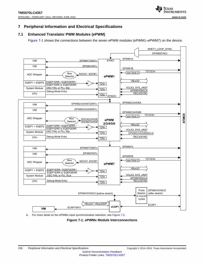
TZ1/2/3nSOCA1, SOCB1
EPWM1INTn
EPWM1TZINTn
EQEP1ERR / EQEP2ERR /
EQEP1ERR or EQEP2ERR
Debug Mode Entry
OSC FAIL or PLL Slip
IOM
UX
EPWMSYNCI
ePWM1
eCAP1
EPWM1A
EPWM1B
EPWM2/3/4/5/6A
EPWM2/3/4/5/6B
ePWM7
EPWM7A
ECAP1
Pulse
Stretch,
8 VCLK3
cycles
EPWM1SYNCO
(after stretch)
ADC Wrapper
VBus32 / VBus32DP
EPWM1ENCLKTBCLKSYNC
VIM
VCLK3, SYS_nRST
EPWM2/3/4/5/6ENCLK
TBCLKSYNC
EPWM7ENCLKTBCLKSYNC
ECAP1INTn
ePWM
2/3/4/5/6
VIM
EQEP1 + EQEP2
EPWM7B
CPU
System Module
TZ6n
TZ5n
TZ4n
VCLK3, SYS_nRST
TZ1/2/3n
TZ1/2/3n
Debug Mode Entry
OSC FAIL or PLL Slip
TZ6n
TZ5n
TZ4n
Debug Mode Entry
OSC FAIL or PLL SLip
TZ6n
TZ5n
TZ4n
SOCA2/3/4/5/6
SOCB2/3/4/5/6
EPWM2/3/4/5/6INTn
EPWM2/3/4/5/6TZINTn
EPWM7INTn
EPWM7TZINTn
VBus32
VBus32
VCLK3, SYS_nRST
VBus32
VIM
ADC Wrapper
VIM
EQEP1 + EQEP2
CPU
System Module
VIM
ADC Wrapper
VIM
EQEP1 + EQEP2
CPU
System Module
VIM
Mux
Selector
Mux
Selector
EQEP1ERR / EQEP2ERR /
EQEP1ERR or EQEP2ERR
EQEP1ERR / EQEP2ERR /
EQEP1ERR or EQEP2ERR
SOCA7, SOCB7Mux
Selector
NHET1_LOOP_SYNC
EPWM1SYNCO (before stretch)
SYNCI
SYNCO
see Note A
see Note A
see Note A
156
TMS570LC4357SPNS195C –FEBRUARY 2014–REVISED JUNE 2016 www.ti.com
Submit Documentation FeedbackProduct Folder Links: TMS570LC4357
Peripheral Information and Electrical Specifications Copyright © 2014–2016, Texas Instruments Incorporated
7 Peripheral Information and Electrical Specifications
7.1 Enhanced Translator PWM Modules (ePWM)Figure 7-1 shows the connections between the seven ePWM modules (ePWM1–ePWM7) on the device.
A. For more detail on the ePWMx input synchronization selection, see Figure 7-2.
Figure 7-1. ePWMx Module Interconnections

TZxn(x = 1, 2, or 3)
ePWMx
doublesync
(x = 1 through 7) 6 VCLK3Cycles Filter
157
TMS570LC4357www.ti.com SPNS195C –FEBRUARY 2014–REVISED JUNE 2016
Submit Documentation FeedbackProduct Folder Links: TMS570LC4357
Peripheral Information and Electrical SpecificationsCopyright © 2014–2016, Texas Instruments Incorporated
Figure 7-2 shows the detailed input synchronization selection (asynchronous, double-synchronous, ordouble synchronous + filter width) for ePWMx.
Figure 7-2. ePWMx Input Synchronization Selection Detail
7.1.1 ePWM Clocking and ResetEach ePWM module has a clock enable (ePWMxENCLK) which is controlled by its respective PeripheralPower Down bit in the PSPWRDWNCLRx register of the PCR2 module. To properly reset the peripherals,the peripherals must be released from reset by setting the PENA bit of the CLKCNTL register in thesystem module. In additional, the peripherals must be released from their power down state by clearingtheir respective bit in the PSPWRDWNCLRx register. By default after reset, the peripherals are inpowerdown state.
Table 7-1. ePWMx Clock Enable Control
ePWM MODULE INSTANCE CONTROL REGISTER TOENABLE CLOCK DEFAULT VALUE
ePWM1 PSPWRDWNCLR3[16] 1ePWM2 PSPWRDWNCLR3[17] 1ePWM3 PSPWRDWNCLR3[18] 1ePWM4 PSPWRDWNCLR3[19] 1ePWM5 PSPWRDWNCLR3[12] 1ePWM6 PSPWRDWNCLR3[13] 1ePWM7 PSPWRDWNCLR3[14] 1
7.1.2 Synchronization of ePWMx Time-Base CountersA time-base synchronization scheme connects all of the ePWM modules on a device. Each ePWMmodule has a synchronization input (EPWMxSYNCI) and a synchronization output (EPWMxSYNCO). Theinput synchronization for the first instance (ePWM1) comes from an external pin. Figure 7-1 shows thesynchronization connections for all the ePWMx modules. Each ePWM module can be configured to use orignore the synchronization input. For more information, see the ePWM module chapter of the device-specific TRM.

N2HET1 N2HET2
ePWM1
2 VCLK3 cyclesPulse Stretch
EPWM1SYNCI
SYNCI
EXT_LOOP_SYNCN2HET1_LOOP_SYNC
doublesync
PINMMR165[24]=0 and PINMMR165[25]=1
6 VCLK3Cycles Filter
158
TMS570LC4357SPNS195C –FEBRUARY 2014–REVISED JUNE 2016 www.ti.com
Submit Documentation FeedbackProduct Folder Links: TMS570LC4357
Peripheral Information and Electrical Specifications Copyright © 2014–2016, Texas Instruments Incorporated
7.1.3 Synchronizing all ePWM Modules to the N2HET1 Module Time BaseThe connection between the NHET1_LOOP_SYNC and the SYNCI input of ePWM1 module isimplemented as shown in Figure 7-3.
Figure 7-3. Synchronizing Time Bases Between N2HET1, N2HET2 and ePWMx Modules
7.1.4 Phase-Locking the Time-Base Clocks of Multiple ePWM ModulesThe TBCLKSYNC bit can be used to globally synchronize the time-base clocks of all enabled ePWMmodules on a device. This bit is implemented as PINMMR166[1] register bit 1.
When TBCLKSYNC = 0, the time-base clock of all ePWM modules is stopped. This is the defaultcondition.
When TBCLKSYNC = 1, all ePWM time-base clocks are started with the rising edge of TBCLK aligned.
For perfectly synchronized TBCLKs, the prescaler bits in the TBCTL register of each ePWM module mustbe set identically. The proper procedure for enabling the ePWM clocks is as follows:• Each ePWM is individually associated with a power down bit in the PSPWRDWNCLRx register of the PCR2
module. Enable the individual ePWM module clocks (if disable) using the control registers in the PCR2.• Configure TBCLKSYNC = 0. This will stop the time-base clock within any enabled ePWM module.• Configure the prescaler values and desired ePWM modes.• Configure TBCLKSYNC = 1.
7.1.5 ePWM Synchronization with External DevicesThe output sync from the ePWM1 module is also exported to the I/O Mux such that multiple devices canbe synchronized together. The signal pulse must be stretched by 8 VCLK3 cycles before being exportedon the IO Mux pin as the ePWMSYNCO signal.

159
TMS570LC4357www.ti.com SPNS195C –FEBRUARY 2014–REVISED JUNE 2016
Submit Documentation FeedbackProduct Folder Links: TMS570LC4357
Peripheral Information and Electrical SpecificationsCopyright © 2014–2016, Texas Instruments Incorporated
(1) The filter width is 6 VCLK3 cycles.
7.1.6 ePWM Trip ZonesThe ePWMx modules have 6 trip zone inputs each. These are active-low signals. The application cancontrol the ePWMx module response to each of the trip zone input separately. The timing requirementsfrom the assertion of the trip zone inputs to the actual response are specified in the electrical and timingsection of this document.
7.1.6.1 Trip Zones TZ1n, TZ2n, TZ3n
These 3 trip zone inputs are driven by external circuits and are connected to device-level inputs. Thesesignals are either connected asynchronously to the ePWMx trip zone inputs, or double-synchronized withVCLK3, or double-synchronized and then filtered with a 6-cycle VCLK3-based counter before connectingto the ePWMx (see Figure 7-2). By default, the trip zone inputs are asynchronously connected to theePWMx modules.
Table 7-2. Connection to ePWMx Modules for Device-Level Trip Zone Inputs
TRIP ZONEINPUT
CONTROL FORASYNCHRONOUS
CONNECTION TO ePWMx
CONTROL FORDOUBLE-SYNCHRONIZEDCONNECTION TO ePWMx
CONTROL FORDOUBLE-SYNCHRONIZED AND
FILTERED CONNECTION TO ePWMx (1)
TZ1n PINMMR172[18:16] = 001 PINMMR172[18:16] = 010 PINMMR172[18:16] = 100
TZ2n PINMMR172[26:24] = 001 PINMMR172[26:24] = 010 PINMMR172[26:24] = 100
TZ3n PINMMR173[2:0] = 001 PINMMR173[2:0] = 010 PINMMR173[2:0] = 100
7.1.6.2 Trip Zone TZ4n
This trip zone input is dedicated to eQEPx error indications. There are 2 eQEP modules on this device.Each eQEP module indicates a phase error by driving its EQEPxERR output high. The following controlregisters allow the application to configure the trip zone input (TZ4n) to each ePWMx module based onthe requirements of the applicationapplication's requirements.
Table 7-3. TZ4n Connections for ePWMx Modules
ePWMx CONTROL FOR TZ4n =NOT(EQEP1ERR OR EQEP2ERR)
CONTROL FOR TZ4n =NOT(EQEP1ERR)
CONTROL FOR TZ4n =NOT(EQEP2ERR)
ePWM1 PINMMR167[2:0] = 001 PINMMR167[2:0] = 010 PINMMR167[2:0] = 100
ePWM2 PINMMR167[10:8] = 001 PINMMR167[10:8] = 010 PINMMR167[10:8] = 100
ePWM3 PINMMR167[18:16] = 001 PINMMR167[18:16] = 010 PINMMR167[18:16] = 100
ePWM4 PINMMR167[26:24] = 001 PINMMR167[26:24] = 010 PINMMR167[26:24] = 100
ePWM5 PINMMR168[2:0] = 001 PINMMR168[2:0] = 010 PINMMR168[2:0] = 100
ePWM6 PINMMR168[10:8] = 001 PINMMR168[10:8] = 010 PINMMR168[10:8] = 100
ePWM7 PINMMR168[18:16] = 001 PINMMR168[18:16] = 010 PINMMR168[18:16] = 100
NOTEThe EQEPxERR signal is an active high signal coming out of EQEPx module. As listed inTable 7-3, the selected combination of the EQEPxERR signals must be inverted beforeconnecting to the TZ4n input of the ePWMx modules.

160
TMS570LC4357SPNS195C –FEBRUARY 2014–REVISED JUNE 2016 www.ti.com
Submit Documentation FeedbackProduct Folder Links: TMS570LC4357
Peripheral Information and Electrical Specifications Copyright © 2014–2016, Texas Instruments Incorporated
(1) The filter width is 6 VCLK3 cycles.
7.1.6.3 Trip Zone TZ5n
This trip zone input is dedicated to a clock failure on the device. That is, this trip zone input is assertedwhenever an oscillator failure or a PLL slip is detected on the device. The applciation can use this tripzone input for each ePWMx module to prevent the external system from going out of control when thedevice clocks are not within expected range (system running at limp clock).
The oscillator failure and PLL slip signals used for this trip zone input are taken from the status flags in thesystem module. These level signals are set until cleared by the application.
7.1.6.4 Trip Zone TZ6n
This trip zone input to the ePWMx modules is dedicated to a debug mode entry of the CPU. If enabled,the user can force the PWM outputs to a known state when the emulator stops the CPU. This prevents theexternal system from going out of control when the CPU is stopped.
NOTEThere is a signal called DBGACK that the CPU drives when it enters debug mode. Thissignal must be inverted and used as the Debug Mode Entry signal for the trip zone input.
7.1.7 Triggering of ADC Start of Conversion Using ePWMx SOCA and SOCB OutputsA special scheme is implemented to select the actual signal used for triggering the start of conversion onthe two ADCs on this device. This scheme is defined in Section 7.4.2.3.
7.1.8 Enhanced Translator-Pulse Width Modulator (ePWMx) Electrical Data/Timing
Table 7-4. ePWMx Timing Requirements
TEST CONDITIONS MIN MAX UNIT
tw(SYNCIN) Synchronization input pulse widthAsynchronous 2 tc(VCLK3) cyclesSynchronous 2 tc(VCLK3) cyclesSynchronous with input filter 2 tc(VCLK3) + filter width (1) cycles
Table 7-5. ePWMx Switching Characteristics
PARAMETER TESTCONDITIONS MIN MAX UNIT
tw(PWM) Pulse duration, ePWMx output high or low 33.33 nstw(SYNCOUT) Synchronization Output Pulse Width 8 tc(VCLK3) cycles
td(PWM)tzaDelay time, trip input active to PWM forced high, ORDelay time, trip input active to PWM forced low No pin load 25 ns
td(TZ-PWM)HZ Delay time, trip input active to PWM Hi-Z 20 ns
(1) The filter width is 6 VCLK3 cycles.
Table 7-6. ePWMx Trip-Zone Timing Requirements
TEST CONDITIONS MIN MAX UNIT
tw(TZ) Pulse duration, TZn input lowAsynchronous 2 * TBePWMx
cyclesSynchronous 2 tc(VCLK3)
Synchronous with input filter 2 tc(VCLK3) + filter width (1)

IOM
UX
EPWM1SYNCO
eCAP1
eCAP
6
ECAP1INTn
ECAP1ENCLK
VCLK3, SYS_nRST
ECAP2ENCLK
eCAP
2/3/4/5
VCLK3, SYS_nRST
ECAP2INTn
ECAP6INTn
VBus32
VBus32
VIM
VIM
VIM
ECAP1
ECAP1SYNCI
ECAP1SYNCO
ECAP2SYNCI
ECAP2SYNCO
ECAP2
ECAP6ENCLK
VCLK3, SYS_nRST
VBus32
ECAP6
ECAP6SYNCI
ECAP6SYNCO
see Note A
see Note A
see Note A
161
TMS570LC4357www.ti.com SPNS195C –FEBRUARY 2014–REVISED JUNE 2016
Submit Documentation FeedbackProduct Folder Links: TMS570LC4357
Peripheral Information and Electrical SpecificationsCopyright © 2014–2016, Texas Instruments Incorporated
7.2 Enhanced Capture Modules (eCAP)Figure 7-4 shows how the eCAP modules are interconnected on this microcontroller.
A. For more detail on the eCAPx input synchronization selection, see Figure 7-5.
Figure 7-4. eCAP Module Connections

ECAPx(x = 1, 2, 3, 4, 5, or 6)
eCAPx
doublesync
(x = 1 through 6) 6 VCLK3Cycles Filter
162
TMS570LC4357SPNS195C –FEBRUARY 2014–REVISED JUNE 2016 www.ti.com
Submit Documentation FeedbackProduct Folder Links: TMS570LC4357
Peripheral Information and Electrical Specifications Copyright © 2014–2016, Texas Instruments Incorporated
Figure 7-5 shows the detailed input synchronization selection (asynchronous, double-synchronous, ordouble synchronous + filter width) for eCAPx.
Figure 7-5. eCAPx Input Synchronization Selection Detail
7.2.1 Clock Enable Control for eCAPx ModulesEach of the eCAPx modules has a clock enable (ECAPxENCLK) which is controlled by its respectivePeripheral Power Down bit in the PSPWRDWNCLRx register of the PCR2 module. To properly reset theperipherals, the peripherals must be released from reset by setting the PENA bit of the CLKCNTL registerin the system module. In addition, the peripherals must be released from their power down state byclearing the respective bit in the PSPWRDWNCLRx register. By default, after reset, the peripherals are inthe power down state.
Table 7-7. eCAPx Clock Enable Control
eCAP MODULE INSTANCE CONTROL REGISTER TOENABLE CLOCK DEFAULT VALUE
eCAP1 PSPWRDWNCLR3[15] 1eCAP2 PSPWRDWNCLR3[8] 1eCAP3 PSPWRDWNCLR3[9] 1eCAP4 PSPWRDWNCLR3[10] 1eCAP5 PSPWRDWNCLR3[11] 1eCAP6 PSPWRDWNCLR3[4] 1
(1) The filter width is 6 VCLK3 cycles.
7.2.2 PWM Output Capability of eCAPxWhen not used in capture mode, each of the eCAPx modules can be used as a single-channel PWMoutput. This is called the Auxiliary PWM (APWM) mode of operation of the eCAPx modules. For moreinformation, see the eCAP module chapter of the device-specific TRM.
7.2.3 Input Connection to eCAPx ModulesThe input connection to each of the eCAPx modules can be selected between a double-VCLK3-synchronized input or a double-VCLK3-synchronized and filtered input, as listed in Table 7-8.
Table 7-8. Device-Level Input Connection to eCAPx Modules
INPUT SIGNALCONTROL FOR
DOUBLE-SYNCHRONIZEDCONNECTION TO eCAPx
CONTROL FORDOUBLE-SYNCHRONIZED AND
FILTERED CONNECTION TO eCAPx (1)
eCAP1 PINMMR169[2:0] = 001 PINMMR169[2:0] = 010eCAP2 PINMMR169[10:8] = 001 PINMMR169[10:8] = 010eCAP3 PINMMR169[18:16] = 001 PINMMR169[18:16] = 010eCAP4 PINMMR169[26:24] = 001 PINMMR169[26:24] = 010eCAP5 PINMMR170[2:0] = 001 PINMMR170[2:0] = 010eCAP6 PINMMR170[10:8] = 001 PINMMR170[10:8] = 010

163
TMS570LC4357www.ti.com SPNS195C –FEBRUARY 2014–REVISED JUNE 2016
Submit Documentation FeedbackProduct Folder Links: TMS570LC4357
Peripheral Information and Electrical SpecificationsCopyright © 2014–2016, Texas Instruments Incorporated
(1) The filter width is 6 VCLK3 cycles.
7.2.4 Enhanced Capture Module (eCAP) Electrical Data/Timing
Table 7-9. eCAPx Timing Requirements
TEST CONDITIONS MIN MAX UNIT
tw(CAP) Pulse width, capture inputSynchronous 2 tc(VCLK3) cyclesSynchronous with input filter 2 tc(VCLK3) + filter width (1) cycles
Table 7-10. eCAPx Switching Characteristics
PARAMETER TEST CONDITIONS MIN MAX UNITtw(APWM) Pulse duration, APWMx output high or low 20 ns

EQEPxA or EQEPxB(x = 1 or 2)
eQEPx
doublesync
(x = 1 or 2) 6 VCLK3Cycles Filter
EQEP1A
VIM EQEP1INTnEQEP1
Module
IO
Mux
EQEP1ENCLK
EQEP1IOEQEP1I
VBus32
VCLK3SYS_nRST
EQEP1B
EQEP1IOE
EQEP1SOEQEP1S
EQEP1SOE
EQEP1ERR
EPWM1/../7
TZ
4n
EQEP2A
VIM EQEP2INTnEQEP2
Module
EQEP2ENCLK
EQEP2IOEQEP2I
VBus32
VCLK3SYS_nRST
EQEP2B
EQEP2IOE
EQEP2SOEQEP2S
EQEP2SOE
EQEP2ERR
Connection
Selection
Mux
see Note A
see Note A
164
TMS570LC4357SPNS195C –FEBRUARY 2014–REVISED JUNE 2016 www.ti.com
Submit Documentation FeedbackProduct Folder Links: TMS570LC4357
Peripheral Information and Electrical Specifications Copyright © 2014–2016, Texas Instruments Incorporated
7.3 Enhanced Quadrature Encoder (eQEP)Figure 7-6 shows the eQEP module interconnections on the device.
A. For more detail on the eQEPx input synchronization selection, see Figure 7-7.
Figure 7-6. eQEP Module Interconnections
Figure 7-7 shows the detailed input synchronization selection (asynchronous, double-synchronous, ordouble synchronous + filter width) for eQEPx.
Figure 7-7. eQEPx Input Synchronization Selection Detail
7.3.1 Clock Enable Control for eQEPx ModulesEach of the EQEPx modules has a clock enable (EQEPxENCLK) which is controlled by its respectivePeripheral Power Down bit in the PSPWRDWNCLRx register of the PCR2 module. To properly reset theperipherals, the peripherals must be released from reset by setting the PENA bit of the CLKCNTL registerin the system module. In addition, the peripherals must be released from their power down state byclearing the respective bit in the PSPWRDWNCLRx register. By default after reset, the peripherals are inpower down state.
Table 7-11. eQEPx Clock Enable Control
eQEP MODULE INSTANCE CONTROL REGISTER TOENABLE CLOCK DEFAULT VALUE
eQEP1 PSPWRDWNCLR3[5] 1eQEP2 PSPWRDWNCLR3[6] 1

165
TMS570LC4357www.ti.com SPNS195C –FEBRUARY 2014–REVISED JUNE 2016
Submit Documentation FeedbackProduct Folder Links: TMS570LC4357
Peripheral Information and Electrical SpecificationsCopyright © 2014–2016, Texas Instruments Incorporated
(1) The filter width is 6 VCLK3 cycles.
7.3.2 Using eQEPx Phase Error to Trip ePWMx OutputsThe eQEP module sets the EQEPERR signal output whenever a phase error is detected in its inputsEQEPxA and EQEPxB. This error signal from both the eQEP modules is input to the connection selectionmultiplexer. This multiplexer is defined in Table 7-3. As shown in Figure 7-6, the output of this selectionmultiplexer is inverted and connected to the TZ4n trip-zone input of all ePWMx modules. This connectionallows the application to define the response of each ePWMx module on a phase error indicated by theeQEP modules.
7.3.3 Input Connection to eQEPx ModulesThe input connection to each of the eQEP modules can be selected between a double-VCLK3-synchronized input or a double-VCLK3-synchronized and filtered input, as listed in Table 7-12.
Table 7-12. Device-Level Input Connection to eQEPx Modules
INPUT SIGNAL CONTROL FOR DOUBLE-SYNCHRONIZEDCONNECTION TO eQEPx
CONTROL FORDOUBLE-SYNCHRONIZED AND
FILTERED CONNECTION (1) TO eQEPxeQEP1A PINMMR170[18:16] = 001 PINMMR170[18:16] = 010eQEP1B PINMMR170[26:24] = 001 PINMMR170[26:24] = 010eQEP1I PINMMR171[2:0] = 001 PINMMR171[2:0] = 010eQEP1S PINMMR171[10:8] = 001 PINMMR171[10:8] = 010eQEP2A PINMMR171[18:16] = 001 PINMMR171[18:16] = 010eQEP2B PINMMR171[26:24] = 001 PINMMR171[26:24] = 010eQEP2I PINMMR172[2:0] = 001 PINMMR172[2:0] = 010eQEP2S PINMMR172[10:8] = 001 PINMMR172[10:8] = 010
(1) The filter width is 6 VCLK3 cycles.
7.3.4 Enhanced Quadrature Encoder Pulse (eQEPx) Timing
Table 7-13. eQEPx Timing Requirements (1)
TEST CONDITIONS MIN MAX UNIT
tw(QEPP) QEP input periodSynchronous 2 tc(VCLK3) cyclesSynchronous with input filter 2 tc(VCLK3) + filter width
tw(INDEXH) QEP Index Input High TimeSynchronous 2 tc(VCLK3) cyclesSynchronous with input filter 2 tc(VCLK3) + filter width
tw(INDEXL) QEP Index Input Low TimeSynchronous 2 tc(VCLK3) cyclesSynchronous with input filter 2 tc(VCLK3) + filter width
tw(STROBH) QEP Strobe Input High TimeSynchronous 2 tc(VCLK3) cyclesSynchronous with input filter 2 tc(VCLK3) + filter width
tw(STROBL) QEP Strobe Input Low TimeSynchronous 2 tc(VCLK3) cyclesSynchronous with input filter 2 tc(VCLK3) + filter width
Table 7-14. eQEPx Switching Characteristics
PARAMETER MIN MAX UNITtd(CNTR)xin Delay time, external clock to counter increment 4 tc(VCLK3) cyclestd(PCS-OUT)QEP Delay time, QEP input edge to position compare sync output 6 tc(VCLK3) cycles

166
TMS570LC4357SPNS195C –FEBRUARY 2014–REVISED JUNE 2016 www.ti.com
Submit Documentation FeedbackProduct Folder Links: TMS570LC4357
Peripheral Information and Electrical Specifications Copyright © 2014–2016, Texas Instruments Incorporated
7.4 12-bit Multibuffered Analog-to-Digital Converter (MibADC)The MibADC has a separate power bus for its analog circuitry that enhances the Analog-to-Digital (A-to-D)performance by preventing digital switching noise on the logic circuitry which could be present on VSS andVCC from coupling into the A-to-D analog stage. All A-to-D specifications are given with respect toADREFLO, unless otherwise noted.
Table 7-15. MibADC Overview
DESCRIPTION VALUEResolution 12 bitsMonotonic Assured
Output conversion code 00h to FFFh [00 for VAI ≤ ADREFLO; FFF for VAI ≥ ADREFHI]
7.4.1 MibADC Features• 10-/12-bit resolution• ADREFHI and ADREFLO pins (high and low reference voltages)• Total Sample/Hold/Convert time: 600 ns Typical Minimum at 30 MHz ADCLK• One memory region per conversion group is available (Event Group, Group 1, and Group 2)• Allocation of channels to conversion groups is completely programmable• Memory regions are serviced either by interrupt or by DMA• Programmable interrupt threshold counter is available for each group• Programmable magnitude threshold interrupt for each group for any one channel• Option to read either 8-, 10-, or 12-bit values from memory regions• Single or continuous conversion modes• Embedded self-test• Embedded calibration logic• Enhanced power-down mode
– Optional feature to automatically power down ADC core when no conversion is in progress• External event pin (ADEVT) programmable as general-purpose I/O
7.4.2 Event Trigger OptionsThe ADC module supports three conversion groups: Event Group, Group1, and Group2. Each of thesethree groups can be configured to be triggered by a hardware event. In that case, the application canselect from among eight event sources to be the trigger for a group's conversions.
7.4.2.1 MibADC1 Event Trigger Hookup
Table 7-16 lists the event sources that can trigger the conversions for the MibADC1 groups.

Copyright © 2014–2016, Texas Instruments Incorporated Peripheral Information and Electrical SpecificationsSubmit Documentation Feedback
Product Folder Links: TMS570LC4357
167
TMS570LC4357www.ti.com SPNS195C –FEBRUARY 2014–REVISED JUNE 2016
Table 7-16. MibADC1 Event Trigger SelectionGROUP SOURCE SELECT BITS
(G1SRC, G2SRC OR EVSRC) EVENT NO. PINMMR161[0] PINMMR161[1] CONTROL FOROPTION A
CONTROL FOROPTION B TRIGGER SOURCE
000 1 x x — — AD1EVT
001 2
1 0 PINMMR161[8] = x PINMMR161[9] = x N2HET1[8]
0 1 PINMMR161[8] = 1 PINMMR161[9] = 0 N2HET2[5]
0 1 PINMMR161[8] = 0 PINMMR161[9] = 1 e_TPWM_B
010 31 0 — — N2HET1[10]
0 1 — — N2HET1[27]
011 4
1 0 PINMMR161[16] = x PINMMR161[17] = x RTI1 Comp0
0 1 PINMMR161[16] = 1 PINMMR161[17] = 0 RTI1 Comp0
0 1 PINMMR161[16] = 0 PINMMR161[17] = 1 e_TPWM_A1
100 51 0 — — N2HET1[12]
0 1 — — N2HET1[17]
101 6
1 0 PINMMR161[24] = x PINMMR161[25] = x N2HET1[14]
0 1 PINMMR161[24] = 1 PINMMR161[25] = 0 N2HET1[19]
0 1 PINMMR161[24] = 0 PINMMR161[25] = 1 N2HET2[1]
110 7
1 0 PINMMR162[0] = x PINMMR162[1] = x GIOB[0]
0 1 PINMMR162[0] = 1 PINMMR162[1] = 0 N2HET1[11]
0 1 PINMMR162[0] = 0 PINMMR162[1] = 1 ePWM_A2
111 8
1 0 PINMMR162[8] = x PINMMR162[9] = x GIOB[1]
0 1 PINMMR162[8] = 1 PINMMR162[9] = 0 N2HET2[13]
0 1 PINMMR162[8] = 0 PINMMR162[9] = 1 ePWM_AB

168
TMS570LC4357SPNS195C –FEBRUARY 2014–REVISED JUNE 2016 www.ti.com
Submit Documentation FeedbackProduct Folder Links: TMS570LC4357
Peripheral Information and Electrical Specifications Copyright © 2014–2016, Texas Instruments Incorporated
NOTEFor ADEVT trigger source, the connection to the MibADC1 module trigger input is made fromthe output side of the input buffer. This way, a trigger condition can be generated either byconfiguring ADEVT as an output function on to the pad (through the mux control), or bydriving the ADEVT signal from an external trigger source as input. If the mux control moduleis used to select different functionality instead of the ADEVT signal, then care must be takento disable ADEVT from triggering conversions; there is no multiplexing on the inputconnection.
If ePWM_B, ePWM_A2, ePWM_AB, N2HET2[1], N2HET2[5], N2HET2[13], N2HET1[11],N2HET1[17], or N2HET1[19] is used to trigger the ADC, the connection to the ADC is madedirectly from the N2HET or ePWM module outputs. As a result, the ADC can be triggeredwithout having to enable the signal from being output on a device terminal.
NOTEFor N2HETx trigger sources, the connection to the MibADC1 module trigger input is madefrom the input side of the output buffer (at the N2HETx module boundary). This way, atrigger condition can be generated even if the N2HETx signal is not selected to be output onthe pad.
NOTEFor the RTI compare 0 interrupt source, the connection is made directly from the output ofthe RTI module. That is, the interrupt condition can be used as a trigger source even if theactual interrupt is not signaled to the CPU.
7.4.2.2 MibADC2 Event Trigger Hookup
Table 7-17 lists the event sources that can trigger the conversions for the MibADC2 groups.

Copyright © 2014–2016, Texas Instruments Incorporated Peripheral Information and Electrical SpecificationsSubmit Documentation Feedback
Product Folder Links: TMS570LC4357
169
TMS570LC4357www.ti.com SPNS195C –FEBRUARY 2014–REVISED JUNE 2016
Table 7-17. MibADC2 Event Trigger Selection
GROUP SOURCE SELECT BITS(G1SRC, G2SRC, or EVSRC) EVENT NO. PINMMR161[0] PINMMR161[1] CONTROL FOR
OPTION ACONTROL FOR
OPTION B TRIGGER SOURCE
000 1 x x NA NA AD2EVT
001 21 0 PINMMR162[16] = x PINMMR162[17] = x N2HET1[8]0 1 PINMMR162[16] = 1 PINMMR162[17] = 0 N2HET2[5]0 1 PINMMR162[16] = 0 PINMMR162[17] = 1 e_TPWM_B
010 31 0 NA NA N2HET1[10]0 1 NA NA N2HET1[27]
011 41 0 PINMMR162[24] = x PINMMR162[25] = x RTI1 Comp00 1 PINMMR162[24] = 1 PINMMR162[25] = 0 RTI1 Comp00 1 PINMMR162[24] = 0 PINMMR162[25] = 1 e_TPWM_A1
100 51 0 NA NA N2HET1[12]0 1 NA NA N2HET1[17]
101 61 0 PINMMR163[0] = x PINMMR163[0] = x N2HET1[14]0 1 PINMMR163[0] = 1 PINMMR163[0] = 0 N2HET1[19]0 1 PINMMR163[0] = 0 PINMMR163[0] = 1 N2HET2[1]
110 71 0 PINMMR163[8] = x PINMMR163[8] = x GIOB[0]0 1 PINMMR163[8] = 1 PINMMR163[8] = 0 N2HET1[11]0 1 PINMMR163[8] = 0 PINMMR163[8] = 1 ePWM_A2
111 81 0 PINMMR163[16] = x PINMMR163[16] = x GIOB[1]0 1 PINMMR163[16] = 1 PINMMR163[16] = 0 N2HET2[13]0 1 PINMMR163[16] = 0 PINMMR163[16] = 1 ePWM_AB

170
TMS570LC4357SPNS195C –FEBRUARY 2014–REVISED JUNE 2016 www.ti.com
Submit Documentation FeedbackProduct Folder Links: TMS570LC4357
Peripheral Information and Electrical Specifications Copyright © 2014–2016, Texas Instruments Incorporated
NOTEFor AD2EVT trigger source, the connection to the MibADC2 module trigger input is madefrom the output side of the input buffer. This way, a trigger condition can be generated eitherby configuring AD2EVT as an output function on to the pad (through the mux control), or bydriving the AD2EVT signal from an external trigger source as input. If the mux control moduleis used to select different functionality instead of the AD2EVT signal, then care must betaken to disable AD2EVT from triggering conversions; there is no multiplexing on the inputconnections.
If ePWM_B, ePWM_A2, ePWM_AB, N2HET2[1], N2HET2[5], N2HET2[13], N2HET1[11],N2HET1[17], or N2HET1[19] is used to trigger the ADC, the connection to the ADC is madedirectly from the N2HET or ePWM module outputs. As a result, the ADC can be triggeredwithout having to enable the signal from being output on a device terminal.
NOTEFor N2HETx trigger sources, the connection to the MibADC2 module trigger input is madefrom the input side of the output buffer (at the N2HETx module boundary). This way, atrigger condition can be generated even if the N2HETx signal is not selected to be output onthe pad.
NOTEFor the RTI compare 0 interrupt source, the connection is made directly from the output ofthe RTI module. That is, the interrupt condition can be used as a trigger source even if theactual interrupt is not signaled to the CPU.
7.4.2.3 Controlling ADC1 and ADC2 Event Trigger Options Using SOC Output from ePWM Modules
As shown in Figure 7-8, the ePWMxSOCA and ePWMxSOCB outputs from each ePWM module are usedto generate four signals – ePWM_B, ePWM_A1, ePWM_A2, and ePWM_AB, that are available to triggerthe ADC based on the application requirement.

EPWM2module
EPWM2SOCA
EPWM2SOCB
EPWM1module
EPWM1SOCA
EPWM1SOCB
EPWM3module
EPWM3SOCA
EPWM3SOCB
EPWM4module
EPWM4SOCA
EPWM4SOCB
EPWM5module
EPWM5SOCA
EPWM5SOCB
EPWM6module
EPWM6SOCA
EPWM6SOCB
EPWM7SOCA
EPWM7SOCBEPWM7module
ePWM_B ePWM_A1 ePWM_A2 ePWM_AB
SOCAEN, SOCBEN bitsinside ePWMx modules
Controlled by PINMMR
171
TMS570LC4357www.ti.com SPNS195C –FEBRUARY 2014–REVISED JUNE 2016
Submit Documentation FeedbackProduct Folder Links: TMS570LC4357
Peripheral Information and Electrical SpecificationsCopyright © 2014–2016, Texas Instruments Incorporated
Figure 7-8. ADC Trigger Source Generation from ePWMx

ePWM1
0 0
1
1
From switch onSOC2Awhen PINMMR164[8] = 0
SOC1A
PINMMR164[0]
EPWM1SOCAFrom switch onSOC2Awhen PINMMR164[8] = 1
0 0
172
TMS570LC4357SPNS195C –FEBRUARY 2014–REVISED JUNE 2016 www.ti.com
Submit Documentation FeedbackProduct Folder Links: TMS570LC4357
Peripheral Information and Electrical Specifications Copyright © 2014–2016, Texas Instruments Incorporated
Table 7-18. Control Bit to SOC Output
CONTROL BIT SOC OUTPUTPINMMR164[0] SOC1A_SELPINMMR164[8] SOC2A_SEL
PINMMR164[16] SOC3A_SELPINMMR164[24] SOC4A_SELPINMMR165[0] SOC5A_SELPINMMR165[8] SOC6A_SEL
PINMMR165[16] SOC7A_SEL
The SOCA output from each ePWM module is connected to a "switch" shown in Figure 7-8. This switch isimplemented by using the control registers in the PINMMR module. Figure 7-9 is an example of theimplementation is shown for the switch on SOC1A. The switches on the other SOCA signals areimplemented in the same way.
Figure 7-9. ePWM1SOC1A Switch Implementation
The logic equations for the four outputs from the combinational logic shown in Figure 7-8 are:ePWM_B = SOC1B or SOC2B or SOC3B or SOC4B or SOC5B or SOC6B or SOC7B (1)
ePWM_A1 = [ SOC1A and not(SOC1A_SEL) ] or [ SOC2A and not(SOC2A_SEL) ] or [ SOC3A and not(SOC3A_SEL) ] or (2)[ SOC4A and not(SOC4A_SEL) ] or [ SOC5A and not(SOC5A_SEL) ] or [ SOC6A and not(SOC6A_SEL) ] or[ SOC7A and not(SOC7A_SEL) ]
ePWM_A2 = [ SOC1A and SOC1A_SEL ] or [ SOC2A and SOC2A_SEL ] or [ SOC3A and SOC3A_SEL ] or (3)[ SOC4A and SOC4A_SEL ] or [ SOC5A and SOC5A_SEL ] or [ SOC6A and SOC6A_SEL ] or[ SOC7A and SOC7A_SEL ]
ePWM_AB = ePWM_B or ePWM_A2 (4)

173
TMS570LC4357www.ti.com SPNS195C –FEBRUARY 2014–REVISED JUNE 2016
Submit Documentation FeedbackProduct Folder Links: TMS570LC4357
Peripheral Information and Electrical SpecificationsCopyright © 2014–2016, Texas Instruments Incorporated
(1) For VCCAD and VSSAD recommended operating conditions, see Section 5.4.(2) Input currents into any ADC input channel outside the specified limits could affect conversion results of other channels.
7.4.3 ADC Electrical and Timing Specifications
Table 7-19. MibADC Recommended Operating Conditions
PARAMETER MIN MAX UNITADREFHI A-to-D high-voltage reference source ADREFLO VCCAD
(1) VADREFLO A-to-D low-voltage reference source VSSAD
(1) ADREFHI VVAI Analog input voltage ADREFLO ADREFHI VIAIC Analog input clamp current (2) (VAI < VSSAD – 0.3 or VAI > VCCAD + 0.3) –2 2 mA
(1) For ICCAD and ICCREFHI see Section 5.7.(2) If a shared channel is being converted by both ADC converters at the same time, the on-state leakage is doubled.
Table 7-20. MibADC Electrical Characteristics Over Full Ranges of Recommended OperatingConditions (1)
PARAMETER DESCRIPTION/CONDITIONS MIN MAX UNITRmux Analog input mux on-resistance See Figure 7-10 250 ΩRsamp ADC sample switch on-resistance See Figure 7-10 250 ΩCmux Input mux capacitance See Figure 7-10 16 pFCsamp ADC sample capacitance See Figure 7-10 13 pF
IAIL Analog off-state input leakage current VCCAD = 3.6 VVSSAD ≤ VIN < VSSAD + 100 mV –300 200
nAVSSAD + 100 mV ≤ VIN ≤ VCCAD - 200 mV –200 200VCCAD - 200 mV < VIN ≤ VCCAD –200 500
IAIL Analog off-state input leakage current VCCAD = 5.25 VVSSAD ≤ VIN < VSSAD + 300 mV –1000 250
nAVSSAD + 300 mV ≤ VIN ≤ VCCAD - 300 mV –250 250VCCAD - 300 mV < VIN ≤ VCCAD –250 1000
IAOSB(2) Analog on-state input bias current VCCAD = 3.6 V
VSSAD ≤ VIN < VSSAD + 100 mV –10 2µAVSSAD + 100 mV < VIN < VCCAD - 200 mV –4 2
VCCAD - 200 mV < VIN < VCCAD –4 16
IAOSB(2) Analog on-state input bias current VCCAD = 5.25 V
VSSAD ≤ VIN < VSSAD + 300 mV –12 3µAVSSAD + 300 mV ≤ VIN ≤ VCCAD - 300 mV –5 3
VCCAD - 300 mV < VIN ≤ VCCAD –5 18

VS1
On-StateBias Current
Off-StateLeakages
VS2
VS24
IAOSB
IAIL
IAIL
Rext
Rext
Rext
Pin SmuxRmux
PinSmux Rmux
PinSmux Rmux Ssamp Rsamp
Csamp
Cext IAIL
IAIL IAIL
IAIL
Cmux
Cext
Cext
174
TMS570LC4357SPNS195C –FEBRUARY 2014–REVISED JUNE 2016 www.ti.com
Submit Documentation FeedbackProduct Folder Links: TMS570LC4357
Peripheral Information and Electrical Specifications Copyright © 2014–2016, Texas Instruments Incorporated
(1) The MibADC clock is the ADCLK, generated by dividing down the VCLK1 by a prescale factor defined by the ADCLOCKCR registerbits 4:0.
(2) The sample and hold time for the ADC conversions is defined by the ADCLK frequency and the AD<GP>SAMP register for eachconversion group. The sample time must be determined by accounting for the external impedance connected to the input channel aswell as the internal impedance of the ADC.
(3) This is the minimum sample/hold and conversion time that can be achieved. These parameters are dependent on many factors (forexample, the prescale settings).
Figure 7-10. MibADC Input Equivalent Circuit
Table 7-21. MibADC Timing Specifications
PARAMETER MIN NOM MAX UNITtc(ADCLK)
(1) Cycle time, MibADC clock 0.033 µstd(SH)
(2) Delay time, sample and hold time 0.2 µs12-BIT MODE
td(C) Delay time, conversion time 0.4 µstd(SHC)
(3) Delay time, total sample/hold and conversion time 0.6 µs10-BIT MODE
td(C) Delay time, conversion time 0.33 µstd(SHC)
(3) Delay time, total sample/hold and conversion time 0.53 µs

175
TMS570LC4357www.ti.com SPNS195C –FEBRUARY 2014–REVISED JUNE 2016
Submit Documentation FeedbackProduct Folder Links: TMS570LC4357
Peripheral Information and Electrical SpecificationsCopyright © 2014–2016, Texas Instruments Incorporated
(1) 1 LSB = (ADREFHI – ADREFLO)/ 212 for 12-bit mode(2) 1 LSB = (ADREFHI – ADREFLO)/ 210 for 10-bit mode
Table 7-22. MibADC Operating Characteristics Over 3.0 V to 3.6 V Operating Conditions (1) (2)
PARAMETER DESCRIPTION/CONDITIONS MIN MAX UNIT
CR Conversion range over which specifiedaccuracy is maintained ADREFHI - ADREFLO 3 3.6 V
ZSET
Zero Scale Offset Difference between the first ideal transition (fromcode 000h to 001h) and the actual transition
10-bit mode 1 LSB12-bit mode 2 LSB
FSET
Full Scale OffsetDifference between the range of the measuredcode transitions (from first to last) and the rangeof the ideal code transitions
10-bit mode 2 LSB
12-bit mode 3 LSB
EDNL
Differential nonlinearity error Difference between the actual step width and theideal value. (See Figure 7-11)
10-bit mode –1 1.5 LSB12-bit mode –1 2 LSB
EINL
Integral nonlinearity errorMaximum deviation from the best straight linethrough the MibADC. MibADC transfercharacteristics, excluding the quantization error.
10-bit mode –2 2 LSB
12-bit mode –2 2 LSB
ETOT
Total unadjusted error (after calibration) Maximum value of the difference between ananalog value and the ideal midstep value.
10-bit mode –2 2 LSB12-bit mode –4 4 LSB
(1) 1 LSB = (ADREFHI – ADREFLO)/ 212 for 12-bit mode(2) 1 LSB = (ADREFHI – ADREFLO)/ 210 for 10-bit mode
Table 7-23. MibADC Operating Characteristics Over 3.6 V to 5.25 V Operating Conditions (1) (2)
PARAMETER DESCRIPTION/CONDITIONS MIN MAX UNIT
CR Conversion range over which specifiedaccuracy is maintained ADREFHI - ADREFLO 3.6 5.25 V
ZSET
Zero Scale Offset Difference between the first ideal transition (fromcode 000h to 001h) and the actual transition
10-bit mode 1 LSB12-bit mode 2 LSB
FSET
Full Scale OffsetDifference between the range of the measuredcode transitions (from first to last) and the rangeof the ideal code transitions
10-bit mode 2 LSB
12-bit mode 3 LSB
EDNL
Differential nonlinearity error Difference between the actual step width and theideal value. (See Figure 7-11)
10-bit mode –1 1.5 LSB12-bit mode –1 3 LSB
EINL
Integral nonlinearity errorMaximum deviation from the best straight linethrough the MibADC. MibADC transfercharacteristics, excluding the quantization error.
10-bit mode –2 2 LSB
12-bit mode –4.5 2 LSB
ETOT
Total unadjusted error (after calibration) Maximum value of the difference between ananalog value and the ideal midstep value.
10-bit mode –2 2 LSB12-bit mode –6 5 LSB

Differential LinearityError (–½ LSB)
1 LSB
1 LSB
Differential LinearityError (–½ LSB)
0 ... 110
0 ... 101
0 ... 100
0 ... 011
0 ... 010
0 ... 001
0 ... 000
0 1 2 3 4 5
Dig
ital O
utp
ut
Co
de
Analog Input Value (LSB)
176
TMS570LC4357SPNS195C –FEBRUARY 2014–REVISED JUNE 2016 www.ti.com
Submit Documentation FeedbackProduct Folder Links: TMS570LC4357
Peripheral Information and Electrical Specifications Copyright © 2014–2016, Texas Instruments Incorporated
7.4.4 Performance (Accuracy) Specifications
7.4.4.1 MibADC Nonlinearity Errors
The differential nonlinearity error shown in Figure 7-11 (sometimes referred to as differential linearity) isthe difference between an actual step width and the ideal value of 1 LSB.
A. 1 LSB = (ADREFHI – ADREFLO)/212
Figure 7-11. Differential Nonlinearity (DNL) Error

0 ... 111
0 ... 101
0 ... 100
0 ... 011
0 ... 010
0 ... 001
0 ... 000
0 1 2 3 4 5
Dig
ital O
utp
ut
Co
de
Analog Input Value (LSB)
0 ... 110
6 7
At Transition011/100(–½ LSB)
At Transition001/010 (–1/4 LSB)
ActualTransition
IdealTransition
End-Point Lin. Error
177
TMS570LC4357www.ti.com SPNS195C –FEBRUARY 2014–REVISED JUNE 2016
Submit Documentation FeedbackProduct Folder Links: TMS570LC4357
Peripheral Information and Electrical SpecificationsCopyright © 2014–2016, Texas Instruments Incorporated
The integral nonlinearity error shown in Figure 7-12 (sometimes referred to as linearity error) is thedeviation of the values on the actual transfer function from a straight line.
A. 1 LSB = (ADREFHI – ADREFLO)/212
Figure 7-12. Integral Nonlinearity (INL) Error(A)

0 ... 111
0 ... 101
0 ... 100
0 ... 011
0 ... 010
0 ... 001
0 ... 000
0 1 2 3 4 5
Dig
ital O
utp
ut
Co
de
Analog Input Value (LSB)
0 ... 110
6 7
Total ErrorAt Step0 ... 001 (1/2 LSB)
Total ErrorAt Step 0 ... 101(–1 1/4 LSB)
178
TMS570LC4357SPNS195C –FEBRUARY 2014–REVISED JUNE 2016 www.ti.com
Submit Documentation FeedbackProduct Folder Links: TMS570LC4357
Peripheral Information and Electrical Specifications Copyright © 2014–2016, Texas Instruments Incorporated
7.4.4.2 MibADC Total Error
The absolute accuracy or total error of an MibADC as shown in Figure 7-13 is the maximum value of thedifference between an analog value and the ideal midstep value.
A. 1 LSB = (ADREFHI – ADREFLO)/212
Figure 7-13. Absolute Accuracy (Total) Error(A)

179
TMS570LC4357www.ti.com SPNS195C –FEBRUARY 2014–REVISED JUNE 2016
Submit Documentation FeedbackProduct Folder Links: TMS570LC4357
Peripheral Information and Electrical SpecificationsCopyright © 2014–2016, Texas Instruments Incorporated
7.5 General-Purpose Input/OutputThe GPIO module on this device supports two ports, GIOA and GIOB. The I/O pins are bidirectional andbit-programmable. Both GIOA and GIOB support external interrupt capability.
7.5.1 FeaturesThe GPIO module has the following features:• Each I/O pin can be configured as:
– Input– Output– Open Drain
• The interrupts have the following characteristics:– Programmable interrupt detection either on both edges or on a single edge (set in GIOINTDET)– Programmable edge-detection polarity, either rising or falling edge (set in GIOPOL register)– Individual interrupt flags (set in GIOFLG register)– Individual interrupt enables, set and cleared through GIOENASET and GIOENACLR registers
respectively– Programmable interrupt priority, set through GIOLVLSET and GIOLVLCLR registers
• Internal pullup/pulldown allows unused I/O pins to be left unconnected
For information on input and output timings see Section 5.10.1 and Section 5.10.2.

N2HETx
3
4
2
1
180
TMS570LC4357SPNS195C –FEBRUARY 2014–REVISED JUNE 2016 www.ti.com
Submit Documentation FeedbackProduct Folder Links: TMS570LC4357
Peripheral Information and Electrical Specifications Copyright © 2014–2016, Texas Instruments Incorporated
7.6 Enhanced High-End Timer (N2HET)The N2HET is an advanced intelligent timer that provides sophisticated timing functions for real-timeapplications. The timer is software-controlled, using a reduced instruction set, with a specialized timermicromachine and an attached I/O port. The N2HET can be used for pulse width modulated outputs,capture or compare inputs, or general-purpose I/O.. It is especially well suited for applications requiringmultiple sensor information and drive actuators with complex and accurate time pulses.
7.6.1 FeaturesThe N2HET module has the following features:• Programmable timer for input and output timing functions• Reduced instruction set (30 instructions) for dedicated time and angle functions• 256 words of instruction RAM protected by parity• User defined number of 25-bit virtual counters for timer, event counters and angle counters• 7-bit hardware counters for each pin allow up to 32-bit resolution in conjunction with the 25-bit virtual
counters• Up to 32 pins usable for input signal measurements or output signal generation• Programmable suppression filter for each input pin with adjustable limiting frequency• Low CPU overhead and interrupt load• Efficient data transfer to or from the CPU memory with dedicated High-End-Timer Transfer Unit (HTU)
or DMA• Diagnostic capabilities with different loopback mechanisms and pin status readback functionality
7.6.2 N2HET RAM OrganizationThe timer RAM uses 4 RAM banks, where each bank has two port access capability. This means that oneRAM address may be written while another address is read. The RAM words are 96-bits wide, which aresplit into three 32-bit fields (program, control, and data).
7.6.3 Input Timing SpecificationsThe N2HET instructions PCNT and WCAP impose some timing constraints on the input signals.
Figure 7-14. N2HET Input Capture Timings

NHET_LOOP_SYNC EXT_LOOP_SYNC
EXT_LOOP_SYNC NHET_LOOP_SYNC
N2HET1 N2HET2
181
TMS570LC4357www.ti.com SPNS195C –FEBRUARY 2014–REVISED JUNE 2016
Submit Documentation FeedbackProduct Folder Links: TMS570LC4357
Peripheral Information and Electrical SpecificationsCopyright © 2014–2016, Texas Instruments Incorporated
Table 7-24. Dynamic Characteristics for the N2HET Input Capture Functionality
PARAMETER MIN MAX UNIT
1 Input signal period, PCNT or WCAP for rising edgeto rising edge (HRP) (LRP) tc(VCLK2) + 2 225 (HRP) (LRP) tc(VCLK2) - 2 ns
2 Input signal period, PCNT or WCAP for falling edgeto falling edge (HRP) (LRP) tc(VCLK2) + 2 225 (HRP) (LRP) tc(VCLK2) - 2 ns
3 Input signal high phase, PCNT or WCAP for risingedge to falling edge 2 (HRP) tc(VCLK2) + 2 225 (HRP) (LRP) tc(VCLK2) - 2 ns
4 Input signal low phase, PCNT or WCAP for fallingedge to rising edge 2 (HRP) tc(VCLK2) + 2 225 (HRP) (LRP) tc(VCLK2) - 2 ns
7.6.4 N2HET1-N2HET2 InterconnectionsIn some applications the N2HET resolutions must be synchronized. Some other applications require asingle time base to be used for all PWM outputs and input timing captures.
The N2HET provides such a synchronization mechanism. The Clk_master/slave (HETGCR.16) configuresthe N2HET in master or slave mode (default is slave mode). A N2HET in master mode provides a signalto synchronize the prescalers of the slave N2HET. The slave N2HET synchronizes its loop resolution tothe loop resolution signal sent by the master. The slave does not require this signal after it receives thefirst synchronization signal. However, anytime the slave receives the resynchronization signal from themaster, the slave must synchronize itself again..
Figure 7-15. N2HET1 – N2HET2 Synchronization Hookup

N2HET1
N2HET2
IOMM mux control signal x
N2HET1[1] / N2HET2[8]
N2HET1[1]
N2HET2[8]
N2HET1[3] / N2HET2[10]
N2HET1[5] / N2HET2[12]
N2HET1[7] / N2HET2[14]
N2HET1[9] / N2HET2[16]
N2HET1
N2HET2
IOMM mux control signal x
N2HET1[11] / N2HET2[18]
N2HET1[11]
N2HET2[18]
182
TMS570LC4357SPNS195C –FEBRUARY 2014–REVISED JUNE 2016 www.ti.com
Submit Documentation FeedbackProduct Folder Links: TMS570LC4357
Peripheral Information and Electrical Specifications Copyright © 2014–2016, Texas Instruments Incorporated
7.6.5 N2HET Checking
7.6.5.1 Internal Monitoring
To assure correctness of the high-end timer operation and output signals, the two N2HET modules can beused to monitor each other’s signals as shown in Figure 7-16. The direction of the monitoring is controlledby the I/O multiplexing control module.
Figure 7-16. N2HET Monitoring
7.6.5.2 Output Monitoring using Dual Clock Comparator (DCC)
N2HET1[31] is connected as a clock source for counter 1 in DCC1. This allows the application to measurethe frequency of the pulse-width modulated (PWM) signal on N2HET1[31].
Similarly, N2HET2[0] is connected as a clock source for counter 1 in DCC2. This allows the application tomeasure the frequency of the pulse-width modulated (PWM) signal on N2HET2[0].
Both N2HET1[31] and N2HET2[0] can be configured to be internal-only channels. That is, the connectionto the DCC module is made directly from the output of the N2HETx module (from the input of the outputbuffer).

183
TMS570LC4357www.ti.com SPNS195C –FEBRUARY 2014–REVISED JUNE 2016
Submit Documentation FeedbackProduct Folder Links: TMS570LC4357
Peripheral Information and Electrical SpecificationsCopyright © 2014–2016, Texas Instruments Incorporated
For more information on DCC see Section 6.7.3.
7.6.6 Disabling N2HET OutputsSome applications require the N2HET outputs to be disabled under some fault condition. The N2HETmodule provides this capability through the "Pin Disable" input signal. This signal, when driven low,causes the N2HET outputs identified by a programmable register (HETPINDIS) to be tri-stated. Refer tothe IOMM chapter in the device specific technical reference manual for more details on the "N2HET PinDisable" feature.
GIOA[5] is connected to the "Pin Disable" input for N2HET1, and GIOB[2] is connected to the "PinDisable" input for N2HET2.

184
TMS570LC4357SPNS195C –FEBRUARY 2014–REVISED JUNE 2016 www.ti.com
Submit Documentation FeedbackProduct Folder Links: TMS570LC4357
Peripheral Information and Electrical Specifications Copyright © 2014–2016, Texas Instruments Incorporated
7.6.7 High-End Timer Transfer Unit (HET-TU)A High End Timer Transfer Unit (HET-TU) can perform DMA type transactions to transfer N2HET data toor from main memory. A Memory Protection Unit (MPU) is built into the HET-TU.
7.6.7.1 Features• CPU and DMA independent• Master Port to access system memory• 8 control packets supporting dual buffer configuration• Control packet information is stored in RAM protected by parity• Event synchronization (HET transfer requests)• Supports 32 or 64 bit transactions• Addressing modes for HET address (8 byte or 16 byte) and system memory address (fixed, 32 bit or 64bit)• One shot, circular and auto switch buffer transfer modes• Request lost detection
7.6.7.2 Trigger Connections
Table 7-25. HET TU1 Request Line Connection
Modules Request Source HET TU1 RequestN2HET1 HTUREQ[0] HET TU1 DCP[0]N2HET1 HTUREQ[1] HET TU1 DCP[1]N2HET1 HTUREQ[2] HET TU1 DCP[2]N2HET1 HTUREQ[3] HET TU1 DCP[3]N2HET1 HTUREQ[4] HET TU1 DCP[4]N2HET1 HTUREQ[5] HET TU1 DCP[5]N2HET1 HTUREQ[6] HET TU1 DCP[6]N2HET1 HTUREQ[7] HET TU1 DCP[7]
Table 7-26. HET TU2 Request Line Connection
Modules Request Source HET TU2 RequestN2HET2 HTUREQ[0] HET TU2 DCP[0]N2HET2 HTUREQ[1] HET TU2 DCP[1]N2HET2 HTUREQ[2] HET TU2 DCP[2]N2HET2 HTUREQ[3] HET TU2 DCP[3]N2HET2 HTUREQ[4] HET TU2 DCP[4]N2HET2 HTUREQ[5] HET TU2 DCP[5]N2HET2 HTUREQ[6] HET TU2 DCP[6]N2HET2 HTUREQ[7] HET TU2 DCP[7]

VCCIO
0.6*VCCIO
0.4*VCCIO
0
Input
tpw
0.6*VCCIO
0.4*VCCIO
185
TMS570LC4357www.ti.com SPNS195C –FEBRUARY 2014–REVISED JUNE 2016
Submit Documentation FeedbackProduct Folder Links: TMS570LC4357
Peripheral Information and Electrical SpecificationsCopyright © 2014–2016, Texas Instruments Incorporated
(1) tc(VCLKA2) = sample clock cycle time for FlexRay = 1 / f(VCLKA2)(2) tRxAsymDelay parameter
7.7 FlexRay InterfaceThe FlexRay module performs communication according to the FlexRay protocol specification v2.1. Thesample clock bitrate can be programmed to values up to 10 MBit per second. Additional bus driver (BD)hardware is required for connection to the physical layer.
For communication on a FlexRay network, individual message buffers with up to 254 data bytes areconfigurable. The message storage consists of a single-ported message RAM that holds up to 128message buffers. All functions concerning the handling of messages are implemented in the messagehandler. Those functions are the acceptance filtering, the transfer of messages between the two FlexRayChannel Protocol Controllers and the message RAM, maintaining the transmission schedule as well asproviding message status information.
The register set of the FlexRay module can be accessed directly by the CPU through the VBUS interface.These registers are used to control, configure and monitor the FlexRay channel protocol controllers,message handler, global time unit, system universal control, frame/symbol processing, networkmanagement, interrupt control, and to access the message RAM through the I/O buffer.
7.7.1 FeaturesThe FlexRay module has the following features:• Conformance with FlexRay protocol specification v2.1• Data rates of up to 10 Mbps on each channel• Up to 128 message buffers• 8KB of message RAM for storage of for example, 128 message buffers with max. 48 byte data section
or up to 30 message buffers with 254 byte data section• Configuration of message buffers with different payload lengths• One configurable receive FIFO• Each message buffer can be configured as receive buffer, as transmit buffer or as part of the receive
FIFO• CPU access to message buffers through input and output buffer• FlexRay Transfer Unit (FTU) for automatic data transfer between data memory and message buffers
without CPU interaction• Filtering for slot counter, cycle counter, and channel ID• Maskable module interrupts• Supports Network Management• ECC protection on the message RAM
7.7.2 Electrical and Timing Specifications
Table 7-27. Timing Requirements for FlexRay Inputs (1)
Parameter MIN MAX UNITtpw Input minimum pulse width to meet the FlexRay sampling
requirementtc(VCLKA2) + 2.5 (2) ns
Figure 7-17. FlexRay Inputs

186
TMS570LC4357SPNS195C –FEBRUARY 2014–REVISED JUNE 2016 www.ti.com
Submit Documentation FeedbackProduct Folder Links: TMS570LC4357
Peripheral Information and Electrical Specifications Copyright © 2014–2016, Texas Instruments Incorporated
(1) This parameter will be characterized, but not production-tested.(2) This value is based on design simulation.
Table 7-28. FlexRay Jitter Timing (1)
PARAMETER MIN MAX UNITtTx1bit Clock jitter and signal symmetry 98 102 nstTx10bit FlexRay BSS (byte start sequence) to BSS 999 1001 nstTx10bitAvg Average over 10000 samples 999.5 1000.5 ns
tRxAsymDelay(2) Delay difference between rise and fall from Rx pin to sample
point in FlexRay core – 2.5 ns
tjit(SCLK) Jitter for the 80-MHz Sample Clock generated by the PLL – 0.5 ns
7.7.3 FlexRay Transfer UnitThe FlexRay Transfer Unit is able to transfer data between the input buffer (IBF) and output buffer (OBF)of the communication controller and the system memory without CPU interaction.
Because the FlexRay module is accessed through the FTU, the FTU must be powered up by the settingbit 23 in the Peripheral Power Down Registers of the System Module before accessing any FlexRaymodule register.
For more information on the FTU see the device specific technical reference manual.

187
TMS570LC4357www.ti.com SPNS195C –FEBRUARY 2014–REVISED JUNE 2016
Submit Documentation FeedbackProduct Folder Links: TMS570LC4357
Peripheral Information and Electrical SpecificationsCopyright © 2014–2016, Texas Instruments Incorporated
(1) These values do not include rise/fall times of the output buffer.
7.8 Controller Area Network (DCAN)The DCAN supports the CAN 2.0B protocol standard and uses a serial, multimaster communicationprotocol that efficiently supports distributed real-time control with robust communication rates of up to 1megabit per second (Mbps). The DCAN is ideal for applications operating in noisy and harshenvironments (e.g., automotive and industrial fields) that require reliable serial communication ormultiplexed wiring.
7.8.1 FeaturesFeatures of the DCAN module include:• Supports CAN protocol version 2.0 part A, B• Bit rates up to 1 MBit/s• The CAN kernel can be clocked by the oscillator for baud-rate generation.• 64 mailboxes on each DCAN• Individual identifier mask for each message object• Programmable FIFO mode for message objects• Programmable loop-back modes for self-test operation• Automatic bus on after Bus-Off state by a programmable 32-bit timer• Message RAM protected by ECC• Direct access to Message RAM during test mode• CAN Rx / Tx pins configurable as general purpose IO pins• Message RAM Auto Initialization• DMA support
For more information on the DCAN see the device specific technical reference manual.
7.8.2 Electrical and Timing Specifications
Table 7-29. Dynamic Characteristics for the DCANx TX and RX pins
Parameter MIN MAX Unittd(CANnTX) Delay time, transmit shift register to CANnTX pin (1) 15 nstd(CANnRX) Delay time, CANnRX pin to receive shift register 5 ns

188
TMS570LC4357SPNS195C –FEBRUARY 2014–REVISED JUNE 2016 www.ti.com
Submit Documentation FeedbackProduct Folder Links: TMS570LC4357
Peripheral Information and Electrical Specifications Copyright © 2014–2016, Texas Instruments Incorporated
7.9 Local Interconnect Network Interface (LIN)The SCI/LIN module can be programmed to work either as an SCI or as a LIN. The core of the module isan SCI. The SCI’s hardware features are augmented to achieve LIN compatibility.
The SCI module is a universal asynchronous receiver-transmitter that implements the standard nonreturnto zero format. The SCI can be used to communicate, for example, through an RS-232 port or over a K-line.
The LIN standard is based on the SCI (UART) serial data link format. The communication concept issingle-master/multiple-slave with a message identification for multicast transmission between any networknodes.
7.9.1 LIN FeaturesThe following are features of the LIN module:• Compatible to LIN 1.3, 2.0 and 2.1 protocols• Multibuffered receive and transmit units DMA capability for minimal CPU intervention• Identification masks for message filtering• Automatic Master Header Generation
– Programmable Synch Break Field– Synch Field– Identifier Field
• Slave Automatic Synchronization– Synch break detection– Optional baudrate update– Synchronization Validation
• 231 programmable transmission rates with 7 fractional bits• Error detection• 2 Interrupt lines with priority encoding

189
TMS570LC4357www.ti.com SPNS195C –FEBRUARY 2014–REVISED JUNE 2016
Submit Documentation FeedbackProduct Folder Links: TMS570LC4357
Peripheral Information and Electrical SpecificationsCopyright © 2014–2016, Texas Instruments Incorporated
7.10 Serial Communication Interface (SCI)
7.10.1 Features• Standard universal asynchronous receiver-transmitter (UART) communication• Supports full- or half-duplex operation• Standard nonreturn to zero (NRZ) format• Double-buffered receive and transmit functions• Configurable frame format of 3 to 13 bits per character based on the following:
– Data word length programmable from one to eight bits– Additional address bit in address-bit mode– Parity programmable for zero or one parity bit, odd or even parity– Stop programmable for one or two stop bits
• Asynchronous or isosynchronous communication modes• Two multiprocessor communication formats allow communication between more than two devices.• Sleep mode is available to free CPU resources during multiprocessor communication.• The 24-bit programmable baud rate supports 224 different baud rates provide high accuracy baud rate selection.• Four error flags and Five status flags provide detailed information regarding SCI events.• Capability to use DMA for transmit and receive data.

190
TMS570LC4357SPNS195C –FEBRUARY 2014–REVISED JUNE 2016 www.ti.com
Submit Documentation FeedbackProduct Folder Links: TMS570LC4357
Peripheral Information and Electrical Specifications Copyright © 2014–2016, Texas Instruments Incorporated
7.11 Inter-Integrated Circuit (I2C)The inter-integrated circuit (I2C) module is a multimaster communication module providing an interfacebetween the TMS570 microcontroller and devices compliant with Philips Semiconductor I2C-busspecification version 2.1 and connected by an I2C-bus. This module will support any slave or master I2Ccompatible device.
7.11.1 FeaturesThe I2C has the following features:• Compliance to the Philips I2C bus specification, v2.1 (The I2C Specification, Philips document number
9398 393 40011)– Bit/Byte format transfer– 7-bit and 10-bit device addressing modes– General call– START byte– Multimaster transmitter/ slave receiver mode– Multimaster receiver/ slave transmitter mode– Combined master transmit/receive and receive/transmit mode– Transfer rates of 10 kbps up to 400 kbps (Phillips fast-mode rate)
• Free data format• Two DMA events (transmit and receive)• DMA event enable/disable capability• Seven interrupts that can be used by the CPU• Module enable/disable capability• The SDA and SCL are optionally configurable as general purpose I/O• Slew rate control of the outputs• Open drain control of the outputs• Programmable pullup/pulldown capability on the inputs• Supports Ignore NACK mode
NOTEThis I2C module does not support:• High-speed (HS) mode• C-bus compatibility mode• The combined format in 10-bit address mode (the I2C sends the slave address second
byte every time it sends the slave address first byte)

SDA
SCL
tw(SDAH)
tw(SCLL)
tw(SCLH)
tw(SP)
th(SCLL-SDAL)
th(SDA-SCLL)
th(SCLL-SDAL)
tsu(SCLH-SDAL)
tf(SCL)tc(SCL)
tr(SCL)tsu(SCLH-SDAH)
Stop Start Repeated Start Stop
tsu(SDA-SCLH)
191
TMS570LC4357www.ti.com SPNS195C –FEBRUARY 2014–REVISED JUNE 2016
Submit Documentation FeedbackProduct Folder Links: TMS570LC4357
Peripheral Information and Electrical SpecificationsCopyright © 2014–2016, Texas Instruments Incorporated
(1) The I2C pins SDA and SCL do not feature fail-safe I/O buffers. These pins could potentially draw current when the device is powereddown.
(2) The maximum th(SDA-SCLL) for I2C bus devices has only to be met if the device does not stretch the low period (tw(SCLL)) of the SCLsignal.
(3) Cb = The total capacitance of one bus line in pF.
7.11.2 I2C I/O Timing Specifications
Table 7-30. I2C Signals (SDA and SCL) Switching Characteristics (1)
PARAMETERSTANDARD MODE FAST MODE
UNITMIN MAX MIN MAX
tc(I2CCLK)Cycle time, Internal Module clock for I2C,prescaled from VCLK 75.2 149 75.2 149 ns
f(SCL) SCL Clock frequency 0 100 0 400 kHztc(SCL) Cycle time, SCL 10 2.5 µs
tsu(SCLH-SDAL)Setup time, SCL high before SDA low (for arepeated START condition) 4.7 0.6 µs
th(SCLL-SDAL)Hold time, SCL low after SDA low (for a repeatedSTART condition) 4 0.6 µs
tw(SCLL) Pulse duration, SCL low 4.7 1.3 µstw(SCLH) Pulse duration, SCL high 4 0.6 µstsu(SDA-SCLH) Setup time, SDA valid before SCL high 250 100 ns
th(SDA-SCLL)Hold time, SDA valid after SCL low (for I2C busdevices) 0 3.45 (2) 0 0.9 µs
tw(SDAH)Pulse duration, SDA high between STOP andSTART conditions 4.7 1.3 µs
tsu(SCLH-SDAH)Setup time, SCL high before SDA high (for STOPcondition) 4.0 0.6 µs
tw(SP) Pulse duration, spike (must be suppressed) 0 50 nsCb
(3) Capacitive load for each bus line 400 400 pF
Figure 7-18. I2C Timings

192
TMS570LC4357SPNS195C –FEBRUARY 2014–REVISED JUNE 2016 www.ti.com
Submit Documentation FeedbackProduct Folder Links: TMS570LC4357
Peripheral Information and Electrical Specifications Copyright © 2014–2016, Texas Instruments Incorporated
NOTE• A device must internally provide a hold time of at least 300 ns for the SDA signal
(referred to the VIHmin of the SCL signal) to bridge the undefined region of the fallingedge of SCL.
• The maximum th(SDA-SCLL) has only to be met if the device does not stretch the LOWperiod (tw(SCLL)) of the SCL signal.
• A Fast-mode I2C-bus device can be used in a Standard-mode I2C-bus system, but therequirement tsu(SDA-SCLH) ≥ 250 ns must then be met. This will automatically be the case ifthe device does not stretch the LOW period of the SCL signal. If such a device doesstretch the LOW period of the SCL signal, it must output the next data bit to the SDA linetr max + tsu(SDA-SCLH).
• Cb = total capacitance of one bus line in pF. If mixed with fast-mode devices, faster fall-times are allowed.

193
TMS570LC4357www.ti.com SPNS195C –FEBRUARY 2014–REVISED JUNE 2016
Submit Documentation FeedbackProduct Folder Links: TMS570LC4357
Peripheral Information and Electrical SpecificationsCopyright © 2014–2016, Texas Instruments Incorporated
7.12 Multibuffered / Standard Serial Peripheral InterfaceThe MibSPI is a high-speed synchronous serial input/output port that allows a serial bit stream ofprogrammed length (2 to 16 bits) to be shifted in and out of the device at a programmed bit-transfer rate.Typical applications for the SPI include interfacing to external peripherals, such as I/Os, memories, displaydrivers, and analog-to-digital converters.
7.12.1 FeaturesBoth Standard and MibSPI modules have the following features:• 16-bit shift register• Receive buffer register• 11-bit baud clock generator• SPICLK can be internally-generated (master mode) or received from an external clock source (slave
mode)• Each word transferred can have a unique format• SPI I/Os not used in the communication can be used as digital input/output signals
Table 7-31. MibSPI Configurations
MibSPIx/SPIx I/OsMibSPI1 MIBSPI1SIMO[1:0], MIBSPI1SOMI[1:0], MIBSPI1CLK, MIBSPI1nCS[5:0], MIBSPI1nENAMibSPI3 MIBSPI3SIMO, MIBSPI3SOMI, MIBSPI3CLK, MIBSPI3nCS[5:0], MIBSPI3nENAMibSPI5 MIBSPI5SIMO[3:0], MIBSPI5SOMI[3:0], MIBSPI5CLK, MIBSPI5nCS[5:0], MIBSPI5nENAMibSPI2 MIBSPI2SIMO,MIBSPI2SOMI,MIBSPI2CLK,MIBSPI2nCS[1:0],MIBSPI2nENAMibSPI4 MIBSPI4SIMO,MIBSPI4SOMI,MIBSPI4CLK,MIBSPI4nCS[5:0],MIBSPI4nENA
7.12.2 MibSPI Transmit and Receive RAM OrganizationThe Multibuffer RAM is comprised of 256 buffers for MibSPI1 and 128 buffers for all other MibSPI. Eachentry in the Multibuffer RAM consists of 4 parts: a 16-bit transmit field, a 16-bit receive field, a 16-bitcontrol field and a 16-bit status field. The Multibuffer RAM can be partitioned into multiple transfer groupswith a variable number of buffers each.
Multibuffered RAM Transfer GroupsMibSPIx/SPIx
MODULESNO OF CHIP
SELECTS MIBSPIxnCS[x] NO. OF RAMBUFFERS
NO. OF TRANSFERGROUPS
MibSPI1 6 MIBSPI1nCS[5:0] 256 8MibSPI2 2 MIBSPI2nCS[1:0] 128 8MibSPI3 6 MIBSPI3nCS[5:0] 128 8MibSPI4 6 MIBSPI4nCS[5:0] 128 8MibSPI5 6 MIBSPI5nCS[5:0] 128 8
7.12.3 MibSPI Transmit Trigger EventsEach of the transfer groups can be configured individually. For each of the transfer groups a trigger eventand a trigger source can be chosen. A trigger event can be for example a rising edge or a permanent lowlevel at a selectable trigger source. For example, up to 15 trigger sources are available which can be usedby each transfer group.

194
TMS570LC4357SPNS195C –FEBRUARY 2014–REVISED JUNE 2016 www.ti.com
Submit Documentation FeedbackProduct Folder Links: TMS570LC4357
Peripheral Information and Electrical Specifications Copyright © 2014–2016, Texas Instruments Incorporated
7.12.3.1 MIBSPI1 Event Trigger Hookup
Table 7-32. MIBSPI1 Event Trigger Hookup
Event # TGxCTRL TRIGSRC[3:0] TriggerDisabled 0000 No trigger sourceEVENT0 0001 GIOA[0]EVENT1 0010 GIOA[1]EVENT2 0011 GIOA[2]EVENT3 0100 GIOA[3]EVENT4 0101 GIOA[4]EVENT5 0110 GIOA[5]EVENT6 0111 GIOA[6]EVENT7 1000 GIOA[7]EVENT8 1001 N2HET1[8]EVENT9 1010 N2HET1[10]EVENT10 1011 N2HET1[12]EVENT11 1100 N2HET1[14]EVENT12 1101 N2HET1[16]EVENT13 1110 N2HET1[18]EVENT14 1111 Intern Tick counter
NOTEFor N2HET1 trigger sources, the connection to the MibSPI1 module trigger input is madefrom the input side of the output buffer (at the N2HET1 module boundary). This way, atrigger condition can be generated even if the N2HET1 signal is not selected to be output onthe pad.
NOTEFor GIOx trigger sources, the connection to the MibSPI1 module trigger input is made fromthe output side of the input buffer. This way, a trigger condition can be generated either byselecting the GIOx pin as an output pin plus selecting the pin to be a GIOx pin, or by drivingthe GIOx pin from an external trigger source. If the mux control module is used to selectdifferent functionality instead of the GIOx signal, then care must be taken to disable GIOxfrom triggering MibSPI1 transfers; there is no multiplexing on the input connections.

195
TMS570LC4357www.ti.com SPNS195C –FEBRUARY 2014–REVISED JUNE 2016
Submit Documentation FeedbackProduct Folder Links: TMS570LC4357
Peripheral Information and Electrical SpecificationsCopyright © 2014–2016, Texas Instruments Incorporated
7.12.3.2 MIBSPI2 Event Trigger Hookup
Table 7-33. MIBSPI2 Event Trigger Hookup
Event # TGxCTRL TRIGSRC[3:0] TriggerDisabled 0000 No trigger sourceEVENT0 0001 GIOA[0]EVENT1 0010 GIOA[1]EVENT2 0011 GIOA[2]EVENT3 0100 GIOA[3]EVENT4 0101 GIOA[4]EVENT5 0110 GIOA[5]EVENT6 0111 GIOA[6]EVENT7 1000 GIOA[7]EVENT8 1001 N2HET1[8]EVENT9 1010 N2HET1[10]EVENT10 1011 N2HET1[12]EVENT11 1100 N2HET1[14]EVENT12 1101 N2HET1[16]EVENT13 1110 N2HET1[18]EVENT14 1111 Intern Tick counter
NOTEFor N2HET1 trigger sources, the connection to the MibSPI1 module trigger input is madefrom the input side of the output buffer (at the N2HET1 module boundary). This way, atrigger condition can be generated even if the N2HET1 signal is not selected to be output onthe pad.
NOTEFor GIOx trigger sources, the connection to the MibSPI1 module trigger input is made fromthe output side of the input buffer. This way, a trigger condition can be generated either byselecting the GIOx pin as an output pin plus selecting the pin to be a GIOx pin, or by drivingthe GIOx pin from an external trigger source. If the mux control module is used to selectdifferent functionality instead of the GIOx signal, then care must be taken to disable GIOxfrom triggering MibSPI1 transfers; there is no multiplexing on the input connections.
7.12.3.3 MIBSPI3 Event Trigger Hookup
Table 7-34. MIBSPI3 Event Trigger Hookup
Event # TGxCTRL TRIGSRC[3:0] TriggerDisabled 0000 No trigger sourceEVENT0 0001 GIOA[0]EVENT1 0010 GIOA[1]EVENT2 0011 GIOA[2]EVENT3 0100 GIOA[3]EVENT4 0101 GIOA[4]EVENT5 0110 GIOA[5]EVENT6 0111 GIOA[6]EVENT7 1000 GIOA[7]EVENT8 1001 H2ET1[8]

196
TMS570LC4357SPNS195C –FEBRUARY 2014–REVISED JUNE 2016 www.ti.com
Submit Documentation FeedbackProduct Folder Links: TMS570LC4357
Peripheral Information and Electrical Specifications Copyright © 2014–2016, Texas Instruments Incorporated
Table 7-34. MIBSPI3 Event Trigger Hookup (continued)Event # TGxCTRL TRIGSRC[3:0] TriggerEVENT9 1010 N2HET1[10]EVENT10 1011 N2HET1[12]EVENT11 1100 N2HET1[14]EVENT12 1101 N2HET1[16]EVENT13 1110 N2HET1[18]EVENT14 1111 Intern Tick counter
NOTEFor N2HET1 trigger sources, the connection to the MibSPI3 module trigger input is madefrom the input side of the output buffer (at the N2HET1 module boundary). This way, atrigger condition can be generated even if the N2HET1 signal is not selected to be output onthe pad.
NOTEFor GIOx trigger sources, the connection to the MibSPI3 module trigger input is made fromthe output side of the input buffer. This way, a trigger condition can be generated either byselecting the GIOx pin as an output pin plus selecting the pin to be a GIOx pin, or by drivingthe GIOx pin from an external trigger source. If the mux control module is used to selectdifferent functionality instead of the GIOx signal, then care must be taken to disable GIOxfrom triggering MibSPI3 transfers; there is no multiplexing on the input connections.

197
TMS570LC4357www.ti.com SPNS195C –FEBRUARY 2014–REVISED JUNE 2016
Submit Documentation FeedbackProduct Folder Links: TMS570LC4357
Peripheral Information and Electrical SpecificationsCopyright © 2014–2016, Texas Instruments Incorporated
7.12.3.4 MIBSPI4 Event Trigger Hookup
Table 7-35. MIBSPI4 Event Trigger Hookup
Event # TGxCTRL TRIGSRC[3:0] TriggerDisabled 0000 No trigger sourceEVENT0 0001 GIOA[0]EVENT1 0010 GIOA[1]EVENT2 0011 GIOA[2]EVENT3 0100 GIOA[3]EVENT4 0101 GIOA[4]EVENT5 0110 GIOA[5]EVENT6 0111 GIOA[6]EVENT7 1000 GIOA[7]EVENT8 1001 N2HET1[8]EVENT9 1010 N2HET1[10]EVENT10 1011 N2HET1[12]EVENT11 1100 N2HET1[14]EVENT12 1101 N2HET1[16]EVENT13 1110 N2HET1[18]EVENT14 1111 Intern Tick counter
NOTEFor N2HET1 trigger sources, the connection to the MibSPI1 module trigger input is madefrom the input side of the output buffer (at the N2HET1 module boundary). This way, atrigger condition can be generated even if the N2HET1 signal is not selected to be output onthe pad.
NOTEFor GIOx trigger sources, the connection to the MibSPI1 module trigger input is made fromthe output side of the input buffer. This way, a trigger condition can be generated either byselecting the GIOx pin as an output pin plus selecting the pin to be a GIOx pin, or by drivingthe GIOx pin from an external trigger source. If the mux control module is used to selectdifferent functionality instead of the GIOx signal, then care must be taken to disable GIOxfrom triggering MibSPI1 transfers; there is no multiplexing on the input connections.
7.12.3.5 MIBSPI5 Event Trigger Hookup
Table 7-36. MIBSPI5 Event Trigger Hookup
Event # TGxCTRL TRIGSRC[3:0] TriggerDisabled 0000 No trigger sourceEVENT0 0001 GIOA[0]EVENT1 0010 GIOA[1]EVENT2 0011 GIOA[2]EVENT3 0100 GIOA[3]EVENT4 0101 GIOA[4]EVENT5 0110 GIOA[5]EVENT6 0111 GIOA[6]EVENT7 1000 GIOA[7]EVENT8 1001 N2HET1[8]

198
TMS570LC4357SPNS195C –FEBRUARY 2014–REVISED JUNE 2016 www.ti.com
Submit Documentation FeedbackProduct Folder Links: TMS570LC4357
Peripheral Information and Electrical Specifications Copyright © 2014–2016, Texas Instruments Incorporated
Table 7-36. MIBSPI5 Event Trigger Hookup (continued)EVENT9 1010 N2HET1[10]EVENT10 1011 N2HET1[12]EVENT11 1100 N2HET1[14]EVENT12 1101 N2HET1[16]EVENT13 1110 N2HET1[18]EVENT14 1111 Intern Tick counter
NOTEFor N2HET1 trigger sources, the connection to the MibSPI5 module trigger input is madefrom the input side of the output buffer (at the N2HET1 module boundary). This way, atrigger condition can be generated even if the N2HET1 signal is not selected to be output onthe pad.
NOTEFor GIOx trigger sources, the connection to the MibSPI5 module trigger input is made fromthe output side of the input buffer. This way, a trigger condition can be generated either byselecting the GIOx pin as an output pin + selecting the pin to be a GIOx pin, or by driving theGIOx pin from an external trigger source. If the mux control module is used to select differentfunctionality instead of the GIOx signal, then care must be taken to disable GIOx fromtriggering MibSPI5 transfers; there is no multiplexing on the input connections.

199
TMS570LC4357www.ti.com SPNS195C –FEBRUARY 2014–REVISED JUNE 2016
Submit Documentation FeedbackProduct Folder Links: TMS570LC4357
Peripheral Information and Electrical SpecificationsCopyright © 2014–2016, Texas Instruments Incorporated
(1) The MASTER bit (SPIGCR1.0) is set and the CLOCK PHASE bit (SPIFMTx.16) is cleared.(2) tc(VCLK) = interface clock cycle time = 1 / f(VCLK)(3) For rise and fall timings, see Table 5-5.(4) When the SPI is in Master mode, the following must be true:
For PS values from 1 to 255: tc(SPC)M ≥ (PS +1)tc(VCLK) ≥ 40ns, where PS is the prescale value set in the SPIFMTx.[15:8] register bits.For PS values of 0: tc(SPC)M = 2tc(VCLK) ≥ 40ns.The external load on the SPICLK pin must be less than 60pF.
(5) The active edge of the SPICLK signal referenced is controlled by the CLOCK POLARITY bit (SPIFMTx.17).(6) C2TDELAY and T2CDELAY is programmed in the SPIDELAY register
7.12.4 MibSPI/SPI Master Mode I/O Timing Specifications
Table 7-37. SPI Master Mode External Timing Parameters (CLOCK PHASE = 0, SPICLK = output, SPISIMO= output, and SPISOMI = input) (1) (2) (3)
NO. Parameter MIN MAX Unit1 tc(SPC)M Cycle time, SPICLK (4) 40 256tc(VCLK) ns
2 (5) tw(SPCH)M Pulse duration, SPICLK high (clockpolarity = 0)
0.5tc(SPC)M – tr(SPC)M – 3 0.5tc(SPC)M + 3 ns
tw(SPCL)M Pulse duration, SPICLK low (clockpolarity = 1)
0.5tc(SPC)M – tf(SPC)M – 3 0.5tc(SPC)M + 3
3 (5) tw(SPCL)M Pulse duration, SPICLK low (clockpolarity = 0)
0.5tc(SPC)M – tf(SPC)M – 3 0.5tc(SPC)M + 3 ns
tw(SPCH)M Pulse duration, SPICLK high (clockpolarity = 1)
0.5tc(SPC)M – tr(SPC)M – 3 0.5tc(SPC)M + 3
4 (5) td(SPCH-SIMO)M Delay time, SPISIMO valid beforeSPICLK low (clock polarity = 0)
0.5tc(SPC)M – 6 ns
td(SPCL-SIMO)M Delay time, SPISIMO valid beforeSPICLK high (clock polarity = 1)
0.5tc(SPC)M – 6
5 (5) tv(SPCL-SIMO)M Valid time, SPISIMO data valid afterSPICLK low (clock polarity = 0)
0.5tc(SPC)M – tf(SPC) – 4 ns
tv(SPCH-SIMO)M Valid time, SPISIMO data valid afterSPICLK high (clock polarity = 1)
0.5tc(SPC)M – tr(SPC) – 4
6 (5) tsu(SOMI-SPCL)M Setup time, SPISOMI before SPICLKlow (clock polarity = 0)
tf(SPC) + 2.2 ns
tsu(SOMI-SPCH)M Setup time, SPISOMI before SPICLKhigh (clock polarity = 1)
tr(SPC) + 2.2
7 (5) th(SPCL-SOMI)M Hold time, SPISOMI data valid afterSPICLK low (clock polarity = 0)
10 ns
th(SPCH-SOMI)M Hold time, SPISOMI data valid afterSPICLK high (clock polarity = 1)
10
8 (6) tC2TDELAY Setup time CS activeuntil SPICLK high(clock polarity = 0)
CSHOLD = 0 C2TDELAY*tc(VCLK) + 2*tc(VCLK)- tf(SPICS) + tr(SPC) – 7
(C2TDELAY+2) * tc(VCLK) -tf(SPICS) + tr(SPC) + 5.5
ns
CSHOLD = 1 C2TDELAY*tc(VCLK) + 3*tc(VCLK)- tf(SPICS) + tr(SPC) – 7
(C2TDELAY+3) * tc(VCLK) -tf(SPICS) + tr(SPC) + 5.5
Setup time CS activeuntil SPICLK low(clock polarity = 1)
CSHOLD = 0 C2TDELAY*tc(VCLK) + 2*tc(VCLK)- tf(SPICS) + tf(SPC) – 7
(C2TDELAY+2) * tc(VCLK) -tf(SPICS) + tf(SPC) + 5.5
ns
CSHOLD = 1 C2TDELAY*tc(VCLK) + 3*tc(VCLK)- tf(SPICS) + tf(SPC) – 7
(C2TDELAY+3) * tc(VCLK) -tf(SPICS) + tf(SPC) + 5.5
9 (6) tT2CDELAY Hold time SPICLK low until CS inactive(clock polarity = 0)
0.5*tc(SPC)M +T2CDELAY*tc(VCLK) + tc(VCLK) -
tf(SPC) + tr(SPICS) - 7
0.5*tc(SPC)M +T2CDELAY*tc(VCLK) + tc(VCLK) -
tf(SPC) + tr(SPICS) + 11
ns
Hold time SPICLK high until CSinactive (clock polarity = 1)
0.5*tc(SPC)M +T2CDELAY*tc(VCLK) + tc(VCLK) -
tr(SPC) + tr(SPICS) - 7
0.5*tc(SPC)M +T2CDELAY*tc(VCLK) + tc(VCLK) -
tr(SPC) + tr(SPICS) + 11
ns
10 tSPIENA SPIENAn Sample point (C2TDELAY+1) * tc(VCLK) -tf(SPICS) – 29
(C2TDELAY+1)*tc(VCLK) ns
11 tSPIENAW SPIENAn Sample point from write tobuffer
(C2TDELAY+2)*tc(VCLK) ns

SPICLK
(clock polarity=0)
SPISIMO
SPICSn
Master Out Data Is Valid
9
SPICLK
(clock polarity=1)
SPIENAn
10
Write to buffer
11
8
SPISOMI
SPISIMO
SPICLK
(clock polarity = 1)
SPICLK
(clock polarity = 0)
Master In DataMust Be Valid
Master Out Data Is Valid
3
2
1
54
66
7
200
TMS570LC4357SPNS195C –FEBRUARY 2014–REVISED JUNE 2016 www.ti.com
Submit Documentation FeedbackProduct Folder Links: TMS570LC4357
Peripheral Information and Electrical Specifications Copyright © 2014–2016, Texas Instruments Incorporated
Figure 7-19. SPI Master Mode External Timing (CLOCK PHASE = 0)
Figure 7-20. SPI Master Mode Chip Select Timing (CLOCK PHASE = 0)

201
TMS570LC4357www.ti.com SPNS195C –FEBRUARY 2014–REVISED JUNE 2016
Submit Documentation FeedbackProduct Folder Links: TMS570LC4357
Peripheral Information and Electrical SpecificationsCopyright © 2014–2016, Texas Instruments Incorporated
(1) The MASTER bit (SPIGCR1.0) is set and the CLOCK PHASE bit (SPIFMTx.16) is set.(2) tc(VCLK) = interface clock cycle time = 1 / f(VCLK)(3) For rise and fall timings, see the Table 5-5.(4) When the SPI is in Master mode, the following must be true:
For PS values from 1 to 255: tc(SPC)M ≥ (PS +1)tc(VCLK) ≥ 40ns, where PS is the prescale value set in the SPIFMTx.[15:8] register bits.For PS values of 0: tc(SPC)M = 2tc(VCLK) ≥ 40ns.The external load on the SPICLK pin must be less than 60pF.
(5) The active edge of the SPICLK signal referenced is controlled by the CLOCK POLARITY bit (SPIFMTx.17).(6) C2TDELAY and T2CDELAY is programmed in the SPIDELAY register
Table 7-38. SPI Master Mode External Timing Parameters (CLOCK PHASE = 1, SPICLK = output, SPISIMO= output, and SPISOMI = input) (1) (2) (3)
NO. Parameter MIN MAX Unit1 tc(SPC)M Cycle time, SPICLK (4) 40 256tc(VCLK) ns
2 (5) tw(SPCH)M Pulse duration, SPICLK high (clockpolarity = 0)
0.5tc(SPC)M – tr(SPC)M – 3 0.5tc(SPC)M + 3 ns
tw(SPCL)M Pulse duration, SPICLK low (clockpolarity = 1)
0.5tc(SPC)M – tf(SPC)M – 3 0.5tc(SPC)M + 3
3 (5) tw(SPCL)M Pulse duration, SPICLK low (clockpolarity = 0)
0.5tc(SPC)M – tf(SPC)M – 3 0.5tc(SPC)M + 3 ns
tw(SPCH)M Pulse duration, SPICLK high (clockpolarity = 1)
0.5tc(SPC)M – tr(SPC)M – 3 0.5tc(SPC)M + 3
4 (5) tv(SIMO-SPCH)M Valid time, SPICLK high afterSPISIMO data valid (clock polarity =0)
0.5tc(SPC)M – 6 ns
tv(SIMO-SPCL)M Valid time, SPICLK low afterSPISIMO data valid (clock polarity =1)
0.5tc(SPC)M – 6
5 (5) tv(SPCH-SIMO)M Valid time, SPISIMO data valid afterSPICLK high (clock polarity = 0)
0.5tc(SPC)M – tr(SPC) – 4 ns
tv(SPCL-SIMO)M Valid time, SPISIMO data valid afterSPICLK low (clock polarity = 1)
0.5tc(SPC)M – tf(SPC) – 4
6 (5) tsu(SOMI-SPCH)M Setup time, SPISOMI beforeSPICLK high (clock polarity = 0)
tr(SPC) + 2.2 ns
tsu(SOMI-SPCL)M Setup time, SPISOMI beforeSPICLK low (clock polarity = 1)
tf(SPC) + 2.2
7 (5) tv(SPCH-SOMI)M Valid time, SPISOMI data valid afterSPICLK high (clock polarity = 0)
10 ns
tv(SPCL-SOMI)M Valid time, SPISOMI data valid afterSPICLK low (clock polarity = 1)
10
8 (6) tC2TDELAY Setup time CSactive until SPICLKhigh (clock polarity =0)
CSHOLD = 0 0.5*tc(SPC)M +(C2TDELAY+2) * tc(VCLK) -
tf(SPICS) + tr(SPC) – 7
0.5*tc(SPC)M +(C2TDELAY+2) * tc(VCLK) -
tf(SPICS) + tr(SPC) + 5.5
ns
CSHOLD = 1 0.5*tc(SPC)M +(C2TDELAY+3) * tc(VCLK) -
tf(SPICS) + tr(SPC) – 7
0.5*tc(SPC)M +(C2TDELAY+3) * tc(VCLK) -
tf(SPICS) + tr(SPC) + 5.5Setup time CSactive until SPICLKlow (clock polarity =1)
CSHOLD = 0 0.5*tc(SPC)M +(C2TDELAY+2) * tc(VCLK) -
tf(SPICS) + tf(SPC) – 7
0.5*tc(SPC)M +(C2TDELAY+2) * tc(VCLK) -
tf(SPICS) + tf(SPC) + 5.5
ns
CSHOLD = 1 0.5*tc(SPC)M +(C2TDELAY+3) * tc(VCLK) -
tf(SPICS) + tf(SPC) – 7
0.5*tc(SPC)M +(C2TDELAY+3) * tc(VCLK) -
tf(SPICS) + tf(SPC) + 5.59 (6) tT2CDELAY Hold time SPICLK low until CS
inactive (clock polarity = 0)T2CDELAY*tc(VCLK) +
tc(VCLK) - tf(SPC) + tr(SPICS) -7
T2CDELAY*tc(VCLK) +tc(VCLK) - tf(SPC) + tr(SPICS) +
11
ns
Hold time SPICLK high until CSinactive (clock polarity = 1)
T2CDELAY*tc(VCLK) +tc(VCLK) - tr(SPC) + tr(SPICS) -
7
T2CDELAY*tc(VCLK) +tc(VCLK) - tr(SPC) + tr(SPICS) +
11
ns
10 tSPIENA SPIENAn Sample Point (C2TDELAY+1)* tc(VCLK) -tf(SPICS) – 29
(C2TDELAY+1)*tc(VCLK) ns
11 tSPIENAW SPIENAn Sample point from write tobuffer
(C2TDELAY+2)*tc(VCLK) ns

SPICLK
(clock polarity=0)
SPISIMO
SPICSn
Master Out Data Is Valid
9
SPICLK
(clock polarity=1)
SPIENAn
10
Write to buffer
11
8
SPISOMI
SPISIMO
SPICLK
(clock polarity = 1)
SPICLK
(clock polarity = 0)
Data Valid
Master In DataMust Be Valid
Master Out Data Is Valid
3
2
1
54
76
202
TMS570LC4357SPNS195C –FEBRUARY 2014–REVISED JUNE 2016 www.ti.com
Submit Documentation FeedbackProduct Folder Links: TMS570LC4357
Peripheral Information and Electrical Specifications Copyright © 2014–2016, Texas Instruments Incorporated
Figure 7-21. SPI Master Mode External Timing (CLOCK PHASE = 1)
Figure 7-22. SPI Master Mode Chip Select Timing (CLOCK PHASE = 1)

203
TMS570LC4357www.ti.com SPNS195C –FEBRUARY 2014–REVISED JUNE 2016
Submit Documentation FeedbackProduct Folder Links: TMS570LC4357
Peripheral Information and Electrical SpecificationsCopyright © 2014–2016, Texas Instruments Incorporated
(1) The MASTER bit (SPIGCR1.0) is cleared and the CLOCK PHASE bit (SPIFMTx.16) is cleared.(2) If the SPI is in slave mode, the following must be true: tc(SPC)S ≥ (PS + 1) tc(VCLK), where PS = prescale value set in SPIFMTx.[15:8].(3) For rise and fall timings, see Table 5-5.(4) tc(VCLK) = interface clock cycle time = 1 /f(VCLK)(5) When the SPI is in Slave mode, the following must be true:
For PS values from 1 to 255: tc(SPC)S ≥ (PS +1)tc(VCLK) ≥ 40ns, where PS is the prescale value set in the SPIFMTx.[15:8] register bits.For PS values of 0: tc(SPC)S = 2tc(VCLK) ≥ 40ns.
(6) The active edge of the SPICLK signal referenced is controlled by the CLOCK POLARITY bit (SPIFMTx.17).
7.12.5 SPI Slave Mode I/O Timings
Table 7-39. SPI Slave Mode External Timing Parameters (CLOCK PHASE = 0, SPICLK = input, SPISIMO =input, and SPISOMI = output) (1) (2) (3) (4)
NO. Parameter MIN MAX Unit1 tc(SPC)S Cycle time, SPICLK (5) 40 ns
2 (6) tw(SPCH)S Pulse duration, SPICLK high (clock polarity = 0) 14 nstw(SPCL)S Pulse duration, SPICLK low (clock polarity = 1) 14
3 (6) tw(SPCL)S Pulse duration, SPICLK low (clock polarity = 0) 14 nstw(SPCH)S Pulse duration, SPICLK high (clock polarity = 1) 14
4 (6) td(SPCH-SOMI)S Delay time, SPISOMI valid after SPICLK high (clockpolarity = 0)
trf(SOMI) + 20 ns
td(SPCL-SOMI)S Delay time, SPISOMI valid after SPICLK low (clock polarity= 1)
trf(SOMI) + 20
5 (6) th(SPCH-SOMI)S Hold time, SPISOMI data valid after SPICLK high (clockpolarity =0)
2 ns
th(SPCL-SOMI)S Hold time, SPISOMI data valid after SPICLK low (clockpolarity =1)
2
6 (6) tsu(SIMO-SPCL)S Setup time, SPISIMO before SPICLK low (clock polarity =0)
4 ns
tsu(SIMO-SPCH)S Setup time, SPISIMO before SPICLK high (clock polarity =1)
4
7 (6) th(SPCL-SIMO)S Hold time, SPISIMO data valid after SPICLK low (clockpolarity = 0)
2 ns
th(SPCH-SIMO)S Hold time, SPISIMO data valid after S PICLK high (clockpolarity = 1)
2
8 td(SPCL-SENAH)S Delay time, SPIENAn high after last SPICLK low (clockpolarity = 0)
1.5tc(VCLK) 2.5tc(VCLK)+tr(ENAn)+22
ns
td(SPCH-SENAH)S Delay time, SPIENAn high after last SPICLK high (clockpolarity = 1)
1.5tc(VCLK) 2.5tc(VCLK)+ tr(ENAn) +22
9 td(SCSL-SENAL)S Delay time, SPIENAn low after SPICSn low (if new datahas been written to the SPI buffer)
tf(ENAn) tc(VCLK)+tf(ENAn)+27 ns

SPICLK
(clock polarity=0)
SPICSn
8
SPICLK
(clock polarity=1)
SPIENAn
9
SPISOMI
SPICLK
(clock polarity = 1)
SPICLK
(clock polarity = 0)
3
2
1
54
7
SPISIMO DataMust Be Valid
SPISOMI Data Is Valid
666
SPISIMO
204
TMS570LC4357SPNS195C –FEBRUARY 2014–REVISED JUNE 2016 www.ti.com
Submit Documentation FeedbackProduct Folder Links: TMS570LC4357
Peripheral Information and Electrical Specifications Copyright © 2014–2016, Texas Instruments Incorporated
Figure 7-23. SPI Slave Mode External Timing (CLOCK PHASE = 0)
Figure 7-24. SPI Slave Mode Enable Timing (CLOCK PHASE = 0)

205
TMS570LC4357www.ti.com SPNS195C –FEBRUARY 2014–REVISED JUNE 2016
Submit Documentation FeedbackProduct Folder Links: TMS570LC4357
Peripheral Information and Electrical SpecificationsCopyright © 2014–2016, Texas Instruments Incorporated
(1) The MASTER bit (SPIGCR1.0) is cleared and the CLOCK PHASE bit (SPIFMTx.16) is set.(2) If the SPI is in slave mode, the following must be true: tc(SPC)S ≤ (PS + 1) tc(VCLK), where PS = prescale value set in SPIFMTx.[15:8].(3) For rise and fall timings, see Table 5-5.(4) tc(VCLK) = interface clock cycle time = 1 /f(VCLK)(5) When the SPI is in Slave mode, the following must be true:
For PS values from 1 to 255: tc(SPC)S ≥ (PS +1)tc(VCLK) ≥ 40ns, where PS is the prescale value set in the SPIFMTx.[15:8] register bits.For PS values of 0: tc(SPC)S = 2tc(VCLK) ≥ 40ns.
(6) The active edge of the SPICLK signal referenced is controlled by the CLOCK POLARITY bit (SPIFMTx.17).
Table 7-40. SPI Slave Mode External Timing Parameters (CLOCK PHASE = 1, SPICLK = input, SPISIMO =input, and SPISOMI = output) (1) (2) (3) (4)
NO. Parameter MIN MAX Unit1 tc(SPC)S Cycle time, SPICLK (5) 40 ns
2 (6) tw(SPCH)S Pulse duration, SPICLK high (clock polarity = 0) 14 nstw(SPCL)S Pulse duration, SPICLK low (clock polarity = 1) 14
3 (6) tw(SPCL)S Pulse duration, SPICLK low (clock polarity = 0) 14 nstw(SPCH)S Pulse duration, SPICLK high (clock polarity = 1) 14
4 (6) td(SOMI-SPCL)S Dealy time, SPISOMI data valid after SPICLK low(clock polarity = 0)
trf(SOMI) + 20 ns
td(SOMI-SPCH)S Delay time, SPISOMI data valid after SPICLK high(clock polarity = 1)
trf(SOMI) + 20
5 (6) th(SPCL-SOMI)S Hold time, SPISOMI data valid after SPICLK high(clock polarity =0)
2 ns
th(SPCH-SOMI)S Hold time, SPISOMI data valid after SPICLK low (clockpolarity =1)
2
6 (6) tsu(SIMO-SPCH)S Setup time, SPISIMO before SPICLK high (clockpolarity = 0)
4 ns
tsu(SIMO-SPCL)S Setup time, SPISIMO before SPICLK low (clock polarity= 1)
4
7 (6) tv(SPCH-SIMO)S High time, SPISIMO data valid after SPICLK high(clock polarity = 0)
2 ns
tv(SPCL-SIMO)S High time, SPISIMO data valid after SPICLK low (clockpolarity = 1)
2
8 td(SPCH-SENAH)S Delay time, SPIENAn high after last SPICLK high(clock polarity = 0)
1.5tc(VCLK) 2.5tc(VCLK)+tr(ENAn) + 22 ns
td(SPCL-SENAH)S Delay time, SPIENAn high after last SPICLK low (clockpolarity = 1)
1.5tc(VCLK) 2.5tc(VCLK)+tr(ENAn) + 22
9 td(SCSL-SENAL)S Delay time, SPIENAn low after SPICSn low (if new datahas been written to the SPI buffer)
tf(ENAn) tc(VCLK)+tf(ENAn)+ 27 ns
10 td(SCSL-SOMI)S Delay time, SOMI valid after SPICSn low (if new datahas been written to the SPI buffer)
tc(VCLK) 2tc(VCLK)+trf(SOMI)+ 28 ns

SPISOMISlave Out Data Is Valid
SPICLK
(clock polarity=0)
SPICSn
8
SPICLK
(clock polarity=1)
SPIENAn
9
10
SPISIMO
SPISOMI
5
7
SPISIMO DataMust Be Valid
SPISOMI Data Is Valid
666
SPICLK
(clock polarity = 1)
SPICLK
(clock polarity = 0)
3
2
1
4
206
TMS570LC4357SPNS195C –FEBRUARY 2014–REVISED JUNE 2016 www.ti.com
Submit Documentation FeedbackProduct Folder Links: TMS570LC4357
Peripheral Information and Electrical Specifications Copyright © 2014–2016, Texas Instruments Incorporated
Figure 7-25. SPI Slave Mode External Timing (CLOCK PHASE = 1)
Figure 7-26. SPI Slave Mode Enable Timing (CLOCK PHASE = 1)

1 2
MII_RX_CLK
MII_RXD[3:0]
MII_RX_DV
MII_RX_ER
VALID
207
TMS570LC4357www.ti.com SPNS195C –FEBRUARY 2014–REVISED JUNE 2016
Submit Documentation FeedbackProduct Folder Links: TMS570LC4357
Peripheral Information and Electrical SpecificationsCopyright © 2014–2016, Texas Instruments Incorporated
7.13 Ethernet Media Access ControllerThe Ethernet Media Access Controller (EMAC) provides an efficient interface between the device and thenetwork. The EMAC supports both 10Base-T and 100Base-TX, or 10 Mbits/second (Mbps) and 100 Mbpsin either half- or full-duplex mode, with hardware flow control and quality of service (QoS) support.
The EMAC controls the flow of packet data from the device to the PHY. The MDIO module controls PHYconfiguration and status monitoring.
Both the EMAC and the MDIO modules interface to the device through a custom interface that allowsefficient data transmission and reception. This custom interface is referred to as the EMAC controlmodule, and is considered integral to the EMAC/MDIO peripheral. The control module is also used tomultiplex and control interrupts.
7.13.1 Ethernet MII Electrical and Timing Specifications
Figure 7-27. MII Receive Timing
Table 7-41. MII Receive Timing
Parameter Description MIN MAXtsu(GMIIMRXD) Setup time, GMIIMRXD to GMIIMRCLK rising edge 8nstsu(GMIIMRXDV) Setup time, GMIIMRXDV to GMIIMRCLK rising edge 8nstsu(GMIIMRXER) Setup time, GMIIMRXER to GMIIMRCLK rising edge 8nsth(GMIIMRXD) Hold time, GMIIMRXD valid after GMIIRCLK rising
edge8ns
th(GMIIMRXDV) Hold time, GMIIMRXDV valid after GMIIRCLK risingedge
8ns
th(GMIIMRXER) Hold time, GMIIMRXDV valid after GMIIRCLK risingedge
8ns

1
MII_TX_CLK
MII_TXD[3:0]
MII_TXENVALID
208
TMS570LC4357SPNS195C –FEBRUARY 2014–REVISED JUNE 2016 www.ti.com
Submit Documentation FeedbackProduct Folder Links: TMS570LC4357
Peripheral Information and Electrical Specifications Copyright © 2014–2016, Texas Instruments Incorporated
Figure 7-28. MII Transmit Timing
Table 7-42. MII Transmit Timing
Parameter Description MIN MAXtd(GMIIMTXD) Delay time, GMIIMTCLK rising edge to GMIIMTXD 5ns 25nstd(GMIIMTXEN) Delay time, GMIIMTCLK rising edge to GMIIMTXEN 5ns 25ns

1
2
3RMII_REFCLK
RMII_TXEN
RMII_TXD[1:0]
RMII_RXD[1:0]
RMII_CRS_DV
RMII_RX_ER
6
7
11
98
5
4
10
5
209
TMS570LC4357www.ti.com SPNS195C –FEBRUARY 2014–REVISED JUNE 2016
Submit Documentation FeedbackProduct Folder Links: TMS570LC4357
Peripheral Information and Electrical SpecificationsCopyright © 2014–2016, Texas Instruments Incorporated
7.13.2 Ethernet RMII Timing
Figure 7-29. RMII Timing Diagram
Table 7-43. RMII Timing Requirements
NO. Parameter Value UnitMIN NOM MAX
1 tc(REFCLK) Cycle time, RMII_REF_CLK - 20 - ns2 tw(REFCLKH) Pulse width, RMII_REF_CLK High 7 - 13 ns3 tw(REFCLKL) Pulse width, RMII_REF_CLK Low 7 - 13 ns6 tsu(RXD-REFCLK) Input setup time, RMII_RXD valid before
RMII_REF_CLK High4 - - ns
7 th(REFCLK-RXD) Input hold time, RMII_RXD valid afterRMII_REF_CLK High
2 - - ns
8 tsu(CRSDV-REFCLK) Input setup time, RMII_CRSDV valid beforeRMII_REF_CLK High
4 - - ns
9 th(REFCLK-CRSDV) Input hold time, RMII_CRSDV valid afterRMII_REF_CLK High
2 - - ns
10 tsu(RXER-REFCLK) Input setup time, RMII_RXER valid beforeRMII_REF_CLK High
4 - - ns
11 th(REFCLK-RXER) Input hold time, RMII_RXER valid afterRMII_REF_CLK High
2 - - ns
4 td(REFCLK-TXD) Output delay time, RMII_REF_CLK High toRMII_TXD valid
2 - 16 ns
5 td(REFCLK-TXEN) Output delay time, RMII_REF_CLK High toRMII_TX_EN valid
2 - 16 ns

MDCLK
MDIO(output)
1
7
3
MDCLK
MDIO(input)
1
3
45
210
TMS570LC4357SPNS195C –FEBRUARY 2014–REVISED JUNE 2016 www.ti.com
Submit Documentation FeedbackProduct Folder Links: TMS570LC4357
Peripheral Information and Electrical Specifications Copyright © 2014–2016, Texas Instruments Incorporated
(1) This is a discrepancy to IEEE 802.3, but is compatible with many PHY devices.
7.13.3 Management Data Input/Output (MDIO)
Figure 7-30. MDIO Input Timing
Table 7-44. MDIO Input Timing Requirements
NO. Parameter Value UnitMIN MAX
1 tc(MDCLK) Cycle time, MDCLK 400 - ns2 tw(MDCLK) Pulse duration, MDCLK high/low 180 - ns3 tt(MDCLK) Transition time, MDCLK - 5 ns4 tsu(MDIO-MDCLKH) Setup time, MDIO data input valid before MDCLK
High12 (1) - ns
5 th(MDCLKH-MDIO) Hold time, MDIO data input valid after MDCLKHigh
1 - ns
Figure 7-31. MDIO Output Timing
Table 7-45. MDIO Output Timing Requirements
NO. Parameter Value UnitMIN MAX
1 tc(MDCLK) Cycle time, MDCLK 400 - ns7 td(MDCLKL-MDIO) Delay time, MDCLK low to MDIO data output
valid0 100 ns

211
TMS570LC4357www.ti.com SPNS195C –FEBRUARY 2014–REVISED JUNE 2016
Submit Documentation FeedbackProduct Folder Links: TMS570LC4357
Applications, Implementation, and LayoutCopyright © 2014–2016, Texas Instruments Incorporated
8 Applications, Implementation, and Layout
NOTEInformation in the following sections is not part of the TI component specification, and TIdoes not warrant its accuracy or completeness. TI’s customers are responsible fordetermining suitability of components for their purposes. Customers should validate and testtheir design implementation to confirm system functionality.
8.1 TI Design or Reference DesignTI Designs Reference Design Library is a robust reference design library spanning analog, embeddedprocessor, and connectivity. Created by TI experts to help you jump start your system design, all TIDesigns include schematic or block diagrams, BOMs, and design files to speed your time to market.Search and download designs at TIDesigns.

212
TMS570LC4357SPNS195C –FEBRUARY 2014–REVISED JUNE 2016 www.ti.com
Submit Documentation FeedbackProduct Folder Links: TMS570LC4357
Device and Documentation Support Copyright © 2014–2016, Texas Instruments Incorporated
9 Device and Documentation Support
9.1 Device Support
9.1.1 Development SupportTexas Instruments (TI) offers an extensive line of development tools for the Hercules™ Safety generationof MCUs, including tools to evaluate the performance of the processors, generate code, develop algorithmimplementations, and fully integrate and debug software and hardware modules.
The following products support development of Hercules™-based applications:
Software Development Tools• Code Composer Studio™ Integrated Development Environment (IDE)
– C/C++ Compiler– Code generation tools– Assembler/Linker– Cycle Accurate Simulator
• Application algorithms• Sample applications code
Hardware Development Tools• Development and evaluation boards• JTAG-based emulators - XDS100 v2, XDS200, XDS560™ v2 emulator• Flash programming tools• Power supply• Documentation and cables
9.1.2 Device and Development-Support Tool NomenclatureTo designate the stages in the product development cycle, TI assigns prefixes to the part numbers of alldevices. Each commercial family member has one of three prefixes: TMX, TMP, or TMS. These prefixesrepresent evolutionary stages of product development from engineering prototypes (TMX) through fullyqualified production devices (TMS).
Device development evolutionary flow:TMX Experimental device that is not necessarily representative of the final device's electrical
specifications.TMP Final silicon die that conforms to the device's electrical specifications but has not completed
quality and reliability verification.TMS Fully-qualified production device.
TMX and TMP devices are shipped against the following disclaimer:
"Developmental product is intended for internal evaluation purposes."
TMS devices have been characterized fully, and the quality and reliability of the device have beendemonstrated fully. TI's standard warranty applies.
Predictions show that prototype devices (TMX or TMP) have a greater failure rate than the standardproduction devices. Texas Instruments recommends that these devices not be used in any productionsystem because their expected end-use failure rate still is undefined. Only qualified production devices areto be used.

Full Part # TMS 570 LC 43 5 7 B ZWT Q Q1 R
Orderable Part # TMX 570 43 5 7 B ZWT Q Q1 R
Prefix: TMTMS = Fully QualifiedTMP = PrototypeTMX = Samples
Core Technology:570 = Cortex R5F
Architecture:LC = Dual CPUs in Lockstep with caches(not included in orderable part #)
Flash Memory Size:43 = 4MB
RAM Size:5 = 512KB
Peripheral Set:7 = FlexRay, Ethernet
Die Revision:A = 1st Die RevisionB = 2nd Die Revision
Package Type:ZWT = 337 BGA Package
Temperature Range:Q = –40 C to 125 C
o o
Quality Designator:Q1 = Automotive
Shipping Options:R = Tape and Reel
213
TMS570LC4357www.ti.com SPNS195C –FEBRUARY 2014–REVISED JUNE 2016
Submit Documentation FeedbackProduct Folder Links: TMS570LC4357
Device and Documentation SupportCopyright © 2014–2016, Texas Instruments Incorporated
Figure 9-1 shows the numbering and symbol nomenclature for the TMS570LC4357.
Figure 9-1. TMS570LC4357 Device Numbering Conventions

214
TMS570LC4357SPNS195C –FEBRUARY 2014–REVISED JUNE 2016 www.ti.com
Submit Documentation FeedbackProduct Folder Links: TMS570LC4357
Device and Documentation Support Copyright © 2014–2016, Texas Instruments Incorporated
9.2 Documentation Support
9.2.1 Related Documentation from Texas InstrumentsThe following documents describe the TMS570LC4357 microcontroller..SPNU563 TMS570LC43x 16/32-Bit RISC Flash Microcontroller Technical Reference Manual
details the integration, the environment, the functional description, and the programmingmodels for each peripheral and subsystem in the device.
SPNZ180 TMS570LC4357 Microcontroller, Silicon Revision A, Silicon Errata describes the usagenotes and known exceptions to the functional specifications for the device silicon revision(s).
SPNZ232 TMS570LC4x Microcontroller, Silicon Revision B, Silicon Errata describes the usagenotes and known exceptions to the functional specifications for the device silicon revision(s).
9.2.2 Receiving Notification of Documentation UpdatesTo receive notification of documentation updates, navigate to the device product folder on ti.com. In theupper right corner, click on Alert me to register and receive a weekly digest of any product information thathas changed. For change details, review the revision history included in any revised document.
9.2.3 Community ResourcesThe following links connect to TI community resources. Linked contents are provided "AS IS" by therespective contributors. They do not constitute TI specifications and do not necessarily reflect TI's views;see TI's Terms of Use.TI E2E™ Online Community TI's Engineer-to-Engineer (E2E) Community. Created to foster
collaboration among engineers. At e2e.ti.com, you can ask questions, share knowledge,explore ideas and help solve problems with fellow engineers.
TI Embedded Processors Wiki Texas Instruments Embedded Processors Wiki. Established to helpdevelopers get started with Embedded Processors from Texas Instruments and to fosterinnovation and growth of general knowledge about the hardware and software surroundingthese devices.
9.3 TrademarksHercules, Code Composer Studio, XDS560, E2E are trademarks of Texas Instruments.ETM is a trademark of ARM Limited.ARM, Cortex are registered trademarks of ARM Limited (or its subsidiaries) in the EU and/or elsewhere.All rights reserved.CoreSight is a trademark of ARM Limited (or its subsidiaries) in the EU and/or elsewhere. All rightsreserved..All other trademarks are the property of their respective owners.
9.4 Electrostatic Discharge CautionThis integrated circuit can be damaged by ESD. Texas Instruments recommends that all integrated circuits be handled withappropriate precautions. Failure to observe proper handling and installation procedures can cause damage.
ESD damage can range from subtle performance degradation to complete device failure. Precision integrated circuits may be moresusceptible to damage because very small parametric changes could cause the device not to meet its published specifications.
9.5 GlossaryTI Glossary This glossary lists and explains terms, acronyms, and definitions.

215
TMS570LC4357www.ti.com SPNS195C –FEBRUARY 2014–REVISED JUNE 2016
Submit Documentation FeedbackProduct Folder Links: TMS570LC4357
Device and Documentation SupportCopyright © 2014–2016, Texas Instruments Incorporated
9.6 Device Identification
9.6.1 Device Identification Code RegisterThe device identification code register is memory mapped to address FFFF FFF0h and identifies severalaspects of the device including the silicon version. The details of the device identification code register areprovided in Table 9-1. The device identification code register value for this device is:• Rev A = 0x8044AD05• Rev B = 0x8044AD0D
31 30 29 28 27 26 25 24 23 22 21 20 19 18 17 16CP-15 UNIQUE ID TECH
R-1 R-00000000100010 R-0
15 14 13 12 11 10 9 8 7 6 5 4 3 2 1 0
TECH I/OVOLTAGE
PERIPHPARITY FLASH ECC RAM
ECC VERSION 1 0 1
R-101 R-0 R-1 R-10 R-1 R-00000 R-1 R-0 R-1LEGEND: R/W = Read/Write; R = Read only; -n = value after reset
Figure 9-2. Device ID Bit Allocation Register
Table 9-1. Device ID Bit Allocation Register Field DescriptionsBit Field Value Description31 CP15 Indicates the presence of coprocessor 15
1 CP15 present30-17 UNIQUE ID 100011
Silicon version (revision) bits.
This bitfield holds a unique number for a dedicated device configuration (die).16-13 TECH Process technology on which the device is manufactured.
0101 F02112 I/O VOLTAGE I/O voltage of the device.
0 I/O are 3.3v11 PERIPHERAL
PARITYPeripheral Parity
1 Parity on peripheral memories10-9 FLASH ECC Flash ECC
10 Program memory with ECC8 RAM ECC Indicates if RAM ECC is present.
1 ECC implemented7-3 REVISION Revision of the Device.2-0 101 The platform family ID is always 0b101

216
TMS570LC4357SPNS195C –FEBRUARY 2014–REVISED JUNE 2016 www.ti.com
Submit Documentation FeedbackProduct Folder Links: TMS570LC4357
Device and Documentation Support Copyright © 2014–2016, Texas Instruments Incorporated
9.6.2 Die Identification RegistersThe two die ID registers at addresses 0xFFFFFF7C and 0xFFFFFF80 form a 64-bit die id with theinformation as listed in Table 9-2.
Table 9-2. Die-ID Registers
Item # of Bits Bit LocationX Coord. on Wafer 12 0xFFFFFF7C[11:0]Y Coord. on Wafer 12 0xFFFFFF7C[23:12]
Wafer # 8 0xFFFFFF7C[31:24]Lot # 24 0xFFFFFF80[23:0]
Reserved 8 0xFFFFFF80[31:24]

217
TMS570LC4357www.ti.com SPNS195C –FEBRUARY 2014–REVISED JUNE 2016
Submit Documentation FeedbackProduct Folder Links: TMS570LC4357
Device and Documentation SupportCopyright © 2014–2016, Texas Instruments Incorporated
9.7 Module CertificationsThe following communications modules have received certification of adherence to a standard.

218
TMS570LC4357SPNS195C –FEBRUARY 2014–REVISED JUNE 2016 www.ti.com
Submit Documentation FeedbackProduct Folder Links: TMS570LC4357
Device and Documentation Support Copyright © 2014–2016, Texas Instruments Incorporated
9.7.1 FlexRay Certifications
Figure 9-3. FlexRay Certification for ZWT Package

219
TMS570LC4357www.ti.com SPNS195C –FEBRUARY 2014–REVISED JUNE 2016
Submit Documentation FeedbackProduct Folder Links: TMS570LC4357
Device and Documentation SupportCopyright © 2014–2016, Texas Instruments Incorporated
9.7.2 DCAN Certification
Figure 9-4. DCAN Certification

220
TMS570LC4357SPNS195C –FEBRUARY 2014–REVISED JUNE 2016 www.ti.com
Submit Documentation FeedbackProduct Folder Links: TMS570LC4357
Device and Documentation Support Copyright © 2014–2016, Texas Instruments Incorporated
9.7.3 LIN Certification
9.7.3.1 LIN Master Mode
Figure 9-5. LIN Certification - Master Mode

221
TMS570LC4357www.ti.com SPNS195C –FEBRUARY 2014–REVISED JUNE 2016
Submit Documentation FeedbackProduct Folder Links: TMS570LC4357
Device and Documentation SupportCopyright © 2014–2016, Texas Instruments Incorporated
9.7.3.2 LIN Slave Mode - Fixed Baud Rate
Figure 9-6. LIN Certification - Slave Mode - Fixed Baud Rate

222
TMS570LC4357SPNS195C –FEBRUARY 2014–REVISED JUNE 2016 www.ti.com
Submit Documentation FeedbackProduct Folder Links: TMS570LC4357
Device and Documentation Support Copyright © 2014–2016, Texas Instruments Incorporated
9.7.3.3 LIN Slave Mode - Adaptive Baud Rate
Figure 9-7. LIN Certification - Slave Mode - Adaptive Baud Rate

223
TMS570LC4357www.ti.com SPNS195C –FEBRUARY 2014–REVISED JUNE 2016
Submit Documentation FeedbackProduct Folder Links: TMS570LC4357
Mechanical DataCopyright © 2014–2016, Texas Instruments Incorporated
10 Mechanical Data
10.1 Packaging InformationThe following pages include mechanical packaging and orderable information. This information is the mostcurrent data available for the designated devices. This data is subject to change without notice andrevision of this document. For browser-based versions of this data sheet, refer to the left-hand navigation.

PACKAGE OPTION ADDENDUM
www.ti.com 10-Dec-2020
Addendum-Page 1
PACKAGING INFORMATION
Orderable Device Status(1)
Package Type PackageDrawing
Pins PackageQty
Eco Plan(2)
Lead finish/Ball material
(6)
MSL Peak Temp(3)
Op Temp (°C) Device Marking(4/5)
Samples
TMS5704357BZWTQQ1 ACTIVE NFBGA ZWT 337 90 RoHS & Green SNAGCU Level-3-260C-168 HR -40 to 125 TMS5704357BZWTQQ1
(1) The marketing status values are defined as follows:ACTIVE: Product device recommended for new designs.LIFEBUY: TI has announced that the device will be discontinued, and a lifetime-buy period is in effect.NRND: Not recommended for new designs. Device is in production to support existing customers, but TI does not recommend using this part in a new design.PREVIEW: Device has been announced but is not in production. Samples may or may not be available.OBSOLETE: TI has discontinued the production of the device.
(2) RoHS: TI defines "RoHS" to mean semiconductor products that are compliant with the current EU RoHS requirements for all 10 RoHS substances, including the requirement that RoHS substancedo not exceed 0.1% by weight in homogeneous materials. Where designed to be soldered at high temperatures, "RoHS" products are suitable for use in specified lead-free processes. TI mayreference these types of products as "Pb-Free".RoHS Exempt: TI defines "RoHS Exempt" to mean products that contain lead but are compliant with EU RoHS pursuant to a specific EU RoHS exemption.Green: TI defines "Green" to mean the content of Chlorine (Cl) and Bromine (Br) based flame retardants meet JS709B low halogen requirements of <=1000ppm threshold. Antimony trioxide basedflame retardants must also meet the <=1000ppm threshold requirement.
(3) MSL, Peak Temp. - The Moisture Sensitivity Level rating according to the JEDEC industry standard classifications, and peak solder temperature.
(4) There may be additional marking, which relates to the logo, the lot trace code information, or the environmental category on the device.
(5) Multiple Device Markings will be inside parentheses. Only one Device Marking contained in parentheses and separated by a "~" will appear on a device. If a line is indented then it is a continuationof the previous line and the two combined represent the entire Device Marking for that device.
(6) Lead finish/Ball material - Orderable Devices may have multiple material finish options. Finish options are separated by a vertical ruled line. Lead finish/Ball material values may wrap to twolines if the finish value exceeds the maximum column width.
Important Information and Disclaimer:The information provided on this page represents TI's knowledge and belief as of the date that it is provided. TI bases its knowledge and belief on informationprovided by third parties, and makes no representation or warranty as to the accuracy of such information. Efforts are underway to better integrate information from third parties. TI has taken andcontinues to take reasonable steps to provide representative and accurate information but may not have conducted destructive testing or chemical analysis on incoming materials and chemicals.TI and TI suppliers consider certain information to be proprietary, and thus CAS numbers and other limited information may not be available for release.
In no event shall TI's liability arising out of such information exceed the total purchase price of the TI part(s) at issue in this document sold by TI to Customer on an annual basis.

PACKAGE OPTION ADDENDUM
www.ti.com 10-Dec-2020
Addendum-Page 2
OTHER QUALIFIED VERSIONS OF TMS570LC4357 :
• Enhanced Product: TMS570LC4357-EP
NOTE: Qualified Version Definitions:
• Enhanced Product - Supports Defense, Aerospace and Medical Applications

TRAY
Chamfer on Tray corner indicates Pin 1 orientation of packed units.
*All dimensions are nominal
Device PackageName
PackageType
Pins SPQ Unit arraymatrix
Maxtemperature
(°C)
L (mm) W(mm)
K0(µm)
P1(mm)
CL(mm)
CW(mm)
TMS5704357BZWTQQ1 ZWT NFBGA 337 90 6 X 15 150 315 135.9 7620 20 17.5 15.45
PACKAGE MATERIALS INFORMATION
www.ti.com 5-Jan-2022
Pack Materials-Page 1

www.ti.com
PACKAGE OUTLINE
C1.4 MAX
TYP0.450.35
14.4TYP
14.4 TYP
0.8 TYP
0.8 TYP
337X 0.550.45
B 16.115.9
A
16.115.9
(0.8) TYP
(0.8) TYP
NFBGA - 1.4 mm max heightZWT0337APLASTIC BALL GRID ARRAY
4223381/A 02/2017
NOTES: 1. All linear dimensions are in millimeters. Any dimensions in parenthesis are for reference only. Dimensioning and tolerancing per ASME Y14.5M. 2. This drawing is subject to change without notice.
13 14 15 16 17 18 19
BALL A1 CORNER
SEATING PLANE
BALL TYP 0.12 C
0.15 C A B0.05 C
SYMM
SYMM
BALL A1 CORNER
W
CDEFGHJKLMNPRTUV
1 2 3 4 5 6 7 8 9 10 11AB
12
SCALE 0.950

www.ti.com
EXAMPLE BOARD LAYOUT
337X ( 0.4) (0.8) TYP
(0.8) TYP
( 0.4)METAL
0.05 MAX
SOLDER MASKOPENING
METAL UNDERSOLDER MASK
( 0.4)SOLDER MASKOPENING
0.05 MIN
NFBGA - 1.4 mm max heightZWT0337APLASTIC BALL GRID ARRAY
4223381/A 02/2017
NOTES: (continued) 3. Final dimensions may vary due to manufacturing tolerance considerations and also routing constraints. For information, see Texas Instruments literature number SPRAA99 (www.ti.com/lit/spraa99).
SYMM
SYMM
LAND PATTERN EXAMPLEEXPOSED METAL SHOWN
SCALE:7X
1 2 3 4 5 6 7 8 9 10 11
B
A
W
V
U
T
R
P
N
M
L
K
J
H
G
F
E
D
C
12 13 14 15 16 17 18 19
NON-SOLDER MASKDEFINED
(PREFERRED)
SOLDER MASK DETAILSNOT TO SCALE
EXPOSED METAL
SOLDER MASKDEFINED
EXPOSED METAL

www.ti.com
EXAMPLE STENCIL DESIGN
(0.8) TYP
(0.8) TYP ( 0.4) TYP
NFBGA - 1.4 mm max heightZWT0337APLASTIC BALL GRID ARRAY
4223381/A 02/2017
NOTES: (continued) 4. Laser cutting apertures with trapezoidal walls and rounded corners may offer better paste release.
SOLDER PASTE EXAMPLEBASED ON 0.15 mm THICK STENCIL
SCALE:7X
SYMM
SYMM
1 2 3 4 5 6 7 8 9 10 11
B
A
W
V
U
T
R
P
N
M
L
K
J
H
G
F
E
D
C
12 13 14 15 16 17 18 19

IMPORTANT NOTICE AND DISCLAIMERTI PROVIDES TECHNICAL AND RELIABILITY DATA (INCLUDING DATA SHEETS), DESIGN RESOURCES (INCLUDING REFERENCE DESIGNS), APPLICATION OR OTHER DESIGN ADVICE, WEB TOOLS, SAFETY INFORMATION, AND OTHER RESOURCES “AS IS” AND WITH ALL FAULTS, AND DISCLAIMS ALL WARRANTIES, EXPRESS AND IMPLIED, INCLUDING WITHOUT LIMITATION ANY IMPLIED WARRANTIES OF MERCHANTABILITY, FITNESS FOR A PARTICULAR PURPOSE OR NON-INFRINGEMENT OF THIRD PARTY INTELLECTUAL PROPERTY RIGHTS.These resources are intended for skilled developers designing with TI products. You are solely responsible for (1) selecting the appropriate TI products for your application, (2) designing, validating and testing your application, and (3) ensuring your application meets applicable standards, and any other safety, security, regulatory or other requirements.These resources are subject to change without notice. TI grants you permission to use these resources only for development of an application that uses the TI products described in the resource. Other reproduction and display of these resources is prohibited. No license is granted to any other TI intellectual property right or to any third party intellectual property right. TI disclaims responsibility for, and you will fully indemnify TI and its representatives against, any claims, damages, costs, losses, and liabilities arising out of your use of these resources.TI’s products are provided subject to TI’s Terms of Sale or other applicable terms available either on ti.com or provided in conjunction with such TI products. TI’s provision of these resources does not expand or otherwise alter TI’s applicable warranties or warranty disclaimers for TI products.TI objects to and rejects any additional or different terms you may have proposed. IMPORTANT NOTICE
Mailing Address: Texas Instruments, Post Office Box 655303, Dallas, Texas 75265Copyright © 2022, Texas Instruments Incorporated
Top Related
Copyright © 2022 FDOKUMEN

