


Bahasa
Halaman
Hukum

TM 9-6625-474-14&P-2
TECHNICAL MANUAL
OPERATOR, ORGANIZATIONAL,DIRECT SUPPORT, AND GENERAL SUPPORT
MAINTENANCE MANUAL(INCLUDING REPAIR PARTS)
FOR
FUNCTION GENERATORTEKTRONIX, MODEL FG 501A
(6625-01-106-9873)
DEPARTMENT OF THE ARMY 27 DECEMBER 1984
TM 9-6625-474-14&P-2
WARNING
RA PD 404264
DANGEROUS VOLTAGE
is used in the operation of this equipment
DEATH ON CONTACT
may result if personnel fail to observe safety precautions
Never work on electronic equipment unless there is another person nearby who is familiar with theoperation and hazards of the equipment and who is competent in administering first aid. When thetechnician is aided by operators, he must warn them about dangerous areas.
Whenever possible, the power supply to the equipment must be shut off before beginning work on theequipment. Take particular care to ground every capacitor likely to hold a dangerous potential. Whenworking inside the equipment, after the power has been turned off, always ground every part beforetouching it.
Be careful not to contact high-voltage connections when installing or operating this equipment.
Whenever the nature of the operation permits, keep one hand away from the equipment to reduce thehazard of current flowing through vital organs of the body.
WARNING
Do not be misled by the term “low voltage.” Potentials as low as 50 volts may cause death under adverseconditions.
COMMON and probe ground straps are electrically connected. Herefore, an elevated reference applied toany is present on each - as indicated by the yellow warning bands under the probe retractable hook tips.
For Artificial Respiration, refer to FM 21-11,
Power Source
This product is intended to operate in a power module connected to a power source that will not apply morethan 250 volts rms between the supply conductors or between either supply conductor and ground. Aprotective ground connection by way of the grounding conductor in the power cord is essential for safeoperation.
a/(b blank)
TM 9-6625-474-14&P-2
Copyright 1980 Tektronix, Inc. All rights reservedReproduced by permission of copyright owner.
TECHNICAL MANUAL HEADQUARTERS
DEPARTMENT OF THE ARMY
No. 9-6625-474-14&P-2 Washington, D.C., 27 December 1984
OPERATOR, ORGANIZATIONAL, DIRECT SUPPORT,AND GENERAL SUPPORT MAINTENANCE MANUAL
(INCLUDING REPAIR PARTS)FOR
FUNCTION GENERATORTEKTRONIX, MODEL FG 501A
(6625-01-106-9873)
REPORTING OF ERRORS
You can help improve this manual. If you find any mistakes or if you know of a wayto improve the procedures, please let us know. Mail your letter or DA Form 2028(Recommended Changes to Publications and Blank Forms), direct to: Command-er, US Army Missile Command, ATTN: DRSMI-SNPM, Redstone Arsenal, AL
35898-5238. A reply will be furnished to you.
TABLE OF CONTENTS
LIST OF ILLUSTRATIONS
LIST OF TABLES
SECTION 0.
SECTION 1.
SECTION 2.
SECTION 3.
SECTION 4.
SECTION 5.
Pageiii
iv
0-10-10-10-10-10-10-1
1-1
2-12-12-22-42-52-62-9
3-1
4-14-14-8
5-15-15-4
This manual is, in part, authenticated manufacturer’s commercial literature. Recommended Spare Parts List has been added to supplement the commercialliterature, The format of this manual has not been structured to consider levels of maintenance.
i
TM 9-6625-474-14&P-2
SECTION 6.
SECTION 7.
SECTION 8.
SECTION 9.
APPENDIX A.
APPENDIX B.
APPENDIX C.
APPENDIX D.
ii
TABLE OF CONTENTS (CONT)
OPTIONS . . . . . . . . . . . . . . . . . . . . . . . . . . . . . . . . . . . . . . . . . . . . . . . . . . . . . . . . . . . . . . . .
REPLACEABLE ELECTRICAL PARTS, . . . . . . . . . . . . . . .
DIAGRAMS AND CIRCUIT BOARD ILLUSTRATIONS . . . . . . .
REPLACEABLE MECHANICAL PARTS . . . . . . . . . . .
REFERENCES . . . . . . . . . . . . . . . . . . . . . . . . . . . . . . .
MAINTENANCE ALLOCATION CHART (MAC) . . . . . .
RECOMMENDED SPARE PARTS LIST..... . . . . . . . . . . . . . . . . . . .
MANUAL CHANGE INFORMATION. . . . . . . . . . . . . . . . . . . . . .. . . . . . . . . . . . . . . . . . . . . . . . . .. . . . . . . . . . .
Page
6 - 1
7-1
8 - 1
9 - 1
A-1
B-1
C-1
D-1
TM 9-6625-474-14&P-2
Fig. No.
0-1
2-1
2-2
2-3
2-4
2-5
2-6
2-7
2-8
2-9
2-10
2-11
2-12
4-1
4-2
4-3
4-4
4-5
5-1
5-2
5-3
5-4
LIST OF ILLUSTRATIONS
Title
FG 501A 2 MHz Function Generator . . . . . . . . . . . . . . . . . . . . . . . . . . . . . . . . . . . . .
Installation and Removal . . . . . . . . . . . . . . . . . . . . . . . . . . . . . . . . . . . . . . . . . . . . . . .
Controls and Connectors . . . . . . . . . . . . . . . . . . . . . . . . . . . . . . . . . . . . . . . . . . . . . . . .
Swept Frequency Range (VCF) . . . . . . . . . . . . . . . . . . . . . . . . . . . . . . . . . . . . . . . . . . .
Basic Functions (Waveforms) . . . . . . . . . . . . . . . . . . . . . . . . . . . . . . . . . . . . . . . . . . . .
Ramps and Pulses . . . . . . . . . . . . . . . . . . . . . . . . . . . . . . . . . . . . . . . . . . . . . . . . . . . . .
Phase Relationships (Output and Trig) . . . . . . . . . . . . . . . . . . . . . . . . . . . . . . . . . . .
Trigger Signal Amplitude Requirements . . . . . . . . . . . . . . . . . . . . . . . . . . . . . . . . . .
Gated Operation (Waveforms) . . . . . . . . . . . . . . . . . . . . . . . . . . . . . . . . . . . . . . . . . . .
Triggered Operation (Waveforms) . . . . . . . . . . . . . . . . . . . . . . . . . . . . . . . . . . . . . . . .
Phase Control (Waveforms) . . . . . . . . . . . . . . . . . . . . . . . . . . . . . . . . . . . . . . . . . . . . .
Analyzing Circuit or System Response . . . . . . . . . . . . . . . . . . . . . . . . . . . . . . . . . . .
Tone Burst Generation . . . . . . . . . . . . . . . . . . . . . . . . . . . . . . . . . . . . . . . . . . . . . . . . . .
Test Setup for Dial Alignment and Offset Adjustment . . . . . . . . . . . . . . . . . . . . .
Test Setup for Sine Distortion Adjustment . . . . . . . . . . . . . . . . . . . . . . . . . . . . . . . .
Test Setup for Offset and Sine/SquareAmplitude
Adjustment . . . . . . . . . . . . . . . . . . . . . . . . . . . . . . . . . . . . . . . . . . . . . . . . . . . . . . . . . .
Test Setup for Squarewave Comp/Rise and Falltime
Adjustment . . . . . . . . . . . . . . . . . . . . . . . . . . . . . . . . . . . . . . . . . . . . . . . . . . . . . . . . . .
Test Setup for Dial Cal and Loop Delay Adjustment . . . . . . . . . . . . . . . . . . . . . . .
Coaxial End Lead Connector Assembly . . . . . . . . . . . . . . . . . . . . . . . . . . . . . . . . . . .
Orientation and Disassembly of Multipin Connectors . . . . . . . . . . . . . . . . . . . . . .
Extension Shaft and Pushbutton Removal . . . . . . . . . . . . . . . . . . . . . . . . . . . . . . . .
Rear Interface Connector Assignments . . . . . . . . . . . . . . . . . . . . . . . . . . . . . . . . . . .
0-2
2-1
2-3
2-6
2-7
2-7
2-7
2-7
2-8
2-8
2-8
2-9
2-10
4-9
4-11
4-12
4-13
4-14
5-3
5-3
5-4
5-5
i i i
TM 9-6625-474-14&P-2
LIST OF TABLES
Table No. Title Page
1-1 Electrical Characteristics . . . . . . . . . . . . . . . . . . . . . . . . . . . . . . . . . . . . . . . . . . . . . . . . 1-2
1-2 Miscellaneous . . . . . . . . . . . . . . . . . . . . . . . . . . . . . . . . . . . . . . . . . . . . . . . . . . . . . . . . . 1-4
1-3 Environmental . . . . . . . . . . . . . . . . . . . . . . . . . . . . . . . . . . . . . . . . . . . . . . . . . . . . . . . . . 1-4
1-4 Physical Characteristics . . . . . . . . . . . . . . . . . . . . . . . . . . . . . . . . . . . . . . . . . . . . . . . . . 1-5
4-1 Test Equipment Required . . . . . . . . . . . . . . . . . . . . . . . . . . . . . . . . . . . . . . . . . . . . . . . 4-1
5-1 Relative Susceptibility to Static Discharge . . . . . . . . . . . . . . . . . . . . . . . . . . . . . 5-1
iv
TM 9-6625-474-14&P-2
SECTION 0
GENERAL INFORMATION
0-1. Scope. This manual contains instructions forthe operator, organizational, direct support, and gen-eral support maintenance of and calibration proce-dures for Tektronix Function Generator, Model FG501A. Throughout this manual, Tektronix FunctionGenerator, Model FG 501A is referred to as the FG501A.
0-2. Indexes of publications. a. DA Pam 310-4.Refer to the latest issue of DA Pam 310-4 to deter-mine whether there are new editions, changes, oradditional publications pertaining to Tektronix Func-tion Generator, Model FG 501A.
b. DA Pam 310-7. Refer to the latest issue of DAPam 310-7 to determine whether there are modifica-tion work orders (MWO’S) pertaining to TektronixFunction Generator, Model FG 501A.
0-3. Forms, Records, and Reports. Department ofArmy forms and procedures used for equipment main-tenance and calibration are those prescribed by TM38-750, The Army Maintenance Management System.Accidents involving injury to personnel or damage tomateriel will be reported on DA Form 285,Report, in accordance with AR 385-40.
Accident
0-4. Reporting Equipment Improvement Recom-mendations (EIR). If your FG 501A needs im-provement, let us know. Send us an EIR. You, theuser, are the only one who can tell us what you don’tlike about your equipment. Let us know why you don’tlike the design. Tell us why a procedure is hard toperform. Put it on an SF 368 (Quality DeficiencyReport). Mail it to Commander, U.S. Army MissileCommand, ATTN: DRSM1-CIMD, Redstone Arsenal,AL 35898-5290. We’ll send you a reply.
0-5. Administrative Storage. To prepare the Tek-tronix Function Generator, Model FG 501A for place-ment into and removal from administrative storage,refer to Section 3, Chapter 4, AR 750-25-1, Mainte-nance of Equipment and Supplies. Temporary storageshould be accomplished in accordance with TB 750-25-1, Section 2, Maintenance of Supplies andEquipment.
0 - 6 . Destruction o f A r m y ElectronicsMateriel. Destruction of Tektronix FunctionGenerator, Model FG 501A to prevent enemy use shallbe in accordance with TM 750-244-2.
0-1
TM 9-6625-474-14&P-2
0-2
.
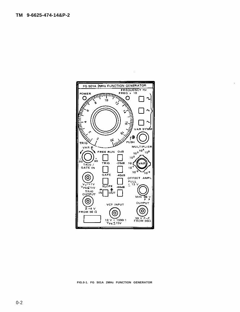
FIG.0-1. FG 501A 2MHz FUNCTION GENERATOR
TM 9-6625-474-14&P-2
SECTION 1
SPECIFICATION
INTRODUCTION
This section of the manual contains a general descrip-tion of the FG 501A and complete electrical, environmen-tal, and physical specifications. Standard accessories arealso listed. Instrument option information is located in theback of this manual in a separate section.
INSTRUMENT DESCRIPTION
The FG 501A Function Generator provides low distor-tion sine, square, triangle, ramp, and pulse waveformsover the frequency range 0.002 Hz to 2 MHz in eightdecade steps. Dc offset up to ±13 V is available. Waveformtriggering and gating functions, in addition to being slope(+ or –) selectable, are provided with variable phasecontrol capable of up to ±90° phase shift. The symmetryof the output waveform may also be varied from 5 to 95%.Step attenuators provide up to 60 dB of attenuation in20 dB steps. A variable amplitude control provides anadditional 20 dB attenuation.
A voltage-controlled frequency (VCF) input is providedto control the output frequency from an external voltagesource. The output frequency can be swept above andbelow the selected frequency to a maximum of 1000:1depending on the polarity and amplitude of the VCF inputsignal and the selected output frequency.
ACCESSORIES
The only accessory shipped with the FG 501A is theInstruction Manual.
PERFORMANCE CONDITIONS
The electrical characteristics are valid with the follow-ing conditions:
1. The instrument must have been adjusted at anambient temperature between +20° C and +30° C andoperating at an ambient temperature between 0° C and+50° C.
2. The instrument must be in a non-condensing en-vironment whose limits are described under Environmen-tal.
3. Allow twenty minutes warm-up time for operation tospecified accuracy; sixty minutes after exposure to orstorage in high humidity (condensing) environment.
Items listed in the Performance Requirements columnof the Electrical Characteristics are verified by completingthe Performance Check in this manual. Items listed in theSupplemental Information column may not be verified inthis manual; they are either explanatory notes or perfor-mance characteristics for which no limits are specified.
1-1
TM 9-6625-474-14&P-2
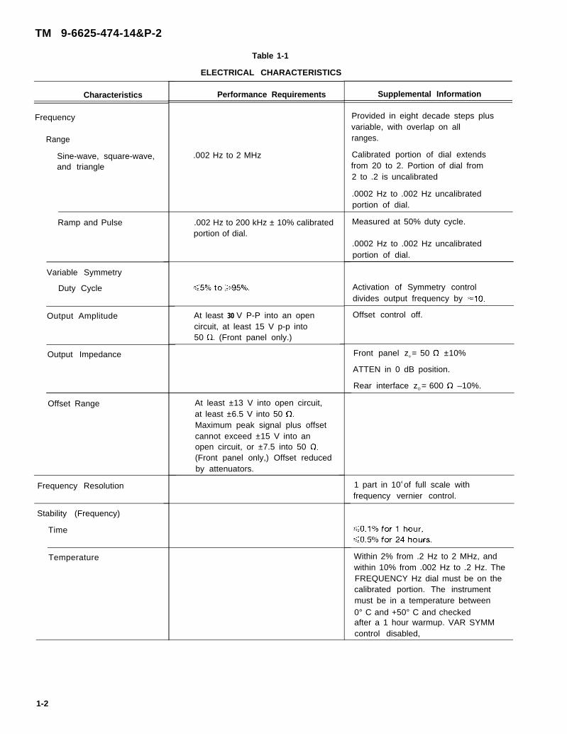
Characteristics
Frequency
Range
Sine-wave, square-wave,and triangle
Ramp and Pulse
Variable Symmetry
Duty Cycle
Output Amplitude
Output Impedance
Offset Range
Frequency Resolution
Stability (Frequency)
Time
Temperature
Table 1-1
ELECTRICAL CHARACTERISTICS
Performance Requirements
.002 Hz to 2 MHz
.002 Hz to 200 kHz ± 10% calibratedportion of dial.
At least 30 V P-P into an opencircuit, at least 15 V p-p into50 Cl, (Front panel only.)
At least ±13 V into open circuit,at least ±6.5 V into 50 Q.Maximum peak signal plus offsetcannot exceed ±15 V into anopen circuit, or ±7.5 into 50 Q.(Front panel only,) Offset reducedby attenuators.
Supplemental Information
Provided in eight decade steps plusvariable, with overlap on allranges.
Calibrated portion of dial extendsfrom 20 to 2. Portion of dial from2 to .2 is uncalibrated
.0002 Hz to .002 Hz uncalibratedportion of dial.
Measured at 50% duty cycle.
.0002 Hz to .002 Hz uncalibratedportion of dial.
Activation of Symmetry controldivides output frequency by =10.
Offset control off.
Front panel zo = 50 (2 ±10%
ATTEN in 0 dB position.
Rear interface zO = 600 Cl –10%.
1 part in 104 of full scale withfrequency vernier control.
Within 2% from .2 Hz to 2 MHz, andwithin 10% from .002 Hz to .2 Hz. TheFREQUENCY Hz dial must be on thecalibrated portion. The instrumentmust be in a temperature between0° C and +50° C and checkedafter a 1 hour warmup. VAR SYMMcontrol disabled,
1-2
TM 9-6625-474-14&P-2
Table 1-1 (cont)
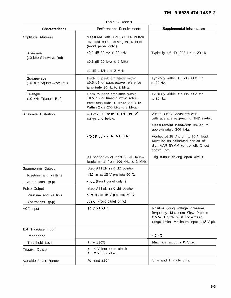
Characteristics
Amplitude Flatness
Sinewave(10 kHz Sinewave Ref)
Squarewave(10 kHz Squarewave Ref)
Triangle(10 kHz Triangle Ref)
Sinewave Distortion
Squarewave Output
Risetime and Falltime
Aberrations (p-p)
Pulse Output
Risetime and Falltime
Aberrations (p-p)
VCF Input
Ext Trig/Gate Input
Impedance
Threshold Level
Trigger Output
Variable Phase Range
Performance Requirements
Measured with 0 dB ATTEN button“IN” and output driving 50 Cl load.(Front panel only.)
±0.1 dB 20 Hz to 20 kHz
±0.5 dB 20 kHz to 1 MHz
±1 dB 1 MHz to 2 MHz
Peak to peak amplitude within±0.5 dB of squarewave referenceamplitude 20 Hz to 2 MHz.
Peak to peak amplitude within±0.5 dB of triangle wave refer-ence amplitude 20 Hz to 200 kHz.Within 2 dB 200 kHz to 2 MHz.
range and below.
All harmonics at least 30 dB belowfundamental from 100 kHz to 2 MHz
Step ATTEN in 0 dB position.
<25 ns at 15 V p-p into 50 Q
s30/o (Front panel only. )
Step ATTEN in 0 dB position.
<25 ns at 15 V p-p into 50 Q,
<30/o (Front panel only.)
+1 V ±20%.
> +4 V into open circuit>+2Vinto50f2.
At Ieast ±90°
Supplemental Information
Typically ±.5 dB .002 Hz to 20 Hz
Typically within ±.5 dB .002 Hzto 20 Hz.
Typically within ±.5 dB .002 Hzto 20 Hz.
20° to 30° C. Measured withwith average responding THD meter.
Measurement bandwidth limited toapproximately 300 kHz.
Verified at 15 V p-p into 50 Q load.Must be on calibrated portion ofdial. VAR SYMM control off, Offsetcontrol off.
Trig output driving open circuit.
Positive going voltage increasesfrequency. Maximum Slew Rate =0.5 V/Ps. VCF must not exceedrange limits, Maximum input <15 V pk.
=2 kf2
Maximum input <15 V pk.
Sine and Triangle only.
1-3
TM 9-6625-474-14&P-2
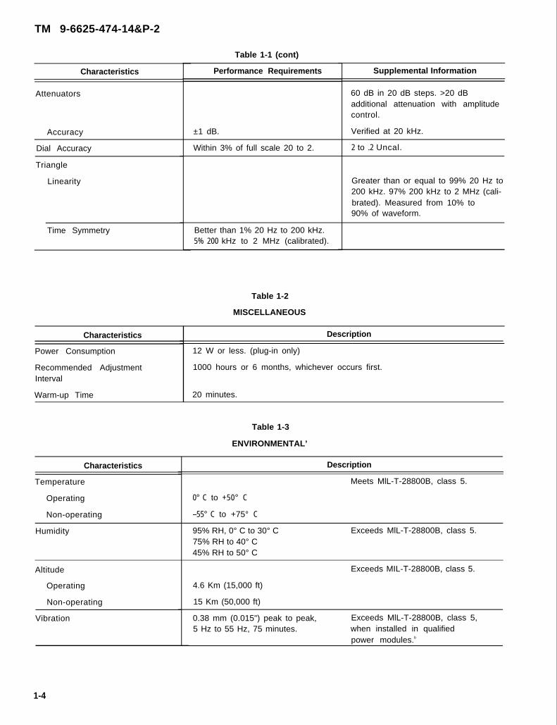
Characteristics
Attenuators
Accuracy
Dial Accuracy
Triangle
Linearity
Time Symmetry
Table 1-1 (cont)
Performance Requirements
±1 dB.
Within 3% of full scale 20 to 2.
Better than 1% 20 Hz to 200 kHz.5% 200 kHz to 2 MHz (calibrated).
Table 1-2
MISCELLANEOUS
Supplemental Information
60 dB in 20 dB steps. >20 dBadditional attenuation with amplitudecontrol.
Verified at 20 kHz.
2 to .2 Uncal.
Greater than or equal to 99% 20 Hz to200 kHz. 97% 200 kHz to 2 MHz (cali-brated). Measured from 10% to90% of waveform.
Characteristics
Power Consumption
Recommended AdjustmentInterval
Warm-up Time
Description
12 W or less. (plug-in only)
1000 hours or 6 months, whichever occurs first.
20 minutes.
Characteristics
Temperature
Operating
Non-operating
Humidity
Altitude
Operating
Non-operating
Vibration
Table 1-3
ENVIRONMENTAL’
Description
Meets MlL-T-28800B, class 5.
0° C to +50° C
–55° C to +75° C
95% RH, 0° C to 30° C Exceeds MlL-T-28800B, class 5.75% RH to 40° C45% RH to 50° C
Exceeds MIL-T-28800B, class 5.
4.6 Km (15,000 ft)
15 Km (50,000 ft)
0.38 mm (0.015") peak to peak, Exceeds MlL-T-28800B, class 5,5 Hz to 55 Hz, 75 minutes. when installed in qualified
power modules.b
1-4
TM 9-6625-474-14&P-2
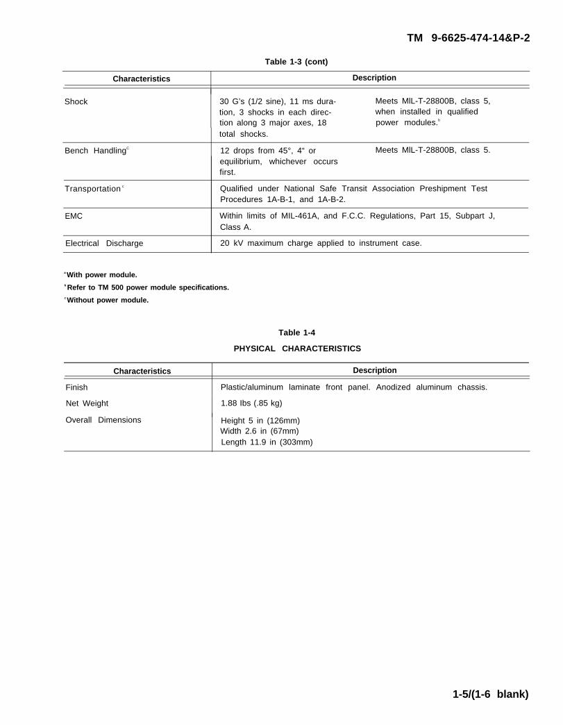
Table 1-3 (cont)
Characteristics Description
Shock 30 G’s (1/2 sine), 11 ms dura- Meets MlL-T-28800B, class 5,tion, 3 shocks in each direc- when installed in qualifiedtion along 3 major axes, 18 power modules.b
total shocks.
Bench HandlingC 12 drops from 45°, 4“ or Meets MlL-T-28800B, class 5.equilibrium, whichever occursfirst.
Transportation c Qualified under National Safe Transit Association Preshipment TestProcedures 1A-B-1, and 1A-B-2.
EMC Within limits of MIL-461A, and F.C.C. Regulations, Part 15, Subpart J,Class A.
Electrical Discharge 20 kV maximum charge applied to instrument case.
a With power module.b Refer to TM 500 power module specifications.c Without power module.
Table 1-4
PHYSICAL CHARACTERISTICS
Characteristics Description
Finish Plastic/aluminum laminate front panel. Anodized aluminum chassis.
Net Weight 1.88 Ibs (.85 kg)
Overall Dimensions Height 5 in (126mm)Width 2.6 in (67mm)Length 11.9 in (303mm)
1-5/(1-6 blank)
CAUTION
TM 9-6625-474-14&P-2
SECTION 2
OPERATING INSTRUCTIONS
INTRODUCTION
This section of the manual provides operating informa-tion required to obtain the most effective performancefrom the FG 501A. Included are installation and removalinstructions, a functional description of the front panelcontrols, and a general description of the operatingmodes. Some basic applications of the instrument are alsobriefly discussed.
INSTALLATION AND REMOVAL
The FG 501A is calibrated and ready to use whenreceived. It operates in one compartment of any TM 500-series power module. Refer to the power module instruc-tion manual for line voltage requirements and powermodule operation.
To prevent damage to the FG 501A, turn the powermodule off before installation or removal of theinstrument from the mainframe. Do not use ex-cessive force to install or remove.
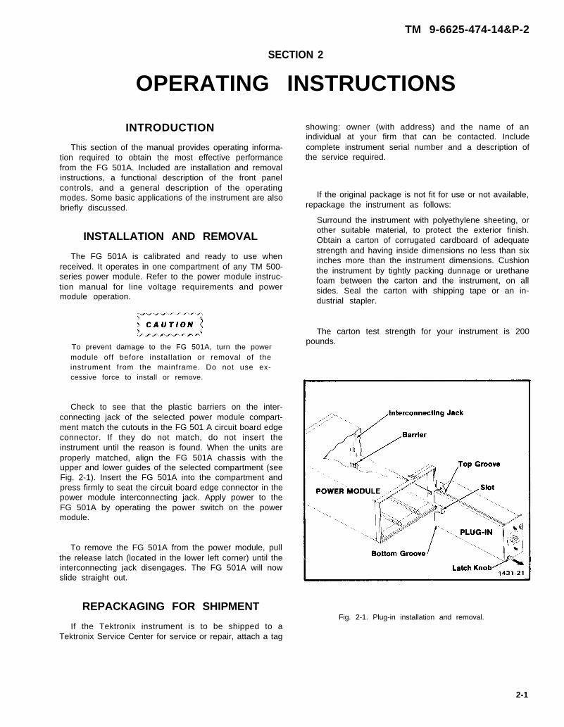
Check to see that the plastic barriers on the inter-connecting jack of the selected power module compart-ment match the cutouts in the FG 501 A circuit board edgeconnector. If they do not match, do not insert theinstrument until the reason is found. When the units areproperly matched, align the FG 501A chassis with theupper and lower guides of the selected compartment (seeFig. 2-1). Insert the FG 501A into the compartment andpress firmly to seat the circuit board edge connector in thepower module interconnecting jack. Apply power to theFG 501A by operating the power switch on the powermodule.
To remove the FG 501A from the power module, pullthe release latch (located in the lower left corner) until theinterconnecting jack disengages. The FG 501A will nowslide straight out.
REPACKAGING FOR SHIPMENT
If the Tektronix instrument is to be shipped to aTektronix Service Center for service or repair, attach a tag
showing: owner (with address) and the name of anindividual at your firm that can be contacted. Includecomplete instrument serial number and a description ofthe service required.
If the original package is not fit for use or not available,repackage the instrument as follows:
Surround the instrument with polyethylene sheeting, orother suitable material, to protect the exterior finish.Obtain a carton of corrugated cardboard of adequatestrength and having inside dimensions no less than sixinches more than the instrument dimensions. Cushionthe instrument by tightly packing dunnage or urethanefoam between the carton and the instrument, on allsides. Seal the carton with shipping tape or an in-dustrial stapler.
The carton test strength for your instrument is 200pounds.
Fig. 2-1. Plug-in installation and removal.
2-1
TM 9-6625-474-14&P-2
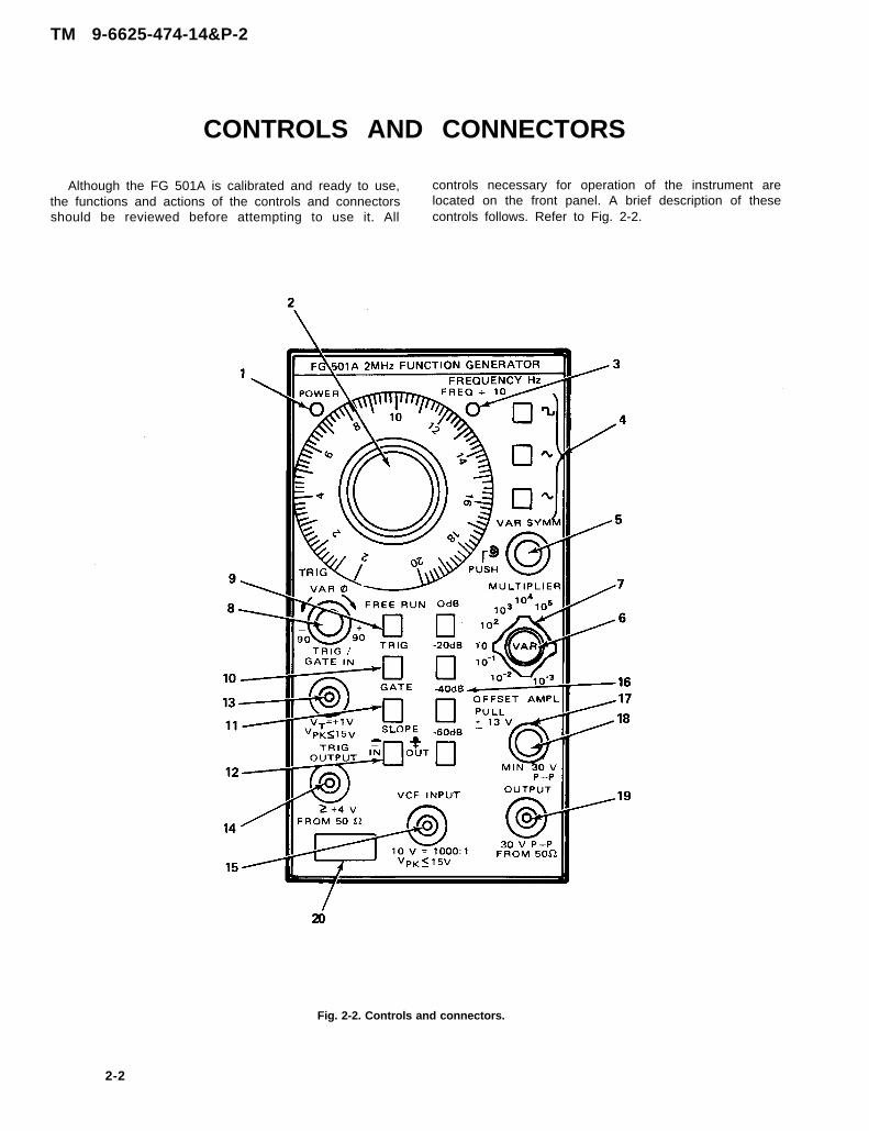
CONTROLS AND CONNECTORS
Although the FG 501A is calibrated and ready to use,the functions and actions of the controls and connectorsshould be reviewed before attempting to use it. All
controls necessary for operation of the instrument arelocated on the front panel. A brief description of thesecontrols follows. Refer to Fig. 2-2.
Fig. 2-2. Controls and connectors.
2-2
POWER - llluminated when power is applied to theFG 501A.
FREQUENCY CONTROL AND FUNCTIONSELECTION
FREQUENCY Hz - Selects the frequency of theoutput waveform in conjunction w i t h t heMULTIPLIER control.
FREQ + 10 - Illuminated when the variable sym-metry function is activated.
FUNCTION BUTTONS - Select square, triangle,and sine waveforms.
VAR SYMM - (push to enable) adjusts time-basedsymmetry of the selected output waveform. Reducesthe frequency of the output waveform by a factor= 10 and illuminates the FREQ + 10 indicator.
FREQUENCY VERNIER - For fine adjustment ofoutput frequency to at least 1 part in 104 of full scale.
MULTIPLIER - Selects the output frequency in eightdecade steps in conjunction with the FREQUENCYHz control.
TRIGGER AND GATE CONTROLS
VAR 0 - Selects phase lead or lag, up to ±90°,relative to input trigger or gate waveform.
FREE RUN - When pressed causes continuouswaveform output.
TRIG - When pressed causes output of one cycle ofselected waveform for each trigger pulse applied tothe TRIG/GATE IN connector.
TM 9-6625-474-14&P-2
GATE - When pressed causes continuous output ofthe selected waveform for the duration of the gatingpulse.
SLOPE - Button selects, in TRIG mode, the slope ofthe input signal which will trigger the selectedoutput waveform. In GATE mode, whether outputgating will occur when the level of the input signal isabove or below the threshold level of +1 V.
TRIG/GATE lN - Bnc connector used to apply theexternal trigger or gating signal.
VCF lNPUT - Bnc connector for applying an exter-nal voltage for controlling the output frequency ofthe generator.
TRIGGER OUTPUT - Bnc connector which outputsone positive pulse for each cycle of the selectedoutput waveform.
OUTPUT CONTROLS
ATTENUATOR BUTTONS - Attenuate the ampli-tude of the selected output waveform in 20 dB stepsto a maximum of 60 dB when pressed.
AMPL - Varies the amplitude of the selected outputwaveform, between steps of the attenuator buttons.
OFFSET - Pull and turn control, concentric with theAMPL control, provides up to ±13 V dc offset of theoutput waveform.
OUTPUT - Bnc connector for output of the selectedwaveform.
RELEASE LATCH - Pull to disengage the FG 501Afrom the power module.
2-3
TM 9-6625-474-14&P-2
OPERATING CONSIDERATIONS
OUTPUT CONNECTIONS
The output of the FG 501A is designed to operate as a50 fl voltage source working into a 50 Q load. At higherfrequencies, an unterminated or improperly terminatedoutput will cause aberrations on the output waveform.Loads less than 50 ~ will reduce the waveform amplitude.
Excessive distortion or aberrations, due to impropertermination, are less noticeable at the lower frequencies(especially with sine and square waveforms). To ensurewaveform purity, observe the following precautions:
1. Use good quality 50 Q coaxial cables and connec-tors.
2. Make all connections tight and as short as possible.
capacitance) of the vertical input of an oscilloscope,connect the transmission line to a 50 Q attenuator, 50 Qtermination, and then to the oscilloscope input. Theattenuator isolates the input capacitance of the device,and the FG 501A is properly terminated.
FIRST TIME OPERATION
The Controls and Connectors pages give a descriptionof the front panel controls and connectors, The waveformselection and frequency determining control sareoutlinedin blue, the trigger function controls and inputs areoutlined in green, and the output controls are outlined inblack.
The following exercise will familiarize the operator withmost functions of the FG 501A.
3. Use good quality attenuators if it is necessary toreduce waveform amplitude applied to sensitive circuits.
NOTE
4. Use terminations orimpedance matching devices toavoid reflections when using long cables (6 feet or more).
5. Ensure that attenuators, terminations, etc. haveadequate power handling capabilities for the outputwaveform.
If there is a dc voltage across the output load, use acoupling capacitor in series with the load. The timeconstant of the coupling capacitor and load must be longenough to maintain pulse flatness.
RISETIME AND FALLTIME
If the FG 501A is used to measure the rise or falltime ofa device, the riestime characteristics of associated equip-ment should be considered. If the risetime of the deviceunder test is at least 10 times greater than the combinedrisetimes of the FG 501A and associated equipment, theerror introduced will not exceed 1%, and generally can beignored. When the rise or falltime of the test device is lessthan 10 times as long as the combined risetimes of thetesting system, the actual risetime of the system must becalculated. The risetime of the device under test can bedetermined once the risetime of the system is known.
IMPEDANCE MATCHING
If the FG 501A is driving a high impedance such as the1 MQ input impedance (para l le led by a s ta ted
I f any discrepancies are encountered during theexercise, refer the condit ion to qualif ied servicepersonnel,
Preset the controls as follows:
Blue section:
FREQUENCY HzMULTIPLIERFREQUENCY VERNIERWAVEFORM—SINEVAR SYMM
Green section:
FREE RUN
Black section:
ATTENUATORAMPL (variable)OFFSET
1010Fully CW
inoff
in
-20 dBCenteredoff
Connect a 50 Q bnc coaxial cable terminated in 50 f2tothe vertical input of an oscilloscope. Set the oscilloscopecontrols to:
Vertical 1 V/Div DC CoupledHorizontal (Time Base) 1 ms/Div
The oscilloscope should display 1 complete cycle perdivision of the sine waveform ( approximately 10 cyclesacross the graticule),
2-4
1. Alternately press the square, triangle and sinebuttons and observe the different waveshapes. Return tothe preset condition.
2. Alternately press the four attenuator buttons androtate the AMPL (variable) control to verify that thewaveform amplitude changes. Return these controls to thepreset condition.
3. Pull the OFFSET knob out and rotate it. Notice thechange in dc level of the displayed waveform. Return theOFFSET knob to the in position.
TM 9-6625-474-14&P-2
4. Push the VAR SYMM button to release it to the outposition. Observe that the FREQ + 10 indicator is il-luminated and only one cycle of the output waveform isdisplayed. Rotate the VAR SYMM control through itsrange and notice the change in shape of the square,triangle, and sine waveforms (with the appropriate buttonspushed in). Return the controls to the preset condition.
5. Rotate the FREQUENCY contro l and theMULTIPLIER switch while observing the change in fre-quency of the displayedto the preset condition,
OPERATING MODES
FREE-RUNNING OUTPUT
The following procedure will provide a free-runningoutput with variable frequency and amplitude.
1. Select the desired waveform.
2. Set the AMPL control fully counterclockwise. Checkthat the VAR SYMM and OFFSET controls are in the off(in) position.
3. Select the desired frequency with the FREQUENCYHz dial and MULTIPLIER switch. Frequency equals dialsetting times multiplier setting.
4. Connect the load to the FG 501A output connectorand adjust the AMPL control for the desired outputamplitude.
TRIGGERED OR GATED (BURST)OPERATION
With the FG 501A set for free-running operation, asdescribed in previous paragraphs, apply the triggering orgating signal to the TRIG/GATE IN connector.
If only one cycle of the output waveform per trigger isdesired, push the TRIG button and select + or – slope.One output cycle will now be generated for each inputtrigger cycle.
waveform, Return these controls
If more than one cycle of the output waveform isdesired, push the GATE button. The output will now becontinuous for the duration of the gating waveform. Thenumber of cycles per burst can be approximated bydividing the gating signal duration by the period ofFG 501A output frequency,
In triggered or gated operation the PHASE controlvaries the start of the output waveform by ±90°. Thisphase change is measured from the 0 V, 0° point on theoutput waveform.
VOLTAGE CONTROLLED FREQUENCY(VCF) OPERATION
The output frequency of any selected waveform can beswept within a range of 1000:1 by applying an externalvoltage to the VCF INPUT connector. The polarity of theVCF input signal determines which direction the outputfrequency sweeps from the selected frequency, A positive(+) going signal increases the frequency while a negative(–) going signal decreases the frequency. The amplitudeand polarity of the input voltage can be selected within arange of ±10 V depending on the FREQUENCY Hz dialsetting.
The maximum swept frequency range of 1000:1 encom-passes the uncalibrated portion of the FREQUENCY Hzdial (<.2 to 2). To ensure that the frequency does sweep atleast a range of 1000:1, it is recommended that theFREQUENCY Hz dial be set at .2 and a 0 to +10 V signal beapplied to the VCF INPUT connector. It may be necessary
2-5
TM 9-6625-474-14&P-2
to vary the FREQUENCY VERNIER control to obtain the TRIGGER OUTPUTfull 1000:1 swept range or the lowest swept frequencydesired. A +4 V square wave is available from the TRIG
OUTPUT connector. The frequency of the trigger outputis determined by the frequency of the selected outputwaveform. One trigger pulse is generated for each positivecycle of the output signal except when square waves are
Since the VCF input amplitude is a linear relationship, selected. When generating square waves, one triggerthe frequency output range can be determined from the pulse is generated for each negative cycle of the outputVCF input amplitude. signal. Trigger output impedance is 50’(2.
BASIC WAVEFORM CAPABILITIES
The following photographs illustrate the basic waveform capabilities of the FG 501A.
Fig. 2-3. Swept Frequency range with 10 V signals applied to VCF IN connector.
2-6
TM 9-6625-474-14&P-2
Fig. 2-4. BASIC FUNCTIONS. Square, triangle, and sinewaveforms selected by front panel pushbuttons.
Fig. 2-6. Phase relationships between OUTPUT waveforms andthe TRIG OUT waveform.
Fig. 2-5. RAMPS AND PULSES. These are obtained from the Fig. 2-7. Trigger Signal amplitude requirements and triggeringbasic waveforms by using the SYMMETRY control. points.
2-7
TM 9-6625-474-14&P-2
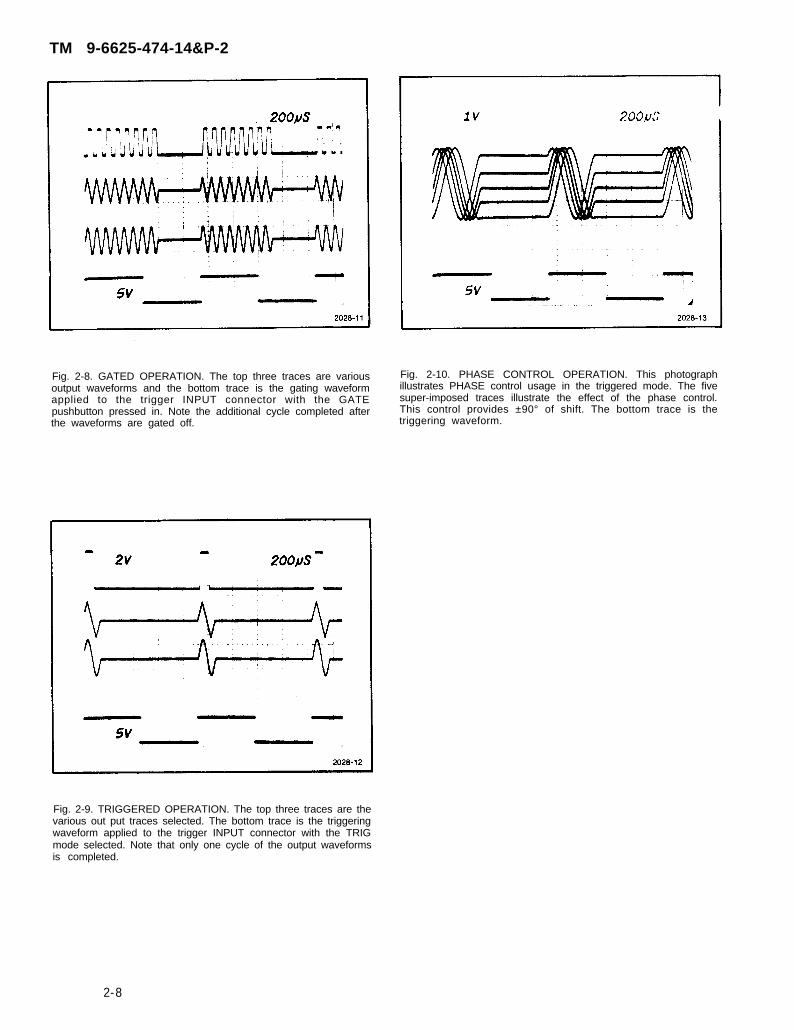
Fig. 2-8. GATED OPERATION. The top three traces are various Fig. 2-10. PHASE CONTROL OPERATION. This photographoutput waveforms and the bottom trace is the gating waveformapplied to the trigger INPUT connector with the GATEpushbutton pressed in. Note the additional cycle completed afterthe waveforms are gated off.
illustrates PHASE control usage in the triggered mode. The fivesuper-imposed traces illustrate the effect of the phase control.This control provides ±90° of shift. The bottom trace is thetriggering waveform.
Fig. 2-9. TRIGGERED OPERATION. The top three traces are thevarious out put traces selected. The bottom trace is the triggeringwaveform applied to the trigger INPUT connector with the TRIGmode selected. Note that only one cycle of the output waveformsis completed.
2-8
TM 9-6625-474-14&P-2
APPLICATIONS
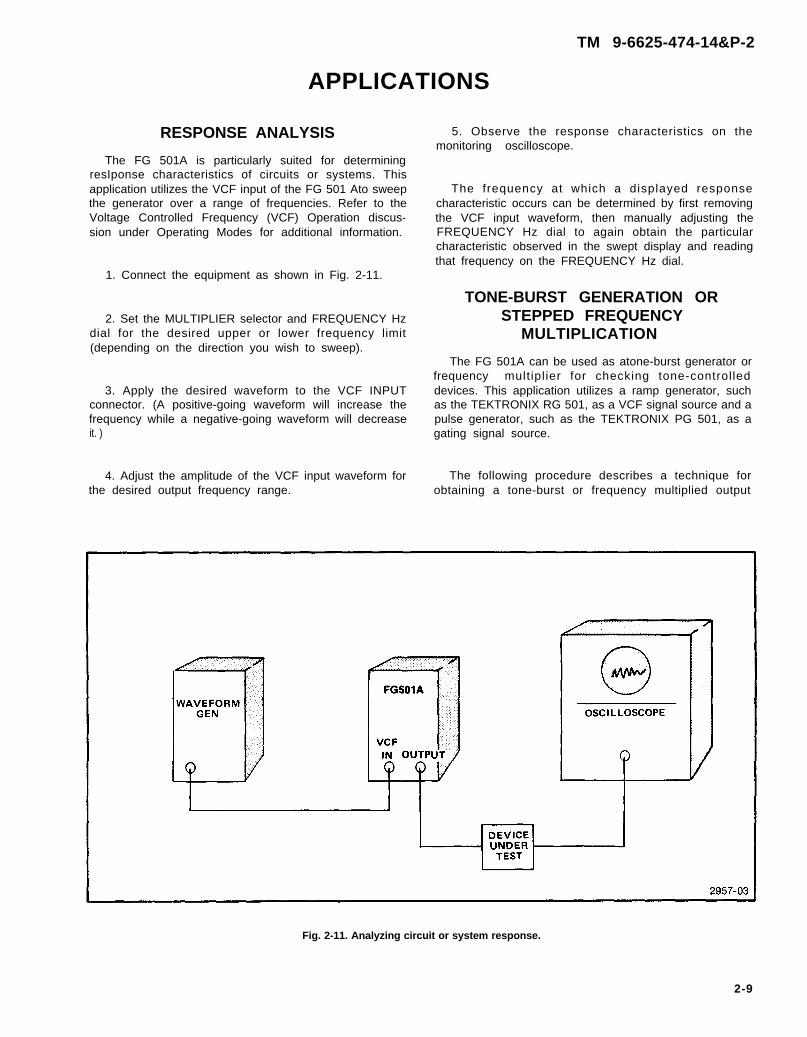
RESPONSE ANALYSIS
The FG 501A is particularly suited for determiningresIponse characteristics of circuits or systems. Thisapplication utilizes the VCF input of the FG 501 Ato sweepthe generator over a range of frequencies. Refer to theVoltage Controlled Frequency (VCF) Operation discus-sion under Operating Modes for additional information.
1. Connect the equipment as shown in Fig. 2-11.
2. Set the MULTIPLIER selector and FREQUENCY Hzdial for the desired upper or lower frequency limit(depending on the direction you wish to sweep).
3. Apply the desired waveform to the VCF INPUTconnector. (A positive-going waveform will increase thefrequency while a negative-going waveform will decreaseit. )
5. Observe the response characteristics on themonitoring oscilloscope.
The frequency at which a displayed responsecharacteristic occurs can be determined by first removingthe VCF input waveform, then manually adjusting theFREQUENCY Hz dial to again obtain the particularcharacteristic observed in the swept display and readingthat frequency on the FREQUENCY Hz dial.
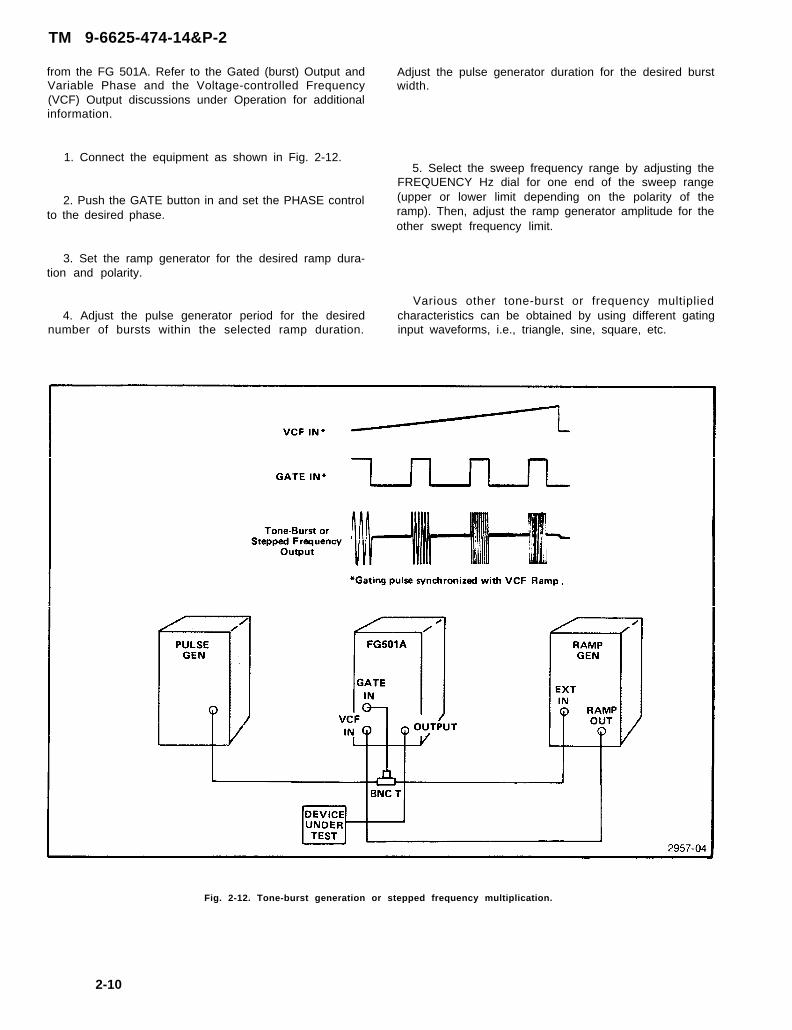
TONE-BURST GENERATION ORSTEPPED FREQUENCY
MULTIPLICATION
The FG 501A can be used as atone-burst generator orfrequency multipl ier for checking tone-controlleddevices. This application utilizes a ramp generator, suchas the TEKTRONIX RG 501, as a VCF signal source and apulse generator, such as the TEKTRONIX PG 501, as agating signal source.
4. Adjust the amplitude of the VCF input waveform for The following procedure describes a technique forthe desired output frequency range. obtaining a tone-burst or frequency multiplied output
Fig. 2-11. Analyzing circuit or system response.
2-9
TM 9-6625-474-14&P-2
from the FG 501A. Refer to the Gated (burst) Output andVariable Phase and the Voltage-controlled Frequency(VCF) Output discussions under Operation for additionalinformation.
1. Connect the equipment as shown in Fig. 2-12.
2. Push the GATE button in and set the PHASE controlto the desired phase.
3. Set the ramp generator for the desired ramp dura-tion and polarity.
4. Adjust the pulse generator period for the desired
Adjust the pulse generator duration for the desired burstwidth.
5. Select the sweep frequency range by adjusting theFREQUENCY Hz dial for one end of the sweep range(upper or lower limit depending on the polarity of theramp). Then, adjust the ramp generator amplitude for theother swept frequency limit.
Various other tone-burst or frequency multipliedcharacteristics can be obtained by using different gating
number of bursts within the selected ramp duration. input waveforms, i.e., triangle, sine, square, etc.
Fig. 2-12. Tone-burst generation or stepped frequency multiplication.
2-10
TM 9-6625-474-14&P-2
SECTION 3
THEORY OF OPERATION
INTRODUCTION
This section of the manual contains a description of the description. Diamond enclosed numbers appearingelectrical circuits in the FG 501A. Refer to the block throughout this section refer to the schematic diagram ondiagram and schematic diagrams on the fold out pages in which the circuit being discussed is located.the back of the manual to aid in understanding this
LOOP @FREQUENCY CONTROL AND SUMMING
AMPLIFIER
The voltage developed across the frequency controldivider string, R1429, R1321, R500 and R510, is applied topin 5 of operational amplifier U1540B. This voltage isbuffered by the amplifier and. a current is developedthrough R1551. This current is applied top in 2 of summingamplifier U1540A where it is summed with any currentsdeveloped by a voltage applied tothe VCF inputs. The VCFinputs are J510 (front panel) through R1553, and pin 21B(rear interface) through R1103. These summed currentsare buffered by Q1445 and flow through R1543. Thevoltage developed across R1543 is proportional to thefrequency.
CURRENT SOURCES AND SWITCH
The voltage developed across R1543 is buffered byU1440 and Q1541 which form the negative current sourcefor the main Ioop timing circuitry. This same voltage is alsobuffered by U1540C and Q1543 which form a currentsource identical to U1440 and Q1541. The output currentfrom Q1543 flows through Q1527, Q1525, and Q1421,which form a current mirror that inverts this current toprovide the positive current source for the main looptiming circuitry. The current through R1521 is the timingcapacitor charging current; the current through R1536 isthe discharging current. The Top Dial Symmetry Cal,R1421, adjusts the balance between these two currents sothey are equal in magnitude.
In the normal mode of operation (fixed symmetry) R520and R540 are in the emitter circuit of Q1541 and Q1543. Inthis condition, equal amounts of current will flow in boththe positive and negative current sources. When S500,VAR SYMM, is activated, R530 is switched into the currentsource emitter circuits. As R530 is varied from one end tothe other, unequal amounts of current flow through the
positive and negative current sources. In this manner thesymmetry of the waveform generated by the loop is varied.These currents are switched into the junction of CR1531and CR1533 where they alternately charge and dischargethe timing capacitor, producing a triangle waveform, Thecurrent switch is formed by Q1531, CR1531, Q1433 andCR1533.
TIMING CAPACITORS ANDCAPACITANCE MULTIPLIER @
The timing capacitors provide for triangle generation inthe five fastest MULTIPLIER ranges. They are switchedinto and out of the circuit in decade stepsfrom 105 (C1631)down to 101 (C1741).
For the four lower MULTIPLIER ranges, 100 down to10-’, C1741 is switched into the feedback loop of U1930forming an integrator. Current from the current switch isapplied to operational amplifier U1940. A voltage isdeveloped at the output of this amplifier that is propor-tional to the applied current times the value of R1941(1 kfl). This voltage is applied, across one of fourresistors, to the input of U1930. These resistors, R1831,R1841, R1842, and R1843, are switched into and out of thecircuit in decade steps with the MULTIPLIER switchS1731. This arrangement provides very large values ofeffective capacitance. The output of U1930 is now thetriangle that is applied to the buffer stage.
TRIANGLE BUFFER @
The voltage developed by the timing capacitor ormultiplier (U1930) is applied to the triangle buffer. Q1725and Q1723 form the differential input stage of this circuit.Q1821 serves as a constant current source for the inputdifferential pair. Q1721 and Q1712 complete the feedbackfor the amplifier such that the voltage at the emitter ofQ1712 is equal to the voltage at the Gate of Q1725.
3-1
TM 9-6625-474-14&P-2
Loop delay compensation is provided by a networkcomprised of R1712, R1812, C1712, and C1714. Thebuffered timing capacitor voltage is applied through thisnetwork to the level comparators.
LEVEL COMPARATORS
The level comparators detect upper and lowerthreshold levels. U1700A is the upper level detector andU1700B the lower. The reference level for these com-parators is supplied by U1400B and C. As the thresholdlevels are detected, the respective comparator triggersU1600B.
REFERENCE VOLTAGES
The reference voltage supplies are composed ofU1400B (–) and U1400C (+) and associated components.The upper (positive) level threshold voltage is establishedby adjusting R1412. This resistor is in a voltage dividerstring from zener diode VR1413. The voltage developedacross R1412 is buffered by U1400C and set to ap-proximately +400 mV at the output. This voltage is appliedto pin 5 of U1700A as the upper threshold level reference.This same voltage is also applied to pin 9 of inverterU1400B. R1511 is used to adjust the gain of this stage sothat the output is nominally –400 mV. This voltage isapplied to pin 13 of U1700B as the lower threshold levelreference.
LOOP LOGIC
When a rising voltage at pin 6 of U1700A passesthrough the threshold level set at pin 5, the output (pin 8)goes low pulling pin 10 of U1600Blow. This action sets theflip-flop causing pin 9 (Q) to go high and pin 8 (Q) to golow. Pin 8 of U1600B is tied back, through R1403, to thejunction of CR1431 and VR1532. VR1532 serves as a levelshifter to change the TTL output gate to the correct level todrive the current switch (Q1531, CR1531, Q1433,CR1533).
As the voltage at the junction of R1532 and R1534drops, it pulls the bases of Q1531 and Q1433 low. Q1531 isturned on and Q1433 is turned off. Any current from thepositive current source, through R1521, now flowsthrough Q1531 and is shunted to the –15 V supply. WithQ1433 turned off, any current flow through the negativecurrent source must come from the positively chargedtiming capacitor through CR1533.
The falling voltage on the timing capacitor is bufferedthrough the triangle buffer and applied to the levelcomparators U1700A and U1700B. As the voltage at pin 12of U1700B falls through the threshold level set at pin 13,the output (pin 1) goes low pulling pin 13 of U1600Blow.This action resets the flip-flop causing pin 9 (Q) tonowgo
low and pin 8 (~) to go high. Taking this high at pin 8 backto the current switch, Q1531 will be turned off and Q1433turned on. This allows the timing capacitor to charge in thepositive direction.
The action just described generates one entire cycle ofa triangle wave.
TRIGGER GENERATOR
The square wave output at pin 8 (~) of U1600B alsodrives the trigger output amplifier. This circuit is com-posed of emitter follower Q1431 and associated com-ponents. Q1440, in conjunction with R1440, serves asoutput short circuit protection. The output of this circuit(at J2043) is a square wave 180° out of phase with the mainloop signal. The output amplitude is greater than +4 V intoan open circuit, and at least +2 V into a 50 f2 load.
SQUARE WAVE GENERATOR
The output at pin 9 (Q) of U1600B is a square wave, but180° out of phase with that at pin 8. This signal is used todrive the square wave generator composed of differentialpair Q1801, Q1901, and associated components. The baseof Q1901 is held at a constant voltage by divider networkR1815 and R1818. R1728 and R1816 form a constantcurrent source for the differential pair. The square wavefrom U1600B alternately switches this constant current toground through Q1801 or through R1819 and Q1901. Inthis manner, a square wave voltage is developed with dclevels sufficient to drive the output amplifier for the squarewave function.
PHASE CLAMP THRESHOLD DETECTOR
The output of the triangle buffer, in addition to possiblybeing fed to the Output Amplifier through S1901B, isconnected to the base of Q1711. Q1711 and Q1611 form adifferential amplifier. Q1621 and associated componentsprovide a constant current source for the differential pair.This amplifier senses the level of the triangle waveformand compares it to the output voltage of U1400A. Theoutput voltage of U1400A is determined by the setting ofthe VAR 0 control, R550. The voltage range of R550 isestablished by reference voltage supplies U1400B (–) andU1400C (+). These are the same reference voltagessupplied to the Level Comparators. This arrangementpermits comparison of the triangle voltage with themaximum possible positive and negative levels, and alllevels between.
When the triangle voltage exceeds the referencevoltage set by the VAR 0 control, Q1711 turns off. Anycurrent flowing through Q1621 now flows through Q1611.
3-2
TM 9-6625-474-14&P-2
CURRENT AMPLIFIER
Current flowing through Q1611 also flows throughR1622 and is amplified by Q1521. Temperature compen-sation for this amplifier is provided by CR1621. Differentialpair Q1511 and Q1523 serve as a current switch. WithQ1511 turned off, any current amplified by Q1521 passesthrough Q1523 to the junction of CR1531 and CR1533.When the timing capacitor voltage rises to the threshold
level set by the VAR 0 control, R550, it is clamped. Q1523now draws exactly the amount of current that the positivecurrent source supplies. Because the square wave at pin 5(Q) of U1600A drives the base of Q1511, the clampingaction only happens during the positive edge of thetriangle wave. On the negative transition, Q1523 is shutoff, and Q1511 is on. In this manner, the timing capacitorvoltage can be clamped at any desired positive level.
TRIG/GATE AMP AND SINE SHAPER @
TRIG/GATE AMP AND LOGIC
The input trigger amplifier consists of an emittercoupled differential pair (Q1320 and Q1322), currentamplifier Q1324, and the required logic circuitry to controlthe operation of the main loop phase clamp. Input circuitprotection is provided by R1203, R1204, CR1220 andCR1221. Triggering signals are applied either throughfront panel connector J520 or interface connections onthe rear edge of the Main circuit board.
The differential pair, Q1320-Q1322, responds to theinput signal when the voltage rises above (+ SLOPE) thereference voltage at the base of Q1320. This referencevoltage is established by divider network R1312 andR1314, The position of S1400D, SLOPE switch, deter-mines whether a positive or negative going input willcause the amplifier Q1324 to conduct. When the thresholdlevel is exceeded and conduction starts, current flowthrough the circuit causes a voltage to be developedacross R1322. This voltage is applied to the base of Q1324.The output at the collector of Q1324 is a TTL compatiblewaveform to drive the logic circuit, U1310. CR1320provides temperature compensation for Q1324.
Three modes of operation are selectable with S1400;Triggered, Gated, and Free Running.
In the TRIG mode, S1400A and S1400C are positionedsuch that the output, pin 6, of U1310B is connected to pin4, set input, of U1600A. In this mode, a very narrow,negative going voltage pulse is developed by U1310B eachtime the input waveform passes through the triggerthreshold. This low sets U1600A, which deactivates thephase clamp until the triangle generator again starts in thepositive direction, and allows the generator to completeone full cycle.
In the GATE mode, S1400A and S1400C are positionedsuch that the output, pin 3, of U1310A is connected to pin4, set input, of U1600A. In this mode, a low level isproduced whenever the input waveform exceeds thethreshold if + SLOPE is selected. The generator free runs
as long as this condition exists. As soon as the level at theinput connector drops below the threshold, the outputvoltage of U1310A rises. This high level causes thegenerator to again stop running when the phase clampreaches its threshold level at the end of the last completecycle.
In the FREE RUN mode, S1400A is positioned such thatpin 4 of U1600A is held low. The generator now outputscontinuous waveforms.
SINE SHAPER
The Sine Shaper is composed of three separate circuitfunctions: a Transconductance Amplifier, the ShaperCircuitry, and an Output Buffer.
Transconductance Amplifier. Emitter coupled tran-sistors Q1210 and Q1212 along with current source Q1200form the Transconductance Amplifier. The amplifier con-verts the triangle voltage at the base of Q1212 to adifferential current. This current flows through two sets ofdiode wired transistors, U1120C, U1120D, U1220C, andU1220D, to the input of the shaper.
Shaper. The active portion of the Shaper is formed bytwo sets of emitter coupled transistors U1220A, U1220B,U1120A and U1120B. These devices have their inputswired in series and their outputs cross coupled. U1120Eand U1220E are current sources for these devices. Thecircuit operates by generating a power series approxima-tion to the sine function. The devices in U1120 generatethe first order term while those in U1220 generate thesecond order term in the approximation.
Output Buffer. The Output Buffer is an operationalamplifier that converts the differential current from Q1010and U1020D to a single ended voltage that is applied,through the function switch, to the output amplifier.U1020E is a current source for the emitter coupleddifferential input pair U1020A and U1020B. Q1012 servesas a current mirror for U1020A and as an active load forU1020B. U1020C is the output emitter follower and R1020is the feedback resistor.
3-3
TM 9-6625-474-14&P-2
OUTPUT AMPLIFIER & ATTENUATORS @The output amplifier is basically a noninverting
operational amplifier whose plus input is the base ofQ2101 and minus input is the base of Q2113.
The three basic waveforms are selected by S1901 andapplied across R560B and R2335 to the input stage of theamplifier. R560B varies the amplitude of the selectedwaveform. The feedback network consists of R2011 andR2012, connected from the output to the minus input ofthe amplifier. C2011 provides high frequency compensa-tion for the feedback, and is used to adjust the squarewavefront corner. The input pair, Q2101 and Q2113, amplify thedifference between the input waveform and the fedbackwaveform.
The output of Q2101 is applied directly to Q2111 whichis cascoded with Q2011. The output of Q2113 passesthrough an inverting amplifier, Q2211, before passing toQ2213 cascoded with Q2311. CR2111 provides tem-perature compensation for Q2211. The two cascodes formdrivers for the amplifier output stage.
The output stage consists of Q2013 and Q2123 inparallel with Q2121 for amplification of positive goingsignals. Q2321 and Q2323 in parallel with Q2325 form theamplifier for negative going signals. The output is taken atthe junction of R2026 and R2228. The 50 f2 outputimpedance is determined by parallel 100 Q resistorsR2033 and R2131. C2121 in this network provides highfrequency compensation for the output impedance, Theattenuator circuit is a constant impedance resistive dividernetwork, switch selectable in 20 dB steps.
An offset current is also summed with the feedbacksignal at the base of Q2113 when S510A is closed. Thisallows R560A to control the dc offset of the output signal.
POWER SUPPLY @The FG 501A receives its power from the power module
via interface connections on the rear edge of the Maincircuit board. The power module supplies plus (+) andminus (–) 33.5 Vdc (unregulated) from which the follow-ing regulated voltages are generated.
+20 V SUPPLY
The +33.5 V from the power module is filtered andapplied to voltage regulator U1210 (pins 11 and 12). Thisregulator contains its own reference, operationalamplifier, and current Iimiting elements. The output of theregulator is applied to Q1231 which serves as a driver thethe series pass transistor located in the power module.The +20 V output is applied across voltage divider R1201,R1301, and R1315. The output level of the supply is set byR1301 (+15 V Adj) which compares the supply output tothe internal reference level of the regulator. This supply iscurrent limited through the action of R1121 and thecurrent limiting element in the regulator. When excessiveamounts of current are drawn from the supply, the voltagedeveloped across R1121 turns on the current limitingelement in the regulator (U1210). This action reduces thebase drive, through Q1231, to the series pass transistorcausing the supply to reduce output, This supply is thereference for other supplies in the FG 501A.
+15 V SUPPLY
The +15 V supply consists of U1230D and Q1221.U1230D serves as an error amplifier which compares theF15 Voutput of the supply to a +15 Preference developed
by divider network R1231, R1232 and R1233 from the
+20 V supply. Since this supply is sourced from the +20 V,it is inherently current limited by the +20 V supply.
+5 V SUPPLY
The +5 V supply consists of U1230C and Q1331.U1230C serves as an error amplifier which compares the+5 V output to a +5 V reference developed by dividernetwork R1231, R1232 and R1233 from the +20 V supply.Since this supply is sourced from the +15 V and referencedto the +20 V supply, it is inherently current limited underthe same conditions that limit those supplies.
–20 V SUPPLY
The –20 V supply is derived from –33.5 V supplied bythe power module. The output of operational amplifierU1230A is applied, through Q1245, to the base of Q1241,which serves as a driver for the series pass transistorlocated in the power module. This supply is also referenc-ed to the +20 V. The supply is current limited through theaction of R1141 and Q1243. When excessive amounts ofcurrent are drawn through R1141, a voltage sufficient toturn Q1243 on develops across R1141. This action reducesthe base drive to the series pass transistor causing thesupply to reduce output.
–15 V SUPPLY
The –15 V supply consists of operational amplifier(U1230B) and a series pass feedback regulator (Q1345),The output of the supply is fed back through dividernetwork R1247, R1341, and R1245. The output level isadjusted by R1341. Because this supply is sourced fromthe –20 V supply, it is current limited by the –20 V supply.
3-4
TM 9-6625-474-14&P-2
SECTION 4
CALIBRATION
PERFORMANCE CHECK
INTRODUCTION specified performance range. Any value within thespecified range, within appropriate limits, may be sub-
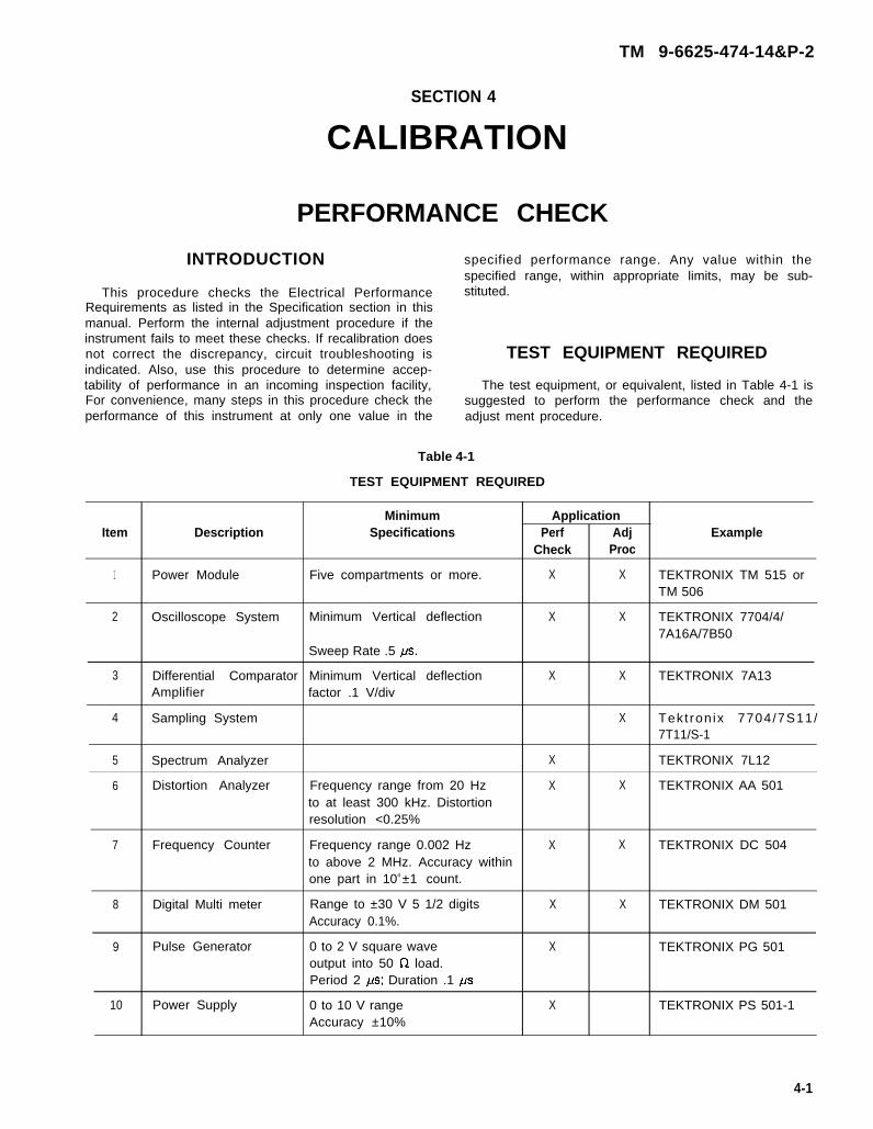
This procedure checks the Electrical Performance stituted.Requirements as listed in the Specification section in thismanual. Perform the internal adjustment procedure if theinstrument fails to meet these checks. If recalibration doesnot correct the discrepancy, circuit troubleshooting is TEST EQUIPMENT REQUIREDindicated. Also, use this procedure to determine accep-tability of performance in an incoming inspection facility, The test equipment, or equivalent, listed in Table 4-1 isFor convenience, many steps in this procedure check the suggested to perform the performance check and theperformance of this instrument at only one value in the adjust ment procedure.
Table 4-1
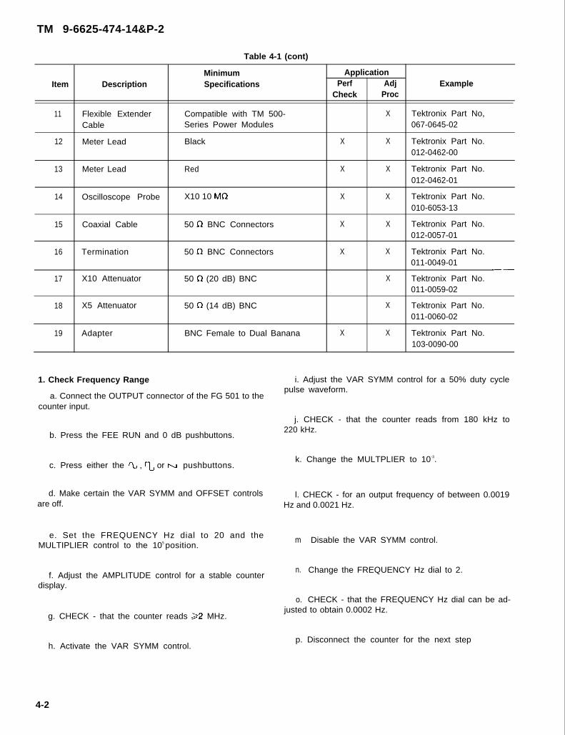
TEST EQUIPMENT REQUIRED
Minimum ApplicationItem Description Specifications Perf Adj Example
Check Proc
1 Power Module Five compartments or more. X X TEKTRONIX TM 515 orTM 506
2 Oscilloscope System Minimum Vertical deflection X X TEKTRONIX 7704/4/7A16A/7B50
Sweep Rate .5 PS.
3 Differential Comparator Minimum Vertical deflection X X TEKTRONIX 7A13Amplifier factor .1 V/div
4 Sampling System X Tekt ron ix 7704/7S11/7T11/S-1
5 Spectrum Analyzer X TEKTRONIX 7L12
6 Distortion Analyzer Frequency range from 20 Hz X X TEKTRONIX AA 501to at least 300 kHz. Distortionresolution <0.25%
7 Frequency Counter Frequency range 0.002 Hz X X TEKTRONIX DC 504to above 2 MHz. Accuracy withinone part in 104 ±1 count.
8 Digital Multi meter Range to ±30 V 5 1/2 digits X X TEKTRONIX DM 501Accuracy 0.1%.
9 Pulse Generator 0 to 2 V square wave X TEKTRONIX PG 501output into 50 f2 load.Period 2 ,US; Duration .1 ps
10 Power Supply 0 to 10 V range X TEKTRONIX PS 501-1Accuracy ±10%
4-1
TM 9-6625-474-14&P-2
Table 4-1 (cont)
Minimum ApplicationItem Description Specifications Perf Adj Example
Check Proc
11 Flexible Extender Compatible with TM 500- X Tektronix Part No,Cable Series Power Modules 067-0645-02
12 Meter Lead Black X X Tektronix Part No.012-0462-00
13 Meter Lead Red X X Tektronix Part No.012-0462-01
14 Oscilloscope Probe X10 10 Mf2 X X Tektronix Part No.010-6053-13
15 Coaxial Cable 50 !2 BNC Connectors X X Tektronix Part No.012-0057-01
16 Termination 50 Cl BNC Connectors X X Tektronix Part No.011-0049-01
17 X10 Attenuator 50 Cl (20 dB) BNC X Tektronix Part No.011-0059-02
18 X5 Attenuator 50 ~ (14 dB) BNC X Tektronix Part No.011-0060-02
19 Adapter BNC Female to Dual Banana X X Tektronix Part No.103-0090-00
1. Check Frequency Range
a. Connect the OUTPUT connector of the FG 501 to thecounter input.
b. Press the FEE RUN and 0 dB pushbuttons.
c. Press either the W , ~ or N pushbuttons.
d. Make certain the VAR SYMM and OFFSET controlsare off.
e. Set the FREQUENCY Hz dial to 20 and theMULTIPLIER control to the 105 position.
f. Adjust the AMPLITUDE control for a stable counterdisplay.
g. CHECK - that the counter reads >2 MHz.
h. Activate the VAR SYMM control.
i. Adjust the VAR SYMM control for a 50% duty cyclepulse waveform.
j. CHECK - that the counter reads from 180 kHz to220 kHz.
k. Change the MULTPLIER to 10-3.
l. CHECK - for an output frequency of between 0.0019Hz and 0.0021 Hz.
m
n.
o.
Disable the VAR SYMM control.
Change the FREQUENCY Hz dial to 2.
CHECK - that the FREQUENCY Hz dial can be ad-justed to obtain 0.0002 Hz.
p. Disconnect the counter for the next step
4-2
TM 9-6625-474-14&P-2
2. Check Variable Symmetry Duty Cycle
a.
b.
c.
Press the FREE RUN, 0 dB and ~ pushbuttons.
Release the VAR SYMM pushbutton.
Connect the OUTPUT connector through a 50 Qcoaxial cable to the oscilloscope vertical input:
d. Adjust the START, MULTIPLIER, AMPLITUDE, andoscilloscope controls to display a squarewave that oc-cupys exactly 10 major divisions for one cycle.
e. Rotate the VAR SYMM control from fully cw to fullyCCW.
f. CHECK - that the oscilloscope display varies eachsquarewave half cycle from <1/2 major division to >9.5major divisions.
g. Leave these connections for the next step.
3. Check Output Amplitude
a. Using the same setup as in the previous step, turnthe AMPLITUDE control fully CW.
b. CHECK - that the waveform on the oscilloscopedisplay is >30 V peak to peak.
c. Remove the coaxial cable from the oscilloscopevertical input and connect a 50 f2termination in series withthe cable.
d. CHECK - that the oscilloscope display is >15 Vpeak to peak.
e. Disconnect the 50 f) cable and remove the 50 f)termination from the oscilloscope for the next step.
4. Check Offset Range
a.
b.
Press the TRIG 0 dB, and N pushbuttons.
Make certain the VAR SYMM pushbutton is in.
c. Connect a dmm set to read ±15 V to the outputconnector.
d. Adjust the VAR 0 control for a 0 V reading on thedmm.
e. Pull and turn the OFFSET control fully cw to fullyCCW.
f. CHECK - that the dmm reads >+13 V at the ap-propriate stops for the OFFSET control.
g. Remove the coaxial cable from the dmm and insert a50 f) termination.
h. CHECK - that the dmm reads at least ±6.5 V at theappropriate stops of the OFFSET control.
i. Remove the connections from the dmm for the nextstep.
5. Check Amplitude Flatness
a. Press the FREE RUN, 0 dB and \ pushbuttons.
b. Make certain the OFFSET is off.
c. Set the FREQUENCY Hz dial to 10 and theMULTIPLIER to 103.
d. Connect the OUTPUT connector through a 50 Qcable and 50 Cl termination to the vertical input of thedifferential oscilloscope plug-in.
e. Adjust the AMPLITUDE control and the gain of thevertial amplifier for an 8 major division peak to peakdisplay.
f. Increase the vertical amplifier gain by a factor of 10.
g. Adjust the vertical amplifier plug-in offset voltage sothat the waveform peaks are on the oscilloscope graticulecenter line.
h. Change the output to any frequency from 20 Hz to20 kHz.
i. CHECK - that the display is within 0.46 majordivisions from graticule center.
4-3
TM 9-6625-474-14&P-2
j. Change the output to any frequency from 20 kHz to1 MHz.
k. CHECK - that the display is within 2.37 majordivisions from graticule center.
l. Decrease the vertical gain of the oscilloscope by afactor of 10 and adjust the offset voltage to 0.
m. Adjust the output frequency to 10 kHz.
n. Adjust the oscilloscope vertical gain and theAMPLITUDE control for a 6 major division peak to peakdisplay.
o. Change the output to any frequency from 1 MHz to2 MHz.
p. CHECK - that the peak to peak display amplitude isfrom 5.36 to 6.73 major divisions.
q. Press the\ pushbutton.
r. Set the output frequency to 10 kHz.
s. Adjust the AMPLITUDE control and the verticalcomparator oscilloscope plug-in for an 8 major divisionpeak to peak display.
t. Increase the oscilloscope vertical plug-in gain by afactor of 10.
u. Adjust the vertical plug-in offset voltage so that thepositive peaks of the squarewaves are at graticule center.
v. Change the output to any frequency from 20 Hz to2 MHz.
w. CHECK—that the positive squarewave peaks arewithin ±2.37 major divisions from graticule center.
x.
y.
z.
Press the N pushbutton.
Change the output frequency to 10 kHz.
Decrease the oscilloscope vertical plug-in gain by a
aa. Adjust the vertical plug-in offset voltage to 0.
bb. Adjust the AMPLITUDE control and the verticalplug-in gain for an 8 major division oscilloscope display ofthe triangle waveform.
cc. Increase the plug-in gain by a factor of 10.
dd. Adjust the offset voltage so that the positive peakof the triangle waveform is at graticule center.
ee. Change the output to any frequency from 20 Hz to200 kHz. .
ff. CHECK - that the positive peak of the trianglewaveform is 2.37 major divisions or Iess from the graticulecenter.
gg. Decrease the vertical amplifier gain by a factor of10.
hh. Remove the comparison voltage from the verticalplug-in.
ii. Adjust the AMPLITUDE control and the verticalplug-in gain for a peak to peak triangle waveform displayof 6 major divisions.
jj. Change the output to any frequency from 200 kHzto 2 MHz.
kk. CHECK - that the peak to peak display reads from4.4 major divisions to 7.6 major divisions in amplitude.
ll. Disconnect the oscilloscope for the next step.
6. Check Sinewave Distortion
a. Press the FREE RUN, 0 dB, and I pushbuttons.The VAR SYMM, and OFFSET controls must be off (in).
b. Connect the OUTPUT connector through a 50 Qcoaxial cable and 50 Q termination to the distortionanal yzer.
c. Set the distortion analyzer to measure total har-factor of 10.
4-4
monic distortion plus noise with average response.
d. Make certain the function generator is in an ambienttemperature from 20° C to 30° C.
e. Select any frequency from 20 Hz to 20 kHz with theFREQUENCY Hz and MULTIPLIER controls. The FRE-QUENCY Hz control must be on the calibrated portion ofthe dial and the MULTIPLIER control must be on the 103
range or below.
f. Adjust the AMPLITUDE control for a 15 V peak topeak signal at the input of the distortion analyzer.
g. CHECK - that the distortion is <0.25°/0.
h. Select any frequency from 20 kHz to 100 kHz. TheFREQUENCY Hz control must be on the calibrated portionof the dial.
i. CHECK - that the distortion is <0.5%.
j. Disconnect the distortion analyzer and the 50 S2termination from the coaxial cable.
k. Connect the coaxial cable to the input of thespectrum analyzer.
l. Set the FREQUENCY Hz dial at 10 and theMULTIPLIER at 104.
m. Adjust the AMPLITUDE control and the spectrumanalyzer controls so that amplitudes 30 dB or greaterbelow the fundamental amplitude are easily viewed on thespectrum analyzer.
n. Rotate the FREQUENCY Hz dial to 20, change theMULTIPLER to 105, and rotate the FREQUENCY Hz dialfrom 20 to 2.
o. CHECK - that all harmonics from 100 kHz to 2 MHzare at least 30 dB below the fundamental amplitude.
p. Remove the connections to the spectrum analyzerfor the next step.
7. Check Squarewave and Pulse Output
a. Press the FREE RUN, 0 dB and ~ pushbuttons. Allother pushbuttons out.
TM 9-6625-474-14&P-2
b. Set the FREQUENCY Hz dial and the MULTIPLIERcontrol for any calibrated frequency. (For ease, theFREQUENCY Hz dial at 20 and the MULTIPLIER at 105 arerecommended. )
c. Turn the AMPLITUDE control fully cw.
d. Connect the OUTPUT connector through a 50 Qcoaxial cable and the necessary attenuators to obtain a 5division display to the 50 fl vertical input of the samplingoscilloscope.
e. Connect the TRIG OUTPUT connector through a50 Q coaxial cable and the necessary attenuators to theexternal trigger input on the sampling oscilloscope.
f. Obtain a stable rise and fall time display on theoscilloscope.
g. CHECK - that the rise time and fall time is <25 nsfrom the 10% to the 90% amplitude points.
h. CHECK - that the peak to peak amplitude of thefront corner ringing does not exceed 3% of the totalsquarewave amplitude. (If the squarewave amplitude is 8major divisions, maximum aberrations allowed are 0.24major divisions. )
i.
j.
k.
Release the VAR SYMM pushbutton.
Adjust the VAR SYMM control for a pulse waveform.
Repeat steps f and g.
l. Remove all connections for the next step.
8. Check VCF Input
a. Press the FREE RUN, 0 dB and ~ pushbuttons. TheVAR SYMM and OFFSET pushbuttons should be in. Setthe FREQUENCY Hz dial to 20 and the MULTPLlER to 105.
b. Connect the OUTPUT connector through a 50 Qcoaxial cable to the input of the frequency counter.
c. Obtain a stable counter display.
d. Apply -10 Vdc to the VCF INPUT connector.
4-5
TM 9-6625-474-14&P-2
CHECK - that the frequency decreases by a factorof >1000.
f. Remove all connections for the next step.
9. Check External Trigger/Gate Input
a. Press the TRIG, 0 dB, and I pushbuttons.
b. Connect the OUTPUT connector to the verticalinput of the oscilloscope.
c. Connect the pulse generator through a 50 Q coaxialcable and 50 f termination to the TRIG/GATE IN connec-tor.
d. Set the pulse generator for a 0 to 1.2 V positivegoing 50% duty cycle pulse at 1/2 the frequency of theFG 501A.
e. CHECK - for one cycle of a sine waveform for eachtrigger pulse.
f. Press the GATE pushbutton.
g. CHECK - for an output waveform that lasts for theduration of the gating waveform.
h. Remove all connections for the next step.
10. Check Trigger Out put
a. Press the FREE RUN pushbutton.
b. Connect the TRIG OUTPUT connector through a50 Q coaxial cable to the vertical input of the oscilloscope.
c. CHECK - for a>+4 V waveform on the oscilloscopedisplay.
d. Insert a 50 ~ termination from the coaxial cable tothe oscilloscope vertical input.
e. CHECK - for a>+2 V waveform on the oscilloscopedisplay.
f. Remove all connections for the next step.
4-6
11. Check Variable Phase Range
a. Press the FREE RUN, 0 dB, and ~ pushbuttons.
b. Connect the OUTPUT connector to the verticalinput of the oscilloscope. Set the oscilloscope forautomatic triggering.
c. Obtain a sine waveform on the oscilloscopecentered around 0 V. Determine the peak-to-peakamplitude of the waveform.
d. Press the TRIG pushbutton.
e. Rotate the VAR 0 from stop to stop and observe theposition of the free running trace on the oscilloscopedisplay.
f. CHECK - that the straight line can be positioned atthe peak amplitudes of the sine waveform.
g. Remove all connections for the next step.
12. Check Attenuator Accuracy
a. Press the FREE RUN, 0 dB and ~ pushbuttons.
b. Set the FREQUENCY Hz dial to 20.
c. Set the MULTIPLIER to the 103 position.
d. Set the AMPLITUDE control fully cw.
e. Connect the OUTPUT connector thorugh a 50 Qcoaxial cable and 50 Q termination to the input of the dBratio meter (AA 501).
f. Set the AA 501 for automatic level ranging.
g. Push the 0 dB REF button on the AA 501.
h. Push the -20 dB pushbutton.
i. CHECK - that the ratio meter reads from -19 dB to-21 dB.
j. Push the -40 dB pushbutton.
k. CHECK-that the display reads from -39 dB to-41 dB.
l. Push the -60 dB pushbutton.
m. CHECK-that the display reads from -59 dB to-61 dB.
n. Remove all connections for the next step.
12A. Alternate Procedure for Checking AttenuatorAccuracy
a. Press the FREE RUN, 0 dB, and I pushbuttons.
b. Set the FREQUENCY Hz dial to 20.
c. Set the MULTIPLIER to 103 position. Connect theoutput through a coaxial cable to the oscilloscope verticalinput.
d. Adjust the AMPLITUDE control for exactly a 30 Vpeak to peak sinewave.
e. Push the -20 dB pushbutton.
f. CHECK-for a waveform amplitude from 2.67 V to3,37 v.
g. Press the -40 dB pushbutton.
h. CHECK-for a waveform amplitude from 0.267 Vto0.337 V.
i. Press the -60 dB pushbutton.
TM 9-6625-474-14&P-2
j. CHECK-for a waveform amplitude from 0.0267 V to0.0337 v.
k. Remove all connections for the next step.
13. Check Triangle Time Symmetry
a. Press the FREE RUN pushbutton.
b. Set the FREQUENCY Hz and MULTIPLIER controlfor any frequency from 20 Hz to 200 kHz in the calibratedportion of the dial. Connect the counter through a coaxialcable to the TRIG OUTPUT connector.
c. Trigger the counter to read the time of the positive-going half cycle of the trigger waveform (+ slope).
d. Record this reading.
e. Trigger the counter to read the negative-going halfcycle of the triggering waveform (- slope).
f. Record this reading.
g. CHECK-that the time difference of both readingsi s <1%.
h. Set the FREQUENCY Hz and MULTIPLIER controlsfor a frequency from 200 kHz to 2 MHz in the calibratedportion of the FREQUENCY Hz dial.
i. Repeat steps c through f.
j. CHECK-that the time difference is <5%.
k. Remove all connections.
4-7
CAUTION
TM 9-6625-474-14&P-2
ADJUSTMENT PROCEDURE
INTRODUCTION
Use this Adjustment Procedure to restore the FG 501Ato original performance requirements. This AdjustmentProcedure need not be performed unless the instrumentfails to meet the Performance Requirements of theElectrical Characteristics listed in the Specification sec-tion, or if the Performance Check procedure cannot becompleted satisfactorily. If the instrument has undegonerepairs, the Adjustment Procedure is recommended.
Satisfactory completion of all adjustment steps in thisprocedure assures that the instrument will meet theperformance requirements.
SERVICES AVAILABLE
Tektronix, Inc. provides complete instrument repairand adjustment at local Field Service Centers and at theFactory Service Center. Contact your local Tektronix FieldOffice or representative for further information.
RECALIBRATION INTERVAL
Recommended recalibration interval is 2000 hours ofoperation or six months, whichever occurs first.
TEST EQUIPMENT REQUIRED
The test equipment (or equivalent) listed in Table 4-1 isrequired for adjustment of the FG 501A. Specificationsgiven for the test equipment are the minimum necessaryfor accurate adjustment. All test equipment is assumed tob e c o r r e c t l y c a l i b r a t e d a n d o p e r a t i n g w i t h i nspecifications.
If other test equipment is used, calibration setup mayneed to be altered to meet the requirements of theequipment used.
PREPARATION
Access to the internal adjustments is achieved mosteasily when the FG 501A is connected to the powermodule with a flexible extender (see equipment list).Removal of the left side cover provides access to allinternal adjustments. Refer to the Adjustment Locations inthe pullout pages at the rear of the manual.
Make adjustments at an ambient temperature between+20°C and +25°C.
Presetfollows:
PRELIMINARY SETTINGS
the FG 501A and test equipment controls as
To prevent damage to equipment, be sure the powermodule and oscilloscope mainframe power is offbefore inserting or removing plug-in units.
Power Module
LINE SELECTOR HI
FG 501A
~ (pushbutton) inFREE RUN (pushbutton) in0 dB (pushbutton) inFREQUENCY Hz dial 20VAR SYMM Mid-range & inVAR 0 Mid-rangeMULTIPLIER 103VAR (frequency) cwOFFSET Mid-range & inAMPL cw
Digital Multimeter (DM 501)
RANGE/FUNCTION 20 DC VOLTSINPUT EXT
POWER SUPPLIES
1. Adjust the +15 V ADJ (R1301), ±0.1%
a. Insert the FG 501A and digital multi meter into thepower module.
b. Connect the power module power cord to 117 Vacsource and turn on the power module.
c. Connect the test leads to the digital multi meter HIand LO INPUTS.
d. Connect the digital multi meter LO test lead to theFG 501A chassis ground. Connect the HI test lead to theFG 501A test point, TP1323 located on the Main board.
e. ADJUST-potentiometer R1301 located on theMain board until the digital multi meter readout indicatesbetween +14.985 and +15.015.
4-8
TM 9-6625-474-14&P-2
2. Adjust the -15 V ADJ (R1341), ±0.1%
a. Remove the digital multi meter HI test lead fromTP1323 and connect to test point, TP1451 (also located onthe Main board).
b. ADJUST-potentiometer R1341 located on theMain board until the digital multi meter readout indicatesbetween -14.985 and -15.015.
3. Check the +5 V Supply Accuracy, ±0.5%
a. Remove the digital multi meter HI test lead fromTP1451 and connect to test point, TP1331 located on theMain board.
b. The digital multi meter must indicate a readoutbetween +4.975 and +5.025.
4. Check the +20 V Supply Accuracy, ±0.5%
a. Change the digital multimeter RANGE/FUNCTIONswitch to 200 DC VOLTS.
b. Remove the digital multimeter HI test lead from TP1331 and connect to test point, TP1321 located on theMain board.
c. The digital multi meter must indicate a readoutbetween +19.90 and +20.10.
5. Check the –20 V Supply Accuracy, ±0.5%
a. Remove the digital multi meter HI test lead fromTP1321 and connect to test point, TP1241 located on theMain board.
b. The digital multi meter must indicate a readoutbetween -19.90 and -20.10.
c. Remove all connections
DIAL ALIGNMENT
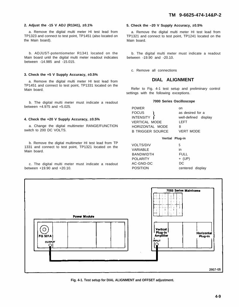
Refer to Fig. 4-1 test setup and preliminary controlsettings with the following exceptions.
7000 Series Oscilloscope
POWER onFOCUS as desired for aINTENSITY well-defined displayVERTICAL MODE LEFTHORIZONTAL MODE BB TRIGGER SOURCE VERT MODE
Vertial Plug-in
VOLTS/DIV 5VARIABLE inBANDWIDTH FULLPOLARITY + (UP)AC-GND-DC DCPOSITION centered display
Fig. 4-1. Test setup for DIAL ALIGNMENT and OFFSET adjustment.
4-9
TM 9-6625-474-14&P-2
Horizontal Plug-in
DISPLAY MODE TIME BASETIME/DIV 50@VARIABLELEVEL/SLOPEMODE AUTOCOUPLING ACSOURCE INTMAGNIFIER X1
6. Frequency Hz Dial Alignment
a. Connect the coaxial cable from the FG 501A OUT-PUT to the vertical plug-in INPUT.
b. Adjust the horizontal plug-in LEVEL control for astable squarewave display on the crt.
c. Locate the coupler holding the FREQUENCY Hzpotentiometer extension shaft and loosen the coupler setscrew.
d. ADJUST-the FREQUENCY Hz potentiometercounterclockwise until the displayed waveform just stopsmoving.
e. While holding the potentiometer (coupler), adjustthe FREQUENCY Hz dial to 20 (exact).
f. Tighten the coupler set screw (snug only).
g. Adjust the FREQUENCY Hz dial to 18. Then rotatedial slowly counterclockwise until the display crtwaveform just stops moving.
h. Check that the FREQUENCY Hz dial is on 20 (±.5minor graticule division).
i. Tighten the coupler set screw.
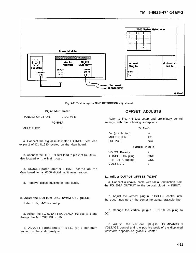
ADJUST OFFSET
Refer to Fig. 4-1 test setup and preliminary controlsettings with the following exceptions.
FG 501A
AMPLITUDE CcwM (pushbutton) inFREQUENCY HZ 20MULTIPLIER 102
4-10
Vertical Plug-in
VOLTS/DIV 2
7. Adjust the OUTPUT OFFSET (R2201) and SINEOFFSET (R1104)
a. The oscilloscope crt display is a triangle.
b. ADJUST-potentiometerMain board until the displayedthe vertical graticule line.
R2201 located on thewaveform is centered on
c.
d.
e.
Press the ~ (pushbutton) in.
The oscilloscope crt display is a sinewave.
ADJUST-potentiometer R1104 located on the Auxboard until the displayed waveform is centered on thevertical graticule line.
ADJUST SINE DISTORTION
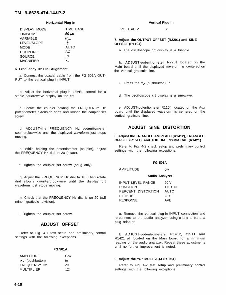
8. Adjust the TRIANGLE AM PLADJ (R1412), TRIANGLEOFFSET (R1511), and TOP DIAL SYMM CAL (R1421)
Refer to Fig. 4-2 check setup and preliminary controlsettings with the following exceptions.
FG 501A
AMPLITUDE cw
Audio Analyzer
INPUT LEVEL RANGE 20 VFUNCTION THD+NPERCENT DISTORTION AUTOFILTERS OUTRESPONSE AVE
a. Remove the vertical plug-inre-connect to the audio analyzerplug adapter.
b. ADJUST-potentiometersR1421 all located on the Main
INPUT connection andusing a bnc to banana
R1412, R1511, andboard for a minimum
reading on the audio analyzer. Repeat these adjustmentsuntil no further improvement is noted.
9. Adjust the “C” MULT ADJ (R1951)
Refer to Fig. 4-2 test setup and preliminary controlsettings with the following exceptions.
TM 9-6625-474-14&P-2
Fig. 4-2. Test setup for SINE DISTORTION adjustment.
Digital Multimeter
RANGE/FUNCTION 2 DC Volts
FG 501A
MULTIPLIER 1
a. Connect the digital mult meter LO INPUT test leadto pin 2 of IC, U1930 located on the Main board.
b. Connect the HI INPUT test Iead to pin 2 of IC, U1940also located on the Main board.
c. ADJUST-potentiometer R1951 located on theMain board for a .0000 digital multimeter readout.
d. Remove digital multimeter test leads.
10. Adjust the BOTTOM DIAL SYMM CAL (R1441)
Refer to Fig. 4-2 test setup.
a. Adjust the FG 501A FREQUENCY Hz dial to 1 andchange the MULTIPLIER to 102.
b. ADJUST-potentiometer R1441 for a minimumreading on the audio analyzer.
OFFSET ADJUSTS
Refer to Fig. 4-3 test setup and preliminary controlsettings with the following exceptions:
FG 501A
(pushbutton) inMULTIPLIER 102OUTPUT ccw
Vertical Plug-in
VOLTS Polarity ++ INPUT Coupling GND- INPUT Coupling GNDVOLTS/DIV .1
11. Adjust OUTPUT OFFSET (R2201)
a. Connect a coaxial cable with 50 Q termination fromthe FG 501A OUTPUT to the vertical plug-in + INPUT.
b. Adjust the vertical plug-in POSITION control untilthe trace lines up on the center horizontal graticule line.
c. Change the vertical plug-in + INPUT coupling toDC.
d. Adjust the vertical plug-in COMPARISONVOLTAGE control until the positive peak of the displayedwaveform appears as graticule center.
4-11
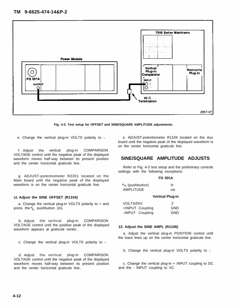
TM 9-6625-474-14&P-2
Fig. 4-3. Test setup for OFFSET and SINE/SQUARE AMPLITUDE adjustments.
e. Change the vertical plug-in VOLTS polarity to -.
f. Adjust the vertical plug-in COMPARISONVOLTAGE control until the negative peak of the displayedwaveform moves half-way between its present positionand the center horizontal graticule line.
g. ADJUST-potentiometer R2201 located on theMain board until the negative peak of the displayedwaveform is on the center horizontal graticule line.
12. Adjust the SINE OFFSET (R1104)
a. Change the vertical plug-in VOLTS polarity to + andpress the pushbutton (in).
b. Adjust the vertical plug-in COMPARISONVOLTAGE control until the positive peak of the displayedwaveform appears at graticule center.
c. Change the vertical plug-in VOLTS polarity to -.
d. Adjust the vertical plug-in COMPARISONVOLTAGE control until the negative peak of the displayedwaveform moves half-way between its present positionand the center horizontal graticule line.
e. ADJUST-potentiometer R1104 located on the Auxboard until the negative peak of the displayed waveform ison the center horizontal graticule line.
SINE/SQUARE AMPLITUDE ADJUSTS
Refer to Fig. 4-3 test setup and the preliminary controlssettings with the following exceptions:
FG 501A
(pushbutton) inAMPLITUDE cw
Vertical Plug-in
VOLTS/DIV .2+INPUT Coupling GND-INPUT Coupling GND
13. Adjust the SINE AMPL (R1106)
a. Adjust the vertical plug-in POSITION control untilthe trace lines up on the center horizontal graticule line.
b. Change the vertical plug-in VOLTS polarity to -.
c. Change the vertical plug-in + INPUT coupling to DCand the - INPUT coupling to VC.
4-12
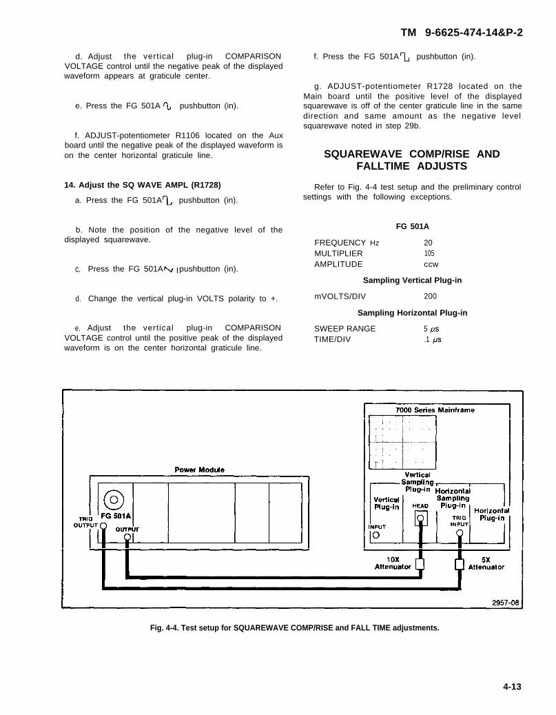
TM 9-6625-474-14&P-2
d. Adjust the vertical plug-in COMPARISONVOLTAGE control until the negative peak of the displayedwaveform appears at graticule center.
e. Press the FG 501A pushbutton (in).
f. ADJUST-potentiometer R1106 located on the Auxboard until the negative peak of the displayed waveform ison the center horizontal graticule line.
14. Adjust the SQ WAVE AMPL (R1728)
f. Press the FG 501A pushbutton (in).
g. ADJUST-potentiometer R1728 located on theMain board until the positive level of the displayedsquarewave is off of the center graticule line in the samedirection and same amount as the negative levelsquarewave noted in step 29b.
SQUAREWAVE COMP/RISE ANDFALLTIME ADJUSTS
Refer to Fig. 4-4 test setup and the preliminary control
a. Press the FG 501A pushbutton (in). settings with the following exceptions.
b. Note the position of the negative level of the FG 501A
displayed squarewave. FREQUENCY Hz 20
c.
d.
e.
MULTIPLIER 105
Press the FG 501A pushbutton (in). AMPLITUDE ccw
Sampling Vertical Plug-in
Change the vertical plug-in VOLTS polarity to +. mVOLTS/DIV 200
Sampling Horizontal Plug-in
Adjust the vertical plug-in COMPARISON SWEEP RANGE 5 VOLTAGE control until the positive peak of the displayed TIME/DIV .1waveform is on the center horizontal graticule line.
Fig. 4-4. Test setup for SQUAREWAVE COMP/RISE and FALL TIME adjustments.
4-13
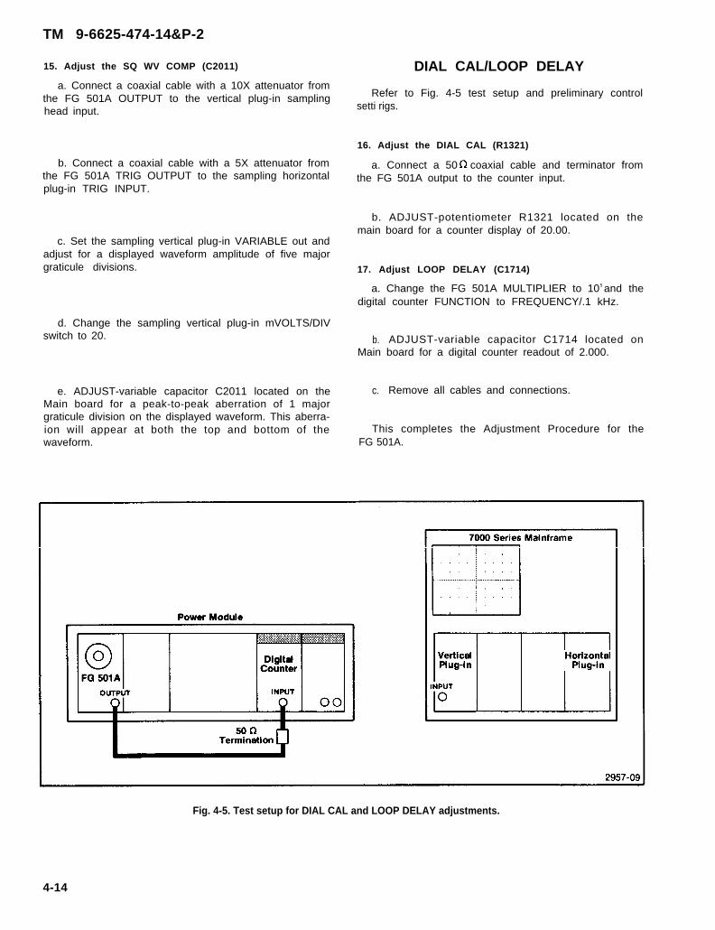
TM 9-6625-474-14&P-2
15. Adjust the SQ WV COMP (C2011)
a. Connect a coaxial cable with a 10X attenuator fromthe FG 501A OUTPUT to the vertical plug-in samplinghead input.
b. Connect a coaxial cable with a 5X attenuator fromthe FG 501A TRIG OUTPUT to the sampling horizontalplug-in TRIG INPUT.
c. Set the sampling vertical plug-in VARIABLE out andadjust for a displayed waveform amplitude of five majorgraticule divisions.
DIAL CAL/LOOP DELAY
Refer to Fig. 4-5 test setup and preliminary controlsetti rigs.
16. Adjust the DIAL CAL (R1321)
a. Connect a 50 coaxial cable and terminator fromthe FG 501A output to the counter input.
b. ADJUST-potentiometer R1321 located on themain board for a counter display of 20.00.
17. Adjust LOOP DELAY (C1714)
a. Change the FG 501A MULTIPLIER to 105 and thedigital counter FUNCTION to FREQUENCY/.1 kHz.
d. Change the sampling vertical plug-in mVOLTS/DIVswitch to 20. b.
Main
e. ADJUST-variable capacitor C2011 located on the c.Main board for a peak-to-peak aberration of 1 majorgraticule division on the displayed waveform. This aberra-
ADJUST-variable capacitor C1714 located onboard for a digital counter readout of 2.000.
Remove all cables and connections.
ion will appear at both the top and bottom of the This completes the Adjustment Procedure for thewaveform. FG 501A.
Fig. 4-5. Test setup for DIAL CAL and LOOP DELAY adjustments.
4-14
CAUTION
CAUTION
TM 9-6625-474-14&P-2
SECTION 5
MAINTENANCE
GENERAL MAINTENANCE INFORMATION
STATIC-SENSITIVE COMPONENTS
Static discharge can damage any semiconductorcomponent in this instrument.
This instrument contains electrical components thatare susceptible to damage from static discharge. SeeTable 5-1 for relative susceptibility of various classes ofsemiconductors. Static voltages of 1 kV to 30 kV arecommon in unprotected environments.
Observe the following precautions to avoid damage:
1.
2.
3.
4.
5.
6.
7.
8.
9.
10.
Minimize handling of static sensitive components.
Transport and store static-sensitive components orassemblies in their original containers, on a metal rail,or on conductive foam. Label any package thatcontains static-sensitive assemblies or components.
Discharge the static voltage from your body bywearing a wrist strap while handling these com-ponents. Servicing static-sensitive assemblies orcomponents should be performed only at a static-freework station by qualified service personnel.
Nothing capable of generating or holding a staticcharge should be allowed on the work station surface.
Keep the component leads shorted togetherwhenever possible.
Pick up components by the body, never by the leads.
Do not slide the components over any surface.
Avoid handling components in areas that have a flooror work surface covering capable of generating astatic charge.
Use a soldering iron that is connected to earthground.
Use only special antistatic suction type or wick type
Table 5-1
RELATIVE SUSCEPTIBILITY TOSTATIC DISCHARGE DAMAGE
RelativeSusceptibility
Semiconductor Classes Levelsa
MOS or CMOS microcircuits ordiscretes or linear microcircuitswith MOS inputs. (Most Sensitive) 1
ECL 2
Schottky signal diodes 3
Schottky TTL 4
High-frequency bipolar transistors 5
JFETs 6
Linear microcircuits 7
Low-power Schottky TTL 8
TTL (Least Sensitive) 9
a Voltage equivalent for levels:
1 = 100 to 500 V 4 = 500 V 7 = 400 to 1000 V (est)2 = 200 to 500 V 5 = 400 to 600 V 8 = 900 V3 = 250 V 6 = 600 to 800 V 9 = 1200 V
(Voltage discharged from a 100 pF capacitor through a resistanceof 100 ohms.)
CLEANING
This instrument should be cleaned as often asoperating conditions require. Loose dust accumulated onthe outside of the instrument can be removed with a softcloth or small brush. Remove dirt that remains with a softcloth dampened in a mild detergent and water solution. Donot use abrasive cleaners.
To clean the front panel use freon, isopropyl alcohol,or totally denatured ethyl alcohol. Do not usepetroleum based cleansing agents. Before using anyother type of cleaner, consult your Tektronix Service
resoldering tools. Center or representative.
5-1
CAUTION
WARNING
TM 9-6625-474-14&P-2
The best way to clean the interior is to blow off theaccumulated dust with dry, low-velocity air (approximate-ly 5 lb/in2) or use a soft brush or cloth dampened with amild detergent and water solution.
Hold the board so the cleaning residue runs away fromthe connectors. Do not scrape or use an eraser to clean theedge connector contacts. Abrasive cleaning can removethe gold plating.
Circuit boards and components must be dry beforeapplying power.
OBTAINING REPLACEMENT PARTS
Electrical and mechanical parts can be obtainedthrough your local Tektronix Field Office or represen-tative. However, it may be possible to obtain many of thestandard electronic components from a local commercialsource. Before purchasing or ordering a part from asource other than Tektronix, Inc., check the ReplaceableElectrical Parts list for the proper value, rating, tolerance,and description.
NOTE
When selecting replacement parts, remember thatthe physical size and shape of a component mayaffect its performance in the instrument.
Some parts are manufactured or selected by Tektronix,Inc., to satisfy particular requirements or are manufac-tured for Tektronix, Inc., to our specifications. Most of themechanical parts used in this instrument have beenmanufactured by Tektronix, Inc. To determine themanufacturer, refer to the Replaceable Parts list and theCross Reference index, Mfr. Code Number to Manufac-turer.
When ordering replacement parts from Tektronix, Inc.,include the following information:
1.
2.
3.
4.
5-2
Instrument type and option number.
Instrument serial number.
A description of the part (if electrical, includecomplete circuit number).
Tektronix part number.
SOLDERING TECHNIQUES
To avoid electric-shock hazard, disconnect theinstrument from the power source before soldering.
The reliability and accuracy of this instrument can bemaintained only if proper soldering techniques are usedwhen repairing or replacing parts. General solderingtechniques which apply to maintenance of any precisionelectronic equipment should be used when working onthis instrument. Use only 60/40 rosin-core electronicgrade solder. The choice of soldering iron is determinedby the reapir to be made.
When soldering on circuit boards or small wiring, useonly a 15 watt, pencil type soldering iron. A higher wattagesoldering iron can cause the etched circuit wiring toseparate from the board base material and melt theinsulation from small wiring. Always keep the solderingiron tip properly tinned to ensure the best heat transfer tothe solder joint. Apply only enough heat to remove thecomponent or to make a good solder joint. To protect heatsensitive components, hold the component lead with apair of long-nose pliers between the component body andthe solder joint. Use a solder removing wick to removeexcess solder from connections or to clean circuit boardpads.
SEMICONDUCTORS
To remove in-line integrated circuits use an extractingtool. This tool is available from Tektronix, Inc.; orderTektronix Part Number 003-0619-00. If an extracting toolis not available, use care to avoid damaging the pins. Pullslowly and evenly on both ends of the integrated circuit.Try to avoid disengaging one end before the other end.
INTERCONNECTING PINS
Several methods of interconnection including multi pinand coaxial cable, are used to electrically connect thecircuit boards with other boards and components.
COAXIAL CABLES
Replacement of coaxial end lead connectors requiresspecial tools. Damaged cables should be replaced as aunit. For cable part numbers see the ReplaceableMechanical Parts list. Fig, 5-1 shows a coaxial connectorassembly.
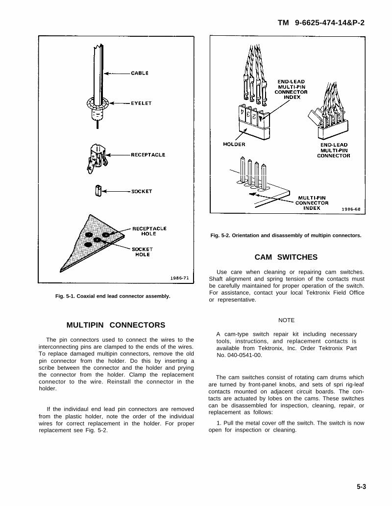
TM 9-6625-474-14&P-2
Fig. 5-1. Coaxial end lead connector assembly.
MULTIPIN CONNECTORS
The pin connectors used to connect the wires to theinterconnecting pins are clamped to the ends of the wires.To replace damaged multipin connectors, remove the oldpin connector from the holder. Do this by inserting ascribe between the connector and the holder and pryingthe connector from the holder. Clamp the replacementconnector to the wire. Reinstall the connector in theholder.
If the individaul end lead pin connectors are removedfrom the plastic holder, note the order of the individualwires for correct replacement in the holder. For properreplacement see Fig. 5-2.
Fig. 5-2. Orientation and disassembly of multipin connectors.
CAM SWITCHES
Use care when cleaning or repairing cam switches.Shaft alignment and spring tension of the contacts mustbe carefully maintained for proper operation of the switch.For assistance, contact your local Tektronix Field Officeor representative.
NOTE
A cam-type switch repair kit including necessarytools, instructions, and replacement contacts isavailable from Tektronix, Inc. Order Tektronix PartNo. 040-0541-00.
The cam switches consist of rotating cam drums whichare turned by front-panel knobs, and sets of spri rig-leafcontacts mounted on adjacent circuit boards. The con-tacts are actuated by lobes on the cams. These switchescan be disassembled for inspection, cleaning, repair, orreplacement as follows:
1. Pull the metal cover off the switch. The switch is nowopen for inspection or cleaning.
5-3
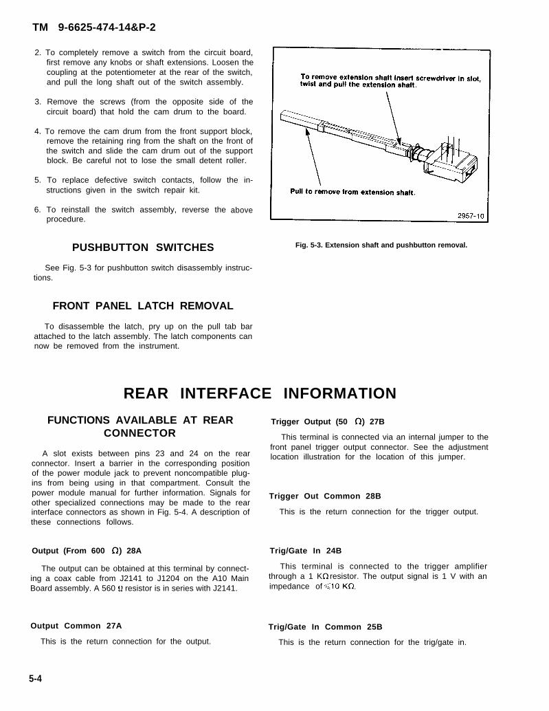
TM 9-6625-474-14&P-2
2. To completely remove a switch from the circuit board,first remove any knobs or shaft extensions. Loosen thecoupling at the potentiometer at the rear of the switch,and pull the long shaft out of the switch assembly.
3. Remove the screws (from the opposite side of thecircuit board) that hold the cam drum to the board.
4. To remove the cam drum from the front support block,remove the retaining ring from the shaft on the front ofthe switch and slide the cam drum out of the supportblock. Be careful not to lose the small detent roller.
5. To replace defective switch contacts, follow the in-structions given in the switch repair kit.
6. To reinstall the switch assembly, reverse theprocedure.
PUSHBUTTON SWITCHES
above
See Fig. 5-3 for pushbutton switch disassembly instruc-tions.
FRONT PANEL LATCH REMOVAL
To disassemble the latch, pry up on the pull tab barattached to the latch assembly. The latch components cannow be removed from the instrument.
Fig. 5-3. Extension shaft and pushbutton removal.
REAR INTERFACE INFORMATION
FUNCTIONS AVAILABLE AT REARCONNECTOR
A slot exists between pins 23 and 24 on the rearconnector. Insert a barrier in the corresponding positionof the power module jack to prevent noncompatible plug-ins from being using in that compartment. Consult thepower module manual for further information. Signals forother specialized connections may be made to the rearinterface connectors as shown in Fig. 5-4. A description ofthese connections follows.
Output (From 600 ) 28A
The output can be obtained at this terminal by connect-ing a coax cable from J2141 to J1204 on the A10 MainBoard assembly. A 560 resistor is in series with J2141.
Output Common 27A
This is the return connection for the output.
Trigger Output (50 ) 27B
This terminal is connected via an internal jumper to thefront panel trigger output connector. See the adjustmentlocation illustration for the location of this jumper.
Trigger Out Common 28B
This is the return connection for the trigger output.
Trig/Gate In 24B
This terminal is connected to the trigger amplifierthrough a 1 K resistor. The output signal is 1 V with animpedance of
Trig/Gate In Common 25B
This is the return connection for the trig/gate in.
5-4
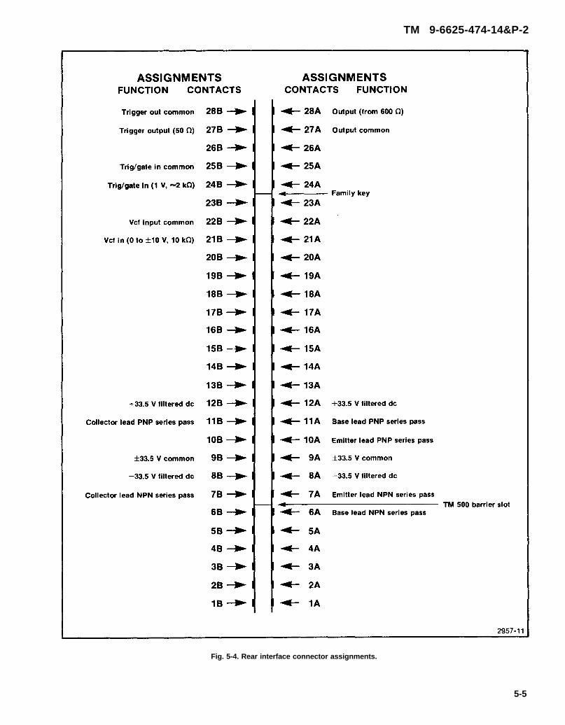
TM 9-6625-474-14&P-2
Fig. 5-4. Rear interface connector assignments.
5-5

TM 9-6625-474-14&P-2
VCF In 21B VCF In Common 22B
This terminal is connected through a 10 resistor via This connection is the ground return for the VCF In.an internal jumper to the virtual ground summing node ofoperational amplifier U1540A (pin 2). See the AdjustmentLocation illustration for the location of this jumper.
5-6

TM 9-6625-474-14&P-2
SECTION 6
OPTIONS
There are no options for the FG 501A at the time of this printing.
6-1(6-2 blank)
SECTION 7 TM 9-6625-474-14&P-2
REPLACEABLEELECTRICAL PARTSPARTS ORDERING INFORMATION
Replacement parts are available from or through your local
Tektronix, Inc. Field Office or representative.
Changes to Tektronix instruments are sometimes made toaccommodate improved components as they become available,
and to give you the benefit of the latest circuit improvements
developed in our engineering department. It is therefore impor-
tant, when ordering parts, to include the following information in
your order: Part number, instrument type or number, aerial
number, and modification number if applicable.
If a part you have ordered has been replaced with a new or
improved part, your local Tektronix, Inc. Field Office or represen-
tative will contact you concerning any change in part number.
Change information, if any, is located at the rear of this
manual.
LIST OF ASSEMBLIES
A list of assemblies can be found at the beginning of the
Electrical Parts List. The assemblies are listed in numerical order.
When thecomplete component number of a part is known, this list
will identify the assembly in which the part is located.
CROSS INDEX-MFR. CODE NUMBER TOMANUFACTURER
The Mfr. Code Number to Manufacturer index for the
Electrical Parts List is located immediately after this page. The
Cross Index provides codes, names and addresses of manufac-
turers of components listed in the Electrical Parts List.
ABBREVIATIONS
Abbreviations conform to American National Standard Y1.1.
COMPONENT NUMBER (column one of theElectrical Parts List)
A numbering method has been used to identify assemblies,
subassemblies and parts. Examples of this numbering method
and typical expansions are illustrated by the following:
Example a. component number
Read Resistor 1234 of Assembly 23
Example b. component number
Read: Resistor 1234 of Subassembly 2 of Assembly 23
Only the circuit number will appear on the diagrams and
circuit board illustrations. Each diagram and circuit board
illustration is clearly marked with the assembly number.
Assembly numbers are also marked on the mechanical exploded
views located in the Mechanical Parts List. The component
number is obtained by adding the assembly number prefix to the
circuit number.
The Electrical Parts List is divided and arranged by
assemblies in numerical sequence (e.g., assembly A1 with its
subassemblies and parts, precedes assembly A2 with ita sub-
assemblies and parts).
Chassis-mounted parts have no assembly number prefix
and are located at the end of the Electrical Parts List.
TEKTRONIX PART NO. (column two of theElectrical Parts List)
Indicates part number to be used when ordering replace-
ment part from Tektronix.
SERIAL/MODEL NO. (columns three and fourof the Electrical Parts List)
Column three (3) indicates the serial number at which the
part was first used. Column four (4) indicates the serial number at
which the part was removed. No serial number entered indicates
part is good for all serial numbers.
NAME & DESCRIPTION (column five of theElectrical Parts List)
In the Parts List, an Item Name is separated from the
description by a colon (:). Because of space limitations, an Item
Name may sometimes appear as incomplete. For further Item
Name identification, the U.S. Federal Cataloging Handbook H6-1
can be utilized where possible.
MFR. CODE (column six of the Electrical PartsList)
Indicates the code number of the actual manufacturer of the
part. (Code to name and address cross reference can be found
immediately after this page.)
MFR. PART NUMBER (column seven of theElectrical Parts List)
Indicates actual manufacturers part number.
7-1
TM 9-6625-474-14&P-2
CROSS INDEX-MFR. CODE NUMBER TO MANUFACTURER
Mfr. Code Manufacturer Address0112101295
021110273503508
03888042220471307263
126971296913511197012252627014329975043453184552105628971400
7298273138738997497075042
8000991637
7 - 2
ALLEN-BRADLEY COMPANYTEXAS INSTRUMENTS, INC., SEMICONDUCTORGROUPSPECTROL ELECTRONICS CORPORATIONRCA CORPORATION, SOLID STATE DIVISIONGENERAL ELECTRIC COMPANY, SEMI-CONDUCTORPRODUCTS DEPARTMENTKDI PYROFILM CORPORATIONAVX CERAMICS, DIVISION OF AVX CORP.MOTOROLA, INC., SEMICONDUCTOR PROD. DIV.FAIRCHILD SEMICONDUCTOR, A DIV. OFFAIRCHILD CAMERA AND INSTRUMENT CORP.CLAROSTAT MFG. CO., INC.UNITRODE CORPORATIONAMPHENOL CARDRE DIV., BUNKER RAMO CORP.ELECTRA-MIDLAND CORP., MEPCO ELECTRA INC.BERG ELECTRONICS, INC.NATIONAL SEMICONDUCTOR CORP.BOURNS, INC., TRIMPOT PRODUCTS DIV.HEWLETT-PACKARD COMPANYXCITON CORPORATIONGETTIG ENG. AND MFG. COMPANYSPRAGUE ELECTRIC CO.BUSSMAN MFG., DIVISION OF MCGRAW-EDISON CO.ERIE TECHNOLOGICAL PRODUCTS, INC.BECKMAN INSTRUMENTS, INC., HELIPOT DIVJFD ELECTRONICS COMPONENTS CORP.JOHNSON, E. F., CO.TRW ELECTRONIC COMPONENTS, IRC FIXEDRESISTORS, PHILADELPHIA DIVISIONTEKTRONIX, INC.DALE ELECTRONICS, INC.
City, State, ZipMILWAUKEE, WI 532041201 2ND STREET SOUTH
P O BOX 5012, 13500 N CENTRALEXPRESSWAY17070 EAST GALE AVENUEROUTE 202
ELECTRONICS PARK60 S JEFFERSON ROADP O BOX 867, 19TH AVE. SOUTH5005 E MCDOWELL RD,PO BOX 20923
464 ELLIS STREETLOWER WASHINGTON STREET580 PLEASANT STREET
P O BOX 760YOUR EXPRESSWAY2900 SEMICONDUCTOR DR.1200 COLUMBIA AVE.640 PAGE MILL ROAD5 HEMLOCK STREETPO BOX 85, OFF ROUTE 4587 MARSHALL ST.
2536 W. UNIVERSITY ST.644 W. 12TH ST.2500 HARBOR BLVD.PINETREE ROAD299 10TH AVE. S. W.
401 N. BROAD ST.P O BOX 500P. O. BOX 609
DALLAS, TX 75222CITY OF INDUSTRY, CA 91745SOMERVILLE, NY 08876
SYRACUSE, NY 13201WHIPPANY, NJ 07981MYRTLE BEACH, SC 29577PHOENIX, AZ 85036
MOUNTAIN VIEW, CA 94042DOVER, NH 03820WATERTOWN, MA 02172LOS GATOS, CA 95030MINERAL WELLS, TX 76067NEW CUMBERLAND, PA 17070SANTA CLARA, CA 95051RIVERSIDE, CA 92507PALO ALTO, CA 94304LATHAM, NY 12110SPRING MILLS, PA 16875NORTH ADAMS, MA 01247
ST. LOUIS, MO 63107ERIE, PA 16512FULLERTON, CA 92634OXFORD, NC 27565WASECA, MN 56093
PHILADELPHIA, PA 19108BEAVERTON, OR 97077COLUMBUS, NE 68601
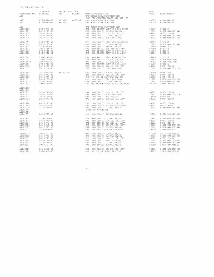
TM9-6625-474-14&P-2
TEKTRONIX SERIAL/MODEL NO. MFRCOMPONENT NO. PART NO. EFF DSCONT NAME & DESCRIPTION CODE PART NUMBERA10 CKT BOARD ASSY:FUNCTION GEN
(NOT REPLACEABLE ORDER 672-0924-01)A12 670-6694-00 B010100 B020349 CKT BOARD ASSY:AUXILIARY 80009 670-6694-00A12 670-6694-01 B020350 CKT BOARD ASSY:AUXILIARY 80009 670-6694-01
A10 CKT BOARD ASSY:FUNCTION GENA10C1115 290-0779-00 CAP.,FXD,ELCTLT:10UF,+50-10%,50VDC 56289 502D237A10C1201 281-0775-00 CAP.,FXD,CER DI:O.1UF,20%,50V 72982 8005D9AABZ5U104MA10C1203 281-0773-00 CAP.,FXD,CER DI:0.01UF,10%,100V 04222 GC70-1C103KA10C1224 281-0775-00 CAP.,FXD,CER DI:0.1UF,20%,50V 72982 8005D9AABZ5U104MA10C1235 281-0763-00 CAP.,FXD,CER DI:47PF,10%,100V 72982 8035D9AADC1G470K
A10C1251 290-0779-00 CAP.,FXD,ELCTLT:10UF,+50-10%,50VDC 56289 502D237A10C1253 281-0775-00 CAP.,FXD,CER DI:0.1UF,20%,50V 72982 8005D9AABZ5U104MA10C1313 281-0820-00 CAP.,FXD,CER DI:680PF,10%,50V 12969 CGB681KDXA10C1321 290-0745-00 CAP.,FXD,ELCTLT:2UF,+50-10%,25V 56289 502D225A10C1323 290-0745-00 CAP.,FXD,ELCTLT:22UF,+50-10%,25V 56289 502D225A10C1325 290-0745-00 CAP.,FXD,ELCTLT:22UF,+50-10%,25V 56289 502D225
A10C1341 290-0745-00 CAP.,FXD,ELCTLT:22UF,+50-10%,25V 56289 502D225A10C1431 283-0203-00 CAP.,FXD,CER DI:0.47UF,20%,50V 72982 8131N075E474MA10C13434 283-0203-00 CAP.,FXD,CER DI:0.47UF,20%,50V 72982 8131N075E474MA10C1451 290-0745-00 CAP.,FXD,ELCTLT:22UF,+50-10%,25V 56289 502D225A10C1516 281-0773-00 CAP.,FXD,CER DI:0.01UF,10%,100V 04222 GC70-1C103KA10C1532 281-0762-00 CAP.,FXD,CER DI:27PF,20%,100V 72982 8035D9AADC0G270M
A10C1543 281-0823-00 XB020350 CAP.,FXD,CER DI:470PF,10%,50V 12969 CGB471KDNA10C1601 281-0773-00 CAP.,FXD,CER DI:O.O1UF,10%,100V 04222 GC70-1C103KA10C1603 281-0773-00 CAP,FXD,CER DI:O.O1UF,10%,100V 04222 GC70-1C103KA10C1611 281-0759-00 CAP.,FXD,CER DI:22PF,10%,100V 72982 8035D9AADC1G220KA10C1613 281-0775-00 CAP.,FXD,CER DI:O.1UF,20%,50V 72982 8005D9AABZ5U104MA10C1631 295-0164-00 CAP.SET,MTCHD:10,1,O.1,0.01UF,950PF 80009 295-0164-00
A10C1633A10C1641A10C1711 281-0773-00 CAP.,FXD,CER DI:O.O1UF,10%,100V 04222 GC70-1C103KA10C1712 281-0763-00 CAP.,FXD,CER DI:47PF,10%,100V 72982 8035D9AADC1G470KA10C1714 281-0158-00 CAP.,VAR,CER DI:7-45PF,50V 73899 DVJ-5006A10C1723 281-0773-00 CAP.,FXD,CER DI:O.O1UF,10%,100V 04222 GC70-1C103K
A10C1724 281-0773-00 CAP.,FXD,CER DI:O.O1UF,10%,100V 04222 GC70-1C103KA10C1725 281-0810-00 CAP.,FXD,CER DI:5.6PF,0.5%,100V 04222 GC10-1A5R6DA10C1726 281-0775-00 CAP.,FXD,CER DI:O.1UF,20%,50V 72982 8005D9AABZ5U104MA10C1741 (PART OF A10C1631)A10C1751A10C1811 281-0775-00 CAP.,FXD,CER DI:0.1UF,20%,50V 72982 8005D9AABZ5U104M
A10C1812 281-0775-00 CAP.,FXD,CER DI:O.1UF,20%,50V 72982 8005D9AABZ5U104MA10C1813 281-0773-00 CAP.,FXD,CER DI:0.01UF,10%,100V 04222 GC70-1C103KA10C1814 281-0773-00 CAP.,FXD,CER DI:O.O1UF,10%,100V 04222 GC70-1C103KA10C2006 281-0812-00 CAP.,FXD,CER DI:1000PF,10%,100V 72982 8035D9AADX7R102KA10C2007 281-0775-00 CAP.,FXD,CER DI:0.1UF,20%,50V 72982 8005D9AABZ5U104MA10C2011 281-0064-00 CAP.,VAR,PLSTC:O.25-1.5PF,600V 74970 273-0001-301
A10C2013 290-0517-00 CAP.,FXD,ELCTLT:6.8UF,20%,35V 56289 196D685X0035KA1A10C2020 281-0775-00 CAP.,FXD,CER DI:O.1UF,20%,50V 72982 8005D9AABZ5U104MA10C2031 281-0773-00 CAP.,FXD,CER DI:O.O1UF,10%,100V 04222 GC70-1C103KA10C2121 281-0764-00 CAP.,FXD,CER DI:82PF,5%,100V 72982 8035D9AADC1G802JA10C2204 281-0775-00 CAP.,FXD,CER DI:O.1UF,20%.50V 72982 8005D9AABZ5U104MA10C2217 290-0517-00 CAP.,FXD,ELCTLT:6.8UF,20%,35V 56289 196D685X0035KA1
A10C2221 281-0812-00 CAP.,FXD,CER DI:1000PF,10%,100V 72982 8035D9AADX7R102KA10C2224 290-0517-00 CAP,FXD,ELCTLT:6.8UF,20%,35V 56289 196D685X0035KA1
7-3
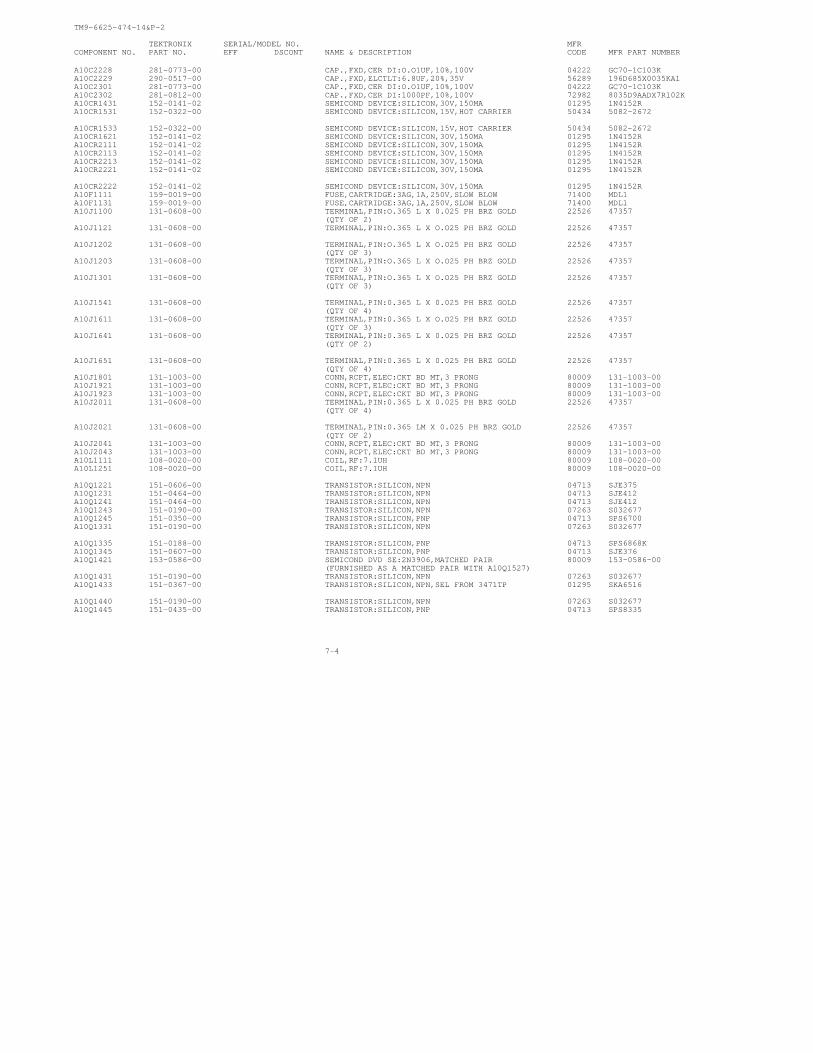
TM9-6625-474-14&P-2
TEKTRONIX SERIAL/MODEL NO. MFRCOMPONENT NO. PART NO. EFF DSCONT NAME & DESCRIPTION CODE MFR PART NUMBER
A10C2228 281-0773-00 CAP.,FXD,CER DI:O.O1UF,10%,100V 04222 GC70-1C103KA10C2229 290-0517-00 CAP.,FXD,ELCTLT:6.8UF,20%,35V 56289 196D685X0035KA1A10C2301 281-0773-00 CAP.,FXD,CER DI:O.O1UF,10%,100V 04222 GC70-1C103KA10C2302 281-0812-00 CAP.,FXD,CER DI:1000PF,10%,100V 72982 8035D9AADX7R102KA10CR1431 152-0141-02 SEMICOND DEVICE:SILICON,30V,150MA 01295 1N4152RA10CR1531 152-0322-00 SEMICOND DEVICE:SILICON,15V,HOT CARRIER 50434 5082-2672
A10CR1533 152-0322-00 SEMICOND DEVICE:SILICON,15V,HOT CARRIER 50434 5082-2672A10CR1621 152-0141-02 SEMICOND DEVICE:SILICON,30V,150MA 01295 1N4152RA10CR2111 152-0141-02 SEMICOND DEVICE:SILICON,30V,150MA 01295 1N4152RA10CR2113 152-0141-02 SEMICOND DEVICE:SILICON,30V,150MA 01295 1N4152RA10CR2213 152-0141-02 SEMICOND DEVICE:SILICON,30V,150MA 01295 1N4152RA10CR2221 152-0141-02 SEMICOND DEVICE:SILICON,30V,150MA 01295 1N4152R
A10CR2222 152-0141-02 SEMICOND DEVICE:SILICON,30V,150MA 01295 1N4152RA10F1111 159-0019-00 FUSE,CARTRIDGE:3AG,1A,250V,SLOW BLOW 71400 MDL1A10F1131 159-0019-00 FUSE,CARTRIDGE:3AG,1A,250V,SLOW BLOW 71400 MDL1A10J1100 131-0608-00 TERMINAL,PIN:O.365 L X 0.025 PH BRZ GOLD 22526 47357
(QTY OF 2)A10J1121 131-0608-00 TERMINAL,PIN:O.365 L X O.O25 PH BRZ GOLD 22526 47357
A10J1202 131-0608-00 TERMINAL,PIN:O.365 L X O.O25 PH BRZ GOLD 22526 47357(QTY OF 3)
A10J1203 131-0608-00 TERMINAL,PIN:O.365 L X O.O25 PH BRZ GOLD 22526 47357(QTY OF 3)
A10J1301 131-0608-00 TERMINAL,PIN:O.365 L X O.O25 PH BRZ GOLD 22526 47357(QTY OF 3)
A10J1541 131-0608-00 TERMINAL,PIN:0.365 L X 0.025 PH BRZ GOLD 22526 47357(QTY OF 4)
A10J1611 131-0608-00 TERMINAL,PIN:0.365 L X O.O25 PH BRZ GOLD 22526 47357(QTY OF 3)
A10J1641 131-0608-00 TERMINAL,PIN:0.365 L X 0.025 PH BRZ GOLD 22526 47357(QTY OF 2)
A10J1651 131-0608-00 TERMINAL,PIN:0.365 L X 0.025 PH BRZ GOLD 22526 47357(QTY OF 4)
A10J1801 131-1003-00 CONN,RCPT,ELEC:CKT BD MT,3 PRONG 80009 131-1003-00A10J1921 131-1003-00 CONN,RCPT,ELEC:CKT BD MT,3 PRONG 80009 131-1003-00A10J1923 131-1003-00 CONN,RCPT,ELEC:CKT BD MT,3 PRONG 80009 131-1003-00A10J2011 131-0608-00 TERMINAL,PIN:0.365 L X 0.025 PH BRZ GOLD 22526 47357
(QTY OF 4)
A10J2021 131-0608-00 TERMINAL,PIN:0.365 LM X 0.025 PH BRZ GOLD 22526 47357(QTY OF 2)
A10J2041 131-1003-00 CONN,RCPT,ELEC:CKT BD MT,3 PRONG 80009 131-1003-00A10J2043 131-1003-00 CONN,RCPT,ELEC:CKT BD MT,3 PRONG 80009 131-1003-00A10L1111 108-0020-00 COIL,RF:7.1UH 80009 108-0020-00A10L1251 108-0020-00 COIL,RF:7.1UH 80009 108-0020-00
A10Q1221 151-0606-00 TRANSISTOR:SILICON,NPN 04713 SJE375A10Q1231 151-0464-00 TRANSISTOR:SILICON,NPN 04713 SJE412A10Q1241 151-0464-00 TRANSISTOR:SILICON,NPN 04713 SJE412A10Q1243 151-0190-00 TRANSISTOR:SILICON,NPN 07263 S032677A10Q1245 151-0350-00 TRANSISTOR:SILICON,PNP 04713 SPS6700A10Q1331 151-0190-00 TRANSISTOR:SILICON,NPN 07263 S032677
A10Q1335 151-0188-00 TRANSISTOR:SILICON,PNP 04713 SPS6868KA10Q1345 151-0607-00 TRANSISTOR:SILICON,PNP 04713 SJE376A10Q1421 153-0586-00 SEMICOND DVD SE:2N3906,MATCHED PAIR 80009 153-0586-00
(FURNISHED AS A MATCHED PAIR WITH A10Q1527)A10Q1431 151-0190-00 TRANSISTOR:SILICON,NPN 07263 S032677A10Q1433 151-0367-00 TRANSISTOR:SILICON,NPN,SEL FROM 3471TP 01295 SKA6516
A10Q1440 151-0190-00 TRANSISTOR:SILICON,NPN 07263 S032677A10Q1445 151-0435-00 TRANSISTOR:SILICON,PNP 04713 SPS8335
7-4
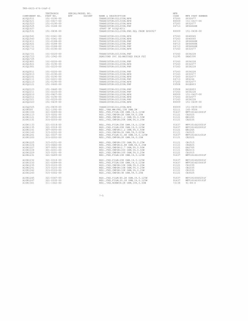
TM9-6625-474-14&P-2
TEKTRONIX SERIAL/MODEL NO. MFRCOMPONENT NO. PART NO. EFF DSCONT NAME & DESCRIPTION CODE MFR PART NUMBERA10Q1511 151-0190-00 TRANSISTOR:SILICON,NPN 07263 S032677A10Q1521 151-0427-00 TRANSISTOR:SILICON,NPN 80009 151-0427-00A10Q1523 151-0190-00 TRANSISTOR:SILICON,NPN 07263 S032677A10Q1525 151-0188-00 TRANSISTOR:SILICON,PNP 04713 SPS6868KA10Q1527 (PART OF A10Q1421)A10Q1531 151-0438-00 TRANSISTOR:SILICON,PNP,SEL FROM SPS6927 80009 151-0438-00
A10Q1541 151-0341-00 TRANSISTOR:SILICON,NPN 07263 S040065A10Q1543 151-0341-00 TRANSISTOR:SILICON,NPN 07263 S040065A10Q1611 151-0188-00 TRANSISTOR:SILICON,PNP 04713 SPS6868KA10Q1621 151-0188-00 TRANSISTOR:SILICON,PNP 04713 SPS6868KA10Q1711 151-0188-00 TRANSISTOR:SILICON,PNP 04713 SPS6868KA10Q1712 151-0190-00 TRANSISTOR:SILICON,NPN 07263 S032677
A10Q1721 151-0220-00 TRANSISTOR:SILICON,PNP 07263 S036228A10Q1723 151-1042-00 SEMICOND DVC SE:MATCHED PAIR FET 01295 SKA5390A10Q1725A10Q1801 151-0220-00 TRANSISTOR:SILICON,PNP 07263 S036228A10Q1821 151-0190-00 TRANSISTOR:SILICON,NPN 07263 S032677A10Q1901 151-0220-00 TRANSISTOR:SILICON,PNP 07263 S036228
A10Q2011 151-0220-00 TRANSISTOR:SILICON,PNP 07263 S036228A10Q2013 151-0190-00 TRANSISTOR:SILICON,NPN 07263 S032677A10Q2101 151-0190-00 TRANSISTOR:SILICON,NPN 07263 S032677A10Q2111 151-0221-00 TRANSISTOR:SILICON,PNP 04713 SPS246A10Q2113 151-0190-00 TRANSISTOR:SILICON,NPN 07263 S032677A10Q2121 151-0440-00 TRANSISTOR:SILICON,PNP 03508 X41E603
A10Q2123 151-0440-00 TRANSISTOR:SILICON,PNP 03508 X41E603A10Q2211 151-0220-00 TRANSISTOR:SILICON,PNP 07263 S036228A10Q2213 151-0427-00 TRANSISTOR:SILICON,NPN 80009 151-0427-00A10Q2311 151-0190-00 TRANSISTOR:SILICON,NPN 07263 S032677A10Q2321 151-0220-00 TRANSISTOR:SILICON,PNP 07263 S036228A10Q2323 151-0439-00 TRANSISTOR:SILICON,NPN 80009 151-0439-00
A10Q2325 151-0439-00 TRANSISTOR:SILICON,NPN 80009 151-0439-00A10R500 311-1392-00 RES.,VAR,WW:PNL,10K OHM,2W 02111 140-9504A10R1103 321-0289-00 RES.,FXD,FILM:10K OHM,1%,O.125W 91637 MFF1816G10001FA10R1113 315-0202-00 RES.,FXD,CMPSN:2K OHM,5%,O.25W 01121 CB2025A10R1121 307-0093-00 RES.,FXD,CMPSN:1.2 OHM,5%,O.50W 01121 EB12G5A10R1131 315-0203-00 RES.,FXD,CMPSN:20K OHM,5%,O.25W 01121 CB2035
A10R1133 321-0318-00 RES.,FXD,FILM:20K OHM,1%,O.125W 91637 MFF1816G20001FA10R1135 321-0318-00 RES.,FXD,FILM:20K OHM,1%,O.125W 91637 MFF1816G20001FA10R1141 307-0093-00 RES.,FXD,CMPSN:1.2 OHM,5%,0.50W 01121 EB12G5A10R1143 315-0202-00 RES.,FXD,CMPSN:2K OHM,5%,0.025W 01121 CB2025A10R1201 321-0337-00 RES.,FXD,FILM:31.6K OHM,1%,0.125W 91637 MFF1816G31601FA10R1203 315-0202-00 RES.,FXD,CMPSN:2K OHM,5%,0.25W 01121 CB2025
A10R1225 315-0151-00 RES.,FXD,CMPSN:150 OHM,5%,0.25W 01121 CB1515A10R1226 315-0682-00 RES.,FXD,CMPSN:6.8K OHM,5%,0.25W 01121 CB6825A10R1227 307-0051-00 RES.,FXD,CMPSN:2.7 OHM,5%,0.50W 01121 EB27G5A10R1228 301-0201-00 RES.,FXD,CMPSN:200 OHM,5%,0.50W 01121 EB2015A10R1229 315-0101-00 RES.,FXD,CMPSN:100 OHM,5%,0.25W 01121 CB1015A10R1231 321-0289-00 RES.,FXD,FILM:10K OHM,1%,0.125W 91637 MFF1816G10001F
A10R1232 321-0318-00 RES.,FXD,FILM:20K OHM,1%,0.125W 91637 MFF1816G20001FA10R1233 321-0289-00 RES.,FXD,FILM:10K OHM,1%,0.125W 91637 MFF1816G10001FA10R1235 315-0103-00 RES.,FXD,CMPSN:10K OHM,5%,0.25W 01121 CB1035A10R1241 315-0103-00 RES.,FXD,CMPSN:10K OHM,5%,0.25W 01121 CB1035A10R1242 315-0103-00 RES.,FXD,CMPSN:10K OHM,5%,0.25W 01121 CB1035A10R1243 315-0302-00 RES.,FXD,CMPSN:3K OHM,5%,0.25W 01121 CB3025
A10R1245 321-0347-00 RES.,FXD,FILM:40.2K OHM,1%,0.125W 91637 MFF1816G40201FA10R1247 321-0335-00 RES.,FXD,FILM:30.1K OHM,1%,0.125W 91637 MFF1816G30101FA10R1301 311-1562-00 RES.,VAR,NONWIR:2K OHM,20%,0.50W 73138 91-84-0
7-5
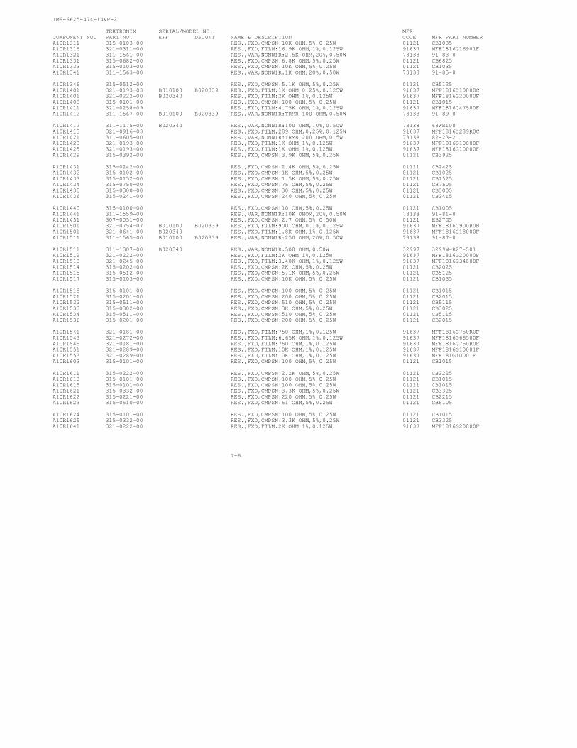
TM9-6625-474-14&P-2
TEKTRONIX SERIAL/MODEL NO. MFRCOMPONENT NO. PART NO. EFF DSCONT NAME & DESCRIPTION CODE MFR PART NUMBERA10R1311 315-0103-00 RES.,FXD,CMPSN:10K OHM,5%,0.25W 01121 CB1035A10R1315 321-0311-00 RES.,FXD,FILM:16.9K OHM,1%,0.125W 91637 MFF1816G16901FA10R1321 311-1561-00 RES.,VAR,NONWIR:2.5K OHM,20%,0.50W 73138 91-83-0A10R1331 315-0682-00 RES.,FXD,CMPSN:6.8K OHM,5%,0.25W 01121 CB6825A10R1333 315-0103-00 RES.,FXD,CMPSN:10K OHM,5%,0.25W 01121 CB1035A10R1341 311-1563-00 RES.,VAR,NONWIR:1K OHM,20%,0.50W 73138 91-85-0
A10R1346 315-0512-00 RES.,FXD,CMPSN:5.1K OHM,5%,0.25W 01121 CB5125A10R1401 321-0193-03 B010100 B020339 RES.,FXD,FILM:1K OHM,0.25%,0.125W 91637 MFF1816D10000CA10R1401 321-0222-00 B020340 RES.,FXD,FILM:2K OHM,1%,0.125W 91637 MFF1816G20000FA10R1403 315-0101-00 RES.,FXD,CMPSN:100 OHM,5%,0.25W 01121 CB1015A10R1411 321-0258-09 RES.,FXD,FILM:4.75K OHM,1%,0.125W 91637 MFF1816C47500FA10R1412 311-1567-00 B010100 B020339 RES.,VAR,NONWIR:TRMR,100 OHM,0.50W 73138 91-89-0
A10R1412 311-1175-00 B020340 RES.,VAR,NONWIR:100 OHM,10%,0.50W 73138 68WR100A10R1413 321-0916-03 RES.,FXD,FILM:289 OHM,0.25%,0.125W 91637 MFF1816D289R0CA10R1421 311-0605-00 RES.,VAR,NONWIR:TRMR,200 OHM,0.5W 73138 82-23-2A10R1423 321-0193-00 RES.,FXD,FILM:1K OHM,1%,0.125W 91637 MFF1816G10000FA10R1425 321-0193-00 RES.,FXD,FILM:1K OHM,1%,0.125W 91637 MFF1816G10000FA10R1429 315-0392-00 RES.,FXD,CMPSN:3.9K OHM,5%,0.25W 01121 CB3925
A10R1431 315-0242-00 RES.,FXD,CMPSN:2.4K OHM,5%,0.25W 01121 CB2425A10R1432 315-0102-00 RES.,FXD,CMPSN:1K OHM,5%,0.25W 01121 CB1025A10R1433 315-0152-00 RES.,FXD,CMPSN:1.5K OHM,5%,0.25W 01121 CB1525A10R1434 315-0750-00 RES.,FXD,CMPSN:75 OHM,5%,0.25W 01121 CB7505A10R1435 315-0300-00 RES.,FXD,CMPSN:30 OHM,5%,0.25W 01121 CB3005A10R1436 315-0241-00 RES.,FXD,CMPSN:240 OHM,5%,0.25W 01121 CB2415
A10R1440 315-0100-00 RES.,FXD,CMPSN:10 OHM,5%,0.25W 01121 CB1005A10R1441 311-1559-00 RES.,VAR,NONWIR:10K OHOM,20%,0.50W 73138 91-81-0A10R1451 307-0051-00 RES.,FXD,CMPSN:2.7 OHM,5%,0.50W 01121 EB27G5A10R1501 321-0754-07 B010100 B020339 RES.,FXD,FILM:900 OHM,0.1%,0.125W 91637 MFF1816C900R0BA10R1501 321-0641-00 B020340 RES.,FXD,FILM:1.8K OHM,1%,0.125W 91637 MFF1816G18000FA10R1511 311-1565-00 B010100 B020339 RES.,VAR,NONWIR:250 OHM,20%,0.50W 73138 91-87-0
A10R1511 311-1307-00 B020340 RES.,VAR,NONWIR:500 OHM,0.50W 32997 3299W-R27-501A10R1512 321-0222-00 RES.,FXD,FILM:2K OHM,1%,0.125W 91637 MFF1816G20000FA10R1513 321-0245-00 RES.,FXD,FILM:3.48K OHM,1%,0.125W 91637 MFF1816G34800FA10R1514 315-0202-00 RES.,FXD,CMPSN:2K OHM,5%,0.25W 01121 CB2025A10R1515 315-0512-00 RES.,FXD,CMPSN:5.1K OHM,5%,0.25W 01121 CB5125A10R1517 315-0103-00 RES.,FXD,CMPSN:10K OHM,5%,0.25W 01121 CB1035
A10R1518 315-0101-00 RES.,FXD,CMPSN:100 OHM,5%,0.25W 01121 CB1015A10R1521 315-0201-00 RES.,FXD,CMPSN:200 OHM,5%,0.25W 01121 CB2015A10R1532 315-0511-00 RES.,FXD,CMPSN:510 OHM,5%,0.25W 01121 CB5115A10R1533 315-0302-00 RES.,FXD,CMPSN:3K OHM,5%,0.25W 01121 CB3025A10R1534 315-0511-00 RES.,FXD,CMPSN:510 OHM,5%,0.25W 01121 CB5115A10R1536 315-0201-00 RES.,FXD,CMPSN:200 OHM,5%,0.25W 01121 CB2015
A10R1541 321-0181-00 RES.,FXD,FILM:750 OHM,1%,0.125W 91637 MFF1816G750R0FA10R1543 321-0272-00 RES.,FXD,FILM:6.65K OHM,1%,0.125W 91637 MFF1816G66500FA10R1545 321-0181-00 RES.,FXD,FILM:750 OHM,1%,0.125W 91637 MFF1816G750R0FA10R1551 321-0289-00 RES.,FXD,FILM:10K OHM,1%,0.125W 91637 MFF1816G10001FA10R1553 321-0289-00 RES.,FXD,FILM:10K OHM,1%,0.125W 91637 MFF181G10001FA10R1603 315-0101-00 RES.,FXD,CMPSN:100 OHM,5%,0.25W 01121 CB1015
A10R1611 315-0222-00 RES.,FXD,CMPSN:2.2K OHM,5%,0.25W 01121 CB2225A10R1613 315-0101-00 RES.,FXD,CMPSN:100 OHM,5%,0.25W 01121 CB1015A10R1615 315-0101-00 RES.,FXD,CMPSN:100 OHM,5%,0.25W 01121 CB1015A10R1621 315-0332-00 RES.,FXD,CMPSN:3.3K OHM,5%,0.25W 01121 CB3325A10R1622 315-0221-00 RES.,FXD,CMPSN:220 OHM,5%,0.25W 01121 CB2215A10R1623 315-0510-00 RES.,FXD,CMPSN:51 OHM,5%,0.25W 01121 CB5105
A10R1624 315-0101-00 RES.,FXD,CMPSN:100 OHM,5%,0.25W 01121 CB1015A10R1625 315-0332-00 RES.,FXD,CMPSN:3.3K OHM,5%,0.25W 01121 CB3325A10R1641 321-0222-00 RES.,FXD,FILM:2K OHM,1%,0.125W 91637 MFF1816G20000F
7-6
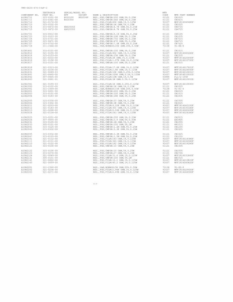
TM9-6625-474-14&P-2
TEKTRONIX SERIAL/MODEL NO. MFRCOMPONENT NO. PART NO. EFF DSCONT NAME & DESCRIPTION CODE MFR PART NUMBERA10R1711 315-0101-00 B010100 B020349 RES.,FXD,CMPSN:100 OHM,5%,0.25W 01121 CB1015A10R1711 315-0361-00 B020350 RES.,FXD,CMPSN:360 OHM,5%,0.25W 01121 CB3615A10R1712 321-0172-00 RES.,FXD,FILM:604 OHM,1%,0.125W 91637 MFF1816G604R0FA10R1713 315-0102-00 RES.,FXD,CMPSN:1K OHM,5%,0.25W 01121 CB1025A10R1714 315-0472-00 XB020350 RES.,FXD,CMPSN:4.7K OHM,5%,0.25W 01121 CB4725A10R1715 315-0472-00 XB020350 RES.,FXD,CMPSN:4.7K OHM,5%,0.25W 01121 CB4725
A10R1721 315-0512-00 RES.,FXD,CMPSN:5.1K OHM,5%,0.25W 01121 CB5125A10R1723 315-0103-00 RES.,FXD,CMPSN:10K OHM,5%,0.25W 01121 CB1035A10R1724 315-0751-00 RES.,FXD,CMPSN:750 OHM,5%,0.25W 01121 CB7515A10R1725 315-0471-00 RES.,FXD,CMPSN:470 OHM,5%,0.25W 01121 CB4715A10R1727 315-0752-00 RES.,FXD,CMPSN:7.5K OHM,5%,0.25W 01121 CB7525A10R1728 311-1566-00 RES.,VAR,NONWIR:200 OHM,20%,0.50W 73138 91-88-0
A10R1801 315-0101-00 RES.,FXD,CMPSN:100 OHM,5%,0.25W 01121 CB1015A10R1812 321-0155-00 RES.,FXD,FILM:402 OHM,1%,0.125W 91637 MFF1816G402R0FA10R1814 315-0153-00 RES.,FXD,CMPSN:15K OHM,5%,0.25W 01121 CB1535A10R1815 321-0222-00 RES.,FXD,FILM:2K OHM,1%,0.125W 91637 MFF1816G20000FA10R1816 321-0196-00 RES.,FXD,FILM:1.07K OHM,1%,0.125W 91637 MFF1816G10700FA10R1817 315-0101-00 RES.,FXD,CMPSN:100 OHM,5%,0.25W 01121 CB1015
A10R1818 321-0313-00 RES.,FXD,FILM:17.8K OHM,1%,0.125W 91637 MFF1816G17801FA10R1819 321-0236-00 RES.,FXD,FILM:2.8K OHM,1%,0.125W 91637 MFF1816G28000FA10R1831 321-0289-03 RES.,FXD,FILM:10K OHM,0.25%,0.125W 91637 MFF1816D10001CA10R1841 321-0645-00 RES.,FXD,FILM:100K OHM,0.5%,0.125W 91637 MFF1816D10002DA10R1842 307-0465-00 RES.,FXD,FILM:10M OHM,1%,0.5W 03888 FL1/2-105FA10R1843 321-0481-01 RES.,FXD,FILM:1M OHM,0.5%,0.125W 91637 MFF1816G10003D
A10R1941 321-0193-03 RES.,FXD,FILM:1K OHM,0.25%,0.125W 91637 MFF1816D10000CA10R1950 315-0102-00 RES.,FXD,CMPSN:1K OHM,5%,0.25W 01121 CB1025A10R1951 311-1559-00 RES.,CAR,NONWIR:10K OHM,20%,0.50W 73138 91-81-0A10R2001 315-0201-00 RES.,FXD,CMPSN:200 OHM,5%,0.25W 01121 CB2015A10R2003 315-0101-00 RES.,FXD,CMPSN:100 OHM,5%,0.25W 01121 CB1015A10R2004 315-0183-00 RES.,FXD,CMPSN:18K OHM,5%,0.25W 01121 CB1835
A10R2005 315-0330-00 RES.,FXD,CMPSN:33 OHM,5%,0.25W 01121 CB3305A10R2006 315-0302-00 RES.,FXD,CMPSN:3K OHM,5%,0.25W 01121 CB3025A10R2011 321-0253-00 RES.,FXD,FILM:4.22K OHM,1%,0.125W 91637 MFF1816G42200FA10R2012 321-0143-00 RES.,FXD,FILM:301 OHM,1%,0.125W 91637 MFF1816G301R0FA10R2013 321-0268-00 RES.,FXD,FILM:6.04K OHM,1%,0.125W 91637 MFF1816G60400FA10R2024 321-0134-00 RES.,FXD,FILM:243 OHM,1%,0.125W 91637 MFF1816G243R0F
A10R2025 315-0201-00 RES.,FXD,CMPSN:200 OHM,5%,0.25W 01121 CB2015A10R2026 307-0055-00 RES.,FXD,CMPSN:3.9 OHM,5%,0.50W 01121 EB39G5A10R2031 315-0105-00 RES.,FXD,CMPSN:1M OHM,5%,0.25W 01121 CB1055A10R2033 305-0101-00 RES.,FXD,CMPSN:100 OHM,5%,2W 01121 HB1015A10R2041 315-0125-00 RES.,FXD,CMPSN:1.2M OHM,5%,0.25W 01121 CB1255A10R2043 315-0332-00 RES.,FXD,CMPSN:3.3K OHM,5%,0.25W 01121 CB3325
A10R2045 315-0332-00 RES.,FXD,CMPSN:3.3K OHM,5%,0.25W 01121 CB3325A10R2047 315-0125-00 RES.,FXD,CMPSN:1.2M OHM,5%,0.25W 01121 CB1255A10R2101 321-0112-00 RES.,FXD,FILM:143 OHM,1%,0.125W 91637 MFF1816G143R0FA10R2111 321-0151-00 RES.,FXD,FILM:365 OHM,1%,0.125W 91637 MFF1816G365R0FA10R2113 321-0122-00 RES.,FXD,FILM:182 OHM,1%,0.125W 91637 MFF1816G182R0FA10R2121 315-0100-00 RES.,FXD,CMPSN:10 OHM,5%,0.25W 01121 CB1005
A10R2122 315-0100-00 RES.,FXD,CMPSN:10 OHM,5%,0.25W 01121 CB1005A10R2123 315-0270-00 RES.,FXD,CMPSN:27 OHM,5%,0.25W 01121 CB2705A10R2124 321-0049-00 RES.,FXD,FILM:31.6 OHM,1%,0.125W 91637 MFF1816G31R60FA10R2131 305-0101-00 RES.,FXD,CMPSN:100 OHM,5%,2W 01121 HB1015A10R2141 321-0002-00 RES.,FXD,FILM:10.2 OHM,1%,0.125W 91637 MFF1816G10R20FA10R2143 321-0059-00 RES.,FXD,FILM:40.2 OHM,1%,0.125W 91637 MFF1816G40R20F
A10R2201 311-1560-00 RES.,VAR,NONWIR:5K OHM,20%,0.50W 73138 91-82-0A10R2202 321-0238-00 RES.,FXD,FILM:2.94K OHM,1%,0.125W 91637 MFF1816G29400FA10R2203 321-0271-00 RES.,FXD,FILM:6.49K OHM,1%,0.125W 91637 MFF1816G64900F
7-7
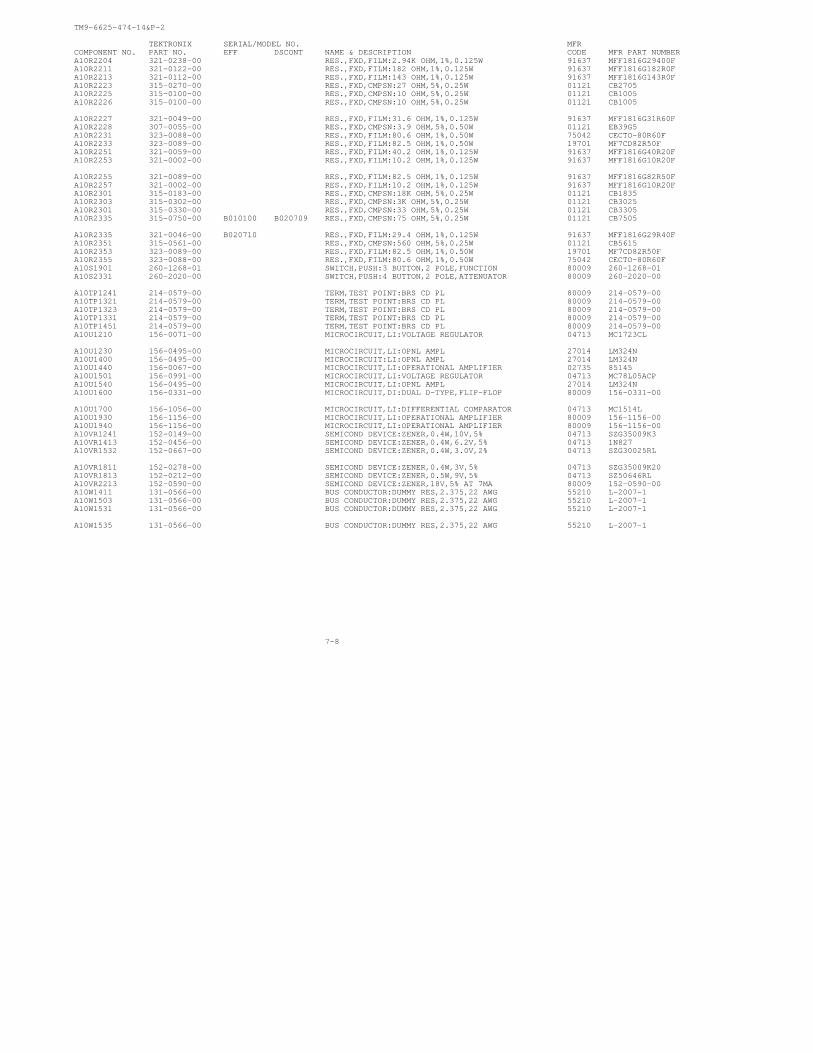
TM9-6625-474-14&P-2
TEKTRONIX SERIAL/MODEL NO. MFRCOMPONENT NO. PART NO. EFF DSCONT NAME & DESCRIPTION CODE MFR PART NUMBERA10R2204 321-0238-00 RES.,FXD,FILM:2.94K OHM,1%,0.125W 91637 MFF1816G29400FA10R2211 321-0122-00 RES.,FXD,FILM:182 OHM,1%,0.125W 91637 MFF1816G182R0FA10R2213 321-0112-00 RES.,FXD,FILM:143 OHM,1%,0.125W 91637 MFF1816G143R0FA10R2223 315-0270-00 RES.,FXD,CMPSN:27 OHM,5%,0.25W 01121 CB2705A10R2225 315-0100-00 RES.,FXD,CMPSN:10 OHM,5%,0.25W 01121 CB1005A10R2226 315-0100-00 RES.,FXD,CMPSN:10 OHM,5%,0.25W 01121 CB1005
A10R2227 321-0049-00 RES.,FXD,FILM:31.6 OHM,1%,0.125W 91637 MFF1816G31R60FA10R2228 307-0055-00 RES.,FXD,CMPSN:3.9 OHM,5%,0.50W 01121 EB39G5A10R2231 323-0088-00 RES.,FXD,FILM:80.6 OHM,1%,0.50W 75042 CECTO-80R60FA10R2233 323-0089-00 RES.,FXD,FILM:82.5 OHM,1%,0.50W 19701 MF7CD82R50FA10R2251 321-0059-00 RES.,FXD,FILM:40.2 OHM,1%,0.125W 91637 MFF1816G40R20FA10R2253 321-0002-00 RES.,FXD,FILM:10.2 OHM,1%,0.125W 91637 MFF1816G10R20F
A10R2255 321-0089-00 RES.,FXD,FILM:82.5 OHM,1%,0.125W 91637 MFF1816G82R50FA10R2257 321-0002-00 RES.,FXD,FILM:10.2 OHM,1%,0.125W 91637 MFF1816G10R20FA10R2301 315-0183-00 RES.,FXD,CMPSN:18K OHM,5%,0.25W 01121 CB1835A10R2303 315-0302-00 RES.,FXD,CMPSN:3K OHM,5%,0.25W 01121 CB3025A10R2301 315-0330-00 RES.,FXD,CMPSN:33 OHM,5%,0.25W 01121 CB3305A10R2335 315-0750-00 B010100 B020709 RES.,FXD,CMPSN:75 OHM,5%,0.25W 01121 CB7505
A10R2335 321-0046-00 B020710 RES.,FXD,FILM:29.4 OHM,1%,0.125W 91637 MFF1816G29R40FA10R2351 315-0561-00 RES.,FXD,CMPSN:560 OHM,5%,0.25W 01121 CB5615A10R2353 323-0089-00 RES.,FXD,FILM:82.5 OHM,1%,0.50W 19701 MF7CD82R50FA10R2355 323-0088-00 RES.,FXD,FILM:80.6 OHM,1%,0.50W 75042 CECTO-80R60FA10S1901 260-1268-01 SWITCH,PUSH:3 BUTTON,2 POLE,FUNCTION 80009 260-1268-01A10S2331 260-2020-00 SWITCH,PUSH:4 BUTTON,2 POLE,ATTENUATOR 80009 260-2020-00
A10TP1241 214-0579-00 TERM,TEST POINT:BRS CD PL 80009 214-0579-00A10TP1321 214-0579-00 TERM,TEST POINT:BRS CD PL 80009 214-0579-00A10TP1323 214-0579-00 TERM,TEST POINT:BRS CD PL 80009 214-0579-00A10TP1331 214-0579-00 TERM,TEST POINT:BRS CD PL 80009 214-0579-00A10TP1451 214-0579-00 TERM,TEST POINT:BRS CD PL 80009 214-0579-00A10U1210 156-0071-00 MICROCIRCUIT,LI:VOLTAGE REGULATOR 04713 MC1723CL
A10U1230 156-0495-00 MICROCIRCUIT,LI:OPNL AMPL 27014 LM324NA10U1400 156-0495-00 MICROCIRCUIT:LI:OPNL AMPL 27014 LM324NA10U1440 156-0067-00 MICROCIRCUIT,LI:OPERATIONAL AMPLIFIER 02735 85145A10U1501 156-0991-00 MICROCIRCUIT,LI:VOLTAGE REGULATOR 04713 MC78L05ACPA10U1540 156-0495-00 MICROCIRCUIT,LI:OPNL AMPL 27014 LM324NA10U1600 156-0331-00 MICROCIRCUIT,DI:DUAL D-TYPE,FLIP-FLOP 80009 156-0331-00
A10U1700 156-1056-00 MICROCIRCUIT,LI:DIFFERENTIAL COMPARATOR 04713 MC1514LA10U1930 156-1156-00 MICROCIRCUIT,LI:OPERATIONAL AMPLIFIER 80009 156-1156-00A10U1940 156-1156-00 MICROCIRCUIT,LI:OPERATIONAL AMPLIFIER 80009 156-1156-00A10VR1241 152-0149-00 SEMICOND DEVICE:ZENER,0.4W,10V,5% 04713 SZG35009K3A10VR1413 152-0456-00 SEMICOND DEVICE:ZENER,0.4W,6.2V,5% 04713 1N827A10VR1532 152-0667-00 SEMICOND DEVICE:ZENER,0.4W,3.0V,2% 04713 SZG30025RL
A10VR1811 152-0278-00 SEMICOND DEVICE:ZENER,0.4W,3V,5% 04713 SZG35009K20A10VR1813 152-0212-00 SEMICOND DEVICE:ZENER,0.5W,9V,5% 04713 SZ50646RLA10VR2213 152-0590-00 SEMICOND DEVICE:ZENER,18V,5% AT 7MA 80009 152-0590-00A10W1411 131-0566-00 BUS CONDUCTOR:DUMMY RES,2.375,22 AWG 55210 L-2007-1A10W1503 131-0566-00 BUS CONDUCTOR:DUMMY RES,2.375,22 AWG 55210 L-2007-1A10W1531 131-0566-00 BUS CONDUCTOR:DUMMY RES,2.375,22 AWG 55210 L-2007-1
A10W1535 131-0566-00 BUS CONDUCTOR:DUMMY RES,2.375,22 AWG 55210 L-2007-1
7-8
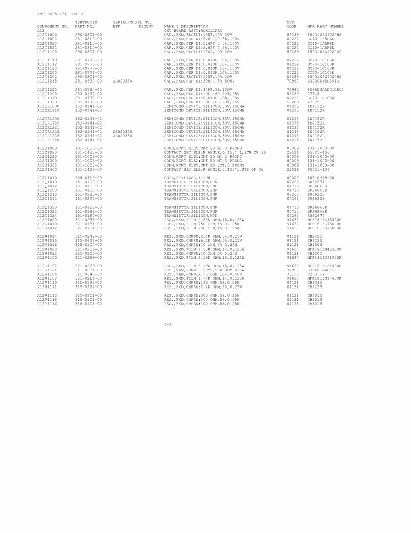
TM9-6625-474-14&P-2
TEKTRONIX SERIAL/MODEL NO. MFRCOMPONENT NO. PART NO. EFF DSCONT NAME & DESCRIPTION CODE MFR PART NUMBERA12 CKT BOARD ASSY:AUXILIARYA12C1000 290-0301-00 CAP.,FXD,ELCTLT:10UF,10%,20V 56289 150D106X9020B2A12C1002 281-0810-00 CAP.,FXD,CER DI:5.6PF,0.5%,100V 04222 GC10-1A5R6DA12C1020 281-0810-00 CAP.,FXD,CER DI:5.6PF,0.5%,100V 04222 GC10-1A5R6DA12C1022 281-0810-00 CAP.,FXD,CER DI:5.6PF,0.5%,100V 04222 GC10-1A5R6DA12C1100 290-0301-00 CAP.,FXD,ELCTLT:10UF,10%,20V 56289 150D106X9020B2
A12C1110 281-0773-00 CAP.,FXD,CER DI:0.01UF,10%,100V 04222 GC70-1C103KA12C1112 281-0773-00 CAP.,FXD,CER DI:0.01UF,10%,100V 04222 GC70-1C103KA12C1120 281-0773-00 CAP.,FXD,CER DI:0.01UF,10%,100V 04222 GC70-1C103KA12C1200 281-0773-00 CAP.,FXD,CER DI:0.01UF,10%,100V 04222 GC70-1C103KA12C1202 290-0301-00 CAP.,FXD,ELCTLT:10UF,10%,20V 56289 150D106X9020B2A12C1215 281-0630-00 XB020350 CAP.,FXD,CER DI:390PF,5%,500V 72982 630000Y5D391J
A12C1220 281-0764-00 CAP.,FXD,CER DI:82PF,5%,100V 72982 8035D9AADC1G802A12C1300 283-0177-00 CAP.,FXD,CER DI:1UF,+80-20%,25V 56289 273C5A12C1310 281-0773-00 CAP.,FXD,CER DI:0.01UF,10%,100V 04222 GC70-1C103KA12C1320 283-0177-00 CAP.,FXD,CER DI:1UF,+80-20%,25V 56289 273C5A12CR1000 152-0141-02 SEMICOND DEVICE:SILICON,30V,150MA 01295 1N4152RA12CR1110 152-0141-02 SEMICOND DEVICE:SILICON,30V,150MA 01295 1N4152R
A12CR1200 152-0141-02 SEMICOND DEVICE:SILICON,30V,150MA 01295 1N4152RA12CR1220 152-0141-02 SEMICOND DEVICE:SILICON,30V,150MA 01295 1N4152RA12CR1221 152-0141-02 SEMICOND DEVICE:SILICON,30V,150MA 01295 1N4152RA12CR1225 152-0141-02 XB020350 SEMICOND DEVICE:SILICON,30V,150MA 01295 1N4152RA12CR1226 152-0141-02 XB020350 SEMICOND DEVICE:SILICON,30V,150MA 01295 1N4152RA12CR1320 152-0141-02 SEMICOND DEVICE:SILICON,30V,150MA 01295 1N4152R
A12J1000 131-1003-00 CONN,RCPT,ELEC:CKT BD MT,3 PRONG 80009 131-1003-00A12J1020 131-1425-00 CONTACT SET,ELE:R ANGLE,O.150" L,STR OF 36 22526 65521-136A12J1220 131-1003-00 CONN,RCPT,ELEC:CKT BD MT,3 PRONG 80009 131-1003-00A12J1300 131-1003-00 CONN,RCPT,ELEC:CKT BD MT,3 PRONG 80009 131-1003-00A12J1302 131-1003-00 CONN,RCPT,ELEC:CKT BD ;MT,3 PRONG 80009 131-1003-00A12J1400 131-1425-00 CONTACT SET,ELE:R ANGLE,0.150"L,STR OF 36 22526 65521-136
A12L1010 108-0419-00 COIL,RF:FIXED,1.1UH 80009 108-0419-00A12Q1010 151-0190-00 TRANSISTOR:SILICON,NPN 07263 S032677A12Q1012 151-0188-00 TRANSISTOR:SILICON,PNP 04713 SPS6868KA12Q1200 151-0188-00 TRANSISTOR:SILICON,PNP 04713 SPS6868KA12Q1210 151-0220-00 TRANSISTOR:SILICON,PNP 07263 S036228A12Q1212 151-0220-00 TRANSISTOR:SILICON,PNP 07263 S036228
A12Q1320 151-0188-00 TRANSISTOR:SILICON,PNP 04713 SPS6868KA12Q1322 151-0188-00 TRANSISTOR:SILICON,PNP 04713 SPS6868KA12Q1324 151-0190-00 TRANSISTOR:SILICON,NPN 07263 S032677A12R1000 321-0256-00 RES.,FXD,FILM:4.53K OHM,1%,0.125W 91637 MFF1816G45300FA12R1010 321-0181-00 RES.,FXD,FILM:750 OHM,1%,0.125W 91637 MFF1816G750R0FA12R1012 321-0181-00 RES.,FXD,FILM:750 OHM,1%,0.125W 91637 MFF1816G750R0F
A12R1014 315-0242-00 RES.,FXD,CMPSN:2.4K OHM,5%,0.25W 01121 CB2425A12R1015 315-0622-00 RES.,FXD,CMPSN:6.2K OHM,5%,0.25W 01121 CB6225A12R1016 315-0100-00 RES.,FXD,CMPSN:10 OHM,5%,0.25W 01121 CB1005A12R1020 321-0256-00 RES.,FXD,FILM:4.53K OHM,1%,0.125W 91637 MFF1816G45300FA12R1022 315-0100-00 RES.,FXD,CMPSN:10 OHM,5%,0.25W 01121 CB1005A12R1100 321-0269-00 RES.,FXD,FILM:6.19K OHM,1%,0.125W 91637 MFF1816G61900F
A12R1102 321-0269-00 RES.,FXD,FILM:6.19K OHM,1%,0.125W 91637 MFF1816G61900FA12R1104 311-0634-00 RES.,VAR,NONWIR:TRMR,500 OHM,0.5W 32997 3326H-G48-501A12R1106 311-0643-00 RES.,VAR,NONWIR:50 OHM,10%,0.50W 73138 82-33-2A12R1108 321-0216-00 RES.,FXD,FILM:1.74K OHM,1%,0.125W 91637 MFF1816G17400FA12R1110 315-0133-00 RES.,FXD,CMPSN:13K OHM,5%,0.25W 01121 CB1335A12R1111 315-0222-00 RES.,FXD,CMPSN:2.2K OHM,5%,0.25W 01121 CB2225
A12R1113 315-0301-00 RES.,FXD,CMPSN:300 OHM,5%,0.25W 01121 CB3015A12R1115 315-0101-00 RES.,FXD,CMPSN:100 OHM,5%,0.25W 01121 CB1015A12R1116 315-0101-00 RES.,FXD,CMPSN:100 OHM,5%,0.25W 01121 CB1015
7-9
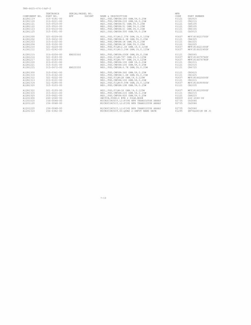
TM9-6625-474-14&P-2
TEKTRONIX SERIAL/MODEL NO. MFRCOMPONENT NO. PART NO. EFF DSCONT NAME & DESCRIPTION CODE PART NUMBERA12R1119 315-0181-00 RES.,FXD,CMPSN:180 OHM,5%,0.25W 01121 CB1815A12R1120 315-0221-00 RES.,FXD,CMPSN:220 OHM,5%,0.25W 01121 CB2215A12R1121 315-0510-00 RES.,FXD,CMPSN:51 OHM,5%,0.25W 01121 CB5105A12R1122 315-0510-00 RES.,FXD,CMPSN:51 OHM,5%,0.25W 01121 CB5105A12R1123 315-0510-00 RES.,FXD,CMPSN:51 OHM,5%,0.25W 01121 CB5105A12R1125 315-0301-00 RES.,FXD,CMPSN:300 OHM,5%,0.25W 01121 CB3015
A12R1200 321-0229-00 RES.,FXD,FILM:2.37K OHM,1%,0.125W 91637 MFF1816G23700FA12R1202 315-0432-00 RES.,FXD,CMPSN:4.3K OHM,5%,0.25W 01121 CB4325A12R1203 315-0102-00 RES.,FXD,CMPSN:1K OHM,5%,0.25W 01121 CB1025A12R1204 315-0102-00 RES.,FXD,CMPSN:1K OHM,5%,0.25W 01121 CB1025A12R1210 321-0224-00 RES.,FXD,FILM:2.1K OHM,1%,0.125W 91637 MFF1816G21000FA12R1212 321-0242-00 RES.,FXD,FILM:3.24K OHM,1%,0.125W 91637 MFF1816G32400F
A12R1215 315-0204-00 XB020350 RES.,FXD,CMPSN:200K OHM,5%,0.25W 01121 CB2045A12R1216 321-0183-00 RES.,FXD,FILM:787 OHM,1%,0.125W 91637 MFF1816G787R0FA12R1217 321-0183-00 RES.,FXD,FILM:787 OHM,1%,0.125W 91637 MFF1816G787R0FA12R1220 315-0101-00 RES.,FXD,CMPSN:100 OHM 5%,0.25W 01121 CB1015A12R1221 315-0101-00 RES.,FXD,CMPSN:100 OHM,5%,0.25W 01121 CB1015A12R1225 315-0472-00 XB020350 RES.,FXD,CMPSN:4.7K OHM,5%,0.25W 01121 CB4725
A12R1300 315-0361-00 RES.,FXD,CMPSN:360 OHM,5%,0.25W 01121 CB3615A12R1310 315-0162-00 RES.,FXD,CMPSN:1.6K OHM,5%,0.25W 01121 CB1625A12R1312 321-0222-00 RES.,FXD,FILM:2K OHM,1%,0.125W 91637 MFF1816G20000FA12R1313 315-0101-00 RES.,FXD,CMPSN:100 OHM,5%,0.25W 01121 CB1015A12R1314 321-0285-00 RES.,FXD,FILM:9.09K OHM,1%,0.125W 91637 MFF1816G90900FA12R1320 315-0103-00 RES.,FXD,CMPSN:10K OHM,5%,0.25W 01121 CB1035
A12R1322 321-0193-00 RES.,FXD,FILM:1K OHM,1%,0.125W 91637 MFF1816G10000FA12R1324 315-0221-00 RES.,FXD,CMPSN:220 OHM,5%,0.25W 01121 CB2215A12R1325 315-0621-00 RES.,FXD,CMPSN:620 OHM,5%,0.25W 01121 CB6215A12S1400 260-2040-00 SWITCH,PUSH:4 BTN 2 POLE,MODE 80009 260-2040-00A12U1020 156-0048-00 MICROCIRCUIT,LI:FIVE NPN TRANSISTOR ARRAY 02735 CA3046A12U1120 156-0048-00 MICROCIRCUIT,LI:FIVE NPN TRANSISTOR ARRAY 02735 CA3046
A12U1220 156-0048-00 MICROCIRCUIT,LI:FIVE NPN TRANSISTOR ARRAY 02735 CA3046A12U1310 156-0382-00 MICROCIRCUIT,DI:QUAD 2-INPUT NAND GATE 01295 SN74LS00(N OR J)
7-10
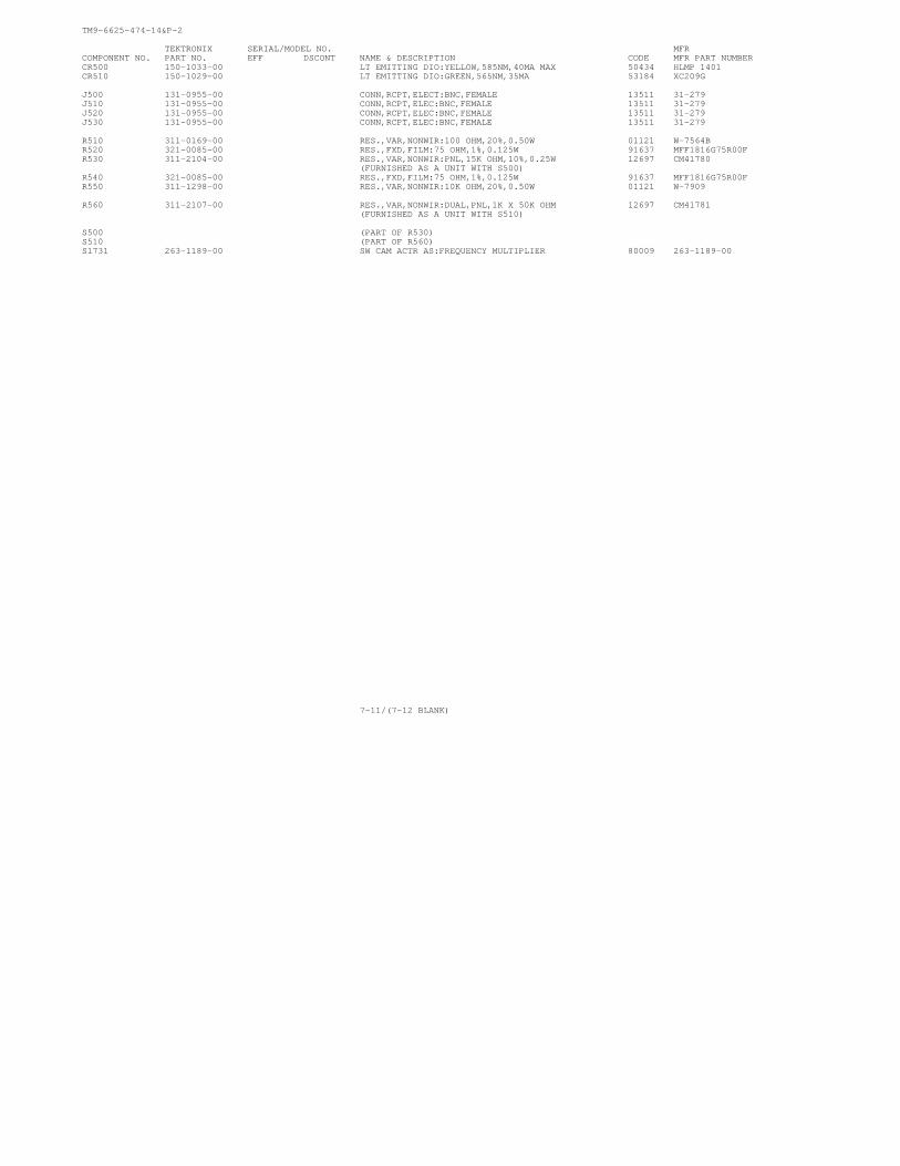
TM9-6625-474-14&P-2
TEKTRONIX SERIAL/MODEL NO. MFRCOMPONENT NO. PART NO. EFF DSCONT NAME & DESCRIPTION CODE MFR PART NUMBERCR500 150-1033-00 LT EMITTING DIO:YELLOW,585NM,40MA MAX 50434 HLMP 1401CR510 150-1029-00 LT EMITTING DIO:GREEN,565NM,35MA 53184 XC209G
J500 131-0955-00 CONN,RCPT,ELECT:BNC,FEMALE 13511 31-279J510 131-0955-00 CONN,RCPT,ELEC:BNC,FEMALE 13511 31-279J520 131-0955-00 CONN,RCPT,ELEC:BNC,FEMALE 13511 31-279J530 131-0955-00 CONN,RCPT,ELEC:BNC,FEMALE 13511 31-279
R510 311-0169-00 RES.,VAR,NONWIR:100 OHM,20%,0.50W 01121 W-7564BR520 321-0085-00 RES.,FXD,FILM:75 OHM,1%,0.125W 91637 MFF1816G75R00FR530 311-2104-00 RES.,VAR,NONWIR:PNL,15K OHM,10%,0.25W 12697 CM41780
(FURNISHED AS A UNIT WITH S500)R540 321-0085-00 RES.,FXD,FILM:75 OHM,1%,0.125W 91637 MFF1816G75R00FR550 311-1298-00 RES.,VAR,NONWIR:10K OHM,20%,0.50W 01121 W-7909
R560 311-2107-00 RES.,VAR,NONWIR:DUAL,PNL,1K X 50K OHM 12697 CM41781(FURNISHED AS A UNIT WITH S510)
S500 (PART OF R530)S510 (PART OF R560)S1731 263-1189-00 SW CAM ACTR AS:FREQUENCY MULTIPLIER 80009 263-1189-00
7-11/(7-12 BLANK)
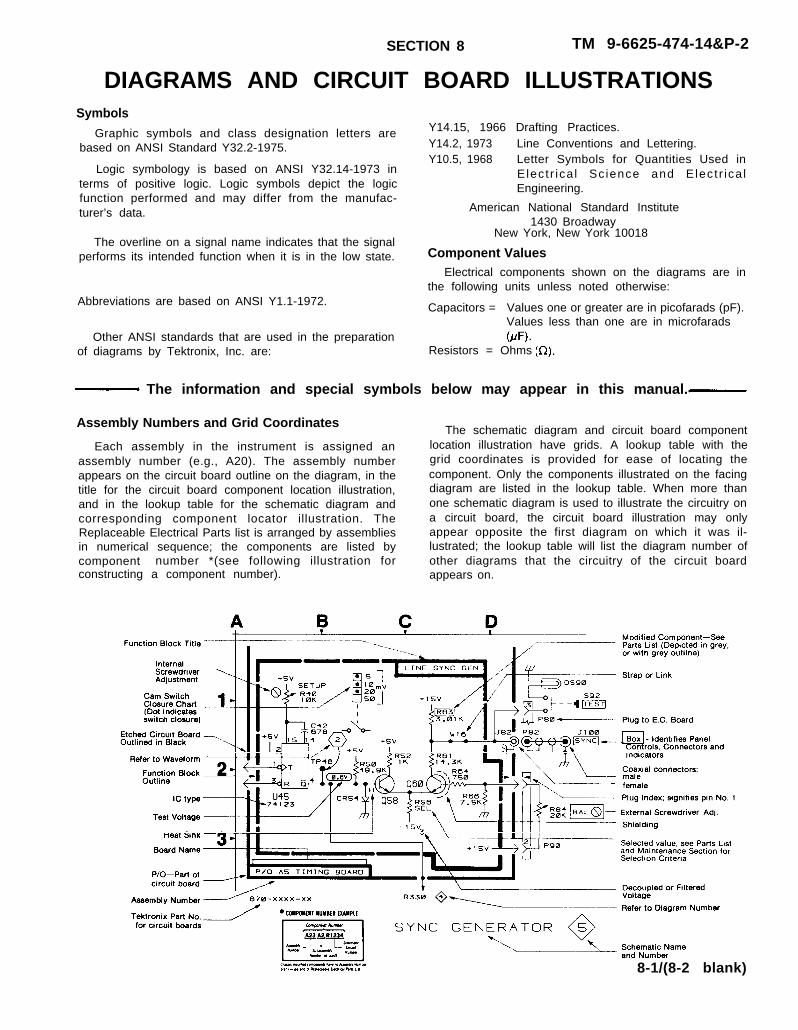
SECTION 8 TM 9-6625-474-14&P-2
DIAGRAMS AND CIRCUIT BOARD ILLUSTRATIONSSymbols
Graphic symbols and class designation letters arebased on ANSI Standard Y32.2-1975.
Logic symbology is based on ANSI Y32.14-1973 interms of positive logic. Logic symbols depict the logicfunction performed and may differ from the manufac-turer’s data.
The overline on a signal name indicates that the signalperforms its intended function when it is in the low state.
Abbreviations are based on ANSI Y1.1-1972.
Other ANSI standards that are used in the preparationof diagrams by Tektronix, Inc. are:
Y14.15, 1966 Drafting Practices.Y14.2, 1973 Line Conventions and Lettering.Y10.5, 1968 Letter Symbols for Quantities Used in
Elect r ica l Sc ience and Elect r ica lEngineering.
American National Standard Institute1430 Broadway
New York, New York 10018
Component ValuesElectrical components shown on the diagrams are in
the following units unless noted otherwise:
Capacitors = Values one or greater are in picofarads (pF).Values less than one are in microfarads
Resistors = Ohms
The information and special symbols below may appear in this manual.
Assembly Numbers and Grid Coordinates
Each assembly in the instrument is assigned anassembly number (e.g., A20). The assembly numberappears on the circuit board outline on the diagram, in thetitle for the circuit board component location illustration,and in the lookup table for the schematic diagram andcorresponding component locator illustration. TheReplaceable Electrical Parts list is arranged by assembliesin numerical sequence; the components are listed bycomponent number *(see following illustration forconstructing a component number).
The schematic diagram and circuit board componentlocation illustration have grids. A lookup table with thegrid coordinates is provided for ease of locating thecomponent. Only the components illustrated on the facingdiagram are listed in the lookup table. When more thanone schematic diagram is used to illustrate the circuitry ona circuit board, the circuit board illustration may onlyappear opposite the first diagram on which it was il-lustrated; the lookup table will list the diagram number ofother diagrams that the circuitry of the circuit boardappears on.
8-1/(8-2 blank)
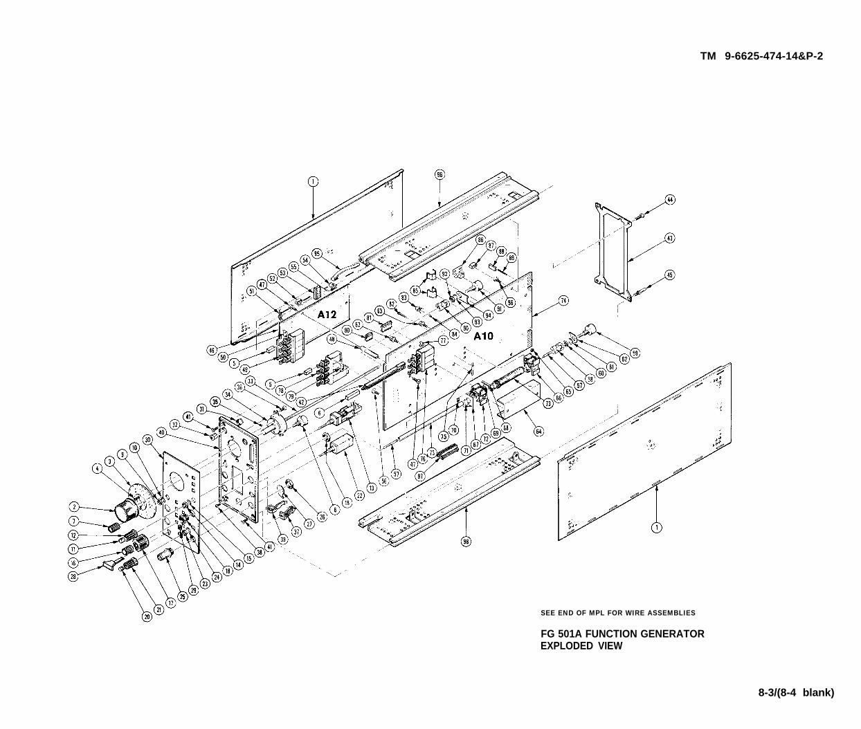
TM 9-6625-474-14&P-2
SEE END OF MPL FOR WIRE ASSEMBLIES
FG 501A FUNCTION GENERATOREXPLODED VIEW
8-3/(8-4 blank)
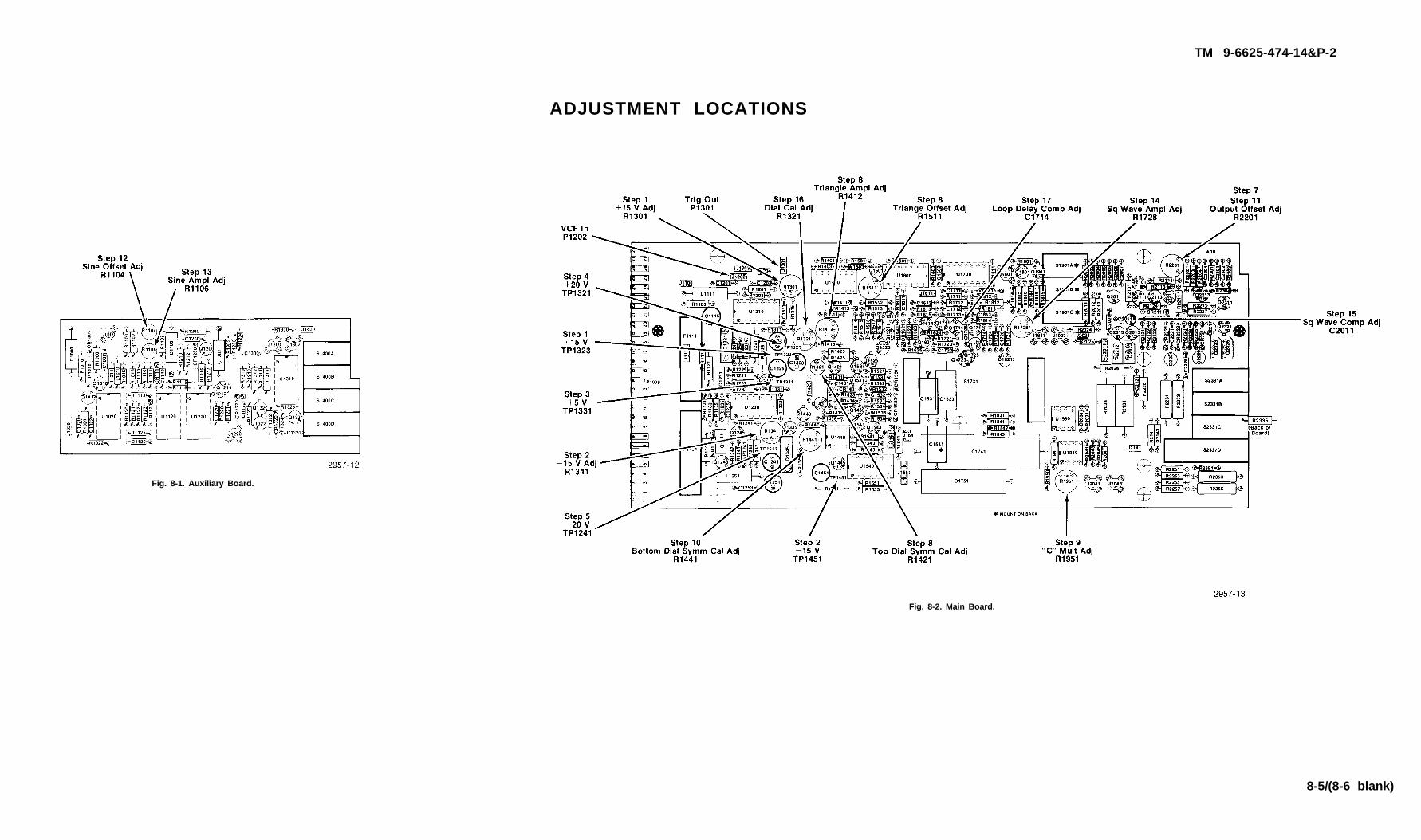
TM 9-6625-474-14&P-2
Fig. 8-1. Auxiliary Board.
ADJUSTMENT LOCATIONS
Fig. 8-2. Main Board.
8-5/(8-6 blank)
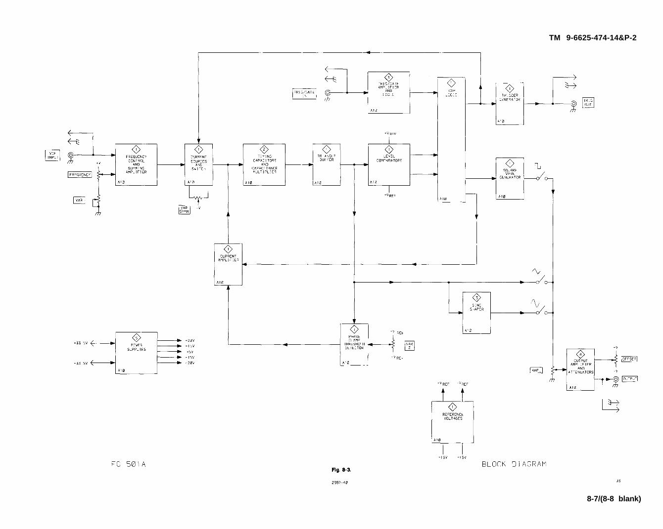
Fig. 8-3.
TM 9-6625-474-14&P-2
8-7/(8-8 blank)
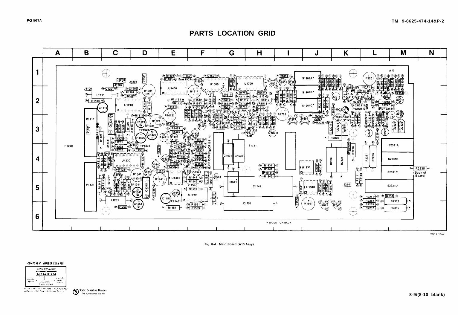
Fig. 8-4.
FG 501A TM 9-6625-474-14&P-2
PARTS LOCATION GRID
8-9/(8-10 blank)
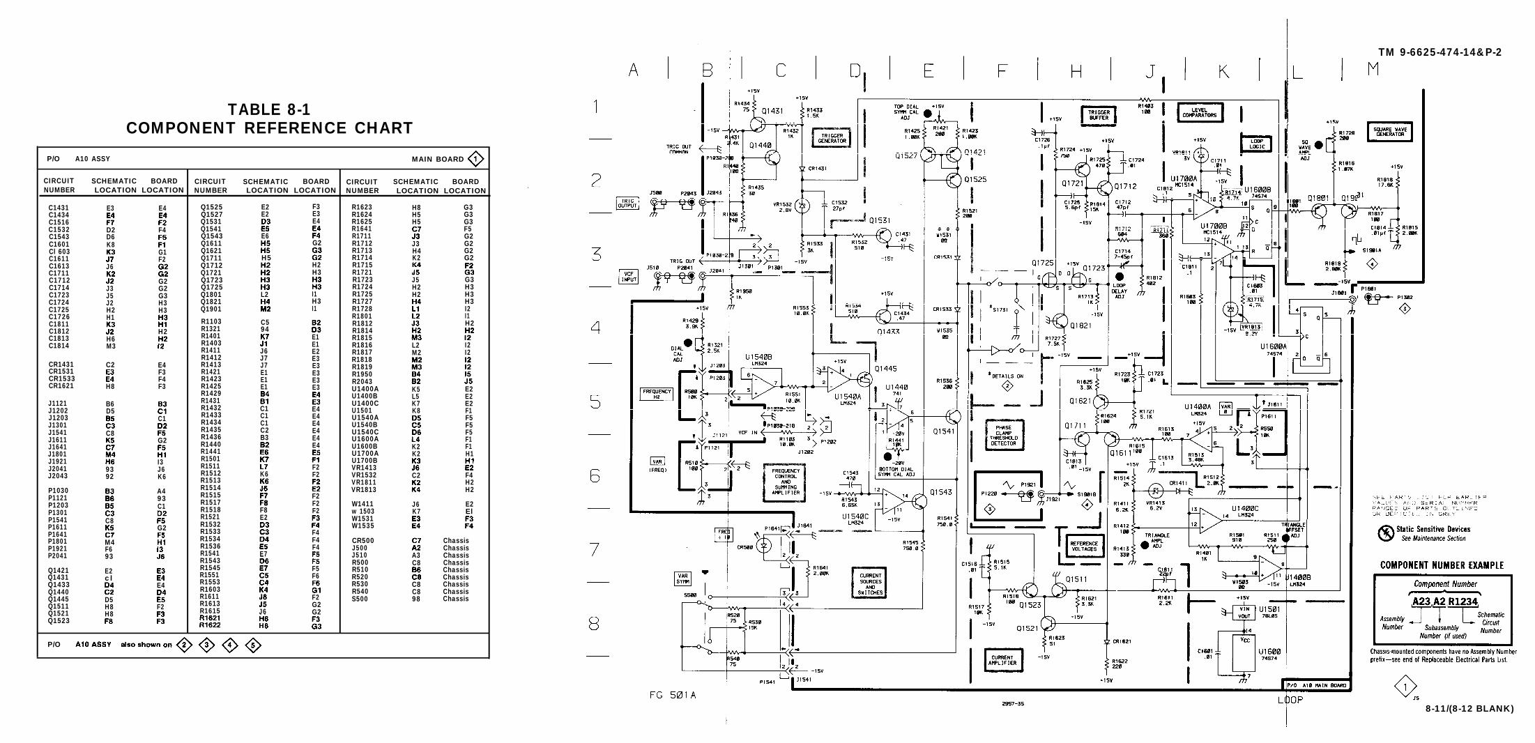
FG 501 A
TM 9-6625-474-14&P-2
TABLE 8-1COMPONENT REFERENCE CHART
P/O A10 ASSY MAIN BOARD
CIRCUIT SCHEMATIC BOARD CIRCUIT SCHEMATIC BOARD CIRCUIT SCHEMATIC BOARDNUMBER LOCATION LOCATION NUMBER LOCATION LOCATION NUMBER LOCATION LOCATION
C1431 E3 E4 Q1525 E2 F3C1434 Q1527
R1623E2 E3
H8 G3
C1516 Q1531R1624
E4H5 G3
C1532 D2 F4 Q1541R1625 H5 G3
C1543 D6 Q1543R1641
E6F5
C1601 K8R1711
Q1611 G2G2
Cl 603 Q1621R1712
G1J3 G2
C1611 Q1711R1713 H4 G2
F2 H5C1613 J6 Q1712
R1714 K2H2
G2R1715
C1711 Q1721 H3 R1721C1712 G2 Q1723C1714
R1723J3 Q1725
J5G2
G3
C1723R1724
J5 Q1801H2
G3 L2H3
I1C1724
R1725J2 Q1821
H2H3 H3
H3
C1725 H2 Q1901R1727 H3
H3 I1C1726
R1728H1
I2
C1811 R1103 C5R1801 I1
C1812 H2 R1321 94R1812 H2
C1813 H6 R1401R1814
E1C1814 M3 R1403
R1815E1
R1411 J6R1816
E2L2 I2
R1412 J7R1817
E3M2 I2
CR1431 C2 E4 R1413 J7R1818
CR1531 F3 R1421E3 R1819
CR1533E1
F4 R1423E3
E1R1950
CR1621 H8 F3 R1425E3
E1 E3R2043
R1429 U1400A K5 E2
J1121 B6 R1431U1400B L5 E2
J1202 D5 R1432 C1U1400C
E4K7 E2
J1203 C1 R1433 C1 E4U1501 K8 F1
J1301 R1434 C1 E4U1540A F5
J1541U1540B
C8 R1435 C2 E4F5
J1611 R1436 B3U1540C
G2 E4F5
J1641 R1440U1600A
E4F1
J1801 R1441U1600B K2 F1
J1921 R1501U1700A
I3K2 H1
J2041 93 R1511U1700B
J6 F2 VR1413J2043 92 K6 R1512 K6 F2
R1513VR1532 C2 F4
P1030 R1514VR1811
A4H2
P1121 R1515VR1813 H2
93 F2P1203 C1 R1517 F2P1301
W1411R1518 F8 F2
J6 E2w 1503
P1541 C8K7 El
R1521 E2P1611 R1532
W1531G2 W1535
P1641 R1533 F4P1801 M4 R1534 F4P1921 F6 R1536
CR500 ChassisF4
P2041J500
93 R1541 E7Chassis
R1543J510 A3 Chassis
Q1421 E2 R1545R500
F5C8 Chassis
Q1431R510 Chassis
cl R1551 F6Q1433 R1553
R520E4
Chassis
Q1440 R1603R530 C8 Chassis
Q1445R540
R1611C8 Chassis
D5 F2Q1511 R1613
S500 98 ChassisH8 F2 G2
Q1521 H8 R1615 J6 G2Q1523
P/O
8-11/(8-12 BLANK)

FG 501 A
TM 9-6625-474-14&P-2
TABLE 8-2COMPONENT REFERENCE CHART
P/O A10 ASSY MAIN BOARD
CIRCUIT SCHEMATIC BOARDNUMBER LOCATION LOCATION
C1631C1633C1641C1741C1751C2031
R1831R1841R1842R1843R1941R1951R2031R2041R2043R2045R2047
S1731
U1930U1940
F5F6F7F6E6
H4H4H4
J6J4
J5J5
C3 H4
K6E6
J4J5
8-13/(8-14 blank)
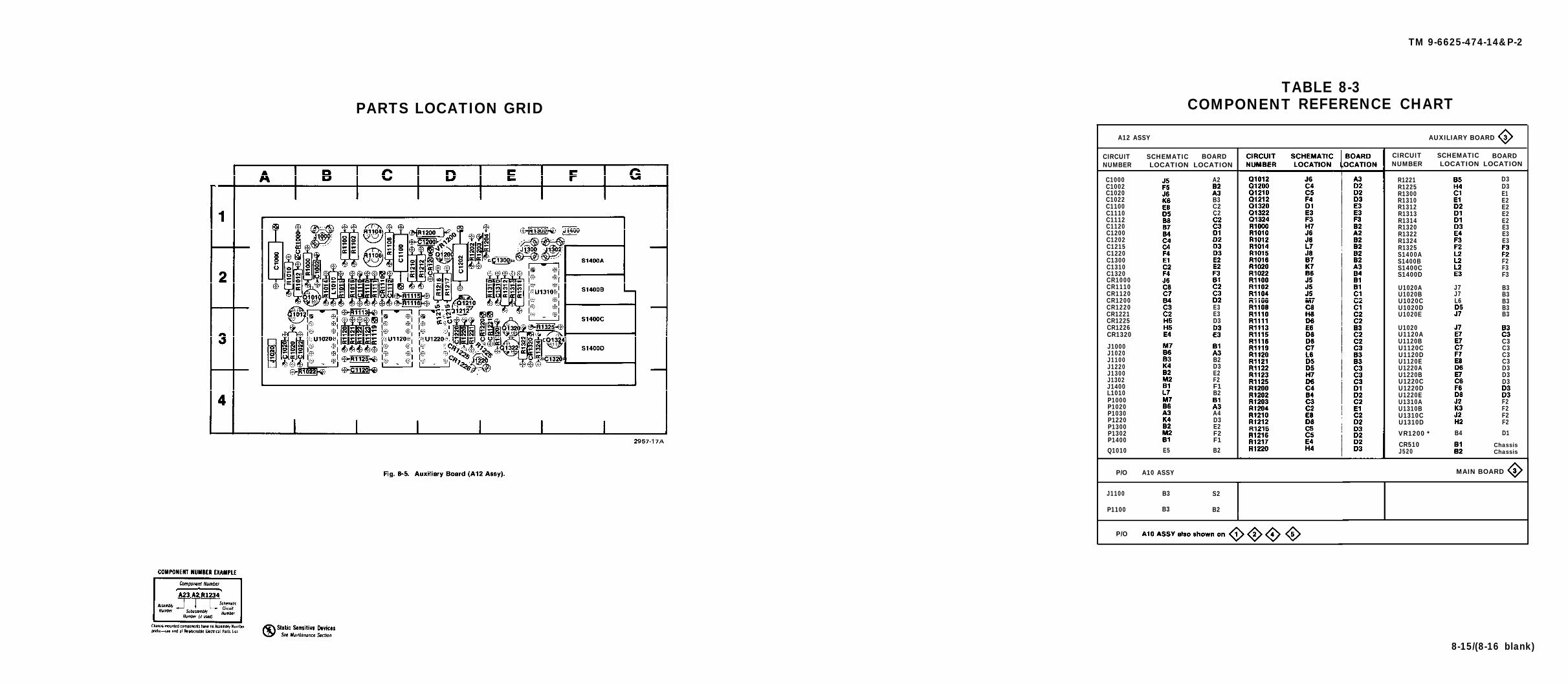
Fig. 8-5.
TM 9-6625-474-14&P-2
TABLECOMPONENT
8-3REFERENCE CHARTPARTS LOCATION GRID
A12 ASSY AUXILIARY BOARD
CIRCUIT SCHEMATIC BOARDNUMBER LOCATION LOCATION
CIRCUIT SCHEMATIC BOARDNUMBER LOCATION LOCATION
C1000C1002C1020C1022C1100C1110C1112C1120C1200C1202C1215C1220C1300C1310C1320CR1000CR1110CR1120CR1200CR1220CR1221CR1225CR1226CR1320
J1000J1020J1100J1220J1300J1302J1400L1010P1000P1020P1030P1220P1300P1302P1400Q1010
A2
B3C2C2
R1221R1225R1300R1310R1312R1313R1314R1320R1322R1324R1325S1400AS1400BS1400CS1400D
U1020AU1020BU1020CU1020DU1020E
U1020U1120AU1120BU1120CU1120DU1120EU1220AU1220BU1220CU1220DU1220EU1310AU1310BU1310CU1310D
D3D3E1E2E2E2E2E3E3E3
F2F3F3
B3B3B3B3B3
C3C3C3C3D3D3D3
F2F2F2F2
J7J7L6
E3E3D3
B2D3E2F2F1B2
A4D3E2F2F1
VR1200 * B4 D1
CR510 ChassisJ520 ChassisE5 B2
MAIN BOARDP/O A10 ASSY
J1100 B3 S2
P1100 B3 B2
P/O
8-15/(8-16 blank)
FG 501 A
TM 9-6625-474-14&P-2
8-17/(8-18 blank)
FG 501 A
TM 9-6625-474-14&P-2
TABLE 8-4COMPONENT REFERENCE CHART
P/O A10 ASSY MAIN BOARD
CIRCUIT SCHEMATIC BOARD CIRCUIT SCHEMATIC BOARDNUMBER LOCATION LOCATION NUMBER LOCATION LOCATION
C2006 H2 K1 R2012 ES J2C2007 H2 K1 R2013 F2 J1C2011 F4 R2024 J2C2013 H1 R2025 J3C2020 K2 R2026 H4C2121 K4 R2033 H5C2204 D6 R2101 D2 K2C2217 H7 R2111 ES L1C2221 F5 L3 R2113 E4 L2C2224 R2121 H3 K3C2228 R2122 H3 K3C2229 F8 L3 R2123 F3 K3C2301 H8 M1 R2124 F2 K2C2302 H8 M1 R2131 K4
R2141 KSCR2111 E4 L2 R2143 J4 L5CR2113 F5 R2201 E5 L1CR2213 R2202 L1CR2221 L3 R2203 L1CR2222 H6 L3 R2204 E6 L1
R2211 F4 L2J1204 M6 D1 R2213 F8J1651 M1 R2223 H7J1923 R2225 L3J2011 J3 R2226 L3J2021 C5 J3 R2227 F8 L2J2141 M6 KS R2228 K4
R2231 L4P1030 M6 R2233 J5P1651 M1 R2251 K4P1923 R2253 K4P2011 R2255 K4P2021 C5 J3 R2257 L6
R2301 M102011 F3 K2 R2303 H8Q2013 F4 K3 R2304 H7Q2101 D5 K2 R2335 C5 N4Q2111 F2 K2 R2351 M602113 E5 K2 R2353 KSQ2121 H4 K3 R2355 K4 M602123 H4 K302211 E4 L2 S1901A C402213 S1901B C5Q2311 S1901C J2Q2321 F6 M2 S2331B M4Q2323 H6 M3 S2331C
S2331DM4
Q2325 H6 M3 K4 MS
R2001 C6 VR2213 F7 L2R2003 D5R2004 J1 J530 M5 ChassisR2005 J1 R560A ChassisR2006 H2 R560B ChassisR2011 B1 Chassis
B2 Chassis
P/O
8-19/(8-20 blank)
FG 501 A
TM 9-6625-474-14&P-2
TABLE 8-5COMPONENT REFERENCE CHART
P/O A10 ASSY MAIN BOARD
CIRCUIT SCHEMATIC BOARD CIRCUIT SCHEMATIC BOARDNUMBER LOCATION LOCATION NUMBER LOCATION LOCATION
C1341C1451
F1111F1131
B3B5
P1030P1030P1030P1030P1030P1030P1030
0122101231Q1241Q124301245Q13310133501345
R1113R1121R1131R1133
TP1241TP1321TP1323TP1331TP1451
U1210U1230AU1230BU1230CU1230DB3
B3B4C4 VR1241 H7 C5
P/O
8-21/(8-22 blank)
TM 9-6625-474-14&P-2SECTION 9
REPLACEABLEMECHANICAL PARTS
PARTS ORDERING INFORMATION
Replacement parts are available from or through your local
Tektronix, Inc. Field Office or representative.
Changes to Tektronix instruments are sometimes made to
accommodate improved components as they become available,and to give you the benefit of the latest circuit improvementsdeveloped in our engineering department. It is therefore
important, when ordering parts, to include the followinginformation in your order: Part number, instrument type or
number, serial number, and modification number if applicable.
If a part you have ordered has been replaced with a new orimproved part, your local Tektronix, Inc. Field Office or
representative will contact you concerning any change in part
number.
Change information, if any, is located at the rear of this
manual.
SPECIAL NOTES AND SYMBOLS
X000 Part first added at this serial number
00X Part removed after this serial number
FIGURE AND INDEX NUMBERS
Items in this section are referenced by figure and index
numbers to the illustrations.
#ACTRADPTRALIGNALASSEMASSYATTENAWGBDBRKTBRSBRZBSHGCABCAPCERCHASCKTCOMPCONNCOVCPLGCRTDEGDWR
INCHNUMBER SIZEACTUATORADAPTERALIGNMENTALUMINUMASSEMBLEDASSEMBLYATTENUATORAMERICAN WIRE GAGEBOARDBRACKETBRASSBRONZEBUSHINGCABINETCAPACITORCERAMICCHASSISCIRCUITCOMPOSITIONCONNECTORCOVERCOUPLINGCATHODE RAY TUBEDEGREEDRAWER
ELCTRNELECELCTLTELEMEPLEQPTEXTFILFLEXFLHFLTRFRFSTNRFTFXDGSKTHDLHEXHEX HDHEX SOCHLCPSHLEXTHVICIDIDENTIMPLR
INDENTATION
This mechanical parts list is
SYSTEM
indented to indicate itemrelationships. Following is an example of the indentation system
used in the description column.
1 2 3 4 5 Name & Description
Assembly and/or Component
Attaching parts for Assembly and/or Component- - - * - - -
Detail Part of Assembly and/or Component
Attaching parts for Detail Part- - - * - - -
Parts of Detail PartAttaching parts for Parts of Detail Part
- - - * - - -
Attaching Parts always appear in the same indentation asthe item it mounts, while the detail parts are indented to the right.Indented items are part of, and included with, the next higher
indentation. The separation symbol ---*--- indicates the end of
attaching parts.
Attaching parts must be purchased separately, unless otherwisespecified.
ITEM NAME
In the Parts List, an Item Name is separated from the
description by a colon (:). Because of space limitations, an ItemName may sometimes appear as incomplete. For further ItemName identification, the U.S. Federal Cataloging Handbook H6-1can be utilized where possible.
ABBREVIATIONS
ELECTRONELECTRICALELECTROLYTICELEMENTELECTRICAL PARTS LISTEQUIPMENTEXTERNALFILLISTER HEADFLEXIBLEFLAT HEADFILTERFRAME or FRONTFASTENERFOOTFIXEDGASKETHANOLEHEXAGONHEXAGONAL HEADHEXAGONAL SOCKETHELICAL COMPRESSIONHELICAL EXTENSIONHIGH VOLTAGEINTEGRATED CIRCUITINSIDE DIAMETERIDENTIFICATIONIMPELLER
ININCANDINSULINTLLPHLDRMACHMECHMTGNIPNON WIREOBDODOVHPH BRZPLPLSTCPNPNHPWRRCPTRESRGDRLFRTNRSCHSCOPESCR
INCHINCANDESCENTINSULATORINTERNALLAMPHOLDERMACHINEMECHANICALMOUNTINGNIPPLENOT WIRE wOUNDORDER BY DESCRIPTIONOUTSIDE DIAMETEROVAL HEADPHOSPHOR BRONZEPLAIN or PLATEPLASTICPART NUMBERPAN HEADPOWERRECEPTACLERESISTORRIGIDRELIEFRETAINERSOCKET HEADOSCILLOSCOPESCREW
SE SINGLE ENDSECT SECTIONSEMICOND SEMICONDUCTORSHLDSHLORSKTSLSLFLKGSLVGSPRSQSSTSTLSWTTERMTHDTHKTNSNTPGTRHVVARW/WSHRXFMRXSTR
SHIELDSHOULDEREDSOCKETSLIDESELF-LOCKINGSLEEVINGSPRINGSQUARESTAINLESS STEELSTEELSWITCHTUBETERMINALTHREADTHICKTENSIONTAPPINGTRUSS HEADVOLTAGEVARIABLEWITHWASHERTRANSFORMERTRANSISTOR
9-1
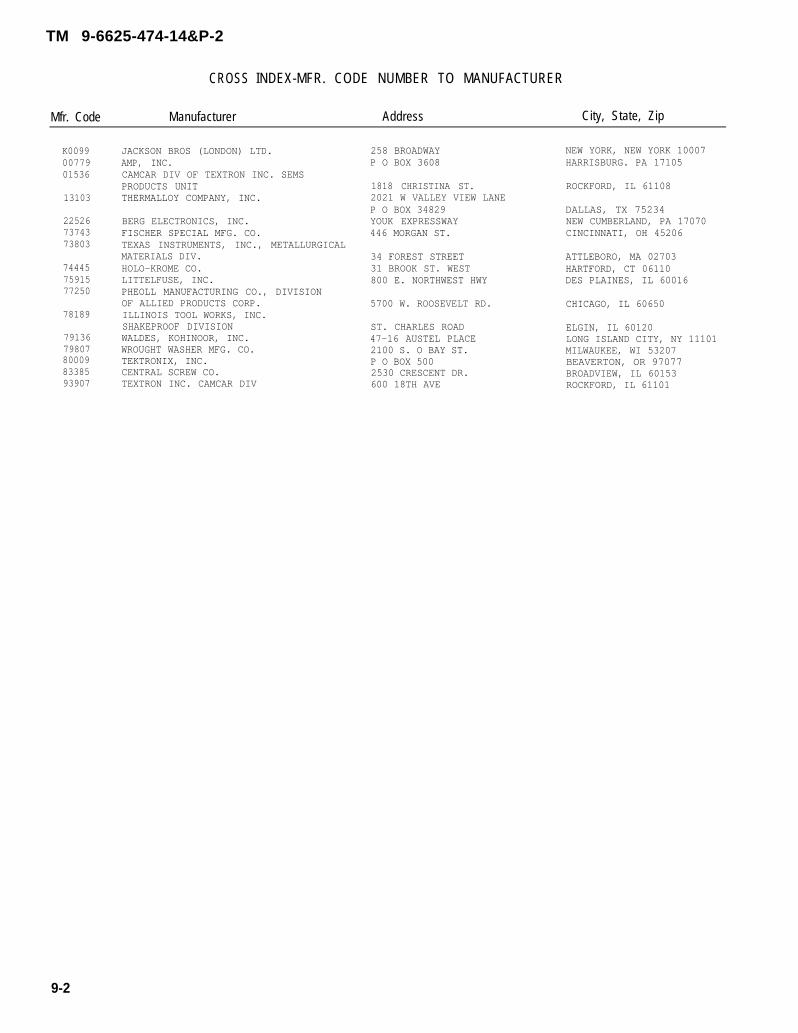
TM 9-6625-474-14&P-2
CROSS
Mfr. Code Manufacturer
INDEX-MFR. CODE NUMBER TO MANUFACTURER
Address City, State, Zip
K00990077901536
13103
225267374373803
744457591577250
78189
7913679807800098338593907
9-2
JACKSON BROS (LONDON) LTD.AMP, INC.CAMCAR DIV OF TEXTRON INC. SEMSPRODUCTS UNITTHERMALLOY COMPANY, INC.
BERG ELECTRONICS, INC.FISCHER SPECIAL MFG. CO.TEXAS INSTRUMENTS, INC., METALLURGICALMATERIALS DIV.HOLO-KROME CO.LITTELFUSE, INC.PHEOLL MANUFACTURING CO., DIVISIONOF ALLIED PRODUCTS CORP.ILLINOIS TOOL WORKS, INC.SHAKEPROOF DIVISIONWALDES, KOHINOOR, INC.WROUGHT WASHER MFG. CO.TEKTRONIX, INC.CENTRAL SCREW CO.TEXTRON INC. CAMCAR DIV
258 BROADWAYP O BOX 3608
1818 CHRISTINA ST.2021 W VALLEY VIEW LANEP O BOX 34829YOUK EXPRESSWAY446 MORGAN ST.
34 FOREST STREET31 BROOK ST. WEST800 E. NORTHWEST HWY
5700 W. ROOSEVELT RD.
ST. CHARLES ROAD47-16 AUSTEL PLACE2100 S. O BAY ST.P O BOX 5002530 CRESCENT DR.600 18TH AVE
NEW YORK, NEW YORK 10007HARRISBURG. PA 17105
ROCKFORD, IL 61108
DALLAS, TX 75234NEW CUMBERLAND, PA 17070CINCINNATI, OH 45206
ATTLEBORO, MA 02703HARTFORD, CT 06110DES PLAINES, IL 60016
CHICAGO, IL 60650
ELGIN, IL 60120LONG ISLAND CITY, NY 11101MILWAUKEE, WI 53207BEAVERTON, OR 97077BROADVIEW, IL 60153ROCKFORD, IL 61101
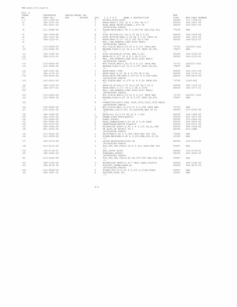
TM9-6625-474-14&P-2
FIG. &INDEX TEKTRONIX SERIAL/MODEL NO. MFRNO. PART NO. EFF DSCONT QTY 1 2 3 4 5 NAME & DESCRIPTION CODE MFR PART NUMBER1-1 337-1399-04 2 SHIELD,ELEC:SIDE 80009 337-1399-04-2 366-1837-00 1 KNOB:GRAY,0.252 ID X 1.041 OD,0.7 80009 366-1837-00-3 354-0557-05 1 RING,KNOB SKIRT:CLEAR,1.875 OD 80009 354-0557-05
(ATTACHING PARTS)-4 211-0088-00 2 SCREW,MACHINE:2-56 X 0.281"82 DEG,FLH STL 77250 OBD
-*--5 366-1559-00 8 PUSH BUTTON:SIL GY,0.18 SQ X 0.43 80009 366-1559-00-6 366-1512-00 3 PUSH BUTTON:GRAY,0.18 SQ X 0.83 INCH LG 80009 366-1512-00-7 366-1023-07 1 KNOB:GRAY,0.127 ID,0.392 OD,0.466 80009 366-1023-07-8 1 RES.,VAR,NONWIR:(SEE R550 REPL)
(ATTACHING PARTS)-9 210-0583-00 1 NUT,PLAIN,HEX:0.25-32 X 0.312 INCH,BRS 73743 2X20317-402-10 210-0940-00 1 WASHER,FLAT:0.25 ID X 0.375 INCH OD,STL 79807 OBD
-*--11 366-1059-03 1 PUSH BUTTON:GY W/YEL BND,0.227 80009 366-1059-03-12 366-1215-01 1 KNOB:GY,0.127 ID X 0.5 OD,0.531 80009 366-1215-01-13 1 RES.,VAR,NONWIR:(SEE R530,S500 REPL)
(ATTACHING PARTS)-14 210-0583-00 1 NUT,PLAIN,HEX:0.25-32 X 0.312 INCH,BRS 73743 2X20317-402-15 210-0940-00 1 WASHER,FLAT:0.25 ID X 0.375 INCH OD,STL 79807 OBD
-*--16 366-1031-06 1 KNOB:GRAY--VAR 80009 366-1031-06-17 366-1170-03 1 KNOB:GRAY,0.25 ID X 0.706 OD,0.6H 80009 366-1170-03-18 358-0029-00 1 BSHG,MACH.THD:HEX,0.375-32 X 0.438"LONG 80009 358-0029-00
(ATTACHING PARTS)-19 210-0413-00 1 NUT,PLAIN,HEX.:0.375-32 X 0.50 INCH,STL 73743 3145-402
-*--20 366-1319-03 1 KNOB:GY,W/IDX,0.79 ID,0.28 OD,0.32 H 80009 366-1319-03-21 366-1077-01 1 KNOB:GRAY,0.127 ID,0.5 OD,0.531H 80009 366-1077-01-22 1 RES.,VAR,NONWIR:(SEE R560,S510 REPL)
(ATTACHING PARTS)-23 210-0583-00 1 NUT,PLAIN,HEX:0.25-32 X 0.312 INCH BRS 73743 2X20317-402-24 210-0940-00 1 WASHER,FLAT:0.25 ID X 0.375 INCH OD,STL 79807 OBD
-*--25 4 CONNECTOR,RCPT:(SEE J500,J510,J520,J530 REPL)
(ATTACHING PARTS)-26 220-0495-00 1 NUT,PLAIN,HEX.:0.375-32 X 0.438 INCH BRS 73743 OBD-27 210-0255-00 4 TERMINAL,LUG:0.391 ID,LOCKING,BRS CD PL 80009 210-0255-00
-*--28 366-1690-00 1 KNOB:SIL GY,0.53 X0.23 X 1.059 80009 366-1690-00-29 426-1072-00 11 FRAME,PUSH BTN:PLASTIC 80009 426-1072-00-30 333-2684-00 1 PANEL,FRONT: 80009 333-2684-00-31 200-0935-00 2 BASE,LAMPHOLDER:0.29 OD X 0.19 CASE 80009 200-0935-00-32 352-0157-00 2 LAMPHOLDER:WHITE PLASTIC 80009 352-0157-00-33 384-1406-00 1 EXTENSION SHAFT:6.64 L X 0.125 OD,AL,CRM 80009 384-1406-00-34 401-0206-00 1 GR ASSY,SP RDCN:6 TO 1 K0099 4511/DAF
(ATTACHING PARTS)-35 213-0022-00 1 SETSCREW:4-40 X 0.188 INCH,HEX SOC STL 74445 OBD-36 211-0008-00 2 SCREW,MACHINE:4-40 X 0.250,PNH,STL,CD PL 83385 OBD
-*--37 105-0719-00 1 LATCH,RETAINING:PLUG-IN 80009 105-0719-00
(ATTACHING PARTS)-38 213-0113-00 1 SCR,TPG,THD FOR:2-32 X 0.312 INCH,PNH STL 93907 OBD
-*--39 105-0718-01 1 BAR,LATCH RLSE: 80009 105-0718-01-40 386-4469-00 1 SUBPANEL,FRONT: 80009 386-4469-00
(ATTACHING PARTS)-41 213-0229-00 4 SCR,TPG,THD FOR:6-20 X0.375"100 GED,FLH STL 93907 OBD
-*--42 384-1292-00 3 EXTENSION SHAFT:2.417 INCH LONG,PLASTIC 80009 384-1292-00-43 386-4278-00 1 SUPPORT,FRAME:REAR,AL 80009 386-4278-00
(ATTACHING PARTS)-44 213-0868-00 2 SCREW,TPG,TF:6-32 X 0.375 L,FILM,STEEL 93907 OBD-45 386-3657-01 2 SUPPORT,PLUG IN: 93907 OBD
-*-
9-3
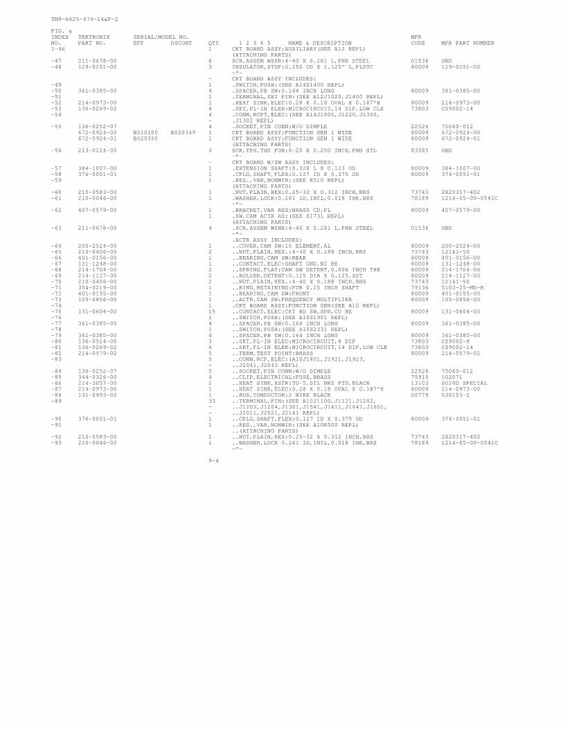
TM9-6625-474-14&P-2
FIG. &INDEX TEKTRONIX SERIAL/MODEL NO. MFRNO. PART NO. EFF DSCONT QTY 1 2 3 4 5 NAME & DESCRIPTION CODE MFR PART NUMBER1-46 1 CKT BOARD ASSY:AUXILIARY(SEE A12 REPL)
(ATTACHING PARTS)-47 211-0678-00 6 SCR,ASSEM WSHR:4-40 X 0.281 L,PNH STEEL 01536 OBD-48 129-0251-00 3 INSULATOR,STDF:O.250 OD X 1.125" L,PLSTC 80009 129-0251-00
-*-- CKT BOARD ASSY INCLUDES:
-49 1 .SWITCH,PUSH:(SEE A14S1400 REPL)-50 361-0385-00 4 .SPACER,PB SW:0.164 INCH LONG 80009 361-0385-00-51 1 .TERMINAL,SET PIN:(SEE A12J1020,J1400 REPL)-52 214-0973-00 1 .HEAT SINK,ELEC:0.28 X 0.18 OVAL X 0.187"H 80009 214-0973-00-53 136-0269-02 4 .SKT,PL-IN ELEK:MICROCIRCUIT,14 DIP,LOW CLE 73803 CS9002-14-54 4 .CONN,RCPT,ELEC:(SEE A14J1000,J1220,J1300,
- .J1302 REPL)-55 136-0252-07 4 .SOCKET,PIN CONN:W/O DIMPLE 22526 75060-012
672-0924-00 B010100 B020349 1 CKT BOARD ASSY:FUNCTION GEN 1 WIDE 80009 672-0924-00672-0924-01 B020350 1 CKT BOARD ASSY:FUNCTION GEN 1 WIDE 80009 672-0924-01
(ATTACHING PARTS)-56 213-0124-00 4 SCR,TPG,THD FOR:6-20 X 0.250 INCH,PNH STL 83385 OBD
-*-- CKT BOARD W/SW ASSY INCLUDES:
-57 384-1007-00 1 .EXTENSION SHAFT:8.328 L X 0.123 OD 80009 384-1007-00-58 376-0051-01 1 .CPLG,SHAFT,FLEX:0.127 ID X 0.375 OD 80009 376-0051-01-59 1 .RES.,VAR,NONWIR:(SEE R510 REPL)
(ATTACHING PARTS)-60 210-0583-00 1 .NUT,PLAIN,HEX:0.25-32 X 0.312 INCH,BRS 73743 2X20317-402-61 210-0046-00 1 .WASHER,LOCK:0.261 ID,INTL,0.018 THK,BRS 78189 1214-05-00-0541C
-*--62 407-0579-00 1 .BRACKET,VAR RES:BRASS CD,PL 80009 407-0579-00
1 .SW,CAM ACTR AS:(SEE S1731 REPL)(ATTACHING PARTS)
-63 211-0678-00 4 .SCR,ASSEM WSHR:4-40 X 0.281 L,PNH STEEL 01536 OBD-*-.ACTR ASSY INCLUDES:
-64 200-2524-00 1 ..COVER,CAM SW:15 ELEMENT,AL 80009 200-2524-00-65 210-0406-00 2 ..NUT,PLAIN,HEX.:4-40 X 0.188 INCH,BRS 73743 12161-50-66 401-0156-00 1 ..BEARING,CAM SW:REAR 80009 401-0156-00-67 131-1248-00 1 ..CONTACT,ELEC:SHAFT GND,NI BE 80009 131-1248-00-68 214-1704-00 2 ..SPRING,FLAT:CAM SW DETENT,0.006 INCH THK 80009 214-1704-00-69 214-1127-00 2 ..ROLLER,DETENT:0.125 DIA X 0.125,SST 80009 214-1127-00-70 210-0406-00 2 ..NUT,PLAIN,HEX.:4-40 X 0.188 INCH,BRS 73743 12161-50-71 354-0219-00 1 ..RING,RETAINING:FOR 0.25 INCH SHAFT 79136 5103-25-MD-R-72 401-0155-00 1 ..BEARING,CAM SW:FRONT 80009 401-0155-00-73 105-0856-00 1 ..ACTR,CAM SW:FREQUENCY MULTIPLIER 80009 105-0856-00-74 1 .CKT BOARD ASSY:FUNCTION GEN(SEE A10 REPL)-75 131-0604-00 15 ..CONTACT,ELEC:CKT BD SW,SPR,CU BE 80009 131-0604-00-76 1 ..SWITCH,PUSH:(SEE A10S1901 REPL)-77 361-0385-00 4 ..SPACER,PB SW:0.164 INCH LONG 80009 361-0385-00-78 1 ..SWITCH,PUSH:(SEE A10S2331 REPL)-79 361-0385-00 4 ..SPACER,PB SW:0.164 INCH LONG 80009 361-0385-00-80 136-0514-00 3 ..SKT,PL-IN ELEC:MICROCIRCUIT,8 DIP 73803 CS9002-8-81 136-0269-02 6 ..SKT,PL-IN ELEK:MICROCIRCUIT,14 DIP,LOW CLE 73803 CS9002-14-82 214-0579-02 5 ..TERM,TEST POINT:BRASS 80009 214-0579-02-83 5 ..CONN,RCP,ELEC:(A10J1801,J1921,J1923,
- ..J2041,J2043 REPL)-84 136-0252-07 5 ..SOCKET,PIN CONN:W/O DIMPLE 22526 75060-012-85 344-0326-00 4 ..CLIP,ELECTRICAL:FUSE,BRASS 75915 102071-86 214-3057-00 2 ..HEAT SINK,XSTR:TO-5,SIL BRZ PTD,BLACK 13103 6024U SPECIAL-87 214-0973-00 1 ..HEAT SINK,ELEC:0.28 X 0.18 OVAL X 0.187"H 80009 214-0973-00-88 131-0993-00 1 ..BUS,CONDUCTOR:2 WIRE BLACK 00779 530153-2-89 33 ..TERMINAL,PIN:(SEE A10J1100,J1121,J1202,
- ..J1203,J1204,J1301,J1541,J1611,J1641,J1651,- ..J2011,J2021,J2141 REPL)
-90 376-0051-01 1 ..CPLG,SHAFT,FLEX:0.127 ID X 0.375 OD 80009 376-0051-01-91 1 ..RES.,VAR,NONWIR:(SEE A10R500 REPL)
..(ATTACHING PARTS)-92 210-0583-00 1 ..NUT,PLAIN,HEX:0.25-32 X 0.312 INCH,BRS 73743 2X20317-402-93 210-0046-00 1 ..WASHER,LOCK 0.261 ID,INTL,0.018 THK,BRS 78189 1214-05-00-0541C
-*-
9-4

TM9-6625-474-14&P-2
FIG.&INDEX TEKTRONIX SERIAL/MODEL NO. MFRNO. PART NO. EFF DSCONT QTY 1 2 3 4 5 NAME & DESCRIPTION CODE MFR PART NUMBER1-94 386-4470-00 1 ..PLATE,RES MTG:BRASS 80009 386-4470-00-95 214-1061-00 1 SPRING,GROUND:FLAT 80009 214-1061-00-96 426-0724-19 1 FR SECT,PLUG-IN:BOTTOM 80009 426-0724-19-97 351-0612-00 2 GUIDE,CKT BOARD:NYLON,1.0 L 80009 351-0612-00-98 426-0725-05 1 FR SECT,PLUG-IN:TOP 80009 426-0725-05
9-5
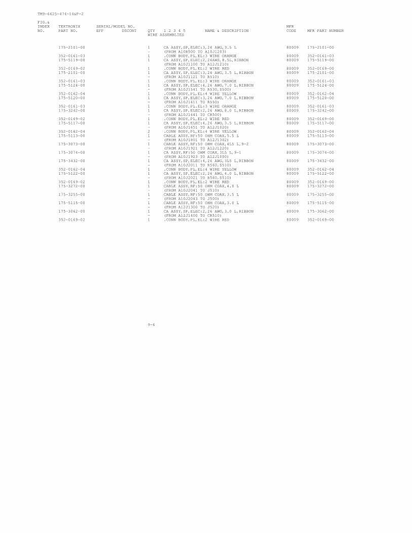
TM9-6625-474-14&P-2
FIG.&INDEX TEKTRONIX SERIAL/MODEL NO. MFRNO. PART NO. EFF DSCONT QTY 1 2 3 4 5 NAME & DESCRIPTION CODE MFR PART NUMBER
WIRE ASSEMBLIES
175-2101-00 1 CA ASSY,SP,ELEC:3,26 AWG,3.5 L 80009 175-2101-00- (FROM A10R500 TO A10J1203)
352-0161-03 1 .CONN BODY,PL,EL:3 WIRE ORANGE 80009 352-0161-03175-5119-00 1 CA ASSY,SP,ELEC:2,26AWS,8.5L,RIBBON 80009 175-5119-00
(FROM A10J1100 TO A12J1210)352-0169-02 1 .CONN BODY,PL,EL:2 WIRE RED 80009 352-0169-00175-2101-00 1 CA ASSY,SP,ELEC:3,26 AWG,3.5 L,RIBBON 80009 175-2101-00
- (FROM A10J1121 TO R510)352-0161-03 1 .CONN BODY,PL,EL:3 WIRE ORANGE 80009 352-0161-03175-5124-00 1 CA ASSY,SP,ELEC:4,26 AWG,7.0 L,RIBBON 80009 175-5124-00
- (FROM A10J1541 TO R530,S500)352-0162-04 1 .CONN BODY,PL,EL:4 WIRE YELLOW 80009 352-0162-04175-5120-00 1 CA ASSY,SP,ELEC:3,26 AWG,7.0 L,RIBBON 80009 175-5120-00
- (FROM A10J1611 TO R550)352-0161-03 1 .CONN BODY,PL.EL:3 WIRE ORANGE 80009 352-0161-03175-3242-00 1 CA ASSY,SP,ELEC:2,26 AWG,8.0 L,RIBBON 80009 175-3242-00
- (FROM A10J1641 TO CR500)352-0169-02 1 .CONN BODY,PL,EL:2 WIRE RED 80009 352-0169-00175-5117-00 1 CA ASSY,SP,ELEC:4,26 AWG,3.5 L,RIBBON 80009 175-5117-00
- (FROM A10J1651 TO A12J1020)352-0162-04 2 .CONN BODY,PL,EL:4 WIRE YELLOW 80009 352-0162-04175-5113-00 1 CABLE ASSY,RF:50 OHM COAX,5.5 L 80009 175-5113-00
- (FROM A10J1801 TO A12J1302)175-3073-00 1 CABLE ASSY,RF:50 OHM COAX,4L5 L,9-2 80009 175-3073-00
- (FROM A10J1921 TO A12J1220)175-3074-00 1 CA ASSY,RF:50 OHM COAX,3L5 L,9-1 80009 175-3074-00
- (FROM A10J1923 TO A12J1000)175-3432-00 1 CA ASSY,SP,ELEC:4,26 AWG,3L5 L,RIBBON 80009 175-3432-00
- (FROM A10J2011 TO R560,S510)352-0162-04 1 .CONN BODY,PL,EL:4 WIRE YELLOW 80009 352-0162-04175-5122-00 1 CA ASSY,SP,ELEC:2,26 AWG,4.0 L,RIBBON 80009 175-5122-00
- (FROM A10J2021 TO R560,S510)352-0169-02 1 .CONN BODY,PL,EL:2 WIRE RED 80009 352-0169-00175-3272-00 1 CABLE ASSY,RF:50 OHM COAX,4.0 L 80009 175-3272-00
- (FROM A10J2041 TO J510)175-3255-00 1 CABLE ASSY,RF:50 OHM COAX,3.5 L 80009 175-3255-00
- (FROM A10J2043 TO J500)175-5115-00 1 CABLE ASSY,RF:50 OHM COAX,3.0 L 80009 175-5115-00
- (FROM A12J1300 TO J520)175-3062-00 1 CA ASSY,SP,ELEC:2,26 AWG,3.0 L,RIBBON 80009 175-3062-00
- (FROM A12J1400 TO CR510)352-0169-02 1 .CONN BODY,PL,EL:2 WIRE RED 80009 352-0169-00
9-6
TM 9-6625-474-14&P-2
APPENDIX A
REFERENCES
DA PAM 310-4
DA PAM 310-7
FM 21-11
AR 385-40
AR 750-1
TB 750-25-1
TM 38-750
TM 750-244-2
Index of Technical Manuals, Technical Bulletins, Supply Manuals(Types 7, 8, and 9), Supply Bulletins, and Lubrication Orders
Index of US Army Equipment Modification Work Orders
First Aid for Soldiers
Accident Reporting and Records
Army Materiel Maintenance Concept and Policies
Maintenance Supplies and Equipment: Army Metrology and Calibration System
The Army Maintenance Management System (TAMMS)
Procedures for Destruction of Electronics Materiel to Prevent Enemy Use
A-1/(A-2 blank)
TM 9-6625-474-14&P-2
APPENDIX B
MAINTENANCE ALLOCATION CHART
Section 1. INTRODUCTION
B-1. GENERAL.
a. This section provides a generaI explanation of all maintenance and repair functions authorized at variousmaintenance categories.
b. The Maintenance Allocation Chart (MAC) in Section II designates overall authority and responsibility for theperformance of maintenance functions on the identified end items or component. The application of themaintenance functions to the end item or component will be consistent with the capacities and capabilities of thedesignated maintenance categories.
c. Section III lists the tools and test equipment (both special and common) required for each maintenancefunction as referenced from Section II.
d. Section IV contains supplemental instructions and explanatory notes for a particular maintenancefunction.
B-2. MAINTENANCE FUNCTIONS. Maintenance Functions will be limited to and defined as follows:
a. Inspect. To determine the serviceability of an item by comparing its physical, mechanical, and/or electricalcharacteristics with established standards through examination (e.g., by sight, sound, or feel).
b. Test. To verify serviceability by measuring the mechanical, pneumatic, hydraulic, electrical characteristicsof an item and comparing those characteristics with prescribed standards.
c. Service. Operations required periodically to keep an item in proper operating condition, i.e., to clean(includes decontaminate, when required), to preserve, to drain, to paint, or to replenish fuel, lubricants, chemicalfluids, or gases.
d. Adjust. To maintain or regulate, within prescribed limits, by bringing into proper or exact position, or bysetting the operating characteristics to specified parameters.
e. Aline. To adjust specified variable elements of an item to bring about optimum or desired performance.
f. Calibrate. To determine and cause corrections to be made or to be adjusted on instruments or test,measuring, and diagnostic equipment used in precision measurement. Consists of comparisons of twoinstruments, one of which is a certified standard of known accuracy, to detect and adjust any discrepancy in theaccuracy of the instrument being compared.
g. Removal/Install. To remove and install the same item when required to perform service or othermaintenance functions. Install may be the act of emplacing, seating, or fixing into position a spare, repair part, ormodule (component or assembly) in a manner to allow the proper functioning of an equipment or system.
h. Replace. To remove an unserviceable item and install a serviceable counterpart in its place.
i. Repair. The application of maintenance services 1, including fault location/troubleshooting 2, removal/installation, and disassembly/assembly 3, procedures, and maintenance actions 4, to identify troubles andrestore serviceability to an item by correcting specific damage, fault, malfunction, or failure in a part,subassembly, module (component or assembly), end item, or system.
B-1
TM 9-6625-474-14&P-2
j. Overhaul. That maintenance effort (service/action) prescribed to restore an item to a completelyserviceable-operational condition as required by maintenance standard in appropriate technical publications.Overhaul is normally the highest degree of maintenance performed by the Army. Overhaul does not normally returnan item to like-new condition.
k. Rebuild. Consists of those services/actions necessary for the restoration of unserviceable equipment to alike-new condition in accordance with original manufacturing standards. Rebuild is the highest degree of materialmaintenance applied to army equipment and is normally reserved for the depot category of maintenance. Therebuild operation includes the act of returning to zero those age measurements (hours/mile, etc. ) considered inclassifying army equipment/components.
(1) Services - inspect, test, service, adjust, aline, calibrate, and/or replace.
(2) Fault locate/troubleshoot - the process of investigating and detecting the cause of equipmentmalfunctioning; the act of isolating a fault within a system or Unit Under Test (UUT).
(3) Disassembly/assembly - encompasses the step-by-step taking apart (or breakdown) of a repairableassembly (group numbered item) to the level of its least componency identified as maintenance significant (i.e.,assigned an SMR code) for the category of maintenance under consideration.
(4) Actions - welding, griding, riveting, straightening, facing, remachinery, and/or resurfacing.
B-3. EXPLANATION OF COLUMNS IN THE MAC, SECTION II.
a. Column 1, Group Number. Column 1 lists group numbers, the purpose of which is to identify maintenancesignificant components, assemblies, subassemblies, and modules with the next higher assembly.
b. Column 2, Component/Assembly. Column 2 contains the names of components, assemblies, subassemb-lies, and modules for which maintenance is authorized.
c. Column 3, Maintenance Function. Column 3 lists the functions to be performed on the item listed inColumn 2 (for detailed explanation of these functions, see paragraph B-2).
d. Column 4, Maintenance Category. Column 4 specifies, by the listing of a work time figure in theappropriate subcolumn(s), the category of maintenance authorized to perform the function listed in Column 3.This figure represents the active time required to perform that maintenance function at the indicated category ofmaintenance. If the number of complexity of the tasks within the listed maintenance function vary at differentmaintenance categories, appropriate work time figures will be shown for each category. The work time figurerepresents the average time required to restore an item (assembly, subassembly, component, module, end item,or system) to a serviceable condition under typical field operating conditions. This time includes preparation time(including any necessary disassembly/assembly time), troubleshooting/fault location time, and quality assurance/quality control time in addition to the time required to perform the specific tasks identified for the maintenancefunctions authorized in the maintenance allocation chart. The symbol designations for the various maintenancecategories are as follows:
COFHLD
5
B-2
Operator or CrewOrganizational Maintenance
Direct Support MaintenanceGeneral Support Maintenance
Specialized Repair Activity (SRA)5
Depot Maintenance
This maintenance category is not included in Section II, column (4) of the Maintenance Allocation Chart. To identify functionsto this category of maintenance, enter a work time figure in the “H” column of Section II, column (4), and use an associatedreference code in the Remarks column (6). Key the code to Section IV, Remarks, and explain the SRA complete repair
application there. The explanatory remark(s) shall reference the specific Repair Parts and Special Tools LIST (RPSTL) TM whichcontains additional SRA criteria and the authorized spare/repair parts.
TM 9-6625-474-14&P-2
e. Column 5, Tools and Test Equipment. Column 5 specifies, by code, those common tools sets (notindividual tools) and special tools, TMDE, and support equipment required to perform the designated function,
f. Column 6, Remarks. This column shall, when applicable, contain a letter code, in alphabetic order, whichshall be keyed to the remarks contained in Section IV.
B-4. EXPLANATION OF COLUMNS IN TOOL AND TEST EQUIPMENT REQUIREMENTS, SECTION III.
a. Colunm 1, Reference Code. The tool and test equipment reference code correlates with a code used in theMAC, Section III, Column 5.
b. Column 2, Maintenance Category. The lowest category of maintenance authorized to use the tool or testequipment.
c. Column 3,
d. Column 4,
e. Column 5,
Nomenclature. Name or identification of the tool or test equipment.
National Stock Number. The National Stock Number of the tool or test equipment.
Tool Number. The manufacturer’s part number
B-5. EXPLANATION OF COLUMNS IN REMARKS, SECTION IV.
a. Column 1, Reference Code. The code recorded in Column 6, Section II.
b. Column 2, Remarks. This column lists information pertinent to the maintenance function being performedas indicated in the MAC, Section II.
B-3
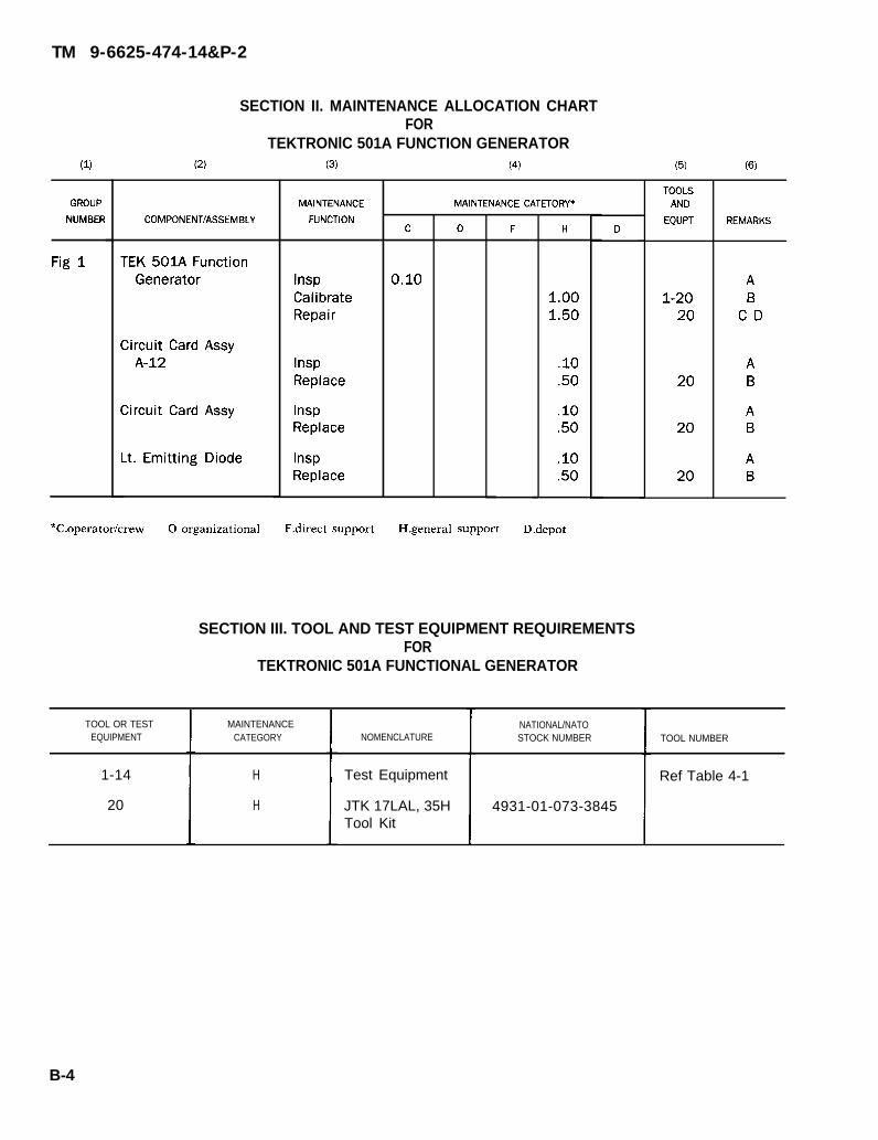
TM 9-6625-474-14&P-2
(1) (2)
GROUP
NUMBER
Fig 1
SECTION II. MAINTENANCE ALLOCATION CHARTFOR
TEKTRONlC 501A FUNCTION GENERATOR
COMPONENT/ASSEMBLY
TEK 50U FunctionGenerator
Circuit Card AssyA-12
Circuit Card Assy
Lt. Emitting Diode
(3) (4)
MAINTENANCE
FUNCTION
InspCalibrateRepair
InspReplace
InspReplace
InspReplace
*C.operator/crew O. Organizational F.direct support
c
0.10
MAINTENANCE CATETORY*
o F H
1.001.50
.10
.50
.10
.50
.10
.50
H.general support D.depot
D
(5) (6)
TOOLSAND
EQUPT
1-2020
20
20
20
REMARKS
AB
CD
AB
AB
AB
SECTION III. TOOL AND TEST EQUIPMENT REQUIREMENTSFOR
TEKTRONIC 501A FUNCTIONAL GENERATOR
TOOL OR TEST MAINTENANCE NATIONAL/NATOEQUIPMENT CATEGORY NOMENCLATURE STOCK NUMBER TOOL NUMBER
1-14 H Test Equipment Ref Table 4-1
20 H JTK 17LAL, 35H 4931-01-073-3845Tool Kit
B-4
TM 9-6625-474-14&P-2
REFERENCECODE
A
B
C
D
SECTION IV. REMARKS
REMARKS
Organizational maintenance will be accomplished by the organizationowning and using the equipment.
All special tools and test equipment are called out in Table 4-1.
Supply of parts will be through normal supply channels.
A recommended repair parts list will be published as part of this manual.Parts that have NSN’S assigned will be requisitioned separately andwill not be part of this kit.
B-5/(B-6 blank)

TM 9-6625-474-14&P-2APPENDIX C
RECOMMENDED SPARE PARTS LISTFORTEKTRONIX 501A FUNCTIONAL GENERATOR
ITEM TEKTRONIXNO. PART NO. ITEM NAME REC. QTY
1 150-1029-00 LT EMITTING DIO 1
2 150-1033-00 LT EMITTING DIO 1
3 670-6694-02 CIRCUIT BOARD ASSY 1
4 670-6697-05 CIRCUIT BOARD ASSY 1
C-1/(C-2 BLANK)
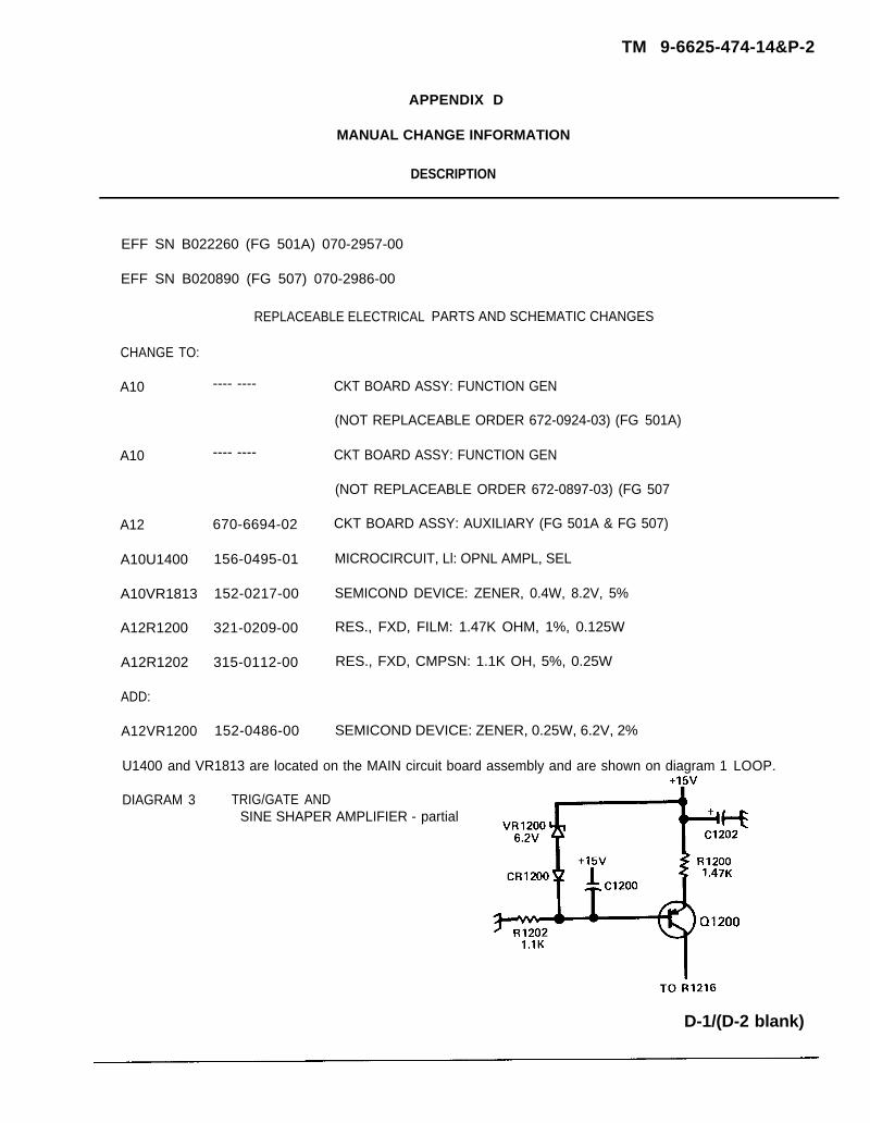
TM 9-6625-474-14&P-2
APPENDIX D
MANUAL CHANGE INFORMATION
DESCRIPTION
EFF SN B022260 (FG 501A) 070-2957-00
EFF SN B020890 (FG 507) 070-2986-00
REPLACEABLE ELECTRICAL
CHANGE TO:
A10
A10
A12
A10U1400
A10VR1813
A12R1200
A12R1202
ADD:
A12VR1200
---- ----
---- ----
670-6694-02
156-0495-01
152-0217-00
321-0209-00
315-0112-00
152-0486-00
PARTS AND SCHEMATIC CHANGES
CKT BOARD ASSY: FUNCTION GEN
(NOT REPLACEABLE ORDER 672-0924-03) (FG 501A)
CKT BOARD ASSY: FUNCTION GEN
(NOT REPLACEABLE ORDER 672-0897-03) (FG 507
CKT BOARD ASSY: AUXILIARY (FG 501A & FG 507)
MICROCIRCUIT, Ll: OPNL AMPL, SEL
SEMICOND DEVICE: ZENER, 0.4W, 8.2V, 5%
RES., FXD, FILM: 1.47K OHM, 1%, 0.125W
RES., FXD, CMPSN: 1.1K OH, 5%, 0.25W
SEMICOND DEVICE: ZENER, 0.25W, 6.2V, 2%
U1400 and VR1813 are located on the MAIN circuit board assembly and are shown on diagram 1 LOOP.
DIAGRAM 3 TRIG/GATE ANDSINE SHAPER AMPLIFIER - partial
D-1/(D-2 blank)

By Order of the Secretary of the Army:
Official:
DONALD J. DELANDROBrigadier General, United States
The Adjutant General
Distribution:
JOHN A. WICKHAM, JR.General, United States Army
Chief of Staff
Army
To be distributed in accordance with DA Form 12-37, Operator, Organizational,DS and GS Maintenance requirements for Bradley Fighting Vehicle TOW Subsystem.
THE METRIC SYSTEM AND EQUIVALENTS

PIN: 056817-000
Copyright © 2022 FDOKUMEN

