


Bahasa
Halaman
Hukum

Registered charity number: 207890
www.rsc.org/MaterialsA
As featured in:
See Kuan Sun, Wallace W. H. Wong, David J. Jones et al.,
J. Mater. Chem. A, 2014, 2, 9048.
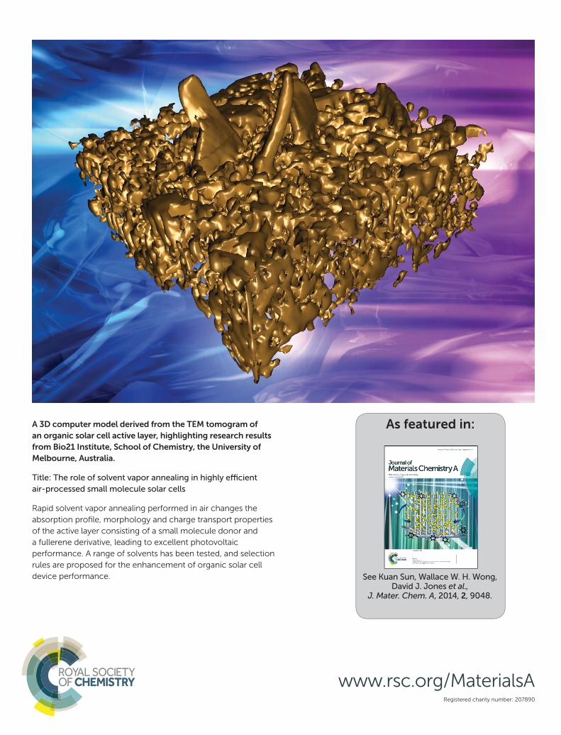
A 3D computer model derived from the TEM tomogram of
an organic solar cell active layer, highlighting research results
from Bio21 Institute, School of Chemistry, the University of
Melbourne, Australia.
Title: The role of solvent vapor annealing in highly effi cient
air-processed small molecule solar cells
Rapid solvent vapor annealing performed in air changes the
absorption profi le, morphology and charge transport properties
of the active layer consisting of a small molecule donor and
a fullerene derivative, leading to excellent photovoltaic
performance. A range of solvents has been tested, and selection
rules are proposed for the enhancement of organic solar cell
device performance.
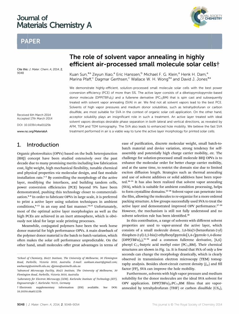
Journal ofMaterials Chemistry A
PAPER
aSchool of Chemistry, Bio21 Institute, The
Road, Parkville, Victoria 3010, Australi
[email protected]; djjones@unimebAdvanced Microscopy Facility, Bio21 Inst
Flemington Road, Parkville, Victoria 3010, AcLaboratory for Electron Microscopy (LEM),
Engesserstraße 7, Karlsruhe 76131, German
† Electronic supplementary informa10.1039/c4ta01125b
Cite this: J. Mater. Chem. A, 2014, 2,9048
Received 6th March 2014Accepted 17th March 2014
DOI: 10.1039/c4ta01125b
www.rsc.org/MaterialsA
9048 | J. Mater. Chem. A, 2014, 2, 904
The role of solvent vapor annealing in highlyefficient air-processed small molecule solar cells†
Kuan Sun,*a Zeyun Xiao,a Eric Hanssen,b Michael F. G. Klein,a Henk H. Dam,a
Marina Pfaff,c Dagmar Gerthsen,c Wallace W. H. Wong*a and David J. Jones*a
We demonstrate highly-efficient, solution-processed small molecule solar cells with the best power
conversion efficiency (PCE) of more than 5%. The active layer consists of a diketopyrrolopyrrole-based
donor molecule (DPP(TBFu)2) and a fullerene derivative (PC71BM) that is spin cast and subsequently
treated with solvent vapor annealing (SVA) in air. We find not all solvent vapors lead to the best PCE.
Solvents of high vapor pressures and medium donor solubilities, such as tetrahydrofuran or carbon
disulfide, are most suitable for SVA in the context of organic solar cell application. On the other hand,
acceptor solubility plays an insignificant role in such a treatment. An active layer treated with ideal
solvent vapors develops desirable phase separation in both lateral and vertical directions, as revealed by
AFM, TEM and TEM tomography. The SVA also leads to enhanced hole mobility. We believe the fast SVA
treatment performed in air is a viable way to tune the active layer morphology for printed solar cells.
1. Introduction
Organic photovoltaics (OPVs) based on the bulk heterojunction(BHJ) concept have been studied extensively over the pastdecade due to many promising merits including low fabricationcost, light weight, high mechanical exibility, tunable chemicaland physical properties via molecular design, and fast moduleinstallation rate.1–5 By controlling the morphology of the activelayer, modifying the interfaces, and building tandem cells,power conversion efficiencies (PCE) beyond 9% have beendemonstrated, pushing this technology closer to commerciali-zation.6–8 In order to fabricate OPVs in large scale, it is preferredto print a active layer using solution techniques in ambientconditions,9–13 in an easy and fast manner.14,15 Unfortunately,most of the optimal active layer morphologies as well as thehigh PCEs are achieved in an inert atmosphere, which is obvi-ously not ideal for large scale printing processes.
Meanwhile, conjugated polymers have been the work horsedonor material for high performance OPVs. A main drawback ofthe polymer donor material is the batch to batch variation, whichoen makes the solar cell performance unpredictable. On theother hand, small molecules offer great advantages in terms of
University of Melbourne, 30 Flemington
a. E-mail: [email protected];
lb.edu.au
itute, The University of Melbourne, 30
ustralia
Karlsruhe Institute of Technology (KIT),
y
tion (ESI) available. See DOI:
8–9054
ease of purication, discrete molecular weight, small batch-to-batch material and device variation, strong tendency for self-assembly and potentially high charge carrier mobility, etc. Thechallenge for solution-processed small molecule BHJ OPVs is toenhance the molecular order for better charge carrier mobility,and at the same time, to restrict the domain size due to limitedexciton diffusion length. Strategies such as thermal annealingand use of solvent additives or solid additives have been repor-ted.16–21 It has also been realized that solvent vapor annealing(SVA), which is suitable for ambient condition processing, helpsto form crystalline domains.22–26 Solvent vapor can penetrate intothe lm, allowing themolecules to re-organize for amore orderedpacking structure. A few groups successfully used SVA to treat theactive layer and demonstrated improved OPV performance.27–29
However, the mechanism is still not fully understood and nosolvent selection rule has been identied.30
In this contribution, a range of solvents with different solventproperties are used to vapor-anneal the active layer, whichconsists of a small molecule donor, 3,6-bis(5-(benzofuran-2-yl)thiophen-2-yl)-2,5-bis(2-ethylhexyl)pyrrolo[3,4-c]pyrrole-1,4-dione(DPP(TBFu)2),31–36 and a common fullerene derivative, [6,6]-phenyl C71-butyric acid methyl ester (PC71BM). Their chemicalstructures are shown in Fig. 1a. It is found that SVA of only a fewseconds can change the morphology drastically, which is clearlyobserved in transmission electron microscopy (TEM) tomog-raphy analysis. Besides short-circuit current density (Jsc) and llfactor (FF), SVA can improve the hole mobility.
Furthermore, solvents with high vapor pressure andmediumsolubility for the donor molecules are the ideal SVA solvent forOPV application. DPP(TBFu)2:PC71BM lms that are vapor-annealed by tetrahydrofuran (THF) or carbon disulde (CS2),
This journal is © The Royal Society of Chemistry 2014

Fig. 1 (a) Chemical structure of DPP(TBFu)2 donor and PC71BMacceptor and (b) OPV cell architecture.
Paper Journal of Materials Chemistry A
produce the highest PCE of 5.2%. We note that the fabricationand treatment of the active layer are entirely done at roomtemperature in air, suggesting that fast SVA is potentiallycompatible with large scale production of OPVs.37
2. Experimental section2.1 Materials & solvents
DPP(TBFu)2 was synthesized by following literature methods.31
PC71BM was purchased from Nano-C. All the solvents were ACSreagent grade and supplied by Sigma-Aldrich.
2.2 Solvent vapor annealing (SVA)
SVA was conducted in ambient conditions at room temperature.The respective vapor pressures are summarized in Table 1.Respective solvent (2 ml) was injected into a 30 mm glass Petridish. The Petri dish was closed for 5 min to let the vapor saturatethe treatment chamber. Then as-castlmwas attached on the backside of a second Petri dish lid, which was quickly swapped with thelid covering the solvent-containing Petri dish. The lm was about1 cm above the solvent level during the SVA. Aer a certain dura-tion, the lm was removed from the treatment chamber.
2.3 Film characterizations
UV-vis-NIR spectra were recorded by a Varian Cary 50 Spec-trometer. TEM bright eld images were obtained by a FEI Tec-nai TF30 TEM equipped with beam blank function. For electrontomography, tilt series were acquired using the Xplore 3Dsoware (FEI Company). Tomograms were recorded between
Table 1 Solvent properties, OPV performance parameters and optimal trof the active layer
SolventVapor pressure20 �C [mm Hg]
Donor solubilitya
[mg ml�1]Acceptor solub[mg ml�1]
No SVA — — —THF 150 4.41 3.45CS2 300 4.46 142CB 9 3.39 60.6oDCB 1.2 4.45 203CHCl3 158 15.3 61.1Acetone 180 <0.5 <0.5DCE 64 0.59 3.47
a Solubility parameters for all solvents were adapted from ref. 42.
This journal is © The Royal Society of Chemistry 2014
�65 and +65 degrees at 2� intervals and aligned with IMOD.38 A3D model rendering employed 3d mod soware.39 Each modelwas generated from the aligned tomogram. The DPP(TBFu)2donor phase was rendered in golden color, while the PC71BMacceptor phase was represented by empty space in ESI moviesexcept movie 2,† in which the acceptor was rendered in greencolor to show the ake-like structure of PC71BM. The scale bar is50 nm in the model movies and 100 nm in the tomogrammovies. AFM images were acquired with an Asylum ResearchCypher scanning probe microscope operated in a tappingmode. To obtain hole mobility using SCLCs, hole-only deviceswere constructed using a cell architecture of ITO/PEDOT:PSS/DPP(TBFu)2:PC71BM/Au. Their dark currents were recorded by acomputer programmed Keithley 2400 source meter and thentted by the Mott–Gurney equation.40,41 Film thickness wasdetermined by a Veeco Dektak 150+ Surface Proler.
2.4 OPV fabrication & characterizations
All the fabrication and characterization processes were carriedout in air. Patterned ITO glasses were washed sequentially bydetergent, deionized water, acetone, and 2-propanol in anultrasonication bath and UV/ozone-treated. PEDOT:PSS (CleviosP VP AI 4083) was spin-coated at 8000 rpm and then baked at150 �C for 10 min in air. Aer cooling down to room tempera-ture, a solution comprising 8 mg DPP(TBFu)2 and 5.3 mgPC71BM in 1 ml of chloroform was spin coated at 65 �C at1500 rpm on top of the substrate. The lms were solvent vaporannealed by respective solvent at various durations. Then theywere transferred to a thermal evaporator where 1 nm LiF and100 nm aluminum were deposited through a shadow mask(active area was 0.10 cm2) at a base pressure of 1 � 10�6 Torr.Film thicknesses were determined by a Veeco Dektak 150+Surface Proler. The thickness of the photoactive layers wasoptimized and was typically between 100 and 120 nm. The solarcells were illuminated at 100 mW cm�2 using a 1 kW Oriel solarsimulator with an AM 1.5G lter in air, and J–V curves weremeasured using a Keithley 2400 source meter. For accuratemeasurement, the light intensity was calibrated using a refer-ence silicon solar cell (PV measurements Inc.) certied by theNational Renewable Energy Laboratory.
eatment durations of different solvents used in solvent vapor annealing
ilitya Voc[V]
Jsc[mA cm�2]
FF[%]
PCE[%]
Treatmentduration [s]
0.95 2.08 28 0.55 —0.78 11.72 56 5.15 200.82 11.15 56 5.16 70.82 8.29 55 3.72 100.8 5.41 56 2.44 200.79 8.18 55 3.57 100.81 10.40 43 3.64 1200.83 10.48 56 4.85 25
J. Mater. Chem. A, 2014, 2, 9048–9054 | 9049

Journal of Materials Chemistry A Paper
3. Results and discussion
The solvent vapor annealing was carried out by lling 2 ml ofthe solvent into a glass Petri dish of 30 mm in diameter. Theclosed Petri-dish was held in ambient conditions (22 �C) for5 min to let the solvent vapor saturate the chamber. The as-castDPP(TBFu)2:PC71BM lm was attached at the back of the Petridish lid and exposed to the vapor for various durations. TheSVA-treated lms were assembled into OPVs with a devicearchitecture of ITO/PEDOT:PSS/DPP(TBFu)2:PC71BM/LiF/Al, asillustrated in Fig. 1b. The active layer deposition and treatmentand OPV characterization were all completed in air.
Solvents with different vapor pressures, DPP(TBFu)2 donorsolubilities and PC71BM acceptor solubilities were selected forSVA, including chloroform (CHCl3), acetone, 1,2-dichloro-ethane (DCE), THF, CS2, chlorobenzene (CB) and 1,2-dichloro-benzene (oDCB). The solvent properties,42 photovoltaicperformance parameters and optimal treatment duration arelisted in Table 1. Fig. 2a displays the current density (J)–voltage(V) curves of OPVs at optimized SVA conditions. The optimiza-tion process for each solvent can be found in Fig. S1 andTable S1 in ESI.† Compared with the untreated OPV, SVA led to
Fig. 2 (a) Current density–voltage (J–V) curves ofDPP(TBFu)2:PC71BM-based OPVs without and with solvent vaporannealing (SVA) by different solvents. (b) UV-Vis-NIR spectra ofDPP(TBFu)2:PC71BM blend films without and with SVA by THF for 20 s.Inset of (b) shows digital pictures of the films before (left) and after(right) the treatment.
9050 | J. Mater. Chem. A, 2014, 2, 9048–9054
signicant improvement in Jsc and FF, but a slight drop in open-circuit voltage (Voc). The overall effect was a more than fourfoldenhancement in PCE. The best photovoltaic performance wasachieved by using THF or CS2 vapors, with Voc around 0.8 V, Jscabove 11 mA cm�2, high FF of 0.56 and PCE of 5.2%. The resultswere reproducible within two material batches and ve devicebatches by two researchers (Fig. S2 and Table S2, ESI†). BothTHF and CS2 have high vapor pressure, and the donor materialDPP(TBFu)2 has medium solubility in both solvents. Interest-ingly however, PC71BM exhibits much better solubility in CS2(142 mg ml�1) compared with THF (3.45 mg ml�1). Theseresults suggest that the combination of high vapor pressure andmedium solubility of the donor material implies fast vaporpenetration into the active layer, moderate solvent–solid inter-action and rapid dissipation of the solvent vapor aer thetreatment, all of which we believe play critical roles in SVA forOPV application. On the other hand, the acceptor solubilityappears to have little effect on the photovoltaic performance,and thus is not important in SVA treatment.
Further evidence for this hypothesis was obtained whensolvents with similar DPP(TBFu)2 solubility but low vaporpressure, such as CB and oDCB, were tested for SVA. Withdecreasing vapor pressure, Voc and FF remained almostconstant while Jsc was reduced. Likely, the low vapor pressuresolvent vapors remained inside the lms for a much longerduration even aer the lms were removed from the treatmentchamber, which caused over-growth of the donor crystals.43
Solvents with high vapor pressure but different DPP(TBFu)2solubilities were also investigated. DPP(TBFu)2 has the highestsolubility in CHCl3 (15.3 mg ml�1), followed by DCE (0.59 mgml�1) and is least soluble in acetone (<0.5 mg ml�1). Table 1suggests that too high or too low solubility does not producegood OPV performance. Donor solubilities in the range between0.5 and 5 mg ml�1 are suitable. Presumably, solvents of highdonor solubility result in fast donor crystal growth, leading tolarge average domain size and wide domain size distribution. Incontrast, solvents of low donor solubility can hardly dissolve thedonor phase and then penetrate into the lm. In fact, theoptimum treatment duration for acetone SVA is much longerthan that for any other solvent (Table 1), which we attribute to amuch slower lm penetration and diffusion rate.
The SVA process can be monitored by color change of theDPP(TBFu)2:PC71BM lm. Fig. 2b shows the respective UV-Vis-NIR spectra and digital images of the lms before and aer THFSVA for 20 s. Upon exposure to these vapors, the lm colorchanged from dark green to purple (inset of Fig. 2b). Theabsorption prole changed drastically as well. Due to aggrega-tion of the DPP(TBFu)2 molecules, the spectrum was blue-shif-ted aer SVA. The intensity of the peak at 660 nm was reduced,while those at 595 and 560 nm were enhanced. The intensityratio between the peak at 595 nm and that at 660 nm increasedfrom 1.1 to 2.6 aer the treatment. SVA by other solventsinduced similar changes in the absorption prole (Fig. S3,ESI†). We attribute the change in the absorption spectrum tochanges in the molecular order and/or inter-molecular inter-action, as it was described in the literature for DPP materialsystems previously.31 A similar phenomenon was observed for
This journal is © The Royal Society of Chemistry 2014

Paper Journal of Materials Chemistry A
the same material system aer thermal annealing anddichloromethane vapor annealing by other research groups.Such a change in the absorption prole was related to improvedcrystallinity of the DPP(TBFu)2 donor phase, as suggested bytheir XRD results.30,31
The SVA inuence on the morphology of the DPP(TBFu)2:PC71BM blend lm was studied by transmission electronmicroscopy (TEM) and tomography, which is the most relevanttechnique to study the morphology in three dimensions, buthas been rarely employed in OPV research,44–47 especially insmall molecule-based OPVs.48 Fig. 3 shows the TEM bright eldimages and 3D computer models of the lms before and aerSVA by different solvents at their best OPV performance. Thevideo clips of the tomograms and constructed models can befound in the ESI movies.† Before SVA treatment, TEM brighteld images (Fig. 3a) showed a few dark structures homoge-neously distributed in the bright background. Its angle-tilttomogram suggested that the dark structures were akes thatwere embedded inside the lm and occasionally protruded outof the front surface (Fig. 3i and ESI movie 1 & 2†). Since PC71BM
Fig. 3 (a–h) TEM bright field images of DPP(TBFu)2:PC71BM blend film (a)(g) CB and (h) oDCB. The scale bar is 200 nm. The defocusing is typitomograms of thin films (i) before and after SVA by (j) acetone, (k) CS2 anPC71BM acceptor phase is rendered in green. The scale bar is 50 nm.
This journal is © The Royal Society of Chemistry 2014
is denser than DPP(TBFu)2, the dark phases can be interpretedas PC71BM acceptors, which form very large aggregates.49 AerSVA treatment, the lm morphology changed considerably.Fig. 3b–h shows that ber-like structures appear in the lmsupon SVA. These ber-like structures can be attributed toDPP(TBFu)2 crystallites. Different solvents resulted inDPP(TBFu)2 crystalline bers of different sizes, with CHCl3, CBand oDCB producing bigger bers (Fig. 3b, g and h), whileacetone, DCE, THF and CS2 producedmuch ner bers (Fig. 3c–f). This observation was further conrmed by tomography and3D models (Fig. S4† and 3j–l). The difference in ber size ismainly determined by the solvent–DPP(TBFu)2 interactionstrength and duration, which are governed by solvent vaporpressure and DPP(TBFu)2 solubility.
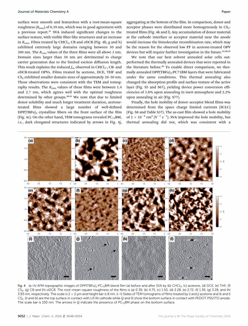
The surface texture and roughness were examined bytapping-mode atomic force microscopy (AFM) to gather addi-tional information on the morphology change induced by SVA.Fig. 4a–h depicts the AFM topographic images of theDPP(TBFu)2:PC71BM blend lm before and aer SVA bydifferent solvents. Without SVA (Fig. 4a), large parts of the lm
before and after SVA by (b) CHCl3, (c) acetone, (d) DCE, (e) THF, (f) CS2,cally between 3 and 5 mm. (i–l) Reconstructed 3D models from thed (l) oDCB. DPP(TBFu)2 donor phase is rendered in golden color while
J. Mater. Chem. A, 2014, 2, 9048–9054 | 9051
Journal of Materials Chemistry A Paper
surface were smooth and featureless with a root-mean-squareroughness (Rrms) of 0.39 nm, which was in good agreement witha previous report.31 SVA induced signicant changes to thesurface texture, with visible ber-like structures and an increasein Rrms. Films treated by CHCl3, CB and oDCB (Fig. 4b, g and h)exhibited extremely large domains ranging between 50 and300 nm. The Rrms values of the three lms were all above 3 nm.Domain sizes larger than 50 nm are detrimental to chargecarrier generation due to the limited exciton diffusion length.This result explains the reduced Jsc observed in CHCl3-, CB- andoDCB-treated OPVs. Films treated by acetone, DCE, THF andCS2 exhibited smaller domain sizes of approximately 20–50 nm.These observations were consistent with the TEM and tomog-raphy results. The Rrms values of these lms were between 1.4and 2.7 nm, which agrees well with the optimal roughnessdetermined by other groups.30,31 We note that due to limiteddonor solubility and much longer treatment duration, acetone-treated lms showed a large number of well-denedDPP(TBFu)2 crystalline bers on the front surface of the lm(Fig. 4c). On the other hand, TEM tomograms revealed PC71BM,i.e., dark elongated structures indicated by arrows in Fig. 4j,
Fig. 4 (a–h) AFM topographic images of DPP(TBFu)2:PC71BM blend filmCS2, (g) CB and (h) oDCB. The root-mean-square roughness of the film3.83 nm, respectively. The scale is 2� 2 mm and height bar is 8 nm. (i–l) SlCS2. (i) and (k) are the top surface in contact with LiF/Al cathode while (j) aThe scale bar is 100 nm. The arrows in (j) indicate the presence of PC71B
9052 | J. Mater. Chem. A, 2014, 2, 9048–9054
aggregating at the bottom of the lm. In comparison, donor andacceptor phases were distributed more homogenously in CS2-treated lms (Fig. 4k and l). Any accumulation of donormaterialat the cathode interface or acceptor material near the anodewould increase the bimolecular recombination rate, which maybe the reason for the observed low FF in acetone-treated OPVdevices but will require further investigation in the future.32,50,51
We note that our best solvent annealed solar cells out-performed the thermally annealed devices that were reported inthe literature before.36 To enable direct comparison, we ther-mally annealed DPP(TBFu)2:PC71BM layers that were fabricatedunder the same conditions. This thermal annealing alsochanged the absorption prole and surface texture of the activelayer (Fig. S5 and S6†), yielding device power conversion effi-ciencies of 3.8% upon annealing in inert atmosphere and 2.2%upon annealing in air (Fig. S7†).
Finally, the hole mobility of donor–acceptor blend lms wasdetermined from the space charge limited currents (SCLC)(Fig. S8 and Table S3†). The as-cast lm showed a hole mobilityof 2 � 10�4 cm2 (V�1 s�1). SVA improved the hole mobility, butthermal annealing did not, which was consistent with a
(a) before and after SVA by (b) CHCl3, (c) acetone, (d) DCE, (e) THF, (f)s is (a) 0.39, (b) 4.75, (c) 1.50, (d) 2.28, (e) 2.72, (f) 1.39, (g) 3.28, and (h)ides of TEM tomograms of films treated by (i and j) acetone and (k and l)nd (l) show the bottom surface in contact with PEDOT:PSS/ITO anode.M phase on the bottom surface.
This journal is © The Royal Society of Chemistry 2014

Paper Journal of Materials Chemistry A
previous report.31 More specically, SVA almost tripled the holemobility to 5–7 � 10�4 cm2 V�1 s�1. We attribute the improvedmobility to a more ordered donor phase aer SVA, enabling theobserved enhancement in Jsc and FF.
4. Conclusions
In summary, a solvent vapor annealing (SVA) method wasdemonstrated to improve the photovoltaic performance ofDPP(TBFu)2:PC71BM-based OPVs through changes in blend lmmorphology that were revealed in 3D by TEM tomography. Arange of solvents were tested and compared. Solvents with highvapor pressure and medium donor solubility were found toproduce changes in morphology leading to higher solar cellefficiency, while acceptor solubility in these solvents played aninsignicant role in determining the photovoltaic performance.The best efficiencies were achieved by SVA using THF or CS2,both yielding a PCE of 5.2%, which was the highest PCE for theDPP(TBFu)2:PC71BM material combination. To the best of ourknowledge, this is the rst demonstration of highly efficient,air-processed small molecule OPVs and is comparable with thebest polymer-based OPVs fabricated in air.52–56 As the treatmentis rapid and takes place in ambient conditions, it has greatpotential to be incorporated into large-scale continuous OPVfabrication processes.
Acknowledgements
We thank Australian Renewable Energy Agency (ARENA) forsupporting this work through the Australia–GermanyResearch Exchange Project Grant (1-GER001) and the VictorianOrganic Solar Cell consortium (VICOSC) with fundingprovided by the Victorian State Government Department ofPrimary Industries (Energy Technology Innovation Strategy),the Victorian State Government Department of BusinessInnovation (Victorian Science Agenda) and ARENA (Project 2-A018). W. W. H. Wong thanks the fellowship sponsored byARENA. The authors are grateful to Prof. Andrew B. Holmes atthe University of Melbourne and Dr Alexander Colsmann atthe Karlsruhe Institute of Technology for in-depth discussionsand kind support.
Notes and references
1 A. W. Hains, Z. Q. Liang, M. A. Woodhouse and B. A. Gregg,Chem. Rev., 2010, 110, 6689–6735.
2 A. Mishra and P. Bauerle, Angew. Chem., Int. Ed., 2012, 51,2020–2067.
3 Y. F. Li, Acc. Chem. Res., 2012, 45, 723–733.4 L. Dou, J. You, Z. Hong, Z. Xu, G. Li, R. A. Street and Y. Yang,Adv. Mater., 2013, 25, 6642–6671.
5 F. C. Krebs, N. Espinosa, M. Hosel, R. R. Søndergaard andM. Jørgensen, Adv. Mater., 2014, 26, 29–39.
6 Z. He, C. Zhong, S. Su, M. Xu, H. Wu and Y. Cao, Nat.Photonics, 2012, 6, 591–595.
This journal is © The Royal Society of Chemistry 2014
7 J. You, C.-C. Chen, Z. Hong, K. Yoshimura, K. Ohya, R. Xu,S. Ye, J. Gao, G. Li and Y. Yang, Adv. Mater., 2013, 25,3973–3978.
8 J. You, L. Dou, K. Yoshimura, T. Kato, K. Ohya, T. Moriarty,K. Emery, C.-C. Chen, J. Gao, G. Li and Y. Yang, Nat.Commun., 2013, 4, 1446.
9 F. C. Krebs, Sol. Energy Mater. Sol. Cells, 2009, 93, 394–412.10 F. C. Krebs, Org. Electron., 2009, 10, 761–768.11 F. C. Krebs, Sol. Energy Mater. Sol. Cells, 2009, 93, 465–475.12 F. C. Krebs, M. Jorgensen, K. Norrman, O. Hagemann,
J. Alstrup, T. D. Nielsen, J. Fyenbo, K. Larsen andJ. Kristensen, Sol. Energy Mater. Sol. Cells, 2009, 93, 422–441.
13 W. Gaynor, J. Y. Lee and P. Peumans, ACS Nano, 2010, 4,30–34.
14 H. J. Park, M.-G. Kang, S. H. Ahn and L. J. Guo, Adv. Mater.,2010, 22, E247–E253.
15 J. Y. Oh, M. Shin, T. I. Lee, W. S. Jang, Y.-J. Lee, C. S. Kim,J.-W. Kang, J.-M. Myoung, H. K. Baik and U. Jeong,Macromolecules, 2013, 46, 3534–3543.
16 W. Shin, T. Yasuda, G. Watanabe, Y. S. Yang and C. Adachi,Chem. Mater., 2013, 25, 2549–2556.
17 K. R. Graham, R. Stalder, P. M. Wieruszewski, D. G. Patel,D. H. Salazar and J. R. Reynolds, ACS Appl. Mater.Interfaces, 2013, 5, 63–71.
18 J. Huang, C. Zhan, X. Zhang, Y. Zhao, Z. Lu, H. Jia, B. Jiang,J. Ye, S. Zhang, A. Tang, Y. Liu, Q. Pei and J. Yao, ACS Appl.Mater. Interfaces, 2013, 5, 2033–2039.
19 H. Wang, F. Liu, L. Bu, J. Gao, C. Wang, W. Wei andT. P. Russell, Adv. Mater., 2013, 25, 6519–6525.
20 K. R. Graham, P. M. Wieruszewski, R. Stalder, M. J. Hartel,J. Mei, F. So and J. R. Reynolds, Adv. Funct. Mater., 2012,22, 4801–4813.
21 J. Zhou, X. Wan, Y. Liu, Y. Zuo, Z. Li, G. He, G. Long, W. Ni,C. Li, X. Su and Y. Chen, J. Am. Chem. Soc., 2012, 134, 16345–16351.
22 B. A. Gregg, J. Phys. Chem., 1996, 100, 852–859.23 K. C. Dickey, J. E. Anthony and Y. L. Loo, Adv. Mater., 2006,
18, 1721–1726.24 M. T. Lloyd, A. C. Mayer, S. Subramanian, D. A. Mourey,
D. J. Herman, A. V. Bapat, J. E. Anthony andG. G. Malliaras, J. Am. Chem. Soc., 2007, 129, 9144–9149.
25 G. H. Lu, L. G. Li and X. N. Yang, Adv. Mater., 2007, 19, 3594–3598.
26 J. Vogelsang, J. Brazard, T. Adachi, J. C. Bolinger andP. F. Barbara, Angew. Chem., Int. Ed., 2011, 50, 2257–2261.
27 Y. Zhao, Z. Xie, Y. Qu, Y. Geng and L. Wang, Appl. Phys. Lett.,2007, 90, 043504.
28 H. Tang, G. Lu, L. Li, J. Li, Y. Wang and X. Yang, J. Mater.Chem., 2010, 20, 683–688.
29 G. Wei, S. Wang, K. Sun, M. E. Thompson and S. R. Forrest,Adv. Energy Mater., 2011, 1, 184–187.
30 A. Viterisi, F. Gispert-Guirado, J. W. Ryan and E. Palomares,J. Mater. Chem., 2012, 22, 15175–15182.
31 B. Walker, A. B. Tamayo, X.-D. Dang, P. Zalar, J. H. Seo,A. Garcia, M. Tantiwiwat and T.-Q. Nguyen, Adv. Funct.Mater., 2009, 19, 3063–3069.
J. Mater. Chem. A, 2014, 2, 9048–9054 | 9053
Journal of Materials Chemistry A Paper
32 Y. Zhang, X.-D. Dang, C. Kim and T.-Q. Nguyen, Adv. EnergyMater., 2011, 1, 610–617.
33 J. Liu, Y. Zhang, H. Phan, A. Sharenko, P. Moonsin,B. Walker, V. Promarak and T.-Q. Nguyen, Adv. Mater.,2013, 25, 3645–3650.
34 Z. Li, X. Zhang, Y. Zhang, C. F. Woellner, M. Kuik, J. Liu,T.-Q. Nguyen and G. Lu, J. Phys. Chem. C, 2013, 117, 6730–6740.
35 X.-D. Dang, A. B. Tamayo, J. Seo, C. V. Hoven, B. Walker andT.-Q. Nguyen, Adv. Funct. Mater., 2010, 20, 3314–3321.
36 J. Liu, B. Walker, A. Tamayo, Y. Zhang and T.-Q. Nguyen, Adv.Funct. Mater., 2013, 23, 47–56.
37 Y. Lin, H. F. Dam, T. R. Andersen, E. Bundgaard, W. Fu,H. Chen, F. C. Krebs and X. Zhan, J. Mater. Chem. C, 2013,1, 8007–8010.
38 J. R. Kremer, D. N. Mastronarde and J. R. McIntosh, J. Struct.Biol., 1996, 116, 71–76.
39 http://bio3d.colorado.edu/.40 V. D. Mihailetchi, J. K. J. van Duren, P. W. M. Blom,
J. C. Hummelen, R. A. J. Janssen, J. M. Kroon,M. T. Rispens, W. J. H. Verhees and M. M. Wienk, Adv.Funct. Mater., 2003, 13, 43–46.
41 V. D. Mihailetchi, J. Wildeman and P. W. M. Blom, Phys. Rev.Lett., 2005, 94, 126602.
42 B. Walker, A. Tamayo, D. T. Duong, X.-D. Dang, C. Kim,J. Granstrom and T.-Q. Nguyen, Adv. Energy Mater., 2011, 1,221–229.
43 L. Chang, H. W. A. Lademann, J.-B. Bonekamp, K. Meerholzand A. J. Moule, Adv. Funct. Mater., 2011, 21, 1779–1787.
9054 | J. Mater. Chem. A, 2014, 2, 9048–9054
44 S. S. van Bavel, E. Sourty, G. de With and J. Loos, Nano Lett.,2009, 9, 507–513.
45 A. A. Herzing, L. J. Richter and I. M. Anderson, J. Phys. Chem.C, 2010, 114, 17501–17508.
46 M. Kim, J.-H. Kim, H. H. Choi, J. H. Park, S. B. Jo, M. Sim,J. S. Kim, H. Jinnai, Y. D. Park and K. Cho, Adv. EnergyMater., 2014, DOI: 10.1002/aenm.201300612.
47 J. D. Roehling, K. J. Batenburg, F. B. Swain, A. J. Moule andI. Arslan, Adv. Funct. Mater., 2013, 23, 2115–2122.
48 M. Pfaff, P. Muller, P. Bockstaller, E. Muller, J. Subbiah,W. W. H. Wong, M. F. G. Klein, A. Kiersnowski,S. R. Puniredd, W. Pisula, A. Colsmann, D. Gerthsen andD. J. Jones, ACS Appl. Mater. Interfaces, 2013, 5, 11554–11562.
49 S. S. van Bavel, M. Barenklau, G. de With, H. Hoppe andJ. Loos, Adv. Funct. Mater., 2010, 20, 1458–1463.
50 L. J. A. Koster, V. D. Mihailetchi and P. W. M. Blom, Appl.Phys. Lett., 2006, 88, 052104.
51 M.-S. Kim, B.-G. Kim and J. Kim, ACS Appl. Mater. Interfaces,2009, 1, 1264–1269.
52 C. Y. Nam, D. Su and C. T. Black, Adv. Funct. Mater., 2009, 19,3552–3559.
53 S. J. Wu, J. H. Li, Q. D. Tai and F. Yan, J. Phys. Chem. C, 2010,114, 21873–21877.
54 Z. Y. Hu, J. J. Zhang, S. Z. Xiong and Y. Zhao, Org. Electron.,2012, 13, 142–146.
55 Z. Y. Hu, J. J. Zhang and Y. J. Zhu, Appl. Phys. Lett., 2013, 102,043307.
56 E. S. R. Bovill, J. Griffin, T. Wang, J. W. Kingsley, H. Yi,A. Iraqi, A. R. Buckley and D. G. Lidzey, Appl. Phys. Lett.,2013, 102, 183303.
This journal is © The Royal Society of Chemistry 2014
Top Related
Copyright © 2022 FDOKUMEN

