


Bahasa
Halaman
Hukum


RFID-BASED WIRELESS SENSOR DATA
COLLECTION UNIT
Harri Näppä 2011 Oulu University of Applied Sciences

RFID-BASED WIRELESS SENSOR DATA
COLLECTION UNIT
Harri Näppä Bachelor’s Thesis 6.5.2011 Information technology Oulu University of Applied Sciences

3
OULU UNIVERSITY OF APPLIED SCIENCES ABSTRACT
Degree programme Thesis Pages + Appendices
Information Technology B.Sc. 68 + 3 Line Date
Electronics design and testing 6.5.2011 Commissioned by Author
Veijo Korhonen Harri Näppä Thesis title
RFID-based wireless sensor data collection unit Keywords
RFID, hardware design, microcontroller programming
The purpose of this thesis was to research the methods of radio frequency
identification based wireless data transfer, battery charging and microcontrol-
ler programming as well as to develop the author’s project work and hard-
ware design skills. The goal was to design and implement a working wireless
sensor data collection unit prototype by using the learned methods. This unit
automatically collects the sensor data in its memory in specified time inter-
vals. The data can be read by a radio frequency identification reader device.
The project was started by searching for the necessary theoretical informa-
tion for a hardware design. The next step was a selection of the components
and after that the schematic design could be done. The antenna design was
done in parallel with the schematic design, because the antenna component
was designed directly on circuit board as a track loop antenna. The layout
design was made after the schematic design was finished. After the circuit
board was ready and assembled it needed to get a life so the hardware pro-
gramming was done in this stage. The rest was testing and further develop-
ment of the design.
The result of this project was a working wireless sensor data collection unit
and one further development design of this prototype. The prototype design,
assembly and programming was successful and the further development
prospects are good.

4
TABLE OF CONTENTS ABSTRACT ………………………………………………………………………….... 3
1 INTRODUCTION ............................................................................................. 6
2 RFID-TECHNOLOGY ...................................................................................... 7
2.1 General ...................................................................................................... 7
2.2 Components of RFID system .................................................................... 8
2.3 RFID Transponders ................................................................................... 9
2.3.1 Passive transponder ......................................................................... 10
2.3.2 Semi-passive transponder ................................................................ 11
2.3.3 Active transponder ............................................................................ 11
2.4 RFID frequencies .................................................................................... 12
2.5 RFID standards ....................................................................................... 14
3 SELECTION AND THEORY OF COMPONENTS .......................................... 17
3.1 Battery charger controller ........................................................................ 18
3.1.1 Charge modes .................................................................................. 19
3.1.2 Functions .......................................................................................... 20
3.1.3 Settings ............................................................................................. 22
3.2 Atmel AVR-microcontroller ...................................................................... 25
3.2.1 AVR architecture ............................................................................... 27
3.2.2 AVR Memories .................................................................................. 30
3.2.3 AVR peripherals ................................................................................ 31
3.3 Communication ....................................................................................... 32
3.3.1 Serial peripheral interface ................................................................. 32
3.3.2 RFID analog front end....................................................................... 36
3.4 Inductive charging ................................................................................... 38
4 HARDWARE DESIGN AND ASSEMBLY ...................................................... 39
4.1 Antenna design ....................................................................................... 39
4.2 PCB design ............................................................................................. 43
5 PROGRAMMING ........................................................................................... 52
6 TESTING ....................................................................................................... 58
7 CONCLUSIONS AND DISCUSSION ............................................................. 62
LIST OF REFERENCES ................................................................................... 65
APPENDICES ................................................................................................... 68

5
VOCABULARY
ALU Arithmetic Logic Unit
ASK Amplitude Shift Keying
CPHA Clock Phase
CPOL Clock Polarity
DMA Direct Memory Access
EPROM Erasable Programmable Read Only Memory
EEPROM Electronically Erasable Programmable Read-Only Memory
EPC Electronic Product Code
ESD Electrostatic Discharge
FBGA Field Programmable Gate Array
FSK Frequency Shift Keying
HF High Frequency
ISO The International Organization for Standardization
JTAG Joint Test Action Group
LED Light Emitting Diode
LF Low Frequency
Li-Ion Lithium-Ion
NFC Near Field Communication
PSK Phase Shift Keying
PCB Printed Circuit Board
PWM Pulse Width Modulation
RFID Radio Frequency Identification
RISC Reduced Instruction Set Computer
ROM Read Only Memory
SCK Serial Clock
SPI Serial Peripheral Interface
TWI Two Wire serial Interface
UHF Ultra High Frequency
USART Universal Synchronous/Asynchronous Receiver-Transmitter

6
1 INTRODUCTION
The topic of this thesis project was to design and implement a RFID- based
wireless sensor data collection unit. This thesis was commissioned by Mr.
Veijo Korhonen, Project Manager from Oulu University of Applied Sciences,
IT department and the contact person was Mr. Tommi Sallinen, Designer.
The data collection unit collects sensor data in its memory at specified time
intervals and memory content can be read over the RFID interface when it is
activated with the RFID reader. When the RFID reader starts communication
between the devices, the data collection unit wakes up and starts to transmit
desired data to the RFID reader. The data collection unit was designed and
implemented in this project.
The communication frequency between the RFID reader and the data collec-
tion unit is 13,56 MHz. In order for the coupling to be possible and the RFID
interface to work between these devices, the data collection unit has to have
its own 13,56 MHz tuned antenna. This high frequency antenna was de-
signed in this project and it is placed directly on the circuit board. The de-
signed unit supports only the ISO 15693 RFID standard, so the reader de-
vice has to support this standard, too.
The data collection unit is powered by a rechargeable battery and charging is
made using induction power, because the final goal is to have a completely
sealed sensor for hazardous environments. The charging circuit for the bat-
tery was also designed in this project. The induction charger was purchased
as a ready product from the market.

7
2 RFID-TECHNOLOGY
The abbreviation RFID stands for Radio Frequency Identification, which
means the wireless identification method where information is transferred us-
ing radio waves. The word RFID is a general name for all kinds of technolo-
gies that work in radio frequency areas. (16)
2.1 General
During the World War II (1939–1945 ) the first passive RFID system was in-
vented by the Germans. The radar system was invented earlier in 1935 to
notify of incoming aircrafts. The problem was that the radar could not see the
difference between an enemy plane and an own plane. The Germans dis-
covered that if pilots rolled their planes when they returned to the base, it
would change the radio signal reflected back. This is the first passive RFID
system. The first active RFID system was developed by the British and it is
called the Identify Friend or Foe system (IFF system). The British put a
transmitter in each plane and when it received the radar signal, it began
broadcasting the signal back. The RFID works in the same way. (11)
The first active RFID transponder (Tag) with rewritable memory was pat-
ented in 1973. That same year the first passive tag was patented. It was
used to unlock the door without a key. The first commercial applications were
introduced in 1980´s. (12)
The basic idea of the RFID is simple: attach the RFID tag to the desired des-
tination, write the information into a tag or read the information from a tag
with the RFID reader. (16)
RFID technology can be compared with barcode technology, but barcode
technology doesn’t offer same kinds of possibilities as RFID technology
does. Barcode technology needs always a direct visual contact between the
reader and the barcode, so that the reading can be done. If the barcode is
dirty, or there is some obstacle between the reader and the barcode, reading

8
fails. The RFID reader can communicate with a tag without any physical- or
visual contact so it differs from the barcode technology. Reading distances
are dependent on the standards that are used and on the frequency range.
(4) (16)
RFID has been technically possible for decades and it has already been
used for a long time, for example on key cards, travel cards and for recording
animals. RFID is also used in industry as a part of production efficiency and
quality control, logistics and cargo tracking. The RFID is not a single technol-
ogy, it is a number of technologies with the same operating principles. (4)
(16)
2.2 Components of RFID system
Main components of a RFID system are a transponder, interrogator or reader
and application. The tag is attached to the object which you want to be identi-
fied. Normally a tag consist of a coupling element which is an antenna and
an electronic microchip where information is hold. The main components of a
RFID system are shown in the Figure 1. (4)
FIGURE 1. Main components of RFID system. (4)
When a tag doesn’t have its own power supply and it is not in an interroga-
tion zone of a reader it is totally passive. An active transponder has its own
power supply. (4)

9
A RFID reader has three functions; to stimulate tags, read tags data and
transmit data to a host computer with an external connection. Nearly all
readers can also write data to the tag’s memory. A better term for the reader
would be “reader/writer”. The reader consists of a radio frequency module, a
control unit and a coupling element which is the antenna. There is a sample
picture of coupling elements in Figure 2. (3)
FIGURE 2. Coupling elements. Left, inductively coupled transponder with an-
tenna coil; right, microwave transponder with dipolar antenna. (4)
An application system includes a computer, database, servers, information
processing applications and terminal equipments. The application system is
used for editing information to suit to the user. (19)
2.3 RFID Transponders
RFID tags can be divided into three categories based on tag properties. An
example picture of a RFID tag in the Figure 3. (23)
FIGURE 3. RFID tag. (17)

10
2.3.1 Passive transponder
A passive transponder is a tag that doesn’t have its own power supply. It is
active only when the RFID reader is near by. The tag takes its energy from
the RFID reader by induction power. With this power, the tag can send a re-
ply to the RFID reader. Normally the reply is just the tag’s own ID-number.
As there is no power supply, the tag can be very small. In year 2007 the
smallest tag was 0,05 mm x 0,05 mm. Passive RFID tags are cheaper to
produce than active RFID tags. For this reason, most RFID tags currently
used are passive tags. (20) (23)
Passive tags are broken down into two categories based on their voltage
technology and data writing technology which are near-field technology and
far-field technology. Near-field technology is based on electromagnetic in-
duction and far-field technology is based on radio waves. Low frequency (LF)
and high frequency (HF) tags use electromagnetic induction, while ultra high
frequency (UHF) tags use electric field reflection to data and the operating
voltage transfer. (15)
In the LF- and HF-bands a reader and a tag forms an inductive connection
like a transformer. Normally there are copper loops in the tag, which form a
coil and it works as a tag antenna. There are same kind of loops in the RFID
reader. By passing an alternating current in to the loop, the reader generates
an oscillating magnetic field, for example a frequency of 13,56 MHz. This
magnetic field induces the same alternating current to the tag coil when the
tag is in the reader’s detection distance. In this case, a microchip in the tag
receives the operating voltage from the induced current. When the microchip
is powered on, the EEPROM memory content is modulated in the tag coil
voltage. The modulated voltage is shown as changes in the reader coil volt-
age. (15)
In the UHF and microwave frequency bands, communication between tag
and reader happens through electromagnetic radiation i.e. using radio
waves. The reader sends out radio waves through its antenna, and the tag’s

11
dipole antenna receives these radio waves and backscatters them. The tag
modulates data from its microchip to a backscattered wave. The tag can
send data with a backscattered signal to the reader in many ways, for exam-
ple like increasing the amplitude of the reflected signal (Amplitude Shift Key-
ing, ASK), shifting of the reflected signal phase (Phase Shift Keying, PSK) or
converting the frequency of the reflected signal (Frequency Shift Keying,
FSK). (15)
2.3.2 Semi-passive transponder
A semi-passive transponder is a tag that has its own power supply, but a
transmitter is missing. Since there is no transmitter, the semi-passive tag
needs power from the reader to be able to send data. The semi-passive tag
has a greater operational range than the passive tag and the semi-passive
tag has memory of its own. This feature allows it to storage data in the mem-
ory, for example temperature data from a sensor to an EEPROM. (23)
2.3.3 Active transponder
An active transponder is a tag that has its own power supply in the same way
as semi-passive tags. Thus the active tags production costs will increase
compared to the passive tags. That’s why active tags are not as popular as
passive tags and active tags are used only for special purposes. Unlike the
semi-passive tag, the active tag has also a transmitter which is powered by a
battery. The active tag listens all the time to the possible incoming signal
from the reader and answers it if necessary. Communication of active tag
and the reader is similar to communication between two radios or mobile
phones. Active tags enable wireless reading even up to 100 meters. (15) (23)
The previously mentioned IFF-system is based exactly on active tags. An ac-
tive tag was attached to the airplane and it answered to the radar signal
automatically by sending an identification signal back to the radar. That is
how the British identified their own planes from the enemy planes.

12
2.4 RFID frequencies
RFID technology uses a number of different frequency bands all over the
world. This section observes only commonly used frequencies used in
Europe. In Finland, the Finnish communications regulatory authority (Ficora)
controls the usage of the frequency bands, which impose requirements and
constraints to the usage of RFID systems. (14)
A LF-band RFID system is working normally at the frequency of 125 kHz and
the frequency band is 125–134 kHz. The data transfer interface of these
RFID systems is based on inductive coupling and these kinds of systems
have slow data transfer rate and the reading distance is usually under half a
meter. As an advantage of LF-band systems can be considered excellent
readability on the dense non-metallic substances and through water. The LF-
band is commonly used for the identification of animals and in some access
control applications. Closed systems are very common and highly used in
this frequency band, which means that different manufacturers products are
not compatible with each other. (4) (14)
13,56 MHz frequency is used in HF-band RFID systems, which is an interna-
tionally open frequency, and anyone can make systems for this frequency. A
RFID system which operates in this frequency band is also based on induc-
tive coupling in the same way as LF-band systems. The data transfer rate is
usually 106 kbit/s which is better than in LF-band systems. The maximum
reading distance between the antenna and the chip is one and a half meter
in optimum conditions. The reading distance depends on the application and
is usually between five centimetres to one meter. The 13,56 MHz RFID sys-
tems are commonly used in libraries for books, airports for baggages, facto-
ries for pallet tracking and access control, and also in personal identification
applications. A high clock frequency enables the usage of microprocessors in
the tag and data encryption. Compared to UHF technology, 13,56 MHz tech-
nology has better field permeability through substances that contains water
such as trees and human beings, better interference resistance in industrial
environments, and it poses no problems with reflection. (4) (14)

13
Modern 13,56 MHz tags are dual interface smart cards which means there
are two interfaces in one card. A card has a contactless interface and a con-
tact interface. Both interfaces has access to the internal memory and proc-
essing. Contactless smart cards can be used in applications where a safe
encryption for the data transfer is required. These kinds of applications are
for example an electronic wallet or a public bus card. (4)
In Europe the 868 MHz frequency is used in UHF-band RFID systems. A
RFID system which operates in the UHF-band has a faster data transfer rate
and a longer reading distance than lower frequency applications. RFID sys-
tems which operates in the UHF-band works in a different way compared to
RFID systems in the LF- and HF-band. When operating in the UHF-band op-
eration technology is called far-field technology and when operating in LF- or
HF-band operation technology is called near-field technology. 868 MHz fre-
quency passive tags can be read about three meters away and active tags
reading distance can grow up to a hundred meters. A dipole antenna is usu-
ally used in tags. This frequency tags are commonly used in logistics, con-
tainer tracking and pallets. (4) (14)
Microwave frequencies which are used in Europe are 2,4 GHz and 5,8 GHz.
These frequencies enable very fast data transfer rate. Passive tags data
transfer rate is 10–50 kbit/s when reading distance is about twelve meters.
Active tags can perform 1 Mbit/s data transfer rate when the reading distance
is the maximum of thirty meters. These kinds of RFID systems has bad per-
meability on non-metallic substances because of reflections and attenuations
of microwaves. RFID systems which operating in microwave frequency band
are usually used in an active mode whose best-know application is an auto-
matic identification of the customs. Frequency of 2,4 GHz is widely used in
different applications as Bluetooth, WLAN, Zigbee etc. so this frequency is
quite congested. (4) (14) (18)

14
2.5 RFID standards
There are many established standards for RFID even though it is quite often
said that there are no standards in RFID. A great deal of work has been done
over the past decade to develop standards for different RFID frequencies
and applications. Main standards determine the data transfer protocol and
tag’s data content. Important standards has been developed in the payment
system- and logistic applications, since different operators have to be able to
read same kinds of tags with their own devices. The ideal situation would be
if with standardization, different manufacturers RFID systems would be able
to read each others tags. When someone building a system, it would be eas-
ier to ensure equipment availability in the future, if would not have to commit
to a single manufacturer’s products. Although a standard does not in itself
guarantee everything , there are so called open standards which can be util-
ized by anyone. (10) (13)
There are no open standards in the LF-band. Most LF-band applications like
different kinds of access control systems have been implemented as closed
systems at the frequency of 125 kHz. The International Organization for
Standardization (ISO) has created standards for tracking cattle. The standard
that has been defined for the cattle identification is ISO 11784 which de-
scribes the tag data content. At the frequency of 134 kHz standard ISO
11785 defines the data transfer protocol. (10) (13)
The HF-band in frequency of 13,56 MHz has agreed standards. The stan-
dard ISO 14443 is not independent of the manufacturer, but NXP Mifare
technology has achieved a de facto standard status of this frequency band.
The reading distance is limited to 3–4 cm and is widely used in various pay-
ment applications. The HF-band’s other standard is ISO 15693 and it is in-
dependent of the manufacturer, Philips I-CODE SLI chip is the most know
chip in Finland which follows this standard. (13)
Today the most important UHF-band standard is ISO 18000-6C also known
as GEN2. It is a standard developed by EPC (Electronic Product Code), a

15
global organization, and the standard orders data transfer protocols. This
standard’s contribution to the UHF band has been more secure identification
and operation has improved especially in a multi-reader environment. (13)
The Auto-ID Center was set up in 1999 to develop the EPC-standard and re-
lated technologies that could be used to identify products and track them
through the global supply chain. The starting point for developing was to
make a low-cost RFID system, because tags needed to be disposable. When
a manufacturer puts tags on products which are shipped to a retailer, the
manufacturer is never going to get those tags back to reuse them. The sec-
ond point was to exploit UHF band’s reading distance which was good for lo-
gistic applications. Auto-ID Center also wanted its RFID system to be global
and to be based on open standards. It needed to be global because the aim
was to use it to track goods as they flowed from a manufacturer in one coun-
try or region to companies in other regions and eventually to store shelves.
Auto-ID Center developed a standard that covers the data transfer protocol
and the tag data content protocol. Auto-ID Center also developed a network
infrastructure to serve the preservation of information and the transfer be-
tween the various actors worldwide. (10) (13)
Unlike the original idea of developing one data transfer protocol, Auto-ID
Center developed many EPC tags in accordance with a number of the class
division, where the upper classes provide more opportunities for a higher
price. The classes changed over time, but there were originally five classes
that were proposed. According to the original class division, for example,
Class 1 tags are passive and could be only read. Class 5 tags are active and
could communicate with other Class 5 tags and/or other devices. In the end
however, the Auto-ID Center adopted a Class 0 tag, which was a read-only
tag that was programmed at the time the microchip was made. Since the
Class 0 tag used a different protocol from the Class 1 tag, end users had to
buy multiprotocol readers to read both Class 1 and Class 0 tags. Class 0 and
Class 1 EPC tags are the most relevant in logistic application. (10) (13)

16
In 2003, the Auto-ID Center licensed EPC Class 0 and Class 1 protocols to
EPC global organization against the condition that the standard had to be
open and freely accessible to everyone. EPC Class 0 and Class 1 are not
compatible with ISO standards, and there is a problem using these standards
globally, because they do not comply with all the European regulations, for
example. (13)
ISO has developed RFID standards for automatic identification and item
management. This standard, known as ISO 18000 series (which also in-
cludes the previously mentioned Gen2) covers the air interface protocol for
systems likely to be used to track goods in a supply chain. They cover major
frequencies used in RFID systems around the world. The seven parts are:
- 18000-1: Generic parameters for air interfaces for globally accepted
frequencies.
- 18000-2: Air interface for 135 kHz
- 18000-3: Air interface for 13,56 MHz
- 18000-4: Air interface for 2,45 GHz
- 18000-5: Air interface for 5,8 GHz
- 18000-6: Air interface from 860 MHz to 930 MHz
- 18000-7: Air interface for 433,92 MHz
Although some of the standards and technologies are fairly well established,
the future reader and software application standards are still some mysteri-
ous. Different tag standards are however finally stabilized because of the
UHF bands Gen2 standard. (10)

17
3 SELECTION AND THEORY OF COMPONENTS
The first step on this project was the selection of the components which this
device could be built, and the search of the induction charger was started.
The design was started by the charging circuit design. At first, it was decided
what operating voltage this device should have and that the capacity of the
battery should be high enough. The result was 3,6 V, because it was decided
that the battery should be a Lithium-Ion (Li-ion) battery and the cell voltage of
these kinds of batteries is 3,6 V. The battery that was chosen was
LR1865AH and it has a 3,6 V nominal voltage, a 2150 mAh nominal capac-
ity, a 4,65 V maximum charge voltage and the maximum charge current of
2200 mA. When charging the Li-Ion battery it is important that the charging
circuit is correct or otherwise the battery may explode when charging. (9)
The next step was to look the battery charger controller. Analog Devices
manufactures a 1,5 A linear charger for a single cell Li-Ion batteries,
ADP2291, and it was just right for the selected battery. So the charger circuit
was designed around ADP2291 battery charger controller. The controller has
an adjustable charging current up to 1,5 A, an output overshoot protection, a
programmable termination timer, a 4,2 V output voltage with +/- 1% accuracy
over the line and the temperature and 1 µA shutdown supply current. (1)
MLX90129 was chosen to make a RFID communication and the sensor data
collection possible. MLX90129 combines a precise acquisition chain for ex-
ternal resistive sensors, with a wide range of interface possibilities, it can be
accessed and controlled through its ISO 15693 RFID front end or via its SPI
port. Adding a battery will enable the use of the standalone data logging
mode. The sensor data can be stored in the internal 3,5 kbits EEPROM user
memory or an external EEPROM. In this project the chip is controlled by a
microcontroller via SPI port. (7)

18
It was decided that a microcontroller will be used in this device. Microcontrol-
ler allows to insert more sensors, more memory space and accessories into
device. Microcontroller also allows debugging source code. When it was de-
cided that MLX90129 would be controlled with microcontroller, it was time to
decide what microcontroller would be suitable to do this job. In the result of a
long consideration it was decided to use ATmega32A, a newer version of
ATmega32 which has been very popular among developers. Main reasons
for why this microcontroller was chosen was its easy availability, a lot of user
experience available, low power consumption in idle mode as well as active
mode, low operating voltage, 32 kbytes of in-system self-programmable flash
program memory, master/slave SPI serial interface, 1024 bytes EEPROM
and JTAG (Joint Test Action Group) interface for programming. (2)
3.1 Battery charger controller
ADP2291 is a linear battery charger controller which is used in this project. It
is designed for a single-cell Li-Ion battery for a supply voltage range of 4,5 V
to 12 V. This charge controller adjusts the base current of an external PNP
transistor to optimise current and voltage applied to the battery during charg-
ing. A low value resistor placed in series with the battery charging current
provides current measurement for ADP2291. The charging circuit which is
designed in this project is shown in the Figure 4. (1)
FIGURE 4. Charging circuit. (1)

19
3.1.1 Charge modes
There are three charge modes in ADP2291 which are a precharge mode, an
end of charge mode and a shutdown mode. ADP2291 charges the battery by
step by step cycle, which ensures safety and a long battery lifetime. The first
thing that the controller does when the charge cycle begins is to determine
the charge level, which is done by measuring the battery voltage. When the
battery is deeply discharged, the controller goes to the low current precharge
mode and once the precharge is ready, the normal fast charge at the maxi-
mum current starts. The maximum current can be adjusted. The charging
current is reduced when the battery starts approaching its full capacity and it
continues until the end of charge condition is reached. If the battery is not
deeply discharged the controller starts right away the fast charging. (1)
When the battery voltage is below 2,8 V the precharge mode starts the
charging cycle, because of deeply discharged cell. The charging current is
reduced in the precharge mode and it is one tenth of the maximum charging
current when the adjust pin voltage is 3 V and one fifth when the adjust pin
voltage is 1,5 V. The precharge time is typically 30 minutes and if the battery
voltage does not increase over 2,8 V before that time, the controller assumes
that the battery is defective and it shuts down. The controller does not restart
the charging before the input voltage is switched OFF and then back ON
again. (1)
The controller goes in the end of charge mode as soon as the voltage loop
reduces the charge current to one tenth of its nominal value i.e. the maxi-
mum current. The controller detects the end of charge state, and the charge
status indicator goes in to the high impedance state. The low level charging
continues as long as the timer ends it, typically in 30 minutes. (1)
The controller goes to the shutdown mode after the adjust input pin voltage is
pulled below 0,4 V. When the controller is in this mode, the charger is dis-
abled and the power consumption of the controller is less than 1 µA and the
current drawn from the source falls to 0,7 mA. (1)

20
3.1.2 Functions
ADP2291 controller has a charge restart function. Once the charging is com-
pleted (the end of charge mode or the timer has expired), the controller con-
tinuously monitors the cell voltage and the charging current. As the time goes
by and the cell voltage drops by 100 mV, the controller initiates another
charge cycle to keep the cell fully charged. The controller also initiates an-
other cycle of charging when the charge current increases beyond the end of
charge hysteresis. (1)
The controller has a programmable timer. The on-chip timer is controlled by
an external capacitor CTIMER, different values of this capacitor gives differ-
ent timeout intervals of the various charger modes. For example, if CTIMER
value is 0,1 µF then the precharge timeout interval is 30 minutes, the fast
charge timeout is 3 hours and the end of charge timeout is 30 minutes. The
ratio between the precharge and the end of charge to the fast charge timeout
is always one sixth. If the timer pin is connected directly to the ground, the
timer is not enabled. (1)
There is a charge status output CHG in ADP2291 controller that sinks cur-
rent when charging is ON. There are two options to connect this pin. When
connecting this pin to a LED (Light Emitting Diode), you get visual signal
when charging is ON or it can be used to generate a logic-level charge status
signal by connecting a resistor between the CHG pin and logic high. (1)
An automatic reverse isolation function of the controller is designed so that,
when the voltage on the BAT pin (battery voltage sense input) is higher than
the IN pin (voltage on input pin), the controller automatically connects the
base of the pass device to BAT. Because of this function there is no need to
use an external diode between the pass device and the battery. The compo-
nent count is reduced and charger’s footprint in the layout is smaller. (1)
The overshoot protection circuit in the controller is activated when the battery
voltage rises up to 5 V and sinks the current up to 1,5 A to protect the exter-

21
nal components. The voltage can rise if the battery is removed while charg-
ing, because the battery sense input maybe disturbed. (1)
The power supply check function, checks the absolute voltage level of the
input supply and the supply voltage relative to the battery. If the source volt-
age is below 3,8 V, the controller is internally powered down and does not
respond to an external control. Charging will only happen when the supply
voltage is more than 165 mV above the battery voltage, ensuring that charg-
ing occurs only if the supply voltage is sufficient. VIN_GOOD comparator
halts operation if the supply voltage is too low (Figure 5). (1)
The thermal shutdown occurs if controller’s junction temperature rises above
135°C. ADP2291 does not start operating during the thermal shutdown until
the on-chip temperature drops below 100°C. There is a block diagram of
functions in the Figure 5. (1)
FIGURE 5. Functional block diagram of ADP2291 charger controller. (1)

22
3.1.3 Settings
The maximum charge current is set by choosing the proper current sense re-
sistor, RS, and the voltage on the ADJ input (Figure 4). The charger nomi-
nally regulates its output current at the point where the voltage across the
current sense resistor VRS = VIN – VCS = 150 mV. The maximum charge cur-
rent rate IMAX is calculated based on Formula 1. (1)
)(
)(max
mR
mVVI
S
RS FORMULA 1
where 50 mV ≤ VRS ≤ 150 mV.
After determining suitable values for VRS and RS, the value of VADJ and RADJ
are calculated as shown in Formulas 2 and 3. (1)
7,66
50)( mVmVVV RS
ADJ
FORMULA 2
ADJ
ADJADJ
VV
VkR
3100 FORMULA 3
The charging circuit which was designed in this project has capability to
maximum charge current of 750 mA. Resistors and voltages were selected in
accordance with the bottom row of Table 1.

23
TABLE 1. Few examples of RS and RADJ selection. (1)
IMAX [mA] RS [mΩ] VRS [mV] VADJ [V] RADJ [kΩ]
1500 100 150 3 Open
1000 100 100 2,25 300
750 100 75 1,87 167
500 100 50 1,5 100
750 200 150 3 Open
The maximum charge time of the charging circuit is set by an external ca-
pacitor CTIMER as described in Chapter 3.1.2. The maximum charge time is
good to be set for the safety reasons. The maximum charge time is intended
as a safety mechanism to prevent the charger from trickle charging the cell
indefinitely. If there is a failure to reach in the end of charge mode charging is
terminated, but otherwise charging lasts as long as it set by CTIMER in nor-
mal charging condition. A typical Lithium-Ion cell is charged in about 1,5
hours of course depending on the cell type, temperature and manufacturer.
Usually, a three hour time limit is good enough and the normal charge cycle
reaches to end, before the charge timer ends charging. (1)
The value of the capacitor CTIMER is calculated using the Formula 4.
min1800
1(min) FtCTIMER
chg FORMULA 4

24
As was said earlier the precharge and the end of charge periods are one
sixth duration of the fast charge time limit. If the timer is disabled, the fault
and the timeout states are never reached, so the timer should only be dis-
abled if charging is monitored and controlled externally. (1)
The external PNP transistor Q1 must be chosen based on the given operat-
ing conditions and power handling capabilities. Also taking into account what
is the input and the output voltage and the maximum charging current. (1)
Providing a charge current of IMAX with a minimum base drive of 40 mA,
minimum beta value for PNP transistor is calculated based on formula 5. (1)
mA
mAI
I
I MAX
B
MAX
40
)(min FORMULA 5
The beta of a transistor drops off with collector current. Because of that, the
beta at IMAX have to meet the minimum requirement. (1)
When the input voltage is low, the saturation voltage must be taken into ac-
count. The input voltage is low when it is under 5,5 V (in this project, the in-
put voltage to charger is about 5 V). The saturation voltage can be calculated
by using the Formula 6. (1)
BATRSMINADAPTERSATCE VVVV )()( FORMULA 6
The power handling capability of the PNP transistor is also an important pa-
rameter that had to be taken into account. The maximum power dissipation
(PDISS) of the PNP transistor can be estimated and calculated by using the
Formula 7. (1)
)()( )( BATRSMAXADAPTERMAXDISS VVVIWP FORMULA 7
where VRS = 150 mV at VADJ = 3,0 V and VBAT is the lowest cell voltage
where the fast charge can occur which is 2,8V. (1)

25
Based on these calculations the PNP pass transistor was selected. The re-
sults of the calculations were:
- β min = 18,75
- V CE(SAT) = 0,65 V
- PDISS = 1,5 W
FZT549 PNP transistor meet these requirements. FZT549 transistor values
are:
- β = 130
- V CE(SAT) = 0,25 V
- PDISS(MAX) = 2 W
3.2 Atmel AVR-microcontroller
AVR is a microcontroller family which was developed by semiconductor
manufacturer Atmel in 1996. AVR was one of the first microcontroller family
which uses on-chip flash memory for program storage, as opposed to single
programmable ROM (Read Only Memory), EPROM (Erasable Programma-
ble Read Only Memory) or EEPROM (Electronically Erasable Programmable
Read-Only Memory) used by other microcontrollers at the time. A flash
memory is a semiconductor memory, which can be electronically erased and
reprogrammed. (22)
The basic architecture that is used in the AVR-microcontrollers, were devel-
oped by two Norwegian students Alf-Egil Bogen and Vegard Wollan. They
sold the architecture to Atmel and continued its development there. AVR
name is believed to came words Alf and Vegard RISC (Reduced Instruction
Set Computer). RISC is a computer processor architecture design philoso-

26
phy, in which machine language instructions have been kept simple and
quickly performed a standard time. (22)
The AVR family has now over 50 different microcontrollers. All models have
the same processor and memory structure. The main differences between
the models are the memory capacity and the number of the I/O ports. AVRs
are generally classified into five broad groups which are tinyAVR, megaAVR,
XMEGA, application specific AVR (as megaAVRs with special features not
found on the other members of the AVR family, such as a LCD controller, a
USB controller, an advanced PWM, CAN etc.) and FPSLIC (AVR with
FPGA). FPGA (Field Programmable Gate Array) is an integrated circuit
designed to be configured by the customer or the designer after
manufacturing – hence "field-programmable". Table 2 shows the comparison
of the characteristics of three main groups. (22)
TABLE 2. Main AVR groups.
tinyAVR megaAVR XMEGA
Program memory (kbyte) 1-8 4-256 16-384
Housing size (pins) 8-32 28-100 44-100
Features Limited pe-
ripherals/ in-
terfaces
Extended in-
struction set,
extensive pe-
ripherals/ in-
terfaces
Enhanced
performance
features, ex-
tensive pe-
ripherals/ in-
terfaces
includes D/A-
converters

27
3.2.1 AVR architecture
Flash, EEPROM and SRAM memories are all integrated onto a single chip,
removing the need for an external memory in most applications. To maximize
the performance, AVR uses a Harvard architecture. It has a separate mem-
ory and buses for command and data. Some devices have a parallel external
bus option to allow adding an additional data memory or memory-mapped
devices. The program memory commands are performed in a pipeline. The
pipeline means that while one command is carried out, at the same time the
next command is accessed from program memory. This allows commands to
be executed with every clock cycle. Almost all devices (except the smallest
tinyAVR chips) have serial interfaces, which can be used to connect larger
serial EEPROMs or flash chips. In the Figure 6 there is a block diagram of
the AVR MCU architecture. (2)
FIGURE 6. Block diagram of the AVR MCU architecture. (2)

28
The AVR ALU (Arithmetic Logic Unit) operates in a direct contact with all 32
general purpose work registers. The ALU is a digital circuit that performs
arithmetic and logical operations. The ALU supports arithmetic and logic op-
erations between of two registers or between a register and a constant. A
single register operations can also be carried out in the ALU. The ALU op-
erations can be divided into three main categories which are: arithmetic-,
logical- and bit-function operations. In a typical ALU operation, two operands
will be fetched in register file, execute the operation and save the result into
register file. All this happens during one clock cycle. (2)
The status register always contains the latest information of the arithmetic
operation. This information can be used to change the program process,
which allows conditional execution of operations. Since the status register is
automatically updated after each arithmetic operation, the code is faster and
more compact. (2)
Fast to use registry file consists of 32 8-bit general purpose registers, and it
is optimised for the AVR’s enhanced RISC instruction set. The access time
of these registers is one clock cycle, which allows one cyclic operation. In or-
der to achieve the required performance and flexibility, the following in-
put/output schemes are supported by the register file, which are presented in
Table 3. (2)

29
TABLE 3. Register file transfer methods.
Output Input
One 8-bit operand One 8-bit result
Two 8-bit operands One 8-bit result
Two 8-bit operands One 16-bit result
One 16-bit operand One 16-bit result
Six of 32 general purpose registers can be combined into three 16-bits point-
ers, which are named as X-, Y- and Z-register. These are used as an indirect
pointers of the data space, enabling effective address calculations. One of
these pointers can also be used in the flash program memory as a lookup
table pointer. X-, Y- and Z-registers have functions in different pointer areas
as an automatic adding and reduction and in the solid transition. The AVR
CPU general purpose working registers are shown in the Figure 7. (2)

30
FIGURE 7. AVR CPU general purpose working registers. (2)
3.2.2 AVR Memories
The AVR microcontrollers has three kinds of memories. Main memory areas
are SRAM data memory and flash program memory spaces. In addition,
there is EEPROM memory for data storage. All three memory spaces are
linear and regular. (2)
The ATmega series microcontrollers has 4 – 256 kbytes on-chip in-system
reprogrammable flash memory for the program storage. The memory is di-
vided into 2 – 128 k x 16-bit parts, because all AVR commands are 16 or 32
bits wide. The flash program memory is divided into two different parts which
are the boot program section and the application program section, this allo-
cation is made for software security. The Flash memory has an endurance of
at least 10,000 write/erase cycles. (2)

31
SRAM data memory includes the register file, the I/O-memory and the inter-
nal data SRAM. The first 32 locations address the register file and the next
64 location address the I/O memory, and the next 2048 locations address the
internal data SRAM. (2)
The ATmega series microcontrollers has 256 – 1024 bytes EEPROM mem-
ory. EEPROM memory is slower than SRAM memory and is frequently used
to store program settings etc. for long term data storage. The memory is lo-
cated in a separate memory area, which can be both read and write individ-
ual bytes through registers that are there for this purpose. These registers
are the EEPROM Address Registers, the EEPROM Data Register, and the
EEPROM Control Register. The EEPROM has an endurance of at least
100,000 write/erase cycles. (2)
3.2.3 AVR peripherals
The AVR microcontrollers have a wide range of integrated peripherals. For
example, the following peripherals can be found in ATmega32A which is go-
ing to be used in this project:
- three counters (two 8-bit and one 16-bit)
- four PWM (Pulse Width Modulation) channels
- eight channel 10-bit A/D-converter
- on-chip analog comparator
For data transfer there is a byte-oriented two-wire serial interface (TWI)
which is compatible with I2C, programmable serial USART (Universal Syn-
chronous/Asynchronous Receiver-Transmitter) and master/slave SPI serial
interface. (2)

32
3.3 Communication
The Melexis sensor tag IC (MLX90129) can be accessed and controlled
through its SPI port or using its ISO 15693 RFID front end.
In this project the microcontroller (µC, ATmega32A) will be attached through
SPI port to the sensor tag IC. The µC controls functions of the sensor tag IC
and a RFID reader can access to it to retrieve the sensor data.
In Chapters 3.3.1 and 3.3.2 are explained how these two data transfer meth-
ods work with the components that are used in this project.
3.3.1 Serial peripheral interface
Telecommunication company Motorola has developed the synchronous se-
rial bus, the Serial Peripheral Interface Bus, SPI. The bus operates in full du-
plex mode which means, that data can be transferred in both directions si-
multaneously. Devices communicate in a master/slave mode and only the
master can start the data transfer. The Figure 8 shows the SPI bus in sim-
plest form. (24)
FIGURE 8. Single master and single slave SPI. (24)
In this project there are only two devices in SPI bus as described in the Fig-
ure 8. The µC is in a master mode and the sensor tag IC is in a slave mode.
Table 4 shows line names and their descriptions and also the pin configura-
tion for both of these devices.

33
TABLE 4. SPI description. (8)
Name Description Pin Tag IC Pin µC
SS Slave Select 12 5
SCK Serial Clock 11 8
MOSI Master data Output, Slave data Input 10 6
MISO Master data Input, Slave data Output 9 7
There is no specific standard for SPI and that’s why different manufacturers
have slightly different solutions. Serial clock frequency (SCK), clock polarity
(CPOL) and clock phase (CPHA) vary between devices. Some devices can
only receive information, while some other devices can only send informa-
tion. The message length can be 8-, 12- or 16-bit. The µCs has settings that
allows SPI bus to be compatible with a variety of different devices. (24)
The sensor tag IC can be in the slave or the master mode. When it’s in the
slave mode, the SPI master (µC) controls the serial clock signal, the slave
select signal and transmits the data to the slave via the Master-Out-Slave-In
(MOSI) signal. As a slave, the sensor tag IC answers with the Master-In-
Slave-Out (MISO) signal, synchronized on a serial clock signal. When the
sensor tag IC is configured as in the master, it’s SPI can select an external
slave, for example an external serial EEPROM for data logging. It is possible
to control the sensor tag IC as a master by using a custom RFID commands
used over the RFID front end. (7)
To enable the communication between the master and the slave device, the
master must set SPI bus clock to the maximum frequency or a smaller value
than slave device supports. The clock polarity and phase must be set in the
same way as the slave device. (24)

34
To enable a SPI communication with the sensor tag IC, the following settings
must be set by the master:
- CPOL=0 which means that the serial clock is active when high and
when the serial clock is low the bus is in the idle mode.
- CPHA=0 which means that the data sampling occurs on rising edges
of the serial clock. The toggling of the data occurs on falling edges.
- DORD=0 (Data order) which leads to that the most significant bit is set
to transmitted first on MISO/MOSI lines and the maximum baud-rate
of the sensor tag IC’s SPI bus is 1 MHz. (7)
Before starting the data transfer, the master puts a byte on the shift register
which will be sent to the slave. Next, the master selects a slave device by
pulling the SS line of the slave device down, after that the master starts cre-
ating a clock pulse. One bit is transferred from the master to the slave and
from the slave to the master on every clock cycle. The information is always
transferred in both directions even while the other device does not have any
useful information being sent. For the data transfer a typical hardware con-
figuration has been carried out by using two shift registers to form an inter-
chip circular buffer as shown in the Figure 9. (24)
FIGURE 9. SPI bus shift registers. (24)

35
Information is usually shifted out with the most significant bit first, while shift-
ing a new least significant bit in to the same register. After that register has
been shifted out, the master and the slave have exchanged register values.
Then the master pulls the SS line back to high and devices do what they are
programmed to do with that information, e.g. write the byte into EEPROM. If
more information needs to be moved, the new values will be loaded in shift
registers and the process starts again. There are no hardware flow control or
hardware slave acknowledgment in SPI bus. These things have to be taken
into account when designing software which is using SPI bus. (24)
To ensure safe SPI communication between the master and the slave, the
master needs to respect some basic timing, as described in timing diagram
in the Figure 10. Table 5 shows timing specifications for the sensor tag IC.
(8)
FIGURE 10. Timing diagram. (8)

36
TABLE 5. Timing specifications for sensor tag IC . (8)
Parameter Description Slave side
Min Max
Units
tch SCK high time 500 - ns
tcl SCK low time 500 - ns
tSU Setup time of data, after a falling edge of
SCK
100 - ns
tHD Hold time of data, after a rising edge of
SCK
500 - ns
tL Leading time before the first SCK edge
- when the MLX90129 is not in sleep mode
- when the MLX90129 is in sleep mode
600 -
1,5 -
ns
ms
tT Trailing time after the last SCK edge 500 - ns
tl Idling time between transfers (SS=1 time) 500 - ns
3.3.2 RFID analog front end
The sensor tag IC’s (MLX90129) RFID interface complies with the ISO
15693 requirements. For example, some of the supported features according
to ISO 15693 are: reader to tag modulation index of 10% and 100%, reader
to tag coding pulse position modulation 1 out of 4 is supported, tag to reader
modulation supports single and dual sub carrier, tag to reader supported sub
carrier frequencies are 423 kHz / 484 kHz, tag to reader coding supports the
Manchester code, and tag to reader data rate supports high data rate which
is 26 kBit/s. (7)

37
A RFID reader access in the sensor tag IC with a modulated 13,56 MHz car-
rier frequency over the RFID interface. The data is recovered from the ampli-
tude modulated signal (ASK, Amplitude Shift Keying 10% or 100%). The
Data transfer rate is 26 kBit/s using the 1/4 pulse coding mode. (7)
The outgoing data is generated by an antenna load variation, using the Man-
chester coding, and using one or two sub carrier frequencies at 423 kHz and
484 kHz. From the incoming field, the RFID interface recovers the clock and
makes its own power supply. The rectified voltage may also be used to sup-
ply the whole device in the batteryless applications, but in this project a
power supply is used. There is a block diagram of the sensor tag IC RFID
analog front end in the Figure 11. (7)
FIGURE 11. Block diagram of RFID analog front end. (7)
The antenna coil is connected to the internal tuning capacitor. This connec-
tion forms a resonance circuit. The capacitor is connected to the protection
diode, which protects the internal circuit from ESD (Electrostatic discharge)
and over voltage spikes.

38
3.4 Inductive charging
Battery of the sensor data collection unit is charged with an induction
charger. As said in Chapter 1 an induction charger was purchased as a
ready product from the market and was not designed in this project.
Two suitable charger products were found after a little searching. The first
product was Powermat wireless charging mat, but the company did not
transport products to Finland directly and dealers could not be found. The
second product was Powerkiss demonstration kit which was selected.
Induction charger overview is shown in the Appendix 3.
An inductive charging is a short distance wireless energy transfer method
and it uses the electromagnetic field to transfer energy between two objects.
A charging platform and a receiver form inductive coupling. Energy is trans-
ferred through this coupling to an electronic device, and when the receiver is
connected to that device it stores the energy to the battery. (25)
The charging platform creates an alternating electromagnetic field by using
an induction coil. The induction coil is inside the charging platform, and the
second induction coil is in the receiver. The receiver takes power from the
electromagnetic field and converts it back into electrical current to charge the
battery. (25)
An advantage of this charging method is low risk of electric shock, because
there are no exposed conductors. Also the ability to fully enclose the charg-
ing connection makes the approach attractive where water impermeability is
required or the casing is sealed. (25)

39
4 HARDWARE DESIGN AND ASSEMBLY
The goal was to design a completely sealed sensor data collection unit which
can be read over the RFID air interface at a reader device. The battery
charging is made by induction power, because the unit’s case has to be
completely sealed for hazardous environments.
The first step was to choose the RFID transmission chip which would be
used in this project. Basically there were two choices: the first choice was
PN511 transmission module from NXP semiconductors and the second
choice was MLX90129 13,56 MHz sensor tag/data logger IC from Melexis.
PN511 chip would have been preferred, because it supports NFC technology
and the reader device could have been a Nokia 6212 classic phone. How-
ever after a little research, it was found out that the MLX90129 has a internal
temperature sensor and two external sensor connection in the chip itself, so
MLX90129 chip was chosen.
The MLX90129 chips were also much easier and cheaper to obtain than
PN511 chips. And there were also many useful application and example
notes for the MLX90129 chip in Melexis website that could be helpful.
To make the RFID interface possible the 13,56 MHz antenna design had to
be done. Melexis website has a good antenna design document, which gave
some guidelines to design an antenna for the RFID interface of the HF en-
abled sensor tag IC (MLX90129). The document explained antenna parame-
ter calculations, prototyping tips and also, two antenna reference designs.
4.1 Antenna design
The antenna was designed directly on the circuit board, so it was drawn as a
component footprint. The antenna was designed and drawn with a printed
circuit board design software.

40
The antenna is attached to the sensor tag IC and this allows energy transfer
and data exchange between the reader device and the sensor tag IC. (6)
In ISO 15693 standard carrier frequency is 13,56 MHz, so the system an-
tenna should be tuned to resonate at 13,56 MHz. In this project the antenna
is designed as a simple LC resonant circuit. The antenna inductance is L and
C corresponds to the parallel tuning capacitor. Theoretical value of the reso-
nance frequency is calculated by the Formula 8. (6)
LCf resonance
2
1 FORMULA 8
There is an internal tuning capacitor in the sensor tag IC, so there is no need
for an external capacitor. It saves space from the circuit board. The internal
tuning capacitor’s typical value is 75 pF. This value cannot be changed after
it is trimmed in the production. There is an example of the configuration in
the Figure 12. (6)
FIGURE 12. Basic configuration. (6)
When the internal tuning capacitor value is 75 pF, the value of the loop an-
tenna inductance should be 1,837 µH, in accordance with the Formula 8. (6)

41
HFHz
L
837,11075)21056,13(
11226
If the inductance of the antenna is not 1,837 µH, it can be adjusted by adding
an external capacitor as shown in the Figure 13. (6)
FIGURE 13. Configuration with the external tuning capacitor. (6)
The value of the external capacitor can be calculated by applying the For-
mula 8. For example, if the inductance of the loop antenna is 0,963 µH, the
external tuning capacitor value has to be 68 pF, so that the resonance fre-
quency of the loop antenna is 13,56 MHz. (6)
pFHHz
Cexternal 6810963,0)21056,13(
1626
There were two antenna reference designs in the Melexis document, the rec-
tangular loop antenna and the circular loop antenna. It was decided to use
the first one, the rectangular loop antenna design. The following parameters
were given in the Melexis document which allows reproducing this antenna
for custom designs as in our device. Parameters are shown in the Figure 14
where the wire width is 0,76 mm and the distance between wires is 0,38 mm.
(6)

42
FIGURE 14. Rectangular antenna parameters. (6)
The inductance of the N turn planar rectangular antenna coil is expressed by
the following formula (Formula 9). (6)
Ha
ww
a
hh
h
whww
w
whhhwhhw
NLT
2ln
2lnlnln22
222222
0
2
1
FORMULA 9
where N is the number of turns, w is the width of the rectangle in meters, h is
the height of the rectangle in meters and a is the wire width in meters. (6)
Concerning the antenna used in this project, the parameters are: N = 3, w =
78,88 x 10⁻³ m, h = 57,38 x 10⁻³ m and a = 0,76 x 10⁻³ m. (6)
It also has to be assumed that the antenna is composed of 12 segments of
planar rectangular inductors shared in 3 turns. The total inductance of the
coil is the sum of the self inductances of these segments and the mutual in-
ductances between the segments. (6)
The rectangle width w and height h will be measured as shown in the Figure
15.

43
FIGURE 15. Rectangular antenna width and height. (6)
When designing the PCB layout it is important that the sensor tag IC’s pins,
COIL 1 and COIL 2 are as close as possible to the antenna connection. The
long connection wire could impact the antenna tuning, because the induc-
tance can change. The second thing which is good to do is to remove a
ground plan inside or behind the antenna to avoid reflections. (6)
4.2 PCB design
The Printed Circuit Board (PCB) design consist of the wiring schematic, the
layout design as well as the correct choice of the components. The design
had to be done carefully, because mistakes made at this stage cost the most
time.
The PCB design software that was used was Eagle version 5.9.0. The soft-
ware is free of charge so it has some limitations as the usable board area is
limited to 100 x 80 mm, only two signal layers can be used (Top and Bottom)
and the schematic editor can only create one sheet. But in this project these
limitations were not a problem and the design could be done with this soft-
ware.

44
At this point components were selected and it was time to start the schematic
design. The charger operating circuit was designed first, around the
ADP2291 battery charger controller.
The charging circuit consist of the charger controller chip and external com-
ponents which are: a micro USB connector, four capacitors, three resistors
and two transistors. The battery charging circuit schematic is shown in the
Figure 16.
FIGURE 16. Battery charging circuit schematic.

45
Table 6 shows pin numbers, abbreviations and these descriptions.
TABLE 6. Pin function descriptions for the ADP2291. (1)
Pin No. Abbr. Description
1 DRV Base Driver output. Controls the base of an external
PNP pass transistor.
2 GND Ground.
3 BAT Battery voltage sense input.
4 CS Current sense resistor negative input.
5 ADJ Charging current adjust and charger shutdown input.
6 IN Power input and current sense resistor positive input.
7 TIMER Timer programming input/disable.
8 CHG Charge status indicator. Open-collector output.

46
FIGURE 17. State diagram for the ADP2291. (1)
The charging circuit operation is described in the block diagram above. The
capacitor CTIMER value is 0,1 µF as shown in charger circuit schematic in
the Figure 16. For notice, in the schematic CTIMER is marked as C2.

47
FIGURE 18. MLX90129 schematic.
After the charger circuit schematic was designed it was time to add the sen-
sor tag IC (MLX90129) and other components to the design. The Figure 18
shows the schematic of the MLX90129 connections. There are only few ex-
ternal components which are: two capacitors, a 10 pin header connector for
external sensor connections and an antenna coil.

48
FIGURE 19. ATmega32A schematic.
The Figure 19 shows schematic of the ATmega32A connection. There are
also few external components in this design. There is an external reset con-
nection which consists of one resistor and one capacitor. One small capaci-
tor is placed close to power connection. The 10 pin header connector for
programming is attached to the µC over its JTAG interface, a programming
device is used over this interface for programming and debugging the µC.

49
FIGURE 20. SPI bus schematic.
Communication between the µC and the sensor tag IC is happening over the
serial peripheral interface, as explained in the Chapter 3.3.1 earlier. The Fig-
ure 20 shows connection between these components.
Full schematic is given in the Appendix 1.
At this point schematic was designed and the layout design could start. The
maximum board dimensions that Eagle software supports is 100 mm x 80
mm and these dimensions were used on this circuit board. The layout of the
sensor data collection unit is presented in the Figure 21.

50
FIGURE 21. Layout of the sensor data collection unit.
A ground plan is left out from inside and behind the antenna, because of rea-
sons given in Chapter 4.1. The signal wires are pulled directly and the same
length to avoid interference. There are basically three different electronics
areas in this layout which are:
- charger circuit connections
- MLX90129 connections
- ATmega32A connections
The assembled PCB’s top layer is shown in the Figure 22 and the bottom
layer in the Figure 23.

51
FIGURE 22. Top layer of the sensor data collection unit.
FIGURE 23. Bottom layer of the sensor data collection unit.

52
5 PROGRAMMING
At this point the sensor data collection unit was assembled and it was time to
start the µC programming. Earlier in this project it was decided to use the
AVR Studio 4 v.4.18 software with the C compiler Win AVR to write, assem-
ble, compile and link source code in to the µC. This set forms integrated de-
velopment environment for programming the AVR devices. The AVR studio
is a freely distributed software from Atmel and it can be downloaded from
Atmel’s web page. (21)
The source code was written in C language. C language is one of the most
commonly used programming languages in embedded system programming,
because it is portable between different µCs. (21)
The communication between MLX90129 and ATmega32A is over SPI, so the
first thing was to ensure that this connection works. The code was written to
write hex decimal value ABCD to the MLX90129 internal EEPROM address
0x11. A small piece of code example for a write routine:
void SPI_MLX90129_write(void)
char write_command;
char address;
char data_MSB;
char data_LSB;
// Write EEPROM at address 0x11 with data 0xABCD
write_command=0x0E;
address=0x11;
data_MSB=0xAB;
data_LSB=0xCD;
SS_L; // SS low selects the slave for the communication
_delay_us(1500); // delay when tag IC is in sleep mode
SPI_MasterTransmit(write_command);
SPI_MasterTransmit(address);
SPI_MasterTransmit(data_MSB);
SPI_MasterTransmit(data_LSB);
SS_H; //SS high deselects the slave
_delay_ms(17); // delay to write EEPROM

53
Characters are described first in this code and then next character values
are described in hex decimal. Then the write routine calls
SPI_masterTransmit routine which sends data to the correct address. This
code tells µC to write EEPROM at address 0x11 with data 0xABCD.
Once the code has been written and compiled, it must be transferred from
PC’s memory to the µC’s program memory. Therefore, the programming de-
vice is needed. In this project the programming device that was used was
Olimex AVR-USB-JTAG dongle for programming and debugging. The dongle
was connected to the PC with a USB cable and other end of the dongle was
connected to the device to be programmed with a JTAG connector. Connec-
tions is shown in the Figure 24.
FIGURE 24. Programming/debugging connections.
In debugging mode the sensor tag IC’s internal EEPROM memory can be
read. In this way it can be ensured, that data 0xABCD went to address 0x11.

54
Code example for a read routine:
void SPI_MLX90129_read(void)
char read_command;
char address;
char data_MSB;
char data_LSB;
// Read Register at address 0x11
read_command=0x0F;
address=0x11;
data_MSB=0xFF;
data_LSB=0xFF;
SS_L; // SS low selects the slave for the communication
_delay_us(1500); // delay when MLXchip is in sleep mode
// send read command and targeted address
SPI_MasterTransmit(read_command);
SPI_MasterTransmit(address);
_delay_us(50); // delay to read EEPROM
// send 0x00 (or other random data) to generate SPI clock
and get the slave answer
data_MSB=SPI_MasterTransmit(0x00);
data_LSB=SPI_MasterTransmit(0x00);
SS_H; // SS high deselects the slave and end the commu-
nication
Data transferred unconverted to the correct address. It was time to start
MLX90129 configuration.

55
FIGURE 25. Block diagram of the source code.
SPI write routine contains all the sensor tag IC (MLX90129) EEPROM con-
figurations. Configurations are written in internal EEPROM of the MLX90129
addresses 0x00 to 0x26. Some configurations are already done by the
manufacturer so these addresses do not need to be touched. These ad-
dresses are 0x00 to 0x06 which contains identification and security options
of the MLX90129. 0x12 and 0x14 contains sensor power configuration and
sensor trimming which are set already as well.
The MLX90129 internal EEPROM addresses 0x09 to 0x0C is used to set
DMA (Direct Memory Access) configurations. The DMA is a digital unit which
manages datalogging. In this project the following configurations are set:
sensor 0 which is internal temperature sensor is set to sensing sequence of
the DMA, destination for collected sensor data is internal EEPROM of the

56
MLX90129. Sensor ADC buffer is source from which the data are collected in
to EEPROM. The sensor values are stored to the internal EEPROM ad-
dresses 0x29 to 0xD7.
0x0D and 0x0E are SPI external memory configuration spaces. Bits are set
to 0, because in this project the external EEPROM is not used.
The timer configurations space is on addresses 0x0F and 0x10. Bits are set
so that the automatic logging mode is on. MLX90129 is in sleep mode and
wakes up once in every hour when the internal sensor measures tempera-
ture, data goes in the ADC buffer where data is transferred to the EEPROM.
After data is collected, MLX90129 goes back in the sleep mode.
Addresses 0x15 to 0x1A are space for the internal temperature sensor con-
figuration. The sensor initialization time is set to 150 µs and the ADC mode
to the slow mode, because it is the most accurate. The data collection inter-
val is long, so the most accurate mode can be used and also data samples
can be controlled. It can be adjusted so that the sensor data value is mean of
2, 8 or 32 samples or just single sample is taken. In this project single sam-
ple was set.
The SPI master transmit is a routine which sends data to the slave device. In
a write routine the SPI master transmit routine will be called to make data
transfer possible.
The SPI update routine updates EEPROM register files. All just sent configu-
rations are set and saved.
The source code with comments can be found in the Appendix 2.
Figure 26 shows the entire sensor data collection unit operation. With the
configuration explained earlier, 216 measurements can be saved to the in-
ternal EEPROM. The memory lasts 9 days with these settings, after that a
DMA starts writing over the oldest measurement.

57
FIGURE 26. Operation of the sensor data collection unit.
The induction charger tag is connected to the board charger circuit with a mi-
cro USB connector. Power is induced to the tag from the induction charger
board and induced power charges the Li-Ion battery.
The 3,6 V battery gives power to the ATmega32A µC and the MLX90129
sensor tag IC so that the system can operate. MLX90129 collects data from
its own internal temperature sensor and sends collected data to the internal
EEPROM.
Power from the RFID reader device induces electromagnetic induction be-
tween the board antenna coil and the reader antenna. ISO 15693 standard
commands are used to read desired data from the sensor data collection unit
board.

58
6 TESTING
Immediately after the board was assembled the charging circuit operation
could be tested. 5 V supply voltage was fed in the charging circuit connector
from the PSU (Power Supply) and the battery voltage was monitored with a
DMM (Digital MultiMeter) from the battery terminal. Measurement connec-
tions is shown in the Figure 27.
FIGURE 27. Measurement connections.
Cell voltage of the battery was 1,68 V when the charging was started. The
battery was charged for 3 hours and 15 minutes and the battery voltage was
monitored at specified time intervals. The voltage behaviour was as it should
be so the charging circuit was working correctly. Table 7 shows the results of
the measurements in different time intervals. After the battery was charged
for 3 hours and 15 minutes the cell voltage of the battery was 4,1 V.

59
TABLE 7. Results of the battery voltage measurements.
Time (min)
Voltage (V)
0 1,68
0,5 2,34
1 2,65
1,5 2,88
3 3,02
5 3,57
7 3,78
10 3,96
15 4,06
30 4,18
45 4,24
60 4,26
75 4,24
90 4,17
105 4,15
120 4,13
135 4,13
150 4,13
165 4,15
180 4,15
195 4,1
Since in this project the AVR µC was used for programming the MLX90129
sensor tag IC, it was easy to examine the MLX90129 internal registers and
configurations. Thereby ensuring that all bits are in the position where they
supposed to be. The AVR studio software with a programming device also
helped to understand the operation of the AVR µCs. Operational testing was
performed in debugging mode by reading the EEPROM contents of the sen-
sor tag IC. Debugging connections is shown in Chapter 5 (Figure 24).
All EEPROM addresses of the sensor tag IC were read in debugging mode
after the configuration was done in the same way as presented in Chapter 5.
Before the sensor tag IC was configured, all EEPROM register values which
weren’t configured by the manufacturer were 0xAAAA, so it was easy to fol-
low when a new temperature value was come into the EEPROM register.
Table 8 shows how to temperature value is read from the EEPROM register

60
of the sensor tag IC in debugging mode by watching µCs general purpose
register R24 from the AVR studio window.
TABLE 8. Changes in general purpose register R24.
0x00 Starting point, register is empty
0x10 SPI configurations
0xB0
0x50
0x01 SS_low selects the slave for the communication
0x0F Read command for sensor tag IC
0xFF Acknowledgement
0x29 Address to be read
0xFF Acknowledgement
0x98 Measured temperature value
0xC3
0x10 SS_high deselects the slave and end the communication
0x00 Register is cleared
FIGURE 28. AVR Studio window in debugging mode.

61
In Figure 28 there is a print screen picture which shows where to watch the
register changes and verify connection and the EEPROM contents. Pro-
gramming of the sensor data collection unit was successful and the system
worked as required.
The antenna was designed in the PCB using the Melexis AN3 MLX90129 an-
tenna design document. The rectangular antenna design was used in the
first version of the PCB. The rectangular antenna takes a lot of space from
the PCB so it was decided to reduce the antenna size in the next version of
the PCB. It was also decided to increase the memory space of the system by
adding an external EEPROM, so if in the future more sensors would be
added, there would be enough memory space. For example humidity and
acceleration sensors might be added.
The final test was to ensure the functionality of the RFID interface. Testing
was performed using the RFID reader. Data was successfully written in the
sensor data collection unit and read from the sensor data collection unit. Test
of RFID interface is shown in the Figure 29.
FIGURE 29. Test of RFID interface.

62
7 CONCLUSIONS AND DISCUSSION
The main objective of this project was to develop a working sensor data col-
lection unit prototype using reasonably priced components. The physical size
of the device was not a matter of importance as long as the device works. All
sections were worked out as desired, so the main target that was set in the
beginning was reached. Testing is explained in Chapter 6.
A few problems occurred as the project progressed: the first version of the
PCB was rejected, because the antenna design went wrong. This was re-
paired by designing the antenna again, but some time was wasted while
waiting for the new PCB to arrive. Another problem was the purchase of the
induction product, because the company did not deliver the induction product
to Finland. Fortunately, another similar product was found in Finland.
There are many opportunities for the further development of this device and
one design was made in this project, but time was running out and the de-
sign was not implemented. This design is presented in this Chapter.
It was thought that if the temperature sensor and two external sensors would
be enough, the µC could be left out of the design and configurations could be
made through a RFID interface with the RFID reader using ISO 15693 RFID
commands. On the other hand the µC offers many flexible applications. The
µC manages the sensor data IC to sense, store or send data via RFID, but it
may also control a RF transceiver and an external non-volatile memory or a
LCD.
In this further development design the ATmega32A µC is replaced with
AT25128B serial SPI EEPROM which is also developed by Atmel.
AT25128B has 128 kbyte memory capacity and as many as 8192 data ac-
quisitions can be stored from sensors. The rectangular antenna is replaced
with a circular antenna. The circular antenna takes up less space from the
PCB than the rectangular antenna.

63
The PCB dimensions was 100 mm x 80 mm and after changes the PCB sur-
face area decreases significantly to dimensions of 77 mm x 22 mm. Sche-
matic improvements are shown in the Figure 30 and the new layout design is
shown in Figure 31.
FIGURE 30. Further development of schematic design.
FIGURE 31. Further development of layout design.

64
This thesis project consisted of many different areas of design such as elec-
tronics design, PCB design and antenna design. Some testing and µC pro-
gramming were also performed. Contents of the project was comprehensive
enough and different design stages made working more interesting.
I am oriented in electronics design and testing, so this topic for a thesis was
a good practise and it supported my studies well.

65
LIST OF REFERENCES
1. Analog devices, ADP2291 datasheet. Date of data acquisition 28 Septem-
ber 2010, http://www.analog.com/static/imported-
files/data_sheets/ADP2291.pdf.
2. Atmel, ATmega32A datasheet. Date of data acquisition 28 September
2010, http://www.atmel.com/dyn/resources/prod_documents/doc8155.pdf.
3. Brown, Dennis E 2007. RFID Implementation. New York, Two Pen plaza:
McGraw-Hill. 90-92.
4. Finkenzeller, Klaus 2003. RFID Handbook. Fundamentals and Applica-
tions in Contactless Smart cards and Identification. Second edition. UK, West
Sussex: Wiley. 7-9, 23-25, 160-169.
5. Kärkkäinen, Mikko 2006. RFID Logistiikassa. Date of data acquisition 3
August 2010,
http://legacy-tuta.hut.fi/logistics/publications/RFID_logistiikassa_010806.pdf.
6. Melexis, AN3 MLX90129 antenna design. Date of data acquisition 1 No-
vember 2010,
http://www.melexis.com/Assets/Antenna_Design_for_MLX90129_5905.aspx.
7. Melexis, MLX90129 datasheet. Date of data acquisition 28 September
2010, http://www.melexis.com/Assets/MLX90129_DataSheet_5193.aspx.
8. Melexis, SPI communication with the MLX90129. Date of data acquisition
29 December 2010,
http://www.melexis.com/Assets/SPI_communication_with_the_MLX90129_5
683.aspx.

66
9. Partco verkkokauppa, 18650-KOON 3,6V 2150mAh LITIUM-KENNO
JUOTOSLIPOILLA. Date of data acquisition 28 September 2010,
http://www.partco.biz/verkkokauppa/product_info.php?cPath=2092_1117_13
73&products_id=1541.
10. RFID journal, a summary of RFID standards. Date of data acquisition 7
July 2010, http://www.rfidjournal.com/article/view/1335/1/129.
11. RFID journal, The History of RFID technology. Date of data acquisition 2
July 2010, http://www.rfidjournal.com/article/view/1338/1/129.
12. RFID Lab Finland, RFID historia. Date of data acquisition 2 July 2010,
http://www.rfidlab.fi/rfid-tekniikan-historia.
13. RFID Lab Finland, RFID-standardit. Date of data acquisition 7 July 2010,
http://www.rfidlab.fi/rfid-standardit.
14. RFID Lab Finland, taajuusalueet. Date of data acquisition 2 August 2010,
http://www.rfidfinland.com/drupal-6.12/taajuusalueet.html.
15. RFID Lab Finland, RFID tekniikan perusteet. Date of data acquisition 7
July 2010, http://www.rfidlab.fi/rfid-tekniikan-perusteet.
16. RFID Lab Finland, RFID tietoutta. Date of data acquisition 2 July 2010,
http://www.rfidlab.fi/rfid-tietoutta.
17. RFID tag picture. Date of data acquisition 21 October 2010,
http://www.sagedata.com/images/2007/RFID%20Tag%20HF.jpg.
18. S.sareskoski Oy, Yleistä tietoa RFID:stä. Date of data acquisition 2 July
2010, http://www.sareskoski.fi/rfid.htm.
19. Target woman, RFID application. Date of data acquisition 2 July 2010,
http://www.targetwoman.com/articles/rfid.html#rfid-application.

67
20. Thangham, Chris V. World's smallest and thinnest RFID tag is powder
made by Hitachi. Date of data acquisition 2 July 2010,
http://www.digitaljournal.com/article/244321.
21. Vaahtera, Pentti 2003. Mikro-ohjaimen ohjelmointi C-kielellä. Porvoo:
WSOY.
22. Wikipedia, Atmel AVR. Date of data acquisition 15 October 2010,
http://en.wikipedia.org/wiki/Atmel_AVR.
23. Wikipedia, RFID. Date of data acquisition 2 July 2010,
http://fi.wikipedia.org/wiki/RFID.
24. Wikipedia, SPI. Date of data acquisition 29 December 2010,
http://en.wikipedia.org/wiki/Serial_Peripheral_Interface_Bus.
25. Wikipedia, Inductive charging. Date of data acquisition 21 February 2011,
http://en.wikipedia.org/wiki/Inductive_charging#Examples.

68
APPENDICES
Appendix 1. Schematic
Appendix 2. Source code
Appendix 3. Induction charger

SCHEMATIC APPENDIX 1

SOURCE CODE APPENDIX 2/1
#include <avr/io.h>
#include <util/delay.h>
/*-------- SPI -------------
SS => PB4 => OUTPUT
MOSI => PB5 => OUTPUT
MISO => PB6 => INPUT
SCK => PB7 => OUTPUT
---------------------------- */
#define PORTSPI PORTB
#define SS PB4
#define MOSI PB5
#define MISO PB6
#define SCK PB7
#define SS_H PORTB=(1<<SS) // SS line with high level output
#define SS_L PORTB=(0<<SS) // SS line with low level output
#define DDR_SPI DDRB // set the pins of PORTB as Input or Output
#define DD_SS DDB4 // set the pin PB4 as Input or Output
#define DD_MOSI DDB5 // set the pin PB5 as Input or Output
#define DD_MISO DDB6 // set the pin PB6 as Input or Output
#define DD_SCK DDB7 // set the pin PB7 as Input or Output
/*--------------------SPI_MasterInit---------------------*/
void SPI_MasterInit(void)
/* Set SS, MOSI and SCK output, MISO input */
DDR_SPI = (1<<DD_MOSI)|(1<<DD_SCK)|(1<<DD_SS);
/* Enable SPI, Master, set clock rate fck/2 = 0,5MHz */
SPCR = (1<<SPE)|(1<<MSTR);
SPSR = (1<<SPI2X);
/*-------------------------------------------------------*/
/*-------------------SPI_MasterTransmit------------------*/
char SPI_MasterTransmit(char cData)
/* Start transmission */
SPDR = cData;
/* Wait for transmission complete */
while(!(SPSR & (1<<SPIF)));
/* Return Data Register */
return SPDR;
/*-------------------------------------------------------*/

SOURCE CODE APPENDIX 2/2
/*-------------------SPI_MLX90129_write------------------*/
void SPI_MLX90129_write(void)
char write_command;
char address;
char data_MSB;
char data_LSB;
//DMA configuration
write_command=0x0E;
address=0x09;
data_MSB=0x10;
data_LSB=0x70;
SS_L; // SS low selects the slave for the communication
_delay_us(1500); // delay only when MLX90129 is in sleep mode
SPI_MasterTransmit(write_command);
SPI_MasterTransmit(address);
SPI_MasterTransmit(data_MSB);
SPI_MasterTransmit(data_LSB);
SS_H; //SS high deselects the slave and end the communication
_delay_ms(17); // delay to write EEPROM
//DMA source start address
write_command=0x0E;
address=0x0A;
data_MSB=0x00;
data_LSB=0x00;
SS_L; // SS low selects the slave for the communication
_delay_us(1500); // delay only when MLX90129 is in sleep mode
SPI_MasterTransmit(write_command);
SPI_MasterTransmit(address);
SPI_MasterTransmit(data_MSB);
SPI_MasterTransmit(data_LSB);
SS_H; //SS high deselects the slave and end the communication
_delay_ms(17); // delay to write EEPROM

SOURCE CODE APPENDIX 2/3
//DMA destination start address
write_command=0x0E;
address=0x0B;
data_MSB=0x00;
data_LSB=0x29;
SS_L; // SS low selects the slave for the communication
_delay_us(1500); // delay only when MLX90129 is in sleep mode
SPI_MasterTransmit(write_command);
SPI_MasterTransmit(address);
SPI_MasterTransmit(data_MSB);
SPI_MasterTransmit(data_LSB);
SS_H; //SS high deselects the slave and end the communication
_delay_ms(17); // delay to write EEPROM
//DMA processing lenght
write_command=0x0E;
address=0x0C;
data_MSB=0x00;
data_LSB=0xD7;
SS_L; // SS low selects the slave for the communication
_delay_us(1500); // delay only when MLX90129 is in sleep mode
SPI_MasterTransmit(write_command);
SPI_MasterTransmit(address);
SPI_MasterTransmit(data_MSB);
SPI_MasterTransmit(data_LSB);
SS_H; //SS high deselects the slave and end the communication
_delay_ms(17); // delay to write EEPROM
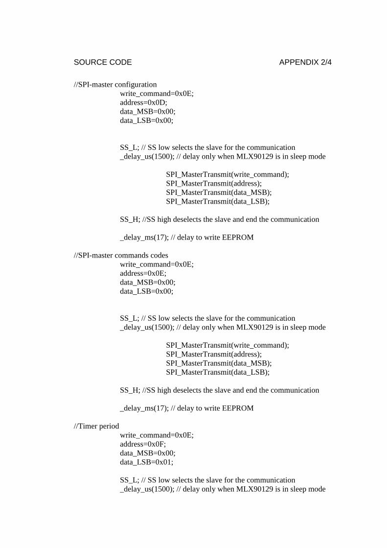
SOURCE CODE APPENDIX 2/4
//SPI-master configuration
write_command=0x0E;
address=0x0D;
data_MSB=0x00;
data_LSB=0x00;
SS_L; // SS low selects the slave for the communication
_delay_us(1500); // delay only when MLX90129 is in sleep mode
SPI_MasterTransmit(write_command);
SPI_MasterTransmit(address);
SPI_MasterTransmit(data_MSB);
SPI_MasterTransmit(data_LSB);
SS_H; //SS high deselects the slave and end the communication
_delay_ms(17); // delay to write EEPROM
//SPI-master commands codes
write_command=0x0E;
address=0x0E;
data_MSB=0x00;
data_LSB=0x00;
SS_L; // SS low selects the slave for the communication
_delay_us(1500); // delay only when MLX90129 is in sleep mode
SPI_MasterTransmit(write_command);
SPI_MasterTransmit(address);
SPI_MasterTransmit(data_MSB);
SPI_MasterTransmit(data_LSB);
SS_H; //SS high deselects the slave and end the communication
_delay_ms(17); // delay to write EEPROM
//Timer period
write_command=0x0E;
address=0x0F;
data_MSB=0x00;
data_LSB=0x01;
SS_L; // SS low selects the slave for the communication
_delay_us(1500); // delay only when MLX90129 is in sleep mode

SOURCE CODE APPENDIX 2/5
SPI_MasterTransmit(write_command);
SPI_MasterTransmit(address);
SPI_MasterTransmit(data_MSB);
SPI_MasterTransmit(data_LSB);
SS_H; //SS high deselects the slave and end the communication
_delay_ms(17); // delay to write EEPROM
//Timer configuration
write_command=0x0E;
address=0x10;
data_MSB=0x00;
data_LSB=0x3C;
SS_L; // SS low selects the slave for the communication
_delay_us(1500); // delay only when MLX90129 is in sleep mode
SPI_MasterTransmit(write_command);
SPI_MasterTransmit(address);
SPI_MasterTransmit(data_MSB);
SPI_MasterTransmit(data_LSB);
SS_H; //SS high deselects the slave and end the communication
_delay_ms(17); // delay to write EEPROM
//Sensor trimming
write_command=0x0E;
address=0x14;
data_MSB=0x00;
data_LSB=0x01;
SS_L; // SS low selects the slave for the communication
_delay_us(1500); // delay only when MLX90129 is in sleep mode
SPI_MasterTransmit(write_command);
SPI_MasterTransmit(address);
SPI_MasterTransmit(data_MSB);
SPI_MasterTransmit(data_LSB);
SS_H; //SS high deselects the slave and end the communication
_delay_ms(17); // delay to write EEPROM

SOURCE CODE APPENDIX 2/6
//Sensor 0 control word
write_command=0x0E;
address=0x15;
data_MSB=0xC0;
data_LSB=0x70;
SS_L; // SS low selects the slave for the communication
_delay_us(1500); // delay only when MLX90129 is in sleep mode
SPI_MasterTransmit(write_command);
SPI_MasterTransmit(address);
SPI_MasterTransmit(data_MSB);
SPI_MasterTransmit(data_LSB);
SS_H; //SS high deselects the slave and end the communication
_delay_ms(17); // delay to write EEPROM
//Sensor 0 low treshold
write_command=0x0E;
address=0x16;
data_MSB=0x00;
data_LSB=0x00;
SS_L; // SS low selects the slave for the communication
_delay_us(1500); // delay only when MLX90129 is in sleep mode
SPI_MasterTransmit(write_command);
SPI_MasterTransmit(address);
SPI_MasterTransmit(data_MSB);
SPI_MasterTransmit(data_LSB);
SS_H; //SS high deselects the slave and end the communication
_delay_ms(17); // delay to write EEPROM
//Sensor 0 high treshold
write_command=0x0E;
address=0x17;
data_MSB=0x00;
data_LSB=0x00;
SS_L; // SS low selects the slave for the communication
_delay_us(1500); // delay only when MLX90129 is in sleep mode
SPI_MasterTransmit(write_command);

SOURCE CODE APPENDIX 2/7
SPI_MasterTransmit(address);
SPI_MasterTransmit(data_MSB);
SPI_MasterTransmit(data_LSB);
SS_H; //SS high deselects the slave and end the communication
_delay_ms(17); // delay to write EEPROM
//Sensor 0 conditionner config
write_command=0x0E;
address=0x18;
data_MSB=0x00;
data_LSB=0x00;
SS_L; // SS low selects the slave for the communication
_delay_us(1500); // delay only when MLX90129 is in sleep mode
SPI_MasterTransmit(write_command);
SPI_MasterTransmit(address);
SPI_MasterTransmit(data_MSB);
SPI_MasterTransmit(data_LSB);
SS_H; //SS high deselects the slave and end the communication
_delay_ms(17); // delay to write EEPROM
//Sensor 0 connection configuration
write_command=0x0E;
address=0x19;
data_MSB=0x02;
data_LSB=0x10;
SS_L; // SS low selects the slave for the communication
_delay_us(1500); // delay only when MLX90129 is in sleep mode
SPI_MasterTransmit(write_command);
SPI_MasterTransmit(address);
SPI_MasterTransmit(data_MSB);
SPI_MasterTransmit(data_LSB);
SS_H; //SS high deselects the slave and end the communication
_delay_ms(17); // delay to write EEPROM

SOURCE CODE APPENDIX 2/8
//Sensor 0 resistance network
write_command=0x0E;
address=0x1A;
data_MSB=0x80;
data_LSB=0x00;
SS_L; // SS low selects the slave for the communication
_delay_us(1500); // delay only when MLX90129 is in sleep mode
SPI_MasterTransmit(write_command);
SPI_MasterTransmit(address);
SPI_MasterTransmit(data_MSB);
SPI_MasterTransmit(data_LSB);
SS_H; //SS high deselects the slave and end the communication
_delay_ms(17); // delay to write EEPROM
/*-------------------SPI_MLX90129_read-------------------*/
void SPI_MLX90129_read(void)
char read_command;
char address;
char data_MSB;
char data_LSB;
// Read Register at address
read_command=0x0F;
address=0x29;
data_MSB=0xFF;
data_LSB=0xFF;
SS_L; // SS low selects the slave for the communication
_delay_us(1500); // delay only when MLX90129 is in sleep mode
// send read command and targeted address
SPI_MasterTransmit(read_command);
SPI_MasterTransmit(address);
_delay_us(50); // delay to read EEPROM
//send 0x00 (or other random data) to generate SPI
clock
// and get the slave answer

SOURCE CODE APPENDIX 2/9
data_MSB=SPI_MasterTransmit(0x00);
data_LSB=SPI_MasterTransmit(0x00);
SS_H; // SS high deselects the slave and end the communication
/*------------------SPI_MLX90129_update------------------*/
void SPI_MLX90129_update(void)
char update_command;
// Update command =0x1C
update_command=0x1C;
SS_L; // SS low selects the slave for the communication
// send the update command
SPI_MasterTransmit(update_command);
SS_H; // SS high deselects the slave and end the communication
_delay_us(1500); // delay for the update of the registers
/*----------------------Main program----------------------*/
int main ( void )
SS_H;
SPI_MasterInit();
SPI_MLX90129_write(); // write MLX90129 config
SPI_MLX90129_update(); // update register file
/*SPI_MLX90129_read(); // read register values*/
return(0);

INDUCTION CHARGER APPENDIX 3/1

INDUCTION CHARGER APPENDIX 3/2

INDUCTION CHARGER APPENDIX 3/3
Top Related
Copyright © 2022 FDOKUMEN

