


Bahasa
Halaman
Hukum


i
Reconfigurable Discrete-time Analog FIR filters for
Wideband Analog Signal Processing
Shinwoong Park
Dissertation submitted to the faculty of the Virginia Polytechnic Institute and State
University in partial fulfillment of the requirements for the degree of
Doctor of Philosophy
In
Electrical Engineering
Sanjay Raman, Chair
Yang Cindy Yi
Dong. S. Ha
Jeffrey H. Reed
Rafael Davalos
January 14, 2018
Blacksburg, VA
Keywords: Integrated Circuits, Analog Signal Processing, Discrete-time Domain
Signal Processing, Analog FIR Filter, Time-interleaved Operation, Charge-scaling DAC
Copyright 2019, Shinwoong Park

Reconfigurable Discrete-time Analog FIR filters for Wideband Analog
Signal Processing
Shinwoong Park
ABSTRACT
Demand for data communication capacity is rapidly increasing with more and more
number of users and higher bandwidth services. As a result, a critical research issue is the
implementation of wideband and flexible signal processing in communication and sensing
applications. Although software defined radio (SDR) is a possible solution, it may not be
practical due to the excessive requirements for analog-to-digital converter (ADCs) and
digital filters for wideband signals. In this environment, discrete-time (DT) domain circuits
are gaining attention in various architectures such as N-path filters, sampling mixers, and
analog FIR/IIR/FFT filters. DT analog signal processing (DT-ASP) ahead of an ADC
considerably relaxes the ADC requirements by flexible filtering, offers the potential for
higher dynamic range performance, and provides robustness in the presence of digital
CMOS scaling.
The primary work presented in this dissertation is the design of wideband analog finite
impulse response (AFIR) filters. Analog FIR filters have been used as low pass filters for
out-of-band rejection in narrow-band applications. However, this work seeks to develop
AFIR filters suitable for wideband applications, extending its possible applications. To
achieve these performance goals, capacitive digital to analog converters (CDACs) have
been introduced for the first time as wideband analog coefficient multipliers, which has led
to high linearity analog multiplication with coefficient selection at the DAC resolution. A
prototype 4th order DT FIR filter has been implemented in 32nm SOI CMOS technology
and has achieved low-pass, band-pass, and high-pass filter (LPF, BPF and HPF) transfer
functions corresponding to the programmed coefficient sets with IIP3>11dBm linearity
and less than 2 mW/tap of power consumption. The AFIR filter is also utilized to
demonstrate a proof-of-concept FIR-based beamforming. The beamforming network
consisting of 4 antenna element inputs followed by AFIR filters was implemented with
PCB modules with the previously fabricated AFIR filter chip. Behavioral simulations are
used to verify the beamforming function with given coefficient sets. Based on the
developed AFIR filter modules, FIR-based beamforming was demonstrated with
measurement results matching well with the simulations.
Further work presented is the design and optimization of multi-section CDAC (MS-
CDAC) structures. The proposed MS-CDAC approach provides wide range of options to
optimize the tradeoff between kT/C noise, linearity versus switching energy, speed and
area. When the optimization approach is applied to a proof-of-concept 10-bit CDAC
design, the selected MS-CDAC structure reduces total capacitance and switching energy
by 97% and 98%, respectively for given linearity and noise limitations. The proposed MS-
CDAC structures are applicable in both DT-ASP coefficient multiplier and SAR-ADC
applications.

Reconfigurable Discrete-time Analog FIR filters for Wideband Analog
Signal Processing
Shinwoong Park
GENERAL AUDIENCE ABSTRACT
In communication systems, filter design is a fundamental task required to recover the
signal of interest in the presence of interference. As upcoming communication systems,
such as 5th generation (5G) mobile communications and future IEEE 802.11 standards
(Wi-Fi), require higher speed and flexibility in signal processing due to the rapidly
increasing number of users and data rates, it becomes more challenging to design such
filters. In general, analog filters are useful for high-speed, digital filters features flexibility.
To take advantage of both aspects, discrete-time (DT) domain filters have become a
promising alternative, which can be used to implement digital signal processing functions
in the analog domain.
This dissertation presents the development of DT analog finite-impulse-response
(AFIR) filter design for mixed-signal processing applications. The core idea in this work
is to adopt the capacitive DAC (CDAC) as a coefficient multiplier, which enables digital
code coefficient multiplication as well as high-speed and high-linearity performance while
consuming low power. A prototype 4th order DT FIR filter implemented in 32nm SOI
CMOS process is demonstrated with measurements. Based on the developed AFIR filters,
proof-of-concept FIR-based beamforming is investigated as well. For this purpose, AFIR
filter modules are built on printed-circuit-boards (PCBs) and coefficients are calculated by
a simplified method.
In addition, this dissertation also includes analysis and optimization of multi-section
CDAC (MS-CDAC) structures. Traditional CDAC approaches have a fundamental trade-
off between noise and linearity versus size, switching energy and speed. This work explores

v
the characteristics of CDACs depending on the section segmentations and the optimal
structure is selected based on the trade-off. Through comprehensive simulations and
calculations, the selected structure for 10-bit MS-CDAC achieved 97% and 98% reduced
total capacitance and switching energy, respectively.

vi
Acknowledgements
First of all, I would like to thank God for making everything possible. He made everything
possible even the things that I did not think it was possible.
I would like to express my profound gratitude to my advisor, Sanjay Raman, for his
guidance and discussions throughout my research. He has shown great insight, kindness,
and patience, which became the most important value for my entire career.
I would like to thank the committee members for their time and valuable comments, and
previous co-advisor, Kwan-Jin Koh, for his advice and excellent lectures.
The early stages of this work were sponsored by the DARPA Arrays at Commercial
Timescales program, program manager Dr. Troy Ollsson, under subcontract from
Raytheon. I greatly appreciate the valuable technical interactions with Raytheon staff who
worked with in the original phase of the project, in particular Dr. Bo Marr. Subsequently,
this work was sponsored in large part by the Air Force Research Laboratory, under
subcontracts from Berrie Hill Corporation, University of Dayton Research Institute
(UDRI), and KBR Wyle. I would like to specifically thank AFRL technical program
manager, Tony Quach, and Aji Mattamana. Without their funding support and technical
guidance, I could not have continued my research.
I sincerely appreciate all my labmates for sharing their knowledge and experience with me.
Special thanks to Dongseok Shin for providing me with abundant advices regarding not
only about research but also about other important things as PhD student.
Special thanks are extended to Dale Simmonds who helped me with Rohde & Schwarz
equipment and provided useful information for my measurements and to Steven Dooley in
AFRL for his time and efforts to make test boards.
Finally yet importantly, I would like to express my deepest gratitude to my family. My
wife, Heejin You, showed me unlimited devotion and patience. My parents, grandparents,
and parents-in-law prayed for me every day and were always willing to support me in all
aspects.

vii
Table of Contents
1 Introduction ........................................................................................ 1
1.1 Motivation ..................................................................................................... 1
1.2 Discrete-time Analog FIR Filters.................................................................. 2
1.2.1 Overview of discrete-time analog signal processing ............................. 2
1.2.2 Overview of FIR filters .......................................................................... 6
1.2.3 Prior analog FIR filters ....................................................................... 10
1.2.4 A charge-sharing multiplier ................................................................ 13
1.3 Overview of FIR-based Beamforming ........................................................ 15
1.4 Dissertation Organization ........................................................................... 18
2 A 3.25GS/s 4th-Order Programmable Analog FIR Filter Design Using
Split-CDAC Coefficient Multipliers ............................................................. 20
2.1 Proposed Analog FIR Filter Architecture ................................................... 20
2.2 Analog FIR Filter Circuit Implementation ................................................. 24
2.2.1 6-bit split-capacitor DAC coefficient multiplier unit .......................... 24
2.2.2 Switch control clock signal .................................................................. 25
2.2.3 Adder ................................................................................................... 26
2.2.4 Clock generation circuitry ................................................................... 27
2.3 Simulation Results ...................................................................................... 27
2.4 Measurement and Malfunction Issues ........................................................ 30
viii
2.4.1 Measurement setup .............................................................................. 31
2.4.2 Transparent shift register issue ........................................................... 32
2.4.3 ESD issue ............................................................................................. 35
2.5 Summary ..................................................................................................... 35
3 Improved 3.25GS/s 4th-Order Programmable Analog FIR Filter
Using Split-CDAC Coefficient Multipliers .................................................. 37
3.1 Introduction ................................................................................................. 37
3.2 Design Objective ......................................................................................... 38
3.3 Architecture of 5-Tap 4th-order AFIR filter ................................................ 38
3.4 Circuit Implementation ............................................................................... 41
3.4.1 Sample and hold .................................................................................. 41
3.4.2 Coefficient multiplier ........................................................................... 49
3.4.3 Adder ................................................................................................... 55
3.4.4 Non-overlapping clock generation ...................................................... 59
3.4.5 Shift register ........................................................................................ 60
3.4.6 I/O buffer ............................................................................................. 62
3.5 Noise Analysis ............................................................................................ 63
3.6 Effect of Time-interleaved Operation Mismatch ........................................ 67
3.7 Measurement Results .................................................................................. 71
3.7.1 Shift register functionality check ......................................................... 73
3.7.2 Frequency response ............................................................................. 73
3.7.3 Nonlinearity ......................................................................................... 76
3.7.4 Noise .................................................................................................... 78
3.7.5 Time-interleaved operation spurs ........................................................ 79
3.7.6 Power consumption ............................................................................. 80

ix
3.7.7 Measurement result comparison ......................................................... 81
3.8 Summary ..................................................................................................... 82
4 Wideband beamforming with 4th order AFIR filter ........................ 83
4.1 Introduction ................................................................................................. 83
4.2 Coefficients for FIR-BF .............................................................................. 84
4.3 Prototype module-level FIR-BF ................................................................. 86
4.4 Measurement Results .................................................................................. 89
4.5 Summary ..................................................................................................... 90
5 Analysis and optimization of multi-section capacitive DACs for
Mixed-Signal Processing .............................................................................. 92
5.1 Introduction ................................................................................................. 92
5.2 Concept of Multi-Section Capacitive DACs............................................... 94
5.3 Characteristics and Tradeoffs of 6-bit MS-CDAC ..................................... 98
5.3.1 Total capacitance and switching energy ............................................. 99
5.3.2 Static linearity.................................................................................... 101
5.3.3 Sampling noise and speed.................................................................. 104
5.3.4 Overall tradeoffs in 6-bit MS-CDAC cases ....................................... 106
5.3.5 Considerations in SAR-ADC and analog coefficient multiplier
applications ........................................................................................................... 108
5.4 10-Bit MS-CDAC Design ......................................................................... 109
5.5 Summary ................................................................................................... 115
6 Contributions and Future Work ..................................................... 117
6.1 Conclusions ............................................................................................... 117
6.2 Future Work .............................................................................................. 119
References ............................................................................................. 121
x
List of Figures
Figure 1-1. DT analog signal processing takes advantage of both analog and digital
circuits. ................................................................................................................................ 2
Figure 1-2. Analog delays: (a) Transmission line, (b) active delay, (c) serial S/H and
(d) parallel S/H. ................................................................................................................... 4
Figure 1-3. Prior arts of analog FIR filters: (a) analog IIR filter, (b) analog FFT, (c)
analog FIR filter. ................................................................................................................. 5
Figure 1-4. Block diagram of 4th order FIR filter. ....................................................... 7
Figure 1-5. Linear phase FIR filter types. .................................................................... 8
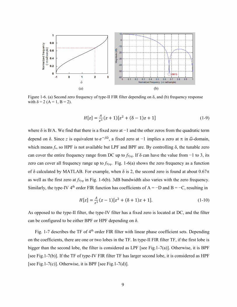
Figure 1-6. (a) Second zero frequency of type-II FIR filter depending on δ, and (b)
frequency response with δ = 2 (A = 1, B = 2)..................................................................... 9
Figure 1-7. Transfer function of (a) LPF and (b) BFP with type-II coefficient sets, and
(c) HPF and (d) BPF with type-IV coefficient sets........................................................... 10
Figure 1-8. Prior analog FIR filter architectures: (a) conventional switched capacitor;
(b) rotational gm and (c) rotational R; and (d) rotational gm with DT input. ................... 11
Figure 1-9. Attenuation of sinc function [sinc(𝝅 ∙ 𝝎/𝝎𝒔)] ....................................... 12
Figure 1-10. Charge-sharing coefficient multiplier. .................................................. 14
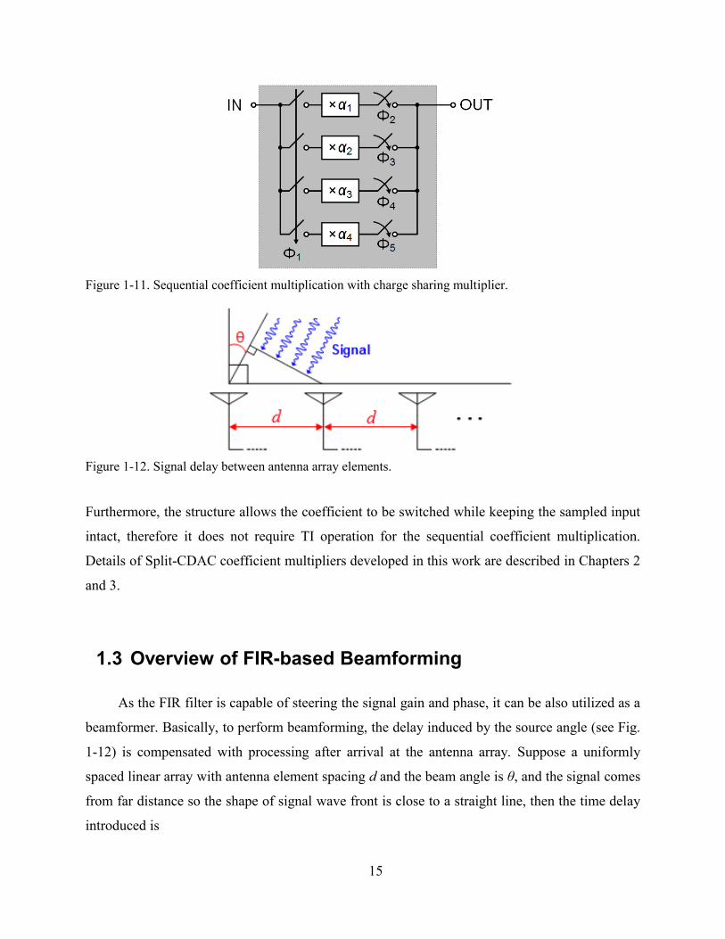
Figure 1-11. Sequential coefficient multiplication with charge sharing multiplier. .. 15
Figure 1-12. Signal delay between antenna array elements. ..................................... 15
Figure 1-13. Comparison between array factors for three different frequencies when
steered to 20 using phase shifters, (a), and time-delay, (b). The phase shifter values were
computed based on the center frequency of 10 GHz. The simulated array is 64 elements
with an element spacing of λ/2 for 12 GHz [16]. ............................................................. 16
Figure 1-14. Concept of FIR-based Beamformer ...................................................... 17
Figure 1-15. (a) Implementation of FIR-based beamformer and (b) measurement
results of transfer function [17]......................................................................................... 18
Figure 2-1. Block diagram of the proposed 4-tap analog FIR filter. ......................... 21
xi
Figure 2-2. Comparison of delay and coefficient pairs between conventional FIR
structure and rotating coefficient at (a) n = 4 and (b) n = 5. ............................................. 22
Figure 2-3. 3dB bandwidth and zero frequency vs. two 6-bit code coefficient sets. . 23
Figure 2-4. 6-bit split-capacitor DAC as a coefficient multiplier unit. ..................... 24
Figure 2-5. Structure of the single tap and the required driving clock signals. ......... 26
Figure 2-6. 4-Input analog adder circuit. ................................................................... 26
Figure 2-7. Clock generation circuitry: (a) clock divider by 16, (b) non-overlapping
clock generation with XOR and XNOR gets including complementary clock generation
circuits, and the rotating coefficient switching logic. ....................................................... 28
Figure 2-8. Layout of the Analog FIR filter fabricated in 32nm SOI CMOS process
and the core is magnified on the right. .............................................................................. 29
Figure 2-9. Frequency response of the AFIR filter with different coefficient sets. ... 29
Figure 2-10. The AFIR filter chip fabricated in 32 nm SOI CMOS technology. ...... 30
Figure 2-11. Measurement setup for the 4-tap Analog FIR filter. ............................. 31
Figure 2-12. Data shift at single clock pulse (a) when shift register function normally,
and (b) with problem of transparent shift register. ........................................................... 32
Figure 2-13. Effect of parasitic inductance from wire bonding on inverter chain. ... 33
Figure 2-14. Sufficient on-chip decoupling capacitor cancels out the effect of
wirebonding parasitic capacitance .................................................................................... 34
Figure 2-15. A simple Schmitt trigger implemented with 3 inverters and the simulated
input versus output hysteresis. .......................................................................................... 34
Figure 2-16. On-chip ESD protection with clamping diodes. ................................... 35
Figure 3-1. The proposed 4-tap discrete time analog FIR filter architecture. ........... 39
Figure 3-2. Timing table of sampling and coefficient multiplication in each channel.
........................................................................................................................................... 40
Figure 3-3. (a) Open-loop S/H, and (b) switch on-resistance depending on the input
level. .................................................................................................................................. 42
Figure 3-4. Clock switching-related errors: (a) channel charge injection and (b) clock
feed through. ..................................................................................................................... 44
Figure 3-5. Simulated comparison of complementary switch + differential structure
and NMOS only + single-ended structure. ....................................................................... 45

xii
Figure 3-6. (a) Dummy switches cancelling out the off-switch leakage when the
sampling SWs are closed (b) simulation result. ................................................................ 46
Figure 3-7. (a) Simulation with two-channel ping-pong operation for complete
discrete-time signal output, (b) its transient simulation result, and (c) its calculated FFT
spectrum. ........................................................................................................................... 47
Figure 3-8. Split-CDAC coefficient multiplier including parasitic capacitance. ...... 50
Figure 3-9. Effect of parasitic capacitors on split-CDAC coefficient multiplier: (a)
Output voltage versus 6-bit digital code when input is 100mV and (b) DNL. ................. 50
Figure 3-10. Single path of AFIR filter with bi-phase (+/-) sign selection switch D752
Figure 3-11. (a) S/H buffer with impedance looking from S/H buffer output, and (b)
simulation to observe settling behavior of coefficient multiplication with its result. ....... 52
Figure 3-12. Implementation of rotating coefficient (clock phases are particularly for
Ch.1).................................................................................................................................. 54
Figure 3-13. Structure of adder and connection to S/H + coefficient multipliers. .... 55
Figure 3-14. Simple transient simulation result of AFIR filter (Input: 100mV @
100MHz and 1GHz, Coefficient sets: A = D = 100101 and B = C = 111111) ......... 57
Figure 3-15. (a) Equivalent adder without linearization, and (b) linearity comparison
over example type-II and type-IV coefficient sets. ........................................................... 58
Figure 3-16. Non-overlapping clock generation circuitry: (a) Clock divider by 10 and
(b) non-overlapping clock generation with XOR and XNOR gates. ................................ 60
Figure 3-17. Diagram of clock waveforms from clock generation circuits to AFIR
filter. .................................................................................................................................. 61
Figure 3-18. 28-bit shift register ................................................................................ 62
Figure 3-19. Noise source of AFIR filter. .................................................................. 63
Figure 3-20. Sampling circuit noise analysis. ............................................................ 64
Figure 3-21. Flow of noise from (a) sampling switch and (b) reset switch. .............. 65
Figure 3-22. Output noise power from each noise source and total output noise power.
........................................................................................................................................... 67
Figure 3-23. Signal errors due to sampling timing mismatch in 5-channel AFIR filter.
........................................................................................................................................... 68
xiii
Figure 3-24. (a) Timing mismatch in two-channel sampling system and (b) the effect
of timing mismatch in frequency-domain. ........................................................................ 68
Figure 3-25. Effect of offset mismatch. ..................................................................... 69
Figure 3-26. Effect of coefficient mismatch: (a) output spectrum when only a single
coefficient set is considered, (b) output spectrum when there is no coefficient mismatch,
and (c) simulation result when there is a maximum 5% of arbitrary mismatches in S/H
buffers, coefficients and adder transconductances. ........................................................... 71
Figure 3-27. Die photo of the 5-tap 4th order AFIR filter and pin description. ......... 72
Figure 3-28. Shift register measurement setup and result. ........................................ 73
Figure 3-29. Measurement setup for transfer function of AFIR filter. ...................... 74
Figure 3-30. Frequency response of the AFIR filter with 7 example coefficient sets of
(a) Type-II and (b) Type-IV .............................................................................................. 75
Figure 3-31. Measured 3dB BW/zero frequency and step size of 3dB BW/zero
frequency and gain over for (a) all possible Type-II LPF coefficient sets, and (b) all possible
Type-IV HPF coefficient sets. .......................................................................................... 76
Figure 3-32. Measurement setup for two-tone test. ................................................... 77
Figure 3-33. Measured IIP3 from two-tone tests compared with simulation results. 77
Figure 3-34. Measured total output noise (when A=B=C=D=63/64) compared with
simulation/calculation result. ............................................................................................ 78
Figure 3-35. Spurs and image tones from time interleaved operation (when A = B = C
= D = 63/64). ..................................................................................................................... 80
Figure 4-1. Delays of signal arrived at each antenna elements with even spacing of d
and different beam angle (a) θ = 0°, (b) θ = 14.5°, (c) θ = 19.5°, (d) θ = 30° and (e) θ = 90°.
........................................................................................................................................... 84
Figure 4-2. Coefficients (/64) for 4 taps and 4 elements FIR-based beamformer with
constant center frequency, bandwidth and different beam angles. ................................... 87
Figure 4-3. Behavioral simulation results with individual coefficient set for the 5 beam
angles. ............................................................................................................................... 87
Figure 4-4. Diagram of the proof-of-concept 4-elements 4th order FIR-BF
measurement. .................................................................................................................... 88
Figure 4-5. Designed AFIR filter module and parts list. .......................................... 89

xiv
Figure 4-6. Measurement setup to demonstrate the FIR-based beamforming with the
fabricated AFIR filters. ..................................................................................................... 90
Figure 4-7. Measurement results of analog FIR-based beamformer with the coefficient
sets from simplified calculation method for 19.5°, 30°, 90° when (a) frequency is fixed at
1GHz or (b) beam angle is fixed at the steered angle. ...................................................... 91
Figure 5-1. Structure of SAR ADC. .......................................................................... 93
Figure 5-2. Integration of two Capacitive DACs: (a) switching a dummy capacitor with
a new CDAC, (b) two-section CDAC, and (c) equivalent description of two-section CDAC.
........................................................................................................................................... 95
Figure 5-3. General MS-CDAC structure. ................................................................. 96
Figure 5-4. Example of 6-bit multi-section CDAC: Case-7 (a) for conventional
switching, (b) for Vcm-based switching and (c) for analog coefficient multiplier. ............ 98
Figure 5-5. (a) Total capacitance of MS-CDAC cases and (b) switching energy versus
total capacitance. ............................................................................................................... 99
Figure 5-6. Sources of nonlinearity (example Case-7) ............................................ 101
Figure 5-7. Nonlinearity compensation steps: (a) original DNL, (b) after increasing
CB1, (c) after re-adjusting CB1 and (d) fixed DNL. ......................................................... 102
Figure 5-8. Static linearity (DNL and INL) with respect to 6-bit MS-CDAC cases.
......................................................................................................................................... 104
Figure 5-9. Unit capacitor scaling versus 95% worst-case |DNL|max with 6-bit MS-
CDAC (Case-13). ............................................................................................................ 105
Figure 5-10. Total capacitance versus DNL. Optimal cases are selected based on total
capacitance and MSB capacitance (group) versus DNL................................................. 106
Figure 5-11. 10-bit C-2C structure with 4-bit MSB section and 6-bit LSB section. 110
Figure 5-12. Design flow of MS-CDAC design from intermediate C-2C cases. (·) refer
to the 10-bit design cases in Table 5-IV. ........................................................................ 111
Figure 5-13. Layout of Case-L and the result of post-layout static linearity simulation.
......................................................................................................................................... 114
Figure 6-1. Block diagram of a 4-element, 4-tap FIR-based beamformer in a single
chip. ................................................................................................................................. 120
xv
List of Tables
TABLE 2-I. POST-LAYOUT SIMULATION RESULTS ...................................................... 30
TABLE 3-I. SUMMARY OF SAMPLING SWITCH AND CAPACITOR DESIGN AND SIMULATED
PERFORMANCE ................................................................................................................... 48
TABLE 3-II. DESIGN PARAMETERS AND SIMULATED PERFORMANCE OF A PAIR OF S/H
BUFFER AND COEFFICIENT MULTIPLIER ............................................................................ 53
TABLE 3-III. DESIGN PARAMETERS OF ADDER ........................................................... 56
TABLE 3-IV. POWER CONSUMPTION OF CLOCK DRIVING CIRCUITS ........................... 61
TABLE 3-V. SUMMARY OF MEASURED PERFORMANCE OF AFIR FILTER WITH
HIGHLIGHTED COEFFICIENT SETS ...................................................................................... 79
TABLE 3-VI. MEASURED POWER CONSUMPTION OF AFIR FILTER ............................. 80
TABLE 3-VII. COMPARISON WITH PREVIOUS AFIR FILTER WORKS ........................... 81
TABLE 5-I. POSSIBLE CASES OF 6-BIT MULTI-SECTION CDAC .................................. 97
TABLE 5-II. PERFORMANCE OF OPTIMAL 6-BIT CASES ............................................. 107
TABLE 5-III. CONSIDERATIONS OF MS-CDAC PERFORMANCE IN SAR-ADC AND
ANALOG COEFFICIENT MULTIPLIER ................................................................................. 109
TABLE 5-IV. 95% WORST-CASE |DNL|MAX OF 10-BIT C-2C AND MS-CDAC
STRUCTURES .................................................................................................................... 113
TABLE 5-V. PERFORMANCE COMPARISON OF SELECTED 10-BIT MS-CDAC WITH
OTHER EXISTING METHODS ............................................................................................. 114

1
1 Introduction
Chapter 1.
Introduction
1.1 Motivation
The volume of communications traffic has been rapidly increasing over the last several years
to accommodate greater numbers of users with higher bandwidth service. Meanwhile, wireless
spectrum is a limited resource requiring the ability to reconfigure communications transceivers to
operate over a wide range of bands. As a result, at the hardware implementation level, it is highly
desirable to realize wideband and flexible signal processing in order to cope with such demands.
Software-defined radio (SDR) [1] is considered to achieve such flexibility by pushing RF functions
into the digital domain. However, wideband processing can overburden the analog-to-digital
converter (ADC) as well as following digital domain blocks due to the need for high dynamic
range at high speed, and the corresponding power consumption. In particular, upcoming wireless
communication standards like 5th generation wireless communication (5G), as well as wideband
sensor applications, require ADCs with multi-GS/s and medium resolution while consuming low
power [2].
Discrete-time analog signal processing can be a promising alternative solution to implement
flexible signal processing with high speed by taking advantage of both analog and digital features,
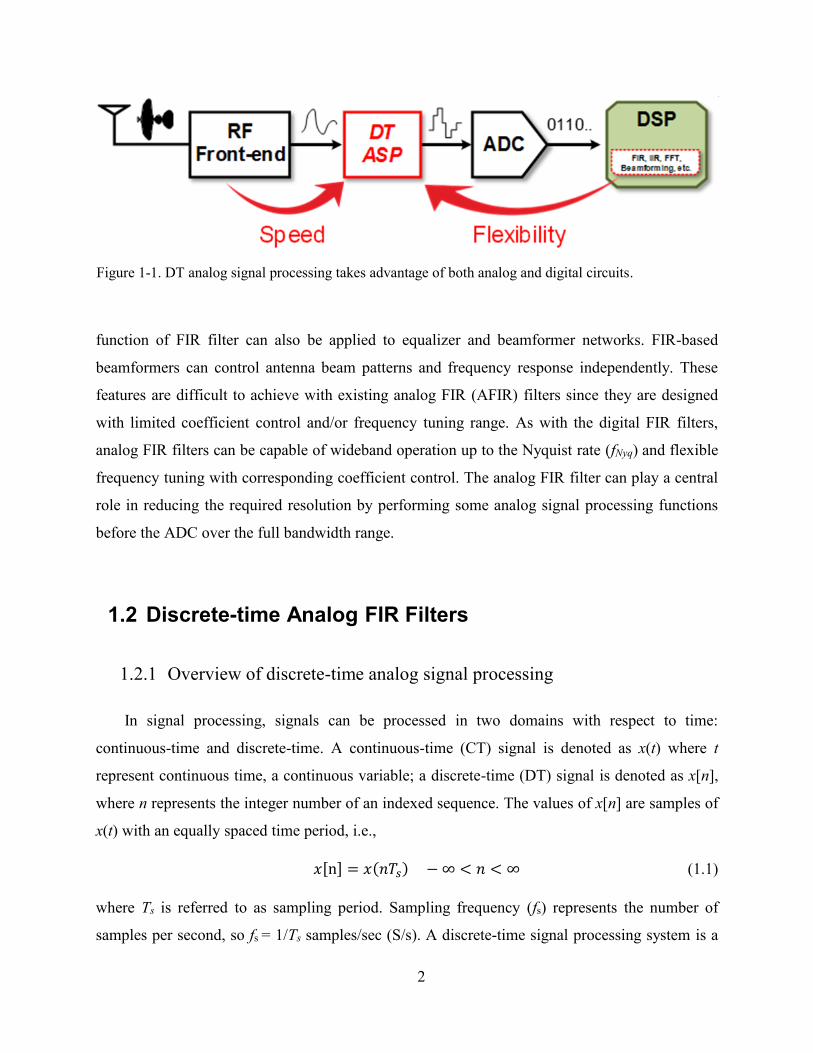
which effectively helps to reduce the burden imposed on following stages (Fig. 1-1). A finite
impulse response (FIR) filter is an extremely useful function that can easily implemented in the
DT-domain. Frequency selection can be adaptable by programming coefficients, and the filter type
can be any of low-pass, band-pass and high-pass with linear phase response. Furthermore, the
2
function of FIR filter can also be applied to equalizer and beamformer networks. FIR-based
beamformers can control antenna beam patterns and frequency response independently. These
features are difficult to achieve with existing analog FIR (AFIR) filters since they are designed
with limited coefficient control and/or frequency tuning range. As with the digital FIR filters,
analog FIR filters can be capable of wideband operation up to the Nyquist rate (fNyq) and flexible
frequency tuning with corresponding coefficient control. The analog FIR filter can play a central
role in reducing the required resolution by performing some analog signal processing functions
before the ADC over the full bandwidth range.
1.2 Discrete-time Analog FIR Filters
1.2.1 Overview of discrete-time analog signal processing
In signal processing, signals can be processed in two domains with respect to time:
continuous-time and discrete-time. A continuous-time (CT) signal is denoted as x(t) where t
represent continuous time, a continuous variable; a discrete-time (DT) signal is denoted as x[n],
where n represents the integer number of an indexed sequence. The values of x[n] are samples of
x(t) with an equally spaced time period, i.e.,
𝑥[n] = 𝑥(𝑛𝑇𝑠) − ∞ < 𝑛 < ∞ (1.1)
where Ts is referred to as sampling period. Sampling frequency (fs) represents the number of
samples per second, so fs = 1/Ts samples/sec (S/s). A discrete-time signal processing system is a
Figure 1-1. DT analog signal processing takes advantage of both analog and digital circuits.

3
system that performs an operation on a discrete-time signal [3]. Specifically, discrete-time
“analog” signal processing (DT-ASP) refers to DT signal processing after sampling and before the
signal is digitized by a quantizer, which distinguishes it from digital signal processing (DSP) where
the processing occurs in the digital domain after the ADC. DT-ASP functions can include not only
sampling but also down-conversion, decimation, filtering and so on.
DT analog circuits can be designed without high performance amplifiers, such as operational
amplifier (op-amp), by mostly utilizing switches and capacitors, which helps to avoid the voltage
headroom consumption from stacking of transistors. For DT circuits in deeply scaled technologies,
reduced switching resistance on-resistance (Ron) is a one of the main advantages along with
reduced parasitic capacitance, which helps to increase the speed of DT-domain circuits.
Furthermore, improved capacitor density saves die area. Clock generation circuitry is improved as
device scaling is advanced for digital circuits, providing higher frequency clock signals with less
power consumption in reduced area. DT circuits can be also designed with robustness against
variation (PVT) because, rather than being affected by uncertainty of absolute device parameters,
DT filter computations tend to rely on the ratio between device parameters. For example,
conventional analog FIR filters with switched capacitor arrays implement coefficient values by the
capacitance ratio, which is introduced later in this section. On the other hand, analog circuit design
is also becoming more challenging with digital CMOS technology scaling, despite dramatic
improvements in transistor cutoff frequency (ft). This is mainly because the device scaling comes
with low supply voltage but not correspondingly reduced threshold voltage (Vth) [4] as well as
deteriorating channel length modulation, resulting in poor gain and linearity.
Meanwhile, flexibility is a distinctive feature of DT-ASP compared to the typical analog
architectures. Traditional digital circuit implementations such as finite-impulse-response (FIR)
and infinite-impulse-response (IIR) filters offer flexibility through programmable coefficients,
which can be easily realized in the digital domain. However, for wideband signal processing, the
DSP functions must be preceded by a high-speed, high dynamic range ADC. Hence, DT analog
processors ahead of the ADC are a potential solution for wideband processing. DT analog circuits

4
can be made programmable or tunable. Furthermore, DT filters can provide high stopband
attenuation over the traditional analog filters by implementing zeros in the frequency response [5].
Efficient and flexible implementation of delay is also a substantial benefit of DT circuits.
While delay can be simply implemented by flip-flops in the digital domain, there are several
methods in the analog domain. Figure 1-2(a) and (b) show continuous time delay implementations,
whereas Figure 1-2(c) and (d) show discrete time implementations. Transmission lines can be
designed to have a specific delay based on their length and propagation constant [Fig 1-2(a)],
which is simple but takes excessive area. For example, assuming that the dielectric constant (Ɛr) is
4, a single period delay of 1ns (equivalent to a single period of 1GS/s rate) requires about 150mm,
which is enormously large for an IC implementation, so this approach is useful only in mm-wave
or higher frequency applications. Fig. 1-2(b) utilizes an amplifier-based delay to reduce the area,
and Fig. 1-3(c) realizes the delay with sample and hold (S/H) instead. These two methods are
inherently vulnerable to the signal distortion by non-unity gain, noise and nonlinearity. As the
signal passes through the multiple amplifiers or buffers, those non-idealities, such as noise and
nonlinearity, are accumulated. If the buffer gain is not exactly unity, it induces coefficient error,
which distorts the frequency response. Therefore, it is difficult to avoid signal deterioration when
the required number of delays are large. On the other hand, the parallel S/H method [Fig. 1-2(d)]
avoids the issue by holding the sampled signals in different channels. The delay time is easily
controlled by the clock rate, which enables frequency tunability.
(a) (b)
(c) (d)
Figure 1-2. Analog delays: (a) Transmission line, (b) active delay, (c) serial S/H and (d) parallel S/H.

5
There are some drawbacks of the DT-ASP. Signals over fNyq fold into the in-band region.
Therefore, the circuits must be preceded by sufficient filtering above fNyq and the sampling
frequency should be sufficiently high, which requires power. However, noise over fNyq needs to be
processed anyway before sampling by either DT-ASP or ADC. Another concern is the driving of
clock signals. As the switches are driven by multi-phase clock signals, DT systems can be sensitive
to clock jitter and timing mismatches. Therefore, high quality clock signal generation and
extremely careful and balanced layout design is essential. Size is rather large since capacitor arrays
are often used in DT-ASP circuits.
Fig. 1-3 shows some of the prior arts of DT ASP circuits. These architectures achieved low
power and high linearity with simple and passive component-oriented design. The IIR filter [Fig.
1-3(a)] implemented high (5th-7th) order filtering with rotational switching over multiple of hold
capacitors [4]. Mark Lehne proposed analog FFT architecture for orthogonal frequency division
multiplexing (OFDM) modulation by implementing Radix-2 computation with transconductor
coefficient multiplier and current domain addition in [6]. Further, the analog FFT reported in [7]
was able to implement the computation with only capacitors and achieved high linearity, speed
and low power [see Fig. 1-3(b)]. An analog FIR filter [Fig. 1-3(c)] can be implemented by
sampling on the capacitors in an order and adding the charge by connect all the top plates of the
capacitors. More details of this structure are discussed in section 1.2.3.
(a) (b) (c)
Figure 1-3. Prior arts of analog FIR filters: (a) analog IIR filter, (b) analog FFT, (c) analog FIR filter.

6
1.2.2 Overview of FIR filters
Before moving on to the analog FIR filter design considerations, it is useful to understand the
fundamental theory of the FIR filter. FIR and IIR are the two main types of digital filtering. Unlike
IIR filters whose transfer function (TF) is derived by processing with previous samples with
different delays from both input and output, FIR filters process input samples only. In other words,
IIR filters include feedback (recursive) processing but FIR filters perform only feedforward (non-
recursive) processing. The benefit of IIR filters is efficiency. That is, for comparable performance,
FIR filters need a higher order than IIR filters, which results in a larger number of computation
blocks. However, FIR filters are often preferred for stability and group delay considerations. IIR
filters may require careful design for stability due to feedback but FIR filters are inherently stable.
Also, FIR filters can provide a linear phase response, which is even more challenging with any
other filter type.
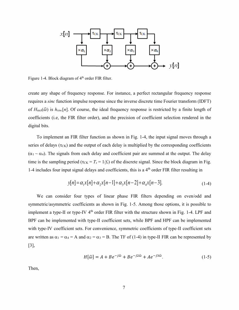
An FIR filter consists of three core elements: delay, coefficient multiplication and addition
(Fig. 1-4). The general equation of an FIR filter in the DT domain is
FIR
1
[ ] [ ]N
k
k
y n x n k
(1-1)
where x[n] and y[n] are the discrete time input and output, k is the coefficient of k-th tap, and NFIR
is the filter order. This equation can be also presented by the input signal with an impulse response
of the FIR filter
[ ] [ ] [ ]y n x n h n , for FIR
1
[ ]N
k
k
h n
. (1-2)
As convolution in the time domain is translated to multiplication in the frequency domain [3],
the frequency response of the FIR filter becomes
𝑌[] = 𝑋[] ∙ 𝐻[] (1-3)
where ω is defined as normalized frequency (ω/ωs). Thus, the H [] is frequency response of the
FIR filter so the characteristics of the FIR filter is determined by the coefficients, which realizes
the impulse response. In theory, with unlimited number of delays and coefficients, the filter can
7
create any shape of frequency response. For instance, a perfect rectangular frequency response
requires a sinc function impulse response since the inverse discrete time Fourier transform (IDFT)
of Hrect() is hsinc[n]. Of course, the ideal frequency response is restricted by a finite length of
coefficients (i.e, the FIR filter order), and the precision of coefficient selection rendered in the
digital bits.
To implement an FIR filter function as shown in Fig. 1-4, the input signal moves through a
series of delays (τCK) and the output of each delay is multiplied by the corresponding coefficients
(1 ~ 4). The signals from each delay and coefficient pair are summed at the output. The delay
time is the sampling period (τCK = Ts = 1/fs) of the discrete signal. Since the block diagram in Fig.
1-4 includes four input signal delays and coefficients, this is a 4th order FIR filter resulting in
1 2 3 4[ ] [ ] [ 1] [ 2] [ 3].y n x n x n x n x n (1-4)
We can consider four types of linear phase FIR filters depending on even/odd and
symmetric/asymmetric coefficients as shown in Fig. 1-5. Among those options, it is possible to
implement a type-II or type-IV 4th order FIR filter with the structure shown in Fig. 1-4. LPF and
BPF can be implemented with type-II coefficient sets, while BPF and HPF can be implemented
with type-IV coefficient sets. For convenience, symmetric coefficients of type-II coefficient sets
are written as 1 = 4 = A and 2 = 3 = B. The TF of (1-4) in type-II FIR can be represented by
[3],
𝐻[] = 𝐴 + 𝐵𝑒−𝑗 + 𝐵𝑒−𝑗2 + 𝐴𝑒−𝑗3. (1-5)
Then,
Figure 1-4. Block diagram of 4th order FIR filter.

8
𝐻[] = 𝐴(1 + 𝑒−𝑗3) + 𝐵(𝑒−𝑗 + 𝐵𝑒−𝑗2). (1-6)
Using Euler’s formula,
𝐻[] = 2𝑒−𝑗1.5 ∙𝐴(𝑒𝑗1.5 + 𝑒−𝑗1.5) + 𝐵(𝑒𝑗0.5 + 𝐵𝑒−𝑗0.5)
2
= 𝑒−𝑗1.5 ∙ (2𝐴 ∙ 𝑐𝑜𝑠 1.5 + 2𝐵 ∙ 𝑐𝑜𝑠 0.5). (1-7)
It is observed that the phase of H[] is determined by −𝑗1.5, presenting linear phase response,
and the magnitude depends on the coefficient set. Assuming that coefficients can be controlled,
the frequency response can be selected as desired.
The z-domain also helps to analyze the poles and zeros of the given FIR filter function [3].
The system function H[] in (1-5) can be transformed into z-domain by converting 𝑒−𝑗 to z-1,
thus
𝐻[𝑧] = 𝐴 + 𝐵𝑧−1 + 𝐵𝑧−2 + 𝐴𝑧−3 . (1-8)
To find the location of pole and zeros, (1-8) can be written as
Figure 1-5. Linear phase FIR filter types.
Odd Even
Coefficient LengthS
ym
metr
icA
sym
metr
ic
Sym
metr
icit
y
Type I Type II
Type III Type IV
/2
2
1
( ) [ ] [ ]cos2 2
M Mj
i
M MH e h h i i
( 1)/2
2
0
( ) 2 [ ]cos2
M Mj
i
MH e h i i
/2 12 2
1
( ) 2 [ ]sin2
M Mj
i
MH e h i i
( /2) 12 2
1
( ) 2 [ ]sin2
M Mj
i
MH e h i i
Even or no zeros at z = 1 and -1
No Restriction
Even or no zeros at z = 1
Odd number of zeros at z=-1
Cannot be used as a HPF
Odd number of zeros at z=1 and -1 Odd number of zeros at z = 1
Even or no zeros at z=-1
Cannot be used as a LPF Cannot be used as a LPF or HPF
9
𝐻[𝑧] =𝐴
𝑧3(𝑧 + 1)[𝑧2 + (δ − 1)𝑧 + 1] (1-9)
where δ is B/A. We find that there is a fixed zero at −1 and the other zeros from the quadratic term
depend on δ. Since z is equivalent to 𝑒−𝑗, a fixed zero at −1 implies a zero at in -domain,
which means fs, so HPF is not available but LPF and BPF are. By controlling δ, the tunable zero
can cover the entire frequency range from DC up to fNyq. If δ can have the value from −1 to 3, its
zero can cover all frequency range up to fNyq. Fig. 1-6(a) shows the zero frequency as a function
of δ calculated by MATLAB. For example, when δ is 2, the second zero is found at about 0.67
as well as the first zero at fNyq in Fig. 1-6(b). 3dB bandwidth also varies with the zero frequency.
Similarly, the type-IV 4th order FIR function has coefficients of A = −D and B = −C, resulting in
𝐻[𝑧] =𝐴
𝑧3(𝑧 − 1)[𝑧2 + (δ + 1)𝑧 + 1]. (1-10)
As opposed to the type-II filter, the type-IV filter has a fixed zero is located at DC, and the filter
can be configured to be either BPF or HPF depending on δ.
Fig. 1-7 describes the TF of 4th order FIR filter with linear phase coefficient sets. Depending
on the coefficients, there are one or two lobes in the TF. In type-II FIR filter TF, if the first lobe is
bigger than the second lobe, the filter is considered as LPF [see Fig.1-7(a)]. Otherwise, it is BPF
[see Fig.1-7(b)]. If the TF of type-IV FIR filter TF has larger second lobe, it is considered as HPF
[see Fig.1-7(c)]. Otherwise, it is BPF [see Fig.1-7(d)].
(a) (b)
Figure 1-6. (a) Second zero frequency of type-II FIR filter depending on δ, and (b) frequency response
with δ = 2 (A = 1, B = 2).

10
1.2.3 Prior analog FIR filters
Previous analog FIR filters have been designed for specific filter functions, mostly for
adjacent channel rejection [4], [8]-[12] or anti-aliasing filtering and down-conversion [13]. Fig. 1-
8 depicts three of the analog FIR filters used in those applications. The Analog FIR filter in Fig.
1-8(a) is a widely adopted architecture that is implemented with only switched capacitors. The
number of capacitors determines the filter order. Thus, Fig. 1-8(a) is a 4th order AFIR filter, which
is driven by 5 clock phases assigned for sequential sampling (Φ1 ~ Φ4) and addition (Φ5). For a 4th
order analog FIR filter, after sampling sequence at Φ1, the charge on each capacitor top plates
becomes QA=Vin,Φ1·CA. The rest of switches are also closed from Φ2 through Φ4, and then the
addition switch in Φ5 connects all top plates of the sampling capacitors. Consequently, the charge
on the capacitors is added together, so the output voltage becomes
, 5
, 1 , 2 , 3 , 4.
A B C Dout
A B C D
A in B in C in D in
A B C D
Q Q Q QV
C C C C
C V C V C V C V
C C C C
(1-11)
(a) (b)
(c) (d)
Figure 1-7. Transfer function of (a) LPF and (b) BFP with type-II coefficient sets, and (c) HPF and (d)
BPF with type-IV coefficient sets.

11
When this operation is periodic, this equation matches with FIR function of (1-4) and the
coefficients are set by the capacitance ratio; e.g., coefficient 1 is CA/(CA + CB + CC + CD). Output
is read out during a single phase (Φ5) for a cycle consisting of 5 phases, so time interleaved (TI)
operation might be required to avoid noise folding due to the downsampling. This analog FIR filter
provides low power and high linearity with passive design. However, there are two main
drawbacks. First, the coefficients are not programmable. Second, as the output is read out only at
the last clock phase, decimation occurs, which precludes operation at higher frequencies
approaching fNyq. Although it is possible to enable control over coefficients with tunable
(switchable) capacitors, and remove decimation by TI operation, the area occupied increases
exponentially with the order of filter.
Alternatively, the AFIR filter proposed in [11] implemented the FIR function by integrating
the input signal through the Gm-cell and capacitor while the transconductance is periodically
switching as shown in Fig. 1-8(b). As with the conventional AFIR filter, this filter may need TI
operation to avoid the decimation. When the coefficients are symmetrical, the TF of the filter is
|𝐻[]| = 𝑠𝑖𝑛𝑐 (𝜋 ∙
𝜔𝑠) ∙ ∑ 𝑛 ∙ 𝑐𝑜𝑠 [2𝜋(𝑛 − 0.5) ∙
𝜔𝑠] .
𝑁FIR𝑛=1 (1-12)
(a) (b)
(c) (d)
Figure 1-8. Prior analog FIR filter architectures: (a) conventional switched capacitor; (b) rotational gm
and (c) rotational R; and (d) rotational gm with DT input.

12
In this structure, coefficients are set by the transconductance selection, and area is comparatively
small as only a single capacitor is required. Nonetheless, this architecture inherently applies a sinc
function due to the signal integration. The signal integration is equivalent to convolution with the
rectangular window. If we convert the rectangular window in time domain to frequency domain,
the result is
ℱ [𝑢 (𝑡 +1
2𝑇) − 𝑢 (𝑡 −
1
2𝑇𝑠)] = 𝑇 ∙ 𝑠𝑖𝑛𝑐 (𝜋 ∙
𝜔𝑠) (1-13)
where ℱ[·] and u [·] denote the Fourier transform and step function, respectively. Therefore, the
signal is filtered by the sinc function regardless of the coefficients. This frequency response
resulting from the integration can be useful to reject narrowband signals preventing anti-aliasing,
as zeros are located at k·fs (k = 1, 2, 3…). However, the sinc function is not appropriate if the FIR
filter is to be used for wideband processing up to the vicinity of fNyq since sinc function has −3.9
dB gain at fNyq and 3 dB bandwidth is found at ~0.44 as shown in Fig. 1-9.
Recently, a similar type of AFIR filter was reported in [14], shown in Fig. 1-8(c). This
architecture also integrates the current signal, but the difference is that the current is scaled by a
linear periodically time-varying (LPTV) resistor. The high gain op-amp allows the input signal
current to be Vin/R, thus 1/R replaces the gm-cell in Fig. 1-8(b), and the current is integrated on the
feedback capacitor. This filter can be used for input matching as the LPTV resistor can be matched
to the source resistance with RIN = 1/C·fs, but the matching with LPTV introduces some coefficient
selection constraints. Considering Fig. 1-8(c) for our application, there are some disadvantages.
First, as with the AFIR filter with periodically switching gm-cell in Fig. 1-8(b), the LPTV resistor
Figure 1-9. Attenuation of sinc function [sinc(𝝅 ∙ /𝝎𝒔)]

13
method also applies the sinc function as the current signal is integrated on the feedback capacitor.
Second, suppose that the LPTV is a binary weighted resistor array; then the on-resistance and
parasitic capacitance degrade the frequency response since they directly influence the coefficients.
In order to minimize the on-resistance of the switches, their size should be large which results in
higher power consumption. Lastly, the performance depends significantly on the op-amp, which
limits the linearity and power consumption. This AFIR filter is well suited for high rejection
narrow band filtering with matching capability but is not capable of more flexible applications
using bandwidth up to fNyq. To avoid the sinc function and implement band-pass filtering, [15]
implemented a current integrating signal with DT input [Fig. 1-8(d)] by sampling the input signal
before converting to the current signal. However, this AFIR filter still relies on high gain op-amps,
which may limit the linearity and low power performance. Although [15] has proven relatively
high linearity (IIP3 > 8.5dBm), it was under condition of relatively high supply voltage (1.8V) and
low sampling speed (75MS/s). This approach may fail to achieve the performance in advanced
technologies for high speed due to the low supply.
1.2.4 A charge-sharing multiplier
The coefficient multiplier is one of the most important computation blocks in the AFIR filter
as it must be able to achieve desired linearity and speed while resolving a range of coefficient
values. In our work, a charge-sharing multiplier was developed in the early stages of AFIR filter
implementation. Eventually, split-CDAC coefficient multipliers were developed, introduced in
chapters 2 and 3, to perform this function, it is still worthwhile for completeness to introduce the
charge sharing multiplier idea and show how the coefficient multiplier is improved.
A charge-sharing multiplier is totally passive and open-loop design consisting of only
switched capacitors as shown in Fig 1-10. At first, the input signal is sampled on all binary-
weighted sampling capacitors (CS). In the next phase, selective sampling capacitors are connected
to selective hold capacitor. At this time, charge on the CS’s are shared with empty CH’s. As a result,
the voltage developed on hold capacitors becomes
𝑉𝐻[𝑛] =𝐶𝑠
𝐶𝑠+𝐶𝐻𝑉𝑆[𝑛]. (1-14)

14
where CS and CH denote the sum of binary-weighted sampling capacitors (Cs1~Cs6) and hold
capacitors (Ch1~Ch6). Effectively, the CS/(CS + CH) term determines the coefficient multiplied by
the sampled signal (VS[n]).
The advantages of this multiplier topology are as follows. With the passive-oriented design,
low power, high linearity and high-speed operation are obtained. Because the circuit directly
samples the signal, a separate sample and hold circuits are not required.
However, the charge sharing multiplier was ultimately not adopted mainly due to some key
disadvantages. First, two sets of binary weighted coefficients are necessary, which takes large area.
Since the coefficients are determined by (1-14), it is necessary to calculate the code for both CS
and CH when we need a specific coefficient value. Furthermore, the charge sharing multiplier is
inefficient for non-decimation systems. In Fig. 1-4, once the input signal is sampled at a particular
instant of time, the sampled input is multiplied by α1 and up to α4 in each period without an empty
period. However, with the charge sharing multiplier, the sampled input is not available to be
multiplied by the other coefficient values after charge sharing. Therefore, for a non-decimation
system, TI operation is required to implement sequential coefficient multiplication as shown in
Fig. 1-11, which further increases the area and switching power consumption at least by a factor
of the number of coefficients. The parasitic capacitance on the output load may also degrade the
FIR function because this capacitance also introduces another charge sharing with CH.
A capacitive DAC coefficient multiplier can resolve the above issues. By using a DAC as a
coefficient multiplier itself, the coefficient value directly corresponds to the digital code.
Figure 1-10. Charge-sharing coefficient multiplier.
Cs1
VS
VS
1
1
1
VIN(t) VOUT[n]
Cs2
VS
Cs6
Ch1 Ch2 Ch6
2
CS selection switches
CH selection switches
1 2
15
Furthermore, the structure allows the coefficient to be switched while keeping the sampled input
intact, therefore it does not require TI operation for the sequential coefficient multiplication.
Details of Split-CDAC coefficient multipliers developed in this work are described in Chapters 2
and 3.
1.3 Overview of FIR-based Beamforming
As the FIR filter is capable of steering the signal gain and phase, it can be also utilized as a
beamformer. Basically, to perform beamforming, the delay induced by the source angle (see Fig.
1-12) is compensated with processing after arrival at the antenna array. Suppose a uniformly
spaced linear array with antenna element spacing d and the beam angle is θ, and the signal comes
from far distance so the shape of signal wave front is close to a straight line, then the time delay
introduced is
Figure 1-11. Sequential coefficient multiplication with charge sharing multiplier.
Figure 1-12. Signal delay between antenna array elements.

16
0
sindt
c
(1-15)
where c0 denotes the speed of light in free space. This time delay can be compensated by a phased
array with phase shifters or true-time delay (TTD) using time-delay units (TDU). Fig. 1-13(a)
shows the beam pattern controlled with phase shifters when the phase shifter has 20 of phase shift
for 10GHz signal, which is a calculation result in [16]. It is observed that the array can steer to the
desired frequency and angle. However, if either the input frequency deviates from the design
frequency or the signal has a wide bandwidth, the center beam alters and null frequency shifts,
which is known as beam squint. This is because the compensated phase delay has the exact time
delay only at a specific frequency. Therefore, traditional phased arrays may not be appropriate for
wideband communications or sensing. Meanwhile, Fig. 1-13(b) depicts the beam pattern when Δt
is compensated by TTD [16]. It is observed that center beam is maintained regardless of the input
frequency because the time-delay does not depend on the input frequency. However, one drawback
is that the null angles still shift with the input frequency.
FIR-based beamforming provides control over both frequency and phase at each antenna
element. The concept of an FIR-based beamformer is illustrated in Fig. 1-14. The transfer function
of an array steered with FIR filters is
(a) (b)
Figure 1-13. Comparison between array factors for three different frequencies when steered to 20 using
phase shifters, (a), and time-delay, (b). The phase shifter values were computed based on the center
frequency of 10 GHz. The simulated array is 64 elements with an element spacing of λ/2 for 12 GHz [16].

17
CK2 1 ( 1)
1 1
( , ) .N M
j f n t m
FIR nm
n m
H f a e
(1-16)
where M, N and anm denote the number of elements, FIR filter order and coefficients for m-th tap
in n-th element, respectively [17]. The coefficients can be used to control the frequency response
and beam pattern independently. In theory, N and M approaching infinity can achieve ideal
frequency independent beam patterns, but N and M are limited in practice. An FIR-based
beamformer using 4th order AFIR filters was presented in [17]. The beamformer was demonstrated
with separately packaged devices on printed circuit board (PCB) [Fig. 1-15(a)] connected to four
elements of circular antenna array. The measurement results showed almost frequency
independent radiation patterns of the antenna array from 1.5GHz to 2GHz as shown in Fig.1-15(b).
In this design, delay, coefficient and addition were implemented by transmission lines, adjustable
amplifiers and a resistive power combiner, respectively. The DT AFIR filter proposed in this work
can be utilized for FIR-based beamformer in an integrated circuit with even less area and power
consumption.
Figure 1-14. Concept of FIR-based Beamformer

18
1.4 Dissertation Organization
The main objective of this dissertation is to study DT AFIR filter approaches for wideband
and flexible signal processing, as well as expanding their application to beamformers. It is
discussed in the previous sections that conventional and current integration methods might not be
appropriate due to sinc function response, decimation and coefficient selectivity. Furthermore,
high linearity is also required over the full band. In order to resolve these issues, the main
innovation in this work is the utilization of capacitive DACs (CDACs) as coefficient multipliers
in advanced SOI CMOS technology. This dissertation is comprised of the following chapters and
contents.
In Chapter 2, an analog FIR filter is presented that adopts CDAC coefficient multipliers. Brief
discussions on the operation, circuit implementation, simulation results of the filter are covered.
The measurements of this design iteration could not be completed due to some issues in the digital
(a) (b)
Figure 1-15. (a) Implementation of FIR-based beamformer and (b) measurement results of transfer function
[17].

19
circuits. This chapter analyzes the cause of the problem, and describes the solutions that were then
applied in the next version of the AFIR filter.
In Chapter 3, an improved version of AFIR filter is presented. By introducing an additional
tap for the same FIR filter order, this version of AFIR filter enhanced its efficiency with simplified
clock generation and reduced number of coefficient multipliers used. Detailed information of
operation, circuit implementation and design issues are provided. After revision of circuits to
prevent the problems that occurred in the previous version, fabricated chip measurement was
successful and the results are demonstrated.
Chapter 4 presents a proof-of-concept implementation of FIR-based beamforming (FIR-BF)
leveraging the analog FIR filter chip design presented in Chapter 3. A method to obtain coefficient
sets that can be used to measure the FIR-BF functionality without high-level coefficient calculation
is introduced and verified by simulations. To enable the beamforming measurement with the
fabricated AFIR chips, a PCB module-based FIR-BF measurement setup is designed and
implemented. The measurement results presented show reasonable response over the available
frequency and beam angle range.
In Chapter 5, the multi-section CDAC is further investigated to realize optimized structures
of capacitive DACs. The principle of the multi-section CDAC is presented with mathematical
reasoning. Using an example 6-bit design, the characteristics of MS-CDAC are examined through
calculations and simulations. Further, an algorithm to find the optimal section segmentation is
introduced and applied to a 10-bit CDAC design, which results in considerably improved
performance compared to conventional and existing structures.
Chapter 6 discusses conclusions of the work, and suggests future works.

20
2 A 3.25GS/s 4th-Order Programmable Analog FIR Filter Design
Using Split-CDAC Coefficient Multipliers
Chapter 2.
A 3.25GS/s 4th-Order Programmable
Analog FIR Filter Design Using Split-CDAC
Coefficient Multipliers
In order to overcome the limitations of the previous analog FIR (AFIR) filters, as discussed
in Chapter 1, and implement wideband reconfigurable discrete-time analog signal processing (DT-
ASP), a new architecture has been developed in this work. This proposed AFIR filter has for the
first time adopted the split-capacitive DAC (spilt-CDAC) as a coefficient multiplier. As a result,
filter coefficients can be controlled with the resolution of the DAC, and low power and high
linearity can be achieved. Furthermore, by using a high-speed buffer, full Nyquist range operation
can be obtained. This first iteration analog FIR filter design was designed, laid out in 32nm SOI
CMOS, and fabricated for testing; however the fabricated chip did not properly work due to several
issues. Nonetheless, this chapter provides the underlying concepts of the proposed architecture and
analysis of the malfunction issues, which led to the final design presented in Chapter 3.
2.1 Proposed Analog FIR Filter Architecture
The block diagram of the proposed 4-tap analog FIR filter is shown in Fig. 2-1. In the
conventional FIR filter design (see Fig.1-4), input data moves to the next tap (delay/coefficient
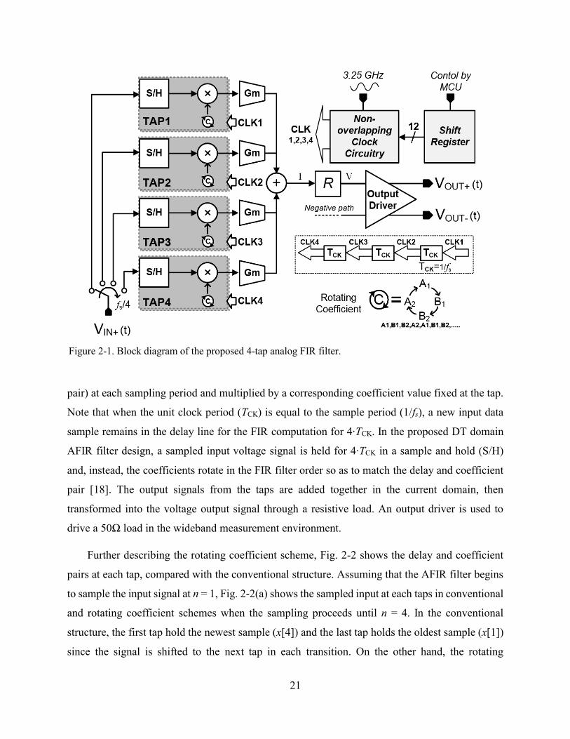
21
pair) at each sampling period and multiplied by a corresponding coefficient value fixed at the tap.
Note that when the unit clock period (TCK) is equal to the sample period (1/fs), a new input data
sample remains in the delay line for the FIR computation for 4∙TCK. In the proposed DT domain
AFIR filter design, a sampled input voltage signal is held for 4∙TCK in a sample and hold (S/H)
and, instead, the coefficients rotate in the FIR filter order so as to match the delay and coefficient
pair [18]. The output signals from the taps are added together in the current domain, then
transformed into the voltage output signal through a resistive load. An output driver is used to
drive a 50Ω load in the wideband measurement environment.
Further describing the rotating coefficient scheme, Fig. 2-2 shows the delay and coefficient
pairs at each tap, compared with the conventional structure. Assuming that the AFIR filter begins
to sample the input signal at n = 1, Fig. 2-2(a) shows the sampled input at each taps in conventional
and rotating coefficient schemes when the sampling proceeds until n = 4. In the conventional
structure, the first tap hold the newest sample (x[4]) and the last tap holds the oldest sample (x[1])
since the signal is shifted to the next tap in each transition. On the other hand, the rotating
Figure 2-1. Block diagram of the proposed 4-tap analog FIR filter.

22
coefficient scheme samples the input signal sequentially, so the order of input samples are opposite
to the conventional scheme. Fig 2-2(b) presents the transition to n = 5 in both schemes. The input
signal samples shift to the next tap in conventional FIR scheme, so new sample (x[5]) comes to
the first tap and the oldest signal (x[1]) disappears while the position of the coefficients is not
changed. On the other hand, in the rotating coefficient scheme, each tap holds the previous signal
but only the oldest sample is switched to a new sample. Instead, to match the correct delay and
coefficient pairs, the coefficient values are shifted from a given tap to the next tap. Consequently,
the rotating coefficient scheme consecutively achieves the FIR function at any sampling period.
The frequency response of a FIR filter system depends on the number of taps and the filter
coefficients. In this version of the AFIR filter, coefficients are only positive and symmetric values
(A and B). With this implementation, a type-II FIR filter function can be achieved with the
frequency response of (1-7). Fig. 2-3 shows the 3 dB cut-off frequency and zero values calculated
by MATLAB based on (1-7) when the sampling rate is 3.25 GS/s and each coefficient is 6-bit
coded. The result shows that the zero can be adjusted from 0.54 to 1.625 GHz and the bandwidth
can be adjusted from 0.27 to 0.8125 GHz. With only possitive values of coefficient available, zero
frequencies and bandwidth cannot be decreased further. To address this issue and extend the
(a) (b)
Figure 2-2. Comparison of delay and coefficient pairs between conventional FIR structure and rotating
coefficient at (a) n = 4 and (b) n = 5.

23
flexibility, it is desired to implement bi-phase coefficient control in the next version of AFIR filter
design.
Custom clock circuitry is required to generate non-overlapping clock signals for switches in
the S/H and coefficient multipliers. For the time-interleaved operation, each of the clock signal
groups (CLK1-CLK4) drives the associated taps and only their phases are different (i.e. CLK2 is
1/fs = TCK delayed version of CLK1) for the time-interleaved operation. The clock generation
circuitry is carefully designed to minimize the clock skew among the clock signal groups. The
shift register converts external series input data into 12-bit parallel output data to control two 6-bit
coefficient values.
The next section describes the component circuit blocks required to implement this
architecture in more detail.
Figure 2-3. 3dB bandwidth and zero frequency vs. two 6-bit code coefficient sets.
Fre
qu
en
cy (
GH
z)
0.2
0.6
1
1.4
1.8
0 10 20 30 40 50 60 70 80 90 100 110 120 130
3dB BW
Zero
① ③ ⑤
Coefficient value with 6-b control
63 63 0102030405060
10 20 30 40 50 6063 630
B
A
② ④
A B B A
① ③A B B A
③ ⑤
63
64
0

24
2.2 Analog FIR Filter Circuit Implementation
2.2.1 6-bit split-capacitor DAC coefficient multiplier unit
A 6-bit split-CDAC [19] is developed as a coefficient multiplier in this work (Fig. 2-4). An
input voltage (VIN) is injected from the S/H in place of a reference voltage and two 6-bit coefficient
(A and B) control codes (D1 - D6) modify the signal. As a result, the output voltage of the
coefficient multiplier (VM) is as follows
5 4 0
6 5 1M IN 6
2 D 2 D 2 D
2V V
, (2-1)
The term multiplying VIN can be used as a tunable coefficient value. The example in Fig. 2-4
shows the clock signals and the resulting output (VM) with a specific coefficient set: A = 001001
equivalent to 9/64 and B = 111111 equivalent to 63/64.
Figure 2-4. 6-bit split-capacitor DAC as a coefficient multiplier unit.
2C1C4C2CRST
1C1C 4C
8/7C
VM
D5D4D3D2D1 D6
※ Unit C = 10 fF
EN
VIN
Vout Vout
Vin Vin
VIN
EN=High EN=LOW
Vout
S/H Buffer
S/HEN
D1
D2
D3
D4
D5
D6
0.59· VIN
0.98· VIN
A B B A
VM
(Example)

25
A common source amplifier with 1/gm load and an enable switch is used as S/H buffer as
shown in Fig. 2-4. When the EN node (gate of load transistor) is tied to VDD (ON), the load
resistance becomes 1/gm, and when the EN node is tied to ground (OFF) the load transistor becomes
open. The size of the input transistor and the load transistor are the same so that the output DC
voltage is set to half VDD without external bias.
The S/H buffer has loss from the short-channel effect, and the coefficient multiplier is also
considered lossy as the maximum coefficient is less than unity and further degraded by parasitic
capacitances. The speed of the unit depends on the RC constant arising from the output resistance
of the S/H buffer and the maximum input capacitance of the capacitive DAC, which is 2C when
only the MSB (D6) is on. The power consumption is dominated by S/H buffer since the switching
energy of the capacitive DAC is negligible.
The multiplier unit non-linearity is dominated by the S/H; the capacitive DAC barely
contributes. The S/H buffer intrinsically has gm non-linearity cancellation with a diode-connected
load. Channel charge-injection and clock feedthrough at the sampling circuit are also mitigated by
using a complementary switch and differential circuit structure. DAC non-linearity (INL, DNL)
does not affect the signal non-linearity but the bandwidth/null frequency selectivity. This
performance determines accuracy of bandwidth and aligning the null frequency with the unwanted
signal, and corresponding attenuation.
2.2.2 Switch control clock signal
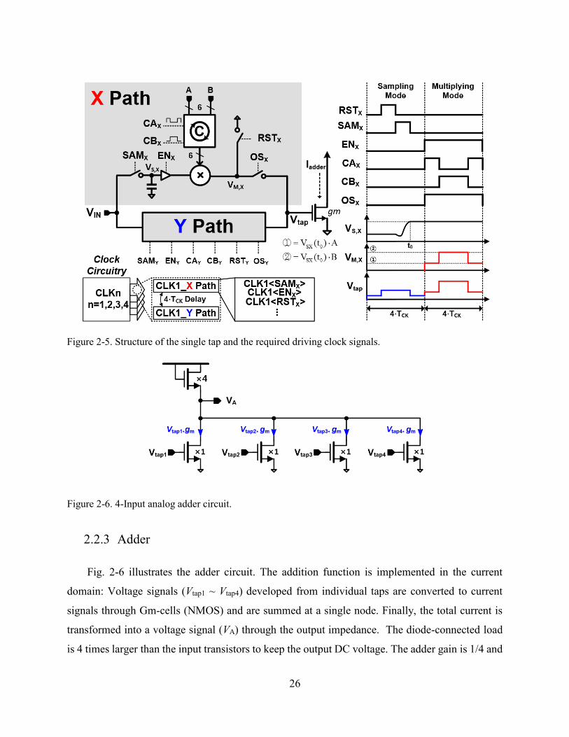
Each tap consists of two paths (X and Y) of the multiplier unit, as depicted in Fig. 2-5. While
one path dumps previous data charge on the capacitor array at the output node and then performs
new data sampling (sampling mode), the other path multiplies the sampled signal in its S/H by the
rotating coefficients being read out at Vtap node (multiplying mode). To implement this operation,
X path clock signal group and Y path clock signal group must differ by 4∙TCK from each other.
The 12-bit coefficient control code (6-bits for each individual coefficient value) is written into the
shift register parallel output and combined with the coefficient multiplier driving clock signals for
rotating coefficient operation.
26
2.2.3 Adder
Fig. 2-6 illustrates the adder circuit. The addition function is implemented in the current
domain: Voltage signals (Vtap1 ~ Vtap4) developed from individual taps are converted to current
signals through Gm-cells (NMOS) and are summed at a single node. Finally, the total current is
transformed into a voltage signal (VA) through the output impedance. The diode-connected load
is 4 times larger than the input transistors to keep the output DC voltage. The adder gain is 1/4 and
Figure 2-5. Structure of the single tap and the required driving clock signals.
Figure 2-6. 4-Input analog adder circuit.
27
makes the FIR filter gain unity when the all four coefficients are set at the maximum. The gain of
the adder may be increased by adding a current source at the load which allows the load resistance
to be increased. Overall performance of the adder is the same as the S/H buffer but the load is the
next stage input impedance.
2.2.4 Clock generation circuitry
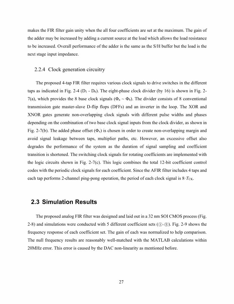
The proposed 4-tap FIR filter requires various clock signals to drive switches in the different
taps as indicated in Fig. 2-4 (D1 - D6). The eight-phase clock divider (by 16) is shown in Fig. 2-
7(a), which provides the 8 base clock signals (Φa ~ Φh). The divider consists of 8 conventional
transmission gate master-slave D-flip flops (DFFs) and an inverter in the loop. The XOR and
XNOR gates generate non-overlapping clock signals with different pulse widths and phases
depending on the combination of two base clock signal inputs from the clock divider, as shown in
Fig. 2-7(b). The added phase offset (Φx) is chosen in order to create non-overlapping margin and
avoid signal leakage between taps, multiplier paths, etc. However, an excessive offset also
degrades the performance of the system as the duration of signal sampling and coefficient
transition is shortened. The switching clock signals for rotating coefficients are implemented with
the logic circuits shown in Fig. 2-7(c). This logic combines the total 12-bit coefficient control
codes with the periodic clock signals for each coefficient. Since the AFIR filter includes 4 taps and
each tap performs 2-channel ping-pong operation, the period of each clock signal is 8·TCK.
2.3 Simulation Results
The proposed analog FIR filter was designed and laid out in a 32 nm SOI CMOS process (Fig.
2-8) and simulations were conducted with 5 different coefficient sets (①~⑤). Fig. 2-9 shows the
frequency response of each coefficient set. The gain of each was normalized to help comparison.
The null frequency results are reasonably well-matched with the MATLAB calculations within
20MHz error. This error is caused by the DAC non-linearity as mentioned before.

28
Overall post-layout simulation results are shown in Table 2-I. The output driver is excluded
in the simulation. The intrinsic gain of the FIR filter is the sum of the 4 coefficient values and the
other gains are independent of the coefficient set. Thus, the maximum gain occurs at set③ and the
minimum is at set① or ⑤. IIP3 performance is high (> 11 dBm) in spite of low VDD (0.9 V) as
the analog amplifiers, S/H buffer and Adder, are simple and designed with non-linearity
(a)
(b)
(c)
Figure 2-7. Clock generation circuitry: (a) clock divider by 16, (b) non-overlapping clock generation with
XOR and XNOR gets including complementary clock generation circuits, and the rotating coefficient
switching logic.

29
cancellation techniques. The noise figure is based on the simulation and noise sampled on the
capacitors was calculated using MATLAB. The worst case NF occurs when the intrinsic FIR filter
gain is minimum because the total output noise is dominated by the adder and the source noise is
0.95mm
0.65
mm
SingleTap
Clock
Clock Distribution
Adder
Output Driver
Figure 2-8. Layout of the Analog FIR filter fabricated in 32nm SOI CMOS process and the core is
magnified on the right.
Figure 2-9. Frequency response of the AFIR filter with different coefficient sets.
-60
-50
-40
-30
-20
-10
0
10
0.00E+00 5.00E+08 1.00E+09 1.50E+090 0.5G 1G 1.5G
-50
-40
-30
-20
-10
0
Frequency (Hz)No
rna
lize
d G
ain
[20
log
(A(f
)/A
max)]
(d
B)
-60①
②
③
④⑤
①A:00, B:63
②A:32, B:63
③A:63, B:63
④A:63, B:32
⑤A:63, B:00

30
subject to the by the loss from the adder. Otherwise, it can be seen that the coefficient set⑤ mostly
has worse performance in the other criteria due to its more complex multiplier switching signals.
2.4 Measurement and Malfunction Issues
The 4-tap AFIR filter designed in 32 nm SOI CMOS technology was fabricated for probe-
station testing [Fig. 2-10]. In the chip design, the left and right pads are the differential input and
TABLE 2-I. POST-LAYOUT SIMULATION RESULTS
Gain Max
Min
- 5.1 dB
-11.6 dB ③ A63, B63
⑤ A00, B63
3dB BW
Tuning
Max
Min
710 MHz
240 MHz ① A63, B00
⑤ A00, B63
Notch Freq.
Tuning
Max
Min
1.625 GHz
540 MHz ① A63, B00
⑤ A00, B63
IIP3 Max
Min
13.9 dBm
11.3 dBm ③ A63, B63
⑤ A00, B63
NF Max 20.4 dB ① A63, B00
SFDR Max
Min
48.8 dBc
42.7 dBc
③ A63, B63 ⑤ A00, B63
Power
Consumption
Max
Min
9.3mW (A4.5/D4.8)
8.1mW (A4.5/D3.6) ① A63, B00
⑤ A00, B63
Figure 2-10. The AFIR filter chip fabricated in 32 nm SOI CMOS technology.
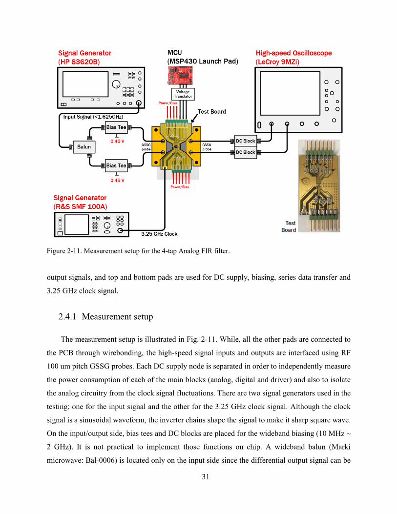
31
output signals, and top and bottom pads are used for DC supply, biasing, series data transfer and
3.25 GHz clock signal.
2.4.1 Measurement setup
The measurement setup is illustrated in Fig. 2-11. While, all the other pads are connected to
the PCB through wirebonding, the high-speed signal inputs and outputs are interfaced using RF
100 um pitch GSSG probes. Each DC supply node is separated in order to independently measure
the power consumption of each of the main blocks (analog, digital and driver) and also to isolate
the analog circuitry from the clock signal fluctuations. There are two signal generators used in the
testing; one for the input signal and the other for the 3.25 GHz clock signal. Although the clock
signal is a sinusoidal waveform, the inverter chains shape the signal to make it sharp square wave.
On the input/output side, bias tees and DC blocks are placed for the wideband biasing (10 MHz ~
2 GHz). It is not practical to implement those functions on chip. A wideband balun (Marki
microwave: Bal-0006) is located only on the input side since the differential output signal can be
Figure 2-11. Measurement setup for the 4-tap Analog FIR filter.
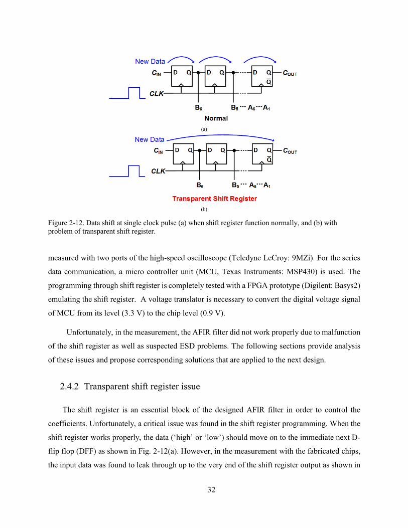
32
measured with two ports of the high-speed oscilloscope (Teledyne LeCroy: 9MZi). For the series
data communication, a micro controller unit (MCU, Texas Instruments: MSP430) is used. The
programming through shift register is completely tested with a FPGA prototype (Digilent: Basys2)
emulating the shift register. A voltage translator is necessary to convert the digital voltage signal
of MCU from its level (3.3 V) to the chip level (0.9 V).
Unfortunately, in the measurement, the AFIR filter did not work properly due to malfunction
of the shift register as well as suspected ESD problems. The following sections provide analysis
of these issues and propose corresponding solutions that are applied to the next design.
2.4.2 Transparent shift register issue
The shift register is an essential block of the designed AFIR filter in order to control the
coefficients. Unfortunately, a critical issue was found in the shift register programming. When the
shift register works properly, the data (‘high’ or ‘low’) should move on to the immediate next D-
flip flop (DFF) as shown in Fig. 2-12(a). However, in the measurement with the fabricated chips,
the input data was found to leak through up to the very end of the shift register output as shown in
(a)
(b)
Figure 2-12. Data shift at single clock pulse (a) when shift register function normally, and (b) with
problem of transparent shift register.
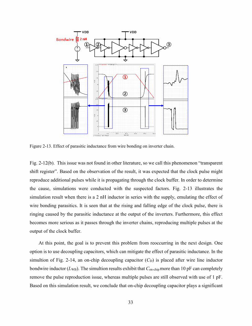
33
Fig. 2-12(b). This issue was not found in other literature, so we call this phenomenon “transparent
shift register”. Based on the observation of the result, it was expected that the clock pulse might
reproduce additional pulses while it is propagating through the clock buffer. In order to determine
the cause, simulations were conducted with the suspected factors. Fig. 2-13 illustrates the
simulation result when there is a 2 nH inductor in series with the supply, emulating the effect of
wire bonding parasitics. It is seen that at the rising and falling edge of the clock pulse, there is
ringing caused by the parasitic inductance at the output of the inverters. Furthermore, this effect
becomes more serious as it passes through the inverter chains, reproducing multiple pulses at the
output of the clock buffer.
At this point, the goal is to prevent this problem from reoccurring in the next design. One
option is to use decoupling capacitors, which can mitigate the effect of parasitic inductance. In the
simultion of Fig. 2-14, an on-chip decoupling capacitor (CD) is placed after wire line inductor
bondwire inductor (LWB). The simultion results exhibit that Con-chip more than 10 pF can completely
remove the pulse reproduction issue, whereas multiple pulses are still observed with use of 1 pF.
Based on this simulation result, we conclude that on-chip decoupling capacitor plays a significant
Figure 2-13. Effect of parasitic inductance from wire bonding on inverter chain.

34
role in cancelling out the parasitic inductance due to wirebonding. In the original design, such a
decoupling capacitor was not placed in the layout and the design relied on the parasitic capacitance
between VDD and ground only.
In addition to the decoupling capacitor, there are also other design considerations to avoid the
transparent shift register issue. The digital buffer can be made more robust by using a Schmitt
trigger, which prevents ringing by creating hysteresis (see Fig. 2-15). Through simulation, it is
also shown that the Schmitt trigger removes the pulse reproduction issue even if an on-chip
decoupling capacitor is not included. Additionally, the number of inverters in the clock buffer
should be minimized.
Figure 2-14. Sufficient on-chip decoupling capacitor cancels out the effect of wirebonding parasitic
capacitance
Figure 2-15. A simple Schmitt trigger implemented with 3 inverters and the simulated input versus output
hysteresis.

35
2.4.3 ESD issue
Although the measurement was conducted very carefully using laboratory ESD safety
precautions (wearing an ESD wrist strap during measurement, using static shielding bag to carry
chips, etc.), the AFIR filter chips were found to fail easily. It was concluded that DUTs were blown
by ESD based on the fact that unexpectedly large current was drawn when the chip failed.
Integrated circuits are often vulnerable to electrostatic discharge (ESD) during measurement.
The chips can be damaged by ESD due to the human contact and measurement equipment [20].
ESD protection may require complicated circuitry to satisfy certain level of ESD specifications.
However, for the research purpose proof-of-concept chips, use of clamping diodes (Fig. 2-16) is
often sufficient. However, in this design, ESD diodes were not included for simplicity. Although
some small size diode connected NMOS are connected between gate and source where the gate is
driven through the pads to avoid antenna rule errors, it turned out to be insufficient for the ESD
protection. We can also minimize the ESD risk by avoiding wirebonding and conducting the
measurement on the probe station with properly arranged pads. These issues are accounted for in
the final AFIR filter design presented in the next chapter.
2.5 Summary
An AFIR filter has been developed by implementing delay with S/H, rotating coefficient
multiplication with split-CDAC and addition with transconductors. Simulations verified the
frequency response corresponding to the coefficient values while keeping high linearity (> 11
Figure 2-16. On-chip ESD protection with clamping diodes.
PAD
VDD
Circuits
GND
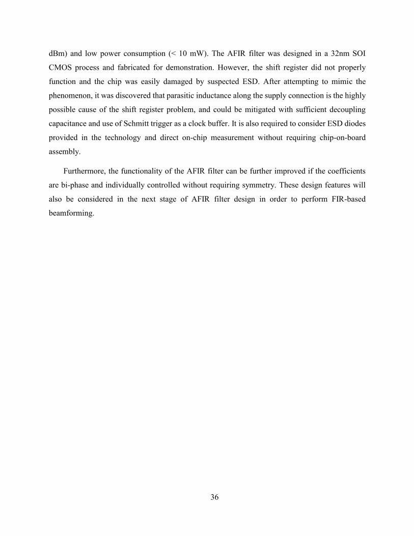
36
dBm) and low power consumption (< 10 mW). The AFIR filter was designed in a 32nm SOI
CMOS process and fabricated for demonstration. However, the shift register did not properly
function and the chip was easily damaged by suspected ESD. After attempting to mimic the
phenomenon, it was discovered that parasitic inductance along the supply connection is the highly
possible cause of the shift register problem, and could be mitigated with sufficient decoupling
capacitance and use of Schmitt trigger as a clock buffer. It is also required to consider ESD diodes
provided in the technology and direct on-chip measurement without requiring chip-on-board
assembly.
Furthermore, the functionality of the AFIR filter can be further improved if the coefficients
are bi-phase and individually controlled without requiring symmetry. These design features will
also be considered in the next stage of AFIR filter design in order to perform FIR-based
beamforming.
37
3 Improved 3.25GS/s 4th-Order Programmable Analog FIR Filter
Using Split-CDAC Coefficient Multipliers
Chapter 3.
Improved 3.25GS/s 4th-Order
Programmable Analog FIR Filter Using
Split-CDAC Coefficient Multipliers
3.1 Introduction
The final version of AFIR filter presented here improves the architecture and overcomes
critical issues from the previous version. First of all, an additional tap is used, which enables a
non-decimation system without 2-way ping pong operation in each channel. As a result, overall
circuitry achieves smaller complexity, power consumption and area. The sign of coefficients can
be selected and all 4 coefficients are individually controlled, thus the coefficient set can be type-
IV as well as type-II and frequency response is programmable with wider range. The ESD issue is
mitigated by simply adding ESD diodes at each pad, sized such that there is minimal effect on the
performance. In order to prevent the ‘transparent shift register’ issue, a large amount of bypass
capacitance is placed all over the empty area on the chip. In addition, Schmitt triggers are also
placed as digital buffers to prevent unwanted clock reproduction. Consequently, no digital
programming issue was found with the shift register in the measurement. The designed analog FIR
filter was fabricated in 32nm SOI CMOS process and the measurement was successfully

38
conducted. This chapter deals with details of the final version of FIR filter design as well as
analysis of time-interleaved operation errors, noise and measurement results.
3.2 Design Objective
The core design objective for this chapter is a proof-of-concept 4th order AFIR filter operated
at 3.25 GS/s speed, which is able to provide signal processing from DC to the Nyquist rate (fNyq).
To utilize full bandwidth up to fNyq, no decimation and no sinc function can be included, since
these cause attenuation and aliasing. In addition, if amplifiers or buffers are used to avoid excessive
charging errors, they must have sufficient bandwidth. Coefficients are to be fully reconfigurable
with individual 6-bit coefficient value, plus one bit for sign (+/-) selection. High linearity over
useful BW is also desired to handle large tones ahead of the ADC with high flexibly. It is also
assumed that noise can be sufficiently suppressed by preceding blocks such as an LNA, and that
the following ADC has 6-bit resolution. In order to extend to beamformer applications and higher
order filters, low power design is essential. Based on the literature study, the following
specifications were considered sufficient for the proof-of-concept design.
4th order 3.25GS/s with full bandwidth utilization up to fs/2.
o No decimation or sinc function
o Amplifier/Buffer: < 1% settling error at 3.25 GS/s
4 coefficients are individually controlled by bi-phase 7-bit digital codes
High linearity over full bandwidth (IIP3 > 10 dBm)
Low power consumption (< 10mW)
3.3 Architecture of 5-Tap 4th-order AFIR filter
The AFIR filter architecture featuring 5-taps for 4th order filtering is illustrated in Fig. 3-1.
The designed 4th order analog FIR filter includes 5-taps through 5 channels consisting of sampling
and coefficient multiplication. As with the previous version, delay is realized by holding the
sampled input. Then, coefficients are rotated periodically in order to achieve the desired FIR

39
function. Addition is implemented in the current domain through gm cells and the current signal
is transformed back to the voltage signal through the resistive load that provides partial
nonlinearity cancellation. Input and output drivers are incorporated for wideband 50 Ω matching
in the measurement setup. The detailed operation will be discussed in Section 3.4.
Switches are used for sampling and rotating coefficient implementation. To drive those
switches, five non-overlapping clock waveforms (Φ1 ~ Φ5) are created by the clock generation
circuitry from a 3.25 GHz sinusoidal input, which is the same frequency as the sampling rate of
the AFIR filter. Each coefficient is a 7-bit digital value consisting of a 6-bit fractional value, i.e.,
[0, 1, 2 …, 63]/64, plus 1-bit for positive or negative sign selection. Four coefficients (A, B, C and
D) are individually controlled by 7-bits, so there are total 28-bits for coefficients. The coefficient
codes are programmed through a shift register with 28-bit parallel output. The overall circuit is a
(quasi)differential structure, using separated paths, which allows bi-phase coefficient control and
helps to reject common-mode errors.
In the previous version of the AFIR filter, two paths were required to sampling, reset and
coefficient multiplication in the form of ping-pong operation: while one path is sampling and
resetting, the other path is multiplying the sampled input with the rotating coefficient and reading
out the processed signal. For this reason, each path has two coefficient multipliers taking large
area and requiring complicated clock signals. On the other hand, the final version of AFIR filter
Figure 3-1. The proposed 4-tap discrete time analog FIR filter architecture.
40
adopts an additional tap architecture [21], i.e., there are 5 channels (taps) to implement 4th order
FIR function as shown in Fig. 3-1. The 5-channels allow 4 input samples to be multiplied by their
corresponding 4 coefficients while the remaining channel samples the input and resets the output.
Moreover, while the previous 4-tap version with ping-pong operation needs 8 S/H and coefficient
multiplier pairs; 5-tap operation requires only 5 pairs, so the area and power consumption are
saved. Besides, the required clock signals are simplified considerably, as to be described in Section
3.4.4, so the area and power consumption are further reduced. Considering general AFIR design
of NFIR-th order filtering, additional tap architecture needs NFIR + 1 of S/H and coefficient
multiplier pairs, while the ping-pong architecture requires 2·NFIR pairs, thus the effectiveness of
additional-tap concept increases for the higher order AFIR filter design.
Fig. 3-2 describes the timing of the sampling and coefficient multiplication sequence in the 5-
channel architecture for the given clock waveforms Φ1 ~ Φ5, ultimately implementing 4th order
FIR function as (1-1) with NFIR = 4. VIN(·) represents the input signal sample at a specific time,
and z-1 denotes the unit delay (z-domain). The sampling switch is closed only for a single tap at a
single period. While sampling, the corresponding channel output is reset to zero. After that, the
sampled signal is multiplied by coefficients in A-B-C-D order. In Fig. 3-2, we can observe this
operation for Ch.1; after sampling the signal at t0, then VIN(t0) is multiplied by A at t1, B at t2, C at
t3 and D at t4. This sequence is executed in time-interleaved (TI) manner throughout the 5-channels.
Figure 3-2. Timing table of sampling and coefficient multiplication in each channel.
41
Thus, sampling is continuous (in discrete time) without an empty period. When the outputs of all
taps are added together, the function matches with the 4th order FIR filter equation. For example,
we can examine the combined output at t4:
VOUT(t4) = VIN(t4)∙0+ A∙VIN(t3) + B∙VIN(t2)+ C∙VIN(t1) + D∙VIN(t0) (3-1)
There are five coefficient and sampled input pairs (five taps) but this effectively matches with the
4th order FIR function as one of tap multiplication is zero. Compared to (1-1) there is an additional
delay but it does not critically change the characteristics of the filter. We can see the output at the
next period t5,
VOUT(t5) = VIN(t5)∙0+ A∙VIN(t4) + B∙VIN(t3)+ C∙VIN(t2) + D∙VIN(t1), (3-2)
which also results in the intended function. This process continues for each subsequent period.
Consequently, this sequence of operation proves the 5-tap FIR filter operates as the 4-th order FIR
function at the sampling speed without decimation in the DT analog domain. The coefficients are
individually controlled bi-phase value, thus the AFIR filter can realize frequency response based
on (1-9) and (1-10).
3.4 Circuit Implementation
In this section, design considerations for each block are presented. To implement the AFIR
filter operation described in 3-1, required blocks include S/H, coefficient multiplier, adder, shift
register, clock generation/distribution and input/output buffers. Each of the below subsections
describes the details of these circuit blocks.
3.4.1 Sample and hold
Since we are targeting high-speed sampling, an open loop topology is preferable [6], which
includes switch, sampling capacitor (Cs) and buffer [Fig. 3-3(a)]. Although sampling is a simple
task, the circuit design must be carefully considered to prevent severe signal distortion due to
imperfections. We focus on the issues regarding the design of S/H switch and CS first, then discuss
the S/H buffer.
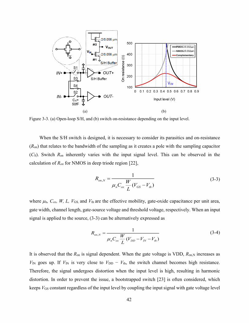
42
When the S/H switch is designed, it is necessary to consider its parasitics and on-resistance
(Ron) that relates to the bandwidth of the sampling as it creates a pole with the sampling capacitor
(CS). Switch Ron inherently varies with the input signal level. This can be observed in the
calculation of Ron for NMOS in deep triode region [22],
,
1
( )on N
n ox GS th
RW
C V VL
(3-3)
where n, Cox, W, L, VGS, and Vth are the effective mobility, gate-oxide capacitance per unit area,
gate width, channel length, gate-source voltage and threshold voltage, respectively. When an input
signal is applied to the source, (3-3) can be alternatively expressed as
,
1
( )on N
n ox DD IN th
RW
C V V VL
(3-4)
It is observed that the Ron is signal dependent. When the gate voltage is VDD, Ron,N increases as
VIN goes up. If VIN is very close to VDD − Vth, the switch channel becomes high resistance.
Therefore, the signal undergoes distortion when the input level is high, resulting in harmonic
distortion. In order to prevent the issue, a bootstrapped switch [23] is often considered, which
keeps VGS constant regardless of the input level by coupling the input signal with gate voltage level
(a) (b)
Figure 3-3. (a) Open-loop S/H, and (b) switch on-resistance depending on the input level.

43
when it turns on. However, with this approach, it is challenging to handle high (several GS/s)
sampling rates, leading to excessive power consumption. Instead, we can mitigate the nonlinear
resistance by adopting a complementary switch as shown in Fig. 3-3(a). Both NMOS and PMOS
switches are 2/0.04 m. Due to well-balanced effective mobilities of PMOS and NMOS in the
selected technology, identical device sizes result in close to symmetric on-resistance around VCM.
In the simulation result presented in Fig. 3-3(b), the on-resistance varies by only 2.7% over 50mV
swing (half of 100mV differential swing), which is greatly reduced from NMOS and PMOS only
switches. The maximum Ron of the complementary switch is 227 Ω.
In S/H systems, CS is often determined by the kT/C noise. However, it is assumed that the
preceding blocks sufficiently relieves the noise requirement with sufficient gain, as mentioned in
Section 3.2. Therefore, Cs can be sized as small as possible for the bandwidth. However, overly
small Cs may lead to excessive voltage droop due to leakage through the next stage. The 3dB
bandwidth due to Ron, following block output resistance (Rout) and CS is given by
3 , /
1
2 ( )dB S H
on out S
fR R C
. (3-5)
In this AFIR filter design, Cs is sized to 50 fF, which results in large bandwidth (> 5· fNyq) in the
simulation with the given S/H switch and 50Ω of Rout. This frequency response has only 0.2 dB of
loss and 1.4 of phase shift at fNyq. Therefore, the overall frequency response of the circuits on the
FIR transfer function is only negligibly affected by S/H bandwidth. Furthermore, this large
bandwidth helps to prevent bandwidth mismatch between channels [24]. In the simulation,
assuming that the following stage is an NMOS gate (2/0.056 m) biased at VCM, the RC time
constant is more than hundreds of nanoseconds, which is sufficient to prevent from drooping for
GS/s sampling rate (hundreds of picoseconds of hold duration).
Channel charge injection and clock feedthrough are also problems caused by switching [22],
which are illustrated in Fig. 3-4. When the NMOS switch is on, the channel is created with charge
carriers under the gate oxide between source and drain. If the gate voltage level goes down, the
charges that was forming the channel is injected to both source and drain. The charges injected
onto CS result in voltage error, which is referred to as channel charge injection [Fig. 3-4(a)]. In the

44
NMOS case, the channel charge is negative so is the voltage error. Assuming that all of the channel
charge moves to CS ,the voltage error can be calculated by [22]
( )ox VDD in TH
S
WLC V V VV
C
. (3-6)
In order to reduce the charge injection error, the switch size should be as small as possible while
CS needs to be large enough but it trades off the speed. It is seen that this error depends on the input
voltages, resulting in gain error.
Similarly, clock feedthrough also occurs at the clock edge, which lead to voltage error [Fig.
3-4(b)]. The parasitic capacitance creates path for the current from the gate to CS. The clock
switching voltage is divided by the parasitic capacitance (WCov, where Cov denotes overlap
capacitance per unit width) and CS resulting in,
ovDD
ov S
WCV V
WC C
(3-7)
when clock signal has maximum swing between ground and supply voltage. As with the charge
injection, voltage error caused by clock feedthrough can be reduced by smaller switch and large
CS, but it does not depend on the signal. Unfortunately, both voltage errors have the same phase
so they are added together, exacerbating the problem.
We can consider several techniques to address the switching errors. Switched-capacitor
amplifiers [22] can be used for bottom plate sampling. However, this technique requires a high
gain op-amp, which would limit the speed and linearity when implemented in deep submicron
(a) (b)
Figure 3-4. Clock switching-related errors: (a) channel charge injection and (b) clock feed through.
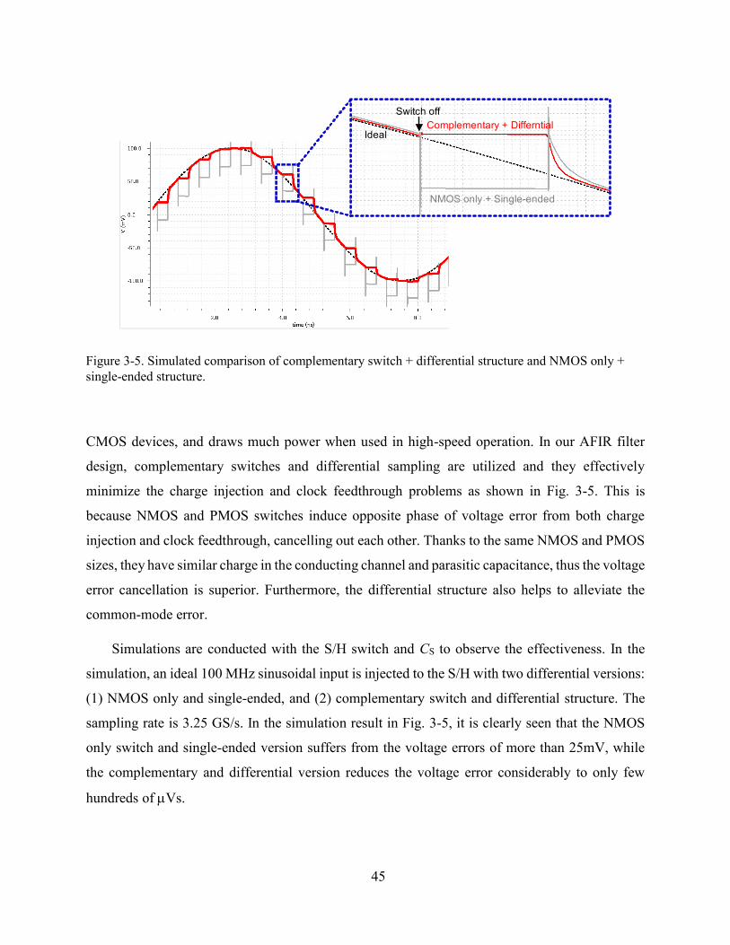
45
CMOS devices, and draws much power when used in high-speed operation. In our AFIR filter
design, complementary switches and differential sampling are utilized and they effectively
minimize the charge injection and clock feedthrough problems as shown in Fig. 3-5. This is
because NMOS and PMOS switches induce opposite phase of voltage error from both charge
injection and clock feedthrough, cancelling out each other. Thanks to the same NMOS and PMOS
sizes, they have similar charge in the conducting channel and parasitic capacitance, thus the voltage
error cancellation is superior. Furthermore, the differential structure also helps to alleviate the
common-mode error.
Simulations are conducted with the S/H switch and CS to observe the effectiveness. In the
simulation, an ideal 100 MHz sinusoidal input is injected to the S/H with two differential versions:
(1) NMOS only and single-ended, and (2) complementary switch and differential structure. The
sampling rate is 3.25 GS/s. In the simulation result in Fig. 3-5, it is clearly seen that the NMOS
only switch and single-ended version suffers from the voltage errors of more than 25mV, while
the complementary and differential version reduces the voltage error considerably to only few
hundreds of Vs.
Figure 3-5. Simulated comparison of complementary switch + differential structure and NMOS only +
single-ended structure.
IdealComplementary + Differntial
NMOS only + Single-ended
Switch off

46
Short channel leakage between input and CS is a possible issue when the switch is off. To
prevent this problem, cross-coupled dummy transistors that are always off [Fig. 3-6(a)] are placed
because the leakage occurs equally on both positive and negative path, so they compensate each
other. Simulation results in Fig. 3-6(b) show that, in a hold period, the voltage level on CS goes up
about 230 V in the case without dummy switches, while with dummy switches only a 10 uV level
shift is experienced.
To verify the performance of the sampling circuits, the S/H is simulated [Fig.3-7(a)], with
ideal buffers and switches to read out the signal only in the hold state. Two-channel ping-pong
operation is implemented in the simulation because the single path output shows both track and
(a)
(b)
Figure 3-6. (a) Dummy switches cancelling out the off-switch leakage when the sampling SWs are closed
(b) simulation result.
w/o Dummy switches
w/ Dummy Switches
HOLD
~200uV
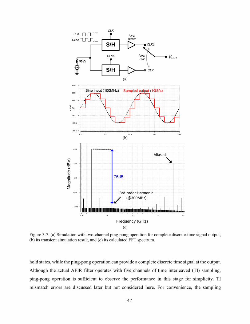
47
hold states, while the ping-pong operation can provide a complete discrete time signal at the output.
Although the actual AFIR filter operates with five channels of time interleaved (TI) sampling,
ping-pong operation is sufficient to observe the performance in this stage for simplicity. TI
mismatch errors are discussed later but not considered here. For convenience, the sampling
(a)
(b)
(c)
Figure 3-7. (a) Simulation with two-channel ping-pong operation for complete discrete-time signal output,
(b) its transient simulation result, and (c) its calculated FFT spectrum.

48
frequency is set to 1 GS/s and the input is 100MHz to avoid fractional frequency components in
the output power spectrum. In the transient simulation result presented in Fig. 3-7(b), the S/H
outputs tracks the input signal well. Harmonics can arise as Ron and charge injection are dependent
on the input signal, which can be seen in (3-4) and (3-6). In the output spectrum obtained by fast
fourier transform (FFT) calculation [Fig. 3-7(c)], the 3rd harmonic is found to be 76dB less than
the input signal. Some other tones within fNyq can be caused by imperfect clock signals (non-zero
rising/falling time). Table 3-I summarizes the design parameters and simulated performance of the
S/H without the buffer.
A S/H buffer is required to isolate the sampled input while the output is multiplied by the
rotating coefficients. Unlike the previous version of the AFIR filter, the S/H buffer does not need
to be switchable since it is not used for ping-pong operation. Unit gain feedback amplifier using
op-amp is a popular option but it is challenging to design it for high-speed and low power with
deeply scaled CMOS technology. Source followers can be also used but the level shift from input
to output (VGS) excessively limits the signal swing at low supply voltage. In order to keep the
linearity high even under the low supply voltage condition, common-source amplifiers with diode-
connected NMOS loads with same size (M1 = M2) are utilized [Fig. 3-3(a)]. This structure helps to
easily bias the output to be VCM when the input is biased to VCM. Analog FETs in SOI technology
allow body connection (not inherently tied to substrate) so the body of the diode-connected load
is tied to its source so as to prevent nonlinearity from body effect. As a result, the gain of the S/H
buffer can be given by
TABLE 3-I. SUMMARY OF SAMPLING SWITCH AND CAPACITOR DESIGN AND SIMULATED PERFORMANCE
Sampling rate (fs) 3.25 GS/s
Complementary switch size (N/PMOS) 2/0.04 m
Sampling capacitance (CS) 50 fF
Sampling Switch*
On-resistance (Ron) < 227 Ω
3dB Bandwidth (f3dB,S/H) @Rout = 50Ω 11 GHz
3-rd Harmonic component -75 dBc
* Supply voltage (‘ON’ voltage level) is 0.9V and the maximum Ron is at the common mode voltage input
(0.45V)

49
11 1 2
2 2
1/ / / / m
buff m o o
m m
gA g r r
g g
(3-8)
if 1/gm2 << ro1//ro2. Since the same current goes through both same-size transistors, gm2 tracks gm1,
keeping the gain close to the unity under the transconductance variation. However, those
transistors see different drain to source voltage (VDS1 ≠ VDS2), which limits nonlinearity
cancellation and output resistance drops the gain from unity. Since the S/H buffer is required to
drive the next stage, which is a capacitor network, the S/H buffer is sized for the consideration
with the coefficient multiplier design. More details are discussed in the coefficient multiplier
design below. In 2-tone test simulations conducted with two −10 dBm input signals at 50 MHz
and 51 MHz, the buffer achieves 18 dBm of IIP3, and loss due to the output resistance is 1.5 dB.
3.4.2 Coefficient multiplier
As with the previous version of the AFIR filter, this 5-tap AFIR utilizes 6-bit split-CDAC as
a coefficient multiplier, introduced in Section. 2.2.1. The split-CDACs in this work are
implemented with vertical natural capacitors (VNCAPs) provided in the 32SOI technology. The
coefficient multiplier inherently provides coefficient control with the resolution of the DAC.
Furthermore, CDAC-based coefficient multipliers provide high linearity and low power
consumption due to the passive-based structure. The main drawback of a conventional CDAC
coefficient multiplier is its large area. However, by using a split-CDAC, the overall area is reduced
by about a factor of 4 compared to a conventional single-section CDAC (64CU to 16.1CU). In
addition, the switching speed is also improved because the capacitance seen from the input signal
is decreased, relieving the required driving capability of the S/H buffer.
The consequent issue is the static linearity of the DAC. In the AFIR filter application, the
nonlinearity of the DAC does not distort the signal with harmonic tones or quantization noise as it
does in A/D or D/A converter architectures. Instead, the static linearity of the split-CDAC affects
the coefficient precision that is relevant to the shape of the FIR transfer function (TF) [14]. Static
linearity of the split-CDAC coefficient multiplier can be caused by the capacitance variation and
parasitic capacitance. While the variation can be handled with sufficient unit capacitance, parasitic
capacitance becomes the main source of nonlinearity in the split-CDAC structure.

50
To address the static linearity of the 6-bit split-CDAC, Fig. 3-8 presents the coefficient
multiplier including the parasitic capacitance (Cp1 and Cp2) on the top plates of the capacitor array,
which affects the output level steps, while the parasitic capacitance on bottom plates and switches
only increase the capacitance loading to the preceding stage. Fig. 3-9(a) is the simulation result of
output voltage versus digital code when the 100 mV DC input is resolved through the coefficient
multiplier, i.e., the output voltage is 100mV multiplied by the fractional coefficient values. It is
observed that the output voltage line deviates from the ideal DAC line and the maximum value is
somewhat decreased. The reduction of the maximum value mainly originates from Cp1 since it
increases the total capacitance on the output. This means that maximum coeffiicent is reduced,
which can be considered as loss. Cp2 can also contribute to the loss, but when Cp1 and Cp2 are
Figure 3-8. Split-CDAC coefficient multiplier including parasitic capacitance.
(a) (b)
Figure 3-9. Effect of parasitic capacitors on split-CDAC coefficient multiplier: (a) Output voltage versus
6-bit digital code when input is 100mV and (b) DNL.

51
comparable, Cp2 hardly contributes to the loss because the bridge capacitor reduces the capacitance
seen from the output. In the simulation result, the gain of coefficient multiplier (ACM) is -1.7 dB.
This loss can be caused by about 0.5 CU of Cp1 with the 6-bit split-CDAC.
Although it may look close to a straight line, the coefficient multiplier output contains
nonlinearities in the response to different digital codes. This error is defined as differential
nonlinearity (DNL) in DACs and can be calculated by
[ 1] [ ]
, 0,1,2...,63out out LSB
LSB
V n V n VDNL n n
V
(3-9)
where VLSB denotes the ideal voltage step size of least significant bit (LSB) change, which is
100mV/64 in 6-bit resolution DAC. Ideal DNL is 0. A split-CDAC may possess this static
nonlinearity due to Cp2 even if the capacitor mismatch does not exist at all. To explain this, we can
first view the 6-bit split-CDAC as two 3-bit CDACs including CB as an attenuator. While the
CDAC with more significant bits (D4 ~ D6) has its original resolution, due to CB attenuation, the
CDAC with less significant bits (D1 ~ D3) can develop the output level with higher resolution
(smaller voltage levels) after the first three bits (detailed discussion is presented in Section 5.2).
However, if there is Cp2, the balance between the two 3-bit CDACs is disrupted, since the CDAC
with less significant bits gets loss. Consequently, large voltage level transitions are found at any
step that changes the 4th bit, i.e. XX0111 to XX1000 or XX1111 to XX0000, in Fig. 3-9(a). The
worst case DNL value is 0.53 LSB found at the corresponding steps, which indicates a bit large
nonlinearity. To remedy this situation, it is possible to substitute the dummy capacitor for Cp2 as
presented in Fig. 3-8. The VNCAP pcell has design parameters of its width, length and layers, so
it is possible to adjust its parasitic capacitance. After removing the dummy capacitor, the worst
case DNL is alleviated to -0.3 LSB as shown in Fig. 3-10, which is an acceptable level. Negative
DNL occurs as Cp2 is less than the unit capacitance. This margin allows additional parasitic
capacitance to be accommodated in the layout process.
The coefficient multiplier is further developed to select the polarity of the coefficients for the
tunability of the AFIR filter. In Fig. 3-10, D7 determines the polarity by switching the positive
and negative paths. In other words, negative coefficient is realized by reversing the sampled input

52
instead of implementing a negative gain in the coefficient multiplier. The sign selection switch
(D7) adds a resistance in series with the switches and capacitor network in the split-CDAC.
The S/H buffer sees switches and coefficient multiplier forming a RC network as shown in
Fig. 3-11(a), and after sampling, the subsequent blocks operate with DT analog signals. Hence,
Figure 3-10. Single path of AFIR filter with bi-phase (+/-) sign selection switch D7
(a)
(b)
Figure 3-11. (a) S/H buffer with impedance looking from S/H buffer output, and (b) simulation to observe
settling behavior of coefficient multiplication with its result.

53
the S/H buffer is required to drive the coefficient multiplier at the sampling rate, which means that
the RC time constant must be reasonably smaller than a single period (307.7ps). When designing
the S/H buffer, switches for the coefficient multiplier needs to be carefully sized since overly small
switches increase the drive requirement of the buffer, while overly large switches increase the
power consumption of the driving clock signals. The capacitance and switch resistance in the
equivalent circuit depend on the coefficient selection other than D7. If there are no parasitics,
maximum input capacitance is presented when only the MSB switch (D6) is on and the others are
all off, resulting in the value of (22/2)·CU. However, the worst time constant may happen at
different digital code due to the parasitic capacitors and switch on-resistance.
In order to design the S/H buffer and switches accordingly, settling behaviors are simulated
for all possible 6-bit coefficient sets as shown in Fig. 3-11(b), while the sign-selection code (D7)
is fixed, as it does not alter the result. In the simulation, the coefficient multiplier is triggered to
multiply a coefficient when the input is at a specific level (−10 dBm). Since the S/H buffer is not
biased with a current source, the settling does not suffer from skew. The S/H buffer and switches
are sized through iterations of simulation and the parameters and performance are presented in
Table 3-II. The simulation results show that the worst settling behavior occurs with coefficient
101101, a higher code than 100000 due to the parasitic capacitance from the top plates of the
TABLE 3-II. DESIGN PARAMETERS AND SIMULATED PERFORMANCE OF A PAIR OF S/H BUFFER AND
COEFFICIENT MULTIPLIER
Parameter Value Comments
Abuff -1.5 dB gm = 2.8 mS
Buffer IIP3 18 dBm -10dBm at 50 & 51 MHz
Buffer Power 330 W (Single) × 10 Vsupply = 0.9V
D1-D6* size
and SWrst 0.63/0.04 m Ron = 560 Ω
D7* size 4.2/0.04 m Ron = 120 Ω
Maximum gain of S/H buffer and
coefficient multiplier pair -3.2 dB ACM = -1.7dB
Worst settling 99.8%
(SS corner: 99%) Digital code: 101101
** Digital FET for low Ron and parasitic capacitance.

54
capacitor array and input of the adder (transistor gate). In the simulation, they achieve 99.8% of
maximum settling within a single period [Fig. 3-11(b)]. 0.2% of settling error is comparable to 1
LSB of 9-bit resolution [25]. For the SS corner environment, the result changes to 99% of
maximum, which exceeds the 6-bit resolution [(1−1/26)·100=98.4%].
Since the coefficient is determined by digital code, clock signals for coefficient multiplier
switches need to couple with the coefficient control bits. A total 28-bit of coefficients from shift
register are combined with the four clock signals through seven MUXs, which then drive the
coefficient multiplier as shown in Fig 3-12(a). The example shows the clock signals for coefficient
(a)
(b)
Figure 3-12. Implementation of rotating coefficient (clock phases are particularly for Ch.1).

55
multiplier and corresponding output voltage when the coefficients are set to −32/64, 63/64, 63/64,
−32/64. All MUXs take the clock phases for coefficient multiplication (for Ch.1, corresponding
clock phases are Φ2 ~ Φ5, while Φ1 is for sampling and reset), and each MUX is responsible for
different digital bits (D1 ~ D7). The MUX is made of OR and NAND gates as shown in Fig. 3-
12(b). The example shows D1 switch driving. When D1 is programmed 0-1-1-0 in sequence, this
code is serialized along with the clock phases (Φ2 - Φ5) through the corresponding MUX while
sampling is conducted in Φ1.To compensate the delay of MUX, equivalend delay(τMUX) is applied
to Φ1 clock. By combining with the clock signals, the digitals bits are serialized from each MUX.
Other channels can be operated with the clock phases as described in Fig. 3-2.
3.4.3 Adder
Although capacitive addition in the conventional switched-capacitor AFIR filter provides high
linearity and low power (Section 1.2.1), the sampled input cannot be re-used after charge addition,
which precludes the non-decimation operation. On the other hand, the implementation of addition
in the current domain allows the sampled input to be held for multiple operations. Fig. 3-13
illustrates the adder implementation and connection with the sampling and coefficient
multiplication channels. Compared to the adder in the previous AFIR filter design, M7 is added as
a current source to raise the gain of the adder by reducing the current through the diode-connected
NMOS (M6) load and correspondingly its gm. In this design, the gain of adder is determined to
have unity gain at the maximum gain coefficient set, i.e. all coefficients are 63/64, taking loss from
Figure 3-13. Structure of adder and connection to S/H + coefficient multipliers.
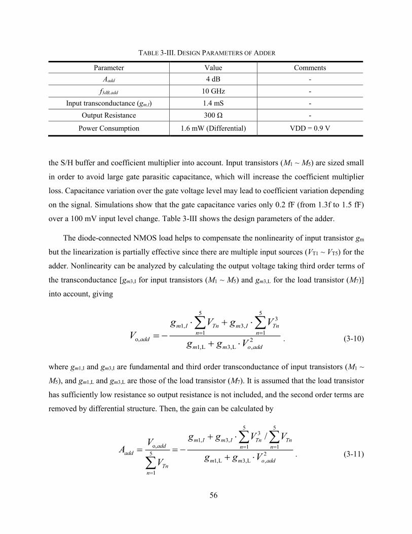
56
the S/H buffer and coefficient multiplier into account. Input transistors (M1 ~ M5) are sized small
in order to avoid large gate parasitic capacitance, which will increase the coefficient multiplier
loss. Capacitance variation over the gate voltage level may lead to coefficient variation depending
on the signal. Simulations show that the gate capacitance varies only 0.2 fF (from 1.3f to 1.5 fF)
over a 100 mV input level change. Table 3-III shows the design parameters of the adder.
The diode-connected NMOS load helps to compensate the nonlinearity of input transistor gm
but the linearization is partially effective since there are multiple input sources (VT1 ~ VT5) for the
adder. Nonlinearity can be analyzed by calculating the output voltage taking third order terms of
the transconductance [gm3,I for input transistors (M1 ~ M5) and gm3,L for the load transistor (M7)]
into account, giving
5 53
1, 3,
1 1o, 2
1,L 3,L ,
m I Tn m I Tn
n nadd
m m o add
g V g V
Vg g V
. (3-10)
where gm1,I and gm3,I are fundamental and third order transconductance of input transistors (M1 ~
M5), and gm1,L and gm3,L are those of the load transistor (M7). It is assumed that the load transistor
has sufficiently low resistance so output resistance is not included, and the second order terms are
removed by differential structure. Then, the gain can be calculated by
5 53
1, 3,o, 1 1
5 2
1,L 3,L ,
1
/m I m I Tn Tnadd n n
add
m m o addTn
n
g g V VV
Ag g V
V
. (3-11)
TABLE 3-III. DESIGN PARAMETERS OF ADDER
Parameter Value Comments
Aadd 4 dB -
f3dB,add 10 GHz -
Input transconductance (gm,I) 1.4 mS -
Output Resistance 300 Ω -
Power Consumption 1.6 mW (Differential) VDD = 0.9 V
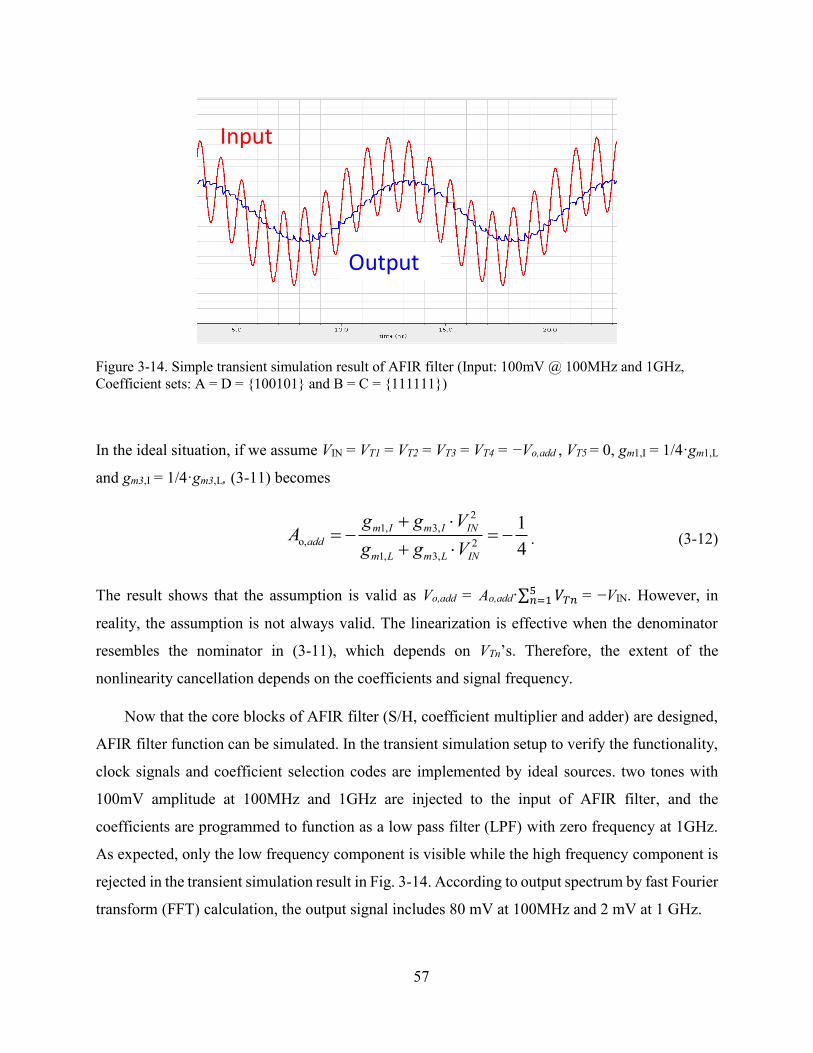
57
In the ideal situation, if we assume VIN = VT1 = VT2 = VT3 = VT4 = −Vo,add , VT5 = 0, gm1,I = 1/4·gm1,L
and gm3,I = 1/4·gm3,L, (3-11) becomes
2
1, 3,
o, 2
1, 3,
1
4
m I m I IN
add
m L m L IN
g g VA
g g V
. (3-12)
The result shows that the assumption is valid as Vo,add = Ao,add·∑ 𝑉𝑇𝑛5𝑛=1 = −VIN. However, in
reality, the assumption is not always valid. The linearization is effective when the denominator
resembles the nominator in (3-11), which depends on VTn’s. Therefore, the extent of the
nonlinearity cancellation depends on the coefficients and signal frequency.
Now that the core blocks of AFIR filter (S/H, coefficient multiplier and adder) are designed,
AFIR filter function can be simulated. In the transient simulation setup to verify the functionality,
clock signals and coefficient selection codes are implemented by ideal sources. two tones with
100mV amplitude at 100MHz and 1GHz are injected to the input of AFIR filter, and the
coefficients are programmed to function as a low pass filter (LPF) with zero frequency at 1GHz.
As expected, only the low frequency component is visible while the high frequency component is
rejected in the transient simulation result in Fig. 3-14. According to output spectrum by fast Fourier
transform (FFT) calculation, the output signal includes 80 mV at 100MHz and 2 mV at 1 GHz.
Figure 3-14. Simple transient simulation result of AFIR filter (Input: 100mV @ 100MHz and 1GHz,
Coefficient sets: A = D = 100101 and B = C = 111111)
Input
Output

58
To validate the linearization effectiveness, an equivalent adder that includes an ideal resistor
and current source instead of the diode-connected NMOS [Fig. 3-15(a)] is compared through two-
tone test simulations for several type-II and IV coefficient sets [Fig. 3-15(b)]. For LPF coefficient
sets, two −10 dBm input tones are injected at 50 MHz and 51 MHz in the simulation. Similarly,
−10 dBm tones with 1 MHz spacing are injected at the center frequency for BPF coefficient sets
and 1.58 GHz (a bit less frequency than fNyq) for HPF coefficient sets. The simulation results in
Fig. 3-15(b) show that the diode-connected load improves the linearity up to 8dB depending on
(a)
(b)
Figure 3-15. (a) Equivalent adder without linearization, and (b) linearity comparison over example type-II
and type-IV coefficient sets.
59
the coefficient set compared to the equivalent circuit. The worst IIP3 is 12.5 dBm, which is 1.5dB
higher than that of the equivalent circuits.
3.4.4 Non-overlapping clock generation
Clock signals are necessary to drive switches sampling and coefficient multiplier blocks. Due
to the additional tap operation, only 5 phases of clock waveforms are required from clock
generation while the previous version needed 10 clock waveforms. Otherwise, the overall structure
of the clock generation circuitry is similar to the previous design. Clock waveforms are required
not to overlap each other in order to avoid signal distortion due to the switching error. Clock
distribution must be carefully considered to prevent timing skew. Shift registers need to carry 28-
bit parallel outputs for the four of 7-bit coefficients. Digital I/O buffers are also required for
sharpening the pulse shape.
Since the AFIR filter consists of five channels that operate in TI manner, each path operates
at fs/5 rate First, the 3.25GHz signal is divided by 10 through the frequency divider implemented
with 5 D flip-flops (DFFs) as presented in Fig. 3-16(a), creating Φa ~ Φe. Reset is required to set
50% duty cycle. The input clock driver takes the sinusoidal signal and converts it to a sharp square
wave. Two clock signals among Φa ~ Φe are XOR’d or XNOR’d [described in Fig. 2-7(b)] to
produce one of Φ1 ~ Φ5 with 5·Tck of period, like the previous design (Section 2.2.4). The added
phase offset (tD) is chosen in order to create non-overlapping margin and avoid signal leakage
between taps, multiplier paths, etc. In this design, the delay for non-overlapping margin (tD) is set
to about 10 ps.
Clock distribution circuits are used for the clock signals to be delivered to each channel of
AFIR filter. This is because the RC delay from clock signal interconnection can be enormous when
the distance is tens of m long, which can lead to slow rising/falling edge and large power
consumption. To prevent these effects, clock buffers are placed intermittently for clock distribution
as shown in Fig. 3-17. Location of the buffers and interconnections are considered carefully to
keep wire length identical to avoid clock skew between the channels. The same clock signals are
delivered to the individual AFIR filter channels but in different orders for TI operation. The
simulated power consumption breakdown is presented in Table 3-IV. The power consumption
varies with the coefficient sets since clock signals from MUX depend on the coefficients.

60
3.4.5 Shift register
The shift register is used for digital bit communication in order to program the coefficient sets.
For the four individual coefficients, each controlled by a 7-bits code, the shift register needs to
output a total 28-bit code (Fig. 3-18). Since the previous AFIR filter suffered from the transparent
shift register issue, the solutions that were discussed in Section 2-4-2 are applied: decoupling
capacitors are used as much as possible and Schmitt triggers are placed at the inputs and output of
(a)
(b)
Figure 3-16. Non-overlapping clock generation circuitry: (a) Clock divider by 10 and (b) non-overlapping
clock generation with XOR and XNOR gates.

61
the shift resister. In addition to those approaches, delays made of inverter chains are inserted
between DFFs in the shift register, which provides two benefits. First, the delay helps the data
shifting to occur in the right order. If the data in preceding DFFs is shifted earlier than the following
DFFs, the shift register results in wrong output code. For example, let us assume that D6 = 1, D7 =
0 and Dnew = 1. At a clock edge, D6 is changed to 0 (previous D7) and D7 is switched to 1 (Dnew).
However, if the clock edge arrives at DFF1 earlier than DFF2, D7 can receive 1 but DFF2 delivers
the changed input to the output, resulting in D6 = 1 instead of 0. The delays in the clock signal path
prevent this error. Due to the delay, clock signals always arrive earlier at the following DFFs.
Second, the delays disperse the data shifting time in each DFF. Therefore, abrupt current draw
Figure 3-17. Diagram of clock waveforms from clock generation circuits to AFIR filter.
TABLE 3-IV. POWER CONSUMPTION OF CLOCK DRIVING CIRCUITS
Clock divider 0.3 mW
XOR and XNOR gates 0.2 mW
CLK Buffer 1 mW
MUX* 0.5 mW
Polarity Splitter (after MUX)* 1.9 mW
Total 3.9 mW
*This power consumption is based on a specific coefficient set (A = D = 000000 and B = C = 111111)

62
from the power supply is mitigated and reduces voltage drop due to parasitics. As a result, the final
version of the AFIR filter eliminated the previously encountered shift register problems, allowing
performance measurements to be conducted.
3.4.6 I/O buffer
I/O buffers are needed to support the wideband measurement from DC to fNyq and are not
considered in the performance of AFIR filter design. In order to observe the high linearity of the
AFIR filter, the structure used for the S/H buffer, i.e. common source amplifier with diode-
connected load (see Fig. 3-11), is employed for both input and output buffers and only device sizes
are different. However, it was found that the 50 Ω load at the output undermines the 1/gm
linearization. As a result, the output buffer has similar or even worse linearity than the AFIR filter
(IIP3 = 12 dBm), which could limit the linearity measurement. This is addressed in the linearity
measurement results. To achieve wideband matching, 50 Ω input resistance is ideal for the input
buffer and the output resistance for the output buffer. For input buffer matching, a 50 Ω bias
resistor is placed at the gate of input transistor. The output buffer is sized to 12.2/0.056 m for the
proper output resistance.
Figure 3-18. 28-bit shift register

63
3.5 Noise Analysis
In this design, it is assumed that noise is not critical. Nonetheless, in the case that noise
becomes a significant factor due to insufficient gain in the preceding blocks, noise analysis of the
AFIR filter is required and is discussed in this section. Fig. 3-19 depicts the sources of noise in the
AFIR filter design. Since the DT AFIR filter use switches and active components, noise sources
can be separated in to two types: sampled noise and continuous noise. Jitter in the sampling clocks
also causes signal dependent noise [21], but is not included in this analysis due to the relaxed noise
performance target.
Fig. 3-20(a) shows an open-loop sample and hold with its output noise. Assuming one pole
system, when the noise of resistor is sampled on a capacitor, it is modulated by integer multiples
of sampling frequency [Fig. 3-20(b)], thus noise above fNyq is aliased into the frequency less than
the Nyquist rate. As a result, the total noise power up to fNyq becomes equal to the integration of
the noise of RC network spectrum, which can be calculated by [22],
2
,
, 2 2 2 2 2 2 2 2
0 0
4
4 1 4 1
n R
n RC
v kTR kTP df df
R C f R C f C
, (3-13)
Figure 3-19. Noise source of AFIR filter.

64
where k is Boltzmann’s constant (1.38·10-23 J/K) and T is the absolute temperature of the resistor.
Then, noise power density of the sampled noise up to fNyq can be derived by dividing the total
integrated noise by fNyq as given by,
,
,s
2
/ 2
n RC
n
s s
P kTS f
f C f
, (3-14)
which matches the calculation in [26].
Noise from source resistor (RS) is sampled on CS at fs, so the noise on CS is given by (3-13).
Since RS is in series with the sampling switch on resistance (Ron,samp), noise from RS sampled on
CH is proportional to RS / (Ron,samp + RS), and from R on,samp is proportional to R on,samp / (Ron,samp +
RS), respectively. The sampled noise is shaped by the AFIR filter transfer function. Therefore, the
output noise contribution of RS is calculated by,
2
,RS
,
2( ) ( ) 2S
n AFIR
s on sam s
R kTS f A f
R R C f
(3-15)
where AAFIR(f) is the gain of overall AFIR filter. Because of the differential structure, total output
noise is doubled, so there is a factor of 2 in the last term of (3-15).
(a)
(b)
Figure 3-20. Sampling circuit noise analysis.

65
Fig. 3-21(a) illustrates how noise is delivered from sampling switch to the output. Unlike the
case of RS, the noise of Ron,sam is only sampled at fs/5 in each channel. Therefore, the sampling rate
needs to be divided by 5 in (3-14). After the sampled noise voltage passes through the S/H buffer,
it is convolved with the rotating coefficient through the multiplier. In the last stage, it is multiplied
by the single path gain of the adder. Consequently, the output noise contribution from Ron,samp is
given by,
22
, 2
,
,
( )2( ) 2 5.
/ 5 5 5
on samp addFIRn samp buff
s on samp s
R AA fkTS f A
R R C f
(3-16)
Because noise power of sampling switches from each path merges at the output, there is a factor
of 5 in the last term of (3-16).
(a)
(b)
Figure 3-21. Flow of noise from (a) sampling switch and (b) reset switch.

66
Noise from the reset switch on resistance (Ron,rst) is sampled on the split-CDAC output
capacitor (8·CU). The reset switch gives continuous noise as well because when the switch is
closed, Ron,rst is directly connected to the adder gate. Fig 3-21(b) illustrates the reset noise flow.
After fs/5 rate sampling, the sampled noise stays on the split-CDAC output capacitor for 4 clock
periods until the next reset. Both sampled and continuous noise are multiplied by the single path
adder gain. Consequently, the output noise power contribution of Ron,rst is given by
2
,4,rst 2 2 2 2
,
4( )2 1( )
/ 5 5 5 1 4 (8 )
on rstZOHn
s on rst U
kTRA fkTS f
C f R C f
2
2 55
addA
(3-17)
where AZOH4(f) denotes the transfer function of 4 clock periods of zero-order-hold (ZOH), which
is expressed as
4
3 1( ) 2 cos 2 2 cos 2
2 2ZOH
s s
f fA f
f f
. (3-18)
Although the coefficient multiplier includes switching due to rotating coefficients, noise from
coefficient multiplier is not considered as sampled noise. The noise from switches (D1 ~ D7) is
momentarily sampled on the capacitor but quickly drains since the impedances looking to both
ground and S/H buffer output are low, so only continuous noise is seen at the output.
Continuous noise contributions are from the S/H buffer with the coefficient multiplier and the
adder. Both active blocks are essentially common-source amplifiers and their noise can be
straightforwardly calculated or simulated. Noise of the proposed AFIR filter is calculated by
MATLAB and simulated with Cadence SpectreRF and the result is shown in Fig. 3-22 when the
coefficient set is 63/64, 63/64, 63/64, 63/64, which is the worst case in terms of the output noise.
It was not feasible to run the total circuit simulation due to the excessively long simulation time
including switch operations so the individual analog blocks are separately calculated. RS is
assumed to be 50Ω in the calculation. As can be seen, the adder is the dominant noise contribution.
In the low frequency region, the reset switch is the second largest contributor. When the peak-to-
peak swing is set to 200 mV, quantization noise of following ADC (≤ 6-bit resolution) is expected
to be ≥1.4V/√Hz, and the simulated and calculated noise level due to the AFIR is lower than that.

67
3.6 Effect of Time-interleaved Operation Mismatch
The proposed AFIR filter is able to avoid decimation by taking advantage of TI operation.
However, mismatches between the channels lead to errors in the signal in the form of unwanted
spurs and signal modulations [21]. One of the mismatch factors is from sampling timing. Fig. 3-
23(a) describes the timing mismatch when the number of channel is two in a TI sampling system.
If there is a timing mismatch of Δ, the sampled signal is equivalent to the discrete input signal
(x[n]) with an equivalent error, which is approximately err[n] ≈ Δt·dx(t + nT)/dt. When the input
signal is x(t) = cos(ωin t + θ) sampled on the system, the output signal is calculated to be [27],
[ ] cos cos2 2
sin sin .2 2 2
in inin
in s inin
t ty n nT
t tnT
(3-19)
First and second terms represent the sampled input and image, respectively, which are described
in Fig. 3-23(b). An image is found at ωs/2 ± ωin as the error signal is aliased around ωs/2. Given
that Δt is very small and thus ωinΔt /2 < π/2, the image signal amplitude increases with fin while
Figure 3-22. Output noise power from each noise source and total output noise power.
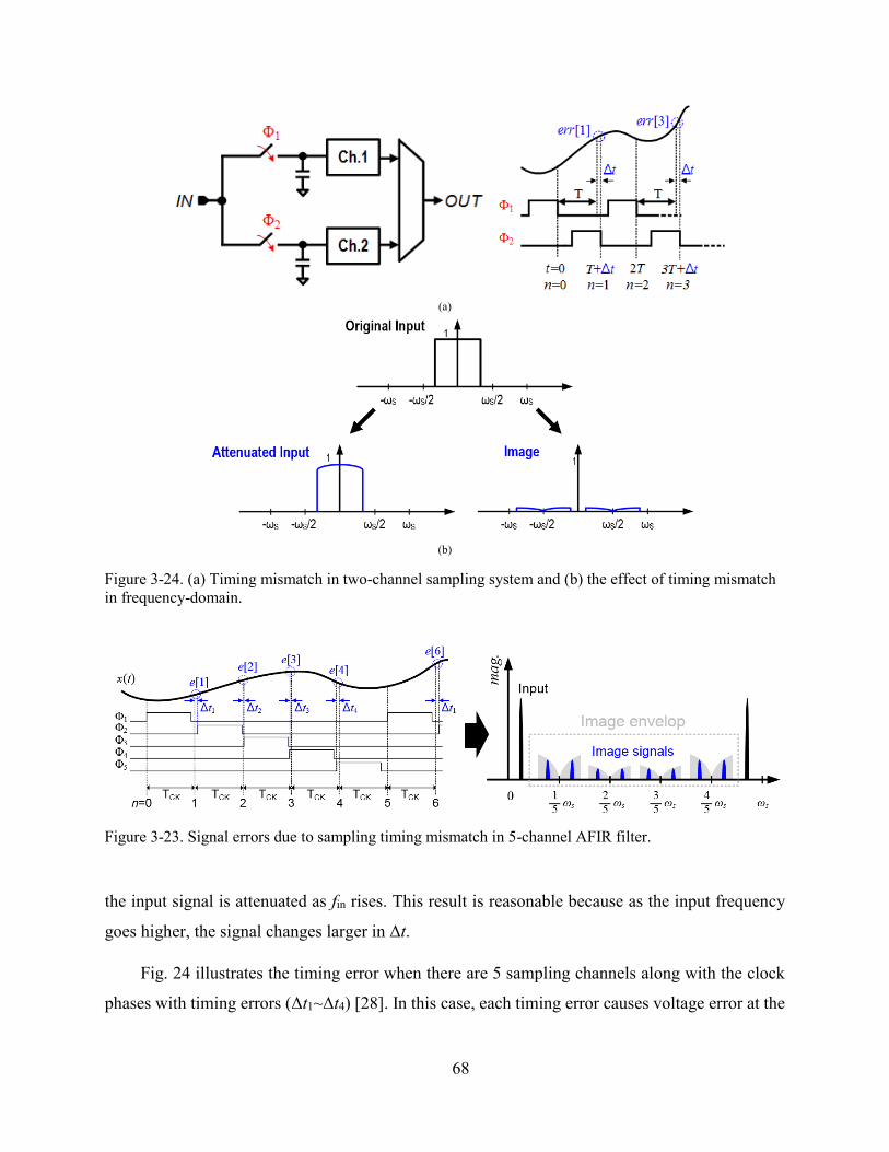
68
the input signal is attenuated as fin rises. This result is reasonable because as the input frequency
goes higher, the signal changes larger in Δt.
Fig. 24 illustrates the timing error when there are 5 sampling channels along with the clock
phases with timing errors (Δt1~Δt4) [28]. In this case, each timing error causes voltage error at the
(a)
(b)
Figure 3-24. (a) Timing mismatch in two-channel sampling system and (b) the effect of timing mismatch
in frequency-domain.
Figure 3-23. Signal errors due to sampling timing mismatch in 5-channel AFIR filter.

69
sampling instant of each individual channel. Consequently, the image is aliased around fs/5, so
spurs caused by sampling timing mismatch can be found at
, , 1,2,3...5
sspur STM in
k ff f k
. (3-20)
Offset mismatch is another contributing factor to TI error. While the mismatch factors
discussed above modulate the input signal, offset mismatch directly generates a signal at the output
even without input signal. The effect of offset can be deduced from Fig. 3-25. In the 5-tap AFIR
filter, S/H buffers are the source of offset, while the adder can only create DC offset at the output
since the input transistors share the output. Input referred offset voltages of the S/H buffers (Vos,1
~ Vos,5) are equivalent to an input signal that has a period of 5·TCK. Even if there is no input, the
combination of offset creates a signal pattern that has fundamental frequency of fs/5. Therefore,
spurs caused by offset mismatch are expected to be found at
,OSM , 1,2,3...5
sspur avg
k ff V k
. (3-21)
The output may also include a DC component that has the amplitude equal to the average of the
offsets (Vavg). However, the offset is not amplified as the gain of AFIR filter is less than unity, so
it does not affect the performance significantly. The effect of sampling timing and offset
mismatches are generally observed in TI ADC applications and simulations with some specific
mismatch conditions are as demonstrated in [21].
Figure 3-25. Effect of offset mismatch.

70
Coefficient mismatch also creates spurs at the output. To account for the coefficient mismatch,
we defines the selected coefficients of each channel to be ACH, BCH, CCH, DCH, where ‘CH’ refers
to the channel numbers. In Fig. 3-2, if we take a look at t5, while Ch.5 is multiplying the sampled
input VIN(t4) by A5, the other sampled inputs [VIN(t1 ~ t3)] are multiplied by B4, C3, D2 in each
channel. This multiplication process occurs at every 5·TCK. If we define Y1 to be the output signal
when Ch.1 samples the input signal, Y1 can be derived by setting all the other coefficients to zero,
such that
1 5 4 3 2[5 ] [5 1] [5 2] [5 3] [5 4].Y k A X k B X k C X k D X k (3-22)
The output signal is as described in Fig. 3-26(a). In this manner, there are other 4 sequences
(Y2, Y3, Y4 and Y5) and the time-interleaved output can be expressed as YTI = Y1 + Y2 + Y3 + Y4
+ Y5. If there is no coefficient mismatch, namely, all ACH = A, all BCH = B, all CCH = C and all
DCH = D, the aliased signals, except for the signals around fs and its harmonics, are removed as Y2
~ Y5 are added together as shown Fig. 3-26(b). This is because the aliased signals of Y1 ~ Y5,
have the same amplitude and evenly distributed phases, such that they cancel out each other, while
the signal at the input frequency, the aliased signal around fs and its harmonics are in phase, so
they are added together [29]. However, coefficient mismatch distorts magnitude and phase of the
aliased signals from each sequence as individual channels perform slightly different transfer
functions, creating residues. It must also be noted that mismatches from Abuf and Aadd over the TI
channels also contribute to the coefficient mismatch as the effective coefficient is the signal
division ratio of the coefficient multiplier multiplied by Abuf · Aadd. Fig. 3-26(c) presents the results
from a behavioral simulation of the AFIR filter with coefficient set of 32/64, 63/64, 63/64, 32/64,
but applying up to 5% of variation to the coefficient values as well as the Abuf and Aadd across the
different TI channels. The gain and phase mismatches arising from the coefficient mismatches
result in the spurs at the frequencies given by (3-20).
Overall, the mismatch errors can be reduced by increasing the size of the devices, which
results in larger area and power consumption. Otherwise, it is possible to take advantage of
calibration techniques [30] or random interleaving techniques [31] to mitigate the effect of
mismatch errors.
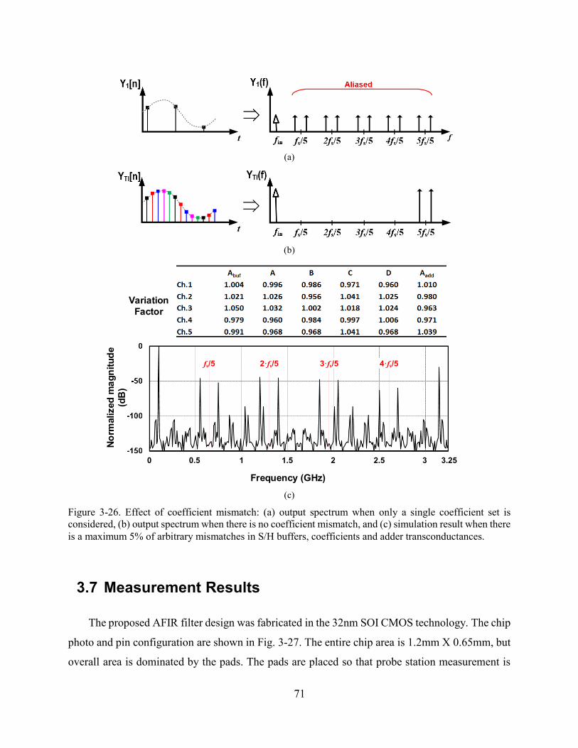
71
3.7 Measurement Results
The proposed AFIR filter design was fabricated in the 32nm SOI CMOS technology. The chip
photo and pin configuration are shown in Fig. 3-27. The entire chip area is 1.2mm X 0.65mm, but
overall area is dominated by the pads. The pads are placed so that probe station measurement is
(a)
(b)
0 0.5 1 1.5 2 2.5 3 3.25
No
rmalized
ma
gn
itu
de
(dB
)
Frequency (GHz)
fs/5 4·fs/53·fs/52·fs/5
Variation
Factor
(c)
Figure 3-26. Effect of coefficient mismatch: (a) output spectrum when only a single coefficient set is
considered, (b) output spectrum when there is no coefficient mismatch, and (c) simulation result when there
is a maximum 5% of arbitrary mismatches in S/H buffers, coefficients and adder transconductances.
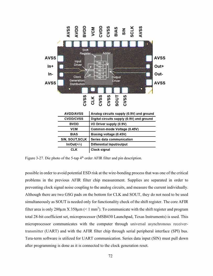
72
possible in order to avoid potential ESD risk at the wire-bonding process that was one of the critical
problems in the previous AFIR filter chip measurement. Supplies are separated in order to
preventing clock signal noise coupling to the analog circuits, and measure the current individually.
Although there are two GSG pads on the bottom for CLK and SOUT, they do not need to be used
simultaneously as SOUT is needed only for functionality check of the shift register. The core AFIR
filter area is only 280m X 350m (< 1 mm2). To communicate with the shift register and program
total 28-bit coefficient set, microprocessor (MSB430 Launchpad, Texas Instruments) is used. This
microprocessor communicates with the computer through universal asynchronous receiver-
transmitter (UART) and with the AFIR filter chip through serial peripheral interface (SPI) bus.
Tera-term software is utilized for UART communication. Series data input (SIN) must pull down
after programming is done as it is connected to the clock generation reset.
Figure 3-27. Die photo of the 5-tap 4th order AFIR filter and pin description.
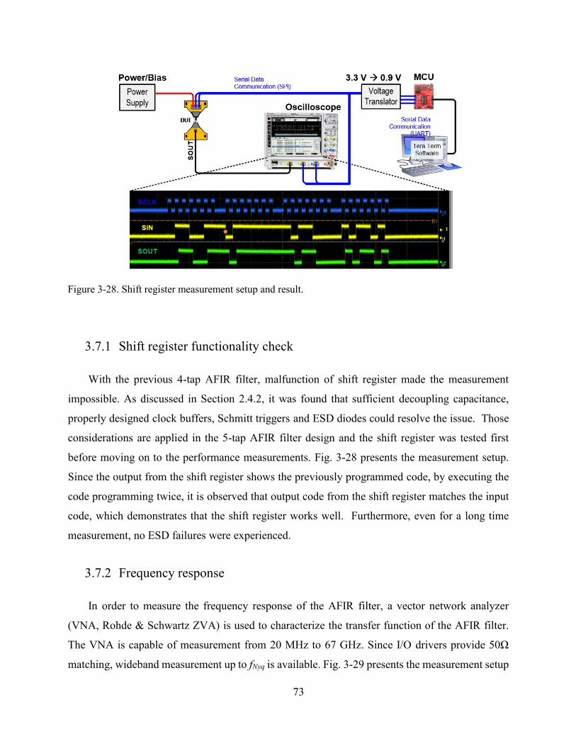
73
3.7.1 Shift register functionality check
With the previous 4-tap AFIR filter, malfunction of shift register made the measurement
impossible. As discussed in Section 2.4.2, it was found that sufficient decoupling capacitance,
properly designed clock buffers, Schmitt triggers and ESD diodes could resolve the issue. Those
considerations are applied in the 5-tap AFIR filter design and the shift register was tested first
before moving on to the performance measurements. Fig. 3-28 presents the measurement setup.
Since the output from the shift register shows the previously programmed code, by executing the
code programming twice, it is observed that output code from the shift register matches the input
code, which demonstrates that the shift register works well. Furthermore, even for a long time
measurement, no ESD failures were experienced.
3.7.2 Frequency response
In order to measure the frequency response of the AFIR filter, a vector network analyzer
(VNA, Rohde & Schwartz ZVA) is used to characterize the transfer function of the AFIR filter.
The VNA is capable of measurement from 20 MHz to 67 GHz. Since I/O drivers provide 50Ω
matching, wideband measurement up to fNyq is available. Fig. 3-29 presents the measurement setup
Figure 3-28. Shift register measurement setup and result.
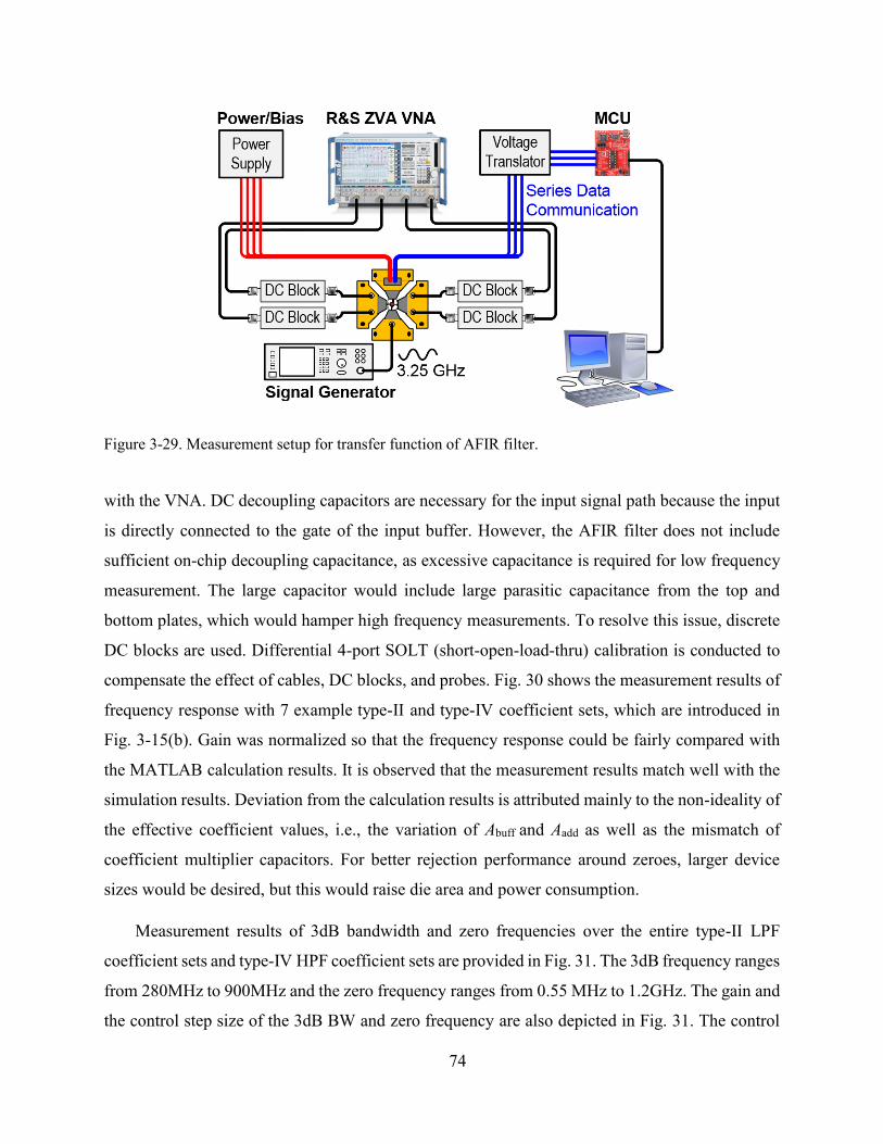
74
with the VNA. DC decoupling capacitors are necessary for the input signal path because the input
is directly connected to the gate of the input buffer. However, the AFIR filter does not include
sufficient on-chip decoupling capacitance, as excessive capacitance is required for low frequency
measurement. The large capacitor would include large parasitic capacitance from the top and
bottom plates, which would hamper high frequency measurements. To resolve this issue, discrete
DC blocks are used. Differential 4-port SOLT (short-open-load-thru) calibration is conducted to
compensate the effect of cables, DC blocks, and probes. Fig. 30 shows the measurement results of
frequency response with 7 example type-II and type-IV coefficient sets, which are introduced in
Fig. 3-15(b). Gain was normalized so that the frequency response could be fairly compared with
the MATLAB calculation results. It is observed that the measurement results match well with the
simulation results. Deviation from the calculation results is attributed mainly to the non-ideality of
the effective coefficient values, i.e., the variation of Abuff and Aadd as well as the mismatch of
coefficient multiplier capacitors. For better rejection performance around zeroes, larger device
sizes would be desired, but this would raise die area and power consumption.
Measurement results of 3dB bandwidth and zero frequencies over the entire type-II LPF
coefficient sets and type-IV HPF coefficient sets are provided in Fig. 31. The 3dB frequency ranges
from 280MHz to 900MHz and the zero frequency ranges from 0.55 MHz to 1.2GHz. The gain and
the control step size of the 3dB BW and zero frequency are also depicted in Fig. 31. The control
Figure 3-29. Measurement setup for transfer function of AFIR filter.

75
step sizes of 3dB BW and zero frequency are at worst 42 MHz and 35MHz, respectively for LPF
coefficient sets, and 39MHz and 42 MHz, respectively for HPF coefficient sets. However, the
coefficients are mostly controlled with 10MHz or less step sizes. Gain in the in-band region is
related to the sum of all coefficients. Therefore, there is gain variation close to 6dB over the
different coefficient sets. If necessary, this gain variation can be minimized by matching the gain
to the minimum value. For example, the maximum gain is given when A = B = C = D = 63/64.
The coefficient set can be substituted with A = B = C = D = 32/64, which does not change the
(a)
(b)
Figure 3-30. Frequency response of the AFIR filter with 7 example coefficient sets of (a) Type-II and (b)
Type-IV

76
shape of the frequency response but the gain is equalized to the minimum value, i.e., the gain of A
= D = 1/64 and B = C = 63/64.
3.7.3 Nonlinearity
The dominant source of nonlinearity in the AFIR filter design is the adder and the effect
depends on the coefficient set. In order to characterize linearity, two-tone tests are performed for
the example coefficient sets. The measurement setup is illustrated in Fig 3-32. Spectrum analyzer
(FSW, Rohde and Schwartz) is utilized to observe the output tones. Baluns are included for
(a) (b)
Figure 3-31. Measured 3dB BW/zero frequency and step size of 3dB BW/zero frequency and gain over
for (a) all possible Type-II LPF coefficient sets, and (b) all possible Type-IV HPF coefficient sets.
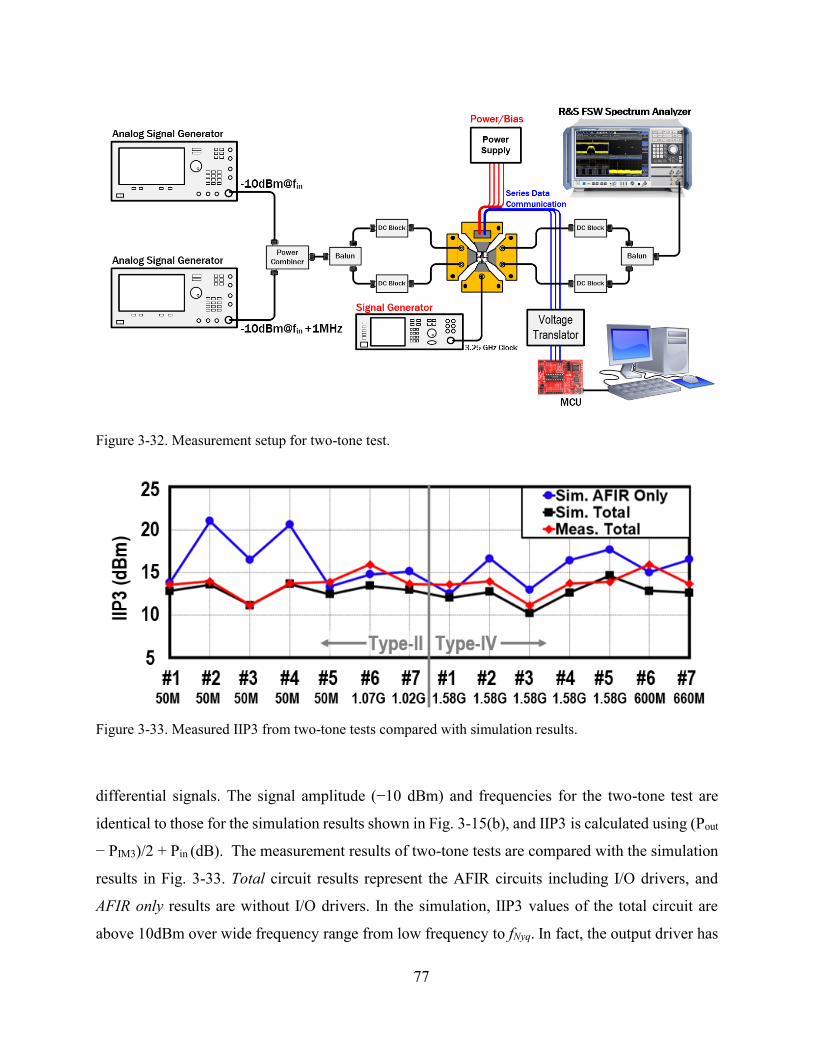
77
differential signals. The signal amplitude (−10 dBm) and frequencies for the two-tone test are
identical to those for the simulation results shown in Fig. 3-15(b), and IIP3 is calculated using (Pout
− PIM3)/2 + Pin (dB). The measurement results of two-tone tests are compared with the simulation
results in Fig. 3-33. Total circuit results represent the AFIR circuits including I/O drivers, and
AFIR only results are without I/O drivers. In the simulation, IIP3 values of the total circuit are
above 10dBm over wide frequency range from low frequency to fNyq. In fact, the output driver has
Figure 3-32. Measurement setup for two-tone test.
Figure 3-33. Measured IIP3 from two-tone tests compared with simulation results.

78
similar or worse linearity than the analog FIR filter core, so the analog FIR filter only circuit has
better linearity (> 13 dBm) as seen in the simulation result. In the measurement, the total AFIR
filter prototype achieves mostly better or similar linearity performance than the simulation result.
Although it was not possible to measure the analog FIR filter excluding I/O drivers, it is expected
that the AFIR filter core in the prototype would also have similar or better performance than the
simulation result, which is minimum 13 dBm.
3.7.4 Noise
Total output noise is also measured with the spectrum analyzer. From the measurement setup
in Fig. 3-32, input of the AFIR is tied to 50Ω terminal and a preamplifier (ZKL-2+, Mini-Circuits)
with 33.5dB gain and 10M – 2GHz of bandwidth is used at the input of the spectrum analyzer to
make the DUT noise visible from the equipment noise. The measurement result when the
coefficients are all maximum is shown in Fig. 3-34. The measurement result is comparable with
the simulation/calculation result using the method described in Section 3-4. The gain and noise
contributions from I/O drivers, DC blocks and balun are removed from the total output noise. TI
operation spurs are also intentionally removed assuming that those will be removed by post
processing. It is observed that the measured total output noise matches well with the simulated and
calculated noise. Furthermore, the total output noise varies with the coefficient set negligibly even
with all zero coefficients in which noise is only from the adder and reset switch. This result shows
that the adder and reset switches are the dominant source of the total AFIR filter noise.
Figure 3-34. Measured total output noise (when A=B=C=D=63/64) compared with simulation/calculation
result.

79
Table 3-V presents input referred noise (IRN) of highlighted coefficient sets as well as other
performance criteria. IRN is calculated by dividing the output noise by the gain of AFIR filter, and
then averaging over the in-band frequency range. Noise level is rather high but sufficiently lower
than the target. If necessary, the noise level can be mitigated by increasing the transconductance
in the adder at the expense of power consumption.
3.7.5 Time-interleaved operation spurs
As studied in Section 3-5, there are signal-modulated (image) tones and spurs found in the
output spectrum of the AFIR filter. Fig. 3-35 shows the output spectrum when coefficients are all
maximum and a 100 MHz input is injected. Image tones are found at the frequencies that are given
by (3-20), and with maximum amplitude of −72 dBm (−80 Vp). However, this amplitude is
affected by the AFIR filter transfer function since the offset is developed from the S/H buffer. If
the gain of AFIR filter at the frequencies given in (3-20) is compensated to the maximum gain, the
amplitude becomes about −60 dBm (−316 V). Sampling timing error and gain mismatch also
create images at the frequencies given in (3-21) with amplitude of −87 dBm (−22 VAs
TABLE 3-V. SUMMARY OF MEASURED PERFORMANCE OF AFIR FILTER WITH HIGHLIGHTED
COEFFICIENT SETS
Type # Pass
Band
3dB BW/
Center freq.
(Hz)
Gain (dB) IIP3 (dBm)** IRN (nV/√Hz)
II
#1 LPF 900M -5.5 14 35
#2 LPF 440M -1.5 14 27
#3 LPF 380M 1.0 11 22
#4 LPF 330M -2.0 14 32
#5 LPF 280M -6.0 14 54
#6 BPF 1.07G -3.6 16 28
#7 BPF 1.02G -1.8 14 22
IV
#1 HPF 732M -8.5 13 35
#2 HPF 1.18G -4.5 14 21
#3 HPF 1.23G -2.2 14 16
#4 HPF 1.28G -4.6 15 20
#5 HPF 1.35G -8.1 13 30
#6 BPF 600M -4.6 13 31
#7 BPF 660M -1.2 15 22
*Worst power consumption is 10.6mW in the extreme coefficient set case. I/O drivers are excluded.
**Measurement results including I/O drivers.
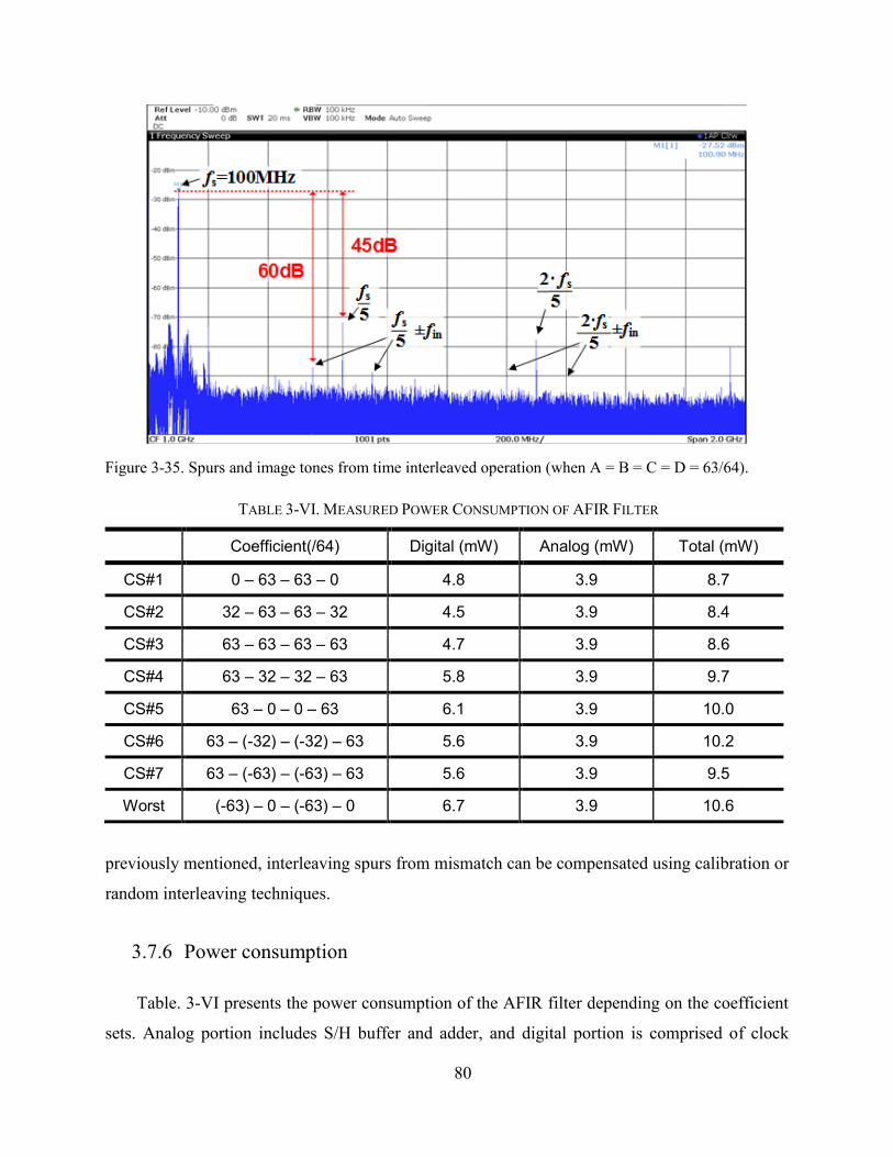
80
previously mentioned, interleaving spurs from mismatch can be compensated using calibration or
random interleaving techniques.
3.7.6 Power consumption
Table. 3-VI presents the power consumption of the AFIR filter depending on the coefficient
sets. Analog portion includes S/H buffer and adder, and digital portion is comprised of clock
Figure 3-35. Spurs and image tones from time interleaved operation (when A = B = C = D = 63/64).
TABLE 3-VI. MEASURED POWER CONSUMPTION OF AFIR FILTER
Coefficient(/64) Digital (mW) Analog (mW) Total (mW)
CS#1 0 – 63 – 63 – 0 4.8 3.9 8.7
CS#2 32 – 63 – 63 – 32 4.5 3.9 8.4
CS#3 63 – 63 – 63 – 63 4.7 3.9 8.6
CS#4 63 – 32 – 32 – 63 5.8 3.9 9.7
CS#5 63 – 0 – 0 – 63 6.1 3.9 10.0
CS#6 63 – (-32) – (-32) – 63 5.6 3.9 10.2
CS#7 63 – (-63) – (-63) – 63 5.6 3.9 9.5
Worst (-63) – 0 – (-63) – 0 6.7 3.9 10.6
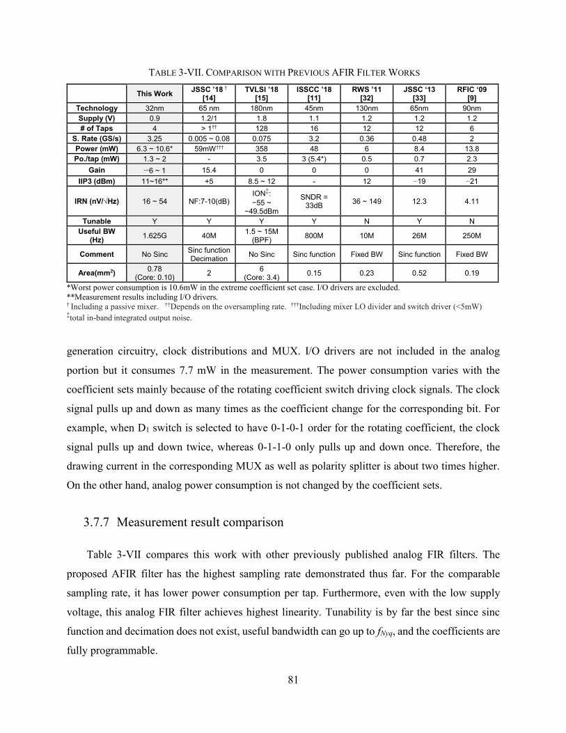
81
generation circuitry, clock distributions and MUX. I/O drivers are not included in the analog
portion but it consumes 7.7 mW in the measurement. The power consumption varies with the
coefficient sets mainly because of the rotating coefficient switch driving clock signals. The clock
signal pulls up and down as many times as the coefficient change for the corresponding bit. For
example, when D1 switch is selected to have 0-1-0-1 order for the rotating coefficient, the clock
signal pulls up and down twice, whereas 0-1-1-0 only pulls up and down once. Therefore, the
drawing current in the corresponding MUX as well as polarity splitter is about two times higher.
On the other hand, analog power consumption is not changed by the coefficient sets.
3.7.7 Measurement result comparison
Table 3-VII compares this work with other previously published analog FIR filters. The
proposed AFIR filter has the highest sampling rate demonstrated thus far. For the comparable
sampling rate, it has lower power consumption per tap. Furthermore, even with the low supply
voltage, this analog FIR filter achieves highest linearity. Tunability is by far the best since sinc
function and decimation does not exist, useful bandwidth can go up to fNyq, and the coefficients are
fully programmable.
TABLE 3-VII. COMPARISON WITH PREVIOUS AFIR FILTER WORKS
This Work JSSC ’18 †
[14] TVLSI ’18
[15] ISSCC ’18
[11] RWS ’11
[32] JSSC ‘13
[33] RFIC ‘09
[9]
Technology 32nm 65 nm 180nm 45nm 130nm 65nm 90nm
Supply (V) 0.9 1.2/1 1.8 1.1 1.2 1.2 1.2
# of Taps 4 > 1†† 128 16 12 12 6
S. Rate (GS/s) 3.25 0.005 ~ 0.08 0.075 3.2 0.36 0.48 2
Power (mW) 6.3 ~ 10.6* 59mW††† 358 48 6 8.4 13.8
Po./tap (mW) 1.3 ~ 2 - 3.5 3 (5.4*) 0.5 0.7 2.3
Gain −6 ~ 1 15.4 0 0 0 41 29
IIP3 (dBm) 11~16** +5 8.5 ~ 12 - 12 −19 −21
IRN (nV/√Hz) 16 ~ 54 NF:7-10(dB) ION‡:
−55 ~ −49.5dBm
SNDR = 33dB
36 ~ 149 12.3 4.11
Tunable Y Y Y Y N Y N
Useful BW (Hz)
1.625G 40M 1.5 ~ 15M
(BPF) 800M 10M 26M 250M
Comment No Sinc Sinc function Decimation
No Sinc Sinc function Fixed BW Sinc function Fixed BW
Area(mm2) 0.78
(Core: 0.10) 2
6 (Core: 3.4)
0.15 0.23 0.52 0.19
*Worst power consumption is 10.6mW in the extreme coefficient set case. I/O drivers are excluded.
**Measurement results including I/O drivers. † Including a passive mixer. ††Depends on the oversampling rate. †††Including mixer LO divider and switch driver (<5mW) ‡total in-band integrated output noise.
*Estimated power consumption for non-decimation operation. **Including I/O drivers.
***Potential BW can cover up to Nyquist rate.

82
3.8 Summary
We have presented an improved 4th order analog FIR filter operating in the discrete-time
domain. By employing a split-capacitive DAC, a low power and high linearity coefficient
multiplier was implemented providing coefficient values with the inherent resolution of the DAC.
Analysis of noise and the effect of 5-channel time-interleaved operation was also conducted. The
AFIR filter was fabricated in 32nm SOI CMOS technology. In the measurement, the chip achieved
the Nyquist rate filtering controlled by the coefficients and demonstrated >11 dBm of IIP3 under
0.9 V supply. Compared to the previously reported AFIR filters, this AFIR filter consumes the
least power per tap (1.3 ~ 2mW/tap) as well as demonstrating higher linearity.

83
4 Wideband beamforming with 4th order AFIR filter
Chapter 4.
Wideband beamforming with 4th order
AFIR filter
4.1 Introduction
In Chapter 3, we demonstrated a 3.25GS/s AFIR filter with comprehensive design, analysis
and measurements. As introduced in Chapter 1, it is possible to extend the application of AFIR
filters to wideband true-time delay (TTD) beamforming. To implement a TTD FIR-based
beamformer (FIR-BF), each antenna element is followed by the AFIR filter as shown in Fig. 1-12.
Interelement distance (d) is typically set to half of the wavelength of the highest frequency [17].
As the highest frequency is desired to be the Nyquist rate of the sampling function, under that
assumption d becomes c0/(3.25GHz), where c0 is the speed of light in free space. This distance is
equivalent to the sampling rate delays (τCK) in the FIR filters. In other words, when the beam angle
is 90°, the signal delay from an antenna to the next antenna becomes the same as τCK. This chapter
describes the realization of a proof-of-concept FIR-BF using the developed AFIR filters,
calculation of coefficients, and the measurement results.

84
4.2 Coefficients for FIR-BF
As illustrated in Chapter 1-3, FIR-BF has the advantage of independent control of spectral
and spatial filtering over wide frequency range, whereas typical phased array beamforming suffers
from beam-squint and shift of nulls [34]. TTD can avoid the beam-squint issue but will still have
shift of nulls. In order to realize this feature of FIR-BF, it is necessary to study the selection of
coefficient values for desired beam and frequency response as demonstrated in [17] and [34].
However, a comprehensive study of coefficient calculations was beyond the scope of this
dissertation.
In this work, we developed a straightforward approach to verify the functionality of FIR-based
beamforming without high-level coefficient calculation. At some specific beam angles, the FIR-
based beamformer can be treated as a single input FIR filter. If we assume that the delay of the
first tap in the first element is zero, delays of the other taps can be calculated by
0
sin( 1) ( 1) .nm CK
dD n m
c
(4-1)
(a) (b) (c)
(d) (e)
Figure 4-1. Delays of signal arrived at each antenna elements with even spacing of d and different beam
angle (a) θ = 0°, (b) θ = 14.5°, (c) θ = 19.5°, (d) θ = 30° and (e) θ = 90°.

85
where m and n are the corresponding tap and antenna numbers, respectively, as indicated in
Chapter 1, and the τCK is the unit delay (=1/fs). The number of elements (N) and taps (M) in this
example is 4. Fig. 4-1 illustrates corresponding delays where each row corresponds to one of the
4 elements and the y-axis represents the amount of delay. For example, the signal on the third tap
(m = 3) in the FIR filter on the second element (n = 2) would have the delay of D23, which is 2·τCK
at θ = 0° [see Fig. 4-1(a)], and (2+1/4)·τCK at θ = 14.5° [see Fig. 4-1(b)]. When the beam angle is
zero [Fig. 4-1(a)], we can consider the whole FIR-BF as a 4th order FIR filter because there is no
phase difference between the elements. As the frequency response of all element is the same, the
total output, i.e. sum of all outputs from each elements, is 4 times larger than the output signal
from single element. Therefore, the coefficient set can be simply determined with the coefficient
calculation for 4th order FIR filter. When the beam angle is 14.5°, the delay due to the inter-element
spacing becomes 1/4·τCK as shown in Fig. 4-1(b). If we arrange the delays in the order of the
amount of delay over the all elements, then the overall FIR-BF function becomes
11 21 31 43 44
1 2 14 15y[ ] [ ] [ ] [ ] [ ] [ ].
4 4 4 4n a x n a x n a x n a x n a x n (4-2)
This result is equivalent to 16 equally spaced (1/4·τCK) delays, which constitute a 16th order
FIR filter. Therefore, to obtain the coefficient sets, a 16th order FIR filter needs to be designed. If
the coefficients of the 16th order FIR filter are C16,1 ~ C16,16 for a desired frequency response, we
can allocate them to each tap of FIR-BF based on the delays. For example, since D23 = (2+1/4)·τCK,
which is the 10th delay among the 16 taps, a23 is set to C16,10. Thus, we can achieve desired
frequency response at the specific beam angle. When the beam deviates from this specific angle,
the delay given by (4-2) is not valid, so the frequency response becomes arbitrary. When the beam
angle becomes 19.5°, the delay due to the interelement distance becomes 1/3·τCK as shown in Fig.
4-1(c) resulting in 13 equally spaced delays leading to
11 21 31 41 21
43 44
1 2 3 3y[ ] [ ] [ ] [ ] [ ] [ ]
3 3 3 3
14 15[ ] [ ].
3 3
n a x n a x n a x n a x n a x n
a x n a x n
(4-3)
Notably, D12 and D41 share the same delay, so the effective coefficient is a12 + a41 at the
corresponding delay. Likewise, two delays are overlapping at 2·τCK and 3·τCK as well [Fig. 4-1(c)].

86
To achieve the 13th order FIR filter function, overlapping-delay taps can take the corresponding
coefficient value divided by 2. For example, if the coefficients of the 13th order FIR filter are C13,1
~ C13,13, a12 and a41 are C13,4/2. If the beam angles are 30° and 90°, the delays due to the
interelement distance become 1/2·τCK and τCK as shown in Fig. 4-1(d) and (e), respectively. In
these cases, the FIR-BF coefficients can be set with 10th order and 7th order FIR filter designs,
respectively. The coefficients for overlapping delays can be the value of desired coefficient divided
by the total number of overlapping delays. For instance, in the 90° case, a13, a22 and a31 are set to
third coefficient of 7th order FIR filter divided by 3 (C7,3/3).
To verify the FIR-BF function with the proposed method of coefficient set calculation,
behavioral simulations were conducted using the Advanced Design System (ADS) software.
Coefficients for desired frequency response with required FIR filter order were obtained from a
FIR filter design tool provided in [35]. In this work, the FIR filters were designed to have a center
frequency (fc) at 1GHz and 500MHz of bandwidth. The coefficient sets for the FIR-BF are
allocated from the designed FIR filter and shown in Fig. 4-2. For example, coefficient set of 16th
order FIR filter for the desired frequency response calculated by [35] is -31 -38 -32 -30 -3 19 48
63 63 48 19 -3 -30 -32 -38 -31 and this coefficient set is allocated to the FIR-BF taps for 14.5°
beamforming as described in the previous section. In the simulation, ideal delay, addition and
coefficient multiplication blocks were used. Fig. 4-3 depicts the simulation results for each of the
specified beam angles. Although the coefficient sets do not have constant frequency response over
some specific azimuth range as in [17], it is observed that the center beam angle moves as desired
according to the coefficient sets and the center frequency stays at 1 GHz.
4.3 Prototype module-level FIR-BF
While the single analog FIR filter can be measured directly on the RF probe station, the
proposed FIR-BF system measurement needs to interconnect separate PCB boards, as there are
multiple inputs and outputs. Fig. 4-4 illustrates the diagram of the poof-of-concept FIR-BF
measurement setup. The VNA (R&S ZVA) provides 4-way signal generation emulating the 4-
antenna array with a function called defined coherence mode; all 4-ports share the same source
and individual phase can be controlled via internal software. A 4-way divider is used to take a
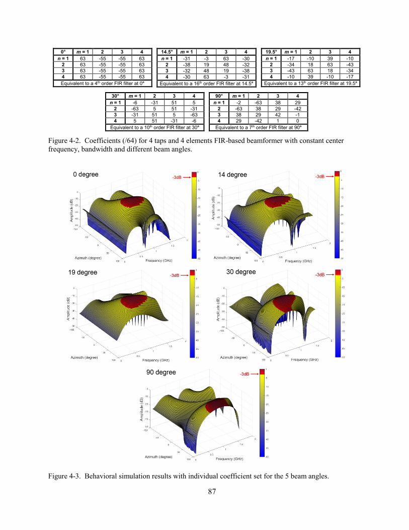
87
Figure 4-3. Behavioral simulation results with individual coefficient set for the 5 beam angles.
Figure 4-2. Coefficients (/64) for 4 taps and 4 elements FIR-based beamformer with constant center
frequency, bandwidth and different beam angles.
0° m = 1 2 3 4
n = 1 63 -55 -55 63
2 63 -55 -55 63
3 63 -55 -55 63
4 63 -55 -55 63
Equivalent to a 4th order FIR filter at 0°
14.5° m = 1 2 3 4
n = 1 -31 -3 63 -30
2 -38 19 48 -32
3 -32 48 19 -38
4 -30 63 -3 -31
Equivalent to a 16th order FIR filter at 14.5°
19.5° m = 1 2 3 4
n = 1 -17 -10 39 -10
2 -34 18 63 -43
3 -43 63 18 -34
4 -10 39 -10 -17
Equivalent to a 13th order FIR filter at 19.5°
30° m = 1 2 3 4
n = 1 -6 -31 51 5
2 -63 5 51 -31
3 -31 51 5 -63
4 5 51 -31 -6
Equivalent to a 10th order FIR filter at 30°
90° m = 1 2 3 4
n = 1 -2 -63 38 29
2 -63 38 29 -42
3 38 29 42 -1
4 29 -42 1 0
Equivalent to a 7th order FIR filter at 90°

88
single 3.25 GHz signal and distribute to the 4 AFIR PCB modules for clock generation. In order
to complete the FIR-BF function, a 4-way combiner adds all outputs from the AFIR modules. The
output signal of the FIR-BF system is observed with a spectrum analyzer (R&S FSW). The input
signal phases can be adjusted in the VNA; however, it is necessary to deal with the signals from
the 4-way divider and output signals of AFIR filters carefully. In order to avoid phase mismatch
of the clock signals, phase trimmers are added at the output ports of the divider. Phase-matched
cables are used for the outputs of each AFIR filter module.
For the FIR-BF measurement, AFIR-based filter modules are implemented on PCB board
(Fig. 4-5). Transmission lines (TL) are placed between the RF devices and the AFIR chips. The
width of the TL is 26 mils (0.66 mm), which gives 50Ω impedance on the PCB board calculated
by Microwave Impedance Calculator [36]. The TLs are designed as short as possible in order to
prevent phase mismatch between the AFIR filter modules. In each module, the input signal first
goes through a single-pole, double-throw (SPDT) switch. While one SPDT output port leads to the
next stage (Balun), the other output is connected to an additional RF port. This port enables the
amplitude and phase of the input signals to be checked before they are delivered to the AFIR filter
chip, and provides a means to adjust them as necessary. Wide-band (30 – 3000 MHz) baluns are
located at the input and output of the AFIR filter. There are DC blocking capacitors between the
baluns and the AFIR filter chip input/output since the balun is connected to ground at DC level.
Figure 4-4. Diagram of the proof-of-concept 4-elements 4th order FIR-BF measurement.
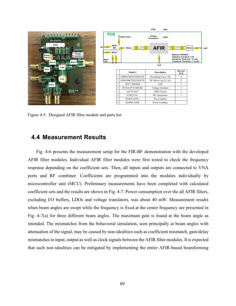
89
4.4 Measurement Results
Fig. 4-6 presents the measurement setup for the FIR-BF demonstration with the developed
AFIR filter modules. Individual AFIR filter modules were first tested to check the frequency
response depending on the coefficient sets. Then, all inputs and outputs are connected to VNA
ports and RF combiner. Coefficients are programmed into the modules individually by
microcontroller unit (MCU). Preliminary measurements have been completed with calculated
coefficient sets and the results are shown in Fig. 4-7. Power consumption over the all AFIR filters,
excluding I/O buffers, LDOs and voltage translators, was about 40 mW. Measurement results
when beam angles are swept while the frequency is fixed at the center frequency are presented in
Fig. 4-7(a) for three different beam angles. The maximum gain is found at the beam angle as
intended. The mismatches from the behavioral simulation, seen principally at beam angles with
attenuation of the signal, may be caused by non-idealities such as coefficient mismatch, gain/delay
mismatches in input, output as well as clock signals between the AFIR filter modules. It is expected
that such non-idealities can be mitigated by implementing the entire AFIR-based beamforming
Figure 4-5. Designed AFIR filter module and parts list.
AFIRBalun
LDOs
VDDCTRL
PCB
SPDT
SW
Signal Check
Balun
Voltage
Translators
TL
TLTL
TL
TL
TL
TL TLBalunTest
TL
TL
TLBalun TL
CLK
OUT
Model # Description Qty per
PCB
1 GRM185R60J105KE26D Decoupling Cap (1 uF) 12
2 GRM188R72D222KW7D DC Block Cap (2.2 nF) 11
3 TPS71709DSER LDO 3
4 SN74AUP1T34DCKR Voltage Translator 2
5 AS179-92LF SPDT Switch 1
6 TCM2-33X+ RF Transformer 3
7 ZN4PD-642W+ Power Splitter
8 ZN4PD1-63HP Power Combiner
TL
TL
TL
TL
Material: RO4003C
Dielectric Constant: 3.55
Substrate Thickness: 12 mils
Conductor Thickness: 1 oz ED Balun
SPDTChip
Balun
Balun
CLK
Signal
Check
LDOs
Voltage
Translators
IN
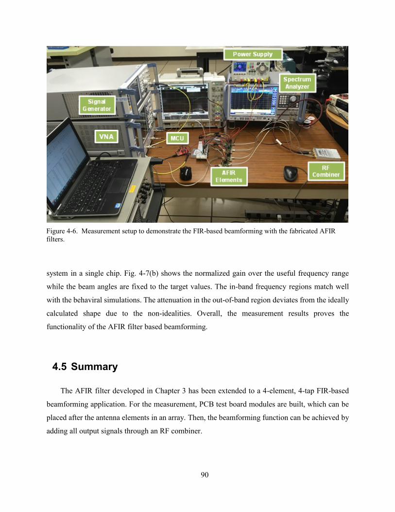
90
system in a single chip. Fig. 4-7(b) shows the normalized gain over the useful frequency range
while the beam angles are fixed to the target values. The in-band frequency regions match well
with the behaviral simulations. The attenuation in the out-of-band region deviates from the ideally
calculated shape due to the non-idealities. Overall, the measurement results proves the
functionality of the AFIR filter based beamforming.
4.5 Summary
The AFIR filter developed in Chapter 3 has been extended to a 4-element, 4-tap FIR-based
beamforming application. For the measurement, PCB test board modules are built, which can be
placed after the antenna elements in an array. Then, the beamforming function can be achieved by
adding all output signals through an RF combiner.
Figure 4-6. Measurement setup to demonstrate the FIR-based beamforming with the fabricated AFIR
filters.
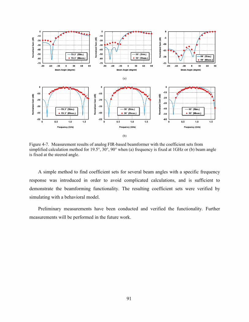
91
A simple method to find coefficient sets for several beam angles with a specific frequency
response was introduced in order to avoid complicated calculations, and is sufficient to
demonstrate the beamforming functionality. The resulting coefficient sets were verified by
simulating with a behavioral model.
Preliminary measurements have been conducted and verified the functionality. Further
measurements will be performed in the future work.
(a)
(b)
Figure 4-7. Measurement results of analog FIR-based beamformer with the coefficient sets from
simplified calculation method for 19.5°, 30°, 90° when (a) frequency is fixed at 1GHz or (b) beam angle
is fixed at the steered angle.

92
5 Analysis and optimization of multi-section capacitive DACs for
Mixed-Signal Processing
Chapter 5.
Analysis and optimization of multi-section
capacitive DACs for Mixed-Signal
Processing
5.1 Introduction
Capacitive digital-to-analog converters (CDACs), consisting of binary-weighted switched-
capacitor arrays to realize voltage levels at their output corresponding to input digital codes, have
been widely adopted in successive approximation register (SAR) analog to digital converter
(ADC) designs as shown in Fig. 5-1 [37]-[51]. Furthermore, the application of CDAC has been
expanded to coefficient multipliers for analog FIR filter design in Chapter 2 – 4 of this dissertation.
The CDAC architecture has the advantage of low power consumption, but increasing resolution
demands larger capacitor arrays, which in turn negatively impacts the speed, power consumption
and area. The split capacitive DAC (Split-CDAC) [19] and C-2C [37] structures were introduced
to help compensate for this issue.
In the conventional CDAC design, there is a fundamental tradeoff with the size of the unit
capacitor (CU). The unit capacitor size should be minimized for area, switching energy and speed,
but must not be too small in order to satisfy kT/C noise or mismatch requirements. Meanwhile, it
is possible that the minimum capacitor available in the process limits the unit capacitor size, even
if those requirements push the unit capacitor size to be further reduced. In this situation, the split-
CDAC/C-2C structures become particularly useful as a means to further reduce area, switching
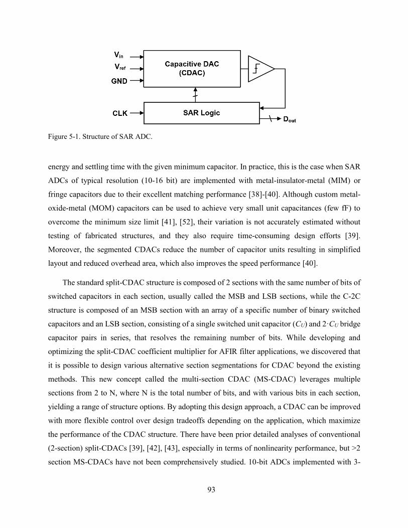
93
energy and settling time with the given minimum capacitor. In practice, this is the case when SAR
ADCs of typical resolution (10-16 bit) are implemented with metal-insulator-metal (MIM) or
fringe capacitors due to their excellent matching performance [38]-[40]. Although custom metal-
oxide-metal (MOM) capacitors can be used to achieve very small unit capacitances (few fF) to
overcome the minimum size limit [41], [52], their variation is not accurately estimated without
testing of fabricated structures, and they also require time-consuming design efforts [39].
Moreover, the segmented CDACs reduce the number of capacitor units resulting in simplified
layout and reduced overhead area, which also improves the speed performance [40].
The standard split-CDAC structure is composed of 2 sections with the same number of bits of
switched capacitors in each section, usually called the MSB and LSB sections, while the C-2C
structure is composed of an MSB section with an array of a specific number of binary switched
capacitors and an LSB section, consisting of a single switched unit capacitor (CU) and 2·CU bridge
capacitor pairs in series, that resolves the remaining number of bits. While developing and
optimizing the split-CDAC coefficient multiplier for AFIR filter applications, we discovered that
it is possible to design various alternative section segmentations for CDAC beyond the existing
methods. This new concept called the multi-section CDAC (MS-CDAC) leverages multiple
sections from 2 to N, where N is the total number of bits, and with various bits in each section,
yielding a range of structure options. By adopting this design approach, a CDAC can be improved
with more flexible control over design tradeoffs depending on the application, which maximize
the performance of the CDAC structure. There have been prior detailed analyses of conventional
(2-section) split-CDACs [39], [42], [43], especially in terms of nonlinearity performance, but >2
section MS-CDACs have not been comprehensively studied. 10-bit ADCs implemented with 3-
Figure 5-1. Structure of SAR ADC.

94
section CDACs were shown in [44] but no details were provided on the CDAC design
optimization. In [45], 3-section CDACs with varied number of bits in each section were considered
but the selection was simply made for the minimum total capacitance. The scope of this chapter is
to investigate the characteristics and tradeoffs of MS-CDACs and identify the optimal selection
among the options for both coefficient multiplier and SAR ADC applications.
5.2 Concept of Multi-Section Capacitive DACs
A capacitive DAC is made up of an array of binary-weighted switched capacitors. The
switched capacitors are usually built with unit capacitors in order to minimize the nonlinearity
from mismatch. The number of unit capacitors increases exponentially with the desired number
resolution bits, which makes the interconnection of the capacitor arrays increasingly complicated
and large. The MS-CDAC architecture, as with split-CDAC and C-2C methods, allows designers
to avoid the large number of capacitor units by segmenting the capacitor array into the multiple
sections. In order to understand the concept, we examine the 2-section (split-CDAC) case before
extending the analysis to more sections.
Fig. 5-2(a) illustrates the integration of M-bit and L-bit binary weighted CDACs. In the M-bit
CDAC structure, the leftmost capacitor is a dummy capacitor of unit capacitance (CU) and is
always connected to ground or other logic ‘0’ reference. Due to the dummy capacitor, the LSB
voltage is Vref /2M and MSB voltage is exactly 0.5∙Vref. The L-bit CDAC section with bridge
capacitor (CB), also known as attenuation capacitor, is substituted for the dummy capacitor. CB
maintains the functionality of both sections at the same time when its value is
2.
2 1
L
B ULC C
(5-1)
The resulting N-bit (M + L = N) 2-section CDAC is presented in Fig. 5-2(b). Given CB, the
capacitance looking from the M-bit section towards the L-bit section (CL) becomes CU, such that
the functionality of the M-bit CDAC remains intact. The equivalent behavior of the split-CDAC

95
is described in Fig. 5-2(c). While the M-bit CDAC has its original resolution, CB works as an
attenuator that exactly multiplies by 1/2M so that the L-bit CDAC can resolve the output level after
M-bits. Correspondingly, the total output voltage level considering all digital codes (D1 ~ DL+M) is
obtained:
(a)
(b)
(c)
Figure 5-2. Integration of two Capacitive DACs: (a) switching a dummy capacitor with a new CDAC, (b)
two-section CDAC, and (c) equivalent description of two-section CDAC.

96
1 1
1 1,L ,M
2 2
2 2
L Ml m
l L m
l mout out out refL M M
D D
V V V V
0 1 1
1 22 2 2.
2
L M
L MrefL M
D D DV
(5-2)
This result verifies that the 2-section CDAC can effectively perform the L + M bits of resolution.
Additional segmentation can be implemented in the last section of the segmented CDAC
through the above process since it always terminates in a dummy capacitor; i.e. another section
can be substituted for the dummy capacitor of the L-bit section. Fig. 5-3 shows a general MS-
CDAC structure. Basically, the number of possible MS-CDAC cases depends on the target bits [#
of possible cases = 2(# of bits) – 1]. In this manner, MS-CDACs can be implemented in various section
arrangements, denoted as ‘Cases’, with different performance tradeoffs.
As a simplified investigation of the characteristics of MS-CDACs, we first study a 6-bit MS-
CDAC, hence having 32 possible cases. In Table 5-I, every possible multi-section structure for 6-
bit resolution is listed. Case-1 is the conventional single-section 6-bit CDAC. The section
arrangements are presented in sequence such that the section including the MSB is the rightmost
number (highlighted in red) and the section including the LSB is the leftmost number, which
conforms to the section placement of the MS-CDAC circuits in this chapter. The cases are grouped
by the number of bits in the first section, which is equivalent to the rightmost numbers. For
Figure 5-3. General MS-CDAC structure.

97
example, Case-7 is shown in Fig. 5-4(a), which has section arrangement of 2-1-3, thus belongs
to group-3. Case-2, 4, 8, 16 and 32 are equivalent to C-2C structures, and Case-5 is equivalent to
the conventional 2-section split-CDAC; thus the MS-CDAC concept can be treated as inclusive of
those other architectures. By having more options over the existing CDAC methods, the MS-
CDAC allows for better optimized structures based on the fundamental tradeoff of static linearity
and noise versus area, switching energy and speed performance. It is straightforward to modify the
MS-CDAC into Vcm-based switching scheme for low switching energy and linearity in SAR ADC
[46], [47], and to the coefficient multiplier, as shown in Fig. 5-4(b) and (c), respectively.
On the other hand, it becomes a challenging issue to find the optimized section segmentations
among the large number of options in MS-CDACs with resolutions of 10-bit or above, typically
seen in SAR-ADC design. For example, a 10-bit MS-CDAC would have 1024 different section
segmentation. As the combination of the sections are various, it is prohibitively complicated to
derive general design methods that cover every possible section arrangements. It is also infeasible
to predict the performance just from the section segmentation. Therefore, detailed simulations and
calculations for each section segmentation must be performed. In the case that the number of
section segmentations is in the hundreds or even thousands, it would take an excessive amount of
time to establish the optimized structure. Therefore, as a proof of concept, this work first studies a
TABLE 5-I. POSSIBLE CASES OF 6-BIT MULTI-SECTION CDAC
Case # Group Section Arrangement Case # Group Section
Arrangement
1 6 6 17
1
5-1
2 5 1-5 18 1-4-1
3 4
2-4 19 2-3-1
4 1-1-4 20 1-1-3-1
5
3
3-3 21 3-2-1
6 1-2-3 22 1-2-2-1
7 2-1-3 23 2-1-2-1
8 1-1-1-3 24 1-1-1-2-1
9
2
4-2 25 4-1-1
10 1-3-2 26 1-3-1-1
11 2-2-2 27 2-2-1-1
12 1-1-2-2 28 1-1-2-1-1
13 3-1-2 29 3-1-1-1
14 1-2-1-2 30 1-2-1-1-1
15 2-1-1-2 31 2-1-1-1-1
16 1-1-1-1-2 32 1-1-1-1-1-1

98
6-bit MS-CDAC structure in order to find its characteristics as a function of section segmentation.
Subsequently, in Section 5.4, we proceed to the design of a higher resolution 10-bit MS-CDAC
building on trends observed in the lower resolution structures.
5.3 Characteristics and Tradeoffs of 6-bit MS-CDAC
In this section, the performance of all 32 cases of a 6-bit MS-CDAC is compared to find the
characteristics as a function of the section segmentation. In a single section CDAC design, overall
performance is scaled with regards to the unit capacitor size. On the other hand, with the same unit
capacitance, each case of the MS-CDAC may have different total capacitance and it is necessary
(a)
(b)
(c)
Figure 5-4. Example of 6-bit multi-section CDAC: Case-7 (a) for conventional switching, (b) for Vcm-
based switching and (c) for analog coefficient multiplier.

99
to understand how the overall performance varies. In this study, Spectre simulations for MS-
CDACs were employed to demonstrate the switching energy and static linearity performance of
the MS-CDAC cases. Other parameters, such as input capacitance and total capacitance are
obtained with straightforward calculations. This section provides a detailed performance
comparison of the cases.
5.3.1 Total capacitance and switching energy
Fig. 5-5(a) shows the total capacitance, which is the sum of all switched capacitors and also
represents the overall area taken by capacitors not considering overhead area (space between
capacitors), under the condition that all cases have the same unit capacitance. The range of the
total capacitance is from 64∙CU (Case-1) to 12.7∙CU (Case-11). It is observed that a larger number
of sections, namely more segmentation, does not guarantee lower area occupation. This is because
when segmenting a 2-bit section into two 1-bit sections, more capacitor units are actually used
(a)
(b)
Figure 5-5. (a) Total capacitance of MS-CDAC cases and (b) switching energy versus total capacitance.
100
since the bridge capacitor is larger than the amount of unit capacitor saved by segmentation. The
reduced total number of capacitor as well as the overall area helps to reduce the cost, and routing
complexity, which lessens the effect of parasitics from the layout.
Meanwhile, current is drawn into the CDAC from the supply at the digital code switching
(D1~D6). This switching energy may represent a significant portion of the total power consumption
in ultra-low power SAR ADC applications [48] so needs to be considered to estimate the efficiency
of MS-CDACs. In conventional CDAC design, the switching power consumption is proportional
to the unit capacitance. However, the section arrangement becomes an additional variable in MS-
CDAC design. While power consumption in single section and split-CDACs is derived in [40],
[49] showing that split-CDAC helps to reduce switching power, it is quite complicated to calculate
the energy consumed in every switching instance for MS-CDACs, so simulations are required. In
the simulation environment, ideal capacitors and ideal switches were used at Cadence schematic
level since switch resistance does not affect the switching energy and parasitic capacitances take
only negligible portion of the energy [49]. Switching clocks are generated from ideal sources and
clock power consumption is not taken into account, as it is consistent regardless of the section
arrangement.
After simulating energy consumption of all the binary switching output codes (64 numbers)
in SAR ADC operation, averaged values for each case were collected and switching energy versus
total capacitance, when CB is considered or not considered in the total capacitance, is plotted in
Fig. 5-5(b). Although bridge capacitors in each case need to be tuned for linearity, which will be
introduced later in this section, the effect is negligible for both total capacitance and switching
energy. It can be seen that switching energy is a highly proportional function of the total
capacitance considering only switched capacitors. However, when CB’s are counted in the total
capacitance, some of the cases deviate from the linear relationship. This is mainly due to the fact
that segmenting a 2-bit section requires less capacitance than two 1-bit sections. Correspondingly,
segmenting a 2-bit section reduces switching energy but increases the total capacitance area.
Leaving aside those minor exceptions, it is reasonable to conclude that both total capacitance area
and switching energy generally benefit from the section segmentation. Compared to the single
section design (Case-1), up to 91% of energy consumption can be saved by a multi-section
structure with the same switching scheme.

101
5.3.2 Static linearity
As previously stated, the main cost of the multi-section structure is the degradation of static
linearity. The sources of nonlinearities in an MS-CDAC are depicted in Fig. 5-6. The first
nonlinearity factor (I) is due to top-to-ground parasitic capacitors, which are associated with the
capacitors or wire-lines. Parasitic capacitors do not degrade the nonlinearity in the single section
CDAC but only create gain error. The second nonlinearity factor (II) is the mismatch of the
capacitors themselves. Capacitor variation is inversely proportional to the physical area of the
capacitor; consequently, static linearity relies on the capacitor size in single section CDAC design.
In the MS-CDAC, the bridge capacitor is an additional critical contributor to nonlinearity, which
leads to the inaccurate attenuation by following sections. The bridge capacitor is typically a
fractional unit value so it cannot be made by multiples of the unit capacitor, so must be individually
sized as close as possible to the desired value, which increases the chance of mismatch with the
other unit capacitors. Furthermore, the mismatch from bridge capacitors degrades static linearity
more significantly than the mismatch between the switched capacitors. Due to those additional
factors of error, the MS-CDAC has worse static linearity than the single-section CDAC as a
tradeoff for reduced total capacitance.
Thanks to Vcm -based switching, 6-bit MS-CDACs can be used in a 7-bit resolution SAR ADC.
However, a 6-bit CDAC linearity analysis is still sufficient for both the SAR ADC and analog
multiplier applications since static linearity of a 6-bit CDAC with conventional switching is
identical to that of a 7-bit CDAC with Vcm -based switching. For instance, let us assume that the
Figure 5-6. Sources of nonlinearity (example Case-7)

102
voltage error is ex in the 6-bit CDAC with a transition between [011111] and [100000], where ‘0’
and ‘1’ represents GND and Vref respectively, and LSB is the rightmost digit. Meanwhile, in Vcm-
based switching for 7-bit CDAC, there is [½ ½ … ½] between the former transition where ‘½’
represents Vcm (= 0.5∙Vref). Both transition [011111] to [½ ½ … ½] and [½ ½ … ½] to [100000]
have ex/2 because all the voltage changes are halved. Since the LSB voltage level in the 7-bit DAC
is half of that in the 6-bit DAC, the DNL of the 6-bit DAC with conventional switching and the 7-
bit DAC with Vcm switching are the same. This characteristic agrees with the observation that Vcm-
based switching can achieve 2X lower DNL than conventional switching for same resolution [40].
Static linearity degradation from top-to-ground parasitic capacitors (CP1 and CP2 in Fig. 5-6)
can be compensated in nominal simulation (process variation neglected for the moment) by
adjusting the bridge capacitor size. Parasitic capacitors in each section lead to more attenuation in
the following sections rather than preceding sections resulting in positive DNL. To fix this
nonlinearity, the bridge capacitors are increased to compensate for the attenuation. For example,
let us assume that both top and bottom plates have 5% parasitic capacitance, then CP1 and CP2 are
0.27CU and 0.22CU, respectively. As a result, nominal simulation initially has a DNL as shown in
Fig. 5-7(a). Process variation is not considered so the resulting DNL is only caused by parasitic
capacitors. It is seen that positive DNLs arise at the rising switching step of D4 ([1110xx] to
Case number Case number
(a) (b)
Case number Case number
(c) (d)
Figure 5-7. Nonlinearity compensation steps: (a) original DNL, (b) after increasing CB1, (c) after re-
adjusting CB1 and (d) fixed DNL.
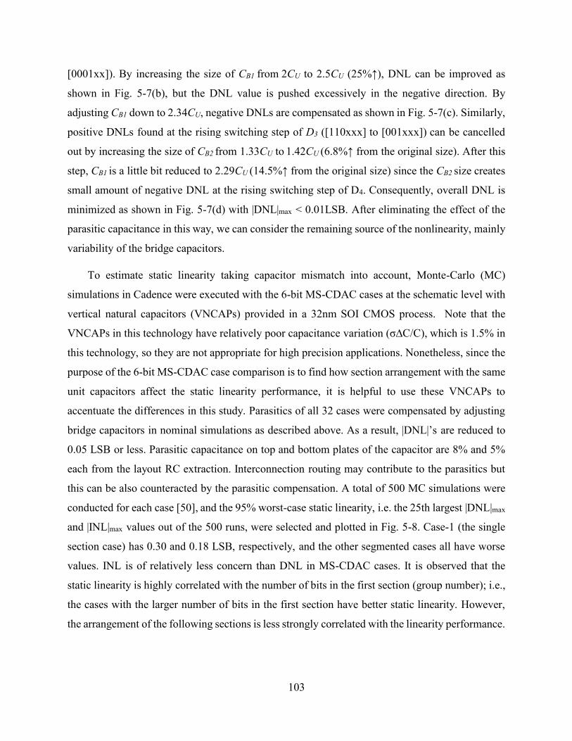
103
[0001xx]). By increasing the size of CB1 from 2CU to 2.5CU (25%↑), DNL can be improved as
shown in Fig. 5-7(b), but the DNL value is pushed excessively in the negative direction. By
adjusting CB1 down to 2.34CU, negative DNLs are compensated as shown in Fig. 5-7(c). Similarly,
positive DNLs found at the rising switching step of D3 ([110xxx] to [001xxx]) can be cancelled
out by increasing the size of CB2 from 1.33CU to 1.42CU (6.8%↑ from the original size). After this
step, CB1 is a little bit reduced to 2.29CU (14.5%↑ from the original size) since the CB2 size creates
small amount of negative DNL at the rising switching step of D4. Consequently, overall DNL is
minimized as shown in Fig. 5-7(d) with |DNL|max < 0.01LSB. After eliminating the effect of the
parasitic capacitance in this way, we can consider the remaining source of the nonlinearity, mainly
variability of the bridge capacitors.
To estimate static linearity taking capacitor mismatch into account, Monte-Carlo (MC)
simulations in Cadence were executed with the 6-bit MS-CDAC cases at the schematic level with
vertical natural capacitors (VNCAPs) provided in a 32nm SOI CMOS process. Note that the
VNCAPs in this technology have relatively poor capacitance variation (σ∆C/C), which is 1.5% in
this technology, so they are not appropriate for high precision applications. Nonetheless, since the
purpose of the 6-bit MS-CDAC case comparison is to find how section arrangement with the same
unit capacitors affect the static linearity performance, it is helpful to use these VNCAPs to
accentuate the differences in this study. Parasitics of all 32 cases were compensated by adjusting
bridge capacitors in nominal simulations as described above. As a result, |DNL|’s are reduced to
0.05 LSB or less. Parasitic capacitance on top and bottom plates of the capacitor are 8% and 5%
each from the layout RC extraction. Interconnection routing may contribute to the parasitics but
this can be also counteracted by the parasitic compensation. A total of 500 MC simulations were
conducted for each case [50], and the 95% worst-case static linearity, i.e. the 25th largest |DNL|max
and |INL|max values out of the 500 runs, were selected and plotted in Fig. 5-8. Case-1 (the single
section case) has 0.30 and 0.18 LSB, respectively, and the other segmented cases all have worse
values. INL is of relatively less concern than DNL in MS-CDAC cases. It is observed that the
static linearity is highly correlated with the number of bits in the first section (group number); i.e.,
the cases with the larger number of bits in the first section have better static linearity. However,
the arrangement of the following sections is less strongly correlated with the linearity performance.

104
It is also possible to scale the unit capacitor size in the MS-CDAC design to adjust
nonlinearity. As the remaining factor of nonlinearity after parasitic compensation is almost entirely
from capacitance variation, it is expected that nonlinearity of the MS-CDAC will be enhanced with
increase of unit capacitance size as with the single-section CDAC, which follows [51]
,
1 1DNL MAX
CU UA C (5-3)
where σDNL,MAX denotes the standard deviation of the maximum DNL of the single section DAC
and ACU is the area of unit capacitor, correspondingly unit . To verify that (5-3) is valid for MS-
CDACs as well, another set of MC simulations is run for Case-13, 3-1-2, with unit capacitor
scaling from 1 to 8 times and the result is shown in Fig. 5-9. The simulation results prove that
|DNL|max is predictable as a linear function of 1/√CU. It should be noted that scaled MS-CDACs
have increased total capacitance, switching energy and MSB section capacitance with the same
scaling ratio, thus need to be compared with non-scaled structures considering those changes.
5.3.3 Sampling noise and speed
Both sampling noise and speed are determined by the number of bits in the first section, which
is referred to as the group number of the MS-CDAC (See Table 5-I). In SAR ADC applications
with VCM -based switching scheme, the input signal is sampled on the top plates of the first section.
Figure 5-8. Static linearity (DNL and INL) with respect to 6-bit MS-CDAC cases.

105
Thus, the input capacitance, which is the sum of capacitors in the first section, i.e. twice the MSB
capacitor, must be sufficient to meet kT/C noise requirements resulting in
2
12 2
ref
NS
VkT
C
(5-4)
where N is the number of bits and CS is the sampling capacitance [38].
On the other hand, the MSB capacitance, which is also determined by the group number, must
be minimized for higher speed. This is because SAR ADCs suffer the worst-case settling time at
the MSB switching, and analog coefficient multipliers see a maximum capacitance load of half
MSB capacitance. For instance, group-4 cases have about 2X longer settling time than group-3
cases due to the 2X larger MSB capacitor. The section segmentation in MS-CDACs effectively
reduces the MSB capacitance, and the following sections do not affect the speed as capacitance
looking from output to the following sections are always seen as a unit capacitance. In addition,
parasitics including the interconnection resistance and capacitance can also be factors in reducing
the speed. The reduced number of capacitor units in MS-CDAC mitigates the effect of parasitics.
It can be also observed that the settling time is also roughly in tradeoff relationship with the static
linearity (Fig. 5-8).
Figure 5-9. Unit capacitor scaling versus 95% worst-case |DNL|max with 6-bit MS-CDAC (Case-13).

106
5.3.4 Overall tradeoffs in 6-bit MS-CDAC cases
The studied MS-CDAC cases present various characteristic of total capacitance, switching
energy and static linearity. In order to observe the fundamental tradeoff, total capacitance versus
static linearity is plotted in Fig. 5-10. Note that total capacitance is not only related to the area, but
also determines switching energy; both area and switching speed are improved by section
segmentation, whereas static linearity is degraded. In addition, we can also examine speed and
noise performance based on the group number. A reference line is drawn on the plot that connects
the cases (1-6 and 11) that are considered ‘optimal’ in terms of the number of capacitor units versus
linearity tradeoff. The cases other than optimal are considered comparatively inefficient, i.e., they
have inferior linearity for the total capacitance. For example, Case-17 has poor linearity although
total capacitance is only slightly less than Case-2. The reference line approximately shows that
DNL is inversely proportional to total capacitance. This result is similar to the scaling of a single
section CDAC, which follows (5-3).
As mentioned before, speed and noise performance can be estimated by the group numbers.
In Fig. 5-10, the optimal cases have lower group numbers as the total capacitance decreases, which
Figure 5-10. Total capacitance versus DNL. Optimal cases are selected based on total capacitance and
MSB capacitance (group) versus DNL.

107
means better speed but degraded noise performance, consistent with reducing the unit capacitance
in single section CDAC.
Based on the above observations, it can be seen that the MS-CDAC offers similar performance
tradeoffs as the single-section CDAC with unit capacitor sizing. In other words, MS-CDAC can
be used to extend the fundamental tradeoff when the minimum capacitor size is the bottleneck of
the design. Table 5-II provides the detailed performance of the optimal cases including the change
relative to Case-1, which represents the design limit of a single section CDAC based on the
available minimum size unit capacitor. Although none of the group-1 cases are on the reference
line, it is still worthwhile to consider them for better settling time. Among the cases of group-1,
Case-27 and 31 can be considered optimal as well and are shown in Table 5-II.
As discussed before, with given options of section segmentation, it is possible to consider unit
capacitor scaling of the MS-CDAC to further optimize the structure. While Case-1 and 2 cannot
have further reduced total capacitance, unit capacitance of the other cases can be increased to fulfill
the requirement. Based on (5-3), required unit capacitor scaling to enhance current |DNL|max to 0.5
LSB can be calculated for each MS-CDAC structure as follows,
2
max, ,min
| |.
0.5U scaled U
DNLC C
(5-5)
In Table 5-II, calculated total capacitance, after unit capacitor scaling based on (5-5), for each case
is included. We can observe that, as a MS-CDAC structure with minimum unit capacitor deviates
TABLE 5-II. PERFORMANCE OF OPTIMAL 6-BIT CASES
Case 1 2 4 3 5 6 11 31 27
Section 6 1-5 1-1-4 2-4 3-3 1-2-3 2-2-2 2-1-1-1-1 2-2-1-1
Group 6 5 4 4 3 3 2 1 1
Total Capacitance (CU) 64
(-)
35
(-45%)
22.0
(-66%)
20.3
(-68%)
16.1
(-75%)
15.3
(-76%)
12.7
(-80%)
15.3
(-76%)
13.7
(-79%)
Switching E (CV2) 43.6 (-)
21.1 (-52%)
11.7 (-73%)
11.1 (-74%)
9.0 (-79%)
7.1 (-84%)
5.7 (-87%)
4.4 (-90%)
5.1 (-88%)
95% worst-case
|DNL|max (LSB)
0.31
(-) 0.45
(+0.13)
0.60
(+0.33)
0.63
(+0.37)
0.84
(+0.52)
0.86
(+0.55)
1.15
(+0.84)
1.25
(+0.84)
1.35
(+0.55)
95% worst-case
|INL|max (LSB)
0.19 (-)
0.27 (+0.08)
0.38 (+0.20)
0.39 (+0.21)
0.50 (+0.32)
0.48 (+0.29)
0.63 (+0.45)
0.68 (+0.50)
0.74 (+0.56)
Input C (CU) 64, 16
(-) 32, 8
(-50%)
16, 4
(-75%)
16, 4
(-75%)
8, 2
(-88%)
8, 2
(-88%)
4, 1
(-94%)
2, 0.5
(-97%)
2, 0.5
(-97%)
Scaling factor* N/A N/A 1.6 1.8 2.8 3.0 5.3 6.3 7.3
Total Capacitance
after scaling N/A N/A 36 38 45 45 67 96 100
* UNIT CAPACITOR SCALING TO ACHIEVE 0.5 LSB OF 95% WORST-CASE |DNL|MAX.

108
further from desired nonlinearity, it requires larger factor of unit capacitor scaling, resulting in
larger total capacitance. After scaling for the same condition of static linearity, the total capacitance
of Case-4 is the least (36CU), Case-5 (45CU) is the next, and Case-11 is the largest (67CU). This
order matches with the scaling factor. This relationship holds true between the other scaling-
required section segmentations as well, since reducing total capacitance by section segmentation
is more strongly traded against linearity than unit capacitance scaling due to the bridge capacitor
variation. Therefore, among the scaling-required MS-CDACs, it is desirable to choose the case
that needs the least scaling factor. After consideration of unit capacitor scaling, the optimal scaled
case needs to be compared with the optimal non-scaled case since it may have smaller total
capacitance.
If we consider selection of 6-bit MS-CDAC based on the collected results shown in Table 5-
II, Case-2 and Case-4 can be chosen, as they represent optimal choices among scaled and non-
scaled cases, respectively. After finding a comparable section segmentation, selection could be
dependent on designer’s choice. Case-2 with the minimum unit capacitor can be selected for
slightly better total capacitance for area and switching energy. On the other hand, Case-4 is chosen
for a bit better speed performance since Case-4 has X0.8 (=0.5·1.6) of MSB section capacitance
after scaling. If the number of unit capacitors is a concern, Case-4 is preferred as it provides about
40% less number of units regardless of the scaling than Case-2.
5.3.5 Considerations in SAR-ADC and analog coefficient multiplier
applications
The tradeoff considerations are applied differently depending on whether the CDAC is being
used in a SAR-ADC or as a coefficient multiplier for analog signal processing. Table 5-III shows
the consideration of various performance criteria in each application. Essentially, SAR-ADC
design requires consideration of all criteria. On the other hand, analog coefficient multipliers do
not consider kT/C noise because the input signal is sampled on the previous stage, which is a
sample and hold. Instead, the speed of the multiplier is associated with the maximum input
capacitance. Thus, the number of bits in the first section is not limited by noise, but rather by static
linearity.
109
The static linearity in the coefficient multiplier does not create any quantization noise or
unwanted harmonics as would be of concern in an ADC. Instead, the coefficient control resolution
may limit the arithmetic accuracy of the analog signal processing, such as the accuracy of the
transfer function of an analog FIR filter. Switching energy is not also critical in analog coefficient
multipliers because the current drawn into the capacitor is negligible compared to the static current
of the S/H buffer as well as the other blocks in the overall circuit.
5.4 10-Bit MS-CDAC Design
To verify the concept of MS-CDAC in a more practical application, the use of MS-CDAC
structures is extended to a medium-resolution, typical of SAR ADC applications. This section
presents the design of a 10-bit MS-CDAC as a proof-of-concept. As mentioned earlier, a major
issue with higher resolution designs is a very large number of possible cases; there are 1024
possible section arrangements for a 10-bit MS-CDAC. This large number of options provides a
greater trade space to optimize the CDAC design but it is prohibitively time-consuming to compare
all the possible section arrangements as was done for the simpler 6-bit example discussed above.
Along with the number of section arrangements, the time required to analyze or simulate each
section arrangement increases exponentially due to the growth of the capacitor unit count and
complexity.
In order to provide a more efficient design process, this paper presents a 10-bit MS-CDAC
design without analyzing all possible structures by considering a C-2C architecture (Fig. 5-11) as
TABLE 5-III. CONSIDERATIONS OF MS-CDAC PERFORMANCE IN SAR-ADC AND ANALOG COEFFICIENT
MULTIPLIER
SAR-ADC Analog Coefficient Multiplier
Capacitance Mismatch Static linearity Coefficient selection
kT/C noise Considered Not considered
Switching Energy Considered Not considered
Area Considered Considered
Speed Considered Considered
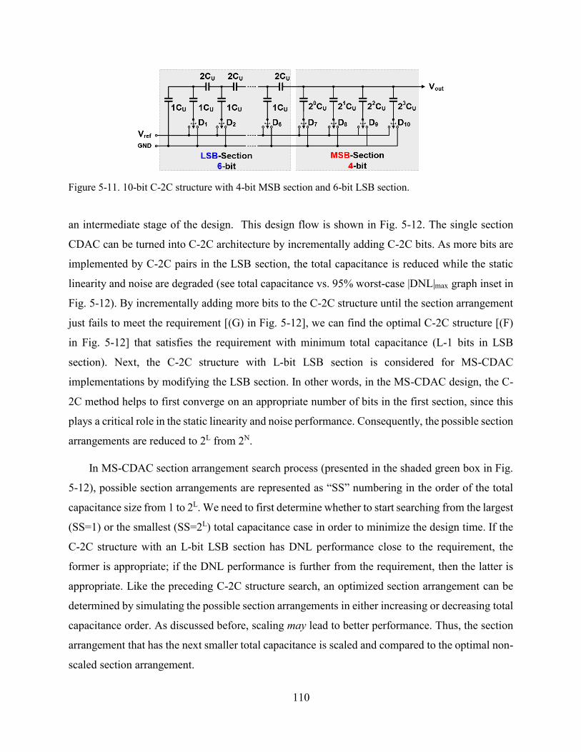
110
an intermediate stage of the design. This design flow is shown in Fig. 5-12. The single section
CDAC can be turned into C-2C architecture by incrementally adding C-2C bits. As more bits are
implemented by C-2C pairs in the LSB section, the total capacitance is reduced while the static
linearity and noise are degraded (see total capacitance vs. 95% worst-case |DNL|max graph inset in
Fig. 5-12). By incrementally adding more bits to the C-2C structure until the section arrangement
just fails to meet the requirement [(G) in Fig. 5-12], we can find the optimal C-2C structure [(F)
in Fig. 5-12] that satisfies the requirement with minimum total capacitance (L-1 bits in LSB
section). Next, the C-2C structure with L-bit LSB section is considered for MS-CDAC
implementations by modifying the LSB section. In other words, in the MS-CDAC design, the C-
2C method helps to first converge on an appropriate number of bits in the first section, since this
plays a critical role in the static linearity and noise performance. Consequently, the possible section
arrangements are reduced to 2L from 2N.
In MS-CDAC section arrangement search process (presented in the shaded green box in Fig.
5-12), possible section arrangements are represented as “SS” numbering in the order of the total
capacitance size from 1 to 2L. We need to first determine whether to start searching from the largest
(SS=1) or the smallest (SS=2L) total capacitance case in order to minimize the design time. If the
C-2C structure with an L-bit LSB section has DNL performance close to the requirement, the
former is appropriate; if the DNL performance is further from the requirement, then the latter is
appropriate. Like the preceding C-2C structure search, an optimized section arrangement can be
determined by simulating the possible section arrangements in either increasing or decreasing total
capacitance order. As discussed before, scaling may lead to better performance. Thus, the section
arrangement that has the next smaller total capacitance is scaled and compared to the optimal non-
scaled section arrangement.
Figure 5-11. 10-bit C-2C structure with 4-bit MSB section and 6-bit LSB section.

111
* Requirements of kT/C noise and DNL
** Numbering possible section segmentation from smallest to largest.
Figure 5-12. Design flow of MS-CDAC design from intermediate C-2C cases. (·) refer to the 10-bit
design cases in Table 5-IV.
112
The optimal MS-CDAC structure resulting from this search process still needs to be compared
with the optimal C-2C structure since it may have larger total capacitance. If the optimal MS-
CDAC structure has smaller total capacitance or even if the MS-CDAC structure has larger total
capacitance but the MSB section capacitance is more critical, the optimal MS-CDAC structure
becomes the final selection. In the case that there is no MS-CDAC case considered that satisfies
the requirement, we can also choose the optimal C-2C structure. The detailed design of a 10-bit
MS-CDAC using the proposed method follows.
For the 10-bit MS-CDAC design, a 130nm CMOS technology is utilized, with MIM
capacitors available having 17 fF of minimum capacitance. This unit capacitor has 0.06%
capacitance variation (σ∆C/C). Table 5-IV shows the results of 500 MC simulation runs in
Cadence with MS-CDACs implemented at the schematic level for the purpose of searching the
optimal section segmentation. Single section CDAC achieved less than 0.05 LSB of 95% worst-
case |DNL|max (Case-A) and 17.4 pF input capacitance with the minimum sized unit capacitor,
which greatly exceeds the requirement. Accordingly, we can pursue the MS-CDAC structure per
the proposed design flow.
Next, the single section CDAC is transformed by segmenting the capacitor array from the
LSB section. In Table 5-IV, 95% worst-case |DNL|max values from 500 MC simulations runs for
10-bit C-2C arrangements are shown. Up to 7-bits of C-2C structures are simulated. It is seen that
Case-F (5-bit MSB) would be chosen to have less than 0.5 LSB of |DNL|max if only the C-2C
method is considered [See Case-F in Fig. 5-12]. However, for the MS-CDAC, the Case-G (5-bit
MSB C-2C arrangement) can be also considered since it has |DNL|max not very far from the desired
value and it is possible to have improved static linearity by modifying the LSB section into
different section arrangements [See Case-G in Fig. 5-12]. The input capacitance (272 fF) is also
above the requirement. Meanwhile, the 7-bit LSB version of the C-2C structure has a more
degraded DNL and its input capacitance (136 fF) is not sufficient to meet kT/C noise requirements.
Due to the fewer bits of the first section, the 4-bit MSB C-2C inherently has about ~2X faster
speed and can achieve much less area/switching energy than the possible 5-bit MSB section cases.
Therefore, we seek to find an MS-CDAC case to replace the 6-bit LSB section of the C-2C.
As the number of bits in the first section is fixed, the number of possible options is largely
reduced (by a factor of X16). Furthermore, it is not necessary to attempt all possible section

113
arrangements with remaining 6-bits. In Section 5.3, it is found that |DNL|max tends to increase as
total capacitance decreased. With that result in mind, we can examine the possible section
arrangements of the total capacitance from either smallest case to largest case, or vice versa, until
the desired structure is found. Since the |DNL|max of a 6-bit LSB section C-2C is not too far from
the desired value, it is preferred to search from the smallest total capacitance case. Table 5-IV also
provides the simulated |DNL|max values from the smallest total capacitance of section arrangement
2-2-2-4, which is Case-I. The optimal non-scaled section arrangement turns out to be Case-L
(see Case-L in Fig. 5-12). Case-J and K also satisfy the condition and very close to Case-L. While
it is possible that simulation inaccuracies may lead to the slight difference, it is not critical issue
since they all achieve |DNL|max value fairly less than the required value and have the same total
capacitance.
The section segmentation of the next smaller total capacitance is Case-I, so it is scaled to see
if it has smaller total capacitance after scaling. As shown in Table 5-IV, if Case-I is scaled, i.e.,
Case-P (see Case-P in Fig. 5-12), it has larger total capacitance than non-scaled Case-L. Due to
the scaling with over a factor of two, the MSB section capacitance is also inferior to Case-L.
Overall, the optimal MS-CDAC section arrangement is Case-L for less than 0.5 LSB of |DNL|max.
TABLE 5-IV. 95% WORST-CASE |DNL|MAX OF 10-BIT C-2C AND MS-CDAC STRUCTURES
Architecture
Method Case
Section
Arrangement Total Cap. (CU)
95% worst-case
|DNL|max (LSB)
Total Cap.
After scaling (CU)
C-2C
A 10 1024 0.04 N/A
B 1-9 515 0.06 N/A
C 1-1-8 262 0.10 N/A
D 1-1-1-7 137 0.16 N/A
E 1-1-1-1-6 76 0.21 N/A
F 1-1-1-1-1-5 47 0.40 N/A
G 1-1-1-1-1-1-4 34 0.73 72
H 1-1-1-1-1-1-1-3 29 1.37 218
MS-CDAC
I 2-2-2-4 30 0.76 69*
J 2-2-1-1-4 31.7 0.43 N/A
K 2-1-2-1-4 31.7 0.42 N/A
L 1-2-2-1-4 31.7 0.40 N/A
M 1-1-2-2-4 31.7 0.78 77
N 1-2-1-2-4 31.7 0.68 59
O 2-1-1-2-4 31.7 0.61 47
* Case-P, which is scaled Case-I for the static linearity.

114
Since interconnect routing in physical layout introduces additional parasitics, it is necessary
to understand the impact of layout parasitics on the MS-CDAC performance. In order to fully
verify the feasibility of the proposed approach, post-layout simulations were conducted. Fig. 5-13
shows the layout design of the Case-L design in a 250m by 250m die area using the available
130nm CMOS technology. As additional top-to-ground parasitic capacitance causes more
attenuation in each section, the bridge capacitor values must be increased correspondingly. After
the bridge capacitor adjustments, post-layout simulation results in <0.1 LSB of |DNL|max, which is
only <0.05 LSB worse than the pre-layout simulation.
Table 5-V compares the selected MS-CDAC structure with split, C-2C and single section
CDAC cases. All of those are designed with the same unit capacitors but only section arrangements
are different. It is observed that the selected 10-bit MS-CDAC architecture achieves 97% lower
TABLE 5-V. PERFORMANCE COMPARISON OF SELECTED 10-BIT MS-CDAC WITH OTHER EXISTING
METHODS
Architecture Case Section
Arrangement
Total
Cap (CU)
Switching E
(CV2)
# of
capacitors
95% worst-case
|INL|max (LSB)
95% worst-case
|DNL|max (LSB)
First
section
Bit #
Single
Section
CDAC
A 10 1024 761.4 1024 0.04 0.04 10
Split-CDAC - 5-5 64.0
(-94%)
46.8
(-94%) 64
0.16
(-0.13)
0.25
(-0.21) 5
C-2C
(5LSB-
5MSB)
F 1-1-1-1-1-5 47
(-95%) 27.4
(-96%) 47
0.29 (-0.25)
0.40 (-0.35)
5
Selected 10-
bit
MS-CDAC
L 1-2-2-1-4 30.7
(-97%)
17.4
(-98%) 30
0.29
(-0.25)
0.40
(-0.35) 4
Figure 5-13. Layout of Case-L and the result of post-layout static linearity simulation.

115
total capacitance, 98% lower switching energy, about a factor of 30 fewer capacitor units, and only
4 first-section bits, while still achieving acceptable static linearity. In addition, having a factor of
~30 fewer capacitor units greatly simplifies the routing in layout. At the same time, it is also shown
that the MS-CDAC outperforms the conventional methods under the given requirements for a 10-
bit CDAC. The selected MS-CDAC has 35% lower total capacitance, as well as 36% lower
switching energy compared to the split-CDAC and C-2C designs. Above all, the first section is
reduced to 4-bit, which could not be attained by the other methods. This result proves that MS-
CDAC design leveraging the intermediate C-2C method effectively leads to optimized section
arrangement selection, avoiding excessive number of options. Although a specific number of bits
and capacitor type using a specific technology are used in this analysis, the method to find the
optimal section segmentation can be generally applied to other technologies and applications.
5.5 Summary
The multi-section capacitive DAC (MS-CDAC) has been investigated as a technique to
optimize CDAC structures for analog multiplier and SAR-ADC applications. It is first observed
that a capacitive DAC can be transformed into multiple sections by replacing a dummy transistor
with additional capacitor array(s) using bridge capacitor(s). In order to understand the
characteristics of MS-CDAC depending on the section segmentation, calculations and simulation
of all possible section arrangements for a low resolution (6-bit) MS-CDAC were conducted. These
different section segmentations have similar tradeoffs of total capacitance, switching energy, speed
versus static linearity and noise as the sizing of unit capacitance in single-section (conventional)
CDAC. Therefore, we can use the MS-CDAC in order to optimize the performance by finding the
section segmentation with minimum total capacitance while the required conditions of linearity
and kT/C noise are met.
To present a practical application of the MS-CDAC concept, a 10-bit MS-CDAC design is
presented. It is shown that a desirable section arrangement can be found by searching candidate C-
2C structures first, and then modifying the LSB section using the MS-CDAC approach, instead of
considering all 1024 options of the 10-bit structure. Following this procedure, targeting <0.5 LSB
of |DNL|max for 95% of 500 MC simulation runs, the selected 10-bit MS-CDAC accomplishes 97%

116
reduction of total capacitance and 98% reduction of switching energy as well as minimized input
capacitance for speed. This achievement is more than 30% better than C-2C and split-CDAC
methods. In addition, the number of bits in the first section is one-bit reduced which can result in
about 2X lower settling time. Post-layout simulation further validates the approach; the selected
MS-CDAC performance is <0.1 LSB of |DNL|max after the effect of additional parasitics from the
layout is compensated by adjusting the bridge capacitors. This MS-CDAC technique can be
applied to wideband reconfigurable analog signal processing circuits in the near future.
117
6 Contributions and Future Work
Chapter 6.
Conclusions and Future Work
6.1 Conclusions
Overall, this work has made two major contributions to the field of RF/mixed-signal IC
design. First, a new Analog FIR filter architecture was investigated as a flexible and wideband
filter, which is highly desired for current and future communications and sensor applications. The
performance and functionality of this AFIR architecture was enabled mainly by adopting the split-
capacitive DAC (split-CDAC) as a coefficient multiplier, while previously reported AFIR
architectures suffered limitations in either bandwidth or coefficient selectivity. Second, the
concept of the Multi-section capacitive DAC (MS-CDAC) was introduced as a novel approach to
optimize CDAC structures by considering various section arrangements. In the situation that the
unit capacitance cannot be further reduced, the MS-CDAC method provides more opportunity to
improve area, speed and switching energy performance, as long as kT/C noise and static linearity
are acceptable, compared to existing split-CDAC and C-2C methods.
In chapter 2, an early stage implementation of a 3.25 GS/s 4th order analog FIR (AFIR) filter
design was introduced with the split-capacitive DAC utilized as a coefficient multiplier for the
first time. The proposed approach allowed the filter to be tunable with DAC resolution, while
achieving high linearity and wideband performance. In this design, symmetric coefficients were
employed, tunable with unsigned 6-bit codes. In simulation, this AFIR filter achieved >11dBm of

118
IIP3 and a 3dB BW tuning range of 240 ~ 710 MHz with less than 10 mW power consumption.
Although the measurement was not feasible due to issues with the coefficient shift register and
suspected ESD failures, important design modifications were identified to avoid these issues in
subsequent iterations. This work with simulated performance was published in [53].
In chapter 3, an improved 4th order AFIR filter was introduced, which has extended coefficient
selection and more efficient system design. The polarity of coefficients is controlled by using a
differential circuit, and all four coefficients are individually controlled. As a result, the application
of the AFIR filter was expanded from LPF only to include BPF and HPF. Clock signal generation
was also much simplified by adding one more tap for resetting phases instead of ping-pong
operation. Analysis of noise and effect of 5-channel time-interleaved operation was also
conducted. The improved AFIR filter was fabricated in 32nm SOI CMOS technology and
demonstrated with measurements. The measured frequency responses depending on the coefficient
sets matched well with the calculations, successfully proving the FIR function within the desired
bandwidth up to the Nyquist rate. The AFIR filter maintained high linearity (IIP3 >11 dBm) over
the different coefficient sets and power consumption was about 10 mW as targeted specification.
This work has been presented in [54], and [55] has been submitted including more measurement
results and detailed analysis.
In chapter 4, the developed AFIR filter design has been extended to FIR-based beamforming.
AFIR filter modules were created so that it is possible that multiple inputs are injected to each
module and their outputs are summed through RF combiner. A set of 4 modules was considered
to form a FIR-based beamformer, for a 4 antenna element array. In lieu of a comprehensive study,
a simplified method for coefficient calculation was developed, which can be effective for several
specific beam angles, and validated through behavioral simulations. Preliminary measurement has
been completed with calculated coefficients. Although the signal attenuation is somewhat limited
by mismatches and coefficient accuracy, overall results follow the desired beam steering and
frequency selection.
In chapter 5, the concept of the MS-CDAC was proposed and analyzed. By conducting 6-bit
MS-CDAC simulations and calculations, it was found that the MS-CDAC can effectively extend
the fundamental tradeoffs in CDAC design. By using minimum sized MIM capacitors in a 0.13
m CMOS technology as the unit capacitor, a proof-of-concept 10-bit MS-CDAC architecture
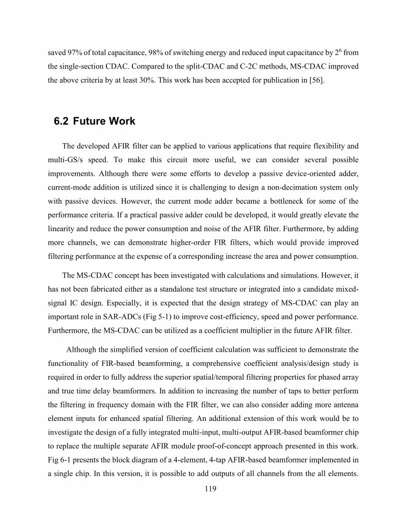
119
saved 97% of total capacitance, 98% of switching energy and reduced input capacitance by 26 from
the single-section CDAC. Compared to the split-CDAC and C-2C methods, MS-CDAC improved
the above criteria by at least 30%. This work has been accepted for publication in [56].
6.2 Future Work
The developed AFIR filter can be applied to various applications that require flexibility and
multi-GS/s speed. To make this circuit more useful, we can consider several possible
improvements. Although there were some efforts to develop a passive device-oriented adder,
current-mode addition is utilized since it is challenging to design a non-decimation system only
with passive devices. However, the current mode adder became a bottleneck for some of the
performance criteria. If a practical passive adder could be developed, it would greatly elevate the
linearity and reduce the power consumption and noise of the AFIR filter. Furthermore, by adding
more channels, we can demonstrate higher-order FIR filters, which would provide improved
filtering performance at the expense of a corresponding increase the area and power consumption.
The MS-CDAC concept has been investigated with calculations and simulations. However, it
has not been fabricated either as a standalone test structure or integrated into a candidate mixed-
signal IC design. Especially, it is expected that the design strategy of MS-CDAC can play an
important role in SAR-ADCs (Fig 5-1) to improve cost-efficiency, speed and power performance.
Furthermore, the MS-CDAC can be utilized as a coefficient multiplier in the future AFIR filter.
Although the simplified version of coefficient calculation was sufficient to demonstrate the
functionality of FIR-based beamforming, a comprehensive coefficient analysis/design study is
required in order to fully address the superior spatial/temporal filtering properties for phased array
and true time delay beamformers. In addition to increasing the number of taps to better perform
the filtering in frequency domain with the FIR filter, we can also consider adding more antenna
element inputs for enhanced spatial filtering. An additional extension of this work would be to
investigate the design of a fully integrated multi-input, multi-output AFIR-based beamformer chip
to replace the multiple separate AFIR module proof-of-concept approach presented in this work.
Fig 6-1 presents the block diagram of a 4-element, 4-tap AFIR-based beamformer implemented in
a single chip. In this version, it is possible to add outputs of all channels from the all elements.

120
However, it can be challenging to connect the outputs of all channels together; a few serial stages
of addition might be required in the single chip implementation as was done in Chapter 4 for the
hybrid architecture, with current addition in each chip and an overall RF combiner. In addition,
clock distribution over the large chip area also needs to be considered very carefully.
Figure 6-1. Block diagram of a 4-element, 4-tap FIR-based beamformer in a single chip.

121
0 References
[1] J. Mitola, "The software radio architecture," in IEEE Communications Magazine, vol. 33,
no. 5, pp. 26-38, May 1995.
[2] C. H. Chan, Y. Zhu, S. W. Sin, S. P. Ben U and R. P. Martins, "A 6 b 5 GS/s 4 Interleaved
3 b/Cycle SAR ADC," in IEEE Journal of Solid-State Circuits, vol. 51, no. 2, pp. 365-377,
Feb. 2016.
[3] Proakis, J., M. Salehi, Digital Communications, 5th ed., McGraw-Hill, NY, 2007.
[4] M. Tohidian, I. Madadi and R. B. Staszewski, "A Fully Integrated Discrete-Time
Superheterodyne Receiver," in IEEE Transactions on Very Large Scale Integration (VLSI)
Systems, vol. 25, no. 2, pp. 635-647, Feb. 2017.
[5] S. H. Shin, S. J. Kweon, S. H. Jo, Y. C. Choi, S. Lee and H. J. Yoo, "A 0.7-MHz–10-
MHz CT+DT Hybrid Baseband Chain With Improved Passband Flatness for LTE
Application," in IEEE Transactions on Circuits and Systems I: Regular Papers, vol. 62, no.
1, pp. 244-253, Jan. 2015.
[6] M. Lehne and S. Raman, "A 0.13m 1-GS/s CMOS Discrete-Time FFT Processor for Ultra-
Wideband OFDM Wireless Receivers," in IEEE Transactions on Microwave Theory and
Techniques, vol. 59, no. 6, pp. 1639-1650, June 2011.
[7] H. Shin and R. Harjani, "Low-Power Wideband Analog Channelization Filter Bank Using
Passive Polyphase-FFT Techniques," in IEEE Journal of Solid-State Circuits, vol. 52, no.
7, pp. 1753-1767, July 2017.
[8] A. Yoshizawa and S. Iida, “A gain-boosted discrete-time charge-domain FIR LPF with
double-complementary MOS parametric amplifiers,” in IEEE Int. Solid-State Circuits Conf.
(ISSCC) Dig. Tech. Papers, Feb. 2008, pp. 568–596.
[9] A. Yoshizawa and S. Iida, “A 250-MHz cutoff charge-domain baseband filter with
improved stopband attenuations,” in Proc. IEEE Radio Freq. Integr. Circuits Symp., Jun.
2009, pp. 491–494.
[10] C. Park, J. Yoon, and B. Kim, “Non-decimation FIR filter for digital RF sampling receiver
with wideband operation capability,” in Proc. IEEE Radio Freq. Integr. Circuits Symp.,
Jun. 2009, pp. 487–490.
[11] E. O’hAnnaidh, E. Rouat, S. Verhaeren, S. Le Tual, and C. Garnier, “A 3.2 GHz-sample-
rate 800 MHz bandwidth highly reconfigurable analog FIR filter in 45 nm CMOS,” in IEEE
Int. Solid-State Circuits Conf. (ISSCC) Dig. Tech. Papers, Feb. 2010, pp. 90–91.
[12] M.-F. Huang, “A discrete-time charge-domain filter with bandwidth calibration for LTE
application,” in Proc. IEEE Custom Integr. Circuit Conf., Sep. 2011, pp. 1–4.

122
[13] J. Yli-Kaakinen, V. Lehtinen and M. Renfors, "Multirate Charge-Domain Filter Design for
RF-Sampling Multi-Standard Receiver," in IEEE Transactions on Circuits and Systems I:
Regular Papers, vol. 62, no. 2, pp. 590-599, Feb. 2015.
[14] S. Hameed and S. Pamarti, "Design and Analysis of a Programmable Receiver Front End
Based on Baseband Analog-FIR Filtering Using an LPTV Resistor," in IEEE Journal of
Solid-State Circuits, vol. PP, no. 99, pp. 1-15.
[15] J. S. Mincey, E. C. Su, J. Silva-Martinez and C. T. Rodenbeck, "A 128-Tap Highly Tunable
CMOS IF Finite Impulse Response Filter for Pulsed Radar Applications," in IEEE
Transactions on Very Large Scale Integration (VLSI) Systems, vol. 26, no. 6, pp. 1192-
1203, June 2018.
[16] M. Longbrake, "True time-delay beamsteering for radar," 2012 IEEE National Aerospace
and Electronics Conference (NAECON), Dayton, OH, 2012, pp. 246-249.
[17] M. Neinhus and K. Solbach, "Finite impulse response-filter-based RF-beamforming
network for wideband and ultra-wideband antenna arrays," in IET Microwaves, Antennas
& Propagation, vol. 5, no. 7, pp. 844-851, 13 May 2011.
[18] Tai-Cheng Lee and B. Razavi, "A 125-MHz CMOS mixed-signal equalizer for Gigabit
Ethernet on copper wire," Custom Integrated Circuits, 2001, IEEE Conference on., San
Diego, CA, 2001, pp. 131- 134.
[19] R. J. Baker, CMOS:Circuit Design, Layout, and Simulation, 3nd Ed, IEEE Press and
Wiley-Interscience, Newyork, 2010.
[20] Ming-Dou Ker and Kuo-Chun Hsu, "Overview of on-chip electrostatic discharge
protection design with SCR-based devices in CMOS integrated circuits," in IEEE
Transactions on Device and Materials Reliability, vol. 5, no. 2, pp. 235-249, June 2005.
[21] S. Kiriaki et al., "A 160-MHz analog equalizer for magnetic disk read channels," in IEEE
Journal of Solid-State Circuits, vol. 32, no. 11, pp. 1839-1850, Nov 1997.
[22] Razavi, B., Design of Analog CMOS Integrated Circuits, New York:McGraw-Hill, 2001.
[23] B. Razavi, "The Bootstrapped Switch [A Circuit for All Seasons]," in IEEE Solid-State
Circuits Magazine, vol. 7, no. 3, pp. 12-15, Summer 2015.
[24] P. Satarzadeh, B. C. Levy and P. J. Hurst, "Bandwidth Mismatch Correction for a Two-
Channel Time-Interleaved A/D Converter," 2007 IEEE International Symposium on
Circuits and Systems, New Orleans, LA, 2007, pp. 1705-1708.
[25] T. Crrigan. ( Ju ly, 2006 ) . How to Calcula te the Set t l ing Time and
Sampling Rate of a Mul t ip lexer . Analog Devices, MA. [Online]. Available:
http://www.analog.com/media/en/technical-documentation/application-notes/AN-
1024.pdf
123
[26] K. Kundert. (2009) . S imulat ing Switched -Capaci tor Fi l ters with
Spect reRF. The Designer’s Guide Community, MA. [Online]. Available:
http://www.designers-guide.org/analysis/sc-filters.pdf
[27] S. M. Jamal, Daihong Fu, M. P. Singh, P. J. Hurst and S. H. Lewis, "Calibration of sample-
time error in a two-channel time-interleaved analog-to-digital converter," in IEEE
Transactions on Circuits and Systems I: Regular Papers, vol. 51, no. 1, pp. 130-139, Jan.
2004.
[28] M El-Chammas, B. Murmann, (2012). Background Calibration of Time-Interleaved Data
Converters [Online]. Available:
http://www.springer.com/cda/content/document/cda_downloaddocument/9781461415107
-c1.pdf?SGWID=0-0-45-1266646-p174192807
[29] B. Razavi, "Design Considerations for Interleaved ADCs," in IEEE Journal of Solid-State
Circuits, vol. 48, no. 8, pp. 1806-1817, Aug. 2013.
[30] P. Benabes, C. Lelandais-Perrault and N. L. Dortz, "Mismatch calibration methods for
high-speed time-interleaved ADCs," 2014 IEEE 12th International New Circuits and
Systems Conference (NEWCAS), Trois-Rivieres, QC, 2014, pp. 49-52.
[31] S. Devarajan et al., "A 12-b 10-GS/s Interleaved Pipeline ADC in 28-nm CMOS
Technology," in IEEE Journal of Solid-State Circuits, vol. 52, no. 12, pp. 3204-3218, Dec.
2017.
[32] D. Ahn and S. Hong, “A low cost analog FIR channel select filter for wireless receiver,”
in Proc. IEEE Radio Wireless Symp., Jan. 2011, pp. 211–214.
[33] M. Huang, M. Kuo, T. Yang and X. Huang, "A 58.9-dB ACR, 85.5-dB SBA, 5–26-MHz
Configurable-Bandwidth, Charge-Domain Filter in 65-nm CMOS," in IEEE Journal of
Solid-State Circuits, vol. 48, no. 11, pp. 2827-2838, Nov. 2013.
[34] Neinhu¨s, M., Solbach, K., Held, S, “Concept of microwave electronic steered array using
analogue FIR-filter’. German Microwave Conf., Ulm, April 2005.
[35] Peter Isza, TFilter, 2018, http://t-filter.engineerjs.com/.
[36] Sharilee, New Online Microwave Impedance Calculator, Sep. 28, 2018,
http://blog.rogerscorp.com/2015/09/28/new-online-microwave-impedance-calculator/.
[37] W. Xiong, Y. Guo, U. Zschieschang, H. Klauk, and B. Murmann, “A 3-V, 6-bit C-2C
digital-to-analog converter using complementary organic thin- film transistors on glass”,
IEEE Journal of Solid-State Circuits, vol. 45, no. 7, pp. 1380–1388, July 2010.
[38] Y. Zhang, E. Bonizzoni and F. Maloberti, "Mismatch and parasitics limits in capacitors-
based SAR ADCs," 2016 IEEE International Conference on Electronics, Circuits and
Systems (ICECS), Monte Carlo, 2016, pp. 33-36.
124
[39] S. Brenna, A. Bonfanti, A. Abba, F. Caponio and A. L. Lacaita, "Analysis and optimization
of a SAR ADC with attenuation capacitor," 2014 37th International Convention on
Information and Communication Technology, Electronics and Microelectronics (MIPRO),
Opatija, 2014, pp. 68-73.
[40] Y. Zhu et al., "Split-SAR ADCs: Improved Linearity With Power and Speed
Optimization," in IEEE Transactions on Very Large Scale Integration (VLSI) Systems, vol.
22, no. 2, pp. 372-383, Feb. 2014.
[41] P. Harpe, E. Cantatore, G. Haller, and B. Murmann, “A 2.2/2.7fJ/conversion-step 10/12b
40kS/s SAR ADC with data-driven noise reduction,” Dig. Tech. Papers Int. Solid State
Circuits Conf., pp. 270–271, Feb. 2013.
[42] J. Liu, Y. Zhu, C. H. Chan, S. W. Sin, S. P. U and R. P. da Silva Martins, "Uniform
Quantization Theory-Based Linearity Calibration for Split Capacitive DAC in an SAR
ADC," in IEEE Transactions on Very Large Scale Integration (VLSI) Systems, vol. 24, no.
7, pp. 2603-2607, July 2016.
[43] J. Y. Um, Y. J. Kim, E. W. Song, J. Y. Sim and H. J. Park, "A Digital-Domain Calibration
of Split-Capacitor DAC for a Differential SAR ADC Without Additional Analog Circuits,"
in IEEE Transactions on Circuits and Systems I: Regular Papers, vol. 60, no. 11, pp. 2845-
2856, Nov. 2013.
[44] M. Yoshioka, K. Ishikawa, T. Takayama and S. Tsukamoto, "A 10-b 50-MS/s 820-uW
SAR ADC With On-Chip Digital Calibration," in IEEE Transactions on Biomedical
Circuits and Systems, vol. 4, no. 6, pp. 410-416, Dec. 2010.
[45] Y. Zheng, Z. Wang, S. Yang, Q. Li, and L. Xiang, "A Novel Two-Split Capacitor Array
with Linearity Analysis for High-Resolution SAR ADCs," International Journal of
Electronics and Electrical Engineering, Vol. 3, No. 3, pp. 177-181, June 2015.
[46] V. Hariprasath, J. Guerber, S. H. Lee and U. K. Moon, "Merged capacitor switching based
SAR ADC with highest switching energy-efficiency," in Electronics Letters, vol. 46, no. 9,
pp. 620-621, April 29 2010.
[47] Y. Zhu et al., "A 10-bit 100-MS/s Reference-Free SAR ADC in 90 nm CMOS," in IEEE
Journal of Solid-State Circuits, vol. 45, no. 6, pp. 1111-1121, June 2010.
[48] Z. Zhu and Y. Liang, "A 0.6-V 38-nW 9.4-ENOB 20-kS/s SAR ADC in 0.18-m CMOS
for Medical Implant Devices," in IEEE Transactions on Circuits and Systems I: Regular
Papers, vol. 62, no. 9, pp. 2167-2176, Sept. 2015.
[49] M. Saberi, R. Lotfi, K. Mafinezhad and W. A. Serdijn, "Analysis of Power Consumption
and Linearity in Capacitive Digital-to-Analog Converters Used in Successive
Approximation ADCs," in IEEE Transactions on Circuits and Systems I: Regular Papers,
vol. 58, no. 8, pp. 1736-1748, Aug. 2011.

125
[50] S. Liu, Y. Shen and Z. Zhu, "A 12-Bit 10 MS/s SAR ADC With High Linearity and
Energy-Efficient Switching," in IEEE Transactions on Circuits and Systems I: Regular
Papers, vol. 63, no. 10, pp. 1616-1627, Oct. 2016.
[51] D. Zhang, A. Bhide and A. Alvandpour, "A 53-nW 9.1-ENOB 1-kS/s SAR ADC in 0.13-
um CMOS for Medical Implant Devices," in IEEE Journal of Solid-State Circuits, vol. 47,
no. 7, pp. 1585-1593, July 2012.
[52] A. Abusleme, A. Dragone, G. Haller, and B. Murmann, “Mismatch of lateral field metal-
oxide-metal capacitors in 180nm CMOS process,” IEEE Electronic Letters, vol. 48, pp.
286–287, Mar. 2012.
[53] S. Park, D. Shin, K. j. Koh and S. Raman, "A 3.25 GS/s 4-Tap analog FIR filter design
with coefficient control using 6-bit split-capacitor DAC as a tunable coefficient
multiplier," 2016 IEEE Dallas Circuits and Systems Conference (DCAS), Arligton, TX,
2016, pp. 1-4.
[54] S. Park, D. Shin, K. Koh and S. Raman, "A low-power 3.25GS/s 4th-order programmable
analog FIR filter using split-CDAC coefficient multipliers for wideband analog signal
processing," 2018 IEEE International Solid-State Circuits Conference(ISSCC), San
Francisco, CA, 2018, pp. 62-64.
[55] S. Park, D. Shin, K-J. Koh and S. Raman, "A Low-Power 3.25GS/s 4th-Order
Programmable Analog FIR Filter Using Split-CDAC Coefficient Multipliers for Wideband
Analog Signal Processing," IEEE Journal of Solid-State Circuits(JSSC). (In progress)
[56] S. Park and S. Raman, “Analysis and Optimization of Multi-Section Capacitive DACs for
Mixed-Signal Processing," IEEE Transactions on Very Large Scale Integration (VLSI)
Systems. (Accepted)
Top Related
Copyright © 2022 FDOKUMEN

