


Bahasa
Halaman
Hukum


Low-voltage translating 8-bit I2C-bus I/O Expander
PI4IOE5V6408 www.diodes.com January 2018
Document Number DS40583 Rev 1-2 1 © Diodes Incorporated
PI4IOE5V6408
Features
Description

PI4IOE5V6408 www.diodes.com January 2018
Document Number DS40583 Rev 1-2 2 © Diodes Incorporated
PI4IOE5V6408
Pin Configuration
Fig 1. UQFN Top View
Pin Description
Table 1: Pin Description
Pin Name Pin No. Description
INT 1 Active-low interrupt output. Connect to VDD(I2C_bus) through a pull-up resistor.
VDD(P) 2 Supply voltage of PI4IOE5V6408 GPIO-port
P7 3 GPIO-port input/output (push-pull design structure). At power on, P7 is configured as an input.
P6 4 GPIO-port input/output (push-pull design structure). At power on, P6 is configured as an input.
P5 5 GPIO-port input/output (push-pull design structure). At power on, P5 is configured as an input.
P4 6 GPIO-port input/output (push-pull design structure). At power on, P4 is configured as an input.
P3 7 GPIO-port input/output (push-pull design structure). At power on, P3 is configured as an input.
P2 8 GPIO-port input/output (push-pull design structure). At power on, P2 is configured as an input.
ADDR 9 Address input. Connect directly to VDD(I2C_bus) or ground.
RESET 10 Active-low reset input. Connect to VDD(I2C_bus) through a pull-up resistor, if no active connection is
used.
P1 11 GPIO-port input/output (push-pull design structure). At power on, P1 is configured as an input.
P0 12 GPIO-port input/output (push-pull design structure). At power on, P0 is configured as an input.
SCL 13 Serial clock bus. Connect to VDD(I2C_bus) through a pull-up resistor.
SDA 14 Serial data bus. Connect to VDD(I2C_bus) through a pull-up resistor.
VDD(I2C_bus) 15 Supply voltage of I2C bus.
GND 16 Ground

PI4IOE5V6408 www.diodes.com January 2018
Document Number DS40583 Rev 1-2 3 © Diodes Incorporated
PI4IOE5V6408
Maximum Ratings
Power supply ...................................................................................................... -0.5V to +4.6V
Voltage on an I/O pin (Input / Output ) ....................................................... -0.5V to +4.0V
Input current ..................................................................................................................... ±20mA
Output current on an I/O pin ...................................................................................... ±50mA
Supply current ............................................................................................................... ±100mA
Ground supply current ................................................................................................. ±100mA
Operation temperature ............................................................................................... -40~85℃
Storage temperature ................................................................................................ -65~150℃
Maximum junction temperature ,T j(max) ................................................................. 125℃
ESD ( HBM ) ........................................................................................................................2kV
Recommended Operating Conditions Table 2: Recommended operating conditions
Symbol Parameter Conditions Min. Typ. Max. Unit
VDD(I2C-bus) I2C-bus supply voltage 1.65 - 3.6 V
VDD(P) GPIO port supply voltage 1.65 - 4 V
VIN Input voltage on IO pins 0 4 V
VOUT Output Voltage 0 VDD(P) V
Note:
Stresses greater than those listed under MAXIMUM
RATINGS may cause permanent damage to the
device. This is a stress rating only and functional
operation of the device at these or any other
conditions above those indicated in the operational
sections of this specification is not implied.
Exposure to absolute maximum rating conditions
for extended periods may affect reliability.

PI4IOE5V6408 www.diodes.com January 2018
Document Number DS40583 Rev 1-2 4 © Diodes Incorporated
PI4IOE5V6408
Static Characteristics VDD(I2C_bus) = 1.8 V to 3.6 V; GND = 0 V; Temp = -40 °C to +85 °C; unless otherwise specified.
Typical values are at Temp = 25 °C.
Table 3: Static characteristics
Symbol Parameter Condition Min. Typ.[1]
Max. Unit
Power supply
IDD[2]
Supply current
VDD(I2C_bus) = 1.8 to 3.6 V; Standby mode
VI on SDA, ADDR and RESET
= VDD(I2C-bus) or GND;
VI on P port = VDD(P) or GND; IO = 0 mA; I/O
= inputs; fSCL = 0 kHz
- 1.2 1.5 μA
VDD(I2C_bus) = 1.8 to 3.6 V; Active mode
VI on RESET = VDD(I2C-bus); VI on P port =
VDD(P) or GND; IO = 0 mA; I/O = inputs;
fSCL = 400 kHz, continuous register read
- - 300 μA
IOFF Power off leakage current - 10 μA
IIN Input leakage current
0 ≤ VIN ≤ VDD(I2C_bus) -10 - 10 μA
VPOR Power-on reset voltage - - 1.25 V
Input SCL, input/output SDA
VIL Low level input voltage -0.5 - 0.3
VDD(I2C-bus) V
VIH High level input voltage 0.7
VDD(I2C-bus) - 3.6 V
IOL Low level output current VOL = 0.4 V 20 - - mA
IL Leakage current VIN = VDD(I2C_bus) or GND -10 - 10 μA
Ci Input capacitance VIN = GND - 5 10 pF
Interrupt INT
IOL Low level output current VOL=0.4V 6
- mA
Co Output capacitance 2.1 10 pF
Select inputs ADDR and RESET
VIL Low level input voltage -0.5 - 0.3
VDD(I2C-bus) V
VIH High level input voltage 0.7
VDD(I2C-bus) - 3.6 V
IL Input leakage current -1 1 μA
Ci Input capacitance 2.4 10 pF

PI4IOE5V6408 www.diodes.com January 2018
Document Number DS40583 Rev 1-2 5 © Diodes Incorporated
PI4IOE5V6408
Static Characteristics Cont.
Symbol Parameter Condition Min. Typ.[1]
Max. Unit
I/Os
VIL Low-level input voltage P0 – P7 -0.5 - +0.3*VDD(
P) V
VIH High-level input voltage P0 – P7 0.7*VDD(P) - 4.0 V
VOH
High-level output voltage
P port; IOH = -100 μA;
VDD(P) = 1.8 V VDD(P) -
0.2 - - V
VDD(P) = 3.6 V VDD(P) -
0.2 - - V
VDD(P) = 4.0 V VDD(P) -
0.2 - - V
P port; IOH = -6 mA
VDD(P) = 1.8 V VDD(P) -
0.2 - - V
VDD(P) = 3.6 V VDD(P) -
0.2 - - V
VOL
Low-level output voltage
P port; IOL = 100 μA;
VDD(P) = 1.8 V - - 0.2 V
VDD(P) = 3.6 V - - 0.2 V
VDD(P) = 4.0 V - - 0.2 V
P port; IOL = 6 mA
VDD(P) = 1.8 V - - 0.5 V
VDD(P) = 3.6 V - - 0.45 V
IOL
Low-level output current P0 – P7 6.0 - - mA
IOH High-level output current P0 – P7 -6.0 - - mA
IIH[3]
High-level input current P port; VI = VDD(P); VDD(P) = 1.65 V to 4.0
V -50 - 50 μA
IIL[3]
Low-level input current P port; VI = GND; VDD(P) = 1.65 V to 4.0
V -50 - 50 μA
Rpu(int) Internal pull-up resistance Input/Output - 100 - kΩ
Rpd(int) Internal pull-down
resistance Input/Output - 100 - kΩ
Note: [1] Includes all internal circuitry consumption from the VDD(I2C_bus) supply. Does not include the I/O buffers, which are supplied by VDD(P) and are load dependent. [2] IIL and IIH specifications only apply when the outputs are configured with pull-down or pull-up resistors, respectively. Specification value assume VIN ≤ VDD(P)

PI4IOE5V6408 www.diodes.com January 2018
Document Number DS40583 Rev 1-2 6 © Diodes Incorporated
PI4IOE5V6408
Dynamic Characteristics Table 4: Dynamic characteristics
Symbol Parameter
Standard mode
I2C
Fast mode I2C Fast mode Plus I
2C Unit
Min Max Min Max Min Max
fSCL SCL clock frequency 0 100 0 400 0 1000 kHz
tBUF Bus free time between a STOP and
START condition 4.7 - 1.3 - 0.5 - μs
tHD;STA Hold time (repeated) START
condition 4.0 - 0.6 - 0.26 - μs
tSU;STA Set-up time for a repeated START
condition 4.7 - 0.6 - 0.26 - μs
tSU;STO Set-up time for STOP condition 4.0 - 0.6 - 0.26 - μs
tVD;ACK[1]
Data valid acknowledge time - 3.45 - 0.9 - 0.45 μs
tHD;DAT[2]
Data hold time 0 - 0 - 0 - ns
tVD;DAT Data valid time - 3.45 - 0.9 - 0.45 ns
tSU;DAT Data set-up time 250 - 100 - 50 - ns
tLOW LOW period of the SCL clock 4.7 - 1.3 - 0.5 - μs
tHIGH HIGH period of the SCL clock 4.0 - 0.6 - 0.26 - μs
tf Fall time of both SDA and SCL
signals - 300 300 - 120 ns
tr Rise time of both SDA and SCL
signals - 1000 300 - 120 ns
tSP Pulse width of spikes that must be
suppressed by the input filter - 50 - 50 50 ns
Interrupt timing
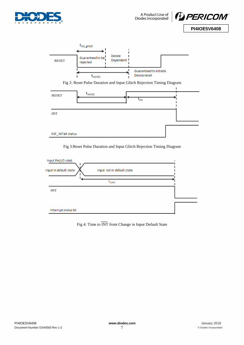
tV(INT) Valid time on pin INT - 4 - 4 - 4 μs
Reset timing
tw(rst) Reset pulse width 150 - 150 - 150 - ns
trst_glitch Reset recovery time[4]
50 150 50 150 50 150 ns
trst Reset time - 150 - 150 - 150 ns
Note:
[1]: tVD;ACK = time for acknowledgement signal from SCL LOW to SDA (out) LOW.
[2]: tVD;DAT = minimum time for SDA data out to be valid following SCL LOW.
PI4IOE5V6408 www.diodes.com January 2018
Document Number DS40583 Rev 1-2 7 © Diodes Incorporated
PI4IOE5V6408
Fig 2: Reset Pulse Duration and Input Glitch Rejection Timing Diagram
Fig 3:Reset Pulse Duration and Input Glitch Rejection Timing Diagram
Fig 4: Time to INT from Change in Input Default State
/RESET
/RESET
/INT
/INT

PI4IOE5V6408 www.diodes.com January 2018
Document Number DS40583 Rev 1-2 8 © Diodes Incorporated
PI4IOE5V6408
PI4IOE5V6408 Block Diagram
Fig 5: Block diagram
Block diagram
Note: All I/Os are set to inputs at reset.
VDD(I2C-BUS)

PI4IOE5V6408 www.diodes.com January 2018
Document Number DS40583 Rev 1-2 9 © Diodes Incorporated
PI4IOE5V6408
Functional Description
a. Device Address
Table 5: Device address
ADDR B7 ( MSB ) B6 B5 B4 B3 B2 B1 B0
0 1 0 0 0 0 1 1 R / W
1 1 0 0 0 1 0 0 R / W
b. Register Map
Table 6: Register Map
Pointer Register Bits Command bye
(hexadecimal ) Register Protocol
Power-up
default B7 B6 B5 B4 B3 B2 B1 B0
0 0 0 0 0 0 0 1 01h Device ID and Control R/W 1010 0010
0 0 0 0 0 0 1 1 03h I/O Direction R/W 0000 0000
0 0 0 0 0 1 0 1 05h Output State R/W 0000 0000
0 0 0 0 0 1 1 1 07h Output High-
impedance R/W 1111 1111
0 0 0 0 1 0 0 1 09h Input Default State R/W 0000 0000
0 0 0 0 1 0 1 1 0Bh Pull-up/down Enable R/W 1111 1111
0 0 0 0 1 1 0 1 0Dh Pull-up/down Select R/W 0000 0000
0 0 0 0 1 1 1 1 0Fh Input Status R xxxx xxxx
0 0 0 1 0 0 0 1 11h Interrupt Mask R/W 0000 0000
0 0 0 1 0 0 1 1 13h Interrupt Status R/W xxxx xxxx
02h, 04h, 06h,
08h, 0Ah, 0Ch,
OEh, 10h, 12h
Reserved R/W

PI4IOE5V6408 www.diodes.com January 2018
Document Number DS40583 Rev 1-2 10 © Diodes Incorporated
PI4IOE5V6408
c. Register Descriptions
i. Register 01h : Device ID and Control
Table 7: Device ID and Control register (address 01h)
Bit B7 B6 B5 B4 B3 B2 B1 B0
Name Manufacture ID Firmware Revision Reset
interrupt
Software
reset
Default 1 0 1 0 0 0 1 R / W
ii. Register 03h : I/O Direction
Table 8: I/O Direction register (address 03h)
Bit B7 B6 B5 B4 B3 B2 B1 B0
Name P7 P6 P5 P4 P3 P2 P1 P0
Default 0 0 0 0 0 0 0 0
iii. Register 05h : Output Port Register
Table 9: Output Port Register (address 05h)
Bit B7 B6 B5 B4 B3 B2 B1 B0
Name P7 P6 P5 P4 P3 P2 P1 P0
Default 0 0 0 0 0 0 0 0
iv. Register 07h : Output High-Impedance

PI4IOE5V6408 www.diodes.com January 2018
Document Number DS40583 Rev 1-2 11 © Diodes Incorporated
PI4IOE5V6408
Table 10: Output High-Impedance Register (address 07h)
Bit B7 B6 B5 B4 B3 B2 B1 B0
Name P7 P6 P5 P4 P3 P2 P1 P0
Default 1 1 1 1 1 1 1 1
v. Register 09h : Input Default State
Table 11. Input Default State Register (address 09h)
Bit B7 B6 B5 B4 B3 B2 B1 B0
Name P7 P6 P5 P4 P3 P2 P1 P0
Default 0 0 0 0 0 0 0 0
vi. Register 0bh : Pull-Up/-Down Enable
Table 12. Pull-up/-down Enable Register (address 0Bh)
Bit B7 B6 B5 B4 B3 B2 B1 B0
Name P7 P6 P5 P4 P3 P2 P1 P0
Default 1 1 1 1 1 1 1 1
vii. Register 0Dh : Pull-Up/-Down Select
Table 13. Pull-up/-down Select Register (address 0Dh)
Bit B7 B6 B5 B4 B3 B2 B1 B0
Name P7 P6 P5 P4 P3 P2 P1 P0
Default 0 0 0 0 0 0 0 0
viii. Register 0Fh : Input Status Register

PI4IOE5V6408 www.diodes.com January 2018
Document Number DS40583 Rev 1-2 12 © Diodes Incorporated
PI4IOE5V6408
Table 14. Input Status Register (address 0Fh)
Bit B7 B6 B5 B4 B3 B2 B1 B0
Name P7 P6 P5 P4 P3 P2 P1 P0
Default X X X X X X X X
ix. Register 11h – Interrupt Mask Register
Table 15. Interrupt Mask Register (address 11h)
Bit B7 B6 B5 B4 B3 B2 B1 B0
Name P7 P6 P5 P4 P3 P2 P1 P0
Default 0 0 0 0 0 0 0 0
x. Register 13h – Interrupt Status Register
Table 16. Interrupt Status Register (address 13h)
Bit B7 B6 B5 B4 B3 B2 B1 B0
Name P7 P6 P5 P4 P3 P2 P1 P0
Default X X X X X X X X
d. I/O Port
e. Power-on Reset

PI4IOE5V6408 www.diodes.com January 2018
Document Number DS40583 Rev 1-2 13 © Diodes Incorporated
PI4IOE5V6408
f. Reset Input (RESET)
g. Software Reset
h. Interrupt output (INT)

PI4IOE5V6408 www.diodes.com January 2018
Document Number DS40583 Rev 1-2 14 © Diodes Incorporated
PI4IOE5V6408
I2
C Read /Write Procedures
Fig 6. I2C Write Sequence
Note : if register is not specified , the master reads from the current register
Fig 7. I2C Read Sequence

PI4IOE5V6408 www.diodes.com January 2018
Document Number DS40583 Rev 1-2 15 © Diodes Incorporated
PI4IOE5V6408
Application Design-In Information
Fig 8. Typical Application
Part Marking
ZTA Packaging

PI4IOE5V6408 www.diodes.com January 2018
Document Number DS40583 Rev 1-2 16 © Diodes Incorporated
PI4IOE5V6408
Packaging Mechanical
16-UQFN (ZTA)
Ordering Information
Part No. Package Code Package
PI4IOE5V6408ZTAEX ZTA 16-Pin, 1.8x2.6 (UQFN) Notes:
1. EU Directive 2002/95/EC (RoHS), 2011/65/EU (RoHS 2) & 2015/863/EU (RoHS 3). Compliant. All applicable RoHS exemptions applied.
2. See http://www.diodes.com/quality/lead-free/ for more information about Diodes Incorporated’s definitions of Halogen- and Antimony-free, “Green” and
Lead-free. 3. Thermal characteristics can be found on the company web site at www.diodes.com/design/support/packaging/
4. E = Pb-free and Green
5. X suffix = Tape/Reel

PI4IOE5V6408 www.diodes.com January 2018
Document Number DS40583 Rev 1-2 17 © Diodes Incorporated
PI4IOE5V6408
IMPORTANT NOTICE
DIODES INCORPORATED MAKES NO WARRANTY OF ANY KIND, EXPRESS OR IMPLIED, WITH REGARDS TO THIS DOCUMENT, INCLUDING, BUT NOT LIMITED
TO, THE IMPLIED WARRANTIES OF MERCHANTABILITY AND FITNESS FOR A PARTICULAR PURPOSE (AND THEIR EQUIVALENTS UNDER THE LAWS OF ANY
JURISDICTION).
Diodes Incorporated and its subsidiaries reserve the right to make modifications, enhancements, improvements, corrections or other changes without further notice to this document and
any product described herein. Diodes Incorporated does not assume any liability arising out of the application or use of this document or any product described herein; neither does Diodes
Incorporated convey any license under its patent or trademark rights, nor the rights of others. Any Customer or user of this document or products described herein in such applications
shall assume all risks of such use and will agree to hold Diodes Incorporated and all the companies whose products are represented on Diodes Incorporated website, harmless against all
damages.
Diodes Incorporated does not warrant or accept any liability whatsoever in respect of any products purchased through unauthorized sales channel.
Should Customers purchase or use Diodes Incorporated products for any unintended or unauthorized application, Customers shall indemnify and hold Diodes Incorporated and its
representatives harmless against all claims, damages, expenses, and attorney fees arising out of, directly or indirectly, any claim of personal injury or death associated with such
unintended or unauthorized application.
Products described herein may be covered by one or more United States, international or foreign patents pending. Product names and markings noted herein may also be covered by one
or more United States, international or foreign trademarks.
This document is written in English but may be translated into multiple languages for reference. Only the English version of this document is the final and determinative format released
by Diodes Incorporated.
LIFE SUPPORT
Diodes Incorporated products are specifically not authorized for use as critical components in life support devices or systems without the express written approval of the Chief Executive
Officer of Diodes Incorporated. As used herein:
A. Life support devices or systems are devices or systems which:
1. are intended to implant into the body, or
2. support or sustain life and whose failure to perform when properly used in accordance with instructions for use provided in the labeling can be reasonably expected to result in
significant injury to the user.
B. A critical component is any component in a life support device or system whose failure to perform can be reasonably expected to cause the
failure of the life support device or to affect its safety or effectiveness.
Customers represent that they have all necessary expertise in the safety and regulatory ramifications of their life support devices or systems, and acknowledge and agree that they are
solely responsible for all legal, regulatory and safety-related requirements concerning their products and any use of Diodes Incorporated products in such safety-critical, life support
devices or systems, notwithstanding any devices- or systems-related information or support that may be provided by Diodes Incorporated. Further, Customers must fully indemnify
Diodes Incorporated and its representatives against any damages arising out of the use of Diodes Incorporated products in such safety-critical, life support devices or systems.
Copyright © 2016, Diodes Incorporated
www.diodes.com

Mouser Electronics
Authorized Distributor
Click to View Pricing, Inventory, Delivery & Lifecycle Information: Diodes Incorporated:
PI4IOE5V6408ZTAEX
Top Related
Copyright © 2022 FDOKUMEN

