


Bahasa
Halaman
Hukum


Phase Change Dynamics and Two-Dimensional 4‑Bit Memory inGe2Sb2Te5 via Telecom-Band EncodingGary A Sevison Shiva Farzinazar Joshua A Burrow Christopher Perez Heungdong Kwon Jaeho LeeMehdi Asheghi Kenneth E Goodson Andrew Sarangan Joshua R Hendrickson and Imad Agha
Cite This ACS Photonics 2020 7 480minus487 Read Online
ACCESS Metrics amp More Article Recommendations
ABSTRACT We propose and demonstrate a two-dimensional 4-bit fully optical nonvolatile memory using Ge2Sb2Te5 (GST) phasechange materials with encoding via a 1550 nm laser Using thetelecom-band laser we are able to reach deeper into the materialdue to the low-loss nature of GST at this wavelength range henceincreasing the number of optical writeread levels compared toprevious demonstrations while simultaneously staying withinacceptable readwrite energies (maximum 60 nJbit for writedepending on the number of pulses) For our experimental results50 ns long pulses with a 25 ns fall time a peak power of 200 mWand a 125 kHz repetition rate were used We verify our design andexperimental results via rigorous numerical simulations based onfinite element and nucleation theory and we successfully write andread a string of characters using direct hexadecimal encoding
KEYWORDS all-optical memory phase change materials crystallization dynamics multilevel encoding single-shot measurementthermo-optical multiphysics
In recent years computing systems have been approachingwhat is known as the von Neumann Bottleneck due to the
inability of current processors to keep up with the needs ofdata transfer12 to and from random access memories One wayto mitigate this issue is by moving toward hybrid systems withboth electronic and optical components3 or to other forms ofcomputation that rely on nontraditional dynamic memoriessuch as accumulator or computational memories45 (that couldbe electronic or optical in nature) With the growing popularityof nonvolatile phase change materials such as GermaniumAntimony Telluride6minus8 (and specifically the Ge2Sb2Te5(GST) stoichiometry) the possibility for a high-speedopticalelectronic nonvolatile memory as a solution has gainedtraction9minus12 Phase change memories operate by storing theinformation in the binary change of material properties (egrefractive index reflectivity or electrical conductivity) thataccompanies a transition between an amorphous state(RESET) and a crystalline state (SET) GST has beenshown to be stable for over 10 years at temperatures below110 degC13 making this material ideal for all manner ofapplications One benefit of using GST is the ability of thematerial to be placed in many intermediate states ofcrystallization leading to a multilevel storage or accumulationThis has been shown recently to work using a waveguidestructure with a strip of GST laying across the top14minus16
However that geometry requires several fabrication steps anddue to the nature of the single-layer guided wave geometry itlimits the amount of real estate on chip that is available forstoring data Other geometries utilized a layered structure withtop and bottom electrodes that can electronically switch theGST1718 These devices can be very small and compact (onthe order of 10s of nms)1920 but most are designed to bewritten and read electronically (hence not conducive to hybridor all-optical computing) and have the additional problem ofthe impedance of the device changing depending on the phaseof the GST21 Simply being able to encode the data in anoptical platform is not enough to identify whether GST-basedPCMs are a viable option for a high bandwidth dynamicmultilevel optical memory The optical and thermal dynamicsand time constants of the phase change need to be identified aswell especially if high-speed operation and long-term stabilityare desired By understanding what happens during thecrystallization of the material we can avoid or at least prolong
Received October 7 2019Published January 22 2020
Articlepubsacsorgjournalapchd5
copy 2020 American Chemical Society480
httpsdxdoiorg101021acsphotonics9b01456ACS Photonics 2020 7 480minus487
Dow
nloa
ded
via
STA
NFO
RD
UN
IV o
n M
ay 1
4 2
020
at 1
649
50
(UT
C)
See
http
sp
ubs
acs
org
shar
ingg
uide
lines
for
opt
ions
on
how
to le
gitim
atel
y sh
are
publ
ishe
d ar
ticle
s
the occurrence of issues that cause breakdown in the GSTOne of the core issues for example is the Tellurium drift22minus24
that occurs during melting and is accelerated by applying anelectric field across the material By optically switching theGST as opposed to electrically switching it and staying belowthe melting point while crystallizing we can lengthen thelifetime of the material The time dynamics of the change areadditionally important to know in order to be able to obtain alimit to the eventual speed of any future device Switchingspeeds for GST have been reported from the singlenanoseconds or shorter25 to the hundreds of nanoseconds ormicroseconds2627 depending on the method used for thechange as well as the power and wavelength of light for opticalswitching28 Similar measurements to those utilized in thispaper have been used previously2628minus30 however no data wasfound for 1550 nm light which is necessary to understand inorder to create devices that work in the telecommunicationsbands In fact current free space optically induced phasechange devices are operated in the visible or near-visiblewavelength regime30minus33 Since the absorption is extremely highat these wavelengths a transmissive device is not a viableoption Moreover the high absorption also limits the volumeof material that can be changed via a free-space laser andtherefore restricts the amount of levels that can be achievedHence by using a telecom wavelength stimulus to trigger thephase change where GST is inherently less absorbing we cangain access to more of the volume of the material to changeTo sum up there is a real need for an optical memory to
drive hybrid computing protocol this memory has to (a) becapable of high speed dynamic storage and retrieval (b) becapable of multilevel storage and accumulation (c) offer long-term stability and (d) have reasonable power requirementsMoreover in order to improve the performances in the futurethere is a need for a deeper understanding of the material anddevice properties through both modeling and experimentalverificationIn this work we present a 2D-ready memory that can
surpass recent waveguide-based memories in terms ofinformation density the expense and complexity of fabrication(our device being a single layer of GST) and can integratewith future optical computing protocols34 that require 2Dstorage or a nonvolatile accumulator While we demonstratesingle-pixel performance we anticipate that our results can beeasily scaled into a two-dimensional high-density deviceSpecifically we demonstrate the use of GST as a multilevelmemory by encoding and decoding information based on a 4-bit all optical writeread scheme Increasing numbers of levelsare achieved by optimizing the GST thin-film thickness onsilicon as well as the power in each pulse Multiple levels areachieved by exciting thin films of GST with sequential single-pulses (ns) of 1550 nm light using a custom built optical setupcapable of active optical monitoring The crystallization time-dynamics are investigated experimentally and corroboratedwith numerical simulations revealing the partial crystallizationincreasing in a volume of GST with each subsequent pulsewith a goal of further improving GST-based memory devices inthe future
OPTOELECTRICAL MODELING OFTWO-DIMENSIONAL 4-BIT GST-BASED MEMORIES
GST PCMs contain a rich set of coupled electrical thermaland optical properties In order to begin studying theseproperties numerical simulations were run for single and
multipulse excitation with a focused pulsed telecom-bandGaussian beam Once we begin to understand what washappening physically from the simulations it is possible tounderstand the optimal conditions needed to implement a highspeed multilevel optical memoryIn our simulations we considered a volume of amorphous
GST subjected to a sharply focused Gaussian beam with adiameter of 400 plusmn 025 μm which will reflect ourexperimental conditions as seen later For the reflectivitycalculation we used a fully coupled optothermal simulationdomain to estimate the temperature evolution of the GSTphases under a pulse width of 50 ns and a 25 ns fall timeCrystallization kinetics of the amorphous phase and solid-ification of the molten areas were assessed using thecrystallization and nucleation model for phase transition as afunction of temperature and time duration36 Pn theprobability of amorphous phase transformation to a crystallinenucleus during the Δt time interval is defined as
Auml
Ccedil
AringAringAringAringAringAringAringAringAringAring
Eacute
Ouml
NtildeNtildeNtildeNtildeNtildeNtildeNtildeNtildeNtildeNtildeα= Δβminus +
ΔP teE A
Gn n
( )a 2(1)
where Ea is the nucleation-based activation energy and ΔG isthe additional Gibbs free energy of amorphous GST A isassociated with the interfacial surface free energy betweencrystalline and amorphous phases αn is the nucleationfrequency factor and β is defined as
k T1
B where kB is the
Boltzmann constant and T is the absolute temperatureAdditionally the probability of crystal growth (Pg) can beexpressed as a function of the mesh size (R) activation energyassociated with atomic diffusion (Ea2) growth frequency factor(αg) atomic jump distance (α0) and the melting temperature(Tm)
ikjjj y
zzzα α= Δ [ minus ]β
βminus minus minus Δminus
P t e ee
R1
TT G
E
g 0 g08 1
m
a2
(2)
The crystallization algorithm that accounts for the parallelmechanisms of probabilistic nucleus formation and crystallinegrowth was initially developed by Li et al37 for modeling theelectrothermal phenomena in phase change memories In theirapproach the electrical conductivity of each node wasiteratively evaluated by applying the Poole-Frenkel model38
In our approach the absorption coefficient of each node isiteratively evaluated by solving the frequency domain form ofMaxwellrsquos equation39 The phase of each node is determinedusing the same crystallization algorithm The optical and phaseproperties are then provided to a finite-element solver(COMSOL Multiphysics) to simulate optical heating-inducedtemperature distributions The geometry and material proper-ties were defined inside the commercial software COMSOLwhich computed the temperature field at each time step Phasechange algorithms and optical switching were implementedusing the MATLAB codes and properties were modified forthe next iteration In simulations the GST layer is discretizedvia mesh grids with dimensions comparable to the critical sizeof nuclei Therefore spatial dependence is a function of thediscretization size of the mesh and is not inherent to eqs 1 and2 The symmetry of the sample reduces the computation timeby using only a quarter of the sample domain The simulationconsiders 056 W
mKand 037 W
mKat room temperature for the
cross-plane and in-plane crystalline thermal conductivity valuesand 018 W
mKfor the thermal conductivity of the amorphous
ACS Photonics pubsacsorgjournalapchd5 Article
httpsdxdoiorg101021acsphotonics9b01456ACS Photonics 2020 7 480minus487
481
phase40minus42 A thermal boundary resistance of 09 m KGW
2was
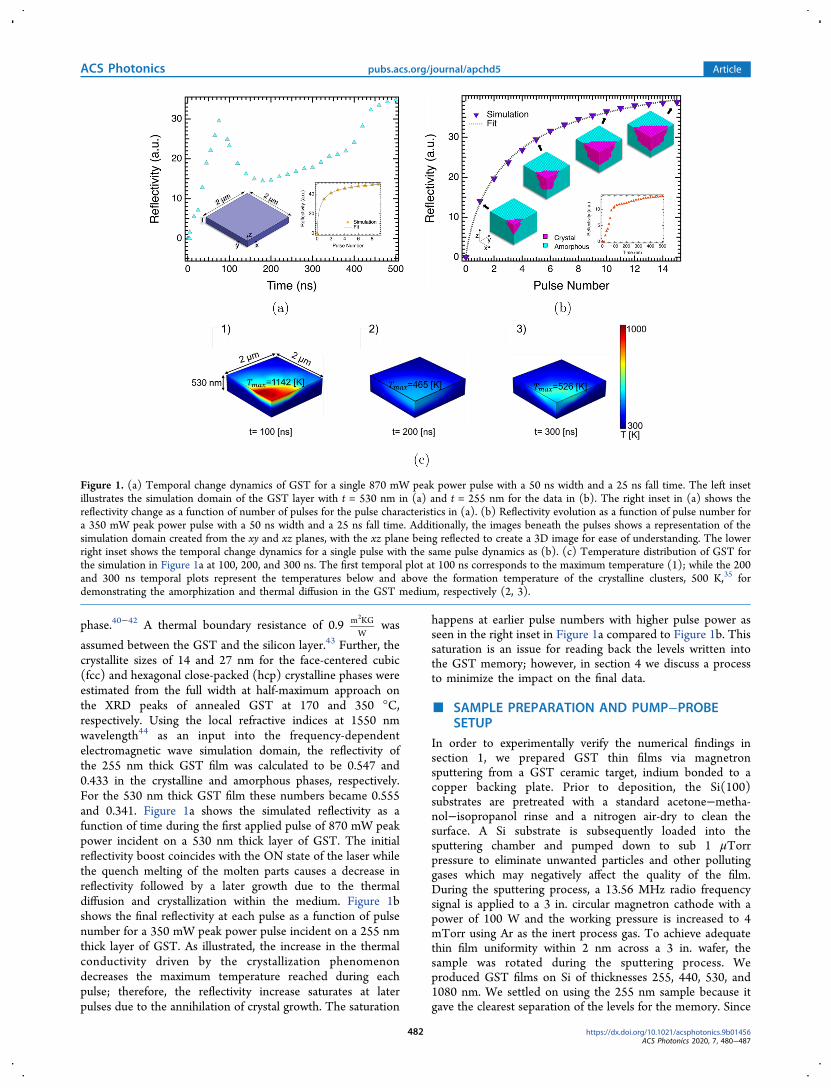
assumed between the GST and the silicon layer43 Further thecrystallite sizes of 14 and 27 nm for the face-centered cubic(fcc) and hexagonal close-packed (hcp) crystalline phases wereestimated from the full width at half-maximum approach onthe XRD peaks of annealed GST at 170 and 350 degCrespectively Using the local refractive indices at 1550 nmwavelength44 as an input into the frequency-dependentelectromagnetic wave simulation domain the reflectivity ofthe 255 nm thick GST film was calculated to be 0547 and0433 in the crystalline and amorphous phases respectivelyFor the 530 nm thick GST film these numbers became 0555and 0341 Figure 1a shows the simulated reflectivity as afunction of time during the first applied pulse of 870 mW peakpower incident on a 530 nm thick layer of GST The initialreflectivity boost coincides with the ON state of the laser whilethe quench melting of the molten parts causes a decrease inreflectivity followed by a later growth due to the thermaldiffusion and crystallization within the medium Figure 1bshows the final reflectivity at each pulse as a function of pulsenumber for a 350 mW peak power pulse incident on a 255 nmthick layer of GST As illustrated the increase in the thermalconductivity driven by the crystallization phenomenondecreases the maximum temperature reached during eachpulse therefore the reflectivity increase saturates at laterpulses due to the annihilation of crystal growth The saturation
happens at earlier pulse numbers with higher pulse power asseen in the right inset in Figure 1a compared to Figure 1b Thissaturation is an issue for reading back the levels written intothe GST memory however in section 4 we discuss a processto minimize the impact on the final data
SAMPLE PREPARATION AND PUMPminusPROBESETUP
In order to experimentally verify the numerical findings insection 1 we prepared GST thin films via magnetronsputtering from a GST ceramic target indium bonded to acopper backing plate Prior to deposition the Si(100)substrates are pretreated with a standard acetoneminusmetha-nolminusisopropanol rinse and a nitrogen air-dry to clean thesurface A Si substrate is subsequently loaded into thesputtering chamber and pumped down to sub 1 μTorrpressure to eliminate unwanted particles and other pollutinggases which may negatively affect the quality of the filmDuring the sputtering process a 1356 MHz radio frequencysignal is applied to a 3 in circular magnetron cathode with apower of 100 W and the working pressure is increased to 4mTorr using Ar as the inert process gas To achieve adequatethin film uniformity within 2 nm across a 3 in wafer thesample was rotated during the sputtering process Weproduced GST films on Si of thicknesses 255 440 530 and1080 nm We settled on using the 255 nm sample because itgave the clearest separation of the levels for the memory Since
Figure 1 (a) Temporal change dynamics of GST for a single 870 mW peak power pulse with a 50 ns width and a 25 ns fall time The left insetillustrates the simulation domain of the GST layer with t = 530 nm in (a) and t = 255 nm for the data in (b) The right inset in (a) shows thereflectivity change as a function of number of pulses for the pulse characteristics in (a) (b) Reflectivity evolution as a function of pulse number fora 350 mW peak power pulse with a 50 ns width and a 25 ns fall time Additionally the images beneath the pulses shows a representation of thesimulation domain created from the xy and xz planes with the xz plane being reflected to create a 3D image for ease of understanding The lowerright inset shows the temporal change dynamics for a single pulse with the same pulse dynamics as (b) (c) Temperature distribution of GST forthe simulation in Figure 1a at 100 200 and 300 ns The first temporal plot at 100 ns corresponds to the maximum temperature (1) while the 200and 300 ns temporal plots represent the temperatures below and above the formation temperature of the crystalline clusters 500 K35 fordemonstrating the amorphization and thermal diffusion in the GST medium respectively (2 3)
ACS Photonics pubsacsorgjournalapchd5 Article
httpsdxdoiorg101021acsphotonics9b01456ACS Photonics 2020 7 480minus487
482
this investigation only studies the crystallization process wedid not include a capping layer on the GST (no appreciableeffect on the temporal dynamics of the crystallization existed insimulations) which is useful in preventing telluriumevaporation while the sample is in a molten stateAfter fabrication the samples were actuated and monitored
in a custom built optical experimental setup shown in Figure2 capable of producing single pulses down to 25 ns and up toconstant wave (CW) using 1550 nm light The setup beginswith a 1550 nm CW laser that runs through a fiber coupledelectro-optic modulator (EOM) connected to an arbitrarywaveform generator (AWG) which allows us to create anypulse shapes that may be needed We then use an erbium-doped fiber amplifier (EDFA) to amplify the power in thepulses to powers adequate for switching the GST (2 mWaverage 210 mW peak power in our experiment) At this pointwe utilize a wavelength demultiplexer (WDM) to couple ourprobe beam which is a CW 1590 nm laser into the same fibervia the second port This coaligns the lasers before they leavethe fiber saving alignment time and loss from additional opticsThe now combined beams then exit the fiber and pass througha free space EOM which can handle the higher powers of ourpulses The EOM is used to pick off as many pulses as we needin a single shot As we were unable to find a high voltage driverfor the EOM that could provide the voltage needed with a fastenough slew rate to pick off a single pulse we created our ownpulse amplifier circuit using a high-slew rate operationalamplifier (APEX Microdevices PA94) We achieved a 400 Vjump in less than 5 μs for an arbitrary wave shape This allowedus to easily capture a single pulse from a train of pulses up to afew hundred kHz After the free-space EOM we coalign a 780nm laser to use for positioning on the sample since the 1550and 1590 nm wavelengths we are working with are not visibleon our CMOS cameraAfter the EOM a glass slide is used to pick off a small
portion of the beam This becomes one arm of the balanceddetection scheme and is also used as a power monitor The
beam then passes through a 1590 nm bandpass filter in orderto filter out the 1550 nm pump pulse as much as possible andis then coupled into a fiber The coupling efficiency into thefiber is used to match the powers before and after the samplefor the balanced measurement The majority of the beam(sim90) enters the microscope and is focused down to a 4minus5μm spot on the sample After reflecting off the sample thebeam is picked up from the microscopersquos output and passesthrough another 1590 nm bandpass filter before being coupledinto a fiber and inserted into the detector as the second arm ofthe balanced detection scheme The detector then subtractsthe two signals and outputs the final signal to an oscilloscopewhere it is captured
PHASE CHANGE DYNAMICS
Using the pumpminusprobe setup we are able to observe thetemporal dynamics of the phase change of the GST viareflection measurements While the absolute reflectivitycontrast is appreciable losses in the microscope which wasinitially designed for visible epi-fluorescence meant that thereflected light was very low power The balanced measurementaspect of our setup allowed us to improve the signal-to-noiseratio in our reflected probe giving a better dynamic range forthe measurement and a more full understanding of theprocesses occurringFigure 3 shows the reflectivity measurement for a single 870
mW peak power pulse incident on our sample Four main areasare highlighted indicating the different parts of the processthat occur during the crystallization of GST by a single 50 nspulse with a 25 ns fall time and experimentally verify what wasseen in the numerical simulations from Figure 1a Taking intoaccount the differing pulse lengths the crystallization times didnot differ significantly for 25minus100 ns pulses and were thereforenot shown here Since the length of the pulse did not changethe crystallization characteristics the 50 ns pulse with a 25 nsfall time was chosen to be consistent with our previousmeasurements for ease of comparison During the initial
Figure 2 Single shot pumpminusprobe measurement setup
ACS Photonics pubsacsorgjournalapchd5 Article
httpsdxdoiorg101021acsphotonics9b01456ACS Photonics 2020 7 480minus487
483
illumination by the pulse nucleation sites are created in theGST These sites act as the seeds for the crystallization processFrom these nucleation sites being created we observe a fastrise in the reflectivity of the material This is highlighted in thefirst shaded area marked as (1) in Figure 3After the pulse ends the energy diffuses through the GST
For higher powered pulses a section of the data can be seen todrop in reflectivity for example the second shaded area labeled(2) and at the end of area (1) in Figure 3 This is due to theGST reaching its melting temperature30 As the material meltsit approaches its amorphous phase and shows a decrease inreflectivity just as seen hereAs the heat continues to diffuse through the material the
temperature drops below the melting point and we beginseeing an increase in reflectivity due to the crystallizationoccurring The shaded region (3) shows this happening with aslowly rising reflectivity The slow rise is due to the fact thatthe GST is still above its crystallization temperature andtherefore still has the energy to break the bonds needed forcrystallization Once the material cools below the crystal-lization temperature a rapid increase in reflectivity is seen inthe shaded area (4) The crystallization is no longer beingimpeded by the energy from the pulse and can relax into itsfinal crystallized stateSince melting the GST allows the tellurium atoms to drift
more easily which is one of the leading causes of switchingfailure22minus24 staying away from melting while crystallizing iscrucial In Figure 4 it can be seen that properly selecting thecorrect power for the pulses can keep the material frommelting This phenomena can be seen in the 206 mW peakpower trace in the figure From Figure 4 we can also see thatthe GST crystallizes more with higher pulse powers Howeverthere is a limit to this that is seen between the 683 and 912mW peak power pulses There is not a significant difference inthe final reflection levels of these two pulses but the 912 mWpeak power trace dips lower after the initial height after thepulse ends indicating more melting
In Figure 5 we show the experimental and simulated data for15minus350 mW pulses incident on a 255 nm film of GST Each
step in the data signifies another pulse incident on the sampleThe peaks seen before the reflectivity settles down to its steadystate are leakage from the pump laser through the filters Asmore of the GST is switched the reflectivity goes up and moreof the pump is leaked As can be seen in Figures 3 and 5 thesimulated data matches the experimental data very closely Byreducing the power of the single pulses a clearer multilevelmemory can be achieved We demonstrate this in the nextsection where we create an optical 4-bit memory
MULTILEVEL MEMORYWith the knowledge that different amounts of crystallizationoccur at different pulse powers we attempted to use multiplepulses to achieve these levels which could be looked at aseither a single-site multibit storage or an accumulator memory
Figure 3 Single pulse (870 mW peak power 50 ns pulse 25 ns falltime) time dynamics from a 530 nm thick GST sample Bothsimulated and experimental data match very closely indicating aworking model Colored areas label the different stages ofcrystallization Top inset shows a 50 ns pulse with a 25 ns fall timeBottom inset is an SEM image of GST illuminated by a single pulse
Figure 4 Single pulse dynamics for differing pulse powers Traces areshifted vertically for clarity
Figure 5 Simulation and experimental data for sim350 mW pulsesEach point of the simulated data and each step of the experimentaldata represent an incremental number of pulses incident on thesample
ACS Photonics pubsacsorgjournalapchd5 Article
httpsdxdoiorg101021acsphotonics9b01456ACS Photonics 2020 7 480minus487
484
(since the low repetition rate implies the material reachessteady-state between the pulses) Figure 6b shows an exampleof a 16-level write with some smoothing used to differentiatethe levels more easily For the smoothing a box algorithm wasemployed using 500 points This figure was obtained bymonitoring the reflection off the sample as a single spot wasilluminated with 15 pulses of peak power sim200 mW It can beseen that there exists a saturation as higher pulse numbers wereincident on the GST This needs to be corrected in order toread data encoded with these pulse powersTo correct for the saturation curve the individual levels were
pulled from the graph in Figure 6b and were fit using the Hillequation
AumlCcedilAringAringAringAringAringAring
EacuteOumlNtildeNtildeNtildeNtildeNtildeNtilde
= + minus
+y
base (max base)
1 xx
rate12
(3)
as seen in the inset in Figure 6b where ldquobaserdquo sets the y valueat small x ldquomaxrdquo sets the y value at large x and x12 is the x
value where = +y base max2
Once the fit parameters were
known we could solve the equation for x and use
AumlCcedilAringAringAringAringAringAringAring
EacuteOumlNtildeNtildeNtildeNtildeNtildeNtildeNtilde
=minusminus
minus
xx
1y
12
max basebase
1rate
(4)
to decode our dataUsing the same power and size of pulses we then encoded an
initial 16 pulse spot and a final 16 pulse spot at the two ends ofwhere the message would be written The space between thesetwo spots was then scanned and the resulting variations in thereflectivity from the bulk GST acted as the baseline forcorrecting the information peaks after they were written Afterreading the baseline ldquoSETRESrdquo was written into the GST bystepping the sample under the laser by a fixed distance andhitting each spot with the corresponding number of pulses forhexadecimal encoding ldquo53 45 54 2f 52 45 53rdquo where the ldquofrdquocorresponds to the 15th level The resulting image of the spots
taken by a visible wavelength microscope can be seen inFigure 6aThe encoded data was then scanned with the 1590 nm CW
probe laser and the background scans were subtracted from thescanned area The peak data was taken from each of thewritten spots run through the decoding algorithm in eq 4 andgraphed as shown in Figure 6c The highest value was set tothe 15th level as that is the maximum level of our memoryAs can be seen in Figure 6c the message ldquoSETRESrdquo was
able to be read back within the expected values plusmn05 Due tothe reversible nature of the GST the storage can be cycled andreused The errors in the readout of the memory can beattributed to fluctuations in both the write and read lasers aswell as density variations and contaminants in the GST With amore consistent laser and a more efficient probing setup thiscould be extended to higher levels and even smaller margins oferrorSince our memory device is encoded using a laser incident
on the surface of the material the individual data spots can bepacked very close together giving a much higher informationdensity for the surface area used than earlier waveguide-basedmemories can achieve From our simulation data in Figure 1bit can be seen that at the point of saturation the crystallizedarea is not even extending to the full 2 μm radius of our beamSince we are only concerned with reading the peak values ofour reflectivity measurements and are using the same size beamto read and write we can put spots on a 4 times 4 μm grid Thiswould give an information density of 25000000 bitscm2 Theinformation density can be raised even higher by tighterfocusing for an even smaller spot size For example by focusingdown to a 500 nm spot size the information density wouldjump up to 1600000000 bitscm2 We believe that this makesour device an interesting and important contender in the nextgeneration of optical memory especially one that can be usedin conjunction with free-space two-dimensional opticalcomputing protocols45
Figure 6 (a) ldquoSETRESrdquo encoded in hexadecimal in GST film The first and last pulses are 16 pulses used as markers for the beginning and endingof the message (b) The 16 levels achieved using multiple pulses with a peak power of sim200 mW Inset shows the fit to the levels using the hill eq 3(c) Final read data from ldquoSETRESrdquo
ACS Photonics pubsacsorgjournalapchd5 Article
httpsdxdoiorg101021acsphotonics9b01456ACS Photonics 2020 7 480minus487
485
CONCLUSIONIn summary we have used a custom-built optical setup capableof active optical monitoring to probe the time dynamics of thecrystallization of GST at 1550 nm incident light Wediscovered that there was hardly any difference in the timescales for the crystallization based on pulse size shape orpower at 1550 nm laser irradiation We identified four mainareas of interest in the crystallization of the GST an initialnucleation step while the pulse is illuminating the sample thatcontinues until melting occurs the dropping of the reflectivityas the GST melts and approaches a more disordered state thediffusion of the heat through the material and a small amountof crystallization indicated by the slowly rising reflectivity andfinally a sharp rise in the reflectivity as the material coolsbelow the crystallization temperature and settles into its finalcrystallized state This whole process was seen to takeapproximately 400 ns We saw this in the numericalsimulations and verified it experimentallyAfter verifying the ability of the GST to remain in partially
crystallized states we were able to encode and decode amessage written in a 4-bit hexadecimal system which could bethought of as either a 4-bit single-site memory or a 16-levelaccumulator We wrote and read the message ldquoSETRESrdquo in a2D multilevel memory application With tuning of the laserpowers the GST thickness and the consistency of the laserpulses we believe we can achieve lower errors and even morelevels making this a viable optical memory
AUTHOR INFORMATIONCorresponding AuthorGary A Sevison minus Department of Electro-Optics and PhotonicsUniversity of Dayton Dayton Ohio United States Air ForceResearch Laboratory Sensors Directorate Wright-PattersonAFB Dayton Ohio United States orcidorg0000-0002-6832-0356 Email sevisong1udaytonedu
AuthorsShiva Farzinazar minus Department of Mechanical EngineeringUniversity of California Irvine Irvine California United States
Joshua A Burrow minus Department of Electro-Optics andPhotonics University of Dayton Dayton Ohio United Statesorcidorg0000-0002-1237-4662
Christopher Perez minus Department of Mechanical and AerospaceEngineering Stanford University Stanford California UnitedStates
Heungdong Kwon minus Department of Mechanical and AerospaceEngineering Stanford University Stanford California UnitedStates
Jaeho Lee minus Department of Mechanical Engineering Universityof California Irvine Irvine California United States
Mehdi Asheghi minus Department of Mechanical and AerospaceEngineering Stanford University Stanford California UnitedStates
Kenneth E Goodson minus Department of Mechanical andAerospace Engineering Stanford University StanfordCalifornia United States
Andrew Sarangan minus Department of Electro-Optics andPhotonics University of Dayton Dayton Ohio United States
Joshua R Hendrickson minus Air Force Research LaboratorySensors Directorate Wright-Patterson AFB Dayton OhioUnited States orcidorg0000-0002-5342-0346
Imad Agha minus Department of Electro-Optics and PhotonicsUniversity of Dayton Dayton Ohio United States Department
of Physics The University of Dayton Dayton Ohio 45469United States
Complete contact information is available athttpspubsacsorg101021acsphotonics9b01456
FundingAir Force Research LaboratoryDefense-Associated GraduateStudent Innovators Program (GS) National ScienceFoundation Electrical Communications and Cyber SystemsGrant No 1710273 (JB) Semiconductor Research Corpo-ration (CP) Kwanjeong Educational Foundation Scholarshipof Korea (HK) Air Force Office of Scientific Research GrantNo 15RYCOR159 (JH)NotesThe authors declare no competing financial interest
ACKNOWLEDGMENTSThe authors thank Pengfei Guo Ryan Laing and Aditya Soodfor their professional input and assistance with the workpresented in this manuscript
REFERENCES(1) Kirchain R Kimerling L A roadmap for nanophotonics NatPhotonics 2007 1 303minus305(2) Alduino A Paniccia M Interconnects Wiring electronics withlight Nat Photonics 2007 1 153minus155(3) Zhao Y Lombardo D Mathews J Agha I All-opticalswitching via four-wave mixing Bragg scattering in a silicon platformAPL Photonics 2017 2 026102(4) Hosseini P Sebastian A Papandreou N Wright C DBhaskaran H Accumulation-Based Computing Using Phase-ChangeMemories With FET Access Devices IEEE Electron Device Lett 201536 975minus977(5) Gao M Pu J Yang X Horowitz M Kozyrakis C TETRISScalable and Efficient Neural Network Acceleration with 3D MemorySIGARCH Comput Archit News 2017 45 751minus764(6) Cheng Z Riacuteos C Youngblood N Wright C D Pernice WH Bhaskaran H Device-Level Photonic Memories and LogicApplications Using Phase-Change Materials Adv Mater 2018 301802435(7) Shu M J Chatzakis I Kuo Y Zalden P Lindenberg A MUltrafast sub-threshold photo-induced response in crystalline andamorphous GeSbTe thin films Appl Phys Lett 2013 102 201903(8) Zalden P Shu M J Chen F Wu X Zhu Y Wen HJohnston S Shen Z X Landreman P Brongersma M Fong SW Wong H S P Sher M J Jost P Kaes M Salinga M VonHoegen A Wuttig M Lindenberg A M Picosecond Electric-Field-Induced Threshold Switching in Phase-Change Materials Phys RevLett 2016 117 1minus6(9) Nirschl T Philipp J B Happ T D Burr G W RajendranB Lee M H Schrott A Yang M Breitwisch M Chen C FJoseph E Lamorey M Cheek R Chen S H Zaidi S Raoux SChen Y C Zhu Y Bergmann R Lung H L Lam C Writestrategies for 2 and 4-bit multi-level phase-change memory TechnicalDigest - International Electron Devices Meeting 2007 461minus464(10) Papandreou N Pantazi A Sebastian A Breitwisch M LamC Pozidis H Eleftheriou E Multilevel phase-change memory 2010IEEE International Conference on Electronics Circuits and SystemsICECS 2010 - Proceedings IEEE 2010 pp 1017minus1020(11) Papandreou N Pozidis H Pantazi A Sebastian ABreitwisch M Lam C Eleftheriou E Programming algorithmsfor multilevel phase-change memory Proceedings - IEEE InternationalSymposium on Circuits and Systems IEEE 2011 pp 329minus332(12) Gyanathan A Yeo Y C Multi-level phase change memorydevices with Ge2Sb2Te5 layers separated by a thermal insulatingTa2O5 barrier layer J Appl Phys 2011 110
ACS Photonics pubsacsorgjournalapchd5 Article
httpsdxdoiorg101021acsphotonics9b01456ACS Photonics 2020 7 480minus487
486
(13) Pirovano A Redaelli A Pellizzer F Ottogalli F Tosi MIelmini D Lacaita A L Member S Bez R Reliability Study ofPhase-Change Nonvolatile Memories IEEE Transactions on Deviceand Materials Reliability IEEE 2004 Vol 4 pp 422minus427(14) Li X Youngblood N Riacuteos C Cheng Z Wright C DPernice W H Bhaskaran H Fast and reliable storage using a 5 bitnonvolatile photonic memory cell Optica 2019 6 1(15) Rios C Stegmaier M Cheng Z Youngblood N Wright CD Pernice W H P Bhaskaran H Controlled switching of phase-change materials by evanescent-field coupling in integrated photonics[Invited] Opt Mater Express 2018 8 2455(16) Zheng J Khanolkar A Xu P Colburn S Deshmukh SMyers J Frantz J Pop E Hendrickson J Doylend J BoechlerN Majumdar A GST-on-silicon hybrid nanophotonic integratedcircuits a non-volatile quasi-continuously reprogrammable platformOpt Mater Express 2018 8 1551(17) Joshi M Zhang W Li T Mercury A fast and energy-efficient multi-level cell based phase change memory systemProceedings - International Symposium on High-Performance ComputerArchitecture 2011 345minus356(18) Bedeschi F Fackenthal R Resta C Donze E MJagasivamani M A Multi-Level-Cell Bipolar-Selected Phase-ChangeMemory 2008 IEEE International Solid-State Circuits Conference -Digest of Technical Papers IEEE 2008 pp 428minus625(19) Close G F Frey U Breitwisch M Lung H L Lam CHagleitner C Eleftheriou E Device circuit and system-level analysisof noise in multi-bit phase-change memory Technical Digest -International Electron Devices Meeting IEDM 2010 Vol 29 pp51minus2954(20) Wong H-S P Raoux S Kim S Liang J Reifenberg J PRajendran B Asheghi M Goodson K E Phase Change MemoryProceedings in IEEE IEEE 2010 Vol 98(21) Guo P Burrow J A Sevison G A Sood A Asheghi MHendrickson J R Goodson K E Agha I Sarangan A Improvingthe performance of Ge2Sb2Te5 materials via nickel doping TowardsRF-compatible phase-change devices Appl Phys Lett 2018 113171903(22) Kim C Kang D Lee T-y Kim K H P Kang S Lee JNam S-w Kim K-b Kim C Kang D Lee T-y Direct evidenceof phase separation in Ge2Sb2Te5 in phase change memory devicesAppl Phys Lett 2009 94 193504(23) Yang T Y Park I M Kim B J Joo Y C Atomic migrationin molten and crystalline Ge2Sb2Te5 under high electric field ApplPhys Lett 2009 95 2007minus2010(24) Kim Y T Kim Y H Failure mechanisms of Ge2Sb2Te5 phasechange memory cell Phys Status Solidi B 2014 251 435minus438(25) Loke D Lee T H Wang W J Shi L P Zhao R Yeo YC Chong T C Elliott S R Breaking the speed limits of phase-change memory Science 2012 336 1566minus9(26) Liang G Zhang K Zhai F Huang H Wang Y Wu YComparison of optical and electrical transient response duringnanosecond laser pulse-induced phase transition of Ge2Sb2Te5 thinfilms Chem Phys Lett 2011 507 203minus207(27) Wright E M Khulbe P K Mansuripur M Dynamic theoryof crystallization in Ge2Sb23Te5 phase-change optical recording mediaAppl Opt 2000 39 6695(28) Zhai F X Liu S Wang D Liu N Ren Y Hao Y YangK Laser-induced phase transition processes of amorphous Ge 2 Sb 2Te 5 films Optik 2019 185 126minus131(29) Zhang K Li S Liang G Huang H Wang Y Lai T WuY Different crystallization processes of as-deposited amorphous Ge2Sb 2Te 5 films on nano- and picosecond single laser pulseirradiation Phys B 2012 407 2447minus2450(30) Khulbe P K Xun X Mansuripur M Crystallization andamorphization studies of a Ge_2Sb_23Te_5 thin-film sample underpulsed laser irradiation Appl Opt 2000 39 2359(31) Lee B S Shelby R M Raoux S Retter C T Burr G WBogle S N Darmawikarta K Bishop S G Abelson J RNanoscale nuclei in phase change materials Origin of different
crystallization mechanisms of Ge2Sb2Te5 and AgInSbTe J ApplPhys 2014 115 063506(32) Waldecker L Miller T A Rude M Bertoni R Osmond JPruneri V Simpson R E Ernstorfer R Wall S Time-domainseparation of optical properties from structural transitions inresonantly bonded materials Nat Mater 2015 14 991minus995(33) Simpson R Ernstorfer R Wall S Decoupled OpticalResponse and Structural Transition in Phase Change Materials ArXiv2015 na(34) Xiang D Liu T Xu J Tan J Y Hu Z Lei B Zheng YWu J Neto A H C Liu L Chen W Two-dimensional multibitoptoelectronic memory with broadband spectrum distinction NatCommun 2018 9 2966(35) Branicio P S Bai K Ramanarayan H Wu D T Song WWang W Li M Zhao R Shi L Srolovitz D J Theamorphization and crystallization of Ge 2 Sb 2 Te 5 an ab initiomolecular dynamics studyMater Res Soc Symp Proc 2012 1431 na(36) Peng C Cheng L Mansuripur M Experimental andtheoretical investigations of laser-induced crystallization and amorph-ization in phase-change optical recording media J Appl Phys 199782 4183minus4191(37) Li Z Jeyasingh R G D Lee J Asheghi M Wong H SGoodson K E Electrothermal modeling and design strategies formultibit phase-change memory IEEE Trans Electron Devices 2012 593561minus3567(38) Ielmini D Zhang Y Analytical model for subthresholdconduction and threshold switching in chalcogenide-based memorydevices J Appl Phys 2007 102 054517(39) Karchevsky A L A frequency-domain analytical solution ofMaxwell rsquo s equations for layered anisotropic media Russian Geologyand Geophysics 2007 48 689minus695(40) Li Z Lee J Reifenberg J P Asheghi M Jeyasingh R GWong H S Goodson K E Grain boundaries phase impurities andanisotropic thermal conduction in phase-change memory IEEEElectron Device Lett 2011 32 961minus963(41) Lee J Li Z Reifenberg J P Lee S Sinclair R AsheghiM Goodson K E Thermal conductivity anisotropy and grainstructure in Ge 2Sb2Te5 films J Appl Phys 2011 109 1minus6(42) Lee J Kim S Marconnet A InrsquoT Zandt M A Asheghi MPhilip Wong H S Goodson K E Thermoelectric characterizationand power generation using a silicon-on-insulator substrate JMicroelectromech Syst 2012 21 4minus6(43) Lee J Bozorg-Grayeli E Kim S Asheghi M Philip WongH S Goodson K E Phonon and electron transport throughGe2Sb2Te 5 films and interfaces bounded by metals Appl Phys Lett2013 102 1minus6(44) Guo P Sarangan A Agha I A Review of Germanium-Antimony-Telluride Phase Change Materials for Non-VolatileMemories and Optical Modulators Appl Sci 2019 9 530(45) Ambs P Optical Computing A 60-Year Adventure Advancesin Optical Technologies 2010 2010 1minus15
ACS Photonics pubsacsorgjournalapchd5 Article
httpsdxdoiorg101021acsphotonics9b01456ACS Photonics 2020 7 480minus487
487

the occurrence of issues that cause breakdown in the GSTOne of the core issues for example is the Tellurium drift22minus24
that occurs during melting and is accelerated by applying anelectric field across the material By optically switching theGST as opposed to electrically switching it and staying belowthe melting point while crystallizing we can lengthen thelifetime of the material The time dynamics of the change areadditionally important to know in order to be able to obtain alimit to the eventual speed of any future device Switchingspeeds for GST have been reported from the singlenanoseconds or shorter25 to the hundreds of nanoseconds ormicroseconds2627 depending on the method used for thechange as well as the power and wavelength of light for opticalswitching28 Similar measurements to those utilized in thispaper have been used previously2628minus30 however no data wasfound for 1550 nm light which is necessary to understand inorder to create devices that work in the telecommunicationsbands In fact current free space optically induced phasechange devices are operated in the visible or near-visiblewavelength regime30minus33 Since the absorption is extremely highat these wavelengths a transmissive device is not a viableoption Moreover the high absorption also limits the volumeof material that can be changed via a free-space laser andtherefore restricts the amount of levels that can be achievedHence by using a telecom wavelength stimulus to trigger thephase change where GST is inherently less absorbing we cangain access to more of the volume of the material to changeTo sum up there is a real need for an optical memory to
drive hybrid computing protocol this memory has to (a) becapable of high speed dynamic storage and retrieval (b) becapable of multilevel storage and accumulation (c) offer long-term stability and (d) have reasonable power requirementsMoreover in order to improve the performances in the futurethere is a need for a deeper understanding of the material anddevice properties through both modeling and experimentalverificationIn this work we present a 2D-ready memory that can
surpass recent waveguide-based memories in terms ofinformation density the expense and complexity of fabrication(our device being a single layer of GST) and can integratewith future optical computing protocols34 that require 2Dstorage or a nonvolatile accumulator While we demonstratesingle-pixel performance we anticipate that our results can beeasily scaled into a two-dimensional high-density deviceSpecifically we demonstrate the use of GST as a multilevelmemory by encoding and decoding information based on a 4-bit all optical writeread scheme Increasing numbers of levelsare achieved by optimizing the GST thin-film thickness onsilicon as well as the power in each pulse Multiple levels areachieved by exciting thin films of GST with sequential single-pulses (ns) of 1550 nm light using a custom built optical setupcapable of active optical monitoring The crystallization time-dynamics are investigated experimentally and corroboratedwith numerical simulations revealing the partial crystallizationincreasing in a volume of GST with each subsequent pulsewith a goal of further improving GST-based memory devices inthe future
OPTOELECTRICAL MODELING OFTWO-DIMENSIONAL 4-BIT GST-BASED MEMORIES
GST PCMs contain a rich set of coupled electrical thermaland optical properties In order to begin studying theseproperties numerical simulations were run for single and
multipulse excitation with a focused pulsed telecom-bandGaussian beam Once we begin to understand what washappening physically from the simulations it is possible tounderstand the optimal conditions needed to implement a highspeed multilevel optical memoryIn our simulations we considered a volume of amorphous
GST subjected to a sharply focused Gaussian beam with adiameter of 400 plusmn 025 μm which will reflect ourexperimental conditions as seen later For the reflectivitycalculation we used a fully coupled optothermal simulationdomain to estimate the temperature evolution of the GSTphases under a pulse width of 50 ns and a 25 ns fall timeCrystallization kinetics of the amorphous phase and solid-ification of the molten areas were assessed using thecrystallization and nucleation model for phase transition as afunction of temperature and time duration36 Pn theprobability of amorphous phase transformation to a crystallinenucleus during the Δt time interval is defined as
Auml
Ccedil
AringAringAringAringAringAringAringAringAringAring
Eacute
Ouml
NtildeNtildeNtildeNtildeNtildeNtildeNtildeNtildeNtildeNtildeα= Δβminus +
ΔP teE A
Gn n
( )a 2(1)
where Ea is the nucleation-based activation energy and ΔG isthe additional Gibbs free energy of amorphous GST A isassociated with the interfacial surface free energy betweencrystalline and amorphous phases αn is the nucleationfrequency factor and β is defined as
k T1
B where kB is the
Boltzmann constant and T is the absolute temperatureAdditionally the probability of crystal growth (Pg) can beexpressed as a function of the mesh size (R) activation energyassociated with atomic diffusion (Ea2) growth frequency factor(αg) atomic jump distance (α0) and the melting temperature(Tm)
ikjjj y
zzzα α= Δ [ minus ]β
βminus minus minus Δminus
P t e ee
R1
TT G
E
g 0 g08 1
m
a2
(2)
The crystallization algorithm that accounts for the parallelmechanisms of probabilistic nucleus formation and crystallinegrowth was initially developed by Li et al37 for modeling theelectrothermal phenomena in phase change memories In theirapproach the electrical conductivity of each node wasiteratively evaluated by applying the Poole-Frenkel model38
In our approach the absorption coefficient of each node isiteratively evaluated by solving the frequency domain form ofMaxwellrsquos equation39 The phase of each node is determinedusing the same crystallization algorithm The optical and phaseproperties are then provided to a finite-element solver(COMSOL Multiphysics) to simulate optical heating-inducedtemperature distributions The geometry and material proper-ties were defined inside the commercial software COMSOLwhich computed the temperature field at each time step Phasechange algorithms and optical switching were implementedusing the MATLAB codes and properties were modified forthe next iteration In simulations the GST layer is discretizedvia mesh grids with dimensions comparable to the critical sizeof nuclei Therefore spatial dependence is a function of thediscretization size of the mesh and is not inherent to eqs 1 and2 The symmetry of the sample reduces the computation timeby using only a quarter of the sample domain The simulationconsiders 056 W
mKand 037 W
mKat room temperature for the
cross-plane and in-plane crystalline thermal conductivity valuesand 018 W
mKfor the thermal conductivity of the amorphous
ACS Photonics pubsacsorgjournalapchd5 Article
httpsdxdoiorg101021acsphotonics9b01456ACS Photonics 2020 7 480minus487
481
phase40minus42 A thermal boundary resistance of 09 m KGW
2was
assumed between the GST and the silicon layer43 Further thecrystallite sizes of 14 and 27 nm for the face-centered cubic(fcc) and hexagonal close-packed (hcp) crystalline phases wereestimated from the full width at half-maximum approach onthe XRD peaks of annealed GST at 170 and 350 degCrespectively Using the local refractive indices at 1550 nmwavelength44 as an input into the frequency-dependentelectromagnetic wave simulation domain the reflectivity ofthe 255 nm thick GST film was calculated to be 0547 and0433 in the crystalline and amorphous phases respectivelyFor the 530 nm thick GST film these numbers became 0555and 0341 Figure 1a shows the simulated reflectivity as afunction of time during the first applied pulse of 870 mW peakpower incident on a 530 nm thick layer of GST The initialreflectivity boost coincides with the ON state of the laser whilethe quench melting of the molten parts causes a decrease inreflectivity followed by a later growth due to the thermaldiffusion and crystallization within the medium Figure 1bshows the final reflectivity at each pulse as a function of pulsenumber for a 350 mW peak power pulse incident on a 255 nmthick layer of GST As illustrated the increase in the thermalconductivity driven by the crystallization phenomenondecreases the maximum temperature reached during eachpulse therefore the reflectivity increase saturates at laterpulses due to the annihilation of crystal growth The saturation
happens at earlier pulse numbers with higher pulse power asseen in the right inset in Figure 1a compared to Figure 1b Thissaturation is an issue for reading back the levels written intothe GST memory however in section 4 we discuss a processto minimize the impact on the final data
SAMPLE PREPARATION AND PUMPminusPROBESETUP
In order to experimentally verify the numerical findings insection 1 we prepared GST thin films via magnetronsputtering from a GST ceramic target indium bonded to acopper backing plate Prior to deposition the Si(100)substrates are pretreated with a standard acetoneminusmetha-nolminusisopropanol rinse and a nitrogen air-dry to clean thesurface A Si substrate is subsequently loaded into thesputtering chamber and pumped down to sub 1 μTorrpressure to eliminate unwanted particles and other pollutinggases which may negatively affect the quality of the filmDuring the sputtering process a 1356 MHz radio frequencysignal is applied to a 3 in circular magnetron cathode with apower of 100 W and the working pressure is increased to 4mTorr using Ar as the inert process gas To achieve adequatethin film uniformity within 2 nm across a 3 in wafer thesample was rotated during the sputtering process Weproduced GST films on Si of thicknesses 255 440 530 and1080 nm We settled on using the 255 nm sample because itgave the clearest separation of the levels for the memory Since
Figure 1 (a) Temporal change dynamics of GST for a single 870 mW peak power pulse with a 50 ns width and a 25 ns fall time The left insetillustrates the simulation domain of the GST layer with t = 530 nm in (a) and t = 255 nm for the data in (b) The right inset in (a) shows thereflectivity change as a function of number of pulses for the pulse characteristics in (a) (b) Reflectivity evolution as a function of pulse number fora 350 mW peak power pulse with a 50 ns width and a 25 ns fall time Additionally the images beneath the pulses shows a representation of thesimulation domain created from the xy and xz planes with the xz plane being reflected to create a 3D image for ease of understanding The lowerright inset shows the temporal change dynamics for a single pulse with the same pulse dynamics as (b) (c) Temperature distribution of GST forthe simulation in Figure 1a at 100 200 and 300 ns The first temporal plot at 100 ns corresponds to the maximum temperature (1) while the 200and 300 ns temporal plots represent the temperatures below and above the formation temperature of the crystalline clusters 500 K35 fordemonstrating the amorphization and thermal diffusion in the GST medium respectively (2 3)
ACS Photonics pubsacsorgjournalapchd5 Article
httpsdxdoiorg101021acsphotonics9b01456ACS Photonics 2020 7 480minus487
482
this investigation only studies the crystallization process wedid not include a capping layer on the GST (no appreciableeffect on the temporal dynamics of the crystallization existed insimulations) which is useful in preventing telluriumevaporation while the sample is in a molten stateAfter fabrication the samples were actuated and monitored
in a custom built optical experimental setup shown in Figure2 capable of producing single pulses down to 25 ns and up toconstant wave (CW) using 1550 nm light The setup beginswith a 1550 nm CW laser that runs through a fiber coupledelectro-optic modulator (EOM) connected to an arbitrarywaveform generator (AWG) which allows us to create anypulse shapes that may be needed We then use an erbium-doped fiber amplifier (EDFA) to amplify the power in thepulses to powers adequate for switching the GST (2 mWaverage 210 mW peak power in our experiment) At this pointwe utilize a wavelength demultiplexer (WDM) to couple ourprobe beam which is a CW 1590 nm laser into the same fibervia the second port This coaligns the lasers before they leavethe fiber saving alignment time and loss from additional opticsThe now combined beams then exit the fiber and pass througha free space EOM which can handle the higher powers of ourpulses The EOM is used to pick off as many pulses as we needin a single shot As we were unable to find a high voltage driverfor the EOM that could provide the voltage needed with a fastenough slew rate to pick off a single pulse we created our ownpulse amplifier circuit using a high-slew rate operationalamplifier (APEX Microdevices PA94) We achieved a 400 Vjump in less than 5 μs for an arbitrary wave shape This allowedus to easily capture a single pulse from a train of pulses up to afew hundred kHz After the free-space EOM we coalign a 780nm laser to use for positioning on the sample since the 1550and 1590 nm wavelengths we are working with are not visibleon our CMOS cameraAfter the EOM a glass slide is used to pick off a small
portion of the beam This becomes one arm of the balanceddetection scheme and is also used as a power monitor The
beam then passes through a 1590 nm bandpass filter in orderto filter out the 1550 nm pump pulse as much as possible andis then coupled into a fiber The coupling efficiency into thefiber is used to match the powers before and after the samplefor the balanced measurement The majority of the beam(sim90) enters the microscope and is focused down to a 4minus5μm spot on the sample After reflecting off the sample thebeam is picked up from the microscopersquos output and passesthrough another 1590 nm bandpass filter before being coupledinto a fiber and inserted into the detector as the second arm ofthe balanced detection scheme The detector then subtractsthe two signals and outputs the final signal to an oscilloscopewhere it is captured
PHASE CHANGE DYNAMICS
Using the pumpminusprobe setup we are able to observe thetemporal dynamics of the phase change of the GST viareflection measurements While the absolute reflectivitycontrast is appreciable losses in the microscope which wasinitially designed for visible epi-fluorescence meant that thereflected light was very low power The balanced measurementaspect of our setup allowed us to improve the signal-to-noiseratio in our reflected probe giving a better dynamic range forthe measurement and a more full understanding of theprocesses occurringFigure 3 shows the reflectivity measurement for a single 870
mW peak power pulse incident on our sample Four main areasare highlighted indicating the different parts of the processthat occur during the crystallization of GST by a single 50 nspulse with a 25 ns fall time and experimentally verify what wasseen in the numerical simulations from Figure 1a Taking intoaccount the differing pulse lengths the crystallization times didnot differ significantly for 25minus100 ns pulses and were thereforenot shown here Since the length of the pulse did not changethe crystallization characteristics the 50 ns pulse with a 25 nsfall time was chosen to be consistent with our previousmeasurements for ease of comparison During the initial
Figure 2 Single shot pumpminusprobe measurement setup
ACS Photonics pubsacsorgjournalapchd5 Article
httpsdxdoiorg101021acsphotonics9b01456ACS Photonics 2020 7 480minus487
483
illumination by the pulse nucleation sites are created in theGST These sites act as the seeds for the crystallization processFrom these nucleation sites being created we observe a fastrise in the reflectivity of the material This is highlighted in thefirst shaded area marked as (1) in Figure 3After the pulse ends the energy diffuses through the GST
For higher powered pulses a section of the data can be seen todrop in reflectivity for example the second shaded area labeled(2) and at the end of area (1) in Figure 3 This is due to theGST reaching its melting temperature30 As the material meltsit approaches its amorphous phase and shows a decrease inreflectivity just as seen hereAs the heat continues to diffuse through the material the
temperature drops below the melting point and we beginseeing an increase in reflectivity due to the crystallizationoccurring The shaded region (3) shows this happening with aslowly rising reflectivity The slow rise is due to the fact thatthe GST is still above its crystallization temperature andtherefore still has the energy to break the bonds needed forcrystallization Once the material cools below the crystal-lization temperature a rapid increase in reflectivity is seen inthe shaded area (4) The crystallization is no longer beingimpeded by the energy from the pulse and can relax into itsfinal crystallized stateSince melting the GST allows the tellurium atoms to drift
more easily which is one of the leading causes of switchingfailure22minus24 staying away from melting while crystallizing iscrucial In Figure 4 it can be seen that properly selecting thecorrect power for the pulses can keep the material frommelting This phenomena can be seen in the 206 mW peakpower trace in the figure From Figure 4 we can also see thatthe GST crystallizes more with higher pulse powers Howeverthere is a limit to this that is seen between the 683 and 912mW peak power pulses There is not a significant difference inthe final reflection levels of these two pulses but the 912 mWpeak power trace dips lower after the initial height after thepulse ends indicating more melting
In Figure 5 we show the experimental and simulated data for15minus350 mW pulses incident on a 255 nm film of GST Each
step in the data signifies another pulse incident on the sampleThe peaks seen before the reflectivity settles down to its steadystate are leakage from the pump laser through the filters Asmore of the GST is switched the reflectivity goes up and moreof the pump is leaked As can be seen in Figures 3 and 5 thesimulated data matches the experimental data very closely Byreducing the power of the single pulses a clearer multilevelmemory can be achieved We demonstrate this in the nextsection where we create an optical 4-bit memory
MULTILEVEL MEMORYWith the knowledge that different amounts of crystallizationoccur at different pulse powers we attempted to use multiplepulses to achieve these levels which could be looked at aseither a single-site multibit storage or an accumulator memory
Figure 3 Single pulse (870 mW peak power 50 ns pulse 25 ns falltime) time dynamics from a 530 nm thick GST sample Bothsimulated and experimental data match very closely indicating aworking model Colored areas label the different stages ofcrystallization Top inset shows a 50 ns pulse with a 25 ns fall timeBottom inset is an SEM image of GST illuminated by a single pulse
Figure 4 Single pulse dynamics for differing pulse powers Traces areshifted vertically for clarity
Figure 5 Simulation and experimental data for sim350 mW pulsesEach point of the simulated data and each step of the experimentaldata represent an incremental number of pulses incident on thesample
ACS Photonics pubsacsorgjournalapchd5 Article
httpsdxdoiorg101021acsphotonics9b01456ACS Photonics 2020 7 480minus487
484
(since the low repetition rate implies the material reachessteady-state between the pulses) Figure 6b shows an exampleof a 16-level write with some smoothing used to differentiatethe levels more easily For the smoothing a box algorithm wasemployed using 500 points This figure was obtained bymonitoring the reflection off the sample as a single spot wasilluminated with 15 pulses of peak power sim200 mW It can beseen that there exists a saturation as higher pulse numbers wereincident on the GST This needs to be corrected in order toread data encoded with these pulse powersTo correct for the saturation curve the individual levels were
pulled from the graph in Figure 6b and were fit using the Hillequation
AumlCcedilAringAringAringAringAringAring
EacuteOumlNtildeNtildeNtildeNtildeNtildeNtilde
= + minus
+y
base (max base)
1 xx
rate12
(3)
as seen in the inset in Figure 6b where ldquobaserdquo sets the y valueat small x ldquomaxrdquo sets the y value at large x and x12 is the x
value where = +y base max2
Once the fit parameters were
known we could solve the equation for x and use
AumlCcedilAringAringAringAringAringAringAring
EacuteOumlNtildeNtildeNtildeNtildeNtildeNtildeNtilde
=minusminus
minus
xx
1y
12
max basebase
1rate
(4)
to decode our dataUsing the same power and size of pulses we then encoded an
initial 16 pulse spot and a final 16 pulse spot at the two ends ofwhere the message would be written The space between thesetwo spots was then scanned and the resulting variations in thereflectivity from the bulk GST acted as the baseline forcorrecting the information peaks after they were written Afterreading the baseline ldquoSETRESrdquo was written into the GST bystepping the sample under the laser by a fixed distance andhitting each spot with the corresponding number of pulses forhexadecimal encoding ldquo53 45 54 2f 52 45 53rdquo where the ldquofrdquocorresponds to the 15th level The resulting image of the spots
taken by a visible wavelength microscope can be seen inFigure 6aThe encoded data was then scanned with the 1590 nm CW
probe laser and the background scans were subtracted from thescanned area The peak data was taken from each of thewritten spots run through the decoding algorithm in eq 4 andgraphed as shown in Figure 6c The highest value was set tothe 15th level as that is the maximum level of our memoryAs can be seen in Figure 6c the message ldquoSETRESrdquo was
able to be read back within the expected values plusmn05 Due tothe reversible nature of the GST the storage can be cycled andreused The errors in the readout of the memory can beattributed to fluctuations in both the write and read lasers aswell as density variations and contaminants in the GST With amore consistent laser and a more efficient probing setup thiscould be extended to higher levels and even smaller margins oferrorSince our memory device is encoded using a laser incident
on the surface of the material the individual data spots can bepacked very close together giving a much higher informationdensity for the surface area used than earlier waveguide-basedmemories can achieve From our simulation data in Figure 1bit can be seen that at the point of saturation the crystallizedarea is not even extending to the full 2 μm radius of our beamSince we are only concerned with reading the peak values ofour reflectivity measurements and are using the same size beamto read and write we can put spots on a 4 times 4 μm grid Thiswould give an information density of 25000000 bitscm2 Theinformation density can be raised even higher by tighterfocusing for an even smaller spot size For example by focusingdown to a 500 nm spot size the information density wouldjump up to 1600000000 bitscm2 We believe that this makesour device an interesting and important contender in the nextgeneration of optical memory especially one that can be usedin conjunction with free-space two-dimensional opticalcomputing protocols45
Figure 6 (a) ldquoSETRESrdquo encoded in hexadecimal in GST film The first and last pulses are 16 pulses used as markers for the beginning and endingof the message (b) The 16 levels achieved using multiple pulses with a peak power of sim200 mW Inset shows the fit to the levels using the hill eq 3(c) Final read data from ldquoSETRESrdquo
ACS Photonics pubsacsorgjournalapchd5 Article
httpsdxdoiorg101021acsphotonics9b01456ACS Photonics 2020 7 480minus487
485
CONCLUSIONIn summary we have used a custom-built optical setup capableof active optical monitoring to probe the time dynamics of thecrystallization of GST at 1550 nm incident light Wediscovered that there was hardly any difference in the timescales for the crystallization based on pulse size shape orpower at 1550 nm laser irradiation We identified four mainareas of interest in the crystallization of the GST an initialnucleation step while the pulse is illuminating the sample thatcontinues until melting occurs the dropping of the reflectivityas the GST melts and approaches a more disordered state thediffusion of the heat through the material and a small amountof crystallization indicated by the slowly rising reflectivity andfinally a sharp rise in the reflectivity as the material coolsbelow the crystallization temperature and settles into its finalcrystallized state This whole process was seen to takeapproximately 400 ns We saw this in the numericalsimulations and verified it experimentallyAfter verifying the ability of the GST to remain in partially
crystallized states we were able to encode and decode amessage written in a 4-bit hexadecimal system which could bethought of as either a 4-bit single-site memory or a 16-levelaccumulator We wrote and read the message ldquoSETRESrdquo in a2D multilevel memory application With tuning of the laserpowers the GST thickness and the consistency of the laserpulses we believe we can achieve lower errors and even morelevels making this a viable optical memory
AUTHOR INFORMATIONCorresponding AuthorGary A Sevison minus Department of Electro-Optics and PhotonicsUniversity of Dayton Dayton Ohio United States Air ForceResearch Laboratory Sensors Directorate Wright-PattersonAFB Dayton Ohio United States orcidorg0000-0002-6832-0356 Email sevisong1udaytonedu
AuthorsShiva Farzinazar minus Department of Mechanical EngineeringUniversity of California Irvine Irvine California United States
Joshua A Burrow minus Department of Electro-Optics andPhotonics University of Dayton Dayton Ohio United Statesorcidorg0000-0002-1237-4662
Christopher Perez minus Department of Mechanical and AerospaceEngineering Stanford University Stanford California UnitedStates
Heungdong Kwon minus Department of Mechanical and AerospaceEngineering Stanford University Stanford California UnitedStates
Jaeho Lee minus Department of Mechanical Engineering Universityof California Irvine Irvine California United States
Mehdi Asheghi minus Department of Mechanical and AerospaceEngineering Stanford University Stanford California UnitedStates
Kenneth E Goodson minus Department of Mechanical andAerospace Engineering Stanford University StanfordCalifornia United States
Andrew Sarangan minus Department of Electro-Optics andPhotonics University of Dayton Dayton Ohio United States
Joshua R Hendrickson minus Air Force Research LaboratorySensors Directorate Wright-Patterson AFB Dayton OhioUnited States orcidorg0000-0002-5342-0346
Imad Agha minus Department of Electro-Optics and PhotonicsUniversity of Dayton Dayton Ohio United States Department
of Physics The University of Dayton Dayton Ohio 45469United States
Complete contact information is available athttpspubsacsorg101021acsphotonics9b01456
FundingAir Force Research LaboratoryDefense-Associated GraduateStudent Innovators Program (GS) National ScienceFoundation Electrical Communications and Cyber SystemsGrant No 1710273 (JB) Semiconductor Research Corpo-ration (CP) Kwanjeong Educational Foundation Scholarshipof Korea (HK) Air Force Office of Scientific Research GrantNo 15RYCOR159 (JH)NotesThe authors declare no competing financial interest
ACKNOWLEDGMENTSThe authors thank Pengfei Guo Ryan Laing and Aditya Soodfor their professional input and assistance with the workpresented in this manuscript
REFERENCES(1) Kirchain R Kimerling L A roadmap for nanophotonics NatPhotonics 2007 1 303minus305(2) Alduino A Paniccia M Interconnects Wiring electronics withlight Nat Photonics 2007 1 153minus155(3) Zhao Y Lombardo D Mathews J Agha I All-opticalswitching via four-wave mixing Bragg scattering in a silicon platformAPL Photonics 2017 2 026102(4) Hosseini P Sebastian A Papandreou N Wright C DBhaskaran H Accumulation-Based Computing Using Phase-ChangeMemories With FET Access Devices IEEE Electron Device Lett 201536 975minus977(5) Gao M Pu J Yang X Horowitz M Kozyrakis C TETRISScalable and Efficient Neural Network Acceleration with 3D MemorySIGARCH Comput Archit News 2017 45 751minus764(6) Cheng Z Riacuteos C Youngblood N Wright C D Pernice WH Bhaskaran H Device-Level Photonic Memories and LogicApplications Using Phase-Change Materials Adv Mater 2018 301802435(7) Shu M J Chatzakis I Kuo Y Zalden P Lindenberg A MUltrafast sub-threshold photo-induced response in crystalline andamorphous GeSbTe thin films Appl Phys Lett 2013 102 201903(8) Zalden P Shu M J Chen F Wu X Zhu Y Wen HJohnston S Shen Z X Landreman P Brongersma M Fong SW Wong H S P Sher M J Jost P Kaes M Salinga M VonHoegen A Wuttig M Lindenberg A M Picosecond Electric-Field-Induced Threshold Switching in Phase-Change Materials Phys RevLett 2016 117 1minus6(9) Nirschl T Philipp J B Happ T D Burr G W RajendranB Lee M H Schrott A Yang M Breitwisch M Chen C FJoseph E Lamorey M Cheek R Chen S H Zaidi S Raoux SChen Y C Zhu Y Bergmann R Lung H L Lam C Writestrategies for 2 and 4-bit multi-level phase-change memory TechnicalDigest - International Electron Devices Meeting 2007 461minus464(10) Papandreou N Pantazi A Sebastian A Breitwisch M LamC Pozidis H Eleftheriou E Multilevel phase-change memory 2010IEEE International Conference on Electronics Circuits and SystemsICECS 2010 - Proceedings IEEE 2010 pp 1017minus1020(11) Papandreou N Pozidis H Pantazi A Sebastian ABreitwisch M Lam C Eleftheriou E Programming algorithmsfor multilevel phase-change memory Proceedings - IEEE InternationalSymposium on Circuits and Systems IEEE 2011 pp 329minus332(12) Gyanathan A Yeo Y C Multi-level phase change memorydevices with Ge2Sb2Te5 layers separated by a thermal insulatingTa2O5 barrier layer J Appl Phys 2011 110
ACS Photonics pubsacsorgjournalapchd5 Article
httpsdxdoiorg101021acsphotonics9b01456ACS Photonics 2020 7 480minus487
486
(13) Pirovano A Redaelli A Pellizzer F Ottogalli F Tosi MIelmini D Lacaita A L Member S Bez R Reliability Study ofPhase-Change Nonvolatile Memories IEEE Transactions on Deviceand Materials Reliability IEEE 2004 Vol 4 pp 422minus427(14) Li X Youngblood N Riacuteos C Cheng Z Wright C DPernice W H Bhaskaran H Fast and reliable storage using a 5 bitnonvolatile photonic memory cell Optica 2019 6 1(15) Rios C Stegmaier M Cheng Z Youngblood N Wright CD Pernice W H P Bhaskaran H Controlled switching of phase-change materials by evanescent-field coupling in integrated photonics[Invited] Opt Mater Express 2018 8 2455(16) Zheng J Khanolkar A Xu P Colburn S Deshmukh SMyers J Frantz J Pop E Hendrickson J Doylend J BoechlerN Majumdar A GST-on-silicon hybrid nanophotonic integratedcircuits a non-volatile quasi-continuously reprogrammable platformOpt Mater Express 2018 8 1551(17) Joshi M Zhang W Li T Mercury A fast and energy-efficient multi-level cell based phase change memory systemProceedings - International Symposium on High-Performance ComputerArchitecture 2011 345minus356(18) Bedeschi F Fackenthal R Resta C Donze E MJagasivamani M A Multi-Level-Cell Bipolar-Selected Phase-ChangeMemory 2008 IEEE International Solid-State Circuits Conference -Digest of Technical Papers IEEE 2008 pp 428minus625(19) Close G F Frey U Breitwisch M Lung H L Lam CHagleitner C Eleftheriou E Device circuit and system-level analysisof noise in multi-bit phase-change memory Technical Digest -International Electron Devices Meeting IEDM 2010 Vol 29 pp51minus2954(20) Wong H-S P Raoux S Kim S Liang J Reifenberg J PRajendran B Asheghi M Goodson K E Phase Change MemoryProceedings in IEEE IEEE 2010 Vol 98(21) Guo P Burrow J A Sevison G A Sood A Asheghi MHendrickson J R Goodson K E Agha I Sarangan A Improvingthe performance of Ge2Sb2Te5 materials via nickel doping TowardsRF-compatible phase-change devices Appl Phys Lett 2018 113171903(22) Kim C Kang D Lee T-y Kim K H P Kang S Lee JNam S-w Kim K-b Kim C Kang D Lee T-y Direct evidenceof phase separation in Ge2Sb2Te5 in phase change memory devicesAppl Phys Lett 2009 94 193504(23) Yang T Y Park I M Kim B J Joo Y C Atomic migrationin molten and crystalline Ge2Sb2Te5 under high electric field ApplPhys Lett 2009 95 2007minus2010(24) Kim Y T Kim Y H Failure mechanisms of Ge2Sb2Te5 phasechange memory cell Phys Status Solidi B 2014 251 435minus438(25) Loke D Lee T H Wang W J Shi L P Zhao R Yeo YC Chong T C Elliott S R Breaking the speed limits of phase-change memory Science 2012 336 1566minus9(26) Liang G Zhang K Zhai F Huang H Wang Y Wu YComparison of optical and electrical transient response duringnanosecond laser pulse-induced phase transition of Ge2Sb2Te5 thinfilms Chem Phys Lett 2011 507 203minus207(27) Wright E M Khulbe P K Mansuripur M Dynamic theoryof crystallization in Ge2Sb23Te5 phase-change optical recording mediaAppl Opt 2000 39 6695(28) Zhai F X Liu S Wang D Liu N Ren Y Hao Y YangK Laser-induced phase transition processes of amorphous Ge 2 Sb 2Te 5 films Optik 2019 185 126minus131(29) Zhang K Li S Liang G Huang H Wang Y Lai T WuY Different crystallization processes of as-deposited amorphous Ge2Sb 2Te 5 films on nano- and picosecond single laser pulseirradiation Phys B 2012 407 2447minus2450(30) Khulbe P K Xun X Mansuripur M Crystallization andamorphization studies of a Ge_2Sb_23Te_5 thin-film sample underpulsed laser irradiation Appl Opt 2000 39 2359(31) Lee B S Shelby R M Raoux S Retter C T Burr G WBogle S N Darmawikarta K Bishop S G Abelson J RNanoscale nuclei in phase change materials Origin of different
crystallization mechanisms of Ge2Sb2Te5 and AgInSbTe J ApplPhys 2014 115 063506(32) Waldecker L Miller T A Rude M Bertoni R Osmond JPruneri V Simpson R E Ernstorfer R Wall S Time-domainseparation of optical properties from structural transitions inresonantly bonded materials Nat Mater 2015 14 991minus995(33) Simpson R Ernstorfer R Wall S Decoupled OpticalResponse and Structural Transition in Phase Change Materials ArXiv2015 na(34) Xiang D Liu T Xu J Tan J Y Hu Z Lei B Zheng YWu J Neto A H C Liu L Chen W Two-dimensional multibitoptoelectronic memory with broadband spectrum distinction NatCommun 2018 9 2966(35) Branicio P S Bai K Ramanarayan H Wu D T Song WWang W Li M Zhao R Shi L Srolovitz D J Theamorphization and crystallization of Ge 2 Sb 2 Te 5 an ab initiomolecular dynamics studyMater Res Soc Symp Proc 2012 1431 na(36) Peng C Cheng L Mansuripur M Experimental andtheoretical investigations of laser-induced crystallization and amorph-ization in phase-change optical recording media J Appl Phys 199782 4183minus4191(37) Li Z Jeyasingh R G D Lee J Asheghi M Wong H SGoodson K E Electrothermal modeling and design strategies formultibit phase-change memory IEEE Trans Electron Devices 2012 593561minus3567(38) Ielmini D Zhang Y Analytical model for subthresholdconduction and threshold switching in chalcogenide-based memorydevices J Appl Phys 2007 102 054517(39) Karchevsky A L A frequency-domain analytical solution ofMaxwell rsquo s equations for layered anisotropic media Russian Geologyand Geophysics 2007 48 689minus695(40) Li Z Lee J Reifenberg J P Asheghi M Jeyasingh R GWong H S Goodson K E Grain boundaries phase impurities andanisotropic thermal conduction in phase-change memory IEEEElectron Device Lett 2011 32 961minus963(41) Lee J Li Z Reifenberg J P Lee S Sinclair R AsheghiM Goodson K E Thermal conductivity anisotropy and grainstructure in Ge 2Sb2Te5 films J Appl Phys 2011 109 1minus6(42) Lee J Kim S Marconnet A InrsquoT Zandt M A Asheghi MPhilip Wong H S Goodson K E Thermoelectric characterizationand power generation using a silicon-on-insulator substrate JMicroelectromech Syst 2012 21 4minus6(43) Lee J Bozorg-Grayeli E Kim S Asheghi M Philip WongH S Goodson K E Phonon and electron transport throughGe2Sb2Te 5 films and interfaces bounded by metals Appl Phys Lett2013 102 1minus6(44) Guo P Sarangan A Agha I A Review of Germanium-Antimony-Telluride Phase Change Materials for Non-VolatileMemories and Optical Modulators Appl Sci 2019 9 530(45) Ambs P Optical Computing A 60-Year Adventure Advancesin Optical Technologies 2010 2010 1minus15
ACS Photonics pubsacsorgjournalapchd5 Article
httpsdxdoiorg101021acsphotonics9b01456ACS Photonics 2020 7 480minus487
487
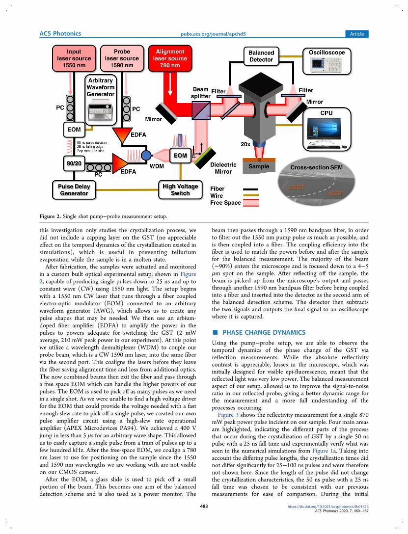
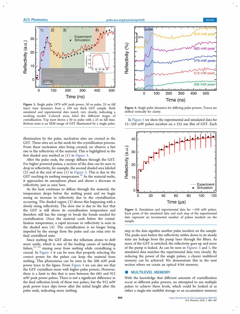
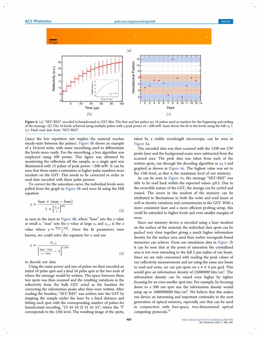
Top Related
Copyright © 2022 FDOKUMEN

