


Bahasa
Halaman
Hukum

Order this documentby MC68331TS/D Rev. 2
Fre
esc
ale
Se
mic
on
du
cto
r, I
Freescale Semiconductor, Inc.n
c..
.
MC68331
Technical Summary32-Bit Modular Microcontroller
1 IntroductionThe MC68331, a highly-integrated 32-bit microcontroller, combines high-performance data manipula-tion capabilities with powerful peripheral subsystems. The MCU is built up from standard modules thatinterface through a common intermodule bus (IMB). Standardization facilitates rapid development ofdevices tailored for specific applications.
The MCU incorporates a 32-bit CPU (CPU32), a system integration module (SIM), a general-purposetimer (GPT), and a queued serial module (QSM).
The MCU can either synthesize an internal clock signal from an external reference or use an externalclock input directly. Operation with a 32.768-kHz reference frequency is standard. The maximum sys-tem clock speed is 20.97 MHz. Because MCU operation is fully static, register and memory contentsare not affected by a loss of clock.
High-density complementary metal-oxide semiconductor (HCMOS) architecture makes the basic powerconsumption of the MCU low. Power consumption can be minimized by stopping the system clock. TheCPU32 instruction set includes a low-power stop (LPSTOP) command that efficiently implements thiscapability.
For More Information On This Product,
Go to: www.freescale.com

Fre
esc
ale
Se
mic
on
du
cto
r, I
Freescale Semiconductor, Inc.n
c..
.
Table 1 Ordering Information
Package Type Temperature Frequency(MHz)
Package Order Quantity
Order Number
132-Pin PQFP –40 to +85 °C 16 MHz 2 pc tray SPAKMC331CFC1636 pc tray MC68331CFC16
20 MHz 2 pc tray SPAKMC331CFC2036 pc tray MC68331CFC20
–40 to +105 °C 16 MHz 2 pc tray SPAKMC331VFC1636 pc tray MC68331VFC16
20 MHz 2 pc tray SPAKMC331VFC2036 pc tray MC68331VFC20
–40 to +125 °C 16 MHz 2 pc tray SPAKMC331MFC1636 pc tray MC68331MFC16
20 MHz 2 pc tray SPAKMC331MFC2036 pc tray MC68331MFC20
144-Pin QFP –40 to +85 °C 16 MHz 2 pc tray SPAKMC331CFV1644 pc tray MC68331CFV16
20 MHz 2 pc tray SPAKMC331CFV2044 pc tray MC68331CFV20
–40 to +105 °C 16 MHz 2 pc tray SPAKMC331VFV1644 pc tray MC68331VFV16
20 MHz 2 pc tray SPAKMC331VFV2044 pc tray MC68331VFV20
–40 to +125 °C 16 MHz 2 pc tray SPAKMC331MFV1644 pc tray MC68331MFV16
20 MHz 2 pc tray SPAKMC331MFV2044 pc tray MC68331MFV20
2 MC68331TS/D
For More Information On This Product, Go to: www.freescale.com

Section Page
MC68331TS/D 3
1 Introduction 1
1.1 Features ......................................................................................................................................41.2 Block Diagram .............................................................................................................................51.3 Pin Assignments ..........................................................................................................................61.4 Address Map ...............................................................................................................................81.5 Intermodule Bus ..........................................................................................................................8
2 Signal Descriptions 9
2.1 Pin Characteristics ......................................................................................................................92.2 MCU Power Connections ..........................................................................................................102.3 MCU Driver Types .....................................................................................................................102.4 Signal Characteristics ................................................................................................................102.5 Signal Function ..........................................................................................................................11
3 System Integration Module 14
3.1 Overview ...................................................................................................................................143.2 System Configuration and Protection ........................................................................................163.3 System Clock ............................................................................................................................213.4 External Bus Interface ...............................................................................................................243.5 Chip Selects ..............................................................................................................................283.6 General-Purpose Input/Output ..................................................................................................353.7 Resets .......................................................................................................................................373.8 Interrupts ...................................................................................................................................393.9 Factory Test Block .....................................................................................................................41
4 Central Processor Unit 43
4.1 Overview ...................................................................................................................................434.2 Programming Model ..................................................................................................................434.3 Status Register ..........................................................................................................................454.4 Data Types ................................................................................................................................454.5 Addressing Modes .....................................................................................................................454.6 Instruction Set Summary ...........................................................................................................464.7 Background Debugging Mode ...................................................................................................50
5 Queued Serial Module 51
5.1 Overview ...................................................................................................................................515.2 Pin Function ..............................................................................................................................525.3 QSM Registers ..........................................................................................................................535.4 QSPI Submodule .......................................................................................................................565.5 SCI Submodule .........................................................................................................................64
6 General-Purpose Timer Module 70
6.1 Overview ...................................................................................................................................706.2 Capture/Compare Unit ..............................................................................................................716.3 Pulse-Width Modulator ..............................................................................................................746.4 GPT Registers ...........................................................................................................................75
7 Summary of Changes 82
TABLE OF CONTENTS
Fre
esc
ale
Se
mic
on
du
cto
r, I
Freescale Semiconductor, Inc.
For More Information On This Product, Go to: www.freescale.com
nc
...

Fre
esc
ale
Se
mic
on
du
cto
r, I
Freescale Semiconductor, Inc.n
c..
.
1.1 Features• Modular Architecture• Central Processing Unit (CPU32)
— Upward Object Code Compatible— New Instructions for Controller Applications— 32-Bit Architecture— Virtual Memory Implementation— Loop Mode of Instruction Execution— Table Lookup and Interpolate Instruction— Improved Exception Handling for Controller Applications— Trace on Change of Flow— Hardware Breakpoint Signal, Background Mode— Fully Static Operation
• System Integration Module (SIM)— External Bus Support— Programmable Chip-Select Outputs— System Protection Logic— Watchdog Timer, Clock Monitor, and Bus Monitor— System Protection Logic— System Clock Based on 32.768-kHz Crystal for Low Power Operation— Test/Debug Submodule for Factory/User Test and Development
• Queued Serial Module (QSM)— Enhanced Serial Communication Interface (SCI), Universal Asynchronous Receiver Transmit-
ter (UART): Modulus Baud Rate, Parity— Queued Serial Peripheral Interface (QSPI): 80-Byte RAM, Up to 16 Automatic Transfers— Dual Function I/O Ports— Continuous Cycling, 8 to 16 Bits per Transfer
• General-Purpose Timer (GPT) — Two 16-Bit Free-Running Counters With One Nine-Stage Prescaler— Three Input Capture Channels— Four Output Compare Channels— One Input Capture/Output Compare Channel— One Pulse Accumulator/Event Counter Input— Two Pulse-Width Modulation Outputs— Optional External Clock Input
4 MC68331TS/D
For More Information On This Product, Go to: www.freescale.com

6789
F
ree
sca
le S
em
ico
nd
uc
tor,
I
Freescale Semiconductor, Inc.n
c..
.
1.2 Block Diagram
Figure 1 MCU Block Diagram
331 BLOCK
PQS5/PCS2
PQS7/TXD
PQS4/PCS1
PQS6/PCS3
CPU32QSM
IMB
GPT
PQS0/MISOPQS1/MOSIPQS2/SCK PO
RTQ
S
TXD
PCS2
SCK
MISOMOSI
CO
NTR
OL
PCS1PQS3/PCS0/SS PCS0/SS
RXD
PCS3
CO
NTR
OL
BKPT/DSCLKIFETCH/DSI
IPIPE/DSO
FREE
ZE
DSI
DSO
DSC
LK
IPIP
EIF
ETC
HBK
PT
IRQ[7:1]
ADDR[23:0]
CO
NTR
OL
POR
T F
CO
NTR
OL
POR
T C
FC2FC1FC0
BGBR
BGACK
MODCLK
ADD
R[2
3:19
]
CLOCK
EBI
CS[10:0]
BR/CS0BG/CS1BGACK/CS2
R/WRESETHALTBERR
CLKOUTXTALEXTAL
CHIPSELECTS
CSBOOT
ADDR[18:0]
DATA[15:0]DATA[15:0]
QUOT
TEST
FREEZE/QUOT
TSC
CO
NTR
OLTSC
PC0/FC0/CS3PC1/FC1/CS4PC2/FC2/CS5PC3/ADDR19/CSPC4/ADDR20/CSPC5/ADDR21/CSPC6/ADDR22/CSADDR23/CS10
PF7/IRQ7PF6/IRQ6PF5/IRQ5PF4/IRQ4PF3/IRQ3PF2/IRQ2PF1/IRQ1PF0/MODCLK
CO
NTR
OL
POR
T E
SIZ1 PE7/SIZ1SIZ0 PE6/SIZ0
DSACK0 PE0/DSACK0DSACK1 PE1/DSACK1
AVEC PE2/AVECRMC PE3/RMC
DS PE5/DSAS PE4/AS
PGP5/OC3/OC1
PGP7/IC4/OC5/OC1
PGP4/OC2/OC1
PGP6/OC4/OC1
PGP0/IC1PGP1/IC2PGP2/IC3 PO
RT
GP
PGP7/IC4/OC5/OC1
PGP5/OC3/OC1
PGP2/IC3
PGP0/IC1PGP1/IC2C
ON
TRO
L
PGP4/OC2/OC1PGP3/OC1 PGP3/OC1
PGP6/OC4/OC1
PAI PAI
PCLK PCLK
PWMB PWMB
PWMA PWMA
MC68331TS/D 5
For More Information On This Product, Go to: www.freescale.com
QFP
91011
121314150
0123
4567
8
SACK1SACK0
VECMCS
OT
K/CS210
F
ree
sca
le S
em
ico
nd
uc
tor,
I
Freescale Semiconductor, Inc.n
c..
.
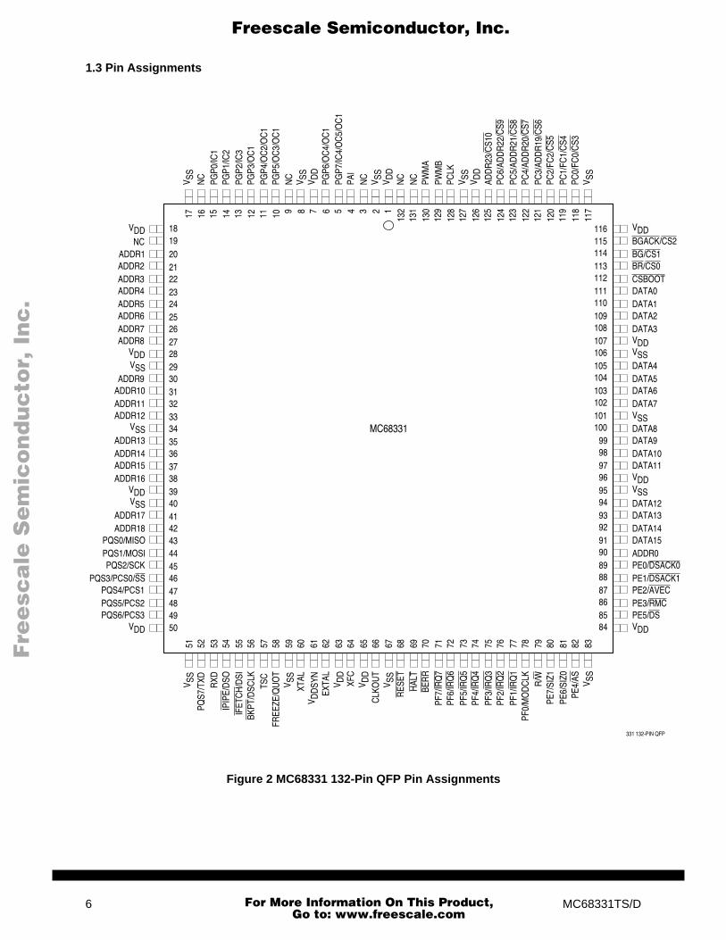
1.3 Pin Assignments
Figure 2 MC68331 132-Pin QFP Pin Assignments
331 132-PIN
MC68331
181920212223242526272829303132333435363738394041424344454647484950
116115114113112111110109108107106105104103102101100
99989796959493929190898887868584
DATADATADATA
DATADATADATADATAADDR
ADDR1ADDR2ADDR3ADDR4ADDR5ADDR6ADDR7ADDR8
ADDR9ADDR10ADDR11ADDR12
ADDR13ADDR14ADDR15ADDR16
ADDR17ADDR18
PQS0/MISOPQS1/MOSIPQS2/SCK
PQS3/PCS0/SSPQS4/PCS1PQS5/PCS2PQS6/PCS3
DATADATADATADATA
DATADATADATADATA
DATA
VDD
VSS
VDD
PE1/DPE0/D
PE2/APE3/RPE5/D
CSBO
BGACBG/CSBR/CS
5117 11
716 15 14 13 12 11 10 9 8 7 6 5 4 3
131
130
129
128
127
126
125
124
123
122
121
120
119
118
52 53 54 55 56 57 58 59 60 61 62 63 64 65 66 67 68 69 70 71 72 73 74 75 76 77 78 79 80 81 82 83
PQS7
/TXD RXD
IPIP
E/D
SO
FREE
ZE/Q
UO
T
XTAL
EXTA
L
XFC
CLK
OU
T
PF0/
MO
DC
LK
PE7/
SIZ1
PE6/
SIZ0
NC
PGP0
/IC1
PGP1
/IC2
PGP2
/IC3
PGP3
/OC
1PG
P4/O
C2/
OC
1PG
P5/O
C3/
OC
1N
C
PGP6
/OC
4/O
C1
PGP7
/IC4/
OC
5/O
C1
PAI
NC
NC
PWM
APW
MB
PCLK
NC
V SS
V DD
V SS
PC0/
FC0/
CS3
PC1/
FC1/
CS4
PC2/
FC2/
CS5
PC3/
ADD
R19
/CS6
PC4/
ADD
R20
/CS7
PC5/
ADD
R21
/CS8
PC6/
ADD
R22
/CS9
ADD
R23
/CS1
0
PE4/
ASR/W
PF1/
IRQ
1PF
2/IR
Q2
PF3/
IRQ
3PF
4/IR
Q4
PF5/
IRQ
5PF
6/IR
Q6
PF7/
IRQ
7BE
RR
HAL
TR
ESET
TSC
BKPT
/DSC
LKIF
ETC
H/D
SI
2 113
2
V DD
SYN
V SS
V SS
V DD
V SS
V DD
V SS
VDD
VSS
VSS
VDD
VDD
V SS
V DD
V DD
V SS
V SS
VDDVSS
VSS
VSS
VDD
VDDNC
6 MC68331TS/D
For More Information On This Product, Go to: www.freescale.com
T
F
ree
sca
le S
em
ico
nd
uc
tor,
I
Freescale Semiconductor, Inc.n
c..
.
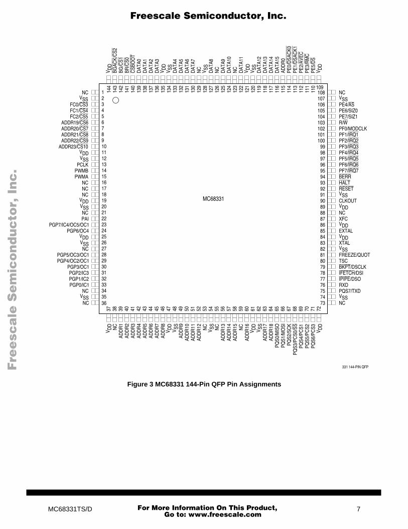
Figure 3 MC68331 144-Pin QFP Pin Assignments
331 144-PIN QFP
VSSNC
FC0/CS3FC1/CS4FC2/CS5
ADDR19/CS6ADDR20/CS7ADDR21/CS8ADDR22/CS9
ADDR23/CS10VDD
PCLKPWMBPWMA
NCNCNC
NCPAI
PGP6/OC4VDDVSSNC
PGP5/OC3/OC1PGP4/OC2/OC1
PGP3/OC1
MC68331
NC
PE4/ASPE6/SIZ0PE7/SIZ1R/WPF0/MODCLKPF1/IRQ1PF2/IRQ2PF3/IRQ3PF4/IRQ4PF5/IRQ5PF6/IRQ6PF7/IRQ7BERRHALTRESET
CLKOUT
NCXFC
EXTALVDDXTAL
FREEZE/QUOTSCBKPT/DSCLKIFETCH/DSIIPIPE/DSORXDPQS7/TXDVSSNC
PGP2/IC3PGP1/IC2PGP0/IC1
NC
NC
21
3456789101112131415161718192021222324252627282930
107108
106105104103102101100
999897969594939291908988878685848382818079787776757473
313233343536
BGAC
K/C
S2BG
/CS1
BR/C
S0C
SBO
OT
DAT
A0D
ATA1
DAT
A2D
ATA3
DAT
A4D
ATA5
DAT
A6D
ATA7
NC
DAT
A8N
CD
ATA9
DAT
A10
NC
DAT
A11
V SS
DAT
A12
DAT
A13
DAT
A14
DAT
A15
ADD
R0
PE0/
DSA
CK0
PE1/
DSA
CK1
PE2/
AVEC
PE3/
RM
CPE
5/D
SV D
D
NC
ADD
R1
ADD
R2
ADD
R3
ADD
R4
ADD
R5
ADD
R6
ADD
R7
ADD
R8
V DD
V SS
ADD
R9
ADD
R10
ADD
R11
ADD
R12 NC
NC
ADD
R13
ADD
R14
ADD
R15 NC
ADD
R16
ADD
R17
ADD
R18
PQS0
/MIS
OPQ
S1/M
OSI
PQS2
/SC
KPQ
S3/P
CS0
/SS
PQS4
/PC
S1PQ
S5/P
CS2
PQS6
/PC
S3
143
144
142
141
140
139
138
137
136
135
134
133
132
131
130
129
128
127
126
125
124
123
122
121
120
119
118
117
116
115
114
113
112
111
110 109
37 65 6838 39 40 41 42 43 44 45 46 47 48 49 50 51 52 53 54 55 56 57 58 59 60 61 62 63 64 66 67 69 70 71 72
V SS
V DD
V SS
V DD
VSS
VDD
VDD
VSS
VSS
V DD
V SS
V SS
V DD
V DD
VSS
VDDVSS
VSS
V DD
PGP7/IC4/OC5/OC1
MC68331TS/D 7
For More Information On This Product, Go to: www.freescale.com
Fre
esc
ale
Se
mic
on
du
cto
r, I
Freescale Semiconductor, Inc.n
c..
.
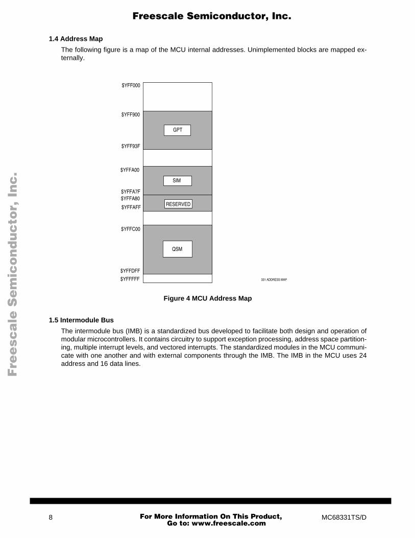
1.4 Address Map
The following figure is a map of the MCU internal addresses. Unimplemented blocks are mapped ex-ternally.
Figure 4 MCU Address Map
1.5 Intermodule Bus
The intermodule bus (IMB) is a standardized bus developed to facilitate both design and operation ofmodular microcontrollers. It contains circuitry to support exception processing, address space partition-ing, multiple interrupt levels, and vectored interrupts. The standardized modules in the MCU communi-cate with one another and with external components through the IMB. The IMB in the MCU uses 24address and 16 data lines.
$YFFDFF
$YFFA7F
$YFF93F
$YFF900
$YFF000
331 ADDRESS MAP
$YFFA00
$YFFC00
$YFFA80RESERVED
SIM
GPT
QSM
$YFFAFF
$YFFFFF
8 MC68331TS/D
For More Information On This Product, Go to: www.freescale.com

Fre
esc
ale
Se
mic
on
du
cto
r, I
Freescale Semiconductor, Inc.n
c..
.
2 Signal Descriptions
2.1 Pin Characteristics
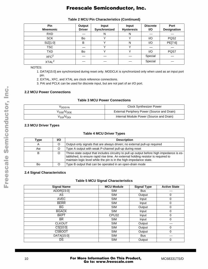
The following table shows MCU pins and their characteristics. All inputs detect CMOS logic levels. Allinputs can be put in a high-impedance state, but the method of doing this differs depending upon pinfunction. Refer to Table 4, for a description of output drivers. An entry in the discrete I/O column of Ta-ble 2 indicates that a pin has an alternate I/O function. The port designation is given when it applies.Refer to the MCU Block Diagram for information about port organization.
Table 2 MCU Pin Characteristics
PinMnemonic
OutputDriver
Input Synchronized
Input Hysteresis
Discrete I/O
PortDesignation
ADDR23/CS10/ECLK A Y N O —ADDR[22:19]/CS[9:6] A Y N O PC[6:3]
ADDR[18:0] A Y N — —AS B Y N I/O PE5
AVEC B Y N I/O PE2BERR B Y N — —
BG/CS1 B — — — —BGACK/CS2 B Y N — —BKPT/DSCLK — Y Y — —
BR/CS0 B Y N — —CLKOUT A — — — —CSBOOT B — — — —
DATA[15:0]1 Aw Y N — —
DS B Y N I/O PE4 DSACK1 B Y N I/O PE1DSACK0 B Y N I/O PE0
DSI/IFETCH A Y Y — —DSO/IPIPE A — — — —
EXTAL2 — — Special — —
FC[2:0]/CS[5:3] A Y N O PC[2:0]FREEZE/QUOT A — — — —
IC4/OC5 A Y Y I/O GP4IC[3:1] A Y Y I/O GP[7:5]HALT Bo Y N — —
IRQ[7:1] B Y Y I/O PF[7:1]MISO Bo Y Y I/O PQS0
MODCLK1 B Y N I/O PF0
MOSI Bo Y Y I/O PQS1OC[4:1] A Y Y I/O GP[3:0]
PAI3 — Y Y I —
PCLK3 — Y Y I —
PCS0/SS Bo Y Y I/O PQS3PCS[3:1] Bo Y Y I/O PQS[6:4]
PWMA, PWMB A — — O —R/W A Y N — —
RESET Bo Y Y — —RMC B Y N I/O PE3
MC68331TS/D 9
For More Information On This Product, Go to: www.freescale.com
Fre
esc
ale
Se
mic
on
du
cto
r, I
Freescale Semiconductor, Inc.n
c..
.
NOTES:1. DATA[15:0] are synchronized during reset only. MODCLK is synchronized only when used as an input port
pin. 2. EXTAL, XFC, and XTAL are clock reference connections.3. PAI and PCLK can be used for discrete input, but are not part of an I/O port.
2.2 MCU Power Connections
2.3 MCU Driver Types
2.4 Signal Characteristics
RXD — N N — —SCK Bo Y Y I/O PQS2
SIZ[1:0] B Y N I/O PE[7:6]TSC — Y Y — —TXD Bo Y Y I/O PQS7
XFC2 — — — Special —
XTAL2 — — — Special —
Table 3 MCU Power Connections
VDDSYN Clock Synthesizer Power
VSSE/VDDE External Periphery Power (Source and Drain)
VSSI/VDDI Internal Module Power (Source and Drain)
Table 4 MCU Driver Types
Type I/O DescriptionA O Output-only signals that are always driven; no external pull-up required
Aw O Type A output with weak P-channel pull-up during resetB O Three-state output that includes circuitry to pull up output before high impedance is es-
tablished, to ensure rapid rise time. An external holding resistor is required to maintain logic level while the pin is in the high-impedance state.
Bo O Type B output that can be operated in an open-drain mode
Table 5 MCU Signal Characteristics
Signal Name MCU Module Signal Type Active StateADDR[23:0] SIM Bus —
AS SIM Output 0AVEC SIM Input 0BERR SIM Input 0
BG SIM Output 0BGACK SIM Input 0BKPT CPU32 Input 0
BR SIM Input 0CLKOUT SIM Output —CS[10:0] SIM Output 0CSBOOT SIM Output 0
DATA[15:0] SIM Bus —DS SIM Output 0
Table 2 MCU Pin Characteristics (Continued)
PinMnemonic
OutputDriver
Input Synchronized
Input Hysteresis
Discrete I/O
PortDesignation
10 MC68331TS/D
For More Information On This Product, Go to: www.freescale.com

Fre
esc
ale
Se
mic
on
du
cto
r, I
Freescale Semiconductor, Inc.n
c..
.
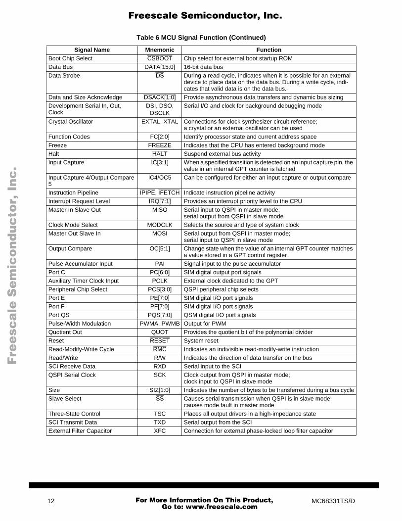
2.5 Signal Function
DSACK[1:0] SIM Input 0DSCLK CPU32 Input Serial Clock
DSI CPU32 Input (Serial Data)DSO CPU32 Output (Serial Data)
EXTAL SIM Input —FC[2:0] SIM Output —
FREEZE SIM Output 1HALT SIM Input/Output 0IC[4:1] GPT Input —
IFETCH CPU32 Output —IPIPE CPU32 Output —
IRQ[7:1] SIM Input 0MISO QSM Input/Output —
MODCLK SIM Input —MOSI QSM Input/Output —
OC[5:1] GPT Output —PAI GPT Input —
PC[6:0] SIM Output (Port)PCS[3:0] QSM Input/Output —PE[7:0] SIM Input/Output (Port)PF[7:0] SIM Input/Output (Port)
PQS[7:0] QSM Input/Output (Port)PCLK GPT Input —
PWMA, PWMB GPT Output —QUOT SIM Output —RESET SIM Input/Output 0RMC SIM Output 0R/W SIM Output 1/0RXD QSM Input —SCK QSM Input/Output —
SIZ[1:0] SIM Output —SS QSM Input 0
TSC SIM Input —TXD QSM Output —XFC SIM Input —XTAL SIM Output —
Table 6 MCU Signal Function
Signal Name Mnemonic FunctionAddress Bus ADDR[23:0] 24-bit address bus Address Strobe AS Indicates that a valid address is on the address busAutovector AVEC Requests an automatic vector during interrupt acknowledgeBus Error BERR Indicates that a bus error has occurredBus Grant BG Indicates that the MCU has relinquished the busBus Grant Acknowledge BGACK Indicates that an external device has assumed bus mastershipBreakpoint BKPT Signals a hardware breakpoint to the CPUBus Request BR Indicates that an external device requires bus mastershipSystem Clockout CLKOUT System clock outputChip Selects CS[10:0] Select external devices at programmed addresses
Table 5 MCU Signal Characteristics (Continued)
Signal Name MCU Module Signal Type Active State
MC68331TS/D 11
For More Information On This Product, Go to: www.freescale.com
Fre
esc
ale
Se
mic
on
du
cto
r, I
Freescale Semiconductor, Inc.n
c..
.
Boot Chip Select CSBOOT Chip select for external boot startup ROM Data Bus DATA[15:0] 16-bit data bus Data Strobe DS During a read cycle, indicates when it is possible for an external
device to place data on the data bus. During a write cycle, indi-cates that valid data is on the data bus.
Data and Size Acknowledge DSACK[1:0] Provide asynchronous data transfers and dynamic bus sizingDevelopment Serial In, Out, Clock
DSI, DSO, DSCLK
Serial I/O and clock for background debugging mode
Crystal Oscillator EXTAL, XTAL Connections for clock synthesizer circuit reference;a crystal or an external oscillator can be used
Function Codes FC[2:0] Identify processor state and current address space Freeze FREEZE Indicates that the CPU has entered background modeHalt HALT Suspend external bus activityInput Capture IC[3:1] When a specified transition is detected on an input capture pin, the
value in an internal GPT counter is latchedInput Capture 4/Output Compare 5
IC4/OC5 Can be configured for either an input capture or output compare
Instruction Pipeline IPIPE, IFETCH Indicate instruction pipeline activityInterrupt Request Level IRQ[7:1] Provides an interrupt priority level to the CPUMaster In Slave Out MISO Serial input to QSPI in master mode;
serial output from QSPI in slave modeClock Mode Select MODCLK Selects the source and type of system clockMaster Out Slave In MOSI Serial output from QSPI in master mode;
serial input to QSPI in slave modeOutput Compare OC[5:1] Change state when the value of an internal GPT counter matches
a value stored in a GPT control registerPulse Accumulator Input PAI Signal input to the pulse accumulatorPort C PC[6:0] SIM digital output port signalsAuxiliary Timer Clock Input PCLK External clock dedicated to the GPTPeripheral Chip Select PCS[3:0] QSPI peripheral chip selectsPort E PE[7:0] SIM digital I/O port signalsPort F PF[7:0] SIM digital I/O port signalsPort QS PQS[7:0] QSM digital I/O port signalsPulse-Width Modulation PWMA, PWMB Output for PWM Quotient Out QUOT Provides the quotient bit of the polynomial divider Reset RESET System resetRead-Modify-Write Cycle RMC Indicates an indivisible read-modify-write instructionRead/Write R/W Indicates the direction of data transfer on the busSCI Receive Data RXD Serial input to the SCIQSPI Serial Clock SCK Clock output from QSPI in master mode;
clock input to QSPI in slave modeSize SIZ[1:0] Indicates the number of bytes to be transferred during a bus cycleSlave Select SS Causes serial transmission when QSPI is in slave mode;
causes mode fault in master modeThree-State Control TSC Places all output drivers in a high-impedance stateSCI Transmit Data TXD Serial output from the SCIExternal Filter Capacitor XFC Connection for external phase-locked loop filter capacitor
Table 6 MCU Signal Function (Continued)
Signal Name Mnemonic Function
12 MC68331TS/D
For More Information On This Product, Go to: www.freescale.com

Fre
esc
ale
Se
mic
on
du
cto
r, I
Freescale Semiconductor, Inc.n
c..
.
MC68331TS/D 13
For More Information On This Product, Go to: www.freescale.com

Fre
esc
ale
Se
mic
on
du
cto
r, I
Freescale Semiconductor, Inc.n
c..
.
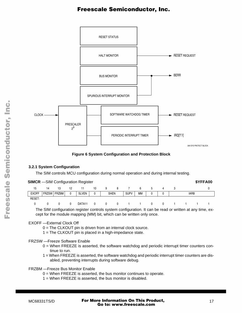
3 System Integration ModuleThe system integration module (SIM) consists of five functional blocks that control system start-up, ini-tialization, configuration, and external bus.
Figure 5 SIM Block Diagram
3.1 Overview
The system configuration and protection block controls MCU configuration and operating mode. Theblock also provides bus and software watchdog monitors.
The system clock generates clock signals used by the SIM, other IMB modules, and external devices.In addition, a periodic interrupt generator supports execution of time-critical control routines.
The external bus interface handles the transfer of information between IMB modules and external ad-dress space.
The chip-select block provides eleven general-purpose chip-select signals and a boot ROM chip-selectsignal. Both general-purpose and boot ROM chip-select signals have associated base address regis-ters and option registers.
The system test block incorporates hardware necessary for testing the MCU. It is used to perform fac-tory tests, and its use in normal applications is not supported.
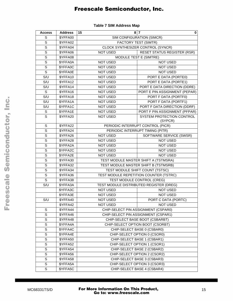
The SIM control register address map occupies 128 bytes. Unused registers within the 128-byte ad-dress space return zeros when read. The “Access” column in the SIM address map below indicateswhich registers are accessible only at the supervisor privilege level and which can be assigned to eitherthe supervisor or user privilege level, according to the value of the SUPV bit in the SIMCR.
300 S(C)IM BLOCK
SYSTEM CONFIGURATION
CLOCK SYNTHESIZER
CHIP SELECTS
EXTERNAL BUS INTERFACE
FACTORY TEST
CLKOUTEXTAL
MODCLK
CHIP SELECTS
EXTERNAL BUS
RESET
TSC
FREEZE/QUOT
XTAL
SYSTEM PROTECTION
14 MC68331TS/D
For More Information On This Product, Go to: www.freescale.com
Fre
esc
ale
Se
mic
on
du
cto
r, I
Freescale Semiconductor, Inc.n
c..
.
Table 7 SIM Address Map
Access Address 15 8 7 0S $YFFA00 SIM CONFIGURATION (SIMCR)S $YFFA02 FACTORY TEST (SIMTR)S $YFFA04 CLOCK SYNTHESIZER CONTROL (SYNCR)S $YFFA06 NOT USED RESET STATUS REGISTER (RSR)S $YFFA08 MODULE TEST E (SIMTRE)S $YFFA0A NOT USED NOT USEDS $YFFA0C NOT USED NOT USEDS $YFFA0E NOT USED NOT USED
S/U $YFFA10 NOT USED PORT E DATA (PORTE0)S/U $YFFA12 NOT USED PORT E DATA (PORTE1)S/U $YFFA14 NOT USED PORT E DATA DIRECTION (DDRE)S $YFFA16 NOT USED PORT E PIN ASSIGNMENT (PEPAR)
S/U $YFFA18 NOT USED PORT F DATA (PORTF0)S/U $YFFA1A NOT USED PORT F DATA (PORTF1)S/U $YFFA1C NOT USED PORT F DATA DIRECTION (DDRF)S $YFFA1E NOT USED PORT F PIN ASSIGNMENT (PFPAR)S $YFFA20 NOT USED SYSTEM PROTECTION CONTROL
(SYPCR)S $YFFA22 PERIODIC INTERRUPT CONTROL (PICR)S $YFFA24 PERIODIC INTERRUPT TIMING (PITR)S $YFFA26 NOT USED SOFTWARE SERVICE (SWSR)S $YFFA28 NOT USED NOT USEDS $YFFA2A NOT USED NOT USEDS $YFFA2C NOT USED NOT USEDS $YFFA2E NOT USED NOT USEDS $YFFA30 TEST MODULE MASTER SHIFT A (TSTMSRA)S $YFFA32 TEST MODULE MASTER SHIFT B (TSTMSRB)S $YFFA34 TEST MODULE SHIFT COUNT (TSTSC)S $YFFA36 TEST MODULE REPETITION COUNTER (TSTRC)S $YFFA38 TEST MODULE CONTROL (CREG)
S/U $YFFA3A TEST MODULE DISTRIBUTED REGISTER (DREG)$YFFA3C NOT USED NOT USED$YFFA3E NOT USED NOT USED
S/U $YFFA40 NOT USED PORT C DATA (PORTC)$YFFA42 NOT USED NOT USED
S $YFFA44 CHIP-SELECT PIN ASSIGNMENT (CSPAR0)S $YFFA46 CHIP-SELECT PIN ASSIGNMENT (CSPAR1)S $YFFA48 CHIP-SELECT BASE BOOT (CSBARBT)S $YFFA4A CHIP-SELECT OPTION BOOT (CSORBT)S $YFFA4C CHIP-SELECT BASE 0 (CSBAR0)S $YFFA4E CHIP-SELECT OPTION 0 (CSOR0)S $YFFA50 CHIP-SELECT BASE 1 (CSBAR1)S $YFFA52 CHIP-SELECT OPTION 1 (CSOR1)S $YFFA54 CHIP-SELECT BASE 2 (CSBAR2)S $YFFA56 CHIP-SELECT OPTION 2 (CSOR2)S $YFFA58 CHIP-SELECT BASE 3 (CSBAR3)S $YFFA5A CHIP-SELECT OPTION 3 (CSOR3)S $YFFA5C CHIP-SELECT BASE 4 (CSBAR4)
MC68331TS/D 15
For More Information On This Product, Go to: www.freescale.com

Fre
esc
ale
Se
mic
on
du
cto
r, I
Freescale Semiconductor, Inc.n
c..
.
Y = M111, where M is the logic state of the module mapping (MM) bit in the SIMCR.
3.2 System Configuration and Protection
This functional block provides configuration control for the entire MCU. It also performs interrupt arbi-tration, bus monitoring, and system test functions. MCU system protection includes a bus monitor, aHALT monitor, a spurious interrupt monitor, and a software watchdog timer. These functions have beenmade integral to the microcontroller to reduce the number of external components in a complete controlsystem.
S $YFFA5E CHIP-SELECT OPTION 4 (CSOR4)S $YFFA60 CHIP-SELECT BASE 5 (CSBAR5)S $YFFA62 CHIP-SELECT OPTION 5 (CSOR5)S $YFFA64 CHIP-SELECT BASE 6 (CSBAR6)S $YFFA66 CHIP-SELECT OPTION 6 (CSOR6)S $YFFA68 CHIP-SELECT BASE 7 (CSBAR7)S $YFFA6A CHIP-SELECT OPTION 7 (CSOR7)S $YFFA6C CHIP-SELECT BASE 8 (CSBAR8)S $YFFA6E CHIP-SELECT OPTION 8 (CSOR8)S $YFFA70 CHIP-SELECT BASE 9 (CSBAR9)S $YFFA72 CHIP-SELECT OPTION 9 (CSOR9)S $YFFA74 CHIP-SELECT BASE 10 (CSBAR10)S $YFFA76 CHIP-SELECT OPTION 10 (CSOR10)
$YFFA78 NOT USED NOT USED$YFFA7A NOT USED NOT USED$YFFA7C NOT USED NOT USED$YFFA7E NOT USED NOT USED
Table 7 SIM Address Map (Continued)
Access Address 15 8 7 0
16 MC68331TS/D
For More Information On This Product, Go to: www.freescale.com
F
ree
sca
le S
em
ico
nd
uc
tor,
I
Freescale Semiconductor, Inc.n
c..
.
Figure 6 System Configuration and Protection Block
3.2.1 System Configuration
The SIM controls MCU configuration during normal operation and during internal testing.
The SIM configuration register controls system configuration. It can be read or written at any time, ex-cept for the module mapping (MM) bit, which can be written only once.
EXOFF —External Clock Off0 = The CLKOUT pin is driven from an internal clock source.1 = The CLKOUT pin is placed in a high-impedance state.
FRZSW —Freeze Software Enable0 = When FREEZE is asserted, the software watchdog and periodic interrupt timer counters con-
tinue to run. 1 = When FREEZE is asserted, the software watchdog and periodic interrupt timer counters are dis-
abled, preventing interrupts during software debug.
FRZBM —Freeze Bus Monitor Enable0 = When FREEZE is asserted, the bus monitor continues to operate.1 = When FREEZE is asserted, the bus monitor is disabled.
SIMCR —SIM Configuration Register $YFFA00
15 14 13 12 11 10 9 8 7 6 5 4 3 0
EXOFF FRZSW FRZBM 0 SLVEN 0 SHEN SUPV MM 0 0 IARB
RESET:
0 0 0 0 DATA11 0 0 0 1 1 0 0 1 1 1 1
300 SYS PROTECT BLOCK
RESET STATUS
HALT MONITOR
BUS MONITOR
SPURIOUS INTERRUPT MONITOR
SOFTWARE WATCHDOG TIMER
PERIODIC INTERRUPT TIMER
29 PRESCALER
CLOCK
IRQ[7:1]
BERR
RESET REQUEST
RESET REQUEST
MC68331TS/D 17
For More Information On This Product, Go to: www.freescale.com

F
ree
sca
le S
em
ico
nd
uc
tor,
I
Freescale Semiconductor, Inc.n
c..
.
SLVEN —Factory Test Mode EnabledThis bit is a read-only status bit that reflects the state of DATA11 during reset.
0 = IMB is not available to an external master. 1 = An external bus master has direct access to the IMB.
SHEN[1:0] —Show Cycle EnableThis field determines what the EBI does with the external bus during internal transfer operations. Ashow cycle allows internal transfers to be externally monitored. The table below shows whether showcycle data is driven externally, and whether external bus arbitration can occur. To prevent bus conflict,external peripherals must not be enabled during show cycles.
SUPV —Supervisor/Unrestricted Data SpaceThe SUPV bit places the SIM global registers in either supervisor or user data space.
0 = Registers with access controlled by the SUPV bit are accessible from either the user or super-visor privilege level.
1 = Registers with access controlled by the SUPV bit are restricted to supervisor access only.
MM —Module Mapping0 = Internal modules are addressed from $7FF000 –$7FFFFF.1 = Internal modules are addressed from $FFF000 –$FFFFFF.
IARB[3:0] —Interrupt Arbitration FieldEach module that can generate interrupt requests has an interrupt arbitration (IARB) field. Arbitrationbetween interrupt requests of the same priority is performed by serial contention between IARB field bitvalues. Contention must take place whenever an interrupt request is acknowledged, even when thereis only a single pending request. An IARB field must have a non-zero value for contention to take place.If an interrupt request from a module with an IARB field value of %0000 is recognized, the CPU pro-cesses a spurious interrupt exception. Because the SIM routes external interrupt requests to the CPU,the SIM IARB field value is used for arbitration between internal and external interrupts of the same pri-ority. The reset value of IARB for the SIM is %1111, and the reset IARB value for all other modules is%0000, which prevents SIM interrupts from being discarded during initialization.
3.2.2 System Protection Control Register
The system protection control register controls system monitor functions, software watchdog clockprescaling, and bus monitor timing. This register can be written only once following power-on or reset,but can be read at any time.
SWE —Software Watchdog Enable0 = Software watchdog disabled1 = Software watchdog enabled
SHEN Action00 Show cycles disabled, external arbitration enabled01 Show cycles enabled, external arbitration disabled10 Show cycles enabled, external arbitration enabled11 Show cycles enabled, external arbitration enabled,
internal activity is halted by a bus grant
SYPCR —System Protection Control Register $YFFA21
15 8 7 6 5 4 3 2 1 0
NOT USED SWE SWP SWT HME BME BMT
RESET:
1 MODCLK 0 0 0 0 0 0
18 MC68331TS/D
For More Information On This Product, Go to: www.freescale.com

Fre
esc
ale
Se
mic
on
du
cto
r, I
Freescale Semiconductor, Inc.n
c..
.
SWP —Software Watchdog PrescaleThis bit controls the value of the software watchdog prescaler.
0 = Software watchdog clock not prescaled1 = Software watchdog clock prescaled by 512
SWT[1:0] —Software Watchdog TimingThis field selects the divide ratio used to establish software watchdog time-out period. The following ta-ble gives the ratio for each combination of SWP and SWT bits.
HME —Halt Monitor Enable0 = Disable halt monitor function1 = Enable halt monitor function
BME —Bus Monitor External Enable0 = Disable bus monitor function for an internal to external bus cycle.1 = Enable bus monitor function for an internal to external bus cycle.
BMT[1:0] —Bus Monitor TimingThis field selects a bus monitor time-out period as shown in the following table.
3.2.3 Bus Monitor
The internal bus monitor checks for excessively long DSACK response times during normal bus cyclesand for excessively long DSACK or AVEC response times during interrupt acknowledge cycles. Themonitor asserts BERR if response time is excessive.
DSACK and AVEC response times are measured in clock cycles. The maximum allowable responsetime can be selected by setting the BMT field.
The monitor does not check DSACK response on the external bus unless the CPU initiates the bus cy-cle. The BME bit in the SYPCR enables the internal bus monitor for internal to external bus cycles. If asystem contains external bus masters, an external bus monitor must be implemented and the internalto external bus monitor option must be disabled.
3.2.4 Halt Monitor
The halt monitor responds to an assertion of HALT on the internal bus. A flag in the reset status register(RSR) indicates that the last reset was caused by the halt monitor. The halt monitor reset can be inhib-ited by the HME bit in the SYPCR.
SWP SWT Ratio0 00 29
0 01 211
0 10 213
0 11 215
1 00 218
1 01 220
1 10 222
1 11 224
BMT Bus Monitor Time-out Period00 64 System Clocks01 32 System Clocks10 16 System Clocks11 8 System Clocks
MC68331TS/D 19
For More Information On This Product, Go to: www.freescale.com
F
ree
sca
le S
em
ico
nd
uc
tor,
I
Freescale Semiconductor, Inc.n
c..
.
3.2.5 Spurious Interrupt Monitor
The spurious interrupt monitor issues BERR if no interrupt arbitration occurs during an interrupt-ac-knowledge cycle.
3.2.6 Software Watchdog
The software watchdog is controlled by SWE in the SYPCR. Once enabled, the watchdog requires thata service sequence be written to SWSR on a periodic basis. If servicing does not take place, the watch-dog times out and issues a reset. This register can be written at any time, but returns zeros when read.
Register shown with read value
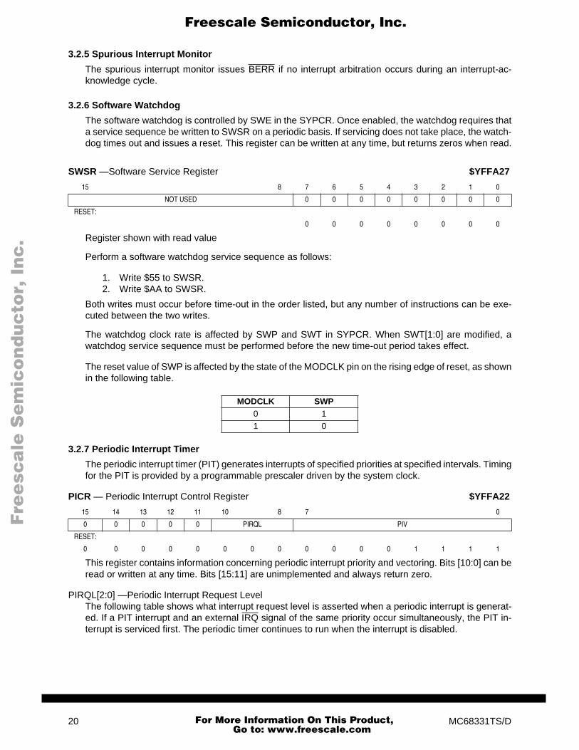
Perform a software watchdog service sequence as follows:
1. Write $55 to SWSR.2. Write $AA to SWSR.
Both writes must occur before time-out in the order listed, but any number of instructions can be exe-cuted between the two writes.
The watchdog clock rate is affected by SWP and SWT in SYPCR. When SWT[1:0] are modified, awatchdog service sequence must be performed before the new time-out period takes effect.
The reset value of SWP is affected by the state of the MODCLK pin on the rising edge of reset, as shownin the following table.
3.2.7 Periodic Interrupt Timer
The periodic interrupt timer (PIT) generates interrupts of specified priorities at specified intervals. Timingfor the PIT is provided by a programmable prescaler driven by the system clock.
This register contains information concerning periodic interrupt priority and vectoring. Bits [10:0] can beread or written at any time. Bits [15:11] are unimplemented and always return zero.
PIRQL[2:0] —Periodic Interrupt Request LevelThe following table shows what interrupt request level is asserted when a periodic interrupt is generat-ed. If a PIT interrupt and an external IRQ signal of the same priority occur simultaneously, the PIT in-terrupt is serviced first. The periodic timer continues to run when the interrupt is disabled.
SWSR —Software Service Register $YFFA27
15 8 7 6 5 4 3 2 1 0
NOT USED 0 0 0 0 0 0 0 0
RESET:
0 0 0 0 0 0 0 0
MODCLK SWP0 11 0
PICR — Periodic Interrupt Control Register $YFFA22
15 14 13 12 11 10 8 7 0
0 0 0 0 0 PIRQL PIV
RESET:
0 0 0 0 0 0 0 0 0 0 0 0 1 1 1 1
20 MC68331TS/D
For More Information On This Product, Go to: www.freescale.com

Fre
esc
ale
Se
mic
on
du
cto
r, I
Freescale Semiconductor, Inc.n
c..
.
PIV[7:0] —Periodic Interrupt VectorThe bits of this field contain the vector generated in response to an interrupt from the periodic timer.When the SIM responds, the periodic interrupt vector is placed on the bus.
The PITR contains the count value for the periodic timer. A zero value turns off the periodic timer. Thisregister can be read or written at any time.
PTP —Periodic Timer Prescaler Control0 = Periodic timer clock not prescaled1 = Periodic timer clock prescaled by a value of 512
The reset state of PTP is the complement of the state of the MODCLK signal during reset.
PITM[7:0] —Periodic Interrupt Timing Modulus FieldThis is an 8-bit timing modulus. The period of the timer can be calculated as follows:
PIT Period = [(PITM)(Prescaler)(4)]/EXTALwhere
PIT Period = Periodic interrupt timer periodPITM = Periodic interrupt timer register modulus (PITR[7:0])EXTAL Frequency = Crystal frequencyPrescale = 512 or 1 depending on the state of the PTP bit in the PITR
3.3 System Clock
The system clock in the SIM provides timing signals for the IMB modules and for an external peripheralbus. Because MCU operation is fully static, register and memory contents are not affected when theclock rate changes. System hardware and software support changes in the clock rate during operation.
The system clock signal can be generated in three ways. An internal phase-locked loop can synthesizethe clock from an internal or external frequency source, or the clock signal can be input from an externalsource.
Following is a block diagram of the clock submodule.
PIRQL Interrupt Request Level000 Periodic Interrupt Disabled001 Interrupt Request Level 1010 Interrupt Request Level 2011 Interrupt Request Level 3100 Interrupt Request Level 4101 Interrupt Request Level 5110 Interrupt Request Level 6111 Interrupt Request Level 7
PITR —Periodic Interrupt Timer Register $YFFA24
15 14 13 12 11 10 9 8 7 0
0 0 0 0 0 0 0 PTP PITM
RESET:
0 0 0 0 0 0 0 MODCLK 0 0 0 0 0 0 0 0
MC68331TS/D 21
For More Information On This Product, Go to: www.freescale.com

F
ree
sca
le S
em
ico
nd
uc
tor,
I
Freescale Semiconductor, Inc.n
c..
.
Figure 7 System Clock Block Diagram
3.3.1 Clock Sources
The state of the clock mode (MODCLK) pin during reset determines the clock source. When MODCLKis held high during reset, the clock synthesizer generates a clock signal from either a crystal oscillatoror an external reference input. Clock synthesizer control register SYNCR determines operating frequen-cy and various modes of operation. When MODCLK is held low during reset, the clock synthesizer isdisabled, and an external system clock signal must be applied. When the synthesizer is disabled, SYN-CR control bits have no effect.
A reference crystal must be connected between the EXTAL and XTAL pins to use the internal oscillator.Use of a 32.768-kHz crystal is recommended. These crystals are inexpensive and readily available. Ifan external reference signal or an external system clock signal is applied through the EXTAL pin, theXTAL pin must be left floating. External reference signal frequency must be less than or equal to max-imum specified reference frequency. External system clock signal frequency must be less than or equalto maximum specified system clock frequency.
When an external system clock signal is applied (i.e., the PLL is not used), duty cycle of the input iscritical, especially at near maximum operating frequencies. The relationship between clock signal dutycycle and clock signal period is expressed:
Minimum external clock period =
minimum external clock high/low time50% — percentage variation of external clock input duty cycle
SYS CLOCKBLOCK 32KHZ
CLKOUT
EXTAL
PHASECOMPARATOR
LOW-PASSFILTER VCO
CRYSTALOSCILLATOR
SYSTEMCLOCK
SYSTEM CLOCK CONTROL
XTAL XFC PIN VDDSYN
XFC
0.1µF 0.01µF
0.1µF
FEEDBACK DIVIDER
22 pF 22 pF
10M
330K
1. MUST BE LOW-LEAKAGE CAPACITOR (INSULATION RESISTANCE 30,000 MΩ OR GREATER).2. RESISTANCE AND CAPACITANCE BASED ON A TEST CIRCUIT CONSTRUCTED WITH A DAISHINKU DMX-38 32.768-kHz CRYSTAL. SPECIFIC COMPONENTS MUST BE BASED ON CRYSTAL TYPE. CONTACT CRYSTAL VENDOR FOR EXACT CIRCUIT.
VDDSYN2 2
W
X
Y
1
VSSI VSSI
VSSI
R3
R4
32.768 KHz
22 MC68331TS/D
For More Information On This Product, Go to: www.freescale.com
F
ree
sca
le S
em
ico
nd
uc
tor,
I
Freescale Semiconductor, Inc.n
c..
.
3.3.2 Clock Synthesizer Operation
A voltage controlled oscillator (VCO) generates the system clock signal. A portion of the clock signal isfed back to a divider/counter. The divider controls the frequency of one input to a phase comparator.The other phase comparator input is a reference signal, either from the internal oscillator or from anexternal source. The comparator generates a control signal proportional to the difference in phase be-tween its two inputs. The signal is low-pass filtered and used to correct VCO output frequency.
The synthesizer locks when VCO frequency is identical to reference frequency. Lock time is affected bythe filter time constant and by the amount of difference between the two comparator inputs. Whenevercomparator input changes, the synthesizer must re-lock. Lock status is shown by the SLOCK bit in SYN-CR.
The MCU does not come out of reset state until the synthesizer locks. Crystal type, characteristic fre-quency, and layout of external oscillator circuitry affect lock time.
The low-pass filter requires an external low-leakage capacitor, typically 0.1 µF, connected between theXFC and VDDSYN pins.
VDDSYN is used to power the clock circuits. A separate power source increases MCU noise immunityand can be used to run the clock when the MCU is powered down. Use a quiet power supply as theVDDSYN source, since PLL stability depends on the VCO, which uses this supply. Place adequate ex-ternal bypass capacitors as close as possible to the VDDSYN pin to ensure stable operating frequency.
When the clock synthesizer is used, control register SYNCR determines operating frequency and vari-ous modes of operation. SYNCR can be read only when the processor is operating at the supervisorprivilege level.
The SYNCR X bit controls a divide by two prescaler that is not in the synthesizer feedback loop. SettingX doubles clock speed without changing VCO speed. There is no VCO relock delay. The SYNCR W bitcontrols a 3-bit prescaler in the feedback divider. Setting W increases VCO speed by a factor of four.The SYNCR Y field determines the count modulus for a modulo 64 down counter, causing it to divideby a value of Y + 1. When either W or Y value changes, there is a VCO relock delay.
Clock frequency is determined by SYNCR bit settings as follows:
FSYSTEM = FREFERENCE [4(Y + 1)(22W +X)]
In order for the device to perform correctly, the clock frequency selected by the W, X, and Y bits mustbe within the limits specified for the MCU. The VCO frequency is twice the system clock frequency if X= 1 or four times the system clock frequency if X = 0.
The reset state of SYNCR ($3F00) produces a modulus-64 count.
3.3.3 Clock Control
The clock control circuits determine system clock frequency and clock operation under special circum-stances, such as following loss of synthesizer reference or during low-power operation. Clock source isdetermined by the logic state of the MODCLK pin during reset.
SYNCR —Clock Synthesizer Control Register $YFFA04
15 14 13 8 7 6 5 4 3 2 1 0
W X Y EDIV 0 0 SLIMP SLOCK RSTEN STSIM STEXT
RESET:
0 0 1 1 1 1 1 1 0 0 0 U U 0 0 0
MC68331TS/D 23
For More Information On This Product, Go to: www.freescale.com

F
ree
sca
le S
em
ico
nd
uc
tor,
I
Freescale Semiconductor, Inc.n
c..
.
When the on-chip clock synthesizer is used, system clock frequency is controlled by the bits in the upperbyte of SYNCR. Bits in the lower byte show status of or control operation of internal and external clocks.The SYNCR can be read or written only when the CPU is operating at the supervisor privilege level.
W —Frequency Control (VCO)This bit controls a prescaler tap in the synthesizer feedback loop. Setting the bit increases the VCOspeed by a factor of four. VCO relock delay is required.
X —Frequency Control Bit (Prescale)This bit controls a divide by two prescaler that is not in the synthesizer feedback loop. Setting the bitdoubles clock speed without changing the VCO speed. There is no VCO relock delay.
Y[5:0] —Frequency Control (Counter)The Y field controls the modulus down counter in the synthesizer feedback loop, causing it to divide bya value of Y + 1. Values range from 0 to 63. VCO relock delay is required.
EDIV —E Clock Divide Rate0 = ECLK frequency is system clock divided by 8.1 = ECLK frequency is system clock divided by 16.
ECLK is an external M6800 bus clock available on pin ADDR23. Refer to 3.5 Chip Selects for more in-formation.
SLIMP —Limp Mode Flag0 = External crystal is VCO reference.1 = Loss of crystal reference.
When the on-chip synthesizer is used, loss of reference frequency causes SLIMP to be set. The VCOcontinues to run using the base control voltage. Maximum limp frequency is maximum specified systemclock frequency. X-bit state affects limp frequency.
SLOCK —Synthesizer Lock Flag0 = VCO is enabled, but has not locked.1 = VCO has locked on the desired frequency (or system clock is external).
The MCU maintains reset state until the synthesizer locks, but SLOCK does not indicate synthesizerlock status until after the user writes to SYNCR.
RSTEN —Reset Enable0 = Loss of crystal causes the MCU to operate in limp mode. 1 = Loss of crystal causes system reset.
STSIM —Stop Mode SIM Clock0 = When LPSTOP is executed, the SIM clock is driven from the crystal oscillator and the VCO is
turned off to conserve power.1 = When LPSTOP is executed, the SIM clock is driven from the VCO.
STEXT —Stop Mode External Clock0 = When LPSTOP is executed, the CLKOUT signal is held negated to conserve power.1 = When LPSTOP is executed, the CLKOUT signal is driven from the SIM clock, as determined by
the state of the STSIM bit.
3.4 External Bus Interface
The external bus interface (EBI) transfers information between the internal MCU bus and external de-vices. The external bus has 24 address lines and 16 data lines.
The EBI provides dynamic sizing between 8-bit and 16-bit data accesses. It supports byte, word, andlong-word transfers. Ports are accessed through the use of asynchronous cycles controlled by the datatransfer (SIZ1 and SIZ0) and data size acknowledge pins (DSACK1 and DSACK0). Multiple bus cyclesmay be required for a transfer to or from an 8-bit port.
24 MC68331TS/D
For More Information On This Product, Go to: www.freescale.com

F
ree
sca
le S
em
ico
nd
uc
tor,
I
Freescale Semiconductor, Inc.n
c..
.
Port width is the maximum number of bits accepted or provided during a bus transfer. External devicesmust follow the handshake protocol described below. Control signals indicate the beginning of the cycle,the address space, the size of the transfer, and the type of cycle. The selected device controls the lengthof the cycle. Strobe signals, one for the address bus and another for the data bus, indicate the validityof an address and provide timing information for data. The EBI operates in an asynchronous mode forany port width.
To add flexibility and minimize the necessity for external logic, MCU chip-select logic can be synchro-nized with EBI transfers. Chip-select logic can also provide internally-generated bus control signals forthese accesses. Refer to 3.5 Chip Selects for more information.
3.4.1 Bus Control Signals
The CPU initiates a bus cycle by driving the address, size, function code, and read/write outputs. At thebeginning of the cycle, size signals SIZ0 and SIZ1 are driven along with the function code signals. Thesize signals indicate the number of bytes remaining to be transferred during an operand cycle. They arevalid while the address strobe (AS) is asserted. The following table shows SIZ0 and SIZ1 encoding. Theread/write (R/W) signal determines the direction of the transfer during a bus cycle. This signal changesstate, when required, at the beginning of a bus cycle, and is valid while AS is asserted. R/W only chang-es state when a write cycle is preceded by a read cycle or vice versa. The signal can remain low for twoconsecutive write cycles.
3.4.2 Function Codes
The CPU32 automatically generates function code signals FC[2:0]. The function codes can be consid-ered address extensions that automatically select one of eight address spaces to which an address ap-plies. These spaces are designated as either user or supervisor, and program or data spaces. Addressspace 7 is designated CPU space. CPU space is used for control information not normally associatedwith read or write bus cycles. Function codes are valid while AS is asserted.
3.4.3 Address Bus
Address bus signals ADDR[23:0] define the address of the most significant byte to be transferred duringa bus cycle. The MCU places the address on the bus at the beginning of a bus cycle. The address isvalid while AS is asserted.
Table 8 Size Signal Encoding
SIZ1 SIZ0 Transfer Size0 1 Byte1 0 Word1 1 Three Byte0 0 Long Word
Table 9 CPU32 Address Space Encoding
FC2 FC1 FC0 Address Space
0 0 0 Reserved
0 0 1 User Data Space
0 1 0 User Program Space
0 1 1 Reserved
1 0 0 Reserved
1 0 1 Supervisor Data Space
1 1 0 Supervisor Program Space
1 1 1 CPU Space
MC68331TS/D 25
For More Information On This Product, Go to: www.freescale.com
F
ree
sca
le S
em
ico
nd
uc
tor,
I
Freescale Semiconductor, Inc.n
c..
.
3.4.4 Address Strobe
AS is a timing signal that indicates the validity of an address on the address bus and the validity of manycontrol signals. It is asserted one-half clock after the beginning of a bus cycle.
3.4.5 Data Bus
Data bus signals DATA[15:0] make up a bidirectional, non-multiplexed parallel bus that transfers datato or from the MCU. A read or write operation can transfer 8 or 16 bits of data in one bus cycle. Duringa read cycle, the data is latched by the MCU on the last falling edge of the clock for that bus cycle. Fora write cycle, all 16 bits of the data bus are driven, regardless of the port width or operand size. TheMCU places the data on the data bus one-half clock cycle after AS is asserted in a write cycle.
3.4.6 Data Strobe
Data strobe (DS) is a timing signal. For a read cycle, the MCU asserts DS to signal an external deviceto place data on the bus. DS is asserted at the same time as AS during a read cycle. For a write cycle,DS signals an external device that data on the bus is valid. The MCU asserts DS one full clock cycleafter the assertion of AS during a write cycle.
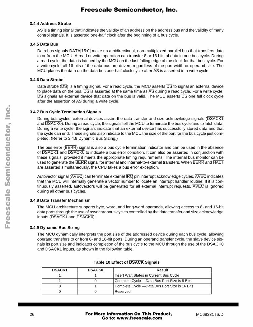
3.4.7 Bus Cycle Termination Signals
During bus cycles, external devices assert the data transfer and size acknowledge signals (DSACK1and DSACK0). During a read cycle, the signals tell the MCU to terminate the bus cycle and to latch data.During a write cycle, the signals indicate that an external device has successfully stored data and thatthe cycle can end. These signals also indicate to the MCU the size of the port for the bus cycle just com-pleted. (Refer to 3.4.9 Dynamic Bus Sizing.)
The bus error (BERR) signal is also a bus cycle termination indicator and can be used in the absenceof DSACK1 and DSACK0 to indicate a bus error condition. It can also be asserted in conjunction withthese signals, provided it meets the appropriate timing requirements. The internal bus monitor can beused to generate the BERR signal for internal and internal-to-external transfers. When BERR and HALTare asserted simultaneously, the CPU takes a bus error exception.
Autovector signal (AVEC) can terminate external IRQ pin interrupt acknowledge cycles. AVEC indicatesthat the MCU will internally generate a vector number to locate an interrupt handler routine. If it is con-tinuously asserted, autovectors will be generated for all external interrupt requests. AVEC is ignoredduring all other bus cycles.
3.4.8 Data Transfer Mechanism
The MCU architecture supports byte, word, and long-word operands, allowing access to 8- and 16-bitdata ports through the use of asynchronous cycles controlled by the data transfer and size acknowledgeinputs (DSACK1 and DSACK0).
3.4.9 Dynamic Bus Sizing
The MCU dynamically interprets the port size of the addressed device during each bus cycle, allowingoperand transfers to or from 8- and 16-bit ports. During an operand transfer cycle, the slave device sig-nals its port size and indicates completion of the bus cycle to the MCU through the use of the DSACK0and DSACK1 inputs, as shown in the following table.
Table 10 Effect of DSACK Signals
DSACK1 DSACK0 Result1 1 Insert Wait States in Current Bus Cycle1 0 Complete Cycle —Data Bus Port Size is 8 Bits0 1 Complete Cycle —Data Bus Port Size is 16 Bits0 0 Reserved
26 MC68331TS/D
For More Information On This Product, Go to: www.freescale.com
F
ree
sca
le S
em
ico
nd
uc
tor,
I
Freescale Semiconductor, Inc.n
c..
.
For example, if the MCU is executing an instruction that reads a long-word operand from a 16-bit port,the MCU latches the 16 bits of valid data and then runs another bus cycle to obtain the other 16 bits.The operation for an 8-bit port is similar, but requires four read cycles. The addressed device uses theDSACK0 and DSACK1 signals to indicate the port width. For instance, a 16-bit device always returnsDSACK0 = 1 and DSACK1 = 0 for a 16-bit port, regardless of whether the bus cycle is a byte or wordoperation.
Dynamic bus sizing requires that the portion of the data bus used for a transfer to or from a particularport size be fixed. A 16-bit port must reside on data bus bits [15:0] and an 8-bit port must reside on databus bits [15:8]. This minimizes the number of bus cycles needed to transfer data and ensures that theMCU transfers valid data.
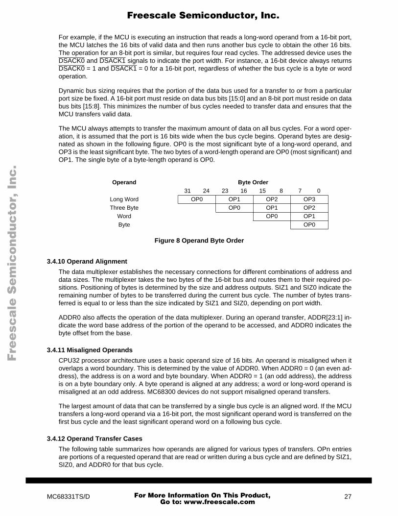
The MCU always attempts to transfer the maximum amount of data on all bus cycles. For a word oper-ation, it is assumed that the port is 16 bits wide when the bus cycle begins. Operand bytes are desig-nated as shown in the following figure. OP0 is the most significant byte of a long-word operand, andOP3 is the least significant byte. The two bytes of a word-length operand are OP0 (most significant) andOP1. The single byte of a byte-length operand is OP0.
Figure 8 Operand Byte Order
3.4.10 Operand Alignment
The data multiplexer establishes the necessary connections for different combinations of address anddata sizes. The multiplexer takes the two bytes of the 16-bit bus and routes them to their required po-sitions. Positioning of bytes is determined by the size and address outputs. SIZ1 and SIZ0 indicate theremaining number of bytes to be transferred during the current bus cycle. The number of bytes trans-ferred is equal to or less than the size indicated by SIZ1 and SIZ0, depending on port width.
ADDR0 also affects the operation of the data multiplexer. During an operand transfer, ADDR[23:1] in-dicate the word base address of the portion of the operand to be accessed, and ADDR0 indicates thebyte offset from the base.
3.4.11 Misaligned Operands
CPU32 processor architecture uses a basic operand size of 16 bits. An operand is misaligned when itoverlaps a word boundary. This is determined by the value of ADDR0. When ADDR0 = 0 (an even ad-dress), the address is on a word and byte boundary. When ADDR0 = 1 (an odd address), the addressis on a byte boundary only. A byte operand is aligned at any address; a word or long-word operand ismisaligned at an odd address. MC68300 devices do not support misaligned operand transfers.
The largest amount of data that can be transferred by a single bus cycle is an aligned word. If the MCUtransfers a long-word operand via a 16-bit port, the most significant operand word is transferred on thefirst bus cycle and the least significant operand word on a following bus cycle.
3.4.12 Operand Transfer Cases
The following table summarizes how operands are aligned for various types of transfers. OPn entriesare portions of a requested operand that are read or written during a bus cycle and are defined by SIZ1,SIZ0, and ADDR0 for that bus cycle.
Operand Byte Order31 24 23 16 15 8 7 0
Long Word OP0 OP1 OP2 OP3Three Byte OP0 OP1 OP2
Word OP0 OP1Byte OP0
MC68331TS/D 27
For More Information On This Product, Go to: www.freescale.com

F
ree
sca
le S
em
ico
nd
uc
tor,
I
Freescale Semiconductor, Inc.n
c..
.
NOTES:1. Operands in parentheses are ignored by the CPU32 during read cycles.2. Three-byte transfer cases occur only as a result of a long word to byte transfer.3. The CPU32 does not support misaligned word or long-word transfers.
3.5 Chip Selects
Typical microcontrollers require additional hardware to provide external chip-select signals. Twelve in-dependently programmable chip selects provide fast two-cycle access to external memory or peripher-als. Address block sizes of 2 Kbytes to 1 Mbyte can be selected.
Chip-select assertion can be synchronized with bus control signals to provide output enable, read/writestrobes, or interrupt acknowledge signals. Logic can also generate DSACK signals internally. A singleDSACK generator is shared by all circuits. Multiple chip selects assigned to the same address and con-trol must have the same number of wait states.
Chip selects can also be synchronized with the ECLK signal available on ADDR23.
When a memory access occurs, chip-select logic compares address space type, address, type of ac-cess, transfer size, and interrupt priority (in the case of interrupt acknowledge) to parameters stored inchip-select registers. If all parameters match, the appropriate chip-select signal is asserted. Select sig-nals are active low. Refer to the following block diagram of a single chip-select circuit.
Table 11 Operand Alignment
Transfer Case SIZ1 SIZ0 ADDR0 DSACK1 DSACK0 DATA[15:8]
DATA[7:0]
Byte to 8-Bit Port (Even/Odd) 0 1 X 1 0 OP0 (OP0)Byte to 16-Bit Port (Even) 0 1 0 0 X OP0 (OP0)Byte to 16-Bit Port (Odd) 0 1 1 0 X (OP0) OP0Word to 8-Bit Port (Aligned) 1 0 0 1 0 OP0 (OP1)
Word to 8-Bit Port (Misaligned)3 1 0 1 1 0 OP0 (OP0)
Word to 16-Bit Port (Aligned) 1 0 0 0 X OP0 OP1
Word to 16-Bit Port (Misaligned)3 1 0 1 0 X (OP0) OP0
3 Byte to 8-Bit Port (Aligned)2 1 1 0 1 0 OP0 (OP1)
3 Byte to 8-Bit Port (Misaligned)2, 3 1 1 1 1 0 OP0 (OP0)
3 Byte to 16-Bit Port (Aligned)2 1 1 0 0 X OP0 OP1
3 Byte to 16-Bit Port (Misaligned)2, 3 1 1 1 0 X (OP0) OP0
Long Word to 8-Bit Port (Aligned) 0 0 0 1 0 OP0 (OP1)
Long Word to 8-Bit Port (Misaligned)3 1 0 1 1 0 OP0 (OP0)
Long Word to 16-Bit Port (Aligned) 0 0 0 0 X OP0 OP1
Long Word to 16-Bit Port (Misaligned)3 1 0 1 0 X (OP0) OP0
28 MC68331TS/D
For More Information On This Product, Go to: www.freescale.com

F
ree
sca
le S
em
ico
nd
uc
tor,
I
Freescale Semiconductor, Inc.n
c..
.
Figure 9 Chip-Select Circuit Block Diagram
The following table lists allocation of chip-selects and discrete outputs on the pins of the MCU.
3.5.1 Chip-Select Registers
Pin assignment registers CSPAR0 and CSPAR1 determine functions of chip-select pins. These regis-ters also determine port size (8- or 16-bit) for dynamic bus allocation.
A pin data register (PORTC) latches discrete output data.
Blocks of addresses are assigned to each chip-select function. Block sizes of 2 Kbytes to 1 Mbyte canbe selected by writing values to the appropriate base address register (CSBAR). Address blocks forseparate chip-select functions can overlap.
Chip-select option registers (CSORBT and CSOR[10:0]) determine timing of and conditions for asser-tion of chip-select signals. Eight parameters, including operating mode, access size, synchronization,and wait state insertion can be specified.
Initialization code often resides in a peripheral memory device controlled by the chip-select circuits. Aset of special chip-select functions and registers (CSORBT, CSBARBT) is provided to support bootstrapoperation.
Pin Chip Select Discrete OutputsCSBOOT CSBOOT —
BR CS0 —BG CS1 —
BGACK CS2 —FC0 CS3 PC0FC1 CS4 PC1FC2 CS5 PC2
ADDR19 CS6 PC3ADDR20 CS7 PC4ADDR21 CS8 PC5ADDR22 CS9 PC6ADDR23 CS10 ECLK
CHIP SEL BLOCK
AVECGENERATOR
DSACKGENERATOR
PIN ASSIGNMENT
REGISTER
PIN DATA
REGISTER
BASE ADDRESS REGISTER
TIMING AND
CONTROL
ADDRESS COMPARATOR
OPTION COMPARE
OPTION REGISTER
AVEC
DSACK
PIN
BUS CONTROL
INTERNALSIGNALS
ADDRESS
MC68331TS/D 29
For More Information On This Product, Go to: www.freescale.com
F
ree
sca
le S
em
ico
nd
uc
tor,
I
Freescale Semiconductor, Inc.n
c..
.
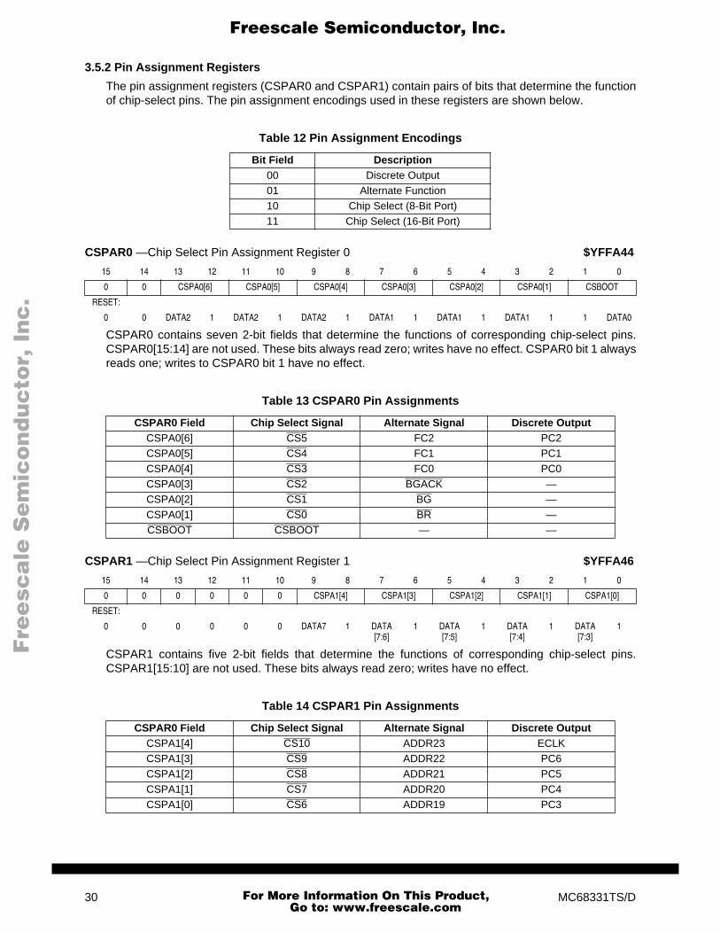
3.5.2 Pin Assignment Registers
The pin assignment registers (CSPAR0 and CSPAR1) contain pairs of bits that determine the functionof chip-select pins. The pin assignment encodings used in these registers are shown below.
CSPAR0 contains seven 2-bit fields that determine the functions of corresponding chip-select pins.CSPAR0[15:14] are not used. These bits always read zero; writes have no effect. CSPAR0 bit 1 alwaysreads one; writes to CSPAR0 bit 1 have no effect.
CSPAR1 contains five 2-bit fields that determine the functions of corresponding chip-select pins.CSPAR1[15:10] are not used. These bits always read zero; writes have no effect.
Table 12 Pin Assignment Encodings
Bit Field Description00 Discrete Output 01 Alternate Function10 Chip Select (8-Bit Port)11 Chip Select (16-Bit Port)
CSPAR0 —Chip Select Pin Assignment Register 0 $YFFA44
15 14 13 12 11 10 9 8 7 6 5 4 3 2 1 0
0 0 CSPA0[6] CSPA0[5] CSPA0[4] CSPA0[3] CSPA0[2] CSPA0[1] CSBOOT
RESET:
0 0 DATA2 1 DATA2 1 DATA2 1 DATA1 1 DATA1 1 DATA1 1 1 DATA0
Table 13 CSPAR0 Pin Assignments
CSPAR0 Field Chip Select Signal Alternate Signal Discrete OutputCSPA0[6] CS5 FC2 PC2CSPA0[5] CS4 FC1 PC1CSPA0[4] CS3 FC0 PC0CSPA0[3] CS2 BGACK —CSPA0[2] CS1 BG —CSPA0[1] CS0 BR —CSBOOT CSBOOT — —
CSPAR1 —Chip Select Pin Assignment Register 1 $YFFA46
15 14 13 12 11 10 9 8 7 6 5 4 3 2 1 0
0 0 0 0 0 0 CSPA1[4] CSPA1[3] CSPA1[2] CSPA1[1] CSPA1[0]
RESET:
0 0 0 0 0 0 DATA7 1 DATA[7:6]
1 DATA[7:5]
1 DATA[7:4]
1 DATA[7:3]
1
Table 14 CSPAR1 Pin Assignments
CSPAR0 Field Chip Select Signal Alternate Signal Discrete OutputCSPA1[4] CS10 ADDR23 ECLKCSPA1[3] CS9 ADDR22 PC6CSPA1[2] CS8 ADDR21 PC5CSPA1[1] CS7 ADDR20 PC4CSPA1[0] CS6 ADDR19 PC3
30 MC68331TS/D
For More Information On This Product, Go to: www.freescale.com

F
ree
sca
le S
em
ico
nd
uc
tor,
I
Freescale Semiconductor, Inc.n
c..
.
At reset, either the alternate function (01) or chip-select function (11) can be encoded. DATA pins aredriven to logic level one by a weak internal pull-up during reset. Encoding is for chip-select function un-less a data line is held low during reset. Note that bus loading can overcome the weak pull-up and holdpins low during reset. The following table shows the hierarchical selection method that determines thereset functions of pins controlled by CSPAR1.
A pin programmed as a discrete output drives an external signal to the value specified in the port C pindata register (PORTC), with the following exceptions:
A. No discrete output function is available on pins BR, BG, or BGACK. B. ADDR23 provides E-clock output rather than a discrete output signal.
When a pin is programmed for discrete output or alternate function, internal chip-select logic still func-tions and can be used to generate DSACK or AVEC internally on an address match.
Port size is determined when a pin is assigned as a chip select. When a pin is assigned to an 8-bit port,the chip select is asserted at all addresses within the block range. If a pin is assigned to a 16-bit port,the upper/lower byte field of the option register selects the byte with which the chip select is associated.
3.5.3 Base Address Registers
A base address is the starting address for the block enabled by a given chip select. Block size deter-mines the extent of the block above the base address. Each chip select has an associated base registerso that an efficient address map can be constructed for each application. If a chip-select base addressregister is programmed with the same address as a microcontroller module or memory array, an accessto that address goes to the module or array and the chip-select signal is not asserted.
BLKSZ —Block Size FieldThis field determines the size of the block that must be enabled by the chip select. The following tableshows bit encoding for the base address registers block size field.
Table 15 Reset Pin Function of CS[10:6]
Data Bus Pins at Reset Chip-Select/Address Bus Pin FunctionDATA7 DATA6 DATA5 DATA4 DATA3 CS10/
ADDR23CS9/
ADDR22CS8/
ADDR21CS7/
ADDR20CS6/
ADDR191 1 1 1 1 CS10 CS9 CS8 CS7 CS61 1 1 1 0 CS10 CS9 CS8 CS7 ADDR191 1 1 0 X CS10 CS9 CS8 ADDR20 ADDR191 1 0 X X CS10 CS9 ADDR21 ADDR20 ADDR191 0 X X X CS10 ADDR22 ADDR21 ADDR20 ADDR190 X X X X ADDR23 ADDR22 ADDR21 ADDR20 ADDR19
CSBARBT — Chip-Select Base Address Register Boot ROM $YFFA48
15 14 13 12 11 10 9 8 7 6 5 4 3 2 0
ADDR23
ADDR22
ADDR21
ADDR20
ADDR19
ADDR18
ADDR17
ADDR16
ADDR15
ADDR14
ADDR13
ADDR12
ADDR11
BLKSZ
RESET:
0 0 0 0 0 0 0 0 0 0 0 0 0 1 1 1
CSBAR[10:0] —Chip-Select Base Address Registers $YFFA4C–$YFFA74
15 14 13 12 11 10 9 8 7 6 5 4 3 2 0
ADDR23
ADDR22
ADDR21
ADDR20
ADDR19
ADDR18
ADDR17
ADDR16
ADDR15
ADDR14
ADDR13
ADDR12
ADDR11
BLKSZ
RESET:
0 0 0 0 0 0 0 0 0 0 0 0 0 0 0 0
MC68331TS/D 31
For More Information On This Product, Go to: www.freescale.com

F
ree
sca
le S
em
ico
nd
uc
tor,
I
Freescale Semiconductor, Inc.n
c..
.
ADDR[23:11] —Base Address FieldThis field sets the starting address of a particular address space. The address compare logic uses onlythe most significant bits to match an address within a block. The value of the base address must be amultiple of block size. Base address register diagrams show how base register bits correspond to ad-dress lines.
3.5.4 Option Registers
The option registers contain eight fields that determine timing of and conditions for assertion of chip-select signals. For a chip-select signal to be asserted, all bits in the base address register must matchthe corresponding internal upper address lines, and all conditions specified in the option register mustbe satisfied. These conditions also apply to providing DSACK or autovector support.
CSORBT, the option register for CSBOOT, contains special reset values that support bootstrap opera-tions from peripheral memory devices.
The following bit descriptions apply to both CSORBT and CSOR[10:0] option registers.
MODE —Asynchronous/Synchronous Mode0 = Asynchronous mode selected (chip-select assertion determined by internal or external bus con-
trol signals)1 = Synchronous mode selected (chip-select assertion synchronized with ECLK signal)
In asynchronous mode, the chip select is asserted synchronized with AS or DS.The DSACK field is not used in synchronous mode because a bus cycle is only performed as a syn-chronous operation. When a match condition occurs on a chip select programmed for synchronous op-eration, the chip select signals the EBI that an ECLK cycle is pending.
BYTE —Upper/Lower Byte OptionThis field is used only when the chip-select 16-bit port option is selected in the pin assignment register.The following table lists upper/lower byte options.
Block Size Field Block Size Address Lines Compared000 2 K ADDR[23:11]001 8 K ADDR[23:13]010 16 K ADDR[23:14]011 64 K ADDR[23:16]100 128 K ADDR[23:17]101 256 K ADDR[23:18]110 512 K ADDR[23:19]111 1 M ADDR[23:20]
CSORBT —Chip-Select Option Register Boot ROM $YFFA4A
15 14 13 12 11 10 9 6 5 4 3 1 0
MODE BYTE R/W STRB DSACK SPACE IPL AVEC
RESET:
0 1 1 1 1 0 1 1 0 1 1 1 0 0 0 0
CSOR[10:0] —Chip-Select Option Registers $YFFA4E–$YFFA76
15 14 13 12 11 10 9 6 5 4 3 1 0
MODE BYTE R/W STRB DSACK SPACE IPL AVEC
RESET:
0 0 0 0 0 0 0 0 0 0 0 0 0 0 0 0
32 MC68331TS/D
For More Information On This Product, Go to: www.freescale.com
F
ree
sca
le S
em
ico
nd
uc
tor,
I
Freescale Semiconductor, Inc.n
c..
.
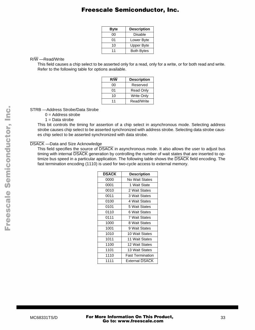
R/W —Read/WriteThis field causes a chip select to be asserted only for a read, only for a write, or for both read and write.Refer to the following table for options available.
STRB —Address Strobe/Data Strobe0 = Address strobe1 = Data strobe
This bit controls the timing for assertion of a chip select in asynchronous mode. Selecting addressstrobe causes chip select to be asserted synchronized with address strobe. Selecting data strobe caus-es chip select to be asserted synchronized with data strobe.
DSACK —Data and Size AcknowledgeThis field specifies the source of DSACK in asynchronous mode. It also allows the user to adjust bustiming with internal DSACK generation by controlling the number of wait states that are inserted to op-timize bus speed in a particular application. The following table shows the DSACK field encoding. Thefast termination encoding (1110) is used for two-cycle access to external memory.
Byte Description00 Disable01 Lower Byte10 Upper Byte11 Both Bytes
R/W Description00 Reserved01 Read Only10 Write Only11 Read/Write
DSACK Description0000 No Wait States0001 1 Wait State0010 2 Wait States0011 3 Wait States0100 4 Wait States0101 5 Wait States0110 6 Wait States0111 7 Wait States1000 8 Wait States1001 9 Wait States1010 10 Wait States1011 11 Wait States1100 12 Wait States1101 13 Wait States1110 Fast Termination1111 External DSACK
MC68331TS/D 33
For More Information On This Product, Go to: www.freescale.com

F
ree
sca
le S
em
ico
nd
uc
tor,
I
Freescale Semiconductor, Inc.n
c..
.
SPACE —Address SpaceUse this option field to select an address space for the chip-select logic. The CPU32 normally operatesin supervisor or user space, but interrupt acknowledge cycles must take place in CPU space.
IPL —Interrupt Priority LevelIf the space field is set for CPU space (00), chip-select logic can be used for interrupt acknowledge.During an interrupt acknowledge cycle, the priority level on address lines ADDR[3:1] is compared to thevalue in the IPL field. If the values are the same, a chip select is asserted, provided that other optionregister conditions are met. The following table shows IPL field encoding.
This field only affects the response of chip selects and does not affect interrupt recognition by the CPU.Any level means that chip select is asserted regardless of the level of the interrupt acknowledge cycle.
AVEC —Autovector Enable0 = External interrupt vector enabled1 = Autovector enabled
This field selects one of two methods of acquiring the interrupt vector during the interrupt acknowledgecycle. It is not usually used in conjunction with a chip-select pin.
If the chip select is configured to trigger on an interrupt acknowledge cycle (SPACE = 00) and the AVECfield is set to one, the chip select automatically generates an AVEC in response to the interrupt cycle.Otherwise, the vector must be supplied by the requesting device.
The AVEC bit must not be used in synchronous mode, as autovector response timing can vary becauseof ECLK synchronization.
3.5.5 Port C Data Register
Bit values in port C determine the state of chip-select pins used for discrete output. When a pin is as-signed as a discrete output, the value in this register appears at the output. This is a read/write register.Bit 7 is not used. Writing to this bit has no effect, and it always returns zero when read.
Space Field Address Space00 CPU Space01 User Space10 Supervisor Space11 Supervisor/User Space
IPL Description000 Any Level001 IPL1010 IPL2011 IPL3100 IPL4101 IPL5110 IPL6111 IPL7
PORTC — Port C Data Register $YFFA41
15 8 7 6 5 4 3 2 1 0
NOT USED 0 PC6 PC5 PC4 PC3 PC2 PC1 PC0
RESET:
0 1 1 1 1 1 1 1
34 MC68331TS/D
For More Information On This Product, Go to: www.freescale.com
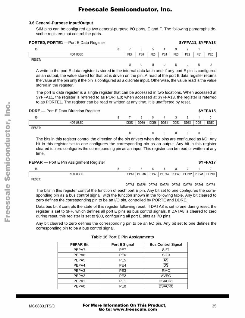
F
ree
sca
le S
em
ico
nd
uc
tor,
I
Freescale Semiconductor, Inc.n
c..
.
3.6 General-Purpose Input/Output
SIM pins can be configured as two general-purpose I/O ports, E and F. The following paragraphs de-scribe registers that control the ports.
A write to the port E data register is stored in the internal data latch and, if any port E pin is configuredas an output, the value stored for that bit is driven on the pin. A read of the port E data register returnsthe value at the pin only if the pin is configured as a discrete input. Otherwise, the value read is the valuestored in the register.
The port E data register is a single register that can be accessed in two locations. When accessed at$YFFA11, the register is referred to as PORTE0; when accessed at $YFFA13, the register is referredto as PORTE1. The register can be read or written at any time. It is unaffected by reset.
The bits in this register control the direction of the pin drivers when the pins are configured as I/O. Anybit in this register set to one configures the corresponding pin as an output. Any bit in this registercleared to zero configures the corresponding pin as an input. This register can be read or written at anytime.
The bits in this register control the function of each port E pin. Any bit set to one configures the corre-sponding pin as a bus control signal, with the function shown in the following table. Any bit cleared tozero defines the corresponding pin to be an I/O pin, controlled by PORTE and DDRE.
Data bus bit 8 controls the state of this register following reset. If DATA8 is set to one during reset, theregister is set to $FF, which defines all port E pins as bus control signals. If DATA8 is cleared to zeroduring reset, this register is set to $00, configuring all port E pins as I/O pins.
Any bit cleared to zero defines the corresponding pin to be an I/O pin. Any bit set to one defines thecorresponding pin to be a bus control signal.
PORTE0, PORTE1 —Port E Data Register $YFFA11, $YFFA13
15 8 7 6 5 4 3 2 1 0
NOT USED PE7 PE6 PE5 PE4 PE3 PE2 PE1 PE0
RESET:
U U U U U U U U
DDRE — Port E Data Direction Register $YFFA15
15 8 7 6 5 4 3 2 1 0
NOT USED DDE7 DDE6 DDE5 DDE4 DDE3 DDE2 DDE1 DDE0
RESET:
0 0 0 0 0 0 0 0
PEPAR — Port E Pin Assignment Register $YFFA17
15 8 7 6 5 4 3 2 1 0
NOT USED PEPA7 PEPA6 PEPA5 PEPA4 PEPA3 PEPA2 PEPA1 PEPA0
RESET:
DATA8 DATA8 DATA8 DATA8 DATA8 DATA8 DATA8 DATA8
Table 16 Port E Pin Assignments
PEPAR Bit Port E Signal Bus Control SignalPEPA7 PE7 SIZ1PEPA6 PE6 SIZ0PEPA5 PE5 AS
PEPA4 PE4 DSPEPA3 PE3 RMCPEPA2 PE2 AVECPEPA1 PE1 DSACK1PEPA0 PE0 DSACK0
MC68331TS/D 35
For More Information On This Product, Go to: www.freescale.com
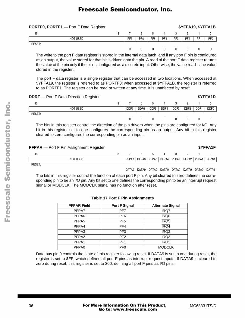
F
ree
sca
le S
em
ico
nd
uc
tor,
I
Freescale Semiconductor, Inc.n
c..
.
The write to the port F data register is stored in the internal data latch, and if any port F pin is configuredas an output, the value stored for that bit is driven onto the pin. A read of the port F data register returnsthe value at the pin only if the pin is configured as a discrete input. Otherwise, the value read is the valuestored in the register.
The port F data register is a single register that can be accessed in two locations. When accessed at$YFFA19, the register is referred to as PORTF0; when accessed at $YFFA1B, the register is referredto as PORTF1. The register can be read or written at any time. It is unaffected by reset.
The bits in this register control the direction of the pin drivers when the pins are configured for I/O. Anybit in this register set to one configures the corresponding pin as an output. Any bit in this registercleared to zero configures the corresponding pin as an input.
The bits in this register control the function of each port F pin. Any bit cleared to zero defines the corre-sponding pin to be an I/O pin. Any bit set to one defines the corresponding pin to be an interrupt requestsignal or MODCLK. The MODCLK signal has no function after reset.
Data bus pin 9 controls the state of this register following reset. If DATA9 is set to one during reset, theregister is set to $FF, which defines all port F pins as interrupt request inputs. If DATA9 is cleared tozero during reset, this register is set to $00, defining all port F pins as I/O pins.
PORTF0, PORTF1 — Port F Data Register $YFFA19, $YFFA1B
15 8 7 6 5 4 3 2 1 0
NOT USED PF7 PF6 PF5 PF4 PF3 PF2 PF1 PF0
RESET:
U U U U U U U U
DDRF — Port F Data Direction Register $YFFA1D
15 8 7 6 5 4 3 2 1 0
NOT USED DDF7 DDF6 DDF5 DDF4 DDF3 DDF2 DDF1 DDF0
RESET:
0 0 0 0 0 0 0 0
PFPAR — Port F Pin Assignment Register $YFFA1F
15 8 7 6 5 4 3 2 1 0
NOT USED PFPA7 PFPA6 PFPA5 PFPA4 PFPA3 PFPA2 PFPA1 PFPA0
RESET:
DATA9 DATA9 DATA9 DATA9 DATA9 DATA9 DATA9 DATA9
Table 17 Port F Pin Assignments
PFPAR Field Port F Signal Alternate SignalPFPA7 PF7 IRQ7PFPA6 PF6 IRQ6PFPA5 PF5 IRQ5PFPA4 PF4 IRQ4PFPA3 PF3 IRQ3PFPA2 PF2 IRQ2PFPA1 PF1 IRQ1PFPA0 PF0 MODCLK
36 MC68331TS/D
For More Information On This Product, Go to: www.freescale.com

F
ree
sca
le S
em
ico
nd
uc
tor,
I
Freescale Semiconductor, Inc.n
c..
.
3.7 Resets
Reset procedures handle system initialization and recovery from catastrophic failure. The MCU per-forms resets with a combination of hardware and software. The system integration module determineswhether a reset is valid, asserts control signals, performs basic system configuration based on hard-ware mode-select inputs, then passes control to the CPU.
Reset occurs when an active low logic level on the RESET pin is clocked into the SIM. Resets are gatedby the CLKOUT signal. Asynchronous resets are assumed to be catastrophic. An asynchronous resetcan occur on any clock edge. Synchronous resets are timed to occur at the end of bus cycles. If thereis no clock when RESET is asserted, reset does not occur until the clock starts. Resets are clocked inorder to allow completion of write cycles in progress at the time RESET is asserted.
Reset is the highest-priority CPU32 exception. Any processing in progress is aborted by the reset ex-ception, and cannot be restarted. Only essential tasks are performed during reset exception processing.Other initialization tasks must be accomplished by the exception handler routine.
3.7.1 SIM Reset Mode Selection
The logic states of certain data bus pins during reset determine SIM operating configuration. In addition,the state of the MODCLK pin determines system clock source and the state of the BKPT pin determineswhat happens during subsequent breakpoint assertions. The following table is a summary of resetmode selection options.
3.7.2 Functions of Pins for Other Modules During Reset
Generally, pins associated with modules other than the SIM default to port functions, and input/outputports are set to input state. This is accomplished by disabling pin functions in the appropriate controlregisters, and by clearing the appropriate port data direction registers. Refer to individual module sec-tions in this manual for more information. The following table is a summary of module pin function outof reset.
Table 18 Reset Mode Selection
Mode Select Pin Default Function(Pin Left High)
Alternate Function(Pin Pulled Low)
DATA0 CSBOOT 16-Bit CSBOOT 8-BitDATA1 CS0
CS1CS2
BRBG
BGACKDATA2 CS3
CS4CS5
FC0FC1FC2
DATA3DATA4DATA5DATA6DATA7
CS6CS[7:6]CS[8:6]CS[9:6]
CS[10:6]
ADDR19ADDR[20:19]ADDR[21:19]ADDR[22:19]ADDR[23:19]
DATA8 DSACK0, DSACK1,AVEC, DS, AS,
SIZ[1:0]
PORTE
DATA9 IRQ[7:1]MODCLK
PORTF
DATA11 Test Mode Disabled Test Mode EnabledMODCLK VCO = System Clock EXTAL = System Clock
BKPT Background Mode Disabled Background Mode Enabled
MC68331TS/D 37
For More Information On This Product, Go to: www.freescale.com
F
ree
sca
le S
em
ico
nd
uc
tor,
I
Freescale Semiconductor, Inc.n
c..
.
3.7.3 Reset Timing
The RESET input must be asserted for a specified minimum period in order for reset to occur. ExternalRESET assertion can be delayed internally for a period equal to the longest bus cycle time (or the busmonitor time-out period) in order to protect write cycles from being aborted by reset. While RESET isasserted, SIM pins are either in a disabled high-impedance state or are driven to their inactive states.
When an external device asserts RESET for the proper period, reset control logic clocks the signal intoan internal latch. The control logic drives the RESET pin low for an additional 512 CLKOUT cycles afterit detects that the RESET signal is no longer being externally driven, to guarantee this length of resetto the entire system.
If an internal source asserts a reset signal, the reset control logic asserts RESET for a minimum of 512cycles. If the reset signal is still asserted at the end of 512 cycles, the control logic continues to assertRESET until the internal reset signal is negated.
After 512 cycles have elapsed, the reset input pin goes to an inactive, high-impedance state for 10 cy-cles. At the end of this 10-cycle period, the reset input is tested. When the input is at logic level one,reset exception processing begins. If, however, the reset input is at logic level zero, the reset controllogic drives the pin low for another 512 cycles. At the end of this period, the pin again goes to high-impedance state for 10 cycles, then it is tested again. The process repeats until RESET is released.
3.7.4 Power-On Reset
When the SIM clock synthesizer is used to generate the system clock, power-on reset involves specialcircumstances related to application of system and clock synthesizer power. Regardless of clocksource, voltage must be applied to clock synthesizer power input pin VDDSYN in order for the MCU tooperate. The following discussion assumes that VDDSYN is applied before and during reset. This mini-mizes crystal start-up time. When VDDSYN is applied at power-on, start-up time is affected by specificcrystal parameters and by oscillator circuit design. VDD ramp-up time also affects pin state during reset.
During power-on reset, an internal circuit in the SIM drives the internal (IMB) and external reset lines.The circuit releases the internal reset line as VDD ramps up to the minimum specified value, and SIMpins are initialized. When VDD reaches the specified minimum value, the clock synthesizer VCO beginsoperation. Clock frequency ramps up to the specified limp mode frequency. The external RESET lineremains asserted until the clock synthesizer PLL locks and 512 CLKOUT cycles elapse.
Table 19 Module Pin Functions
Module Pin Mnemonic FunctionCPU32 DSI/IFETCH DSI/IFETCH
DSO/IPIPE DSO/IPIPEBKPT/DSCLK BKPT/DSCLK
GPT PGP7/IC4/OC5 Discrete InputPGP[6:3]/OC[4:1] Discrete InputPGP[2:0]/IC[3:1] Discrete Input
PAI Discrete InputPCLK Discrete Input
PWMA, PWMB Discrete OutputQSM PQS7/TXD Discrete Input
PQS[6:4]/PCS[3:1] Discrete InputPQS3/PCS0/SS Discrete Input
PQS2/SCK Discrete InputPQS1/MOSI Discrete InputPQS0/MISO Discrete Input
RXD RXD
38 MC68331TS/D
For More Information On This Product, Go to: www.freescale.com
F
ree
sca
le S
em
ico
nd
uc
tor,
I
Freescale Semiconductor, Inc.n
c..
.
The SIM clock synthesizer provides clock signals to the other MCU modules. After the clock is runningand the internal reset signal is asserted for four clock cycles, these modules reset. VDD ramp time andVCO frequency ramp time determine how long these four cycles take. Worst case is approximately 15milliseconds. During this period, module port pins may be in an indeterminate state. While input-onlypins can be put in a known state by means of external pull-up resistors, external logic on input/outputor output-only pins must condition the lines during this time. Active drivers require high-impedance buff-ers or isolation resistors to prevent conflict.
3.7.5 Use of Three State Control Pin
Asserting the three-state control (TSC) input causes the MCU to put all output drivers in an inactive,high-impedance state. The signal must remain asserted for 10 clock cycles in order for drivers tochange state. There are certain constraints on use of TSC during power-on reset:
When the internal clock synthesizer is used (MODCLK held high during reset), synthesizer ramp-up time affects how long the 10 cycles take. Worst case is approximately 20 milliseconds from TSCassertion.
When an external clock signal is applied (MODCLK held low during reset), pins go to high-imped-ance state as soon after TSC assertion as 10 clock pulses have been applied to the EXTAL pin.
When TSC assertion takes effect, internal signals are forced to values that can cause inadvertentmode selection. Once the output drivers change state, the MCU must be powered down and re-started before normal operation can resume.
3.8 Interrupts
Interrupt recognition and servicing involve complex interaction between the central processing unit, thesystem integration module, and a device or module requesting interrupt service.
The CPU32 provides for eight levels of interrupt priority (0–7), seven automatic interrupt vectors and200 assignable interrupt vector. All interrupts with priorities less than 7 can be masked by the interruptpriority (IP) field in the status register. The CPU32 handles interrupts as a type of asynchronous excep-tion.
Interrupt recognition is based on the states of interrupt request signals IRQ[7:1] and the IP mask value.Each of the signals corresponds to an interrupt priority. IRQ1 has the lowest priority, and IRQ7 has thehighest priority.
The IP field consists of three bits. Binary values %000 to %111 provide eight priority masks. Masks pre-vent an interrupt request of a priority less than or equal to the mask value (except for IRQ7) from beingrecognized and processed. When IP contains %000, no interrupt is masked. During exception process-ing, the IP field is set to the priority of the interrupt being serviced.
Interrupt request signals can be asserted by external devices or by microcontroller modules. Requestlines are connected internally by means of a wired NOR — simultaneous requests of differing prioritycan be made. Internal assertion of an interrupt request signal does not affect the logic state of the cor-responding MCU pin.
External interrupt requests are routed to the CPU via the external bus interface and SIM interrupt controllogic. The CPU treats external interrupt requests as though they come from the SIM.
External IRQ[6:1] are active-low level-sensitive inputs. External IRQ7 is an active-low transition-sensi-tive input. IRQ7 requires both an edge and a voltage level for validity.
IRQ[6:1] are maskable. IRQ7 is nonmaskable. The IRQ7 input is transition-sensitive in order to preventredundant servicing and stack overflow. A nonmaskable interrupt is generated each time IRQ7 is as-serted, and each time the priority mask changes from %111 to a lower number while IRQ7 is asserted.
MC68331TS/D 39
For More Information On This Product, Go to: www.freescale.com

F
ree
sca
le S
em
ico
nd
uc
tor,
I
Freescale Semiconductor, Inc.n
c..
.
Interrupt requests are sampled on consecutive falling edges of the system clock. Interrupt request inputcircuitry has hysteresis. To be valid, a request signal must be asserted for at least two consecutive clockperiods. Valid requests do not cause immediate exception processing, but are left pending. Pending re-quests are processed at instruction boundaries or when exception processing of higher-priority excep-tions is complete.
The CPU32 does not latch the priority of a pending interrupt request. If an interrupt source of higherpriority makes a service request while a lower priority request is pending, the higher priority request isserviced. If an interrupt request of equal or lower priority than the current IP mask value is made, theCPU does not recognize the occurrence of the request in any way.
3.8.1 Interrupt Acknowledge and Arbitration
Interrupt acknowledge bus cycles are generated during exception processing. When the CPU detectsone or more interrupt requests of a priority higher than the interrupt priority mask value, it performs aCPU space read from address $FFFFF : [IP] : 1.
The CPU space read cycle performs two functions: it places a mask value corresponding to the highestpriority interrupt request on the address bus, and it acquires an exception vector number from the inter-rupt source. The mask value also serves two purposes: it is latched into the CCR IP field in order tomask lower-priority interrupts during exception processing, and it is decoded by modules that have re-quested interrupt service to determine whether the current interrupt acknowledge cycle pertains tothem.
Modules that have requested interrupt service decode the IP value placed on the address bus at thebeginning of the interrupt acknowledge cycle, and if their requests are at the specified IP level, respondto the cycle. Arbitration between simultaneous requests of the same priority is performed by means ofserial contention between module interrupt arbitration (IARB) field bit values.
Each module that can make an interrupt service request, including the SIM, has an IARB field in its con-figuration register. An IARB field can be assigned a value from %0001 (lowest priority) to %1111 (high-est priority). A value of %0000 in an IARB field causes the CPU to process a spurious interruptexception when an interrupt from that module is recognized.
Because the EBI manages external interrupt requests, the SIM IARB value is used for arbitration be-tween internal and external interrupt requests. The reset value of IARB for the SIM is %1111, and thereset IARB value for all other modules is %0000. Initialization software must assign different IARB val-ues in order to implement an arbitration scheme.
Each module must have a unique IARB value. When two or more IARB fields have the same nonzerovalue, the CPU interprets multiple vector numbers simultaneously, with unpredictable consequences.
Arbitration must always take place, even when a single source requests service. This point is importantfor two reasons: the CPU interrupt acknowledge cycle is not driven on the external bus unless the SIMwins contention, and failure to contend causes an interrupt acknowledge bus cycle to be terminated bya bus error, which causes a spurious interrupt exception to be taken.
When arbitration is complete, the dominant module must place an interrupt vector number on the databus and terminate the bus cycle. In the case of an external interrupt request, because the interrupt ac-knowledge cycle is transferred to the external bus, an external device must decode the mask value andrespond with a vector number, then generate bus cycle termination signals. If the device does not re-spond in time, a spurious interrupt exception is taken.
The periodic interrupt timer (PIT) in the SIM can generate internal interrupt requests of specific priorityat predetermined intervals. By hardware convention, PIT interrupts are serviced before external inter-rupt service requests of the same priority. Refer to 3.2.7 Periodic Interrupt Timer for more information.
40 MC68331TS/D
For More Information On This Product, Go to: www.freescale.com

F
ree
sca
le S
em
ico
nd
uc
tor,
I
Freescale Semiconductor, Inc.n
c..
.
3.8.2 Interrupt Processing Summary
A summary of the interrupt processing sequence follows. When the sequence begins, a valid interruptservice request has been detected and is pending.
A. The CPU finishes higher priority exception processing or reaches an instruction boundary. B. Processor state is stacked. The contents of the status register and program counter are saved.C. The interrupt acknowledge cycle begins:
1. FC[2:0] are driven to %111 (CPU space) encoding. 2. The address bus is driven as follows. ADDR[23:20] = %1111; ADDR[19:16] = %1111,
which indicates that the cycle is an interrupt acknowledge CPU space cycle; ADDR[15:4]= %111111111111; ADDR[3:1] = the level of the interrupt request being acknowledged;and ADDR0 = %1.
3. Request priority level is latched into the IP field in the status register from the address bus. D. Modules or external peripherals that have requested interrupt service decode the request level
in ADDR[3:1]. If the request level of at least one interrupting module or device is the same asthe value in ADDR[3:1], interrupt arbitration contention takes place. When there is no conten-tion, the spurious interrupt monitor asserts BERR, and a spurious interrupt exception is pro-cessed.
E. After arbitration, the interrupt acknowledge cycle can be completed in one of three ways:1. The dominant interrupt source supplies a vector number and DSACK signals appropriate
to the access. The CPU32 acquires the vector number. 2. The AVEC signal is asserted (the signal can be asserted by the dominant interrupt source
or the pin can be tied low), and the CPU32 generates an autovector number correspondingto interrupt priority.
3. The bus monitor asserts BERR and the CPU32 generates the spurious interrupt vectornumber.
F. The vector number is converted to a vector address. G. The content of the vector address is loaded into the PC, and the processor transfers control to
the exception handler routine.
3.9 Factory Test Block
The test submodule supports scan-based testing of the various MCU modules. It is integrated into theSIM to support production testing.
Test submodule registers are intended for Motorola use. Register names and addresses are providedto indicate that these addresses are occupied.
SIMTR — System Integration Module Test Register $YFFA02
SIMTRE — System Integration Module Test Register (E Clock) $YFFA08
TSTMSRA — Master Shift Register A $YFFA30
TSTMSRB — Master Shift Register B $YFFA32
TSTSC — Test Module Shift Count $YFFA34
TSTRC — Test Module Repetition Count $YFFA36
CREG — Test Module Control Register $YFFA38
DREG — Test Module Distributed Register $YFFA3A
MC68331TS/D 41
For More Information On This Product, Go to: www.freescale.com

F
ree
sca
le S
em
ico
nd
uc
tor,
I
Freescale Semiconductor, Inc.n
c..
.
42 MC68331TS/D
For More Information On This Product, Go to: www.freescale.com

F
ree
sca
le S
em
ico
nd
uc
tor,
I
Freescale Semiconductor, Inc.n
c..
.
4 Central Processor UnitBased on the powerful MC68020, the CPU32 processing module provides enhanced system perfor-mance and also uses the extensive software base for the Motorola M68000 family.
4.1 Overview
The CPU32 is fully object code compatible with the M68000 Family, which excels at processing calcu-lation-intensive algorithms and supporting high-level languages. The CPU32 supports all of theMC68010 and most of the MC68020 enhancements, such as virtual memory support, loop mode oper-ation, instruction pipeline, and 32-bit mathematical operations. Powerful addressing modes providecompatibility with existing software programs and increase the efficiency of high-level language compil-ers. Special instructions, such as table lookup and interpolate and low-power stop, support the specificrequirements of controller applications. Also included is the background debugging mode, an alternateoperating mode that suspends normal operation and allows the CPU to accept debugging commandsfrom the development system.
Ease of programming is an important consideration in using a microcontroller. The CPU32 instructionset is optimized for high performance. The eight 32-bit general-purpose data registers readily support8-bit (byte), 16-bit (word), and 32-bit (long word) operations. Ease of program checking and diagnosisis further enhanced by trace and trap capabilities at the instruction level.
Use of high-level languages is increasing as controller applications become more complex and controlprograms become larger. High-level languages aid rapid development of software, with less error, andare readily portable. The CPU32 instruction set supports high-level languages.
4.2 Programming Model
The CPU32 has sixteen 32-bit general registers, a 32-bit program counter, one 32-bit supervisor stackpointer, a 16-bit status register, two alternate function code registers, and a 32-bit vector base register.
The programming model of the CPU32 consists of a user model and supervisor model, correspondingto the user and supervisor privilege levels. Some instructions available at the supervisor level are notavailable at the user level, allowing the supervisor to protect system resources from uncontrolled ac-cess. Bit S in the status register determines the privilege level.
The user programming model remains unchanged from previous M68000 Family microprocessors. Ap-plication software written to run at the nonprivileged user level migrates without modification to theCPU32 from any M68000 platform. The move from SR instruction, however, is privileged in the CPU32.It is not privileged in the M68000.
MC68331TS/D 43
For More Information On This Product, Go to: www.freescale.com
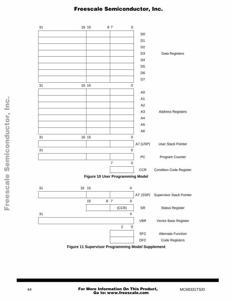
F
ree
sca
le S
em
ico
nd
uc
tor,
I
Freescale Semiconductor, Inc.n
c..
.
31 16 15 8 7 0
D0
D1
D2
D3 Data Registers
D4
D5
D6
D7
31 16 15 0
A0
A1
A2
A3 Address Registers
A4
A5
A6
31 16 15 0
A7 (USP) User Stack Pointer
31 0
PC Program Counter
7 0
CCR Condition Code Register
Figure 10 User Programming Model
31 16 15 0
A7' (SSP) Supervisor Stack Pointer
15 8 7 0
(CCR) SR Status Register
31 0
VBR Vector Base Register
2 0
SFC Alternate Function
DFC Code Registers
Figure 11 Supervisor Programming Model Supplement
44 MC68331TS/D
For More Information On This Product, Go to: www.freescale.com

F
ree
sca
le S
em
ico
nd
uc
tor,
I
Freescale Semiconductor, Inc.n
c..
.
4.3 Status Register
The status register contains the condition codes that reflect the results of a previous operation and canbe used for conditional instruction execution in a program. The lower byte containing the conditioncodes is the only portion of the register available at the user privilege level; it is referenced as the con-dition code register (CCR) in user programs. At the supervisor privilege level, software can access thefull status register, including the interrupt priority mask and additional control bits.
System ByteT[1:0] —Trace EnableS —Supervisor/User StateBits [12:11] —UnimplementedIP[2:0] —Interrupt Priority Mask
User Byte (Condition Code Register)Bits [7:5] —UnimplementedX —ExtendN —NegativeZ —ZeroV —OverflowC —Carry
4.4 Data Types
Six basic data types are supported:
• Bits• Packed Binary Coded Decimal Digits• Byte Integers (8 bits)• Word Integers (16 bits)• Long-Word Integers (32 bits)• Quad-Word Integers (64 bits)
4.5 Addressing Modes
Addressing in the CPU32 is register-oriented. Most instructions allow the results of the specified oper-ation to be placed either in a register or directly in memory. This flexibility eliminates the need for extrainstructions to store register contents in memory. The CPU32 supports seven basic addressing modes:
• Register direct• Register indirect• Register indirect with index• Program counter indirect with displacement• Program counter indirect with index• Absolute• Immediate
Included in the register indirect addressing modes are the capabilities to post-increment, predecrement,and offset. The program counter relative mode also has index and offset capabilities. In addition tothese addressing modes, many instructions implicitly specify the use of the status register, stack point-er, or program counter.
SR —Status Register
15 14 13 12 11 10 8 7 6 5 4 3 2 1 0
T1 T0 S 0 0 IP 0 0 0 X N Z V C
RESET:
0 0 1 0 0 1 1 1 0 0 0 U U U U U
MC68331TS/D 45
For More Information On This Product, Go to: www.freescale.com
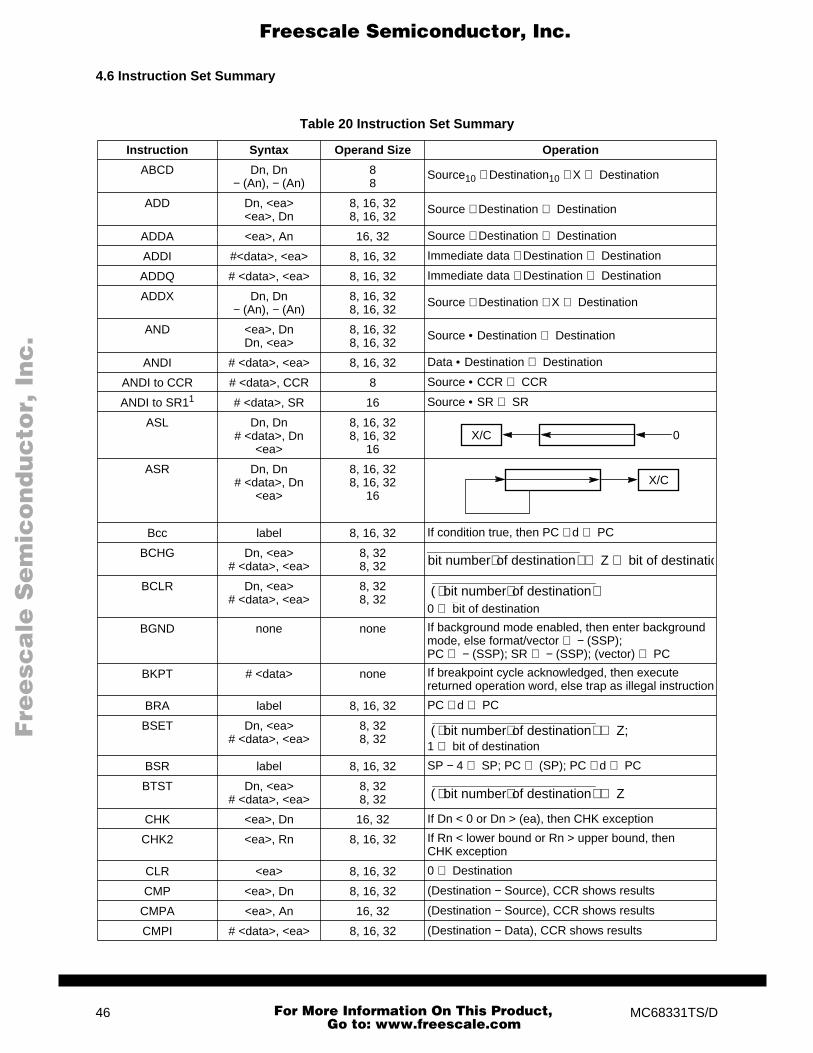
F
ree
sca
le S
em
ico
nd
uc
tor,
I
Freescale Semiconductor, Inc.n
c..
.
4.6 Instruction Set Summary
Table 20 Instruction Set Summary
Instruction Syntax Operand Size Operation
ABCD Dn, Dn− (An), − (An)
88
Source10 + Destination10 + X ⇒ Destination
ADD Dn, <ea><ea>, Dn
8, 16, 328, 16, 32
Source + Destination ⇒ Destination
ADDA <ea>, An 16, 32 Source + Destination ⇒ Destination
ADDI #<data>, <ea> 8, 16, 32 Immediate data + Destination ⇒ Destination
ADDQ # <data>, <ea> 8, 16, 32 Immediate data + Destination ⇒ Destination
ADDX Dn, Dn− (An), − (An)
8, 16, 328, 16, 32
Source + Destination + X ⇒ Destination
AND <ea>, DnDn, <ea>
8, 16, 328, 16, 32
Source • Destination ⇒ Destination
ANDI # <data>, <ea> 8, 16, 32 Data • Destination ⇒ Destination
ANDI to CCR # <data>, CCR 8 Source • CCR ⇒ CCR
ANDI to SR11 # <data>, SR 16 Source • SR ⇒ SR
ASL Dn, Dn# <data>, Dn
<ea>
8, 16, 328, 16, 32
16
ASR Dn, Dn# <data>, Dn
<ea>
8, 16, 328, 16, 32
16
Bcc label 8, 16, 32 If condition true, then PC + d ⇒ PC
BCHG Dn, <ea># <data>, <ea>
8, 328, 32
BCLR Dn, <ea># <data>, <ea>
8, 328, 32
0 ⇒ bit of destination
BGND none none If background mode enabled, then enter background mode, else format/vector ⇒ − (SSP);PC ⇒ − (SSP); SR ⇒ − (SSP); (vector) ⇒ PC
BKPT # <data> none If breakpoint cycle acknowledged, then execute returned operation word, else trap as illegal instruction
BRA label 8, 16, 32 PC + d ⇒ PC
BSET Dn, <ea># <data>, <ea>
8, 328, 32
1 ⇒ bit of destination
BSR label 8, 16, 32 SP − 4 ⇒ SP; PC ⇒ (SP); PC + d ⇒ PC
BTST Dn, <ea># <data>, <ea>
8, 328, 32
CHK <ea>, Dn 16, 32 If Dn < 0 or Dn > (ea), then CHK exception
CHK2 <ea>, Rn 8, 16, 32 If Rn < lower bound or Rn > upper bound, then CHK exception
CLR <ea> 8, 16, 32 0 ⇒ Destination
CMP <ea>, Dn 8, 16, 32 (Destination − Source), CCR shows results
CMPA <ea>, An 16, 32 (Destination − Source), CCR shows results
CMPI # <data>, <ea> 8, 16, 32 (Destination − Data), CCR shows results
X/C 0
X/C
bit number⟩ of destination) Z bit of destinatio⇒ ⇒
bit number⟨ ⟩ of destination( )Z
bit number⟨ ⟩ of destination( ) Z;⇒
bit number⟨ ⟩ of destination( ) Z⇒
46 MC68331TS/D
For More Information On This Product, Go to: www.freescale.com

F
ree
sca
le S
em
ico
nd
uc
tor,
I
Freescale Semiconductor, Inc.n
c..
.
CMPM (An) +, (An) + 8, 16, 32 (Destination − Source), CCR shows results
CMP2 <ea>, Rn 8, 16, 32 Lower bound ≤ Rn ≤ Upper bound, CCR shows result
DBcc Dn, label 16 If condition false, then Dn − 1 ⇒ PC;if Dn ≠ (− 1), then PC + d ⇒ PC
DIVS/DIVU <ea>, Dn 32/16 ⇒ 16 : 16 Destination / Source ⇒ Destination (signed or unsigned)
DIVSL/DIVUL <ea>, Dr : Dq<ea>, Dq
<ea>, Dr : Dq
64/32 ⇒ 32 : 3232/32 ⇒ 32
32/32 ⇒ 32 : 32
Destination / Source ⇒ Destination (signed or unsigned)
EOR Dn, <ea> 8, 16, 32 Source ⊕ Destination ⇒ Destination
EORI # <data>, <ea> 8, 16, 32 Data ⊕ Destination ⇒ Destination
EORI to CCR # <data>, CCR 8 Source ⊕ CCR ⇒ CCR
EORI to SR1 # <data>, SR 16 Source ⊕ SR ⇒ SR
EXG Rn, Rn 32 Rn ⇒ Rn
EXT DnDn
8 ⇒ 1616 ⇒ 32
Sign extended Destination ⇒ Destination
EXTB Dn 8 ⇒ 32 Sign extended Destination ⇒ Destination
ILLEGAL none none SSP − 2 ⇒ SSP; vector offset ⇒ (SSP);SSP − 4 ⇒ SSP; PC ⇒ (SSP);SSP − 2 ⇒ SSP; SR ⇒ (SSP);Illegal instruction vector address ⇒ PC
JMP <ea> none Destination ⇒ PC
JSR <ea> none SP − 4 ⇒ SP; PC ⇒ (SP); destination ⇒ PC
LEA <ea>, An 32 <ea> ⇒ An
LINK An, # d 16, 32 SP − 4 ⇒ SP, An ⇒ (SP); SP ⇒ An, SP + d ⇒ SP
LPSTOP1 # <data> 16 Data ⇒ SR; interrupt mask ⇒ EBI; STOP
LSL Dn, Dn# <data>, Dn
<ea>
8, 16, 328, 16, 32
16
LSR Dn, Dn#<data>, Dn
<ea>
8, 16, 328, 16, 32
16
MOVE <ea>, <ea> 8, 16, 32 Source ⇒ Destination
MOVEA <ea>, An 16, 32 ⇒ 32 Source ⇒ Destination
MOVEA1 USP, AnAn, USP
3232
USP ⇒ AnAn ⇒ USP
MOVE from CCR CCR, <ea> 16 CCR ⇒ Destination
MOVE to CCR <ea>, CCR 16 Source ⇒ CCR
MOVE from SR1 SR, <ea> 16 SR ⇒ Destination
MOVE to SR1 <ea>, SR 16 Source ⇒ SR
MOVE USP1 USP, AnAn, USP
3232
USP ⇒ AnAn ⇒ USP
MOVEC1 Rc, RnRn, Rc
3232
Rc ⇒ RnRn ⇒ Rc
MOVEM list, <ea><ea>, list
16, 3216, 32 ⇒ 32
Listed registers ⇒ DestinationSource ⇒ Listed registers
Table 20 Instruction Set Summary (Continued)
Instruction Syntax Operand Size Operation
X/C 0
X/C0
MC68331TS/D 47
For More Information On This Product, Go to: www.freescale.com

F
ree
sca
le S
em
ico
nd
uc
tor,
I
Freescale Semiconductor, Inc.n
c..
.
MOVEP Dn, (d16, An)
(d16, An), Dn
16, 32 Dn [31 : 24] ⇒ (An + d); Dn [23 : 16] ⇒ (An + d + 2);Dn [15 : 8] ⇒ (An + d + 4); Dn [7 : 0] ⇒ (An + d + 6)
(An + d) ⇒ Dn [31 : 24]; (An + d + 2) ⇒ Dn [23 : 16]; (An + d + 4) ⇒ Dn [15 : 8]; (An + d + 6) ⇒ Dn [7 : 0]
MOVEQ #<data>, Dn 8 ⇒ 32 Immediate data ⇒ Destination
MOVES1 Rn, <ea><ea>, Rn
8, 16, 32 Rn ⇒ Destination using DFCSource using SFC ⇒ Rn
MULS/MULU <ea>, Dn<ea>, Dl
<ea>, Dh : Dl
16 ∗ 16 ⇒ 3232 ∗ 32 ⇒ 3232 ∗ 32 ⇒ 64
Source ∗ Destination ⇒ Destination(signed or unsigned)
NBCD <ea> 88
0 − Destination10 − X ⇒ Destination
NEG <ea> 8, 16, 32 0 − Destination ⇒ Destination
NEGX <ea> 8, 16, 32 0 − Destination − X ⇒ Destination
NOP none none PC + 2 ⇒ PC
NOT <ea> 8, 16, 32 Destination ⇒ Destination
OR <ea>, DnDn, <ea>
8, 16, 328, 16, 32
Source + Destination ⇒ Destination
ORI #<data>, <ea> 8, 16, 32 Data + Destination ⇒ Destination
ORI to CCR #<data>, CCR 16 Source + CCR ⇒ SR
ORI to SR1 #<data>, SR 16 Source ; SR ⇒ SR
PEA <ea> 32 SP − 4 ⇒ SP; <ea> ⇒ SP
RESET1 none none Assert RESET line
ROL Dn, Dn#<data>, Dn
<ea>
8, 16, 328, 16, 32
16
ROR Dn, Dn#<data>, Dn
<ea>
8, 16, 328, 16, 32
16
ROXL Dn, Dn#<data>, Dn
<ea>
8, 16, 328, 16, 32
16
ROXR Dn, Dn#<data>, Dn
<ea>
8, 16, 328, 16, 32
16
RTD #d 16 (SP) ⇒ PC; SP + 4 + d ⇒ SP
RTE1 none none (SP) ⇒ SR; SP + 2 ⇒ SP; (SP) ⇒ PC;SP + 4 ⇒ SP;Restore stack according to format
RTR none none (SP) ⇒ CCR; SP + 2 ⇒ SP; (SP) ⇒ PC; SP + 4 ⇒ SP
RTS none none (SP) ⇒ PC; SP + 4 ⇒ SP
SBCD Dn, Dn− (An), − (An)
88
Destination10 − Source10 − X ⇒ Destination
Scc <ea> 8 If condition true, then destination bits are set to 1;else, destination bits are cleared to 0
STOP1 #<data> 16 Data ⇒ SR; STOP
Table 20 Instruction Set Summary (Continued)
Instruction Syntax Operand Size Operation
C
C
C X
CX
48 MC68331TS/D
For More Information On This Product, Go to: www.freescale.com
F
ree
sca
le S
em
ico
nd
uc
tor,
I
Freescale Semiconductor, Inc.n
c..
.
1. Privileged instruction.
SUB <ea>, DnDn, <ea>
8, 16, 32 Destination − Source ⇒ Destination
SUBA <ea>, An 16, 32 Destination − Source ⇒ Destination
SUBI #<data>, <ea> 8, 16, 32 Destination − Data ⇒ Destination
SUBQ #<data>, <ea> 8, 16, 32 Destination − Data ⇒ Destination
SUBX Dn, Dn− (An), − (An)
8, 16, 328, 16, 32
Destination − Source − X ⇒ Destination
SWAP Dn 16
TAS <ea> 8 Destination Tested Condition Codes bit 7 ofDestination
TBLS/TBLU <ea>, DnDym : Dyn, Dn
8, 16, 32 Dyn − Dym ⇒ Temp(Temp ∗ Dn [7 : 0]) ⇒ Temp(Dym ∗ 256) + Temp ⇒ Dn
TBLSN/TBLUN <ea>, DnDym : Dyn, Dn
8, 16, 32 Dyn − Dym ⇒ Temp(Temp ∗ Dn [7 : 0]) / 256 ⇒ TempDym + Temp ⇒ Dn
TRAP #<data> none SSP − 2 ⇒ SSP; format/vector offset ⇒ (SSP);SSP − 4 ⇒ SSP; PC ⇒ (SSP); SR ⇒ (SSP);vector address ⇒ PC
TRAPcc none#<data>
none16, 32
If cc true, then TRAP exception
TRAPV none none If V set, then overflow TRAP exception
TST <ea> 8, 16, 32 Source − 0, to set condition codes
UNLK An 32 An ⇒ SP; (SP) ⇒ An, SP + 4 ⇒ SP
Table 20 Instruction Set Summary (Continued)
Instruction Syntax Operand Size Operation
MSW LSW
MC68331TS/D 49
For More Information On This Product, Go to: www.freescale.com
F
ree
sca
le S
em
ico
nd
uc
tor,
I
Freescale Semiconductor, Inc.n
c..
.
4.7 Background Debugging Mode
The background debugger on the CPU32 is implemented in CPU microcode. The background debug-ging commands are summarized below.
Table 21 Background Debugging Mode
Command Mnemonic Description
Read D/A Register RDREG/RAREG Read the selected address or data register and return the results through the serial interface.
Write D/A Register WDREG/WAREG The data operand is written to the specified address or data register.
Read System Register RSREG The specified system control register is read. All registers that can be read in supervisor mode can be read in background mode.
Write System Register WSREG The operand data is written into the specified system control register.
Read Memory Location READ Read the sized data at the memory location specified by the long-word address. The source function code register (SFC) determines the address space accessed.
Write Memory Location WRITE Write the operand data to the memory location specified by the long-word address. The destination function code (DFC) register determines the address space accessed.
Dump Memory Block DUMP Used in conjunction with the READ command to dump large blocks of memory. An initial READ is executed to set up the starting address of the block and retrieve the first result. Subsequent operands are retrieved with the DUMP command.
Fill Memory Block FILL Used in conjunction with the WRITE command to fill large blocks of memory. Initially, a WRITE is executed to set up the starting address of the block and supply the first operand. The FILL command writes subsequent operands.
Resume Execution GO The pipe is flushed and refilled before resuming instruction execution at the current PC.
Patch User Code CALL Current program counter is stacked at the location of the current stack pointer. Instruction execution begins at user patch code.
Reset Peripherals RST Asserts RESET for 512 clock cycles. The CPU is not reset by this command. Synonymous with the CPU RESET instruction.
No Operation NOP NOP performs no operation and can be used as a null command.
50 MC68331TS/D
For More Information On This Product, Go to: www.freescale.com

F
ree
sca
le S
em
ico
nd
uc
tor,
I
Freescale Semiconductor, Inc.n
c..
.
5 Queued Serial ModuleThe QSM contains two serial interfaces, the queued serial peripheral interface (QSPI) and the serialcommunication interface (SCI).
Figure 12 QSM Block Diagram
5.1 Overview
The QSPI provides easy peripheral expansion or interprocessor communication through a full-duplex,synchronous, three-line bus: data in, data out, and a serial clock. Four programmable peripheral chip-select pins provide addressability for up to 16 peripheral devices. A self-contained RAM queue allowsup to 16 serial transfers of 8 to 16 bits each, or transmission of a 256-bit data stream without CPU in-tervention. A special wraparound mode supports continuous sampling of a serial peripheral, with auto-matic QSPI RAM updating, which makes the interface to A/D converters more efficient.
The SCI provides a standard nonreturn to zero (NRZ) mark/space format. It operates in either full- orhalf-duplex mode. There are separate transmitter and receiver enable bits and dual data buffers. Amodulus-type baud rate generator provides rates from 64 to 524 kbaud with a 16.78-MHz system clock,or 110 to 655 kbaud with a 20.97 MHz system clock. Word length of either 8 or 9 bits is software select-able. Optional parity generation and detection provide either even or odd parity check capability. Ad-vanced error detection circuitry catches glitches of up to 1/16 of a bit time in duration. Wakeup functionsallow the CPU to run uninterrupted until meaningful data is available.
An address map of the QSM is shown below. The “Access” column indicates which registers are acces-sible only at the supervisor privilege level and which can be assigned to either the supervisor or userprivilege level, according to the value of the SUPV bit in the QSMCR.
QSPI
INTERFACE LOGIC
SCI
MISO/PQS0MOSI/PQS1SCK/PQS2PCS0/SS/PQS3PCS1/PQS4PCS2/PQS5PCS3/PQS6
TXD/PQS7
RXD
POR
T Q
SQSM BLOCK
IMB
MC68331TS/D 51
For More Information On This Product, Go to: www.freescale.com

F
ree
sca
le S
em
ico
nd
uc
tor,
I
Freescale Semiconductor, Inc.n
c..
.
Y = M111, where M is the logic state of the module mapping (MM) bit in the SIMCR
5.2 Pin Function
The following table is a summary of the functions of the QSM pins when they are not configured for gen-eral-purpose I/O. The QSM data direction register (DDRQS) designates each pin except RXD as an in-put or output.
Table 22 QSM Address Map
Access Address 15 8 7 0S $YFFC00 QSM MODULE CONFIGURATION (QSMCR)S $YFFC02 QSM TEST (QTEST)S $YFFC04 QSM INTERRUPT LEVEL (QILR) QSM INTERRUPT VECTOR (QIVR)
S/U $YFFC06 NOT USEDS/U $YFFC08 SCI CONTROL 0 (SCCR0)S/U $YFFC0A SCI CONTROL 1 (SCCR1)S/U $YFFC0C SCI STATUS (SCSR)S/U $YFFC0E SCI DATA (SCDR)S/U $YFFC10 NOT USEDS/U $YFFC12 NOT USEDS/U $YFFC14 NOT USED PQS DATA (PORTQS)S/U $YFFC16 PQS PIN ASSIGNMENT (PQSPAR) PQS DATA DIRECTION (DDRQS)S/U $YFFC18 SPI CONTROL 0 (SPCR0)S/U $YFFC1A SPI CONTROL 1 (SPCR1)S/U $YFFC1C SPI CONTROL 2 (SPCR2)S/U $YFFC1E SPI CONTROL 3 (SPCR3) SPI STATUS (SPSR)S/U $YFFC20–
$YFFCFFNOT USED
S/U $YFFD00–$YFFD1F
RECEIVE RAM (RR[0:F])
S/U $YFFD20–$YFFD3F
TRANSMIT RAM (TR[0:F])
S/U $YFFD40–$YFFD4F
COMMAND RAM (CR[0:F])
Pin Mode Pin FunctionMISO Master Serial Data Input to QSPI
QSPI Pins Slave Serial Data Output from QSPIMOSI Master Serial Data Output from QSPI
Slave Serial Data Input to QSPISCK Master Clock Output from QSPI
Slave Clock Input to QSPIPCS0/SSMaster Input: Assertion Causes Mode Fault
Output: Selects PeripheralsSlave Input: Selects the QSPI
PCS[3:1] Master Output: Selects PeripheralsSlave None
SCI Pins TXD Transmit Serial Data Output from SCI RXD Receive Serial Data Input to SCI
52 MC68331TS/D
For More Information On This Product, Go to: www.freescale.com
F
ree
sca
le S
em
ico
nd
uc
tor,
I
Freescale Semiconductor, Inc.n
c..
.
5.3 QSM Registers
QSM registers are divided into four categories: QSM global registers, QSM pin control registers, QSPIsubmodule registers, and SCI submodule registers. The QSPI and SCI registers are defined in separatesections below. Writes to unimplemented register bits have no meaning or effect, and reads from unim-plemented bits always return a logic zero value.
The module mapping bit of the SIM configuration register (SIMCR) defines the most significant bit(ADDR23) of the address, shown in each register figure as Y (Y = $7 or $F). This bit, concatenated withthe rest of the address given, forms the absolute address of each register. Refer to the SIM section ofthis technical summary for more information about how the state of MM affects the system.
5.3.1 Global Registers
The QSM global registers contain system parameters used by both the QSPI and the SCI submodules.These registers contain the bits and fields used to configure the QSM.
The QSMCR contains parameters for the QSM/CPU/intermodule bus (IMB) interface.
STOP — Stop Enable0 = Normal QSM clock operation1 = QSM clock operation stopped
STOP places the QSM in a low-power state by disabling the system clock in most parts of the module.The QSMCR is the only register guaranteed to be readable while STOP is asserted. The QSPI RAM isnot readable. However, writes to RAM or any register are guaranteed to be valid while STOP is assert-ed. STOP can be negated by the CPU and by reset.
The system software must stop each submodule before asserting STOP to avoid complications at re-start and to avoid data corruption. The SCI submodule receiver and transmitter should be disabled, andthe operation should be verified for completion before asserting STOP. The QSPI submodule should bestopped by asserting the HALT bit in SPCR3 and by asserting STOP after the HALTA flag is set.
FRZ1 — Freeze 10 = Ignore the FREEZE signal on the IMB1 = Halt the QSPI (on a transfer boundary)
FRZ1 determines what action is taken by the QSPI when the FREEZE signal of the IMB is asserted.FREEZE is asserted whenever the CPU enters the background mode.
FRZ0 — Freeze 0Reserved
Bits [12:8] — Not Implemented
SUPV — Supervisor/Unrestricted0 = User access1 = Supervisor access
SUPV defines the assignable QSM registers as either supervisor-only data space or unrestricted dataspace.
IARB — Interrupt Arbitration Identification NumberThe IARB field is used to arbitrate between simultaneous interrupt requests of the same priority. Eachmodule that can generate interrupt requests must be assigned a unique, non-zero IARB field value. Re-fer to 3.8 Interrupts for more information.
QSMCR — QSM Configuration Register $YFFC00
15 14 13 12 11 10 9 8 7 6 5 4 3 0
STOP FRZ1 FRZ0 0 0 0 0 0 SUPV 0 0 0 IARB
RESET:
0 0 0 0 0 0 0 0 1 0 0 0 0 0 0 0
MC68331TS/D 53
For More Information On This Product, Go to: www.freescale.com
F
ree
sca
le S
em
ico
nd
uc
tor,
I
Freescale Semiconductor, Inc.n
c..
.
QTEST — QSM Test Register $YFFC02
QTEST is used during factory testing of the QSM. Accesses to QTEST must be made while the MCUis in test mode.
QILR determines the priority level of interrupts requested by the QSM and the vector used when an in-terrupt is acknowledged.
ILQSPI — Interrupt Level for QSPIILQSPI determines the priority of QSPI interrupts. This field must be given a value between $0 (inter-rupts disabled) to $7 (highest priority).
ILSCI — Interrupt Level of SCIILSCI determines the priority of SCI interrupts. This field must be given a value between $0 (interruptsdisabled) to $7 (highest priority).If ILQSPI and ILSCI are the same nonzero value, and both submodules simultaneously request inter-rupt service, QSPI has priority.
QIVR determines which two vector numbers in the exception vector table are to be used for QSM inter-rupts. The seven MSB of a user-defined vector number ($40–$FF) must be written into the INTV fieldduring initialization. The value of INTV0 is supplied by the QSM when an interrupt service request isacknowledged.
During an interrupt-acknowledge cycle, INTV[7:1] are driven on DATA[7:1] IMB lines. DATA0 is negatedfor an SCI interrupt and asserted for a QSPI interrupt. Writes to INTV0 have no meaning or effect.Reads of INTV0 return a value of one.
At reset, QIVR is initialized to $0F, which corresponds to the uninitialized interrupt vector in the excep-tion table.
5.3.2 Pin Control Registers
The QSM uses nine pins, eight of which form a parallel port (PORTQS) on the MCU. Although thesepins are used by the serial subsystems, any pin can alternately be assigned as general-purpose I/O ona pin-by-pin basis.
Pins used for general-purpose I/O must not be assigned to the QSPI by register PQSPAR. To avoiddriving incorrect data, the first byte to be output must be written before DDRQS is configured. DDRQSmust then be written to determine the direction of data flow and to output the value contained in registerPORTQS. Subsequent data for output is written to PORTQS.
QILR — QSM Interrupt Levels Register $YFFC04
15 14 13 11 10 8 7 0
0 0 ILQSPI ILSCI QIVR
RESET:
0 0 0 0 0 0 0 0
QIVR — QSM Interrupt Vector Register $YFFC05
15 8 7 0
QILR INTV
RESET:
0 0 0 0 1 1 1 1
54 MC68331TS/D
For More Information On This Product, Go to: www.freescale.com
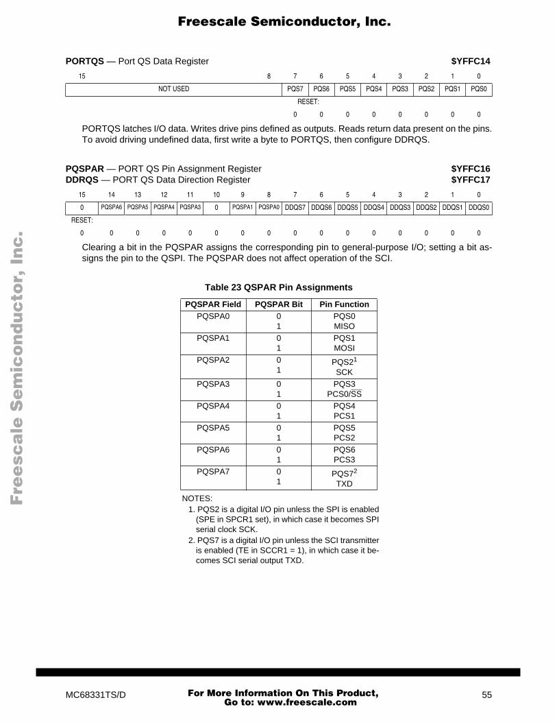
F
ree
sca
le S
em
ico
nd
uc
tor,
I
Freescale Semiconductor, Inc.n
c..
.
PORTQS latches I/O data. Writes drive pins defined as outputs. Reads return data present on the pins.To avoid driving undefined data, first write a byte to PORTQS, then configure DDRQS.
Clearing a bit in the PQSPAR assigns the corresponding pin to general-purpose I/O; setting a bit as-signs the pin to the QSPI. The PQSPAR does not affect operation of the SCI.
NOTES:1. PQS2 is a digital I/O pin unless the SPI is enabled
(SPE in SPCR1 set), in which case it becomes SPIserial clock SCK.
2. PQS7 is a digital I/O pin unless the SCI transmitteris enabled (TE in SCCR1 = 1), in which case it be-comes SCI serial output TXD.
PORTQS — Port QS Data Register $YFFC14
15 8 7 6 5 4 3 2 1 0
NOT USED PQS7 PQS6 PQS5 PQS4 PQS3 PQS2 PQS1 PQS0
RESET:
0 0 0 0 0 0 0 0
PQSPAR — PORT QS Pin Assignment Register $YFFC16DDRQS — PORT QS Data Direction Register $YFFC17
15 14 13 12 11 10 9 8 7 6 5 4 3 2 1 0
0 PQSPA6 PQSPA5 PQSPA4 PQSPA3 0 PQSPA1 PQSPA0 DDQS7 DDQS6 DDQS5 DDQS4 DDQS3 DDQS2 DDQS1 DDQS0
RESET:
0 0 0 0 0 0 0 0 0 0 0 0 0 0 0 0
Table 23 QSPAR Pin Assignments
PQSPAR Field PQSPAR Bit Pin FunctionPQSPA0 0
1PQS0MISO
PQSPA1 01
PQS1MOSI
PQSPA2 01
PQS21
SCKPQSPA3 0
1PQS3
PCS0/SS
PQSPA4 01
PQS4PCS1
PQSPA5 01
PQS5PCS2
PQSPA6 01
PQS6PCS3
PQSPA7 01
PQS72
TXD
MC68331TS/D 55
For More Information On This Product, Go to: www.freescale.com
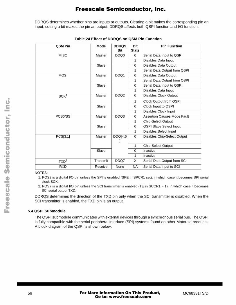
F
ree
sca
le S
em
ico
nd
uc
tor,
I
Freescale Semiconductor, Inc.n
c..
.
DDRQS determines whether pins are inputs or outputs. Clearing a bit makes the corresponding pin aninput; setting a bit makes the pin an output. DDRQS affects both QSPI function and I/O function.
NOTES:1. PQS2 is a digital I/O pin unless the SPI is enabled (SPE in SPCR1 set), in which case it becomes SPI serial
clock SCK.2. PQS7 is a digital I/O pin unless the SCI transmitter is enabled (TE in SCCR1 = 1), in which case it becomes
SCI serial output TXD.
DDRQS determines the direction of the TXD pin only when the SCI transmitter is disabled. When theSCI transmitter is enabled, the TXD pin is an output.
5.4 QSPI Submodule
The QSPI submodule communicates with external devices through a synchronous serial bus. The QSPIis fully compatible with the serial peripheral interface (SPI) systems found on other Motorola products.A block diagram of the QSPI is shown below.
Table 24 Effect of DDRQS on QSM Pin Function
QSM Pin Mode DDRQS Bit
Bit State
Pin Function
MISO Master DDQ0 0 Serial Data Input to QSPI1 Disables Data Input
Slave 0 Disables Data Output1 Serial Data Output from QSPI
MOSI Master DDQ1 0 Disables Data Output1 Serial Data Output from QSPI
Slave 0 Serial Data Input to QSPI1 Disables Data Input
SCK1 Master DDQ2 0 Disables Clock Output
1 Clock Output from QSPISlave 0 Clock Input to QSPI
1 Disables Clock InputPCS0/SS Master DDQ3 0 Assertion Causes Mode Fault
1 Chip-Select OutputSlave 0 QSPI Slave Select Input
1 Disables Select InputPCS[3:1] Master DDQ[4:6
]0 Disables Chip-Select Output
1 Chip-Select OutputSlave 0 Inactive
1 Inactive
TXD2 Transmit DDQ7 X Serial Data Output from SCI
RXD Receive None NA Serial Data Input to SCI
56 MC68331TS/D
For More Information On This Product, Go to: www.freescale.com
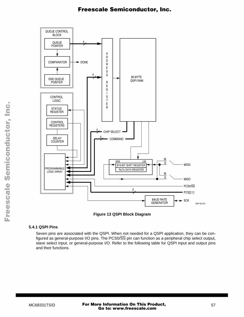
F
ree
sca
le S
em
ico
nd
uc
tor,
I
Freescale Semiconductor, Inc.n
c..
.
Figure 13 QSPI Block Diagram
5.4.1 QSPI Pins
Seven pins are associated with the QSPI. When not needed for a QSPI application, they can be con-figured as general-purpose I/O pins. The PCS0/SS pin can function as a peripheral chip select output,slave select input, or general-purpose I/O. Refer to the following table for QSPI input and output pinsand their functions.
QSPI BLOCK
CONTROLREGISTERS
END QUEUEPOINTER
QUEUEPOINTER
STATUS REGISTER
DELAYCOUNTER
COMPARATOR
PROGRAMMABLELOGIC ARRAY
80-BYTEQSPI RAM
CHIP SELECT
COMMAND
DONE
4
4
2
BAUD RATEGENERATOR
PCS[2:1]
PCS0/SS
MISO
MOSI
SCK
MS
MS
8/16-BIT SHIFT REGISTER
Rx/Tx DATA REGISTER
MSB LSB
4
4
QUEUE CONTROLBLOCK
CONTROLLOGIC
ADDRESS REGISTER
MC68331TS/D 57
For More Information On This Product, Go to: www.freescale.com

F
ree
sca
le S
em
ico
nd
uc
tor,
I
Freescale Semiconductor, Inc.n
c..
.
5.4.2 QSPI Registers
The programmer's model for the QSPI submodule consists of the QSM global and pin control registers,four QSPI control registers, one status register, and the 80-byte QSPI RAM.
The CPU can read and write to registers and RAM. The four control registers must be initialized beforethe QSPI is enabled to ensure defined operation. SPCR1 should be written last because it containsQSPI enable bit SPE. Asserting this bit starts the QSPI. The QSPI control registers are reset to a de-fined state and can then be changed by the CPU. Reset values are shown below each register.
Refer to the following memory map of the QSPI.
Writing a different value into any control register except SPCR2 while the QSPI is enabled disrupts op-eration. SPCR2 is buffered to prevent disruption of the current serial transfer. After completion of thecurrent serial transfer, the new SPCR2 values become effective.
Writing the same value into any control register except SPCR2 while the QSPI is enabled has no effecton QSPI operation. Rewriting NEWQP in SPCR2 causes execution to restart at the designated location.
SPCR0 contains parameters for configuring the QSPI before it is enabled. The CPU can read and writethis register. The QSM has read-only access.
Pin Names Mnemonics Mode FunctionMaster In Slave Out MISO Master
SlaveSerial Data Input to QSPI Serial Data Output from QSPI
Master Out Slave In MOSI MasterSlave
Serial Data Output from QSPISerial Data Input to QSPI
Serial Clock SCK MasterSlave
Clock Output from QSPI Clock Input to QSPI
Peripheral Chip Selects PCS[3:1] Master Select PeripheralsPeripheral Chip Select Slave Select
PCS0SS
MasterMasterSlave
Selects PeripheralCauses Mode Fault Initiates Serial Transfer
Address Name Usage
$YFFC18 SPCR0 QSPI Control Register 0
$YFFC1A SPCR1 QSPI Control Register 1
$YFFC1C SPCR2 QSPI Control Register 2
$YFFC1E SPCR3 QSPI Control Register 3
$YFFC1F SPSR QSPI Status Register
$YFFD00 RAM QSPI Receive Data (16 Words)
$YFFD20 RAM QSPI Transmit Data (16 Words)
$YFFD40 RAM QSPI Command Control (8 Words)
SPCR0 — QSPI Control Register 0 $YFFC18
15 14 13 10 9 8 7 0
MSTR WOMQ BITS CPOL CPHA SPBR
RESET:
0 0 0 0 0 0 0 1 0 0 0 0 0 1 0 0
58 MC68331TS/D
For More Information On This Product, Go to: www.freescale.com

F
ree
sca
le S
em
ico
nd
uc
tor,
I
Freescale Semiconductor, Inc.n
c..
.
MSTR — Master/Slave Mode Select0 = QSPI is a slave device and only responds to externally generated serial data. 1 = QSPI is system master and can initiate transmission to external SPI devices.
MSTR configures the QSPI for either master or slave mode operation. This bit is cleared on reset andmay only be written by the CPU.
WOMQ — Wired-OR Mode for QSPI Pins0 = Outputs have normal MOS drivers.1 = Pins designated for output by DDRQS have open-drain drivers.
WOMQ allows the wired-OR function to be used on QSPI pins, regardless of whether they are used asgeneral-purpose outputs or as QSPI outputs. WOMQ affects the QSPI pins regardless of whether theQSPI is enabled or disabled.
BITS — Bits Per TransferIn master mode, when BITSE in a command is set, the BITS field determines the number of data bitstransferred. When BITSE is cleared, eight bits are transferred. Reserved values default to eight bits.BITSE is not used in slave mode.
The following table shows the number of bits per transfer.
CPOL — Clock Polarity0 = The inactive state value of SCK is logic level zero.1 = The inactive state value of SCK is logic level one.
CPOL is used to determine the inactive state value of the serial clock (SCK). It is used with CPHA toproduce a desired clock/data relationship between master and slave devices.
CPHA — Clock Phase0 = Data is captured on the leading edge of SCK and changed on the following edge of SCK.1 = Data is changed on the leading edge of SCK and captured on the following edge of SCK.
CPHA determines which edge of SCK causes data to change and which edge causes data to be cap-tured. CPHA is used with CPOL to produce a desired clock/data relationship between master and slavedevices. CPHA is set at reset.
BITS Bits per Transfer0000 160001 Reserved0010 Reserved0011 Reserved0100 Reserved0101 Reserved0110 Reserved0111 Reserved1000 81001 91010 101011 111100 121101 131110 141111 15
MC68331TS/D 59
For More Information On This Product, Go to: www.freescale.com

F
ree
sca
le S
em
ico
nd
uc
tor,
I
Freescale Semiconductor, Inc.n
c..
.
SPBR — Serial Clock Baud RateThe QSPI uses a modulus counter to derive SCK baud rate from the MCU system clock. Baud rate isselected by writing a value from 2 to 255 into the SPBR field. The following equation determines theSCK baud rate:
SCK Baud Rate = System Clock/(2SPBR)or
SPBR = System Clock/(2SCK)(Baud Rate Desired)
where SPBR equals 2, 3, 4,..., 255Giving SPBR a value of zero or one disables the baud rate generator. SCK is disabled and assumes itsinactive state value. No serial transfers occur. At reset, baud rate is initialized to one eighth of the sys-tem clock frequency.
SPCR1 contains parameters for configuring the QSPI before it is enabled. The CPU can read and writethis register, but the QSM has read access only, except for SPE, which is automatically cleared by theQSPI after completing all serial transfers, or when a mode fault occurs.
SPE — QSPI Enable0 = QSPI is disabled. QSPI pins can be used for general-purpose I/O.1 = QSPI is enabled. Pins allocated by PQSPAR are controlled by the QSPI.
DSCKL — Delay before SCKWhen the DSCK bit in command RAM is set, this field determines the length of delay from PCS valid toSCK transition. PCS can be any of the four peripheral chip-select pins. The following equation deter-mines the actual delay before SCK:
PCS to SCK Delay = [DSCKL/System Clock]
where DSCKL equals 1, 2, 3,..., 127.
When the DSCK value of a queue entry equals zero, then DSCKL is not used. Instead, the PCS valid-to-SCK transition is one-half SCK period.
DTL — Length of Delay after TransferWhen the DT bit in command RAM is set, this field determines the length of delay after serial transfer.The following equation is used to calculate the delay:
Delay after Transfer = [(32DTL)/System Clock]
where DTL equals 1, 2, 3,..., 255.
A zero value for DTL causes a delay-after-transfer value of 8192/System Clock.
If DT equals zero, a standard delay is inserted.
Standard Delay after Transfer = [17/System Clock]
Delay after transfer can be used to provide a peripheral deselect interval. A delay can also be insertedbetween consecutive transfers to allow serial A/D converters to complete conversion.
SPCR1 — QSPI Control Register 1 $YFFC1A
15 14 8 7 0
SPE DSCKL DTL
RESET:
0 0 0 0 0 1 0 0 0 0 0 0 0 1 0 0
60 MC68331TS/D
For More Information On This Product, Go to: www.freescale.com
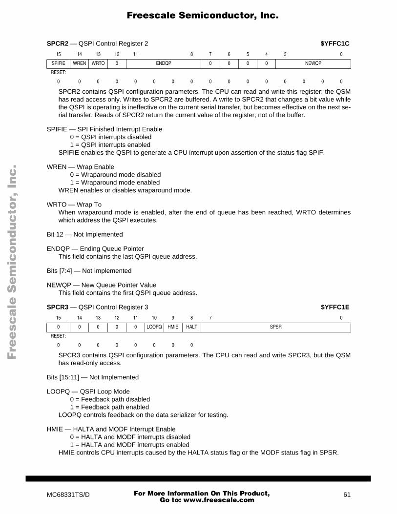
F
ree
sca
le S
em
ico
nd
uc
tor,
I
Freescale Semiconductor, Inc.n
c..
.
SPCR2 contains QSPI configuration parameters. The CPU can read and write this register; the QSMhas read access only. Writes to SPCR2 are buffered. A write to SPCR2 that changes a bit value whilethe QSPI is operating is ineffective on the current serial transfer, but becomes effective on the next se-rial transfer. Reads of SPCR2 return the current value of the register, not of the buffer.
SPIFIE — SPI Finished Interrupt Enable0 = QSPI interrupts disabled1 = QSPI interrupts enabled
SPIFIE enables the QSPI to generate a CPU interrupt upon assertion of the status flag SPIF.
WREN — Wrap Enable0 = Wraparound mode disabled1 = Wraparound mode enabled
WREN enables or disables wraparound mode.
WRTO — Wrap ToWhen wraparound mode is enabled, after the end of queue has been reached, WRTO determineswhich address the QSPI executes.
Bit 12 — Not Implemented
ENDQP — Ending Queue PointerThis field contains the last QSPI queue address.
Bits [7:4] — Not Implemented
NEWQP — New Queue Pointer ValueThis field contains the first QSPI queue address.
SPCR3 contains QSPI configuration parameters. The CPU can read and write SPCR3, but the QSMhas read-only access.
Bits [15:11] — Not Implemented
LOOPQ — QSPI Loop Mode0 = Feedback path disabled1 = Feedback path enabled
LOOPQ controls feedback on the data serializer for testing.
HMIE — HALTA and MODF Interrupt Enable0 = HALTA and MODF interrupts disabled1 = HALTA and MODF interrupts enabled
HMIE controls CPU interrupts caused by the HALTA status flag or the MODF status flag in SPSR.
SPCR2 — QSPI Control Register 2 $YFFC1C
15 14 13 12 11 8 7 6 5 4 3 0
SPIFIE WREN WRTO 0 ENDQP 0 0 0 0 NEWQP
RESET:
0 0 0 0 0 0 0 0 0 0 0 0 0 0 0 0
SPCR3 — QSPI Control Register 3 $YFFC1E
15 14 13 12 11 10 9 8 7 0
0 0 0 0 0 LOOPQ HMIE HALT SPSR
RESET:
0 0 0 0 0 0 0 0
MC68331TS/D 61
For More Information On This Product, Go to: www.freescale.com
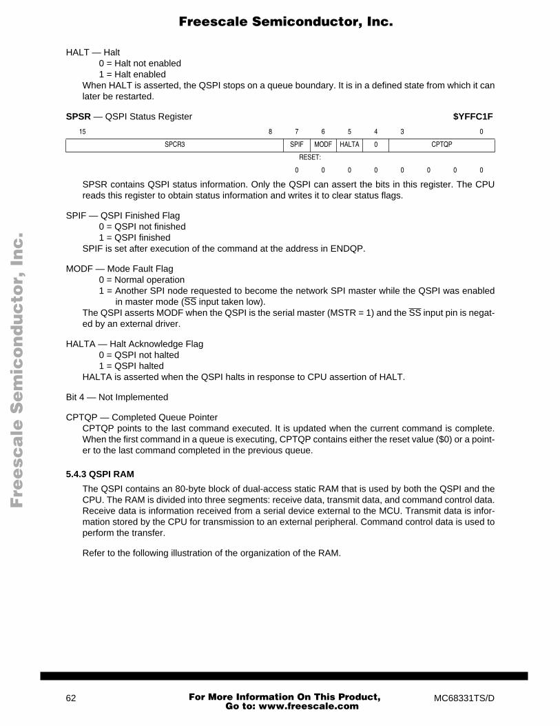
F
ree
sca
le S
em
ico
nd
uc
tor,
I
Freescale Semiconductor, Inc.n
c..
.
HALT — Halt0 = Halt not enabled1 = Halt enabled
When HALT is asserted, the QSPI stops on a queue boundary. It is in a defined state from which it canlater be restarted.
SPSR contains QSPI status information. Only the QSPI can assert the bits in this register. The CPUreads this register to obtain status information and writes it to clear status flags.
SPIF — QSPI Finished Flag0 = QSPI not finished1 = QSPI finished
SPIF is set after execution of the command at the address in ENDQP.
MODF — Mode Fault Flag0 = Normal operation1 = Another SPI node requested to become the network SPI master while the QSPI was enabled
in master mode (SS input taken low).The QSPI asserts MODF when the QSPI is the serial master (MSTR = 1) and the SS input pin is negat-ed by an external driver.
HALTA — Halt Acknowledge Flag0 = QSPI not halted1 = QSPI halted
HALTA is asserted when the QSPI halts in response to CPU assertion of HALT.
Bit 4 — Not Implemented
CPTQP — Completed Queue PointerCPTQP points to the last command executed. It is updated when the current command is complete.When the first command in a queue is executing, CPTQP contains either the reset value ($0) or a point-er to the last command completed in the previous queue.
5.4.3 QSPI RAM
The QSPI contains an 80-byte block of dual-access static RAM that is used by both the QSPI and theCPU. The RAM is divided into three segments: receive data, transmit data, and command control data.Receive data is information received from a serial device external to the MCU. Transmit data is infor-mation stored by the CPU for transmission to an external peripheral. Command control data is used toperform the transfer.
Refer to the following illustration of the organization of the RAM.
SPSR — QSPI Status Register $YFFC1F
15 8 7 6 5 4 3 0
SPCR3 SPIF MODF HALTA 0 CPTQP
RESET:
0 0 0 0 0 0 0 0
62 MC68331TS/D
For More Information On This Product, Go to: www.freescale.com
F
ree
sca
le S
em
ico
nd
uc
tor,
I
Freescale Semiconductor, Inc.n
c..
.
Figure 14 QSPI RAM
Once the CPU has set up the queue of QSPI commands and enabled the QSPI, the QSPI can operateindependently of the CPU. The QSPI executes all of the commands in its queue, sets a flag indicatingthat it is finished, and then either interrupts the CPU or waits for CPU intervention. It is possible to ex-ecute a queue of commands repeatedly without CPU intervention.
RR[0:F] — Receive Data RAM $YFFD00
Data received by the QSPI is stored in this segment. The CPU reads this segment to retrieve data fromthe QSPI. Data stored in receive RAM is right-justified. Unused bits in a receive queue entry are set tozero by the QSPI upon completion of the individual queue entry. The CPU can access the data usingbyte, word, or long-word addressing.
The CPTQP value in SPSR shows which queue entries have been executed. The CPU uses this infor-mation to determine which locations in receive RAM contain valid data before reading them.
TR[0:F] — Transmit Data RAM $YFFD20
Data that is to be transmitted by the QSPI is stored in this segment. The CPU usually writes one wordof data into this segment for each queue command to be executed.
Information to be transmitted must be written to transmit data RAM in a right-justified format. The QSPIcannot modify information in the transmit data RAM. The QSPI copies the information to its data serial-izer for transmission. Information remains in transmit RAM until overwritten.
*The PCS0 bit represents the dual-function PCS0/SS.
Command RAM is used by the QSPI when in master mode. The CPU writes one byte of control infor-mation to this segment for each QSPI command to be executed. The QSPI cannot modify informationin command RAM.
CR[0:F] — Command RAM $YFFD40
7 6 5 4 3 2 1 0
CONT BITSE DT DSCK PCS3 PCS2 PCS1 PCS0*
— — — — — — — —
CONT BITSE DT DSCK PCS3 PCS2 PCS1 PCS0*
RECEIVE RAM
TRANSMIT RAM
500
51E
520
53E
WORD
540
54F
COMMANDRAM
BYTEWORD
RR0RR1RR2
RRDRRERRF
TR0TR1TR2
TRDTRETRF
CR0CR1CR2
CRDCRECRF
MC68331TS/D 63
For More Information On This Product, Go to: www.freescale.com
F
ree
sca
le S
em
ico
nd
uc
tor,
I
Freescale Semiconductor, Inc.n
c..
.
Command RAM consists of 16 bytes. Each byte is divided into two fields. The peripheral chip-selectfield enables peripherals for transfer. The command control field provides transfer options.
A maximum of 16 commands can be in the queue. Queue execution by the QSPI proceeds from theaddress in NEWQP through the address in ENDQP. (Both of these fields are in SPCR2.)
CONT — Continue0 = Control of chip selects returned to PORTQS after transfer is complete.1 = Peripheral chip selects remain asserted after transfer is complete.
BITSE — Bits per Transfer Enable0 = 8 bits1 = Number of bits set in BITS field of SPCR0
DT — Delay after TransferThe QSPI provides a variable delay at the end of serial transfer to facilitate the interface with peripheralsthat have a latency requirement. The delay between transfers is determined by the SPCR1 DTL field.
DSCK — PCS to SCK Delay0 = PCS valid to SCK transition is one-half SCK.1 = SPCR1 DSCKL field specifies delay from PCS valid to SCK.
PCS[3:0] — Peripheral Chip SelectUse peripheral chip-select bits to select an external device for serial data transfer. More than one pe-ripheral chip select can be activated at a time, and more than one peripheral chip can be connected toeach PCS pin, provided that proper fanout is observed.
SS — Slave Mode SelectInitiates slave mode serial transfer. If SS is taken low when the QSPI is in master mode, a mode faultwill be generated.
5.4.4 Operating Modes
The QSPI operates in either master or slave mode. Master mode is used when the MCU originates datatransfers. Slave mode is used when an external device initiates serial transfers to the MCU through theQSPI. Switching between the modes is controlled by MSTR in SPCR0. Before entering either mode,appropriate QSM and QSPI registers must be properly initialized.
In master mode, the QSPI executes a queue of commands defined by control bits in each commandRAM queue entry. Chip-select pins are activated, data is transmitted from transmit RAM and receivedinto receive RAM.
In slave mode, operation proceeds in response to SS pin activation by an external bus master. Opera-tion is similar to master mode, but no peripheral chip selects are generated, and the number of bitstransferred is controlled in a different manner. When the QSPI is selected, it automatically executes thenext queue transfer to exchange data with the external device correctly.
Although the QSPI inherently supports multimaster operation, no special arbitration mechanism is pro-vided. A mode fault flag (MODF) indicates a request for SPI master arbitration. System software mustprovide arbitration. Note that unlike previous SPI systems, MSTR is not cleared by a mode fault beingset, nor are the QSPI pin output drivers disabled. The QSPI and associated output drivers must be dis-abled by clearing SPE in SPCR1.
5.5 SCI Submodule
The SCI submodule is used to communicate with external devices through an asynchronous serial bus.The SCI is fully compatible with the SCI systems found on other Motorola MCUs, such as the M68HC11and M68HC05 Families.
64 MC68331TS/D
For More Information On This Product, Go to: www.freescale.com
F
ree
sca
le S
em
ico
nd
uc
tor,
I
Freescale Semiconductor, Inc.n
c..
.
5.5.1 SCI Pins
There are two unidirectional pins associated with the SCI. The SCI controls the transmit data (TXD) pinwhen enabled, whereas the receive data (RXD) pin remains a dedicated input pin to the SCI. TXD isavailable as a general-purpose I/O pin when the SCI transmitter is disabled. When used for I/O, TXDcan be configured either as input or output, as determined by QSM register DDRQS.
The following table shows SCI pins and their functions.
5.5.2 SCI Registers
The SCI programming model includes QSM global and pin control registers, and four SCI registers.There are two SCI control registers, one status register, and one data register. All registers can be reador written at any time by the CPU.
Changing the value of SCI control bits during a transfer operation may disrupt operation. Before chang-ing register values, allow the transmitter to complete the current transfer, then disable the receiver andtransmitter. Status flags in the SCSR may be cleared at any time.
SCCR0 contains a baud rate selection parameter. Baud rate must be set before the SCI is enabled. TheCPU can read and write this register at any time.
Bits [15:13] — Not Implemented
SCBR — Baud RateSCI baud rate is programmed by writing a 13-bit value to BR. The baud rate is derived from the MCUsystem clock by a modulus counter.The SCI receiver operates asynchronously. An internal clock is necessary to synchronize with an in-coming data stream. The SCI baud rate generator produces a receiver sampling clock with a frequency16 times that of the expected baud rate of the incoming data. The SCI determines the position of bitboundaries from transitions within the received waveform, and adjusts sampling points to the proper po-sitions within the bit period. Receiver sampling rate is always 16 times the frequency of the SCI baudrate, which is calculated as follows:
SCI Baud Rate = System Clock/(32SCBR)
or
SCBR = System Clock(32SCK)(Baud Rate Desired)
where SCBR is in the range 1, 2, 3, ..., 8191
Writing a value of zero to SCBR disables the baud rate generator.
The following table lists the SCBR settings for standard and maximum baud rates using 16.78-MHz and20.97-MHz system clocks.
Pin Names Mnemonics Mode FunctionReceive Data RXD Receiver Disabled
Receiver EnabledNot UsedSerial Data Input to SCI
Transmit Data TXD Transmitter DisabledTransmitter Enabled
General-Purpose I/OSerial Data Output from SCI
SCCR0 — SCI Control Register 0 $YFFC08
15 14 13 12 0
0 0 0 SCBR
RESET:
0 0 0 0 0 0 0 0 0 0 0 0 0 1 0 0
MC68331TS/D 65
For More Information On This Product, Go to: www.freescale.com
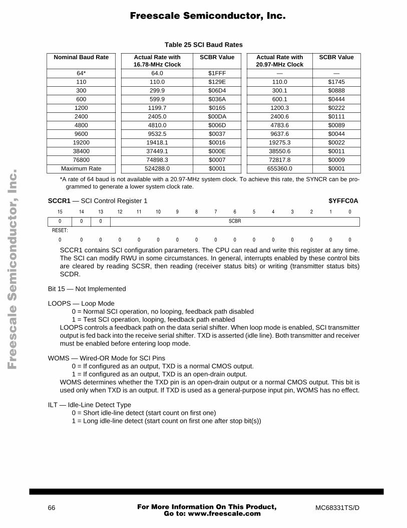
F
ree
sca
le S
em
ico
nd
uc
tor,
I
Freescale Semiconductor, Inc.n
c..
.
*A rate of 64 baud is not available with a 20.97-MHz system clock. To achieve this rate, the SYNCR can be pro-grammed to generate a lower system clock rate.
SCCR1 contains SCI configuration parameters. The CPU can read and write this register at any time.The SCI can modify RWU in some circumstances. In general, interrupts enabled by these control bitsare cleared by reading SCSR, then reading (receiver status bits) or writing (transmitter status bits)SCDR.
Bit 15 — Not Implemented
LOOPS — Loop Mode0 = Normal SCI operation, no looping, feedback path disabled1 = Test SCI operation, looping, feedback path enabled
LOOPS controls a feedback path on the data serial shifter. When loop mode is enabled, SCI transmitteroutput is fed back into the receive serial shifter. TXD is asserted (idle line). Both transmitter and receivermust be enabled before entering loop mode.
WOMS — Wired-OR Mode for SCI Pins0 = If configured as an output, TXD is a normal CMOS output.1 = If configured as an output, TXD is an open-drain output.
WOMS determines whether the TXD pin is an open-drain output or a normal CMOS output. This bit isused only when TXD is an output. If TXD is used as a general-purpose input pin, WOMS has no effect.
ILT — Idle-Line Detect Type0 = Short idle-line detect (start count on first one)1 = Long idle-line detect (start count on first one after stop bit(s))
Table 25 SCI Baud Rates
Nominal Baud Rate Actual Rate with 16.78-MHz Clock
SCBR Value Actual Rate with 20.97-MHz Clock
SCBR Value
64* 64.0 $1FFF — —110 110.0 $129E 110.0 $1745300 299.9 $06D4 300.1 $0888600 599.9 $036A 600.1 $0444
1200 1199.7 $0165 1200.3 $02222400 2405.0 $00DA 2400.6 $01114800 4810.0 $006D 4783.6 $00899600 9532.5 $0037 9637.6 $004419200 19418.1 $0016 19275.3 $002238400 37449.1 $000E 38550.6 $001176800 74898.3 $0007 72817.8 $0009
Maximum Rate 524288.0 $0001 655360.0 $0001
SCCR1 — SCI Control Register 1 $YFFC0A
15 14 13 12 11 10 9 8 7 6 5 4 3 2 1 0
0 0 0 SCBR
RESET:
0 0 0 0 0 0 0 0 0 0 0 0 0 0 0 0
66 MC68331TS/D
For More Information On This Product, Go to: www.freescale.com
F
ree
sca
le S
em
ico
nd
uc
tor,
I
Freescale Semiconductor, Inc.n
c..
.
PT — Parity Type0 = Even parity1 = Odd parity
When parity is enabled, PT determines whether parity is even or odd for both the receiver and the trans-mitter.
PE — Parity Enable0 = SCI parity disabled1 = SCI parity enabled
PE determines whether parity is enabled or disabled for both the receiver and the transmitter. If the re-ceived parity bit is not correct, the SCI sets the PF error flag in SCSR.When PE is set, the most significant bit (MSB) of the data field is used for the parity function, which re-sults in either seven or eight bits of user data, depending on the condition of M bit. The following tablelists the available choices.
M — Mode Select0 = SCI frame: 1 start bit, 8 data bits, 1 stop bit (10 bits total)1 = SCI frame: 1 start bit, 9 data bits, 1 stop bit (11 bits total)
WAKE — Wakeup by Address Mark0 = SCI receiver awakened by idle-line detection1 = SCI receiver awakened by address mark (last bit set)
TIE — Transmit Interrupt Enable0 = SCI TDRE interrupts inhibited1 = SCI TDRE interrupts enabled
TCIE — Transmit Complete Interrupt Enable0 = SCI TC interrupts inhibited1 = SCI TC interrupts enabled
RIE — Receiver Interrupt Enable0 = SCI RDRF interrupt inhibited1 = SCI RDRF interrupt enabled
ILIE — Idle-Line Interrupt Enable0 = SCI IDLE interrupts inhibited1 = SCI IDLE interrupts enabled
TE — Transmitter Enable0 = SCI transmitter disabled (TXD pin may be used as I/O)1 = SCI transmitter enabled (TXD pin dedicated to SCI transmitter)
The transmitter retains control of the TXD pin until completion of any character transfer in progresswhen TE is cleared.
RE — Receiver Enable0 = SCI receiver disabled (status bits inhibited)1 = SCI receiver enabled
M PE Result0 0 8 Data Bits0 1 7 Data Bits, 1 Parity Bit1 0 9 Data Bits1 1 8 Data Bits, 1 Parity Bit
MC68331TS/D 67
For More Information On This Product, Go to: www.freescale.com

F
ree
sca
le S
em
ico
nd
uc
tor,
I
Freescale Semiconductor, Inc.n
c..
.
RWU — Receiver Wakeup0 = Normal receiver operation (received data recognized)1 = Wakeup mode enabled (received data ignored until awakened)
Setting RWU enables the wakeup function, which allows the SCI to ignore received data until awakenedby either an idle line or address mark (as determined by WAKE). When in wakeup mode, the receiverstatus flags are not set, and interrupts are inhibited. This bit is cleared automatically (returned to normalmode) when the receiver is awakened.
SBK — Send Break0 = Normal operation1 = Break frame(s) transmitted after completion of current frame
SBK provides the ability to transmit a break code from the SCI. If the SCI is transmitting when SBK isset, it will transmit continuous frames of zeros after it completes the current frame, until SBK is cleared.If SBK is toggled (one to zero in less than one frame interval), the transmitter sends only one or twobreak frames before reverting to idle line or beginning to send data.
SCSR contains flags that show SCI operational conditions. These flags can be cleared either by hard-ware or by a special acknowledgment sequence. The sequence consists of SCSR read with flags set,followed by SCDR read (write in the case of TDRE and TC). A long-word read can consecutively accessboth SCSR and SCDR. This action clears receive status flag bits that were set at the time of the read,but does not clear TDRE or TC flags.
If an internal SCI signal for setting a status bit comes after the CPU has read the asserted status bits,but before the CPU has written or read register SCDR, the newly set status bit is not cleared. SCSRmust be read again with the bit set. Also, SCDR must be written or read before the status bit is cleared.
Reading either byte of SCSR causes all 16 bits to be accessed. Any status bit already set in either bytewill be cleared on a subsequent read or write of register SCDR.
TDRE — Transmit Data Register Empty Flag0 = Register TDR still contains data to be sent to the transmit serial shifter.1 = A new character can now be written to register TDR.
TDRE is set when the byte in register TDR is transferred to the transmit serial shifter. If TDRE is zero,transfer has not occurred and a write to TDR will overwrite the previous value. New data is not trans-mitted if TDR is written without first clearing TDRE.
TC — Transmit Complete Flag0 = SCI transmitter is busy1 = SCI transmitter is idle
TC is set when the transmitter finishes shifting out all data, queued preambles (mark/idle line), orqueued breaks (logic zero). The interrupt can be cleared by reading SCSR when TC is set and then bywriting the transmit data register (TDR) of SCDR.
RDRF — Receive Data Register Full Flag0 = Register RDR is empty or contains previously read data.1 = Register RDR contains new data.
RDRF is set when the content of the receive serial shifter is transferred to the RDR. If one or more errorsare detected in the received word, flag(s) NF, FE, and/or PF are set within the same clock cycle.
SCSR — SCI Status Register $YFFC0C
15 9 8 7 6 5 4 3 2 1 0
NOT USED TDRE TC RDRF RAF IDLE OR NF FE PF
RESET:
1 1 0 0 0 0 0 0 0
68 MC68331TS/D
For More Information On This Product, Go to: www.freescale.com

F
ree
sca
le S
em
ico
nd
uc
tor,
I
Freescale Semiconductor, Inc.n
c..
.
RAF — Receiver Active Flag0 = SCI receiver is idle1 = SCI receiver is busy
RAF indicates whether the SCI receiver is busy. It is set when the receiver detects a possible start bitand is cleared when the chosen type of idle line is detected. RAF can be used to reduce collisions insystems with multiple masters.
IDLE — Idle-Line Detected Flag0 = SCI receiver did not detect an idle-line condition.1 = SCI receiver detected an idle-line condition.
IDLE is disabled when RWU in SCCR1 is set. IDLE is set when the SCI receiver detects the idle-linecondition specified by ILT in SCCR1. If cleared, IDLE will not set again until after RDRF is set. RDRFis set when a break is received, so that a subsequent idle line can be detected.
OR — Overrun Error Flag0 = RDRF is cleared before new data arrives.1 = RDRF is not cleared before new data arrives.
OR is set when a new byte is ready to be transferred from the receive serial shifter to the RDR, andRDRF is still set. Data transfer is inhibited until OR is cleared. Previous data in RDR remains valid, butdata received during overrun condition (including the byte that set OR) is lost.
NF — Noise Error Flag0 = No noise detected on the received data1 = Noise occurred on the received data
NF is set when the SCI receiver detects noise on a valid start bit, on any data bit, or on a stop bit. It isnot set by noise on the idle line or on invalid start bits. Each bit is sampled three times. If none of thethree samples are the same logic level, the majority value is used for the received data value, and NFis set. NF is not set until an entire frame is received and RDRF is set.
FE — Framing Error Flag0 = No framing error on the received data.1 = Framing error or break occurred on the received data.
FE is set when the SCI receiver detects a zero where a stop bit was to have occurred. FE is not set untilthe entire frame is received and RDRF is set. A break can also cause FE to be set. It is possible to missa framing error if RXD happens to be at logic level one at the time the stop bit is expected.
PF — Parity Error Flag0 = No parity error on the received data1 = Parity error occurred on the received data
PF is set when the SCI receiver detects a parity error. PF is not set until the entire frame is received andRDRF is set.
SCDR contains two data registers at the same address. Receive data register (RDR) is a read-only reg-ister that contains data received by the SCI. The data comes into the receive serial shifter and is trans-ferred to RDR. Transmit data register (TDR) is a write-only register that contains data to be transmitted.The data is first written to TDR, then transferred to the transmit serial shifter, where additional formatbits are added before transmission. R[7:0]/T[7:0] contain either the first eight data bits received whenSCDR is read, or the first eight data bits to be transmitted when SCDR is written. R8/T8 are used whenthe SCI is configured for 9-bit operation. When it is configured for 8-bit operation, they have no meaningor effect.
SCDR — SCI Data Register $YFFC0E
15 14 13 12 11 10 9 8 7 6 5 4 3 2 1 0
0 0 0 0 0 0 0 R8/T8 R7/T7 R6/T6 R5/T5 R4/T4 R3/T3 R2/T2 R1/T1 R0/T0
RESET:
0 0 0 0 0 0 0 U U U U U U U U U
MC68331TS/D 69
For More Information On This Product, Go to: www.freescale.com

F
ree
sca
le S
em
ico
nd
uc
tor,
I
Freescale Semiconductor, Inc.n
c..
.
6 General-Purpose Timer Module The 11-channel general-purpose timer (GPT) is used in systems where a moderate level of CPU controlis required. The GPT consists of a capture/compare unit, a pulse accumulator, and two pulse-widthmodulators. A bus interface unit connects the GPT to the intermodule bus.
Figure 15 GPT Block Diagram
6.1 Overview
The capture/compare unit features three input capture channels, four output compare channels, andone channel that can be selected as an input capture or output compare channel. These channels sharea 16-bit free-running counter (TCNT) which derives its clock from a nine-stage prescaler or from the ex-ternal clock input signal, PCLK.
Pulse accumulator channel logic includes an 8-bit counter; the pulse accumulator can operate in eitherevent counting mode or gated time accumulation mode.
Pulse-width modulator outputs are periodic waveforms whose duty cycles can be independently select-ed and modified by user software. The PWM circuits share a 16-bit free-running counter that can beclocked by the same nine-stage prescaler used by the capture/compare unit or by the PCLK input.
All GPT pins can also be used for general-purpose input/output. The input capture and output comparepins form a bidirectional 8-bit parallel port (PORTGP). PWM pins are outputs only. PAI and PCLK pinsare inputs only.
GPT input capture/output compare pins are bidirectional and can be used to form an 8-bit parallel port.The pulse-width modulator outputs can be used as general-purpose outputs. The PAI and PCLK inputscan be used as general-purpose inputs.
The GPT control register address map is shown below. The “Access” column in the GPT address mapindicates which registers are accessible only at the supervisor privilege level and which can be assignedto either the supervisor or user privilege level, according to the value of the SUPV bit in the GPTMCR.
GPT BLOCK
PULSE ACCUMULATOR
PWM UNIT
BUS INTERFACE
IMB
CAPTURE/COMPARE UNIT
PRESCALER
IC1/PGP0
IC2/PGP1
IC3/PGP2
PCLK
PWMB
PWMA
PAI
IC4/OC5/OC1/PGP7
OC4/OC1/PGP6
OC3/OC1/PGP5
OC2/OC1/PGP4
OC1/PGP3
70 MC68331TS/D
For More Information On This Product, Go to: www.freescale.com
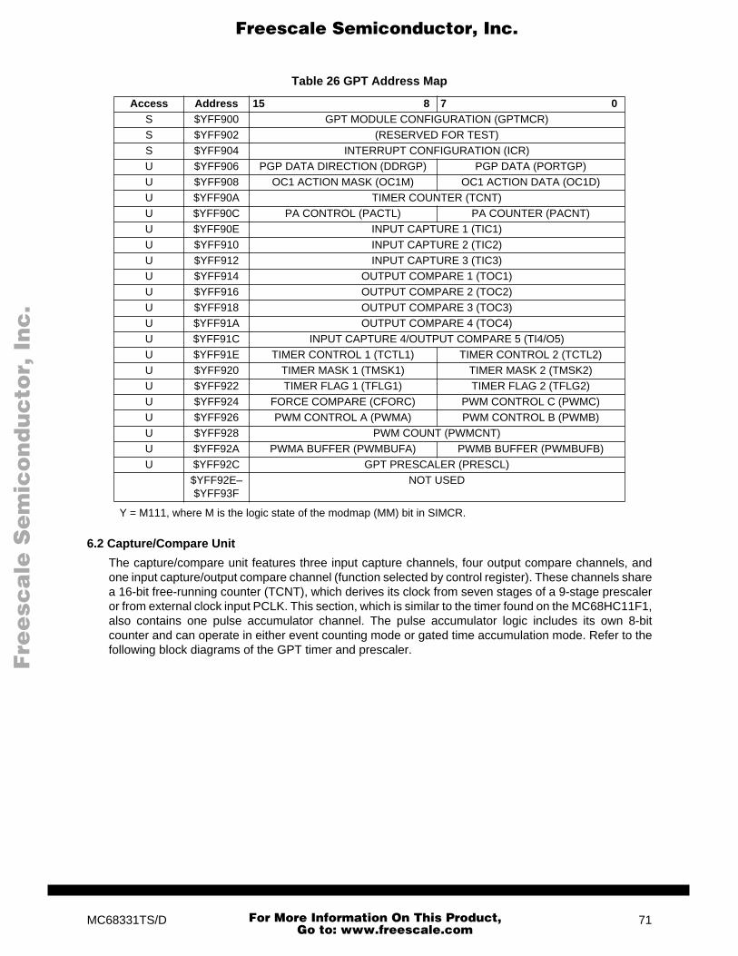
F
ree
sca
le S
em
ico
nd
uc
tor,
I
Freescale Semiconductor, Inc.n
c..
.
Y = M111, where M is the logic state of the modmap (MM) bit in SIMCR.
6.2 Capture/Compare Unit
The capture/compare unit features three input capture channels, four output compare channels, andone input capture/output compare channel (function selected by control register). These channels sharea 16-bit free-running counter (TCNT), which derives its clock from seven stages of a 9-stage prescaleror from external clock input PCLK. This section, which is similar to the timer found on the MC68HC11F1,also contains one pulse accumulator channel. The pulse accumulator logic includes its own 8-bitcounter and can operate in either event counting mode or gated time accumulation mode. Refer to thefollowing block diagrams of the GPT timer and prescaler.
Table 26 GPT Address Map
Access Address 15 8 7 0S $YFF900 GPT MODULE CONFIGURATION (GPTMCR)S $YFF902 (RESERVED FOR TEST)S $YFF904 INTERRUPT CONFIGURATION (ICR)U $YFF906 PGP DATA DIRECTION (DDRGP) PGP DATA (PORTGP)U $YFF908 OC1 ACTION MASK (OC1M) OC1 ACTION DATA (OC1D)U $YFF90A TIMER COUNTER (TCNT)U $YFF90C PA CONTROL (PACTL) PA COUNTER (PACNT)U $YFF90E INPUT CAPTURE 1 (TIC1)U $YFF910 INPUT CAPTURE 2 (TIC2)U $YFF912 INPUT CAPTURE 3 (TIC3)U $YFF914 OUTPUT COMPARE 1 (TOC1)U $YFF916 OUTPUT COMPARE 2 (TOC2)U $YFF918 OUTPUT COMPARE 3 (TOC3)U $YFF91A OUTPUT COMPARE 4 (TOC4)U $YFF91C INPUT CAPTURE 4/OUTPUT COMPARE 5 (TI4/O5)U $YFF91E TIMER CONTROL 1 (TCTL1) TIMER CONTROL 2 (TCTL2)U $YFF920 TIMER MASK 1 (TMSK1) TIMER MASK 2 (TMSK2)U $YFF922 TIMER FLAG 1 (TFLG1) TIMER FLAG 2 (TFLG2)U $YFF924 FORCE COMPARE (CFORC) PWM CONTROL C (PWMC)U $YFF926 PWM CONTROL A (PWMA) PWM CONTROL B (PWMB) U $YFF928 PWM COUNT (PWMCNT)U $YFF92A PWMA BUFFER (PWMBUFA) PWMB BUFFER (PWMBUFB)U $YFF92C GPT PRESCALER (PRESCL)
$YFF92E–$YFF93F
NOT USED
MC68331TS/D 71
For More Information On This Product, Go to: www.freescale.com

SC
F
ree
sca
le S
em
ico
nd
uc
tor,
I
Freescale Semiconductor, Inc.n
c..
.
Figure 16 GPT Timer Block Diagram
16/32 CC BLOCK
YSTEMLOCK
16-BIT LATCH CLK
8
7
6
5
4
BIT 3
BIT 4
BIT 5
BIT 6
BIT 7
PARALLEL PORTPIN CONTROL
OC1I
OC2I
OC3I
OC4I
I4/O5I
TFLG1STATUSFLAGS
FOC1
FOC2
FOC3
FOC4
FOC5
OC1F
OC2F
OC3F
OC4F
I4/O5F
I4/O5
16-BIT COMPARATOR
TOC1 (HI) TOC1 (LO)
=
16-BIT COMPARATOR
TOC2 (HI) TOC2 (LO)
=
16-BIT COMPARATOR
TOC3 (HI) TOC3 (LO)
=
16-BIT COMPARATOR
TOC4 (HI) TOC4 (LO)
=
16-BIT COMPARATOR
TI4/O5 (HI) TI4/O5 (LO)
=
16-BIT FREE RUNNINGCOUNTER
TCNT (HI) TCNT (LO)9
TOI
TOF
INTERRUPT REQUESTS
PRESCALER – DIVIDE BY4, 8, 16, 32, 64, 128, 256
CPR2 CPR1
16-BIT TIMER BUS
OC5
IC4
1
2
3
BIT 0
BIT 1
BIT 2
IC1I
IC2I
IC3I
IC1F
IC2F
IC3F
16-BIT LATCH
TIC1 (HI) TIC1 (LO)
CLK
16-BIT LATCH
TIC2 (HI) TIC2 (LO)
CLK
16-BIT LATCH
TIC3 (HI) TIC3 (LO)
CLK
TMSK1INTERRUPT
ENABLES
CFORCFORCE OUTPUT
COMPARE
PINFUNCTIONS
CPR01 OF 8 SELECT
PCLK
IC4/OC5/
OC4/OC1
OC3/OC1
OC2/OC1
OC1
IC3
IC2
IC1PGP0
PGP1
PGP2
PGP3
PGP4
PGP5
PGP6
PGP7
OC1
72 MC68331TS/D
For More Information On This Product, Go to: www.freescale.com

F
ree
sca
le S
em
ico
nd
uc
tor,
I
Freescale Semiconductor, Inc.n
c..
.
Figure 17 Prescaler Block Diagram
GPT PRE BLOCK
CPR2 CPR1 CPR0
TO PULSE ACCUMULATOR
TO PULSE ACCUMULATOR
TO CAPTURE/COMPARE
TIMERSELECT
DIVIDER
÷256
÷128
÷64
÷32
÷16
÷8
÷4
÷64
÷32
÷16
÷8÷4÷2 ÷128
÷256
÷512
SYSTEM CLOCK
÷512
PPR2 PPR1 PPR0
PWM UNITTO
SELECT
÷2
÷4
÷8
÷16
÷32
÷64
÷128
TO PULSE ACCUMULATOREXT.
SYNCHRONIZER ANDDIGITAL FILTER
EXT.
EXT.
PCLKPIN
MC68331TS/D 73
For More Information On This Product, Go to: www.freescale.com
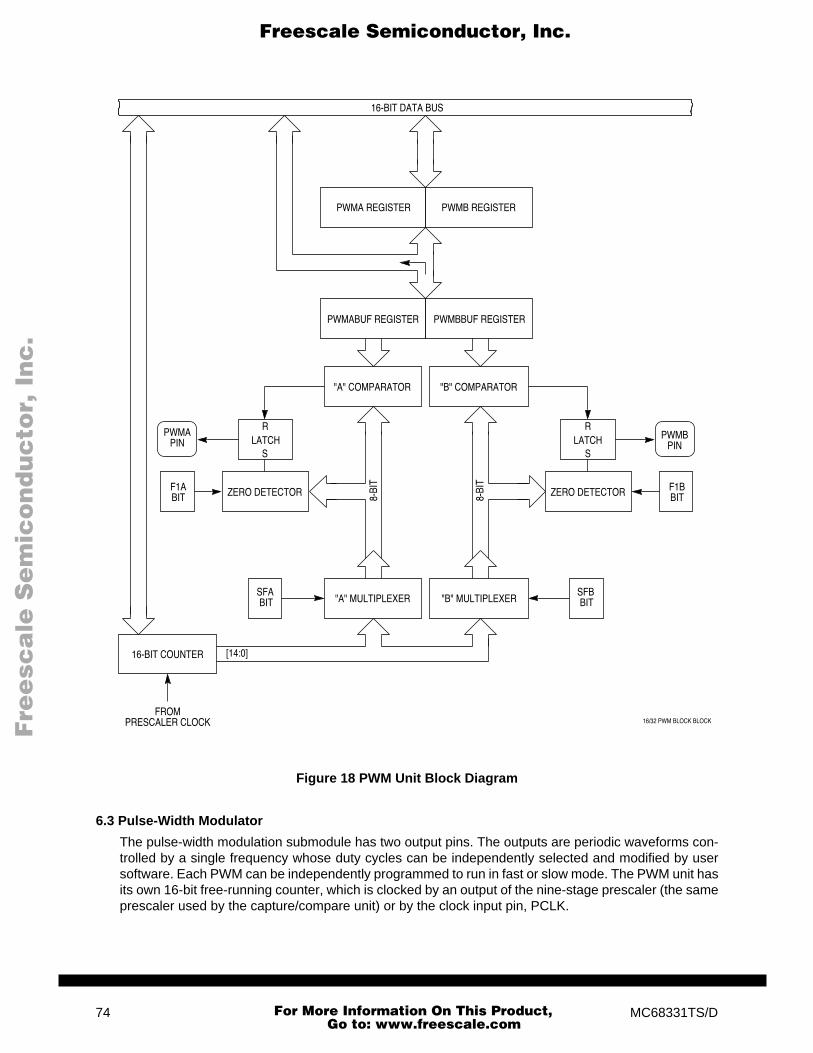
F
ree
sca
le S
em
ico
nd
uc
tor,
I
Freescale Semiconductor, Inc.n
c..
.
Figure 18 PWM Unit Block Diagram
6.3 Pulse-Width Modulator
The pulse-width modulation submodule has two output pins. The outputs are periodic waveforms con-trolled by a single frequency whose duty cycles can be independently selected and modified by usersoftware. Each PWM can be independently programmed to run in fast or slow mode. The PWM unit hasits own 16-bit free-running counter, which is clocked by an output of the nine-stage prescaler (the sameprescaler used by the capture/compare unit) or by the clock input pin, PCLK.
16/32 PWM BLOCK BLOCK
ZERO DETECTOR
16-BIT COUNTER
PWMA REGISTER PWMB REGISTER
PWMABUF REGISTER PWMBBUF REGISTER
"A" COMPARATOR "B" COMPARATOR
"A" MULTIPLEXER "B" MULTIPLEXERSFBBIT
SFABIT
F1ABIT
F1BBIT
LATCHR
SLATCH
R
S
ZERO DETECTOR
PWMBPIN
PWMAPIN
FROMPRESCALER CLOCK
[14:0]
16-BIT DATA BUS
8-BI
T
8-BI
T
74 MC68331TS/D
For More Information On This Product, Go to: www.freescale.com
F
ree
sca
le S
em
ico
nd
uc
tor,
I
Freescale Semiconductor, Inc.n
c..
.
6.4 GPT Registers
The GPTMCR contains parameters for configuring the GPT.
STOP — Stop Clocks0 = Internal clocks not shut down1 = Internal clocks shut down
FRZ1 — Not implemented at this time
FRZ0 — FREEZE Response0 = Ignore FREEZE1 = FREEZE the current state of the GPT
STOPP — Stop Prescaler0 = Normal operation1 = Stop prescaler and pulse accumulator from incrementing. Ignore changes to input pins.
INCP — Increment Prescaler0 = Has no meaning1 = If STOPP is asserted, increment prescaler once and clock input synchronizers once.
SUPV — Supervisor/Unrestricted Data Space0 = Registers with access controlled by SUPV bit are accessible from either user or supervisor priv-
ilege level.1 = Registers with access controlled by SUPV bit are restricted to supervisor access only.
IARB — Interrupt Arbitration FieldThe IARB field is used to arbitrate between simultaneous interrupt requests of the same priority. Eachmodule that can generate interrupt requests must be assigned a unique, non-zero IARB field value. Re-fer to 3.8 Interrupts for more information.
MTR — GPT Module Test Register (Reserved) $YFF902
This address is currently unused and returns zeros if read. It is reserved for GPT factory test.
IPA — Interrupt Priority Adjust Specifies which GPT interrupt source is given highest internal priority
IPL — Interrupt Priority Level Specifies the priority level of interrupts generated by the GPT.
IVBA — Interrupt Vector Base Address Most significant nibble of interrupt vector number generated by the GPT when an interrupt service re-quest is acknowledged.
GPTMCR — GPT Module Configuration Register $YFF900
15 14 13 12 11 10 9 8 7 6 5 4 3 0
STOP FRZ1 FRZ0 STOPP INCP 0 0 0 SUPV 0 0 0 IARB
RESET:
0 0 0 0 0 0 0 0 1 0 0 0 0 0 0 0
ICR — GPT Interrupt Configuration Register $YFF904
15 12 11 10 8 7 4 3 2 1 0
IPA 0 IPL IVBA 0 0 0 0
RESET:
0 0 0 0 0 0 0 0 0 0 0 0 0 0 0 0
MC68331TS/D 75
For More Information On This Product, Go to: www.freescale.com

F
ree
sca
le S
em
ico
nd
uc
tor,
I
Freescale Semiconductor, Inc.n
c..
.
When GPT pins are used as an 8-bit port, DDRGP determines whether pins are input or output andPORTGP holds the 8-bit data.
DDRGP[7:0] — Port GP Data Direction Register0 = Input only1 = Output
Each bit in DDRGP determines whether the corresponding PORTGP bit is input or output.
All OC outputs can be controlled by the action of OC1. OC1M contains a mask that determines whichpins are affected. OC1D determines what the outputs are.
OC1M[5:1] — OC1 Mask Field0 = Corresponding output compare pin is not affected by OC1 compare.1 = Corresponding output compare pin is affected by OC1 compare.
OC1M[5:1] correspond to OC[5:1].
OC1D[5:1] — OC1 Data Field0 = If OC1 mask bit is set, clear the corresponding output compare pin on OC1 match.1 = If OC1 mask bit is set, set the corresponding output compare pin on OC1 match.
OC1D[5:1] correspond to OC[5:1].
TCNT — Timer Counter Register $YFF90A
TCNT is the 16-bit free-running counter associated with the input capture, output compare, and pulseaccumulator functions of the GPT module.
PACTL enables the pulse accumulator and selects either event counting or gated mode. In event count-ing mode, PACNT is incremented each time an event occurs. In gated mode, it is incremented by aninternal clock.
PAIS — PAI Pin State (Read Only)
PAEN — Pulse Accumulator System Enable0 = Pulse accumulator disabled1 = Pulse accumulator enabled
DDRGP/PORTGP — Port GP Data Direction Register/Port GP Data Register $YFF906
15 14 13 12 11 10 9 8 7 6 5 4 3 2 1 0
DDGP7 DDGP6 DDGP5 DDGP4 DDGP3 DDGP2 DDGP1 DDGP0 PGP7 PGP6 PGP5 PGP4 PGP3 PGP2 PGP1 PGP0
RESET:
0 0 0 0 0 0 0 0 0 0 0 0 0 0 0 0
OC1M/OC1D — OC1 Action Mask Register/OC1 Action Data Register $YFF908
15 11 10 9 8 7 3 2 1 0
OC1M 0 0 0 OC1D 0 0 0
RESET:
0 0 0 0 0 0 0 0 0 0 0 0 0 0 0 0
PACTL/PACNT — Pulse Accumulator Control Register/Counter $YFF90C
15 14 13 12 11 10 9 8 7 0
PAIS PAEN PAMOD PEDGE PCLKS I4/O5 PACLK PACNT
RESET:
U 0 0 0 U 0 0 0 0 0 0 0 0 0 0 0
76 MC68331TS/D
For More Information On This Product, Go to: www.freescale.com
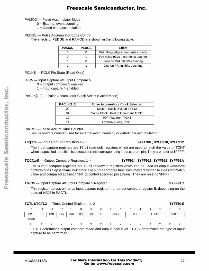
F
ree
sca
le S
em
ico
nd
uc
tor,
I
Freescale Semiconductor, Inc.n
c..
.
PAMOD — Pulse Accumulator Mode0 = External event counting1 = Gated time accumulation
PEDGE — Pulse Accumulator Edge ControlThe effects of PEDGE and PAMOD are shown in the following table.
PCLKS — PCLK Pin State (Read Only)
I4/O5 — Input Capture 4/Output Compare 50 = Output compare 5 enabled1 = Input capture 4 enabled
PACLK[1:0] — Pulse Accumulator Clock Select (Gated Mode)
PACNT — Pulse Accumulator Counter8-bit read/write counter used for external event counting or gated time accumulation.
TIC[1:3] — Input Capture Registers 1–3 $YFF90E, $YFF910, $YFF912
The input capture registers are 16-bit read-only registers which are used to latch the value of TCNTwhen a specified transition is detected on the corresponding input capture pin. They are reset to $FFFF.
TOC[1:4] — Output Compare Registers 1–4 $YFF914, $YFF916, $YFF918, $YFF91A
The output compare registers are 16-bit read/write registers which can be used as output waveformcontrols or as elapsed time indicators. For output compare functions, they are written to a desired matchvalue and compared against TCNT to control specified pin actions. They are reset to $FFFF.
TI4/O5 — Input Capture 4/Output Compare 5 Register $YFF91C
This register serves either as input capture register 4 or output compare register 5, depending on thestate of I4/O5 in PACTL.
TCTL1 determines output compare mode and output logic level. TCTL2 determines the type of inputcapture to be performed.
PAMOD PEDGE Effect0 0 PAI falling edge increments counter0 1 PAI rising edge increments counter1 0 Zero on PAI inhibits counting1 1 One on PAI inhibits counting
PACLK[1:0] Pulse Accumulator Clock Selected00 System Clock Divided by 51201 Same Clock Used to Increment TCNT10 TOF Flag from TCNT11 External Clock, PCLK
TCTL1/TCTL2 — Timer Control Registers 1–2 $YFF91E
15 14 13 12 11 10 9 8 7 6 5 4 3 2 1 0
OM5 OL5 OM4 OL4 OM3 OL3 OM2 OL2 EDGE4 EDGE3 EDGE2 EDGE1
RESET:
0 0 0 0 0 0 0 0 0 0 0 0 0 0 0 0
MC68331TS/D 77
For More Information On This Product, Go to: www.freescale.com

F
ree
sca
le S
em
ico
nd
uc
tor,
I
Freescale Semiconductor, Inc.n
c..
.
OM/OL[5:2] — Output Compare Mode Bits and Output Compare Level BitsEach pair of bits specifies an action to be taken when output comparison is successful.
EDGE[4:1] — Input Capture Edge Control BitsEach pair of bits configures input sensing logic for the corresponding input capture.
TMSK1 enables OC and IC interrupts. TMSK2 controls pulse accumulator interrupts and TCNT func-tions.
I4/O5I — Input Capture 4/Output Compare 5 Interrupt Enable0 = IC4/OC5 interrupt disabled 1 = IC4/OC5 interrupt requested when I4/O5F flag in TFLG1 is set
OCI[4:1] — Output Compare Interrupt Enable0 = OC interrupt disabled1 = OC interrupt requested when OC flag set
OCI[4:1] correspond to OC[4:1].
ICI[3:1] — Input Capture Interrupt Enable0 = IC interrupt disabled1 = IC interrupt requested when IC flag set
ICI[3:1] correspond to IC[3:1].
TOI — Timer Overflow Interrupt Enable0 = Timer overflow interrupt disabled1 = Interrupt requested when TOF flag is set
PAOVI — Pulse Accumulator Overflow Interrupt Enable0 = Pulse accumulator overflow interrupt disabled1 = Interrupt requested when PAOVF flag is set
PAII — Pulse Accumulator Input Interrupt Enable0 = Pulse accumulator interrupt disabled1 = Interrupt requested when PAIF flag is set
CPROUT — Compare/Capture Unit Clock Output Enable0 = Normal operation for OC1 pin 1 = TCNT clock driven out OC1 pin
OM/OL[5:2] Action Taken00 Timer Disconnected from Output Logic01 Toggle OCx Output Line10 Clear OCx Output Line to 011 Set OCx Output Line to 1
EDGE[4:1] Configuration00 Capture Disabled01 Capture on Rising Edge Only10 Capture on Falling Edge Only11 Capture on Any (Rising or Falling) Edge
TMSK1/TMSK2 — Timer Interrupt Mask Registers 1–2 $YFF920
15 14 11 10 8 7 6 5 4 3 2 0
I4/O5I OCI ICI TOI 0 PAOVI PAII CPROUT CPR
RESET:
0 0 0 0 0 0 0 0 0 0 0 0 0 0 0 0
78 MC68331TS/D
For More Information On This Product, Go to: www.freescale.com

F
ree
sca
le S
em
ico
nd
uc
tor,
I
Freescale Semiconductor, Inc.n
c..
.
CPR[2:0] — Timer Prescaler/PCLK Select FieldThis field selects one of seven prescaler taps or PCLK to be TCNT input.
These registers show condition flags that correspond to various GPT events. If the corresponding inter-rupt enable bit in TMSK1/TMSK2 is set, an interrupt occurs.
I4/O5F — Input Capture 4/Output Compare 5 FlagWhen I4/O5 in PACTL is zero, this flag is set each time TCNT matches the value in TOC5. When I4/O5in PACTL is one, the flag is set each time a selected edge is detected at the I4/O5 pin.
OCF[4:1] — Output Compare FlagsAn output compare flag is set each time TCNT matches the corresponding TOC register. OCF[4:1] cor-respond to OC[4:1].
ICF[3:1] — Input Capture FlagsA flag is set each time a selected edge is detected at the corresponding input capture pin. ICF[3:1] cor-respond to IC[3:1].
TOF — Timer Overflow Flag This flag is set each time TCNT advances from a value of $FFFF to $0000.
PAOVF — Pulse Accumulator Overflow FlagThis flag is set each time the pulse accumulator counter advances from a value of $FF to $00.
PAIF — Pulse Accumulator FlagIn event counting mode, this flag is set when an active edge is detected on the PAI pin. In gated timeaccumulation mode, PAIF is set at the end of the timed period.
CFORC/PWMC — Compare Force Register/PWM Control Register C $YFF924
Setting a bit in CFORC causes a specific output on OC or PWM pins. PWMC sets PWM operating con-ditions.
CPR[2:0] System Clock Divide-By Factor
000 4001 8010 16011 32100 64101 128110 256111 PCLK
TFLG1/TFLG2 — Timer Interrupt Flag Registers 1–2 $YFF922
15 14 11 10 8 7 6 5 4 3 2 1 0
I4/O5F OCF ICF TOF 0 PAOVF PAIF 0 0 0 0
RESET:
0 0 0 0 0 0 0 0 0 0 0 0 0 0 0 0
15 11 10 9 8 7 6 4 3 2 1 0
FOC 0 FPWMA FPWMB PPROUT PPR SFA SFB F1A F1B
RESET:
0 0 0 0 0 0 0 0 0 0 0 0 0 0 0 0
MC68331TS/D 79
For More Information On This Product, Go to: www.freescale.com

F
ree
sca
le S
em
ico
nd
uc
tor,
I
Freescale Semiconductor, Inc.n
c..
.
FOC[5:1] — Force Output Compare 0 = Has no meaning1 = Causes pin action programmed for corresponding OC pin, but the OC flag is not set.
FOC[5:1] correspond to OC[5:1].
FPWMA — Force PWMA Value0 = Normal PWMA operation1 = The value of F1A is driven out on the PWMA pin, regardless of the state of PPROUT.
FPWMB — Force PWMB Value0 = Normal PWMB operation1 = The value of F1B is driven out on the PWMB pin.
PPROUT — PWM Clock Output Enable0 = Normal PWM operation on PWMA1 = TCNT clock driven out PWMA pin
PPR[2:0] — PWM Prescaler/PCLK SelectThis field selects one of seven prescaler taps, or PCLK, to be PWMCNT input.
SFA — PWMA Slow/Fast Select0 = PWMA period is 256 PWMCNT increments long.1 = PWMA period is 32768 PWMCNT increments long.
SFB — PWMB Slow/Fast Select0 = PWMB period is 256 PWMCNT increments long.1 = PWMB period is 32768 PWMCNT increments long.
The following table shows the effects of SF settings on PWM frequency for a 16.78-MHz system clockand a 20.97-MHz system clock.
F1A — Force Logic Level One on PWMA0 = Force logic level zero output on PWMA pin1 = Force logic level one output on PWMA pin
PPR[2:0] System Clock Divide-By Factor
000 2001 4010 8011 16100 32101 64110 128111 PCLK
PPR[2:0] Prescaler Tap SFA/B = 0 SFA/B = 116.78 MHz 20.97 MHz 16.78 MHz 20.97 MHz 16.78 MHz 20.97 MHz
000 Div 2 = 8.39 MHz Div 2 = 10.5 MHz 32.8 kHz 41 kHz 256 Hz 320 Hz001 Div 4 = 4.19 MHz Div 4 = 5.25 MHz 16.4 kHz 20.5 kHz 128 Hz 160 Hz010 Div 8 = 2.10 MHz Div 8 = 2.62 MHz 8.19 kHz 10.2 kHz 64.0 Hz 80.0 Hz011 Div 16 = 1.05 MHz Div 16 = 1.31 MHz 4.09 kHz 5.15 kHz 32.0 Hz 40.0 Hz100 Div 32 = 524 kHz Div 32 = 655 kHz 2.05 kHz 2.56 kHz 16.0 Hz 20.0 Hz101 Div 64 = 262 kHz Div 64 = 328 kHz 1.02 kHz 1.28 kHz 8.0 Hz 10.0 Hz110 Div 128 = 131 kHz Div 128 = 164 kHz 512 Hz 641 Hz 4.0 Hz 5.0 Hz111 PCLK PCLK PCLK/256 PCLK/256 PCLK/32768 PCLK/32768
80 MC68331TS/D
For More Information On This Product, Go to: www.freescale.com

F
ree
sca
le S
em
ico
nd
uc
tor,
I
Freescale Semiconductor, Inc.n
c..
.
F1B — Force Logic Level One on PWMB0 = Force logic level zero output on PWMB pin1 = Force logic level one output on PWMB pin
PWMA/PWMB — PWM Control Registers A/B $YFF926, $YFF927
These registers are associated with the pulse-width value of the PWM output on the correspondingPWM pin. A value of $00 loaded into one of these registers results in a continuously low output on thecorresponding pin. A value of $80 results in a 50% duty cycle output. Maximum value ($FF) selects anoutput that is high for 255/256 of the period.
PWMCNT — PWM Count Register $YFF928
PWMCNT is the 16-bit free-running counter associated with the PWM functions of the GPT module.
PWMBUFA/B — PWM Buffer Registers A/B $YFF92A, $YFF92B
These read-only registers contain values associated with the duty cycles of the corresponding PWM.Reset state is $0000.
PRESCL — GPT Prescaler $YFF92C
The 9-bit prescaler value can be read from bits [8:0] at this address. Bits [15:9] always read as zeros.Reset state is $0000.
MC68331TS/D 81
For More Information On This Product, Go to: www.freescale.com

F
ree
sca
le S
em
ico
nd
uc
tor,
I
Freescale Semiconductor, Inc.n
c..
.
7 Summary of ChangesThis is a complete revision, with complete reprint. All known errors in the publication have been correct-ed. The following summary lists significant changes. Typographical errors that do not affect content arenot annotated.
Page 2 Revised ordering information.
Page 5 New block diagram drawn.
Page 6 New 132-pin assignment diagram drawn.
Page 7 New 144-pin assignment diagram drawn.
Page 8 New address map drawn.
Page 9-13 Added Signal Description section.
Page 14-46 Expanded and revised SIM section. Made all register diagrams and bit mnemonicsconsistent. Incorporated new information concerning the system clock, resets, in-terrupts, and chip-select circuits.
Page 47-55 Expanded and revised CPU section. Made all register diagrams and bit mnemon-ics consistent. Revised instruction set summary information.
Page 56-76 Expanded and revised QSM section. Made all register diagrams and bit mnemon-ics consistent. Added information concerning SPI and SCI operation.
Page 77-89 Expanded and revised GPT section. Made all registerdiagrams and bit mnemonicsconsistent. Added information concerning input capture, output compare, andPWM operation.
82 MC68331TS/D
For More Information On This Product, Go to: www.freescale.com

F
ree
sca
le S
em
ico
nd
uc
tor,
I
Freescale Semiconductor, Inc.n
c..
.
MC68331TS/D 83
For More Information On This Product, Go to: www.freescale.com
MC68331TS/D
Fre
esc
ale
Se
mic
on
du
cto
r, I
Freescale Semiconductor, Inc.
For More Information On This Product, Go to: www.freescale.com
nc
...
Top Related
Copyright © 2022 FDOKUMEN

