

Bahasa
Halaman
Hukum


FN9054Rev.7.00
Oct 2, 2020
ISL72991RHRadiation Hardened Low Dropout Adjustable Negative Voltage Regulator
DATASHEET
The radiation hardened ISL72991RH is a low dropout adjustable negative regulator with an output voltage range of -2.25V to -26V. The device features a 1A output current capability, an adjustable current limit pin (ILIM), and a shutdown pin (SD) for easy on/off control.
The device incorporates unique circuitry that enables precision performance across the -55°C to +125°C temperature range and post-irradiation. Specifications across the full temperature range include an internal reference voltage of -1.25V +40mV/-50mV (maximum), line regulation of ±25mV (maximum), and load regulation of ±15mV (maximum). The reference voltage is the ADJ to GND voltage.
Constructed with the dielectrically isolated Rad Hard Silicon Gate (RSG) BiCMOS process, these devices are immune to single event latch-up and have been specifically designed to provide highly reliable performance in harsh radiation environments.
Applications• Post switching power supplies
• DC/DC converters
• Motor controllers
Features• Electrically screened to DLA SMD # 5962-02503
• QML qualified per MIL-PRF-38535 requirements
• Latch-up immune DI process
• Wide input voltage range . . . . . . . . . . . . . . . . . . . . -3V to -30V
• Nominal output voltage range . . . . . . . . . . . . . -2.25V to -26V
• Line regulation. . . . . . . . . . . . . . . . . . . . . . . .±25mV (maximum)
• Load regulation . . . . . . . . . . .±12mV (typ); ±15mV (maximum)
• Dropout voltage (100mA) . . . . . . 0.2V (typ); 0.3V (maximum)
• Dropout voltage (1A) . . . . . . . . . . . . . . . . . . . . . 1V (maximum)
• Minimum load current. . . . . . . . . . . . . . . . . . . . . . . . . . . 3.0mA
• TTL input-level shutdown (SD); low = on
• Operating temperature range. . . . . . . . . . . . -55°C to +125°C
• Radiation acceptance testing
- HDR (50-300rad(Si)/s): . . . . . . . . . . . . . . . . . . . 300krad(Si)
• SEE hardness (see SEE report for details)
- SEL/SEB LETTH (VS = -30V) . . . . . . . . . . 86.4MeV•cm2/mg
Related LiteratureFor a full list of related documents, visit our website
- ISL72991RH product page
FIGURE 1. TYPICAL APPLICATION FIGURE 2. VREF AND ISCL vs TEMPERATURE
ISL72991RHVINILIMSDGND
VOUT
ADJ
VIN
CIN
RCL
R1
CC
R2
COUT
VOUT
R1
R2
TEMPERATURE (°C)
-75 -50 -25 0 25 50 75 100 125-1.249
-1.248
-1.247
-1.246
-1.245
-1.244
VR
EF (
V)
ISCL (RCL = 3.7kΩ)
750
760
770
780
790
800
ISC
L (mA
)
VREF (VIN = -7V, IOUT = 1A)
FN9054 Rev.7.00 Page 1 of 14Oct 2, 2020

ISL72991RH
Ordering InformationORDERING SMD
NUMBER (Note 2)PART NUMBER
(Note 1)RADIATION HARDNESS
(Total Ionizing Dose)TEMP RANGE
(°C)PACKAGE
(RoHS COMPLIANT)PKG.
DWG. #
5962F0250301VXC ISL72991RHVF HDR to 300krad(Si) -55 to +125 28 Ld Flatpack K28.A
5962F0250301QXC ISL72991RHQF -55 to +125 28 Ld Flatpack K28.A
5962F0250301V9A ISL72991RHVX (Note 3) -55 to +125 DIE N/A
N/A ISL72991RHF/PROTO (Note 4) N/A -55 to +125 28 Ld Flatpack K28.A
N/A ISL72991RHX/SAMPLE (Notes 3, 4) N/A -55 to +125 DIE N/A
N/A ISL72991RHEVAL2Z (Note 5) Evaluation Board
NOTES:
1. These Pb-free Hermetic packaged products employ 100% Au plate - e4 termination finish, which is RoHS compliant and compatible with both SnPb and Pb-free soldering operations.
2. Specifications for Rad Hard QML devices are controlled by the Defense Logistics Agency Land and Maritime (DLA). The SMD numbers listed must be used when ordering.
3. Die product tested at TA = + 25°C. The wafer probe test includes functional and parametric testing sufficient to make the die capable of meeting the electrical performance outlined in “Electrical Specifications” on page 5.
4. The /PROTO and /SAMPLE are not rated or certified for Total Ionizing Dose (TID) or Single Event Effect (SEE) immunity. These parts are intended for engineering evaluation purposes only. The /PROTO parts meet the electrical limits and conditions across temperature specified in the DLA SMD and are in the same form and fit as the qualified device. The /SAMPLE parts are capable of meeting the electrical limits and conditions specified in the DLA SMD. The /SAMPLE parts do not receive 100% screening across temperature to the DLA SMD electrical limits. These part types do not come with a Certificate of Conformance because they are not DLA qualified devices.
5. Evaluation board uses the /PROTO parts. The /PROTO parts are not rated or certified for Total Ionizing Dose (TID) or Single Event Effect (SEE) immunity.
Pin Configuration28 LD FLATPACK
TOP VIEW
1
2
3
4
5
6
7
8
9
10
11
12
13
14
28
27
26
25
24
23
22
21
20
19
18
17
16
15
VIN
VIN
NC
NC
NC
NC
NC
NC
NC
NC
GND
ILIM
VOUT
VOUT
VIN
VIN
NC
NC
NC
NC
NC
NC
NC
NC
ADJ
SD
VOUT
VOUT
FN9054 Rev.7.00 Page 2 of 14Oct 2, 2020

ISL72991RH
Functional Block Diagram
Pin DescriptionsPIN NUMBER PIN NAME EQUIVALENT CIRCUIT DESCRIPTION
1, 2, 27, 28 VIN Circuit 2 Regulator bias and input connection. All 4 pins must be tied together.
12 ILIM Circuit 2 Current limiting set input.
13, 14, 15, 16 VOUT Circuit 2 Regulator output connection. All 4 pins must be tied together.
17 SD Circuit 1 Shut down input, active high.
18 ADJ Circuit 2 Output voltage adjust input
11 GND Ground connection
3, 4, 5, 6, 7, 8, 9, 10, 19, 20, 21, 22, 23, 24, 25, 26
NC No Internal connections. Can be connected to ground or thermal plane.
GNDCIRCUIT 1
CAPACITIVELYCOUPLED
ESD CLAMP
GND
CIRCUIT 2
CAPACITIVELYCOUPLED
ESD CLAMP
+
-
VIN
ADJ
ILIM
SDAI
IIN I
GND
VOUT
-1.25V
VIN+
-I
2.4kΩ
-1
FIGURE 3. FUNCTIONAL BLOCK DIAGRAM
FN9054 Rev.7.00 Page 3 of 14Oct 2, 2020

ISL72991RH
Typical Application
ISL72991RHVINILIMSDGND
VOUT
ADJ
VIN
CIN
RCL
R1
CC
R2
COUT
VOUT
ON/OFF
UNREGULATED VIN(-3V to -30V) (-2.25V to -26V)
- VDC TO -VDC VOLTAGE REGULATION CIRCUIT
REGULATED VOUT
R1
R2
FIGURE 4. TYPICAL APPLICATION
FN9054 Rev.7.00 Page 4 of 14Oct 2, 2020

ISL72991RH
Absolute Maximum Ratings Thermal InformationMinimum Supply Voltage . . . . . . . . . . . . . . . . . . . . . . . . . . . . . . . . . . . . -35VMinimum Supply Voltage (Note 8) . . . . . . . . . . . . . . . . . . . . . . . . . . . . . -30VMinimum Output Current . . . . . . . . . . . . . . . . . . . . . . . . . . . . . . . . . . . . 3mAOutput Short-Circuit Duration. Thermal Protection . . . . . . . . . . . IndefiniteESD Rating
Human Body Model (HBM) (Tested per MIL-PRF-883 3015.7). . . . . 3kVMachine Model (MM) (Tested per EIA/JESD22-A115-A) . . . . . . . . . 300VCharged Device Model (CDM) (Tested per JESD22-C101D) . . . . . . . 1kV
Thermal Resistance (Typical) JA (°C/W) JC (°C/W)28 Ld Flatpack (Notes 6, 7). . . . . . . . . . . . . 60 5
Maximum Storage Temperature Range . . . . . . . . . . . . . .-65°C to +150°CMaximum Junction Temperature (TJMAX) . . . . . . . . . . . . . . . . . . . . .+150°C
Recommended Operating ConditionsAmbient Operating Temperature Range . . . . . . . . . . . . . .-55°C to +125°CMaximum Operating Junction Temperature . . . . . . . . . . . . . . . . . .+150°CSupply Voltage . . . . . . . . . . . . . . . . . . . . . . . . . . . . . . . . . . . . . . . . -3V to -30V
CAUTION: Do not operate at or near the maximum ratings listed for extended periods of time. Exposure to such conditions may adversely impact productreliability and result in failures not covered by warranty.
NOTES:
6. JA is measured with the component mounted on a low-effective thermal conductivity test board in free air. See TB379 for details.
7. For JC, the “case temp” location is the center of the package underside.
8. The minimum supply limit specified is for operation in a heavy ion environment at an LET = 86.4MeV•cm2/mg.
Electrical Specifications VO ≤ VIN -1.5V, IO = 100mA, CO = 47µF, SD = 0V, TA = +25°C, unless otherwise noted. Boldface limits apply across the operating temperature range, -55°C to +125°C.
DESCRIPTION PARAMETER TEST CONDITIONSMIN
(Note 9) TYPMAX
(Note 9) UNIT
Reference Voltage (ADJ to GND) VREF IO = 3mA to 1A -1.279 -1.250 -1.231 V
-1.300 -1.210 V
Minimum Output Voltage VOmin VIN = -3V, IO = 3mA to 100mA -2.25 V
Maximum Output Voltage VOmax VIN = -30V, IO = 3mA to 100mA -26 V
Output Voltage Load Regulation VLDR VIN = -7V, VO = -5V IO = 3mA to 1A -12 12 mV
-15 15 mV
Output Voltage Line Regulation VLNR VO ≤ VIN -1V to VIN = -30V, IO = 100mA -25 25 mV
0.1A Dropout Voltage VDOL dVO ≤ 50mV, IO = 0.1A 0.2 V
0.3 V
1A Dropout Voltage (Pulse Tested) VDOH dVO ≤ 50mV, IO = 1A 1 V
Adjust Current IADJ VO ≤ VIN -1V to VIN = -30V, IO = 500mA 1.7 5.0 µA
Dropout Quiescent Current IQDO VO - VIN = 0.2V, IO = 500mA 25 mA
VO - VIN = 0.3V, IO = 500mA 25 mA
SD Input Voltage VSD VO = ON 0.8 V
VO = OFF 2.4 V
SD Input Current ISD VSD = 0.8V 50 µA
VSD = 2.4V 100 µA
150 µA
Output Short-Circuit Current Limit ISCL VIN = - 7V, VO = 0V, RCL = 3.7kΩ 0.60 0.75 0.90 A
GND Quiescent Current IGND -3V≤ VIN ≤ -30V, IO < 1A 6 mA
Power Supply Rejection Ratio PSRR Frequency = 1MHz -49 dB
Thermal Protection OTPROT 150 °C
Thermal Hysteresis OTHYS 20 °C
FN9054 Rev.7.00 Page 5 of 14Oct 2, 2020

ISL72991RH
Post Radiation Electrical Specifications VO ≤ VIN -1.5V, IO = 100mA, CO = 47µF, SD = 0V, TA = +25°C, across a total ionizing dose of 300krad(Si) with exposure at a high dose rate of 50 to 300rad(Si)/s.
PARAMETER DESCRIPTION TEST CONDITIONSMIN
(Note 9) TYPMAX
(Note 9) UNITS
VREF Reference Voltage IO = 3mA to 1A -1.279 -1.231 V
VOmin Minimum Output Voltage VIN = -3V, IO = 3mA to 100mA -2.25 V
VOmax Maximum Output Voltage VIN = -30V, IO = 3mA to 100mA -26 V
VLDR Output Voltage Load Regulation VIN = -7V, VO = -5V IO = 3mA to 1A -12 12 mV
VLNR Output Voltage Line Regulation VO ≤ VIN -1V to VIN = -30V, IO = 100mA -25 25 mV
VDOL 0.1A Dropout Voltage dVO ≤ 50mV, IO = 0.1A 0.2 V
VDOH 1A Dropout Voltage (Pulse Tested) dVO ≤ 50mV, IO = 1A 1 V
IADJ Adjust Current VO ≤ VIN -1V to VIN = -30V, IO = 500mA 5 µA
IQDO Dropout Quiescent Current VO - VIN = 0.3V, IO = 500mA 25 mA
VSD SD Input Voltage VO = ON 0.8 V
VO = OFF 2.4 V
ISD SD Input Current VSD = 0.8V 50 µA
VSD = 2.4V 100 µA
ICL Output Short-Circuit Current Limit VIN = - 7V, VO = 0V, RCL = 3.7kΩ 0.6 0.9 A
NOTE:9. Compliance to datasheet limits is assured by one or more methods: production test, characterization, and/or design.
FN9054 Rev.7.00 Page 6 of 14Oct 2, 2020
ISL72991RH
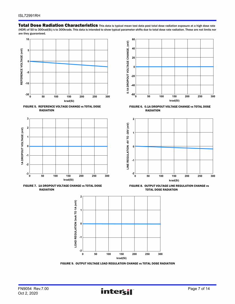
Total Dose Radiation Characteristics This data is typical mean test data post total dose radiation exposure at a high dose rate (HDR) of 50 to 300rad(Si)/s to 300krads. This data is intended to show typical parameter shifts due to total dose rate radiation. These are not limits nor are they guaranteed.
FIGURE 5. REFERENCE VOLTAGE CHANGE vs TOTAL DOSE RADIATION
FIGURE 6. 0.1A DROPOUT VOLTAGE CHANGE vs TOTAL DOSE RADIATION
FIGURE 7. 1A DROPOUT VOLTAGE CHANGE vs TOTAL DOSE RADIATION
FIGURE 8. OUTPUT VOLTAGE LINE REGULATION CHANGE vs TOTAL DOSE RADIATION
FIGURE 9. OUTPUT VOLTAGE LOAD REGULATION CHANGE vs TOTAL DOSE RADIATION
-30
-10
-5
0
5
10
0 50 100 150 200 250 300
krad(Si)
RE
FE
RE
NC
E V
OLT
AG
E (
mV
)
0 50 100 150 200 250 300
krad(Si)
-60
-40
-20
0
20
40
60
0.1
A D
RO
PO
UT
VO
LTA
GE
CH
AN
GE
, (m
V)
krad(Si)
-3
-2
-1
0
1
2
3
1A
DR
OP
OU
T V
OLT
AG
E (
mV
)
0 50 100 150 200 250 300 0 50 100 150 200 250 300
krad(Si)
LIN
E R
EG
UL
AT
ION
-4V
TO
-30
V (
mV
)
-2
-1
0
1
2
0 50 100 150 200 250 300
krad(Si)
LO
AD
RE
GU
LA
TIO
N 3
mA
TO
1A
(m
V)
-2
-1
0
1
2
FN9054 Rev.7.00 Page 7 of 14Oct 2, 2020

ISL72991RH
Typical Performance Curves
FIGURE 10. -7VIN, -5VOUT FIGURE 11. -12VIN, -5VOUT
FIGURE 12. -12VIN, -10VOUT FIGURE 13. -20VIN, -10VOUT
FIGURE 14. VREF vs TEMPERATURE FIGURE 15. DROPOUT VOLTAGE vs TEMPERATURE
0.0
0.2
0.4
0.6
0.8
1.0
1.2
1.4
2 3 4 5 6 7 8 9 10
-55°C
+125°C
+25°C
CU
RR
EN
T L
IMIT
(A
)
RCL (kΩ)
0.0
0.2
0.4
0.6
0.8
1.0
1.2
1.4
1.6
2 3 4 5 6 7 8 9 10
+25°C
+125°C
-55°C
CU
RR
EN
T L
IMIT
(A
)
RCL (kΩ)
0.0
0.2
0.4
0.6
0.8
1.0
1.2
1.4
1.6
2 3 4 5 6 7 8 9 10
CU
RR
EN
T L
IMIT
(A
)
RCL (kΩ)
-55°C
+125°C
+25°C
0.0
0.5
1.0
1.5
2.0
2.5
2 3 4 5 6 7 8 9 10
CU
RR
EN
T L
IMIT
(A
)
RCL (kΩ)
+125°C
+25°C
-55°C
TEMPERATURE (°C)
-50 -25 0 25 50 75 100 125-1.250
-1.249
-1.248
-1.247
-1.246
-1.245
VR
EF (
V)
-1.244
VREF (VIN = -30V, IOUT = 0A)
VREF (VIN = -30V, IOUT = 1A)
VREF (VIN = -3.5V, IOUT = 0A)
VREF (VIN = -3.5V, IOUT = 1A)
150
CONTINUOUS OUTPUT CURRENT (mA)
VD
O (
mV
)
VDO (VOUT = -10V)
1200
1000
800
600
400
200
0 100 200 300 400 500 600 700 8000
-55°C
+25°C
+125°C
FN9054 Rev.7.00 Page 8 of 14Oct 2, 2020

ISL72991RH
FIGURE 16. LINE REGULATION vs TEMPERATURE FIGURE 17. LOAD REGULATION vs TEMPERATURE
FIGURE 18. PSRR vs FREQUENCY (VIN = -20V, VOUT = -18V) FIGURE 19. PSRR vs FREQUENCY (VIN = -7V, VOUT = -5V)
FIGURE 20. GAIN/PHASE -12VIN, -5VOUT, 0.5A IOUT FIGURE 21. THERMAL (VIN = -12V, VOUT = -5V, IOUT = 0.74A, TA = +25°C)
Typical Performance Curves (Continued)
TEMPERATURE (°C)
-50 -25 0 25 50 75 100 1250.0
0.5
1.0
1.5
2.0
2.5
VL
NR
(m
V)
3.0
VLNR (VIN = -4V TO -30V, IOUT = 100mA)
TEMPERATURE (°C)-50 -25 0 25 50 75 100 125
0
2
4
6
8
10
VL
DR
(m
V)
VLDR
(IOUT = 3mA TO 1A)
-100
-90
-80
-70
-60
-50
-40
10 100 1k 10k 100k 1M 10M
FREQUENCY (Hz)
PS
RR
(d
B)
COUT = 30µF
COUT = 10µF
-100
-90
-80
-70
-60
-50
-40
FREQUENCY (Hz)
PS
RR
(d
B)
10 100 1k 10k 100k 1M 10M
COUT = 30µF
COUT = 10µF
0
20
40
60
80
100
120
140
160
180
200
-10
-5
0
5
10
15
20
25
30
35
40
45
100 1k 10k 100k 1M
PH
AS
E (
°)
GA
IN (
dB
)
FREQUENCY (Hz)
PHASE
GAIN
FN9054 Rev.7.00 Page 9 of 14Oct 2, 2020

ISL72991RH
Functional DescriptionFunctional OverviewThe radiation hardened ISL72991RH is a low dropout adjustable negative regulator with an output voltage range of -2.25V to -26V. The device features a 1A output current capability, an adjustable current limit pin (ILIM), and a shutdown pin (SD) for easy on/off control. The part is constructed using the dielectrically isolated, complimentary bipolar RSG process. It is immune to single-event latch-up and has been specifically designed to provide reliable performance in harsh radiation environments.
Application InformationOutput Voltage ProgrammingThe output voltage of the regulator can be programmed with two external resistors and is described by Equation 1:
Output Current Limit ProgrammingThe output current limit threshold of the regulator is set with a single external resistor (RCL) connected from ILIM to ground.
The effective current limit at any single RCL value is influenced by the VIN to VOUT difference, temperature, and VIN amplitude. Figures 22 through 24 illustrate these effects.
Figure 22 shows that for a given VOUT (-5V) and temperature (+25°C) the effect of VIN to VOUT differential on the current limit level is significant.
Figure 23 shows the effect of temperature at a single VIN to VOUT voltage condition across the RCL range of 2.1kΩ to 10kΩ.
Figure 24 shows that for a given differential voltage (VIN to VOUT) and temperature, the effect of VIN amplitude is less significant than seen in Figure 22.
Because of these numerous variables, there is no one formula relating RCL to ICL that will suffice for the range of likely possible conditions. Figures 10 through 13 on page 8 provide guidance in setting the RCL value for a limited number of possible conditions. Users are advised to evaluate their specific condition for satisfactory performance.
Capacitor SelectionAn input capacitor is required if the regulator is located more than 6 inches from the power supply filter capacitors. A 10µF solid tantalum capacitor is recommended.
An output capacitor of at least 10µF must be used to ensure stability of the regulator. Additional capacitance may be added as required to improve the dynamic response of the regulator. Solid tantalum or ceramic capacitors are recommended.
Loop CompensationThe output capacitor and ESR comprise a zero in the loop transfer function that must be compensated with a pole to ensure loop stability in accordance with Equation 2:
The compensating capacitor should be a low ESR ceramic type.
Layout GuidelinesThe stability of the regulator is sensitive to layout. It is strongly recommended that a continuous copper ground plane (1oz. or greater) be used. In addition, component lead lengths and interconnects should be minimized, but should not exceed 1/2 inch. Finally, the return lead of the compensation capacitor (CC) should be connected as close as possible to the GND pin of the IC.
VOUT 1.25– 1 R1 R2+ IADJ R1 –= (EQ. 1)
CC R1 COUT ESR= (EQ. 2)
FIGURE 22. ICL vs RCL AND VIN AMPLITUDE
FIGURE 23. ICL vs RCL AND TEMPERATURE
FIGURE 24. ICL vs RCL AND VIN TO VOUT DIFFERENTIAL
0.0
0.2
0.4
0.6
0.8
1.0
1.2
1.4
1.6
1.8
2.0
2 3 4 5 6 7 8 9 10
-12VIN, -5VOUT
-7VIN, -5VOUT
+25°C
RCL (kΩ)C
UR
RE
NT
LIM
IT (
A)
0.0
0.2
0.4
0.6
0.8
1.0
1.2
1.4
2 3 4 5 6 7 8 9 10
CU
RR
EN
T L
IMIT
(A
)
RCL (kΩ)
-7VIN, -5VOUT
+125°C
+25°C
-55°C
0.0
0.2
0.4
0.6
0.8
1.0
1.2
1.4
2 3 4 5 6 7 8 9 10
-12VIN, -10VOUT
-7VIN, -5VOUT
RCL (kΩ)
+25°C
CU
RR
EN
T L
IMIT
(A
)
FN9054 Rev.7.00 Page 10 of 14Oct 2, 2020

ISL72991RH
Package CharacteristicsWeight of Packaged Device
2.2 Grams (Typical)
Lid CharacteristicsFinish: GoldPotential: UnbiasedCase Isolation to Any Lead: 20 x 109 Ω (min)
Die CharacteristicsDie Dimensions
5870µm x 5210µm (231.1 mils x 205.1 mils)Thickness: 483µm ±25.4µm (19 mils ±1 mil)
Interface Materials
GLASSIVATIONType: PSG (Phosphorous Silicon Glass)Thickness: 8.0kÅ ±1.0kÅ
TOP METALLIZATIONType: AlSiCu (Si 0.75-1%/Cu 0.5%)Thickness: 16.0kÅ ±2kÅ
BACKSIDE FINISH Silicon
Assembly Related Information
SUBSTRATE AND LID POTENTIALFloating
Additional Information
WORST CASE CURRENT DENSITY<2 x 10⁵ A/cm2
PROCESSDielectrically Isolated Radiation Hardened Silicon Gate
Metallization Mask Layout
(1) VIN (28) VIN
(27) VIN
(16) VOUT
(18) ADJUST
(17) SHUTDOWN(12) ILIM
(11) GND
(15) VOUT
(14) VOUT
(2) VIN
2
1 28
27
14 15 16
11
12
17
18
FN9054 Rev.7.00 Page 11 of 14Oct 2, 2020

ISL72991RH
TABLE 1. DIE PAD COORDINATES
PAD NAME X-COR CENTER Y-COR CENTER DX PAD SIZE DY PAD SIZE
ILIM -1300.5 -4348 258 516
(15)VOUT 920 -2554 516 516
SHUTDOWN 3140.5 -4348 258 516
ADJUST 3473.5 -3658 258 516
(16)VOUT 2917 -2554 516 516
(27)VIN 3580 0 258 516
(28)VIN 1840 0 516 516
(1)VIN 0 0 516 516
(2)VIN -1740 0 258 516
(14)VOUT -1077 -2554 516 516
GND -1662 -3657 258 516
FN9054 Rev.7.00 Page 12 of 14Oct 2, 2020

ISL72991RH
Revision History The revision history provided is for informational purposes only and is believed to be accurate, but not warranted. Please go to web to make sure you have the latest Revision.
DATE REVISION CHANGE
Oct 2, 2020 7.00 Updated links throughout.Applied new formatting standard to Radiation Acceptance Testing and SEE Hardness Features bullets.Updated Ordering information table by adding Rad Hard data, adding Note 3, and updating Note 4.In Table 1 on page 12 Updated pad name (27) to VIN and corrected Y-COR CENTER coordinates for the following pad names: - (15)VOUT, (27) VIN, and (2)VINRemoved About Intersil section
Apr 14, 2017 6.00 Added Notes 4 and 5 on page 2.Added Table 1 on page 12.
Aug 17, 2016 5.00 Updated Equation 2 Loop Compensation equation to change R2 to R1.
May 7, 2015 4.00 Replaced Figures 10, 11, 12 and 13 on page 8.Replaced Figures 22, 23 and 24 on page 10.Updated Equation 1 on page 10: from VOUT = -1.25(1+R2/R1) - (IADJ x R2) to VOUT = -1.25(1+R1/R2) - (IADJ x R1).
Jan 29, 2015 3.00 “Typical Performance Curves” on page 8: Added Figures 18 and 19.
Mar 26, 2014 2.00 Added Related Literature on page 1.Added significant relevant content throughout the document, expanding from 3 to 12 pages.
Jun, 28, 2004 1.00 Updated file.
Jul 9, 2001 4.00 Initial Release.
FN9054 Rev.7.00 Page 13 of 14Oct 2, 2020

ISL72991RH
Package Outline Drawing
NOTES:
1. Index area: A notch or a pin one identification mark shall be located adjacent to pin one and shall be located within the shaded areashown. The manufacturer’s identification shall not be used as a pinone identification mark. Alternately, a tab (dimension k) may beused to identify pin one.
2. If a pin one identification mark is used in addition to a tab, the limits of dimension k do not apply.
3. This dimension allows for off-center lid, meniscus, and glass over-run.
4. Dimensions b1 and c1 apply to lead base metal only. Dimension M applies to lead plating and finish thickness. The maximum limits oflead dimensions b and c or M shall be measured at the centroid ofthe finished lead surfaces, when solder dip or tin plate lead finish isapplied.
5. N is the maximum number of terminal positions.
6. Measure dimension S1 at all four corners.
7. For bottom-brazed lead packages, no organic or polymeric materi-als shall be molded to the bottom of the package to cover the leads.
8. Dimension Q shall be measured at the point of exit (beyond the me-niscus) of the lead from the body. Dimension Q minimum shall bereduced by 0.0015 inch (0.038mm) maximum when solder dip leadfinish is applied.
9. Dimensioning and tolerancing per ANSI Y14.5M - 1982.
10. Controlling dimension: INCH.
-D-
-C-
0.004 H A - BM DS S
-A- -B-
0.036 H A - BM DS S
e
E
A
Q
L
D
A
E1
SEATING AND
LE2
E3 E3
BASE PLANE
-H-
b
C
S1
M
c1
b1
(c)
(b)
SECTION A-A
BASE
LEAD FINISH
METAL
PIN NO. 1ID AREA
A
M
K28.A MIL-STD-1835 CDFP3-F28 (F-11A, CONFIGURATION B)28 lead ceramic metal seal flatpack package
SYMBOL
INCHES MILLIMETERS
NOTESMIN MAX MIN MAX
A 0.045 0.115 1.14 2.92 -
b 0.015 0.022 0.38 0.56 -
b1 0.015 0.019 0.38 0.48 -
c 0.004 0.009 0.10 0.23 -
c1 0.004 0.006 0.10 0.15 -
D - 0.740 - 18.80 3
E 0.460 0.520 11.68 13.21 -
E1 - 0.550 - 13.97 3
E2 0.180 - 4.57 - -
E3 0.030 - 0.76 - 7
e 0.050 BSC 1.27 BSC -
k 0.008 0.015 0.20 0.38 2
L 0.250 0.370 6.35 9.40 -
Q 0.026 0.045 0.66 1.14 8
S1 0.00 - 0.00 - 6
M - 0.0015 - 0.04 -
N 28 28 -
Rev. 0 5/18/94
For the most recent package outline drawing, see K28.A.
FN9054 Rev.7.00 Page 14 of 14Oct 2, 2020

Corporate HeadquartersTOYOSU FORESIA, 3-2-24 Toyosu,Koto-ku, Tokyo 135-0061, Japanwww.renesas.com
Contact InformationFor further information on a product, technology, the most up-to-date version of a document, or your nearest sales office, please visit:www.renesas.com/contact/
TrademarksRenesas and the Renesas logo are trademarks of Renesas Electronics Corporation. All trademarks and registered trademarks are the property of their respective owners.
IMPORTANT NOTICE AND DISCLAIMER
RENESAS ELECTRONICS CORPORATION AND ITS SUBSIDIARIES (“RENESAS”) PROVIDES TECHNICAL SPECIFICATIONS AND RELIABILITY DATA (INCLUDING DATASHEETS), DESIGN RESOURCES (INCLUDING REFERENCE DESIGNS), APPLICATION OR OTHER DESIGN ADVICE, WEB TOOLS, SAFETY INFORMATION, AND OTHER RESOURCES “AS IS” AND WITH ALL FAULTS, AND DISCLAIMS ALL WARRANTIES, EXPRESS OR IMPLIED, INCLUDING, WITHOUT LIMITATION, ANY IMPLIED WARRANTIES OF MERCHANTABILITY, FITNESS FOR A PARTICULAR PURPOSE, OR NON-INFRINGEMENT OF THIRD PARTY INTELLECTUAL PROPERTY RIGHTS.
These resources are intended for developers skilled in the art designing with Renesas products. You are solely responsible for (1) selecting the appropriate products for your application, (2) designing, validating, and testing your application, and (3) ensuring your application meets applicable standards, and any other safety, security, or other requirements. These resources are subject to change without notice. Renesas grants you permission to use these resources only for development of an application that uses Renesas products. Other reproduction or use of these resources is strictly prohibited. No license is granted to any other Renesas intellectual property or to any third party intellectual property. Renesas disclaims responsibility for, and you will fully indemnify Renesas and its representatives against, any claims, damages, costs, losses, or liabilities arising out of your use of these resources. Renesas' products are provided only subject to Renesas' Terms and Conditions of Sale or other applicable terms agreed to in writing. No use of any Renesas resources expands or otherwise alters any applicable warranties or warranty disclaimers for these products.
(Rev.1.0 Mar 2020)
© 2020 Renesas Electronics Corporation. All rights reserved.
Copyright © 2022 FDOKUMEN

