


Bahasa
Halaman
Hukum


Impact of technology scaling on leakage power in nano-scale bulkCMOS digital standard cells
Zia Abbas n, Mauro OlivieriDepartment of Information, Electronics and Telecommunication Engineering (DIET), University of Rome “La Sapienza”, Via Eudossiana 18,00184 Rome, Lazio, Italy
a r t i c l e i n f o
Article history:Received 18 April 2013Received in revised form21 October 2013Accepted 23 October 2013Available online 14 November 2013
Keywords:CMOSScalingStandard cellSub-threshold leakageGate leakageJunction leakage
a b s t r a c t
Leakage estimation is an important step in nano-scale technology digital design flows. While reliabledata exist on leakage trends with bulk CMOS technology scaling in stand-alone devices and circuits, thereis a lack of public domain results on the effect of scaling on leakage power consumption for a completestandard cell set. We present an analysis on a standard cell library applying a logic-level estimationmodel, supported by SPICE BSIM4 comparison. The logic-level model speedup over SPICE is 4103 withaverage accuracy below 1% error. We therefore explore the effects of scaling on the whole standard cellset with respect to different leakage mechanisms (sub-threshold, body, gate) and to input patterndependence. While body leakage appears to be dominant, sub-threshold leakage is expected to increasemore than other components with scaling. Detailed data of the whole analysis are reported for use infurther research on leakage aware digital design.
& 2013 Elsevier Ltd. All rights reserved.
1. Introduction
Broadly speaking, power dissipation in digital circuits can begrouped in two different components:
1. Dynamic power – resulting from the currents needed to chargeand discharge load capacitances during signal switching andfrom short circuit current in transitions when both the pull-upand pull-down networks are simultaneously on.
2. Static power – occurring even if there is no signal transition,due to leakage currents in the devices.
Leakage currents depend in a complex manner on the devicestructure properties like doping profile, gate oxide thickness,channel dimensions etc., as they are due to different physicalphenomena such as gate oxide tunneling, sub-threshold conduc-tion and reverse bias junction conduction. As per InternationalTechnology Road-map for Semiconductors (ITRS) for the trend ofpower dissipation with respect to technology progress, staticpower dissipation in bulk CMOS is expected to exceed dynamicpower dissipation [5]. Fig. 1 shows that while dynamic power wasthe dominant source of power dissipation in past years, now it iscomparable or even surpassed by the sub-threshold leakage and
junction leakage, while gate oxide leakage has been limited by theintroduction high-K dielectrics [5].
As a consequence, design-level leakage reduction techniques havebeen proposed, such as input-pattern selection [2], supply and bodyvoltage biasing [7,9], sleep transistors and dual threshold [15]; at thesame time leakage current estimation is an increasingly critical stepin the design flows for predicting the effectiveness of the appliedtechnique, also because of the extremely high dependence of leakagecurrents on technology parameter variations [7,15].
Technology scaling, pushed by the market demand for more andmore functions in ICs, has always been done for the sake of increasingtransistor count and operating frequency. However, scaling alwayspromotes unwanted leakage power dissipation for several reasons.As an example, downsizing of the channel length gives rise to shortchannel effects, which increases the sub-threshold current; scalingoxide thickness increases the gate tunneling currents and affects thethreshold voltage which in turns increases sub-threshold current [19].Ultimately, neither the thermal voltage (KT/q) nor the silicon band gapchange with scaling. Constant thermal voltage results in non-scaling ofthe inverse sub-threshold voltage slope while constant silicon bandgap results in non-scalability of built-in junction potential and deple-tion layer width. Therefore transistor density, functionality and speedhave increased with technology scaling on one hand, but powerdensity and variability have also increased on the other hand [24].
In such scenario, it is of great interest to have a clear assess-ment of the impact of scaling on leakage power behavior andcomposition, in a complete cell library rather than in singledevices or isolated simple test circuits. An early and accurateestimation of the leakage currents in the design flow is valuable
Contents lists available at ScienceDirect
journal homepage: www.elsevier.com/locate/mejo
Microelectronics Journal
0026-2692/$ - see front matter & 2013 Elsevier Ltd. All rights reserved.http://dx.doi.org/10.1016/j.mejo.2013.10.013
n Corresponding author. Tel.: þ39 06 44585557.E-mail addresses: [email protected] (Z. Abbas),
[email protected] (M. Olivieri).
Microelectronics Journal 45 (2014) 179–195

for considering technology-based and design-based countermea-sures. Estimation of leakage currents at SPICE level guarantees themost accurate results, but it is not feasible means for estimatingleakage currents in medium/high complexity integrated circuits(IC), and even less when Monte Carlo iterations are needed for thestatistical analysis of technology variation effects on leakagecurrents. Moreover, SPICE-level simulation does not allow astraightforward distinction among the contributions of differentphysical sources of leakage in a complex IC, which would allow amore clear definition of countermeasure trade-offs. On the otherhand, logic level estimation models can be used for its inherentlyfaster computation. Many efforts have been done in the last yearsin order to define fast leakage power calculation at logic level withas high as possible accuracy, which could be applied before gettingto the circuit implementation of the design [10,13,1]. The techni-que described in [1] presents an approach at logic level HDLmodeling of leakage currents, which is capable of obtaining verygood accuracy and is equally valid for scaled technologies.
This work presents an analysis of calculated leakage currents for awhole standard cell library when scaling bulk CMOS technology,reporting the verification at SPICE level of the obtained conclusions.We analyze the impact of leakage currents with technologies scaled
from 45 nm technology to 32 nm and 22 nm (Table 1). By utilizing thecapabilities of the model described in [1], we also show the impact oftechnology scaling separately on the three major leakage componenti.e. gate leakage, sub-threshold leakage and junction leakage, includinginput pattern dependence and stacking effects up to three stackedMOSFETs. Loading effect can be also included, though in the giventechnologies our experiments showed that the overall impact is notrelevant. The paper is organized as follows: in Section 2, six-leakagecurrent model of static power dissipation is explained and interpretedin the view of the logic level calculation model; Section 3 discusses theleakage calculation model and the used implementation. Section 4reports the leakage results through SPICE and VHDL along with error %between them in three scaled technologies for all input patterns in16 standard cells, sub-categorized by their fan-in. Section 5 is devotedto the input combination dependent analysis of the three majorleakage components in the three scaled technologies for the 16 cells,followed by Conclusions in Section 6.
2. Review of leakage mechanisms in scaled technologies
In nano-scale traditional bulk CMOS technologies, six leakagemechanisms contributing to total static power dissipation havebeen identified [15], as shown in Fig. 2. The six leakage currentmechanisms are as follows (shown for n-MOS):
Reverse junction bias current and band-to-band tunneling (I1):Drain/source to body PN junction reverse bias current occurs bothin off and on states. The current occurs when transistor terminalsare held at high voltages, the parasitic diodes are strongly reversebiased and therefore give rise to a junction reverse bias currentmodeled in BSIM4 [4] as follows:
Ijunc ¼ m0CoxWLef f
V2therme
1:8 ð1Þ
where m0 is the zero bias mobility, Cox is the gate oxide capacitanceper unit area, W is the width of device, Leff is the effective length ofthe transistor and Vtherm is the thermal voltage [21]. Band-to-band-tunneling (BTBT) occurs due to gated drain/substrate diode in offstate, BTBT takes place in the deeply depleted region between thegate oxide and the heavily doped drain junction. If the presentelectric is large enough to bend the band that exceeds thetunneling gap from conduction to valence band of the drain/substrate diode, therefore a current flows from the drain-gateoverlap region to the substrate. BTBT is increasing because of thereduction in junction depletion width, calculated as follows [22]:
JBTBT ¼ AEVRffiffiffiffiffiEg
p exp �BE3=2g
E
!ð2Þ
where JBTBT is the current density, A and B are the carrier effectivemass dependent constant, E is the electric field across the junction,VR is the applied voltage across the junction and Eg is the band gap
Year
Sub-threshold+ junction leakage
Dynamic Power
Gate OxideLeakage
Gate Length
Nor
mal
ized
Ful
l-Chi
p po
wer
19951990 2000 2005 2010 2015 202010-6
10-4
10-2
102
1
0
75
150
225
300
Dra
wn
gate
leng
th (i
n nm
)
Fig. 1. Trends of major sources of power dissipation in nano-CMOS transistor. (As in[23], adapted from [5].)
Fig. 2. Leakage mechanism in nano-CMOS transistor [16].
Table 1Parameter values in three-technology node used.
Parameter 45 nm 32 nm 22 nm
Threshold voltage (Vth0)PMOS �0.23122 �0.24123 �0.25399NMOS 0.3423 0.3558 0.3692
Channel doping concentration (NDEP)PMOS 2.3e18 3.5e18 4.4e18NMOS 6.5e18 8.7e18 1.2e19
Low field mobility (U0)PMOS 0.00391 0.00306 0.0023NMOS 0.02947 0.0238 0.0181
Source-drain junction depth (Xj)PMOS 1.4e�008 1.008e�008 7.2e�009NMOS 1.4e�008 1e�008 7.2e�009
Electrical oxide thickness (toxe)PMOS 9.2e�010 7.7e�010 6.7e�010NMOS 9.0e�010 7.5e�010 6.5e�010
Physical oxide thickness (toxp)PMOS 6.5e�010 5.0e�010 4.0e�010NMOS 6.5e�010 5.0e�010 4.0e�010
Z. Abbas, M. Olivieri / Microelectronics Journal 45 (2014) 179–195180

at the junction [20]. A recent introduction of BTBT in BSIM4 hasbeen reported [14].
Sub-threshold currents (I2): Sub-threshold current is due to theflow of minority carriers flowing diffusion through substrate fromsource to drain, occurring in off state. Sub-threshold is increasing(i) with reduction in the threshold voltage, (ii) with decrease inchannel length i.e. scaled technologies, (iii) with temperature, (iv)with short channel effects, and (v) with drain induced barrier
lowering (DIBL) effect. Therefore, sub-threshold effect becomesone of the dominating sources of power leakage in modernnano-CMOS devices. The BSIM model calculates the sub-threshold current accounted for DIBL as follows [4]:
ISub�Vt ¼ Ijunc 1�exp�VDS
Vtherm
� �� �exp
VGS�Vth�Vof f
nVtherm
� �ð3Þ
where Ijunc is the junction reverse current, VDS is the applied drainsource voltage, VGS is the applied gate source voltage, Vth is thethreshold voltage, n is the DIBL coefficient and Voff is the offsetvoltage calculated by BSIM internally accounted for body effectand DIBL on threshold voltage. Drain-Induced Barrier Lowering(DIBL) is a direct consequence of physical proximity of the sourceand drain regions in nano-CMOS.
Tunneling through and into gate oxide (I3): Tunneling of elec-trons through and into gate oxide occurs when the high electricfield is coupled with low oxide thickness (in typical 45 nmtechnology, tox¼1.4 nm), therefore sizeable current flows to/fromthe gate terminal. At 65 nm technology node or higher, its impactwas fairly small, but with 45 nm channel length and below,its effect becomes more severe and even may surpass the
B
A
C
A B
C
B
D
B
A
C D
C D
A
E F
C
A
D E
F
B
B
A
C
A B
B
E
B
A
C
D E
A
D E
D
A
E
C
F
B
C D C
D F
Fig. 5. Internal node voltage circuits for three N-type and two P-type stacked devices (two internal nodes). NMOS stacks are considered accordingly.
A
B
A
BC
A
C DB
A
C
BA
D
BC
B
A
C
AB
D
B CA
B
A
CB
A
C D
Fig. 4. Internal node voltage circuits for two N-type and two P-type stacked devices (only one internal node).
1
0
0
0
0
1Sub-Vt
BodyGate Gate
Gate
Fig. 3. Terminal state dependent flow of various leakages (shown for nMOS device).
Z. Abbas, M. Olivieri / Microelectronics Journal 45 (2014) 179–195 181

sub-threshold currents. The mechanism can be primarily dividedinto Fowler–Nordheim and direct tunneling [15,18].
Injection of hot carriers from substrate to gate oxide (I4): Hotcarrier injection from substrate to gate happens due to the highelectric fields in the gate-drain overlap region apart from GIDLcurrents. At high electric fields, electrons are energetic enough i.e.hot enough to overcome the barrier heights of oxides and pass tothe gate. Hot carrier injection can occur in both on and off states.This current calculated in BSIM as follows [4]:
I5 ¼ALPHA0 þ ALPHA1 Lef f
Lef f
ðVDS� VDSef f ÞexpBETA0
VDS� VDSef f
� �IdsNoSCBE ð4Þ
where ALPHA0, ALPHA1 and BETA0 are the model parameters, VDSeff
is the internally computed drain-source voltage for having smoothtransition from triode to saturation region and IdsNoSCBE is thedrain-source current.
Gate induced drain leakage (GIDL) (I5): The scaling in the oxidethickness results in high electric fields in the gate oxide regioneven with small applied voltages near drain junction [20,16,24].With sufficiently high electric field an electron–hole pair can begenerated in the drain-gate overlap region, and while the majoritycarrier recombine in the heavily doped drain region, the minoritycarrier is swept away in the substrate producing a GIDL current.GIDL occurs in off state. The following equation represents theBSIM calculations for GIDL currents [4]:
IGIDKL ¼ AGIDL:Wef f CJNfVDS� VGS� EGIDL
3Tox
exp � 3:BGIDL:Tox
VDS� VGS� EGIDL
� �V3DB
CGIDL V3DB
ð5Þ
where AGIDL, BGIDL, CGIDL and EGIDL are the model parameters,obtained through experimental data, WeffCJ is the effective width ofthe drain diffusion and Nf is the number of fingers in the device.
Punch through (I6): Punch-through current is the outcome ofphysical closeness of the source and drain region in scaled CMOS[19]. When the depletion regions of drain/substrate (p–n junction)and source/substrate (p–n junction) touches each other, as a resulta conducting path establishes between them and therefore punch-through current flows in the bulk and occurs in off state.
In digital circuits below 65 nm technology node, junction reversebias currents (I1), sub-threshold currents (I2) and gate leakages (I3) arethe dominant sources of leakage [11] and are the focus of estimation/reduction techniques. These sources of leakages behave differently soit is important to estimate each individually. In our analysis, thecontributions of GIDL currents and punch-through currents areconsidered in sub-threshold currents occurring in off states whileband to band tunneling currents have been considered in bodyleakages (junction currents). Gate currents due to hot carrier injectionare contributed over gate leakages.
Fig. 3 shows the flow of the major leakage components sub-threshold, gate and body leakage in NMOS transistor depending onthe input state (NMOS-on and NMOS-off):
� When NMOS is off and drain and source terminals are supposedto be at different voltages:– Sub-threshold leakage, from drain to source terminal.– Gate leakage, from drain to gate terminal.– Body leakage, from drain to substrate terminal.
� When NMOS is on and drain and source terminals are supposedto be at practically the same voltage:– Gate leakage, flowing from gate to drain and source
terminals.– Body leakage, flowing from gate to substrate terminal.
There are two special effects that can modify the leakagecurrents in the transistor: the stacking effect and the loadingeffect. The former occurs whenever transistors are stacked ina drain-source-drain series connection, and very strongly affectsall leakage components, due the substantial change in the internal
Fig. 6. Two-input standard cells (NAND2, NOR2, AND2, and XOR2).
Z. Abbas, M. Olivieri / Microelectronics Journal 45 (2014) 179–195182

node voltages [3,15]. The latter occurs when the gate leakage ofa cell driven by another cell, is such to induce a voltage differenceΔV on the output terminal of the driving cell, thus affecting theleakage in both. It has been shown that in complex circuits theeffect is not cumulative, rather exhibiting a compensationbetween positive and negative effects in different cells [17,11].
3. Leakage calculation model
All the characterizations at the basis of our analysis wereperformed at SPICE level using Berkeley Short-channel IGFETModel (BSIM4) [4] with 45 nm, 32 nm and 22 nm Metal-Gatetraditional bulk CMOS based on predictive technology modelparameters (PTM) [12]. The SPICE simulator used in our analysisis NGSPICE [6,14].
The logic level leakage estimation technique [1] used in ouranalysis relies on the implementation of two VHDL packages:
� Single_MOS_leakage.vhd: This package contains the data arraysof all extracted leakage currents from four single MOS (NMOS-on, NMOS-off, PMOS-on and PMOS-off) in the form of matrices.
� Single_cell_voltage_leakage.vhd: In this package, data arrayscontains all the internal node voltages (needed to correctlyevaluate the leakage) are available in the form matrices.
The single-MOS characterization aims to print the currentvalues at drain, gate, source and substrate terminals for eachvariation in width (W) from 1 to 8 times the minimum value, eachvariation in voltage from 0 V to 1.2 V with 0.05 V steps, attemperature 30 1C and 100 1C. Thereafter all the extracted leakagecurrents, referring to multiples of the minimum channel width,were saved in the Single_MOS_leakage.vhd package in the form ofmatrices. Therefore 24 such matrices were created, each matricescontaining 48 rows, the first 24 rows for 30 1C and later 24 rowsfor 100 1C temperature. All the results presented in the following
refer to 30 1C, corresponding to low activity circuits where leakageestimation has more practical relevance.
In the Single_MOS_leakage.vhd package, three VHDL functionsIsub, Igate and Ibody are defined, corresponding to sub-threshold, gateand junction leakage respectively, evaluating the currents at logiclevel using the characterized data. The declarations of the threefunctions is as follows:
function Isub (Wmin: in integer; —gate length[nm], technologyparameter
NWmin: in integer; —gate width asmultiple of Wmin
Vds: in real; —Vdstemperature: in integer —temperature
[1C])function Igate (Wmin: in integer; —gate length
[nm], technologyparameter
NWmin: in integer; —gate width asmultiple of Wmin
Vdsg: in real; —Vdg or Vsgtemperature: in integer —temperature
[1C])function Ibody (Wmin: in integer; —gate length[nm],
technologyparameter
NWmin: in integer; —gate width asmultiple of Wmin
Vdsb: in real; —Vdb or VsbVgb: in real; —Vgbtemperature: in integer —temperature
[1C])
The internal node voltage characterization is needed for correctlyevaluating currents in structures including stacked transistors, which
Table 2Pattern dependent leakages in single and two-input cells. Values in nA.
Standardcell name
Signalpattern
45 nm Technology 32 nm Technology 22 nm Technology Body bias. 45 nm tec. Body bias. 32 nm tec Body bias. 22 nm tec
SPICE VHDL Er % SPICE VHDL Er % SPICE VHDL Er % SPICE VHDL Er % SPICE VHDL Er % SPICE VHDL Er %
NOT 0 34.47 34.48 0.01 39.88 39.89 0.02 45.49 45.51 0.05 30.35 30.30 0.17 33.87 33.80 0.18 36.89 36.87 �0.041 39.77 39.78 0.03 44.61 44.63 0.05 50.85 50.90 0.10 29.82 29.94 0.38 33.67 33.73 0.15 37.68 37.98 0.80Aver. 37.12 37.13 0.02 42.25 42.26 0.04 48.17 48.21 0.08 30.09 30.12 0.10 33.77 33.76 0.02 37.28 37.43 0.38
2-InputNANDgate
00 57.63 57.61 �0.04 66.82 66.82 0.00 72.09 72.10 0.01 55.43 55.33 0.18 61.81 61.76 0.09 65.08 65.07 0.0201 38.55 38.78 0.58 43.73 44.31 1.31 46.87 47.67 1.67 63.61 63.82 0.34 73.61 74.21 0.82 38.08 38.07 0.0210 72.27 72.31 0.07 85.66 85.75 0.11 96.93 97.13 0.21 31.97 32.56 1.83 35.57 36.09 1.43 81.47 82.33 1.0411 107.07 107.15 0.07 124.00 124.14 0.11 144.01 144.32 0.22 87.51 87.46 0.06 102.48 102.39 0.09 118.76 118.56 0.17Aver. 68.88 68.96 0.12 80.05 80.26 0.25 89.97 90.30 0.37 59.63 59.79 0.28 68.37 68.61 0.36 75.85 76.01 0.21
2-InputNORgate
00 123.14 123.23 0.08 147.40 147.58 0.12 171.77 172.16 0.23 113.10 113.03 0.07 130.00 129.87 0.10 146.27 146.02 0.1701 123.29 123.69 0.32 145.01 145.74 0.50 171.71 173.44 1.00 38.93 39.82 2.25 42.80 43.07 0.61 45.89 45.78 0.2410 55.59 55.65 0.11 59.30 59.31 0.03 62.80 62.96 0.26 100.94 100.91 0.03 116.61 116.57 0.03 135.89 135.38 0.3811 37.92 37.71 �0.56 40.19 39.97 �0.54 38.66 38.42 �0.63 35.83 35.39 1.26 38.63 38.42 0.55 37.56 37.56 0.01Aver. 84.98 85.07 0.10 97.97 98.15 0.18 111.23 111.74 0.46 72.20 72.29 0.12 82.01 81.98 0.03 91.40 91.18 0.24
2-InputANDgate
00 97.49 97.39 �0.11 111.60 111.55 �0.05 123.26 123.00 �0.22 85.27 85.32 0.06 95.29 95.58 0.31 102.76 103.26 0.4801 78.49 78.56 0.09 88.63 88.12 �0.58 98.29 98.57 0.28 61.51 62.59 1.72 69.05 69.97 1.31 75.75 76.37 0.8110 112.24 112.10 �0.12 130.62 130.38 �0.19 148.53 148.03 �0.34 93.45 93.85 0.43 107.09 108.11 0.95 119.15 120.70 1.2811 141.54 141.62 0.06 163.89 164.03 0.09 189.55 189.83 0.15 117.36 117.75 0.33 135.01 136.16 0.85 153.76 155.41 1.06Aver. 107.44 107.42 �0.02 123.69 123.52 �0.13 139.91 139.86 �0.04 89.40 89.88 0.53 101.61 102.46 0.83 112.86 113.93 0.95
2-InputXORgate
00 276.10 270.88 �1.92 320.16 317.30 �0.90 370.50 370.03 �0.13 227.79 229.33 0.67 260.06 262.91 1.08 296.80 299.08 0.7601 239.23 238.78 �0.19 281.41 280.04 �0.49 320.67 318.94 �0.54 207.91 208.98 0.51 238.84 239.98 0.47 266.60 267.33 0.2710 239.26 239.41 0.06 281.50 281.75 0.09 320.89 321.32 0.13 207.91 208.98 0.51 238.84 239.99 0.48 266.60 267.38 0.2911 285.80 281.50 �1.53 328.02 326.78 �0.38 377.96 380.81 0.75 225.82 228.09 1.00 259.35 261.85 0.96 298.33 299.40 0.36Aver. 260.09 257.64 �0.95 302.77 301.47 �0.43 347.51 347.78 0.08 217.36 218.85 0.68 249.28 251.18 0.76 282.08 283.30 0.43
Z. Abbas, M. Olivieri / Microelectronics Journal 45 (2014) 179–195 183

Fig. 7. Three-input standard cells (NAND3, NOR3, AND3, AO12, MUX21, and Full Adder).
Z. Abbas, M. Olivieri / Microelectronics Journal 45 (2014) 179–195184
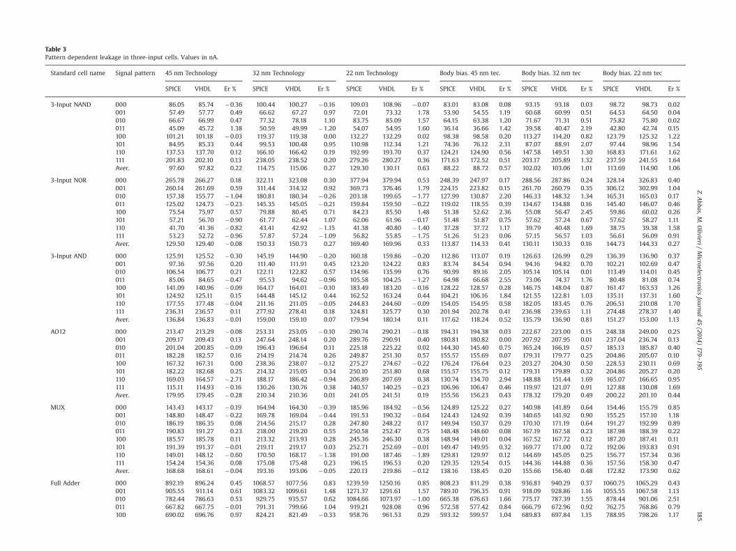
Table 3Pattern dependent leakage in three-input cells. Values in nA.
Standard cell name Signal pattern 45 nm Technology 32 nm Technology 22 nm Technology Body bias. 45 nm tec. Body bias. 32 nm tec Body bias. 22 nm tec
SPICE VHDL Er % SPICE VHDL Er % SPICE VHDL Er % SPICE VHDL Er % SPICE VHDL Er % SPICE VHDL Er %
3-Input NAND 000 86.05 85.74 �0.36 100.44 100.27 �0.16 109.03 108.96 �0.07 83.01 83.08 0.08 93.15 93.18 0.03 98.72 98.73 0.02001 57.49 57.77 0.49 66.62 67.27 0.97 72.01 73.32 1.78 53.90 54.55 1.19 60.68 60.99 0.51 64.53 64.50 0.04010 66.67 66.99 0.47 77.32 78.18 1.10 83.75 85.09 1.57 64.15 63.38 1.20 71.67 71.31 0.51 75.82 75.80 0.02011 45.09 45.72 1.38 50.59 49.99 �1.20 54.07 54.95 1.60 36.14 36.66 1.42 39.58 40.47 2.19 42.80 42.74 0.15100 101.21 101.18 �0.03 119.37 119.38 0.00 132.27 132.29 0.02 98.38 98.58 0.20 113.27 114.20 0.82 123.79 125.32 1.22101 84.95 85.33 0.44 99.53 100.48 0.95 110.98 112.34 1.21 74.36 76.12 2.31 87.07 88.91 2.07 97.44 98.96 1.54110 137.53 137.70 0.12 166.10 166.42 0.19 192.99 193.70 0.37 124.21 124.90 0.56 147.58 149.51 1.30 168.83 171.61 1.62111 201.83 202.10 0.13 238.05 238.52 0.20 279.26 280.27 0.36 171.63 172.52 0.51 203.17 205.89 1.32 237.59 241.55 1.64Aver. 97.60 97.82 0.22 114.75 115.06 0.27 129.30 130.11 0.63 88.22 88.72 0.57 102.02 103.06 1.01 113.69 114.90 1.06
3-Input NOR 000 265.78 266.27 0.18 322.11 323.08 0.30 377.94 379.94 0.53 248.39 247.97 0.17 288.56 287.86 0.24 328.14 326.83 0.40001 260.14 261.69 0.59 311.44 314.32 0.92 369.73 376.46 1.79 224.15 223.82 0.15 261.70 260.79 0.35 306.12 302.99 1.04010 157.38 155.77 �1.04 180.81 180.34 �0.26 203.18 199.65 �1.77 127.99 130.87 2.20 146.33 148.32 1.34 165.31 165.03 0.17011 125.02 124.73 �0.23 145.35 145.05 �0.21 159.84 159.50 �0.22 119.02 118.55 0.39 134.67 134.88 0.16 145.40 146.07 0.46100 75.54 75.97 0.57 79.88 80.45 0.71 84.23 85.50 1.48 51.38 52.62 2.36 55.08 56.47 2.45 59.86 60.02 0.26101 57.21 56.70 �0.90 61.77 62.44 1.07 62.06 61.96 �0.17 51.48 51.87 0.75 57.62 57.24 0.67 57.62 58.27 1.11110 41.70 41.36 �0.82 43.41 42.92 �1.15 41.38 40.80 �1.40 37.28 37.72 1.17 39.79 40.48 1.69 38.75 39.38 1.58111 53.23 52.72 �0.96 57.87 57.24 �1.09 56.82 55.85 �1.75 51.26 51.23 0.06 57.15 56.57 1.03 56.61 56.09 0.91Aver. 129.50 129.40 �0.08 150.33 150.73 0.27 169.40 169.96 0.33 113.87 114.33 0.41 130.11 130.33 0.16 144.73 144.33 0.27
3-Input AND 000 125.91 125.52 �0.30 145.19 144.90 �0.20 160.18 159.86 �0.20 112.86 113.07 0.19 126.63 126.99 0.29 136.39 136.90 0.37001 97.36 97.56 0.20 111.40 111.91 0.45 123.20 124.22 0.83 83.74 84.54 0.94 94.16 94.82 0.70 102.21 102.69 0.47010 106.54 106.77 0.21 122.11 122.82 0.57 134.96 135.99 0.76 90.99 89.16 2.05 105.14 105.14 0.01 113.49 114.01 0.45011 85.06 84.65 �0.47 95.53 94.62 �0.96 105.58 104.25 �1.27 64.98 66.68 2.55 73.06 74.37 1.76 80.48 81.08 0.74100 141.09 140.96 �0.09 164.17 164.01 �0.10 183.49 183.20 �0.16 128.22 128.57 0.28 146.75 148.04 0.87 161.47 163.53 1.26101 124.92 125.11 0.15 144.48 145.12 0.44 162.52 163.24 0.44 104.21 106.16 1.84 121.55 122.81 1.03 135.11 137.31 1.60110 177.55 177.48 �0.04 211.16 211.05 �0.05 244.83 244.60 �0.09 154.05 154.95 0.58 182.05 183.45 0.76 206.51 210.08 1.70111 236.31 236.57 0.11 277.92 278.41 0.18 324.81 325.77 0.30 201.94 202.78 0.41 236.98 239.63 1.11 274.48 278.37 1.40Aver. 136.84 136.83 �0.01 159.00 159.10 0.07 179.94 180.14 0.11 117.62 118.24 0.52 135.79 136.90 0.81 151.27 153.00 1.13
AO12 000 213.47 213.29 �0.08 253.31 253.05 �0.10 290.74 290.21 �0.18 194.31 194.38 0.03 222.67 223.00 0.15 248.38 249.00 0.25001 209.17 209.43 0.13 247.64 248.14 0.20 289.76 290.91 0.40 180.81 180.82 0.00 207.92 207.95 0.01 237.04 236.74 0.13010 201.04 200.85 �0.09 196.43 196.64 0.11 225.18 225.22 0.02 144.30 145.40 0.75 165.24 166.19 0.57 185.13 185.87 0.40011 182.28 182.57 0.16 214.19 214.74 0.26 249.87 251.30 0.57 155.57 155.69 0.07 179.31 179.77 0.25 204.86 205.07 0.10100 167.32 167.31 0.00 238.36 238.07 �0.12 275.27 274.67 �0.22 176.24 176.64 0.23 203.27 204.30 0.50 228.53 230.11 0.69101 182.22 182.68 0.25 214.32 215.05 0.34 250.10 251.80 0.68 155.57 155.75 0.12 179.31 179.89 0.32 204.86 205.27 0.20110 169.03 164.57 �2.71 188.17 186.42 �0.94 206.89 207.69 0.38 130.74 134.70 2.94 148.88 151.44 1.69 165.07 166.65 0.95111 115.11 114.93 �0.16 130.26 130.76 0.38 140.57 140.25 �0.23 106.96 106.47 0.46 119.97 121.07 0.91 127.88 130.08 1.69Aver. 179.95 179.45 �0.28 210.34 210.36 0.01 241.05 241.51 0.19 155.56 156.23 0.43 178.32 179.20 0.49 200.22 201.10 0.44
MUX 000 143.43 143.17 �0.19 164.94 164.30 �0.39 185.96 184.92 �0.56 124.89 125.22 0.27 140.98 141.89 0.64 154.46 155.79 0.85001 148.80 148.47 �0.22 169.78 169.04 �0.44 191.53 190.32 �0.64 124.43 124.92 0.39 140.65 141.92 0.90 155.25 157.10 1.18010 186.19 186.35 0.08 214.56 215.17 0.28 247.80 248.22 0.17 149.94 150.37 0.29 170.10 171.19 0.64 191.27 192.99 0.89011 190.83 191.27 0.23 218.00 219.20 0.55 250.58 252.47 0.75 148.48 148.60 0.08 167.19 167.58 0.23 187.98 188.39 0.22100 185.57 185.78 0.11 213.32 213.93 0.28 245.36 246.30 0.38 148.94 149.01 0.04 167.52 167.72 0.12 187.20 187.41 0.11101 191.39 191.37 �0.01 219.11 219.17 0.03 252.71 252.69 �0.01 149.47 149.95 0.32 169.77 171.00 0.72 192.06 193.83 0.91110 149.01 148.12 �0.60 170.50 168.17 �1.38 191.00 187.46 �1.89 129.81 129.97 0.12 144.69 145.05 0.25 156.77 157.34 0.36111 154.24 154.36 0.08 175.08 175.48 0.23 196.15 196.53 0.20 129.35 129.54 0.15 144.36 144.88 0.36 157.56 158.30 0.47Aver. 168.68 168.61 �0.04 193.16 193.06 �0.05 220.13 219.86 �0.12 138.16 138.45 0.20 155.66 156.40 0.48 172.82 173.90 0.62
Full Adder 000 892.19 896.24 0.45 1068.57 1077.56 0.83 1239.59 1250.16 0.85 808.23 811.29 0.38 936.81 940.29 0.37 1060.75 1065.29 0.43001 905.55 911.14 0.61 1083.32 1099.61 1.48 1271.37 1291.61 1.57 789.10 796.35 0.91 918.09 928.86 1.16 1055.55 1067.58 1.13010 782.44 786.63 0.53 929.75 935.57 0.62 1084.66 1073.97 �1.00 665.38 676.63 1.66 775.17 787.39 1.55 878.44 901.06 2.51011 667.82 667.75 �0.01 791.31 799.66 1.04 919.21 928.08 0.96 572.58 577.42 0.84 666.79 672.96 0.92 762.75 768.86 0.79100 690.02 696.76 0.97 824.21 821.49 �0.33 958.76 961.53 0.29 593.32 599.57 1.04 689.83 697.84 1.15 788.95 798.26 1.17
Z.Abbas,M
.Olivieri
/Microelectronics
Journal45
(2014)179
–195185

is essential for modeling real cells. Each basic structure was using aDC sweep at 30 1C and 100 1C for all input signal combinations i.e. allinput patterns. All the resulting internal node voltages were saved ina matrix in the Single_Cell_voltage_leakage.vhd VHDL package. Thecharacterization of the internal node voltages covered all the basicstructures shown in Figs. 4 and 5.
Given a standard cell circuit, it is possible to identify the basiccircuit structures in it, so to recover the internal node voltages forany input pattern of logic signals. Once node voltages are deter-mined, one can recover leakage currents values for virtually all thetransistors in the cell, correctly taking into account stacking effectson all the leakage components. Actually, in order to calculate thetotal leakage current flowing in the cell from the external powersupply, we have to sum all the currents directly flowing to theground node [3,1].
The adopted model also include loading effect calculation,occurring when the gate leakage of a cell driven by another cellintroduces a voltage difference ΔV on the output terminal of thedriving cell, thus affecting the leakage in both the ones. Theloading effect may either increase or reduce the total leakage ofthe gate. In our analysis, the implementation of the loadingeffect model is based on the characterization of ΔV by SPICEBSIM4 simulation of all possible combinations and device widthsof pull-up, pull-down and load. It must be pointed out that due tothe small ΔV values found and to the compensation betweenpositive and negative effects, we found a practically not relevantimpact.
In the following, we report a sample of the VHDL code of theNAND to show, how leakage estimation model accesses the datafrom the tables in the packages.
constant Wmin: integer:¼22; —to set gate length [nm]constant NWmin: integer:¼1; —to set gate width as a
multiple of Wminconstant temperature:
integer:¼30;—to set temperature [1C],25, 30 or 100
constant Vdd: real:¼1.0; —to set power supplyvoltage
variable comb: std_logic_vector (1 downto 0);– assigned with the input signals;variable matrix: matrix_23NP:¼choosematrix(temperature,
Vdd);– chooses the matrix in INV packages based on temperature and
supply voltage values.variable a00Vdd: real:¼-matrix(48).Vn1;variable a01Vdd: real:¼matrix(49).Vn1;variable a10Vdd: real:¼matrix(50).Vn1;variable a11Vdd: real:¼matrix(51).Vn1;– these are variables assigned with node voltages for the four
input combinations– of NAND cell. Matrix 48, 49, 50 and 51 corresponds to line
number– in the chosen matrix, while.Vn1 corresponds to the node.– oother omitted code here4case comb iswhen "00"¼4—oomitted code4when "01"¼4 PrintLeakages (
Isub(Wmin,2nNWmin,a01Vdd, temperature),2.0nIbody(Wmin,2nNWmin,þa01Vdd,0.0,temperature)þIbody(Wmin,2nNWmin, Vdd, 0.0,temperature),2.0nIgate(1,Wmin,2nNWmin,Vdd,temperature)þ Igate(0,Wmin,2nNWmin,a01Vdd,temperature));– equation for “01” input combination; current functions areinvoked with node voltage values.Ta
ble
3(con
tinu
ed)
Stan
dardcellnam
eSign
alpattern
45nm
Tech
nolog
y32
nm
Tech
nolog
y22
nm
Tech
nolog
yBod
ybias.4
5nm
tec.
Bod
ybias.3
2nm
tec
Bod
ybias.2
2nm
tec
SPICE
VHDL
Er%
SPICE
VHDL
Er%
SPICE
VHDL
Er%
SPICE
VHDL
Er%
SPICE
VHDL
Er%
SPICE
VHDL
Er%
101
725.98
728.79
0.39
856.72
857.61
0.10
997.83
1005
.55
0.77
613.67
622.36
1.40
718.42
725.99
1.04
828.31
833.49
0.62
110
729.49
731.12
0.22
861.75
865.27
0.41
991.58
995.64
0.41
635.13
640.12
0.78
741.66
748.88
0.96
843.04
851.32
0.97
111
643.77
645.25
0.23
743.47
755.41
1.58
827.40
830.85
0.42
567.82
572.01
0.73
662.72
664.64
0.29
752.99
740.60
1.67
Ave
r.75
4.66
757.96
0.44
894.89
901.52
0.74
1036
.30
1042
.17
0.56
655.65
661.97
0.95
763.69
770.86
0.93
871.35
878.31
0.79
Z. Abbas, M. Olivieri / Microelectronics Journal 45 (2014) 179–195186
– similar equations written for other input combinations.– equations are derived from the topology of the involved
stacks;
4. Comparison of estimated leakage currents in scaledtechnologies
In the presented data, we focus on minimum-size standardcells, however the technique was equally applied to resized cells.We found leakage currents grow approximately linear with theresizing factor of the cells.
In the three technology nodes device sizes have been scaledaccording to the minimum feature size in each technology, whileVDD has been kept at 1 V as this is compatible with high-speedlibraries in the target technology nodes [5]. The reported resultsalso include the case of reverse body biasing applied in each of thethree technologies. Body biasing was applied as �0.2 V in N-typedevices and VDDþ0.2 V in P-type devices.
The two-input standard cells of our library are detailed in Fig. 6,with highlighted symbolic name and type of stack needed toaccess the internal node voltage tables (INV) for the specific inputcombination in Single_cell_voltage_leakage.vhd package. All stacksin two-input cells have one internal node voltage. Table 2 shows theleakage currents for two-input cells calculated by the estimationmodel in VHDL and by NGSPICE, along with error percentage. Thedata are reported for all input patterns in 45 nm, 32 nm and 22 nmtechnology nodes, and the vast majority of the results are showingerror percentage below 1%. The different accuracy for different inputpatterns might be referred to quantization errors in internal voltagevalues. The results related to reverse body biasing generally showthat in the target technologies the technique is not effectivefor leakage reduction because sub-threshold leakage is often domi-nated by gate leakage and because the modification of internalnode voltages in the cells limit the reduction of sub-thresholdleakage.
Accordingly, three-input standard cells are detailed in Fig. 7,highlighting the type of stacks to access the internal node voltagetables. The stacks contain two internal nodes except for standard cell
MUX21 that does not have floating internal nodes. Table 3 reportsthe leakage results for three-input standard cells calculated by VHDLmodel and by NGSPICE, along with error percentage.
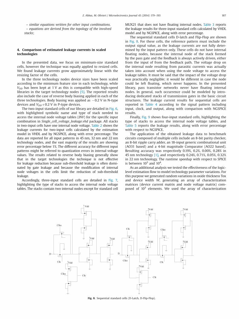
The sequential standard cells D-latch and Flip-Flop are shownin Fig. 8. For these cells, the reference pattern must include theoutput signal value, as the leakage currents are not fully deter-mined by the input pattern only. These cells do not have internalfloating nodes, because the internal node of the stack formedby the pass gate and the feedback is always actively driven, eitherfrom the input of from the feedback path. The voltage drop onthe internal node resulting from parasitic currents was actuallytaken into account when using the node voltage to access theleakage tables. It must be said that the impact of the voltage dropwas practically negligible; it would be different in case the nodecould be left floating, which never happens. In the presentedlibrary, pass transistor networks never have floating internalnodes. In general, such occurrence could be modeled by intro-ducing dedicated stacks of transmission gates in the basic circuitstructures. The leakage current results for sequential cells arereported in Table 4 according to the signal pattern includinginput, clock, and output, along with comparison with NGSPICEresults.
Finally, Fig. 9 shows four-input standard cells, highlighting thetype of stacks to access the internal node voltage tables, andTable 5 reports the leakage results, along with error percentagewith respect to NGSPICE.
The application of the obtained leakage data to benchmarkcircuits composed of multiple cells include an 8-bit parity checker,an 8-bit ripple carry adder, an 18-input generic combinational unit(AO31 based) and a 4-bit magnitude Comparator (AO22 based).Resulting accuracy was respectively 0.19%, 0.2%, 0.00%, 0.28% in45 nm technology [1], and respectively 0.24%, 0.71%, 0.05%, 0.32%in 22 nm technology. The runtime speedup with respect to SPICEis between 103 and 104.
As an additional analysis we tested the effectiveness of the logic-level estimation flow to model technology parameter variations. Forthis purpose we generated random variations in oxide thickness Toxand device width W, generating an array of characterizationmatrices (device current matrix and node voltage matrix) com-posed of 103 elements. We used the array of characterization
Clkn
Clk
D
Clkn
Clk
Vdd
VddVdd
Vdd
Clk
Clk
D
Clkn
Clkn
Clk
Vdd Vdd
Vdd
Vdd
Vdd
Fig. 8. Sequential standard cells (D-Latch, D-Flip-Flop).
Z. Abbas, M. Olivieri / Microelectronics Journal 45 (2014) 179–195 187

matrices
toiterate
alogic-level
Mon
te-Carloevalu
ationof
thecell
leakage.Variations
were
Gau
ssianwith
10%deviation
at3s.
Thefrequ
ency
distribution
obtainedby
tracingthe
obtainedleakage
Table 4Pattern dependent leakage in sequential cells. Values in nA.
Standard cell name Signal pattern 45 nm Technology 32 nm Technology 22 nm Technology Body bias. 45 nm tec. Body bias. 32 nm tec Body bias. 22 nm tec
SPICE VHDL Er % SPICE VHDL Er % SPICE VHDL Er % SPICE VHDL Er % SPICE VHDL Er % SPICE VHDL Er %
DLatch 000 142.54 142.28 �0.18 161.14 160.69 �0.27 182.84 181.88 �0.53 119.61 119.93 0.27 132.70 133.44 0.55 145.20 146.39 0.81001 182.15 182.36 0.12 207.30 207.73 0.21 238.54 239.39 0.35 98.56 97.38 �1.21 109.08 108.57 �0.47 119.01 117.63 �1.17010 162.27 162.84 0.36 184.31 186.21 1.02 210.14 212.60 1.16 133.36 134.03 0.50 150.27 151.93 1.09 167.15 169.62 1.46100 185.04 184.90 �0.08 210.28 210.08 �0.10 243.72 243.19 �0.22 144.65 144.94 0.20 161.82 162.48 0.41 182.01 183.05 0.57101 145.98 145.66 �0.22 165.22 164.63 �0.35 185.55 184.46 �0.59 123.37 122.40 �0.80 137.36 137.61 0.18 152.86 154.30 0.93111 159.18 158.41 �0.48 180.80 178.89 �1.06 204.08 201.27 �1.39 93.59 92.88 �0.76 113.57 112.46 �0.98 124.79 123.86 �0.75Aver. 162.86 162.74 �0.07 184.84 184.71 �0.07 210.81 210.46 �0.16 118.86 118.59 �0.22 134.13 134.42 0.21 148.50 149.14 0.43
D FF 001 308.20 309.32 0.36 360.17 363.07 0.80 417.32 421.79 1.06 258.94 259.16 0.09 295.87 296.66 0.27 333.65 334.64 0.30010 325.95 325.85 �0.03 376.78 376.80 0.01 446.68 446.39 �0.06 253.41 254.03 0.25 289.31 290.91 0.55 335.24 337.82 0.77011 274.66 274.44 �0.08 319.46 319.24 �0.07 371.57 370.71 �0.23 230.63 231.13 0.22 262.18 263.43 0.47 295.60 297.73 0.72100 280.21 279.75 �0.16 324.63 323.99 �0.20 377.88 376.11 �0.47 230.16 230.87 0.31 261.85 262.94 0.42 296.39 297.92 0.52101 323.31 323.42 0.03 375.17 376.00 0.22 441.77 441.54 �0.05 256.24 257.13 0.35 296.69 295.93 �0.26 340.65 341.40 0.22110 322.64 322.37 �0.08 373.64 373.37 �0.07 438.41 437.42 �0.23 255.21 255.82 0.24 290.97 292.49 0.52 333.19 335.77 0.77111 286.99 286.72 �0.09 332.75 332.90 0.05 387.78 386.61 �0.30 237.08 238.32 0.52 270.72 273.70 1.09 306.85 312.01 1.66Aver. 303.14 303.12 0.00 351.80 352.20 0.11 411.63 411.51 �0.03 245.95 246.64 0.28 281.08 282.30 0.43 320.22 322.47 0.70
Fig.9.Fou
r-inputstan
dard
cells(A
O112,A
O22
andAO31).
Z.Abbas,M
.Olivieri
/Microelectronics
Journal45
(2014)179
–195188

values subject to technology parameter variations are shown inFig. 10 for a subset of the cell library. The data are overlapped withthe distributions obtained by performing a SPICE Monte-Carloanalysis with the same technology variations. Interestingly theresulting leakage distribution is closely but not perfectly Gaussianin all the cells.
5. Analysis of leakage components subject to scaling effects
Having verified the accuracy of total leakage calculation withrespect to SPICE BSIM4 results, we were able to proceed in using
the logic level model in order to analyze the impact of technologyscaling and of input patterns on the three major leakage currentcomponents individually, i.e. gate, sub-threshold and bodyleakage.
Table 6 reports the results of the three major leakage compo-nents for all input patterns in single-input and 2-input standardcells. All leakage components are estimated in 45 nm, 32 nm and22 nm technology. Obviously, all leakage component summedtogether corresponds to the total leakage current for a particularinput combination in the respective technology node. Table 7reports the sub-threshold leakage, body leakage and gate leakageestimated values for all input patterns in three-input standardcells, while Tables 8 and 9 report the estimation results of
Table 5Pattern dependent leakages in four-input cells. Values in nA.
Standardcell name
Signalpattern
45 nm Technology 32 nm Technology 22 nm Technology Body bias. 45 nm tec. Body bias. 32 nm tec Body bias. 22 nm tec
SPICE VHDL Er % SPICE VHDL Er % SPICE VHDL Er % SPICE VHDL Er % SPICE VHDL Er % SPICE VHDL Er %
AO112 0000 383.57 383.46 �0.03 462.52 462.45 �0.02 538.77 538.57 �0.04 355.84 355.77 0.02 412.42 412.54 0.03 466.50 466.83 0.070001 373.46 374.90 0.38 448.54 451.43 0.64 529.58 535.49 1.10 330.32 330.15 0.05 384.25 383.67 0.15 443.55 441.30 �0.510010 270.39 270.03 �0.14 317.29 313.85 �1.10 361.55 362.33 0.22 234.08 237.02 1.24 268.80 270.88 0.77 302.67 302.54 �0.040011 237.90 237.58 �0.13 281.65 281.31 �0.12 317.85 317.43 �0.13 224.90 224.67 0.11 256.85 257.37 0.20 282.38 283.44 0.370100 343.89 343.89 0.00 413.43 413.58 0.03 482.22 482.47 0.05 313.41 311.70 0.55 358.99 362.49 0.97 402.17 411.41 2.250101 319.14 320.67 0.48 380.75 383.60 0.74 448.13 454.66 1.44 278.73 278.66 0.03 324.33 324.09 0.07 374.96 372.85 �0.570110 216.40 217.12 0.33 250.15 248.05 �0.85 281.64 279.32 �0.83 182.62 185.73 1.67 209.03 211.66 1.24 234.28 234.96 0.290111 184.01 183.70 �0.17 214.66 214.35 �0.15 238.21 237.83 �0.16 173.44 173.41 0.02 197.08 198.21 0.57 214.00 215.97 0.921000 310.22 310.35 0.04 371.60 372.14 0.15 432.35 433.00 0.15 287.21 280.48 2.40 326.32 324.44 0.58 372.98 367.29 �1.551001 319.04 320.67 0.51 380.57 383.60 0.79 447.82 454.66 1.50 278.73 278.57 0.06 324.33 323.94 0.12 374.96 372.58 �0.641010 216.34 216.17 �0.08 250.05 246.92 �1.27 281.50 282.80 0.46 182.62 185.67 1.64 209.03 211.56 1.20 234.28 234.83 0.231011 183.99 183.70 �0.15 214.63 214.35 �0.13 238.17 237.83 �0.14 173.44 173.38 0.04 197.08 198.17 0.55 214.00 215.91 0.891100 206.62 207.02 0.19 226.48 225.13 �0.60 246.04 241.02 �2.08 157.42 158.76 0.84 171.17 176.35 2.94 191.23 192.66 0.741101 140.37 141.73 0.96 157.64 156.08 �1.00 169.75 172.37 1.52 127.39 127.67 0.21 140.73 144.63 2.69 156.05 155.69 �0.231110 120.36 118.49 �1.58 134.65 132.85 �1.36 144.10 144.42 0.22 109.80 109.57 0.21 122.40 123.73 1.07 130.14 132.33 1.651111 127.34 128.59 0.97 145.55 148.48 1.97 157.05 160.59 2.21 119.47 120.61 0.94 135.82 137.89 1.50 144.98 147.66 1.82Aver. 247.06 247.38 0.13 290.64 290.51 �0.04 332.17 333.42 0.38 220.59 220.74 0.07 252.41 253.85 0.57 283.69 284.27 0.20
AO22 0000 263.69 263.55 �0.05 314.01 313.88 �0.04 357.66 357.37 �0.08 245.68 245.58 0.04 281.86 282.03 0.06 312.83 313.28 0.150001 217.52 217.64 0.05 257.19 257.59 0.16 292.16 292.58 0.14 195.76 196.64 0.45 224.57 225.30 0.32 249.77 250.22 0.180010 251.22 251.12 �0.04 299.13 298.90 �0.08 342.28 341.83 �0.13 227.61 227.90 0.13 262.46 263.41 0.36 292.97 294.48 0.510011 308.50 309.43 0.30 364.51 366.24 0.47 430.83 434.91 0.94 259.70 259.62 0.03 301.47 301.75 0.09 350.47 349.94 0.150100 217.56 217.58 0.01 257.08 257.48 0.15 292.01 292.39 0.13 195.68 196.57 0.45 224.44 225.18 0.33 249.59 250.10 0.200101 173.22 171.61 �0.94 200.32 201.06 0.37 226.63 227.37 0.33 145.66 147.66 1.35 167.00 168.50 0.89 186.33 187.11 0.420110 210.10 211.26 0.55 242.25 245.59 1.36 276.73 276.71 0.00 175.62 178.91 1.84 203.69 206.60 1.41 236.71 231.35 2.320111 281.23 281.75 0.18 330.27 330.42 0.04 389.07 391.52 0.62 234.46 234.30 0.07 272.86 273.22 0.13 318.30 317.41 0.281000 251.28 251.12 �0.06 298.97 298.91 �0.02 342.01 341.84 �0.05 227.62 227.80 0.08 262.47 263.26 0.30 292.97 294.29 0.451001 205.14 205.14 0.00 242.25 242.50 0.10 276.73 276.83 0.04 177.60 178.91 0.73 205.04 206.60 0.76 229.72 231.35 0.711010 238.84 238.68 �0.07 284.17 283.93 �0.08 326.77 326.28 �0.15 209.54 210.16 0.29 243.07 244.70 0.67 273.11 275.57 0.891011 281.10 282.70 0.57 330.49 333.19 0.81 389.49 395.91 1.62 234.46 234.41 0.02 272.86 273.42 0.20 318.30 317.76 0.171100 171.42 170.15 �0.75 193.33 196.06 1.40 213.64 210.59 �1.45 138.53 137.54 0.72 159.10 154.89 2.72 170.59 171.13 0.311101 205.14 204.24 �0.44 235.89 234.27 �0.69 258.56 251.58 �2.78 178.82 175.75 1.75 194.26 199.30 2.53 221.58 218.52 1.401110 210.01 207.53 �1.20 236.04 236.81 0.33 258.79 251.58 �2.87 177.17 175.84 0.76 199.17 199.44 0.13 211.58 218.74 3.281111 165.45 165.06 �0.23 189.94 189.58 �0.19 207.80 207.39 �0.20 152.23 156.29 2.60 185.07 180.58 2.49 198.39 197.37 0.52Aver. 228.21 228.04 �0.08 267.24 267.90 0.25 305.07 304.79 �0.09 198.51 198.99 0.24 228.71 229.26 0.24 257.08 257.41 0.13
AO31 0000 269.01 268.56 �0.17 320.81 320.40 �0.13 368.23 367.65 �0.16 248.14 248.37 0.09 285.20 285.60 0.14 318.27 318.89 0.200001 260.47 260.72 0.10 310.23 310.70 0.15 361.87 362.94 0.29 230.45 230.40 0.02 265.50 265.48 0.01 301.38 301.07 0.100010 257.05 256.85 �0.08 305.87 305.60 �0.09 350.95 350.41 �0.16 237.25 237.63 0.16 274.12 275.44 0.48 307.09 309.27 0.700011 257.05 257.43 0.15 294.50 292.71 �0.61 343.87 341.71 �0.63 218.88 219.19 0.14 254.00 254.99 0.39 289.96 291.14 0.400100 222.50 222.36 �0.06 263.82 263.56 �0.10 302.42 301.92 �0.17 203.03 202.43 0.30 232.52 232.55 0.01 259.12 259.74 0.240101 217.86 216.77 �0.50 256.32 249.04 �2.92 298.56 292.28 �2.15 180.87 186.58 3.06 209.99 214.18 1.96 237.11 243.44 2.600110 266.32 266.23 �0.03 318.84 318.74 �0.03 371.43 371.24 �0.05 236.85 237.73 0.37 277.24 279.60 0.84 315.88 319.43 1.110111 234.37 234.80 0.18 278.59 279.38 0.28 325.43 327.25 0.56 207.31 207.92 0.29 242.50 244.40 0.78 278.52 280.99 0.881000 213.34 213.45 0.05 253.12 253.69 0.22 290.69 291.44 0.26 192.78 193.61 0.42 221.54 222.24 0.32 247.83 248.45 0.251001 247.35 247.76 0.17 294.27 295.05 0.27 343.46 345.11 0.48 218.88 219.07 0.09 254.00 254.77 0.30 289.96 290.77 0.281010 213.74 213.86 0.06 252.26 252.81 0.22 289.37 289.89 0.18 187.00 188.96 1.04 216.74 219.02 1.04 244.49 246.79 0.931011 234.27 234.80 0.23 278.38 279.38 0.36 325.07 327.25 0.67 207.31 207.82 0.25 242.50 244.22 0.70 278.52 280.67 0.761100 173.88 173.95 0.05 203.32 203.81 0.24 232.44 233.01 0.24 147.78 149.50 1.15 169.25 170.58 0.78 189.86 190.56 0.371101 234.06 234.80 0.31 278.01 279.38 0.49 324.42 327.25 0.86 207.31 207.62 0.15 242.50 243.85 0.55 278.52 280.05 0.541110 273.85 276.01 0.78 309.92 315.60 1.80 345.21 353.53 2.35 219.67 225.76 2.69 253.34 259.60 2.41 287.42 291.48 1.391111 184.55 183.05 �0.82 214.84 214.73 �0.05 239.17 238.89 �0.12 175.16 174.41 0.43 202.11 204.63 1.23 223.40 228.24 2.12Aver. 234.98 235.09 0.05 277.07 277.16 0.03 319.54 320.11 0.18 207.42 208.56 0.55 240.19 241.95 0.73 271.71 273.81 0.77
Z. Abbas, M. Olivieri / Microelectronics Journal 45 (2014) 179–195 189

sub-threshold leakage, body leakage and gate leakage in sequen-tial cells and four-input cells, respectively.
As expected, the general trend from Table 6 is that all of thethree leakage components are increasing with technology scaling.Interestingly, in each cell input pattern dependence in the three
target technologies shows an almost constant ratio betweenleakage values associated to any two different patterns. Thiseffect is relevant for differential power analysis techniques forattacking cryptographic integrated circuits, where the possibilityof successful attacks based on static power associated to logic
-100
0
100
200
300
400
500
0 20 40 60 80
nand2
nand2_spicenand2_mod
µspice= 47.769 σspice= 9.083µmod= 47.907 σmod= 9.114
-100
0
100
200
300
400
500
0 20 40 60 80 100
nor2
nor2_spicenor2_mod
µspice= 63.379 σspice= 7.647 µmod= 63.434 σmod= 7.626
-100
0
100
200
300
400
500
0 50 100 150 200
and2
and2_spiceand2_mod
µspice= 99.701 σspice= 15.356 µmod= 99.311 σmod= 15.264
-100
0
100
200
300
400
500
0 100 200 300 400 500 600
xor2
xor2_spicexor2_mod
µspice= 326.813 σspice= 61.573 µmod= 326.823 σmod= 61.726
-100
0
100
200
300
400
500
0 100 200 300 400 500 600
AO31
AO31_spiceAO31_mod
µspice= 350.054 σspice= 66.651 µmod= 350.194 σmod= 66.802
-100
0
100
200
300
400
500
0 500 1000 1500 2000 2500
FA
FA_spiceFA_mod
µspice= 1295.669 σspice= 246.873 µmod= 1297.764 σmod= 245.719
Fig. 10. Results of logic-level and SPICE Monte Carlo analysis of leakage variations.
Table 6Impact of scaling on major leakage components in single-input and two-input cells. (S¼Sub-threshold, B¼Body, G¼Gate.)
Standard cell name Input pattern 45 nm Technology 32 nm Technology 22 nm Technology
S [nA] B [nA] G [nA] S [nA] B [nA] G [nA] S [nA] B [nA] G [nA]
NOT 0 6.844 0.848 26.783 7.766 2.343 29.782 11.103 3.399 31.0061 24.000 0.084 15.697 27.150 0.217 17.266 33.840 0.276 16.785
NAND2 00 1.301 1.696 54.610 0.886 4.686 61.248 0.603 6.797 64.69501 10.298 1.040 27.437 10.644 2.876 30.794 11.027 4.180 32.45910 15.656 1.040 55.618 19.083 2.876 63.792 24.268 4.181 68.68211 48.000 0.384 58.762 54.300 1.067 68.772 67.681 1.564 75.079
NOR2 00 13.689 3.604 105.940 15.532 10.239 121.810 22.206 15.594 134.35001 51.001 2.210 70.847 59.327 5.337 81.167 77.455 8.073 87.91110 37.030 1.886 17.145 39.680 0.217 19.326 43.577 0.276 19.11011 5.080 0.168 32.026 4.450 0.435 35.550 2.691 0.553 35.178
AND2 00 25.302 1.780 70.307 28.107 4.903 78.536 34.443 7.074 81.48101 39.656 1.124 71.314 37.239 3.094 47.786 58.108 4.457 85.46810 54.845 1.232 85.545 46.229 3.094 81.057 78.784 4.963 106.08011 34.298 1.124 43.134 62.065 3.410 98.554 44.867 4.457 49.244
XOR2 00 102.770 5.684 162.430 114.550 15.991 186.740 143.240 23.956 202.83001 56.799 4.072 177.910 64.642 11.523 203.870 80.238 17.433 221.27010 56.799 4.704 177.910 64.642 13.233 203.870 80.238 19.820 221.27011 137.080 4.156 140.260 153.320 11.740 161.710 188.710 17.710 174.390
Z. Abbas, M. Olivieri / Microelectronics Journal 45 (2014) 179–195190

levels has been demonstrated [8]. Our results show that thesuccess of the attack can be expected to be technology indepen-dent. The effect is also relevant for leakage limitation techniquesbased on input pattern selection in idle units, as from our resultswe can expect that the achievable relative leakage reduction ispractically technology independent. Also, NAND2 and NAND3gates show a dramatic difference (more than one order ofmagnitude) in sub-threshold leakage current associated to inputpatterns “0..0” and “1..1”, differently from other cells; this could betaken into account when designing logic units with input-pattern-based leakage management.
The average incremental trends of each leakage component areindividually illustrated in Fig. 11 for single-input and two-inputcells, in Fig. 12 for three-input cells, and in Fig. 13 for four-inputand sequential cells. The number in percentage over the barsrepresents the average % increase over the preceding technology inrespective leakage component in particular cell. We observe that,on average, the increment in sub-threshold leakage for 2-inputbasic cells scaling from 45 nm to 32 nm is approximately 12%,while it is around 25% when scaling from 32 nm to 22 nmtechnology. Interestingly, while in both the scaling steps thereduction factor of geometric feature size is around 0.7, the second
Table 7Impact of scaling on major leakage components in three-input cells. (S¼Sub-threshold, B¼Body, G¼Gate.)
Standard cell name Input pattern 45 nm Technology 32 nm Technology 22 nm Technology
S [nA] B [nA] G [nA] S [nA] B [nA] G [nA] S [nA] B [nA] G [nA]
NAND3 000 0.742 2.544 82.455 0.497 7.028 92.744 0.331 10.197 98.429001 1.941 1.996 53.837 1.125 5.535 60.613 0.902 8.084 64.334010 4.737 1.996 60.254 4.245 5.535 68.404 3.872 8.086 73.128011 15.127 1.449 29.145 15.520 1.700 32.770 16.143 4.180 34.630100 2.034 1.996 97.152 1.411 5.535 112.430 0.993 8.086 123.220101 16.095 1.449 67.785 16.957 4.042 79.485 18.170 5.974 88.197110 24.463 1.449 111.790 30.387 4.042 131.990 39.951 5.977 147.770111 72.001 0.901 129.190 81.449 2.549 154.520 101.520 3.863 174.880
NOR3 000 20.533 8.267 237.470 23.298 23.688 276.090 33.310 36.585 310.050001 77.938 5.596 178.150 91.361 16.009 206.950 120.990 24.666 230.810010 58.272 0.084 97.410 61.301 0.217 118.820 68.134 0.277 131.240011 8.439 2.924 113.360 6.146 8.331 130.580 4.208 12.748 142.540100 55.313 2.840 17.821 57.301 8.113 15.040 61.653 12.470 11.374101 17.542 2.924 36.238 16.084 8.331 38.026 14.631 12.746 34.580110 8.195 0.084 33.081 5.886 0.217 36.816 3.948 0.277 36.578111 3.142 1.225 48.354 2.752 0.652 53.834 1.450 0.827 53.570
AND3 000 24.742 2.628 98.152 27.647 7.246 110.010 34.172 10.473 115.210001 25.941 2.080 69.534 28.275 5.753 77.879 34.742 8.362 81.119010 28.737 2.080 75.951 31.395 5.753 85.670 37.712 8.362 89.913011 39.127 0.685 44.842 42.670 1.917 50.036 49.983 2.853 51.415100 26.034 2.080 112.850 28.561 5.753 129.690 34.834 8.362 140.000101 40.095 1.533 83.481 44.107 4.260 96.751 52.010 6.251 104.980110 48.463 1.533 127.480 57.537 4.260 149.250 73.791 6.253 164.550111 78.845 1.749 155.980 89.215 4.892 184.300 112.620 7.262 205.890
AO12 000 32.146 5.490 175.650 35.802 15.576 201.670 45.546 23.666 221.000001 57.828 4.536 147.070 67.056 12.799 168.290 88.621 19.269 183.020010 46.501 3.880 150.470 45.560 10.990 140.090 55.970 16.652 152.590011 57.820 2.818 121.940 67.037 7.897 139.800 88.558 11.747 150.990100 41.143 3.880 122.290 53.998 10.990 173.080 69.211 16.652 188.810101 57.820 2.926 121.940 67.037 8.213 139.800 88.558 12.254 150.990110 79.759 3.034 81.779 83.221 8.529 94.672 92.450 12.760 102.480111 16.789 1.316 96.820 15.789 3.627 111.340 15.994 5.239 119.010
MUX12 000 37.689 1.780 103.700 42.682 4.903 116.710 56.047 7.076 121.800001 54.845 1.016 92.612 62.066 2.778 104.200 78.784 3.953 107.580010 77.348 2.343 106.660 88.920 6.391 119.860 114.170 9.058 124.990011 94.504 2.248 94.521 108.300 6.188 104.710 136.910 8.914 106.650100 77.348 2.820 105.610 88.920 7.780 117.230 114.170 11.258 120.870101 94.504 1.292 95.571 108.300 3.529 107.340 136.910 5.011 110.770110 37.689 1.864 108.570 42.682 5.121 120.370 56.047 7.355 124.060111 54.845 2.032 97.481 62.066 5.555 107.860 78.784 7.906 109.840
FA 000 108.920 21.457 765.860 124.970 61.125 891.470 158.860 93.509 997.780001 217.520 21.949 671.670 270.440 62.508 766.660 342.090 95.580 853.940010 187.050 17.584 582.000 198.340 50.026 687.200 271.840 76.368 725.770011 185.120 13.519 469.110 213.700 38.394 547.570 263.550 58.446 606.090100 200.680 12.072 484.010 224.740 34.234 562.510 285.620 51.977 623.940101 211.820 13.519 503.450 233.120 38.394 586.100 299.650 58.449 647.460110 185.930 11.909 533.370 207.330 33.808 624.130 250.190 51.435 694.020111 271.360 7.844 366.050 198.120 22.175 535.120 224.080 33.502 573.260
Z. Abbas, M. Olivieri / Microelectronics Journal 45 (2014) 179–195 191

Table 8Impact of scaling on major leakage components in sequential cells. (S¼Sub-threshold, B¼Body, G¼Gate.)
Standard cell name Signal pattern 45 nm Technology 32 nm Technology 22 nm Technology
S [nA] B [nA] G [nA] S [nA] B [mA] G [nA] S [nA] B [nA] G [nA]
DLatch 000 48.189 1.864 92.225 53.743 5.121 101.830 71.551 7.352 102.980001 84.192 2.151 96.020 96.686 5.858 105.180 125.270 8.276 105.840010 65.345 2.140 95.358 73.127 5.871 107.210 94.289 8.408 109.900100 87.848 1.864 95.184 99.981 5.121 104.970 129.670 7.352 106.170101 44.533 2.151 98.979 50.448 5.858 108.330 67.150 8.277 109.030111 61.689 1.579 95.144 69.832 4.266 104.790 89.887 5.936 105.450
DFF 001 98.821 5.660 204.840 114.300 15.893 232.880 148.800 23.728 249.260010 162.190 3.014 160.640 188.190 8.196 180.420 246.700 11.548 188.140011 90.848 4.337 179.260 105.010 12.044 202.190 139.630 17.638 213.450100 108.000 3.573 168.170 124.390 9.919 189.680 162.360 14.515 199.230101 147.660 3.573 172.180 170.630 9.919 195.450 220.490 14.515 206.540110 147.660 3.573 171.130 170.630 9.919 192.820 220.490 14.516 202.420111 108.000 3.573 175.140 124.390 9.919 198.590 162.360 14.515 209.730
Table 9Impact of scaling on major leakage component in four-input cells. (S¼Sub-threshold, B¼Body, G¼Gate.)
Standard cell name Signal pattern 45 nm Technology 32 nm Technology 22 nm Technology
S [nA] B [nA] G [nA] S [nA] B [nA] G [nA] S [nA] B [nA] G [nA]
AO112 0000 38.990 11.107 333.370 43.568 31.802 387.080 56.650 49.056 432.8640001 84.769 9.486 280.650 99.097 26.985 325.340 131.993 41.183 362.3100010 65.118 9.199 195.720 69.071 26.248 218.530 79.244 40.259 242.8240011 15.283 6.528 215.770 13.912 18.570 248.830 15.311 28.341 273.7770100 53.348 8.543 282.000 61.770 24.439 327.370 80.329 37.643 364.4990101 84.744 6.636 229.300 99.041 18.886 265.670 131.819 28.847 293.9910110 65.116 5.788 146.220 69.067 16.543 162.440 79.237 25.448 174.6380111 15.283 3.964 164.460 13.912 11.207 189.230 15.311 16.928 205.5901000 47.987 8.543 253.820 53.326 24.439 294.370 67.074 37.643 328.2851001 84.744 6.636 229.300 99.041 18.886 265.670 131.819 28.847 293.9911010 65.116 6.636 144.430 69.067 18.886 158.970 79.237 28.847 174.7121011 15.283 3.964 164.460 13.912 11.207 189.230 15.311 16.928 205.5901100 112.420 3.988 90.612 115.650 11.306 98.167 125.492 17.156 98.3711101 35.128 4.072 102.540 33.174 11.523 111.380 33.663 17.432 121.2761110 20.347 3.224 94.926 18.429 9.181 105.240 18.222 14.035 112.1631111 8.728 1.401 118.470 9.125 3.845 135.510 12.008 5.515 143.065
AO22 0000 26.603 7.291 229.660 28.921 20.695 264.260 35.046 31.464 290.8600001 35.600 5.682 176.360 38.679 16.109 202.800 45.470 24.449 222.6600010 40.958 5.682 204.480 47.118 16.109 235.680 58.711 24.449 258.6700011 108.800 4.836 195.800 126.310 13.649 226.290 166.010 20.556 248.3400100 35.600 5.682 176.310 38.679 16.109 202.690 45.470 24.449 222.4700101 44.597 4.072 122.940 48.437 11.523 141.100 55.894 17.434 154.0500110 49.957 2.164 159.140 56.881 5.970 182.740 69.149 8.638 198.9300111 108.800 2.272 170.690 126.310 6.286 197.820 166.010 9.144 216.3601000 40.958 5.682 204.490 47.118 16.109 235.680 58.711 24.449 258.6801001 49.955 4.072 151.120 56.876 11.523 174.100 69.135 17.434 190.2601010 55.313 4.072 179.300 65.315 11.523 207.090 82.376 17.434 226.4701011 108.800 3.226 170.690 126.310 9.063 197.820 166.010 13.542 216.3601100 83.053 4.836 82.262 87.271 13.649 95.143 98.258 17.156 95.1771101 83.053 3.875 117.320 87.271 10.960 136.030 98.258 13.540 139.7801110 83.053 3.226 121.250 87.271 9.063 140.480 98.258 13.542 139.7801111 17.881 1.617 145.570 15.736 4.477 169.360 16.485 6.527 184.380
AO31 0000 31.587 7.291 229.680 35.413 20.695 264.290 45.275 31.464 290.9060001 57.831 6.338 196.560 67.062 17.918 225.720 88.642 27.065 247.2290010 32.879 5.790 218.190 36.327 16.425 252.850 45.937 24.955 279.5140011 57.828 3.988 195.620 67.056 11.306 214.340 88.621 17.157 235.9360100 35.582 5.490 181.290 39.161 15.576 208.830 48.816 23.668 229.4330101 57.828 4.836 154.110 67.056 13.649 168.330 88.621 20.556 183.1070110 55.308 4.288 206.640 65.303 12.156 241.290 84.894 18.446 267.9040111 57.820 3.334 173.650 67.037 9.379 202.970 88.558 14.046 224.6431000 32.785 5.790 174.880 36.231 16.425 201.040 45.846 24.955 220.6401001 57.828 4.836 185.100 67.056 13.649 214.340 88.621 20.556 235.9361010 46.940 4.288 162.640 51.873 12.156 188.780 63.114 18.446 208.3311011 57.820 3.334 173.650 67.037 9.379 202.970 88.558 14.046 224.6431100 45.971 3.988 124.000 50.436 11.306 142.070 61.086 17.158 154.7641101 57.820 3.334 173.650 67.037 9.379 202.970 88.558 14.046 224.6431110 113.420 3.551 159.040 117.300 10.011 188.290 127.864 15.058 210.6131111 19.025 1.833 162.200 18.029 5.109 191.590 18.007 7.537 213.350
Z. Abbas, M. Olivieri / Microelectronics Journal 45 (2014) 179–195192

scaling step shows a double percentage increase in sub-thresholdcurrent than the first scaling step. This is not the case for body andgate leakage where we observe an opposite behavior, with a muchsmaller increase in the 32-to-22 nm scaling step with respect tothe 45-to-32 nm step. The super-linear behavior of the sub-threshold current might be ascribed to its exponential dependenceon the threshold voltage, which in turn depends on oxide thick-ness scaling.
Examples of leakage reduction techniques that can benefit froman in-depth characterization of leakage current data are various.For instance, input pattern based techniques can be applied toarithmetic units during idle periods. Considering a 32þ32 bitripple carry adder implemented in 22 nm technology, the applica-tion of the minimum consumption input pattern FFFFFFFFHEX toboth input operands leads to an idle power consumption of 32�831¼26587 nW, saving 21% power with respect to the average33349 nW that would result from allowing a random input patternduring idle periods.
As another example, if we consider a 32 bit binary equalitycomparator, whose core logic is composed of 32 xor operators, we
may choose to implement each xor by a XOR2 cell, or by 2 NOT and3 NAND2 cells (nand-nand synthesis), or by 2 NOT cells and oneAO22 cell (and-or synthesis). Of the three technology mappingsolutions, the single XOR cell would have the minimum averageleakage, leading to 32�831¼11129 nW idle consumption. How-ever, if we know that the statistically prevalent input pattern ofthe comparator is composed of strings of ‘1’ bit values, theminimum leakage would result from the nand-nand solution,leading to 32� (50þ50þ48þ48þ72)¼8576 nW. The advantageof the latter solution is due to the dominance of gate leakage in theNAND and XOR cells of our library. In a cell library with sub-threshold dominated leakage, the optimal solution would bedifferent.
Overall, based on the analysis of leakage currents calculatedthrough the estimation model for the whole cell library, we predictthe trend of three major leakage component with technologyscaling as shown in Fig. 14. As a general trend, the increase in thebody leakage is enormous despite its absolute quantity is presentlyless important than other contributions, but in technologynodes below 22 nm we can expect a saturated behavior of bodyleakage. Gate leakage shows an almost linear increase. On thecontrary, sub-threshold leakage seems to maintain more than
0.0E+00
2.0E-08
4.0E-08
6.0E-08
8.0E-08
1.0E-07
1.2E-07
1.4E-07
not nand2 nor2 and2 xor2
45nm
32nm
22nm+
13.2
%
+ 28
.7%
+12.
8 %
+22
%
+11.
4 %
+22.
6 %
+24.
7 %
+12.
4%
+24.
5 %
+12.
7 %
0.0E+00
5.0E-09
1.0E-08
1.5E-08
2.0E-08
2.5E-08
not nand2 nor2 and2 xor2
45nm
32nm
22nm
+ 17
5 %
+ 18
2 %
+ 44
.5 %
+ 17
5.6
%
+ 51
%
+ 10
6.3
%
+ 45
.3 %
+ 17
6 %
+ 43
.6 %
+ 50
.4
%
0.0E+00
5.0E-08
1.0E-07
1.5E-07
2.0E-07
2.5E-07
not nand2 nor2 and2 xor2
45nm
32nm
22nm
+ 8.
4 %
+ 14
.9%
+ 5.
4 %
+ 13
.2 %
+ 7.
3 %
+ 14
.1 %
+ 7.
3 %
+ 14
.3 %
+ 1.
60 %
+ 10
.8 %
Sub -Threshold
Body
Gate
Fig. 11. Scaling effect on sub-threshold, body, and gate leakage in single-input andtwo-input cells; average values with respect to input pattern.
0.0E+00
5.0E-08
1.0E-07
1.5E-07
2.0E-07
2.5E-07
3.0E-07
NAND3 NOR3 AND3 AO12 MUX21 FA
45nm
32nm
22nm
+ 10
.5 %
+ 20
%
+ 20
%
+ 27
.8 %
+ 6.
5 %
+ 25
.1 %
+ 14
.2 %
+ 23
%
+ 6
% + 11
.7 %
+ 25
.4 %
+ 16
.7 %
0.0E+00
1.0E-08
2.0E-08
3.0E-08
4.0E-08
5.0E-08
6.0E-08
7.0E-08
NAND3 NOR3 AND3 AO12 MUX21 FA
45nm
32nm
22nm
+ 52
. 4 %
+ 18
4. 2
%
+ 43
. 3 %
+ 17
4. 3
%+ 50
. 3 %
+ 18
2 %
+ 46
%
+ 17
7. 2
%+ 53
. 4 %
+ 17
3. 8
%
+ 51
. 3 %
+ 16
1 %
0.0E+00
1.0E-07
2.0E-07
3.0E-07
4.0E-07
5.0E-07
6.0E-07
7.0E-07
8.0E-07
NAND3 NOR3 AND3 AO12 MUX21 FA
45nm
32nm
22nm
+ 10
%
+ 18
. 9%
+ 3.
2 %
+ 11
. 6 %
+ 8.
6 %
+ 14
. 8 %
+ 7.
9 %
+ 15
%
+ 8.
5 %
+ 15
%
+ 9.
8 %
+ 16
%
Sub -Threshold
Body
Gate
Fig. 12. Scaling effect on sub-threshold, body, and gate leakage in three-input cells;average values with respect to input pattern.
Z. Abbas, M. Olivieri / Microelectronics Journal 45 (2014) 179–195 193

linear growth in future CMOS technologies so that we expect thatcountermeasures should be focused on sub-threshold currentlimitation.
6. Conclusions
We have presented the characterization of the effect of tech-nology scaling on different leakage current components ina complete standard cell set, referring to 45 nm, 32 nm and22 nm traditional bulk CMOS process. The analysis was conductedaccording to a logic-level estimation method, supported by com-parison with SPICE BSIM4 with less than 1% average error.An outcome of the analysis is that input pattern dependenceshows significant differences from one cell to another, but main-tain the same ratio between any two different input patternsindependently of technology scaling, which is of interest inpattern-based leakage limitation approaches. Also, we saw thatwhile sub-threshold current impact on the cell library leakageshows a more-than-linear increase with scaling (12% from 45 nmto 32 nm, 25% from 32 nm to 22 nm), the gate current and bodycurrent impact shows a mitigation in their increase as thegeometry reduces. Overall, the reported data can be used foranalysis and verification of leakage reduction design techniques.
References
[1] Z. Abbas, V. Genua, M. Olivieri, A novel logic level calculation model forleakage currents in digital nano CMOS circuits, in: Proceedings of the 7thConference on PhD Research in Microelectronics & Electronics, 3–7 July,Madonna di Campiglio, Trento, Italy.
[2] A. Abdollahi, F. Fallah, M. Pedram, Leakage current reduction in CMOS VLSIcircuits by input vector control, IEEE Trans. Very Large Scale Integration (VLSI)Systems 12 (2) (2004). (pp. 140, 154).
[3] A. Agarwal, S. Mukhopadhyay, A. Raychowdhury, K. Roy, C.H. Kim, Leakagepower analysis and reduction for nanoscale circuits, IEEE Micro 26 (2) (2006)68–80.
[4] M.W. Dunga, W. Yang, X. Xi, J. He, W. Liu, M. Cao, X. Jin, J. Ou, M. Chan, A.M.Niknejad, C. Hu, Bsim 4.6.1 Mosfet Model – User's Manual (Technical Report),EECS Department, University of California, Berkeley, 2007.
[5] International Technology Roadmap for Semiconductors. International SEMA-TECH, Austin, TX. ⟨http://public.itrs.net⟩.
[6] F. Lannutti, P. Nenzi, M. Olivieri, KLU sparse direct linear solver implementa-tion into NGSPICE, in: Proceedings of the 19th International Conference onMixed Design of Integrated Circuits and Systems, MIXDES 2012, IEEE, pp. 69,2012.
[7] M. Olivieri, G. Scotti, A. Trifiletti, A novel yield optimization technique fordigital CMOS circuits design bt means of process parameters run-timeestimation and body bias active control, IEEE Trans. Very Large Scale Integra-tion (VLSI) Syst. 13 (5) (2005).
0.0E+00
2.0E-08
4.0E-08
6.0E-08
8.0E-08
1.0E-07
1.2E-07
1.4E-07
1.6E-07
1.8E-07
2.0E-07
AO112 AO22 AO31 D-Latch Flip-flop
45nm
32nm
22nm
+ 30
. 4 %
+ 15
. 6 %
+ 30
. 2 %
+ 13
. 3 %
+ 26
. 3 %
+ 12
. 4 %+
22. 6
%
+ 11
. 5 %
+ 21
. 7 %
+ 8.
5 %
0.0E+00
5.0E-09
1.0E-08
1.5E-08
2.0E-08
2.5E-08
3.0E-08
AO112 AO22 AO31 D-Latch Flip-flop
45nm
32nm
22nm
+ 46
. 4 %
+ 17
7. 7
%
+ 42
%
+ 17
3. 2
%
+ 51
. 2 %
+ 18
2. 9
%+ 47
. 4 %
+ 18
2. 4
%
+ 52
. 9 %
+ 18
4. 8
%
0.0E+00
5.0E-08
1.0E-07
1.5E-07
2.0E-07
2.5E-07
3.0E-07
AO112 AO22 AO31 D-Latch Flip-flop
45nm
32nm
22nm
+ 5.
5 %
+ 13
%
+ 1.
2%
+ 10
.4%
+ 10
. 3 %
+ 15
. 3%
+ 8.
4 %
+ 15
. 4 %
+ 10
%
+ 14
. 3 %
Sub-Threshold
Body
Gate
Fig. 13. Scaling effect on sub-threshold, body, and gate leakage in four-input andsequential cells; average values with respect to input pattern.
1
1.5
2
2.5
3
3.5
0 5 10 15 20 25 30 35 40 45 50
Subthreshold
norm
aliz
ed le
akag
e cu
rren
t1
1.5
2
2.5
3
3.5
0 5 10 15 20 25 30 35 40 45 50
Body
norm
aliz
ed le
akag
e cu
rrent
1
1.5
2
2.5
3
3.5
0 5 10 15 20 25 30 35 40 45 50
Gate
technology node [nm]
norm
aliz
ed le
akag
e cu
rrent
Fig. 14. Estimated average trend of different leakage currents in cell library,normalized to 45 nm values.
Z. Abbas, M. Olivieri / Microelectronics Journal 45 (2014) 179–195194

[8] F. Menichelli, R. Menicocci, M. Olivieri, A. Trifiletti, High level side channelattack modeling and simulation for security-critical systems-on-chips, IEEETrans. Secure Dependable Comput. 5 (3) (2008).
[9] F. Menichelli, M. Olivieri, Static minimization of total energy consumption inmemory subsystem for scratchpad-based systems-on-chips, IEEE Trans. VeryLarge Scale Integration (VLSI) Syst. 17 (2) (2009) 161–171.
[10] S. Mukhopadhyay, A. Raychowdhury, K. Roy, Accurate estimation of totalleakage current in scaled CMOS logic circuits based on compact currentmodeling, in: Proceedings of the IEEE/ACM Design Automation Conference.(DAC '03), pp. 169–174, 2003.
[11] S. Mukhopadhyay, S. Bhunia, K. Roy, Modeling and analysis of loading effect inleakage of nano-scaled bulk-CMOS logic circuits, IEEE Trans. Comput. AidedDes. Electron. Circuits Syst. 25 (8) (2006).
[12] Predictive Technology Model. ⟨http://ptm.asu.edu/⟩.[13] R. Rao, J. Burns, A. Devgan, R. Brown, Efficient techniques for gate leakage
estimation, in: Proceedings of the International Symposium on Low PowerElectronics and Design (ISLPED'03), 2003, pp. 100–103.
[14] F. Ramundo, P. Nenzi, M. Olivieri, First integration of MOSFET band-to-band-tunneling current in BSIM4, Microelectron. J. 44 (1) (2013) 26–32. (Elsevier).
[15] K. Roy, S. Mukhopadhyay, H.M. Meimand, Leakage current mechanisms andleakage reduction techniques in deep-submicrometer CMOS circuits, Proceed-ings of IEEE (2003) 305–327.
[16] K. Roy, S.C. Prasad, Low Power CMOS VLSI Circuits, Wiley, USA, 2000.[17] A. Sanyal, A. Rastogi, W. Chen, K. Roy, S. Kundu, An efficient technique for
leakage current estimation in nanoscaled CMOS circuits incorporating self-loading effects, IEEE Trans. Comput. 59 (7) (2010) 922–932.
[18] K. Schuegraf, C. Hu, Hole injection SiO2 breakdown model for very low voltagelifetime extrapolation, IEEE Trans. Electron Devices 41 (1994) 761–767.
[19] A.K. Sultania, D. Sylvester, S.S. Sapatnekar, Gate oxide leakage and delaytradeoffs for dual-Tox circuits, IEEE Trans. Very Large Scale Integration (VLSI)Syst. 13 (2005) 1362–1375.
[20] Y. Taur, T.H. Ning, Fundamentals of Modern VLSI Devices, CambridgeUniversity Press, USA, 1998.
[21] Y. Tsividis, Operation and Modeling of the MOS Transistor, 2nd edition, OxfordUniversity Press, USA, 2003.
[22] S.H. Voldman, J.A. Brachitta, D.J. Fitzgerald, Band-to-band tunneling andthermal generation gate-induced drain leakage, IEEE Trans. Electron Devices35 (12) (1988) 2433.
[23] J. Xue, T. Li, Y. Deng, Z. Yu, Full-chip leakage analysis for 65 nm CMOStechnology and beyond, Integration VLSI J. 43 (4) (2010) 353–364.
[24] K.S. Yeo, K. Roy, Low-Voltage, Low-Power VLSI Subsystems, McGraw Hill, USA,2005.
Z. Abbas, M. Olivieri / Microelectronics Journal 45 (2014) 179–195 195
Top Related
Copyright © 2022 FDOKUMEN

