


Bahasa
Halaman
Hukum

International Technology Research Institute Technology Transfer (TTEC) Division
A^c O "**^ Itl
*DVN T
'•w*** /
TTEC Panel Report on
High-Temperature Electronics in Europe
Vladimir Dmitriev (Chair) T. Paul Chow Steven P. DenBaars Michael S. Shur Michael G. Spencer George White
DISTRIBUTION STATEMENT A Approved for Publtp Release
Distribution: Unlimited
August 2000
20020315 051
LCWOIA COLLEGE IN MAJMAND
International Technology Research Institute R.D. Shelton, Director
J. Brad Mooney Jr., TTEC Director
4501 North Charles Street Baltimore, Maryland 21210-2699
TTEC PANEL ON HIGH-TEMPERATURE ELECTRONICS IN EUROPE
Sponsored by the Office of Naval Research and the National Science Foundation of the United States government.
Vladimir Dmitriev TDI, Inc. 8660 Dakota Drive Gaithersburg, MD 20877
T. Paul Chow ECSE Department Rensselaer Polytechnic Institute Troy, NY 12180-3590
Steven P. DenBaars Materials Department University of California Santa Barbara, CA 93106
Michael S. Shur CIEEMCII Room 9017 Rensselaer Polytechnic Institute Troy, NY 12180-3590
Michael G. Spencer 418 Phillips Hall Cornell University Ithaca, NY 14850
George White Packaging Research Center Georgia Institute of Technology 813 Ferst Drive NW Atlanta, GA 30332-0560
INTERNATIONAL TECHNOLOGY RESEARCH INSTITUTE Technology Transfer (TTEC) Division
The Technology Transfer (TTEC) Division at Loyola College's International Technology Research Institute (ITRI) provides assessments of foreign research and development in selected technologies. Dr. R.D. Shelton is Director of ITRI. Support is provided by a variety of U.S. government agencies, including ONR, DoC, and NSF.
ITRI's mission is two-pronged: (1) to inform U.S. policymakers, strategic planners, and managers of the state of selected technologies in foreign countries in comparison to the United States; and (2) to identify opportunities for international cooperation among countries and collaboration among researchers. ITRI assessments cover basic research, advanced development, and applications. Panels of typically six technical experts conduct these assessments. Panelists are leading authorities in their fields, technically active, and knowledgeable about U.S. and foreign research programs. As part of the assessment process, panels visit and carry out extensive discussions with foreign scientists and engineers in their labs.
The ITRI staff at Loyola College helps select topics, recruits expert panelists, arranges study visits to foreign laboratories, organizes workshop presentations, and finally, edits and disseminates the final reports.
Dr. R.D. Shelton ITRI Director Loyola College Baltimore, MD 21210
RADM J. Brad Mooney Jr., USN (Ret.) TTEC Director 2111 Jeff Davis Hwy. Arlington, VA 22202
Dr. George Gamota ITRI Associate Director 17 Solomon Pierce Road Lexington, MA 02173
TTEC Panel Report on
HIGH-TEMPERATURE ELECTRONICS IN EUROPE
August 2000
Vladimir Dmitriev (Chair) T. Paul Chow Steven P. DenBaars Michael S. Shur Michael G. Spencer George White
ISBN 1-883712-56-4 This document was sponsored by the Office of Naval Research (ONR) and the National Science Foundation (NSF) under ONR Grant NOOO14-99-1-0529 and NSF Cooperative Agreement ENG-9707092, both awarded to the International Technology Research Institute at Loyola College in Maryland. The government has certain rights in this material. Any opinions, findings, and conclusions or recommendations expressed in this material are those of the authors and do not necessarily reflect the views of the United States government, the authors' parent institutions, or Loyola College.
ABSTRACT
This final report of ITRI's panel on high-temperature electronics in Europe consists of an executive summary, an introductory chapter, and six chapters by panel members on various aspects of wide bandgap electronics. The report also contains site reports for the various companies, labs, universities, and government offices that the panel visited in Europe. Comparisons are made between developments in Europe and the United States. Principal findings include: • European scientists and engineers see optoelectronics and high-power, high-frequency electronics as the major application opportunities for wide bandgap semiconductors. • The size of the GaN and SiC technology and device development effort in Europe is comparable with that in the United Statews. • Europe is ahead of the U.S. in in bulk GaN growth technology. • The United States is currently ahead in GaN-based device developments for light emitters, and high-power/high-frequency applications. • In silicon carbide technology, the U.S. is ahead in SiC bulk crystal and epitaxial production. • In R&D silicon carbide effort, European organization both academic and industrial have recently demonstrated outstanding results in both material growth (bulk and epi) and device development proving the leading position in the world; in the area of SiC power switching devices Europe is leading in both R&D and pre-production activity. • Strength of European approach is in the powerful combination of national and international projects both R&D and product oriented.
International Technology Research Institute (ITRI)
R.D. Shelton, Principal Investigator, ITRI Director George Mackiw, Deputy ITRI Director
George Gamota, ITRI Associate Director
Technology Transfer (TTEC) Division
J. Brad Mooney Jr., Division Director Bobby A. Williams, Head, TTEC Studies (to 12/99)
Stephen Gould, Head, TTEC Studies Section Elliot King, Head, Education Section
Copyright 2000 by Loyola College in Maryland except where otherwise noted. This work relates to ONR Grant N00014-99-1- 0529 and NSF Cooperative Agreement ENG-9707092. The U.S. government retains a nonexclusive and nontransferable license to exercise all exclusive rights provided by copyright.
TABLE OF CONTENTS
Table of Contents i List of Figures iii List of Tables v
Executive Summary vii
1. Introduction Vladimir A. Dmitriev
Goals of the Study 1 The Study Panel 1 Approach 2 The US-Europe Conference 3 Overview of the Report 4
2. Status of SiC Technology: Bulk and Epitaxial Growth Vladimir A. Dmitriev
Introduction 5 Bulk SiC Growth 5 Epitaxial SiC Growth 14 Conclusions 17 Acknowledgements 17 References 18
3. Gallium Nitride Materials Technology Steven P. DenBaars
Introduction 23 Materials Technology for GaN 23 Materials Growth 24 Optoelectronic Materials 30 Conclusions 31 Acknowledgements 31 References 31
4. SiC Growth Technology in Europe Michael G. Spencer
Introduction 35 SiC Bulk Crystal Growth 35 SiC Epitaxial Growth 38 Ion Implantation in SiC 43 Research on SiC Growth and Processing in Europe 44 References 47
5. GaN-based Electronic Devices Michael S. Shur
Introduction 59 Materials Parameters and Transport Properties of Nitrides Relevant to Device Performance 60 Materials Growth 67

ii Table of Contents
Ohmic Contacts 68 GaN-based Transistors 69 GaN Electronic Device Research in Japan 73 GaN Device Research in Europe 77 References 79
6. High Temperature Electronics Packaging in Europe George White
Introduction 85 Passive Device Selection 86 First Level Packaging 89 Second Level Packaging 91 Summary 93 References 93
7. High Voltage SiC Power Devices T. Paul Chow
Introduction 97 Figures of Merit 99 Power Rectifiers 104 Schottky Rectifiers 106 Pin Junction Rectifiers Ill Hybrid Rectifiers 120 Power Transistors 121 Unipolar Rectifiers 122 Bipolar Transistors 129 Power Thyristors 138 Materials and Process Challenges 142 Summary 142 Acknowledgements 143 References 143
APPENDICES
A. Biographies of Panelists and Other Team Members 149
B. Site Reports
DaimlerChrysler 153 High Pressure Research Center (Polish Academy of Sciences) 154 IMC, ABB and KTH 156 Infineon Corporate Research (Siemans Munich Corporate Research Laboratory) 161 Laboratoire dElectronique de Technologie et dTnstrumenation (LETI) 163 Russian GaN-based Research (Virtual Site Report) 169 Siemens-Erlangen 172 University of Erlangen-Nurnberg 173 University of Linkoping 175 University of Ulm 177
Ill
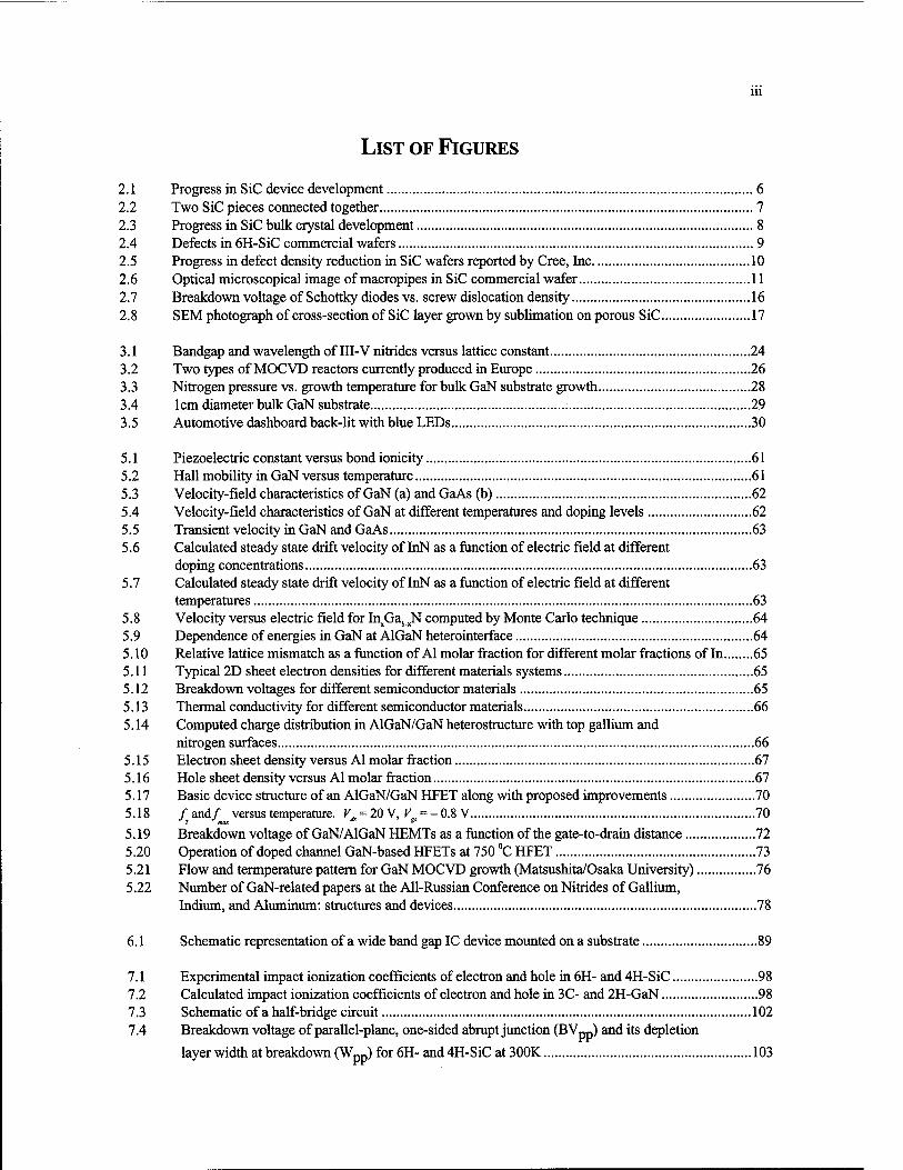
LIST OF FIGURES
2.1 Progress in SiC device development 6 2.2 Two SiC pieces connected together 7 2.3 Progress in SiC bulk crystal development 8 2.4 Defects in 6H-SiC commercial wafers 9 2.5 Progress in defect density reduction in SiC wafers reported by Cree, Inc 10 2.6 Optical microscopical image of macropipes in SiC commercial wafer 11 2.7 Breakdown voltage of Schottky diodes vs. screw dislocation density 16 2.8 SEM photograph of cross-section of SiC layer grown by sublimation on porous SiC 17
3.1 Bandgap and wavelength of III-V nitrides versus lattice constant 24 3.2 Two types of MOCVD reactors currently produced in Europe 26 3.3 Nitrogen pressure vs. growth temperature for bulk GaN substrate growth 28 3.4 1cm diameter bulk GaN substrate 29 3.5 Automotive dashboard back-lit with blue LEDs 30
5.1 Piezoelectric constant versus bond ionicity 61 5.2 Hall mobility in GaN versus temperature 61 5.3 Velocity-field characteristics of GaN (a) and GaAs (b) 62 5.4 Velocity-field characteristics of GaN at different temperatures and doping levels 62 5.5 Transient velocity in GaN and GaAs 63 5.6 Calculated steady state drift velocity of InN as a function of electric field at different
doping concentrations 63 5.7 Calculated steady state drift velocity of InN as a function of electric field at different
temperatures 63 5.8 Velocity versus electric field for In5GalxN computed by Monte Carlo technique 64 5.9 Dependence of energies in GaN at AlGaN heterointerface 64 5.10 Relative lattice mismatch as a function of Al molar fraction for different molar fractions of In 65 5.11 Typical 2D sheet electron densities for different materials systems 65 5.12 Breakdown voltages for different semiconductor materials 65 5.13 Thermal conductivity for different semiconductor materials 66 5.14 Computed charge distribution in AlGaN/GaN heterostructure with top gallium and
nitrogen surfaces 66 5.15 Electron sheet density versus Al molar fraction 67 5.16 Hole sheet density versus Al molar fraction 67 5.17 Basic device structure of an AlGaN/GaN HFET along with proposed improvements 70 5.18 /and/ versus temperature. FA = 20V, K, = -0.8V 70
5.19 Breakdown voltage of GaN/AlGaN HEMTs as a function of the gate-to-drain distance 72 5.20 Operation of doped channel GaN-based HFETs at 750 °C HFET 73 5.21 Flow and temperature pattern for GaN MOCVD growth (Matsushita/Osaka University) 76 5.22 Number of GaN-related papers at the Ail-Russian Conference on Nitrides of Gallium,
Indium, and Aluminum: structures and devices 78
6.1 Schematic representation of a wide band gap IC device mounted on a substrate 89
7.1 Experimental impact ionization coefficients of electron and hole in 6H- and 4H-SiC 98 7.2 Calculated impact ionization coefficients of electron and hole in 3C- and 2H-GaN 98 7.3 Schematic of a half-bridge circuit 102 7.4 Breakdown voltage of parallel-plane, one-sided abrupt junction (BVpp) and its depletion
layer width at breakdown (Wpp) for 6H-and 4H-SiC at 300K 103
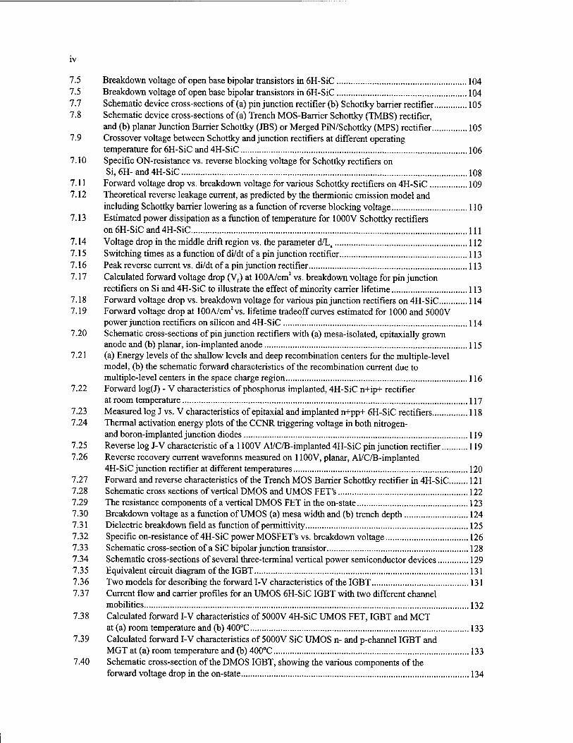
IV
7.5 Breakdown voltage of open base bipolar transistors in 6H-S1C 104 7.5 Breakdown voltage of open base bipolar transistors in 6H-SiC 104 7.7 Schematic device cross-sections of (a) pin junction rectifier (b) Schottky barrier rectifier 105 7.8 Schematic device cross-sections of (a) Trench MOS-Barrier Schottky (TMBS) rectifier,
and (b) planar Junction Barrier Schottky (JBS) or Merged PiN/Schottky (MPS) rectifier 105 7.9 Crossover voltage between Schottky and junction rectifiers at different operating
temperature for 6H-SiC and 4H-SiC 106 7.10 Specific ON-resistance vs. reverse blocking voltage for Schottky rectifiers on
Si, 6H- and 4H-SiC 108 7.11 Forward voltage drop vs. breakdown voltage for various Schottky rectifiers on 4H-SiC 109 7.12 Theoretical reverse leakage current, as predicted by the thermionic emission model and
including Schottky barrier lowering as a function of reverse blocking voltage 110 7.13 Estimated power dissipation as a function of temperature for 1000V Schottky rectifiers
on 6H-SiC and 4H-SiC Ill 7.14 Voltage drop in the middle drift region vs. the parameter d/La 112 7.15 Switching times as a function of di/dt of a pin junction rectifier 113 7.16 Peak reverse current vs. di/dt of a pin junction rectifier 113 7.17 Calculated forward voltage drop (VF) at 100A/cm2 vs. breakdown voltage for pin junction
rectifiers on Si and 4H-SiC to illustrate the effect of minority carrier lifetime 113 7.18 Forward voltage drop vs. breakdown voltage for various pin junction rectifiers on 4H-SiC 114 7.19 Forward voltage drop at 100A/cm2 vs. lifetime tradeoff curves estimated for 1000 and 5000V
power junction rectifiers on silicon and 4H-SiC 114 7.20 Schematic cross-sections of pin junction rectifiers with (a) mesa-isolated, epitaxially grown
anode and (b) planar, ion-implanted anode 115 7.21 (a) Energy levels of the shallow levels and deep recombination centers for the multiple-level
model, (b) the schematic forward characteristics of the recombination current due to multiple-level centers in the space charge region 116
7.22 Forward log(J) - V characteristics of phosphorus implanted, 4H-SiC n+ip+ rectifier at room temperature 117
7.23 Measured log J vs. V characteristics of epitaxial and implanted n+pp+ 6H-SiC rectifiers 118 7.24 Thermal activation energy plots of the CCNR triggering voltage in both nitrogen-
and boron-implanted junction diodes 119 7.25 Reverse log J-V characteristic of a 1100V Al/C/B-implanted 4H-SiC pin junction rectifier 119 7.26 Reverse recovery current waveforms measured on 1100V, planar, Al/C/B-implanted
4H-SiC junction rectifier at different temperatures 120 7.27 Forward and reverse characteristics of the Trench MOS Barrier Schottky rectifier in 4H-SiC 121 7.28 Schematic cross sections of vertical DMOS and UMOS FET's 122 7.29 The resistance components of a vertical DMOS FET in the on-state 123 7.30 Breakdown voltage as a function of UMOS (a) mesa width and (b) trench depth 124 7.31 Dielectric breakdown field as function of permittivity 125 7.32 Specific on-resistance of 4H-SiC power MOSFET's vs. breakdown voltage 126 7.33 Schematic cross-section of a SiC bipolar junction transistor 128 7.34 Schematic cross-sections of several three-terminal vertical power semiconductor devices 129 7.35 Equivalent circuit diagram of the IGBT 131 7.36 Two models for describing the forward I-V characteristics of the IGBT 131 7.37 Current flow and carrier profiles for an UMOS 6H-SiC IGBT with two different channel
mobilities 132 7.38 Calculated forward I-V characteristics of 5000V 4H-SiC UMOS FET, IGBT and MCT
at (a) room temperature and (b) 400°C 133 7.39 Calculated forward I-V characteristics of 5000V SiC UMOS n- and p-channel IGBT and
MGT at (a) room temperature and (b) 400°C 133 7.40 Schematic cross-section of the DMOS IGBT, showing the various components of the
forward voltage drop in the on-state 134
7.41 Turn-off characteristics of 5000V 4H-SiC UMOS IGBT with different lifetimes 134 7.42 Forward drop vs. turn-off time tradeoff for 5000V 4H-SiC IGBT 135 7.43 Reverse-biased safe-operating-area (RBSOA) of 5000V UMOS n- and p-channel IGBT's
with punch-through and non-punch-through structures 135 7.44 Equivalent circuit diagram of the MGT 136 7.45 Passive and active turn-off characteristics of a 5000V 4H-SiC MGT 137 7.46 Reverse-biased safe-operating-area (RBSOA) of 5000V UMOS n-channel MGT 137 7.47 Schematic cross-section of the silicon controlled rectifier (SCR) 139 7.48 Schematic cross-section of the silicon controlled thyrister 139 7.49 Simulated holding currents for 5000V 4H-SiC pnpn and npnp SCR's 139 7.50 Turn-on current waveforms of an 1100V 4H-SiC GTO at various temperatur 140 7.51 Unity gain turn-off characteristics of an 1100V 4H-SiC GTO at various temperatures 141
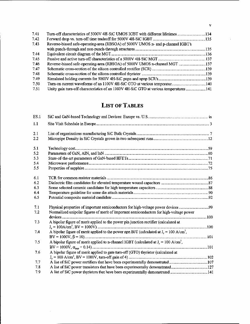
LIST OF TABLES
ES.l SiC and GaN-based Technology and Devices: Europe vs. U.S ix
1.1 Site Visit Schedule in Europe 3
2.1 List of organizations manufacturing SiC Bulk Crystals 7 2.2 Micropipe Density in SiC Crystals grown in two subsequent runs 12
5.1 Technology cost 59 5.2 Parameters of GaN, AIN, andlnN 60 5.3 State-of-the-art parameters of GaN-based HFETs 71 5.4 Microwave performance 72 5.5 Properties of sapphire 75
6.1 TCR for common resistor materials 86 6.2 Dielectric film candidates for elevated temperature wound capacitors 87 6.3 Some selected ceramic candidates for high temperature capacitors 88 6.4 Temperature guideline for some die attach materials 90 6.5 Potential composite material candidate 92
7.1 Physical properties of important semiconductors for high-voltage power devices 99 7.2 Normalized unipolar figures of merit of important semiconductors for high-voltage power
devices 100 7.3 A bipolar figure of merit applied to the power pin junction rectifier (calculated at
JF=100A/cm2,BV=1000V) 100 7.4 A bipolar figure of merit applied to the power npn BJT (calculated at JF = 100 A/cm2,
BV = 1000V, ß = 10) 101 7.5 A bipolar figure of merit applied to n-channel IGBT (calculated at JF = 100 A/cm2,
BV=1000V,aPNP = 0.14) 101 7.6 A bipolar figure of merit applied to gate turn-off (GTO) thyristor (calculated at
JF = 100 A/cm2, BV = 1000V, turn-off gain of 4) 102 7.7 A list of SiC power rectifiers that have been experimentally demonstrated 107 7.8 A list of SiC power transistors that have been experimentally demonstrated 127 7.9 A list of SiC power thyristors that have been experimentally demonstrated 141

VI
EXECUTIVE SUMMARY
INTRODUCTION
Wide bandgap semiconductors (SiC, GaN, A1N) have great potential for high-temperature, high-power, high- frequency electronics, and for short-wavelength optoelectronics. Now, the rapid progress of the last few years in SiC and group III nitrides technology and device development is providing us with unique opportunities for development of the next generation of semiconductor electronics—semiconductor electronics for the 21st century.
In 1999, the U.S. National Science Foundation and the Office of Naval Research assembled a panel on "High-Temperature Electronics" to evaluate and compare the status, trends, and perspectives of wide bandgap semiconductor electronics in the U.S. and Europe, with particular emphasis on Europe. This panel was composed of individuals representing industry, academia and government organizations: Prof. T.P. Chow, Rensselaer Polytechnic Institute; Prof. S.P. DenBaars, University of California at Santa Barbara; Dr. V.A. Dmitriev, TDI, Inc. (Panel Chair); Prof. M.S. Shur, Rensselaer Polytechnic Institute; Prof. M.G. Spencer, Cornell University; and Dr. G. White, Georgia Institute of Technology. Accompanying and working with the panel during its site visits in Japan were Dr. U. Varshney of the National Science Foundation and Dr. J. Zavada of the European Research Office. This study was a continuation of the "High Temperature Electronic in Japan" study, which was managed by ITRI in 1998.l
In its investigation, the panel focused on the following topical areas:
• basic research on wide bandgap semiconductors (SiC and Group III nitrides)
• bulk crystal growth of wide bandgap semiconductors
• epitaxial growth of wide bandgap semiconductors
• post growth technology for device fabrication (etching, metallization, edge termination, and passivation)
• packaging technology for high-temperature/high-power/high frequency applications
• design of high-temperature devices on SiC and group III nitrides
• applications and markets of high-temperature/high-power/high frequency electronics
In June 1999, as part of this study, panelists traveled to Europe where they visited companies, universities, and government research institutes at 11 sites. The organizations visited were chosen because they have established leadership roles in important aspects of wide bandgap semiconductor research and development. All of them have significant efforts, either in the field of SiC or in group III nitride materials and devices - some in both.
1 TTEC Panel Report on High-Temperature Electronics in Japan, International Technology Research Institute, Loyola College, 1999.

viii Dmitriev
Results of the study have been reported and discussed at the 1999 Fall Material Research Society Meeting in Boston and The US-Europe Conference on Wide Bandgap Semiconductor Technology for Next Generation Electronic and Photonic Devices.
This report is based on: the panel's observations during site visits in Europe; discussions with our hosts and colleagues in the Europe companies, universities, and government laboratories visited; and on published literature that details recent work in Europe and United States.
PRINCIPAL CONCLUSIONS
There is a strong interest in both the United States and Europe in advanced electronics based on wide bandgap semiconductors. European countries most active in the field are Germany, Sweden, and France. The European Union has recently initiated a few R&D programs in this area, including projects on silicon carbide and gallium nitride crystal growth and device fabrication.
Other major conclusions include:
European scientists and engineers see optoelectronics and high-power, high-frequency electronics as the major application opportunities for wide bandgap semiconductors. In Europe, high- temperature electronics is not considered a major applications field.
• The size of the GaN and SiC technology and device development effort in Europe is comparable with that in the United States.
• Europe is ahead of the U.S. in bulk GaN growth technology and related homoepitaxial technology.
• The United States is currently ahead of Europe in GaN-based device developments for light emitters, and high-power/high-frequency applications. However, the strong GaN R&D effort that is rapidly progressing in Europe will provide a foundation that will help enable both photonic and electronic markets. The earlier assessment concluded that Japan lead the U.S. in this field.
• In silicon carbide technology, the U.S. is ahead in SiC bulk crystal and epitaxial production. Excellent bulk growth research is being done in Europe, but at present there is no 3-inch commercial product and no semi-insulating wafers.
• In silicon carbide R&D, European organizations both academic and industrial have recently demonstrated outstanding results in both material growth (bulk and epi) and device development proving their leading position in the world. In the area of SiC power switching devices, Europe is leading in both R&D and pre-production activity.
• Strength of European approach is in the powerful combination of national and international projects both R&D and product oriented. These projects are usually coordinated by one or a few industrial organizations highly motivated by new product development. They involve a number of leading research teams from academia and are funded by a national government or European Union. A number of such projects involve research teams from Eastern Europe having unique experience in R&D work in the field of wide band gap semiconductors.
The conclusions of the panel and of this report are summarized in Table 1, in which SiC and GaN-based R&D and production activities of Europe and the United States are compared.
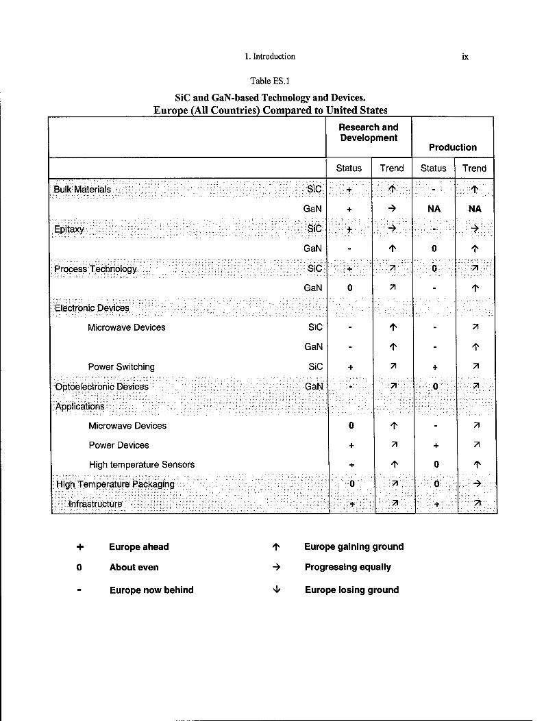
1. Introduction ix
Table ES. 1
SiC and GaN-based Technology and Devices. Europe (All Countries) Compared to United States
Research and Development
Production
Status Trend Status Trend
Bulk Materials
Epitaxy
Process Technology
Electronic Devices
Microwave Devices
Power Switching
Optoelectronic Devices
Applications
Microwave Devices
Power Devices
High temperature Sensors
High Temperature Packaging
Infrastructure
SiC
GaN
SiC
GaN
SiC
GaN
SiC
GaN
SiC
GaN
+
0
0
+
+
0
+
71
71
71
71
71
71
71
NA
0
0
+
0
+
0
o
+
NA
7)
71
71
71
71
71
71
+ Europe ahead
0 About even
Europe now behind
1" Europe gaining ground
-> Progressing equally
4< Europe losing ground

Dmitriev

CHAPTER 1
INTRODUCTION
Vladimir A. Dmitriev
GOALS OF THE STUDY
In 1999, U.S. Government agencies requested the International Technology Research Institute (ITRI) to assess the state of high-temperature electronics basic research, development, manufacturing, and applications in Europe compared to that in the United States. A similar study was conducted in 1998 examining the status of high temperature electronics in Japan and the USA. ITRI assembled the High-Temperature Electronic (HTE) Panel to conduct a study on silicon carbide (SiC) and gallium nitride (GaN) R&D and production activities in Europe. The study was focused on the following topical areas:
• basic study of wide band gap semiconductors (SiC and group III nitrides);
• bulk crystal growth of wide band gap semiconductors;
• epitaxial growth of wide band gap semiconductors for device structures;
• post growth technology for device fabrication (etching, metallization, edge termination, and passivation);
• packaging technology for high temperature applications;
• design of high temperature devices on SiC and group III nitrides;
• applications and market for high temperature electronic devices.
THE STUDY PANEL
Six experts served as panel members for this study. (Short biographies are in Appendix A). Coming from both academia and industry, they reflect the diversity of professional backgrounds currently contributing to the advancement of wide band gap semiconductor electronics in the United States.
• Vladimir A. Dmitriev (Panel Chairman), President, TDI, Inc. Expertise: wide band gap semiconductor epitaxial growth and device development.
• T. Paul Chow, Associate Professor, Rensselaer Polytechnic Institute. Expertise: power semiconductor devices.
• Steven P. DenBaars, Associate Professor, University of California at Santa Barbara. Expertise: growth and characterization of wide band gap semiconductors and device structures.
1. Introduction
• Michael S. Shur, Patricia W. and C. Sheldon Roberts '48 Professor, Rensselaer Polytechnic Institute. Expertise: solid state device physics.
• Michael G. Spencer, Cornell University. Expertise: epitaxial and bulk growth of wide band gap semiconductors.
• George White, Georgia Institute of Technology. Expertise: electronic device packaging.
The panelists were accompanied on site visits to European organizations by the following representatives from the sponsoring organizations (Appendix A):
• Usha Varshney, Program Director, National Science Foundation.
• John Zavada, European Research Office.
APPROACH
Panelists and government sponsors prepared a list of organizations that have established leadership in some important aspects of high temperature electronics and wide band gap electronics in Europe. ITRI then contacted these organizations with letters of introduction from individual panelists to determine if they were willing to host a visit by the panel.
Before the trip, panel members collected information on recent achievements in high temperature electronics and wide band gap electronics in the United States. To provide some reciprosity, panel members gave presentations during site visits reviewing the status of high-temperature electronics in the USA.
Site visits took place from June 6 to June 12, 1999. Members of the panel arrived in Europe and had a planning meeting on Sunday 6 in Grenoble. On June 7, the panel had a meeting with leading French scientists from different organizations working on wide band gap semiconductors. This full-day meeting organized at CEA LETI gave the panel members an opportunity to obtain very helpful information on wide band gap electronics R&D in France. For the following site visits, the panel was divided in two teams. The visit schedule is shown in Table 1. On Friday June 11, both teams had joint meetings at Stockholm, visiting ABB, IMC, and RIT. On Saturday morning, June 12, we had a debriefing meeting at Stockholm to compare notes and come to some conclusions.
While the site visit format varied from site to site, mostly they had the following format:
1. Introduction of participants and a brief discussion of the visit. At some sites, panel members gave short background presentations on the status of wide band gap electronics in the United States. These presentations lasted 40 - 60 minutes.
2. Presentation of the organization's background and technical objectives in the wide band gap semiconductor field; some of these presentations gave details such as company size, income, research and production goals.
3. Discussion, extended question and answer period. These discussions, which typically lasted between two and four hours, were based on a detailed questionnaire sent earlier to the organizations. The panel did not ask organizations to answer every question on the questionnaire, but rather to focus on those issues most relevant to their own work. Before or after discussion, some host organizations provided laboratory or plant tours.
For each site visited, one attending panelist or other traveling team member had the task of writing a detailed site report. Each draft site report was circulated to other members of the site visit team, who drew from their own notes to make additions to or deletions from the draft to ensure accuracy and completeness. ITRI then submitted each draft site report to the host organization for its own editing of the contents to ensure that the report is accurate and does not inadvertently compromise proprietary information.

Dmitriev 3
The results of the study were reported at the 1999 Fall MRS Meeting in Boston on December 1, 1999. A special session devoted to the panel report was organized by Michael Shur and Randall Feenstra (co-chair of the MRS Symposium "GaN and Related Alloys") and chaired by Vladimir Dmitriev. At the session, John Zolper (ONR) and John Zavada (European Research Office) shared with the participants their views on the future of high-temperature electronics. Professor Sylwester Porowski (HPRC) gave an overview of bulk GaN effort in Europe.
Table 1.1
Site Visit Schedule in Europe
Team A TeamB
S. DenBaars V. Dmitriev
M. Shur P. Chow
G. White M. Spencer
J. Zavada
U. Varshney
June 6 Panel business meeting, Grenoble, France
June 7 CEA LETI, Grenoble, France
June 8 University of Ulm Siemens (Erlangen)
June 9 Siemens (Munich) University of Erlangen
June 10 HPRC, Warsaw University of Linkoping
June 11 IMC/ABB/RIT, Stockholm, Sweden
June 12 Panel business meeting, Stockholm , Sweden
THE US-EUROPE CONFERENCE
It is ITRI's practice to hold workshops in the Washington, DC area to present the findings of its panels. For this study, it was decided to organize a US-Europe Conference on Wide Bandgap Semiconductor Technology for Next Generation Electronic and Photonic Devices. Leading European scientists and engineers were invited to report the latest results in the field. The conference was held in Arlington, Virginia on December 9 - 10, 1999. The following reports were presented at the conference on December 9:
1. Michael G. Spencer, Cornell University, SiC growth and processing technology
2. Vladimir Dmitriev, TDI, Inc., Progress and issues in SiC technology
3. T. Paul Chow, Rensselaer Polytechnic Institute, High voltage SiC power switching devices
4. Heinz Lendenmann, ABB Corporate Research, Application and operation of high voltage, high current SilGBT / SiC diode modules
5. Steven DenBaars, University of California, Santa Barbara, GaN-based materials research in Europe

4 1. Introduction
6. Sylwester Porowski, High Pressure Research Center, PAS, Application of pressure grown GaN substrates to epitaxy
7. Michael Shur, Rensselaer Polytechnic Institute, GaN-based electronic device research in Europe
8. Christian Brylinski, Thomson CSF, Wide bandgap microwave power devices
9. George White, Georgia Institute of Technology, High temperature electronic packaging in Europe
10. Roumen Kakanakov, Institute of Applied Physics, BAS, Ohmic contacts and packaging for wide bandgap semiconductors
On December 10, there was a general discussion on different aspects of wide band gap electronics. The following reports were presented after the discussion:
1. NSF programs (U. Varshney)
2. ONR programs (I. Mack)
3. DARPA programs (E. Martinez)
More than 100 experts in the field of wide band gap semiconductors attended the conference. Viewgraphs presented at the conference are available on the ITRI Web site (http://itri.loyola.edu/ttec/).
OVERVIEW OF THE REPORT
This written report is the final evaluation of the panel on the current status of silicon carbide and gallium nitride electronics in Europe and the United States. It consists of six chapters devoted to specific aspects of wide band gap electronics written by panel members and site reports. Brief biographies of panel members are given in Appendix A.
CHAPTER 2
STATUS OF SIC TECHNOLOGY: BULK AND EPITAXIAL GROWTH
Vladimir A. Dmitriev
INTRODUCTION
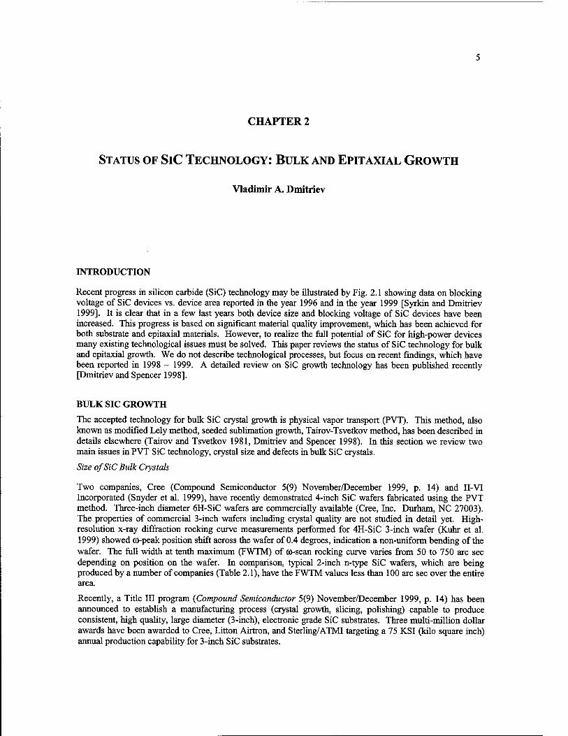
Recent progress in silicon carbide (SiC) technology may be illustrated by Fig. 2.1 showing data on blocking voltage of SiC devices vs. device area reported in the year 1996 and in the year 1999 [Syrkin and Dmitriev 1999]. It is clear that in a few last years both device size and blocking voltage of SiC devices have been increased. This progress is based on significant material quality improvement, which has been achieved for both substrate and epitaxial materials. However, to realize the full potential of SiC for high-power devices many existing technological issues must be solved. This paper reviews the status of SiC technology for bulk and epitaxial growth. We do not describe technological processes, but focus on recent findings, which have been reported in 1998 - 1999. A detailed review on SiC growth technology has been published recently [Dmitriev and Spencer 1998].
BULK SIC GROWTH
The accepted technology for bulk SiC crystal growth is physical vapor transport (PVT). This method, also known as modified Lely method, seeded sublimation growth, Tairov-Tsvetkov method, has been described in details elsewhere (Tairov and Tsvetkov 1981, Dmitriev and Spencer 1998). In this section we review two main issues in PVT SiC technology, crystal size and defects in bulk SiC crystals.
Size of SiC Bulk Crystals
Two companies, Cree (Compound Semiconductor 5(9) November/December 1999, p. 14) and II-VI Incorporated (Snyder et al. 1999), have recently demonstrated 4-inch SiC wafers fabricated using the PVT method. Three-inch diameter 6H-SiC wafers are commercially available (Cree, Inc. Durham, NC 27003). The properties of commercial 3-inch wafers including crystal quality are not studied in detail yet. High- resolution x-ray diffraction rocking curve measurements performed for 4H-SiC 3-inch wafer (Kuhr et al. 1999) showed (0-peak position shift across the wafer of 0.4 degrees, indication a non-uniform bending of the wafer. The full width at tenth maximum (FWTM) of ©-scan rocking curve varies from 50 to 750 arc sec depending on position on the wafer. In comparison, typical 2-inch n-type SiC wafers, which are being produced by a number of companies (Table 2.1), have the FWTM values less than 100 arc sec over the entire area.
Recently, a Title III program {Compound Semiconductor 5(9) November/December 1999, p. 14) has been announced to establish a manufacturing process (crystal growth, slicing, polishing) capable to produce consistent, high quality, large diameter (3-inch), electronic grade SiC substrates. Three multi-million dollar awards have been awarded to Cree, Litton Airtron, and Sterling/ATMI targeting a 75 KSI (kilo square inch) annual production capability for 3-inch SiC substrates.

2. Status of SiC Technology: Bulk and Epitaxial Growth
10000
8000 > o S 6000 o > O) I 4000 u o m
2000
•
V
V
V
V
■
\ ° *
's» :
i i
• pn Diodes
■ Data 1996
o SD
D JFET
A GTO
- - trend for pn Diodes 1999
— trend for Data 1996
1.E-05 1.E-04 1.E-03 1.E-02 1.E-01 1.E+00 Device Area, sq.cm
Fig. 2.1. Progress in SiC device development. Blocking voltage for different types of SiC devices vs. device area reported in 1996 and 1999 (Syrkin and Dmitriev, 1999).
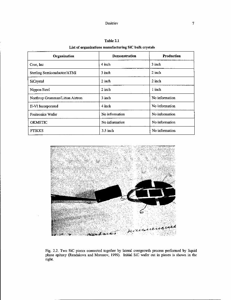
The above results on the increase of SiC bulk crystal diameter have been achieved by gradual increase in crystal size during the crystal growth. Starting from a 2-inch diameter seed, it is possible to obtain an SiC ingot having diameter of 2.5 inches in one growth run. In order to make a leap in SiC crystal size, it is necessary to have a large diameter seed. Rendakova and Morozov recently demonstrated that large SiC wafer may be obtained by "gluing" together smaller SiC wafers (Rendakova and Morozov, 1999). This idea was proved when two lxl cm2 pieces of SiC wafer were connected to each other by single crystal SiC epitaxial layer grown by liquid phase epitaxy (LPE) on both pieces in a single epitaxial run (Fig. 2.2). The single crystal nature of the resulting sample was proved using x-ray diffraction measurements. This technical approach may be applied to fabricate large area SiC seeds for >6-inch SiC bulk growth.
The progress in the development and production of large-size SiC wafers is demonstrated in Fig. 2.3. Using the trend shown, we may predict that 4-inch and 6-inch SiC wafers will be commercially available in 2001 and 2005, respectively.
Defect density reduction
Defects in SiC substrates currently are the main obstacle for realization of large area (>0.1 cm2) high-power devices. Typical defects in SiC commercial wafers (Fig. 2.4) are voids, dislocations, misoriented blocks, and foreign polytype inclusions. In the past few years, defect density in SiC wafers has been significantly reduced. Cree, Inc. has demonstrated 2-inch SiC wafers having 1.1 cm"2 micropipe density over an entire wafer (Hobgood et al. 1999). An ATMI-Sterling research team reported 30 mm diameter wafer having 4 cm2 area without micropipes (an average micropipe density for the whole wafer was of 3.1 cm"2) (Powel et al. 1999). However, defect density in commercial SiC wafers is still high and must be reduced to much lower level in order to demonstrate devices with operating area from 1 to 10 cm2.
Dmitriev
Table 2.1
List of organizations manufacturing SiC bulk crystals
Organization Demonstration Production
Cree, Inc 4 inch 3 inch
Sterling Semiconductor/ATMI 3 inch 2 inch
SiCrystal 2 inch 2 inch
Nippon Steel 2 inch 1 inch
Northrop Grumman/Litton Airtron 3 inch No information
II-VI Incorporated 4 inch No information
Freitronics Wafer No information No information
OKMETIC No information No information
FTIKKS 3.5 inch No information
■i.^Ct,ij*A^'
-i. t " <i *• '• *' *
Fig. 2.2. Two SiC pieces connected together by lateral overgrowth process performed by liquid phase epitaxy (Rendakova and Morozov, 1999). Initial SiC wafer cut in pieces is shown in the right.

2. Status of SiC Technology: Bulk and Epitaxial Growth
E E
0) 0) E « Q w
3 O ffi
160
140
120
100
80
60
40
20 Tairov's Lab.
Cree
Cree
Cree
ll-VI Inc.
Cree
Taiiwrtabr
FTIKKS
6 inch
4 inch
• 6H-SiCWaffers
• 4H-SiC Waffers
O 6H-SiC Expected
04H-SiC Expected
1975 1980 1985 1990 1995 2000 2005 2010
Fig. 2.3. Progress in SiC bulk crystal development performed at Leningrad Electrotechnical Institute (Tairov's Lab), Cree, Inc., FTIKKS (St. Petersburg, Russia), and II-VI Incorporated.
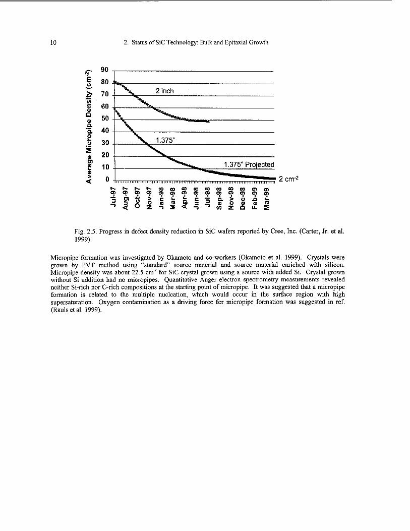
Progress in defect reduction in SiC crystals is much more pronounced for smaller size SiC crystals. Usually it takes a few years to reduce defect density for SiC crystals of a particular size (Fig. 2.5) (Carter, Jr. et al 1999). Note that the record size SiC pn diodes with the area of 7x7 mm2 were fabricated in 1999 on 35 mm SiC wafers, although 41 mm and 50 mm SiC wafers were commercially available (Lendenmann et al. 1999). This development was possible because defect density in 35 mm wafer was low. In this section we review recent results on defect investigation and defect density reduction for SiC bulk crystals.
Voids in SiC wafers
Hofmann and co-authors (Hofmann et al. 1999a) gave a classification of void defects in SiC bulk crystals. The following three categories of voids were selected: (1) micropipes and nanopipes, (2) macrodefects (pipes), and (3) planar voids. Micropipes, nanopipes, and macropipes propagate through SiC crystals in the growth direction, which is usually close to c axis direction. In the [0001] plane, nanopipes, micropipes and macropipes have a typical size less that 1 micron, from 1 to 10 microns, and larger that 10 microns, respectively. Planar voids usually have the largest dimension in the direction perpendicular to the c axis. There has been practically no investigation of the nature and properties of nanopipes in SiC crystals. Micropipes were studied by a several research teams (Giocondi et al. 1996, Heindl et al. 1998, Huang et al. 1999, Pirouz 1998, Yamaguchi et al. 1999a). Some micropipes are related to hollow core dislocations. In SiC wafers, micropipe and dislocation densities range from 10 to 100 cm"2 (Anikin et al. 1999) and 10" to 106 cm'2
(Kalinina et al. 1999a), respectively. Usually micropipe density is higher at the periphery of SiC wafer. Planar defects (Sudarshan et al. 1999) are rather random in commercial SiC wafers.
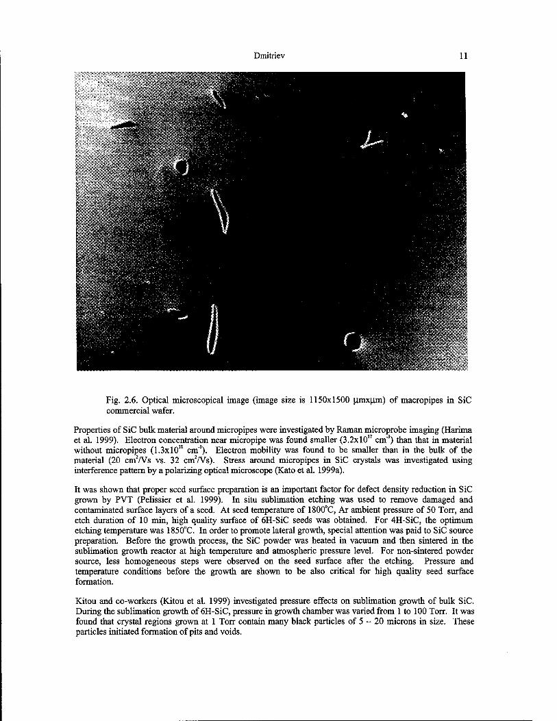
Macropipes (Fig. 2.6) usually have diameter ranging from 10 to 100 microns and are not associated with dislocations. Macropipes are often located at boundaries of foreign polytype and misoriented block. They are also observed to start at the interface between the SiC seed and the graphite crucible lid (Sanchez et al. 1999a). These defects are believed to be formed due to local decomposition and evaporation of seed crystal. The micropipe defects may be reduced by the formation of continuous uniform graphite layer on the back side of SiC seed.
Defect generation during SiC bulk growth was investigated by Hofmann and co-workers (Hofmann et al. 1999b). SiC crystals having diameter from 1.2 to 1.5 inch were grown on seeds with different micropipe density in order to study the defect formation. The source material was synthesized from elemental high

Dmitriev 9
purity Si and C. After heating up to about 2100 - 2300°C, the growth was initiated by lowering the system pressure from the starting value of 800 Torr to the growth pressure of 5 - 40 Torr. The pumping time constant (Tairov and Tsvetkov 1983), x, was varied between 120 sec and 2400 sec, to control supersaturation. Besides the micropipes penetrated from the seed, no other micropipes were created at the initial stage of SiC crystal growth. The authors indicted that sublimation etching of the seed was not necessary to avoid defect formation and pumping time variation did not provide significant effect on the defect generation. The micropipe formation strongly correlated with occurrence of second phases in SiC like carbon inclusions. Carbon inclusions formed in grown SiC crystal often caused micropipe formation. Other inclusions, possibly Si droplets, also acted as a starting point of micropipes. Crystals grown on micropipe-free substrates had micropipe density ranged from 100 - 200 cm"2. Although most of the micropipes were caused by inclusions, no obvious correlation between the density of inclusions and the density of micropipes was found. Two additional sources of micropipe formation were identified such as polytype inclusions and micropipe multiplication from large diameter micropipes. A remarkable micropipe density reduction (factor 2-4) was observed in the case of temperature gradient reduction in growth zone.
Fig. 2.4. Defects in 6H-SiC commercial wafers (image size is 450x575 ^mx^m): (a) surface of as received commercial 6H-SiC wafer, optical photo of polished (0001)Si surface, (b) the same wafer after 2 minutes chemical etching in molten KOH at 500"C, black hexagonal pits are micropipes, white etch pits are probably related to dislocations.
10 2. Status of SiC Technology: Bulk and Epitaxial Growth
iiMini in ii min iiimiiiiniiiiiiMiiiiiininiiiiiiiMiiimiMiiiiiimiiiiiiiiiiiiiii ii
h-h-f-r^-coeoMcooocoeococnc) aaaomoiinaittoißoioioi 3Ö)-g>Ci|;J;C3ä>Öx>>!:
2 crrr
S < (0 Z Q
Fig. 2.5. Progress in defect density reduction in SiC wafers reported by Cree, Inc. (Carter, Jr. et al. 1999).
Micropipe formation was investigated by Okamoto and co-workers (Okamoto et al. 1999). Crystals were grown by PVT method using "standard" source material and source material enriched with silicon. Micropipe density was about 22.5 cm"2 for SiC crystal grown using a source with added Si. Crystal grown without Si addition had no micropipes. Quantitative Auger electron spectrometry measurements revealed neither Si-rich nor C-rich compositions at the starting point of micropipe. It was suggested that a micropipe formation is related to the multiple nucleation, which would occur in the surface region with high supersaturation. Oxygen contamination as a driving force for micropipe formation was suggested in ref. (Rauls et al. 1999).
Dmitriev 11
Fig. 2.6. Optical microscopical image (image size is 1150x1500 ^mx(xm) of macropipes in SiC commercial wafer.
Properties of SiC bulk material around micropipes were investigated by Raman microprobe imaging (Harima et al. 1999). Electron concentration near micropipe was found smaller (3.2xl017 cm"1) than that in material without micropipes (1.3xl018 cm'). Electron mobility was found to be smaller than in the bulk of the material (20 cmVVs vs. 32 cmVVs). Stress around micropipes in SiC crystals was investigated using interference pattern by a polarizing optical microscope (Kato et al. 1999a).
It was shown that proper seed surface preparation is an important factor for defect density reduction in SiC grown by PVT (Pelissier et al. 1999). In situ sublimation etching was used to remove damaged and contaminated surface layers of a seed. At seed temperature of 1800°C, Ar ambient pressure of 50 Torr, and etch duration of 10 min, high quality surface of 6H-SiC seeds was obtained. For 4H-SiC, the optimum etching temperature was 1850°C. In order to promote lateral growth, special attention was paid to SiC source preparation. Before the growth process, the SiC powder was heated in vacuum and then sintered in the sublimation growth reactor at high temperature and atmospheric pressure level. For non-sintered powder source, less homogeneous steps were observed on the seed surface after the etching. Pressure and temperature conditions before the growth are shown to be also critical for high quality seed surface formation.
Kitou and co-workers (Kitou et al. 1999) investigated pressure effects on sublimation growth of bulk SiC. During the sublimation growth of 6H-SiC, pressure in growth chamber was varied from 1 to 100 Torr. It was found that crystal regions grown at 1 Torr contain many black particles of 5 - 20 microns in size. These particles initiated formation of pits and voids.
12 2. Status of SiC Technology: Bulk and Epitaxial Growth
Sasaki and co-workers (Sasaki et al., 1999) investigated SiC growth performed at Ar gas pressure of about 5 - 10 Torr, source temperature range of 2250 - 2350°C, and substrate temperature of 1800°C. SiC crystals were grown in two growth runs. Source material was recharged between these two growth runs. A highly nitrogen doped region of about 0.5 mm thick was detected on the interface between materials grown in the first and second growth runs. In the course of growth, nitrogen concentration dropped down to the 1017 cm'' level. It was found that half of the micropipes disappeared at the interface between two growth regions (Table 2.2). Micropipes annihilated by meeting planar defects or other micropipes. These results show the possibility to control micropipe formation and annihilation in sublimation process.
Residual stress in SiC boules grown by sublimation was investigated (Ha et al. 1999a). The radial and axial temperature gradients imposed on a growing crystal create thermal stresses in the crystal even in the absence of external mechanical forces. During the growth the center part of a crystal is cooler than the periphery, putting the center in tension while the periphery region is under compression. If plastic expansion occurs during the growth, crystal periphery is expected to be under tension while the center is under compression. X-ray diffraction measurements were used to determine the plastic deformation frozen in SiC crystals. It was found that the total misorientation of the basal plane across boule diameter was typically between 100 - 2000 arc sec. A continuous reduction of the c-lattice spacing was observed along the radii of crystals from the center to the edge. The amount of strain of the c-lattice spacing at the edge compared to the center was (-0.003) ~ (~0.002)%.
Table 2.2
Micropipe densities in SiC crystals grown in two subsequent runs [Sasaki et al. 1999].
Number of micropipes
2nd growth Surface 9
Interface between la and 2nd growth 20
T growth Interface between 1" and 2nd growth 38
Seed 39
Micropipe penetrated from seed to the surface 7
Defect formation during SiC bulk sublimation growth was investigated by a few research teams. X-ray imaging technique was applied during SiC crystal growth. This method allowed Wellmann and co-workers (Wellmann et al. 1999) to monitor SiC crystal growth interface, change of source material, and crystal growth stability.
In-situ investigation of defect formation during bulk SiC sublimation growth has been reported (Yamaguchi et al. 1999b, Kato et al. 1999b). X-ray topography technique has been used. The growth chamber was equipped with x-ray goniometer, x-ray source (a rotating-anode 18 kW generator with molybdenum target) and CCD camera. The x-ray beam was transmitted directly from the bottom to the top of the crucible through the growing crystal and x-ray intensity was measured by a scintillation counter. Low defect density Acheson and Lely crystals were used as seeds for SiC bulk sublimation growth. Formation of micropipes and domain boundaries were detected during the growth. Evolution of these defects during the growth was tracked using x-ray topography imaging. The same technique has been used for growth rate measurements (Oyanagi et al. 1999). This technique may become a very important tool for the development of low defect density SiC bulk crystals.
One way to avoid micropipe formation has been reported by a Erlangen University research team. 6H-SiC micropipe-free bulk crystals were grown by PVT method at the average thermal gradient inside the growth container less than 5 K cm"' (Schulze et al. 1999). It was found that a crucial point in avoiding micropipes is
Dmitri ev 13
the annealing step of the seed prior to the growth and the initial slow nucleation at thermal equilibrium conditions. It was also noticed that (1) micropipes already contained in the seed penetrate the entire boule, and (2) micropipes are formed in the neighborhood of polytype inclusions. SiC growth rates for micropipe- free growth was less than 0.3 mm/hr due to low temperature gradient. It is still an open question if micropipe-free SiC sublimation growth is possible at growth rates suitable for bulk crystal growth.
Makarov and co-workers (Makarov et al. 1999) used a tantalum container to reduce defect density in SiC crystal grown by sublimation. It was shown that the Ta container suppresses graphitization of the SiC source and reduces formation of graphite inclusions at the surface of the seed. An additional advantage of the use of a Ta container is low chemical reactivity of the container side walls compared to the graphite crucible usually etched during the SiC sublimation growth process. Sublimation growth technology with a Ta container allowed bulk SiC crystals growth at rates of 0.5 - 0.8 mm/hr with micropipe density less than 30 cm"2 and source utilization efficiency higher than 90%.
Another growth technology for SiC crystals with low defect density was proposed based on an idea of lateral crystal growth without crystal contact with crucible walls. It is known that free-standing SiC crystals grown by Lely method (Lely 1955) have lower defect density than SiC crystal grown by seeded sublimation technique. Vodakov and co-workers (Vodakov et al. 1999) used the same approach to grow 40 mm diameter SiC free-standing crystals. Sublimation growth was performed in closed Ta or graphite containers at temperatures 2000-2300°C and Ar gas pressure 10"' - 50 Torr. Micropipe density in grown material was less than 20 cm"2. Dislocation density ranged from 100 to 1000 cm"2.
Another way to fabricate SiC wafers with low micropipe density is to "reaper" micropipes in commercial SiC wafers. A few research teams have demonstrated micropipe closing during liquid phase epitaxial growth of SiC (Yakimova et al. 1996, Hofmann and Müller 1999).
Micropipe filling process has been developed at TDI, Inc. (TDI, Inc., Gaithersburg, MD 20877). This "repairing" process is based on SiC growth inside micropipe channels. The micropipe filling technique can reduce micropipe density by a few times and resulted in zero micropipe density in best R&D 35 mm and 41 mm 6H-SiC and 4H-SiC wafers (Dmitriev et al. 1999). Micropipe density in the initial SiC wafer before micropipe filling process exceeded 100 cm"2.
Dislocations
Recently, it has been recognized that not only voids but dislocations also limit the performance of SiC devices (Chelnokov et al. 1998). It was shown that dislocations in SiC epitaxial structures may lead to premature electric breakdown and increase leakage current in SiC device structures (Neudecket al. 1998a). These results triggered intense investigation of dislocation formation in SiC bulk crystals. One source of dislocations in bulk SiC crystals was identified to be defects of seed surface treatment (Sanchez et al. 1999b). Screw dislocation densities for SiC grown by sublimation on Lely crystal seeds varied from less than 10' cm"2
for hydrogen etched seeds to 106 cm"2 for roughly polished seeds. Graphite inclusions (artificially created graphite dots) on the seed surface were found to be another source of dislocations. The screw dislocation density over the graphite inclusions was in the order of 5xl05 cm"2, while in the other areas of the grown material it was below 10" cm"2.
It was shown (Neudecket al. 1998b) that most 4H-SiC pn diodes containing no dislocations in device area exhibited excellent current-voltage (I-V) characteristics. In contrast, devices that contained at least one elementary screw dislocation exhibited 5-35% reduction in breakdown voltage and a softer (higher leakage) reverse I-V characteristic. A mechanism of threading dislocation formation in bulk SiC crystals was investigated (Ha et al. 1999b).
Dislocation density reduction in SiC grown by sublimation has been reported by using porous buffer layers (Mynbaeva et al. 1999a). Porous SiC substrates were fabricated by surface anodization of SiC commercial wafers. Thickness of SiC material grown on porous buffer was about 10 microns. X-ray topography showed defect density and stress reduction in SiC grown on porous material (see section on Defects in Epitaxial Layers).
14 2. Status of SiC Technology: Bulk and Epitaxial Growth
Alternative Methods for SiC Bulk Crystal Growth
Two alternative methods to grow bulk SiC crystals are under investigation, high-temperature chemical vapor deposition (CVD) and liquid phase growth. High-temperature CVD (Ellison et al. 1999) provides SiC growth rate up to a few millimeters per hour. SiC crystals 6 mm thick and 30 mm in diameter were grown by this method. Micropipe density was about 50 cm"2.
SiC bulk crystals 30 mm in diameter and up to 10 mm in length were grown from the liquid phase (Epelbaum et al. 1999). SiC crystals were grown using silicon melt as solvent at temperatures 1900-2400°C and ambient Ar gas pressures of 100-120 bar. This technique is in the development stage and may lead to SiC substrates without micropipes and a high doping level for both n- and p-type materials (Rendakova et al. 1998).
3C-SiC crystals were grown from carbon-silicon melt-solution (Wollweber et al. 1999). Conventional Floating Zone method was utilized to grow 3C SiC boules up to 11 mm in diameter and 3-4 mm in length. Growth rate of 0.1 to 0.4 mm/hr has been reached.
Currently, these methods are far away from industrial use, but they may become important tools for SiC bulk crystal fabrication if PVT method will be insufficient to further increase SiC boule size and eliminate micropipes.
EPITAXIAL SIC GROWTH
The main epitaxial technology used for SiC device structure fabrication is CVD. Northrop Grumman reported results on preproduction growth of 4H-SiC epitaxial layers employing multi-wafer CVD reactor (Nordbyet al. 1999). For 13/8-inch diameter substrates, reported layer uniformity was typically better than +5% (standard deviation/mean) for doping and +3% for thickness. In a multi-wafer run, interwafer uniformity is typically better than +8% for doping and +3% for thickness. For 2-inch diameter wafers, reported doping and thickness uniformity was approximately +5%. Cree reported thickness non-uniformity for SiC epitaxial layers grown over a 50 mm wafer about 1% and doping non-uniformity less than 5%.
Bergman and co-workers (Bergman et al. 1999) investigated uniformity of carrier lifetime in 4H-SiC epi layers using photoluminescence technique. The highest value for the carrier lifetime of 2.9 |is has been measured for a 80 am thick epi layer grown by a hot-wall CVD technique with concentration Nd-NB < 5x10" cm"'. An average lifetime in epi layers for four wafers ranged from 0.29 to 0.39 us. Results of this study indicated that substrate defects propagate into the epi layer and creates intrinsic defects, which influence the lifetime.
Thick epitaxial layers
In order to fabricate SiC devices for high voltage applications, thick SiC epitaxial layers with low background doping concentration are needed. For example, SiC devices designed for 10 kV reverse voltage require about 100 microns thick base region with concentration Nd-N3 less than 5xl014 cm'1.
4H-SiC diode with breakdown voltage of 5.5 kV was fabricated at Cree based on 85 |im thick epitaxial layer grown by CVD technique using a horizontal hot-wall reactor (Irvine et al. 1998). Silane and propane were used as the precursors. Growth temperatures and the C/Si ration were varied from 1500 to 1700 C and 1 - 2, respectively. Growth rate was 10 um/hr. The concentration Nd-Na was controlled from high 1014 cm"'1 to low 1019 cm"3 using nitrogen gas for doping.
4H-SiC 120 um thick epitaxial layers have been reported by Rowland and co-workers using CVD process (Rowlandet al. 1999). Concentration Nd-Na was of 9xl015 cm"3. Growth rate was <5 um/hr. Small changes in C/Si ratio lead to high background doping. Even a 10% change in C/Si value from the optimum one gave a background doping in the 1017 cm"3 range.
High-temperature (1800 - 1900°C) CVD method was used to grow 4H-SiC layers with growth rate of 16-27 Um/hr [Zhanget al. 1999]. Background concentration Nd-Na ranged from mid 10" to low 101S cm"'1. Usually, the epitaxial layers grown at temperatures higher than 1870 C or with high SiH4 flow rates showed a much
Dmitriev 15
smoother surface than those grown at lower temperatures or lower SiH4 flows. Surface of epitaxial layers was smooth even for 80 pm thick layers. The C-face samples showed much smoother surface than Si-face samples. Pit-like defects with density of about 104 cm'2 were on epi surface. Size of the pits monotonically increased with layer thickness, while pit density did not depend on layer thickness.
Another technique to grow thick SiC epitaxial layers is sublimation epitaxy. Sublimation epitaxy is promising for epitaxial growth of SiC with high growth rates (Syvajarvi et al. 1999a, Segal et al. 2000). Thick 4H-SiC layers have been grown with an average growth rate of 100 mm/hr at 1775°C on 35 mm diameter wafers (Syvajarvi et al. 1999b). The window for morphological stability was determined by growth rate ramp-up, growth rate, temperature gradient, source to substrate distance, and substrate surface orientation. For 100 (im thick layer, macrosteps were not resolved with optical microscopy, although the growth mode was given by the step flow mechanism. The thickness non-uniformity of the layers (expressed by a/mean) was less than 5% for 32 mm. Crystal structure was improved by sublimation epitaxial growth. Average values of the FWHM for co-rocking curves are 64 arcsec for the substrate and 15 arcsec for the epitaxial layer. The layer was n-type with a concentration Nd-Na of about (l-2)xl015 cm"'1. Intentional doping with B (3xl016 cm"1) provided compensated material with a resistivity of 6xl04 Ohm cm. Additional V doping ((2-3)xl016 cm'1) resulted in semi-insulating material with a resistivity of about one order of magnitude less than commercial SiC. Degradation of surface morphology or structural quality due to V doping was not observed.
Summarizing, CVD and sublimation epitaxial method are promising techniques for deposition of thick low- doped SiC layers for high-power devices. Two material parameters will determine the method to win this competition, defect density and minority carrier diffusion length.
Defects in Epitaxial Layers
Elimination of defects in SiC epitaxial layers is the key issue in the fabrication of large area high power SiC devices. Information on defect formation in SiC epitaxial layers is limited. Surface defects called "tetrahedral pits", "comet tails", "carrots", "shallow round pits", and "half-moon" have been described in literature (Seshadri et al. 1999, Kimoto et al. 1999). Formation mechanisms for these defects are not clear yet. Micropipes and dislocations are usually present in SiC epitaxial layers. Step-bunching on SiC surface was investigated for epitaxial layers grown by CVD, sublimation, and LPE (Syvajarvi et al. 1999c).
Surface morphology of thick 4H-SiC epitaxial layers was investigated for materials grown by CVD using SiH4 and C2H„ in the temperature range from 1800 to 1900°C (Zhang et al. 1999). It was found that the epitaxial layers grown at temperatures higher than 1870°C or with high SiH4 flow rates have much smoother surface than those grown at lower temperatures or lower SiH4 flows. Most of observed pit defects were substrate related defects. For high growth temperatures, a smooth surface was obtained even for 80 um thick epitaxial layers. These layers were used to demonstrate 3 kV Schottky diodes.
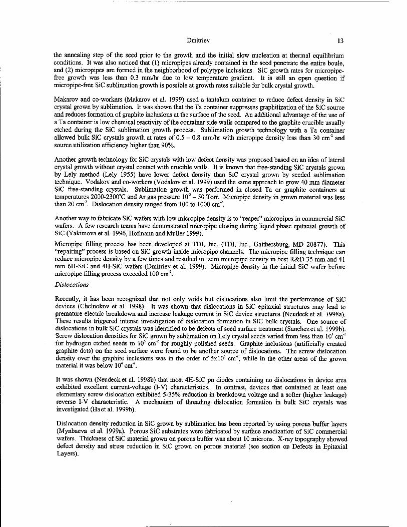
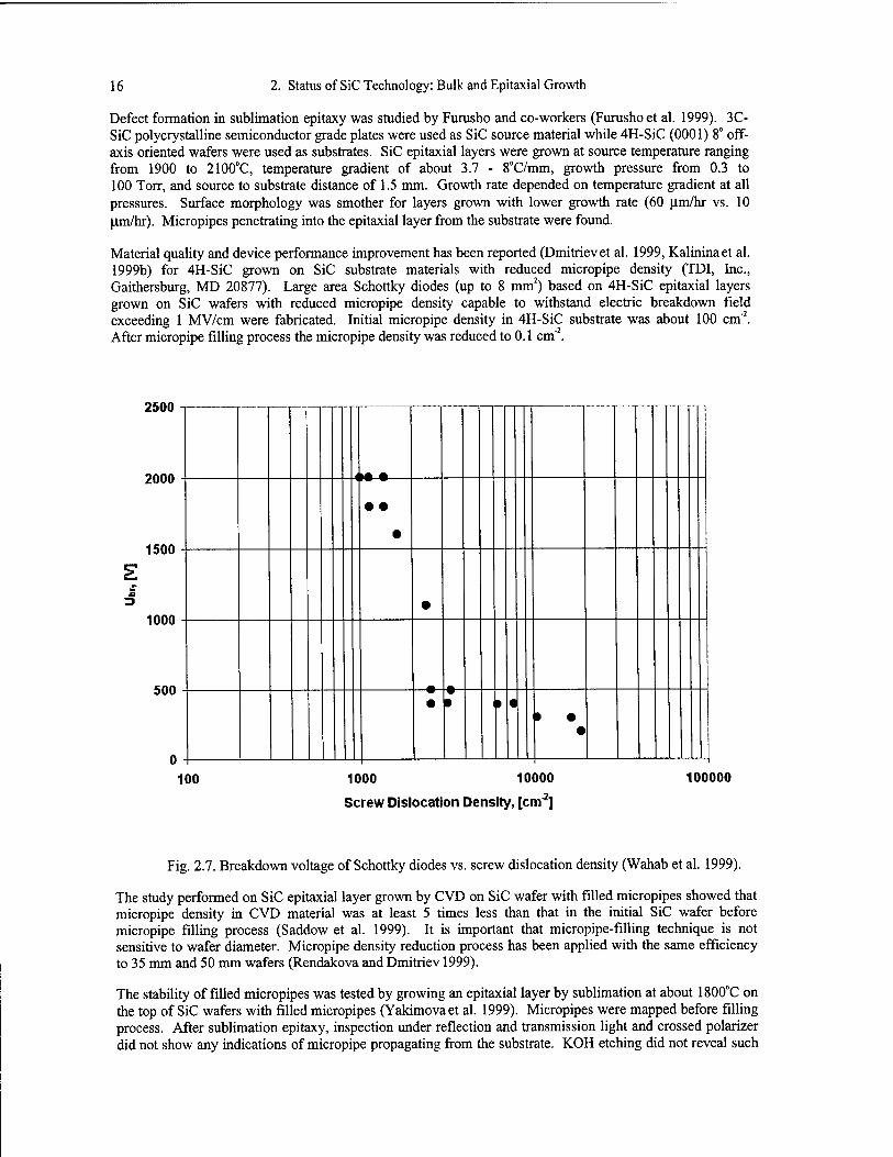
Defects in 4H-SiC 25 urn thick epitaxial layers grown by hot-wall CVD in SiH„-C,H8-H2 gas system at 1600°C were studied by Wahab and co-workers (Wahab et al. 1999). Doping level in the epilayer was about 2xl015 cm"3. Schottky diodes were formed by direct "writing" technique on the top of selected defects. All diodes formed on material having micropipes exhibited breakdown voltage less than 1 kV. The diodes placed on triangular defects showed low breakdown voltage and high leakage current. Carrot shaped ditches in epilayer surface were not found to be harmful with respect to the absolute value of breakdown voltage. Diodes placed on other defects such as foreign polytype inclusions did not show device performance. Only 20% of diodes, which were placed on surface areas containing no defects, were found to block 2 kV or higher voltages. The clear correlation between breakdown voltage and screw dislocation density was observed (Fig. 2.7).
Defects in SiC epitaxial layers grown by sublimation and LPE were investigated using KOH etching and sample cleavages (Syvajarvi et al. 2000). From examination of cross-sectional cleavages with optical microscopy, defects in homoepitaxial SiC layers including stacking faults, stripe defects, and micropipes were studied. For 6H and 4H-SiC layer grown by sublimation, it was shown that smooth surface can be obtained even for 120 (Am thick layers (Syvajarviet al. 1999d).
16 2. Status of SiC Technology: Bulk and Epitaxial Growth
Defect formation in sublimation epitaxy was studied by Furusho and co-workers (Furushoet al. 1999). 3C- SiC polycrystalline semiconductor grade plates were used as SiC source material while 4H-SiC (0001) 8" off- axis oriented wafers were used as substrates. SiC epitaxial layers were grown at source temperature ranging from 1900 to 2100°C, temperature gradient of about 3.7 - 8°C/mm, growth pressure from 0.3 to 100 Torr, and source to substrate distance of 1.5 mm. Growth rate depended on temperature gradient at all pressures. Surface morphology was smother for layers grown with lower growth rate (60 (i.m/hr vs. 10 |im/hr). Micropipes penetrating into the epitaxial layer from the substrate were found.
Material quality and device performance improvement has been reported (Dmitrievet al. 1999, Kalininaet al. 1999b) for 4H-SiC grown on SiC substrate materials with reduced micropipe density (TDI, Inc., Gaithersburg, MD 20877). Large area Schottky diodes (up to 8 mm2) based on 4H-SiC epitaxial layers grown on SiC wafers with reduced micropipe density capable to withstand electric breakdown field exceeding 1 MV/cm were fabricated. Initial micropipe density in 4H-SiC substrate was about 100 cm"2. After micropipe filling process the micropipe density was reduced to 0.1 cm"2.
2500
2000
1500
1000
500
• •
•
•
• i » • » •
•
100 1000 10000 100000
Screw Dislocation Density, [cnr]
Fig. 2.7. Breakdown voltage of Schottky diodes vs. screw dislocation density (Wahab et al. 1999).
The study performed on SiC epitaxial layer grown by CVD on SiC wafer with filled micropipes showed that micropipe density in CVD material was at least 5 times less than that in the initial SiC wafer before micropipe filling process (Saddow et al. 1999). It is important that micropipe-filling technique is not sensitive to wafer diameter. Micropipe density reduction process has been applied with the same efficiency to 35 mm and 50 mm wafers (Rendakova and Dmitriev 1999).
The stability of filled micropipes was tested by growing an epitaxial layer by sublimation at about 1800°C on the top of SiC wafers with filled micropipes (Yakimovaet al. 1999). Micropipes were mapped before filling process. After sublimation epitaxy, inspection under reflection and transmission light and crossed polarizer did not show any indications of micropipe propagating from the substrate. KOH etching did not reveal such
Dmitriev 17
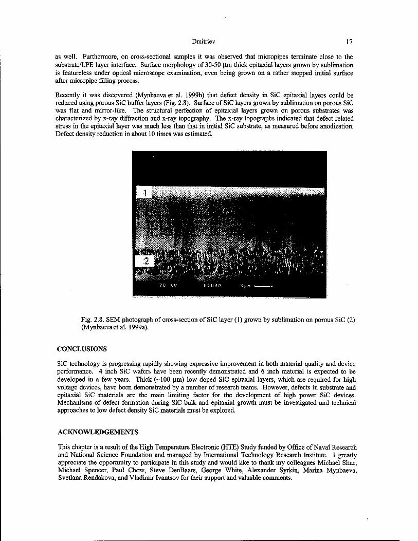
as well. Furthermore, on cross-sectional samples it was observed that micropipes terminate close to the substrate/LPE layer interface. Surface morphology of 30-50 (Am thick epitaxial layers grown by sublimation is featureless under optical microscope examination, even being grown on a rather stepped initial surface after micropipe filling process.
Recently it was discovered (Mynbaeva et al. 1999b) that defect density in SiC epitaxial layers could be reduced using porous SiC buffer layers (Fig. 2.8). Surface of SiC layers grown by sublimation on porous SiC was flat and mirror-like. The structural perfection of epitaxial layers grown on porous substrates was characterized by x-ray diffraction and x-ray topography. The x-ray topographs indicated that defect related stress in the epitaxial layer was much less than that in initial SiC substrate, as measured before anodization. Defect density reduction in about 10 times was estimated.
Fig. 2.8. SEM photograph of cross-section of SiC layer (1) grown by sublimation on porous SiC (2) (Mynbaevaet al. 1999a).
CONCLUSIONS
SiC technology is progressing rapidly showing expressive improvement in both material quality and device performance. 4 inch SiC wafers have been recently demonstrated and 6 inch material is expected to be developed in a few years. Thick (~100 ^im) low doped SiC epitaxial layers, which are required for high voltage devices, have been demonstrated by a number of research teams. However, defects in substrate and epitaxial SiC materials are the main limiting factor for the development of high power SiC devices. Mechanisms of defect formation during SiC bulk and epitaxial growth must be investigated and technical approaches to low defect density SiC materials must be explored.
ACKNOWLEDGEMENTS
This chapter is a result of the High Temperature Electronic (HTE) Study funded by Office of Naval Research and National Science Foundation and managed by International Technology Research Institute. I greatly appreciate the opportunity to participate in this study and would like to thank my colleagues Michael Shur, Michael Spencer, Paul Chow, Steve DenBaars, George White, Alexander Syrkin, Marina Mynbaeva, Svetlana Rendakova, and Vladimir Ivantsov for their support and valuable comments.
18 2. Status of SiC Technology: Bulk and Epitaxial Growth
REFERENCES
Anikin, M., O. Chaix, E. Pernot, B. Pelissier, M. Pons, A. Pisch, C. Bernard, P. Grosse, C. Faure, Y. Grange, G. Basset, C. Moulin, and R. Madar, Progress in SiC bulk growth, Abstracts of the Int. Conf. on Silicon Carbide and Related Materials 1999, NC, October 1999, 49.
Bergman, J.P., G. Pozina, C. Hallin and E. Janzen, Carrier lifetimes in 4H-SiC, studied by different optical techniques, Abstracts of the Int. Conf. on Silicon Carbide and Related Materials 1999, NC, October 1999, 398.
Carter, Jr., C.H., V.F. Tsvetkov, R.C. Glass, D. Henshall, M. Bardy, St.G. Muller, O. Kordina, K. Irvine, J.A. Edmond, H.-S. Kong, R. Singh, S.T. Allen, J.W. Palmour, Progress in SiC: from material growth to commercial device development, Material Science and Engineering B61-62 (1999) 1-8.
Chelnokov, V.E., A.L. Syrkin, V.A. Dmitriev, Overview of SiC power electronics, Diamond and Related Materials, 27 (1998)1480-1484.
Compound Semiconductor 5(9) November/December 1999, p. 14.
Cree, Inc. Durham, NC. 27003.
Dmitriev, V.A. and M.G. Spencer, SiC Fabrication Technology: Growth and Doping, in "SiC Materials and Devices, Ed. Yoon Soo Park, Semiconductors and Semimetals, Vol. 52 (Academic press, San Diego, 1998) pp. 21-76.
Dmitriev, V., S. Rendakova, N. Kuznetsov, N. Savkina, A. Andreev, M. Rastegaeva, M. Mynbaeva, A. Morozov, Large area silicon carbide devices fabricated on SiC wafers with reduced micropipe density, Materials Science and Engineering, B61-62 (1999) 446.
Ellison, A., J. Zhang, J. Peterson, A. Henry, Q. Wahab, J.P. Bergman, Y.N. Makarov, A. Vorob'ev. A. Vehanen, E. Janzen, High temperature CVD growth of SiC, Materials Science and Engineering B61-62 (1999) 113.
Epelbaum, B.M., D. Hofmann, M. Müller, A. Winnacker, Top-seeded solution growth of bulk SiC: search for fast growth regimes, Abstracts of the Int. Conf. on Silicon Carbide and Related Materials 1999, NC, October 1999, 182.
Furusho, T., K. Matsumoto, H. Harima, and S,. Nishino, Mechanism of various defects formation in epitaxial layer prepared by sublimation epitaxy, Abstracts of the Int. Conf. on Silicon Carbide and Related Materials 1999, NC, October 1999, 120.
Giocondi, J., G.S. Rohrer, M. Skowronski, V. Balakrishna, G. Augustine, H.M. Hobgood, and R.H. Hopkins, The relationship between micropipes and screw dislocations in PVT grown 6H-SiC, Mat. Res. Soc. Symp. Proc. Vol. 423(1996)539.
Ha, S., 1999a G.S. Rohrer, M. Scowronski, V.D. Heydenmann and D.W. Snyder, Plastic deformation and residual stresses in SiC boules grown by PVT, Abstracts of the Int. Conf. on Silicon Carbide and Related Materials 1999, NC, October 1999, 152.
Ha, S., 1999b N.T. Nuhfer, M.De Graef, G.S. Rohrer, and M. Skowronski, Origin of threading dislocation arrays in SiC boules grown by PVT, Abstracts of the Int. Conf. on Silicon Carbide and Related Materials 1999, NC, October 1999, 151.
Harima, H., T. Hosoda, and S. Nakashima, Raman imaging characterization of electric properties of SiC near a micropipe, Abstracts of the Int. Conf. on Silicon Carbide and Related Materials 1999, NC, October 1999, 114.
Heindl, J., W. Dorsch, H.P. Strunk, St.G. Muller, R. Eckstein, D. Hofmann, and A. Winnacher, Dislocation content of micropipes in SiC, Physical Review Letters, 80 (1998) 740.
Hobgood, D., V. Tsvetkov, R. Glass, D. Henshall, M. Bardy, J. Jenny, G. Fechko, R. Leonard, D. Malta, S. Mueller, and C. Carter, Jr., Current status of large diameter SiC crystal growth for electronic and optical applications, Abstracts of the Int. Conf. on Silicon Carbide and Related Materials 1999, NC, October 1999, 138.
Hofmann, D.H., M.H. Müller, Prospects of the use of liquid phase techniques for the growth of bulk silicon carbide crystals, Materials Science and Engineering B61-62 (1999) 29-39.
Hofmann, 1999a D., M. Bickermann and A. Winnacker, Analysis of the formation and elimination of filamentory and planar voids in silicon carbide bulk crystals, Abstracts of the Int. Conf. on Silicon Carbide and Related Materials 1999, NC, October 1999, 183.
Hofmann, D., E. Schmitt, M. Bickermann, M. Kolbl, P.J. Wellmann, A. Winnacher, Analysis on defect generation during the SiC bulk growth process, Mater. Sei. and Eng. B61-62 (1999b) 48.
Huang, X.R., M. Dudley, W.M. Vetter, W. Huang, S. Wang, C.H. Carter, Jr., Direct evidence of micropipe-related pure superscrew dislocations in SiC, Appl. Phys. Lett. 74 (1999) 353.
Dmitriev 19
Irvine, K.G., R. Singh, M.J. Paisley, J.W. Palmour, O. Kordina, and C.H. Carter, Jr., 5.5 kV bipolar diodes from high quality CVD 4H-SiC, Mat. Res. Soc. Symp. Proc. Vol. 512 (1998) 119.
Kalinina, E.V., 1999a A.S. Zubrilov, N.I. Kuznetsov, I.P. Nikitina, A.S. Tregubova, M.P. Shcheglov, V.Ya. Bratus', Structural, electrical and optical properties of bulk 4H and 6H p-type SiC, to be published in the Proceedings of the Int. Conf. on Silicon Carbide and Related Materials 1999, NC, October 1999.
Kalinina, E., 1999b A. Zubrilov, V. Solov'ev, A. Hallen, A. Konstantinov, S. Rendakova, V. Dmitriev, Material quality and device parameters improvement for 4H-SiC CVD layers grown on SiC wafers with reduced micropipe density, Abstracts of the Int. Conf. on Silicon Carbide and Related Materials 1999, NC, October 1999,477.
Kato, T., 1999a H. Ohsato and T. Okuda, Origin of the internal stress around the micropipe of 6H-SiC single crystal, Abstracts of the Int. Conf. on Silicon Carbide and Related Materials 1999, NC, October 1999, 391.
Kato, T., N. 1999b Oyanagi, H. Yamaguchi, Y. Takano, S. Nishizawa, and K. Arai, In-situ observation of SiC bulk single crystal growth by x-ray topography, Abstracts of the Int. Conf. on Silicon Carbide and Related Materials 1999, NC, October 1999,468.
Kimoto, T., N. Miyamoto, H. Matsunami, Effects of surface defects on the performance of 4H- and 6H-SiC pn junction diodes, Materials Science and Engineering B61-62 (1999) 349-352.
Kitou, Y., W. Bahng, S. Nishizawa, S. Nishino, K. Arai, Pressure effect in sublimation growth of bulk SiC, Abstracts of the Int. Conf. on Silicon Carbide and Related Materials 1999, NC, October 1999, 88.
Kuhr, T.A., M. Skowronski, W.M. Veter, M. Dudley, X-ray characterization of 3 inch diameter experimental 4H-SiC wafer, Abstracts of the Int. Conf. on Silicon Carbide and Related Materials 1999, NC, October 1999,153.
Lely, J.A., Silizium carbide von Art und mendge der eingebeunten verunreininungen, Ber. Dtsch. Kerm. Ges. 32 (1955) 229-231.
Lendenmann, H., N. Johansson, D. Mou, M. Frischholz, B. Astrand, P. Isberg, C. Overn, Abstracts of the Int. Conf. on Silicon Carbide and Related Materials 1999, NC, October 1999, 189.
Makarov, Yu.N., S.E. Demina, S.Yu. Karpov, A.V. Kulik, E.N. Mokhov, M.G. Ramm, M.S. Rumm, A.D. Roenkov, Yu.A. Vodakov, A.I. Zhmakin, Specific features of sublimation growth of bulk SiC crystals in tantalum container, Abstracts of the Int. Conf. on Silicon Carbide and Related Materials 1999, NC, October 1999, 247.
Mynbaeva, 1999a M., N. Savkina, D. Davidov, A. Zubrilov, A. Strel'chuk, A. Tregubova, A. Lebedev, A. Nikolaev, A. Titkov, A. Kryzhanovski, V. Ratnikov, V. Davidov, N. Kuznetsov, K. Mynbaev, D. Tsvetkov, S. Stepanov, A. Cherenkov, I. Kotousova, V. Dmitriev, Growth of SiC and GaN on porous buffer layers, Abstracts of the Int. Conf. on Silicon Carbide and Related Materials 1999, NC, October 1999, 476.
Mynbaeva, 1999b M., N. Savkina, D. Davidov, A. Zubrilov, A. Strel'chuk, A. Tregubova, A. Lebedev, I. Kotousova, N. Seredova, V. Dmitriev, Porous SiC substrate materials for high quality epitaxial and bulk growth, Abstracts of the MRS 1999 Fall Meeting, November 29-December 3,1999, p. 251.
Neudeck, P.G., W. Huang and M. Dudley, Breakdown degradation associated with elementary screw dislocations in 4H- SiC p+n junction rectifiers, Solid State Electronics, 42 (1998a) 2157.
Neudeck, P.G., W. Huang, and M. Dudley, Breakdown degradation associated with elementary screw dislocations in 4H- SiC p+n junction rectifiers, Mat. Res. Soc. Symp. Proc. Vol. 483 (1998b) 285.
Nordby, H.D., Jr., M.J. O'Loughlin,, and M.F. MacMillan, Multi-Wafer VPE Growth and Characterization of SiC epitaxial layers, Abstracts of the Int. Conf. on Silicon Carbide and Related Materials 1999, NC, October 1999, 389.
Okamoto, A., N. Sugiyama, T. Tani, and N. Kamiya, Investigation of the origin of micropipe defect, Abstracts of the Int. Conf. on Silicon Carbide and Related Materials 1999, NC, October 1999, 73.
Oyanagi, N., S. Nishizawa, T. Kato, H. Yamaguchi, and K. Arai, Abstracts of the Int. Conf. on Silicon Carbide and Related Materials 1999, NC, October 1999,471.
Pelissier, B., C. Moulin, E. Pernot, M. Anikin, P. Grosse, C. Faure, M. Couchaud, B. Ferrand, G. Basset, R. Madar, Seed surface preparation for SiC sublimation growth, Abstracts of the Int. Conf. on Silicon Carbide and Related Materials 1999, NC, October 1999,134.
Pirouz, P., The origin of nanopipes and micropipes in non-cubic GaN and SiC, Mat. Res. Soc. Symp. Proc. Vol. 512 (1998)113.
Powel, A., S. Wang, and G. R. Brandes, Growth of low micropipe density SiC wafers, Abstracts of the Int. Conf. on Silicon Carbide and Related Materials 1999, NC, October 1999, 385.
Rauls, E., J. Eisner, R. Gutierrez, Z. Hajnal, Th. Frauenheim, Formation of micropipes in SiC: the role of oxygen, Abstracts of the Int. Conf. on Silicon Carbide and Related Materials 1999, NC, October 1999, 360.
20 2. Status of SiC Technology: Bulk and Epitaxial Growth
Rendakova, S. and V. Dmitriev, Two inch SiC wafers with reduced micropipe density, Abstracts of MRS 1999 Spring Meeting, San Francisco, April 5-9, 1999, p. 308.
Rendakova, S., V. Ivantsov and V. Dmitriev, High quality 6H- and 4H-SiC pn structures with stable electric breakdown grown by liquid phase epitaxy, Materials Science Forum Vols. 264-268 (1998) 163-166.
Rendakova, S. and A. Morozov, 1999, unpublished.
Rowland, L.B., G.T. Dunne, J.A. Freitas, Jr., Initial results on thick 4H-SiC epitaxial layers grown using vapor phase epitaxy, Abstracts of the Int. Conf. on Silicon Carbide and Related Materials 1999, NC, October 1999, 110.
Saddow, S.E., M.S. Mazzola, S.V. Rendakova, V.A. Dmitriev, Silicon carbide CVD homoepitaxy on wafers with reduced micropipe density, Materials Science and Engineering B61-62 (1999) 158-160.
Sanchez, E.K., 1999a G.S. Rohrer, M. Skowronski, V.D. Heydemann and D.W. Snyder, Thermal decomposition voids in physical vapor growth SiC, Abstracts of the Int. Conf. on Silicon Carbide and Related Materials 1999, NC, October 1999, 154.
Sanchez, E.K., 1999b T.A. Kuhr, G.S. Pohrer, M. Skowronski, Nucleation of Screw Dislocations During Physical Vapor Transport Growth of Silicon Carbide, Abstracts of the Int. Conf. on Silicon Carbide and Related Materials 1999, NC, October 1999, 150.
Sasaki, M., H. Shiomi, H. Harima and S. Nishino, Polytype and Defect Control of 2 inches bulk SiC, Abstracts of the Int. Conf. on Silicon Carbide and Related Materials 1999, NC, October 1999, 121.
Schulze, N., D.L. Barrett, G. Pensl, S. Rohmfeld, M. Hundhausen, Near-thermal equilibrium growth of SiC by physical vapor transport, Materials Science and Engineering B61-62 (1999) 44-47.
Segal, A.S., A.N. Vorobev, S.Yu. Karpov, E.N. Mokhov, M.G. Ramm, M.S. Ramm, A.D. Roenkov, Yu.A. Vodakov, Yu.N. Makarov, Growth of silicon carbide by sublimation sandwich method in the atmosphere of inert gas, J. Cryst. Growth 208 (20000 431.
Seshadri, S., A.K. Agarwal, W.B. Hall, S.S. Mani, M.F. Macmillan, R. Rodrigues, T. Hanson, S. Khatri and P.A. Sänger, Current status of SiC power switching devices: diodes and GTOs, Mat. Res. Soc. Symp. Proc. Vol. 572 (1999) 23.
Snyder, D.W., V.D. Heydemann, W.J. Everson, and D.L. Barrett, Large diameter PVT Growth of bulk 6H-SiC crystals, Abstracts of the Int. Conf. on Silicon Carbide and Related Materials 1999, NC, October 1999, 155.
Sudarshan, T.S., S. Soloviev, I. Khlebnikov, V. Madangarli, Structural defect visualization and oxide breakdown in SiC wafers after thermal oxidation, Materials Science and Engineering B61-62 (1999) 464-467.
Syrkin, A. and V. Dmitriev, Silicon Carbide Potential for Applications in Electronics and Microelectronics, Proceedings of the 1999 International Semiconductor Device Research Symposium, December 1-3, 1999, Charlottesville, pp. 461-464.
Syvajarvi, M., 1999a R. Yakimova, E.A.M. Johansson, A. Henry, Q. Wahab, C. Hallin, E. Janzen, Purity and surface structure of thick 6H and 4H SiC layers grown by sublimation epitaxy, Materials Science and Engineering B61-62 (1999) 147-150.
Syvajarvi, M., 1999b R. Yakimova, H. Jacobsson, A. Henry, and E. Janzen, High growth rate epitaxy of thick 4H-SiC layers, Abstracts of the Int. Conf. on Silicon Carbide and Related Materials 1999, NC, October 1999, 302.
Syvajarvi, M., 1999c R, Yakimova, T. Iakimov, and E. Janzen, Characterization of anisotropic step-bunching on as- grown SiC surfaces, Abstracts of the Int. Conf. on Silicon Carbide and Related Materials 1999, NC, October 1999, 301.
Syvajarvi, M., 1999d R. Yakimova, M. Tuominen, A. Kakanakova-Georgieva, M.F. MacMillan, A. Henry, Q. Wahab, and E. Janzen, J. Cryst. Growth 197 (1999) 155.
Syvajarvi, M., R. Yakimova, E. Jansen, Cross-sectional cleavages of SiC for evaluation of epitaxial layers, J. Cryst. Growth. 208 (2000) 409.
Tairov, Yu.M. and V.F. Tsvetkov, General principals of growing large-size single crystals of various silicon carbide polytypes, J. Cryst. Growth 52 (1981) 146.
Tairov, Yu.M. and V.F. Tsvetkov, Progress in controlling the growth of polytypic crystals, in "Progress in Crystal Growth and Characterization, Vol. 7, Ed. P. Krishna (Pergamon, Oxford, 1983) pp. 111-161.
TDI, Inc., Gaithersburg, MD 20877 (www.tdii.com).
Vodakov, Yu.A., E.N. Mokhov, M.G. Ramm, A.D. Roenkov, Yu.N. Makarov, H. Helava, Growth and doping of free- standing bulk SiC crystals, Abstracts of the Int. Conf. On Silicon Carbide and Related Materials 1999, NC, October 1999, 248.
Dmitriev 21
Wahab, Q., A. Ellison, C. Hallin, A. Heniy and E. Janzen, Study of breakdown limiting defects in 4H-SiC substrates and epilayers on the performance of high voltage Schottky diodes, Abstracts of the Int. Conf. On Silicon Carbide and Related Materials 1999, NC, October 1999,298.
Wellmann, P.J., M. Bickermann, M. Grau, D. Hofmann, T.L. Straubinger, A.T. Tiedemannand A. Winnacker, Digital x- ray imaging of SiC physical vapor transport process: analysis of crystal growth and powder source degradation, Abstracts of the Int. Conf. on Silicon Carbide and Related Materials 1999, NC, October 1999, 181.
Wollweber, J., V. Chevrier, D. Siehe, Th. Duffar, Growth of 3C SiC single crystals from convection dominated melts, Abstracts of the Int. Conf. on Silicon Carbide and Related Materials 1999, NC, October 1999,42.
Yakimova, R., M. Syvajarvi, A. Henry, E. Janzen, S. Rendakova, and V. Dmitriev, Micropipe healing in liquid phase epitaxial growth of SiC, Abstracts of the Int. Conf. on Silicon Carbide and Related Materials 1999, NC, October 1999, 303.
Yakimova, R, M. Tuominen, A.S. Bakin, J.-O. Fornell, A. Vehanen and E. Janzen, Silicon carbide liquid phase epitaxy in the Si-Sc-C system, Inst. Phys. Conf. Ser. N142 (IOP Publishing Ltd. 1996) 101.
Yamaguchi, H., S. Nishizawa, W. Bahng, K. Fukuda, S. Yoshida, K. Arai, Y. Takano, Reflection and transmission x-ray topographic study of a SiC crystal and epitaxial wafer, Materials Science and Engineering B61-62 (1999a) 221-224.
Yamaguchi, H., 1999b N. Oyanagi, T. Kato, Y. Takano, S. Nishizawa, W. Bahng, S. Yoshida, and K. Arai, X-ray topographic study of SiC crystal at high temperature, Abstracts of the Int. Conf. on Silicon Carbide and Related Materials 1999, NC, October 1999, 315.
Zhang, J., A. Ellison, and E. Janzen, Morphology control for the growth of thick epitaxial 4H-SiC layers, Abstracts of the Int. Conf. on Silicon Carbide and Related Materials 1999, NC, October 1999,292.

22 2. Status of SiC Technology: Bulk and Epitaxial Growth
23
CHAPTER 3
GALLIUM NITRIDE MATERIALS TECHNOLOGY
Steven P. DenBaars
INTRODUCTION
The Group-Ill nitride-based semiconductors have emerged as the leading material for the production of blue LEDs, blue laser diodes, and high power, high temperature electronics. The achievement of high brightness (HB) blue InGaN LEDs has basically led to a revolution in LED technology and opened up enormous new markets that were not accesible before. The historical evolution of GaN materials and device technology in Japan to the USA and Europe in the early 1990's is regarded as one the key developments in solid-state devices today. In Europe gallium nitride materials and devices have gained increasing attention from both academic institutions and industry. The industrial effort is being led by the Siemens/Osram joint venture (Osram Opto Semiconductors), which is in full scale production of blue and white LEDs. In addition, Philips lighting has a joint venture with Agilent technologies (LumiLedsLighting LLC) to develop GaN-based solid- state lighting. The automotive industry in Europe is leading the world in implementing GaN LED backlights in dashboards with several models of Volkswagen automobiles already in production. Europe also possesses leading efforts in both bulk crystal growth and the leading producer of epitaxial systems (Aixtron). The purpose of this chapter is to review the status of GaN materials technology with an emphasis on epitaxial growth.
MATERIALS TECHNOLOGY FOR GAN
Substrates
Several problems in the epitaxial growth of nitrides originate from the non availability of single crystalline GaN substrates or other high quality single crystalline substrates with the same lattice parameters as GaN. For this reason, so far, most of the epitaxial growth of nitrides has been performed on sapphire or SiC substrates. In both cases, problems due to the lattice mismatch between the nitride epi-layer and the substrate (16% for sapphire and 3.5 % for SiC) have to be overcome. One of the major breakthroughs in the growth of device quality group-Ill nitride material was the implementation of nucleation layers. Using sapphire substrates, thin A1N or GaN nucleation layers deposited at temperatures between 500 and 750 °C showed to remarkably improve the quality of the GaN film grown at temperatures above 1000 °C (Akasaki, et al. 1989; Nakamura 1991). In the case of SiC substrates, the growth is usually initiated with the deposition of a thin A1N nucleation layer at high temperatures (Weeks, et al. 1995).
By this means, GaN material of comparable quality on both types of substrates could be achieved. Since so far, most GaN growth has been performed on c-plane sapphire substrates, in the following section just the growth on c-plane sapphire will be discussed.
Additional substrate materials are currently being examined to determine if the properties of the GaN thin films can be enhanced by improved structural matching. From Figure 3.1 we can see that in addition to sapphire several other substrates offer potentially much better latticed and thermal matching. To this end,
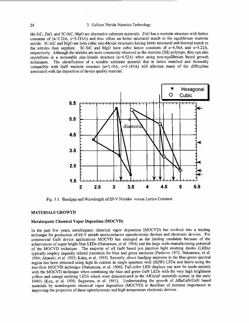
24 3. Gallium Nitride Materials Technology
6H-SiC, ZnO, and 3C-SiC, MgO are alternative substrate materials. ZnO has a wurtzite structure with lattice constants of (a=3.32A, c=5.213A) and thus offers an better structural match to the equilibrium wurtzite nitride. 3C-SiC and MgO are both cubic zinc-blende structures having better structural and thermal match to the nitrides than sapphire. 3C-SiC and MgO have cubic lattice constants of a=4.36A and a=4.22A, respectively. Although the nitrides are most commonly observed as the wurtzite (2H) polytype, they can also crystallizes in a metastable zinc-blende structure (a=4.52A) when using non-equilibrium based growth techniques. The identification of a suitable substrate material that is lattice matched and thermally compatible with GaN wurtzite structure (a=3.19A, c=5.185A) will alleviate many of the difficulties associated with the deposition of device quality material.
6.5
5.5
4.5
3.5
2.5
1.5
■ Hexagonal O Cubic
2.5 3.5 4.5 5.5
Fig. 3.1. Bandgap and Wavelength of III-V Nitrides versus Lattice Constant.
MATERIALS GROWTH
Metalorganic Chemical Vapor Deposition (MOCVD)
In the past few years, metalorganic chemical vapor deposition (MOCVD) has evolved into a leading technique for production of III-V nitride semiconductor optoelectronic devices and electronic devices. For commercial GaN device applications MOCVD has emerged as the leading candidate because of the achievement of super-bright blue LEDs (Nakamura, et al. 1994) and the large scale-manufacturing potential of the MOCVD technique. The majority of all GaN based p-n junction light emitting diodes (LEDs) typically employ impurity related transition for blue and green emission (Pankove 1972; Nakamura, et al. 1994; Akasaki, et al. 1993; Kahn, et al. 1995). Recently, direct bandgap emission in the blue-green spectral region has been obtained using high In content in single quantum well (SQW) LEDs and lasers using the two-flow MOCVD technique (Nakamura, et al. 1996). Full-color LED displays can now be made entirely with the MOCVD technique when combining the blue and green GaN LEDs with the very high brightness yellow and orange emitting LEDs which were demonstrated in the AlGalnP materials system in the early 1990's (Kou, et al. 1990; Sugawara, et al. 1991). Understanding the growth of AlInGaN/GaN based materials by metalorganic chemical vapor deposition (MOCVD) is therefore of extreme importance in improving the properties of these optoelectronic and high temperature electronic devices.
DenBaars 25
MOCVD Reaction Chemistry
The basic MOCVD reaction describing the GaN deposition process can be described by the following reaction:
Ga(CH3)3(v) + NH3(v) ->GaN(s) + 3CH4(v)
where (v)=vapor and (s)=solid
This balanced expression ignores that the specific reaction path and reactive species are largely unknown. The details of the reaction are not well known and the intermediate reactions are thought to be complex. A more likely reaction pathway leading to growth of the GaAs epitaxial layers involves the homogeneous decomposition of TMGa as reported in an earlier study on GaAs epitaxy (Nishizawa, et al. 1985; DenBaars, et al. 1986).
Ga(CH3)3(v) —> Ga(CH3)2(v) + CH3(v)
Ga(CH3)2(v) —> GaCH3(v) + CH3(v)
Ga(CH3)(v) —> Ga(v) + CH3(v)
The Group-V hydride source, is thought to decompose heterogeneously on the GaN surface or reactor walls to yield atomic nitrogen or a nitrogen containing radical at high growth temperatures. Abstraction of the first hydrogen bond is thought to be the rate limiting step in the decomposition of ammonia.
NH3(s/v) —> NH(3-x)(s/v) + x H(s/v)
Therefore one possible growth mechanism of GaN that might occur at the solid vapor interface could be expressed as follows:
GaCH3(s/v) + NH(s/v) —> GaN(s) + 1/2H2
However, the level of understanding of the growth process is inadequate at best. The most difficult topic, and certainly the least developed, is the area of the kinetics of the process and growth mechanisms occurring at the solid/vapor interface during MOCVD growth. Pyrolysis and diffusion of the group-Ill source through the boundary layer is the main pathway controlling the growth rate. However, parasitic side reactions such as solid adduct formation between TMA1 and ammonia will decrease the growth rate by limiting the flux of group-Ill sources to the growing interface.
Optimization of MOCVD growth is typically done by empirical studies of external parameters such as growth temperature, V/III ratio, substrate tilt and mass flow rates. These studies have identified three regions of growth: mass transport limited, desorption and surface kinetically limited regimes. Conventional GaN MOCVD is usually performed in the mass transport limited regime that occurs over a wide temperature range (600°C-1100°C). In this temperature region growth is limited by mass transport of the column III reactant to the growing interface. Because the diffusion process is slightly temperature dependent, there exists a slight increase in the growth rate in this temperature range.
MOCVD System and Reactor Design Issues
Both atmospheric-pressure and low-pressure MOCVD reactors are employed by various research and industrial groups in the growth of GaN. Atmospheric pressure reactors are favored because a high partial pressures of ammonia or nitrogen containing precursor is achievable. MOCVD Reactor design for GaN growth must overcome problems presented by high growth temperatures, prereactions, flow and film non- uniformity. Typically in GaN growth very high temperatures are required because of the high bond-strength of the N-H bond in ammonia precursors. Compounding this fact is the thermodynamic tendency of ammonia to prereact with the group-Ill metalorganic compounds to form non-volatile adducts. These factors
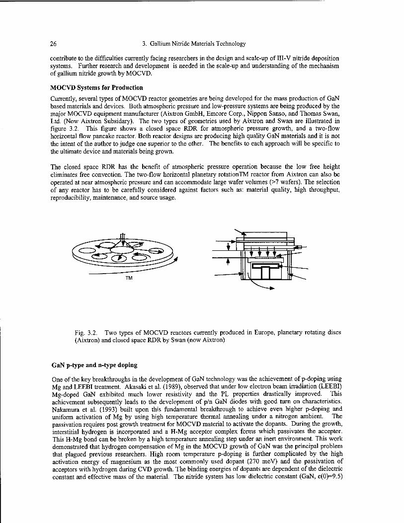
26 3. Gallium Nitride Materials Technology
contribute to the difficulties currently facing researchers in the design and scale-up of III-V nitride deposition systems. Further research and development is needed in the scale-up and understanding of the mechanism of gallium nitride growth by MOCVD.
MOCVD Systems for Production
Currently, several types of MOCVD reactor geometries are being developed for the mass production of GaN based materials and devices. Both atmospheric pressure and low-pressure systems are being produced by the major MOCVD equipment manufacturer (Aixtron GmbH, Emcore Corp., Nippon Sanso, and Thomas Swan, Ltd. (Now Aixtron Subsidary). The two types of geometries used by Aixtron and Swan are illustrated in figure 3.2. This figure shows a closed space RDR for atmospheric pressure growth, and a two-flow horizontal flow pancake reactor. Both reactor designs are producing high quality GaN materials and it is not the intent of the author to judge one superior to the other. The benefits to each approach will be specific to the ultimate device and materials being grown.
The closed space RDR has the benefit of atmospheric pressure operation because the low free height eliminates free convection. The two-flow horizontal planetary rotationTM reactor from Aixtron can also be operated at near atmospheric pressure and can accommodate large wafer volumes (>7 wafers). The selection of any reactor has to be carefully considered against factors such as: material quality, high throughput, reproducibility, maintenance, and source usage.
Fig. 3.2. Two types of MOCVD reactors currently produced in Europe, planetary rotating discs (Aixtron) and closed space RDR by Swan (now Aixtron)
GaN p-type and n-type doping
One of the key breakthroughs in the development of GaN technology was the achievement of p-doping using Mg and LEEBI treatment. Akasaki et al. (1989), observed that under low electron beam irradiation (LEEBI) Mg-doped GaN exhibited much lower resistivity and the PL properties drastically improved. This achievement subsequently leads to the development of p/n GaN diodes with good turn on characteristics. Nakamura et al. (1993) built upon this fundamental breakthrough to achieve even higher p-doping and uniform activation of Mg by using high temperature thermal annealing under a nitrogen ambient. The passivation requires post growth treatment for MOCVD material to activate the dopants. During the growth, interstitial hydrogen is incorporated and a H-Mg acceptor complex forms which passivates the acceptor. This H-Mg bond can be broken by a high temperature annealing step under an inert environment. This work demonstrated that hydrogen compensation of Mg in the MOCVD growth of GaN was the principal problem that plagued previous researchers. High room temperature p-doping is further complicated by the high activation energy of magnesium as the most commonly used dopant (270 meV) and the passivation of acceptors with hydrogen during CVD growth. The binding energies of dopants are dependent of the dielectric constant and effective mass of the material. The nitride system has low dielectric constant (GaN, e(0)=9.5)
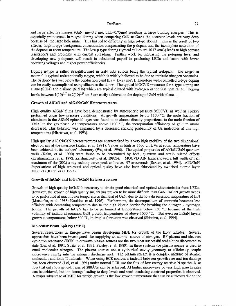
DenBaars 27
and large effective masses (GaN, me=0.2 mo, mhh=0.75mo) resulting in large binding energies. This is especially pronounced in p-type doping when comparing GaN to GaAs the acceptor levels are very deep because of the large hole mass. This has led to difficulty in high p-type doping. This is the result of two effects: high n-type background concentration compensating the p-dopant and the incomplete activation of the dopants at room temperature. The low p-type doping (typical values are 1017 /cm3) leads to high contact resistance's and problems with current spreading. Further work on increasing the p-doping level and developing new p-dopants will result in substantial payoff in producing LEDs and lasers with lower operating voltages and higher power efficiencies.
Doping n-type is rather straightforward in GaN with silicon being the typical n-dopant. The as-grown material is typical unintentionally n-type, which is widely believed to be due to intrinsic nitrogen vacancies. The Si donor lies just below the conduction band (Ea = 15-25 meV). Therefore well-controlled n-type doping can be easily accomplished using silicon as the donor. The typical MOCVD precursor for n-type doping are silane (SiH4) and disilane (Si2H6) which are typical diluted with hydrogen in the 200 ppm range. Doping
levels between 1(10)*' to 2(10)*" cm-3 are easily achieved in the doping of GaN with silane.
Growth of AlGaN and AlGaN/GaN Heterostructures
High quality AlGaN films have been demonstrated by atmospheric pressure MOCVD as well as epitaxy performed under low pressure conditions. At growth temperatures below 1100 °C, the mole fraction of aluminum in the AlGaN epitaxial layer was found to be almost directly proportional to the mole fraction of TMA1 in the gas phase. At temperatures above 1100 °C, the incorporation efficiency of gallium atoms decreased. This behavior was explained by a decreased sticking probability of Ga molecules at this high temperatures (Hirosawa, et al. 1993).
High quality AlGaN/GaN heterostructures are characterized by a very high mobility of the two dimensional electron gas at the interface (Kahn, et al. 1991). Values as high as 1500 cm2/Vs at room temperature have been achieved in the authors' laboratory (Wu, et al. 1996). The optical properties of AlGaN/GaN quantum wells (Kahn, et al. 1990) were found to be determined by both, quantum and strain related effects (Krishnankutty, et al. 1992; Krishnankutty, et al. 1992b). MOCVD A1N films showed a full width of half maximum of the (002) x-ray rocking curve peak as low as 97 arcseconds (Saxler, et al. 1994). AIN/GaN Superlattices of high structural and optical quality have also been fabricated by switched atomic layer MOCVD (Kahn, et al. 1993).
Growth of InGaN and InGaN/GaN Heterostructures
Growth of high quality InGaN is necessary to obtain good electrical and optical characteristics from LEDs. However, the growth of high quality InGaN has proven to be more difficult than GaN. InGaN growth needs to be performed at much lower temperatures than that of GaN, due to the low dissociation temperature of InN (Matsuoka, et al. 1988; Koukitu, et al. 1996). Furthermore, the decomposition of ammonia becomes less efficient with decreasing temperature due to the high kinetic barrier for breaking the nitrogen - hydrogen bonds. The growth of InGaN has to be performed at temperatures below 850 °C because of the high volatility of indium at common GaN growth temperatures of above 1000 CC. But even on InGaN layers grown at temperatures below 800 °C, In droplet formation was observed (Shimizu, et al. 1994).
Molecular Beam Epitaxy (MBE)
Several researchers in Europe have begun developing MBE for growth of the III-V nitrides. Several approaches have been investigated for supplying an atomic source of nitrogen. RF plasma and electron cyclotron resonance (ECR) microwave plasma sources are the two most successful techniques discovered to date (Lei, et al. 1991; Strite, et al. 1991; Paisley, et al. 1989). In these systems the plasma source is used to crack molecular nitrogen. The plasma sources use a cylindrical cavity geometry to efficiently couple microwave energy into the nitrogen discharge area. The plasma stream is a complex mixture of atomic, molecular, and ionic N radicals. When using ECR sources a tradeoff between growth rate and ion damage has been observed (Lei, et al. 1991) under normal ECR use the flux of low energy reactive N species is so low that only low growth rates of 500A/hr can be achieved. At higher microwave powers high growth rates can be achieved, but ion damage leading to deep levels and semi-insulating electrical properties is observed. A major advantage of MBE for nitride growth is the low growth temperature that can be achieved due to the
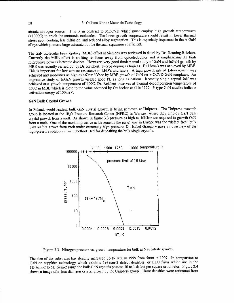
28 3. Gallium Nitride Materials Technology
atomic nitrogen source. This is in contrast to MOCVD which must employ high growth temperatures (>1000C) to crack the ammonia molecules. The lower growth temperature should result in lower thermal stress upon cooling, less diffusion, and reduced alloy segregation. This is especially important in the AlGaN alloys which posses a large mismatch in the thermal expansion coefficient.
The GaN molecular beam epitaxy (MBE) effort at Siemens was reviewed in detail by Dr. Henning Reichert. Currently the MBE effort is shifting its focus away from optoelectronics and is emphasizing the high microwave power electronic devices. However, very good fundamental study of GaN and InGaN growth by MBE was recently carried out by Dr. Reichert. P-type doping as high as lE+18cm-3 was achieved by MBE. This is important for low contact resistance to LED's and lasers. A high growth rate of 1.4microns/hr was achieved and mobilities as high as 460cm2/Vsec by MBE growth of GaN on MOCVD GaN templates. An impressive study of InGaN growth yielded good PL as long as 540nm. Recently single crystal InN was achieved at a growth temperature of 400C. Dr. Reichert observes at thermal decomposition temperature of 530C in MBE which is close to the value obtained by Ombacher et al in 1999. P-type GaN studies indicate activation energy of 150meV.
GaN Bulk Crystal Growth
In Poland, world-leading bulk GaN crystal growth is being achieved at Unipress. The Unipress research group is located at the High Pressure Research Center (HPRC) in Warsaw, where they employ GaN bulk crystal growth from a melt. As shown in figure 3.3 pressure as high as lOKbar are required to growth GaN from a melt. One of the most impressive achievements the panel saw in Europe was the "defect free" bulk GaN wafers grown from melt under extremely high pressure. Dr. Isabel Grzegory gave an overview of the high-pressure solution growth method used for depositing the bulk single crystals.
2000 1500 1250 1000 temperature,K 100000
10000
1000
en CO CD
I00
10
H—I 1 h
pressure limit of 1 5 kbar
GaN
Ga+1/2N,
0.0004 0.0006 0.0008 0.0010 0.0012
1H", K
Figure 3.3. Nitrogen pressure vs. growth temperature for bulk gaN substrate growth.
The size of the substrates has steadily increased up to 1cm in 1999 from 5mm in 1997. In comparison to GaN on sapphire technology which exhibits le+9cm-2 defect densities, or ELO films which are in the lE+6cm-2 to 5E+5cm-2 range the bulk GaN crystals possess 10 to 1 defect per square centimeter. Figure 3.4 shows a image of a 1cm diameter crystal grown by the Unipress group. These densities were estimated from
DenBaars 29
etch pit counts and correlated to TEM measurements of higher defect densities found on standard GaN sapphire technology. The team was allowed to observe the bulk crystals under both optical microscopes and field emission SEM. Both n-type bulk crystals and semi-insulating bulk crystal have been grown. The semi- insulating substrates were highly resistive lE+5ohm-cm and could be used for thin film deposition of high power AlGaN/GaN microwave amplifiers (Litwin-Staszewska, et al. 1999). Very high quality homoepiatxial growth of GaN by MOCVD was obtained on top of these substrates and the films exhibited narrow double- Crystal x-ray diffraction (DCXRD) linewidths a s low as 21 arcsec. The group at University of Ulm in collaboration with Unipress has obtained thin films which exhibit the narrowest reported PL linewidths at low temperature (O.lmeV) which is indicative of the uniform high quality film (Kornitzer, et al. 1999). MBE has also been performed on the bulk crystals. Both Ga-face and N-face polarity bulk substrates have been produced. The bulk crystals also display extremely smooth cleaved facets with rms roughness of 5 angstroms which would make excellent laser facets.
Fig.3.4. 1cm Diameter Bulk GaN Substrate
Lateral Epitaxial Overgrowth
Lateral Epitaxial Overgrowth (LEO) is an attractive method to produce GaN films with a low density of extended defects, which is beneficial both to studies of the fundamental properties of the GalnAIN materials system and to GaN-based device technology. The basic concept is to reduce defect propogation in masked regions of the substrate where the laterally overgrowing GaN is defect free. This is illustrated in the transmission electron micrograph in Figure 3.3. Recent studies in Europe, Japan and USA have confirmed that the density of threading dislocations (TDs) is reduced by 3-4 orders of magnitude in the LEO material grown on 6H-SiC (Zheleva, et al. 1997) and A1203 (Sakai, et al. 1997; Marchand, et al. 1998; Marchand, et al. 1998b) substrates, and the mechanisms of threading dislocations evolution during LEO have been investigated. Studies of the optical properties of LEO GaN (Chichibu, et al. 1998; Freitas, et al. 1998) and InGaN quantum wells (Rosner, et al. in press) have revealed that TDs act as non-radiative recombination centers. However, the minority carrier diffusion length (<200 nm) is smaller than the average distance between Tds such that the emission mechanisms of the carriers that do recombine radiatively appear to be unaffected by moderate TD densities (-106-109 cm-2). On the other hand, reducing the TD density has been shown to reduce the reverse leakage current by ~3 orders of magnitude in GaN p-n junctions (Kozodoy, et al. 1998), InGaN single (Mukai, et al. 1998) and multiple (Sasaoka, et al. 1998) quantum well light emitting diodes, and GaN/AlGaN heterojunction field-effect transistors (Vetury, et al., 1998) fabricated on LEO GaN. More recently, ultraviolet p-i-n photodetectors fabricated on LEO AlGaN have exhibited a similar reduction of the reverse leakage current by up to 6 orders of magnitude (Parish, et al. 1998). The use of LEO GaN has also resulted in marked improvements in the lifetime of InGaN/GaN laser diodes (Nakamura, et al. 1998).
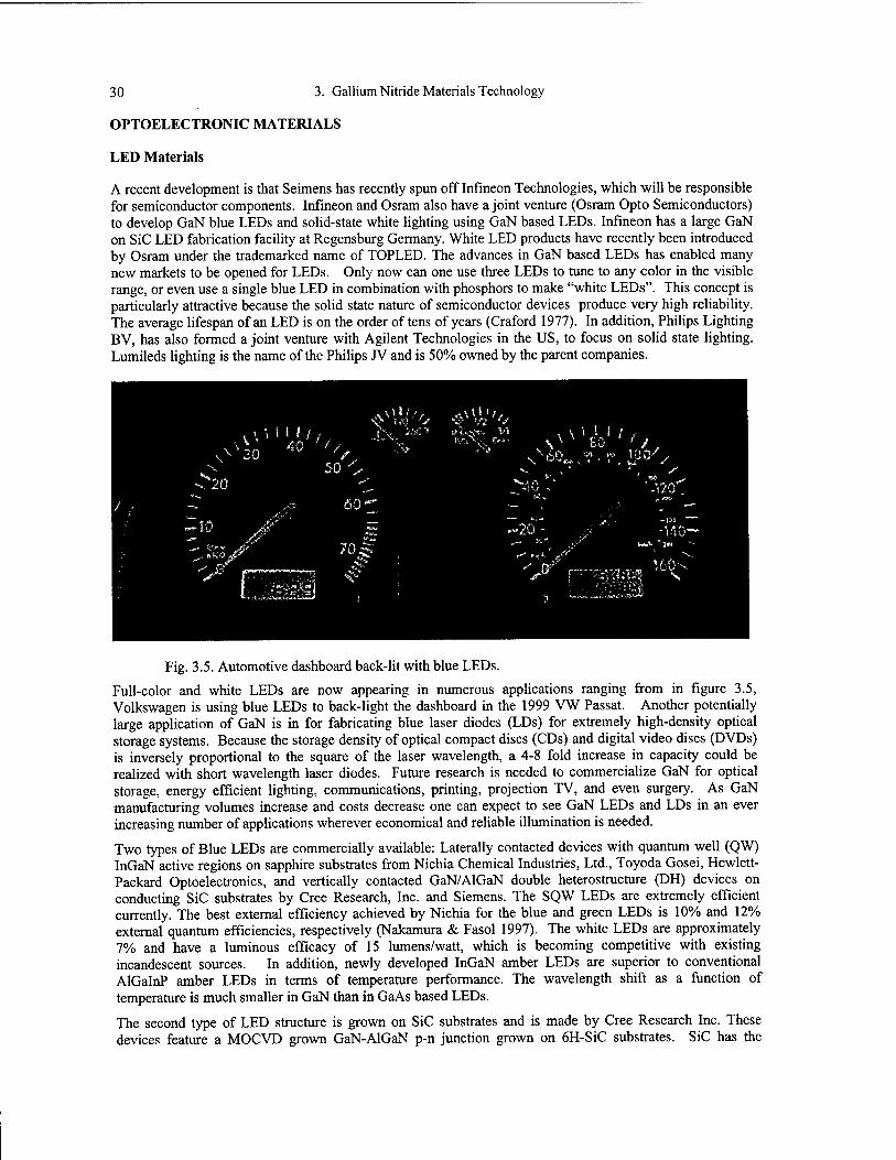
30 3. Gallium Nitride Materials Technology
OPTOELECTRONIC MATERIALS
LED Materials
A recent development is that Seimens has recently spun off Infineon Technologies, which will be responsible for semiconductor components. Infineon and Osram also have a joint venture (Osram Opto Semiconductors) to develop GaN blue LEDs and solid-state white lighting using GaN based LEDs. Infineon has a large GaN on SiC LED fabrication facility at Regensburg Germany. White LED products have recently been introduced by Osram under the trademarked name of TOPLED. The advances in GaN based LEDs has enabled many new markets to be opened for LEDs. Only now can one use three LEDs to tune to any color in the visible range, or even use a single blue LED in combination with phosphors to make "white LEDs". This concept is particularly attractive because the solid state nature of semiconductor devices produce very high reliability. The average lifespan of an LED is on the order of tens of years (Craford 1977). In addition, Philips Lighting BV, has also formed a joint venture with Agilent Technologies in the US, to focus on solid state lighting. Lumileds lighting is the name of the Philips JV and is 50% owned by the parent companies.
Fig. 3.5. Automotive dashboard back-lit with blue LEDs.
Full-color and white LEDs are now appearing in numerous applications ranging from in figure 3.5, Volkswagen is using blue LEDs to back-light the dashboard in the 1999 VW Passat. Another potentially large application of GaN is in for fabricating blue laser diodes (LDs) for extremely high-density optical storage systems. Because the storage density of optical compact discs (CDs) and digital video discs (DVDs) is inversely proportional to the square of the laser wavelength, a 4-8 fold increase in capacity could be realized with short wavelength laser diodes. Future research is needed to commercialize GaN for optical storage, energy efficient lighting, communications, printing, projection TV, and even surgery. As GaN manufacturing volumes increase and costs decrease one can expect to see GaN LEDs and LDs in an ever increasing number of applications wherever economical and reliable illumination is needed.
Two types of Blue LEDs are commercially available: Laterally contacted devices with quantum well (QW) InGaN active regions on sapphire substrates from Nichia Chemical Industries, Ltd., Toyoda Gosei, Hewlett- Packard Optoelectronics, and vertically contacted GaN/AlGaN double heterostructure (DH) devices on conducting SiC substrates by Cree Research, Inc. and Siemens. The SQW LEDs are extremely efficient currently. The best external efficiency achieved by Nichia for the blue and green LEDs is 10% and 12% external quantum efficiencies, respectively (Nakamura & Fasol 1997). The white LEDs are approximately 7% and have a luminous efficacy of 15 lumens/watt, which is becoming competitive with existing incandescent sources. In addition, newly developed InGaN amber LEDs are superior to conventional AlGalnP amber LEDs in terms of temperature performance. The wavelength shift as a function of temperature is much smaller in GaN than in GaAs based LEDs.
The second type of LED structure is grown on SiC substrates and is made by Cree Research Inc. These devices feature a MOCVD grown GaN-AlGaN p-n junction grown on 6H-SiC substrates. SiC has the
DenBaars 31
advantage of having a smaller lattice misfit to GaN and the possibility of providing n-doped substrates. Another advantage is the vertical conduction pathway allows for a drop in replacement part similar to the other GaP and GaAs based structures, which have the same vertical geometry. The high thermal conductivity of SiC substrates might also benefit the high temperature high output power applications of GaN LEDs.
Blue Laser Materials
Several groups in Japan, USA, and now Europe have recently reported obtaining laser diodes in the GaN materials system. Osram Opto Semiconductors was the first European group to achieve reasonable pulse blue laser performance in 1999 (HARLE 2000). Of all the groups in the world to date, only Nichia has obtained long-life continuous wave (CW) emission, and the laser diode was market released in January 1999. Nichia was the first company in the world to successful achieve a blue laser diode in GaN materials system. Initially the GaN laser lasted only a few seconds but reliability has improved dramatically to the current state at which Dr. Nakamura has achieved CW operation up to 10,000 hours at room temperature, elevated temperature testing at 50°C has projected the actual lifetime is in excess of 20,000 hours at 2mW. Current estimates are the reduction in the spot size which can be achieved with blue GaN lasers will yield a storage capacity of 12GB per 5.25 inch diameter discs, enough for recording a full-length motion picture in high resolution mode.
CONCLUSIONS
The Group-Ill nitride semiconductors have emerged as the leading material for fabricating high reliability short wavelength emitters, and emerging high power electronic devices. MOCVD and MBE are the leading growth technologies for depositing high quality GaN/InGaN heterostructure based devices. Lateral epitaxial overgrowth (LEO) and bulk crystals are some of the key technologies requiring further study to enable the next generation of GaN based devices.
ACKNOWLEDGEMENTS
I would like to acknowledge the honor to participate in this study with a great group of colleagues: Vladamir Dmitriev, Paul Chow, Michael Shur, Michael Spencer, Usha Varshney, John Zavada, and George White. Also we gratefully acknowledge the Office of Naval Research (ONR) and NSF for sponsoring the High Temperature Electronics study.
REFERENCES
Akasaki, I., H. Amano, Y. Koide, H. Hiramatsu, and N. Sawaki. J. Cryst. Growth 89, 209 (1989)
Akasaki, I., H. Amano, H. Murakami, M. Sassa, H. Kato, K. Manabe; J. Cryst. Growth 128,379, (1993)
Chichibu, S., H. Marchand, S. Keller, P. Fini, J.P. Ibbetson, M. Minsky, S. Fleischer, J.S. Speck, J. Bowers, E. Hu, U.K. Mishra, S.P. DenBaars, T. Deguchi, T. Sota, and S. Nakamura, 2nd Int. Conf. on Blue Laser and Light Emitting Diodes, Chiba, Japan, Sept. 29 - Oct. 2, 1998; S. Chichibu, H. Marchand, M. Minsky, S. Keller, P. Fini, J. Ibbetson, S. Fleisher, J.S. Speck, J.E. Bowers, E. Hu, U.K. Mishra, S.P. DenBaars, T. Deguchi, T. Sota, and S. Nakamura, Appl. Phys. Lett, (in press).
Craford, M.G. (1977) IEEE Trans. Electron Devices, ED-24, 935.
DenBaars, S.P., B.Y. Maa, P.D. Dapkus, and H.C. Lee, J. Cryst. Growth, 77,188 (1986)
Freitas, J.A., Jr., O.H. Nam, R.F. Davis, G.V. Saparin, and S.K. Obyden, Appl. Phys. Lett. 72, 2990 (1998); X. Li, S.G. Bishop, and J.J Coleman, Appl. Phys. Lett. 73, 1179 (1998).
V. HÄRLE, B. Hahn, H.-J. Lugauer, S. Bader, G. Briiderl, J. Baur, D. Eisert U. Strauss, U. Zehnder, M. Mundbrod, A. Lell, GaN-based LED's and lasers on SiC, OSRAM Opto Semiconductors, Wernerwerkstraße 2, 93049 Regensburg, GERMANY. Intl. Conf. On Blue LEDs and Lasers, Berlin (2000) Paper TuA-1
Hirosawa, K., K. Hiramatsu, N. Sawaki, and I. Akasaki, Jpn. J. Appl. Phys. 32, L1030 (1993)
Kahn, M.A., Q. Chen, R.A. Skogman, J.N. Kuznia; Appl. Phys. Lett. 66,2046,(1995)
32 3. Gallium Nitride Materials Technology
Kahn, M.A., J. N. Kuznia, and D. T. Olson, T. George and W. T. Pike, Appl. Phys. Lett. 63, 3470 (1993)
Kahn, M.A., R. A. Skogman, and J.M. van Hove, S. Krishnankutty, and R.M. Kolbas, Appl. Phys. Lett. 56, 1257 (1990)
Kahn, M.A., J.M. Van Hove, J.N. Kuznia, and D.T. Olson, Appl. Phys. Lett. 58, 2408 (1991)
Komitzer, K., T. Ebner, M. Grehl, K. Thonke, R. Sauer, C. Kirchner, V. Schwelger, M. Kamp, M. Leszczynski, I. Grzergory, S. Porowski, "High Resolution PL and Refelectance Spectra of Hmoepitaxial GaN Layers" Paper Tu-17, Proceedings of Intl. Conf. on Nitride Semiconductors, Montpelliar, France (1999), pg 49
Kou, C.P., R.M. Flecther, T.D. Ostenowski, M.C. Lardizabal, M.G. Craford, and V.M. Robbins, Appl. Phys. Lett., 57, 2937,(1990)
Koukitu, A., N. Tkahashi, T. Taki, and H. Seki, Jpn. J. Appl. Phys. 35, L673 (1996)
Kozodoy, P., J.P. Ibbetson, H. Marchand, P.T. Fini, S. Keller, S.P. DenBaars, J.S. Speck, U.K. Mishra, Appl. Phys. Lett. 73 975(1998).
Krishnankutty, S., R.M. Kolbas, M. A. Kahn, J. N. Kuznia, J.M. van Hove and D.T. Olson, J. Electron. Mat. 21, 437 (1992)
Krishnankutty, S., R.M. Kolbas, M. A. Kahn, J. N. Kuznia, J.M. van Hove and D.T. Olson, J. Electron. Mat. 21, 609 (1992)
Lei, T., M. Fanciulli, R.J. Molnar, T.D. Moustakas, R.J. Graham, and J.D. Scanion, Appl. Physics Lett. 59 (1991) 94
Litwin-Staszewska, E., T. Suski, I. Grzegory, S. Porowski, J. Robert, D. Wasik, A. Witowski,D. Cote, and B. Clerjund, "Electrical Properties of GaN Bulk Single Crsytals Doped with Mg" Paper We-P082, Proceedings of Intl. Conf. on Nitride Semiconductors, Montpelliar, France (1999), pg 124.
Marchand, H., J.P. Ibbetson, P.T. Fini, P. Kozodoy, S. Keller, J.S. Speck, S.P. DenBaars, and U.K. Mishra, MRS Internet J. Nitride Semicond. Res. 3, 3 (1998).
Marchand, H., X.H. Wu, J.P. Ibbetson, P.T. Fini, P. Kozodoy, S. Keller, J.S. Speck, S.P. DenBaars, and U.K. Mishra, Appl. Phys. Lett. 73, 747 (1998).
Matsuoka, T., H. Tanaka, T. Sasaki and A. Katsui, Inst. Phys. Conf. Ser. No 106, GasAs and related compounds , chapter 3, p. 141(1988).
Mukai, T., K. Takekawa, S. Nakamura, Jpn. J. Appl. Phys. 37 L839 (1998).
Nakamura, S., Jpn. J. Appl. Phys. 30, L1705 (1991).
Nakamura, S., G. Fasol, The Blue Laser Diode. Springer-Verlag, Heildelberg,Germany (1997)
Nakamura, S., T. Mukai, M. Senoh, Appl.Phys Lett. 64 ,1687 (1994)
Nakamura, S., M. Senoh, T. Mukai,Jpn. J. Appl. Phys., Vol 32, pp.L8-l 1 (1993)
Nakamura, S., M. Senoh, S. Nagahama, N. Iwasa, T. Yamada, T. Matshushita, H. Kiyoku, and Y. Sugimoto, Jpn. J. Appl. Phys. Vol 35, L74-L76 (1996)
Nakamura, S., M. Senoh, S. Nagahama, N. Isawa, T. Yamada, T. Matsushita, H. Kiyoku, Y. Sugimoto, T. Kozaki, H. Umemoto, M. Sano, M. Chocho, Appl. Phys. Lett. 72, 211 (1998).
Nishizawa, J., H. Abe, and T. Kurabayashi, J. Electrochem. Soc, 132, 1197.(1985)
Paisley, M.J., Z. Sitar, J.B. Posthill, and R. F. Davis, J. vac Sei. Technol. A7, (1989) 701.
Pankove, J.I., J. Electrochem. Soc, 119, 1118 (1972).
Parish, G, S. Keller, P. Kozodoy, J.P. Ibbetson, H. Marchand, P.T. Fini, S.B. Fleischer, S.P. DenBaars, U.K. Mishra, E.J. Tarsa, 1998 Conference on Optoelectronic and Microelectronic Materials And Devices, Perth, Australia, 14-16 Dec. 1998.
Rosner, S.J., G. Girolami. H. Marchand, P.T. Fini, J.P. Ibbetson, L. Zhao, S. Keller, U.K. Mishra, S.P. DenBaars, J.S. Speck, Appl. Phys. Lett, (in press).
Sakai, A., H. Sunakawa, and A. Usui, Appl. Phys. Lett. 71, 2259 (1997).
Sasaoka, C, H. Sumakawa, A. Kimura, M. Nido, A. Usui, and A. Sakai, J. Cryst. Growth 189, 61 (1998).
Saxler, A., P. Kung, C.J. Sun,E. Bigan, and M. Razeghi, Appl. Phys. Lett. 64 , 339 (1994)
Shimizu, M., K. Hiramatsu and N. Sawaki, J. Cryst. Growth 145,209 (1994)
Strite, S.,J. Ruan, Z. Li, N. Manning, A. Salavador, H. Chen, D.J. Smith, W.J. Choyke, and H. Morkoc, J. Vac. Sei. Technol. m, 1924(1991).

DenBaars 33
Sugawara, H., M. Ishikawa, and G. Hatakoshi^pp/. Phys. Lett. 58,1010, (1991)
Weeks, T.W., Jr., M.D. Bremser, K.S. Ailey, E. Carlson et al., Appl. Phys. Lett. 67,401 (1995)
Vetury, R., H. Marchand, J.P. Ibbetson, P.T. Fini, S. Keller, J.S. Speck, S.P. Denbaars, and U.K. Mishra, 25th Int. Symp. on Compound Semicond., Nara, Japan, Oct 12-16, 1998.
Wu, Y.F., B.P. Keller, S. Keller, D. Kapolnek, P. Kozodoy, S.P. DenBaars and U.K. Mishra, Appl. Phys. Lett. 69, 1438 (1996)
Zheleva, T.S., O.H. Nam, M.D. Bremser, and R.F. Davis, Appl. Phys. Lett. 71, 2472 (1997).

34 3. Gallium Nitride Materials Technology
35
CHAPTER 4
SiC GROWTH TECHNOLOGY IN EUROPE
Michael G. Spencer
INTRODUCTION
This chapter gives a review of SiC growth technology and then discusses the results of the TTEC panel review of European growth technology.
SIC BULK CRYSTAL GROWTH
Silicon carbide substrates are the key elements in the development of SiC electronics. Because of the phase equilibria in the Si and C materials system, (specifically the material sublimes before it melts) the most popular bulk growth techniques are based on physical vapor transport. These techniques were initially developed in the late fifties and have been modified and introduced for production in the early eighties. Although sublimation techniques are relatively easy to implement, (at the high growth temperatures required) these processes are difficult to control particularly over large substrate areas.
Bulk Growth by Physical Vapor Transport
Physical vapor growth is accomplished by the sublimation of a SiC source placed in the hot zone of the growth furnace, and the subsequent mass transport of the vapor species to a cooler region of the furnace. Single crystal SiC material is formed from deposition of the supersaturated vapor species. Source materials may be composed of SiC powder, Si and C powders mechanically mixed, or crystalline SiC. The vapor transport is performed in either a vacuum or gas ambient. Single crystal growth can be realized either seeded or unseeded. Typical temperature and pressure ranges for SiC sublimation growth are 1600 to 2700°C and
10"" to 20 torr, respectively. Usually, the lower temperatures are employed for sublimation epitaxial SiC growth, while bulk SiC growth is performed at the higher temperatures.
Modified Lely Process
Growth of SiC boules is possible using the modified, or seeded Lely method, also called the Tairov - Tsvetkov method (Tairov & Tsvetkov 1978; Tairov & Tsvetkov 1981) or physical vapor transport technique. In this technique, a seed crystal of SiC is introduced into the Lely chamber, and growth proceeds (usually along the c-axis) by vapor transport of carbon and silicon bearing species from the source (or carbon species from the graphite walls). For a typical 6H- and 4H-SiC bulk sublimation growth process, the SiC source temperature is 2100 - 2400°C (Barrett, et al. 1992), growth pressure is less than 20 Torr and the temperature gradient between source and seed ranges from 20 to 35 °C/cm. Currently the maximum commercially available 4H and 6H-SiC crystals are 2" in diameter, however record 4" boules of SiC have been recently demonstrated. Sublimation growth is usually performed on {0001} (Si or C face) of either 6H-SiC or 4H- SiC seeds. Growth on faces perpendicular to the (0001) basal plane has also been reported (Takahash, et al. 1994) in an effort to reduce micropipe defects.
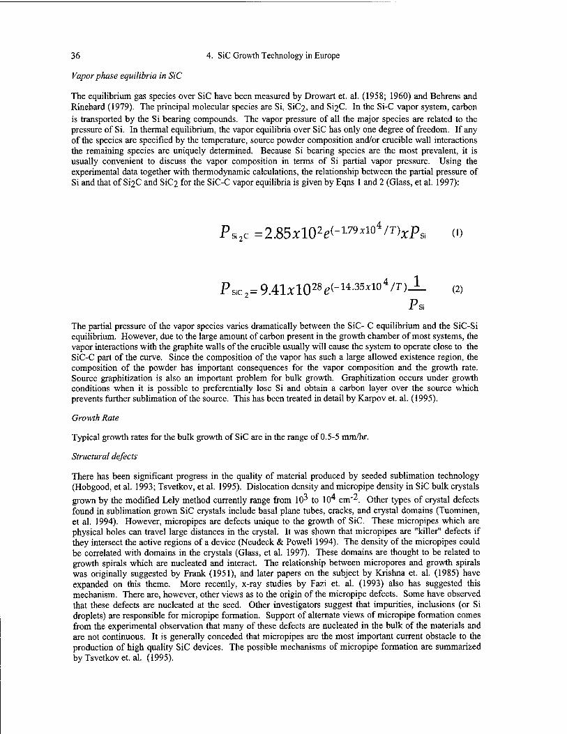
36 4. SiC Growth Technology in Europe
Vapor phase equilibria in SiC
The equilibrium gas species over SiC have been measured by Drowart et. al. (1958; 1960) and Behrens and Rinehard (1979). The principal molecular species are Si, SiC2, and Si2C. In the Si-C vapor system, carbon is transported by the Si bearing compounds. The vapor pressure of all the major species are related to the pressure of Si. In thermal equilibrium, the vapor equilibria over SiC has only one degree of freedom. If any of the species are specified by the temperature, source powder composition and/or crucible wall interactions the remaining species are uniquely determined. Because Si bearing species are the most prevalent, it is usually convenient to discuss the vapor composition in terms of Si partial vapor pressure. Using the experimental data together with thermodynamic calculations, the relationship between the partial pressure of Si and that of S12C and SiC2 for the SiC-C vapor equilibria is given by Eqns 1 and 2 (Glass, et al. 1997):
PSi2c =2.85xl02e(-179*lo4/T)xPSi U)
Psic2=9.41xl028^-14-35^°4/T)— (2)
The partial pressure of the vapor species varies dramatically between the SiC- C equilibrium and the SiC-Si equilibrium. However, due to the large amount of carbon present in the growth chamber of most systems, the vapor interactions with the graphite walls of the crucible usually will cause the system to operate close to the SiC-C part of the curve. Since the composition of the vapor has such a large allowed existence region, the composition of the powder has important consequences for the vapor composition and the growth rate. Source graphitization is also an important problem for bulk growth. Graphitization occurs under growth conditions when it is possible to preferentially lose Si and obtain a carbon layer over the source which prevents further sublimation of the source. This has been treated in detail by Karpov et. al. (1995).
Growth Rate
Typical growth rates for the bulk growth of SiC are in the range of 0.5-5 mm/hr.
Structural defects
There has been significant progress in the quality of material produced by seeded sublimation technology (Hobgood, et al. 1993; Tsvetkov, et al. 1995). Dislocation density and micropipe density in SiC bulk crystals
grown by the modified Lely method currently range from 10^ to 10^ cm"2. Other types of crystal defects found in sublimation grown SiC crystals include basal plane tubes, cracks, and crystal domains (Tuominen, et al. 1994). However, micropipes are defects unique to the growth of SiC. These micropipes which are physical holes can travel large distances in the crystal. It was shown that micropipes are "killer" defects if they intersect the active regions of a device (Neudeck & Powell 1994). The density of the micropipes could be correlated with domains in the crystals (Glass, et al. 1997). These domains are thought to be related to growth spirals which are nucleated and interact. The relationship between micropores and growth spirals was originally suggested by Frank (1951), and later papers on the subject by Krishna et. al. (1985) have expanded on this theme. More recently, x-ray studies by Fazi et. al. (1993) also has suggested this mechanism. There are, however, other views as to the origin of the micropipe defects. Some have observed that these defects are nucleated at the seed. Other investigators suggest that impurities, inclusions (or Si droplets) are responsible for micropipe formation. Support of alternate views of micropipe formation comes from the experimental observation that many of these defects are nucleated in the bulk of the materials and are not continuous. It is generally conceded that micropipes are the most important current obstacle to the production of high quality SiC devices. The possible mechanisms of micropipe formation are summarized by Tsvetkov et. al. (1995).
Spencer 37
Recently, x-ray and TEM techniques have been applied to the study of the quality of bulk SiC (Barrett, et al. 1993). Lely platelets as well as substrates grown by the modified Lely method have been investigated. In general, the results of various investigations suggest that Lely crystals exhibit higher material quality. The full width at a half maximum (FWHM) of the x-ray rocking curve is ~7-10 arc sec for Lely platelets, while for modified Lely crystals this value ranges from 20-100 arc sec. For Lely crystals, a single x-ray diffraction peak is observed for each x-ray reflection. Conversely for modified Lely crystals several peaks are observed indicating a mosaicity in the material.
Electrical characteristics
Undoped SiC bulk material usually is contaminated by nitrogen which produces n-type conductivity. The typical background level of electron concentration at room temperature for undoped SiC crystals grown by
modified Lely method is 10^ -10^ cm"^. High purity undoped SiC crystals with room temperature
resistivity from 10^ to 10^ • cm have been reported by Hobgood et. al. (1993). These crystals had p-type
conductivity with a background carrier concentration of 10^ cm"3 due to residual boron impurities.
N-type SiC crystals with carrier concentrations up to 10^0 cm"3 were produced using nitrogen doping (Onoue, et al. 1995). The minimum reported resistivity for 6H-SiC and 4H-SiC bulk crystals are 1.6 m* cm and 2.8 m* cm, respectively (Glass, et al. 1997). No information on defect density in highly doped n-type material is available. P-type SiC crystals with carrier concentrations up to 10^0 cm"^ were obtained using aluminum doping (Glass, et al. 1997). Information about Al doping during bulk SiC growth is limited. No information on defect density in highly doped p-type material is available.
Semi-insulating 6H-SiC crystals were produced using vanadium doping (Hobgood, et al. 1995). The amount of vanadium soluble in the material is limited by the precipitation of vanadium suicide. The material resistivity at room temperature can be estimated by high temperature resistivity measurements and was
determined to be in the range of lO*-*« cm. Semi-insulating 4H-SiC crystals with comparable resistivities have also been reported (Tsvetkov, et al. 1995; Glass, et al. 1997).
Bulk growth by chemical vapor deposition
6H-SiC crystals have been grown by high temperature CVD with growth rates of 0.5 mm/hr (Kordina, et al. 1996). This technique is a direct adaptation of the CVD epitaxial technique for growth of SiC. The control of the Si/C ratio in such a system is excellent compared with sublimation growth and additional results have been presented in the recent SiC conference.
Bulk Growth from the Liquid Phase
Crystal growth from melt-solutions is widely used for many semiconductor materials. Liquid phase growth of SiC has not been considered promising based on results obtained during the early stage of SiC development. Two main objections to liquid phase technology are low solubility of SiC in the Si melt (which limits the growth rate), and inclusions incorporated in grown crystals due to parasitic phase formation. On the other hand, it has been shown that high quality SiC can be grown from melt-solutions (Nelson. Et al. 1966; Marshall 1969; Wolff, et al. 1969): undoped cubic SiC crystals grown from a silicon melt at ~1500°C
exhibited a mobility of 980 cwrfV s and carrier concentration of 4x10^ cm'^ (300 K). Significant progress has also been made in understanding the nature of SiC growth from liquids (Dmitriev 1995; Yakimova, et al. 1995). It has been shown that high quality SiC epitaxial layers with no micropipes and low dislocation density can be grown from a Si melt (Rendakova, et al. 1997). Epitaxial layers of 6H- and 4H-SiC were grown from Si melts on 35 mm diameter substrates indicating the possibility of liquid phase growth of large crystals. It was also found that the solubility of SiC in Si melt does not severely limit the growth rate, and a SiC growth rate of about ~0.2 mm/hr has been obtained at 1650°C.
38 4. SiC Growth Technology in Europe
SIC EPITAXIAL GROWTH
In order to improve the quality of bulk material and produce complicated device structures, epitaxial techniques are necessary. As with other semiconductor material systems, liquid phase epitaxial techniques and CVD were used early in the development of SiC to produce device structures. Although the material produced by LPE was of high quality, difficulties with molten Si (used as the melt) prompted the development of vapor phase techniques such as sublimation epitaxy and CVD. Chemical vapor deposition is presently the most widely used epitaxial technique for growth of SiC device structures.
Chemical Vapor Deposition
Chemical vapor deposition is a growth process in which gaseous compounds are transported to the substrate surface where chemical reactions occur resulting in formation and growth of the desired material. The growth of 6H-SiC layers on 6H-SiC {0001} substrates by CVD in the temperature range from 1500 to 1850°C have been reported since the sixties (Campbell & Chu 1966; Jennings, et al. 1966; Minagawa & Gatos 1971; Wessels, et al. 1974; Matsunami, et al. 1975; Muench, et al. 1975; Muench & Pfaffeneder 1976; Nishino, et al. 1978). A significant lowering of the growth temperature and improvement of material quality has been achieved by using substrates which are mis-oriented a few degrees off the {0001} plane toward the
<11 2 0> direction. This growth on mis-oriented substrates has been termed "step controlled epitaxy" and has the added advantage of stabilizing the polytype structure.
A review of CVD growth of SiC has been published by Nishino (1995) and Larkin (1997). Growth temperatures for typical SiC CVD processes range from 1200-1800°C while growth pressures vary from 100- 760 torr.
Growth Equipment
Three types of growth apparatus are used for SiC CVD: 1) cold-wall horizontal atmospheric pressure reactors have been used for many years with results reported by Siemens AG (Karmann, et al. 1993), Kyoto University (Matsunami 1992), NASA Lewis Research Center (Mandel 1962). A commercial horizontal water-cooled reactor for SiC CVD operating in the pressure range from 10 to 1000 mbar was developed by AIXTRON GmbH (Sculte, et al. 1994). This system uses low pressure and a specially designed inner sleeve to maintain laminar gas flow. 2) hot-wall horizontal atmospheric pressure reactors have been designed at Linkoping University (Kordina, et al. 1993). Still another hot wall horizontal reactor design was proposed by the Industrial Microelectronic Center in Sweden (Nordell, et al. 1995). 3) cold-wall vertical low pressure reactors (Feng, et al. 1996) have been built commercially by EMCORE Corp. and used at Howard University and Siemens AG (Rupp, et al. 1995). In these reactors, laminar flow is obtained by a high speed rotating disk (in conjunction with high gas flow velocities) which produces a pumping action.
High temperatures in SiC epitaxial reactors can be obtained with either resistive or rf heating. In most systems the susceptor is made from graphite. Because of the reaction between graphite and H2 at
temperatures in excess of 1300 C a thin SiC coating layer has been used by many researchers. Unintentional incorporation of contaminants from the susceptor during SiC CVD was studied by Karmann and coworkers (Karmann, et al. 1995). In these experiments, 6H-SiC layers were grown in an atmospheric pressure reactor at 1390°C with a growth rate of 0.7 «m/hr. Uncoated and SiC coated (100 - 120 «m thick) graphite susceptors were used for comparison. For the uncoated susceptors, the layers were found to be contaminated with aluminum, boron and nitrogen. Conversely, using a SiC coated graphite susceptor in the same system, SiC
layers with concentration Nd - Na of 4xl015 cm"^ could be grown. In a low pressure vertical reactor with
high speed substrate rotation, SiC with background concentrations in lO1^ cm"^ range was demonstrated without use of SiC-coated parts (Rupp, et al. 1995). This low amount of contamination is attributed to the favorable gas flow patterns generated in this reactor
Temperature measurement is a major equipment issue for CVD growth at high temperatures. During growth, substrate temperature is usually measured by an optical pyrometer calibrated by melting of Si or Ge. The temperature of the susceptor typically is found to be 50 - 100°C higher than that of the SiC substrate. Power settings are often used to calibrate the substrate temperature.
Spencer 39
Precursors and Reaction Chemistry
A number of precursors have been used for the growth of silicon carbide. For transport of the Si species the most popular choice is SiH4 (Powell, et al. 1987), but Si2H6 (Nishino & Saraie 1989a) and SiCLj. (Muench & Pfaffeneder 1976) have also been used. For growth of Si, the hydrocarbon species most reported is C3H8. However, there are also reports of SiC growth using C2H2 (Liaw & Davis 1985), CH3CI (Ikoma, et al. 1991), CH4 (Rai-Choudhury & Formigoni 1969), CCI4, CyHs, or C6H14 as carbon sources. In addition to the use of individual gas species, single precursors have also been investigated, among them CH3SiCl3 (Nishino & Sarate 1989b) and (CH3)2SiCl2 (Rai-Choudhury & Formigoni 1969).
Gas-phase equilibrium calculations were reported for Si-H-C gas mixtures (Allendorf 1993) in the temperature range used in CVD growth of SiC. Modeling of the gas phase chemical processes which occur during growth as a function of distance from the heated susceptor was reported by Stinespring and Wormhoudt (Stinespring & Wormhoudt 1988). The results of the modeling study shows that the injected C species are not fully decomposed to equilibrium values at the growth interface. Gas-phase reactions in SiC CVD growth using the S1H4-C3H8-H2 gas system were experimentally investigated by Hong et. al. (1993) using a microcavity technique. The microcavity study suggested 1) that multiple species contribute to the film growth in the system, and 2) possible precursors in the chamber contain S1H2 (a gas-phase intermediate derived from SiH4); and another species containing Si and C derived from SiH2 and C3H8. Under certain experimental conditions Si droplets and graphite inclusions have been observed in SiC epitaxy. Modeling of these Si-droplets and graphite inclusions formation in the CVD process was done (Karpov, et al. 1995) considering several homogeneous and heterogeneous chemical reactions.
Growth Rate
Increasing the growth rate in SiC epitaxy is important because of the demands of SiC power device structures. A typical base layer in a power thyristor can be as thick as 100 «m. Since growth rates of SiC films vary from 0.1 to 6 •m/hr for a growth temperature of 1500°C, the minimum growth time for a single structure can be as long as 15 hours. Growth under normal conditions is determined by the diffusive transport of the Si species through the stagnant layer, although control of the growth by carbon species has been observed. Since the growth rate of 6 mm/hr is too low for layers greater than 10-12 «m there are several studies in progress on increasing the CVD growth rate. Growth rates of 500 •m/hr were obtained by high temperature CVD (1800 to 2300°C) (Kordina, et al. 1996) with a maximum crystal thickness of 2 mm. This result looks very promising for growth of thick layers (>100 *m) for high power SiC devices, but many questions about this technique, including possible material contamination at high temperature, remain unanswered.
The temperature dependence of SiC CVD growth rate has been investigated by several researchers. If the growth rate is determined by surface kinetics, the activation energy of the growth is expected to be relatively large. If on the other hand the growth is transport limited, the observed activation energy is expected to be small. For the SiCl4-CCl4-He gas system, an activation energy of 20 kcal/mol was reported for growth on well-oriented substrates (Jennings, et al. 1966). An activation energy of 22 kcal/mol was obtained for SiC
growth on the (000 1 )C face of well-oriented substrates for the C3H8-S1H4-H2 gas mixture (Wessels, et al. 1974), however the same investigators observed a complicated temperature dependence on well-oriented (0001)Si faces. The complicated temperature dependence of growth rate on the Si face was explained using a growth model in which the growth rate is limited by the adsorption-desorption of reactants at the growth interface. For step-controlled epitaxy an activation energy of SiC growth rate was measured to be 3.0 kcal/mol (Kimoto, et al. 1993). The layers were grown at atmospheric pressure in the temperature range from 1200 to 1500°C on 6H-SiC {0001} substrates (with 6° off-orientation) using S1H4-C3H8-H2 precursors. The small value of activation energy is attributed to the fact that the growth in step-controlled epitaxy is mass transport limited and the temperature dependence is due diffusion through the stagnant layer.
40 4. SiC Growth Technology in Europe
Homoepitaxy of »-SiC
Homoepitaxial growth of »-SiC (6H-SiC, 4H-SiC, 21R-SiC) by CVD has been advanced at Kyoto University using off-oriented SiC substrates (Itoh, et al. 1994; Hong, et al. 1995). This technique is called step- controlled epitaxy because the growth process is determined by the lateral growth rate of the terraces. The growth rate, substrate mis-orientation and growth temperature determine if growth will occur via the step controlled mechanism. If the growth is step controlled, the epilayer will replicate the stacking order of the substrate. The growth mechanism for SiC homoepitaxial CVD has been discussed by a number of researchers (Kimoto, et al. 1993; Kimoto & Matsunami 1993; Hong, et al. 1995). Nucleation processes during SiC CVD growth were investigated by Kimoto and Matsunami (1993) and the surface kinetics of adatoms in CVD growth of SiC were analyzed based on Burton-Cabrera-Frank theory (Kimoto & Matsunami 1994).
Typical growth of epitaxial 6H-SiC is performed on wafers which are mis-orientated 3.5° toward the
< 11 2 0> direction. The growth temperatures are about 1500°C. 6H-SiC is usually grown with large amounts of H2 in the chamber, gas ratios of 1:1000 (SiH4+C3H8):H2 are usual. 4H-SiC layers are typically grown (the growth is performed at temperatures somewhat higher than those used for 6H growth) on 5-8° off-oriented 4H-SiC substrates using the same gas system. The (0001)Si face 4H substrates are misoriented
toward the <11 2 0> direction. A typical growth rate is about 2.5 *m/hr.
At high growth temperatures (1500°C or greater) used for 6H-SiC and 4H-SiC deposition, a wide range of Si/C ratios have been used (Rupp, et al. 1995b). The Si/C ratio affects not only the growth rate and crystal quality but also the dopant incorporation. A major problem in the epitazial growth of SiC is the unintentional incorporation of C in the gas phase which comes from various parts of the reactor. This unintentional C is transported to the substrate via reaction with H2 in the gas stream and the subsequent formation of hydrocarbons makes it difficult to maintain a proper Si/C ratio.
Details of several epitaxial growth processes have been published. A growth process employing the SiH4- C2H4-H2 gas system was described by researchers from North Carolina State University (Wang & Davis 1991). In this process, SiC substrates were initially heated to the growth temperature (1350-1600°C) for 10 minutes in H2 flow t0 clean the surface. In the growth procedure developed at NASA Lewis Research
Center (Powell, et al. 1995) for 6H-SiC and 4H-SiC CVD, the samples are initially etched by HC1 at 1350°C prior to the growth. The initial HC1 purge reduces the density of surface defects in resulting SiC layers. The importance of pre-growth treatment of the substrates was emphasized in this study. A high resolution x-ray diffraction study on 6H-SiC layers grown by CVD (Bakin, et al. 1995) also demonstrated the importance of pre-growth treatment. The layers in the study were grown in the temperature range from 1500 to 1600°C with the growth rate of 2 to 2.5 •m/hr using a C/Si ratio of 2.5 to 3. Prior to the growth, the substrates were etched in H2 gas flow at 1500-1600°C for 10 - 30 min. A 9 arcsec full width at the half maximum x-ray rocking curve was obtained for layers grown on substrates having a FWHM of 72 arcsec. Without H2 etching, the FWHM for the layer was often observed to be larger than the FWHM of the substrate.
All the CVD processes discussed up to this point were developed for SiC deposition on polar {0001} (C or Si face) substrates. Epitaxial growth of SiC has also been investigated on the two nonpolar crystal planes,
namely, the (10 10 ) and (1210 ) planes (Burk, et al. 1993).
Structural Properties
The surface of SiC epitaxial layers can contain a large number of imperfections. Surface defects observed in SiC CVD layers are growth pits, polytype inclusions (which sometimes appear as triangular features), macro-steps (often referred to as step bunching), and micropipes. Some of these defects are relatively large (tens of microns), while others have an average size less than one micron.
Attempts to understand the nature of surface defects in SiC CVD layers have appeared in several recent studies (Burk, et al. 1996; Powell, et al. 1995; Powell, et al. 1995b; Powell, et al. 1996; Kimoto, et al. 1993d; Rupp, et al. 1995; Rupp, et al. 1995b). A large number of factors influence the production and density of
Spencer 41
surface defects. These include substrate characteristics (orientation, face polarity, tilt angle, crystallographic direction of the misorientation), mechanical and chemical treatment of the substrate before the epitaxy, substrate pre-growth treatment in the reactor, and growth conditions such as Si/C ratio, growth rate, and growth termination procedure. The best reported results thus achieved indicate surface defect densities of
1(P cm"2. It is noteworthy that this value corresponds to the density of unknown defects in SiC pn structures which appear to cause pre-mature junction breakdown (Chelnokov, et al. 1996). Investigation of surface defects in 6H-SiC and 4H-SiC layers have shown that the morphological defect density varies widely from run to run.
Growth pits are a common morphological defect observed in the growth of SiC. The relationship between growth pits on the epitaxial layer and surface imperfections in the starting substrates has been studied by Powell et. al. (Powell, et al. 1995). It was concluded that the main factor in the formation of growth pits is the polishing and preparation of the substrate rather than bulk defects such as micropipes and dislocations. This conclusion has lead to improved substrate polishing techniques such as the use of colloidal silica for chemo-mechanical polishing (Powell, et al. 1997).
Step bunching (which is the combination of atomic steps on the surface to form large macro-steps) often occurs in the CVD growth of SiC. Results on the initial investigations of step bunching on 6H-SiC epitaxy (which enhances terrace nucleation) was discussed by Kong et. al. (1988). Step bunching in 6H- and 4H- SiC growth by step-controlled CVD on mis-oriented {0001} substrates was investigated by AFM and TEM techniques (Kimoto, et al. 1993d). In this study, the SiC {0001} substrates were mis-oriented 3-5° toward
the <11 20> irection. It was observed that epitaxial growth on (0001)Si face yielded macrosteps with an
average terrace width of 280 nm and an average step height of 3 run. On the (000 1 )C face, the surface was relatively flat and no microsteps were observed. On the (0001)Si faces, 3 bilayer-height steps were the most dominant type of step seen using 6H-SiC samples while 4 bilayer-height steps predominated on 4H-SiC samples. Step bunching as a function of tilt angle (0.1-3.5°) was studied by Powell et. al. (1995b) with a conclusion that step bunching in epitaxial growth can actually be reduced at higher substrate mis- orientations. A TEM study as well as a qualitative model of the step bunching phenomena was reported by Chein et. al. (1994). In their model, Chein and co-workers show that variations in the surface energies of the different steps which comprise the 6H unit cell are responsible for the different lateral growth velocities and consequently the step bunching.
Typical 4H-SiC and 6H-SiC epitaxial layers also contain dislocations and micropipes. In all cases in which micropipes were observed at an layer/substrate interface, the micropipes originated in the substrate and propagated into the epitaxial layer (Powell, et al. 1993). This result implies that if micropipes in the substrate are eliminated or closed (such as by liquid phase techniques), the epitaxial films will be micropipe free.
Polytype inclusions are a common type of crystalline defect in 6H and 4H-SiC epitaxial layers grown by CVD These polytype inclusions (usually 3C-SiC) are formed due to nucleation on terraces or dislocation sites. It was found that with proper pre-growth surface treatment with HC1 etching, 6H-SiC layers without 3C-SiC inclusions can be grown by CVD on {0001} 6H-SiC substrates with small tilt angles (0.1°-0.6°) (Powell, et al. 1991). Conversely if a pre-growth HC1 etch at 1375°C for 20 minutes was used, predominantly 6H-SiC growth was obtained. The etching process appears to be effective in removing unintentional 3C nucleation sites on 6H-SiC wafers. However, deviation from the optimal etching conditions lead to 3C-SiC growth on the 6H-SiC substrates. It was also found that 4H-SiC homoepitaxial layers are more susceptible than 6H layers to 3C inclusions (Powell, et al. 1995). The mechanism of cubic SiC nucleation on off-axis 6H and 4H substrates has been investigated by Hallin et. al. (1995). These investigators showed that the 3C-SiC nucleation occurs via the formation of triangular stacking faults at substrate imperfections. In 6H-SiC, these defects are usually found in on-axis material where the probability for 2-dimensional nucleation of 3C-SiC is increased. In 4H-SiC epitaxial layers, 3C-SiC inclusions having a triangle shape are found even if substrates have a tilt angle of 3.5°. In order to reduce the density of inclusions in 4H material, a 8° tilt angle was found to be necessary. In the 4H-SiC epitaxial layers grown on 8° off-substrates, the 3C-SiC inclusions are almost eliminated.
42 4. SiC Growth Technology in Europe
Although some progress has been made in understanding the nature and cause of structural defects such as step bunching and polytype inclusions, the origin and control of many defects in epitaxial SiC remains to be investigated.
Electrical Properties
Significant progress has been achieved in producing epitaxial layers of 6H and 4H-SiC with superior electrical properties. 6H-SiC epitaxial layers having a low background doping concentration were grown and characterized by Kordina et. al. (1994). It was shown that using propane as a carbon precursor
uncompensated SiC layers with donor concentrations less than 10" cm"-' may be grown, whereas with
methane uncompensated layers can be produced with electron concentrations in the mid 10" cm"3 range (however with a slightly worse morphology). The optimal growth temperatures for these films was found to vary between 1550 and 1600°C. At higher temperature, contamination from graphite parts became noticeable and bake-out of the growth system had a significant impact on the background doping. The effect of unintentional hydrogen doping by CVD was studied by Clemen et. al. (1993).
4H-SiC layers with electron concentrations as low as 2x10^ cm"3 were reported (Kordina, et al. 1994; Itoh, et al. 1993; Kimoto, et al. 1995) (to obtain the low impurity concentration, the growth system was pumped for several hours prior to growth according to some of the authors). Electrical and optical measurements on high quality 4H-SiC layers were reported by Kimoto and co-authors (1995). The background doping
concentration in the layers was determined to be 3x10^ - 2x10*" cm"3 and electron mobility in the {0001}
basal plane was 600 - 720 cmr/V s (300 K). Deep level transient spectroscopy (DLTS) measurements on
these films showed that the concentration of electron traps was approximately 10" cm"3 independent of substrate polarity. Minority carrier lifetimes have been measured on 6H-SiC layers with Nj - Na ranging
from 10*4 to 10*7 cm"3. Lifetimes as high as 0.45**s (300 K) have been achieved for thick low doped samples (Kordina, et al. 1995a). However the maximum reported values of minority carrier diffusion length for CVD grown SiC pn structures do not exceed 3 *m.
Doping of SiC homoepitaxial layers grown by CVD has been reported in numerous publications. Nitrogen is commonly used as a donor and aluminum is the acceptor of choice. Nitrogen doping has been investigated for several years as a n-type dopant (see for example Rupp, et al. 1995b; Karmann, et al. 1992). Nitrogen doping in these studies produced donor concentrations ranging from 10*° to 10*' cm"-'.
P-type doping has been achieved by using Al as a dopant (see for example Nordell, et al. 1995). Epitaxial layers in this study were grown using SiH4-C3H8-H2-TMA (Trimethylaluminium) precursors at a C/Si ratio of 2.5. The reactor pressure was 800 mbar and growth temperature was 1550°C. A growth rate was about
2 »m/hr. The atomic Al concentration in 6H-SiC was controlled from 10^ to 10^' cm"-'. When the Al
concentration exceeded 2x10^0 cm"3, impurity banding occurred and the Al acceptors were completely ionized while 1% ionization was observed at lower doping levels (in keeping with the measured Al ionization energy of-0.25 eV). Schoner and coworkers (1995) found that the Al ionization energy varied with doping concentration as well as the degree of compensation. As expected, at high doping levels crystal quality was degraded.
A greater range of doping control is possible with site-competition epitaxy (Larkin, et al. 1993, 1994; Larkin 1995). The method is based on varying the Si/C ratio within the CVD reactor in order to control the dopant incorporation in SiC during epitaxial growth. Site-competition epitaxy has been used for control of nitrogen, phosphorus, aluminum and boron incorporation in 6H-SiC and 4H-SiC films. The layers were grown using SiH4-C3H8-H2 gas precursors at 1450°C with a typical growth rate of 3-4 •m/hr. Secondary ion mass spectroscopy (SIMS) determined that the Al incorporation increased as the propane flow was increased and also when the silane flow was decreased. It was found that results of site-competition doping control is similar for 6H-SiC and 4H-SiC epitaxial layers grown on (0001)Si faces of the substrates. The effect of surface polarity and the chemistry of the particular impurity on site-competition doping control are discussed by Larkin (1995). Deep-level impurities in SiC pn structures grown by site-competition epitaxy have also been investigated also by Saddow et. al. (1995).
Spencer 43
Impurity memory effects on dopant concentration profiles in 4H and 6H-SiC were investigated by SIMS (Nordell, et al. 1997). It was found that dopants were absorbed by the reactor walls and re-evaporated after the dopant precursor flow was switched off. These memory effects limit the doping control range to about three orders of magnitude for aluminum, and two orders of magnitude for boron. The dynamic range for Al doping was increased up to five orders of magnitude by controlling the Si/C ratio and using HC1 etching during the 10 min growth interruption after gas switching. For boron, a dynamic range of more than three orders of magnitude was obtained. Doping spikes at the substrate/layer interface were also reduced by an in situ HC1 etch (Burk, et al. 1996).
Liquid Phase Epitaxy
SiC LPE growth takes place from a supersaturated solution of Si and C in a melt solvent. The main feature of LPE is that the growing films are in equilibrium with the liquid phase. The endpoints of the process are determined by the phase diagrams for Si, C and the solvent material. Liquid phase epitaxy was used early in the development of SiC technology. Growth from Si melt as well as alloy melts were demonstrated. LPE has been performed in graphite boats, by vertical dipping and by a novel levitation process called container- free epitaxy. Doping of SiC was accomplished in LPE over a large range of concentrations. Due to the difficulty in control of surface morphology, LPE techniques have lost ground in favor of CVD approaches. However, recently discovered unique properties of LPE such as micropipe closing (Yakimova, et al. 1995;
Rendakova, et al. 1997) and the ability to produce very heavily doped p-type films (>5xl0^^ cm"-*) (Rendakova, et al. 1997) may secure this technology a future role. The usual melt for SiC LPE is silicon, but alternative materials like Sn, Ge, Ga, and their mixtures are also used for SiC LPE (see Dmitriev 1995 for a review).
Sublimation Epitaxy
The mechanism and principals of SiC sublimation epitaxy are similar to those for bulk SiC sublimation growth discussed at the beginning of this chapter. However, sublimation epitaxy is usually performed at lower temperatures with smaller growth rates and for shorter time periods than bulk SiC sublimation growth. Growth of epitaxial SiC using the sublimation process had been the subject of many early investigations (for early work, the reader is refereed to the Proceedings of 1st, 2nd, and 3rd International Conferences on Silicon CarbideO. The breakthrough in sublimation epitaxial technology was achieved with the development of "sublimation sandwich method" by Vodakov and Mokhov (1970). They employed a nearly flat source positioned close to the substrate and performed the growth under near-equilibrium conditions. This method allowed for the vapor equilibrium to be constant over the substrate. The "sublimation sandwich method" made it possible to grow high quality SiC layers in the temperature range 1600 - 2100°C (Vodakov, et al. 1979; Mokhov, et al. 1992; Tairov, et al. 1976; Anikin, et al. 1992). An excellent review on SiC sublimation epitaxy was written by Konstantinov (1996).
ION IMPLANTATION IN SIC
Ion implantation currently is the only alternative to doping during growth and is widely used in SiC device fabrication technology. For a review of ion implantation in silicon carbide see Davis, et al. 1991; Ivanov & Chelnokov 1992; and Wongchotigul 1995. Ion implantation has been used for: 1) pn junction formation (Anikin, et al. 1984; Ramungul, et al. 1995; Shenoy & Baliga 1995; Xie, et al. 1995; Wang, et al. 1995; Palmour, et al. 1995), 2) light emitting diode fabrication (Gusev, et al. 1983), 3) highly doped contact layers (Spieb, et al. 1995; Slater, et al. 1995), (4) field effect transistors channels (Alok & Baliga 1995; Slater, et al. 1995) and (5) device isolation and termination (Nadella & Capono 1997).
Since the sixties, many elements have been implanted into silicon carbide (Al, B, Ga, In, Tl, N, P, Sb, Be, Bi, Kr, Ar, Er, Si, C) (Leith, et al. 1967; Dunlap & Marsh 1969) although, the most commonly used are Al, B, and N. Ion implanted dopant activation is achieved by thermal annealing using resistively or rf heated furnaces (Gardner, et al. 1997). Excimer laser activation has also been reported (Ahmed, et al. 1995). Simulation of implantation profiles in SiC and their comparison with experimental results has been performed (Ahmed, et al. 1995; Pan, et al. 1997).
44 4. SiC Growth Technology in Europe
N-type doping by ion implantation has been developed into a production process. Annealing of nitrogen implantation has in general resulted in low residual damage due to the small size of the nitrogen atom. Nitrogen ion implantation is usually performed in 6H-SiC at elevated temperatures. Annealing at 1500 and 1600°C for 15 min performed in SiC crucibles results in Reserford back scattering yields at the virgin crystal level indicating a good recovery of the crystalline quality. Recently, activation processes of high-dose
(3.8x10*^ and 7.1x10** cm"2) nitrogen implants into 6H-SiC has been investigated (Pan, et al. 1997). It was shown that low resistivity of the implanted material can be obtained after long time (2000 min) anneals at 900°C.
One of the current problems in ion implantation technology is activation of the p-type dopants. Because Al is a large atom, higher annealing temperatures and times are required to produce device quality p-type layers. Amorphization and re-crystallization of Al-implanted 6H-SiC were investigated (Pan, et al. 1997). Ion implantation was performed in n-type 6H-SiC in the temperature range from room temperature to 1000°C.
Al ions were implanted with a dose ranged from 5x10*3 to 5x10^" cm"2 and implant energies of 180 and
360 keV into 6H-SiC epitaxial layers having doping concentrations of lxlO1" cm~3. After implantation, the samples were annealed between 800 and 1600°C for 30 min in an Ar flow. It was shown that density of defects induced by implantation decreased exponentially with implantation temperature. However residual defects were detected even after annealing at 1600°C. At 1600°C anneal temperature, sublimation of SiC was observed. Carrier concentration and mobility were found to be independent of the implantation temperature and the carrier concentrations at room temperature was measured to be about 5% of implanted
dopant. The measured hole mobility was less than 1 cm^/Vs (300 K). Annealing p-type implants at lower temperatures has proven ineffective. For example, annealing at 1400°C resulted in hole concentration of
only 5x10*7 cm-3 (Ra0) et al. 1995). Also C or Si co-implantation also did not improve Al activation efficiency (Rao, et al. 1995). Experimental data on ion implantation in other than 6H polytype are limited.
RESEARCH ON SIC GROWTH AND PROCESSING IN EUROPE
In this section the results of the TTEC panel trip to Europe will be discussed. In this chapter the efforts on SiC growth and processing will be highlighted
Wide Band Gap Efforts in France
The SiC efforts in France are centered in several universities, Laboratoire d'Electronique de Technologie et d'lnstrumentation (LETI), and Thompson CSF. Leti is perhaps the largest French research institute with over 950 people. LETI consists of five departments and several programs. LETI is particularly known for it's contribution to wafer bonding technology. At LETI the Smart Cut ® process was described. It was pointed out that the quality of Si bonded using the Smart Cut ® process is similar to that of the starting material. This technology is applicable not only to Si but also to GaAs-based materials and SiC. The current status of SiC growth research in France is that crystal growth is in the research stage and development has just started for wafers. SiC epitaxy activity is primarily in LETI and in approximately 10 universities.
The funding sources for the effort include: CNRS, industry, and defense programs. SiC projects are divided into national programs and European programs. The two national programs in SiC include "Saut Technologique", which is a three-year program (funded by the government and coordinated by industry, with industrial partners contributing some funding as well). The European SiC program has a goal to achieve 3- inch wafers with no micropipes in three and to achieve a low defect density on two-inch wafers (less than 10 micropipes per cm2). Under the auspices of this project, the French teamed with a Swedish-Finnish company, Okmetic. More detailed goals include cheaper and bigger crystals, a lower defect density, and the development of SiC fabrication process compatible with a silicon line. The bulk SiC material grown at LETI was described. The boule diameter was 50 mm. However, the material quality was inferior at the edges. The effort at LETI also includes the simulation of crystal growth. Results of ion implantation investigations were also discussed. The best results achieved at LETI include 95 mohm cm, p = 10" cm'1, 14% activation for 102' cm"3 of Al acceptors.

Spencer 45
Wide Bandgap Efforts in Germany
The SiC research efforts in Germany is dominated by the work at Erlangen University and Siemens Corporation. Both institutions have a long history of contribution to SiC technology. In Siemens the main effort is at Siemens Erlangen, although some work is also being done in the coporate research laboratory. Two spinoff institutions were discussed. The first, Infineon Technologies, will be responsible for semiconductor components. Not much information was available on the second institution, Frielectronics, but there was speculation that this organization could do bulk crystal growth. In Seimens Erlangan the focus of the work is on power switching electronics. Over the last few years investigators in Erlangan have made significant contributions to the understanding of epitaxial growth technology (see the technology discussion above). In the last few years they have advanced their understanding of the growth and fabrication processes. The investigators in Seimens have reported detailed studies of the reliability and failure mechanisms of their high voltage diodes. Their understanding of these mechanisms has put them in the position to go into high volume production of SiC diodes. This would be the first high volume production of a SiC product (discounting the early effort on SiC LED's). In addition to the work on optimization of their 6H and 4H processes, they have demonstrated the advantage of using 15R polytype for MOSFET, instead of 4H polytype. The reason for this is that there are apparently few localized trap states near the conduction band edge in 15 R-SiC and, consequently, a much higher inversion electron mobility can be achieved than in 4 H-SiC (33 vs. 0.4 cm2/V-s). Besides, while 6 H-SiC also has similar inversion electron mobility values, the anistropy in bulk mobilities is much less in 15 R-SiC than in 6H-SiC. The Siemens researchers are working with Erlangan University to characterize the 15R polytype.
The University of Erlangan has two separate departments with active SiC programs. The first is the Department of Material Science and Engineering. This department forms part of the Technische Fakultät (Faculty of Engineering Sciences). Conversely the second group visited was a part of the traditional Physics Department of the University. In the Department of Materials Science most of the work in wide bandgap technology is done in the Electronic Engineering Materials group. The TTEC group received a detailed presentation on the research for the bulk growth of SiC. Most of this effort is supported by a research grant from Bavaria. This research grant ~ $1 million/year has also supported SiCrystal (a startup wafer company) in their effort to commercialize bulk crystal growth in Germany. SiCrystal was present and gave a brief overview of the progress and direction of the company. In the Materials Science Deponent there are efforts to understand the basic thermodynamics of bulk crystal growth and defect formation. Of special interest, micropipes and their formation and research results on formation mechanisms were presented. These topics are investigated experimentally in a sublimation reactor, which is currently growing 1.5" SiC boules. Theoretical modeling of heat transfer is closely linked to this effort. Another technique for the production of bulk SiC is Liquid Phase Growth. The group in Erlangen and another group in Russia are unique in their efforts to investigate the possibility of large area growth of SiC by this technique. The Erlangen group is producing SiC at 2100°C and 150 torr of pressure. Under these conditions the growth rate is .6 mm/hr. The potential advantages of this technique include improved mass transfer and easier scaling.
SiCrystal was formed in August 1996. They are currently producing SiC principally for use in LED technology. This material is 2" in diameter. The company estimates that 90% of their market is based on nitride technology. They expect this number to decrease to 50% when manufacture of SiC based devices commences. When the demand for SiC material increases they will start production of 4" SiC.
The other SiC research community is in the Department of Physics. In the Department of Physics there is significant activity on crystal growth and characterization. The specific topics were:
• Bulk Crystal Growth-zero micropipes (6 H), 15 R polytype (in collaboration with Kyoto University)
• Ion Implantation -intrinsic defects, effects of non stociemetry, diffusion (Boron)
• Reconstruction of SiC surface
• MOS interface state density studies-admittance and constant capacitance DLTS
Most of the work is funded by the German Science Foundation. There is however no national program on SiC. The group does participate in a European program, which funds some of the ion implantation work.
46 4. SiC Growth Technology in Europe
Wide Bandgap Research in Sweden
In Sweden the SiC research is conducted in four main locations: Linkoping University, IMC, ABB and the Royal Institute. In Linkoping the TTEC panel visited the Department of Physics and Measurement Technology. The SiC activities in Sweden are funded from several sources:
SiCep
This is a national program on SiC, which provides a total of 18 million SEK of funding for SiC per year. Ofthat total Linoping receives 8 million SEK.
Jesica
Joint European SiC Activity. This program funds one million SEK/year. This money is split with Okmetic, a wafer growth startup company.
Okmetic
A wafer growth startup company which is partnering with Grenoble to grow semi-insulating and n+ SiC.
ABB
Linkoping is in direct partnership with ABB (a major multi-national company) for development of materials growth processing and basic understanding necessary to fabricate high voltage rectifiers.
Other
Linkoping receives about 3 million SEK from the Swedish Engineering Research Council (TFR), Science Research Council (NFR), Defense Department (FOA).
The emphasis in the Linkoping group was to provide a technology for high voltage devices. To that end they have developed high temperature epi for SiC and are using a variant of this technology for bulk crystal growth. The results for the high temperature epi are impressive. They have obtained a background doping of 2-4 1014cm"' with a growth rate of 40 microns/hr. For the HTCVD (as applied to bulk growth) they have achieved a growth rate .5 - .8 mm/hr. The TTEC Panelists were shown the facilities at Linkoping. All the growth equipment was designed in collaboration with EPIGRISS (a local equipment supplier). After development at Linkoping this equipment is now available on the open market. The Linkoping facilities were about three years old and very impressive. All the equipment was "state of the art" and often brand new. The panel was told that the equipment was purchased with funds from a private foundation as indicated earlier in the report. In addition to the growth effort there is an extensive effort to characterize the defects and impurties in SiC. This characterization is both experimental and theorectical. As a result of this effort the Linkoping can sustainally support ABB in it's effort to commercialize SiC
IMC is an applied research company that facilitates technology transfer from the research and development stage to prototyping and manufacturing. It has received both industrial (80%) and government (20%) support to enhance Swedish competitiveness. Recently, it has merged with IOF to form a new company called ACLEO. IMC has mostly performed research in microelectronics and IOF on optoelectronics, the new company has a wide range of interests in both of these technical areas and has more European presence. IMC has locations in Kista and Linkoping. The Linkoping location focuses on interconnect and packaging of electronics and optoelectronics systems.
There are 53 employees in Kista and 27 in Linkoping. The budget for 1998 was 85 million SEK ($10.5 million) and 120 million SEK ($15 million) respectively. It spins off one new company per year on the average. There is a high turnover rate (15-20% per year) with the average age of its employees being 34. IMC utilizes the growth technology developed by EPIGRESS and Linksoping. However IMC has developed novel processing technology. An example of this is the high-temperature sensor research. One approach is to use high-temperature gas-absorbing metal-gate MOSFET. Using a Pd gate, hydrocarbons (CHJ decompose
Spencer 47
after adsorption to the Pd and the resulting H+ ions diffuse to the interface, thereby shifting the barrier height (sensor arrays). The TTEC panel was given a facility tour of the clean room area that is on the ground floor and where all the micro-electronics device processing facilities of three institutions are housed, though separately. The IMC processes a large variety of compound semiconductors for several applications (such as solar cells and optoelectronics). These facilities are very impressive and world-class.
ABB is a large international industrial company that has a major presence in power generation, transmission and distribution. It was instrumental in getting the SiC program started in Sweden in 1988 and has sponsored many programs in developing the SiC infrastructure in Sweden. ABB is very focused in getting SiC devices into power electronics systems. For example, for a 1-5 MW industrial converter system, it is estimated that Si device replacement with SiC can reduce the size by 1/3. Significant improvement in HVDC system is also projected with SiC devices, with the goal of 50 MW plant in 300 m2 area. The goal is to first implement SiC diodes with Si IGBT, with the implementation of SiC three-terminal switching devices later. Actually, they project that at higher frequencies, the Si IGBT will be thermally limited. At present, there is no GaN work at ABB. In summary, ABB focuses on the system application and leverage of SiC devices and is perhaps most advanced in the world in incorporating SiC devices into power electronics systems.
The SiC work at the Royal Institute of Technology (KTH - Kungl Tekniska Hogskolan a University) was presented, including efforts on the heterojunction SiC HBT with GaN emitter. The SiC/GaN HBT consists of 1018 cm"' SiC p-base, over which a n+ GaN emitter was grown by MBE. The p-base thickness can be either optimized for high-voltage power (1 |0.m) or microwave power (optimized for 2 GHz). The device work is largely supported by SiC EP program of the Swedish government. The heterojunction GaN/SiC diode has been improving, reaching a low value of IR ~ 10"* A/cm2 at -50V, which is close to ideal. Contact work on SiC was also presented. TiC formation with CoSi2/Ti bilayer after 900oC anneal leads to a low contact resistivity<1M Q-cm2) on p-type, 10" cm"' doped epi of 6H-SiC.
REFERENCES
For the sake of brevity, the following abbreviations will be used:
1993 Washington 1CSCRM. - Silicon Carbide and Related Materials: Proceedings of the Fifth International Conference, Nov. 1-3, 1993 Washington D.C. Eds. M. G. Spencer, R. P. Devaty, J. A. Edmond, M. Asif Kahn, R. Kaplan and M. Rahman, Institute of Physics Conf. Series 137, Philadelphia and Bristol.
1995 Kyoto ICSCRM. - Silicon Carbide and Related Materials 1995: Proceedings of the Sixth International Conference Kyoto, Japan, September 18-21, 1995, Eds. S. Nakashima, H. Matsunami, S. Yoshida and H. Harma, Institute of Physics Conf. Series 142, Philadelphia and Bristol.
Ahmed, S., Barbero, C. J., Sigmon, T. W., Ericson, J. W. "Boron and aluminum implantation in -SiC." Appl. Phys. Lett. 65 (1994) 67.
Ahmed, S., Barbero, C.J., and Sigmon, T.W. "Activation of ion implanted dopants in a-SiC." Appl. Phys. Lett. 66 (1995) 712.
Ahmed, S., Barbero, C. J., Sigmon, T. W., Ericson, J. W. "Empirical depth profile simulator for ion implantation in 6H- SiC." J. Appl. Phys. 77 1995) 6194.
Allendorf, M. D. "Equilibrium predictions of the role of organosilicon compounds in the chemical vapor deposition of silicon carbide." J. Electochem. Soc. 140 (1993) 747-753.
Alok, D, and Baliga, B. J. "High voltage (450 V) 6H-SiC substrate gate JFET (SG-JFET)", (1995) Kyoto ICSCRM, pp. 749 - 752.
Anikin, M.M., Lebedev, A.A., Popov, I. V., Sevastjanov, V. N., Syrkin, A. L., Suvorov, A. V., Chelnokov, V.E., and Shpinev, G. P., "SiC based rectifying diode" Sov. Phys. Techn. Lett. 10 (1984) 1053.
Anikin, M.M., Ivanov, P.A., Lebedev, A.A., Pyatko, S.N., Strel'chuk, A.M., and Syrkin, A.L., "High-temperature discrete devices in 6H-SiC: sublimation epitaxial growth, device technology and electrical performance." (1992) In Semiconductor Interfaces and Microstructures pp. 280-311. World Scientific Publishing Co. Ltd. Singapore.
Acheson, A. G., Engl. Pat. 17911, (1892); the method has been described in Knippenberg, W.F. (1963). "Growth Phenomena in Silicon Carbide." Philips Research Reports 18, p. 161 - 274, Edited by the Research Laboratory of N.V. Philips Gloeilampenfabriken, Eindhoven, Netherlands.

48 4. SiC Growth Technology in Europe
Bakin, A. S., Hallin, C, Kordina, O., Janzen, E. "High resolution XRD study of silicon carbide CVD growth", (1995) Koyto ICSCRM, pp. 433-436.
Barash A.S., Vodakov, Yu.A., Kottsova, E.N., Malteev, A.A., Mokhov, E.N., Roenkov, A.D., "Green light emitting diodes fabricated on heteroepitaxial layers of 4H silicon carbide", s<>v. Phys. Techn. Lett. 14 (1988) 2222.
Barlett, R. W., and Mueller, R. A. "Epitaxial Growth b-SiC." Mat. Res. Bull. Vol. 4 (1969) S 341.
Brandt, CD., Agarwal, A.K., Augustine, G, Barren, R.R., Burk Jr., A.A., Clarke R.C., Glass, R.C., Hobgood, H.M., Morse, A.W., Rowland, L.B., Seshadri, S., Siergiej, R.R., Smith, T.J., Sriram, S., Driver, M.C., and Hopkins, R.H., Advances in SiC materials and devices for high frequency applications, (1995) Kyoto ICSCRM, pp. 659 - 664..
Barrett, D. L., Seidensticker, R. G, Gaida, W., Hopkins, R. H. and Choyke, W. J. "Sublimation Vapor Transport Growth of Silicon Carbide." Springer Proc. in Physics, v. 56, eds. GL. Harris, M.G. Spencer, and C.Y. Yang (Springer, Berlin, 1992) pp. 33 - 39.
Barrett, D.L., Mchugh, J. P., Hobgood, H. M., Hopkins, R. H., McMillin, P.G., Clark, R. C, and Choyke, W. J. "Growth of large SiC single crystal." J. Crystal Growth 128 (1993) 356-362.
Behrens, R. G, and Rinehard, G.H. "Vaporization Thermodynamics and Kinetics of Hexagonal Silicon Carbide." NBS Special Publication N 561 (1979).
Berman, I., and Comer, J. " Heteroepitaxy of Beta Silicon Carbides Employing Liquid Metals." Mater. Res. Bull. 4 (1969) 107.
Brander, R.W., and Sutton, R. P., "Solution grown SiC pn junctions" Brit, J. Appl Phys. 2 (1969) 309.
Buchan, N. I.,, Choi, S., Henshall, D., Woo Sik Yoo, Tischler, M.A., Roth, M. D., Mitchel, W. C. "Characterization of impurity incorporation in 6H-SiC grown by physical vapor transport", Transactions of the Second Int. High Temperature Electronics Conf. June 5-10, 1994, Charltte, NC, v. 1, pp. X-l 1 - X-16.
Burk, Jr., A. A., Barrett, D. L., Hobgood, H.M., Siergiej, R.R., Braggins, T.T., Clarke, R.C., Eldridge, G.W., Brandt, C. D., Larkin, D.J., Powell, J.A., Choyke, W.J. "SiC epitaxial growth on a-axis SiC substrates" (1993) Washington ICSCRM, pp. 29-32.
Brandt, CD., Agarwal, A.K., Augustine, G, Barren, R.R., Burk, A.A. Jr., Clarke, R.C., Glass, R.C, Hobgood, H.M., Morse, A.W., Rowland, L.B., Seshadri, S., Siergiej, R.R., Smith, T.J., Sriram, S., Driver, M.C, and Hopkins, R.H., (1996) "Advances in SiC materials and devices for high frequency applications" (1995) Kyoto ICSCRM, pp. 659 - 664.
Burk Jr., A.A., and Rowland, L.B. "Reduction of Unintentional Aluminum Spikes at SiC Vapor Phase epitaxial layer/substrate interfaces." Appl. Phys. Lett. 68 (1996) 382.
Burk Jr., A.A., Rowland, L.B., Augustine, G, Hobgood, H.M., and Hopkins, R.H."The impact of pre-growth conditions and substrate polytype on SiC epitaxial layer morphology" Mat. Res. Soc. Symp. Proc. Vol. 423 (1996) 275-280.
Campbell, R. B., Chu, T.L. "Epitaxial Growth of Silicon Carbide by the Thermal Reduction Technique." J. Electrochem. Soc. 113(1966)825.
Campbell, R. B., and Berman, H.S. "Electrical properties of SiC devices", Mat. Res. Bull. 4 (1969) S211 - S222.
Chein, F.R., Nutt, S.R., Yoo, W. S., Kimoto, T. and Matsunami, H. "Terrace Growth and Polytype Development in Epitaxial ß-SiC Films on a-SiC (6H and 15R) Substrates" J. Mater Res 9 (1994) 940.
Rai-Choudhury, P. and Formigoni, N. P. "ß-Silicon Carbide Film." J. Electrochem. Soc. 116 (1969) 1440.
Chelnokov, V.E., Syrkin, A.L., and Dmitriev, V.A., (1996) "Overview of silicon carbide power electronics", reported at the 1 st European Conference on Silicon Carbide and Related Materials, Greece, October 6-9, 1996, to be published.
Choyke, W. J., Devaty, R. P., Clemen, L. L., Yoganathan, M., Pensl G, and Hassler, C. "Intense erbium-1.54- Umphotoluminescence from 2 to 525 K in ion-implanted 4H, 6H, 15R, and 3C-SiC" Appl. Phys. Lett., 65 (1994) 1668-1670.
Clemen, L.L., Devaty, R.P., Choyke, W.J., Burk, Jr., A. A., Larkin, D. J., and Powell, J. A. "Hydrogen in CVD films of 6H, 4H and 15R SiC." (1993) Washington ICSCRM, pp. 227-230.
Davis, R. F." Epitaxial Growth and Doping of and Device Development in Monocrystalline ß-SiC Semiconductor Thin Films" Thin Solid Films 181 (1989).
Davis, R. F., Keiner, G, Shur, M., Palmour, J. A., and Edmond, J. A. "Thin Film Deposition and Microelectronic and Optoelectronic Device Fabrication and Characterization in Monocrystalline Alpha and Beta SiliconCarbide" Proc. of the IEEE, 79 (1991) 677-701.
Spencer 49
Drowart, J., De Maria, G., Inghram, M. G. "Thermodynamic Study of SiC Utilizing a Mass Spectrometer." J. Chem Phys. 41,5(1958)1015.
Drowart, J., De Maria "Thermodynamic Study of the binary system carbon-silicon using a mass spectrometer." in Silicon Carbide: A High Temperature Semiconductor. J. R. OXDonnor and J. Smiltens, Eds. (New York Pergamon, 1960) p 16.
Dmitriev, V.A., Ivanov, P.A., Morozenko, Ya.V., Chelnokov, V.E., and Cherenkov, A.E. (1991) "Silicon carbide devices for active electronics and optoelectronics", In Applications of Diamond Films and Related Materials. Y. Tang, M. Yoshikawa, M. Murakawa, A. Feldman, eds., pp. 769-774. Elsevier Science Publishers.
Dmitriev, V. A., Irvine, K. G., and Spencer, M.G. Presented at Office of Naval Research Workshop on SiC Materials and Devices, Charlottesville, VA, September, (1992).
Dmitriev, V.A., Elfimov, L. B. , Illnskaya, N. D. and Rendakova, S.V. "Liquid-Phase Epitaxy of Silicon Carbide at
temperatures of 1100-1200 C." In Springer Proceedings in Physics, Vol. 56 Amorphous and Crystalline Silicon Carbide III. Eds. G.L Harris, M. G. Spencer, and C.Y. Yang (Springer, Berlin) pp. 307-311.
Dmitriev, V. A., and Cherenkov, A. "Growth of SiC and SiC-AIN solid solution by container-free liquid phase epitaxy." J. Cryst. Growth 128 (1993) 343-348.
Dmitriev, V. A., Irvine, K. G., Spencer, M. G., and Nikitina, I.P. "Heteroepitaxial Growth of SiC on A1N by Chemical Vapor Deposition." (1993b) Washington ICSCRM, p. 67.
Dmitriev, V. A., "Silicon carbide and SiC-AIN solid solution p-n structures grown by liquid-phase epitaxy", Physica B, 185(1993)440.
Dmitriev, V.A. "LPE of SiC and SiC-AIN." in: Properties of Silicon Carbide. Ed. G.L. Harris, EMIS data reviews series N13 (INSPEC, IEE, London, 1995) pp. 214 - 227.
Dunlap, H.L., and Marsh, O.J. "Diodes in silicon carbide by ion implantation." Appl. Phys. Lett. 15 (1969)311-313.
Fazi, C, Dudley, M., Wang, S., and Ghezz, M. "Issues associated with large-area SiC diodes with avalanche breakdown. " (1993) Washington ICSCRM, pp. 487-490.
Feng, Z. C, Rohatgi, A., Tin, C. C, Hu, R., Wee, A. T .S., and Se, K. P. "Structural, Optical, and Surface Science Studies of 4H-SiC Epilayers Grown by Low Pressure Chemical Vapor Deposition." J. Electron. Mater. 25 (1996) 917.
Fissel, A., Schroter, B., and Richter, W. " Low-temperature growth of SiC thin films on Si and 6H-SiC by solid-source molecular beam epitaxy" Appl. Phys. Lett. 66 (1995) 3182 - 3184.
Fissel, A., Kaiser, U., Pfennighaus, K., Ducke, E., Schröter, B., and Richter, W. "Adlayer-determined epitaxial growth ofSiC on Si-stabilized a-SiC(0001)by solid-source MBE" (1995) Kyoto ICSCRM, pp. 121 - 124.
Frank, F.C. "Capillary Equilibria of Dislocated Crystals." ActaCryst. 4 (1951).
Furukawa, K., Tajima, Y., Saito, H., Fujii, Y., Suzuki, A., and Nakajima, S. "Bulk Growth of Single Crystal Cubic Silicon Carbide by Vacuum Sublimation Method" Jpn. J. Appl. Phys. 32, Pt. 2, No. 5A (1993) L645.
Fuyuki, T., Nakayama, M., Yoshinobu, T., Shiomi, H., and Matsunami, H." Atomic Layer Epitaxy of Cubic SiC by Gas Source MBE Using Surface Superstructure." J. Cryst. Growth 95 (1989) 461.
Fuyuki, T., Yoshinobu, T., and Matsunami, H. "Atomic Layer Epitaxy Controlled by Surface Superstructure in SiC" Thin Solid Films 225 (1993) 225.
Gardner, J. A., Rao, M. V., Tian, Y. L, Holland, O. W., Roth, E. G. Chi, P. H. Ahmad, I. "Rapid Thermal Annealing of Ion Implanted 6H-SiC by Microwave Processing." J. Electron. Material, 26 (1997) 144.
Glasow, P.A., "6H-SiC Studies and Developments at the Corporate Research Laboratory of Siemens AG and the Institute for Applied Physics of the University in Erlangen (FRG)" in Springer Proceedings in Physics, Vol. 34, Eds. G.L. Harris and C.Y.-W. Yang (Springer, Berlin, 1989) pp. 13 - 34.
Glass, R. C, Henshall, D., Tsvetkov, V. F., and Carter, Jr., C. H. "SiC-Seeded Crystal Growth" MRS Bulletin, March (1997) pp. 30-35.
Glass, R. C, Kjellberg, L. O., Tsvetkov, V. F., Sundgren, J. E., and Janzen, E. "Structural Macro-Defects in 6H-SiC Wafers" J. Crystal Growth 132 (1993) 504.
Glagovski, A. A., Grankovski, E. V., Drozdov, A. K, Efimov, V. M., Skrinnikova, G. Ya., Smirnov, B. V, Travadgan, M. G., Chertkov, M. P., Shevchenko, V. A. "Some aspects of obtaining silicon carbide and epitaxial SiC-based structures." In: Problems of Physics and Technology of Wide Band Gap Semiconductors (LIYaF, Leningrad, 1980) pp. 226 - 240 [in Russian].
50 4. SiC Growth Technology in Europe
Gorin, S. N, and Pletushkin, A.A. "Crystal structure peculiarities of cubic silicon carbide crystals obtained from a gas phase." Izvestiya Academii Nauk USSR, Ser. Fizicheskaya, Vol. 28, N 8 (1964) 1310 -1315.
Gusev, V. M., Demakov, K. D., and Stolyarova, V. G. "Radiative recombination of Al+-implanted alpha-SiC pn structures." Radiation Effects 69 (1983) 307-310.
Hallin, J. C, Konstantinov, A. 0., Kordina, O., and Janzen, E. "The mechanism of cubic SiC nucleation on off-axis substrates." (1995) Kyoto ICSCRM, p.85.
Hobgood, H. M., McHugh, J. P., Greggi, J., Hopkins, R. H., Skowronski, M. "Large diameter 6H-SiC crystal growth for microwave device applications." (1993) Washington ICSCRM, pp. 7-12.
Hobgood, H. M., Glass, R. C, Augustine, G., Hopkins, R. H., Jenny, J., Skowronski, M., Mitchel W. C, and Roth, M. "Semi-insulating 6H-SiC grown by physical vapor transport", Appl. Phys. Lett. 66 (1995) 1364-1366.
Hofmann, D., Eckstein, R., Makarov, Y., Müller, M., Müller, St. G., Schmitt, E., Winnacker, A., (1996) "Innovative aspects of SiC bulk growth technology", presented at the 1st European Conference on Silicon Carbide and Related Materials, Greece, (October 6-9, 1996).
Hong, L., Misawa, S., Okumura, H., and Yoshida, S. "Gas-phase reaction in epitaxial growth of SiC films by chemical vapor deposition from SiH4 and C3H8", (1993) Washington ICSCRM, pp. 239-242.
Hong, L., Misawa, S., Okumura, H., and Yoshida, S. "Gas-phase reaction in epitaxial growth of SiC films by chemical vapor deposition from SiH4 and C3H8" (1995) Kyoto ICSCRM, pp. 239-242.
Ikeda, M., Hayakawa, T., Yamagiwa, S., Matsunami, H., and Tanaka, T. "Fabrication of 6H-SiC light-emitting diodes by a rotation dipping technique: Electroluminescence mechanisms." J. Appl. Phys. (1979) 8215.
Ikeda, M., Matsunami, H., and Tanaka, T. "Site effect on the impurity levels in 4H, 6H, and 15R SiC" (1980) Phys. Rev. B 22, 6, 2842 - 2854.
Ikoma, K., Yamanaka, M., Yamaguchi, H., and Shichi, Y. "Heteroepitaxial Growth of b-SiC on Si(l 11) by CVD Using a CH3Cl-SiH4-H2 Gas System" J. Electrochem. Soc. 138, 10 (1991) 3031-3028
Itoh, A., Akita, H., Kimoto, T., and Matsunami, H. "Step-controlled epitaxy of 4H-SiC and its physical properties", (1993) Washington ICSCRM, pp. 59-62.
Itoh, A., Akita, H., Kimoto, T., and Matsunami, H. "High-quality 4H-SiC homoepitaxial layers grown by step-controlled epitaxy", Appl. Phys. Lett. 65 (1994) 1400.
Ivanov, P. A. and Chelnokov, V. E. "Recent developments in SiC single-crystal electronics", Semicond. Sei. Technol. 7 (1992)863-880.
Jang, S., Kimoto, T., and Matsunami, H. "Deep level in 6H-SiC wafers and step-controlled epitaxial layers", Appl. Phys. Lett. 65(1994)581.
Jayatirtha, H. N., and Spencer, M. G. "The effect of source powder height on the growth rate of 3C-SiC grown by the sublimation technique", 1995 Kyoto ICSCRM, pp. 61 - 64.
Janzen, E., Kordina, O. " Recent Progress in epitaxial growth of SiC for Power device applications," (1995) Kyoto ICSCRM, pp. 653 - 658.
Jennings, V. L., Sommer, A., Chang, H. C. "The Epitaxial Growth of Silicon Carbide", J. Electrochem. Soc. 113 (1966) 728.
Kanaya, M., Takahashi, J., Fujiwara, Y., and Moritani, A. "Controlled sublimation growth of single crystalline 4H-SiC and 6H-SiC and identification of polytypes by x-ray diffraction", Appl. Phys. Lett. (1991) 58-60 .
Kaneda, S., Sakamoto, Y., Nishi, C, Kanaya, M., and Hannai, S. I. "The Growth of Single Crystal of 3C-SiC on Si Substrate by the MBE Method of Using Multi Electron Beam Heating," Jpn. J. Appl. Phys. 25 (1986) 1307.
Kaneda, S, Sakamoto, Y, Mihara, T, and Tanaka, T. "MBE growth of 3C-SiC/6H-SiC and Electrical Properties of its pn Junctions", J. Cryst. Growth 81 (1987) 536 - 542.
Karmann, S., Suttrop, W., Schoner, A., Schadt, M., Haberstroh, C, Engeibrecht, F., Helbig, R., Penal, G., Stein, R.A., and Leibenzeder, S. "Chemical vapor deposition and characterization of undoped and nitrogen-doped crystalline 6H- SiC", J. Appl. Phys. 72 (1992) 5437.
Karmann, S., Haberstorh, C, Engelbrecht, F., Suttrop, W., Schoner, A., Schadt, M., Helbig, R., Pensl, G., Stein, R. A., and Leibenzeder, S. "CVD growth and characterization of single-crystalline 6H silicon carbide", Physica B 185 (1993)75-78.
Karmann, S., Di Cioccio, L., Blanchard, B., Ouisse, T., Muyard, D., Jaussaud, C. "Unintentional incorporation of contaminants during chemical vapor deposition of silicon carbide", Mater. Sei, Eng. B 29 (1995) 134 - 137.
Spencer 51
Karpov, S. Y., Makarov, Y., N., Ramm, M. S., and Talalaev, R. A. "Excess phase formation during sublimation growth of silicon carbide, (1995) Kyoto ICSCRM, pp. 69-72.
Karpov, S. Y., Makarov, Y. N., and Ramm, M. S. "Theoretical consideration of Si-droplets and graphite inclusions formation during chemical vapor deposition of SiC epitaxial layers", (1995) Kyoto ICSCRM, pp. 177-180.
Kawase, D., Ohno, T., Iwasaki, T., and Yatsuo, T., "Amorphization and re-crystallization of Al-implanted 6H-SiC", (1995 ) Kyoto ICSCRM, pp. 513-516.
Kendall, J. T. "Electronic Conduction in Silicon Carbide," J. Chem. Phys., 21 (1953) 821.
Kern, R. S., Tanaka, S. and Davis, R. F. "Growth and characterization of thin, epitaxial silicon carbide films by gas- source molecular beam epitaxy", Transactions of the Second International High Temperature Electronic Conf. (1994) Charlotte, NC, June 5-10, 1994, v. 2, pp. P-141 - P-146.
Kimoto, T., Nishino, H., Yoo, W.S., and Matsunami, H. "Growth Mechanism of 6H-SiC in step controlled epitaxy", J. Appl. Phys. 73 (1993) 726.
Kimoto, T., and Matsunami, H. "Growth model for step-controlled epitaxy of SiC: surface kinetics of adatoms on vicinal 6H-SiC{0001} faces", (1993) Washington ICSCRM, pp. 95-98.
Kimoto, T., and Matsunami, H. "Two-dimensional nucleation and step dynamics in crystal growth of SiC", (1993) Washington ICSCRM, pp. 55- 58.
Kimoto, T, Itoh, A., and Matsunami, H. "Step Bunching in 6H and 4H-SiC growth by step-controlled epitaxy" in (1993d) Washington ICSCRM, p. 241.
Kimoto, T., and Matsunami, H. "Surface kinetics of adatoms in vapor phase epitaxial growth of SiC on 6H-SiC{0001} vicinal surfaces", J. Appl. Phys. 75 (1994) 850-859.
Kimoto, T., Itoh, A., Matsunami, H., Ridhara, S.S., Clemen, L.L., Devaty, R.P., Choyke, W. J., Dalibor, T., Peppermuller, C, and Pensl, G. "Characterization of high-quality 4H-SiC epitaxial layers", (1995) Kyoto ICSCRM, pp. 393-396.
Kimoto, T., Itoh, A., Matsunami, H., Nakata, T., and Watanabe, M."Aluminum and Boron Ion Implantations into 6H-SiC Epilayers", J. Electron. Mater. 25 (1996) 879.
Knippenberg, W. F. "Growth Phenomena in Silicon Carbide", Philips Research Reports 18, p. 161 - 274, Edited by the Research Laboratory of N.V. Philips Gloeilampenfabriken, Eindhoven, Netherlands. Phillips Research Reports 18 (1963) pp. 161-274.
Koga, K., Fujikawa, Y., Ueda, Y., and Yamaguchi, T. (1992) "Growth and Characterization of 6H-SiC Bulk Crystals by the Sublimation Method", Springer Proc. in Physics, v. 71, pp. 96 - 100.
Kong, H. S., Jiang, B. L., Glass, J. T., Rozogonyi, G. A., and More, K. L. "An Examination of Double Positioning Boundaries and Interface Misfit in Beta-SiC Films on Alpha-SiC substrates.", J. Appl Phys., 63 (1988) 2645 - 2650.
Kong, H. S., Glass, J. T, and Davis, R. F." Chemical Vapor Deposition and Characterization 6H-SiC Thin Films on Off- Axis 6H-SiC Substrates," J. Appl. Phys. 64 5 (1988) 2672-2679.
Konstantinov, A. O., and Ivanov, P. A. "Sublimation growth of silicon carbide in the growth system free of carbon materials", (1993) Washington ICSCRM, p. 37.
Konstantinov, A. O. "Sublimation Growth of SiC," in: Properties of SiC Edited by G.L. Harris published by INSPEC , the Institution of Electrical Engineers London , United Kingdom (1996) pp. 170 - 203.
Konstantinov, A. O., Hallin, C, Kordina, O., and Janzen, E., "Effect of vapor composition on polytype homogeneity of epitaxial silicon carbide" J. Appl. Phys. 80 (1996) 5704-5712.
Kordina, O., Hallin, C, Glass, R. C, Henry, A., and Janzen, E. "A novel hot-wall CVD reactor for SiC epitaxy", (1993) Washington ICSCRM, pp. 41-44.
Kordina, O., Henry, A., Hallin, C, Glass, R.C., Konstantinov, A. O., Hemmingsson, C, Son, N. T., and Janzen, E. "CVD-growth of low-doped 6H SiC epitaxial films", Mat. Res. Soc. Symp. Proc. 339 (1994) 405-410.
Kordina, O., Bergman, J. P., Henry, A., and Jansen, E. "Long minority carrier lifetimes in 6H-SiC grown by chemical vapor deposition", Appl. Phys. Lett. 66 (1995a) 189.
Kordina, O., Hallin, C, Ellison, A., Bakin, A.S., Ivanov, I.G., Henry, A., Yakimova, R., Touminen, M., Vehanen, A., and Janzen, E. "High Temperature Chemical Vapor Deposition of SiC" Appl. Phys. Lett. 69, 10 (1996) 1456 - 1458.
Krishna, P., Jiang, S. S., and Lang, A. R. "An Optical and X-Ray Study of Giant Screw Dislocations in Silicon Carbide", J. Crystal Growth 71 (1985) 41.
52 4. SiC Growth Technology in Europe
Krotz, G., Wanger, C, Legner, W., Sonntag, H., Möller, H. and Muller, G., "Micromachining applications of heteroepitaxially grown ß-SiC layers on silicon", (1995) Kyoto ICSCRM, pp. 829 - 832.
Kutt, R. N., Mokhov, E. N., and Tregubova, A. S., "Crystal lattice deformation and crystal quality of silicon carbide epitaxial layers doped with aluminum and boron", Fizika Tverdogo Tela 23 (1981) 3196.
Larkin, D. J. "An Overview of SiC Epitaxial Growth" Materials Research Society Bulletin, Vol. 22 March (1997) pp. 36- 40.
Larkin, D. J., Neudeck, P. G, Powell, J. A., and Matus, L. G. "Site-competition epitaxy for controlled doping of CVD silicon carbide", (1993) Washington ICSCRM, pp. 51-54.
Larkin, D. J., Neudeck, P. G, Powell, J. A., and Matus, L. G. "Site-competition epitaxy for superior silicon carbide electronics", Appl. Phys. Lett. 65 (1994) 1659-1661.
Larkin, D. J. "Site-competition epitaxy for n-type and p-type dopant control in CVD SiC epilayers", (1995) Kyoto ICSCRM, pp. 23-28.
Leith, F. A, King, W. J, and McNally, P. US Air Force Report, AF CRL-67-0123, June (1967).
Lely, J. A., "Silizium carbide von Art und Mendge der eingebeunten verunreininungen", (1955) Ber. Dtsch. Kerm. Ges. 32, P. 229-231.
Lever, R. F. "Transport of solid through the gas phase using a single heterogeneous equilibrium" J. Chem. Phys. 37, 6 (1962) 1174.
Lever, R. F. "Multiple reaction vapor transport of solids", J. Chem. Phys. 37,5(1962) 1078.
Lever, R. F., and Mandel, G "Diffusion and the vapor transport of solids", J. Phys. Chem. Solids 23 (1962) 599.
Lever, R. F. "Gaseous Equilibria in the Germanium Iodine System", J Electrochem. Soc. 110, 7 (1963) 775.
Liaw, P., and Davis, R. F. "Epitaxial Growth and Characterization ß-SiC thin films" J. Electrochem. Soc. 132 (1985) 642.
Lilov, D. S. K., Tairov, Y. M., Tsvetkov, V. F., and Chernov, M. V. "Structural and Morphological Peculiarities of the Epitaxial Layers and Monocrystals of Silicon Carbide Highly Doped by Nitrogen" Phys. Stat. Sol. (a) 37 (1976) 143.
Lilov, Yu., Tairov, M., and Tsvetkov, V. F. "Study of silicon carbide epitaxial growth kinetics in the SiC-C system", J. Crystal Growth 46 (1979) 269.
Mandel, G. "Vapor transport of solids by vapor phase reactions", J. Phys. Chem. Solids 23 (1962)587.
Mandel, G. "Multiple reactions and vapor transport of solids", J. Chem. Phys. 37, 6 (1962) 1177.
Mandel, G, "Surface Limited vapor Solvent Growth of Crystals", J. Chem. Phys. 40, 3 (1964) 683.
Marshall, R, C. "Growth of silicon carbide from solution", Mat. Res. Bull. 4 (1969) pp. S 73 - S 84.
Matsunami, H., Nishino, S., Odaka, M., Tanaka, T. "Epitaxial growth of a-SiC layers by chemical vapor deposition technique", J. Cryst. Growth. 31 (1975) 72.
Matsunami, H. "Recent Progress in Epitaxial Growth of SiC", In: Amorphous and Crystalline Silicon Carbide IV. Springer Proceedings in Physics, Vol. 71. Eds: C.Y. Yang, M.M. Rahman, G.L. Harris (Springer, Berlin, 1992) 3- 12.
Matsunami, H. "Progress in epitaxial growth of SiC," Physica B 185 (1993) 65.
Minagawa, S., Gatos, H.C. "Epitaxial Growth of a-SiC from the Vapor Phase", Jpn. J. Appl. Phys. 10 (1971) 1680.
Mokhov, E.N., Shulpina, I.L., Tregubova, A.S., Vodakov, Y.A. "Epitaxial Growth of Silicon Carbide Layers by Sublimation "Sandwich Method" (II)" Crystal Research and Technology 16 (1981) 879.
Mokhov, E. N., Vodakov, Y. A., Lomakina, G A. "Issues in controllable fabrication of SiC-based doped structures", in: Problems of Physics and Technology of Wide Band Gap Semiconductors (LIYaF, Leningrad, 1980) pp. 136 - 150 (in Russian).
Mokhov, E. N., Ramm, M. G, Roenkov, A. D., Vodakov, Y. A., Verenchikova, R. G, Zabrodski, G.A., Kortsova, E. N., Lomakina, G. A., Maltsev, A.A., and Oding, V. G, in: Properties of doped semiconductor materials. Ed. V.S. Zemskov (Nauka, Moscow 1990) 51 [in Russian].
Mokhov, E. N., Radovanova, E. I. and Sitnikova, A. A. "Investigation of Structural Defects in SiC Crystals by Transmission Electron Microscopy", In Amorphous and crystalline Silicon Carbide III, Springer Proceedings in Physics, Vol. 56, G.L. Harris, M.G. Spencer and C.Y. Yang, Eds. (Springer, Berlin 1992) 231.
Spencer 53
Mokhov, E. N., Radovanova, E. I., and Sitnikova, A. A. "Investigation of Structural Defects in SiC Crystals by Transmission Electron Microscopy," Amorphous and Crystalline Silicon Carbide III. Springer Proceedings in Physics, Vol. 56, G. L. Harris, M. G. Spencer, and C.Y. Yang, Eds. (Springer, Berlin 1992) p. 231.
Mokhov, E. N., Roenkov, A. D., Vodakov, Y. A., Saparin, G. V., Obyden, S. K. "4H-SiC Growth by Sublimation Sandwich Method" (1995) Kyoto ICSCRM, pp. 245-248.
Moore, W. J. "Identification and activation energies of shallow donors in cubic SiC" (1993) J. Appl. Phys. 74, 3, pp. 1805 -1809.
Moore, W. J., Freitas, Jr., J. A., Altaiskii, Y. M., Zuev, V. L., Ivanova, L.M. "Donor excitation spectra in 3C-SiC", (1993) Washington ICSCRM, pp. 181-184.
Motoyama, S., and Kaneda, S. "Low Temperature Growth of 3C-SiC by the Gas Source Molecular Beam Epitaxial Technique," Appl. Phys. Lett. 54 (1989) 242.
Motoyama, S., Morikawa, N., and Kaneda, S. "Low Temperature Growth and its Growth Mechanisms of 3C-SiC Crystal by Gas Source Molecular Beam Epitaxial Method," J. Cryst. Growth 100 (1990) 615.
Sugii, T., Aoyama, T., and Ito, T. "Low-Temperature Growth of ß-SiC on Si by Gas-Source MBE," J. Electrochem. Soc. 137(1990)989.
Muench, W., Kurzinger, W., and Pfaffeneder, I. "Silicon carbide light-emitting diodes with epitaxial junctions", Solid State Electron. 19 (1975) 871-874.
Muench, W. V., and Pfaffeneder, I., "Epitaxial deposition of silicon carbide from silicon tetrachloride and hexane", Thin Solid Films 31(1976)39-51.
Muench, W. V., and Kurzinger, W. "Silicon Carbide Blue-Emitting Diodes Produces by Liquid Phase Epitaxy" Solid State Electron. 21 (1978) 1129.
Nadella, R. K., Capono, M. A. "High-resistance layers in n-type 4H-silicon carbide by hydrogen ion implantation", Appl. Phys. Lett. 70(1997)886.
Nakata, T., Koga, K., Matsushita, Y., Ueda,Y., and Niina,T, (1989) Single Crystal Growth of 6H-SiC by a Vacuum Sublimation Method and Blue LEDs" in Springer Proceedings in Physics, Vol. 43, Eds. M.M. Rahman, C.Y. Yang, G.L. Harris (Springer Berlin 1989) pp. 26 - 34.
Nelson, W. E., Halden, F. A., and Rosengreen, A. "Growth and properties of ß-SiC Single Crystals", J. App. Phys. 37 (1966) 333.
Neudeck, P.G., and Powell, J.A., (1994) "Performance Limiting Micropipe Defects in Silicon Carbide Wafers", IEEE Electron Device Letters, 15, 63-65.
Nikolaev, A. E., Nikitina, I. P., and Dmitriev, V. A. "Highly nitrogen doped 3C-SiC grown by liquid phase epitaxy", (1995) Kyoto ICSCRM, pp. 125 -128.
Nikolaev, A.E., Ivantsov, V.A., Rendakova, S.V., Blashenkov, M.N., Dmitriev, V.A.,"SiC liquid-phase epitaxy on patterned substrates" J. Cryst. Growth 166 (1996) 607 - 611.
Nishino, K., Kimoto, T., and Matsunami, H. "Epitaxial Growth of 3C-SiC on a-SiC substrates by Chemical Vapor Deposition," (1993) Washington ICSCRM, p. 33.
Nishino, K., Kimoto, T., and Matsunami, H. "Homoepitaxial growth of 3C-SiC on 3C-SiC substrates grown by sublimation method", 1995 Kyoto ICSCRM, pp. 89 - 92.
Nishino, S., Matsunami, H., Tanaka, T. "Growth and morphology of 6H-SiC epitaxial layers by CVD", J. Cryst. Growth 45(1978)144-149.
Nishino, S., Powell, J. A., and Will, H. A. "Production of large-area single crystal wafers of cubic SiC for semiconductor devices" Appl. Phys. Lett. 42 (1983) 460.
Nishino, S., Suhara, H., Ono, H., Matsunami, H. "Epitaxial growth and electric characteristics of cubic SiC on silicon", J. Appl. Phys. 61(1987)4889.
Nishino, S., and Saraie, J. "Heteroepitaxial Growth of Cubic SiC on a Si Substrate Using the Si2H6-C2H2-H2 System", In Amorphous and Crystalline Silicon Carbide II. Springer Proceedings in Physics Vol. 43, Eds. M.M. Rahman, C.Y. Yang and G.L. Harris (Springer Berlin, 1989a) pp. 8-13.
Nishino, S., and Sarate, J. "Epitaxial growth of 3C-SiC on Si Substrate Using Methyltrichlorosilane", In Springer Proceedings in Physics Vol. 34, Amorphous and Crystalline Silicon Carbide. Eds. G.L. Harris and C.Y. - W. Yang (1989b) p. 45.
54 4. SiC Growth Technology in Europe
Nishino, S., Takahashi, K., Tanaka, H., and Saraie, J. "Crystal Growth of SiC on AIN/Sapphire by CVD method", (1993) Washington ICSCRM, p. 63.
Nishino, S. "Chemical vapor deposition of SiC", in: Properties of SiliconCarbide. Edited by G. Harris, (INSPEC, IEE London 1995) pp. 204-213.
Nordell, N., Andersson, S. G, and Schoner, A. "A new reactor concept for epitaxial growth of SiC", (1995) Kyoto ICSCRM, pp. 81-84.
Nordell, N., Savage, S., and Sconer, A. "Aluminum doped 6H-SiC: CVD growth and formation of ohmic contacts", (1995) Kyoto ICSCRM, pp. 573-576.
Nordell, N., Schoner, A., Linnarsson, M.K., "Control of Al and B doping transients in 6H and 4H SiC grown by vapor phase epitaxy", J. Electron. Mater. 26 (1997) 187.
Onoue, K., Nishikawa, T., Katsuno, M., Ohtani, N., Yashiro, H., and Kanaya, M. "Fabrication of low resistivity n-type 6H and 4H SiC substrates by the sublimation growth", (1995) Kyoto ICSCRM, pp. 65 - 68.
Palmour, J. W., Allen, S. T., Singh, R., Lipkin, L. A., and Waltz, D. G, "4H-silicon carbide power switching devices" (1995) Kyoto ICSCRM, pp. 813 - 816
Pan, J.N., Cooper, Jr., J.A., and Melloch, M.R. "Activation of Nitrogen Implants in 6H-SiC", J. Electron. Mater. 26 (1997)208.
Pazik, J. C, Keiner, G, Bottka, N., and Freitas Jr., J. A. "Chemical Vapor Deposition of ß-SiC on silicon-on-sapphire and silicon-on-insulator substrates" Materials Science and Engineering Bl 1 (1992).
Pensl, G, Afanas'ev, V.V., Bassler, M., Schadt, M., Troffer, T., Heindl, J., Strunk, H. P., Maier, M., and Choyke, W. J. "Electrical properties of silicon carbide polytypes", (1995) Kyoto ICSCRM, pp. 275 - 280.
Powell, J. A., Matus, L. G, and Kuczmarski, M. A., "Growth and Characterization of Cubic SiC Single-Crystal Films on Si", J. Electrochem. Soc. 134 (1987) 1558-1564.
Powell, J. A., Petit, J. B., Edgar, J. H., Jenkins, I. G, Matus, L. G, Yang, J. W., Pirouz, P., Choyke, W. J., Clemen, L., and Yoganathan, M. "Controlled growth of 3C-SiC and 6H-SiC films on low-tilt-angle vicinal (0001) 6H-SiC wafers", Appl. Phys. Lett. 59 (1991) 333-335.
Powell, J.A., Petit, J.B., Matus, L.G., and Lempner, S.E. " Growth and Characterization 3C-SiC and 6H-SiC Films on 6H-SiC Wafers," in Springer Proceedings in Physics, Vol. 56 Amorphous and Crystalline Silicon Carbide III. G.L. Harris, M.G. Spencer, and C.Y. Yang, Eds. (Springer, Berlin 1992) p. 313.
Powell, J. A., Larkin, D. J., Petit, J. B., and Edgar, J. H. "Investigation of the Growth of 3C-SiC and 6H-SiC films on Low-Tilt-Angle Vicinal (0001) 6H-SiC Wafers," Springer Proceedings in Physics, Vol. 71, Amorphous and Crystalline Silicon Carbide IV. C.Y. Yang, M.M. Rahman, and G.L. Harris, Eds. (Springer, Berlin 1992) p. 23.
Powell, J. A., Neudeck, P. G, Larkin, D. J.,Yang, J. W., and Pirouz, P. "Investigation of defects in epitaxial 3C-SiC, 4H- SiC and 6H-SiC films grown on SiC substrates", (1993) Washington ICSCRM, pp. 161-164.
Powell, J. A., Larkin, D. J., and Abel, P. B. "Surface morphology of silicon carbide epitaxial films", J. Electron, Mater. 24(1995)295-301.
Powell, J.A., Larkin, D.J., and Abel, P.B. "Effect of tilt angle on the morphology of SiC epitaxial films grown on vicinal (0001)SiC substrate", (1995b) Kyoto ICSCRM, pp. 77-80.
Powell, J. A., Larkin, D. J., Zhou, L., and Pirouz, P. "Sources of morphological defects in SiC epilayers", Transactions of the Third Int. High Temperature Electronics Conference, Albuquerque, NM, June 9 -14, (1996), 11-3.
Powell, J.A., and Neudeck, P., (1997) "Chemical vapor deposition (CVD) of 4H-SiC epitaxial films with reduced defects and improved morphology", reported at DARPA Silicon Carbide (SiC) High-Power Electronic Materials Program Review, Arlington, VA, February 10, (1997).
Ramungul, N., Khemka, V., Tyagi, R, Chow, T.P., Ghezzo, M., Neudeck, P.G, Kretchmer, J., Hennessy, W., and
Brown, D.M. "Comparison of aluminum- and boron-implanted vertical 6H-SiC p+n junction diodes", (1995) Kyoto ICSCRM, pp. 713-716.
Rao, M. V., Griffiths, P., Holland, O.W., Keiner G, Freitas Jr., J.A., Simons, D.S., Chi, P.H., Ghezzo, M., "Al and B ion-implantations in 6H- and 3C-SiC" J. Appl. Phys. 77, 6 (1995) 2479-2485.
Rao, M.V., Gardner, J., Holland, O.W., Keiner, G, Ghezzo, M., Simons, D.S., and Chi, P.H. "Al and N ion implantations in 6H-SiC", (1995) Kyoto ICSCRM, pp. 521-524.
Rendakova, S. V., Ivantsov, V. A., Nikitina, I. P., Tregubova, A. S., and Dmitriev, V.A. "Defects in 6H-SiC and 4H- SiC layers grown by liquid phase epitaxy" reported at the Workshop on "Wide band semiconductors: Defects and Fundamental properties", NC, USA, January (1997).
Spencer 55
Rowland, L.B., Tanaka, S., Kern, R.S., and Davis, R.F. "Growth and Characterization of ß-SiC Films Grown on Si by Gas-Source Molecular Beam Epitaxy", Springer Proceedings in Physics, Eds. C.Y. Yang, M.M. Rahman, G.L. Harris v. 71 (Springer, Berlin 1992) pp. 84 - 89.
Rowland, L.B., Tanaka, S., Kern, R.S., and Davis, R.F. "Aluminum Nitride/Silicon Carbide Multilayer Heterostructure Produced by Plasma-assisted, Gas-source Molecular Beam Epitaxy", Appl. Phys. Lett. 62 (1993) 3333 - 3335.
Rupp, R., Lanig, P., Schorner, R., Dohnke, K.O., Volkl, J., and Stephani, D. "Improvement of the SiC CVD epitaxial process in a vertical reactor configuration", (1995) Kyoto ICSCRM, pp. 185-188.
Rupp, R., Lanig, P., Volkl, J., Stephani, D. "First results on silicon carbide vapor phase epitaxy growth in a new type of vertical low pressure chemical vapor deposition reactor", J. Cryst. Growth 146 (1995b) 37.
Ryu, S., Kornegay, K.T., "Design and fabrication of depletion load NMOS integrated circuits in 6H-SiC", (1995) Kyoto ICSCRM, pp. 789-792.
Sacuma, E., Yoshida, S., Okumura, H., Wisawa, S., and Endo, K. "Heteroepitaxial Growth of SiC Polytypes" Bulletin of the Electrotechnical Laboratory, Vol. 51, 12 (1987) 26.
Saddow, S.E., Tipton, C.W., Mazzola, M.S., Neudeck, P. G., Larkin, D. J. "Capacitance spectroscopy on 6H-SiC pn junctions grown by site- competition epitaxy", (1995) Kyoto ICSCRM, pp. 289-292.
Scace, R. I., and Slack, G. A. "Solubility of Carbon in Silicon and Germanium", J. Chem Phys. 30 (1959) 1551-1555.
Schoner, A., Nordell, N., Rottner, K., Helbig, R., Pensei, G. "Dependence of the aluminum ionization energy on doping concentration and compensation in 6H-SiC", (1995) Koyto ICSCRM, pp. 493-496.
Sculte, F., Strauch, G., Jurgensen, H., Niemann, E., Leidich, D. "Horizontal laminar flow CVD reactor for 4" high temperature SiC growth", Transactions of the Second International High Temperature Electronics Conference, Charlotte, NC, June 5-11, (1994), v. 1, p. X-3.
Shenoy, P.M., and Baliga, B.J. "Planar, high voltage, boron implanted 6H-SiC P-N junction diodes", (1995) Kyoto ICSCRM, pp. 717-720.
Shields, V.B., Fekade, K., and Spencer, M.G. "Near-equilibrium growth of thick, high quality beta-SiC by sublimation", Appl. Phys. Lett. 62 (1993) 1919 - 1921.
Si, W., Dudley, M., Kong, H., Sumakeris, J., and Carter, Jr., C. "Investigations of 3C-SiC inclusions in 4H-SiC epilayers on 4H-SiC single crystal substrates", J. Electron. Mater. 26 (1997) 151.
Slater, Jr., D.B., Lipkin, L.A., Johnson, G.M., Suvorov, A.V., and Palmour, J.W. "NMOS and PMOS high temperature enhancement-mode devices and circuits in 6H-SiC", (1995) Kyoto ICSCRM, pp. 805-808.
Spieb, L., Nennewitz, O., and Pezoldt, J. "Improved ohmic contacts to p-type 6H-SiC", (1995) Kyoto ICSCRM, pp. 585- 588.
Stein, R.A., Lanig, P., and Leibenzeder, S. "Influence of surface energy on the growth of 6H- and 4H-SiC polytypes by sublimation", Materials Science and Engineering, Bl 1 (1992) 69-71.
Stein, R. A. "Formation of macrodefects in SiC", Physica B 185 (1993) 211-216.
Stinespring, CD., and Wormhoudt, J.C. "Gas phase kinetics analysis and implications for silicon carbide chemical vapor deposition", J. Cryst. Growth 87 (1988) 481-493.
Suzukui, A., Ikeda, M., Matsunami, H., and Tanaka, T. "Liquid-Phase Epitaxial Growth of 6H-SiC by Vertical Dipping Technique", J. Electrochem. Soc. 122 (1975) 1741-1742.
Sywe, B. S., Yu, Z.J., Burchhard, S., and Edgar, J. H. "Epitaxial Growth of SiC on Sapphire Substrates with an A1N Buffer Layer", J. Electrochem. Soc, 141 (1994) 510-513.
Takahashi, J., Kanaya, M., and Fujiwara, Y. "Sublimation growth of SiC single crystalline ingots on faces perpendicular to the (0001) basal plane", J. Cryst. Growth 135 (1994) 61 - 70.
Tairov, Y.M., Tsvetkov, V.F., Lilov, S.K., and Safaraliev, G.K. "Studies of growth kinetics and polytypism of silicon carbide epitaxial layers grown from the vapor phase", J. Cryst. Growth 36 (1976) 147- 151.
Tairov, Yu.M., Raihel, F.I., Tsvetkov, V.F., "Silicon carbide solubility in tan and gallium", Neorganicheskie Materiali (1982) 1390-1391.
Tairov, Y. M., Tsvetkov, V.F. "Investigation of Growth Processes of Ingots of Silicon Carbide Single Crystals" J. Crystal Growth 43 (1978) 209.
Tairov, Yu M., and Tsvetkov, V. F. "General Principals of Growing Large-Size Single Crystals of Various Silicon Carbide Polytypes" J. Crystal Growth 52 (1981) 146.
56 4. SiC Growth Technology in Europe
Tairov, Y.M., and Tsvetkov, V.F. "Progress in controlling the growth of polytypic crystals" In Progress in Crystal Growth and Characterization , Vol. 7, P. Krishna Ed. (Peragamon, Oxford, 1983) pp. 111-161.
Tanaka, S., Kern., R.S., and Davis, R.F. "Effects of Gas Flow ratio on Silicon Carbide Thin Film Growth Mode and Polytype Formation During Gas Source molecular beam epitaxy," Appl. Phys. Lett. 65 (1994) 2851 - 2853.
Tanaka, S., King, S. W., Kern, R. S., and Davis, R. F. "Control of the polytypes (3C, 2H) of silicon carbide thin films deposited on pseudomorphic aluminum nitride (0001) surfaces", (1995) Kyoto ICSCRM, pp. 107 - 112.
Tsvetkov, V.F., Allen, ST., Kong, H.S., and Carter, Jr., C.H. "Recent progress in SiC crystals growth", (1995) Kyoto ICSCRM, pp. 17-22.
Tuominen, M., Yakimova, R., Glass, R.C., Tuomi, T., and Janzen, E. "Investigation of structural defects in 4H SiC wafers", Materials Research. Society Symposium Proceedings, Vol. 339 (1994) pp. 729 - 734.
Tuominen, M., Yakimova, R., Bakin, R.S., Ivanov, I.G., Henry, A., Vehanen, A., and Janzen, E. "Control of the rate- determining step of the silicon carbide sublimation growth", (1995) Kyoto ICSCRM, pp. 45 - 48.
Violin, E.E., "SiC-based light emitting devices" In: Problems of Physics and Technology of Wide Band Gap Semiconductors (LIYaF, Leningrad, 1980) pp. 185 -1197 (in Russian).
Vodakov, Y.A., and Mokhov, E.N, Patent USSR No 403275 (1970), Patent France No 7409089.
Vodakov, Y.A., Mokhov, E.N., Ramm, M.G, Roenkov, A.D. "Epitaxial Growth of Silicon Carbide Layers by Sublimation Sandwich Method (I)", Kristall und Technik 14 (1979) 729-740.
Vodakov, Y.A., Mokhov, E.N., Roenkov, A.D., and Anikin, M. M. Effect of impurities on polytypism of silicon carbide", Pisma v Jurnal Technich. Phisiki 5 (1979) 367-369.
Vodakov, Y.A., Mokhov, E.N., Roenkov, A.D., and Saidbekov, D.T. "Effect of Crystallographic Orientation on the Polytype Stabilization and Transformation of Silicon Carbide", Phys. Stat. Sol. (a) 51(1979) 209-215.
Vodakov, Y.A., Mokhov, E.N., Ramm, M.G., and Roenkov, A.D., Springer Proceedings in Physics, Vol. 56 Amorphous and Crystalline Silicon Carbide III, G.L. Harris, M.G. Spencer, and C.Y. Yang , Eds. (Springer, Berlin 1992) p. 329.
Wang, Y.A., and Davis, R.F. "Growth Rate and Surface Microstructure in (6H)-SiC Thin Films Grown by Chemical Vapor Deposition", J. Electron. Mater. 20 (1991) 869.
Wang, Y., Xie, W., Cooper, Jr., J.A., Melloch, M.R., and Palmour, J.W. "Mechanisms limiting current gain in SiC bipolar junction transistors", 1995 Kyoto ICSCRM, pp. 809-812.
Wessels, B., Gatos, H.C., and Witt, A.F., "Epitaxial Growth of Silicon Carbide by Chemical Vapor Deposition" in Silicon Carbide 1973 edited by R.C. Marshall , J.W. Faust Jr. and C.E. Ryan (University of South Carolina Press Columbia SC 1974) p. 25.
Wolff, G.A., Das, B.N., Lamport, C.B., Mlavsky, A.I., and Trickett, E.A. "Principles of solution and traveling solvent growth of silicon carbide", Mat. Res. Bull. 4 (1969) S67 - S72.
Wongchotigul, K, Ion implantation and anneal characteristics of SiC, In Properties of Silicon carbide, Ed. G.L. Harris (INSPEC, IEE, London, 1995) pp. 157-161.
Xie, W., Wang, Y., Melloch, M. R, Cooper, Jr., J. A., Johnson, G. A., Lipkin, L.A., Palmour, J.W., and Carter, Jr., C.H. "Development of nonvolatile random access memories in 6H-SiC", (1995) Kyoto ICSCRM, pp. 785-788.
Yakimova, R., Tuominen, M., Bakin, A. S., Fornall, J. O., Vehanen, A., and Janzen, E. "Silicon carbide liquid phase epitaxy in the Si-Sc-C system", (1995) Kyoto ICSCRM, pp. 101 - 104.
Yoo, W., Nishino, S., and Matsunami, H. "Epitaxial Growth of Thick Single Crystalline Cubic Silicon Carbide by Sublimation Method", Memoirsof the Faculty of Engineering, Kyoto Univ. Vol. 49, Part 1 (1987)21 -31.
Yoo, W.S., Hamaguchi, N., Carufli, Jr., J.N., Buchan, N.I., Tischler, M.A., Fen-Ren Chien, and Nutt, S.R "Characterization of ß-SiC CVD films on a-SiC substrates" (1993) Washington ICSCRM, pp. 259-262.
Yoshida, S., Sakuma, E., Okumura, H., Misawaand, S., and Kondo, K. "Heteroepitaxial Growth of SiC polytypes" J.Appl. Phys. 62(1987)303.
Yoshinobu, T., Nakayama, M., Shiomi, H., Fuyuki, T., and Matsunami, H. "Atomic Level Control in Gas Source MBE Growth of Cubic SiC," J. Cryst. Growth 99 (1990) 520.
Yoshinobu, T., Mitsui, H., Izumlkawa, 1., Fuyuki, T., and Matsunami, H. "Lattice-matched Epitaxial Growth of Single Crystalline 3C-SiC on 6H-SiC Substrates by Gas Source Molecular Beam Epitaxy", Appl. Phys. Lett. 60 (1992) 824 -826.
Yoshikawa, T„ Nishino, S., and Saraie, J. "Sublimation growth of cubic SiC bulk", 1995 Kyoto ICSCRM, pp. 57 - 60.
Spencer 57
Yuldashev, G. F., Usmanova, M. M., Rachmatullaeva, H., Mokhov, E. N., Roenkov, A. D., and Ramm, M. G. "Macrosegregation of doping impurities in silicon carbide single crystals and epitaxial layers" in: Properties of doped semiconductor materials. Ed. V.S. Zemskov (Nauka, Moscow 1990) pp. 152-156 [in Russian].
Zeigler, G, Lanig, P., Theis, D., Weirich, C. "Single Crystal Growth of SiC Substrate Material for Blue Light Emitting Diodes" IEEE Trans Electron Devices, vol. ED-30 (1983) 277-281.
Zhou, G.L., Ma, Z., Shen, T.C., Allen, L.H., and Markoc, H. "Low Temperature Growth of Single Crystalline Cubic SiC on SiC by Solid Source Molecular Beam Epitaxy" J. Cryst. Growth 134 (1993) 167.

58 4. SiC Growth Technology in Europe
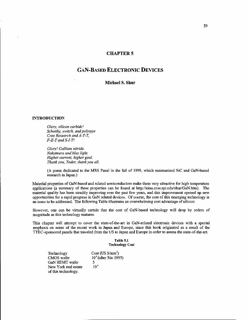
59
CHAPTER 5
GAN-BASED ELECTRONIC DEVICES
Michael S. Shur
INTRODUCTION
Glory, silicon carbide! Schottky, switch, andpolytype Cree Research andA-T-T, F-E-T and S-I-T!
Glory! Gallium nitride. Nakamura and blue light. Higher current, higher goal. Thank you, Yoder, thank you all.
(A poem dedicated to the MRS Panel in the fall of 1998, which summarized SiC and GaN-based research in Japan.)
Material properties of GaN-based and related semiconductors make them very attractive for high temperature applications (a summary of these properties can be found at http://nina.ecse.rpi.edu/shur/GaN.htm). The material quality has been steadily improving over the past few years, and this improvement opened up new opportunities for a rapid progress in GaN related devices. Of course, the cost of this emerging technology is an issue to be addressed. The following Table illustrates an overwhelming cost advantage of silicon:
However, one can be virtually certain that the cost of GaN-based technology will drop by orders of magnitude as this technology matures.
This chapter will attempt to cover the state-of-the-art in GaN-related electronic devices with a special emphasis on some of the recent work in Japan and Europe, since this book originated as a result of the TTEC-sponsored panels that traveled from the US to Japan and Europe in order to assess the state-of-the-art.
Table 5.1 Technology Cost
Technology Cost (US $/mm2) CMOS wafer 10"4 (after Rin 1995) GaN HEMT wafer 5 New York real estate 10"* of this technology.
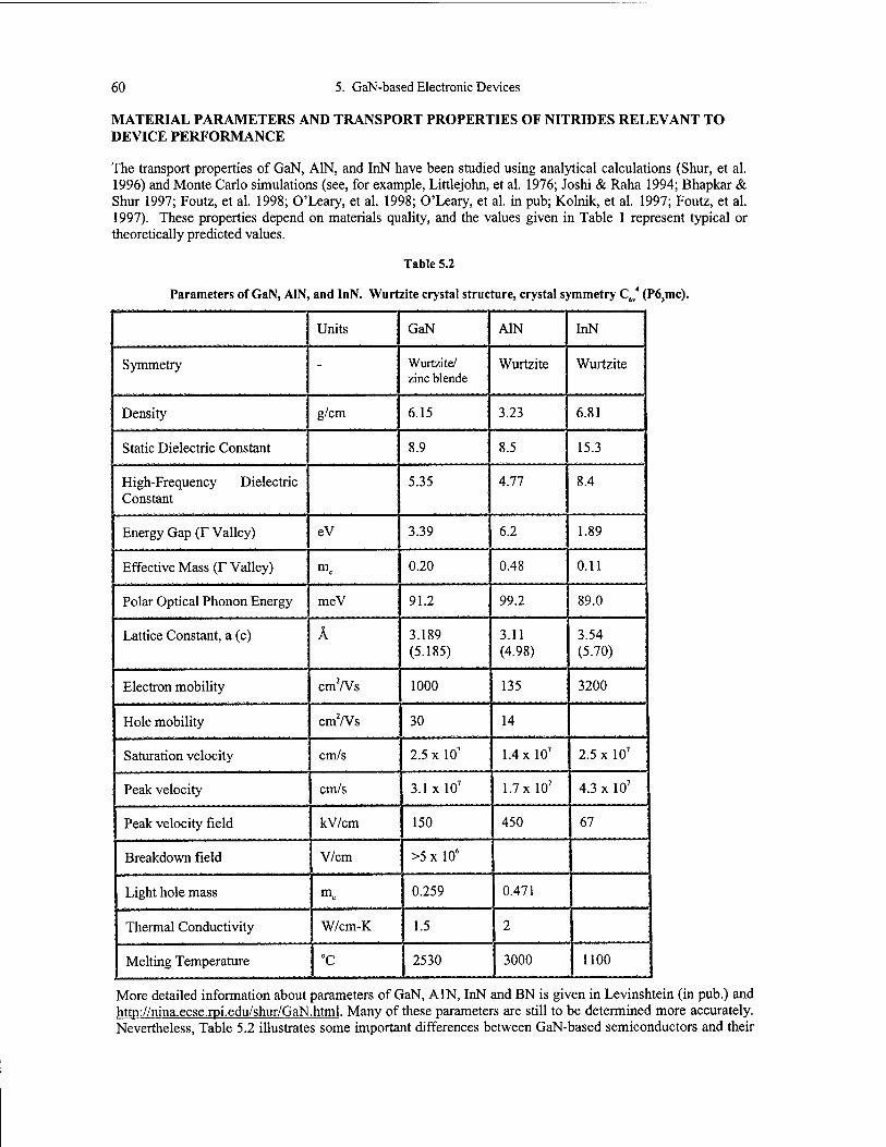
60 5. GaN-based Electronic Devices
MATERIAL PARAMETERS AND TRANSPORT PROPERTIES OF NITRIDES RELEVANT TO DEVICE PERFORMANCE
The transport properties of GaN, A1N, and InN have been studied using analytical calculations (Shur, et al. 1996) and Monte Carlo simulations (see, for example, Littlejohn, et al. 1976; Joshi & Raha 1994; Bhapkar & Shur 1997; Foutz, et al. 1998; O'Leary, et al. 1998; O'Leary, et al. in pub; Kolnik, et al. 1997; Foutz, et al. 1997). These properties depend on materials quality, and the values given in Table 1 represent typical or theoretically predicted values.
Table 5.2
Parameters of GaN, A1N, and InN. Wurtzite crystal structure, crystal symmetry C6v4 (P6,mc).
Units GaN A1N InN
Symmetry - Wurtzite/ zinc blende
Wurtzite Wurtzite
Density g/cm 6.15 3.23 6.81
Static Dielectric Constant 8.9 8.5 15.3
High-Frequency Dielectric Constant
5.35 4.77 8.4
Energy Gap (r Valley) eV 3.39 6.2 1.89
Effective Mass (r Valley) mc 0.20 0.48 0.11
Polar Optical Phonon Energy meV 91.2 99.2 89.0
Lattice Constant, a (c) A 3.189 (5.185)
3.11 (4.98)
3.54 (5.70)
Electron mobility cmYVs 1000 135 3200
Hole mobility cm2/Vs 30 14
Saturation velocity cm/s 2.5 x 10⁷ 1.4 xlO7 2.5 x 10⁷
Peak velocity cm/s 3.1 x 10⁷ 1.7 xlO7 4.3 x 10⁷
Peak velocity field kV/cm 150 450 67
Breakdown field V/cm >5 x 10*
Light hole mass mc
0.259 0.471
Thermal Conductivity W/cm-K 1.5 2
Melting Temperature °C 2530 3000 1100
More detailed information about parameters of GaN, A IN, InN and BN is given in Levinshtein (in pub.) and http://nina.ecse.rpi.edu/shur/GaN.html. Many of these parameters are still to be determined more accurately. Nevertheless, Table 5.2 illustrates some important differences between GaN-based semiconductors and their
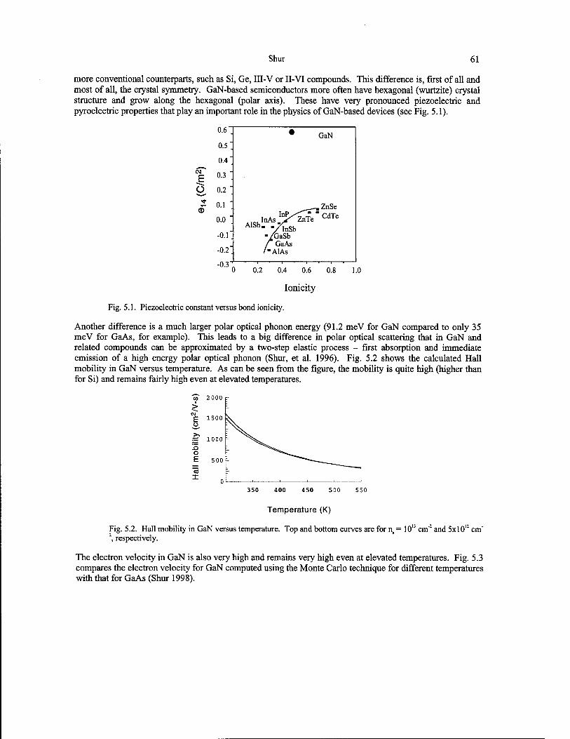
Shur 61
more conventional counterparts, such as Si, Ge, III-V or II-VI compounds. This difference is, first of all and most of all, the crystal symmetry. GaN-based semiconductors more often have hexagonal (wurtzite) crystal structure and grow along the hexagonal (polar axis). These have very pronounced piezoelectric and pyroelectric properties that play an important role in the physics of GaN-based devices (see Fig. 5.1).
CO
E O
Ionicity
Fig. 5.1. Piezoelectric constant versus bond ionicity.
Another difference is a much larger polar optical phonon energy (91.2 meV for GaN compared to only 35 meV for GaAs, for example). This leads to a big difference in polar optical scattering that in GaN and related compounds can be approximated by a two-step elastic process - first absorption and immediate emission of a high energy polar optical phonon (Shur, et al. 1996). Fig. 5.2 shows the calculated Hall mobility in GaN versus temperature. As can be seen from the figure, the mobility is quite high (higher than for Si) and remains fairly high even at elevated temperatures.
O) 2000
^ E 1500
n o E
1000
500
"ÖS
0
r
350 400 450 500 55
Temperature (K)
Fig. 5.2. Hall mobility in GaN versus temperature. Top and bottom curves are for ns = 101! cm"2 and 5x10U cm" 2, respectively.
The electron velocity in GaN is also very high and remains very high even at elevated temperatures. Fig. 5.3 compares the electron velocity for GaN computed using the Monte Carlo technique for different temperatures with that for GaAs (Shur 1998).
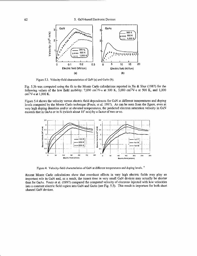
62 5. GaN-based Electronic Devices
o o
>
3- GaN
/ c / 0
- /o°°
%°°°o0
_/ 0 t
7° *** 1° '4
r 300 K, "\ O000 500 K ^„„ 1,000 Ky«
i I i
? GaAs
~/o°°\0°o /O ' /o * f ■ I
f 300K "N
2
1
0 000 500 K ^,,, 1,000 Kyi
0 5 MJ 9 I0-0
i
0.1 0.2
Electric field (MV/cm)
(a)
0.3 5 10 15 20
Electric field (kV/cm)
(b)
Figure 5.3. Velocity-field characteristics of GaN (a) and GaAs (b).
Fig. 5.3b was computed using the fit to the Monte Carlo calculations reported in Xu & Shur (1987) for the following values of the low field mobility: 7,000 cm7V-s at 300 K, 3,000 cm7V-s at 500 K, and 1,100 cm2/V-s at 1,000 K.
Figure 5.4 shows the velocity versus electric field dependences for GaN at different temperatures and doping levels computed by the Monte Carlo technique (Foutz, et al. 1997). As can be seen from the figure, even at very high doping densities and/or at elevated temperatures, the predicted electron saturation velocity in GaN exceeds that in GaAs or in Si (which about 105 m/s) by a factor of two or so.
---^- .... ._._
Ks^ ~"->»--_ 22=-r
i lel7[
I/A j 1e18 j | 1e19|
100 150 200
Electric Field [kV/cm] 100 150 200
Electric Field [kV/cm]
Figure 4. Velocity-field characteristics of GaN at different temperatures and doping levels. "
Recent Monte Carlo calculations show that overshoot effects in very high electric fields may play an important role in GaN and, as a result, the transit time in very small GaN devices may actually be shorter than for GaAs. Foutz et al. (1997) compared the computed velocity of electrons injected with low velocities into a constant electric field region into GaN and GaAs (see Fig. 5.5). This result is important for both short channel GaN devices.
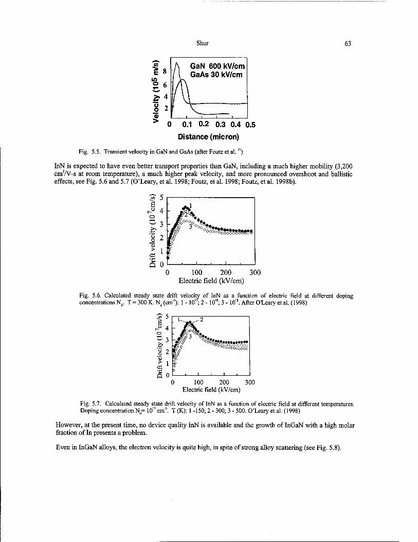
Shur 63
f. in
I4
N GaN 600 kV/cm / I GaAs 30 kV/cm
K 8 2 V 0) 1 1 1 1
^ 0 0.1 0.2 0.3 0.4 0.5
Distance (micron)
Fig. 5.5. Transient velocity in GaN and GaAs (after Foutz et al.,0)
InN is expected to have even better transport properties than GaN, including a much higher mobility (3,200 cmVV-s at room temperature), a much higher peak velocity, and more pronounced overshoot and ballistic effects, see Fig. 5.6 and 5.7 (O'Leary, et al. 1998; Foutz, et al. 1998; Foutz, et al. 1998b).
1- -° 4 - 4L o
■ #^.
S3 - JP0 3°4% o z
<D
> 1 «C
So 1,1.
0 100 200 300 Electric field (kV/cm)
Fig. 5.6. Calculated steady state drift velocity of InN as a function of electric field at different doping concentrations N„. T = 300 K. Nd (cm"'): 1 -10"; 2 -1018; 3 -1018. After O'Leary et al. (1998)
1^ -2
./r^
w ^^S
> I,I.
^ 4\- o
I3 5 T o L
t 1 So
0 100 200 300 Electric field (kV/cm)
Fig. 5.7. Calculated steady state drift velocity of InN as a function of electric field at different temperatures. Doping concentration N= 10" cm"3. T (K): 1 -150; 2 - 300; 3 - 500. O'Leary et al. (1998)
However, at the present time, no device quality InN is available and the growth of InGaN with a high molar fraction of In presents a problem.
Even in InGaN alloys, the electron velocity is quite high, in spite of strong alloy scattering (see Fig. 5.8).
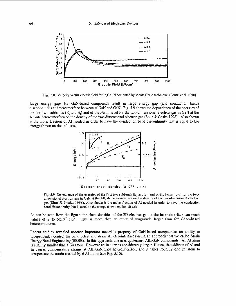
64 5. GaN-based Electronic Devices
300 400 500 600 700
Electric Field (kV/cm) 1000
Fig. 5.8. Velocity versus electric field for InxGa, N computed by Monte Carlo technique. (Foutz, et al. 1998)
Large energy gaps for GaN-based compounds result in large energy gap (and conduction band) discontinuities at heterointerface between AlGaN and GaN. Fig. 5.9 shows the dependence of the energies of the first two subbands (Eo and E,) and of the Fermi level for the two-dimensional electron gas in GaN at the AlGaN heterointerface on the density of the two-dimensional electron gas (Shur & Gaska 1998). Also shown is the molar fraction of Al needed in order to have the conduction band discontinuity that is equal to the energy shown on the left axis.
1 .5
> >, 0.5 E? <D C
LU
r-0.05 ^
//
/ 1 E 'J^ ~
lilt
0.5 c o
0.2 5 -fc « o £
-0.5 10 20 30 40 50
Electron sheet density (x1012 cm'2)
Fig. 5.9. Dependence of the energies of the first two subbands (Eo and E,) and of the Fermi level for the two- dimensional electron gas in GaN at the AlGaN heterointerface on the density of the two-dimensional electron gas (Shur & Gaska 1998). Also shown is the molar fraction of Al needed in order to have the conduction band discontinuity that is equal to the energy shown on the left axis.
As can be seen from the figure, the sheet densities of the 2D electron gas at the heterointerface can reach values of 2 to 5x10" cm"2. This is more than an order of magnitude larger than for GaAs-based heterostructures.
Recent studies revealed another important materials property of GaN-based compounds: an ability to independently control the band offset and strain at heterointerfaces using an approach that we called Strain Energy Band Engineering (SEBE). In this approach, one uses quaternary AlInGaN compounds. An Al atom is slightly smaller than a Ga atom. However an In atom is considerably larger. Hence, the addition of Al and In causes compensating strains at AlInGaN/GaN heterointerface, and it takes roughly one In atom to compensate the strain created by 6 Al atoms (see Fig. 5.10).
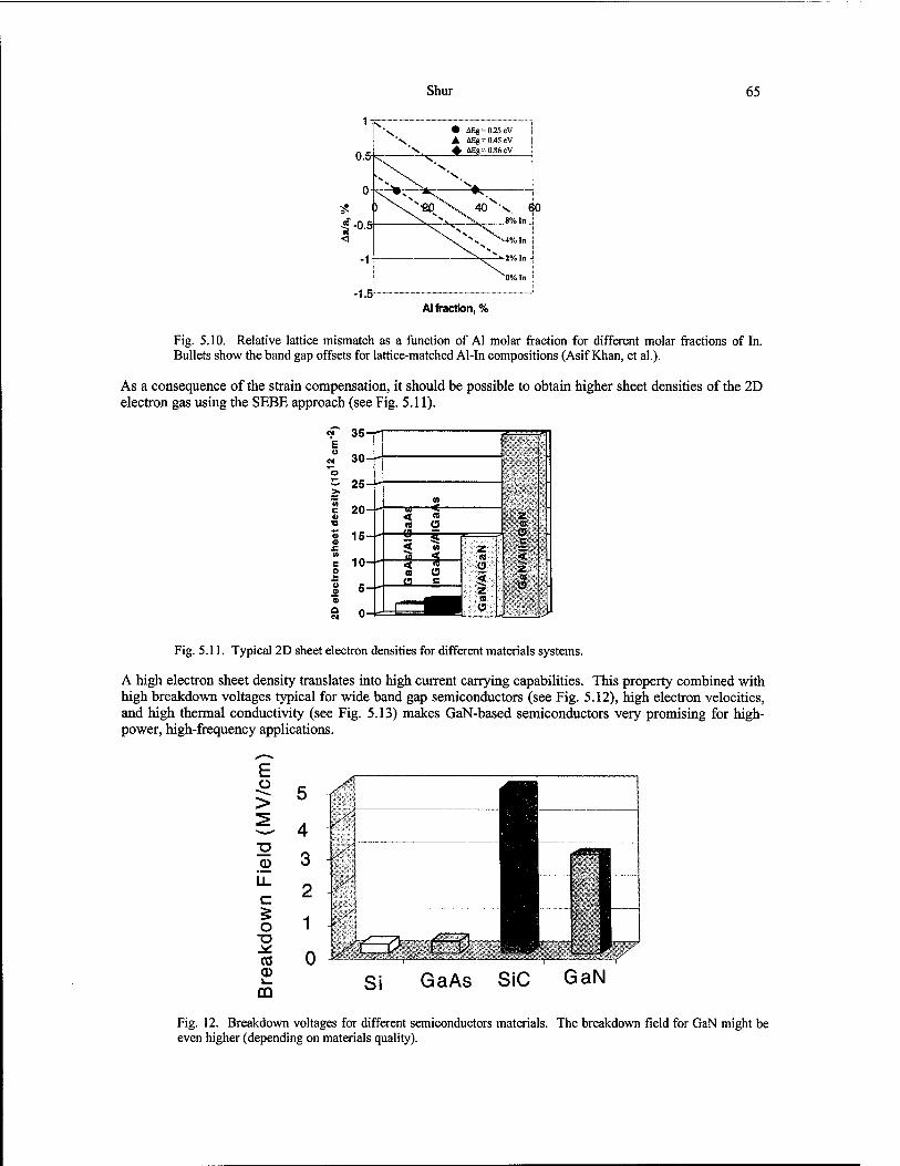
Shur 65
• 4Eg-0.25eV ▲ AEg = 0.45eV + AEg»0.86eV
.-•20 \. 40 V 60 X 8% In
Al fraction, %
Fig. 5.10. Relative lattice mismatch as a function of Al molar fraction for different molar fractions of In. Bullets show the band gap offsets for lattice-matched Al-In compositions (Asif Khan, et al.).
As a consequence of the strain compensation, it should be possible to obtain higher sheet densities of the 2D electron gas using the SEBE approach (see Fig. 5.11).
35-
30—
25-H
20
15-r-
10
5-M
-07- < IS
< 10
V)
(0 a
< co
_£3_ a c
Kg«
o
mm. o c
Ü
Fig. 5.11. Typical 2D sheet electron densities for different materials systems.
A high electron sheet density translates into high current carrying capabilities. This property combined with high breakdown voltages typical for wide band gap semiconductors (see Fig. 5.12), high electron velocities, and high thermal conductivity (see Fig. 5.13) makes GaN-based semiconductors very promising for high- power, high-frequency applications.
E " 5
£ 4 - q
C
o
CO <D
CO
2
1
0 Si GaAs
~y
SiC GaN
Fig. 12. Breakdown voltages for different semiconductors materials. The breakdown field for GaN might be even higher (depending on materials quality).
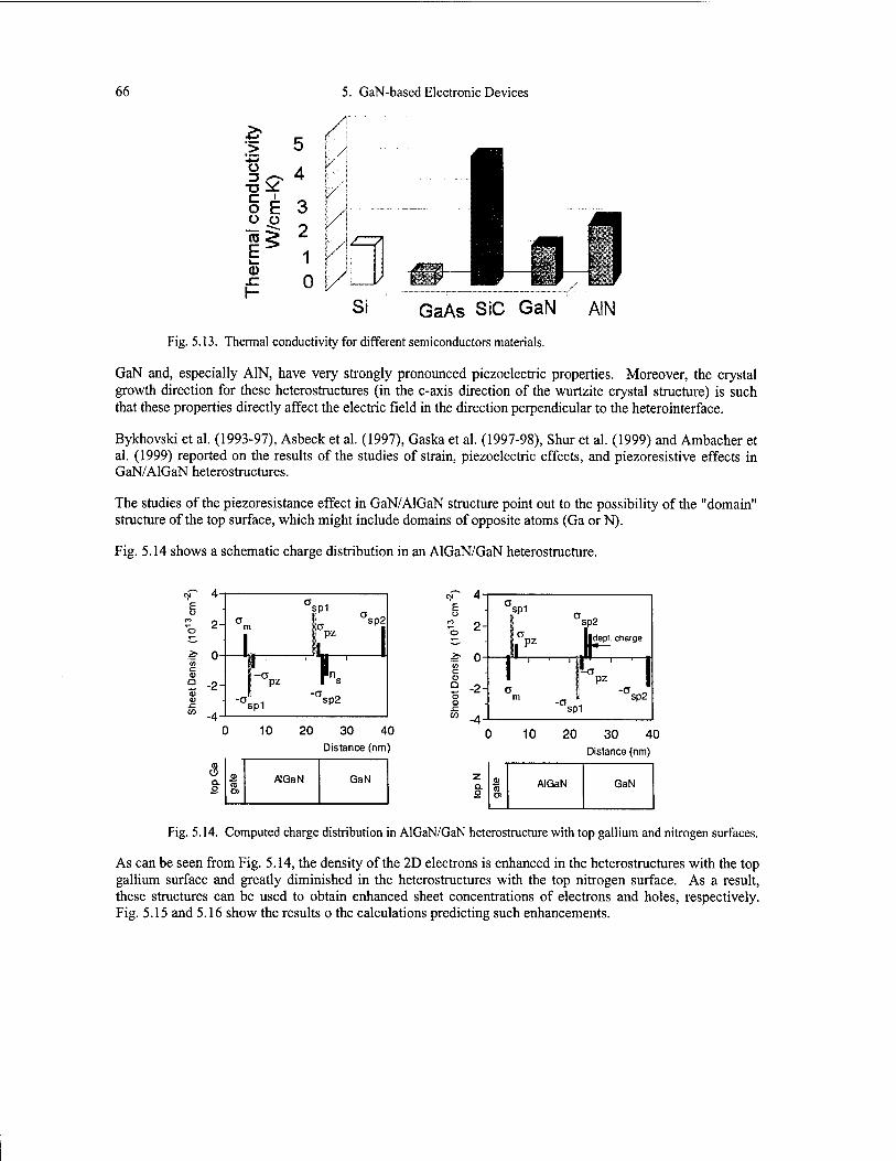
66 5. GaN-based Electronic Devices
"> Ü ~i
TJ X. C o
i
E Ü o
10 E g i_ a> sz h-
5
4
3 2 1 0
/
A
Si GaAs SiC GaN AIN
Fig. 5.13. Thermal conductivity for different semiconductors materials.
GaN and, especially AIN, have very strongly pronounced piezoelectric properties. Moreover, the crystal growth direction for these heterostructures (in the c-axis direction of the wurtzite crystal structure) is such that these properties directly affect the electric field in the direction perpendicular to the heterointerface.
Bykhovski et al. (1993-97), Asbeck et al. (1997), Gaska et al. (1997-98), Shur et al. (1999) and Ambacher et al. (1999) reported on the results of the studies of strain, piezoelectric effects, and piezoresistive effects in GaN/AlGaN heterostructures.
The studies of the piezoresistance effect in GaN/AlGaN structure point out to the possibility of the "domain" structure of the top surface, which might include domains of opposite atoms (Ga orN).
Fig. 5.14 shows a schematic charge distribution in an AlGaN/GaN heterostructure.
20 30 40 Distance (nm)
3 0) m
AIGaN GaN
"o 2-
£ 0-
2 -2-
■ %1 Gsp2
- ll PZ Hdepl. charge
I h \ I pz 1 a m -a * "°SP2
spl
0 10 20 30 4 0 Distance (nm)
L aj AIGaN GaN en
Fig. 5.14. Computed charge distribution in AlGaN/GaN heterostructure with top gallium and nitrogen surfaces.
As can be seen from Fig. 5.14, the density of the 2D electrons is enhanced in the heterostructures with the top gallium surface and greatly diminished in the heterostructures with the top nitrogen surface. As a result, these structures can be used to obtain enhanced sheet concentrations of electrons and holes, respectively. Fig. 5.15 and 5.16 show the results o the calculations predicting such enhancements.
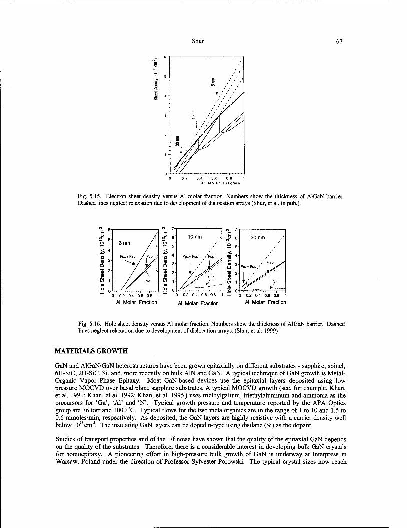
Shur 67
.■&
0.4 0.6 0.8 1 Al Molar Fraction
Fig. 5.15. Electron sheet density versus Al molar fraction. Numbers show the thickness of AlGaN barrier. Dashed lines neglect relaxation due to development of dislocation arrays (Shur, et al. in pub.).
o ti 5- o 3nm
*» D
Ppz + Psp /lpsp ':
■8 2- o x: W 1-
7 \
-? n- " '' I I' " ' ' ' ' ' I ""■' I 0.2 0.4 0.6 0.8 1
Al Molar Fraction
0 0.2 0.4 0.6 0.8 1
Al Molar Fraction
0 0.2 0.4 0.6 0.8 1
Al Molar Fraction
Fig. 5.16. Hole sheet density versus Al molar fraction. Numbers show the thickness of AlGaN barrier. Dashed lines neglect relaxation due to development of dislocation arrays. (Shur, et al. 1999)
MATERIALS GROWTH
GaN and AlGaN/GaN heterostructures have been grown epitaxially on different substrates - sapphire, spinel, 6H-SiC, 2H-SiC, Si, and, more recently on bulk A1N and GaN. A typical technique of GaN growth is Metal- Organic Vapor Phase Epitaxy. Most GaN-based devices use the epitaxial layers deposited using low pressure MOCVD over basal plane sapphire substrates. A typical MOCVD growth (see, for example, Khan, et al. 1991; Khan, et al. 1992; Khan, et al. 1995) uses triethylgalium, triethylaluminum and ammonia as the precursors for 'Ga', 'Al' and 'N'. Typical growth pressure and temperature reported by the APA Optics group are 76 torr and 1000 °C. Typical flows for the two metalorganics are in the range of 1 to 10 and 1.5 to 0.6 mmoles/min, respectively. As deposited, the GaN layers are highly resistive with a carrier density well below 1015cm'3. The insulating GaN layers can be doped n-type using disilane (Si) as the dopant.
Studies of transport properties and of the 1/f noise have shown that the quality of the epitaxial GaN depends on the quality of the substrates. Therefore, there is a considerable interest in developing bulk GaN crystals for homoepitaxy. A pioneering effort in high-pressure bulk growth of GaN is underway at Interpress in Warsaw, Poland under the direction of Professor Sylvester Porowski. The typical crystal sizes now reach

68 5. GaN-based Electronic Devices
over a square centimeter. The quality of epitaxial layers grown on these substrates is excellent, with no interface detected and with the dislocation density below the detection limit.
Recently, a lot of attention has been paid to Lateral Epitaxial Overgrowth (LEO), which allows production of GaN films with the density of threading dislocations, which is up to 4 orders of magnitude smaller than for GaN films grown on sapphire (Sakai, et al. 1997; Marchand, et al. 1998; Marchand, et al. 1998b) and 6H-SiC (Zheleva, et al. 1997) substrates. UCSB group reported on studies of threading dislocations in GaN films and investigated the LEO-grown GaN films (Nam, et al. 1997; Sakai, et al. 1998; Sakai, et al. 1998b). The reduction of the dislocation density results in a dramatic drop in the leakage current in GaN-based p-n junctions (Kozodoy, et al. 1998) and GaN/AlGaN heterojunction field-effect transistors (Vetury, et al. 1998) grown by LEO.
Other techniques of the epitaxial growth of GaN include Molecular Beam Epitaxy (MBE), (see, for example, Birkman & Steckl 1997; Cheng, et al. 1997) and Hydride Vapor Phase Epitaxy (HVPE) (Molnar 1997). GaN layers grown by MBE are similar in quality to the layers grown by MOCVD. HVPE can yield thick GaN layers, which is important for potential applications of GaN-based materials in power devices. Recently, this technique was used for the epitaxial growth of AIN/AlGaN/GaN heterostructures on SiC substrates (Yu, et al. 1997).
One interesting emerging direction in the epitaxial growth of GaN, A1N, and InN materials is the fabrication of quantum dots (Tanaka, et al. 1997).
N-type GaN can be obtained with electron density higher than 10" cm"'. However, p-doping remains a serious problem, and the highest reported hole concentration in p-GaN was around low 1018 cm"' (using Mg as an acceptor) (Nakamura & Fasol). This is because the ionization energy of this acceptor is quite high (160 meV) so that less than 1% of Mg acceptor is activated at room temperature.
OHMIC CONTACTS
Low-resistance, thermally stable ohmic contacts to GaN are crucial for obtaining good device performance and for fabricating devices operating in a wide temperature range. At first, Al and Au ohmic contacts to GaN were used. These contacts yielded specific contact resistances of 104 and 10"' Qcm2, respectively (Foresi & Moustakos 1993). The use Ti in ohmic contacts to GaN resulted in much smaller contact resistance. Lin et al. described an Al/Ti ohmic contact to n-GaN with a specific contact resistance of 8X10"6 Qcm2 (Lin, et al. 1994). Later, Fan et al. (1996) reported on the Al/Ni/Al/Ti contact to n-GaN, and obtained the specific ohmic resistance as low as 9xl0'8 Qcm2 using this approach. The mechanism of obtaining such low contact resistance was shown to be the formation of TiN, which leads to a large concentration of N vacancies (that behave as donors in GaN) near the surface (Ruvimov, et al. 1996). (The dependence of the specific contact resistance on doping was studied by Khan et al (1996).
Wolter et al. (1999) studied ZrN/Zr ohmic contact to GaN that showed promise of a better thermal stability with a reasonable specific contact resistance of 2xl0"5 Qcm2 for GaN with the electron concentration of 7x10" cm"' and sheet resistance of 44 Q/square. These contacts exhibited excellent thermal stability in evacuated quartz tubes at 600 °C for 1000 hours.
Holloway et al. (1997) reviewed the results obtained for ohmic contacts to GaN. A low contact metallization for ohmic contacts was reported in Qiao, et al. (1999)
Low-resistivity ohmic contacts to p-GaN layers are crucial building blocks for GaN based bipolar electronic and optoelectronic devices, such HBTs, LEDs, and lasers. Lunev et al. (1999) compare a new Pd/Au and the commonly used Ni/Au metallization schemes for such contacts and demonstrated contact resistances as low as 10"4 Qcm2 at room temperature and 1.5X10"6 Qcm2 at 250 "C for Pd/Au contacts. The p-GaN layers for this study were grown on sapphire substrates using a standard low-pressure MOCVD process with Mg as the p- dopant. Prior to the 0.5-um thick p-GaN layer, a l-|im thick layer of insulating GaN was also grown. Using standard Van-der Pauw geometry, the carrier concentration in the p-GaN was measured to be 3 x 1017 cm'3 at room temperature and 1018 cm"' at 250 °C. With annealing the Pd/Au contact resistance decreases to a value
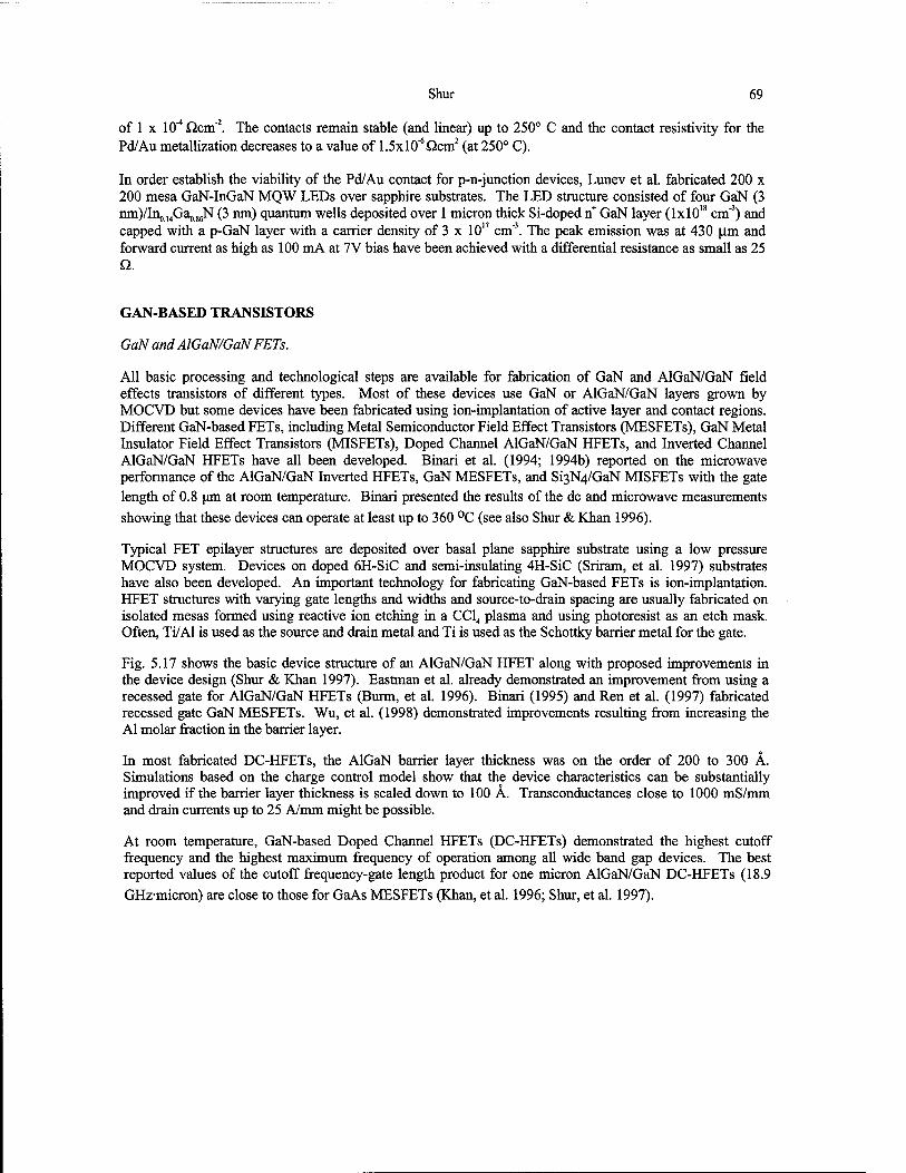
Shur 69
of 1 x 10"4 £2cm"2. The contacts remain stable (and linear) up to 250° C and the contact resistivity for the Pd/Au metallization decreases to a value of l.SxlO^ßcm2 (at 250° C).
In order establish the viability of the Pd/Au contact for p-n-junction devices, Lunev et al. fabricated 200 x 200 mesa GaN-InGaN MQW LEDs over sapphire substrates. The LED structure consisted of four GaN (3 nm)/In014Ga086N (3 nm) quantum wells deposited over 1 micron thick Si-doped n+ GaN layer (lxlO18 cm'3) and capped with a p-GaN layer with a carrier density of 3 x 10" cm"3. The peak emission was at 430 |im and forward current as high as 100 mA at 7 V bias have been achieved with a differential resistance as small as 25 Q.
GAN-BASED TRANSISTORS
GaN andAlGaN/GaN FETs.
All basic processing and technological steps are available for fabrication of GaN and AlGaN/GaN field effects transistors of different types. Most of these devices use GaN or AlGaN/GaN layers grown by MOCVD but some devices have been fabricated using ion-implantation of active layer and contact regions. Different GaN-based FETs, including Metal Semiconductor Field Effect Transistors (MESFETs), GaN Metal Insulator Field Effect Transistors (MISFETs), Doped Channel AlGaN/GaN HFETs, and Inverted Channel AlGaN/GaN HFETs have all been developed. Binari et al. (1994; 1994b) reported on the microwave performance of the AlGaN/GaN Inverted HFETs, GaN MESFETs, and Si3N4/GaN MISFETs with the gate length of 0.8 um at room temperature. Binari presented the results of the dc and microwave measurements
showing that these devices can operate at least up to 360 °C (see also Shur & Khan 1996).
Typical FET epilayer structures are deposited over basal plane sapphire substrate using a low pressure MOCVD system. Devices on doped 6H-SiC and semi-insulating 4H-SiC (Sriram, et al. 1997) substrates have also been developed. An important technology for fabricating GaN-based FETs is ion-implantation. HFET structures with varying gate lengths and widths and source-to-drain spacing are usually fabricated on isolated mesas formed using reactive ion etching in a CC1„ plasma and using photoresist as an etch mask. Often, Ti/Al is used as the source and drain metal and Ti is used as the Schottky barrier metal for the gate.
Fig. 5.17 shows the basic device structure of an AlGaN/GaN HFET along with proposed improvements in the device design (Shur & Khan 1997). Eastman et al. already demonstrated an improvement from using a recessed gate for AlGaN/GaN HFETs (Burm, et al. 1996). Binari (1995) and Ren et al. (1997) fabricated recessed gate GaN MESFETs. Wu, et al. (1998) demonstrated improvements resulting from increasing the Al molar fraction in the barrier layer.
In most fabricated DC-HFETs, the AlGaN barrier layer thickness was on the order of 200 to 300 A. Simulations based on the charge control model show that the device characteristics can be substantially improved if the barrier layer thickness is scaled down to 100 A. Transconductances close to 1000 mS/mm and drain currents up to 25 A/mm might be possible.
At room temperature, GaN-based Doped Channel HFETs (DC-HFETs) demonstrated the highest cutoff frequency and the highest maximum frequency of operation among all wide band gap devices. The best reported values of the cutoff frequency-gate length product for one micron AlGaN/GaN DC-HFETs (18.9
GHzmicron) are close to those for GaAs MESFETs (Khan, et al. 1996; Shur, et al. 1997).
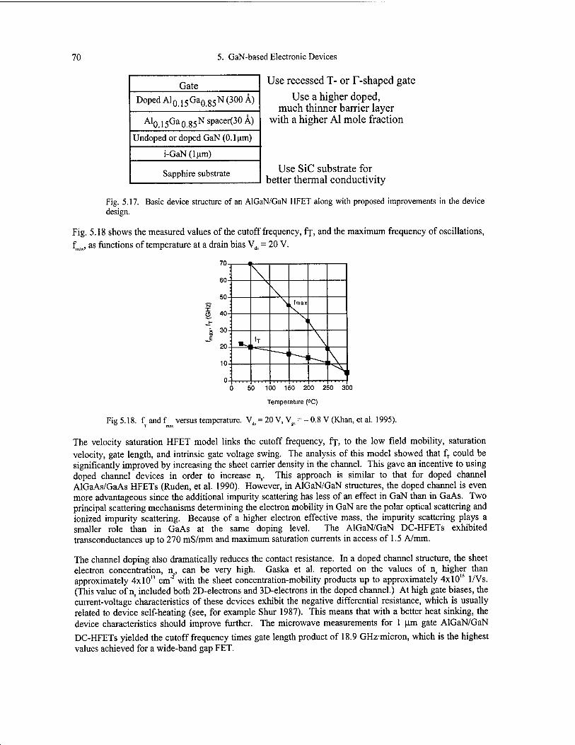
70 5. GaN-based Electronic Devices
Gate
Doped Al0 15Ga0 g5N (300 A)
AIQ j5Ga0 85 N spacer(30 A)
Undoped or doped GaN (0.1 urn)
i-GaN(lum)
Sapphire substrate
Use recessed T- or T-shaped gate
Use a higher doped, much thinner barrier layer
with a higher Al mole fraction
Use SiC substrate for better thermal conductivity
Fig. 5.17. Basic device structure of an AlGaN/GaN HFET along with proposed improvements in the device design.
Fig. 5.18 shows the measured values of the cutoff frequency, fr, and the maximum frequency of oscillations, fnox, as functions of temperature at a drain bias V^ = 20 V.
70-
60.
50-
S. 40'
x 30- en
"" 20
10
I <
\ \
. fmax
■^1 IT
"
Temperature (°C)
Fig 5.18. f andf versus temperature. V. = 20 V, V = - 0.8 V (Khan, et al. 1995). T max *
The velocity saturation HFET model links the cutoff frequency, fj, to the low field mobility, saturation velocity, gate length, and intrinsic gate voltage swing. The analysis of this model showed that fT could be significantly improved by increasing the sheet carrier density in the channel. This gave an incentive to using doped channel devices in order to increase ns. This approach is similar to that for doped channel AlGaAs/GaAs HFETs (Rüden, et al. 1990). However, in AlGaN/GaN structures, the doped channel is even more advantageous since the additional impurity scattering has less of an effect in GaN than in GaAs. Two principal scattering mechanisms determining the electron mobility in GaN are the polar optical scattering and ionized impurity scattering. Because of a higher electron effective mass, the impurity scattering plays a smaller role than in GaAs at the same doping level. The AlGaN/GaN DC-HFETs exhibited transconductances up to 270 mS/mm and maximum saturation currents in access of 1.5 A/mm.
The channel doping also dramatically reduces the contact resistance. In a doped channel structure, the sheet electron concentration, n, can be very high. Gaska et al. reported on the values of ns higher than approximately 4x10" cm"f with the sheet concentration-mobility products up to approximately 4xl016 1/Vs. (This value of ns included both 2D-electrons and 3D-electrons in the doped channel.) At high gate biases, the current-voltage characteristics of these devices exhibit the negative differential resistance, which is usually related to device self-heating (see, for example Shur 1987). This means that with a better heat sinking, the device characteristics should improve further. The microwave measurements for 1 urn gate AlGaN/GaN
DC-HFETs yielded the cutoff frequency times gate length product of 18.9 GHzmicron, which is the highest values achieved for a wide-band gap FET.

Shur 71
The importance of a large electron sheet concentration in the channel for the improved FET performance was confirmed by a transconductance increase in an Al 015Ga0g5N/GaN HFET under UV illumination. The illumination acted as "optical" channel underdoping. A relatively modest positive trapped charge in the active channel (4x10" cm"3) was sufficient for a considerable shift in the threshold voltage and, consequently, for the enhancement of the ns value. The maximum transconductance, gm, reached 64 mS/mm, nearly three time higher than for similar devices with a comparable threshold voltage and many times larger than for the same device in the dark. This enhancement was explained by a large reduction in the source and drain series resistances and by the enhancement of the rig value. Calculations (based on the HEMT model developed in
Lee, et al. 1993) confirm that the gin enhancement is caused by the reduction in Rs, and by a larger ns.
For deep sub-micron gate GaN/AlGaN DC-HFETs, record values of the cutoff frequency, fT, and the maximum frequency of oscillations, fmax, are 46.9 GHz and 103 GHz, respectively (Khan, et al. 1996).
The advantages of DC-HFETs compared to other GaN-based devices should be even more pronounced at elevated temperatures. The reason for the expected good performance of AlGaN-GaN DC-HFETs at elevated temperatures is the decrease in ionized impurity scattering with an increase in temperature. The measured I-V characteristics of AlGaN-GaN DC-HFETs and the investigations of microwave characteristics of these devices at elevated temperatures support this assumption.
AlGaN/GaN HFETs reached record power levels at microwave frequencies as high as 9.2 W/mm. These results show that, in spite of a smaller thermal conductivity than for SiC, excellent transport properties of GaN at elevated temperatures make these devices a viable alternative for high-temperature and high-power microwave and digital applications. A further improvement in high temperature performance can be achieved if self-heating effects are reduced. The replacement of sapphire substrates with SiC substrates drastically decreases the thermal impedance of the Doped Channel AlGaN/GaN HFETs and self-heating effects.
Tables 5.3 and 5.4 (from) summarize parameters of GaN-based HFETs.
Table 5.3
State-of-the-art parameters of GaN-based HFETs (Khan, et al. 1999).
PARAMETER UNIT (Um) (Urn)
REFERENCE
Saturated Current IM,(25C)
mA/mm 2 5 2
0.25 2.0 0.25
1.7 1.35 1.2
Khan et al., Elec. Lett. 1997 Gaskaetal.,ICNS2 1997 Mishraetal.EDL1996
Transconductance Sm
mS/mm 2 2 2 2
1.4
0.25 0.25 0.25 0.25 1.2
220 250 270 270 400*
Khan et al., Elec. Lett. 1997 Gaska et at. Elec. Lett. 1998 Mishra et al. Elec. Lett. 1997 Eastman et al. 1999 Mishra et.al'1999
ft/fmax GHz 2 2 2 2
0.25 0.12 0.15 0.4
38/81 47/103 67/140* 28/114
Khan et al., Elec. Lett. 1997 Burm/Khan et. al, EDL 1997 Chu et al. WOCSEMMAD 1998 Shephard et al. EDL 1999
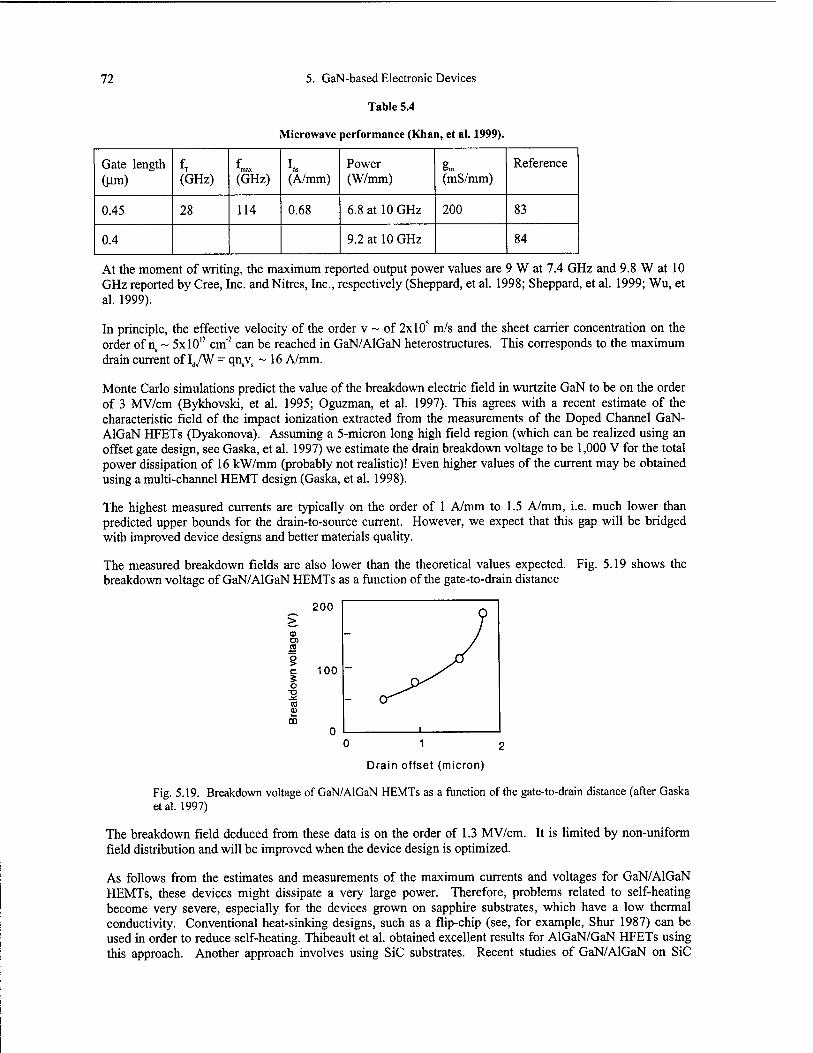
72 5. GaN-based Electronic Devices
Table 5.4
Microwave performance (Khan, et al. 1999).
Gate length (Um) (GHz)
max
(GHz) (A/mm) Power (W/mm)
©in
(mS/mm) Reference
0.45 28 114 0.68 6.8 at 10 GHz 200 83
0.4 9.2 at 10 GHz 84
At the moment of writing, the maximum reported output power values are 9 W at 7.4 GHz and 9.8 W at 10 GHz reported by Cree, Inc. and Nitres, Inc., respectively (Sheppard, et al. 1998; Sheppard, et al. 1999; Wu, et al. 1999).
In principle, the effective velocity of the order v ~ of 2xl05 m/s and the sheet carrier concentration on the order of ns ~ 5x10" cm"2 can be reached in GaN/AlGaN heterostructures. This corresponds to the maximum drain current of 1JW = qnsvs ~ 16 A/mm.
Monte Carlo simulations predict the value of the breakdown electric field in wurtzite GaN to be on the order of 3 MV/cm (Bykhovski, et al. 1995; Oguzman, et al. 1997). This agrees with a recent estimate of the characteristic field of the impact ionization extracted from the measurements of the Doped Channel GaN- AlGaN HFETs (Dyakonova). Assuming a 5-micron long high field region (which can be realized using an offset gate design, see Gaska, et al. 1997) we estimate the drain breakdown voltage to be 1,000 V for the total power dissipation of 16 kW/mm (probably not realistic)! Even higher values of the current may be obtained using a multi-channel HEMT design (Gaska, et al. 1998).
The highest measured currents are typically on the order of 1 A/mm to 1.5 A/mm, i.e. much lower than predicted upper bounds for the drain-to-source current. However, we expect that this gap will be bridged with improved device designs and better materials quality.
The measured breakdown fields are also lower than the theoretical values expected. Fig. 5.19 shows the breakdown voltage of GaN/AlGaN HEMTs as a function of the gate-to-drain distance
^ 200 > Q) TO B
c 100 g o CD CD
m
Drain offset (micron)
Fig. 5.19. Breakdown voltage of GaN/AlGaN HEMTs as a function of the gate-to-drain distance (after Gaska etal. 1997)
The breakdown field deduced from these data is on the order of 1.3 MV/cm. It is limited by non-uniform field distribution and will be improved when the device design is optimized.
As follows from the estimates and measurements of the maximum currents and voltages for GaN/AlGaN HEMTs, these devices might dissipate a very large power. Therefore, problems related to self-heating become very severe, especially for the devices grown on sapphire substrates, which have a low thermal conductivity. Conventional heat-sinking designs, such as a flip-chip (see, for example, Shur 1987) can be used in order to reduce self-heating. Thibeault et al. obtained excellent results for AlGaN/GaN HFETs using this approach. Another approach involves using SiC substrates. Recent studies of GaN/AlGaN on SiC
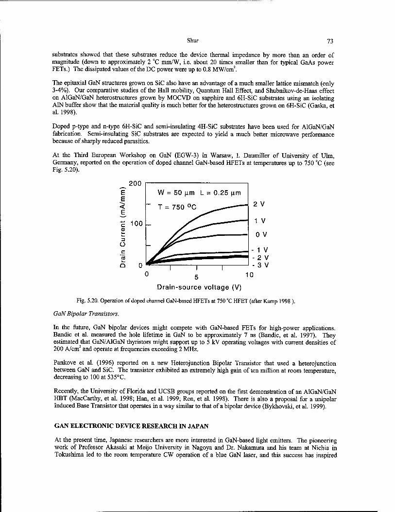
Shur 73
substrates showed that these substrates reduce the device thermal impedance by more than an order of magnitude (down to approximately 2 °C mm/W, i.e. about 20 times smaller than for typical GaAs power FETs.) The dissipated values of the DC power were up to 0.8 MW/cm2.
The epitaxial GaN structures grown on SiC also have an advantage of a much smaller lattice mismatch (only 3-4%). Our comparative studies of the Hall mobility, Quantum Hall Effect, and Shubnikov-de-Haas effect on AlGaN/GaN heterostructures grown by MOCVD on sapphire and 6H-SiC substrates using an isolating A1N buffer show that the material quality is much better for the heterostructures grown on 6H-SiC (Gaska, et al. 1998).
Doped p-type and n-type 6H-SiC and semi-insulating 4H-SiC substrates have been used for AlGaN/GaN fabrication. Semi-insulating SiC substrates are expected to yield a much better microwave performance because of sharply reduced parasitics.
At the Third European Workshop on GaN (EGW-3) in Warsaw, I. Daumiller of University of Ulm, Germany, reported on the operation of doped channel GaN-based HFETs at temperatures up to 750 °C (see Fig. 5.20).
200 E E < £
W = 50 um L = 0.25 u.m
T = 750 °C 2 V
1 V
0 V
1 V 2 V 3 V
5 1° Drain-source voltage (V)
Fig. 5.20. Operation of doped channel GaN-based HFETs at 750 °C HFET (after Kamp 1998 ).
GaN Bipolar Transistors.
In the future, GaN bipolar devices might compete with GaN-based FETs for high-power applications. Bandic et al. measured the hole lifetime in GaN to be approximately 7 ns (Bandic, et al. 1997). They estimated that GaN/AlGaN thyristors might support up to 5 kV operating voltages with current densities of 200 A/cm2 and operate at frequencies exceeding 2 MHz.
Pankove et al. (1996) reported on a new Heterojunction Bipolar Transistor that used a heterojunction between GaN and SiC. The transistor exhibited an extremely high gain of ten million at room temperature, decreasing to 100 at 535°C.
Recently, the University of Florida and UCSB groups reported on the first demonstration of an AlGaN/GaN HBT (MacCarthy, et al. 1998; Han, et al. 1999; Ren, et al. 1998). There is also a proposal for a unipolar Induced Base Transistor that operates in a way similar to that of a bipolar device (Bykhovski, et al. 1999).
GAN ELECTRONIC DEVICE RESEARCH IN JAPAN
At the present time, Japanese researchers are more interested in GaN-based light emitters. The pioneering work of Professor Akasaki at Meijo University in Nagoya and Dr. Nakamura and his team at Nichia in Tokushima led to the room temperature CW operation of a blue GaN laser, and this success has inspired
74 5. GaN-based Electronic Devices
many groups world wide to pursue GaN light emitters (Nakamura, et al. 1997) and photodetectors (Shur & Khan 1997; Shur & Khan 1998).
However, the effort in GaN-based electronic devices (or, at least planning for such research and development) has started as well. Examples include NEC, Nippon Steel, Hokkaido University (Koyama, et al. 1998), and Tokushima University. Professor Shiro is interested in developing GaN FETs for wireless communication applications and for collision avoidance radars. Low toxicity of GaN is seen as a major advantage compared to GaAs-based FETs. Furukawa group, which pursues epitaxial growth of GaN by gas source MBE is planning to develop high voltage, GaN-based high power devices, in addition to pursuing GaN laser diodes. They are also investigating high temperature GaN MESFET with Pt gate, oxide passivation on GaN, GaN Schottky diodes, and AIN/GaN MISFETs.
ETL and Sony also have GaN research programs, even though in electronic device the emphasis at the present time is on SiC and, to a lesser degree, diamond devices.
Prof. Egawa of Nagoya is doing research on GaN on Si. His interests include geothermal applications of GaN-based electronic devices. He demonstrated GaN MESFET operation at 300 °C.
Professor Akasaki sees possible applications of GaN-based devices in radiation hard electronics and for atmospheric pollution monitoring. However, most of his research is still focused on optical GaN devices.
Nippon Steel, which produces SiC substrates grown by modified Lely method, has interest in expanding their SiC program to include epitaxial growth of SiC and, possibly, of GaN-based materials. Plans are under way to develop 2-inch SiC bulk technology and (in a more distant future) 3-inch bulk SiC technology. This will be important for GaN-based devices grown on SiC substrates. Nippon Steel projects the development of high-temperature GaN electronics after year 2,000.
Professor Shiro is interested in developing GaN FETs for wireless communication applications and for collision avoidance radars. Low toxicity of GaN is seen as a major advantage compared to GaAs-based FETs. Furukawa group, which pursues epitaxial growth of GaN by gas source MBE, is planning to develop high voltage, GaN-based high power devices, in addition to pursuing GaN laser diodes. They are also investigating high temperature GaN MESFET with Pt gate, oxide passivation on GaN, GaN Schottky diodes, and AIN/GaN MISFETs.
NEC at Tsukuba is planning to use GaN for microwave power at power levels above 100 W and at frequencies above 10 GHz (up to 100 GHz). Their target is to obtain 100 W at 20 GHz (for applications in base stations). They are also evaluating radar and collision avoidance applications.
ETL and Sony also have GaN research programs, even though in electronic device the emphasis at the present time is on SiC and, to a lesser degree, diamond devices.
Prof. Egawa of Nagoya is doing research on GaN on Si. His interests include geothermal applications of GaN-based electronic devices. He demonstrated GaN MESFET operation at 300 oC.
Professor Akasaki sees possible applications of GaN-based devices in radiation hard electronics and for atmospheric pollution monitoring. However, most of his research is still focused on optical GaN devices.
Nippon Steel, which produces SiC substrates grown by modified Lely method, has interest in expanding their SiC program to include epitaxial growth of SiC and, possibly, of GaN-based materials. Plans are under way to develop 2-inch SiC bulk technology and (in a more distant future) 3-inch bulk SiC technology. This will be important for GaN-based devices grown on SiC substrates.
Many Japanese researchers predict that the "environmentally friendly" nature of GaN and SiC, as opposed to GaAs, is a big incentive for commercial development. Professor Sakai of Tokushima University used cellular phones as an example. These phones contain toxic GaAs chips, which may be replaced with GaN or SiC chips.
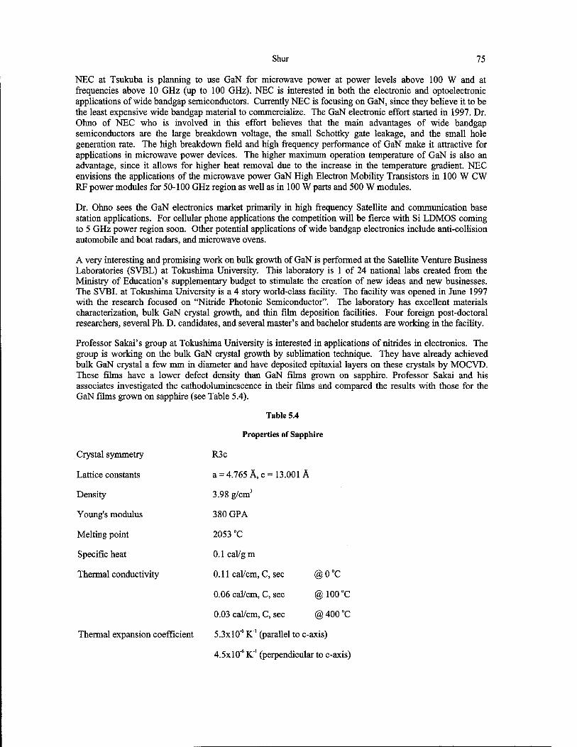
Shur 75
NEC at Tsukuba is planning to use GaN for microwave power at power levels above 100 W and at frequencies above 10 GHz (up to 100 GHz). NEC is interested in both the electronic and optoelectronic applications of wide bandgap semiconductors. Currently NEC is focusing on GaN, since they believe it to be the least expensive wide bandgap material to commercialize. The GaN electronic effort started in 1997. Dr. Ohno of NEC who is involved in this effort believes that the main advantages of wide bandgap semiconductors are the large breakdown voltage, the small Schottky gate leakage, and the small hole generation rate. The high breakdown field and high frequency performance of GaN make it attractive for applications in microwave power devices. The higher maximum operation temperature of GaN is also an advantage, since it allows for higher heat removal due to the increase in the temperature gradient. NEC envisions the applications of the microwave power GaN High Electron Mobility Transistors in 100 W CW RF power modules for 50-100 GHz region as well as in 100 W parts and 500 W modules.
Dr. Ohno sees the GaN electronics market primarily in high frequency Satellite and communication base station applications. For cellular phone applications the competition will be fierce with Si LDMOS coming to 5 GHz power region soon. Other potential applications of wide bandgap electronics include anti-collision automobile and boat radars, and microwave ovens.
A very interesting and promising work on bulk growth of GaN is performed at the Satellite Venture Business Laboratories (SVBL) at Tokushima University. This laboratory is 1 of 24 national labs created from the Ministry of Education's supplementary budget to stimulate the creation of new ideas and new businesses. The SVBL at Tokushima University is a 4 story world-class facility. The facility was opened in June 1997 with the research focused on "Nitride Photonic Semiconductor". The laboratory has excellent materials characterization, bulk GaN crystal growth, and thin film deposition facilities. Four foreign post-doctoral researchers, several Ph. D. candidates, and several master's and bachelor students are working in the facility.
Professor Sakai's group at Tokushima University is interested in applications of nitrides in electronics. The group is working on the bulk GaN crystal growth by sublimation technique. They have already achieved bulk GaN crystal a few mm in diameter and have deposited epitaxial layers on these crystals by MOCVD. These films have a lower defect density than GaN films grown on sapphire. Professor Sakai and his associates investigated the cathodoluminescence in their films and compared the results with those for the GaN films grown on sapphire (see Table 5.4).
Table 5.4
Properties of Sapphire
Crystal symmetry R3c
Lattice constants a = 4.765 Ä,c= 13.001 Ä
Density 3.98 g/cm3
Young's modulus 380 GPA
Melting point 2053 °C
Specific heat 0.1 cal/gm
Thermal conductivity 0.11 cal/cm, C, sec @0°C
0.06 cal/cm, C, sec @100°C
0.03 cal/cm, C, sec @ 400 °C
Thermal expansion coefficient 5.3x10"* K"1 (parallel to c-axis)
rv* V-' 4.5x10 K" (perpendicular to c-axis)
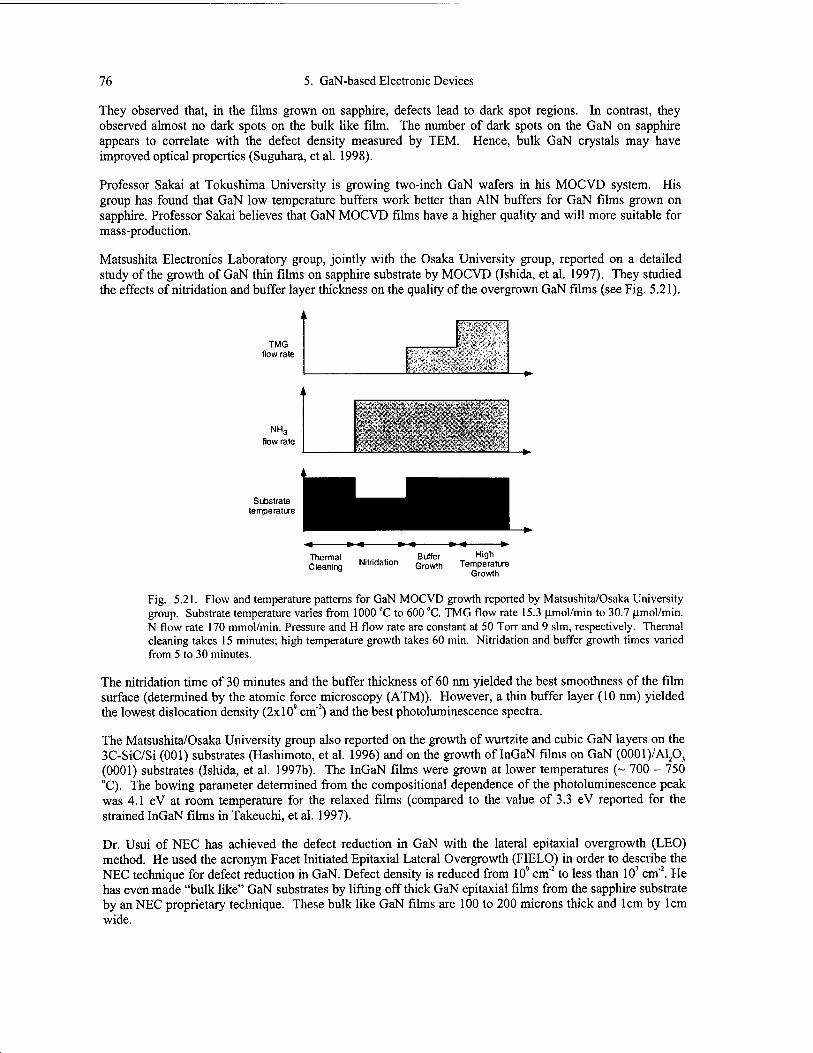
76 5. GaN-based Electronic Devices
They observed that, in the films grown on sapphire, defects lead to dark spot regions. In contrast, they observed almost no dark spots on the bulk like film. The number of dark spots on the GaN on sapphire appears to correlate with the defect density measured by TEM. Hence, bulk GaN crystals may have improved optical properties (Suguhara, et al. 1998).
Professor Sakai at Tokushima University is growing two-inch GaN wafers in his MOCVD system. His group has found that GaN low temperature buffers work better than A1N buffers for GaN films grown on sapphire. Professor Sakai believes that GaN MOCVD films have a higher quality and will more suitable for mass-production.
Matsushita Electronics Laboratory group, jointly with the Osaka University group, reported on a detailed study of the growth of GaN thin films on sapphire substrate by MOCVD (Ishida, et al. 1997). They studied the effects of nitridation and buffer layer thickness on the quality of the overgrown GaN films (see Fig. 5.21).
i i
TMG i"/~>y., *•
flow rate
i i
NH3
flow rate
Substrate temperature
Thermal Cleaning Nitridation
Buffer Growth
High Temperature
Growth
Fig. 5.21. Flow and temperature patterns for GaN MOCVD growth reported by Matsushita/Osaka University group. Substrate temperature varies from 1000 °C to 600 °C. TMG flow rate 15.3 umol/min to 30.7 Umol/min. N flow rate 170 mmol/min. Pressure and H flow rate are constant at 50 Torr and 9 slm, respectively. Thermal cleaning takes 15 minutes; high temperature growth takes 60 min. Nitridation and buffer growth times varied from 5 to 30 minutes.
The nitridation time of 30 minutes and the buffer thickness of 60 ran yielded the best smoothness of the film surface (determined by the atomic force microscopy (ATM)). However, a thin buffer layer (10 ran) yielded the lowest dislocation density (2x10' cm"2) and the best photoluminescence spectra.
The Matsushita/Osaka University group also reported on the growth of wurtzite and cubic GaN layers on the 3C-SiC/Si (001) substrates (Hashimoto, et al. 1996) and on the growth of InGaN films on GaN (0001)/Al2O, (0001) substrates (Ishida, et al. 1997b). The InGaN films were grown at lower temperatures (~ 700 - 750 °C). The bowing parameter determined from the compositional dependence of the photoluminescence peak was 4.1 eV at room temperature for the relaxed films (compared to the value of 3.3 eV reported for the strained InGaN films in Takeuchi, et al. 1997).
Dr. Usui of NEC has achieved the defect reduction in GaN with the lateral epitaxial overgrowth (LEO) method. He used the acronym Facet Initiated Epitaxial Lateral Overgrowth (FIELO) in order to describe the NEC technique for defect reduction in GaN. Defect density is reduced from 109 cm"2 to less than 107 cm"2. He has even made "bulk like" GaN substrates by lifting off thick GaN epitaxial films from the sapphire substrate by an NEC proprietary technique. These bulk like GaN films are 100 to 200 microns thick and 1cm by 1cm wide.
Shur 77
All in all, Japanese scientists and engineers see short-term applications of GaN technology in optical devices, mostly light emitters. However, in year 2000 and beyond, a larger market is expected to develop for high temperature, high power GaN electronics components.
GAN DEVICE RESEARCH IN EUROPE
Many universities, government and private research laboratories and electronics companies in France, Germany, Sweden, Italy, Great Britain, Spain, and other European companies are now involved in GaN- related research. Most of their efforts involve studies of fundamental properties of GaN-based compounds and materials growth. However, the device research is being ramped up.
French effort is representative of the overall European effort. CRNS in Lille is involved in device processing and electronic applications, CNRS and University in Caen are studying crystallography; CNRS group in Strasbourg is doing research on nonlinear optics applications of GaN. The university group in Clermond Ferran is involved with crystal growth and optical properties. The optical properties are also studied by the University of Lyon group, by CEA in Grenoble, and by CRNS in Valbolne. CEA in Grenoble and the University of Montpellier groups are working on MBE and MOCVD growth, respectively. CRNS in Valbolne is involved in growth and optical characterization studies. This effort is funded by several European and EEC projects such as ANISET (which is materials oriented research project), LAQUANI (which is both material and device oriented), RAINBOW (which is concentrated on multicolor LEDs and blue lasers), MIGHT (material and device oriented and targeted toward high power, high frequency electronics, with the goal of getting 3 W at 10 GHz). A typical budget for these projects is 3 to 4 million Euro per year.
In Poland, High Pressure Research Center and Unipress (which is the research group within HPRC working of GaN bulk crystal growth from a melt) developed the "defect free" semi-insulating (105 ohm-cm) and doped bulk GaN wafers grown from melt under very high pressure. The bulk crystals have extremely smooth cleaved facets with RMS roughness of 0.5 nm. Both Ga-face and N-face polarity bulk substrates have been demonstrated. The size of the substrates has reached 1cm in 1999 (Litwin-Staszewska, et al. 1999). MOCVD and MBE growth has also been performed on these bulk substrates. The group at University of Ulm in collaboration with Unipress demonstrated epitaxial films, which exhibited the narrowest reported photoluminescence line widths at low temperature (O.lmeV) (Kornitzer, et al. 1999). The UNIPRESS group is also working high power HEMTs, Schottky diodes, and UV detectors.
In Germany, Siemens has recently spun off Infineon Technologies, which will be responsible for semiconductor components. Infineon and Osram have a Joint Venture, which is developing GaN blue LEDs and solid-state white lighting using GaN based LEDs. In Munich, Siemens Munich Corporate research laboratory has a GaN MBE facility, which is geared towards high microwave power electronic devices. The future work in the Siemens MBE lab will be on AlGaN/GaN electronic devices and GaAsN for long wavelength lasers.
There is now a considerable and growing interest in GaN research in Russia. Fig. 5.22 shows the number of GaN-related papers at the All-Russian Conference on Nitrides of Gallium, Indium, and Aluminum: structures and devices.
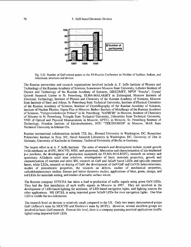
78 5. GaN-based Electronic Devices
1997 1998 1999
□ Number of particpants
Fig. 5.22. Number of GaN-related papers at the Ail-Russian Conference on Nitrides of Gallium, Indium, and Aluminum: structures and devices.
The Russian universities and research organizations involved include A. F. Ioffe Institute of Physics and Technology of the Russian Academy of Sciences, Lomonosov Moscow State University, Lebedev Institute of Physics and Technology of the Russian Academy of Sciences, GIREDMET, NPVF "Svecha", Crystal Growth Research Center in St. Petersburg, ELMA-MALAKHIT in Zelenograd, Moscow Institute of Electronic Technology, Institute of Physics and Chemistry of the Russian Academy of Sciences, Moscow State Institute of Steel and Alloys, St. Petersburg State Technical University, Institute of Physical Chemistry of the Russian Academy of Sciences, Institute of Crystallography of the Russian Academy of Sciences, Institute of Nuclear Physics, Sigma Plus in Moscow, Baikov Institute of Metallurgy of the Russian Academy of Sciences, "Polyprovodnikovye Pribory" in St. Petersburg, "SAPHFIR" in Moscow, Institute of Chemistry of Silicates in St. Petersburg, Vologda State Technical University, Udmurtsky State Technical University, VNII of Optical and Physical Measurements in Moscow, OPTEL in Moscow, St. Petersburg Institute of Technology, Frumkin Institute of Electrochemistry, NITI "TEKHNOMSH" in Moscow, MAR State Technical University in Iohskar-Ola.
Russian international collaborations include TDI, Inc., Howard University in Washington, DC, Rensselaer Polytechnic Institute in Troy, NY, Naval Research Laboratory in Washington, DC, University of Ulm in Germany, University of Karlsruhe in Germany, Technical University of Berlin in Germany.
The largest effort is at A. F. Ioffe Institute. The areas of research and development include crystal growth (with emphasis on HVPE, MOCVD, MBE, and sputtering), fabrication and characterization of ion-implanted p-n junctions, the development of production equipment (at ELMA-MALKHIT), research on ternary and quaternary AlGalnAs solid state solutions, investigations of basic materials properties, growth and characterization of wurtzite and cubic BN, research on GaN and InGaN based LEDs and optically pumped lasers, white LEDs, research on doping of GaN, the development of GaN/GaP and GaN/Si heterostructures, studies of piezoelectric properties, the research on defects, studies of mechanical properties, cathodoluminescence studies, Raman and lattice dynamics studies, applications of blue, green, orange, and red LEDs for materials testing, and studies of acoustic surface waves.
The Russian company SVECHA has taken a lead in production of traffic signals using green GaN LEDs. They had the first installation of such traffic signals in Moscow in 1997. They are involved in the development of LED-based lighting for airplanes, of LED-based navigation lights, and lighting sources for other applications. Nil OPTEL is using imported green InGaN LEDs for river navigation lights. One blue LED is visible for two kilometers.
The research level on devices is relatively small compared to the US. Only two teams demonstrated p-type GaN (Alferov's team by MOCVD and Dmitriev's team by HVPE). However, several excellent groups are involved in basic GaN research. Even at this level, there is a company pursuing practical applications (traffic lights) using imported GaN LEDs
Shur 79
REFERENCES
Ambacher, O., J. Smart, J. R. Shealy, N. G. Weimann, K. Chu, M. Murphy, W. J. Schaff, and L. F. Eastman, Two- dimensional Electron gases Induced by Spontaneous and Piezoelectric Polarization Charges in N- and Ga-face AlGaN/GaN Heterostructures, J. Appl. Phys., vol. 85, No. 6, pp. 3222-3233, 15 March (1999)
Asbeck, P. M., G. J. Sullivan, E. T. Yu, S. S. Lau, and B. McDermott, Device Research Conference Abstracts, paper V- B-5, Fort Collins, Colorado (1997)
Asbeck, P.M., E. T. Yu, S. S. Lau, G.J. Sullivan, J. Van Hove, J. Redwing, Piezoelectric charge densities in AlGaN/GaN HFETs, Electronics Letters 33(14), 1230 (1997)
Asif Khan, M., M. S. Shur, and R. Gaska, Strain Energy Band Engineering in AlGalnN/GaN Heterostructure Field Effect Transistors, GaAs-99 Proceedings, to be published
Bandic, Z. Z., E. C. Piquette, P. M. Bridger, T. F. Kuech, and T. C. McGill, Design and Fabrication of Nitride Based High Power Devices, in Proceedings of Materials Research Society Conference, December 1997, Boston, MA, to be published
Bhapkar, U.V., and M. S. Shur, Monte Carlo Calculation of Velocity-Field Characteristic of Wurtzite GaN, J. Appl. Phys., 82 (4), pp. 1649-1655, August 15 (1997)Joshi, R.P., and P. K. Raha, in Proc. 5th Conf. Silicon Carbide and Related Compounds, Bristol and Philadelphia: Institute of Physics Publishing, Conference Series Number 137, p. 687(1994)
Binari, S. C, Proc. Symp. Wide Band Gap Semiconductors and Devices, Vol. 95-21, pp. 136-143, Electrochemical Society, Pennington, NJ (1995)
Binari, S., L. B. Rowland, W. Kruppa, G. Keiner, K. Doverspike, and D. K. Gatskill, Electronics Letters, vol. 30, No 15, p. 1248 July (1994)
Binari, S., L. B. Rowland, W. Kruppa, G. Keiner, K. Doverspike, and D. K. Gatskill, presented at the 21-st International Symposium on Compound Semiconductors, San Diego, Sep. 1994 (1994b)
Birkman, R. H., and A. J. Steckl, GaN Molecular Beam Heteroepitaxy on Sapphire and 3C-SiC substrates, Abstract D5.33, p. 109, Material Research Society Meeting, Boston, December (1997)
Burm, J., W. J. Schaff, L. F. Eastman , H. Amano, I. Akasaki, 75 A GaN channel modulation doped field effect transistors Applied Physics Letters 68(20), 2849 (1996).
Bykhovski, A. D., B. Gelmont, and M. S. Shur, Strain and Charge Distribution in GaN-AlN-GaN SIS Structure for Arbitrary Growth Orientation, Appl. Phys. Lett., vol. 63, p. 2243 (1993)
Bykhovski, A., B. Gelmont, and M. S. Shur, The Influence of the Strain-Induced Electric Field on the Charge Distribution in GaN-AlN-GaN SIS Structure, J. Appl. Phys. Dec., vol. 74 (11), p. 6734 (1993)
Bykhovski, A., B. Gelmont, and M. S. Shur, Elastic Strain Relaxation in GaN-AlN-GaN Semiconductor-Insulator- Semiconductor Structures, J. Appl. Phys. 78 (6), pp. 3691-3696, 15 September (1995)
Bykhovski, A. D., B. L. Gelmont, and M. S. Shur, Elastic Strain Relaxation in GaN-AIN, GaN-AlGaN, and GaN-InGaN Superlattices, J. Appl. Phys., Vol. 81, No. 9, pp. 6332, May (1997)
Bykhovski, A., B. Gelmont, M. S. Shur, and A. Khan, Current-Voltage Characteristics of Strained Piezoelectric Structures, J. Appl. Phys., vol. 76, Feb. 15, p. 1616-1620 (1995)
Bykhovski, A. D., V. V. Kaminski, M. S. Shur, Q. C. Chen, and M. A. Khan, Piezoresistive Effect in Wurtzite n-type GaN, Appl. Phys. Lett., 68 (6), pp. 818-819 (1996)
Bykhovski, A. D., V. V. Kaminski, M. S. Shur, Q. C. Chen, M. A. Khan, Pyroelectricity in Gallium Nitride Thin Films, Applied Physics Letters, November 18,69(21), p. 3254 (1996)
Bykhovski, A. D., M. S. Shur, R. Gaska, M. A. Khan, J. W. Yang, AlGaN-GaN-AlGaN Induced Base Transistor, MRS 99 Fall Meeting, Nov. 30- Dec. 4, Boston, MA
Cheng, T.S., C. T. Foxon, N. J. Jeffs, D. J. Dewsnip, L. Flannery, J. W. Orton, S. V. Novikov, B. Ya. Ber, Yu A. Kudriavtsev, Studies of Mg-GaN grown by MBE on GaAs (111) B substrates, MRS Internet J. Nitride Semicond. Res. 2, 13(1997).
Dyakonova, N., A. Dickens, M. S. Shur, R. Gaska, J. W. Yang, Temperature dependence of impact ionization in AlGaN- GaN Heterostructure Field Effect Transistors, submitted for publication
Fan, Z. F., S. N. Mohammad, W. Kim, A. E. Botchkarev, and H. Morkoc, Appl. Phys. Lett., 68, 1672 (1996)
Foresi, J. S., and T. D. Moustakos, Appl. Phys. Lett., 62, 2859 (1993)
80 5. GaN-based Electronic Devices
Foutz, B.E., L. F. Eastman, U. V. Bhapkar, M. S. Shur, Appl. Phys. Lett., 70, No 21, pp. 2849-2851 (1997)
Foutz, B.E., L. F. Eastman, S. K. OLeary, M. S. Shur, and U. V. Bhapkar, Velocity overshoot and ballistic transport in indium nitride, Mat. Res. Soc. Proc. Vol. 482, pp. 821-825 (1998)
Foutz, B.E., S. K. OLeary, M. S. Shur, and L. F. Eastman, A Semi-analytical Interpretation of Transient Electron Transport in Gallium Nitride, Indium Nitride, and Aluminum Nitride, Mat. Res. Soc. Symp. Proc. Vol. 512, S. DenBaars, J. Palmour, M. Shur, and M. Spencer, Editors, pp. 555-560 (1998)
Gaska, R., Q. Chen, J. Yang, A. Osinsky, M. A. Khan, and M. S. Shur, AlGaN/GaN Heterostructure FETs with Offset Gate Design, Electronics Letters, 33, No. 14, pp. 1255-1257, 3 July (1997)
Gaska, R., M. S. Shur, J. Yang, and T. A. Fjeldly, Double Channel AlGaN/GaN Heterostructure Field Effect Transistors, MRS, Symposium D, Spring, accepted (1998)
Gaska, R., J. Yang, A. D. Bykhovski, M. S. Shur, V. V. Kaminski, and S. M. Soloviov, Piezoresistive Effect in GaN- AlN-GaN Structures, Appl. Phys. Lett., vol. 71 (26), pp. 3817-3819 29 Dec. (1997)
Gaska, R., J. Yang, A. D. Bykhovski, M. S. Shur, V. V. Kaminski, and S. M. Soloviov, The Influence of the Deformation on the Two-Dimensional Electron Gas Density in GaN-AlGaN Heterostructures, Appl. Phys. Lett., vol. 72 (1), pp. 64-66, Jan. 5.(1998)
Gaska, R., J. Yang, A. Osinsky, A. D. Bykhovski, and M. S. Shur, Piezoeffect and Gate Current in AlGaN/GaN High Electron Mobility Transistors, Appl. Phys. Lett., Applied Physics Letters 71(25), p. 3673, December 22 (1997)
Gaska, R., J. W. Yang, A. Osinsky, Q. Chen and M. A. Khan, A. O. Orlov, G L. Snider, and M. S. Shur, Electron Transport in AlGaN-GaN Heterostructures Grown on 6H-SiC Substrates, Appl. Phys. Lett., No. 6, Feb. 1998
Han, J., A. G. Baca, RJ Shul, C. G. Willison, L Zhang, F. Ren, A. P. Zhang, G. T. Dang, S. M. Donovan, X. A. Cao, H Cho, K. B. Jung, C.R. Abernathy, S. I. Pearton, R. G. Wilson, Applied Physics Letters 74(18), 2702-2704 (1999).
Hashimoto, T., O. Imafuji, M. Ishida, Y. Terakoshi, T. Sugino, A. Yoshikawa, K. Itoh, and J. Shirafuji, J. Cryst. Growth, 169, pp. 185-189(1996)
Holloway, P. H., T. J. Kim, J. T. Tresler, S. Milla, J. J. Fijol, W. V. Lampert, and T. W. Haas, Appl. Surface Science, 117/118,362(1997)
Ishida, M., T. Hashimoto, Y. Terakoshi, O. Imafuji, M. Yuri, A. Yoshikawa, K. Itoh,, and T. Sugino, Technical Report of IEC1CE, ED97-127, CPM97-114, pp. 57-62 (1997b), in Japanese
Ishida, M., T. Hashimoto, T. Takayma, O. Imafuji, M. Yuri, A. Yoshikawa, K. Itoh, Y. Terakoshi, T. Sugino, and J. Shirafuji, Mat. Res. Soc. Symp. Proc. Vol. 468, pp. 69-74 (1997)
Kamp, M., GaN workshop continues the substrate search, III-Vs Review, Vol. 11, No 6, pp. 42-44 (1998)
Khan, M. A., Q. Chen, M. S. Shur, B. T. Dermott and J. A. Higgins, Microwave Operation of GaN/AlGaN Doped Channel Heterostructure Field Effect Transistors, IEEE Electron Device Letters, vol. 17, No. 7, pp. 325-327, July (1996)
Khan, M. A., Q. Chen, M. S. Shur, B. T. Dermott, J. A. Higgins, J. Burm, W. J. Schaff, and L. F. Eastman, CW Operation of Short Channel GaN/AlGaN Doped Channel Heterostructure Field Effect Transistors at 10 GHz and 15 GHz, IEEE Electron Device Lett., vol. 17, No. 12, December (1996)
Khan, M.A., Q. Chen, C. J. Sun, M. S. Shur, and B. Gelmont, Appl. Phys. Lett., 67, 1429 (1995).
Khan, M.A., J. N. Kuznia, J. M. Van Hove, N. Pan, and J. Carter, Appl. Phys. Lett., 60, 3027 (1992)
Khan, M.A., M. S. Shur, and Q. Chen, Hall Measurements and Contact Resistance in Doped GaN/AlGaN Heterostructures, Appl. Phys. Lett., 68 (21), pp. 3022-3024, 20 May (1996)
Khan, M. A., M. S. Shur, R. Gaska, presented at the 1-st Cornell GaN Symposium, Ithaca, NY August (1999)
Khan, M. A., M. S. Shur, J. N. Kuznia, J. Burm, W. Schaff, Temperature Activated Conductance in GaN/AlGaN Heterostructure Field Effect Transistors Operating at Temperatures up to 300 oC, Applied Physics Letters, 66,(9), pp. 1083-1085, 27 Feb. (1995)
Khan, M.A., J. M. Van Hove, J. N. Kuznia, and D. T. Olson, Appl. Phys. Lett., 58, 2408 (1991)
Kolnik, J., I.H. Oguzman, K.F. Brennan, R. Wang and P.P. Ruden, Monte-Carlo calculation of electron initiated impact ionization in bulk zinc-blende and wurtzite GaN, J. Appl. Phys. 81 (2), pp.726-733 (1997)
Kornitzer, K., T. Ebner, M. Grehl, K. Thonke, R. Sauer, C. Kirchner, V. Schwelger, M. Kamp, M. Leszczynski, I. Grzergory, S. Porowski, "High Resolution PL and Reflectance Spectra of Homoepitaxial GaN Layers" Paper Tu-17, Proceedings of Intl. Conf. on Nitride Semiconductors, Montpelliar, France (1999), pg 49
Shur 81
Koyama, Y., T. Hashizume, and H. Hasegawa, Optimization of Schottky Gate Fonnation Process for n-channel GaN MESFETs, presented at Topical Workshop on Heterostructure Microelectronics for Information Systems Applications (TWHM-ISA '98), see also, Final Program and Abstracts, Topical Workshop on Heterostructure Microelectronics for Information Systems Applications (TWHM-ISA '98), p. 56 (1998)
Kozodoy, P., J.P. Ibbetson, H. Marchand, P.T. Fini, S. Keller, S.P. DenBaars, J.S. Speck, U.K. Mishra, Appl. Phys. Lett 73 975(1998).
Lee, K, M. S. Shur, T. A. Fjeldly, and T. Ytterdal, Semiconductor Device Modeling for VLSI, Prentice Hall, Enelewood Cliffs, NJ (1993)
Levinshtein, M.E., S. L. Rumyantsev, and M. S. Shur, Editors, "Properties of Advanced Semiconductor Materials: GaN, A1N, InN, BN, and SiGe", John Wiley and Sons, to be published
Lin, M E., Z. Ma, F. Y. Huang, Z. F. Fan, L. H. Allen, and H. Morkoc, Appl. Phys. Lett., 64, 1003 (1994)
Littlejohn, M.A., J. R. Häuser and T. H. Glisson, Appl. Phys. Lett., 26, 625 (1976)
Litwin-Staszewska, E., T. Suski, I. Grzegory, S. Porowski, J. Robert, D. Wasik, A. Witowski, D. Cote, and B. Clerjund, "Electrical Properties of GaN Bulk Single Crsytals Doped with Mg" Paper We-P082, Proceedings of Intl. Conf. on Nitride Semiconductors, Montpellier, France (1999), pg 124.
Lunev, A., V. Chaturvedi, A. Chitnis, G. Simin, J. Yang, M. A. Khan, R. Gaska, M. S. Shur, Low-Resistivity Pd/Au Ohmic Contacts to p-GaN for Heterostructure Bipolar Transistors and Light Emitting Diodes, presented at ICSRM- 99, October 10-15, 1999
MacCarthy, L., P. Kozodoy, M. Rodwell, S. DenBaars, The First Look at AlGaN/GaN HBTs, Compound semiconductor, vol. 4, No. 8, p. 16(1998)
Marchand, H., J.P. Ibbetson, P.T. Fini, P. Kozodoy, S. Keller, J.S. Speck, S.P. DenBaars, and U.K. Mishra, MRS Internet J. Nitride Semicond. Res. 3, 3 (1998).
Marchand, H, X.H. Wu, J.P. Ibbetson, P.T. Fini, P. Kozodoy, S. Keller, J.S. Speck, S.P. DenBaars, and U.K. Mishra, Appl. Phys. Lett. 73, 747 (1998b).
Molnar, R. J., Hydride Vapor Phase Epitaxy of Gallium Nitride, Abstract D16.1, in Abstracts of Materials Research Society Conference, December 1997, Boston, MA
Nakamura, S., and G. Fasol, The blue Laser Diode, Springer, Berlin, p. 79
Nakamura, S., and G. Fasol, The Blue Laser Diode - GaN based Light Emitters and Lasers, Springer-Verlag, Heidelberg 1997
Nam, O.-H., M.D. Bremser, T.S. Zheleva, and R.F. Davis, Appl. Phys. Lett. 71, 2638 (1997).
Oguzman, I. H, E. Bellotti, K. F. Brennan, J. Kolnik, R. Wang and P. P. Ruden, Monte-Carlo calculation of hole initiated impact ionization in bulk zinc-blende and wurtzite GaN, J. Appl. Phys. 81(12), pp. 7827-7824 (1997)
O'Leary, S.K., B. E. Foutz, M. S. Shur, U. V. Bhapkar, and L. F. Eastman, Electron Transport in Wurtzite Indium Nitride, J. Appl. Phys. 83 (2), pp. 826-829,15 Jan. (1998)
O'Leary, S.K., B. E. Foutz, M. S. Shur, U. V. Bhapkar, and L. F. Eastman, Monte Carlo Simulation of Electron Transport in Wurtzite Aluminum Nitride, Solid State Comm, accepted for publication
O'Leary, S.K., M. S. Shur, B. E. Foutz, L. F. Eastman, and U. V. Bhapkar, Velocity field characteristics of indium nitride, in Symposium Proceedings of Material Research Society, (1998)
Pankove, J.I., M. Leksono, S. S. Chang, C. Walker, and B. Van Zeghbroeck, High-Power High-Temperature Heterobipolar Transistor With Gallium Nitride Emitter, MRS Internet J. Nitride Semicond. Res. Vol. 1, 39 (1996).
Qiao, D., Z. F. Guan, J Carlton, S. S. Lau, G. J. Sullivan, Low resistance ohmic contacts on AlGaN/GaN structures using implantation and the "advancing" Al/Ti metallization Applied Physics Letters 74(18), 2652-2654 (1999).
Ren, F., C. R. Abernathy, J. M. Van Hove, P. P. Chow, R. Hickman, J. Klaasen, R.F. Kopf, H. Cho, K. B. Jung, J. R. LaRoche, R. G. Wilson, J. Han, R. J. Shul, A. G. Baca and S. J. Pearton, 300C GaN/AlGaN HBT", MRS Internet J. Nitride Semicond. Res. 3 41 (1998);
Ren, F., J. R. Lothian, Y. K. Chen, R. F. Karlichek, Jr., L. Tran, M. Schumann, R. A. Stall, J. W. Lee, and S. J. Pearton, Recessed Gate GaN Field Effect Transistors, Solid-State Electronics, Vol. 41, No. 11, pp. 1819-1820 (1997)
Rin, I., III-V Review, 8, 4 (1995) 20
Ruden, P. P., M. S. Shur, A. I. Akinwande, J. Nohava, D. Grider, and J. H. Baek, AlGaAs-InGaAs-GaAs Quantum Well Doped Channel Heterostructure Field Effect Transistors. IEEE Trans. Electron Devices, vol. 37, No. 10, pp. 2171- 2175, October (1990)
82 5. GaN-based Electronic Devices
Ruvimov, S., Z. Liliental-Weber, J. Washburn, K. J. Duxstad, E. E. Haller, Z. F. Fan, S. N. Mohammad, W. Kim, A. E. Botchkarev, and H. Morkoc, Appl. Phys. Lett., 69, 1556 (1996)
Sakai, A., H. Sunakawa, and A. Usui, Appl. Phys. Lett. 71,2259 (1997).
Sakai, A., U. Sunakawa, and A. Usui, Appl. Phys. Lett. 73,481 (1998)
Sakai, A., H. Sunakawa, and A. Usui, Appl. Phys. Lett. 71, 2259 (1998b).
Sheppard, S. T., et al. Device Research Conference, Charlottesville, VA (1998)
Sheppard, S. T., et al., IEEE Electron Device Lett. 20 (4), 161 (1999)
Shur, M.S., GaN and related materials for high power applications, in Symposium Proceedings of Material Research Society, Symposium E, Spring (1998), to be published
Shur, M. S., GaAs Devices and Circuits, Plenum Publishing Corporation, New York (1987)
Shur, M. S. and M. Asif Khan, GaN/AlGaN Heterosrructure Devices: Photodetectors and Field Effect Transistors, MRS Bulletin, vol. 22, No. 2, pp. 44-50, Feb. (1997)
Shur, M. S. and M. Asif Khan, GaN and AlGaN Ultraviolet Photodetectors, Academic Press, Semiconductors and Semimetals, T. Moustakos and J. Pankove, Editors (1998), to be published
Shur, M.S., A. D. Bykhovski, R. Gaska, Accumulation Hole Layer in Inverted p-GaN/A10.15Ga 0.85N Heterostructures, presented at the 1-st GaN Device Symposium, Cornell, Ithaca, NY (1999)
Shur, M.S., A. D. Bykhovski, R. Gaska, Pyroelectric and Piezoelectric Properties of GaN-Based Materials, MRS Internet J. Nitride Semicond. Res. 4SI, G1.6 (1999)
Shur, M.S., A. D. Bykhovski, R. Gaska, Two Dimensional Hole Gas Induced by Piezoelectric and Pyroelectric Charges, to be published in the special issue of Solid-State Electronics, accepted 19 July, 1999.
Shur, M. S., Q. Chen, J. Yang, R. Gaska, M. Blasingame, M. A. Khan, A. Ping, I. Idesida, V. P. Madangarli, and T. S. Sudarshan, High Pinch-off Voltage AlGaN-GaN Heterostructure Field Effect Transistor, Proceedings of ISDRS-97, pp. 377-380, Charlottesville, VA, Dec. (1997)
Shur, M.S., and R. Gaska, GaN-based two dimensional electron devices, 6-th International Symposium", Nanostructures: Physics and Technology," Ioffe Institute, St. Petersburg, ISBN 5-86763-120-6, pp.524-530 (1998)
Shur, M.S., B. Gelmont, and M. Asif Khan, High Electron Mobility in Two-Dimensional Electrons Gas in AlGaN/GaN Heterostructures and in Bulk GaN, J. Electronic Materials, Vol. 25, No. 5, pp. 777-785 May (1996)
Shur, M. and A. Khan, GaN Based Field Effect Transistors, in "High Temperature Electronics", ed. M. Willander and H. L. Hartnagel, Chapman and Hall, pp. 297-321, London (1996)
Shur, M. S. and M. A. Khan, Wide Band Gap Semiconductors. Good Results and Great Expectations., in the Proceedings of 23d International Symposium on GaAs and Related Compounds, St. Petersburg, Russia, Sep. 22-28, 1996, Institute Phys. Conference Series, No. 155, Chapter 2, pp. 25-32, M. S. Shur and R. Suris, Editors, IOP Publishing, London(1997)
Sriram, S., T. J. Smith, L. B. Rowland, A. A. Burk, Jr., G. Augustine, V. Balakrishna, H. M. Hobgood, and C. D. Brandt, in Conf. Dig. 55-th Device Research Conference, 1997, pp. 138-139
Suguhara, T., H. Sato, M. Hao, Y. Naoi, Y. Kurai, S. Tottori, S. Yamashita, K. Nishino, S. Sakai, Jap. J. Appl. Phys. v.37,No. 4a. L398,(1998).
Takeuchi, T., H. Takeuchi, S. Sota, H. Sakai, H. Amano, and I. Akasaki, Jpn. J. Appl. Phys., vol. 36, p. L177 (1997)
Tanaka, S., P. Ramvall, and Y. Aoyagi, InGaN Quantum Dots Fabricated on AlGaN Surfaces - Growth Mechanisms and Optical Properties, Abstract D15.48, in Abstracts of Materials Research Society Conference, December 1997, Boston, MA
Usui, A., H. Sunakawa, N. Kurado, A. Kimura, A. Sakai, and A.A. Yamaguchi, 2nd Int. Conf. on Blue Laser and Light Emitting Diodes, Chiba, Japan, Sept. 29 - Oct. 2, 1998.
Vetury, R, H. Marchand, J.P. Ibbetson, P.T. Fini, S. Keller, J.S. Speck, S.P. Denbaars, and U.K. Mishra, 25th Int. Symp. on Compound Semicond., Nara, Japan, Oct 12-16, 1998.
Wolter, S. D., B. P. Luther, S. E. Mohney, R. F. Karlicek, Jr., and R. S. Kern, Electrochemical and Solid State letters, 2 (3), pp. 151-153(1999)
Wu, Y., et al. Presented at 1st Gallium Nitride Electronic Device Workshop, August 1999, Cornell University, Ithaca, NY

Shur 83
Wu, Y.-F., B. P. Keller, P. Fini, S. Keller, T. J. Jenkins, L. T. Kehias, S. P. Denbaars, and U. K. Mishra, High Al-content AlGaN/GaN MODFET for Ultrahigh Performance, IEEE Electron Device Lett., Vol. 19, No. 2, pp. 50-53 Feb. (1998)
Xu, J. and M. S. Shur, IEEE Trans. Electron Devices, vol. ED-34, No. 8, pp. 1831-1832, Aug. (1987)
Yu. V. Melnik et al., Physical Properties of Bulk GaN Crystals Grown by HVPE, MRS Internet J. Nitride Semicond. Res., 2, 39 (1997)
Zheleva, T.S., O.-H. Nam, M.D. Bremser, and R.F. Davis, Appl. Phys. Lett. 71, 2472 (1997).

84 5. GaN-based Electronic Devices
85
CHAPTER 6
HIGH-TEMPERATURE ELECTRONICS PACKAGING IN EUROPE
George White
INTRODUCTION
To understand the meaning of high temperature electronic packaging one would have to have a clear understanding of high temperature electronics in general. High temperature electronics may be defined as those devices and/or subsystems that operate at elevated temperatures above 200°C. Similarly high temperature electronic packaging may be defined as establishing interconnections and a suitable operating environment for these electronic devices (e.g., SiC, GaN or Si) at temperatures above 200°C. These definitions can be argued as too vague or inadequate since many researchers have varying opinions on what constitutes high temperature (i.e., electronics operating above 300 °C, above 400 °C, etc.). However, most researchers would agree that there needs to be significant consideration given to addressing both the components and packaging needs for high temperature applications to achieve similar levels of integration and functionality to what is currently being practiced at ambient and near ambient conditions for today's silicon and III-V compound IC's.
Most high temperature applications will find their niche in harsh environments, such as under the hood for exhaust gas sensors and in exposed areas of an aircraft. Applications such as these may be impractical for conventional silicon, unless one introduces highly complex and expensive packaging techniques involving liquid cooling, etc. Although these are very important issues to address, many in the silicon IC world are very reluctant to make the necessary investments to produce the high quality devices necessary to meet these challenges. As a result, the electronic packaging community, which is under tremendous pressure to find low cost solutions to package IC's, will also be slow to address the packaging needs for high temperature applications. In addition to business pressures and challenges, there are also significant technical challenges to package wide band gap materials for high temperature applications.
To package wide band gap materials for high temperature applications a number of alternative materials, including substrates and solders, and fabrication techniques have to be considered over conventional packaging practices. Today most devices are packaged using glass epoxy boards and organic encapsulants. At the temperatures of interest in this study, these components would melt or significantly degrade thermally, thus proving impractical for use. Eutectic solders as well as conventional die attach materials will also need to be addressed. Passive device selection and reliability testing are also critical issues as well.
The following chapter will address some of these issues as they were discussed during the TTEC sponsored study on "High Temperature Electronics in Europe". I should caution however, the amount of interaction was very limited for this subject matter, as many of the researchers whom the team visited were not directly involved in electronic packaging and had little knowledge regarding plans and future directions for the packaging of their devices. However, some were knowledgeable, including experts at Siemens and IMC. It is therefore our intention to present in this chapter their views as well as some of the views of the author on
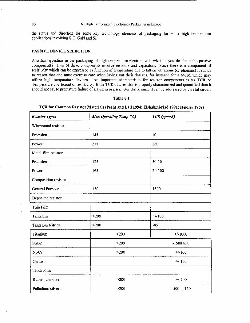
86 6. High Temperature Electronics Packaging in Europe
the status and direction for some key technology elements of packaging for some high temperature applications involving SiC, GaN and Si.
PASSIVE DEVICE SELECTION
A critical question in the packaging of high temperature electronics is what do you do about the passive components? Two of these components involve resistors and capacitors. Since there is a component of resistivity which can be expressed as function of temperature due to lattice vibrations (or phonons) it stands to reason that one must exercise care when laying out their designs, for instance for a MCM which may utilize high temperature devices. An important characteristic for resistor components is its TCR or Temperature coefficient of resistivity. If the TCR of a resistor is properly characterized and quantified then it should not cause premature failure of a system or parameter drifts, since it can be addressed by careful circuit
Table 6.1
TCR for Common Resistor Materials (Pecht and Lall 1994; Elshabini-riad 1991; Heidler 1969)
Resistor Types Max Operating Temp (°C) TCR (ppm/K)
Wirewound resistor
Precision 145 10
Power 275 260
Metal-film resistor
Precision 125 50-10
Power 165 20-100
Composition resistor
General Purpose 130 1500
Deposited resistor
Thin Film
Tantalum >200 +/-100
Tantalum Nitride >200 -85
Titanium >200 +/-1000
Sn02 >200 -1500 to 0
Ni-Cr >200 +/-100
Cermet +/-150
Thick Film
Ruthenium silver >200 +/-200
Palladium silver >200 -500 to 150
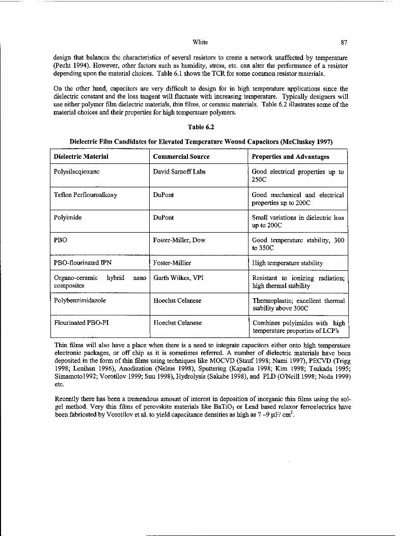
White 87
design that balances the characteristics of several resistors to create a network unaffected by temperature (Pecht 1994). However, other factors such as humidity, stress, etc. can alter the performance of a resistor depending upon the material choices. Table 6.1 shows the TCR for some common resistor materials.
On the other hand, capacitors are very difficult to design for in high temperature applications since the dielectric constant and the loss tangent will fluctuate with increasing temperature. Typically designers will use either polymer film dielectric materials, thin films, or ceramic materials. Table 6.2 illustrates some of the material choices and their properties for high temperature polymers.
Table 6.2
Dielectric Film Candidates for Elevated Temperature Wound Capacitors (McCluskey 1997)
Dielectric Material Commercial Source Properties and Advantages
Polysilseqioxane David Sarnoff Labs Good electrical properties up to 250C
Teflon Perflouroalkoxy DuPont Good mechanical and electrical properties up to 200C
Polyimide DuPont Small variations in dielectric loss up to 200C
PBO Foster-Miller, Dow Good temperature stability, 300 to 350C
PBO-flourinated IPN Foster-Millier High temperature stability
Organo-ceramic hybrid nano composites
Garth Wilkes.VPI Resistant to ionizing radiation; high thermal stability
Polybenzimidazole Hoechst Celanese Thermoplastic; excellent thermal stability above 300C
Flourinated PBO-PI Hoechst Celanese Combines polyimides with high temperature properties of LCP's
Thin films will also have a place when there is a need to integrate capacitors either onto high temperature electronic packages, or off chip as it is sometimes referred. A number of dielectric materials have been deposited in the form of thin films using techniques like MOCVD (Stauf 1998; Nami 1997), PECVD (Trigg 1998; Lenihan 1996), Anodization (Nelms 1998), Sputtering (Kapadia 1998; Kim 1998; Tsukada 1995; Simamotol992; Vorotilov 1999; Suu 1998), Hydrolysis (Sakabe 1998), and PLD (O'Neill 1998; Noda 1999) etc.
Recently there has been a tremendous amount of interest in deposition of inorganic thin films using the sol- gel method. Very thin films of perovskite materials like BaTi03 or Lead based relaxor ferroelectrics have been fabricated by Vorotilov et al. to yield capacitance densities as high as 7 -9 |iF/ cm2.
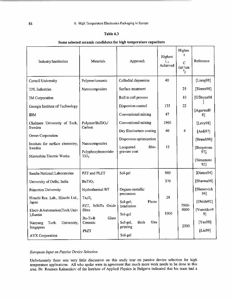
88 6. High Temperature Electronics Packaging in Europe
Table 6.3
Some selected ceramic candidates for high temperature capacitors
Highes
Highest t
Industry/Institution Materials Approach □r Achieved
C (nF/cm
2)
Reference
Cornell University Polymer/ceramic Collodial dispersion 40 [Liang98]
TPL Industries Nanocomposites Surface treatment 25 [Slenes98]
3M Corporation Roll to roll process 10 [OBryan98 1
Georgia Institute of Technology Dispersion control 135 22 J
[Agarwal9 IBM Conventional mixing 47 8]
Chalmers University of Tech, Polymer/BaTiCty Conventional mixing 1960 [Levy98] Sweden Carbon
Dry film/curtain coating 40 4 [Ardi97] Ormet Corporation
Dispersion optimization [Brandt98] Institute for surface chemistry, Nanocomposites Sweden Lacquered film- 12 [Bergstrom
Polyphenyleneoxide- gravure coat 97] Matsushita Electric Works Ti02
[Simamoto 92]
Sandia National Laboratories PZT and PLZT Sol-gel 900 [Dimos94]
University of Delhi, India BaTi03 370 [Sharma98]
Princeton University Hydrothermal BT Organo-metallic precursors
[Slamovich 96]
Hitachi Res. Lab., Hitachi Ltd., TaxOy 28 Japan Sol-gel; Photo [Ohishi92]
PZT, SrBiTa Oxide Irradiation 7000- Electr.&Automation(Tech.Univ films 9000 [Vorotilov9 ),Russia
Ba-Ti-B Glass Sol-gel 1000 9]
Nanyang Tech. University, Ceramic Sol-gel, thick film [Yao98] Singapore
PbZT printing 2500
[Liu99] AVX Corporation Sol-gel
European Input on Passive Device Selection
Unfortunately there was very little discussion on this study tour on passive device selection for high temperature applications. All who spoke were in agreement that much more work needs to be done in this area. Dr. Roumen Kakanakov of the Institute of Applied Physics in Bulgaria indicated that his team had a
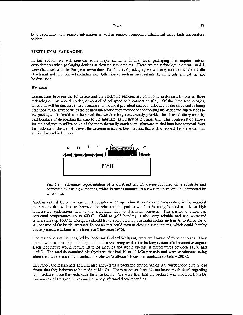
White 89
little experience with passive integration as well as passive component attachment using high temperature solders.
FIRST LEVEL PACKAGING
In this section we will consider some major elements of first level packaging that require serious consideration when packaging devices at elevated temperatures. These are the technology elements, which were discussed with the European researchers. For first level packaging we will only consider wirebond, die attach materials and contact metallization. Other issues such as encapsulants, hermetic lids, and C4 will not be discussed.
Wirebond
Connections between the IC device and the electronic package are commonly performed by one of three technologies: wirebond, solder, or controlled collapsed chip connection (C4). Of the three technologies, wirebond will be discussed here because it is the most prevalent and cost effective of the three and is being practiced by the Europeans as the desired interconnection method for connecting the wideband gap devices to the package. It should also be noted that wirebonding concurrently provides for thermal dissipation by backbonding or diebonding the chip to the substrate, as illustrated in Figure 6.1. This configuration allows for the designer to utilize some of the more thermally conductive substrates to facilitate heat removal from the backside of the die. However, the designer must also keep in mind that with wirebond, he or she will pay a price for lead inductance.
R R ' r. A
fäm&fi/msSyQm&fißm&l ■■■■■■HI IHfflHt\
Fig. 6.1. Schematic representation of a wideband gap IC device mounted on a substrate and connected to it using wirebonds, which in turn is mounted to a PWB motherboard and connected by wirebonds.
Another critical factor that one must consider when operating at an elevated temperature is the material interactions that will occur between the wire and the pad to which it is being bonded to. Most high temperature applications tend to use aluminum wire to aluminum contacts. This particular union can withstand temperatures up to 600°C. Gold to gold bonding is also very reliable and can withstand temperatures up 1000°C. Designers should try to avoid bonding dissimilar metals such as Al to Au or Cu to Al, because of the brittle intermetallic phases that could form at elevated temperatures, which could thereby cause premature failures at the interface (Newsome 1976).
The researchers at Siemens, led by Professor Eckhard Wolfgang, were well aware of these concerns. They shared with us a six-chip multichip module that was being used in the braking system of a locomotive engine. Each locomotive would require 18 to 24 modules and would operate at temperatures between 110°C and 125°C. The module contained six thyristors that had 30 to 40 I/Os per chip and were wirebonded using aluminum wire to aluminum contacts. Professor Wolfgang's focus is in applications below 200°C.
In France, the researchers at LETI also showed us a packaged device, which was wirebonded onto a lead frame that they believed to be made of Mo-Cu. The researchers there did not know much detail regarding this package, since they outsource their packaging. We were later told the package was procured from Dr. Kakanakov of Bulgaria. It was unclear who performed the wirebonding.
90
Die Attach
6. High Temperature Electronics Packaging in Europe
Another critical element in the packaging of high temperature electronic devices is the die attach material. The die attach material is used to ensure that the device remains in place throughout the entire lifetime of the system. The die attach material should also have good thermal conductivity, as well as good contact resistance. There are a number of die attach materials, which have inherent advantages and disadvantages depending on the temperature of operation of the device. Table 6.4 displays temperature guidelines for a select number of die attach materials.
Table 6.4
Temperature guideline for Some Die Attach Materials (Manko 1992; Pecht 1994; Feinstein 1989; Khatchatourian 1995; Olson 1995)
Die attach material Maximum use temperature Reason
Au80Sn20 280°C Eutectic melting point
Au88Gel2 356°C Eutectic melting point
Au97Si3 363°C Eutectic melting point
Sn96Ag4 221°C Solidus
Sn95Sb5 235°C Solidus
Sn92Sb8 236°C Solidus
Sn65Ag25Inl0 236°C Liquidus
Polyimide 300°C Glass transition temperature
Silver filled glass 450°C Softening point
In Europe, significant input on die attach materials was provided by Dr. Kakanakov. The following is a summary of our discussion relative to die attach materials and his rationale for material selection. After completion of this project in 1997, Kakanakov continued to make a small series of packages for power SiC MESFETS from Thomson CSF. In early 1999 work began on the NATO project "High Power and High Frequency Devices on LPE-grown SiC films", where Kakanakov's group was responsible for R&D of packages and packaging of power SiC diodes (Kakanakov 1999). Two gold-based alloy materials were used as attach materials. The attach materials were gold based alloys of Au and (6%) Si, (12%) Ge. The 6% alloy has a melting point of 373°C, and the 12% alloy melts at 363°C. Kakanakov mentioned (but did not go into great detail) that his group also investigated AuSn (20%) alloy and an Auln (25%) alloy which had a melting point of 450°C. The Auln system exhibited a favorable melting point but there was significant concern regarding the oxidation of In at the high temperatures.
Contact Metallization
The contact metallization is very critical as it serves a number of purposes such as providing a wetting layer for the die attach material, as well as ensuring optimal adhesion between the device and the die attach material. The contact metallization should be resistant to oxidation and be thermally stable at elevated temperatures. Typically this metallization is accomplished in a multilayering arrangement. The first metal layer is usually an adhesive layer, typically Cr or Ti. The second layer in this metal stack is usually referred to as the barrier layer metal. It serves to protect the adhesive layer. Typical barrier metals may be Ni, Ni alloys, Co, Co alloys, Pt and phased CrCu alloys. The third layer is typically called the wetting layer. This layer allows for wetting of the die attach alloys to ensure a reliable contact. Work by Kakanakov showed that the contact metallization of TiPtAu was suitable for SiC MESFET devices up to joining temperatures of
White 91
400°C. The advantages here were that there was no change in thermal resistance during high temperature testing. However, Pt and Ti will dissolve in both of the solders when it is liquified, thereby indicating that more suitable barrier metallurgies will have to be identified at the temperature extremes. Kakanakov et al indicated that the solders used in this study were only in liquid state during chip attachment and not during actual device operation. To limit the solubility of their barrier metallization of platinum and increase adhesion, a new process was developed in their laboratories. The new process involved vibrating the device during attach. This resulted in a reduction of the bonding time and reduced dissolution of the Pt in the Au alloy solders, thereby enhancing adhesion and improving reliability. No additional details were given. Gold wiring bonding is performed using a ball bonder from K&S when making connections from the chip to the second level of packaging, the substrate. The substrate in this case is made of a CuMo alloy.
SECOND LEVEL PACKAGING
Second level packaging includes substrates, solders, connectors, housing and cables. However, in this section we will only discuss substrates and briefly mention solders since our discussions in Europe were limited to these areas. Dr. Kakanakov and Professor Wolfgang of Siemens provided the majority of the input from Europe for this section.
As mentioned earlier plastic substrates such as glass reinforced epoxy boards may not be satisfactory due to its low Tg and melting point. However, many designers are looking to a new class of organic boards called BT Resins, which offer the opportunity to meet some of the high temperature requirements just above 200°C. Although these organic materials have a fairly high Tg, they still are poor conductors of heat and therefore will require intricate cooling schemes to efficiently remove heat. Also organic materials such as BT resins will provide challenges from a thermal mismatch standpoint because of its large CTE > 17ppm/°C and polyimide another high temperature organic, which has a CTE of > 30ppm/°C. These materials may warrant consideration because of their low cost nature and the ability to procure them in bulk quantities.
On the other hand, there are a number of inorganic candidates, which should be satisfactory, both from a performance and cost standpoint to meet the needs of most of these high temperature applications. A leading candidate would certainly have to be ceramic substrates. Ceramics have typically been used for a number of high temperature applications such as A1203, A1N and glass ceramic. The majority of high temperature packaging, including the majority of automotive under the hood applications, consists of thick film hybrid cermet and ceramics (Aday 1993). One drawback of the ceramic however, is its thermal conductivity and its high cost relative to organics. DuPont addressed these cost issues with the introduction of their low temperature co-fired ceramic (LTCC) material. Here layers of unfired or "green tape" materials are circuitize and laminated to form a circuit and then simultaneously fired to form the final product at a low temperature.
Other inorganic substrate materials include silicon and metal alloys, such as Mo-Cu. Here one is afforded the ability to closely match the CTE of the high temperature device. However, there is one inorganic material, which has almost all of the desirable properties from a mechanical standpoint. That material is diamond, although cost remains a question mark (Tummala, 1989).
Another class of materials that may warrant consideration from a substrate standpoint are composites. These composites include fiber and particle reinforced metals and polymers as well as metal matrix composites. Because of the large amount of potential combinations of materials that may be suitable candidates, a summary of these materials is presented in Table 6.5.
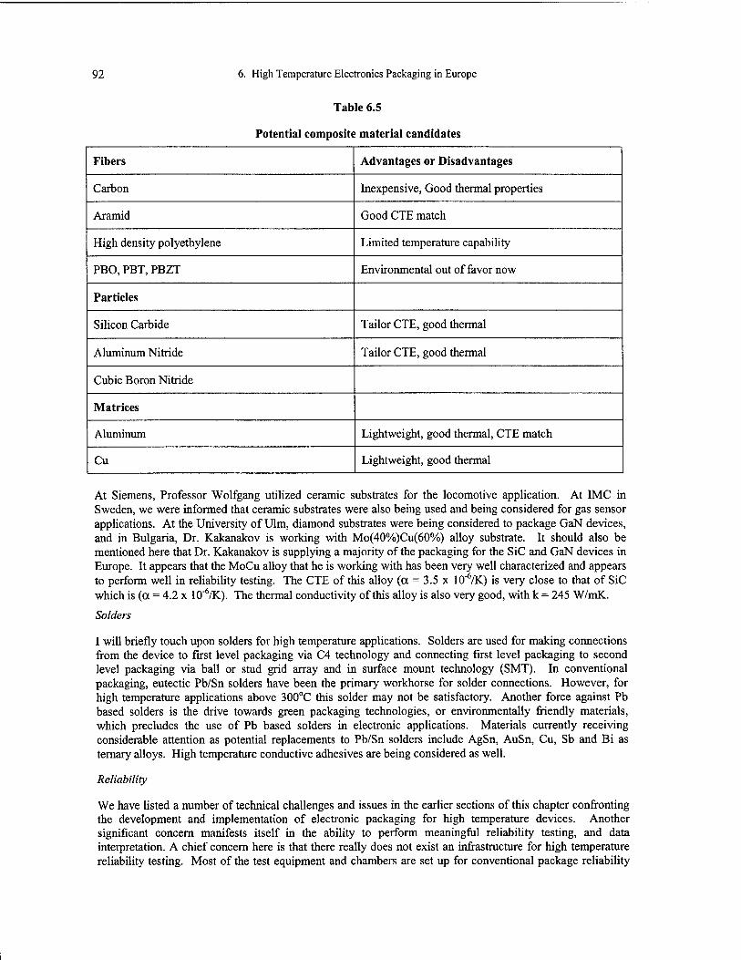
92 6. High Temperature Electronics Packaging in Europe
Table 6.5
Potential composite material candidates
Fibers Advantages or Disadvantages
Carbon Inexpensive, Good thermal properties
Aramid Good CTE match
High density polyethylene Limited temperature capability
PBO, PBT, PBZT Environmental out of favor now
Particles
Silicon Carbide Tailor CTE, good thermal
Aluminum Nitride Tailor CTE, good thermal
Cubic Boron Nitride
Matrices
Aluminum Lightweight, good thermal, CTE match
Cu Lightweight, good thermal
At Siemens, Professor Wolfgang utilized ceramic substrates for the locomotive application. At IMC in Sweden, we were informed that ceramic substrates were also being used and being considered for gas sensor applications. At the University of Ulm, diamond substrates were being considered to package GaN devices, and in Bulgaria, Dr. Kakanakov is working with Mo(40%)Cu(60%) alloy substrate. It should also be mentioned here that Dr. Kakanakov is supplying a majority of the packaging for the SiC and GaN devices in Europe. It appears that the MoCu alloy that he is working with has been very well characterized and appears to perform well in reliability testing. The CTE of this alloy (a = 3.5 x 10"6/K) is very close to that of SiC which is (a = 4.2 x 10'6/K). The thermal conductivity of this alloy is also very good, with k = 245 W/mK.
Solders
I will briefly touch upon solders for high temperature applications. Solders are used for making connections from the device to first level packaging via C4 technology and connecting first level packaging to second level packaging via ball or stud grid array and in surface mount technology (SMT). In conventional packaging, eutectic Pb/Sn solders have been the primary workhorse for solder connections. However, for high temperature applications above 300°C this solder may not be satisfactory. Another force against Pb based solders is the drive towards green packaging technologies, or environmentally friendly materials, which precludes the use of Pb based solders in electronic applications. Materials currently receiving considerable attention as potential replacements to Pb/Sn solders include AgSn, AuSn, Cu, Sb and Bi as ternary alloys. High temperature conductive adhesives are being considered as well.
Reliability
We have listed a number of technical challenges and issues in the earlier sections of this chapter confronting the development and implementation of electronic packaging for high temperature devices. Another significant concern manifests itself in the ability to perform meaningful reliability testing, and data interpretation. A chief concern here is that there really does not exist an infrastructure for high temperature reliability testing. Most of the test equipment and chambers are set up for conventional package reliability

White 93
testing and therefore only cover a limited temperature range. All of the European researchers who are actively involved in packaging also realize that this is a valid concern, and are exploring means to fill this void. Professor Wolfgang of Siemens indicated that there is a real need to perform extended life cycle tests out to 35 years due to the fact that some products will have to survive in the field with no failures for that long. Siemens has also put a task force in place (RAPSDRA) to identify failures and failure mechanisms through accelerated testing, and develop a set of standards for power electronics that correspond to a 35 year life cycle. In addition Siemens is pursuing the following to gain more understanding on the reliability of their electronic packages at elevated temperatures of operation:
• Siemens would like built in reliability (monitor process parameters and materials)
• Developing standardization for accelerated testing (1 OOx)
• Monitor operation of devices in real time (in-situ) using optical fibers
• Explore the theoretical limit for Si device operation (may be higher than 250°C)
Siemens has also developed reliability models that can be downloaded from their website at www.Infineon.com "SFET".
Dr. Kakanakov agrees that new reliability test equipment and methodologies may be needed for high temperature reliability assessment. Limited reliability data exists for some of his systems; however, some reliability studies were done using thermal resistance measurements. An important need for the advancement of high temperature electronic packaging will be the advent of better reliability modeling and simulation tools over and above what is currently being used today.
SUMMARY
I have tried to convey some of the challenges for the packaging of high temperature devices such as GaN and SiC. These challenges are not insurmountable and will be overcome when the proper resources are put into place to address specific areas. It appears that the Institute of Physics in Bulgaria, as well as Siemens in Germany are addressing a number of these issues already and have made significant progress in finding potential solutions for some applications. Of course there are a number of vertically integrated companies around the world, which have found solutions to most of the high temperature applications but at a cost premium. Here the challenge is to find similar cost performance packaging solutions for high temperature applications much like that of conventional Si IC packaging.
REFERENCES
Aday, J., R.W. Johnson, J.L. Evans, and C. Romanczuk, "Thick Film Silver Multilayers for Under-the-Hood Applications", Proc. Int. Symp. On Microelectroncs, ISHM, 1993 pp 126-131.
Agarwal, V., P. Chahal, R. Tummala, and M. Allen, "Improvements and recent advances in nanocomposites capacitors using a colloidal technique", IEEE 48th Electronic Components and Technology Conference, p 165.
Brandt, L., "New materials for embedded passive components", PAN Pacific Microelectronics Symposium Proceedings, IM APS, 1998, pp 195-199.
Bergstorm, L., K. Shinozaki, H. Tomiyama and N Mizutani, "Colloidal Processing of a Very fine BaTiO, Powder - Effect of Particle Interactions on the Suspension Properties, Consolidation, and Sintering Behavior", J. Am. Ceram. Soc, 80 [2], (1997), p 291 -300.
Dimos, D., S. J. Lockwood, and M. Rodgers, "Thin film decoupling capacitors for multichip module", IEEE, 1994, pp 894-899
Feinstein, L., Die Attachment Methods, Electronic Materials Handbook, Vol. 1 Packaging, ASM International, Materials Park 1989.
Kakanakov, R., L. Kassamakova, G. Sarov, U.S. Europe Conference on Wide Bandgap Semiconductor Technology for Next Generation Electronic and Photonic Devices, Arlington, Va 1999
94 6. High Temperature Electronics Packaging in Europe
Kapadia, H., H. Cole, M. Nielsen, N. Krishnamurthy, "Necessary characterization of integral passives for high performance applications", Integrated Passive Advanced Technology Workshop, Denver, 1998.
Lenihan, T., L. Schaper, Y. Shi, G. Morcan and J. Parkerson, "Embedded thin film resistors, capacitors, and inductors in flexible polyimide films", 46,b Electronic Components and Technology Conference, 1996, pp 119-124
Levy, F., "High dielectric loaded films", Advanced Materials & Manufacturing Processes, 1988, pp 309-326
Liang, S., S. Chong, E. Giannelis, "Barium titanate/epoxy composite dielectric materials for integrated thin film capacitors", 48"' ECTC, 1998, pp 171-175.
Liu, D., R. Kennedy, G. Korony, S. Makl, J. Mevissen, J. Hock and R. Heistand, "Integrated thin film capacitor arrays", Proc SPIE Int Soc Opt Eng ,3830, (1999), p 431-437.
Manko, H., Solders and Soldering, 3rd. ed., McGraw-Hill, N.Y. 1992, pi 16
Martin, B., C. Basceri, S. Strifer and A. Kingon, "Electrical properties of integrated Ta,Os metal-insulator-metal capacitors", Electrically Based Microstructural Characterization II Mater. Res. Soc. Symp. Proc,500, (1998), p 101- 106
McCluskey, F., R. Grzybowski, and T. Podlesak, "High Temperature Electronics", CRC Press, Inc., N.Y., 1997
Nami, Z., O. Misman, A. Erbil, G. S. May, "Computer simulation study of the MOCVD growth of titanium dioxide film", J. Crystal Growth, 171 (1997) 154-165.
Nelms, D., R. Ulrich, L. Schaper and B. Bowen, "Fabrication and performance of integrated capacitors on silicon and flexible substrates", Proc SPIE Int. Soc. Opt. Eng., 3582, (1998), p. 441-446.
Noda, M., H. Sugiyama and M. Okuyama, "Study on a metal-ferroelectric-oxide-semiconductor structure with thin silicon oxide film using SrBi,Ta,0, ferroelectric films prepared by pulsed laser deposition", Jpn. J. Appl. Phys. Part 1 Regul. Pap. Short Note Rev. Paper, 38, 9, (1999), p. 5432-5436.
O'Bryan, N., "Making embedded capacitors by roll-to-roll process", IMAPS Integrated Passive Advanced Technology Workshop, Denver, 1998.
O'neill, D., G. Catalan, F. Porras, R. M. Bowman and J. M. Gregg, "Thin film ferroelectric for capacitor applications", J. of Materials Science, Materials in Electronics, 9, (1998), p 199-205.
Ohishi, T., S. Maekawa and A. Katoh, "Synthesis and properties of tantalum oxide films prepared by the sol-gel method using photo-irradiation, J. of Non-Crystalline Solids, 147 & 148, (1992), 493-498.
Pecht, M., P.Lall, Passive components of the Electrical Engineering Handbook, R.C. Dorf, ed., CRC Press, Boca Raton, Fl. 1994 p 5-15
Rymaszewski, E. J., T.M. Lu, M. C. Nielsen, J.-Y. Kim, "Integrated Discrete Components", 193"1 Meeting of the Electrochemical Society, San Diego, CA, May 1998.
Sakabe, Y., N. Wada, J. Ikeda, and Y. Hamaji, "Ceramic for Ultra-thin Dielectric Layer of Multilayer Ceramic Capacitors", IEEE Int. Symp. Appl. Ferroelectrics, 1998,p 565-569.
Sharma, H. B. and A. Mansingh, "Sol-gel processed barium titanate ceramics and thin films", J. of Materials Science, 33 (1998), p 4455-4459.
Simamoto, S., Y. Sakata, J. Kojima, N. Kume and Y. Tsujimoto, "Lacquered Polymer-Ceramic Composite Dielectric Film for Capacitors", IEEE Intnl. Symp. On electrical Insulation, 1992, p 140 - 143.
Slamovich, E. B., and I. A. Aksay, "Structure Evolution in Hydrothermally Processed (<100C) BaTiO, Films", J. Am. Ceram. Soc, 79[1], (1996), p 239 -247
Slenes, K. and K. Law, "A polymer-ceramic composite for integrated capacitors",
IMAPS Advanced Technology Workshop in Integrated Passives, Denver, 1998.
Stauf, G., C. Seegel, R. Watts, and H. O'Bryan, "Modified stochiometry for integrated RF capacitors", IMAPS Advanced Technology Workshop on Integrated Passives, Denver, 1998.
Suu, K, T. Masuda, Y. Nishiyoka and N. Tani, "Preparation of SrBi,Ta,0, ferroelectric thin film by rf magnetron sputtering", Integr. Ferroelectr., 21,1-4, pt 1, (1998), p. 407-418.
Trigg, A., "Thin film resistors and capacitors for multichip modules", Proceedings of IEEE 48"' ECTC, 1998, pp 228-231.
Tsukada, M., J. Cross, M. Nishizawa, K. Kurihara, and N. Kamehara, Preparation and characterization of dielectric thin films for decoupling capacitors", Proceedings, ICEMCM, 1995, pp 347-352.
Tummala, R., E. Rymaszewski, Microelectronics Packaging Handbook, Van Nostrand Reinhold, New York 1989

White 95
Vorotilov, K., M. Yanovskaya, E. Turevskaya and A. Sigov, "Sol-gel derived ferroelectric thin films: avenues for control of microstructural and electric properties", J. Sol Gel Sei. Technol., 16,1-2, (1999), p 109-118.
Yao, K.., W. Zhu and X. Yao, "Development of Ba-Ti-B Glass-Ceramic thick-film capacitors by sol-gel technology", IEEE Transactions on CPMT -Part C, 21, No. 1, (1998), p 20-25.

96 6. High Temperature Electronics Packaging in Europe
97
CHAPTER 7
HIGH VOLTAGE SIC POWER DEVICES
T. Paul Chow
INTRODUCTION
Silicon has long been the dominant semiconductor of choice for high-voltage power electronics applications (Ghandhi 1998; Baliga 1996). However, recently, wide bandgap semiconductors, particularly SiC and GaN, have attracted much attention because they are projected to have much better performance than silicon (Shenai, et al. 1989; Baliga 1989; Bhalla & Chow 1994; Chow & Tyagi 1994). Compared to silicon, these wide bandgap semiconductors, SiC, GaN and InN can be categorized into one group while diamond, BN and A1N into another, because the former has bandgaps of 2-3.5 eV and the latter 5.5-6.5 eV. On the other hand, the Group IV or IV-IV semiconductors have indirect bandgaps whereas most of the Group Ill-nitrides are direct (except BN). The superior physical properties of these semiconductors offer a lower intrinsic carrier concentration (10 to 35 orders of magnitude), a higher electric breakdown field (4-20 times), a higher thermal conductivity (3-13 times), a larger saturated electron drift velocity (2-2.5 times), when compared to silicon (See Table 7.1).
SiC has over 150 polytypes (which are different crystal structures with the same stoichiometry of a compound semiconductor). Also, only the 6H- and 4H-SiC polytypes are available commercially in both bulk wafers and custom epitaxial layers. Between the two polytypes, 4H-SiC has become preferred due to the more isotropic nature of many of its electrical properties. Besides these properties, the impact ionization coefficients of electron and hole are also very important for power device considerations. The experimental coefficients, usually extracted from breakdown characteristics of reverse-biased pn or Schottky junctions, are shown in Fig. 7.1 for both 6H- and 4H-SiC (Kyuregyan & Yurkob 1989; Konstantinov, et al. 1997; Raghunathan & Baliga 1997). Also included in the figure is the average ionization coefficient for 6H-SiC. Such an average ionization coefficient, usually modeled by a power law dependence on the electric field (a <x ^°, where n is 5 or 7), allows one to estimate analytically the breakdown voltage and depletion width at breakdown. (See Fulop 1967 for the silicon case and Ramungul, et al. 1995 for 6H-SiC.) For GaN, there are very little experimental data on the ionization coefficients, probably due to the high defect density of the heteroepitaxial grown layers (Dmitriev, et al. 1996). Theoretically calculated coefficients for both 3C-and 2H-GaN have been recently performed (Komik, et al. 1996; Oguzman, et al. 1997) and are shown in Fig. 7.2. It should be emphasized that, unlike in silicon, the hole ionization coefficient is mostly higher than the electron one within the electric field range shown in both SiC and GaN cases. Such trends have significant impact on bipolar transistor structure (npn vs. pnp) considerations, as will be discussed later. Another important parameter is carrier lifetime, and SiC, like silicon, is an indirect semiconductor whereas GaN, like GaAs, is a direct semiconductor. Consequently, SiC has minority carrier lifetimes much longer than those in GaN. Experimentally, recombination lifetimes > 1 \is have been extracted in 4H-SiC (Singh, et al. 1998) vs. 6ns in 2H-GaN Bandic, et al. 1998) experimentally).
In this chapter, the figures of merit for unipolar and bipolar devices for power electronic applications will be first discussed to demonstrate the potential performance improvement using wide bandgap semiconductors.
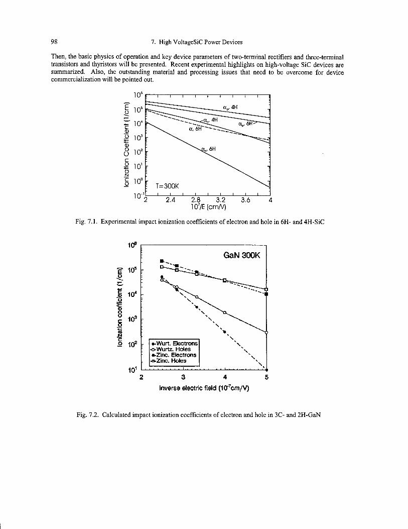
98 7. High VoltageSiC Power Devices
Then, the basic physics of operation and key device parameters of two-terminal rectifiers and three-terminal transistors and thyristors will be presented. Recent experimental highlights on high-voltage SiC devices are summarized. Also, the outstanding material and processing issues that need to be overcome for device commercialization will be pointed out.
o
106r
106 r*^
rio<
1 io3
0 ° in2
S 10' o N
10"
1 1 1 1 1 1 1 1 i i
! ^\. «. 6H "--^r^^^ 6FP
i
\ ^S\^,6H
^^-- -3
r N. "!
[ T=300K ^^ "!
1
2.4 2.8 3.2 107/E(cm/V)
3.6
Fig. 7.1. Experimental impact ionization coefficients of electron and hole in 6H- and 4H-SiC
106
10s
i io4
o
o 102
101
: GaN 300K
*-. D-^L""-
- ^"*^^*"~~^^ m. j. ^i5lAj*—-^, ^*V ~"*^*^-~^_
SD\. •** J^*^**^^J| \V^ """-ii s^\^
"*> ^Vv\ S, >{\
- \ ^^\^ S, ^v
* \> ■ \ . •-Wurt. Electrons V \ : •o-Wurtz. Holes >
••Zinc. Electrons -a-Zinc. Holes
X
3 4 5
Inverse electric field (10"7cm/V)
Fig. 7.2. Calculated impact ionization coefficients of electron and hole in 3C- and 2H-GaN
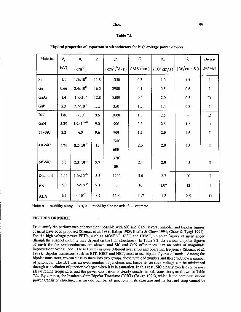
Chow
Table 7.1
99
Physical properties of important semiconductors for high-voltage power devices.
Material Es n, e. M„ Ec V sal X Direct/
(eV) (cm"3) (cm2/V-s) (MV/cm) (107cm/s) (W/cm-K) Indirect
Si 1.1 1.5x10'° 11.8 1350 0.3 1.0 1.5 I
Ge 0.66 2.4x10" 16.0 3900 0.1 0.5 0.6 I
GaAs 1.4 1.8xl06 12.8 8500 0.4 2.0 0.5 D
GaP 2.3 7.7x10"' 11.1 350 1.3 1.4 0.8 I
InN 1.86 -ltf 9.6 3000 1.0 2.5 - D
GaN 3.39 1.9X10⁻¹⁰ 9.0 900 3.3 2.5 1.3 D
3C-SiC 2.2 6.9 9.6 900
720"
1.2 2.0 4.5 I
4H-SiC 3.26 8.2x10"' 10 650c
370"
2.0 2.0 4.5 I
6H-SiC 3.0 2.3x10"' 9.7 50c
2.4 2.0 4.5 I
Diamond 5.45 1.6x10"" 5.5 1900 5.6 2.7 20 I
BN 6.0 1.5x10"" 7.1 5 10 1.0* 13 I
ALN 6.1 ~ 10"" 8.7 1100 11.7 1.8 2.5 D
Note: a — mobility along a-axis, c — mobility along c axis, *— estimate.
FIGURES OF MERIT
To quantify the performance enhancement possible with SiC and GaN, several unipolar and bipolar figures of merit have been proposed (Shenai, et al. 1989; Baliga 1989; Bhalla & Chow 1994; Chow & Tyagi 1994). For the high-voltage power FET's, such as MOSFET, JFET and HEMT, unipolar figures of merit apply (though the channel mobility may depend on the FET structures). In Table 7.2, the various unipolar figures of merit for the semiconductors are shown, and SiC and GaN offer more than an order of magnitude improvement over silicon. These figures assume different heat sinks and operating frequency (Shenai, et al. 1989). Bipolar transistors, such as BJT, IGBT and HBT, need to use bipolar figures of merit. Among the bipolar transistors, we can classify them into two groups, those with odd number and those with even number of junctions. The BJT has an even number of junctions and hence its on-state voltage can be minimized through cancellation of junction voltages when it is in saturation. In this case, SiC clearly excels over Si over all switching frequencies and the power dissipation is clearly smaller in SiC transistors, as shown in Table 7.3. By contrast, the Insulated-Gate Bipolar Transistor (IGBT) (Baliga 1996), which is the dominant silicon power transistor structure, has an odd number of junctions in its structure and its forward drop cannot be

100 7. High VoltageSiC Power Devices
reduced to less than a diode drop. Since SiC has a large diode turn-on voltage due to its larger bandgap, its conduction loss cannot be less than the silicon device at low to medium current density and only yields a lower total power loss when the switching frequency exceeds a certain frequency, fmin (Bhalla & Chow 1994).
Table 7.2
Normalized unipolar figures of merit of important semiconductors for high-voltage power devices (Baliga 1989).
Material \ JM MJM KM Qn Q« BM (Qra) BHFM
{EcvJ%)2 A*JM K-J^f hsA XcAEc CrMEl tä
Si 1 1 1 i 1 l 1 1
Ge 0.4 0.03 0.012 0.20 0.06 0.02 0.2 0.3
GaAs 0.33 7.1 2.4 0.45 5.2 6.9 15.6 10.8
GaP 0.53 37 20 0.7 10 40 16 5
InN - 58 - - - - 46 19
GaN 0.87 760 655 1.6 560 6220 650 77.8
3C-SiC 3 65 195 1.6 100 400 33.4 10.3
4H-SiC 3 180 540 4.61 390 2580 130 22.9
6H-SiC 3 260 780 4.68 330 2670 110 16.9
Diamond 13.3 2540 33800 32.1 54860 1024000 4110 470
BN 8.7 1100 9700 11 715 23800 83 4
A1N 1.7 5120 8700 21 52890 2059000 31700 1100
Table 7.3 A bipolar figure of merit applied to the power pin junction rectifier (calculated at JF = 100A/cm2, BV:
1000V) (Baliga 1989 .
Name Nd W N' VF Jend Joff ', /i tj-2 Eqtr f . ./min
(cm"') Cum) (V) (A/cm2) (A/cm2) (A«) (ps) (ps) (mJ) (KHz)
Si 1.3x10" 100 0.88 9.7 2xl0-5 7xl0"3 0.81 0 5.4X10"3 -
Ge 4.4x10" 285 0.60 8.3 8xl0"2 7.6xl0~3 1.8 0 6.2x10"3 0
3C-SiC 3.8X10¹⁵ 33.1 2.00 42.8 2x10~" 4.4x10~3 0.2 2.2x10"3 2xl0"2 1.62
6H-SiC 1.6xl0'6 23.9 2.65 46.2 3xl0"21 l.OxlO"2 0.14 4.6x10"3 5.5xl0"3 1.82
Diamond 1.2x10" 72.0 5.21 93.4 5x10"" 2.6x10"' 0.02 lxlO"2 l.lxlO"3 4.12
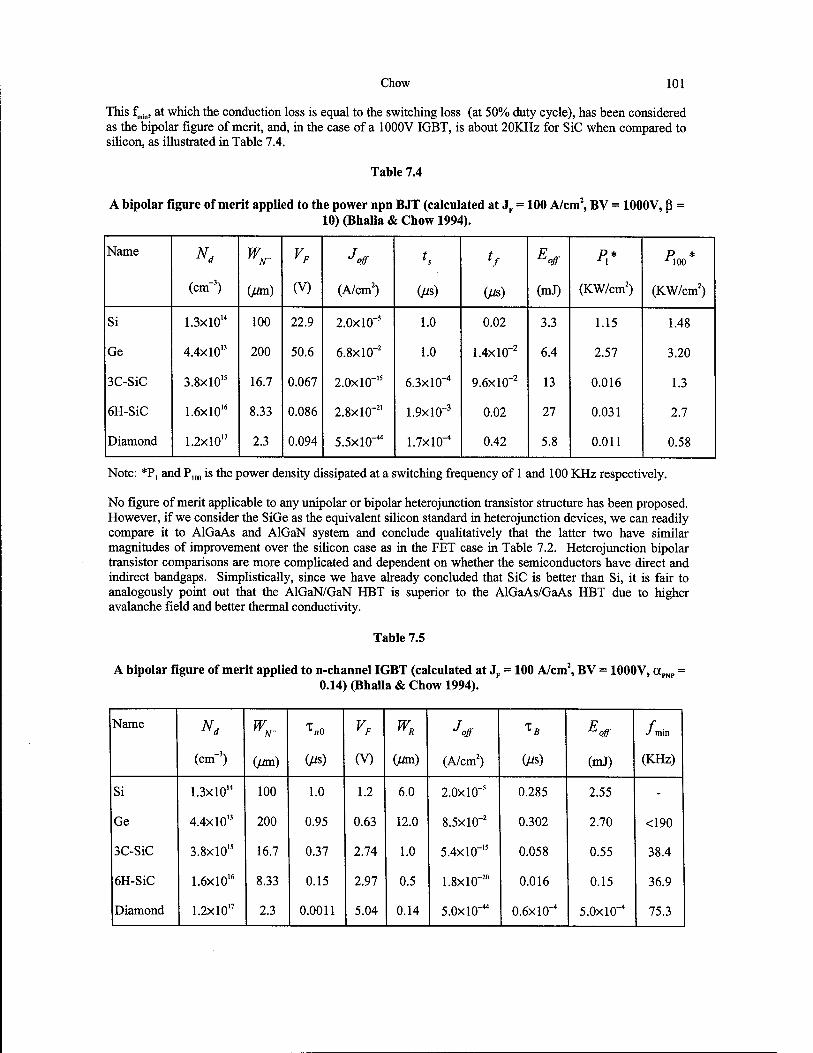
Chow 101
This fmil], at which the conduction loss is equal to the switching loss (at 50% duty cycle), has been considered as the bipolar figure of merit, and, in the case of a 1000V IGBT, is about 20KHz for SiC when compared to silicon, as illustrated in Table 7.4.
Table 7.4
A bipolar figure of merit applied to the power npn BJT (calculated at JF = 100 A/cm2, BV = 1000V, ß = 10) (Bhalla & Chow 1994).
Name Nd W vF off *, *f Eoff Px* p *
M00
(cm-5) (/fln) (V) (A/cm2) m (JX) (mJ) (KW/cm2) (KW/cm2)
Si 1.3X10¹⁴ 100 22.9 2.0xl0"5 1.0 0.02 3.3 1.15 1.48
Ge 4.4x10" 200 50.6 6.8x10"2 1.0 1.4xl0"2 6.4 2.57 3.20
3C-SiC 3.8xl015 16.7 0.067 2.0x10"IS 6.3X10⁻⁴ 9.6xl0"2 13 0.016 1.3
6H-SiC 1.6xl016 8.33 0.086 2.8X10""2' 1.9xl0-3 0.02 27 0.031 2.7
Diamond 1.2x10" 2.3 0.094 5.5X10-44 1.7xl0-4 0.42 5.8 0.011 0.58
Note: *P, and P100 is the power density dissipated at a switching frequency of 1 and 100 KHz respectively.
No figure of merit applicable to any unipolar or bipolar heterojunction transistor structure has been proposed. However, if we consider the SiGe as the equivalent silicon standard in heterojunction devices, we can readily compare it to AlGaAs and AlGaN system and conclude qualitatively that the latter two have similar magnitudes of improvement over the silicon case as in the FET case in Table 7.2. Heterojunction bipolar transistor comparisons are more complicated and dependent on whether the semiconductors have direct and indirect bandgaps. Simplistically, since we have already concluded that SiC is better than Si, it is fair to analogously point out that the AlGaN/GaN HBT is superior to the AlGaAs/GaAs HBT due to higher avalanche field and better thermal conductivity.
Table 7.5
A bipolar figure of merit applied to n-channel IGBT (calculated at JF = 100 A/cm2, BV = 1000V, aPNP = 0.14) (Bhalla & Chow 1994).
Name Nd W N~ ^«0 vF wR Joff *B Eoff f . J min
(cm-3) (m) C"s) (V) (/an) (A/cm2) (/ß) (mJ) (KHz)
Si 1.3X10'4 100 1.0 1.2 6.0 2.0X10"5 0.285 2.55 -
Ge 4.4x10" 200 0.95 0.63 12.0 8.5x10"2 0.302 2.70 <190
3C-SiC 3.8xl015 16.7 0.37 2.74 1.0 5.4xl0"15 0.058 0.55 38.4
6H-SiC 1.6xl016 8.33 0.15 2.97 0.5 1.8xl0"20 0.016 0.15 36.9
Diamond 1.2xl017 2.3 0.0011 5.04 0.14 5.0X10-44 0.6xl0"4 5.0X10⁻⁴ 75.3
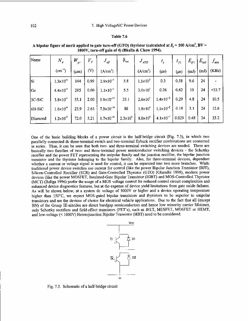
102 7. High VoltageSiC Power Devices
Table 7.6
A bipolar figure of merit applied to gate turn-off (GTO) thyristor (calculated at JF = 100 A/cm2, BV = 1000V, turn-off gain of 4) (Bhalla & Chow 1994).
Name Nd W AT vF Joff Hinax J ATO ', tfX *Vi ^lail f . J rmn
(cm"') (/mi) (V) (A/cm2) (A/cm2) </«) m (ml) (ml) (KHz)
Si 1.3X10¹⁴ 144 0.99 2.9x10"s 5.8 l.lxlO3 0.3 0.58 9.6 24 -
Ge 4.4x10" 285 0.60 1.1x10"' 5.5 3.0x10' 0.26 0.62 10 24 <53.7
3C-SiC 3.8x10" 33.1 2.00 3.9x10"" 25.1 2.6x10' 1.4xl0"2 0.29 4.8 24 10.5
6H-SiC 1.6X10'6 23.9 2.65 7.9x10"" 88 1.8xl04 l.lxlO"2 0.19 3.1 24 12.6
Diamond 1.2x10" 72.0 5.21 1.7X10"41 2.3xl04 8.0x10s 4.1X10"5 0.029 0.48 24 23.2
One of the basic building blocks of a power circuit is the half-bridge circuit (Fig. 7.3), in which two parallelly connected dc three-terminal switch and two-terminal flyback rectifier combinations are connected in series. Thus, it can be seen that both two- and three-terminal switching devices are needed. There are basically two families of two- and three-terminal power semiconductor switching devices - the Schottky rectifier and the power FET representing the unipolar family and the junction rectifier, the bipolar junction transistor and the thyristor belonging to the bipolar family. Also, for three-terminal devices, dependent whether a current or voltage signal is used for control, it can be separated into two more branches. While traditional power device switches use current for control (like the power Bipolar Junction Transistor (BJT), Silicon-Controlled Rectifier (SCR) and Gate-Controlled Thyristor (GTO) (Ghandhi 1998), modern power devices (like the power MOSFET, Insulated-Gate Bipolar Transistor (IGBT) and MOS-Controlled Thyristor (MCT) (Baliga 1996) prefer the usage of a MOS voltage control for reduced control circuit complexities and enhanced device diagnostics features, but at the expense of device yield limitations from gate oxide failures. As will be shown below, at a system dc voltage of 5000V or higher and a device operating temperature higher than 150°C, we expect MOS-gated bipolar transistors and thyristors to be superior to unipolar transistors and are the devices of choice for electrical vehicle applications. Due to the fact that all (except BN) of the Group Ill-nitrides are direct bandgap semiconductors and hence low minority carrier lifetimes, only Schottky rectifiers and field-effect transistors (FET's), such as JFET, MESFET, MOSFET or HEMT, and low-voltage (< 1000V) Heterojunction Bipolar Transistor (HBT) need to be considered.
vcc
HK Dl
T2 Q D2
Fig. 7.3. Schematic of a half-bridge circuit
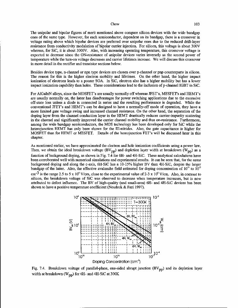
Chow 103
The unipolar and bipolar figures of merit mentioned above compare silicon devices with the wide bandgap ones of the same type. However, for each semiconductor, dependent on its bandgap, there is a crossover in voltage rating above which bipolar devices are preferred over unipolar ones due to the reduced drift-layer resistance from conductivity modulation of bipolar carrier injection. For silicon, this voltage is about 300V whereas, for SiC, it is about 3000V. Also, with increasing operating temperature, this crossover voltage is expected to decrease since the ON-resistance of unipolar devices varies inversely as the second power of temperature while the turn-on voltage decreases and carrier lifetimes increase. We will discuss this crossover in more detail in the rectifier and transistor sections below.
Besides device type, n-channel or npn type devices are chosen over p-channel or pnp counterparts in silicon. The reason for this is the higher electron mobility and lifetimes. On the other hand, the higher impact ionization of electrons leads to a poorer SOA. In SiC, electron also has a higher mobility but has a lower impact ionization capability than holes. These considerations lead to the inclusion of p-channel IGBT in SiC.
For AlGalnN alloys, since the MOSFET's are usually normally off whereas JFET's, MESFET's and HEMT's are usually normally on, the latter has disadvantages for power switching applications due to the excessive off-state loss unless a diode is connected in series and the resulting performance is degraded. While the conventional JFET's and HEMT's can be designed to have a normally-off mode of operation, they have a more limited gate voltage swing and increased channel resistance. On the other hand, the separation of the doping layer from the channel conduction layer in the HEMT drastically reduces carrier-impurity scattering in the channel and significantly improved the carrier channel mobility and thus on-resistance. Furthermore, among the wide bandgap semiconductors, the MOS technology has been developed only for SiC while the heterojunction HEMT has only been shown for the Ill-nitrides. Also, the gate capacitance is higher for MOSFET than for HEMT or MESFET. Details of the homojunction FET's will be discussed later in this chapter.
As mentioned earlier, we have approximated the electron and hole ionization coefficients using a power law. Then, we obtain the ideal breakdown voltage (BVpp) and depletion layer width at breakdown (Wpp) as a
function of background doping, as shown in Fig. 7.4 for 6H- and 4H-SiC. These analytical calculations have been corroborated well with numerical simulations and experimental results. It can be seen that, for the same background doping and along the c-axis, 6H-SiC has a 10-15% higher BV than 4H-SiC, despite the larger bandgap of the latter. Also, the effective avalanche field estimated for doping concentration of 1015 to 10"
cm"3 is the range 2.5 to 5 x 10⁶ V/cm, close to the experimental value of 2-3 x 10⁶ V/cm. Also, in contrast to silicon, the breakdown voltage of SiC was observed to decrease when temperature increases, but is now attributed to defect influence. The BV of high-quality (and small-area) 6H- and 4H-SiC devices has been shown to have a positive temperature coefficient (Neudeck & Fazi 1997).
104p
alO3
—i i 11ii i i i i i :inid"i=rrr—<-<-T -f-t-n-H 1--- T=300K '■
■n 1 1—i-rrrrr rn 1 n-rrrrr J 1—l_l_4-i-U.
i i i i i i i i .6H,BV„-i-n.u.
I Mill
io-2
Doping Concentration (cm
Fig. 7.4. Breakdown voltage of parallel-plane, one-sided abrupt junction (BVpp) and its depletion layer
width at breakdown (Wpp) for 6H- and 4H-SiC at 300K
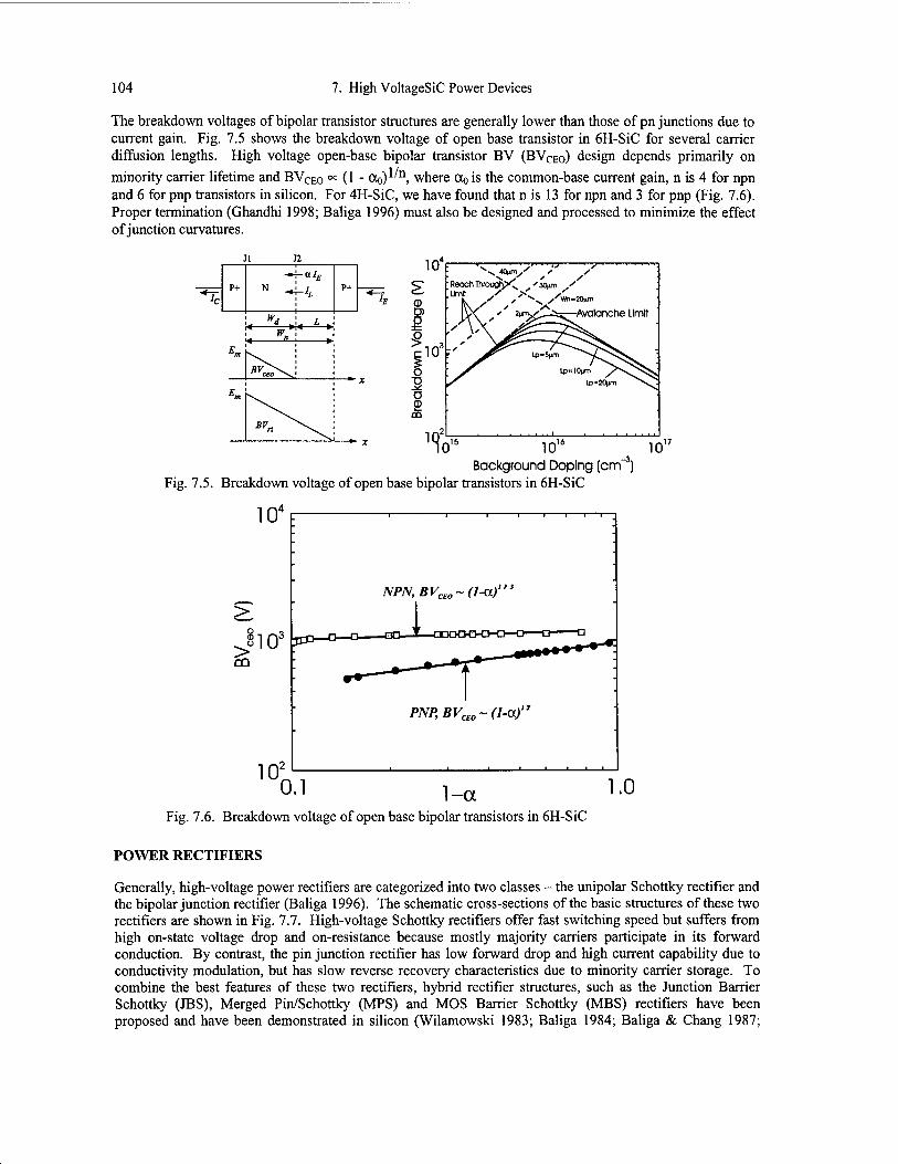
104 7. High VoltageSiC Power Devices
The breakdown voltages of bipolar transistor structures are generally lower than those of pn junctions due to current gain. Fig. 7.5 shows the breakdown voltage of open base transistor in 6H-SiC for several carrier diffusion lengths. High voltage open-base bipolar transistor BV (BVCEO) design depends primarily on
minority carrier lifetime and BVCE0 <* (1 - (Xo) , where Oo is the common-base current gain, n is 4 for npn and 6 for pnp transistors in silicon. For 4H-SiC, we have found that n is 13 for npn and 3 for pnp (Fig. 7.6). Proper termination (Ghandhi 1998; Baliga 1996) must also be designed and processed to minimize the effect of junction curvatures.
■*\-aIE
P+ N 4/, p+
*T~c %
4 W* *'* L > o * Em
*%X> X
Em
*r„ ^^
10'
B |io3
o S D <D
CD
' Reach Through,?*^ '3<tym . • ""¥ S >'-^ "C.
' • ■ •
•
»20nm
-Avalanche Limit V 1
*
' \ _^?5^
lp-5nm ~\^^^ - lp. 10nm /^^N^^SS
U>-20pm ^v^.
... i
■
%'" 10'° Background Doping (cm"'
10'
Fig. 7.5. Breakdown voltage of open base bipolar transistors in 6H-SiC
104
g §1 o3
102
-l 1 1 1 1 r-
jö>-
NPN,BVC£0~(l-a)'
0__n___QO-Jt_03DOCH>-D—C3——D
PNP,BVao~(l-af
0.1 !_a 1.0 Fig. 7.6. Breakdown voltage of open base bipolar transistors in 6H-SiC
POWER RECTIFIERS
Generally, high-voltage power rectifiers are categorized into two classes - the unipolar Schottky rectifier and the bipolar junction rectifier (Baliga 1996). The schematic cross-sections of the basic structures of these two rectifiers are shown in Fig. 7.7. High-voltage Schottky rectifiers offer fast switching speed but suffers from high on-state voltage drop and on-resistance because mostly majority carriers participate in its forward conduction. By contrast, the pin junction rectifier has low forward drop and high current capability due to conductivity modulation, but has slow reverse recovery characteristics due to minority carrier storage. To combine the best features of these two rectifiers, hybrid rectifier structures, such as the Junction Barrier Schottky (JBS), Merged Pin/Schottky (MPS) and MOS Barrier Schottky (MBS) rectifiers have been proposed and have been demonstrated in silicon (Wilamowski 1983; Baliga 1984; Baliga & Chang 1987;
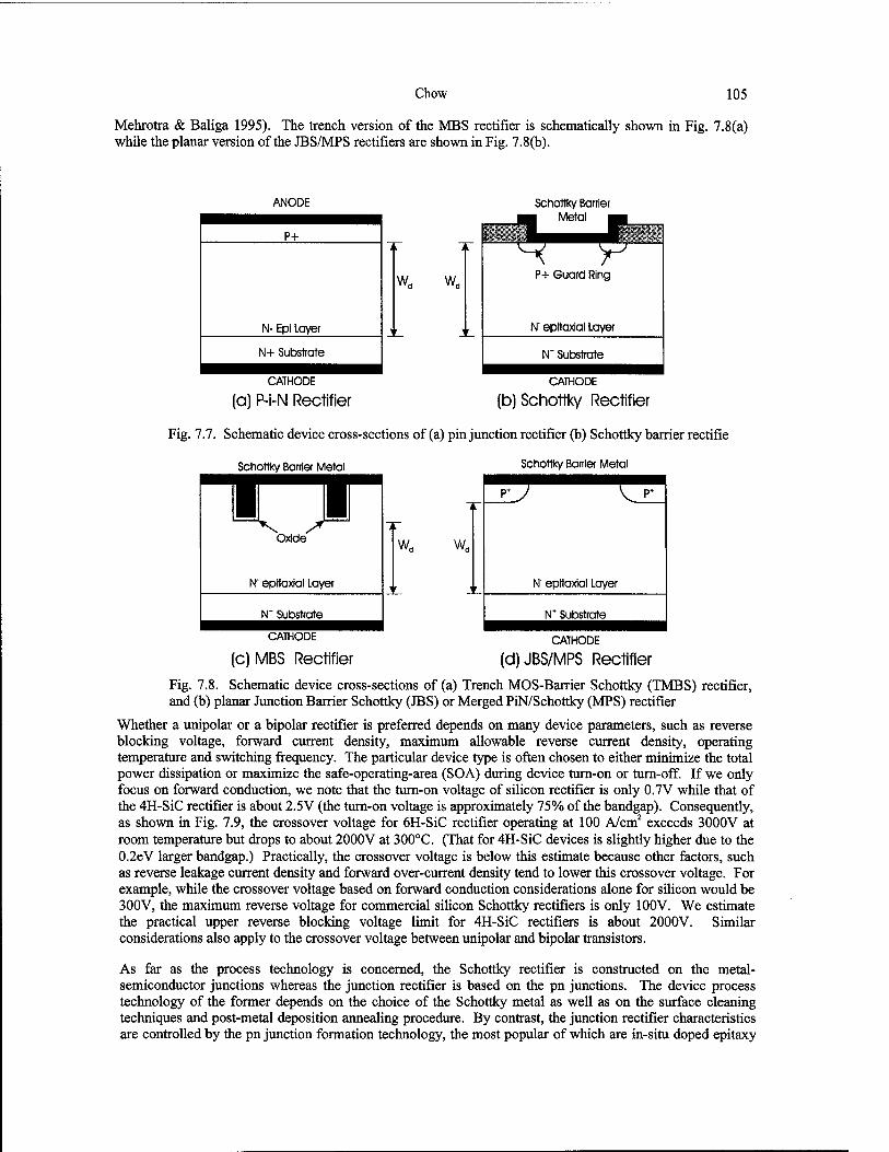
Chow 105
Mehrotra & Baliga 1995). The trench version of the MBS rectifier is schematically shown in Fig. while the planar version of the JBS/MPS rectifiers are shown in Fig. 7.8(b).
7.8(a)
ANODE
P+
N- Epl Layer
N+ Substrate
Schottky Barrier Metal
W„ W„ P+ Guard Ring
H epitaxial Layer
NT Substrate
CATHODE
(a) P-i-N Rectifier CATHODE
(b) Schottky Rectifier
Fig. 7.7. Schematic device cross-sections of (a) pin junction rectifier (b) Schottky barrier rectifie
Schottky Barrier Metal Schottky Barrier Metal
Oxide
N' epitaxial Layer
N+ Substrate
W„ Wr
rr xz.
N' epitaxial Layer
NT Substrate
CATHODE
(c)MBS Rectifier CATHODE
(d) JBS/MPS Rectifier
Fig. 7.8. Schematic device cross-sections of (a) Trench MOS-Barrier Schottky (TMBS) rectifier, and (b) planar Junction Barrier Schottky (JBS) or Merged PiN/Schottky (MPS) rectifier
Whether a unipolar or a bipolar rectifier is preferred depends on many device parameters, such as reverse blocking voltage, forward current density, maximum allowable reverse current density, operating temperature and switching frequency. The particular device type is often chosen to either minimize the total power dissipation or maximize the safe-operating-area (SOA) during device turn-on or turn-off. If we only focus on forward conduction, we note that the turn-on voltage of silicon rectifier is only 0.7V while that of the 4H-SiC rectifier is about 2.5 V (the turn-on voltage is approximately 75% of the bandgap). Consequently, as shown in Fig. 7.9, the crossover voltage for 6H-SiC rectifier operating at 100 A/cm2 exceeds 3000V at room temperature but drops to about 2000V at 300°C. (That for 4H-SiC devices is slightly higher due to the 0.2eV larger bandgap.) Practically, the crossover voltage is below this estimate because other factors, such as reverse leakage current density and forward over-current density tend to lower this crossover voltage. For example, while the crossover voltage based on forward conduction considerations alone for silicon would be 300V, the maximum reverse voltage for commercial silicon Schottky rectifiers is only 100V. We estimate the practical upper reverse blocking voltage limit for 4H-SiC rectifiers is about 2000V. Similar considerations also apply to the crossover voltage between unipolar and bipolar transistors.
As far as the process technology is concerned, the Schottky rectifier is constructed on the metal- semiconductor junctions whereas the junction rectifier is based on the pn junctions. The device process technology of the former depends on the choice of the Schottky metal as well as on the surface cleaning techniques and post-metal deposition annealing procedure. By contrast, the junction rectifier characteristics are controlled by the pn junction formation technology, the most popular of which are in-situ doped epitaxy
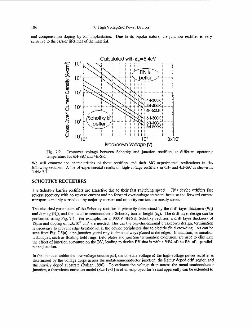
106
and compensation doping by ion implantation, sensitive to the carrier lifetimes of the material.
7. High VoltageSiC Power Devices
Due to its bipolar nature, the junction rectifier is very
Calculated with (j>m=5.4eV
E
to C <D a c CD
Ü
O V) V) o o
104
Breakdown Voltage (V) 3x1 o4
Fig. 7.9. Crossover voltage between Schottky and junction rectifiers at different operating temperature for 6H-SiC and 4H-SiC
We will examine the characteristics of these rectifiers and their SiC experimental realizations in the following sections. A list of experimental results on high-voltage rectifiers in 6H- and 4H-SiC is shown in Table 7.7.
SCHOTTKY RECTIFIERS
The Schottky barrier rectifiers are attractive due to their fast switching speed. This device exhibits fast reverse recovery with no reverse current and no forward over-voltage transient because the forward current transport is mainly carried out by majority carriers and minority carriers are mostly absent.
The electrical parameters of the Schottky rectifier is primarily determined by the drift layer thickness (Wd) and doping (Nd), and the metal-to-semiconductor Schottky barrier height (<|)B). The drift layer design can be performed using Fig. 7.4. For example, for a 1000V 4H-SiC Schottky rectifier, a drift layer thickness of 12|J.m and doping of 1.3xl016 cm'3 are needed. Besides the one-dimensional breakdown design, termination is necessary to prevent edge breakdown at the device peripheries due to electric field crowding. As can be seen from Fig. 7.5(a), a pn junction guard ring is almost always placed at the edges. In addition, termination techniques, such as floating field rings, field plates and junction termination extension, are used to eliminate the effect of junction curvature on the BV, leading to device BV that is within 95% of the BV of a parallel- plane junction.
In the on-state, unlike the low-voltage counterpart, the on-state voltage of the high-voltage power rectifier is determined by the voltage drops across the metal-semiconductor junction, the lightly doped drift region and the heavily doped substrate (Baliga 1996). To estimate the voltage drop across the metal-semiconductor junction, a thermionic emission model (Sze 1981) is often employed for Si and apparently can be extended to
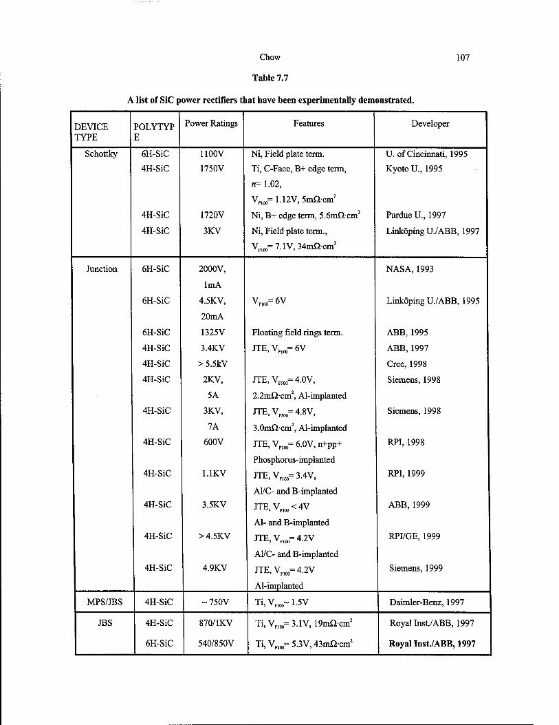
Chow
Table 7.7
A list of SiC power rectifiers that have been experimentally demonstrated.
107
DEVICE TYPE
POLYTYP E
Power Ratings Features Developer
Schottky 6H-SiC 1100V Ni, Field plate term. U. of Cincinnati, 1995
4H-SiC 1750V Ti, C-Face, B+ edge term,
n= 1.02,
VF100= 1.12V, 5mQcm2
Kyoto U., 1995
4H-SiC 1720V Ni, B+ edge term, 5.6mQcm2 Purdue U., 1997
4H-SiC 3KV Ni, Field plate term.,
VF100=7.1V,34mQ-cm2
LinköpingU./ABB, 1997
Junction 6H-SiC 2000V,
1mA
NASA, 1993
6H-SiC 4.5KV,
20mA
V„„=6V LinköpingU./ABB, 1995
6H-SiC 1325V Floating field rings term. ABB, 1995
4H-SiC 3.4KV JTE,VF1[W=6V ABB, 1997
4H-SiC > 5.5kV Cree, 1998
4H-SiC 2KV,
5A
JTE,VF50O=4.OV,
2.2m£2-cm2, Al-implanted
Siemens, 1998
4H-SiC 3KV, JTE, VFS(W= 4.8V, Siemens, 1998
4H-SiC
7A
600V
3.0mQ-cm2, Al-implanted
JTE, VF100= 6.0V, n+pp+ PvPI, 1998
4H-SiC 1.1KV
Phosphorus-implanted
JTE, VF100= 3.4V, RPI, 1999
4H-SiC 3.5KV
Al/C- and B-implanted
JTE,VF10o<4V ABB, 1999
4H-SiC > 4.5KV
Al- and B-implanted
JTE, VF100= 4.2V RPI/GE, 1999
4H-SiC 4.9KV
Al/C- and B-implanted
JTE, VF100= 4.2V
Al-implanted
Siemens, 1999
MPS/JBS 4H-SiC -750V Ti V ~ 1 5V xl» VF100 l"J * Daimler-Benz, 1997
JBS 4H-SiC 870/1KV Ti,VF100=3.1V, 19mfi-cm2 Royal Inst./ABB, 1997
6H-SiC 540/850V Ti, VF10 = 5.3V, 43mQ-cm2 Royal Inst./ABB, 1997
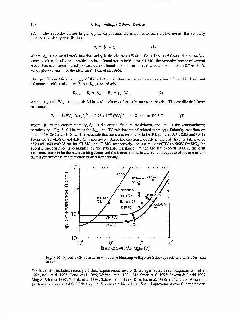
108 7. High VoltageSiC Power Devices
SiC. The Schottky barrier height, <|>B, which controls the asymmetric current flow across the Schottky junctions, is ideally described as
<!>B = 4>M - X (l)
where <j)M is the metal work function and % is the electron affinity. For silicon and GaAs, due to surface states, such an ideally relationship has been found not to hold. For 6H-SiC, the Schottky barrier of several metals has been experimentally measured and found to be closer to ideal with a slope of about 0.7 in the <()„ vs. (j)M plot (vs. unity for the ideal case) (Itoh, et al. 1995).
The specific on-resistance, RQN sp, of the Schottky rectifier can be expressed as a sum of the drift layer and substrate specific resistances, Rd and Rsub, respectively.
**,„ = ** + R^ = Rd + Psuhwsv (2)
where psub and Wmb are the resistivities and thickness of the substrate respectively. The specific drift layer resistance is
Rd = 4 (BV)V(n es &) = 2.78 x 10"'2 (BV)" in Q-cm2 for 4H-SiC (3)
where |J, is the carrier mobility, %c is the critical field at breakdown, and es is the semiconductor permittivity. Fig. 7.10 illustrates the R,^ vs. BV relationship calculated for n-type Schottky rectifiers on silicon, 6H-SiC and 4H-SiC. The substrate thickness and resistivity to be 300 urn and 0.01, 0.03 and 0.015 Q-cm for Si, 6H-SiC and 4H-SiC, respectively. Also, the electron mobility in the drift layer is taken to be 450 and 1000 cm2/ V-sec for 6H-SiC and 4H-SiC, respectively. At low values of BV (< 500V for SiC), the specific on-resistance is dominated by the substrate resistance. When the BV exceeds 1000V, the drift resistance starts to be the main limiting factor and the increase in Rd is a direct consequence of the increase in drift layer thickness and reduction in drift layer doping.
10 101
Kyoto Univ. NCSIT95 *X / Vb.
RPI '98
10 10 Breakdown Voltage (V)
IGT
Fig. 7.10. Specific ON-resistance vs. reverse blocking voltage for Schottky rectifiers on Si, 6H- and 4H-SiC
We have also included recent published experimental results (Bhatnagar, et al. 1992; Raghunathan, et al. 1995; Itoh, et al. 1995; Ueno, et al. 1995; Weitzel, et al. 1996; Mitlehner, et al. 1997; Saxena & Steckl 1997; Sing & Palmour 1997; Wahab, et al. 1998; Schoen, et al. 1998; Khemka, et al. 1998) in Fig. 7.10. As seen in the figure, experimental SiC Schottky rectifiers have achieved significant improvement over Si counterparts,
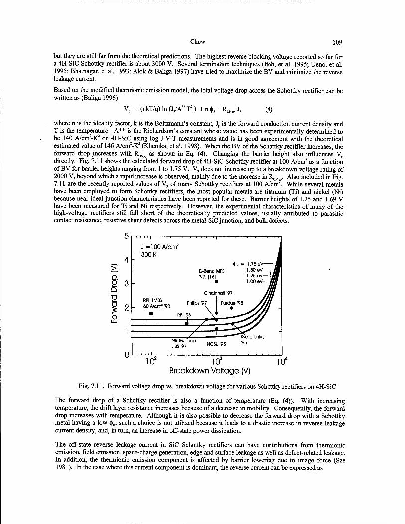
Chow 109
but they are still far from the theoretical predictions. The highest reverse blocking voltage reported so far for a 4H-SiC Schottky rectifier is about 3000 V. Several termination techniques (Itoh, et al. 1995; Ueno, et al. 1995; Bhatnagar, et al. 1993; Alok & Baliga 1997) have tried to maximize the BV and minimize the reverse leakage current.
Based on the modified thermionic emission model, the total voltage drop across the Schottky rectifier can be written as (Baliga 1996)
VF = (nCT/q)1n(JF/A,T1)+n4>I1 + Ra^Jp (4)
where n is the ideality factor, k is the Boltzmann's constant, JF is the forward conduction current density and T is the temperature. A** is the Richardson's constant whose value has been experimentally determined to be 140 A/cm2-K2 on 4H-SiC using log J-V-T measurements and is in good agreement with the theoretical estimated value of 146 A/cm2-K2 (Khemka, et al. 1998). When the BV of the Schottky rectifier increases, the forward drop increases with R^ as shown in Eq. (4). Changing the barrier height also influences VF
directly. Fig. 7.11 shows the calculated forward drop of 4H-SiC Schottky rectifier at 100 A/cm2 as a function of BV for barrier heights ranging from 1 to 1.75 V. VF does not increase up to a breakdown voltage rating of 2000 V, beyond which a rapid increase is observed, mainly due to the increase in R^ . Also included in Fig. 7.11 are the recently reported values of VF of many Schottky rectifiers at 100 A/cm . While several metals have been employed to form Schottky rectifiers, the most popular metals are titanium (Ti) and nickel (Ni) because near-ideal junction characteristics have been reported for these. Barrier heights of 1.25 and 1.69 V have been measured for Ti and Ni respectively. However, the experimental characteristics of many of the high-voltage rectifiers still fall short of the theoretically predicted values, usually attributed to parasitic contact resistance, resistive shunt defects across the metal-SiC junction, and bulk defects.
5
4
3
2
1
> Q. O Q ■o Ö
0
I I I I I
JF= 100 A/cm2
300 K
RPI, TMBS 60 A/cm2 "98
RPI '98
±Z2 Z
RIT Sweden JBS'97
<D, = 1.75eV-
D-Benz, MPS 1 -50 eV- "97. [16]
Cincinnati "97
Philips'97 I Purdue "98
z
10' 10' Breakdown Voltage (V)
104
Fig. 7.11. Forward voltage drop vs. breakdown voltage for various Schottky rectifiers on 4H-SiC
The forward drop of a Schottky rectifier is also a function of temperature (Eq. (4)). With increasing temperature, the drift layer resistance increases because of a decrease in mobility. Consequently, the forward drop increases with temperature. Although it is also possible to decrease the forward drop with a Schottky metal having a low <|)B, such a choice is not utilized because it leads to a drastic increase in reverse leakage current density, and, in turn, an increase in off-state power dissipation.
The off-state reverse leakage current in SiC Schottky rectifiers can have contributions from thermionic emission, field emission, space-charge generation, edge and surface leakage as well as defect-related leakage. In addition, the thermionic emission component is affected by barrier lowering due to image force (Sze 1981). In the case where this current component is dominant, the reverse current can be expressed as
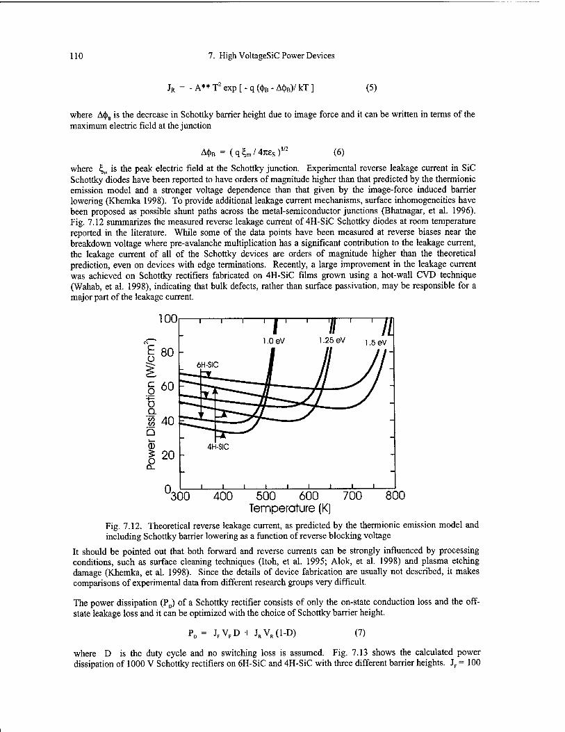
110 7. High VoltageSiC Power Devices
JR = -A**T2exp[-q(<j>B-A<j>B)/kT] (5)
where A<|>B is the decrease in Schottky barrier height due to image force and it can be written in terms of the maximum electric field at the junction
A<t>B = (q^m/47tes) 1/2
(6)
where £m is the peak electric field at the Schottky junction. Experimental reverse leakage current in SiC Schottky diodes have been reported to have orders of magnitude higher than that predicted by the thermionic emission model and a stronger voltage dependence than that given by the image-force induced barrier lowering (Khemka 1998). To provide additional leakage current mechanisms, surface inhomogeneities have been proposed as possible shunt paths across the metal-semiconductor junctions (Bhatnagar, et al. 1996). Fig. 7.12 summarizes the measured reverse leakage current of 4H-SiC Schottky diodes at room temperature reported in the literature. While some of the data points have been measured at reverse biases near the breakdown voltage where pre-avalanche multiplication has a significant contribution to the leakage current, the leakage current of all of the Schottky devices are orders of magnitude higher than the theoretical prediction, even on devices with edge terminations. Recently, a large improvement in the leakage current was achieved on Schottky rectifiers fabricated on 4H-SiC films grown using a hot-wall CVD technique (Wahab, et al. 1998), indicating that bulk defects, rather than surface passivation, may be responsible for a major part of the leakage current.
100
0 300 400 500 600 700 Temperature (K)
800
Fig. 7.12. Theoretical reverse leakage current, as predicted by the thermionic emission model and including Schottky barrier lowering as a function of reverse blocking voltage
It should be pointed out that both forward and reverse currents can be strongly influenced by processing conditions, such as surface cleaning techniques (Itoh, et al. 1995; Alok, et al. 1998) and plasma etching damage (Khemka, et al. 1998). Since the details of device fabrication are usually not described, it makes comparisons of experimental data from different research groups very difficult.
The power dissipation (PD) of a Schottky rectifier consists of only the on-state conduction loss and the off- state leakage loss and it can be optimized with the choice of Schottky barrier height.
= JFVFD JRVR(1-D) (7)
where D is the duty cycle and no switching loss is assumed. Fig. 7.13 shows the calculated power dissipation of 1000 V Schottky rectifiers on 6H-SiC and 4H-SiC with three different barrier heights. JF = 100
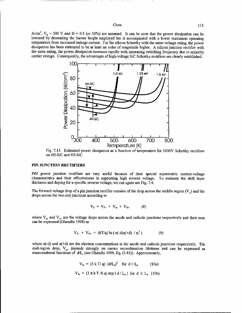
Chow 111
A/cm, VR = 500 V and D = 0.5 (or 50%) are assumed. It can be seen that the power dissipation can be lowered by decreasing the barrier height employed but is accompanied with a lower maximum operating temperature from increased leakage current. For the silicon Schottky with the same voltage rating, the power dissipation has been estimated to be at least an order of magnitude higher. A silicon junction rectifier with the same rating, the power dissipation increases rapidly with increasing switching frequency due to minority carrier storage. Consequently, the advantages of high-voltage SiC Schottky rectifiers are clearly established.
TOO
0
T r
1.0 eV 1.25 eV -\ 5 eV
300 400 800 500 600 700 Temperature (K)
Fig. 7.13. Estimated power dissipation as a function of temperature for 1000V Schottky rectifiers on6H-SiCand4H-SiC
PIN JUNCTION RECTIFIERS
PiN power junction rectifiers are very useful because of their special asymmetric current-voltage characteristics and their effectiveness in supporting high reverse voltage. To estimate the drift layer thickness and doping for a specific reverse voltage, we can again use Fig. 7.4.
The forward voltage drop of a pin junction rectifier consists of the drop across the middle region (VJ and the drops across the two end junctions according to
VF = VP+ + Vm + V, N+ (8)
where Vp+ and VN+ are the voltage drops across the anode and cathode junctions respectively and their sum can be expressed (Ghandhi 1998) as
VP+ + VN+ = (kT/q)ln(n(-d)n(+d) /ni2) (9)
where n(-d) and n(+d) are the electron concentrations at the anode and cathode junctions respectively. The mid-region drop, Vm, depends strongly on carrier recombination lifetimes and can be expressed as transcendental functions of d/La (see Ghandhi 1998, Eq. (3.81)). Approximately,
Vm = (3kT/q) (d/La)2 for d<La (10a)
Vm = (3nkT/8q)exp(d/La) for d > La (10b)
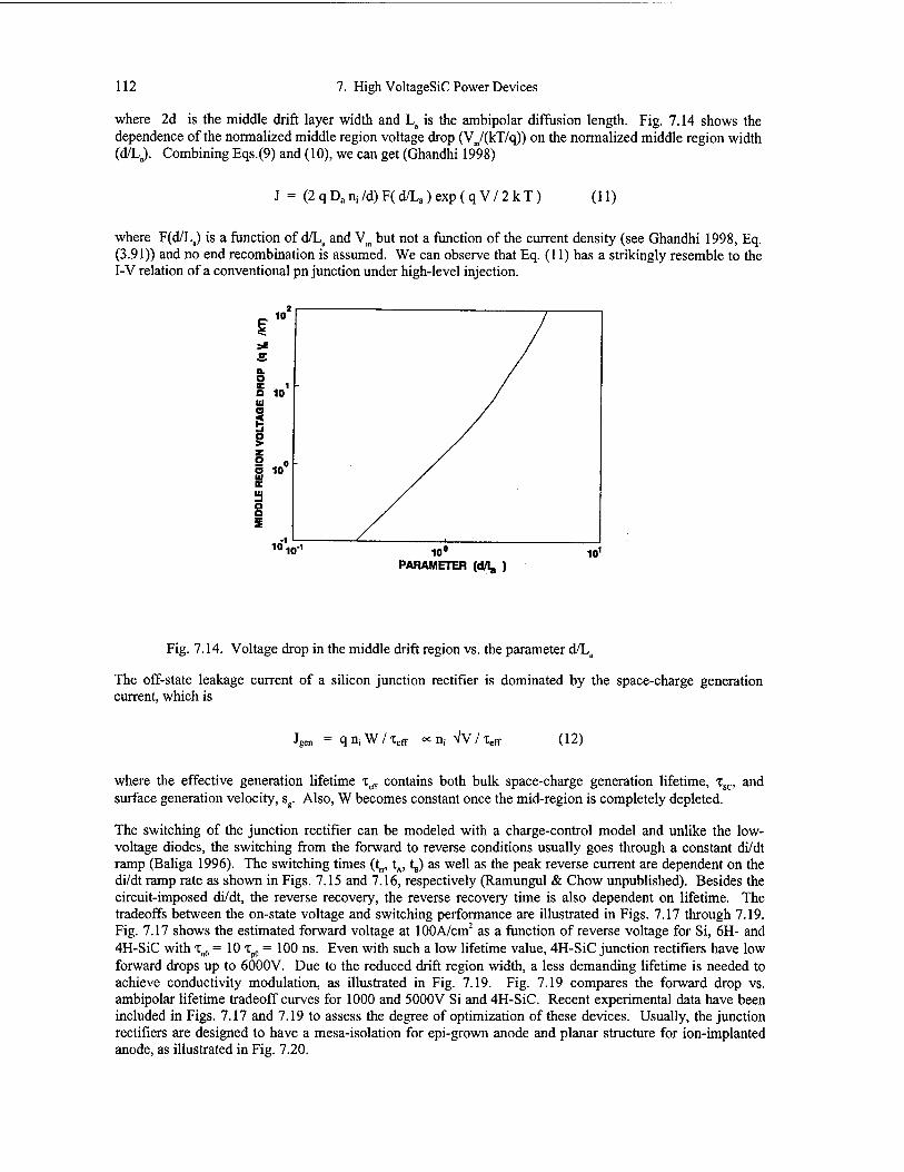
112 7. High VoltageSiC Power Devices
where 2d is the middle drift layer width and La is the ambipolar diffusion length. Fig. 7.14 shows the dependence of the normalized middle region voltage drop (V]n/(kT/q)) on the normalized middle region width (d/L„). Combining Eqs.(9) and (10), we can get (Ghandhi 1998)
J = (2qDani/d)F(d/La)exp(qV/2kT) (11)
where F(d/Lo) is a function of d/La and Vm but not a function of the current density (see Ghandhi 1998, Eq. (3.91)) and no end recombination is assumed. We can observe that Eq. (11) has a strikingly resemble to the I-V relation of a conventional pn junction under high-level injection.
PARAMETER (d/I, )
Fig. 7.14. Voltage drop in the middle drift region vs. the parameter d/La
The off-state leakage current of a silicon junction rectifier is dominated by the space-charge generation current, which is
Jgen = q n, W / Xeff oc m VV / X, eff (12)
where the effective generation lifetime xcfr contains both bulk space-charge generation lifetime, xsc, surface generation velocity, s . Also, W becomes constant once the mid-region is completely depleted.
and
The switching of the junction rectifier can be modeled with a charge-control model and unlike the low- voltage diodes, the switching from the forward to reverse conditions usually goes through a constant di/dt ramp (Baliga 1996). The switching times (t^, tA, t„) as well as the peak reverse current are dependent on the di/dt ramp rate as shown in Figs. 7.15 and 7.16, respectively (Ramungul & Chow unpublished). Besides the circuit-imposed di/dt, the reverse recovery, the reverse recovery time is also dependent on lifetime. The tradeoffs between the on-state voltage and switching performance are illustrated in Figs. 7.17 through 7.19. Fig. 7.17 shows the estimated forward voltage at 100A/cm2 as a function of reverse voltage for Si, 6H- and 4H-SiC with xn0 = 10 xp0 = 100 ns. Even with such a low lifetime value, 4H-SiC junction rectifiers have low forward drops up to 6000V. Due to the reduced drift region width, a less demanding lifetime is needed to achieve conductivity modulation, as illustrated in Fig. 7.19. Fig. 7.19 compares the forward drop vs. ambipolar lifetime tradeoff curves for 1000 and 5000V Si and 4H-SiC. Recent experimental data have been included in Figs. 7.17 and 7.19 to assess the degree of optimization of these devices. Usually, the junction rectifiers are designed to have a mesa-isolation for epi-grown anode and planar structure for ion-implanted anode, as illustrated in Fig. 7.20.
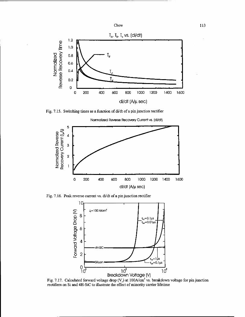
Chow
TA,TB,Trtvs.(di/dt)
113
<D 1.2
E i n i—
T3 (11
> 0.8
M > Ö
o o 0.6 h CD o ü; 0.4 z CD
to CD >
0.2 CD
C£. 0 200 400 600 800 1000 1200 1400 1600
di/dt (A/|i sec)
Fig. 7.15. Switching times as a function of di/dt of a pin junction rectifier
Normalized Reverse Recovery Current vs. (di/dt)
6 co
CD ^
o I £ c5 o u
4 •
3 ■
0 200 400 600 800 1000 1200 1400 1600
di/dt (A/|i sec)
Fig. 7.16. Peak reverse current vs. di/dt of a pin junction rectifier
io2 io3 io4
Breakdown Voltage (V) Fig. 7.17. Calculated forward voltage drop (VF) at 100A/cm2 vs. breakdown voltage for pin junction rectifiers on Si and 4H-SiC to illustrate the effect of minority carrier lifetime
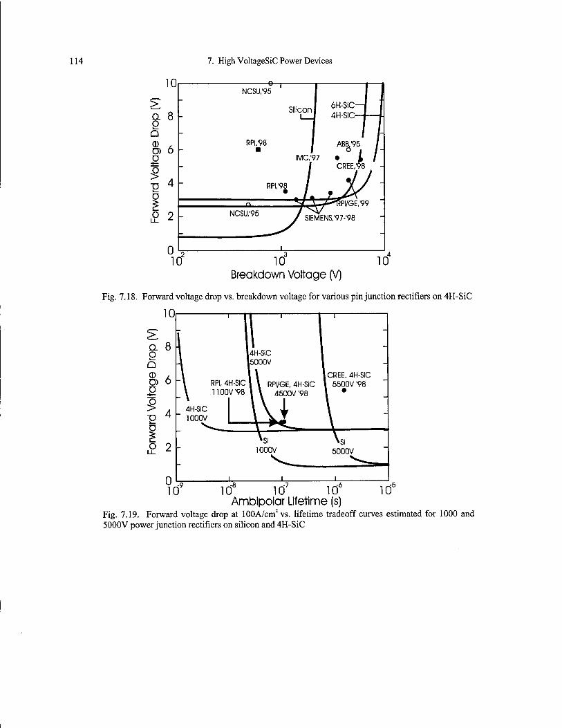
114 7. High VoltageSiC Power Devices
10
a 8 2 Q
O) 6 ö
o
o 2
e-r NCSU,'95
RPL'98
Silicon
-Ou NCSU/95
RPL'98
PI/GE/99
SIEMENS.'97-'98
0 10' 10°
Breakdown Voltage (V) 10
Fig. 7.18. Forward voltage drop vs. breakdown voltage for various pin junction rectifiers on 4H-SiC
10, r-
8 o. o Q 0 Ö) Ö
■<—
$ p Ö
.9 2
RPI. 4H-S1C 1100V98
4H-SIC 1000V
RPI/GE. 4H-SiC 4500V "98
|CREE. 4H-SIC 5500V '98
5000V
0 10'
K-7 10° 10" 10' 10 Ambipolar Lifetime (s)
Fig. 7.19. Forward voltage drop at 100A/cm2vs. lifetime tradeoff curves estimated for 1000 and 5000V power junction rectifiers on silicon and 4H-SiC
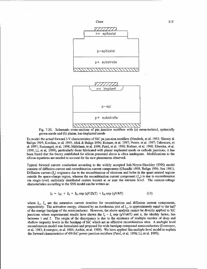
Chow 115
Y//////Ä n+ epitaxial
p-epitaxial
V//////A V n+ implant J
p-epi
p+ substrate
k\\\\\\\\\\\\\\\\\\\^^ Fig. 7.20. Schematic cross-sections of pin junction rectifiers with (a) mesa-isolated, epitaxially grown anode and (b) planar, ion-implanted anode
To model the actual forward I-V characteristics of SiC pn junction rectifiers (Neudeck, et al. 1993; Shenoy & Baliga 1995; Kordina, et al. 1995; Alok & Baliga 1996; Rottner, et al. 1997; Peters, et al. 1997; Takemura, et al. 1997; Ramungul, et al. 1998; Mitlehner, et al. 1998; Patel, et al. 1998; Rottner, et al. 1998; Khemka, et al. 1999; Li, et al. 1999), particularly those fabricated with planar implanted anode or cathode junctions, it has been found that the theory established for silicon presented above is often inadequate. Modifications to the silicon equations are needed to account for the new phenomena observed.
Typical forward current conduction according to the widely accepted Sah-Noyce-Shockley (SNS) model consists of diffusion current and recombination current components (Ghandhi 1998; Baliga 1996; Sze 1981). Diffusion current (Jd) originates due to the recombination of electrons and holes in the quasi-neutral regions outside the space-charge region, whereas the recombination current component (JJ is due to recombination via single-level, uniformly distributed centers located at or near the intrinsic level. The current-voltage characteristics according to the SNS model can be written as:
JF = Jsc + Jd = Jsi exp (qV/2kT) + JS2 exp (qV/kT) (13)
where Jsl, Js2 are the saturation current densities for recombination and diffusion current components, respectively. The activation energy, obtained by an Arrehenius plot of Jsl, is approximately equal to the half of the energy bandgap of the semiconductor. However, the above analysis cannot be directly applied to SiC junctions where experimental results have shown the JF ~ J0 exp (gV/nkT) and n, the ideality factor, lies between 1 and 2. The origin of the discrepancy is due to the existence of multiple number of deep and shallow impurity levels in the bandgap of SiC which act as effective recombination sites. A multiple level recombination model was formulated and proposed for wide bandgap compound semiconductors (Evstropov, et al. 1983; Evstropov, et al. 1984; Anikin, et al. 1989). We have applied this multiple level model to explain the forward characteristics of 4H-SiC power junction rectifiers (Patel, et al. 1998; Li, et al. 1999).
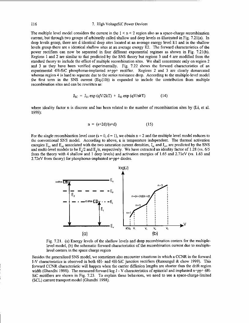
116 7. High VoltageSiC Power Devices
The multiple level model considers the current in the 1 < n < 2 region also as a space-charge recombination current, but through two groups of arbitrarily called shallow and deep levels as illustrated in Fig. 7.21(a). In deep levels group, there are d identical deep sites located at an average energy level El and in the shallow levels group there are s identical shallow sites at an average energy E2. The forward characteristics of the power rectifiers can now be separated in four different exponential regimes as shown in Fig. 7.21(b). Regions 1 and 2 are similar to that predicted by the SNS theory but regions 3 and 4 are modified from the standard theory to include the effect of multiple recombination sites. We shall concentrate only on region 2 and 3 as they have been verified experimentally. Fig. 7.22 shows the forward characteristics of an experimental 4H-SiC phosphorus-implanted n+pp+ rectifier. Regions 2 and 3 are clearly demarcated whereas region 4 is hard to separate due to the series resistance drop. According to the multiple-level model the first term in the SNS current (Eq.(lO)) is expanded to include the contribution from multiple recombination sites and can be rewritten as:
Jsc = Joi exp (qV/2kT) + J02 exp (qV/nkT) (14)
where ideality factor n is discrete and has been related to the number of recombination sites by (Li, et al. 1999):
n = (s+2d)/(s+d) (15)
For the single recombination level case (s = 0, d = 1), we obtain n = 2 and the multiple level model reduces to the conventional SNS model. According to above, n is temperature independent. The thermal activation energies EA1 and EA2 associated with the two saturation current densities, J01 and J02, are predicted by the SNS and multi-level models to be Eg/2 and Eg/n, respectively. We have extracted an ideality factor of 1.28 (vs. 6/5 from the theory with 4 shallow and 1 deep levels) and activation energies of 1.65 and 2.71eV (vs. 1.63 and 2.72eV from theory) for phosphorus-implanted n+pp+ diodes.
log(J)
s sites-(_s-r-
_ . _d sites ■[ =j
n=2.
n=fs+2cf)/(s+c!)
n=l
.V KT/q V, V,
(a) (b) Fig. 7.21. (a) Energy levels of the shallow levels and deep recombination centers for the multiple- level model, (b) the schematic forward characteristics of the recombination current due to multiple- level centers in the space charge region
Besides the generalized SNS model, we sometimes also encounter situations in which a CCNR in the forward I-V characteristics is observed in both 6H- and 4H-SiC junction rectifiers (Ramungul & chow 1999). This forward CCNR characteristic will happen when the carrier diffusion lengths are shorter than the drift region width (Ghandhi 1998). The measured forward log J - V characteristics of epitaxial and implanted n+pp+ 6H- SiC rectifiers are shown in Fig. 7.23. To explain these behaviors, we need to use a space-charge-limited (SCL) current transport model (Ghandhi 1998).
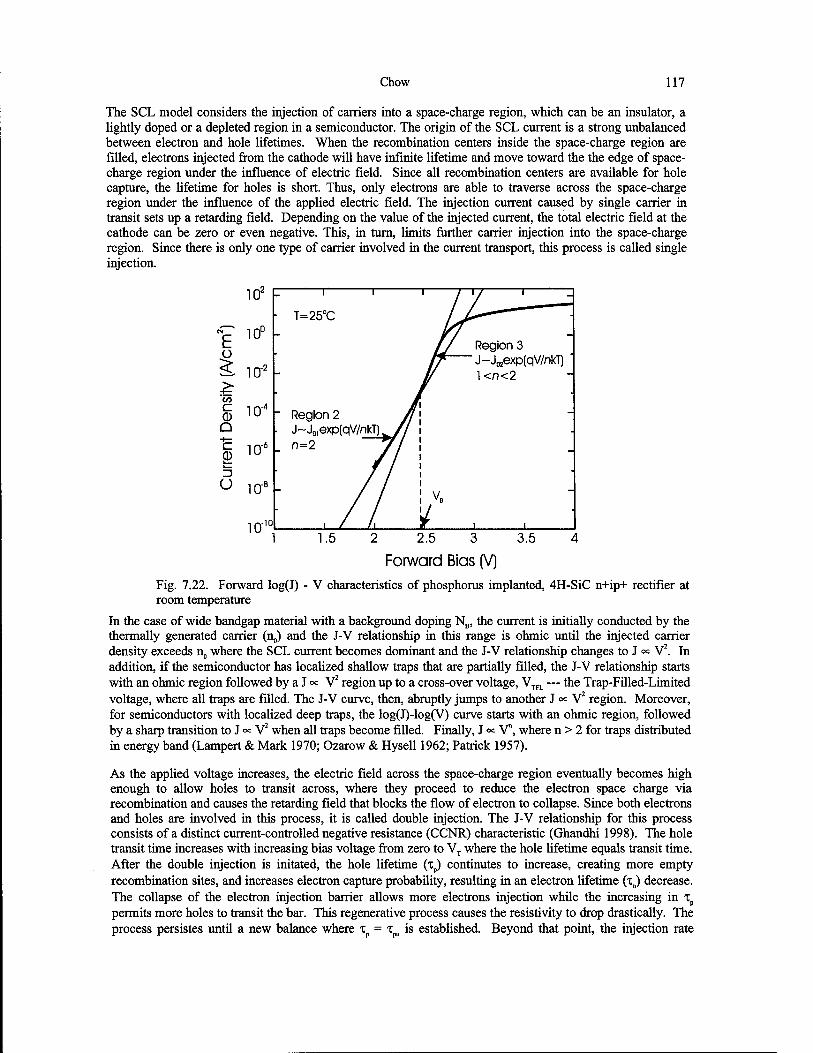
Chow 117
The SCL model considers the injection of carriers into a space-charge region, which can be an insulator, a lightly doped or a depleted region in a semiconductor. The origin of the SCL current is a strong unbalanced between electron and hole lifetimes. When the recombination centers inside the space-charge region are filled, electrons injected from the cathode will have infinite lifetime and move toward the the edge of space- charge region under the influence of electric field. Since all recombination centers are available for hole capture, the lifetime for holes is short. Thus, only electrons are able to traverse across the space-charge region under the influence of the applied electric field. The injection current caused by single carrier in transit sets up a retarding field. Depending on the value of the injected current, the total electric field at the cathode can be zero or even negative. This, in turn, limits further carrier injection into the space-charge region. Since there is only one type of carrier involved in the current transport, this process is called single injection.
10z
<V 10°
^ io-2
c irr4
Q
"<= in6 CD lu
O in-8 10"
1010
1 i I / '/ '
■ T=25°C Z-—— "" ■
■
Region 3 j~j02expiqv/nKij l<n<2
" Region 2 - . J~J0,exp(qV
n=2 7nkT)w/
- Wf I
- ! vB -
i / l\ \f i i 1.5 2 2.5 3 3.5 4
Forward Bias (V)
Fig. 7.22. Forward log(J) - V characteristics of phosphorus implanted, 4H-SiC n+ip+ rectifier at room temperature
In the case of wide bandgap material with a background doping NB, the current is initially conducted by the thermally generated carrier (n„) and the J-V relationship in this range is ohmic until the injected carrier density exceeds n,, where the SCL current becomes dominant and the J-V relationship changes to J « V2. In addition, if the semiconductor has localized shallow traps that are partially filled, the J-V relationship starts with an ohmic region followed by a J « V2 region up to a cross-over voltage, VTFL — the Trap-Filled-Limited voltage, where all traps are filled. The J-V curve, then, abruptly jumps to another J oe V2 region. Moreover, for semiconductors with localized deep traps, the log(J)-log(V) curve starts with an ohmic region, followed by a sharp transition to J °c V2 when all traps become filled. Finally, J <* V", where n > 2 for traps distributed in energy band (Lampert & Mark 1970; Ozarow & Hysell 1962; Patrick 1957).
As the applied voltage increases, the electric field across the space-charge region eventually becomes high enough to allow holes to transit across, where they proceed to reduce the electron space charge via recombination and causes the retarding field that blocks the flow of electron to collapse. Since both electrons and holes are involved in this process, it is called double injection. The J-V relationship for this process consists of a distinct current-controlled negative resistance (CCNR) characteristic (Ghandhi 1998). The hole transit time increases with increasing bias voltage from zero to VT where the hole lifetime equals transit time. After the double injection is initated, the hole lifetime (xp) continutes to increase, creating more empty recombination sites, and increases electron capture probability, resulting in an electron lifetime (T„) decrease. The collapse of the electron injection barrier allows more electrons injection while the increasing in z permits more holes to transit the bar. This regenerative process causes the resistivity to drop drastically. The process persistes until a new balance where xp = Tpn is established. Beyond that point, the injection rate

118 7. High VoltageSiC Power Devices
exceeds the recombination rate, making it possible for space charge to build up again. The J-V relationship in this two-carrier space-charge limited region can be characterized by a J <* V law (Ghandhi 19981].
S. iff
u io-'°
0 0.5 1.0 1.5 2.0 2.5 3.0 3.5 4.0
Forward Voltage (V)
10"
10"4
-£ icr
3 io-u
10-
io-'
(a)
- 25O°C^0^*.
ft0 jE^%%ryS~ 25°C ■
y^— l«V6(REF.)
0.1 6.0 1.0 Forward Voltage (V)
(b)
Fig. 7.23. Measured log J vs. V characteristics of epitaxial and implanted n+pp+ 6H-SiC rectifier
The triggering or threshold voltage, at which the electron transit time is equal to the electron lifetime under low level injection, can be estimated as (Ghandhi 1998)
VT ~ L2 / (n„ v,ow) (16)
This simple model has been applied to both nitrogen- and boron-implanted 6H-SiC junction diodes (Ramungul & Chow 1999), as shown in Fig. 7.24. The deep levels responsible for such CCNR characteristics can be either due to epitaxial material quality or implantation-induced defects that have not been completely annealed out. Deep levels from nitrogen implantation is also responsible for other anamolous behaviors, such as a new charge trapping phenomenon (Ramungul & Chow 1997).
The reverse leakage current has been found to be orders of magnitude higher than that predicted by standard silicon theory extensions. Obviously, material defects, such as screw dislocations, play a role in determining the reverse current (Neudeck, et al. 1999). With the improvement in material quality, fairly low reverse current densities (< 10s cm2) have been observed, at least for small area devices (Takemura, et al. 1997; Ramungul, et al. 1998; Mitlehner, et al. 1998; Patel, et al. 1998; Rottner, et al. 1998; Khemka, et al. 1999). Fig. 7.25 shows the reverse log J vs. V of a 4H-SiC, 1100V, Al/C/B-implanted pin junction rectifier
Chow 119
(Khemka, et al. 1999). At high reverse bias, some of the SiC junction rectifiers show an increase in reverse current (Patel, et al. 1998) that resembles a band-to-band tunneling characteristic, which has been observed in Si on insulator (Arnold, et al. 1996). In another case, a space-charge-limited current flow mechanism due to deep traps is also used to explain the dependence of the reverse current on reverse bias (JR ~ VR°, where 2 < n <5) (Anikin, et al. 1989).
icr 300
Temperature (°C) 200150 100 50
| io-3
to
t-
10"
~i—\—r T
Slope=0.06eV
• N-lmplanted Junction H N-Epltaxlal Junction
A B-lmplanted Junction i i
1.5 2.0 3.5 4.0 2.5 3.0 1000/T(1/K)
Fig. 7.24. Thermal activation energy plots of the CCNR triggering voltage in both nitrogen- and boron-implanted junction diode
-.-4
E i
ü
* , £.10° ^T CO C 0 Q ■£10"6 ^~-^~*<S='~'^--~~~' 2 -r-^^'^T- - -" J-V"2
u <J ' l-250c fRia' / L--50°C
<D 100°C > 0 a.
1
10' irf Reverse Voltage (V)
10'
Fig. 7.25. Reverse log J-V characteristic of a 1100V Al/C/B-implanted 4H-SiC pin junction rectifier
The reverse recovery current waveforms of both epitaxial and implanted junction rectifiers have an interesting temperature dependence that has not been seen in Si devices (Peters, et al. 1997; Mitlehner, et al. 1998). In Fig. 7.26, typical reverse recovery current waveforms of a 1100V, p+n implanted diode are measured up to 200°C. Interestingly, the reverse recovery charge (QJ and recovery time (Xn) remains constant with increasing temperature, which may indicate the deepness of the energy level of the
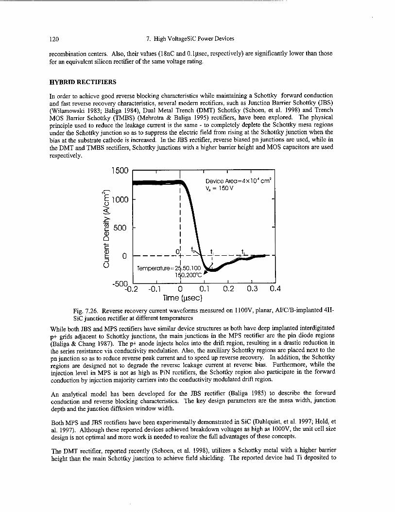
120 7. High VoltageSiC Power Devices
recombination centers. Also, their values (18nC and 0. l|j.sec, respectively) are significantly lower than those for an equivalent silicon rectifier of the same voltage rating.
HYBRID RECTIFIERS
In order to achieve good reverse blocking characteristics while maintaining a Schottky forward conduction and fast reverse recovery characteristics, several modern rectifiers, such as Junction Barrier Schottky (JBS) (Wilamowski 1983; Baliga 1984), Dual Metal Trench (DMT) Schottky (Schoen, et al. 1998) and Trench MOS Barrier Schottky (TMBS) (Mehrotra & Baliga 1995) rectifiers, have been explored. The physical principle used to reduce the leakage current is the same - to completely deplete the Schottky mesa regions under the Schottky junction so as to suppress the electric field from rising at the Schottky junction when the bias at the substrate cathode is increased. In the JBS rectifier, reverse biased pn junctions are used, while in the DMT and TMBS rectifiers, Schottky junctions with a higher barrier height and MOS capacitors are used respectively.
1500
£ o
CO C CD Q
c 0
O
1000
500
0
-500
1 1 1
Device Area=4x 10' cm2
V„= 150 V
Temperature=2q,50,100 iqO,200°C
-0.2 -0.1 0 0.1 Time (|isec)
0.2 0.3 0.4
Fig. 7.26. Reverse recovery current waveforms measured on 1100V, planar, Al/C/B-implanted 4H- SiC junction rectifier at different temperatures
While both JBS and MPS rectifiers have similar device structures as both have deep implanted interdigitated p+ grids adjacent to Schottky junctions, the main junctions in the MPS rectifier are the pin diode regions (Baliga & Chang 1987). The p+ anode injects holes into the drift region, resulting in a drastic reduction in the series resistance via conductivity modulation. Also, the auxiliary Schottky regions are placed next to the pn junction so as to reduce reverse peak current and to speed up reverse recovery. In addition, the Schottky regions are designed not to degrade the reverse leakage current at reverse bias. Furthermore, while the injection level in MPS is not as high as PiN rectifiers, the Schottky region also participate in the forward conduction by injection majority carriers into the conductivity modulated drift region.
An analytical model has been developed for the JBS rectifier (Baliga 1985) to describe the forward conduction and reverse blocking characteristics. The key design parameters are the mesa width, junction depth and the junction diffusion window width.
Both MPS and JBS rectifiers have been experimentally demonstrated in SiC (Dahlquist, et al. 1997; Held, et al. 1997). Although these reported devices achieved breakdown voltages as high as 1000V, the unit cell size design is not optimal and more work is needed to realize the full advantages of these concepts.
The DMT rectifier, reported recently (Schoen, et al. 1998), utilizes a Schottky metal with a higher barrier height than the main Schottky junction to achieve field shielding. The reported device had Ti deposited to
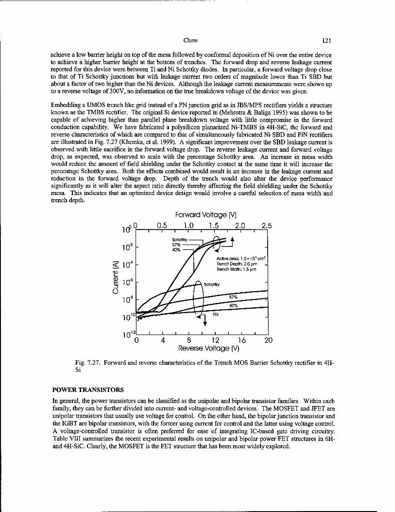
Chow 121
achieve a low barrier height on top of the mesa followed by conformal deposition of Ni over the entire device to achieve a higher barrier height at the bottom of trenches. The forward drop and reverse leakage current reported for this device were between Ti and Ni Schottky diodes. In particular, a forward voltage drop close to that of Ti Schottky junctions but with leakage current two orders of magnitude lower than Ti SBD but about a factor of two higher than the Ni devices. Although the leakage current measurements were shown up to a reverse voltage of 300V, no information on the true breakdown voltage of the device was given.
Embedding a UMOS trench like grid instead of a PN junction grid as in JBS/MPS rectifiers yields a structure known as the TMBS rectifier. The original Si device reported in (Mehrotra & Baliga 1995) was shown to be capable of achieving higher than parallel plane breakdown voltage with little compromise in the forward conduction capability. We have fabricated a polysilicon planarized Ni-TMBS in 4H-SiC, the forward and reverse characteristics of which are compared to that of simultaneously fabricated Ni SBD and PiN rectifiers are illustrated in Fig. 7.27 (Khemka, et al. 1999). A significant improvement over the SBD leakage current is observed with little sacrifice in the forward voltage drop. The reverse leakage current and forward voltage drop, as expected, was observed to scale with the percentage Schottky area. An increase in mesa width would reduce the amount of field shielding under the Schottky contact at the same time it will increase the percentage Schottky area. Both the effects combined would result in an increase in the leakage current and reduction in the forward voltage drop. Depth of the trench would also alter the device performance significantly as it will alter the aspect ratio directly thereby affecting the field shielding under the Schottky mesa. This indicates that an optimized device design would involve a careful selection of mesa width and trench depth.
10" .-12
Forward Voltage (V)
0.5 1.0 1.5 2.0 2.5 T 1 1 r
Aclive area: 1.5x 10s crrf liench Deptti: 2.0 um Irench Width: 1.5 |im
J l_ J L J l_
8 12 16 Reverse Voltage (V)
20
Fig. 7.27. Forward and reverse characteristics of the Trench MOS Barrier Schottky rectifier in 4H- Si
POWER TRANSISTORS
In general, the power transistors can be classified as the unipolar and bipolar transistor families. Within each family, they can be further divided into current- and voltage-controlled devices. The MOSFET and JFET are unipolar transistors that usually use voltage for control. On the other hand, the bipolar junction transistor and the IGBT are bipolar transistors, with the former using current for control and the latter using voltage control. A voltage-controlled transistor is often preferred for ease of integrating IC-based gate driving circuitry. Table VIII summarizes the recent experimental results on unipolar and bipolar power FET structures in 6H- and 4H-SiC. Clearly, the MOSFET is the FET structure that has been most widely explored.
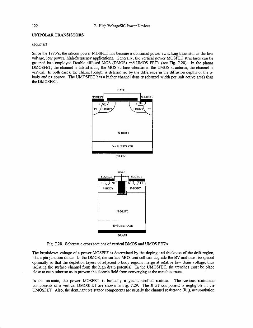
122 7. High VoltageSiC Power Devices
UNIPOLAR TRANSISTORS
MOSFET
Since the 1970's, the silicon power MOSFET has become a dominant power switching transistor in the low voltage, low power, high-frequency applications. Generally, the vertical power MOSFET structures can be grouped into employed Double-diffused MOS (DMOS) and UMOS FET's (see Fig. 7.28). In the planar DMOSFET, the channel is lateral along the MOS surface whereas in the UMOS structures, the channel is vertical. In both cases, the channel length is determined by the difference in the diffusion depths of the p- body and n+ source. The UMOSFET has a higher channel density (channel width per unit active area) than the DMOSFET.
GATE
SOURCE SOURCE
N-DRIFT
N+ SUBSTRATE
DRAIN
GATE
SOURCE I 1 1 SOURCE
P+l J N+ N+CTP+ P-BODY P-BODY
N-DRIF T
N+SUBSTRATE
DRAIN
Fig. 7.28. Schematic cross sections of vertical DMOS and UMOS FET's
The breakdown voltage of a power MOSFET is determined by the doping and thickness of the drift region, like a pin junction diode. In the DMOS, the surface MOS unit cell can degrade the BV and must be spaced optimally so that the depletion layers of adjacent p body regions merge at relative low drain voltage, thus isolating the surface channel from the high drain potential. In the UMOSFET, the trenches must be place close to each other so as to prevent the electric field from converging at the trench corners.
In the on-state, the power MOSFET is basically a gate-controlled resistor. The various resistance components of a vertical DMOSFET are shown in Fig. 7.29. The JFET component is negligible in the UMOSFET. Also, the dominant resistance components are usually the channel resistance (Rch), accumulation
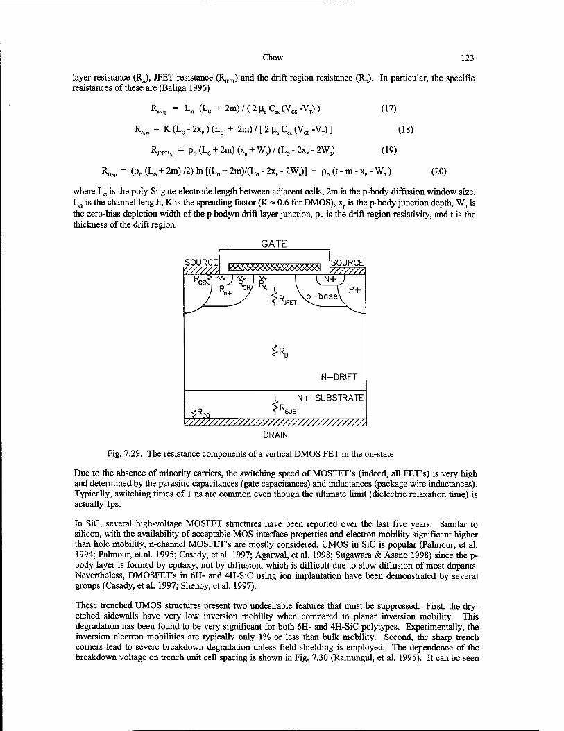
Chow 123
layer resistance (RA), JFET resistance (RJFET) and the drift region resistance (RD). In particular, the specific resistances of these are (Baliga 1996)
R. "ch,sp Lch(L0 + 2m)/(2nnC0X(V0S-VT)) (17)
R^ = K (LG - 2xp) (LG + 2m) / [ 2 n„ Cn (VGS -VT) ]
RTOT>SP = PD (LG + 2m) (x + W0) / (LG - 2xp - 2W0)
(18)
(19)
RD,sp = (Po (L0 + 2m) 12) In [(LG + 2m)/(L0 - 2xp - 2W0)] + pD (t - m - xp - W0) (20)
where LG is the poly-Si gate electrode length between adjacent cells, 2m is the p-body diffusion window size, Lch is the channel length, K is the spreading factor (K ~ 0.6 for DMOS), xp is the p-body junction depth, W0 is the zero-bias depletion width of the p body/n drift layer junction, pD is the drift region resistivity, and t is the thickness of the drift region.
GATE
SOURCE SOURCE V/////A
N-DRIFT
*
N+ SUBSTRATE
SUB
YZZ '///////////////////////////////A DRAIN
Fig. 7.29. The resistance components of a vertical DMOS FET in the on-state
Due to the absence of minority carriers, the switching speed of MOSFET's (indeed, all FET's) is very high and determined by the parasitic capacitances (gate capacitances) and inductances (package wire inductances). Typically, switching times of 1 ns are common even though the ultimate limit (dielectric relaxation time) is actually lps.
In SiC, several high-voltage MOSFET structures have been reported over the last five years. Similar to silicon, with the availability of acceptable MOS interface properties and electron mobility significant higher than hole mobility, n-channel MOSFET's are mostly considered. UMOS in SiC is popular (Palmour, et al. 1994; Palmour, et al. 1995; Casady, et al. 1997; Agarwal, et al. 1998; Sugawara & Asano 1998) since the p- body layer is formed by epitaxy, not by diffusion, which is difficult due to slow diffusion of most dopants. Nevertheless, DMOSFET's in 6H- and 4H-SiC using ion implantation have been demonstrated by several groups (Casady, et al. 1997; Shenoy, et al. 1997).
These trenched UMOS structures present two undesirable features that must be suppressed. First, the dry- etched sidewalls have very low inversion mobility when compared to planar inversion mobility. This degradation has been found to be very significant for both 6H- and 4H-SiC polytypes. Experimentally, the inversion electron mobilities are typically only 1% or less than bulk mobility. Second, the sharp trench corners lead to severe breakdown degradation unless field shielding is employed. The dependence of the breakdown voltage on trench unit cell spacing is shown in Fig. 7.30 (Ramungul, et al. 1995). It can be seen

124 7. High VoltageSiC Power Devices
from these simulations that a maximum esa width of 2 urn is to be designed. Utilizing such design rules, experimental UMOSFET's with a BV over 1000V have been realized (Casady, et al. 1997). In addition, the MOS capacitors at the bottom of the trenches also experience a more severe field stressing than in the silicon case. The reason for the high field problem in SiC MOS is the higher avalanche field in SiC vs. Si (2-3 vs. 0.2 MV/cm) and a lower permittivity of SiC vs. Si (10 vs. 12), resulting in an oxide field of ~7 MV/cm or ~70% of the oxide breakdown field. Such a high field could reduce device yield and lead to potential device reliability problems. By comparison, the oxide field in Si is less than 1 MV/cm when the silicon reaches avalanche condition. Replacing Si02 with a dielectric of a higher permittivity is not as an attractive as it may first appear. Besides the need to have MOS interface properties close to those obtained for oxide/SiC, while replacing the oxide with a dielectric with higher permittivity leads to a low field, the decreasing breakdown field with increasing permittivity trend (see Fig. 31) (^ <* e'2) (Chow & Ramungul) negates much of the gain with this technique. Novel device structures can also be used to circumvent this issue (Agarwal, et. Al. 1997).
1600
2 1400 CD D) 5 1200 h
§ 1000 o S 800 CO
600
-i—i—i—i—i—i—i—p Trench depth=2,15um, and BVpp
Trench depth=2.5|im
■V. Trench depth=3.0nm
Trench depth=4.0jim
20 40 60 80 Mesa width (|am)
100
1600
2.5 3.0 3.5 4.0
Trench Depth (urn) 4.5
Fig. 7.30. Breakdown voltage as a function of UMOS (a) mesa width and (b) trench depth

Chow 125
TOO
E O
2 10 p
C
O 1 2 ö 0
0.1
: 1 '
Si02
1—i—i—i—1111 i '".
\ SiaN4 .
; blÜ2 *•" *.Ji ^/
RPI Multi-Layered -
.PTO W
^TK>T* •
* .PZT
: RPI Composite STO' " f '-I- ■f»
i
BST
* • *
1
10 100
Permittivity 1000 10000
Fig. 7.31. Dielectric breakdown field as function of permittivity
Besides the field problem in the oxide, the band offsets between the 6H-SiC or 4H-SiC and Si02 in both the conduction and valence band edges are smaller than those between silicon and oxide (Agarwal, et. al. 1997). Consequently, it is easier for electrons and holes to surmount the barrier and inject into the oxide when they are confined to the SiC/Si02 interface, particularly at elevated temperatures. Fowler-Nordhelm tunneling has been measured for SiC MOS capacitors and found to be quite severe at 300°C (Agarwal, et. al. 1997; Bano, et. al. 1997).
To circumvent the low electron inversion layer mobility, normally-off accumulation type MOSFET's have become popular and have been demonstrated (Hara 1998; Shenoy & Baliga 1997; Tan, et. al. 1998; Seshadri, et. al. 1998; Crofton, et. al. 1997; Peters, et. al. 1999). However, these devices have higher leakage currents, particularly at elevated temperatures and near BV. In Fig. 7.32, the specific on-resistance of the various UMOS, DMOS and accumulation-mode FET's are plotted as a function of breakdown voltage. It can be seen that many of the experimental MOSFET's have already exceeded the silicon material limit. However, as indicated in Table 7.8, the current level is still low ( < 5A). Also, since the inversion layer mobility of electrons in 4H-SiC is usually very low (< 10 cmVV-sec) while that in 6H-SiC is acceptable (30-50 cmVV- sec), the best inversion-mode vertical SiC MOSFET's have been shown in 6H-SiC so far (Seshadri, et. al. 1998; Crofton, et. al. 1997). Furthermore, it has been suggested that the 15R polytype may be most suitable for SiC power MOSFET due to its high electron inversion mobility (33 cm2/V-sec) (like 6H-SiC) but more isotropic bulk mobilties (like 4H-SiC) (Chatty, et. al. 1999).
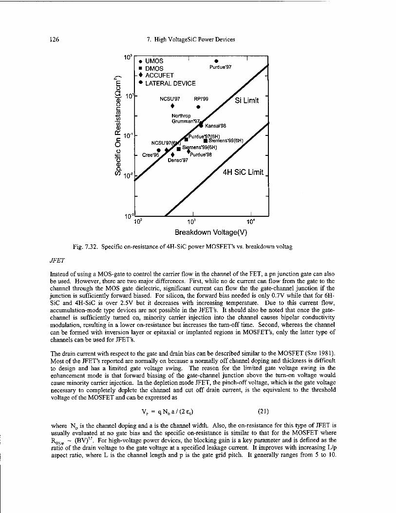
126 7. High VoltageSiC Power Devices
103
E o a o c CO *—» w to <D (Z c O
o CD Q.
CO
101
• UMOS ■ DMOS • ACCUFET • LATERAL DEVICE
NCSU'97
♦
Purdue'97
IQ"1
10"
10" 103 104
Breakdown Voltage(V)
Fig. 7.32. Specific on-resistance of 4H-SiC power MOSFET's vs. breakdown voltag
JFET
Instead of using a MOS-gate to control the carrier flow in the channel of the FET, a pn junction gate can also be used. However, there are two major differences. First, while no dc current can flow from the gate to the channel through the MOS gate dielectric, significant current can flow the the gate-channel junction if the junction is sufficiently forward biased. For silicon, the forward bias needed is only 0.7V while that for 6H- SiC and 4H-SiC is over 2.5V but it decreases with increasing temperature. Due to this current flow, accumulation-mode type devices are not possible in the JFET's. It should also be noted that once the gate- channel is sufficiently turned on, minority carrier injection into the channel causes bipolar conductivity modulation, resulting in a lower on-resistance but increases the turn-off time. Second, whereas the channel can be formed with inversion layer or epitaxial or implanted regions in MOSFET's, only the latter type of channels can be used for JFET's.
The drain current with respect to the gate and drain bias can be described similar to the MOSFET (Sze 1981). Most of the JFET's reported are normally on because a normally off channel doping and thickness is difficult to design and has a limited gate voltage swing. The reason for the limited gate voltage swing in the enhancement mode is that forward biasing of the gate-channel junction above the turn-on voltage would cause minority carrier injection. In the depletion mode JFET, the pinch-off voltage, which is the gate voltage necessary to completely deplete the channel and cut off drain current, is the equivalent to the threshold voltage of the MOSFET and can be expressed as
Vp = qNDa/(2es) (21)
where ND is the channel doping and a is the channel width. Also, the on-resistance for this type of JFET is usually evaluated at no gate bias and the specific on-resistance is similar to that for the MOSFET where R0Ns ~ (BV)2S. For high-voltage power devices, the blocking gain is a key parameter and is defined as the ratio of the drain voltage to the gate voltage at a specified leakage current. It improves with increasing L/p aspect ratio, where L is the channel length and p is the gate grid pitch. It generally ranges from 5 to 10.
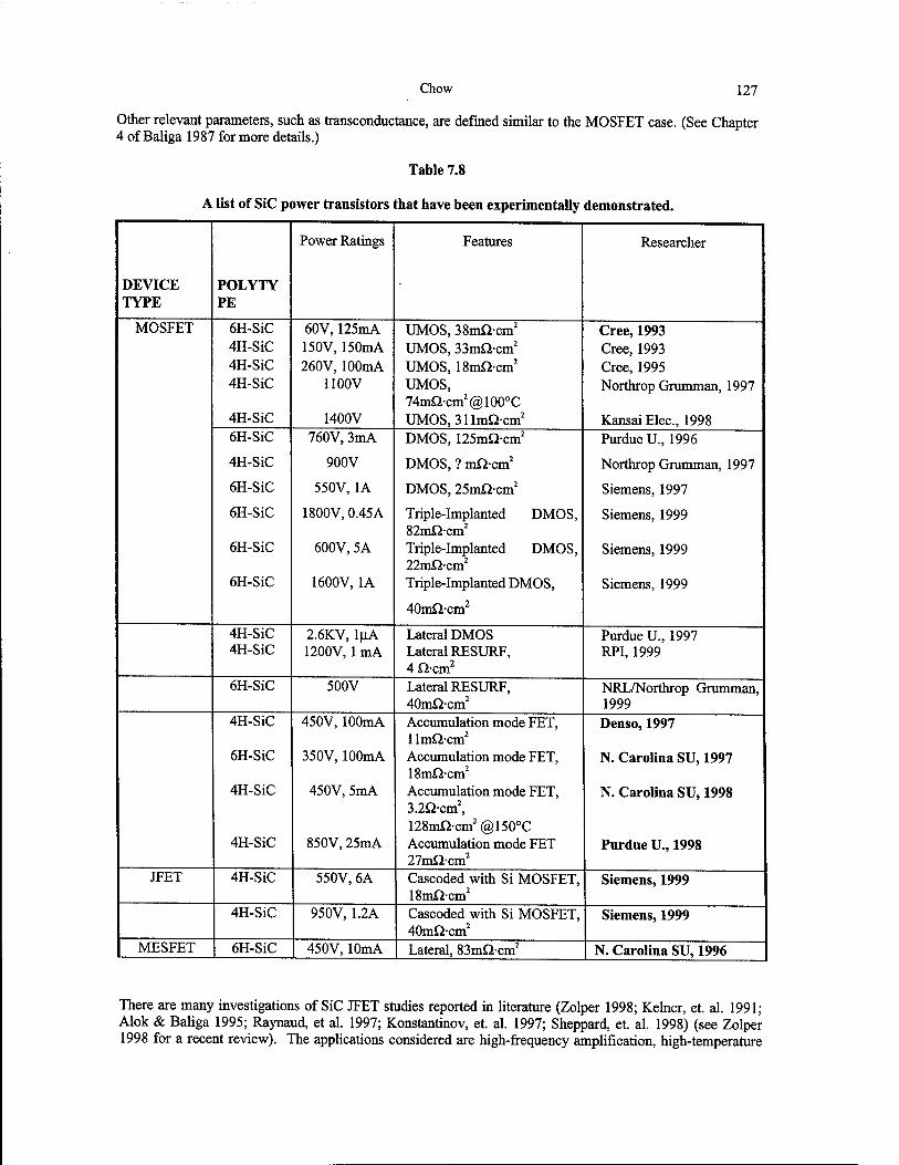
Chow 127
Other relevant parameters, such as transconductance, are defined similar to the MOSFET case. (See Chapter 4 of Baliga 1987 for more details.)
Table 7.8
A list of SiC power transistors that have been experimentally demonstrated.
Power Ratings Features Researcher
DEVICE POLYTY TYPE PE
MOSFET 6H-SiC 60V, 125mA UMOS, 38mQ-cm2 Cree, 1993 4H-SiC 150V, 150mA UMOS, 33mQ-cm2 Cree, 1993 4H-SiC 260V, 100mA UMOS, 18mQ-cm2 Cree, 1995 4H-SiC 1100V UMOS,
74mQ-cm2@100°C Northrop Grumman, 1997
4H-SiC 1400V UMOS,311mQcm2 Kansai Elec, 1998 6H-SiC 760V, 3mA DMOS, 125mQcm2 Purdue U., 1996
4H-SiC 900V DMOS, ?mßcm2 Northrop Grumman, 1997
6H-SiC 550V, 1A DMOS, 25mQcm2 Siemens, 1997
6H-SiC 1800V, 0.45A Triple-Implanted DMOS, 82mQcm2
Siemens, 1999
6H-SiC 600V, 5A Triple-Implanted DMOS, 22m£2-cm2
Siemens, 1999
6H-SiC 1600V, 1A Triple-Implanted DMOS,
40mQ-cm2
Siemens, 1999
4H-SiC 2.6KV, ljiA Lateral DMOS Purdue U., 1997 4H-SiC 1200V, 1 mA Lateral RESURF,
4 Qcm2 RPI, 1999
6H-SiC 500V Lateral RESURF, 40mQ-cm2
NRL/Northrop Grumman, 1999
4H-SiC 450V, 100mA Accumulation mode FET, 1 lmfitcm2
Denso, 1997
6H-SiC 350V, 100mA Accumulation mode FET, 18mQcm2
N. Carolina SU, 1997
4H-SiC 450V, 5mA Accumulation mode FET, 3.2Qcm2, 128mQ-cm2@150°C
N. Carolina SU, 1998
4H-SiC 850V, 25mA Accumulation mode FET 27mQ-cm2
Purdue U., 1998
JFET 4H-SiC 550V, 6A Cascoded with Si MOSFET, 18mficm2
Siemens, 1999
4H-SiC 950V, 1.2A Cascoded with Si MOSFET, 40mQ-cm2
Siemens, 1999
MESFET 6H-SiC 450V, 10mA Lateral, 83mQ-cm2 N. Carolina SU, 1996 |
There are many investigations of SiC JFET studies reported in literature (Zolper 1998; Keiner, et. al. 1991; Alok & Baliga 1995; Raynaud, et al. 1997; Konstantinov, et. al. 1997; Sheppard, et. al. 1998) (see Zolper 1998 for a recent review). The applications considered are high-frequency amplification, high-temperature
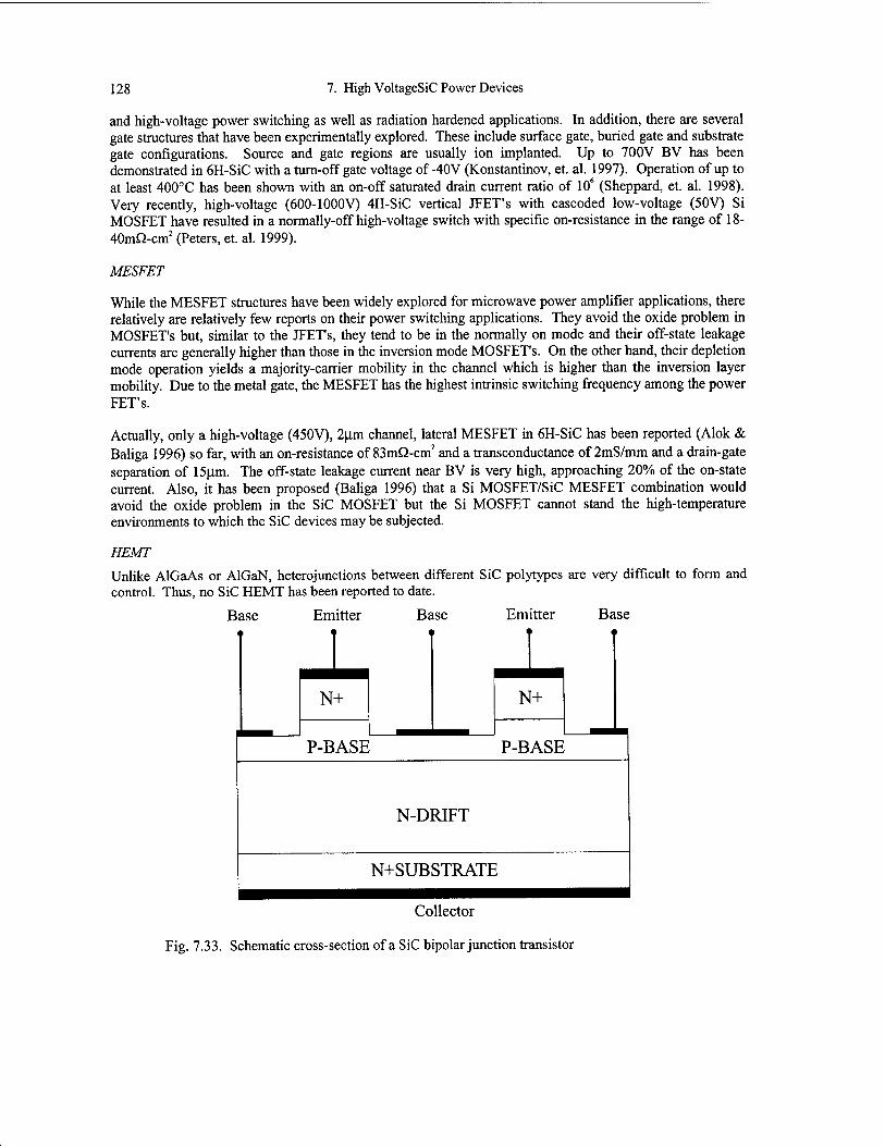
128 7. High VoltageSiC Power Devices
and high-voltage power switching as well as radiation hardened applications. In addition, there are several gate structures that have been experimentally explored. These include surface gate, buried gate and substrate gate configurations. Source and gate regions are usually ion implanted. Up to 700V BV has been demonstrated in 6H-SiC with a turn-off gate voltage of-40V (Konstantinov, et. al. 1997). Operation of up to at least 400°C has been shown with an on-off saturated drain current ratio of 106 (Sheppard, et. al. 1998). Very recently, high-voltage (600-1000V) 4H-SiC vertical JFET's with cascoded low-voltage (50V) Si MOSFET have resulted in a normally-off high-voltage switch with specific on-resistance in the range of 18- 40mQ-cm2 (Peters, et. al. 1999).
MESFET
While the MESFET structures have been widely explored for microwave power amplifier applications, there relatively are relatively few reports on their power switching applications. They avoid the oxide problem in MOSFET's but, similar to the JFET's, they tend to be in the normally on mode and their off-state leakage currents are generally higher than those in the inversion mode MOSFET's. On the other hand, their depletion mode operation yields a majority-carrier mobility in the channel which is higher than the inversion layer mobility. Due to the metal gate, the MESFET has the highest intrinsic switching frequency among the power FET's.
Actually, only a high-voltage (450V), 2(0.m channel, lateral MESFET in 6H-SiC has been reported (Alok & Baliga 1996) so far, with an on-resistance of 83mQ-cm2 and a transconductance of 2mS/mm and a drain-gate separation of 15n_m. The off-state leakage current near BV is very high, approaching 20% of the on-state current. Also, it has been proposed (Baliga 1996) that a Si MOSFET/SiC MESFET combination would avoid the oxide problem in the SiC MOSFET but the Si MOSFET cannot stand the high-temperature environments to which the SiC devices may be subjected.
HEMT
Unlike AlGaAs or AlGaN, heterojunctions between different SiC polytypes are very difficult to form and control. Thus, no SiC HEMT has been reported to date.
Base Emitter Base Emitter Base 11 i i i • ( i 11
N+ N+
P-BASE P-BASE
N-DRIFT
N+SUBSTRATE
Collector
Fig. 7.33. Schematic cross-section of a SiC bipolar junction transistor
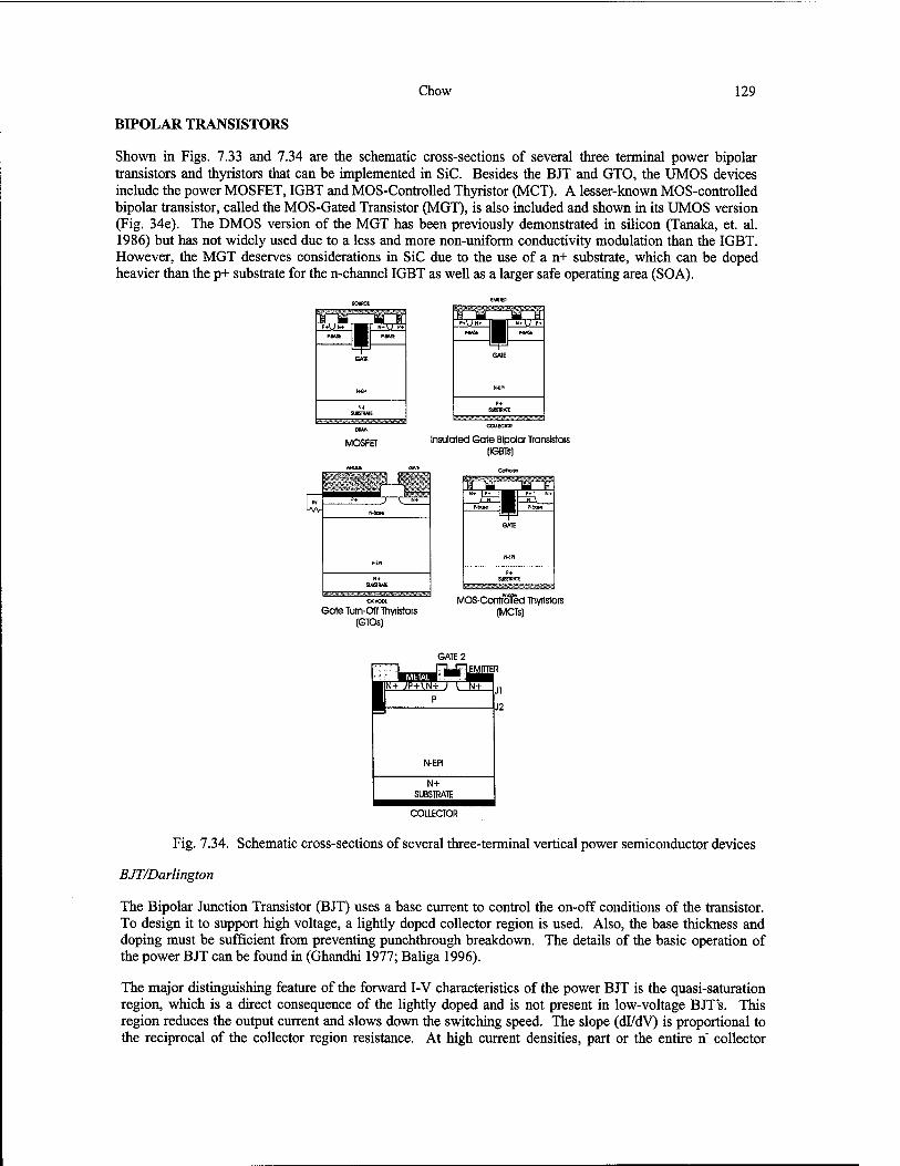
Chow 129
BIPOLAR TRANSISTORS
Shown in Figs. 7.33 and 7.34 are the schematic cross-sections of several three terminal power bipolar transistors and thyristors that can be implemented in SiC. Besides the BJT and GTO, the UMOS devices include the power MOSFET, IGBT and MOS-Controlled Thyristor (MCT). A lesser-known MOS-controlled bipolar transistor, called the MOS-Gated Transistor (MGT), is also included and shown in its UMOS version (Fig. 34e). The DMOS version of the MGT has been previously demonstrated in silicon (Tanaka, et. al. 1986) but has not widely used due to a less and more non-uniform conductivity modulation than the IGBT. However, the MGT deserves considerations in SiC due to the use of a n+ substrate, which can be doped heavier than the p+ substrate for the n-channel IGBT as well as a larger safe operating area (SOA).
MOSFET Insulated Gate Bipolar Transistors (IGBTs)
." ' - 1 VBHMa r1— p. J k
H*~
MP1
SUOTRME
Gate Tutn-Off Thyristors (GTOs)
MOS-ConttoiJed Thyristors (MCTs)
GATE 2
N-EPI
N+ SUBSTRATE
COLLECTOR
Fig. 7.34. Schematic cross-sections of several three-terminal vertical power semiconductor devices
BJT/Darlington
The Bipolar Junction Transistor (BJT) uses a base current to control the on-off conditions of the transistor. To design it to support high voltage, a lightly doped collector region is used. Also, the base thickness and doping must be sufficient from preventing punchthrough breakdown. The details of the basic operation of the power BJT can be found in (Ghandhi 1977; Baliga 1996).
The major distinguishing feature of the forward I-V characteristics of the power BJT is the quasi-saturation region, which is a direct consequence of the lightly doped and is not present in low-voltage BJT's. This region reduces the output current and slows down the switching speed. The slope (dl/dV) is proportional to the reciprocal of the collector region resistance. At high current densities, part or the entire n" collector
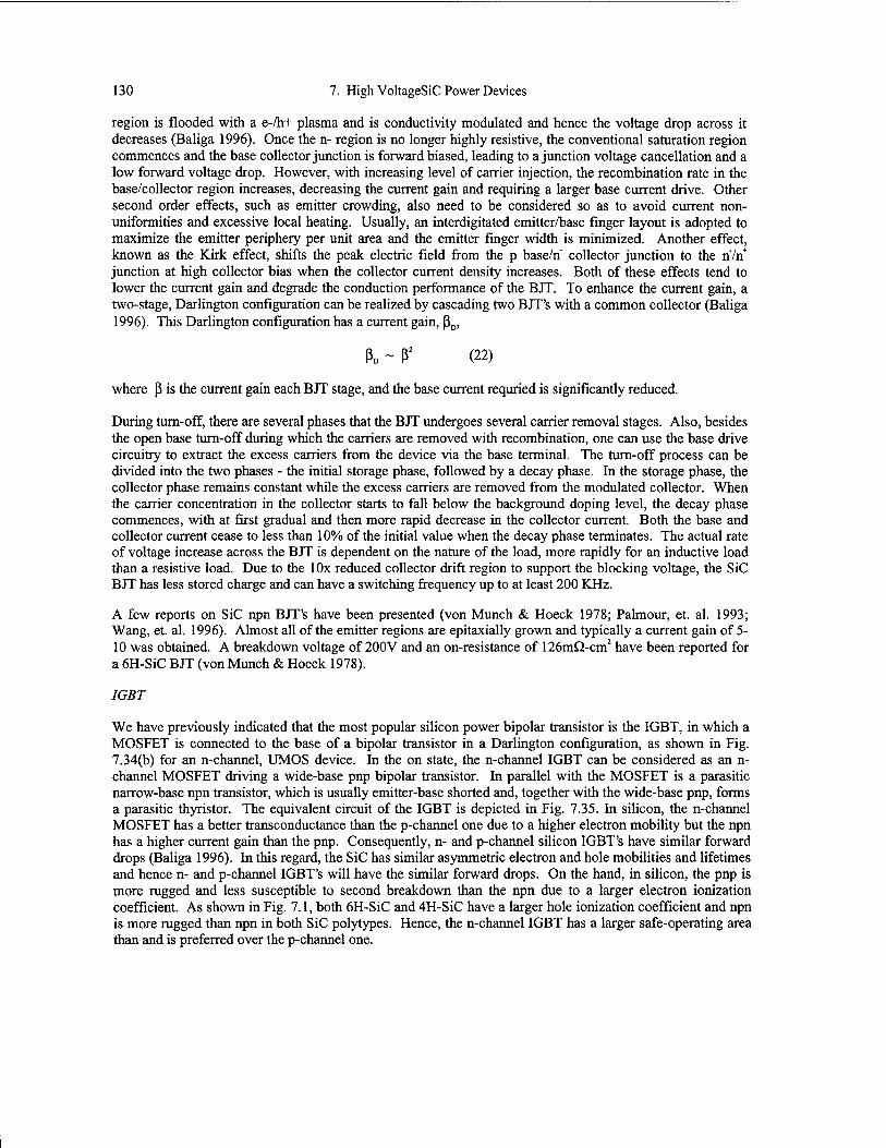
130 7. High VoltageSiC Power Devices
region is flooded with a e-/h+ plasma and is conductivity modulated and hence the voltage drop across it decreases (Baliga 1996). Once the n- region is no longer highly resistive, the conventional saturation region commences and the base collector junction is forward biased, leading to a junction voltage cancellation and a low forward voltage drop. However, with increasing level of carrier injection, the recombination rate in the base/collector region increases, decreasing the current gain and requiring a larger base current drive. Other second order effects, such as emitter crowding, also need to be considered so as to avoid current non- uniformities and excessive local heating. Usually, an interdigitated emitter/base finger layout is adopted to maximize the emitter periphery per unit area and the emitter finger width is minimized. Another effect, known as the Kirk effect, shifts the peak electric field from the p base/n" collector junction to the n"/n+
junction at high collector bias when the collector current density increases. Both of these effects tend to lower the current gain and degrade the conduction performance of the BJT. To enhance the current gain, a two-stage, Darlington configuration can be realized by cascading two BJT's with a common collector (Baliga 1996). This Darlington configuration has a current gain, ßD,
ßo ~ ß2 (22)
where ß is the current gain each BJT stage, and the base current requried is significantly reduced.
During turn-off, there are several phases that the BJT undergoes several carrier removal stages. Also, besides the open base turn-off during which the carriers are removed with recombination, one can use the base drive circuitry to extract the excess carriers from the device via the base terminal. The turn-off process can be divided into the two phases - the initial storage phase, followed by a decay phase. In the storage phase, the collector phase remains constant while the excess carriers are removed from the modulated collector. When the carrier concentration in the collector starts to fall below the background doping level, the decay phase commences, with at first gradual and then more rapid decrease in the collector current. Both the base and collector current cease to less than 10% of the initial value when the decay phase terminates. The actual rate of voltage increase across the BJT is dependent on the nature of the load, more rapidly for an inductive load than a resistive load. Due to the lOx reduced collector drift region to support the blocking voltage, the SiC BJT has less stored charge and can have a switching frequency up to at least 200 KHz.
A few reports on SiC npn BJT's have been presented (von Munch & Hoeck 1978; Palmour, et. al. 1993; Wang, et. al. 1996). Almost all of the emitter regions are epitaxially grown and typically a current gain of 5- 10 was obtained. A breakdown voltage of 200V and an on-resistance of 126mfi-cm2 have been reported for a 6H-SiC BJT (von Munch & Hoeck 1978).
IGBT
We have previously indicated that the most popular silicon power bipolar transistor is the IGBT, in which a MOSFET is connected to the base of a bipolar transistor in a Darlington configuration, as shown in Fig. 7.34(b) for an n-channel, UMOS device. In the on state, the n-channel IGBT can be considered as an n- channel MOSFET driving a wide-base pnp bipolar transistor. In parallel with the MOSFET is a parasitic narrow-base npn transistor, which is usually emitter-base shorted and, together with the wide-base pnp, forms a parasitic thyristor. The equivalent circuit of the IGBT is depicted in Fig. 7.35. In silicon, the n-channel MOSFET has a better transconductance than the p-channel one due to a higher electron mobility but the npn has a higher current gain than the pnp. Consequently, n- and p-channel silicon IGBT's have similar forward drops (Baliga 1996). In this regard, the SiC has similar asymmetric electron and hole mobilities and lifetimes and hence n- and p-channel IGBT's will have the similar forward drops. On the hand, in silicon, the pnp is more rugged and less susceptible to second breakdown than the npn due to a larger electron ionization coefficient. As shown in Fig. 7.1, both 6H-SiC and 4H-SiC have a larger hole ionization coefficient and npn is more rugged than npn in both SiC polytypes. Hence, the n-channel IGBT has a larger safe-operating area than and is preferred over the p-channel one.
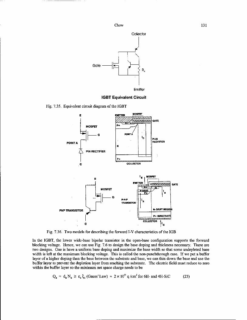
Chow 131
Collector
Gate
Emitter
IGBT Equivalent Circuit
Fig. 7.35. Equivalent circuit diagram of the IGBT
EMITTER
MOSFET
POINT A
A PiN RECTIFIER
P-f-N RECTIFIER
lE , MOSFET
EMITTER
MOSFET
PNP TRANSISTOR y TRANSISTOR
-zzzzz. & gsssss
ggSBSEZ P+x
N- DRIFT REGION
P+ SUBSTRATE I ft > > / t 1 I 1 3 1 > ' I t ■> > >
COLLECTOR C l-c
Fig. 7.36. Two models for describing the forward I-V characteristics of the IGB
In the IGBT, the lower wide-base bipolar transistor in the open-base configuration supports the forward blocking voltage. Hence, we can use Fig. 7.6 to design the base doping and thickness necessary. There are two designs. One is have a uniform base doping and maximize the base width so that some undepleted base width is left at the maximum blocking voltage. This is called the non-punchthrough case. If we put a buffer layer of a higher doping than the base between the substrate and base, we can thin down the base and use the buffer layer to prevent the depletion layer from reaching the substrate. The electric field must reduce to zero within the buffer layer so the minimum net space charge needs to be
QB = d,, NB > es ^c (Gauss'Law) = 2 x 10" q /cm2 for 6H- and 4H-SiC (23)
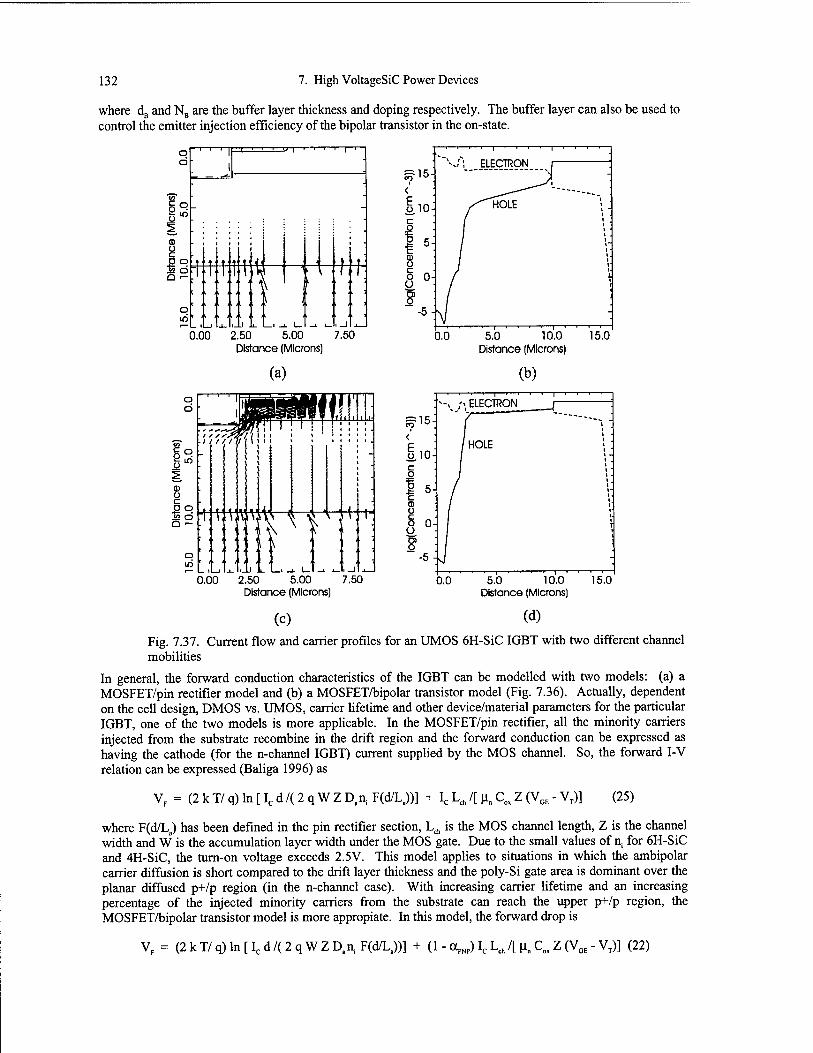
132 7. High VoltageSiC Power Devices
where dg and NB are the buffer layer thickness and doping respectively. The buffer layer can also be used to control the emitter injection efficiency of the bipolar transistor in the on-state.
§s U c BR w o Q >-
|| I . I iLin ' i r-
_Li
1 f i —4-L
0.00 2.50 5.00 7.50 Distance (Microns)
(a)
5.0 10.0 Distance (Microns)
(b)
0.00 2.50 5.00 Distance (Microns)
7.50
'-» ;»ELECTRON j
f I»: < 1 ' ' £ / HOLE >: o 10- 1 ' " c I 1 ■ O 1 1 ■
trat
/ '" c <D / j1
O / '" c _ - o 0- O I »
8s / -5 - J ■ ' 1 1 1 1 1 1 ■ 1 1 1 1 1
(c)
0.0 5.0 10.0 Distance (Microns)
(d)
15.0
Fig. 7.37. Current flow and carrier profiles for an UMOS 6H-SiC IGBT with two different channel mobilities
In general, the forward conduction characteristics of the IGBT can be modelled with two models: (a) a MOSFET/pin rectifier model and (b) a MOSFET/bipolar transistor model (Fig. 7.36). Actually, dependent on the cell design, DMOS vs. UMOS, carrier lifetime and other device/material parameters for the particular IGBT, one of the two models is more applicable. In the MOSFET/pin rectifier, all the minority carriers injected from the substrate recombine in the drift region and the forward conduction can be expressed as having the cathode (for the n-channel IGBT) current supplied by the MOS channel. So, the forward I-V relation can be expressed (Baliga 1996) as
VF = (2 k V q) In [ Ic d /(2 q W Z Dan, F(d/La))] + Ic Ldi /[ n„ Cox Z (VGE - VT)] (25)
where F(d/L0) has been defined in the pin rectifier section, Lch is the MOS channel length, Z is the channel width and W is the accumulation layer width under the MOS gate. Due to the small values of n, for 6H-SiC and 4H-SiC, the turn-on voltage exceeds 2.5V. This model applies to situations in which the ambipolar carrier diffusion is short compared to the drift layer thickness and the poly-Si gate area is dominant over the planar diffused p+/p region (in the n-channel case). With increasing carrier lifetime and an increasing percentage of the injected minority carriers from the substrate can reach the upper p+/p region, the MOSFET/bipolar transistor model is more appropiate. In this model, the forward drop is
VF = (2 k II q) In [ Ic d /(2 q W Z Dan, F(d/La))] + (1 - aj Ic Lch /[ \l„ C0, Z (V0E - VT)] (22)
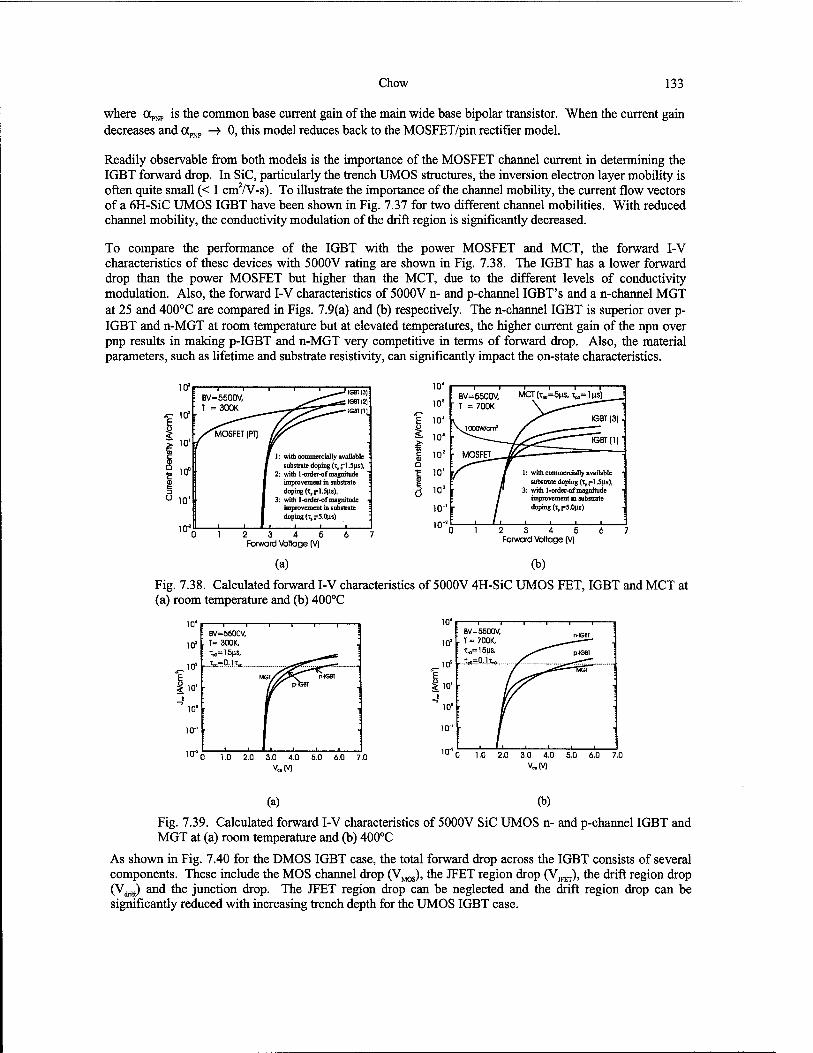
Chow 133
where aPNP is the common base current gain of the main wide base bipolar transistor. When the current gain decreases and a^ -> 0, this model reduces back to the MOSFET/pin rectifier model.
Readily observable from both models is the importance of the MOSFET channel current in determining the IGBT forward drop. In SiC, particularly the trench UMOS structures, the inversion electron layer mobility is often quite small (< 1 cmVV-s). To illustrate the importance of the channel mobility, the current flow vectors of a 6H-SiC UMOS IGBT have been shown in Fig. 7.37 for two different channel mobilities. With reduced channel mobility, the conductivity modulation of the drift region is significantly decreased.
To compare the performance of the IGBT with the power MOSFET and MCT, the forward I-V characteristics of these devices with 5000V rating are shown in Fig. 7.38. The IGBT has a lower forward drop than the power MOSFET but higher than the MCT, due to the different levels of conductivity modulation. Also, the forward I-V characteristics of 5000V n- and p-channel IGBT's and a n-channel MGT at 25 and 400°C are compared in Figs. 7.9(a) and (b) respectively. The n-channel IGBT is superior over p- IGBT and n-MGT at room temperature but at elevated temperatures, the higher current gain of the npn over pnp results in making p-IGBT and n-MGT very competitive in terms of forward drop. Also, the material parameters, such as lifetime and substrate resistivity, can significantly impact the on-state characteristics.
iff
c ic
10'
iff
iff'
10*
-1 1— • BV= 5500V, ' T = 300K
1 * *^—-' IGBT (3]| -^*000\-~~ IGBT (2] ■
, •'O^^T-^**^IGBT (1l : /MOSFET (PI) f/C^
i i... J
F 1: with commercially available : substrate doping (t, j=l ,5(ls),
2: with 1-crder-of magnitude 1 improvement in substrate doping (Trrl.5(is),
3: with 1-order-of magnitude -i improvement in substrate doping (t, r 5.0)is)
.1. J -J L
iff r
iff r
10'
Iff
Iff
Iff
Iff
10"'
io-!
8V=5500V, MCT (x„=5ns. T„= 1 ns| T = 700K
IGBT (3)
TGBT(1)
1: wife commercially available substrate doping (t, pi .5us),
3: with 1-order-of magnitude improvement in substrate doping (T, f 5.0ns)
12 3 4 5 Forward Voltage (V)
12 3 4 5 Forward Voltage (V)
(a) (b)
Fig. 7.38. Calculated forward I-V characteristics of 5000V 4H-SiC UMOS FET, IGBT and MCT at (a) room temperature and (b) 400°C
0 1.0 2.0 3.0 4.0 5.0 6.0 7.0 V„M
(a) (b)
Fig. 7.39. Calculated forward I-V characteristics of 5000V SiC UMOS n- and p-channel IGBT and MGT at (a) room temperature and (b) 400°C
As shown in Fig. 7.40 for the DMOS IGBT case, the total forward drop across the IGBT consists of several components. These include the MOS channel drop (VM0S), the JFET region drop (VJFET), the drift region drop (V^,,) and the junction drop. The JFET region drop can be neglected and the drift region drop can be significantly reduced with increasing trench depth for the UMOS IGBT case.
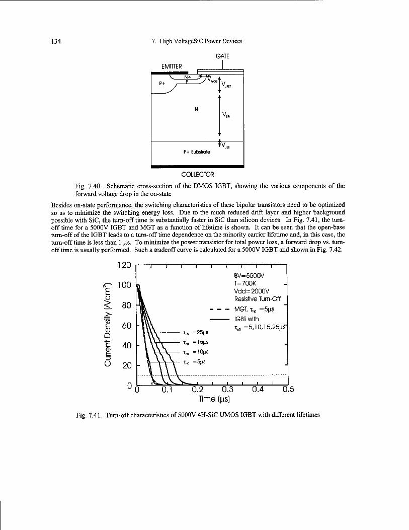
134 7. High VoltageSiC Power Devices
GATE
EMITTER
P , p y VMOS "JFEI
vE„ N-
*vJEB P+ Substrate
Besides so as to possible off time turn-off turn-off off time
COLLECTOR
Fig. 7.40. Schematic cross-section of the DMOS IGBT, showing the various components of the forward voltage drop in the on-state
on-state performance, the switching characteristics of these bipolar transistors need to be optimized minimize the switching energy loss. Due to the much reduced drift layer and higher background with SiC, the turn-off time is substantially faster in SiC than silicon devices. In Fig. 7.41, the turn- for a 5000V IGBT and MGT as a function of lifetime is shown. It can be seen that the open-base of the IGBT leads to a turn-off time dependence on the minority carrier lifetime and, in this case, the time is less than 1 (is. To minimize the power transistor for total power loss, a forward drop vs. turn- is usually performed. Such a tradeoff curve is calculated for a 5000V IGBT and shown in Fig. 7.42.
120
«P 100
<: 80
CO c 0) a c 0
U
60
40
20 -
0
1 1 I 1 1 1 1 1 1
BV=5500V T=700K Vdd=2000V Resistive Turn-Off
- - - - MGT, I«, =5us
IP.RT with
" iv\ I*, =5,10,15,25us- xn0 ^O^o
_ - \ \\ \ Xn0 ' °M-°
Tn0 ' U^"1
^ c .. - \ \ \
A ''no °M^
iVfc-J^L. ̂- ^—■ ' ' ■
0 0.1 0.2 0.3 0.4 0.5 Time (LIS)
Fig. 7.41. Turn-off characteristics of 5000V 4H-SiC UMOS IGBT with different lifetimes
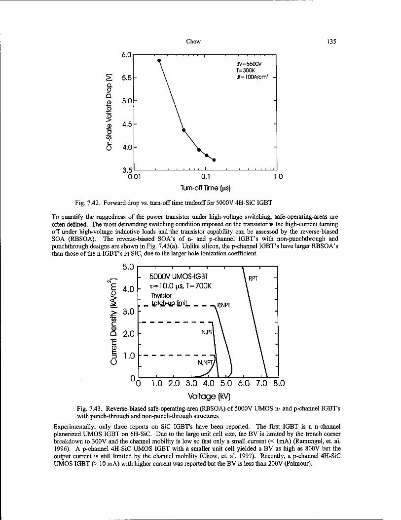
Chow 135
6.0
£ 5.5 Q. O n (i) 5.U
■&.
o ■•—
o •> fl> 4.b o uf r O 4.U
3.5
BV= 5500V T=300K Jf=100A/cm2
_l I I I_L
0.01 0.1
Turn-off Time (us)
1.0
Fig. 7.42. Forward drop vs. turn-off time tradeoff for 5000V 4H-SiC IGBT
To quantify the ruggedness of the power transistor under high-voltage switching, safe-operating-areas are often defined. The most demanding switching condition imposed on the transistor is the high-current turning off under high-voltage inductive loads and the transistor capability can be assessed by the reverse-biased SOA (RBSOA). The reverse-biased SOA's of n- and p-channel IGBT's with non-punchthrough and punchthrough designs are shown in Fig. 7.43(a). Unlike silicon, the p-channel IGBT's have larger RBSOA's than those of the n-IGBT's in SiC, due to the larger hole ionization coefficient.
5.0 —i 1 1 1 1—
_ - 5000V UMOS-IGBT x=10.0nS,T=700K Thyristor
_ Igtch-up limit p^pr
E .0 4.0
5 3.0 V) C (1) Q 2.0 +- c CD 13 1.0 o
0
RPT
0 1.0 2.0 3.0 4.0 5.0 6.0 7.0 8.0
Voltage (kV)
Fig. 7.43. Reverse-biased safe-operating-area (RBSOA) of 5000V UMOS n- and p-channel IGBT's with punch-through and non-punch-through structures
Experimentally, only three reports on SiC IGBT's have been reported. The first IGBT is a n-channel planerized UMOS IGBT on 6H-SiC. Due to the large unit cell size, the BV is limited by the trench corner breakdown to 300V and the channel mobility is low so that only a small current (< 1mA) (Ramungul, et. al. 1996). A p-channel 4H-SiC UMOS IGBT with a smaller unit cell yielded a BV as high as 800V but the output current is still limited by the channel mobility (Chow, et. al. 1997). Recently, a p-channel 4H-SiC UMOS IGBT (> 10 mA) with higher current was reported but the BV is less than 200V (Palmour).
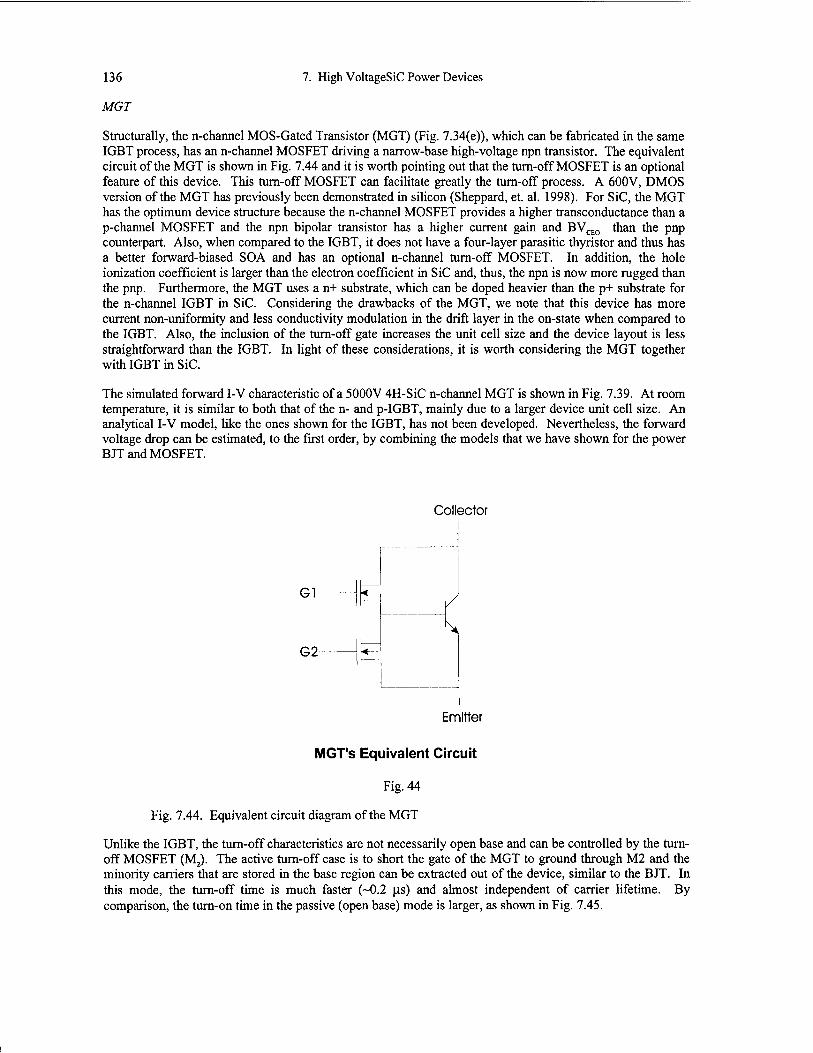
136
MGT
7. High VoltageSiC Power Devices
Structurally, the n-channel MOS-Gated Transistor (MGT) (Fig. 7.34(e)), which can be fabricated in the same IGBT process, has an n-channel MOSFET driving a narrow-base high-voltage npn transistor. The equivalent circuit of the MGT is shown in Fig. 7.44 and it is worth pointing out that the turn-off MOSFET is an optional feature of this device. This turn-off MOSFET can facilitate greatly the turn-off process. A 600V, DMOS version of the MGT has previously been demonstrated in silicon (Sheppard, et. al. 1998). For SiC, the MGT has the optimum device structure because the n-channel MOSFET provides a higher transconductance than a p-channel MOSFET and the npn bipolar transistor has a higher current gain and BVCE0 than the pnp counterpart. Also, when compared to the IGBT, it does not have a four-layer parasitic thyristor and thus has a better forward-biased SOA and has an optional n-channel turn-off MOSFET. In addition, the hole ionization coefficient is larger than the electron coefficient in SiC and, thus, the npn is now more rugged than the pnp. Furthermore, the MGT uses a n+ substrate, which can be doped heavier than the p+ substrate for the n-channel IGBT in SiC. Considering the drawbacks of the MGT, we note that this device has more current non-uniformity and less conductivity modulation in the drift layer in the on-state when compared to the IGBT. Also, the inclusion of the turn-off gate increases the unit cell size and the device layout is less straightforward than the IGBT. In light of these considerations, it is worth considering the MGT together with IGBT in SiC.
The simulated forward I-V characteristic of a 5000V 4H-SiC n-channel MGT is shown in Fig. 7.39. At room temperature, it is similar to both that of the n- and p-IGBT, mainly due to a larger device unit cell size. An analytical I-V model, like the ones shown for the IGBT, has not been developed. Nevertheless, the forward voltage drop can be estimated, to the first order, by combining the models that we have shown for the power BJT and MOSFET.
Collector
Gl-
G2-
s*
Emitter
MGT's Equivalent Circuit
Fig. 44
Fig. 7.44. Equivalent circuit diagram of the MGT
Unlike the IGBT, the turn-off characteristics are not necessarily open base and can be controlled by the turn- off MOSFET (M2). The active turn-off case is to short the gate of the MGT to ground through M2 and the minority carriers that are stored in the base region can be extracted out of the device, similar to the BJT. In this mode, the turn-off time is much faster (~0.2 \is) and almost independent of carrier lifetime. By comparison, the turn-on time in the passive (open base) mode is larger, as shown in Fig. 7.45.

Chow 137
E 2
60
50
40
30
20
10
0
T=700K,VM=2000V
Tn0=15HS,Tp0=1.5|lS P-Base doping=3e17/cm3
vPassiveTumoff
Active Tumoff with Vai.G*.^0V
0.5 1
Time (|is)
1.5
Fig. 7.45. Passive and active turn-off characteristics of a 5000V 4H-SiC MGT
The main bipolar transistor of the MGT has a narrow-base, lightly doped collector structure. At high current densities with high-level injection, the base region will extend into the collector region and the peak electric field at the p base/n- collector junction will shift to the h/n+ collector junction (the Kirk Effect). As a result, the reverse-biased SOA of the MGT, as shown in Fig. 7.46, is unusual in that when the collector current increases, the maximum sustainable collector voltage actually increases. Eventually, the MGT still fails with the formation of current filaments and second breakdown commences. Nevertheless, because of the Kirk effect, the n-channel 4H-SiC MGT has been projected to have a larger RBSOA than those of n- or p-channel IGBT's.
5000
NE 4000 ü
£■ 3000 c CD Q 2000
ß 1000
1000 2000 3000 4000 5000
Breakdown Voltage (V)
6000 7000
Fig. 7.46. Reverse-biased safe-operating-area (RBSOA) of 5000V UMOS n-channel MGT
The development of the SiC MGT is still in its early stage so that no experimental device has been demonstrated. Also, we can observe that the MOSFET in the structure can be replaced with a JFET or MESFET, particularly if one is concerned with the gate oxide reliability.
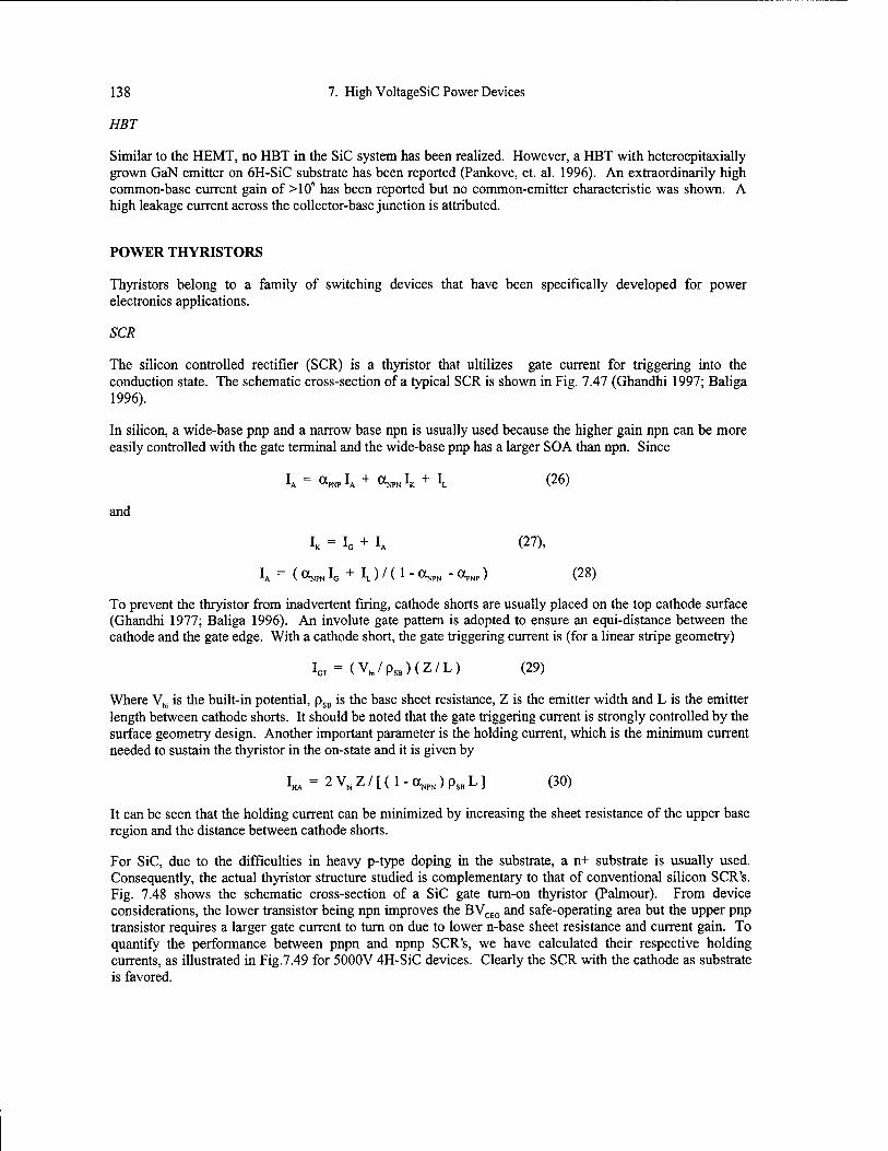
138 7. High VoltageSiC Power Devices
HBT
Similar to the HEMT, no HBT in the SiC system has been realized. However, a HBT with heteroepitaxially grown GaN emitter on 6H-SiC substrate has been reported (Pankove, et. al. 1996). An extraordinarily high common-base current gain of >106 has been reported but no common-emitter characteristic was shown. A high leakage current across the collector-base junction is attributed.
POWER THYRISTORS
Thyristors belong to a family of switching devices that have been specifically developed for power electronics applications.
SCR
The silicon controlled rectifier (SCR) is a thyristor that ultilizes gate current for triggering into the conduction state. The schematic cross-section of a typical SCR is shown in Fig. 7.47 (Ghandhi 1997; Baliga 1996).
In silicon, a wide-base pnp and a narrow base npn is usually used because the higher gain npn can be more easily controlled with the gate terminal and the wide-base pnp has a larger SOA than npn. Since
(26)
and
(27),
h = (ONPNIG + IL)/(l-ccNPN -aPNP) (28)
To prevent the thryistor from inadvertent firing, cathode shorts are usually placed on the top cathode surface (Ghandhi 1977; Baliga 1996). An involute gate pattern is adopted to ensure an equi-distance between the cathode and the gate edge. With a cathode short, the gate triggering current is (for a linear stripe geometry)
Ior = (Vbi/pSB)(Z/L) (29)
Where Vbi is the built-in potential, pSB is the base sheet resistance, Z is the emitter width and L is the emitter length between cathode shorts. It should be noted that the gate triggering current is strongly controlled by the surface geometry design. Another important parameter is the holding current, which is the minimum current needed to sustain the thyristor in the on-state and it is given by
IHA = 2VbiZ/[(l-aNPN)pSBL] (30)
It can be seen that the holding current can be minimized by increasing the sheet resistance of the upper base region and the distance between cathode shorts.
For SiC, due to the difficulties in heavy p-type doping in the substrate, a n+ substrate is usually used. Consequently, the actual thyristor structure studied is complementary to that of conventional silicon SCR's. Fig. 7.48 shows the schematic cross-section of a SiC gate turn-on thyristor (Palmour). From device considerations, the lower transistor being npn improves the BVCE0 and safe-operating area but the upper pnp transistor requires a larger gate current to turn on due to lower n-base sheet resistance and current gain. To quantify the performance between pnpn and npnp SCR's, we have calculated their respective holding currents, as illustrated in Fig.7.49 for 5000V 4H-SiC devices. Clearly the SCR with the cathode as substrate is favored.
A "TOP IA +
**NPN *K + IL
IK = Ic + IA
V ""NPN ^G + \ )/(!- ""NPN
Ot "•PNP )

Chow 139
G?1'0
Ao-
«A 4-
■9J.
PI Nl Jz ^3
P2
-oJC
1V2
Fig. 7.47. Schematic cross-section of the silicon controlled rectifier (SCR)
ANODE
p-
N+ Substrate
CATHODE
Fig. 7.48. Schematic cross-section of the silicon controlled thyrister
'W
I.« I,
(a) (b)
Fig. 7.49. Simulated holding currents for 5000V 4H-SiC pnpn and npnp SCR's
Once triggered on, the thyrisor on-state characteristics strongly resembles that of a pin junction rectifier, as shown earlier in this chapter. With both the upper and low base conductivities moduated with carriers injected from the anode and cathode, the forward drop approaches that of the pin diode.
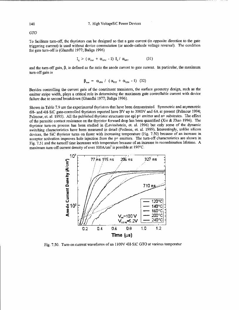
140 7. High VoltageSiC Power Devices
GTO
To facilitate turn-off, the thyristors can be designed so that a gate current (in opposite direction to the gate triggering current) is used without device commutation (or anode-cathode voltage reversal). The condition for gate turn-off is (Ghandhi 1977; Baliga 1996)
lo > («PNP + <VN -1)1*/ «NP. (31)
and the turn-off gain, ß, is defined as the ratio the anode current to gate current. In particular, the maximum turn-off gain is
ß™. = oNPN / (ov + cvN - 1) (32)
Besides controlling the current gain of the constituent transistors, the surface geometry design, such as the emitter stripe width, plays a critical role in determining the maximum gate controllable current with device failure due to second breakdown (Ghandhi 1977; Baliga 1996).
Shown in Table 7.9 are the experimental thyristors that have been demonstrated. Symmetric and asymmetric 6H- and 4H-SiC gate-controlled thyristors reported have BV up to 3000V and 6A at present (Palmour 1994; Palmour, et. al. 1995). All the published thyristor structures use epi p+ emitter and n+ substrates. The effect of the parasitic contact resistance on the thyristor forward drop has been quantified (Xie & Zhao 1996). The thyristor turn-on process has been studied in (Levinshstein, et. al. 1996) but only some of the dynamic switching characteristics have been measured in detail (Fedison, et. al. 1999). Interestingly, unlike silicon devices, the SiC thyristor turns on faster with increasing temperature (Fig. 7.50) because of an increase in acceptor activation improves hole injection from the p+ emitters. The turn-off characteristics are shown in Fig. 7.51 and the turnoff time increases with temperature because of an increase in recombination lifetime. A maximum turn-off current density of over 100A/cm2 is possible at 190°C.
103r E
<# S
a
u ■S102
o
77,+is 115 ns 206 ns 32? ns :
■ f/X yiOns^^
■M'/j VÄ=100V ■ij/.f ( VC(ON)=5.2V
— 120°C — 140°C: — 160°C ' — 200°C - — 240°C -
, 0.2 1.2 0.4 0.6 0.8 1.0
Time (us)
Fig. 7.50. Turn-on current waveforms of an 1100V 4H-SiC GTO at various temperatur
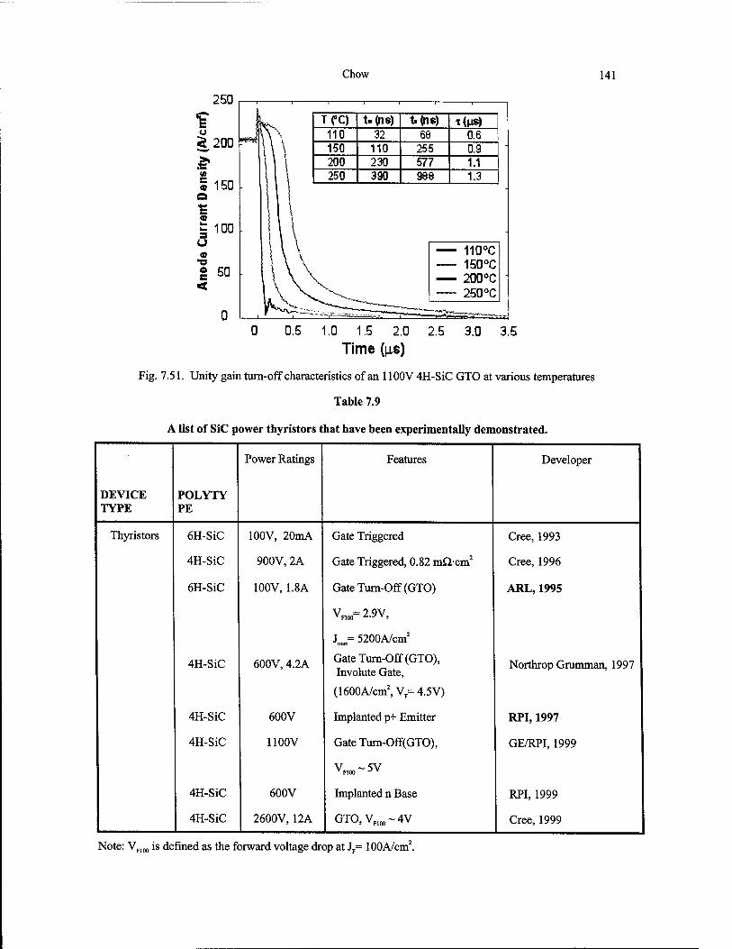
Chow 141
250
TfC) t.<ns) fcfos) 1<MS) 110 32 66 0.6 150 110 255 0.9 200 230 577 1.1 250 390 gee 1.3
110°C —_ 150°C 200°C ___ 250°C
0 0.5 1.0 1.5 2.0 2.5 3.0 3.5 Time (|is)
Fig. 7.51. Unity gain turn-off characteristics of an 1100V 4H-SiC GTO at various temperatures
Table 7.9
A list of SiC power thyristors that have been experimentally demonstrated.
Power Ratings Features Developer
DEVICE POLYTY TYPE PE
Thyristors 6H-SiC 100V, 20mA Gate Triggered Cree, 1993
4H-SiC 900V, 2A Gate Triggered, 0.82 mQ-cm2 Cree, 1996
6H-SiC 100V, 1.8A Gate Turn-Off (GTO)
V =2 9V v F100 'i--7 y '
Jinax= 5200A/cm2
ARL, 1995
4H-SiC 600V, 4.2A Gate Turn-Off (GTO), Involute Gate,
(1600A/cm2,VF=4.5V)
Northrop Grumman, 1997
4H-SiC 600V Implanted p+ Emitter RPI, 1997
4H-SiC 1100V Gate Turn-Off(GTO),
V ~5V v FI00 J *
GE/RPI, 1999
4H-SiC 600V Implanted n Base RPI, 1999
4H-SiC 2600V, 12A GTO,VF100~4V Cree, 1999
Note: VF100 is defined as the forward voltage drop at JF= 100A/cm2.
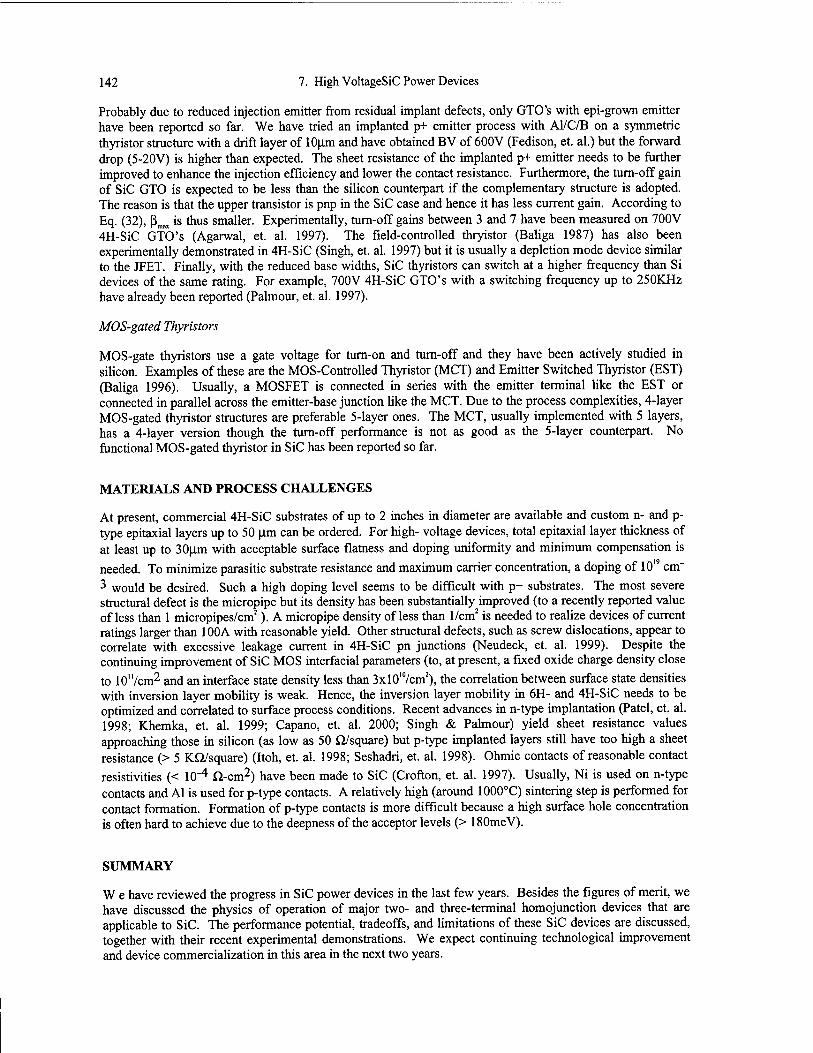
142 7. High VoltageSiC Power Devices
Probably due to reduced injection emitter from residual implant defects, only GTO's with epi-grown emitter have been reported so far. We have tried an implanted p+ emitter process with Al/C/B on a symmetric thyristor structure with a drift layer of lOum and have obtained BV of 600V (Fedison, et. al.) but the forward drop (5-20V) is higher than expected. The sheet resistance of the implanted p+ emitter needs to be further improved to enhance the injection efficiency and lower the contact resistance. Furthermore, the turn-off gain of SiC GTO is expected to be less than the silicon counterpart if the complementary structure is adopted. The reason is that the upper transistor is pnp in the SiC case and hence it has less current gain. According to Eq. (32), ßIMX is thus smaller. Experimentally, turn-off gains between 3 and 7 have been measured on 700V 4H-SiC GTO's (Agarwal, et. al. 1997). The field-controlled thryistor (Baliga 1987) has also been experimentally demonstrated in 4H-SiC (Singh, et. al. 1997) but it is usually a depletion mode device similar to the JFET. Finally, with the reduced base widths, SiC thyristors can switch at a higher frequency than Si devices of the same rating. For example, 700V 4H-SiC GTO's with a switching frequency up to 250KHz have already been reported (Palmour, et. al. 1997).
MOS-gated Thyristors
MOS-gate thyristors use a gate voltage for turn-on and turn-off and they have been actively studied in silicon. Examples of these are the MOS-Controlled Thyristor (MCT) and Emitter Switched Thyristor (EST) (Baliga 1996). Usually, a MOSFET is connected in series with the emitter terminal like the EST or connected in parallel across the emitter-base junction like the MCT. Due to the process complexities, 4-layer MOS-gated thyristor structures are preferable 5-layer ones. The MCT, usually implemented with 5 layers, has a 4-layer version though the turn-off performance is not as good as the 5-layer counterpart. No functional MOS-gated thyristor in SiC has been reported so far.
MATERIALS AND PROCESS CHALLENGES
At present, commercial 4H-SiC substrates of up to 2 inches in diameter are available and custom n- and p- type epitaxial layers up to 50 (J.m can be ordered. For high- voltage devices, total epitaxial layer thickness of at least up to 30|Xm with acceptable surface flatness and doping uniformity and minimum compensation is
needed. To minimize parasitic substrate resistance and maximum carrier concentration, a doping of 10 cm"
3 would be desired. Such a high doping level seems to be difficult with p+ substrates. The most severe structural defect is the micropipe but its density has been substantially improved (to a recently reported value of less than 1 micropipes/cm2). A micropipe density of less than 1/cm2 is needed to realize devices of current ratings larger than 100A with reasonable yield. Other structural defects, such as screw dislocations, appear to correlate with excessive leakage current in 4H-SiC pn junctions (Neudeck, et. al. 1999). Despite the continuing improvement of SiC MOS interfacial parameters (to, at present, a fixed oxide charge density close
to 10'Vcm2 and an interface state density less than 3xl0'7cm2), the correlation between surface state densities with inversion layer mobility is weak. Hence, the inversion layer mobility in 6H- and 4H-SiC needs to be optimized and correlated to surface process conditions. Recent advances in n-type implantation (Patel, et. al. 1998; Khemka, et. al. 1999; Capano, et. al. 2000; Singh & Palmour) yield sheet resistance values approaching those in silicon (as low as 50 ft/square) but p-type implanted layers still have too high a sheet resistance (> 5 KQ/square) (Itoh, et. al. 1998; Seshadri, et. al. 1998). Ohmic contacts of reasonable contact
resistivities (< 10"4 Q-cm2) have been made to SiC (Crofton, et. al. 1997). Usually, Ni is used on n-type contacts and Al is used for p-type contacts. A relatively high (around 1000°C) sintering step is performed for contact formation. Formation of p-type contacts is more difficult because a high surface hole concentration is often hard to achieve due to the deepness of the acceptor levels (> 180meV).
SUMMARY
W e have reviewed the progress in SiC power devices in the last few years. Besides the figures of merit, we have discussed the physics of operation of major two- and three-terminal homojunction devices that are applicable to SiC. The performance potential, tradeoffs, and limitations of these SiC devices are discussed, together with their recent experimental demonstrations. We expect continuing technological improvement and device commercialization in this area in the next two years.
Chow 143
ACKNOWLEDGEMENTS
I would like to acknowledge support from Office of Naval Research under Grant # N00014-95-1-1302, DARPA under Contract # MDA 972-98-C-0001 and the ERC Program of the National Science Foundation under Award Number EEC-9731677. Also, I would like to thank my former and present graduate students and collaborators for many of the results presented here.
REFERENCES
A.K. Agarwal, J.B. Casady, L.B. Rowland, S. Seshadri, R.R. Siergiej, W.F. Valek, CD. Brandt, "700-V Asymmertic 4H- SiC Gate Turn-Off Thyristors," IEEE Electron Device Letters, 18, 518-520 (1997).
A.K. Agarwal, J.B. Casady, L.B. Rowland, W.F. Valek, and CD. Brandt, "1400V 4H-SiC power MOSFETs," Materials Science Forum, vol.264-268, pt.2, pp.989-992 (1998).
A. Agarwal, S.-H. Ryu, R. Singh, and J. Palmour, "2600V, 12A, 4H-SiC, asymmetric gate turn off (GTO) thyristor development," Proc. International Conference on Silicon Carbide and Related Materials (1999).
A.K. Agarwal, S. Seshadri, and L.B. Rowland "Temperature dependence of Fowler-Nordheim current in 6H- and 4H-SiC MOS capacitors," IEEE Electron Device Letters, 18, no. 12, pp.592-594 (1997).
D. Alok and B.J. Baliga, "High voltage (450 V) 6H-SiC substrate gate JFET (SG-JFET)," Proceedings of the Sixth International Conference on Silicon Carbide and Related Materials, pp.749-752 (1995).
D. Alok and B.J. Baliga, "High voltage (450 V) 6H-SiC lateral MESFET structure," Electronics Letters, 32, 1929-1931 (1996).
D. Alok and B.J. Baliga, "Nitrogen implanted, high voltage, planar, 6H-SiC N+-P junction diodes," Proc. 8th International Symp. Power Semiconductor Devices and ICs pp. 107-110 (1996).
D. Alok and B.J. Baliga, "SiC device edge termination using finite area argon implantation," IEEE Transactions on Electron Devices, 44, no.6, pp.1013-1017 (1997).
D. Alok, R. Egloff and E. Arnold, "Effect of surface preparation and thermal anneal on electrical characteristics of 4H- SiC Schottky barrier diodes," Materials Science Forum, vol.264-268, pt.2, pp.929-932 (1998).
M.M. Anikin, V.V. Evstropov, I.V. Popov, V.N. Rastegaev, A.M. Strel'chuck, and A.L. Syrkin, "Nonclassical thermal injection current in silicon carbide p-n structures," Sov. Phys. Semicond., 23,405-407 (1989).
M.M. Anikin, V.V. Evstropov, I.V. Popov, A.M. Strel'chuck, and A.L. Syrkin, "Variant of a nonclassical thermal injection current in silicon carbide p-n structures," Sov. Phys. Semicond., 23, 1122-1125 (1989).
E. Arnold, T. Letavic, S. Merchant, and H. Bhimnathwala, "High-temperature performance of SOI and bulk-silicon RESURF LDMOS transistors," Proc. 8th International Symposium on Power Semiconductor Devices and ICs, pp.93-96(1996).
B.J. Baliga, "The pinch rectifier: a low forward drop, high speed power diode," Electron Device Letters, 5, 194-196 (1984).
B.J. Baliga, "Analysis of junction barrier controlled Schottky rectifier characteristics," Solid-State Electronics, 28, 1089- 1093 (1985).
B.J. Baliga, Modern Power Devices, John Wiley & Sons, 1987.
B.J. Baliga, "Power semiconductor device figure of merit for high frequency applications," IEEE Electron Device Lett. 10,455-457(1989).
B.J. Baliga, Physics of Semiconductor Power Devices, JWS Publishing, 1996.
B.J. Baliga, "Comparison of 6H- and 4H-SiC ACCUFET's,", Proc. 10th International Symposium on Power Semiconductor Devices and ICs, (1998).
B.J. Baliga and H.-R. Chang, "The merged p-i-n/Schottky (MPS) rectifier: A high-voltage, high-speed power diode," IEEE IEDM, Tech. Dig., 658-661 (1987).
Z.Z. Bandic, P.M. Bridger, E.C. Piquette, and T.C. McGill, Appl. Phys. Lett., 72, 3166 (1998).
E. Bano, T. Ouisse, C. Leonard, A. Golz, E.G. Stein von Kamienski, "High-field Fowler-Nordheim stress of n-type silicon carbide metal-oxide-semiconductor capacitors," Semiconductor Science and Technology, 12, no.5, pp.525- 528 (1997).
144 7. High VoltageSiC Power Devices
A. Bhalla and T.P. Chow, "Examination of semiconductors for bipolar power devices," Inst. Phys. Conf. Ser. No. 137, p.621, IOP Publishing Ltd. (1994).
A. Bhalla and T.P. Chow, "Bipolar power device performance: dependence on materials, lifetime and device ratings," Proc. 6th International Symp. Power Semiconductor Devices and ICs, pp.287-292 (1994).
M. Bhatnagar, B.J. Baliga, H.R. Kirk, and G.A. Rozgoni, "Effect of surface inhomogeneities on the electrical characteristics of SiC Schottky contacts," IEEE Trans. Electron Devices, 43, 150-156 (1996).
M. Bhatnagar, P.K. McLarty, and B.J. Baliga, "Silicon carbide high-voltage (400V) Schottky barrier diodes," IEEE Electron Device Letters, 13, 501-503 (1992).
M. Bhatnagar, H. Nakanishi, S. Bothra, P.K. McLarty, and B.J. Baliga, "Edge terminations for SiC high voltage Schottky rectifiers," Proc. 5th International Symposium on Power Semiconductor Devices and ICs, 89-94 (1993).
M. Capano, R. Santhakumar, R. Venugopal, M.R. Melloch, and J.A. Cooper, Jr., J. Electronic Materials, 29, pp.210-214 (2000).
J.B. Casady, A. Agarwal, L.B. Rowland, W.F. Valek, and CD. Brandt, "900 V DMOS and 1100 V UMOS 4H-SiC power FETs," 55th Annual Device Research Conference Digest, pp.32-33 (1997).
K. Chatty, T.P. Chow, and R.J. Gutmann, Device Research Conference (1999).
T.P. Chow and N. Ramungul, unpublished.
T.P. Chow, N. Ramungul, and M. Ghezzo, Materials Research Society Fall Meeting (1997).
T.P. Chow and R. Tyagi, "Wide bandgap compound semiconductors for superior high-voltage power devices," IEEE Trans. Electron Devices 41, 1481-1482 (1994).
J. Crofton, L. Beyer, J.R. Williams, E.D. Luckowski, S.E. Mohney, J.M. Delucca, "Titanium and aluminium-titanium ohmic contacts to p-type SiC," Solid-State Electronics, 41, pp.1725-1729 (1997).
F. Dahlquist, C.-M. Zetterling, M. Ostling, and K. Rottner, "Junction barrier Schottky diodes in 4H-SiC and 6H-SiC," Materials Science Forum, vol.264-268, pt.2, pp. 1061-1064 (1997).
V.A. Dmitriev, K.G. Irvine, C.H. Carter, Jr., N.I. Kuznetsov, and E.V. Kalinina, Appl. Phys. Lett., "Electric breakdown in GaN p-n junctions," 68, 229-231 (1996).
V.V. Evstropov, B.N. Kalinin, and B.V. Tsarenkov, "Nonclassical thermal injection current in GaP p-n structures," Sov. Phys. Semicond., 17, 373-378 (1983).
V.V. Evstropov, K.V. Kiselev, I.L. Petrovich, and B.V. Tsarenkov, "Current due to recombination via multilevel centers in the space charge layer of a p-n structure," Sov. Phys. Semicond., 18, 1156-1159 (1984).
J. Fedison, et al., to be published.
J. Fedison, et al., Proc. International Conference on Silicon Carbide and Related Materials (1999).
W. Fulop, "Calculation of avalanche breakdown of silicon p-n junctions," Solid-State Electronics, 10, 39-43 (1967).
S.K. Ghandhi, Semiconductor Power Devices, Wiley, 1977, republished 1998.
K. Hara, "Vital issues for SiC power devices," Materials Science Forum, vol.264-268, pt.2, pp.901-906 (1998).
R. Held, N. Kaminski, and E. Neimann, "SiC merged p-n/Schottky rectifiers for high voltage applications," Materials Science Forum, vol.264-268, pt.2, pp. 1057-1060 (1997).
A. Itoh, T. Kimoto, and H. Matsunami, "Low power-loss 4H-SiC Schottky rectifiers with high blocking voltage," Inst. Phys. Conf. Ser. No. 142, pp.689-692 (1995).
A. Itoh, O. Takemura, T. Kimoto, and H. Matsunami, "Barrier height analysis of metal/4H-SiC Schottky contacts," Inst. Phys. Conf. Ser. No. 142, pp.685-688, 1995.
H. Itoh, T. Troffer, and G. Pensl, "Coimplantation effects on the electrical properties of boron and aluminum acceptors in 4H-SiC," Materials Science Forum, vol.264-268, pt.2, pp.685-688 (1998).
G. Keiner, S. Banari, M. Shur, and J. Palmour, "High temperature operation of alpha -silicon carbide buried-gate junction field-effect transistors," Electronics Letters, vol.27, no. 12, pp. 1038-40 (1991).
V. Khemka, V. Ananthan, and T.P. Chow, "A fully planarized 4H-SiC trench MOS barrier Schottky (TMBS) rectifier," Proc. 11th International Symp. Power Semiconductor Devices and ICs, pp. 165-168 (1999).
V. Khemka, T.P. Chow, and R.J. Gutmann, "Effect of reactive ion etch-damage on the performance of 4H-SiC Schottky barrier diodes," J. Electron. Mat., 27, 1128-1135 (1998).
Chow 145
V. Khemka, R. Patel, N. Ramungul, T.P. Chow, M. Ghezzo, and J. Kretchmer, "Characterization of phosphorus implantations in 4H-SiC," J. Electron. Mat., 28,167-174 (1999).
V. Khemka, R. Patel, N. Ramungul, T.P. Chow, and R.J. Gutmann, "Static and dynamic characteristics of planar, 1100V, double implanted 4H-SiC junction rectifiers," Proc. 11th International Symp. Power Semiconductor Devices and ICs (1999).
J. Kolnik, I.H. Oguzman, K.F. Brennan, R. Wang, and P.P. Ruden, "Theoretical prediction of zinc blende phase GaN avalanche photodiode performance based on numerically calculated electron and hole impact ionization rate ratio," Mat. Res. Soc. Symp. Proc. 423,45-50 (1996).
A.O. Konstantinov, P.A. Ivanov, N. Nordell, S. Karlsson, and C.I. Harris, "High-voltage operation of field-effect transistors in silicon carbide," IEEE Electron Device Letters, 18, 521-522 (1997).
A.O. Konstantinov, Q. Wahab, N. Nordell, and U. Lindefelt, "Ionization rates and critical fields in 4H silicon carbide," Appl. Phys. Lett., 71, 90-92, (1997)
O. Kordina, J.P. Bergman, A. Henry, E. Janzen, S. Savage, J. Andre, L.P. Ramberg, U. Lindefelt, W. Hermansson, and K. Bergman, "A 4.5 kV 6H silicon carbide rectifier," Appl. Phys. Lett., 67,1561 (1995).
A.S. Kyuregyan and S.N. Yurkov, "Room-temperature avalanche breakdown voltages of p-n junctions made of Si, Ge, SiC, GaAs, GaP, and InP," Sov. Phys. Semicond., 23,1126-1131 (1989).
M.A. Lampert and P. Mark, Current Injection in Solids, Academic Press, New York, 1970.
M.E. Levinshstein, J.W. Palmour, S.L. Rumyantsev, and R. Singh, 'Turn-on process in 4H-SiC thyristors," Proceedings of the Twenty-Third International Symposium on Compound Semiconductors, pp.601-603 (1996).
Z. Li, J. Fedison, V. Khemka, N. Ramungul, T.P. Chow, M. Ghezzo, and J. Kretchmer, and A. Elasser, "A/C/B co- implanterd high voltage 4H-SiC pin junction rectifiers," Proc. International Conference on Silicon Carbide and Related Materials (1999).
M. Mehrotra and B.J. Baliga, "Trench MOS barrier Schottky (TMBS) rectifier," Solid-State Electronics, 38, 703-713 (1995).
H. Mitlehner, W. Bartsch, M. Bruckmann, K.O. Dohnke, and U. Weinert, "The potential of fast high voltage SiC diodes," Proc. 9th International Symp. Power Semiconductor Devices and ICs, pp. 165-168 (1997).
H. Mitlehner, W. Bartsch, K. Otto Dohnke, P. Friedrichs, R. Kaltschmidt, U. Weinert, B. Weis, and D. Stephani, "Dynamic characteristics of high voltage 4H-SiC vertical JFETs," Proc. 11th International Symp. Power Semiconductor Devices and ICs, pp.339-342 (1999).
H. Mitlehner, P. Friedrichs, D. Peters, R. Schorner, U. Weinert, B. Weis, and D. Stephani, "Switching behavior of fast high voltage SiC pn diodes," Proc. 10th International Symp. Power Semiconductor Devices and ICs pp.127-130 (1998).
P. Neudeck and C. Fazi, "Positive temperature coefficient of breakdown voltage in 4H-SiC pn junction rectifiers, IEEE Electron Device Letters, 18, 96-98 (1997).
P.G. Neudeck, D.J. Larkin, C.S. Salupo, JA. Powell, and L.G. Matus, Inst. Phys. Conf. Ser. No. 137,475-478 (1993).
P. Neudeck, W. Huang, and M. Dudley, "Breakdown degradation associated with elementary screw dislocations in 4H- SiC p7n junction rectifiers," Solid-State Electronics, 42, 2157-64 (1999).
I.H. Oguzman, E. Belloti, K.F. Brennan, J. Kolnik, R. Wang, and P.P. Ruden, "Theory of hole initiated impact ionization in bulk zincblende and wurtzite GaN," J. Appl. Phys., 81, 7827-7834 (1997).
V. Ozarow and R.E. Hysell, "Space-charge-limited currents in single-crystal silicon carbide," J. Appl. Phys., 33, 3013- 3015(1962).
J.W. Palmour, to be published.
J.W. Palmour, et al., Inst. Phys. Conf. Ser. No. 137,499-502 (1994).
J.W. Palmour, S.T. Allen, R. Singh, L.A. Lipkin, and D.G. Waltz, "4H-silicon carbide power switching devices," Inst. Phys. Conf. Ser. No. 142, 813-816 (1995).
J.W. Palmour, J.A. Edmond, and C.H. Carter, presented at the 51st Device Research Conference, 1993
J.W. Palmour, R. Singh, R.C. Glass, O. Kordina, C.H. Carter, Jr., "Silicon carbide for power devices," Proc. 9th International Symp. Power Semiconductor Devices and ICs, pp.25-30 (1997).
J.W. Palmour, R. Singh, and D.G. Waltz,"High power 4H-SiC thyristors," 54th Annual Device Research Conference Digest, pp. 54-55 (1996).
146 7. High VoltageSiC Power Devices
J.I. Pankove, M. Leksono, S.S. Chang, C. Walker, and B. Van Zeghbroeck, "High-power high-temperature heterobipolar transistor with gallium nitride emitter," MRS Internet Journal of Nitride Semiconductor Research, 1, 1092-5783 (1996).
R. Patel, V. Khemka, N. Ramungul, and T.P. Chow, "Phosphorus-implanted high-voltage np 4H-SiC junction rectifiers," Proc. 10th International Symp. Power Semiconductor Devices and ICs, pp.387-390 (1998).
L. Patrick, "Structure and characteristics of silicon carbide light emitting diodes," J. Appl. Phys., 28, 765-776 (1957).
D. Peters, P. Friedrichs, R. Schorner, H. Mitlehner, B. Weis, and D. Stephani, "Electrical performance of triple implanted vertical silicon carbide MOSFETs with low on-resistance," Proc. 11th International Symp. Power Semiconductor Devices and ICs, pp. 103-106 (1999).
D. Peters, R. Schorner, P. Friedrichs, J. Voikl, H. Mitlehner, and D. Stephani, "An 1800V Triple Implanted Vertical SiC MOSFET," IEEE Trans. Electron Devices, 46, pp.542-545 (1999).
D. Peters, R. Schorner, K.-H. Holzlein, and P. Friedrichs, "Planar aluminum-implanted 1400V 4H silicon carbide p-n diodes with low on resistance," Appl. Phys. Lett., 71, 2996-2997 (1997).
R. Raghunathan, D. Alok, and B.J. Baliga, "High voltage 4H-SiC Schottky barrier diodes," IEEE Electron Device Letters, 16, 226-228 (1995).
R. Raghunathan and B.J. Baliga, "Measurement of electron and hole impact ionization coefficients for SiC," Proc. 9th IEEE International Symposium on Power Semiconductor Devices and ICs, pp. 173-176 (1997).
N. Ramungul and T.P. Chow, unpublished
N. Ramungul and T.P. Chow, "Charge trapping in nitrogen implanted 6H-SiC n+p junctions," Proc. 9th International Symp. Power Semiconductor Devices and ICs, pp.161-164 (1997).
N. Ramungul and T.P. Chow, "Current controlled negative resistance (CCNR) in SiC junction rectifiers," IEEE Trans. Electron Devices, 46, 493-496 (1999).
N. Ramungul, T.P. Chow, M. Ghezzo, J. Kretchmer, and W. Hennessy, "A Fully Planarized , 6H-SiC UMOS Insulated- Gate Bipolar Transistor," 54th Annual Device Research Conference Digest, pp.56-58 (1996).
N. Ramungul, R. Tyagi, A. Bhalla, T.P. Chow, M. Ghezzo, J. Kretchmer, W. Hennessy, "Design and Simulation of 6H- SiC UMOS FET and IGBT for High-Temperature Power Electronics Applications," Inst. Phys. Conf. Ser. No. 142, pp.773-776, 1995.
N. Ramungul, Y.P. Zheng, R. Patel, V. Khemka, and T.P. Chow, "Beryllium-implanted 6H-SiC p*n junctions," Materials Science Forum, vol.264-268, pt.2, p. 1049-1052 (1998).
C. Raynaud, C. Richier, G. Guillot, "Temperature dependence of electrical properties of 6H-SiC buried gate JFET," Diamond and Related Materials, 6, 1504-1507 (1997).
K. Rottner, et al., European SiC Conference (1998).
K.H. Rottner, A. Schoner, S.M. Savage, M. Frischholz, C. Hallin, O. Kordina, and E. Janzen, "2.5 KV ion-implanted p*n diodes in 6H-SiC," Diamond and Related Materials, 6, 1485-1488 (1997).
E.J. Rymaszewski, private communications.
V. Saxena and A.J. Steckl, "High voltage 4H SiC rectifiers using Pt and Ni metallization," Materials Science Forum, vol.264-268, pt.2, pp.937-940 (1997).
K.J. Schoen, J.P. Henning, J.M. Woodall, J.A. Cooper, Jr., and M.R. Melloch, "A dual-metal-trench (DMT) Schottky pinch-rectifier in 4H-SiC," IEEE Electron Device Letters, 19, 97-99 (1998).
K.J. Schoen, J.M. Woodall, J.A. Cooper, Jr., and M.R. Melloch, "Design considerations and experimental analysis of high-voltage SiC Schottky barrier rectifiers," IEEE Trans. Electron Devices, 45, 1595-1604 (1998).
R. Schorner, P. Friedrichs, D. Peters, and D. Stephani, "Significantly improved performance of MOSFET's on silicon carbide using the 15R polytype," Electron Device Letters, 20, 241-244 (1999).
S. Seshadri, J.B. Casady, R.R. Siergiej, L.B. Rowland,, P.A. Sänger, CD. Brandt, J. Barrow, D. Piccone, R. Rodrigues, and T. Hansen, "Turn-Off Characteristics of 1000V SiC Gate-Turn-Off Thyristors," Proc. 10th International Symp. Power Semiconductor Devices and ICs, 25, 1998.
S. Seshadri, G.W. Eldridge, and A.K. Agarwal, "Comparison of the annealing behavior of high-dose nitrogen-, aluminum-, and boron-implanted 4H-SiC," Appl. Phys. Lett., 72, 2026-2028 (1998).
K. Shenai, R.S. Scott, and B.J. Baliga., "Optimum semiconductors for high power electronics," IEEE Trans. Electron Devices 36, 1811 (1989).
Chow 147
P.M. Shenoy and B.J. Baliga, "Planar, high voltage, boron implanted 6H-SiC P-N junction diodes," Inst. Phys. Conf. Ser. No. 142, 717-720(1995).
P.M. Shenoy and B.J. Baliga, "The planar 6H-SiC ACCUFET: a new high-voltage power MOSFET structure," IEEE Electron Device Letters, 18, pp. 589-591 (1997).
J.N. Shenoy, J.A. Cooper, Jr., and M.R. Melloch, "High-voltage double-implanted power MOSFET's in 6H-SiC," IEEE Electron Device Letters, 18, 93-95 (1997).
S.T. Sheppard, V. Lauer, W. Wondrak, E. Niemann, "High temperature performance of implanted-gate n-channel JFETs in 6H-SiC," Materials Science Forum, vol.264-268, pt.2, pp.1077-1080 (1998).
R.R. Siergiej, J.B. Casady, A.K. Agarwal, L.B. Rowland, S. Seshadri, S. Mani, P.A. Sänger, and CD. Brandt, "1000V 4H-SiC Gate Turn Off (GTO) Thyristor," Proc. International Symp. Comp. Semicond., San Diego, CA, Sept., 1997.
R. Singh, K.G. Irvine, O. Kordina, J.W. Palmour, M.E. Levinshtein, S.L. Rumyanetsev, "4H-SiC bipolar P-i-N Diodes with 5.5 KV blocking voltage," 56th Annual Device Research Conference Digest, pp.86-87 (1998).
R. Singh, K.G. Irvine, and J.W. Palmour, "4H-SiC buried gate field controlled thyristor," 55th Annual Device Research Conference Digest, pp.34-35 (1997).
R. Singh and J.W. Palmour, "Planar terminations in 4H-SiC Schottky diodes with low leakage and high yields," Proc. 9th International Symp. Power Semiconductor Devices and ICs, pp. 157-160 (1997).
R. Singh and J.W. Palmour, to be published
Y. Sugawara and L. Asano, "1.4 kV 4H-SiC UMOSFET with low specific on-resistance," Proc. 10th International Symposium on Power Semiconductor Devices and ICs, pp. 119-22 (1998).
S.M. Sze, Physics of Semiconductor Devices, Wiley, 1981.
O. Takemura, T. Kimoto, H. Matsunami, T. Nakata, M. Watanabe, and M. Inoue, "Implantation of Al and B acceptors into alpha-SiC and pn junction diodes," Materials Science Forum, vol.264-268, pt.2, pp.701-704 (1997).
J. Tan, J.A. Cooper, Jr., and M.R. Melloch, "High-voltage accumulation-layer UMOSFETs in 4H-SiC," 56th Device Research Conference Digest, 88-89 (1998).
T. Tanaka, Y. Yasuda, and M. Ohayashi, "A new MOS-gate bipolar transistor for power switches," IEEE Trans. Electron Devices, ED-33, 2041-2045 (1986).
K. Ueno, T. Urushidani, K. Hashimoto, and Y. Seki, "The gurard-ring termination for the high-voltage SiC Schottky barrier diodes," IEEE Electron Device Letters, 16, 331 -332 (1995).
W. von Munch and P. Hoeck, "Silicon carbide bipolar transistor," Solid-State Electronics, 21,479-480 (1978).
Q. Wahab, T. Kimoto, A. Ellison, C. Hallin, M. Tuominen, R. Yakimova, A. Henry, J.P. Bergmann, and E. Janzen, "A 3 kV Schottky barrier diode in 4H-SiC," Appl. Phys. Lett., 72,445-447 (1998).
Y. Wang, W. Xie, J.A. Cooper, Jr., M.R. Melloch, and J.W. Palmour, "Mechanisms limiting current gain in SiC bipolar junction transistors," Proceedings of the Sixth International Conference on Silicon Carbide and Related Materials, pp.809-812(1996).
C.E. Weitzel, J.W. Palmour, C.H. Carter, Jr., K. Moore, K.J. Nordquist, S. Allen, C. There, and M. Bhatnagar, "Silicon carbide high power devices," IEEE Trans. Electron Devices, 43, 1732-1741 (1996).
B.M. Wilamowski, "Schottky diodes with high breakdown voltages," Solid-State Electronics, 26, 491-493 (1983).
K. Xie, J.H. Zhao, A high-current and high-temperature 6H-SiC thyristor," IEEE Electron Device Letters, 17, pp.142-144 (1996).
J.C. Zolper, "A review of junction field effect transistors for high-temperature and high-power electronics," Solid-State Electronics, vol.42, no.12, p. 2153-2156 (1998).

148 7. High VoltageSiC Power Devices
149
APPENDICES
APPENDIX A: BIOGRAPHIES OF PANELISTS AND OTHER TEAM MEMBERS
PANELISTS
Name: Vladimir Dmitriev, Panel Chair Address: TDI, Inc.
8660 Dakota Drive Gaithersburg, MD 20877
Dr. Dmitriev has over 18 years of research experience in the epitaxial growth of wide bandgap semiconductors and device fabrication. He received his masters of science degree at Leningrad Electrotechnical Institute in 1978, Ph.D. in 1986 and Doctor in Science degree in 1996, both at the Ioffe Institute. His experience includes four years at Cree Research, Inc., where he was primarily responsible for the development of epitaxial process for III-V nitrides for blue light emitters. From 1992-96 he also directed Cree Research Eastern European Division, the Russian affiliate of Cree.
His particular interest is in mechanisms of epitaxial growth of semiconductors, and in the physics of wide bandgap semiconductor pn structures. He has published over 60 scientific papers and is co-inventor on eight USSR and three U.S. issued patents.
Name: T. Paul Chow Address: ECSE Department and Center for Integrated Electronics
Rensselaer Polytechnic Institute Troy, NY 12180-3590
Dr. Chow received his B.A. (mathematics and physics, summa cum laude, 1975) from Augustana College, Sioux Falls, South Dakota, M.S. (Materials Science, 1977) from Columbia University, and Ph.D. (electrical engineering, 1982) from Rensselaer Polytechnic Institute, Troy, New York. From 1977-89 he worked at General Electric Corporate Research and Development, Schenectady, NY. He was first involved with developing CVD processes and characterization of doped tin oxide and indium oxide thin films for transparent electrode applications in solid-state imagers, and with refractory metals and metal silicides for MOS VLSI applications. From 1982 to 1989, he participated in the design and process development of various discrete and integrable MOS-gated unipolar and bipolar devices (such as the MOSFET, IGBT, and MCT), and in process architecture and integration of high-voltage integrated circuits. Since 1989, he has been on the faculty of the Electrical Systems and Computer Engineering Department of Rensselaer Polytechnic Institute as an associate professor.
His present research interests are in developing new device concepts and circuit models for high-voltage power devices and integrated circuits, process integration of ULSI metallization, and in process research of silicon and wide bandgap compound semiconductors. He has published over 50 papers in scientific journals, presented over 70 conference talks, contributed three chapters in technical textbooks and has over ten patents. He received the Solid State Science and Technology Young Author Award of the Electrochemical Society in 1982 and the Horizon Award from Augustana College in 1986. He is a senior member of the IEEE and a member of the Electrochemical Society. In 1990-97, he was the Editor for Solid State Power in the IEEE Transactions on Electron Devices. At present, he is the Chair of the Membership Committee of the IEEE Electron Devices Society.
150 Appendix A. Biographies of Panelists and Other Team Members
Name: Steven P. DenBaars Address: Materials and ECE Depts.
University of California Santa Barbara, CA 93106
Dr. DenBaars is a Professor of Materials and Electrical Engineering at the University of California, Santa Barbara. He received his Ph.D. Degree in Electrical Engineering from the University of Southern California in 1988 under the direction of Professor P.D. Dapkus. From 1988 to 1991 Professor DenBaars was a member of the technical staff at Hewlett-Packard's Optoelectronics Division involved in the growth and fabrication of visible LEDs.
His current research interests are in metal organic chemical vapor deposition (MOCVD) of III-V compound semiconductor materials and devices. Specific research interests include growth of wide bandgap semiconductors (GaN based), and their application to blue LEDs and lasers and high power electronic devices. This research has lead to the first U.S. university blue laser demonstration and over seven patents pending on GaN growth and processing. He is the principal investigator of the DARPA-funded Multi- university Nitride Consortium, which will develop and transfer GaN technology to industry. In 1994 he received a NSF Young Investigator award. He has authored or co-authored over 75 technical publications, given 60 conference presentations and has ten patents.
Name: Michael S. Shur Address: Center for Integrated Electronics and Electronics Manufacturing
CIEMMCII#9017 Rensselaer Polytechnic Institute 110 8th St. Troy, NY 121180-3590
Dr. Shur received his MSEE degree (with honors) from St. Petersburg Electrotechnical Institute in 1965 while he received his Ph.D. in Physics (1967) and Doctor of Physics and Mathematics degree (1992) from Ioffe Institute. He has held research or faculty positions at A.F. Ioffe Institute, Wayne State University, Oakland University, Cornell University, IBM T.J. Watson Research Center and the University of Minnesota. In 1989-1996, he was John Marshal Money Professor at the University of Virginia, where he was also a member of the Center for Advanced Studies from 1989 to 1991 and the Director of the Applied ElectroPhysics Laboratories in 1996. Since 1996 he has been Patricia W. and C. Sheldon Roberts '48 Professor of Solid State Electronics at Rensselaer Polytechnic Institute, where he is also Associate Director of the Center for Integrated Electronics and Electronic Manufacturing. Dr. Shur has served as a consultant to major electronics companies, published more than 600 technical papers, has given many invited, keynote and plenary talks and lectures, authored, co-authored and edited 17 books and holds 25 patents on solid state devices.
He is a Fellow of IEEE, a Fellow of the American Physical Society, a member of Eta Kappa Nu and Tau Beta Pi, a member of the Electrochemical Society, SPIE, and Commission D (electronics and photonics) of the International Union of Radio Science. In 1987-96 he served as Secretary, Vice-Chair and Chair of the U.S. Commission D. In 1990-93 he served as an Associate Editor of IEEE Transactions on Electron Devices. He is now co-Editor-in-Chief of the International Journal of High Speed Electronics and Systems and Member, Honorary Advisory Board of Solid State Electronics magazine. He has also served as General Chair, Program Committee Chair, Committee Member, Session Chair and Organizer at many national and international conferences. In 1994, the Saint Petersburg State Technical University awarded him an Honorary Doctorate.
Appendix A. Biographies of Panelists and Other Team Members 151
Name: Michael Spencer Address: 418 Phillips Hall
Cornell University Ithaca, NY 14850
Dr. Michael Spencer, Professor of Electrical Engineering, Cornell University was born in Detroit, Michigan and raised in Washington, DC. Dr. Spencer has over fourteen years of research experience in the epitaxial and bulk growth of compound semiconductors such as GaAs, SiC and A1N (growth techniques include molecular beam epitaxy, vapor phase epitaxy, liquid phase epitaxy, and sublimation), microwave devices, solar cells and electronic materials characterization techniques (including deep level transient spectroscopy and photoluminescence). His particular interest has been in the correlation of device performance with material growth and processing parameters. Recent work has emphasized wide bandgap materials and Dr. Spencer's group was the first to produce conducting A1N and thick films of beta SiC grown by the bulk sublimation technique.
Dr. Spencer, has received a Presidential Young Investigator Award for 1985, the Alan Berman Research Publication Award from the Naval Research Laboratories in 1986 (for research leading to the first identification of a self interstitial defect in AlGaAs), the White House Initiative Faculty Award for Excellence in 1988, a Distinguished Visiting Scientist appointment at Jet Propulsion Laboratories in 1989 and a 1992 recipient of a NASA Certificate of Recognition. He received his B.S. and M.S. in Electrical Engineering and his Ph.D. in Electro-Physics from Cornell University. Dr. Spencer's experience includes two years at AT&T Bell Laboratories, where he supervised and managed the design, prototype production and manufacture of two different product lines of power rectifiers. Dr. Spencer has served as a research scientist and/or consultant to General Electric, the Naval Research Laboratories, Jet Propulsion Laboratories, Lawrence Livermore National Laboratories and (NASA) National Aeronautics and Space Administration.
He has authored over 50 publications in the area of compound semiconductor research. He has also presented numerous scientific papers. Dr. Spencer is on the permanent committee for the Electronic Materials Conference, the Compound Semiconductor Conference, as well as helped initiate and form the International Conference on Silicon Carbide and Related Materials. Dr. Spencer is currently one of the Directors of the NSF sponsored National Nano-Fabrication Network (NNUN). He currently has co-authored three U.S. patents with several patents pending.
Name: George White Address: Packaging Research Center
Georgia Institute of Technology 813 Ferst Drive NW Atlanta, GA 30332-0560
George White is currently the Associate Director for Research of the Packaging Research Center at the Georgia Institute of Technology in Atlanta. Prior to joining the Packaging Research Center in November of 1998, he was employed by the Motorola Corporation of Schaumburg, Illinois was he was the Government Programs Manager for the Applied Simulation and Modeling Research Group of the Corporate Computer Software Center. There he served as program manager for the Motorola led embedded mass formed passives consortium, the demonstration of electrical and mechanical design of low cost mixed mode modules and the holographic optical interconnect technology consortium. Prior to joining Motorola, he was employed at the International Business Machines, Corporation as a Development Manager for the Advanced Thin Films Group in Fishkill, NY. There he developed low cost thin film processes for electronic packaging for IBM's mainframe and cost performance products. He holds over 11 US patents, and a number of publications. He received his Ph.D. and M.S. degrees from the University of Illinois in Metallurgical Engineering in Urbana, Illinois, and his bachelor's degree in Physics from Hampton University in Hampton, VA.
152 Appendix A. Biographies of Panelists and Other Team Members
OTHER TEAM MEMBERS
Name: Usha Varshney Address: Program Director,
Div. of Electrical and Communications Systems Directorate of Engineering National Science Foundation 4201 Wilson Boulevard, #675 Arlington, VA 22230
Dr. Varshney received her B.Sc. Honors School and M.Sc. Honors School degrees from Panjab University. She was awarded the Ph.D. degree in Physics by the Indian Institute of Technology, New Delhi in 1983. She joined the National Science Foundation in 1997 as Program Director of the Physical Foundations of Enabling Technologies and Integrative Systems programs in the Division of Electrical and Communications Systems. She comes from an industrial background and maintains a strong interest in the interdisciplinary nature of scientific and engineering research. She has conducted research in industry/university/government cooperative programs. She has been involved with research in the areas of electro-ceramic materials and thin films for integrated microelectronic components and devices including non-volatile random access memories using ferroelectrics, uncooled focal plane arrays using pyroelectrics, radiation-resistant solar cells and photovoltaic devices using optoelectronic materials, thermal detectors and antennas using high Tc superconducting fibers, thin and thick films, and flat panel displays using phosphors, magnetic materials, thin films and devices including integrated planar magnetic components and circuits, monolithic magnetics for megahertz frequency high density power supplies and giant magnetoresistance sensors and devices. Dr. Varshney has also been involved with laser and plasma processing of materials and devices, and high temperature, high frequency wide bandgap semiconductor materials and associated devices including silicon carbide, aluminum nitride, diamond and iron titanates. She has a strong interest in the area of processing of bulk material, epitaxial growth of films and patterning techniques for high temperature electronic devices. She also has interests in electronic packaging and interconnections for high temperature applications, sensors, microelectromechanical systems (MEMS) and nanotechnolgy.
Name: John M. Zavada Address: ARL-European Research Office
223 Old Marylebone Road London NW1 5TH, UK
John M. Zavada is the Director of the U.S. Army Research Laboratory - European Research Office in ondon and also serves as Chief of the Electronics and Physics Branch. Previously, he managed a research program in optoelectronics at the U.S. Army Research Office in Durham, NC. He earned his BA from the Catholic University of America and his MS and PhD degrees in physics from New York University. Later he worked as a research physicist at Army laboratories in Philadelphia, PA, and at Picatinny, NJ. Dr. Zavada has authored more than 100 papers in the areas of scattering of light from rough surfaces, ion implantation, optical characterization of semiconductors, and hydrogen and rare earth impurities in materials. He has served on numerous advisory panels, including the Joint Services Electronics Program and the Advisory Group on Electronics, and on program committees for international conferences in solid state physics and electronics. He has held adjunct academic positions at Drexel University, North Carolina State University, and the Imperial College of Science and Technology. He is a member of the American Physical Society, the Materials Research Society, and is a Fellow of the Optical Society of America.
153
APPENDIX B: EUROPEAN SITE REPORTS
Site: DaimlerChrysler Ulm, GERMANY
Date Visited: 9 June 1999
TTEC Attendees: J. Zavada (report author)
Hosts: Prof. Hermann Schumacher, University of Ulm Dr. Andrei Vescan, DaimlerChrysler Dr. Helmut Leier, DaimlerChrysler
DAIMLERCHRYSLER
Introduction
DaimlerChrysler is a German-American company that was formed by the merger of two industrial giants, Daimler-Benz and Chrysler, in 1997. On Wednesday afternoon, Dr. Zavada met with Dr. Helmut Leier, who is director of the high frequency electronics department, and with Dr. Andrei Vescan, who is involved with research technology of III-V components.
Dr. Leier gave an overview of DaimlerChrysler and its research activities. The central research center employs about 1,800 people and sponsors nearly 500 students. Since the main activity of the company is automobiles, much of the research activities concentrate on cars and traffic.
There are three main areas of research: microelectronics and micro-systems; information and communications; and high frequency devices. Currently, most of the high frequency device work is based on GaAs. High power (> 1 W/mm), high frequency (> 10 GHz) HEMTs and MESFETs are being developed. The research on GaN is directed at extending the performance of the GaAs devices. Dr. Leier emphasized the importance of minimizing the cost while extending device performance. High power GaN devices will not make a major impact until fabrication costs are competitive with GaAs devices. Dr. Leier also mentioned that DaimlerChrysler is part owner, with Thomson-CSF, in United Monolithic Semiconductor (UMS). DaimlerChrysler acquires the GaAs wafers for high power devices from UMS.
III-V Components
Dr. Vescan gave Dr. Zavada a presentation on the research at DaimlerChrysler concerning high frequency, high power GaN-based devices. He said that DaimlerChrysler is not presently involved with growth of GaN films. SVT Associates, in the United States, is collaborating with DaimlerChrysler and currently provides the necessary films. The work at DaimlerChrysler centers on the design, processing, and fabrication of GaN- based devices. Dr. Vescan said that the optimum processing conditions are very dependent upon the source of the GaN films. These conditions can be determined only after repeated trials and device testing. The group at DaimlerChrysler has been working in close collaboration with Prof. Kohn at the University of Ulm on device properties of AlGaN/GaN MODFETs (modulation doped field effect transistors).
Clean Room Facilities
Later in the afternoon, Dr. Leier and Dr. Vescan took Dr. Zavada on a tour of the clean room facilities at DaimlerChrysler. The clean rooms are similar to the ones at the University of Ulm; however, they are larger, measuring approximately 1,000 sq. meters. Some areas are class 100 and others are class 10. Following the merger of Daimler-Benz and Chrysler, half of the clean space was divided between DaimlerChrysler and UMS. I was only shown the DaimlerChrysler clean rooms. Still they comprise a first-rate facility for processing III-V materials.
154 HTE European Site Reports
Site: High Pressure Research Center (Workshop) Polish Academy of Sciences Ul. Sokolowska 29/37 01-142 Warsaw POLAND +48-226-32-5010 www.unipress.waw.pl
Date Visited: 10 June 1999
TTEC Attendees: S. DenBaars (report author), M. Shur, U. Varshney, G. White
Hosts: Dr. W. Porowski (HPRC) Dr. I. Grzegory (HPRC) L. Leszynski (HPRC) L. Dobrzauski (IEMT) W. Wolosinski (Warsaw Univ. of Tech.) A. Jelenski (IEMT) J. Szmidt (Warsaw Univ. of Tech) Dr. J. Weyher (HPRC) R. Beck (Warsaw Univ. of Tech.)
BACKGROUND
A comprehensive workshop on GaN activities in Poland was held for the panel members at the High Pressure Research Center (HPRC) in Warsaw, Poland. This included groups from Warsaw University of Technology, the HPRC research group Unipress, and the Institute of Technology of Materials and Electronics (IEMT).
TECHNOLOGY DISCUSSION
Dr. Porowski of Unipress hosted the meeting at the High Pressure Research Center and had also invited representatives of several of the other leading Polish research efforts in wide bandgap semiconductors to the workshop. Within Poland there are 14 research efforts developing GaN materials and devices. Recently the Polish government has approved funding of the large national project "Development of Blue Optoelectronics". This program will focus on blue lasers, solar blind detectors, and full-color industrial displays.
GaN Bulk Substrate
Unipress is the research group within HPRC working on GaN bulk crystal growth from a melt. One of the most impressive achievements the panel saw in Europe was the "defect free" bulk GaN wafers grown from melt under extremely high pressure. Dr. Isabel Grzegory gave an overview of the high pressure solution growth method used for depositing the bulk single crystals.
The size of the substrates has steadily increased up to 1 cm in 1999 from 5 mm in 1997. In comparison to GaN on sapphire technology which exhibits 1 E+9 cm"2 defect densities, or ELO films, which are in the 1 E+6 cm"2 to 5 E+5 cm"2 range, the bulk GaN crystals possess 10 to 1 defect per square centimeter. These densities were estimated from etch pit counts and correlated to TEM measurements of higher defect densities found on standard GaN sapphire technology.
The team was allowed to observe the bulk crystals under both optical microscopes and field emission SEM. Both n-type bulk crystals and semi-insulating bulk crystal have been grown. The semi-insulating substrates were highly resistive 1 E+5 ohm""" and could be used for thin film deposition of high power AlGaN/GaN microwave amplifiers (Litwin-Staszewska et al. 1999). Very high quality homeoepitaxial growth of GaN by MOCVD was obtained on top of these substrates and the films exhibited narrow double-crystal x-ray diffraction (DCXRD) linewidths as low as 21 arcsec. The group at University of Ulm, in collaboration with
HTE European Site Reports 155
Unipress, has obtained thin films that exhibit the narrowest reported PL linewidths at low temperature (0.1 meV)—which is indicative of the uniform high quality film (Komitzer et al. 1999). MBE has also been performed on the bulk crystals. Both Ga-face and N-face polarity bulk substrates have been produced. The bulk crystals also display extremely smooth cleaved facets with rms roughness of 5 angstroms, which would make excellent laser facets.
Unipress is also investigating high power HEMTs, Schottky diodes, and UV detectros. Using MOCVD AlGaN/GaN materials have been grown with sheet carrier charge of 1.2 e+12 cm"2. Large geometry, 1 micron gate length FETs have been fabricated and FET characteristics obtained. High quality Schottky contacts were obtained using Pd/Au metallization, which exhibited barrier heights of 0.8 eV.
IEMT
Researchers at the Institute of Technology of Materials and Electronics are focusing on device fabrication and bulk growth of novel substrates. Panelists toured the facilities for fabricating laser diodes and detectors. Dr. Dobrzauski has already fabricated a GaN UV detector, which showed a peak responsivity at 364 nm. Numerous bulk crystal pullers were in operation. Also, a wide range of high quality optical bulk substrates was being grown such as: Si, GaAs, InP, ZnSe, YAG, LiGa02, and LiA102. Large banks of UPS backup are needed to ensure safe operation in event of a power failure.
REFERENCES
Litwin-Staszewska, E., T. Suski, I. Grzegory, S. Porowski, J. Robert, D. Wasik, A. Witowski, D. Cote, and B. Clerjund. 1999. Electrical Properties of GaN Bulk Single Crsytals Doped with Mg. Paper We-P082, Proceedings of Intl. Conf. on Nitride Semiconductors, Montpellier, France,, pg 124.
Komitzer, K., T. Ebner, M. Grehl, K. Thonke, R. Sauer, C. Kirchner, V. Schwelger, M. Kamp, M. Leszczynski, I. Grzergory, S. Porowski. 1999. High Resolution PL and Reflectance Spectra of Homoepitaxial GaN Layers. Paper Tu-17, Proceedings of Intl. Conf. on Nitride Semiconductors, Montpellier, France, pg. 49.

156 HTE European Site Reports
Site: IMC, ABB, and KTH Electrum Building Kistagangen 15 Kista, Stockholm, SWEDEN
Date Visited: 11 June 1999
TTEC Attendees: T.P. Chow (report author), V. Dmitriev, M. Spencer, S. DenBaars, M. Shur, U. Varshney, G. White
Hosts (IMC): Dr. Christopher Harris, SiC Project Manager Dr. Meitek Bakowski Dr. Andrey Konstantinov
Hosts (ABB): Dr. Heinz Lendenmann, Project Leader, Switch Development, SiC Project
Hosts (KTH): Dr. Mikael Oostling Dr. Nils Nordell
IMC
IMC is an applied research company that facilitates technology transfer from the research and development stage to prototyping and manufacturing. It has received both industrial (80%) and government (20%) support to enhance Swedish competitiveness. Recently, it has merged with IOF to form a new company called ACLEO.
IMC has mostly performed research in microelectronics and IOF on optoelectronics. The new company has a wide range of interests in both of these technical areas and has more European presence. IMC has locations in Kista and Linkoping. The Linkoping location focuses on interconnect and packaging of electronics and optoelectronics systems.
There are 53 employees in Kista and 27 in Linkoping. The budget for 1998 was 85 million SEK ($10.5 million) and 120 million SEK ($15 million) for Kista and Linkoping, respectively. It spins off one new company per year on the average. There is a high labor turnover rate (15-20% per year) with the average age of its employees being 34.
Dr. Harris indicated that the researchers in the Kista facility perform work in a variety of areas, including (a) radiation detectors (QWIP, bolometers), (b) optoelectronics, (c) SiC electronics, particularly power devices and (d) microsystem technology (microstructures, sensors). The wide bandgap semiconductor technology has mostly focused on SiC and the application areas are:
power devices (development for ABB)
microwave electronics (Ericsson)—high power amplifiers for base stations, 3 GHz, 100 W, entirely SiC so far, but expecting GaN to be applicable at higher frequencies
high temperature electronics
sensors, e.g., SiC as X-ray detectors, sensitivity close to human tissues
The highlights of specific technical activities are:
numerical simulations and design—TMA software based
portfolio of SiC specific process technologies
- epi growth (Emcore and Epigress reactors, process support for Epigress)
- ion implantation
- dry etching (ECR etching)

HTE European Site Reports 157
- dielectric growth and deposition
• device and characterization
- IV, CV, DLTS, Hall
- optical
- SEM/TEM/SPM
One example of the application of these process technologies in device fabrication is the demonstration of a 16 GHz (fmJ 4 H-SiC implanted-channel SiC MESFET. The gate width is 0.8 ^m with optical lithography and 2x smaller with e-beam lithography. A channel mobility of 200 cmVV-s has been achieved. Also, measurements of basic material properties of SiC are also performed as part of the Swedish National SiC Program (SiCEP).
Dr. Bakowski presented the high temperature electronics work. This area can be broadly categorized into two sub-areas:
• 200-300°C
- integrated motor control
- smart fuel pumps
- brake by wire
• 400-800(C
- combustion
- geothermal
The multi-chip module (MCM) concepts that are devised for these two temperature ranges are different.
• 200-300°C
- power electronics SiC
- sensor SiC
- control electronics Si SOI
• 400-800°C
- power electronics, sensors, control electronics, all SiC
Besides active devices, high temperature passive components also need to be addressed.
Dr. Konstantinov presented the high temperature sensor research. One approach is to use high temperature gas-absorbing metal-gate MOSFET. Using a Pd gate, hydrocarbons (CHX) decompose after adsorption to the Pd and the resulting H+ ions diffuse to the interface, thereby shifting the barrier height. The advantages of using SiC are:
• high operating temperature (e.g., engine exhaust at 600°C)
• fast operation
Other devices that can also be used are MOS capacitors, metal-semiconductor diodes (I-V shift) and MESFETs.
For automotive applications, compared to the conventional Lambda sensor which utilizes a thick Zr layer, the gas-sensor SiC MOSFET developed at IMC offers much faster feedback so that adjustment to each engine cylinder can be made. The salient features of this SiC MOSFET are:
• buried channel
• low threshold voltage
• high temperature operation (17 hrs at 600°C so far)
• high gas response
158 HTE European Site Reports
The goals of this program are:
• long term stability at 600°C
• sensitivity to exhaust products other than hydrocarbons
• electronic noses (MOSFET sensor arrays)
Different metal gates may be used to sense different gas products.
The panel was given a facility tour of the clean room area that is on the ground floor and where all the microelectronics device processing facilities of the three institutions are housed, though separately. The ABB facility includes a high-energy (3 MeV) ion implanter that has a heated end station and a laser direct write aligner. IMC processes a large variety of compound semiconductors for several applications (such as solar cells and optoelectronics). These facilities are very impressive and world-class.
ABB
ABB is a large international industrial company that has a major presence in power generation, transmission and distribution. It was instrumental in getting the SiC program started in Sweden in 1988 and has sponsored many programs in developing the SiC infrastructure in Sweden.
Dr. Lendenmann presented an overview of the ABB businesses and elements of the SiC device program. The power generation plants include hydro, "clean coal," nuclear power and fuel gas cleaning types. ABB is very focused in getting SiC devices into power electronics systems. For example, for a 1-5 MW industrial converter system, it is estimated that Si device replacement with SiC can reduce the size by 1/3. Significant improvement in HVDC system is also projected with SiC devices, with the goal of 50 MW plant in 300 m2
area.
A 3.5 kV, 200 A 4 H-SiC pin junction rectifier was presented. The diode structure consists of a deep boron junction for good junction leakage and a shallow aluminum implant topped with a p+ epi regrown region for optimal contact resistivity. A multiple-zone boron-implanted JTE has been used for junction termination, in conjunction with a SiN/polyimide over the field oxide as the passivation layer. A phosphorus-implanted n+ region was used as channel stop. Sensitivity analysis between device on-state voltage (VF < 4 V) vs. epi thickness has been shown for correlation. The leakage current density for diodes with three different areas was shown, with the largest device (7x7 mm2) size having a value of less than 10"! A/cm2, the best value to date for large-area devices. Dynamic switching of 150 A to 800 V with a dl/dt > 200 V/|asec results in an IRP < 0.2 IF. The goal is to first implement SiC diodes with Si IGBT, with the implementation of SiC three- terminal switching devices later. Actually, they project that at higher frequencies, the Si IGBT will be thermally limited. At present, there is no GaN work at ABB.
In summary, ABB focuses on the system application and leverage of SiC devices and is perhaps most advanced in the world in incorporating SiC devices into power electronics systems.
ROYAL INSTITUTE OF TECHNOLGY (KTH - KUNGL TEKNISKA HOGSKOLAN)
Prof. Oostling presented his work on semiconductor devices, including heterojunction SiC HBT with GaN emitter. Prof. Oostling collaborates with many researchers around the world. The SiC/GaN HBT consists of 1018 cm"' SiC p-base, over which a n+ GaN emitter was grown by MBE. The p-base thickness can be either optimized for high-voltage power (1 |im) or microwave power (optimized for 2 GHz). The device work is largely supported by SiC EP program of the Swedish government. The heterojunction GaN/SiC diode has been improving, reaching a low value of IR ~ W
4 A/cm2 at -50V, which is close to ideal. SiC MISFET with MBE grown 17 nm A1N has also been fabricated. The device is functional but the gate is still leaky. Prof. Oostling is well known for his contact work on SiC. TiC formation with CoSi2/Ti bilayer after 900°C anneal leads to a low contact resistivity (10"6 Q-cm2) on p-type, 1019 cm'' doped epi of 6H-SiC. He is also exploring epi TiC layer on SiC that can be formed at 500°C or lower.
HTE European Site Reports 159
Dr. Nordell presented the clean room organization, funding structure and the various programs that utilize the facilities.
Addendum: High Temperature Packaging Capability (George White)
Dr. Chris Harris indicated to us that most of the packaging efforts for IMC were being conducted in Linkoping. However, the effort there is focused primarily on Si multi-chip modules. There they have demonstrated a 3" x 2" compact computing module which consists of a processor and memory chips.
Dr. Vladimir Dmitriev introduced us to Dr. Roumen Kakanakov of the Institute of Applied Physics of Plovdiv, Bulgaria. Dr. Kakanakov, who by chance was working at the offices of IMC during our visit, is a leading authority on high temperature packaging. He has started a small company, which is doing R&D in microelectronics, optoelectronics and sensor semiconductor devices, on Si, GaAs and SiC substrates. Their expertise is in the field of ohmic contacts and packaging. Unfortunately, we were unable to meet with Dr. Kakanakov for any useful length of time, but we subsequently communicated with him via telephone and e- mail. Below is a summary of the conversation and correspondence with Dr. Kakanakov.
In our evaluation of high temperature electronics in Europe, there were very few programs associated with packaging of components for temperatures above 300°C. Therefore, Dr. Kakanakov was asked to comment on a number of questions. Below is a summary of his responses.
Q: What plans are in place to package SiC and GaN devices at temperatures above 300°C ?
A: The problems of high temperature electronics packaging were addressed through European project CP 94063 "Contacts encapsulants and packaging for high temperatures silicon carbide microelectronics", where Kakanakov et al. were responsible for:
• development and manufacture of high temperature packages for power SiC MESFET'S (300-350°C) • R&D work on packaging processes for SiC chips, which involved the choice of SiC back side
metallization, high temperature attach material and chip attachment process to the package—all of which contribute to device reliability at high temperatures (300-350°C)
• evaluation of the reliability of the SiC MESFETs and the packaging process during a 350°C storage test • measurement of thermal resistance (R,i,)and its behavior during the storage test
After completion of this project in 1997, Kakanakov continued to make a small series of packages for power SiC MESFETs from Thomson-CSF. In early 1999, work began on the NATO project "High Power and High Frequency Devices on LPE-Grown SiC Films", where the packaging group was responsible for R&D of packages and packaging of power SiC diodes. It was also indicated that Kakanakov may have the possibility to get involved in packaging of GaN/SiC HBTs for this project.
An important element in the packaging of high temperature electronics is the base substrate material and attach material. Kakanakov was asked to comment on his work in this area.
As a material for the package base plate, Kakanakov chose a Mo-Cu alloy because of its high electrical and thermo conductivity, and good mechanical properties at high temperatures. Two gold based alloy materials were used as attach materials. The attach materials were gold based alloys of Au (6%) and Si, and Au (12%). The 6% alloy has a melting point of 373°C, and the 12% alloy melts at 363°C. Eventually the group primarily concentrated on the first alloy as the attach material. The backside contact metallization that was used was Ti-Pt-Au on SiC. The advantage here was no change in thermal resistance during high temperature testing. However, Pt and Ti will dissolve in the Au/Si solder when it is liquidus, thereby indicating that more suitable barrier metallurgies will have to be identified at the temperature extremes. Gold wiring bonding is performed using a ball bonder from K&S when making connections from the chip to substrate. When asked about the packaging of passive components, Kakanakov indicated that in principle the same attach material

160 HTE European Site Reports
could be used to attach the passives, but they have no experience with attaching cermet components at high temperature.
From a reliability standpoint Kakanakov agrees that new reliability test equipment and methodologies may be needed for high temperature reliability assessment. Limited reliability data exist for some of their systems; however, some reliability studies were done using thermal resistance measurements. An important need for the advancement of high temperature electronics packaging will be the advent of reliability modeling and simulation.
HTE European Site Reports 161
Site: Infineon Corporate Research (formerly Siemens AG) Siemens Munich Corporate Research Laboratory Otto-Hahn-Ring 6 D-81-730 Munich GERMANY Tel: +49-89656-45230 Fax: +49-89656-53294
Date Visited: 9 June 1999
TTEC Attendees: S. DenBaars (report author), M. Shur, U. Varshney, J. Zavada, G. White
Hosts: Dr. Henning Reichert Dr. Walter Kellner Dr. Eckhard Wolfgang Dr. Peter Turkes
BACKGROUND
The Siemens Munich Corporate Research Laboratory is the main research arm of Siemens' semiconductor business. Siemens has recently spun off Infineon Technologies which will be responsible for semiconductor components. Infineon and Osram also have a joint venture to develop GaN blue LEDs and solid-state white lighting using GaN based LEDs. Infineon has a large GaN on SiC LED fabrication facility at Regensburg, Germany. White LED products have recently been introduced by Osram under the trademarked name of TOPLED. In Munich the Central Research Laboratory is involved in GaN MBE (lead by Dr. Reichert), while the GaN optoelectronics effort at Regensburg is primarily using MOCVD.
TECHNOLOGY DISCUSSION
Dr. W. Kellner gave a review of Infineon GaAs products and developments in electronics. As wide bandgap semiconductors may play a role in the microwave power electronic area, Dr. Kellner informed the panel of some recent developments in power electronics. Cellular phone base stations, radio links, and automotive radar are three large applications where semiconductor products are beginning to appear. The automotive radar application requires 77 GHz and only 20 mW; therefore GaAs products are most likely to be marketed first. In the cellular base station application very high powers of 20 to 100 Watts are required at frequencies above 2 GHz. It is unclear if GaN or SiC can address this market at this stage of development, but development on both materials is progressing.
The GaN molecular beam epitaxy (MBE) effort at Siemens was reviewed in detail by Dr. Henning Reichert. Currently the MBE effort is shifting its focus away from optoelectronics and is emphasizing the high microwave power electronic devices. However, Dr. Reichert recently carried out very good fundamental study of GaN and InGaN growth by MBE. P-type doping as high as 1 E+18 cm"' was achieved by MBE. This is important for low contact resistance to LEDs and lasers. A high growth rate of 1.4 microns/hr was achieved and mobilities as high as 460 cm7V-sec by MBE growth of GaN on MOCVD GaN templates. An impressive study of InGaN growth yielded good PL as long as 540 nm. Recently single crystal InN was achieved at a growth temperature of 400°C. Dr. Reichert observes a thermal decomposition temperature of 530°C in MBE, which is close to the value obtained by Ombacher et al in 199???. P-type GaN studies indicate an activation energy of 150 meV. The future emphasis in the MBE lab will be on AlGaN/GaN electronic devices and GaAsN for long wavelength lasers.
Siemens Corporate Research Laboratory also has a high temperature silicon electronics effort underway. Dr. Eckhard Wolfgang reviewed the status of silicon on insulator (SOI) and SiC technology at Siemens. SOI is the main material being developed, with SOI technology way ahead of other materials in terms of commercialization. Currently SOI is used for 8 kV thyristors and IGBT 3 kV with are used in railway tram. Eighteen modules are used for power switching of megawatts in railway systems. There is a small research effort on investigating the new wide bandgap semiconductors (mainly SiC) for higher temperature operation.
162 HTE European Site Reports
SiC is mainly being look at for high temperature applications. Currently, silicon is limited to operation temperatures below 200°C. Therefore SiC and GaN could play a role above 200°C. In automotive applications several areas have temperatures in which silicon based devices can be placed. These are in combustion, exhaust, on the engine, and mounted near the brakes. Even if wide bandgap semiconductors can operate at these temperatures, new packaging technology is needed to make devices stand-up to these harsh environments. In addition, reliability of 35 years before failure needs to be designed into the parts. Dr. Wolfgang concluded by saying that much work is needed before WBS can play a role in the high temperature automotive markets.
Pspice models for modeling power electronic devices are available on the web at www.infmeon.com.
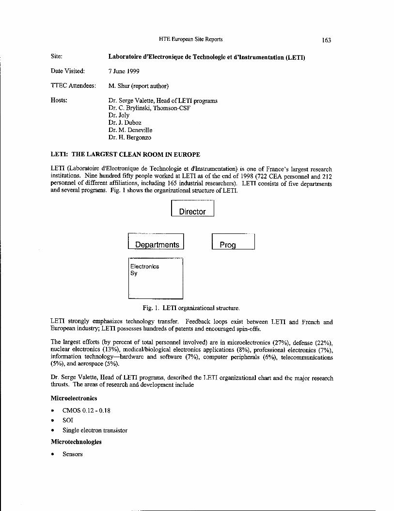
HTE European Site Reports 163
Site:
Date Visited:
TTEC Attendees:
Hosts:
Laboratoire d'Electronique de Technologie et d'Instrumentation (LETI)
7 June 1999
M. Shur (report author)
Dr. Serge Valette, Head of LETI programs Dr. C. Brylinski, Thomson-CSF Dr. Joly Dr. J. Duboz Dr. M. Deneville Dr. H. Bergonzo
LETI: THE LARGEST CLEAN ROOM IN EUROPE
LETI (Laboratoire d'Electronique de Technologie et d'Instrumentation) is one of France's largest research institutions. Nine hundred fifty people worked at LETI as of the end of 1998 (722 CEA personnel and 212 personnel of different affiliations, including 165 industrial researchers). LETI consists of five departments and several programs. Fig. 1 shows the organizational structure of LETI.
Director
Departments Prog
Electronics Sy
Fig. 1. LETI organizational structure.
LETI strongly emphasizes technology transfer. Feedback loops exist between LETI and French and European industry; LETI possesses hundreds of patents and encouraged spin-offs.
The largest efforts (by percent of total personnel involved) are in microelectronics (27%), defense (22%), nuclear electronics (13%), medical/biological electronics applications (8%), professional electronics (7%), information technology—hardware and software (7%), computer peripherals (6%), telecommunications (5%), and aerospace (5%).
Dr. Serge Valette, Head of LETI programs, described the LETI organizational chart and the major research thrusts. The areas of research and development include
Microelectronics
• CMOS 0.12-0.18
• SOI
• Single electron transistor
Microtechnologies
• Sensors

164 HTE European Site Reports
MEMs
Recording and displays (fluorescent tip displays)
Silicon microwave power
Packages and interconnects
Optoelectronics
Infrared photodetection (cooled and uncooled)
Materials for optics
Microlasers
Laser induced damage threshold from UV to infrared
Physico-chemical characterization of materials and thin films
Systems
Electronics for medical applications
Medical imaging
Biochip
Information technology
Nuclear instrumentation
Sensors
Organic components (polymers for optical applications)
Organic LEDs and flat screens
SILICON-ON-INSULATOR
Drs. B. Aspar and J. L. Pelloie presented the results of silicon-on-insulator (SOI) research at LETI. He described the Smart Cut® process and demonstrated that the quality of Si bonded using the Smart Cut® process is similar to that of the starting material. This technology is applicable not only to Si but also to GaAs-based materials and SiC. For silicon technology, SOI technology demonstrates a higher temperature performance.
SIC ACTIVITIES IN FRANCE
Dr. C. Brylinski of Thomson-CSF reported on the results of SiC research in France. This is his summary of the status of SiC research in France:
• Crystals: research stage
• Wafers: started development
• Devices: started development
• Equipment: first demonstration
SiC epitaxy activity is primarily in LETI and in approximately 10 universities.
Funding sources include: CNRS, industry, and defense programs. SiC projects are divided into those that are part of national programs and those that are part of European programs.
Two national programs in SiC include "Saut Technologique", which is a three-year program (funded by the government and coordinated by industry, with industrial partners contributing some funding as well).
HTE European Site Reports 165
The European SiC program has a goal of achieving 3 inch wafers with no micropipes in three??? and to obtain a low defect density on 2 inch wafers (less than 10 micropipes per cm2). Under the auspices of this project, the French have teamed with a Swedish-Finnish company, Okmetic.
More detailed goals include cheaper and bigger crystals, lower defect density, the development of a SiC fabrication process compatible with a silicon line, the development of MOS and HBT devices.
Thomson-CSF is developing recessed SiC MESFETs. They fabricated modules with the total 14.4 mm gate periphery with four chips. For devices with wide gates (a few mm), the microwave power was on the order of 1 W/mm; for narrow gate devices, it was about 4 W/mm. The devices were operational up to 500°C in Copernicus package (AlCuMo frame package). In devices fabricated on semi-insulating SiC substrates, the current decreased with time and disappeared in approximately 100s. (Most likely this is a trapping program, most likely associated with vanadium.) The devices fabricated on conductive substrates did not exhibit this effect.
Dr. Joly described the bulk SiC material grown at LETI. The boule diameter was 50 mm. However, the material quality was inferior at the edges. They are using an Epigress two reactor system. The effort at LETI also includes the simulation of crystal growth. Best results achieved at LETI include 95 mohm cm, p = 10" cm"3, 14% activation for 1021 cm"1 of Al acceptors. A p-n junction operated at 650°C. The junction depth was 220 nm.
There are two European projects dealing with SiC. The funding scale is on the order of one million dollars per year. The first project is called TECSICA. This project provided the basic research funding.
The participants are:
• T.U.B. Berlin
• UAB/CCM (Barcelona)
• Aristoyeles Univ. (Thessaloniki)
• F.O.R.T.H. (Crete)
Endorsers:
• Schlumberger (Clamart)
• C. S. GmbH (Munich)
• LETI (Grenoble)
The second project is called SICOIN. This is an industrial project. Its main goal is to develop a high temperature pressure sensor.
The participants are
• Daimler
• Schlumberger (Clamart)
• T.U.B Berlin
• Aristoyeles Univ. (Thessaloniki)
• Epichem
GaN-RELATED RESEARCH IN FRANCE
Dr. J. Duboz gave an overview of GaN-related research in France.
• Lille: CNRS—Process, electronics
• Caen: CNRS and University—Crystallography
• Strasbourg: CNRS—Nonlinear optics

166 HTE European Site Reports
Orsay: Thomson-CSF—Everything
Clermond Ferran: University—Growth, optical
Lyons: University—Optical
Grenoble: CEA—Growth (MBE), optical
Montpellier: ???—Growth (MOCVD), characterization)
Valbonne: CNRS—Growth optical studies
EEC project
ANISET: Material oriented. Developed a commercial reactor (available from Riber). Also ECR source and thermal cracker
LAQUANI: Material and device oriented
- Nottingham, Madrid, Lausanne, CNRS (finished), EPFL
- Valbonne (finished)
RAINBOW: Multicolor LEDs and blue laser
- Thomson-CSF
- Philips
- Axion
- Epichem
- University of Seville
- Valbonne
- Erlangen
- Surrey
- Aveires
MIGHT: Material and device oriented high power, high frequency electronics ???/ HEMT 5 W, 10 GHz, - goals;
- GEC, Thomson-CSF
- Siemens
- Thomas Swan, Univ. Nottingham, Univ. of Gent
Started this year
Total budget 3-4 million Euro per project per year
Results:
Materials
- P doping 5 x 10" (Valbonne, 3 MBE, 5 MOCVD), conductivity 1 ohm-cm
- InGaN bulk FWHM 50 meV at 10 K, 400 nm, Stokes shift < 30 meV
- InGaN QW FWHM 35 meV at 10 K
- GaN/AlGaN QW FWHM 15 meV at 10 K
ELOG-HVPE
- GaN on Si (111) quality similar to sapphire
HTE European Site Reports 167
- GaN/AlGaN quantum dots: intense, large Stark effect (red PL)
Process:
n-contact lO^ohmcm2
p-contact 10"3 ohm cm2
Etching: vertical facets by CAIBE and optically pumped laser
LEDs
- <-/l mW ???
- GWHM 15 nm at 235 nm
- High turn-on voltage
Laser
- Optical pumped
FETs
MESFETs
2 micron gate, breakdown ~ 300 V, for a 0.3 micron gate, f,= 12 GHz flliax = 25 max Ite = 330 mA/mm
Photodetectors
Photoconductive
3000 A/W
UV-visible 104 to 107
1/f noise is large
Schottky photovoltaic on GaN
ns response
10"8 A reverse current
Johnson noise low bias
roA 108 W cm2
Schottky photovoltaic on AlGaN
Cutoff at 320 nm
4-year delay compared to US
Materials are catching up. Devices behind, except for photodetectors (state of the art)
DIAMOND RESEARCH IN FRANCE
Drs. M. Deneville and P. H. Bergonzo discussed diamond research in France.
Applications
- window (microwave and laser)

168 HTE European Site Reports
- pressure sensors and SAW
- UV,V, X, and particle detectors
Coating
- Electrochemical reactions
p-n junction 900 °C
Schottky700°C
MESFET 500 °C
Groups in France
Window (microwave and laser)
Thomson, CEA in Bordeaux
LPL Paris
SAW (with A1N), Univ. Lens
Pressure sensors and SAW
Univ. of Nancy
UV,V, X, and particle detectors
Coating
University of Orleans
Electrochemical reactions:
LCTMR, CNRS
Basic research
Reactor modeling
Large monocrystalline substrates
Physical and electrical properties
Device
Schottky
MESFET
Surface studies
At LETI, they have grown 0.5 cm 250 micron diamond crystal film.
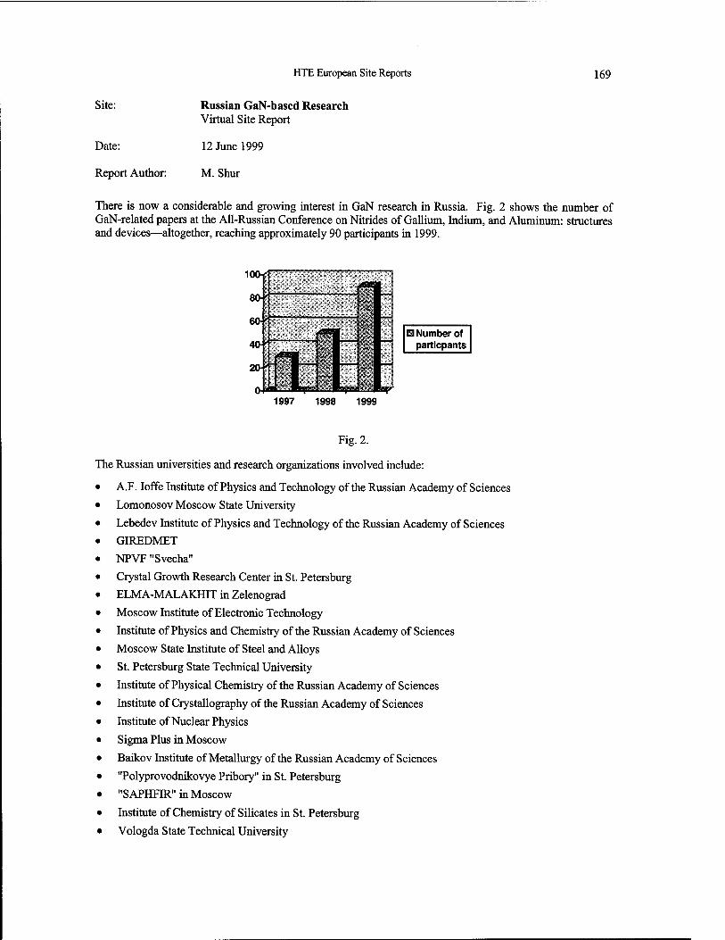
HTE European Site Reports 169
Site:
Date:
Report Author:
Russian GaN-based Research Virtual Site Report
12 June 1999
M. Shur
There is now a considerable and growing interest in GaN research in Russia. Fig. 2 shows the number of GaN-related papers at the All-Russian Conference on Nitrides of Gallium, Indium, and Aluminum: structures and devices—altogether, reaching approximately 90 participants in 1999.
100-(f
1 Number of particpants
1997 1998 1999
Fig. 2.
The Russian universities and research organizations involved include:
A.F. Ioffe Institute of Physics and Technology of the Russian Academy of Sciences
Lomonosov Moscow State University
Lebedev Institute of Physics and Technology of the Russian Academy of Sciences
GIREDMET
NPVF "Svecha"
Crystal Growth Research Center in St. Petersburg
ELMA-MALAKHIT in Zelenograd
Moscow Institute of Electronic Technology
Institute of Physics and Chemistry of the Russian Academy of Sciences
Moscow State Institute of Steel and Alloys
St. Petersburg State Technical University
Institute of Physical Chemistry of the Russian Academy of Sciences
Institute of Crystallography of the Russian Academy of Sciences
Institute of Nuclear Physics
Sigma Plus in Moscow
Baikov Institute of Metallurgy of the Russian Academy of Sciences
"Polyprovodnikovye Pribory" in St. Petersburg
"SAPHFIR" in Moscow
Institute of Chemistry of Silicates in St. Petersburg
Vologda State Technical University
170 HTE European Site Reports
Udmurtsky State Technical University
VNII of Optical and Physical Measurements in Moscow
OPTEL in Moscow
St. Petersburg Institute of Technology
Frumkin Institute of Electrochemistry
NITI "TEKHNOMSH" in Moscow
MAR State Technical University in Iohskar-Ola.
INTERNATIONAL COLLABORATIONS
Russian international collaborations include:
TDI, Inc. in Gaithersburg, Maryland
Howard University in Washington, DC
Rensselaer Polytechnic Institute in Troy, NY
Naval Research Laboratory in Washington, DC
University of Ulm in Germany
University of Karlsruhe in Germany
Technical University of Berlin in Germany
RESEARCH AREAS
The largest effort is at A.F. Ioffe Institute. The areas of research and development include:
crystal growth (with emphasis on HVPE, MOCVD, MBE, and sputtering)
fabrication and characterization of ion-implanted p-n junctions
the development of production equipment (at ELMA-MALAKHIT)
research on ternary and quaternary AlGalnAs solid state solutions
investigations of basic materials properties
growth and characterization of wurtzite and cubic BN
research on GaN and InGaN based LEDs and optically pumped lasers
white LEDs
research on doping of GaN
the development of GaN/GaP and GaN/Si heterostructures
studies of piezoelectric properties
the research on defects, studies of mechanical properties
cathodoluminescence studies
Raman and lattice dynamics studies
applications of blue, green, orange, and red LEDs for materials testing
studies of acoustic surface waves
APPLICATIONS
The Russian company, SVECHA, has taken a lead in production of traffic signals using green GaN LEDs. They had the first installation of such traffic signals in Moscow in 1997. They are involved in the development of LED-based lighting for airplanes, of LED-based navigation lights, and lighting sources for
HTE European Site Reports 171
other applications. Nil OPTEL is using imported green InGaN LEDs for river navigation lights. One blue LED is visible for two kilometers.
CONCLUSION
The research level on devices is relatively small compared to the United States. Only two teams have demonstrated p-type GaN (Alferov's team by MOCVD and Dmitriev's team by HVPE). However, several excellent groups are involved in basic GaN research. Even at this level, there is a company pursuing practical applications (traffic lights) using imported GaN LEDs.
172 HTE European Site Reports
Site: Siemens-Erlangen Paul-Gossen Str. 100 D-91052 Erlangen GERMANY
Date Visited: 8 June 1999
TTEC Attendees: T.P. Chow, (report author), V. Dmitriev, M. Spencer
Hosts: Dr. Dieter Stephani Dr. Roland Rupp Dr. Mitlener Dr. Peter Friedrichs
INTRODUCTION
Siemens is an international industrial company that has major businesses in power generation, transmission and power electronics. There are significant technology development efforts in its research and development laboratory in Erlangen, involving SiC materials growth and processing, device design, fabrication and characterization and prototype device/circuit demonstrations. This group is expected to remain with Siemens after the Infineon spinoff, though some SiC team members have left to join the new company.
Dr. Stephani, who is the project leader, gave an overview of their SiC device program, emphasizing exclusively power electronics applications. The focus of their effort is to replace silicon power devices where SiC can offer better performance, including large-volume applications. There are about 20 people in their group, including epitaxial growth, device design, fabrication and characterization. Over the last few years, the researchers at Siemens have demonstrated many high-voltage power switching devices. They are clearly one of the top SiC device research groups in the world. The devices they have reported include:
• 600-1,200 V Schottky rectifiers
• 3,000 V (soon tobe 5-6 kV) pin junction rectifiers in 4 H-SiC
• 1,800 V power DMOSFETs in 6 H-SiC
• high voltage JFET in 4 H-SiC (with a Si MOSFET gate driver)
• first 15 R-SiC MOSFET
They all have very impressive performance characteristics, such as specific on-resistance and short circuit capabilities. For example, 1,200 V 4 H-SiC Schottky diodes have a specific on-resistance of 2 m£2cm2. Their vertical DMOSFETs have the lowest specific on-resistance of 25 m£2cm2 for an 1,800 V inversion mode SiC MOSFET. Actually, panelists were shown a hybrid package that incorporates the SiC JFEET and Si power MOSFET driver. Also, they have demonstrated the advantage of using 15 R polytype for MOSFET, instead of 4 H polytype (Schorner et al. 1999). The reason for this is that there apparently are few localized trap states near the conduction band edge in 15 R-SiC and, consequently, a much higher inversion electron mobility can be achieved than in 4 H-SiC (33 vs. 0.4 cm2/V-s). Besides, while 6 H-SiC also has similar inversion electron mobility values, the anistropy in bulk mobilities is much less in 15 R-SiC than in 6 H-SiC. Nevertheless, there is no 15 R-SiC commercial wafer supplier at present.
In summary, the SiC research performed in the Siemens group is extremely impressive due to its breadth and outstanding performance characteristics.
REFERENCES
Schorner, R., P. Friedrichs, D. Peters, and D. Stephani. 1999. IEEE Electron Device Letters, vol. 20, pp. 241-244.

HTE European Site Reports 173
University of Erlangen-Nurnberg Marenstrasse II Institute Bid. V, Rm 368 D 91058 Erlangen, Germany Tel: +49 9131 852 7634 or +49-91 31 852 8426
Date Visited: 9 June 1999
TTEC Attendees M.G. Spencer (report author), T.P. Chow, V. Dmitriev
Hosts Dr. Dieter Hoffmann, Electronic Engineering Materials Group Prof. Gerhardt Pensei, Dept. of Physics Prof. Winnacker, Dept. of Physics Dr. Eckstein, SiCrystal
INTRODUCTION
At the University of Erlangen the panel visited two separate departments. The first department was the Department of Materials Science and Engineering. This department forms part of the Technische Fakultät (Faculty of Engineering Sciences). The second group that we visited was a part of the traditional physics department of the university. Both groups were extremely active in materials growth and characterization of SiC.
DEPARTMENT OF MATERIALS SCIENCE AND ENGINEERING
In the Dept. of Materials Science and Engineering most of the work in wide bandgap technology is done in the Electronic Engineering Materials Group. Professor Winnacker gave an overview of the efforts in that group. Major topics under investigation were:
• bulk crystal growth of GaAs, InP and SiC
• modeling of the growth process
• development of phosphorus for blue light conversion
Dr. Dieter Hoffmann gave the panelists a detailed presentation on the research for the bulk growth of SiC. Most of this effort is supported by a research grant from Bavaria. This research grant, ~ $1 million/year, has also supported SiCrystal in their effort to commercialize bulk crystal growth in Germany.
Dr. Eckstein of SiCrystal was present and gave a brief overview of the progress and direction of the company. During the talk by Dr. Hoffman he described efforts to understand the basic thermodynamics of bulk crystal growth and defect formation. Of special interest, micropipes and their formation and research results on formation mechanisms were presented. These topics are investigated experimentally in a sublimation reactor, which is currently growing 1.5" SiC boules. Theoretical modeling of heat transfer is closely linked to this effort.
Another technique for the production of bulk SiC is Liquid Phase Growth. The group in Erlangen and another group in Russia are unique in their efforts to investigate the possibility of large area growth of SiC by this technique. The Erlangen group is producing SiC at 2100°C and 150 torr of pressure. Under these conditions the growth rate is 0.6 mm/hr. The potential advantages of this technique include improved mass transfer and easier scaling.
Dr. Eckstein described SiCrystal, which was formed in August 1996. They are currently producing SiC principally for use in LED technology. This material is 2" in diameter. The company estimates that 90% of their market is based on nitride technology. They expect this number to decrease to 50% when manufacture of SiC based devices commences. When the demand for SiC material increases they will start production of 4" SiC.

174 HTE European Site Reports
DEPARTMENT OF PHYSICS
In the afternoon panelists met with Professor Pensel and Professor Helbig of the Dept. of Physics. In the Department of Physics there is significant activity on crystal growth and characterization. The specific topics were:
• bulk crystal growth—zero micropipes (6 H), 15 R polytype (in collaboration with Kyoto University)
• ion implantation—-intrinsic defects, effects of non stoichiometry, diffusion (Boron)
• reconstruction of SiC surface
• MOS interface state density studies—admittance and constant capacitance DLTS
Most of the work is funded by the German Science Foundation. There is, however, no national program on SiC. The group does participate in a European program, which funds some of the ion implantation work.
In informal discussions with Professors Pensel and Helbig, they both agreed that 15 R had great potential for MOS applications. They indicated that in collaboration with Prof. Matsunami of Kyoto they had obtained inversion layer mobility of 70 cmVV-sec.

HTE European Site Reports 175
Site: University of Linkoping Dept. of Physics and Measurement Technology IFM-FOA S-581 83 Linkoping, Sweden Tel 46 13 8 1765 or 46 13 28 1797
Date Visited: 10 June 1999
TTEC Attendees M.G. Spencer (report author), T.P. Chow, V. Dmitriev
Hosts Professor Bo Monemare Professor Erik Janzen
INTRODUCTION
In Linkoping the panel visited the Dept. of Physics and Measurement Technology. This organization employs over 350 people, including approximately 115 graduate students (who are government employees). The concentration in solid state physics and materials studies is broken down into several topics:
materials physics—125 people
thin film physics
chemical physics
surface physics—this where the sensor work is taking place
theory group
device modeling
biology
chemistry
The materials under study, ordered by research support, are:
SiC—good support from several sources
III/V nitrides /II-VI -III/ V nitride do not currently have local industrial support ???
ffl/V quantum structures
silicon and SiGe
In general the group at Linkoping is interested in the studying the physics of the material topics are: ???
Electronic Properties of Quantum Structures
Electronic Properties of Defects
Properties and Characterization of Epi and Bulk Material
Bulk and Surface Band Structures
SIC ACTIVITIES
Professor Janzen described the SiC activities, which involve two professors, 20 seniors???, 7 PhD students and 6 technical support staff. These activities receive funding from several sources:
SiCep
This is a national program on SiC which provides a total of 18 million SEK of funding for SiC per year. Of that total Linkoping receives 8 million SEK.

176 HTE European Site Reports
Jesica
Joint European SiC Activity: funding from this program totals one million SEK/year. This money is split with Okmetic, a wafer growth startup company.
Okmetic
A wafer growth startup company which is partnering with Grenoble to grow semi-insulating and n+ SiC.
ABB
Linkoping is in direct partnership with ABB (a major multi-national company) for development of materials growth processing and the basic understanding necessary to fabricate high voltage rectifiers.
Other
Linkoping receives about 3 million SEK from the Swedish Engineering Research Council (TFR), Science Research Council (NFR), and the Defense Department (FOA).
Looking in more detail at SiCep, the work is split as follows:
• technology (bulk growth, epi and defects)— 8 million SEK, Linkoping
• devices (power devices, high voltage diodes, high voltage switches)—KTH (KTH is also known as the Royal Institute)
• ion implantation, contacts—KTH
• dielectrics—Chambers
The SiCep program is funded by a private foundation (strategic research foundation???) with government interest or direction; the funds are only for universities. A separate foundation funds equipment.
The emphasis in Janzen's group is to provide a technology for high voltage devices. To that end they have developed high temperature epi for SiC and are using a variant of this technology for bulk crystal growth. The results for the high temperature epi are impressive. They have obtained a background doping of 2-4 x 10Hcm"3 with a growth rate of 40 microns per hour. For the HTCVD (as applied to bulk growth) they have achieved a growth rate 0.5 - 0.8 mm/hr.
III/V Nitrides
Professor Bo Monemare discussed the nitride efforts. The goal of the work is to measure the basic materials parameters. Professor Monemare feels that because the quality of the material is currently so poor all the basic measurements are suspect and need a second look. In an effort to obtain high quality material the group has decided to develop HVPE. The specific topics mentioned were:
• homo epi—HVPE
• thick epi—HVPE
• bulk GaN—high speed HVPE
• physics of AlGaN/GaN and GaN/InGaN multi quantum wells
FACILITIES TOUR
Panelists were shown the facilities at Linkoping. All the growth equipment was designed in collaboration with Epigress (a local equipment supplier). After development at Linkoping this equipment is available on the open market. The Linkoping facilities were about three years old and very impressive. All the equipment was "state of the art" and often brand new. The panel was told that the equipment was purchased with funds from a private foundation as indicated earlier in the report.
HTE European Site Reports 177
Site: University of Ulm Albert-Einstein-Allee 45 D-89081 Ulm, Germany Tel: +49-73150-26454-26050 Fax: +49-73150-26454-26049
Date Visited: 8 June 1999
TTEC Attendees: J. Zavada (report author), S. DenBaars, M. Shur, U. Varshney, G. White
Hosts: Dr. Markus Kamp Prof. Erhard Kohn Prof. Hermann Schumacher
INTRODUCTION
At the University of Ulm, the panel visited the Department of Electron Devices and Circuits and the Department of Optoelectronics, each of which is headed by two professors.
Prof. Kohn, who is with the Department of Electronics and Circuits, gave the panel an overview of the University of Ulm. There are approximately 5,000 students at the university, which is only 30 years old. There are nearly 300 students in the Electrical Engineering Department. Only five students are involved with GaN research at present. However, there is a very active program in GaN materials growth, optical and electrical characterization, and device fabrication and testing.
DEPARTMENT OF OPTOELECTRONICS
Professors K. Ebeling and P. Unger are the two professors in charge of Optoelectronics. Neither one was at the university during the panel's visit. Dr. Kamp gave the panel an overview of the research activities in this department. At present, the main areas of investigation are:
• vertical cavity surface emitting lasers (VCSELs) having low threshold currents
optical interconnects for high data rate transmission
high power laser diodes based on InAlGaAs compounds
high brightness light emitting diodes (LEDs), which encompasses the GaN research
•
•
Dr. Kamp gave panelists a detailed presentation on the research on GaN LEDs and laser diodes. Most of this effort is supported by a research grant from state government and includes GaN growth, optical characterization, device fabrication and testing.
Initially, Dr. Kamp's group was using gas source molecular beam epitaxy (MBE) to synthesize the GaN layers. However, due to the unimpressive device results with this method, the group is now using chemical vapor deposition (CVD) to grow the GaN layers. Much improved optoelectronics devices have resulted using this approach.
The group has grown GaN LED structures on sapphire substrates and on GaN bulk crystals obtained from UNIPRESS in Poland. In general, GaN homoepitaxy leads to much improved optical characteristics. Photoluminescence (PL) taken at 20 K shows all of the relevant exitonic features and linewidths as narrow as 1 meV. The LEDs grown on GaN substrates are nearly twice as bright as the ones grown on sapphire. These results are similar to those found with LEDs grown on GaN lateral overgrowth epitaxy (LEO) substrates. In spite of the large reduction of dislocation defects in the GaN films, the LEDs only show a two-fold improvement in brightness.
178 HTE European Site Reports
Dr. Kamp also described efforts to develop GaN waveguide structures. The intent is to design and fabricate suitable laser structures and to produce a room temperature, cw laser.
DEPARTMENT OF ELECTRON DEVICES AND CLRCUITS
Prof. E. Kohn and H. Schumacher are the two professors in charge of Electron Devices and Circuits. The main research activities in this department relating to GaN are electronic device modeling and characterization.
Prof. Hermann Schumacher's group is mainly involved in the modeling and device characterization of SiGe heterostructure bipolar transistors. This research is being done in close collaboration with Temic Semiconductors GmbH, which is a spin-off company of Siemens AG.
Prof. Schumacher gave a presentation on the advantages of SiGe devices for telecommunications. He described his research in exploring the performance potential of SiGe integrated circuit technology, at frequencies above 3 GHz, for front-end receivers.
Prof. Kohn gave the panel a detailed presentation on his research concerning electrical characterization of GaN-based devices. His group has been involved in the small and large signal dispersion analysis of AlGaN/GaN MODFETs (modulation doped field effect transistors) and AIN/n-GaN FETs (field effect transistors). The device structures were grown by SVT Associates, in the United States, and processed into devices at DaimlerChrysler in Ulm. Their results indicate that the I-V characteristics of these devices change with heat treatment. A degradation of the I-V curves occurs after treatment at 600°C. These effects may be due to a materials problem (defects in the buffer layer) or to changes in the electrical contacts (surface charge).
Later Prof. Schumacher gave a tour of his labs for device characterization. These labs have also been used for the signal dispersion analysis of AlGaN/GaN MODFETs done by Prof. Kohn's group. Some of the research concerning electrical characterization of GaN-based devices has not as yet been published.
CLEAN ROOM FACILITIES
Later in the day, Dr. Kamp took the panel on a tour of the clean room facilities in the microelectronics technology center at the University. There is approximately 600 sq. meters of clean room space; some areas are class 100 and others are class 10. All the growth equipment was located in the center. There are a total of seven growth reactors for synthesis of different compound semiconductors. Currently, no synthesis of Si is being undertaken.
At present two Aixtron reactors are being used for GaN thin film growth, one for CVD and the other for hydride vapor phase epitaxy. Three other reactors are being used for growth of InAlGaAs compounds. One reactor is not presently in service.

HTE European Site Reports 179
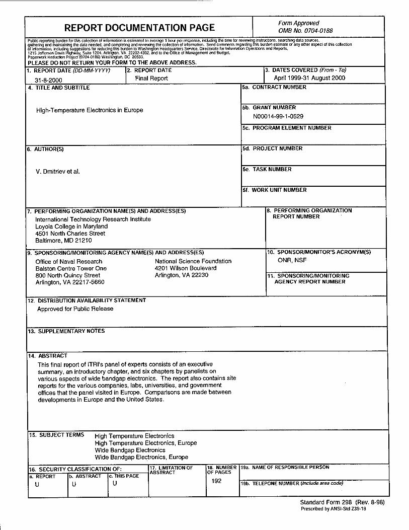
REPORT DOCUMENTATION PAGE Form Approved OMB No. 0704-0188
Public reporting burden for this collection of information is estimated to average 1 hour per response, including the time for reviewing instructions, searching data sources, gathering and maintaining the data needed, and completing and reviewing the collection of information. Send comments regarding this burden estimate or any other aspect of this collection of information, including suggestions for reducing this burden to Washington Headquarters Service, Directorate for Information Operations and Reports, 1215 Jefferson Davis Highway, Suite 1204, Arlington, VA 22202-4302, and to the Office of Management and Budget, Paperwork Reduction Project (0704-0188) Washington, DC 20503.
PLEASE DO NOT RETURN YOUR FORM TO THE ABOVE ADDRESS. 1. REPORT DATE (DD-MM-YYYY)
31-8-2000
2. REPORT DATE
Final Report
3. DATES COVERED (From - To)
April 1999-31 August 2000
4. TITLE AND SUBTITLE
High-Temperature Electronics in Europe
5a. CONTRACT NUMBER
5b. GRANT NUMBER
N00014-99-1-0529
5c. PROGRAM ELEMENT NUMBER
6. AUTHOR(S)
V. Dmitriev et al.
5d. PROJECT NUMBER
5e. TASK NUMBER
5f. WORK UNIT NUMBER
PERFORMING ORGANIZATION NAME(S) AND ADDRESS(ES)
International Technology Research Institute Loyola College in Maryland 4501 North Charles Street Baltimore, MD 21210
8. PERFORMING ORGANIZATION REPORT NUMBER
SPONSORING/MONITORING AGENCY NAME(S) AND ADDRESS(ES)
Office of Naval Research National Science Foundation Balston Centre Tower One 4201 Wilson Boulevard 800 North Quincy Street Arlington, VA 22230 Arlington, VA 22217-5660
10. SPONSOR/MONITOR'S ACRONYM(S)
ONR, NSF
11. SPONSORING/MONITORING AGENCY REPORT NUMBER
12. DISTRIBUTION AVAILABILITY STATEMENT
Approved for Public Release
13. SUPPLEMENTARY NOTES
14. ABSTRACT
This final report of ITRI's panel of experts consists of an executive summary, an introductory chapter, and six chapters by panelists on various aspects of wide bandgap electronics. The report also contains site reports for the various companies, labs, universities, and government offices that the panel visited in Europe. Comparisons are made between developments in Europe and the United States.
15. SUBJECT TERMS High Temperature Electronics High Temperature Electronics, Europe Wide Bandgap Electronics Wide Bandgap Electronics, Europe
16. SECURITY CLASSIFICATION OF: a. REPORT
U
b. ABSTRACT
U
C. THIS PAGE
U
17. LIMITATION OF ABSTRACT
18. NUMBER OF PAGES
192
19a. NAME OF RESPONSIBLE PERSON
19b. TELEFONE NUMBER (Include area code)
Standard Form 298 (Rev. 8-98) Prescribed by ANSI-Std Z39-18
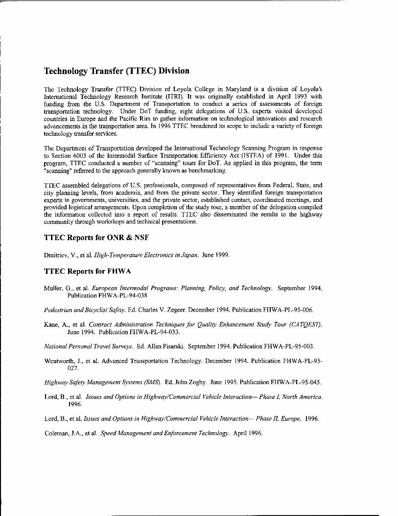
Technology Transfer (TTEC) Division
The Technology Transfer (TTEC) Division of Loyola College in Maryland is a division of Loyola's International Technology Research Institute (ITRI). It was originally established in April 1993 with funding from the U.S. Department of Transportation to conduct a series of assessments of foreign transportation technology. Under DoT funding, eight delegations of U.S. experts visited developed countries in Europe and the Pacific Rim to gather information on technological innovations and research advancements in the transportation area. In 1996 TTEC broadened its scope to include a variety of foreign technology transfer services.
The Department of Transportation developed the International Technology Scanning Program in response to Section 6003 of the Intermodal Surface Transportation Efficiency Act (ISTEA) of 1991. Under this program, TTEC conducted a number of "scanning" tours for DoT. As applied in this program, the term "scanning" referred to the approach generally known as benchmarking.
TTEC assembled delegations of U.S. professionals, composed of representatives from Federal, State, and city planning levels, from academia, and from the private sector. They identified foreign transportation experts in governments, universities, and the private sector, established contact, coordinated meetings, and provided logistical arrangements. Upon completion of the study tour, a member of the delegation compiled the information collected into a report of results. TTEC also disseminated the results to the highway community through workshops and technical presentations.
TTEC Reports for ONR & NSF
Dmitriev, V., et al. High-Temperature Electronics in Japan. June 1999.
TTEC Reports for FHWA
Müller, G., et al. European Intermodal Programs: Planning, Policy, and Technology. September 1994, Publication FHWA-PL-94-038
Pedestrian and Bicyclist Safety. Ed. Charles V. Zegeer. December 1994. Publication FHWA-PL-95-006.
Kane, A., et al. Contract Administration Techniques for Quality Enhancement Study Tour (CATQEST). June 1994. Publication FHWA-PL-94-033.
National Personal Travel Surveys. Ed. Allan Pisarski. September 1994. Publication FHWA-PL-95-003.
Wentworth, J., et al. Advanced Transportation Technology. December 1994. Publication FHWA-PL-95- 027.
Highway Safety Management Systems (SMS). Ed. John Zogby. June 1995. Publication FHWA-PL-95-045.
Lord, B., et al. Issues and Options in Highway/Commercial Vehicle Interaction— Phase I, North America. 1996.
Lord, B., et al. Issues and Options in Highway/Commercial Vehicle Interaction— Phase II, Europe. 1996.
Coleman, J.A., et al. Speed Management and Enforcement Technology. April 1996.

ISBN 1-883712-59-9
Copyright © 2022 FDOKUMEN

