


Bahasa
Halaman
Hukum

UNIVERSIDAD AUTÓNOMA DE MADRID
ESCUELA POLITÉCNICA SUPERIOR
PROYECTO FIN DE CARRERA
Economic aspects of FPGA technology
Ingeniería de Telecomunicación
Borja Díaz Arroyo
Marzo de 2014


i
Economic aspects of FPGA technology
AUTOR: Borja Díaz Arroyo
TUTOR: Eduardo Boemo
Laboratorio DSLab
Escuela Politécnica Superior
Universidad Autónoma de Madrid
Marzo de 2014

ii

iii
Resumen
En este PFC se ha recogido y analizado diversa información acerca de la
tecnología de Xilinx. Incluyendo los datasheets de Xilinx notas del E.E.
Times, informes financieros, y artículos de internet. Todos los datos se han
unificado en unas ciento cincuenta figuras y tablas. Además, se han
revisado los proceedings de la conferencia FPL desde 1991 (la primera en
Oxford) hasta 2013 (el último en Porto).

iv
Abstract
In this PFC, diverse information about Xilinx technology has been
collected and analyzed. It includes Xilinx datasheets, notes on E.E. Times,
financial reports, and Internet articles. All the data have been unified in
around one hundred and fifty figures and tables. In addition, FPL
proceedings from 1991 (the first in Oxford) to 2013 (the last in Porto)
have been revised.

v
Acknowledgements
First of all, I want to thank my tutor Eduardo Boemo the opportunity to make a bit
different project, which has opened my mind to new possibilities in life. Your help and
support have been invaluable.
Secondly I would like to thank all the people who have formed me both academically
and personally, professors, teachers and coaches. With your help I have got enough tools to
face any challenge.
I would especially like to thank my family for all the support and patience they have
had with me. They have transmitted me the values that have made me the person I am. My
father is an example of effort and hard work, my mother has given me the serenity and calm to
see the good in everything and my brother is a diamond in the rough. There are no words to
describe how grateful I am to have the family that I have.
I do not forget all the colleagues and friends who have been staying with me over the
years, without you the path that has brought me here would have been much more
complicated.
And last but not least, thanks to my closest friends. You have been like my family when
I needed and your support has been crucial. Thank you very much guys without you nothing
would be the same. I would like to make a special mention, Miriam thanks for always being
there, your help and support have made the difference.

vi
Index
List of figures…………………………………………………………………………………………………………IX List of tables………………………………………………………………………………………………………..XIII
1. General aspects
1.1. Motivations and Objectives………………………………….……………………..……………….…………1
1.2. Scope of this study.…………………………………………………….………………………...………………..1
1.3. Methodology and work plan…………………………………………………………………………………..2
1.4. PFC organization and contents……………………………………………………………………………….3
1.5. Acronyms list……………………………………………………………………………….………………………..3
2. What is a FPGA?
2.1. Abstract………………………………………………………………………….….………………..………………..5
2.2. Evolution of PLDs………………………………………………………………….……………………………….6
2.3. Architecture of FPGAs……..………………………………………………………….…….…………………...15
2.4. Programming technologies……..………………………………………..……………………………………19
2.5. Applications of FPGAs………..……………………………………………………..…………………………...21
3. Economic approach
3.1. Abstract…………..…………………………………………….………………………….……………….………….25
3.2. Introduction……………...………………………………………………………………………..…………………26
3.3. Historical notes……………...…………………………………………………………………..………………….31
3.3.1. Xilinx…………………………………………………………………………………………………………31
3.3.2. Altera………………...………………………………………………………………………………………31
3.3.3. Actel……...………………………………………………………………………………………………..…32
3.4. FPGA Market along 30 years……………..……………………………………..…………………………….32
3.5. Financial aspects of FPGA companies……...……………………………………………………………...34
3.6. Xilinx vs. Altera and FPGA market share historic…….……………….……………………………...36
3.7. EDA tools………...………………………………………………………………..…………………………………..43
3.8. ASIC vs. FPGA………...………………………………………………………………………………..…………….46

vii
3.9. Job market in FPGA…………..………………………………………………..………………………………….48
4. Xilinx devices
4.1. Abstract…………………………………………………………………………….………………………………….52
4.2. Introduction…..………………………………………………………..……………………………………………52
4.3. A brief list of Xilinx’s FPGAs………..…………………………………………..……………………………..54
4.4. Xilinx evolution……………………………………………………….………….………………………………...61
4.5. Architecture of Xilinx FPGAs: Catalog of Logic Blocks………………………..……………………64
4.6. Summary of main characteristics of Xilinx FPGAs………….…………..……………………………75
5. FPL Congress
5.1. Abstract………………..…………………………………………………………………….……..………………….82
5.2. Introduction………...………………………………………………………………………………..………………82
5.3. Research in FPGA and geographical areas……..……………………………………….……………….85
5.4. Authors and topics…………………..…………………………………………………………..……………...100
5.5. Main information available about the FPL conference.…………………………………………..105
6. Conclusion and complement information
6.1. Final remarks………..……………………….…………………………………………….……..……………….119
6.2. Conclusion..…………..……………………….…………………………………………….……..……………….119
6.3. Future work………...…………………….…………………………………………………………..……………120
7. Apendix A: Aspectos Generales……………………………………………………………………..122
8. Apendix B: Conclusión e información complementaria……………………………………125
9. Apendix C: Economical estimation……………………………………………………………..…..130
10. Apendix D: Tender specifications…………………………………………………………..….….132

viii

ix
List of figures
Fig. 1: Logical structure of a fuse PROM................................................................................................................7
Fig. 2: FPLA structure....................................................................................................................................................8
Fig. 3: PLA structure......................................................................................................................................................9
Fig. 4: GAL16V8 OLM convinational configuration.......................................................................................10
Fig. 5: Classic Altera’s EPLD OLMC.......................................................................................................................11
Fig. 6: The Cypress PALCE22V10 macrocell.....................................................................................................12
Fig. 7: CPLD block diagram......................................................................................................................................13
Fig. 8: Basic FPGA block diagram..........................................................................................................................14
Fig. 9: FPD categories by logic capacity..............................................................................................................15
Fig. 10: Xilinx CLB structure....................................................................................................................................16
Fig. 11: Xilinx I/O block.............................................................................................................................................17
Fig. 12: Model of FPGA routing structures........................................................................................................18
Fig. 13: Percentage of application in 1995........................................................................................................22
Fig. 14: Percentage of application in 2002........................................................................................................22
Fig. 15: Percentage of application in 2009........................................................................................................23
Fig. 16: Main FPGA players 1983/2008.............................................................................................................26
Fig. 17: Window market…………………………………………………………………………………………………….28
Fig. 18: Situation of the Silicon Valley. ……………………………………………………………………………….28
Fig. 19: Xilinx Worldwide. …………………………………………………………………………………………………29
Fig. 20: Xilinx, Altera, and Intel share revaluation. ……………………………………………………………..34
Fig. 21: Real Interest Rate. ………………………………………………………………………………………………..35
Fig. 22: Xilinx and Altera revenues. …………………………………………………………………………………...38
Fig. 23: Xilinx/Altera revenues. …………………………………………………………………………………………39
Fig. 24: Market share. ……………………………………………………………………………………………………….40
Fig. 25: The percentage of revenue. …………………………………………………………………………………...42
Fig. 26: The percentage of profits divided by geographical in 2010. ……………………………………43
Fig. 27: Design languages. …………………………………………………………………………………………………44
Fig. 28: Number of new FPGA/ASIC designs. ……………………………………………………………………...46

x
Fig. 29: Job offers and average salary per country. ……………………………………………………………..50
Fig. 30: Flip-Flops. ……………………………………………………………………………………………………………60
Fig. 31: System speed. ………………………………………………………………………………………………………60
Fig. 32: Equivalent gates. …………………………………………………………………………………………………..61
Fig. 33: I/Os. …………………………………………………………………………………………………………................61
Fig. 34: Process. ……………………………………………………………………………………………………................62
Fig. 35: Process Xilinx vs. Intel. ………………………………………………………………………………………….63
Fig. 36: Row and column relationship between CLBs and Slices. …………………………………………64
Fig. 37: XC2000 logic block. ………………………………………………………………………………………………65
Fig. 38: XC3000 logic block. ………………………………………………………………………………………………66
Fig. 39: XC4000 logic block. ………………………………………………………………………………………………67
Fig. 40: XC5200 logic cell (Four LCs per CLB). ……………………………………………………………………68
Fig. 41: Spartan and Spartan-XL logic block. ………………………………………………………………………69
Fig. 42: Half CLB of Spartan-II-called slice. …………………………………………………………………………70
Fig. 43: Spartan-IIE CLB slice. ……………………………………………………………………………………………71
Fig. 44: Virtex-E slice. ……………………………………………………………………………………………………….72
Fig. 45: Virtex-II slice. ……………………………………………………………………………………………………….73
Fig. 46: Technology regions proposed by IEEE. ………………………………………………………………….84
Fig. 47: Submissions by its region. …………………………………………………………………………………….86
Fig. 48: North America submissions. …………………………………………………………………………………86
Fig. 49: USA submissions contribution from 1992 to 2012. ………………………………………………...87
Fig. 50: Canada submissions contribution from 1992 to 2012……………………………………………..87
Fig. 51: Example of US papers published in 2009. ………………………………………………………………88
Fig. 52: Latin America submissions. …………………………………………………………………………………..89
Fig. 53: Latin America submissions contribution from 1992 to 2012…………………………………..90
Fig. 54: Brazilian submissions contribution from 1992 to 2012…………………………………………..90
Fig. 55: Europe submissions. ……………………………………………………………………………………………91
Fig. 56: UK submissions contribution from 1992 to 2012. ………………………………………………….92
Fig. 57: Spain submissions contribution from 1992 to 2012. ………………………………………………92

xi
Fig. 58: Germany submissions contribution from 1992 to 2012. …………………………………………93
Fig. 59: France submissions contribution from 1992 to 2012. …………………………………………….93
Fig. 60: Spain published papers 2009…………………………………………………………………………………94
Fig. 61: Spain published papers from 2009 to 2013…………………………………………………………….95
Fig. 62: East Asia submissions contribution from 1992 to 2012…………………………………………..96
Fig. 63: Southern Asia submissions contribution from 1992 to 2012…………………………………...96
Fig. 64: South-western Asia submissions contribution from 1992 to 2012. ………………..………..97
Fig. 65: Oceania submissions. …………………………………………………………………………………………... 97
Fig. 66: Japan submissions contribution from 1992 to 2012………………………………………………..98
Fig. 67: China submissions contribution from 1992 to 2012. ……………………………………………...98
Fig. 68: Oceania submissions contribution from 1992 to 2012……………………………………………99
Fig. 69: The most active authors. ………………………………………………………………………………………99
Fig. 70: Power papers from 2005 to 2013. ………………………………………………………………………100
Fig. 71: Embedded papers from 2005 to 2013. ………………………………………………………………...101
Fig. 72: Reconfiguration papers from 2005 to 2013………………………………………………………….101
Fig. 73: Filters papers from 2005 to 2013………………………………………………………………………...102
Fig. 74: Multiplier papers from 2005 to 2013…………………………………………………………………...102
Fig. 75: DSP papers from 2005 to 2013…………………………………………………………………………….103

xii

xiii
List of tables
Table 1: Top ten pure foundries 2004………………………………………………………………………………..30
Table 2: Data from Xilinx, Altera, and Intel…………………………………………………………………………37
Table 3: Top ten Fabless 2009…………………………………………………………………………………………...41
Table 4: Top ten OEMs 2011..…………………………………………………………………………………………….45
Table 5: LSI Logic vs. Altera……………………………………………………………………………………………….47
Table 6: Year of introduction of each new process……………………………………………………………...52
Table 7: XC2064 VCC 5V……………………………………………………………………………………………………53
Table 8: XC3000, XC3000A, XC3100A/L…………………………………………………………………………….53
Table 9: XC4000 VCC 5V…………………………………………………………………………………………………...53
Table 10: XC4000E……………………………………………………………………………………………………………53
Table 11: XC4000EX/XL……………………………………………………………………………………………………54
Table 12: XC4000XV………………………………………………………………………………………………………….54
Table 13: XC4000XLA………………………………………………………………………………………………………..54
Table 14: XC5200 Series……………………………………………………………………………………………………54
Table 15: Xilinx Spartan (Jan. 1998) and Spartan-XL (Nov. 1998) Families………………………….55
Table 16: Spartan-II 2.5V. …………………………………………………………………………………………………55
Table 17: Xilinx Spartan-IIE 1.8V……………………………………………………………………………………….55
Table 18: Xilinx Spartan-3…………………………………………………………………………………………………55
Table 19: Xilinx Spartan-3E………………………………………………………………………………………………56
Table 20: Xilinx Spartan-3A………………………………………………………………………………………………56
Table 21: Xilinx Spartan-3AN. …………………………………………………………………………………………..56
Table 22: Xilinx Spartan-3A DSP………………………………………………………………………………………..56
Table 23: Xilinx Virtex……………………………………………………………………………………………………….57
Table 24: Xilinx Virtex E…………………………………………………………………………………………………….57
Table 25: Xilinx Virtex 2.5 V………………………………………………………………………………………………57
Table 26: Xilinx Virtex-II……………………………………………………………………………………………………57
Table 27: Xilinx Virtex-II PRO (2002) ………………………………………………………………………………..58
Table 28: Hardened QPro Virtex-II…………………………………………………………………………………….58

xiv
Table 29: Xilinx Virtex-4……………………………………………………………………………………………………58
Table 30: Xilinx Virtex-5 (2006) ………………………………………………………………………………………..58
Table 31: XC6200……………………………………………………………………………………………………………...59
Table 32: XC8100……………………………………………………………………………………………………………...59
Table 33: Logic Resources in one CLB………………………………………………………………………………...64
Table 34: XC3000 Series……………………………………………………………………………………………………74
Table 35: XC4000XLA Series……………………………………………………………………………………………...74
Table 36: XC4000E and XC4000X Series…………………………………………………………………………….75
Table 37: XC5200 Series……………………………………………………………………………………………………75
Table 38: Spartan and Spartan-XL Series……………………………………………………………………………75
Table 39: Spartan-II Series………………………………………………………………………………………………...76
Table 40: XA Spartan-IIE Series…………………………………………………………………………………………76
Table 41: Spartan-3 Series. ……………………………………………………………………………………………….76
Table 42: Spartan-3A Series………………………………………………………………………………………………77
Table 43: Spartan-3E Series………………………………………………………………………………………………77
Table 44: Virtex-E Series…………………………………………………………………………………………………...77
Table 45: Virtex Series………………………………………………………………………………………………………78
Table 46: Virtex-II Series…………………………………………………………………………………………………...78
Table 47: Virtex-4 Series…………………………………………………………………………………………………...79
Table 48: XC8100 Series……………………………………………………………………………………………………79
Table 49: Virtex-5 Series…………………………………………………………………………………………………...80
Table 50: FPL editions, venues, and general chairpersons…………………………………………………..83

1
1. General aspects
1.1. Motivation and Objectives
This work is the first step of a project to create a smartphone-based Atlas of FPGA
Technology. The present PFC embraces the tasks of studying, classificating, and organizating
the main information available on FPGAs. It can be framed under the Item 3 of the Regulations
of Final Project Thesis of Telecommunication Engineering at the EPS-UAM:
Studies ... related to equipment, systems, services ... related to technical, economic,
management, planning, operating, related to the degree.
One of the basic sources of this study has been the technical records preserved at the
DSLab of the School of Engineering of the Universidad Autónoma de Madrid during nearly the
last 25 years. These documents include data books, data sheets, marketing information, press
information, financial reports, magazines, and even chip samples and boards. Most of them
have been retired from the servers of Xilinx long time ago.
Thus, the objective of this PFC is the analysis of FPGA phenomenon from a
technological, geographical and economical point of view. There are several facts that make
the goal feasible:
• The companies started in 1984. They are modern. So, the amount of information is
limited.
• Main inventors are alive, and they are accessible by email. In addition, they can be
interviewed in the main conference of the area.
• FPGA is very innovative milestone in electronic technology standardization in the
Makimoto´s Wave sense.
• The technology has very few manufacturers.
• There are a clear number of reference conferences.
• Finally, the technology is widespread in Spain.

2
Other similar technologies as microprocessors (1972) or TTL (1960) devices were discarded
for failing to meet most of the above conditions.
1.2. Scope of this study
The points that are intended to explore in this PFC are listed bellow in order of
interest:
1. Technological evolution of the HW: Study the devices and physical parameters
such as size, number of pins, embedded blocks, system speed, scale process, and
delays. Devices description embraces from PALs to Virtex FPGAs.
2. Economic matters and aspects of marketing. It includes information about the
business leaders and contributions to this technology, as well as brief history of
main acquisitions. Comparisions between Xilinx, Altera and Intel (the last one as a
benchmark company). Xilinx in the stock market. And finally, an example of high-
tech company profits: Xilinx vs. Inditex numbers.
3. A list of academic researchers in FPGAs. The information is based on the
proceedings of the FPL, which is an acceptable sample size. The conference is also
the largest international meeting on the subject.
4. Main technology development areas, separated geographically in U.S. and Canada,
Europe, Latin America, and Asia - Oceania.
1.3. Methodology and work plan
The goal of this PFC is a set of organized and indexed information. By the nature of the
investigation, the final report is a collection of tables and graphs. The referencing is other
important results: most of the data presented in this PFC have been connected with the
original bibliophrapical source. The main sources analyzed are:
• Media news; in particular EE Times.
• Internet reports.
• Xilinx Xcell Journal
• IEEE Xplore Database.

3
• LNCS Database.
• FPL Conference Proceedings.
• Xilinx Technical Notes.
• Financial reports and Nasdaq information.
• Printed Databooks.
• Preliminary data sheets.
1.4. PFC organization and contents
This PFC is divided in six chapters organized in the following form:
• Chapter 1: PFC goals and organization.
• Chapter 2: Description of FPGA. Evolution of the main programmable devices from the
PLA to current FPGAs. Principal architectures. Gallery of CLBs. Programming options.
Applications of FPGAs.
• Chapter 3: Economical aspects of FPGA Technology. Historical notes of Xilinx and
Altera. FPGA and the economic framework (1985-2010). Stock quotes. Financial
reports of Xilinx. Altera versus Xilinx. EDA Industry. ASIC versus FPGAs. Jobs in FPGA
at England, USA, France, Germany, Ireland, and Spain.
• Chapter 4: FPGA Architecture. Graphical gallery of Xilinx CLBs. Main tables and
features of Xilinx devices.
• Chapter 5: FPL Conference. Principal researchers. Geographical areas. Hot topics on
FPGAs.
1.5. Acronyms List
ASIC: Application Specific Integrated Circuit.
CLB: Configurable Logic Block.
CT: Computerised Tomography.
EDA: Electronic Design Automation.
EPLD: Erasable Programmable Logic Device.
4
EPROM: Erasable PROM.
FF: Flip Flop.
FPD: Field-Programmable Device.
FPGA: Field Programmable Gate Array.
FPL: Field-Programmable Logic.
GDP: Gross Domestic Product.
IEEE: Institute of Electrical and Electronics Engineers.
LUT: Look-up Table.
NASDAQ: National Association of Securities Dealers Automated Quotation.
NRE: Non-Recurring Engineer.
OEM: Original Equipment Manufacturers.
OLMC: Output Logic Macro Cell.
OTPROM: One Time PROM.
PAL: Programmable Array Logic.
PET: Positron Emission Tomography.
PLA: Programmable Logic Array.
PLD: Programmable Logic Device.
PROM: Programmable Read-Only Memory.
RAM: Random Access Memory.
ROE: Return On Equity.
TSMC: Taiwan Semiconductor Manufacturing Company.
UAM: Universidad Autónoma of Madrid.
UCM: Universidad Complutense of Madrid
UPM: Universidad Politécnica of Madrid.
UMC: United Microekectronics Corporation.

5
2. What is a FPGA?
2.1. Abstract
This chapter provides a brief vision of what a FPGA is. It starts from the PAL and FPD
to the current high density FPGAs, showing the history, architecture, and applications.
In order to understand this chapter it could be useful to make some basics definitions1:
• CPLD: Single chip where is focused multiple SPLD-like blocks. It features logic
resources with a wide number of inputs.
• FPD: Field-Programmable Device: Also known as PLDs (Programmable Logic Devices),
the FPDs are integrated circuits utilized to implement digital hardware with the
particularity that the end-user is able to program or adapt it to get different designs.
• FPGA: equivalent to FPD. A structure that presents high capacity of logical resources,
nearly 106 gates in 2013.
• Logic Block: The basic element of a FPGA. At least it is composed of a LUT and a
register.
• Logic Capacity: Characteristic of the FPGAs that informs the designer about the
quantity of digital logic that the device is able to map.
• LUT: Look-up table: small multiplexers or ROMs utilized to construct a combinational
logic function.
• OLMC (Output Logic Macro Cell): Section of the devices that includes the necessary
elements to set its input/outputs.
• SPLD: Acronyms utilized to refer to any type of Simple PLD.
• System Speed: A number close to the maximum operable speed of a generic circuit.
1 “Circuitos lógicos programables” C. Tavernier.

6
2.2. Evolution of PLDs
The following informations have been condensed from the book “Circuitos lógicos
programables” of C. Tavernier.
Programmable Read-Only Memory (PROM) was the first type of user-programmable
devices to implement logic circuits. This technology can be divided in different families:
• Fuse PROM, programmable memory through physical destruction of fuse.
• EPROM (Erasable PROM), re-programmable memory by different ways that depend
on the technology of the families:
o EEPROM (Electrical Erasable PROM).
o UVPROM (Ultra Violet PROM).
o Flash EPROM (similar to EEPROM).
• OTPROM (One Time PROM), programmable memory like the EPROM.
The PROM devices are able to implement logic circuits. They require to have defined
all the possible input combinations in a separate memory location. PLA devices improve the
implementation of logic circuits reducing the number of transistors needed. The characteristic
of PLA device is that are composed of two programmable planes, the AND gate plane and the
OR gate plane.
The double programmable plane of PLA devices made them relatively slow and
expensive. The solution was the PAL device with only one programmable plane that allows
higher operating speed in a compact package.
All these devices are known as simple programmable logic devices (SPLD). To increase
their capacity, it began to be combined in the same package resulting in the complex
programmable logic devices (CPLD), direct ancestors of FPGA.
In order to have a deep vision of the evolution of PLDs the structures of FPGAs
preceding devices are shown below. The main object of these pictures is to illustrate how the
different architectures have been evolucionated.

7
The structure of a fuse PROM memory shows the association of the “AND” fixed gates
area with the “OR” programmable gates area. Memories do not only have the main function of
data storage, they can easily be utilized as a logic circuit. However, PROMs are an inefficient
architecture for realizing logic circuits, and so are rarely utilized in practice for that purpose.
Fig. 1: Logical structure of a fuse PROM (Reproduced from2)
2 http://www.eej.ulst.ac.uk/~ian/modules/EEE515/files/Tour_of_PLDs.htm

8
The first device designed specifically for the implementing of logic circuits was the
Field-Programmable Logic Array (FPLA), or simply PLA. A PLA contains two levels of logic
gates: a programmable AND-plane and a programmable OR-plane.
Fig. 2: FPLA structure (Reproduced from3)
3 http://www.cse.dmu.ac.uk/~sexton/WWWPages/pal/out.html

9
The use of this kind of circuits is very flexible, but they have two major drawbacks:
• Their high manufacture cost.
• Their low system speed.
Both disadvantages were caused by the two levels of configurable logic. So, to improve
these faults, the Programmable Array Logic (PAL) was designed. The characteristic of this
technology is the implementation as a single level of programmability consisting of a
programmable AND-plane that feeds fixed OR-gates. Initially we may assume that the
flexibility of a PAL is similar to a PROM but the difference is that programmable zones change.
Fig. 3: PAL structure (Reproduced from4)
4 http://www.eej.ulst.ac.uk/~ian/modules/EEE515/files/Tour_of_PLDs.htm

10
The erasable PAL (PAL CMOS) appeared in 1983, approximately five years after the
first PAL, without a significant decrement in the speed system. PAL CMOS utilized two
different technologies, erasable with ultra violet light and electrically re-programmable.
Similar to these re-programmable technologies there are two different devices:
• GAL (Generic Array Logic): close to the electrical erasable PAL CMOS but includes
circuits that do not exist in PAL CMOS technology like Output Logic Macro Cells
(OLMCs). This provides more flexibility because they can be configured as a
combinational output or as a registered output. It is also electrically erasable.
Fig. 4: GAL16V8 OLMC Combinational configuration (Reproduced from5)
5 “Programmable Logic” Adapted from slides by R. H. Katz http://dal.snu.ac.kr/~kchoi/class/lc_intro/programmable_logic.pdf

11
• EPLD (Erasable Programmable Logic Device), erasable logic circuits but the internal
structures (the output macro cells, and interconnection nets) are completely different
from PAL CMOS.
Fig. 5: Classic Altera’s EPLD OLMC (Reproduced from6)
6 “Altera Classic EPLD” data sheet, January 1998. http://www.datasheetcatalog.com/datasheets_pdf/E/P/6/1/EP610.shtml

12
The PAL CMOS was utilized in development phases and also in stages of production
despite its price. A single 20-pin CMOS PAL replaced any 20-pin fuse PAL, due to its more
advanced output macro cell:
Fig. 6: The Cypress PALCE22V10 macro cell (Reproduced from7)
PAL devices were very relevant in digital hardware because of their new architecture.
Now, they are the basis for some of the newer, more sophisticated FPD architectures. All
small PLDs, including PLAs, PALs, and PAL-like devices are grouped into a single category
called Simple PLDs (SPLDs).
7 “Flash Erasable, Reprogrammable CMOS PAL Device” Cypress data sheet. http://web.mit.edu/6.111/www/s2004/datasheets/palce22v10.pdf

13
Multiple SPLDs are integrated onto a single chip with a common programmable
interconnection matrix to connect SPLD blocks together, as is showed in the figure below.
Nowadays, many commercial FPD products exist on the market with this basic structure. They
are known as Complex PLDs (CPLDs). A CPLD is equivalent to near 50 typical SPLDs.
Next figure shows the architecture of a Xilin's CPLD:
Fig. 7: CPLD Block Diagram (Reproduced from8)
The RAM-based FPGA was invented by Xilinx and was marketed in 1984. The basic
structure is an array of logic blocks, and interconnections resources. The principal feature is
that the configuration is performed by the end-user.
8 “Programmable Logic Devices” http://ee.sharif.edu/~logic_circuits_t/readings/PLD.pdf

14
Next figure shows the typical architecture of FPGAs:
Fig, 8: Basic FPGA Block Diagram (Reproduced from9).
9 “Spartan and Spartan-XL FPGA Families Data Sheet”, Xilinx Inc. DS060 (v2.0) March 1, 2013.

15
The following illustration compares the number of equivalent gates of Altera’s SPLD,
CPLD, and FPGA in year 2009:
Fig. 9: FPD Categories by Logic Capacity (Reproduced from10).
2.3 Architecture of FGPAs
The FPGA architecture was thought to map different designs by the flexibility of
interconnections among the logic blocks. Both logic blocks and interconnections are
reprogrammable. The matrix connection structure is justified by resource efficiency because
the classic circuits (PLDs), according to Xilinx, squandered area.
10 “Architecture of FPGAs and CPLDs: A Tutorial”, Stephen Brown and Jonathan Rose.

16
Generic CLBs usually present the following components:
• Look-up tables (LUT’s).
• FF with set and/or reset.
• Multiplexers.
• Clock resources.
Fig. 10: Xilinx CLB structure (Reproduced from11)
11 “XC3000 Series Field Programmable Gate Arrays (XC3000A/L, XC3100A/L)” Xilinx Inc. November 9, 1998 (Version 3.1).

17
Another basic part of the architecture is the I/O blocks; that is, the input and output
terminals of each device. The block can be configured as input, output or bidirectional. A tri-
state buffer controls the output of data.
Fig. 11: Xilinx I/O Block (Reproduced from12)
On top of the previous figure there are five squares that are not directly correspond to
connections; they are operating mode selections (starting from the left):
1. Output signal inversion (or not).
2. Output enable of the 3-state output buffer can be programmed active high or active
low.
12 “XC3000 Series Field Programmable Gate Arrays (XC3000A/L, XC3100A/L)” Xilinx Inc. November 9, 1998 (Version 3.1).

18
3. Selection of registered (or not) output.
4. Slew rate (volts/sec): indicates the speed of the IOB. Lower slew-rate minimizes
power consumption and glitches but penalizes speed.
5. Passive pull-up.
Routing architecture of FPGAs is performed by wires which can be interconnected by
switches. To carry out the routing is important to take into account two aspects:
• The number of wires, this affects to the density of the FPGA.
• The length of wires, this affects to the delay of the FPGA.
The routing structure is illustrated in the following figure where the C blocks contain
switches to connect the logic-block (L block) pins to the routing wires, and the S block
switches connect one wire segment to another.
Fig. 12: Model of FPGA routing structures13
13 “FPGA Architectural Research: A Survey”, Stephen Brown, University of Toronto.

19
Several different programming technologies are employed to implement the
programmable switches. These three types of programmable switch technologies are
frequently utilized today:
• SRAM: The switch is a pass transistor controlled by the state of a SRAM bit.
• Anti-fuse: It is electrically programmed, by creating a low resistance path.
• EPROM: The switch is a floating gate transistor that can be turned off by injecting
charge onto its floating gate.
2.4. Programming Technologies
The configuration of fuse to be permanent close is called anti-fuse-based FPGAs. They
are one-time programmable chips.
SRAM-based FPGAs are reprogrammable but SRAMs are volatile, so these FPGAs must
be reprogrammed every time the system is turned on. It is usually done using an external
ROM (or EPROM) that holds configuration files. This memory must be configured at design-
time in advance, because the EPROMs need high voltages to be programmed.
- The main characteristics of SRAM Programming Technology are:
• Uses Static RAM cells to control pass gates or multiplexers.
• If a 1 is stored in the SRAM cell the switch will close so can be utilized to make a
connexion. And if a 0 is stored, the switch will open having a high resistance between
two wires.
• LUT are done with multiplexers and SRAM 1-bit cells.
• The main drawback of SRAM programming technology is the large area. The SRAM cell
itself needs five transistors, plus at least one more as a programmable switch.
• As advantages, it has a fast re-programmability and the use of a standard integrated
circuit process technology.

20
- Anti-fuse Programming Technology:
• An anti-fuse is a two terminal device. When it is in the un-programmed state, a very
high resistance between its terminals exists.
• To program the anti-fuse, a high voltage across its terminals is applied. It creates a
permanent low resistance path.
• Programming an anti-fuse requires extra circuitry for high voltages and the relatively
high currents.
• The main advantages of the anti-fuse chips are its small size, the relatively low series
resistance, and the low parasitic capacitance of an un-programmed anti-fuse.
• The disadvantage is clear: it is not reprogrammable chip.
- EPROM Programming technology:
• It uses technology of ultraviolet erasable EPROM (in the past) or electrically erasable
EEPROM devices in newest devices.
• The programmable switch is a transistor that can be permanently “disabled” by
connecting a charge on the floating gate using a high voltage between the control gate
and the drain of the transistor.
• The charge was removed by exposing the floating gate to ultra-violet light.
• The major advantage is their fast power-up.
• The three main disadvantages are: it requires three more processing steps over
ordinary CMOS process, the high ON resistance of an EPROM transistor, and the high
static power consumption.
21
2.5. Applications of FPGAs
The special characteristic of FPGAs is the re-programmability. It reduce cost respect
the gate arrays, broading its application field. The multi-mode hardware is maybe the singular
example of reprogrammablilty: two or more different configurations can be stored in the
ROM and selecting the required function in each moment. In this way, a single piece of
hardware performs multiple tasks.
Xilinx lists the following current most important segments for their FPGAs14:
• Aerospace and Defence.
• ASIC prototyping.
• SoC system modelling and verification of embedded software.
• Audio: Process of many channels of audio.
• Automotive, driver assistance, and driver information systems.
• High Performance Computing: fixed function hardware accelerators supporting high
throughput data processing.
• Industrial, intelligent controls.
• Medical, for diagnostic, monitoring, and therapy applications.
• Security, access control to surveillance, and safety systems.
• Networks.
• Smart vision products.
• Wired communications.
• Wireless communications, from base stations to microwave backhaul to satellite
communications.
14 http://www.xilinx.com/applications/index.htm.

22
Percentage of application usage in 1995:
Fig. 13 Percentage of application in 1995
In 1995, the applications of FPGA were clearly oriented to the communication and
data processing. High reliability applications were moderately popular in that time, and
slowly have been reducing their participation leaving their position to other applications like
military aerospace or automotive.
Percentage of application usage in 2002:
Fig. 14 Percentage of application in 2002

23
In 2002, communication was the sector in which the FPGA technology had greater
percentage. On the other hand, the automotive industry incorporated FPGA technology in its
products. Sectors such as military and consumers had a very discreet participation.
Percentage of application usage in 2009:
Fig. 15 Percentage of application in 2009
In 2009, communication still dominated the FPGA applications but the evolution has
led sectors such as automotive, military, consumer, and industrial take relevance. The main
application of FPGAs is digital signal processing (DSP), which is utilized in communications,
data processing, etc. The high operating frequency and the high capacity of parallel processing
are the characteristics that make FPGAs a good choice for DSP. Some applications are:
• Artificial vision systems like surveillance cameras. Systems for determining positions
or recognize objects in their environment. Face recognizing.
• Medical Imaging Systems for the treatment of biomedical images obtained by PET
processes, CT scanner, x-rays etc.
• Encoding and Encryption using its ability to handle large volumes of information and
blocks optimized to perform arithmetic operations.
• Voice Recognition.

24
FPGAs also are utilized for High Performance Computing. The hardware is configured
to run part or all of the software. There are FPGAs in servers, supercomputers, high-end radar
etc. Hence a system of FPGAs can be seen as a computing substrate with complementary
characteristics respect to microprocessors. Each device has its own strengths:
• Microprocessors: Complex control flow and irregular computations.
• FPGA-based computing machine: Data-parallel applications and blocks optimized to
perform arithmetic operations.

25
3. Economic approach
3.1. Abstract
The purpose of this chapter is the study of the two most important manufacturers of
FPGA technology: Xilinx Inc. and Altera Corp. They will be compared using Intel Corp. as a
reference. Intel is a landmark in microelectronics industry and is leader in the sector. The
main points to highlight are:
• Historical Notes
• Xilinx
• Altera
• Xilinx vs. Altera and FPGA Market Share Historics.
• Financial aspects of FPGA companies.
• EDA Tools
• FPGA vs. ASIC
• Job market in FPGA.

26
3.2. Introduction
Figure shows the main companies that worked on FPGAs. Most of them are out of the market
except Xilinx, Altera and Actel (today acquired by Micron Semi).
Fig. 16: Main FPGA players 1983-2008 (Reproduced from15)
The graph – that covers until 2008 - shows that:
• Only 3 from 52 companies survived.
• The average time in the market was 6 years.
• Most of the companies are from USA except Pilkington (UK), Samsung (Korea), Plessey
(UK), Phillips (Holland), and Toshiba (Japan).
• The unique Spanish FPGA – called FIPSOC and commercialized by SIDSA - it is not
reported in the graph.
15 Oliver Couldert, “Why FPGA startups keep failing”, http://www.ocoudert.com/blog/2009/09/15/why-fpga-startups-keep-failing/ , Sep. 2009.
27
The main consequences of this fact are:
• Most of the FPGA user does not consider new FPGA players.
• Xilinx and Altera absorb the knowledge of these new companies in two ways: buying
the patents, and hiring the engineers.
• Sometimes Xilinx or Altera (and also Intel) are financial investors of these companies.
• Xilinx and Altera are the owners of most of FPGA patents; so they can start legal
demands to any new player.
In the previous graph Achronix is the exception. The company is delivering FPGAs in
2013. Its market is oriented to high-speed applications in the area of 16 :
• Networking.
• Optical/telecom.
• High-performance computing.
• Test and measurement.
• Military and security.
Achronix fabricates in the Intel facilities, as many other companies that use OEM
manufacturers to fabricate their chips. All these companies are known as “Fabless”,
meanwhile the manufacturers are called “Foundries”. The reason why a company becomes a
Fabless is to be able to focus entirely on developing architectures, software tools, and
intellectual property without the requirement of building and running a chip factory.
Xilinx, as a Fabless company, has collaborated with foundry companies like IBM or
Seiko-Epson. In the moment of wrinting this PFC, Altera is collaborating with Intel to fabricate
their chips and to develop the next-generation 14-nm FPGA chip17.
16 http://www.achronix.com/products.html 17 ZACKS Investment Research, Xilinx Inc. November 08, 2013.

28
Next graph shows the market window depending on the time required for a company
to launch a new device. This produce a design and manufacturing race to get the market first.
Fig. 17: Window Market (Reproduced from18)
Most of the FPGA companies are situated in the Silicon Valley, the famous region
between San Francisco and San Jose, in California. The term Silicon Valley was created in the
early 70’s by Don Hoeffler, who was the editor of Electronic News. Several reasons encourage
the creation of high-tech companies in this area: a) the Stanford University, b) a long tradition
of risk acceptance; and c) the access to venture capital. All this facts promotes creativity and a
unique industrial atmosphere in the world. Different companies like IBM were installed in the
region contributing further to the strengthening of research and business.
Fig. 18: Situation of the Silicon Valley (Reproduced from19)
18 http://www.altera.com/ 19 http://www.rockiesventureclub.org/wp-content/uploads/2013/02/Map-of-the-Silicon-Valley-based-on-Google-Maps.jpg

29
Xilinx was born as a company in Silicon Valley in 1984 having as predecessors the
following companies. The next paragraphs are reproduced from20:
• 1955 Shockley Labs; William Shockley, and others. Co-inventor of the transistor, Shockley
recruited eight young men from East Coast labs to develop the technology. They left
because of Shockley’s erratic management style and became the founding cadre for the
West Coast semiconductor industry.
• 1957 Fairchild Semiconductor; Gordon Moore, Sheldon Roberts, Eugene Kleiner, Robert
Noyce, Victor Grinich, Julius Blank, Jean Hoerni, Jay Last. Fairchild was the first company
to work exclusively in silicon. It spawned more than 30 Silicon Valley companies,
including Intel, advanced Micro Devices, and National.
• 1968 Intel; Robert Noyce, Gordon Moore. Intel is now the largest chip company in the
world, with revenues top ping $20 billion. Most Intel execs stay on board instead of
launching startups.
• 1974 Zilog; Federico Faggin, Ralph Ungermann.
• 1984 Xilinx; Bernard Vonderschmitt, Ross Freeman and James V Barnett II.
Nowadays, Xilinx is present in several areas of the world:
Fig. 19: Xilinx Worldwide (Reproduced from21)
20 http://www.businessweek.com/pdfs/fairkid.pdf 21 http://www.xilinx.com/

30
Most of Xilinx’s foundries are in Asia. These companies maintain a strong relationship
with Xilinx. For example, Xilinx partially funded the new Seiko-Epson semiconductor
manufacturing facility with $300 million22. This fact made the relationship between Xilinx and
Seiko-Epson closer.
Xilinx collaborates with foundries all around the world looking for manufacture and
cost efficiency, so that, each foundry chosen by Xilinx is specialized in a specific manufacturing
process. In the past, Xilinx and Altera have been collaborated with the same foundry. An
example was when both companies were presenting their new 20nm chips, built with the
same process in the same place, TSMC facilities23.
Next table shows the ranking of the top ten pure foundries in 2004:
Rank 2004 Company Headquarters Revenue ($M)
1 TSMC Taiwan 8,030
2 UMC Group Taiwan 4,200
3 Chartered Singapore 1,215
4 SMIC China 1,030
5 Dongbu/Aman S. Korea 450
6 SSMC Singapore 270
7 HHNEC China 255
8 Jazz U.S. 240
9 Silterra Malaysia 210
10 X-Fab Europe 200
Table 1: Top ten pure foundries 2004
22 XCELL 22 23 http://www.eejournal.com/archives/articles/20121113-clearish/?printView=true
31
It is interesting to highlight that:
• All companies are pure foundries and do not include companies like Intel or Samsung.
• Asia has the largest number of manufactures. There is only one in United States and
other in Europe.
• Xilinx’s most active pure foundries partners are TSMC and UMC Group.
• Altera’s most active pure foundry partner is TSMC.
• For comparison, the GDP of Spain, as the European example is 1,046,894M€ ($ 1,431,875 M) about 178 times the revenue of the first in the ranking.
3.3. Historical Notes
3.3.1. Xilinx:
• Ross Freeman, Bernard Vonderschmitt, and James V Barnett II founded Xilinx in 1984.
• Xilinx first FPGA was designed by Bill Carter in 1985.
• From 1988 to 1990, the company which had been providing funding to Xilinx,
Monolithic Memories Inc. (MMI), was purchased by AMD. As a result, Xilinx dissolved
the deal with MMI and went public on the NASDAQ in 1989.
• Xilinx has held the top position in programmable logic device market for years.
• Xilinx customers represent just over half of the entire programmable logic market, at
51%. Altera is Xilinx's strongest competitor with 34% of the market. 24 25 26
3.3.2. Altera:
• Was founded in 1983 by Robert Hartmann, Michael Magranet, Paul Newhagen, and Jim
Sansbury.
• Altera Corporation is also placed in San José in the Silicon Valley, California (USA).
• Altera pioneered the first reprogrammable logic device, the EP3000, in 1984.
• Atera’s first RAM-based FPGA was launched in 1992, known as FLEX 8000.
24 Funding Universe. "Xilinx, Inc.", xilinx.com. 25 http://www.ehow.com/about_5390865_introduction-xilinx.html#ixzz2gH2XTV8u 26 http://www.fundinguniverse.com/company-histories/xilinx-inc-history/

32
• During the tech boom years, Altera topped the PLD market. Today their largest
competitor and long-time rival, Xilinx, is market leader.27 28 29
3.3.3. Actel (Microsemi):
• Actel started as a publicly traded company in 1985 and became known for its high-
reliability and antifuse-based FPGAs, dominating the military and aerospace markets.
• It is headquartered in Mountain View, California (USA).
• In 2005, Actel introduced a new technology known as Fusion to bring FPGA
programmability to mixed-signal solutions.
• Actel is not in SRAM FPGAs market like Altera and Xilinx.
• In November 2010, Actel Corporation was acquired by Microsemi Corporation.30 31 32
3.4. FPGA Market along 30 years
The technology market, like other markets, suffered a "financial bubble" as a result of
a financial deregulation policy over the years since the R. Reagan Govern. In conditions of full
deregulation, the instability of the finances turns on a structural instability of the capitalist
economy. The financial cycle determines the economic period. It stimulates the growth in the
expansion phases and it also gets the crisis factors loose in the recession phases.
In the 80s, the financial markets acquired value. From the middle of the decade, the
price of the shares got accelerated in stock exchanges as Wall Street and Nasdaq.
From the end of 1989 to 1992, the economy entered a recession phase. Until the
middle of 90s the price of the shares were rising up and it was because, between other things,
the important technological innovations. That caused an increase of 17.3% per year in the
index of Nasdaq.
Between 1996 and 1998, the prices accentuate their rise and entered a typical
speculative spiral. The increase of the transactions in Nasdaq was even more vertiginous: they
went from 191 million to 544 million.
27 http://www.altera.com/corporate/about_us/history/abt-history.html 28 Zacks Equity Research, NASDAQ. "Altera Shipping 28-nm FPGAs". 29 John Edwards, EDN. “No room for Second Place”. 30 Andrew Hamm, SJ Business Journal. "The sky's the limit for Actel chips in planned European satellites." 31 EETimes. "Actel Claims To Usher In Era Of 'Programmable System Chip'." 32 Electronics Weekly. "FPGA / PLD."

33
From 1998 and 2000 showed the speculative character of the investors. In Nasdaq, the
number of shares traded multiplied by 3.3 reaching to 1,797 million.
In the spring of 2000 the stock exchange crisis started and the “race without
destination” finished. Certain agents liquidated their positions in a cautious attitude to limit
its latest earnings before stock losses. Immediately were seconded by a multitude of investors
leading to a typical situation of panic: the prices quickly plummeted. The Nasdaq began its fall
in March 2000 and this movement lasted over three years reduced the index by 75%.
Gradually, since 2003, the U.S. economy began a clear recovery process, expressed in
GDP growth and labour productivity. In 2002 and 2003 grew at an average rate of 4.7%. This
recovery was supported in deepening the computer and technology revolution.33 34 35
33 Palazuelos E. (2002): “Estados unidos: esplendor y oropel de la Nueva Economía. Del auge a la recesión”, in E. Palazuelos and Mª J. Vara, Grandes áreas de la economía mundial. 34 Palazuelos E. (2010): “El agotamiento del modelo de crecimiento 1981-2009” in E. Correa and A. Palazuelos, Opacidad y hegemonía en la crisis global, (Pág. 93-120) 35 Lordon F. (2009): “El porqué de las crisis financieras y como evitarlas” (Pag. 114-187)

34
3.5. Financial aspects of FPGA companies
The following information has been processed from Nasdaq webpage. This is the
second-largest stock market in the world, after the New York Stock Exchange.
Fig. 20: Xilinx, Altera, and Intel share revaluation (Produced using tools of36)
In the graph is shown the revaluation of shares of Xilinx and Altera. Intel has been
included in order to do the reader a well-known reference. The graph covers up to at 25th Sept
2013, starting from 31st October 1993.
The highlight information of this graph is that:
• The most profitable company has been Altera, with a revalorization of 2063%
(measured at 25th Sept 2013). This is near four times the Intel growth (499.6 %).
Xilinx grew 1,310.3 % in the same period.
• The peak occurred exactly at the same time for all three companies: 31th July 2000.
36 http://www.nasdaq.com/symbol/xlnx/interactive-chart

35
• The decline of FPGA stock value does not depend on the technology itself. Both are
quite different from Intel, and have the same figure. Therefore these data are not valid
to assess the work of the company.
A way to check the profitability of an investment is the real interest rate. The
definition of the real interest rate is37:
The growth rate of purchasing power derived from an investment. By adjusting the
nominal interest rate to compensate for inflation, you are keeping the purchasing power of a
given level of capital constant over time.
Real Interest Rate from 1969 to 2005:
Fig 21 Real Interest Rate
The main points of this graphic are:
• There are negative values. This means that the inflation is bigger than the nominal
interest rate.
• The peak value of the stock corresponds to one of the period with lower interest rate
in United States.
• From 1974 to 1980 was the period with the lowest rate with an average value of
-1.7%. This age match with a period of consumer price inflation in the United States.
37 http://www.investopedia.com/terms/r/realinterestrate.asp

36
• From 2000 to 2005, another low-rate period begins. During this time, United States
was suffering an economic crisis.
• In the early 80s the greater jump is produced: the rate was incremented in almost six
points.
• The best periods to invest were from 1981 to 1990 and 1994 to 2000.
3.6. Xilinx vs. Altera and FPGA Market Share Historic
Xilinx today can be seen as a very profitable company. It can be illustrated by
comparing Xilinx figures with a large company such as Inditex (textile sector):
Xilinx
• Market Capitalization ($M): $11, 848. (8,700 M Euros)
• 5-Yr. Historical Growth Rates Sales (%): 5.6
• Earnings Per Share: 2.14 times
• 3,330 employees.
• 436.5 M Euros net revenues
Inditex
• Market Capitalization: 73,490 M Euros.
• 1-Yr. Historical Growth Rates Sales (%): 4.9
• Earnings Per Share last year: 1.87 times
• 24,880 employees.
• 1,674 M Euros net revenues
With the data obtained can be observed that:
• Xilinx’s Market Capitalization is almost ten times less than Inditex’s.
• Xilinx has eight times less employees than Inditex.
• The Xilinx net revenues are only four times less than Inditex’s.
• The Xilinx Earning Per Share are almost ten points higher than Inditex ones.

37
Continuing with these comparisons is shown data from the direct competitor of Xilinx,
Altera, and as third reference is utilized Intel (extracted from38 39 40):
Xilinx Altera Intel
Number of employees 3,330 3,130 105,000
Revenue 2.3B 1,73B 52,35B
Gross profit 1.43B 1.24B 33.15B
Net income 604.98M 440.07M 9.48B
R&D(2007) 388.1M 265.58M 5.76B
ROE 21.09% 12.86% 19.5%
Table 2: Data from Xilinx, Altera, and Intel
• The number of employees in Xilinx and Altera is nearly the same. Intel is clearly
bigger. Xilinx and Altera can be classified as medium-large companies.
• The gross profit is similar for Xilinx and Altera. Intel one is almost 30 times bigger.
• The net income for Xilinx is almost 1 billion less than the gross profit. For Altera that
difference is 740,000,000 so Altera is more cost efficient, although Xilinx’s net income
is bigger. Intel has almost 23 billion of difference.
• Return on equity (ROE) measures a corporation's profitability by revealing how much
profit a company generates with the money shareholders have invested41. So this data is
a good way to check if a company is profitable to investment. Xilinx’s ROE is 5.4 points
higher than Altera’s and only 0.6 points lower than Intel.
The results obtained show that Xilinx and Altera are very similar companies. Intel
holds higher numbers. They are a large and old company and its sector is bigger than PLD
market.
38 http://www.macroaxis.com/invest/ratio/XLNX--Number_of_Employees 39 http://www.macroaxis.com/invest/ratio/ALTR--Number_of_Employees 40 http://www.macroaxis.com/invest/ratio/INTC--Number-of-Employees 41 http://www.investopedia.com/terms/r/returnonequity.asp
38
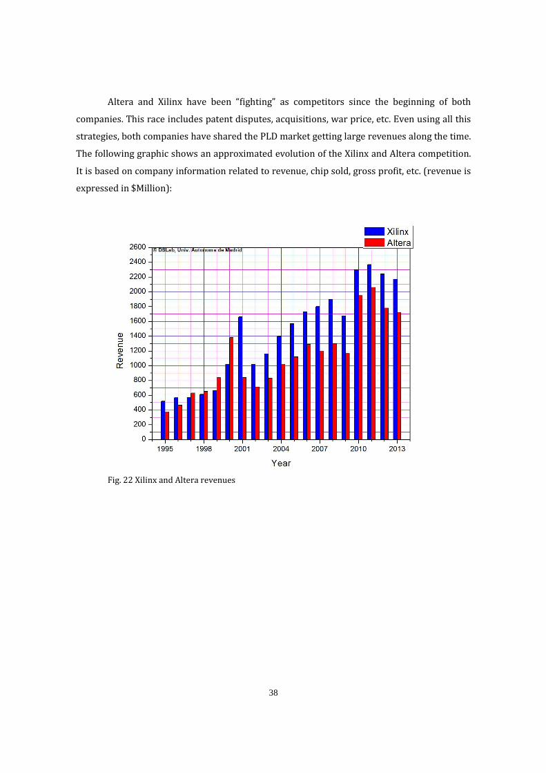
Altera and Xilinx have been “fighting” as competitors since the beginning of both
companies. This race includes patent disputes, acquisitions, war price, etc. Even using all this
strategies, both companies have shared the PLD market getting large revenues along the time.
The following graphic shows an approximated evolution of the Xilinx and Altera competition.
It is based on company information related to revenue, chip sold, gross profit, etc. (revenue is
expressed in $Million):
Fig. 22 Xilinx and Altera revenues
39
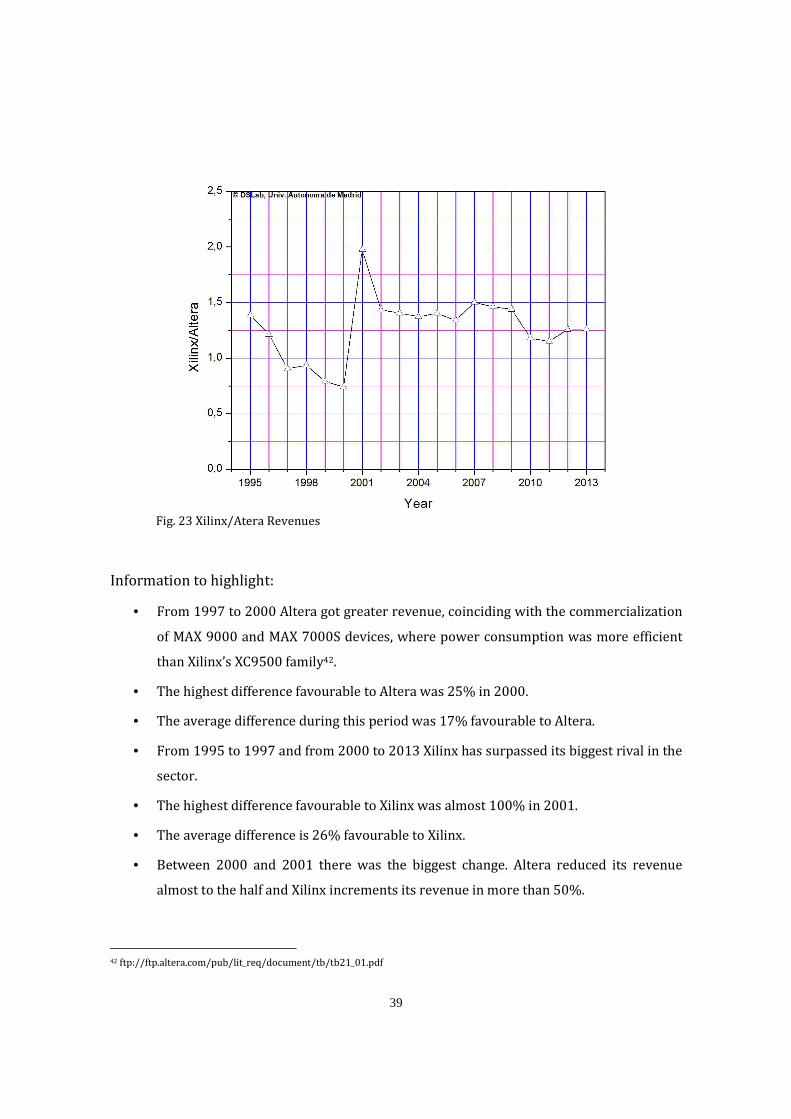
Fig. 23 Xilinx/Atera Revenues
Information to highlight:
• From 1997 to 2000 Altera got greater revenue, coinciding with the commercialization
of MAX 9000 and MAX 7000S devices, where power consumption was more efficient
than Xilinx’s XC9500 family42.
• The highest difference favourable to Altera was 25% in 2000.
• The average difference during this period was 17% favourable to Altera.
• From 1995 to 1997 and from 2000 to 2013 Xilinx has surpassed its biggest rival in the
sector.
• The highest difference favourable to Xilinx was almost 100% in 2001.
• The average difference is 26% favourable to Xilinx.
• Between 2000 and 2001 there was the biggest change. Altera reduced its revenue
almost to the half and Xilinx increments its revenue in more than 50%.
42 ftp://ftp.altera.com/pub/lit_req/document/tb/tb21_01.pdf
40
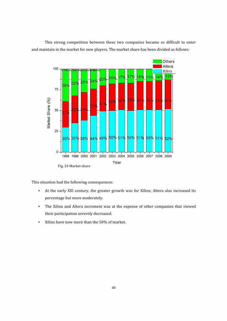
This strong competition between these two companies became so difficult to enter
and maintain in the market for new players. The market share has been divided as follows:
Fig. 24 Market share
This situation had the following consequences:
• At the early XXI century, the greater growth was for Xilinx; Altera also increased its
percentage but more moderately.
• The Xilinx and Altera increment was at the expense of other companies that viewed
their participation severely decreased.
• Xilinx have now more than the 50% of market.

41
Both Altera and Xilinx have been in the top ten Fabless companies in 2009. That list is
composed of the following names:
2009 Rank Company Headquaters Revenue ($M)
1 Qualcomm U.S. 6,585
2 AMD U.S. 5,252
3 Broadcom U.S. 4,190
4 MediaTek Taiwan 3,500
5 Nvidia U.S. 3,135
6 Marvell U.S. 2,700
7 Xilinx U.S. 1,675
8 LSI Corp. U.S. 1,445
9 Altera U.S. 1,165
10 Avago U.S. 870
Table 3: Top ten Fabless 2009
The most important information of this chart is:
• The main fabless companies are situated in United States, except one from Taiwan,
Asia.
• Only Xilinx and Altera are specialized in FPGA.
• The top three companies design chips for different sectors, but the main profits come
from the telecommunication.
• Xilinx and Altera are far from the revenue of the first companies, but they have been in
this ranking for years.
• The GDP of Spain, as the European example is 1,046,894M€ ($ 1,431,875 M) about
217 times the revenue of the first fables in the ranking.
• Xilinx’s revenue is five times less than its foundry, TSMC.

42
Xilinx is a highly specialized company in the sector. Their profits are clearly divided in
function of the product sold. As is indicated by Zacks, this division is:
• New Products: including Virtex-7, Kintex-7, Zynq-7000, Virtex-6, Virtex-5, and Spartan-6
products.
• Mainstream Products: including Virtex-5, Spartan-3, Spartan II and CoolRunner-II
products.
• Base Products: including the oldest families Virtex-4, Virtex-E, Virtex-II, Spartan,
Spartan-II, CoolRunner and XC9500 product families.
• Support Products: including PROMs, software, IP cores, customer training, design
services and support.
The percentage of revenue is divided as is shown in the following graph:
Fig. 25 The percentage of revenue
The mainstream products report more revenues, followed by the base products.
Together, they represent the 74% of the company. However some profit is obtained from very
old products: customers with older systems still in production need this old-fashioned
technology. In these cases, the customers do not need to change to the newest devices.

43
Xilinx get revenues from everywhere. Next is shown the percentage of profits divided
by geographical area in 2010:
Fig. 26 the percentage of profits divided by geographical in 2010
3.7. EDA Tools
Electronic Design Automation (EDA) tools are used for design and test functionalities
in FPGAs. The high-level design languages for FPGA are VHDL, Verilog, System C, System
Verilog, and C/C++.

44
Next is shown FPGA trends in languages utilized for Register-Transfer Level (RTL) design:
Fig. 27: Design languages (Reproduced from43).
Referred to the graphic it can be observed that:
• VHDL is the most utilized language followed closely by Verilog.
• System C is the only language that always has increment its usage percentage.
• The interest in System Verilog is increasing but still far from VHDL.
EDA tools are also utilized to design ASICs. Dataquest, reported that the ASIC market
was $16.6 Billion while the FPGA market was $2.6 Billion in 2001. And the ASIC EDA market
was $2.2 Billion while the FPGA EDA market was only $91.9 Million, making it obvious that
the benefit of EDA vendors is much higher in the market of ASICs. Xilinx and Altera have
produced and distributed freeware version of their EDA software, in order to broad the
number of applications. On the contrary, the masked-ASICs require very specific EDA tools
making much more profitable this market.
43 http://blogs.mentor.com/verificationhorizons/blog/tag/vhdl/

45
Xilinx as a company focused on hardware design, disregards the development of
design tools. To solve this problem, Xilinx integrates third-party solutions (“Third-party” are
called the companies that develop and integrate software in FPGA tools). This solution has
problems like bugs on error in interfaces between tools, as well as trade tensions. Xilinx itself
is an active buyer of EDA tools companies.
Companies that provide the EDA tools or manufacture components utilized to
fabricate other products are known as Original Equipment Manufacturers (OEM). The top ten
fiscal OEMs in 2011 were:
Rank Company Category
1 Qualcomm Inc. Communication
2 Rockwell Automation Inc. Industrial Controls
3 Mentor Graphic Corp. EDA
3 Synopsys Inc. EDA
3 Linear Technology Corp. Components & Subassemblies
6 Molex Inc. Industrial Controls
7 Maxim Integrated Products Inc. Components & Subassemblies
7 Intel Corp. Components & Subassemblies
9 Analogic Corp. Industrial Controls
10 Cadence Design Systems Inc. EDA
Table 4: Top ten OEMs 2011
Some points to emphasize:
• Communication is the principal sector.
• Rockwell Automation Inc., representing the industrial sector, is situated in the second
place of the rank.
• As it is expected, IC design is an OEM active actor in the consumer electronic business.
• Two EDA companies are placed in the third position, above important companies like
Intel, showing the importance of this industry.
• The ranking shows three representatives of three different sectors (industrial
controls, components & subassemblies, and EDA).

46
3.8. ASIC vs. FPGA
The number of new ASIC design is about 3,500 per year from 2000 to 2011. On the
other hand, FPGA new designs ascend to about 90,000 per year in the same time period. This
enormous difference can be appreciated in the following figure:
Fig. 28 Number of new FPGA/ASIC designs
A new FPGA design means tens of thousands dollars meanwhile a new ASIC can reach
millions of dollars. The costs of these designs are justified as follows:
ASIC
• NRE, Non-Recurring Engineer is a cost that covers the research, develop, design, fab
setup, and test of a new device. Although it is paid once its cost can be prohibitive
high.
• Unit costs, these are all the costs necessaries per device manufactured. This includes
fixed costs like equipment and variable costs like materials.
• Development costs, these encompass costs from the beginning of a new design to the
final implementation of the device.
• Inventory costs, these costs are associated with the storage and maintenance of the
goods in stock. Expressed usually as a percentage of the inventory value.

47
• Opportunity costs: is the costs related to an abandoned alternative. It not always can
be described with a number.
FPGA
• Unit costs.
• Development costs.
The FPGA is better economically than technologically. And the ASIC has the opposite
situation. This makes the FPGA market more fluent than ASIC one.
Main problem of FPGA is power. The density of a FPGA can be up to hundred times
more than the ASIC one. Thus, the consumption of the FPGA can be up 100x the power of an
equivalent ASIC.
To illustrate ASIC-FPGA a comparison between Altera and LSI Logic (ASIC company)
is reproduced from E.E. Times:
Table 5 LSI Logix vs. Altera
Although these two technologies maintain a commercial competition, sometimes the
benefits of a technology are utilized by the others one to improve their devices. For example,
the Spartan FPGA family of Xilinx presents several blocks that previously have been employed
in ASIC technology44.
44 http://www.xilinx.com/support/documentation/application_notes/xapp119.pdf
LSI Logic Altera
High gate density (50K-70K gates/mm²) Low gate density (<2K gates/mm²)
Low gate cost (0.5 Millicent/gate) High gate cost (100 Millicent/gate at
0.18um)
Own fabs, process control Do not own fabs, low overhead
High NRE charges No NRE charges
Design changes require new prototypes Design changes require only a couple of
hours reprogramming a part
1M-unit order is large 1K-unit order is large

48
Some companies try to combine both technologies. The idea is to have a
programmable part in a fixed hardware. IBM and Xilinx was an example using a FPGA as a
core in an ASIC device45. No news exists about the final product.
3.9. Job market in FPGAs
In this point is explored current jobs related to FPGA technology in Spain, United
Kingdom, Ireland, France, Germany, and United States. The following parameters have been
extracted from the same job websites:
• Number of offers per country.
• Average salary.
• Requirements.
According to the webpage “Monster.co.uk” using FPGA as keyword in United Kingdom
are found46:
• 111 job offers.
• ₤ 55,000 per year as average salary.
• Only few temporary offers do not require experience. FPGA design and VHDL are basic
requirements of all the jobs. Most of the companies offer extra benefits that could
increment de average salary.
According to the webpage “Monster.de” using FPGA as keyword in Germany are
found47:
• 62 job offers.
• There are not enough results, but salaries are over 75,000€ per year.
• Some offers are for students. The knowledge of VHDL, Matlab, and C/C++ is necessary
for almost all the companies. High level in German is a basic requirement and English
is convenient.
45 http://www.xilinx.com/support/documentation/white_papers/wp164.pdf 46 http://jobsearch.monster.co.uk/jobs/?q=fpga&pg=1&cy=uk 47 http://jobsuche.monster.de/Jobs/?q=fpga&pg=3&cy=de

49
According to the webpage “Monster.com” using FPGA as keyword in United States are
found48:
• 247 job offers.
• $ 75,000 per year as average salary.
• Experience required in different fields of electronics and strong knowledge in design
of FPGA with VHDL and Verilog. Languages are necessary in some cases. Salary
sometimes is complemented with bonus, and even with stock options.
According to the webpage “Monster.fr” using FPGA as keyword in France are found49:
• 3 job offers.
• There are not enough results to get a reliable average value but salaries are over
50,000€ per year.
• Minimum 5 years experience in different fields of electronic. Creativity and social
skills with both the client and group work is valued.
According to the webpage “Monster.ie” using FPGA as keyword in Ireland are found50:
• 2 job offers.
• There are not enough results to get a reliable average salary but in an indicative value
is over 60,000€ per year.
• Experience in technological and commercial aspects is required. Excellent written and
spoken English also is a must.
48 http://jobsearch.monster.com/search/?q=FPGA 49 http://offres.monster.fr/offres-d-emploi/?q=FPGA&cy=fr 50 http://jobsearch.monster.ie/jobs/?q=FPGA&cy=ie

50
According to the web pages “Monster.es”, “Infoempleo.com”, “Trabajando.es”,
“Computrabajo.es”, and “Infojobs.net” using FPGA as keyword in Spain, no job was returned51.
Even so, there are some job openings for electronics engineer in which, knowledge and
experience in FPGAs and VHDL are required.
Fig. 29: Job offers and average salary per country.
As a conclusion it cab be stated that:
• UK, Germany, and United States are countries where FPGA engineers have many
opportunities and good working conditions.
• The average salary is high but previous experience in the sector is necessary.
51 http://buscartrabajo.monster.es/trabajos/?q=fpga&cy=es http://www.infojobs.net/jobsearch/search-results/list.xhtml http://www.infoempleo.com/trabajo/i/fpga/ http://www.computrabajo.es/bt-ofrlistado.htm?Bqd=&Bqd=&Bqd=&Bqd=&BqdPalabras=fpga&x=0&y=0 http://www.trabajando.es/buscar-trabajo/?ciudad=0&palabra=fpga

51
4. Xilinx devices
4.1. Abstract
In this chapter is showed the different devices and families of FPGA.
The main points to highlight are:
• Xilinx’s FPGAs.
• Time evolution.
• Architecture of Xilinx’s FPGAs.
• Main characteristics.
4.2. Introduction
We decided to choose six relevant aspects of each kind of FPGA. They are:
• Year of fabrication: This data is approximated. It has been obtained from Xilinx
presentations, application notes and component datasheets.
• System clock speed: This is a marketing parameter obtained from Xilinx data sheets.
The number gives an idea of the maximum speed that can be obtained from a given
chip. More detailed information should be based on:
o The minimum propagation time of signals between two lines of flip flops in the
design (path delay).
o The maximum speed of the I/O pads.
o Toggle rate (the maximum speed of a flip-flop to change it output)
• Equivalent Gates: This is another marketing parameter, very utilized by Xilinx, and
discussed by the other manufacturers. In principle, is the approximated number of
gates that can be mapped in FPGAs component like LUTs or basic embedded circuits.
This number has no sense in modern FPGAs with microprocessors and other complex
embedded blocks. Xilinx itself abandoned this metric.
• Flip-Flop Count: This is an objective parameter. The number of FF can be extracted
from datasheet information. In modern FPGAs, this value has less importance because
of the use of configuration chains as shift-registers (component SRL16, 32, 64, etc).
Xilinx itself omitted this metric in the latest FPGAs. In a big Virtex FPGA can have

52
nearly 106 FF. So they are enough for any application, becoming a non relevant
number.
• User I/Os: The number of pins available for the user (programmed as an input, output,
bi-directional o differential). This is also a critical parameter. This value is different of
the maximum pin count of the package (that includes Vcc, GND, and control pins).
• Process technology: This is a non clear parameter. In principle was the wide of the
silicon channel in a MOS transistor. Also is defined as the minimum size of the basic
element of the chip. The next table indicates the year of introduction of each new
process. Normally, FPGAs access to the latest process of the foundries due to the
regularity of these circuits.
Table 6: Year of introduction of each new process (Reproduced from52)
52 http://www.pcmag.com/encyclopedia/term/49759/process-technology
53
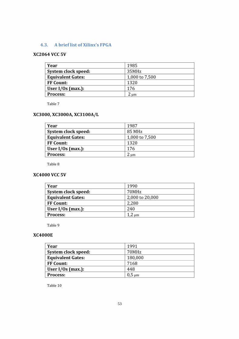
4.3. A brief list of Xilinx’s FPGA
XC2064 VCC 5V
Year 1985 System clock speed: 35MHz Equivalent Gates: 1,000 to 7,500
FF Count: 1320
User I/Os (max.): 176
Process: 2 μm
Table 7
XC3000, XC3000A, XC3100A/L
Year 1987 System clock speed: 85 MHz
Equivalent Gates: 1,000 to 7,500
FF Count: 1320
User I/Os (max.): 176
Process: 2 μm
Table 8
XC4000 VCC 5V
Year 1990 System clock speed: 70MHz
Equivalent Gates: 2,000 to 20,000
FF Count: 2,280 User I/Os (max.): 240
Process: 1,2 μm
Table 9
XC4000E
Year 1991 System clock speed: 70MHz
Equivalent Gates: 180,000
FF Count: 7168 User I/Os (max.): 448
Process: 0,5 μm
Table 10

54
XC4000EX/XL
Year 1996 System clock speed: 66MHz
Equivalent Gates: 180,000
FF Count: 7168 User I/Os (max.): 448
Process: 0,5 μm(EX)/ 0,35 μm(XL)
Table 11
XC4000XV
Year 1999 System clock speed: 200MHz Equivalent Gates: 500,000
FF Count: 9,216 to 18,400 User I/Os (max.): 448
Process: 0.25 μm
Table 12
XC4000XLA
Year 1999 System clock speed: 200 MHz
Equivalent Gates: 500,000
FF Count: 1,536 to 18,400 User I/Os (max.): 448 Process: 0.35 μm
Table 13
XC5200 Series
Year 1995(version 3) System clock speed: 50 MHz
Equivalent Gates: 3,000 to 23,000
FF Count: 256 to 1,936
User I/Os (max.): 84 to 244
Process: 0.5μm
Table 14

55
Xilinx Spartan (Jan. 1998) and Spartan-XL (Nov. 1998) Families
Year 1998 System clock speed: 80 MHz
Equivalent Gates: 40,000
FF Count: 2016
User I/Os (max.): 224
Process: 500 nm/(XL)350nm Table 15
Spartan-II 2.5V
Year 2000 System clock speed: 200 MHz. Equivalent Gates: 200,000
FF Count: 4,016 User I/Os (max.): 284
Process: 220nm/180nm(2008)
Table 16
Xilinx Spartan-IIE 1.8V
Year 2001 System clock speed: 200 MHz Equivalent Gates: 600,000
FF Count: -- User I/Os (max.): 514
Process: 180nm Table 17
Xilinx Spartan-3
Year 2003 System clock speed: -- Equivalent Gates: 5M
FF Count: 1,536 to 66,560 User I/Os (max.): 633
Process: 90nm Table 18

56
Xilinx Spartan-3E
Year -- System clock speed: 300 MHz
Equivalent Gates: 1,600K
FF Count: CLB count: 3,688
User I/Os (max.): 376
Process: 90 nm
Table 19
XilinxSpartan-3A
Year -- System clock speed: 320 MHz
Equivalent Gates: 3,400K
FF Count: CLB count: 5,968
User I/Os (max.): 469
Process: -- Table 20
Xilinx Spartan-3AN
Year -- System clock speed: -- Equivalent Gates: 1,400K
FF Count: CLB count: 2,816
User I/Os (max.): 502
Process: 90nm
Table 21
Xilinx Spartan-3A DSP
Year -- System clock speed: 320 MHz
Equivalent Gates: 1,400K
FF Count: CLB count: 2,816
User I/Os (max.): 502
Process: -- Table 22

57
Xilinx Virtex
Year 1998 System clock speed: -- Equivalent Gates: 1M
FF Count: 74,616 User I/Os (max.): 804
Process: 220 nm/250 nm
Table 23
Xilinx Virtex E
Year 1999 System clock speed: 130MHz
Equivalent Gates: 4M
FF Count: 74,616
User I/Os (max.): 804
Process: 0.18μm
Table 24
Xilinx Virtex 2.5 V
Year 1999 System clock speed: 200 MHz
Equivalent Gates: 1M
FF Count: 28672 User I/Os (max.): 512
Process: 0.22μm
Table 25
Xilinx Virtex-II
Year 2000 System clock speed: 420 MHz
Equivalent Gates: 8 M
FF Count: 10,240 to 28,627
User I/Os (max.): 1,108
Process: 150 nm
Table 26

58
Xilinx Virtex-II PRO (2002)
Year 2002 System clock speed: -- Equivalent Gates: -- FF Count: 127,536 User I/Os (max.): 1,200
Process: 130nm
Table 27
Hardened QPro™ Virtex-II
Year 2002 System clock speed: 300 MHz
Equivalent Gates: 6M
FF Count: CLB count: 8,448
User I/Os (max.): 1,104
Process: 150nm
Table 28
XILINX Virtex-4
Year 2004 System clock speed: -- Equivalent Gates: -- FF Count: CLB count: 22,272
User I/Os (max.): 960
Process: 90 nm
Table 29
Xilinx Virtex-5 (2006)
Year 2006 System clock speed: -- Equivalent Gates: -- FF Count: 19,200 to 69,120
User I/Os (max.): 960
Process: 65 nm
Table 30

59
XC6200
Year 1995 System clock speed: -- Equivalent Gates: 60,000 to 100,000 FF Count: 2,304 to 16,384 User I/Os (max.): 64 to 512 Process: --
Table 31
XC 8100
Year 1996 System clock speed: -- Equivalent Gates: -- FF Count: 96 User I/Os (max.): 32 Process: --
Table 32
All data are taken from the original Xilinx datasheets. The missing information is not
provided by Xilinx.

60
4.4. Xilinx evolution (flip flop, system speed, equivalent gate, I/Os, process):
Fig. 30: Flip-Flops.
Fig. 31: System speed.

61
Fig. 32: Equivalent Gates.
Fig. 33: I/Os.

62
Fig. 34: Process.
It is easy to appreciate at the late nineties begins a significant increase in the number
of FF, I/O pads, Equivalent Gates, System Speed. Process Scale is significantly reduced on the
same dates. Moore's Law states that approximately every 18 months, is doubling the number
of transistors on an integrated circuit. Regarding this study, we can affirm that this law is
fulfilled depending on the characteristic to evaluate.

63
In order to evaluate Xilinx development has been performed a graph using Intel as a
reference. In this graph compared the evolution of process scale:
Fig. 35: Process, Xilinx vs. Intel.
It can be seen how Xilinx remains only a step behind Intel. Xilinx gets the same process
technology approximately one year after Intel did it. This situation is expected since Intel is
the largest semiconductor company and is plenty of technological resources.
4.5. Architecture of Xilinx FPGAs: Catalog of Logic Blocks.
The basic element of a FPGA is the Logic Block. It is defined as a slice with LUT, the
output Flip-Flop, and the associated control logic (multiplexers, reset, clock, etc.)
Xilinx utilizes two different names for describe groups of Logic Elements: CLB and
Slice. But the manufacturer itself has changed the meaning of these names. The following
figures try to clarify the evolution of these works. Some information is added in each figure.
Historically, the draw of multiplexers without control lines means that the control is done by
the EDA Tool. Nowadays Xilinx has launched the 7 series of FPGAs, where one CLB contains
two Slices and each Slice is composed of four 6-input LUTs and eight storage elements.

64
The following figure shows the resources of one of this CLB.
Table 33: Logic Resources in One CLB (Reproduced from53)
This pair of Slices is situated in column. When group some CLBs the Xilinx tools
designate slices as a kind of matrix as is showed in the figure:
Fig. 36: Row and Column Relationship between CLBs and Slices (Reproduced from54).
53 54 Xilinx Inc. “7 Series FPGAs Configurable Logic Block” UG474 (v1.5) August 6, 2013.

65
Next are described the CLB structures of the most common Xilinx’s FPGA families:
Fig. 37: XC2000 Logic Block (Reproduced from55).
• Double 4-LUT (4-input LUT) with inputs A, B, C, and D.
• The LUT share the inputs and has 2 outputs F, and G.
• 1 Type D FF with reset.
• C and G signals can trigger the FF.
• F can be stored in the FF but no G, G can control the CLK and reset.
• FF output (Q) can be an input in the LUT.
• The CLB has two outputs X and Y that can output F, G or the FF output on both
outputs.
55 Xilinx Inc , “XC2000 Logic Cell Array Families”.

66
Fig. 38: XC3000 Logic Block (Reproduced from56).
• Double 5-LUT (5-input LUT) with inputs A, B, C, D, and E.
• The LUT share the inputs and has 4 outputs F, G, Qx, and Qy.
• 2 Type D FF with reset.
• 1 input DI.
• F, G, and DI can be stored in both FF.
• Direct Reset, Eneable Clock, and Clock with multiplexor to invert the signal.
• The CLB has two outputs X and Y that can output F or Qx on X, G or Qy on Y and
everything registered in the FFs. Qx and Qy can be stored in only one FF each one.
56 Xilinx Inc , “XC3000 Series Field Programmable Gate Arrays (XC3000A/L, XC3100A/L)”, ,November 9, 1998 (Version 3.1).

67
Fig. 39: XC4000 Logic Block. (Reproduced from57).
• 2 4-LUT (4-input LUT) with inputs G1, G2, G3, G4, F1, F2, F3, and F4 and 1 3-LUT with
H’, F’, G’, and H1.
• The 4-LUTs do not share the inputs and have 1 output each one F and G.
• 1 four-bit input C1 to C4.
• 2 Type D FF with set and reset.
• F’, G’, H’, and Din can be stored in both FF
• 4 final outputs Y, YQ, X, and XQ
• Y can output H’ and G’, YQ can output stored data from one FF, X can output H’ and F’,
XQ can output stored data from the other FF
57 Xilinx Inc, “XC4000E and XC4000X Series Field Programmable Gate Arrays”, May 14, 1999

68
Fig. 40: XC5200 Logic Cell (Four LCs per CLB) (Reproduced from58).
• 1 4-LUT (4-input LUT) with inputs F1, F2, F3, and F4.
• 2 input DI and CO.
• 1 Type D FF with reset.
• The LUT output can be stored in FF.
• 3 final outputs DO, Q, and X.
• DO can output DI and CO, Q output stored data from the FF, X output the LUT output
58 Xilinx Inc, “XC5200 Series Field Programmable Gate Arrays”, November 5, 1998

69
Fig. 41: Spartan and Spartan-XL Logic Block (Reproduced from59).
• 2 4-LUT (4-input LUT) with inputs G1, G2, G3, G4, F1, F2, F3, and F4 and 1 3-LUT with
input F, G, and H1 and output H.
• The 4-LUTs do not share the inputs and have 1 output each one G and G.
• 3 input SR, H1 and Din.
• 2 Type D FF with set and reset.
• G, G, H, and Din can be stored in both FF.
• 4 final outputs Y, YQ, X, and XQ.
• Y can output H and G, YQ can output stored data from one FF, X can output H and G,
and XQ can output stored data from the other FF.
59 Xilinx Inc., “Spartan and Spartan-XL FPGA Families Data Sheet”, DS060 (v2.0), March 1, 2013.

70
Fig. 42: Half CLB of Spartan II - called Slice. (Reproduced from60).
• 2 4-LUT (4-input LUT) with inputs G1, G2, G3, G4, F1, F2, F3, and F4.
• 5 input F5in, BY, SR, BX, and CIN.
• 2 Type D FF with set and reset.
• 7 final outputs Cout, YB, Y, YQ, XB, X, and XQ.
• 2 Carry and control blocks.
60 Xilinx Inc, “Spartan-II FPGA Family Data Sheet”, DS001 June 13, 2008.
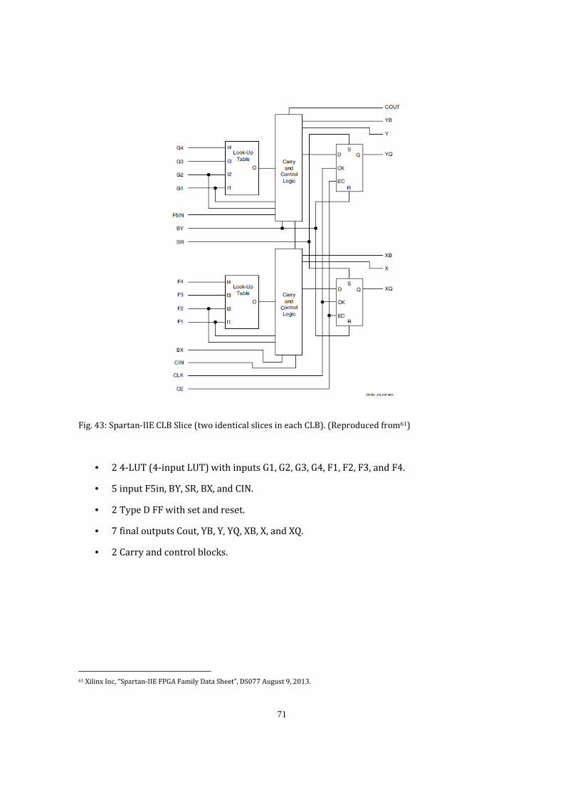
71
Fig. 43: Spartan-IIE CLB Slice (two identical slices in each CLB). (Reproduced from61)
• 2 4-LUT (4-input LUT) with inputs G1, G2, G3, G4, F1, F2, F3, and F4.
• 5 input F5in, BY, SR, BX, and CIN.
• 2 Type D FF with set and reset.
• 7 final outputs Cout, YB, Y, YQ, XB, X, and XQ.
• 2 Carry and control blocks.
61 Xilinx Inc, “Spartan-IIE FPGA Family Data Sheet”, DS077 August 9, 2013.

72
Fig. 44: Virtex-E Slice (Reproduced from62).
• 2 4-LUT (4-input LUT) with inputs G1, G2, G3, G4, F1, F2, F3, and F4.
• 5 input F5in, BY, SR, BX, and CIN.
• 2 Type D FF with set, reset, and clock enable.
• One FF can store Bx, outputs of both LUTs, and the XOR dedicated gate. The stored
output is connected to XQ.
• The other FF can store BY, F5IN, outputs of both LUTs, and the XOR dedicated gate.
The store output is connected to YQ.
• 8 final outputs COUT, YB, Y, YQ, XB, X, XQ, and F5.
• 2 Blocks to control LUTs in 16x1 memories (distributed RAM).
• The COUT is calculated with F1, F2, G1, G2, and CIN.
62 Xilinx Inc,“Virtex™-E 1.8 V Field Programmable Gate Arrays”, DS022-1 (v2.3) July 17, 2002.

73
Fig. 45: Virtex-II Slice. (Reproduced from63)
• 2 4-input function generators, carry logic, arithmetic logic gates, wide function
multiplexers and 2 storage elements per slice.
• Each 4-input function generator is programmable as a 4-input LUT, 16bits of
distributed SelectRAM memory, or a 16-bit variable-tap shift register element.
• Four independent inputs are provided to each function generators G1, G2, G3, and G4.
63 Xilinx Inc, “Virtex-II Platform FPGAs: Complete Data Sheet”, DS031 (v3.5) November 5, 2007

74
• The function generator can exit Y or X (other slice) output, can input the XOR
dedicated gate, or input the carry-logic multiplexer, or feed the D input of the storage
element.
• The storage elements can be configured either as edge-triggered D-type FF or as level-
sensitive latches.
• The D input can be connected with the X or Y output via the DX or DY input, or by the
slice inputs bypassing the function generators via the BX or BY input. Each storage
element has clock, clock enable, set and reset.
4.6. Summary of the main characteristics of Xilinx’s FPGAs.
Table 34: XC3000 Series.
Table 35: XC4000XLA Series.

75
Table 36: XC4000E and XC4000X Series.
Table 37: XC5200 Series.
Table 38: Spartan and Spartan-XL Series.

76
Table 39: Spartan-II Series.
Table 40: XA Spartan-IIE Series.
Table 41: Spartan-3 Series.

77
Table 42: Spartan-3A Series.
Table 43: Spartan-3E Series.
Table 44: Virtex-E Series.

78
Table 45: Virtex Series.
Table 46: Virtex-II Series.

79
Table 47: Virtex-4 Series.
Table 48: XC8100 Series.

80
Table 49: Virtex-5 Series.

81
5. FPL Congress
5.1. Abstract
In this chapter, several contents of the FPL Conference Proceedings are analyzed in
order to make visible the principal milestones of FPGA technology evolution. The main points
to highlight are:
• Active geographical areas on FPGA research.
• Ranking of authors in the FPL Conference.
• Most recurrent topics in the FPL Conference.
5.2. Introduction
The goal of this chapter is to answer if a worldwide map of the human resources
involved in FPGA can be constructed. To do that, lots of sources should be analyzed. In this
study, the problem is overcome by limiting the source of information to FPL conference.
The International Conference on Field-Programmable Logic and Applications (FPL
Conference) is the oldest scientific meeting on FPGA Technology. It was created by professors
Will Moore and Wayne Luk in Oxford University in 1991.

82
The list of editions, venues and general chairpersons are listed in table below.
2013 23rd
Edition
September 2 - 4, 2013 University of Porto, Portugal. General Chair: João M. P. Cardoso (U. Porto) Proceedings Editors: João M. P. Cardoso, Katherine (Compton) Morrow, Pedro Diniz.
2012 22th
Edition
August 29 - 31, 2012 University of Oslo, Norway, General Chair: Jim Torresen (U. Oslo) Proceedings Editors: Jim Torresen, Dirk Koch, Satnam Singh
2011 21th
Edition
September 5 – 7, 2011 Technical University of Crete, Chania, Greece General Chair: Apostolos Dollas (T.U. Crete), Manfred Glesner (T.U. Darmstadt) Proceedings Editors: Peter Athanas , Dionisios Pnevmatikatos, Nicolas Sklavos
2010 20th
Edition
August 31 – September 2, 2010 Politecnico di Milano, Italy General Chair: Fabrizio Ferrandi (P. Milano) Proceedings Editors: Fabrizio Ferrandi, Jari Nurmi, Marco D. Santambrogio
2009 19th
Edition
August 31 – September 2, 2009 Institute of Information Theory and Automation of the Czech Academy of Sciences, Prague, Czech Republic General chair: Jiri Kadlec (A.S.C.R) Proceedings Editors: Martik Danek, Jiri Kadlec, Brent nelson
2008 18th
Edition
September 8 - 10, 2008 University of Heidelberg , Germany General Chair: Udo Kebschull (U. Heidelberg) Proceedings Editors: Udo Kebschull, Marco Platzner, Jürgen Teich
2007 17th
Edition
August 27 - 29, 2007 Delft University of Technology, Amsterdam, Holland General Chair: Stamatis Vassiliadis (TU Delft) Proceedings Editors: Koen Bertels, Walid Najjar, Arjan van Genderen, Stamatis Vassiliadis
2006 16th
Edition
August 28 - 30, 2006 Universidad Autonoma of Madrid, Spain General Chair: Eduardo Boemo (U.A. Madrid) Proceedings Editors: Andreas Koch, Philip Leong, Eduardo Boemo
2005 15th
Edition
August 24 - 26, 2005, University of Technology of Tampere, Finland General Chair: Jari Nurmi (U.T. Tampere) Proceedings Editors: Tero Rissa, Steve Wilton, Philip Leong
2004 14th
Edition
Aug 29 - Sep 1, 2004, Antwerp, Belgium General Chair: Serge Vernalde (IMEC vzw) Proceedings Editors: Jürgen Becker, Marco Platzner, Serge Vernalde
1997 7th
Edition
September 1 - 3, 1997 Imperial College of Science, Technology and Medicine, London, UK General Chair: Wayne Luk, Peter Y.K. Cheung (I.C. London) Proceedings Editors: Wayne Luk, Peter Y.K. Cheung, Manfred Glesner

83
1996 6th
Edition
September 23 - 25, 1996 Darmstadt, Germany General Chair: Manfred Glesner (Darmstadt U.T.) Proceedings Editors: Reiner W. Hartenstein, Manfred Glesner
1995 5th
Edition
Aug. 29 - Sep. 1,1995 Oxford, UK General Chair: Wayne Luk Proceedings Editors: Will Moore, Wayne Luk
1994 4th
Edition
September 7 - 9, 1994, Prague, Czech Republic General Chair: Proceedings Editors:Reiner W. Hartenstein, Michal Z. Servit
1993 3th
Edition
September 1993, Oxford, UK General Chair: Wayne Luk Proceedings Editors: Will Moore, Wayne Luk
1992 2th
Edition
Aug. 31 - Sep. 2, 1992 Vienna, Austria General Chair: Herbert Gruenbacher Proceedings Editors: Reiner W. Hartenstein, Herbert Gruenbacher
1991 1th
Edition
September 4 - 6, 1991 Oxford, UK General Chair: Will Moore, Wayne Luk Proceedings Editors:Will Moore, Wayne Luk
Table 50: FPL editions, venues, and general chairpersons

84
5.3. Research in FPGA and geographical areas
In this section, the most active areas on FPGA R&D are highlighted. The study
separates the papers in 4 different regions departing from the division of IEEE depicted in
Fig.5.1
Fig. 46: Technology Regions proposed by IEEE (Extracted from64).
64 http://www.ieee.org/societies_communities/geo_activities/regional_world_map.html

85
The countries that contributed to FPL conference are listed by region below.
Region 1-7: North America:
• Canada
• USA
Region 2 (Africa, Europe, and Middle East):
• Austria
• Belgium
• Bulgaria
• Croatia
• Cyprus
• Czech R.
• Denmark
• Estonia
• Finland
• France
• Germany
• Greece
• Hungary
• Ireland
• Israel
• Italy
• Latvia
• Netherland
• Norway
• Poland
• Portugal
• R. Belarus
• R. Slovak
• Romania
• Russia
• Slovenia
• South Africa
• Spain
• Sweden
• Switzerland
• Tunisia
• Turkey
• Ukraine
• Yugoslavia
Region 9 Latin America:
• Argentina
• Brazil
• Mexico
• Puerto Rico
Region 10 Asia and Pacific:
• Australia
• China
• Egypt
• Hong Kong
• India
• Iran
• Japan
• Korea
• Lebanon
• Malaysia
• N. Zealand
• Philippines
• Singapore
• Syria
• Taiwan
• Thailand

86
Every year the FPL congress receives several submissions from all over the world, but
only a few are published. The following figures show all the submissions sent to the FPL
congress, except in cases like USA or Spain where is detailed only the amount of published
papers. For example, the number of submissions by each region in FPL 2009 is shown in the
below map:
Fig. 47 Submissions by each region Number of submissions from North America in 2009: Fig. 48 North America Submissions

87
Fig. 49: USA submissions contribution from 1992 to 2012.
Fig. 50: Canada submissions contribution from 1992 to 2012.

88
USA obviously is one of the most active countries related to the FPGA technology, even
in an European-based conference like FPL. For example, the results in 2009 are shown below.
The information was complemented using data of IEEE Xplore and associating the area to the
first author address.
Fig. 51: Example of U.S. papers published in 2009.

89
Number of submissions from Latin America in 2009:
Fig. 52 Latin America submissions

90
Fig. 53: Latin America submissions contribution from 1992 to 2012.
Fig. 54: Brazilian submissions contribution from 1992 to 2012.

91
Number of submissions from Europe in 2009:
Fig. 55 Europe submissions

92
The next graphics are from the most representative European countries:
Fig. 56: UK submissions contribution from 1992 to 2012.
Fig. 57: Spain submissions contribution from 1992 to 2012.

93
Fig. 58: Germany submissions contribution from 1992 to 2012.
Fig. 59: France submissions contribution from 1992 to 2012.

94
Spain is one of the main contributors in Europe. The figure below shows the
distribution of the number of papers published by autonomous communities in 2009. This
information was taken from IEEE Xplore setting the areas by the first author address.
Fig. 60: Spain published papers in 2009.
This figure shows 10 published papers, but there were 22 submissions. The 45% of
the submissions were published in 2009. The percentage is lower than United States’, but
both are around the 50%.

95
To extend the information about the Spanish contribution to the FPL Congress, the
following figure includes the number of articles published from 2009 to 2013.
Fig.61: Spain published papers from 2009 to 2013.

96
Number of submissions from Asia in 2009: Fig. 62: East Asia submissions contribution in 2009.
Fig. 63: Southern Asia submissions contribution in 2009.

97
Fig. 64: South-western Asia submissions contribution in 2009. Number of submissions from Oceania in 2009: Fig. 65 Oceania submissions

98
Graphics of the most representative Asian countries:
Fig. 66: Japan submissions contribution from 1992 to 2012.
Fig. 67: China submissions contribution from 1992 to 2012.

99
Fig. 68: Oceania submissions contribution along the years.
5.4. Authors and topics
According the IEEE Xplore the most active authors from 2005 to 2013 are:
Fig. 69 The most active authors

100
The themes usually covered at the FPL conference are:
• Power • Embedded systems • Reconfiguration • Filters • Multiplier • Digital signal processing (DSP)
Next is shown the number of papers of each theme from 2005 to 2013:
Fig. 70: Power papers from 2005 to 2013.

101
Fig. 71: Embedded papers from 2005 to 2013.
Fig. 72: Reconfiguration papers from 2005 to 2013.

102
Fig. 73: Filters papers from 2005 to 2013.
Fig. 74: Multiplier papers from 2005 to 2013.

103
Fig. 75: DSP papers from 2005 to 2013.
The topics or a conference are proposed by the Program Chairs, and can vary from a year to
other. However, some conclusions can be observed:
• Embedded systems are one of the most recurrent topics along the years.
• Reconfiguration has a moderate participation with a trendy period from 2006 to 2008
and another peak in 2012.
• Power consumption is decreasing, except in 2010.

104
5.5. Main information available about FPL Conference
Field-Programmable Logic Architectures, Synthesis and Applications
4th International Workshop on Field-Programmable Logic and Applications, FPL'94 Prague,
Czech Republic, September 7–9, 1994 Proceedings
Editors:
• Reiner W. Hartenstein,
• Michal Z. Servít
ISBN: 978-3-540-58419-3 (Print) 978-3-540-48783-8 (Online)
http://link.springer.com/book/10.1007/3-540-58419-6/page/1
Austria 7
Belgium 1
Brazil 1
Canada 1
Czech Republic 5
Finland 2
France 9
Germany 17
Greece 2
Hungary 2
India 1
Japan 2
Latvia 1
Malaysia 1
Norway 2
Poland 5
Rep. of Belarus 5
Slovakia 3
South Africa 1
Spain 4
Sweden 2
Switzerland 3
Syria 1
Turkey 1
UK 18
USA 19

105
Field-Programmable Logic and Applications
5th International Workshop, FPL '95 Oxford, United Kingdom, August 29–September 1, 1995
Proceedings
Editors:
• Will Moore
• Wayne Luk
ISBN: 978-3-540-60294-1 (Print) 978-3-540-44786-3 (Online)
http://link.springer.com/book/10.1007/3-540-60294-1/page/1

106
Field-Programmable Logic Smart Applications, New Paradigms and Compilers
6th International Workshop on Field-Programmable Logic and Applications, FPL '96
Darmstadt, Germany, September 23–25, 1996 Proceedings
Editors:
• Reiner W. Hartenstein,
• Manfred Glesner
ISBN: 978-3-540-61730-3 (Print) 978-3-540-70670-0 (Online)
http://link.springer.com/book/10.1007/3-540-61730-2/page/1
Australia: 3
Japan: 4
Austria: 2
Korea: 1
Belgium: 1
Latvia: 1
Bulgaria: 1
New Zealand: 2
Canada: 1
Poland: 4
China: 3
Portugal: 2
Croatia: 1
Rep. of Belarus: 1
Czech Republic: 1
Slovenia: 1
France: 4
Spain: 6
Germany: 13
Sweden: 3
Hungary: 1
Switzerland: 2
India: 1
USA: 6
Ireland: 1
United Kingdom: 15
Italy: 1

107
Field-Programmable Logic and Applications
7th International Workshop, FPL '97 London, UK, September 1–3, 1997 Proceedings
Editors:
• Wayne Luk,
• Peter Y. K. Cheung,
• Manfred Glesner
ISBN: 978-3-540-63465-2 (Print) 978-3-540-69557-8 (Online)
http://link.springer.com/book/10.1007/3-540-63465-7/page/1

108
Field-Programmable Logic and Applications From FPGAs to Computing Paradigm
8th International Workshop, FPL '98 Tallinn, Estonia, August 31–September 3, 1998
Proceedings
Editors:
• Reiner W. Hartenstein,
• Andres Keevallik
ISBN: 978-3-540-64948-9 (Print) 978-3-540-68066-6 (Online)
http://link.springer.com/book/10.1007/BFb0055226/page/1
Australia 2
Latvia 1
Belarus 1
Philippines 1
Belgium 1
Portugal 1
Czech Republik 1
Russia 1
Estonia 1
Slovenia 1
Finland 2
Spain 4
France 4
Switzerland 1
Germany 20
Tunisia 1
Hong Kong 2
USA 14
Hungary 3
United Kingdom 17
Israel 1
Yugoslavia 1
Japan 5

109
Field Programmable Logic and Applications
9th International Workshop, FPL’99, Glasgow, UK, August 30 - September 1, 1999.
Proceedings
Editors:
• Patrick Lysaght
• James Irvine
• Reiner Hartenstein
ISBN: 978-3-540-66457-4 (Print) 978-3-540-48302-1 (Online)
http://link.springer.com/book/10.1007/b72332/page/1

110
Proceedings FPL 2000
Reiner W. Hartenstein and Herbert Grunbacher (Eds.)
10th International Conference, FPL 2000
Villach, Austria, August 27-30, 2000
http://link.springer.com/book/10.1007/3-540-44614-1/page/1
Argentina: 1
Australia: 1
Austria: 4
Belarus: 1
Belgium: 1
Brazil: 2
Canada: 3
China: 2
Czech Rep.: 4
Estonia: 1
Finland: 2
France: 5
Germany: 23
Greece: 3
India 3
Ireland: 1
Japan: 12
Mexico: 3
Netherlands: 3
Norway: 1
Poland: 5
Portugal: 1
Slovakia: 1
Slovenia: 1
Spain: 7
Sweden: 2
Switzerland: 2
Thailand: 1
UK: 15
USA: 20

111
Field-Programmable Logic and Applications
11th International Conference, FPL 2001 Belfast, Northern Ireland, UK, August 27-29, 2001
Proceedings
Editors:
• Gordon Brebner,
• Roger Woods
ISBN: 978-3-540-42499-4 (Print) 978-3-540-44687-3 (Online)
http://link.springer.com/book/10.1007/3-540-44687-7/page/1
USA 26
UK 24
Germany 14
Spain 12
Japan 7
France 4
Greece 3
Ireland 3
Belgium 2
Canada 2
Czech Republic 2
Finland 2
Italy 2
The Netherlands 2
Poland 2
Switzerland 2
Austria 1
Belarus 1
Brazil 1
Iran 1
Mexico 1
Portugal 1
South Africa 1
Sweden 1

112
Field-Programmable Logic and Applications: Reconfigurable Computing Is Going
Mainstream
12th International Conference, FPL 2002 Montpellier, France, September 2–4, 2002
Proceedings
Editors:
• Manfred Glesner
• Peter Zipf
• Michel Renovell
ISBN: 978-3-540-44108-3 (Print) 978-3-540-46117-3 (Online)
http://link.springer.com/book/10.1007/3-540-46117-5/page/1
USA: 30
Canada: 5
Ireland: 2
Lebanon: 1
UK: 15
Poland: 5
Portugal: 2
Mexico: 1
Germany: 12
Hong Kong: 4
Slovakia: 2
New Zealand: 1
Japan: 11
The Netherlands: 4
Australia: 1
Switzerland: 1
Spain: 9
Belgium: 3
Brazil: 1
Singapore: 1
France: 6
Czech Republic: 3
Greece: 1
Italy: 6
Finland: 3
Iran: 1

113
Field Programmable Logic and Application
13th International Conference, FPL 2003, Lisbon, Portugal, September 1-3, 2003 Proceedings
Editors:
• Peter Y. K. Cheung,
• George A. Constantinides
ISBN: 978-3-540-40822-2 (Print) 978-3-540-45234-8 (Online)
http://link.springer.com/book/10.1007/b12007/page/1
USA 42
Belgium 6
Brazil 2
Estonia 1
Spain 33
Netherlands 6
Canada 2
Norway 1
UK 29
Mexico 5
Hungary 2
India 1
Germany 14
Greece 4
Iran 2
Slovakia 1
Japan 13
Poland 4
Korea 2
Slovenia 1
Portugal 12
Switzerland 4
Romania 2
Italy 9
Australia 3
Singapore 2
Czech Rep. 8
Ireland 3
Austria 1
France 7
China 2
Egypt 1

114
Field Programmable Logic and Application
14th International Conference, FPL 2004, Leuven, Belgium, August 30-September 1, 2004.
Proceedings
Editors:
• Jürgen Becker
• Marco Platzner
• Serge Vernalde
ISBN: 978-3-540-22989-6 (Print) 978-3-540-30117-2 (Online)
http://link.springer.com/book/10.1007/b99787/page/1
USA 37
Canada 6
Netherlands 3
Mexico 2
Spain 21
Portugal 6
Austria 2
Switzerland 2
Germany 20
Brazil 5
Belgium 2
Australia 1
UK 11
Finland 3
Czechia 2
China 1
Japan 9
Ireland 3
Greece 2
Estonia 1
France 7
Poland 3
Italy 2
Lebanon 1

115
Field Programmable Logic and Application
15th International Conference, FPL 2005, Tampere, Finland, August 24-26, 2005. Proceedings
Editors:
• Tero Rissa
• Steve Wilton
• Philip Leong
USA 28
UK 21
Germany 19
Spain 14
Japan 12
Canada 7
Finland 5
France 5
Australia 4
Belgium 4
Greece 4
Portugal 4
Netherlands 4
China 3
Czech Rep. 3
India 2
Sweden 2
Brazil 1
Hungary 1
Ireland 1
Italy 1
Poland 1
Singapore 1
Turkey 1

116
Field Programmable Logic and Application
16th International Conference, FPL 2006, Madrid, Spain, August 28-30, 2006. Proceedings
Editors:
• Andreas Koch,
• Eduardo Boemo,
• Philip Leong
USA 37
UK 28
Spain 24
Germany 23
Japan 15
Canada 14
Belgium 5
Greece 5
Australia 4
Finland 3
France 3
Netherlands 3
Brazil 3
Portugal 2
Czech Rep. 2
India 2
Ireland 2
Switzerland 2
Taiwan 2
Hong Kong 1
Mexico 1
Puerto Rico 1
Turkey 1

117
Field Programmable Logic and Application
19th International Conference, FPL 2009, Prague, Czech Republic, August 31 – September 2,
2006. Proceedings Editors:
• Martik Danek
• Jiri Kadled
• Brent Nelson
USA 44
Germany 28
UK 22
Spain 22
Japan 22
France 20
Canada 14
Greece 10
Czech Rep. 10
China 9
Italy 7
Brazil 6
Netherland 4
Switzerland 4
India 4
Australia 4
Singapore 4
Argentina 1
Mexico 1
Belgium 3
Finland 1
Portugal 3
Sweden 2
Norway 1
Poland 1
Romania 2
R. Slovak 2
Ukraine 1
Austria 1
Taiwan 1
Hong Kong 2
Turkey 2
Israel 1
Lebanon 1
N. Zealand 1

118
6. Conclusions and complement information
6.1. Final Remarks
This work is a partial analysis of FPGA technology. The final text includes:
• 75 Figures
• 50 Tables
• 65 References
Main sources of information have been records of DSLab Laboratory at UAM, Xilinx
reports and Datasheets, IEEE Xplore and E.E. Times magazine.
The PFC emphasizes the use of original sources of information for the elaboration of
unified tables and graphs.
6.2. Conclusions
From this work can be extracted the following conclusions:
• The key of the success of FPGAs is the re-programmability. This makes them being
a very flexible technology that provides countless applications.
• The FPGAs were invented with the idea of avoiding the risks of manufacturing a
masked ASIC.
• Xilinx is the leader company in the sector of FPGAs. Since its foundation has
maintained a hard rivalry with its largest competitor, Altera.
• Xilinx FPGA devices double their components every 18 months fulfilling the
Moore’s law.
• Xilinx and Altera have many similar products (as well as patent litigation). One
difference is the partial dynamic reprogrammability of Xilinx devices. Altera never
considered practical this option.
• The most attractive company in terms of stock quote has been Altera. More
profitable than Xilinx and even Intel.

119
• Xilinx is 8 times lower than Inditex in number of employees but is only 4 times less
in profits.
• The GDP of Spain is about 504 times the combined gross profit of Xilinx and Altera.
• Xilinx was ahead of Altera in all years except from 1997 to 2000.
• Most of the foundry companies are in Asia, except IBM and Jazz that are in USA.
• Xilinx was the inventors of the fables concepts but in 2013, the fables company
number one is Qualcomm. It is about 4 times bigger than Xilinx.
• Sometimes Xilinx and Altera utilize the same foundry.
• Xilinx and Altera are active buyers of EDA tools start-up companies.
• Altera is using the fab facilities of INTEL. It can be a clue of a future acquisition of
Altera by Intel.
• Altera fabrication in Intel will produce soon the fastest FPGAs.
• From 52 companies that entered in the FPGA business only survive 3.
• At the end of the stock crash in year 2003, the value of Xilinx was 77% lower and
the Altera one was 84% lower.
• Both Altera and Xilinx suffered the consequences of the crash, even maintaining
the profits, sales, etc.
• Main countries in terms of FPGA jobs opportunities are U.S.A., England, and
Germany.
• According to FPL Conference, Spain is on active academic area on FPGA
applications.
6.3. Future work
This study will continue with the aim of getting enough information to make a mobile-
phone Atlas about FPGA Technology. Most detailed information about old FPGAs will be
included. In addition, the history of the Spanish FPGA called FIPSOC will be included in a
special chapter.

120
The inclusion of all available sources would transform this type of studies in an infinite
job. However, new sources to be analyzed and confronted in future works are:
• IEEE XPlore Database: The IEEE collection of papers is probably the most important
source of technical information. The searching of the word FPGA returns 23.727
entries (July, 2013).
• ACM Digital Library: The Association of Computer Machinery database. The searching
of the word FPGA returns 6596 entries (July, 2013).
• ACM/SIGDA International Symposium on Field-Programmable Gate Arrays (FPGA
Conference): This meeting is held annually each February in Monterey, California. The
presence of the technologist of industry is relevant. The conference is famous for the
low number of accepted papers.
• Google Scholar: This is a part of Google search related to academic papers. In addition
to the usual information, it includes paper citation. The searching of the word FPGA
returns 544.000 entries (July, 2013).
• IEEE Symposium on Field-Programmable Custom Computing Machines (FCCM
Conference): This conference is held in USA since 1997. Main topics are summarized
in the conference webpage: “… new research related to computing that exploits the
unique features and capabilities of FPGAs and other reconfigurable hardware. Over the
past two decades, FCCM has been the place to present papers on architectures, tools, and
programming models for field-programmable custom computing machines as well as
applications that use such systems”.
• SPL Conference: It is a regional conference of FPGA held annually in Latin America.
The papers are collected in IEEE Xplore.
• Reconfig: An international conference on Mexico.
• RAW: Reconfigurable Architectures Workshop65.
65 http://helios.informatik.uni-kl.de/raw/index_raw.html

121

122
7. Apéndice A: Aspectos generales
7.1. Motivaciones y objetivos
Este trabajo es el primer paso de un proyecto de creación de un Atlas de Tecnología
FPGA para smartphone. El presente PFC abarca las tareas de estudio, clasificación y
organización de los principales datos disponibles sobre FPGAs. Se puede encuadrar en el
marco del artículo 3 del Reglamento del Proyecto Final de Tesis de Ingeniería de
Telecomunicaciones en la EPS-UAM:
Estudios ... de equipo, sistemas, servicios ... otras relacionadas con aspectos técnicos, económicos,
gestión, planificación, operación relacionada con el grado.
Una de las fuentes básicas de este estudio ha sido la de los expedientes técnicos que se
conservan en el DSLab de la Escuela de Ingeniería de la Universidad Autónoma de Madrid
durante casi los últimos 25 años. Estos documentos incluyen libros de datos, hojas de datos,
información de marketing, información de prensa, informes financieros, revistas, e incluso
muestras de chips y placas. La mayoría de ellos se han retirado de los servidores de Xilinx
hace mucho tiempo.
Por lo tanto, el objetivo de este PFC es el análisis de fenómeno FPGA desde un punto
de vista tecnológico, geográfico y económico. Hay varios hechos que hacen que el objetivo sea
viable:
• Las empresas comenzaron en 1984. Son modernas. Así, la cantidad de información es
limitada.
• Principales inventores están vivos y son accesibles por correo electrónico. Además,
pueden ser entrevistados en la conferencia principal de la zona.
• FPGA es un hito innovador en la estandarización de la tecnología electrónica en el
sentido de la onda de la Makimoto.
• La tecnología tiene muy pocos fabricantes.
• Hay conferencias de referencia.
• Por último, la tecnología está muy extendida en España.

123
Otras tecnologías similares como microprocesadores (1972) o TTL (1960) fueron
descartados por no cumplir con la mayoría de las condiciones anteriores.
7.2. Alcance del estudio
Los puntos que se pretenden explorar en este PFC se enumeran abajo en orden de
interés:
1. La evolución tecnológica del HW: Estudiar los dispositivos y parámetros físicos
tales como el tamaño, número de pines, bloques embebidos, la velocidad del
sistema, el proceso de escala, y los retardos. Descripción de dispositivos desde
PALs hasta Virtex FPGAs.
2. Asuntos económicos y aspectos de comercialización. Incluye información sobre los
líderes empresariales y aportaciones a esta tecnología, así como la breve historia
de las principales adquisiciones. Comparaciones entre Xilinx, Altera e Intel (el
último como una empresa de referencia). Xilinx en el mercado de valores. Un
ejemplo de los beneficios de la empresa de alta tecnología: Xilinx vs Inditex.
3. Una lista de los investigadores académicos en FPGAs. La información se basa en
los trabajos de la FPL, que es un tamaño de la muestra rangos aceptables, y la
conferencia sigue siendo el mayor encuentro internacional sobre el tema.
4. Principal de las áreas de desarrollo tecnológico separados geográficamente en
EE.UU. y Canadá, Europa, América Latina y Asia - Oceanía.
7.3. Metodología y plan de trabajo
El resultado final de este PFC es la organización e indexado de información. Por la
naturaleza de la investigación, el informe final es un conjunto de tablas y gráficos. La
referencia son otros importantes trabajos: la mayor parte de los datos presentados en este
PFC se han conectado con la fuente original. Las principales fuentes analizadas son:
• Noticias de los medios de comunicación, en particular EE Times.
• Los informes de Internet.

124
• Xilinx Xcell Journal.
• Base de datos IEEE Xplore.
• LNCS Database.
• FPL Conference Proceedings.
• Xilinx Notas Técnicas.
• Los informes financieros e información Nasdaq.
• libros de datos impresos.
• Hojas de datos preliminares.
7.4. Alcance del estudio
Este PFC se divide en seis capítulos organizados de la siguiente forma:
• Capítulo 1: Objetivos de PFC y organización.
• Capítulo 2: Descripción de FPGA. Evolución de los dispositivos programables
electrónicos desde PLAs hasta las FPGAs actuales. Arquitecturas principales. Galería
de CLB. Las opciones de programación. Aplicaciones de FPGAs.
• Capítulo 3: Aspectos económicos de Tecnología FPGA. Notas históricas de Xilinx y
Altera. FPGA y el marco económico (1985-2010). Las cotizaciones bursátiles. Los
informes financieros de Xilinx. Altera Xilinx vs. Industria EDA. ASIC vs FPGA. Trabajo
en FPGA en Inglaterra, EE.UU., Francia, Alemania, Irlanda y España.
• Capítulo 4: FPGA Arquitectura. Galería gráfica de Xilinx CLB. Principales tablas y
características.
• Capítulo 5: Conferencia FPL. Investigadores principales. Áreas geográficas. Temas de
actualidad en FPGAs.

125
8. Apendix B: Conclusiones e información complementaria
8.1. Comentarios finales
El trabajo es un análisis parcial de la tecnología FPGA. El texto final incluye:
• 75 figuras
• 50 Tablas
• 65 Referencias
Las principales fuentes de información han sido los registros de DSLab Laboratorio de
la UAM, los informes de Xilinx y hojas de datos, IEEE Xplore y la revista EE Times.
El PFC hace hincapié en el uso de las fuentes originales de la información para la
elaboración de tablas y gráficas unificadas.
8.2. Conclusiones
De este trabajo se pueden extraer las siguientes conclusiones:
• La clave del Éxito de FPGAs es la re-programación. Esto los hace ser una tecnología
muy flexible que ofrece un sinfín de aplicaciones.
• Los FPGAs se inventaron con la idea de evitar los riesgos de fabricación de un
ASIC.
• Xilinx es la empresa líder en el sector de las FPGAs. Desde que se fundó ha
mantenido una rivalidad fuerte con su mayor competidor, Altera.
• Los dispositivos de Xilinx FPGA duplican sus componentes cada 18 meses
cumpliendo la ley de Moore.
• Xilinx y Altera tienen muchos productos similares (así como los litigios sobre
patentes). Una diferencia es la reprogramabilidad dinámica parcial de los
dispositivos de Xilinx. Altera nunca consideró práctica esta opción.

126
• La empresa más atractiva en términos de cotización de valores ha sido Altera. Más
rentable que Xilinx e incluso Intel.
• Xilinx es 8 veces menor que Inditex en número de empleados, pero está a sólo 4
veces por detrás en los beneficios.
• El PIB de España es de aproximadamente 504 veces el beneficio bruto combinado
de Xilinx y Altera.
• Xilinx estaba por delante, en ingresos, de Altera en todo el tiempo excepto de 1997
a 2000.
• La mayoría de las empresas de fundición se encuentran en Asia, con la excepción
de IBM y Jazz que se encuentran en EE.UU.
• En Xilinx fueron los inventores del concepto de Fables, pero en 2013, la compañía
fables número uno es Qualcomm. Es unas 4 veces más grande que Xilinx.
• A veces, Xilinx y Altera utilizan la misma fundición.
• Xilinx y Altera son compradores activos de las compañías de lanzamiento de
herramientas EDA.
• Altera está utilizando las instalaciones de INTEL. Puede ser un indicio de una
futura adquisición de Intel.
• La fabricación de Altera en Intel producirá pronto los FPGAs más rápidos.
• De 52 empresas que entraron en el negocio de FPGA sólo sobreviven 3.
• Al final de la caída de la bolsa en el año 2003, el valor de Xilinx fue 77% más bajo y
el de Altera fue 84% más bajo.
• Ambos Altera y Xilinx sufrieron las consecuencias de la crisis, incluso
manteniendo de los beneficios, ventas, etc.
• Principales países en términos oportunidades de empleo en FPGA son EE.UU.,
Inglaterra y Alemania.
• De acuerdo con la Conferencia FPL, España es un área académica activa en las
aplicaciones de FPGAs.

127
8.3. Futuro trabajo
Este estudio continuará con el objetivo de obtener suficiente información para hacer
un Atlas de telefonía móvil sobre FPGA Technology. Se incluirá más información detallada
sobre las antiguas FPGAs. Además, la historia de la FPGA española llamada FIPSOC se incluirá
en un capítulo especial.
La inclusión de todas las fuentes disponibles transformaría este tipo de estudios en un
trabajo infinito. Sin embargo, las nuevas fuentes analizadas y confrontadas en futuros trabajos
son:
• Base de datos IEEE Xplore: El IEEE colección de artículos es probablemente la fuente
más importante de información técnica. La búsqueda de la palabra FPGA devuelve
23.727 entradas (julio de 2013).
• ACM Digital Library: La Asociación de la base de datos de Maquinaria Informática. La
búsqueda de la palabra FPGA devuelve 6.596 entradas (julio, 2013).
• ACM / SIGDA Simposio Internacional de Field-Programmable Gate Arrays
(Conferencia FPGA): Esta reunión se celebra anualmente cada mes de febrero en
Monterey, California. La presencia del técnico de la industria es relevante. La
conferencia es famosa por el bajo número de trabajos aceptados.
• Google Scholar: Esta es una parte de la búsqueda de Google relacionados con trabajos
académicos. Además de la información habitual, que incluye la citación de papel. La
búsqueda de la palabra FPGA devuelve 544.000 entradas (julio de 2013).
• IEEE Simposio sobre Máquinas Informáticas Personalizadas Field-Programmable
(Conferencia FCCM): Esta conferencia se celebra en EE.UU. desde 1997. Los temas
principales se resumen en la página web del congreso: "... una nueva investigación
relacionada con la informática que explota las características y capacidades de FPGAs y
otros hardwares reconfigurables únicos. En las últimas dos décadas, FCCM ha sido el
lugar para presentar trabajos sobre arquitecturas, herramientas y modelos de
programación para las máquinas de computación personalizada programables en
campo, así como las aplicaciones que utilizan este tipo de sistemas".
• Conferencia SPL: Se trata de una conferencia regional de la FPGA se realiza
anualmente en América Latina. Los trabajos se recogen en IEEE Xplore.

128
• Reconfig: Una conferencia internacional en México.
• RAW: Taller de Arquitecturas reconfigurables.

129

130
9. Apendix C: Economical estimation
Material Execution
• Personal computer (Software included)....... ....................................................... 2,000 €
• Laser printer ...............................................................................................................................50 €
• Office material ...........................................................................................................................50 €
• Total ........................................................................................................................................ 2,100 €
General costs
• 21 % over Material Execution........................................................................................ 441 €
Project earnings
• 425 hours , 15 € / hour.................................................................................................. 6,375 €
Fungible material
• Print cost...................................................................................................................................... 60 €
• Encuadernación ..................................................................................................................... 200 €
Subtotal
• Subtotal .................................................................................................................................. 8,735 €
Taxes
• 21% over Subtotal ..................................................................................................... 1,834.35 €
Total
• Total ............................................................................................................................... 10,569.35 €

131
Madrid, Marzo de 2014
El Ingeniero Jefe de Proyecto
Fdo.: Borja Díaz Arroyo Ingeniero Superior de Telecomunicación

132
10. Appendix D: Tender specification
This document contains the legal conditions that guide the performance on this
project in The Economics of FPGA technology. In what follows, it is assumed that the project
has been commissioned by a client company to a consulting firm in order to make such a
system. This company has had to develop a line of research to develop the project. This
research, along with the further development of the program is covered by the conditions of
the following statement.
Assuming that the industrial use of the methods described in this project has been decided by
the client company or other, the work to be performed shall be governed by the following:
Generals terms
1. The type of contract will be the competition. The award will be therefore the most
favorable tender without regard solely to economic value, depending on the major
guarantees offered. The company that submitted the project in competition reserves
the right to declare it void.
2. The complete machining and assembly equipment involved will be fully realized by
the tendering company.
3. The offer shall include the total price that is committed to do the work and the
percentage involved in this low price in relation to a ceiling if this had been fixed.
4. The work will be performed under the technical direction of a Senior
Telecommunications Engineer, assisted by the number of Engineers and Programmers
deemed necessary for the development of it.
5. Apart from the Chief Engineer, the contractor shall have the right to hire other staff,
may assign this privilege in favor of the Chief Engineer, who is not obliged to accept it.
6. The contractor is entitled to make copies at your expense of plans, specifications and
budgets. The author Project Engineer shall authorize by signing copies requested by
the contractor after confront.

133
7. The contractor is paid work really run subject to the project that was the basis for
recruitment,, to modifications authorized by the superiority or orders under its
powers have been communicated in writing to the Engineer Manager works provided
that the work has been set to the provisions of the specifications, under which, they
will make the changes and assessment of the various units that the total amount can
exceed approved budgets. Therefore, the number of units entered in the project or
budget, cannot serve as a basis to file claims of any kind, except in cases of
termination.
8. Both works certifications and final settlement, the work performed by the contractor
for the actual execution prices contained in the budget for each unit of work will be
paid.
9. If you have exceptionally executed any work that does not comply with the terms of
the contract but which is nevertheless permissible opinion of the Engineer Manager
Works, knowledge to the Management will be given, while proposing lowering prices
as the Engineer may deem just and if the Management resolved to accept the work,
will be required to settle the rebate than Contractor.
10. When deemed necessary to use materials or perform works not included in the budget
of the contract, the amount allocated to the prices of other works or similar material if
any will be evaluated and if not, he discussed between the Chief Engineer and the
Contractor, subject to the approval of the Directorate. The new prices agreed by either
method, always be subject to the provisions of the preceding paragraph.
11. When the contractor, with approval of the Engineer Manager works, use materials of
higher quality or larger than stipulated in the project, or replace a class manufacturing
to one that is assigned higher price or run with larger elsewhere works, or in general,
enter into them any change that is beneficial to the judgment of the Engineer of
workshall not be entitled however, but what it would be if the work were performed
with strict adherence to projected and contracted.
12. The amounts calculated for accessory works, although listed by item raised in the final
budget (general), but will not be paid the contract price under the terms thereof and
the individual projects for them to form, or your default, so that results from the final
measurement.

134
13. The contractor is obligated to pay to the author of the project engineer and director of
works and the Engineers, the amount of their optional fees for project training,
coaching and management where appropriate, in accordance with the rates and fees
in force .
14. After the execution of the work shall be accepted by the Engineer Director designated
for this purpose the company.
15. The final cover shall be 4% of the provisional budget and 2%.
16. The payment will be monthly certifications for work performed in accordance with
budget prices, minus low if any.
17. The date of commencement of work will be from 15 calendar days of the official
staking them and ultimately executed a year after the provisional, proceeding in the
absence of any claim, the claim of the bond.
18. If the Contractor to stake out, we observe an error in the project, must notify within
fifteen days to the Engineer Manager works, because after this period will be
responsible for the accuracy of the project.
19. The contractor shall designate a responsible person who shall mean the Engineer of
works, or the Chief's designee, for all associated with it. As the Chief Engineer
which interprets works project, the contractor must consult any doubt arising in
their implementation.
20. While performing the work, visits by medical staff of the client company will be
rotated to make the checks deem appropriate. It is the obligation of the contractor,
the preservation of the work already performed until the receipt of the same, so the
partial or total deterioration of it, even weathering or other causes, shall be repaired
or rebuilt on their own.
21. The contractor shall perform the work within the said period from the date of the
contract, incurring a fine for delay of execution provided that this is not due to force
majeure. Upon completion of the work, there will be a reception prior provisional
recognition and review the technical, the repository of effects, the controller and the
service manager or a representative, stamping contractor compliance.

135
22. Made provisional acceptance, the contractor shall certify the rest of the work, the
administration reserves the amount of maintenance costs thereof until final
acceptance and security during the time period designated as collateral. The final
acceptance will be made in the same conditions as the provisional, extending the
minutes. The Technical Director will propose to the Economic Board the refund of the
deposit to the contractor in accordance with established legal economic conditions.
23. The rates for the determination of fees, regulated by the Prime Minister on October 19,
1961, will be applied to the so-called today "Budget Execution of Contract" and
formerly the "Budget Execution Material" designating today other capacity.

136
Particular conditions
The consulting firm, which has developed this project, deliver it to the client company
under the general conditions already made, must be added the following special conditions:
1. The intellectual property of the processes described and analyzed in this paper,
belongs entirely to the consulting firm represented by Project Director Engineer.
2. The consulting company reserves the right to use all or part of the results of research
to develop the next project, either for publication or for use in subsequent projects or
work for the same client company or another.
3. Reproduction in any manner other than those described in the general conditions,
either for private use of the client company, or any other application, you will express
written permission of the Engineer Project Manager, acting on behalf of the consulting
firm
4. The authorization must be noted that the application to their views and their number
are used.
5. In all reproductions source is indicated, specifying the project name, name of Chief
Engineer and consulting firm.
6. If the bill passes the stage of development, any modifications made on it, must be
notified to the Engineer and Project Director of this criterion, the consulting firm will
decide to accept or not the proposed amendment.
7. If the amendment is accepted, the consulting firm will be responsible at the same level
as the initial project which underlies add.
8. If the amendment is not accepted, however, the consulting firm declines all liability
arising out of the application or influence it.
9. If the client company decides to develop industrially one or more products resulting in
partially or fully apply the study of this project, it should inform the consulting firm.
10. The consulting firm is not responsible for the side effects that may occur at the time
you use the tool object of this project for the realization of other applications.
11. The consulting firm shall take priority over others in the development of ancillary
projects necessary to develop this industrial application, provided no explicit

137
renunciations do this. In this case, you must explicitly authorize the projects
submitted by others.
12. The Chief Engineer of this project, will be responsible for the management of
industrial application provided that the consultant considers it appropriate. Otherwise
designee shall be authorized the same, who delegate the responsibilities that holds.
Copyright © 2022 FDOKUMEN

