


![5V]YZ 8`ge ^VR_d µ=8¶ dRjd 3Z]] - Daily Pioneer](https://static.fdokumen.com/doc/165x107/6328c60d051fac18490ee3d5/5vyz-8ge-vrd-8-drjd-3z-daily-pioneer.jpg)
Bahasa
Halaman
Hukum

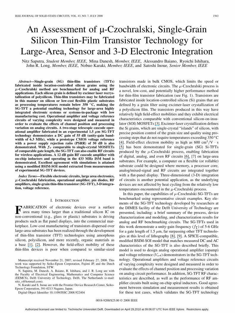
IEEE JOURNAL OF SOLID-STATE CIRCUITS, VOL. 43, NO. 7, JULY 2008 1563
An Assessment of µ-Czochralski, Single-GrainSilicon Thin-Film Transistor Technology for
Large-Area, Sensor and 3-D Electronic IntegrationNitz Saputra, Student Member, IEEE, Mina Danesh, Member, IEEE, Alessandro Baiano, Ryoichi Ishihara,
John R. Long, Member, IEEE, Nobuo Karaki, Member, IEEE, and Satoshi Inoue, Senior Member, IEEE
Abstract—Single-grain (SG) thin-film transistors (TFTs)fabricated inside location-controlled silicon grains using the
-Czochralski method are benchmarked for analog and RFapplications. Each silicon grain is defined by excimer laser recrys-tallization of polysilicon. Thin-film transistors may be fabricatedin this manner on silicon or low-cost flexible plastic substratesas processing temperatures remain below 350 C, making theSG-TFT a potential enabling technology for large-area highlyintegrated electronic systems or systems-in-package with lowmanufacturing cost. Operational amplifier and voltage referencecircuits of varying complexity were designed and measured inorder to evaluate the effects of channel position and processingvariation on analog circuits. A two-stage telescopic cascode oper-ational amplifier fabricated in an experimental 1.5 m SG-TFTtechnology demonstrates a DC gain of 55 dB (unity-gain band-width of 6.3 MHz), while a prototype CMOS voltage referencewith a power supply rejection ratio (PSRR) of 50 dB is alsodemonstrated. With � comparable to single-crystal MOSFETsof comparable gate length, the SG-TFT can also enable RF circuitsfor wireless applications. A 12 dB gain RF cascode amplifier withon-chip inductors and operating in the 433 MHz ISM band isdemonstrated. Excellent agreement with simulations is attainedusing a modified BSIM-SOI model extracted from measurementsof experimental SG-TFT devices.
Index Terms—Flexible electronic circuits, large area electronics,-Czochralski fabrication, operational amplifier, pin diodes, RF
amplifiers, single-grain thin-film transistor (SG-TFT), 3-D integra-tion, voltage reference.
I. INTRODUCTION
FABRICATION of electronic devices over a surfacearea many times larger than a traditional silicon IC on
non-conventional (e.g., glass or plastic) substrates is drivingproducts such as flat panel displays, into the commercial mar-ketplace. Low-cost manufacturing of transistors dispersed overlarge-area substrates has been realized through the developmentof thin-film transistor (TFT) technologies using amorphoussilicon, polysilicon, and more recently, organic materials asa base [1], [2]. However, the field-effect mobility of thesethin-film devices is poor when compared to similar-sized
Manuscript received November 21, 2007; revised February 27, 2008. Thiswork was supported by Seiko-Epson Corporation, Fujimi JP, and the DutchTechnology Foundation, STW.
N. Saputra, M. Danesh, A. Baiano, R. Ishihara, and J. R. Long are withthe Faculty of Electrical Engineering, Mathematics and Computer Science(EEMCS), Delft University of Technology, Delft, The Netherlands (e-mail:[email protected]).
N. Karaki and S. Inoue are with the Frontier Device Research Center, Seiko-Epson Corporation, 391-0213 Nagano, Japan.
Digital Object Identifier 10.1109/JSSC.2008.922404
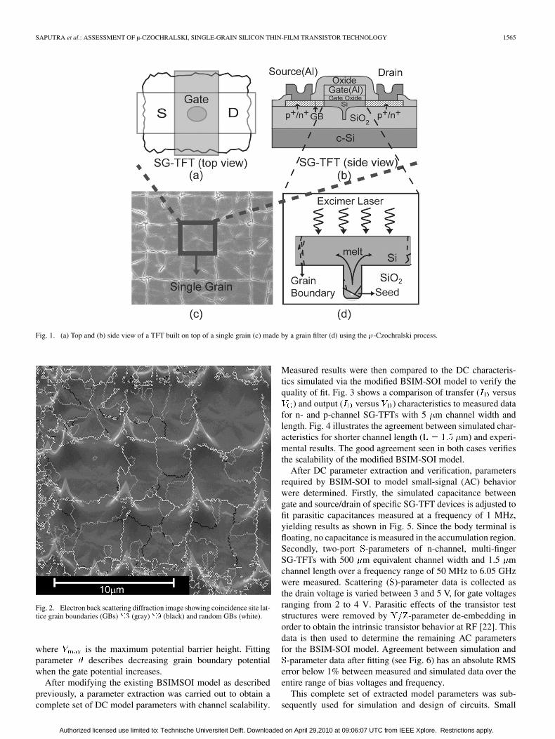
transistors made in bulk CMOS, which limits the speed orbandwidth of electronic circuits. The -Czochralski process isa novel, low-cost, and potentially higher performance methodfor thin-film transistor fabrication (see Fig. 1). Transistors arefabricated inside location-controlled silicon (Si) grains that aredefined by a grain filter using excimer-laser crystallization ofa polysilicon film. The transistors produced in this way haverelatively high field-effect mobilities and they exhibit electricalcharacteristics comparable with conventional silicon-on-insu-lator (SOI) MOSFETs [3]. Excimer-laser crystallization definesthe Si grains, which are single-crystal “islands” of silicon, withprecise position control of the grain size and quality using pro-cessing steps that do not require temperatures exceeding 350 C[4]. Field-effect electron mobility as high as 600 cm V s[5] has been demonstrated for single-grain (SG) Si-TFTsproduced by the -Czochralski process, enabling fabricationof digital, analog, and even RF circuits [6], [7] on large-areasubstrates. For example, a computer on a flexible (or rollable)substrate could be designed where memory, a processor core,analog/mixed-signal and RF circuits are integrated togetherwith a flat-panel display. Three-dimensional (3-D) integrationof circuits is another potential application, as the underlyingdevices are not affected by heat cycling from the relatively lowtemperatures encountered in the -Czochralski process.
In this paper, the capabilities of -Czochralski SG-TFTs arebenchmarked using representative circuit examples. Key ele-ments of the SG-TFT technology developed by researchers atthe DIMES facility of the Delft University of Technology arepresented, including: a brief summary of the process, devicecharacterization and modeling, and characterization results foranalog and RF benchmarking circuits. The SG-TFTs used inthis work demonstrate a unity-gain frequency ( ) of 5-6 GHzfor a gate length of 1.5 m, far surpassing other TFT technolo-gies at this level of lithography [8], [9]. A SPICE-compatible,modified BSIM-SOI model that matches measured DC and ACcharacteristics of the SG-TFT is also described briefly. Thismodel is used to design analog operational amplifier (opamp)and voltage reference ( ) demonstrators in the SG-TFT tech-nology. Operational amplifiers and voltage reference circuitsof varying complexity were designed and measured in order toevaluate the effects of channel position and processing variationon analog circuit performance. In addition, SG-TFT RF charac-teristics are described, as well as the performance of RF am-plifier circuits built using on-chip spiral inductors. Good agree-ment between simulation and measurement results is obtainedfor these test cases, which validates the SG-TFT technology
0018-9200/$25.00 © 2008 IEEE
Authorized licensed use limited to: Technische Universiteit Delft. Downloaded on April 29,2010 at 09:06:07 UTC from IEEE Xplore. Restrictions apply.
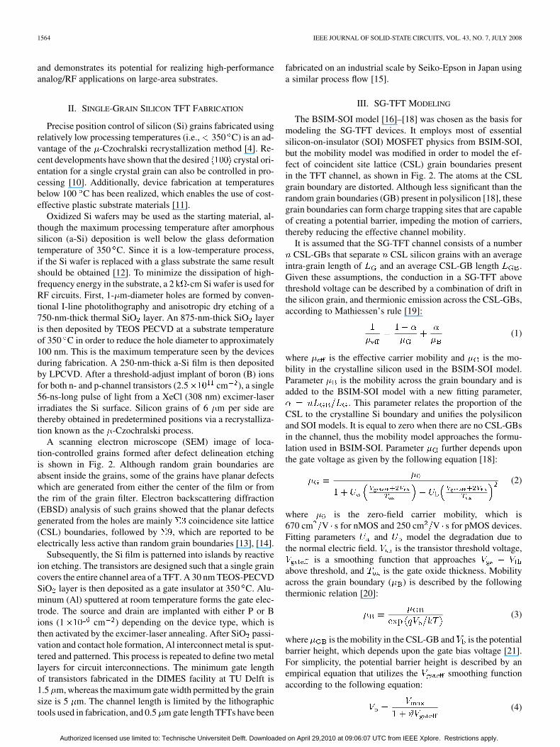
1564 IEEE JOURNAL OF SOLID-STATE CIRCUITS, VOL. 43, NO. 7, JULY 2008
and demonstrates its potential for realizing high-performanceanalog/RF applications on large-area substrates.
II. SINGLE-GRAIN SILICON TFT FABRICATION
Precise position control of silicon (Si) grains fabricated usingrelatively low processing temperatures (i.e., 350 C) is an ad-vantage of the -Czochralski recrystallization method [4]. Re-cent developments have shown that the desired crystal ori-entation for a single crystal grain can also be controlled in pro-cessing [10]. Additionally, device fabrication at temperaturesbelow 100 C has been realized, which enables the use of cost-effective plastic substrate materials [11].
Oxidized Si wafers may be used as the starting material, al-though the maximum processing temperature after amorphoussilicon (a-Si) deposition is well below the glass deformationtemperature of 350 C. Since it is a low-temperature process,if the Si wafer is replaced with a glass substrate the same resultshould be obtained [12]. To minimize the dissipation of high-frequency energy in the substrate, a 2 k cm Si wafer is used forRF circuits. First, 1- m-diameter holes are formed by conven-tional I-line photolithography and anisotropic dry etching of a750-nm-thick thermal SiO layer. An 875-nm-thick SiO layeris then deposited by TEOS PECVD at a substrate temperatureof 350 C in order to reduce the hole diameter to approximately100 nm. This is the maximum temperature seen by the devicesduring fabrication. A 250-nm-thick a-Si film is then depositedby LPCVD. After a threshold-adjust implant of boron (B) ionsfor both n- and p-channel transistors (2.5 cm ), a single56-ns-long pulse of light from a XeCl (308 nm) excimer-laserirradiates the Si surface. Silicon grains of 6 m per side arethereby obtained in predetermined positions via a recrystalliza-tion known as the -Czochralski process.
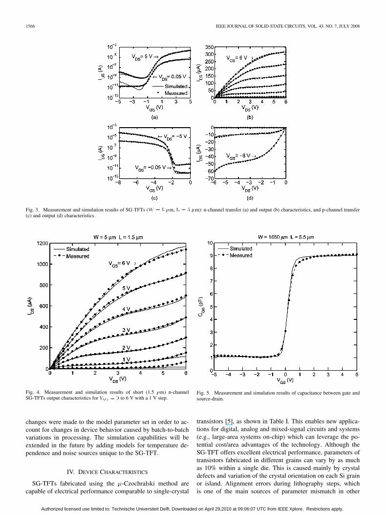
A scanning electron microscope (SEM) image of loca-tion-controlled grains formed after defect delineation etchingis shown in Fig. 2. Although random grain boundaries areabsent inside the grains, some of the grains have planar defectswhich are generated from either the center of the film or fromthe rim of the grain filter. Electron backscattering diffraction(EBSD) analysis of such grains showed that the planar defectsgenerated from the holes are mainly coincidence site lattice(CSL) boundaries, followed by , which are reported to beelectrically less active than random grain boundaries [13], [14].
Subsequently, the Si film is patterned into islands by reactiveion etching. The transistors are designed such that a single graincovers the entire channel area of a TFT. A 30 nm TEOS-PECVDSiO layer is then deposited as a gate insulator at 350 C. Alu-minum (Al) sputtered at room temperature forms the gate elec-trode. The source and drain are implanted with either P or Bions (1 cm ) depending on the device type, which isthen activated by the excimer-laser annealing. After SiO passi-vation and contact hole formation, Al interconnect metal is sput-tered and patterned. This process is repeated to define two metallayers for circuit interconnections. The minimum gate lengthof transistors fabricated in the DIMES facility at TU Delft is1.5 m, whereas the maximum gate width permitted by the grainsize is 5 m. The channel length is limited by the lithographictools used in fabrication, and 0.5 m gate length TFTs have been
fabricated on an industrial scale by Seiko-Epson in Japan usinga similar process flow [15].
III. SG-TFT MODELING
The BSIM-SOI model [16]–[18] was chosen as the basis formodeling the SG-TFT devices. It employs most of essentialsilicon-on-insulator (SOI) MOSFET physics from BSIM-SOI,but the mobility model was modified in order to model the ef-fect of coincident site lattice (CSL) grain boundaries presentin the TFT channel, as shown in Fig. 2. The atoms at the CSLgrain boundary are distorted. Although less significant than therandom grain boundaries (GB) present in polysilicon [18], thesegrain boundaries can form charge trapping sites that are capableof creating a potential barrier, impeding the motion of carriers,thereby reducing the effective channel mobility.
It is assumed that the SG-TFT channel consists of a numberCSL-GBs that separate CSL silicon grains with an average
intra-grain length of and an average CSL-GB length .Given these assumptions, the conduction in a SG-TFT abovethreshold voltage can be described by a combination of drift inthe silicon grain, and thermionic emission across the CSL-GBs,according to Mathiessen’s rule [19]:
(1)
where is the effective carrier mobility and is the mo-bility in the crystalline silicon used in the BSIM-SOI model.Parameter is the mobility across the grain boundary and isadded to the BSIM-SOI model with a new fitting parameter,
. This parameter relates the proportion of theCSL to the crystalline Si boundary and unifies the polysiliconand SOI models. It is equal to zero when there are no CSL-GBsin the channel, thus the mobility model approaches the formu-lation used in BSIM-SOI. Parameter further depends uponthe gate voltage as given by the following equation [18]:
(2)
where is the zero-field carrier mobility, which is670 cm V s for nMOS and 250 cm V s for pMOS devices.Fitting parameters and model the degradation due tothe normal electric field. is the transistor threshold voltage,
is a smoothing function that approachesabove threshold, and is the gate oxide thickness. Mobilityacross the grain boundary ( ) is described by the followingthermionic relation [20]:
(3)
where is the mobility in the CSL-GB and is the potentialbarrier height, which depends upon the gate bias voltage [21].For simplicity, the potential barrier height is described by anempirical equation that utilizes the smoothing functionaccording to the following equation:
(4)
Authorized licensed use limited to: Technische Universiteit Delft. Downloaded on April 29,2010 at 09:06:07 UTC from IEEE Xplore. Restrictions apply.
SAPUTRA et al.: ASSESSMENT OF µ-CZOCHRALSKI, SINGLE-GRAIN SILICON THIN-FILM TRANSISTOR TECHNOLOGY 1565
Fig. 1. (a) Top and (b) side view of a TFT built on top of a single grain (c) made by a grain filter (d) using the �-Czochralski process.
Fig. 2. Electron back scattering diffraction image showing coincidence site lat-tice grain boundaries (GBs) �� (gray) �� (black) and random GBs (white).
where is the maximum potential barrier height. Fittingparameter describes decreasing grain boundary potentialwhen the gate potential increases.
After modifying the existing BSIMSOI model as describedpreviously, a parameter extraction was carried out to obtain acomplete set of DC model parameters with channel scalability.
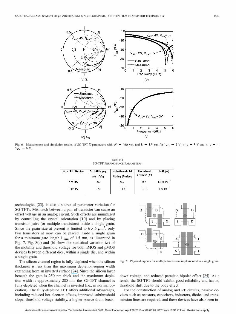
Measured results were then compared to the DC characteris-tics simulated via the modified BSIM-SOI model to verify thequality of fit. Fig. 3 shows a comparison of transfer ( versus
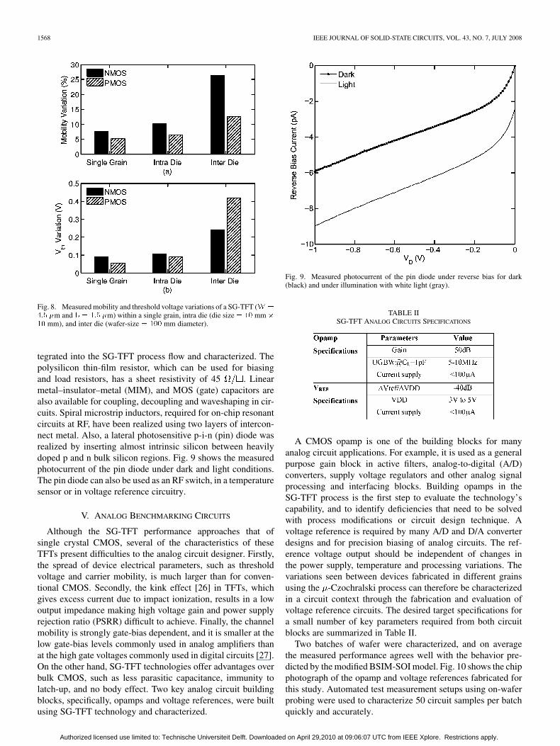
) and output ( versus ) characteristics to measured datafor n- and p-channel SG-TFTs with 5 m channel width andlength. Fig. 4 illustrates the agreement between simulated char-acteristics for shorter channel length ( m) and experi-mental results. The good agreement seen in both cases verifiesthe scalability of the modified BSIM-SOI model.
After DC parameter extraction and verification, parametersrequired by BSIM-SOI to model small-signal (AC) behaviorwere determined. Firstly, the simulated capacitance betweengate and source/drain of specific SG-TFT devices is adjusted tofit parasitic capacitances measured at a frequency of 1 MHz,yielding results as shown in Fig. 5. Since the body terminal isfloating, no capacitance is measured in the accumulation region.Secondly, two-port -parameters of n-channel, multi-fingerSG-TFTs with 500 m equivalent channel width and 1.5 mchannel length over a frequency range of 50 MHz to 6.05 GHzwere measured. Scattering ( )-parameter data is collected asthe drain voltage is varied between 3 and 5 V, for gate voltagesranging from 2 to 4 V. Parasitic effects of the transistor teststructures were removed by -parameter de-embedding inorder to obtain the intrinsic transistor behavior at RF [22]. Thisdata is then used to determine the remaining AC parametersfor the BSIM-SOI model. Agreement between simulation and
-parameter data after fitting (see Fig. 6) has an absolute RMSerror below 1% between measured and simulated data over theentire range of bias voltages and frequency.
This complete set of extracted model parameters was sub-sequently used for simulation and design of circuits. Small
Authorized licensed use limited to: Technische Universiteit Delft. Downloaded on April 29,2010 at 09:06:07 UTC from IEEE Xplore. Restrictions apply.
1566 IEEE JOURNAL OF SOLID-STATE CIRCUITS, VOL. 43, NO. 7, JULY 2008
Fig. 3. Measurement and simulation results of SG-TFTs (� � � �m, � � � �m): n-channel transfer (a) and output (b) characteristics, and p-channel transfer(c) and output (d) characteristics.
Fig. 4. Measurement and simulation results of short (1.5 �m) n-channelSG-TFTs output characteristics for � � � to 6 V with a 1 V step.
changes were made to the model parameter set in order to ac-count for changes in device behavior caused by batch-to-batchvariations in processing. The simulation capabilities will beextended in the future by adding models for temperature de-pendence and noise sources unique to the SG-TFT.
IV. DEVICE CHARACTERISTICS
SG-TFTs fabricated using the -Czochralski method arecapable of electrical performance comparable to single-crystal
Fig. 5. Measurement and simulation results of capacitance between gate andsource-drain.
transistors [5], as shown in Table I. This enables new applica-tions for digital, analog and mixed-signal circuits and systems(e.g., large-area systems on-chip) which can leverage the po-tential cost/area advantages of the technology. Although theSG-TFT offers excellent electrical performance, parameters oftransistors fabricated in different grains can vary by as muchas 10% within a single die. This is caused mainly by crystaldefects and variation of the crystal orientation on each Si grainor island. Alignment errors during lithography steps, whichis one of the main sources of parameter mismatch in other
Authorized licensed use limited to: Technische Universiteit Delft. Downloaded on April 29,2010 at 09:06:07 UTC from IEEE Xplore. Restrictions apply.
SAPUTRA et al.: ASSESSMENT OF µ-CZOCHRALSKI, SINGLE-GRAIN SILICON THIN-FILM TRANSISTOR TECHNOLOGY 1567
Fig. 6. Measurement and simulation results of SG-TFT �-parameters with � � ��� �m, and � � ��� �m for � � � V, � � V and � � ,� � � V.
TABLE ISG-TFT PERFORMANCE PARAMETERS
technologies [23], is also a source of parameter variation forSG-TFTs. Mismatch between a pair of transistor can cause anoffset voltage in an analog circuit. Such offsets are minimizedby controlling the crystal orientation [10] and by placingtransistor pairs (or multiple transistors) inside a single grain.Since the grain size at present is limited to 6 6 m , onlytwo transistors at most can be placed inside a single grainfor a minimum gate length of 1.5 m, as illustrated inFig. 7. Fig. 8(a) and (b) show the statistical variation ( ) ofthe mobility and threshold voltage for both nMOS and pMOSdevices between different dice, within a single die, and withina single grain.
The silicon channel region is fully-depleted when the siliconthickness is less than the maximum depletion-region widthextending from an inverted surface [24]. Since the silicon layerbeneath the gate is 250 nm thick and the maximum deple-tion width is approximately 285 nm, the SG-TFT channel isfully-depleted when the channel is inverted (i.e., in normal op-eration). The fully-depleted TFT offers additional advantages,including reduced hot-electron effects, improved subthresholdslope, threshold-voltage stability, a higher source-drain break-
Fig. 7. Physical layouts for multiple transistors implemented in a single grain.
down voltage, and reduced parasitic bipolar effect [25]. As aresult, the SG-TFT should exhibit good reliability and has nothreshold shift due to the body effect.
For the construction of analog and RF circuits, passive de-vices such as resistors, capacitors, inductors, diodes and trans-mission lines are required, and these devices have also been in-
Authorized licensed use limited to: Technische Universiteit Delft. Downloaded on April 29,2010 at 09:06:07 UTC from IEEE Xplore. Restrictions apply.
1568 IEEE JOURNAL OF SOLID-STATE CIRCUITS, VOL. 43, NO. 7, JULY 2008
Fig. 8. Measured mobility and threshold voltage variations of a SG-TFT (� �
��� �m and � � ��� �m) within a single grain, intra die (die size � ��mm��� mm), and inter die (wafer-size � ��� mm diameter).
tegrated into the SG-TFT process flow and characterized. Thepolysilicon thin-film resistor, which can be used for biasingand load resistors, has a sheet resistivity of 45 . Linearmetal–insulator–metal (MIM), and MOS (gate) capacitors arealso available for coupling, decoupling and waveshaping in cir-cuits. Spiral microstrip inductors, required for on-chip resonantcircuits at RF, have been realized using two layers of intercon-nect metal. Also, a lateral photosensitive p-i-n (pin) diode wasrealized by inserting almost intrinsic silicon between heavilydoped p and n bulk silicon regions. Fig. 9 shows the measuredphotocurrent of the pin diode under dark and light conditions.The pin diode can also be used as an RF switch, in a temperaturesensor or in voltage reference circuitry.
V. ANALOG BENCHMARKING CIRCUITS
Although the SG-TFT performance approaches that ofsingle crystal CMOS, several of the characteristics of theseTFTs present difficulties to the analog circuit designer. Firstly,the spread of device electrical parameters, such as thresholdvoltage and carrier mobility, is much larger than for conven-tional CMOS. Secondly, the kink effect [26] in TFTs, whichgives excess current due to impact ionization, results in a lowoutput impedance making high voltage gain and power supplyrejection ratio (PSRR) difficult to achieve. Finally, the channelmobility is strongly gate-bias dependent, and it is smaller at thelow gate-bias levels commonly used in analog amplifiers thanat the high gate voltages commonly used in digital circuits [27].On the other hand, SG-TFT technologies offer advantages overbulk CMOS, such as less parasitic capacitance, immunity tolatch-up, and no body effect. Two key analog circuit buildingblocks, specifically, opamps and voltage references, were builtusing SG-TFT technology and characterized.
Fig. 9. Measured photocurrent of the pin diode under reverse bias for dark(black) and under illumination with white light (gray).
TABLE IISG-TFT ANALOG CIRCUITS SPECIFICATIONS
A CMOS opamp is one of the building blocks for manyanalog circuit applications. For example, it is used as a generalpurpose gain block in active filters, analog-to-digital (A/D)converters, supply voltage regulators and other analog signalprocessing and interfacing blocks. Building opamps in theSG-TFT process is the first step to evaluate the technology’scapability, and to identify deficiencies that need to be solvedwith process modifications or circuit design technique. Avoltage reference is required by many A/D and D/A converterdesigns and for precision biasing of analog circuits. The ref-erence voltage output should be independent of changes inthe power supply, temperature and processing variations. Thevariations seen between devices fabricated in different grainsusing the -Czochralski process can therefore be characterizedin a circuit context through the fabrication and evaluation ofvoltage reference circuits. The desired target specifications fora small number of key parameters required from both circuitblocks are summarized in Table II.
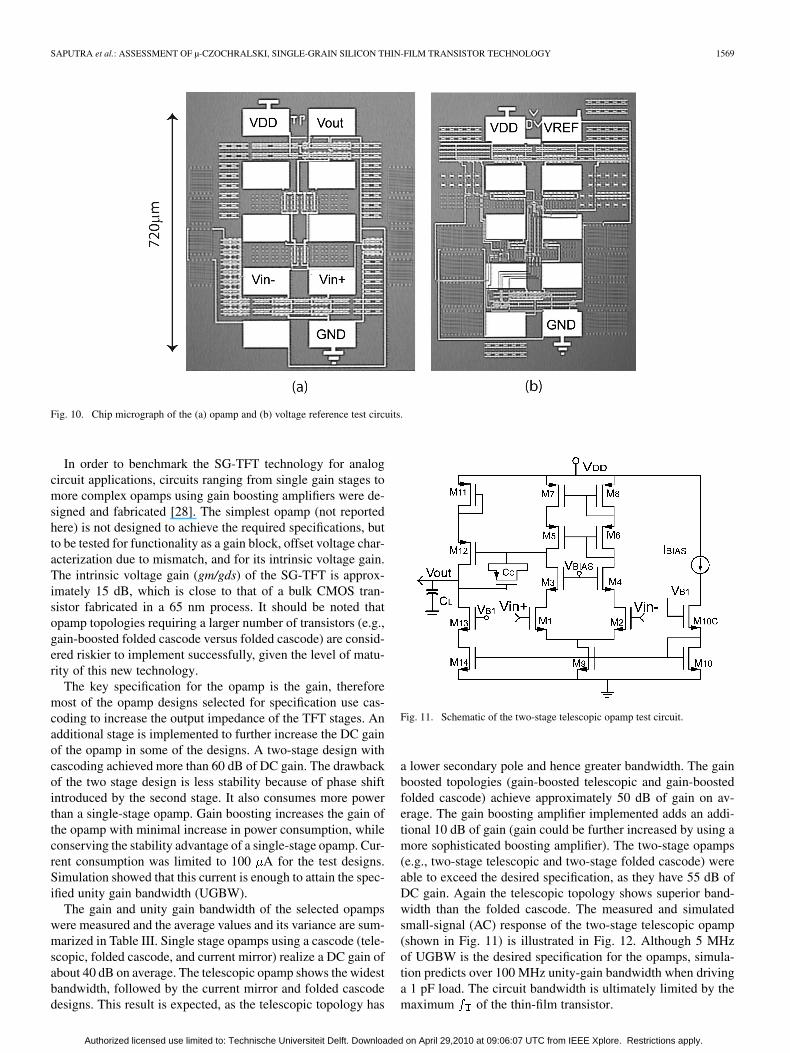
Two batches of wafer were characterized, and on averagethe measured performance agrees well with the behavior pre-dicted by the modified BSIM-SOI model. Fig. 10 shows the chipphotograph of the opamp and voltage references fabricated forthis study. Automated test measurement setups using on-waferprobing were used to characterize 50 circuit samples per batchquickly and accurately.
Authorized licensed use limited to: Technische Universiteit Delft. Downloaded on April 29,2010 at 09:06:07 UTC from IEEE Xplore. Restrictions apply.
SAPUTRA et al.: ASSESSMENT OF µ-CZOCHRALSKI, SINGLE-GRAIN SILICON THIN-FILM TRANSISTOR TECHNOLOGY 1569
Fig. 10. Chip micrograph of the (a) opamp and (b) voltage reference test circuits.
In order to benchmark the SG-TFT technology for analogcircuit applications, circuits ranging from single gain stages tomore complex opamps using gain boosting amplifiers were de-signed and fabricated [28]. The simplest opamp (not reportedhere) is not designed to achieve the required specifications, butto be tested for functionality as a gain block, offset voltage char-acterization due to mismatch, and for its intrinsic voltage gain.The intrinsic voltage gain (gm/gds) of the SG-TFT is approx-imately 15 dB, which is close to that of a bulk CMOS tran-sistor fabricated in a 65 nm process. It should be noted thatopamp topologies requiring a larger number of transistors (e.g.,gain-boosted folded cascode versus folded cascode) are consid-ered riskier to implement successfully, given the level of matu-rity of this new technology.
The key specification for the opamp is the gain, thereforemost of the opamp designs selected for specification use cas-coding to increase the output impedance of the TFT stages. Anadditional stage is implemented to further increase the DC gainof the opamp in some of the designs. A two-stage design withcascoding achieved more than 60 dB of DC gain. The drawbackof the two stage design is less stability because of phase shiftintroduced by the second stage. It also consumes more powerthan a single-stage opamp. Gain boosting increases the gain ofthe opamp with minimal increase in power consumption, whileconserving the stability advantage of a single-stage opamp. Cur-rent consumption was limited to 100 A for the test designs.Simulation showed that this current is enough to attain the spec-ified unity gain bandwidth (UGBW).
The gain and unity gain bandwidth of the selected opampswere measured and the average values and its variance are sum-marized in Table III. Single stage opamps using a cascode (tele-scopic, folded cascode, and current mirror) realize a DC gain ofabout 40 dB on average. The telescopic opamp shows the widestbandwidth, followed by the current mirror and folded cascodedesigns. This result is expected, as the telescopic topology has
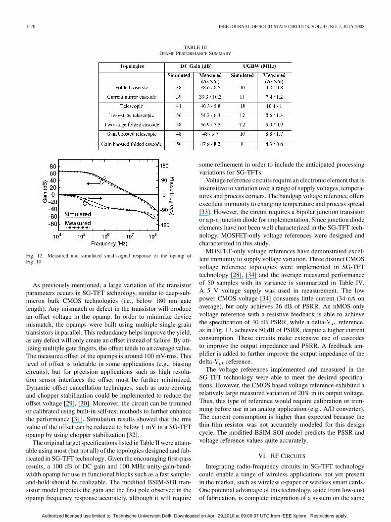
Fig. 11. Schematic of the two-stage telescopic opamp test circuit.
a lower secondary pole and hence greater bandwidth. The gainboosted topologies (gain-boosted telescopic and gain-boostedfolded cascode) achieve approximately 50 dB of gain on av-erage. The gain boosting amplifier implemented adds an addi-tional 10 dB of gain (gain could be further increased by using amore sophisticated boosting amplifier). The two-stage opamps(e.g., two-stage telescopic and two-stage folded cascode) wereable to exceed the desired specification, as they have 55 dB ofDC gain. Again the telescopic topology shows superior band-width than the folded cascode. The measured and simulatedsmall-signal (AC) response of the two-stage telescopic opamp(shown in Fig. 11) is illustrated in Fig. 12. Although 5 MHzof UGBW is the desired specification for the opamps, simula-tion predicts over 100 MHz unity-gain bandwidth when drivinga 1 pF load. The circuit bandwidth is ultimately limited by themaximum of the thin-film transistor.
Authorized licensed use limited to: Technische Universiteit Delft. Downloaded on April 29,2010 at 09:06:07 UTC from IEEE Xplore. Restrictions apply.
1570 IEEE JOURNAL OF SOLID-STATE CIRCUITS, VOL. 43, NO. 7, JULY 2008
TABLE IIIOPAMP PERFORMANCE SUMMARY
Fig. 12. Measured and simulated small-signal response of the opamp ofFig. 10.
As previously mentioned, a large variation of the transistorparameters occurs in SG-TFT technology, similar to deep-sub-micron bulk CMOS technologies (i.e., below 180 nm gatelength). Any mismatch or defect in the transistor will producean offset voltage in the opamp. In order to minimize devicemismatch, the opamps were built using multiple single-graintransistors in parallel. This redundancy helps improve the yield,as any defect will only create an offset instead of failure. By uti-lizing multiple gate fingers, the offset tends to an average value.The measured offset of the opamps is around 100 mV-rms. Thislevel of offset is tolerable in some applications (e.g., biasingcircuits), but for precision applications such as high resolu-tion sensor interfaces the offset must be further minimized.Dynamic offset cancellation techniques, such as auto-zeroingand chopper stabilization could be implemented to reduce theoffset voltage [29], [30]. Moreover, the circuit can be trimmedor calibrated using built-in self-test methods to further enhancethe performance [31]. Simulation results showed that the rmsvalue of the offset can be reduced to below 1 mV in a SG-TFTopamp by using chopper stabilization [32].
The original target specifications listed in Table II were attain-able using most (but not all) of the topologies designed and fab-ricated in SG-TFT technology. Given the encouraging first-passresults, a 100 dB of DC gain and 100 MHz unity-gain-band-width opamp for use in functional blocks such as a fast sample-and-hold should be realizable. The modified BSIM-SOI tran-sistor model predicts the gain and the first pole observed in theopamp frequency response accurately, although it will require
some refinement in order to include the anticipated processingvariations for SG-TFTs.
Voltage reference circuits require an electronic element that isinsensitive to variation over a range of supply voltages, tempera-tures and process corners. The bandgap voltage reference offersexcellent immunity to changing temperature and process spread[33]. However, the circuit requires a bipolar junction transistoror a p-n junction diode for implementation. Since junction diodeelements have not been well characterized in the SG-TFT tech-nology, MOSFET-only voltage references were designed andcharacterized in this study.
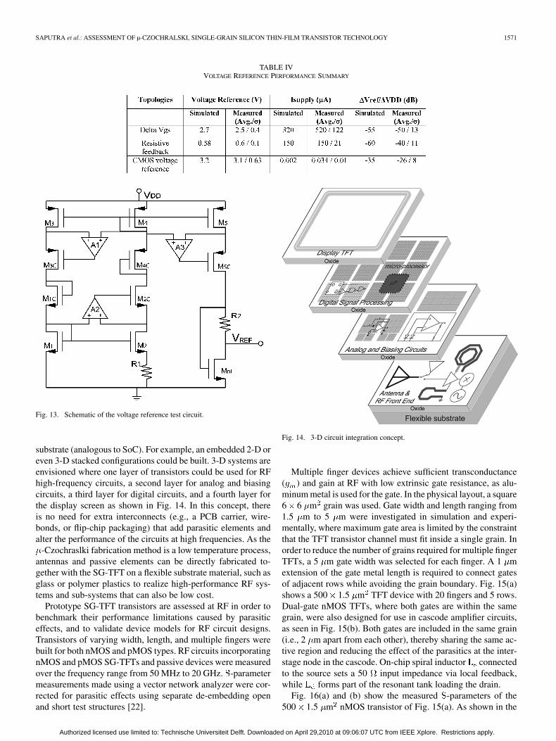
MOSFET-only voltage references have demonstrated excel-lent immunity to supply voltage variation. Three distinct CMOSvoltage reference topologies were implemented in SG-TFTtechnology [28], [34] and the average measured performanceof 50 samples with its variance is summarized in Table IV.A 5 V voltage supply was used in measurement. The lowpower CMOS voltage [34] consumes little current (34 nA onaverage), but only achieves 26 dB of PSRR. An nMOS-onlyvoltage reference with a resistive feedback is able to achievethe specification of 40 dB PSRR, while a delta- reference,as in Fig. 13, achieves 50 dB of PSRR, despite a higher currentconsumption. These circuits make extensive use of cascodesto improve the output impedance and PSRR. A feedback am-plifier is added to further improve the output impedance of thedelta- reference.
The voltage references implemented and measured in theSG-TFT technology were able to meet the desired specifica-tions. However, the CMOS based voltage reference exhibited arelatively large measured variation of 20% in its output voltage.Thus, this type of reference would require calibration or trim-ming before use in an analog application (e.g., A/D converter).The current consumption is higher than expected because thethin-film resistor was not accurately modeled for this designcycle. The modified BSIM-SOI model predicts the PSSR andvoltage reference values quite accurately.
VI. RF CIRCUITS
Integrating radio-frequency circuits in SG-TFT technologycould enable a range of wireless applications not yet presentin the market, such as wireless e-paper or wireless smart cards.One potential advantage of this technology, aside from low-costof fabrication, is complete integration of a system on the same
Authorized licensed use limited to: Technische Universiteit Delft. Downloaded on April 29,2010 at 09:06:07 UTC from IEEE Xplore. Restrictions apply.
SAPUTRA et al.: ASSESSMENT OF µ-CZOCHRALSKI, SINGLE-GRAIN SILICON THIN-FILM TRANSISTOR TECHNOLOGY 1571
TABLE IVVOLTAGE REFERENCE PERFORMANCE SUMMARY
Fig. 13. Schematic of the voltage reference test circuit.
substrate (analogous to SoC). For example, an embedded 2-D oreven 3-D stacked configurations could be built. 3-D systems areenvisioned where one layer of transistors could be used for RFhigh-frequency circuits, a second layer for analog and biasingcircuits, a third layer for digital circuits, and a fourth layer forthe display screen as shown in Fig. 14. In this concept, thereis no need for extra interconnects (e.g., a PCB carrier, wire-bonds, or flip-chip packaging) that add parasitic elements andalter the performance of the circuits at high frequencies. As the
-Czochraslki fabrication method is a low temperature process,antennas and passive elements can be directly fabricated to-gether with the SG-TFT on a flexible substrate material, such asglass or polymer plastics to realize high-performance RF sys-tems and sub-systems that can also be low cost.
Prototype SG-TFT transistors are assessed at RF in order tobenchmark their performance limitations caused by parasiticeffects, and to validate device models for RF circuit designs.Transistors of varying width, length, and multiple fingers werebuilt for both nMOS and pMOS types. RF circuits incorporatingnMOS and pMOS SG-TFTs and passive devices were measuredover the frequency range from 50 MHz to 20 GHz. -parametermeasurements made using a vector network analyzer were cor-rected for parasitic effects using separate de-embedding openand short test structures [22].
Fig. 14. 3-D circuit integration concept.
Multiple finger devices achieve sufficient transconductance( ) and gain at RF with low extrinsic gate resistance, as alu-minum metal is used for the gate. In the physical layout, a square6 6 m grain was used. Gate width and length ranging from1.5 m to 5 m were investigated in simulation and experi-mentally, where maximum gate area is limited by the constraintthat the TFT transistor channel must fit inside a single grain. Inorder to reduce the number of grains required for multiple fingerTFTs, a 5 m gate width was selected for each finger. A 1 mextension of the gate metal length is required to connect gatesof adjacent rows while avoiding the grain boundary. Fig. 15(a)shows a 500 1.5 m TFT device with 20 fingers and 5 rows.Dual-gate nMOS TFTs, where both gates are within the samegrain, were also designed for use in cascode amplifier circuits,as seen in Fig. 15(b). Both gates are included in the same grain(i.e., 2 m apart from each other), thereby sharing the same ac-tive region and reducing the effect of the parasitics at the inter-stage node in the cascode. On-chip spiral inductor connectedto the source sets a 50 input impedance via local feedback,while forms part of the resonant tank loading the drain.
Fig. 16(a) and (b) show the measured -parameters of the500 1.5 m nMOS transistor of Fig. 15(a). As shown in the
Authorized licensed use limited to: Technische Universiteit Delft. Downloaded on April 29,2010 at 09:06:07 UTC from IEEE Xplore. Restrictions apply.
1572 IEEE JOURNAL OF SOLID-STATE CIRCUITS, VOL. 43, NO. 7, JULY 2008
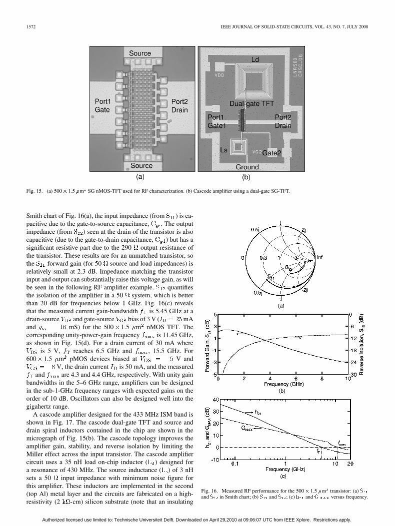
Fig. 15. (a) 500� 1.5 �m SG nMOS-TFT used for RF characterization. (b) Cascode amplifier using a dual-gate SG-TFT.
Smith chart of Fig. 16(a), the input impedance (from ) is ca-pacitive due to the gate-to-source capacitance, . The outputimpedance (from ) seen at the drain of the transistor is alsocapacitive (due to the gate-to-drain capacitance, ) but has asignificant resistive part due to the 290 output resistance ofthe transistor. These results are for an unmatched transistor, sothe forward gain (for 50 source and load impedances) isrelatively small at 2.3 dB. Impedance matching the transistorinput and output can substantially raise this voltage gain, as willbe seen in the following RF amplifier example. quantifiesthe isolation of the amplifier in a 50 system, which is betterthan 20 dB for frequencies below 1 GHz. Fig. 16(c) revealsthat the measured current gain-bandwidth is 5.45 GHz at adrain-source and gate-source bias of 3 V ( mAand mS) for the 500 1.5 m nMOS TFT. Thecorresponding unity-power-gain frequency is 11.45 GHz,as shown in Fig. 15(d). For a drain current of 30 mA where
is 5 V, reaches 6.5 GHz and , 15.5 GHz. For600 1.5 m pMOS devices biased at V and
V, the drain current is 50 mA, and the measuredand are 4.3 and 4.4 GHz, respectively. With unity gain
bandwidths in the 5–6 GHz range, amplifiers can be designedin the sub-1-GHz frequency ranges with expected gains on theorder of 10 dB. Oscillators can also be designed well into thegigahertz range.
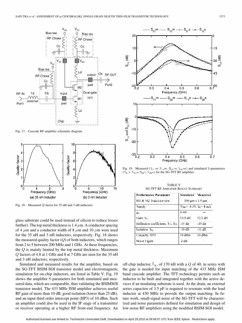
A cascode amplifier designed for the 433 MHz ISM band isshown in Fig. 17. The cascode dual-gate TFT and source anddrain spiral inductors contained in the chip are shown in themicrograph of Fig. 15(b). The cascode topology improves theamplifier gain, stability, and reverse isolation by limiting theMiller effect across the input transistor. The cascode amplifiercircuit uses a 35 nH load on-chip inductor ( ) designed fora resonance of 430 MHz. The source inductance ( ) of 3 nHsets a 50 input impedance with minimum noise figure forthis amplifier. These inductors are implemented in the second(top Al) metal layer and the circuits are fabricated on a high-resistivity (2 cm) silicon substrate (note that an insulating
Fig. 16. Measured RF performance for the 500� 1.5 �m transistor: (a) �and � in Smith chart; (b) � and � ; (c) � and � versus frequency.
Authorized licensed use limited to: Technische Universiteit Delft. Downloaded on April 29,2010 at 09:06:07 UTC from IEEE Xplore. Restrictions apply.
SAPUTRA et al.: ASSESSMENT OF µ-CZOCHRALSKI, SINGLE-GRAIN SILICON THIN-FILM TRANSISTOR TECHNOLOGY 1573
Fig. 17. Cascode RF amplifier schematic diagram.
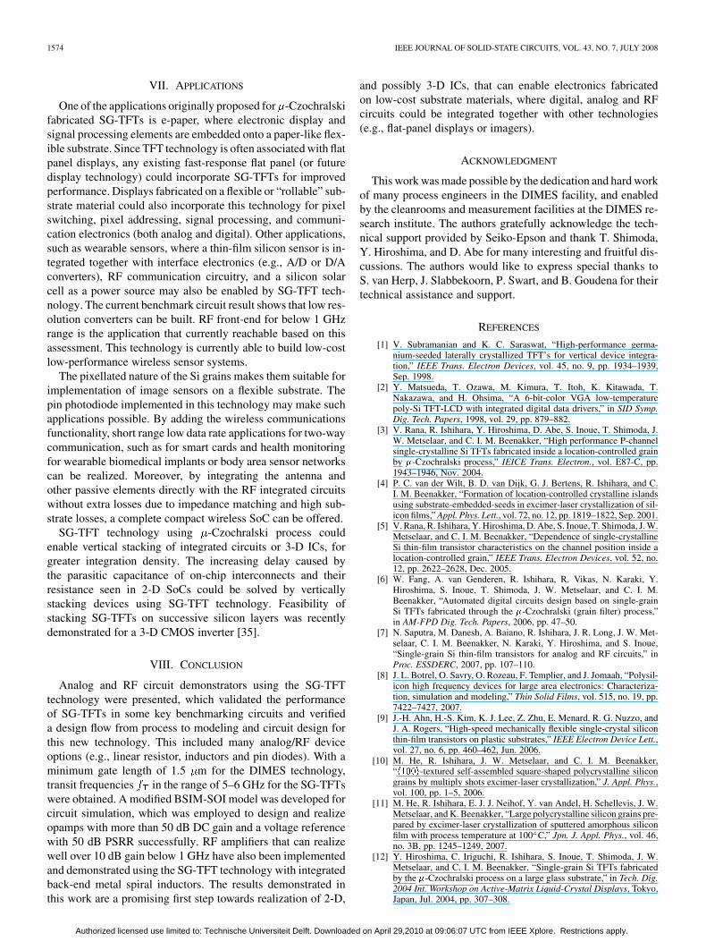
Fig. 18. Measured �-factor for 35 nH and 3 nH inductors.
glass substrate could be used instead of silicon to reduce lossesfurther). The top metal thickness is 1.4 m. A conductor spacingof 4 m and a conductor width of 8 m and 10 m were usedfor the 35 nH and 3 nH inductors, respectively. Fig. 18 showsthe measured quality factor ( ) of both inductors, which rangesfrom 2 to 5 between 200 MHz and 1 GHz. At these frequencies,the is mainly limited by the top metal thickness. Maximum
factors of 4.8 at 1 GHz and 8 at 7 GHz are seen for the 35 nHand 3 nH inductors, respectively.
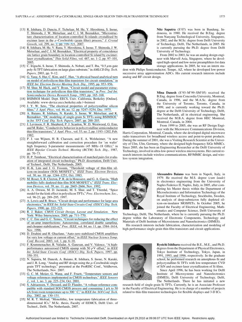
Simulated and measured results for the amplifier, based onthe SG-TFT BSIM-SOI transistor model and electromagneticsimulation for on-chip inductors, are listed in Table V. Fig. 19shows the amplifier -parameters for both simulated and mea-sured data, which are comparable, thus validating the BSIMSOItransistor model. The 433 MHz ISM amplifier achieves usefulRF gain of more than 10 dB, good isolation (lower than 25 dB),and an input third order intercept point (IIP3) of 10 dBm. Suchan amplifier could also be used in the IF stage of a transmitteror receiver operating at a higher RF front-end frequency. An
Fig. 19. Measured �� �� � �� � �� � �� and simulated �-parameters�� �� � �� � �� � �� for the SG-TFT RF amplifier.
TABLE VSG-TFT RF AMPLIFIER RESULT SUMMARY
off-chip inductor, , of 170 nH with a of 40, in series withthe gate is needed for input matching of the 433 MHz ISMband cascode amplifier. The TFT technology permits such aninductor to be built and integrated together with the active de-vices if an insulating substrate is used. At the drain, an externalseries capacitor of 3.5 pF is required to resonate with the loadinductor at 430 MHz to provide the output matching. In fu-ture work, small-signal noise of the SG-TFT will be character-ized and noise parameters defined for simulation and design oflow-noise RF amplifiers using the modified BSIM-SOI model.
Authorized licensed use limited to: Technische Universiteit Delft. Downloaded on April 29,2010 at 09:06:07 UTC from IEEE Xplore. Restrictions apply.
1574 IEEE JOURNAL OF SOLID-STATE CIRCUITS, VOL. 43, NO. 7, JULY 2008
VII. APPLICATIONS
One of the applications originally proposed for -Czochralskifabricated SG-TFTs is e-paper, where electronic display andsignal processing elements are embedded onto a paper-like flex-ible substrate. Since TFT technology is often associated with flatpanel displays, any existing fast-response flat panel (or futuredisplay technology) could incorporate SG-TFTs for improvedperformance. Displays fabricated on a flexible or “rollable” sub-strate material could also incorporate this technology for pixelswitching, pixel addressing, signal processing, and communi-cation electronics (both analog and digital). Other applications,such as wearable sensors, where a thin-film silicon sensor is in-tegrated together with interface electronics (e.g., A/D or D/Aconverters), RF communication circuitry, and a silicon solarcell as a power source may also be enabled by SG-TFT tech-nology. The current benchmark circuit result shows that low res-olution converters can be built. RF front-end for below 1 GHzrange is the application that currently reachable based on thisassessment. This technology is currently able to build low-costlow-performance wireless sensor systems.
The pixellated nature of the Si grains makes them suitable forimplementation of image sensors on a flexible substrate. Thepin photodiode implemented in this technology may make suchapplications possible. By adding the wireless communicationsfunctionality, short range low data rate applications for two-waycommunication, such as for smart cards and health monitoringfor wearable biomedical implants or body area sensor networkscan be realized. Moreover, by integrating the antenna andother passive elements directly with the RF integrated circuitswithout extra losses due to impedance matching and high sub-strate losses, a complete compact wireless SoC can be offered.
SG-TFT technology using -Czochralski process couldenable vertical stacking of integrated circuits or 3-D ICs, forgreater integration density. The increasing delay caused bythe parasitic capacitance of on-chip interconnects and theirresistance seen in 2-D SoCs could be solved by verticallystacking devices using SG-TFT technology. Feasibility ofstacking SG-TFTs on successive silicon layers was recentlydemonstrated for a 3-D CMOS inverter [35].
VIII. CONCLUSION
Analog and RF circuit demonstrators using the SG-TFTtechnology were presented, which validated the performanceof SG-TFTs in some key benchmarking circuits and verifieda design flow from process to modeling and circuit design forthis new technology. This included many analog/RF deviceoptions (e.g., linear resistor, inductors and pin diodes). With aminimum gate length of 1.5 m for the DIMES technology,transit frequencies in the range of 5–6 GHz for the SG-TFTswere obtained. A modified BSIM-SOI model was developed forcircuit simulation, which was employed to design and realizeopamps with more than 50 dB DC gain and a voltage referencewith 50 dB PSRR successfully. RF amplifiers that can realizewell over 10 dB gain below 1 GHz have also been implementedand demonstrated using the SG-TFT technology with integratedback-end metal spiral inductors. The results demonstrated inthis work are a promising first step towards realization of 2-D,
and possibly 3-D ICs, that can enable electronics fabricatedon low-cost substrate materials, where digital, analog and RFcircuits could be integrated together with other technologies(e.g., flat-panel displays or imagers).
ACKNOWLEDGMENT
This work was made possible by the dedication and hard workof many process engineers in the DIMES facility, and enabledby the cleanrooms and measurement facilities at the DIMES re-search institute. The authors gratefully acknowledge the tech-nical support provided by Seiko-Epson and thank T. Shimoda,Y. Hiroshima, and D. Abe for many interesting and fruitful dis-cussions. The authors would like to express special thanks toS. van Herp, J. Slabbekoorn, P. Swart, and B. Goudena for theirtechnical assistance and support.
REFERENCES
[1] V. Subramanian and K. C. Saraswat, “High-performance germa-nium-seeded laterally crystallized TFT’s for vertical device integra-tion,” IEEE Trans. Electron Devices, vol. 45, no. 9, pp. 1934–1939,Sep. 1998.
[2] Y. Matsueda, T. Ozawa, M. Kimura, T. Itoh, K. Kitawada, T.Nakazawa, and H. Ohsima, “A 6-bit-color VGA low-temperaturepoly-Si TFT-LCD with integrated digital data drivers,” in SID Symp.Dig. Tech. Papers, 1998, vol. 29, pp. 879–882.
[3] V. Rana, R. Ishihara, Y. Hiroshima, D. Abe, S. Inoue, T. Shimoda, J.W. Metselaar, and C. I. M. Beenakker, “High performance P-channelsingle-crystalline Si TFTs fabricated inside a location-controlled grainby �-Czochralski process,” IEICE Trans. Electron., vol. E87-C, pp.1943–1946, Nov. 2004.
[4] P. C. van der Wilt, B. D. van Dijk, G. J. Bertens, R. Ishihara, and C.I. M. Beenakker, “Formation of location-controlled crystalline islandsusing substrate-embedded-seeds in excimer-laser crystallization of sil-icon films,” Appl. Phys. Lett., vol. 72, no. 12, pp. 1819–1822, Sep. 2001.
[5] V. Rana, R. Ishihara, Y. Hiroshima, D. Abe, S. Inoue, T. Shimoda, J. W.Metselaar, and C. I. M. Beenakker, “Dependence of single-crystallineSi thin-film transistor characteristics on the channel position inside alocation-controlled grain,” IEEE Trans. Electron Devices, vol. 52, no.12, pp. 2622–2628, Dec. 2005.
[6] W. Fang, A. van Genderen, R. Ishihara, R. Vikas, N. Karaki, Y.Hiroshima, S. Inoue, T. Shimoda, J. W. Metselaar, and C. I. M.Beenakker, “Automated digital circuits design based on single-grainSi TFTs fabricated through the �-Czochralski (grain filter) process,”in AM-FPD Dig. Tech. Papers, 2006, pp. 47–50.
[7] N. Saputra, M. Danesh, A. Baiano, R. Ishihara, J. R. Long, J. W. Met-selaar, C. I. M. Beenakker, N. Karaki, Y. Hiroshima, and S. Inoue,“Single-grain Si thin-film transistors for analog and RF circuits,” inProc. ESSDERC, 2007, pp. 107–110.
[8] J. L. Botrel, O. Savry, O. Rozeau, F. Templier, and J. Jomaah, “Polysil-icon high frequency devices for large area electronics: Characteriza-tion, simulation and modeling,” Thin Solid Films, vol. 515, no. 19, pp.7422–7427, 2007.
[9] J.-H. Ahn, H.-S. Kim, K. J. Lee, Z. Zhu, E. Menard, R. G. Nuzzo, andJ. A. Rogers, “High-speed mechanically flexible single-crystal siliconthin-film transistors on plastic substrates,” IEEE Electron Device Lett.,vol. 27, no. 6, pp. 460–462, Jun. 2006.
[10] M. He, R. Ishihara, J. W. Metselaar, and C. I. M. Beenakker,“�����-textured self-assembled square-shaped polycrystalline silicongrains by multiply shots excimer-laser crystallization,” J. Appl. Phys.,vol. 100, pp. 1–5, 2006.
[11] M. He, R. Ishihara, E. J. J. Neihof, Y. van Andel, H. Schellevis, J. W.Metselaar, and K. Beenakker, “Large polycrystalline silicon grains pre-pared by excimer-laser crystallization of sputtered amorphous siliconfilm with process temperature at 100 C,” Jpn. J. Appl. Phys., vol. 46,no. 3B, pp. 1245–1249, 2007.
[12] Y. Hiroshima, C. Iriguchi, R. Ishihara, S. Inoue, T. Shimoda, J. W.Metselaar, and C. I. M. Beenakker, “Single-grain Si TFTs fabricatedby the �-Czochralski process on a large glass substrate,” in Tech. Dig.2004 Int. Workshop on Active-Matrix Liquid-Crystal Displays, Tokyo,Japan, Jul. 2004, pp. 307–308.
Authorized licensed use limited to: Technische Universiteit Delft. Downloaded on April 29,2010 at 09:06:07 UTC from IEEE Xplore. Restrictions apply.
SAPUTRA et al.: ASSESSMENT OF µ-CZOCHRALSKI, SINGLE-GRAIN SILICON THIN-FILM TRANSISTOR TECHNOLOGY 1575
[13] R. Ishihara, D. Danciu, F. Tichelaar, M. He, Y. Hiroshima, S. Inoue,T. Shimoda, J. W. Metselaar, and C. I. M. Beenakker, “Microstruc-ture characterisation of location-controlled Si-islands crystallised byexcimer laser in the �-Czochralski (grain filter) process,” J. CrystalGrowth, vol. 299, no. 2, pp. 316–321, 2007.
[14] R. Ishihara, M. He, V. Rana, Y. Hiroshima, S. Inoue, T. Shimoda, J. W.Metselaar, and C. I. M. Beenakker, “Electrical property of coincidencesite lattice grain boundary in location-controlled Si island by excimer-laser crystallization,” Thin Solid Films, vol. 487, no. 1–2, pp. 97–101,2005.
[15] C. Iriguchi, S. Inoue, T. Shimoda, A. Nobari, and T. Iba, “0.5 �m-gatepoly-Si TFT fabrication on large glass substrate,” in AMLCD Dig. Tech.Papers, 2003, pp. 9–12.
[16] G. Yang, S. Hur, C. Kim, and C. Han, “A physical based analytical turnon model of polysilicon thin-film transistors for circuit simulation,” inIEEE Int. Electron Device Meeting Tech. Dig., 1995, pp. 953–956.
[17] M. Shur, M. Hack, and Y. Byun, “Circuit model and parameter extrac-tion technique for polysilicon thin-film transistors,” in Proc. 2nd Int.Semiconductor Device Research Symp., 1993, pp. 165–168.
[18] BSIMSOI Model. Dept. EECS, Univ. California, Berkeley [Online].Available: www-device.eecs.berkeley.edu /~bsimsoi
[19] J. Y. W. Seto, “The electrical properties of polycrystalline siliconfilms,” J. Appl. Phys., vol. 46, no. 12, pp. 5247–5254, Dec. 1975.
[20] A. Baiano, R. Ishihara, N. Karaki, S. Inoue, W. Metselaar, and K.Beenakker, “DC modeling of single-grain Si TFTs using BSIMSOI,”in Int. TFT Conf. Dig. Tech. Papers, 2007, pp. 200–203.
[21] J. Levinson, F. R. Shepherd, P. J. Scanlon, W. D. Westwood, G. Este,and M. Rider, “Conductivity behavior in polycrystalline semiconductorthin film transistors,” J. Appl. Phys., vol. 53, no. 2, pp. 1193–1202, Feb.1982.
[22] P. J. van Wijnen, H. R. Claessen, and E. A. Wolsheimer, “A newstraightforward calibration and correction procedure for ’on wafer’high frequency S-parameter measurements (45 MHz–18 GHz),” inIEEE Bipolar Circuits Technol. Meeting (BCTM) Tech. Dig., 1987,pp. 70–73.
[23] H. P. Tuinhout, “Electrical characterisation of matched pairs for evalu-ation of integrated circuit technology,” Ph.D. dissertation, Delft Univ.of Technol., Delft, The Netherlands, 2005.
[24] H.-K. Lim and J. G. Fossum, “Threshold voltage of thin-film sil-icon-on-insulator (SOI) MOSFET’s,” IEEE Trans. Electron Devices,vol. 30, no. 10, pp. 1244–1251, Oct. 1983.
[25] M. Roser, S. R. Clayton, P. R. de la Houssaye, and G. A. Garcia, “Highmobility fully depleted thin-film SOS MOSFET’s,” IEEE Trans. Elec-tron Devices, vol. 39, no. 11, pp. 2665–2666, Nov. 1992.
[26] A. A. Owusu, M. D. Jacunski, M. S. Shur, and T. Ytterdal, “Spicemodel for the kink effect in polysilicon TFTs,” Proc. Electrochem. Soc.,vol. 96-23, pp. 289–295, 1997.
[27] A. Lewis and R. Bruce, “Circuit design and performance for large areaelectronics,” in IEEE Int. Solid-State Circuits Conf. (ISSCC) Dig. Tech.Papers, 1990, pp. 222–223.
[28] R. J. Baker, CMOS Circuit Design, Layout and Simulation. NewYork: Wiley Interscience, 2005, pp. 711–770.
[29] C. C. Enz and G. C. Temes, “Circuit techniques for reducing the effectof op-amp imperfections: Autozeroing, correlated double sampling,and chopper stabilization,” Proc. IEEE, vol. 84, no. 11, pp. 1584–1614,Nov. 1996.
[30] D. Dzahini and H. Ghazlane, “Auto-zero stabilized CMOS amplifiersfor very low voltage or current offset,” in IEEE Nuclear Science Symp.Conf. Record, 2003, vol. 1, pp. 6–10.
[31] F. Krummenacher, R. Vafadar, A. Ganesan, and V. Valence, “A high-performance autozeroed CMOS opamp with 50 �V offset,” in IEEEInt. Solid-State Circuits Conf. (ISSCC) Dig. Tech. Papers, 1997, pp.350–351.
[32] N. Saputra, M. Danesh, A. Baiano, R. Ishihara, S. Inoue, N. Karaki,and J. R. Long, “Analog and RF design using the �-Czochralski singlegrain TFT technology,” presented at the ProRISC Conf., Veldhoven,The Netherlands, Nov. 2007.
[33] G. C. M. Meijer, G. Wang, and F. Fruett, “Temperature sensors andvoltage references implemented in CMOS technology,” IEEE SensorsJ., vol. 1, no. 3, pp. 225–234, Oct. 2001.
[34] S. Adriaensen, V. Dessard, and D. Flandre, “A voltage reference com-patible with standard SOI CMOS process and consuming 1 pA to 50nA from room temperature up to 300 C,” in IEEE Int. SOI Conf. Tech.Dig., 2002, pp. 130–131.
[35] M. R. T. Mofrad, “Monolithic, low temperature fabrication of three-dimensional ICs,” M.Sc. thesis, Faculty of EEMCS, Delft Univ. ofTechnol., Delft, The Netherlands, 2007.
Nitz Saputra (S’07) was born in Bandung, In-donesia, in 1980. He received the B.Eng. degreefrom Nanyang Technological University, Singapore,in 2002, and the M.Sc. degree from Delft Universityof Technology, Delft, The Netherlands, in 2005. Heis currently pursuing the Ph.D. degree from DelftUniversity of Technology.
From 2002 to 2003, he was an analog design engi-neer with Marvell Asia, Singapore, where he devel-oped high-speed and low-noise preamplifiers for datastorage applications. In 2005, he was an intern stu-
dent with Philips Semiconductor, Tempe, AZ, where he developed low-powersuccessive array approximation ADCs. His current research interests includeanalog and RF circuit design.
Mina Danesh (S’93–M’99–SM’05) received theB.Eng. degree from Concordia University, Montreal,Canada, in 1996, and the M.A.Sc. degree fromthe University of Toronto, Toronto, Canada, in1999, and is currently working toward the Ph.D.degree at the Delft University of Technology, Delft,The Netherlands, all in electrical engineering. Shereceived the M.B.A. degree from HEC Montreal,Montreal, Canada, in 2004.
From 1999 to 2005, she was an RF Design Engi-neer with the Microwave Communications Division,
Harris Corporation, Montreal, Canada, where she developed digital microwaveradio transceivers for broadband wireless access and point-to-point products.During the summer of 2001, she was a Visiting Research Scientist at the Univer-sity of Ulm, Ulm, Germany, where she designed high-frequency SiGe MMICs.Since 2005, she has been an Engineering Researcher at the Delft University ofTechnology, involved in ultra-low-power wireless microsystems. Her current re-search interests include wireless communications, RF/MMIC design, and wire-less system integration.
Alessandro Baiano was born in Napoli, Italy, in1979. He received the M.S. degree (cum laude)in electronics engineering from the University ofNaples Federico II, Naples, Italy, in 2005, after com-pleting his Master thesis within the Department ofMicroelectronics and Information Technology of theRoyal Institute of Technology, Stockholm, Sweden,on analysis of deep-submicron fully depleted sil-icon-on-insulator MOSFETs. In October 2005, hejoined the Faculty of Electrical Engineering, Math-ematics and Computer Science, Delft University of
Technology, Delft, The Netherlands, where he is currently pursuing the Ph.D.degree within the Laboratory of Electronic Components, Technology andMaterials of Delft Institute of Microsistems and Nanoelectronics (DIMES).
His research interests include fabrication, characterization and modeling ofhigh-performance single-grain thin-film transistors and circuit applications.
Ryoichi Ishihara received the B.E., M.E., and Ph.D.degrees from the Department of Physical Electronics,Tokyo Institute of Technology, Tokyo, Japan, in1991, 1993, and 1996, respectively. In the graduateschool, he performed research on amorphous-Si andpolycrystalline-Si TFTs with low-temperature CVDof SiN and excimer-laser crystallization of Si films.
Since April 1996, he has been working for DelftInstitute of Microsystems and Nanoelectronics(DIMES), Delft University of Technology, Delft,The Netherlands. There he has initiated a new
research field of single-grain Si TFTs. Currently, he is an Associate Professorin the Faculty of Electrical Engineering. He is in charge of a number of projectsrelated to thin-film transistor technologies for flexible displays and 3-D ICs.
Authorized licensed use limited to: Technische Universiteit Delft. Downloaded on April 29,2010 at 09:06:07 UTC from IEEE Xplore. Restrictions apply.
1576 IEEE JOURNAL OF SOLID-STATE CIRCUITS, VOL. 43, NO. 7, JULY 2008
John R. Long (M’83) received the B.Sc. degreein electrical engineering from the University ofCalgary, Canada, in 1984, and the M.Eng. and Ph.D.degrees in electronics from Carleton University,Ottawa, Canada, in 1992 and 1996, respectively.
He was employed for 10 years by Bell-NorthernResearch, Ottawa (now Nortel Networks R&D), in-volved in the design of ASICs for Gb/s fiber-optictransmission systems, and from 1996 to 2001 as anAssistant, and then Associate Professor, at the Uni-versity of Toronto, Toronto, Canada. Since January
2002, he has been Chair of the Electronics Research Laboratory at the Delft Uni-versity of Technology, Delft, The Netherlands. His current research interests in-clude low-power and broadband transceiver circuitry for highly-integrated wire-less applications, energy-efficient wireless sensors, mm-wave integrated elec-tronics, and electronics design for high-speed data communications systems.
Prof. Long currently chairs the RF circuits subcommittee for the 2008 IEEEInternational Solid-State Circuits Conference (ISSCC), and is a member ofthe technical program committees for the European Solid-State Circuits (ESS-CIRC) and ICUWB conferences. He is a Distinguished Lecturer for the IEEESolid-State Circuits Society, and Co-Chair of the 2008 European MicrowaveIC(EuMIC) in Amsterdam. He is also a former Associate Editor of the IEEEJOURNAL OF SOLID-STATE CIRCUITS and Past General Chair of the IEEEBipolar/BiCMOS Circuits and Technology Meeting (BCTM). He received theNSERC Doctoral Prize, Douglas R. Colton and Governor General’s Medalsfor research excellence, and Best Paper Awards from ISSCC in 2000 and 2007,IEEE BCTM 2003, the 2006 RFIC Symposium, and EuMW 2006.
Nobuo Karaki (M’97) received the Ph.D. degreein electrical engineering and computer science fromKyushu University, Japan.
He is currently a researcher at Frontier DeviceResearch Center, Seiko Epson Corporation, Nagano,Japan. From 1998, he spent 10 years for researchingon an ASIC-style asynchronous circuit designtechnique dedicated to flexible microelectronicsfeaturing low-temperature-processed polysiliconthin-film transistor (LTPS TFT) technology and asurface-free fabrication technique, SUFTLA. He
is now researching an asynchronous circuit design technique for enablingultra-low-power VLSIs based on the deep-submicron process technologies,and 3-D fabrication technologies.
Dr. Karaki is a member of the IEEE Solid-State Circuit Society, ACM, andIEICE.
Satoshi Inoue (M’00–SM’07) received the B.S.degree in applied physics from Nagoya University,Japan, in 1982. He received the Ph.D. degree inelectrical and electric engineering from TokyoUniversity of Agriculture and Technology, Tokyo,Japan, in 2002.
He joined Toshiba Corporation in 1982, andworked on the research of EEPROMs, DRAMs,and ULSI technology at ULSI Research Center. Hejoined Seiko Epson Corporation, Nagano, Japan, in1990, and has been working on the research of TFTs
and displays using TFTs at Frontier Device Research Center.Dr. Inoue is a member of the SID, Japan Society of Applied Physics, and the
IEEE Electron Devices Society.
Authorized licensed use limited to: Technische Universiteit Delft. Downloaded on April 29,2010 at 09:06:07 UTC from IEEE Xplore. Restrictions apply.
Top Related
Copyright © 2022 FDOKUMEN

