


Bahasa
Halaman
Hukum


1
Advanced Digital Design with the Verilog HDL
Michael D. Ciletti [email protected]
Copyright 2003, 2004, 2005 M.D. Ciletti
Selected Solutions
Updated: 10/31/2005 Solutions to the following problems are available to faculty at academic institutions using Advanced Digital Design with the Verilog HDL. This list will be updated as additional solutions are developed. Request the solutions by contacting the author directly ([email protected]). Chapter 2: #1, 2, 3, 4, 5, 8, 9, 10, 12 Chapter 3: #1, 2, 4, 5, 6, 7, 9, 10, 11 Chapter 4: #1, 2, 4, 7, 10, 11, 12, 14, 15, 16 Chapter 5: #1, 2, 3, 4, 6, 7, 8, 9, 10, 11, 13, 16, 17, 18, 19, 20, 23, 24, 26, 27, 28, 29, 30, 32, 33 Chapter 6: #4, #7, 8, 21 Chapter 7: #12 Chapter 9: #12, #18, #19
Copyright 2004, 2005 Note to the instructor: These solutions are provided solely for classroom use in academic institutions by the instructor using the text, Advance Digital Design with the Verilog HDL by Michael Ciletti, published by Prentice Hall. This material may not be used in off-campus instruction, resold, reproduced or generally distributed in the original or modified format for any purpose without the permission of the Author. This material may not be placed on any server or network, and is protected under all copyright laws, as they currently exist. I am providing these solutions to you subject to your agreeing that you will not provide them to your students in hardcopy or electronic format or use them for off-campus instruction of any kind. Please email to me your agreement to these conditions.
I will greatly appreciate your assisting me by calling to my attention any errors or any other revisions that would enhance the utility of these slides for classroom use.
rev 10/10/2005

2
Advanced Digital Design with the Verilog Hardware Description Language Michael D. Ciletti Prentice-Hall, Pearson Education, 2003 Problem 2-1 F(a, b, c) = Σ m(1, 3, 5, 7) Canonical SOP form: F(a,b,c) = a'b'c + a'bc + ab'c + abc Also: K-map for F:
0
1
00 01 11 10
0a
bc
1 1 0
0 1 01m0 m1 m3 m2
m4 m5 m7 m6 F' = m0 + m2 + m4 + m6 F' = a'b'c' + a'bc' + a'bc + abc F = (a'b'c' + a'bc' + a'bc + abc)' F = (a'b'c')' (a'bc')' (a'bc)' (abc)' Canonical POS form: F = (a + b + c)(a + b' +c) (a + b' + c') (a' + b' +c')

3
Advanced Digital Design with the Verilog Hardware Description Language Michael D. Ciletti Prentice-Hall, Pearson Education, 2003 Problem 2-2 F(a, b, c, d) = Π M(0, 1, 2, 3, 4, 5, 12) F(a, b, c, d) = (a’+ b’ + c’ + d’)(a’ + b’ + c’ + d)(a’ + b’ + c + d’)(a’ + b’ + c + d)(a’ + b + c’ + d’)(a’ + b + c’ + d)(a + b + c’ + d’)

4
Advanced Digital Design with the Verilog Hardware Description Language Michael D. Ciletti Prentice-Hall, Pearson Education, 2003 Problem 2-3 F(a, b, c) = a'b + c
0
1
00 01 11 10
0a
bc
1 1 1
0 1 01m0 m1 m3 m2
m4 m5 m7 m6 F(a, b, c) = m1 + m2 + m3 + m5 + m7 F(a, b, c) = a'b'c + a'bc' + a'bc + ab'c + abc

5
Advanced Digital Design with the Verilog Hardware Description Language Michael D. Ciletti Prentice-Hall, Pearson Education, 2003 Problem 2-4 F(a, b, c, d) = a'bcd' + a'bcd + a'b'c'd' + a'b'c'd = m6 + m7 + m0 + m1 F(a, b, c, d) = Σ m(0, 1, 6, 7)

6
Advanced Digital Design with the Verilog Hardware Description Language Michael D. Ciletti Prentice-Hall, Pearson Education, 2003 Problem 2-5 G(a, b, c, d) = (a'bcd' + a'bcd + a'b'c'd' + a'b'c'd)' G'(a, b, c, d) = a'bcd' + a'bcd + a'b'c'd' + a'b'c'd K-map for G':
00
10
11
01
00 01 11 10
1ab
cd
1 0 0
0 1 1
0 0 0 0
0 0 0 0
0m0 m1 m3 m2
m4 m5 m7 m6
m12 m13 m15 m14
m8 m9 m11 m10 G(a, b, c) = Σ m(2, 3, 4, 5, 8, 9, 10 , 11, 12, 13, 14, 15)

7
Advanced Digital Design with the Verilog Hardware Description Language Michael D. Ciletti Prentice-Hall, Pearson Education, 2003 Problem 2-8 (a) (ab’ + a’b)’ = a’b’ + ab (b) (b + (cd’ + e)a’)’ = b’(c’ + d) e’ + a (c) ((a’ + b + c)(b’ + c’)(a + c))’ = ab’c’ + bc + a’c’

8
Advanced Digital Design with the Verilog Hardware Description Language Michael D. Ciletti Prentice-Hall, Pearson Education, 2003 Problem 2-9 (a) F = a + a’b = a + b (b) F = a(a’ + b) = ab (c) F = ac + bc’ + ab = ac + bc’

9
Advanced Digital Design with the Verilog Hardware Description Language Michael D. Ciletti Prentice-Hall, Pearson Education, 2003 Problem 2-10a F(a, b, c) = Σ m(0, 2, 4, 5, 6)
0
1
00 01 11 10
1a
bc
0 0 1
1 0 11m0 m1 m3 m2
m4 m5 m7 m6 F(a, b, c) = Σ m(0, 2, 4, 5, 6) = ab' + c'

10
Advanced Digital Design with the Verilog Hardware Description Language Michael D. Ciletti Prentice-Hall, Pearson Education, 2003 Problem 2-10b F(a, b, c) = Σ m(2, 3, 4, 5)
0
1
00 01 11 10
0a
bc
0 1 1
1 0 01m0 m1 m3 m2
m4 m5 m7 m6 F(a, b, c) = Σ m(2, 3, 4, 5) = ab' + a'b = a ⊕ b

11
Advanced Digital Design with the Verilog Hardware Description Language Michael D. Ciletti Prentice-Hall, Pearson Education, 2003 Problem 2-10e (e) F = a’b’c’ + b’cd’ + a’bcd’ + ab’c’
00
10
11
01
00 01 11 10abcd
1 1
1
1 1 1
m0 m1 m3 m2
m4 m5 m7 m6
m12 m13 m15 m14
m8 m9 m11 m10
1
F = b’c’ + b’d’ + a’cd’

12
Advanced Digital Design with the Verilog Hardware Description Language Michael D. Ciletti Prentice-Hall, Pearson Education, 2003 Problem 2-12 Karnaugh Map for f = Σ m(0, 4, 6, 8, 9, 11, 12, 14, 15)
00
10
11
01
00 01 11 10
1ab
cd
0 0 0
1 0 1
1 0 1 1
1 1 1 0
0m0 m1 m3 m2
m4 m5 m7 m6
m12 m13 m15 m14
m8 m9 m11 m10
bd'
acdab'd
c'd'
ab'c'abc
1. Prime implicants are implicants that do not imply any other implicant Answer: c'd', ab'c', ab'd, acd, abc, bd'
2. Essential prime implicants are prime implicants that cannot be covered by a set of other implicants:
Answer: c'd', bd'
3. A minimal expression consists of the set of essential prime implicants together with other implicants that cover the function:
Answer: f = c'd' + bd' + ab'd + abc f = c'd' + bd' + ab'd + acd f = c'd' + bd' + ab'c' +acd

13
Advanced Digital Design with the Verilog Hardware Description Language Michael D. Ciletti Prentice-Hall, Pearson Education, 2003 Problem 3 – 1
00
s00
00
00
00
s10
s20
s30
s41
Problem 3.1, mdc 9/9/2004
01, 10
01, 10
01, 10
01, 10
11
11
1111
11
01, 10
00
s0 / 0
s1 / 0
AB
s2 / 0
01, 10
reset
State transition graph - Moore Machine
00
01, 10
AB
s3 / 0
01, 10
AB
s4 / 1
01, 10
AB00
00
00
11
AB00
11
11
11
01, 10
ASM Chart - Moore Machine
11

14
Problem 3 - 2 Advanced Digital Design with the Verilog Hardware Description Language Michael D. Ciletti Prentice-Hall, Pearson Education, 2003 9/26/ 2006
Par_DetectParityBit_in
clk rst
Assumption: asynchronous resetBit_in clocked on rising edge.Interpretation: Even parity will beasserted unless an odd number of1s have been received.rst
001
1
s01
s10
Q
QSET
CLR
DBit_in
clock
rst
parity

15
Problem 3 - 4 Advanced Digital Design with the Verilog Hardware Description Language Michael D. Ciletti Prentice-Hall, Pearson Education, 2003 9/24/ 2003
s1
1/1State transition graph - Mealy Machine
0 1/0
0/0
s0 s21/0
0/0
s3
0/0
reset
1/0
s1
1/1
0 1/0
0/0
s0 s21/0
0/0
reset
Note: s2 and s3 areequivalent states.
State transition graph - Equivalent Mealy Machine
Problem 3 – 5
1State transition graph - Moore Machine
1
0
1
0
0
reset
1s00
s10
s20
s31
0

16
Advanced Digital Design with the Verilog Hardware Description Language Michael D. Ciletti Prentice-Hall, Pearson Education, 2003 9/26/ 2005 Problem 3 - 6 No static-0 or static-1 hazards.

17
Advanced Digital Design with the Verilog Hardware Description Language Michael D. Ciletti Prentice-Hall, Pearson Education, 2003 9/24/ 2003 Problem 3 - 7
reset
B_in = 0
B_in = 0
B_in = 1
S_00
0
S_10
0
S_11
0B_in = 1 S_21
0B_in = 1 S_31
1
B_in = 0
B_in = 0
B_in = 1
B_in = 1
B_in = 0 Advanced Digital Design with the Verilog Hardware Description Language Michael D. Ciletti Prentice-Hall, Pearson Education, 2003 9/13/ 2004

18
Advanced Digital Design with the Verilog Hardware Description Language Michael D. Ciletti Prentice-Hall, Pearson Education, 2003 9/26/ 2005 Problem 3 - 8
Pattern_DetectDetectBit_in
clk rst
Approach: linked state machines, with the sequence detector asserting a signal thatincrements a counter. To avoid race conditions, the counter is clocked on theopposite edge of the clock that drives the sequence detecter.
Assumption: asynchronous reset. Bit_in clocked on rising edge.LSB (1) of 0111 arrives first. Transitions for reset condition are omitted for simplicity.
rst 1 0s00
s10
s20
s30
s41
1 1
01
Counter_of_6Done
clk_bar rst
Detect00
0
1Bit_in
rst 1s00
s10
1
0
Done
Detect
0
s20
1
0
s30
1
0
s40
1
0
s50
1
0
s61

19
Assumption: asynchronous reset. Bit_in clocked on rising edge.MSB (0) of 0111 arrives first. Transitions for reset condition are omitted for simplicity.
rst 0 1s00
s10
s20
s30
s41
1 1
1
Detect00 0
0Bit_in
rst 1s00
s10
1
0
Done
Detect
0
s20
1
0
s30
1
0
s40
1
0
s50
1
0
s61
0

20
Advanced Digital Design with the Verilog Hardware Description Language Michael D. Ciletti Prentice-Hall, Pearson Education, 2003 Problem 3 - 9
s00
s11 0
State transition graph - NRZ - NRZI Moore Machine
0
1
1 Sample at the midpoint of the bit time. module NRZ_NRZI (B_out, B_in, clk, rst); // problem 3.9 output B_out; input B_in; input clk, rst; parameter s0 = 0; parameter s1 = 1; reg state, next_state; reg B_out; always @ (negedge clk or posedge rst) if (rst == 1) state <= s0; else state <= next_state; always @ (state or B_in) begin next_state = state; B_out = 0; case(state) s0: if (B_in == 1) begin next_state = s1; B_out = 0; end s1: if (B_in == 1) begin next_state = s0; B_out = 1; end endcase end endmodule module t_NRZ_NRZI (); // problem 3.9 wire B_out; reg B_in; reg clk, rst; reg clk_NRZ; NRZ_NRZI M1 (B_out, B_in, clk, rst); initial #400 $finish; initial begin rst = 0; #10 rst = 1; #20 rst = 0;

21
#147 rst = 1; // reset on-the-fly #5 rst = 0; end initial begin clk = 1; forever #5 clk = ~clk; end initial begin clk_NRZ = 1; forever #10 clk_NRZ = ~clk_NRZ; end initial begin // Data waveform B_in = 1; #40 B_in = 0; #40 B_in = 1; #40 B_in = 0; #40 B_in = 1; #100 B_in = 0; #100 B_in = 1; end endmodule

22
Advanced Digital Design with the Verilog Hardware Description Language Michael D. Ciletti Prentice-Hall, Pearson Education, 2003 9/26/2005 Problem 3 – 10 NRZI Line encoder
1 11 1
NRZI_EncoderNRZIBit_in
clk rst
rst
001
1
s01
s10
Q
QSET
CLR
DBit_in
clock
rst
NRZI
Moore machine assumptions: Data is sampled in the middle of the bit time.NRZI Moore machine output is formed with ½ cycle of latency.
Startingfrom 0
Startingfrom 1
NRZI
NRZI
Bit_in
t
t
t
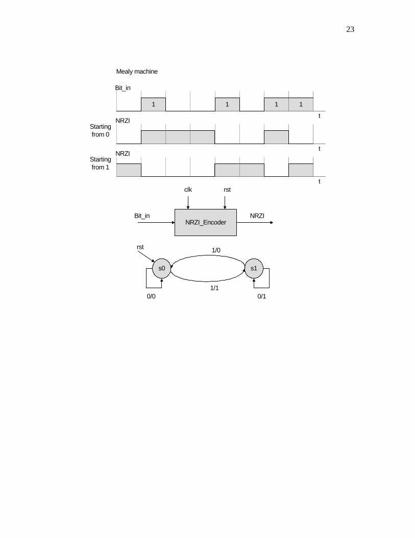
23
1 11 1
NRZI_EncoderNRZIBit_in
clk rst
Mealy machine
Startingfrom 0
Startingfrom 1
NRZI
NRZI
Bit_in
t
t
t
s0
rst
0/01/1
1/0
s1
0/1

24
Advanced Digital Design with the Verilog Hardware Description Language Michael D. Ciletti Prentice-Hall, Pearson Education, 2003 9/24/2003 Problem 4-1 module Combo_str (Y, A, B, C, D); output Y; input A, B, C, D; and (Y, w1, w3); not (w1, w2); or (w2, A, D); and (w3, B, C, w4); not (w4, D); endmodule module t_Combo_str (); reg A, B, C, D; wire Y; Combo_str M0 (Y, A, B, C, D); initial begin #5 {A, B, C, D} = 4'b0000; #5 {A, B, C, D} = 4'b0001; #5 {A, B, C, D} = 4'b0010; #5 {A, B, C, D} = 4'b0011; #5 {A, B, C, D} = 4'b0100; #5 {A, B, C, D} = 4'b0101; #5 {A, B, C, D} = 4'b0110; #5 {A, B, C, D} = 4'b0111; #5 {A, B, C, D} = 4'b1000; #5 {A, B, C, D} = 4'b1001; #5 {A, B, C, D} = 4'b1010; #5 {A, B, C, D} = 4'b1011; #5 {A, B, C, D} = 4'b1100; #5 {A, B, C, D} = 4'b1101; #5 {A, B, C, D} = 4'b1110; #5 {A, B, C, D} = 4'b1111; end initial begin #500 $finish; end //initial begin $monitor ($time,,”%h %b“, {A, B, C, D}, Y); end endmodule

25
Advanced Digital Design with the Verilog Hardware Description Language Michael D. Ciletti Prentice-Hall, Pearson Education, 2003 9/24/2003 Problem 4-2 module Combo_UDP (Y, A, B, C, D); output Y; input A, B, C, D; Combo_prim M0 (Y, A, B, C, D); endmodule module t_Combo_UDP (); reg A, B, C, D; wire Y; Combo_UDP M0 (Y, A, B, C, D); initial begin #5 {A, B, C, D} = 4'b0000; #5 {A, B, C, D} = 4'b0001; #5 {A, B, C, D} = 4'b0010; #5 {A, B, C, D} = 4'b0011; #5 {A, B, C, D} = 4'b0100; #5 {A, B, C, D} = 4'b0101; #5 {A, B, C, D} = 4'b0110; #5 {A, B, C, D} = 4'b0111; #5 {A, B, C, D} = 4'b1000; #5 {A, B, C, D} = 4'b1001; #5 {A, B, C, D} = 4'b1010; #5 {A, B, C, D} = 4'b1011; #5 {A, B, C, D} = 4'b1100; #5 {A, B, C, D} = 4'b1101; #5 {A, B, C, D} = 4'b1110; #5 {A, B, C, D} = 4'b1111; end initial begin #500 $finish; end //initial begin $monitor ($time,,”%h %b“, {A, B, C, D}, Y); end endmodule primitive Combo_prim (Y, A, B, C, D);

26
output Y; input A, B, C, D; table 0000 : 0; 0001 : 0; 0010 : 0; 0011 : 0; 0100 : 0; 0101 : 0; 0110 : 1; 0111 : 0; 1000 : 0; 1001 : 0; 1010 : 0; 1011 : 0; 1100 : 0; 1101 : 0; 1110 : 0; 1111 : 0; endtable endprimitive
T1 T2 Tdelta
Name 0 70 140 210 280DefaultYABCD
27
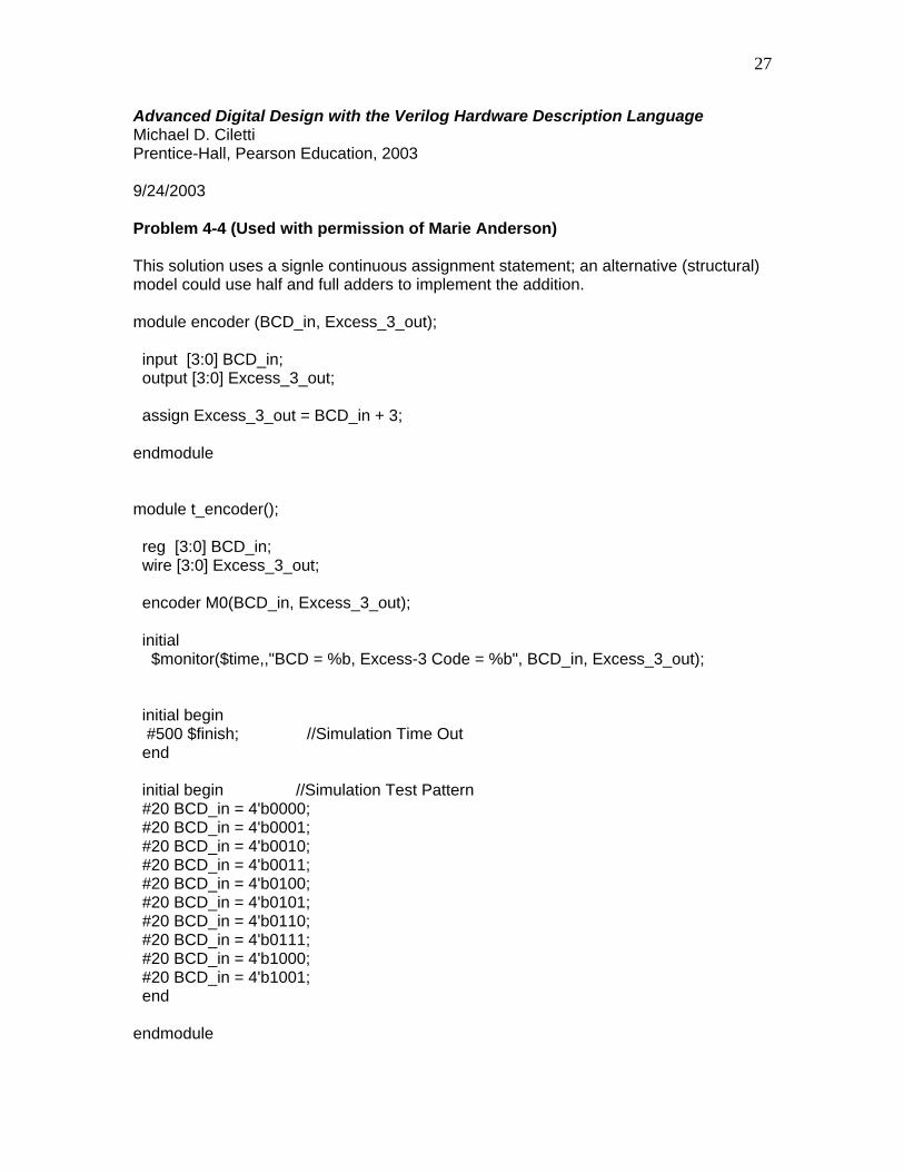
Advanced Digital Design with the Verilog Hardware Description Language Michael D. Ciletti Prentice-Hall, Pearson Education, 2003 9/24/2003 Problem 4-4 (Used with permission of Marie Anderson) This solution uses a signle continuous assignment statement; an alternative (structural) model could use half and full adders to implement the addition. module encoder (BCD_in, Excess_3_out); input [3:0] BCD_in; output [3:0] Excess_3_out; assign Excess_3_out = BCD_in + 3; endmodule module t_encoder(); reg [3:0] BCD_in; wire [3:0] Excess_3_out; encoder M0(BCD_in, Excess_3_out); initial $monitor($time,,"BCD = %b, Excess-3 Code = %b", BCD_in, Excess_3_out); initial begin #500 $finish; //Simulation Time Out end initial begin //Simulation Test Pattern #20 BCD_in = 4'b0000; #20 BCD_in = 4'b0001; #20 BCD_in = 4'b0010; #20 BCD_in = 4'b0011; #20 BCD_in = 4'b0100; #20 BCD_in = 4'b0101; #20 BCD_in = 4'b0110; #20 BCD_in = 4'b0111; #20 BCD_in = 4'b1000; #20 BCD_in = 4'b1001; end endmodule

28
Simulation Output: Reading "encoder.v" Reading "t_encoder.v" sim to 0 Highest level modules (that have been auto-instantiated): t_encoder 3 total devices. Linking ... 9 nets total: 17 saved and 0 monitored. 68 registers total: 68 saved. Done. 0 BCD = xxxx, Excess-3 Code = xxxx 0 State changes on observable nets. Simulation stopped at the end of time 0. Ready: sim 20 BCD = 0000, Excess-3 Code = 0011 40 BCD = 0001, Excess-3 Code = 0100 60 BCD = 0010, Excess-3 Code = 0101 80 BCD = 0011, Excess-3 Code = 0110 100 BCD = 0100, Excess-3 Code = 0111 120 BCD = 0101, Excess-3 Code = 1000 140 BCD = 0110, Excess-3 Code = 1001 160 BCD = 0111, Excess-3 Code = 1010 180 BCD = 1000, Excess-3 Code = 1011 200 BCD = 1001, Excess-3 Code = 1100 62 State changes on observable nets. Simulation stopped at the end of time 500.

29

30
Advanced Digital Design with the Verilog Hardware Description Language Michael D. Ciletti Prentice-Hall, Pearson Education, 2003 9/24/2003 Problem 4-7 module Problem_4_7 (Y1, Y2, A, B, C, D); output Y1, Y2; input A, B, C, D; not (A_not, A); not (B_not, B); not (C_not, C); not (D_not, D); and (w1, A_not, B, C_not, D_not); and (w2, A_not, B, C_not, D); and (w3, A_not, B, C, D_not); and (w4, A_not, B, C, D); and (w5, A, B_not, C, D); and (w6, A, B, C_not, D_not); and (w7, A, B, C_not, D); or (Y1, w1, w2, w3, w4, w5, w6, w7); and (w8, A_not, B_not, C_not, D); and (w9, A_not, B_not, C, D_not); and (w10, A_not, B, C_not, D_not); and (w11, A_not, B, C_not, D); or (Y2, w8, w9, w10, w11); endmodule module t_Problem_4_7(); reg A, B, C, D; wire Y1, Y2; Problem_4_7 M0 (Y1, Y2, A, B, C, D); initial begin #5 {A, B, C, D} = 4'b0000; #5 {A, B, C, D} = 4'b0001; #5 {A, B, C, D} = 4'b0010; #5 {A, B, C, D} = 4'b0011; #5 {A, B, C, D} = 4'b0100; #5 {A, B, C, D} = 4'b0101; #5 {A, B, C, D} = 4'b0110; #5 {A, B, C, D} = 4'b0111;

31
#5 {A, B, C, D} = 4'b1000; #5 {A, B, C, D} = 4'b1001; #5 {A, B, C, D} = 4'b1010; #5 {A, B, C, D} = 4'b1011; #5 {A, B, C, D} = 4'b1100; #5 {A, B, C, D} = 4'b1101; #5 {A, B, C, D} = 4'b1110; #5 {A, B, C, D} = 4'b1111; end initial begin #500 $finish; end //initial begin $monitor ($time,,”%h %b“, {A, B, C, D}, Y); end endmodule
T1 T2 Tdelta
Name 0 60 120 180 240DefaultABCDY1Y2

32
Advanced Digital Design with the Verilog Hardware Description Language Michael D. Ciletti Prentice-Hall, Pearson Education, 2003 10/03/2005 Problem 4-10 module t_latch_rp (); reg enable, data; wire q_out; latch_rp M0 (q_out, enable, data); initial #200 $finish; initial begin data = 0; forever #20 data = ~data; end initial fork #10 enable = 1; #30 enable = 0; // latch a 1 #50 enable = 1; #90 enable= 0; // latch a 0; #130 enable = 1; join endmodule
33
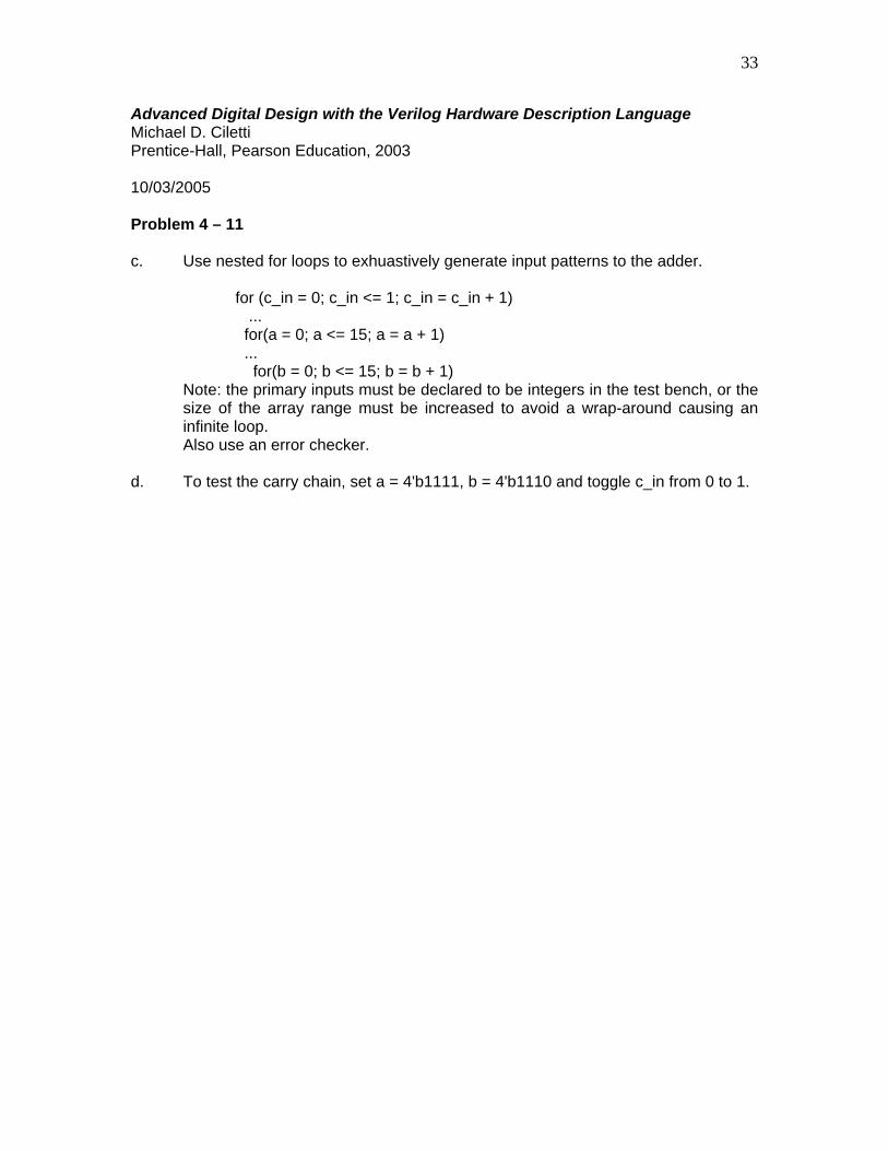
Advanced Digital Design with the Verilog Hardware Description Language Michael D. Ciletti Prentice-Hall, Pearson Education, 2003 10/03/2005 Problem 4 – 11 c. Use nested for loops to exhuastively generate input patterns to the adder.
for (c_in = 0; c_in <= 1; c_in = c_in + 1) ... for(a = 0; a <= 15; a = a + 1) ... for(b = 0; b <= 15; b = b + 1)
Note: the primary inputs must be declared to be integers in the test bench, or the size of the array range must be increased to avoid a wrap-around causing an infinite loop.
Also use an error checker. d. To test the carry chain, set a = 4'b1111, b = 4'b1110 and toggle c_in from 0 to 1.

34
Advanced Digital Design with the Verilog Hardware Description Language Michael D. Ciletti Prentice-Hall, Pearson Education, 2003 9/24/2003 Problem 4-12 (Used with permission of Marie Anderson) Test Plan: For this problem, a testbench was developed to verify a gate-level model of a full adder. The model which was used for the full adder was that which was given in Example 4.8 (pg 127) of the text. Since the provided full adder model is only a 1-bit adder, it was possible to test the module using every combination of inputs: a, b, and c_in. The expected results for each input combination are listed in the following table:
a B c_in sum c_out 0 0 0 0 0 0 0 1 1 0 0 1 0 1 0 0 1 1 0 1 1 0 0 1 0 1 0 1 0 1 1 1 0 0 1 1 1 1 1 1
UModule Code: module Add_full(sum, c_out, a, b, c_in); output sum, c_out; input a, b, c_in; wire w1, w2, w3; Add_half M1(w1, w2, a, b); Add_half M2(sum, w3, w1, c_in); or #1 M3(c_out, w2, w3); endmodule module Add_half(sum, c_out, a, b); output sum, c_out; input a,b; xor #1 M1(sum, a, b); and #1 M2(c_out, a, b);

35
endmodule Testbench Code: module t_Adder(); wire sum, c_out; reg a, b, c_in; Add_full M0(sum, c_out, a, b, c_in); initial $monitor($time,,"a=%b, b=%b, c_in=%b, sum=%b, c_out=%b", a, b, c_in, sum, c_out); initial begin #500 $finish; end initial begin #10 a=0; b=0; c_in=0; #10 a=0; b=0; c_in=1; #10 a=0; b=1; c_in=0; #10 a=0; b=1; c_in=1; #10 a=1; b=0; c_in=0; #10 a=1; b=0; c_in=1; #10 a=1; b=1; c_in=0; #10 a=1; b=1; c_in=1; end endmodule Simulation Output / Results: Reading "adder.v" Reading "t_adder.v" sim to 0 Highest level modules (that have been auto-instantiated): t_Adder 10 total devices. Linking ... 9 nets total: 17 saved and 0 monitored. 67 registers total: 67 saved. Done. 0 a=x, b=x, c_in=x, sum=x, c_out=x 0 State changes on observable nets. Simulation stopped at the end of time 0.

36
Ready: sim 10 a=0, b=0, c_in=0, sum=x, c_out=x 12 a=0, b=0, c_in=0, sum=0, c_out=0 20 a=0, b=0, c_in=1, sum=0, c_out=0 21 a=0, b=0, c_in=1, sum=1, c_out=0 30 a=0, b=1, c_in=0, sum=1, c_out=0 31 a=0, b=1, c_in=0, sum=0, c_out=0 32 a=0, b=1, c_in=0, sum=1, c_out=0 40 a=0, b=1, c_in=1, sum=1, c_out=0 41 a=0, b=1, c_in=1, sum=0, c_out=0 42 a=0, b=1, c_in=1, sum=0, c_out=1 50 a=1, b=0, c_in=0, sum=0, c_out=1 51 a=1, b=0, c_in=0, sum=1, c_out=1 52 a=1, b=0, c_in=0, sum=1, c_out=0 60 a=1, b=0, c_in=1, sum=1, c_out=0 61 a=1, b=0, c_in=1, sum=0, c_out=0 62 a=1, b=0, c_in=1, sum=0, c_out=1 70 a=1, b=1, c_in=0, sum=0, c_out=1 71 a=1, b=1, c_in=0, sum=1, c_out=1 72 a=1, b=1, c_in=0, sum=0, c_out=1 80 a=1, b=1, c_in=1, sum=0, c_out=1 81 a=1, b=1, c_in=1, sum=1, c_out=1 52 State changes on observable nets. Simulation stopped at the end of time 500. Ready:

37
Advanced Digital Design with the Verilog Hardware Description Language Michael D. Ciletti Prentice-Hall, Pearson Education, 2003 9/24/2003 Problem 4-13 Nor-based latch S = 1; R = 0; sets output to 1 S = 0; R = 0; latches output to 1 S = 0; R = 1; resets output to 0 S = 0; R = 0; latches output to 0 NAND-based latch Use active – low inputs (see p. 70)

38
Advanced Digital Design with the Verilog Hardware Description Language Michael D. Ciletti Prentice-Hall, Pearson Education, 2003 9/24/2003 Problem 4-14 Assumption: Develop the answer using combinational logic. Brute force approach: Develop a truth table for 256 possible codes of the word. Write a UDP for each column of the result (Remember, the output of a UDP is a scalar) Better approach: Consider using adders to form the sum of the 1s in a word. Use the following architecture:
Add_half Add_halfAdd_half Add_half
b7 b6 b5 b4 b3 b2 b1 b0
2-bit adderslice
22
2-bit adderslice
22
3-bit adderslice
3 3
4
sum

39
Advanced Digital Design with the Verilog Hardware Description Language Michael D. Ciletti Prentice-Hall, Pearson Education, 2003 9/24/2003 Problem 4-15 (Used with permission of Marie Anderson) Note: The simulation results shown below are for dimensionless values fo the propagation delays of the nand gates. To display the effect of the propagations delays shown in Figure P4-14 insert the following timescale directive at the beginning of the source file: `timescale 1ns/10ps module delay_mux (y, Sel, A, B, C, D); input A, B, C, D, Sel; output y; wire Out1, Out2; nand #3 M1(Out1, A, B); nand #4 M2(Out2, C, D); mux M3(y, Out1, Out2, Sel); endmodule module mux(y, y1, y2, Sel); input y1, y2, Sel; output y; wire w1, w2; or M1(w1, y1, Sel); or M2(w2, y2, Sel); nand M3(y, w1, w1); endmodule module t_delay_mux (); reg A, B, C, D, Sel; wire y; delay_mux M0(y, Sel, A, B, C, D); initial

40
$monitor($time,,"A=%b, B=%b, C=%b, D=%b, Sel=%b, y=%b", A, B, C, D, Sel, y); initial begin #500 $finish; end initial begin #10 A=0; B=0; C=0; D=0; Sel=0; #10 A=0; B=0; C=0; D=0; Sel=1; #10 A=1; B=0; C=0; D=0; Sel=0; #10 A=1; B=0; C=0; D=0; Sel=1; #10 A=0; B=1; C=0; D=0; Sel=0; #10 A=0; B=1; C=0; D=0; Sel=1; #10 A=1; B=1; C=0; D=0; Sel=0; #10 A=1; B=1; C=0; D=0; Sel=1; #10 A=0; B=0; C=1; D=0; Sel=0; #10 A=0; B=0; C=1; D=0; Sel=1; #10 A=0; B=0; C=0; D=1; Sel=0; #10 A=0; B=0; C=0; D=1; Sel=1; end endmodule

41
Simulation Output: Reading "delay_mux.v" Reading "t_delay_mux.v" Reading "mux.v" sim to 0 Highest level modules (that have been auto-instantiated): t_delay_mux mux 12 total devices. Linking ... 17 nets total: 25 saved and 0 monitored. 69 registers total: 69 saved. Done. 0 A=x, B=x, C=x, D=x, Sel=x, y=x 0 State changes on observable nets. Simulation stopped at the end of time 0. Ready: sim 10 A=0, B=0, C=0, D=0, Sel=0, y=x 13 A=0, B=0, C=0, D=0, Sel=0, y=0 20 A=0, B=0, C=0, D=0, Sel=1, y=0 30 A=1, B=0, C=0, D=0, Sel=0, y=0 40 A=1, B=0, C=0, D=0, Sel=1, y=0 50 A=0, B=1, C=0, D=0, Sel=0, y=0 60 A=0, B=1, C=0, D=0, Sel=1, y=0 70 A=1, B=1, C=0, D=0, Sel=0, y=0 73 A=1, B=1, C=0, D=0, Sel=0, y=1 80 A=1, B=1, C=0, D=0, Sel=1, y=0 90 A=0, B=0, C=1, D=0, Sel=0, y=1 93 A=0, B=0, C=1, D=0, Sel=0, y=0 100 A=0, B=0, C=1, D=0, Sel=1, y=0 110 A=0, B=0, C=0, D=1, Sel=0, y=0 120 A=0, B=0, C=0, D=1, Sel=1, y=0 65 State changes on observable nets. Simulation stopped at the end of time 500. Ready:

42

43
Advanced Digital Design with the Verilog Hardware Description Language Michael D. Ciletti Prentice-Hall, Pearson Education, 2003 Problem 4-16 10/7/2003 primitive d_prim (q_out, data, clock, reset); output q_out; input data, clock, reset; reg q_out; table
// clk reset data state q_out/next_state ? 1 ? : ? : 0; ? * ? : 0 : 0; r 1 ? : ? : 0; (01) 0 0 : ? : 0 ; // Rising clock edge (01) 0 1 : ? : 1 ; (0?) 0 1 : 1 : 1 ; (?0) 0 ? : ? : - ; // Falling or steady
// clock edge ? 0 (??) : ? : - ; // Steady clock,
//ignore data endtable // transitions endprimitive module d_flop_structural (q_out, q_bar, data, clock, reset); output q_out; input data, clock, reset; d_prim (q_out, data, clock, reset); not (q_bar, q_out); endmodule module Problem_4_16 (count, mode, clk, rst); // Bidirectional ring counter // Assume positive-edge sensitive clock; active high reset output [7: 0] count; input mode; //0 for left, 1 for right input clk, rst; reg [7: 0] count; endmodule

44
/* //For comparison, a behavioral model is given below. module Problem_4_16 (count, mode, clk, rst); // Bidirectional ring counter // Assume positive-edge sensitive clock; active high reset output [7: 0] count; input mode; //0 for left, 1 for right input clk, rst; reg [7: 0] count; always @ (posedge clk or posedge rst) if (rst) count = 1; else if (mode == 0) count <= {count[6: 0], count [7]}; else if (mode == 1) count <= {count[0], count[7: 1]}; endmodule */ module t_Problem_4_16 (); wire [7: 0] count; reg mode; // mode = 0 for left, mode = 1 for right reg clk, rst; Problem_4_16 M0 (count, mode, clk, rst); initial #500 $finish; initial begin clk = 0; forever #5 clk = ~clk; end initial fork #10 rst = 1; // initial reset #30 rst = 0; #400 rst = 1; // power-up reset #430 rst = 0; #80 mode = 0; #200 mode = 1; // Reverse: count up to down #300 mode = 0; // Reverse: count down to up join endmodule

45
T1 0 T2 Tdelta
Name 0 100 200 300 400
clkrst
modecount[7:0]count[7:0] count[7] count[6] count[5] count[4] count[3] count[2] count[1] count[0]
0101
0101

46
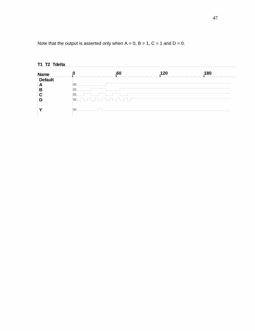
Advanced Digital Design with the Verilog Hardware Description Language Michael D. Ciletti Prentice-Hall, Pearson Education, 2003 9/24/2003 Problem 5-1 module Combo_CA (Y, A, B, C, D); // 9/12/2003 output Y; input A, B, C, D; assign Y = (~(A | D)) & (B & C & ~D); endmodule module t_Combo_CA(); reg A, B, C, D; wire Y; Combo_CA M0 (Y, A, B, C, D); initial begin #5 {A, B, C, D} = 4'b0000; #5 {A, B, C, D} = 4'b0001; #5 {A, B, C, D} = 4'b0010; #5 {A, B, C, D} = 4'b0011; #5 {A, B, C, D} = 4'b0100; #5 {A, B, C, D} = 4'b0101; #5 {A, B, C, D} = 4'b0110; #5 {A, B, C, D} = 4'b0111; #5 {A, B, C, D} = 4'b1000; #5 {A, B, C, D} = 4'b1001; #5 {A, B, C, D} = 4'b1010; #5 {A, B, C, D} = 4'b1011; #5 {A, B, C, D} = 4'b1100; #5 {A, B, C, D} = 4'b1101; #5 {A, B, C, D} = 4'b1110; #5 {A, B, C, D} = 4'b1111; end initial begin #500 $finish; end //initial begin $monitor ($time,,”%h %b“, {A, B, C, D}, Y); end endmodule
47
Note that the output is asserted only when A = 0, B = 1, C = 1 and D = 0.
T1 T2 Tdelta
Name 0 60 120 180DefaultABCD
Y

48
Advanced Digital Design with the Verilog Hardware Description Language Michael D. Ciletti Prentice-Hall, Pearson Education, 2003 9/12/2003 Problem 5-2 module Combo_str (Y, A, B, C, D); output Y; input A, B, C, D; and (Y, w1, w3); not (w1, w2); or (w2, A, D); and (w3, B, C, w4); not (w4, D); endmodule module Combo_CA (Y, A, B, C, D); output Y; input A, B, C, D; assign Y = (~(A | D)) & (B & C & ~D); endmodule module Combo_UDP (Y, A, B, C, D); output Y; input A, B, C, D; Combo_prim M0 (Y, A, B, C, D); endmodule primitive Combo_prim (Y, A, B, C, D); output Y; input A, B, C, D; table 0000 : 0; 0001 : 0; 0010 : 0; 0011 : 0; 0100 : 0; 0101 : 0; 0110 : 1; 0111 : 0; 1000 : 0;

49
1001 : 0; 1010 : 0; 1011 : 0; 1100 : 0; 1101 : 0; 1110 : 0; 1111 : 0; endtable endprimitive module t_Combo_all(); reg A, B, C, D; wire Y; Combo_str M0 (Y_str, A, B, C, D); Combo_UDP M1 (Y_UDP, A, B, C, D); Combo_CA M2 (Y_CA, A, B, C, D); initial begin #5 {A, B, C, D} = 4'b0000; #5 {A, B, C, D} = 4'b0001; #5 {A, B, C, D} = 4'b0010; #5 {A, B, C, D} = 4'b0011; #5 {A, B, C, D} = 4'b0100; #5 {A, B, C, D} = 4'b0101; #5 {A, B, C, D} = 4'b0110; #5 {A, B, C, D} = 4'b0111; #5 {A, B, C, D} = 4'b1000; #5 {A, B, C, D} = 4'b1001; #5 {A, B, C, D} = 4'b1010; #5 {A, B, C, D} = 4'b1011; #5 {A, B, C, D} = 4'b1100; #5 {A, B, C, D} = 4'b1101; #5 {A, B, C, D} = 4'b1110; #5 {A, B, C, D} = 4'b1111; end initial begin #500 $finish; end endmodule

50
T1 T2 Tdelta
Name Sco0 60 120 180DefaultA t_B t_C t_D t_
Y_str t_Y_UDP t_Y_CA t_

51
Advanced Digital Design with the Verilog Hardware Description Language Michael D. Ciletti Prentice-Hall, Pearson Education, 2003 9/24/2003 Problem 5-3 module Combo_str_unit (Y, A, B, C, D); // 9/12/2003 output Y; input A, B, C, D; and #1 (Y, w1, w3); not #1 (w1, w2); or #1 (w2, A, D); and #1 (w3, B, C, w4); not #1 (w4, D); endmodule module Combo_CA_unit (Y, A, B, C, D); output Y; input A, B, C, D; assign #1 Y = (~(A | D)) & (B & C & ~D); endmodule module Combo_UDP_unit (Y, A, B, C, D); output Y; input A, B, C, D; Combo_prim_unit #1 M0 (Y, A, B, C, D); endmodule primitive Combo_prim_unit (Y, A, B, C, D); output Y; input A, B, C, D; table 0000 : 0; 0001 : 0; 0010 : 0; 0011 : 0; 0100 : 0; 0101 : 0; 0110 : 1; 0111 : 0;

52
1000 : 0; 1001 : 0; 1010 : 0; 1011 : 0; 1100 : 0; 1101 : 0; 1110 : 0; 1111 : 0; endtable endprimitive module t_Combo_all_unit(); reg A, B, C, D; wire Y; Combo_str_unit M0 (Y_str, A, B, C, D); Combo_UDP_unit M1 (Y_UDP, A, B, C, D); Combo_CA_unit M2 (Y_CA, A, B, C, D); initial begin #5 {A, B, C, D} = 4'b0000; #5 {A, B, C, D} = 4'b0001; #5 {A, B, C, D} = 4'b0010; #5 {A, B, C, D} = 4'b0011; #5 {A, B, C, D} = 4'b0100; #5 {A, B, C, D} = 4'b0101; #5 {A, B, C, D} = 4'b0110; #5 {A, B, C, D} = 4'b0111; #5 {A, B, C, D} = 4'b1000; #5 {A, B, C, D} = 4'b1001; #5 {A, B, C, D} = 4'b1010; #5 {A, B, C, D} = 4'b1011; #5 {A, B, C, D} = 4'b1100; #5 {A, B, C, D} = 4'b1101; #5 {A, B, C, D} = 4'b1110; #5 {A, B, C, D} = 4'b1111; end initial begin #500 $finish; end endmodule

53
T1 0 T2 0 Tdelta 0
Name 0 30 60 90 120 150DefaultABCD
Y_strY_UDPY_CA

54
Advanced Digital Design with the Verilog Hardware Description Language Michael D. Ciletti Prentice-Hall, Pearson Education, 2003 9/24/2003 Problem 5-4 module AOI_5_CA1_str (y_out, x_in1, x_in2, x_in3, x_in4, x_in5, enable); input x_in1, x_in2, x_in3, x_in4, x_in5, enable; output y_out; and (w1, x_in1, x_in2); and (w2, x_in3, x_in4, x_in5); or (w3, w1, w2); notif1 (y_out, w3, enable); //assign y_out = enable ? ~((x_in1 & x_in2) | (x_in3 & x_in4 & x_in5)) : 1'bz; endmodule module t_AOI_5_CA1_str (); reg x_in1, x_in2, x_in3, x_in4, x_in5, enable; wire y_out; AOI_5_CA1_str M0 (y_out, x_in1, x_in2, x_in3, x_in4, x_in5, enable); initial #350 $finish; initial begin #5 enable = 1; #5 {x_in1, x_in2, x_in3, x_in4, x_in5} = 5'b00000; #5 {x_in1, x_in2, x_in3, x_in4, x_in5} = 5'b00001; #5 {x_in1, x_in2, x_in3, x_in4, x_in5} = 5'b00010; #5 {x_in1, x_in2, x_in3, x_in4, x_in5} = 5'b00011; #5 {x_in1, x_in2, x_in3, x_in4, x_in5} = 5'b00100; #5 {x_in1, x_in2, x_in3, x_in4, x_in5} = 5'b00101; #5 {x_in1, x_in2, x_in3, x_in4, x_in5} = 5'b00110; #5 {x_in1, x_in2, x_in3, x_in4, x_in5} = 5'b00111; #5 {x_in1, x_in2, x_in3, x_in4, x_in5} = 5'b01000; #5 {x_in1, x_in2, x_in3, x_in4, x_in5} = 5'b01001; #5 {x_in1, x_in2, x_in3, x_in4, x_in5} = 5'b01010; #5 {x_in1, x_in2, x_in3, x_in4, x_in5} = 5'b01011; #5 {x_in1, x_in2, x_in3, x_in4, x_in5} = 5'b01100; #5 {x_in1, x_in2, x_in3, x_in4, x_in5} = 5'b01101; #5 {x_in1, x_in2, x_in3, x_in4, x_in5} = 5'b01110; #5 {x_in1, x_in2, x_in3, x_in4, x_in5} = 5'b01111;

55
#5 {x_in1, x_in2, x_in3, x_in4, x_in5} = 5'b10000; #5 {x_in1, x_in2, x_in3, x_in4, x_in5} = 5'b10001; #5 {x_in1, x_in2, x_in3, x_in4, x_in5} = 5'b10010; #5 {x_in1, x_in2, x_in3, x_in4, x_in5} = 5'b10011; #5 {x_in1, x_in2, x_in3, x_in4, x_in5} = 5'b10100; #5 {x_in1, x_in2, x_in3, x_in4, x_in5} = 5'b10101; #5 {x_in1, x_in2, x_in3, x_in4, x_in5} = 5'b10110; #5 {x_in1, x_in2, x_in3, x_in4, x_in5} = 5'b10111; #5 {x_in1, x_in2, x_in3, x_in4, x_in5} = 5'b11000; #5 {x_in1, x_in2, x_in3, x_in4, x_in5} = 5'b11001; #5 {x_in1, x_in2, x_in3, x_in4, x_in5} = 5'b11010; #5 {x_in1, x_in2, x_in3, x_in4, x_in5} = 5'b11011; #5 {x_in1, x_in2, x_in3, x_in4, x_in5} = 5'b11100; #5 {x_in1, x_in2, x_in3, x_in4, x_in5} = 5'b11101; #5 {x_in1, x_in2, x_in3, x_in4, x_in5} = 5'b11110; #5 {x_in1, x_in2, x_in3, x_in4, x_in5} = 5'b11111; #5 enable = 0; #5 {x_in1, x_in2, x_in3, x_in4, x_in5} = 5'b00000; #5 {x_in1, x_in2, x_in3, x_in4, x_in5} = 5'b00001; #5 {x_in1, x_in2, x_in3, x_in4, x_in5} = 5'b00010; #5 {x_in1, x_in2, x_in3, x_in4, x_in5} = 5'b00011; #5 {x_in1, x_in2, x_in3, x_in4, x_in5} = 5'b00100; #5 {x_in1, x_in2, x_in3, x_in4, x_in5} = 5'b00101; #5 {x_in1, x_in2, x_in3, x_in4, x_in5} = 5'b00110; #5 {x_in1, x_in2, x_in3, x_in4, x_in5} = 5'b00111; #5 {x_in1, x_in2, x_in3, x_in4, x_in5} = 5'b01000; #5 {x_in1, x_in2, x_in3, x_in4, x_in5} = 5'b01001; #5 {x_in1, x_in2, x_in3, x_in4, x_in5} = 5'b01010; #5 {x_in1, x_in2, x_in3, x_in4, x_in5} = 5'b01011; #5 {x_in1, x_in2, x_in3, x_in4, x_in5} = 5'b01100; #5 {x_in1, x_in2, x_in3, x_in4, x_in5} = 5'b01101; #5 {x_in1, x_in2, x_in3, x_in4, x_in5} = 5'b01110; #5 {x_in1, x_in2, x_in3, x_in4, x_in5} = 5'b01111; #5 {x_in1, x_in2, x_in3, x_in4, x_in5} = 5'b10000; #5 {x_in1, x_in2, x_in3, x_in4, x_in5} = 5'b10001; #5 {x_in1, x_in2, x_in3, x_in4, x_in5} = 5'b10010; #5 {x_in1, x_in2, x_in3, x_in4, x_in5} = 5'b10011; #5 {x_in1, x_in2, x_in3, x_in4, x_in5} = 5'b10100; #5 {x_in1, x_in2, x_in3, x_in4, x_in5} = 5'b10101; #5 {x_in1, x_in2, x_in3, x_in4, x_in5} = 5'b10110; #5 {x_in1, x_in2, x_in3, x_in4, x_in5} = 5'b10111;

56
#5 {x_in1, x_in2, x_in3, x_in4, x_in5} = 5'b11000; #5 {x_in1, x_in2, x_in3, x_in4, x_in5} = 5'b11001; #5 {x_in1, x_in2, x_in3, x_in4, x_in5} = 5'b11010; #5 {x_in1, x_in2, x_in3, x_in4, x_in5} = 5'b11011; #5 {x_in1, x_in2, x_in3, x_in4, x_in5} = 5'b11100; #5 {x_in1, x_in2, x_in3, x_in4, x_in5} = 5'b11101; #5 {x_in1, x_in2, x_in3, x_in4, x_in5} = 5'b11110; #5 {x_in1, x_in2, x_in3, x_in4, x_in5} = 5'b11111; end endmodule
T1 1 T2 1 Tdelta 0
Name 0 100 200 300Defaultx_in1x_in2
x_in3x_in4x_in5
enable
y_out

57
Advanced Digital Design with the Verilog Hardware Description Language Michael D. Ciletti Prentice-Hall, Pearson Education, 2003 9/24/2003 Problem 5-6 module tr_latch (q_out, enable, data); output q_out; input enable, data; reg q_out; always @ (enable or data) begin if (enable) q_out = data; end endmodule module t_tr_latch (); wire q_out; reg enable, data; tr_latch M0(q_out, enable, data); initial #500 $finish; initial fork #20 data = 0; #50 forever #15 data = ~data; #200 data= 0; join initial fork #100 enable = 0; #200 enable = 1; #400 enable = 0; join endmodule

58
T1 T2 Tdelta
Name Sc0 150 300 450Defaultenable tdata tq_out t

59
Advanced Digital Design with the Verilog Hardware Description Language Michael D. Ciletti Prentice-Hall, Pearson Education, 2003 9/24/2003 Problem 5-7 primitive AOI_UDP (y, x_in1, x_in2, x_in3, x_in4, x_in5); output y; input x_in1, x_in2, x_in3, x_in4, x_in5; table // x1 x2 x3 x4 x5 0 0 0 0 0 : 1; 0 0 0 0 1 : 1; 0 0 0 1 0 : 1; 0 0 0 1 1 : 1; 0 0 1 0 0 : 1; 0 0 1 0 1 : 1; 0 0 1 1 0 : 1; 0 0 1 1 1 : 0; 0 1 0 0 0 : 1; 0 1 0 0 1 : 1; 0 1 0 1 0 : 1; 0 1 0 1 1 : 1; 0 1 1 0 0 : 1; 0 1 1 0 1 : 1; 0 1 1 1 0 : 1; 0 1 1 1 1 : 0; 1 0 0 0 0 : 1; 1 0 0 0 1 : 1; 1 0 0 1 0 : 1; 1 0 0 1 1 : 1; 1 0 1 0 0 : 1; 1 0 1 0 1 : 1; 1 0 1 1 0 : 1; 1 0 1 1 1 : 0; 1 1 0 0 0 : 0; 1 1 0 0 1 : 0; 1 1 0 1 0 : 0; 1 1 0 1 1 : 0; 1 1 1 0 0 : 0; 1 1 1 0 1 : 0; 1 1 1 1 0 : 0; 1 1 1 1 1 : 0; endtable endprimitive

60
module AOI_UDP_mod (y, x_in1, x_in2, x_in3, x_in4, x_in5); output y; input x_in1, x_in2, x_in3, x_in4, x_in5; AOI_UDP (y, x_in1, x_in2, x_in3, x_in4, x_in5); endmodule module t_AOI_UDP_mod(); reg x_in1, x_in2, x_in3, x_in4, x_in5; wire y_out; AOI_UDP_mod M0 (y_out, x_in1, x_in2, x_in3, x_in4, x_in5); initial #350 $finish; initial begin #5 {x_in1, x_in2, x_in3, x_in4, x_in5} = 5'b00000; #5 {x_in1, x_in2, x_in3, x_in4, x_in5} = 5'b00001; #5 {x_in1, x_in2, x_in3, x_in4, x_in5} = 5'b00010; #5 {x_in1, x_in2, x_in3, x_in4, x_in5} = 5'b00011; #5 {x_in1, x_in2, x_in3, x_in4, x_in5} = 5'b00100; #5 {x_in1, x_in2, x_in3, x_in4, x_in5} = 5'b00101; #5 {x_in1, x_in2, x_in3, x_in4, x_in5} = 5'b00110; #5 {x_in1, x_in2, x_in3, x_in4, x_in5} = 5'b00111; #5 {x_in1, x_in2, x_in3, x_in4, x_in5} = 5'b01000; #5 {x_in1, x_in2, x_in3, x_in4, x_in5} = 5'b01001; #5 {x_in1, x_in2, x_in3, x_in4, x_in5} = 5'b01010; #5 {x_in1, x_in2, x_in3, x_in4, x_in5} = 5'b01011; #5 {x_in1, x_in2, x_in3, x_in4, x_in5} = 5'b01100; #5 {x_in1, x_in2, x_in3, x_in4, x_in5} = 5'b01101; #5 {x_in1, x_in2, x_in3, x_in4, x_in5} = 5'b01110; #5 {x_in1, x_in2, x_in3, x_in4, x_in5} = 5'b01111; #5 {x_in1, x_in2, x_in3, x_in4, x_in5} = 5'b10000; #5 {x_in1, x_in2, x_in3, x_in4, x_in5} = 5'b10001; #5 {x_in1, x_in2, x_in3, x_in4, x_in5} = 5'b10010; #5 {x_in1, x_in2, x_in3, x_in4, x_in5} = 5'b10011; #5 {x_in1, x_in2, x_in3, x_in4, x_in5} = 5'b10100; #5 {x_in1, x_in2, x_in3, x_in4, x_in5} = 5'b10101; #5 {x_in1, x_in2, x_in3, x_in4, x_in5} = 5'b10110; #5 {x_in1, x_in2, x_in3, x_in4, x_in5} = 5'b10111; #5 {x_in1, x_in2, x_in3, x_in4, x_in5} = 5'b11000; #5 {x_in1, x_in2, x_in3, x_in4, x_in5} = 5'b11001; #5 {x_in1, x_in2, x_in3, x_in4, x_in5} = 5'b11010; #5 {x_in1, x_in2, x_in3, x_in4, x_in5} = 5'b11011;

61
#5 {x_in1, x_in2, x_in3, x_in4, x_in5} = 5'b11100; #5 {x_in1, x_in2, x_in3, x_in4, x_in5} = 5'b11101; #5 {x_in1, x_in2, x_in3, x_in4, x_in5} = 5'b11110; #5 {x_in1, x_in2, x_in3, x_in4, x_in5} = 5'b11111; end endmodule
T1 T2 Tdelta
Name 0 70 140 210Defaultx_in1x_in2
x_in3x_in4x_in5
y_out

62
Advanced Digital Design with the Verilog Hardware Description Language Michael D. Ciletti Prentice-Hall, Pearson Education, 2003 9/24/2003 Problem 5-8 module Problem_5_8 (q_out, data, enable, set, reset); output q_out; input data, enable, set, reset; reg q_out; always @ (data, enable, set, reset) // asynchronous set and reset if (set == 0) q_out <= 1; else if (reset == 0) q_out <= 0; else if (enable == 1) q_out <= data; endmodule module t_Problem_5_8 (); wire q_out; reg data, enable, set, reset; Problem_5_8 M0 (q_out, data, enable, set, reset); initial #800 $finish; initial fork #20 data = 0; #50 forever #100 data = ~data; #200 data= 0; join initial fork #10 enable = 0; #20 enable = 1; #400 enable = 0; join initial fork set = 1; reset = 1; #125 set = 0; #135 set = 1; #185 reset = 0; #195 reset = 1; #250 set = 0; #255 set = 1; #275 reset = 0; #295 reset = 1;

63
#285 set = 0; #290 set = 1; #425 set = 0; #430 set = 1; #500 reset = 0; #510 reset = 1; #625 set = 0; #630 set = 1; #700 reset = 0; #710 reset = 1; join endmodule
T1 0 T2 Tdelta
Name S0 200 400 600 800Defaultsetenableresetdata
q out

64
Advanced Digital Design with the Verilog Hardware Description Language Michael D. Ciletti Prentice-Hall, Pearson Education, 2003 10/13/2004 Problem 5-9 module JK_flip_flop (q, q_bar, j, k, clock, reset_bar); output q, q_bar; input clock, reset_bar assign q_bar = ~q; always @( posedge clock, negedge reset_bar) if (reset_bar == 0) q <= 0; else case {j,k} 2'b00: q <= q; 2'b01: q <= 0; 2'b10: q <= 1; 2'b11: q <= ~q; endcase endmodule Test plan
1. Verify that q responds to initial reset 2. Verify that q responds to j = 0, k = 0
a. j = 0, k = 1 b. j = 1, k = 0 c. j = 1, k = 1
3. Verify that q responds to reset-on-the-fly 4. Verify that q_bar is complement of q 5. Verify that reset action is active low and asynchronous 6. Verify that transitions between clock edges are ignored 7. Verify that reset_bar overrides the clock
module t_JK_flip_flop (); wire q, q_bar; reg clock, reset_bar JK_flip_flop M0 (q, q_bar, j, k, clock, reset_bar); initial #500 $finish; initial begin clock = 0; forever #5 clock = ~clock; end endmodule

65

66
Advanced Digital Design with the Verilog Hardware Description Language Michael D. Ciletti Prentice-Hall, Pearson Education, 2003 10/13/2004 Problem 5-10 module BCD_checker (data, flag); output flag; input [3:0] data; reg flag; always @ (data) case (data) 0, 1, 2, 3, 4, 5, 6, 7, 8, 9: flag = 0; default: flag = 1; endcase endmodule module t_BCD_checker (); wire flag; reg [3:0] data; integer k; BCD_checker M0 (data, flag); initial #500 $finish; initial begin data = 0; for (k = 0; k < 100; k = k +1) #20 data = data + 1; end endmodule

67

68
Advanced Digital Design with the Verilog Hardware Description Language Michael D. Ciletti Prentice-Hall, Pearson Education, 2003 9/24/2003 Problem 5-11 The for loop executes if K <= 15. If K is declared as a 4-bit register it will roll over from 1111 to 0000 after executing with K = 1111B2B. The test will again be true, with K <= 15. To work around this issue, use an integer for the loop index, or declare K to be 5 bits wide.

69
Advanced Digital Design with the Verilog Hardware Description Language Michael D. Ciletti Prentice-Hall, Pearson Education, 2003 10/25004 Problem 5-13 module Prob_5_13 (GTE, LTE, A, B, C, D); output [3:0] GTE, LTE; input [31: 0] A, B, C, D; reg [3:0] GTE, LTE; always @ (A, B, C, D) begin GTE = 0; LTE = 0; if ((A>=B) && (A>=C) && (A>=D)) GTE = GTE | 4'b1000; if ((B>=A) && (B>=C) && (B>=D)) GTE = GTE | 4'b0100; if ((C>=A) && (C>=B) && (C>=D)) GTE = GTE | 4'b0010; if ((D>=A) && (D>=B) && (D>=C)) GTE = GTE | 4'b0001; if ((A<=B) && (A<=C) && (A<=D)) LTE = LTE | 4'b1000; if ((B<=A) && (B<=C) && (B<=D)) LTE = LTE | 4'b0100; if ((C<=A) && (C<=B) && (C<=D)) LTE = LTE | 4'b0010; if ((D<=A) && (D<=B) && (D<=C)) LTE = LTE | 4'b0001; end endmodule module t_Prob_5_13 (); wire [3:0] GTE, LTE; reg [31: 0] A, B, C, D; Prob_5_13 M0 (GTE, LTE, A, B, C, D); initial begin A = 2; B = 2; C = 2; D = 2; #10 A = 2; B = 2; C = 2; D = 1; #10 A = 2; B = 2; C = 1; D = 1; #10 A = 2; B = 1; C = 1; D = 1; #10 A = 525; B = 1; C = 2; D = 1; #10 $finish; end endmodule

70
Note: The above apporach does not treat cases where two or more are equal and largest and/or smallest. Consider: always @ (A, B, C, D) begin A_GT = (A >= B) && (A >= C) && (A > = D); B_GT = (B >= A) && (B >= C) && (C >= D); C_GT = (C >= A) && (C >= B) && (C >= D); D_GT = (D >= A) && (D >= B) && (D >= C); A_LT = (A <= B) && (A <= C) && (A < = D); B_LT = (B <= A) && (B <= C) && (C <= D); C_LT = (C <= A) && (C <= B) && (C <= D); D_LT = (D <= A) && (D <= B) && (D <= C); end

71
Advanced Digital Design with the Verilog Hardware Description Language Michael D. Ciletti Prentice-Hall, Pearson Education, 2003 10/13/2004 Problem 5-14 module Universal_Shift_Reg (Data_Out, MSB_Out, LSB_Out, Data_In, MSB_In, LSB_In, s1, s0, clk, rst); output [3: 0] Data_Out; output MSB_Out, LSB_Out; input [3: 0] Data_In; input MSB_In, LSB_In; reg [3: 0] Data_Out; // 10-12-2004 input s1, s0, clk, rst; assign MSB_Out = Data_Out[3]; assign LSB_Out = Data_Out[0]; always @ (posedge clk) begin if (rst) Data_Out <= 0; else case ({s1, s0}) 0: Data_Out <= Data_Out; // Idle 1: Data_Out <= {MSB_In, Data_Out[3:1]}; // Shift right 2: Data_Out <= {Data_Out[2:0], LSB_In}; // Shift Left 3: Data_Out <= Data_In; // Parallel Load endcase end endmodule /* Test Plan Verify initial reset Verify idle Verify shift right Verify shift left Verify parallel load Verify reset-on-the-fly */ module t_Universal_Shift_Reg(); wire [3: 0] Data_Out; reg [3: 0] Data_In; wire MSB_Out, LSB_Out; reg MSB_In, LSB_In; reg s1, s0, rst; defparam M2.half_cycle = 5;

72
Universal_Shift_Reg M1 (Data_Out, MSB_Out, LSB_Out, Data_In, MSB_In, LSB_In, s1, s0, clk, rst); Clock_Gen M2(clk); initial #1000 $finish; initial fork begin #5 rst = 1; #20 rst = 0;end begin #120 rst = 1; #20 rst = 0;end begin #260 rst = 1; #20 rst = 0;end begin #380 rst = 1; #20 rst = 0;end join initial fork #10 fork // Verify right shift #10 begin Data_In = 4'b1111; s0 = 0; s1 = 0; LSB_In = 1; MSB_In = 1; end #40 s0 = 1; join #120 fork begin // Verify left shift #10 Data_In = 4'b1111; s0 = 0; s1 = 0; LSB_In = 1; MSB_In = 1; end #40 s1 = 1; join #250 fork begin // Verify load #10 Data_In = 4'b1111; s0 = 0; s1 = 0; LSB_In = 1; MSB_In = 1; end #40 begin s0 = 1; s1 = 1;end join #320 fork begin // reset #10 Data_In = 4'b1111; s0 = 0; s1 = 0; LSB_In = 1; MSB_In = 1; end #40 begin s0 = 0; s1 = 0;end join join endmodule

73

74
Advanced Digital Design with the Verilog Hardware Description Language Michael D. Ciletti Prentice-Hall, Pearson Education, 2003 10/18/2005 Problem 5-16 module Problem_5_16 (count, initial_count, load, enable_b, clock, reset); output [3: 0] count; input [3: 0] initial_count; input load, enable_b, clock, reset; reg [3: 0] count; always @ (negedge clock) if (reset == 1) count <= 0; else if (enable_b == 0) count <= count + 1; else if (load) count <= initial_count; // Alternative below is also possible: // else if (load) count <= initial_count; // else if (enable_b == 0) count <= count + 1; endmodule module t_Problem_5_16 (); wire [3: 0] count; reg [3: 0] initial_count; reg load, enable_b, clock, reset; initial #500 $finish; initial begin clock = 0; forever #5 clock = ~clock; end initial fork #5 initial_count = 4'b1010; join initial fork #15 reset = 1; #25 reset = 0; join initial fork #55 enable_b = 0; #155 enable_b = 1; #195 enable_b = 0; #495 enable_b = 1; join initial fork

75
#195 load = 1; #205 load = 0; join Problem_5_16 M0(count, initial_count, load, enable_b, clock, reset); endmodule
T1 0 T2 0 Tdelta 0
Name S0 60 120 180 240Defaultclockresetloadenable_b
initial_count[3:0]count[3:0] x 0 1 2 3 4 5 6 7 8 9 a b c d e f 0 1 2 3
a

76
Advanced Digital Design with the Verilog Hardware Description Language Michael D. Ciletti Prentice-Hall, Pearson Education, 2003 10/13/2004 Problem 5-18 module Johnson_Counter (count, enable, clock, reset); output [3: 0] count; input enable; input clock, reset; reg [3: 0] count; always @ (posedge clock, posedge reset) if (reset == 1) count <= 0; else if (enable) case (count) 4'b0000, 4'b0001, 4'b0011, 4'b0111: count <= {count[2: 0], 1'b1}; 4'b1111, 4'b1110, 4'b1100, 4'b1000: count <= {count[2: 0], 1'b0}; default: count <= 0; endcase endmodule module t_Johnson_Counter (); wire [3: 0] count; reg enable; reg clock, reset; Johnson_Counter M0 (count, enable, clock, reset); initial #500 $finish; initial begin clock = 0; forever #5 clock = ~clock; end initial fork #20 reset = 1; #60 reset = 0; #142 reset = 1; #154 reset = 0; #50 enable = 1; #300 enable = 0; #400 enable = 1; join

77
endmodule

78
Advanced Digital Design with the Verilog Hardware Description Language Michael D. Ciletti Prentice-Hall, Pearson Education, 2003 10/7/2003 Problem 5-19 // Assumption: positive-edge sensitive, active-high reset. // Assumption: count from reset value module BCD_Counter (count, clk, rst); output [3: 0] count; input clk, rst; reg [3: 0] count; always @ (posedge clk , posedge rst) if (rst == 1) count <= 0; else if (count < 9) count <= count + 1; else count <= 0; endmodule module t_BCD_Counter (); wire [3: 0] count; reg clk, rst; BCD_Counter M0 (count, clk, rst); initial #200 $finish; initial begin clk = 0; forever #5 clk = ~clk; end initial begin #10 rst = 1; #20 rst = 0; #100 rst = 1; // Reset 0n-the-fly #20 rst = 0; end endmodule

79
T1 T2 Tdelta
Name 0 50 100 150 200Defaultclkrstcount[3:0] x 0 1 2 3 4 5 6 7 8 9 0 1 2 3 4 5

80
Advanced Digital Design with the Verilog Hardware Description Language Michael D. Ciletti Prentice-Hall, Pearson Education, 2003 10/7/2003 Problem 5-20 // Assumption: positive-edge sensitive, active-high reset. // Assumption: count from reset value module Modulo_6_Counter (count, clk, rst); output [2: 0] count; input clk, rst; reg [2: 0] count; always @ (posedge clk , posedge rst) if (rst == 1) count <= 0; else if (count < 5) count <= count + 1; else count <= 0; endmodule module t_Modulo_6_Counter (); wire [2: 0] count; reg clk, rst; Modulo_6_Counter M0 (count, clk, rst); initial #200 $finish; initial begin clk = 0; forever #5 clk = ~clk; end initial begin #10 rst = 1; #20 rst = 0; #100 rst = 1; // Reset 0n-the-fly #20 rst = 0; end endmodule

81
T1 T2 Tdelta
Name 0 50 100 150 200Defaultclkrstcount[2:0] x 0 1 2 3 4 5 0 1 2 3 4 0 1 2 3 4 5

82
Advanced Digital Design with the Verilog Hardware Description Language Michael D. Ciletti Prentice-Hall, Pearson Education, 2003 10/7/2003 Problem 5-23 module Problem_5_23 (count, clk, rst); // 8-bit ring counter, MSB to LSB // Assume positive-edge sensitive; active high reset parameter size = 8; output [size -1: 0] count; input clk, rst; reg [size -1: 0] count; always @ (posedge clk or posedge rst) if (rst) count <= {1'b1, (size -1)* {1'b0)}; //Assumed initial count else count <= {count[0], count[size -1: 1]}; endmodule module t_Problem_5_23 (); parameter size = 8; wire [size -1: 0] count; reg clk, rst; Problem_5_23 M0 (count, clk, rst); initial #500 $finish; initial begin clk = 0; forever #5 clk = ~clk; end initial fork #10 rst = 1; // initial reset #30 rst = 0; #200 rst = 1; // power-up reset #230 rst = 0; join endmodule

83
T1 T2 Tdelta
Name 0 100 200 300 400
clkrst
count[7:0]count[7:0] count[7] count[6] count[5] count[4] count[3] count[2] count[1] count[0]
8080
8080 20
20

84

85
Advanced Digital Design with the Verilog Hardware Description Language Michael D. Ciletti Prentice-Hall, Pearson Education, 2003 10/18/2003 Problem 5-24 module Problem_5_24a (count, clk, reset); output [7:0] count; input clk, reset; reg [3: 0] state, next_state; reg [7:0] count; always @ (posedge clk) if (reset) state <= 0; else state <= next_state; always @ (state) begin next_state = 1; count = 1; case (state) 0: begin next_state = 1; count = 1; end 1: begin next_state = 2; count = 2; end 2: begin next_state = 3; count = 1; end 3: begin next_state = 4; count = 4; end 4: begin next_state = 5; count = 1; end 5: begin next_state = 6; count = 8; end 6: begin next_state = 7; count = 1; end 7: begin next_state = 8; count = 16; end 8: begin next_state = 9; count = 1; end 9: begin next_state = 10; count = 32; end 10: begin next_state = 11; count = 1; end 11: begin next_state = 12; count = 64; end 12: begin next_state = 13; count = 1; end 13: begin next_state = 0; count = 128; end endcase end endmodule

86
module t_Problem_5_24a (); wire [7:0] count; reg clk, reset; Problem_5_24a M0(count, clk, reset); initial #700 $finish; initial fork #0 reset = 1; #20 reset = 0; #200 reset = 1; #250 reset = 0; join initial begin #0 clk = 0; forever #5 clk = ~clk; end endmodule

87

88
Advanced Digital Design with the Verilog Hardware Description Language Michael D. Ciletti Prentice-Hall, Pearson Education, 2003 Problem 5-26 // Problem 5-26 Three versions // m.d. ciletti 10/21/2004
rst
A, C <= 0(flush_A_C)S_idle
1
Go
F1 F2
S_1
S_2/ incr =1
1
B <= 0(flush_B)
B <= 1(set_B)
C <= 1 (set_C)
1
A <= A + 1
1
control_unit datapath_unit
F1F2Go
clockrst
flush_A_Cincr_ASet_Bflush_bSet_C
A
B
C
Problem_5_26
// Problem 5-26 Three versions // m.d. ciletti 10/25/2004 // Note: the issue of flushing A and C is dealt with by the datapath unit // in version c. module Problem_5_26 (A, B, C, F1, F2, Go, clock, rst); output [7: 0] A, B, C; input F1, F2, Go, clock, rst;

89
wire flush_A_C, incr_A, set_B, set_C, flush_B; control_unit M0 (flush_A_C, incr_A, set_B, set_C, flush_B, F1, F2, Go, clock, rst); // datapath_unit // version a, b // M1 (A, B, C, flush_A_C, incr_A, set_B, set_C, flush_B, clock); datapath_unit // version c M1 (A, B, C, flush_A_C, incr_A, set_B, set_C, flush_B, clock, rst); endmodule module control_unit (flush_A_C, incr_A, set_B, set_C, flush_B, F1, F2, Go, clock, rst); output flush_A_C, incr_A, set_B, set_C, flush_B; input F1, F2, Go, clock, rst; reg [1: 0] state, next_state; reg flush_A_C, incr_A, set_B, set_C, flush_B; parameter S_idle = 0, S_1 = 1, S_2 = 2; always @ (posedge clock) if (rst) state <= S_idle; else state <= next_state; // Version a: incomplete event control expression – missing rst // always @ (state, F1, F2, Go) begin // Version a // Version b: complete event control expression //always @ (state, F1, F2, Go, rst) begin // Version b // Version c: remove rst from event control and logic always @ (state, F1, F2, Go) begin // Version c flush_A_C = 0; incr_A = 0; set_B = 0; set_C = 0; flush_B = 0; next_state = S_idle; case (state) //S_idle: if ((rst == 0) && Go) // Version a, b S_idle: if (Go) // Version c begin next_state = S_1; incr_A = 1; end else flush_A_C = 1; S_1: casex ({F1, F2}) 2'b0x: begin next_state = S_1; flush_B = 1; end 2'b10: begin next_state = S_1; set_B = 1; end 2'b11: begin next_state = S_2; set_B = 1; end endcase S_2: set_C = 1; endcase

90
end endmodule //module datapath_unit (A, B, C, flush_A_C, incr_A, set_B, set_C, flush_B, //clock); // version a, b module datapath_unit (A, B, C, flush_A_C, incr_A, set_B, set_C, flush_B, clock, rst); // version c output [7: 0] A, B, C; //input flush_A_C, incr_A, set_B, set_C, flush_B, clock;// a & b input flush_A_C, incr_A, set_B, set_C, flush_B, clock, rst; reg [7: 0] A, B, C; always @ (posedge clock) begin // version c if (rst) begin A <= 0; C <= 0; end else begin if (incr_A) A <= A+1; if (set_B) B <= 1; if (set_C) C <= 1; if (flush_A_C) begin A <= 0; C <= 0; end if (flush_B) B <= 0; end end /* // version a, b always @ (posedge clock) begin if (incr_A) A <= A+1; if (set_B) B <= 1; if (set_C) C <= 1; if (flush_A_C) begin A <= 0; C <= 0; end if (flush_B) B <= 0; end */endmodule // Test Plan // verify power-up reset // verify rst = 1 steers to S_idle and asserts flush_A_C // verify action of Go (remain in S_idle until Go = 1) // verify Go = 1` steers to S_1 and asserts incr_A // verify F1 = 0 steers state to S_1 and asserts flush_B // verify F1 = 1, F2 = 1 steers to S_2 and asserts set_B // verify F1 = 1, F2 = 0 steers to S_1 and asserts set_B // verify F1 = 1, F2 = 1 steers to S_idle and asserts set_C // verify reset on-the-fly module t_Problem_5_26 (); wire [7: 0] A, B, C; reg F1, F2, Go, clock, rst;

91
Problem_5_26 M0 (A, B, C, F1, F2, Go, clock, rst); initial #700 $finish; initial begin clock = 0; forever #5 clock = ~clock; end initial fork #20 rst = 0; // Power-up reset #50 rst = 1; #80 rst = 0; #120 Go = 0; // Waits for assertion of Go, assert flush_A_C #160 Go = 1; // Steer to S_1, assert incr_A #180 Go = 0; #20 F1 = 0; // De-assert F1, F2, assert flush_B in S_1 #20 F2 = 0; #200 F1 = 1; // Waits in S_1 for F1, asserts set_B #250 F2 = 1; // Waits in S_1 for F1 = 1, F2 = 1, assert set_C #300 Go = 1; // Launch another pass from S_idle #400 rst = 1; // Reset on-the-fly #460 rst = 0; join endmodule Version a: Incomplete event control expression. Note that reset on-the-fly with Go already asserted does not launch new activity because the event control expression does not include rst, and therefore does not trigger an update of the next-state logic when rst is de-asserted. The machine remains in the idle state, and will do so until Go is de-asserted and then re-asserted.

92
Version a: always @ (state, F1, F2, Go) // incomplete event control expression…S_idle: if (Go && (rst == 0)) ...
Version b: Complete event control expression (includes rst). Note that the state returns to the idle state with reset on-the-fly, and the new activity is launched when rst de-asserts with Go already asserted. The event control expression is sensitive to rst, so the next-state combinational logic is updated when rst de-asserts.
Version b: always @ (state, F1, F2, Go, rst // icomplete event control expression…S_idle: if (Go && (rst == 0)) ...
Version c: Event control expression is complete, and rst is removed from the next-state logic. Note that the machine returns to the idle state when rst is asserted, and that new activity is launched while Go is asserted and rst is de-asserted. This solution is equivalent to version a, but does not include rst in the next-state logic.

93
When rst is de-asserted while Go is asserted the next –state logic is update when the state returns to S_idle. This is the preferred style. The datapath unit in this version flushes registers A and C if rst is asserted.

94
Advanced Digital Design with the Verilog Hardware Description Language Michael D. Ciletti Prentice-Hall, Pearson Education, 2003 10/15/2004 Problem 5-27 module Problem_5_27 (alu_out, a, b, c_in, opcode); input [7: 0] a, b; input c_in; input [2: 0] opcode; output reg [8: 0] alu_out; parameter [2: 0] add = 0; parameter [2: 0] subtract = 1; parameter [2: 0] subtract_a = 2; parameter [2: 0] or_ab = 3; parameter [2: 0] and_ab = 4; parameter [2: 0] not_ab = 5; parameter [2: 0] exor = 6; parameter [2: 0] exnor = 7; always @ (a, b, c_in, opcode) case (opcode) add: alu_out = a + b + c_in; subtract: alu_out = a + (~b) + c_in; subtract_a: alu_out = b + (~a) + ~c_in; or_ab: alu_out = {1'b0, a | b}; and_ab: alu_out = {1'b0, a & b}; not_ab: alu_out = {1'b0, (~a) &b}; exor: alu_out = {1'b0, a^b}; exnor: alu_out = {1'b0, a ~^ b}; endcase endmodule // Test Plan: Verify combinational logic by inspection // for c_in = 0, 1, a = 8'h55, b = 8'haa module t_Problem_5_27 (); reg [7: 0] a, b; reg c_in; reg [2: 0] opcode; reg [79: 0] ocs; wire [8: 0] alu_out; integer j, k; parameter [2: 0] add = 0; parameter [2: 0] subtract = 1; parameter [2: 0] subtract_a = 2; parameter [2: 0] or_ab = 3; parameter [2: 0] and_ab = 4;

95
parameter [2: 0] not_ab = 5; parameter [2: 0] exor = 6; parameter [2: 0] exnor = 7; parameter [79: 0] ocs_0 = "add"; parameter [79: 0] ocs_1 = "subtract"; parameter [79: 0] ocs_2 = "subtract_a"; parameter [79: 0] ocs_3 = "or_ab"; parameter [79: 0] ocs_4 = "and_ab"; parameter [79: 0] ocs_5 = "not_ab"; parameter [79: 0] ocs_6 = "exor"; parameter [79: 0] ocs_7 = "exnor"; Problem_5_27 M0 (alu_out, a, b, c_in, opcode); initial #1000 $finish; initial begin #10 a = 8'h55; //0101_0101 b = 8'haa; //1010_1010 for (j = 0; j <= 1;j = j + 1) for (k = 0; k <=7; k = k + 1) begin #10 c_in = j; case (k) 0: opcode = add; 1: opcode = subtract; 2: opcode = subtract_a; 3: opcode = or_ab; 4: opcode = and_ab; 5: opcode = not_ab; 6: opcode = exor; 7: opcode = exnor; endcase end end always @(opcode) case (opcode) add: ocs = ocs_0; subtract: ocs = ocs_1; subtract_a: ocs = ocs_2; or_ab: ocs = ocs_3; and_ab: ocs = ocs_4; not_ab: ocs = ocs_5; exor: ocs = ocs_6; exnor: ocs = ocs_7; endcase endmodule

96

97
Advanced Digital Design with the Verilog Hardware Description Language Michael D. Ciletti Prentice-Hall, Pearson Education, 2003 10/15/2004 Problem 5-28 // Eliminate feeedback from alu to Data_in // Provide c_in to alu module Problem_5_28 (alu_out, Data_in, Read_Addr_1, Read_Addr_2, Write_Addr, opcode, Write_Enable, c_in, Clock); output [8: 0] alu_out; // Re-sized input [7: 0] Data_in; input [2: 0] Read_Addr_1, Read_Addr_2, Write_Addr; input [2: 0] opcode; input Write_Enable, Clock; input c_in; wire [7: 0] Data_Out_1, Data_Out_2; Problem_5_27_ALU M0_ALU (alu_out, Data_Out_1, Data_Out_2, c_in, opcode); Register_File M1_Reg_File (Data_Out_1, Data_Out_2, Data_in, Read_Addr_1, Read_Addr_2, Write_Addr, Write_Enable, Clock); endmodule module Register_File (Data_Out_1, Data_Out_2, Data_in, Read_Addr_1, Read_Addr_2, Write_Addr, Write_Enable, Clock); output [7: 0] Data_Out_1, Data_Out_2; input [7: 0] Data_in; input [2: 0] Read_Addr_1, Read_Addr_2, Write_Addr; input Write_Enable, Clock; reg [7: 0] Reg_File [31: 0]; // 8 x 32 Memory declaration assign Data_Out_1 = Reg_File[Read_Addr_1]; assign Data_Out_2 = Reg_File[Read_Addr_2]; always @ (posedge Clock) begin if (Write_Enable) Reg_File [Write_Addr] <= Data_in; end endmodule // Test Plan: Register File // Write to memory with walking ones // Verify read of walking ones from each port /* module t_Register_File ();
98
wire [7: 0] Data_Out_1, Data_Out_2; reg [7: 0] Data_in; reg [2: 0] Read_Addr_1, Read_Addr_2, Write_Addr; reg Write_Enable, Clock; integer k; Register_File M0(Data_Out_1, Data_Out_2, Data_in, Read_Addr_1, Read_Addr_2, Write_Addr, Write_Enable, Clock); initial #500 $finish; initial begin Clock = 0; forever #5 Clock = ~Clock; end initial begin Data_in = 8'b1000_0000; Write_Enable = 1; Write_Addr = 0; Read_Addr_1 = 0; Read_Addr_2 = 0; for (k = 0; k <= 31; k = k + 1) begin @ (negedge Clock) if (Data_in == 8'b1000_0000) Data_in = 8'b0000_0001; else Data_in <= Data_in << 1; Write_Addr <= Write_Addr + 1; Read_Addr_1 <= Read_Addr_1 + 1; Read_Addr_2 <= Read_Addr_2 + 1; end end endmodule */ module Problem_5_27_ALU (alu_out, a, b, c_in, opcode); input [7: 0] a, b; input c_in; input [2: 0] opcode; output reg [8: 0] alu_out; // Re-sized parameter [2: 0] add = 0; parameter [2: 0] subtract = 1; parameter [2: 0] subtract_a = 2; parameter [2: 0] or_ab = 3; parameter [2: 0] and_ab = 4; parameter [2: 0] not_ab = 5; parameter [2: 0] exor = 6; parameter [2: 0] exnor = 7; always @ (a, b, c_in, opcode) case (opcode) add: alu_out = a + b + c_in; subtract: alu_out = a + (~b) + c_in;

99
subtract_a: alu_out = b + (~a) + ~c_in; or_ab: alu_out = {1'b0, a | b}; and_ab: alu_out = {1'b0, a & b}; not_ab: alu_out = {1'b0, (~a) &b}; exor: alu_out = {1'b0, a^b}; exnor: alu_out = {1'b0, a ~^ b}; endcase endmodule // Test plan: Register file and ALU //Verify write of walking ones to all registers //Verify alu operations for data read from registers module t_Problem_5_28 (); wire [8: 0] alu_out; // Re-sized reg [7: 0] Data_in; reg [2: 0] Read_Addr_1, Read_Addr_2, Write_Addr; reg [2: 0] opcode; reg Write_Enable, Clock; reg c_in; reg [79: 0] ocs; integer k; parameter [2: 0] add = 0; parameter [2: 0] subtract = 1; parameter [2: 0] subtract_a = 2; parameter [2: 0] or_ab = 3; parameter [2: 0] and_ab = 4; parameter [2: 0] not_ab = 5; parameter [2: 0] exor = 6; parameter [2: 0] exnor = 7; parameter [79: 0] ocs_0 = "add"; parameter [79: 0] ocs_1 = "subtract"; parameter [79: 0] ocs_2 = "subtract_a"; parameter [79: 0] ocs_3 = "or_ab"; parameter [79: 0] ocs_4 = "and_ab"; parameter [79: 0] ocs_5 = "not_ab"; parameter [79: 0] ocs_6 = "exor"; parameter [79: 0] ocs_7 = "exnor"; Problem_5_28 M0 (alu_out, Data_in, Read_Addr_1, Read_Addr_2, Write_Addr, opcode, Write_Enable, c_in, Clock); initial #500 $finish; initial begin Clock = 0; forever #5 Clock = ~Clock; end initial begin
100
#1 Data_in = 8'b1000_0000; opcode = add; c_in = 0; Write_Enable = 1; Write_Addr = 0; Read_Addr_1 = 0; Read_Addr_2 = 0; for (k = 0; k <= 31; k = k + 1) begin @ (negedge Clock) if (Data_in == 8'b1000_0000) Data_in = 8'b0000_0001; else Data_in <= Data_in << 1; Write_Addr <= Write_Addr + 1; Read_Addr_1 <= Read_Addr_1 + 1; Read_Addr_2 <= Read_Addr_2 + 1; end end always @(opcode) case (opcode) add: ocs = ocs_0; subtract: ocs = ocs_1; subtract_a: ocs = ocs_2; or_ab: ocs = ocs_3; and_ab: ocs = ocs_4; not_ab: ocs = ocs_5; exor: ocs = ocs_6; exnor: ocs = ocs_7; endcase endmodule

101

102
Advanced Digital Design with the Verilog Hardware Description Language Michael D. Ciletti Prentice-Hall, Pearson Education, 2003 Problem 5-29 10/15/2004
P1 <= DataP0 <= P1(ld_P1, ld_P0)
Ld
Ld 1
R0 <= {P1, P0}(ld_R0)
S_1
En
S_full
P1 <= DataP0 <= P1
S_wait
1
1
1rst
S_idle
{P1, P0} <= {0, 0}(flush_P1_P0)
En
1
8 8 8
Data
R0[15: 0]P1[7: 0] P0[7: 0]
P1[7: 0] P0[7: 0]
{P1, P0} <= {0, 0}(flush_P1_P0)
P1 <= DataP0 <= P1(ld_P0, ld_P1)
module Problem_5_29 (P0, Data, Ld, En, clock, rst); output [7: 0] P0; input [7:0] Data; input Ld, En, clock, rst; wire flush_P0_P1, Ld_P1, Ld_P0, Ld_R0;

103
control_unit M0 (flush_P0_P1, Ld_P1, Ld_P0, Ld_R0, Ld, En, clock, rst); datapath_unit M1 (P0, Data, flush_P0_P1, Ld_P1, Ld_P0, Ld_R0, clock); endmodule module control_unit (flush_P0_P1, Ld_P1, Ld_P0, Ld_R0, Ld, En, clock, rst); output reg flush_P0_P1, Ld_P1, Ld_P0, Ld_R0; input Ld, En, clock, rst; reg [1: 0] state, next_state; parameter S_idle = 0, S_1 = 1, S_full = 2, S_wait = 3; always @ (posedge clock) if (rst) state <= S_idle; else state <= next_state; always @ (state, Ld, En) begin flush_P0_P1 = 0; Ld_P1 = 0; Ld_P0 = 0; Ld_R0 = 0; next_state = S_idle; case (state) S_idle: if (En) begin next_state = S_1; Ld_P1 = 1; Ld_P0 = 1; end else flush_P0_P1 = 1; S_1: begin next_state = S_full; Ld_P1 = 1; Ld_P0 = 1; end S_full: if (Ld == 1) begin Ld_R0 = 1; case (En) 0: begin next_state = S_idle; flush_P0_P1 = 1; end 1: begin next_state = S_1; Ld_P1 = 1; Ld_P0 = 1; end endcase end else next_state = S_wait; S_wait: if (Ld == 1) begin Ld_R0 = 1; case (En) 0: begin next_state = S_idle; flush_P0_P1 = 1; end 1: begin next_state = S_1; Ld_P1 = 1; Ld_P0 = 1; end endcase end else next_state = S_wait; endcase

104
end endmodule module datapath_unit (P0, Data, flush_P0_P1, Ld_P1, Ld_P0, Ld_R0, clock); output [7: 0] P0; input [7: 0] Data; input flush_P0_P1, Ld_P1, Ld_P0, Ld_R0, clock; reg [7: 0] P0, P1; reg [15: 0] R0; always @ (posedge clock) begin if (flush_P0_P1) begin P0 <= 0; P1 <= 0; end if (Ld_P1) P1 <= Data; if (Ld_P0) P0 <= P1; if (Ld_R0) R0 <= {P1, P0}; end endmodule

105
// Test Plan // verify power-up reset // Verify pipeline action // Verify load of R0 action // Verify reset on-the-fly module t_Problem_5_29 (); wire [7: 0] P0; reg [7:0] Data; reg Ld, En, clock, rst; Problem_5_29 M0 (P0, Data, Ld, En, clock, rst); initial #700 $finish; initial begin clock = 0; forever #5 clock = ~clock; end initial fork Data = 8'haa; #10 rst = 0; // Power-up reset #20 rst = 1; #50 rst = 0; #80 En = 0; // Waits for assertion of En, assert flush_P0_P1 #100 En = 1; // Steer to S_1, load P0, load P1 #110 En = 0; #20 Ld = 0; // De-assert Ld #150 Ld = 1; // Waits in S_1 for F1, asserts set_B #180 Ld = 1; // Waits in S_1 for F1 = 1, F2 = 1, assert set_C #200 En = 1; // Launch another pass from S_idle #220 rst = 1; // Reset on-the-fly #240 rst = 0; join endmodule

106
Advanced Digital Design with the Verilog Hardware Description Language Michael D. Ciletti Prentice-Hall, Pearson Education, 2003 10/15/2004 Problem 5-30
Ld
Ld 1
R0 <= R0
S_1
En
S_full
S_wait
1
1
1rst
S_idle
R0 <= 0(flush_P0_P1)
En
1
R0[
7: 0
]
8 8 8
DataP0
R0[
15: 8
]
R0 <= 0(flush_P0_P1)
R0 <= {Data, R0[15: 8}Ld_P1, Ld_P0
R0 <= {Data, R0[15: 8}(Ld_P1, Ld_P0)
R0 <= {Data, R0[15: 8}(Ld_P1, Ld_P0)
module Problem_5_30 (P0, Data, Ld, En, clock, rst); output [7: 0] P0; input [7:0] Data; input Ld, En, clock, rst; wire flush_P0_P1, Ld_P1, Ld_P0;

107
control_unit M0 (flush_P0_P1, Ld_P1, Ld_P0, Ld, En, clock, rst); datapath_unit M1 (P0, Data, flush_P0_P1, Ld_P1, Ld_P0, clock); endmodule module control_unit (flush_P0_P1, Ld_P1, Ld_P0, Ld, En, clock, rst); output reg flush_P0_P1, Ld_P1, Ld_P0; input Ld, En, clock, rst; reg [1: 0] state, next_state; parameter S_idle = 0, S_1 = 1, S_full = 2, S_wait = 3; always @ (posedge clock) if (rst) state <= S_idle; else state <= next_state; always @ (state, Ld, En) begin flush_P0_P1 = 0; Ld_P1 = 0; Ld_P0 = 0; //Ld_R0 = 0; next_state = S_idle; case (state) S_idle: if (En) begin next_state = S_1; Ld_P1 = 1; Ld_P0 = 1; end else flush_P0_P1 = 1; S_1: begin next_state = S_full; Ld_P1 = 1; Ld_P0 = 1; end S_full: if (Ld == 1) begin //Ld_R0 = 1; case (En) 0: begin next_state = S_idle; flush_P0_P1 = 1; end 1: begin next_state = S_1; Ld_P1 = 1; Ld_P0 = 1; end endcase end else next_state = S_wait; S_wait: if (Ld == 1) begin //Ld_R0 = 1; case (En) 0: begin next_state = S_idle; flush_P0_P1 = 1; end 1: begin next_state = S_1; Ld_P1 = 1; Ld_P0 = 1; end endcase end else next_state = S_wait; endcase end

108
endmodule module datapath_unit (P0, Data, flush_P0_P1, Ld_P1, Ld_P0, clock); output [7: 0] P0; input [7: 0] Data; input flush_P0_P1, Ld_P1, Ld_P0, clock; reg [15: 0] R0; wire [7: 0] P0 = R0[7: 0]; always @ (posedge clock) begin if (flush_P0_P1) begin R0 <= {Data, R0[15: 0]}; end if (Ld_P1) R0[15: 7] <= Data; if (Ld_P0) R0[7: 0] <= R0[15: 8]; end endmodule // Test Plan // verify power-up reset // Verify pipeline action // Verify load of R0 action // Verify reset on-the-fly module t_Problem_5_30 (); wire [7: 0] P0; reg [7:0] Data; reg Ld, En, clock, rst; Problem_5_30 M0 (P0, Data, Ld, En, clock, rst); initial #700 $finish; initial begin clock = 0; forever #5 clock = ~clock; end initial fork Data = 8'haa; #10 rst = 0; // Power-up reset #20 rst = 1; #50 rst = 0; #80 En = 0; // Waits for assertion of En, assert flush_P0_P1 #100 En = 1; // Steer to S_1, load P0, load P1 #110 En = 0; #20 Ld = 0; // De-assert Ld #150 Ld = 1; // Waits in S_1 for F1, asserts set_B #180 Ld = 1; // Waits in S_1 for F1 = 1, F2 = 1, assert set_C #200 En = 1; // Launch another pass from S_idle #220 rst = 1; // Reset on-the-fly #240 rst = 0;

109
join endmodule

110
Advanced Digital Design with the Verilog Hardware Description Language Michael D. Ciletti Prentice-Hall, Pearson Education, 2003 10/12/2004 Problem 5-32
S_Row0
0S_2
/Col_1
0
1
S_1/Col_0
S_0/Col_0,1,2,3
1
Row_0,1,2,3
Row_0,1,2,3
S_3/Col_2
Row_0,1,2,3 S_5
/Col_0,1,2,3
Row_0,1,2,3
1
Valid
0
1
1
reset
S_4/Col_3
Row_0,1,2,3
0
1
0
S_6/Col_0
Row_0,1,2,3 Count<25
1
1
Problem 5-32
count <= count +1
count <= 0
S_7/Col_1
Row_0,1,2,3 Count<25
1
1
S_8/Col2
Row_0,1,2,3 Count<25
1
1
S_9/Col_3
Row_0,1,2,3 Count<25
1
1
Valid
Valid
Valid
0
0S_2
/Col_1
0
1
S_1/Col_0
S_0/Col_0,1,2,3
/ flush
1
Row_0,1,2,3
Row_0,1,2,3
S_3/Col_2
Row_0,1,2,3 S_5
/Col_0,1,2,3
Row_0,1,2,3
1
Valid
0
1
1
reset
S_4/Col_3
Row_0,1,2,3
0
1
0
S_6/Col_0
Row_0,1,2,3 Count<25
1
1
Problem 5-32 with datapath operations and control signals
count <= count +1
count <= 0
S_7/Col_1
Row_0,1,2,3 Count<25
1
1
S_8/Col2
Row_0,1,2,3 Count<25
1
1
S_9/Col_3
Row_0,1,2,3 Count<25
1
1
Valid
Valid
Valid
incr
incr
incr
incr
S_Row

111
Advanced Digital Design with the Verilog Hardware Description Language Michael D. Ciletti Prentice-Hall, Pearson Education, 2003 10/12/2004 Problem 5-32 Alternative solution
S_Row0
0S_2
/Col_1
0
1
S_1/Col_0
S_0/Col_0,1,2,3
1
Row_0,1,2,3
Row_0,1,2,3
S_3/Col_2
Row_0,1,2,3
S_5/Col_0,1,2,3
Row_0,1,2,3
1
Valid
0
1
1
reset
S_4/Col_3
Row_0,1,2,3
0
10
Problem 5-32
count <= 0
Datapath unit:
always @(posedge clk) if ((reset ) || (flush)) count <= 0;else if (incr) count <= count + 1;
count <= 0
count <251
count <= count+1
1
1

112
Advanced Digital Design with the Verilog Hardware Description Language Michael D. Ciletti Prentice-Hall, Pearson Education, 2003 9/24/2003 Problem 5-33 module Clock_Prog (clock); output clock; reg clock; parameter Latency = 100; parameter Pulse_Width = 50; parameter Offset = 50; initial begin #0 clock = 0; #Latency forever begin #Offset clock = ~clock; #Pulse_Width clock = ~clock; end end endmodule module t_Clock_Prog (); wire clock; initial #100 $finish; Clock_Prog M1 (clk); endmodule module annotate_Clock_Prog (); defparam t_Clock_Prog.M1.Latency = 10; defparam t_Clock_Prog.M1.Offset = 5; defparam t_Clock_Prog.M1.Pulse_Width = 5; endmodule

113
T1 0 T2 0 Tdelta 0
Name Scope0 50 100Defaultclk t_Clo

114
11/05/2004 Question: In working problems 1, 2, 3 in Chapter 6 I noticed that I have glitches (spikes) in the waveform of the output of the synthesized Moore machines. What is the cause? Answer: The bits of the state of a Moore machine register change simultaneously when the clock arrives, but each bit may propagate on a different path with different delay before affecting the value of the output. This might be alleviated by using a one-hot code. Otherwise, consider registering the output. 11/01/2004 Question: When I compare a behavioral model and a gate-level model I find that the gate-level model does match. In fact, it produces waveforms that are x. Why? Answer: Some of you might be experiencing difficulty in simulating the gate level model (e.g., problem 6.2) with the behavioral model and noting that the waveforms don’t match, or that the gate-level model is stuck in an unknown state. Two things can be causing the problem. If the reset pulse is too narrow the flip-flops will report a timing violation and assert an x on their output. This locks the machine in the x state. To fix this, extend the duration of the reset pulse. The reset action drives the state register to 0, but this action has to propagate through the combinational logic that forms the next state. If the active edge of the clock arrives before the output of that logic has stabilized, the gate-level model will not match the behavioral model, because the former launches from a transient state. To fix this, delay the assertion of the clock long enough to allow the next-state to stabilize. Lesson: power-up reset must be done carefully in hardware.
115
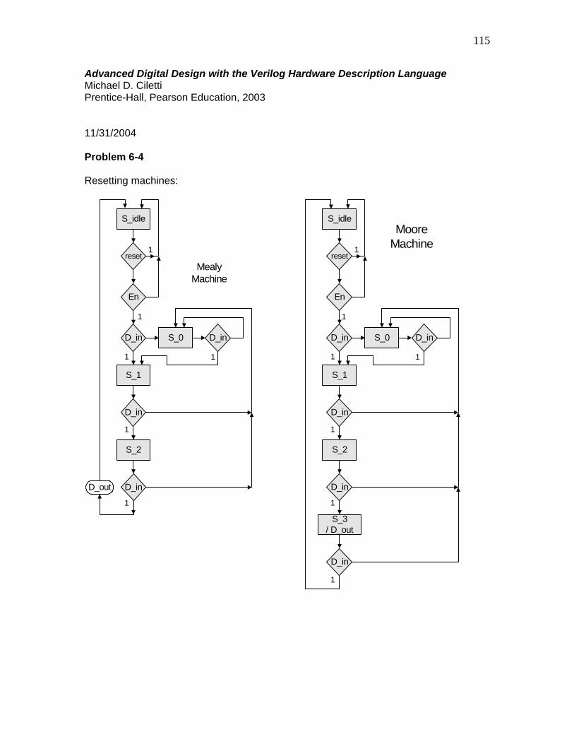
Advanced Digital Design with the Verilog Hardware Description Language Michael D. Ciletti Prentice-Hall, Pearson Education, 2003 11/31/2004 Problem 6-4 Resetting machines:
S_idle
reset1
En
1
D_in
S_1
S_0 D_in
1 1
D_in
S_2
D_in
1
1
D_out
MealyMachine
S_idle
reset1
En
1
D_in
S_1
S_0 D_in
1 1
D_in
S_2
D_in
S_3/ D_out
1
D_in
1
1
MooreMachine

116
Advanced Digital Design with the Verilog Hardware Description Language Michael D. Ciletti Prentice-Hall, Pearson Education, 2003 11/31/2004 Problem 6-5
S_idle
reset1
En
1
D_in
S_1
S_0 D_in
0 0
D_in
S_2
D_in
1
0
MooreMachine
Sequencerecognizer:101010102LSB first
0
10
S_3
D_in
1010
S_4
D_in
0
1010
S_5
D_in
1
01010
S_6
D_in
0
101010
S_7/D_out 0101010
D_in
1
S_8/D_out 10101010
S_idle
reset1
En
1
D_in
S_1
S_0 D_in
0 0
D_in
S_2
D_in
1
0
MealyMachine
Sequencerecognizer:101010102LSB first
0
10
S_3
D_in
1010
S_4
D_in
0
1010
S_5
D_in
1
01010
S_6
D_in
0
101010
S_7/D_out 0101010
D_in
1
D_out

117
Advanced Digital Design with the Verilog Hardware Description Language Michael D. Ciletti Prentice-Hall, Pearson Education, 2003 11/08/2004 Problem 6-7 Solution for resetting machine is not required, but is shown here for comparison.
rst1
S_1
Problem 6-7: Mooreresetting machine
S_0
1
D_in
D_in0
S_2
D_in0
S_3
D_in
S_4/Detect
S_5
D_in
S_6
0
D_in
0
S_7
D_in
S_8/Detect
1
1
0
1
1
0
1
0
Problem 6-7: Mealyresetting machine
Problem 6-7: Moorenon-resetting machine
Problem 6-7: Mealynon-resetting machine
1
rst1
S_1
S_0
1
D_in
D_in0
S_2
D_in0
S_3
D_in
S_5
D_in
S_6
0
D_in
0
S_7
D_in
1
1
0
1
1
0
1
01
DetectDetect
rst1
S_1
S_0
1
D_in
D_in0
S_2
D_in0
S_3
D_in
S_4/Detect
S_5
D_in
S_6
0
D_in
0
S_7
D_in
S_8/Detect
1
1
0
1
1
0
1
01
D_in
D_in
1 0
01
01110111
111
11
1 0
00
000
1000 1000
Detect
rst1
S_1
S_0
1
D_in
D_in0
S_2
D_in0
S_3
D_in
S_5
D_in
S_6
0
D_in
0
S_7
D_in
1
1
0
1
1
0
1
01
0111 1000
Detect
module Prob_6_7_Moore (Detect_Moore, D_in, clk, rst); // Moore nonresetting sequence detector output Detect_Moore; input D_in, clk, rst; parameter S_0 = 0, S_1 = 1, S_2 = 2, S_3 = 3, S_4 = 4; parameter S_5 = 5, S_6 = 6, S_7 = 7, S_8 = 8; reg [3: 0] state_Moore, next_state; wire Detect_Moore = ((state_Moore == S_4) || (state_Moore == S_8)); always @ (posedge clk) if (rst) state_Moore <= S_0; else state_Moore <= next_state; always @ (state_Moore, D_in) begin next_state = S_0; case (state_Moore) S_0: if (D_in) next_state = S_1; else if (D_in == 0) next_state = S_5; S_1: if (D_in) next_state = S_2; else if (D_in == 0) next_state = S_5;

118
S_2: if (D_in) next_state = S_3; else if (D_in == 0) next_state = S_5; S_3: if (D_in) next_state = S_3; else if (D_in == 0) next_state = S_4; S_4: if (D_in) next_state = S_1; else if (D_in == 0) next_state = S_6; S_5: if (D_in) next_state = S_1; else if (D_in == 0) next_state = S_6; S_6: if (D_in) next_state = S_1; else if (D_in == 0) next_state = S_7; S_7: if (D_in) next_state = S_8; else if (D_in == 0) next_state = S_7; S_8: if (D_in) next_state = S_1; else if (D_in == 0) next_state = S_6; default: next_state = S_0; endcase end endmodule module Prob_6_7_Mealy (Detect_Mealy, D_in, clk, rst); // Mealy nonresetting sequence detector output Detect_Mealy; input D_in, clk, rst; parameter S_0 = 0, S_1 = 1, S_2 = 2, S_3 = 3; parameter S_5 = 5, S_6 = 6, S_7 = 7; reg [2: 0] state_Mealy, next_state; wire Detect_Mealy = (((state_Mealy == S_3)&&(D_in == 0)) || ((state_Mealy == S_7)&&(D_in ==1))); always @ (posedge clk) if (rst) state_Mealy <= S_0; else state_Mealy <= next_state; always @ (state_Mealy, D_in) begin next_state = S_0; case (state_Mealy) S_0: if (D_in) next_state = S_1; else if (D_in == 0) next_state = S_5; S_1: if (D_in) next_state = S_2; else if (D_in == 0) next_state = S_5; S_2: if (D_in) next_state = S_3; else if (D_in == 0) next_state = S_5; S_3: if (D_in) next_state = S_3; else if (D_in == 0) next_state = S_5; S_5: if (D_in) next_state = S_1; else if (D_in == 0) next_state = S_6; S_6: if (D_in) next_state = S_1; else if (D_in == 0) next_state = S_7; S_7: if (D_in) next_state = S_1; else if (D_in == 0) next_state = S_7; default: next_state = S_0; endcase end endmodule module t_Prob_6_7 (); wire Detect_Moore, Detect_Mealy; reg D_in, clk, rst; Prob_6_7_Moore M0 (Detect_Moore, D_in, clk, rst); Prob_6_7_Mealy M1 (Detect_Mealy, D_in, clk, rst); initial #500 $finish; initial begin clk = 0; forever #5 clk = ~clk; end initial fork #10 rst = 1;

119
#50 rst = 0; #40 D_in = 1; #120 D_in = 0; #170 D_in = 1; #200 rst = 1; #230 rst = 0; join endmodule

120
Advanced Digital Design with the Verilog Hardware Description Language Michael D. Ciletti Prentice-Hall, Pearson Education, 2003 11/08/2004 Problem 6-8 For simplicity, the machine is realized as a state machine with an output that asserts the majority function.
rst1
S_1
Problem 6-8: Mooreresetting machine
S_0
1
D_in
D_in0
S_2
D_in0
S_3/majority
D_in
111
0
1
1
S_5
1
11 01
S_4/majority
011
D_in0
S_6/majority
D_in
101
1
1
S_7
001
D_in1
D_in
0
S_8
D_in0
S_9
D_in0
S_10/majority
D_in
110
1
1
1
S_12
0
10 00
S_11
010
D_in0
S_13
D_in
100
1
0
S_14
000
D_in
0
D_in
1
1
10
10 1
0
A simple hardware realization (alternative).

121
3-bitShift_Register
Decode_Logic
D_in
majority
module Prob_6_8 (majority, D_in, clk, rst); // majority function output majority; input D_in, clk, rst; parameter S_0 = 0, S_1 = 1, S_2 = 2, S_3 = 3, S_4 = 4; parameter S_5 = 5, S_6 = 6, S_7 = 7, S_8 = 8; parameter S_9 = 9, S_10 = 10, S_11 = 11, S_12 = 12; parameter S_13 = 13, S_14 = 14; reg [4: 0] state, next_state; reg majority; always @ (posedge clk) if (rst) state <= S_0; else state <= next_state; always @ (state, D_in) begin next_state = S_0; case (state) S_0: if (D_in) next_state = S_1; else if (D_in == 0) next_state = S_8; S_1: if (D_in) next_state = S_2; else if (D_in == 0) next_state = S_5; S_2: if (D_in) next_state = S_3; else if (D_in == 0) next_state = S_4; S_3: if (D_in) next_state = S_3; else if (D_in == 0) next_state = S_4; S_4: if (D_in) next_state = S_6; else if (D_in == 0) next_state = S_7; S_5: if (D_in) next_state = S_6; else if (D_in == 0) next_state = S_7; S_6: if (D_in) next_state = S_10; else if (D_in == 0) next_state = S_11; S_7: if (D_in) next_state = S_13; else if (D_in == 0) next_state = S_14; S_8: if (D_in) next_state = S_9; else if (D_in == 0) next_state = S_12; S_9: if (D_in) next_state = S_10; else if (D_in == 0) next_state = S_11; S_10: if (D_in) next_state = S_3; else if (D_in == 0) next_state = S_4; S_11: if (D_in) next_state = S_6; else if (D_in == 0) next_state = S_7; S_12: if (D_in) next_state = S_13; else if (D_in == 0) next_state = S_14; S_13: if (D_in) next_state = S_10; else if (D_in == 0) next_state = S_11; S_14: if (D_in) next_state = S_13; else if (D_in == 0) next_state = S_14; default: next_state = S_0; endcase end always @ (state, D_in) begin majority = 0; case (state) S_3, S_4, S_6, S_10: majority = 1; default: majority = 0; endcase end

122
endmodule module t_Prob_6_8 (); wire majority; reg D_in, clk, rst; reg [2:0] Data_Reg; // View the data stream: always @ (posedge clk) Data_Reg <= {D_in,Data_Reg[2: 1]}; Prob_6_8 M0 (majority, D_in, clk, rst); initial #500 $finish; initial begin clk = 0; forever #5 clk = ~clk; end initial fork #10 rst = 1; #50 rst = 0; #100 D_in = 0; #130 D_in = 1; #160 D_in = 0; #170 D_in = 1; #180 D_in = 0; join endmodule Note: The simple testbench does not fully test the next-state logic. A more robutst testplan is needed. The testbench does, however, include a 3-bit data register to view the bit stream.

123
Advanced Digital Design with the Verilog Hardware Description Language Michael D. Ciletti Prentice-Hall, Pearson Education, 2003 11/10/2004 Problem 6-21
Mux andParallelto Serial
Converter
Channel_0(t)
Channel_31(t)
8
8Serial_in
A/DD_in0
8
Demux
D_Out0
D_Out1
D_Out318
8
8
Control_Unit
A/DD_in31
Par_out
reset
frame_synchclock_488ns
8000 samples / s@ 8 bits ea
2.048Mbps
shift
load
Serial_2_Parallel
sel_mux
Load_Data_Register
sel_demux
Figure 1 Block diagram for digital switch.
488 ns
byte slot 0byte slot 31 byte slot 31
32 byte slots per Sample Frameframe_synch
125 µs
8 clock ticks per byte
Figure 2 Synchronized frame format.

124
module Digital_Switch (D_Out31, D_Out30, D_Out29, D_Out28, D_Out27, D_Out26, D_Out25, D_Out24, D_Out23, D_Out22,D_Out21, D_Out20, D_Out19, D_Out18, D_Out17, D_Out16, D_Out15, D_Out14, D_Out13, D_Out12, D_Out11, D_Out10, D_Out9, D_Out8, D_Out7, D_Out6, D_Out5, D_Out4, D_Out3, D_Out2, D_Out1, D_Out0, D_in31, D_in30, D_in29, D_in28, D_in27, D_in26, D_in25, D_in24, D_in23, D_in22,D_in21, D_in20, D_in19, D_in18, D_in17, D_in16, D_in15, D_in14, D_in13, D_in12, D_in11, D_in10, D_in9, D_in8, D_in7, D_in6, D_in5, D_in4, D_in3, D_in2, D_in1, D_in0, frame_synch, clock_488ns, reset); output [7: 0] D_Out31, D_Out30, D_Out29, D_Out28, D_Out27, D_Out26, D_Out25, D_Out24, D_Out23, D_Out22,D_Out21, D_Out20, D_Out19, D_Out18, D_Out17, D_Out16, D_Out15, D_Out14, D_Out13, D_Out12, D_Out11, D_Out10, D_Out9, D_Out8, D_Out7, D_Out6, D_Out5, D_Out4, D_Out3, D_Out2, D_Out1,D_Out0; input [7: 0] D_in31, D_in30, D_in29, D_in28, D_in27, D_in26, D_in25, D_in24, D_in23, D_in22, D_in21, D_in20, D_in19, D_in18, D_in17, D_in16, D_in15, D_in14, D_in13, D_in12, D_in11, D_in10, D_in9, D_in8, D_in7, D_in6, D_in5, D_in4, D_in3, D_in2, D_in1, D_in0; input frame_synch, clock_488ns, reset; wire [7:0] mux_out; wire Serial_in; wire [4: 0] sel_mux; wire [4: 0] sel_demux; wire [7:0] Par_out; wire load, load_Data_Register; Digital_Switch_Mux M0 (mux_out, D_in31, D_in30, D_in29, D_in28, D_in27, D_in26, D_in25, D_in24, D_in23, D_in22, D_in21, D_in20, D_in19, D_in18, D_in17, D_in16, D_in15, D_in14, D_in13, D_in12, D_in11, D_in10, D_in9, D_in8, D_in7, D_in6, D_in5, D_in4, D_in3, D_in2, D_in1, D_in0, sel_mux); Digital_Switch_Par_2_Serial M1 (Serial_in, mux_out, load_Data_Register, clock_488ns, reset); Digital_Switch_Ser_2_Parallel M2 (Par_out, Serial_in, load, clock_488ns, reset); Digital_Switch_Demux M3 (D_Out31, D_Out30, D_Out29, D_Out28, D_Out27, D_Out26, D_Out25, D_Out24, D_Out23, D_Out22,D_Out21, D_Out20, D_Out19, D_Out18, D_Out17, D_Out16, D_Out15, D_Out14, D_Out13, D_Out12, D_Out11, D_Out10, D_Out9, D_Out8, D_Out7, D_Out6, D_Out5, D_Out4, D_Out3, D_Out2, D_Out1, D_Out0, Par_out, sel_demux); Digital_Switch_Control_Unit M4 (sel_mux, sel_demux, load, load_Data_Register, frame_synch, clock_488ns, reset);

125
endmodule `timescale 1 ns / 10 ps module t_Digital_Switch (); wire [7: 0] D_Out31, D_Out30, D_Out29, D_Out28, D_Out27, D_Out26, D_Out25, D_Out24, D_Out23, D_Out22,D_Out21, D_Out20, D_Out19, D_Out18, D_Out17, D_Out16, D_Out15, D_Out14, D_Out13, D_Out12, D_Out11, D_Out10, D_Out9, D_Out8, D_Out7, D_Out6, D_Out5, D_Out4, D_Out3, D_Out2, D_Out1,D_Out0; reg [7: 0] D_in31, D_in30, D_in29, D_in28, D_in27, D_in26, D_in25, D_in24, D_in23, D_in22, D_in21, D_in20, D_in19, D_in18, D_in17, D_in16, D_in15, D_in14, D_in13, D_in12, D_in11, D_in10, D_in9, D_in8, D_in7, D_in6, D_in5, D_in4, D_in3, D_in2, D_in1, D_in0; reg clock_488ns, reset; reg frame_synch; parameter clock_488ns_period = 488; // 488 ns parameter synch_period = 125000; // 125 usec Digital_Switch M0 (D_Out31, D_Out30, D_Out29, D_Out28, D_Out27, D_Out26, D_Out25, D_Out24, D_Out23, D_Out22,D_Out21, D_Out20, D_Out19, D_Out18, D_Out17, D_Out16, D_Out15, D_Out14, D_Out13, D_Out12, D_Out11, D_Out10, D_Out9, D_Out8, D_Out7, D_Out6, D_Out5, D_Out4, D_Out3, D_Out2, D_Out1, D_Out0, D_in31, D_in30, D_in29, D_in28, D_in27, D_in26, D_in25, D_in24, D_in23, D_in22,D_in21, D_in20, D_in19, D_in18, D_in17, D_in16, D_in15, D_in14, D_in13, D_in12, D_in11, D_in10, D_in9, D_in8, D_in7, D_in6, D_in5, D_in4, D_in3, D_in2, D_in1, D_in0, frame_synch, clock_488ns, reset); reg [7: 0] state; always @ (posedge clock_488ns, negedge frame_synch, posedge reset) if (reset || (frame_synch == 0)) state <= 8'h0; else state <= state + 1; //assign frame_synch = (state == 8'hff); initial #3000000 $finish; always begin: synchronization // Generate synch pulses #100 frame_synch = 1; #clock_488ns_period; frame_synch = 0; forever begin # (synch_period - clock_488ns_period) frame_synch = 1; #clock_488ns_period frame_synch = 0; end

126
end initial begin clock_488ns = 1; end always @ (negedge frame_synch or posedge reset) begin: bit_clock if (reset) disable bit_clock; else begin clock_488ns = 0; repeat (255) begin #(clock_488ns_period/2) if (reset) disable bit_clock; else clock_488ns = ~clock_488ns; #(clock_488ns_period/2)clock_488ns = ~clock_488ns; end #(clock_488ns_period/2)clock_488ns = ~clock_488ns; end end initial begin #1 reset = 1; #1 reset = 0; end initial begin # 255000 reset = 1; #1000 reset = 0; end initial forever begin #5 D_in0 = 8'hff; D_in1 = 8'haa; D_in2 = 2; D_in3 = 3; D_in4 = 4; D_in5 = 5; D_in6 = 6; D_in7 = 7; D_in8 = 8; D_in9 = 9; D_in10 = 10; D_in11 = 11; D_in12 = 12; D_in13 = 13; D_in14 = 14; D_in15 = 15; D_in16 = 16; D_in17 = 17; D_in18 = 18; D_in19 = 19; D_in20 = 20; D_in21 = 21; D_in22 = 22; D_in23 = 23; D_in24 = 24; D_in25 = 25; D_in26 = 26; D_in27 = 27; D_in28 = 28; D_in29 = 29; D_in30 = 30;

127
D_in31 = 31; #125000 D_in0 = 200; D_in1 = 201; D_in2 = 202; D_in3 = 203; D_in4 = 204; D_in5 = 205; D_in6 = 206; D_in7 = 207; D_in8 = 208; D_in9 = 209; D_in10 = 210; D_in11 = 211; D_in12 = 212; D_in13 = 213; D_in14 = 214; D_in15 = 215; D_in16 = 216; D_in17 = 217; D_in18 = 218; D_in19 = 219; D_in20 = 220; D_in21 = 221; D_in22 = 222; D_in23 = 223; D_in24 = 224; D_in25 = 225; D_in26 = 226; D_in27 = 227; D_in28 = 228; D_in29 = 229; D_in30 = 230; D_in31 = 231; #125000; end endmodule module Digital_Switch_Control_Unit (sel_mux, sel_demux, load, load_Data_Register, fs, clock, reset); output [4: 0] sel_mux, sel_demux; output load, load_Data_Register; input fs; input clock, reset; reg [7:0] state; wire [2: 0] bit_count = state [2: 0]; wire [4: 0] byte_count = state [7: 3]; reg sel_demux;

128
always @(negedge clock, posedge reset, negedge fs) if (reset) state <= 8'hff; else if (fs) state <= 8'hff; else state <= state +1; assign load_Data_Register = (state[2:0] == 7); assign sel_mux = byte_count + 1; always @(negedge clock) begin sel_demux <= sel_mux-2; end assign load = (state[2:0] == 0); endmodule module Digital_Switch_Demux (Ch31, Ch30, Ch29, Ch28, Ch27, Ch26, Ch25, Ch24, Ch23, Ch22,Ch21, Ch20, Ch19, Ch18, Ch17, Ch16, Ch15, Ch14, Ch13, Ch12, Ch11, Ch10, Ch9, Ch8, Ch7, Ch6, Ch5, Ch4, Ch3, Ch2, Ch1, Ch0, demux_in, sel_demux); output [7: 0] Ch31, Ch30, Ch29, Ch28, Ch27, Ch26, Ch25, Ch24, Ch23, Ch22, Ch21, Ch20, Ch19, Ch18, Ch17, Ch16, Ch15, Ch14, Ch13, Ch12, Ch11, Ch10, Ch9, Ch8, Ch7, Ch6, Ch5, Ch4, Ch3, Ch2, Ch1, Ch0; reg Ch31, Ch30, Ch29, Ch28, Ch27, Ch26, Ch25, Ch24, Ch23, Ch22, Ch21, Ch20, Ch19, Ch18, Ch17, Ch16, Ch15, Ch14, Ch13, Ch12, Ch11, Ch10, Ch9, Ch8, Ch7, Ch6, Ch5, Ch4, Ch3, Ch2, Ch1, Ch0; input [7: 0] demux_in; input [4: 0] sel_demux; always @ (demux_in, sel_demux) begin // Remove initial values to have latches show data progression /*Ch0 = 0; Ch1 = 0; Ch2 = 0; Ch3 = 0; Ch4 = 0; Ch5 = 0; Ch6 = 0; Ch7 = 0; Ch8 = 0; Ch9 = 0; Ch10 = 0; Ch11 = 0; Ch12 = 0; Ch13 = 0; Ch14 = 0; Ch15 = 0; Ch16 = 0; Ch17 = 0; Ch18 = 0; Ch19 = 0; Ch20 = 0; Ch21 = 0; Ch22 = 0; Ch23 = 0; Ch24 = 0; Ch25 = 0; Ch26 = 0; Ch27 = 0; Ch28 = 0; Ch29 = 0; Ch30 = 0; Ch31 = 0; */ case (sel_demux) 0: Ch0 = demux_in;

129
1: Ch1 = demux_in; 2: Ch2 = demux_in; 3: Ch3 = demux_in; 4: Ch4 = demux_in; 5: Ch5 = demux_in; 6: Ch6 = demux_in; 7: Ch7 = demux_in; 8: Ch8 = demux_in; 9: Ch9 = demux_in; 10: Ch10 = demux_in; 11: Ch11 = demux_in; 12: Ch12 = demux_in; 13: Ch13 = demux_in; 14: Ch14 = demux_in; 15: Ch15 = demux_in; 16: Ch16 = demux_in; 17: Ch17 = demux_in; 18: Ch18 = demux_in; 19: Ch19 = demux_in; 20: Ch20 = demux_in; 21: Ch21 = demux_in; 22: Ch22 = demux_in; 23: Ch23 = demux_in; 24: Ch24 = demux_in; 25: Ch25 = demux_in; 26: Ch26 = demux_in; 27: Ch27 = demux_in; 28: Ch28 = demux_in; 29: Ch29 = demux_in; 30: Ch30 = demux_in; 31: Ch31 = demux_in; endcase end endmodule /* module t_Digital_Switch_Demux (); wire [7: 0] Ch31, Ch30, Ch29, Ch28, Ch27, Ch26, Ch25, Ch24, Ch23, Ch22, Ch21, Ch20, Ch19, Ch18, Ch17, Ch16, Ch15, Ch14, Ch13, Ch12, Ch11, Ch10, Ch9, Ch8, Ch7, Ch6, Ch5, Ch4, Ch3, Ch2, Ch1, Ch0; reg [7: 0] demux_in; reg [4: 0] sel_demux; integer j, k;

130
Digital_Switch_Demux M0 (Ch31, Ch30, Ch29, Ch28, Ch27, Ch26, Ch25, Ch24, Ch23, Ch22,Ch21, Ch20, Ch19, Ch18, Ch17, Ch16, Ch15, Ch14, Ch13, Ch12, Ch11, Ch10, Ch9, Ch8, Ch7, Ch6, Ch5, Ch4, Ch3, Ch2, Ch1,Ch0, demux_in, sel_demux); initial #5000 $finish; initial begin #10 for (k = 0; k <= 31; k = k + 1) #10 sel_demux = k; end initial begin #15 for (j = 0; j <= 31; j = j + 1) #10demux_in = j; end endmodule */ module Digital_Switch_Mux (mux_out, Ch31, Ch30, Ch29, Ch28, Ch27, Ch26, Ch25, Ch24, Ch23, Ch22,Ch21, Ch20, Ch19, Ch18, Ch17, Ch16, Ch15, Ch14, Ch13, Ch12, Ch11, Ch10, Ch9, Ch8, Ch7, Ch6, Ch5, Ch4, Ch3, Ch2, Ch1,Ch0, sel_mux); output [7: 0] mux_out; input [7: 0] Ch31, Ch30, Ch29, Ch28, Ch27, Ch26, Ch25, Ch24, Ch23, Ch22, Ch21, Ch20, Ch19, Ch18, Ch17, Ch16, Ch15, Ch14, Ch13, Ch12, Ch11, Ch10, Ch9, Ch8, Ch7, Ch6, Ch5, Ch4, Ch3, Ch2, Ch1, Ch0; input [4: 0] sel_mux; reg mux_out; always @ (Ch31, Ch30, Ch29, Ch28, Ch27, Ch26, Ch25, Ch24, Ch23, Ch22,Ch21, Ch20, Ch19, Ch18, Ch17, Ch16, Ch15, Ch14, Ch13, Ch12, Ch11, Ch10, Ch9, Ch8, Ch7, Ch6, Ch5, Ch4, Ch3, Ch2, Ch1,Ch0, sel_mux) begin mux_out = 0; case (sel_mux) 0: mux_out = Ch0; 1: mux_out = Ch1; 2: mux_out = Ch2; 3: mux_out = Ch3; 4: mux_out = Ch4; 5: mux_out = Ch5; 6: mux_out = Ch6; 7: mux_out = Ch7; 8: mux_out = Ch8; 9: mux_out = Ch9; 10: mux_out = Ch10; 11: mux_out = Ch11; 12: mux_out = Ch12; 13: mux_out = Ch13;

131
14: mux_out = Ch14; 15: mux_out = Ch15; 16: mux_out = Ch16; 17: mux_out = Ch17; 18: mux_out = Ch18; 19: mux_out = Ch19; 20: mux_out = Ch20; 21: mux_out = Ch21; 22: mux_out = Ch22; 23: mux_out = Ch23; 24: mux_out = Ch24; 25: mux_out = Ch25; 26: mux_out = Ch26; 27: mux_out = Ch27; 28: mux_out = Ch28; 29: mux_out = Ch29; 30: mux_out = Ch30; 31: mux_out = Ch31; default mux_out = 8'bx; endcase end endmodule /* module t_Digital_Switch_Mux (); wire [7: 0] mux_out; reg [7: 0] Ch31, Ch30, Ch29, Ch28, Ch27, Ch26, Ch25, Ch24, Ch23, Ch22, Ch21, Ch20, Ch19, Ch18, Ch17, Ch16, Ch15, Ch14, Ch13, Ch12, Ch11, Ch10, Ch9, Ch8, Ch7, Ch6, Ch5, Ch4, Ch3, Ch2, Ch1, Ch0; reg [4: 0] sel_mux; integer k; Digital_Switch_Mux M0 (mux_out, Ch31, Ch30, Ch29, Ch28, Ch27, Ch26, Ch25, Ch24, Ch23, Ch22,Ch21, Ch20, Ch19, Ch18, Ch17, Ch16, Ch15, Ch14, Ch13, Ch12, Ch11, Ch10, Ch9, Ch8, Ch7, Ch6, Ch5, Ch4, Ch3, Ch2, Ch1,Ch0, sel_mux); initial #5000 $finish; initial begin #5 Ch0 = 0; Ch1 = 1; Ch2 = 2; Ch3 = 3; Ch4 = 4; Ch5 = 5;

132
Ch6 = 6; Ch7 = 7; Ch8 = 8; Ch9 = 9; Ch10 = 10; Ch11 = 11; Ch12 = 12; Ch13 = 13; Ch14 = 14; Ch15 = 15; Ch16 = 16; Ch17 = 17; Ch18 = 18; Ch19 = 19; Ch20 = 20; Ch21 = 21; Ch22 = 22; Ch23 = 23; Ch24 = 24; Ch25 = 25; Ch26 = 26; Ch27 = 27; Ch28 = 28; Ch29 = 29; Ch30 = 30; Ch31 = 31; end initial begin #10 for (k = 0; k <= 31; k = k + 1) #10 sel_mux = k; #10 for (k = 31; k >= 0; k = k - 1) #10 sel_mux = k; end endmodule */ module Digital_Switch_Par_2_Serial (Serial_out, data, load, clock, reset); output Serial_out; input [7: 0] data; input load; input clock, reset; reg [7: 0] Data_Register;
133
assign Serial_out = Data_Register[0]; always @ (negedge clock, posedge reset) if (reset) Data_Register <= 0; else if (load) Data_Register <= data; else Data_Register <= Data_Register >> 1; endmodule module Digital_Switch_Ser_2_Parallel (Par_out, Serial_in, load, clock, reset); output [7: 0] Par_out; input Serial_in; input clock, reset; input load; reg [7: 0] Shift_Register; reg [7: 0] Par_out; always @ (negedge clock or posedge reset) if (reset) Shift_Register <= 0; else Shift_Register <= {Serial_in, Shift_Register [7: 1]}; always @ (negedge clock or posedge reset) if (reset) Par_out <= 0; else if (load) Par_out <= Shift_Register; endmodule /* module t_Digital_Switch_Ser_2_Parallel (); wire [7: 0] Par_out; reg Serial_in; reg clock, reset; reg load, shift; Digital_Switch_Ser_2_Parallel M0 (Par_out, Serial_in, load, shift, clock, reset); initial #5000 $finish; initial begin clock = 0; forever #10 clock = ~clock; end initial begin #2 reset = 1; #2 reset = 0; end initial forever begin repeat (8) @ (negedge clock ) Serial_in = 1; repeat (8) @ (negedge clock ) Serial_in = 0; end initial forever begin

134
repeat (16) @ (negedge clock) shift = 1; repeat (16) @ (negedge clock) shift = 0; end initial forever begin @ (posedge clock) load = 0; repeat (8) @ (negedge clock); load = 1; end endmodule */ Power-up reset with initial conditions.

135

136
Initial bit sequence of first byte after first synch pulse. Note location of load_Data_Register and load pulses Note correct loading of Data_Register, formation of Par_out, and steering of data to D_out7

137
End of first frame with byte 31. Note that the kast byte time of clock_488ns is elongated to the negative edge of frame_synch, recovering the last 72 ns of the frame. Next frame begins correctly.

138
reset on-the-fly

139
reset on-the-fly, with wait for the frame_synch pulse to launch the machine.

140
Recovery from reset on-the-fly.

141
Alternating channel data patterns.

142
Alternating data patterns

143
Advanced Digital Design with the Verilog Hardware Description Language Michael D. Ciletti Prentice-Hall, Pearson Education, 2003 11/18/2004 Problem 7-12 module Binary_Counter_Part_RTL_by_3 (count, enable, clk, rst); parameter size = 4; output [size -1: 0] count; input enable; input clk, rst; wire enable_DP; Control_Unit_by_3 M0 (enable_DP, enable, clk, rst); Datapath_Unit M1 (count, enable_DP, clk, rst); endmodule module Control_Unit_by_3 (enable_DP, enable, clk, rst); output enable_DP; input enable; input clk, rst; reg [1:0] state, next_state; parameter s0 = 0, s1 = 1, s2 = 2, s3 = 3; reg enable_DP; always @ (posedge clk) if (rst == 1) state <= s0; else state <= next_state; always @(state or enable) begin enable_DP = 0; case (state) s0: begin next_state = s1; end s1: begin next_state = s2; end s2: begin next_state = s0; if (enable) enable_DP = 1; end endcase end endmodule /* module Control_Unit_by_3 (enable_DP, enable, clk, rst); output enable_DP; input enable; input clk, rst; reg enable_DP;

144
always begin: Cycle_by_3 @ (posedge clk) enable_DP <= 0; if ((rst == 1) || (enable != 1)) disable Cycle_by_3; else @ (posedge clk) if ((rst == 1) || (enable != 1)) disable Cycle_by_3; else @ (posedge clk) if ((rst == 1) || (enable != 1)) disable Cycle_by_3; else enable_DP <= 1; end // Cycle_by_3 endmodule */ module Datapath_Unit (count, enable, clk, rst); parameter size = 4; output [size-1: 0] count; input enable; input clk, rst; reg count; //wire [size-1: 0] next_count; always @ (posedge clk) if (rst == 1) count <= 0; else if (enable == 1) count <= next_count(count); function [size-1: 0] next_count; input [size-1:0] count; begin next_count = count + 1; end endfunction endmodule module t_Binary_Counter_Partioned_RTL_by_3 (); parameter size = 4; wire [size -1: 0] count; reg enable; reg clk, rst; Binary_Counter_Part_RTL_by_3 M0 (count, enable, clk, rst); initial #800 $finish; initial begin clk = 0; forever #5 clk = ~clk; end initial fork #2 begin rst = 1; enable = 0; end #10 rst = 0; #20 enable = 1; #120 enable = 0; #140 enable = 1; #160 rst = 1;

145
#190 rst = 0; #300 enable = 0; #340 enable = 1; join endmodule

146
Advanced Digital Design with the Verilog Hardware Description Language Michael D. Ciletti Prentice-Hall, Pearson Education, 2003 12/08/2004 Problem 9-12 The synthesized Circular_Buffer_1 has a simpler hardware implementation that Circular_Buffer_2. Also note that the reset action displayed in Figure 9.43 has a race condition between the deassertion of reset and the rising edge of the clock. Depending on the simulator, this could result in the write pointer being set to x. To eliminate the race condition, modify the test bench to have the reset de-assert on the falling edge of the clock. Advanced Digital Design with the Verilog Hardware Description Language Michael D. Ciletti Prentice-Hall, Pearson Education, 2003 12/08/2004 Problem 9-18 The pipeline in Figure P9-18 does not maintain data coherency. To establish coherency, place two pipeline registers in the path for data_in_2. Advanced Digital Design with the Verilog Hardware Description Language Michael D. Ciletti Prentice-Hall, Pearson Education, 2003 12/08/2004 Problem 9-19
12 15 9 4
7 6
Optimum cutset for coherencyand stage balance.
Top Related
Copyright © 2022 FDOKUMEN

