XGT Analog Output Module - LS Electric
72
XGT Analog Output Module XGF-DV4A/DV8A/DC4A/DC8A Right choice for ultimate yield LSIS strives to maximize customers' profit in gratitude of choosing us for your partner. User’s Manual LS values every single customer. Quality and service come first at LSIS. Always at your service, standing for our customers. Read this manual carefully before installing, wiring, operating, servicing or inspecting this equipment. Keep this manual within easy reach for quick reference. Programmable Logic Controller ■ HEAD OFFICE Yonsei Jaedan Severance Bldg. 84-11 5 ga, Namdaemun-ro, Jung-gu Seoul 100-753, Korea http://eng.lsis.biz Tel. (82-2)2034-4643~4649 Fax.(82-2)2034-4879, 2034-4885 ■ LS Industrial Systems Tokyo Office >> Japan Address: 16F, Higashi-Kan, Akasaka Twin Towers 17- 22, 2-chome, Akasaka, Minato-ku, Tokyo 107-8470, Japan Tel: 81-3-3582-9128 Fax: 81-3-3582-2667 e-mail: [email protected] ■ LS Industrial Systems Dubai Rep. Office >> UAE Address: P.O.BOX-114216, API World Tower, 303B, Sheikh Zayed road, Dubai, UAE. e-mail: [email protected] Tel: 971-4-3328289 Fax: 971-4-3329444 ■ LS-VINA Industrial Systems Co., Ltd. >> Vietnam Address: LSIS VINA Congty che tao may dien Viet-Hung Dong Anh Hanoi, Vietnam e-mail: [email protected] Tel: 84-4-882-0222 Fax: 84-4-882-0220 ■ LS Industrial Systems Hanoi Office >> Vietnam Address: Room C21, 5th Floor, Horison Hotel, 40 Cat Linh, Hanoi, Vietnam Tel: 84-4-736-6270/1 Fax: 84-4-736-6269 ■ Dalian LS Industrial Systems co., Ltd, >> China Address: No. 15 Liaohexi 3 Road, economic and technical development zone, Dalian, China e-mail: [email protected] Tel: 86-411-8273-7777 Fax: 86-411-8730-7560 ■ LS Industrial Systems (Shanghai) Co., Ltd. >> China Address: Room E-G, 12th Floor Huamin Empire Plaza, No. 726, West Yan’an Road, Shanghai, China Tel: 86-21-5237-9977 ■ LS Industrial Systems(Wuxi) Co., Ltd. >> China Address: 102-A National High & New Tech Industrial Development Area, Wuxi, Jiangsu, China e-mail: [email protected] Tel: 86-510-534-6666 Fax: 86-510-522-4078 ■ LS Industrial Systems Beijing Office >> China Address: B-tower 17th Floor, Beijing Global Trade Center building, No. 36, BeiSanHuanDong-Lu, DongCheng-District, Beijing, China Tel: 86-10-5825-6025 ■ LS Industrial Systems Guangzhou Office >> China Address: Room 1403, 14F, New Poly Tower, 2 Zhongshan Liu Rad, Guangzhou, China e-mail: [email protected] Tel: 86-20-8326-6754 Fax: 86-20-8326-6287 ■ LS Industrial Systems Chengdu Office >> China Address: Room 2907, Zhong Yin B/D, No. 35, Renminzhong(2)- Road, Chengdu, China e-mail: [email protected] Tel: 86-28-8612-9151 Fax: 86-28-8612-9236 ■ LS Industrial Systems Qingdao Office >> China Address: 12th Floor, Guodong building, No52 Jindun Road, Chengdu, China e-mail: [email protected] Tel: 86-532-580-2539 Fax: 86-532-583-3793 10310000609 XGT Series/2006,11 ※ LS Industrial Systems constantly endeavors to improve its product so that Information in this manual is subject to change without notice. ⓒ LS Industrial systems Co., Ltd 2006 All Rights Reserved.
-
Upload
khangminh22 -
Category
Documents
-
view
6 -
download
0
Transcript of XGT Analog Output Module - LS Electric

XGT Analog Output Module
XGF-DV4A/DV8A/DC4A/DC8A
Right choice for ultimate yield LSIS strives to maximize customers' profit in gratitude of choosing us for your partner.
User’s Manual
LS values every single customer.
Quality and service come first at LSIS.
Always at your service, standing for our customers.
Read this manual carefully before installing, wiring, operating, servicing or inspecting this equipment.
Keep this manual within easy reach for quick reference.
Programmable Logic Controller
HEAD OFFICE
Yonsei Jaedan Severance Bldg. 84-11 5 ga, Namdaemun-ro,
Jung-gu Seoul 100-753, Korea http://eng.lsis.biz
Tel. (82-2)2034-4643~4649 Fax.(82-2)2034-4879, 2034-4885
LS Industrial Systems Tokyo Office >> Japan
Address: 16F, Higashi-Kan, Akasaka Twin Towers 17- 22,
2-chome, Akasaka, Minato-ku, Tokyo 107-8470, Japan
Tel: 81-3-3582-9128 Fax: 81-3-3582-2667
e-mail: [email protected]
LS Industrial Systems Dubai Rep. Office >> UAE
Address: P.O.BOX-114216, API World Tower, 303B, Sheikh
Zayed road, Dubai, UAE. e-mail: [email protected]
Tel: 971-4-3328289 Fax: 971-4-3329444
LS-VINA Industrial Systems Co., Ltd. >> Vietnam
Address: LSIS VINA Congty che tao may dien Viet-Hung
Dong Anh Hanoi, Vietnam e-mail: [email protected]
Tel: 84-4-882-0222 Fax: 84-4-882-0220
LS Industrial Systems Hanoi Office >> Vietnam
Address: Room C21, 5th Floor, Horison Hotel, 40 Cat Linh,
Hanoi, Vietnam
Tel: 84-4-736-6270/1 Fax: 84-4-736-6269
Dalian LS Industrial Systems co., Ltd, >> China
Address: No. 15 Liaohexi 3 Road, economic and technical
development zone, Dalian, China e-mail: [email protected]
Tel: 86-411-8273-7777 Fax: 86-411-8730-7560
LS Industrial Systems (Shanghai) Co., Ltd. >> China
Address: Room E-G, 12th Floor Huamin Empire Plaza,
No. 726, West Yan’an Road, Shanghai, China
Tel: 86-21-5237-9977
LS Industrial Systems(Wuxi) Co., Ltd. >> China
Address: 102-A National High & New Tech Industrial
Development Area, Wuxi, Jiangsu, China e-mail: [email protected]
Tel: 86-510-534-6666 Fax: 86-510-522-4078
LS Industrial Systems Beijing Office >> China
Address: B-tower 17th Floor, Beijing Global Trade Center building,
No. 36, BeiSanHuanDong-Lu, DongCheng-District, Beijing, China
Tel: 86-10-5825-6025
LS Industrial Systems Guangzhou Office >> China
Address: Room 1403, 14F, New Poly Tower, 2 Zhongshan Liu
Rad, Guangzhou, China e-mail: [email protected]
Tel: 86-20-8326-6754 Fax: 86-20-8326-6287
LS Industrial Systems Chengdu Office >> China
Address: Room 2907, Zhong Yin B/D, No. 35, Renminzhong(2)-
Road, Chengdu, China e-mail: [email protected]
Tel: 86-28-8612-9151 Fax: 86-28-8612-9236
LS Industrial Systems Qingdao Office >> China
Address: 12th Floor, Guodong building, No52 Jindun Road,
Chengdu, China e-mail: [email protected]
Tel: 86-532-580-2539 Fax: 86-532-583-3793
10310000609
XGT Series/2006,11※ LS Industrial Systems constantly endeavors to improve its product so that Information in this manual is subject to change without notice.
LS Industrial systems Co., Ltd 2006 All Rights Reserved.

Safety Instructions
Before using the product … For your safety and effective operation, please read the safety instructions thoroughly before using the product. Safety Instructions should always be observed in order to prevent accident
or risk with the safe and proper use the product. Instructions are separated into “Warning” and “Caution”, and the meaning of
the terms is as follows;
This symbol indicates the possibility of serious injury or death if some applicable instruction is violated
This symbol indicates the possibility of slight injury or damage to products if some applicable instruction is violated
The marks displayed on the product and in the user’s manual have the
following meanings.
Be careful! Danger may be expected.
Be careful! Electric shock may occur. The user’s manual even after read shall be kept available and accessible to
any user of the product.
Warning
Caution

Safety Instructions
Safety Instructions when designing
Please, install protection circuit on the exterior of PLC to protect the whole control system from any error in external power or PLC
module. Any abnormal output or operation may cause serious problem in safety of the whole system.
- Install applicable protection unit on the exterior of PLC to protect the system from physical damage such as emergent stop switch, protection circuit, the upper/lowest limit switch, forward/reverse operation interlock circuit, etc.
- If any system error (watch-dog timer error, module installation error, etc.) is detected during CPU operation in PLC, the whole output is designed to be turned off and stopped for system safety. However, in case CPU error if caused on output device itself such as relay or TR can not be detected, the output may be kept on, which may cause serious problems. Thus, you are recommended to install an addition circuit to monitor the output status.
Never connect the overload than rated to the output module nor allow the output circuit to have a short circuit, which may cause a fire.
Never let the external power of the output circuit be designed to be On earlier than PLC power, which may cause abnormal output or
operation.
In case of data exchange between computer or other external equipment and PLC through communication or any operation of PLC (e.g. operation mode change), please install interlock in the sequence program to protect the system from any error. If not, it may cause abnormal output or operation.
Warning

Safety Instructions
Safety Instructions when designing
Safety Instructions when designing
I/O signal or communication line shall be wired at least 100mm away from a high-voltage cable or power line. If not, it may cause abnormal output or operation.
Caution
Use PLC only in the environment specified in PLC manual or general standard of data sheet. If not, electric shock, fire, abnormal operation of the product or flames may be caused.
Before installing the module, be sure PLC power is off. If not, electric shock or damage on the product may be caused.
Be sure that each module of PLC is correctly secured. If the product is installed loosely or incorrectly, abnormal operation, error or dropping may be caused.
Be sure that I/O or extension connecter is correctly secured. If not, electric shock, fire or abnormal operation may be caused.
If lots of vibration is expected in the installation environment, don’t let PLC directly vibrated. Electric shock, fire or abnormal operation may be caused.
Don’t let any metallic foreign materials inside the product, which may cause electric shock, fire or abnormal operation..
Caution

Safety Instructions
Safety Instructions when wiring
Prior to wiring, be sure that power of PLC and external power is turned off. If not, electric shock or damage on the product may be caused.
Before PLC system is powered on, be sure that all the covers of the terminal are securely closed. If not, electric shock may be caused
Warning
Let the wiring installed correctly after checking the voltage rated of each product and the arrangement of terminals. If not, fire, electric shock or abnormal operation may be caused.
Secure the screws of terminals tightly with specified torque when wiring. If the screws of terminals get loose, short circuit, fire or abnormal operation may be caused.
Surely use the ground wire of Class 3 for FG terminals, which is exclusively used for PLC. If the terminals not grounded correctly, abnormal operation may be caused.
Don’t let any foreign materials such as wiring waste inside the module while wiring, which may cause fire, damage on the product or abnormal operation.
Caution

Safety Instructions
Safety Instructions for test-operation or repair
Safety Instructions for waste disposal
Don’t touch the terminal when powered. Electric shock or abnormal operation may occur.
Prior to cleaning or tightening the terminal screws, let all the external power off including PLC power. If not, electric shock or abnormal operation may occur.
Don’t let the battery recharged, disassembled, heated, short or soldered. Heat, explosion or ignition may cause injuries or fire.
Warning
Don’t remove PCB from the module case nor remodel the module. Fire, electric shock or abnormal operation may occur.
Prior to installing or disassembling the module, let all the external power off including PLC power. If not, electric shock or abnormal operation may occur.
Keep any wireless installations or cell phone at least 30cm away from PLC. If not, abnormal operation may be caused.
Caution
Product or battery waste shall be processed as industrial waste. The waste may discharge toxic materials or explode itself.
Caution

Revision History
Version Date Remark Page
V 1.0 ’06.05 First Edition -

About User’s Manual
About User’s Manual
Congratulations on purchasing PLC of LS Industrial System Co.,Ltd.
Before use, make sure to carefully read and understand the User’s Manual about the functions,
performances, installation and programming of the product you purchased in order for correct use and
importantly, let the end user and maintenance administrator to be provided with the User’s Manual.
The Use’s Manual describes the product. If necessary, you may refer to the following description and order
accordingly. In addition, you may connect our website(http://www.lsis.biz/) and download the information as a
PDF file.
Relevant User’s Manuals
Title Description No. of User’s
Manual
XGK-CPUA/CPUE/CPUH/CPUS
It describes specifications, system structure and EMC
spec. correspondence of CPU module, power module,
base, I/O module and increase cable
10310000508
XG5000 User’s Manual
It describes how to use XG5000 software especially
about online functions such as programming, printing,
monitoring and debugging by using XGT series
products.
10310000512
XGK Series
Instructions & Programming
It is the user’s manual for programming to explain how
to use commands that are used PLC system with XGK
CPU.
10310000510

Chapter 1 Introduction ……………………………………………………………… 1-1 ~ 1-3
1.1 Characteristics ...................................................................................................................................... 1-1
1.2 Terminology .......................................................................................................................................... 1-2
1.2.1 Analog quantity − A ..................................................................................................................... 1-2
1.2.2 Digital quantity − D...................................................................................................................... 1-2
1.2.3 Characteristics of D/A conversion............................................................................................... 1-3
Chapter 2 Specifications …………………………………………………………… 2-1 ~ 2-9
2.1 General Specifications .......................................................................................................................... 2-1
2.2 Performance Specifications .................................................................................................................. 2-2
2.3 Respective Designations and Functions............................................................................................... 2-3
2.4 Characteristic of I/O Conversion........................................................................................................... 2-4
2.4.1 Characteristic of voltage output .................................................................................................. 2-4
2.4.2 Characteristic of current output .................................................................................................. 2-6
2.4.3 Accuracy ..................................................................................................................................... 2-7
2.5 Main Functions...................................................................................................................................... 2-8
2.5.1 Output status setting................................................................................................................... 2-8
2.5.2 Display and diagnosis functions ................................................................................................. 2-9
3.1 Installation............................................................................................................................................. 3-1
3.1.1 Installation environment.............................................................................................................. 3-1
3.1.2 Precautions for handling ............................................................................................................. 3-1
3.2 Wiring.................................................................................................................................................... 3-1
3.2.1 Precautions for wiring ................................................................................................................. 3-1
3.2.2 Wiring examples ......................................................................................................................... 3-2
3.3 Wiring of DC 24V .................................................................................................................................. 3-3
3.3.1 Specification of power supply ..................................................................................................... 3-3
Table of Contents
Chapter 3 Installation and Wiring ……………………………………………… 3-1 ~ 3-4

3.3.2 If XGP-ACF1 power module is used........................................................................................... 3-3
3.3.3 If an external power module is used........................................................................................... 3-4
Chapter 4 Operation Procedure and Monitoring ……………………………… 4-1 ~ 4-13
4.1 Operation Procedures ......................................................................................................................... 4-1
4.2 Operation Parameters Setting .............................................................................................................. 4-2
4.2.1 Setting items ............................................................................................................................... 4-2
4.2.2 How to use I/O parameters......................................................................................................... 4-2
4.3 Parameters Setting ............................................................................................................................... 4-3
4.3.1 Setting screen of parameters...................................................................................................... 4-3
4.4 Monitoring / Test ................................................................................................................................... 4-7
4.4.1 Monitoring/Test screen................................................................................................................ 4-7
4.4.2 Operation by program................................................................................................................. 4-9
4.5 Register U Devices ............................................................................................................................. 4-10
4.5.1 Register U devices.................................................................................................................... 4-10
4.5.2 Save variables .......................................................................................................................... 4-11
4.5.3 View variables........................................................................................................................... 4-12
Chapter 5 Configuration and Function of Internal Memory ………………… 5-1 ~ 5-7
5.1 Configuration of Internal Memory ......................................................................................................... 5-1
5.1.1 I/O area of D/A converted data ................................................................................................... 5-1
5.1.2 Setting area of operation parameters ......................................................................................... 5-2
5.2 I/O area of D/A Converted Data .......................................................................................................... 5-3
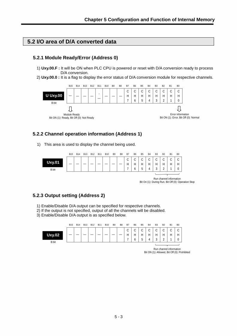
5.2.1 Module Ready/Error (Address 0)................................................................................................ 5-3
5.2.2 Channel operation information (Address 1)................................................................................ 5-3
5.2.3 Output setting (Address 2).......................................................................................................... 5-3
5.2.4 Digital input (Address 3~6) ......................................................................................................... 5-4
5.3 Operation Parameters settings ............................................................................................................. 5-5
5.3.1 Specifying channel to use........................................................................................................... 5-5
5.3.2 Setting Output Voltage/Current range ........................................................................................ 5-5
5.3.3 Specifying Input data type........................................................................................................... 5-6
5.3.4 Setting Output data type ............................................................................................................. 5-6
5.3.5 Error code ................................................................................................................................... 5-7

Chapter 6 Programming …………………………………………………………… 6-1 ~ 6-9
6.1 Internal Memory Read/Write................................................................................................................. 6-1
6.1.1 Read of internal memory (GET, GETP instruction)..................................................................... 6-1
6.1.2 Write of internal memory (PUT, PUTP instruction) ..................................................................... 6-2
6.2 Basic Program ...................................................................................................................................... 6-3
6.2.1 XGF-DC4A.................................................................................................................................. 6-3
6.3 Application Program.............................................................................................................................. 6-5
6.3.1 Inverter speed control ................................................................................................................. 6-5
6.3.2 BCD output of error code............................................................................................................ 6-8
Chapter 7 Troubleshooting ………………………………………………………… 7-1 ~ 7-9
7.1 Error Codes........................................................................................................................................... 7-1
7.2 Troubleshooting ……………… ............................................................................................................. 7-3
7.2.1 RUN LED blinks……………........................................................................................................ 7-3
7.2.2 RUN LED is Off......................................................................................................... ……………7-3
7.2.3 D/A Output Value hunted too much ............................................................................................ 7-4
7.2.4 Relationship discordant between Digital Input Value & Analog Output Value. ........................... 7-5
7.2.5 D/A Output Value always exceeds the value specified............................................................... 7-6
7.2.6 Analog Output Value does not change accordingly to the change of Digital Input Value........... 7-7
7.2.7 Hardware error of D/A conversion module ................................................................................. 7-7
7.2.8 Status check of D/A conversion module through XG5000 System Monitoring........................... 7-8
Appendix …………………………………………………… Appendix 1-1 ~ Appendix 2-2
Appendix 1 Terminology ………………………………………………………………………… Appendix 1 - 1
Appendix 2 Dimensions ………………………………………………………………………… Appendix 2 - 1
1) Dimensions of XGF-DV4A/DC4A ……………………………………………………… Appendix 2 - 1
2) Dimensions of XGF-DV8A/DC8A ……………………………………………………… Appendix 2 - 2
Index ……………………………………………………………………… Index - 1 ~ Index - 2

Chapter 1 Introduction
1 - 1
Chapter 1 Introduction Voltage output is called as XGF-DV4A/DV8A, and current output is as XGF-DC4A/DV8A in this product. D/A conversion module is used to convert the digital value of signed 16-bit binary data (data: 14 bits) specified in PLC CPU to analog signal (voltage or current output).
1) D/A conversion of 4 channels is available with one module.
XGF-DV4A/DV8A: D/A conversion of 4 channels (voltage output) is available with one module. XGF-DC4A/DC8A: D/A conversion of 4 channels (current output) is available with one module.
2) High resolution of 1/16000
Through the digital value resolution of1/16000, high resolution of analog value can be obtained.
3) High accuracy High accuracy of ±0.2% or less (when ambient temperature is 25 ) .
4) Conversion process at high speed
Conversion speed is 250/channel.
5) Various output ranges available XGF-DV4A/DV8A: 1~5V, 0~5V, 0~10V, -10~10V XGF-DC4A/DC8A: 4~20mA, 0~20mA
6) The number of modules used for one base is not limited.
(However, it should be within the capacity of the power module.)
1.1 Characteristics

Chapter 1 Introduction
1 - 2
1.2 Terminology
1.2.1 Analog quantity − A Such a quantity continuously changed is called Analog Quantity as voltage, current, temperature, speed, pressure and flow. For example, temperature can change continuously together with time as shown in Fig. 1.1. Since the changing temperature can not be input directly on PLC, it should be input on PLC through the transducer converting to identical analog quantity of DC voltage -10 ~+10V or current 4~20 .
1.2.2 Digital quantity − D
Such a quantity discontinuously changed is called Digital Quantity as displayed in figures of 0, 1, 2 and 3. For example, On and Off signal can be displayed in a digital quantity of 0 and 1. BCD and binary value is also the digital quantity
Analog quantity can not be directly input on PLC CPU for calculation of the digital quantity. Thus, convert analog quantity to digital quantity as in Fig. 1.4 so to input on CPU. In addition, in order to output the analog quantity outward, convert CPU’s digital quantity to analog quantity.
[Fig 1.3] Digital Quantity
CPU (Digital calculation)
A/D Conversio
D/A Conversion
Analog input 0 ~ ±10V or
4~20
Analog 0 ~ 10V or
4~20
[Fig 1.4] Process in PLC
[Fig.1.1] Analog Quantity [Fig.1.2] Transducer Example
Temperature0 ~ 1000°C
Transducer
Voltage -10 ~ 10V input on
A/D conversion module
⇒ ⇒
Time
Tem
pera
ture
0 Time
Tem
pera
ture

Chapter 1 Introduction
1 - 3
1.2.3 Characteristics of D/A conversion 1) Voltage output
D/A conversion module is used to convert digital quantity output from CPU to analog value so to output to the external device. When the voltage output range of D/A conversion module is in -10~10V, -10V will be output if digital quantity of 0 is input. And 10V will be output if digital quantity of 16000 is input, where analog quantity converted from digital input of 1 is equivalent to 1.25. 2) Current output
When the current output range of D/A conversion module is in 4~20mA, 4mA will be output if digital quantity of 0 is input. And 20mA will be output if digital quantity of 16000 is input, where analog quantity converted from digital input of 1 is equivalent to 1.
[Fig. 1.5] Characteristics of D/A conversion (voltage output)
[Fig. 1.6] Characteristics of D/A conversion (current output)
Analog output current
12
4 0 8000 16000
Digital input value
8008000 8001 8002 8003
Digital input
Analog output current 800
12.001
12.000
1
20
Analog output voltage
10V
0V
-10V
0 8000 16000
Digital input value
8004 8001 8002 8003
Digital input A
nalog output voltage
8005
0.00125
0.000V
1.25
8000

Chapter 2 Specifications
2 - 1
Chapter 2 Specifications
General specifications of XGT series are as specified below.
No. Item Specifications Related standards
1 Operating temperature 0 +55∼
2 Storage temperature -25 +70∼
3 Operating humidity 5 95%RH∼ , Non-condensing
4 Storage humidity 5 95%RH, ∼ Non-condensing
For discontinuous vibration Frequency Acceleration Amplitude Number10≤f< 57 - 0.075mm 57≤f≤150 9.8m/s2 (1G) -
For continuous vibration Frequency Acceleration Amplitude
10≤f< 57 - 0.035mm
5 Vibration
57≤f≤150 4.9m/s2 (0.5G) -
Each 10 times in X,Y,Z
directions
IEC61131-2
6 Shocks
* Max. impact acceleration:147(15G) * Authorized time :11 * Pulse wave : Signal half-wave pulse (Each 3 times in X,Y,Z directions)
IEC61131-2
Square wave impulse noise ±1,500V LSIS standard
Electrostatic discharging Voltage : 4kV (contact discharging) IEC 61131-2, IEC 61000-4-2
Radiated electromagnetic field noise 27 ~ 500MHz, 10 V/m IEC 61131-2, IEC 61000-4-3
Class Power module
Digital/Analog I/O communication interface
7 Impulse Noise
Fast Transient
/Burst noise
Voltage 2kV 1kV
IEC 61131-2, IEC 61000-4-4
8 Ambient conditions No corrosive gas or dust
9 Operating height 2000m or less
10 Pollution degree 2 or less
11 Cooling type Natural air cooling
Remark
1) IEC (International Electrotechnical Commission): An international nongovernmental organization which promotes internationally cooperated standardization in
electric/electronic fields, publishes international standards and manages applicable estimation system related with.
2) Pollution degree: An index indicating pollution level of the operating environment which decides insulation performance of the
devices. For instance, Pollution level 2 indicates the state generally that only non- conductive pollution occurs. However, this state contains temporary conduction due to dew produced.
2.1 General Specifications

Chapter 2 Specifications
2 - 2
2.2 Performance Specifications
Performance specifications of D/A conversion module are as specified in table below.
Specification Item XGF-DV4A
(Voltage Output Type)XGF-DV8A
(Voltage Output Type)XGF-DC4A
(Current Output Type) XGF-DC8A
(Current Output Type)DC 4 ~ 20 DC 0 ~ 20
DC 1 ~ 5V DC 0 ~ 5V
DC 0 ~ 10V DC -10 ~ 10V
Load resistance :600Ω or less
Load resistance :550Ω or less Analog output
Output range can be selected through applicable program or parameters (for respective channels)
Digital input
Signed 16-bit binary value (data: 14 bits) : Format of input data can be set through applicable program or parameters
(for respective channels)
Analog outputDigital input 1 ~ 5V 0 ~ 5V 0 ~ 10V -10 ~ 10V
Unsigned Value 0 ~ 16000 Signed Value -8000 ~ 8000 Precise Value 100 ~ 5000 0 ~ 5000 0 ~ 10000 -10000~10000
Percentile Value 0 ~ 10000
Analog outputDigital input 4 ~ 20mA 0 ~ 20mA
Unsigned Value 0 ~ 16000 Signed Value -8000 ~ 8000 Precise Value 4000 ~ 20000 0 ~ 20000
Percentile Value 0 ~ 10000
1/16000 (for respective output ranges) 1~5 V 0.250 0~5 V 0.3125
4~20 1.0
0~10 V 0.625
Maximum resolution
±10 V 1.250 0~20 1.25
Accuracy ±0.2% or less (when ambient temperature is 25 ) ±0.3% or less (when the range is within operational temperature)
Maximum conversion speed 250 /channel
Absolute maximum output ±15 V ±24
Number of output channels
4 channels/ 1 module
8 channels/ 1 module
4 channels/ 1 module
8 channels/ 1 module
Insulation method Photo-coupler insulation between input terminal and PLC power (no insulation between channels)
Terminal connected 18-point terminal
I/O points occupied Changeable type: 16 points, Fixed type: 64 points
DC 5V 190 190 190 190 Current consumption DC 24V 140 180 210 300
Weight (g) 150g
Load resistance : 1 or more

Chapter 2 Specifications
2 - 3
2.3 Respective Designations and Functions Respective designations of the parts are as described below.
No. Description
RUN LED ①
Displays the operation status of D/A conversion module On: Operation normal Blinks: Error occurs (Refer to 7.1 for more details)
Off: DC 5V disconnected, D/A conversion module error
Analog Terminal
②
Analog terminal, whose respective channels can be connected with external devices
Power Terminal ③
Supply terminal of external power DC24V (No.17~18)
②
①
③
XGF-DV4A XGF-DC4A

Chapter 2 Specifications
2 - 4
2.4 Characteristics of I/O Conversion
Characteristics of I/O conversion are displayed in a straight line with the inclination as shown below
when converting digital signal specified in PLC to analog signal (voltage or current).
Input formats of digital data are classified into Unsigned Value, Signed Value, Precise Value and
Percentile Value, and I/O conversion characteristics for respective digital input ranges are as described
below.
2.4.1 Characteristic of voltage output
Voltage output range can be selected through user program or special module parameters setting for respective channels.
1) If the range is 1~5V
Analog Voltage Output Digital Input
0.952 1.0 2.0 3.0 4.0 5.0 5.048
Max. Resolu
tion
Unsigned value -192 0 4000 8000 12000 16000 16191
Signed value -8192 -8000 -4000 0 4000 8000 8191
Precise value 952 1000 2000 3000 4000 5000 5047
Percentile value -120 0 2500 5000 7500 10000 10119
0.25
※ In the case of 1~5V voltage output, analog voltage output for digital value of “1” is equivalent to 0.25 .
Digital Input Value
Anal
og V
olta
ge O
utpu
t

Chapter 2 Specifications
2 - 5
2) If the range is 0~5V
Analog Voltage Output Digital Input
-0.06 0.0 1.25 2.5 3.75 5.0 5.06 MaximumResolution
Unsigned value -192 0 4000 8000 12000 16000 16191
Signed value -8192 -8000 -4000 0 4000 8000 8191
Precise value -60 0 1250 2500 3750 5000 5059
Percentile value -120 0 2500 5000 7500 10000 10119
0.3125
※ In the case of 0~5V voltage output, analog voltage output for digital value of “1” is equivalent to 0.3125 . 3) If the range is 0~10V
Analog Voltage Output Digital Input
-0.12 0.0 2.5 5.0 7.5 10.0 10.12 MaximumResolution
Unsigned value -192 0 4000 8000 12000 16000 16191
Signed value -8192 -8000 -4000 0 4000 8000 8191
Precise value -120 0 2500 5000 7500 10000 10119
Percentile value -120 0 2500 5000 7500 10000 10119
0.625
※ In the case of 0~10V voltage output, analog voltage output for digital value of “1” is equivalent to 0.625 .
4) If the range is -10~10V
Analog Voltage Output Digital Input
-10.24 -10.0 -5.0 0.0 5.0 10.0 10.24 MaximumResolution
Unsigned value -192 0 4000 8000 12000 16000 16191
Signed value -8192 -8000 -4000 0 4000 8000 8191
Precise value -10240 -10000 -5000 0 5000 10000 10238
Percentile value -120 0 2500 5000 7500 10000 10119
1.25
※ In the case of -10~10V voltage output, analog voltage output for digital value of “1” is equivalent to 1.25 .

Chapter 2 Specifications
2 - 6
2.4.2 Characteristic of current output
Current output range can be selected through user program or special module parameters setting for respective channels.
1) If the range is 4~20
Analog Current Output Digital Input
3.808 4 8 12 16 20 20.192 MaximumResolution
Unsigned value -192 0 4000 8000 12000 16000 16191
Signed value -8192 -8000 -4000 0 4000 8000 8191
Precise value 3808 4000 8000 12000 16000 20000 20192
Percentile value -120 0 2500 5000 7500 10000 10119
1.0
※ In the case of 4~20 current output, analog current output for digital value of “1” is equivalent to 1.0 .
2) If the range is 0~20
Analog Current Output Digital Input
- 0 5 10 15 20 20.24 MaximumResolution
Unsigned value 0 0 4000 8000 12000 16000 16191
Signed value 0 -8000 -4000 0 4000 8000 8191
Precise value 0 0 5000 10000 15000 20000 20192
Percentile value 0 0 2500 5000 7500 10000 10119
1.25
※ In the case of 0~20 current output, analog current output for digital value of “1” is equivalent to 1.25 .
Digital Input Value
Anal
og C
urre
nt O
utpu
t

Chapter 2 Specifications
2 - 7
2.4.3 Accuracy
Although the output range is changed, the accuracy for the analog output value does not change. Fig. 2.1 shows the accuracy change range at the ambient temperature of 25 ± 5 . The analog output range is set between 4 to 20 mA and an unsigned integer is selected for the input type. (±0.2% at 25 ± 5 , ±0.3% at 0 ~ 55 )
0
4
8000
20mA
16000
Analog Output Value
Dig
ital In
put V
alu
e
15968
16032
-32
32
[Fig 2.1] Accuracy

Chapter 2 Specifications
2 - 8
2.5 Main Functions
2.5.1 Output status setting
1) Normal Mode
Channel CPU status Output Status Run Stop
Remarks
Enable Digital Input Value 0V or 0 RUN
Disable As specified Setting output type 0V or 0
Enable As specified Setting output type 0V or 0
STOP Disable As specified Setting
output type 0V or 0
0 : previous value kept 1 : minimum value output 2 : middle value output 3 : maximum value output
2) Test Mode
Channel CPU status Output Status Run Stop
Remarks
Enable Digital Input Value 0V or 0 STOP
Disable As specified Setting output type 0V or 0
0 : previous value kept 1 : minimum value output2 : middle value output 3 : maximum value output
※ Test Mode is available only when CPU is in STOP status. 3) If any DA module error occurs
Channel CPU status Output Status Run Stop
Remarks
Enable Digital Input setting error Note1) 0V or 0
RUN Disable As specified
Setting output type 0V or 0
Enable As specified Setting output type 0V or 0
STOP Disable As specified
Setting output type 0V or 0
When Power is on /H/W error 0V or 0
0 : previous value kept 1 : minimum value output 2 : middle value output 3 : maximum value output
Note1) Digital Input setting error: upper limit or lower limit, Parameter setting error: as specified CH output type
4) If any CPU error occurs
Channel CPU status Output Status
Run Stop
Enable ERROR
Disable 0V or 0

Chapter 2 Specifications
2 - 9
2.5.2 Display and diagnosis functions
1) Run LED: displays the operation status of D/A conversion module • On: Operation normal • Blinks: Error occurs (Refer to Error Status below) • Off: DC 5V disconnected or module error
2) Error status: classifies and sorts errors identified during the module operation.
Classification Error Details LED
Internal memory error Blinks every 200 ms H/W System error
ASIC I/F error Blinks every 200 ms
Parameters setting Output status setting error Blinks every 1 sec. S/W
Offset/Gain adjustment Offset/Gain setting error Blinks every 1 sec.
Remark
1) When D/A conversion module is released from the factory, Offset/Gain value is as adjusted for respective analog output ranges, which is unavailable for user to change.

Chapter 3 Installation and Wiring
3 - 1
Chapter 3 Installation and Wiring
3.1.1 Installation environment This product is of high reliance regardless of installation environment. However, for the sake of reliance and stability of the system, please pay attention to those precautions described below.
1) Environmental conditions
- To be installed on the control panel waterproof and dustproof. - No continuous impact or vibration shall be expected. - Not to be exposed to the direct sunlight. - No dew shall be caused by rapid temperature change. - Ambient temperature shall be kept 0-55 .
2) Installation
- No wiring waste is allowed inside PLC when wiring or drilling screw holes. - To be installed on a good location to work on. - Don’t let it installed on the same panel as a high-voltage device is on. - Let it kept at least 50 away from duct or near-by module.
- To be grounded in an agreeable place free from noise.
3.1.2 Precautions for handling Precautions for handling D/A conversion module are as described below from the opening to the installation. 1) Don’t let it dropped or shocked hard. 2) Don’t remove PCB from the case. It will cause abnormal operation 3) Don’t let any foreign materials including wiring waste inside the top of the module when
wiring. Remove foreign materials if any inside. 4) Don’t install or remove the module while powered on.
3.2.1 Precautions for wiring
1) Use a cable for external output sign of D/A conversion module separate from the alternating
current so to be free from surge or inductive noise produced from the alternating current side.
2) Cable shall be selected in due consideration of ambient temperature and allowable current, whose size is not less than the max. cable standard of AWG22 (0.3).
3) Don’t let the cable too close to hot device and material or in direct contact with oil for long, which will cause damage or abnormal operation due to short-circuit.
4) Check the polarity before external power is supplied to the terminal.
5) Wiring with high-voltage line or power line may produce inductive hindrance causing abnormal operation or defect.
3.1 Installation
3.2 Wiring

Chapter 3 Installation and Wiring
3 - 2
3.2.2 Wiring examples
1) XGF-DV4A/DV8A 2) XGF-DC4A/DC8A
∗ 1 : Use a 2-core twisted shielded wire.
1 2
D/A conversion circuit
CH3
1 ~1
Motor driver etc
78
1 ~1
Motor driver etc
GND
GND
CH0
*1
*1
18
17+15V
AGND
DC +24V
DC 0V
DC/DC Conversion
circuit -15V
1 2
D/A conversion circuit
CH3
600Ω or less
Motor driver etc
7
8 600Ω or less
Motor driver etc
GND
GND
CH0
*1
*1
18
17+18V
AGND
DC +24V
DC 0V
DC/DC Conversion
circuit -12V
XGF-DV4A/DV8A
XGF-DC4A/DC8A

Chapter 3 Installation and Wiring
3 - 3
3.3.1 Specification of power supply DC24V specification of XGP-ACF1 is as described below;
Rated Output Voltage DC24V
Output Current 0.6A
Range of Output Voltage 21.6 ~ 26.4V
Fluctuation of Output Voltage ±10%
3.3.2 If XGP-ACF1 power module is used
Remark
If more than 1 analog output module are used, refer to 2.2 Performance Specifications to calculate
DC24V consumed power for the application appropriate to power capacity.
3.3 Wiring of DC 24V
XGP-AF1 XGF-DV4A/DV8A/ XGF-DC4A/DC8A

Chapter 3 Installation and Wiring
3 - 4
3.3.3 If an external power module is used − If an external power supplier is used, connect D/A conversion module with DC+24V of the external power supplier.
− If an external power supplier is used, a noise filter is recommended for D/A conversion module side. − Refer to 3.3.1 Specification of power supply for details on power specification of DC+24V
necessary for D/A conversion module.
If a noise filter is not used
XGF-DV4A/DV8A/DC4A/DC8A
If a noise filter is used
XGF-DV4A/DV8A/DC4A/DC8A
Remark
1) Wiring between noise filter and D/A conversion module should be separately performed from other cables.2) Wiring between noise filter and D/A conversion module should be as short as possible.

Chapter 4 Operation Procedures and Monitoring
4 - 1
Chapter 4 Operation Procedures and Monitoring
The processing for the operation is as shown in Fig. 4.1
[Fig. 4. 1] Procedures for the operation
4.1 Operation Procedures
Start
Install D/A conversion module the slot.
Connect D/A conversion module with the external device.
Will you specify operation
parameters through
[I/O Parameter Setting]?
Specify operation parameters through
[I/O Parameter Setting]
YES
Prepare PLC program
END
NO

Chapter 4 Operation Procedures and Monitoring
4 - 2
D/A conversion module’s operation parameters can be specified through XG5000’s [I/O Parameters].
4.2.1 Setting items
D/A conversion module is used to execute parameters setting and monitoring/test function of the
applicable module through XG5000 menu or tool bar, or read/write the data of internal memory by
means of the scan program.
For the user’s convenience with D/A conversion module, XG5000 provides GUI (Graphical User
Interface) for parameters setting of D/A conversion module. Setting is available through [I/O Parameters]
on the XG5000 project window.
Function of [I/O Parameters]
Item Details
[I/O parameters]
(1) Specify the following setting items necessary for the module operation. - Channel Disable/Enable - Analog output range - Input data type - Channel output type
(2) The data specified by user through XG5000 will be saved on D/A conversion module when [Special Module Parameters] are downloaded. In other words, the point of time when [Special Module Parameters] are saved on D/A conversion module has nothing to do with PLC CPU’s status Enable or Disable.
4.2.2 How to use I/O parameters How to use [I/O parameters] will be described below as based on XGF-DV4A. Sequence of XGF-
DC4A/DC8A/DV8A to use is also as identical as specified below.
1) Run XG5000 to create a project. (Refer to XG5000 program manual for details on how to
create the project)
2) Double-click [I/O Parameters] on the project window.
4.2 Operation Parameters Setting

Chapter 4 Operation Procedures and Monitoring
4 - 3
4.3.1 Setting screen of parameters
1) Double-click I/O parameters on the project window, to the left side of the XG5000 project created.
2) If [IO Parameters] setting window is displayed, click the module area of the applicable slot to select
the applicable module.
3) On the [I/O Parameters] Setting screen, find and click the slot of the base D/A conversion module is
installed on.
4.3 Parameters Setting

Chapter 4 Operation Procedures and Monitoring
4 - 4
4) Click the arrow button on the screen above to display the screen where an applicable module can
be selected. Search for the applicable module to select.
5) A screen will be displayed for you to specify parameters for respective channels as shown below.
Click a desired item to display parameters to set for respective items.
Double-click the applicable slot selected for parameters setting or click [Details].
(1) Channels: Select Disable or Enable.

Chapter 4 Operation Procedures and Monitoring
4 - 5
(2) Analog output range: Select the range of analog output voltage as desired. XGF-DV4A
provides 4 voltage output ranges, and XGF-DC4A provides 2 current output ranges.
(3) Input type: Select the format of input data. 4 formats are available in total.
(4) CH. Output type: Select the type of output status. 4 ranges are available in total.

Chapter 4 Operation Procedures and Monitoring
4 - 6
6) Specify parameters as necessary.
After setting, click [OK].
7) Default of parameters setting
Parameter Setting Item Default
Channels Enable/Disable Stop
Analog range 1~5V/0~5V/0~10V/-10~10V (voltage type) 4~20mA/0~20mA (current type)
1~5V 4~20mA
Input type 0~16000/-8000~8000/1000-5000/0~10000%(changed based on the output range) 0~16000
Channel output type Prev/Min/Mid/Max Previous
8) How to select the whole channels to change parameters.
Click and check the button in the parameters item in order to change the whole channels to identical
setting value. And then change the parameters of an optional channel to change the parameters of
the whole channels at a time. The Figure below shows an example that the channel is changed to
whole channels ‘Enable’ by means of this function.

Chapter 4 Operation Procedures and Monitoring
4 - 7
4.4 Monitoring /Test
4.4.1 Monitoring / Test screen
1) Go through [Online] -> [Connect] and [Monitor] -> [Special Module Monitoring] to start. If the
status is not [Online], [Special Module Monitoring] menu will not be active.
2) With XG5000 connected to PLC CPU (Online status), click [Monitor] -> [Special Module
Monitoring] to display ‘Special Module List’ screen as in the figure below showing base/slot
information in addition to special module type. The module installed on the present PLC system
will be displayed on the list dialog box.

Chapter 4 Operation Procedures and Monitoring
4 - 8
3) Select Special Module in the figure and click [Module Info.] to display the information as
described below.
4) After the module is selected, click [Monitor] to display the monitoring screen as shown below.
Specified parameters when tested

Chapter 4 Operation Procedures and Monitoring
4 - 9
5) [Start Monitoring]: Click [Start Monitoring] to display D/A output value of the presently operated
channel. The figure is the monitoring screen displayed when the whole channels of XGF-DV4A are in
Run mode.
6) [Test]: [Test] is used to change the presently specified parameters of D/A conversion module. Click
the setting value at the bottom field of the screen to change parameters.
[Test] can be set only when CPU operation status is in [Stop Monitoring].
- [Setting Value Change] -> [Test] -> Change current value
7) [Close]: [Close] is used to escape from the monitoring/test screen.
4.4.2. Operation by program
• D/A conversion module can be operated with Tx. (Write) instruction of PUT/PUTP and Rx. (Read)
instruction of GET/GETP executed from PLC CPU by means of the scan program.
• Refer to Chapter 6 Programming for more details.
Monitoring screen
Details of channel 0

Chapter 4 Operation Procedures and Monitoring
4 - 10
4. 5 Register U Devices
This section describes the automatic registration function of the U device in the XG5000
4.5.1 Register U devices Register the variables for each module referring to the special module information that is set in the
I/O parameter. The user can modify the variables and comments.
[Procedure]
1) Select the special module type in [I/O parameters] setting window.
2) Double click ‘Variable/Comment’ from the project window.
3) Select [Edit] -> [Register U Device].

Chapter 4 Operation Procedures and Monitoring
4 - 11
4) Click ‘Yes’
5) As shown below, the variables are registered.
4.5.2 Save variables 1) The contents of ‘View Variable’ can be saved as a text file.
2) Select [Edit] -> [Export to File].
3) The contents of ‘View Variable’ are saved as a text file.

Chapter 4 Operation Procedures and Monitoring
4 - 12
4.5.3 View variables
1) The example program of XG5000 is shown below.
2) Select [View] -> [Variables]. The devices are changed into variables.
3) Select [View] -> [Device/Variable]. Devices and variables are both displayed.

Chapter 4 Operation Procedures and Monitoring
4 - 13
4) Select [View] -> [Device/Comment]. Devices and comments are both displayed.
Register U device function delete previous U device information and Variable/Comment is added to Variable/Comment list referring to the current I/O parameter.
Remark

Chapter 5 Configuration and Function of Internal Memory
5 - 1
Chapter 5 Configuration and Function of Internal Memory
Configuration of internal memory is as described below. 5.1.1 I/O area of D/A converted data
I/O area of D/A converted data is as displayed in Table 5.1
[Table 5. 1] I/O area of D/A converted data
Address Description Details Remarks
Uxy.00 Module Ready / Error Area to display D/A module operation status (Module Ready / Error)
Uxy.01 CH operation information Area to save operation information of respective channels
Read available
Uxy.02 Output setting Bit On (1) : Output Enable Bit Off (0) : Output Disable
Uxy.03 CH0 digital input value Uxy.04 CH1 digital input value Uxy.05 CH2 digital input value Uxy.06 CH3 digital input value Uxy.07 CH4 digital input value*1 Uxy.08 CH5 digital input value*1 Uxy.09 CH6 digital input value*1 Uxy.10 CH7 digital input value*1
Area to specify digital data for D/A conversion (*1: Only for XGF-DV8A/DC8A)
Read/Write available
1) In the device assigned, x stands for the Base Number and y for the Slot Number on which
module is installed. 2) In order to read ‘CH1 digital output value’ of D/A conversion module installed on Base No.0, Slot
No.4, it should be displayed as U04.03.
5.1 Configuration of Internal Memory
Chapter 5 Configuration and Function of Internal Memory
5 - 2
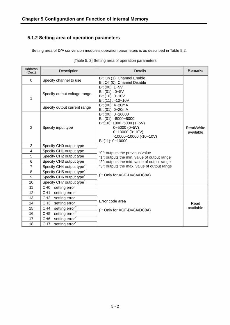
5.1.2 Setting area of operation parameters
Setting area of D/A conversion module’s operation parameters is as described in Table 5.2.
[Table 5. 2] Setting area of operation parameters
Address (Dec.) Description Details Remarks
0 Specify channel to use Bit On (1): Channel Enable Bit Off (0): Channel Disable
Specify output voltage range
Bit (00): 1~5V Bit (01) : 0~5V Bit (10): 0~10V Bit (11) : -10~10V 1
Specify output current range Bit (00): 4~20mA Bit (01): 0~20mA
2 Specify input type
Bit (00): 0~16000 Bit (01): -8000~8000 Bit(10): 1000~5000 (1~5V)
0~5000 (0~5V) 0~10000 (0~10V) -10000~10000 (-10~10V)
Bit(11): 0~10000 3 Specify CH0 output type 4 Specify CH1 output type 5 Specify CH2 output type 6 Specify CH3 output type 7 Specify CH4 output type*1 8 Specify CH5 output type*1 9 Specify CH6 output type*1 10 Specify CH7 output type*1
“0”: outputs the previous value “1”: outputs the min. value of output range “2”: outputs the mid. value of output range “3”: outputs the max. value of output range (*1: Only for XGF-DV8A/DC8A)
Read/Writeavailable
11 CH0 setting error 12 CH1 setting error 13 CH2 setting error 14 CH3 setting error 15 CH4 setting error*1 16 CH5 setting error*1 17 CH6 setting error*1 18 CH7 setting error*1
Error code area (*1: Only for XGF-DV8A/DC8A)
Read available
Chapter 5 Configuration and Function of Internal Memory
5 - 3
5.2 I/O area of D/A converted data
5.2.1 Module Ready/Error (Address 0)
1) Uxy.00.F : It will be ON when PLC CPU is powered or reset with D/A conversion ready to process D/A conversion.
2) Uxy.00.0 : It is a flag to display the error status of D/A conversion module for respective channels.
5.2.2 Channel operation information (Address 1)
1) This area is used to display the channel being used.
5.2.3 Output setting (Address 2)
1) Enable/Disable D/A output can be specified for respective channels. 2) If the output is not specified, output of all the channels will be disabled. 3) Enable/Disable D/A output is as specified below.
B15 B14 B13 B12 B11 B10 B9 B8 B7 B6 B5 B4 B3 B2 B1 B0
— — — — -
—— — —
CH7
CH6
CH5
CH4
CH3
CH2
CH1
CH0
B15 B14 B13 B12 B11 B10 B9 B8 B7 B6 B5 B4 B3 B2 B1 B0
— — — — — — — —CH7
CH6
CH5
CH4
CH3
CH2
CH1
CH0
B15 B14 B13 B12 B11 B10 B9 B8 B7 B6 B5 B4 B3 B2 B1 B0
— — — — — — — —CH7
CH6
CH5
CH4
CH3
CH2
CH1
CH0
U Uxy.00
Error information Bit ON (1): Error, Bit Off (0): Normal
Module Ready Bit ON (1): Ready, Bit Off (0): Not Ready
Run channel information Bit On (1): During Run, Bit Off (0): Operation Stop
Uxy.01
Run channel information Bit ON (1): Allowed, Bit Off (0): Prohibited
Uxy.02
B:bit
B:bit
B:bit

Chapter 5 Configuration and Function of Internal Memory
5 - 4
5.2.4 Digital input (Address 3~6)
1) Digital input value can be selected and used within the range of -192~16191, -8192~8191, 952~5047 or -120~10191 for 1~5V based on input type.
2) If the digital input value is not specified, it will be set to 0.
B15 B14 B13 B12 B11 B10 B9 B8 B7 B6 B5 B4 B3 B2 B1 B0
Channel# digital input value
Address Details
3 CH0 digital output value
4 CH1 digital output value
5 CH2 digital output value
6 CH3 digital output value
7 CH4 digital output value
8 CH5 digital output value
9 CH6 digital output value
10 CH7 digital output value
Uxy.03 ~ Uxy.6
B:bit

Chapter 5 Configuration and Function of Internal Memory
5 - 5
5.3.1 Specifying channels to use
If the channel to use is not specified, all the channels will be set to Disable.
BIT Details 0 Stop 1 Run
5.3.2 Setting Output Voltage/Current range 1) The range of analog output can be specified for respective channels. 2) If the output range is not specified, the range of all the channels will be set to 1~5V for voltage
output, and 4~20 mA for current output. 3) Setting of output range is as specified below.
B15 B14 B13 B12 B11 B10 B9 B8 B7 B6 B5 B4 B3 B2 B1 B0
C
H
7
C
H
6
C
H
5
C
H
4
C
H
3
C
H
2
C
H
1
C
H
0
BIT Details 00 1V ~ 5V / 4 ~ 20mA 01 0V ~ 5V / 0 ~ 20mA 10 0V ~ 10V 11 -10V ~ 10V
5.3 operation parameters settings
B15 B14 B13 B12 B11 B10 B9 B8 B7 B6 B5 B4 B3 B2 B1 B0
— — — — -
—— — —
CH7
CH6
CH5
CH4
CH3
CH2
CH1
CH0
Address “0”
B:bit
B:bit

Chapter 5 Configuration and Function of Internal Memory
5 - 6
5.3.3 Specifying Input data type
1) Input type can be specified for respective channels. If input type is not specified, all the channels will be set to the range of 0~16000.
B15 B14 B13 B12 B11 B10 B9 B8 B7 B6 B5 B4 B3 B2 B1 B0
C
H
7
C
H
6
C
H
5
C
H
4
C
H
3
C
H
2
C
H
1
C
H
0
BIT Details 00 0 ~ 16000 01 -8000 ~ 8000 10 Precise Value 11 0 ~ 10000
This area is used to specify D/A input type for respective channels. The precise value has the digital input ranges as follows;
Analog output
Digital input 1 ~ 5V 0 ~ 5V 0 ~ 10V -10 ~ 10V
Precise Value 1000~5000 0~5000 0 ~ 10000 -10000 ~ 10000
Analog output Digital input 4 ~ 20mA 0 ~ 20mA
Precise Value 4000 ~ 20000 0 ~ 20000
5.3.4 Setting Output data type Based on setting value, the output status is as follows;
Setting value Details 0 Keeps the previous value as it is 1 Outputs the minimum value of output range 2 Outputs the middle value of output range 3 Outputs the maximum value of output range
B15 B14 B13 B12 B11 B10 B9 B8 B7 B6 B5 B4 B3 B2 B1 B0
Channel# Setting value Address “3~10”
B:bit

Chapter 5 Configuration and Function of Internal Memory
5 - 7
5.3.5 Error code
Error codes detected from D/A conversion module will be saved.
Error Code (Dec) Details LED status
10 Module error (Reset Check Error) 11 Module error (Ram Check Error) 12 Module error (Register Check Error) 13 Module error (E2PROM Check Error) 21 Module error (D/A Conversion Error)
Blinks every 0.2 sec.
31# Note) Current module’s parameters setting error 32# Note) Parameters setting error when setting current module’s Offset/Gain
40# Note) Setting error of current module’s digital input range (If input value is set less than -192, or greater than 16191) The range changes based on input type
41# Note) Setting error of voltage module’s digital input range (If input value is set less than -192, or greater than 16191) The range changes based on input type
50# Note) Offset/Gain setting error in current module of 4~20 mA (If Offset value is set greater than or equal to Gain value)
51# Note) Offset/Gain setting error in current module of 0~20 mA (If Offset value is set greater than or equal to Gain value)
52# Note) Offset/Gain setting error in voltage module of 1~5V (If Offset value is set greater than or equal to Gain value)
53# Note) Offset/Gain setting error in voltage module of 0~5V (If Offset value is set greater than or equal to Gain value)
54# Note) Offset/Gain setting error in voltage module of 0~10V (If Offset value is set greater than or equal to Gain value)
55# Note) Offset/Gain setting error in voltage module of -10~10V (#: channel) (If Offset value is set greater than or equal to Gain value)
Blinks every 1 sec.
Note) # (0~3) stands for the channel with error found.
B15 B14 B13 B12 B11 B10 B9 B8 B7 B6 B5 B4 B3 B2 B1 B0
— — — —-
—— — — Channel# Error code Address 11~14”
Refer to the table below for detailed error codes

Chapter 6 Programming
6 - 1
Chapter 6 Programming
6.1 Internal Memory Read/Write
6.1.1 Read of internal memory (GET, GETP instruction)
< Difference between GET instruction and GETP instruction > GET : always executed with execution condition On ( )
GETP : executed with execution condition of operation start ( )
If D/A conversion module is installed on base No.0 and slot No.3, and internal memory address No.0 & 1’s data in D/A conversion module is read to D16 and D17 of CPU module.
Address D area of CPU module Internal memory of D/A conversion module Address
D00015
D00016 Run channel setting Run channel setting 0
D00017 Range of output voltage/current Range of output voltage/current 1
D00018 2
D00019 3
Type Description Area available
n1 Slot No. the special module is installed on Integer
n2 Start address of special module’s internal memory to read data Integer
D Device’s start address with saved data to read M, P, K, L, T, C, D, #D
n3 Number of words data to read Integer
GET instruction Execution condition
GET n1 n2 D n3
Type
Example

Chapter 6 Programming
6 - 2
6.1.2 Write of internal memory (PUT, PUTP instruction)
< Difference between PUT instruction and PUTP instruction > PUT : always executed with execution condition On ( )
PUTP : executed with execution condition of operation start ( )
If D/A conversion module is installed on Base No.0 and Slot No.6, and CPU module’s data of D16~D17 is written on internal memory addresses 0~1 of D/A conversion module,
Address D area of CPU module Internal memory of D/A
conversion module Addres
s
D00015
D00016 Data 1 Run channel setting 0
D00017 Data 2 Range of output voltage/current 1
D00018 2
D00019 3
Type Description Area available
n1 Slot No. the special module is installed on Integer
n2 Start address of special module’s internal memory to write data. Integer
S Device’s start address or integer with saved data to write. M, P, K, L, T, C, D, #D, integer
n3 Number of words data to write Integer
PUT instruction Execution condition
PUT n1 n2 S n3
Type
Example

Chapter 6 Programming
6 - 3
6.2 Basic Program 1) How to specify Run condition details of D/A conversion module’s internal memory will be described. 2) D/A conversion module is as installed on slot 1. 3) I/O assigned points of D/A conversion module is 16 points.
System Configuration
XGP-APF1
XGK-CPUH
XGF-DC4A
RUN
6.2.1 XGF-DC4A
1) Program example through [I/O Parameters] setting

Chapter 6 Programming
6 - 4
2) Program example with PUT/GET instruction used
All CH output enable
CH0 digital value Write
CH1 digital value Write
CH2 digital value Write
CH3 digital value Write
CH Run information
Digital value to output Module Ready
All CH output enable
CH0 digital value Write
CH1 digital value Write
CH2 digital value Write
CH3 digital value Write
Used CH(CH0.1.2.3) Output range(4~20mA)
Data type (0~16000)
CH output status setting 0,1,2,3:Output previous value
Module Ready
CH Run information
Slot No. Internal memory address
Setting data
The number of data to write

Chapter 6 Programming
6 - 5
6.3 Application Program
6.3.1 Inverter speed control
1) System Configuration
2) Details of initial setting
No Parameters Setting Details Internal Memory Address1 Channels CH 0 ~ 3 0 2 Output voltage range 0 ~ 10V 1 3 Data type 0 ~ 16,000 2 4 Channel Output type Previous value 3,4,5,6
3) Description of program (1) At the same time Module Ready Contact is On, output of all the channels will be set to
Allowed. (2) If P0001 is On, 0V will be output. (3) If P0002 is Off and P0002 is On, 2.5V will be output. (4) If P0003 is Off and P0003 is On, 5V will be output. (5) If P0004 is Off and P0004 is On, 7.5V will be output.
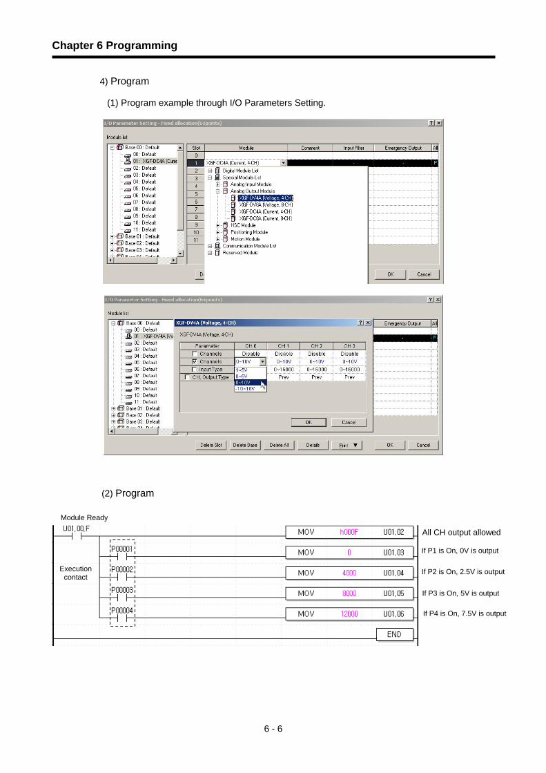
Chapter 6 Programming
6 - 6
4) Program
(1) Program example through I/O Parameters Setting.
(2) Program
All CH output allowed
If P1 is On, 0V is output
If P2 is On, 2.5V is output
If P3 is On, 5V is output
If P4 is On, 7.5V is output
Module Ready
Execution contact

Chapter 6 Programming
6 - 7
(3) Program example with PUT/GET instruction used
Module Ready Slot No.
Internal memory address
Setting data
Output allowed
CH Run (0~3)
Output range(0~10V)
Data type (0~16,000) CH0 output status(Previous value)
CH1 output status(Previous value)
CH2 output status(Previous value)
CH0 output status(Previous value)
CH0 output value(0V output) CH1 output value(2.5V output)
CH2 output value(5V output)
CH3 output value(7.5V output)
The number of data to write

Chapter 6 Programming
6 - 8
6.3.2 BCD output of error code
1) System Configuration
2) Details of initial setting
(1) Used CH: CH 0 (2) Analog output current range: DC 4 ~ 20 mA (3) Digital input data range: 0 ~ 16000
3) Description of program
(1) If P00000 is On, D/A conversion will be initially specified. (2) If P00001 is On, D/A converted value and error code will be saved respectively on D00000
and D00001. (3) If P00002 is On, applicable error code will be output to digital BCD display. (P00040 ~
P0004F)
4) Program
(1) Program example through [I/O Parameter] setting
XGP- ACF2
XGK- CPUS
XGI- D24A
XGQ- RY2A
XGF- DC4A
Digital BCD display (error display)
XGQ- RY2A
Initial value setting
Error code output to BCD
P0000
P0001
P0002
D/A converted value & errorcode value saved
Execution contact

Chapter 6 Programming
6 - 9
(2) Program example with PUT/GET instruction used
Used CH setting (CH 0)
CH 0’s 12mA output
Save error code on D1 Convert D1 saved data to BCD to output to P040
Conversion setting of error code to BCD
Module READY Execution contact
Conversion setting of error code to BCD
Module READY
CH 0’s 12mA output
Save error code on D1 Convert D1 saved data to BCD to output to P040
Used CH setting(CH 0)
Output range (4~20mA)
Data type (0~16,000)
CH0 output status(Previous value)
D/A output allowed
D/A output allowed
P

Chapter 7 Troubleshooting
7 - 1
Chapter 7 Troubleshooting 7.1 Error codes
Details and diagnosis of errors which occur while D/A conversion module is used will be described.
Error Code
(Dec) Description
LED
status
10 Module error (Reset Check Error)
11 Module error (RAM Check Error)
12 Module error (Register Check Error)
13 Module error (E2PROM Check Error)
21 Module error (D/A Conversion Error)
Blinks
every 0.2
sec.
31#note) Parameters setting error of current module
32#note) Parameters setting error of current module when setting Offset/Gain.
40#note) Setting error of current module’s digital input range (If input value is set less than -192 or greater than 16191). The range changes based on input data type.
41# note) Setting error of voltage module’s digital input range (If input value is set less than -192 or greater than 16191). The range changes based on input data type.
50# note) Offset/Gain setting error in current module of 4~20 (Offset value is set greater than or equal to Gain value)
51# note) Offset/Gain setting error in current module of 0~20 (Offset value is set greater than or equal to Gain value)
52# note) Offset/Gain setting error in voltage module of 1~5V (Offset value is set greater than or equal to Gain value)
53# note) Offset/Gain setting error in voltage module of 0~5V (Offset value is set greater than or equal to Gain value)
54# note) Offset/Gain setting error in voltage module of 0~10V (Offset value is set greater than or equal to Gain value)
55# note) Offset/Gain setting error in voltage module of -10~10V (Offset value is set greater than or equal to Gain value)
Blinks
every 1
sec.
Remark (1) # of the error code stands for the channel with error found.
(2) If 2 or more errors occur, the module will not save other error codes than the first error code found.
Chapter 7 Troubleshooting
7 - 2
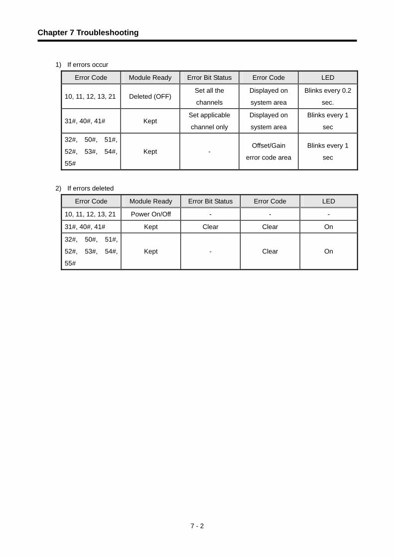
1) If errors occur
Error Code Module Ready Error Bit Status Error Code LED
10, 11, 12, 13, 21 Deleted (OFF) Set all the
channels
Displayed on
system area
Blinks every 0.2
sec.
31#, 40#, 41# Kept Set applicable
channel only
Displayed on
system area
Blinks every 1
sec
32#, 50#, 51#,
52#, 53#, 54#,
55#
Kept - Offset/Gain
error code area
Blinks every 1
sec
2) If errors deleted
Error Code Module Ready Error Bit Status Error Code LED
10, 11, 12, 13, 21 Power On/Off - - -
31#, 40#, 41# Kept Clear Clear On
32#, 50#, 51#,
52#, 53#, 54#,
55#
Kept - Clear On

Chapter 7 Troubleshooting
7 - 3
7.2 Troubleshooting
7.2.1 RUN LED blinks
7.2.2 RUN LED is Off
RUN LED is Off.
D/A conversion module is installed on the base correctly
Correctly install D/A conversion module on the base.
Contact the nearest agency or Customer service
center.
Normally operated if D/A conversion module with error is changed to another module
Error due to other module than D/A conversion module. Refer to CPU manual for more details.
No
Yes
Yes
No
RUN LED blinks.
RUN LED blinks every 0.2 sec.
RUN LED blinks every 1 sec.
Go to 7.2.7
Contact the nearest agency or Customer service
center.
Contact the nearest agency or Customer service
center.
Yes
No
Yes
No
XG5000 can be connected with.
Check error code. Yes
No

Chapter 7 Troubleshooting
7 - 4
7.2.3 D/A Output Value hunted too much
N
D/A output value is hunted too much.
Wiring between D/A conversion module and external device is correct.
External power (DC 24V) is supplied.
Correct the wiring with the external device.
Connect to DC 24V.
Supply sufficient DC 24V current for D/A conversion module.
Capacity of DC 24V power supply is sufficient.
D/A output value is hunted too much.
Go to 7.2.7
No
Yes
No
Yes
No
Yes
Chapter 7 Troubleshooting
7 - 5
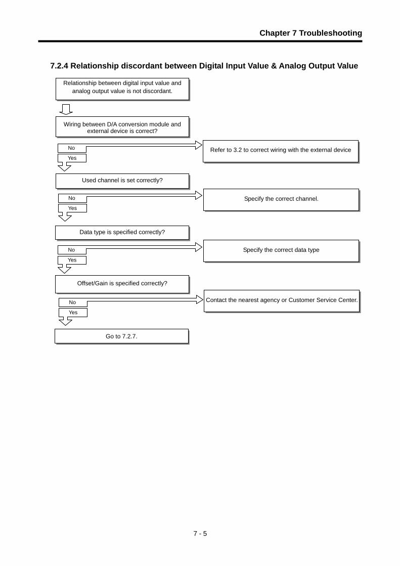
7.2.4 Relationship discordant between Digital Input Value & Analog Output Value
Relationship between digital input value and analog output value is not discordant.
Wiring between D/A conversion module and external device is correct?
Used channel is set correctly?
Refer to 3.2 to correct wiring with the external device
Specify the correct channel.
Go to 7.2.7.
Data type is specified correctly?
Offset/Gain is specified correctly?
Specify the correct data type
Contact the nearest agency or Customer Service Center.
No
Yes
No
Yes
No
Yes
No
Yes

Chapter 7 Troubleshooting
7 - 6
7.2.5 D/A Output Value always exceeds the value specified
D/A output value always exceeds the value specified
External power is normally supplied
Offset/Gain is specified correctly.
Supply external power properly.
Contact the nearest agency or Service center
Go to 7.2.7
Wiring between D/A conversion module and external device is correct.
D/A output value exceeds setting range.
Refer to 3.2 to correct wiring with the external device
Specify D/A input value range correctly.
No
Yes
No
Yes
No
Yes
No
Yes

Chapter 7 Troubleshooting
7 - 7
7.2.6 Analog Output Value does not changed according to the change of Digital Input Value
7.2.7 Hardware error of D/A conversion module
It is D/A conversion module’s Hardware error.
Contact the nearest Customer Service Center.
Analog output value does not changed accordingly to the D/A input value converted.
Applicable channel is specified correctly?
Offset/Gain is specified correctly?
Specify the applicable channel correctly.
Contact the nearest agency or Service center.
Go to 7.2.7.
Wiring with external device is correct?
Correct wiring with the external device.
No
Yes
No
Yes
No
Yes

Chapter 7 Troubleshooting
7 - 8
7.2.8 Status check of D/A conversion module through XG5000 System Monitoring Module type, module information, O/S version and module status of D/A conversion module can
be checked through XG5000 system monitoring function.
1) Execution sequence
Two routes are available for the execution.
(1) [Monitor] -> [System Monitoring] -> And on the module screen, click the right mouse button
to display [Module Information].
(2) [Monitor] -> [System Monitoring] -> And Double-click the module screen.
2) Module Information
(1) Module type: shows the information of the module presently installed.
(2) Module information: shows the O/S version information of D/A conversion module.
(3) O/S version: shows the O/S prepared date of D/A conversion module.
(4) Module status: shows the present error code.
3) System Monitor

Chapter 7 Troubleshooting
7 - 9
4) Monitor through program

Appendix 1 Terminology
Appendix 1- 1
Terms and abbreviation used in this user’s manual and the analog module in general are as described below.
A/D converter: converts analog to digital value proportionately to the size of analog input signal.
Analog input module: as a module with the circuit to convert analog voltage/current input signalal to digital
value, it has resolution of 14 and 16 bits according to converters.
Channel: related with the terminal of analog I/O module and connected to various voltage/current I/O
devices respectively, with applicable data and diagnosis function as well.
Conversion time: time necessary for analog input module to sample and convert the analog signal for the
processor inside the module to get digital-converted value input. On the other hand, it is time necessary for
analog output module to convert the digital value output from the processor inside the module to analog
output signal so to transmit to the output channel.
D/A converter: related with the output module, it is used to make continuous size of analog voltage and
current signal proportionately to the digital value.
Full scale: defined as the size of voltage/current where the normal operation is executed.
Full scale error: displayed with graph difference between agreeable analog-converted value and actual
analog-converted value.
Full scale range: displayed with difference between the maximum and the minimum of the analog input.
LSB (Least Signalificant Bit): displays the minimum value of the bit unit.
Appendix 1 Terminology

Appendix 1 Terminology
Appendix 1- 2
Linearity error: analog I/O is related between continuous voltage/current value and digital value, whose
agreeable I/O value is defined as a line within a distance of the minimum 1LSB of voltage/current. I/O
linearity error is regarded as the declination between the agreeable-converted value and the actual-
converted value on the graph.
Multiplexer: a switching circuit where many signals share one A/D converter or D/A converter.
Analog output module: a module with output circuit to convert analog DC voltage or current signal
proportionate to digital value delivered to the module from the processor.
Resolution: the minimum value recognizable by a measuring instrument, which is usually displayed in the
engineering unit (1mv) or the number of bits. In other words, 16383 types of output are available for 14 bits.
Filter: used to reduce the change of the digital-converted output value by sudden change of the external
noise or input for the analog circuit, through two methods of Software and Hardware filters.
Accuracy: displayed with the maximum declination between agreeable value and output voltage or current
for the whole range of output. On the other hand, it is displayed with the maximum declination between
agreeable value and digital-converted input signal value for the whole range of input. Generally, percentage
will be displayed for the full scale.
Gain, Offset and Linearity error are all included in the error type available.
Output accuracy: displayed with the difference between the actual analog output voltage/current value and
the agreeable-converted value on the conversion graph for the full scale, with Offset, Gain and Drift error
factors included as well as normal temperature (25) and available temperature range displayed
respectively.
Agreeable-converted value
Actual-converted value

Appendix 2 Dimensions
Appendix 2-1
1) Dimensions of XGF-DV4A/DC4A
(Unit : mm)
Appendix 2 Dimensions

Appendix 2-2
2) Dimensions of XGF-DV8A/DC8A
(Unit : mm)

Index
Index - 1
(A)
Absolute maximum output ---------------------- (2.2)
Accuracy -------------------------------------------- (2.7)
Analog quantity ------------------------------------ (1.2)
(B)
Base number -------------------------------------- (5.1)
Blinks ------------------------------------------------ (2.3)
(C)
Channels --------------------------------------- (4.4)
Characteristic of current output --------------- (2.6)
Characteristic of I/O conversion -------------- (2.4)
Characteristic of voltage output --------------- (2.4)
CH operation information ----------------------- (5.1)
Conversion speed ------------------------- (1.1),(2.2)
Cooling type ---------------------------------------- (2.1)
Current consumption ---------------------------- (2.2)
(D)
Default ----------------------------------------------- (4.6)
Device ------------------------------------- (4.12),(4.13)
Digital input ---------------------------------- (2.2)
Digital quantity ------------------------------------- (1.2)
Disable ---------------------------------------------- (2.8)
Display and diagnosis functions -------------- (2.9)
(E)
Enable ----------------------------------------------- (2.8)
Error code ----------------------------------- (5.7),(7.1)
Error status ----------------------------------------- (2.9)
External power ------------------------------------ (3.4)
(F)
Flag view ----------------------------------------- (4.12)
(G)
Gain ------------------------------------------- (2.9),(7.1)
GUI -------------------------------------------------- (4.2)
(H)
High accuracy ------------------------------------- (1.1)
High resolution ------------------------------------ (1.1)
(I)
Input type ------------------------------- (4.5),(5.2),(5.6)
Installation ------------------------------------------- (3.1)
Insulation method ---------------------------------- (2.2)
Internal memory ----------------------------- (5.1),(6.1)
Impulse noise -------------------------------- (2.1)
I/O area ----------------------------------------------- (5.1)
I/O parameter --------------------------------------- (4.2)
I/O points occupied -------------------------------- (2.2)
(M)
Maximum conversion speed ------------------- (2.2)
Maximum resolution ----------------------------- (2.2)
Maximum value ----------------------------------- (2.8)
Middle value --------------------------------------- (2.8)
Minimum value ------------------------------------ (2.8)
Module information ------------------------ (4.8),(7.8)
Module Ready ------------------------------------- (5.1)
Monitoring ----------------------------------- (4.7),(4.9)
(N)
Noise filter ------------------------------------------ (3.4)
Normal mode -------------------------------------- (2.8)
(O)
Off --------------------------------------------------- (2.3)
Offset ---------------------------------------- (2.9),(7.1)
On ---------------------------------------------------- (2.3)
Operation parameter ----------------------------- (5.2)
Operating height ---------------------------------- (2.1)
Operating humidity ------------------------------ (2.1)
Operating temperature -------------------------- (2.1)
Output disable ------------------------------------- (5.1)
Output enable ------------------------------ (5.1),(6.4)
Output range --------------------------------------- (4.5)
O/S version ----------------------------------------- (7.8)
(P)
Parameters setting ------------------------------ (4.3)

Index
Index - 2
Percentile value ----------------------------------- (2.2)
Performance specifications-------------------- (2.2)
Pollution degree ----------------------------------- (2.1)
Precise value -------------------------------------- (2.2)
Previous value ------------------------------------- (2.9)
Project window ------------------------------------ (4.2)
(R)
Run LED -------------------------------------------- (2.9)
(S)
Save variables ----------------------------------- (4.11)
Setting error --------------------------------- (5.2),(7.1)
Setting output type ---------------- (2.8),(4.5),(5.6)
Shocks --------------------------------------------- (2.1)
Signed value --------------------------------------- (2.2)
Slot Number ---------------------------------------- (5.1)
Special module monitoring --------------------- (4.7)
Specification -------------------------------------- (2.1)
Specifying channel to use ---------------------- (5.5)
Storage humidity ----------------------------- (2.1)
Storage temperature ----------------------- (2.1)
System error -------------------------------------- (2.9)
System monitor ------------------------------- (7.8)
(T)
Terminal --------------------------------------------- (2.3)
Terminal connected ----------------------------- (2.2)
Test --------------------------------------------------- (4.9)
Test mode ------------------------------------------ (2.8)
Troubleshooting ----------------------------------- (7.3)
Twisted shield ------------------------------ (3.2)
(U)
U device ------------------------------------------ (4.10)
Unsigned value ---------------------------------- (2.2)
(V)
Variable save ------------------------------------- (4.11)
Vibration --------------------------------------------- (2.1)
View variables ------------------------------------ (4.11)
(W)
Weight ----------------------------------------------- (2.2)
Wiring ------------------------------------------------ (3.1)
(X)
XG5000---------------------------------------------- (4.2)

Warranty 1. Terms of warranty
LSIS provides an 18-month warranty starting from the date of production. 2. Range of warranty
For problems within the terms of the warranty, LSIS will replace the entire PLC or repair the defective parts free of charge except for the following cases. (1) Problems caused by improper conditions, environment or treatment. (2) Problems caused by external devices. (3) Problems caused by the user remodeling or repairing the PLC. (4) Problems caused by improper use of the product. (5) Problems caused by circumstances where the expectations exceed that of the science and technology level
when LSIS produced the product. (6) Problems caused by natural disaster.
3. This warranty is limited to the PLC itself only. It is not valid for the whole system which the PLC is attached to.