
When self-consistency makes a difference
10
Politecnico di Torino Porto Institutional Repository [Article] When self-consistency makes a difference Original Citation: F. Bonani; Camarchia V.; F. Cappelluti; S. Donati Guerrieri; G. Ghione; M. Pirola (2008). When self-consistency makes a difference. In: IEEE MICROWAVE MAGAZINE, vol. 9 issue 5, pp. 81-89. - ISSN 1527-3342 Availability: This version is available at : http://porto.polito.it/1683174/ since: September 2008 Publisher: IEEE Published version: DOI:10.1109/MMM.2008.927638 Terms of use: This article is made available under terms and conditions applicable to Open Access Policy Article ("Public - All rights reserved") , as described at http://porto.polito.it/terms_and_conditions. html Porto, the institutional repository of the Politecnico di Torino, is provided by the University Library and the IT-Services. The aim is to enable open access to all the world. Please share with us how this access benefits you. Your story matters. (Article begins on next page)
-
Upload
independent -
Category
Documents
-
view
3 -
download
0
Transcript of When self-consistency makes a difference
Politecnico di Torino
Porto Institutional Repository
[Article] When self-consistency makes a difference
Original Citation:F. Bonani; Camarchia V.; F. Cappelluti; S. Donati Guerrieri; G. Ghione; M. Pirola (2008). Whenself-consistency makes a difference. In: IEEE MICROWAVE MAGAZINE, vol. 9 issue 5, pp. 81-89.- ISSN 1527-3342
Availability:This version is available at : http://porto.polito.it/1683174/ since: September 2008
Publisher:IEEE
Published version:DOI:10.1109/MMM.2008.927638
Terms of use:This article is made available under terms and conditions applicable to Open Access Policy Article("Public - All rights reserved") , as described at http://porto.polito.it/terms_and_conditions.html
Porto, the institutional repository of the Politecnico di Torino, is provided by the University Libraryand the IT-Services. The aim is to enable open access to all the world. Please share with us howthis access benefits you. Your story matters.
(Article begins on next page)
October 2008 811527-3342/08/$25.00©2008 IEEE
Digital Object Identifier 10.1109/MMM.2008.927638
Thermal management of semiconductordevices and integrated circuits [from digi-tal to analog and power radio frequency(RF) and microwave circuits] is a well-known critical issue in modern electronic
design. Technology advances, such as device down-scaling to increase the maxi-mum operating frequency andthe use of wide-bandgap semi-conductors [such as silicon car-bide and (SiC) and galliumnitride (GaN)] with breakdownvoltages one order of magni-tude larger than in convention-al III-V compounds, have sig-nificantly increased powerdensities in compound semi-conductor microwave and mm-wave transistors, thus making effective thermal designa key point for successful technology development.Heating is an issue also in Si-based RF technologies, asin lateral double diffused metal oxide semiconductor
(LDMOS) devices; however, despite the impressivetotal RF power such devices exhibit, the power densityis in fact much lower, of the order of 1 W/mm against10 W/mm or more in GaN high electron mobility tran-sistor HEMTs; gallium arsenide GaAs FETs have simi-lar or somewhat larger power densities than LDMOS,
but with poorer substrate ther-mal conductivity. Self-heatingnot only is a major limitation tothe device reliability (throughthermal instabilities, hot spotformation, and thermal run-away), but also affects [some-times in a subtle way, e.g.,when long-term thermal mem-ory affects the device linearity(see the “Dynamic ThermalModeling” section)] the device
performance. In many applications, a critical role isalso played by the transient thermal response.Examples are pulsed-mode high-power amplifiers(HPAs) (RF and microwave). RF power circuit design
© COMSTOCK
Fabrizio Bonani, Vittorio Camarchia, Federica Cappelluti, Simona Donati Guerrieri, Giovanni Ghione, and Marco Pirola are with the Electronic Department, Politecnico di Torino,
Corso Duca degli Abruzzi, 24, 10129 Torino, Italy.
Fabrizio Bonani, Vittorio Camarchia, Federica Cappelluti,
Simona Donati Guerrieri, Giovanni Ghione, and Marco Pirola
82 October 2008
therefore increasingly needs to be supported by reli-able electrothermal semiconductor device models,whose development requires accurate nonlineardynamic thermal models, which may ultimately bederived from complex three-dimensional (3-D) multi-physics analysis techniques, to be coupled with tem-perature-dependent electrical compact models, suit-able for the integration in circuit computer aideddesign (CAD) environments. In fact, even thoughfully-coupled 3-D or even quasi-two-dimensional (2-D) physics-based electrothermal models would accu-rately reproduce the dynamic electrothermal interac-tion, the related computational burden most often pre-vents their use in simulating the device performanceunder practical operating conditions, also accountingfor the interaction with other active or passive devices.
The Thermal ModelSemiconductor device thermal analysis can be final-ized to different goals, ranging from the technologicallevel (e.g., optimization of the device mounting andlayout) to the electrical level (e.g., investigation on howtemperature affects the device electrical performance).A preliminary condition is, in all cases, the availabilityof reliable data for the thermal conductivity and thespecific heat of the relevant materials, from semicon-ductors (sometimes exotic and recently developed likeGaN or with a large variety of crystal polytypes withdifferent thermal properties, like SiC) to metals anddielectrics [1]. All material parameters should, in prin-ciple, include nonlinearities, i.e., the temperaturedependency. A crucial role in assessing the validity ofmodel parameters and of simulation techniques is ofcourse played by the availability of device-level ther-mal measurements, including both averaged parame-ters (such as the thermal resistance) and detailed sur-face temperature maps. Under this framework, theproposed measurement techniques vary from standardpulse characterization [2] to optical photolumines-cence mapping [3], [4], Raman spectroscopy [5], andphotocurrent measurements [6].
The purpose of thermal modeling (and therefore thesimulation approaches and tools of choice), alsodepends on the kind of analysis required. At the tech-nological level, thermal modeling focuses on evaluat-ing the device temperature distribution (see the “HeatEquation and Temperature Distribution” section),while at the electrical level (where such detailed infor-mation typically is redundant and scarcely manage-able), an averaged thermal resistance, to be coupled toan electrical (temperature-dependent) device model inorder to yield a self-consistent electrothermal model, isa more convenient choice (see the “Thermal ResistanceModels” section). However, in modern RF andmicrowave communication systems exploiting broad-band modulation schemes, the slow dynamic deviceresponse, also related to thermal effects, plays a signifi-
cant role, making the issue of accurate dynamic thermalmodeling (yielding the time-dependent temperaturedistribution, and the device thermal impedance) veryhot today, as discussed in the “Dynamic ThermalModeling” section.
Heat Equation and Temperature DistributionIdeally, the detailed temperature distribution inside thedevice volume yields a complete picture of the thermalbehavior. Under this respect, numerical simulation isable to resolve temperature variations at a submicronscale, and can therefore perform better than most exper-imental techniques, which are typically limited in spa-tial resolution and, often, to the surface of the activedevice [7], [8]. However, an exact device-level thermalmodel calls for the solution of the heat equation overthe device volume in the presence of a self-consistentdissipated power distribution, which in turn has to beidentified from the solution of a physics-based trans-port model, like for instance the drift-diffusion orhydrodynamic (see, e.g., [9]).
The resulting self-consistent physics-based coupledelectrothermal model is, unfortunately, extremelydemanding from a computational standpoint, particular-ly when the device structure under consideration isdescribed through a realistic 3-D approach, includinglarge-scale features such as the thermal mounting. In fact,this turns out to be a typical multiphysics problem, wherethe spatial scale of the relevant physical effects can varyover several orders of magnitude, from the submicronscale typical of the electric operation (electric field and car-rier density distributions), to the millimeter or even cen-timeter scale typical of heat flow.
Furthermore, while electrical simulations are oftenrestricted to the 2-D case, because of the nature of elec-tron transport inside the device, accurate heat flowsimulations do require a fully 3-D approach. As aresult, the discretization mesh should be very denseover the active device area and coarser over all theother parts of the device that play little or no role inelectrical simulations but need to be included for thethermal analysis (e.g., substrate, metal layers, heatsinks, etc.). Numerical multigrid approaches (in whichthe thermal and electrical models are discretized ondifferent meshes, individually optimized for therespective spatial scale), or a simplified treatment ofthe heat boundary conditions [10] have been proposedin the past to make the approach viable; however,although most of the available physics-based simula-tion tools today allow for the self-consistent couplingof the heat equation to the transport equation, thepractical use is confined to idealized 2-D cases, andthe accurate modeling of realistic, 3-D large-scaledevices still is beyond reach.
Even neglecting consistency in a physics-based,microscopic sense, the 3-D solution of the heat equationwith an assigned dissipated power density is the kind

October 2008 83
of analysis typically required, e.g., for the device tech-nological evaluation. Well known heuristic rules,derived from physics-based simulations or measure-ments, enable to approximate the dissipated power dis-tribution with a number of constant or Gaussiansources (whose exact position and shape is however insome cases somewhat controversial, see [11]). Theknowledge of the detailed temperature distribution onthe device surface allows optimizing the layout (e.g., bydecreasing the thermal coupling between parallel gatesor emitters), estimating the device reliability (from themaximum channel or junction temperature), and opti-mizing the substrate thickness or the mounting.
Nonetheless, the very solution of the heat equation(also in the simplest case of stationary, dc conditions)poses various problems. The 3-D meshing problem isalleviated but not completely solved, since the volumewhere the dissipated power is significant is very small(micron scale) compared to the device dimensions(mm scale at least); this requires again the cumbersomemanagement of extremely nonuniform grids, with pos-sible inaccuracies in the problem solution and, in gen-eral, a worse numerical conditioning, which oftenbecomes critical when the material parameters are tem-perature-dependent, and therefore the heat equationnonlinear. Nonlinearity is a difficult problem in itself,in most cases alleviated by the application of theKirchhoff transformation [12], which allows to lin-earize the heat equation. Unfortunately, its exact appli-cation is limited to the case of homogenous materials.This is rarely the case in practical devices, which typi-cally exploit inhomogeneous multilayered or fully 3-Dgeometries. For the general case of T-dependent materi-al parameters, an approximate application is only pos-sible for piecewise nonhomogeneous structures [13],
while for time-varying (dynamic) analysis approxima-tions are mandatory [14], [15]. Furthermore, fast, quasi-3-D (or 2.5-dimensional) planar solution methods,based on Fourier series or Green’s function approach-es, fail to capture fully 3-D geometries (although insome cases they can be modified to include, e.g., theeffects of the metallizations [16]), and are not generallyapplicable to multilayered media with temperature-dependent parameters. In conclusion, the only safeapproach to the large-scale temperature simulation ofrealistic device structures appears to be today thedirect, three-dimensional solution of the heat equationvia finite element (FEM) discretization; to this aim, sev-eral commercial software tools are available on themarket, e.g., [17]–[19]. It should be stressed that,although such tools are today quite efficient and flexi-ble from a computational standpoint, most of the prob-lem solving time is spent in training the program user(sometimes a not overly enthusiastic Ph.D. student),and in setting up a working 3-D mesh.
As an example of a finite element heat equationsolution for a multifinger HEMT (12 × 200 μm) onAlGaN/GaN, Figure 1 shows the discretization of onequarter of the device with the resulting grid, and thetemperature profile for a dissipated power of 4 W.
Thermal Resistance ModelsFEM-based 3-D models are too computationally inten-sive to be exploited within a circuit design environ-ment, e.g., in connection with a self-consistent elec-trothermal circuit-level compact model; moreover, theinformation they provide is redundant. Electrical-levelthermal modeling should yield an average or maxi-mum value of the device active region temperature as afunction of the total dissipated power, possibly derived
Figure 1. Example of layout exploited in FEM thermal simulations. One quarter of a 12 × 200 μm AlGaN/GaN multifingerHEMT. (a) Nonuniform mesh discretizazion and (b) temperature profile. The dissipated power is 4 W, and the maximum tem-perature in the gates is, in this case, roughly 80 °C.
−600
(a) (b)
−600
−400
−2000
−400−200
0
200
00
yz
x yz
x
200
400
600
800
0
200
400
600
800

84 October 2008
in turn as a time-varying unknown that depends on thedevice instantaneous working point. To this purpose,the so called thermal resistance approach is widelyexploited, in which the temperature increase in thedevice active volume is related to the dissipated electri-cal power by a lumped model (often associated to anequivalent thermal network, as shown in Figure 2). Thisallows evaluating the temperature of a limited numberof thermal nodes, corresponding to physical hot spotson the device layout.
In the simplest case, the active area of an electricaldevice reduces to a single thermal node and the thermalnetwork to a simple resistance. However, this simplifi-cation may be inaccurate in multifinger (multigate ormultiemitter) devices where the active region tempera-ture undergoes significant variations along (and across)the device fingers; in this case, each finger should bedivided into subsections, each one having its own tem-
perature and its equivalent thermal network alsoaccounting for thermal coupling between subsections.In the static (dc) case, and neglecting the material non-linearity, the thermal network can be derived by repeat-edly solving the heat equation through FEM 3-Dapproaches and by surface temperature averagingand/or heat source lumping; in this case, the outputnodal temperature of the thermal network can be iden-tified as a linear combination, through self and mutualthermal resistances, of the powers dissipated in eachoutput node. More advanced methods rely on system-oriented approaches like model reduction identificationtools [20], [21]. In many cases, the Green’s functionapproach seems to be especially useful for the extractionof the thermal network, as it aims at the evaluation ofthe temperature distribution only for selected observa-tion or injection points in the device [16], [21], but it isinherently restricted to the linear case, and therefore canbe exploited only when the Kirchhoff transformation isapplicable. The identification of a nonlinear equivalentthermal network still is a problem, although simplifiedsystem-level approaches can be applied to this purpose.
Thermal resistance models can be effectively exploit-ed as technology level models since they yield a concisepicture of the device thermal behavior, which can help inassessing the available technology choices. As an exam-ple, Figure 3 shows the impact of substrate and mount-ing choices [backside on SiC or flip-chip (FC) on AlN,diamond or ideal heat sink] and nonlinearity on the ther-mal resistance of a 1 mm (10 × 100 μm) AlGaN/GaNHEMT on SiC from SELEX SI.
Dynamic Thermal Modeling Although temperature does not respond as fast as theelectrical variables to an external excitation, because ofthe slower dynamics involved in the very nature of heatflow, exact dynamic thermal models for electron devicesare still difficult to be identified or extracted. Very often,simplified models are exploited, based on the bare ideathat a cut-off frequency must exist, above which temper-ature is in some sense frozen and cannot vary followingthe fast variation of the instantaneous dissipated electri-cal power. According to this approach, thermal modelsare often limited to the identification of a reasonable timeconstant to set the limit of the thermal dynamics. Thedevice is then modeled by a first-order dynamic system,i.e., a simple resistance-capacitance (RC) thermal circuit,where R is given by the thermal resistance, while thecapacitance is set in order to yield the cut-off frequencycorresponding to the chosen time constant.
Unfortunately, as will be shown further on, resultsbased on more accurate thermal models point outthat the thermal impedance of an electron device (i.e.,the temperature response to a small-signal time-varying sinusoidal dissipated power) has a frequen-cy behavior often far from being comparable to asimple, single-pole RC circuit low-pass response,
Figure 2. Electron device equivalent thermal network[26]. Indices i and j refer to different thermal nodes(i.e., either different devices or fingers of the samedevice); �T is the corresponding temperature raise withrespect to reference (ambient) temperature.
.
.
PDiPDj
. . . . . . . .
Z
Device ThermalImpedance .
.
.
.
.
.
.
.
ΔTj
ΔTi
Figure 3. Thermal resistance of an AlGaN/GaN device asa function of the dissipated power and for different mount-ings setups [25].
0 2 4 6 8 10 12 14 1610
15
20
25
30
35
Dissipated Power (W)
The
rmal
Res
ista
nce
(K/W
)
FC AlN
FC Diamond
Backside
FC Ideal
October 2008 85
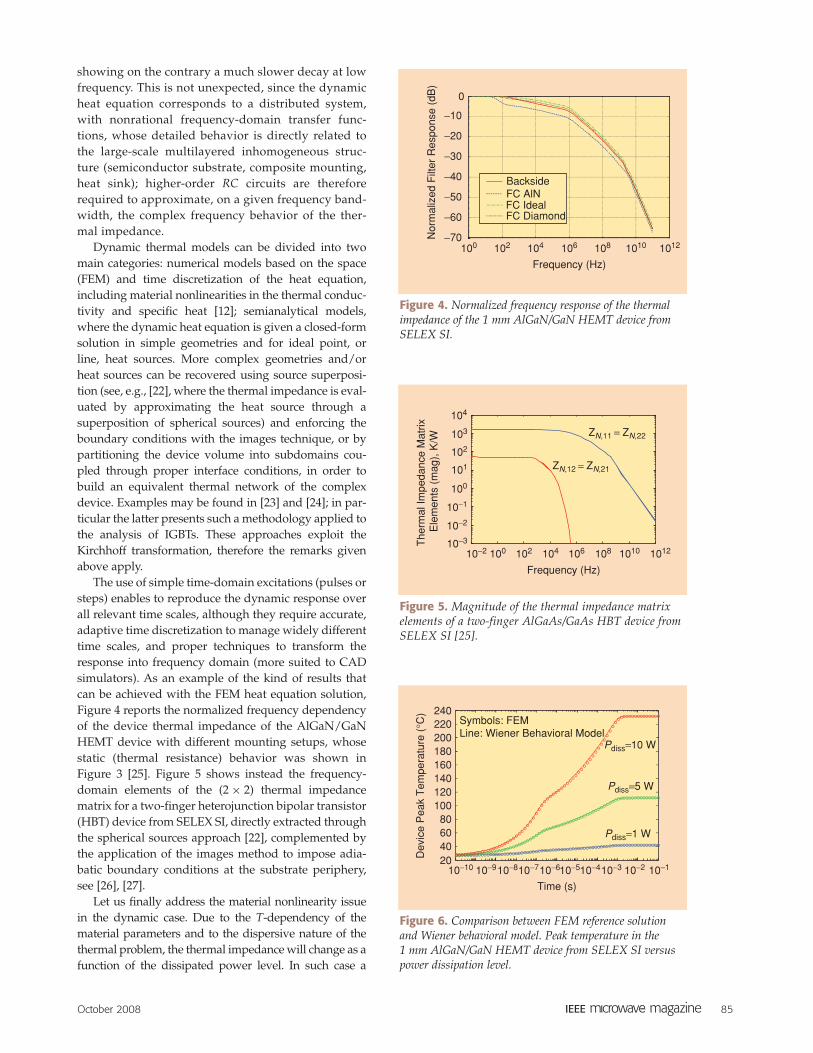
showing on the contrary a much slower decay at lowfrequency. This is not unexpected, since the dynamicheat equation corresponds to a distributed system,with nonrational frequency-domain transfer func-tions, whose detailed behavior is directly related tothe large-scale multilayered inhomogeneous struc-ture (semiconductor substrate, composite mounting,heat sink); higher-order RC circuits are thereforerequired to approximate, on a given frequency band-width, the complex frequency behavior of the ther-mal impedance.
Dynamic thermal models can be divided into twomain categories: numerical models based on the space(FEM) and time discretization of the heat equation,including material nonlinearities in the thermal conduc-tivity and specific heat [12]; semianalytical models,where the dynamic heat equation is given a closed-formsolution in simple geometries and for ideal point, orline, heat sources. More complex geometries and/orheat sources can be recovered using source superposi-tion (see, e.g., [22], where the thermal impedance is eval-uated by approximating the heat source through asuperposition of spherical sources) and enforcing theboundary conditions with the images technique, or bypartitioning the device volume into subdomains cou-pled through proper interface conditions, in order tobuild an equivalent thermal network of the complexdevice. Examples may be found in [23] and [24]; in par-ticular the latter presents such a methodology applied tothe analysis of IGBTs. These approaches exploit theKirchhoff transformation, therefore the remarks givenabove apply.
The use of simple time-domain excitations (pulses orsteps) enables to reproduce the dynamic response overall relevant time scales, although they require accurate,adaptive time discretization to manage widely differenttime scales, and proper techniques to transform theresponse into frequency domain (more suited to CADsimulators). As an example of the kind of results thatcan be achieved with the FEM heat equation solution,Figure 4 reports the normalized frequency dependencyof the device thermal impedance of the AlGaN/GaNHEMT device with different mounting setups, whosestatic (thermal resistance) behavior was shown inFigure 3 [25]. Figure 5 shows instead the frequency-domain elements of the (2 × 2) thermal impedancematrix for a two-finger heterojunction bipolar transistor(HBT) device from SELEX SI, directly extracted throughthe spherical sources approach [22], complemented bythe application of the images method to impose adia-batic boundary conditions at the substrate periphery,see [26], [27].
Let us finally address the material nonlinearity issuein the dynamic case. Due to the T-dependency of thematerial parameters and to the dispersive nature of thethermal problem, the thermal impedance will change as afunction of the dissipated power level. In such case a
Figure 5. Magnitude of the thermal impedance matrixelements of a two-finger AlGaAs/GaAs HBT device from SELEX SI [25].
10−2 100 102 104 106 108 1010 1012
Frequency (Hz)
The
rmal
Impe
danc
e M
atrix
Ele
men
ts (
mag
), K
/W
10−3
10−2
10−1
100
101
102
103
104
ZN,11 = ZN,22
ZN,12 = ZN,21
Figure 4. Normalized frequency response of the thermalimpedance of the 1 mm AlGaN/GaN HEMT device fromSELEX SI.
100 102 104 106 108 1010 1012−70
−60
−50
−40
−30
−20
−10
0
Frequency (Hz)
Nor
mal
ized
Filt
er R
espo
nse
(dB
)
FC AlNBackside
FC IdealFC Diamond
Figure 6. Comparison between FEM reference solutionand Wiener behavioral model. Peak temperature in the1 mm AlGaN/GaN HEMT device from SELEX SI versuspower dissipation level.
20406080
100120140160180200220240
10−10 10−910−8 10−210−310−410−510−610−7 10−1
Time (s)
Dev
ice
Pea
k T
empe
ratu
re (
°C)
Pdiss=1 W
Pdiss=5 W
Symbols: FEMLine: Wiener Behavioral Model
Pdiss=10 W
86 October 2008
system-level description, valid for any input dissipatedpower excitation waveform, can be derived by applyingwell-established results from the modeling of nonlineardynamic systems. Approximate device thermal modelscan be based on Wiener, Hammerstein or Wiener-Hammerstein approaches [28]; as an example, Figure 6shows that a Wiener-like model, based on the cascade ofa memory-less nonlinear block followed by a linear filter,is able to accurately reproduce the transient thermalresponse of the AlGaN/GaN HEMT of Figure 4 at differ-ent power levels. Besides being suited to be implementedinto CAD tools, the Wiener approach is readily identifiedwith a two step procedure: first the static simulation, atvarious power dissipation levels, is performed in order toidentify the nonlinear block; then only one time-domainsimulation at a low level of dissipation (linear case) suf-fices to identify the frequency dependent block.
Electrothermal Simulation and ResultsCoupling a suitable thermal model to an electricalmodel allows for the investigation of some criticaleffects occurring in power RF and microwave devices.The examples discussed here concern the stability of III-V based HBTs and the dispersion in the intermodulationbehavior of power GaN HEMTs due to the thermal feed-back. All these phenomena cannot be addressed unlessa fully coupled electrothermal model is adopted. Similarissues and modeling solution techniques are also pre-sent in Si RF LDMOS devices, see, e.g., [29]–[31].
A preliminary remark refers to the fact that powermicrowave devices such as HBTs, heterostructure fieldeffect transistors (HFETs), HEMTs (but also Si LDMOS)most often are characterized by a multifinger layout todecrease parasitic resistances and to allow for scalabili-ty. In this case, it is sometimes necessary to extract anelectrical model for each device finger in order to cou-ple it to a multiport thermal model allowing for thedescription of the thermal cross-coupling among thevarious device parts.
This is particularly relevant for multifinger HBTs,where current collapse instabilities are due to thermaleffects combined with device asymmetries. Current col-lapse is a sudden decrease in the output collector cur-rent as a function of the collector-emitter voltage.Collapse causes degradation in the HBT power capabil-ities, and possibly device failure due to thermal run-away. Self-consistent electrothermal HBT simulationshave been widely used to assess the current collapseonset mechanism; this is due to current hogginginduced by small layout or finger-to-finger electricalasymmetries whereby, with increasing temperature, asingle device finger drains all the device current whilethe other fingers are ultimately turned off. HBT thermalsimulations allow for the identification of the thermalcoupling, and allow for layout optimization or thedesign of suitable emitter or base resistive ballasting.
In the vast majority of cases, HBT stability analysisthrough electrothermal simulations is based on thethermal resistance approach [32], where all thermaldynamic effects are neglected. However, experimentalevidence shows that the onset of the instability occursat different collector voltages in static or pulsed dc mea-surements, thus suggesting that the phenomenon isaffected by significant dispersion, to be also attributedto thermal dynamical effects.
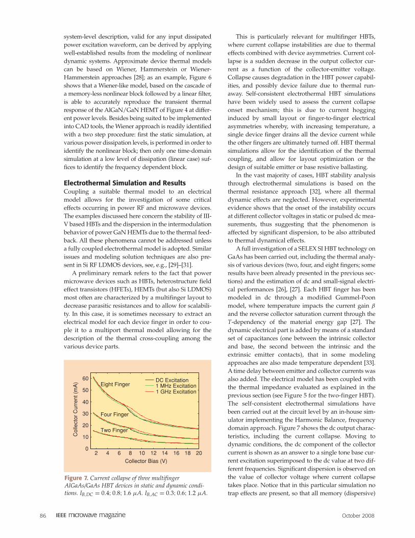
A full investigation of a SELEX SI HBT technology onGaAs has been carried out, including the thermal analy-sis of various devices (two, four, and eight fingers; someresults have been already presented in the previous sec-tions) and the estimation of dc and small-signal electri-cal performances [26], [27]. Each HBT finger has beenmodeled in dc through a modified Gummel-Poonmodel, where temperature impacts the current gain βand the reverse collector saturation current through theT-dependency of the material energy gap [27]. Thedynamic electrical part is added by means of a standardset of capacitances (one between the intrinsic collectorand base, the second between the intrinsic and theextrinsic emitter contacts), that in some modelingapproaches are also made temperature dependent [33].A time delay between emitter and collector currents wasalso added. The electrical model has been coupled withthe thermal impedance evaluated as explained in theprevious section (see Figure 5 for the two-finger HBT).The self-consistent electrothermal simulations havebeen carried out at the circuit level by an in-house sim-ulator implementing the Harmonic Balance, frequencydomain approach. Figure 7 shows the dc output charac-teristics, including the current collapse. Moving todynamic conditions, the dc component of the collectorcurrent is shown as an answer to a single tone base cur-rent excitation superimposed to the dc value at two dif-ferent frequencies. Significant dispersion is observed onthe value of collector voltage where current collapsetakes place. Notice that in this particular simulation notrap effects are present, so that all memory (dispersive)
Figure 7. Current collapse of three multifingerAlGaAs/GaAs HBT devices in static and dynamic condi-tions. IB,DC = 0.4; 0.8; 1.6 μA. IB,AC = 0.3; 0.6; 1.2 μA.
2 4 6 8 10 12 14 16 18 200
10
20
30
40
50
60
Four Finger
Two Finger
DC Excitation1 MHz Excitation1 GHz Excitation
Col
lect
or C
urre
nt (
mA
)
Collector Bias (V)
Eight Finger
October 2008 87
phenomena are to be ascribed entirely to thermaldynamics. It is important to remark that thermal effectsplay a significant role also at very high frequencies (ascan be seen by the marked difference between the 1MHz and the 1 GHz excitation), showing that the fre-quency decrease of the thermal impedance is extremelyslow compared to a single pole RC network.
Instability problems are peculiar of bipolar devices:in fact, the active device self-heating may act as aneffective positive feedback, basically due to the currentincrease with temperature. FET based devices, instead,are intrinsically immune to this kind of problems, sincein this case device self-heating mainly degrades carriermobility in the semiconductor, thus decreasing thedrain current. The net effect is equivalent to a negativefeedback that, equalizing the several current contribu-tions, makes multifinger devices inherently stable.
In the field of power amplifier design, great interest isgiven to the impact of thermal effects on device nonlin-earities. In fact, accurate modeling of intermodulationproducts (IMPs) allows for the design of high linearitymodules, either by exploiting the device sweet spots or byusing proper predistorting stages. This issue is particular-ly important for advanced wireless communication sys-tems, characterized by nonconstant envelope broadbandmodulation schemes: in this case the design of powermodules, especially for base stations, is extremelydemanding in term of linearity and efficiency. Broadbandsignals are influenced not only by the instantaneous non-linearities typical of the electrical device operation at highfrequencies, but also by long-term memory effects such asthe ones related to thermal dynamics. Under this respect,the design of advanced power amplifiers requires thedevice to be described by a full electrothermal model,including nonstatic thermal effects. The latter, asexplained in the previous section, can be described by athermal impedance network in the linear case, or, moregenerally, by a system-oriented nonlinear dynamic model.
Among high-power compound semiconductormicrowave and RF technologies, AlGaN/GaN HEMThave shown appealing performances in terms of powerdensity. A fully self consistent electrothermal modelextracted and tailored on the coplanar power GaNHEMTs on SiC already seen in the previous sections willbe used to gain insight into the impact of thermal effectson amplifier linearity. The FET model is a cubic Curtice[34], with temperature dependent parameters (see [25]for additional details). The thermal behavior is modeledby the Wiener approach (see Figure 6), with the dynam-ic part approximated through a multipole rational trans-fer function, cascaded with a nonlinear memorylessblock. The electrothermal model has been implementedwithin the Agilent advanced design system (ADS) envi-ronment exploiting a symbolic defined device (SDD)block. The model has been fitted on dc, pulsed dc, multi-bias scattering parameters, time-domain RF waveformsand the Pin-Pout output characteristics [25].
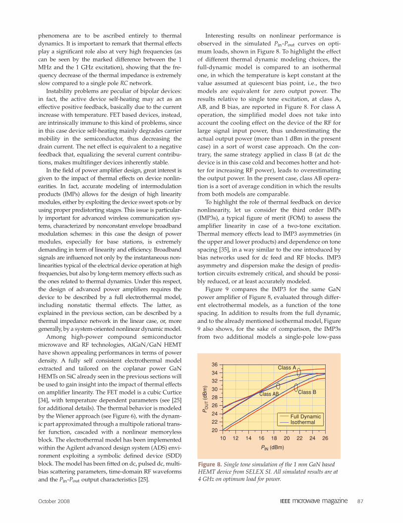
Interesting results on nonlinear performance isobserved in the simulated Pin-Pout curves on opti-mum loads, shown in Figure 8. To highlight the effectof different thermal dynamic modeling choices, thefull-dynamic model is compared to an isothermalone, in which the temperature is kept constant at thevalue assumed at quiescent bias point, i.e., the twomodels are equivalent for zero output power. Theresults relative to single tone excitation, at class A,AB, and B bias, are reported in Figure 8. For class Aoperation, the simplified model does not take intoaccount the cooling effect on the device of the RF forlarge signal input power, thus underestimating theactual output power (more than 1 dBm in the presentcase) in a sort of worst case approach. On the con-trary, the same strategy applied in class B (at dc thedevice is in this case cold and becomes hotter and hot-ter for increasing RF power), leads to overestimatingthe output power. In the present case, class AB opera-tion is a sort of average condition in which the resultsfrom both models are comparable.
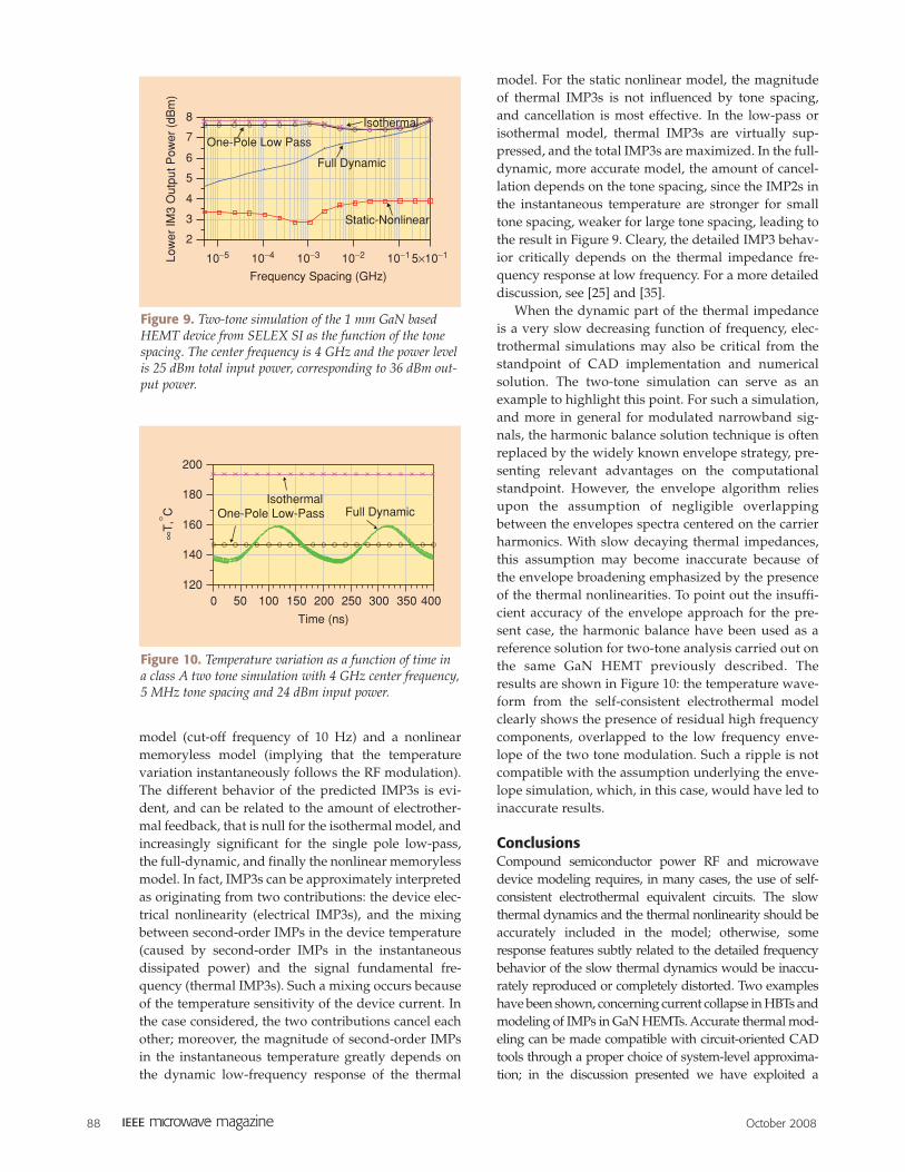
To highlight the role of thermal feedback on devicenonlinearity, let us consider the third order IMPs(IMP3s), a typical figure of merit (FOM) to assess theamplifier linearity in case of a two-tone excitation.Thermal memory effects lead to IMP3 asymmetries (inthe upper and lower products) and dependence on tonespacing [35], in a way similar to the one introduced bybias networks used for dc feed and RF blocks. IMP3asymmetry and dispersion make the design of predis-tortion circuits extremely critical, and should be possi-bly reduced, or at least accurately modeled.
Figure 9 compares the IMP3 for the same GaNpower amplifier of Figure 8, evaluated through differ-ent electrothermal models, as a function of the tonespacing. In addition to results from the full dynamic,and to the already mentioned isothermal model, Figure9 also shows, for the sake of comparison, the IMP3sfrom two additional models a single-pole low-pass
Figure 8. Single tone simulation of the 1 mm GaN basedHEMT device from SELEX SI. All simulated results are at4 GHz on optimum load for power.
12 14 16 18 20 22 2410 26
22
24
26
28
30
32
34
20
36
PIN (dBm)
PO
UT
(dB
m)
Class AB
Class A
Class B
Full DynamicIsothermal
88 October 2008
model (cut-off frequency of 10 Hz) and a nonlinearmemoryless model (implying that the temperaturevariation instantaneously follows the RF modulation).The different behavior of the predicted IMP3s is evi-dent, and can be related to the amount of electrother-mal feedback, that is null for the isothermal model, andincreasingly significant for the single pole low-pass,the full-dynamic, and finally the nonlinear memorylessmodel. In fact, IMP3s can be approximately interpretedas originating from two contributions: the device elec-trical nonlinearity (electrical IMP3s), and the mixingbetween second-order IMPs in the device temperature(caused by second-order IMPs in the instantaneousdissipated power) and the signal fundamental fre-quency (thermal IMP3s). Such a mixing occurs becauseof the temperature sensitivity of the device current. Inthe case considered, the two contributions cancel eachother; moreover, the magnitude of second-order IMPsin the instantaneous temperature greatly depends onthe dynamic low-frequency response of the thermal
model. For the static nonlinear model, the magnitudeof thermal IMP3s is not influenced by tone spacing,and cancellation is most effective. In the low-pass orisothermal model, thermal IMP3s are virtually sup-pressed, and the total IMP3s are maximized. In the full-dynamic, more accurate model, the amount of cancel-lation depends on the tone spacing, since the IMP2s inthe instantaneous temperature are stronger for smalltone spacing, weaker for large tone spacing, leading tothe result in Figure 9. Cleary, the detailed IMP3 behav-ior critically depends on the thermal impedance fre-quency response at low frequency. For a more detaileddiscussion, see [25] and [35].
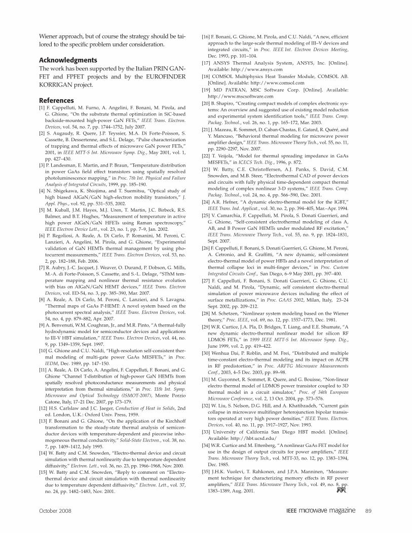
When the dynamic part of the thermal impedanceis a very slow decreasing function of frequency, elec-trothermal simulations may also be critical from thestandpoint of CAD implementation and numericalsolution. The two-tone simulation can serve as anexample to highlight this point. For such a simulation,and more in general for modulated narrowband sig-nals, the harmonic balance solution technique is oftenreplaced by the widely known envelope strategy, pre-senting relevant advantages on the computationalstandpoint. However, the envelope algorithm reliesupon the assumption of negligible overlappingbetween the envelopes spectra centered on the carrierharmonics. With slow decaying thermal impedances,this assumption may become inaccurate because ofthe envelope broadening emphasized by the presenceof the thermal nonlinearities. To point out the insuffi-cient accuracy of the envelope approach for the pre-sent case, the harmonic balance have been used as areference solution for two-tone analysis carried out onthe same GaN HEMT previously described. Theresults are shown in Figure 10: the temperature wave-form from the self-consistent electrothermal modelclearly shows the presence of residual high frequencycomponents, overlapped to the low frequency enve-lope of the two tone modulation. Such a ripple is notcompatible with the assumption underlying the enve-lope simulation, which, in this case, would have led toinaccurate results.
ConclusionsCompound semiconductor power RF and microwavedevice modeling requires, in many cases, the use of self-consistent electrothermal equivalent circuits. The slowthermal dynamics and the thermal nonlinearity should beaccurately included in the model; otherwise, someresponse features subtly related to the detailed frequencybehavior of the slow thermal dynamics would be inaccu-rately reproduced or completely distorted. Two exampleshave been shown, concerning current collapse in HBTs andmodeling of IMPs in GaN HEMTs. Accurate thermal mod-eling can be made compatible with circuit-oriented CADtools through a proper choice of system-level approxima-tion; in the discussion presented we have exploited a
Figure 10. Temperature variation as a function of time ina class A two tone simulation with 4 GHz center frequency,5 MHz tone spacing and 24 dBm input power.
50 100 150 200 250 300 3500 400
140
160
180
120
200
Time (ns)
∞T
,°C
IsothermalOne-Pole Low-Pass Full Dynamic
Figure 9. Two-tone simulation of the 1 mm GaN basedHEMT device from SELEX SI as the function of the tonespacing. The center frequency is 4 GHz and the power levelis 25 dBm total input power, corresponding to 36 dBm out-put power.
3
4
5
6
7
2
8
Frequency Spacing (GHz)
Low
er IM
3 O
utpu
t Pow
er (
dBm
)
10−5 10−4 10−3 10−2 10−1 5×10⁻¹
One-Pole Low Pass
Full Dynamic
Static-Nonlinear
Isothermal
October 2008 89
Wiener approach, but of course the strategy should be tai-lored to the specific problem under consideration.
AcknowledgmentsThe work has been supported by the Italian PRIN GAN-FET and FPFET projects and by the EUROFINDERKORRIGAN project.
References[1] F. Cappelluti, M. Furno, A. Angelini, F. Bonani, M. Pirola, and
G. Ghione, “On the substrate thermal optimization in SiC-basedbackside-mounted high-power GaN FETs,” IEEE Trans. Electron.Devices, vol. 54, no. 7, pp. 1744–1752, July 2007.
[2] S. Augaudy, R. Quere, J.P. Teyssier, M.A. Di Forte-Poisson, S.Cassette, B. Dessertenne, and S.L. Delage, “Pulse characterizationof trapping and thermal effects of microwave GaN power FETs,”2001, in IEEE MTT-S Int. Microwave Symp. Dig., May 2001, vol. 1,pp. 427–430.
[3] P. Landesman, E. Martin, and P. Braun, “Temperature distributionin power GaAs field effect transistors using spatially resolvedphotoluminescence mapping,” in Proc. 7th Int. Physical and FailureAnalysis of Integrated Circuits, 1999, pp. 185–190.
[4] N. Shigekawa, K. Shiojima, and T. Suemitsu, “Optical study ofhigh biased AlGaN/GaN high-electron mobility transistors,” J.Appl. Phys., vol. 92, pp. 531–535, 2002.
[5] M. Kuball, J.M. Hayes, M.J. Uren, T. Martin, J.C. Birbeck, R.S.Balmer, and B.T. Hughes, “Measurement of temperature in activehigh power AlGaN/GaN HFETs using Raman spectroscopy,”IEEE Electron Device Lett., vol. 23, no. 1, pp. 7–9, Jan. 2002.
[6] P. Regoliosi, A. Reale, A. Di Carlo, P. Romanini, M. Peroni, C.Lanzieri, A. Angelini, M. Pirola, and G. Ghione, “Experimentalvalidation of GaN HEMTs thermal management by using pho-tocurrent measurements,” IEEE Trans. Electron Devices, vol. 53, no.2, pp. 182–188, Feb. 2006.
[7] R. Aubry, J.-C. Jacquet, J. Weaver, O. Durand, P. Dobson, G. Mills,M.-A. di Forte-Poisson, S. Cassette, and S.-L. Delage, “SThM tem-perature mapping and nonlinear thermal resistance evolutionwith bias on AlGaN/GaN HEMT devices,” IEEE Trans. ElectronDevices, vol. ED-54, no. 3, pp. 385–390, Mar. 2007.
[8] A. Reale, A. Di Carlo, M. Peroni, C. Lanzieri, and S. Lavagna.“Thermal maps of GaAs P-HEMT: A novel system based on thephotocurrent spectral analysis,” IEEE Trans. Electron Devices, vol.54, no. 4, pp. 879–882, Apr. 2007.
[9] A. Benvenuti, W.M. Coughran, Jr., and M.R. Pinto, “A thermal-fullyhydrodynamic model for semiconductor devices and applicationsto III-V HBT simulation,” IEEE Trans. Electron Devices, vol. 44, no.9, pp. 1349–1359, Sept. 1997.
[10] G. Ghione and C.U. Naldi, “High-resolution self-consistent ther-mal modeling of multi-gate power GaAs MESFETs,” in Proc.IEDM, Dec. 1989, pp. 147–150.
[11] A. Reale, A. Di Carlo, A. Angelini, F. Cappelluti, F. Bonani, and G.Ghione “Channel T-distribution of high-power GaN HEMTs fromspatially resolved photoconductance measurements and physicalinterpretation from thermal simulations,” in Proc. 11th Int. Symp.Microwave and Optical Technology (ISMOT-2007), Monte PorzioCatone, Italy, 17–21 Dec. 2007, pp 173–179.
[12] H.S. Carlslaw and J.C. Jaeger, Conduction of Heat in Solids, 2nded. London, U.K.: Oxford Univ. Press, 1959.
[13] F. Bonani and G. Ghione, “On the application of the Kirchhofftransformation to the steady-state thermal analysis of semicon-ductor devices with temperature-dependent and piecewise inho-mogeneous thermal conductivity,” Solid-State Electron., vol. 38, no.7, pp. 1409–1412, July 1995.
[14] W. Batty and C.M. Snowden, “Electro-thermal device and circuitsimulation with thermal nonlinearity due to temperature dependentdiffusivity,” Electron. Lett., vol. 36, no. 23, pp. 1966–1968, Nov. 2000.
[15] W. Batty and C.M. Snowden, “Reply to comment on “Electro-thermal device and circuit simulation with thermal nonlinearitydue to temperature dependent diffusivity,” Electron. Lett., vol. 37,no. 24, pp. 1482–1483, Nov. 2001.
[16] F. Bonani, G. Ghione, M. Pirola, and C.U. Naldi, “A new, efficientapproach to the large-scale thermal modeling of III–V devices andintegrated circuits,” in Proc. IEEE Int. Electron Devices Meeting,Dec. 1993, pp. 101–104.
[17] ANSYS Thermal Analysis System, ANSYS, Inc. [Online].Available: http://www.ansys.com
[18] COMSOL Multiphysics Heat Transfer Module, COMSOL AB.[Online]. Available: http://www.comsol.com
[19] MD PATRAN, MSC Software Corp. [Online]. Available:http://www.mscsoftware.com
[20] B. Shapiro, “Creating compact models of complex electronic sys-tems: An overview and suggested use of existing model reductionand experimental system identification tools,” IEEE Trans. Comp.Packag. Technol., vol. 26, no. 1, pp. 165–172, Mar. 2003.
[21] J. Mazeau, R. Sommet, D. Caban-Chastas, E. Gatard, R. Quéré, andY. Mancuso, “Behavioral thermal modeling for microwave poweramplifier design,” IEEE Trans. Microwave Theory Tech., vol. 55, no. 11,pp. 2290–2297, Nov. 2007.
[22] T. Veijola, “Model for thermal spreading impedance in GaAsMESFETs,” in ICECS Tech. Dig., 1996, p. 872.
[23] W. Batty, C.E. Christoffersen, A.J. Panks, S. David, C.M.Snowden, and M.B. Steer, “Electrothermal CAD of power devicesand circuits with fully physical time-dependent compact thermalmodeling of complex nonlinear 3-D systems,” IEEE Trans. Comp.Packag. Technol., vol. 24, no. 4, pp. 566–590, Dec. 2001.
[24] A.R. Hefner, “A dynamic electro-thermal model for the IGBT,”IEEE Trans. Ind. Applicat., vol. 30, no. 2, pp. 394–405, Mar.–Apr. 1994.
[25] V. Camarchia, F. Cappelluti, M. Pirola, S. Donati Guerrieri, andG. Ghione, “Self-consistent electrothermal modeling of class A,AB, and B Power GaN HEMTs under modulated RF excitation,”IEEE Trans. Microwave Theory Tech., vol. 55, no. 9, pp. 1824–1831,Sept. 2007.
[26] F. Cappelluti, F. Bonani, S. Donati Guerrieri, G. Ghione, M. Peroni,A. Cetronio, and R. Graffitti, “A new dynamic, self-consistentelectro-thermal model of power HBTs and a novel interpretation ofthermal collapse loci in multi-finger devices,” in Proc. CustomIntegrated Circuits Conf., San Diego, 6–9 May 2001, pp. 397–400.
[27] F. Cappelluti, F. Bonani, S. Donati Guerrieri, G. Ghione, C.U.Naldi, and M. Pirola, “Dynamic, self consistent electro-thermalsimulation of power microwave devices including the effect ofsurface metallizations,” in Proc. GAAS 2002, Milan, Italy, 23–24Sept. 2002, pp. 209–212.
[28] M. Schetzen, “Nonlinear system modeling based on the Wienertheory,” Proc. IEEE, vol. 69, no. 12, pp. 1557–1773, Dec. 1981.
[29] W.R. Curtice, J.A. Pla, D. Bridges, T. Liang, and E.E. Shumate, “Anew dynamic electro-thermal nonlinear model for silicon RFLDMOS FETs,” in 1999 IEEE MTT-S Int. Microwave Symp. Dig.,June 1999, vol. 2, pp. 419–422.
[30] Wenhua Dai, P. Roblin, and M. Frei, “Distributed and multipletime-constant electro-thermal modeling and its impact on ACPRin RF predistortion,” in Proc. ARFTG Microwave MeasurementsConf., 2003, 4–5 Dec. 2003, pp. 89–98.
[31] M. Guyonnet, R. Sommet, R. Quere, and G. Bouisse, “Non-linearelectro thermal model of LDMOS power transistor coupled to 3Dthermal model in a circuit simulator,” Proc. of 34th EuropeanMicrowave Conference, vol. 2, 13 Oct. 2004, pp. 573–576.
[32] W. Liu, S. Nelson, D.G. Hill, and A. Khatibzadeh, “Current gaincollapse in microwave multifinger heterojunction bipolar transis-tors operated at very high power densities,” IEEE Trans. Electron.Devices, vol. 40, no. 11, pp. 1917–1927, Nov. 1993.
[33] University of California San Diego HBT model. [Online].Available: http://hbt.ucsd.edu/
[34] W.R. Curtice and M. Ettenberg, “A nonlinear GaAs FET model foruse in the design of output circuits for power amplifiers,” IEEETrans. Microwave Theory Tech., vol. MTT-33, no. 12, pp. 1383–1394,Dec. 1985.
[35] J.H.K. Vuolevi, T. Rahkonen, and J.P.A. Manninen, “Measure-ment technique for characterizing memory effects in RF poweramplifiers,” IEEE Trans. Microwave Theory Tech., vol. 49, no. 8, pp.1383–1389, Aug. 2001.