VS-VSKT26.., VS-VSKH26.., VS-VSKL26.., VS-VSKN26.. Series
10
VS-VSKT26.., VS-VSKH26.., VS-VSKL26.., VS-VSKN26.. Series www.vishay.com Vishay Semiconductors Revision: 26-Jul-2018 1 Document Number: 94629 For technical questions within your region: [email protected] , [email protected] , [email protected] THIS DOCUMENT IS SUBJECT TO CHANGE WITHOUT NOTICE. THE PRODUCTS DESCRIBED HEREIN AND THIS DOCUMENT ARE SUBJECT TO SPECIFIC DISCLAIMERS, SET FORTH AT www.vishay.com/doc?91000 AAP Gen 7 (TO-240AA) Power Modules Thyristor/Diode and Thyristor/Thyristor, 27 A MECHANICAL DESCRIPTION The AAP Gen 7 (TO-240AA), new generation of APP module, combines the excellent thermal performances obtained by the usage of exposed direct bonded copper substrate, with advanced compact simple package solution and simplified internal structure with minimized number of interfaces. FEATURES • High voltage • Industrial standard package • UL approved file E78996 • Low thermal resistance • Designed and qualified for industrial level • Material categorization: for definitions of compliance please see www.vishay.com/doc?99912 BENEFITS • Excellent thermal performances obtained by the usage of exposed direct bonded copper substrate • Up to 1600 V • High surge capability • Easy mounting on heatsink ELECTRICAL DESCRIPTION These modules are intended for general purpose high voltage applications such as high voltage regulated power supplies, lighting circuits, temperature and motor speed control circuits, UPS and battery charger. PRIMARY CHARACTERISTICS I T(AV) or I F(AV) 27 A Type Modules - thyristor, standard Package AAP Gen 7 (TO-240AA) ADD-A-PAK MAJOR RATINGS AND CHARACTERISTICS SYMBOL CHARACTERISTICS VALUES UNITS I T(AV) or I F(AV) 85 °C 27 A I O(RMS) As AC switch 60 I TSM, I FSM 50 Hz 400 60 Hz 420 I 2 t 50 Hz 800 kA 2 s 60 Hz 730 I 2 t 8000 kA 2 s V RRM Range 400 to 1600 V T Stg -40 to +125 °C T J -40 to +125 °C
-
Upload
khangminh22 -
Category
Documents
-
view
2 -
download
0
Transcript of VS-VSKT26.., VS-VSKH26.., VS-VSKL26.., VS-VSKN26.. Series

VS-VSKT26.., VS-VSKH26.., VS-VSKL26.., VS-VSKN26.. Serieswww.vishay.com Vishay Semiconductors
Revision: 26-Jul-2018 1 Document Number: 94629For technical questions within your region: [email protected], [email protected], [email protected]
THIS DOCUMENT IS SUBJECT TO CHANGE WITHOUT NOTICE. THE PRODUCTS DESCRIBED HEREIN AND THIS DOCUMENTARE SUBJECT TO SPECIFIC DISCLAIMERS, SET FORTH AT www.vishay.com/doc?91000
AAP Gen 7 (TO-240AA) Power Modules Thyristor/Diode and Thyristor/Thyristor, 27 A
MECHANICAL DESCRIPTIONThe AAP Gen 7 (TO-240AA), new generation of APP module, combines the excellent thermal performances obtained by the usage of exposed direct bonded copper substrate, with advanced compact simple package solution and simplified internal structure with minimized number of interfaces.
FEATURES
• High voltage
• Industrial standard package
• UL approved file E78996
• Low thermal resistance
• Designed and qualified for industrial level
• Material categorization: for definitions of compliance please see www.vishay.com/doc?99912
BENEFITS
• Excellent thermal performances obtained by the usage of exposed direct bonded copper substrate
• Up to 1600 V
• High surge capability
• Easy mounting on heatsink
ELECTRICAL DESCRIPTION
These modules are intended for general purpose high voltage applications such as high voltage regulated power supplies, lighting circuits, temperature and motor speed control circuits, UPS and battery charger.
PRIMARY CHARACTERISTICSIT(AV) or IF(AV) 27 A
Type Modules - thyristor, standard
Package AAP Gen 7 (TO-240AA)
ADD-A-PAK
MAJOR RATINGS AND CHARACTERISTICSSYMBOL CHARACTERISTICS VALUES UNITS
IT(AV) or IF(AV) 85 °C 27
AIO(RMS) As AC switch 60
ITSM,
IFSM
50 Hz 400
60 Hz 420
I2t50 Hz 800
kA2s60 Hz 730
I2t 8000 kA2s
VRRM Range 400 to 1600 V
TStg -40 to +125 °C
TJ -40 to +125 °C

VS-VSKT26.., VS-VSKH26.., VS-VSKL26.., VS-VSKN26.. Serieswww.vishay.com Vishay Semiconductors
Revision: 26-Jul-2018 2 Document Number: 94629For technical questions within your region: [email protected], [email protected], [email protected]
THIS DOCUMENT IS SUBJECT TO CHANGE WITHOUT NOTICE. THE PRODUCTS DESCRIBED HEREIN AND THIS DOCUMENTARE SUBJECT TO SPECIFIC DISCLAIMERS, SET FORTH AT www.vishay.com/doc?91000
ELECTRICAL SPECIFICATIONS
Notes(1) I2t for time tx = I2t x tx(2) Average power = VT(TO) x IT(AV) + rt x (IT(RMS))2(3) 16.7 % x x IAV < I < x IAV(4) I > x IAV
VOLTAGE RATINGS
TYPE NUMBERVOLTAGE
CODE
VRRM, MAXIMUM REPETITIVE PEAK
REVERSE VOLTAGE V
VRSM, MAXIMUM NON-REPETITIVE PEAK
REVERSE VOLTAGE V
VDRM, MAXIMUM REPETITIVE PEAK OFF-STATE VOLTAGE,
GATE OPEN CIRCUIT V
IRRM, IDRMAT 125 °C
mA
VS-VSK.26
04 400 500 400
15
06 600 700 600
08 800 900 800
10 1000 1100 1000
12 1200 1300 1200
14 1400 1500 1400
16 1600 1700 1600
ON-STATE CONDUCTIONPARAMETER SYMBOL TEST CONDITIONS VALUES UNITS
Maximum average on-state current (thyristors) IT(AV) 180° conduction, half sine wave,TC = 85 °C
27
A
Maximum average forward current (diodes) IF(AV)
Maximum continuous RMS on-state current,as AC switch
IO(RMS) 60
Maximum peak, one-cycle non-repetitive on-state or forward current
ITSM
orIFSM
t = 10 ms No voltagereapplied Sinusoidal
half wave,initial TJ = TJ maximum
400
t = 8.3 ms 420
t = 10 ms 100 % VRRMreapplied
335
t = 8.3 ms 350
Maximum I2t for fusing I2t
t = 10 ms No voltagereapplied
Initial TJ = TJ maximum
800
A2st = 8.3 ms 730
t = 10 ms 100 % VRRMreapplied
560
t = 8.3 ms 510
Maximum I2t for fusing I2t (1) t = 0.1 ms to 10 ms, no voltage reapplied TJ = TJ maximum
8000 A2s
Maximum value or threshold voltage VT(TO) (2)Low level (3)
TJ = TJ maximum0.86
VHigh level (4) 1.09
Maximum value of on-state slope resistance
rt (2)Low level (3)
TJ = TJ maximum9.58
mHigh level (4) 7.31
Maximum peak on-state or forward voltageVTM ITM = x IT(AV)
TJ = 25 °C 1.65 VVFM IFM = x IF(AV)
Maximum non-repetitive rate of rise ofturned on current
dI/dtTJ = 25 °C, from 0.67 VDRM,ITM = x IT(AV), Ig = 500 mA, tr < 0.5 μs, tp > 6 μs
150 A/μs
Maximum holding current IHTJ = 25 °C, anode supply = 6 V,resistive load, gate open circuit
200mA
Maximum latching current IL TJ = 25 °C, anode supply = 6 V, resistive load 400
orI(RMS) I(RMS)

VS-VSKT26.., VS-VSKH26.., VS-VSKL26.., VS-VSKN26.. Serieswww.vishay.com Vishay Semiconductors
Revision: 26-Jul-2018 3 Document Number: 94629For technical questions within your region: [email protected], [email protected], [email protected]
THIS DOCUMENT IS SUBJECT TO CHANGE WITHOUT NOTICE. THE PRODUCTS DESCRIBED HEREIN AND THIS DOCUMENTARE SUBJECT TO SPECIFIC DISCLAIMERS, SET FORTH AT www.vishay.com/doc?91000
Note• Table shows the increment of thermal resistance RthJC when devices operate at different conduction angles than DC
TRIGGERINGPARAMETER SYMBOL TEST CONDITIONS VALUES UNITS
Maximum peak gate power PGM 10W
Maximum average gate power PG(AV) 2.5
Maximum peak gate current IGM 2.5 A
Maximum peak negative gate voltage -VGM 10
VMaximum gate voltage required to trigger VGT
TJ = -40 °CAnode supply = 6 Vresistive load
4.0
TJ = 25 °C 2.5
TJ = 125 °C 1.7
Maximum gate current required to trigger IGT
TJ = -40 °CAnode supply = 6 Vresistive load
270
mATJ = 25 °C 150
TJ = 125 °C 80
Maximum gate voltage that will not trigger VGD TJ = 125 °C, rated VDRM applied 0.25 V
Maximum gate current that will not trigger IGD TJ = 125 °C, rated VDRM applied 6 mA
BLOCKINGPARAMETER SYMBOL TEST CONDITIONS VALUES UNITS
Maximum peak reverse and off-state leakage current at VRRM, VDRM
IRRM,
IDRMTJ = 125 °C, gate open circuit 15 mA
Maximum RMS insulation voltage VINS 50 Hz3000 (1 min)
3600 (1 s)V
Maximum critical rate of rise of off-state voltage dV/dt TJ = 125 °C, linear to 0.67 VDRM 1000 V/μs
THERMAL AND MECHANICAL SPECIFICATIONSPARAMETER SYMBOL TEST CONDITIONS VALUES UNITS
Junction operating and storagetemperature range
TJ, TStg -40 to +125 °C
Maximum internal thermal resistance,junction to case per leg
RthJC DC operation 0.76
°C/WTypical thermal resistance,case to heatsink per module
RthCS Mounting surface flat, smooth and greased 0.1
Mounting torque ± 10 %to heatsink A mounting compound is recommended and the
torque should be rechecked after a period of3 hours to allow for the spread of the compound.
4Nm
busbar 3
Approximate weight75 g
2.7 oz.
Case style JEDEC® AAP Gen 7 (TO-240AA)
R CONDUCTION PER JUNCTION
DEVICESSINE HALF WAVE CONDUCTION RECTANGULAR WAVE CONDUCTION
UNITS180° 120° 90° 60° 30° 180° 120° 90° 60° 30°
VSK.26.. 0.212 0.258 0.330 0.466 0.72 0.166 0.276 0.357 0.482 0.726 °C/W

VS-VSKT26.., VS-VSKH26.., VS-VSKL26.., VS-VSKN26.. Serieswww.vishay.com Vishay Semiconductors
Revision: 26-Jul-2018 4 Document Number: 94629For technical questions within your region: [email protected], [email protected], [email protected]
THIS DOCUMENT IS SUBJECT TO CHANGE WITHOUT NOTICE. THE PRODUCTS DESCRIBED HEREIN AND THIS DOCUMENTARE SUBJECT TO SPECIFIC DISCLAIMERS, SET FORTH AT www.vishay.com/doc?91000
Fig. 1 - Current Ratings Characteristics
Fig. 2 - Current Ratings Characteristics
Fig. 3 - On-State Power Loss Characteristics
Fig. 4 - On-State Power Loss Characteristics
Fig. 5 - Maximum Non-Repetitive Surge Current
Fig. 6 - Maximum Non-Repetitive Surge Current
Average on-state current (A)
Max
imum
allo
wab
le c
ase
tem
pera
ture
(°C
)
0 5 10 15 20 25 3080
90
100
110
120
130
180°120°
90°60°30°
RthJC (DC) = 0.76°C/W
0 10 20 30 40 5080
90
100
110
120
130
180°120°
90°60°30°
DC
RthJC (DC) = 0.76 °C/W
Average on-state current (A)
Max
imum
allo
wab
le c
ase
tem
pera
ture
(°C
)
Average on-state current (A)
Max
imum
ave
rage
on-
stat
e po
wer
loss
(W)
0 5 10 15 20 25 300
10
20
30
40
50180°120°
90°60°30°
RMS limit
Per leg, Tj = 125°C
Average on-state current (A)
Max
imum
ave
rage
on-
stat
e po
wer
loss
(W)
0 10 20 30 40 500
10
20
30
40
50
60180°120°
90°60°30°
RMS limit
DC
Per leg, Tj = 125°C
Pea
k ha
lf si
ne w
ave
on-s
tate
cur
rent
(A)
Number of equal amplitude half cycle current pulses (N)
1 10 100150
200
250
300
350
400At any rated load condition and with rated Vrrm applied following surge
Initial Tj = Tj max @ 60 Hz 0.0083 s
@ 50 Hz 0.0100s
Per leg
Pea
k ha
lf si
ne w
ave
on-s
tate
cur
rent
(A)
Pulse train duration (s)
0.01 0.1 1150
200
250
300
350
400Maximum Non-repetitive Surge
Current. Controlof conduction may not be maintained.
Versus Pulse Train DurationInitial Tj = 125°C
No Voltage ReappliedRated Vrrm reapplied
Per leg

VS-VSKT26.., VS-VSKH26.., VS-VSKL26.., VS-VSKN26.. Serieswww.vishay.com Vishay Semiconductors
Revision: 26-Jul-2018 5 Document Number: 94629For technical questions within your region: [email protected], [email protected], [email protected]
THIS DOCUMENT IS SUBJECT TO CHANGE WITHOUT NOTICE. THE PRODUCTS DESCRIBED HEREIN AND THIS DOCUMENTARE SUBJECT TO SPECIFIC DISCLAIMERS, SET FORTH AT www.vishay.com/doc?91000
Fig. 7 - On-State Power Loss Characteristics
Fig. 8 - On-State Power Loss Characteristics
Fig. 9 - On-State Power Loss Characteristics
Total RMS output current (A)
Max
imum
tota
l on-
stat
e po
wer
loss
(W)
Maximum allowable ambient temperature (°C)
0 20 40 60 80 100 120 140
RthSA = 0.1 °C/W0.3 °C/W0.5 °C/W0.7 °C/W1 °C/W1.5 °C/W2 °C/W3 °C/W4 °C/W8 °C/W
0 10 20 30 40 50 600
10
20
30
40
50
60
70
80
90
100
180°120°90°60°30°
VSK.26 SeriesPer moduleTj = 125°C
Total output current (A)
Max
imum
tota
l pow
er lo
ss (W
)
Maximum allowable ambient temperature (°C)
0 20 40 60 80 100 120 140
RthSA = 0.1 °C/W0.3 °C/W0.5 °C/W0.7 °C/W1 °C/W1.5 °C/W3 °C/W8 °C/W
0 10 20 30 40 50 600
50
100
150
200
250
180°(sine)180°(rect)
2 x VSK.26 Seriessingle phase bridge connected
Tj = 125°C
∼
Total output current (A) Maximum allowable ambient temperature (°C)
Max
imum
tota
l pow
er lo
ss (W
)
0 20 40 60 80 100 120 140
RthSA = 0.1 °C/W0.3 °C/W0.4 °C/W0.5 °C/W0.7 °C/W1 °C/W1.5 °C/W3 °C/W
0 20 40 60 800
50
100
150
200
250
300
120°(rect)
3 x VSK.26 Seriesthree phase bridge connected
Tj = 125°C

VS-VSKT26.., VS-VSKH26.., VS-VSKL26.., VS-VSKN26.. Serieswww.vishay.com Vishay Semiconductors
Revision: 26-Jul-2018 6 Document Number: 94629For technical questions within your region: [email protected], [email protected], [email protected]
THIS DOCUMENT IS SUBJECT TO CHANGE WITHOUT NOTICE. THE PRODUCTS DESCRIBED HEREIN AND THIS DOCUMENTARE SUBJECT TO SPECIFIC DISCLAIMERS, SET FORTH AT www.vishay.com/doc?91000
Fig. 10 - On-State Voltage Drop Characteristics
Fig. 11 - Thermal Impedance ZthJC Characteristics
Fig. 12 - Gate Characteristics
Instantaneous on-state voltage (V)
Inst
anta
neou
s on
-sta
te c
urre
nt (A
)
0.0 1.0 2.0 3.0 4.0 5.0 6.01
10
100
1000
Tj = 25°C
Tj = 125°C
Per leg
Square wave pulse duration (s)
Tran
sien
t the
rmal
impe
danc
e Z th
JC (
°C/W
)
0.001 0.01 0.1 1 100.01
0.1
1
10Steady state valueRthJC = 0.76 °C/W(DC operation)
Per leg
0.1
1
10
100
0.001 0.01 0.1 1 10 100 1000
(b)(a)
Rectangular gate pulse
(4) (3) (2) (1)
(1) PGM = 100 W, tp = 500 µs(2) PGM = 50 W, tp = 1 ms(3) PGM = 20 W, tp = 25 ms(4) PGM = 10 W, tp = 5 ms
TJ = -40 °C
TJ = 25 °C
TJ = 125 °C
a)Recommended load line for
b)Recommended load line for
VGD
IGDFrequency Limited by PG(AV)
rated di/dt: 20 V, 30 ohmstr = 0.5 µs, tp >= 6 µs
<= 30% rated di/dt: 20 V, 65 ohmstr = 1 µs, tp >= 6 µs
IRK.26.. Series
Inst
anta
neou
s ga
te v
olta
ge (V
)
Instantaneous gate current (A)
VSK.

VS-VSKT26.., VS-VSKH26.., VS-VSKL26.., VS-VSKN26.. Serieswww.vishay.com Vishay Semiconductors
Revision: 26-Jul-2018 7 Document Number: 94629For technical questions within your region: [email protected], [email protected], [email protected]
THIS DOCUMENT IS SUBJECT TO CHANGE WITHOUT NOTICE. THE PRODUCTS DESCRIBED HEREIN AND THIS DOCUMENTARE SUBJECT TO SPECIFIC DISCLAIMERS, SET FORTH AT www.vishay.com/doc?91000
ORDERING INFORMATION TABLE
Note• To order the optional hardware go to www.vishay.com/doc?95172
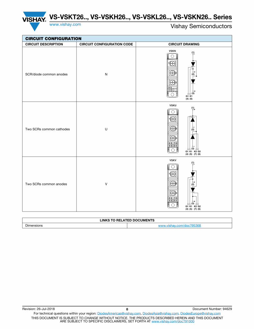
CIRCUIT CONFIGURATIONCIRCUIT DESCRIPTION CIRCUIT CONFIGURATION CODE CIRCUIT DRAWING
Two SCRs doubler circuit T
SCR/diode doubler circuit, positive control H
SCR/diode doubler circuit, negative control L
2 - Module type3 - Circuit configuration (see Circuit Configuration table)4 - Current code (26 A)5 - Voltage code (see Voltage Ratings table)
Device code
21 43 5
K T 26 / 16
1 - Vishay Semiconductors product
VS-VS
+
-
K1(5)
K2(7)
G2(6)
G1(4)
~(1)
(2)
(3)
VSKT
1
2
3
4 5 7 6
+
-
K1(5)
G1(4)
~(1)
(2)
(3)
VSKH
1
2
3
4 5
+
-
K2(7)
G2(6)
~(1)
(2)
(3)
VSKL
1
2
3
7 6
VS-VSKT26.., VS-VSKH26.., VS-VSKL26.., VS-VSKN26.. Serieswww.vishay.com Vishay Semiconductors
Revision: 26-Jul-2018 8 Document Number: 94629For technical questions within your region: [email protected], [email protected], [email protected]
THIS DOCUMENT IS SUBJECT TO CHANGE WITHOUT NOTICE. THE PRODUCTS DESCRIBED HEREIN AND THIS DOCUMENTARE SUBJECT TO SPECIFIC DISCLAIMERS, SET FORTH AT www.vishay.com/doc?91000
SCR/diode common anodes N
Two SCRs common cathodes U
Two SCRs common anodes V
LINKS TO RELATED DOCUMENTS
Dimensions www.vishay.com/doc?95368
CIRCUIT CONFIGURATIONCIRCUIT DESCRIPTION CIRCUIT CONFIGURATION CODE CIRCUIT DRAWING
+
+
K1(5)
G1(4)
-(1)
(2)
(3)
VSKN
1
2
3
4 5
-
-
K1(5)
K2(7)
G2(6)
G1(4)
+(1)
(2)
(3)
VSKU
1
2
3
4 5 7 6
1
2
3
4 5 7 6
VSKV
+
+
K1(5)
K2(7)
G2(6)
G1(4)
-(1)
(2)
(3)

Document Number: 95368 For technical questions, contact: [email protected] www.vishay.comRevision: 11-Nov-08 1
ADD-A-PAK Generation VII - Thyristor
Outline DimensionsVishay Semiconductors
DIMENSIONS in millimeters (inches)35
RE
F.
30 ±
0.5
(1.1
8 ±
0.0
20)
29 ±
0.5
(1 ±
0.0
20)
Viti M5 x 0.8Screws M5 x 0.8
18 (0.7) REF.
15.5 ± 0.5(0.6 ± 0.020)
Fast-on tab 2.8 x 0.8 (0.110 x 0.03)
6.7
± 0
.3 (
0.26
± 0
.012
)
30 ±
1 (
1.18
± 0
.039
)
24 ±
0.5
(1 ±
0.0
20)
1
2 3
45
76
80 ± 0.3 (3.15 ± 0.012)
92 ± 0.75 (3.6 ± 0.030)
20 ± 0.5 (0.79 ± 0.020)
20 ± 0.5 (0.79 ± 0.020)
15 ± 0.5 (0.59 ± 0.020)
22.6
± 0
.2(0
.89
± 0
.008
)
6.3
± 0
.2 (
0.24
8 ±
0.0
08)
5.8
± 0
.25
(0.2
28 ±
0.0
10)
4 ±
0.2
(0.
157
± 0
.008
)

Legal Disclaimer Noticewww.vishay.com Vishay
Revision: 09-Jul-2021 1 Document Number: 91000
Disclaimer ALL PRODUCT, PRODUCT SPECIFICATIONS AND DATA ARE SUBJECT TO CHANGE WITHOUT NOTICE TO IMPROVE RELIABILITY, FUNCTION OR DESIGN OR OTHERWISE.
Vishay Intertechnology, Inc., its affiliates, agents, and employees, and all persons acting on its or their behalf (collectively, “Vishay”), disclaim any and all liability for any errors, inaccuracies or incompleteness contained in any datasheet or in any other disclosure relating to any product.
Vishay makes no warranty, representation or guarantee regarding the suitability of the products for any particular purpose or the continuing production of any product. To the maximum extent permitted by applicable law, Vishay disclaims (i) any and all liability arising out of the application or use of any product, (ii) any and all liability, including without limitation special, consequential or incidental damages, and (iii) any and all implied warranties, including warranties of fitness for particular purpose, non-infringement and merchantability.
Statements regarding the suitability of products for certain types of applications are based on Vishay's knowledge of typical requirements that are often placed on Vishay products in generic applications. Such statements are not binding statements about the suitability of products for a particular application. It is the customer's responsibility to validate that a particular product with the properties described in the product specification is suitable for use in a particular application. Parameters provided in datasheets and / or specifications may vary in different applications and performance may vary over time. All operating parameters, including typical parameters, must be validated for each customer application by the customer's technical experts. Product specifications do not expand or otherwise modify Vishay's terms and conditions of purchase, including but not limited to the warranty expressed therein.
Hyperlinks included in this datasheet may direct users to third-party websites. These links are provided as a convenience and for informational purposes only. Inclusion of these hyperlinks does not constitute an endorsement or an approval by Vishay of any of the products, services or opinions of the corporation, organization or individual associated with the third-party website. Vishay disclaims any and all liability and bears no responsibility for the accuracy, legality or content of the third-party website or for that of subsequent links.
Except as expressly indicated in writing, Vishay products are not designed for use in medical, life-saving, or life-sustaining applications or for any other application in which the failure of the Vishay product could result in personal injury or death. Customers using or selling Vishay products not expressly indicated for use in such applications do so at their own risk. Please contact authorized Vishay personnel to obtain written terms and conditions regarding products designed for such applications.
No license, express or implied, by estoppel or otherwise, to any intellectual property rights is granted by this document or by any conduct of Vishay. Product names and markings noted herein may be trademarks of their respective owners.
© 2021 VISHAY INTERTECHNOLOGY, INC. ALL RIGHTS RESERVED