Visualizador termohigrógrafo con alarma - UVaDOC Principal
371
UNIVERSIDAD DE VALLADOLID ESCUELA DE INGENIERIAS INDUSTRIALES Grado en Ingeniería en Electrónica Industrial y Automática Visualizador termohigrógrafo con alarma Autor: Alonso Fernández, Ricardo Tutor: Díez Muñoz, Pedro Luis Tecnología Electrónica Valladolid, Julio 2021.
-
Upload
khangminh22 -
Category
Documents
-
view
1 -
download
0
Transcript of Visualizador termohigrógrafo con alarma - UVaDOC Principal
UNIVERSIDAD DE VALLADOLID
ESCUELA DE INGENIERIAS INDUSTRIALES
Grado en Ingeniería en Electrónica Industrial y
Automática
Visualizador termohigrógrafo con alarma
Autor:
Alonso Fernández, Ricardo
Tutor:
Díez Muñoz, Pedro Luis
Tecnología Electrónica
Valladolid, Julio 2021.


Agradecimientos
Ricardo Alonso Fernández
Agradecimientos
Quiero transmitir mi más sincero agradecimiento
a todos aquellos que me han ayudado a lo largo
de esta etapa.
En primer lugar, quiero agradecer especialmente
a mi familia: a mi madre Ana, a mi padre Vicen,
mi hermana Sara y a mis abuelas (Milagros,
Chuchi y Vicente ) y mis tíos por su gran apoyo y
ánimos en esta etapa de mi vida, en la que aun
estando separados siempre os he tenido cerca.
En segundo lugar, agradezco a mi tutor Pedro
Luis Díez por haberme ofrecido y guiado durante
el desarrollo de este proyecto.
En tercer lugar, quiero agradecer a todos aquellos
profesores que habéis transmitido vuestra gran
pasión por la materia, haciéndome amar la
carrera cuando yo mismo tenía mis dudas.
También a los amigos que he hecho a lo largo de
estos años en la universidad, y la gran familia que
hemos formado a lo largo del camino. Y
especialmente, mi agradecimiento a Alejandro
Egido por su gran apoyo y ayuda a lo largo de la
carrera.


Resumen y palabras clave
Ricardo Alonso Fernández 5 de 155
Resumen.
Hoy en día se necesita de una gran precisión en las medidas, por ello se han
desarrollado aparatos de gran exactitud, pero estas mediciones dependen
fuertemente de las condiciones ambientales. Por este motivo en los laboratorios de
calibración es de gran importancia realizar el trabajo en unas condiciones de
temperatura y humedad controladas, aquí es donde entra en juego el visualizador
termohigrógrafo con alarma que se va a desarrollar en el presente proyecto.
Palabras clave: Termohigrógrafo1. Datalogger, RS232, ESP32, LCD-TFT
Abstract:
Nowadays, a great precision in the measurements is needed, for this reason
high accuracy devices have been developed, but these measurements strongly
depend on the environmental conditions. This is why in calibration laboratories it is
of great importance to work under controlled temperature and humidity conditions,
this is where the thermo-hygrograph display with alarm that will be developed in the
present project comes into play.
Keywords: Thermo-hygrograph2, Datalogger, RS232, ESP32, LCD-TFT
1 Instrumento de medición para registrar la temperatura y humedad relativa 2 Device that measures and records temperature and humidity


Índice
Ricardo Alonso Fernández 7 de 155
Índice
Introducción y objetivos ............................................................................................ 15
Marco teórico ................................................................................................. 15
Objetivo general ............................................................................................. 18
Objetivos específicos ..................................................................................... 18
Justificación del proyecto ......................................................................................... 19
Capítulo 1: Posibles soluciones ................................................................................ 21
Idea 1: PC como transmisor: ......................................................................... 21
Idea 2: ESP32 como transmisor conectado al ordenador: ......................... 22
Idea 3: ESP32 entre el datalogger y el ordenador: ..................................... 27
Capítulo 2: Tecnología utilizada ................................................................................ 29
2.1 Interfaz de datos RS-232 .................................................................... 29
2.2 Pantalla TFT-LCD .................................................................................. 33
2.2.1 Tecnología LCD ............................................................................... 33
2.2.2 Tecnología TFT-LCD ........................................................................ 37
2.3 ESP32 ................................................................................................... 38
2.4 Sistemas BMS y baterías..................................................................... 40
Capítulo 3: Desarrollo de los circuitos ...................................................................... 53
3.1 Servidor: ................................................................................................... 53
3.1.1 Circuito conversor de RS232 a TTL ................................................ 54
3.1.1.1 Prueba de la comunicación serie ............................................ 62
3.1.2 Circuito de alimentación ................................................................. 64
3.1.3 Circuito de datos RS232 ................................................................. 65
3.2 Visualizador: ............................................................................................ 66
3.2.1 Circuito de alimentación ................................................................. 66
3.2.2 Circuito de alarma, buzzer .............................................................. 67
3.2.3 Circuito de la pantalla...................................................................... 69
Capítulo 4: Desarrollo de las PCBs ........................................................................... 73
4.1 Creación de símbolos y de huellas en KiCad ........................................ 73
4.1.1 Símbolo y footprint de la pantalla TFT ............................................ 73
4.1.2 Símbolo y footprint del módulo de carga de la batería ................. 79
4.2 Diseño de la PCB del Servidor ................................................................ 81
4.3 Diseño de la PCB del visualizador.......................................................... 85
4.4 Fabricación de las PCBs ......................................................................... 89
4.4.1 Fabricación mediante aislado de pistas con CNC ......................... 90
4.1.2 Fabricación mediante insolación y ataque con ácido ................... 98

Visualizador Termohigrógrafo con alarma
8 de 155 EII-Uva
Capítulo 5: Programación ....................................................................................... 107
5.1 Servidor ................................................................................................. 107
5.1.1 Diseño de la página web .............................................................. 108
5.1.2 Recepción de la trama en el ESP32 ............................................ 110
5.1.3 Servidor asíncrono ........................................................................ 112
5.2 Visualizador .......................................................................................... 114
5.2.1 Proceso de sincronización ........................................................... 114
5.2.2 Planteamiento general del código ............................................... 116
Capítulo 6: Envolventes .......................................................................................... 121
6.1 Servidor ................................................................................................. 126
6.2 Visualizador .......................................................................................... 129
Capítulo 7: Estudio económico ............................................................................... 133
7.1 Introducción .......................................................................................... 133
7.2 Recursos empleados ........................................................................... 133
7.3 Costes directos ..................................................................................... 134
7.3.1 Coste del personal ........................................................................ 134
7.3.2 Coste de amortización de material (equipos y software) ........... 135
7.3.3 Costes derivados de consumibles ............................................... 137
7.3.4 Costes directos totales ................................................................. 139
7.4 Costes indirectos .................................................................................. 139
7.5 Costes totales ....................................................................................... 139
Capítulo 8: Repercusiones sociales, económicas y ambientales .......................... 141
8.1 Repercusiones sociales ....................................................................... 141
8.2 Repercusiones económicas ................................................................ 141
8.2 Repercusiones ambientales ................................................................ 142
Capítulo 9: Puesta en marcha del prototipo en el laboratorio ............................... 143
9.1 Modificación del código del servidor .................................................. 143
Capítulo 10: Conclusiones y líneas futuras de desarrollo ...................................... 149
Bibliografía .............................................................................................................. 151
Anexos ..................................................................................................................... 155

Índices de figuras
Ricardo Alonso Fernández 9 de 155
Índice de figuras
Figura 1: Unidades del SI ......................................................................................................................... 15
Figura 2: Infraestructura Metrológica Española .................................................................................... 16
Figura 3: Variación de la corriente de colector del transistor 2N3904 con la temperatura ............... 17
Figura 4: Formato del fichero .txt con los datos del datalogger ............................................................ 21
Figura 5: Esquema de la Idea 1 .............................................................................................................. 21
Figura 6: Esquema de la Idea 2 .............................................................................................................. 22
Figura 7: Esquema de la Idea 3 .............................................................................................................. 27
Figura 8: RS-232-C Características Eléctricas ....................................................................................... 29
Figura 9: Pines del conector DB25 RS-232 ............................................................................................ 30
Figura 10: Pines Conector DB9 ............................................................................................................... 31
Figura 11: Conexión entre dos ETCD ...................................................................................................... 31
Figura 12: Pantalla LCD monocromática ................................................................................................ 33
Figura 13: Filtros polarizadores de pantalla LCD ................................................................................... 33
Figura 14: Termómetro de cristal líquido ............................................................................................... 34
Figura 15: Pintura termo-cromática ........................................................................................................ 34
Figura 16: Cristal líquido pantalla LCD permitiendo el paso de la luz .................................................. 35
Figura 17: Cristal líquido pantalla LCD impidiendo el paso de la luz ................................................... 35
Figura 18: Píxel RGB formado por tres subpíxeles ................................................................................ 36
Figura 19: Esquema pixel pantalla LCD.................................................................................................. 36
Figura 20: Esquema pixel pantalla TFT................................................................................................... 37
Figura 21: Vista al microscopio de pantalla TFT .................................................................................... 37
Figura 22: Empaquetado QFN48 6x6mm .............................................................................................. 38
Figura 23: Diagrama funcional de las series ESP32 ............................................................................. 39
Figura 24: Equilibrado de baterías por resistencia fija .......................................................................... 42
Figura 25: Equilibrado de baterías por resistencia conmutada ............................................................ 42
Figura 26: Equilibrado de baterías por diodos Zener ............................................................................ 43
Figura 27: Equilibrado de baterías analógico ........................................................................................ 43
Figura 28: Equilibrado de baterías por condensador conmutado ........................................................ 44
Figura 29: Equilibrado de baterías por inductancia .............................................................................. 45
Figura 30: Equilibrado de baterías con varios condensadores ............................................................. 45
Figura 31: Equilibrado de baterías con varias inductancias ................................................................. 45
Figura 32: Equilibrado de baterías con transformador conmutado ..................................................... 46
Figura 33: Esquema batería ácido plomo .............................................................................................. 47
Figura 34: Efecto de la temperatura sobre la capacidad de la batería ................................................ 47
Figura 35: Batería Iones de litio de 3400mAh ....................................................................................... 49
Figura 36: Batería LiPo de 3400mAh ..................................................................................................... 49
Figura 37: Curvas de descarga de una batería LiPo .............................................................................. 50
Figura 38: Módulo 03962A ..................................................................................................................... 50
Figura 39: Curva de carga del módulo 03962ª ...................................................................................... 51
Figura 40: Circuito de protección de la batería del 03962A ................................................................. 52
Figura 41: Esquema eléctrico del módulo 03962A ............................................................................... 52
Figura 42: Esquema conexión datalogger-ordenador ........................................................................... 53
Figura 43: Comparación de tensiones y lógica digital en RS-232 y TTL .............................................. 53
Figura 44: Esquema conexión datalogger-ordenador con ESP32 ........................................................ 54
Figura 45: Circuito conversor de RS232 a TTL ...................................................................................... 54
Figura 46: Cámara portátil hp Photosmart con SDIO ............................................................................ 55
Figura 47: Esquema de potencia del ESP32 .......................................................................................... 56
Figura 48: Corriente y tensiones con transistor en corte ...................................................................... 57
Figura 49: Corrientes y tensiones con transistor en saturación ........................................................... 59

Visualizador Termohigrógrafo con alarma
10 de 155 EII-Uva
Figura 50: Prueba del circuito del servidor en protoboard .................................................................... 61
Figura 51: Comunicación asíncrona ....................................................................................................... 62
Figura 52: Circuito LED indicador del Servidor ...................................................................................... 65
Figura 53: Esquema del circuito del Servidor ........................................................................................ 65
Figura 54: Esquema de alimentación del Visualizador.......................................................................... 66
Figura 55: Circuito de alimentación del visualizador en protoboard .................................................... 67
Figura 56: Esquema del circuito de alarma del visualizador ................................................................ 68
Figura 57: Prueba del circuito de alarma del visualizador en protoboard ........................................... 68
Figura 58: Esquema del circuito del Visualizador .................................................................................. 70
Figura 59: Prueba del circuito completo del Visualizador en protoboard ............................................ 70
Figura 60: Modelo 3D de la pantalla TFT ............................................................................................... 75
Figura 61: Medida del consumo del Servidor ........................................................................................ 81
Figura 62: Medida del consumo del Visualizador .................................................................................. 85
Figura 63: Fotolito positivo ...................................................................................................................... 98
Figura 64: Fotolito negativo ..................................................................................................................... 98
Figura 65: Fotolito superior del servidor ............................................................................................... 100
Figura 66: Fotolito inferior del servidor ................................................................................................. 100
Figura 67: Placa del servidor en la insoladora ..................................................................................... 100
Figura 68: Placa del Visualizador revelada .......................................................................................... 101
Figura 69: Proceso de atacado de la placa del visualizador ............................................................... 101
Figura 70: Limpieza de la placa del servidor ........................................................................................ 102
Figura 71: CNC Bungard CCD ................................................................................................................ 102
Figura 72: Carga del fichero de taladrado en Isocam ......................................................................... 103
Figura 73: Fichero de taladrado en Isocam ......................................................................................... 103
Figura 74: Generación del fichero de trabajo de la CNC ..................................................................... 104
Figura 75: Prototipo del visualizador, cara frontal ............................................................................... 104
Figura 76: Prototipo del visualizador, cara trasera .............................................................................. 105
Figura 77: Prototipo del servidor, cara superior .................................................................................. 105
Figura 78: Prototipo del servidor, cara inferior .................................................................................... 105
Figura 79: Estructura de la página web ................................................................................................ 109
Figura 80: Prueba de recepción de mensaje por puerto serie usando pantalla LCD........................ 111
Figura 81: Función procesamiento y página web ................................................................................ 112
Figura 82: Concurrencia en multiprocesador....................................................................................... 116
Figura 83: Concurrencia en un solo procesador .................................................................................. 117
Figura 84: Niveles de alerta del visualizador ....................................................................................... 119
Figura 85: Método MDF de impresión 3D ............................................................................................ 123
Figura 86: Impresora 3d Ender 5 Pro ................................................................................................... 124
Figura 87: Ciclo del PLA ......................................................................................................................... 142
Figura 88: Servidor instalado en el laboratorio .................................................................................... 146
Figura 89: Servidor y visualizador en la zona de la base de datos ..................................................... 146
Figura 90: Visualizador en la zona de calibración ............................................................................... 147
Figura 91: Visualizador en la zona de ensayos .................................................................................... 147

Índices de figuras
Ricardo Alonso Fernández 11 de 155
Índice de diagramas
Diagrama 1: Conexión Serie Ordenador-ESP32 ..................................................................................... 23
Diagrama 2: Categorías y procedimientos de equilibrado de baterías ................................................ 41
Diagrama 3: Programa del servidor ...................................................................................................... 107
Diagrama 4: Recepción de mensaje por el puerto serie y separación de campos ........................... 110
Diagrama 5: Esquema general del programa del visualizador ........................................................... 114
Diagrama 6: diagrama temporal del proceso de sincronización ........................................................ 115
Diagrama 7: diagrama del código del proceso de sincronización ...................................................... 115
Diagrama 8: diagrama del código principal del visualizador .............................................................. 118
Diagrama 9: Estructura e interfaces de los menús del visualizador .................................................. 120
Diagrama 10: Recepción de mensaje por el puerto serie y separación de campos modificación .. 145
Índice de tablas
Tabla 1: Características eléctricas a 3.3V y 25ºC del ESP32-WROOM32 ............................................ 55
Tabla 2: Fragmento tabla IO_MUX .......................................................................................................... 56
Tabla 3: Condiciones de operación recomendadas ............................................................................... 57
Tabla 4: 2N3904: Características eléctricas en corte del transistor .................................................... 58
Tabla 5: Valores máximos del transistor 2N3904 ................................................................................. 61
Tabla 6: Características en saturación del transistor 2N3904 ............................................................. 61
Tabla 7: Lista de materiales del circuito del servidor ............................................................................ 71
Tabla 8: Lista de materiales del circuito del visualizador ...................................................................... 71
Tabla 9: Lista de componentes y footprints asociados del servidor ..................................................... 82
Tabla 10: Lista de componentes y footprints asociados del Visualizador ............................................ 86
Tabla 11: Direcciones y contenido del servidor ................................................................................... 108
Tabla 12: Coste anual ............................................................................................................................ 134
Tabla 13: Días efectivos por año ........................................................................................................... 134
Tabla 14: Distribución temporal de trabajo .......................................................................................... 135
Tabla 15: Amortización del software .................................................................................................... 136
Tabla 16: Amortización del equipo........................................................................................................ 136
Tabla 17: Coste de fabricación con PCBWay ....................................................................................... 137
Tabla 18: Coste de prototipado ............................................................................................................. 137
Tabla 19: Coste de producción en masa .............................................................................................. 138
Tabla 20: Costes indirectos parciales ................................................................................................... 139
Tabla 21: Costes totales ........................................................................................................................ 139
Tabla 22: Análisis de la transmisión del datalogger ............................................................................ 144

Visualizador Termohigrógrafo con alarma
12 de 155 EII-Uva
Índice de capturas
Captura 1: Administrador de equipos ..................................................................................................... 24
Captura 2: Propiedades Puerto COM ...................................................................................................... 24
Captura 3: Configuración avanzada puerto COM................................................................................... 25
Captura 4: Tensión del diodo 1N4001 en función de la corriente ....................................................... 59
Captura 5: Envío mensaje con hyperterminal Hércules ........................................................................ 63
Captura 6: Trama Analizador lógico, mensaje completo ....................................................................... 63
Captura 7: Envío mensaje corto hyperterminal hércules ...................................................................... 63
Captura 8: Trama analizada del mensaje corto ..................................................................................... 64
Captura 9: Editor de símbolos de KiCad, nuevo símbolo ....................................................................... 73
Captura 10: Numeración de pines de la pantalla en el editor de símbolos ......................................... 74
Captura 11: Símbolo esquemático de la pantalla TFT ........................................................................... 74
Captura 12: Propiedades del símbolo de la pantalla ............................................................................. 75
Captura 13: Colocación de los pads en la footprint de la pantalla ....................................................... 76
Captura 14: Footprint de la pantalla ....................................................................................................... 77
Captura 15: Configuración del modelo 3D de la footprint de la pantalla ............................................. 77
Captura 16: Modelo 3D de la footprint de la pantalla TFT .................................................................... 78
Captura 17: Modelo 3D de la footprint de la pantalla TFT V2 ............................................................... 78
Captura 18: Símbolo esquemático del módulo 03962A ....................................................................... 79
Captura 19: Modelo 3D del módulo 03962A ......................................................................................... 79
Captura 20: Footprint del módulo 03962A ............................................................................................ 80
Captura 21: Modelo 3D de la footprint del módulo 03962ª ................................................................. 80
Captura 22: Cálculo ancho de pista para el circuito del servidor ......................................................... 82
Captura 23: Emplazamiento de los componentes en la PCB del servidor ........................................... 83
Captura 24: Rutado de la PCB del Servidor ........................................................................................... 83
Captura 25: Vista 3D superior de la PCB del Servidor ........................................................................... 84
Captura 26: Vista 3D inferior de la PCB del Servidor ............................................................................. 84
Captura 27: Cálculo ancho de pista para el circuito del Visualizador .................................................. 85
Captura 28: Emplazamiento de los componentes en la PCB del Visualizador .................................... 87
Captura 29: Rutado de la cara superior de la PCB del Visualizador..................................................... 87
Captura 30: Rutado de la cara inferior de la PCB del Visualizador ...................................................... 87
Captura 31: Vista 3D superior de la PCB del Visualizador .................................................................... 88
Captura 32: Vista 3D inferior de la PCB del Visualizador ...................................................................... 88
Captura 33: Trazado de ficheros de fabricación Gerber ....................................................................... 90
Captura 34: Ficheros Gerber en FlatCAM ............................................................................................... 91
Captura 35: Mirror Y en FlatCAM ............................................................................................................ 91
Captura 36: Generación del Gcode de taladrado .................................................................................. 92
Captura 37: Fichero drl_cnc de 1mm en FlatCAM ................................................................................. 92
Captura 38: Taladros en GRBLcontrol .................................................................................................... 93
Captura 39: Ruta de aislado de las pistas en FlatCAM ......................................................................... 93
Captura 40: Generación del fichero de aislado de pistas en FlatCAM ................................................. 94
Captura 41: Gcode del aislado de pistas en la CNC .............................................................................. 94
Captura 42: Ruta del corte de placa en FlatCAM .................................................................................. 95
Captura 43: Rutas para el corte de la placa en FlatCAM ...................................................................... 95
Captura 44: Corte de la placa en la CNC ................................................................................................ 96
Captura 45: PCB realizada con CNC, lado de las pistas ........................................................................ 97
Captura 46: PCB realizada con CNC, serigrafía ..................................................................................... 97
Captura 47: PCB realizada con CNC, montaje final ............................................................................... 97
Captura 48: Pagina web del servidor .................................................................................................... 109
Captura 49: Caja RS PRO de ABS Gris.................................................................................................. 121

Índices de figuras
Ricardo Alonso Fernández 13 de 155
Captura 50: Caja Hammond de ABS piro retardante Gris ................................................................... 121
Captura 51: Posprocesado del ABS ...................................................................................................... 125
Captura 52: Efecto warping ................................................................................................................... 125
Captura 53: Efecto cracking .................................................................................................................. 125
Captura 54: Vista explosionada del servidor ........................................................................................ 126
Captura 55: Segmentación servidor (PLA Glitter Verde) ..................................................................... 127
Captura 56: Segmentación servidor (PLA Silk Gold) ............................................................................ 128
Captura 57: Vista superior de la envolvente del servidor .................................................................... 128
Captura 58: Vista inferior de la envolvente del servidor...................................................................... 128
Captura 59: Vista explosionada del visualizador ................................................................................. 129
Captura 60: Segmentación visualizador (PLA Glitter Verde) ............................................................... 130
Captura 61: Impresión de la envolvente del visualizador.................................................................... 130
Captura 62: Vista superior de la envolvente del visualizador ............................................................. 131
Captura 63: Vista inferior de la envolvente del visualizador ............................................................... 131
Captura 64: Captura del analizador lógico sobre el datalogger.......................................................... 143
Captura 65: Captura del analizador lógico, primera trama ................................................................. 144


Introducción y objetivos
Ricardo Alonso Fernández 15 de 155
Introducción y objetivos
Marco teórico
El desarrollo de la ciencia y la tecnología, la investigación, fabricación y control
de procesos industriales, la protección del medio ambiente, gestión energética y de
los recursos naturales, todo ello depende en gran parte de que las medidas sean
fiables.
Metrología, “ciencia que tiene por objeto el estudio de los sistemas de pesas y
medidas” (Española, 2021)
La metrología es una de las ciencias más antiguas del mundo cuya relevancia
e incidencia en la economía y la sociedad es desconocida por muchos. “Su papel en
el progreso humano es invasivo, pero discreto hasta el punto de que puede pasar
desapercibido como la necesidad de un ambiente respirable para la inmensa
mayoría de las especies vivientes (Comité de Metrología del Instituto de la Ingeniería
en España, 2019)
El origen de la metrología actual surge después de la Revolución Francesa,
con el decreto de la Asamblea Nacional Francesa, que estableció un sistema
nacional de pesas y medidas. En 1791 legalizó un sistema métrico decimal de
medida en el que la unidad de masa era el decímetro cúbico de agua a 4ºC y como
medida de longitud el metro, definido por la diezmillonésima parte del cuadrante
meridiano terrestre. Ambas unidades se materializaron, en un cilindro de platino en
el caso de la masa y en una barra de platino para la longitud. Ambas se depositaron
en los Archivos del Imperio en el año 1799. Siendo este sistema el antecesor del
actual Sistema Internacional de Unidades (SI).
Finalmente, en la Conferencia General de Pesos y Medidas de 2018 (CGPM),
(Burea International des Poids er Mesures, 2018), se establecieron 7 unidades
básicas en función de constantes universales (ver Figura 1), permitiendo una menor
incertidumbre y mayor estabilidad en las realizaciones prácticas.
Figura 1: Unidades del SI
(Fuente: (Ministerio de Industria Comercio y Turismo, 2021; Fairchild
Semiconductor Corporation, 2014))

Visualizador Termohigrógrafo con alarma
16 de 155 EII-Uva
Una vez definidas unas unidades, es necesario que todos los instrumentos de
medición estén calibrados para que las medidas obtenidas sean fiables. Para ello se
necesita de una calibración adecuada que se hace por medio de la trazabilidad, de
manera que cualquier medición debe ser trazable hasta un patrón o estándar.
En el proceso de calibración de un instrumento, se compara la medición del
instrumento con el resultado de un instrumento de exactitud conocida, que a su vez
es calibrado contra un patrón nacional o internacional.
Para garantizar la trazabilidad durante la práctica, se debe cumplir los
siguientes puntos:
• La cadena de comparación no debe interrumpirse.
• El instrumento de medición superior debe tener una exactitud de
medición de 3 a 4 veces mayor. De manera que la incertidumbre de
cada medición sea conocida y pueda calcularse la incertidumbre total.
• Todos los resultados en cada paso deben documentarse.
• Todos los organismos involucrados deben probar su competencia
mediante acreditación.
• Las calibraciones deben repetirse en intervalos periódicos apropiados.
Figura 2: Infraestructura Metrológica Española
Fuente: (Ministerio de Industria Comercio y Turismo, 2021)

Introducción y objetivos
Ricardo Alonso Fernández 17 de 155
Todos los instrumentos de medida varían su comportamiento en función de
las condiciones ambientales, debido a los cambios de físicos y químicos de la materia
que afectan tanto al instrumento de medida como a la variable a medir. Un ejemplo
claro sería medir una varilla de acero con una regla de aluminio, a una temperatura
baja ambos materiales se contraen, pero no de igual manera y a una temperatura
alta ambos se dilatan de distinta forma, por ello las medidas obtenidas serán
distintas.
Hoy en día, la mayor parte de los instrumentos de medida son electrónicos, y
esta electrónica también está sujeta a variaciones en su comportamiento en función
de las condiciones ambientales, principalmente temperatura y humedad, ver Figura
3. A medida que buscamos obtener valores más precisos (más pequeños) el efecto
negativo de los cambios ambientales aumenta.
Los laboratorios acreditados, para garantizar la fiabilidad de sus medidas
deben realizar las mediciones en condiciones ambientales controladas, con
instrumentos calibrados por una entidad superior.
Figura 3: Variación de la corriente de colector del transistor 2N3904 con la temperatura
Fuente: (Fairchild Semiconductor Corporation, 2014)

Visualizador Termohigrógrafo con alarma
18 de 155 EII-Uva
Objetivo general
En este proyecto se busca desarrollar un visualizador termohigrógrafo con
alarma. Este dispositivo informará de manera clara y rápida al personal de
laboratorio de las condiciones ambientales en la zona de trabajo.
El visualizador tendrá una forma compacta y admitirá carga por USB, de
manera que el operario podrá situarlo en su mesa de trabajo y alimentarlo mediante
un cargador de móvil o un puerto USB libre del ordenador. Admitirá una configuración
básica de algunos parámetros como los rangos de alarma para la temperatura y la
humedad. Para informar de las condiciones ambientales de la sala dispondrá de una
pantalla que muestre dichos valores y unos indicadores de colores que cambiarán
en función de las condiciones ambientales. El patrón que seguirán los indicadores
será similar al de los semáforos ya que es un código simple de tres colores que las
personas han interiorizado. De manera que un color rojo se relaciona rápidamente
con “detente” un naranja o amarillo con “cuidado” y el verde con “continua”.
El dispositivo se utilizará en el laboratorio LACECAL3 situado en el sótano de
la Escuela de Ingenierías Industriales. Este laboratorio se encuentra dividido en dos
partes “Calibración” y “Ensayos”, para ello se crearán dos visualizadores idénticos
pero cada uno estará configurado para mostrar las condiciones de la parte del
laboratorio en que se encuentre.
Actualmente el laboratorio cuenta con una sonda de temperatura y humedad
en cada zona de medición, ambas conectadas a un datalogger4 que almacena los
valores medidos y los transmite mediante cable por comunicación RS232 a un
ordenador al que puede acceder el personal de laboratorio para consultar las
condiciones ambientales del lugar.
Objetivos específicos
- Pantalla que muestre la temperatura y humedad actual.
- Señalización luminosa.
- Batería propia que garantice una autonomía de varias horas.
- Comunicación inalámbrica para obtener los datos de temperatura y
humedad.
- Configuración manual de los parámetros de alarma a través de botonera
o similar.
3 Laboratorio de Calibración Eléctrica de Castilla y León. 4 Dispositivo electrónico que registra los datos obtenidos a través de sensores externos.

Justificación del proyecto
Ricardo Alonso Fernández 19 de 155
Justificación del proyecto En el presente trabajo se busca integrar los conocimientos y capacidades
adquiridos durante la titulación, desarrollando un proyecto en el ámbito de la
electrónica y la automatización.
Desde el laboratorio LACECAL se propone un proyecto que busca crear un
visualizador termohigrógrafo con alarma, cuyas características técnicas coinciden
con las competencias adquiridas durante los estudios. De forma que el correcto
desarrollo de este Trabajo de Fin de Grado permita la finalización de los estudios y la
obtención del título de Ingeniero especializado en Electrónica Industrial y Automática.


Capítulo 1: Posibles soluciones
Ricardo Alonso Fernández 21 de 155
Capítulo 1: Posibles soluciones
Idea 1: PC como transmisor:
En el laboratorio existe un ordenador conectado al datalogger por cable,
usando el protocolo RS232 en la comunicación entre ambos dispositivos. El
datalogger recibe los valores de las sondas de temperatura y humedad repartidas
por el laboratorio y por medio de la comunicación serie, transmite estos valores al
ordenador que los almacena en un fichero de texto con el formato de la Figura 4,
comenzando con la fecha, seguida la hora de la medida y después la temperatura y
humedad captada por la primera sonda, por último, los valores de la segunda sonda.
Figura 4: Formato del fichero .txt con los datos del datalogger
Fuente: Elaboración propia
Aprovechando que cada minuto se genera un fichero de texto llamado
“ahora.txt” con los valores de la última medición realizada en el formato descrito
anteriormente. Se busca desarrollar un programa en c/c++ que acceda a dicho
fichero y utilice una antena Wifi conectada al ordenador para crear una red
inalámbrica a la que se conecten los visualizadores repartidos por el laboratorio y
reciban la información de la última medida (ver Figura 5).
Figura 5: Esquema de la Idea 1
Fuente: Elaboración propia
Para el desarrollo de esta idea habría que añadir una antena Wifi al ordenador
del laboratorio, pero no haría falta modificar la conexión entre el datalogger y el
ordenador.

Visualizador Termohigrógrafo con alarma
22 de 155 EII-Uva
Idea 2: ESP32 como transmisor conectado al ordenador:
Siguiendo el planteamiento de la idea anterior, se conserva la actual conexión
de los dispositivos, pero en vez de añadir una antena Wifi al ordenador, se conecta
un ESP32 a través de un puerto USB, actuando este como punto de acceso
inalámbrico (menor coste que la antena), ver Figura 6.
Figura 6: Esquema de la Idea 2
Fuente: Elaboración propia
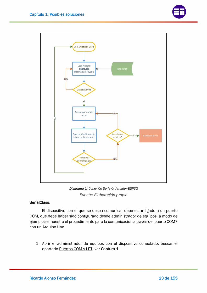
Mediante un programa en c++ en constante ejecución en el ordenador,
utilizando la librería SerialClass se pueden comunicar el ESP32 y el ordenador, ver
Diagrama 1.
Este programa lee el fichero ahora.txt, transmitiendo su contenido a través
del puerto serie al ESP32 que a su vez comparte la información de manera
inalámbrica a los visualizadores del laboratorio.
La librería SerialClass permite la comunicación a través del puerto serie y la
librería fstream implementa los elementos necesarios para la lectura y escritura de
ficheros.
Esta idea fue descartada debido a los problemas de concurrencia en el
archivo de texto con los datos, ya que a la vez lo utilizan el programa del ordenador
que recibe los datos del datalogger y el programa que debería transmitir al ESP32.
Capítulo 1: Posibles soluciones
Ricardo Alonso Fernández 23 de 155
Diagrama 1: Conexión Serie Ordenador-ESP32
Fuente: Elaboración propia
SerialClass:
El dispositivo con el que se desea comunicar debe estar ligado a un puerto
COM, que debe haber sido configurado desde administrador de equipos, a modo de
ejemplo se muestra el procedimiento para la comunicación a través del puerto COM7
con un Arduino Uno.
1 Abrir el administrador de equipos con el dispositivo conectado, buscar el
apartado Puertos COM y LPT, ver Captura 1.

Visualizador Termohigrógrafo con alarma
24 de 155 EII-Uva
Captura 1: Administrador de equipos
Fuente: Elaboración propia
2 Hacer doble clic sobre el dispositivo e ir a la pestaña Configuración de puerto
aquí se configura el protocolo de comunicación, en este caso 8N1 (8 bits de
datos, sin paridad y 1 bit de parada) a 9600 baudios (ver Captura 2). En
opciones avanzadas se puedes configurar el número de puerto asignado (ver
Captura 3). Estas son las características por defecto de la comunicación serie
con Arduino.
Captura 2: Propiedades Puerto COM
Fuente: Elaboración propia

Capítulo 1: Posibles soluciones
Ricardo Alonso Fernández 25 de 155
Captura 3: Configuración avanzada puerto COM
Fuente: Elaboración propia
3 En el código para el ordenador se crea un elemento de clase Serial, en este
caso se llama Puerto, para ello se utiliza la siguiente línea de código:
Serial* Puerto = new Serial( "COM7" );
Para comprobar que el puerto está correctamente conectado se utiliza:
Puerto -> IsConnected();
Devuelve un 0 si no está disponible y un 1 en caso contrario.
Para enviar y recibir datos a través del puerto COM:
Puerto -> WriteData(buffer, sizeof(buffer) - 1);
n = Puerto -> ReadData(lectura, 49);
Buffer y lectura son dos arrays de char que contienen el mensaje a
enviar y el mensaje recibido, respectivamente. n es una variable entera que
representa la longitud del mensaje recibido.

Visualizador Termohigrógrafo con alarma
26 de 155 EII-Uva
fstream:
Para acceder a un fichero se debe crear un elemento de clase fstream para
un fichero que de solo lectura (ifstream) llamado fichero, ligado al archivo de texto
TFG.txt.
Solo lectura: ifstream fichero("TFG.txt");
Solo escritura: ofstream fichero("TFG.txt");
Lectura y escritura: fstream fichero("TFG.txt");
Utilizando fichero >> ‘Variable destino’ se puede copiar el contenido de una
línea del fichero en la variable deseada, y utilizando fichero << ‘Variable origen’ se
puede escribir el contenido de la variable en una línea del fichero.
El constructor de la clase por defecto abre el fichero para su utilización, por
ello cuando se terminen las operaciones en el archivo hay que cerrarlo mediante:
fichero.close();

Capítulo 1: Posibles soluciones
Ricardo Alonso Fernández 27 de 155
Idea 3: ESP32 entre el datalogger y el ordenador:
Mediante esta solución, no se necesita ningún programa en el ordenador, el
ESP32 toma la señal de datos Tx que va del datalogger al ordenador. El protocolo
RS232 de la señal no es admitido por el ESP32, por ello se necesita convertir tanto
el rango de tensiones (de ±12V a 0-5V) de la señal, como la lógica digital utilizada,
en RS232 el 0 se representa por tensión positiva y en TTL con 0V y el 1 por tensión
negativa en RS232 y por 5V en TTL, ver Interfaz de datos RS-232.
El ESP32 actúa como punto de acceso inalámbrico (servidor de datos),
creando su propia red Wifi a la que se conectan los visualizadores o cualquier usuario
conectado a dicha red que conozca la dirección IP del servidor.
Para que el ESP32 pueda tomar la señal de datos solo hay que desconectar
el cable que une el datalogger y el ordenador por el extremo del datalogger, conectar
ese extremo a la tarjeta con el ESP32 servidor y esta tarjeta conectarla al datalogger.
De esta manera tanto ordenador como ESP32 reciben la información de temperatura
y presión de las sondas.
Figura 7: Esquema de la Idea 3
Fuente: Elaboración propia
Esta es la idea que se desarrollará a lo largo del presente trabajo debido a su
mayor relación con la electrónica y mejor dominio de los conceptos necesarios para
su funcionamiento.


Capítulo 2: Tecnología utilizada
Ricardo Alonso Fernández 29 de 155
Capítulo 2: Tecnología utilizada
2.1 Interfaz de datos RS-232
Interfaz: “Conexión, física o lógica, entre una computadora y el usuario, un dispositivo
periférico o un enlace de comunicaciones” (Española, 2021)
En 1969, la EIA5 y los laboratorios Bell (AT&T) conjuntamente formularon y
publicaron la recomendación EIA RS-232, que tras algunas revisiones se convirtió en
RS-232-C.
La norma abarca la descripción de un “interfaz de propósito general entre un
Equipo Terminal de Datos (ETD) y un Equipo de Comunicación de Datos (ETCD),
mediante un intercambio de datos binarios en serie.
La comunicación se realiza mediante señales digitales, binarias codificadas
por nivel de tensión. Se definen dos bandas de tensión una para el cero lógico y otra
para el uno lógico. Las bandas son diferentes para emisión y recepción, ver Figura 8.
La norma especifica que el conector tendrá como máximo 25 patillas, cada
una con una función asignada, ver Figura 9. Además, es posible cortocircuitar
cualquier número de patillas del conector sin causar daños al equipo o a la interfaz.
Velocidad máxima recomendada de 20000 bps6 y longitud máxima
recomendada de 15 metros. La velocidad máxima y la distancia útil máxima se
relacionan de forma inversa.
Figura 8: RS-232-C Características Eléctricas
(Fuente: (Pérez Turiel, 2020))
5 Electronic Industries Alliance, Alianza de Industrias Electrónicas de Estados Unidos. 6 Bits por segundo.

Visualizador Termohigrógrafo con alarma
30 de 155 EII-Uva
De las 25 señales de la interfaz RS232, solo se definen 21 circuitos de
intercambio, quedando cuatro no asignados. Los definidos se clasifican en 5 grupos:
• Circuitos de masa.
• Circuitos de datos.
• Circuitos de control del interfaz.
• Circuitos de temporización.
• Canal secundario.
Solo el circuito de masa es de uso obligatorio.
La denominación de los circuitos se define respecto a su función en el lado
ETD, de manera que, por ejemplo, el circuito de transmisión de datos es la salida de
datos desde el ETD y el circuito de recepción de datos es la entrada de datos al ETD.
Figura 9: Pines del conector DB25 RS-232
(Fuente: (AGGSoftware, 2021))
Para una comunicación completa (enviar y recibir datos), solo se necesitan 3
de los circuitos: GND, TD (Transmisión de datos) y RD (Recepción de datos). Por ello
es habitual utilizar conectores reducidos como el DB9, ver Figura 10.

Capítulo 2: Tecnología utilizada
Ricardo Alonso Fernández 31 de 155
Figura 10: Pines Conector DB9
Fuente: (Diagram Database, 2021)
Aunque la norma se define para la conexión de un ETD y un ETCD, es posible
conectar dos ETD entre sí. Para ello es suficiente con cruzar los conductores de
transmisión (pin 2) y de recepción (pin 3), ver Figura 11.
Figura 11: Conexión entre dos ETCD
Fuente: (AmericanCableAssemblies, 2021)

Visualizador Termohigrógrafo con alarma
32 de 155 EII-Uva
Tiempo después (1978) surge la norma RS-422 que supera las limitaciones
de la norma RS-232-C. La nueva norma cambia los aspectos eléctricos de la interfaz,
realizándose la transmisión de datos en modo diferencial, a través de dos pares de
hilos independientes. Un par para el circuito de transmisión y otro para el de
recepción. La tensión especificada es de +5V, de manera que en uno de los
conductores del par se transmite en lógica positiva y simultáneamente en el otro par
en lógica negativa, por ello la tensión existente entre ambos conductores es el doble
de la tensión de alimentación.
El conductor empleado cuando no se utilizan circuitos de control es el par
trenzado apantallado.
El uso de la doble codificación en lógica positiva y negativa permite obtener
una variación efectiva de 10V entre el ‘0’ y el ‘1’ lógico. Esto da lugar a un mejor
comportamiento ante interferencias, permitiendo aumentar la distancia máxima
hasta 1200 metros, aunque esto depende inversamente de la velocidad de
transmisión, al igual que en RS232.
Finalmente, en abril de 1983 la EIA presenta la interfaz RS-485, cuyas
características son similares a la RS-422, pero ofrece mejores prestaciones en la
conexión multipunto, permitiendo la conexión simultanea de hasta 32 dispositivos
sobre un mismo par trenzado.

Capítulo 2: Tecnología utilizada
Ricardo Alonso Fernández 33 de 155
2.2 Pantalla TFT-LCD
La tecnología TFT7 es una evolución de las pantallas LCD8. En las pantallas
LCD los elementos de imagen se excitan de forma directa, esto hace que cada uno
de los tres colores (subpíxeles) que forman cada pixel de la pantalla necesite
conexiones por ambos extremos. Por ello, este sistema resulta viable en pequeñas
pantallas como las de las calculadoras que habitualmente solo utilizan un color de
texto sobre un fondo de otro color.
Figura 12: Pantalla LCD monocromática
Fuente: Elaboración propia
2.2.1 Tecnología LCD
Las pantallas LCD utilizan una iluminación trasera y dos filtros
polarizadores cruzados a 90º. El primer filtro solo deja pasar la luz en una
orientación, y al encontrarse esta con el segundo filtro en perpendicular, la luz
no puede pasar y la pantalla se ve negra.
Figura 13: Filtros polarizadores de pantalla LCD
Fuente: (SCHWENKE, 2021)
7 Thin Film Transistor, Transistor de Película Delgada 8 Liquid Crystal Display, Pantalla de Cristal Líquido

Visualizador Termohigrógrafo con alarma
34 de 155 EII-Uva
Para que la luz pueda atravesar el segundo filtro polarizador necesita ser
girada 90º en el camino. Para esta tarea se utiliza el cristal líquido, que son
sustancias que combinan características de sólido y de líquido. Presentan la
anisotropía de un sólido cristalino (algunas propiedades varían en función de la
dirección considerada) y la movilidad entre moléculas de un líquido.
Los cristales líquidos se clasifican en función de la forma de sus moléculas,
existiendo dos tipos principalmente:
• Cristales Líquidos Calamíticos: moléculas en forma de varilla
• Cristales Líquidos Discóticos o Columnares: moléculas en forma de
disco.
También se pueden dividir en función de que efecto origina el estado de cristal
líquido:
• Cristal Líquido Termótropo: originado por el efecto de la temperatura.
• Cristal Líquido Liótropos: creados por la presencia de algún disolvente.
Un uso habitual de los cristales líquidos liótropos es en la industria de los
cosméticos y los termótropos se emplean en los termómetros o pinturas termo-
cromáticas que cambian la manera en que reflejan la luz al variar la temperatura, ver
Figura 14 y Figura 15.
Información adaptada de una publicación del (Instituto de Síntesis Química y
Catálisis Homogénea, Universidad de Zaragoza, 2021).
Figura 14: Termómetro de cristal líquido Figura 15: Pintura termo-cromática
Fuente: (Alibaba, 2021) Fuente: (PintarSinParar, 2021)
En el caso de las pantallas se hace uso de las propiedades electroópticas,
combinando la anisotropía de los cristales, la fluidez de los líquidos y las propiedades
dieléctricas. Como resultado, al aplicar un campo electromagnético sobre el cristal
líquido, las moléculas de este se orientan siguiendo la dirección del campo.

Capítulo 2: Tecnología utilizada
Ricardo Alonso Fernández 35 de 155
En la Figura 16, se ha añadido la capa de cristal líquido entre los dos filtros
polarizadores, junto con dos electrodos que generan un campo electromagnético
para cambiar la forma de las moléculas del cristal. En el estado que se muestra, la
luz es girada por el cristal pudiendo pasar el último filtro de polarización, iluminando
la pantalla. Sin embargo, en la Figura 17 al variar la tensión en los electrodos, las
moléculas se reorientan y la luz deja de cambiar de orientación, eliminando la imagen
de la pantalla.
Al regular la tensión aplicada, se varía la orientación de los cristales,
cambiando la cantidad de luz que puede pasar, variando la intensidad del color
mostrado.
Figura 16: Cristal líquido pantalla LCD permitiendo el paso de la luz
Fuente: (SCHWENKE, 2021)
Figura 17: Cristal líquido pantalla LCD impidiendo el paso de la luz
Fuente: (SCHWENKE, 2021)

Visualizador Termohigrógrafo con alarma
36 de 155 EII-Uva
Cada uno de los elementos explicados anteriormente formarían un píxel de
una pantalla monocromática. Sin embargo, en las pantallas a color cada píxel está
formado por tres subpíxeles, uno rojo, otro verde y otro azul (RGB). Estando cada uno
formado por el conjunto anterior, junto con un filtro de color. Ver Figura 18.
Figura 18: Píxel RGB formado por tres subpíxeles
Fuente: (SCHWENKE, 2021)
Figura 19: Esquema pixel pantalla LCD
Fuente: (Sanyo, 2021)

Capítulo 2: Tecnología utilizada
Ricardo Alonso Fernández 37 de 155
2.2.2 Tecnología TFT-LCD
El problema de las pantallas LCD es que cada subpíxel necesita estar
controlado individualmente, dando lugar a millones de conexiones. Con la tecnología
TFT, se conectan los subpíxeles por filas y columnas de manera que al aplicar tensión
positiva en una fila y tensión negativa en una columna, el pixel situado en el cruce
será el único activo. Sin embargo, aunque solo un pixel recibe la tensión completa,
el resto de los pixeles de la fila y columna reciben parte de la tensión tendiendo a
oscurecerse. Para evitar esto se añade un transistor conmutador a cada pixel.
Figura 20: Esquema pixel pantalla TFT
Fuente: (Wikimedia Commons, 2021)
Figura 21: Vista al microscopio de pantalla TFT
Fuente: (Wikimedia Commons, 2021)

Visualizador Termohigrógrafo con alarma
38 de 155 EII-Uva
2.3 ESP32
Es un microcontrolador con Wifi, Bluetooth y Bluetooth de Baja Energía (BLE)
que permite trabajar desde sensores de baja-energía hasta las tareas más complejas
como tratamiento de audio.
El núcleo del módulo es el chip ESP32-D0WDQ6:
• D: Doble núcleo
• 0: Sin memoria flash integrada
• WD: Wi-Fi+ BT+ BTE.
• Q6: empaquetado QFN 6*6, ver Figura 22.
Figura 22: Empaquetado QFN48 6x6mm
Fuente: (Espressif Systems, 2021)
Las dos CPUs pueden ser controladas individualmente y la frecuencia del reloj
puede ajustarse de 80MHz a 240MHz. Para las tareas sencillas como monitoreo de
los periféricos existe un coprocesador de bajo consumo que permite desactivar la
CPU principal para ahorra energía.
También se integran algunos periféricos como sensores capacitivos de
contacto, sensores de efecto Hall, SPI9 de alta velocidad, UART10, I2C, convertidores
ADC y DCA, ver Figura 23.
9 Serial Peripheral Interface, Interfaz de Periféricos en Serie 10 Universal Asynchronous Receiver-Transmitter, Transmisor-Receptor Asíncrono Universal

Capítulo 2: Tecnología utilizada
Ricardo Alonso Fernández 39 de 155
Figura 23: Diagrama funcional de las series ESP32
Fuente: (Espressif Systems, 2021)
El sistema operativo es FreeRTOS (Real-Time operating system for
microcontrollers) junto con lwIP (lightweight IP), una pila TCP/IP alternativa de código
abierto utilizada en los sistemas integrados.
Debido a su extendido uso existen diferentes comunidades que han
desarrollado código que permite utilizar las funciones más complejas del procesador
de manera más sencilla.

Visualizador Termohigrógrafo con alarma
40 de 155 EII-Uva
2.4 Sistemas BMS y baterías.
Información extraída de los apuntes de (Vazquez, 2021)
Para regular la carga y descarga de la batería se necesita un sistema de
gestión de batería BMS11. Un sistema electrónico que gestiona una batería
recargable y la protege mediante el análisis de diferentes parámetros.
Dependiendo del uso de la batería, el sistema BMS será más o menos
complejo, incluyendo diferentes funciones y características entre las que destacan:
• Protección de las celdas de la batería: el sistema de gestión debe asegurar
que las celdas trabajan dentro de sus márgenes de seguridad.
• Control de la carga: el sistema debe encargarse de que las condiciones
durante la recarga de la batería son las adecuadas.
• Control de la descarga: el BMS debe garantizar que la batería trabaja en un
régimen de descarga apropiado para la aplicación en la que se está usando y
debe evitar que la batería sobrepase sus límites de funcionamiento para
prolongar su vida útil.
• Determinación del estado de carga: es una función a través de la cual y
mediante diferentes algoritmos, el sistema es capaz de reconocer en qué
estado se encuentra la batería.
• Determinación del estado de salud: el sistema, a través de un análisis de
diferentes parámetros debe ser capaz de saber si la batería o alguna celda se
encuentra en buen estado o si por el contrario está dañada o ha perdido una
parte importante de su capacidad.
• Balance de celdas: en una batería compuesta por múltiples celdas, es posible
que no todas se encuentren en el mismo estado y esto afecta directamente
al rendimiento y al deterioro de toda la batería. Por ello el sistema debe tratar
de que todas las celdas estén en un estado lo más parecido posible.
• Control de temperatura: la temperatura es una variable determinante para el
correcto funcionamiento de las baterías. Por ello el sistema debe conocer la
temperatura de las celdas y del ambiente para, en caso de que se sobrepasen
unos límites, aplicar las acciones necesarias para mantener la batería en una
temperatura adecuada para no afectar a su rendimiento ni a su vida útil.
En sistemas más complejos e inteligentes, se pueden encontrar módulos que
se encargan de recoger información histórica de diferentes parámetros de la batería,
para comprobar que las celdas de la batería pertenecen al tipo que corresponde (por
si se han cambiado celdas viejas por nuevas) o sistemas de comunicación con la
batería para una mejor carga y descarga.
11 Battery Manager System

Capítulo 2: Tecnología utilizada
Ricardo Alonso Fernández 41 de 155
Los sistemas de equilibrado de celdas se dividen en dos tipos, pasivos o
activos, dependiendo si para el equilibrado consumen la energía de las celdas más
cargadas o la transfieren a las celdas menos cargadas.
Los métodos pasivos o métodos de celda a calor transforman la energía en
calor, por medio de distintos procedimientos. Los métodos activos, se clasifican en
función de cómo reparten la energía sobrante de las celdas. Ver Diagrama 2.
Diagrama 2: Categorías y procedimientos de equilibrado de baterías
Fuente: (Vazquez, 2021)
Los métodos pasivos son los más simples en cuanto a control e
implementación y por tanto más baratos, por ello son los más empleados en la
actualidad. Sus principales desventajas son la pérdida de la energía al disiparse en
forma de calor. También existe la posibilidad de tener altas corrientes durante el
periodo de disipación, lo cual implica tener componentes capaces de soportarlas, y
capaces de disipar todo el calor generado.

Visualizador Termohigrógrafo con alarma
42 de 155 EII-Uva
Algunos métodos pasivos empleados son los siguientes:
• Resistencia fija: Este método desvía constantemente corriente de las celdas
a una resistencia fija en paralelo con ellas. Esta resistencia limita la tensión
de cada celda a cambio de una pérdida constante de energía por la
resistencia. Es el método más barato y simple, pero la continua pérdida de
energía está llevando a reducir su uso en la actualidad.
Figura 24: Equilibrado de baterías por resistencia fija
Fuente: (Vazquez, 2021)
• Resistencia conmutada: se basa en la resistencia fija, pero para evitar un
consumo continuo, se añade un interruptor controlado que conecta la resistencia
a la celda solo para liberar la sobrecarga. Es un método un poco más complejo,
pero es fácil y económico de implementar.
Figura 25: Equilibrado de baterías por resistencia conmutada
Fuente: (Vazquez, 2021)

Capítulo 2: Tecnología utilizada
Ricardo Alonso Fernández 43 de 155
• Diodos Zener: se sustituyen las resistencias por diodos Zener, limitando la
tensión, protegiendo a las celdas de la sobrecarga. Pero se generan grandes
corrientes durante la carga y el equilibrado, por ello se necesitan
componentes sobredimensionados y costosos.
Figura 26: Equilibrado de baterías por diodos Zener
Fuente: (Vazquez, 2021)
• Derivación analógica: Es el método más efectivo debido a que sustituye la
resistencia por un transistor controlado por una referencia de tensión. De esta
manera la tensión de la celda está controlada constantemente hasta que
todas las celdas alcanzan la tensión media. El transistor opera en la zona
lineal, y se emplea solamente en baterías de baja potencia debido a la baja
capacidad de disipación de los transistores. Es más complejo que los circuitos
anteriores ya que necesita controladores analógicos.
Figura 27: Equilibrado de baterías analógico
Fuente: (Vazquez, 2021)

Visualizador Termohigrógrafo con alarma
44 de 155 EII-Uva
En cuanto a los métodos activos, algunos son:
• Condensador conmutado: Existe un condensador y una serie de interruptores
que se encargan de ir conectando el condensador en paralelo a las distintas
celdas de la batería en un proceso cíclico. Cuando el condensador está
conectado a una celda, la diferencia de tensión entre ambos hace que el
condensador absorba o entregue carga de la celda. De esta manera, las
celdas más cargadas transfieren carga al condensador y este se la pasa a las
celdas más cargadas. Tras varios ciclos los potenciales se van igualando.
Este proceso es más lento cuanto mayor diferencia de tensión existe
entre las celdas más alejadas de la serie. Esto se puede mejorar añadiendo
medidores de tensión que especifiquen a que celdas se debe conectar el
condensador, aunque se necesita un control más complejo.
Para reducir las corrientes por el condensador se puede añadir una
resistencia en serie.
Figura 28: Equilibrado de baterías por condensador conmutado
Fuente: (Vazquez, 2021)
• Un inductor: similar al método de un condensador, pero emplea una
inductancia como elemento para transferir energía. Los interruptores que
conectan la inductancia a cada celda son unidireccionales, excepto los de los
extremos, ya que la corriente en una inductancia no puede cambiar
bruscamente. Es un método rápido pero el control es complejo.

Capítulo 2: Tecnología utilizada
Ricardo Alonso Fernández 45 de 155
Figura 29: Equilibrado de baterías por inductancia
Fuente: (Vazquez, 2021)
Tanto para el método de condensador como de bobina, existen circuitos más
complejos en los que se utilizan varios condensadores o varias bobinas para acelerar
el proceso de equilibrado.
Figura 30: Equilibrado de baterías con varios
condensadores
Figura 31: Equilibrado de baterías con varias
inductancias
Fuente: (Vazquez, 2021) Fuente: (Vazquez, 2021)

Visualizador Termohigrógrafo con alarma
46 de 155 EII-Uva
• Transformador conmutado: en este circuito se utiliza un transformador para
transferir carga entre las celdas. Controlando como se carga el transformador
se puede intercambiar energía de las celdas al paquete o del paquete a las
celdas. El principal inconveniente de este sistema es que se requiere de un
control preciso y continuo del estado de carga de cada celda.
Figura 32: Equilibrado de baterías con transformador conmutado
Fuente: (Vazquez, 2021)
Existen distintos tipos de baterías en función de que están compuestas, esto
afecta a la capacidad que almacenan, vida útil o incluso el daño medioambiental que
pueden causar.
• Baterías de plomo-ácido: hoy en día son las más utilizadas en la industria,
debido a que utilizan plomo (barato) tanto para la placa positiva como para la
negativa. Ambas placas, la positiva (PbO2, óxido de plomo) y la negativa (Pb,
plomo puro esponjoso), están sumergidas en ácido sulfúrico (H2SO4) con el
electrolito disuelto. Ambas placas se sulfatan y la densidad del electrolito
disminuye.
Cuando se aplica una corriente eléctrica continua a la batería, la
densidad del ácido aumenta, la placa positiva pierde sulfato y la placa
negativa se oxida, quedando ambas placas cargadas por mucho tiempo. Al
descargarse se produce la reacción inversa, la placa positiva se sulfata y en
la negativa se produce la electrodeposición de plomo puro.

Capítulo 2: Tecnología utilizada
Ricardo Alonso Fernández 47 de 155
Las baterías de plomo ácido varían en función del uso que tengan:
o Baterías estacionarias: están constantemente cargándose, por ello
hay que tener cuidado de que no se sequen. Los materiales de la rejilla
y el electrolito están diseñados para minimizar la corrosión. Se utilizan
en sistemas de alimentación ininterrumpida (SAI) o de emergencia.
o Baterías de tracción: están sometidas a una constante y ligera
descarga durante largos periodos de tiempo. Poseen electrodos
gruesos, rejillas pesadas y exceso de material activo (Pb y PbO2). Se
utilizan en carretillas elevadoras, sillas de ruedas eléctricas o
automóviles eléctricos.
o Baterías de arranque: tienen la capacidad de descargar el máximo de
corriente posible en un corto espacio de tiempo, manteniendo un alto
voltaje. Tiene una baja resistencia interna, mediante una gran
superficie de electrodo, poco espacio entre placas y conexiones
“heavy-duty” (baja resistividad) entre celdas. Se utilizan en los motores
de arranque de vehículos de motor diésel o gasolina.
Figura 33: Esquema batería ácido plomo
Fuente: (Exide Group, 2021)
La capacidad de estas baterías depende fuertemente de la temperatura
respecto a la temperatura de diseño. La capacidad aumenta si la temperatura se
incrementa, y viceversa. Esto no significa que se obtengan mejores resultados,
porque una mayor temperatura acelera el proceso de reducción-oxidación,
reduciéndose su vida útil.
Figura 34: Efecto de la temperatura sobre la capacidad de la batería
Fuente: (Vazquez, 2021)

Visualizador Termohigrógrafo con alarma
48 de 155 EII-Uva
• Baterías de Níquel-Cadmio: a diferencia de las baterías de Plomo-ácido, en
estas el electrolito no participa en la reacción electrónica, por ello la densidad
no depende del estado de carga. El electrolito es una disolución acuosa de
hidróxido de potasio (KOH), y Níquel y Cadmio para cátodo y el ánodo
respectivamente.
Cada elemento tiene una tensión nominal de 1.2V. Pueden realizarse
descargas profundas y sobrecargas, por ello no necesitan reguladores.
Pueden permanecer largos periodos de tiempo en bajo estado de carga sin
dañarse. Durante la descarga la tensión se mantiene estable hasta casi el
90% de profundidad de descarga. Tiene una velocidad de recarga superior a
otros tipos de baterías y una vida útil mucho mayor que las de plomo-ácido.
Es muy costosa, tiene una auto descarga superior a las de plomo-ácido y el
cadmio es tóxico.
• Baterías de Ion- Litio: debido a que el litio es el más liviano de los metales y
posee un gran potencial electroquímico, si se usa como electrodo negativo se
puede obtener alto voltaje y gran capacidad dando lugar a una alta densidad
de energía.
En los años 80 se descubrió que el ciclaje de carga afecta la
estabilidad térmica del electrodo de litio dando lugar a una fuga térmica que
lleva rápidamente la temperatura de la celda a la temperatura de fusión del
litio originando una violenta reacción. Esto llevó a desarrollar baterías de litio
no metálico, usando iones de litio como el Dióxido de litio-cobalto (LiCoO2),
haciéndolo seguro si se toman precauciones durante la carga y descarga.
Para el electrodo positivo se comenzó utilizando carbón y después
grafito. Y para el electrodo negativo cobalto y manganeso.
Estas baterías tienen mucho menos impacto ambiental que las de
cadmio o plomo.
• Baterías de Litio-Fosfato de Hierro: se emplea Fosfato de Hierro Litio (LiFePO4)
como cátodo de una batería de iones de litio. Esto hace que la batería sea
capaz de mantener su voltaje hasta el mismo momento de la descarga,
además no hay peligro de explosión o incendio por sobrecarga. Pueden pasar
largos periodos de tiempo a medio cargar sin dañarse y pueden cargarse
hasta el 90% de su capacidad en 15 minutos.

Capítulo 2: Tecnología utilizada
Ricardo Alonso Fernández 49 de 155
• Baterías de Polímero de Litio: son una variación de las baterías de iones de
litio, en esas los iones de litio circulan entre los dos electrodos a través de un
papel separador empapado en disolvente, debido a esto y que la humedad
ambiental no ataca al grafito, hacen que tengan que estar selladas
herméticamente en cápsulas de acero. Sin embargo, en las de polímero de
Litio se emplea un electrolito sólido semejante a una película de plástico, que
permite crear baterías de menor espesor y peso. Pero esta lámina seca no
tiene buena conductividad y no permite generar potencias instantáneas altas,
por ello en la mayoría de las baterías comerciales se agrega un electrolito
gelificado, dando lugar a unas baterías hibridas entre las de Ion de litio y las
de polímero de litio.
Tanto las baterías de Ion de litio como las de polímero de Litio,
necesitan de circuitos externos que regulen la carga y descarga.
Figura 35: Batería Iones de litio de 3400mAh Figura 36: Batería LiPo de 3400mAh
Ø18 mm L55mm Peso: 48g 62 x 49 x 10 mm Peso: 50g
Fuente: (RS Components, 2021) Fuente: (RS Components, 2021)
En las curvas de descarga de una batería LiPo (Figura 37) se observa como la
tensión de la batería se reduce a medida que se reduce su carga, y la manera en que
evoluciona la tensión depende de la velocidad de descarga C (C rating), de manera
que si, por ejemplo, la batería tiene una capacidad de 1000mAh, y la descargamos
completamente en 1h (1C), nos proporcionará 1000mA. Sin embargo, si la
descargamos con una velocidad de 2C, durará media hora y nos proporcionará 2A.
Aunque esto no implica que la batería pueda proporcionar cualquier intensidad a
cambio de reducir la duración de la carga. Los fabricantes suelen proporcionar dos
valores de C, el primero más pequeño es la velocidad de descarga máxima admisible
de forma constante y el segundo valor de C, la velocidad máxima de descarga a
ráfagas, la batería admite esa descarga durante cortos intervalos de tiempo.

Visualizador Termohigrógrafo con alarma
50 de 155 EII-Uva
Figura 37: Curvas de descarga de una batería LiPo
Fuente: (EEMB Corporation, 2010)
En el proyecto se utilizará una batería LiPo, porque su pequeño espesor y
forma rectangular coincide con la forma de los visualizadores, de manera que una
batería de estas características se puede situar en la parte trasera del circuito
permitiendo hacer el visualizador lo más delgado posible.
Como este tipo de batería necesita de un circuito externo que regule su carga
y descarga, y la proteja de sobrecargas y descargas demasiado profundas. Se utiliza
el módulo 03962A, que trabaja con baterías de una única celda y posee una entrada
de 5V mediante micro USB-b.
Figura 38: Módulo 03962A
Fuente: (Bike Pixels, 2021)

Capítulo 2: Tecnología utilizada
Ricardo Alonso Fernández 51 de 155
El módulo 03962A está formado por tres circuitos integrados:
• TP4056: cargador de corriente y tensión constante para baterías de Litio de
una única celda, que permite regular la corriente de carga mediante una
resistencia externa. La tensión nominal de carga es de 4.2V. Posee protección
contra sobre descarga de la batería, activando automáticamente la recarga y
una constante monitorización de la corriente, finalizando la carga cuando se
alcanza un valor de 0.1C, ver Figura 39. También posee dos salidas para
conectar un diodo led en cada una. Uno indica que la batería se ha cargado
completamente y el otro que se está cargando.
Figura 39: Curva de carga del módulo 03962ª
Fuente: (NanJing Top Power ASIC Corp., 2021)
• DW01A: protege la batería de sobrecargas y sobre descargas, cuando se
activa la protección, en sus pines OC (pin de puerta de control de carga) u OD
(pin de puerta de control de descarga) cambian de estado activando o
desactivando dos MOSFET externos.

Visualizador Termohigrógrafo con alarma
52 de 155 EII-Uva
• FS8205A: circuito que implementa dos MOSFET, controlados por el circuito
anterior para regular la carga y descarga de la batería.
Figura 40: Circuito de protección de la batería del 03962A
Fuente: DW01A datasheet
Figura 41: Esquema eléctrico del módulo 03962A
Fuente: (EasyEDA, 2021)

Capítulo 3: Desarrollo de los circuitos
Ricardo Alonso Fernández 53 de 155
Capítulo 3: Desarrollo de los circuitos
3.1 Servidor:
El registrador de datos del laboratorio se encuentra actualmente conectado a
un ordenador por medio de una interfaz RS-232, (ver Figura 42), como la
comunicación real entre ambos dispositivos es solo en un sentido, del datalogger al
ordenador, será suficiente con tomar la señal Tx del cable, visto desde el datalogger,
y convertirla a una señal de 0-3.3V con la lógica invertida respecto a la anterior, ver
Figura 43. De manera que la conexión quedará como la descrita en la Figura 44.
Figura 42: Esquema conexión datalogger-ordenador
Fuente: Elaboración propia
Figura 43: Comparación de tensiones y lógica digital en RS-232 y TTL
Fuente: Elaboración propia
+12V
-12V
+5V
0V
0 1 01
RS-232
TTL
1 0 0 1 0 1

Visualizador Termohigrógrafo con alarma
54 de 155 EII-Uva
Figura 44: Esquema conexión datalogger-ordenador con ESP32
Fuente: Elaboración propia
3.1.1 Circuito conversor de RS232 a TTL
Para el circuito de conversión de RS232 a TTL se utilizará el mostrado en la
Figura 45.
Figura 45: Circuito conversor de RS232 a TTL
Fuente: Elaboración propia

Capítulo 3: Desarrollo de los circuitos
Ricardo Alonso Fernández 55 de 155
Los pines GPIO12 del ESP32 actuando como entradas digitales tienen un
consumo de corriente dependiendo de si están recibiendo un uno lógico (𝐼𝐼𝐻) o un
cero lógico (𝐼𝐼𝐿), de manera que el circuito conectado a ellos debe ser capaz de
suministrar la intensidad necesaria para el correcto funcionamiento. Estos valores
están definidos por el fabricante en el datasheet del ESP32-Wroom32, ver Tabla 1.
Tabla 1: Características eléctricas a 3.3V y 25ºC del ESP32-WROOM32
Fuente: (Espressif Systems, 2020)
El valor 𝑉𝐷𝐷1 se obtiene del datasheet de las series del ESP32. Este valor
depende de cada pin del dispositivo que se agrupan en tres dominios de potencia,
ver Figura 47:
• VDD_SDIO: Interfaz de conexión a tarjeta SD. SD+IO “Secure Digital
Input/Output”, es una de las cinco versiones del formato SD, siendo el
resto: SDSC, Capacidad Estándar, SDHC, Alta Capacidad, SDXC,
Capacidad Extendida y SDUC, Ultra Capacidad. Los dispositivos que
soportan SDIO son pequeños módulos periféricos como GPS, Wifi,
bluetooth, lectores de códigos de barras o incluso pequeñas cámaras que
están diseñados para encajar en una ranura SD, ver Figura 46.
Figura 46: Cámara portátil hp Photosmart con SDIO
Fuente: (Wikimedia Commons, 2021)
12 General Purpose Input/Output, Entrada/Salida de Propósito General.

Visualizador Termohigrógrafo con alarma
56 de 155 EII-Uva
• VDD3P3_CPU: Alimentación de las CPUs de 1.8V a 3.6V
• VDD3P3_RTC: “Real Time Clock”,
Figura 47: Esquema de potencia del ESP32
Fuente: (Espressif Systems, 2021)
Tabla 2: Fragmento tabla IO_MUX
Fuente: (Espressif Systems, 2021)

Capítulo 3: Desarrollo de los circuitos
Ricardo Alonso Fernández 57 de 155
En el caso del pin 16, el valor de VDD es VDD3P3_RTC que se corresponde
con un valor de tensión típico de 3.3V, ver Tabla 3.
Tabla 3: Condiciones de operación recomendadas
Fuente: (Espressif Systems, 2021)
Por tanto, el pin 16 necesita una tensión mínima de entrada de 2.475V para
que se detecte un uno lógico. Además, el circuito debe ser capaz de suministrar una
corriente en el peor caso de 𝑰𝟏 = 𝑰𝑰𝑯𝒎á𝒙≤ 𝟓𝟎𝒏𝑨, ver Tabla 1.
𝑽𝑰𝑯𝒎𝒊𝒏= 0.75 ∗ 𝑉𝐷𝐷3𝑃3 _ 𝑅𝑇𝐶 = 0.75 ∗ 3.3𝑉 = 𝟐. 𝟒𝟕𝟓𝑽 [ 1]
Análisis del circuito con el transistor en corte:
Figura 48: Corriente y tensiones con transistor en corte
Fuente: Elaboración propia

Visualizador Termohigrógrafo con alarma
58 de 155 EII-Uva
Resolviendo la malla de I1 para el transistor en corte, de manera que se da la
mayor IC al estar el pin Rx en estado alto VIH, se obtiene:
𝑉𝐶𝐶 − 𝑅𝐶 ∙ 𝐼1 − 𝑉𝐼𝐻𝑚𝑖𝑛= 0 𝑠𝑖 𝐼1 = 𝐼𝐼𝐻
𝑽𝑪𝑪 − 𝑹𝑪 ∙ 𝑰𝑰𝑯 − 𝑽𝑰𝑯𝒎𝒊𝒏= 𝟎 [ 2]
𝐼𝐼𝐻 ≥ 𝐼𝐼𝐻𝑚á𝑥→ 𝐼𝐼𝐻𝑚á𝑥
≤𝑉𝑐𝑐 − 𝑉𝐼𝐻𝑚í𝑛
𝑅𝐶 →
𝑅𝐶 ≤𝑉𝑐𝑐 − 𝑉𝐼𝐻𝑚í𝑛
𝐼𝐼𝐻𝑚á𝑥
→ 𝑅𝐶 ≤3.3𝑉 − 2.475𝑉
60 𝑛𝐴 → 𝑹𝑪 ≤ 𝟏𝟔. 𝟓𝑴𝛀
En este estado se puede dar que la tensión entre base y emisor del transistor
supere la que puede aguantar la unión, 𝑉𝐸𝐵𝑏𝑟𝑒𝑎𝑘= 6 𝑉 → 𝑽𝑩𝑬𝒃𝒓𝒆𝒂𝒌
= −𝟔 𝑽, ver Tabla
4.
Tabla 4: 2N3904: Características eléctricas en corte del transistor
Fuente: (Fairchild Semiconductor Corporation, 2014)
Como la tensión de base- emisor está definida por la conexión del RS232 a
9V. Como −𝑽𝑩𝑬𝑹𝑺𝟐𝟑𝟐= −𝟗 𝑽 → |−𝑽𝑩𝑬𝑹𝑺𝟐𝟑𝟐
| = 𝟗 𝑽 > |𝑽𝑩𝑬𝒃𝒓𝒆𝒂𝒌| = 𝟔 𝑽 el transistor
se dañaría ante esta tensión, por ello hay que limitar la tensión −𝑽𝑩𝑬. Utilizando un
diodo como el 1N4001, la tensión queda limitada a −𝑽𝑩𝑬 = −𝟎. 𝟔 𝑽 , al ser la
corriente del protocolo RS232 muy baja, ver Captura 4.

Capítulo 3: Desarrollo de los circuitos
Ricardo Alonso Fernández 59 de 155
Captura 4: Tensión del diodo 1N4001 en función de la corriente
Fuente: (Vishay General Semiconductor, 2011)
Análisis del circuito con el transistor en saturación:
Figura 49: Corrientes y tensiones con transistor en saturación
Fuente: Elaboración propia

Visualizador Termohigrógrafo con alarma
60 de 155 EII-Uva
Resolviendo la malla para I1 se obtiene:
𝑉𝑐𝑐 − 𝑅𝐶 ∙ 𝐼1 − 𝑉𝐶𝐸𝑠𝑎𝑡= 0
Como 𝐼𝐼𝐿 = 50 𝑛𝐴 ≪ 𝐼1 → 𝑰𝑪 ≅ 𝑰𝟏 ⟹ 𝑽𝒄𝒄 − 𝑹𝑪 ∙ 𝑰𝑪 − 𝑽𝑪𝑬𝒔𝒂𝒕= 𝟎 [ 3]
Resolviendo la malla para IB se obtiene:
+𝑽𝑹𝑺𝟐𝟑𝟐 − 𝑹𝑩 ∙ 𝑰𝑩 − 𝑽𝑩𝑬𝒔𝒂𝒕= 𝟎 [ 4]
Además: 𝐼𝐶 = 𝛽 ∙ 𝐼𝐵 + (𝛽 + 1)𝐼𝐶0 𝑐𝑜𝑛𝑠𝑖𝑑𝑒𝑟𝑎𝑛𝑑𝑜 𝐼𝐶0 ≈ 0 → 𝐼𝐶 = 𝛽 ∙ 𝐼𝐵
𝑒𝑛 𝑠𝑎𝑡𝑢𝑟𝑎𝑐𝑖ó𝑛 𝑰𝑩 >𝑰𝑪
𝜷 [ 5]
Según el datasheet del transistor 2N3904, ver Tabla 5 y Tabla 6.
𝐼𝐶𝑚𝑎𝑥= 200𝑚𝐴, 𝑉𝐶𝐸𝑠𝑎𝑡
∈ [0.2, 0.3] 𝑉, 𝑉𝐵𝐸𝑠𝑎𝑡∈ [0.85, 0.95] V y ℎ𝑓𝑒 = 60
Despejando 𝐼𝐶 de [ 2] se obtiene:
𝐼𝐶 =𝑉𝐶𝐶 − 𝑉𝐶𝐸𝑠𝑎𝑡−𝑚𝑎𝑥
𝑅𝐶< 𝐼𝐶𝑚á𝑥
→ 𝑅𝐶 > 𝑉𝐶𝐶 − 𝑉𝐶𝐸𝑠𝑎𝑡−𝑚𝑎𝑥
𝐼𝐶𝑚á𝑥
𝑅𝐶 >3.3 𝑉 − 0.3 𝑉
200 𝑚𝐴= 15.5 Ω → 𝑹𝑪 > 𝟏𝟓 𝛀
De manera que 𝑹𝑪 ∈ [𝟏𝟓 𝛀, 𝟏𝟔. 𝟓 𝐌𝛀]
𝑆𝑒 𝑒𝑙𝑖𝑔𝑒 𝑹𝑪 = 𝟏𝟎 𝑲𝛀 → 𝑰𝑪 = 𝟎. 𝟑𝟏 𝒎𝑨
Conocido 𝑰𝑪 y sustituyendo en [ 5] se obtiene:
𝐼𝐵 >0.31𝑚𝐴
60= 𝟓. 𝟏𝟕𝝁𝑨 = 𝑰𝑩𝒎í𝒏
para garantizar que se trabaja entre corte y
saturación.
Despejando 𝐼𝐵 de [ 4] se puede calcular el valor mínimo de 𝑅𝐵:
𝐼𝐵 =𝑉𝑅𝑆232 − 𝑉𝐵𝐸𝑠𝑎𝑡−𝑚á𝑥
𝑅𝐵> 𝐼𝐵𝑚í𝑛
→ 𝑅𝐵𝑚í𝑛<
𝑉𝑅𝑆232 − 𝑉𝐵𝐸𝑠𝑎𝑡−𝑚á𝑥
𝐼𝐵𝑚í𝑛
𝑹𝑩 <9𝑉 − 0.95
5.17 𝜇𝐴= 𝟏. 𝟓𝟓 𝑴𝛀
Luego 𝑹𝑩 = 𝟒𝟕𝟎𝟎 𝛀 → 𝑰𝑩 = 𝟏. 𝟕𝟏𝒎𝑨

Capítulo 3: Desarrollo de los circuitos
Ricardo Alonso Fernández 61 de 155
Tabla 5: Valores máximos del transistor 2N3904
Fuente: (Fairchild Semiconductor Corporation, 2014)
Tabla 6: Características en saturación del transistor 2N3904
Fuente: (Fairchild Semiconductor Corporation, 2014)
Figura 50: Prueba del circuito del servidor en protoboard
Fuente: Elaboración propia

Visualizador Termohigrógrafo con alarma
62 de 155 EII-Uva
3.1.1.1 Prueba de la comunicación serie
Para simular el datalogger se utiliza un cable conversor de USB a RS232 con
conector DB-9 hembra, la misma salida del datalogger. Utilizando el hyperterminal
Hércules SETUP utility (de HW-group) se envían las mismas cadenas de caracteres
que utiliza el datalogger del laboratorio.
Se utiliza una transmisión asíncrona cuya unidad de transmisión es el carácter
usando codificación ASCII13. Para una correcta comunicación ambos interlocutores
deben utilizar la misma velocidad de comunicación y el mismo formato de carácter.
Cuando la línea está libre el emisor la mantiene al nivel del 1 lógico, en el caso
de RS232 a 12V y en el caso de USB/TTL a 5V, Para indicar al receptor que va a
recibir un carácter, el emisor comienza enviando un bit de arranque cuyo nivel lógico
es el 0, opuesto al estado de reposo de la línea, esto activa la circuitería del receptor
para recibir los bits de datos. Tras estos se puede mandar un bit de paridad y por
último uno o varios bits de parada que coinciden con el estado de reposo de la línea.
Figura 51: Comunicación asíncrona
Fuente: Elaboración propia
Utilizando el hyperterminal Hércules se envía la siguiente cadena de
caracteres (ver Captura 5):
02/02/2021<HT>10:09:18<HT>24,02<HT>39,0<HT>25,51<HT>34,8<HT><LF>
Los caracteres entre <> son códigos ASCII, siendo HT el Tabulador horizontal
y LF Nueva línea.
13 American Standard Code for Information Interchange, Código Estadounidense Estándar
para el Intercambio de Información.
Paridad
BitParada Libre
Dato
Bit 6
Dato
Bit 7Libre Arranque
Dato
Bit 8
Dato
Bit 1
Dato
Bit 2
Dato
Bit 3
Dato
Bit 4
Dato
Bit 5

Capítulo 3: Desarrollo de los circuitos
Ricardo Alonso Fernández 63 de 155
Captura 5: Envío mensaje con hyperterminal Hércules
Fuente: Elaboración propia
Utilizando el analizador lógico se puede observar la trama TTL que se obtiene
a la salida del circuito conversor, ver Captura 6. La transmisión completa de la trama
lleva un tiempo de 44.65ms que equivale a una frecuencia de 22.39Hz.
Captura 6: Trama Analizador lógico, mensaje completo
Fuente: Elaboración propia
Para analizar la trama transmitida se analiza un caso más sencillo con el
siguiente conjunto de caracteres, ver Captura 7:
EII<HT>UVa<HT><LF>
Captura 7: Envío mensaje corto hyperterminal hércules
Fuente: Elaboración propia

Visualizador Termohigrógrafo con alarma
64 de 155 EII-Uva
La trama obtenida con el analizador lógico se puede ver en la Captura 8 junto
con su análisis al transformar los pulsos a los estados lógicos binarios
correspondientes, su conversión a número decimal y el carácter ASCII que
representan. Teniendo en cuenta que el bit de la derecha de la parte de datos es el
Bit Más Significativo, el de mayor peso (Most Significant Bit, MSB) y el de la derecha
el Bit Menos Significativo, el de menor peso (Less Significant Bit, LSB), de manera
que al transmitir el “número 1”, su codificación binaria sería “10000000”.
Captura 8: Trama analizada del mensaje corto
Fuente: Elaboración propia
3.1.2 Circuito de alimentación
Este circuito se mantendrá siempre en el mismo lugar, por ello no necesita
alimentación desde batería. Pero debido a la dificultad de soldar manualmente un
puerto hembra micro USB-B a una PCB, se ha optado por utilizar la entrada USB del
módulo de carga de baterías ya que se dispone de gran cantidad de ellos.
Como la tensión de alimentación será constante a 5V, no como en el
visualizador que al usar batería la tensión parte 4.2V y va disminuyendo con el
tiempo. En el caso del servidor se utiliza el LDO14 (AMS1117 3.3V) integrado en el
propio ESP32, el inconveniente de este componente es que tiene un dropout de 1V,
de manera que la diferencia entre la tensión de entrada y de salida debe ser de al
menos un 1V. Como la alimentación es de 5V y la salida de 3.3V, la diferencia es de
1.7V superando el dropout del LDO.
El circuito conversor se ha diseñado para trabajar a 3.3V que obtiene del pin
de 3.3V del ESP32, ya que como el consumo de corriente va a ser mínimo, el ESP32
puede realizar la función de alimentación sin peligro.
También se ha incluido un diodo LED que indicará si el circuito se encuentra
alimentado.
14 Low Dropout Regulator, Regulador de Baja Caída

Capítulo 3: Desarrollo de los circuitos
Ricardo Alonso Fernández 65 de 155
Figura 52: Circuito LED indicador del Servidor
Fuente: Elaboración propia
Se busca que la intensidad del LED no supere los 15mA y se toma como tensión de
caída en el LED un valor de 2V. Obteniéndose como resultado una resistencia de
100Ω.
𝑅𝐿𝐸𝐷 =𝑉𝑐𝑐 − 𝑉𝐿𝐸𝐷
𝐼𝐿𝐸𝐷=
3.3𝑉 − 2𝑉
15 𝑚𝐴= 86.6 Ω (𝑉𝑎𝑙𝑜𝑟 𝑐𝑜𝑚𝑒𝑟𝑐𝑖𝑎𝑙) → 𝟏𝟎𝟎𝛀 [ 6]
3.1.3 Circuito de datos RS232
Para la conexión del RS232, se utilizan dos conectores, uno macho que se
conecta al datalogger y uno hembra que se conecta al ordenador. Los pines de cada
conector se conectan con el correspondiente del otro sin cruzar Tx y Rx, y haciendo
una derivación de Tx visto desde el datalogger al circuito conversor.
El resultado final de la unión de todos los circuitos descritos se puede ver en la Figura
53 y en detalle en los documentos Anexos.
Figura 53: Esquema del circuito del Servidor
Fuente: Elaboración propia

Visualizador Termohigrógrafo con alarma
66 de 155 EII-Uva
3.2 Visualizador:
3.2.1 Circuito de alimentación
Debido a que este dispositivo es portátil dispondrá de alimentación auxiliar
desde una batería. Además, incluirá una pantalla TFT táctil que necesita ser
alimentada a 3.3V, y aunque el ESP32 admite alimentación a 5V aunque
internamente trabaja a 3.3V. Por este motivo todos los elementos del circuito se han
elegido para trabajar a esta tensión.
Una batería LiPo de una única celda proporciona una tensión máxima de 4.2V
y una nominal de 3.7V, como estas tensiones son demasiado elevadas para
alimentar directamente la pantalla o el ESP32 por el pin de 3.3V o demasiado baja
para alimentarlo por el pin de 5V del ESP32. Se necesita un regulador lineal de voltaje
externo que proporcione 3.3V estables a partir de la tensión de la batería. Además,
este LDO debe tener un dropout muy pequeño, ya que, si fuera como el interno del
ESP32, de un 1V, al utilizar la tensión de la batería, incluso en el mejor caso de 4.2V,
la salida del LDO sería de 3.2V, insuficiente para alimentar los componentes.
Además, esta tensión irá reduciéndose a medida que se descargue la batería. Por
ello, se emplea el LDO MCP1825S, con un dropout de 210 mV.
La alimentación del circuito desde el exterior se realiza a través del conector
micro USB-b del módulo 03962A a 5V. Este módulo regula la carga y descarga de la
batería, y a partir de su salida se alimenta el regulador de tensión de 3.3V.
También se monitoriza el estado de carga de la batería a través del
convertidor analógico del ESP32, para así informar al usuario del nivel de carga. Para
ello se mide la tensión de la batería desde un pin analógico del ESP32, hay que
reducir la tensión que recibe el pin a un máximo de 3.3V, para ello, la manera más
sencilla de lograrlo es crear un divisor de tensión con dos resistencias entre bornas
de la batería y conectar el pin analógico al punto medio del divisor de tensiones. Si
las resistencias son del mismo valor, la tensión medida será la mitad de la tensión
de la batería. Además, para que este divisor no suponga un consumo para la batería,
se deben utilizar resistencias del orden de kΩ. Las utilizadas son de 47kΩ.
Figura 54: Esquema de alimentación del Visualizador
Fuente: Elaboración propia

Capítulo 3: Desarrollo de los circuitos
Ricardo Alonso Fernández 67 de 155
Figura 55: Circuito de alimentación del visualizador en protoboard
Fuente: Elaboración propia
3.2.2 Circuito de alarma, buzzer
Los visualizadores disponen de alarma sonora para alertar al usuario cuando
los valores de temperatura y humedad están fuera del rango adecuado.
Para realizar esta alarma se puede emplear un buzzer activo o uno pasivo, el
primero tiene electrónica interna y al alimentarse con tensión continua emite un
único sonido, sin embargo, el buzzer pasivo no tiene electrónica interna y necesita
ser alimentado por una señal de frecuencia variable que define el sonido que emite.
Para el visualizador, se opta por usar un buzzer pasivo, porque puede emitir
distintos sonidos o notas, que se emplearán para hacer más interactivo el uso del
visualizador, por ejemplo, al pulsar en ciertos menús de la pantalla se pueden
producir distintas notas, o también, se puede usar un sonido para alertar al usuario
si la batería está baja y otro cuando sea porque las condiciones de la sala no son las
adecuadas.
A nivel de diseño electrónico el buzzer pasivo supone una resistencia de unos
8Ω, de manera que para no dañar el ESP32, es necesario añadir una resistencia en
serie para que la corriente por el GPIO no sea muy elevada.
El buzzer está conectado al GPIO 32, que se corresponde con el pin 7 del
ESP32 y pertenece al dominio de potencia VDD3P3_RTC, de acuerdo con la Tabla 1,
la corriente máxima de salida es de 40mA.
𝐼𝑏𝑢𝑧 =𝑉𝑐𝑐
𝑅 + 𝑅𝑏𝑢𝑧𝑧< 𝐼𝑚á𝑥 → 𝑅 >
𝑉𝑐𝑐
𝐼𝑚á𝑥− 𝑅𝑏𝑢𝑧 [ 7]

Visualizador Termohigrógrafo con alarma
68 de 155 EII-Uva
Sustituyendo y resolviendo en [ 7] se obtiene:
𝑅 >3.3𝑉
40𝑚𝐴− 8Ω → 𝐑 > 𝟕𝟒. 𝟓𝛀 → (valor comercial) 𝑹 = 𝟏𝟎𝟎 𝛀
Figura 56: Esquema del circuito de alarma del visualizador
Fuente: Elaboración propia
Figura 57: Prueba del circuito de alarma del visualizador en protoboard
Fuente: Elaboración propia

Capítulo 3: Desarrollo de los circuitos
Ricardo Alonso Fernández 69 de 155
3.2.3 Circuito de la pantalla
La pantalla empleada se comunica por SPI de manera separada para la parte
gráfica y para la parte táctil. La pantalla se puede considerar como dos módulos
esclavos separados conectados al maestro, el ESP32. Para seleccionar el
microcontrolador al que se desea acceder, el ILI9341 para la pantalla gráfica o el
TSC2046 para la parte táctil, el maestro activa el pin de Chip Select correspondiente.
Para la comunicación se necesitan 3 líneas comunes para ambos
microcontroladores, MISO, MOSI y CLK. Además, de una línea de control del ILI9341
para la entrada D/C (data/register) y otra de reset. Si a estas se suman dos líneas
de alimentación comunes, 3.3V y GND, en total se necesitan 8 conexiones del ESP32
a la tarjeta de la pantalla. El módulo táctil dispone de una salida digital que pasa a
nivel bajo cuando se detecta una pulsación en la pantalla. Para mejorar el
funcionamiento software del visualizador, se utiliza este pin para que el ESP32
solamente acceda a la información del táctil cuando se ha activado la interrupción,
en vez de hacer un programa periódico que consulte los datos cada cierto tiempo.
Como la pantalla necesita iluminación desde el fondo, el pin de backlight de
la pantalla debe estar conectado a 3.3V, luego no es necesario conectarlo al ESP32.
En total se necesitan 8 conexiones del ESP32: MISO, MOSI, CLK, CS_tactil,
CS_grafico, T_IRQ, D/C, RESET.
La placa de la pantalla también cuenta con un lector de tarjetas SD, que
también utiliza SPI, pero como no es necesario, no se ha conectado al maestro. Si se
quisiera utilizar, solo supondría una conexión a mayores con el ESP32, la entrada de
Chip Select.
El circuito resultante es el que se muestra en la Figura 58 y en detalle en los
documentos Anexos.

Visualizador Termohigrógrafo con alarma
70 de 155 EII-Uva
Figura 58: Esquema del circuito del Visualizador
Fuente: Elaboración propia
Figura 59: Prueba del circuito completo del Visualizador en protoboard
Fuente: Elaboración propia

Capítulo 3: Desarrollo de los circuitos
Ricardo Alonso Fernández 71 de 155
Tabla 7: Lista de materiales del circuito del servidor
Fuente: Elaboración propia
Tabla 8: Lista de materiales del circuito del visualizador
Fuente: Elaboración propia
Id Identificador Empaquetado Cantidad Identificación
1 U1 MODULE_ESP32-DEVKITC-32D 1 ESP32-DEVKITC-32D
2 SW1 TL2285 1 TL2285EE
3 J4 Pin_D0.9mm_L10.0mm_W2.4mm_FlatFork 1 Conn_01x01
4 J3 Pin_D1.0mm_L10.0mm 1 Conn_01x01
5 R3R_Axial_DIN0207_L6.3mm_D2.5mm_P10.1
6mm_Horizontal1 100
6 D2 LED_D5.0mm 1 LED
7 D1 D_DO-41_SOD81_P10.16mm_Horizontal 1 1N4001
8 J2
DSUB-
9_Female_Horizontal_P2.77x2.84mm_EdgePi
nOffset9.90mm_Housed_MountingHolesOffset
11.32mm
1 DB9_Female_MountingHoles
9 J1
DSUB-
9_Male_Horizontal_P2.77x2.84mm_EdgePin
Offset9.90mm_Housed_MountingHolesOffset
11.32mm
1 DB9_Male_MountingHoles
10 Q1 TO-92L_Wide 1 2N3904
11 R2R_Axial_DIN0207_L6.3mm_D2.5mm_P10.1
6mm_Horizontal1 4700
12 R1R_Axial_DIN0207_L6.3mm_D2.5mm_P10.1
6mm_Horizontal1 10000
Id Identificador Empaquetado Cantidad Identificación
1 TFT1 TFT_eSPI 1 TFT_eSPI
2 U2 MODULE_ESP32-DEVKITC-32D 1 ESP32-DEVKITC-32D
3 MC1 Modulo_carga 1 ModuloCarga
4 SW1 TL2285 1 TL2285EE
5 R3 R_Axial_DIN0207_L6.3mm_D2.5mm_P10.16mm_Horizontal 1 100
6 R2,R1 R_Axial_DIN0207_L6.3mm_D2.5mm_P10.16mm_Horizontal 2 47000
7 C2 CP_Radial_Tantal_D5.0mm_P2.50mm 1 10uF
8 C1 C_Disc_D3.4mm_W2.1mm_P2.50mm 1 100nF
9 BZ1 Buzzer_12x9.5RM7.6 1 Buzzer
10 U1 SOT-223-3_TabPin2 1 MCP1825S


Capítulo 4: Desarrollo de las PCBs
Ricardo Alonso Fernández 73 de 155
Capítulo 4: Desarrollo de las PCBs Para el desarrollo de los circuitos impresos o PCB15 se ha empleado KiCad un
software libre de automatización de diseño electrónico o EDA16.
Tras haber diseñado y calculado los componentes necesarios para los
circuitos, se realiza el esquema electrónico de cada uno. Para ello KiCad dispone de
numerosas librerías de componentes con sus distintas footprint17 y representaciones
gráficas para el esquema electrónico. Sin embargo, para componentes más
elaborados, que ya de por sí son un circuito impreso, como la pantalla o el módulo
de control de la batería, se han creado representaciones graficas del esquema, sus
correspondientes footprints y, además, se han añadido modelos 3d para la vista 3d
de la PCB.
4.1 Creación de símbolos y de huellas en KiCad
Como no existen datasheet de la pantalla o del módulo de carga de la batería
que proporcionen medidas exactas de los componentes o posiciones de las patillas
o pads, resulta complicado y laborioso elaborar la footprint del componente tomando
medidas manuales del objeto real. Por suerte, se encontraron modelos 3D
elaborados en detalle por la comunidad de GrabCAD, sobre los que se pueden tomar
medidas precisas utilizando un programa de diseño 3D como Autodesk Inventor.
4.1.1 Símbolo y footprint de la pantalla TFT
Para elaborar el modelo esquemático de KiCAD se abre el Editor de símbolos
y se selecciona la opción de crear nuevo símbolo y la librería de componentes donde
se quiere añadir, después se introduce el nombre del componente. Si se necesita
crear una nueva librería, antes de crear el símbolo hay que ir a Archivo > New Library.
Captura 9: Editor de símbolos de KiCad, nuevo símbolo
Fuente: Elaboración propia
15 Printed Circuit Board 16 Electronic Design Automation 17 Huella de un componente en la PCB
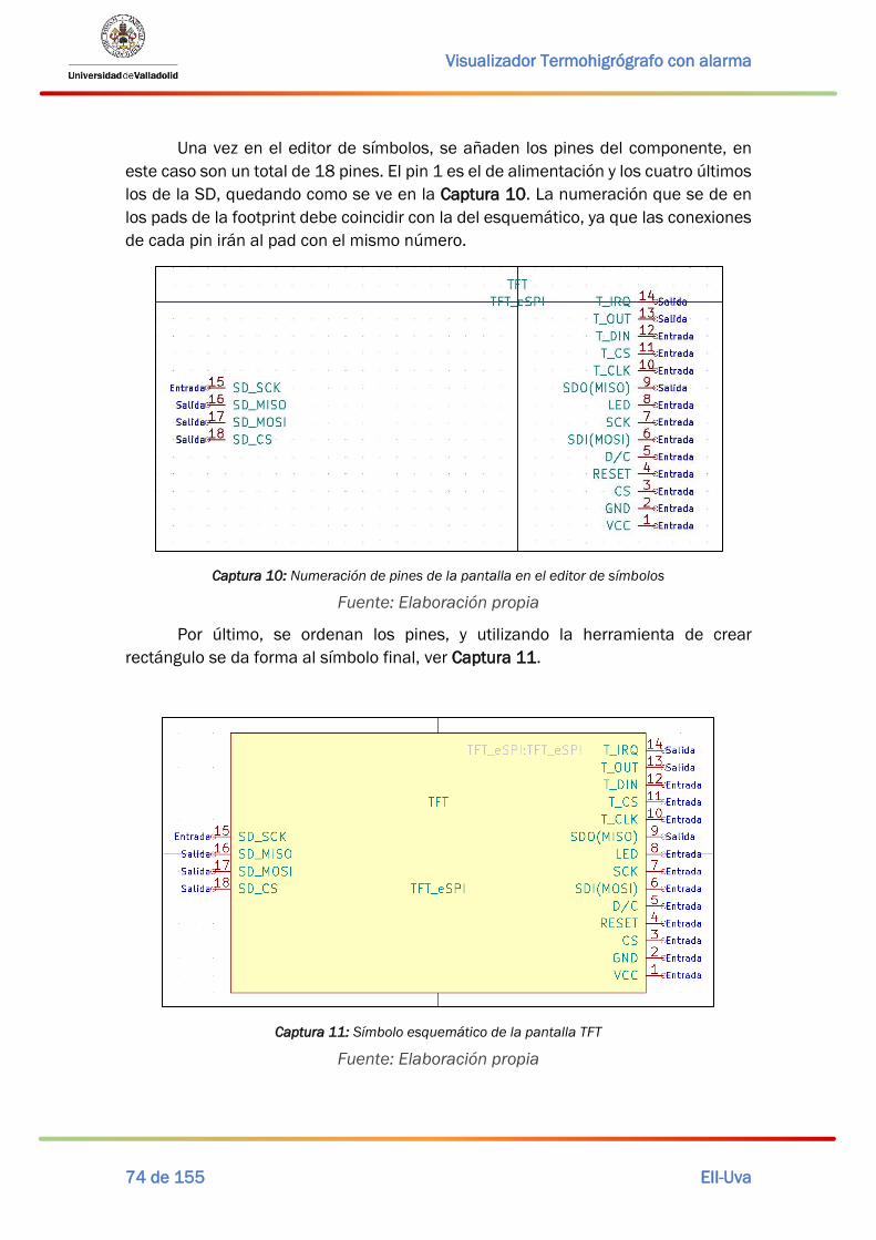
Visualizador Termohigrógrafo con alarma
74 de 155 EII-Uva
Una vez en el editor de símbolos, se añaden los pines del componente, en
este caso son un total de 18 pines. El pin 1 es el de alimentación y los cuatro últimos
los de la SD, quedando como se ve en la Captura 10. La numeración que se de en
los pads de la footprint debe coincidir con la del esquemático, ya que las conexiones
de cada pin irán al pad con el mismo número.
Captura 10: Numeración de pines de la pantalla en el editor de símbolos
Fuente: Elaboración propia
Por último, se ordenan los pines, y utilizando la herramienta de crear
rectángulo se da forma al símbolo final, ver Captura 11.
Captura 11: Símbolo esquemático de la pantalla TFT
Fuente: Elaboración propia
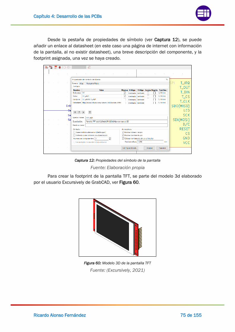
Capítulo 4: Desarrollo de las PCBs
Ricardo Alonso Fernández 75 de 155
Desde la pestaña de propiedades de símbolo (ver Captura 12), se puede
añadir un enlace al datasheet (en este caso una página de internet con información
de la pantalla, al no existir datasheet), una breve descripción del componente, y la
footprint asignada, una vez se haya creado.
Captura 12: Propiedades del símbolo de la pantalla
Fuente: Elaboración propia
Para crear la footprint de la pantalla TFT, se parte del modelo 3d elaborado
por el usuario Excursively de GrabCAD, ver Figura 60.
Figura 60: Modelo 3D de la pantalla TFT
Fuente: (Excursively, 2021)

Visualizador Termohigrógrafo con alarma
76 de 155 EII-Uva
Desde KiCad se abre el Editor de huellas, y se selecciona crear nueva huella,
aquí se introduce un nombre para la huella.
Al igual que con el símbolo del esquema, se comienzan añadiendo los pads,
teniendo cuidado de que se colocan en las posiciones exactas para que luego
coincidan con el componente real, para ello se toman las medidas del modelo 3D.
Una vez colocados todos los pads, se numeran del 1 al 18 como se definió en el
esquema. También se añaden cuatro orificios de 3mm, que coinciden con los de la
pantalla, para ello se crean cuatro pads con orificio de 3mm y sin borde de pad, ver
Captura 13.
Captura 13: Colocación de los pads en la footprint de la pantalla
Fuente: Elaboración propia
Usando la herramienta de polilínea se crea un rectángulo del tamaño de la
pantalla como símbolo de la capa gráfica (azul) y otro rectángulo ligeramente más
grande (gris) como zona que ocupa la pantalla, de esta manera KiCad no deja añadir
componentes dentro del espacio de otro a la hora de realizar circuitos.

Capítulo 4: Desarrollo de las PCBs
Ricardo Alonso Fernández 77 de 155
Captura 14: Footprint de la pantalla
Fuente: Elaboración propia
Finalmente, desde la pestaña de propiedades de huella, se añade el modelo
3D descargado anteriormente, y mediante giros y desplazamientos se alinea con los
pads de la PCB, ver Captura 15.
Captura 15: Configuración del modelo 3D de la footprint de la pantalla
Fuente: Elaboración propia

Visualizador Termohigrógrafo con alarma
78 de 155 EII-Uva
Captura 16: Modelo 3D de la footprint de la pantalla TFT
Fuente: Elaboración propia
Desde el editor de símbolos, se puede ligar el símbolo creado a esta footprint
A la hora de soldar la pantalla real a la PCB, no se insertó directamente
como en la Captura 16, si no que se utilizaron pines hembra, haciendo que quede
elevado sobre la placa. Como el modelo 3D de la PCB se va a utilizar para facilitar el
diseño de la envolvente, se han añadido los modelos 3D de los pines hembra a la
footprint de la pantalla, quedando como se aprecia en la Captura 17 .
Captura 17: Modelo 3D de la footprint de la pantalla TFT V2
Fuente: Elaboración propia

Capítulo 4: Desarrollo de las PCBs
Ricardo Alonso Fernández 79 de 155
4.1.2 Símbolo y footprint del módulo de carga de la batería
Al igual que para crear el símbolo de la pantalla, se abre el editor de símbolos
de KiCad y se selecciona la opción de crear nuevo componente.
El módulo 03962A se representa mediante un rectángulo con 6 pines. El
resultado se observa en la Captura 18
Captura 18: Símbolo esquemático del módulo 03962A
Fuente: Elaboración propia
Para el desarrollo de la footprint, se utiliza el modelo 3D realizado por el
usuario JS de GrabCAD, ver Captura 19.
Captura 19: Modelo 3D del módulo 03962A
Fuente: (JS, 2021)

Visualizador Termohigrógrafo con alarma
80 de 155 EII-Uva
Como footprint (ver Captura 20), se ha diseñado una que permite soldar el
módulo a su huella utilizando conectores machos rectos. Para ello, al añadir el
modelo 3D a la footprint, también se han añadido los modelos 3D de los pines
macho, ya disponibles entre los elementos de KiCAD.
Captura 20: Footprint del módulo 03962A
Fuente: Elaboración propia
Captura 21: Modelo 3D de la footprint del módulo 03962ª
Fuente: Elaboración propia

Capítulo 4: Desarrollo de las PCBs
Ricardo Alonso Fernández 81 de 155
4.2 Diseño de la PCB del Servidor
Para calcular el ancho de los conductores de la placa se necesita conocer el
consumo de corriente que requiere el circuito, esto se ha medido experimentalmente
obteniéndose una medida de intensidad máxima de 160mA, ver Figura 61. Todo el
circuito se va a sobredimensionar, utilizando el mismo ancho de pista en todos los
conductores. Aunque este valor máximo de corriente realmente solo circula por las
pistas de alimentación.
Figura 61: Medida del consumo del Servidor
Fuente: Elaboración propia
Para el cálculo del ancho de pista se utilizan las fórmulas [ 8] y [ 9].
𝐴 = [𝐼
0.048 ∙ ∆𝑇0.44]
10.725
[ 8]
𝑊 =𝐴
𝑒
[ 9]
Siendo A el área de la sección del conductor, W la anchura de la pista, e el
espesor de la pista en milésimas de pulgada, I la corriente máxima en Amperios e ∆T
el incremento máximo admisible de temperatura.
Estas ecuaciones se encuentran implementadas en una herramienta online
(Smith, 2021), ver Captura 22.

Visualizador Termohigrógrafo con alarma
82 de 155 EII-Uva
Captura 22: Cálculo ancho de pista para el circuito del servidor
Fuente: (Smith, 2021)
Se plantea un incremento máximo de temperatura de 10ºC y una temperatura
ambiente de trabajo de 25ºC. El espesor de la capa de cobre es de 35 μm y se supone
un valor aproximado de longitud del conductor, que lo utiliza el programa para
calcular la resistencia del tramo de pista, pero que no influye para el valor del ancho
de pista.
Como el rutado se va a realizar a una cara y por el exterior, el valor de ancho
de pista necesario es de 0.02mm o 0.94mil. Como este valor es demasiado pequeño
para realizarlo con los medios disponibles en el laboratorio, se ensanchan las pistas
hasta un valor de 1mm. También se obtiene una separación mínima entre pistas de
24mil o 0.6mm.
El primer paso es asignar las footprints a cada componente, ver Tabla 9 . Esto
se hace desde el esquema eléctrico, en las propiedades del componente se accede
a la biblioteca de huellas de KiCad y se selecciona la huella deseada. Por último, se
anota el esquema asignando una referencia a cada componente y se abre el editor
de PCBs.
Componente Huella
D1 Diode_THT:D_DO-41_SOD81_P10.16mm_Horizontal
D2 LED_THT: LED_D5.0mm
J1
Connector_Dsub: DSUB-
9_Male_Horizontal_P2.77x2.84mm_EdgePinOffset9.90mm_Ho
used_MountingHolesOffset11.32mm
J2
Connector_Dsub: DSUB-
9_Female_Horizontal_P2.77x2.84mm_EdgePinOffset9.90mm_
Housed_MountingHolesOffset11.32mm
Q1 Package_TO_SOT_THT:TO-92L_Wide
R1, R2, R3 Resistor_THT:R_Axial_DIN0207_L6.3mm_D2.5mm_P10.16mm
_Horizontal
SW1 e-switch:TL2285
U1 MODULE_ESP32-DEVKITC-32D
Tabla 9: Lista de componentes y footprints asociados del servidor
Fuente: Elaboración propia

Capítulo 4: Desarrollo de las PCBs
Ricardo Alonso Fernández 83 de 155
La placa diseñada de este circuito tiene forma rectangular de dimensiones
98x62.5mm. Con cuatro orificios de métrica 3 en los vértices, a 5mm de los bordes,
que permitirán su fijación a la envolvente. Además, los conectores se encuentran en
los lados cortos del rectángulo, de manera que sobresalgan del borde de la placa
para una mejor conexión, ver Captura 23.
Captura 23: Emplazamiento de los componentes en la PCB del servidor
Fuente: Elaboración propia
El rutado se realiza por la cara de cobre inferior utilizando el ancho de pista
calculado de 1mm y una separación entre ellas mínima de 0.6mm. Además, como
no se va a añadir serigrafía superior ni inferior, se utiliza el cobre de las zonas no
rutadas de la placa para escribir el nombre, que aparece invertido debido a que la
vista es desde la capa superior, ver Captura 24.
Captura 24: Rutado de la PCB del Servidor
Fuente: Elaboración propia

Visualizador Termohigrógrafo con alarma
84 de 155 EII-Uva
El resultado final en forma de vista 3D se observa en las Captura 24 y Captura 25.
Captura 25: Vista 3D superior de la PCB del Servidor
Fuente: Elaboración propia
Captura 26: Vista 3D inferior de la PCB del Servidor
Fuente: Elaboración propia

Capítulo 4: Desarrollo de las PCBs
Ricardo Alonso Fernández 85 de 155
4.3 Diseño de la PCB del visualizador
Para calcular el ancho de los conductores de la placa se necesita conocer el
consumo de corriente que requiere el circuito, esto se ha medido experimentalmente
obteniéndose una medida de intensidad máxima de 200mA, ver Figura 62. Todo el
circuito se va a sobredimensionar, utilizando el mismo ancho de pista en todos los
conductores. Aunque este valor máximo de corriente realmente solo circula por las
pistas de alimentación.
Figura 62: Medida del consumo del Visualizador
Fuente: Elaboración propia
El cálculo es similar al realizado para el Servidor, pero cambiando el valor de
corriente máxima por 200mA, ver Captura 27.
Captura 27: Cálculo ancho de pista para el circuito del Visualizador
Fuente: Elaboración propia

Visualizador Termohigrógrafo con alarma
86 de 155 EII-Uva
Como el rutado se va a realizar a doble cara y por el exterior, el valor de ancho
de pista necesario es de 0.03mm o 1.28mil. Como este valor es demasiado pequeño
para realizarlo con los medios disponibles en el laboratorio, se ensanchan las pistas
hasta un valor de 1mm. También se obtiene una separación entre pistas mínima de
24mil o 0.6mm.
Para realizar la placa se han asignado las siguientes footprint a cada
componente del visualizador.
Componente Huella
BZ1 Buzzer_Beeper: Buzzer_12x9.5RM7.6
C1 Capacitor_THT:C_Disc_D3.4mm_W2.1mm_P2.50mm
C2 Capacitor_THT:CP_Radial_Tantal_D5.0mm_P2.50mm
MC1 Modulo carga
R1,R2,R3 Resistor_THT:R_Axial_DIN0207_L6.3mm_D2.5mm_P10.16mm_
Horizontal
SW1A e-switch:TL2285
TFT1 TFT_eSPI
U1 Package_TO_SOT_SMD: SOT-223-3_TabPin2
U2 ESP32: MODULE_ESP32-DEVKITC-32D
Tabla 10: Lista de componentes y footprints asociados del Visualizador
Fuente: Elaboración propia
La placa diseñada de este circuito tiene forma rectangular de dimensiones
151x81mm. Con cuatro orificios de métrica 3 en los vértices, a 5mm de los bordes,
que permitirán su fijación a la envolvente. Debido a la configuración de los pines de
la pantalla es imposible realizar un rutado por una sola cara sin que se crucen pistas,
esto lleva a rutar por ambas caras, lo cual complica la soldadura del prototipo al no
poderse metalizar los orificios, por ello a la hora de soldar en las vías que conectan
una cara con la otra hay que aplicar soldadura por ambos lados.
En la cara frontal se coloca la pantalla centrada en la placa y el zumbador de
manera que ambos queden orientados hacia el usuario. En la cara trasera se colocan
el resto de los componentes, situando el puerto USB del módulo de carga hacia el
exterior de la placa (ver Captura 28). Además, para conectar las dos patillas de masa
del LDO se utiliza una pequeña área de cobre en vez de una pista, para ayudar en la
disipación térmica. También se utilizan áreas de cobre para dibujar los rectángulos
internos del logo de escuela, y se añade texto en las capas de cobre al no disponer
de serigrafía.

Capítulo 4: Desarrollo de las PCBs
Ricardo Alonso Fernández 87 de 155
Captura 28: Emplazamiento de los componentes en la PCB del Visualizador
Fuente: Elaboración propia
Captura 29: Rutado de la cara superior de la PCB del Visualizador
Fuente: Elaboración propia
Captura 30: Rutado de la cara inferior de la PCB del Visualizador
Fuente: Elaboración propia

Visualizador Termohigrógrafo con alarma
88 de 155 EII-Uva
El resultado final en forma de vista 3D se observa en las Captura 31 y Captura 32.
Captura 31: Vista 3D superior de la PCB del Visualizador
Fuente: Elaboración propia
Captura 32: Vista 3D inferior de la PCB del Visualizador
Fuente: Elaboración propia

Capítulo 4: Desarrollo de las PCBs
Ricardo Alonso Fernández 89 de 155
4.4 Fabricación de las PCBs
Los circuitos impresos o PCBs, son un soporte de material aislante sobre el
que se encuentran adheridas pistas conductoras que conectan entre si puntos de un
circuito eléctrico.
El sustrato de material no conductor es un buen aislante eléctrico y resistente
al fuego. El espesor más común es de 1.6 mm, aunque existen otros de acuerdo con
la norma UNE 20-621-84/3. Los materiales habituales son:
• Baquelita: Resina Fenólica y fibra de papel. Son baratas, de color
marrón opaco, absorben la humedad y tienen poca resistencia al calor.
Y sus características mecánicas y eléctricas son pobres.
• Fibra de vidrio: Resina epoxi y tela de vidrio. Son las más utilizadas
industrialmente debido a sus buenas características mecánicas y
eléctricas. De color verde claro y traslúcidas.
• Teflón: politetrafluoroetileno, PTFE. Tienen un alto precio, muy buenas
características eléctricas y mecánicas y se utilizan en aplicaciones de
muy alta frecuencia. Requiere de un soporte mecánico adicional.
El material conductor es cobre electrolítico de distintos espesores, los más
habituales son: 1 Oz = 35μm y 2 Oz = 70μm.
Algunas de las propiedades físicas y eléctricas de una placa de circuito
impreso son:
• Rigidez mecánica: Debe ser capaz de soportar el peso de los
componentes y los procesos de mecanización. Además, debe soportar
los cambios de temperatura durante la soldadura y los debidos al
funcionamiento del circuito. También debe resistir la llama o el fuego
y absorber la mínima humedad posible (antigroscópicos).
• Adhesión del cobre: el adhesivo debe soportar los ácidos y disolventes
del proceso de fabricación.
• Anchura de las pistas: suficiente para soportar la corriente que circula
por ellas
• Separación entre pistas: suficiente para evitar arcos eléctricos entre
pistas debido a la diferencia de potencial.
Existen distintos procesos para la fabricación de PCBs a nivel de prototipo.
Los dos tipos principales son: mediante insolación y ataque con ácido, o mediante
grabado mecánico.

Visualizador Termohigrógrafo con alarma
90 de 155 EII-Uva
4.4.1 Fabricación mediante aislado de pistas con CNC
En este proceso una máquina de control numérico computarizado (CNC)
dotada de una cuchilla corta sobre una placa de cobre para PCB. De esta forma se
va dibujando el perímetro de las pistas, profundizando lo suficiente como para
eliminar completamente el grosor del cobre.
Es un proceso lento que depende en gran medida de la precisión de la
máquina utilizada. Si los surcos que aíslan las pistas no son lo suficientemente
anchos el polvo o el óxido pueden hacer que la pista toque otra área de cobre.
Además, todas esas zonas de cobre pueden causar interferencias en los circuitos
que trabajen con radiofrecuencias. Una solución a esto es eliminar esas áreas de
cobre. Si las áreas a eliminar suponen un gran porcentaje de la placa resulta más
lógico utilizar el método del ácido.
Una vez se tiene diseñada la PCB, se pueden generar los ficheros de
fabricación, en este caso el formato debe ser Gerber, en KiCad esto se hace desde
la opción Trazar.
Los ficheros necesarios son los de las caras con cobre (las pistas) y si la placa
solo tiene pistas por un lado se puede generar el fichero de serigrafía para después
grabarla con la CNC sobre el lado sin cobre. También es necesario generar el fichero
de taladrado. A modo de ejemplo se describe el proceso para la placa del Servidor
(una sola cara de cobre).
Para evitar tener que voltear la placa tras realizar los agujeros, los taladros se
realizan desde la cara inferior. Si se tuviera que voltear y no queda perfectamente
alineada los pads no coincidirán con los orificios.
Se generan los archivos de la cara inferior de cobre, el borde de la placa y el
fichero de taladrado, ver Captura 33. El fichero de taladrado se genera desde la
pestaña Generar archivos de taladrado.
Captura 33: Trazado de ficheros de fabricación Gerber
Fuente: Elaboración propia

Capítulo 4: Desarrollo de las PCBs
Ricardo Alonso Fernández 91 de 155
Existen diferentes programas para obtener el código máquina o gcode que
utilizará la CNC a partir de los ficheros Gerber. Se va a utilizar FlatCAM un software
libre y de código abierto en constante desarrollo.
Lo primero es cargar los ficheros Gerber en FlatCAM. Al hacer esto se observa
que los ficheros no están invertidos, aparecen vistos desde la capa superior, ver
Captura 34.
Captura 34: Ficheros Gerber en FlatCAM
Fuente: Elaboración propia
Para poder invertir las capas, hay que ir a Tool > Double-Sided PCB Tool. En la
nueva ventana que aparece se seleccionan de uno en uno los ficheros de las pistas
y de taladrado, y se les aplica Mirror Y sobre la capa del borde la placa, que al ser
simétrica respecto al eje Y sirve como referencia para las otras. Ver Captura 35.
Captura 35: Mirror Y en FlatCAM
Fuente: Elaboración propia

Visualizador Termohigrógrafo con alarma
92 de 155 EII-Uva
Una vez colocadas las capas, se vuelve a la pestaña de proyecto y se
selecciona el archivo de taladrado. En esta nueva ventana aparece una lista de los
distintos diámetros de orificios, para acelerar el proceso se va a utilizar la misma
broca para todos los orificios que oscilan en torno al valor de 1mm. Se seleccionan
todos esos valores y se configura el diámetro de broca de 1mm. También se
introduce la profundidad en Z de corte (mm/min) , y la altura de desplazamiento
sobre la placa (mm), junto con la velocidad de penetración de la broca al realizar el
agujero (mm/min) y la velocidad de giro del taladro (rpm). Finalmente se pulsa en
Generate.
Captura 36: Generación del Gcode de taladrado
Fuente: Elaboración propia
Este proceso se repite para generar los ficheros con otros diámetros de broca.
En la pestaña de proyecto aparecerá un fichero drl_cnc para cada caso. Además, en
la ventana gráfica aparece el camino que seguirá la broca y el orden en que se harán
los orificios, ver Captura 37.
Captura 37: Fichero drl_cnc de 1mm en FlatCAM
Fuente: Elaboración propia

Capítulo 4: Desarrollo de las PCBs
Ricardo Alonso Fernández 93 de 155
Finalmente se introduce el diámetro de la broca en el campo correspondiente
y se pulsa en Export Gcode, y se guarda con la extensión .ngc que es la que admite
la CNC.
Desde el programa de control de la CNC, en este caso es GRBLcontrol, se abre
el fichero de taladrado, ver Captura 38. Aquí se muestra la posición actual de la broca
y la ruta que va a seguir, junto con los controles de la máquina.
Captura 38: Taladros en GRBLcontrol
Fuente: Elaboración propia
Para las pistas, el proceso es algo diferente, se utiliza una cuchilla de diámetro
0.1mm, que realiza varias pasadas alrededor de las pistas aumentando el ancho de
la zona sin cobre. Para ello hay que configurar el diámetro de la herramienta, el
número de pasadas y el solapamiento entre pasadas, por último, se pulsa en la
primera opción de Generate Geometry para obtener la ruta de la CNC.
Captura 39: Ruta de aislado de las pistas en FlatCAM
Fuente: Elaboración propia
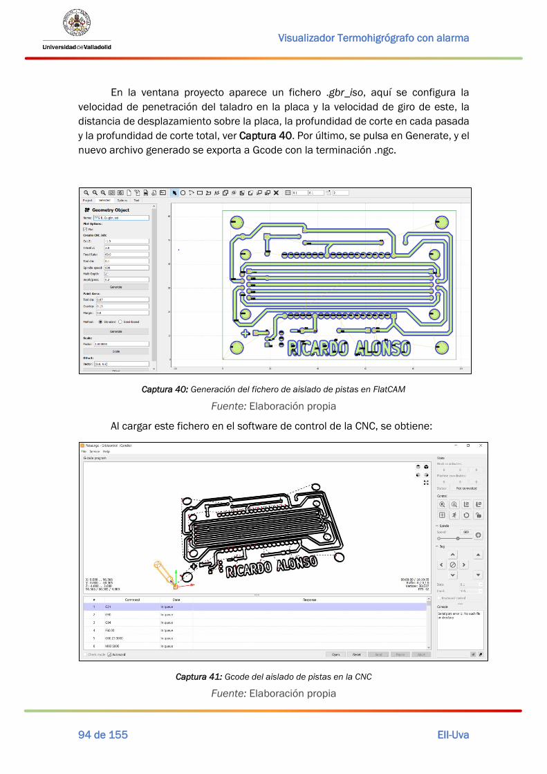
Visualizador Termohigrógrafo con alarma
94 de 155 EII-Uva
En la ventana proyecto aparece un fichero .gbr_iso, aquí se configura la
velocidad de penetración del taladro en la placa y la velocidad de giro de este, la
distancia de desplazamiento sobre la placa, la profundidad de corte en cada pasada
y la profundidad de corte total, ver Captura 40. Por último, se pulsa en Generate, y el
nuevo archivo generado se exporta a Gcode con la terminación .ngc.
Captura 40: Generación del fichero de aislado de pistas en FlatCAM
Fuente: Elaboración propia
Al cargar este fichero en el software de control de la CNC, se obtiene:
Captura 41: Gcode del aislado de pistas en la CNC
Fuente: Elaboración propia

Capítulo 4: Desarrollo de las PCBs
Ricardo Alonso Fernández 95 de 155
Finalmente, para cortar los bordes de la PCB, en la pestaña proyecto, se
selecciona el fichero de los bordes y en el apartado Board cutout, se introduce el
diámetro de la herramienta, la distancia del borde a la línea de corte, en este caso
0mm, porque la propia línea es el corte. También se generan huecos, que mantienen
la PCB unida al resto de la placa para que no se suelte durante el corte. Se genera la
geometría de corte y se obtiene:
Captura 42: Ruta del corte de placa en FlatCAM
Fuente: Elaboración propia
En la pestaña de proyecto se ha generado un archivo .gbr_cutout. La
configuración es similar a la del aislado de pistas, velocidades y varias pasadas hasta
completar la profundidad del corte.
Captura 43: Rutas para el corte de la placa en FlatCAM
Fuente: Elaboración propia

Visualizador Termohigrógrafo con alarma
96 de 155 EII-Uva
Por último, se exporta a Gcode con la terminación .ngc y se carga en la CNC.
Captura 44: Corte de la placa en la CNC
Fuente: Elaboración propia
Aunque las PCBs de este proyecto no se realizan utilizando este método, se
muestran imágenes de otro proyecto desarrollado a nivel personal. Ver Captura 45,
Captura 46 y Captura 47.

Capítulo 4: Desarrollo de las PCBs
Ricardo Alonso Fernández 97 de 155
Captura 45: PCB realizada con CNC, lado de las pistas
Fuente: Elaboración propia
Captura 46: PCB realizada con CNC, serigrafía
Fuente: Elaboración propia
Captura 47: PCB realizada con CNC, montaje final
Fuente: Elaboración propia

Visualizador Termohigrógrafo con alarma
98 de 155 EII-Uva
4.1.2 Fabricación mediante insolación y ataque con ácido
Para este método de fabricación se generan los dibujos en negro de las
distintas capas o fotolitos que se imprimen sobre un papel vegetal o se dibujan
mediante un foto plóter.
En este proceso se toma una placa de cobre fotosensible para PCBs
recubierta de una fotoresina, que puede ser positiva o negativa. Si es positiva la
fotoresina expuesta a la luz se degrada durante la insolación, de manera que tras el
proceso de revelado la superficie de cobre sobre la que ha incidido la luz queda
expuesta. Si la fotoresina es negativa, al recibir la luz la resina se cura y las zonas de
cobre sobre las que ha incidido la luz son las que se mantienen durante el revelado.
Los fotolitos también pueden ser positivos o negativos, los primeros llevan las
pistas en negro y los segundos dejan las pistas en transparente, ver Figura 63 y
Figura 64.
Figura 63: Fotolito positivo Figura 64: Fotolito negativo
Fuente: Elaboración propia Fuente: Elaboración propia
De manera que si se aplica un fotolito positivo sobre una placa positiva se
obtiene el mismo resultado que si se utiliza un fotolito negativo sobre una placa
negativa.
Una vez se tiene la placa de cobre revelada, esta se somete a un proceso
químico de eliminación del cobre expuesto, sumergiendo la placa en una disolución
de Agua, ácido clorhídrico al 35% y agua oxigenada (peróxido de hidrógeno 110 vol.),
mezclado a partes iguales.

Capítulo 4: Desarrollo de las PCBs
Ricardo Alonso Fernández 99 de 155
En este proceso químico en un medio ácido, (presencia de ácido clorhídrico,
𝐻𝐶𝑙 ), el 𝐻2𝑂2 oxida el 𝐶𝑢 en 𝐶𝑢+2 debido a la diferencia de potencial entre las dos
siguientes semirreacciones:
𝐶𝑢+2 + 2𝑒− → 𝐶𝑢0 E reducción = +0.34V
𝐻2𝑂2 + 2𝐻+ + 2𝑒− → 2𝐻2𝑂 E reducción = +1.77V
Después el 𝐻2𝑂2 actúa como oxidante y el 𝐶𝑢 como reductor, dando lugar a
las siguientes reacciones de oxidación reducción:
𝐶𝑢0 → 𝐶𝑢+2 + 2𝑒− E = -0.34V
𝐻2𝑂2 + 2𝐻+ + 2𝑒− → 2𝐻2𝑂
E = +1.77
𝐶𝑢0 + 𝐻2𝑂2 + 2𝐻+ → 𝐶𝑢+2 + 2𝐻2𝑂
E = +1.43V
Como el potencial total de la reacción es positivo, la reacción es espontánea,
quedando como resultado cloruro de cobre disuelto en agua (disolución de color
verdoso).
𝐶𝑢0 + 𝐻2𝑂2 + 2𝐻𝐶𝑙 → 𝐶𝑢𝐶𝑙2 + 2𝐻2𝑂
Tras eliminar el cobre se lava la placa con agua y se utiliza alcohol para retirar
la fotoresina que cubre las pistas y pads, para que después se pueda soldar
correctamente.
A modo de ejemplo se muestra el proceso de fabricación de la PCB del
visualizador. Se comienza imprimiendo los fotolitos de la cara de cobre superior e
inferior en papel vegetal, y cortando la placa una placa de cobre de doble cara con
resina fotosensible a unas dimensiones ligeramente mayores a las necesarias. Para
un mejor resultado se coloca el lado del papel del fotolito con la tinta sobre el cobre,
para ello a la hora de imprimir el fotolito de la cara inferior no se refleja y el de la
superior sí. En la Figura 65 y la Figura 66, se muestran los fotolitos del visualizador
vistos desde el lado que va en contacto con el cobre.

Visualizador Termohigrógrafo con alarma
100 de 155 EII-Uva
Figura 65: Fotolito superior del servidor Figura 66: Fotolito inferior del servidor
Fuente: Elaboración propia Fuente: Elaboración propia
Una vez impresos los fotolitos se colocan uno sobre otro alineando los pads
entre sí y utilizando celo se pegan los bordes de las hojas entre sí para obtener una
especie de bolsa donde meter la placa.
En una sala oscura utilizando luz roja, se retira la lámina de plástico que
recubre la placa de cobre para proteger la fotoresina de la luz, y se introduce entre
los fotolitos. Ahora se coloca en la insoladora donde un cristal y el vacío que genera
la máquina sujetan los fotolitos sobre la placa mientras la luz ultravioleta actúa sobre
la fotoresina durante 4 minutos, ver Figura 67.
Figura 67: Placa del servidor en la insoladora
Fuente: Elaboración propia
Una vez transcurridos los 4 minutos, se saca la placa de insoladora y aún con
luz roja, se sumerge la placa en el revelador, sosa caustica diluida en agua. Se mueve
la placa dentro de la disolución para asegurar que se reparte por toda la superficie,
poco a poco las zonas cubiertas por la fotoresina curada se van oscureciendo y
cuando el dibujo está bien definido, la placa se lava con agua y se seca, ver Figura
68.

Capítulo 4: Desarrollo de las PCBs
Ricardo Alonso Fernández 101 de 155
Figura 68: Placa del Visualizador revelada
Fuente: Elaboración propia
Al tratarse de una placa muy grande con mucho cobre a eliminar, la reacción
con el ácido es muy intensa y si se sumerge así en él, las burbujas que se generan
por debajo impedirán que el cobre de la cara superior se elimine correctamente y
que en la parte inferior el ácido comience a eliminar pistas. Para controlar mejor el
proceso de atacado se recubre una de las caras con celo, de esta forma el ácido no
afectará a esta cara de la placa. Se prepara la disolución y se introduce la placa con
la cara con celo pegando a la superficie de la cubeta, mediante un movimiento de
vaivén de la cubeta se mueve la disolución por toda la superficie hasta que todo el
cobre se ha eliminado quedando solo las pistas. Rápidamente se saca y se lava con
abundante agua, ya que si pasa más tiempo el ácido comenzará a eliminar las pistas.
Tras secar bien la placa se retira el celo y se cubre con él la cara que ya ha
sido descubierta. Se prepara una nueva disolución del atacador y se repite el mismo
proceso para esta cara, ver Figura 69.
Figura 69: Proceso de atacado de la placa del visualizador
Fuente: Elaboración propia

Visualizador Termohigrógrafo con alarma
102 de 155 EII-Uva
Una vez retirado todo el celo, se aplica alcohol en las superficies de la placa y
se frota para eliminar la fotoresina, en la Figura 70 se puede apreciar como la
fotoresina se disuelve en el alcohol creando zonas borrosas, y como las zonas ya
limpias son más brillantes.
Figura 70: Limpieza de la placa del servidor
Fuente: Elaboración propia
Para realizar los taladros, primero se realizan manualmente mediante un
taladro de columna los orificios de 3mm, y después sobre la base de sacrificio de la
CNC se realizan los mismos desde el fichero de taladros de la placa cargado en la
CNC. De esta manera rápida se obtiene la posición exacta en la que colocar la placa.
Se sitúa la placa con la cara superior hacia arriba haciendo coincidir los
orificios con los de la base y se colocan unos pivotes de madera en ellos, fijando la
placa en su posición. Tras esto, se procede a realizar los orificios, con los distintos
diámetros de broca. El propio programa de control de la CNC pide el cambio de
herramienta y una vez realizado el cambio, continua con el proceso.
Figura 71: CNC Bungard CCD
Fuente: Elaboración propia

Capítulo 4: Desarrollo de las PCBs
Ricardo Alonso Fernández 103 de 155
Una vez generado el archivo de taladrado desde KiCad, se abre desde Isocam
y al pulsar en OK (ventana izquierda) se abre la ventana de la derecha, donde al
pulsar en Hint by program, la configuración se adapta a la del fichero, ver .
Figura 72: Carga del fichero de taladrado en Isocam
Fuente: Elaboración propia
El resultado es el siguiente:
Figura 73: Fichero de taladrado en Isocam
Fuente: Elaboración propia
Para generar el fichero de trabajo para la CNC, desde la pestaña File se
selecciona la opción Save y en la ventana que aparece se selecciona formato
Excellon, unidades inch, Leading zero supression y formato de dígitos 2:4, por último,
se guarda el fichero con el formato .ncd. Ver Figura 74.

Visualizador Termohigrógrafo con alarma
104 de 155 EII-Uva
Figura 74: Generación del fichero de trabajo de la CNC
Fuente: Elaboración propia
Una vez soldados los componentes en las placas, el resultado es el siguiente:
Figura 75: Prototipo del visualizador, cara frontal
Fuente: Elaboración propia

Capítulo 4: Desarrollo de las PCBs
Ricardo Alonso Fernández 105 de 155
Figura 76: Prototipo del visualizador, cara trasera
Fuente: Elaboración propia
Figura 77: Prototipo del servidor, cara superior
Fuente: Elaboración propia
Figura 78: Prototipo del servidor, cara inferior
Fuente: Elaboración propia

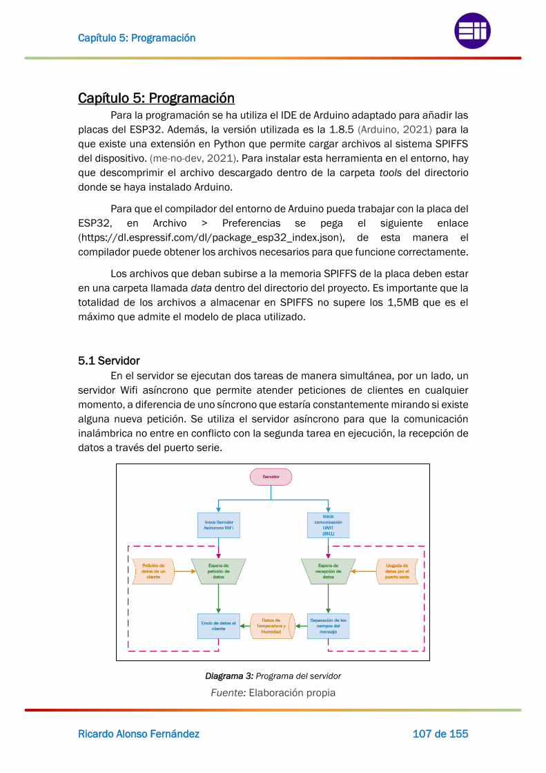
Capítulo 5: Programación
Ricardo Alonso Fernández 107 de 155
Capítulo 5: Programación Para la programación se ha utiliza el IDE de Arduino adaptado para añadir las
placas del ESP32. Además, la versión utilizada es la 1.8.5 (Arduino, 2021) para la
que existe una extensión en Python que permite cargar archivos al sistema SPIFFS
del dispositivo. (me-no-dev, 2021). Para instalar esta herramienta en el entorno, hay
que descomprimir el archivo descargado dentro de la carpeta tools del directorio
donde se haya instalado Arduino.
Para que el compilador del entorno de Arduino pueda trabajar con la placa del
ESP32, en Archivo > Preferencias se pega el siguiente enlace
(https://dl.espressif.com/dl/package_esp32_index.json), de esta manera el
compilador puede obtener los archivos necesarios para que funcione correctamente.
Los archivos que deban subirse a la memoria SPIFFS de la placa deben estar
en una carpeta llamada data dentro del directorio del proyecto. Es importante que la
totalidad de los archivos a almacenar en SPIFFS no supere los 1,5MB que es el
máximo que admite el modelo de placa utilizado.
5.1 Servidor
En el servidor se ejecutan dos tareas de manera simultánea, por un lado, un
servidor Wifi asíncrono que permite atender peticiones de clientes en cualquier
momento, a diferencia de uno síncrono que estaría constantemente mirando si existe
alguna nueva petición. Se utiliza el servidor asíncrono para que la comunicación
inalámbrica no entre en conflicto con la segunda tarea en ejecución, la recepción de
datos a través del puerto serie.
Diagrama 3: Programa del servidor
Fuente: Elaboración propia

Visualizador Termohigrógrafo con alarma
108 de 155 EII-Uva
Al conectarse a la red Wifi creada por el servidor, se puede acceder a cada
uno de los datos disponibles de manera individual o a una página web diseñada para
mostrar al usuario las condiciones de cada zona. De esta forma, conectando un
dispositivo móvil u ordenador a esta red e introduciendo la IP 192.168.4.1 en el
navegador se pueden observar los datos sin necesidad de tener el visualizador cerca
(ver Tabla 11).
Dirección Contenido
192.168.4.1 Página web
192.168.4.1/Fecha Fecha
192.168.4.1/Hora Hora
192.168.4.1/TCalibracion Temperatura de la zona de calibración
192.168.4.1/TEnsayos Temperatura de la zona de ensayos
192.168.4.1/HCalibracion Humedad de la zona de calibración
192.168.4.1/HEnsayos Humedad de la zona de ensayos Tabla 11: Direcciones y contenido del servidor
Fuente: Elaboración propia
5.1.1 Diseño de la página web
Para el diseño de la página web se ha diseñado una interfaz sencilla que
muestre los valores de temperatura y humedad en una tabla, y la fecha y hora en un
lateral. Para su diseño se ha utilizado lenguaje HTML18 estructurando la página como
se indica en la Figura 79. Para su programación se ha utilizado Visual Studio Code
(Microsoft, 2021).
head: establece el nombre de la página que se muestra en el navegador al
acceder a ella. También el tipo de codificación de caracteres utilizado (UTF-8) e
invoca a la hoja de estilos CSS19.
• body: es el contenido principal de la página
o header: contiene el logo de la escuela y de la universidad, junto con la
palabra Lacecal.
o article superior: contiene la tabla con los datos de temperatura y
humedad y en el lateral izquierdo la fecha y hora.
o article inferior: muestra el logo del Lacecal.
o footer: autor y curso.
18 HyperText Markup Language, Lenguaje de Marcas de Hipertexto 19 Cascading Style Sheets, Hojas de Estilo en Cascada

Capítulo 5: Programación
Ricardo Alonso Fernández 109 de 155
Figura 79: Estructura de la página web
Fuente: Elaboración propia
Para estructurar el contenido del fichero HTML, se crea una hoja de estilo, que
define los tamaños, colores y posiciones de los campos definidos anteriormente.
Estas medidas se pueden realizar de manera relativa o absoluta. Se utiliza el formato
relativo para que la pagina se adapte al tamaño de la pantalla del dispositivo desde
el que se visualiza.
También se genera una pequeña función de JavaScript, que actualiza la
página cada 60 segundos para refrescar los datos mostrados.
El resultado final de la página web se puede ver en la Captura 48.
Captura 48: Pagina web del servidor
Fuente: Elaboración propia

Visualizador Termohigrógrafo con alarma
110 de 155 EII-Uva
5.1.2 Recepción de la trama en el ESP32
Para poder recibir la trama, en el setup se habilita el puerto UART 2 del
microcontrolador, estableciendo un protocolo 8N1 a 9600baudios (ocho bits de
datos, sin paridad y un bit de parada), la misma a la que transmite el datalogger.
El puerto UART 2 está formado por los dos pines TX, pin 17 y RX pin 16.
Serial2.begin(9600, SERIAL_8N1, RX, TX);
El microcontrolador debe ser capaz de separar los campos del mensaje
recibido. Como cada campo está separado por una tabulación horizontal, el
programa las va detectando y almacenando los caracteres que hay entre dos
tabulaciones en una misma variable. Finalmente, cuando detecta el carácter de
nueva línea, finaliza la recepción del mensaje.
Diagrama 4: Recepción de mensaje por el puerto serie y separación de campos
Fuente: Elaboración propia

Capítulo 5: Programación
Ricardo Alonso Fernández 111 de 155
Por último, a modo de prueba, los datos recibidos se muestran a través de una
pantalla LCD. En la Figura 80 se muestra el montaje en protoboard del circuito
convertidor de RS232 a TTL, el ESP32 y una pantalla LCD, en la que aparece el
mensaje del apartado 3.1.1.1 Prueba de la comunicación serie junto con el
analizador lógico usado.
Figura 80: Prueba de recepción de mensaje por puerto serie usando pantalla LCD
Fuente: Elaboración propia

Visualizador Termohigrógrafo con alarma
112 de 155 EII-Uva
5.1.3 Servidor asíncrono
Para crear un servidor asíncrono se utiliza la librería de funciones
ESPAsyncWebServer (me-no-dev, 2021).
El funcionamiento de este servidor se basa en llamadas. Se implementan un
conjunto de peticiones o direcciones válidas (ver Tabla 11) que tienen asignadas
unos recursos o elementos de retorno, por ejemplo, al acceder a la temperatura de
una zona, se devuelve una cadena de texto con el valor de la variable
correspondiente. Si se accede a la dirección de la raíz, la página web, las fotos que
aparecen en ella están almacenadas en la memoria SPIFFs del ESP32, de manera
que se lee de memoria y se envía la imagen al cliente.
En el caso de la página web, esta se envía como texto al dispositivo conectado
y el navegador interpreta el contenido para mostrarlo adecuadamente, sin embargo,
la página es dinámica, muestra variables que cambian con el tiempo. Para que estas
aparezcan en los lugares correspondientes se utilizan placeholders20 palabras entre
“%”, por ejemplo, %T_CALIBRACION%. Cuando se está transmitiendo la página, este
proceso se realiza a través de una función llamada procesamiento() por la que pasa
cada carácter de la página y cuando detecta un “%” concatena las letras que hay
hasta el siguiente “%”. La palabra obtenida la compara con las definidas y la sustituye
por el valor que se haya indicado.
Figura 81: Función procesamiento y página web
Fuente: Elaboración propia
20 Marcadores de posición

Capítulo 5: Programación
Ricardo Alonso Fernández 113 de 155
El servidor web se inicia en el puerto o WebSocket 80, el predeterminado para
HTTP. De manera que la comunicación bidireccional entre el cliente y el servidor se
realiza a través de este puerto.
Al utilizarse TCP/IP para la comunicación se deben definir tanto la dirección
IP, como la máscara y el Gateway o puerta de enlace. Como el ESP32 genera su
propia red se podría utilizar distintos valores, pero por simplicidad se utilizan las que
vienen por defecto que funcionan correctamente:
IP: 192.168.4.1
Gateway: 192.168.4.9
Máscara: 255.255.255.0
Si el ESP32 se fuera a conectar a una red Wifi existente, habría que configurar
la dirección IP, Gateway y Máscara según defina la red.
También se definen las credenciales de la red, identificación y contraseña:
ssid: LACECAL_TyH
password: (no se muestra)

Visualizador Termohigrógrafo con alarma
114 de 155 EII-Uva
5.2 Visualizador
En el visualizador se ejecutan dos tareas21, la consulta del servidor por Wifi y
la actualización de la pantalla. Al encender el dispositivo, se inicia la conexión con la
pantalla y se activa el almacenamiento SPIFFS. A continuación, se intenta conectar
a la red Wifi del servidor, mientras realiza esta tarea se muestra en la pantalla la
imagen de conectando.
5.2.1 Proceso de sincronización
Una vez conectado, comienza el proceso de sincronización con el servidor,
durante el cual el cliente consulta cada 5 segundos la hora del servidor, en el
momento en el que dos valores consecutivos son distintos, es que el servidor acaba
de obtener nuevos valores. A partir de este momento el visualizador consultará al
servidor cada 60 segundos para obtener nuevos valores. Debido al proceso de
sincronización inicial, el visualizador recibirá los datos como mucho 5 segundos más
tarde de que estos estén disponibles, ver Diagrama 6 y Diagrama 7.
Diagrama 5: Esquema general del programa del visualizador
Fuente: Elaboración propia
21 Programa independiente que necesita utilizar los recursos del dispositivo

Capítulo 5: Programación
Ricardo Alonso Fernández 115 de 155
Diagrama 6: diagrama temporal del proceso de sincronización
Fuente: Elaboración propia
Diagrama 7: diagrama del código del proceso de sincronización
Fuente: Elaboración propia

Visualizador Termohigrógrafo con alarma
116 de 155 EII-Uva
5.2.2 Planteamiento general del código
El programa principal se puede dividir en dos tareas, una que se encarga de
la comunicación con el servidor cada 60 segundos y otra que debe estar
constantemente leyendo el táctil de la pantalla y refrescando la imagen si hiciera
falta, esto origina un problema de concurrencia en el que dos programas buscan
utilizar los recursos de la CPU. Para poder ejecutar ambas tareas existen varias
posibles soluciones:
• Uso de ambos procesadores:
Cada tarea se ejecuta en uno de los dos procesadores que posee el ESP32.
El principal inconveniente es que supone un aumento en el consumo
del dispositivo. En cuanto a programación necesita de sistemas RTOS22,
sistemas de tiempo real. Sistemas operativos que implementan un
planificador de tareas, que en función de la prioridad de cada tarea, su
periodo de ejecución, tiempos límites (deadlines) y otros parámetros definidos
por el usuario, organiza el acceso de cada tarea a los recursos del dispositivo
(GPIOs, Memoria, etc.).
Figura 82: Concurrencia en multiprocesador
Fuente: (de la Fuente, 2019)
22 Real-Time Operating System, Sistema Operativo de Tiempo Real

Capítulo 5: Programación
Ricardo Alonso Fernández 117 de 155
• Dos hilos en un solo procesador
El planteamiento es similar al anterior, se ejecutan dos tareas distintas
pero esta vez en un solo procesador. Se crean dos threads o hilos, que son
dos tareas en ejecución en un mismo procesador, por ello se necesita
también de un sistema RTOS y en el que a diferencia del caso anterior el
propio procesador es un recurso compartido. Este es el funcionamiento
habitual de cualquier ordenador o dispositivo móvil, en el que existe una sola
CPU y varias aplicaciones en ejecución simultánea.
Resulta complejo de programar, debido a que al compartir recursos,
existen secciones críticas en cada tarea, partes de la ejecución del programa
que no puede ser interrumpida, por ejemplo, cuando accede a memoria. Para
regular las secciones críticas se necesita de IPC23, funciones que permiten la
sincronización y comunicación entre los procesos.
Figura 83: Concurrencia en un solo procesador
Fuente: (de la Fuente, 2019)
• Tarea continua y tarea periódica con interrupción
Se trata de una modificación del planteamiento anterior, en el que se
crean dos hilos ficticios. La tarea de leer y actualizar la pantalla se ejecuta
continuamente, y se crea una interrupción periódica cada 60s utilizando uno
de los contadores del ESP32. Después, en la rutina de tratamiento de la
interrupción se ejecuta la parte de comunicación con el servidor.
El problema de este planteamiento es que crea un comportamiento
inestable en el microcontrolador debido a que el Wifi ocupa gran parte de los
recursos del dispositivo de manera continua y el sistema de almacenamiento
SPIFFS es incompatible con las interrupciones, ya que si se da una durante
un acceso a memoria existe gran probabilidad de que produzca un error en el
núcleo del procesador.
23 Inter-Processor Call, Comunicación entre procesos

Visualizador Termohigrógrafo con alarma
118 de 155 EII-Uva
• Código continuo con consulta periódica
Se crea un único código en ejecución, y cada 60 segundos se realiza
una consulta al servidor. Para crear una espera de 60 segundos, no se puede
utilizar la función delay() ya que esta detiene por completo la ejecución del
código. En su lugar se utiliza millis() que devuelve los microsegundos desde
el momento en que se encendió el dispositivo. De esta forma, se almacena el
momento de la última consulta y cuando exista 60 segundos de diferencia
con el tiempo actual se vuelve a consultar y se actualiza el tiempo de la última
consulta. El resto del tiempo se trabaja únicamente con la pantalla.
Esta es la solución más eficiente y más controlable por parte del
programador, ya que no requiere de programas externos de gran complejidad.
Diagrama 8: diagrama del código principal del visualizador
Fuente: Elaboración propia
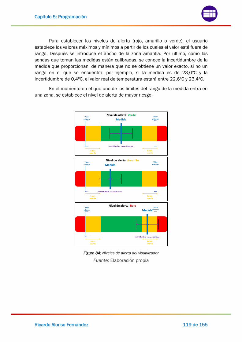
Capítulo 5: Programación
Ricardo Alonso Fernández 119 de 155
Para establecer los niveles de alerta (rojo, amarillo o verde), el usuario
establece los valores máximos y mínimos a partir de los cuales el valor está fuera de
rango. Después se introduce el ancho de la zona amarilla. Por último, como las
sondas que toman las medidas están calibradas, se conoce la incertidumbre de la
medida que proporcionan, de manera que no se obtiene un valor exacto, si no un
rango en el que se encuentra, por ejemplo, si la medida es de 23,0ºC y la
incertidumbre de 0,4ºC, el valor real de temperatura estará entre 22,6ºC y 23,4ºC.
En el momento en el que uno de los límites del rango de la medida entra en
una zona, se establece el nivel de alerta de mayor riesgo.
Figura 84: Niveles de alerta del visualizador
Fuente: Elaboración propia

Visualizador Termohigrógrafo con alarma
120 de 155 EII-Uva
Diagrama 9: Estructura e interfaces de los menús del visualizador

Capítulo 6: Envolventes
Ricardo Alonso Fernández 121 de 155
Capítulo 6: Envolventes Para las envolventes existen dos posibles soluciones, utilizar una caja
comercial y adaptar el diseño de la PCB para que se adapte a la forma de esta o
diseñar desde cero una envolvente para cada prototipo.
Utilizar una caja comercial implica que habrá que modificarla para crear
acceso a los conectores o dar salida a la pantalla, lo cual empeoraría el acabado
final. A modo de ejemplo en la Captura 49 se muestra una posible envolvente
comercial para el prototipo del visualizador y en la Captura 50 una para el servidor.
Captura 49: Caja RS PRO de ABS Gris
Fuente: (RS Components, 2021)
Dimensiones: 100 x 150 x 75mm Código RS: 192-0700
Precio unidad: 13,14€
Captura 50: Caja Hammond de ABS piro retardante Gris
Fuente: (RS Components, 2021)
Dimensiones: 106.5 x 66 x 45.4mm Código RS: 528-6984
Precio unidad: 10,54€

Visualizador Termohigrógrafo con alarma
122 de 155 EII-Uva

Capítulo 6: Envolventes
Ricardo Alonso Fernández 123 de 155
La segunda opción consiste en diseñar en 3D las envolventes
utilizando Autodesk Inventor Professional, para después imprimirlas en 3D mediante
el método MDF24 en el que se deposita de manera selectiva polímeros
termoplásticos fundidos en un camino predeterminado capa por capa.
Figura 85: Método MDF de impresión 3D
Fuente: (Universitat Politècnica de Catalunya Barcelonatech, 2021)
La opción utilizada para el desarrollo de las carcasas es la impresión 3D por
razones de mejor acabado aprovechando que se dispone de impresora y manejo de
programas de diseño 3D. Además, al tratarse únicamente de un par de prototipos el
coste de la impresión es bajo.
Tras diseñar las piezas en Inventor, se exportan a .stl, ya que no se necesita
conservar texturas o colores del modelo diseñado, y es suficiente con un modelo de
malla triangular. Para exportarlo en Inventor hay que ir a Archivo > Guardar copia
como.
Una vez se tiene el modelo de malla se tiene que generar el código G adaptado
al software de la impresora. En el caso de la impresora Ender 5 Pro del fabricante
Creality (ver Figura 86), el firmware es Marlin. Este proceso se conoce como
laminación o segmentación, para ello se existen diversos programas de laminación
o Slicers. Se va a utilizar PrusaSlicer, el cual originalmente estaba orientado
únicamente a las impresoras de la empresa Prusa, pero con unas pequeñas
modificaciones de los parámetros (velocidades, dimensiones de la máquina, etc.) se
pueden añadir impresoras de otras marcas.
24 Modelado por Deposición Fundida

Visualizador Termohigrógrafo con alarma
124 de 155 EII-Uva
Figura 86: Impresora 3d Ender 5 Pro
Fuente: (Creality 3D, 2021)
El Slicer convierte el modelo de malla en capas de una altura determinada por
el usuario (0.2mm habitualmente) en función del acabado final deseado, cuanto más
alto es el valor más tosco es el acabado, pero menor es el tiempo de impresión. A
continuación, cada capa se divide en líneas de un ancho igual al de la boquilla del
extrusor o nozzle (0.4mm habitualmente).
Dependiendo de las características mecánicas requeridas por la pieza se
configuran el número de líneas de perímetro y el relleno. Un relleno muy denso y con
patrones específicos crea una pieza resistente pero muy pesada. En el caso de los
perímetros, varias líneas refuerzan el exterior de la pieza permitiendo reducir el
relleno, aunque suponen un mayor gasto de filamento.
También el material plástico empleado otorga diferentes características a la
pieza, los más utilizados son el PLA25, ABS26 y el PETG27. El ABS, tiene una gran
resistencia mecánica y a las vibraciones, además si la pieza se somete a un
posprocesamiento en el que se introduce en un baño de vapor de acetona durante
unos minutos, se obtiene una unión perfecta entre capas y un acabado superficial
liso y brillante (ver Captura 51). Los inconvenientes de este material es que resulta
complicado de imprimir, ya que necesita de altas temperaturas (>220ºC) y una
impresora cubierta para que no le afecten las corrientes de aire. Además, al ser
derivado del petróleo desprende gases tóxicos al fundirse y no es biodegradable. Es
el material más utilizado a nivel industrial.
25 Poliácido Láctico 26 Acrylonitrile Butadiene Styrene, Acrilonitrilo Butadieno Estireno 27 Polyethylene Terephthalate, Polietileno Tereftalato

Capítulo 6: Envolventes
Ricardo Alonso Fernández 125 de 155
Captura 51: Posprocesado del ABS
Fuente: (Doutel, 2021)
El PLA, tiene menor adherencia entre capas y por tanto peor resistencia
mecánica. Se imprime a temperaturas bajas (>190ºC), existen mayor variedad de
colores y acabados (fluorescente, metalizado, efecto seda, etc.). Al obtenerse a partir
de la fécula de la patata o el maíz, es biodegradable y no emite vapores perjudiciales
para la salud. Por ello, es el material más habitual usado a nivel doméstico. Su
posprocesamiento es complicado al necesitarse de mucho tiempo de lijado y
masillas plásticas para tapar pequeños huecos antes del pintado. Por ello se habitual
utilizar filamentos con texturas que supongan el acabado final de la pieza.
El PETG se encuentra entre el PLA y el ABS en cuanto a resistencia mecánica
y temperatura de impresión. Es reciclable y no emite vapores tóxicos, pero si algo de
olor. Su principal inconveniente es el warping y el cracking, en el primero debido a la
diferencia de temperatura entre la pieza y el exterior, el material se contrae doblando
la pieza de la base hacia arriba. En el cracking, esta curva llega al punto de romper
la unión entre las capas causando la fractura de la pieza dejándola inservible.
Captura 52: Efecto warping Captura 53: Efecto cracking
Fuente: (Createc3D, 2021) Fuente: (Createc3D, 2021)

Visualizador Termohigrógrafo con alarma
126 de 155 EII-Uva
6.1 Servidor
La envolvente del servidor tiene forma rectangular de ancho 71mm, alto
33.60mm y largo 106mm. En la cara superior tiene un orificio para el botón de
encendido y otro para el led indicador de encendido. También incluye el logo de la
escuela y la palabra LACECAL insertadas en relieve. En los laterales cortos tiene
ranuras para los conectores DB9, y una ranura en la parte delantera para el conector
de alimentación.
En el interior posee un espacio para el módulo de carga 03962A, que se
sujeta mediante una tapa pegada con una rendija para pasar los cables y conectarlos
a la placa del circuito.
La carcasa frontal posee cuatro orificios ciegos en el interior coincidentes con
los taladros de sujeción de la PCB. En estos orificios se coloca una tuerca de inserción
de M3x8x5mm utilizando el calor del soldador.
Por último, una tapa cubre la parte inferior y mediante 4 tornillos de M3 y
15mm de largo se sujeta todo entre sí.
Captura 54: Vista explosionada del servidor
Fuente: Elaboración propia

Capítulo 6: Envolventes
Ricardo Alonso Fernández 127 de 155
El color de las envolventes se ha elegido en base a informes (Kutchma, 2021)
que establecen que el color de las habitaciones y de los objetos en ellas pueden
influir en el estado anímico de las personas que se encuentran en ellas. Por ejemplo,
pequeños elementos rojos provocan un carácter más optimista y sociable. Pero
debido a su intensidad si se utiliza en grandes cantidades aumenta los niveles de
estrés. El verde y el azul transmiten calma y ayudan a la concentración, por ello son
adecuados para zonas de trabajo o de estudio Por esta razón las envolventes se
hacen de PLA Glitter Verde. Además, el efecto Glitter o de purpurina evita un efecto
monótono en las carcasas haciendo que resulte más agradable visualmente.
También se utiliza PLA Silk Gold para añadir pequeños elementos dorados en relieve
en las letras y el logo de la escuela.
El coste de la bobina de PLA Glitter de 750g es de 18,25€ y el de la bobina
PLA Silk Gold de 250g es de 5,06€. En función de la cantidad de plástico utilizado
en cada envolvente se puede calcular el coste que supone.
Captura 55: Segmentación servidor (PLA Glitter Verde)
Fuente: Elaboración propia
Tiempo de impresión: 7h 6minutos
Filamento usado: 31,79m, Coste: 2,31€

Visualizador Termohigrógrafo con alarma
128 de 155 EII-Uva
Captura 56: Segmentación servidor (PLA Silk Gold)
Fuente: Elaboración propia
Tiempo de impresión: 19 minutos
Filamento usado: 0,40m, Coste: 0,02€
Captura 57: Vista superior de la envolvente del servidor
Fuente: Elaboración propia
Captura 58: Vista inferior de la envolvente del servidor
Fuente: Elaboración propia
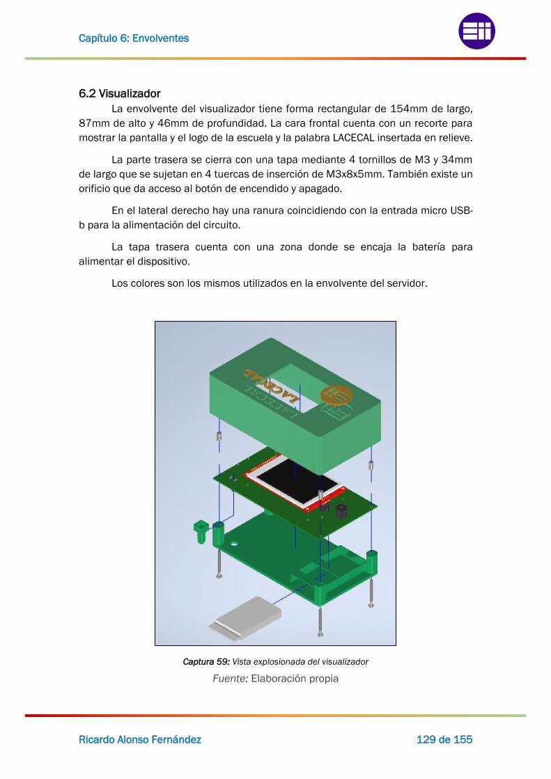
Capítulo 6: Envolventes
Ricardo Alonso Fernández 129 de 155
6.2 Visualizador
La envolvente del visualizador tiene forma rectangular de 154mm de largo,
87mm de alto y 46mm de profundidad. La cara frontal cuenta con un recorte para
mostrar la pantalla y el logo de la escuela y la palabra LACECAL insertada en relieve.
La parte trasera se cierra con una tapa mediante 4 tornillos de M3 y 34mm
de largo que se sujetan en 4 tuercas de inserción de M3x8x5mm. También existe un
orificio que da acceso al botón de encendido y apagado.
En el lateral derecho hay una ranura coincidiendo con la entrada micro USB-
b para la alimentación del circuito.
La tapa trasera cuenta con una zona donde se encaja la batería para
alimentar el dispositivo.
Los colores son los mismos utilizados en la envolvente del servidor.
Captura 59: Vista explosionada del visualizador
Fuente: Elaboración propia

Visualizador Termohigrógrafo con alarma
130 de 155 EII-Uva
Captura 60: Segmentación visualizador (PLA Glitter Verde)
Fuente: Elaboración propia
Tiempo de impresión: 10h 26minutos
Filamento usado: 51,63m, Coste: 3,75€
Captura 61: Impresión de la envolvente del visualizador
Fuente: Elaboración propia

Capítulo 6: Envolventes
Ricardo Alonso Fernández 131 de 155
Captura 62: Vista superior de la envolvente del visualizador
Fuente: Elaboración propia
Captura 63: Vista inferior de la envolvente del visualizador
Fuente: Elaboración propia


Capítulo 7: Estudio económico
Ricardo Alonso Fernández 133 de 155
Capítulo 7: Estudio económico
7.1 Introducción
En el presente capítulo se realizará un estudio del coste económico que
supone la realización del proyecto desarrollado.
Hasta este momento se ha estudiado la viabilidad de este proyecto desde un
punto de vista técnico, es decir, si cumple o no el objetivo marcado desde el
comienzo. Habiendo concluido este punto, queda pendiente comprobar la viabilidad
económica del mismo.
En los siguientes apartados se estudiarán por separado costes directos e
indirectos y finalmente se mostrarán los costes totales del proyecto.
7.2 Recursos empleados
• Software
Como sistema operativo del ordenador se ha utilizado una licencia de
Windows 10. También se ha necesitado una licencia del paquete de Microsoft
Office. Para el desarrollo de las envolventes y de los planos de estas, se ha
utilizado el paquete de Autodesk con licencia de estudiante. El resto de
software empleado es de licencia gratuita por ello no se tiene en cuenta en el
presente estudio.
• Equipamiento
En primer lugar, se ha utilizado un ordenador portátil MSI GL63 8RC para el
desarrollo del informe, circuitos electrónicos, envolventes, programación, etc.
Para la fabricación de las placas de circuito impreso se ha utilizado la
fresadora CNC Bungar CCD, una insoladora de rayos UV AZ210 y un estañador
de 220 V y 60 W, un multímetro digital avanzado 400BMM-MY64 de KPS y
una multiherramienta de precisión de 135W a 230V- 50Hz. Para la
fabricación de las envolventes se ha utilizado la impresora Ender 5 Pro de
Creality.
• Consumibles
Para el desarrollo de los circuitos se han utilizado componentes electrónicos
como los ESP32-Wroom, resistencias fijas de orificio pasante, diodos y diodos
LED, conectores DB9 y baterías, entre otros. Se detalla en profundidad en el
apartado . Para la fabricación de las envolventes se ha utilizado una bobina
de PLA Glitter Verde de 1.75mm y para algunas partes una bobina de PLA Silk
Gold de 1.75mm. Además, se ha necesitado de tornillería, pegamento
termofusible y aleación de estaño-plomo para la soldadura de los
componentes.

Visualizador Termohigrógrafo con alarma
134 de 155 EII-Uva
7.3 Costes directos
7.3.1 Coste del personal
Este proyecto se ha llevado a cabo por un ingeniero técnico con especialidad
en Electrónica Industrial y Automática encargado del desarrollo de este desde su
planteamiento y cálculos, hasta el diseño y la fabricación del prototipo final.
Se ha calculado el coste anual del ingeniero y a continuación se ha adaptado
al número de horas trabajadas por él. Este coste incluye tanto el sueldo bruto anual
con posibles incentivos, así como la cotización a la Seguridad Social, que supone un
35% del sueldo bruto, ver Tabla 12.
Coste anual
Sueldo bruto más incentivos 30.000,00€
Seguridad Social (35% sueldo bruto) 10.500,00
Coste total 40.500,00 Tabla 12: Coste anual
Fuente: Elaboración propia
A continuación, se calcula una estimación de los días efectivos trabajados al
año, ver Tabla 13.
Días efectivos por año
Año medio 365,25
Sábados y Domingos -104,36
Días de vacaciones efectivos -20,00
Días festivos reconocidos -15,00
Días perdidos estimados -4,00
Total de días estimados 223,89 Tabla 13: Días efectivos por año
Fuente: Elaboración propia
A partir del número total de días efectivos trabajados, y con una jornada
laboral de 8h/día, se calcula el número total de horas efectivas de trabajo utilizando
la ecuación [ 10].
𝒉𝒐𝒓𝒂𝒔 𝒆𝒇𝒆𝒄𝒕𝒊𝒗𝒂𝒔 𝒕𝒓𝒂𝒃𝒂𝒋𝒂𝒅𝒂𝒔 = 223,89𝑑í𝑎𝑠
𝑎ñ𝑜·
8ℎ
𝑑í𝑎= 𝟏𝟕𝟗𝟏, 𝟏𝟐
𝒉𝒐𝒓𝒂𝒔
𝒂ñ𝒐 [ 10]
Para calcular el coste por hora de un ingeniero, se divide el sueldo anual entre el
número de horas efectivas trabajadas por año, ver ecuación [ 11]. .
𝑪𝒐𝒔𝒕𝒆 𝒉𝒐𝒓𝒂 𝒊𝒏𝒈𝒆𝒏𝒊𝒆𝒓𝒐 = 40.500,00
€𝑎ñ𝑜
1791,12ℎ𝑜𝑟𝑎𝑠
𝑎ñ𝑜
= 𝟐𝟐, 𝟔𝟏€
𝒉𝒐𝒓𝒂 [ 11]

Capítulo 7: Estudio económico
Ricardo Alonso Fernández 135 de 155
En la Tabla 14 se muestra una distribución en el tiempo aproximada del
trabajo realizado por el ingeniero durante el desarrollo del proyecto.
Distribución temporal de trabajo
Formación y documentación 100 horas
Estudio del problema 100 horas
Desarrollo de prototipos 200 horas
Desarrollo y puesta a punto del
producto final 50 horas
Elaboración de la documentación 200 horas
Total de horas empleadas 650 horas Tabla 14: Distribución temporal de trabajo
Fuente: Elaboración propia
Por último, para calcular el coste personal directo, se multiplica el número
total de horas empleadas por el coste de una hora, ver ecuación [ 12] .
𝑪𝒐𝒔𝒕𝒆 𝒑𝒆𝒓𝒔𝒐𝒏𝒂𝒍 𝒅𝒊𝒓𝒆𝒄𝒕𝒐 = 650 ℎ𝑜𝑟𝑎𝑠 · 22,61€
ℎ𝑜𝑟𝑎= 𝟏𝟒. 𝟔𝟗𝟔, 𝟓𝟎€ [ 12]
Coste personal directo 14.696,50 €
7.3.2 Coste de amortización de material (equipos y software)
Para el cálculo del coste de amortización del material, se debe realizar
previamente la inversión total y calcular la amortización lineal correspondiente según
los criterios aconsejados por la ley. En este apartado se estudiará tanto los costes
de la amortización software, como los costes de amortización de los equipos
empleados en el desarrollo de los prototipos citados en el apartado 7.2 Recursos
empleados.
En cuanto al software, se estima su tiempo de amortización en función de la
duración de la licencia, de manera que, si por ejemplo una licencia dura dos años,
durante el transcurso de un año se habrá amortizado la mitad y su factor de
amortización será 0,5. Para los equipos usados, su vida útil se estima en 4 años, y
su factor de amortización será de 0,25.

Visualizador Termohigrógrafo con alarma
136 de 155 EII-Uva
Licencia de software Importe (€/año) Amortización (€)
Sistema operativo
Windows 10
259,00 259,00
Paquete de Microsoft
Office 2020
69,00 69,00
Autodesk Inventor 7.793,00 (3años) =
2597,70
2.597,70
Total Software 8.121,00 2.925,70 Tabla 15: Amortización del software
Fuente: Elaboración propia
Equipo Importe (€) Amortización (€)
MSI GL63 8RC 900,00 225
Creality Ender 5 Pro 260,00 65
Bungar CCD 5.044,00 1.261,00
UV AZ210 1.521,50 380,38
Estañador 60W 16,90 4,23
Multímetro digital 35,00 8,75
Total equipo 7.777,4 1.944,36 Tabla 16: Amortización del equipo
Fuente: Elaboración propia
Coste final software y equipo 4.870,06 €
Para calcular el coste final por hora de utilización, se divide la amortización
anual entre el número de horas de uso, ver ecuación [ 13].
𝑪𝒐𝒔𝒕𝒆 𝒇𝒊𝒏𝒂𝒍 𝒔𝒐𝒇𝒕𝒘𝒂𝒓𝒆 𝒚 𝒆𝒒𝒖𝒊𝒑𝒐
𝒉𝒐𝒓𝒂=
4870,06 €
𝑎ñ𝑜
1783.12ℎ𝑜𝑟𝑎𝑠
𝑎ñ𝑜
≅ 𝟐. 𝟕𝟑€
𝒉𝒐𝒓𝒂 [ 13]
El coste de amortización del material (equipo y software) depende del
tiempo total necesario para la realización del proyecto, ver ecuación [ 14].
𝑪𝒐𝒔𝒕𝒆 𝒅𝒆 𝒂𝒎𝒐𝒓𝒕𝒊𝒛𝒂𝒄𝒊ó𝒏 𝒅𝒆 𝒎𝒂𝒕𝒆𝒓𝒊𝒂𝒍 = 650 ℎ · 2.73€
ℎ≅ 𝟏𝟕𝟕𝟒, 𝟓𝟎 € [ 14]
Coste de amortización de material 1.774,50 €

Capítulo 7: Estudio económico
Ricardo Alonso Fernández 137 de 155
7.3.3 Costes derivados de consumibles
Para el cálculo de los costes de producir los dispositivos, se ha tenido en
cuenta tanto el coste de componentes, el coste de las envolventes (ver Capítulo 6:
Envolventes) y el coste de fabricación de las PCB a través de la empresa PCBWay
(PCBWay, 2021) tanto para la fabricación de prototipos (pedido pequeño de
componentes y placas) o para una supuesta producción en masa para sacar el
producto al mercado.
El coste de fabricación de las placas a nivel de prototipo y a gran escala se
refleja en la Tabla 17 .
Tabla 17: Coste de fabricación con PCBWay
Fuente: Elaboración propia
El coste de prototipado de un visualizador y de un servidor es de 56,54 € (ver
Tabla 18) y es el que se tiene en cuenta en este apartado.
Tabla 18: Coste de prototipado
Fuente: Elaboración propia
Unidades Precio Fabricación (€) Gastos Envío (€) Total (€) Precio/Unidad (€)
5 41,18 26,06 67,24 13,448
500 41,18 338,72 379,9 0,7598
5 4,2 20,17 24,37 4,874
500 202,56 147,09 349,65 0,6993
PCBWay
PCB Visualizador 150x180mm
PCB Servidor 62x98mm
Fa
bri
ca
ció
n

Visualizador Termohigrógrafo con alarma
138 de 155 EII-Uva
Si se quisiera realizar una producción a gran escala, los costes de fabricación
se reducirían al realizar pedidos más grandes, ver Tabla 19.
Tabla 19: Coste de producción en masa
Fuente: Elaboración propia
Coste de consumibles 56,54 €

Capítulo 7: Estudio económico
Ricardo Alonso Fernández 139 de 155
7.3.4 Costes directos totales
A partir de todos los costes directos obtenidos en los apartados anteriores, se
puede calcular los costes directos total a partir de la suma de los costes de personal,
costes de amortización de material y costes derivados de consumibles.
Costes directos 16.527,54€
7.4 Costes indirectos
Los costes indirectos son aquellos requeridos en el desarrollo del proyecto,
pero no se pueden atribuir a ninguno de los gastos directos citados.
Costes indirectos parciales
Consumo de electricidad 230,00 €
Consumo de desplazamiento 50 €
Total de gastos indirectos 280 € Tabla 20: Costes indirectos parciales
Fuente: Elaboración propia
Costes indirectos 280 €
7.5 Costes totales
Costes totales
Costes directos 16.527,54€
Costes indirectos 280 €
Coste total del proyecto 16.807,54 Tabla 21: Costes totales
Fuente: Elaboración propia
Coste final del proyecto 16.807,54€


Capítulo 8: Repercusiones sociales, económicas y ambientales
Ricardo Alonso Fernández 141 de 155
Capítulo 8: Repercusiones sociales, económicas y ambientales
8.1 Repercusiones sociales
A nivel inmediato este proyecto repercute de manera positiva sobre las
personas que trabajan en el laboratorio del LACECAL, al disponer de una manera más
sencilla y agradable de conocer las condiciones ambientales en las que se
encuentran. Esto mejora su ambiente y condiciones de trabajo, incrementando su
bienestar y productividad.
Conocer las condiciones de la sala en todo momento dará lugar a que las
medidas de los instrumentos que están siendo tratados en el laboratorio sean
mejores. Si este factor se tiene en cuenta en la cadena de comparación (ver
Introducción y objetivos y Figura 2), del laboratorio LACECAL dependen los
instrumentos de las industrias, mercados, centros de i+d y laboratorios de
metrología, entre otros. De manera que parte de los bienes o servicios que consume
la sociedad, especialmente dentro del territorio de la comunidad, pasarán por un
instrumento que haya sido calibrado directa o indirectamente en el laboratorio.
8.2 Repercusiones económicas
De acuerdo con el apartado anterior, parte de los instrumentos que pasan por
el laboratorio se utilizan en fábricas, mercados o centros de i+d. De manera que si
un aparato recibiera una mala calibración debido a las condiciones ambientales,
todos los productos que pasen por él no cumplirían con los requisitos de la empresa
y supondrían una gran perdida económica. Por este motivo es de gran importancia
que en todo momento los técnicos de laboratorio puedan conocer las condiciones de
la sala de trabajo.

Visualizador Termohigrógrafo con alarma
142 de 155 EII-Uva
8.2 Repercusiones ambientales
Para la elaboración del proyecto se ha considerado en todo momento como
cada paso dado pudiera afectar al medio ambiente. Todos los residuos que se han
producido durante el proceso de fabricación han sido correctamente eliminados, ya
sean los químicos utilizados en el proceso de fabricación de las placas o los restos
de plástico sobrante del tras la impresión.
Las envolventes se han fabricado con PLA que se obtiene de recursos
vegetales renovables al 100% y es reciclable y biodegradable. Por tanto, la
fabricación de las envolventes no tiene un resultado negativo sobre la naturaleza o
la salud de las personas.
Figura 87: Ciclo del PLA
Fuente: (Multitask Technology, 2021)
En el caso de las placas de circuito impreso, todos los componentes utilizados
siguen la normativa RoHS28. Esto implica que en su fabricación no se han utilizado
ciertas sustancias peligrosas como el Plomo, Cadmio o Mercurio. Aunque en la
soldadura de los prototipos se ha utilizado aleación de estaño-plomo para la unión
mecánica y eléctrica de los componentes de la placa. Si el producto se fuera a
comercializar las soldaduras se realizarían sin plomo, de esta forma el producto final
respetaría las normativas.
28 Restriction of Hazardous Substances

Capítulo 9: Puesta en marcha del prototipo en el laboratorio
Ricardo Alonso Fernández 143 de 155
Capítulo 9: Puesta en marcha del prototipo en el laboratorio
Todo el desarrollo del trabajo se ha realizado a partir de unas pautas dadas
fuera del laboratorio. Una vez completado el prototipo se procede a su prueba en el
lugar de trabajo para realizar su puesta a punto, lo cual implica pequeñas
modificaciones para lograr su correcto funcionamiento.
9.1 Modificación del código del servidor
Inicialmente se planteó que el formato del mensaje transmitido por el
datalogger era el que se mostraba en el fichero ahora.txt de la forma:
02/02/2021<HT>10:09:18<HT>24,02<HT>39,0<HT>25,51<HT>34,8<HT><LF>
Estando los campos separados por tabuladores y finalizando el mensaje con salto de
línea. Además, todo se envía en un único mensaje, una sola trama de datos, ver
Captura 6.
Sin embargo, al realizar la prueba conectando el servidor al datalogger, se
observa que el código no separa los campos como se esperaba. Por ello, se utiliza
un analizador lógico directamente en el cable para observar el formato del mensaje
que se transmite, ver Captura 64.
Captura 64: Captura del analizador lógico sobre el datalogger
Fuente: Elaboración propia

Visualizador Termohigrógrafo con alarma
144 de 155 EII-Uva
Aquí se observa que no se envía un único mensaje, sino 8 mensajes
repartidos en un intervalo de 3 segundos. Esto se debe a que durante el proceso de
transmisión el datalogger hace un barrido de sus canales de entrada y va
transmitiendo la información que obtiene de ellos. Después, un programa en
ejecución en el ordenador recibe estas tramas, separa sus campos y los formatea
para finalmente crear el fichero ahora.txt.
Si se analiza la primera trama, mediante su representación ASCII, se observa
que ese mensaje porta la fecha entre comillas y separada por puntos simples, la hora
entre comillas separada por dos puntos y separada de la fecha por punto y coma y
temperatura de la zona de calibración, separada de lo anterior por punto y coma. Ver
Captura 65.
Captura 65: Captura del analizador lógico, primera trama
Fuente: Elaboración propia
El análisis completo de los campos de todos los mensajes se muestra en la
Tabla 22.
“Fecha”;”Hora”;TCalibración
;TEnsayos
;;;;HCalibración
;HEnsayos
;;;;Valor1
;Valor2
;;;;Valor3
;Valor4/Retorno/SaltoDeLínea
Tabla 22: Análisis de la transmisión del datalogger
Fuente: Elaboración propia

Capítulo 9: Puesta en marcha del prototipo en el laboratorio
Ricardo Alonso Fernández 145 de 155
Esta forma de transmitir los datos lleva a modificar el código del servidor,
como se muestra en el Diagrama 10.
Diagrama 10: Recepción de mensaje por el puerto serie y separación de campos modificación
Fuente: Elaboración propia
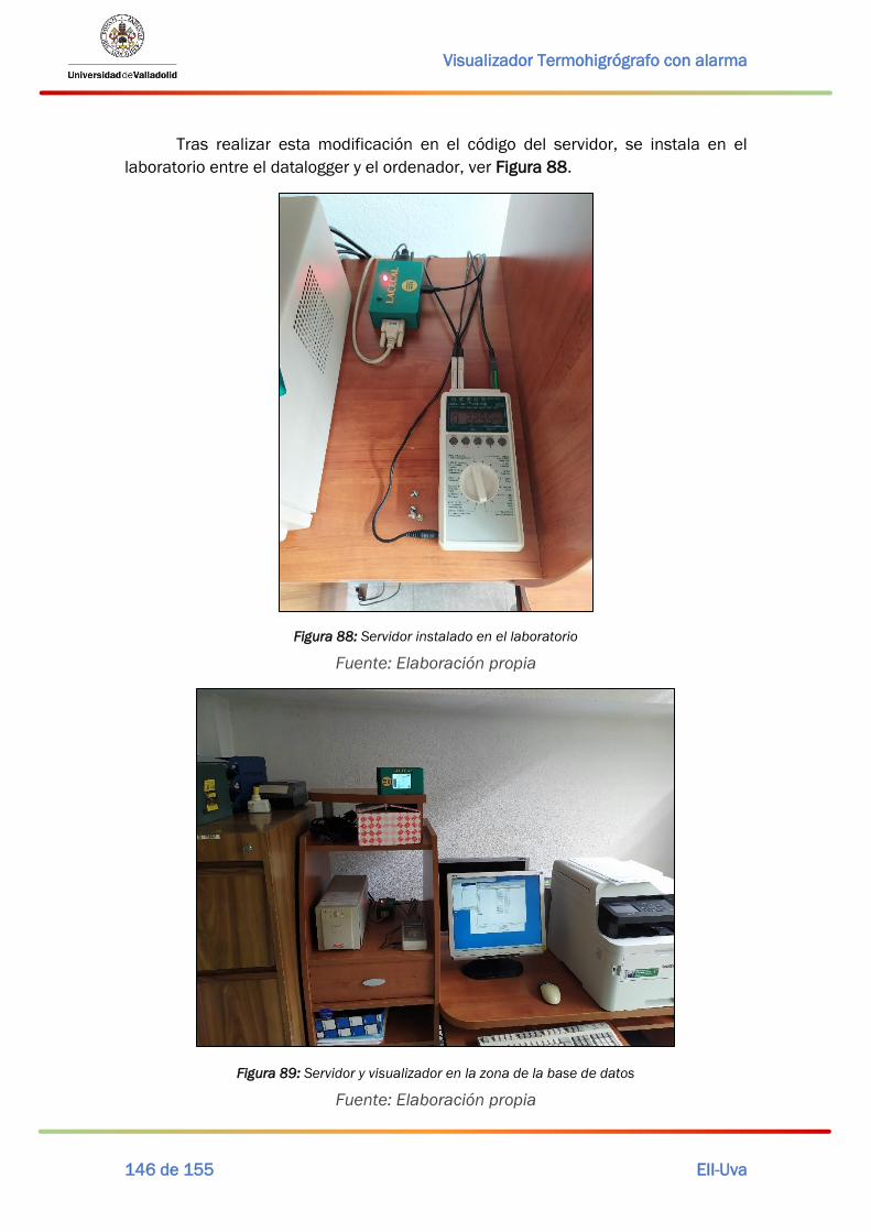
Visualizador Termohigrógrafo con alarma
146 de 155 EII-Uva
Tras realizar esta modificación en el código del servidor, se instala en el
laboratorio entre el datalogger y el ordenador, ver Figura 88.
Figura 88: Servidor instalado en el laboratorio
Fuente: Elaboración propia
Figura 89: Servidor y visualizador en la zona de la base de datos
Fuente: Elaboración propia

Capítulo 9: Puesta en marcha del prototipo en el laboratorio
Ricardo Alonso Fernández 147 de 155
Figura 90: Visualizador en la zona de calibración
Fuente: Elaboración propia
Figura 91: Visualizador en la zona de ensayos
Fuente: Elaboración propia


Capítulo 10: Conclusiones y líneas futuras de desarrollo
Ricardo Alonso Fernández 149 de 155
Capítulo 10: Conclusiones y líneas futuras de desarrollo El prototipo desarrollado cumple con los objetivos globales y específicos
propuestos en el apartado Introducción y objetivos.
Wifi para comunicar inalámbricamente los dispositivos.
Pantalla TFT a color para mostrar los valores y configuraciones.
Pantalla táctil para configurar los parámetros por parte del usuario.
Señalización luminosa utilizando la propia pantalla e iconos de color rojo,
amarillo o verde según el nivel de alerta de la temperatura y humedad.
Alimentación por batería en el visualizador para permitir su movilidad por el
laboratorio.
Alimentación a 5V a través de USB micro b en ambos dispositivos.
También se han añadido algunas características a mayores:
Alarma sonora mediante un zumbador cuando se entra en el nivel rojo de
alerta.
Los parámetros de configuración se almacenan en la memoria no volátil del
dispositivo para que se conserven aun cuando este se apague.
Página web que muestra los valores de temperatura y humedad a la que se
puede acceder desde cualquier navegador en un dispositivo conectado a la
red Wifi del servidor.
Líneas futuras de desarrollo
En el caso del prototipo del visualizador, al utilizar una placa de circuito de
doble cara, tanto la pantalla como el ESP32 se han tenido que elevar sobre la
superficie para poder soldar por ambos lados, al no tener pads metalizados que
conecten ambos lados de la placa. Esto ha ocasionado que el grosor de la envolvente
sea mayor al deseado. Por ello, se propone como futura línea de desarrollo reducir
la superficie de la PCB, juntando los componentes y eliminando el texto de la capa
de cobre. Además, al mandar fabricar la PCB a una empresa especializada, se
tendrán pads metalizados, pudiendo apoyar los componentes en la superficie y de
esta manera reducir el tamaño del visualizador.
También se propone utilizar otra versión del ESP32 para el visualizador que tenga
mayor espacio de almacenamiento, para así mejorar el acabado de la interfaz de la
pantalla.


Bibliografía
Ricardo Alonso Fernández 151 de 155
Bibliografía AGGSoftware. (30 de enero de 2021). AGGSoftware. Obtenido de
https://www.aggsoft.com/rs232-pinout-cable/serial-cable-connections.htm
Alibaba. (Junio de 2021). Alibaba. Obtenido de https://spanish.alibaba.com/product-
detail/liquid-crystal-thermometer-adhesive-thermometer-strip-to-measure-
indoor-room-temperature-1553688141.html
AmericanCableAssemblies. (30 de enero de 2021). AmericanCableAssemblies.
Obtenido de https://americancableassemblies.com/db9-to-db9-metal-hood-
female-male-build-your-own-assembly/
Arduino. (junio de 2021). Arduino Versiones anteriores. Obtenido de
https://www.arduino.cc/en/Main/OldSoftwareReleases#previous
Bike Pixels. (Junio de 2021). Bike Pixels. Obtenido de
https://bikepixels.com/2019/11/10/anadir-una-bateria-lipo-en-proyectos-
con-arduino/?lang=es
Burea International des Poids er Mesures. (2018). Conferencia General de Pesos y
Medidas 26ª reunión., (pág. 562). Saint-Cloud, Francia.
Comité de Metrología del Instituto de la Ingeniería en España. (2019). La Metrología
también existe.
Creality 3D. (Junio de 2021). Creality 3D . Obtenido de https://creality3d.shop/
Createc3D. (Junio de 2021). Createc3D. Obtenido de
https://createc3d.com/blog/evitar-el-temido-warping/
de la Fuente, E. (2019). Apuntes Informática Industrial. Valladolid, España.
Diagram Database. (30 de enero de 2021). Diagram Database. Obtenido de
http://rv.lerosediposillipo.it/diagram/m12-to-db9-wiring-diagram
Doutel, F. (Junio de 2021). Xataka. Obtenido de
https://www.xatakahome.com/trucos-y-bricolaje-smart/polysmooth-and-
polysher-vienen-a-mejorar-la-impresion-3d
EasyEDA. (Junio de 2021). EasyEDA Resources. Obtenido de
https://easyeda.com/modules/TP4056-03962A-Lithium-Battery-
Charger_b4e588fcbeaa4b9b951f751938fe06f2
EEMB Corporation. (2010). LIR18650 Datasheet.
Española, R. A. (2021). Diccionario de la lengua española.
Espressif Systems. (2020). ESP32-WROOM-32 datasheet.

Visualizador Termohigrógrafo con alarma
152 de 155 EII-Uva
Espressif Systems. (2021). ESP32 Series Datasheet. Obtenido de
https://www.espressif.com/sites/default/files/documentation/esp32_datas
heet_en.pdf
Excursively. (Junio de 2021). GrabCAD. Obtenido de https://grabcad.com/library/3-
2-tft-spi-240x320-v1-0-1
Exide Group. (Junio de 2021). Exide Technologies. Obtenido de
https://www.exidegroup.com/en
Fairchild Semiconductor Corporation. (2014). 2N3904 datasheet.
Instituto de Síntesis Química y Catálisis Homogénea, Universidad de Zaragoza. (Junio
de 2021). Instituto de Síntesis Química y Catálisis Homogénea. Obtenido de
http://www.isqch.unizar-
csic.es/ISQCHportal/cristalesLiquidos.do?enlaceMenuDerecha=temas&enla
ceMenuIzquierda=divulgacion
JS. (Junio de 2021). GrabCAD. Obtenido de https://grabcad.com/library/tc4056a-
charger-module-5v-1a-usb-micro-1
Kutchma, T. M. (Junio de 2021). The Effects of Room Color on Stress Perception: Red
versus Green Environments. Obtenido de Minnesota State University,
Mankato: https://cornerstone.lib.mnsu.edu/jur/vol3/iss1/3/
me-no-dev. (Junio de 2021). Github. Obtenido de https://github.com/me-no-
dev/arduino-esp32fs-plugin/releases
Microsoft. (junio de 2021). Visual Studio Code. Obtenido de
https://code.visualstudio.com/
Ministerio de Industria Comercio y Turismo. (02 de febrero de 2021). Centro Español
de Metrología. Obtenido de https://www.cem.es/
Multitask Technology. (Julio de 2021). Multitask Technology. Panamá.
NanJing Top Power ASIC Corp. (2021). TP4056 1A Standalone Linear Li-Ion Battery
Charger with Thermal Regulation in SOP-8.
PCBWay. (Junio de 2021). PCBWay. Obtenido de https://www.pcbway.es/
Pérez Turiel, J. (2020). Apuntes Asignatura Control y Comunicaciones Industriales.
(U. EII, Ed.) Valladolid, Castilla y León, España.
PintarSinParar. (Junio de 2021). PintarSinParar. Obtenido de
https://pintarsinparar.com/custom/962-spray-pintura-termocromica.html
RS Components. (Junio de 2021). RS Components. Obtenido de https://es.rs-
online.com/web/

Bibliografía
Ricardo Alonso Fernández 153 de 155
Sanyo. (2021). Funcionamiento de la pantalla LCD.
SCHWENKE, T. (Junio de 2021). Bring Knowledge To The World. Obtenido de
http://www.bring-knowledge-to-the-world.com/
Smith, N. d. (Junio de 2021). ANSI IPC-2221A PCB Trace Width Calculator. Obtenido
de https://www.desmith.net/NMdS/Electronics/TraceWidth.html
Universitat Politècnica de Catalunya Barcelonatech. (Julio de 2021). Universitat
Politècnica de Catalunya Barcelonatech. Obtenido de
https://upcommons.upc.edu/bitstream/handle/2117/126329/xavier.rodrig
uez.campillo_130960.pdf
Vazquez, J. A. (2021). Apuntes Electrónica Industrial.
Vishay General Semiconductor. (2011). 1N4007 General Purpose Plastic Rectifier.
Wikimedia Commons. (Junio de 2021). HP PhotoSmart SDIO Kamera.jpg.


Anexos
Ricardo Alonso Fernández 155 de 155
Anexos

UNIVERSIDAD DE VALLADOLID
ESCUELA DE INGENIERIAS INDUSTRIALES
Grado en Ingeniería en Electrónica Industrial y
Automática
Visualizador termohigrógrafo con alarma
ANEXOS
Autor:
Alonso Fernández, Ricardo
Tutor:
Díez Muñoz, Pedro Luis
Tecnología Electrónica
Valladolid, Julio 2021

Visualizador termohigrógrafo con alarma
Ricardo Alonso Fernández EII-UVa
Anexos I: Manual de usuario del visualizador termohigrógrafo con
alarma
Anexos II: Planos
• Plano 1: Envolvente del servidor
• Plano 2: Tapa del servidor
• Plano 3 Botón y cubierta del servidor
• Plano 4: Vista explosionada del servidor
• Plano 5: Envolvente del visualizador
• Plano 6: Tapa del visualizador
• Plano 7: Vista explosionada del visualizador
Anexos III: Esquemas y fotolitos
• Esquema 1: Esquema eléctrico del servidor
• Esquema 2: Esquema eléctrico del visualizador
• Fotolitos de las PCBs
Anexos IV: Datasheet
• Datasheet 1: Resistencias de película metálica
• Datasheet 2: Zumbador electromecánico
• Datasheet 3: Condensadores de tántalo
• Datasheet 4: Transistor NPN 2N3904
• Datasheet 5: Regulador de tensión de baja caída MCP1825
• Datasheet 6: Interruptores de botón TL2201
• Datasheet 7: Diodos LED de 5 mm
• Datasheet 8: Diodo rectificador 1N4001
• Datasheet 9: Conectores DB9
• Datasheet 10: Módulo de carga y descarga de baterías TP4056A
• Datasheet 11: ESP32 WROOM 32
• Datasheet 12: ESP32 Series
• Manual de usuario Datalogger ALMEMO 2290-8
• Ficha técnica PLA Glitter

Visualizador termohigrógrafo con alarma
Ricardo Alonso Fernández EII-UVa
ANEXOS I

Manual de usuario
Trabajo Fin de Grado
Autor: Ricardo Alonso Fernández
Tutor: Pedro Luis Díez Muñoz
EII-UVa Curso2020/21
Visualizador termohigrógrafo
con alarma


Índice
Ricardo Alonso Fernández 3
Índice I. Introducción ...................................................................................................... 4
1 Objetivo ......................................................................................................... 4
2 Requerimientos ............................................................................................ 4
3 Materiales incluidos en el kit ....................................................................... 4
II. Advertencias ..................................................................................................... 5
III. Puesta en funcionamiento ............................................................................. 7
IV. Funcionamiento del servidor ......................................................................... 8
V. Funcionamiento del visualizador .................................................................... 9
Menú principal ............................................................................................... 10
Menú de alarma ............................................................................................. 10
Menú de configuración .................................................................................. 11
Menú de selección de zona .......................................................................... 11
Menú de configuración de temperatura y de humedad ............................. 12
Menú de configuración de las bandas amarillas ........................................ 12
VI. Posibles problemas y soluciones ................................................................. 13

Manual de usuario
4 EII-Uva
I. Introducción El visualizador termohigrógrafo con alarma ha sido específicamente diseñado
para funcionar con los equipos instalados en el laboratorio LACECAL situado en la
Escuela de Ingenierías Industriales.
1 Objetivo
Otorgar soporte a los usuarios del visualizador termohigrógrafo con alarma
2 Requerimientos
• Datalogger Almemo 2290-8 con interfaz RS232 para la comunicación
3 Materiales incluidos en el kit
• Módulo servidor con conectores DB9 hembra y macho
• Módulo visualizador
• Dos cables micro USB-b de 1m para alimentación de los dispositivos
• Lápiz para pantalla táctil
Figura 1: Materiales incluidos

II. Advertencias
Ricardo Alonso Fernández 5
II. Advertencias
USO CORRECTO DEL APARATO
Leer con atención las siguientes instrucciones. Conservar las instrucciones de
uso y montaje.
Comprobar el aparato al sacarlo del embalaje. El dispositivo no debe
conectarse en caso de haber sufrido daños durante el transporte.
El aparato debe ser alimentado a 5 V en corriente continua. Los daños
provocados por una conexión incorrecta no están cubiertos por la garantía.
El aparato ha sido diseñado exclusivamente para uso doméstico. Si va a ser
manipulado por un niño menor de 12 años es necesaria la supervisión de un adulto.
El conjunto está previsto para ser utilizado a una altura máxima de 2000
metros sobre el nivel del mar. Puede ser utilizado por personas que carezcan de
conocimientos eléctricos y electrónicos siempre que se sigan las instrucciones
cuidadosamente.
No manipular con el cuerpo húmedo. Si entra agua en el dispositivo,
desconectar inmediatamente y no volver a conectar hasta que esté completamente
seco.
No dejar que los niños jueguen con el aparato. Mantener a los niños alejados
del dispositivo y de los cables de conexión.
INDICACIONES DE SEGURIDAD
ADVERTENCIA – ¡PELIGRO DE DESCARGA ELÉCTRICA!
Las reparaciones inadecuadas son peligrosas. Si el aparato está averiado,
desenchufar el dispositivo de la alimentación inmediatamente.
No utilizar limpiadores de alta presión ni por chorro de vapor. La humedad
interior puede dañar la electrónica.
Un aparato defectuoso puede ocasionar una descarga eléctrica. No conectar
nunca un dispositivo defectuoso.
No abrir ni desacoplar ningún componente del dispositivo, pues puede
provocar riesgos de asfixia e intoxicación.
Peligro de descarga eléctrica.

Manual de usuario
6 EII-Uva
CAUSAS DE LOS DAÑOS
Mantener el aparato en un lugar fresco y seco, no lo deje a la intemperie.
No tirar al suelo ni golpear con objetos contundentes.
No alimentar a una tensión mayor a la indicada (5 VDC).
PROTECCIÓN DEL MEDIO AMBIENTE
Los componentes siguen la normativa RoHS (Restriction of
Hazardous Substances), que se refiere a la Directiva 2011/65/UE de
Restricción de ciertas Sustancias Peligrosas en aparatos eléctricos y
electrónicos, adoptada en junio de 2011 por la Unión Europea. La directiva está
transpuesta a la legislación española por medio del Real Decreto 219/2013. Esta
normativa restringe el uso de seis materiales peligrosos en la fabricación de varios
tipos de equipos eléctricos y electrónicos, entre otros, el plomo, mercurio y cadmio.
ELIMINACIÓN DE RESIDUOS RESPETUOSA CON EL MEDIO AMBIENTE
Eliminar el embalaje de forma ecológica, depositándolo en el
contenedor correspondiente.
Este aparato está marcado con el símbolo de cumplimiento con la
Directiva Europea 2012/19/UE relativa a los aparatos eléctricos y
electrónicos usados (Residuos de aparatos eléctricos y electrónicos RAEE).
La directiva proporciona el marco general válido en todo el ámbito de la Unión
Europea para la retirada y la reutilización de los residuos de los aparatos eléctricos y
electrónicos.
Una vez finalizada la vida útil del dispositivo es necesario llevar el aparato a
un centro de tratamiento de residuos electrónicos para deshacerse de una manera
segura y responsable de los restos

III. Puesta en funcionamiento
Ricardo Alonso Fernández 7
III. Puesta en funcionamiento 1. Preparar la zona donde se situará el servidor.
2. Desconectar el datalogger del ordenador y conectarlo al servidor (entrada
hembra).
3. Mediante un cable de datos con terminaciones macho y hembra DB9,
conectar el puerto hembra del servidor a la entrada macho del ordenador.
4. Conectar el cable de alimentación del servidor.
5. Cuando se haya completado una transmisión del datalogger al ordenador
encender el servidor utilizando el botón, el led se encenderá.
6. Situar el visualizador en una superficie plana y conectar el cable de
alimentación
7. Al encender el visualizador procederá a conectarse a la red Wifi del servidor.
8. Una vez conectado, el visualizador sincronizará su intervalo de consulta con
la llegada de datos al servidor.
No desconectar los cables ni conectar el servidor durante la
transmisión del datalogger
Figura 2: Ejemplo de instalación del servidor

Manual de usuario
8 EII-Uva
IV. Funcionamiento del servidor El dispositivo del servidor obtiene los datos transmitidos por el datalogger a
través de la interfaz RS232, considerando el siguiente formato de mensaje durante
la transmisión:
“Fecha”;”Hora”;TCalibración
;TEnsayos
;;;;HCalibración
;HEnsayos
;;;;Valor1
;Valor2
;;;;Valor3
;Valor4/Retorno/SaltoDeLínea
Tabla 1: Formato de mensaje del datalogger
Una vez recibidos los datos, el servidor genera una red Wifi de nombre
LACECAL_TyH y con contraseña de acceso TFG_LACECAL.
Cualquier dispositivo puede conectarse a ella y al acceder desde el navegador
a la dirección IP 192.168,4.1 se accede a una página web que muestra los datos de
ambas zonas. Para acceder a un dato en concreto se pueden usar las siguientes
direcciones:
Dirección Contenido
192.168.4.1 Página web
192.168.4.1/Fecha Fecha
192.168.4.1/Hora Hora
192.168.4.1/TCalibracion Temperatura de la zona de calibración
192.168.4.1/TEnsayos Temperatura de la zona de ensayos
192.168.4.1/HCalibracion Humedad de la zona de calibración
192.168.4.1/HEnsayos Humedad de la zona de ensayos
Tabla 2: Direcciones y contenido del servidor
El servidor puede atender un máximo de 4 dispositivos conectados
simultáneamente.

V. Funcionamiento del visualizador
Ricardo Alonso Fernández 9
V. Funcionamiento del visualizador El visualizador muestra por pantalla los valores de temperatura y humedad
proporcionados por el datalogger, junto con la fecha y hora. Admite la configuración
de los valores máximos, mínimos, incertidumbres y zonas amarillas a través de la
pantalla táctil. Todos los parámetros de configuración se almacenan en memoria no
volátil.
Los niveles de alerta se dividen en verde, amarillo y rojo. Se establecen por
separado para temperatura y humedad y se toma como global el peor de los dos.
Figura 3: Niveles de alerta del visualizador

Manual de usuario
10 EII-Uva
Menú principal
Figura 4: Interfaz del menú principal
En la parte superior se muestra la zona activa, la hora y fecha de la última
medida. En la parte central la temperatura y humedad de la zona, con distintos
colores de imagen en función del nivel de alerta y un semáforo que representa el
nivel de alerta global. Además, en la esquina superior derecha se muestra el nivel de
carga de la batería.
Menú de alarma
Cuando se alcanza el nivel rojo de alerta, el visualizador muestra una pantalla
de alarma si la pantalla activa es la principal.
En este menú de alarma, se muestra el parámetro que está fuera de rango y
se mantiene activo el zumbador. Para desactivarlo es suficiente con tocar la pantalla.
Aunque los parámetros sigan fuera de rango el menú de alarma no se vuelve a
mostrar hasta que haya habido un paso por amarillo o verde.
Figura 5: Interfaz del menú de alarma

V. Funcionamiento del visualizador
Ricardo Alonso Fernández 11
Menú de configuración
Al pulsar sobre el icono del engranaje en el menú principal se accede a esta
pantalla que lleva a las distintos menús de configuraciones de parámetros.
En la esquina superior derecha se puede desactivar el sonido de pulsación.
Figura 6: Interfaz del menú de configuración
Menú de selección de zona
Permite elegir la zona activa, de la cual se muestran los valores de
temperatura y humedad.
Figura 7: Interfaz del menú de selección de zona

Manual de usuario
12 EII-Uva
Menú de configuración de temperatura y de humedad
Desde estos menús se introduce el valor máximo y mínimo de humedad o
temperatura (inicio zonas rojas). También se puede configurar la incertidumbre de
las medidas proporcionadas por las sondas.
Figura 8: Interfaz del menú de configuración de
temperatura
Figura 9: Interfaz del menú de configuración de
humedad
Menú de configuración de las bandas amarillas
Desde aquí se configura el ancho de cada banda amarilla, tanto para
temperatura como para humedad. Un valor de 0 elimina la zona amarilla.
Figura 10: Interfaz del menú de configuración de las zonas amarillas

VI. Posibles problemas y soluciones
Ricardo Alonso Fernández 13
VI. Posibles problemas y soluciones
• El datalogger hace un barrido de los canales pero no se actualizan los datos
del servidor ni del ordenador
Si este problema se da nada más conectar el servidor al datalogger y
se ha evitado interrumpir la transmisión al conectarlo. Desde el ordenador
detener el servicio de la toma de datos y seguidamente iniciarlo de nuevo. Si
al hacer esto el ordenador actualiza la información pero el servidor no,
reiniciar el servidor, asegurándose de encenderlo después de que el
datalogger haya transmitido para no pillar datos a medias.
• El visualizador se queda bloqueado o no actualiza los datos
Se ha perdido la conexión con el servidor. Si al reiniciar el visualizador
este no pasa de la pantalla de conectando, es necesario revisar el servidor.
• El visualizador no enciende
El nivel de carga es demasiado bajo. Conectar el cable de alimentación y
dejarlo cargar unos minutos antes de encenderlo.

Visualizador termohigrógrafo con alarma
Ricardo Alonso Fernández EII-UVa
ANEXOS II

A-A ( 1 : 1 )
A
A
1
1
2
2
3
3
4
4
5
5
6
6
A A
B B
C C
D D
Visualizador Termohigrógrafo con alarmaEII-UVaCurso 2020/21
Dibujado por:Ricardo Alonso Fernández
Envolvente servidorPieza:
Grado en Ingeniería en Electrónica Industrial y Automática
Plano Nº: 1
71,00
106,00
R
4
,
0
0
12,92
16,50
66,26
25,56
5,00
R
2
,
0
0
50,50
5,60
33,60
106,00
4
,
0
0
8
,
0
0 5
,
0
0
R
1
1
,
0
0
17,00
25,00
32,00
28,00
5,00
2,60
R
1
1
,
0
0
3,50
4,00
9,25
10,00
20,10
30,80
69,00
R
3
,
0
0
71,00
33,60
Vista trasera
2,00
23,00
102,00
106,00
3,00
R
4
,
0
0
33,60

A-A ( 1 : 1 )
A
A
1
1
2
2
3
3
4
4
5
5
6
6
A A
B B
C C
D D
Visualizador Termohigrógrafo con alarmaEII-UVaCurso 2020/21
Dibujado por:Ricardo Alonso Fernández
Tapa servidorPieza:
Grado en Ingeniería en Electrónica Industrial y Automática
Plano Nº: 2
106,00
102,00
30,80
5
,0
03
,0
0
67,00
7,25
8,00
R
1
1
,
0
0
R
3
,
0
0
3,00
2,00
7,60
2,00
4,00
6,00
7,60
30,80
52,50
86,00
R
2
,
0
0
67,00
106,00
3,00
R
2
,
0
0

A-A ( 4 : 1 )
B-B ( 2 : 1 )
A
A
B
B
1
1
2
2
3
3
4
4
5
5
6
6
A A
B B
C C
D D
Visualizador Termohigrógrafo con alarmaEII-UVaCurso 2020/21
Dibujado por:Ricardo Alonso Fernández
Botón y cubierta conector servidorPieza:
Grado en Ingeniería en Electrónica Industrial y Automática
Plano Nº: 3
R
4
,
0
0
24,75
10,90
9,00
4,00
7,75
8,50
3,00
5,00
4,00
29,20
10,20
7,00
25,20
32,20
34,20
6,00
4,00
34,20

LISTA DE PIEZAS
DESCRIPCIÓN
Nº DE PIEZACTDADELEMENTO
PLA Verde GlitterEnvolvente Servidor11
PCB ServidorCircuito Servidor12
PLA Verde GlitterTapa Servidor13
PLA Verde GlitterBoton Servidor14
CATIA V5 STEP ExchangeModulo Carga15
PLA Verde GlitterTapa Modulo Carga16
PLA Silk GoldTexto Servidor17
Insert round nutsNut GB 809 A M3 x 848
Cabeza cilíndrica con
cavidad cruzada de tipo
H o Z. Productos de
clase A
EN ISO 7045 - M2,5 x 14
- 4.8 - H
49
1
1
2
2
3
3
4
4
5
5
6
6
A A
B B
C C
D D
Visualizador Termohigrógrafo con alarmaEII-UVaCurso 2020/21
Dibujado por:Ricardo Alonso Fernández
Vista explosionada servidorPieza:
Grado en Ingeniería en Electrónica Industrial y Automática
Plano Nº: 4
7
1
4
8
2
3
9
5
6

A-A ( 1:1 )
A
A
1
1
2
2
3
3
4
4
5
5
6
6
A A
B B
C C
D D
Visualizador Termohigrógrafo con alarmaEII-UVaCurso 2020/21
Dibujado por:Ricardo Alonso Fernández
Envolvente visualizadorPieza:
Grado en Ingeniería en Electrónica Industrial y Automática
Plano Nº: 5
87,40
69,00
51,00
18,20
45,20
2,00
3,50
14,009,00
3,50
R
1
0
,
0
0
5,20
4
,
0
0
5,00
4,00
43,70
46,00
R
4
,
0
0
R
4
,
0
0
27,00
10,50
27,00
154,40
17,00
46,00
150,00
154,40
92,00
96,00
69,00
10,003,00
43,00
8,70
7,20
19,00
2,20

A-A ( 1:1 )
B ( 2 : 1 )
A
A
B
1
1
2
2
3
3
4
4
5
5
6
6
A A
B B
C C
D D
Visualizador Termohigrógrafo con alarmaEII-UVaCurso 2020/21
Dibujado por:Ricardo Alonso Fernández
Tapa visualizadorPieza:
Grado en Ingeniería en Electrónica Industrial y Automática
Plano Nº: 6
150,00
83,00
17,43
14,63
70,00
140,00
13,00
23,50
10,00
58,00
70,00
38,40
36,00
18,00
2,00 5,50
3
,
4
0
R
4
,
0
0
R
4
,
0
0
R
4
,
0
0
R
5
,
0
0
10,00
11,50
2,00
21,50
6,50
5,00
83,00
60,00
3,00
9,00
R
2
,
0
0
5
,
2
0
-
2
,
0
0
150,00
130,00
10,00
36,00
8,80
R
2
,
0
0
R
4
,
0
0

LISTA DE PIEZAS
DESCRIPCIÓN
Nº DE PIEZACTDADELEMENTO
EnvolventeVisualizador11
CircuitoVisualizador12
BotonVisualizador13
TapaVisualizador14
Bateria15
TextoVisualizador16
Insert round nutsNut GB 809 A M3 x 847
Cabeza cilíndrica con
cavidad cruzada de tipo
H o Z. Productos de
clase A
EN ISO 7045 - M3 x 30
- 4.8 - H
48
1
1
2
2
3
3
4
4
5
5
6
6
A A
B B
C C
D D
Visualizador Termohigrógrafo con alarmaEII-UVaCurso 2020/21
Dibujado por:Ricardo Alonso Fernández
Vista explosionada visualizadorPieza:
Grado en Ingeniería en Electrónica Industrial y Automática
Plano Nº: 7
6
1
7
2
3
5
8
4

Visualizador termohigrógrafo con alarma
Ricardo Alonso Fernández EII-UVa
ANEXOS III
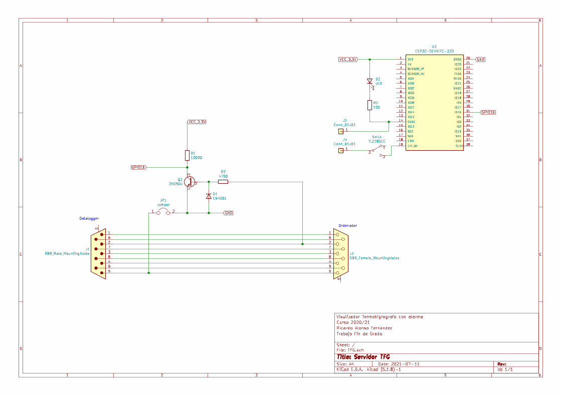


1 2 3 4 5 6
1 2 3 4 5 6
A
B
C
D
A
B
C
D
Date: 2021-07-11KiCad E.D.A. kicad (5.1.8)-1
Rev: Size: A4Id: 1/1
Title: Circuito servidorFile: TFG.kicad_pcbSheet:
Trabajo Fin de GradoRicardo Alonso FernándezCurso 2020/21Visualizador Termohigrógráfo con alarma
-
+RICARDO ALONSO

1 2 3 4 5 6
1 2 3 4 5 6
A
B
C
D
A
B
C
D
Date: 2021-07-11KiCad E.D.A. kicad (5.1.8)-1
Rev: Size: A4Id: 1/1
Title: Circuito servidorFile: TFG.kicad_pcbSheet:
Trabajo Fin de GradoRicardo Alonso FernándezCurso 2020/21Visualizador Termohigrógráfo con alarma

1 2 3 4 5 6
1 2 3 4 5 6
A
B
C
D
A
B
C
D
Date: 2021-07-11KiCad E.D.A. kicad (5.1.8)-1
Rev: Size: A4Id: 1/1
Title: Circuito servidorFile: TFG.kicad_pcbSheet:
Trabajo Fin de GradoRicardo Alonso FernándezCurso 2020/21Visualizador Termohigrógráfo con alarma
U1 JP
1
D1K
R2
SW1J4
J3
R3
D2
J2J1
Q1R1

1 2 3 4 5 6
1 2 3 4 5 6
A
B
C
D
A
B
C
D
Date: 2021-07-11KiCad E.D.A. kicad (5.1.8)-1
Rev: Size: A4Id: 1/1
Title: Circuito visualizadorFile: Circuito_visualizador.kicad_pcbSheet:
Trabajo Fin de GradoRicardo Alonso FernándezCurso 2020/21Visualizador termohigrógrafo con alarma
TRABAJO FIN DE GRADO

1 2 3 4 5 6
1 2 3 4 5 6
A
B
C
D
A
B
C
D
Date: 2021-07-11KiCad E.D.A. kicad (5.1.8)-1
Rev: Size: A4Id: 1/1
Title: Circuito visualizadorFile: Circuito_visualizador.kicad_pcbSheet:
Trabajo Fin de GradoRicardo Alonso FernándezCurso 2020/21Visualizador termohigrógrafo con alarma

1 2 3 4 5 6
1 2 3 4 5 6
A
B
C
D
A
B
C
D
Date: 2021-07-11KiCad E.D.A. kicad (5.1.8)-1
Rev: Size: A4Id: 1/1
Title: Circuito visualizadorFile: Circuito_visualizador.kicad_pcbSheet:
Trabajo Fin de GradoRicardo Alonso FernándezCurso 2020/21Visualizador termohigrógrafo con alarma
U2
MC1
03962AIn-
In+
Out-
Bat-
Bat+
Out+
SW1
R3
R2 R1
C2
C1
U1

1 2 3 4 5 6
1 2 3 4 5 6
A
B
C
D
A
B
C
D
Date: 2021-07-11KiCad E.D.A. kicad (5.1.8)-1
Rev: Size: A4Id: 1/1
Title: Circuito visualizadorFile: Circuito_visualizador.kicad_pcbSheet:
Trabajo Fin de GradoRicardo Alonso FernándezCurso 2020/21Visualizador termohigrógrafo con alarma
CURSO2020/21
RICARDO ALONSO FDEZ

1 2 3 4 5 6
1 2 3 4 5 6
A
B
C
D
A
B
C
D
Date: 2021-07-11KiCad E.D.A. kicad (5.1.8)-1
Rev: Size: A4Id: 1/1
Title: Circuito visualizadorFile: Circuito_visualizador.kicad_pcbSheet:
Trabajo Fin de GradoRicardo Alonso FernándezCurso 2020/21Visualizador termohigrógrafo con alarma
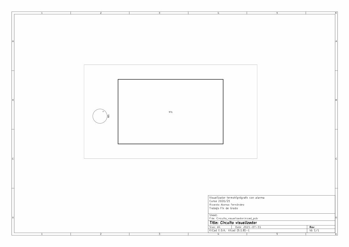
1 2 3 4 5 6
1 2 3 4 5 6
A
B
C
D
A
B
C
D
Date: 2021-07-11KiCad E.D.A. kicad (5.1.8)-1
Rev: Size: A4Id: 1/1
Title: Circuito visualizadorFile: Circuito_visualizador.kicad_pcbSheet:
Trabajo Fin de GradoRicardo Alonso FernándezCurso 2020/21Visualizador termohigrógrafo con alarma
TFT1
BZ
1
+

Visualizador termohigrógrafo con alarma
Ricardo Alonso Fernández EII-UVa
ANEXOS IV

Characteristics - Electrical
LR0204 LR1L LR1 LR2 LR100 LR200
Rated Power @ 70°C (W) 0.25 0.5 0.6 0.75 1 2
Resistance Range (Ohms) Min 1R0 10R R10 1R0 10R 1M1 1R0 10R 10R
Max 9R1 1M0 R82 9R1 1M0 10M 1M0 1M0 1M0
Tolerance (%) 1 1 5 1 2 1 2 1 5 1 2 1 5 1 5
Code Letter F F J F G F G F J F G F J F J
Temp. Coefficient (ppm/°C) ± 100 ± 100 ± 200 ± 100 ± 50 ± 100 ± 100 25/50/100 25/50/100
Selection Series E24 E24 E12 E24 E24 E24 E24 E24 E24
On Request E96 E96 E96 E96 E96
Limiting Element Voltage 200 350 350 350 500 500
Max Permitted Element Voltage 200 350 350 350 500 500
Max Overload Voltage 400 500 700 700 1000 1000
Max Intermittent Overload Voltage 500 750 750 750 1000 1000
Operating Temp. Range (°C) -55 to +155
Climatic Category 55/155/56
Dielectric Strength (V) 500 700 700 700 700 700
Insulation Resistance 1000Min Dry (Mohms)
0.5 1 2
D F G
0.5 1 2
D F G0.5 1 5
D F J
Metal Film Fixed Resistors
Type LR Series
1773241 CIS BI 06/2011 Dimensions are in millimeters Dimensions are shown for For email, phone or live chat, go to: te.com/helpand inches unless otherwise reference purposes only.specified. Values in brackets Specifications subject are standard equivalents. to change.
Key Features Superior quality metal
film resistors with 1%tolerance andtemperature coefficients down to 50 ppm. 3 case sizes are available in 0.25, 0.6, 0.75W. The LR1L series is a low ohmic value range from 0.1 to 0.82 ohm.Ideally suited where low resistance and small size are required.
Metal film resistors have excellent stability under load and severeenvironmentalconditions. They exhibit very low noise current and voltage coefficients.They are available in a wide range of resistance values and are suitable for general purpose and precisionapplications.
The resistive element comprises a thin film of nickel-chrome alloy evaporated onto a highthermal conductivity ceramic element. Metal end caps are force fitted to the element priorto spiralling to value. Tinned copper lead wires are welded to the end caps and thecomponents are then coated. One coat of phenolic resin is followed by three coats ofepoxy resin. All resistors are tested for value and tolerance.

Metal Film Fixed Resistors
Type LR Series
1773241 CIS BI 06/2011 Dimensions are in millimeters Dimensions are shown for For email, phone or live chat, go to: te.com/helpand inches unless otherwise reference purposes only.specified. Values in brackets Specifications subject are standard equivalents. to change.
Dimensions
Style L* D d Nom l
LR0204 3.5 +/-0.2 2.0 max 0.45 28 +/-3.0
LR1 6.2 +/-0.5 2.3 +/-0.2 0.55 28 +/-3.0
LR1L 6.2 +/-0.5 2.3 +/-0.2 0.55 28 +/-3.0
LR2 9.7 +/-0.3 3.5 +/-0.2 0.55 28 +/-3.0
LR100 12.0 max 5.0 max 0.7 28 +/-3.0
LR200 12.0 max 5.5 max 0.7 28 +/-3.0
* Length is measured in accordance with IEC 294.
Power Derating Curve
0 20 40 60 70 80 100 120 125
100
80
60
40
20
0
Rat
ed P
ow
er (
%)
Ambient Temperature (°C)
Surface Temperature Rise Vs Load
0 0 0.2 0.25 0.4 0.6 0.75
100
80
60
40
20
0Tem
per
atu
re R
ise
abo
ve A
mb
ien
t (°
C)
Power Dissipation (W)
LR0204
LR1LLR1 LR2

Performance Characteristics
The evaluation of the performance characteristics is carried out with reference to IECSpecifications QC 400 000 and QC 400 100.
TEST REF Long Term Tests ±(1% + 0.05 ohm)
4.23 Climatic sequence
4.24 Damp heat, steady state
4.25.1 Endurance at 70°C
4.25.3 Endurance at 125°C
TEST REF Short Term Tests ±(0.25% + 0.05 ohm)
4.13 Overload
4.16 Robustness of terminations
4.18 Resistance to soldering heat
4.19 Rapid change of temperature
4.22 Vibration
* For LR1L the limits are ± (5% + 0.1 ohm) and ± (1% + 0.05 ohm)respectively. All resistance values are measured at a distance of 12mmfrom the end cap.
Mounting
The resistors are suitable for processing on automatic insertion equipment and cutting and bending machines.
Marking
The resistors are marked with a colour band code in accordance with JIS C 0802.
Packaging
LR0204, LR1L and LR1 resistors are normally supplied taped in 'ammo' boxes of 4000 pieces.LR2 resistors are normally supplied taped in 'ammo' boxes of 1000 pieces. Other package styles on request.All tape specifications are in accordance with IEC 286-1.
How to Order
LR 1 F 100R
Common Part0204 - 0.25W
1L - 0.5W
1 - 0.6W
2 - 0.75W
100 - 1W
200 - 2W
Style
J - 5%
G - 2%
F - 1%
D - 0.5%
Tolerance Value
LR - Metal FilmFixed Resistor
100 ohm(100 ohms) 100R
1K0(1000 ohms) 1K0
100 K ohm(100,000 ohms) 100K
Metal Film Fixed Resistors
Type LR Series
TE Connectivity, TE connectivity (logo) and TE (logo) are trademarks.Other logos, product and Company names mentioned herein may be trademarks of their respective owners.
While TE has made every reasonable effort to ensure the accuracy of the information in this datasheet, TE does not guarantee that it is error-free, nor does TE make any otherrepresentation, warranty or guarantee that the information is accurate, correct, reliable or current. TE reserves the right to make any adjustments to the information contained hereinat any time without notice. TE expressly disclaims all implied warranties regarding the information contained herein, including, but not limited to, any implied warranties of merchantabili-ty or fitness for a particular purpose. The dimensions in this datasheet are for reference purposes only and are subject to change without notice. Specifications are subject to changewithout notice. Consult TE for the latest dimensions and design specifications.

EN
RS Stock number 780-0712
RS, Professionally Approved Products, gives you professional quality parts across all products categories. Our range has been testified by engineers as giving comparable quality to that of the leading brands without paying a premium price.
Dimensions(mm):
Features: • ROHS Compliant • Sealed base
All data at 25°C unless otherwise specified
Specifications: Rated Voltage (Vp-p square wave): 5Vp-p Operating Voltage: 3~8Vp-p Rated Current at Rated Voltage: < 40mA Sound Ouput at 2731Hz at 10cm: > 85dB Resonant Frequency: 2400Hz Coil Resistance: 47 + 5Ω Operating Temperature: -20~ +70°C Storage Temperature: -30~ +85°C Weight: 2g Requires additional electronic circuitry to operate as a sounder
RS, Professionally Approved Products, gives you professional quality parts across all products categories. Our range hasbeen testified by engineers as giving comparable quality to that of the leading brands without paying a premium price.
ENGLISH

1
Datasheet RS PRO CB Series Epoxy-coated Solid Electrolytic Tantalum Capacitor
EN

2
Article No. Product description Uf Voltage Pitch Tolerance
1814615 Tantalum Capacitors dipped type 10 50 5.0 20
1814613 Tantalum Capacitors dipped type 6.8 50 5.0 20
1814612 Tantalum Capacitors dipped type 4.7 50 2.5 20
1814611 Tantalum Capacitors dipped type 3.3 50 2.5 20
1814610 Tantalum Capacitors dipped type 2.2 50 2.5 20
1814609 Tantalum Capacitors dipped type 1.5 50 2.5 20
1814607 Tantalum Capacitors dipped type 1 50 2.5 20
1814606 Tantalum Capacitors dipped type 0.7 50 2.5 20
1814605 Tantalum Capacitors dipped type 0.5 50 2.5 20
1814604 Tantalum Capacitors dipped type 0.3 50 2.5 20
1814603 Tantalum Capacitors dipped type 0.2 50 2.5 20
1814602 Tantalum Capacitors dipped type 0.1 50 2.5 20
1814601 Tantalum Capacitors dipped type 47 35 5.0 20
1814600 Tantalum Capacitors dipped type 33 35 5.0 20
1814599 Tantalum Capacitors dipped type 22 35 5.0 20
1814598 Tantalum Capacitors dipped type 15 35 5.0 20
1814597 Tantalum Capacitors dipped type 10 35 2.5 20
1814596 Tantalum Capacitors dipped type 6.8 35 2.5 20
1814595 Tantalum Capacitors dipped type 4.7 35 2.5 20
1814594 Tantalum Capacitors dipped type 3.3 35 2.5 20
1814593 Tantalum Capacitors dipped type 2.2 35 2.5 20
1814592 Tantalum Capacitors dipped type 1.5 35 2.5 20
1814590 Tantalum Capacitors dipped type 1 35 2.5 20
1814589 Tantalum Capacitors dipped type 0.7 35 2.5 20
1814588 Tantalum Capacitors dipped type 0.5 35 2.5 20
1814587 Tantalum Capacitors dipped type 0.3 35 2.5 20
1814586 Tantalum Capacitors dipped type 0.2 35 2.5 20
1814584 Tantalum Capacitors dipped type 0.2 35 2.5 20
1814583 Tantalum Capacitors dipped type 0.1 35 2.5 20
1814582 Tantalum Capacitors dipped type 100 25 5.0 20
1814581 Tantalum Capacitors dipped type 68 25 5.0 20
1814580 Tantalum Capacitors dipped type 47 25 5.0 20
1814578 Tantalum Capacitors dipped type 33 25 5.0 20
1814577 Tantalum Capacitors dipped type 22 25 2.5 20
1814576 Tantalum Capacitors dipped type 15 25 2.5 20
1814575 Tantalum Capacitors dipped type 10 25 2.5 20
1814574 Tantalum Capacitors dipped type 6.8 25 2.5 20

3
Article No. Product description Uf Voltage Pitch Tolerance
1814573 Tantalum Capacitors dipped type 4.7 25 2.5 20
1814572 Tantalum Capacitors dipped type 3.3 25 2.5 20
1814571 Tantalum Capacitors dipped type 2.2 25 2.5 20
1814570 Tantalum Capacitors dipped type 1.5 25 2.5 20
1814569 Tantalum Capacitors dipped type 1 25 2.5 20
1814568 Tantalum Capacitors dipped type 150 16 5.0 20
1814567 Tantalum Capacitors dipped type 100 16 5.0 20
1814566 Tantalum Capacitors dipped type 68 16 5.0 20
1814565 Tantalum Capacitors dipped type 47 16 2.5 20
1814564 Tantalum Capacitors dipped type 33 16 2.5 20
1814562 Tantalum Capacitors dipped type 22 16 2.5 20
1814561 Tantalum Capacitors dipped type 15 16 2.5 20
1814560 Tantalum Capacitors dipped type 10 16 2.5 20
1814559 Tantalum Capacitors dipped type 6.8 16 2.5 20
1814558 Tantalum Capacitors dipped type 4.7 16 2.5 20
1814556 Tantalum Capacitors dipped type 3.3 16 2.5 20
1814555 Tantalum Capacitors dipped type 2.2 16 2.5 20
1814554 Tantalum Capacitors dipped type 220 10 5.0 20
1814553 Tantalum Capacitors dipped type 150 10 5.0 20
1814552 Tantalum Capacitors dipped type 100 10 5.0 20
1814551 Tantalum Capacitors dipped type 68 10 2.5 20
1814550 Tantalum Capacitors dipped type 47 10 2.5 20
1814549 Tantalum Capacitors dipped type 33 10 2.5 20
1814548 Tantalum Capacitors dipped type 22 10 2.5 20
1814547 Tantalum Capacitors dipped type 15 10 2.5 20
1814546 Tantalum Capacitors dipped type 10 10 2.5 20
1814545 Tantalum Capacitors dipped type 6.8 10 2.5 20
1814544 Tantalum Capacitors dipped type 4.7 10 2.5 20
1814543 Tantalum Capacitors dipped type 220 6.3 5.0 20
1814542 Tantalum Capacitors dipped type 150 6.3 5.0 20
1814540 Tantalum Capacitors dipped type 100 6.3 5.0 20
1814539 Tantalum Capacitors dipped type 68 6.3 2.5 20
1814538 Tantalum Capacitors dipped type 47 6.3 2.5 20
1814537 Tantalum Capacitors dipped type 33 6.3 2.5 20
1814536 Tantalum Capacitors dipped type 22 6.3 2.5 20
1814534 Tantalum Capacitors dipped type 15 6.3 2.5 20
1814533 Tantalum Capacitors dipped type 10 6.3 2.5 20

4
Article No. Product description Uf Voltage Pitch Tolerance
1814532 Tantalum Capacitors dipped type 6.8 6.3 2.5 20
1814531 Tantalum Capacitors dipped type 4.7 6.3 2.5 20
1. Technical Specification
table I
Note:1. Leakage Current test condition: Series protective resistor:1000Ω,Measuring voltage: rated
voltage,Measuring time:1 minutes
2. Capacitance, Dissipation Factor test condition: Measurement circuit: Equivalent series circuit,
Measuring frequency:120Hz±10%,Measuring voltage max.:0.5Vrms,+1.5Vdc.
2. Temperature Characteristic
Table II
Cap.
(μF)
Change in cap. (%) DF max. (%) DCL max. (μA)
-55 +85 +125 -55 +20 +85 +125 +20 +85 +125
≤1.0
±10 ±15 ±25
6 4 6 6 Io=0.01CRVR
0.5μA( whichever
is greater) 10Io 12.5Io 1.5~6.8 8 6 8 8
10~68 10 8 10 10
100~680 12 10 12 12
Nominal cap. Range 0.047~680μF
capacitance tolerance ±20% ±10% ±5% (Special order)
(V) Rated voltage 3 4 6.3 10 16 20 25 35 50
(V)Derating Voltage ≤+125 2 2.5 4 6.3 10 13 16 20 32
(V) Surge voltage ≤+85 4 5.2 8 13 20 26 33 46 65
Temperature range -55 ~ +125
Leakage Current(DCL) 0.01CRVR or 0.5μA (whichever is greater)
Dissipation Factor
(DF)
≤1.0uF:≤0.04
1.5~6.8uF:≤0.06
10~68uF: ≤0.08
100~680uF: ≤0.1
The life test 1000Hr

5
3. Appearance & Dimensions
4.1 Appearance & Dimensions (Fig. 4.1)
Table III (unit:mm)
ase size DMAX. H MAX. h(±0.5mm) d(±0.05mm)
A 4.5 7.0 2.5 0.5
B 5.0 8.0 2.5 0.5
C 5.5 9.5 2.5 0.5
D 6.5 11.0 2.5 0.5
E 8.5 13.0 5.0 0.5
F 9.5 16.5 5.0 0.5
Capacitance
Rated Voltage Polarity Bar(+)
(other lead styles are available)
4. Marking
Fig. 4.1,capacitance, DC voltage and polarity are laser marked on the capacitor body.
Fig. 4.1
H
18±2
h
d
D
V +

6
5. The Range of the Capacitance and Case
(letter expresses case ) table IV
capacitance
(μF)
Rated voltage
3 V 4V 6.3 V 10 V 16V 20V 25V 35V 50V
0.1 A A
0.15 A A
0.22 A A
0.33 A A
0.47 A A
0.68 A A
1.0 A A A A B
1.5 A A A A C
2.2 A A A A B C
3.3 A A A B B B D
4.7 A A A A B B B C D
6.8 A A A B B C C D E
10 A A B B B C C D E
15 A A B C C D D E F
22 B B C C C D D E F
33 B B C D D E E F
47 C C D D D E E F
68 D D D D E F F
100 D D E E E F F
150 D E E E F
220 E E E F
330 E F F
470 F
680 F

7
6. Reliable Performance
Items Performance Characteristics Conditions of test
(1)
Characteristics
at high and low
temperature
Step Performance characteristics Step Temperature Duration
1: +20±2 -
2: -55±3 30min
3: +85±2 30min
4: +125±2 30min
2 Change in cap. See table
II Dissipation Factor(DF)
3 Change in cap.
Dissipation Factor(DF)
Leakage current
4 Change in cap.
Dissipation Factor(DF)
Leakage current
(2) Surge test
Change in cap.
Relative to the Value
before test ±10%
Temperature: 85±2
protective series resistor: 1000Ω
1000次1000cycles.
charge time : 30±5s
discharge time: 5min 30s
(Discharge)
(R.V.)Measuring voltage:
(S.V.)surge voltage]
Dissipation Factor
(DF)
See table II DF max
Leakage current See table II DCL max
Appearance There shall be no such
mechanical damage
(3) Resistance to
soldering heat
Appearance No visible damage
The marking shall be
legible.
Test method
Solder temperature: 260±5
Dip duration:5±0.5s
(4) Solderability A new uniform coating of solder shall cover
the surface being immersed
Test method
Solder temperature: 235±5
Dip duration: 2±0.5s

8
(5)
Vibration
Appearance No visible damage The entire frequency range:
10 to 55Hz
Amplitude: 0.35mm
Duration: 3×0.5h
(6) Damp heat Change in cap. ±12% Relative to value
before test ±12%
Test temp: 40±2
Humidity: 90-95%R.H
Test time: 10天10 days
No voltage applied
Recovery: 1-2h
Dissipation Factor
(DF)
See table II DF max
Leakage current See table II DCL max
Appearance No visible damage
The marking
shall be legible
(7) Electrical
endurance
Change in cap. ±10%Relative to value
before test ±10%
1. Test temp: 85±2
Test time: 1000 hours
Voltage:Rated voltage
2. Test temp: 125±2
Test time: 1000 hours
Voltage:
Derated voltage
Recovery: 16h
(R.V.)Measuring voltage:
(D.V.)Derated voltage]
Dissipation
Factor(DF)
See table II DF max
Leakage current ×1.25 See table II DCL
max×1.25
Appearance No visible damage
The marking
shall be legible

CB E
TO-92
C
B
E
BC
C
SOT-223
E
NPN General Purpose AmplifierThis device is designed as a general purpose amplifier and switch.
The useful dynamic range extends to 100 mA as a switch and to
100 MHz as an amplifier.
Absolute Maximum Ratings* TA = 25°C unless otherwise noted
*These ratings are limiting values above which the serviceability of any semiconductor device may be impaired.
NOTES:
1) These ratings are based on a maximum junction temperature of 150 degrees C.
2) These are steady state limits. The factory should be consulted on applications involving pulsed or low duty cycle operations.
Symbol Parameter Value UnitsVCEO Collector-Emitter Voltage 40 V
VCBO Collector-Base Voltage 60 V
VEBO Emitter-Base Voltage 6.0 V
IC Collector Current - Continuous 200 mA
TJ, Tstg Operating and Storage Junction Temperature Range -55 to +150 °C
2001 Fairchild Semiconductor Corporation
Thermal Characteristics TA = 25°C unless otherwise noted
Symbol Characteristic Max Units2N3904 *MMBT3904 **PZT3904
PD Total Device Dissipation
Derate above 25°C6255.0
3502.8
1,0008.0
mW
mW/°CRθJC Thermal Resistance, Junction to Case 83.3 °C/W
RθJA Thermal Resistance, Junction to Ambient 200 357 125 °C/W
*Device mounted on FR-4 PCB 1.6" X 1.6" X 0.06."
**Device mounted on FR-4 PCB 36 mm X 18 mm X 1.5 mm; mounting pad for the collector lead min. 6 cm2.
2N3904 MMBT3904
SOT-23Mark: 1A
PZT3904
2N3904 / M
MB
T3904 / PZT3904
2N3904/MMBT3904/PZT3904, Rev A

Electrical Characteristics TA = 25°C unless otherwise noted
Symbol Parameter Test Conditions Min Max Units
V(BR)CEO Collector-Emitter BreakdownVoltage
IC = 1.0 mA, IB = 0 40 V
V(BR)CBO Collector-Base Breakdown Voltage IC = 10 µA, IE = 0 60 V
V(BR)EBO Emitter-Base Breakdown Voltage IE = 10 µA, IC = 0 6.0 V
IBL Base Cutoff Current VCE = 30 V, VEB = 3V 50 nA
ICEX Collector Cutoff Current VCE = 30 V, VEB = 3V 50 nA
OFF CHARACTERISTICS
ON CHARACTERISTICS*
SMALL SIGNAL CHARACTERISTICS
SWITCHING CHARACTERISTICS
*Pulse Test: Pulse Width ≤ 300 µs, Duty Cycle ≤ 2.0%
NPN (Is=6.734f Xti=3 Eg=1.11 Vaf=74.03 Bf=416.4 Ne=1.259 Ise=6.734 Ikf=66.78m Xtb=1.5 Br=.7371 Nc=2
Isc=0 Ikr=0 Rc=1 Cjc=3.638p Mjc=.3085 Vjc=.75 Fc=.5 Cje=4.493p Mje=.2593 Vje=.75 Tr=239.5n Tf=301.2p
Itf=.4 Vtf=4 Xtf=2 Rb=10)
Spice Model
fT Current Gain - Bandwidth Product IC = 10 mA, VCE = 20 V,f = 100 MHz
300 MHz
Cobo Output Capacitance VCB = 5.0 V, IE = 0,f = 1.0 MHz
4.0 pF
Cibo Input Capacitance VEB = 0.5 V, IC = 0,f = 1.0 MHz
8.0 pF
NF Noise Figure IC = 100 µA, VCE = 5.0 V,
RS =1.0kΩ,f=10 Hz to 15.7kHz
5.0 dB
td Delay Time VCC = 3.0 V, VBE = 0.5 V, 35 ns
tr Rise Time IC = 10 mA, IB1 = 1.0 mA 35 ns
ts Storage Time VCC = 3.0 V, IC = 10mA 200 ns
tf Fall Time IB1 = IB2 = 1.0 mA 50 ns
hFE DC Current Gain IC = 0.1 mA, VCE = 1.0 V
IC = 1.0 mA, VCE = 1.0 V
IC = 10 mA, VCE = 1.0 V
IC = 50 mA, VCE = 1.0 V
IC = 100 mA, VCE = 1.0 V
40
70
100
60
30
300
VCE(sat) Collector-Emitter Saturation Voltage IC = 10 mA, IB = 1.0 mA
IC = 50 mA, IB = 5.0 mA
0.2
0.3
V
V
VBE(sat) Base-Emitter Saturation Voltage IC = 10 mA, IB = 1.0 mA
IC = 50 mA, IB = 5.0 mA
0.65 0.85
0.95
V
V
2N3904 / M
MB
T3904 / PZT3904NPN General Purpose Amplifier
(continued)

2N3904 / M
MB
T3904 / P
ZT
3904
Typical Characteristics
Base-Emitter ON Voltage vsCollector Current
0.1 1 10 1000.2
0.4
0.6
0.8
1
I - COLLECTOR CURRENT (mA)V
-
BA
SE
-EM
ITT
ER
ON
VO
LTA
GE
(V
)B
E(O
N)
C
V = 5VCE
25 °C
125 °C
- 40 °C
NPN General Purpose Amplifier(continued)
Base-Emitter SaturationVoltage vs Collector Current
0.1 1 10 100
0.4
0.6
0.8
1
I - COLLECTOR CURRENT (mA)
V
-
BA
SE
-EM
ITT
ER
VO
LTA
GE
(V)
BE
SA
T
C
β = 10
25 °C
125 °C
- 40 °C
Collector-Emitter SaturationVoltage vs Collector Current
0.1 1 10 100
0.05
0.1
0.15
I - COLLECTOR CURRENT (mA)V
-
CO
LL
EC
TOR
-EM
ITT
ER
VO
LTA
GE
(V
)C
ES
AT
25 °C
C
β = 10
125 °C
- 40 °C
Collector-Cutoff Currentvs Ambient Temperature
25 50 75 100 125 150
0.1
1
10
100
500
T - AMBIENT TEMPERATURE ( C)
I
- C
OL
LE
CTO
R C
UR
RE
NT
(n
A)
A
V = 30VCB
CB
O
°
Capacitance vs Reverse Bias Voltage
0.1 1 10 1001
2
3
4
5
10
REVERSE BIAS VOLTAGE (V)
CA
PAC
ITA
NC
E (
pF)
C obo
C ibo
f = 1.0 MHz
Typical Pulsed Current Gainvs Collector Current
0.1 1 10 1000
100
200
300
400
500
I - COLLECTOR CURRENT (mA)h
- T
YP
ICA
L P
UL
SE
D C
UR
RE
NT
GA
INF
E
- 40 °C
25 °C
C
V = 5VCE
125 °C

Power Dissipation vsAmbient Temperature
0 25 50 75 100 125 1500
0.25
0.5
0.75
1
TEMPERATURE ( C)
P
- PO
WE
R D
ISS
IPAT
ION
(W)
D
o
SOT-223
SOT-23
TO-92
Typical Characteristics (continued)
Noise Figure vs Frequency
0.1 1 10 1000
2
4
6
8
10
12
f - FREQUENCY (kHz)
NF
- N
OIS
E F
IGU
RE
(d
B)
V = 5.0VCE
I = 100 µA, R = 500 ΩC S
I = 1.0 mA R = 200ΩC
S
I = 50 µA
R = 1.0 kΩCS
I = 0.5 mA R = 200ΩC
S
kΩ
Noise Figure vs Source Resistance
0.1 1 10 1000
2
4
6
8
10
12
R - SOURCE RESISTANCE ( )
NF
- N
OIS
E F
IGU
RE
(d
B)
I = 100 µAC
I = 1.0 mAC
S
I = 50 µAC
I = 5.0 mAC
θ - DE
GR
EE
S
0
406080100120
140160
20
180
Current Gain and Phase Anglevs Frequency
1 10 100 10000
5
10
15
20
25
30
35
40
45
50
f - FREQUENCY (MHz)
h
-
CU
RR
EN
T G
AIN
(d
B)
θ
V = 40VCE
I = 10 mAC
h fe
fe
Turn-On Time vs Collector Current
1 10 1005
10
100
500
I - COLLECTOR CURRENT (mA)
TIM
E (
nS
)
I = I = B1
C
B2I c
1040V
15V
2.0V
t @ V = 0VCBd
t @ V = 3.0VCCr
Rise Time vs Collector Current
1 10 1005
10
100
500
I - COLLECTOR CURRENT (mA)
t
- R
ISE
TIM
E (
ns)
I = I = B1
C
B2I c
10
T = 125°C
T = 25°CJ
V = 40VCC
r
J
2N3904 / M
MB
T3904 / P
ZT
3904NPN General Purpose Amplifier
(continued)

2N3904 / M
MB
T3904 / P
ZT
3904NPN General Purpose Amplifier
(continued)
Typical Characteristics (continued)
Storage Time vs Collector Current
1 10 1005
10
100
500
I - COLLECTOR CURRENT (mA)
t
- S
TOR
AG
E T
IME
(n
s)
I = I = B1
C
B2I c
10
S
T = 125°C
T = 25°CJ
J
Fall Time vs Collector Current
1 10 1005
10
100
500
I - COLLECTOR CURRENT (mA)
t
- FA
LL
TIM
E (
ns)
I = I = B1
C
B2I c
10V = 40VCC
f
T = 125°C
T = 25°CJ
J
Current Gain
0.1 1 1010
100
500
I - COLLECTOR CURRENT (mA)
h
- C
UR
RE
NT
GA
IN
V = 10 VCE
C
fe
f = 1.0 kHzT = 25 CA
o
Output Admittance
0.1 1 101
10
100
I - COLLECTOR CURRENT (mA)
h
- O
UT
PU
T A
DM
ITTA
NC
E (
mho
s) V = 10 VCE
C
oe
f = 1.0 kHzT = 25 CA
oµ
Input Impedance
0.1 1 100.1
1
10
100
I - COLLECTOR CURRENT (mA)
h
- IN
PU
T IM
PE
DA
NC
E (
k )
V = 10 VCE
C
ie
f = 1.0 kHzT = 25 CA
oΩ
Voltage Feedback Ratio
0.1 1 101
2
3
4
5
7
10
I - COLLECTOR CURRENT (mA)
h
- V
OLT
AG
E F
EE
DB
AC
K R
AT
IO (
x10
)
V = 10 VCE
C
re
f = 1.0 kHzT = 25 CA
o
_4

Test Circuits
10 KΩΩΩΩΩ
3.0 V
275 ΩΩΩΩΩ
t1
C1 <<<<< 4.0 pF
Duty Cycle ===== 2%
Duty Cycle ===== 2%
<<<<< 1.0 ns
- 0.5 V
300 ns
10.6 V
10 < < < < < t1 <<<<< 500 µµµµµs
10.9 V
- 9.1 V
<<<<< 1.0 ns
0
0
10 KΩΩΩΩΩ
3.0 V
275 ΩΩΩΩΩ
C1 <<<<< 4.0 pF
1N916
FIGURE 2: Storage and Fall Time Equivalent Test Circuit
FIGURE 1: Delay and Rise Time Equivalent Test Circuit
2N3904 / M
MB
T3904 / P
ZT
3904NPN General Purpose Amplifier
(continued)

TRADEMARKSThe following are registered and unregistered trademarks Fairchild Semiconductor owns or is authorized to use and is
not intended to be an exhaustive list of all such trademarks.
LIFE SUPPORT POLICY
FAIRCHILD’S PRODUCTS ARE NOT AUTHORIZED FOR USE AS CRITICAL COMPONENTS IN LIFE SUPPORT
DEVICES OR SYSTEMS WITHOUT THE EXPRESS WRITTEN APPROVAL OF FAIRCHILD SEMICONDUCTOR CORPORATION.
As used herein:
1. Life support devices or systems are devices or
systems which, (a) are intended for surgical implant into
the body, or (b) support or sustain life, or (c) whose
failure to perform when properly used in accordance
with instructions for use provided in the labeling, can be
reasonably expected to result in significant injury to the
user.
2. A critical component is any component of a life
support device or system whose failure to perform can
be reasonably expected to cause the failure of the life
support device or system, or to affect its safety or
effectiveness.
PRODUCT STATUS DEFINITIONS
Definition of Terms
Datasheet Identification Product Status Definition
Advance Information
Preliminary
No Identification Needed
Obsolete
This datasheet contains the design specifications for
product development. Specifications may change in
any manner without notice.
This datasheet contains preliminary data, and
supplementary data will be published at a later date.
Fairchild Semiconductor reserves the right to make
changes at any time without notice in order to improve
design.
This datasheet contains final specifications. Fairchild
Semiconductor reserves the right to make changes at
any time without notice in order to improve design.
This datasheet contains specifications on a product
that has been discontinued by Fairchild semiconductor.
The datasheet is printed for reference information only.
Formative or
In Design
First Production
Full Production
Not In Production
DISCLAIMER
FAIRCHILD SEMICONDUCTOR RESERVES THE RIGHT TO MAKE CHANGES WITHOUT FURTHER
NOTICE TO ANY PRODUCTS HEREIN TO IMPROVE RELIABILITY, FUNCTION OR DESIGN. FAIRCHILD
DOES NOT ASSUME ANY LIABILITY ARISING OUT OF THE APPLICATION OR USE OF ANY PRODUCT
OR CIRCUIT DESCRIBED HEREIN; NEITHER DOES IT CONVEY ANY LICENSE UNDER ITS PATENT
RIGHTS, NOR THE RIGHTS OF OTHERS.
PowerTrench
QFET™
QS™
QT Optoelectronics™
Quiet Series™
SILENT SWITCHER
SMART START™
SuperSOT™-3
SuperSOT™-6
SuperSOT™-8
FASTr™
GlobalOptoisolator™
GTO™
HiSeC™
ISOPLANAR™
MICROWIRE™
OPTOLOGIC™
OPTOPLANAR™
PACMAN™
POP™
Rev. G
ACEx™
Bottomless™
CoolFET™
CROSSVOLT™
DOME™
E2CMOSTM
EnSignaTM
FACT™
FACT Quiet Series™
FAST
SyncFET™
TinyLogic™
UHC™
VCX™

www.e-switch.com [email protected] 51
TACT
SWIT
CHES
NAV
IGAT
ION
SWIT
CHES
PUSH
BU
TTO
NSW
ITCH
ESTO
GG
LESW
ITCH
ESRO
CKER
SWIT
CHES
SLID
ESW
ITCH
ESSN
AP-
ACT
ION
SWIT
CHES
DIP
SWIT
CHES
KEYL
OCK
SWIT
CHES
ROTA
RYSW
ITCH
ESD
ETEC
TOR
SWIT
CHES
CAP
OPT
ION
S
SERIES TL 2201 SWITCHES
Specifications subject to change without notice.
SERIESMECHANICAL
CONFIGURATION TERMINATIONACTUATOR
("L" Dimension)
22302285
EE = LatchingOA = Momentary
See Cap Section
CAP(Where Avail.)
CAPCOLORMODEL NO.
TL
Example Ordering NumberTL _2201_ EE_ Y_ B_.09_ BLK
PUSHBUTTON SWITCHES - SUB MINIATURE
SPECIFICATIONSContact Rating: 100mA@30 VDC
Life Expectancy: 10,000 cycles
Contact Resistance: 100mΩ max.
Insulation Resistance: 100MΩ min.
Dielectric Strength: 500 VAC
Actuation Force: See individual model
Travel: See individual model
MATERIALSHousing: PBT
Actuator: Acetal
Cover: Acetal
Contacts: Silver plated phosphor bronze
Terminals: Silver plated copper alloy
Spring: Stainless steel
Latching Pin: Stainless steel
HOW TO ORDER
(None) = Std.TL (None) = Std.
2201 = DPDT4201 = 4PDT
EE = LatchingOA = Momentary
See Cap SectionXYZ
TL AB
2202*2203
EE = LatchingOA = Momentary
*Note: TL 2202 is an MBB (shorting)version.
FEATURES & BENEFITSMomentary & latching designsLong travel
APPLICATIONS/MARKETSTelecommunicationsNetworkingComputers/serversPerformance audioInstrumentationLow power on/off designsExternal hard drives and modems
TL 2230
SCHEMATIC P.C. MOUNTING

TL 4201
SCHEMATIC
Phone: 800-867-2717 Fax: 763-531-823552
TACT
SWIT
CHES
NAV
IGAT
ION
SWIT
CHES
PUSH
BU
TTO
NSW
ITCH
ESTO
GG
LESW
ITCH
ESRO
CKER
SWIT
CHES
SLID
ESW
ITCH
ESSN
AP-
ACT
ION
SWIT
CHES
DIP
SWIT
CHES
KEYL
OCK
SWIT
CHES
ROTA
RYSW
ITCH
ESD
ETEC
TOR
SWIT
CHES
CAP
OPT
ION
S
TL 2285
TL 2201
SCHEMATIC P.C. MOUNTING
SCHEMATIC P.C. MOUNTING
SERIES TL 2201 SWITCHESPUSHBUTTON SWITCHES - SUB MINIATURE
P.C. MOUNTING

www.e-switch.com [email protected] 53
TACT
SWIT
CHES
NAV
IGAT
ION
SWIT
CHES
PUSH
BU
TTO
NSW
ITCH
ESTO
GG
LESW
ITCH
ESRO
CKER
SWIT
CHES
SLID
ESW
ITCH
ESSN
AP-
ACT
ION
SWIT
CHES
DIP
SWIT
CHES
KEYL
OCK
SWIT
CHES
ROTA
RYSW
ITCH
ESD
ETEC
TOR
SWIT
CHES
CAP
OPT
ION
S
ACTUATOR OPTIONS – TL 2201 & TL 4201
See Cap Section
TERMINATION OPTIONS – TL 2201 & TL 4201
X Y Z
A B
See Cap Section See Cap Section
TL 2202
SCHEMATIC P.C. MOUNTING
TL 2203
SCHEMATIC P.C. MOUNTING

!" #$
± !
"# $ %&
!
!
!
!
!
!
!"
!"#$%&' ((&)& $*!(%+ ,+$-!#
+))!',&%.!$$!"#,!##!/"!&$

!" #$
# $ %
θ' $ ( ' )
#!#"#&'!!()°°°°°&
'*(+(,-.
%! %
* # + ,()°°°°°&
2/1θ2 2/1θ2 2/1θ2 2/1θ2 2/1θ2
!"#$ %&'!%'( &)*++&' , # -.
/ ) / ) / ) / ) / ) 0 0 0 0 0 * * * * * 1 1 1 1 1
λ 2 342 '3( 5 + 67
λ 34 '3( .. + 67
λ∆ 68 3$9!) '3( #: + 67
1 1 '3( : + + ;! 79<7
+ + '3( #66 #6 + 67
' =1' '3( = ' #7
'3( '3( '3( '3( '3( * * * * *
6 4
=1+1 #6
>?=1+2 "
' #
=)8@ :$ ° #,A1 °1
>6?=) .6 ° )#+1

!" #$
-!',%.

Document Number: 88503 For technical questions within your region, please contact one of the following: www.vishay.comRevision: 23-Feb-11 [email protected], [email protected], [email protected] 1
General Purpose Plastic Rectifier
1N4001 thru 1N4007Vishay General Semiconductor
FEATURES• Low forward voltage drop
• Low leakage current
• High forward surge capability
• Solder dip 275 °C max. 10 s, per JESD 22-B106
• Compliant to RoHS Directive 2002/95/EC and inaccordance to WEEE 2002/96/EC
TYPICAL APPLICATIONSFor use in general purpose rectification of power supplies,inverters, converters and freewheeling diodes application.
Note• These devices are not AEC-Q101 qualified.
MECHANICAL DATACase: DO-204AL, molded epoxy bodyMolding compound meets UL 94 V-0 flammability ratingBase P/N-E3 - RoHS compliant, commercial grade
Terminals: Matte tin plated leads, solderable perJ-STD-002 and JESD 22-B102E3 suffix meets JESD 201 class 1A whisker test
Polarity: Color band denotes cathode end
Note(1) For device using on bridge rectifier appliaction
PRIMARY CHARACTERISTICSIF(AV) 1.0 A
VRRM 50 V to 1000 V
IFSM (8.3 ms sine-wave) 30 A
IFSM (square wave tp = 1 ms) 45 A
VF 1.1 V
IR 5.0 μA
TJ max. 150 °C
DO-204AL (DO-41)
MAXIMUM RATINGS (TA = 25 °C unless otherwise noted)PARAMETER SYMBOL 1N4001 1N4002 1N4003 1N4004 1N4005 1N4006 1N4007 UNIT
Maximum repetitive peak reverse voltage VRRM 50 100 200 400 600 800 1000 V
Maximum RMS voltage VRMS 35 70 140 280 420 560 700 V
Maximum DC blocking voltage VDC 50 100 200 400 600 800 1000 V
Maximum average forward rectified current0.375" (9.5 mm) lead length at TA = 75 °C IF(AV) 1.0 A
Peak forward surge current 8.3 ms single halfsine-wave superimposed on rated load IFSM 30 A
Non-repetitive peak forwardsurge current square waveformTA = 25 °C (fig. 3)
tp = 1 ms
IFSM
45
Atp = 2 ms 35
tp = 5 ms 30
Maximum full load reverse current, full cycle average 0.375" (9.5 mm) lead length TL = 75 °C IR(AV) 30 μA
Rating for fusing (t < 8.3 ms) I2t (1) 3.7 A2s
Operating junction andstorage temperature range TJ, TSTG - 50 to + 150 °C

www.vishay.com For technical questions within your region, please contact one of the following: Document Number: 885032 [email protected], [email protected], [email protected] Revision: 23-Feb-11
1N4001 thru 1N4007Vishay General Semiconductor
Note(1) Thermal resistance from junction to ambient at 0.375" (9.5 mm) lead length, PCB mounted
RATINGS AND CHARACTERISTICS CURVES(TA = 25 °C unless otherwise noted)
Fig. 1 - Forward Current Derating Curve Fig. 2 - Maximum Non-repetitive Peak Forward Surge Current
ELECTRICAL CHARACTERISTICS (TA = 25 °C unless otherwise noted)PARAMETER TEST CONDITIONS SYMBOL 1N4001 1N4002 1N4003 1N4004 1N4005 1N4006 1N4007 UNIT
Maximum instantaneous forward voltage 1.0 A VF 1.1 V
Maximum DC reverse current at rated DC blocking voltage
TA = 25 °CIR
5.0μA
TA = 125 °C 50
Typical junction capacitance 4.0 V, 1 MHz CJ 15 pF
THERMAL CHARACTERISTICS (TA = 25 °C unless otherwise noted)PARAMETER SYMBOL 1N4001 1N4002 1N4003 1N4004 1N4005 1N4006 1N4007 UNIT
Typical thermal resistanceRJA (1) 50
°C/WRJL (1) 25
ORDERING INFORMATION (Example)PREFERRED P/N UNIT WEIGHT (g) PREFERRED PACKAGE CODE BASE QUANTITY DELIVERY MODE
1N4004-E3/54 0.33 54 5500 13" diameter paper tape and reel
1N4004-E3/73 0.33 73 3000 Ammo pack packaging
00 25 50 75 100 125 150 175
0.2
0.4
0.6
0.8
1.0
Junction Temperature (°C)
Ave
rage
For
war
d R
ectifi
ed C
urre
nt (A
)
0.375" (9.5 mm) Lead Length
0.2" x 0.2"(5.0 mm x 5.0 mm)
Copper Pads
60 Hz Resistiveor Inductive Load
5
10
15
20
25
30
Number of Cycles at 60 Hz
1 10 100
TA = 55 °C8.3 ms Single Half Sine-Wave
Pea
k Fo
rwar
d S
urge
Cur
rent
(A)

Document Number: 88503 For technical questions within your region, please contact one of the following: www.vishay.comRevision: 23-Feb-11 [email protected], [email protected], [email protected] 3
1N4001 thru 1N4007Vishay General Semiconductor
Fig. 3 - Non-Repetitive Peak Forward Surge Current
Fig. 4 - Typical Instantaneous Forward Characteristics
Fig. 5 - Typical Reverse Characteristics
Fig. 6 - Typical Junction Capacitance
Fig. 7 - Typical Transient Thermal Impedance
50 75 100
50
25 125
30
25
20
15
45
40
35
10
Ambient Temperature (°C)
Square Waveform
tp
tp = 1 ms
tp = 5 ms
tp = 2 ms
Pea
k Fo
rwar
d S
urge
Cur
rent
(A)
0.6 0.8 1.0 1.2 1.4 1.6 1.80.01
0.1
1
10
100
Instantaneous Forward Voltage (V)
Inst
anta
neou
s Fo
rwar
d C
urre
nt (A
) TJ = 25 °CPulse Width = 300 μs
1 % Duty Cycle
00.01
0.1
1
10
100
60 80 10020 40
1000
Percentage of Peak Reverse Voltage (%)
Inst
anta
neou
s R
ever
se C
urre
nt (μ
A)
TJ = 150 °C
TJ = 25 °C
TJ = 100 °C
1
10
100
Reverse Voltage (V)
0.1 1 10 100
Junc
tion
Cap
acita
nce
(pF)
TJ = 25 °Cf = 1.0 MHz
Vsig = 50 mVp-p
0.1
10
100
1
0.01 0.1 1 10 100
t - Pulse Duration (s)
Tran
sien
t Th
erm
al Im
ped
ance
(°C
/W)

www.vishay.com For technical questions within your region, please contact one of the following: Document Number: 885034 [email protected], [email protected], [email protected] Revision: 23-Feb-11
1N4001 thru 1N4007Vishay General Semiconductor
PACKAGE OUTLINE DIMENSIONS in inches (millimeters)DO-204AL (DO-41)
1.0 (25.4)MIN.
1.0 (25.4)MIN.
0.205 (5.2)0.160 (4.1)
0.107 (2.7)0.080 (2.0)
DIA.
0.034 (0.86)0.028 (0.71)
DIA.
• Lead diameter is for suffix “E” part numbers0.026 (0.66)0.023 (0.58)
Note

Legal Disclaimer Noticewww.vishay.com Vishay
Revision: 02-Oct-12 1 Document Number: 91000
DisclaimerALL PRODUCT, PRODUCT SPECIFICATIONS AND DATA ARE SUBJECT TO CHANGE WITHOUT NOTICE TO IMPROVERELIABILITY, FUNCTION OR DESIGN OR OTHERWISE.
Vishay Intertechnology, Inc., its affiliates, agents, and employees, and all persons acting on its or their behalf (collectively,“Vishay”), disclaim any and all liability for any errors, inaccuracies or incompleteness contained in any datasheet or in any otherdisclosure relating to any product.
Vishay makes no warranty, representation or guarantee regarding the suitability of the products for any particular purpose orthe continuing production of any product. To the maximum extent permitted by applicable law, Vishay disclaims (i) any and allliability arising out of the application or use of any product, (ii) any and all liability, including without limitation special,consequential or incidental damages, and (iii) any and all implied warranties, including warranties of fitness for particularpurpose, non-infringement and merchantability.
Statements regarding the suitability of products for certain types of applications are based on Vishay’s knowledge of typicalrequirements that are often placed on Vishay products in generic applications. Such statements are not binding statementsabout the suitability of products for a particular application. It is the customer’s responsibility to validate that a particularproduct with the properties described in the product specification is suitable for use in a particular application. Parametersprovided in datasheets and/or specifications may vary in different applications and performance may vary over time. Alloperating parameters, including typical parameters, must be validated for each customer application by the customer’stechnical experts. Product specifications do not expand or otherwise modify Vishay’s terms and conditions of purchase,including but not limited to the warranty expressed therein.
Except as expressly indicated in writing, Vishay products are not designed for use in medical, life-saving, or life-sustainingapplications or for any other application in which the failure of the Vishay product could result in personal injury or death.Customers using or selling Vishay products not expressly indicated for use in such applications do so at their own risk. Pleasecontact authorized Vishay personnel to obtain written terms and conditions regarding products designed for such applications.
No license, express or implied, by estoppel or otherwise, to any intellectual property rights is granted by this document or byany conduct of Vishay. Product names and markings noted herein may be trademarks of their respective owners.
Material Category PolicyVishay Intertechnology, Inc. hereby certifies that all its products that are identified as RoHS-Compliant fulfill thedefinitions and restrictions defined under Directive 2011/65/EU of The European Parliament and of the Councilof June 8, 2011 on the restriction of the use of certain hazardous substances in electrical and electronic equipment(EEE) - recast, unless otherwise specified as non-compliant.
Please note that some Vishay documentation may still make reference to RoHS Directive 2002/95/EC. We confirm thatall the products identified as being compliant to Directive 2002/95/EC conform to Directive 2011/65/EU.
Vishay Intertechnology, Inc. hereby certifies that all its products that are identified as Halogen-Free follow Halogen-Freerequirements as per JEDEC JS709A standards. Please note that some Vishay documentation may still make referenceto the IEC 61249-2-21 definition. We confirm that all the products identified as being compliant to IEC 61249-2-21conform to JEDEC JS709A standards.

EN
RS Stock number 811-7115
RS, Professionally Approved Products, gives you professional quality parts across all products categories. Our range has been testified by engineers as giving comparable quality to that of the leading brands without paying a premium price.
Dimensions: (mm)
RS, Professionally Approved Products, gives you professional quality parts across all products categories. Our range hasbeen testified by engineers as giving comparable quality to that of the leading brands without paying a premium price.
ENGLISH

RS, Professionally Approved Products, gives you professional quality parts across all products categories. Our range hasbeen testified by engineers as giving comparable quality to that of the leading brands without paying a premium price.
ENGLISH

南京拓微集成电路有限公司 NanJing Top Power ASIC Corp.
1
TP4056 1A Standalone Linear Li-lon Battery Charger with Thermal
Regulation in SOP-8
DESCRIPTION The TP4056 is a complete constant-current/constant-voltage linear charger for single cell lithium-ion batteries. Its SOP package and low external component count make the TP4056 ideally suited for portable applications. Furthermore, the TP4056 can work within USB and wall adapter. No blocking diode is required due to the internal PMOSFET architecture and have prevent to negative Charge Current Circuit. Thermal feedback regulates the charge current to limit the die temperature during high power operation or high ambient temperature. The charge voltage is fixed at 4.2V, and the charge current can be programmed externally with a single resistor. The TP4056 automatically terminates the charge cycle when the charge current drops to 1/10th the programmed value after the final float voltage is reached. TP4056 Other features include current monitor, under voltage lockout, automatic recharge and two status pin to indicate charge termination and the presence of an input voltage.
FEATURES · Programmable Charge Current Up to
1000mA ·No MOSFET, Sense Resistor or Blocking
Diode Required · Complete Linear Charger in SOP-8
Package for Single Cell Lithium-Ion Batteries ·Constant-Current/Constant-Voltage ·Charges Single Cell Li-Ion Batteries Directly
from USB Port ·Preset 4.2V Charge Voltage with 1.5%
Accuracy ·Automatic Recharge ·two Charge Status Output Pins ·C/10 Charge Termination ·2.9V Trickle Charge Threshold (TP4056) ·Soft-Start Limits Inrush Current ·Available Radiator in 8-Lead SOP Package,
the Radiator need connect GND or impending
PACKAGE/ORDER INFORMATION
SOP-8
ORDER PART NUMBER TP4056-42-SOP8-PP
photo
PART MARKING TP4056
ABSOLUTE MAXIMUM RATINGS ·Input Supply Voltage(VCC):-0.3V~8V
·TEMP:-0.3V~10V ·CE:-0.3V~10V ·BAT Short-Circuit Duration:Continuous ·BAT Pin Current:1200mA ·PROG Pin Current:1200uA ·Maximum Junction Temperature:145 ·Operating Ambient Temperature Range:-40~85
·Lead Temp.(Soldering, 10sec):260 APPLICATIONS ·Cellular Telephones, PDAs, GPS ·Charging Docks and Cradles ·Digital Still Cameras, Portable Devices
·USB Bus-Powered Chargers,Chargers
Complete Charge Cycle (1000mAh Battery)

南京拓微集成电路有限公司 NanJing Top Power ASIC Corp.
2
TEMP(Pin 1) :Temperature Sense Input Connecting TEMP pin to NTC thermistor’s output in Lithium ion battery pack. If TEMP pin’s voltage is below 45% or above 80% of supply voltage VIN
for more than 0.15S, this means that battery’s temperature is too high or too low, charging is suspended. The temperature sense function can be disabled by grounding the TEMP pin. PROG(Pin 2): Constant Charge Current Setting and Charge Current Monitor Pin charge current is set by connecting a resistor RISET from this pin to GND. When in precharge mode, the ISET pin’s voltage is regulated to 0.2V. When in constant charge current mode, the ISET pin’s voltage is regulated to 2V.In all modes during charging, the voltage on ISET pin can be used to measure the charge current as follows:
GND(Pin3): Ground Terminal Vcc(Pin 4): Positive Input Supply Voltage VIN is the power supply to the internal circuit. When VIN drops to within 30mv of the BAT pin voltage, TP4056 enters low power sleep mode, dropping BAT pin’s current to less than 2uA. BAT(Pin5): Battery Connection Pin. Connect the positive terminal of the battery to BAT pin. BAT pin draws less than 2uA current in chip disable mode or in sleep mode. BAT pin provides charge current to the battery and provides regulation voltage of 4.2V.
(Pin6): Open Drain Charge Status Output When the battery Charge Termination, the
pin is pulled low by an internal switch, otherwise pin is in high impedance state. (Pin7): Open Drain Charge Status Output When the battery is being charged, the
pin is pulled low by an internal switch, otherwise pin is in high impedance state.
CE(Pin8): Chip Enable Input. A high input will put the device in the normal operating mode.
Pulling the CE pin to low level will put the YP4056 into disable mode. The CE pin can be driven by
TTL or CMOS logic level. ELECTRICAL CHARACTERISTICS The denotes specifications which apply over the full operating temperature range, otherwise specifications are at TA=25,VCC =5V,unless otherwise noted.
SYMBOL PARAMETER CONDITIONS MIN TYP MAX UNITS
VCC Input Supply Voltage 4.0 5 8.0 V
ICC
Input Supply Current Charge Mode, RPROG = 1.2k
StandbyMode(Charge
Terminated)
Shutdown Mode (RPROG Not
Connected,VCC < VBAT, or VCC < VUV)
150
55
55
500
100
100
μA
μA
μA
VFLOAL Regulated Output (Float)
Voltage
0≤TA≤85,IBAT=40mA 4.137 4.2 4.263 V
IBAT
BAT Pin Current
Text condition:VBAT=4.0V
RPROG = 2.4k, Current
Mode RPROG = 1.2k, Current
Mode Standby Mode, VBAT = 4.2V
450
950
0
500
1000
-2.5
550
1050
-6
mA
mA
μA
ITRIKL Trickle Charge Current VBAT<VTRIKL, RPROG=1.2K 120 130 140 mA
VTRIKL Trickle Charge Threshold
Voltage
RPROG=1.2K, VBAT Rising 2.8 2.9 3.0 V
VTRHYS Trickle Charge Hysteresis
Voltage
RPROG=1.2K 60 80 100 mV
TLIM
Junction Temperature in
Constant Temperature
Mode
145
1200PROGBAT
PROG
VIR
= × (VPROG=1V)

南京拓微集成电路有限公司 NanJing Top Power ASIC Corp.
3
indicator light state
Charge state Red LED
Greed LED
charging bright extinguish
Charge Termination extinguish bright
Vin too low;
Temperature of
battery too low or
too high;
no battery
extinguish extinguish
BAT PIN Connect
10u Capacitance;
No battery
Greed LED bright,Red
LED Coruscate T=1-4 S
TYPICAL APPLICATIONS
Rprog Current Setting RPROG
(k) IBAT
(mA) 10 130 5 250 4 300 3 400 2 580
1.66 690 1.5 780 1.33 900 1.2 1000

ESP32WROOM32Datasheet
Version 3.0
Espressif Systems
Copyright © 2020
www.espressif.com

About This Document
This document provides the specifications for the ESP32-WROOM-32 module.
Document Updates
Please always refer to the latest version on https://www.espressif.com/en/support/download/documents.
Revision History
For revision history of this document, please refer to the last page.
Documentation Change Notification
Espressif provides email notifications to keep customers updated on changes to technical documentation.
Please subscribe at www.espressif.com/en/subscribe. Note that you need to update your subscription to receive
notifications of new products you are not currently subscribed to.
Certification
Download certificates for Espressif products from www.espressif.com/en/certificates.
Disclaimer and Copyright Notice
Information in this document, including URL references, is subject to change without notice. THIS DOCUMENT
IS PROVIDED AS IS WITH NO WARRANTIES WHATSOEVER, INCLUDING ANY WARRANTY OF
MERCHANTABILITY, NON-INFRINGEMENT, FITNESS FOR ANY PARTICULAR PURPOSE, OR ANY WARRANTY
OTHERWISE ARISING OUT OF ANY PROPOSAL, SPECIFICATION OR SAMPLE.
All liability, including liability for infringement of any proprietary rights, relating to use of information in this
document is disclaimed. No licenses express or implied, by estoppel or otherwise, to any intellectual property
rights are granted herein. The Wi-Fi Alliance Member logo is a trademark of the Wi-Fi Alliance. The Bluetooth
logo is a registered trademark of Bluetooth SIG.
All trade names, trademarks and registered trademarks mentioned in this document are property of their
respective owners, and are hereby acknowledged.
Copyright © 2020 Espressif Systems (Shanghai) Co., Ltd. All rights reserved.

Contents
1 Overview 6
2 Pin Definitions 8
2.1 Pin Layout 8
2.2 Pin Description 8
2.3 Strapping Pins 9
3 Functional Description 12
3.1 CPU and Internal Memory 12
3.2 External Flash and SRAM 12
3.3 Crystal Oscillators 12
3.4 RTC and Low-Power Management 13
4 Peripherals and Sensors 14
5 Electrical Characteristics 15
5.1 Absolute Maximum Ratings 15
5.2 Recommended Operating Conditions 15
5.3 DC Characteristics (3.3 V, 25 °C) 15
5.4 Wi-Fi Radio 16
5.5 BLE Radio 17
5.5.1 Receiver 17
5.5.2 Transmitter 17
5.6 Reflow Profile 18
6 Schematics 19
7 Peripheral Schematics 20
8 Physical Dimensions 22
9 Recommended PCB Land Pattern 23
10 Learning Resources 24
10.1 Must-Read Documents 24
10.2 Must-Have Resources 24
Revision History 26

List of Tables
1 ESP32-WROOM-32 Specifications 6
2 Pin Definitions 8
3 Strapping Pins 10
4 Absolute Maximum Ratings 15
5 Recommended Operating Conditions 15
6 DC Characteristics (3.3 V, 25 °C) 15
7 Wi-Fi Radio Characteristics 16
8 Receiver Characteristics – BLE 17
9 Transmitter Characteristics – BLE 17

List of Figures
1 ESP32-WROOM-32 Pin Layout (Top View) 8
2 Reflow Profile 18
3 ESP32-WROOM-32 Schematics 19
4 ESP32-WROOM-32 Peripheral Schematics 20
5 Discharge Circuit for VDD33 Rail 20
6 Reset Circuit 21
7 Physical Dimensions of ESP32-WROOM-32 22
8 Recommended PCB Land Pattern 23

1 Overview
1 Overview
ESP32-WROOM-32 is a powerful, generic Wi-Fi+BT+BLE MCU module that targets a wide variety of
applications, ranging from low-power sensor networks to the most demanding tasks, such as voice encoding,
music streaming and MP3 decoding.
At the core of this module is the ESP32-D0WDQ6 chip*. The chip embedded is designed to be scalable and
adaptive. There are two CPU cores that can be individually controlled, and the CPU clock frequency is adjustable
from 80 MHz to 240 MHz. The chip also has a low-power co-processor that can be used instead of the CPU to
save power while performing tasks that do not require much computing power, such as monitoring of
peripherals. ESP32 integrates a rich set of peripherals, ranging from capacitive touch sensors, Hall sensors, SD
card interface, Ethernet, high-speed SPI, UART, I²S and I²C.
Note:
* For details on the part numbers of the ESP32 family of chips, please refer to the document ESP32 Datasheet.
The integration of Bluetooth®, Bluetooth LE and Wi-Fi ensures that a wide range of applications can be targeted,
and that the module is all-around: using Wi-Fi allows a large physical range and direct connection to the Internet
through a Wi-Fi router, while using Bluetooth allows the user to conveniently connect to the phone or broadcast
low energy beacons for its detection. The sleep current of the ESP32 chip is less than 5 µA, making it suitable for
battery powered and wearable electronics applications. The module supports a data rate of up to 150 Mbps,
and 20 dBm output power at the antenna to ensure the widest physical range. As such the module does offer
industry-leading specifications and the best performance for electronic integration, range, power consumption,
and connectivity.
The operating system chosen for ESP32 is freeRTOS with LwIP; TLS 1.2 with hardware acceleration is built in as
well. Secure (encrypted) over the air (OTA) upgrade is also supported, so that users can upgrade their products
even after their release, at minimum cost and effort.
Table 1 provides the specifications of ESP32-WROOM-32.
Table 1: ESP32WROOM32 Specifications
Categories Items Specifications
Certification
RF certification FCC/CE-RED/IC/TELEC/KCC/SRRC/NCC
Wi-Fi certification Wi-Fi Alliance
Bluetooth certification BQB
Green certification RoHS/REACH
Test Reliablity HTOL/HTSL/uHAST/TCT/ESD
Wi-FiProtocols
802.11 b/g/n (802.11n up to 150 Mbps)
A-MPDU and A-MSDU aggregation and 0.4 µs guard interval
support
Frequency range 2.4 GHz ~ 2.5 GHz
Bluetooth
Protocols Bluetooth v4.2 BR/EDR and BLE specification
Radio
NZIF receiver with –97 dBm sensitivity
Class-1, class-2 and class-3 transmitter
AFH
Audio CVSD and SBC
Espressif Systems 6Submit Documentation Feedback
ESP32-WROOM-32 Datasheet v3.0

1 Overview
Categories Items Specifications
Hardware
Module interfaces
SD card, UART, SPI, SDIO, I2C, LED PWM, Motor PWM,
I2S, IR, pulse counter, GPIO, capacitive touch sensor, ADC,
DAC, Two-Wire Automotive Interface (TWAITM, compatible
with ISO11898-1)
On-chip sensor Hall sensor
Integrated crystal 40 MHz crystal
Integrated SPI flash 4 MB
Operating voltage/Power supply 3.0 V ~ 3.6 V
Operating current Average: 80 mA
Minimum current delivered by
power supply500 mA
Recommended operating tem-
perature range–40 °C ~ +85 °C
Package size (18.00±0.10) mm × (25.50±0.10) mm × (3.10±0.10) mm
Moisture sensitivity level (MSL) Level 3
Espressif Systems 7Submit Documentation Feedback
ESP32-WROOM-32 Datasheet v3.0

2 Pin Definitions
2 Pin Definitions
2.1 Pin Layout
Keepout Zone
GND
IO23
IO22
TXD0
RXD0
IO21
NC
IO19
IO18
IO5
IO17
IO16
IO4
IO0
38
37
36
35
34
33
32
31
30
29
28
27
26
25
24232221201918171615
IO2
IO15
SD
1
SD
0
CLK
CM
D
SD
3
SD
2
IO13
GN
D
1
2
3
4
5
6
7
8
9
10
11
12
13
14
GND
3V3
EN
SENSOR_VP
SENSOR_VN
IO34
IO35
IO32
IO33
IO25
IO26
IO27
IO14
IO12
39 GND
Figure 1: ESP32WROOM32 Pin Layout (Top View)
2.2 Pin Description
ESP32-WROOM-32 has 38 pins. See pin definitions in Table 2.
Table 2: Pin Definitions
Name No. Type Function
GND 1 P Ground
3V3 2 P Power supply
EN 3 I Module-enable signal. Active high.
SENSOR_VP 4 I GPIO36, ADC1_CH0, RTC_GPIO0
SENSOR_VN 5 I GPIO39, ADC1_CH3, RTC_GPIO3
IO34 6 I GPIO34, ADC1_CH6, RTC_GPIO4
IO35 7 I GPIO35, ADC1_CH7, RTC_GPIO5
IO32 8 I/OGPIO32, XTAL_32K_P (32.768 kHz crystal oscillator input), ADC1_CH4,
TOUCH9, RTC_GPIO9
IO33 9 I/OGPIO33, XTAL_32K_N (32.768 kHz crystal oscillator output), ADC1_CH5,
TOUCH8, RTC_GPIO8
Espressif Systems 8Submit Documentation Feedback
ESP32-WROOM-32 Datasheet v3.0

2 Pin Definitions
Name No. Type Function
IO25 10 I/O GPIO25, DAC_1, ADC2_CH8, RTC_GPIO6, EMAC_RXD0
IO26 11 I/O GPIO26, DAC_2, ADC2_CH9, RTC_GPIO7, EMAC_RXD1
IO27 12 I/O GPIO27, ADC2_CH7, TOUCH7, RTC_GPIO17, EMAC_RX_DV
IO14 13 I/OGPIO14, ADC2_CH6, TOUCH6, RTC_GPIO16, MTMS, HSPICLK, HS2_CLK,
SD_CLK, EMAC_TXD2
IO12 14 I/OGPIO12, ADC2_CH5, TOUCH5, RTC_GPIO15, MTDI, HSPIQ, HS2_DATA2,
SD_DATA2, EMAC_TXD3
GND 15 P Ground
IO13 16 I/OGPIO13, ADC2_CH4, TOUCH4, RTC_GPIO14, MTCK, HSPID, HS2_DATA3,
SD_DATA3, EMAC_RX_ER
SHD/SD2* 17 I/O GPIO9, SD_DATA2, SPIHD, HS1_DATA2, U1RXD
SWP/SD3* 18 I/O GPIO10, SD_DATA3, SPIWP, HS1_DATA3, U1TXD
SCS/CMD* 19 I/O GPIO11, SD_CMD, SPICS0, HS1_CMD, U1RTS
SCK/CLK* 20 I/O GPIO6, SD_CLK, SPICLK, HS1_CLK, U1CTS
SDO/SD0* 21 I/O GPIO7, SD_DATA0, SPIQ, HS1_DATA0, U2RTS
SDI/SD1* 22 I/O GPIO8, SD_DATA1, SPID, HS1_DATA1, U2CTS
IO15 23 I/OGPIO15, ADC2_CH3, TOUCH3, MTDO, HSPICS0, RTC_GPIO13, HS2_CMD,
SD_CMD, EMAC_RXD3
IO2 24 I/OGPIO2, ADC2_CH2, TOUCH2, RTC_GPIO12, HSPIWP, HS2_DATA0,
SD_DATA0
IO0 25 I/O GPIO0, ADC2_CH1, TOUCH1, RTC_GPIO11, CLK_OUT1, EMAC_TX_CLK
IO4 26 I/OGPIO4, ADC2_CH0, TOUCH0, RTC_GPIO10, HSPIHD, HS2_DATA1,
SD_DATA1, EMAC_TX_ER
IO16 27 I/O GPIO16, HS1_DATA4, U2RXD, EMAC_CLK_OUT
IO17 28 I/O GPIO17, HS1_DATA5, U2TXD, EMAC_CLK_OUT_180
IO5 29 I/O GPIO5, VSPICS0, HS1_DATA6, EMAC_RX_CLK
IO18 30 I/O GPIO18, VSPICLK, HS1_DATA7
IO19 31 I/O GPIO19, VSPIQ, U0CTS, EMAC_TXD0
NC 32 - -
IO21 33 I/O GPIO21, VSPIHD, EMAC_TX_EN
RXD0 34 I/O GPIO3, U0RXD, CLK_OUT2
TXD0 35 I/O GPIO1, U0TXD, CLK_OUT3, EMAC_RXD2
IO22 36 I/O GPIO22, VSPIWP, U0RTS, EMAC_TXD1
IO23 37 I/O GPIO23, VSPID, HS1_STROBE
GND 38 P Ground
Notice:
* Pins SCK/CLK, SDO/SD0, SDI/SD1, SHD/SD2, SWP/SD3 and SCS/CMD, namely, GPIO6 to GPIO11 are connected
to the integrated SPI flash integrated on the module and are not recommended for other uses.
2.3 Strapping Pins
ESP32 has five strapping pins, which can be seen in Chapter 6 Schematics:
Espressif Systems 9Submit Documentation Feedback
ESP32-WROOM-32 Datasheet v3.0

2 Pin Definitions
• MTDI
• GPIO0
• GPIO2
• MTDO
• GPIO5
Software can read the values of these five bits from register ”GPIO_STRAPPING”.
During the chip’s system reset release (power-on-reset, RTC watchdog reset and brownout reset), the latches of
the strapping pins sample the voltage level as strapping bits of ”0” or ”1”, and hold these bits until the chip is
powered down or shut down. The strapping bits configure the device’s boot mode, the operating voltage of
VDD_SDIO and other initial system settings.
Each strapping pin is connected to its internal pull-up/pull-down during the chip reset. Consequently, if a
strapping pin is unconnected or the connected external circuit is high-impedance, the internal weak
pull-up/pull-down will determine the default input level of the strapping pins.
To change the strapping bit values, users can apply the external pull-down/pull-up resistances, or use the host
MCU’s GPIOs to control the voltage level of these pins when powering on ESP32.
After reset release, the strapping pins work as normal-function pins.
Refer to Table 3 for a detailed boot-mode configuration by strapping pins.
Table 3: Strapping Pins
Voltage of Internal LDO (VDD_SDIO)
Pin Default 3.3 V 1.8 V
MTDI Pull-down 0 1
Booting Mode
Pin Default SPI Boot Download Boot
GPIO0 Pull-up 1 0
GPIO2 Pull-down Don’t-care 0
Enabling/Disabling Debugging Log Print over U0TXD During Booting
Pin Default U0TXD Active U0TXD Silent
MTDO Pull-up 1 0
Timing of SDIO Slave
Pin Default
FE Sampling
FE Output
FE Sampling
RE Output
RE Sampling
FE Output
RE Sampling
RE Output
MTDO Pull-up 0 0 1 1
GPIO5 Pull-up 0 1 0 1
Note:
• Firmware can configure register bits to change the settings of ”Voltage of Internal LDO (VDD_SDIO)” and ”Timing
of SDIO Slave” after booting.
• The module integrates a 3.3 V SPI flash, so the pin MTDI cannot be set to 1 when the module is powered up.
The strapping pins need a setup and hold time before and after the EN signal goes high. For details please refer
Espressif Systems 10Submit Documentation Feedback
ESP32-WROOM-32 Datasheet v3.0

2 Pin Definitions
to Section Strapping Pins in ESP32 Datasheet.
Espressif Systems 11Submit Documentation Feedback
ESP32-WROOM-32 Datasheet v3.0
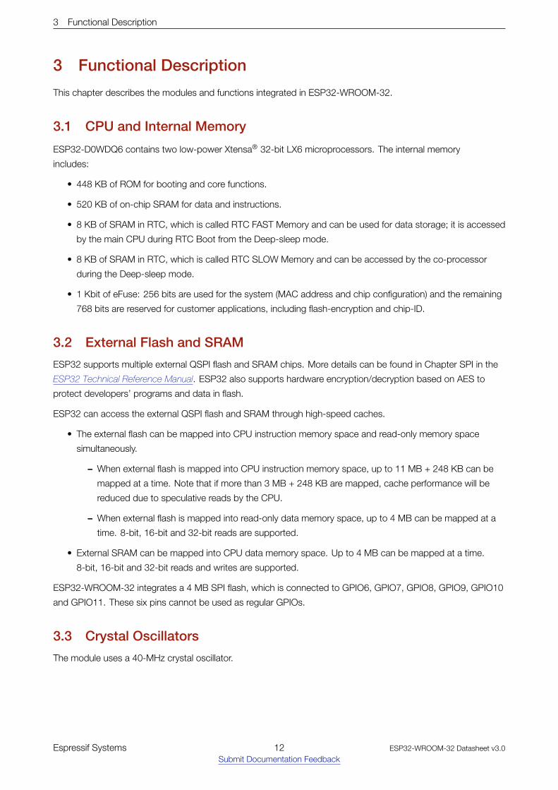
3 Functional Description
3 Functional Description
This chapter describes the modules and functions integrated in ESP32-WROOM-32.
3.1 CPU and Internal Memory
ESP32-D0WDQ6 contains two low-power Xtensa® 32-bit LX6 microprocessors. The internal memory
includes:
• 448 KB of ROM for booting and core functions.
• 520 KB of on-chip SRAM for data and instructions.
• 8 KB of SRAM in RTC, which is called RTC FAST Memory and can be used for data storage; it is accessed
by the main CPU during RTC Boot from the Deep-sleep mode.
• 8 KB of SRAM in RTC, which is called RTC SLOW Memory and can be accessed by the co-processor
during the Deep-sleep mode.
• 1 Kbit of eFuse: 256 bits are used for the system (MAC address and chip configuration) and the remaining
768 bits are reserved for customer applications, including flash-encryption and chip-ID.
3.2 External Flash and SRAM
ESP32 supports multiple external QSPI flash and SRAM chips. More details can be found in Chapter SPI in the
ESP32 Technical Reference Manual. ESP32 also supports hardware encryption/decryption based on AES to
protect developers’ programs and data in flash.
ESP32 can access the external QSPI flash and SRAM through high-speed caches.
• The external flash can be mapped into CPU instruction memory space and read-only memory space
simultaneously.
– When external flash is mapped into CPU instruction memory space, up to 11 MB + 248 KB can be
mapped at a time. Note that if more than 3 MB + 248 KB are mapped, cache performance will be
reduced due to speculative reads by the CPU.
– When external flash is mapped into read-only data memory space, up to 4 MB can be mapped at a
time. 8-bit, 16-bit and 32-bit reads are supported.
• External SRAM can be mapped into CPU data memory space. Up to 4 MB can be mapped at a time.
8-bit, 16-bit and 32-bit reads and writes are supported.
ESP32-WROOM-32 integrates a 4 MB SPI flash, which is connected to GPIO6, GPIO7, GPIO8, GPIO9, GPIO10
and GPIO11. These six pins cannot be used as regular GPIOs.
3.3 Crystal Oscillators
The module uses a 40-MHz crystal oscillator.
Espressif Systems 12Submit Documentation Feedback
ESP32-WROOM-32 Datasheet v3.0

3 Functional Description
3.4 RTC and LowPower Management
With the use of advanced power-management technologies, ESP32 can switch between different power
modes.
For details on ESP32’s power consumption in different power modes, please refer to section ”RTC and
Low-Power Management” in ESP32 Datasheet.
Espressif Systems 13Submit Documentation Feedback
ESP32-WROOM-32 Datasheet v3.0

4 Peripherals and Sensors
4 Peripherals and Sensors
Please refer to Section Peripherals and Sensors in ESP32 Datasheet.
Note:
External connections can be made to any GPIO except for GPIOs in the range 6-11. These six GPIOs are connected to
the module’s integrated SPI flash. For details, please see Section 6 Schematics.
Espressif Systems 14Submit Documentation Feedback
ESP32-WROOM-32 Datasheet v3.0
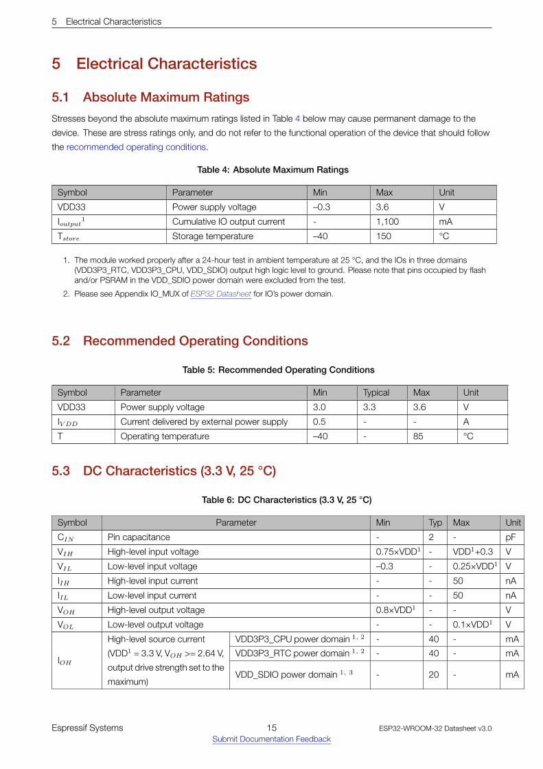
5 Electrical Characteristics
5 Electrical Characteristics
5.1 Absolute Maximum Ratings
Stresses beyond the absolute maximum ratings listed in Table 4 below may cause permanent damage to the
device. These are stress ratings only, and do not refer to the functional operation of the device that should follow
the recommended operating conditions.
Table 4: Absolute Maximum Ratings
Symbol Parameter Min Max Unit
VDD33 Power supply voltage –0.3 3.6 V
Ioutput1 Cumulative IO output current - 1,100 mA
Tstore Storage temperature –40 150 °C
1. The module worked properly after a 24-hour test in ambient temperature at 25 °C, and the IOs in three domains(VDD3P3_RTC, VDD3P3_CPU, VDD_SDIO) output high logic level to ground. Please note that pins occupied by flashand/or PSRAM in the VDD_SDIO power domain were excluded from the test.
2. Please see Appendix IO_MUX of ESP32 Datasheet for IO’s power domain.
5.2 Recommended Operating Conditions
Table 5: Recommended Operating Conditions
Symbol Parameter Min Typical Max Unit
VDD33 Power supply voltage 3.0 3.3 3.6 V
IV DD Current delivered by external power supply 0.5 - - A
T Operating temperature –40 - 85 °C
5.3 DC Characteristics (3.3 V, 25 °C)
Table 6: DC Characteristics (3.3 V, 25 °C)
Symbol Parameter Min Typ Max Unit
CIN Pin capacitance - 2 - pF
VIH High-level input voltage 0.75×VDD1 - VDD1+0.3 V
VIL Low-level input voltage –0.3 - 0.25×VDD1 V
IIH High-level input current - - 50 nA
IIL Low-level input current - - 50 nA
VOH High-level output voltage 0.8×VDD1 - - V
VOL Low-level output voltage - - 0.1×VDD1 V
IOH
High-level source current VDD3P3_CPU power domain 1, 2 - 40 - mA
(VDD1 = 3.3 V, VOH >= 2.64 V, VDD3P3_RTC power domain 1, 2 - 40 - mA
output drive strength set to the
maximum)VDD_SDIO power domain 1, 3 - 20 - mA
Espressif Systems 15Submit Documentation Feedback
ESP32-WROOM-32 Datasheet v3.0

5 Electrical Characteristics
Symbol Parameter Min Typ Max Unit
IOL
Low-level sink current
(VDD1 = 3.3 V, VOL = 0.495 V,
output drive strength set to the maximum)
- 28 - mA
RPU Resistance of internal pull-up resistor - 45 - kΩ
RPD Resistance of internal pull-down resistor - 45 - kΩ
VIL_nRST Low-level input voltage of CHIP_PU to power off the chip - - 0.6 V
Notes:
1. Please see Appendix IO_MUX of ESP32 Datasheet for IO’s power domain. VDD is the I/O voltage for a particular powerdomain of pins.
2. For VDD3P3_CPU and VDD3P3_RTC power domain, per-pin current sourced in the same domain is gradually reducedfrom around 40 mA to around 29 mA, VOH>=2.64 V, as the number of current-source pins increases.
3. Pins occupied by flash and/or PSRAM in the VDD_SDIO power domain were excluded from the test.
5.4 WiFi Radio
Table 7: WiFi Radio Characteristics
Parameter Condition Min Typical Max Unit
Operating frequency range note1 - 2412 - 2484 MHz
Output impedance note2 - - note 2 - Ω
TX power note3 11n, MCS7 12 13 14 dBm
11b mode 17.5 18.5 20 dBm
Sensitivity 11b, 1 Mbps - –98 - dBm
11b, 11 Mbps - –89 - dBm
11g, 6 Mbps - –92 - dBm
11g, 54 Mbps - –74 - dBm
11n, HT20, MCS0 - –91 - dBm
11n, HT20, MCS7 - –71 - dBm
11n, HT40, MCS0 - –89 - dBm
11n, HT40, MCS7 - –69 - dBm
Adjacent channel rejection 11g, 6 Mbps - 31 - dB
11g, 54 Mbps - 14 - dB
11n, HT20, MCS0 - 31 - dB
11n, HT20, MCS7 - 13 - dB
1. Device should operate in the frequency range allocated by regional regulatory authorities. Target operating frequencyrange is configurable by software.
2. For the modules that use IPEX antennas, the output impedance is 50 Ω. For other modules without IPEX antennas,users do not need to concern about the output impedance.
3. Target TX power is configurable based on device or certification requirements.
Espressif Systems 16Submit Documentation Feedback
ESP32-WROOM-32 Datasheet v3.0

5 Electrical Characteristics
5.5 BLE Radio
5.5.1 Receiver
Table 8: Receiver Characteristics – BLE
Parameter Conditions Min Typ Max Unit
Sensitivity @30.8% PER - - –97 - dBm
Maximum received signal @30.8% PER - 0 - - dBm
Co-channel C/I - - +10 - dB
Adjacent channel selectivity C/I
F = F0 + 1 MHz - –5 - dB
F = F0 – 1 MHz - –5 - dB
F = F0 + 2 MHz - –25 - dB
F = F0 – 2 MHz - –35 - dB
F = F0 + 3 MHz - –25 - dB
F = F0 – 3 MHz - –45 - dB
Out-of-band blocking performance
30 MHz ~ 2000 MHz –10 - - dBm
2000 MHz ~ 2400 MHz –27 - - dBm
2500 MHz ~ 3000 MHz –27 - - dBm
3000 MHz ~ 12.5 GHz –10 - - dBm
Intermodulation - –36 - - dBm
5.5.2 Transmitter
Table 9: Transmitter Characteristics – BLE
Parameter Conditions Min Typ Max Unit
RF transmit power - - 0 - dBm
Gain control step - - 3 - dBm
RF power control range - –12 - +9 dBm
Adjacent channel transmit power
F = F0 ± 2 MHz - –52 - dBm
F = F0 ± 3 MHz - –58 - dBm
F = F0 ± > 3 MHz - –60 - dBm
∆ f1avg - - - 265 kHz
∆ f2max - 247 - - kHz
∆ f2avg/∆ f1avg - - –0.92 - -
ICFT - - –10 - kHz
Drift rate - - 0.7 - kHz/50 µs
Drift - - 2 - kHz
Espressif Systems 17Submit Documentation Feedback
ESP32-WROOM-32 Datasheet v3.0

5 Electrical Characteristics
5.6 Reflow Profile
50 150
0
25
1 ~ 3 /s
0
200
250
200
–1 ~ –5 /sCooling zone
100
217
50
100 250
Reflow zone
!217 60 ~ 90 s
Tem
pera
ture
()
Preheating zone150 ~ 200 60 ~ 120 s
Ramp-up zone
Peak Temp. 235 ~ 250
Soldering time> 30 s
Time (sec.)
Ramp-up zone — Temp.: 25 ~ 150 Time: 60 ~ 90 s Ramp-up rate: 1 ~ 3 /sPreheating zone — Temp.: 150 ~ 200 Time: 60 ~ 120 s
Reflow zone — Temp.: >217 7LPH60 ~ 90 s; Peak Temp.: 235 ~ 250 Time: 30 ~ 70 s
Cooling zone — Peak Temp. ~ 180 Ramp-down rate: –1 ~ –5 /sSolder — Sn-Ag-Cu (SAC305) lead-free solder alloy
Figure 2: Reflow Profile
Note:
Solder the module in a single reflow. If the PCBA requires multiple reflows, place the module on the PCB during the final
reflow.
Espressif Systems 18Submit Documentation Feedback
ESP32-WROOM-32 Datasheet v3.0

6S
chematics
6 Schematics
SDI/SD1SDO/SD0SCK/CLKSCS/CMDSWP/SD3SHD/SD2CHIP_PU
GPIO35
SCK/CLK
SCS/CMD
SHD/SD2 SWP/SD3
SDI/SD1
SDO/SD0
GPIO34
GP
IO2
5G
PIO
26
GP
IO2
7G
PIO
14
GP
IO1
2
GP
IO1
5G
PIO
13
GP
IO2
GP
IO0
GPIO5GPIO18
GPIO17
GP
IO4
SENSOR_VP
SENSOR_VN
U0RXDGPIO22
GPIO23
GPIO21
GPIO19
U0TXD
GPIO16GPIO32
SENSOR_VP
SENSOR_VN
GPIO32
GPIO33 GPIO18
U0TXD
U0RXD
GPIO22
GPIO21
GPIO19
GPIO23
CHIP_PU
GPIO34
GPIO35
GPIO25
GPIO26
GPIO27
GPIO14
GPIO12 GPIO0
GPIO4
GPIO16
GPIO5
GPIO17
GPIO13
SHD/SD2
SWP/SD3
SCS/CMD
SCK/CLK
SDO/SD0
SDI/SD1
GPIO15
GPIO2
GP
IO3
3
GND
GNDGND
GND
GND
VDD33
GND
GND
GND
VDD_SDIO
GND
GND
VDD33
GND GND
GND
GNDGND GND
GND
GND
VDD33
GND
GND
VDD33
GNDGND
GND
GND
VDD33
VDD33
VDD_SDIO
Pin.39GND
Pin.1GND
Pin.15GND
Pin.38GND
Pin.23V3
Pin.3CHIP_PU/EN
Pin.4SENSOR_VP
Pin.5SENSOR_VN
Pin.6IO34
Pin.7IO35
Pin.8IO32
Pin.9IO33
Pin.10IO25
Pin.11IO26
Pin.12IO27
Pin.13IO14
Pin.14IO12
Pin.16IO13
Pin.17SD2
Pin.18SD3
Pin.19CMD
Pin.20CLK
Pin.21SD0
Pin.22SD1
Pin.23IO15
Pin.24IO2
Pin.25IO0
Pin.26IO4
Pin.27IO16
Pin.28IO17
Pin.29IO5
Pin.30IO18
Pin.31IO19
Pin.32NC
Pin.33IO21
Pin.34RXD0
Pin.35TXD0
Pin.36IO22
Pin.37IO23
The values of C14, L4 and C15 vary with the actual selection of a PCB board.
The values of C1 and C2 vary with the selection of a crystal.
C13
10uF
U1
40MHz+/-10ppm
XIN
1
GN
D2
XO
UT
3
GN
D4
C4
0.1uF
C15
TBD
C1
22pF
C11
1uF
R1 20K(5%)
C10
0.1uF
C14 TBDU3
FLASH
/CS1
DO2
/WP3
GN
D4
DI5
CLK6
/HOLD7
VC
C8
D1ESD3.3V88D-C
C19
0.1uF
C2
22pF
C20
1uF
ANT1
PCB ANT
12
C5
10nF/6.3V(10%)
C12
10uF
C18
1uF
C3
100pF
C17
270pF
C16
270pF
C9
0.1uF
U2ESP32-D0WDQ6
VDDA1
LNA_IN2
VDD3P33
VDD3P34
SENSOR_VP5
SENSOR_CAPP6
SENSOR_CAPN7
SENSOR_VN8
CHIP_PU9
VDET_110
VDET_211
32K_XP12
32
K_X
N13
GP
IO25
14
GP
IO26
15
GP
IO27
16
MT
MS
17
MT
DI
18
VD
D3P
3_
RT
C19
MT
CK
20
MT
DO
21
GP
IO2
22
GP
IO0
23
GP
IO4
24
VDD_SDIO26
GPIO1625
GPIO1727SD_DATA_228SD_DATA_329SD_CMD30SD_CLK31SD_DATA_032
GN
D49
SD_DATA_133GPIO534GPIO1835
GP
IO19
38
CA
P2
47
VD
DA
43
XT
AL_
N44
XT
AL_
P45
GPIO2336
U0T
XD
41
GP
IO22
39
GP
IO21
42
VD
D3P
3_
CP
U37
CA
P1
48
VD
DA
46
U0R
XD
40
L4
TBD
C6
3.3nF/6.3V(10%)
Figure 3: ESP32WROOM32 Schematics
EspressifS
ystems
19S
ubmitD
ocumentation
FeedbackE
SP
32-WR
OO
M-32
Datasheetv3.0

7 Peripheral Schematics
7 Peripheral Schematics
5
5
4
4
3
3
2
2
1
1
D D
C C
B B
A A
Espressif Systems
MTDI should be kept at a low electric level when powering up the module.
ENTXDRXD
IO0
MTMSMTDIMTCKMTDO
IO23IO22
IO21
IO19IO18IO5
IO4
IO2
SD
2S
D3
CM
DC
LK
SD
0S
D1
SENSOR_VPSENSOR_VNIO34IO35IO32IO33IO25IO26IO27
IO17IO16
VDD33
GND
VDD33
GND
GNDGND
GND
GND
GND
Title
Size Document Number Rev
Date: Sheet o f
<Doc> 1.0
Application of ESP32-WROOM-32
A4
1 1Wednesday, August 07, 2019
Title
Size Document Number Rev
Date: Sheet o f
<Doc> 1.0
Application of ESP32-WROOM-32
A4
1 1Wednesday, August 07, 2019
Title
Size Document Number Rev
Date: Sheet o f
<Doc> 1.0
Application of ESP32-WROOM-32
A4
1 1Wednesday, August 07, 2019
R2 100R
R4 100R
C1 10uF
U2
JTAG
MTMS1
MTDI2
MTCK3
MTDO4
U1
GND11
3V32
EN3
SENSOR_VP4
SENSOR_VN5
IO346
IO357
IO328
IO339
IO2510
IO2611
IO2712
IO1413
IO1214
GND338
IO2337
IO2236
TXD035
RXD034
IO2133
NC32
IO1931
IO1830
IO529
IO1728
IO1627
IO426
IO025
GN
D2
15
IO1
31
6
SD
21
7
SD
31
8
CM
D1
9
CL
K2
0
SD
02
1
SD
12
2
IO1
52
3
IO2
24
P_GND39
R1TBD
C3 TBD
J1
UART DOWNLOAD
123
R3 100R
R5 100R
C2 0.1uF
J2
BOOT OPTION
1 2
Figure 4: ESP32WROOM32 Peripheral Schematics
Note:
• Soldering Pad 39 to the Ground of the base board is not necessary for a satisfactory thermal performance. If users
do want to solder it, they need to ensure that the correct quantity of soldering paste is applied.
• To ensure the power supply to the ESP32 chip during power-up, it is advised to add an RC delay circuit at the EN pin.
The recommended setting for the RC delay circuit is usually R = 10 kΩ and C = 1 µF. However, specific parameters
should be adjusted based on the power-up timing of the module and the power-up and reset sequence timing
of the chip. For ESP32’s power-up and reset sequence timing diagram, please refer to Section Power Scheme in
ESP32 Datasheet.
VCC
GNDGND GND
VDD33
GND
ESP Module
Discharge Circuit CAP Added By User
Q1
R1
100K
D1SW11 2
R2
1K
+ C1
Bulk CAP
Figure 5: Discharge Circuit for VDD33 Rail
Espressif Systems 20Submit Documentation Feedback
ESP32-WROOM-32 Datasheet v3.0

7 Peripheral Schematics
Note:
The discharge circuit can be applied in scenarios where ESP32 is powered on and off repeatedly by switching the
power rails, and there is a large capacitor on the VDD33 rail. For details, please refer to Section Power Scheme in
ESP32 Datasheet.
5
5
4
4
3
3
2
2
1
1
D D
C C
B B
A A
CHIP_PU
VBAT
GND
GND
Title
Size Document Number Rev
Date: Sheet o f
<Doc> V1
<ResetCirciut>
A4
1 1Thursday, May 31, 2018
Title
Size Document Number Rev
Date: Sheet o f
<Doc> V1
<ResetCirciut>
A4
1 1Thursday, May 31, 2018
Title
Size Document Number Rev
Date: Sheet o f
<Doc> V1
<ResetCirciut>
A4
1 1Thursday, May 31, 2018
R1 0R
R2
100K
U1
Power Supply Supervisor
GND1
VCC3
RESET#2
Figure 6: Reset Circuit
Note:
When battery is used as the power supply for ESP32 series of chips and modules, a supply voltage supervisor is recom-
mended to avoid boot failure due to low voltage. Users are recommended to pull CHIP_PU low if the power supply for
ESP32 is below 2.3 V.
Espressif Systems 21Submit Documentation Feedback
ESP32-WROOM-32 Datasheet v3.0

8P
hysicalDim
ensions
8 Physical Dimensions
PCB Thickness
Module Thickness
3.10±0.10
0.80±0.10
1.27±0.10
1.50±0.10
17.60±0.10
Module Width
Module Length
1.27±0.10
11.43±0.10
25.50±0.10
18.00±0.10
Unit: mm
16.51±0.10
11.43±0.10
1.50±0.10
1.27±0.10
25.50±0.10
18.00±0.10
15.80±0.10
ESP32-WROOM-32 DIMENSIONS
Top ViewSide View
Bottom View
Antenna Area
4.00±0.10
4.00±0.10
8.65±0.10
6.30±0.10
0.90±0.10
0.85±0.10
6.00±0.10
0.45±0.10
0.90±0.10
∅1.00±0.10
3.28±0.10 3.28±0.10
Figure 7: Physical Dimensions of ESP32WROOM32
EspressifS
ystems
22S
ubmitD
ocumentation
FeedbackE
SP
32-WR
OO
M-32
Datasheetv3.0

9 Recommended PCB Land Pattern
9 Recommended PCB Land Pattern
Unit: mm
Copper
Via for thermal pad
Antenna Area
18.00
25
.5
0
1.5
0
1.2
7
1.27
2.00
0.9
0
5.00
5.0
0
1.3
3
1.33
10
.5
1
8.00
0.50
0.5
0
1
15 24
38
6.3
0
17.00
Figure 8: Recommended PCB Land Pattern
Espressif Systems 23Submit Documentation Feedback
ESP32-WROOM-32 Datasheet v3.0

10 Learning Resources
10 Learning Resources
10.1 MustRead Documents
The following link provides documents related to ESP32.
• ESP32 Datasheet
This document provides an introduction to the specifications of the ESP32 hardware, including overview,
pin definitions, functional description, peripheral interface, electrical characteristics, etc.
• ESP32 ECO V3 User Guide
This document describes differences between V3 and previous ESP32 silicon wafer revisions.
• ECO and Workarounds for Bugs in ESP32
This document details hardware errata and workarounds in the ESP32.
• ESP-IDF Programming Guide
It hosts extensive documentation for ESP-IDF ranging from hardware guides to API reference.
• ESP32 Technical Reference Manual
The manual provides detailed information on how to use the ESP32 memory and peripherals.
• ESP32 Hardware Resources
The zip files include the schematics, PCB layout, Gerber and BOM list of ESP32 modules and development
boards.
• ESP32 Hardware Design Guidelines
The guidelines outline recommended design practices when developing standalone or add-on systems
based on the ESP32 series of products, including the ESP32 chip, the ESP32 modules and development
boards.
• ESP32 AT Instruction Set and Examples
This document introduces the ESP32 AT commands, explains how to use them, and provides examples of
several common AT commands.
• Espressif Products Ordering Information
10.2 MustHave Resources
Here are the ESP32-related must-have resources.
• ESP32 BBS
This is an Engineer-to-Engineer (E2E) Community for ESP32 where you can post questions, share
knowledge, explore ideas, and help solve problems with fellow engineers.
• ESP32 GitHub
ESP32 development projects are freely distributed under Espressif’s MIT license on GitHub. It is
established to help developers get started with ESP32 and foster innovation and the growth of general
knowledge about the hardware and software surrounding ESP32 devices.
• ESP32 Tools
This is a webpage where users can download ESP32 Flash Download Tools and the zip file ”ESP32
Certification and Test”.
Espressif Systems 24Submit Documentation Feedback
ESP32-WROOM-32 Datasheet v3.0

10 Learning Resources
• ESP-IDF
This webpage links users to the official IoT development framework for ESP32.
• ESP32 Resources
This webpage provides the links to all available ESP32 documents, SDK and tools.
Espressif Systems 25Submit Documentation Feedback
ESP32-WROOM-32 Datasheet v3.0

Revision History
Revision History
Date Version Release notes
2020.11 V3.0
Added TWAITM in Table 1;
Added a note under Figure 2: Reflow Profile;
Updated the C value in RC circuit from 0.1 µF to 1 µF;
Provided feedback link.
2019.09 V2.9
• Changed the supply voltage range from 2.7 V ~ 3.6 V to 3.0 V ~ 3.6 V;
• Added Moisture sensitivity level (MSL) 3 in Table 1 ESP32-WROOM-32 Specifications;
• Added notes about ”Operating frequency range” and ”TX power” under Table 7 Wi-Fi
Radio Characteristics;
• Updated Section 7 Peripheral Schematics and added a note about RC delay circuit
under it;
• Updated Figure 8 Recommended PCB Land Pattern.
2019.01 V2.8 Changed the RF power control range in Table 9 from –12 ~ +12 to –12 ~ +9 dBm.
2018.10 V2.7Added ”Cumulative IO output current” entry to Table 4: Absolute Maximum Ratings;
Added more parameters to Table 6: DC Characteristics.
2018.08 V2.6
• Added reliability test items the module has passed in Table 1: ESP32-WROOM-32
Specifications, and removed software-specific information;
• Updated section 3.4: RTC and Low-Power Management;
• Changed the module’s dimensions from (18±0.2) mm x (25.5 ±0.2) mm x (3.1±0.15)
mm to (18.00±0.10) mm x (25.50±0.10) mm x (3.10±0.10) mm;
• Updated Figure 8: Physical Dimensions;
• Updated Table 7: Wi-Fi Radio.
2018.06 V2.5
• Changed the module name to ESP32-WROOM-32;
• Deleted Temperature Sensor in Table 1: ESP32-WROOM-32 Specifications;
• Updated Chapter 3: Functional Description;
• Added Chapter 8: Recommended PCB Land Pattern;
Changes to electrical characteristics:
• Updated Table 4: Absolute Maximum Ratings;
• Added Table 5: Recommended Operating Conditions;
• Added Table 6: DC Characteristics;
• Updated the values of ”Gain control step”, ”Adjacent channel transmit power” in Table
9: Transmitter Characteristics - BLE.
2018.03 V2.4 Updated Table 1 in Chapter 1.
2018.01 V2.3
Deleted information on LNA pre-amplifier;
Updated section 3.4 RTC and Low-Power Management;
Added reset circuit in Chapter 7 and a note to it.
2017.10 V2.2
Updated the description of the chip’s system reset in Section 2.3 Strapping Pins;
Deleted ”Association sleep pattern” in Table “Power Consumption by Power Modes” and
added notes to Active sleep and Modem-sleep;
Updated the note to Figure 4 Peripheral Schematics;
Added discharge circuit for VDD33 rail in Chapter 7 and a note to it.
2017.09 V2.1Updated operating voltage/power supply range updated to 2.7 ~ 3.6V;
Espressif Systems 26Submit Documentation Feedback
ESP32-WROOM-32 Datasheet v3.0

Revision History
Date Version Release notes
Updated Chapter 7.
2017.08 V2.0
Changed the sensitivity of NZIF receiver to -97 dBm in Table 1;
Updated the dimensions of the module;
Updated Table “Power Consumption by Power Modes” Power Consumption by Power
Modes, and added two notes to it;
Updated Table 4, 7, 8, 9;
Added Chapter 8;
Added the link to certification download.
2017.06 V1.9
Added a note to Section 2.1 Pin Layout;
Updated Section 3.3 Crystal Oscillators;
Updated Figure 3 ESP-WROOM-32 Schematics;
Added Documentation Change Notification.
2017.05 V1.8 Updated Figure 1 Top and Side View of ESP32-WROOM-32 (ESP-WROOM-32).
2017.04 V1.7
Added the module’s dimensional tolerance;
Changed the input impedance value of 50Ω in Table 7 Wi-Fi Radio Characteristics to output
impedance value of 30+j10 Ω.
2017.04 V1.6 Added Figure 2 Reflow Profile.
2017.03 V1.5
Updated Section 2.2 Pin Description;
Updated Section 3.2 External Flash and SRAM;
Updated Section 4 Peripherals and Sensors Description.
2017.03 V1.4
Updated Chapter 1 Preface;
Updated Chapter 2 Pin Definitions;
Updated Chapter 3 Functional Description;
Updated Table Recommended Operating Conditions;
Updated Table 7 Wi-Fi Radio Characteristics;
Updated Section 5.6 Reflow Profile;
Added Chapter 10 Learning Resources.
2016.12 V1.3 Updated Section 2.1 Pin Layout.
2016.11 V1.2 Added Figure 7 Peripheral Schematics.
2016.11 V1.1 Updated Chapter 6 Schematics.
2016.08 V1.0 First release.
Espressif Systems 27Submit Documentation Feedback
ESP32-WROOM-32 Datasheet v3.0

ESP32 SeriesDatasheet
Including:ESP32-D0WD-V3
ESP32-D0WDQ6-V3
ESP32-D0WD
ESP32-D0WDQ6
ESP32-D2WD
ESP32-S0WD
ESP32-U4WDH
Version 3.5
Espressif Systems
Copyright © 2021
www.espressif.com

About This Guide
This document provides the specifications of ESP32 family of chips.
Document Updates
Please always refer to the latest version on https://www.espressif.com/en/support/download/documents.
Revision History
For any changes to this document over time, please refer to the last page.
Documentation Change Notification
Espressif provides email notifications to keep customers updated on changes to technical documentation.
Please subscribe at www.espressif.com/en/subscribe. Note that you need to update your subscription to receive
notifications of new products you are not currently subscribed to.
Certification
Download certificates for Espressif products from www.espressif.com/en/certificates.

Contents
Contents
1 Overview 8
1.1 Featured Solutions 8
1.1.1 Ultra-Low-Power Solution 8
1.1.2 Complete Integration Solution 8
1.2 Wi-Fi Key Features 8
1.3 BT Key Features 9
1.4 MCU and Advanced Features 9
1.4.1 CPU and Memory 9
1.4.2 Clocks and Timers 10
1.4.3 Advanced Peripheral Interfaces 10
1.4.4 Security 10
1.5 Applications (A Non-exhaustive List) 11
1.6 Block Diagram 12
2 Pin Definitions 13
2.1 Pin Layout 13
2.2 Pin Description 15
2.3 Power Scheme 18
2.4 Strapping Pins 19
3 Functional Description 22
3.1 CPU and Memory 22
3.1.1 CPU 22
3.1.2 Internal Memory 22
3.1.3 External Flash and SRAM 23
3.1.4 Memory Map 23
3.2 Timers and Watchdogs 25
3.2.1 64-bit Timers 25
3.2.2 Watchdog Timers 25
3.3 System Clocks 26
3.3.1 CPU Clock 26
3.3.2 RTC Clock 26
3.3.3 Audio PLL Clock 26
3.4 Radio 26
3.4.1 2.4 GHz Receiver 27
3.4.2 2.4 GHz Transmitter 27
3.4.3 Clock Generator 27
3.5 Wi-Fi 27
3.5.1 Wi-Fi Radio and Baseband 27
3.5.2 Wi-Fi MAC 28
3.6 Bluetooth 28
3.6.1 Bluetooth Radio and Baseband 28
Espressif Systems 3Submit Documentation Feedback
ESP32 Series Datasheet v3.5

Contents
3.6.2 Bluetooth Interface 29
3.6.3 Bluetooth Stack 29
3.6.4 Bluetooth Link Controller 29
3.7 RTC and Low-Power Management 30
4 Peripherals and Sensors 32
4.1 Descriptions of Peripherals and Sensors 32
4.1.1 General Purpose Input / Output Interface (GPIO) 32
4.1.2 Analog-to-Digital Converter (ADC) 32
4.1.3 Hall Sensor 33
4.1.4 Digital-to-Analog Converter (DAC) 33
4.1.5 Touch Sensor 33
4.1.6 Ultra-Low-Power Co-processor 33
4.1.7 Ethernet MAC Interface 34
4.1.8 SD/SDIO/MMC Host Controller 34
4.1.9 SDIO/SPI Slave Controller 34
4.1.10 Universal Asynchronous Receiver Transmitter (UART) 35
4.1.11 I²C Interface 35
4.1.12 I²S Interface 35
4.1.13 Infrared Remote Controller 35
4.1.14 Pulse Counter 35
4.1.15 Pulse Width Modulation (PWM) 36
4.1.16 LED PWM 36
4.1.17 Serial Peripheral Interface (SPI) 36
4.1.18 Accelerator 36
4.2 Peripheral Pin Configurations 37
5 Electrical Characteristics 42
5.1 Absolute Maximum Ratings 42
5.2 Recommended Operating Conditions 42
5.3 DC Characteristics (3.3 V, 25 °C) 43
5.4 Reliability Qualifications 43
5.5 RF Power-Consumption Specifications 44
5.6 Wi-Fi Radio 44
5.7 Bluetooth Radio 45
5.7.1 Receiver – Basic Data Rate 45
5.7.2 Transmitter – Basic Data Rate 45
5.7.3 Receiver – Enhanced Data Rate 46
5.7.4 Transmitter – Enhanced Data Rate 46
5.8 Bluetooth LE Radio 47
5.8.1 Receiver 47
5.8.2 Transmitter 47
6 Package Information 48
7 Part Number and Ordering Information 49
Espressif Systems 4Submit Documentation Feedback
ESP32 Series Datasheet v3.5

Contents
8 Learning Resources 50
8.1 Must-Read Documents 50
8.2 Must-Have Resources 50
Appendix A – ESP32 Pin Lists 51
A.1. Notes on ESP32 Pin Lists 51
A.2. GPIO_Matrix 53
A.3. Ethernet_MAC 58
A.4. IO_MUX 58
Revision History 60
Espressif Systems 5Submit Documentation Feedback
ESP32 Series Datasheet v3.5

List of Tables
List of Tables
1 Pin Description 15
2 Description of ESP32 Power-up and Reset Timing Parameters 19
3 Strapping Pins 20
4 Parameter Descriptions of Setup and Hold Times for the Strapping Pin 21
5 Memory and Peripheral Mapping 24
6 Power Consumption by Power Modes 30
7 ADC Characteristics 32
8 ADC Calibration Results 33
9 Capacitive-Sensing GPIOs Available on ESP32 33
10 Peripheral Pin Configurations 37
11 Absolute Maximum Ratings 42
12 Recommended Operating Conditions 42
13 DC Characteristics (3.3 V, 25 °C) 43
14 Reliability Qualifications 43
15 RF Power-Consumption Specifications 44
16 Wi-Fi Radio Characteristics 44
17 Receiver Characteristics – Basic Data Rate 45
18 Transmitter Characteristics – Basic Data Rate 45
19 Receiver Characteristics – Enhanced Data Rate 46
20 Transmitter Characteristics – Enhanced Data Rate 46
21 Receiver Characteristics – BLE 47
22 Transmitter Characteristics – BLE 47
23 ESP32 Ordering Information 49
24 Notes on ESP32 Pin Lists 51
25 GPIO_Matrix 53
26 Ethernet_MAC 58
Espressif Systems 6Submit Documentation Feedback
ESP32 Series Datasheet v3.5

List of Figures
List of Figures
1 Functional Block Diagram 12
2 ESP32 Pin Layout (QFN 6*6, Top View) 13
3 ESP32 Pin Layout (QFN 5*5, Top View) 14
4 ESP32 Power Scheme 18
5 ESP32 Power-up and Reset Timing 19
6 Setup and Hold Times for the Strapping Pin 21
7 Address Mapping Structure 23
8 QFN48 (6x6 mm) Package 48
9 QFN48 (5x5 mm) Package 48
10 ESP32 Part Number 49
Espressif Systems 7Submit Documentation Feedback
ESP32 Series Datasheet v3.5

1 Overview
1 Overview
ESP32 is a single 2.4 GHz Wi-Fi-and-Bluetooth combo chip designed with the TSMC ultra-low-power 40 nm
technology. It is designed to achieve the best power and RF performance, showing robustness, versatility and
reliability in a wide variety of applications and power scenarios.
The ESP32 series of chips includes ESP32-D0WD-V3, ESP32-D0WDQ6-V3, ESP32-D0WD, ESP32-D0WDQ6,
ESP32-D2WD, ESP32-S0WD, and ESP32-U4WDH, among which, ESP32-D0WD-V3, ESP32-D0WDQ6-V3,
and ESP32-U4WDH are based on ECO V3 wafer.
For details on part numbers and ordering information, please refer to Section 7.
For details on ECO V3 instructions, please refer to ESP32 ECO V3 User Guide.
1.1 Featured Solutions
1.1.1 UltraLowPower Solution
ESP32 is designed for mobile, wearable electronics, and Internet-of-Things (IoT) applications. It features all the
state-of-the-art characteristics of low-power chips, including fine-grained clock gating, multiple power modes,
and dynamic power scaling. For instance, in a low-power IoT sensor hub application scenario, ESP32 is woken
up periodically and only when a specified condition is detected. Low-duty cycle is used to minimize the amount
of energy that the chip expends. The output of the power amplifier is also adjustable, thus contributing to an
optimal trade-off between communication range, data rate and power consumption.
Note:
For more information, refer to Section 3.7 RTC and Low-Power Management.
1.1.2 Complete Integration Solution
ESP32 is a highly-integrated solution for Wi-Fi-and-Bluetooth IoT applications, with around 20 external
components. ESP32 integrates an antenna switch, RF balun, power amplifier, low-noise receive amplifier, filters,
and power management modules. As such, the entire solution occupies minimal Printed Circuit Board (PCB)
area.
ESP32 uses CMOS for single-chip fully-integrated radio and baseband, while also integrating advanced
calibration circuitries that allow the solution to remove external circuit imperfections or adjust to changes in
external conditions. As such, the mass production of ESP32 solutions does not require expensive and
specialized Wi-Fi testing equipment.
1.2 WiFi Key Features
• 802.11 b/g/n
• 802.11 n (2.4 GHz), up to 150 Mbps
• WMM
• TX/RX A-MPDU, RX A-MSDU
• Immediate Block ACK
Espressif Systems 8Submit Documentation Feedback
ESP32 Series Datasheet v3.5

1 Overview
• Defragmentation
• Automatic Beacon monitoring (hardware TSF)
• 4 × virtual Wi-Fi interfaces
• Simultaneous support for Infrastructure Station, SoftAP, and Promiscuous modes
Note that when ESP32 is in Station mode, performing a scan, the SoftAP channel will be changed.
• Antenna diversity
Note:
For more information, please refer to Section 3.5 Wi-Fi.
1.3 BT Key Features
• Compliant with Bluetooth v4.2 BR/EDR and BLE specifications
• Class-1, class-2 and class-3 transmitter without external power amplifier
• Enhanced Power Control
• +12 dBm transmitting power
• NZIF receiver with –94 dBm BLE sensitivity
• Adaptive Frequency Hopping (AFH)
• Standard HCI based on SDIO/SPI/UART
• High-speed UART HCI, up to 4 Mbps
• Bluetooth 4.2 BR/EDR BLE dual mode controller
• Synchronous Connection-Oriented/Extended (SCO/eSCO)
• CVSD and SBC for audio codec
• Bluetooth Piconet and Scatternet
• Multi-connections in Classic BT and BLE
• Simultaneous advertising and scanning
1.4 MCU and Advanced Features
1.4.1 CPU and Memory
• Xtensa® single-/dual-core 32-bit LX6 microprocessor(s), up to 600 MIPS (200 MIPS for
ESP32-S0WD/ESP32-U4WDH, 400 MIPS for ESP32-D2WD)
• 448 KB ROM
• 520 KB SRAM
• 16 KB SRAM in RTC
• QSPI supports multiple flash/SRAM chips
Espressif Systems 9Submit Documentation Feedback
ESP32 Series Datasheet v3.5

1 Overview
1.4.2 Clocks and Timers
• Internal 8 MHz oscillator with calibration
• Internal RC oscillator with calibration
• External 2 MHz ~ 60 MHz crystal oscillator (40 MHz only for Wi-Fi/BT functionality)
• External 32 kHz crystal oscillator for RTC with calibration
• Two timer groups, including 2 × 64-bit timers and 1 × main watchdog in each group
• One RTC timer
• RTC watchdog
1.4.3 Advanced Peripheral Interfaces
• 34 × programmable GPIOs
• 12-bit SAR ADC up to 18 channels
• 2 × 8-bit DAC
• 10 × touch sensors
• 4 × SPI
• 2 × I²S
• 2 × I²C
• 3 × UART
• 1 host (SD/eMMC/SDIO)
• 1 slave (SDIO/SPI)
• Ethernet MAC interface with dedicated DMA and IEEE 1588 support
• Two-Wire Automotive Interface (TWAI®, compatible with ISO11898-1)
• IR (TX/RX)
• Motor PWM
• LED PWM up to 16 channels
• Hall sensor
1.4.4 Security
• Secure boot
• Flash encryption
• 1024-bit OTP, up to 768-bit for customers
• Cryptographic hardware acceleration:
– AES
– Hash (SHA-2)
Espressif Systems 10Submit Documentation Feedback
ESP32 Series Datasheet v3.5

1 Overview
– RSA
– ECC
– Random Number Generator (RNG)
1.5 Applications (A Nonexhaustive List)
• Generic Low-power IoT Sensor Hub
• Generic Low-power IoT Data Loggers
• Cameras for Video Streaming
• Over-the-top (OTT) Devices
• Speech Recognition
• Image Recognition
• Mesh Network
• Home Automation
– Light control
– Smart plugs
– Smart door locks
• Smart Building
– Smart lighting
– Energy monitoring
• Industrial Automation
– Industrial wireless control
– Industrial robotics
• Smart Agriculture
– Smart greenhouses
– Smart irrigation
– Agriculture robotics
• Audio Applications
– Internet music players
– Live streaming devices
– Internet radio players
– Audio headsets
• Health Care Applications
– Health monitoring
– Baby monitors
• Wi-Fi-enabled Toys
– Remote control toys
– Proximity sensing toys
– Educational toys
• Wearable Electronics
– Smart watches
– Smart bracelets
• Retail & Catering Applications
– POS machines
– Service robots
Espressif Systems 11Submit Documentation Feedback
ESP32 Series Datasheet v3.5

1 Overview
1.6 Block Diagram
Core and memory
ROM
Cryptographic hardware acceleration
AES
SHA RSA
RTC
ULP coprocessor
Recovery memoryPMU
Bluetooth link
controllerBluetooth baseband
Wi-Fi MAC Wi-Fi baseband
SPI
2 or 1 x Xtensa® 32-bit LX6 Microprocessors
RF receive
RF transmit
Switc
h
Balu
n
I2C
I2S
SDIO
UART
TWAI®
ETH
IR
PWM
Touch sensor
DAC
ADC
Clock generator
RNGSRAM
Embedded Flash
Figure 1: Functional Block Diagram
Note:
Products in the ESP32 series differ from each other in terms of their support for embedded flash and the number of CPUs
they have. For details, please refer to Section 7 Part Number and Ordering Information.
Espressif Systems 12Submit Documentation Feedback
ESP32 Series Datasheet v3.5

2 Pin Definitions
2 Pin Definitions
2.1 Pin Layout
32K_XP 12
VDET_2 11
10
9
8
7
6
5
4
3
2
1
VDET_1
CHIP_PU
SENSOR_VN
SENSOR_CAPN
SENSOR_CAPP
SENSOR_VP
VDD3P3
VDD3P3
LNA_IN
VDDA
25
26
27
28
29
30
31
32
33
34
35
36
GPIO16
VDD_SDIO
GPIO5
VDD3
P3_C
PU37
GPI
O19
3839404142434445464748
GPI
O22
U0RX
D
U0TX
D
GPI
O21
XTAL
_N
XTAL
_P
VDDA
CAP2
CAP1
GPI
O2
24
MTD
O
2322212019181716151413
MTC
K
VDD3
P3_R
TC
MTD
I
MTM
S
GPI
O27
GPI
O26
GPI
O25
32K_
XN
SD_DATA_2
SD_DATA_3
SD_CMD
SD_CLK
SD_DATA_0
SD_DATA_1
GPI
O4
GPI
O0
GPIO23
GPIO18
VDDA
GPIO17
ESP3249 GND
Figure 2: ESP32 Pin Layout (QFN 6*6, Top View)
Espressif Systems 13Submit Documentation Feedback
ESP32 Series Datasheet v3.5

2 Pin Definitions
10
9
8
7
6
5
4
3
2
1
VDET_1
CHIP_PU
SENSOR_VN
SENSOR_CAPN
SENSOR_CAPP
SENSOR_VP
VDD3P3
VDD3P3
LNA_IN
VDDA
25
26
27
28
29
30
31
32
33
34
GPIO16
VDD_SDIO
GPIO5
VDD3P3_CPU
GPIO19
39404142434445464748
GPI
O22
U0RX
D
U0TX
D
GPI
O21
XTAL
_N
XTAL
_P
VDDA
CAP2
CAP1
GPI
O2
24
MTD
O
232221201918171615
MTC
K
VDD3
P3_R
TC
MTD
I
MTM
S
GPI
O27
GPI
O26
GPIO25
32K_XN
SD_DATA_2
SD_DATA_3
SD_CMD
SD_CLK
SD_DATA_0
SD_DATA_1
GPI
O4
GPI
O0
VDDA
GPIO1732K_XP
VDET_2
GPIO18
GPIO23
11
12
13
14
35
36
37
38
ESP3249 GND
Figure 3: ESP32 Pin Layout (QFN 5*5, Top View)
Note:
For details on ESP32’s part numbers and the corresponding packaging, please refer to Section 7 Part Number and Ordering
Information.
Espressif Systems 14Submit Documentation Feedback
ESP32 Series Datasheet v3.5

2P
inD
efinitions
2.2 Pin Description
Table 1: Pin Description
Name No. Type Function
Analog
VDDA 1 P Analog power supply (2.3 V ∼ 3.6 V)
LNA_IN 2 I/O RF input and output
VDD3P3 3 P Analog power supply (2.3 V ∼ 3.6 V)
VDD3P3 4 P Analog power supply (2.3 V ∼ 3.6 V)
VDD3P3_RTC
SENSOR_VP 5 I GPIO36, ADC1_CH0, RTC_GPIO0
SENSOR_CAPP 6 I GPIO37, ADC1_CH1, RTC_GPIO1
SENSOR_CAPN 7 I GPIO38, ADC1_CH2, RTC_GPIO2
SENSOR_VN 8 I GPIO39, ADC1_CH3, RTC_GPIO3
CHIP_PU 9 I
High: On; enables the chip
Low: Off; the chip powers off
Note: Do not leave the CHIP_PU pin floating.
VDET_1 10 I GPIO34, ADC1_CH6, RTC_GPIO4
VDET_2 11 I GPIO35, ADC1_CH7, RTC_GPIO5
32K_XP 12 I/O GPIO32, ADC1_CH4, RTC_GPIO9, TOUCH9, 32K_XP (32.768 kHz crystal oscillator input)
32K_XN 13 I/O GPIO33, ADC1_CH5, RTC_GPIO8, TOUCH8, 32K_XN (32.768 kHz crystal oscillator output)
GPIO25 14 I/O GPIO25, ADC2_CH8, RTC_GPIO6, DAC_1, EMAC_RXD0
GPIO26 15 I/O GPIO26, ADC2_CH9, RTC_GPIO7, DAC_2, EMAC_RXD1
GPIO27 16 I/O GPIO27, ADC2_CH7, RTC_GPIO17, TOUCH7, EMAC_RX_DV
MTMS 17 I/O GPIO14, ADC2_CH6, RTC_GPIO16, TOUCH6, EMAC_TXD2, HSPICLK, HS2_CLK, SD_CLK, MTMS
MTDI 18 I/O GPIO12, ADC2_CH5, RTC_GPIO15, TOUCH5, EMAC_TXD3, HSPIQ, HS2_DATA2, SD_DATA2, MTDI
VDD3P3_RTC 19 P Input power supply for RTC IO (2.3 V ∼ 3.6 V)
MTCK 20 I/O GPIO13, ADC2_CH4, RTC_GPIO14, TOUCH4, EMAC_RX_ER, HSPID, HS2_DATA3, SD_DATA3, MTCK
MTDO 21 I/O GPIO15, ADC2_CH3, RTC_GPIO13, TOUCH3, EMAC_RXD3, HSPICS0, HS2_CMD, SD_CMD, MTDO
EspressifS
ystems
15S
ubmitD
ocumentation
FeedbackE
SP
32S
eriesD
atasheetv3.5

2P
inD
efinitions
Name No. Type Function
GPIO2 22 I/O GPIO2, ADC2_CH2, RTC_GPIO12, TOUCH2, HSPIWP, HS2_DATA0, SD_DATA0
GPIO0 23 I/O GPIO0, ADC2_CH1, RTC_GPIO11, TOUCH1, EMAC_TX_CLK, CLK_OUT1,
GPIO4 24 I/O GPIO4, ADC2_CH0, RTC_GPIO10, TOUCH0, EMAC_TX_ER, HSPIHD, HS2_DATA1, SD_DATA1
VDD_SDIO
GPIO16 25 I/O GPIO16, HS1_DATA4, U2RXD, EMAC_CLK_OUT
VDD_SDIO 26 P Output power supply: 1.8 V or the same voltage as VDD3P3_RTC
GPIO17 27 I/O GPIO17, HS1_DATA5, U2TXD, EMAC_CLK_OUT_180
SD_DATA_2 28 I/O GPIO9, HS1_DATA2, U1RXD, SD_DATA2, SPIHD
SD_DATA_3 29 I/O GPIO10, HS1_DATA3, U1TXD, SD_DATA3, SPIWP
SD_CMD 30 I/O GPIO11, HS1_CMD, U1RTS, SD_CMD, SPICS0
SD_CLK 31 I/O GPIO6, HS1_CLK, U1CTS, SD_CLK, SPICLK
SD_DATA_0 32 I/O GPIO7, HS1_DATA0, U2RTS, SD_DATA0, SPIQ
SD_DATA_1 33 I/O GPIO8, HS1_DATA1, U2CTS, SD_DATA1, SPID
VDD3P3_CPU
GPIO5 34 I/O GPIO5, HS1_DATA6, VSPICS0, EMAC_RX_CLK
GPIO18 35 I/O GPIO18, HS1_DATA7, VSPICLK
GPIO23 36 I/O GPIO23, HS1_STROBE, VSPID
VDD3P3_CPU 37 P Input power supply for CPU IO (1.8 V ∼ 3.6 V)
GPIO19 38 I/O GPIO19, U0CTS, VSPIQ, EMAC_TXD0
GPIO22 39 I/O GPIO22, U0RTS, VSPIWP, EMAC_TXD1
U0RXD 40 I/O GPIO3, U0RXD, CLK_OUT2
U0TXD 41 I/O GPIO1, U0TXD, CLK_OUT3, EMAC_RXD2
GPIO21 42 I/O GPIO21, VSPIHD, EMAC_TX_EN
Analog
VDDA 43 P Analog power supply (2.3 V ∼ 3.6 V)
XTAL_N 44 O External crystal output
XTAL_P 45 I External crystal input
VDDA 46 P Analog power supply (2.3 V ∼ 3.6 V)
CAP2 47 I Connects to a 3.3 nF (10%) capacitor and 20 kΩ resistor in parallel to CAP1
EspressifS
ystems
16S
ubmitD
ocumentation
FeedbackE
SP
32S
eriesD
atasheetv3.5

2P
inD
efinitions
Name No. Type Function
CAP1 48 I Connects to a 10 nF series capacitor to ground
GND 49 P Ground
Note:
• The pin-pin mapping between ESP32-D2WD/ESP32-U4WDH and the embedded flash is as follows: GPIO16 = CS#, GPIO17 = IO1/DO, SD_CMD = IO3/HOLD#, SD_CLK =
CLK, SD_DATA_0 = IO2/WP#, SD_DATA_1 = IO0/DI. The pins used for embedded flash are not recommended for other uses.
• In most cases, the data port connection between ESP32 series of chips other than ESP32-D2WD/ESP32-U4WDH and external flash is as follows: SD_DATA0/SPIQ = IO1/DO,
SD_DATA1/SPID = IO0/DI, SD_DATA2/SPIHD = IO3/HOLD#, SD_DATA3/SPIWP = IO2/WP#.
• For a quick reference guide to using the IO_MUX, Ethernet MAC, and GIPO Matrix pins of ESP32, please refer to Appendix ESP32 Pin Lists.
EspressifS
ystems
17S
ubmitD
ocumentation
FeedbackE
SP
32S
eriesD
atasheetv3.5

2 Pin Definitions
2.3 Power Scheme
ESP32’s digital pins are divided into three different power domains:
• VDD3P3_RTC
• VDD3P3_CPU
• VDD_SDIO
VDD3P3_RTC is also the input power supply for RTC and CPU.
VDD3P3_CPU is also the input power supply for CPU.
VDD_SDIO connects to the output of an internal LDO whose input is VDD3P3_RTC. When VDD_SDIO is
connected to the same PCB net together with VDD3P3_RTC, the internal LDO is disabled automatically. The
power scheme diagram is shown below:
SDIO
Domain
RTC
Domain
CPU
Domain
LDOLDO LDO1.8 V 1.1 V1.1 V
VDD3P3_RTC VDD3P3_CPU
VDD_SDIO
3.3 V/1.8 V
Figure 4: ESP32 Power Scheme
The internal LDO can be configured as having 1.8 V, or the same voltage as VDD3P3_RTC. It can be powered off
via software to minimize the current of flash/SRAM during the Deep-sleep mode.
Notes on CHIP_PU:
• The illustration below shows the ESP32 power-up and reset timing. Details about the parameters are listed
in Table 2.
Espressif Systems 18Submit Documentation Feedback
ESP32 Series Datasheet v3.5

2 Pin Definitions
VDD
CHIP_PU
t0 t1
VIL_nRST
VDD3P3_RTC Min
Figure 5: ESP32 Powerup and Reset Timing
Table 2: Description of ESP32 Powerup and Reset Timing Parameters
Parameters Description Min. Unit
t0Time between the 3.3 V rails being brought up and CHIP_PU being
activated50 µs
t1Duration of CHIP_PU signal level < VIL_nRST (refer to its value in
Table 13 DC Characteristics) to reset the chip50 µs
• In scenarios where ESP32 is powered on and off repeatedly by switching the power rails, while there is a
large capacitor on the VDD33 rail and CHIP_PU and VDD33 are connected, simply switching off the
CHIP_PU power rail and immediately switching it back on may cause an incomplete power discharge cycle
and failure to reset the chip adequately.
An additional discharge circuit may be required to accelerate the discharge of the large capacitor on rail
VDD33, which will ensure proper power-on-reset when the ESP32 is powered up again. Please find the
discharge circuit in Figure ESP32WROOM32 Peripheral Schematics, in ESP32-WROOM-32 Datasheet.
• When a battery is used as the power supply for the ESP32 series of chips and modules, a supply voltage
supervisor is recommended, so that a boot failure due to low voltage is avoided. Users are recommended
to pull CHIP_PU low if the power supply for ESP32 is below 2.3 V. For the reset circuit, please refer to
Figure ESP32WROOM32 Peripheral Schematics, in ESP32-WROOM-32 Datasheet.
Notes on power supply:
• The operating voltage of ESP32 ranges from 2.3 V to 3.6 V. When using a single-power supply, the
recommended voltage of the power supply is 3.3 V, and its recommended output current is 500 mA or
more.
• When VDD_SDIO 1.8 V is used as the power supply for external flash/PSRAM, a 2-kohm grounding
resistor should be added to VDD_SDIO. For the circuit design, please refer to Figure ESP32WROVER
Schematics, in ESP32-WROVER Datasheet.
• When the three digital power supplies are used to drive peripherals, e.g., 3.3 V flash, they should comply
with the peripherals’ specifications.
2.4 Strapping Pins
There are five strapping pins:
• MTDI
Espressif Systems 19Submit Documentation Feedback
ESP32 Series Datasheet v3.5

2 Pin Definitions
• GPIO0
• GPIO2
• MTDO
• GPIO5
Software can read the values of these five bits from register ”GPIO_STRAPPING”.
During the chip’s system reset release (power-on-reset, RTC watchdog reset and brownout reset), the latches of
the strapping pins sample the voltage level as strapping bits of ”0” or ”1”, and hold these bits until the chip is
powered down or shut down. The strapping bits configure the device’s boot mode, the operating voltage of
VDD_SDIO and other initial system settings.
Each strapping pin is connected to its internal pull-up/pull-down during the chip reset. Consequently, if a
strapping pin is unconnected or the connected external circuit is high-impedance, the internal weak
pull-up/pull-down will determine the default input level of the strapping pins.
To change the strapping bit values, users can apply the external pull-down/pull-up resistances, or use the host
MCU’s GPIOs to control the voltage level of these pins when powering on the chip.
After reset release, the strapping pins work as normal-function pins.
Refer to Table 3 for a detailed boot-mode configuration by strapping pins.
Table 3: Strapping Pins
Voltage of Internal LDO (VDD_SDIO)
Pin Default 3.3 V 1.8 V
MTDI Pull-down 0 1
Booting Mode
Pin Default SPI Boot Download Boot
GPIO0 Pull-up 1 0
GPIO2 Pull-down Don’t-care 0
Enabling/Disabling Debugging Log Print over U0TXD During Booting
Pin Default U0TXD Active U0TXD Silent
MTDO Pull-up 1 0
Timing of SDIO Slave
Pin Default
FE Sampling
FE Output
FE Sampling
RE Output
RE Sampling
FE Output
RE Sampling
RE Output
MTDO Pull-up 0 0 1 1
GPIO5 Pull-up 0 1 0 1
Note:
• FE: falling-edge, RE: rising-edge.
• Firmware can configure register bits to change the settings of “Voltage of Internal LDO (VDD_SDIO)” and “Timing
of SDIO Slave”, after booting.
• For ESP32 chips that contain an embedded flash, users need to note the logic level of MTDI. For example, ESP32-
D2WD contains an embedded flash that operates at 1.8 V, therefore, the MTDI should be pulled high. ESP32-
U4WDH contains an embedded flash that operates at 3.3 V, therefore, the MTDI should be low.
Espressif Systems 20Submit Documentation Feedback
ESP32 Series Datasheet v3.5

2 Pin Definitions
The illustration below shows the setup and hold times for the strapping pin before and after the CHIP_PU signal
goes high. Details about the parameters are listed in Table 4.
CHIP_PU
t1t0
Strapping pin
VIL_nRST
VIH
Figure 6: Setup and Hold Times for the Strapping Pin
Table 4: Parameter Descriptions of Setup and Hold Times for the Strapping Pin
Parameters Description Min. Unit
t0 Setup time before CHIP_PU goes from low to high 0 ms
t1 Hold time after CHIP_PU goes high 1 ms
Espressif Systems 21Submit Documentation Feedback
ESP32 Series Datasheet v3.5

3 Functional Description
3 Functional Description
This chapter describes the functions integrated in ESP32.
3.1 CPU and Memory
3.1.1 CPU
ESP32 contains one or two low-power Xtensa® 32-bit LX6 microprocessor(s) with the following features:
• 7-stage pipeline to support the clock frequency of up to 240 MHz (160 MHz for ESP32-S0WD,
ESP32-D2WD, and ESP32-U4WDH)
• 16/24-bit Instruction Set provides high code-density
• Support for Floating Point Unit
• Support for DSP instructions, such as a 32-bit multiplier, a 32-bit divider, and a 40-bit MAC
• Support for 32 interrupt vectors from about 70 interrupt sources
The single-/dual-CPU interfaces include:
• Xtensa RAM/ROM Interface for instructions and data
• Xtensa Local Memory Interface for fast peripheral register access
• External and internal interrupt sources
• JTAG for debugging
3.1.2 Internal Memory
ESP32’s internal memory includes:
• 448 KB of ROM for booting and core functions
• 520 KB of on-chip SRAM for data and instructions
• 8 KB of SRAM in RTC, which is called RTC FAST Memory and can be used for data storage; it is accessed
by the main CPU during RTC Boot from the Deep-sleep mode.
• 8 KB of SRAM in RTC, which is called RTC SLOW Memory and can be accessed by the co-processor
during the Deep-sleep mode.
• 1 Kbit of eFuse: 256 bits are used for the system (MAC address and chip configuration) and the remaining
768 bits are reserved for customer applications, including flash-encryption and chip-ID.
• Embedded flash
Note:
Products in the ESP32 series differ from each other, in terms of their support for embedded flash and the size of it. For
details, please refer to Section 7 Part Number and Ordering Information.
Espressif Systems 22Submit Documentation Feedback
ESP32 Series Datasheet v3.5

3 Functional Description
3.1.3 External Flash and SRAM
ESP32 supports multiple external QSPI flash and SRAM chips. More details can be found in Chapter SPI in the
ESP32 Technical Reference Manual. ESP32 also supports hardware encryption/decryption based on AES to
protect developers’ programs and data in flash.
ESP32 can access the external QSPI flash and SRAM through high-speed caches.
• Up to 16 MB of external flash can be mapped into CPU instruction memory space and read-only memory
space simultaneously.
– When external flash is mapped into CPU instruction memory space, up to 11 MB + 248 KB can be
mapped at a time. Note that if more than 3 MB + 248 KB are mapped, cache performance will be
reduced due to speculative reads by the CPU.
– When external flash is mapped into read-only data memory space, up to 4 MB can be mapped at a
time. 8-bit, 16-bit and 32-bit reads are supported.
• External SRAM can be mapped into CPU data memory space. SRAM up to 8 MB is supported and up to 4
MB can be mapped at a time. 8-bit, 16-bit and 32-bit reads and writes are supported.
Note:
After ESP32 is initialized, firmware can customize the mapping of external SRAM or flash into the CPU address space.
3.1.4 Memory Map
The structure of address mapping is shown in Figure 7. The memory and peripheral mapping of ESP32 is shown
in Table 5.
Figure 7: Address Mapping Structure
Espressif Systems 23Submit Documentation Feedback
ESP32 Series Datasheet v3.5

3 Functional Description
Table 5: Memory and Peripheral Mapping
Category Target Start Address End Address Size
Embedded
Memory
Internal ROM 0 0x4000_0000 0x4005_FFFF 384 KB
Internal ROM 1 0x3FF9_0000 0x3FF9_FFFF 64 KB
Internal SRAM 0 0x4007_0000 0x4009_FFFF 192 KB
Internal SRAM 10x3FFE_0000 0x3FFF_FFFF
128 KB0x400A_0000 0x400B_FFFF
Internal SRAM 2 0x3FFA_E000 0x3FFD_FFFF 200 KB
RTC FAST Memory0x3FF8_0000 0x3FF8_1FFF
8 KB0x400C_0000 0x400C_1FFF
RTC SLOW Memory 0x5000_0000 0x5000_1FFF 8 KB
External
Memory
External Flash0x3F40_0000 0x3F7F_FFFF 4 MB
0x400C_2000 0x40BF_FFFF 11 MB+248 KB
External RAM 0x3F80_0000 0x3FBF_FFFF 4 MB
Peripheral
DPort Register 0x3FF0_0000 0x3FF0_0FFF 4 KB
AES Accelerator 0x3FF0_1000 0x3FF0_1FFF 4 KB
RSA Accelerator 0x3FF0_2000 0x3FF0_2FFF 4 KB
SHA Accelerator 0x3FF0_3000 0x3FF0_3FFF 4 KB
Secure Boot 0x3FF0_4000 0x3FF0_4FFF 4 KB
Cache MMU Table 0x3FF1_0000 0x3FF1_3FFF 16 KB
PID Controller 0x3FF1_F000 0x3FF1_FFFF 4 KB
UART0 0x3FF4_0000 0x3FF4_0FFF 4 KB
SPI1 0x3FF4_2000 0x3FF4_2FFF 4 KB
SPI0 0x3FF4_3000 0x3FF4_3FFF 4 KB
GPIO 0x3FF4_4000 0x3FF4_4FFF 4 KB
RTC 0x3FF4_8000 0x3FF4_8FFF 4 KB
IO MUX 0x3FF4_9000 0x3FF4_9FFF 4 KB
SDIO Slave 0x3FF4_B000 0x3FF4_BFFF 4 KB
UDMA1 0x3FF4_C000 0x3FF4_CFFF 4 KB
I2S0 0x3FF4_F000 0x3FF4_FFFF 4 KB
UART1 0x3FF5_0000 0x3FF5_0FFF 4 KB
I2C0 0x3FF5_3000 0x3FF5_3FFF 4 KB
UDMA0 0x3FF5_4000 0x3FF5_4FFF 4 KB
SDIO Slave 0x3FF5_5000 0x3FF5_5FFF 4 KB
RMT 0x3FF5_6000 0x3FF5_6FFF 4 KB
PCNT 0x3FF5_7000 0x3FF5_7FFF 4 KB
SDIO Slave 0x3FF5_8000 0x3FF5_8FFF 4 KB
LED PWM 0x3FF5_9000 0x3FF5_9FFF 4 KB
eFuse Controller 0x3FF5_A000 0x3FF5_AFFF 4 KB
Flash Encryption 0x3FF5_B000 0x3FF5_BFFF 4 KB
PWM0 0x3FF5_E000 0x3FF5_EFFF 4 KB
TIMG0 0x3FF5_F000 0x3FF5_FFFF 4 KB
TIMG1 0x3FF6_0000 0x3FF6_0FFF 4 KB
SPI2 0x3FF6_4000 0x3FF6_4FFF 4 KB
SPI3 0x3FF6_5000 0x3FF6_5FFF 4 KB
Espressif Systems 24Submit Documentation Feedback
ESP32 Series Datasheet v3.5
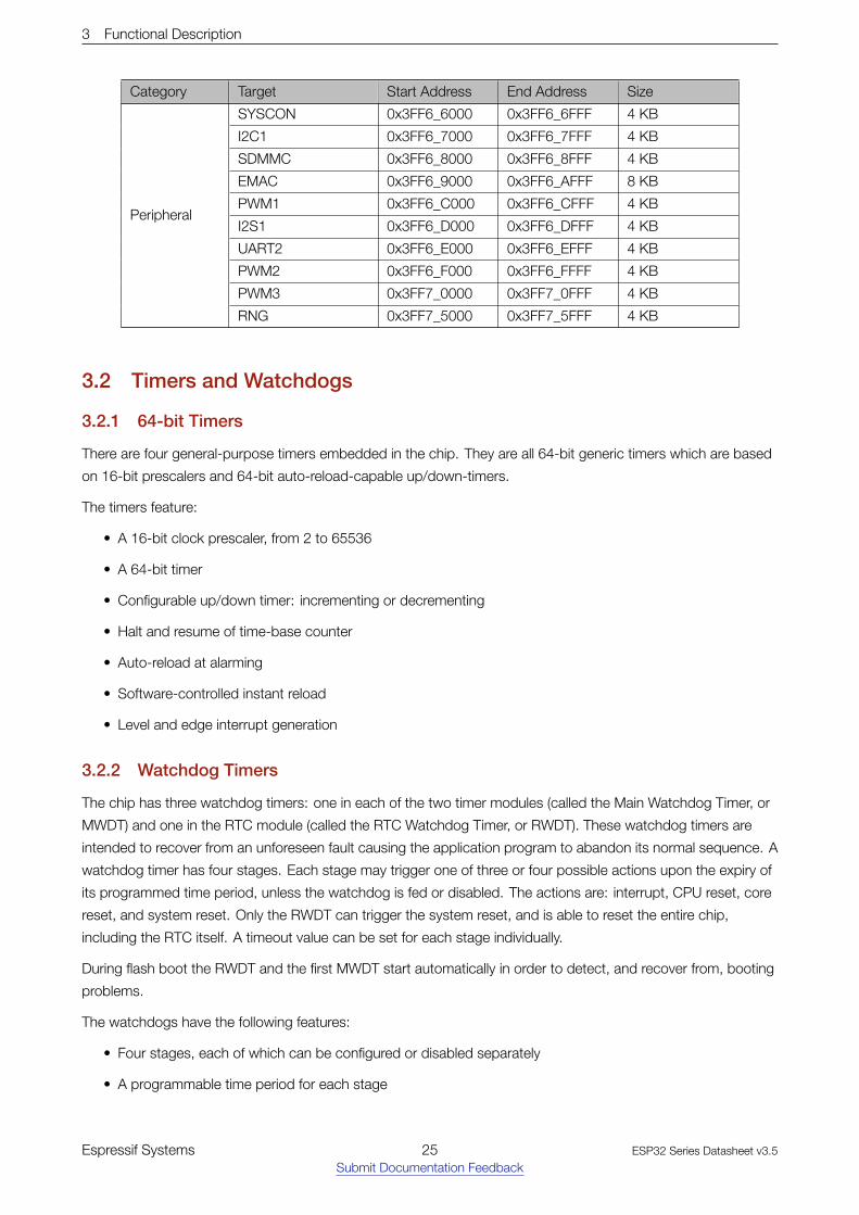
3 Functional Description
Category Target Start Address End Address Size
Peripheral
SYSCON 0x3FF6_6000 0x3FF6_6FFF 4 KB
I2C1 0x3FF6_7000 0x3FF6_7FFF 4 KB
SDMMC 0x3FF6_8000 0x3FF6_8FFF 4 KB
EMAC 0x3FF6_9000 0x3FF6_AFFF 8 KB
PWM1 0x3FF6_C000 0x3FF6_CFFF 4 KB
I2S1 0x3FF6_D000 0x3FF6_DFFF 4 KB
UART2 0x3FF6_E000 0x3FF6_EFFF 4 KB
PWM2 0x3FF6_F000 0x3FF6_FFFF 4 KB
PWM3 0x3FF7_0000 0x3FF7_0FFF 4 KB
RNG 0x3FF7_5000 0x3FF7_5FFF 4 KB
3.2 Timers and Watchdogs
3.2.1 64bit Timers
There are four general-purpose timers embedded in the chip. They are all 64-bit generic timers which are based
on 16-bit prescalers and 64-bit auto-reload-capable up/down-timers.
The timers feature:
• A 16-bit clock prescaler, from 2 to 65536
• A 64-bit timer
• Configurable up/down timer: incrementing or decrementing
• Halt and resume of time-base counter
• Auto-reload at alarming
• Software-controlled instant reload
• Level and edge interrupt generation
3.2.2 Watchdog Timers
The chip has three watchdog timers: one in each of the two timer modules (called the Main Watchdog Timer, or
MWDT) and one in the RTC module (called the RTC Watchdog Timer, or RWDT). These watchdog timers are
intended to recover from an unforeseen fault causing the application program to abandon its normal sequence. A
watchdog timer has four stages. Each stage may trigger one of three or four possible actions upon the expiry of
its programmed time period, unless the watchdog is fed or disabled. The actions are: interrupt, CPU reset, core
reset, and system reset. Only the RWDT can trigger the system reset, and is able to reset the entire chip,
including the RTC itself. A timeout value can be set for each stage individually.
During flash boot the RWDT and the first MWDT start automatically in order to detect, and recover from, booting
problems.
The watchdogs have the following features:
• Four stages, each of which can be configured or disabled separately
• A programmable time period for each stage
Espressif Systems 25Submit Documentation Feedback
ESP32 Series Datasheet v3.5

3 Functional Description
• One of three or four possible actions (interrupt, CPU reset, core reset, and system reset) upon the expiry of
each stage
• 32-bit expiry counter
• Write protection that prevents the RWDT and MWDT configuration from being inadvertently altered
• SPI flash boot protection
If the boot process from an SPI flash does not complete within a predetermined time period, the watchdog
will reboot the entire system.
3.3 System Clocks
3.3.1 CPU Clock
Upon reset, an external crystal clock source is selected as the default CPU clock. The external crystal clock
source also connects to a PLL to generate a high-frequency clock (typically 160 MHz).
In addition, ESP32 has an internal 8 MHz oscillator. The application can select the clock source from the external
crystal clock source, the PLL clock or the internal 8 MHz oscillator. The selected clock source drives the CPU
clock directly, or after division, depending on the application.
3.3.2 RTC Clock
The RTC clock has five possible sources:
• external low-speed (32 kHz) crystal clock
• external crystal clock divided by 4
• internal RC oscillator (typically about 150 kHz, and adjustable)
• internal 8 MHz oscillator
• internal 31.25 kHz clock (derived from the internal 8 MHz oscillator divided by 256)
When the chip is in the normal power mode and needs faster CPU accessing, the application can choose the
external high-speed crystal clock divided by 4 or the internal 8 MHz oscillator. When the chip operates in the
low-power mode, the application chooses the external low-speed (32 kHz) crystal clock, the internal RC clock or
the internal 31.25 kHz clock.
3.3.3 Audio PLL Clock
The audio clock is generated by the ultra-low-noise fractional-N PLL. More details can be found in Chapter Reset
and Clock in the ESP32 Technical Reference Manual.
3.4 Radio
The radio module consists of the following blocks:
• 2.4 GHz receiver
• 2.4 GHz transmitter
• bias and regulators
Espressif Systems 26Submit Documentation Feedback
ESP32 Series Datasheet v3.5

3 Functional Description
• balun and transmit-receive switch
• clock generator
3.4.1 2.4 GHz Receiver
The 2.4 GHz receiver demodulates the 2.4 GHz RF signal to quadrature baseband signals and converts them to
the digital domain with two high-resolution, high-speed ADCs. To adapt to varying signal channel conditions, RF
filters, Automatic Gain Control (AGC), DC offset cancelation circuits and baseband filters are integrated in the
chip.
3.4.2 2.4 GHz Transmitter
The 2.4 GHz transmitter modulates the quadrature baseband signals to the 2.4 GHz RF signal, and drives the
antenna with a high-powered Complementary Metal Oxide Semiconductor (CMOS) power amplifier. The use of
digital calibration further improves the linearity of the power amplifier, enabling state-of-the-art performance in
delivering up to +20.5 dBm of power for an 802.11b transmission and +18 dBm for an 802.11n
transmission.
Additional calibrations are integrated to cancel any radio imperfections, such as:
• Carrier leakage
• I/Q phase matching
• Baseband nonlinearities
• RF nonlinearities
• Antenna matching
These built-in calibration routines reduce the amount of time required for product testing, and render the testing
equipment unnecessary.
3.4.3 Clock Generator
The clock generator produces quadrature clock signals of 2.4 GHz for both the receiver and the transmitter. All
components of the clock generator are integrated into the chip, including all inductors, varactors, filters,
regulators and dividers.
The clock generator has built-in calibration and self-test circuits. Quadrature clock phases and phase noise are
optimized on-chip with patented calibration algorithms which ensure the best performance of the receiver and
the transmitter.
3.5 WiFi
ESP32 implements a TCP/IP and full 802.11 b/g/n Wi-Fi MAC protocol. It supports the Basic Service Set (BSS)
STA and SoftAP operations under the Distributed Control Function (DCF). Power management is handled with
minimal host interaction to minimize the active-duty period.
3.5.1 WiFi Radio and Baseband
The ESP32 Wi-Fi Radio and Baseband support the following features:
Espressif Systems 27Submit Documentation Feedback
ESP32 Series Datasheet v3.5

3 Functional Description
• 802.11b/g/n
• 802.11n MCS0-7 in both 20 MHz and 40 MHz bandwidth
• 802.11n MCS32 (RX)
• 802.11n 0.4 µs guard-interval
• up to 150 Mbps of data rate
• Receiving STBC 2×1
• Up to 20.5 dBm of transmitting power
• Adjustable transmitting power
• Antenna diversity
ESP32 supports antenna diversity with an external RF switch. One or more GPIOs control the RF switch
and selects the best antenna to minimize the effects of channel fading.
3.5.2 WiFi MAC
The ESP32 Wi-Fi MAC applies low-level protocol functions automatically. They are as follows:
• 4 × virtual Wi-Fi interfaces
• Simultaneous Infrastructure BSS Station mode/SoftAP mode/Promiscuous mode
• RTS protection, CTS protection, Immediate Block ACK
• Defragmentation
• TX/RX A-MPDU, RX A-MSDU
• TXOP
• WMM
• CCMP (CBC-MAC, counter mode), TKIP (MIC, RC4), WAPI (SMS4), WEP (RC4) and CRC
• Automatic beacon monitoring (hardware TSF)
3.6 Bluetooth
The chip integrates a Bluetooth link controller and Bluetooth baseband, which carry out the baseband protocols
and other low-level link routines, such as modulation/demodulation, packet processing, bit stream processing,
frequency hopping, etc.
3.6.1 Bluetooth Radio and Baseband
The Bluetooth Radio and Baseband support the following features:
• Class-1, class-2 and class-3 transmit output powers, and a dynamic control range of up to 24 dB
• π/4 DQPSK and 8 DPSK modulation
• High performance in NZIF receiver sensitivity with over 94 dBm of dynamic range
• Class-1 operation without external PA
• Internal SRAM allows full-speed data-transfer, mixed voice and data, and full piconet operation
Espressif Systems 28Submit Documentation Feedback
ESP32 Series Datasheet v3.5

3 Functional Description
• Logic for forward error correction, header error control, access code correlation, CRC, demodulation,
encryption bit stream generation, whitening and transmit pulse shaping
• ACL, SCO, eSCO and AFH
• A-law, µ-law and CVSD digital audio CODEC in PCM interface
• SBC audio CODEC
• Power management for low-power applications
• SMP with 128-bit AES
3.6.2 Bluetooth Interface
• Provides UART HCI interface, up to 4 Mbps
• Provides SDIO / SPI HCI interface
• Provides PCM / I²S audio interface
3.6.3 Bluetooth Stack
The Bluetooth stack of the chip is compliant with the Bluetooth v4.2 BR/EDR and Bluetooth LE
specifications.
3.6.4 Bluetooth Link Controller
The link controller operates in three major states: standby, connection and sniff. It enables multiple connections,
and other operations, such as inquiry, page, and secure simple-pairing, and therefore enables Piconet and
Scatternet. Below are the features:
• Classic Bluetooth
– Device Discovery (inquiry, and inquiry scan)
– Connection establishment (page, and page scan)
– Multi-connections
– Asynchronous data reception and transmission
– Synchronous links (SCO/eSCO)
– Master/Slave Switch
– Adaptive Frequency Hopping and Channel assessment
– Broadcast encryption
– Authentication and encryption
– Secure Simple-Pairing
– Multi-point and scatternet management
– Sniff mode
– Connectionless Slave Broadcast (transmitter and receiver)
– Enhanced power control
Espressif Systems 29Submit Documentation Feedback
ESP32 Series Datasheet v3.5

3 Functional Description
– Ping
• Bluetooth Low Energy
– Advertising
– Scanning
– Simultaneous advertising and scanning
– Multiple connections
– Asynchronous data reception and transmission
– Adaptive Frequency Hopping and Channel assessment
– Connection parameter update
– Data Length Extension
– Link Layer Encryption
– LE Ping
3.7 RTC and LowPower Management
With the use of advanced power-management technologies, ESP32 can switch between different power
modes.
• Power modes
– Active mode: The chip radio is powered on. The chip can receive, transmit, or listen.
– Modemsleep mode: The CPU is operational and the clock is configurable. The Wi-Fi/Bluetooth
baseband and radio are disabled.
– Lightsleep mode: The CPU is paused. The RTC memory and RTC peripherals, as well as the ULP
co-processor are running. Any wake-up events (MAC, host, RTC timer, or external interrupts) will wake
up the chip.
– Deepsleep mode: Only the RTC memory and RTC peripherals are powered on. Wi-Fi and Bluetooth
connection data are stored in the RTC memory. The ULP co-processor is functional.
– Hibernation mode: The internal 8-MHz oscillator and ULP co-processor are disabled. The RTC
recovery memory is powered down. Only one RTC timer on the slow clock and certain RTC GPIOs are
active. The RTC timer or the RTC GPIOs can wake up the chip from the Hibernation mode.
Table 6: Power Consumption by Power Modes
Power mode Description Power consumption
Active (RF working)
Wi-Fi Tx packetPlease refer to
Table 15 for details.Wi-Fi/BT Tx packet
Wi-Fi/BT Rx and listening
Modem-sleepThe CPU is
powered on.
240 MHz* Dual-core chip(s) 30 mA ~ 68 mA
Single-core chip(s) N/A
160 MHz* Dual-core chip(s) 27 mA ~ 44 mA
Single-core chip(s) 27 mA ~ 34 mA
Espressif Systems 30Submit Documentation Feedback
ESP32 Series Datasheet v3.5

3 Functional Description
Power mode Description Power consumption
Normal speed: 80 MHzDual-core chip(s) 20 mA ~ 31 mA
Single-core chip(s) 20 mA ~ 25 mA
Light-sleep - 0.8 mA
Deep-sleep
The ULP co-processor is powered on. 150 µA
ULP sensor-monitored pattern 100 µA @1% duty
RTC timer + RTC memory 10 µA
Hibernation RTC timer only 5 µA
Power off CHIP_PU is set to low level, the chip is powered off. 1 µA
Note:
• * Among the ESP32 series of SoCs, ESP32-D0WD-V3, ESP32-D0WDQ6-V3, ESP32-D0WD, and ESP32-D0WDQ6
have a maximum CPU frequency of 240 MHz, ESP32-D2WD, ESP32-S0WD, and ESP32-U4WDH have a maximum
CPU frequency of 160 MHz.
• When Wi-Fi is enabled, the chip switches between Active and Modem-sleep modes. Therefore, power consumption
changes accordingly.
• In Modem-sleep mode, the CPU frequency changes automatically. The frequency depends on the CPU load and
the peripherals used.
• During Deep-sleep, when the ULP co-processor is powered on, peripherals such as GPIO and I²C are able to
operate.
• When the system works in the ULP sensor-monitored pattern, the ULP co-processor works with the ULP sensor
periodically and the ADC works with a duty cycle of 1%, so the power consumption is 100 µA.
Espressif Systems 31Submit Documentation Feedback
ESP32 Series Datasheet v3.5

4 Peripherals and Sensors
4 Peripherals and Sensors
4.1 Descriptions of Peripherals and Sensors
4.1.1 General Purpose Input / Output Interface (GPIO)
ESP32 has 34 GPIO pins which can be assigned various functions by programming the appropriate registers.
There are several kinds of GPIOs: digital-only, analog-enabled, capacitive-touch-enabled, etc. Analog-enabled
GPIOs and Capacitive-touch-enabled GPIOs can be configured as digital GPIOs.
Most of the digital GPIOs can be configured as internal pull-up or pull-down, or set to high impedance. When
configured as an input, the input value can be read through the register. The input can also be set to edge-trigger
or level-trigger to generate CPU interrupts. Most of the digital IO pins are bi-directional, non-inverting and tristate,
including input and output buffers with tristate control. These pins can be multiplexed with other functions, such
as the SDIO, UART, SPI, etc. (More details can be found in the Appendix, Table IO_MUX.) For low-power
operations, the GPIOs can be set to hold their states.
4.1.2 AnalogtoDigital Converter (ADC)
ESP32 integrates 12-bit SAR ADCs and supports measurements on 18 channels (analog-enabled pins). The
ULP-coprocessor in ESP32 is also designed to measure voltage, while operating in the sleep mode, which
enables low-power consumption. The CPU can be woken up by a threshold setting and/or via other
triggers.
With appropriate settings, the ADCs can be configured to measure voltage on 18 pins maximum.
Table 7 describes the ADC characteristics.
Table 7: ADC Characteristics
Parameter Description Min Max Unit
DNL (Differential nonlinearity)RTC controller; ADC connected to an
–7 7 LSBexternal 100 nF capacitor; DC signal input;
INL (Integral nonlinearity)ambient temperature at 25 °C;
–12 12 LSBWi-Fi&BT off
Sampling rateRTC controller – 200 ksps
DIG controller – 2 Msps
Notes:
• When atten=3 and the measurement result is above 3000 (voltage at approx. 2450 mV), the ADC accuracy
will be worse than described in the table above.
• To get better DNL results, users can take multiple sampling tests with a filter, or calculate the average value.
• The input voltage range of GPIO pins within VDD3P3_RTC domain should strictly follow the DC
characteristics provided in Table 13. Otherwise, measurement errors may be introduced, and chip
performance may be affected.
By default, there are ±6% differences in measured results between chips. ESP-IDF provides couple of calibration
methods for ADC1. Results after calibration using eFuse Vref value are shown in Table 8. For higher accuracy,
users may apply other calibration methods provided in ESP-IDF, or implement their own.
Espressif Systems 32Submit Documentation Feedback
ESP32 Series Datasheet v3.5

4 Peripherals and Sensors
Table 8: ADC Calibration Results
Parameter Description Min Max Unit
Total error
Atten=0, effective measurement range of 100 ∼ 950 mV –23 23 mV
Atten=1, effective measurement range of 100 ∼ 1250 mV –30 30 mV
Atten=2, effective measurement range of 150 ∼ 1750 mV –40 40 mV
Atten=3, effective measurement range of 150 ∼ 2450 mV –60 60 mV
4.1.3 Hall Sensor
ESP32 integrates a Hall sensor based on an N-carrier resistor. When the chip is in the magnetic field, the Hall
sensor develops a small voltage laterally on the resistor, which can be directly measured by the ADC.
4.1.4 DigitaltoAnalog Converter (DAC)
Two 8-bit DAC channels can be used to convert two digital signals into two analog voltage signal outputs. The
design structure is composed of integrated resistor strings and a buffer. This dual DAC supports power supply as
input voltage reference. The two DAC channels can also support independent conversions.
4.1.5 Touch Sensor
ESP32 has 10 capacitive-sensing GPIOs, which detect variations induced by touching or approaching the GPIOs
with a finger or other objects. The low-noise nature of the design and the high sensitivity of the circuit allow
relatively small pads to be used. Arrays of pads can also be used, so that a larger area or more points can be
detected. The 10 capacitive-sensing GPIOs are listed in Table 9.
Table 9: CapacitiveSensing GPIOs Available on ESP32
Capacitive-sensing signal name Pin name
T0 GPIO4
T1 GPIO0
T2 GPIO2
T3 MTDO
T4 MTCK
T5 MTDI
T6 MTMS
T7 GPIO27
T8 32K_XN
T9 32K_XP
4.1.6 UltraLowPower Coprocessor
The ULP processor and RTC memory remain powered on during the Deep-sleep mode. Hence, the developer
can store a program for the ULP processor in the RTC slow memory to access the peripheral devices, internal
timers and internal sensors during the Deep-sleep mode. This is useful for designing applications where the CPU
needs to be woken up by an external event, or a timer, or a combination of the two, while maintaining minimal
power consumption.
Espressif Systems 33Submit Documentation Feedback
ESP32 Series Datasheet v3.5

4 Peripherals and Sensors
4.1.7 Ethernet MAC Interface
An IEEE-802.3-2008-compliant Media Access Controller (MAC) is provided for Ethernet LAN communications.
ESP32 requires an external physical interface device (PHY) to connect to the physical LAN bus (twisted-pair, fiber,
etc.). The PHY is connected to ESP32 through 17 signals of MII or nine signals of RMII. The following features are
supported on the Ethernet MAC (EMAC) interface:
• 10 Mbps and 100 Mbps rates
• Dedicated DMA controller allowing high-speed transfer between the dedicated SRAM and Ethernet MAC
• Tagged MAC frame (VLAN support)
• Half-duplex (CSMA/CD) and full-duplex operation
• MAC control sublayer (control frames)
• 32-bit CRC generation and removal
• Several address-filtering modes for physical and multicast address (multicast and group addresses)
• 32-bit status code for each transmitted or received frame
• Internal FIFOs to buffer transmit and receive frames. The transmit FIFO and the receive FIFO are both 512
words (32-bit)
• Hardware PTP (Precision Time Protocol) in accordance with IEEE 1588 2008 (PTP V2)
• 25 MHz/50 MHz clock output
4.1.8 SD/SDIO/MMC Host Controller
An SD/SDIO/MMC host controller is available on ESP32, which supports the following features:
• Secure Digital memory (SD mem Version 3.0 and Version 3.01)
• Secure Digital I/O (SDIO Version 3.0)
• Consumer Electronics Advanced Transport Architecture (CE-ATA Version 1.1)
• Multimedia Cards (MMC Version 4.41, eMMC Version 4.5 and Version 4.51)
The controller allows up to 80 MHz clock output in three different data-bus modes: 1-bit, 4-bit and 8-bit. It
supports two SD/SDIO/MMC4.41 cards in a 4-bit data-bus mode. It also supports one SD card operating at 1.8
V.
4.1.9 SDIO/SPI Slave Controller
ESP32 integrates an SD device interface that conforms to the industry-standard SDIO Card Specification Version
2.0, and allows a host controller to access the SoC, using the SDIO bus interface and protocol. ESP32 acts as
the slave on the SDIO bus. The host can access the SDIO-interface registers directly and can access shared
memory via a DMA engine, thus maximizing performance without engaging the processor cores.
The SDIO/SPI slave controller supports the following features:
• SPI, 1-bit SDIO, and 4-bit SDIO transfer modes over the full clock range from 0 to 50 MHz
• Configurable sampling and driving clock edge
• Special registers for direct access by host
Espressif Systems 34Submit Documentation Feedback
ESP32 Series Datasheet v3.5

4 Peripherals and Sensors
• Interrupts to host for initiating data transfer
• Automatic loading of SDIO bus data and automatic discarding of padding data
• Block size of up to 512 bytes
• Interrupt vectors between the host and the slave, allowing both to interrupt each other
• Supports DMA for data transfer
4.1.10 Universal Asynchronous Receiver Transmitter (UART)
ESP32 has three UART interfaces, i.e., UART0, UART1 and UART2, which provide asynchronous
communication (RS232 and RS485) and IrDA support, communicating at a speed of up to 5 Mbps. UART
provides hardware management of the CTS and RTS signals and software flow control (XON and XOFF). All of
the interfaces can be accessed by the DMA controller or directly by the CPU.
4.1.11 I²C Interface
ESP32 has two I²C bus interfaces which can serve as I²C master or slave, depending on the user’s configuration.
The I²C interfaces support:
• Standard mode (100 Kbit/s)
• Fast mode (400 Kbit/s)
• Up to 5 MHz, yet constrained by SDA pull-up strength
• 7-bit/10-bit addressing mode
• Dual addressing mode
Users can program command registers to control I²C interfaces, so that they have more flexibility.
4.1.12 I²S Interface
Two standard I²S interfaces are available in ESP32. They can be operated in master or slave mode, in full duplex
and half-duplex communication modes, and can be configured to operate with an 8-/16-/32-/48-/64-bit
resolution as input or output channels. BCK clock frequency, from 10 kHz up to 40 MHz, is supported. When
one or both of the I²S interfaces are configured in the master mode, the master clock can be output to the
external DAC/CODEC.
Both of the I²S interfaces have dedicated DMA controllers. PDM and BT PCM interfaces are supported.
4.1.13 Infrared Remote Controller
The infrared remote controller supports eight channels of infrared remote transmission and receiving. By
programming the pulse waveform, it supports various infrared protocols. Eight channels share a 512 x 32-bit
block of memory to store the transmitting or receiving waveform.
4.1.14 Pulse Counter
The pulse counter captures pulse and counts pulse edges through seven modes. It has eight channels, each of
which captures four signals at a time. The four input signals include two pulse signals and two control signals.
When the counter reaches a defined threshold, an interrupt is generated.
Espressif Systems 35Submit Documentation Feedback
ESP32 Series Datasheet v3.5

4 Peripherals and Sensors
4.1.15 Pulse Width Modulation (PWM)
The Pulse Width Modulation (PWM) controller can be used for driving digital motors and smart lights. The
controller consists of PWM timers, the PWM operator and a dedicated capture sub-module. Each timer provides
timing in synchronous or independent form, and each PWM operator generates a waveform for one PWM
channel. The dedicated capture sub-module can accurately capture events with external timing.
4.1.16 LED PWM
The LED PWM controller can generate 16 independent channels of digital waveforms with configurable periods
and duties.
The 16 channels of digital waveforms operate with an APB clock of 80 MHz. Eight of these channels have the
option of using the 8 MHz oscillator clock. Each channel can select a 20-bit timer with configurable counting
range, while its accuracy of duty can be up to 16 bits within a 1 ms period.
The software can change the duty immediately. Moreover, each channel automatically supports step-by-step
duty increase or decrease, which is useful for the LED RGB color-gradient generator.
4.1.17 Serial Peripheral Interface (SPI)
ESP32 features three SPIs (SPI, HSPI and VSPI) in slave and master modes in 1-line full-duplex and 1/2/4-line
half-duplex communication modes. These SPIs also support the following general-purpose SPI features:
• Four modes of SPI transfer format, which depend on the polarity (CPOL) and the phase (CPHA) of the SPI
clock
• Up to 80 MHz (The actual speed it can reach depends on the selected pads, PCB tracing, peripheral
characteristics, etc.)
• up to 64-byte FIFO
All SPIs can also be connected to the external flash/SRAM and LCD. Each SPI can be served by DMA
controllers.
4.1.18 Accelerator
ESP32 is equipped with hardware accelerators of general algorithms, such as AES (FIPS PUB 197), SHA (FIPS
PUB 180-4), RSA, and ECC, which support independent arithmetic, such as Big Integer Multiplication and Big
Integer Modular Multiplication. The maximum operation length for RSA, ECC, Big Integer Multiply and Big Integer
Modular Multiplication is 4096 bits.
The hardware accelerators greatly improve operation speed and reduce software complexity. They also support
code encryption and dynamic decryption, which ensures that code in the flash will not be hacked.
Espressif Systems 36Submit Documentation Feedback
ESP32 Series Datasheet v3.5

4 Peripherals and Sensors
4.2 Peripheral Pin Configurations
Table 10: Peripheral Pin Configurations
Interface Signal Pin Function
ADC
ADC1_CH0 SENSOR_VP
Two 12-bit SAR ADCs
ADC1_CH1 SENSOR_CAPP
ADC1_CH2 SENSOR_CAPN
ADC1_CH3 SENSOR_VN
ADC1_CH4 32K_XP
ADC1_CH5 32K_XN
ADC1_CH6 VDET_1
ADC1_CH7 VDET_2
ADC2_CH0 GPIO4
ADC2_CH1 GPIO0
ADC2_CH2 GPIO2
ADC2_CH3 MTDO
ADC2_CH4 MTCK
ADC2_CH5 MTDI
ADC2_CH6 MTMS
ADC2_CH7 GPIO27
ADC2_CH8 GPIO25
ADC2_CH9 GPIO26
DACDAC_1 GPIO25
Two 8-bit DACsDAC_2 GPIO26
Touch Sensor
TOUCH0 GPIO4
Capacitive touch sensors
TOUCH1 GPIO0
TOUCH2 GPIO2
TOUCH3 MTDO
TOUCH4 MTCK
TOUCH5 MTDI
TOUCH6 MTMS
TOUCH7 GPIO27
TOUCH8 32K_XN
TOUCH9 32K_XP
JTAG
MTDI MTDI
JTAG for software debuggingMTCK MTCK
MTMS MTMS
MTDO MTDO
Espressif Systems 37Submit Documentation Feedback
ESP32 Series Datasheet v3.5

4 Peripherals and Sensors
Interface Signal Pin Function
SD/SDIO/MMC Host
Controller
HS2_CLK MTMS
Supports SD memory card V3.01 standard
HS2_CMD MTDO
HS2_DATA0 GPIO2
HS2_DATA1 GPIO4
HS2_DATA2 MTDI
HS2_DATA3 MTCK
Motor PWM
PWM0_OUT0~2
Any GPIO Pins
Three channels of 16-bit timers generate
PWM waveforms. Each channel has a pair
of output signals, three fault detection
signals, three event-capture signals, and
three sync signals.
PWM1_OUT_IN0~2
PWM0_FLT_IN0~2
PWM1_FLT_IN0~2
PWM0_CAP_IN0~2
PWM1_CAP_IN0~2
PWM0_SYNC_IN0~2
PWM1_SYNC_IN0~2
SDIO/SPI Slave
Controller
SD_CLK MTMS
SDIO interface that conforms to the
industry standard SDIO 2.0 card
specification
SD_CMD MTDO
SD_DATA0 GPIO2
SD_DATA1 GPIO4
SD_DATA2 MTDI
SD_DATA3 MTCK
UART
U0RXD_in
Any GPIO PinsTwo UART devices with hardware
flow-control and DMA
U0CTS_in
U0DSR_in
U0TXD_out
U0RTS_out
U0DTR_out
U1RXD_in
U1CTS_in
U1TXD_out
U1RTS_out
U2RXD_in
U2CTS_in
U2TXD_out
U2RTS_out
I²C
I2CEXT0_SCL_in
Any GPIO Pins Two I²C devices in slave or master mode
I2CEXT0_SDA_in
I2CEXT1_SCL_in
I2CEXT1_SDA_in
I2CEXT0_SCL_out
I2CEXT0_SDA_out
I2CEXT1_SCL_out
I2CEXT1_SDA_out
Espressif Systems 38Submit Documentation Feedback
ESP32 Series Datasheet v3.5

4 Peripherals and Sensors
Interface Signal Pin Function
LED PWMledc_hs_sig_out0~7
Any GPIO Pins16 independent channels @80 MHz
clock/RTC CLK. Duty accuracy: 16 bits.ledc_ls_sig_out0~7
I2S
I2S0I_DATA_in0~15
Any GPIO Pins
Stereo input and output from/to the audio
codec; parallel LCD data output; parallel
camera data input
I2S0O_BCK_in
I2S0O_WS_in
I2S0I_BCK_in
I2S0I_WS_in
I2S0I_H_SYNC
I2S0I_V_SYNC
I2S0I_H_ENABLE
I2S0O_BCK_out
I2S0O_WS_out
I2S0I_BCK_out
I2S0I_WS_out
I2S0O_DATA_out0~23
I2S1I_DATA_in0~15
I2S1O_BCK_in
I2S1O_WS_in
I2S1I_BCK_in
I2S1I_WS_in
I2S1I_H_SYNC
I2S1I_V_SYNC
I2S1I_H_ENABLE
I2S1O_BCK_out
I2S1O_WS_out
I2S1I_BCK_out
I2S1I_WS_out
I2S1O_DATA_out0~23
Infrared Remote
Controller
RMT_SIG_IN0~7Any GPIO Pins
Eight channels for an IR transmitter and
receiver of various waveformsRMT_SIG_OUT0~7
General Purpose
SPI
HSPIQ_in/_out
Any GPIO Pins
Standard SPI consists of clock,
chip-select, MOSI and MISO. These SPIs
can be connected to LCD and other
external devices. They support the
following features:
• Both master and slave modes;
• Four sub-modes of the SPI transfer
format;
• Configurable SPI frequency;
• Up to 64 bytes of FIFO and DMA.
HSPID_in/_out
HSPICLK_in/_out
HSPI_CS0_in/_out
HSPI_CS1_out
HSPI_CS2_out
VSPIQ_in/_out
VSPID_in/_out
VSPICLK_in/_out
VSPI_CS0_in/_out
VSPI_CS1_out
VSPI_CS2_out
Espressif Systems 39Submit Documentation Feedback
ESP32 Series Datasheet v3.5

4 Peripherals and Sensors
Interface Signal Pin Function
Parallel QSPI
SPIHD SD_DATA_2
Supports Standard SPI, Dual SPI, and
Quad SPI that can be connected to the
external flash and SRAM
SPIWP SD_DATA_3
SPICS0 SD_CMD
SPICLK SD_CLK
SPIQ SD_DATA_0
SPID SD_DATA_1
HSPICLK MTMS
HSPICS0 MTDO
HSPIQ MTDI
HSPID MTCK
HSPIHD GPIO4
HSPIWP GPIO2
VSPICLK GPIO18
VSPICS0 GPIO5
VSPIQ GPIO19
VSPID GPIO23
VSPIHD GPIO21
VSPIWP GPIO22
EMAC
EMAC_TX_CLK GPIO0
Ethernet MAC with MII/RMII interface
EMAC_RX_CLK GPIO5
EMAC_TX_EN GPIO21
EMAC_TXD0 GPIO19
EMAC_TXD1 GPIO22
EMAC_TXD2 MTMS
EMAC_TXD3 MTDI
EMAC_RX_ER MTCK
EMAC_RX_DV GPIO27
EMAC_RXD0 GPIO25
EMAC_RXD1 GPIO26
EMAC_RXD2 U0TXD
EMAC_RXD3 MTDO
EMAC_CLK_OUT GPIO16
EMAC_CLK_OUT_180 GPIO17
EMAC_TX_ER GPIO4
EMAC_MDC_out Any GPIO Pins
EMAC_MDI_in Any GPIO Pins
EMAC_MDO_out Any GPIO Pins
EMAC_CRS_out Any GPIO Pins
EMAC_COL_out Any GPIO Pins
Espressif Systems 40Submit Documentation Feedback
ESP32 Series Datasheet v3.5
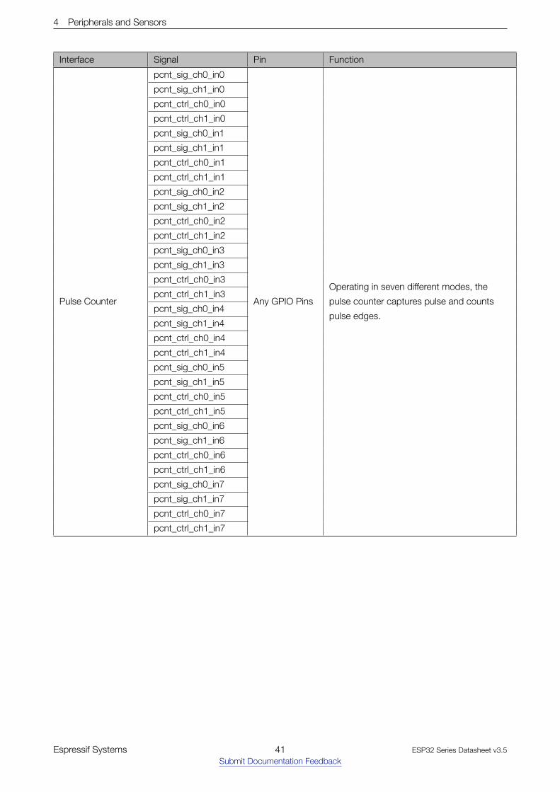
4 Peripherals and Sensors
Interface Signal Pin Function
Pulse Counter
pcnt_sig_ch0_in0
Any GPIO Pins
Operating in seven different modes, the
pulse counter captures pulse and counts
pulse edges.
pcnt_sig_ch1_in0
pcnt_ctrl_ch0_in0
pcnt_ctrl_ch1_in0
pcnt_sig_ch0_in1
pcnt_sig_ch1_in1
pcnt_ctrl_ch0_in1
pcnt_ctrl_ch1_in1
pcnt_sig_ch0_in2
pcnt_sig_ch1_in2
pcnt_ctrl_ch0_in2
pcnt_ctrl_ch1_in2
pcnt_sig_ch0_in3
pcnt_sig_ch1_in3
pcnt_ctrl_ch0_in3
pcnt_ctrl_ch1_in3
pcnt_sig_ch0_in4
pcnt_sig_ch1_in4
pcnt_ctrl_ch0_in4
pcnt_ctrl_ch1_in4
pcnt_sig_ch0_in5
pcnt_sig_ch1_in5
pcnt_ctrl_ch0_in5
pcnt_ctrl_ch1_in5
pcnt_sig_ch0_in6
pcnt_sig_ch1_in6
pcnt_ctrl_ch0_in6
pcnt_ctrl_ch1_in6
pcnt_sig_ch0_in7
pcnt_sig_ch1_in7
pcnt_ctrl_ch0_in7
pcnt_ctrl_ch1_in7
Espressif Systems 41Submit Documentation Feedback
ESP32 Series Datasheet v3.5

5 Electrical Characteristics
5 Electrical Characteristics
5.1 Absolute Maximum Ratings
Stresses beyond the absolute maximum ratings listed in the table below may cause permanent damage to the
device. These are stress ratings only, and do not refer to the functional operation of the device that should follow
the recommended operating conditions.
Table 11: Absolute Maximum Ratings
Symbol Parameter Min Max Unit
VDDA, VDD3P3, VDD3P3_RTC,
VDD3P3_CPU, VDD_SDIO
Voltage applied to power supply pins per
power domain–0.3 3.6 V
Ioutput * Cumulative IO output current - 1200 mA
Tstore Storage temperature –40 150 °C
* The chip worked properly after a 24-hour test in ambient temperature at 25 °C, and the IOs in three domains(VDD3P3_RTC, VDD3P3_CPU, VDD_SDIO) output high logic level to ground.
5.2 Recommended Operating Conditions
Table 12: Recommended Operating Conditions
Symbol Parameter Min Typ Max Unit
VDDA, VDD3P3_RTC 1
VDD3P3, VDD_SDIO (3.3 V mode) 2
Voltage applied to power supply pins per
power domain2.3 3.3 3.6 V
VDD3P3_CPU Voltage applied to power supply pin 1.8 3.3 3.6 V
IV DD Current delivered by external power supply 0.5 - - A
T 3 Operating temperature –40 - 125 °C
1. When writing eFuse, VDD3P3_RTC should be at least 3.3 V.
2. • VDD_SDIO works as the power supply for the related IO, and also for an external device. Please refer to theAppendix IO_MUX of this datasheet for more details.
• VDD_SDIO can be sourced internally by the ESP32 from the VDD3P3_RTC power domain:– When VDD_SDIO operates at 3.3 V, it is driven directly by VDD3P3_RTC through a 6 Ω resistor, therefore,
there will be some voltage drop from VDD3P3_RTC.– When VDD_SDIO operates at 1.8 V, it can be generated from ESP32’s internal LDO. The maximum current
this LDO can offer is 40 mA, and the output voltage range is 1.65 V ~ 2.0 V.• VDD_SDIO can also be driven by an external power supply.• Please refer to Power Scheme, section 2.3, for more information.
3. The operating temperature of ESP32-D2WD and ESP32-U4WDH ranges from –40 °C to 105 °C, due to the flashembedded in them. The other chips in this series have no embedded flash, so their range of operating temperatures is–40 °C ~ 125 °C.
Espressif Systems 42Submit Documentation Feedback
ESP32 Series Datasheet v3.5

5 Electrical Characteristics
5.3 DC Characteristics (3.3 V, 25 °C)
Table 13: DC Characteristics (3.3 V, 25 °C)
Symbol Parameter Min Typ Max Unit
CIN Pin capacitance - 2 - pF
VIH High-level input voltage 0.75×VDD1 - VDD1+0.3 V
VIL Low-level input voltage –0.3 - 0.25×VDD1 V
IIH High-level input current - - 50 nA
IIL Low-level input current - - 50 nA
VOH High-level output voltage 0.8×VDD1 - - V
VOL Low-level output voltage - - 0.1×VDD1 V
IOH
High-level source current
(VDD1 = 3.3 V,
VOH >= 2.64 V,
output drive strength set
to the maximum)
VDD3P3_CPU
power domain 1, 2- 40 - mA
VDD3P3_RTC
power domain 1, 2- 40 - mA
VDD_SDIO power
domain 1, 3- 20 - mA
IOL
Low-level sink current
(VDD1 = 3.3 V, VOL = 0.495 V,
output drive strength set to the maximum)
- 28 - mA
RPU Resistance of internal pull-up resistor - 45 - kΩ
RPD Resistance of internal pull-down resistor - 45 - kΩ
VIL_nRSTLow-level input voltage of CHIP_PU
to power off the chip- - 0.6 V
Notes:
1. Please see Table IO_MUX for IO’s power domain. VDD is the I/O voltage for a particular power domain of pins.
2. For VDD3P3_CPU and VDD3P3_RTC power domain, per-pin current sourced in the same domain is gradually reducedfrom around 40 mA to around 29 mA, VOH>=2.64 V, as the number of current-source pins increases.
3. For VDD_SDIO power domain, per-pin current sourced in the same domain is gradually reduced from around 30 mA toaround 10 mA, VOH>=2.64 V, as the number of current-source pins increases.
5.4 Reliability Qualifications
Table 14: Reliability Qualifications
Reliability tests Standards Test conditions Result
Electro-Static Discharge Sensitivity
(ESD), Charge Device Mode (CDM) 1JEDEC EIA/JESD22-C101 ±500 V, all pins Pass
Electro-Static Discharge Sensitivity
(ESD), Human Body Mode (HBM) 2JEDEC EIA/JESD22-A114 ±1500 V, all pins Pass
Latch-up (Over-current test) JEDEC STANDARD NO.78±50 mA ~ ±200 mA, room
temperature, test for IOPass
Latch-up (Over-voltage test) JEDEC STANDARD NO.781.5 × Vmax, room temper-
ature, test for Vsupply
Pass
Moisture Sensitivity Level (MSL) J-STD-020, MSL 330 °C, 60% RH, 192
hours, IR × 3 @260 °CPass
Espressif Systems 43Submit Documentation Feedback
ESP32 Series Datasheet v3.5

5 Electrical Characteristics
1. JEDEC document JEP157 states that 250 V CDM allows safe manufacturing with a standard ESD control process.
2. JEDEC document JEP155 states that 500 V HBM allows safe manufacturing with a standard ESD control process.
5.5 RF PowerConsumption Specifications
The power consumption measurements are taken with a 3.3 V supply at 25 °C of ambient temperature at the RF
port. All transmitters’ measurements are based on a 50% duty cycle.
Table 15: RF PowerConsumption Specifications
Mode Min Typ Max Unit
Transmit 802.11b, DSSS 1 Mbps, POUT = +19.5 dBm - 240 - mA
Transmit 802.11g, OFDM 54 Mbps, POUT = +16 dBm - 190 - mA
Transmit 802.11n, OFDM MCS7, POUT = +14 dBm - 180 - mA
Receive 802.11b/g/n - 95 ~ 100 - mA
Transmit BT/BLE, POUT = 0 dBm - 130 - mA
Receive BT/BLE - 95 ~ 100 - mA
5.6 WiFi Radio
Table 16: WiFi Radio Characteristics
Parameter Condition Min Typ Max Unit
Operating frequency range note1 - 2412 - 2484 MHz
Output impedance note2 - - note 2 - Ω
TX power note311n, MCS7 12 13 14 dBm
11b mode 18.5 19.5 20.5 dBm
Sensitivity
11b, 1 Mbps - –98 - dBm
11b, 11 Mbps - –88 - dBm
11g, 6 Mbps - –93 - dBm
11g, 54 Mbps - –75 - dBm
11n, HT20, MCS0 - –93 - dBm
11n, HT20, MCS7 - –73 - dBm
11n, HT40, MCS0 - –90 - dBm
11n, HT40, MCS7 - –70 - dBm
Adjacent channel rejection
11g, 6 Mbps - 27 - dB
11g, 54 Mbps - 13 - dB
11n, HT20, MCS0 - 27 - dB
11n, HT20, MCS7 - 12 - dB
1. Device should operate in the frequency range allocated by regional regulatory authorities. Target operating frequencyrange is configurable by software.
2. The typical value of ESP32’s Wi-Fi radio output impedance is different between chips in different QFN packages. ForESP32 chips with a QFN 6×6 package, the value is 30+j10 Ω. For ESP32 chips with a QFN 5×5 package, the value is35+j10 Ω.
3. Target TX power is configurable based on device or certification requirements.
Espressif Systems 44Submit Documentation Feedback
ESP32 Series Datasheet v3.5

5 Electrical Characteristics
5.7 Bluetooth Radio
5.7.1 Receiver – Basic Data Rate
Table 17: Receiver Characteristics – Basic Data Rate
Parameter Conditions Min Typ Max Unit
Sensitivity @0.1% BER - –90 –89 –88 dBm
Maximum received signal @0.1% BER - 0 - - dBm
Co-channel C/I - - +7 - dB
Adjacent channel selectivity C/I
F = F0 + 1 MHz - - –6 dB
F = F0 – 1 MHz - - –6 dB
F = F0 + 2 MHz - - –25 dB
F = F0 – 2 MHz - - –33 dB
F = F0 + 3 MHz - - –25 dB
F = F0 – 3 MHz - - –45 dB
Out-of-band blocking performance
30 MHz ~ 2000 MHz –10 - - dBm
2000 MHz ~ 2400 MHz –27 - - dBm
2500 MHz ~ 3000 MHz –27 - - dBm
3000 MHz ~ 12.5 GHz –10 - - dBm
Intermodulation - –36 - - dBm
5.7.2 Transmitter – Basic Data Rate
Table 18: Transmitter Characteristics – Basic Data Rate
Parameter Conditions Min Typ Max Unit
RF transmit power (see note under Table 18) - - 0 - dBm
Gain control step - - 3 - dB
RF power control range - –12 - +9 dBm
+20 dB bandwidth - - 0.9 - MHz
Adjacent channel transmit power
F = F0 ± 2 MHz - –47 - dBm
F = F0 ± 3 MHz - –55 - dBm
F = F0 ± > 3 MHz - –60 - dBm
∆ f1avg - - - 155 kHz
∆ f2max - 133.7 - - kHz
∆ f2avg/∆ f1avg - - 0.92 - -
ICFT - - –7 - kHz
Drift rate - - 0.7 - kHz/50 µs
Drift (DH1) - - 6 - kHz
Drift (DH5) - - 6 - kHz
Note:
There are a total of eight power levels from 0 to 7, and the transmit power ranges from –12 dBm to 9 dBm. When the
power level rises by 1, the transmit power increases by 3 dB. Power level 4 is used by default and the corresponding
transmit power is 0 dBm.
Espressif Systems 45Submit Documentation Feedback
ESP32 Series Datasheet v3.5

5 Electrical Characteristics
5.7.3 Receiver – Enhanced Data Rate
Table 19: Receiver Characteristics – Enhanced Data Rate
Parameter Conditions Min Typ Max Unit
π/4 DQPSK
Sensitivity @0.01% BER - –90 –89 –88 dBm
Maximum received signal @0.01% BER - - 0 - dBm
Co-channel C/I - - 11 - dB
Adjacent channel selectivity C/I
F = F0 + 1 MHz - –7 - dB
F = F0 – 1 MHz - –7 - dB
F = F0 + 2 MHz - –25 - dB
F = F0 – 2 MHz - –35 - dB
F = F0 + 3 MHz - –25 - dB
F = F0 – 3 MHz - –45 - dB
8DPSK
Sensitivity @0.01% BER - –84 –83 –82 dBm
Maximum received signal @0.01% BER - - –5 - dBm
C/I c-channel - - 18 - dB
Adjacent channel selectivity C/I
F = F0 + 1 MHz - 2 - dB
F = F0 – 1 MHz - 2 - dB
F = F0 + 2 MHz - –25 - dB
F = F0 – 2 MHz - –25 - dB
F = F0 + 3 MHz - –25 - dB
F = F0 – 3 MHz - –38 - dB
5.7.4 Transmitter – Enhanced Data Rate
Table 20: Transmitter Characteristics – Enhanced Data Rate
Parameter Conditions Min Typ Max Unit
RF transmit power (see note under Table 18) - - 0 - dBm
Gain control step - - 3 - dB
RF power control range - –12 - +9 dBm
π/4 DQPSK max w0 - - –0.72 - kHz
π/4 DQPSK max wi - - –6 - kHz
π/4 DQPSK max |wi + w0| - - –7.42 - kHz
8DPSK max w0 - - 0.7 - kHz
8DPSK max wi - - –9.6 - kHz
8DPSK max |wi + w0| - - –10 - kHz
π/4 DQPSK modulation accuracy
RMS DEVM - 4.28 - %
99% DEVM - 100 - %
Peak DEVM - 13.3 - %
8 DPSK modulation accuracy
RMS DEVM - 5.8 - %
99% DEVM - 100 - %
Peak DEVM - 14 - %
Espressif Systems 46Submit Documentation Feedback
ESP32 Series Datasheet v3.5

5 Electrical Characteristics
Parameter Conditions Min Typ Max Unit
In-band spurious emissions
F = F0 ± 1 MHz - –46 - dBm
F = F0 ± 2 MHz - –40 - dBm
F = F0 ± 3 MHz - –46 - dBm
F = F0 +/– > 3 MHz - - –53 dBm
EDR differential phase coding - - 100 - %
5.8 Bluetooth LE Radio
5.8.1 Receiver
Table 21: Receiver Characteristics – BLE
Parameter Conditions Min Typ Max Unit
Sensitivity @30.8% PER - –94 –93 –92 dBm
Maximum received signal @30.8% PER - 0 - - dBm
Co-channel C/I - - +10 - dB
Adjacent channel selectivity C/I
F = F0 + 1 MHz - –5 - dB
F = F0 – 1 MHz - –5 - dB
F = F0 + 2 MHz - –25 - dB
F = F0 – 2 MHz - –35 - dB
F = F0 + 3 MHz - –25 - dB
F = F0 – 3 MHz - –45 - dB
Out-of-band blocking performance
30 MHz ~ 2000 MHz –10 - - dBm
2000 MHz ~ 2400 MHz –27 - - dBm
2500 MHz ~ 3000 MHz –27 - - dBm
3000 MHz ~ 12.5 GHz –10 - - dBm
Intermodulation - –36 - - dBm
5.8.2 Transmitter
Table 22: Transmitter Characteristics – BLE
Parameter Conditions Min Typ Max Unit
RF transmit power (see note under Table 18) - - 0 - dBm
Gain control step - - 3 - dB
RF power control range - –12 - +9 dBm
Adjacent channel transmit power
F = F0 ± 2 MHz - –52 - dBm
F = F0 ± 3 MHz - –58 - dBm
F = F0 ± > 3 MHz - –60 - dBm
∆ f1avg - - - 265 kHz
∆ f2max - 247 - - kHz
∆ f2avg/∆ f1avg - - 0.92 - -
ICFT - - –10 - kHz
Drift rate - - 0.7 - kHz/50 µs
Drift - - 2 - kHz
Espressif Systems 47Submit Documentation Feedback
ESP32 Series Datasheet v3.5

6 Package Information
6 Package Information
Pin 1Pin 2Pin 3
Pin 1Pin 2Pin 3
Figure 8: QFN48 (6x6 mm) Package
Pin 1 Pin 2 Pin 3 3 2 1
Figure 9: QFN48 (5x5 mm) Package
Note:
The pins of the chip are numbered in an anti-clockwise direction from Pin 1 in the top view.
Espressif Systems 48Submit Documentation Feedback
ESP32 Series Datasheet v3.5

7 Part Number and Ordering Information
7 Part Number and Ordering Information
ESP32 - D WD Q6
PackageQ6=QFN 6*6N/A=QFN 5*5
ConnectionWD=Wi-Fi b/g/n + BT/BLE dual mode
CoreD=Dual coreS8=Single core
0
Embedded flash0=No embedded flash2=2 MB flash4=4 MB flash
V3
Wafer version 3
H
+LJKWHPSHUDWXUH
Figure 10: ESP32 Part Number
The table below provides the ordering information of the ESP32 series of chips.
Table 23: ESP32 Ordering Information
Ordering code Core Embedded flash Package
ESP32-D0WD-V3 Dual core No embedded flash QFN 5*5
ESP32-D0WDQ6-V3 Dual core No embedded flash QFN 6*6
ESP32-D0WD Dual core No embedded flash QFN 5*5
ESP32-D0WDQ6 Dual core No embedded flash QFN 6*6
ESP32-D2WD Dual core 2 MB embedded flash (40 MHz) QFN 5*5
ESP32-S0WD Single core No embedded flash QFN 5*5
ESP32-U4WDH Single core 4 MB embedded flash (80 MHz) QFN 5*5
Note: All above chips support Wi-Fi b/g/n + BT/BLE Dual Mode connection.
Espressif Systems 49Submit Documentation Feedback
ESP32 Series Datasheet v3.5

8 Learning Resources
8 Learning Resources
8.1 MustRead Documents
Click on the following links to access documents related to ESP32.
• ESP32 ECO V3 User Guide
This document describes differences between V3 and previous ESP32 silicon wafer revisions.
• ECO and Workarounds for Bugs in ESP32
This document details hardware errata and workarounds in the ESP32.
• ESP-IDF Programming Guide
It hosts extensive documentation for ESP-IDF, ranging from hardware guides to API reference.
• ESP32 Technical Reference Manual
The manual provides detailed information on how to use the ESP32 memory and peripherals.
• ESP32 Hardware Resources
The zip files include schematics, PCB layout, Gerber and BOM list.
• ESP32 Hardware Design Guidelines
The guidelines provide recommended design practices when developing standalone or add-on systems
based on the ESP32 series of products, including the ESP32 chip, the ESP32 modules and development
boards.
• ESP32 AT Instruction Set and Examples
This document introduces the ESP32 AT commands, explains how to use them, and provides examples of
several common AT commands.
• Espressif Products Ordering Information
8.2 MustHave Resources
Here are the ESP32-related must-have resources.
• ESP32 BBS
This is an Engineer-to-Engineer (E2E) Community for ESP32, where you can post questions, share
knowledge, explore ideas, and solve problems together with fellow engineers.
• ESP32 GitHub
ESP32 development projects are freely distributed under Espressif’s MIT license on GitHub. This channel of
communication has been established to help developers get started with ESP32 and encourage them to
share their knowledge of ESP32-related hardware and software.
• ESP32 Tools
This is a webpage where users can download ESP32 Flash Download Tools and the zip file ”ESP32
Certification and Test”.
• ESP-IDF
This webpage links users to the official IoT development framework for ESP32.
• ESP32 Resources
This webpage provides the links to all available ESP32 documents, SDK and tools.
Espressif Systems 50Submit Documentation Feedback
ESP32 Series Datasheet v3.5

Appendix A
Appendix A – ESP32 Pin Lists
A.1. Notes on ESP32 Pin Lists
Table 24: Notes on ESP32 Pin Lists
No. Description
1In Table IO_MUX, the boxes highlighted in yellow indicate the GPIO pins that are input-only.
Please see the following note for further details.
2
GPIO pins 34-39 are input-only. These pins do not feature an output driver or internal pull-
up/pull-down circuitry. The pin names are: SENSOR_VP (GPIO36), SENSOR_CAPP (GPIO37),
SENSOR_CAPN (GPIO38), SENSOR_VN (GPIO39), VDET_1 (GPIO34), VDET_2 (GPIO35).
3
The pins are grouped into four power domains: VDDA (analog power supply), VDD3P3_RTC
(RTC power supply), VDD3P3_CPU (power supply of digital IOs and CPU cores), VDD_SDIO
(power supply of SDIO IOs). VDD_SDIO is the output of the internal SDIO-LDO. The voltage of
SDIO-LDO can be configured at 1.8 V or be the same as that of VDD3P3_RTC. The strapping
pin and eFuse bits determine the default voltage of the SDIO-LDO. Software can change the
voltage of the SDIO-LDO by configuring register bits. For details, please see the column “Power
Domain” in Table IO_MUX.
4
The functional pins in the VDD3P3_RTC domain are those with analog functions, including the
32 kHz crystal oscillator, ADC, DAC, and the capacitive touch sensor. Please see columns
“Analog Function 1~3” in Table IO_MUX.
5These VDD3P3_RTC pins support the RTC function, and can work during Deep-sleep. For
example, an RTC-GPIO can be used for waking up the chip from Deep-sleep.
6
The GPIO pins support up to six digital functions, as shown in columns “Function 1~6” In Table
IO_MUX. The function selection registers will be set as “N-1”, where N is the function number.
Below are some definitions:
• SD_* is for signals of the SDIO slave.
• HS1_* is for Port 1 signals of the SDIO host.
• HS2_* is for Port 2 signals of the SDIO host.
• MT* is for signals of the JTAG.
• U0* is for signals of the UART0 module.
• U1* is for signals of the UART1 module.
• U2* is for signals of the UART2 module.
• SPI* is for signals of the SPI01 module.
• HSPI* is for signals of the SPI2 module.
• VSPI* is for signals of the SPI3 module.
Espressif Systems 51Submit Documentation Feedback
ESP32 Series Datasheet v3.5

Appendix A
No. Description
7
Each column about digital “Function” is accompanied by a column about “Type”. Please see
the following explanations for the meanings of “type” with respect to each “function” they are
associated with. For each “Function-N”, “type” signifies:
• I: input only. If a function other than “Function-N” is assigned, the input signal of
“Function-N” is still from this pin.
• I1: input only. If a function other than “Function-N” is assigned, the input signal of
“Function-N” is always “1”.
• I0: input only. If a function other than “Function-N” is assigned, the input signal of
“Function-N” is always “0”.
• O: output only.
• T: high-impedance.
• I/O/T: combinations of input, output, and high-impedance according to the function sig-
nal.
• I1/O/T: combinations of input, output, and high-impedance, according to the function
signal. If a function is not selected, the input signal of the function is “1”.
For example, pin 30 can function as HS1_CMD or SD_CMD, where HS1_CMD is of an “I1/O/T”
type. If pin 30 is selected as HS1_CMD, this pin’s input and output are controlled by the SDIO
host. If pin 30 is not selected as HS1_CMD, the input signal of the SDIO host is always “1”.
8
Each digital output pin is associated with its configurable drive strength. Column “Drive
Strength” in Table IO_MUX lists the default values. The drive strength of the digital output
pins can be configured into one of the following four options:
• 0: ~5 mA
• 1: ~10 mA
• 2: ~20 mA
• 3: ~40 mA
The default value is 2.
The drive strength of the internal pull-up (wpu) and pull-down (wpd) is ~75 µA.
9
Column “At Reset” in Table IO_MUX lists the status of each pin during reset, including input-
enable (ie=1), internal pull-up (wpu) and internal pull-down (wpd). During reset, all pins are
output-disabled.
10
Column “After Reset” in Table IO_MUX lists the status of each pin immediately after reset,
including input-enable (ie=1), internal pull-up (wpu) and internal pull-down (wpd). After reset,
each pin is set to “Function 1”. The output-enable is controlled by digital Function 1.
11
Table Ethernet_MAC is about the signal mapping inside Ethernet MAC. The Ethernet MAC
supports MII and RMII interfaces, and supports both the internal PLL clock and the external
clock source. For the MII interface, the Ethernet MAC is with/without the TX_ERR signal. MDC,
MDIO, CRS and COL are slow signals, and can be mapped onto any GPIO pin through the
GPIO-Matrix.
12
Table GPIO Matrix is for the GPIO-Matrix. The signals of the on-chip functional modules can
be mapped onto any GPIO pin. Some signals can be mapped onto a pin by both IO-MUX
and GPIO-Matrix, as shown in the column tagged as “Same input signal from IO_MUX core”
in Table GPIO Matrix.
Espressif Systems 52Submit Documentation Feedback
ESP32 Series Datasheet v3.5

Appendix A
No. Description
13
*In Table GPIO_Matrixthe column “Default Value if unassigned” records the default value of
the an input signal if no GPIO is assigned to it. The actual value is determined by register
GPIO_FUNCm_IN_INV_SEL and GPIO_FUNCm_IN_SEL. (The value of m ranges from 1 to
255.)
A.2. GPIO_Matrix
Table 25: GPIO_Matrix
Signal
No. Input signals
Default
value if
unassigned*
Same input
signal from
IO_MUX core Output signals
Output enable of
output signals
0 SPICLK_in 0 yes SPICLK_out SPICLK_oe
1 SPIQ_in 0 yes SPIQ_out SPIQ_oe
2 SPID_in 0 yes SPID_out SPID_oe
3 SPIHD_in 0 yes SPIHD_out SPIHD_oe
4 SPIWP_in 0 yes SPIWP_out SPIWP_oe
5 SPICS0_in 0 yes SPICS0_out SPICS0_oe
6 SPICS1_in 0 no SPICS1_out SPICS1_oe
7 SPICS2_in 0 no SPICS2_out SPICS2_oe
8 HSPICLK_in 0 yes HSPICLK_out HSPICLK_oe
9 HSPIQ_in 0 yes HSPIQ_out HSPIQ_oe
10 HSPID_in 0 yes HSPID_out HSPID_oe
11 HSPICS0_in 0 yes HSPICS0_out HSPICS0_oe
12 HSPIHD_in 0 yes HSPIHD_out HSPIHD_oe
13 HSPIWP_in 0 yes HSPIWP_out HSPIWP_oe
14 U0RXD_in 0 yes U0TXD_out 1’d1
15 U0CTS_in 0 yes U0RTS_out 1’d1
16 U0DSR_in 0 no U0DTR_out 1’d1
17 U1RXD_in 0 yes U1TXD_out 1’d1
18 U1CTS_in 0 yes U1RTS_out 1’d1
23 I2S0O_BCK_in 0 no I2S0O_BCK_out 1’d1
24 I2S1O_BCK_in 0 no I2S1O_BCK_out 1’d1
25 I2S0O_WS_in 0 no I2S0O_WS_out 1’d1
26 I2S1O_WS_in 0 no I2S1O_WS_out 1’d1
27 I2S0I_BCK_in 0 no I2S0I_BCK_out 1’d1
28 I2S0I_WS_in 0 no I2S0I_WS_out 1’d1
29 I2CEXT0_SCL_in 1 no I2CEXT0_SCL_out 1’d1
30 I2CEXT0_SDA_in 1 no I2CEXT0_SDA_out 1’d1
31 pwm0_sync0_in 0 no sdio_tohost_int_out 1’d1
32 pwm0_sync1_in 0 no pwm0_out0a 1’d1
33 pwm0_sync2_in 0 no pwm0_out0b 1’d1
34 pwm0_f0_in 0 no pwm0_out1a 1’d1
Espressif Systems 53Submit Documentation Feedback
ESP32 Series Datasheet v3.5

Appendix A
Signal
No. Input signals
Default
value if
unassigned*
Same input
signal from
IO_MUX core Output signals
Output enable of
output signals
35 pwm0_f1_in 0 no pwm0_out1b 1’d1
36 pwm0_f2_in 0 no pwm0_out2a 1’d1
37 - 0 no pwm0_out2b 1’d1
39 pcnt_sig_ch0_in0 0 no - 1’d1
40 pcnt_sig_ch1_in0 0 no - 1’d1
41 pcnt_ctrl_ch0_in0 0 no - 1’d1
42 pcnt_ctrl_ch1_in0 0 no - 1’d1
43 pcnt_sig_ch0_in1 0 no - 1’d1
44 pcnt_sig_ch1_in1 0 no - 1’d1
45 pcnt_ctrl_ch0_in1 0 no - 1’d1
46 pcnt_ctrl_ch1_in1 0 no - 1’d1
47 pcnt_sig_ch0_in2 0 no - 1’d1
48 pcnt_sig_ch1_in2 0 no - 1’d1
49 pcnt_ctrl_ch0_in2 0 no - 1’d1
50 pcnt_ctrl_ch1_in2 0 no - 1’d1
51 pcnt_sig_ch0_in3 0 no - 1’d1
52 pcnt_sig_ch1_in3 0 no - 1’d1
53 pcnt_ctrl_ch0_in3 0 no - 1’d1
54 pcnt_ctrl_ch1_in3 0 no - 1’d1
55 pcnt_sig_ch0_in4 0 no - 1’d1
56 pcnt_sig_ch1_in4 0 no - 1’d1
57 pcnt_ctrl_ch0_in4 0 no - 1’d1
58 pcnt_ctrl_ch1_in4 0 no - 1’d1
61 HSPICS1_in 0 no HSPICS1_out HSPICS1_oe
62 HSPICS2_in 0 no HSPICS2_out HSPICS2_oe
63 VSPICLK_in 0 yes VSPICLK_out_mux VSPICLK_oe
64 VSPIQ_in 0 yes VSPIQ_out VSPIQ_oe
65 VSPID_in 0 yes VSPID_out VSPID_oe
66 VSPIHD_in 0 yes VSPIHD_out VSPIHD_oe
67 VSPIWP_in 0 yes VSPIWP_out VSPIWP_oe
68 VSPICS0_in 0 yes VSPICS0_out VSPICS0_oe
69 VSPICS1_in 0 no VSPICS1_out VSPICS1_oe
70 VSPICS2_in 0 no VSPICS2_out VSPICS2_oe
71 pcnt_sig_ch0_in5 0 no ledc_hs_sig_out0 1’d1
72 pcnt_sig_ch1_in5 0 no ledc_hs_sig_out1 1’d1
73 pcnt_ctrl_ch0_in5 0 no ledc_hs_sig_out2 1’d1
74 pcnt_ctrl_ch1_in5 0 no ledc_hs_sig_out3 1’d1
75 pcnt_sig_ch0_in6 0 no ledc_hs_sig_out4 1’d1
76 pcnt_sig_ch1_in6 0 no ledc_hs_sig_out5 1’d1
77 pcnt_ctrl_ch0_in6 0 no ledc_hs_sig_out6 1’d1
78 pcnt_ctrl_ch1_in6 0 no ledc_hs_sig_out7 1’d1
Espressif Systems 54Submit Documentation Feedback
ESP32 Series Datasheet v3.5

Appendix A
Signal
No. Input signals
Default
value if
unassigned*
Same input
signal from
IO_MUX core Output signals
Output enable of
output signals
79 pcnt_sig_ch0_in7 0 no ledc_ls_sig_out0 1’d1
80 pcnt_sig_ch1_in7 0 no ledc_ls_sig_out1 1’d1
81 pcnt_ctrl_ch0_in7 0 no ledc_ls_sig_out2 1’d1
82 pcnt_ctrl_ch1_in7 0 no ledc_ls_sig_out3 1’d1
83 rmt_sig_in0 0 no ledc_ls_sig_out4 1’d1
84 rmt_sig_in1 0 no ledc_ls_sig_out5 1’d1
85 rmt_sig_in2 0 no ledc_ls_sig_out6 1’d1
86 rmt_sig_in3 0 no ledc_ls_sig_out7 1’d1
87 rmt_sig_in4 0 no rmt_sig_out0 1’d1
88 rmt_sig_in5 0 no rmt_sig_out1 1’d1
89 rmt_sig_in6 0 no rmt_sig_out2 1’d1
90 rmt_sig_in7 0 no rmt_sig_out3 1’d1
91 - - - rmt_sig_out4 1’d1
92 - - - rmt_sig_out6 1’d1
94 - - - rmt_sig_out7 1’d1
95 I2CEXT1_SCL_in 1 no I2CEXT1_SCL_out 1’d1
96 I2CEXT1_SDA_in 1 no I2CEXT1_SDA_out 1’d1
97 host_card_detect_n_1 0 no host_ccmd_od_pullup_en_n 1’d1
98 host_card_detect_n_2 0 no host_rst_n_1 1’d1
99 host_card_write_prt_1 0 no host_rst_n_2 1’d1
100 host_card_write_prt_2 0 no gpio_sd0_out 1’d1
101 host_card_int_n_1 0 no gpio_sd1_out 1’d1
102 host_card_int_n_2 0 no gpio_sd2_out 1’d1
103 pwm1_sync0_in 0 no gpio_sd3_out 1’d1
104 pwm1_sync1_in 0 no gpio_sd4_out 1’d1
105 pwm1_sync2_in 0 no gpio_sd5_out 1’d1
106 pwm1_f0_in 0 no gpio_sd6_out 1’d1
107 pwm1_f1_in 0 no gpio_sd7_out 1’d1
108 pwm1_f2_in 0 no pwm1_out0a 1’d1
109 pwm0_cap0_in 0 no pwm1_out0b 1’d1
110 pwm0_cap1_in 0 no pwm1_out1a 1’d1
111 pwm0_cap2_in 0 no pwm1_out1b 1’d1
112 pwm1_cap0_in 0 no pwm1_out2a 1’d1
113 pwm1_cap1_in 0 no pwm1_out2b 1’d1
114 pwm1_cap2_in 0 no pwm2_out1h 1’d1
115 pwm2_flta 1 no pwm2_out1l 1’d1
116 pwm2_fltb 1 no pwm2_out2h 1’d1
117 pwm2_cap1_in 0 no pwm2_out2l 1’d1
118 pwm2_cap2_in 0 no pwm2_out3h 1’d1
119 pwm2_cap3_in 0 no pwm2_out3l 1’d1
120 pwm3_flta 1 no pwm2_out4h 1’d1
Espressif Systems 55Submit Documentation Feedback
ESP32 Series Datasheet v3.5

Appendix A
Signal
No. Input signals
Default
value if
unassigned*
Same input
signal from
IO_MUX core Output signals
Output enable of
output signals
121 pwm3_fltb 1 no pwm2_out4l 1’d1
122 pwm3_cap1_in 0 no - 1’d1
123 pwm3_cap2_in 0 no - 1’d1
124 pwm3_cap3_in 0 no - 1’d1
140 I2S0I_DATA_in0 0 no I2S0O_DATA_out0 1’d1
141 I2S0I_DATA_in1 0 no I2S0O_DATA_out1 1’d1
142 I2S0I_DATA_in2 0 no I2S0O_DATA_out2 1’d1
143 I2S0I_DATA_in3 0 no I2S0O_DATA_out3 1’d1
144 I2S0I_DATA_in4 0 no I2S0O_DATA_out4 1’d1
145 I2S0I_DATA_in5 0 no I2S0O_DATA_out5 1’d1
146 I2S0I_DATA_in6 0 no I2S0O_DATA_out6 1’d1
147 I2S0I_DATA_in7 0 no I2S0O_DATA_out7 1’d1
148 I2S0I_DATA_in8 0 no I2S0O_DATA_out8 1’d1
149 I2S0I_DATA_in9 0 no I2S0O_DATA_out9 1’d1
150 I2S0I_DATA_in10 0 no I2S0O_DATA_out10 1’d1
151 I2S0I_DATA_in11 0 no I2S0O_DATA_out11 1’d1
152 I2S0I_DATA_in12 0 no I2S0O_DATA_out12 1’d1
153 I2S0I_DATA_in13 0 no I2S0O_DATA_out13 1’d1
154 I2S0I_DATA_in14 0 no I2S0O_DATA_out14 1’d1
155 I2S0I_DATA_in15 0 no I2S0O_DATA_out15 1’d1
156 - - - I2S0O_DATA_out16 1’d1
157 - - - I2S0O_DATA_out17 1’d1
158 - - - I2S0O_DATA_out18 1’d1
159 - - - I2S0O_DATA_out19 1’d1
160 - - - I2S0O_DATA_out20 1’d1
161 - - - I2S0O_DATA_out21 1’d1
162 - - - I2S0O_DATA_out22 1’d1
163 - - - I2S0O_DATA_out23 1’d1
164 I2S1I_BCK_in 0 no I2S1I_BCK_out 1’d1
165 I2S1I_WS_in 0 no I2S1I_WS_out 1’d1
166 I2S1I_DATA_in0 0 no I2S1O_DATA_out0 1’d1
167 I2S1I_DATA_in1 0 no I2S1O_DATA_out1 1’d1
168 I2S1I_DATA_in2 0 no I2S1O_DATA_out2 1’d1
169 I2S1I_DATA_in3 0 no I2S1O_DATA_out3 1’d1
170 I2S1I_DATA_in4 0 no I2S1O_DATA_out4 1’d1
171 I2S1I_DATA_in5 0 no I2S1O_DATA_out5 1’d1
172 I2S1I_DATA_in6 0 no I2S1O_DATA_out6 1’d1
173 I2S1I_DATA_in7 0 no I2S1O_DATA_out7 1’d1
174 I2S1I_DATA_in8 0 no I2S1O_DATA_out8 1’d1
175 I2S1I_DATA_in9 0 no I2S1O_DATA_out9 1’d1
176 I2S1I_DATA_in10 0 no I2S1O_DATA_out10 1’d1
Espressif Systems 56Submit Documentation Feedback
ESP32 Series Datasheet v3.5

Appendix A
Signal
No. Input signals
Default
value if
unassigned*
Same input
signal from
IO_MUX core Output signals
Output enable of
output signals
177 I2S1I_DATA_in11 0 no I2S1O_DATA_out11 1’d1
178 I2S1I_DATA_in12 0 no I2S1O_DATA_out12 1’d1
179 I2S1I_DATA_in13 0 no I2S1O_DATA_out13 1’d1
180 I2S1I_DATA_in14 0 no I2S1O_DATA_out14 1’d1
181 I2S1I_DATA_in15 0 no I2S1O_DATA_out15 1’d1
182 - - - I2S1O_DATA_out16 1’d1
183 - - - I2S1O_DATA_out17 1’d1
184 - - - I2S1O_DATA_out18 1’d1
185 - - - I2S1O_DATA_out19 1’d1
186 - - - I2S1O_DATA_out20 1’d1
187 - - - I2S1O_DATA_out21 1’d1
188 - - - I2S1O_DATA_out22 1’d1
189 - - - I2S1O_DATA_out23 1’d1
190 I2S0I_H_SYNC 0 no pwm3_out1h 1’d1
191 I2S0I_V_SYNC 0 no pwm3_out1l 1’d1
192 I2S0I_H_ENABLE 0 no pwm3_out2h 1’d1
193 I2S1I_H_SYNC 0 no pwm3_out2l 1’d1
194 I2S1I_V_SYNC 0 no pwm3_out3h 1’d1
195 I2S1I_H_ENABLE 0 no pwm3_out3l 1’d1
196 - - - pwm3_out4h 1’d1
197 - - - pwm3_out4l 1’d1
198 U2RXD_in 0 yes U2TXD_out 1’d1
199 U2CTS_in 0 yes U2RTS_out 1’d1
200 emac_mdc_i 0 no emac_mdc_o emac_mdc_oe
201 emac_mdi_i 0 no emac_mdo_o emac_mdo_o_e
202 emac_crs_i 0 no emac_crs_o emac_crs_oe
203 emac_col_i 0 no emac_col_o emac_col_oe
204 pcmfsync_in 0 no bt_audio0_irq 1’d1
205 pcmclk_in 0 no bt_audio1_irq 1’d1
206 pcmdin 0 no bt_audio2_irq 1’d1
207 - - - ble_audio0_irq 1’d1
208 - - - ble_audio1_irq 1’d1
209 - - - ble_audio2_irq 1’d1
210 - - - pcmfsync_out pcmfsync_en
211 - - - pcmclk_out pcmclk_en
212 - - - pcmdout pcmdout_en
213 - - - ble_audio_sync0_p 1’d1
214 - - - ble_audio_sync1_p 1’d1
215 - - - ble_audio_sync2_p 1’d1
224 - - - sig_in_func224 1’d1
225 - - - sig_in_func225 1’d1
Espressif Systems 57Submit Documentation Feedback
ESP32 Series Datasheet v3.5

Appendix A
Signal
No. Input signals
Default
value if
unassigned*
Same input
signal from
IO_MUX core Output signals
Output enable of
output signals
226 - - - sig_in_func226 1’d1
227 - - - sig_in_func227 1’d1
228 - - - sig_in_func228 1’d1
A.3. Ethernet_MAC
Table 26: Ethernet_MAC
PIN Name Function6 MII (int_osc) MII (ext_osc) RMII (int_osc) RMII (ext_osc)
GPIO0 EMAC_TX_CLK TX_CLK (I) TX_CLK (I) CLK_OUT(O) EXT_OSC_CLK(I)
GPIO5 EMAC_RX_CLK RX_CLK (I) RX_CLK (I) - -
GPIO21 EMAC_TX_EN TX_EN(O) TX_EN(O) TX_EN(O) TX_EN(O)
GPIO19 EMAC_TXD0 TXD[0](O) TXD[0](O) TXD[0](O) TXD[0](O)
GPIO22 EMAC_TXD1 TXD[1](O) TXD[1](O) TXD[1](O) TXD[1](O)
MTMS EMAC_TXD2 TXD[2](O) TXD[2](O) - -
MTDI EMAC_TXD3 TXD[3](O) TXD[3](O) - -
MTCK EMAC_RX_ER RX_ER(I) RX_ER(I) - -
GPIO27 EMAC_RX_DV RX_DV(I) RX_DV(I) CRS_DV(I) CRS_DV(I)
GPIO25 EMAC_RXD0 RXD[0](I) RXD[0](I) RXD[0](I) RXD[0](I)
GPIO26 EMAC_RXD1 RXD[1](I) RXD[1](I) RXD[1](I) RXD[1](I)
U0TXD EMAC_RXD2 RXD[2](I) RXD[2](I) - -
MTDO EMAC_RXD3 RXD[3](I) RXD[3](I) - -
GPIO16 EMAC_CLK_OUT CLK_OUT(O) - CLK_OUT(O) -
GPIO17 EMAC_CLK_OUT_180 CLK_OUT_180(O) - CLK_OUT_180(O) -
GPIO4 EMAC_TX_ER TX_ERR(O)* TX_ERR(O)* - -
In GPIO Matrix* - MDC(O) MDC(O) MDC(O) MDC(O)
In GPIO Matrix* - MDIO(IO) MDIO(IO) MDIO(IO) MDIO(IO)
In GPIO Matrix* - CRS(I) CRS(I) - -
In GPIO Matrix* - COL(I) COL(I) - -
*Notes: 1. The GPIO Matrix can be any GPIO. 2. The TX_ERR (O) is optional.
A.4. IO_MUX
For the list of IO_MUX pins, please see the next page.
Espressif Systems 58Submit Documentation Feedback
ESP32 Series Datasheet v3.5

Appendix
A
IO_MUX
Pin No. Power Supply Pin Analog Pin Digital Pin Power Domain Analog
Function1Analog Function2
Analog Function3
RTC Function1
RTC Function2 Function1 Type Function2 Type Function3 Type Function4 Type Function5 Type Function6 Type Drive Strength
(2’d2: 20 mA) At Reset After Reset
1 VDDA VDDA supply in2 LNA_IN VDD3P33 VDD3P3 VDD3P3 supply in4 VDD3P3 VDD3P3 supply in5 SENSOR_VP VDD3P3_RTC ADC_H ADC1_CH0 RTC_GPIO0 GPIO36 I GPIO36 I oe=0, ie=0 oe=0, ie=06 SENSOR_CAPP VDD3P3_RTC ADC_H ADC1_CH1 RTC_GPIO1 GPIO37 I GPIO37 I oe=0, ie=0 oe=0, ie=07 SENSOR_CAPN VDD3P3_RTC ADC_H ADC1_CH2 RTC_GPIO2 GPIO38 I GPIO38 I oe=0, ie=0 oe=0, ie=08 SENSOR_VN VDD3P3_RTC ADC_H ADC1_CH3 RTC_GPIO3 GPIO39 I GPIO39 I oe=0, ie=0 oe=0, ie=09 CHIP_PU VDD3P3_RTC10 VDET_1 VDD3P3_RTC ADC1_CH6 RTC_GPIO4 GPIO34 I GPIO34 I oe=0, ie=0 oe=0, ie=011 VDET_2 VDD3P3_RTC ADC1_CH7 RTC_GPIO5 GPIO35 I GPIO35 I oe=0, ie=0 oe=0, ie=012 32K_XP VDD3P3_RTC XTAL_32K_P ADC1_CH4 TOUCH9 RTC_GPIO9 GPIO32 I/O/T GPIO32 I/O/T 2'd2 oe=0, ie=0 oe=0, ie=0
13 32K_XN VDD3P3_RTC XTAL_32K_N ADC1_CH5 TOUCH8 RTC_GPIO8 GPIO33 I/O/T GPIO33 I/O/T 2'd2 oe=0, ie=0 oe=0, ie=014 GPIO25 VDD3P3_RTC DAC_1 ADC2_CH8 RTC_GPIO6 GPIO25 I/O/T GPIO25 I/O/T EMAC_RXD0 I 2'd2 oe=0, ie=0 oe=0, ie=015 GPIO26 VDD3P3_RTC DAC_2 ADC2_CH9 RTC_GPIO7 GPIO26 I/O/T GPIO26 I/O/T EMAC_RXD1 I 2'd2 oe=0, ie=0 oe=0, ie=016 GPIO27 VDD3P3_RTC ADC2_CH7 TOUCH7 RTC_GPIO17 GPIO27 I/O/T GPIO27 I/O/T EMAC_RX_DV I 2'd2 oe=0, ie=0 oe=0, ie=017 MTMS VDD3P3_RTC ADC2_CH6 TOUCH6 RTC_GPIO16 MTMS I0 HSPICLK I/O/T GPIO14 I/O/T HS2_CLK O SD_CLK I0 EMAC_TXD2 O 2'd2 oe=0, ie=0 oe=0, ie=1, wpu18 MTDI VDD3P3_RTC ADC2_CH5 TOUCH5 RTC_GPIO15 MTDI I1 HSPIQ I/O/T GPIO12 I/O/T HS2_DATA2 I1/O/T SD_DATA2 I1/O/T EMAC_TXD3 O 2'd2 oe=0, ie=1, wpd oe=0, ie=1, wpd19 VDD3P3_RTC VDD3P3_RTC supply in20 MTCK VDD3P3_RTC ADC2_CH4 TOUCH4 RTC_GPIO14 MTCK I1 HSPID I/O/T GPIO13 I/O/T HS2_DATA3 I1/O/T SD_DATA3 I1/O/T EMAC_RX_ER I 2'd2 oe=0, ie=0 oe=0, ie=1, wpd21 MTDO VDD3P3_RTC ADC2_CH3 TOUCH3 RTC_GPIO13 I2C_SDA MTDO O/T HSPICS0 I/O/T GPIO15 I/O/T HS2_CMD I1/O/T SD_CMD I1/O/T EMAC_RXD3 I 2'd2 oe=0, ie=1, wpu oe=0, ie=1, wpu22 GPIO2 VDD3P3_RTC ADC2_CH2 TOUCH2 RTC_GPIO12 I2C_SCL GPIO2 I/O/T HSPIWP I/O/T GPIO2 I/O/T HS2_DATA0 I1/O/T SD_DATA0 I1/O/T 2'd2 oe=0, ie=1, wpd oe=0, ie=1, wpd23 GPIO0 VDD3P3_RTC ADC2_CH1 TOUCH1 RTC_GPIO11 I2C_SDA GPIO0 I/O/T CLK_OUT1 O GPIO0 I/O/T EMAC_TX_CLK I 2'd2 oe=0, ie=1, wpu oe=0, ie=1, wpu24 GPIO4 VDD3P3_RTC ADC2_CH0 TOUCH0 RTC_GPIO10 I2C_SCL GPIO4 I/O/T HSPIHD I/O/T GPIO4 I/O/T HS2_DATA1 I1/O/T SD_DATA1 I1/O/T EMAC_TX_ER O 2'd2 oe=0, ie=1, wpd oe=0, ie=1, wpd
25 GPIO16 VDD_SDIO GPIO16 I/O/T GPIO16 I/O/T HS1_DATA4 I1/O/T U2RXD I1 EMAC_CLK_OUT O 2'd2 oe=0, ie=0 oe=0, ie=126 VDD_SDIO VDD_SDIO supply out/in27 GPIO17 VDD_SDIO GPIO17 I/O/T GPIO17 I/O/T HS1_DATA5 I1/O/T U2TXD O EMAC_CLK_OUT_180 O 2'd2 oe=0, ie=0 oe=0, ie=128 SD_DATA_2 VDD_SDIO SD_DATA2 I1/O/T SPIHD I/O/T GPIO9 I/O/T HS1_DATA2 I1/O/T U1RXD I1 2'd2 oe=0, ie=1, wpu oe=0, ie=1, wpu29 SD_DATA_3 VDD_SDIO SD_DATA3 I0/O/T SPIWP I/O/T GPIO10 I/O/T HS1_DATA3 I1/O/T U1TXD O 2'd2 oe=0, ie=1, wpu oe=0, ie=1, wpu30 SD_CMD VDD_SDIO SD_CMD I1/O/T SPICS0 I/O/T GPIO11 I/O/T HS1_CMD I1/O/T U1RTS O 2'd2 oe=0, ie=1, wpu oe=0, ie=1, wpu31 SD_CLK VDD_SDIO SD_CLK I0 SPICLK I/O/T GPIO6 I/O/T HS1_CLK O U1CTS I1 2'd2 oe=0, ie=1, wpu oe=0, ie=1, wpu32 SD_DATA_0 VDD_SDIO SD_DATA0 I1/O/T SPIQ I/O/T GPIO7 I/O/T HS1_DATA0 I1/O/T U2RTS O 2'd2 oe=0, ie=1, wpu oe=0, ie=1, wpu33 SD_DATA_1 VDD_SDIO SD_DATA1 I1/O/T SPID I/O/T GPIO8 I/O/T HS1_DATA1 I1/O/T U2CTS I1 2'd2 oe=0, ie=1, wpu oe=0, ie=1, wpu34 GPIO5 VDD3P3_CPU GPIO5 I/O/T VSPICS0 I/O/T GPIO5 I/O/T HS1_DATA6 I1/O/T EMAC_RX_CLK I 2'd2 oe=0, ie=1, wpu oe=0, ie=1, wpu35 GPIO18 VDD3P3_CPU GPIO18 I/O/T VSPICLK I/O/T GPIO18 I/O/T HS1_DATA7 I1/O/T 2'd2 oe=0, ie=0 oe=0, ie=136 GPIO23 VDD3P3_CPU GPIO23 I/O/T VSPID I/O/T GPIO23 I/O/T HS1_STROBE I0 2'd2 oe=0, ie=0 oe=0, ie=1
37 VDD3P3_CPU VDD3P3_CPU supply in38 GPIO19 VDD3P3_CPU GPIO19 I/O/T VSPIQ I/O/T GPIO19 I/O/T U0CTS I1 EMAC_TXD0 O 2'd2 oe=0, ie=0 oe=0, ie=139 GPIO22 VDD3P3_CPU GPIO22 I/O/T VSPIWP I/O/T GPIO22 I/O/T U0RTS O EMAC_TXD1 O 2'd2 oe=0, ie=0 oe=0, ie=140 U0RXD VDD3P3_CPU U0RXD I1 CLK_OUT2 O GPIO3 I/O/T 2'd2 oe=0, ie=1, wpu oe=0, ie=1, wpu41 U0TXD VDD3P3_CPU U0TXD O CLK_OUT3 O GPIO1 I/O/T EMAC_RXD2 I 2'd2 oe=0, ie=1, wpu oe=0, ie=1, wpu42 GPIO21 VDD3P3_CPU GPIO21 I/O/T VSPIHD I/O/T GPIO21 I/O/T EMAC_TX_EN O 2'd2 oe=0, ie=0 oe=0, ie=143 VDDA VDDA supply in44 XTAL_N VDDA45 XTAL_P VDDA46 VDDA VDDA supply in47 CAP2 VDDA48 CAP1 VDDA
Total Number 8 14 26
Notes: • wpu: weak pull-up;• wpd: weak pull-down;• ie: input enable;• oe: output enable;• Please see Table: Notes on ESP32 Pin Lists for more information.(请参考表:管脚清单说明。)
Espressif www.espressif.com
EspressifS
ystems
59S
ubmitD
ocumentation
FeedbackE
SP
32S
eriesD
atasheetv3.5
Revision History
Revision History
Date Version Release notes
2021-01-22 V3.5
Updated the description for CAP2 from 3 nF to 3.3 nF
Added TWAI® in Section 1.4.3: Advanced Peripheral Interfaces
Updated Figure 1: Functional Block Diagram
Updated the reset values for MTCK, MTMS, GPIO27 in Appendix IO_MUX
2020-04-27 V3.4
Added one chip variant: ESP32-U4WDH
Updated some figures in Table 6, 16, 17, 19, 21, 22
Added a note under Table 18
2020.01 V3.3Added two chip variants: ESP32-D0WD-V3 and ESP32-D0WDQ6-V3.
Added a note under Table 7.
2019.10 V3.2 Updated Figure 5: ESP32 Power-up and Reset Timing.
2019.07 V3.1
Added pin-pin mapping between ESP32-D2WD and the embedded flash under
Table 1 Pin Description;
Updated Figure 10 ESP32 Part Number.
2019.04 V3.0Added information about the setup and hold times for the strapping pins in Section
2.4: Strapping Pins.
2019.02 V2.9
Applied new formatting to Table 1: Pin Description;
Fixed typos with respect to the ADC1 channel mappings in Table 10: Peripheral
Pin Configurations.
2019.01 V2.8
Changed the RF power control range in Table 18, Table 20 and Table 22 from –12
~ +12 to –12 ~ +9 dBm;
Small text changes.
2018.11 V2.7Updated Section 1.5;
Updated pin statuses at reset and after reset in Table IO_MUX.
2018.10 V2.6 Updated QFN package drawings in Chapter 6: Package Information.
2018.08 V2.5
• Added ”Cumulative IO output current” entry to Table 11: Absolute Maximum
Ratings;
• Added more parameters to Table 13: DC Characteristics;
• Changed the power domain names in Table IO_MUX to be consistent with
the pin names.
2018.07 V2.4
• Deleted information on Packet Traffic Arbitration (PTA);
• Added Figure 5: ESP32 Power-up and Reset Timing in Section 2.3: Power
Scheme;
• Added the power consumption of dual-core SoCs in Table 6: Power Con-
sumption by Power Modes;
• Updated section 4.1.2: Analog-to-Digital Converter (ADC).
2018.06 V2.3Added the power consumption at CPU frequency of 160 MHz in Table 6: Power
Consumption by Power Modes.
Espressif Systems 60Submit Documentation Feedback
ESP32 Series Datasheet v3.5

Revision History
Date Version Release notes
2018.05 V2.2
• Changed the voltage range of VDD3P3_RTC from 1.8-3.6V to 2.3-3.6V in
Table 1: Pin Description;
• Updated Section 2.3: Power Scheme;
• Updated Section 3.1.3: External Flash and SRAM;
• Updated Table 6: Power Consumption by Power Modes;
• Deleted content about temperature sensor;
Changes to electrical characteristics:
• Updated Table 11: Absolute Maximum Ratings;
• Added Table 12: Recommended Operating Conditions;
• Added Table 13: DC Characteristics;
• Added Table 14: Reliability Qualifications;
• Updated the values of ”Gain control step” and ”Adjacent channel transmit
power” in Table 18: Transmitter Characteristics - Basic Data Rate;
• Updated the values of ”Gain control step”, ”π/4 DQPSK modulation accu-
racy”, ”8 DPSK modulation accuracy” and ”In-band spurious emissions” in
Table 20: Transmitter Characteristics – Enhanced Data Rate;
• Updated the values of ”Gain control step”, ”Adjacent channel transmit
power” in Table 22: Transmitter Characteristics - BLE.
2018.01 V2.1
• Deleted software-specific features;
• Deleted information on LNA pre-amplifier;
• Specified the CPU speed and flash speed of ESP32-D2WD;
• Added notes to Section 2.3: Power Scheme.
2017.12 V2.0 Added a note on the sequence of pin number in Chapter 6.
2017.10 V1.9
• Updated the description of the pin CHIP_PU in Table 1;
• Added a note to Section 2.3: Power Scheme;
• Updated the description of the chip’s system reset in Section 2.4: Strapping
Pins;
• Added a description of antenna diversity and selection to Section 3.5.1;
• Deleted ”Association sleep pattern” in Table 6 and added notes to Active
sleep and Modem-sleep.
2017.08 V1.8• Added Table 4.2 in Section 4;
• Corrected a typo in Figure 1.
Espressif Systems 61Submit Documentation Feedback
ESP32 Series Datasheet v3.5

Revision History
Date Version Release notes
2017.08 V1.7
• Changed the transmitting power to +12 dBm; the sensitivity of NZIF receiver
to -97 dBm in Section 1.3;
• Added a note to Table 1 Pin Description;
• Added 160 MHz clock frequency in section 3.1.1;
• Changed the transmitting power from 21 dBm to 20.5 dBm in Section 3.5.1;
• Changed the dynamic control range of class-1, class-2 and class-3 transmit
output powers to ”up to 24 dBm”; and changed the dynamic range of NZIF
receiver sensitivity to ”over 97 dB” in Section 3.6.1;
• Updated Table 6: Power Consumption by Power Modes, and added two
notes to it;
• Updated sections 4.1.1, 4.1.9;
• Updated Table 11: Absolute Maximum Ratings;
• Updated Table 15: RF Power Consumption Specifications, and changed the
duty cycle on which the transmitters’ measurements are based by 50%.
• Updated Table 16: Wi-Fi Radio Characteristics and added a note on “Output
impedance” to it;
• Updated parameter ”Sensitivity” in Table 17, 19, 21;
• Updated parameters ”RF transmit power” and ”RF power control range”,
and added parameter ”Gain control step” in Table 18, 20, 22;
• Deleted Chapters: ”Touch Sensor” and ”Code Examples”;
• Added a link to certification download.
2017.06 V1.6
Corrected two typos:
• Changed the number of external components to 20 in Section 1.1.2;
• Changed the number of GPIO pins to 34 in Section 4.1.1.
2017.06 V1.5
• Changed the power supply range in Section: 1.4.1 CPU and Memory;
• Updated the note in Section 2.3: Power Scheme;
• Updated Table 11: Absolute Maximum Ratings;
• Changed the drive strength values of the digital output pins in Note 8, in
Table 24: Notes on ESP32 Pin Lists;
• Added the option to subscribe for notifications of documentation changes.
2017.05 V1.4
• Added a note to the frequency of the external crystal oscillator in Section
1.4.2: Clocks and Timers;
• Added a note to Section 2.4: Strapping Pins;
• Updated Section 3.7: RTC and Low-Power Management;
• Changed the maximum driving capability from 12 mA to 80 mA, in Table 11:
Absolulte Maximum Ratings;
• Changed the input impedance value of 50Ω, in Table 16: Wi-Fi Radio Char-
acteristics, to output impedance value of 30+j10 Ω;
• Added a note to No.8 in Table 24: Notes on ESP32 Pin Lists;
• Deleted GPIO20 in Table IO_MUX.
2017.04 V1.3
• Added Appendix: ESP32 Pin Lists;
• Updated Table: Wi-Fi Radio Characteristics;
• Updated Figure: ESP32 Pin Layout (for QFN 5*5).
Espressif Systems 62Submit Documentation Feedback
ESP32 Series Datasheet v3.5

Revision History
Date Version Release notes
2017.03 V1.2• Added a note to Table: Pin Description;
• Updated the note in Section: Internal Memory.
2017.02 V1.1
• Added Chapter: Part Number and Ordering Information;
• Updated Section: MCU and Advanced Features;
• Updated Section: Block Diagram;
• Updated Chapter: Pin Definitions;
• Updated Section: CPU and Memory;
• Updated Section: Audio PLL Clock;
• Updated Section: Absolute Maximum Ratings;
• Updated Chapter: Package Information;
• Updated Chapter: Learning Resources.
2016.08 V1.0 First release.
Espressif Systems 63Submit Documentation Feedback
ESP32 Series Datasheet v3.5

www.espressif.com
Disclaimer and Copyright NoticeInformation in this document, including URL references, is subject to change without notice.
ALL THIRD PARTY’S INFORMATION IN THIS DOCUMENT IS PROVIDED AS IS WITH NOWARRANTIES TO ITS AUTHENTICITY AND ACCURACY.
NO WARRANTY IS PROVIDED TO THIS DOCUMENT FOR ITS MERCHANTABILITY, NON-INFRINGEMENT, FITNESS FOR ANY PARTICULAR PURPOSE, NOR DOES ANY WARRANTYOTHERWISE ARISING OUT OF ANY PROPOSAL, SPECIFICATION OR SAMPLE.
All liability, including liability for infringement of any proprietary rights, relating to use of informationin this document is disclaimed. No licenses express or implied, by estoppel or otherwise, to anyintellectual property rights are granted herein.
The Wi-Fi Alliance Member logo is a trademark of the Wi-Fi Alliance. The Bluetooth logo is aregistered trademark of Bluetooth SIG.
All trade names, trademarks and registered trademarks mentioned in this document are propertyof their respective owners, and are hereby acknowledged.
Copyright © 2021 Espressif Systems (Shanghai) Co., Ltd. All rights reserved.

Operating Instructions
Data Logger
ALMEMO® 2290-8
V2.104.12.2003
ALMEMO® 2290-8 1

Operating Instructions
Data Logger
ALMEMO® 2290-8For reference with the ALMEMO® Manual
Table of ContentsPage
1 INTRODUCTION 41.1 Function Range 41.2 Operating Controls 9
2 INITIAL OPERATION 11
3 POWER SUPPLY 123.1 Operation with Battery and Rechargeable Battery 123.2 External Voltage Supply 133.3 Switch On/Off, Reinitialisation 143.4 Battery Buffer 14
4. CONNECTION OF THE TRANSDUCERS 154.1 Transducers 154.2 Measuring Inputs and Additional Channels 15
5 DISPLAY AND KEYBOARD 175.1 Display and Function Selection 175.2 Keyboard 185.3 Data Entry 195.4 Keyboard Lock 19
6 SENSOR PROGRAMMING 206.1 Selecting the Input Channel 206.2 Selecting the Measuring Range 216.3 Changing the Dimension 246.4 Limit Values 24
2 ALMEMO® 2290-8
Table of Contents

Page6.5 Correction Values 256.6 Scaling, Decimal Point Setting 266.7 Locking the Programming of the Sensor 27
7 MEASUREMENT 277.1 Continuous Measurement of a Measuring Point 287.1.1 Selecting the Measuring Point 287.1.2 Memory for Peak Values 297.1.3 Averaging 297.1.4 Setting the Measured Value to Zero, Zero Point Correction 317.1.5 Atmospheric Pressure Compensation 327.2 Single Measuring Point Scan 337.3 Cyclic Measuring Point Scan 337.3.1 Print Cycle, Output Channel, Output Format 347.3.2 Measuring Cycle and Memory Activation 357.3.3 Conversion Rate, Continuous Measuring Point Scan 357.3.4 Time and Date 367.3.5 Time and Date of Start, Time and Date of End 367.3.6 Start and Stop by Limit Values 377.4 Data Memory 387.4.1 Data Acquisition 387.4.2 Memorry Connector 397.4.3 Output of Measuring Data 407.5 Numbering Measurements 417.6 Sleep Mode 42
8 DIGITAL DATA OUTPUT 438.1 Baud Rate, Data Format 438.2 Device Address and Networking 448.3 Manual Data Output 44
9 ANALOGUE OUTPUT 46
10 TROUBLESHOOTING 47
11 ELECTROMAGNETIC COMPATIBILITY 48
APPENDIX 49Technical Data 49Product Overview 49
ALMEMO® 2290-8 3
Table of Contents

1. INTRODUCTIONThe new data logger ALMEMO® 2290-8 Version 5 is an instrument from theunique product range of measuring devices that are all equipped with theALMEMO® connector system, which has been patented by Ahlborn GmbH. Theintelligent ALMEMO® connector provides important advantages with regard tothe connection of sensors and peripherals as all parameters are stored in anEEPROM within the connector. As a result, the programming that usually hasto be performed for the connection is not required.All sensors and output modules can be connected to all ALMEMO® measuringdevices in the same way. The operation and programming is identical with allunits. Therefore, all of the ALMEMO® measuring system items listed below aredescribed, in detail, in a separate ALMEMO® manual that is supplied with everydevice:
Detailed description of the ALMEMO® system (manual section 1)Overview of the device functions and measuring ranges (manual section 2)All sensors with basic principles, operation, technical data (man. section 3)The options for connecting existing sensors (manual section 4)All analogue and digital output modules (manual section 5.1)The interface module RS232, fiber optics, Centronics (manual section 5.2)The entire ALMEMO® networking system (manual section 5.3)All functions and their control via the interface (manual section 6) A complete interface command list with all print outputs (manual section 7)
These operating instructions only cover features and controls that are specificfor a certain device. As a result, the sections dealing with the system controlvia keyboard will only often provide a note referring to a more detaileddescription within the manual (manual section x.x.x).
1.1 Function RangeThe ALMEMO® 2290-8 data logger has five electrically isolated measuringinputs with up to 20 measuring channels for more than 70 measuring ranges, areal time clock and a 500kB memory for approximately 100,000 measuredvalues. Two output sockets allow for connecting any ALMEMO® outputmodules, for example, the analogue output, digital interface, trigger input oralarm contacts. Several devices can be networked by a simple connectionbetween the devices. For easy operation it is equipped with a rotary switch,keyboard and an 8½ digit LCD display.
SENSOR PROGRAMMINGThe measuring channels are automatically programmed by the ALMEMO®
connectors of the sensors. However, the user can easily complete or modifythe programming via keyboard or via interface.
4 ALMEMO® 2290-8
Introduction

Measuring RangesThere are corresponding measuring ranges for sensors with a non-linearcharacteristic such as 10 thermocouple types, Ntc and Pt100 sensors, infraredsensors, and flow sensors (rotating vanes, thermoanemometers, pitot tubes).Humidity sensors are available with function channels that also calculatehumidity data such as dew point, mixture ratio, vapour pressure and enthalpy.Even complex chemical sensors can be used. The acquisition of measureddata from other sensors is easily possible by using voltage, current andresistance ranges with individual scaling in the connector. Existing sensors canbe used without problems. Only the corresponding ALMEMO® connector has tobe connected using its terminals. Furthermore, there are adapter connectorswith an own microcontroller for digital signals and for measuring frequenciesand pulses. This way, nearly all sensors can be connected to any ALMEMO®
measuring instrument and are interchangeable without requiring any settings.
Function ChannelsMaximum, minimum, average values and differences of certain measuringjunctions can be programmed as function channels and can be processed andprinted like normal measuring junctions. Furthermore, function channels forspecial measuring tasks are provided to determine temperature coefficientQ/∆t and wet bulb globe temperatures.
DimensionThe 2 digit dimension can be altered for each measuring channel so that thedisplay and the printout will always indicate the correct dimension, for examplewhen a transmitter is connected. The conversion from °C to °F is automaticallyperformed according to the dimension.
Name of Measured ValuesSensors can be identified by a 10 digit alphanumeric designation. It is enteredvia the interface and appears on the printout or display if the evaluation is donevia PC.
Correction of Measured ValuesFor correcting measured values a zero point and slope (gain) correction can beapplied to the measured value of each measuring channel. This also allows forsensors to be interchanged that usually, at first, require an adjustment(expansion, force, pH). The zero point and the slope (gain) correction arevirtually performed by the push of a button.
ScalingThe base value and the factor allow for a further scaling of the correctedmeasured value of each measuring channel for zero point and slope (gain).The decimal point position can be set by the exponent. By setting to zero andentering the nominal value the scaling values can be automatically calculated.
ALMEMO® 2290-8 5
Functions

Limit Values and AlarmTwo limit values (1 max and 1 min) can be set for each measuring channel. Analarm value printout can be performed if a limit value is exceeded and, bymeans of relay output modules, alarm contacts are provided that can beindividually allocated to limit values. As a standard, the hysteresis is set to 10digits, however, it can also be adjusted. Furthermore, limit value exceeding canalso be used to start or stop a data logging.
Sensor LockingAll sensor data stored in the EEPROM of the connector can be protectedagainst undesired access by means of a graded locking function.
MEASUREMENTA total of up to 20 measuring channels are available for 5 transducers, i.e. it isalso possible to evaluate double sensors, individually scaled sensors, orsensors with function channels. The measuring channels can be successivelyselected forwards or backwards via keyboard. The selected measuring pointcan be scanned with a conversion rate of 2.5 or 10 measurements/second.The measured value is calculated and indicated on the display or, if available,provided on the analogue output.
Measured ValueA continuous presentation of measuring data from the selected measuringpoint is provided and also includes automatic zero point correction and optionalcorrection of the measured value or new scaling.A sensor breakage condition is, with most sensors, automatically detected(exception: connectors with shunts, dividers or additional electronics).
Analogue Output and ScalingBy means of analogue start and analogue end the indicated measured valuecan be scaled so that the resulting measuring range covers the full analogueoutput range (2V, 10V or 20mA).
Measuring FunctionsSpecial measuring functions are required for some sensors in order to achievean optimal acquisition of measuring data. The cold junction compensation isavailable for thermocouples, a temperature compensation for dynamicpressure and pH and conductivity probes, and an atmospheric air pressurecompensation for humidity sensors, dynamic pressure sensors and O2
sensors. With infrared sensors the parameters zero point and slope correctionare used for background temperature and emissivity factor.
Maximum and Minimum ValueEach measurement involves an acquisition and storing of the maximum andminimum value. These values can be displayed, printed or cleared.
6 ALMEMO® 2290-8
Functions

Average Value of a ChannelA manual averaging over a particular period or over single measurements isavailable for the selected channel.
PROCESS FLOW PROGRAMMINGA cyclic measuring point scan with a time-based process flow control isrequired to register the measuring data of all connected sensors. For thispurpose, the real time clock, the print cycle and the measuring cycle areavailable and, if fast processing is required, the conversion rate is available.The measurement can be started and stopped by using the keyboard, theinterface, an external trigger signal, the real time clock or an exceeding of limitvalues.
Time and DateThe real time clock with date function or the pure measuring time are used foran accurate recording of any measurement. Start and end time/date can beprogrammed in order to start or stop a measurement.
Print CycleThe print cycle is programmable between 1s and 59h/59min/59s and providesa cyclic output of measured values to the interfaces or memories and alsoprovides a cyclic averaging.
Print Cycle FactorIf necessary, the print cycle factor allows for limiting the data output ofparticular channels so that an excessive data flow can be limited, especiallyduring data storage.
Measuring CycleThe measuring cycle, also programmable between 1s and 59h/59min/59s, isfor a cyclic scanning with a display of all measured values, limit valuemonitoring including alarm message and output of alarm values, averagingand, if necessary, a storage of measured values.
Average Value over Measuring Point ScansThe measured values that result from scanning the measuring junctions canbe averaged as desired either over the total measuring time or over the printcycle time. Function channels are provided for a cyclic output of averagevalues.
Conversion RateWith ALMEMO® V5 devices, all measuring points can be continuouslyscanned with the conversion rate (2.5 or 10 meas./s). It is possible to store allmeasured values in the memory and/or to perform an output via the interface.
ALMEMO® 2290-8 7
Functions

Storage of Measured ValuesDuring the measuring or print cycle, all measured values or alarm values canbe manually or automatically stored in a buffered RAM. The memory capacityis, as standard, 500kB, which allows up to 100,000 measured values. Thememory organisation can be configured as linear or ring memory. DeductibleALMEMO® memory connectors are alternative usably. The output can beoptionally performed via interface, analogue output or display. It is possible toselect a certain time interval, number or alarm value.
Numbering of MeasurementsSingle scans or entire series of measurements can be identified and selectivelyread out from the memory.
Control OutputsThe interface allows to individually trigger up to four output relays and oneanalogue output.
Keyboard LockThe keyboard operation can be locked with a password.
OutputAll measuring and programming data is accessible by means of the LCDdisplay. RS232, RS422, Ethernet and a Centronics interface are available byusing different interface cables. All data logs, measured values andprogrammed parameters can be provided as output to any peripheralequipment. The output of measuring data can be selected in list format,columns or spreadsheet format. Files in spreadsheet format can be processedby each spreadsheet software. The print header can be programmedspecifically to the company or application.
NetworkingAll ALMEMO® devices can be addressed and can be easily networked by asimple connection with network cables or network junctions for longerdistances.
SoftwareThe AMR-Control software, which allows for the entire programming of thesensors, the configuration of the measuring instrument and the read-out of thedata memory is supplied with each ALMEMO® manual. The integrated terminalalso allows for online measurements. The WINDOWS® software packages,Win-Control and DATA-Control, are available for data acquisition of networkeddevices, graphical presentation and complex data processing.
8 ALMEMO® 2290-8
Functions

1.2 Operating Controls(1) ON/OFF switch
up SLEEPcentre ONdown OFF
(2) Measuring Inputs CH0 to CH4CH0 to CH4 for all ALMEMO® sensorCH5 to CH19additional channels
(3) Output Sockets OUT1, OUT2OUT1 Interface RS232 (ZA 1909-DK5)
Fiber Optics RS232 (ZA 1909-DKL)Ethernet (ZA 1945-DK)Centronics (ZA 1936-DK)RS 422 (ZA 5099-NVB)Analogue Output 1 (ZA 1601-RK)
OUT2 Network Cable (ZA1999-NK5)Memory connector (ZA1904-SS)Trigger Input (ZA 1000-ET/EK)Relay Outputs (ZA 1000-EGK)Analogue Output 2 (ZA 1601-RK)
(4) DC SocketMains Adapter (ZB 2290-NA, 12V, 200mA)Cable, electr. isol. (ZB 2290-UK, 10-30V)
(5) LCD Display(6) Function Keys(7) Function Selector Switch(8) Battery Box (back of unit)
Alkaline mangan. battery 9V (6F22)Space for spare battery
(5) LCD Display(a) Symbols for operating modes
U battery < 7 V BAT
CORR Correction of meas. value AVERAGE Averaging START Measuring point scan MEMORY Memory receive, output RS232C Output of meas. value ALARM Exceeding of limit value F Additional function
(b) 6½ x 7 segment display for:Meas. point, meas. value, meas. range,meas. and progr. values, cycles, time,date
(c) 2 x 16 segment display for:Dimension of the measured value,Abbrev. for additional functions
ALMEMO® 2290-8 9
(1) (2) (3)
(4)
(5)
(6)
(7)
(8)
LV : MA X
M IN . V.
2290-8
Operating Controls
23
BAT
CORR AVERAGE START RS232CMEMORY ALARM F
a
b c

(2) FUNCTION KEYS
ENTER CH START/STOP OUTPUT F
CLEAR ±
ENTER, ± , , for entering programming values
ENTER, CLEAR clear data, set meas. value to zeroENTER, ± calibrate measured valueM select measuring pointSTART/STOP cyclic measuring point scan OUTPUT data output to interfaceF single measuring point scan
select additional functions
(3) FUNCTION SELECTOR SWITCH
Function Key Additional functions Abbrev.MEAS. VALUE, UNIT F single measuring point scanNUMBER F deactivate (A)
CH increase (A)MAX VALUE F analogue output-end (AE)MIN VALUE F analogue output-start (AS)AVERAGE V F averaging mode (AM)
F,F number of aver. values CRANGE F locking mode LM
F,F locking code LCLV MAX F action Hi start/stop AHLV MIN F action Lo start/stop ALBASE F zero point correction ZC
F ambient temperature AT *
FACTOR, ± Exponent F slope (gain) correction SCF emissivity factor EF *
MEMORY F free memory FRMEAS CYCLE CH store on/off S
F conversion rate CRPRINT CYCLE CH output channel / format U
F device address ATIME F start time S
F,F end time EDATE F start date S
F,F end date EBAUD RATE F atmospheric pressure mb
* infrared sensors only
10 ALMEMO® 2290-8
Operating Controls

2. INITIAL OPERATION1. Connect transducers in the correct order to the sockets CH0 to CH4, see 4.2. Ensure power supply with 9V battery or mains adapter, see 3.1, 3.2.3. For switching on move the slide switch (1) on the left side of the unit to the
centre position, see 3.3.4. For displaying the measured values,
select function MEAS. VALUE by using the rotary switch (7), use key CH to select the measuring channels, read meas. values, see 7.1.
5. For storing the measured values, see 7.4. Use function MEMORY and keys ENTER, CLEAR to clear the memory. Use MEAS. CYCLE and key CH to activate the memory ´S´, see 7.3.2. Single measuring point scan by key F within function MEAS.VALUE, see 7.2. Enter measuring cycle for cyclic storing, see 7.3.2. Enter time and date, as required, see 7.3.4. Enter time and date of start or end of a measurement as required, see 7.3.5. Use key START/STOP to start and stop a cyclic storing, see 7.3. Output of memory data to printer or computer Connect peripheral device via interface cable to socket A1, see manual 5.2. Set 9600 bd, 8 data bits, 1 stop bit, no parity at peripheral device, see 8.1. Use key CH within function OUTPUT CYCLE to set the output channel ´ U´
and, possibly, the format columns ´nU´ or spreadsheet/table ´tU´, see 7.3.1. Use key OUTPUT within function MEMORY to output meas.values, see 7.4.2.6. Cyclic output of measured values to printer or computer Connect peripheral device via interface cable to socket A1, see manual 5.2. Set 9600 bd, 8 data bits, 1 stop bit, no parity at peripheral device, see 8.1. Enter time and date, as required, see 7.3.4. Program the print cycle within function OUTPUT CYCLE,
use key CH to set the output channel ´ U´ and, if required, the output format columns ´nU´ or spreadsheet/table ´tU´, see 7.3.1.
Use key START/STOP to start and stop the cyclic meas. point scan, see 7.3.7. Monitoring of limit values Enter limit values, see 6.4. Program measuring cycle, see 7.3.2. Connect alarm device with alarm module to socket OUT2,
see man. 5.1.2/5.1.3.For an alarm print use key CH within function OUTPUT CYCLE to activatethe output channel ´ U´, see 7.3.1. Use key START/STOP to start and stop the cyclic meas. point scan, see 7.3.
8. Evaluation of the measurement Display max and min values within function MAX or MIN VALUE, see 7.1.2.
ALMEMO® 2290-8 11
Initial Operation

3. POWER SUPPLYThe following options are available for the power supply of the instrument:
9V battery IEC 6 F22 ZB 2000-B99V rechargeable battery,as above with charger unit integrated in plug ZB 2000-A9, ZB 2000-LSMains adapter 12V/200mA ZB 2290-NAExternal power supply, connecting cable ZB 2290-UK
Our product line includes corresponding accessories.
3.1 Operation with Battery and Rechargeable BatteryOnly use type IEC 6 F22 alkaline manganese batteries. At a currentconsumption of approximately 10mA, they last for an operating time of 35hours. The operating time will be shortened if sensors or modules areconnected that consume additional current.
Inserting Batteries:
The battery box (8) is located at the underside of the instrument.
1. Press the area that is marked with the arrow and,at the same time, pull as marked by the arrow, asillustrated left.
2. Use the connector clip to connect the battery. Theconnector shape prevents from confusing thepoles.
3. Use the second battery box to store a sparebattery.
Battery Control:If the battery warning symbol is illuminated in the display the battery will still operate for approx. 5 hours (supply voltage <7V).
If the battery voltage drops below 6 volts ´ LobAt ´ willbe indicated on the display.The battery should be immediately removed. Leakageof the battery and damage to the instrument can thenbe avoided.
The actual battery voltage can be accurately monitored with anown measuring channel Ubat and the remaining battery life canbe estimated accordingly.
12 ALMEMO® 2290-8
Power Supply

Tips regarding correct handling of batteries:Do not leave used batteries in the instrument!
Remove batteries from the instrument if it is not used for a long period. Risk to health and instrument failure can result from leaking batteries!
Therefore, only use leak-proof batteries.Used batteries are hazardous waste and must be disposed in anenvironmentally friendly way! Return them to the dealer or dispose ofthem in a battery storage container.
Operation with rechargeable batteries:Rechargeable batteries can be used instead of normal batteries. Due to theirsmaller capacity of 110mAh they only reach an operating time of 11 hours. Theoperating time will be shortened if sensors or modules are connected thatconsume additional current. It is recommended to use the 9V rechargeablebattery with plug-integrated charger unit ZB 2000 LS, which is included in therange of accessories.Tips regarding correct handling of rechargeable batteries:
The rechargeable batteries supplied are not charged when delivered!If NiCD cells are only partly discharged, the full capacity cannot bereached by a normal recharging.Therefore, use the instrument until the rechargeable batteries arecompletely discharged.
Completely recharge the rechargeable batteries afterwards.As a result, the life of the rechargeable batteries is significantlyincreased.Completely recharged batteries will slowly discharge during storage.
3.2 External Voltage SupplyFor an external voltage supply the connector socket (4) is located at the rightside of the device. The range of accessories includes the mains adapter ZB2290-NA (12V/200mA). However, any other DC voltage source (7 to 13V) canalso be used. The connection is performed by a low-voltage connector (NES1according to DIN 42323, centre pin to negative). The electrically isolated supply cable ZB 2290-UK must be used if anelectrical isolation between power supply and transducers is required or if alarger input voltage range 10...30V is required. It allows to operate themeasuring instrument with 12V or 24V mains supply.
If a battery is used in addition it will take over the power supplyif the voltage drops under 9V.
ALMEMO® 2290-8 13
Power Supply

3.3 Switch On/Off, ReinitialisationThe ON/OFF switch (1) on the left side of the device has three positions:
up: ON sleep mode centre: ON normal mode down: OFF
To switch-on the active measuring mode the slide switch (1) on the left sidemust be moved one step upwards (centre position). The second, top position is meant for a power-saving operation when thedevice is temporarily switched off and afterwards by the real time clock isregularly, in cycles, switched on again for measuring point scans. An automaticquery cycle (for at least 2 minutes) must be started (see 7.6) for switching tothe sleep mode for long term monitoring.
The device is switched off when the slide switch is moved to the lowerposition. However, the real time clock continues its operation and all storedvalues will be maintained (see 3.4).If the device shows an irregular behaviour due to interference influences (e.g.electrostatical charging or wrong connection of peripheral devices) or ifincorrect programming must be avoided, the device can be completelyreinitialised.The reset can be achieved if the key CLEAR is pressed during switch-on. Allinternal data such as max, min and average values, and the data memory willbe cleared. Furthermore, cycles, time, date and device address are set to zeroand the conversion rate and atmospheric pressure will be set to the standardvalues. However, the device configuration and the sensor programming withinthe ALMEMO® connectors will not be affected by the reset.
3.4 Battery BufferA lithium battery (3V) is integrated in the device and ensures an uninterruptedpower supply for the real time clock and memory. As a result, the time anddate and all stored data will be maintained if the 9V battery is replaced or if thepower fails during operation with mains supply.
14 ALMEMO® 2290-8
Power Supply

4. CONNECTION OF THE TRANSDUCERSAny ALMEMO® sensors can be connected to the ALMEMO® input sockets CH0to CH4 of the measuring instrument (2). For connecting existing sensors it isonly necessary to connect a corresponding ALMEMO® connector.
4.1 TransducersA detailed description of the comprehensive ALMEMO® sensor range (seemanual section 3) and the connection of existing sensors (see manual section4) to the ALMEMO® instruments are provided in the ALMEMO® manual. Allstandard sensors with ALMEMO® connector usually have the measuring rangeand dimension already programmed and can be immediately connected to anyinput socket. A mechanical coding ensures that sensor and output modulescan only be connected to the correct sockets. Furthermore, each ALMEMO®
connector has two locking levers that snap in when the insertion into the socketis established and that prevent a disconnection caused by pulling the cable.Both levers must be pressed on the sides for disconnecting the connector.
4.2 Measuring Inputs and Additional ChannelsThe measuring instrument ALMEMO® 2290-8 has 5 input sockets (2) that themeasuring channels CH0 to CH4 are initially allocated to. However, ALMEMO®
sensors can, if required, provide up to 4 channels so that 20 channels areavailable with 5 input sockets. The additional channels can be especially usedwith humidity sensors with 4 measuring variables (temperature/humidity/dewpoint/mixture ratio) or used for function channels. If required, the sensor canalso be programmed with several ranges or scalings or, depending on the pinassignment, 2 or 3 sensors can be combined in one connector (e.g. rH/Ntc,mV/V, mA/V etc.). The additional measuring channels of a connector areincreased in steps of 5 (e.g. the first sensor has the channels CH0, CH5,CH10, CH15, the second sensor has the channels CH1, CH6, CH11, CH16etc.).
00 01 02 03 04
05 06 07 08 09
10 11 12 13 14
15 16 17 18 19
chann. 1
chann. 2
chann. 3
chann. 4
CH0 CH1 CH2 CH3 CH4 OUT2 OUT1
ALMEMO® 2290-8 15
Connection of the Transducers

The 5 analogue inputs are electrically isolated by usingphotovoltaic relays and a potential difference of 50V DC or 60VAC, at maximum, is permissible between them. However,sensors combined within one connector and sensors with anown power supply are electrically connected to each other andmust, therefore, be operated in isolation. The voltage appliedto the measuring inputs must not exceed ±5V (between B,C,Dand A or - respectively).
The cold junction compensation for thermocouple measurement is integratedin socket CH0 of the device.
16 ALMEMO® 2290-8
Connection of the Transducers

5. DISPLAY AND KEYBOARD
5.1 Display and Function SelectionThe display (5) of the measuring device ALMEMO® 2290-8 consists of an LCDmodule with six and a half 7-segment digits, two 16-segment digits, and abattery symbol and seven arrows for indicating the operating status.
CORR AVERAGE START MEMORY RS232C ALARM F
The basic functions are set by the function selector switch (7). If required, theadditional functions can be selected by the key F. The presentation of thefunctions on the display is as follows:
Meas. Val.: chann. - meas. value dimension 19:2.1 2 3 4 mV
Range: chann. short name dimension 1: N i C r °CParameter: chann. - value dimension
chann. - factor exponent
Number: value -/active N 1 2 - 0 1 A
Cycles: hours minutes seconds output chann.Times: hours minutes seconds function
Start: not activated function - - - - - - S
End: hours minutes seconds function 1 8:3 0:0 0 E
Date: day month year function 0 1.0 1.9 6 DA
Baud Rate: baud BR 9 6 0 0 BR
23
BAT
1 2:3 4:5 6 TM
ALMEMO® 2290-8 17
Display and Keyboard

Special Operating ConditionsSegment test of the display automatically after switch-on.Supply voltage: lower than 7V: symbol illuminated BAT lower than 6V:
1:L o b A t Sensors that are not connected,deactivated measuring points, cleared programming values.
Memory output S O u t U
Sensor correction or scaling arrow CORR illuminated.Measuring point scan in progress arrow START illuminated.Measuring point scan with storing arrow MEMORY illuminated.Measuring point scan with output arrow RS232C illuminated.Additional function selected arrow F illuminated.
Alarm Conditionsare displayed as follows and cause an alarm (see manual 6.3.9):
Sensor breakage: abbr. flashes 1: N i C r °COvershooting of measuring range: maximum value flashesUndershooting of measuring range: minimum value flashesExceeding of limit value: arrow ALARM illuminatedUndershoot. of meas. range CJ compens. (cold junction)Measuring without ext. CJC or CJC break.: flashes
Exceeding of range of values (>65000): flashes 1:6 5 0 0 0
5.2 KeyboardThe keyboard (6) has the following functions that are displayed above the keys:
Function Normal EnterProgramming of Parameters ENTER
Selecting Measuring Points CH CLEAR Start and Stop of Meas. Point Scans START/STOP Data Output OUTPUT Selecting Additional Functions F ±
After operating the key ENTER a digit or abbreviation is flashes in the display,i.e. the instrument is in edit mode and the red designations below the keys arevalid. The keys ±, , are then available for altering the input figure, thekey operates as cursor key and CLEAR is available for clearing parameter
data. The input is complete when the last digit has been confirmed withoperating the key .
1: - - - -
1: C J
18 ALMEMO® 2290-8
Display and Keyboard

5.3 Data EntryThe programming of numeric parameters is performed as follows:
The desired function can be selected using the rotary switch (7).
Additional functions, if required, are selected using the key F.
The programming is started by the key ENTER.The first digit flashes and can be altered.
The digit can be increased using the key . After exceeding the maximum value the cycle restarts from zero.
The digit can be decreased using the key . After falling below zero the maximum value follows (9 or 5).
The sign can be changed using the key ± . ±
A switch to the next digit is performed using the key .
To switch back to the previous digit press and hold the key .
1s
The programming process is completeafter setting the last digit and again operating the key .
Programming and measured values can be cleared using ,
ENTER
CLEAR
The programming process can be cancelled by operating the rotary switch.
5.4 Keyboard Lock To protect all settings during a measurement against unauthorised alterationthe keyboard can, in addition to the sensor locking (see. 6.7), be locked byusing a locking code (password).
F
ENTER
ENTER
ALMEMO® 2290-8 19
Display and Keyboard

Locking Code (LC): RANGE Keys: ,
F F
If the locking is switched off, the display indicates:
To lock the access a four digit numberis entered (see 5.3) and the display indicates:
The functions ENTER, START/STOP and OUTPUT are no longer available in thisoperating stage. However, a reading of all parameters on all channels is stillpossible. The locking can only be released by re-entering the same lockingcode. The locking is also cleared when a reinitialisation is performed (see 3.3).
6. SENSOR PROGRAMMINGAs all ALMEMO® instruments contain the whole sensor programming stored inthe ALMEMO® connector plug, the user does not usually need to perform anyprogramming. Only if, for example, sensor errors must be corrected or existingsensors must be scaled or limit values need to be specified the comprehensiveprogramming options have to be used. It must be considered that standardsensors are, by a locking mode, protected against unintentional modificationand that the locking level must first be reduced before desired changes can beperformed (see 6.7). All parameters can easily be entered or changed viakeyboard when the corresponding sensor connector is connected.
6.1 Selecting the Input ChannelTo query or to program the parameters of a sensor the corresponding inputchannel must be selected within the desired function using the key CH. If thisis performed within any programming function, i.e. not with the rotary switchmoved to MEAS. VALUE, only the input channel will be changed but not theselected measuring channel, i.e. the measurement is not being interrupted.
Increase the input channel by: (programmed channels only)
CH
Decrease the input channel by: press and hold (approx. 1 sec)
CH
1s
O P E N LC
C L O S E d LC
20 ALMEMO® 2290-8
Sensor Programming

6.2 Selecting the Measuring RangeIf users want to program the connectors on their own or frequently change themeasuring range, it is necessary that the locking is cleared (see 6.7) andspecial connectors may be required for some transducers (e.g. thermo, shunt,divider etc., see table).The selection of the measuring range is performed within the function RANGE.For activating a channel that has not yet been programmed the locking of the1st channel must be cleared for the corresponding sensor. After selecting theinput channel and pressing the key ENTER the abbreviation for the measuringrange flashes in the display. The keys and allow to select all availableranges in the sequence given below. If the key ENTER is pressed and held it ispossible to jump from group to group (group ranges bolded in table). If thedesired range is displayed the programming can be completed by pressingENTER once again and the data is transmitted to the connector. Allprogramming values of the input channel are then cleared.
Function Selection: RANGE 1: N i C r °CExample: channel CH1, range NiCr, dimension °C
Meas. Range Selection: , ... or ... ,
ENTER ENTER
Transducer Connector /Cable / Sensor
Meas. Range Dim. Display
Pt100-1 ZA 9000-FS -200.0... +850.0 °C P104Pt100-2 ZA 9000-FS -200.00...+200.00 °C P204Ni100 ZA 9000-FS -60.0... +240.0 °C N104NiCr-Ni (K) ZA 9020-FS -200.0...+1370.0 °C NiCrNiCroSil-NiSil (N) ZA 9020-FS -200.0...+1300.0 °C NiSiFe-CuNi (L) ZA 9000-FS -200.0... +900.0 °C FECOFe-CuNi (J) ZA 9000-FS -200.0...+1000.0 °C IrCoCu-CuNi (U) ZA 9000-FS -200.0... +600.0 °C CUCOCu-CuNi (T) ZA 9000-FS -200.0... +400.0 °C CoCoPtRh10-Pt (S) ZA 9000-FS 0.0...+1760.0 °C Pt10PtRh13-Pt (R) ZA 9000-FS 0.0...+1760.0 °C Pt13PtRh30-PtRh6 (B) ZA 9000-FS +400.0...+1800.0 °C EL18Au-FeCr ZA 9000-FS -270.0... +60.0 °C AUFENtc type N ZA 9000-FS -30.00...+125.00 °C NtcMillivolt 1 ZA 9000-FS -26.000...+26.000 mV U 26Millivolt ZA 9000-FS -10.000...+55.000 mV U 55
ALMEMO® 2290-8 21
Sensor Programming

Transducer Conn. / Cable Meas. Range Dim. DisplayMillivolt 2 ZA 9000-FS -260.00...+260.00 mV U260Volt ZA 9000-FS -2.6000...+2.6000 V U2.60Differential-Millivolt 1 ZA 9050-FS -26.000...+26.000 mV d 26Differential-Millivolt ZA 9050-FS -10.000...+55.000 mV d 55Differential-Millivolt 2 ZA 9050-FS -260.00...+260.00 mV d260Differential-Volt ZA 9050-FS -2.6000...+2.6000 V d2.60Sensor Voltage ZA 9000-FS 0.00...20.00 V UbAtMilliampere ZA 9601-FS -32.000...+32.000 mA I032Percent (4-20mA) ZA 9000-FS 0.00... 100.00 % P420Ohm ZA 9000-FS 0.00... 400.00 Ω OhnFrequency ZA 9909-AK 0... 25000 Hz FrEqPulses ZA 9909-AK 0... 65000 PULSDigital input ZA 9000-EK2 0.0... 100.0 % InpDigital interface ZA 9919-AKxx -65000... +65000 diGiInfrared 1 ZA 9000-FS 0.0... +200.0 °C Ir 1Infrared 2 ZA 9000-FS 0.0... +800.0 °C Ir 2Infrared 3 ZA 9000-FS -30.0... +70.0 °C Ir 3Infrared 4 ZA 9000-FS -30.0... +100.0 °C Ir 4Infrared 6 ZA 9000-FS 0.0... +500.0 °C Ir 6Snap-on head Normal 20 FV A915-S120 0.30... 20.00 m/s S120Snap-on head Normal 40 FV A915-S140 0.40... 40.00 m/s S140Snap-on head Micro 20 FV A915-S220 0.50... 20.00 m/s S220Snap-on head Micro 40 FV A915-S240 0.60... 40.00 m/s S240Macro FV A915-MA1 0.10... 20.00 m/s L420Water-Micro FV A915-WM1 0.00... 5.00 m/s L605Dyn.press. 40m/s w. TC a. PC FD A612-M1 0.50... 40.00 m/s L840Dyn.press. 90m/s w. TC a. PC FD A612-M6 1.00... 90.00 m/s L890Relative air humidity cap. FH A646 0.0... 100.0 %H °orHRelat. air humidity cap. w. TC FH A646-R 0.0... 100.0 %H H rHMixture ratio w. PC FH A646 0.0 ... 500.0 g/kg H AHDew point temperature FH A646 -25.0... 100.0 °C H dtPartial vapour pressure FH A646 0.0 ...1050.0 mbar H UPEnthalpy w. PC FH A646 0.0 ... 400.0 kJ/kg H EnHumid temperature FN A846 -30.00 ... +125.00 °C P HtRel. humidity psychr. w. PC FN A846 0.0 ... 100.0 %H P RHMixture ratio w. PC FN A846 0.0 ... 500.0 g/kg P AHDew point temperature w. PC FN A846 -25.0 ... +100.0 °C P dtPartial vapour pressure w. PC FN A846 0.0 ...1050.0 mbar P UPEnthalpy w. PC FN A846 0.0 ... 400.0 kJ/kg P EnConductivity probe w. TC FY A641-LF 0.0 ... 20.000 mS LFCO2 sensor FY A600-CO2 0.0 ... 2.500 % CO2O2 saturation w. TC a. PC FY A640-O2 0 ... 260 % O2-SO2 concentration w. TC FY A640-O2 0 ... 40.0 mg/l O2-C
22 ALMEMO® 2290-8
Sensor Programming

Transducer Conn. / Cable Meas. Range Dim. DisplayFunction Channels Difference any diFFMaximum value any HiMinimum value any LoAverage value over time any A[t]Averag. val. over junctions any A[n]Sum over junctions any S[n]Total number of pulses ZA 9909-AK2 0 ... 65000 S[t]Pulses/print cycle ZA 9909-AK2 0 ... 65000 S[P]Alarm value any AlrmThermal coefficient ZA 9000-FS W/m2K q:dtWet bulb globe temp. ZA 9000-FS °C UbGt TC Temperature Compensation, PC Atmospheric Pressure Compensation
The use of the function channels for the output of measuring and calculatedvariables with the corresponding reference channels is described in the manualsection 6.3.4.
Switch-off, i.e. deactivation of a programmed measuring channel
Function: RANGE Keys: ,
ENTER
CLEAR
After switch-off the measured value is no longer indicated, queried, or providedas output. However, the programming is still maintained.
Re-activation of the measuring channel:
Function: RANGE Keys: ,
ENTER ENTER
If the channel was previously activated, the channel will be re-activated with allprogramming values. However, if the channel is already active, allprogramming values will be cleared by operating the above key combination(corresponds to selecting a measuring range).
ALMEMO® 2290-8 23
Sensor Programming

6.3 Changing the DimensionEach measuring channel allows to replace the standard dimension of themeasuring range by any other dimension that has two digits (see manual6.3.5). In addition to all capital and normal letters, the characters , Ω, %, [,,], *, -, =, ~ and spaces (_) are available. The dimension is indicated by two16-segment characters that are indicated following the measuring andprogramming values.The change of the dimension can be performed within the function MEAS.VALUE, DIM by pressing the key ENTER. The first character of the dimensionwill flash in the display. It can then be changed by using the keys and .When the first character is selected the key should be pressed and the
same procedure will be performed for the second character. When the desireddimension has been set the programming can be completed by the key ENTER.
Function: MEAS. VAL., DIM , ... , , ... ,
ENTER ENTER
1st dim change 2nd dim change End
When the dimension °F is entered a temperature value in degreesCelsius will be converted into degrees Fahrenheit.The cold junction compensation can be switched off by using thecharacter .The dimension ms is indicated on the display as m/s, and mh as m3/h.
6.4 Limit ValuesTwo limit values (MAX and MIN) can be programmed for each measuringchannel. The exceeding of the limit values is handled as a fault, similar to theexceeding of the measuring range limits and sensor breakage. The arrowALARM will appear in the display and the alarm relays will respond and thealarm values will be provided as output during the measuring cycle (seemanual 6.3.9).
Function:Limit value Max LV MAXLimit value Min LV MIN
Programming: Input according to 5.3
Switch-off: ,
ENTER
CLEAR 1: - - - - °C
1: 1 2 3.0 °C
24 ALMEMO® 2290-8
Sensor Programming

6.5 Correction ValuesThe correction values ZERO POINT and SLOPE allow for correcting sensorswith regard to zero point and slope (gain) (see manual 6.3.10).
Corrected Meas. Value = (Meas. Value - ZERO POINT) x SLOPE.
Function:Zero point correct.(ZC) BASE Key:
Programming: Input according to 5.3
Clear: Keys: ,
ENTER
CLEAR 1: - - - - ZC
Function:Slope correction (SC) FACTOR Key:
Programming: Input according to 5.3If correction values are programmed and, as a result, the measured value iscorrected, the arrow CORR will be indicated in the display.
Sensor AdjustmentTo simplify the correction of sensors for the zero point and, possibly, also theslope (gain), a key combination for an automatic adjustment is available in thefunction MEAS. VALUE (see 7.1.4). The corrected measured value is stored aszero point correction and will be set to zero. However, the base value will bemaintained.
Function: MEAS. VALUE Adjustment with keys: ,
ENTER
±
F
1: 0 0 3.2 ZC
F
1:1.5 0 0 0 SC
ALMEMO® 2290-8 25
Sensor Programming

6.6 Scaling, Decimal Point SettingFor indicating the electrical signal of a sensor as a measured value of aphysical variable it is, in most cases, necessary to set a zero point shift and toperform a multiplication with a certain factor. The functions BASE andFACTOR are available for this. A detailed description of the scaling, includingan example, can be found in the manual section 6.3.11.
Indicated value = (corrected measured value - BASE) x FACTOR.
The FACTOR can be programmed in the range -2.0000 to +2.0000. For factorsover 2.0 or under 0.2 a corresponding decimal point setting must beconsidered by entering the EXPONENT.
Function:Base value BASE input see 5.3
Function: Factor,Exponent FACTOR input see 5.3The arrow CORR will be indicated in the display if scaling values areprogrammed and if the measured value is actually modified.
Decimal Point SettingThe EXPONENT allows to shift the decimal point to the left (-) or right (+) asfar as it can be indicated on the display and printer. An exponentialrepresentation of measured values is not possible.For entering the exponent within the function FACTOR the keys ENTER, ± must be pressed so that the exponent is flashing. The sign can then bechanged by using the key ± . The numerical value is set by using the keys and and the programming can be completed by using the key ENTER.
Input exponent: , , ( ) , ... or ... ,
ENTER
± ±
ENTER
1:- 7.0 0 pH
1:1.0 3 5 0 +2
26 ALMEMO® 2290-8
Sensor Programming

Two-Point AdjustmentThe scaling values can be automatically determined by using a two-pointadjustment. First, the measured value is, at its 'zero state' (ice water,unpressurized etc.), set to zero within the function MEAS. VALUE by using thekeys ENTER, CLEAR (see 7.1.4). The sensor is then brought to a defined nominal value (boiling water, knownweight etc.) and the nominal value is entered. For this purpose the key ENTERmust be pressed and held (approx. 1s) within the function MEAS. VALUE untilthe first digit of the measured value flashes. Then, by entering the nominalvalue (see 5.3), the scaling value is calculated and the measured value isindicated accordingly.
6.7 Locking the Programming of the Sensor (man. 6.3.12)The function parameters of each measuring point are protected by the lockingmode up to an adjustable locking level. Before any programming is performedthe locking mode must be correspondingly lowered. If a dot is indicatedfollowing the locking mode on the display then a modification is not possible.
Locking Level Locked Functions0 none1 measuring range + element flags2 measuring range + zero point and slope correction3 measuring range + dimension4 + zero point and slope correction5 + base value, factor, exponent6 + analogue output, start and end7 + limit values, max and min
Function:Locking mode(LM) RANGE Key:
Programming: Input according to 5.3
If programmed, the element flags and the multiplexer settings are indicated onthe display next to the locking mode (see manual 6.10.2/3).Keyboard locking and a locking code can be used to protect againstunauthorised modification (see 5.4) during a measurement and to protect theprogramming and the process control .
F
1:0 0 0 5 LM
ALMEMO® 2290-8 27
Sensor Programming

7. MEASUREMENTThe instrument ALMEMO® 2290-8 provides the following options for theacquisition of measuring data:1. Continuous measurement of a selectable measuring point, see manual 6.4.
Output of measuring data to the analogue output see manual 5.1.1.2. Single measuring point scan, see manual 6.5.1.1.3. Cyclic measuring point scan, see manual 6.5.1.2.4. Continuous measuring point scan, see manual 6.5.1.3.
Total Clearing of all Measured ValuesPrevious measuring data should be cleared before a measurement. Max, min,and average values of all channels and the memory can be cleared with therotary switch in position MEMORY, by using the keys ENTER, ±, CLEAR.
Key: flashing (clear memory)
ENTER
S C l r
flashing (clear memory and meas. values)±
A C l r
cleared (not with other key) CLEAR
1: - - - - °CFor automatic clearing on each START, see manual 6.10.13.2.
7.1 Continuous Measurement of a Measuring PointAs long as no cycle and no continuous measuring point scan have beenprogrammed (e.g. after a reinitialisation, see 3.3) only the measured value of aselected measuring point, which is at first CH0, is continuously acquired withthe specified conversion rate (see 7.3.3) (optimal for analogue output).
7.1.1 Selecting the Measuring PointWith the rotary switch moved to position MEAS. VALUE, the key CH allows tosuccessively select all measuring points and indicate the actual measuredvalue. If the key CH is pressed and held (approx. 1s) the previous channel isagain indicated. By selecting the measuring channel the input channel is, at thesame time, also selected (see 6.1). If the measuring range changes whenswitching over, the abbreviation of the measuring range is indicated first.
Increase measuring channel with key:
CH
2: 1 2 3.4 °C
Decrease measuring channel with key: press and hold (approx. 1s)
CH
1s
28 ALMEMO® 2290-8
Continuous Measurement of a Measuring Point

7.1.2 Memory for Peak ValuesFrom the acquired measured values of each measuring point the highest andlowest value is determined and stored. For indicating the peak values thefunction MAX. VALUE or MIN V. must be selected with the rotary switch andthe desired channel must be set by using the key CH.Function:Peak values: MAX. VALUE
MIN. V.Clear: Using the keys ENTER, CLEARThe peak values are cleared if a total clearing (see 7) or change of the range(see 6.2) is carried out. If the cleared channel is the selected measuringchannel, the measured value will be indicated immediately after the clearing.
7.1.3 AveragingThe average value of the measured value is required for various applications:e.g. - the average flow velocity in a ventilating channel
- smoothing of a largely varying measured value (wind, pressure etc.)- hourly or daily average values of weather data (temp., wind etc.)- as above, of consumption values (current, water, gas etc.)
The average value of a measured value, , results when a number ofAmeasured values Ai are added together and then divided by the number N ofthe measured values:
Average Value A =i
(ΣAi)/N
Indication and programming of an average value is performed by settingthe rotary switch to AVERAGE V. The type of averaging is determinedthrough the averaging mode. This function (AM) is activated by key F.
Averaging Mode: AVERAGE V. Key:
F
1:S t S t P AMThe following modes can be set with the keys ENTER, , ENTER, if a sensorwith an ALMEMO® connector is connected:
Function DisplayNo averaging: - - - -
Averaging over Measuring Point Scans:Continuous averaging over all cycles: C o n tAveraging over all measuring cycles of a print cycle: C Y C L Manual Averaging over Measured Values of a Channel:Continuous average value from start to stop via keyboard S t S t PAver. val. over single measurements that are captured via 'hold' S i n G L
1: 1 8 7.5 °C
ALMEMO® 2290-8 29
Continuous Measurement of a Measuring Point

Manual AveragingIn this section manual averaging over measured values of the selected channelwill be described. The averaging over measuring point scans can be found inthe manual section 6.7.4.
Averaging over TimeTo obtain the average value of all measured values of a measuring channelover a specified time period, the averaging mode ´StStP´ must be set for theselected measuring channel. For example, by uniformly scanning an area, thismode also allows to determine the average flow velocity in a ventilatingchannel (see manual 3.5.5). For distinguishing between the manual and thecyclic averaging the following requirements must be met:
averaging mode of the selected channel ´StStP´ no cyclic measuring point scan (cycles stopped) no continuous measuring point scan (no C in conversion rate)
1. Move rotary switch to the function AVERAGE V.2. Clear the average value by
the keys ENTER, CLEAR.
3. Start the averaging with the key START/STOP, thearrow ´AVERAGE´ will be illuminated in thedisplay.
4. Stop the averaging by operating the same key. START/STOP, the arrow ´AVERAGE´ disappearsand the average value can be read.
Averaging over a Number of Single MeasurementsFor an averaging of isolated measurements at certain points or times (e.g. netmeasurements according to VDI/VDE 2640, see manual 3.5.5) the averagingmode ´SinGL´ must be used. In this case corresponding requirements mustalso be met:
averaging mode of the selected channel ´SinGL´ no cyclic measuring point scan (cycles stopped) no continuous measuring point scan (no C in conversion rate)
1. Before each measurement the average value must be cleared in thefunction AVERAGE V. by using the keys ENTER, CLEAR.
2. In the function MEAS. VALUE the single values are captured in the memoryfor instant values by pressing the key START/STOP. The arrow ´MEMORY´appears in the display.
3. If the value is correct, it can be transferred into the memory for averagevalues by operating the key ENTER. The arrow ´MEMORY´ disappears andthe arrow ´AVERAGE´ is now indicated.
1: - - - - m/s
1: 1 2.3 4 m/s
30 ALMEMO® 2290-8
Continuous Measurement of a Measuring Point

4. If the value is not correct, it can be rejected by operating the keySTART/STOP once again, i.e. the arrow ´MEMORY´ disappears and theinstantaneous value is indicated again.
5. To acquire more values, the steps 2 to 4 can be repeated.
6. To indicate the average value the function AVERAGE V. must beselected.
7. By operating the key F twice, the count C of averaged values can beobtained within the function ´ C´.
Count N: AVERAGE V. Keys: ,
F F
1: 0 1 2 3 C
The key OUTPUT allows for a printout of average values, at any time, either assingle values or as a list, including the count and max/min values (see 8.3).
7.1.4 Setting Measured Value to Zero, Zero Point CorrectionSetting the Measured Value to ZeroThe user can zero the measured value at certain locations or at certain times inorder to check the deviation from this reference value. The indicated measuredvalue is, by the following key combination, stored as base value and, as aresult, set to zero.
Function: AVERAGE V. Zero setting by keys: ,
ENTER
CLEAR
Please note that this function is only available if the locking code isset below 5 (see 6.7).The arrow CORR. appears in the display as long as the deviationfrom the base value is indicated, but not the actual measuredvalue.
The base value must be cleared in order to obtain the actual measured value(see 6.6). For this purpose the rotary switch must be set to the function BASEand the base value must be cleared with the keys ENTER, CLEAR.
Function: BASE Clear base value: ,
ENTER
CLEAR
ALMEMO® 2290-8 31
Continuous Measurement of a Measuring Point

Zero Point AdjustmentMany sensors must be adjusted at least once or at regular intervals tocompensate for instabilities. For this purpose, a specific zero pointadjustment is available, in addition to the ´Set Measured Value to Zero´mentioned above, as some sensors require an additional scaling (e.g. pHprobes). In this function the zero point error is not stored as base value but aszero point correction (special cases and slope correction, see 6.5). In this case,the locking mode must be set below 4 (see 6.7). The zero point correction isperformed using the following keys:
Function: MEAS. VALUE Zero point adjustment: ,
ENTER
±If a base value is programmed the measured value is not indicatedas zero but as the negative base value after the adjustment.
For some sensors special functions are available in this context:1. With pH probes, if the two keys ENTER and F are pressed during switch-on,
the locking is only temporary, i.e. until the device is switched off and set to3. An undesired adjustment can then be avoided.
2. Dynamic pressure probes are very delicate and should be adjusted in anunpressurized state before each use (i.e. disconnected hoses or Pitot tubeout of flow). The correction value must be entered before the conversion'pressure-to-velocity' is performed. For the ranges L840 and L890 anadjustment is possible even if the channel is locked. The zero point error is temporarily being written into the calibration offsetuntil the switch-off is performed.
3. With the following sensors, a slope adjustment is performed in the sameway for the corresponding calibration value:
pH-probe: ZA 9610-AKY: pH4 or pH10Conductivity: FY A641-LF: 2.77 mS/cm,
FY A641-LF2: 147 uS/cmFY A641-LF3: 111.8 mS/cm
O2 saturation: FY A640-O2: 101 %
32 ALMEMO® 2290-8
Continuous Measurement of a Measuring Point

7.1.5 Atmospheric Pressure CompensationSome measuring variables depend on the environmental atmospheric pressure(see 6.2 measuring range list ´w. PC´). As a result, higher deviations from thenormal pressure of 1013mbar can cause corresponding measuring errors:
e.g. error per 100 mbar: Compensation range:Rel. humidity psychrometer approx. 2% 500 to 1500 mbar Mixture ratio, capacitive approx. 10 % Vapor pressure VP up to 8 bar Dynamic pressure approx. 5% 800 to 1250 mbar (error < 2%) O2 saturation approx. 10% 500 to 1500 mbarTherefore, the atmospheric pressure should be considered (approx.-11mb/100m over mean sea level, MSL) especially during use in acorresponding height above sea level. It can either be programmed ormeasured with a sensor (see manual 6.7.2). The atmospheric pressure isindicated in the function ´mb´.
Atm. Press: BAUD RATE Key:
F
1 0 1 3 m b
With each reset the atmospheric pressure is set to 1013mb. It can be set to theactual value by the usual data entry (see 5.3).
7.2 Single Measuring Point Scan (see manual 6.5.1.1)Measuring point scans can be used to acquire, indicate and, in most cases, todocument data from the selected measuring point and also from othermeasuring points. Single measuring point scans for acquiring the momentarymeasuring values of all active measuring points are triggered by the key F inthe function MEAS. VALUE.
Single Meas. Point Scan: Key: MEAS. VALUE
F
The measured values are sequentially indicated on the display for approx. 1.5seconds.(not by continuous measuring point scan) During this process thearrow ´START´ is displayed and then disappears. The time is started if it hasbeen previously cleared. If a peripheral device is connected (e.g. printer) themeasured values are provided one time as an output via interface and, inaddition, the arrow ´RS232C´ is indicated (print output, see manual 6.6.1). Theoutput format can be set in the function OUTPUT CYCLE (see 7.3.1). If allmeasured values also need to be stored, the memory must be activated (see7.4.1). If this is the case, the arrow ´MEMORY´ also appears during the scan.With each press of the key the measured values are equally processed withthe corresponding measuring time. If true time has to be indicated, it must firstbe set (see 7.3.4).
ALMEMO® 2290-8 33
Single Measuring Point Scan

7.3 Cyclic Measuring Point Scan (see manual 6.5.1.2)For cyclic measuring point scans the measuring or print cycle (see 7.3.1/2)must be programmed. The measurement is started with the key START/STOPand the arrow ´START´ is continuously indicated. If the memory is active (see7.4.1) the measured values are stored and the arrow ´MEMORY´ is indicated. Ifa peripheral device is connected, the measured values are provided as a cyclicoutput and, in addition, the arrow ´RS232C´ is indicated. Different output formatsare available (see 7.3.1). The measurement must be started in the functionRANGE if the programming is to be indicated before the measured values. Thecorresponding print outputs can be found in manual section 6.6.1.
Start Cyclic Meas. Point Scan: Key: ALL
START/STOP
Stopping of the automatic measuring point scan can be achieved byoperating the key START/STOP once again. The indications ´START´, ´RS232C´and ´MEMORY´ will disappear.
Stop Cyclic Meas. Point Scan: Key:
START/STOP
7.3.1 Print Cycle, Output Channel, Output FormatThe print cycle, the output channel and the output format can be set in thefunction OUTPUT CYCLE for cyclic measuring point scans and outputs.
Function:Print cycleOutput channelOutput format OUTPUT CYCLE
Example: print cycle 30 min, output channel ´U´, column format ´n´
The print cycle is programmed with 6 digits in the format hh:mm:ss (see 5.3).
Clear print cycle: Keys: ,
ENTER
CLEAR
0 0:0 0:0 0 n U
A running cyclic scan is terminated by this.
The output channel allows to select whether the measured values areprovided as output to the interface or to the memory. However, for storing allmeasuring point scans the memory activation in the measuring cycle can alsobe used (see 7.3.2).
0 0:3 0:0 0 n U
34 ALMEMO® 2290-8
Cyclic Measuring Point Scan

Output formats (see manual 6.6.1)The output format determines the print output at measuring point scans and atthe memory output. Apart from the standard list format, with all measuredvalues given in a list, the column output format allows for a clear andspace-saving printout in columns. For this purpose, a printer will automaticallyswitch to the condensed character mode. Alarm lists during the measuringcycle are not available for this format. The spreadsheet format is available tofurther process measuring data by means of spreadsheet applications (seemanual 6.1).Output channel and output format are displayed in the dimension field. Byusing the key CH the following options can be successively selected. Bypressing CH and holding (approx. 1s) a back switch is possible. Ab. Designation Output Format U Measured values interface in a list n U Measured values interface in columnst U Measured values interface in spreadsheet format a U Alarms out memory to interface in a list S Meas. values interface and memory
Meas. values one channel from memoryin a listto analog output
n S Meas. values interface and memory in columns t S Meas. values interface and memory in spreadsheet format
7.3.2 Measuring Cycle and Memory Activation The measuring cycle is used for storing measured values, for cyclic averaging(see manual 6.7.4) or for monitoring the measured values including alarm listoutput in case of limiting values being exceeded. The display of the measuringcycle has 6 digits (hh:mm:ss) in the function MEAS. CYCLE.
Function Meas. Cycle: MEAS. CYCLE 0 0:0 1:0 0 S
Example: meas. cycle 1 min, memory activated ´S´
The input of the measuring cycle has 6 digits and format hh:mm:ss accordingto 5.3. The clearing of the measuring cycle and, as a result, the switch-off ofthe automatic scan can be achieved by using the keys ENTER, CLEAR.The memory activation for all manual and cyclic measuring point scans (see7.4.1) can be performed with the key CH. An ´S´ is indicated on the displayfollowing the measuring cycle.
Memory Activation: MEAS. CYCLE With key:
CH
ALMEMO® 2290-8 35
Cyclic Measuring Point Scan

7.3.3 Conversion Rate, Continuous Measuring Point ScanIf required the conversion rate can be increased from 2.5 to 10M/sec (seemanual 6.5, 6.5.4). The rotary switch must be moved to position MEAS.CYCLE and the additional function CONVERSION RATE ´CR´ must be selectedby using the key F and must be set by using the keys ENTER, , ENTER.
At the same time, the continuous measuring point scan (see man. 6.5.1.3)can be set with coding ´C´, i.e. not only the selected measuring point but allactive measuring channels are scanned successively without interruption. Thestorage with the conversion rate (coding ´S´) can be activated with key CH,the output of the measured values ´U´ can only be activated via the interface.
Function:Conversion Rate(CR) MEAS. CYCLE Key:
Example: 10M/s, continuous, with saving
Change conversion rate: , ... , Memory on/off:
ENTER ENTER CH
7.3.4 Time and DateThe ALMEMO® 2290-8 is equipped with a real time clock with date function forrecording the measuring time. It has a lithium battery so the time and date aremaintained after a switch-off.
Function Time: TIME 1 2:3 4:5 6 TM
The time is programmed in the format hh:mm:ss (see 5.3). Stopping the clock and setting it to zero can be performed by using the keysENTER, CLEAR.The clock can be started in any switch position by using the key START/STOP.
Function Date: DATE 0 1:0 5:9 9 DA
Example: date 1st May 1999
Enter the date in the format dd.mm.yy (see 5.3). The year number can also beprovided with 4 digits via interface (see manual 6.10.13).Clear the date by using the keys ENTER, CLEAR.
F
1 0 C S CR
36 ALMEMO® 2290-8
Cyclic Measuring Point Scan

7.3.5 Time and Date of Start, Time and Date of EndA sequence of measurements can, at certain points in time, be automaticallystarted and stopped. For this purpose, the time and date of the start and thetime and date of the end can be programmed. If no date has been specifiedthe measurement is performed on a daily basis at the specified time interval.The actual time must be programmed before.
Start Time: TIME
F
- - - - - - S
End Time: TIME ,
F F
- - - - - - E
Input of time data in the format hh:mm:ss (see 5.3): 0 7:3 0:0 0 S
Start date ´ S´ and end date ´ E´ are programmed in the same way in theformat dd:mm:yy and with the switch positioned on DATE (see 5.3).
Clearing of the values is performed by using the keys ENTER, CLEAR.
7.3.6 Start and Stop by Limit ValuesAnother possibility for starting or stopping a data logging automatically is thetriggering by the exceeding of limit values (see manual 6.6.3). The allocationof the start or stop command to a limit value is performed with the switch inposition LV: MAX or LV: MIN. The key F allows for running the additionalfunction ´AH´ or ´AL´ (action Hi, Lo).
When the action is cleared the display shows: 1: - - - - AH
The activation of the functions ´Start´ or ´Stop´ is performed by pressing thekey ENTER and selecting with the keys and . The symbol ´S t A r t´ or ´S t o P´ flashes on the display. The programming can be terminated by the key ENTER.
Display action measurement START at LV: MAX: 1:S t A r t AH
ALMEMO® 2290-8 37
Data Memory

7.4 Data MemoryThe basic information with regard to data storage in ALMEMO® devices isgiven in the manual section 6.9. The memory organisation can be reconfiguredfrom linear to ring memory (see manual 6.10.13.2).
7.4.1 Data AcquisitionSwitch-on and Switch-off of the Storage within the Measuring CycleIf the memory has been activated in position MEAS. CYCLE by using the keyCH (see 7.3.2) each measuring point scan (exception: continuous) is stored.This is applicable for each scan in the measuring cycle, print cycle and amanually started scan (even when the measuring cycle is zero). Outputs to theselected interface will still be performed.
Switch-on of the Storage within the Print CycleIf the output channel has been set to ´S´ by using the key CH while inOUTPUT CYCLE (see 7.3.1) all outputs that are normally transmitted to theinterface will be stored in the memory, i.e. measuring point scans in the printcycle or manually started scans and also alarm outputs (e.g. exceeding of limitvalues) in the measuring cycle.
For starting a cyclic storing the key START/STOP must be operated. Ifmeasured values are stored the arrow ´MEMORY´ is indicated for controlpurposes, e.g. continuously during automatic scans and only during the scan ifthe scan has been manually started.
Stopping the storing is performed by pressing the key START/STOP again.
Displaying the Data Memory: MEMORY
The display shows the last stored measured valueof the input channel. Change of the indicated channel with key CH.
On sensor breakage the abbreviation of the range: 1: N i C r °C
When the memory is cleared the display indicates: S - - - -
If the memory is full the display indicates:Further measured values will no longer be stored when in the linear memory. Old values will be overwritten when in the ring memory.
The free memory space is displayed in kB in function ´FR´ by pressing the key F:
1: 1 2 3.4 °C
S F U L L
0 0 2 3 4.5 FR
38 ALMEMO® 2290-8
Data Memory

7.4.2 Memory ConnectorThe ALMEMO® 2290-8 is the device that allows connecting external ALMEMO®
EEPROM Memory Connectors ZA 1904-SS with capacities of 128kB or 256kB(25,000 or 50,000 measured values). These memories do not require a batteryto keep stored data available. They can be removed, sent away and,independent from the device they can be evaluated on a computer by meansof a readout interface (ZA 1409-SLK). The baud rate for the readout of datausing the readout interface can be set via the measuring instrument (see 9.1).The function ring memory will not be supported when storing data on thememory connectors.The memory connector is plugged into socket A2 and will be automaticallyidentified and, as long as it is connected, will be used in place of the internalmemory. This will also be visible at the display of the memory capacity. Left ofthe memory space a 2-digit connector number will be indicated. Foridentification of the connector it can be programmed from 00 to 99 with keysENTER, ,!, ,!.
Function memory free: MEMORY F
0 3:1 2 8.5 FR
Memory number: 03Memory free: 128.5 kB
If the internal data memory contains data when connecting thememory connector the message ´SCLr´ will flash in the display andprompt the user to delete the memory by using the key CLEAR (see7.4.3). If the data needs to be rescued the connector must beremoved again and the data must first be read out.You must not, inthe course of a measuring operation, either plug or unplug the con-nector; the change will not be considered until the measuring operati-on stops; i.e. if a connector is unplugged during a measuring operati-on, all subsequent data for that operation will be lost.
ALMEMO® 2290-8 39
Numbering of Measurements

7.4.3 Measured values OutputThe content of the data memory can, using measuring points, be provided asoutput to the display and the analogue output or, using cycles, be provided asoutput to the serial interface. The output channel is relevant in this context.
Output to the Display and to the Analogue Output Select output channel: Display: output channel ´-´ Analogue output: output channel ´S´Output to the display and to the analogue output is onlypossible, if the data cable not connected.
Select desired measuring point, CHobtain first meas. value on the display, OUTPUTrecall individual measured values, Fstart automatic output OUTPUT
display (´-´): 1 value/srecorder output (´S´): 2 values/sstop automatic output START/STOPrecall individual measured values Fre-start automatic output OUTPUTcancel automatic output CLEAR
During the memory output the arrow ´MEMORY´ is indicated for controlpurposes, similar to when recording. At the end a ±20 digit notch is written on arecording device. The output can be repeated for each further measuring point.
Output to the Serial Interface Select output channel: ´ U´(No longer required as of version 5.71)Set output format: e.g. ´nU´
Start automatic output: OUTPUTstop automatic output START/STOPrecall individual measured values Fre-start automatic output OUTPUTcancel automatic output CLEAR
During the memory output the display indicates ´S Out ´ and the arrow´MEMORY´ is indicated. The memory content is provided as output with thesame print output as used for an output via printer and, if necessary, severaltimes and in different formats (see manual 6.6.1).
OUTPUT CYCLE
MEMORY
OUTPUT CYCLE
MEMORY
40 ALMEMO® 2290-8
Sleep Mode

Print Output: MEMORY: NUMBER: 12-001 (if activated)DATE: 12.03.90
list format 12:30:00 01: +0012.0 °C NiCr designation 02:!+0008.8 °C NiCr water 03:>+125.00 °C Ntc motor oil
Clear Memory
MEMORY Clear with keys: ,
ENTER
CLEAR
To completely clear all measured values use ENTER, ± , CLEAR (see 7.).
7.5 Numbering of MeasurementsFor an identification of measurements or sequences of measurements anumber can be entered that will be printed or stored with the next measuringpoint scan. As a result, individually stored measurements can be allocated tocertain measuring locations or measuring points (see manual 6.7).
Displaying the Number NUMBER N 1 2 - 0 1 A Example: Room No.: 12, Meas. Point 1, activeProgramming of the 6 digit number (see 5.3). In addition to the figures 0 to 9the characters A,F,N,P,- or _ (space) can be used. The characters can beaccessed either above 9 or below 0. The numbering output is activated afterthe input and ´ A´ is indicated in the dimension field.
Increasing the number by 1 and activating by using the key:
CH
Activating and deactivating of the number output by using the key:(identified by ´ A´ or ´ ´)
Setting to zero and deactivating the number with the keys: ,
ENTER
CLEAR
F
ALMEMO® 2290-8 41
Digital Data Output

7.6 Sleep ModeFor long term monitoring with larger measuring cycles it is possible to operatethe measuring device in sleep mode. Within this power saving mode the devicewill be switched off after each measuring point scan and will be automaticallyswitched on for the next measuring point scan after the cycle time has expired.This procedure allows for one battery to perform approximately 7,000measuring point scans. At 15 minutes for one cycle this results in a totalmeasuring time of more than 70 days.
The following steps must be performed for an operation in sleep mode:1. Enter a measuring or print cycle of a minimum of 2 minutes.
If both are programmed the measuring cycle will be ignored.2. Start measuring point scan using the key START/STOP.
The starting and stopping by the start and end time, and also by the limit values, is generally not possible in sleep mode andmust, therefore, be switched off!
3. Switch over to sleep mode Move the slide switch (1) to the upper position,´SLEEP ON´will be displayed for a short period,and the instrument will be practically switched off.
4. Within the set cycle the instrument will automatically switch on, perform a measuring point scan,display ´SLEEP ON´ and the measured values,and then switch off again.
5. Switch over to active normal operation:Move the slide switch (1) to the centre position.
6. Terminate the measurement by pressing the key START/STOP.
S L E E P ON
42 ALMEMO® 2290-8
Digital Data Output

8. DIGITAL DATA OUTPUTThe entire programming of the sensors and the instrument, as well as allmeasured values, can be provided as output to a printer or computer via serialinterface. The different interface modules can be connected to socket OUT1(3). The connection to the instruments is described in the manual section 5.2.Other modules for networking the instruments follow in the manual section 5.3.
8.1 Baud Rate, Data FormatAll interface modules are factory-set and programmed to 9600 baud. To avoidunnecessary problems when networking several devices the baud rate shouldnot be modified but the computer or printer should be set up accordingly. If thisis not possible, the values 150, 300, 600, 1200, 2400, 4800, 9600 or 57600bdcan be entered via keyboard if the rotary switch is in position BAUD RATE. Theinput is started with the key ENTER. The display will start to flash and can bemodified by using the keys and . When the desired transmission rate hasbeen selected the programming can be terminated by operating the key ENTERonce again. The baud rate setting will be stored in the EEPROM of theinterface module and will then be valid for use with all other ALMEMO®
devices.
Function: BAUD RATE 9 6 0 0 BR Example: 9600 bd
Data format: unchangeable 8 data bits, no parity, 1 stop bit
8.2 Device Address and NetworkingAll ALMEMO® instruments can be very easily networked to centrally acquire themeasured values of several instruments that are located at different places(see manual 5.3). For communicating with networked devices it is mandatorythat each device has its own address as only one device is allowed to respondto each command. Therefore, before any network operation it is necessarythat all connected devices are set to different device numbers. This isperformed with the rotary switch in position OUTPUT CYCLE. The key F isused to select the function DEVICE ADDRESS ´ A´ and the currently setdevice number is displayed, which is usually factory-set to 00. It can then bemodified by the normal data entry (see 5.3).
ALMEMO® 2290-8 43
Digital Data Output
OUTPUT CYCLE Key:
F
0 1 A Example: address 01
Only successive numbers between 01 and 99 should be entered for networkoperation so that the device 00 cannot be falsely addressed in case of a powersupply failure.
8.3 Manual Data OutputFor the output of data to a printer the output channel must be set to ´ U´ byusing the key CH within the function OUTPUT CYCLE (see 7.3.1). The outputformat is not relevant for the manual data output, with the exception of theread-out of the memory. All function values that have been selected by usingthe rotary switch and, possibly, with the key F, can be printed out with the nextprint output by using the key OUTPUT.
Manual data output within each function with key:
OUTPUT
Switch Func Key Print OutputMEAS. VAL. 12:34:00 01: +0023.5 °CMAX VALUE MAXIMUM: 01: +0020.0 °CMIN VALUE MINIMUM: 01: -0010.0 °CAVERAGE V. AVEARGE VAL: 01: +0017.8 °CAVERAGE V.all meas. values
AM N
FF, F
CH MEAS.VAL MAXIMUM MINIMUM AVG. COUNT 01: +0023.0 +0025.0 +0019.0 +0022.0 99999 s. man. 6.4.4
NUMBER NUMBER: 00-123MEMORY MEMORY: - - - - see 7.4.2MEMORY FR F MEMORY: S0501.3 F0324.6 ARANGE 01:NiCr +0123.4 -0012.0 +0000.0 °C 1.0000 E+0 - - -
RANGE ext. programm.
LM F CH ZERO SLOPE LM P FUNC CALOFS CALFA A-START A-END B1 MX EF AH AL CF UMIN01:+0000.0 +1.0000 5. 1 MESS +00000 32000 +0000.0 +1000.0-01 M1 -- S- E2 05 12.0
see manual 6.10.1LV MAX LIM-MAX: 01: -0100.0 °CLV MIN LIM-MIN: 01: +0020.0 °CBASE BASE: 01: -0273.0 °CFACTOR FACTOR: 01: +1.0350E-1BASE ZC F ZERO CORR: 01: -0000.7 °C FACTOR SC F SLOPE CORR: 01: +1.0013TIME TM TIME: 12:34:00TIME S F START TIME: 07:00:00
44 ALMEMO® 2290-8
Analogue Output

Switch Func Key Print OutputTIME E F, F END TIME 17:00:00DATE DA DATE: 01.02.99DATE S F START DATE: 01.02.99DATE E F, F END DATE: 02.02.99PRINT CYCLE PRINT CYCLE: 00:06:00MEAS. CYCL. MEAS. CYCLE: 00:01:30BAUD RATESensorProgramming
if programmed
BR AMR ALMEMO 2290-8CH RANGE LIM-MAX LIM-MIN OFFSET D FACTOR EXP AVG COMMENT01:NiCr +0123.4 - - - - - - °C 1.0350 E+0 - - - Designation02:NiCr - - - +0012.0 - - - °C - - - E+0 CONT WaterMEAS. CYCLE: 00:00:30 S S0501.9 F0304.7 A W010 C-SU-PRINT CYCLE: 00:10:00 U 9600 bd START TIME: 00:07:00START DATE: 02.01.99END TIME: 18:30:00END DATE: 03.01.99 see manual 6.2.3
BAUD RATEDeviceProgramming
mb F DEVICE: G00 M20 A08 P05/20/00A.PRESSURE: +01013. mb
CJ-TEMP: +0023.5 °CU-SENSOR: ! 12.5 VHYSTERESIS: 10CONFIG: FCRDAS-- -L--ALARM: -1-3A1: DK0 UnA2: AK1 see manual 6.2.5
ALMEMO® 2290-8 45
Troubleshooting

9. ANALOGUE OUTPUTFor analogue acquisition of the selected measuring point either an analogueoutput cable ZA 1601-RK (see manual 5.1.1) without electrical isolation or arelay trigger analogue adapter ZA 8000-RTA (see manual 5.1.3) withelectrically isolated analogue output can be connected to the socketsA1(OUT1) or A2(OUT2).
ScalingIt is possible to spread any partial range to the standard output signal of thethree available options 0-2V, 0-10V, 0/4-20mA if the partial range covers atleast 100 digits (e.g. 0-20mA for +200.0 to +1000.0°C). To achieve this theanalogue output-start and the analogue output-end of the desiredmeasuring range must be entered within the functions AS and AE (see manual6.10.7). If the initial value is zero it will remain cleared.
Function ANALOGUE OUTPUT-START:
MIN. V. Key:
F
1: - 1 0.0 A SProgramming: Input see 5.4
Function ANALOGUE OUTPUT-END:
MAX. VALUE Key:
F
1: 0 5 0.0 A E
Example: Meas. Range -10.0 to 50.0 °CThese two parameters, analogue output-start and analogue output-end, arealso stored in the EEPROM of the sensor and can, therefore, be individuallyprogrammed for each channel, i.e. during a manual switch through thechannels an individual scaling is available for each measuring variable.
46 ALMEMO® 2290-8
Electromagnetic Compatibility

10. TROUBLESHOOTINGThe data logger ALMEMO® 2290-8 can be configured and programmed inmany different ways. It allows for a connection of many different sensors,additional measuring instruments, alarm signalisers and peripheral devices.Due to the large variety of options it is possible that, under certain conditions, itdoes not perform as the user would expect. In most cases this will not berelated to a defective device but to operating errors such as wrong settings oran inadmissible wiring. The following tests should be performed to correct or tocorrectly identify the error.Error: No display data or all display segments are permanently illuminated.Remedy:Check power supply, recharge battery, switch off and on again,
reinitialise (see 3.3) Error: False measured values.Remedy:Thoroughly check the programming of the channel (especially base
and zero point), query the entire programming by means of thesoftware AMR-Control or the terminal and command P15 (seemanual 6.2.3) and f1 P15 (see manual 6.10.1)
Error: Varying meas. values, segment test or blockage during operation.Remedy:Check cabling for inadmissible electrical connection,
disconnect all suspicious sensors, hold hand-held sensors in air or connect dummies and check (shortcircuit AB at thermocouples, 100Ω at Pt100 sensors), then reconnectsensors successively and check. If an error occurs with one sensor,check the wiring, isolate the sensor if necessary, prevent influencesfrom disturbances by shielding or twisting.
Error: Data transmission via interface does not function.Remedy:Check interface module, connections and settings:
Are both devices set to the same baud rate and transmission mode(see 8.1)?Is the correct COM interface addressed at the computer?Is the output channel set to ´U´ (see 7.3.1)?Is the printer set to ONLINE mode? Are the handshake lines DTR and DSR active?
A small interface tester with LEDs is very useful for checking the dataflow and the handshake lines (during standby mode the data lines TXDand RXD are on a negative potential of approximately -9V and the diodesare illuminated green. The handshake lines DSR, DTR, RTS and CTShave a positive voltage of approximately +9V and the LEDs areilluminated red. During the data transmission the data lines must flashred).
ALMEMO® 2290-8 47
Appendix

Test the data transmission by using a terminal (AMR-Control,WIN-Control, DATA-Control, WINDOWS Terminal):Address the device with its device number Gxy (see manual 6.2.1),query the programming by P15 (see manual 6.2.3),only check the sending line by cycle input via command Z123456 andcontrol in the display.Test the receiving line by using the key OUTPUT and monitorcontrol.
Error: Data transmission within network does not functionRemedy:Check that all devices are set to different addresses,
address devices individually via terminal and command Gxy,addressed device is OK when the feedback is at least y CR LF.If data transmission is still not possible, disconnect networkeddevices, check devices separately at data cable of the computer (seeabove),check the wiring regarding short circuit or twisting.Are all network distributors supplied with power?Network and check the devices successively again (see above).
If the device is, after the above inspections, still not performing as specified inthe operating instructions, it must be sent to the factory in Holzkirchen,Germany, including a short report and possibly control printouts. The softwareAMR-Control allows to print the monitor pages including the programming andalso to save the terminal operation and to print it out.
11. ELECTROMAGNETIC COMPATIBILITYThe data logger ALMEMO® 2290-8 meets the electromagnetic compatibility(EMC) safety requirements specified in the relevant CE directive issued by thecouncil for the alignment of legal regulations of the member states(89/336/EWG).
The following standards have been applied for the evaluation of the product: EMC: IEC 61326:1997+A1:1998+A2:2000
IEC 61000-6-1:1997 IEC 61000-6-3:1996IEC 61000-4-2: 1995+A1:1998+A2:2000 8kV IEC 61000-4-4: 1995+A1:2000 2kVIEC 61000-4-3: 1995+A1:1998+A2:2000 3V/m
The following notes must be observed when operating the instrument:1. If the standard sensor cables (1.5m) are extended it must be considered that the
measuring lines are not guided together with power mains and that they areappropriately shielded to protect against any coupling of disturbance signals.
2. If the instrument is operated within strong electromagnetic fields an additionalmeasuring error must be expected (<50µV at 3V/m and 1.5m thermocoupletransducers). After the irradiation the device operates again within the specifiedtechnical data.
48 ALMEMO® 2290-8
Appendix

Technical Data (see also Section 2.2 in Manual )Measuring Inputs: 5 ALMEMO® sockets for ALMEMO® connectorMeas. channels: 5 primary chann. electr. isol., max. 15 addit. chann.
for double sensors and function channelsSensor voltage supply: battery: 7...9V, max. 100mA
mains adapter: approx 12V, max. 100mA
Outputs: 2 ALMEMO® sockets for all output modules
Equipment:Display: 6½ digit 7-segment, 2 digit 16-segment, 12mmFunction selection: 16-position rotary switchKeyboard: 5 keysMemory: 500 kB (100000 meas.val.) buffered with lithium batt.Time and date: real time clock buffered with lithium batteryMicroprocessor: HD 6303 Y
Voltage Supply: 7 to 13V DC not electr. isol.Mains adapter: ZB 2290-NA 230V AC to 12V DC, 200mA electr. isol.Adapter cable electr. isol.: ZB 2290-UK 10...30V DC to 12V DC, 250mACurrent consumption withoutinput and output modules: approx. 10mA
sleep mode: approx. 20µA
Housing: 180x85x33mm, ABS high impact strength (70°C max)
Operating Conditions:Operating temperature: -10 ... +60 °CStorage temperature: -30 ... +60 °CHumidity of ambient air: 10 ... 90 % rH (non-condensing)
Extent of the Delivery: Measuring Instrument ALMEMO 2290-8Operating Instructions ALMEMO 2290-8ALMEMO® Manual incl. software AMR-Control
Product Overview Order No.Data Logger ALMEMO 2290-8 5 inputs, 20 channels at maximum, 500 kB memory, real time clock, 5 keys, RS232 interface that can be cascaded, sleep mode MA 2290-8Mains Adapter 12V DC, 200mA ZB 2290-NADC Adapter Cable 10 to 30V DC, 12V/250mA electr. isol. ZB 2290-UKALMEMO® Recording Cable -1.25 to 2.00 V ZA 1601-RKALMEMO® Data Cable V24 Interface, electr. isolated ZA 1909-DK5ALMEMO® Data Cable Centronics Interface, electr. isolated ZA 1936-DKALMEMO®-Data Cable Ethernet Interface, electr. isolated ZA 1945-DKALMEMO® Network Cable Current Loop, electr. isolated ZA 1999-NK5ALMEMO® I/O Cable for Triggering and Limit Value Alarm ZA 1000-EGKALMEMO® Memory Connector 256kB (up to 50000 Meas. values) ZA 1904-SS8V24 Adapter Cable to read the memory connector with PC ZA 1409-SLK
ALMEMO® 2290-8 49
Appendix

50 ALMEMO® 2290-8
Appendix

ALMEMO® 2290-8 51
Appendix

52 ALMEMO® 2290-8
Appendix

PLA
Biodegradable filament and ok for all 3d printers. It is very easy to print as it has no contractions so you can make really big pieces. With our PLA filament you can achieve a fantastic finish and lively colours in all your pieces.
SmartBag, security seal,desiccant bagVarious colors1.75 mm/2.85 mm975 gM 750 g
PRINTING PROPERTIES
PHYSICAL PROPERTIES
Polylactic AcidChemical Name
60 MPa
1.24 g/cm3Material Density
83 MPa
3.5 GPa
50 MPa
D882
ISO 1183
D790
D882
D882
°C 200-240Print Temperature°C0-60Hot Pad%ON (100)Fan Layer
MECHANICAL PROPERTIES
THERMAL PROPERTIES
55 °C Heat Distorsion Temperature (0.45 MPa) E2092
1.75 mm/2.85 mm1256 gL 1000 g Various colors
3.8 GPa
Tensile Strength at Break
Tensile Yield Strength
Tensile Modulus
Tensile Elongation
Notched Charpy Impact
Flexural Strength
Flexural Modulus D790
60 °CGlass Transition Temperature D3418
Various colors1.75 mm475 gS 330 g
GROSS W.SIZE NET W. DIAMETERS COLOR PACKAGING
DISCLAIMER: The information provided in the data sheets is intended to be just a reference. It should not be used as design or quality control values. Actualvalues may differ significantly depending on the printing conditions. The final performance of the printed components does not only depend on the materials, also the design and printing conditions are important.Smart Materials assumes no responsibility for any damage, injury or loss produced by the use of its filaments in any particular application.
6 % D882
5 KJ/m2 ISO-179-1eA