universidad de valladolid - UVaDOC Principal
95
UNIVERSIDAD DE VALLADOLID ESCUELA DE INGENIERIAS INDUSTRIALES Grado en Ingeniería Electrónica Industrial y Automática Survey on individual components for a 5 GHz receiver system using 130 nm CMOS technology Autor: Noriega del Rivero, Sergio Francisco Javier Rey Martínez Technische Universität Dresden
-
Upload
khangminh22 -
Category
Documents
-
view
0 -
download
0
Transcript of universidad de valladolid - UVaDOC Principal
UNIVERSIDAD DE VALLADOLID
ESCUELA DE INGENIERIAS INDUSTRIALES
Grado en Ingeniería Electrónica Industrial y Automática
Survey on individual components for a 5 GHz receiver system
using 130 nm CMOS technology
Autor:
Noriega del Rivero, Sergio
Francisco Javier Rey Martínez
Technische Universität Dresden
Valladolid, JUNIO 2020.
TFG REALIZADO EN PROGRAMA DE INTERCAMBIO
TÍTULO: Survey on individual components for a 5 GHz receiver system
using 130 nm CMOS technology
ALUMNO: NORIEGA DEL RIVERO, SERGIO
FECHA: 11/06/2020
CENTRO: FAKULTAT ELEKTROTECHNIK UND INFORMATIONSTECHNIK
UNIVERSIDAD: TECHNISCHE UNIVERSITÄT DRESDEN
TUTOR: PROF. DR-ING. HABIL. MICHAEL SCHRÖTER
Abstract
The intention of this thesis is to gather information from an overview
point about the different types of components used in a 5 GHz receiver using
CMOS technology. A review of each of the components that form the system
has been made, highlighting different types of configurations, figure of
merits and parameters. A summary table is shown at the end of each section,
comparing many designs that have been presented over the years at
international conferences of the IEEE.
Keywords: CMOS, Receiver, Amplifier, Mixer, Oscillator.
Resumen
La intención de esta tesis es recopilar información desde un punto de vista
general sobre los diferentes tipos de componentes utilizados en un receptor
de señales a 5 GHz utilizando tecnología CMOS. Se ha realizado una
descripción y análisis de cada uno de los componentes que forman el sistema,
destacando diferentes tipos de configuraciones, figuras de mérito y otros
parámetros. Se muestra una tabla resumen al final de cada sección,
comparando algunos diseños que se han ido presentando a lo largo de los
años en conferencias internacionales de la IEEE.
Palabras clave: CMOS, Receptor, Amplificador, Mezclador, Oscilador.

TECHNISCHE UNIVERSITÄT DRESDEN FAKULTAT ELEKTROTECHNIK UND
INFORMATIONSTECHNIK -
Institute for Fundamentals of Electrical Engineering and Electronics (IEE)
Chair of Electronic Components and Integrated Circuits
BACHELOR THESIS
on the subject
Survey on individual components for a 5 GHz receiver system
using 130 nm CMOS technology.
Presented by
Sergio Noriega del Rivero
Matriculation Number: 4920837
Supervisor 1: Dr. Ing. Anindya Mukherjee
Supervisor 2: Prof. Dr-Ing. habil. Michael Schröter
June 2020 Copyright © 2020 by Sergio Noriega del Rivero.
All rights reserved

To my parents and brother

i
Abstract
The intention of this thesis is to gather information from an overview
point about the different types of components used in a 5 GHz receiver using
CMOS technology. A review of each of the components that form the system
has been made, highlighting different types of configurations, figure of
merits and parameters. A summary table is shown at the end of each section,
comparing many designs that have been presented over the years at
international conferences of the IEEE.
ii
Contents
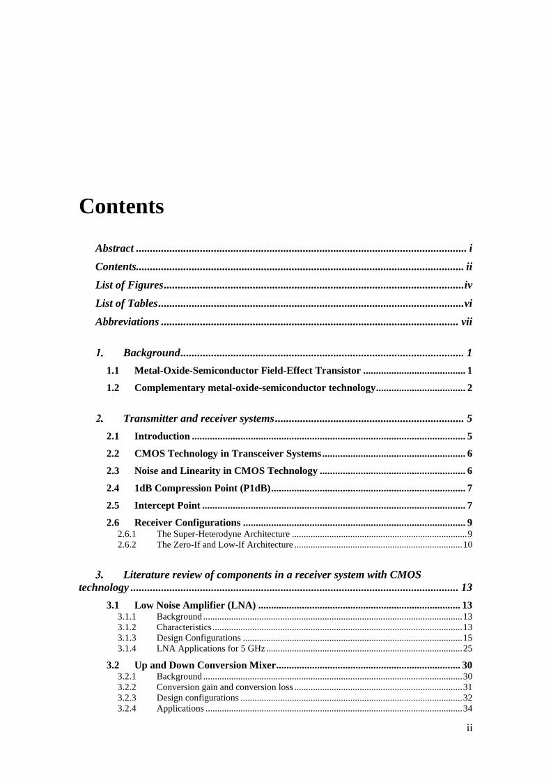
Abstract ....................................................................................................................... i
Contents...................................................................................................................... ii
List of Figures ............................................................................................................ iv
List of Tables .............................................................................................................. vi
Abbreviations ........................................................................................................... vii
Background ...................................................................................................... 1
1.1 Metal-Oxide-Semiconductor Field-Effect Transistor ........................................ 1
1.2 Complementary metal-oxide-semiconductor technology ................................... 2
Transmitter and receiver systems .................................................................... 5
2.1 Introduction ........................................................................................................... 5
2.2 CMOS Technology in Transceiver Systems ........................................................ 6
2.3 Noise and Linearity in CMOS Technology ......................................................... 6
2.4 1dB Compression Point (P1dB) ............................................................................ 7
2.5 Intercept Point ....................................................................................................... 7
2.6 Receiver Configurations ....................................................................................... 9 2.6.1 The Super-Heterodyne Architecture ........................................................................... 9 2.6.2 The Zero-If and Low-If Architecture ........................................................................ 10
Literature review of components in a receiver system with CMOS
technology ...................................................................................................................... 13
3.1 Low Noise Amplifier (LNA) ............................................................................... 13 3.1.1 Background ............................................................................................................... 13 3.1.2 Characteristics ........................................................................................................... 13 3.1.3 Design Configurations .............................................................................................. 15 3.1.4 LNA Applications for 5 GHz .................................................................................... 25
3.2 Up and Down Conversion Mixer ........................................................................ 30 3.2.1 Background ............................................................................................................... 30 3.2.2 Conversion gain and conversion loss ........................................................................ 31 3.2.3 Design configurations ............................................................................................... 32 3.2.4 Applications .............................................................................................................. 34
iii
3.3 Oscillator .............................................................................................................. 37 3.3.1 Introduction and General Background ...................................................................... 37 3.3.2 Ideal LC Tank ........................................................................................................... 38 3.3.3 Oscillator parameters ................................................................................................ 40 3.3.4 Voltage Controlled Oscillator (VCO) ....................................................................... 43
3.4 Power amplifier (PA) .......................................................................................... 51 3.4.1 Background ............................................................................................................... 51 3.4.2 Basic PA Parameters and Characteristics .................................................................. 51 3.4.3 Amplification-mode PA ............................................................................................ 53 3.4.4 Switching-mode PAs ................................................................................................. 59 3.4.5 Applications and Figure of Merits (FoMs)................................................................ 62
Conclusion ..................................................................................................... 66
References ...................................................................................................... 68

iv
List of Figures
Figure 1. a) MOS structure. Symbols of MOS b) with bulk terminal c) without bulk terminal [1].
....................................................................................................................................................... 1 Figure 2. Example of CMOS digital circuit. NMOS and PMOS connected in parallel. ............... 2 Figure 3.Fabrication of a CMOS Transistor [4]. ........................................................................... 3 Figure 4. Common Logic Gate using pull-up and pull-down blocks. ........................................... 3 Figure 5. Definition of P1dB. ........................................................................................................ 7 Figure 6. Definition of third order intercept point. ........................................................................ 8 Figure 7. Super-heterodyne receiver. ............................................................................................ 9 Figure 8. Generic Zero/Low IF receiver. .................................................................................... 10 Figure 9. Techniques to get resistive term in the input impedance of an LNA [11]. .................. 14 Figure 10. Common gate CMOS LNA [24]. ............................................................................... 16 Figure 11. NMOS common-source amplifier.............................................................................. 18 Figure 12. Common-source CMOS LNA with input matching [32]........................................... 18 Figure 13.CS LNA with an inductive degeneration [38]. ........................................................... 19 Figure 14. Cascode topology with source degeneration [24]. ..................................................... 20 Figure 15. Amplifier with capacitance between input and output............................................... 22 Figure 16. Effective capacitance circuit. ..................................................................................... 22 Figure 17. Distributed amplifier [46]. ......................................................................................... 22 Figure 18. Conventional differential amplifier. ........................................................................... 23 Figure 19.Differential capacitive cross coupled low-noise amplifier configuration [45]. .......... 24 Figure 20. Resistive current reuse amplifier [53]. ....................................................................... 25 Figure 21. Frequency mixer symbol a) Up-conversion b) Down-conversion. ............................ 30 Figure 22. Two input signals mixed and the output as the result. ............................................... 31 Figure 23. CMOS voltage mixer [72]. ........................................................................................ 32 Figure 24. Gilbert cell mixer topology [6]. ................................................................................. 33 Figure 25. Double-balanced Gilbert cell mixer [6]. .................................................................... 33 Figure 26. Block diagram with positive feedback [8]. ................................................................ 37 Figure 27. Most basic LC oscillator. ........................................................................................... 38 Figure 28. Oscillation of the basic LC oscillator a) with no feedback b) with feedback and
energy supply. ............................................................................................................................. 39 Figure 29. LC tank a) parallel b) series. ...................................................................................... 39 Figure 30. Possible parallel LC tank solutions. .......................................................................... 40 Figure 31. Possible interferences caused by phase noise [8]....................................................... 41 Figure 32. Frequency spectrum of a) ideal oscillator b) real oscillator [95]. .............................. 42 Figure 33. Amplitude and phase noise in time domain [8]. ........................................................ 43 Figure 34. Triangular waveform from a relaxation oscillator. .................................................... 44 Figure 35. CMOS single ended Colpitts oscillator [97]. ............................................................. 45 Figure 36. Cross-coupled VCO using CMOS [5]. ...................................................................... 46 Figure 37. 3-stages ring-VCO [98]. ............................................................................................ 47 Figure 38. Three stages oscillator [3]. ......................................................................................... 47 Figure 39. Graphics representing linearity of a PA: a) AM-to-AM b) AM-to-PM [118]. .......... 52
v
Figure 40. Power amplifiers divided by classes [121]. ............................................................... 53 Figure 41. Single-stage Class A PA [122]. ................................................................................. 54 Figure 42. Drain voltage and current waveforms for Class A PA [119]. .................................... 54 Figure 43. Differential Class B PA [117]. ................................................................................... 55 Figure 44. Drain voltage and current waveforms for Class B PA [119]. .................................... 55 Figure 45. Pull-push CMOS Class-B PA. ................................................................................... 56 Figure 46. Crossover distortion for Class-B PA [125]. ............................................................... 56 Figure 47. Drain voltage and current waveforms for Class-C [119]. .......................................... 57 Figure 48. Conduction mode in different classes of amplification-mode PA [114]. ................... 58 Figure 49. Class D PA [122]. ...................................................................................................... 59 Figure 50. Class E PA [122]. ....................................................................................................... 60 Figure 51. Class F PA [122]. ....................................................................................................... 61
vi
List of Tables Table 1. 5GHz LNA comparison with 130 nm CMOS technology. ........................................... 27 Table 2. 5GHz LNA comparison with 90, 180 and 250 nm CMOS technology. ....................... 28 Table 3. Comparison table of reported 5 GHz low-voltage CMOS UP-conversion mixers. ...... 35 Table 4. Comparison table of reported 5 GHz low-voltage CMOS DOWN-conversion mixers. 35 Table 5. Comparison table of reported 130 nm CMOS VCOs.................................................... 49 Table 6. Comparison table of reported 90, 180 and 250 nm CMOS VCOs. ............................... 49 Table 7. Summary table of the theoretical characteristics of the amplification-mode PA. ......... 58 Table 8. CMOS Amplification-Mode Power Amplifier comparison table. ................................ 63 Table 9. CMOS Switching-Mode Power Amplifier comparison table. ...................................... 64
vii
Abbreviations
ACLR Adjacent Channel Leakage Ratio
ACPR Adjacent Channel Power Ratio
BJT Bipolar Junction Transistor
CG Common gate
CMOS Complementary Metal-Oxide-Silicon
CS Common source
DC Direct Current
DE Drain Efficiency
ESD Electrostatic discharge
EVM Error Vector Magnitude
FET Field-Effect Transistor
FoM Figure of Merit
GaAs Gallium-Arsenide
HBT Heterojunction Bipolar Transistor
IC Integrated Circuit
IMN Input Matching Network
ITRS International Terrestrial Reference System
LNA Low-noise Amplifier
LO Local Oscillator
MOS Metal-Oxide-Semiconductor
MOSFET Metal-Oxide-Semiconductor Field Effect Transistor
NMOS N-channel Metal-Oxide-Semiconductor
OMN Output Matching Network
PA Power Amplifier
PAE Power-added efficiency
viii
PMOS P-channel Metal-Oxide-Semiconductor
RF Radio-Frequency
RX Receiver
SNR Signal-to-noise Ratio
SoC System on chip
TX Transmitter
VCO Voltage-Controlled Oscillator
WLAN Wireless Local Area Network

CHAPTER 1: Background -
1
CHAPTER 1
Background
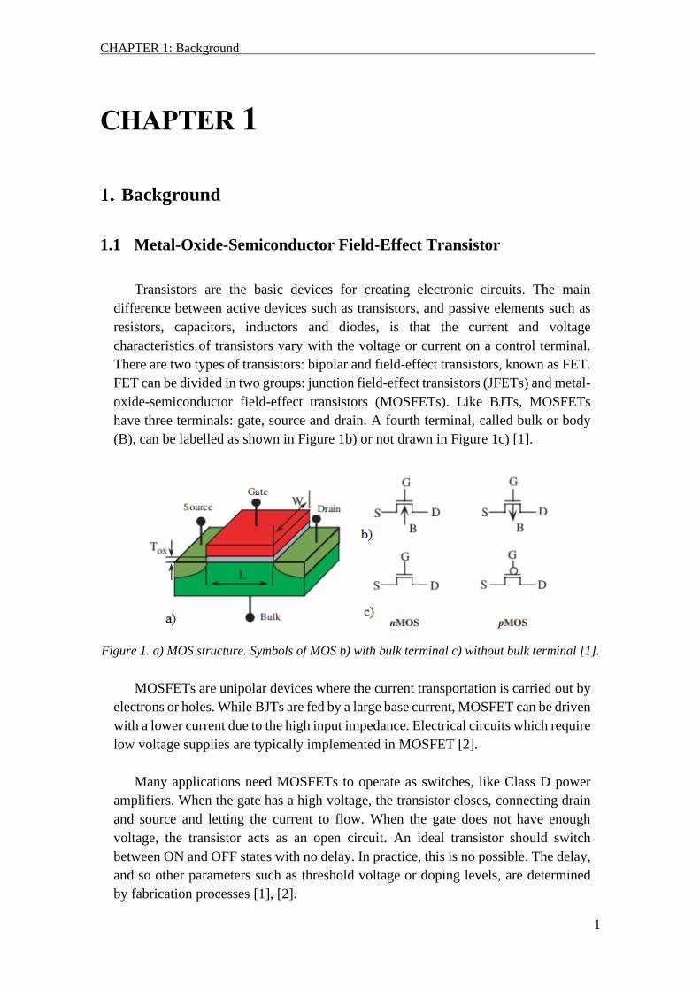
1.1 Metal-Oxide-Semiconductor Field-Effect Transistor
Transistors are the basic devices for creating electronic circuits. The main
difference between active devices such as transistors, and passive elements such as
resistors, capacitors, inductors and diodes, is that the current and voltage
characteristics of transistors vary with the voltage or current on a control terminal.
There are two types of transistors: bipolar and field-effect transistors, known as FET.
FET can be divided in two groups: junction field-effect transistors (JFETs) and metal-
oxide-semiconductor field-effect transistors (MOSFETs). Like BJTs, MOSFETs
have three terminals: gate, source and drain. A fourth terminal, called bulk or body
(B), can be labelled as shown in Figure 1b) or not drawn in Figure 1c) [1].
Figure 1. a) MOS structure. Symbols of MOS b) with bulk terminal c) without bulk terminal [1].
MOSFETs are unipolar devices where the current transportation is carried out by
electrons or holes. While BJTs are fed by a large base current, MOSFET can be driven
with a lower current due to the high input impedance. Electrical circuits which require
low voltage supplies are typically implemented in MOSFET [2].
Many applications need MOSFETs to operate as switches, like Class D power
amplifiers. When the gate has a high voltage, the transistor closes, connecting drain
and source and letting the current to flow. When the gate does not have enough
voltage, the transistor acts as an open circuit. An ideal transistor should switch
between ON and OFF states with no delay. In practice, this is no possible. The delay,
and so other parameters such as threshold voltage or doping levels, are determined
by fabrication processes [1], [2].
CHAPTER 1: Background -
2
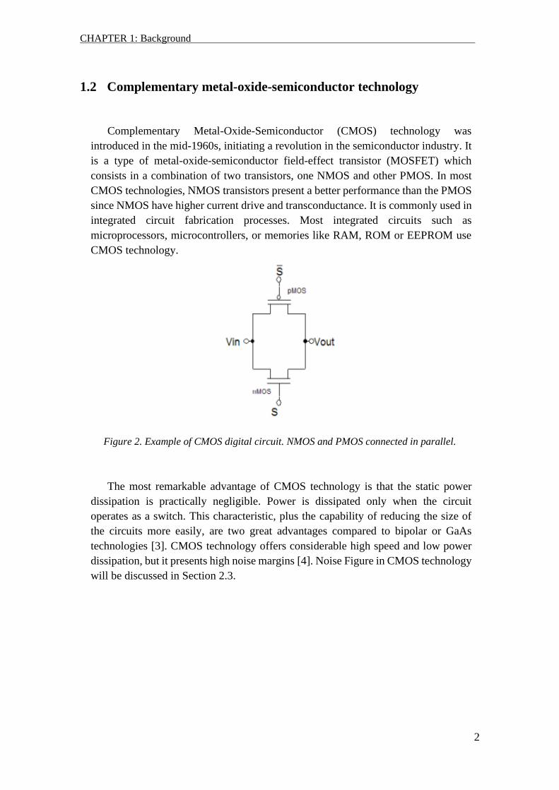
1.2 Complementary metal-oxide-semiconductor technology
Complementary Metal-Oxide-Semiconductor (CMOS) technology was
introduced in the mid-1960s, initiating a revolution in the semiconductor industry. It
is a type of metal-oxide-semiconductor field-effect transistor (MOSFET) which
consists in a combination of two transistors, one NMOS and other PMOS. In most
CMOS technologies, NMOS transistors present a better performance than the PMOS
since NMOS have higher current drive and transconductance. It is commonly used in
integrated circuit fabrication processes. Most integrated circuits such as
microprocessors, microcontrollers, or memories like RAM, ROM or EEPROM use
CMOS technology.
Figure 2. Example of CMOS digital circuit. NMOS and PMOS connected in parallel.
The most remarkable advantage of CMOS technology is that the static power
dissipation is practically negligible. Power is dissipated only when the circuit
operates as a switch. This characteristic, plus the capability of reducing the size of
the circuits more easily, are two great advantages compared to bipolar or GaAs
technologies [3]. CMOS technology offers considerable high speed and low power
dissipation, but it presents high noise margins [4]. Noise Figure in CMOS technology
will be discussed in Section 2.3.
CHAPTER 1: Background -
3
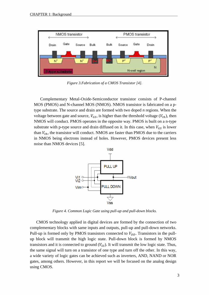
Figure 3.Fabrication of a CMOS Transistor [4].
Complementary Metal-Oxide-Semiconductor transistor consists of P-channel
MOS (PMOS) and N-channel MOS (NMOS). NMOS transistor is fabricated on a p-
type substrate. The source and drain are formed with two doped n regions. When the
voltage between gate and source, 𝑉𝐺𝑆, is higher than the threshold voltage (𝑉𝑡ℎ), then
NMOS will conduct. PMOS operates in the opposite way. PMOS is built on a n-type
substrate with p-type source and drain diffused on it. In this case, when 𝑉𝐺𝑆 is lower
than 𝑉𝑡ℎ, the transistor will conduct. NMOS are faster than PMOS due to the carriers
in NMOS being electrons instead of holes. However, PMOS devices present less
noise than NMOS devices [5].
Figure 4. Common Logic Gate using pull-up and pull-down blocks.
CMOS technology applied in digital devices are formed by the connection of two
complementary blocks with same inputs and outputs, pull-up and pull-down networks.
Pull-up is formed only by PMOS transistors connected to 𝑉𝐷𝐷. Transistors in the pull-
up block will transmit the high logic state. Pull-down block is formed by NMOS
transistors and it is connected to ground (𝑉𝑆𝑆). It will transmit the low logic state. Thus,
the same signal will turn on a transistor of one type and turn off the other. In this way,
a wide variety of logic gates can be achieved such as inverters, AND, NAND or NOR
gates, among others. However, in this report we will be focused on the analog design
using CMOS.


CHAPTER 2: Transmitter and receiver systems -
- -
5
CHAPTER 2
Transmitter and receiver systems
At first, an introduction about transmission and receiver systems is presented.
Different components used in a 5 GHz receiver system are discussed in this report.
Main components used in a receiver are low-noise amplifiers (LNAs), mixer, voltage-
controlled oscillators (VCOs) and power amplifiers (PAs).
2.1 Introduction
Transmission and receiver (or transceiver) systems are devices which transmit
and receive electromagnetic signals. The signals in which information travels are
transmitted by using high frequency. Transceiver systems, like a common radio are
characterized by their carrier frequency. Usually a carrier frequency for a radio is
900MHz or 5 GHz [6], and generally, the higher the carrier frequency, the better
directivity, but the more complex circuit design.
Most radio receiver systems use the same basic architecture although there are
varieties on the configuration [7]. These different configurations will be discussed in
this report. Main functions of a receiver system are capturing the radio waves with an
antenna, processing all the waves and extracting only the desired waves which vibrate
at the wanted frequency. An important aspect to consider is the strong attenuation
that signals can suffer during air transmission. For this reason, RF signals must be
amplified and recovered [8].
Receivers should not be turn off completely, otherwise, signals cannot be received
when a transmitter is emitting data. Receivers shall detect whenever a transmitter
requests an active communication. That is the reason why two different working
modes are found in the receivers. If the receiver is not active, then it must work in the
stand-by mode, in which DC power consumption should be much less than in the
active mode. Due to this reason, DC power consumption is one of the most important
parameters when designing a receiver. On the other hand, some transmitter functions
are modulation, frequency conversion and power amplification. Unlike receivers,
transmitters can be completely switched off for power saving. These only need to be
in the active mode when data wants to be transmitted. Normally, the power
consumption of transceivers is measured by its transmitter power consumption rather
than by its receiver’s. This is because transmitters need a high output power to emit
data and that leads to a high DC power consumption [8].
CHAPTER 2: Transmitter and receiver systems -
- -
6
2.2 CMOS Technology in Transceiver Systems
Over the years, the integration of more complex circuits into smaller chips has
become a reality. The integration of circuits using CMOS technology went low cost
and drives the improvement of modern radio frequency integrated circuit designs. It
is now possible to use this technology in transceiver systems, such as 5 GHz wireless
LAN systems. Designers have been studying how to implement improvements to the
main features of the various IC building blocks which make up a device on smaller
and smaller chips.
CMOS processes are usually preferable in comparison with other processes, like
bipolar or GaAs, because of its lower cost and better integration with digital signal
processing (DSP) chips. In addition, the size of CMOS devices has been more easily
shrunken than other technologies. However, limitations in noise and linearity has
become a challenge for designers since other processes like GaAs present better
performance in these aspects [6].
2.3 Noise and Linearity in CMOS Technology
The Noise Figure (NF) also called noise factor, is the decrease in the signal-to-
noise ratio (SNR) as a signal passes through a system network [9]. The signal-to-
noise ratio is an important figure of merit (FoM) in receivers. It is a measure which
compares the level of the wanted signal to the level of the noise. Thus, a low noise
figure means the system is working with very little level of added noise.
This parameter is used to make comparisons between different devices by
measuring the added noise produced by these systems. With the noise figure,
system’s sensitivity can be calculated from its bandwidth. In case of a receiver, the
sensitivity indicates what is the weakest signal that the receiver will be able to identify
and process [9], [10]. The lower the noise figure, the better the sensitivity. Some
authors have studied how the use of MOSFET transistors normally present more
noise figure than circuits which use bipolar transistors. However, the use of CMOS
technology has improved the performance in this aspect in recent years, obtaining
noise figures close to HBT or bipolar circuits [6]. The way of improving the NF of
CMOS technology is by applying noise figure optimization techniques described in
[11]. Noise figure optimization techniques will be discussed in the next sections.
Linearity specifies the capacity of a device to manage large signals.
Intermodulation can appear while using large signals which drive to an inefficient
circuit and bad performance. CMOS circuits need linearization techniques to improve
linearity and to try getting as good performance as GaAs circuits.
CHAPTER 2: Transmitter and receiver systems -
- -
7
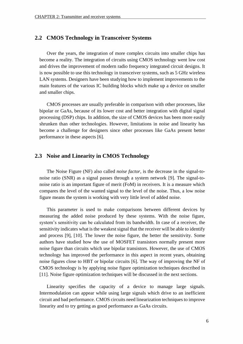
2.4 1dB Compression Point (P1dB)
Related to linearity limitations of CMOS technology, there is a parameter which
describes the tolerance to desensitization of a circuit called the 1 dB compression
point. This parameter describes the output power level at which the gain decreases 1
dB from its constant value. When an amplifier reaches the P1dB it goes into
compression and behaves more in non-linear way producing harmonics, distortion
and intermodulation products.
Figure 5. Definition of P1dB.
The 1 dB compression point is one of important figure of merit (FoM) for circuits
like low-noise amplifiers, power amplifiers or mixers. In general, CMOS have a
lower P1dB which limits the output power for linear operations [6].
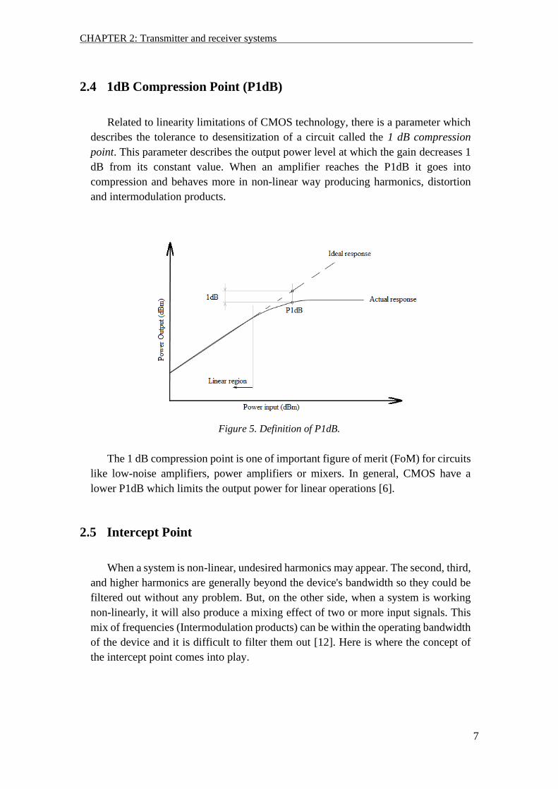
2.5 Intercept Point
When a system is non-linear, undesired harmonics may appear. The second, third,
and higher harmonics are generally beyond the device's bandwidth so they could be
filtered out without any problem. But, on the other side, when a system is working
non-linearly, it will also produce a mixing effect of two or more input signals. This
mix of frequencies (Intermodulation products) can be within the operating bandwidth
of the device and it is difficult to filter them out [12]. Here is where the concept of
the intercept point comes into play.
CHAPTER 2: Transmitter and receiver systems -
- -
8
Figure 6. Definition of third order intercept point.
The third intercept point value (IP3) measures how long a signal can be processed
by the device before intermodulation distortion (IMD) occurs [12]. This concept
describes the linearity of a circuit and is commonly used to indicate the level of
intermodulation. It is defined as the point in which linear extrapolation of the
fundamental signal and linear extrapolation of the 𝑛𝑡ℎ order harmonic crosses each
other. It can be read from the input (IIP3) or output (OIP3) power axis [6]. The third
order intercept point (IP3) is shown in Figure 6. Specially, IP3 is a specific figure of
merit of nonlinear systems and devices like receivers, transmitters, amplifiers or
mixers. The higher the IP3, the smaller the intermodulation signal [6].
The IIP3 is an important parameter when designing a receiver because it gives an
idea of how much distortion is produced by our device [12]. The objective when
designing a circuit is to achieve the highest IIP3 taking care of power consumption,
size or gain. Keeping a high value of IIP3 means the device will be better.
CHAPTER 2: Transmitter and receiver systems -
- -
9
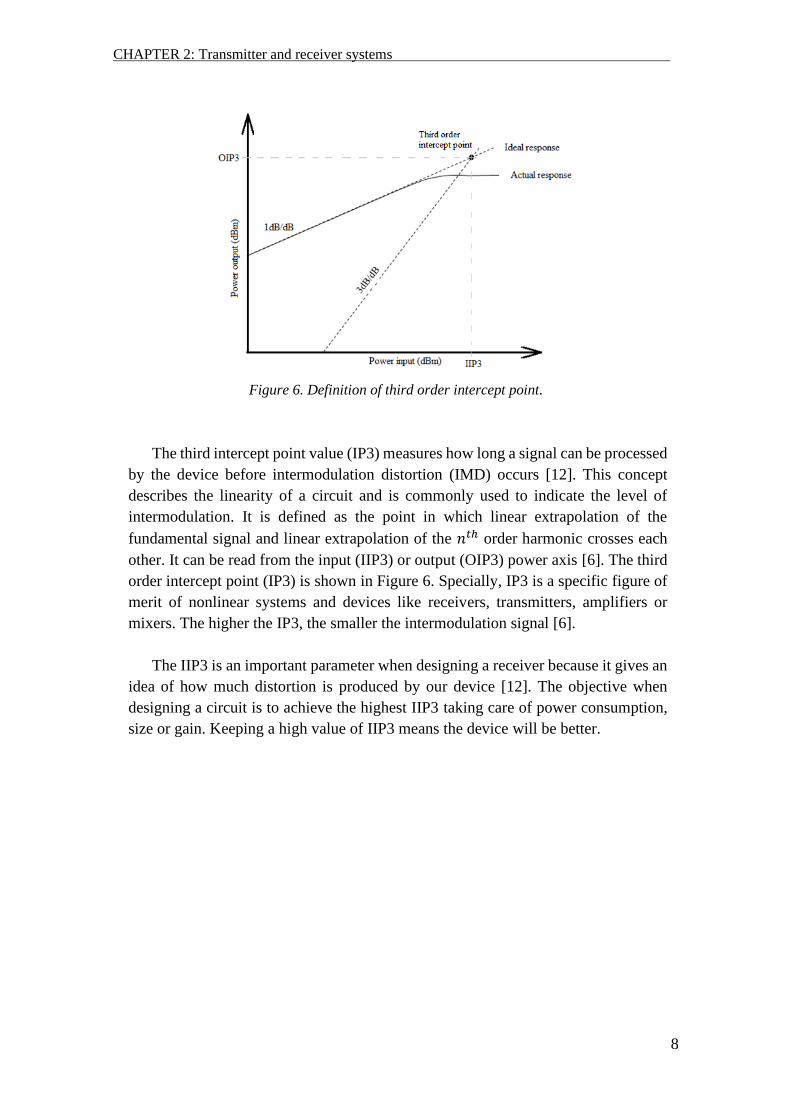
2.6 Receiver Configurations
2.6.1 The Super-Heterodyne Architecture
Figure 7. Super-heterodyne receiver.
Conventional super-heterodyne receiver is shown in image above. Main
components of a receiver are low-noise amplifiers, mixer, filters, local oscillator and
demodulator. This configuration is called super-heterodyne because of the
combination of terms “supersonic” and “heterodyne”. It is supersonic, since signal is
not audible in the intermediate frequency stage, and heterodyne, because the local
oscillator device must work at a different frequency than the received signal [13].
The antenna is connected to the LNA, but it also could be connected to a selective
bandpass filter which eliminates possible interferers. Low-noise amplifier improves
the weakest channels and send the signal to next block, the mixer. Mixer will get a
new output signal frequency from two input signals, RF and LO.
In receivers, it is important to pay attention in filters, especially in image filters.
These are in charge of filtering out those frequencies that could be located above and
below the LO frequency. If those frequencies are not filtered and they pass through
the mixer, there is no way to separate the original signal and the interferer image
signal. To solve this problem, an image rejection filter is required to supress the
mirror signal at next frequency,
𝑓𝑖𝑚𝑎𝑔𝑒 = 𝐼𝐹𝑐𝑢𝑟𝑟𝑒𝑛𝑡 + 2𝐼𝐹𝑛𝑒𝑤
( 1 )
where 𝐼𝐹𝑐𝑢𝑟𝑟𝑒𝑛𝑡 is the frequency of the current of the signal received and 𝐼𝐹𝑛𝑒𝑤 is the
frequency signal obtained after the mixer [7]. Is important to pay attention on this
issue, otherwise, signals whose frequency is similar to the image frequency could
interfered in our desired signal [13]. This means that, if the frequency of an image
CHAPTER 2: Transmitter and receiver systems -
- -
10
signal is less than two times the intermediate frequency, the receiver will pick it up
and will convert it to the IF [14]. In addition, the first filter connected before the LNA
contributes to filtering image frequency signals. The way of solving image interfering
problem is by using high-Q (quality factor) tuned circuits ahead of the mixer. With a
higher quality factor, the bandwidth is reduced, so there are fewer frequencies that
can interfere with the system. Normally, having higher Qs is difficult and circuit
designs become more complicate. Another solution is using a higher IF. With a higher
IF, the minimum frequency that can interfere with the system also increases [14].
Thus, it is very difficult to achieve the necessary Q factor. That is the reason why the
conversion ratio must be realized in two or more steps, requiring more image filters
[7].
2.6.2 The Zero-If and Low-If Architecture
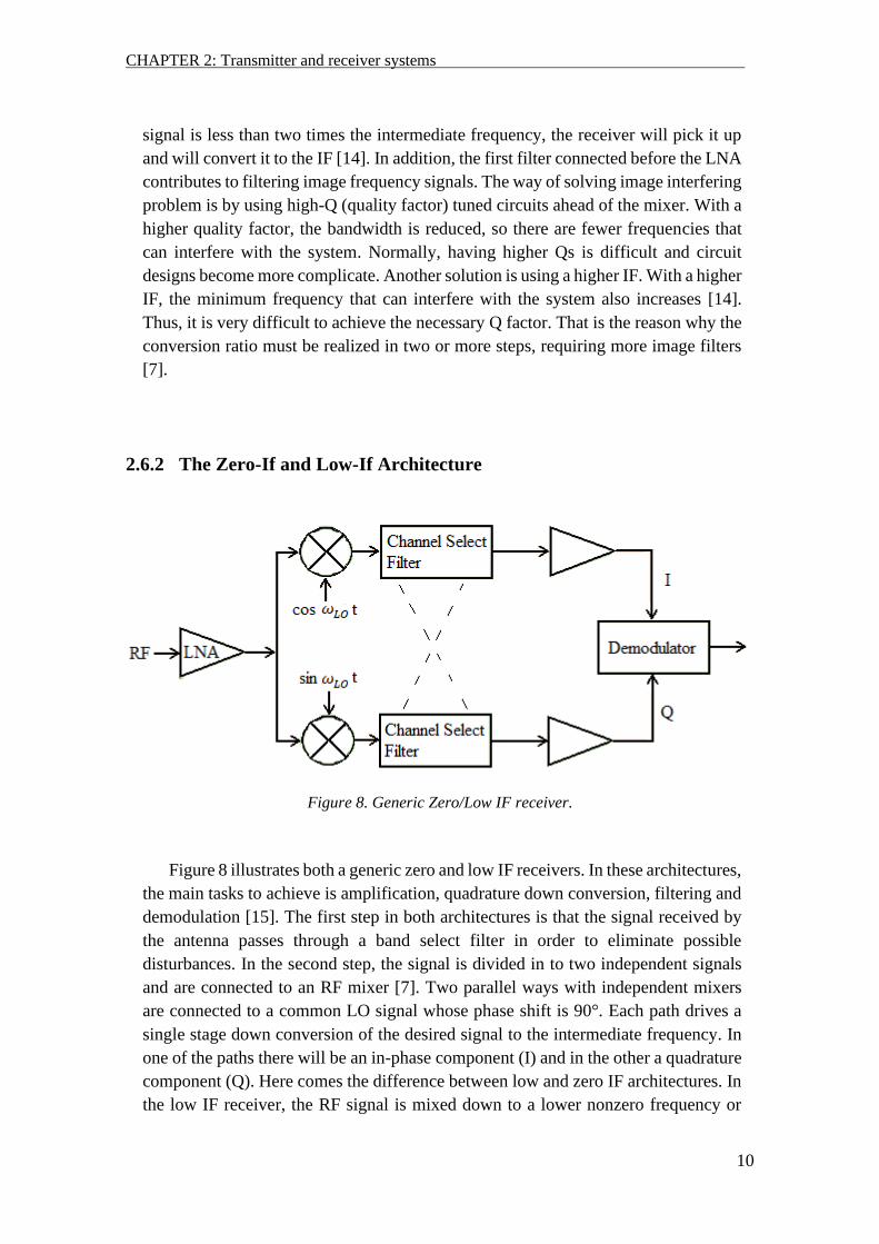
Figure 8. Generic Zero/Low IF receiver.
Figure 8 illustrates both a generic zero and low IF receivers. In these architectures,
the main tasks to achieve is amplification, quadrature down conversion, filtering and
demodulation [15]. The first step in both architectures is that the signal received by
the antenna passes through a band select filter in order to eliminate possible
disturbances. In the second step, the signal is divided in to two independent signals
and are connected to an RF mixer [7]. Two parallel ways with independent mixers
are connected to a common LO signal whose phase shift is 90°. Each path drives a
single stage down conversion of the desired signal to the intermediate frequency. In
one of the paths there will be an in-phase component (I) and in the other a quadrature
component (Q). Here comes the difference between low and zero IF architectures. In
the low IF receiver, the RF signal is mixed down to a lower nonzero frequency or
CHAPTER 2: Transmitter and receiver systems -
- -
11
intermediate frequency while in the zero IF receiver, the signal is converted to DC
[7].
In the next chapter, the necessary components for implementing a receiver system
using CMOS technology will be discussed. Different characteristics of those
components will be compared.

CHAPTER 3: Literature review of components in a receiver system with CMOS technology -
-
13
CHAPTER 3
Literature review of components in a receiver system with
CMOS technology
3.1 Low Noise Amplifier (LNA)
3.1.1 Background
A low-noise amplifier is an electronic amplifier that operates with a low input
signal and obtains considerable good gain without amplifying possible noise received
in the input. It amplifies the signal without adding much noise at its output. A typical
amplifier receives the power signal and undesired noise in its input and increase both.
In addition, the amplifier itself produces an undesired noise which will make the
amplifier’s output worse. Hence, there will be too much amplified noise in the output
signal. To achieve a better performance, LNAs are necessary to have optimum noise
performance while having decent gain.
Thus, in most high-performance radio receivers a receiver system must have an
LNA as the first active block. It is typically the first block after the antenna and its
design is fundamental for the correct operation of the receiver. It is the one in charge
of amplifying the input signals so that the noise produced by following blocks have
less impact on the system signal-to-noise ratio (SNR) [16], [17].
Depending on the applications, several circuits with different configurations have
been proposed over the years for LNA. The most common designs of CMOS LNA
circuits were generated with common gate (CG) or common source (CS) topologies.
There are other different configurations, such as cascode stages, used in radio
frequencies (RF) [18] which will be discussed in Section 3.1.3.
3.1.2 Characteristics
The two most critical characteristics of an LNA architecture are noise efficiency
and power gain. Other parameters, such as DC power consumption, stability or
voltage supply can also affect LNA’s performance.
Getting minimum noise figure (NF) and maximum power gain hardly happen at
the same impedance state. That is why a correct input matching network is required
in order to improve both parameters [17]. One of the most significant aspects of
CMOS technology is that it can provide a good minimal LNA noise (𝑁𝐹𝑚í𝑛) with
also a considerable good usable power gain at the same time. Having a good noise
figure is possible using optimum noise matching. On the other hand, having
CHAPTER 3: Literature review of components in a receiver system with CMOS technology -
-
14
maximum power gain is possible using a correct impedance matching known as
conjugate matching. Hence, these two different configurations are opposite ways of
matching the transmission line, so it would not be possible to obtain them
simultaneously without CMOS technology [19], [20]. T. Yao et. al [19] designed a
60 GHz power and low-noise amplifier using 90 nm CMOS technology. In this paper,
T. Yao et. al measured the optimal minimum noise figure (𝑁𝐹𝑚í𝑛), which occurs at
0.15 mA/𝜇m and was considerably close to the peak (𝑓𝑚𝑎𝑥) current density which
occurs at 0.2 mA/𝜇m.
Favourably, as we have seen, one important advantage of CMOS technology is
that minimum noise figure and maximum power gain are very close together, so it is
easier to get a considerable good noise performance [19]. It depends on the width of
the CMOS transistor. Input and noise matching were studied by H. Song et. al in 2008
[21] where it is explained how to choose components to satisfy the optimum matching
conditions using the Smith Chart.
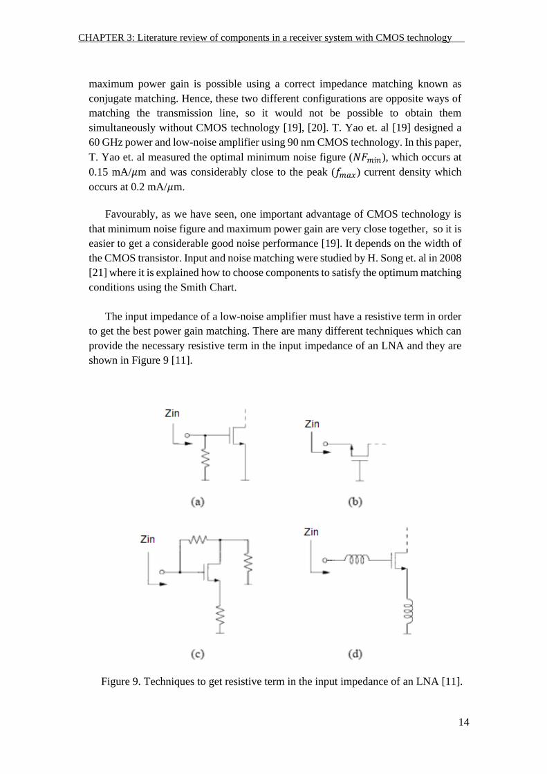
The input impedance of a low-noise amplifier must have a resistive term in order
to get the best power gain matching. There are many different techniques which can
provide the necessary resistive term in the input impedance of an LNA and they are
shown in Figure 9 [11].
Figure 9. Techniques to get resistive term in the input impedance of an LNA [11].
CHAPTER 3: Literature review of components in a receiver system with CMOS technology -
-
15
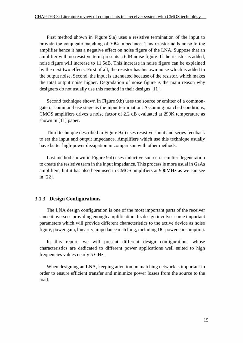
First method shown in Figure 9.a) uses a resistive termination of the input to
provide the conjugate matching of 50Ω impedance. This resistor adds noise to the
amplifier hence it has a negative effect on noise figure of the LNA. Suppose that an
amplifier with no resistive term presents a 6dB noise figure. If the resistor is added,
noise figure will increase to 11.5dB. This increase in noise figure can be explained
by the next two effects. First of all, the resistor has his own noise which is added to
the output noise. Second, the input is attenuated because of the resistor, which makes
the total output noise higher. Degradation of noise figure is the main reason why
designers do not usually use this method in their designs [11].
Second technique shown in Figure 9.b) uses the source or emitter of a common-
gate or common-base stage as the input termination. Assuming matched conditions,
CMOS amplifiers drives a noise factor of 2.2 dB evaluated at 290K temperature as
shown in [11] paper.
Third technique described in Figure 9.c) uses resistive shunt and series feedback
to set the input and output impedance. Amplifiers which use this technique usually
have better high-power dissipation in comparison with other methods.
Last method shown in Figure 9.d) uses inductive source or emitter degeneration
to create the resistive term in the input impedance. This process is more usual in GaAs
amplifiers, but it has also been used in CMOS amplifiers at 900MHz as we can see
in [22].
3.1.3 Design Configurations
The LNA design configuration is one of the most important parts of the receiver
since it oversees providing enough amplification. Its design involves some important
parameters which will provide different characteristics to the active device as noise
figure, power gain, linearity, impedance matching, including DC power consumption.
In this report, we will present different design configurations whose
characteristics are dedicated to different power applications well suited to high
frequencies values nearly 5 GHz.
When designing an LNA, keeping attention on matching network is important in
order to ensure efficient transfer and minimize power losses from the source to the
load.
CHAPTER 3: Literature review of components in a receiver system with CMOS technology -
-
16
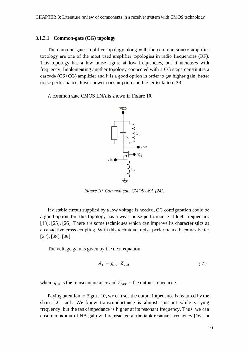
3.1.3.1 Common-gate (CG) topology
The common gate amplifier topology along with the common source amplifier
topology are one of the most used amplifier topologies in radio frequencies (RF).
This topology has a low noise figure at low frequencies, but it increases with
frequency. Implementing another topology connected with a CG stage constitutes a
cascode (CS+CG) amplifier and it is a good option in order to get higher gain, better
noise performance, lower power consumption and higher isolation [23].
A common gate CMOS LNA is shown in Figure 10.
Figure 10. Common gate CMOS LNA [24].
If a stable circuit supplied by a low voltage is needed, CG configuration could be
a good option, but this topology has a weak noise performance at high frequencies
[18], [25], [26]. There are some techniques which can improve its characteristics as
a capacitive cross coupling. With this technique, noise performance becomes better
[27], [28], [29].
The voltage gain is given by the next equation
𝐴𝑣 = 𝑔𝑚 · 𝑍𝑜𝑢𝑡
( 2 )
where 𝑔𝑚 is the transconductance and 𝑍𝑜𝑢𝑡 is the output impedance.
Paying attention to Figure 10, we can see the output impedance is featured by the
shunt LC tank. We know transconductance is almost constant while varying
frequency, but the tank impedance is higher at its resonant frequency. Thus, we can
ensure maximum LNA gain will be reached at the tank resonant frequency [16]. In

CHAPTER 3: Literature review of components in a receiver system with CMOS technology -
-
17
general, the inductor of the tank has worse quality than the capacitor, so the tank
impedance is mostly limited by the inductor’s quality. The tank impedance at the
resonant frequency is given by
𝑍𝑜𝑢𝑡 = 𝑄𝐿𝑂𝑤𝑜𝐿𝑜
( 3 )
where 𝑄𝐿𝑂 is the quality factor of the inductor, 𝑤𝑜 is the resonant angular frequency
and 𝐿𝑜 is the inductance of the tank inductor [6].
CMOS RF receivers usually need a common gate (CG) stage because it is easy to
make the impedance matching and also has lower noise than other topologies [30].
One example of a CG LNA is the design created by David J. Allstot et. al [31].
They designed a common-gate LNA using a general 𝑔𝑚 boosted technique using
cross-coupled capacitors. They concluded that a 𝑔𝑚 boosted CG LNA can provide
better noise performance, and power consumption is lower than a conventional
common gate (CG) or common source (CS) LNA. At a frequency of 5.6 GHz, CS
and CG LNA exhibit a noise figure of 2.87 dB and 2.95 dB, respectively, while the
𝑔𝑚 boosted CG LNA presents 1.69 dB of NF.
3.1.3.2 Common-source (CS) topology
Common source amplifier is one of the most used amplifiers in industry in CMOS
analog circuits because it exhibits some advantages over common-gate (CG) LNAs
such as lower NF or higher gain [32], [33], [34], [35]. Other characteristics of this
topology are high input impedance, speed or simplicity. Basic CS LNA circuits are
extensively used in CMOS RF integrated circuits because its stage provides superior
noise figure performance. However, temperature, sensitivity to bias and component
tolerances could be critical characteristics while trying to achieve best noise figure
performance [17], [31].
In this topology the input signal is introduced into the gate terminal and exits the
drain, and the only remaining terminal source is grounded. Typically, the output of a
common source circuit is connected either a common drain (CD) stage or to a
common gate (CG) stage in order to get better output results and better frequency
characteristics [36]. The mixed configuration formed by a common-source (CS) stage
and a common-gate (CG) stage is called a cascode amplifier. Cascode amplifier will
be discussed in Section 3.1.3.3.
CHAPTER 3: Literature review of components in a receiver system with CMOS technology -
-
18
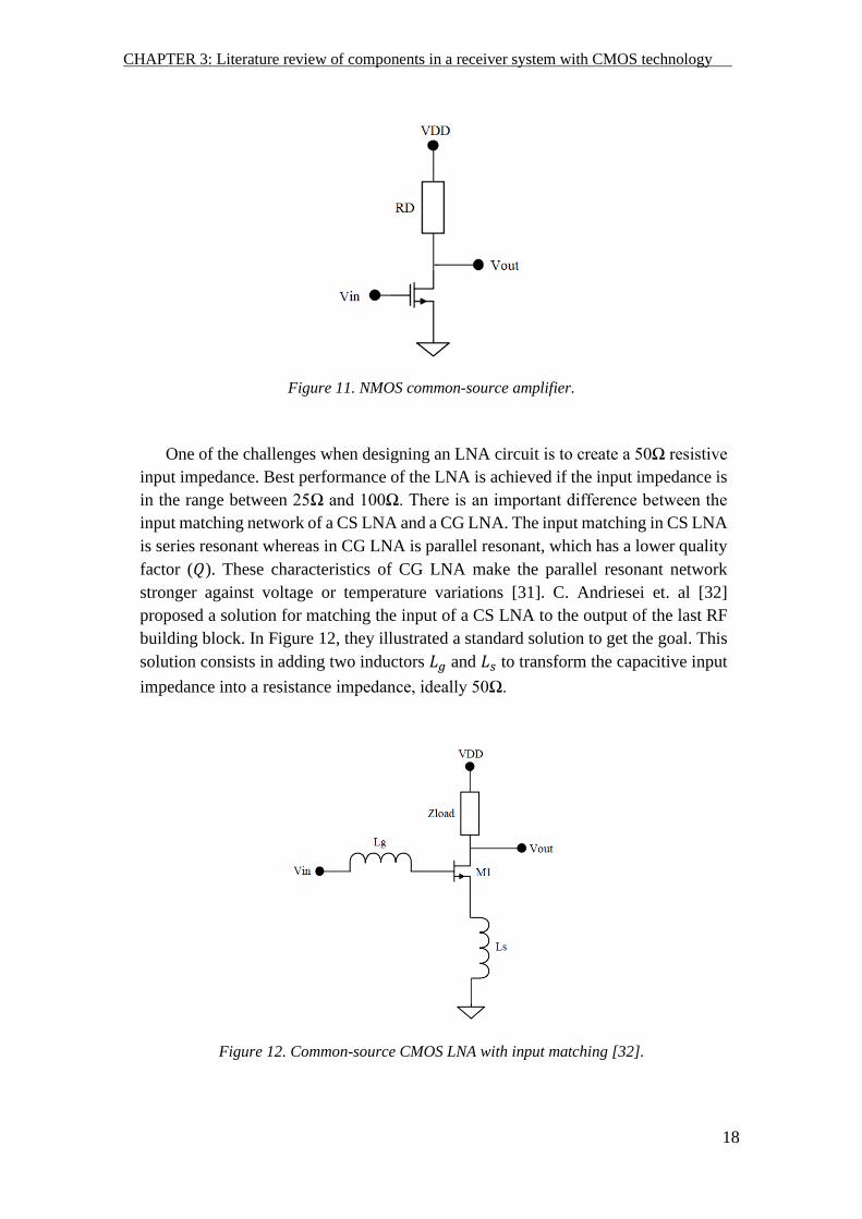
Figure 11. NMOS common-source amplifier.
One of the challenges when designing an LNA circuit is to create a 50Ω resistive
input impedance. Best performance of the LNA is achieved if the input impedance is
in the range between 25Ω and 100Ω. There is an important difference between the
input matching network of a CS LNA and a CG LNA. The input matching in CS LNA
is series resonant whereas in CG LNA is parallel resonant, which has a lower quality
factor (𝑄). These characteristics of CG LNA make the parallel resonant network
stronger against voltage or temperature variations [31]. C. Andriesei et. al [32]
proposed a solution for matching the input of a CS LNA to the output of the last RF
building block. In Figure 12, they illustrated a standard solution to get the goal. This
solution consists in adding two inductors 𝐿𝑔 and 𝐿𝑠 to transform the capacitive input
impedance into a resistance impedance, ideally 50Ω.
Figure 12. Common-source CMOS LNA with input matching [32].
CHAPTER 3: Literature review of components in a receiver system with CMOS technology -
-
19
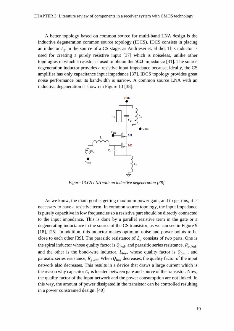
A better topology based on common source for multi-band LNA design is the
inductive degeneration common source topology (IDCS). IDCS consists in placing
an inductor 𝐿𝑔 in the source of a CS stage, as Andriesei et. al did. This inductor is
used for creating a purely resistive input [37] which is noiseless, unlike other
topologies in which a resistor is used to obtain the 50Ω impedance [31]. The source
degeneration inductor provides a resistive input impedance because, ideally, the CS
amplifier has only capacitance input impedance [37]. IDCS topology provides great
noise performance but its bandwidth is narrow. A common source LNA with an
inductive degeneration is shown in Figure 13 [38].
Figure 13.CS LNA with an inductive degeneration [38].
As we know, the main goal is getting maximum power gain, and to get this, it is
necessary to have a resistive term. In common source topology, the input impedance
is purely capacitive in low frequencies so a resistive part should be directly connected
to the input impedance. This is done by a parallel resistive term in the gate or a
degenerating inductance in the source of the CS transistor, as we can see in Figure 9
[18], [25]. In addition, this inductor makes optimum noise and power points to be
close to each other [39]. The parasitic resistance of 𝐿𝑔 consists of two parts. One is
the spiral inductor whose quality factor is 𝑄𝑖𝑛𝑑, and parasitic series resistance, 𝑅𝑔,𝑖𝑛𝑑,
and the other is the bond-wire inductor, 𝐿𝑏𝑤, whose quality factor is 𝑄𝑏𝑤 , and
parasitic series resistance, 𝑅𝑔,𝑏𝑤. When 𝑄𝑖𝑛𝑑 decreases, the quality factor of the input
network also decreases. This results in a device that draws a large current which is
the reason why capacitor 𝐶1 is located between gate and source of the transistor. Now,
the quality factor of the input network and the power consumption are not linked. In
this way, the amount of power dissipated in the transistor can be controlled resulting
in a power constrained design. [40]
CHAPTER 3: Literature review of components in a receiver system with CMOS technology -
-
20
The advantages of the IDCS topology, combined with the use of a multi-section
input network, makes that a lot of narrowband systems work with this topology. Its
good input noise properties can be used in wideband CMOS LNA designs [41].
An example of an IDCS CMOS LNA design is proposed by F. Gianesello et. al
[42] who designed a 5 GHz LNA using 130 nm SOI CMOS technology for WLAN
applications. Their design presents 1.4 dB noise figure and a gain of 14 dB at 5 GHz
with a DC power consumption of 10 mW.
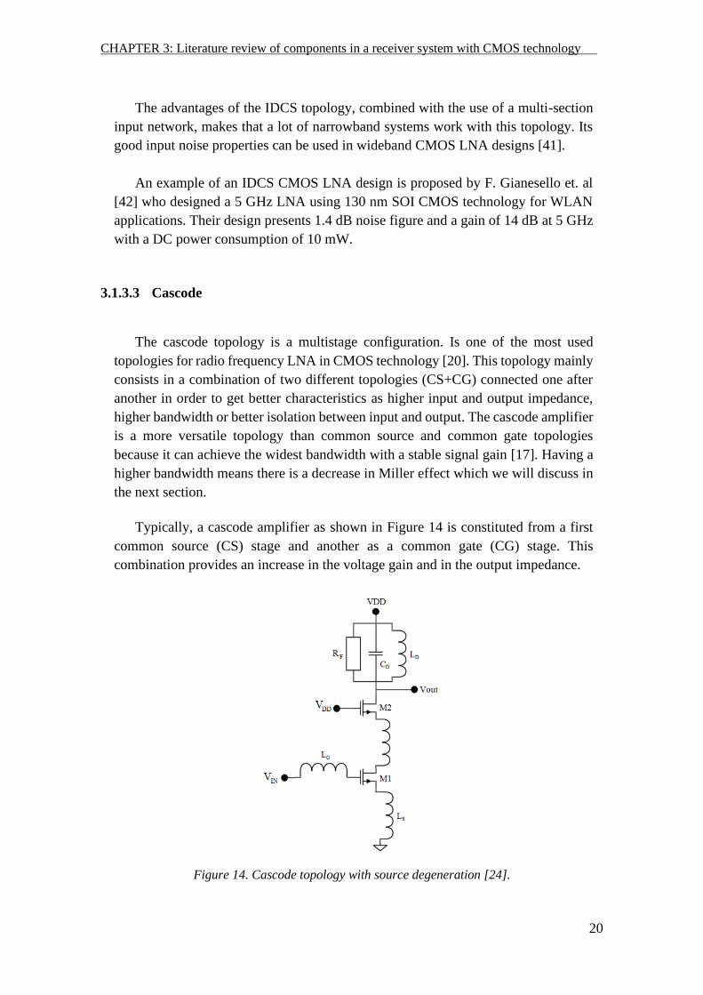
3.1.3.3 Cascode
The cascode topology is a multistage configuration. Is one of the most used
topologies for radio frequency LNA in CMOS technology [20]. This topology mainly
consists in a combination of two different topologies (CS+CG) connected one after
another in order to get better characteristics as higher input and output impedance,
higher bandwidth or better isolation between input and output. The cascode amplifier
is a more versatile topology than common source and common gate topologies
because it can achieve the widest bandwidth with a stable signal gain [17]. Having a
higher bandwidth means there is a decrease in Miller effect which we will discuss in
the next section.
Typically, a cascode amplifier as shown in Figure 14 is constituted from a first
common source (CS) stage and another as a common gate (CG) stage. This
combination provides an increase in the voltage gain and in the output impedance.
Figure 14. Cascode topology with source degeneration [24].

CHAPTER 3: Literature review of components in a receiver system with CMOS technology -
-
21
The first stage of the circuit is a common source amplifier in which the input
signal is introduced into the gate terminal of M1. The following stage is a common
gate amplifier which is the output of the circuit. As we can see in the Figure 14, the
output voltage is taken from the drain gate of M2.
At high frequencies, we should take care about the different capacitances the
transistors present. Otherwise, an imprecisely frequency response will be obtained.
Cascode topology with source degeneration is widely used in LNA circuits with
CMOS technology [23]. As we can see in Figure 14 there are two inductors 𝐿𝑠 and
𝐿𝑔. The first of them, 𝐿𝑠 is connected to the source of first transistor 𝑀1 and it is the
source degeneration inductor. The second one, 𝐿𝑔, connected at the gate terminal of
same transistor 𝑀1 is used for input matching [23].
An example of a cascode circuit design is the one made by S. Ambulker et. al [43]
where they used a single stage common source amplifier followed by a common gate
stage. Their design presents a gain of 14.4 dB and 2.04 dB of noise figure.
Some other authors have been studying different techniques for improving
cascode topologies like T.S. Kim et. al [44] who applied the IMD Sinking Method to
a cascode topology to improve linearity of the cascode LNA at the expense of lower
gain and noise figure. The design with this technique implemented achieved an IIP3
of 13.3 dB which is an 8 dB improvement.
Miller Effect
Miller effect is the multiplication of the input capacitance times the voltage gain
(Equation 4). This capacitance tends to reduce the bandwidth and, will be worse if it
is increased because of the multiplication of the voltage gain. If bandwidth is reduced,
the operation range will also be reduced, and the device could work improperly at
certain frequencies. In Figure 16 it is shown how the equivalent circuit of an amplifier
is considering Miller Effect.
At high frequencies, input impedance is almost zero because, as we know, the
higher the frequency, the lower the impedance of a capacitor. If the input impedance
is close to zero, then it can be considered as a short circuit and could cause serious
damage to the circuit.
𝐶𝑀𝑖𝑙𝑙𝑒𝑟 = 𝐶(1 − 𝐴𝑉)
( 4 )
CHAPTER 3: Literature review of components in a receiver system with CMOS technology -
-
22
Figure 15. Amplifier with capacitance between input and output.
Figure 16. Effective capacitance circuit.
This effect can be reduced in different ways, by adding a voltage buffer stage in
the input, by adding a current buffer stage in the output or with cascade topology [11].
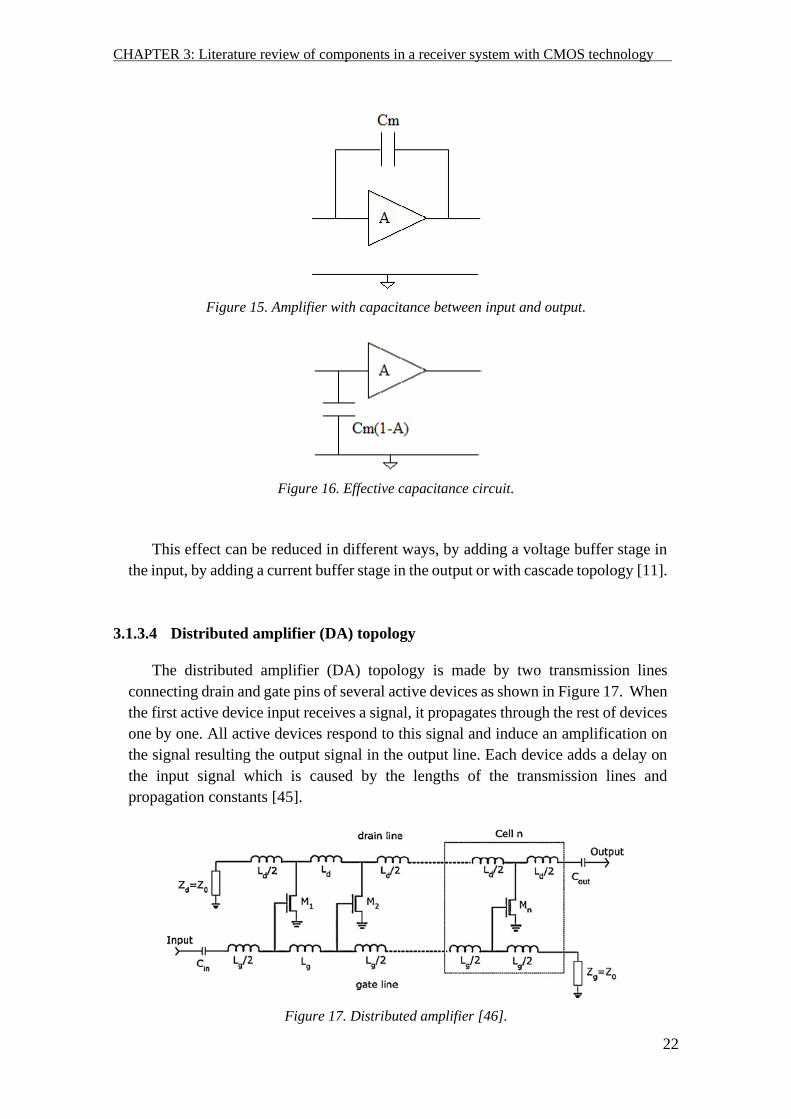
3.1.3.4 Distributed amplifier (DA) topology
The distributed amplifier (DA) topology is made by two transmission lines
connecting drain and gate pins of several active devices as shown in Figure 17. When
the first active device input receives a signal, it propagates through the rest of devices
one by one. All active devices respond to this signal and induce an amplification on
the signal resulting the output signal in the output line. Each device adds a delay on
the input signal which is caused by the lengths of the transmission lines and
propagation constants [45].
Figure 17. Distributed amplifier [46].
CHAPTER 3: Literature review of components in a receiver system with CMOS technology -
-
23
As we can see in Figure 17, each cell is separated using inductors which
accumulate the gain of each transistor without any negative effects on the bandwidth.
Main advantage of DA topology is that it has good input and output impedance
matching but the high-power consumption they need to work properly, and the big
size they occupy have both limited its applications [47]. A disadvantage of the CMOS
distributed amplifiers (DAs) is that they present a high noise figure due to the thermal
noise generated by resistive parts, especially the terminating gate resistor [48]. This,
along the high-power consumption, made this architecture unattractive for LNA
designers. However, authors like C. Aitchison [49] have demonstrated that the
reverse gain of the distributed amplifier topology shields the noise generated by the
terminating gate resistor located at the output, so noise figure is not limited by a 3 dB
floor except at very low or high frequencies [47].
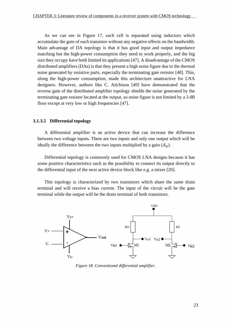
3.1.3.5 Differential topology
A differential amplifier is an active device that can increase the difference
between two voltage inputs. There are two inputs and only one output which will be
ideally the difference between the two inputs multiplied by a gain (𝐴𝑑).
Differential topology is commonly used for CMOS LNA designs because it has
some positive characteristics such as the possibility to connect its output directly to
the differential input of the next active device block like e.g. a mixer [20].
This topology is characterized by two transistors which share the same drain
terminal and will receive a bias current. The input of the circuit will be the gate
terminal while the output will be the drain terminal of both transistors.
Figure 18. Conventional differential amplifier.
CHAPTER 3: Literature review of components in a receiver system with CMOS technology -
-
24
The output voltage of a differential amplifier is given by
𝑉𝑜𝑢𝑡 = 𝐴𝑑(𝑉𝑖𝑛1 − 𝑉𝑖𝑛2)
(5)
where 𝑉𝑖𝑛1 − 𝑉𝑖𝑛2 are the input voltages.
Reality is different, thus if both inputs have same voltage, output voltage should
be zero, but we notice this fact does not happen. Hence, we must consider this factor
and add it to the equation.
𝑉𝑜𝑢𝑡 = 𝐴𝑑(𝑉𝑖𝑛1 − 𝑉𝑖𝑛2) + 𝐴𝑐(𝑉𝑖𝑛1 + 𝑉𝑖𝑛2
2)
(6)
where 𝐴𝑐 is the gain when both input voltages are the same, called the common-mode
gain.
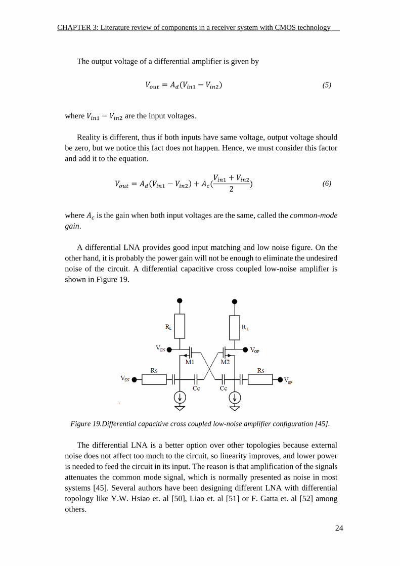
A differential LNA provides good input matching and low noise figure. On the
other hand, it is probably the power gain will not be enough to eliminate the undesired
noise of the circuit. A differential capacitive cross coupled low-noise amplifier is
shown in Figure 19.
Figure 19.Differential capacitive cross coupled low-noise amplifier configuration [45].
The differential LNA is a better option over other topologies because external
noise does not affect too much to the circuit, so linearity improves, and lower power
is needed to feed the circuit in its input. The reason is that amplification of the signals
attenuates the common mode signal, which is normally presented as noise in most
systems [45]. Several authors have been designing different LNA with differential
topology like Y.W. Hsiao et. al [50], Liao et. al [51] or F. Gatta et. al [52] among
others.
CHAPTER 3: Literature review of components in a receiver system with CMOS technology -
-
25
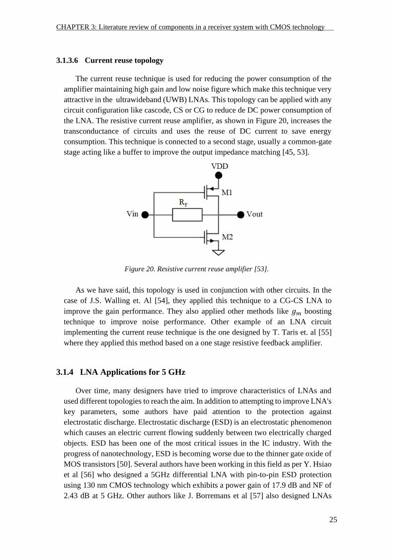
3.1.3.6 Current reuse topology
The current reuse technique is used for reducing the power consumption of the
amplifier maintaining high gain and low noise figure which make this technique very
attractive in the ultrawideband (UWB) LNAs. This topology can be applied with any
circuit configuration like cascode, CS or CG to reduce de DC power consumption of
the LNA. The resistive current reuse amplifier, as shown in Figure 20, increases the
transconductance of circuits and uses the reuse of DC current to save energy
consumption. This technique is connected to a second stage, usually a common-gate
stage acting like a buffer to improve the output impedance matching [45, 53].
Figure 20. Resistive current reuse amplifier [53].
As we have said, this topology is used in conjunction with other circuits. In the
case of J.S. Walling et. Al [54], they applied this technique to a CG-CS LNA to
improve the gain performance. They also applied other methods like 𝑔𝑚 boosting
technique to improve noise performance. Other example of an LNA circuit
implementing the current reuse technique is the one designed by T. Taris et. al [55]
where they applied this method based on a one stage resistive feedback amplifier.
3.1.4 LNA Applications for 5 GHz
Over time, many designers have tried to improve characteristics of LNAs and
used different topologies to reach the aim. In addition to attempting to improve LNA's
key parameters, some authors have paid attention to the protection against
electrostatic discharge. Electrostatic discharge (ESD) is an electrostatic phenomenon
which causes an electric current flowing suddenly between two electrically charged
objects. ESD has been one of the most critical issues in the IC industry. With the
progress of nanotechnology, ESD is becoming worse due to the thinner gate oxide of
MOS transistors [50]. Several authors have been working in this field as per Y. Hsiao
et al [56] who designed a 5GHz differential LNA with pin-to-pin ESD protection
using 130 nm CMOS technology which exhibits a power gain of 17.9 dB and NF of
2.43 dB at 5 GHz. Other authors like J. Borremans et al [57] also designed LNAs
CHAPTER 3: Literature review of components in a receiver system with CMOS technology -
-
26
with ESD protection. In this case, they achieved an LNA with a NF of 2.6 dB and
power gain of 14.8 dB. Both LNA designs used a differential topology with 130 nm
CMOS process. A deeper comparison with more LNA designs is shown in Table 1
and Table 2.
CMOS technology is commonly used in LNAs for wireless communications at
gigahertz frequencies due to its low cost, high-level integration and high performance
in terms of cutoff frequency [58]. Wireless local area networks (WLANs) working in
5 GHz frequency are being used for multimedia applications. Depending on the
WLAN, it is necessary to design a transceiver which is suitable for each WLAN. In
a receiver, the LNA must provide enough voltage gain and input matching with a low
NF [59]. For applications above 5 GHz, CMOS technology presents low
transconductance and signal loss through the conducting silicon substrate [42].
CMOS LNAs also have important functions in ultrawideband (UWB) systems.
The Federal Communications Commission (FCC) authorized the UWB technology
to be used in the frequency band between 3.1 GHz and 10.6 GHz. This technology
can manage high data rate communications in short range applications. UWB was
defined by the International Telecommunication Union (ITU) in 2006 as a
“technology for short-range radiocommunication, involving the intentional
generation and transmission of radio-frequency energy that spreads over a very large
frequency range, which may overlap several frequency bands allocated to
radiocommunication services. Devices using UWB technology typically have
intentional radiation from the antenna with either a –10 dB bandwidth of at least 500
MHz or a –10 dB fractional bandwidth greater than 0.2”. Authors have been studying
different techniques and configurations to obtain better performances in the design of
the UWB LNA. Some examples of these designs are shown in Table 1 and Table 2,
like M. Khurram et al [60] whose design exhibits a small signal gain (𝑆21) of 13 dB
and a noise figure (NF) of 3.5-4.5 dB.
A standard FoM has been used in literatures to make comparisons between
different LNA designs. Several authors [61], [62], [63], [64] defined the FoM of an
LNA as
𝐹𝑜𝑀 =𝐺 · 𝐼𝐼𝑃3 · 𝐵𝑊
𝑃𝐷𝐶(𝑁𝐹 − 1)
( 7 )
where G is the small signal gain (|𝑆21|), IIP3 is the value of the third order input
intercept point, BW is the bandwidth in GHz, PDC is the DC power consumption and
NF is the noise figure in dB. There are some cases in which IIP3 can be substituted
by P1dB. However, other ways for comparing different LNA designs are
implemented.

CHAPTER 3: Literature review of components in a receiver system with CMOS technology -
-
27
Reference
CMOS
Technology
(nm)
Architecture
Gain
(|S21|)
(dB)
Frequency
(GHz)
NF
(dB)
S11
(dB)
P1dB
(dBm)
IIP3
(dBm)
PDC
(mW)
[42] 130 IDCS 14 5 1.4 -12 -* -* 10
[50] 130 Differential w/
ESD
protection 18 5 2.62 <-25 -* -* 10.3
[50] 130 Differential
w/o ESD
protection 16.2 5 2 <-25 -* -* 10.3
[57] 130 IDCS with
ESD
protection 14.8 5.5 2.6 -* -* -9 6.6
[60] 130 CS 13 3.1-4.8 3.5 -8 -15.4 6.1 -*
*Missing information.
Table 1. 5GHz LNA comparison with 130 nm CMOS technology.
CHAPTER 3: Literature review of components in a receiver system with CMOS technology -
-
28
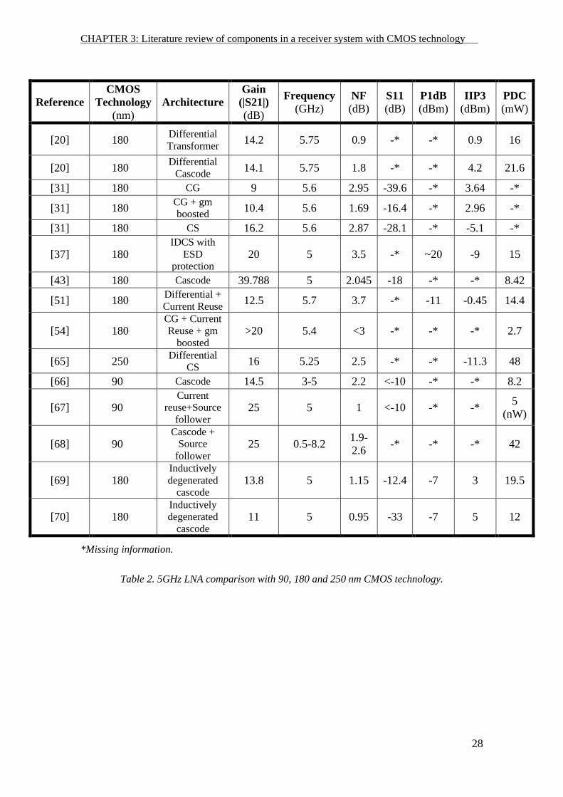
Reference
CMOS
Technology
(nm)
Architecture
Gain
(|S21|)
(dB)
Frequency
(GHz)
NF
(dB)
S11
(dB)
P1dB
(dBm)
IIP3
(dBm)
PDC
(mW)
[20] 180 Differential
Transformer 14.2 5.75 0.9 -* -* 0.9 16
[20] 180 Differential
Cascode 14.1 5.75 1.8 -* -* 4.2 21.6
[31] 180 CG 9 5.6 2.95 -39.6 -* 3.64 -*
[31] 180 CG + gm
boosted 10.4 5.6 1.69 -16.4 -* 2.96 -*
[31] 180 CS 16.2 5.6 2.87 -28.1 -* -5.1 -*
[37] 180 IDCS with
ESD
protection 20 5 3.5 -* ~20 -9 15
[43] 180 Cascode 39.788 5 2.045 -18 -* -* 8.42
[51] 180 Differential +
Current Reuse 12.5 5.7 3.7 -* -11 -0.45 14.4
[54] 180 CG + Current
Reuse + gm
boosted >20 5.4 <3 -* -* -* 2.7
[65] 250 Differential
CS 16 5.25 2.5 -* -* -11.3 48
[66] 90 Cascode 14.5 3-5 2.2 <-10 -* -* 8.2
[67] 90 Current
reuse+Source
follower 25 5 1 <-10 -* -*
5
(nW)
[68] 90 Cascode +
Source
follower 25 0.5-8.2
1.9-
2.6 -* -* -* 42
[69] 180 Inductively
degenerated
cascode 13.8 5 1.15 -12.4 -7 3 19.5
[70] 180 Inductively
degenerated
cascode 11 5 0.95 -33 -7 5 12
*Missing information.
Table 2. 5GHz LNA comparison with 90, 180 and 250 nm CMOS technology.

-
CHAPTER 3: Literature review of components in a receiver system with CMOS technology -
-
30
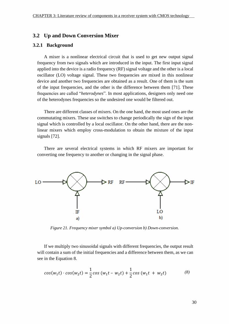
3.2 Up and Down Conversion Mixer
3.2.1 Background
A mixer is a nonlinear electrical circuit that is used to get new output signal
frequency from two signals which are introduced in the input. The first input signal
applied into the device is a radio frequency (RF) signal voltage and the other is a local
oscillator (LO) voltage signal. These two frequencies are mixed in this nonlinear
device and another two frequencies are obtained as a result. One of them is the sum
of the input frequencies, and the other is the difference between them [71]. These
frequencies are called “heterodynes”. In most applications, designers only need one
of the heterodynes frequencies so the undesired one would be filtered out.
There are different classes of mixers. On the one hand, the most used ones are the
commutating mixers. These use switches to change periodically the sign of the input
signal which is controlled by a local oscillator. On the other hand, there are the non-
linear mixers which employ cross-modulation to obtain the mixture of the input
signals [72].
There are several electrical systems in which RF mixers are important for
converting one frequency to another or changing in the signal phase.
Figure 21. Frequency mixer symbol a) Up-conversion b) Down-conversion.
If we multiply two sinusoidal signals with different frequencies, the output result
will contain a sum of the initial frequencies and a difference between them, as we can
see in the Equation 8.
𝑐𝑜𝑠(𝑤1𝑡) · 𝑐𝑜𝑠(𝑤2𝑡) =1
2𝑐𝑜𝑠 (𝑤1𝑡 – 𝑤2𝑡) +
1
2𝑐𝑜𝑠 (𝑤1𝑡 + 𝑤2𝑡) (8)
CHAPTER 3: Literature review of components in a receiver system with CMOS technology -
-
31
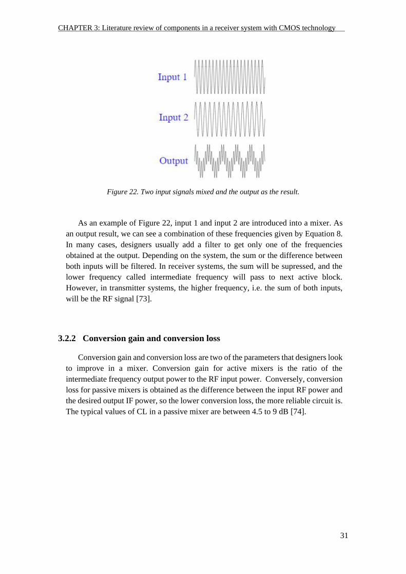
Figure 22. Two input signals mixed and the output as the result.
As an example of Figure 22, input 1 and input 2 are introduced into a mixer. As
an output result, we can see a combination of these frequencies given by Equation 8.
In many cases, designers usually add a filter to get only one of the frequencies
obtained at the output. Depending on the system, the sum or the difference between
both inputs will be filtered. In receiver systems, the sum will be supressed, and the
lower frequency called intermediate frequency will pass to next active block.
However, in transmitter systems, the higher frequency, i.e. the sum of both inputs,
will be the RF signal [73].
3.2.2 Conversion gain and conversion loss
Conversion gain and conversion loss are two of the parameters that designers look
to improve in a mixer. Conversion gain for active mixers is the ratio of the
intermediate frequency output power to the RF input power. Conversely, conversion
loss for passive mixers is obtained as the difference between the input RF power and
the desired output IF power, so the lower conversion loss, the more reliable circuit is.
The typical values of CL in a passive mixer are between 4.5 to 9 dB [74].
CHAPTER 3: Literature review of components in a receiver system with CMOS technology -
-
32
3.2.3 Design configurations
When designing a mixer, one of the parameters that designers have always been
concerned about is IP3. The big challenge is to filter the third order product. The
tolerance level that a mixer supports is measured by IP3. Getting higher IP3 is
possible by increasing local oscillator power or by having a better design [75].
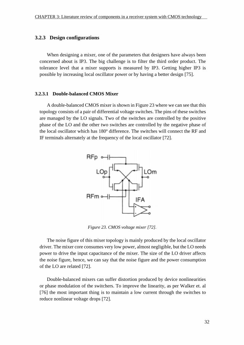
3.2.3.1 Double-balanced CMOS Mixer
A double-balanced CMOS mixer is shown in Figure 23 where we can see that this
topology consists of a pair of differential voltage switches. The pins of these switches
are managed by the LO signals. Two of the switches are controlled by the positive
phase of the LO and the other two switches are controlled by the negative phase of
the local oscillator which has 180º difference. The switches will connect the RF and
IF terminals alternately at the frequency of the local oscillator [72].
Figure 23. CMOS voltage mixer [72].
The noise figure of this mixer topology is mainly produced by the local oscillator
driver. The mixer core consumes very low power, almost negligible, but the LO needs
power to drive the input capacitance of the mixer. The size of the LO driver affects
the noise figure, hence, we can say that the noise figure and the power consumption
of the LO are related [72].
Double-balanced mixers can suffer distortion produced by device nonlinearities
or phase modulation of the switchers. To improve the linearity, as per Walker et. al
[76] the most important thing is to maintain a low current through the switches to
reduce nonlinear voltage drops [72].
CHAPTER 3: Literature review of components in a receiver system with CMOS technology -
-
33
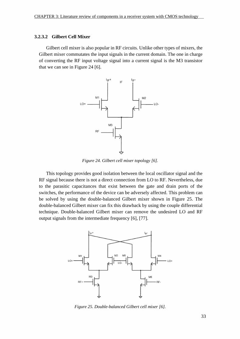
3.2.3.2 Gilbert Cell Mixer
Gilbert cell mixer is also popular in RF circuits. Unlike other types of mixers, the
Gilbert mixer commutates the input signals in the current domain. The one in charge
of converting the RF input voltage signal into a current signal is the M3 transistor
that we can see in Figure 24 [6].
Figure 24. Gilbert cell mixer topology [6].
This topology provides good isolation between the local oscillator signal and the
RF signal because there is not a direct connection from LO to RF. Nevertheless, due
to the parasitic capacitances that exist between the gate and drain ports of the
switches, the performance of the device can be adversely affected. This problem can
be solved by using the double-balanced Gilbert mixer shown in Figure 25. The
double-balanced Gilbert mixer can fix this drawback by using the couple differential
technique. Double-balanced Gilbert mixer can remove the undesired LO and RF
output signals from the intermediate frequency [6], [77].
Figure 25. Double-balanced Gilbert cell mixer [6].
CHAPTER 3: Literature review of components in a receiver system with CMOS technology -
-
34
Designers usually modify the basic structure of the Gilbert cell mixer to achieve
better results. A. Kara-Omar et. al [78] presented an example of up-conversion mixer
using a new topology of mixer based on the Gilbert cell architecture. It was created
to improve the input impedance matching over a bigger frequency range. Another
technique used for improving the linearity of the Gilbert topology is described by W.-
S. Hxiao et. al [79] who designed a Gilbert mixer with a current-reuse technique.
Some other 5 GHz mixer designs are shown in Table 3 and Table 4.
3.2.4 Applications
Mixer converters are commonly used in radio transmitters, modems, satellite
communications, radar, telemetry systems and phones, among others. The local
oscillator can be either a sinusoidal wave or a square wave. These are commonly used
in receiver front-ends and transmitter systems. In these systems, double balanced
topology is the most used because the sum of input frequencies is filtered and only
the intermediate frequency (IF) is seen at the output. In the case of a receiver, a down-
conversion mixer is required, so inputs are RF signal and LO signal. Thus, the
intermediate frequency will be seen at the output. On the other hand, in the case of
transmitter systems, the IF signal is the input of the mixer and will be multiplied by
LO to produce the RF signal [73]. Other configurations like Gilbert cells are also
quite common in industry for implementing circuits, not only as frequency mixers,
but also as variable gain amplifier, balanced modulator, phase detector or four
quadrant analog multiplier.
With a mixer it is also possible to compare the phase of the input signals. The
mixer will extract the phase difference between them and will be seen at the output
[71].
In the medical field, the Wireless Body Area Networks (WBANs) are beginning
to grow. WBANs are wireless communication network used by low-power devices
placed in the human body. These networks are made up of electronic devices, such
as sensors or microphones, with the aim of obtaining information on the vital signs
of the patient. These components need to transmit the captured information being
powered by small batteries. In line with these needs, designers have been studying
the way of creating RF circuits powered with less than 1 V. M. Rahman et. al [80]
designed a low-power low-noise mixer using 65 nm CMOS technology which could
be powered with 0.7 V at a frequency range of 2.3-2.5 GHz.
In order to compare the performance of different mixers designs, there are many
ways to express the figure of merit of a mixer. One common FoM is defined in [81]
given by
CHAPTER 3: Literature review of components in a receiver system with CMOS technology -
-
35
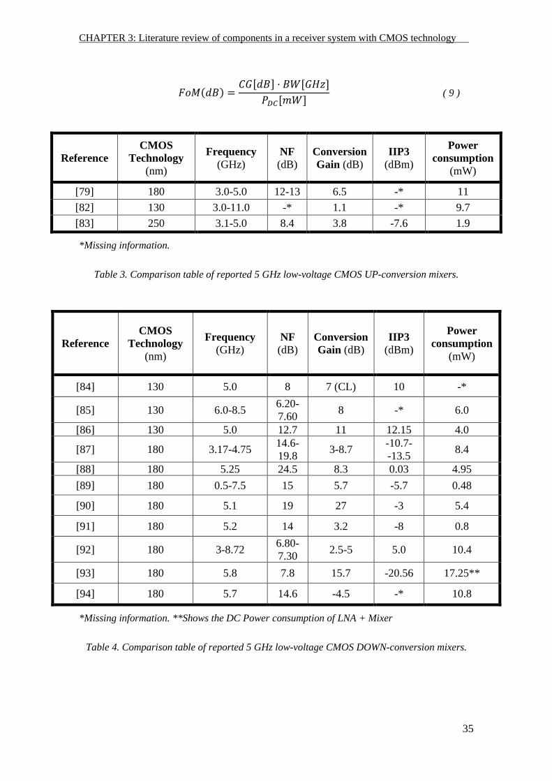
𝐹𝑜𝑀(𝑑𝐵) =𝐶𝐺[𝑑𝐵] · 𝐵𝑊[𝐺𝐻𝑧]
𝑃𝐷𝐶[𝑚𝑊]
( 9 )
Reference
CMOS
Technology
(nm)
Frequency
(GHz)
NF
(dB)
Conversion
Gain (dB)
IIP3
(dBm)
Power
consumption
(mW)
[79] 180 3.0-5.0 12-13 6.5 -* 11
[82] 130 3.0-11.0 -* 1.1 -* 9.7
[83] 250 3.1-5.0 8.4 3.8 -7.6 1.9
*Missing information.
Table 3. Comparison table of reported 5 GHz low-voltage CMOS UP-conversion mixers.
Reference
CMOS
Technology
(nm)
Frequency
(GHz)
NF
(dB)
Conversion
Gain (dB)
IIP3
(dBm)
Power
consumption
(mW)
[84] 130 5.0 8 7 (CL) 10 -*
[85] 130 6.0-8.5 6.20-
7.60 8 -* 6.0
[86] 130 5.0 12.7 11 12.15 4.0
[87] 180 3.17-4.75 14.6-
19.8 3-8.7
-10.7-
-13.5 8.4
[88] 180 5.25 24.5 8.3 0.03 4.95
[89] 180 0.5-7.5 15 5.7 -5.7 0.48
[90] 180 5.1 19 27 -3 5.4
[91] 180 5.2 14 3.2 -8 0.8
[92] 180 3-8.72 6.80-
7.30 2.5-5 5.0 10.4
[93] 180 5.8 7.8 15.7 -20.56 17.25**
[94] 180 5.7 14.6 -4.5 -* 10.8
*Missing information. **Shows the DC Power consumption of LNA + Mixer
Table 4. Comparison table of reported 5 GHz low-voltage CMOS DOWN-conversion mixers.

-
CHAPTER 3: Literature review of components in a receiver system with CMOS technology -
37
3.3 Oscillator
3.3.1 Introduction and General Background
The electronic oscillator is a device which provides an oscillating and periodic
electric signal without an input AC signal. An oscillator converts DC power input
into an AC waveform. In transceivers, the function of the oscillator is to provide the
local oscillator (LO) signal which is connected to one of the inputs of the mixer.
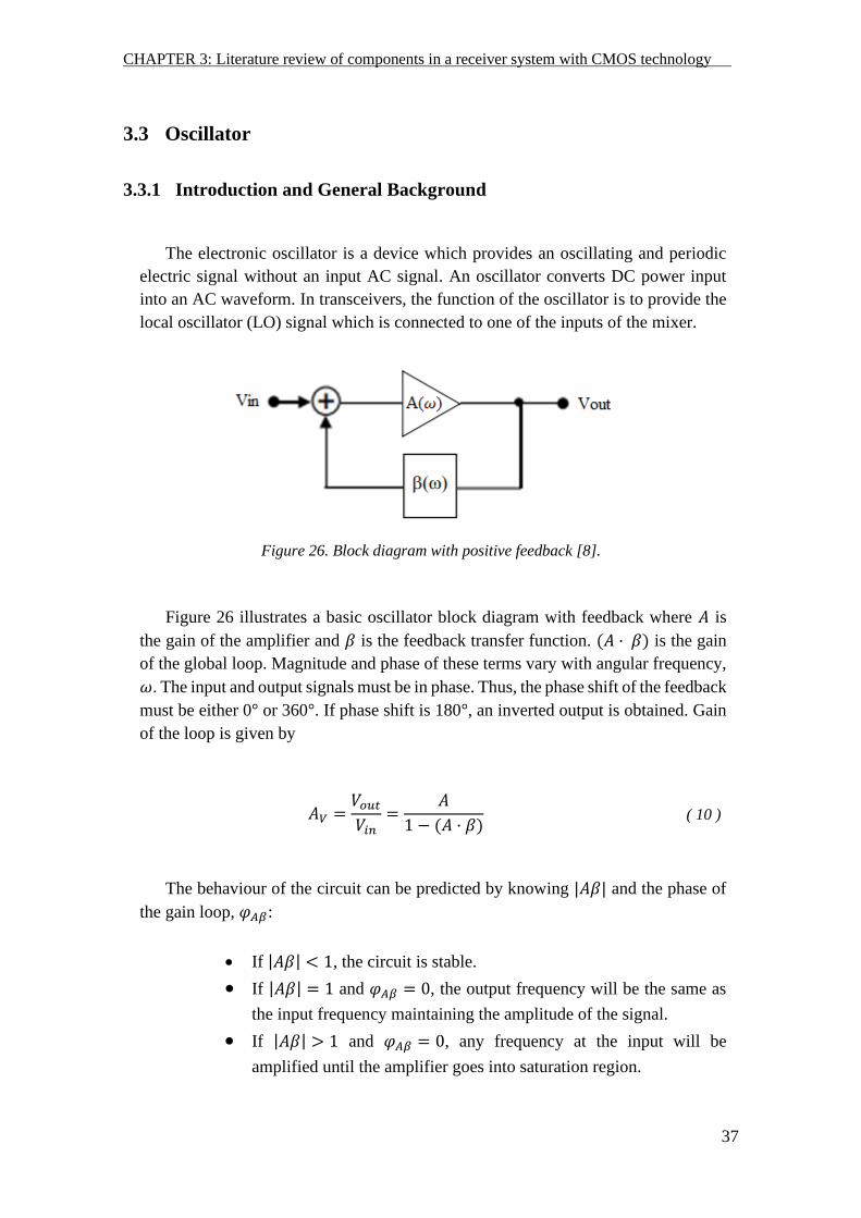
Figure 26. Block diagram with positive feedback [8].
Figure 26 illustrates a basic oscillator block diagram with feedback where 𝐴 is
the gain of the amplifier and 𝛽 is the feedback transfer function. (𝐴 · 𝛽) is the gain
of the global loop. Magnitude and phase of these terms vary with angular frequency,
𝜔. The input and output signals must be in phase. Thus, the phase shift of the feedback
must be either 0° or 360°. If phase shift is 180°, an inverted output is obtained. Gain
of the loop is given by
𝐴𝑉 =𝑉𝑜𝑢𝑡
𝑉𝑖𝑛=
𝐴
1 − (𝐴 · 𝛽)
( 10 )
The behaviour of the circuit can be predicted by knowing |𝐴𝛽| and the phase of
the gain loop, 𝜑𝐴𝛽:
• If |𝐴𝛽| < 1, the circuit is stable.
• If |𝐴𝛽| = 1 and 𝜑𝐴𝛽 = 0, the output frequency will be the same as
the input frequency maintaining the amplitude of the signal.
• If |𝐴𝛽| > 1 and 𝜑𝐴𝛽 = 0, any frequency at the input will be
amplified until the amplifier goes into saturation region.
CHAPTER 3: Literature review of components in a receiver system with CMOS technology -
38
These conditions are known as the Barkhausen Criterion. These need to be
satisfied in order to obtain oscillations in a circuit. However, it is important to note
that these conditions are necessary but not sufficient.
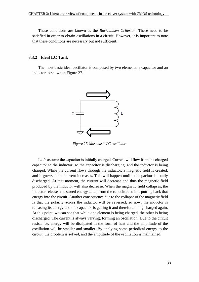
3.3.2 Ideal LC Tank
The most basic ideal oscillator is composed by two elements: a capacitor and an
inductor as shown in Figure 27.
Figure 27. Most basic LC oscillator.
Let’s assume the capacitor is initially charged. Current will flow from the charged
capacitor to the inductor, so the capacitor is discharging, and the inductor is being
charged. While the current flows through the inductor, a magnetic field is created,
and it grows as the current increases. This will happen until the capacitor is totally
discharged. At that moment, the current will decrease and thus the magnetic field
produced by the inductor will also decrease. When the magnetic field collapses, the
inductor releases the stored energy taken from the capacitor, so it is putting back that
energy into the circuit. Another consequence due to the collapse of the magnetic field
is that the polarity across the inductor will be reversed, so now, the inductor is
releasing its energy and the capacitor is getting it and therefore being charged again.
At this point, we can see that while one element is being charged, the other is being
discharged. The current is always varying, forming an oscillation. Due to the circuit
resistance, energy will be dissipated in the form of heat and the amplitude of the
oscillation will be smaller and smaller. By applying some periodical energy to the
circuit, the problem is solved, and the amplitude of the oscillation is maintained.
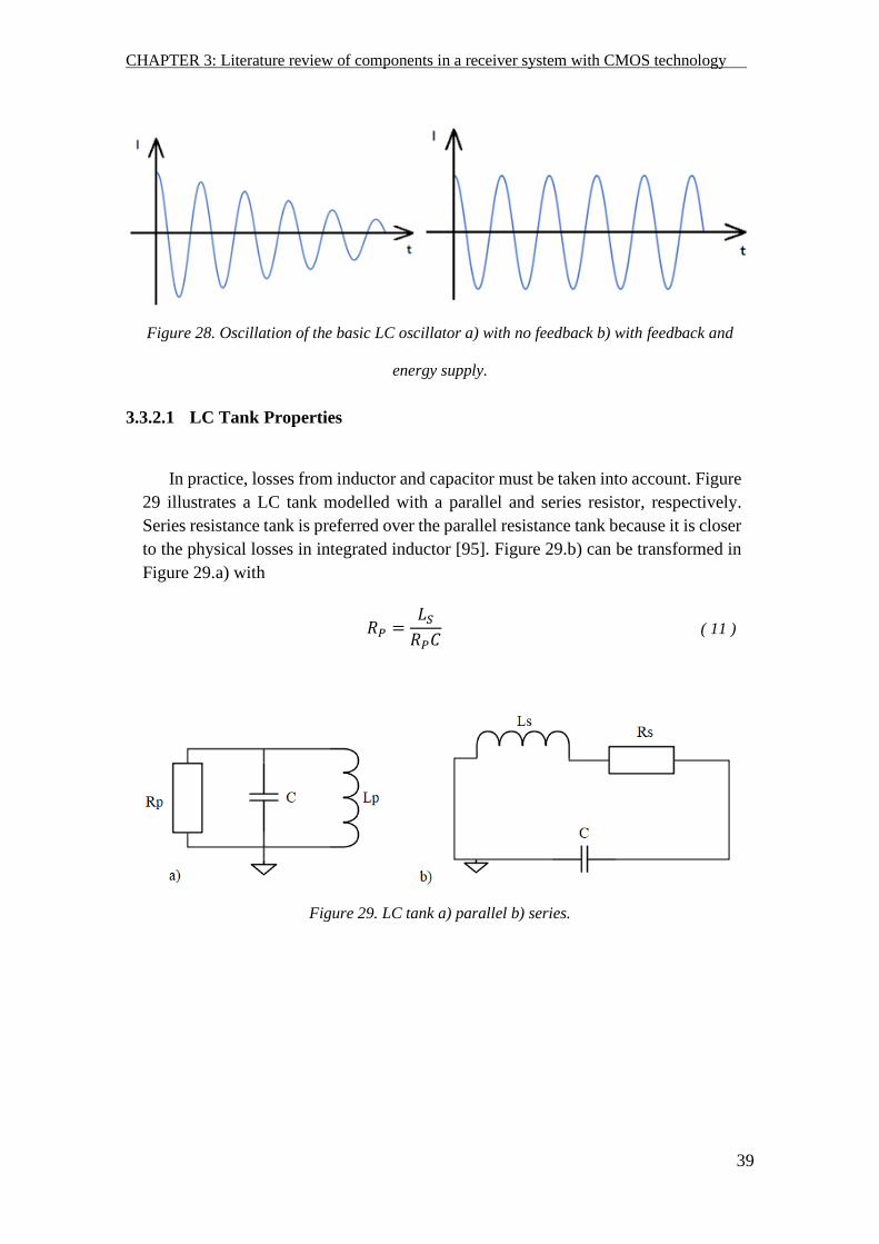
CHAPTER 3: Literature review of components in a receiver system with CMOS technology -
39
Figure 28. Oscillation of the basic LC oscillator a) with no feedback b) with feedback and
energy supply.
3.3.2.1 LC Tank Properties
In practice, losses from inductor and capacitor must be taken into account. Figure
29 illustrates a LC tank modelled with a parallel and series resistor, respectively.
Series resistance tank is preferred over the parallel resistance tank because it is closer
to the physical losses in integrated inductor [95]. Figure 29.b) can be transformed in
Figure 29.a) with
𝑅𝑃 =𝐿𝑆
𝑅𝑃𝐶
( 11 )
Figure 29. LC tank a) parallel b) series.

CHAPTER 3: Literature review of components in a receiver system with CMOS technology -
40
Depending on the values of the components, different output voltage cases are
possible. Situations on a parallel LC tank are described and shown in Figure 30.
1) If 𝑅 > 0 and 𝑅2 < 𝐿4𝐶⁄ , stable case.
2) If 𝑅 > 0 and 𝑅2 > 𝐿4𝐶⁄ , as first situation, has a stable response. Both cases are
commonly used in passive RLC circuits.
3) 𝑅 = ±∞, refers to oscillations with constant amplitude.
4) 𝑅 < 0 and 𝑅2 > 𝐿4𝐶⁄ , its amplitude oscillation increases over time.
5) 𝑅 < 0 and 𝑅2 < 𝐿4𝐶⁄ , the output voltage does not oscillate. Situation number 4
and 5 belongs to unstable cases.
Figure 30. Possible parallel LC tank solutions.
3.3.3 Oscillator parameters
3.3.3.1 Negative Resistance (NR)
As situation 4 and 5 show in last section, LC circuits are linked to negative
resistances. This resistance is necessary to compensate energy losses related to the
parasitic resistances of the capacitor, and mainly, of the inductor. Initially, the total
equivalent resistance must be negative in order to get oscillations with increasing
amplitude. Then, the amplitude of the oscillator stabilizes, and the oscillation
frequency is the resonant frequency of the circuit given by
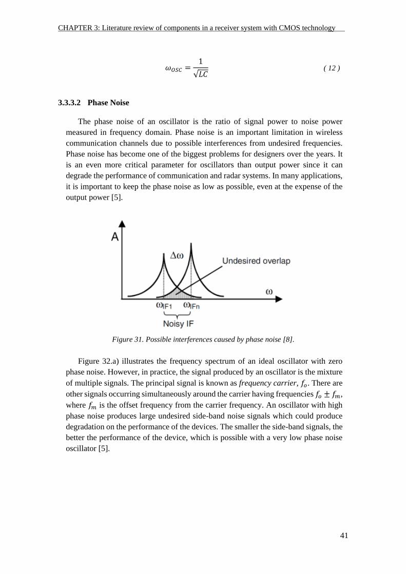
CHAPTER 3: Literature review of components in a receiver system with CMOS technology -
41
𝜔𝑂𝑆𝐶 =1
√𝐿𝐶
( 12 )
3.3.3.2 Phase Noise
The phase noise of an oscillator is the ratio of signal power to noise power
measured in frequency domain. Phase noise is an important limitation in wireless
communication channels due to possible interferences from undesired frequencies.
Phase noise has become one of the biggest problems for designers over the years. It
is an even more critical parameter for oscillators than output power since it can
degrade the performance of communication and radar systems. In many applications,
it is important to keep the phase noise as low as possible, even at the expense of the
output power [5].
Figure 31. Possible interferences caused by phase noise [8].
Figure 32.a) illustrates the frequency spectrum of an ideal oscillator with zero
phase noise. However, in practice, the signal produced by an oscillator is the mixture
of multiple signals. The principal signal is known as frequency carrier, 𝑓𝑜. There are
other signals occurring simultaneously around the carrier having frequencies 𝑓𝑜 ± 𝑓𝑚,
where 𝑓𝑚 is the offset frequency from the carrier frequency. An oscillator with high
phase noise produces large undesired side-band noise signals which could produce
degradation on the performance of the devices. The smaller the side-band signals, the
better the performance of the device, which is possible with a very low phase noise
oscillator [5].
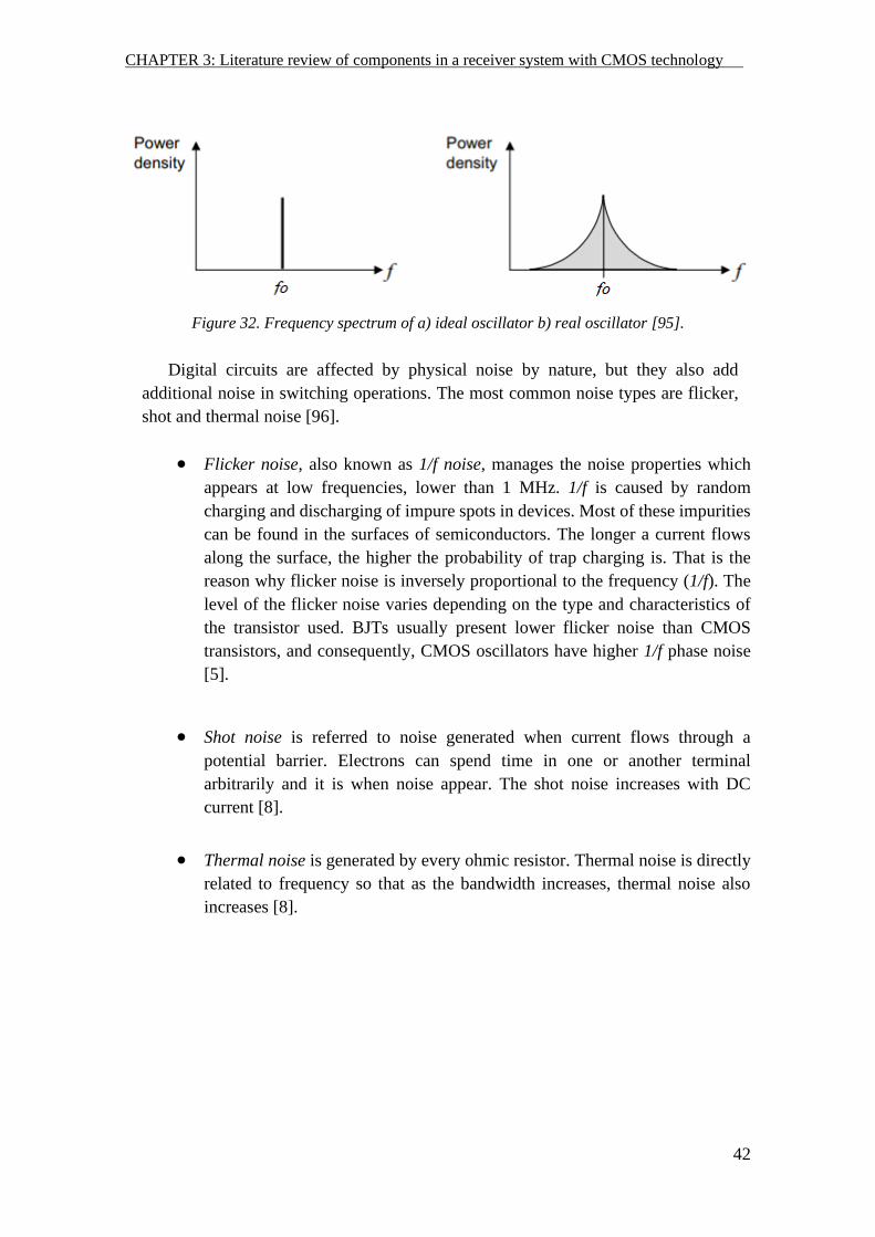
CHAPTER 3: Literature review of components in a receiver system with CMOS technology -
42
Figure 32. Frequency spectrum of a) ideal oscillator b) real oscillator [95].
Digital circuits are affected by physical noise by nature, but they also add
additional noise in switching operations. The most common noise types are flicker,
shot and thermal noise [96].
• Flicker noise, also known as 1/f noise, manages the noise properties which
appears at low frequencies, lower than 1 MHz. 1/f is caused by random
charging and discharging of impure spots in devices. Most of these impurities
can be found in the surfaces of semiconductors. The longer a current flows
along the surface, the higher the probability of trap charging is. That is the
reason why flicker noise is inversely proportional to the frequency (1/f). The
level of the flicker noise varies depending on the type and characteristics of
the transistor used. BJTs usually present lower flicker noise than CMOS
transistors, and consequently, CMOS oscillators have higher 1/f phase noise
[5].
• Shot noise is referred to noise generated when current flows through a
potential barrier. Electrons can spend time in one or another terminal
arbitrarily and it is when noise appear. The shot noise increases with DC
current [8].
• Thermal noise is generated by every ohmic resistor. Thermal noise is directly
related to frequency so that as the bandwidth increases, thermal noise also
increases [8].
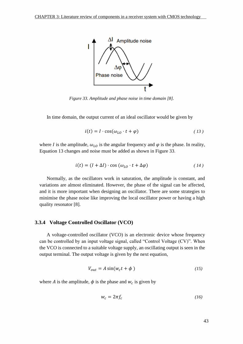
CHAPTER 3: Literature review of components in a receiver system with CMOS technology -
43
Figure 33. Amplitude and phase noise in time domain [8].
In time domain, the output current of an ideal oscillator would be given by
𝑖(𝑡) = 𝐼 · cos(𝜔𝐿𝑂 · 𝑡 + 𝜑)
( 13 )
where 𝐼 is the amplitude, 𝜔𝐿𝑂 is the angular frequency and 𝜑 is the phase. In reality,
Equation 13 changes and noise must be added as shown in Figure 33.
𝑖(𝑡) = (𝐼 + ∆𝐼) · cos (𝜔𝐿𝑂 · 𝑡 + ∆𝜑)
( 14 )
Normally, as the oscillators work in saturation, the amplitude is constant, and
variations are almost eliminated. However, the phase of the signal can be affected,
and it is more important when designing an oscillator. There are some strategies to
minimise the phase noise like improving the local oscillator power or having a high
quality resonator [8].
3.3.4 Voltage Controlled Oscillator (VCO)
A voltage-controlled oscillator (VCO) is an electronic device whose frequency
can be controlled by an input voltage signal, called “Control Voltage (CV)”. When
the VCO is connected to a suitable voltage supply, an oscillating output is seen in the
output terminal. The output voltage is given by the next equation,
𝑉𝑜𝑢𝑡 = 𝐴 sin(𝑤𝑐𝑡 + 𝜙 )
(15)
where 𝐴 is the amplitude, 𝜙 is the phase and 𝑤𝑐 is given by
𝑤𝑐 = 2𝜋𝑓𝑐
(16)
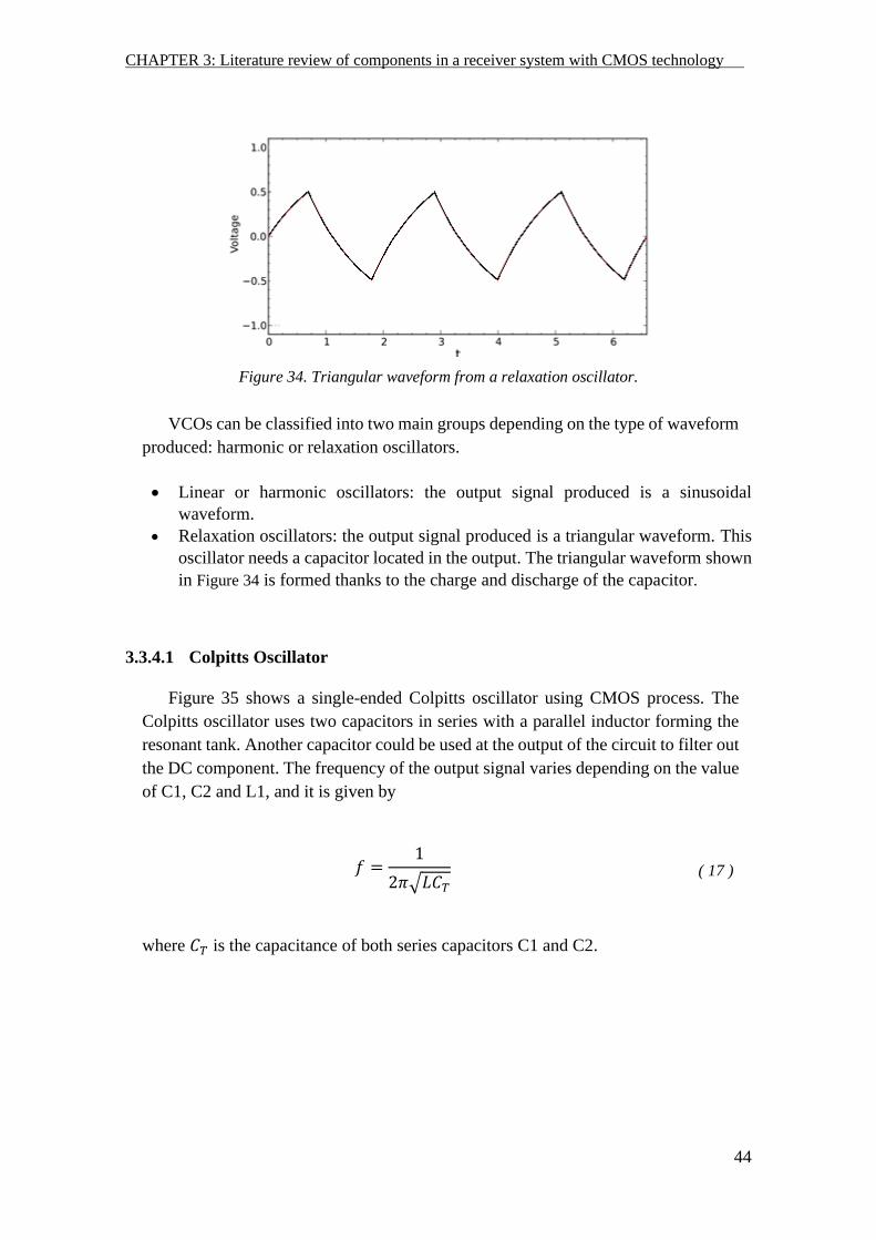
CHAPTER 3: Literature review of components in a receiver system with CMOS technology -
44
Figure 34. Triangular waveform from a relaxation oscillator.
VCOs can be classified into two main groups depending on the type of waveform
produced: harmonic or relaxation oscillators.
• Linear or harmonic oscillators: the output signal produced is a sinusoidal
waveform.
• Relaxation oscillators: the output signal produced is a triangular waveform. This
oscillator needs a capacitor located in the output. The triangular waveform shown
in Figure 34 is formed thanks to the charge and discharge of the capacitor.
3.3.4.1 Colpitts Oscillator
Figure 35 shows a single-ended Colpitts oscillator using CMOS process. The
Colpitts oscillator uses two capacitors in series with a parallel inductor forming the
resonant tank. Another capacitor could be used at the output of the circuit to filter out
the DC component. The frequency of the output signal varies depending on the value
of C1, C2 and L1, and it is given by
𝑓 =1
2𝜋√𝐿𝐶𝑇
( 17 )
where 𝐶𝑇 is the capacitance of both series capacitors C1 and C2.
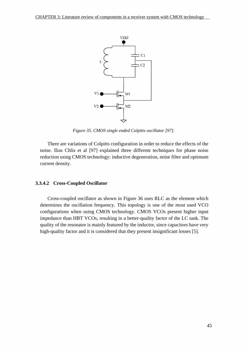
CHAPTER 3: Literature review of components in a receiver system with CMOS technology -
45
Figure 35. CMOS single ended Colpitts oscillator [97].
There are variations of Colpitts configuration in order to reduce the effects of the
noise. Ilias Chlis et al [97] explained three different techniques for phase noise
reduction using CMOS technology: inductive degeneration, noise filter and optimum
current density.
3.3.4.2 Cross-Coupled Oscillator
Cross-coupled oscillator as shown in Figure 36 uses RLC as the element which
determines the oscillation frequency. This topology is one of the most used VCO
configurations when using CMOS technology. CMOS VCOs present higher input
impedance than HBT VCOs, resulting in a better-quality factor of the LC tank. The
quality of the resonator is mainly featured by the inductor, since capacitors have very
high-quality factor and it is considered that they present insignificant losses [5].
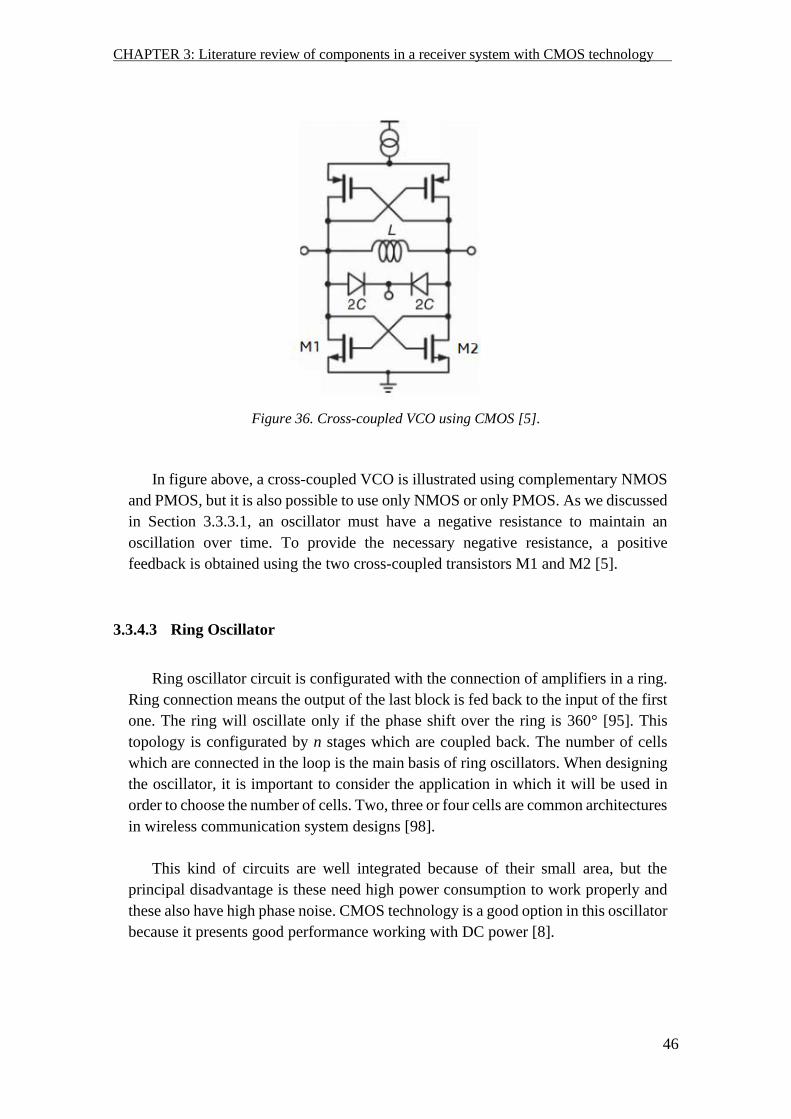
CHAPTER 3: Literature review of components in a receiver system with CMOS technology -
46
Figure 36. Cross-coupled VCO using CMOS [5].
In figure above, a cross-coupled VCO is illustrated using complementary NMOS
and PMOS, but it is also possible to use only NMOS or only PMOS. As we discussed
in Section 3.3.3.1, an oscillator must have a negative resistance to maintain an
oscillation over time. To provide the necessary negative resistance, a positive
feedback is obtained using the two cross-coupled transistors M1 and M2 [5].
3.3.4.3 Ring Oscillator
Ring oscillator circuit is configurated with the connection of amplifiers in a ring.
Ring connection means the output of the last block is fed back to the input of the first
one. The ring will oscillate only if the phase shift over the ring is 360° [95]. This
topology is configurated by n stages which are coupled back. The number of cells
which are connected in the loop is the main basis of ring oscillators. When designing
the oscillator, it is important to consider the application in which it will be used in
order to choose the number of cells. Two, three or four cells are common architectures
in wireless communication system designs [98].
This kind of circuits are well integrated because of their small area, but the
principal disadvantage is these need high power consumption to work properly and
these also have high phase noise. CMOS technology is a good option in this oscillator
because it presents good performance working with DC power [8].
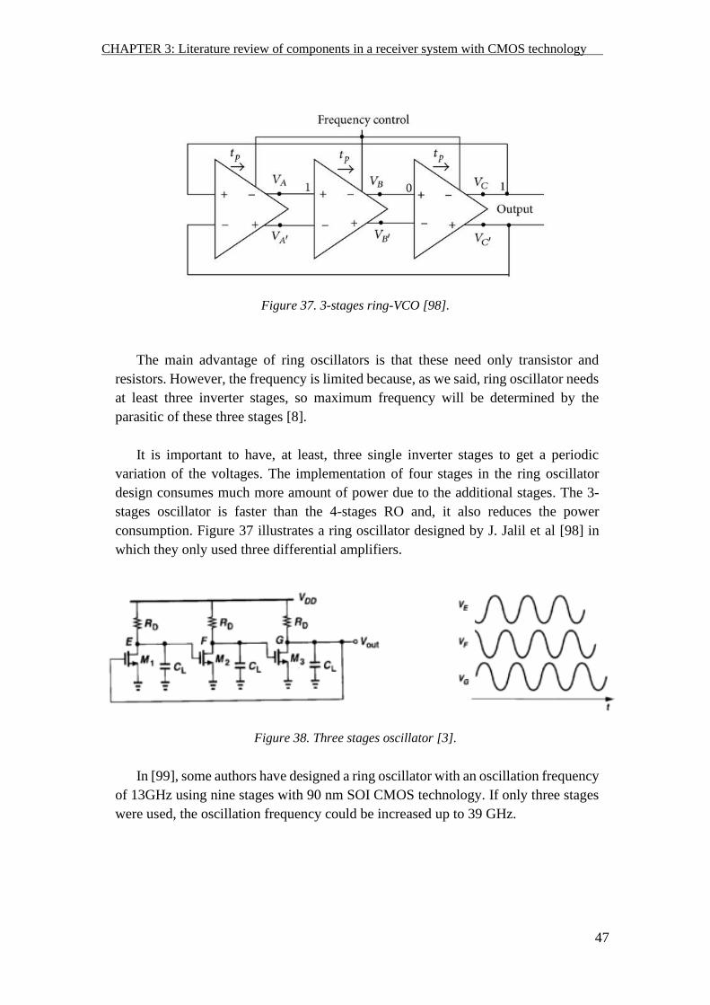
CHAPTER 3: Literature review of components in a receiver system with CMOS technology -
47
Figure 37. 3-stages ring-VCO [98].
The main advantage of ring oscillators is that these need only transistor and
resistors. However, the frequency is limited because, as we said, ring oscillator needs
at least three inverter stages, so maximum frequency will be determined by the
parasitic of these three stages [8].
It is important to have, at least, three single inverter stages to get a periodic
variation of the voltages. The implementation of four stages in the ring oscillator
design consumes much more amount of power due to the additional stages. The 3-
stages oscillator is faster than the 4-stages RO and, it also reduces the power
consumption. Figure 37 illustrates a ring oscillator designed by J. Jalil et al [98] in
which they only used three differential amplifiers.
Figure 38. Three stages oscillator [3].
In [99], some authors have designed a ring oscillator with an oscillation frequency
of 13GHz using nine stages with 90 nm SOI CMOS technology. If only three stages
were used, the oscillation frequency could be increased up to 39 GHz.
CHAPTER 3: Literature review of components in a receiver system with CMOS technology -
48
3.3.4.4 Figure of Merit of a VCO
The voltage-controlled oscillator is an important device in RF signal processing.
Its main aim is to minimize the phase noise and the power consumption [24]. As we
said, the VCO is used for generating the LO signal connected to the mixer. The
efficiency is given by the relation between LO output power and required DC power.
Thus, one commonly used way of comparing VCOs is considering the output power
generated by the device. The figure of merit is given by [24]
𝐹𝑜𝑀𝑉𝐶𝑂 = (𝑓
∆𝑓) ·
𝑃𝑂𝑈𝑇
𝐿[∆𝑓] · 𝑃𝑐𝑜𝑛𝑠𝑢𝑚𝑝𝑡𝑖𝑜𝑛
( 18 )
where 𝑓 is the oscillation frequency, ∆𝑓 is the frequency offset, 𝑃𝑂𝑈𝑇 is the power
generated at the output, 𝐿[∆𝑓] is the phase noise evaluated at the frequency offset and
𝑃𝑐𝑜𝑛𝑠𝑢𝑚𝑝𝑡𝑖𝑜𝑛 is the power consumption.
FoM of an VCO must be evaluated at the frequency where maximum phase noise
is achieved. Phase noise varies depending on parameters like the quality of the LC
tank (which determines the oscillation frequency), the amplitude of this oscillation,
and possible noise added, produced by active and passive components of the VCO.
The amplitude of the oscillation is limited by the maximum permissible voltage of
the transistor [24].
Another common way of comparing different VCOs is using the phase noise
figure of merit. Noise performance of a voltage-controlled oscillator depends on the
frequency offset. Thus, the higher the frequency offset, the lower the phase noise.
This FoM [8] is given by
𝐹𝑜𝑀 = 𝐿(∆𝜔) − 20 log (∆𝜔
𝜔𝐿𝑂) − 10 log(
[𝑚𝑊]
𝑃𝑑𝑐[𝑚𝑊])
( 19 )
where 𝐿(∆𝜔) is a concept which measures noise floor, resonator noise and flicker
noise explained by Ellinger [8].

CHAPTER 3: Literature review of components in a receiver system with CMOS technology -
49
Reference Architecture
CMOS
Technology
(nm)
Centre
Frequency
(GHz)
Phase
Noise
(dBc/Hz)
Supply
(V)
Tuning
range
(MHz)
Power
DC
(mW)
[100] Class-C 130 4.9 -132.8 1 685 1.4
[101] LC VCO 130 5.17 -122.3 0.4 2200 0.495
[102] DM VCO 130 4.9 -117.6 1.2 1900 9
[103] DM VCO 130 5.7 -104 1 4200 8
[104] UWB VCO 130 5.6 -75.42 1.8 3600 29.1
[105] LC VCO 130 5.225 -110 1.2 450 12
[106] Differential
Colpitts 130 4.9 -132.6 0.4 122.5 1.92
*Missing information.
Table 5. Comparison table of reported 130 nm CMOS VCOs.
Reference Architecture
CMOS
Technology
(nm)
Centre
Frequency
(GHz)
Phase
Noise
(dBc/Hz)
Supply
(V)
Tuning
range
(MHz)
Power
DC
(mW)
[5] Cross-
coupled 250 5.2 -117 1.8 1300 -*
[5] Distributed 180 15 -100.2 1.8 1700 34.2
[98] RO 180 1.5 -126.62 1.5 2000 2.47
[107] LC VCO 180 2.5 -128.7 1.8 275 5.4
[108] TF VCO 180 1.4 -129 0.35 0 1.46
[108] TF VCO 180 3.8 -119 0.5 320 0.57
[109] Multi-band
VCO 180 5 -125 1 200 6
[109] PMOS 180 5.21 -127 1 420 4.2
[110] Cross-
coupled 180 7.128 -111.2 1 330 2.2
[111] Differential
Colpitts 180 5.46 -100.3 1.8 580 6.4
[112] LC VCO 250 1.3 -142 2 200 14
[113]
Cross-
coupled
quadrature
250 1.86 -143 2.5 280 20
[114] Push-push 250 63 -85 1.8 2520 119
*Missing information.
Table 6. Comparison table of reported 90, 180 and 250 nm CMOS VCOs.

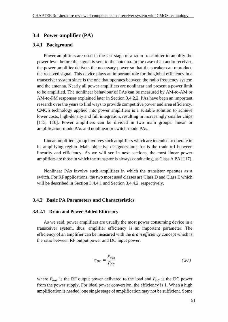
CHAPTER 3: Literature review of components in a receiver system with CMOS technology -
-
51
3.4 Power amplifier (PA)
3.4.1 Background
Power amplifiers are used in the last stage of a radio transmitter to amplify the
power level before the signal is sent to the antenna. In the case of an audio receiver,
the power amplifier delivers the necessary power so that the speaker can reproduce
the received signal. This device plays an important role for the global efficiency in a
transceiver system since is the one that operates between the radio frequency system
and the antenna. Nearly all power amplifiers are nonlinear and present a power limit
to be amplified. The nonlinear behaviour of PAs can be measured by AM-to-AM or
AM-to-PM responses explained later in Section 3.4.2.2. PAs have been an important
research over the years to find ways to provide competitive power and area efficiency.
CMOS technology applied into power amplifiers is a suitable solution to achieve
lower costs, high-density and full integration, resulting in increasingly smaller chips
[115, 116]. Power amplifiers can be divided in two main groups: linear or
amplification-mode PAs and nonlinear or switch-mode PAs.
Linear amplifiers group involves such amplifiers which are intended to operate in
its amplifying region. Main objective designers look for is the trade-off between
linearity and efficiency. As we will see in next sections, the most linear power
amplifiers are those in which the transistor is always conducting, as Class A PA [117].
Nonlinear PAs involve such amplifiers in which the transistor operates as a
switch. For RF applications, the two most used classes are Class D and Class E which
will be described in Section 3.4.4.1 and Section 3.4.4.2, respectively.
3.4.2 Basic PA Parameters and Characteristics
3.4.2.1 Drain and Power-Added Efficiency
As we said, power amplifiers are usually the most power consuming device in a
transceiver system, thus, amplifier efficiency is an important parameter. The
efficiency of an amplifier can be measured with the drain efficiency concept which is
the ratio between RF output power and DC input power.
𝜂𝐷𝐶 =𝑃𝑜𝑢𝑡
𝑃𝐷𝐶
( 20 )
where 𝑃𝑜𝑢𝑡 is the RF output power delivered to the load and 𝑃𝐷𝐶 is the DC power
from the power supply. For ideal power conversion, the efficiency is 1. When a high
amplification is needed, one single stage of amplification may not be sufficient. Some
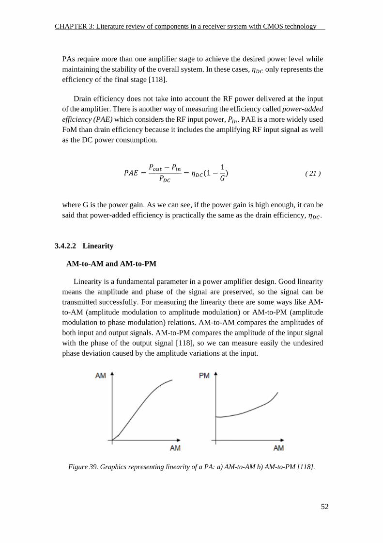
CHAPTER 3: Literature review of components in a receiver system with CMOS technology -
-
52
PAs require more than one amplifier stage to achieve the desired power level while
maintaining the stability of the overall system. In these cases, 𝜂𝐷𝐶 only represents the
efficiency of the final stage [118].
Drain efficiency does not take into account the RF power delivered at the input
of the amplifier. There is another way of measuring the efficiency called power-added
efficiency (PAE) which considers the RF input power, 𝑃𝑖𝑛. PAE is a more widely used
FoM than drain efficiency because it includes the amplifying RF input signal as well
as the DC power consumption.
𝑃𝐴𝐸 =𝑃𝑜𝑢𝑡 − 𝑃𝑖𝑛
𝑃𝐷𝐶= 𝜂𝐷𝐶(1 −
1
𝐺)
( 21 )
where G is the power gain. As we can see, if the power gain is high enough, it can be
said that power-added efficiency is practically the same as the drain efficiency, 𝜂𝐷𝐶.
3.4.2.2 Linearity
AM-to-AM and AM-to-PM
Linearity is a fundamental parameter in a power amplifier design. Good linearity
means the amplitude and phase of the signal are preserved, so the signal can be
transmitted successfully. For measuring the linearity there are some ways like AM-
to-AM (amplitude modulation to amplitude modulation) or AM-to-PM (amplitude
modulation to phase modulation) relations. AM-to-AM compares the amplitudes of
both input and output signals. AM-to-PM compares the amplitude of the input signal
with the phase of the output signal [118], so we can measure easily the undesired
phase deviation caused by the amplitude variations at the input.
Figure 39. Graphics representing linearity of a PA: a) AM-to-AM b) AM-to-PM [118].
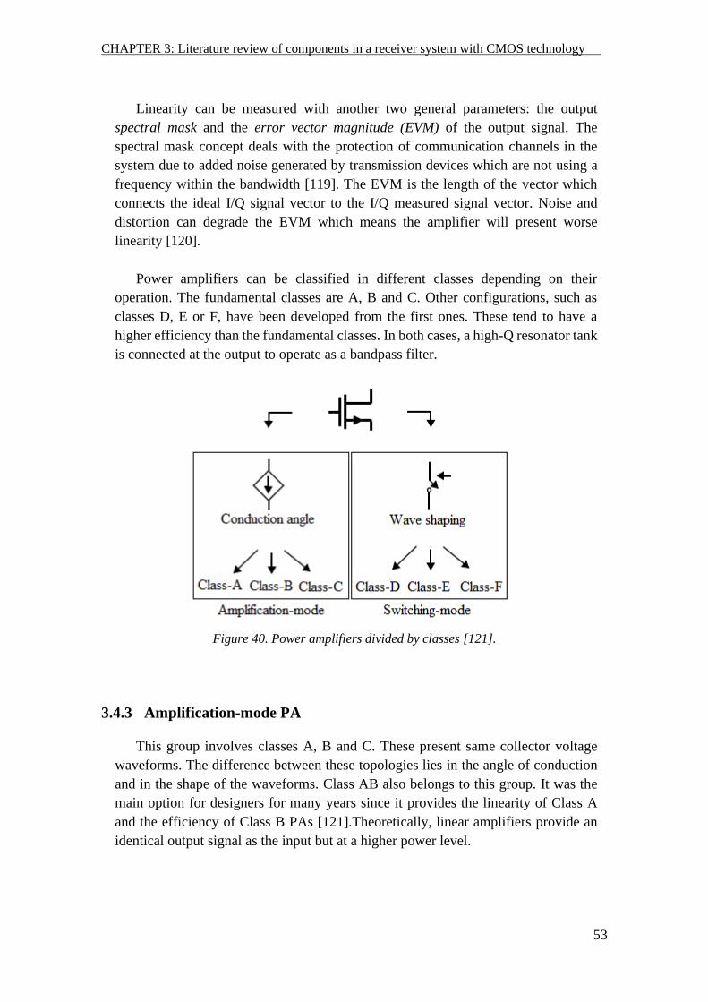
CHAPTER 3: Literature review of components in a receiver system with CMOS technology -
-
53
Linearity can be measured with another two general parameters: the output
spectral mask and the error vector magnitude (EVM) of the output signal. The
spectral mask concept deals with the protection of communication channels in the
system due to added noise generated by transmission devices which are not using a
frequency within the bandwidth [119]. The EVM is the length of the vector which
connects the ideal I/Q signal vector to the I/Q measured signal vector. Noise and
distortion can degrade the EVM which means the amplifier will present worse
linearity [120].
Power amplifiers can be classified in different classes depending on their
operation. The fundamental classes are A, B and C. Other configurations, such as
classes D, E or F, have been developed from the first ones. These tend to have a
higher efficiency than the fundamental classes. In both cases, a high-Q resonator tank
is connected at the output to operate as a bandpass filter.
Figure 40. Power amplifiers divided by classes [121].
3.4.3 Amplification-mode PA
This group involves classes A, B and C. These present same collector voltage
waveforms. The difference between these topologies lies in the angle of conduction
and in the shape of the waveforms. Class AB also belongs to this group. It was the
main option for designers for many years since it provides the linearity of Class A
and the efficiency of Class B PAs [121].Theoretically, linear amplifiers provide an
identical output signal as the input but at a higher power level.
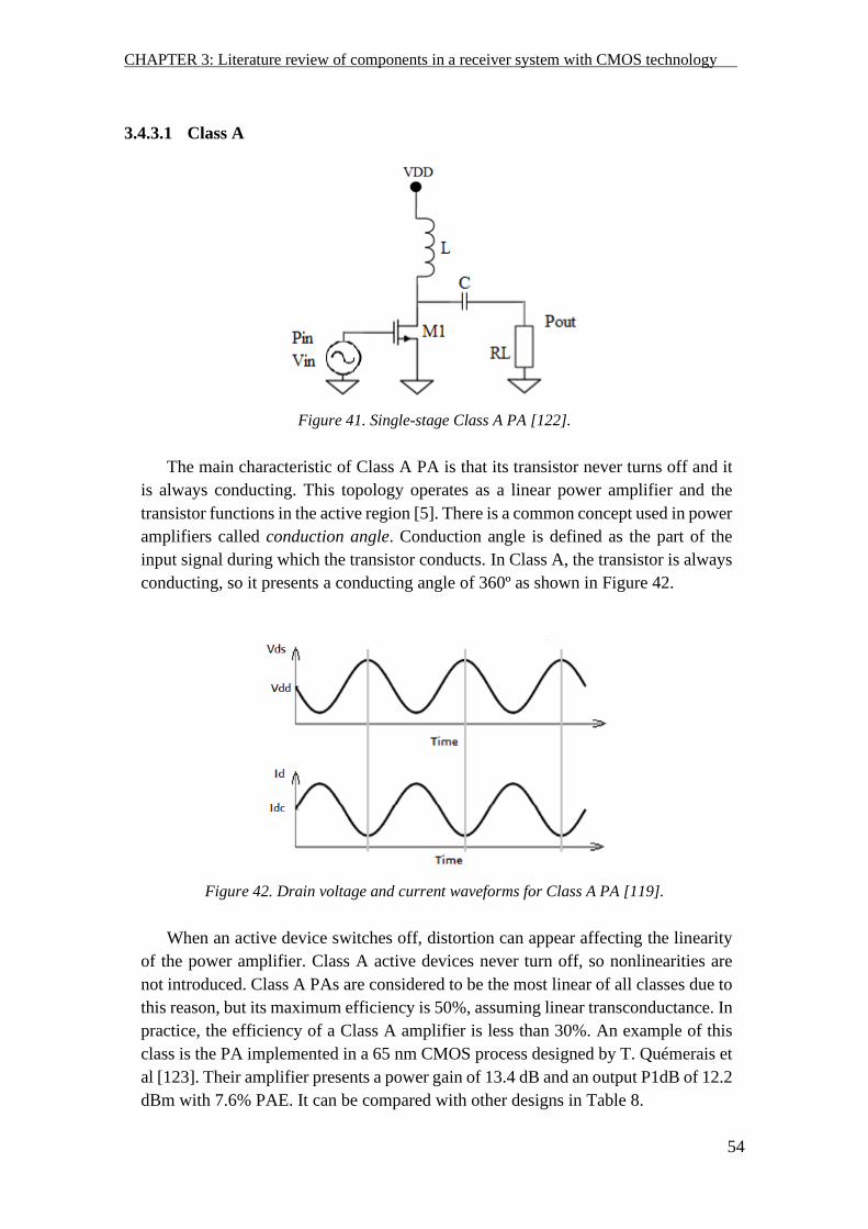
CHAPTER 3: Literature review of components in a receiver system with CMOS technology -
-
54
3.4.3.1 Class A
Figure 41. Single-stage Class A PA [122].
The main characteristic of Class A PA is that its transistor never turns off and it
is always conducting. This topology operates as a linear power amplifier and the
transistor functions in the active region [5]. There is a common concept used in power
amplifiers called conduction angle. Conduction angle is defined as the part of the
input signal during which the transistor conducts. In Class A, the transistor is always
conducting, so it presents a conducting angle of 360º as shown in Figure 42.
Figure 42. Drain voltage and current waveforms for Class A PA [119].
When an active device switches off, distortion can appear affecting the linearity
of the power amplifier. Class A active devices never turn off, so nonlinearities are
not introduced. Class A PAs are considered to be the most linear of all classes due to
this reason, but its maximum efficiency is 50%, assuming linear transconductance. In
practice, the efficiency of a Class A amplifier is less than 30%. An example of this
class is the PA implemented in a 65 nm CMOS process designed by T. Quémerais et
al [123]. Their amplifier presents a power gain of 13.4 dB and an output P1dB of 12.2
dBm with 7.6% PAE. It can be compared with other designs in Table 8.
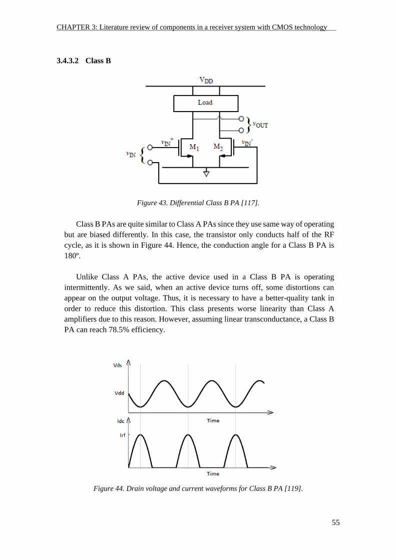
CHAPTER 3: Literature review of components in a receiver system with CMOS technology -
-
55
3.4.3.2 Class B
Figure 43. Differential Class B PA [117].
Class B PAs are quite similar to Class A PAs since they use same way of operating
but are biased differently. In this case, the transistor only conducts half of the RF
cycle, as it is shown in Figure 44. Hence, the conduction angle for a Class B PA is
180º.
Unlike Class A PAs, the active device used in a Class B PA is operating
intermittently. As we said, when an active device turns off, some distortions can
appear on the output voltage. Thus, it is necessary to have a better-quality tank in
order to reduce this distortion. This class presents worse linearity than Class A
amplifiers due to this reason. However, assuming linear transconductance, a Class B
PA can reach 78.5% efficiency.
Figure 44. Drain voltage and current waveforms for Class B PA [119].
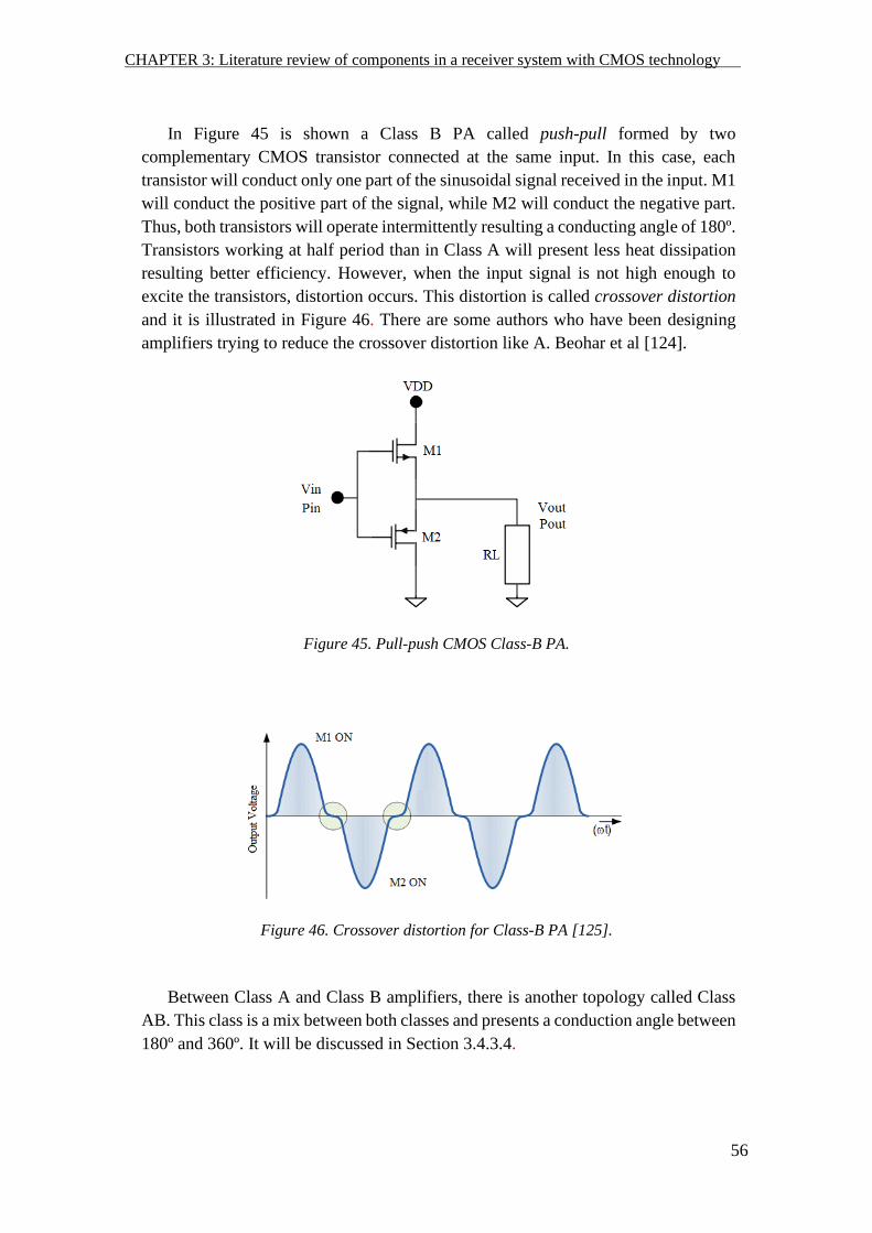
CHAPTER 3: Literature review of components in a receiver system with CMOS technology -
-
56
In Figure 45 is shown a Class B PA called push-pull formed by two
complementary CMOS transistor connected at the same input. In this case, each
transistor will conduct only one part of the sinusoidal signal received in the input. M1
will conduct the positive part of the signal, while M2 will conduct the negative part.
Thus, both transistors will operate intermittently resulting a conducting angle of 180º.
Transistors working at half period than in Class A will present less heat dissipation
resulting better efficiency. However, when the input signal is not high enough to
excite the transistors, distortion occurs. This distortion is called crossover distortion
and it is illustrated in Figure 46. There are some authors who have been designing
amplifiers trying to reduce the crossover distortion like A. Beohar et al [124].
Figure 45. Pull-push CMOS Class-B PA.
Figure 46. Crossover distortion for Class-B PA [125].
Between Class A and Class B amplifiers, there is another topology called Class
AB. This class is a mix between both classes and presents a conduction angle between
180º and 360º. It will be discussed in Section 3.4.3.4.
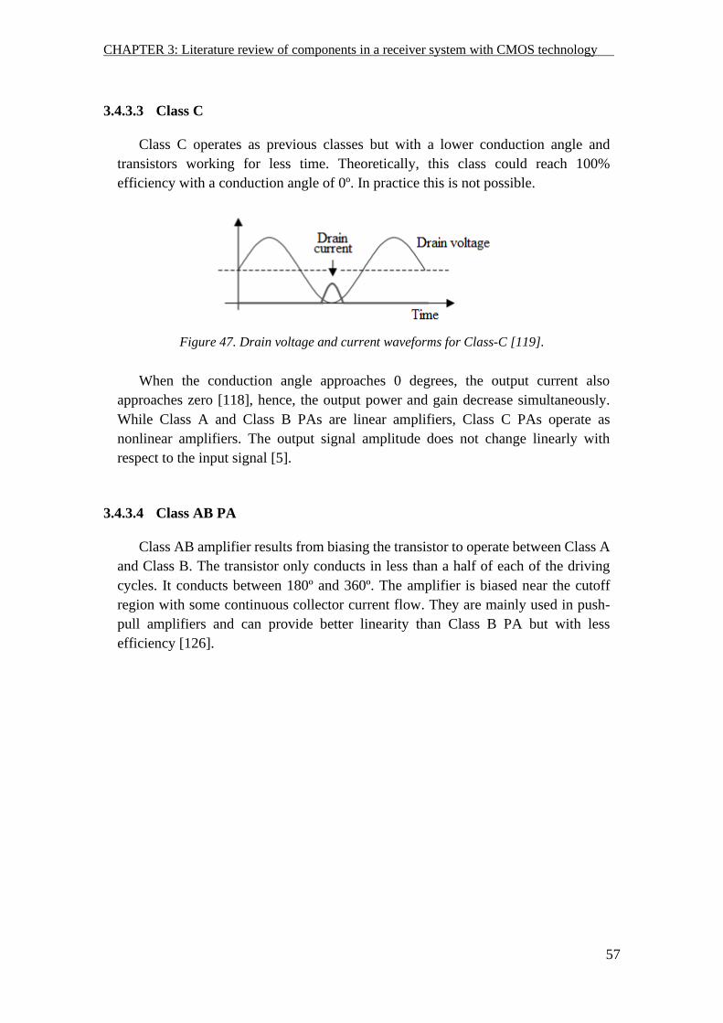
CHAPTER 3: Literature review of components in a receiver system with CMOS technology -
-
57
3.4.3.3 Class C
Class C operates as previous classes but with a lower conduction angle and
transistors working for less time. Theoretically, this class could reach 100%
efficiency with a conduction angle of 0º. In practice this is not possible.
Figure 47. Drain voltage and current waveforms for Class-C [119].
When the conduction angle approaches 0 degrees, the output current also
approaches zero [118], hence, the output power and gain decrease simultaneously.
While Class A and Class B PAs are linear amplifiers, Class C PAs operate as
nonlinear amplifiers. The output signal amplitude does not change linearly with
respect to the input signal [5].
3.4.3.4 Class AB PA
Class AB amplifier results from biasing the transistor to operate between Class A
and Class B. The transistor only conducts in less than a half of each of the driving
cycles. It conducts between 180º and 360º. The amplifier is biased near the cutoff
region with some continuous collector current flow. They are mainly used in push-
pull amplifiers and can provide better linearity than Class B PA but with less
efficiency [126].
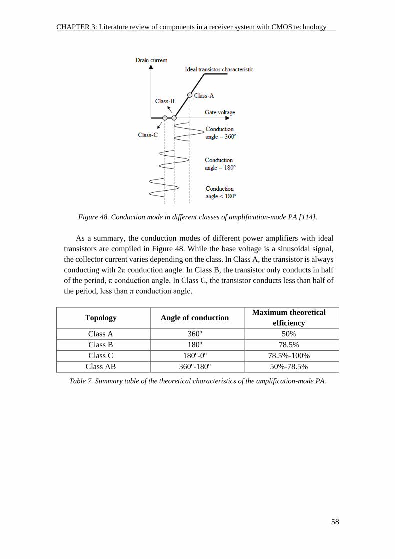
CHAPTER 3: Literature review of components in a receiver system with CMOS technology -
-
58
Figure 48. Conduction mode in different classes of amplification-mode PA [114].
As a summary, the conduction modes of different power amplifiers with ideal
transistors are compiled in Figure 48. While the base voltage is a sinusoidal signal,
the collector current varies depending on the class. In Class A, the transistor is always
conducting with 2π conduction angle. In Class B, the transistor only conducts in half
of the period, π conduction angle. In Class C, the transistor conducts less than half of
the period, less than π conduction angle.
Topology Angle of conduction Maximum theoretical
efficiency
Class A 360º 50%
Class B 180º 78.5%
Class C 180º-0º 78.5%-100%
Class AB 360º-180º 50%-78.5%
Table 7. Summary table of the theoretical characteristics of the amplification-mode PA.
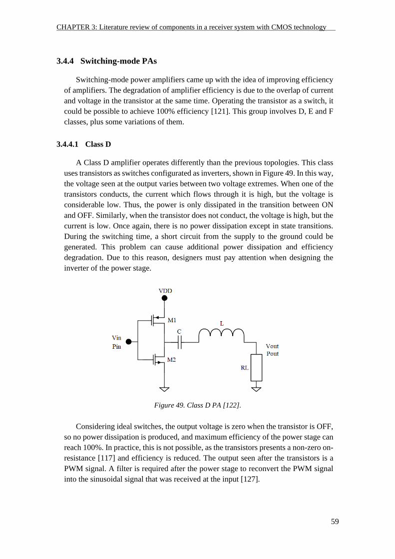
CHAPTER 3: Literature review of components in a receiver system with CMOS technology -
-
59
3.4.4 Switching-mode PAs
Switching-mode power amplifiers came up with the idea of improving efficiency
of amplifiers. The degradation of amplifier efficiency is due to the overlap of current
and voltage in the transistor at the same time. Operating the transistor as a switch, it
could be possible to achieve 100% efficiency [121]. This group involves D, E and F
classes, plus some variations of them.
3.4.4.1 Class D
A Class D amplifier operates differently than the previous topologies. This class
uses transistors as switches configurated as inverters, shown in Figure 49. In this way,
the voltage seen at the output varies between two voltage extremes. When one of the
transistors conducts, the current which flows through it is high, but the voltage is
considerable low. Thus, the power is only dissipated in the transition between ON
and OFF. Similarly, when the transistor does not conduct, the voltage is high, but the
current is low. Once again, there is no power dissipation except in state transitions.
During the switching time, a short circuit from the supply to the ground could be
generated. This problem can cause additional power dissipation and efficiency
degradation. Due to this reason, designers must pay attention when designing the
inverter of the power stage.
Figure 49. Class D PA [122].
Considering ideal switches, the output voltage is zero when the transistor is OFF,
so no power dissipation is produced, and maximum efficiency of the power stage can
reach 100%. In practice, this is not possible, as the transistors presents a non-zero on-
resistance [117] and efficiency is reduced. The output seen after the transistors is a
PWM signal. A filter is required after the power stage to reconvert the PWM signal
into the sinusoidal signal that was received at the input [127].
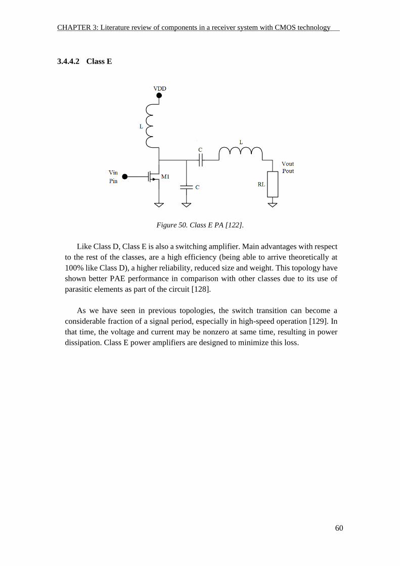
CHAPTER 3: Literature review of components in a receiver system with CMOS technology -
-
60
3.4.4.2 Class E
Figure 50. Class E PA [122].
Like Class D, Class E is also a switching amplifier. Main advantages with respect
to the rest of the classes, are a high efficiency (being able to arrive theoretically at
100% like Class D), a higher reliability, reduced size and weight. This topology have
shown better PAE performance in comparison with other classes due to its use of
parasitic elements as part of the circuit [128].
As we have seen in previous topologies, the switch transition can become a
considerable fraction of a signal period, especially in high-speed operation [129]. In
that time, the voltage and current may be nonzero at same time, resulting in power
dissipation. Class E power amplifiers are designed to minimize this loss.
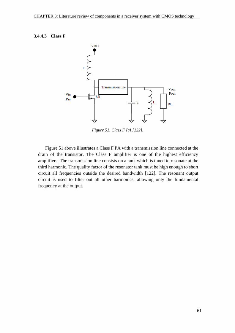
CHAPTER 3: Literature review of components in a receiver system with CMOS technology -
-
61
3.4.4.3 Class F
Figure 51. Class F PA [122].
Figure 51 above illustrates a Class F PA with a transmission line connected at the
drain of the transistor. The Class F amplifier is one of the highest efficiency
amplifiers. The transmission line consists on a tank which is tuned to resonate at the
third harmonic. The quality factor of the resonator tank must be high enough to short
circuit all frequencies outside the desired bandwidth [122]. The resonant output
circuit is used to filter out all other harmonics, allowing only the fundamental
frequency at the output.
CHAPTER 3: Literature review of components in a receiver system with CMOS technology -
-
62
3.4.5 Applications and Figure of Merits (FoMs)
As we said before, microwave PAs becomes an important issue in wireless
communication systems, especially in fifth generation (5G) wireless services. They
are used in the transmission part of the wireless communication systems and in
automotive radar. For battery operated applications, minimum DC power
consumption is required [121]. CMOS is the process chosen for recent power
amplifier designs since they present low cost and high-level integration. On the other
hand, this technology also has some drawbacks. CMOS processes provide less power
efficiency than GaAs processes, due to limitations from substrate conductivity and
silicon breakdown field. Hence, 5G wireless systems need efficient CMOS power
amplifiers [130].
The International Terrestrial Reference System (ITRS) defined the power
amplifier figure of merit (𝐹𝑜𝑀𝑃𝐴) in 2001. It considers the output power (𝑃𝑂𝑈𝑇), the
power gain (G), the power-added efficiency (PAE) and the carrier frequency (𝑓). It
is a standard to compare different power amplifier designs. However, linearity
depends on the operating class of the amplifiers, which makes it difficult to compare
different classes amplifiers.
𝐹𝑜𝑀𝑃𝐴 = 𝑃𝑂𝑈𝑇 · 𝐺 · 𝑃𝐴𝐸 · 𝑓2
( 22 )
Despite of this, some authors have used other figure of merits to compare power
amplifiers. One clear example is D. Zhao et al in [131]. The figure of merit they used
is given by
𝐹𝑂𝑀 = 𝑃𝑆𝐴𝑇[𝑑𝐵𝑚] + 𝐺[𝑑𝐵]+ 20 log(𝑓𝑐[𝐺𝐻𝑧]) + 10 log(𝑃𝐴𝐸𝑀𝐴𝑋[%])
( 23 )
Their 60 GHz power amplifier was implemented in 40 nm CMOS technology. It
achieves 17 dB power gain and 30.3% PAE.
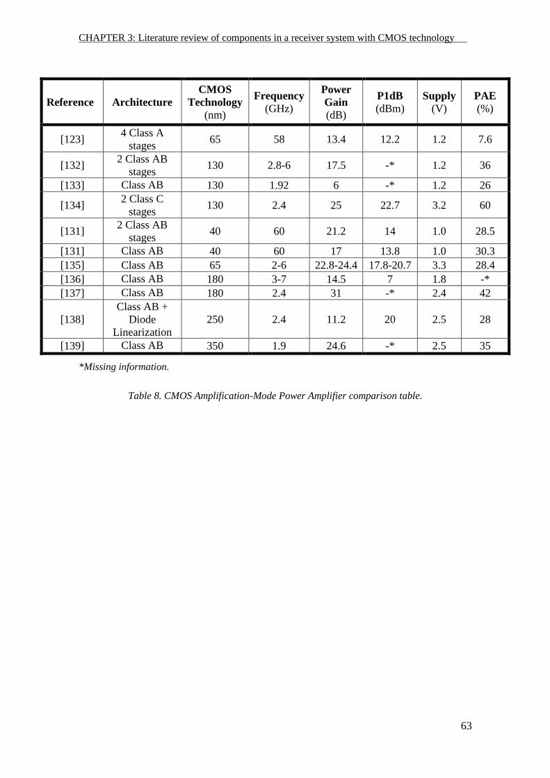
CHAPTER 3: Literature review of components in a receiver system with CMOS technology -
-
63
Reference Architecture
CMOS
Technology
(nm)
Frequency
(GHz)
Power
Gain
(dB)
P1dB
(dBm)
Supply
(V)
PAE
(%)
[123] 4 Class A
stages 65 58 13.4 12.2 1.2 7.6
[132] 2 Class AB
stages 130 2.8-6 17.5 -* 1.2 36
[133] Class AB 130 1.92 6 -* 1.2 26
[134] 2 Class C
stages 130 2.4 25 22.7 3.2 60
[131] 2 Class AB
stages 40 60 21.2 14 1.0 28.5
[131] Class AB 40 60 17 13.8 1.0 30.3
[135] Class AB 65 2-6 22.8-24.4 17.8-20.7 3.3 28.4
[136] Class AB 180 3-7 14.5 7 1.8 -*
[137] Class AB 180 2.4 31 -* 2.4 42
[138]
Class AB +
Diode
Linearization
250 2.4 11.2 20 2.5 28
[139] Class AB 350 1.9 24.6 -* 2.5 35
*Missing information.
Table 8. CMOS Amplification-Mode Power Amplifier comparison table.

CHAPTER 3: Literature review of components in a receiver system with CMOS technology -
-
64
Reference Architecture
CMOS
Technology
(nm)
Frequency
(GHz)
Pout
(dBm) Supply (V) PAE (%)
[140] Class D 130 1.85 32.0 -* 15.3
[141] Differential Class E 130 1.6 30.5 2.5 48
[142] Class F 130 3.5 20.5 1.8 52.9
[143] Class D 28 1.8 32.4 -* 34.1
[144] Inverse Class D 32 2.4 25.3 2 35
[145] Class F 65 29 14.8 1.1 46.4
[146] Inverse Class D 65 2.25 21.8 1 44
[147] Class E + Class D 180 0.9 31.7 1.7-1.9 62.4
[128] Class E + FB
Technique 180 1.8 27.0 3.3 52
[148] Class E 180 1.8 33.8 3.3 50
[149] Class E 180 2.4 21.3 3.3 40
[150] Class D 180 0.54 -* -* 46
[129] Differential Class E 350 2.0 -* 2 48
*Missing information.
Table 9. CMOS Switching-Mode Power Amplifier comparison table.

Conclusion _ _
66
Conclusion
In this thesis, a compilation of general information about the components that
form a receiver has been proposed. The device technology on which the low noise
amplifiers, mixers, oscillators and power amplifiers shown in this thesis are based is
CMOS with a 130 nm node process. However, a comparison with other designs using
processes such 90, 180 or 250 nm, has also been carried out in order to compare the
different performances.


References -
68
References
[1] J. Segura and C. F. Hawkins, “Mosfet Transistors,” in CMOS Electronics:
How It Works, How It Fails, 2004, pp. 53-98.
[2] R. Perret, “Power MOSFET Transistors,” in Power Electronics
Semiconductor Devices, 2009, pp. 1-56.
[3] B. Razavi, Design of Analog CMOS Integrated Circuits, McGraw-Hill, 2000.
[4] ElProcus, “Electronic Projects Focus,” [Online]. Available:
https://www.elprocus.com/cmos-working-principle-and-applications/.
[Accessed May 2020].
[5] C. Nguyen, Radio‐Frequency Integrated‐Circuit Engineering, New Yersey:
John Wiley & Sons, 2015.
[6] R. H. Yongwang Ding, “High-Linearity CMOS RF Front-End Circuits”.
[7] M. S. Johan Janssens, “CMOS Cellular Receiver Front-Ends from
Specification to Realization”.
[8] F. Ellinger, Radio Frequency Integrated Circuits and Technologies, Dresden,
Germany: Springer, 2007.
[9] B. Zarlingo, “Keysight Technologies,” 30 May 2017. [Online]. Available:
https://community.keysight.com/community/keysight-blogs/rf-
test/blog/2017/05/30/the-four-ws-of-noise-figure. [Accessed April 2020].
[10] “Everything RF,” 2 December 2018. [Online]. Available:
https://www.everythingrf.com/community/what-is-receiver-sensitivity.
[Accessed April 2020].
[11] T. H. Lee and D. K. Shaeffer, “A 1.5-V, 1.5-GHz CMOS Low Noise
Amplifier,” IEEE Journal of Solid-State Circuits, vol. 32, no. 5, pp. 745-759,
1997.
[12] “What is physical significance of IP3, why it is more important in Receiver
Chain ?,” Techplayon, 19 August 2017. [Online]. Available:
http://www.techplayon.com/physical-significance-iip3-important-receiver-
chain/. [Accessed April 2020].
[13] S. J. Flores, “El receptor superheterodino,” Departamento de Comunicaciones.
Universitat Politecnica de Valencia, 4 October 2017. [Online]. Available:
https://www.youtube.com/watch?v=f4qMdT6DmE0. [Accessed April 2020].
[14] L. Frenzel, “Chapter 9: Communication Receivers,” in Principles of Electronic
Communication Systems, New York, USA, 2016, pp. 291-346.
[15] C. Durdodt, A. Hanke, S. Heinen and U. Langmann, “Comparison of an
inductorless low-IF and zero-IF receiver for Bluetooth,,” The 2002 45th
Midwest Symposium on Circuits and Systems, pp. 563-566, 2002.
[16] B. M. Springer, “LNA Design in CMOS,” in High-Linearity CMOS RF Front-
End Circuits, 2005.
[17] T. Das, Practical Considerations for Low Noise Amplifier Design, May 2005.
References -
69
[18] S. Shekhar, J. S. Walling, S. Aniruddhan and D. J. Allstot, “CMOS VCO and
LNA using tuned-input tuned-output circuits,” in IEEE Journal of Solid-State
Circuits, 2008.
[19] T. Yao, M. Gordon, K. Yau, M. Yang and S. P. Voinigescu, “A 60-GHz PA
and LNA in 90-nm RF-CMOS,,” Proceedings of the IEEE Radio Frequency
Integrated Circuits Symposium (RFIC), p. 4, 2006.
[20] J. R. Long and D. J. Cassan, “A 1-V Transformer-Feedback Low-Noise
Amplifier for 5-GHz Wireless LAN in 0.18-m CMOS,” IEEE Journal of
Solid-State Circuits, vol. 38, no. 3, 2003.
[21] H. Song, H. Kim, K. Han, J. Choi, C. Park and B. Kim, “A sub-2 dB NF dual-
band CMOS LNA for CDMA/WCDMA applications,” IEEE Microwave and
Wireless Components Letters, vol. 18, no. 3, pp. 212-214, 2008.
[22] A. N. Karanicolas, “A 2.7V 900MHz CMOS LNA and mixer,” ISSCC Dig.
Tech. Papers, vol. 39, pp. 50-51, 1996.
[23] A. Abidi, “On the operation of cascode gain stages,” IEEE Journal of Solid-
State Circuits, vol. 23, no. 6, pp. 1434-1437, 1988.
[24] S. P. Voinigescu, T. O. Dickson, M. Gordon, C. Lee, T. Y. A. Mangan, K.
Tang and K. H. K. Yau , RF and millimeter-wave IC design in the nano-
(Bi)CMOS era, University of Toronto: Dept. of Electrical and Computer
Engineering.
[25] A. A. Abidi, “RF CMOS comes of age,” IEEE Journal of Solid-State Circuits,
vol. 39, no. 4, pp. 549-561, 2004.
[26] E. Sánchez-Sinencio;, X. Fan and H. Zhang, “A noise reduction and linearity
improvement technique for a differential cascode LNA,” IEEE Journal of
Solid-State Circuits, vol. 43, no. 3, pp. 588-599, 2008.
[27] W. Zhuo, S. H. K. Embabi and J. Pineda de Gyvez, “Using capacitive
crosscoupling technique in RF low-noise amplifiers and down-conversion
mixer design,” Proceedings of the European Solid-State Circuits Conference
(ESSCIRC), pp. 116-199, 2000.
[28] X. Li, S. Shekhar and D. J. Allstot, “Gm-boosted common-gate LNA and
differential Colpitts VCO/QVCO in 0.18-_m CMOS,” IEEE Journal of Solid-
State Circuits, vol. 40, no. 12, pp. 2609-2619, 2005.
[29] W. Zhuo, S. H. K. Embabi, J. Pineda de Gyvez and E. Sánchez-Sinencio, “A
capacitor cross-coupled common-gate low noise amplifier,” IEEE Transaction
on Circuits and Systems II: Express Briefs, vol. 52, no. 12, pp. 875-879, 2005.
[30] P. R. Gray, P. J. Hurst, S. H. Lewis and R. G. Meyer, Analysis and Design of
Analog Integrated Circuits, New York: 4th Edition, 2001.
[31] D. J. Allstot, X. Li and S. Shekhar, “Design considerations for CMOS low-
noise amplifiers,” 2004 IEE Radio Frequency Integrated Circuits (RFIC)
Systems. Digest of Papers, pp. 97-100, 2004.
[32] C. Andriesei and C. Ţurcă, “Revisiting the impedance matching for CS-LNA,”
2017 International Symposium on Signals, Circuits and Systems (ISSCS), pp.
1-4, 2017.
[33] B. Kim, D. Im, J. Choi and K. Lee, “A highly linear 1 GHz 1.3 dB NF CMOS
low-noise amplifier with complementary transconductance linearization,”
IEEE Journal of Solid-State Circuit, vol. 49, no. 6, pp. 1286-1302, 2014.
References -
70
[34] F. Song, S. Tan and O. Shanaa, “An ultra-low-cost ESD-protected 0.65dB NF
+10dBm OP1dB GNSS LNA in 0.18-μm SOI CMOS,” IEEE Asian Solid-
State Circ. Conf. (A-SSCC), pp. 341-344, 2014.
[35] E. Kargaran, G. Nabovati, M. Baghbanmanesh, K. Mafmezhad and H.
Nabovati, “An ultra low voltage ultra high gain CMOS LNA using forward
body biasing technique,” IEEE International Midwest Symp. Circ. and Syst.
(MWSCAS), pp. 1-4, 2011.
[36] T. H. Lee, The design of CMOS radio-frequency integrated circuits,
Cambridge University Press: 2nd Edition, 2004.
[37] M. S. Paul Leroux, A 5 GHz CMOS Low-Noise Amplifier with Inductive ESD
Protection Exceeding 3 kV HBM, Leuven, Belgium, 2004.
[38] M. Vidojkovic, M. Sanduleanu, J. van der Tang, P. Baltus and A. van
Roermund, A 1.2 V, Inductorless, Broadband LNA in 90 nm CMOS LP,
Eindhoven, The Netherlands, 2007.
[39] H. S. Savci, Z. Wang, A. Sula and N. S. Dogan, “A 1-V UHF low noise
amplifier forultralow-power applications,” Proceedings of the IEEE
International Symposium on Circuit andSystems (ISCAS2006), pp. 4495-
4498, 2006.
[40] L. Belostotski and J. Haslett, “Noise figure optimization of inductively
degenerated CMOS LNAs with integrated gate inductors,” IEEE Transactions
on Circuits and Systems I: Regular Papers, vol. 53, no. 7, pp. 1409-1422, 2006.
[41] A. Bevilacqua, A. Vallese, C. Sandner, M. Tiebout, A. Gerosa and A. Neviani,
“A 0.13/spl mu/m CMOS LNA with Integrated Balun and Notch Filter for 3-
to-5GHz UWB Receivers,,” 2007 IEEE International Solid-State Circuits
Conference. Digest of Technical Papers, pp. 420-612, 2007.
[42] F. Gianesello, D. Gloria, C. Raynaud and S. Boret, “5 GHz 1.4 dB NF CMOS
LNA integrated in 130 nm High Resistivity SOI technology,” 2007
International Symposium on Integrated Circuits, pp. 96-99, 2007.
[43] S. Ambulker, J. Kumar Mishra and S. Nakhate, “A CMOS Low Noise
Amplifier with Improved Gain,” in Communications in Computer and
Information Science, Springer, 2019, pp. 215-223.
[44] T.-S. Kim and B.-S. Kim, “Post-linearization of cascode CMOS low noise
amplifier using folded PMOS IMD sinker,” IEEE Microwave and Wireless
Components Letters, vol. 16, no. 4, pp. 182-184, 2006.
[45] J. Sureja, S. Oza, Vineeta and P. Joshi, “An UWB CMOS LNA: Comparative
Analysis of various LNA topologies,” in National Conference on Power
systems, Embedded Systems, Power electronics, Communication, Control and
Instrumentation - PEPCCI, 2012.
[46] A. Slimane, M. Trabelsi and M. Moussa, “Bandwidth improvement technique
of distributed amplifiers using combined filtering structures,” AEU -
International Journal of Electronics and Communications, vol. 65, no. 10, pp.
777-782, 2011.
[47] P. R. Kinget and F. Zhang, “Low-power programmable gain CMOS
distributed LNA,” IEEE Journal of Solid-State Circuits, vol. 41, no. 6, pp.
1333-1343, 2006.
References -
71
[48] S. O. Fateme Aghaee, “Distributed amplifier: a tutorial Review,” in
International Conference on Innovation, Knowledge and Enterprise, 2017.
[49] C. Aitchison, “The intrinsic noise figure of the MESFET distributed,” IEEE
Trans. Microw. Theory Tech., vol. 33, no. 6, pp. 460-466, 1985.
[50] Y.-W. Hsiao and M.-D. Ker, “An ESD-protected 5-GHz differential low-noise
amplifier in a 130-nm CMOS process,,” IEEE 2008 Custom Intergrated
Circuits Conference (CICC), pp. 233-236, 2008.
[51] C.-H. Liao and H.-R. Chuang, “A 5.7-GHz 0.18-μm CMOS gain-controlled
differential LNA with current reuse for WLAN receiver,” IEEE Microwave
and Wireless Components Letters, vol. 13, no. 12, pp. 526-528, 2003.
[52] F. Gatta, E. Sacchi, F. Svelto, P. Vilmercati and R. Castello, “A 2-dB noise
figure 900-MHz differential CMOS LNA,” IEEE Journal of Solid-State
Circuits, vol. 36, no. 10, pp. 1444-1452, 2001.
[53] Q. Wan and C. Wang, “Design of 3.1–10.6 GHz ultra-wideband CMOS low
noise amplifier with currentreuse technique,” International Journal of
Electronics and Communications (AEÜ), pp. 1006-1011, 2011.
[54] J. Walling, S. Shekhar and D. Allstot, “A gm-Boosted Current-Reuse LNA in
0.18μm CMOS,,” 2007 IEEE Radio Frequency Integrated Circuits (RFIC)
Symposium, pp. 613-616, 2007.
[55] T. Taris, J. Begueret and Y. Deval, “A low voltage current reuse LNA in a
130nm CMOS technology for UWB applications,,” 2007 European
Microwave Integrated Circuit Conference, pp. 307-310, 2007.
[56] Y. Hsiao and M. Ker, “A 5-GHz Differential Low-Noise Amplifier With High
Pin-to-Pin ESD Robustness in a 130-nm CMOS Process,,” IEEE Transactions
on Microwave Theory and Techniques, vol. 57, no. 5, pp. 1044-1053, 2009.
[57] J. Borremans, S. Thijs, P. Wambacq, Y. Rolain, D. Linten and M. Kuijk, “A
Fully Integrated 7.3 kV HBM ESD-Protected Transformer-Based 4.5–6 GHz
CMOS LNA,,” IEEE Journal of Solid-State Circuits, vol. 44, no. 2, pp. 344-
353, 2009.
[58] G. Dambrine and e. al, “High frequency low noise potentialities of down to
65nm technology nodes MOSFETs,” IEEE GaAs Symposium, 2005.
[59] A. Homayoun and B. Razavi, “A low-power CMOS receiver for 5 GHz
WLAN,,” IEEE J Solid-State Circuits 50, pp. 630-643, 2015.
[60] M. Khurram and S. Hasan, “A 3–5 GHz Current-Reuse $g_m$-Boosted CG
LNA for Ultrawideband in 130 nm CMOS,,” IEEE Transactions on Very
Large Scale Integration (VLSI) Systems, vol. 20, no. 3, pp. 400-409, 2012.
[61] S. Asgaran, M. J. Deen and C.-H. Chen, “A 4-mW monolithic CMOS LNA at
5.7 GHz with the gate resistance used for input matching,,” IEEE Microwave
and Wireless Components Letters, vol. 16, no. 4, pp. 188-190, 2006.
[62] H. Lee and S. Mohammadi, “A 3GHz sub-threshold CMOS low noise
amplifier,,” Proceedings of the IEEE Radio Frequency Integrated Circuits
(RFIC) Symposium, 2006.
[63] M. Sanduleanu, G. Zhang and J. Long, “31-34GHz low noise amplifier with
on-chip microstrip lines and inter-stage matching in 90nm baseline CMOS,,”
Proceedings of the IEEE Radio Frequency Integrated Circuits (RFIC)
Symposium, pp. 143-146, 2006.
References -
72
[64] O. Dupuis, X. Sun, G. Carchon, P. Soussan, M. Ferndahl, S. Decoutere and
W. De Raedt, “24 GHz LNA in 90nm RF-CMOS with high-Q above-IC
inductors,,” Proceedings of the 31st European Solid-State Circuits
Conference, pp. 89-92, 2005.
[65] T. Liu, E. Westerwick, N. Rohani and R. Yan, “5-GHz CMOS radio
transceiver front-end chipset,,” IEEE Int. Solid-State Circuits (ISSCC) Dig.
Tech. Papers, pp. 320-321, 2000.
[66] M. Rafati, S. Qasemi, A. Nejati and P. Amiri, “A gm-Boosting 3–5 GHz
Noise-Cancelling LNA,,” 2019 27th Iranian Conference on Electrical
Engineering (ICEE), pp. 376-379, 2019.
[67] A. Vidhya and K. Suganthi, “A 5- GHz CMOS Low Noise Amplifier with
High gain and Low power using Pre-distortion technique,,” International
Journal of Pure and Applied Mathematics, vol. 118, no. 20, pp. 4187-4194,
2018.
[68] J.-H. Conan Zhan and S. Taylor, “A 5GHz resistive-feedback CMOS LNA for
low-cost multi-standard applications,,” 2006 IEEE International Solid State
Circuits Conference - Digest of Technical Papers, pp. 721-730, 2006.
[69] M. Lee and I. Kwon, “A 5‐GHz highly linear floating‐body CMOS LNA with
switched gain control,” Microwave and Optical Technology Letters, vol. 59,
no. 3, pp. 593-596, 2017.
[70] A. Madan, M. McPartlin, C. Masse, W. Vaillancourt and J. Cressler, “A 5 GHz
0.95 dB NF Highly Linear Cascode Floating-Body LNA in 180 nm SOI
CMOS Technology,,” IEEE Microwave and Wireless Components Letters,
vol. 22, no. 4, pp. 200-202, 2012.
[71] “Electronics Notes,” [Online]. Available: https://www.electronics-
notes.com/articles/radio/rf-mixer/rf-mixing-basics.php#. [Accessed April
2020].
[72] D. K. Shaeffer and T. H. Lee, “CMOS Mixers,” in The Design and
Implementation of Low-Power CMOS Radio Receivers, Springer, Boston,
MA, 2002, pp. 77-90.
[73] “Arrow Electronics,” [Online]. Available:
https://www.arrow.com/en/categories/rf-and-microwave/rf-ics/up-down-
converters-and-mixers. [Accessed 15 April 2020].
[74] C. Nickolas, “The Basics of Mixers,” October 2011. [Online]. Available:
https://www.digikey.com/en/articles/the-basics-of-mixers. [Accessed April
2020].
[75] R. Setty, D. Ji and H. Kaylie, “Figure of Merit of Mixer Intermod
Performance,” Mini-Circuits, 14 April 2015. [Online]. Available:
https://www.minicircuits.com/app/AN00-001.pdf. [Accessed April 2020].
[76] H. Walker, “Sources of intermodulation in diod-ring mixers,,” The Radio and
Electronic Engineer, vol. 46, no. 5, pp. 247-255, 1976.
[77] “Electronics Notes,” [Online]. Available: https://www.electronics-
notes.com/articles/radio/rf-mixer/gilbert-cell-rf-mixer.php. [Accessed April
2020].
[78] A. Kara-Omar, D. Dragomirescu, A. Coustou and R. Plana, “Low Power Ultra
Wideband Up-Conversion Mixer in CMOS 0.13 um Technology,” IEEE
References -
73
Mediterranean Electrotechnical Conference (MELECON 2010), pp. 1050-
1055, 2010.
[79] W.-S. Hxiao and Z.-M. Lin, “A 1-V 11.6-dBm IIP3 Up Conversion Mixer for
UWB Wireless System,” IEEE International Midwest Symposium on Circuits
and Systems, pp. 1042-1046, 2009.
[80] M. Rahman and R. Harjani, “A Sub-1-V 194- uW 31-dB FOM 2.3–2.5-GHz
Mixer-First Receiver Frontend for WBAN With Mutual Noise Cancellation,”
IEEE Transactions on Microwave Theory and Techniques, vol. 64, no. 4, pp.
1102-1109, 2016.
[81] H.-Y. Liao, C.-M. Tseng and H.-K. Chiou, “Lossy Lc Ladder Matching
Network For Ultra-Wideband Cmos Gilbert Cell Mixer Design,” Microwave
And Optical Technology Letters, vol. 50, 2008.
[82] W.-C. Wang, C.-P. Liao, Y.-K. Lo, Z.-D. Huang, F. R. Shahroury and C.-Y.
Wu, “The Design of Integrated 3-GHz to 11-GHz CMOS Transmitter for Full-
Band Ultra-Wideband (UWB) Applications,” IEEE International Symposium
on Circuits and Systems, pp. 2709-2712, 2008.
[83] G. Sapone and G. Palmisano, “A 0.25- μm CMOS Low-Power Up-Conversion
Mixer for 3.1-5 GHz Ultra-Wideband Applications,” 2006 Ph.D. Research in
Microelectronics and Electronics, pp. 457-460, 2006.
[84] R. Circa, D. Pienkowski and G. Boeck, “Integrated 130 nm CMOS passive
mixer for 5 GHz WLAN applications,” SBMO/IEEE MTT-S International
Conference on Microwave and Optoelectronics, pp. 103-106, 2005.
[85] A. Kara-Omar, D. Dragomirescu, A. Coustou and R. Plana, “UWB down-
conversion mixer in CMOS 130 nm technology for wireless sensor network
applied to aerospace application,” 2013 European Microwave Integrated
Circuit Conference, pp. 192-195, 2013.
[86] G. Theodoratos, Y. Papananos and G. Vitzilaios, “A Low-Voltage 5-GHz
Downconversion Mixer Employing A Second Harmonic Injection
Linearization Technique,” IEEE Transactions on Circuits and Systems II:
Express Briefs, vol. 54, no. 11, pp. 964-968, 2007.
[87] H.-. Wang, K.-. Wei, J.-. Lin and H.-. Chuang, “A 1.2-V low LO-power 3–5
GHz broadband CMOS folded-switching mixer for UWB receiver,” 2008
IEEE Radio Frequency Integrated Circuits Symposium, pp. 621-624, 2008.
[88] M.-F. Hung, C.-J. Kuo and S.-Y. Lee, “A 5.25-GHz CMOS folded-cascode
even-harmonic mixer for-low voltage applications,” IEEE Trans. Microw.
Theory Tech., vol. 54, no. 2, pp. 660-669, 2006.
[89] K.-H. Liang, H.-Y. Chang and Y.-J. Chan, “A 0.5–7.5 GHz Ultra Low-Voltage
Low-Power Mixer Using Bulk-Injection Method by 0.18- μm CMOS
Technology,” IEEE Microwave and wireless components letters, vol. 17, no.
7, pp. 531-533, 2007.
[90] M. Abdelghany, R. Pokharel, H. Kanaya and K. Yoshida, “Low-voltage low-
power combined LNA-single gate mixer for 5GHz wireless systems,” 2011
IEEE Radio Frequency Integrated Circuits Symposium, pp. 1-4, 2011.
[91] H. Hsieh and L. Lu, “Design of Ultra-Low-Voltage RF Frontends With
Complementary Current-Reused Architectures,” IEEE Transactions on
Microwave Theory and Techniques, vol. 55, no. 7, pp. 1445-1458, 2007.
References -
74
[92] A. Safarian, A. Yazdi and P. Heydari, “Design and analysis of an ultrawide-
band distributed CMOS mixer,,” IEEE Transactions on Very Large Scale
Integration (VLSI) Systems, vol. 13, no. 5, pp. 618-629, 2005.
[93] X. Wang and R. Weber, “A novel low power low voltage LNA and mixer for
WLAN IEEE 802.11a standard,” Digest of Papers. 2004 Topical Meeting
onSilicon Monolithic Integrated Circuits in RF Systems, pp. 231-234, 2004.
[94] Y.-K. Chu, C.-H. Liao and H.-R. Chuang, “5.7 GHz 0.18 /spl mu/m CMOS
gain-controlled LNA and mixer for 802.11a WLAN applications,” IEEE
Radio Frequency Integrated Circuits (RFIC) Symposium, pp. 221-224, 2003.
[95] M. Tiebout, “A Fully Integrated 51 GHz VCO in 0.13 µm CMOS,” in Low
Power VCO Design in CMOS, Springer, 2006, pp. 91-97.
[96] M. Figueiredo and R. Aguiar, “Noise and Jitter in CMOS Digitally Controlled
Delay Lines,” 2006 13th IEEE International Conference on Electronics,
Circuits and Systems, pp. 1356-1359, 2006.
[97] I. Chlis, D. Pepe and D. Zito, “Analyses and techniques for phase noise
reduction in CMOS Colpitts oscillator topology,” International Journal of
Circuit Theory and Applications, vol. 44, no. 3, pp. 616-638, 2015.
[98] J. Jalil, M. Bin Ibne Reaz, M. Arif Sobhan Bhuiyan, L. Farzana Rahman and
T. Gyu Chang , “Designing a Ring-VCO for RFID Transponders in 0.18um
CMOS Process,” The Scientific World Journal, 2014.
[99] L. Rodoni, F. Ellinger and H. Jäckel, “CMOS inverter with 4.7 ps gate delay
fabricated on 90 nm SOI technology,” Electronics Letters, vol. 40, no. 20, pp.
1251-1252, 2004.
[100] A. Mazzanti and P. Andreani, “Class-C Harmonic CMOS VCOs, With a
General Result on Phase Noise,” IEEE Journal of Solid-State Circuits, vol. 43,
no. 12, pp. 2716-2729, 2008.
[101] A. Aitoumeri, A. Bouyahyaoui and M. Alami, “5.18–7.42 GHz LC-VCO in
subthreshold regime with low power low phase noise and immunity to PVT
variations in 130 nm CMOS technology,” Analog Integrated Circuits and
Signal Processing, vol. 95, pp. 67-82, 2018.
[102] J. Zhou, W. Li, D. Huang, C. Lian, N. Li, J. Ren and J. Chen, “A 0.4–6-GHz
Frequency Synthesizer Using Dual-Mode VCO for Software-Defined Radio,”
IEEE Transactions on Microwave Theory and Techniques, vol. 61, no. 2, pp.
949-859, 2013.
[103] A. Bevilacqua, F. P. Pavan, C. Sandner, A. Gerosa and A. Neviani,
“Transformer-Based Dual-Mode Voltage-Controlled Oscillators,” IEEE
Transactions on Circuits and Systems II: Express Briefs, vol. 54, no. 4, pp.
293-297, 2007.
[104] M. Mehrabian, A. Nabavi and N. Rashidi, “A 4∼7GHz ultra wideband VCO
with tunable active inductor,” 2008 IEEE International Conference on Ultra-
Wideband, pp. 21-24, 2008.
[105] Y. J. Lee and C. S. Kim, “Q - Enhanced 5GHz CMOS VCO Using 4-port
Transformer,” 2007 Topical Meeting on Silicon Monolithic Integrated
Circuits in RF Systems, pp. 119-122, 2007.
[106] F. Farhabakhshian, T. Brown, K. Mayaram and T. Fiez, “A 475 mV, 4.9 GHz
enhanced swing differential Colpitts VCO in 130 nm CMOS with an FoM of
References -
75
196.2 dBc/Hz,” IEEE Custom Integrated Circuits Conference 2010, pp. 1-4,
2010.
[107] J.-h. Duan, J.-p. Li and C. Qin, “A 2.5GHz Low Phase Noise LC VCO for
WLAN Applications in 0.18 um CMOS Technology,” 3rd IEEE International
Symposium on Microwave, Antenna, Propagation and EMC Technologies for
Wireless Communications, 2009.
[108] K. Kwok and H. Luong, “Ultra-low-Voltage high-performance CMOS VCOs
using transformer feedback,” IEEE Journal of Solid-State Circuits, vol. 40, no.
3, pp. 652-660, 2005.
[109] Z. Li and K. K. O, “A low-phase-noise and low-power multiband CMOS
voltage-controlled oscillator,” IEEE Journal of Solid-State Circuits, vol. 40,
no. 6, pp. 1296-1302, 2005.
[110] T. Huang and Y. Tseng, “A 1 V 2.2 mW 7 GHz CMOS Quadrature VCO
Using Current-Reuse and Cross-Coupled Transformer-Feedback
Technology,” IEEE Microwave and Wireless Components Letters, vol. 18, no.
10, pp. 698-700, 2008.
[111] J. Hou and Y. Wang, “A 5 GHz Differential Colpitts CMOS VCO Using the
Bottom PMOS Cross-Coupled Current Source,” IEEE Microwave and
Wireless Components Letters, vol. 19, no. 6, pp. 401-403, 2009.
[112] M. Tiebout, “A Fully Integrated 1.3 GHz VCO for GSM in 0.25 µm Standard
CMOS with a Phase Noise of -142 dBc/Hz at 3 MHz Offset,” Proc. of the 30th
European Microwave Conference, 2000.
[113] M. Tiebout, “1.8 GHz Quadrature VCO Design for DCS1800 and GSM,” in
Low Power VCO Desing in CMOS, Springer, 2006, pp. 83-90.
[114] R.-C. Liu, H.-Y. Chang, C.-H. Wang and H. Wang, “A 63 GHz VCO using a
standard 0.25 /spl mu/m CMOS process,” 2004 IEEE International Solid-State
Circuits Conference (IEEE Cat. No.04CH37519), vol. 1, pp. 446-447, 2004.
[115] S. Kousai, K. Onizuka, S. Hu, H. Wang and A. Hajimiri, “A new wave of
CMOS power amplifier innovations: Fusing digital and analog techniques
with large signal RF operations,” Proceedings of the IEEE 2014 Custom
Integrated Circuits Conference, pp. 1-8, 2014.
[116] I. Aoki, S. Kee, D. Rutledge and A. Hajimiri, “Distributed active transformer-
a new power-combining and impedance-transformation technique,” IEEE
TMTT, vol. 50, no. 1, pp. 316-331, 2002.
[117] R. S. Narayanaswami, “RF CMOS Class C Power Amplifiers for Wireless
Communications,” University of California, Berkeley, 2001.
[118] N. Wongkomet, Efficiency Enhancement Techniques for CMOS RF Power
Amplifiers, University of California at Berkeley: Ph.D. Thesis, Technical
Report No. UCB/EECS-2006-74, 2006.
[119] V. Prodanov and M. Banu, “Power amplifier principles and modern design,”
in Wireless Technologies, Systems, Circuits Devices, K. Iniewski, Ed., 2008,
pp. 349-381.
[120] I. Keysight Technologies. [Online]. Available:
http://rfmw.em.keysight.com/wireless/helpfiles/89600b/webhelp/subsystems/
digdemod/Content/digdemod_symtblerrdata_evm.htm. [Accessed May
2020].
References -
76
[121] A. Mukherjee, “High-frequency benchmark circuits for compact model
verification with special emphasis on evaluating the impact of physical effects
on circuit performance,” Dissertation, CEDIC, 2017.
[122] J. Fritzin, Power Amplifier Circuits in CMOS technologies, Department of
Electrical Engineering Linköpings universitet, SE-581 83 Linköping, Sweden,
2009.
[123] T. Quémerais, L. Moquillon, S. Pruvost, J.-. Fournier, P. Benech and N.
Corrao, “A CMOS class-A 65nm power amplifier for 60 GHz applications,”
2010 Topical Meeting on Silicon Monolithic Integrated Circuits in RF
Systems (SiRF), pp. 120-123, 2010.
[124] A. Beohar and D. Baghel, “A Class AB Amplifier with a Reduced Crossover
Distortion for Real Time Video Applications,” International Journal of
Engineering Science and Technology, vol. 2, no. 7, pp. 2783-2789, 2010.
[125] “Electronics Tutorials,” [Online]. Available: https://www.electronics-
tutorials.ws/amplifier/amp_7.html. [Accessed May 2020].
[126] L. Frenzel, “Chapter 8: Radio Transmitters,” in Electronic Communication
Systems, New York, USA, 2016, pp. 236-290.
[127] A. Pini, “DigiKey,” 31 October 2018. [Online]. Available:
https://www.digikey.com/es/articles/simplify-portable-low-power-audio-
circuit-design-class-d-amplifiers. [Accessed May 2020].
[128] A. Dehqan, S. Toofan and H. Lotfi, “Floating Bulk Cascode Class-E Power
Amplifier,” IEEE Transactions on Circuits and Systems II: Express Briefs,
vol. 66, no. 4, pp. 537-541, 2019.
[129] K.-C. Tsai and P. R. Gray, “A 1.9-GHz, 1-W CMOS class-E power amplifier
for wireless communications,” IEEE Journal of Solid-State Circuits, vol. 34,
no. 7, pp. 962-970, 1999.
[130] S. Shakib, H. Park, J. Dunworth, V. Aparin and K. Entesari, “A Highly
Efficient and Linear Power Amplifier for 28-GHz 5G Phased Array Radios in
28-nm CMOS,” IEEE Journal of Solid-State Circuits, vol. 51, no. 12, pp.
3020-3036, 2016.
[131] D. Zhao and P. Reynaert, “A 60-GHz Dual-Mode Class AB Power Amplifier
in 40-nm CMOS,” IEEE Journal of Solid-State Circuits, vol. 48, no. 10, pp.
2323-2337, 2013.
[132] A. Basaligheh, P. Saffari, M. Taherzadeh-Sani and F. Nabki, “A Highly
Efficient and Linear Broadband Common-Drain CMOS Power Amplifier
With Transformer-Based Input-Matching Network,” IEEE Microwave and
Wireless Components Letters, vol. 25, no. 12, pp. 814-816, 2015.
[133] Y. Chee, J. Rabaey and A. Niknejad, “A class A/B low power amplifier for
wireless sensor networks,” 2004 IEEE International Symposium on Circuits
and Systems (IEEE Cat. No.04CH37512), pp. IV-409, 2004.
[134] J. Kang, D. Yu, K. Min and B. Kim, “A Ultra-High PAE Doherty Amplifier
Basedon 0.13um CMOS Process,” IEEE Microwave and Wireless
Components Letters, vol. 16, no. 9, pp. 505-507, 2006.
[135] W. Ye, K. Ma and K. Yeo, “2.5 A 2-to-6GHz Class-AB power amplifier with
28.4% PAE in 65nm CMOS supporting 256QAM,” 2015 IEEE International
References -
77
Solid-State Circuits Conference - (ISSCC) Digest of Technical Papers, pp. 1-
3, 2015.
[136] S. Murad, R. Pokharel, A. Galal, R. Sapawi, H. Kanaya and K. Yoshida, “An
Excellent Gain Flatness 3.0–7.0 GHz CMOS PA for UWB Applications,”
IEEE Microwave and Wireless Components Letters, vol. 20, no. 9, pp. 510-
512, 2010.
[137] T. Sowlati and D. Leenaerts, “A 2.4 GHz 0.18 /spl mu/m CMOS self-biased
cascode power amplifier with 23 dBm output power,” 2002 IEEE International
Solid-State Circuits Conference. Digest of Technical Papers (Cat.
No.02CH37315), vol. 1, pp. 294-467, 2002.
[138] C.-C. Yen and H.-R. Chuang, “A 0.25-μm 20-dBm 2.4-GHz CMOS power
amplifier with an integrated diode linearizer,” IEEE Microwave and Wireless
Components Letters, vol. 13, no. 2, pp. 45-47, 2003.
[139] A. Giry, J.-. Fourniert and M. Pons, “1.9 GHz low voltage CMOS power
amplifier for medium power RF applications,” 2000 IEEE Radio Frequency
Integrated Circuits (RFIC) Symposium Digest of Papers (Cat.
No.00CH37096), pp. 121-124, 2000.
[140] J. Fritzin, C. Svensson and A. Alvandpour, “A +32 dBm 1.85 GHz class-D
outphasing RF PA in 130nm CMOS for WCDMA/LTE,” 2011 Proceedings
of the ESSCIRC (ESSCIRC), pp. 127-130, 2011.
[141] R. Brama, L. Larcher, A. Mazzanti and F. Svelto, “A 30.5 dBm 48% PAE
CMOS class-E PA with integrated balun for RF applications,” IEEE J. Solid-
State Circuits, vol. 43, no. 8, pp. 1755-1762, 2008.
[142] Y. Sun and S. Du, “A 20.5 dBm Outphasing Class-F PA with Chireix
Architecture at 3.5 GHz for RF Transmitter Front-end Architecture at 3.5 GHz
for RF Transmitter Front-end,” IOP Conf. Series: Materials Science and
Engineering, vol. 717, 2020.
[143] M. Martelius, K. Stadius, J. Lemberg, T. Nieminen, E. Roverato, M. Kosunen
and J. Ryynänen, “Class D CMOS power amplifier with on/off logic for a
multilevel outphasing transmitter,” 2016 IEEE International Symposium on
Circuits and Systems (ISCAS), pp. 710-713, 2016.
[144] H. Xu, Y. Palaskas, A. Ravi, M. Sajadieh, M. El-Tanani and K. Soumyanath,
“A Flip-Chip-Packaged 25.3 dBm Class-D Outphasing Power Amplifier in 32
nm CMOS for WLAN Application,” IEEE Journal of Solid-State Circuits, vol.
46, no. 7, pp. 1596-1605, 2011.
[145] S. Ali, P. Agarwal, S. Gopal, S. Mirabbasi and D. Heo, “A 25–35 GHz
Neutralized Continuous Class-F CMOS Power Amplifier for 5G Mobile
Communications Achieving 26% Modulation PAE at 1.5 Gb/s and 46.4%
Peak PAE,” IEEE Transactions on Circuits and Systems I: Regular Papers,
vol. 66, no. 2, pp. 834-847, 2019.
[146] D. Chowdhury, S. Thyagarajan, L. Ye, E. Alon and A. Niknejad, “A Fully-
Integrated Efficient CMOS Inverse Class-D Power Amplifier for Digital Polar
Transmitters,” IEEE Journal of Solid-State Circuits, vol. 47, no. 5, pp. 1113-
1122, 2012.
[147] J. Jang, C. Park, H. Kim and S. Hong, “A CMOS RF Power Amplifier Using
an Off-Chip Transmision Line Transformer With 62% PAE,” IEEE
References -
78
Microwave and Wireless Components Letters, vol. 17, no. 5, pp. 385-387,
2007.
[148] H. Lee, C. Park and S. Hong, “A Quasi-Four-Pair Class-E CMOS RF Power
Amplifier With an Integrated Passive Device Transformer,” IEEE
Transactions on Microwave Theory and Techniques, vol. 57, no. 4, pp. 752-
759, 2009.
[149] V. Saari, P. Juurakko, J. Ryynanen and K. Halonen, “Integrated 2.4 GHz class-
E CMOS power amplifier,” 2005 IEEE Radio Frequency integrated Circuits
(RFIC) Symposium - Digest of Papers, pp. 645-648, 2005.
[150] J. Hur, O. Lee, C. Lee, K. Lim and J. Laskar, “A Multi-Level and Multi-Band
Class-D CMOS Power Amplifier for the LINC System in the Cognitive Radio
Application,” IEEE Microwave and Wireless Components Letters, vol. 20, no.
6, pp. 352-354, 2010.
[151] C.-W. Kim, M. Jung and S. Lee, “Ultra-Wideband CMOS low noise
amplifier,” Electronics letters, vol. 41, no. 7, pp. 384-385.
All websites and online documents were last accessed in June 2020.