
^^V^A fy^'r-^'
65
INTERFEROMETRIC IMPEDANCE MEASUREMENTS OF IMPATT DIODES AT X-BAND by BILLY CHARLES BROCK, B.S. in E.E. A THESIS IN ELECTRICAL ENGINEERING Submitted to the Graduate Faculty of Texas Tech University in Partial Fulfillment of the Requirements for the Degree of MASTER OF SCIENCE IN ELECTRICAL ENGINEERING pprov( Cnairman of tk'e Commi ^^V^A fy^'r-^' Accepted GradiuAte School August, 1973
-
Upload
khangminh22 -
Category
Documents
-
view
0 -
download
0
Transcript of ^^V^A fy^'r-^'

INTERFEROMETRIC IMPEDANCE MEASUREMENTS
OF IMPATT DIODES AT X-BAND
by
BILLY CHARLES BROCK, B.S. in E.E.
A THESIS
IN
ELECTRICAL ENGINEERING
Submitted to the Graduate Faculty of Texas Tech University in Partial Fulfillment of the Requirements for
the Degree of
MASTER OF SCIENCE
IN
ELECTRICAL ENGINEERING
pprov(
Cnairman of tk'e Commi
^^V^A fy^'r-^'
Accepted
GradiuAte School
Augus t , 1973

No. 92, "-op. 2

ACKNOWLEDGEMENTS
I am deeply indebted to Dr. D. K. Ferry for his aid
and encouragement in the carrying out of this investiga
tion and to Dr. R. H. Seacat and to Dr. H. D. Meyer for
their service on my committee. I also express my appre
ciation to E. F. Adamczyk of Alpha Industries, Inc. for
supplying the IMPATT diodes used in this study.
ii

TABLE OF CONTENTS
ACKNOWLEDGEMENTS 11
LIST OF TABLES. iv
LIST OF FIGURES v
I. INTRODUCTION 1
The Theoretical Approach 1
The Measurement Techniques ^
II. THEORY OF THE IMPATT DIODE 8
Avalanche Breakdown in Abrupt p -n Junction 8
Generalized Small-Signal Theory of
the p"*"-n IMPATT Diode 9
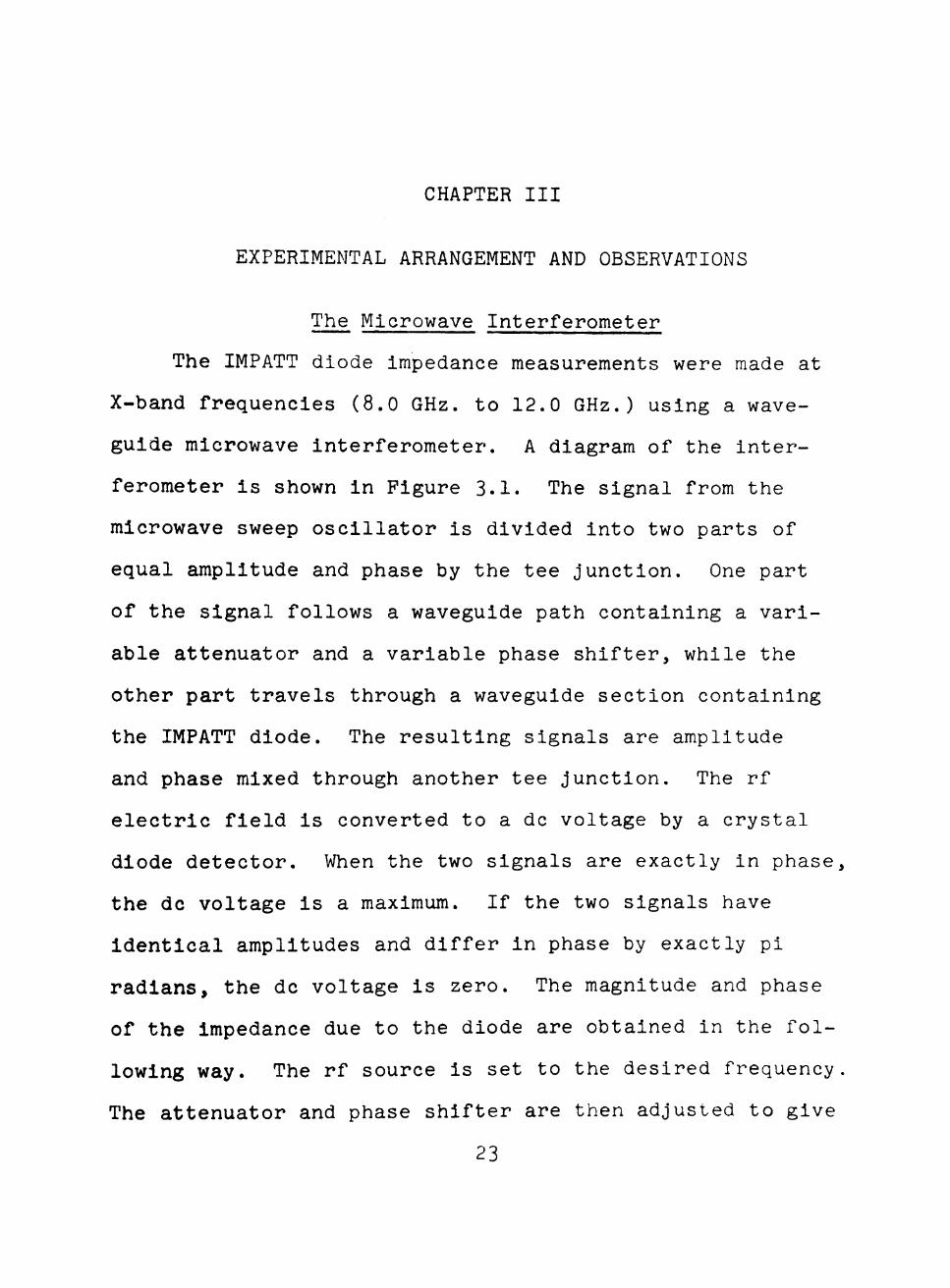
III. EXPERIMENTAL ARRANGEMENT AND OBSERVATIONS. . 23
The Microwave Interferometer 23
Additional Diode Measurements 30
Experimental Results 32
IV. CONCLUSION 37
LIST OF REFERENCES 40 APPENDIX 43
A. FORTRAN IV COMPUTER PROGRAM FOR COMPUTING IMPATT DIODE IMPEDANCE 44
B. THEORY OF THE ONE-SIDED ABRUPT p'*'-n JUNCTION 49
C. ALTERNATE METHOD FOR OBTAINING CURRENT DENSITY EXPRESSIONS 55
ill

LIST OF TABLES
Table Page
3.1. ADDITIONAL DIODE DATA 33
IV
LIST OF FIGURES
Figure Page
2.1. Ionization coefficient as a function of distance in an avalanching diode 10
2.2. Generalized IMPATT diode model 12
2.3. IMPATT diode impedance as function of frequency 21
2.4. Diode susceptance plotted against conductance for several values of current 22
3.1. Schematic diagram of microwave inter
ferometer 24
3.2. Reduced height waveguide and diode mount . . . 26
3.3. Linearly tapered waveguide section 27 3.4. Reflection coefficient as a function o.
frequency for a linearly tapered waveguide transition section 29
3.5. Schematic diagram for measuring dioae capacitance as a function of reverse bias voltage 31
3.6. Theoretical and experimental impedance . . . . 3^
3.7. Theoretical and experimental impedance . . . . 35
B.l. Doping; profile and electric field for the one-sided abrupt Junction ^1)0
B.2. Depletion capacitance as a function of applied voltage for a one-sided abrupt junction 5^
V

CHAPTER I
INTRODUCTION
The acronym IMPATT stands for IMPact ionization Ava
lanche Transit Time (which describe the semiconductor prop
erties that give the IMPATT diode its negative resistance
behavior at microwave frequencies). The use of avalanche
properties to obtain high frequency negative resistance was
first proposed in 1958 by W. T. Read, Jr. [1]. The Read
+ + diode utilized an n ~p-i-p structure. The first IMPATT
operation was obtained in 1964 by Johnston, DeLoach, and
Cohen using a p-n junction diode [2]. The diode structure
can be that of the p-n diode, the p-i-n diode, or the Read
diode [3]. The following work is based on the abrupt p -n
junction.
The Theoretical Approach
The theory proposed by Read [1] in 1958 resulted in a
very complicated expression for the diode impedance. His
work applied to the specialized structure mentioned above
and not to the simple p -n junction. Since 1958, several
approaches have been tried to simplify Read's model and to
develop a more general model that can be applied to other
structures.
1

Gilden and Hines [4] used a space-charge wave approach
to obtain a simplified small signal model which is much
si..pier than the model proposed by Read. Their approach
was applied to a p -n abrupt junction. The diode is con
sidered to consist of three regions: an avalanche region,
a drift region, and an inactive region. The diode impe
dance that results from this analysis shows a positive real
part below an avalanche frequency and a negative real part
above this frequency. The reactive part changes from in
ductive to capacitive at the avalanche frequency. The ava
lanche frequency is an increasing function of the diode
current.
A detailed study of the IMPATT diode under small sig
nal conditions, similar to that of Gilden and Hines, was
reported by Gummel and Scharfetter [5]. This analysis
placed more importance on the avalanche region and was ap
plied to a diode with a localized avalanche region. The
impedance calculated from this approach also shows a reso
nance effect. In this case, the real part changes from
positive to negative at a frequency below the avalanche
frequency, where the reactive part changes from inductive
to capacitive. The real part remains negative for frequen
cies above the transition frequency.
A small signal lumped model based on a state-space
analysis was proposed by Stewart, et_ a]^. [6]. This model

J
was applied to the Read structure and to a p -n junction.
As with the previous approaches, the impedance found by
this method shows resonance effects. The results for a
p -n diode show the real part changing from positive to
negative and the reactive part changing from inductive to
capacitive, but the changes do not occur at the same fre
quency, the transition frequency for the reactance being
higher than the transition frequency for the resistance.
Misawa [7], [8] has reported an approach that allows
an analytical expression to be derived for the IMPATT diode
impedance. This method uses a multiple uniform layer ap
proximation, similar to that of Gilden and Hines, for the
diode. The avalanche is considered to be uniform and is
limited to a specific region. The resulting impedance be
haves in much the same way as that resulting from the pre
viously mentioned methods, except that it shows a positive
real part at some frequencies above the transition fre
quency. As will be shown in Chapter IV, this result agrees
well with experimental measurements.
The theoretical approach used in this work is that of
Misawa's multiple uniform layer approximation. Chapter II
explains the assumptions made with this approach. The
theory of avalanche multiplication is introduced. An anal
ysis is then performed on the diode model and an analytical
expression for the diode impedance is derived. This ex-

pression is evaluated numerically for several realistic
diodes by computer calculation. The computer programx,
written in FORTRAN IV, is presented in Appendix A. Real
istic input data for p -n diodes were obtained from meas
urements performed on non-avalanching diodes. A discussion
of the theoretical considerations needed to obtain this in
formation is included in Appendix B.
The Measurement Techniques
The IMPATT diode operates at microwave frequencies so
that conventional impedance measurement techniques cannot
be employed. Because of the difficulties associated with
microwave impedance measurements, some investigators [9],
[10] have been content to measure signal gain as functions
of diode bias current and signal frequency. Small signal
gain and oscillations have been observed in a region where
a negative resistance is predicted by the theories. This
provides some evidence for verification of the IMPATT diode
theory. More precise information is needed, though, to
show any detailed accuracy of the theories.
A measurement technique reported by Gewartowski and
Morris [11] Involved using a computer to reduce measured
data to diode impedance values. This method has also been
applied by Isobe and Nakamura [12]. It requires diode
measurement to be made at low frequency (about 1 MHz.) with
conventional techniques and at microwave frequencies with a
slotted transmission line. Accurate dimensions for the
slotted line and diode mount must be known. This technique
allows the determination of the active diode impedance in
dependent of parasitic impedance.
Another measurement technique using computer calcula
tions has been applied by Kuno, Fong, and English [13].
This method involves Using a slotted transmission line and
an adjustable short to measure voltage standing wave ratio
and phase shift. An iterative computer calculation is used
to evaluate circuit model parameters to fit the experi
mental curves to the model. The package reactance is in
cluded in this measurement. The resulting impedance has
been successfully used to predict diode performance.
Impedance measurements have been made from measurements
of the reflected wave resulting from the diode impedance.
In the method described by Steinbrecher and Peterson [l4],
a reflection type microwave network analyzer is required.
The impedance as a function of bias current can be plotted
directly on a Smith chart. This impedance consists of the
diode impedance and the network impedance. Measurements
with known impedances in place of the diode are required so
that the actual diode impedance can be separated from the
measured impedance. Another reflected wave measurement,
reported by Misawa [15], uses simpler equipment, but pro
vides only evidence of the existence of a negative resis-

tance as a function of frequency and bias current. In this
method, the diode, mounted in a coaxial transmission line,
is fed by a leveled microwave power source and the reflected
power is measured. The actual value of the Impedance is
not calculated. A change in the reflection coefficient
shows evidence of the negative resistance.
Accurate impedance values were obtained by van Iperen
and Tjassens [16] with a microwave bridge technique. To
obtain the high accuracy reported, the diode mount was
machined with optically flat surfaces, and the dimensional
requirements were very stringent. The system was precisely
calibrated for a given frequency and results were reported
only for one frequency. Although accurate measurements can
be made with this method, the inconvenience in obtaining
data over a band of frequencies is considerable.
The microwave impedance measuring techniques described
above each have important disadvantages. For some cases
the package reactance can mask the actual active device re
actance causing inaccurate results unless package para
meters are known precisely. The conductor supplying dc
bias to the diode results in a transmission line impedance
that must be considered in analyzing the data. Transmis
sion line lengths must be known accurately. In some cases,
the changing of the measurement frequency requires the
changing of circuit dimensions or calibration. Accurate
7
impedance measurements can be made, but with considerable
inconvenience on the part of the investigator.
The u.se of a microwave interferometer as the measuring
device can provide accurate yet simple measurements. The
Interferometer measures differences between impedances in
two arms of a microwave circuit. Because only difference
measurements are made, any deviation from symmetry in the
two circuit arms can be zeroed out of the measurements.
The effects of the diode package can also be zeroed out of
the measurement so that only the active device parameters
are measured. The interferometer is readjusted for each
new frequency so that any frequency dependence of the meas
urement accuracy is eliminated. Chapter III describes the
microwave interferometer and the procedure used in making
the impedance measurements reported here.

CHAPTER II
THEORY OF THE IMPATT DIODE
Avalanche Breakdown in Abrupt p -n Junction
When high electric fields are applied to semiconductor
materials, carriers are accelerated to high velocities and,
when the field is high enough, they can knock more carriers
off of the atoms during collisions. Thus a carrier multi
plication process occurs and the current suddenly increases.
The carrier concentration increases by a factor of M, the
multiplication coefficient. The rate a at which the ioni
zation process occurs can be expressed as [17]
where m = 1 for silicon, and
A = 3.8-10^cm"i n
b = 1.75-lO^V/cm
for electrons in silicon, and
A = 2.25-10^cm~i P
b = 3.26-lO^V/cm P
for holes in silicon. When the multiplication process is
due primarily to electrons, as in the one-sided p -n
8

junction. Miller [l8] has shown a general result that
1-i = M
rX ^d - (a -a )dx' ^ a^e ^0 " P dx , (2-2)
where M is the carrier multiplication factor, and w. is the
width of the depletion region. The condition for avalanche
breakdown occurs when
M->«, , (2-3)
and the integral in equation (2-2) approaches unity. The
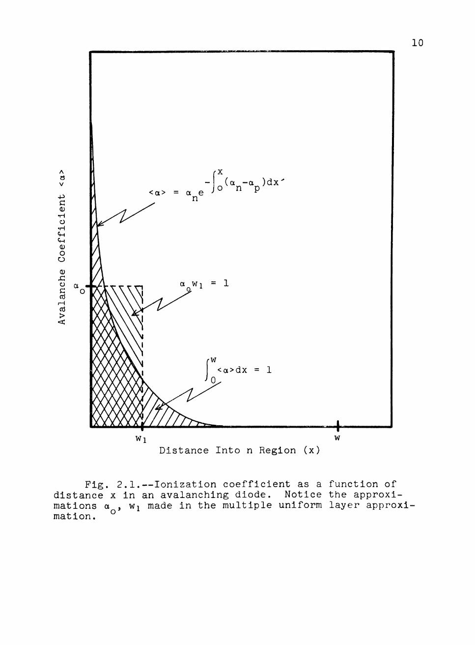
integrand of equation (2-2) is plotted as a function of x
for the avalanche condition in Figure 2.1. The diode
voltage at which the avalanche occurs is called the break
down voltage V and has been shown by Sze and Gibbons [17]
to be given by the empirical expression
V^ = 60(E^/l.l)3/2(N^/10i6)"3/^ , (2-4)
where E =1.12 eV for silicon and N^ is the donor concen-g D
tration in the abrupt junction. The diode area A, the im
purity concentration N^, and the n region width w can be
determined from measurements based on equations (B-14) and
(2-4).
Generalized Small-Signal Theory
of; the_ p' -n IMPATT Diode
The generalized theory is based on the multiple uni-
10
A 25 V
4^ G 0
O •H CM CM 0 O
O
0 Xi O G cd
rH cd >
< a > = a e n
a Wi = 1
rX
(a - a )dx o n p
<a>dx = 1
+ Wi w
Distance Into n Region (x)
Fig. 2.1.—-Ionization coefficient as a function of distance x in an avalanching diode. Notice the approximations matlon.
a o w I made in the multiple uniform layer approxi-
11
form layer model of the IMPATT diode suggested by T. Misawa
in 1967 [8]. The model consists of an avalanche region
(x = 0 to X = wj) in which the avalanche coefficient a is
constant, non-zero, and in which 95% of the avalanche oc
curs and a drift region (x = wj to x = w) in which a = 0.
It is also assumed that the carrier drift velocities are
the saturation drift velocities (in silicon, the saturated
velocity, v^ (= lO" cm/sec), occurs when the electric field S X
exceeds about 10^ V/cm)[3]. The model for a p -n diode is
shown in Figure 2.2. The analysis begins with the applica
tion of Poisson's equation
If = q/e(Nj^-N^+p-n) , (2-5)
where q is the electronic charge, e is the material perma-
tivity, N. is the accepter concentration, and p and n are
the hole and electron concentrations respectively. The
current density in the diode is composed of two parts such
that
J = J +J , (2-6) p n
where the components Jp and J^ are given by
J = qpvi 2 = -qpVg- , (2-7)
and
J = qny £ = -qnv^. , (2-8) n n ^ si

12
(a) +
p 1 i 2 In
X = 0 Wi w
E(x)
(b)
Wi w <a>
(c)
X
Wi w
Fig. 2.2. —(a)
(b) (c)
Generalized IMPATT diode model 1. Avalanche region 2. Drift region Electric field distribution Avalanche coefficient <a>
13
where u and u are the hole and electron mobilities, re-p n
spectively. Imposing current continuity for the avalanch
ing junction requires that
3J ! t = ^33r^»^i("^p^ ' (2-9'
and
If = - J al^-si("^P) • (2-10)
A substitution of (2-7) and (2-8) into (2-5), (2-9), and
(2-10) delivers the equations in terms of the quantities of
interest, current densities and electric fields, as follows
|1 = a(N N J + - ^ ( J -J ) , (2-11) ax e D A V , e n p ' si ^
, 9J dJ - - ^ TT^ = r-^ - a(J +J ) , (2-12) V T 8t ax n p ' si '^
and
. aj -aj - -i- — ^ = --^ - a(J^+J^) . (2-13)
V -, at ax n p si
For the small signal case, the following quantities are de
fined
E(x,t) = Eo(x)+E(x,t)
Jp(x,t) H Jp^(x)+Jp(x,t)
• n ""* ^ ' ' no ' ' ' n ''' ^
14
a(x,t) = a^(x)+a"(x)E(x,t)
a^(x) E ll (2-14)
where the time dependence is assumed to be of the form
e'' . After substituting the relations of (2-14) into
(2-11), (2-12), and (2-13) and ignoring second order pro
ducts of time varying terms, the following time dependent
equations result:
lf = 7rT(VJp) ' (2-15) si ^
aj . . . . T—^ = - ^r-^ +OL(J +J ) + a'E(J +J ^ , (2-16) ax V , n o n p no po *
and
aJ . , . . ^ = ^ J -a (J +J )-a E(J +J ) . (2-17) ax V -, p o n p no po
S J-
Equations (2-l6) and (2-17) are added together, resulting
in
aj aJ . . . -J^--^ = ^^^{J -J ) , (2-18) ax ax V , p n ' si
which is then substituted into (2-15) to give
^^ . aJ aJ II = ^(jz^^TT') . (2-19) ax £03 ax ax
Integration with respect to x of the above equation gives
15
the following Important result
jeu)E+J +J = constant = J . (2-20) " p n
The time dependent current density is a constant function
of X in the diode. It is composed of hole, electron, and
displacement components.
A second order differential equation for E is found by
differentiating equation (2-15) with respect to x and mak
ing substitutions with equations (2-16), (2-17), and (2-20)
as follows
; 2F ,.,2 J2aoa) 2a'Jo ~ ~ 2ao ax" v -. V -, V ,e V ,e v -, e + (- i H- )E = J( - V") , (2-21)
" T^ V T V ,£ V ,£ V T^'~ ' Sl sl sl sl sl
where
Jn = J +J . (2-22) ^ no po
The electric field E will then have the form
i = CieJ' ''+Cae-J' ''+(|H - T^^W ' (2-23) sl sl
where Cj and C2 are coefficients, which can be complex and
k = [-^ - 2oLjLa .i2aj -il/2 (2-24) sl sl sl
is the propagation function. V(x) can be obtained by in
tegrating E(x)
V(x) = (X~
E(x)dx . (2-c'5) 0

16
Using equations (2-l8), (2-19), (2-20), and (2-23) to solve
for J and J algebraically, the following are obtained:
} = _ i!^l(kWv3,)C,e^'^='.q^(Wv^^)C,e-J'<'^-J?^ ^ sl
(2-26)
and
J„ = i^(k-<./v ,)CieJ'^^-i^(kWv ^)c,e-J'^^-^^:i^ . n 2 s l ^ 2 sl"^ k v , e sl
(2-27)
These results can also be obtained by solving the differ
ential equations (2-l6) and (2-17). The details are shown
in Appendix C. These results for J and J are similar to p n
those obtained by Sze [3] and Misawa [7], and DeLoach [19].
The solutions obtained for the electric field and cur
rent densities contain tv;o arbitrary constants that must be
evaluated. The form of the solutions in each region of the
uniform layer model must be considered. In region 1, where
a is a non-zero constant, the solutions are exactly as
above, but in region 2,
ao = a" = 0
and k = oj/v -, si
The results for the two regions are
17
il(x) = Cne^'^^+Ci2e-J'^^+(f^ - ^ ; ^ ) T ^ , (2-23) ^sl^ ^sl ^ ^
• •
T - "^ ^sl/, ^ /„ Np jkx.'^^^sl/, / v^ -jkx Jg'Jn
^ sl
(2-26)
T - ^_^sl/, /, Np jkx "^^^sl/, , / N^ -jkx Jg'Jn
sl
(2-27)
for region 1, and
ECO
(2-28)
J = -jea)C2ie-' ''''' ''sl , (2-29)
P2 " ^ ^
J = -jea)C2 2e'^'''''^''sl (2-30) n2 ^ ^ '
for region 2.
The following boundary information is used to evaluate
the four coefficients:
J - = 0 at X = 0 y ^^ (2-31)
Jpi = Jp2 = 0 at X = wi ^ (2.32)
and
J = J at X = wi . (2-33) ni n2
The resulting coefficients are
11
- j k w i - j 2 k w i c J ( b e +ae )_
- j 2 k w i ( b ^ - a ^ e )
18
( 2 - 3 4 )
- j kw 1 cJ ( b+ae )_
12 - - j 2 k w i ( b 2 - a 2 e )
( 2 -35 )
C21 = 0 ( 2 - 3 6 )
a n d
22
V j b w i V - j a w i : 5 ^ a C i i e + 3 ^ b C i 2 e 2a) ^ - 2(1) ^ ^
J v ^ ce s l 2a)
j a )Wi /Vg^
( 2 -37 )
w h e r e
a = k-a) /v s l
( 2 -38 )
b = k+a}/v s l
( 2 - 3 9 )
and
s l (2 -40 )
The t i m e v a r y i n g v o l t a g e a c r o s s t h e d i o d e i s g i v e n by
V =
rW
' 0
rw
Eidx+ E2dx ( 2 - 4 1 ) Wi
w h i c h r e s u l t s i n
V = C i i j k w i C12 - j k w i
' \ ( e - 1 ) - T ^ ( e - 1 ) j k 3^
19
sl sl
C22V--1 -ja)w/v . -ja)Wi/v . S-L.(e si_g Sl)
_JCw::w^ (2-42) eo) '
where it should be noted that C n , Ci2> O22 are propor
tional to J. The diode Impedance is defined as
Z = J- , (2-43) JA
where A is the diode area. This gives the following result
for the impedance
-jkwj -j2kwi jkwj r. f s _ c(be +ae )(e -1) ^ ^ = jtol
jkA(b2-a2e )
-jkwj -jkwi ,c(b+ae H e -1)
-jkwi jkA(b2-a2e )
. (2an _ J(o )Wi iw-wi) ^ v .£ V '^e^iPT ea)A Sl" Sl
2 - j kwi - j2kwi jbwi - j kwi - j a w i . ^ s l / ^ r a ( b e +ae )e - b ( b + ae )e T2Z7X'- - j2kwi
(b2-a2e )
ja)Wi/v^-, -joiw/v -Ju)Wi/v +e ^ ^ ] [ e ^ - e ^ ^ ] . ( 2 - 4 4 )

20
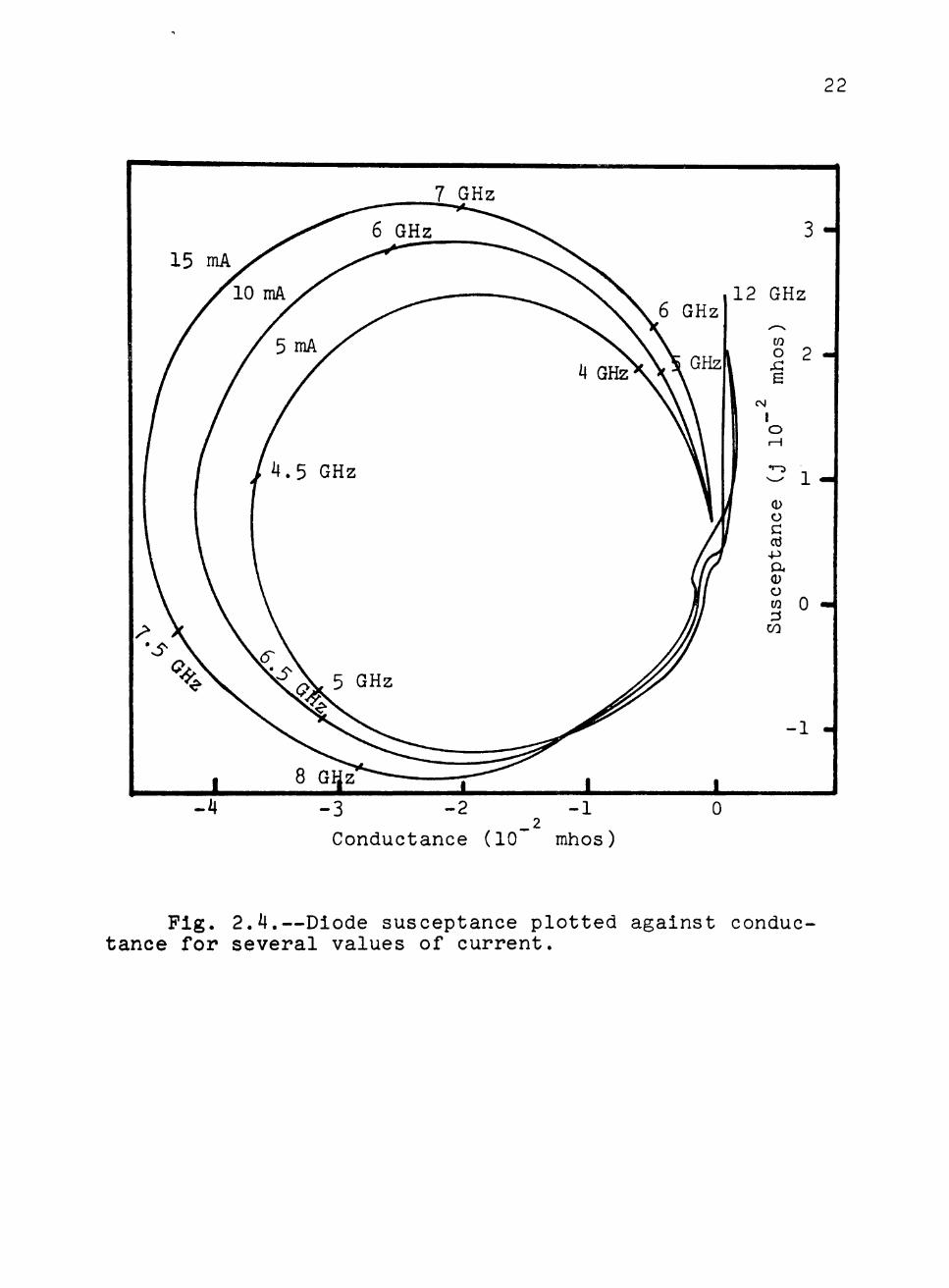
The impedance is shown in Figure 2.3 as a function of fre
quency for a typical diode. The diode susceptance is
plotted against conductance for several current values in
Figure 2.4. The diode exhibits resonance properties with
the reactance inductive below the resonance and capacitive
above the resonance. The reactance also shows the expected
capacitive behavior at frequencies much below the resonant
frequency. The real part of the impedance is negative over
a large range, showing capability for amplification or
oscillation at microwave frequencies. These results are
very similar to those obtained by Misawa [7].

21
a; o C CTJ
- p o Cd 0 Pi
<L) O C cti 4-> (0 . H CO <U PC
X
:ii
o C 0)
o o
o o CO
o o CVJ
o o
o o r-A 1
o o C\J 1
o o en 1
o o I
(suiqo) aouBpaduii
CO 0)
cd >
cd ?-. Q) > 0 CO
o C M
O
:^ cr 0)
«M
«M
o
o -P O :3
«M
CO cd
0) o C cd
<u
B
(D
O •H T5
H EH < cu S M
1 1 •
m •
C\J
. -^^ 4J
c <D U U :^ o
bO 0) •H fc
r ) o •H T?
< M
o
22
Conductance (10 mhos)
Fig. 2.4.—Diode susceptance plotted against conductance for several values of current.
CHAPTER III
EXPERIMENTAL ARRANGEMENT AND OBSERVATIONS
The Microwave Interferometer
The IMPATT diode impedance measurements were made at
X-band frequencies (8.0 GHz. to 12.0 GHz.) using a wave
guide microwave interferometer. A diagram of the inter
ferometer is shown in Figure 3.1. The signal from the
microwave sweep oscillator is divided into two parts of
equal amplitude and phase by the tee junction. One part
of the signal follows a waveguide path containing a vari
able attenuator and a variable phase shifter, while the
other part travels through a waveguide section containing
the IMPATT diode. The resulting signals are amplitude
and phase mixed through another tee junction. The rf
electric field is converted to a dc voltage by a crystal
diode detector. When the two signals are exactly in phase,
the dc voltage is a maximum. If the two signals have
identical amplitudes and differ in phase by exactly pi
radians, the dc voltage is zero. The magnitude and phase
of the impedance due to the diode are obtained in the fol
lowing way. The rf source is set to the desired frequency.
The attenuator and phase shifter are then adjusted to give
23

24
u r-i O cd -P -P O t o <1> >s-P
u o O Q
PQ
cri
o TA
bO cd
/sA/\ c o
-d cd G -^ -H G
zi Q) O 'd s o •H <D Q 73
.H
<D G Xi -H o B 4J ? cd 0) S EH
E-i EH
M
:3 hO 0) > cd
\ > > < ^
T3 Cd 0)
o -p
G • H
s Cd <D S EH
(U -P r-A Cd
cd G
U -P cd -p > <
s^^ 0) 0)
EH
o •H bO cd
o
cd -a 0)
a
O «M
0) CO
^
• P <U
e o <D
CM ?H 0) -P G
• H
0 >
Cd
o
o
0 Xi -p
<M
o B cd fn bO cd
TA
O •H • P Cd B 0
o CO
I I
• to en ^
G
bO •H
0
0
w cd 0

25
a zero voltage null at the crystal detector, as measured
with a microvolt meter. The required attenuation and phase
shift are noted. Bias voltage is then applied to the diode
to obtain the avalanche condition. The attenuator and
phase shifter are readjusted to obtain a zero voltage null
at the crystal detector and the attenuation and phase are
noted. The change in attenuation and phase are functions
of the impedance magnitude and phase due to the diode.
These values are normalized to the characteristic Impedance,
Z , of the waveguide in which the diode is situated. The
diode is placed in a reduced height waveguide to obtain a
Z near the magnitude of the diode impedance to produce
more accurate measurements.
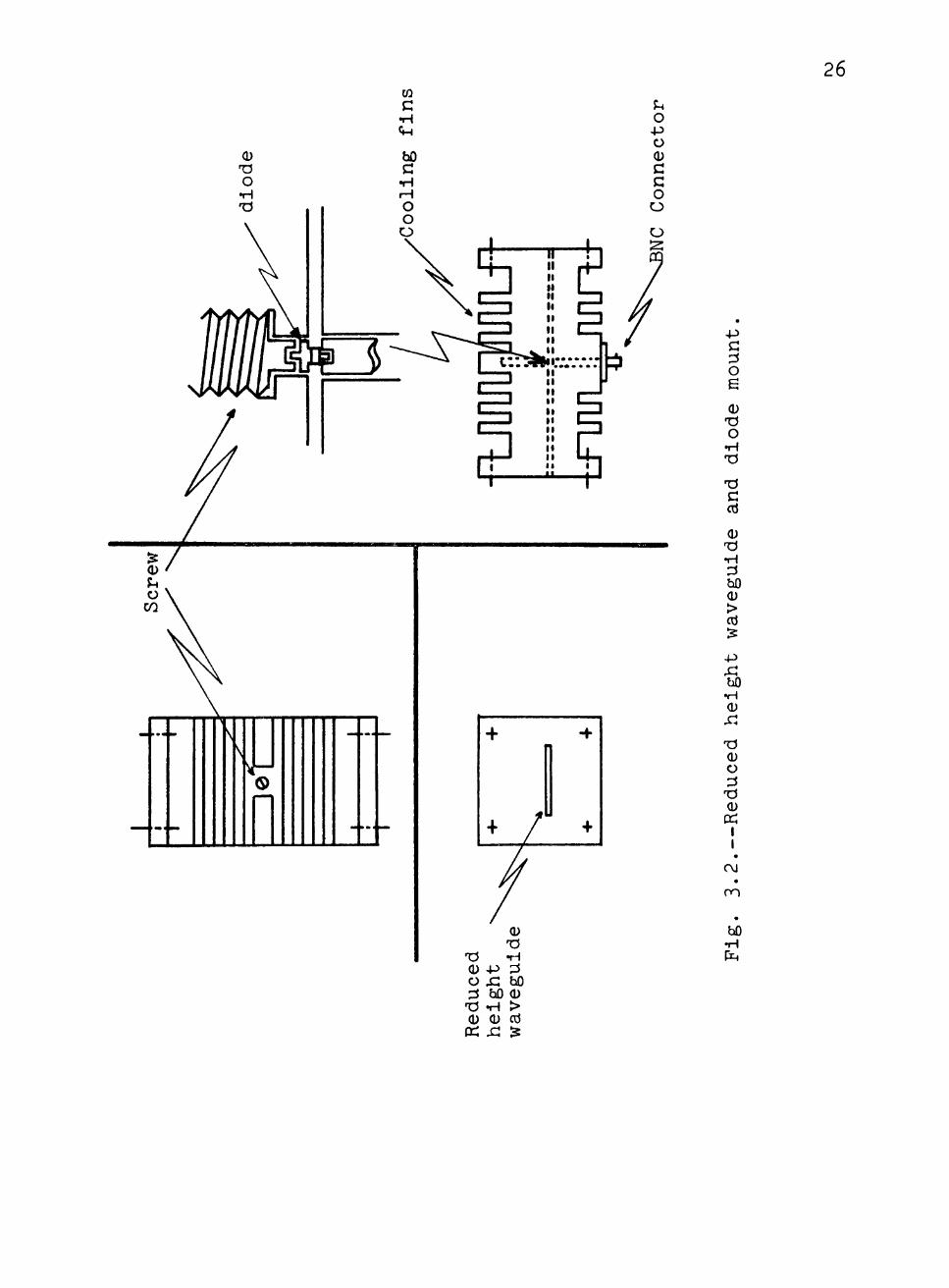
The reduced height waveguide with the diode mount is
matched to the standard waveguide through matching sections
of tapered waveguide. The diode mount is shown in Figure
3.2 and the tapered section is shown in Figure 3.3. When
they are properly matched so that there are no reflections
due to the transition sections, the impedance magnitude and
phase as measured by the interferometer are that of the
diode impedance. If reflections do occur, the measured
impedance would have to be corrected by taking these re
flections into account and correcting the measurements ac
cordingly.
A linearly tapered section of waveguide with impedance
26
— --•\ \
\ J-"
Xi 0 -P o Xi
TA
p bO
:3 bO 0 -O -rA 0 0
Qd Xi
> cd ^
-p G Zi O B
0 Ti O •H n G cd 0
bO 0 > Cd
-p
bO .H 0
Xi
0 o zi xi 0 I I •
C\J m
bO TA PH

Xi
27
S O S o o i n Lnoo c\j
• C\J o CO . • rH C\J ^^
11 ii II 1—4
•J X) cd
s C)
vo -=r C\J
•
II <M
Cd
• ^ - ' — t -
<N Cd
o -p Xi 0
G O •H -P O 0 CO
-^
I T3 0
0
& -p
I I
on c>n

28
Z such that
Z(x) = Zi+(Z2-Zi)x/L (3-1)
where L is the length of the taper, Zi and Z2 are the ini
tial and final Impedances, is used to match the reduced
height waveguide to the standard waveguide. The reflec
tion coefficient, r, has been shown [20] for a tapered
waveguide section to be given by
-I 0
e^^^^A.(lnZ)dx , (3-2)
where 3 is the propagation function and
32 = a)2y e - Tr2/a2 . ( 3 - 3 ) 0 0
The characteristic impedance of the rectangular waveguide
is [21]
1/2 p, (u^/e )
^ /l-xV^a^
where a is the waveguide width and b is the waveguide
height. The dimensions of the taper section are given in
Figure 3.3. A numerical integration of r shows it small
enough to be neglected in these measurements. The reflec
tion coefficient as a function of frequency across the
X-band is shown in Figure 3.^.
An absorbing ring is placed around the diode to pre
vent oscillations when the diode is biased to avalar^che.

29
8.5 9.0 9.5 10.0 10.5 11.0 11.5 12.0
Frequency in GHz
Fig. 3.4.—Reflection coefficient as a function of frequency for a linearly tapered waveguide transition.

30
The dc bias current is applied through a low pass filter
consisting of a capacitor to ground and a ferrite ring
series inductor in the mount, and reaches the diode through
a conducting post. The effects of the absorber and post
cancel at each frequency since the interferometer is used
only to measure changes in Impedance.
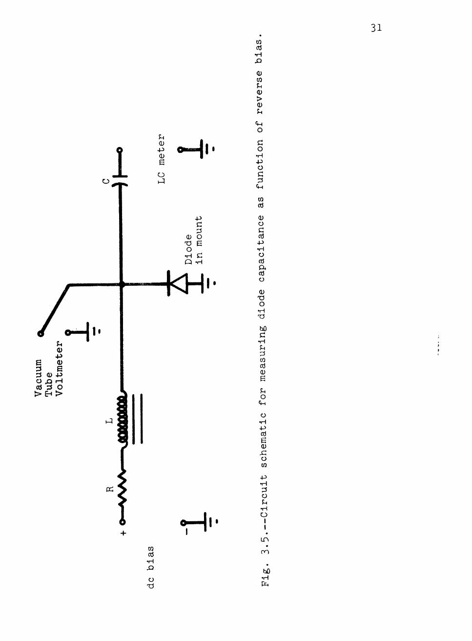
Additional Diode Measurements
The doping concentration in the n region, the width
of the n region, and the diode area are obtained from meas
urements of the diode capacitance and reverse breakdown
voltage. The capacitance is measured at 1 kHz. using a
capacitance meter in the arrangement shown in Figure 3.5.
The bias source has a very low impedance. Therefore a
series resistor and inductor are used to isolate it from
the capacitance meter. The diode package capacitance is
removed from the measurement by zeroing the meter with an
empty package in the diode mount. Measuring the capaci
tance at a known reverse voltage and also at the saturation
point of the capacitance-voltage curve allow the determina
tion of the diode area and the n region width in terms of
the n layer doping from equation (B-l4). The breakdown
voltage is taken as the voltage at which the reverse cur
rent increases to 0.05 mA. This voltage allows the n layer
doping to be obtained from equation (2-4). These parameters
are used in the theoretical calculations of the diode
31
Cd
0 to
0 > 0 u
<M
o G O
'rA 4 ^ O G : 3
<M
CO cd
0 o C cd
4-> • H O Cd
cd o
0
o
•H
bO
c: • H : 3 CO cd 0
o <M
H 4 o
• H - P Cd 6 0 o CO
(r;
HI CO Cd
• H X3
o
:3 o •H o
I I «
bO •H

32
Impedances.
Experimental Results
Measurements of the breakdown voltage V^, capacitance
at 5 V reverse bias Cc, capacitance at saturation C ^, n sat
region doping N^, n region width w, and diode area A are
recorded in Table 1 for typical diodes. Magnitude and
phase measurements were made with the interferometer at
0.5 GHz. intervals from 8.0 GHz. to 12.0 GHz. Having ob
tained the magnitude and phase of the diode impedances, the
real and imaginary parts are calculated. Experimental
values and theoretical values are plotted as a function of
frequency for the diodes listed in Table 1 in Figure 3.6
and Figure 3.7.
The impedance function shows a resonance that is pre
dicted by the theory. The diode reactance changes from in
ductive to capacitive at the resonant frequency. As pre
dicted, the real part of the impedance is negative over a
range of frequencies below the resonant frequency. Above
the resonant frequency, the real part is positive and de
creases toward zero as the frequency is increased. The
peak magnitude of the negative real part occurs at a fre
quency just below the resonant frequency. The occurrence
of the negative real part shows the capability of the IMPATT
diode to function as an oscillator or amplifier.
The experimental measurements show a smaller than pre-

33
TABLE 3.1
ADDITIONAL DIODE DATA
V3 C^ Cg N^ W A
Diode (Volts) (pF) (pF) (lO cm' ) (lO cm) (lO' cm )
Fig. 3.6 68 .30 .08 .8874 .1078 .2063
Fig. 3.7 71 .50 .25 .8283 .1268 .4247
dieted change in resonant frequency for a given change in
diode current. (The impedance measured at 10 mA. deviates
only slightly from the impedances shown in Figures 3.6 and
3.7 which were measured at 15 mA. For this reason only
one set of data is shown.) It is believed that this result
is due to a cavity effect of the diode mount. Placing an
adjustable short at the standard waveguide end of a transi
tion section attached to the diode mount forms a microwave
cavity. Adjustment of the waveguide short produced only
small changes in the oscillation frequency. This oscilla
tion frequency was centered approximately at 11.0 GHz.
(there was some variation from diode to diode). This re
sult implies a tuning effect of the diode mount on the
diode. The interferometric measurements will not include
any impedance due to the cavity, but it cannot diminish
its effect on the diode. The tuning effects found in the
oscillator circuit and the smaller than predicted change

34
400
300
200
100 -
Theoretical Reactance
— — Theoretical Resistance • Experimental Reactance X Experimental Resistance
CO
O
-100 -
/ ^
I
I I
I .
8.0 8.5 9.0 9.5 10.0 10.5 11.0 11.5 12.0
Frequency in GHz
Fig. 3.6.—Theoretical and experimental diode impedance .

35
CO
O
400
300
2001-
100
0.0
-lOOh
-200
-300
-400
1 1 1
1 1
1 1
1 1
/ /
—-1
1
1
1 **
• Experimental Reactance
* Experimental Resistance
•
It -^ *
/ «* ** / ^ / ^
J • / / / / 1 / / t
1 •
1 J - I « « 1 • 8.0 8.5 9.0 9.5 10.0 10.5 H.O 11.5 12.0
Frequency in GHz
Fig. 3.7.-—Theoretical and experimental diode impedance.
36
in the resonant frequency for a diode current change im
ply the cavity effect does exist.
The accuracy of phase and attenuation measurements
which affects the plots of impedance shown in Figures 3.6,
3.7 are determined by the instrument accuracy (+ 3% for the
phase shifter and + 2% for the attenuator) added to the un
certainty of the interferometric measurements. The uncer
tainty for the interferometer is due to the ambiguity of
the phase and attenuation near the null. This ambiguity is
not constant for all frequencies, but is approximately 5*
in phase and 1/2 dB in attenuation.

CHAPTER IV
CONCLUSION
The theoretical calculations predict a resistance that
is negative over a range of frequencies and then becomes
positive or near zero for higher frequencies. The reac
tance shows the expected capacitive reactance at lower fre
quencies. The reactance becomes inductive in a large por
tion of the spectrum where the negative resistance exists.
A resonance effect appears at a frequency near where the
negative resistance becomes positive, and here the reac
tance again becomes capacitive. As can be seen in Figures
3-6, 3-7, the experimental data clearly shows the tendency
for the negative resistance to become positive or near zero
at frequencies above the frequencies where the useful nega
tive resistance occurs. This effect has been reported [12],
[15], [22] before but has largely been ignored. It repre
sents an important limitation on the upper operating fre
quency of the IMPATT diode. From the evidence presented
here, it can be seen that the effect is predicted by the
theory and is a physical reality.
The theoretical curves are based on Indirect measure
ment of the diode parameters (the n side doping level,
37

38
diode area, and length of the n side). These measurements
are based on the breakdown voltage and capacitance measure
ments. The capacitance magnitudes are near the resolution
of the capacitance meter available and some uncertainty
concerning the accuracy of the values exists. The satura
tion capacitance is difficult to determine since the deple
tion region will continue to spread into the highly doped
p and n regions. These diode parameters are very signifi
cant in determining the resonant frequency of the diode,
and the uncertainty accounts for the experimental and
theoretical resonances not occurring at the same frequen
cies. For these reasons, the comparison between experi
ment and theory should be viewed as qualitative rather than
quantitative.
The theoretical calculations show a strong dependence
of the resonant frequency on the diode current. This has
been observed in reported measurements [4], [15]. The cur
rent tuning effects in the measurements reported here are
not as strong as predicted. The reduced height waveguide
transitions demonstrated a resonance effect with a diode
operating as an oscillator. An adjustable short placed on
one transition section proved ineffective in significantly
tuning the cavity. Also decreases in the diode current did
not strongly affect the oscillation frequency although the
output magnitude decreased. This result is expected be-

39
cause the diode negative resistance becomes closer to zero
at the oscillation frequency as the current decreases. The
interferometer will not measure the impedance of the cavity,
but the effect on the diode cannot completely be discounted.
The interferometric impedance measurements are thus still
representative of the diode impedance.
In summary, the data presented shows agreement in
theoretical and experimental impedance values. Of special
interest is the appearance of a positive resistance at fre
quencies above the frequencies at which the useful negative
resistance occurs.
The measurements show good qualitative agreement with
theory. As mentioned above, the lack of quantitative agree
ment is thought to be caused by the lack of accuracy of the
capacitance measurements which determine the input data for
the theoretical calculation and by the cavity effect of the
diode mount. The interferometric measurement technique
holds promise if these problems are overcome. It is a much
simpler measurement technique than the other techniques re
ported and shows potential for accurate results.

LIST OF REFERENCES
1. Read, W. T., Jr. "A Proposed Hlgh-Frequency, Negative-Resistance Diode." The Bell System Technical Journal, Vol. 37, No. 2, March 1958, pp. 401-
2. Johnston, R. L., DeLoach, B. C , and Cohen, B. G. "A Silicon Diode Microwave Oscillator." The Bell System Technical Journal. Vol. 44, No. 2, Febru-ary 1965, pp. 369-372.
3. Sze, S. M. Physics of Semiconductor Devices. New York: John Wiley and Sons, Inc., 1969.
4. Gilden, M. and Hines, M. E. "Electronic Tuning Effects in the Read Microwave Avalanche Diode." IEEE Transactions on Electron Devices, Vol. ED-13, No. 1, January 1966, pp. 169-175.
5. Gummel, H. K. and Scharfetter, D. L. "Avalanche Region of IMPATT Diodes." The Bell System Technical Journal, Vol. 45, December 1966, pp. lT97-1827.
6. Stewart, J. A. C , Conn, D. R. , and Mitchell, H. R. "State-Space Analysis of General IMPATT Diode Small-Signal Lumped Models." IEEE Transactions on Microwave Theory and Techniques. Vol. MTT-18. No. 11, November 1966, pp. 835-842.
7. Misawa, T. "Negative Resistance in pn Junctions Under Avalanche Breakdown Conditions, Part I, and Part II." IEEE Transactions on Electron Devices, Vol. ED-13, No. 1, January 1966, pp. 137-151.
8. Misawa, T. "Multiple Uniform Layer Assproimations in Analysis of Negative Resistance in pn Junctions in Breakdown." IEEE Transactions on Electron Devices, Vol. ED-14, No. 12, December 1967, pp. 795-808.
9. Takayama, Yoichiro. "Power Amplification with IMPATT Diodes in Stable and Injection-Locked Modes."
40

41
IEEE Transactions on Microwave Theory and Techniques, Vol. MTT-20, No. 4, April 1972, pp. 266-272.
10. DeLoach, B. C. and Johnston, R. L. "Avalanche Transit-Time Microwave Oscillators and Amplifiers." IEEE Transactions on Electron Devices, Vol. ED-13, No. 1, January 1966, pp. 181-186.
11. Gewartowski, J. W. and Morris, J. E. "Active IMPATT Diode Parameters Obtained by Computer Reduction of Experimental Data." IEEE Transactions on Microwave Theory and Techniques, Vol. MTT-18, No. 3, March 1970, pp. 157-161.
12. Isobe, Toyosaku and Nakamura, Tetsuo. "Admittance Measurements of IMPATT Diodes at X-Band." IEEE Transactions on Microwave Theory and Techniques, Vol. MTT-18, No. 11, November 1970, pp. 993-995.
13. Kuno, H. J., Fong, T. T., and English, D. L. "Characterization of IMPATT Diodes at Millimeter-Wave Frequencies." IEEE Transactions on Electron Devices. Vol. ED-19, No. 6, June 1972, pp. 752-757.
14. Steinbrecher, D. H. and Peterson, D. F. "Small-Signal Model with Frequency-Independent Elements for the Avalanche Region of a Microwave Negative Resistance Diode." IEEE Transactions on Electron Devices. Vol. ED-17, No. 10, October 1970, pp. 883-891.
15. Misawa, T. "Silicon pn Avalanche Transit-Time Diodes." IEEE Transactions on Electron Devices, Vol. ED-17, No. 4, April 1970, pp. 299-304.
16. Iperen, B. B. van and Tjassens, H. "An Accurate Bridge Method for Impedance Measurements of IMPATT Diodes." Microwave Journal, Vol. 15, No. 11, November 1972, pp. 29-33.
17. Sze, S. M. and Gibbons, G. "Avalanche Breakdown Voltages of Abrupt and Linearly Graded p-n Junctions in Ge, Si, GaAs, and GaP." Applied Physics Letters, Vol. 8, No. 5, March 1966, pp. 111-113.

42
18. Miller, S. L. "Avalanche Breakdown in Germanium." Physical Review, Vol. 99, No. 4, August 1955, pp. 1234-1241.
19. Watson, H. A., ed. Microwave Semiconductor Devices and Their Circuit Applications. New York: McGraw-Hill Book Co., 1969.
20. Collin, Robert E. Foundations for Microwave Engineering. New Yorlcl McGraw-Hill Book Co., 1966.
21. Montgomery, C. G., Dicke, R. H., and Purcell, E. M., eds. Principles of Microwave Circuits. New York: McGraw-Hill Book Co., 1948.
22. Irvln, J. C , Coleman, D. C , Johnson, W. A., Tatuguchi, I., Decker, D. R., and Dunn, C. N. "Fabrication and Noise Performance of High Power GaAs IMPATTS." Proceedings of IEEE, Vol. 59, No. 8, August 1971, pp. 1212-1221.

APPENDIX
A. Fortran IV Computer Program for Computing IMPATT
Diode Impedance
B. Theory of the One-Sided Abrupt p -n Junction
C. Alternate Method for Obtaining Current Density
Expressions
43

APPENCU A
FC^T-^AN IV C r y i M l i r ' * PRnCRAf-' Prvt CALCULATING IVPATT OIGUR I^'PF^A^CG
^ A I N P W O G R A M
c c r.
n(:\F M T M nri.cLf: P'^tcisifN. sui'Roun^ji: P R N P L T IS LTiLi/ro f l ]R DISPLAYING HATA
C A L C L L A T l f J S M'T LIH:-^/iRY S 'JP 'JLIFr - iRAPHICALLY.
I N P L I C l r '>E AL*R ( A - H , C - Z ) l^f^AL^'^'i X <( '»(:C) . Y Y C C C ) , 7,?(^CC) , i - F ,FL - ( ^CO) .AM'- fOO) , X X X l ' » 0 0 ) Rf-AL'-^ \ L , I , J C , lisTGRL CCM-LN/ I APiJS/ NCLT CnVV( ' \ ' : f^,U1 ,l^0 , A \ ' , A P , H N ,nP,'/« C r v P L r X U i ^ / 1 , Z 2 , 7 3 , / ' . , / 5 CCf^i^LFK :=l!S J , K , A , P , C , / , E N 2KW , EMKK , G P K W ,CI'X!', C SORT , C M P L X . C O S U R T ,
icnExp^pc.'^r'Lx.r. 11 ,r, i ? , c ? i r x r U R N A L A L F A . F ? SCi' T ( M ) ^ ^ S ' : R T ( A l ) r,SuRT( ^) ^ c o s r j u ( A ) c/' 'pL X ( M , nK,) =nc N cL X ( A I , R e) CfEXP( / ) = C r F X P ( A) /i (' S ( X ) = C A P S ( X )
I N I T I A L I Z ' ^ CnN'STA^irS. ALL PHYSICAL CATA F C S I L I C O N IS OHTAINLC FROM Rf-F':RtNCF ( 3 ) .
V S L 1 . L- 7 EPSR-=1 1.8 FPSn=P.f?5'.E-l''« A N = 3 . H F 6 AP = -?. 25(:7 H-J=l . 7 5 F 6 HP=3.?'5E6 EG = 1 .1? C=1.6C2P-iq
C C
C C
INPUT rFVICL- PARAVtTERS I N REGIHN DUPING LEVEL, LENGTH CF N REGION,
AREA CF C i r C F ) . PF An( '"> , 1 ) ND,Vs , AREA FPRrAT ( :M7?C. *= ) IF(Mr.FC.O) CALL EXIT
CALCLLATE »';<FAKf:CWN VCLTAGE ANC CHPLETICM WIOTH FOR CASE WHERE N PEGir\ LENGTH IS LCN^^E'^ TFAN THE CtPLEIICN ViICTH.
VR = .0.*<LG/l . ! )**!.«:'(NC/l.Fl6)*«(-.7 5) ^^c=S(.RT(?.*EPSC/f:*F"S"/Nr:=>vh')
CALCLLATE NAvi^U'N ELECTRIC F IELC PRESENT. EN = ? . « v b / v > n W l = 0 .
44
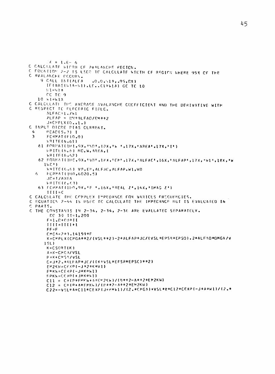
45
C C A L C c r Q (: A C AVAL
9
10 C CALC C RESF
C TNPL
3
fcl
62 I
C C r C
63
CALC ECUA PART THE
I
X = I.LAT r la^• A N C F C A L L ir ( A U l = W cc T U 1-U L L A T ECT A L F A A L F A J = CN T ni READ FCRV V, R I T FOR?' V' R I T v ^ R I r FORP-: •AC ' ) l . ••( I T F C R f' j r = T ^ R IT r c p y 1 1 1 1 l i L A T T I C N S . CONS
nc F = I . 1 1 1 1 FF = F
K-C^' SL) K = CS A = K-P=K + C = J *
E W K U F P K ' A
C l l C 1 2 C 2 2 =
I . E - 6 F W i r i H CF A V A L A N C H E P E G I C N .
2-2 IS L S E C TC C A L C L L A T E M L T H CF RFGir\' V.HERF '15% CF THE i: rCCURS. INT (ALFA .O.C'.IA, .95,nx )
B S ( M A - M ) . L r . . CI * H A ) G C T C 10 1 A C 0 lA
t TH-: AVERAGE AVALAMCHE COEFFICIENT AND THE DERIVATIVE WITH rc FLFCTRIC FIELC. C^l ./IAI
P = l!\'--MLFAa/FM4«2 FLX(0.,l . ) CViE P IAS C L R R E M . ( 5 , 3 ) I AT ( F I O . O ) E ( 6 , 61 ) A T ( l H l , q x , ' N n » , l O X , ' l > • , 1 7 X , « A R E A » , 1 7 X , M » ) I; ( 6 , 6 ) MC, W, AREA, I E ( 6 , ^ 2 ) A T ( I H C , 9 X , M ; n » , l ^ X , ' E f " , 1 7 X , ' A L F A C ' , l 6 X , ' A L F A P « , I 7 X , ' W l ' , l 8 X , ' W
E (6 ,f: ) VP.Er^, ALFAC, ALFAP.Wl.WO A T ( lHn,r>D20.5) /AREA E (f, c. n AT(ll'n,0X,«F •,16X,»REAL Z',1AX,«IHAG /. • ) ^C E TfU; CCNPLEX IMPEDANCE FOR VARICLS FRICOEN'C IES. 2-''. IS USEi: TC CALCULATE THE IKPECANCF UUT IS EVALUAfEO IN
TAN'TS IN 2-3A, 2-3A, 2-3^ ARE EVALUATEC SEPARATELY. 30 11^=1,200 n + C >} x I I
= 1 m n
PLX(Cr'GA**2/(VSL**2)-2*ALFAP*JC/(VSL'>EPSR*EPSO) , 2*aLF AO*OMGA / V
CRTIK)
Cf'Ci/VSL C N G W S L 2.*ALFAP*JC/((K*VSL*EFSR*EPSC)**2) K = CF.<D(-J*2*K«Wl ) = CE<P(-.J*K«V,1) = Cr XP( +.|«K«Vv 1 ) = C^(P*F^'K'W + A->F»'2KV^)/('}**2-A**2*Ef'2KW) = (;*(P*A«FyKU)/(P**2-A**2*E'''2KW) -VSL*&*Cll*CFXP(J*H*l^l)/(2.*C^'GA)•VSL•e•Cl2«CEXP(-J•A*Wl)/(2.•

46
C THE 30 5
111 11?
113
16
15
C THE C FUN
17
200 210
211
212
iny.GA )-v
7 1 = \ C U /.?=-Cl? Z3=-C22
lA) Z'. = M ? .
I/AREA /'-;=(-)-:' Z = Z1 M 2 X X ( II I I V Y ( T I rI ? ? ( I I I I I f' P F C A N V R I T E I t F O R M A T ( F O R M A T ! F C R ' A T ( V> R I T F U . C A L L P R V-. o I T F ( 6 FCRf-'A T ( V R I T E ( : C A L L F ••' > R I T E ( I I I I T - C X = 0 . V, f' I T F ( r> FOR'''AT ( I X = W l / l Y l = A L r A Y2 = E( F I I I 1= I F L E C T R I
C T I C N S C EEl I I I I AA(I I I I XXX (III WRI T E ( 6 F O R M A T ! X = X + U X I F I X . G T GO TO I W R I T F ( 6 F C R N A T ( C A L L F- W R I T E ! 6 FCR^'AT( U R I T E ( 6 FORf''AT( C A L L PR
S L *C *CF X P ( .) •/r ,v 1A * U 1 / V SL ) / ( ?. *r 'G A ) MCFXP(.J*K=^.J l)-I . )/( J * K * A R r A ) ) •• ( C P < P ( - J '•.• K v,s 1 ) - 1 . ) / ( J * X « A R E )
- V S L - = ( C £ x P ( - J v r V G A * W / V S L ) - C E X F ( - J > C N G A * W l / V S L ) ) / ( J «Of^GA • A R E
•:' A L F A C / ( V ': L 1" F P S R « F P S C ) - J : (Jf' G A/ ( V SL « * 2 'S'E P SR F P SU ) ) * W 1 /K * • 2
(\v-Kl )/(f'VGA I'f.PSO^'rPSR) ) / A R E A
• Z 3 » / 4 • Z '") ) = F F ) = R E A L ( Z ) )= AIN^AGIZ ) C E IS PR I NT EC IN r a j M E R I C A L F O R M A N O IS P L O T T E D B Y P R N P L T . , 5 ) F , Z IH , lPn2C.5, 1^020.5,IPD2C.5) IF 1 , 'REAL PA ?r OF Z)• ) IHl ,' IMAGINARY PART CF Z« ) ,111) NPLT(YY,XX,-S0G.,';CC.,l.Ed,2C.ES,Iin,l,l,50,2) ,113) IHC,6CX,'FRFCL-NCY l\fl,)*) ,112) NPlT(ZZ,XX,-l.E3,l.F3,l.Ert,20.E9,niI,l,l,50,2) . ] 1 3)
,16) IHC,////,1H ,')X,'X«,16X,«ALFA(X)«,15X,'E(X)') C.
(X) X) I IT I + l C F I F L P ANO THE I O N I Z A T I O N C O E F F I C I E N T ARE P L O T T E O AS F C I S T A N C E IN T H E N R E G I O N . I ) = E ( X ) I ) = A L F A { X ) I I )=X , 1 7 ) X , Y 1 , Y 2 IH , 3 ( I P 0 2 0 . 5 ) )
.V.) GC TC 2 0 0 c
,210) IHl,'ELECTRIC FIELC (VOLTS/CK . ) • ) NPLT(EE,XXX,-C.,-C.,0.,V',niII»lfl,50,2)
, 2 U ) l F n , 6 0 X , T I S T A f v C F INTO N REGION ( C M . ) ' ) . 2 1 2 ) n - ) , • I C M Z A T I C N C C E F F I C I f c N T * ) r.'PLT ( A A , X X X , - C . , - C . » C . , W , I I I I I , I , 1 . 5 0 , 2 )

47
V R I T E ( 6 ,2 M ) GC TO 2 END
SUBROUTINES
C C c
SO SUPRCU I N T E G R C O N D T T
IV AP P = S = < -
I
IF IF P = CC <; =
rx CO EN
BR OUT TINE AL IS ION. PLICI S(X) = A 4-0 0.
S+(F( ( ARS ( ( S . G T
(; + nx TC 2
S-(F( = 0X/2 TO 2
0
INE IMT(F, A . H . C C X ) INT INTEGRATES A fUNCT ICN F FCUAL TC C a,\r: RfTLRNS THE
FROM LIMIT A UNTIL THE UPPER LIMIT REClJIREO FOR THIS
T i?E^.L«8 C A P S ( X ) X
(A-F,0-Z)
P ) tFIP-CX ) ) «CX/2. S-C).LE.C*.OI ) RETURN .C) GO TC 3
! ) * F (P-CX ) )*rx/2.
rCUPLF PRFCISION FUVCTION F(X) C FUNCTILN F(X) IS THE FLFCTRIC FIELC
INFLICIT ''EAL + b (A-H,C-Z) COMMON' E M , H ,VNU ,AN',AP,BN ,eP,W IF(X.LC.V.l) F = EM IF (X.GT.V.I ) E.= EM*(WC*W1-X )/WC RETURN END
IN THE N REGION.
OCLPLF Pf'FCISICN FUNCTION ALFA(X) C FUNCTIO-^' ALrA(X) GIVES THE ICNIZATICN COEFFICIENT IN THE N REGION
IMPLICIT REAL«rt (A-H,0-Z) PFAL*R INTCRL
CCMMCN P M . M ,U0, AN,AP,PN ,BP,V» EXTERNAL Fl LXP(AA)=nrxP(AA) 7 = - BN/r(X) - INTCRL(Fl,0.,X) ALFA = AN'*EXP(Z)

48
RETURN ENC
I^CUPLF P R r C I S l O N F i r 'CT i rV . ' INTG'JLIF , A , P ) C F l INCTICN INTG) G I V L S THE VALUE CF THE iNfEGRAL C T R A p r Z C 1 n ^ L I N T I C R A r I r N .
I M P L I C I T Ri-AC'S ( A - H , r - Z ) R E A L * " 1\TCRL S = 0 . 0 X = ( n - A ) / 1 0 0 . X=A-DX CC 1 .J = i , i c n x = x + c x
1 S = S + ( F ( X ) t F ( X + UX) ) - 0 X / 2 . C INTGRL^S RrTlJRN
ENO
F UJM A TO B CF F BY
C C
rCUPLE PRFCISICN r t lNCTICN F l ( X ) FUNCTIC.N F l IS THE C I F F i ; i r \ C E IN FLECTRCK ANC HOLE lO^ I IZAT lUN COEFr iCTENTS LSCO IN TMI- EXPONENTIAL IN FCUATICN 2 - 2 .
I M P L I C I T '^EAL'fH { \ - h , r - l \ CCMMCN FM.V.l TVC, A N , AP,r .N,PP,W F X P ( \ ' i ) = P f ' X P ( A A ) F 1 = AN ^E < P ( - ( ' f ' / r ( X ) ) - A P * E X P ( - B P / E ( X ) ) RETURN END

APPENDIX B
THEORY OF THE ONE-SIDED ABRUPT p" -n JUNCTION
The abrupt p-n junction occurs when the impurity con
centration changes abruptly from net acceptor concentration,
N -Nj. = N., to net donor concentration, Nj.-N = N . When
N
profile for the one-sided abrupt junction is shown in
Figure B.l. Applying Gauss' law for the electric field in
the diode, Poisson's equation in x is obtained
.. >> N- , a one-sided abrupt junction occurs. The doping
1^ = p/e . (B-1) 3X
For the abrupt junction case
-qN^ -w 1 X <_ 0
p(x) = < . (B-2) qNj) o < X £ w^
The solution obtained for E(x) is
-q/eN (x+w ) -w^ < x < 0 ^ a p p - -
_E + — — o < X < w ' m e — n
where
qN^w N^w
19

50
» ^D-^A
N D
-w -N A
(a)
w n
E(x)
X
Fig. B.l.— (a) Doping profile for the one-sided abrupt junction.
(b) Electric field inside the onesided abrupt junction.

51
The electric field is also shown in Figure B.l. Integra
tion of the electric field across the diode gives the diode
potential,
V = 1/2 E^w^ (B-5)
where w^ is the total depletion width. Solving for w, and
eliminating E^ results in
2c V ^ D 1/2
-d = T N77 ^ • ^^-'^ The depletion width is thus a function of the diode poten
tial V. The diode potential includes the applied potential
V^ and the built-in potential V . that arises from equilib
rium requirements with zero applied voltage. The potential
arises to oppose the tendency for the diffusion current to
flow due to the impurity gradient across the junction. The
current is composed of a drift component and a diffusion
component such that
J^(x) = q(y^pE(x)-D^|^) = 0 , (B-7) P P po A
and
J^(x) = q(y^nE(x)+D^|^)= 0 , (B-8) n n iio A
where u and u are the mobilities of holes and electrons p n
respectively and D and D are the diffusion constants for '^ p n
holes and electrons respectively. Using the Einstein

52
relation
^ = q/KgT , (B-9)
and solving for E(x) and integrating across the junction
for the case of no current flow through the junction, there
results in an expression for the built in potential V j_-
K^T n K^T p V,, = - ^ m - ^ = - ^ i n ^ . (B-10) bi q np q p^
The total diode potential used in equation (B-6) is given
by
V = V,,-V^ , (B-11)
where V is the applied voltage, referenced to the forward a
direction (voltage on p side is positive with respect to
the n side). The sign of V^ can be verified by considering a
that a positive voltage tends to force carriers into the
junction region while a negative voltage tends to deplete the junction region.
A capacitance due to the depletion region can be de
fined as
C = , (B-12) ^ - dV
so that
d(qN^w^A) C - D ^ . (B-13)
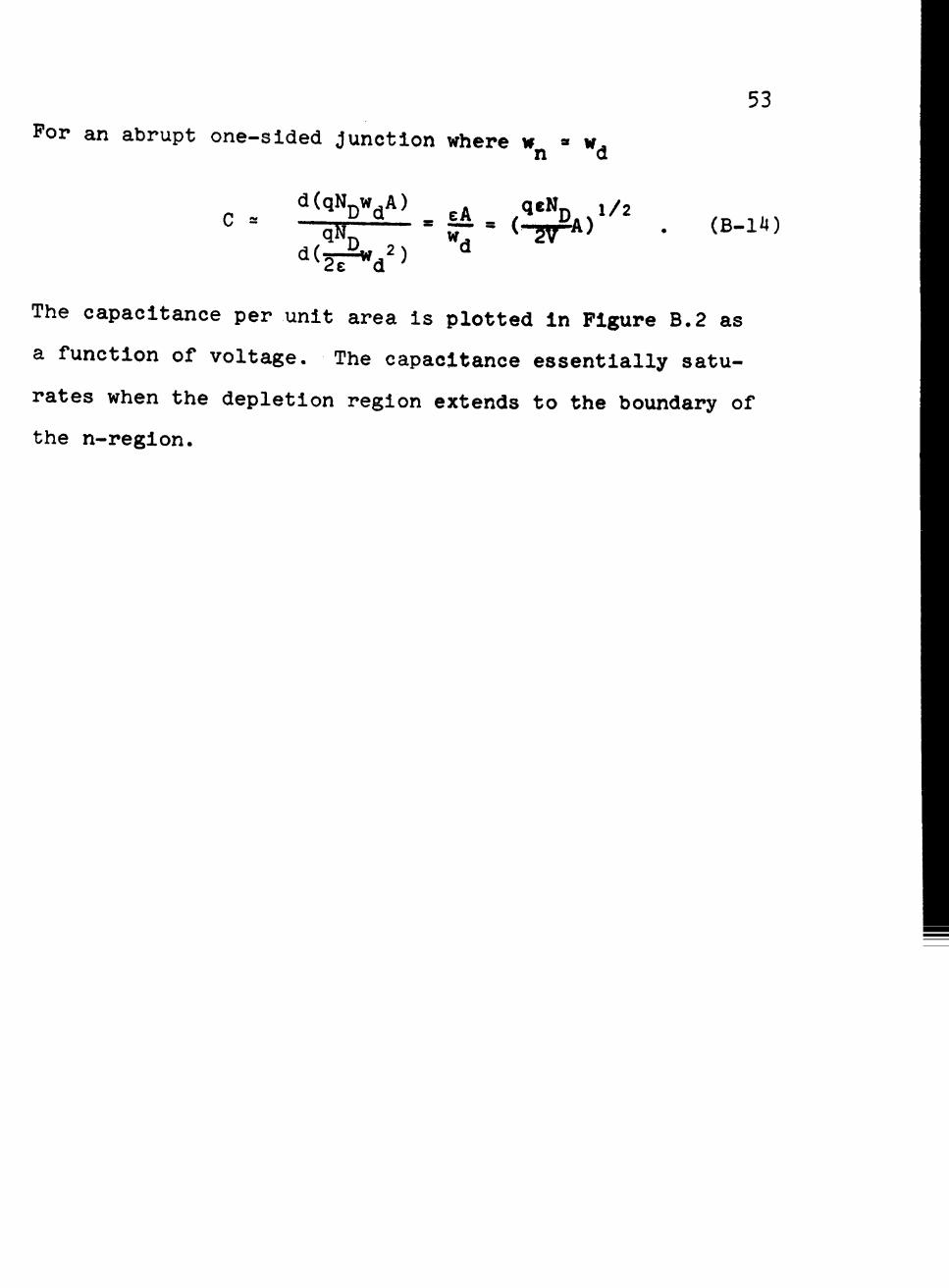
53
For an abrupt one-sided junction where w « w^ n d
C « ^^^VdA> eA ,<1^VN^/^
d( ilw 2)
(B-14)
The capacitance per unit area is plotted In Figure B.2 as
a function of voltage. The capacitance essentially satu
rates when the depletion region extends to the boundary of
the n-region.
51
Fig. B.2.—Depletion capacitance for an abrupt onesided pn junction diode as a function of bias voltage. Notice the saturation effect due to the depletion region extending through the entire n region of the diode.

APPENDIX C
ALTERNATE METHOD FOR OBTAINING CURRENT
DENSITY EXPRESSIONS
In Chapter II, the expressions for J and J given by n p ° '^
equations (2-26) and (2-27) are obtained through algebraic
manipulations. These results can be obtained directly by
solving the two following differential equations:
and
3J . . . . r-^ = ^^^^J -a (J +J )-a E(J +J ) . (2-1?) V -. p o n p no po '
Substituting equations (2-20) and (2-22) into (2-l6) and
(2-17), the following are obtained
3 J jojJ ^ . •r-^ ^ = a J+E(J a'-jwea ) , (C-1) 3x V T o o " o ' sl
and
3J jcjJ . . r-^" 2. = Qt J+E(ja)ea -J a') . (C-2) 3X V , O 0 0
sl Particular solutions of the following form are assumed
55

56
and
The X dependence is assumed to be that of E(x) since E(x)
appears in the differential equations. These solutions are
now substituted into (C-1) and (C-2) and, using (2-23) for
E(x), the constants can be evaluated as follows:
Ci (J^a^-jtoea^)
^ m " j(k+a3/v J > ^"5^ sl
Cgd.a'-jooea ) A ^ = r-r-1 T T ^ . (C-6) n2 J (to/v -j -k) *
Ja +(J^a--j(oea^)(-^ - -iiii^)J/k2 o o o v - , e v^'^e A , = , ; ^^ ^= , (C-7) n3 "^^/^sl
Cj(jwea^-J^a")
C2(ja,sap-J^a-)
and
Ja^HJ^a-j.sa^)(^-/^)J/k2
A = r-^ ^ . (C-10) P3 J' /Vg-L
Using equation (2-24), it is found that
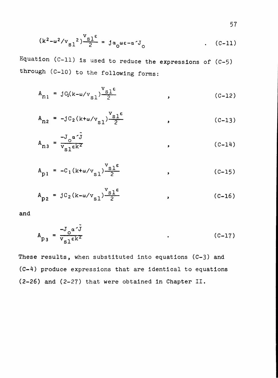
(k2.co2/v^^2)!^. J
57
(C-11)
Equation (C-11) is used to reduce the expressions of (C-5)
through (C-10) to the following forms:
^ni = jCi(k-co/v^3_)I^ (C-12)
^sl^ ^nz = -JCaCkWv^,)-^ (C-13)
-J a'J
'n3 " vTrTk^ sl (C-lM
A = - C i ( k W v ^ , ) ^ (C-15)
Ap, = jC,(k../v^^)^ (C-16)
and
-J a'J
PS Vg^ek^ (C-17)
These results, when substituted into equations (C-3) and
(C-4) produce expressions that are Identical to equations
(2-26) and (2-27) that were obtained in Chapter II.


![:_UZR dVe e` ^R\V ^R[`c ]VRa Z_ 2^cZe `UZ Z_g ...](https://static.fdokumen.com/doc/165x107/63390bf2a5d86d6ce607cc7d/uzr-dve-e-rv-rc-vra-z-2cze-rr-drjd-uz-zg-.jpg)