
uninterruptible power system - Repositorio Comillas
143
GRADO EN INGENIERÍA ELECTROMECÁNICA TRABAJO FIN DE GRADO UNINTERRUPTIBLE POWER SYSTEM (WANDA, THE WAKE-UP WINDOW) Autor: Paula Fernández Oceja Director: Jonathan Wierer Madrid Mayo de 2019
-
Upload
khangminh22 -
Category
Documents
-
view
0 -
download
0
Transcript of uninterruptible power system - Repositorio Comillas
GRADO EN INGENIERÍA ELECTROMECÁNICA
TRABAJO FIN DE GRADO UNINTERRUPTIBLE POWER SYSTEM
(WANDA, THE WAKE-UP WINDOW)
Autor: Paula Fernández Oceja Director: Jonathan Wierer
Madrid Mayo de 2019

UNIVERSIDAD PONTIFICIA DE COMILLAS ESCUELA TÉCNICA SUPERIOR DE INGENIERÍA (ICAI)

UNIVERSIDAD PONTIFICIA DE COMILLAS ESCUELA TÉCNICA SUPERIOR DE INGENIERÍA (ICAI)

UNIVERSIDAD PONTIFICIA DE COMILLAS ESCUELA TÉCNICA SUPERIOR DE INGENIERÍA (ICAI)
UNIVERSIDAD PONTIFICIA DE COMILLAS ESCUELA TÉCNICA SUPERIOR DE INGENIERÍA (ICAI)
UNIVERSIDAD PONTIFICIA DE COMILLAS ESCUELA TÉCNICA SUPERIOR DE INGENIERÍA (ICAI)

UNIVERSIDAD PONTIFICIA DE COMILLAS ESCUELA TÉCNICA SUPERIOR DE INGENIERÍA (ICAI)

UNIVERSIDAD PONTIFICIA DE COMILLAS ESCUELA TÉCNICA SUPERIOR DE INGENIERÍA (ICAI)

UNIVERSIDAD PONTIFICIA DE COMILLAS ESCUELA TÉCNICA SUPERIOR DE INGENIERÍA (ICAI)
Acknowledgement First of all, I would like to thank my teammates, Rebecca Lentz and Nayantara Chaisson,
our advisor Jonathan Wierer and ECE lab manager Theodore Bowen, for giving me the
opportunity to develop such interesting project during my stay in Lehigh University,
trusting without knowing me personally that I would work and achieve all of the
objectives we wanted to accomplish.
Moreover, I would like to express my most sincere gratitude to my parents and my
brother, and everyone else in my close family, who always were there cheering for me
and believing in me even when I could not trust myself or my own performance.
A special thanks to all my friends and colleagues from Pontificia Comillas ICAI
University and Lehigh University, who showed me how with hard work and dedication
(and a bit of luck) you are capable of doing extraordinary things, and who were always
there for me. Thank you to my best friends from high school, who always supported me
during these years and believed in me to become the Engineer and professional woman I
am growing into.

UNIVERSIDAD PONTIFICIA DE COMILLAS ESCUELA TÉCNICA SUPERIOR DE INGENIERÍA (ICAI)
UNIVERSIDAD PONTIFICIA DE COMILLAS ESCUELA TÉCNICA SUPERIOR DE INGENIERÍA (ICAI)
I
UNINTERRUPTIBLE POWER SUPPLY (WANDA, THE WAKE UP WINDOW)
Autor: Fernández Oceja, Paula.
Director: Wierer, Jonathan.
Entidad colaboradora: Lehigh University.
RESUMEN DEL PROYECTO:
1. INTRODUCCIÓN:
Actualmente, el uso del conocido vidrio inteligente (Smart Glass) está en continuo
crecimiento: aparte de ser utilizado en salas de reuniones en grandes oficinas, para así
conseguir el deseado efecto de privacidad, se ha implementado en otras disposiciones,
como puede ser en aviones, o en hoteles, ayudando a crear un ambiente lujoso y más
cómodo. Debido a que su uso es cada vez más común, consiguiendo que su precio
disminuya, se ha querido buscar la manera de incluir esta tecnología en el hogar, buscando
desarrollar un producto innovador que procure una mayor comodidad en el día a día.
El principal objetivo de este proyecto para un futuro es diseñar una ventana inteligente
que, combinada con un control vía App, sea capaz de conectarse a la alarma de cualquier
individuo, regulando la luz entrante un tiempo específico antes de que suene, simulando
así un amanecer, y ayudando a levantarse de manera natural, lo que se ha estudiado que
conlleva a un mayor descanso a lo largo de la jornada y, por tanto, a un mayor grado de
comodidad y felicidad (https://www.mindbodygreen.com/0-28702/if-you-want-to-wake-
up-happy-try-this-alarm-clock-t rick.html).
El estado natural de determinado vidrio es mantenerse completamente opaco si no existe
una tensión que lo alimente. En casos de emergencia que conlleve a una situación de
perdida de la tensión de alimentación, o en un simple apagón, se crearía una atmosfera
oscura que resulta incómoda para cualquier individuo, y que debe evitarse. Esto, unido a
UNIVERSIDAD PONTIFICIA DE COMILLAS ESCUELA TÉCNICA SUPERIOR DE INGENIERÍA (ICAI)
II
que el cristal se alimente con corriente alterna y cuya carga sea ínfima, lleva a pensar un
diseño no convencional respecto a los sistemas de alimentación ininterrumpidos que
existen en la actualidad, ya que estos mismos están diseñados para alimentar varias cargas
externas alimentadas por corriente continua (normalmente 5V CC), como pueden ser
ordenadores, televisiones, o electrodomésticos comunes a todo tipo de hogares.
El diseño pensado se compone de dos bloques generales, uno que funcione en caso
general, y otro que actúe en caso de emergencia, los cuales serán controlados por un relé
que cambie la fuente que alimente al circuito que regula el voltaje de alimentación del
vidrio. Este voltaje de entrada será monitorizado desde un microcontrolador Arduino,
conectado a la App mediante tecnología Wifi.
Por otro lado, en caso de pérdida de tensión en el alojamiento, el circuito se alimentaría
con un sistema externo, compuesto por una batería y un módulo de carga para la misma
cuyo circuito interno se cierra en cuanto la batería está completamente cargada, evitando
que se sobrealimente y dañe la vida de esta.
El circuito tiene que ser capaz de funcionar en cualquiera de las situaciones proyectadas,
y poder la opacidad ser regulada de manera manual por la aplicación para ser considerado
completamente satisfactorio. En un primer momento, no se tuvo mucho en cuenta la
eficiencia (aunque se calculará e incluirá en el documento), si no conseguir resultados
visuales como prototipo previo para un futuro producto final.
2. METODOLOGÍA:
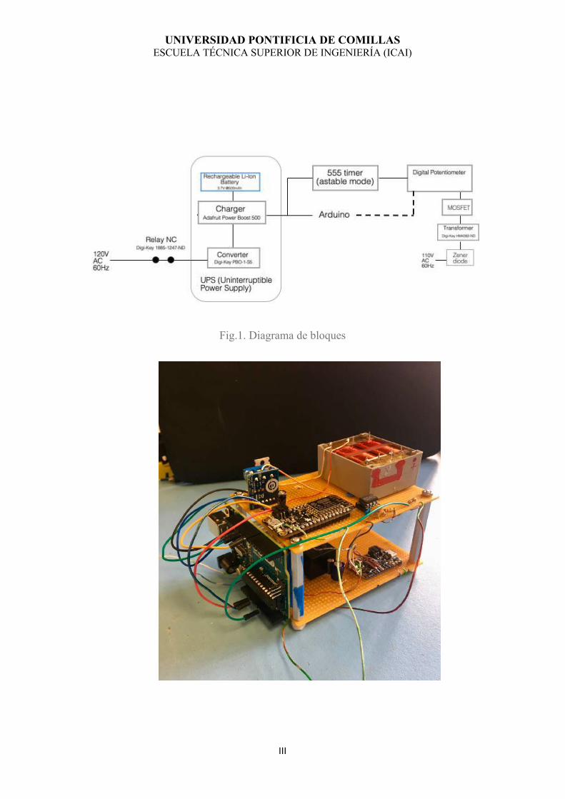
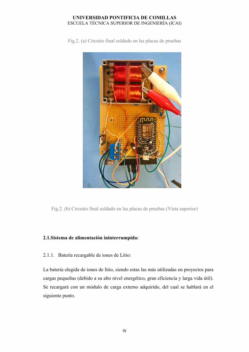
La figura 1 muestra el diagrama de bloques global del circuito que ha sido desarrollado,
y que ha sido soldado en una placa de pruebas en su totalidad, circuito que podemos
observar en la figura 2, a excepción del microcontrolador Arduino, para verificar su
correcto funcionamiento:
UNIVERSIDAD PONTIFICIA DE COMILLAS ESCUELA TÉCNICA SUPERIOR DE INGENIERÍA (ICAI)
III
Fig.1. Diagrama de bloques
UNIVERSIDAD PONTIFICIA DE COMILLAS ESCUELA TÉCNICA SUPERIOR DE INGENIERÍA (ICAI)
IV
Fig.2. (a) Circuito final soldado en las placas de pruebas
Fig.2. (b) Circuito final soldado en las placas de pruebas (Vista superior)
2.1.Sistema de alimentación ininterrumpida:
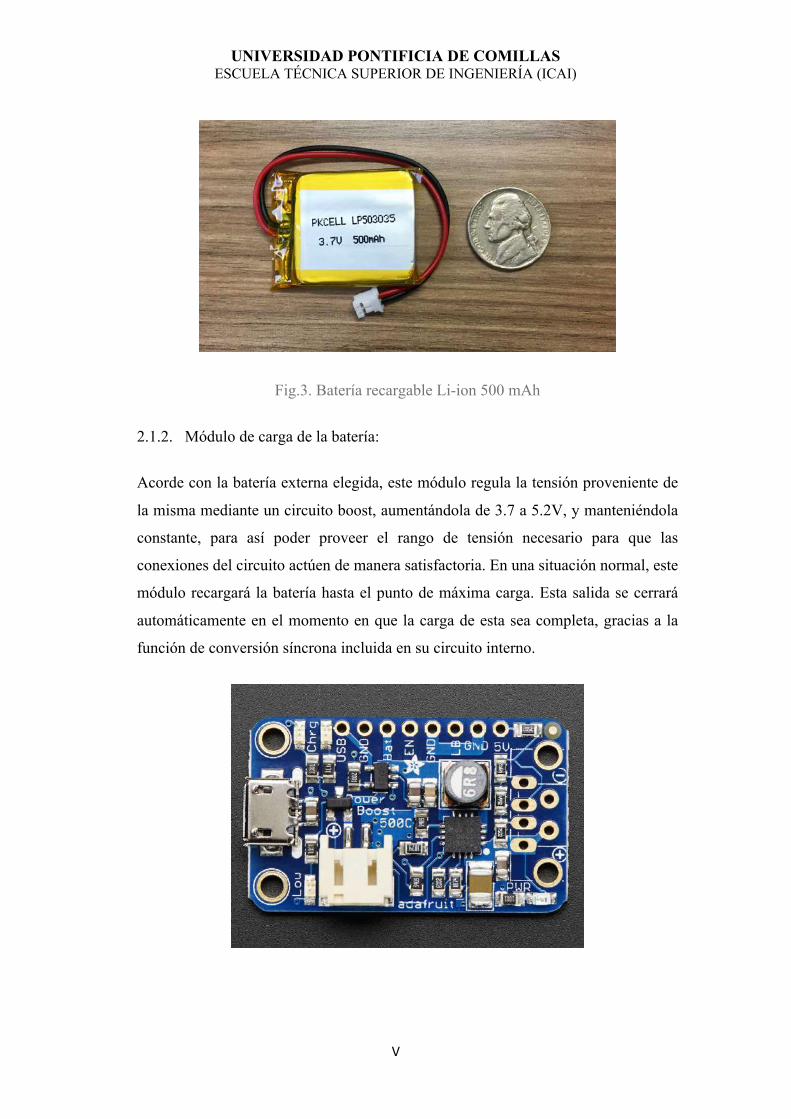
2.1.1. Batería recargable de iones de Litio:
La batería elegida de iones de litio, siendo estas las más utilizadas en proyectos para
cargas pequeñas (debido a su alto nivel energético, gran eficiencia y larga vida útil).
Se recargará con un módulo de carga externo adquirido, del cual se hablará en el
siguiente punto.
UNIVERSIDAD PONTIFICIA DE COMILLAS ESCUELA TÉCNICA SUPERIOR DE INGENIERÍA (ICAI)
V
Fig.3. Batería recargable Li-ion 500 mAh
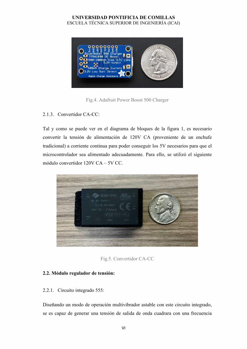
2.1.2. Módulo de carga de la batería:
Acorde con la batería externa elegida, este módulo regula la tensión proveniente de
la misma mediante un circuito boost, aumentándola de 3.7 a 5.2V, y manteniéndola
constante, para así poder proveer el rango de tensión necesario para que las
conexiones del circuito actúen de manera satisfactoria. En una situación normal, este
módulo recargará la batería hasta el punto de máxima carga. Esta salida se cerrará
automáticamente en el momento en que la carga de esta sea completa, gracias a la
función de conversión síncrona incluida en su circuito interno.
UNIVERSIDAD PONTIFICIA DE COMILLAS ESCUELA TÉCNICA SUPERIOR DE INGENIERÍA (ICAI)
VI
Fig.4. Adafruit Power Boost 500 Charger
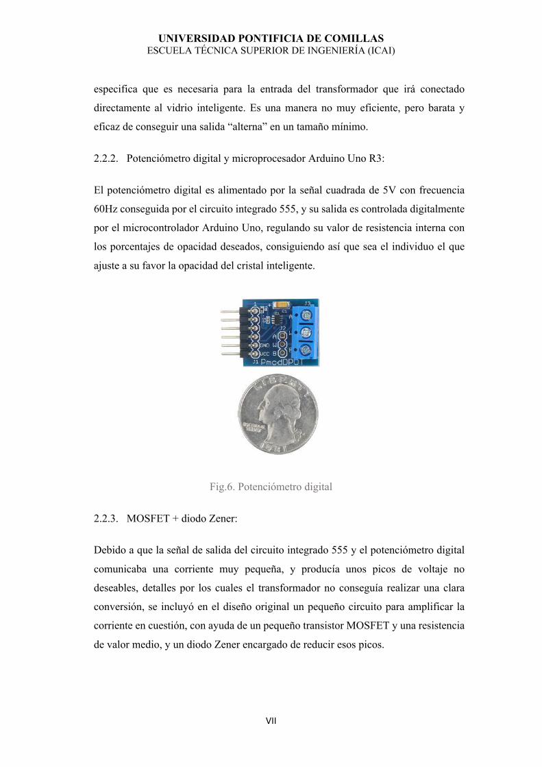
2.1.3. Convertidor CA-CC:
Tal y como se puede ver en el diagrama de bloques de la figura 1, es necesario
convertir la tensión de alimentación de 120V CA (proveniente de un enchufe
tradicional) a corriente continua para poder conseguir los 5V necesarios para que el
microcontrolador sea alimentado adecuadamente. Para ello, se utilizó el siguiente
módulo convertidor 120V CA – 5V CC.
Fig.5. Convertidor CA-CC
2.2. Módulo regulador de tensión:
2.2.1. Circuito integrado 555:
Diseñando un modo de operación multivibrador astable con este circuito integrado,
se es capaz de generar una tensión de salida de onda cuadrara con una frecuencia
UNIVERSIDAD PONTIFICIA DE COMILLAS ESCUELA TÉCNICA SUPERIOR DE INGENIERÍA (ICAI)
VII
especifica que es necesaria para la entrada del transformador que irá conectado
directamente al vidrio inteligente. Es una manera no muy eficiente, pero barata y
eficaz de conseguir una salida “alterna” en un tamaño mínimo.
2.2.2. Potenciómetro digital y microprocesador Arduino Uno R3:
El potenciómetro digital es alimentado por la señal cuadrada de 5V con frecuencia
60Hz conseguida por el circuito integrado 555, y su salida es controlada digitalmente
por el microcontrolador Arduino Uno, regulando su valor de resistencia interna con
los porcentajes de opacidad deseados, consiguiendo así que sea el individuo el que
ajuste a su favor la opacidad del cristal inteligente.
Fig.6. Potenciómetro digital
2.2.3. MOSFET + diodo Zener:
Debido a que la señal de salida del circuito integrado 555 y el potenciómetro digital
comunicaba una corriente muy pequeña, y producía unos picos de voltaje no
deseables, detalles por los cuales el transformador no conseguía realizar una clara
conversión, se incluyó en el diseño original un pequeño circuito para amplificar la
corriente en cuestión, con ayuda de un pequeño transistor MOSFET y una resistencia
de valor medio, y un diodo Zener encargado de reducir esos picos.
UNIVERSIDAD PONTIFICIA DE COMILLAS ESCUELA TÉCNICA SUPERIOR DE INGENIERÍA (ICAI)
VIII
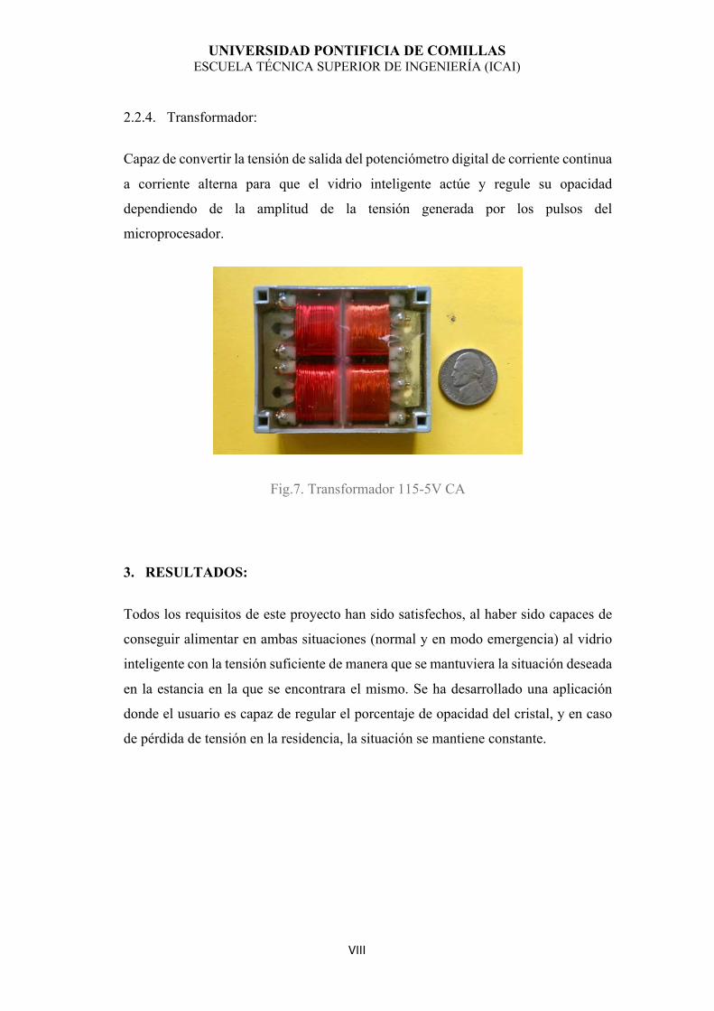
2.2.4. Transformador:
Capaz de convertir la tensión de salida del potenciómetro digital de corriente continua
a corriente alterna para que el vidrio inteligente actúe y regule su opacidad
dependiendo de la amplitud de la tensión generada por los pulsos del
microprocesador.
Fig.7. Transformador 115-5V CA
3. RESULTADOS:
Todos los requisitos de este proyecto han sido satisfechos, al haber sido capaces de
conseguir alimentar en ambas situaciones (normal y en modo emergencia) al vidrio
inteligente con la tensión suficiente de manera que se mantuviera la situación deseada
en la estancia en la que se encontrara el mismo. Se ha desarrollado una aplicación
donde el usuario es capaz de regular el porcentaje de opacidad del cristal, y en caso
de pérdida de tensión en la residencia, la situación se mantiene constante.
UNIVERSIDAD PONTIFICIA DE COMILLAS ESCUELA TÉCNICA SUPERIOR DE INGENIERÍA (ICAI)
IX
4. CONCLUSIONES:
El mayor problema que hemos encontrado al realizar este proyecto ha sido el
conseguir desarrollar un control rápido y flexible con el nivel de opacidad del cristal
(la ciencia de partículas tras él funciona con un rango de cambio menor del que
esperábamos). Creemos que una vez se vaya utilizando esta tecnología en diversas
situaciones, y alimentando varias cargas en vez de un solo prototipo, se podrá reducir
tanto el precio como la complejidad de este diseño, incluso llegando a conseguir que
todo pueda ser implantado en un circuito PCB.

UNIVERSIDAD PONTIFICIA DE COMILLAS ESCUELA TÉCNICA SUPERIOR DE INGENIERÍA (ICAI)
X
UNIVERSIDAD PONTIFICIA DE COMILLAS ESCUELA TÉCNICA SUPERIOR DE INGENIERÍA (ICAI)
XI
UNINTERRUPTIBLE POWER SUPPLY
ABSTRACT:
1. INTRODUCTION:
Currently, the use of the technology known as Smart Glass is becoming a trendy new
addition to buildings across the globe: besides having been installed in business
headquarters, so as to achieve the desired privacy effect it was meant for, it has been
implemented in other locations, such as airplanes, or hotels, in order to create a more
luxurious and comfortable environment. On account of its use becoming more and more
frequent, a new way to incorporate it in every home has been explored, towards the
development of an innovative product which will procure comfort in every household.
The main objective of this project for a close future is to design a smart window (Wanda)
that, combined with an App-control, will be able to connect itself to the alarm of any
customer, constantly customizing the light entering a room so that the user can wake-up
to natural light just as they might have back in the day, which has been studied that
increases wakefulness throughout the rest of the day and overall happiness levels
(https://www.mindbodygreen.com/0-28702/if-you-want-to-wake-up-happy-try-this-
alarm-clock-t rick.html).
The glass natural state is to stay frosted when no voltage is applied to it. Specifically, the
product that was purchased, with no voltage on has a light transmittance of 7%, which
creates an uncomfortable dark atmosphere when there is a grid failure or a power outage
in our home that needs to be avoided. Additionally, an AC supply was necessary for this
low-load glass to run, so in order to surpass this inconvenience, it was decided to design
a circuit that will enable the glass to be powered up in case of emergency, which leaded
to arrange an unconventional design compared to the actual uninterruptible power
systems used nowadays, as these are modeled to supply power to several DC loads
(usually 5V DC), like PC computers, televisions, or any other electrical appliances found
in any household.
UNIVERSIDAD PONTIFICIA DE COMILLAS ESCUELA TÉCNICA SUPERIOR DE INGENIERÍA (ICAI)
XII
The final design is formed by two major general blocks: the first one will work on an
average situation, and a second one that will supply the necessary power in case of
emergency. Both these blocks will be controlled by a relay that will connect and
disconnect the existing sources that provide power to the circuit that regulates the voltage
that goes into the smart glass. This input voltage will be monitored from an Arduino One
Microcontroller, connected to the App through a Wi-fi module.
On the other side, in case of power outage or any other local loss of power, the circuit
would get its power from an external system, formed by a Li-Ion battery and a charger
module which its internal circuit closes when the battery is fully charged, preventing it to
be overcharged and damaging its life or cycles.
The circuits need to be able to perform in any of the situations projected, and any
individual has to be able to regulate manually through the App the opacity of the glass to
be considered satisfactory. On a first approach, efficiency was not really kept in mind
(although it will be figured and included in this document), but to achieve a visual result
for this previous prototype for the future product.
2. METHOLODOGY:
Figure 1 shows the global block diagram of the circuit that has been design and soldered
on a breadboard in its totality, circuit that we can observe on Figure 2, except for the
Arduino microcontroller, to verify its correct performance:

UNIVERSIDAD PONTIFICIA DE COMILLAS ESCUELA TÉCNICA SUPERIOR DE INGENIERÍA (ICAI)
XIII
Fig.1. Block Diagram
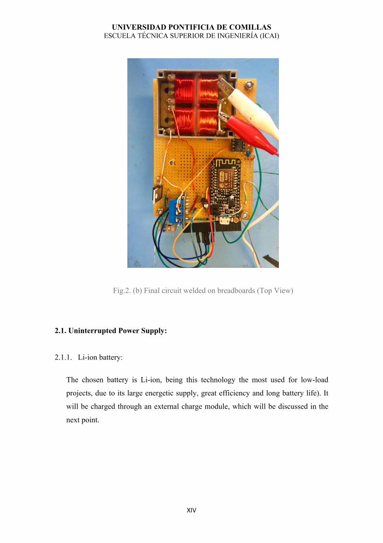
Fig.2. (a) Final circuit welded on breadboards
UNIVERSIDAD PONTIFICIA DE COMILLAS ESCUELA TÉCNICA SUPERIOR DE INGENIERÍA (ICAI)
XIV
Fig.2. (b) Final circuit welded on breadboards (Top View)
2.1. Uninterrupted Power Supply:
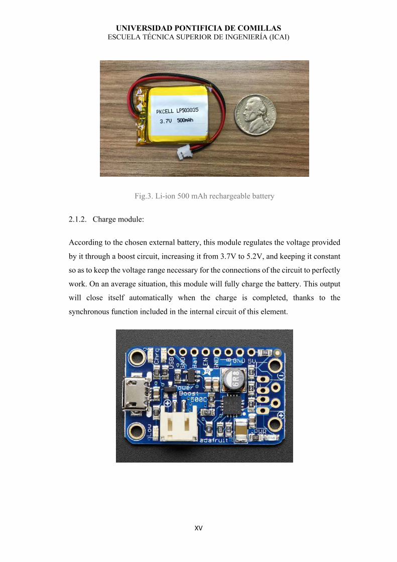
2.1.1. Li-ion battery:
The chosen battery is Li-ion, being this technology the most used for low-load
projects, due to its large energetic supply, great efficiency and long battery life). It
will be charged through an external charge module, which will be discussed in the
next point.
UNIVERSIDAD PONTIFICIA DE COMILLAS ESCUELA TÉCNICA SUPERIOR DE INGENIERÍA (ICAI)
XV
Fig.3. Li-ion 500 mAh rechargeable battery
2.1.2. Charge module:
According to the chosen external battery, this module regulates the voltage provided
by it through a boost circuit, increasing it from 3.7V to 5.2V, and keeping it constant
so as to keep the voltage range necessary for the connections of the circuit to perfectly
work. On an average situation, this module will fully charge the battery. This output
will close itself automatically when the charge is completed, thanks to the
synchronous function included in the internal circuit of this element.

UNIVERSIDAD PONTIFICIA DE COMILLAS ESCUELA TÉCNICA SUPERIOR DE INGENIERÍA (ICAI)
XVI
Fig.4. Adafruit Power Boost 500 Charger
2.1.3. AC – DC Converter:
As we can observe on the block diagram on Figure 1, it is necessary to convert the
supply voltage of 120V AC (coming from any household outlet) to DC so as to get
5V to supply power to the microcontroller. For this purpose, the following 120 VAC
– 5V DC converter module was used:
Fig.5. AC-DC Converter Module
2.2. Voltage regulation circuit:
2.2.1. 555 Timer:
UNIVERSIDAD PONTIFICIA DE COMILLAS ESCUELA TÉCNICA SUPERIOR DE INGENIERÍA (ICAI)
XVII
Designing an astable mode with this integrated circuit, we are capable to generate a
specific frequency square wave output necessary for the input of the power
transformer (as it works with AC) which will be connected to the smart glass. It is a
way not really efficient, but cheap and effective to get an “alternating” output on a
minimum space.
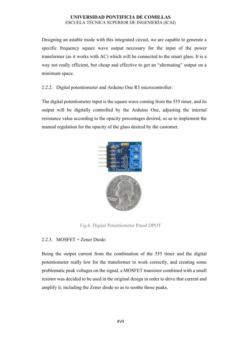
2.2.2. Digital potentiometer and Arduino One R3 microcontroller:
The digital potentiometer input is the square wave coming from the 555 timer, and its
output will be digitally controlled by the Arduino One, adjusting the internal
resistance value according to the opacity percentages desired, so as to implement the
manual regulation for the opacity of the glass desired by the customer.
Fig.6. Digital Potentiometer Pmod DPOT
2.2.3. MOSFET + Zener Diode:
Being the output current from the combination of the 555 timer and the digital
potentiometer really low for the transformer to work correctly, and creating some
problematic peak voltages on the signal, a MOSFET transistor combined with a small
resistor was decided to be used in the original design in order to drive that current and
amplify it, including the Zener diode so as to soothe those peaks.
UNIVERSIDAD PONTIFICIA DE COMILLAS ESCUELA TÉCNICA SUPERIOR DE INGENIERÍA (ICAI)
XVIII
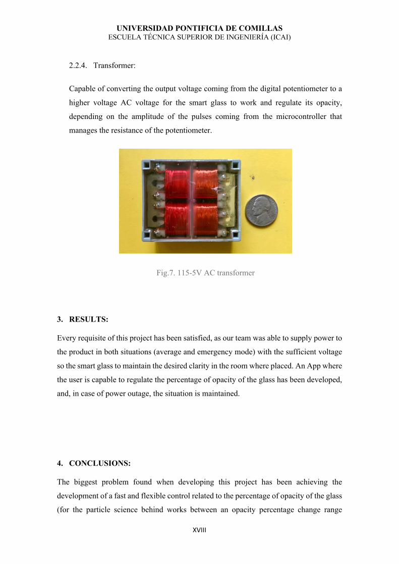
2.2.4. Transformer:
Capable of converting the output voltage coming from the digital potentiometer to a
higher voltage AC voltage for the smart glass to work and regulate its opacity,
depending on the amplitude of the pulses coming from the microcontroller that
manages the resistance of the potentiometer.
Fig.7. 115-5V AC transformer
3. RESULTS:
Every requisite of this project has been satisfied, as our team was able to supply power to
the product in both situations (average and emergency mode) with the sufficient voltage
so the smart glass to maintain the desired clarity in the room where placed. An App where
the user is capable to regulate the percentage of opacity of the glass has been developed,
and, in case of power outage, the situation is maintained.
4. CONCLUSIONS:
The biggest problem found when developing this project has been achieving the
development of a fast and flexible control related to the percentage of opacity of the glass
(for the particle science behind works between an opacity percentage change range

UNIVERSIDAD PONTIFICIA DE COMILLAS ESCUELA TÉCNICA SUPERIOR DE INGENIERÍA (ICAI)
XIX
smaller than we expected). We think that, once this technology has a more frequent use,
the price and complexity of this design could be optimized, even achieving the circuit to
be set up on a PCB.

UNIVERSIDAD PONTIFICIA DE COMILLAS ESCUELA TÉCNICA SUPERIOR DE INGENIERÍA (ICAI)
XX
UNIVERSIDAD PONTIFICIA DE COMILLAS ESCUELA TÉCNICA SUPERIOR DE INGENIERÍA (ICAI)
1
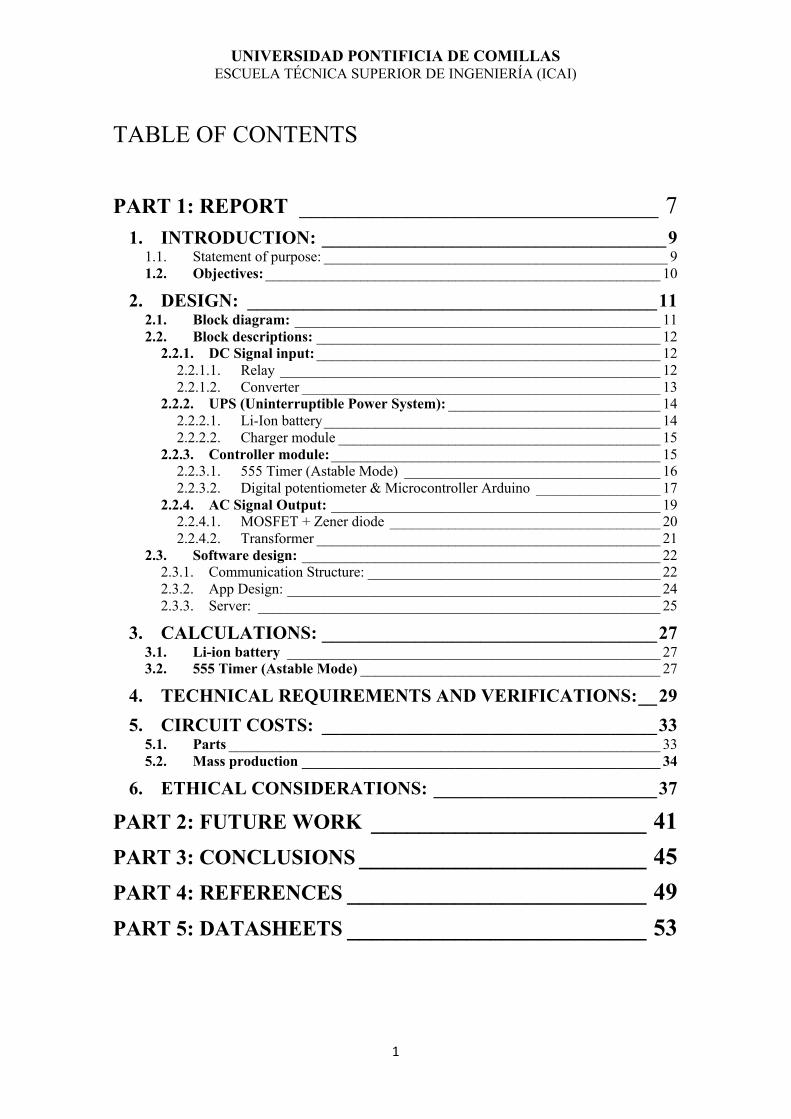
TABLE OF CONTENTS PART 1: REPORT ______________________________ 7
1. INTRODUCTION: _____________________________________ 9 1.1. Statement of purpose: _______________________________________________ 9 1.2. Objectives: ______________________________________________________ 10
2. DESIGN: ____________________________________________ 11 2.1. Block diagram: __________________________________________________ 11 2.2. Block descriptions: _______________________________________________ 12
2.2.1. DC Signal input: _______________________________________________ 12 2.2.1.1. Relay ____________________________________________________ 12 2.2.1.2. Converter _________________________________________________ 13
2.2.2. UPS (Uninterruptible Power System): _____________________________ 14 2.2.2.1. Li-Ion battery ______________________________________________ 14 2.2.2.2. Charger module ____________________________________________ 15
2.2.3. Controller module: _____________________________________________ 15 2.2.3.1. 555 Timer (Astable Mode) ___________________________________ 16 2.2.3.2. Digital potentiometer & Microcontroller Arduino _________________ 17
2.2.4. AC Signal Output: _____________________________________________ 19 2.2.4.1. MOSFET + Zener diode _____________________________________ 20 2.2.4.2. Transformer _______________________________________________ 21
2.3. Software design: _________________________________________________ 22 2.3.1. Communication Structure: ________________________________________ 22 2.3.2. App Design: ___________________________________________________ 24 2.3.3. Server: _______________________________________________________ 25
3. CALCULATIONS: ____________________________________ 27 3.1. Li-ion battery ___________________________________________________ 27 3.2. 555 Timer (Astable Mode) _________________________________________ 27
4. TECHNICAL REQUIREMENTS AND VERIFICATIONS: __ 29 5. CIRCUIT COSTS: ____________________________________ 33
5.1. Parts ___________________________________________________________ 33 5.2. Mass production _________________________________________________ 34
6. ETHICAL CONSIDERATIONS: ________________________ 37 PART 2: FUTURE WORK _______________________ 41 PART 3: CONCLUSIONS ________________________ 45 PART 4: REFERENCES _________________________ 49 PART 5: DATASHEETS _________________________ 53

UNIVERSIDAD PONTIFICIA DE COMILLAS ESCUELA TÉCNICA SUPERIOR DE INGENIERÍA (ICAI)
2
UNIVERSIDAD PONTIFICIA DE COMILLAS ESCUELA TÉCNICA SUPERIOR DE INGENIERÍA (ICAI)
3
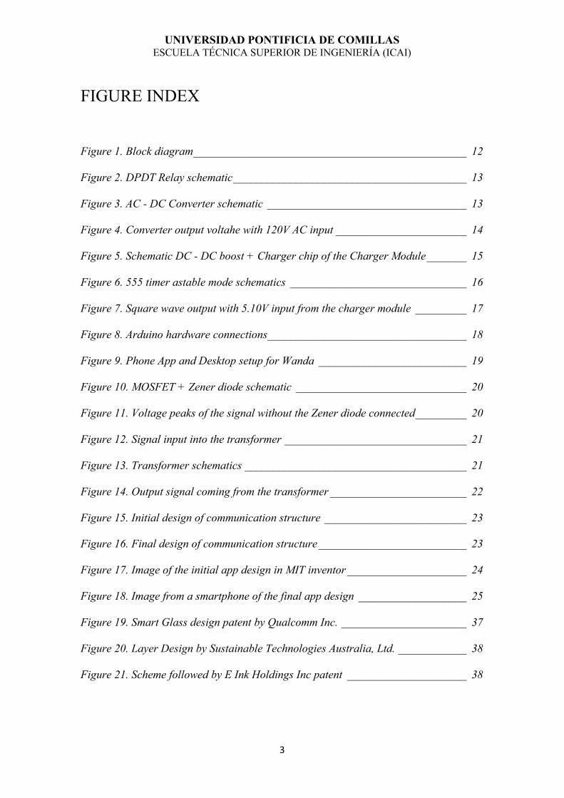
FIGURE INDEX Figure 1. Block diagram ________________________________________________ 12 Figure 2. DPDT Relay schematic _________________________________________ 13 Figure 3. AC - DC Converter schematic ___________________________________ 13 Figure 4. Converter output voltahe with 120V AC input _______________________ 14 Figure 5. Schematic DC - DC boost + Charger chip of the Charger Module _______ 15 Figure 6. 555 timer astable mode schematics _______________________________ 16 Figure 7. Square wave output with 5.10V input from the charger module _________ 17 Figure 8. Arduino hardware connections ___________________________________ 18 Figure 9. Phone App and Desktop setup for Wanda __________________________ 19 Figure 10. MOSFET + Zener diode schematic ______________________________ 20 Figure 11. Voltage peaks of the signal without the Zener diode connected _________ 20 Figure 12. Signal input into the transformer ________________________________ 21 Figure 13. Transformer schematics _______________________________________ 21 Figure 14. Output signal coming from the transformer ________________________ 22 Figure 15. Initial design of communication structure _________________________ 23 Figure 16. Final design of communication structure __________________________ 23 Figure 17. Image of the initial app design in MIT inventor _____________________ 24 Figure 18. Image from a smartphone of the final app design ___________________ 25 Figure 19. Smart Glass design patent by Qualcomm Inc. ______________________ 37 Figure 20. Layer Design by Sustainable Technologies Australia, Ltd. ____________ 38 Figure 21. Scheme followed by E Ink Holdings Inc patent _____________________ 38

UNIVERSIDAD PONTIFICIA DE COMILLAS ESCUELA TÉCNICA SUPERIOR DE INGENIERÍA (ICAI)
4
UNIVERSIDAD PONTIFICIA DE COMILLAS ESCUELA TÉCNICA SUPERIOR DE INGENIERÍA (ICAI)
5
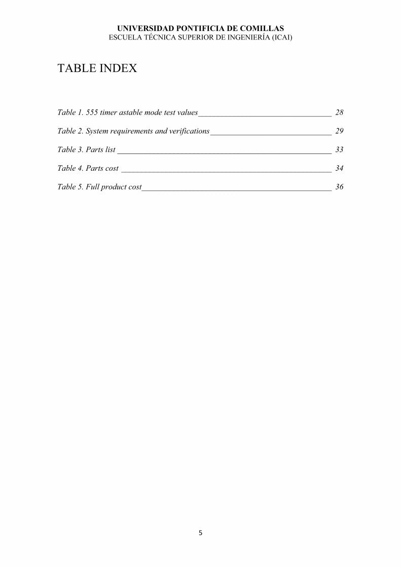
TABLE INDEX
Table 1. 555 timer astable mode test values _________________________________ 28 Table 2. System requirements and verifications ______________________________ 29 Table 3. Parts list _____________________________________________________ 33 Table 4. Parts cost ____________________________________________________ 34 Table 5. Full product cost _______________________________________________ 36

UNIVERSIDAD PONTIFICIA DE COMILLAS ESCUELA TÉCNICA SUPERIOR DE INGENIERÍA (ICAI)
6

UNIVERSIDAD PONTIFICIA DE COMILLAS ESCUELA TÉCNICA SUPERIOR DE INGENIERÍA (ICAI)
7
PART 1: REPORT

UNIVERSIDAD PONTIFICIA DE COMILLAS ESCUELA TÉCNICA SUPERIOR DE INGENIERÍA (ICAI)
8

UNIVERSIDAD PONTIFICIA DE COMILLAS ESCUELA TÉCNICA SUPERIOR DE INGENIERÍA (ICAI)
9
1. INTRODUCTION:
This report will be arranged into five parts, starting with the report of the work done during this past academic year, which itself will be separated into sections, beginning after this short presentation. As a first section, the rationale on why this project wanted to be developed will be introduced, as well as the objectives wanted to be achieved for the circuit and for the full model during this past time.
The second section will discuss the design of the final circuit that was assembled.
Then, for the third and fourth section, theoretical calculations needed and requirements and verifications for each individual component of the circuit will be presented.
For a fifth section, an analysis of costs for this project and future costs of mass production will be examined. Finally, for the last section, some ethical considerations that were found significant during class this past year will be shown.
As for the second segment for this report, a point of view on the future work related to this initial prototype will be presented, what the next steps to get to a completed and how a more functionable product could be developed.
The third part of this record will talk about the conclusions reached after working towards the objectives of this project.
Lastly, parts five and six are formed by the references used to finish this document and the datasheets of the purchased elements, for any necessary observation needed.
1.1. Statement of purpose:
Electronically dimming glass is becoming a trendy new addition to buildings across the globe. This recently-developed technology has been installed in business headquarters, airplanes, hotels, high-end residences, and even hospitals. According to BCC Research, global revenues reached $1.6 billion in as early as 2011. As the glass becomes more common and the price lowers, the next logical step for this commodity is integration into the average home. With this integration, customers will be desiring comprehensive and simple methods for their windows to meet the needs of their daily life. Our final product, Wanda, is a Smart Window that provides a simple and elegant product to fulfill these desires. Wanda allows the user to control the amount of light coming through their window from the outside using an app. In the modern era, humans have lost touch with their natural sleep cycles, often going to sleep long after the sun sets, and waking up far after it rises. This window is designed to customize the light entering a room so that the user can wake-up to natural light just as they might have back in the day. Studies show waking up to natural light increases wakefulness throughout the rest of the
UNIVERSIDAD PONTIFICIA DE COMILLAS ESCUELA TÉCNICA SUPERIOR DE INGENIERÍA (ICAI)
10
day and overall happiness levels (https://www.mindbodygreen.com/0-28702/if-you-want-to-wake-up-happy-try-this-alarm-clock-trick.html). Additionally, this window can frost at the press of a button, allowing users privacy without compromising their access to natural light. Initially, the window will be controllable via a mobile app, and it exists the aim to eventually make it voice-controllable. The window will come with an external sensor to sense the amount of natural light that is incident on the window pane. This will help to keep light levels constant for the user’s settings. Using the sensor, it is possible to adjust the dimness of the window to compensate for the lack of light coming through, allowing more natural light to maintain the same level of comfort. A possible concern with this automated window is that it will need to be controlled using electricity. Since the glass’ resting tendency is to be opaque, it would not be ideal in a power outage. The solution to this issue is to include an external power system for the window so as it can still work even during a power outage, allowing natural light into the house.
1.2. Objectives:
The major purposes for this circuit to be considered satisfactory are the following:
i. Power up the microcontroller and the whole circuit from any power outlet indefinitely.
ii. Power up the microcontroller and the whole circuit from the additional battery, in case of emergency for a specified time (tmin = 1h).
iii. Proof that the circuit would be able to power several loads, if necessary. iv. Dimensionally small, acceptable to hide and move around.
As for the whole product, the main objectives for the prototype to be completed are listed below:
I. Control the dimming of the glass through a phone App or web platform. II. Connect both the App and desktop setup so if you change the specs from one,
the other corrects it as well. III. Design an intuitive App background. IV. Design an external power system to power up the load in case of emergency. V. Adapt the signal coming from the photodiode to respond correctly on the
control.
UNIVERSIDAD PONTIFICIA DE COMILLAS ESCUELA TÉCNICA SUPERIOR DE INGENIERÍA (ICAI)
11
2. DESIGN:
2.1. Block diagram:
The system is divided into four central blocks, the DC signal input circuit, the UPS (Uninterruptible Power Supply) circuit, the Controller module and the AC signal output circuit.
The DC signal input circuit holds the AC-DC converter that achieves a constant 5V DC when connected to 120V AC power outlet and the NC terminal of a relay that allows the power input to change to the external UPS when it senses a power outage.
The UPS is formed by three elements that provide the additional power supply to the setup in case of power outage or any other emergency situation, which are a 3.7V 500mAh Li-Ion battery, a charging module that steps up the previous voltage to 5.2V DC and internally recharges the battery when connected to any household outlet, through the converter.
On the other hand, the Controller module, which goal is to communicate and follow orders from the Arduino microcontroller and provide a frequency-based signal, is formed by the following components: a 555 timer internal circuit astable mode that is capable to create a square wave with a particular frequency, and a digital potentiometer connected to the microcontroller that regulates the amplitude of that square, which makes possible the regulation of the voltage that will provide a modulation of the dimming opacity on the window.
Lastly, the AC signal output signal will achieve to re-turn the DC signal to its initial AC state, thanks to a setup which heart is a 115V-8V AC transformer, which its input current is driven by a MOSFET transistor, and its output its corrected by a Zener diode.
UNIVERSIDAD PONTIFICIA DE COMILLAS ESCUELA TÉCNICA SUPERIOR DE INGENIERÍA (ICAI)
12
Figure 1. Block diagram
2.2. Block descriptions:
2.2.1. DC Signal input:
A single pole relay would be enough so as to open the circuit in order to protect the rest of the circuit of over currents in case of emergency, as it is the first block connected to a power outlet, even though we used a DPDT in this project due to its availability in the lab. The circuit continues with the connection of a 120V AC-5V DC converter, voltage necessary to power up the rest of elements.
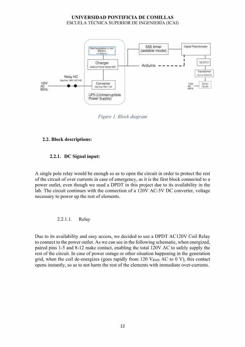
2.2.1.1. Relay
Due to its availability and easy access, we decided to use a DPDT AC120V Coil Relay to connect to the power outlet. As we can see in the following schematic, when energized, paired pins 1-5 and 8-12 make contact, enabling the total 120V AC to safely supply the rest of the circuit. In case of power outage or other situation happening in the generation grid, when the coil de-energizes (goes rapidly from 120 VRMS AC to 0 V), this contact opens instantly, so as to not harm the rest of the elements with immediate over-currents.
UNIVERSIDAD PONTIFICIA DE COMILLAS ESCUELA TÉCNICA SUPERIOR DE INGENIERÍA (ICAI)
13
Figure 2. DPDT Relay schematic
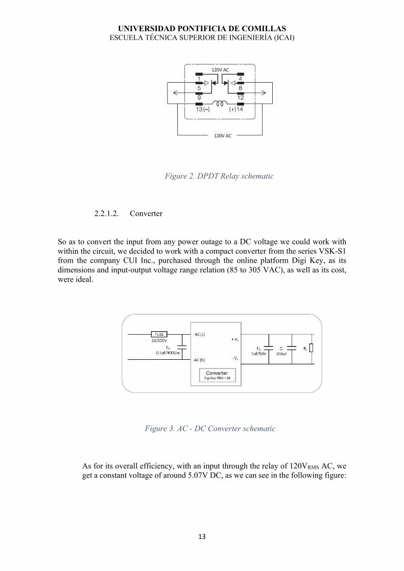
2.2.1.2. Converter
So as to convert the input from any power outage to a DC voltage we could work with within the circuit, we decided to work with a compact converter from the series VSK-S1 from the company CUI Inc., purchased through the online platform Digi Key, as its dimensions and input-output voltage range relation (85 to 305 VAC), as well as its cost, were ideal.
Figure 3. AC - DC Converter schematic
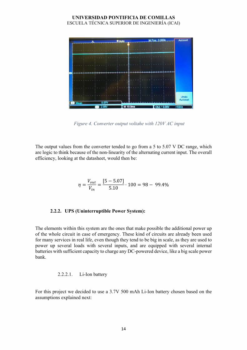
As for its overall efficiency, with an input through the relay of 120VRMS AC, we get a constant voltage of around 5.07V DC, as we can see in the following figure:
UNIVERSIDAD PONTIFICIA DE COMILLAS ESCUELA TÉCNICA SUPERIOR DE INGENIERÍA (ICAI)
14
Figure 4. Converter output voltahe with 120V AC input
The output values from the converter tended to go from a 5 to 5.07 V DC range, which are logic to think because of the non-linearity of the alternating current input. The overall efficiency, looking at the datasheet, would then be:
𝜂 =𝑉$%&𝑉'(
=[5 − 5.07]5.10 · 100 = 98 − 99.4%
2.2.2. UPS (Uninterruptible Power System):
The elements within this system are the ones that make possible the additional power up of the whole circuit in case of emergency. These kind of circuits are already been used for many services in real life, even though they tend to be big in scale, as they are used to power up several loads with several inputs, and are equipped with several internal batteries with sufficient capacity to charge any DC-powered device, like a big scale power bank.
2.2.2.1. Li-Ion battery
For this project we decided to use a 3.7V 500 mAh Li-Ion battery chosen based on the assumptions explained next:
UNIVERSIDAD PONTIFICIA DE COMILLAS ESCUELA TÉCNICA SUPERIOR DE INGENIERÍA (ICAI)
15
In any common grid emergency situation that creates a power outage in any home, the problem tends to be fixed within the maximum time of an hour, so we chose the capacitance of our battery based on that assumption. The calculations explaining how we got to our final battery purchase are discussed in section 3.
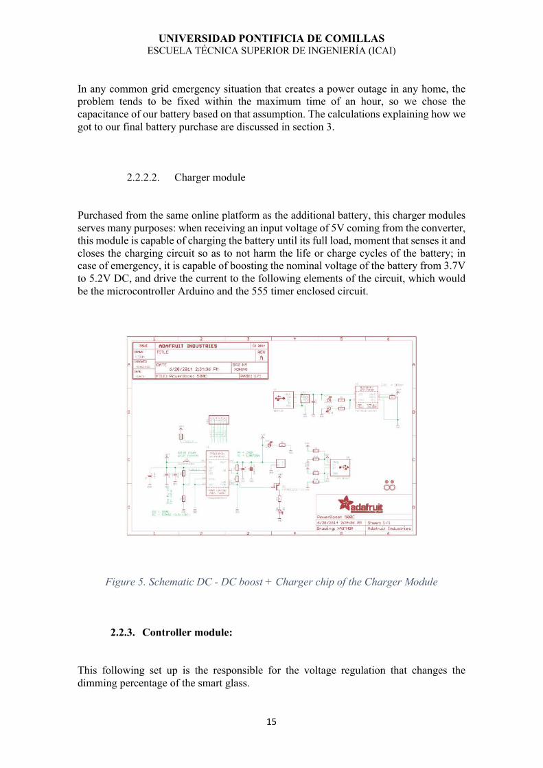
2.2.2.2. Charger module
Purchased from the same online platform as the additional battery, this charger modules serves many purposes: when receiving an input voltage of 5V coming from the converter, this module is capable of charging the battery until its full load, moment that senses it and closes the charging circuit so as to not harm the life or charge cycles of the battery; in case of emergency, it is capable of boosting the nominal voltage of the battery from 3.7V to 5.2V DC, and drive the current to the following elements of the circuit, which would be the microcontroller Arduino and the 555 timer enclosed circuit.
Figure 5. Schematic DC - DC boost + Charger chip of the Charger Module
2.2.3. Controller module:
This following set up is the responsible for the voltage regulation that changes the dimming percentage of the smart glass.
UNIVERSIDAD PONTIFICIA DE COMILLAS ESCUELA TÉCNICA SUPERIOR DE INGENIERÍA (ICAI)
16
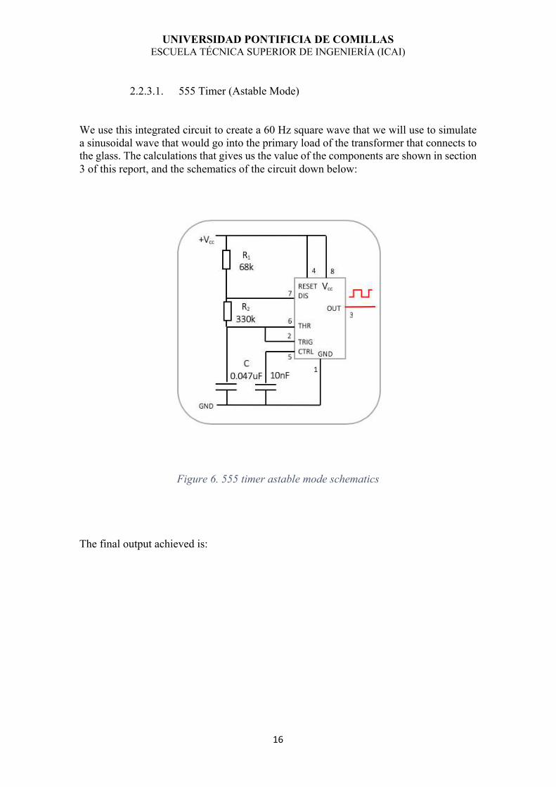
2.2.3.1. 555 Timer (Astable Mode)
We use this integrated circuit to create a 60 Hz square wave that we will use to simulate a sinusoidal wave that would go into the primary load of the transformer that connects to the glass. The calculations that gives us the value of the components are shown in section 3 of this report, and the schematics of the circuit down below:
Figure 6. 555 timer astable mode schematics
The final output achieved is:
UNIVERSIDAD PONTIFICIA DE COMILLAS ESCUELA TÉCNICA SUPERIOR DE INGENIERÍA (ICAI)
17
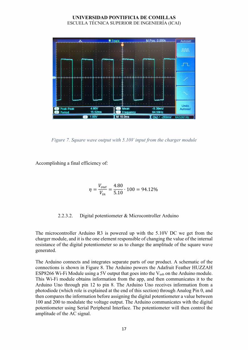
Figure 7. Square wave output with 5.10V input from the charger module
Accomplishing a final efficiency of:
𝜂 =𝑉$%&𝑉'(
=4.805.10 · 100 = 94.12%
2.2.3.2. Digital potentiometer & Microcontroller Arduino
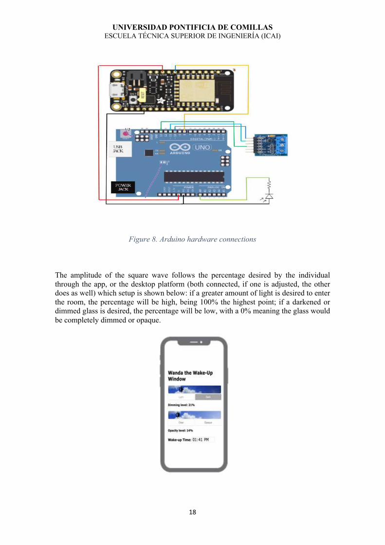
The microcontroller Arduino R3 is powered up with the 5.10V DC we get from the charger module, and it is the one element responsible of changing the value of the internal resistance of the digital potentiometer so as to change the amplitude of the square wave generated.
The Arduino connects and integrates separate parts of our product. A schematic of the connections is shown in Figure 8. The Arduino powers the Adafruit Feather HUZZAH ESP8266 Wi-Fi Module using a 5V output that goes into the Vusb on the Arduino module. This Wi-Fi module obtains information from the app, and then communicates it to the Arduino Uno through pin 12 to pin 8. The Arduino Uno receives information from a photodiode (which role is explained at the end of this section) through Analog Pin 0, and then compares the information before assigning the digital potentiometer a value between 100 and 200 to modulate the voltage output. The Arduino communicates with the digital potentiometer using Serial Peripheral Interface. The potentiometer will then control the amplitude of the AC signal.
UNIVERSIDAD PONTIFICIA DE COMILLAS ESCUELA TÉCNICA SUPERIOR DE INGENIERÍA (ICAI)
18
Figure 8. Arduino hardware connections
The amplitude of the square wave follows the percentage desired by the individual through the app, or the desktop platform (both connected, if one is adjusted, the other does as well) which setup is shown below: if a greater amount of light is desired to enter the room, the percentage will be high, being 100% the highest point; if a darkened or dimmed glass is desired, the percentage will be low, with a 0% meaning the glass would be completely dimmed or opaque.

UNIVERSIDAD PONTIFICIA DE COMILLAS ESCUELA TÉCNICA SUPERIOR DE INGENIERÍA (ICAI)
19
Figure 9. Phone App and Desktop setup for Wanda
Through this intuitive program, we came up with the baseline design which includes an alarm to be set by the user, communication with the clock on the users phone, a switch to determine whether the alarm is one, and a slider so the user can choose what percentage of the maximum light they would like the window to transmit. As for the purpose of the photodiode, we added it to the window as an external sensor to sense the amount of natural light that is incident on the window pane. This will help to keep light levels constant for the user’s settings. For example, on a sunny day the user may want about 50% of the maximum outside light to be coming through, but when a cloud covers the house, there will be even less light coming through than they desire. Using the sensor, it is possible to adjust the dimness of the window to compensate for the lack of light coming through, allowing more natural light to maintain the same level of comfort.
2.2.4. AC Signal Output:
As we are using a 60Hz square wave as the input for our power transformer, that will be the one creating the sine wave that power up our glass, it was logic to think that some problems were going to come with it, as it is far from ideal. So, as to help amplify the signal, and then clean it, we came up with the following elements:
UNIVERSIDAD PONTIFICIA DE COMILLAS ESCUELA TÉCNICA SUPERIOR DE INGENIERÍA (ICAI)
20
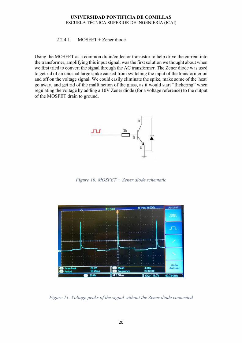
2.2.4.1. MOSFET + Zener diode
Using the MOSFET as a common drain/collector transistor to help drive the current into the transformer, amplifying this input signal, was the first solution we thought about when we first tried to convert the signal through the AC transformer. The Zener diode was used to get rid of an unusual large spike caused from switching the input of the transformer on and off on the voltage signal. We could easily eliminate the spike, make some of the 'heat' go away, and get rid of the malfunction of the glass, as it would start “flickering” when regulating the voltage by adding a 10V Zener diode (for a voltage reference) to the output of the MOSFET drain to ground.
Figure 10. MOSFET + Zener diode schematic
Figure 11. Voltage peaks of the signal without the Zener diode connected

UNIVERSIDAD PONTIFICIA DE COMILLAS ESCUELA TÉCNICA SUPERIOR DE INGENIERÍA (ICAI)
21
Figure 12. Signal input into the transformer
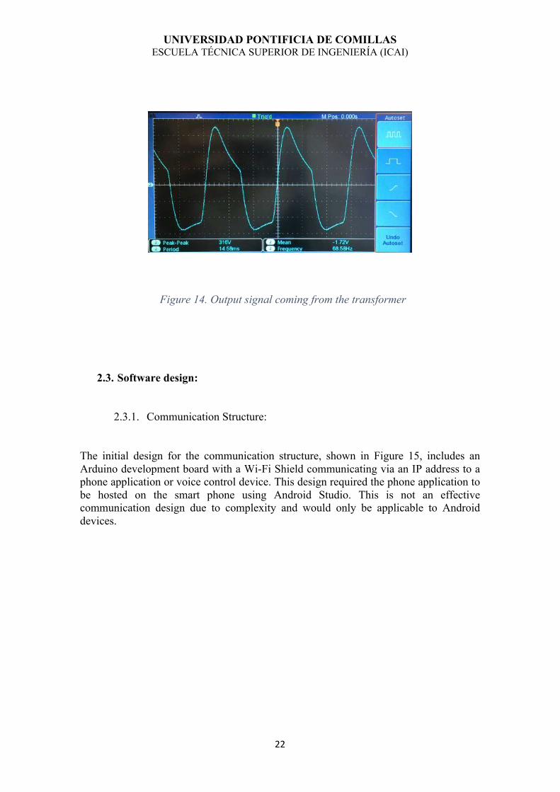
2.2.4.2. Transformer
The final stage of our fully working circuit is a dual secondary 230/115 VAC transformer that enables the previous input leaving the amplifier to be converted to a 60 Hz square wave capable of powering up the smart glass.
Figure 13. Transformer schematics
UNIVERSIDAD PONTIFICIA DE COMILLAS ESCUELA TÉCNICA SUPERIOR DE INGENIERÍA (ICAI)
22
Figure 14. Output signal coming from the transformer
2.3. Software design:
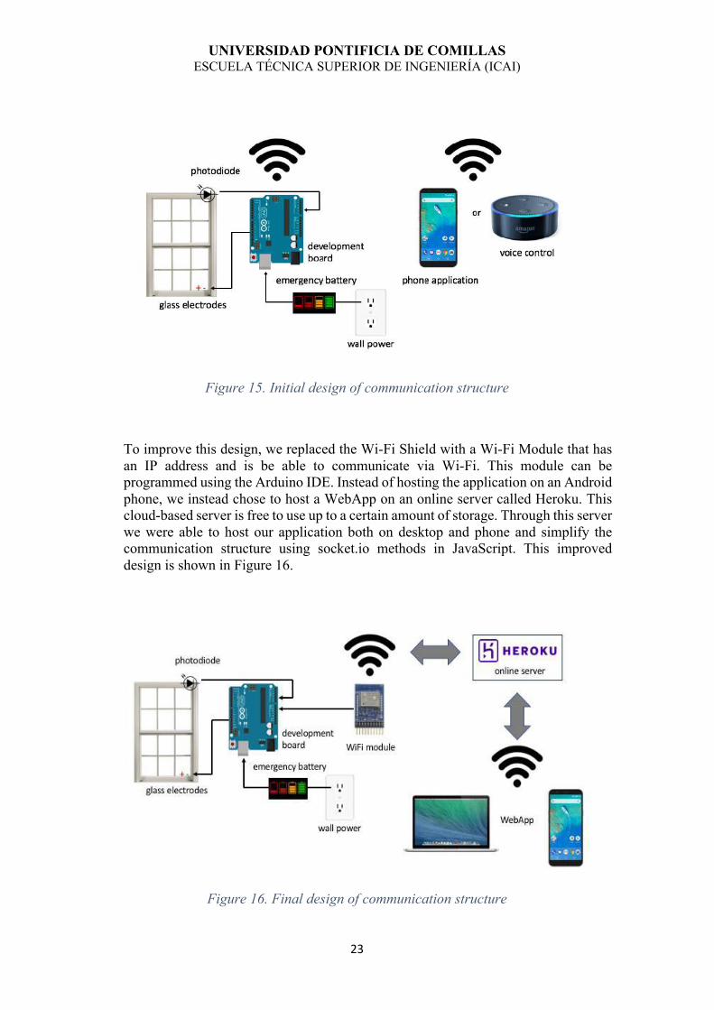
2.3.1. Communication Structure:
The initial design for the communication structure, shown in Figure 15, includes an Arduino development board with a Wi-Fi Shield communicating via an IP address to a phone application or voice control device. This design required the phone application to be hosted on the smart phone using Android Studio. This is not an effective communication design due to complexity and would only be applicable to Android devices.
UNIVERSIDAD PONTIFICIA DE COMILLAS ESCUELA TÉCNICA SUPERIOR DE INGENIERÍA (ICAI)
23
Figure 15. Initial design of communication structure
To improve this design, we replaced the Wi-Fi Shield with a Wi-Fi Module that has an IP address and is be able to communicate via Wi-Fi. This module can be programmed using the Arduino IDE. Instead of hosting the application on an Android phone, we instead chose to host a WebApp on an online server called Heroku. This cloud-based server is free to use up to a certain amount of storage. Through this server we were able to host our application both on desktop and phone and simplify the communication structure using socket.io methods in JavaScript. This improved design is shown in Figure 16.
Figure 16. Final design of communication structure
UNIVERSIDAD PONTIFICIA DE COMILLAS ESCUELA TÉCNICA SUPERIOR DE INGENIERÍA (ICAI)
24
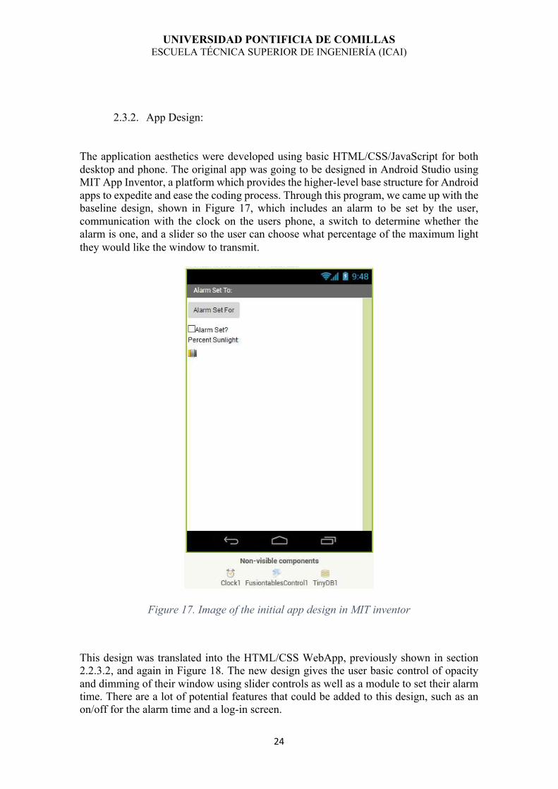
2.3.2. App Design:
The application aesthetics were developed using basic HTML/CSS/JavaScript for both desktop and phone. The original app was going to be designed in Android Studio using MIT App Inventor, a platform which provides the higher-level base structure for Android apps to expedite and ease the coding process. Through this program, we came up with the baseline design, shown in Figure 17, which includes an alarm to be set by the user, communication with the clock on the users phone, a switch to determine whether the alarm is one, and a slider so the user can choose what percentage of the maximum light they would like the window to transmit.
Figure 17. Image of the initial app design in MIT inventor
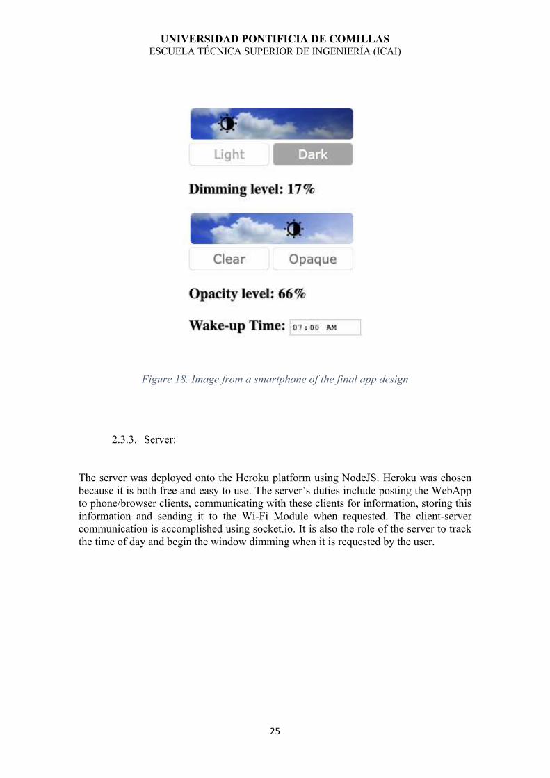
This design was translated into the HTML/CSS WebApp, previously shown in section 2.2.3.2, and again in Figure 18. The new design gives the user basic control of opacity and dimming of their window using slider controls as well as a module to set their alarm time. There are a lot of potential features that could be added to this design, such as an on/off for the alarm time and a log-in screen.
UNIVERSIDAD PONTIFICIA DE COMILLAS ESCUELA TÉCNICA SUPERIOR DE INGENIERÍA (ICAI)
25
Figure 18. Image from a smartphone of the final app design
2.3.3. Server:
The server was deployed onto the Heroku platform using NodeJS. Heroku was chosen because it is both free and easy to use. The server’s duties include posting the WebApp to phone/browser clients, communicating with these clients for information, storing this information and sending it to the Wi-Fi Module when requested. The client-server communication is accomplished using socket.io. It is also the role of the server to track the time of day and begin the window dimming when it is requested by the user.

UNIVERSIDAD PONTIFICIA DE COMILLAS ESCUELA TÉCNICA SUPERIOR DE INGENIERÍA (ICAI)
26
UNIVERSIDAD PONTIFICIA DE COMILLAS ESCUELA TÉCNICA SUPERIOR DE INGENIERÍA (ICAI)
27
3. CALCULATIONS:
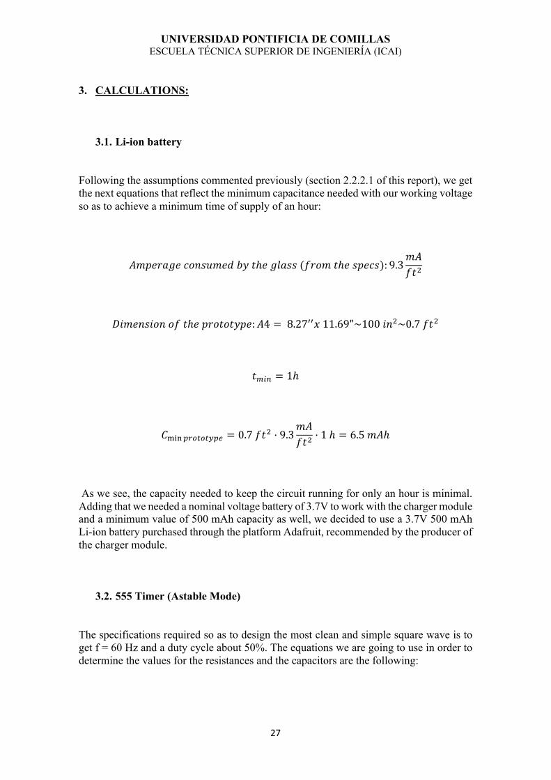
3.1. Li-ion battery
Following the assumptions commented previously (section 2.2.2.1 of this report), we get the next equations that reflect the minimum capacitance needed with our working voltage so as to achieve a minimum time of supply of an hour:
𝐴𝑚𝑝𝑒𝑟𝑎𝑔𝑒𝑐𝑜𝑛𝑠𝑢𝑚𝑒𝑑𝑏𝑦𝑡ℎ𝑒𝑔𝑙𝑎𝑠𝑠(𝑓𝑟𝑜𝑚𝑡ℎ𝑒𝑠𝑝𝑒𝑐𝑠): 9.3𝑚𝐴𝑓𝑡O
𝐷𝑖𝑚𝑒𝑛𝑠𝑖𝑜𝑛𝑜𝑓𝑡ℎ𝑒𝑝𝑟𝑜𝑡𝑜𝑡𝑦𝑝𝑒: 𝐴4 = 8.27RR𝑥11.69"~100𝑖𝑛O~0.7𝑓𝑡O
𝑡W'( = 1ℎ
𝐶YZ[\]$&$&^\_ = 0.7𝑓𝑡O · 9.3𝑚𝐴𝑓𝑡O · 1ℎ = 6.5𝑚𝐴ℎ
As we see, the capacity needed to keep the circuit running for only an hour is minimal. Adding that we needed a nominal voltage battery of 3.7V to work with the charger module and a minimum value of 500 mAh capacity as well, we decided to use a 3.7V 500 mAh Li-ion battery purchased through the platform Adafruit, recommended by the producer of the charger module.
3.2. 555 Timer (Astable Mode)
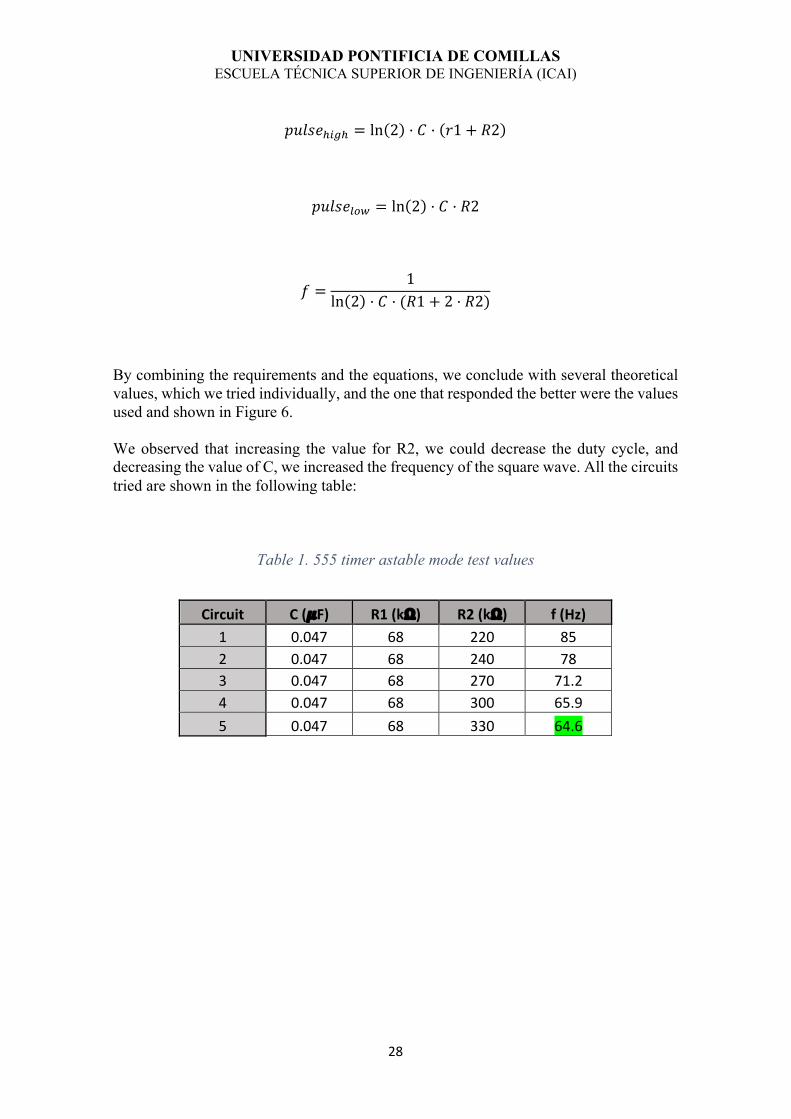
The specifications required so as to design the most clean and simple square wave is to get f = 60 Hz and a duty cycle about 50%. The equations we are going to use in order to determine the values for the resistances and the capacitors are the following:
UNIVERSIDAD PONTIFICIA DE COMILLAS ESCUELA TÉCNICA SUPERIOR DE INGENIERÍA (ICAI)
28
𝑝𝑢𝑙𝑠𝑒`'a` = ln(2) · 𝐶 · (𝑟1 + 𝑅2)
𝑝𝑢𝑙𝑠𝑒f$g = ln(2) · 𝐶 · 𝑅2
𝑓 =1
ln(2) · 𝐶 · (𝑅1 + 2 · 𝑅2)
By combining the requirements and the equations, we conclude with several theoretical values, which we tried individually, and the one that responded the better were the values used and shown in Figure 6.
We observed that increasing the value for R2, we could decrease the duty cycle, and decreasing the value of C, we increased the frequency of the square wave. All the circuits tried are shown in the following table:
Table 1. 555 timer astable mode test values
Circuit C (𝝁F) R1 (k𝝮) R2 (k𝝮) f (Hz)
1 0.047 68 220 85 2 0.047 68 240 78 3 0.047 68 270 71.2 4 0.047 68 300 65.9 5 0.047 68 330 64.6
UNIVERSIDAD PONTIFICIA DE COMILLAS ESCUELA TÉCNICA SUPERIOR DE INGENIERÍA (ICAI)
29
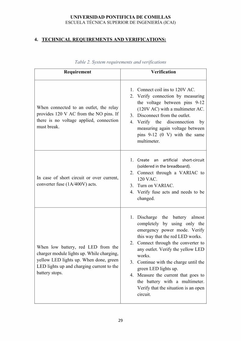
4. TECHNICAL REQUIREMENTS AND VERIFICATIONS:
Table 2. System requirements and verifications
Requirement Verification
When connected to an outlet, the relay provides 120 V AC from the NO pins. If there is no voltage applied, connection must break.
1. Connect coil ins to 120V AC. 2. Verify connection by measuring
the voltage between pins 9-12 (120V AC) with a multimeter AC.
3. Disconnect from the outlet. 4. Verify the disconnection by
measuring again voltage between pins 9-12 (0 V) with the same multimeter.
In case of short circuit or over current, converter fuse (1A/400V) acts.
1. Create an artificial short-circuit
(soldered in the breadboard). 2. Connect through a VARIAC to
120 VAC. 3. Turn on VARIAC. 4. Verify fuse acts and needs to be
changed.
When low battery, red LED from the charger module lights up. While charging, yellow LED lights up. When done, green LED lights up and charging current to the battery stops.
1. Discharge the battery almost
completely by using only the emergency power mode. Verify this way that the red LED works.
2. Connect through the converter to any outlet. Verify the yellow LED works.
3. Continue with the charge until the green LED lights up.
4. Measure the current that goes to the battery with a multimeter. Verify that the situation is an open circuit.
UNIVERSIDAD PONTIFICIA DE COMILLAS ESCUELA TÉCNICA SUPERIOR DE INGENIERÍA (ICAI)
30
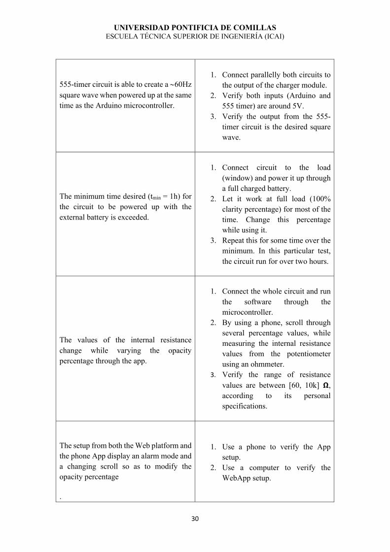
555-timer circuit is able to create a ~60Hz square wave when powered up at the same time as the Arduino microcontroller.
1. Connect parallelly both circuits to
the output of the charger module. 2. Verify both inputs (Arduino and
555 timer) are around 5V. 3. Verify the output from the 555-
timer circuit is the desired square wave.
The minimum time desired (tmin = 1h) for the circuit to be powered up with the external battery is exceeded.
1. Connect circuit to the load
(window) and power it up through a full charged battery.
2. Let it work at full load (100% clarity percentage) for most of the time. Change this percentage while using it.
3. Repeat this for some time over the minimum. In this particular test, the circuit run for over two hours.
The values of the internal resistance change while varying the opacity percentage through the app.
1. Connect the whole circuit and run
the software through the microcontroller.
2. By using a phone, scroll through several percentage values, while measuring the internal resistance values from the potentiometer using an ohmmeter.
3. Verify the range of resistance values are between [60, 10k] 𝝮, according to its personal specifications.
The setup from both the Web platform and the phone App display an alarm mode and a changing scroll so as to modify the opacity percentage
.
1. Use a phone to verify the App setup.
2. Use a computer to verify the WebApp setup.
UNIVERSIDAD PONTIFICIA DE COMILLAS ESCUELA TÉCNICA SUPERIOR DE INGENIERÍA (ICAI)
31
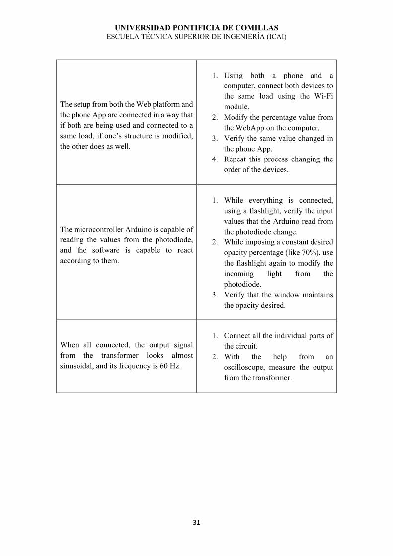
The setup from both the Web platform and the phone App are connected in a way that if both are being used and connected to a same load, if one’s structure is modified, the other does as well.
1. Using both a phone and a
computer, connect both devices to the same load using the Wi-Fi module.
2. Modify the percentage value from the WebApp on the computer.
3. Verify the same value changed in the phone App.
4. Repeat this process changing the order of the devices.
The microcontroller Arduino is capable of reading the values from the photodiode, and the software is capable to react according to them.
1. While everything is connected,
using a flashlight, verify the input values that the Arduino read from the photodiode change.
2. While imposing a constant desired opacity percentage (like 70%), use the flashlight again to modify the incoming light from the photodiode.
3. Verify that the window maintains the opacity desired.
When all connected, the output signal from the transformer looks almost sinusoidal, and its frequency is 60 Hz.
1. Connect all the individual parts of
the circuit. 2. With the help from an
oscilloscope, measure the output from the transformer.

UNIVERSIDAD PONTIFICIA DE COMILLAS ESCUELA TÉCNICA SUPERIOR DE INGENIERÍA (ICAI)
32
UNIVERSIDAD PONTIFICIA DE COMILLAS ESCUELA TÉCNICA SUPERIOR DE INGENIERÍA (ICAI)
33
5. CIRCUIT COSTS:
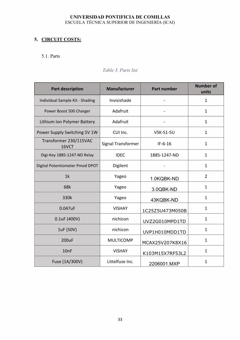
5.1. Parts
Table 3. Parts list
Part description Manufacturer Part number Number of units
Individual Sample Kit - Shading Invisishade - 1
Power Boost 500 Charger Adafruit - 1
Lithium Ion Polymer Battery Adafruit - 1
Power Supply Switching 5V 1W CUI Inc. VSK-S1-5U 1
Transformer 230/115VAC 16VCT Signal Transformer IF-6-16 1
Digi-Key 1885-1247-ND Relay IDEC 1885-1247-ND 1
Digital Potentiometer Pmod DPOT Digilent - 1
1k Yageo 1.0KQBK-ND 2
68k Yageo 3.0QBK-ND 1
330k Yageo 43KQBK-ND 1
0.047uF VISHAY 1C25Z5U473M050B 1
0.1uF (400V) nichicon UVZ2G010MPD1TD 1
1uF (50V) nichicon UVP1H010MDD1TD 1
200uF MULTICOMP MCAX25V207K8X16 1
10nF VISHAY K103M15X7RF53L2 1
Fuse (1A/300V) Littelfuse Inc. 2206001.MXP 1
UNIVERSIDAD PONTIFICIA DE COMILLAS ESCUELA TÉCNICA SUPERIOR DE INGENIERÍA (ICAI)
34
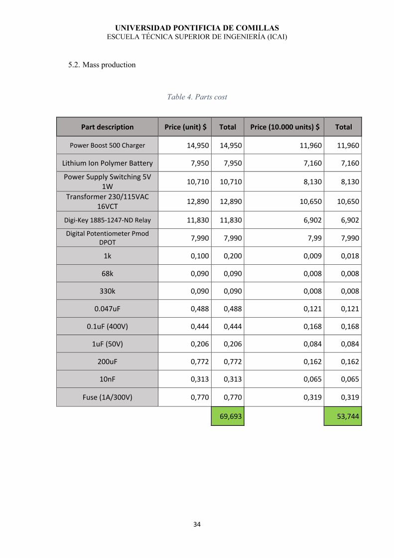
5.2. Mass production
Table 4. Parts cost
Part description Price (unit) $ Total Price (10.000 units) $ Total
Power Boost 500 Charger 14,950 14,950 11,960 11,960
Lithium Ion Polymer Battery 7,950 7,950 7,160 7,160
Power Supply Switching 5V 1W 10,710 10,710 8,130 8,130
Transformer 230/115VAC 16VCT 12,890 12,890 10,650 10,650
Digi-Key 1885-1247-ND Relay 11,830 11,830 6,902 6,902
Digital Potentiometer Pmod DPOT 7,990 7,990 7,99 7,990
1k 0,100 0,200 0,009 0,018
68k 0,090 0,090 0,008 0,008
330k 0,090 0,090 0,008 0,008
0.047uF 0,488 0,488 0,121 0,121
0.1uF (400V) 0,444 0,444 0,168 0,168
1uF (50V) 0,206 0,206 0,084 0,084
200uF 0,772 0,772 0,162 0,162
10nF 0,313 0,313 0,065 0,065
Fuse (1A/300V) 0,770 0,770 0,319 0,319
69,693 53,744

UNIVERSIDAD PONTIFICIA DE COMILLAS ESCUELA TÉCNICA SUPERIOR DE INGENIERÍA (ICAI)
35
As we can see in the previous table, the total cost for the parts that compose the Power System circuit is $69,70. This may look like a large amount for such a small circuit, but we have to take into account that just one circuit is able to power up several loads, several windows, and if the components are purchased in industrial quantities, the final cost reduce itself by almost a 23%, to $53,75.
In order to completely analyze if the circuit is economically viable for mass production, we should take into care multiple estimations, such as how many workers are needed to develop this product, or if it could be an automotive process, Labor Costs, Production Costs, Maintenance Costs for the machinery, etc.
In order to complete this economic study, let’s summarize the estimations that will be taking into account:
1) The leasing cost for the plant and space where the circuit would be stored and assembled is about 500$/month.
2) Each circuit needs to be assembled by a worker. 3) Labor cost has an hourly rate of 15$. Each day, each worker works 8 hours,
and each hour mounts 3 circuits per hour, connects them to a load, downloads the program into the microcontroller and stores it.
4) We pay three workers. 5) There is no O&M Cost. 6) The total cost for the shipped product is shown in table 5. Each product is
sold for 375$.
Each month a total amount of 552 circuits are mounted and shipped (3 workers, 8 hours a day, 23 days a month), a total of 6624 circuits a year. When purchasing the items with the mass production price, there are a total of 3376 extra pieces that can be assembled the following year. The total profit each month developing this product will be: Total Present Worth Cost: [ ($15 · 8 · 23) + ($500) + ($242.81 · (10,000 / 12)) ] = $204,768.33 Total Present Worth Benefit: [ ($375 · 552) ] = $207,000
Monthly profit = Benefit – Cost = $2,231.67

UNIVERSIDAD PONTIFICIA DE COMILLAS ESCUELA TÉCNICA SUPERIOR DE INGENIERÍA (ICAI)
36
Even though this example may be too simple to really understand the true economic viability of the project, we can sense that in a future it would be, as the numbers show us an initial profitability if the product catches the interest of the market.
Table 5. Full product cost
Item Cost
Smart Glass (2)
- Invisishade Individual Sample Kit – Shading - SmartFilm Grey Sample 8x11’
$158.00
Power System $53.75
Sensors (2) PHOTODIODE VTP9812FH-ND
$3.12
Development Board (1) Arduino Uno R3
$8.99
WiFi Module (1) Adafruit Feather HUZZAH ESP8266
$18.95
Total
$242.81
UNIVERSIDAD PONTIFICIA DE COMILLAS ESCUELA TÉCNICA SUPERIOR DE INGENIERÍA (ICAI)
37
6. ETHICAL CONSIDERATIONS:
Our product does not bear a lot of ethical implications, since it is more a product of convenience and leisure than anything else and affects only the user.
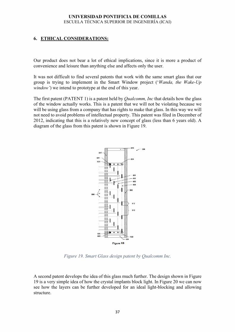
It was not difficult to find several patents that work with the same smart glass that our group is trying to implement in the Smart Window project (‘Wanda, the Wake-Up window’) we intend to prototype at the end of this year.
The first patent (PATENT 1) is a patent held by Qualcomm, Inc that details how the glass of the window actually works. This is a patent that we will not be violating because we will be using glass from a company that has rights to make that glass. In this way we will not need to avoid problems of intellectual property. This patent was filed in December of 2012, indicating that this is a relatively new concept of glass (less than 6 years old). A diagram of the glass from this patent is shown in Figure 19.
Figure 19. Smart Glass design patent by Qualcomm Inc.
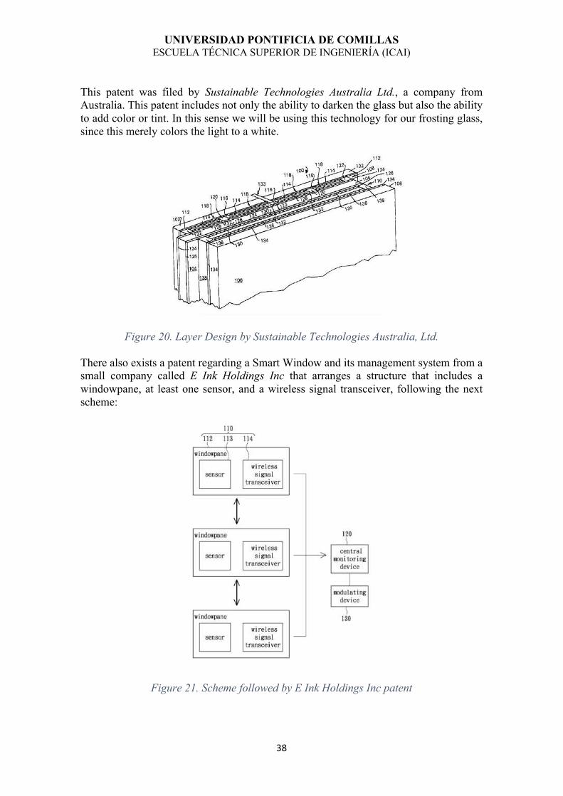
A second patent develops the idea of this glass much further. The design shown in Figure 19 is a very simple idea of how the crystal implants block light. In Figure 20 we can now see how the layers can be further developed for an ideal light-blocking and allowing structure.
UNIVERSIDAD PONTIFICIA DE COMILLAS ESCUELA TÉCNICA SUPERIOR DE INGENIERÍA (ICAI)
38
This patent was filed by Sustainable Technologies Australia Ltd., a company from Australia. This patent includes not only the ability to darken the glass but also the ability to add color or tint. In this sense we will be using this technology for our frosting glass, since this merely colors the light to a white.
Figure 20. Layer Design by Sustainable Technologies Australia, Ltd.
There also exists a patent regarding a Smart Window and its management system from a small company called E Ink Holdings Inc that arranges a structure that includes a windowpane, at least one sensor, and a wireless signal transceiver, following the next scheme:
Figure 21. Scheme followed by E Ink Holdings Inc patent

UNIVERSIDAD PONTIFICIA DE COMILLAS ESCUELA TÉCNICA SUPERIOR DE INGENIERÍA (ICAI)
39
Figure 21 shows a simple structure based on the idea of designing a control that enable the window itself to manage the modulation of the opacity of the glass with the data recovered from the sensors (at least one), which are configured to receive and collect the amount of light outside in order to perform an effectual intelligent modulation.
This patent is connected to our project as we intend to use sensors to collect data from the outside to control the transmission of light, but our goal is for the consumers themselves to be able to control the opacity of the window depending on how much natural light they want to enter their homes.
In our patent search we did not find any problems that we may run into regarding intellectual property other than the use of the most recent patent. For our smart window structure, however, we will be incorporating much more than the basics of this design.
As listed in the technical specification section, the window blocks UV exposure, making its users healthy and safe. The main environmental impact as far as we could find was that the smart windows would be consuming power, whereas normal windows do not consume electricity. However, the window runs on less than a Watt, and the power consumed to run the window will likely be offset by energy savings on heating and cooling. In fact, smart windows could be integrated with other smart home technologies such as lights, solar panels, etc. that could more effectively manage energy use. The minimal energy consumption also helps to avoid conflict with any government power regulations.

UNIVERSIDAD PONTIFICIA DE COMILLAS ESCUELA TÉCNICA SUPERIOR DE INGENIERÍA (ICAI)
40

UNIVERSIDAD PONTIFICIA DE COMILLAS ESCUELA TÉCNICA SUPERIOR DE INGENIERÍA (ICAI)
41
PART 2: FUTURE WORK

UNIVERSIDAD PONTIFICIA DE COMILLAS ESCUELA TÉCNICA SUPERIOR DE INGENIERÍA (ICAI)
42
UNIVERSIDAD PONTIFICIA DE COMILLAS ESCUELA TÉCNICA SUPERIOR DE INGENIERÍA (ICAI)
43
There are many potential improvements that can be made to this design to improve functionality and cater to the customer’s desires. Firstly, Wanda the Window has the perfect potential to be integrated into the smart home structure, controlled by Alexa or any other voice control equivalent. A module such as the one created could be programmed to respond to smart home commands sent by a voice control module. Commands such as “Wanda, set my windows to 20% light” will be processed and sent to the window’s hardware to set the window’s electrical dimming percentage. As indicated by our survey results, this is a desirable control method and if integrated with the smart home will increase the attractiveness of this product for customers. Another important step would be to create a native app accessible through any app store. Companies such as Lutron offer app control of their devices through a native app, and therefore it would be very desirable to offer this same feature. This app would be able to use the functionality of the phone itself, making it possible for Touch Id sign-in and possibly even integration with the alarm of the phone itself. Therefore, it would be possible for the user to set only one alarm. Additionally, as the user adds more Wanda Windows to their home, there will need to be an app feature to organize and control all of the windows separately in an intuitive manner. There are also a variety of improvements that could be made on this prototype design. Firstly, the ESP8266 Wi-Fi Module was the greatest flaw in the final design due to its occasional hang-ups during operation. To reduce this error, it would be prudent to replace this module with a Wi-Fi Shield and replace the Uno R3 with a Mega to handle the increase in occupied pins. Or, if necessary, replace the Arduino itself with a Raspberry Pi to handle the internet interaction. The improvement of this hardware would increase the speed of response and ultimately create a better user experience. Another consideration is that when multiple windows are connected, it must be possible to control them individually. Our design allows for control of one window currently. The app/server design would need to be expanded to handle and organize the opacity/dimming information for multiple windows. In the future, customers would also likely prefer windows that are able to both frost and dim. This design of two films that would be controlled with a separate voltage would need to be designed into the circuit and the communication structure.

UNIVERSIDAD PONTIFICIA DE COMILLAS ESCUELA TÉCNICA SUPERIOR DE INGENIERÍA (ICAI)
44

UNIVERSIDAD PONTIFICIA DE COMILLAS ESCUELA TÉCNICA SUPERIOR DE INGENIERÍA (ICAI)
45
PART 3: CONCLUSIONS

UNIVERSIDAD PONTIFICIA DE COMILLAS ESCUELA TÉCNICA SUPERIOR DE INGENIERÍA (ICAI)
46
UNIVERSIDAD PONTIFICIA DE COMILLAS ESCUELA TÉCNICA SUPERIOR DE INGENIERÍA (ICAI)
47
We should analyze if the objectives of both the Power System and the general product purposes have been accomplished during this past year work. The main objectives for the power system were:
i. Power up the microcontroller and the whole circuit from any power outlet indefinitely.
ii. Power up the microcontroller and the whole circuit from the additional battery, in case of emergency for a specified time (tmin = 1h).
iii. Proof that the circuit would be able to power several loads, if necessary. iv. Dimensionally small, acceptable to hide and move around.
All objectives have been achieved, as the circuit is able to work with power coming from any household outlet as well as the external battery, that lasts for at least two hours (checked during the test explained in Table 2), and that would be able, following that logic, to power up several loads at the same time for a smaller period. The charger module is capable to drawn over 1000 mA (usually 500 mA+) and each small load only consumes less than 9 mA.
When soldered altogether, the power circuit hardware is relatively compact and can easily be hidden within drywall or condensed into a small unassuming box.
The following objectives are referred to the final product.
I. Control the dimming of the glass through a phone App or web platform. II. Connect both the App and desktop setup so if you change the specs from one,
the other corrects it as well. III. Design an intuitive App background. IV. Design an external power system to power up the load in case of emergency. V. Adapt the signal coming from the photodiode to respond correctly on the
control.
The final result of this project is a fully-functional app control structure for an electronically dimming window. The power circuit hardware communicates with the app via Wi-Fi and responds almost immediately to the dimming percentage set on the app. There are sporadic hang-ups with the ESP8266 module that could be improved by replacement with more reliable hardware. Otherwise, the window will respond in milliseconds providing the customer with the ideal amount of light for their room. This also affects the response time to the input from the photodiode.

UNIVERSIDAD PONTIFICIA DE COMILLAS ESCUELA TÉCNICA SUPERIOR DE INGENIERÍA (ICAI)
48

UNIVERSIDAD PONTIFICIA DE COMILLAS ESCUELA TÉCNICA SUPERIOR DE INGENIERÍA (ICAI)
49
PART 4: REFERENCES

UNIVERSIDAD PONTIFICIA DE COMILLAS ESCUELA TÉCNICA SUPERIOR DE INGENIERÍA (ICAI)
50
UNIVERSIDAD PONTIFICIA DE COMILLAS ESCUELA TÉCNICA SUPERIOR DE INGENIERÍA (ICAI)
51
[1] Carissa Johnson, “If you want to wake up happy, try this alarm clock trick”
https://www.mindbodygreen.com/0-28702/if-you-want-to-wake-up-happy-try-this-alarm-clock-t rick.html
[2] Invisishade, “Self-Adhesive Film Features and Specifications”
http://www.invisishade.com/ [3] Adafruit, “Miniature Single Cell, Fully Integrated Li-Ion, Li-Polymer Charge
Management Controller” DataSheet: https://cdn-shop.adafruit.com/datasheets/MCP73831.pdf [4] Adafruit, “SYNCHRONOUS BOOST CONVERTER WITH 2A SWITCH” DataSheet: https://cdn-shop.adafruit.com/datasheets/tps61090.pdf [5] Belfuse, “International Flathead Low Profile Transformers” DataSheet: https://belfuse.com/resources/IF.pdf [6] Analog, “256-Position SPI-Compatible Digital Potentiometer”
DataSheet: https://www.analog.com/media/en/technical-documentation/data-sheets/AD5160.pdf?_ga=2.189675691.1674535084.1555104651-1998442838.1555005985
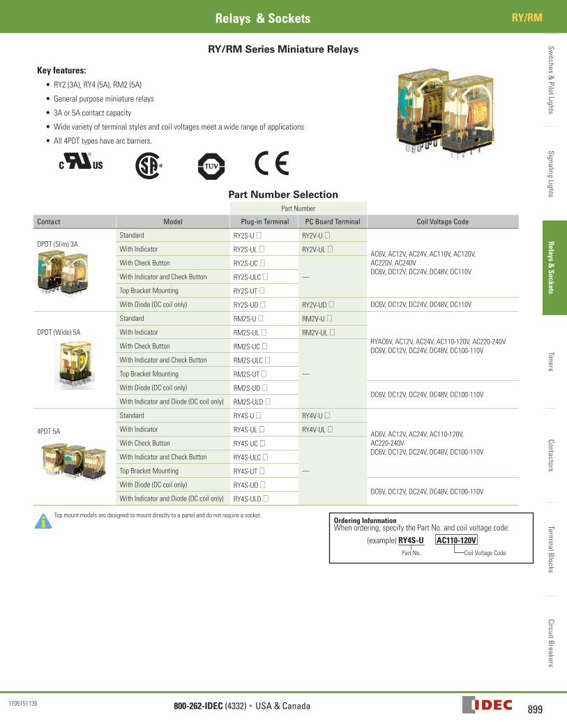
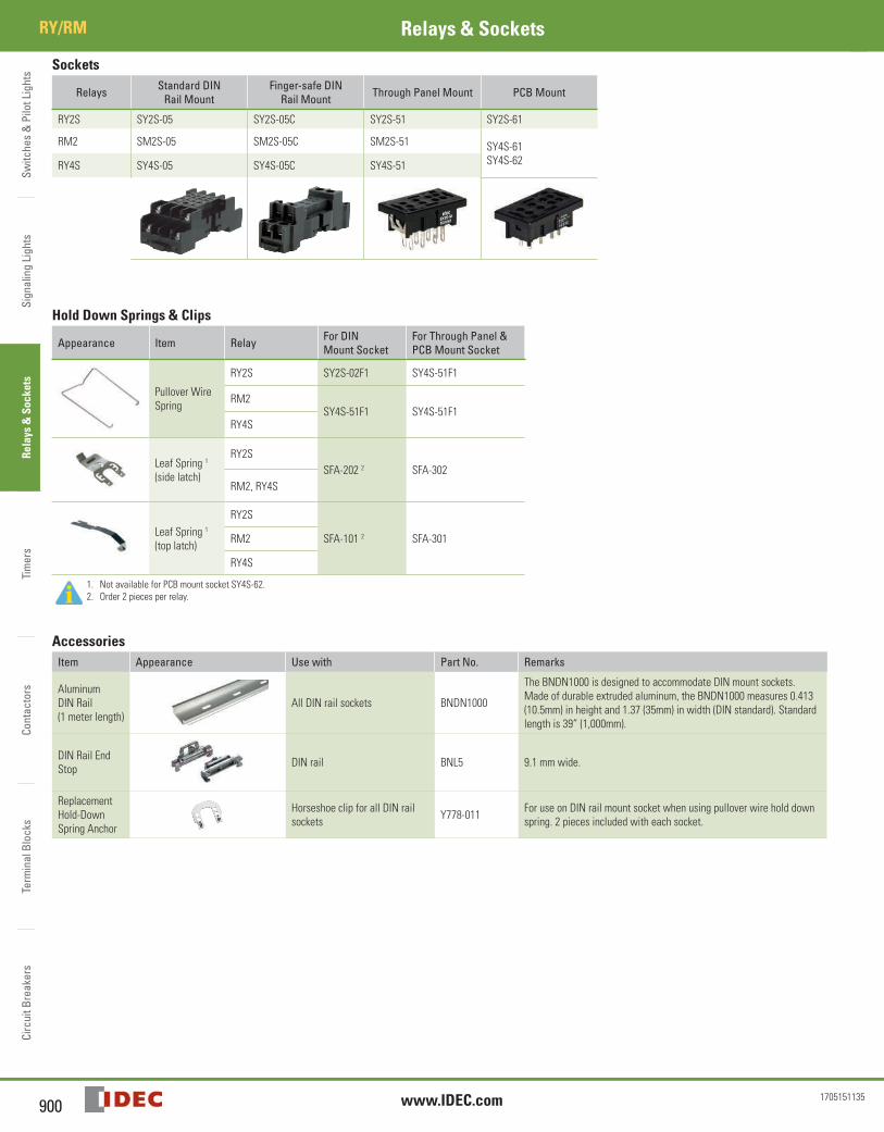
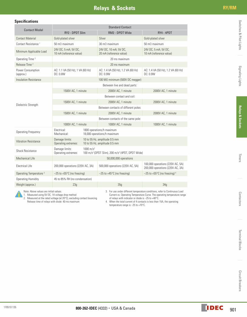
[7] IDEC, “RY/RM Series Miniature Relays” DataSheet: http://us.idec.com/Common/Download.aspx?d=33685 [8] Cui Inc., “VSK-S1 Series”
DataSheet: https://www.cui.com/product/power/ac-dc-power-supplies/board-mount/vsk-s1-series
[9] Qualcomm Inc., “MECHANICAL SMART WINDOW WITH
CONTINUOUSLY TUNABLE TRANSMISSION” Datasheet:
https://patentimages.storage.googleapis.com/60/a3/ff/3a9bca0dd1bd23/WO2013096008A3.pdf
[10] E Ink Holdings Inc., “SMART WINDOW AND SMART WINDOW SYSTEM
USING THE SAME”

UNIVERSIDAD PONTIFICIA DE COMILLAS ESCUELA TÉCNICA SUPERIOR DE INGENIERÍA (ICAI)
52
Datasheet: https://patentimages.storage.googleapis.com/cf/24/8a/3e8bd7ea86ec49/US20120188627A1.pdf
[11] Sustainable Technologies Australia Limited, “ELECTRO PHOTOCHROMIC
SMART WINDOWS AND METHODS” Datasheet: https://patents.google.com/patent/JP4311876B2/en

UNIVERSIDAD PONTIFICIA DE COMILLAS ESCUELA TÉCNICA SUPERIOR DE INGENIERÍA (ICAI)
53
PART 5: DATASHEETS

UNIVERSIDAD PONTIFICIA DE COMILLAS ESCUELA TÉCNICA SUPERIOR DE INGENIERÍA (ICAI)
54
Switches &
Pilot LightsSignaling Lights
Relays & Sockets
Timers
ContactorsTerm
inal BlocksCircuit Breakers
899800-262-IDEC (4332) • USA & Canada
RY/RMRelays & Sockets
1705151135
RY/RM Series Miniature Relays
Key features:• RY2 (3A), RY4 (5A), RM2 (5A)
• General purpose miniature relays
• 3A or 5A contact capacity
• Wide variety of terminal styles and coil voltages meet a wide range of applications
• All 4PDT types have arc barriers.
Part Number SelectionPart Number
Contact Model Plug-in Terminal PC Board Terminal Coil Voltage Code
DPDT (Slim) 3AStandard RY2S-U 0 RY2V-U 0
AC6V, AC12V, AC24V, AC110V, AC120V, AC220V, AC240VDC6V, DC12V, DC24V, DC48V, DC110V
With Indicator RY2S-UL 0 RY2V-UL 0
With Check Button RY2S-UC 0
—With Indicator and Check Button RY2S-ULC 0
Top Bracket Mounting RY2S-UT 0
With Diode (DC coil only) RY2S-UD 0 RY2V-UD 0 DC6V, DC12V, DC24V, DC48V, DC110V
DPDT (Wide) 5A
Standard RM2S-U 0 RM2V-U 0
RYAC6V, AC12V, AC24V, AC110-120V, AC220-240VDC6V, DC12V, DC24V, DC48V, DC100-110V
With Indicator RM2S-UL 0 RM2V-UL 0
With Check Button RM2S-UC 0
—
With Indicator and Check Button RM2S-ULC 0
Top Bracket Mounting RM2S-UT 0
With Diode (DC coil only) RM2S-UD 0DC6V, DC12V, DC24V, DC48V, DC100-110V
With Indicator and Diode (DC coil only) RM2S-ULD 0
4PDT 5A
Standard RY4S-U 0 RY4V-U 0
AC6V, AC12V, AC24V, AC110-120V, AC220-240VDC6V, DC12V, DC24V, DC48V, DC100-110V
With Indicator RY4S-UL 0 RY4V-UL 0
With Check Button RY4S-UC 0
—
With Indicator and Check Button RY4S-ULC 0
Top Bracket Mounting RY4S-UT 0
With Diode (DC coil only) RY4S-UD 0DC6V, DC12V, DC24V, DC48V, DC100-110V
With Indicator and Diode (DC coil only) RY4S-ULD 0
Top mount models are designed to mount directly to a panel and do not require a socket.Ordering Information When ordering, specify the Part No. and coil voltage code:
(example) RY4S-U AC110-120V Part No. Coil Voltage Code
Switc
hes
& P
ilot L
ight
sSi
gnal
ing
Ligh
tsRe
lays
& S
ocke
tsTi
mer
sCo
ntac
tors
Term
inal
Blo
cks
Circ
uit B
reak
ers
RY/RM Relays & Sockets
900 www.IDEC.com 1705151135
Sockets
Relays Standard DIN Rail Mount
Finger-safe DIN Rail Mount Through Panel Mount PCB Mount
RY2S SY2S-05 SY2S-05C SY2S-51 SY2S-61
RM2 SM2S-05 SM2S-05C SM2S-51 SY4S-61SY4S-62RY4S SY4S-05 SY4S-05C SY4S-51
Hold Down Springs & Clips
Appearance Item Relay For DIN Mount Socket
For Through Panel & PCB Mount Socket
Pullover Wire Spring
RY2S SY2S-02F1 SY4S-51F1
RM2SY4S-51F1 SY4S-51F1
RY4S
Leaf Spring 1 (side latch)
RY2SSFA-202 2 SFA-302
RM2, RY4S
Leaf Spring 1 (top latch)
RY2S
SFA-101 2 SFA-301RM2
RY4S
1. Not available for PCB mount socket SY4S-62.2. Order 2 pieces per relay.
AccessoriesItem Appearance Use with Part No. Remarks
Aluminum DIN Rail (1 meter length)
All DIN rail sockets BNDN1000
The BNDN1000 is designed to accommodate DIN mount sockets. Made of durable extruded aluminum, the BNDN1000 measures 0.413 (10.5mm) in height and 1.37 (35mm) in width (DIN standard). Standard length is 39” (1,000mm).
DIN Rail End Stop DIN rail BNL5 9.1 mm wide.
Replacement Hold-Down Spring Anchor
Horseshoe clip for all DIN rail sockets Y778-011 For use on DIN rail mount socket when using pullover wire hold down
spring. 2 pieces included with each socket.
Switches &
Pilot LightsSignaling Lights
Relays & Sockets
Timers
ContactorsTerm
inal BlocksCircuit Breakers
901800-262-IDEC (4332) • USA & Canada
RY/RMRelays & Sockets
1705151135
Specifications
Contact ModelStandard Contact
RY2 - DPDT Slim RM2 - DPDT Wide RY4 - 4PDT
Contact Material Gold-plated silver Silver Gold-plated silver
Contact Resistance 1 50 mΩ maximum 30 mΩ maximum 50 mΩ maximum
Minimum Applicable Load 24V DC, 5 mA; 5V DC, 10 mA (reference value)
24V DC, 10 mA; 5V DC, 20 mA (reference value)
24V DC, 5 mA; 5V DC, 10 mA (reference value)
Operating Time 2 20 ms maximum
Release Time 2 20 ms maximum
Power Consumption (approx.)
AC: 1.1 VA (50 Hz), 1 VA (60 Hz)DC: 0.8W
AC: 1.4 VA (50 Hz), 1.2 VA (60 Hz)DC: 0.9W
AC: 1.4 VA (50 Hz), 1.2 VA (60 Hz)DC: 0.9W
Insulation Resistance 100 MΩ minimum (500V DC megger)
Dielectric Strength
Between live and dead parts:
1500V AC, 1 minute 2000V AC, 1 minute 2000V AC, 1 minute
Between contact and coil:
1500V AC, 1 minute 2000V AC, 1 minute 2000V AC, 1 minute
Between contacts of different poles:
1500V AC, 1 minute 2000V AC, 1 minute 2000V AC, 1 minute
Between contacts of the same pole:
1000V AC, 1 minute 1000V AC, 1 minute 1000V AC, 1 minute
Operating Frequency Electrical: 1800 operations/h maximumMechanical: 18,000 operations/h maximum
Vibration Resistance Damage limits: 10 to 55 Hz, amplitude 0.5 mmOperating extremes: 10 to 55 Hz, amplitude 0.5 mm
Shock Resistance Damage limits: 1000 m/s2
Operating extremes: 100 m/s2 (DPDT Slim), 200 m/s2 (4PDT, DPDT Wide)
Mechanical Life 50,000,000 operations
Electrical Life 200,000 operations (220V AC, 3A) 500,000 operations (220V AC, 5A) 100,000 operations (220V AC, 5A)200,000 operations (220V AC, 3A)
Operating Temperature 3 –25 to +55°C (no freezing) –25 to +45°C (no freezing) –25 to +55°C (no freezing) 4
Operating Humidity 45 to 85% RH (no condensation)
Weight (approx.) 23g 35g 34g
Note: Above values are initial values. 1. Measured using 5V DC, 1A voltage drop method2. Measured at the rated voltage (at 20°C), excluding contact bouncing Release time of relays with diode: 40 ms maximum
3. For use under different temperature conditions, refer to Continuous Load Current vs. Operating Temperature Curve. The operating temperature range of relays with indicator or diode is –25 to +40°C.
4. When the total current of 4 contacts is less than 15A, the operating temperature range is –25 to +70°C.
Switc
hes
& P
ilot L
ight
sSi
gnal
ing
Ligh
tsRe
lays
& S
ocke
tsTi
mer
sCo
ntac
tors
Term
inal
Blo
cks
Circ
uit B
reak
ers
RY/RM Relays & Sockets
902 www.IDEC.com 1705151135
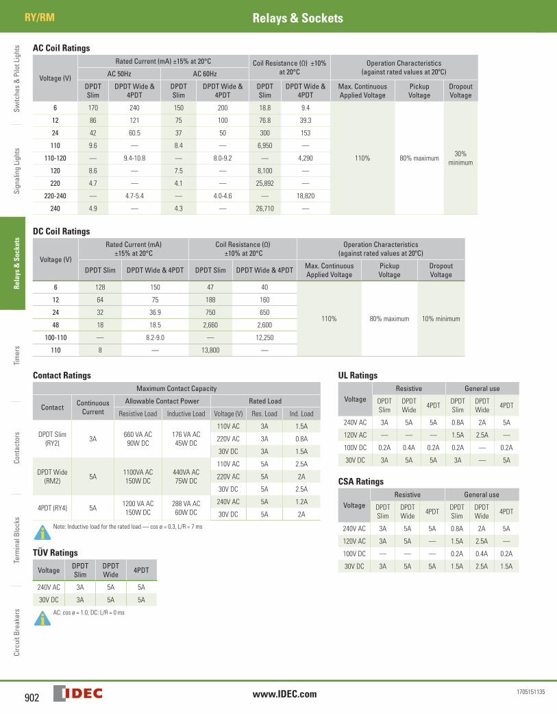
AC Coil Ratings
Voltage (V)
Rated Current (mA) ±15% at 20°C Coil Resistance (Ω) ±10% at 20°C
Operation Characteristics(against rated values at 20ºC)AC 50Hz AC 60Hz
DPDT Slim
DPDT Wide & 4PDT
DPDT Slim
DPDT Wide & 4PDT
DPDT Slim
DPDT Wide & 4PDT
Max. Continuous Applied Voltage
Pickup Voltage
Dropout Voltage
6 170 240 150 200 18.8 9.4
110% 80% maximum 30% minimum
12 86 121 75 100 76.8 39.3
24 42 60.5 37 50 300 153
110 9.6 — 8.4 — 6,950 —
110-120 — 9.4-10.8 — 8.0-9.2 — 4,290
120 8.6 — 7.5 — 8,100 —
220 4.7 — 4.1 — 25,892 —
220-240 — 4.7-5.4 — 4.0-4.6 — 18,820
240 4.9 — 4.3 — 26,710 —
DC Coil Ratings
Voltage (V)
Rated Current (mA) ±15% at 20°C
Coil Resistance (Ω) ±10% at 20°C
Operation Characteristics(against rated values at 20ºC)
DPDT Slim DPDT Wide & 4PDT DPDT Slim DPDT Wide & 4PDT Max. Continuous Applied Voltage
Pickup Voltage
Dropout Voltage
6 128 150 47 40
110% 80% maximum 10% minimum
12 64 75 188 160
24 32 36.9 750 650
48 18 18.5 2,660 2,600
100-110 — 8.2-9.0 — 12,250
110 8 — 13,800 —
Contact Ratings UL Ratings Maximum Contact Capacity
VoltageResistive General use
DPDT Slim
DPDT Wide 4PDT DPDT
SlimDPDT Wide 4PDT
240V AC 3A 5A 5A 0.8A 2A 5A
120V AC — — — 1.5A 2.5A —
100V DC 0.2A 0.4A 0.2A 0.2A — 0.2A
30V DC 3A 5A 5A 3A — 5A
CSA Ratings
VoltageResistive General use
DPDT Slim
DPDT Wide 4PDT DPDT
SlimDPDT Wide 4PDT
240V AC 3A 5A 5A 0.8A 2A 5A
120V AC 3A 5A — 1.5A 2.5A —
100V DC — — — 0.2A 0.4A 0.2A
30V DC 3A 5A 5A 1.5A 2.5A 1.5A
Contact Continuous Current
Allowable Contact Power Rated Load
Resistive Load Inductive Load Voltage (V) Res. Load Ind. Load
DPDT Slim(RY2) 3A 660 VA AC
90W DC176 VA AC45W DC
110V AC 3A 1.5A
220V AC 3A 0.8A
30V DC 3A 1.5A
DPDT Wide (RM2) 5A 1100VA AC
150W DC440VA AC75W DC
110V AC 5A 2.5A
220V AC 5A 2A
30V DC 5A 2.5A
4PDT (RY4) 5A 1200 VA AC150W DC
288 VA AC60W DC
240V AC 5A 1.2A
30V DC 5A 2A
Note: Inductive load for the rated load — cos ø = 0.3, L/R = 7 ms
TÜV Ratings
Voltage DPDT Slim
DPDT Wide 4PDT
240V AC 3A 5A 5A
30V DC 3A 5A 5A
AC: cos ø = 1.0, DC: L/R = 0 ms

Switches &
Pilot LightsSignaling Lights
Relays & Sockets
Timers
ContactorsTerm
inal BlocksCircuit Breakers
903800-262-IDEC (4332) • USA & Canada
RY/RMRelays & Sockets
1705151135
Socket SpecificationsSockets Terminal Electrical Rating Wire Size Torque
DIN Rail Mount Sockets
SY2S-05 M3 screws with captive wire clamp 300V, 7A Maximum up to 2–#14AWG 5.5 - 9 in•lbs
SM2S-05 M3 screw with captive wire clamp 300V, 10A Maximum up to 2–#14AWG 5.5 - 9 in•lbs
SY4S-05 M3 screw with captive wire clamp 300V, 7A* Maximum up to 2–#14AWG 5.5 - 9 in•lbs
Finger-safe DIN Rail Mount
SY2S-05C M3 screws with captive wire clamp, fingersafe 300V, 7A Maximum up to 2–#14AWG 5.5 - 9 in•lbs
SM2S-05C M3 screw with captive wire clamp, fingersafe 300V, 10A Maximum up to 2–#14AWG 5.5 - 9 in•lbs
SY4S-05C M3 screw with captive wire clamp, fingersafe 300V, 7A* Maximum up to 2–#14AWG 5.5 - 9 in•lbs
Through Panel Mount Socket
SY2S-51 Solder 250V, 7A — —
SM2S-51 Solder 250V, 10A — —
SY4S-51 Solder 250V, 7A* — —
PCB Mount Socket
SY2S-61 PCB Mount 300V, 7A — —
SY4S-61 PCB Mount 300V, 7A — —
SY4S-62 PCB Mount 250V, 7A — —
* When using only 2 poles of the 4-poles, the UL recognized current is 10A.
Switc
hes
& P
ilot L
ight
sSi
gnal
ing
Ligh
tsRe
lays
& S
ocke
tsTi
mer
sCo
ntac
tors
Term
inal
Blo
cks
Circ
uit B
reak
ers
RY/RM Relays & Sockets
904 www.IDEC.com 1705151135
Characteristics (Reference Data)
Electrical Life CurvesAC Load
(RY2)
0 1
50
100
200
500
1000
20
102 3
Load Current (A)
110V AC resistive
220V AC inductive110V AC inductive
220V AC resistive
Life
(¥ 1
0,00
0 op
erat
ions
)
(RY4)
500
50
20
100
200
1000
1010 3 52 4
Load Current (A)
Life
( ¥
10,0
00 o
pera
tions
)
240V AC resistive
240V AC inductive
(RM2)
10 3 52 4
50
100
500
1000
10
Load Current (A)
Life
( ¥
10,0
00 o
pera
tions
)
110V AC resistive
220V AC resistive
110V AC inductive
220V AC inductive
DC Load `(RY2)
0 5
50
100
200
500
1000
20
102 3
100V DC inductive100V DC resistive
30V DC inductive
Life
(¥ 1
0,00
0 op
erat
ions
)
Load Current (A)
30V DC resistive (RY4)
30V DC resistive
30V DC inductive
500
50
20
100
200
1000
1010 3 52 4
Life
(¥ 1
0,00
0 op
erat
ions
)
Load Current (A)
(RM2)
10 3 52 4
50
100
500
1000
10
Life
(¥ 1
0,00
0 op
erat
ions
)
Load Current (A)
30V DC resistive
100V DC resistive
30V DC inductive
100V DC inductive
Switches &
Pilot LightsSignaling Lights
Relays & Sockets
Timers
ContactorsTerm
inal BlocksCircuit Breakers
905800-262-IDEC (4332) • USA & Canada
RY/RMRelays & Sockets
1705151135
Maximum Switching Capacity
(RY2)
1 5
0.5
1
5
3
10 100 200 30050
Load Voltage (V)
DC inductive DC resistive
Load
Cur
rent
(A)
AC resistive
AC inductive
0.1
(RY4)
1
0.5
0.3
0.2
1
5
3
2
10 100 200 300503020
Load Voltage (V)
DC inductiveLoad
Cur
rent
(A)
AC resistive
AC inductive
DC resistive
(RM2)
1 5
0.5
0.1
1
5
10 100 200 30050
Load Voltage (V)
Load
Cur
rent
(A)
DC inductive
ACinductive
AC resistive
DC resistive
Continuous Load Current vs. Operating Temperature Curve (Standard Type, With Check Button, and Top Bracket Mounting Type)
(RY2)
10
10
20
30
40
50
60
70
80
90
100
32
DC Coil
AC Coil
Load Current (A)
Oper
atin
g Te
mpe
ratu
re (C
)
(RY4)
0
10
20
30
40
50
60
70
80
90
100
Load Current (A)
DC Coil
1 32
AC Coil
Oper
atin
g Te
mpe
ratu
re (C
)
(RM2)
10
10
20
30
40
50
60
70
80
90
100
3 52 4Load Current (A)
Oper
atin
g Te
mpe
ratu
re (C
)
DC Coil
AC Coil

Switc
hes
& P
ilot L
ight
sSi
gnal
ing
Ligh
tsRe
lays
& S
ocke
tsTi
mer
sCo
ntac
tors
Term
inal
Blo
cks
Circ
uit B
reak
ers
RY/RM Relays & Sockets
906 www.IDEC.com 1705151135
Internal Connection (View from Bottom)Standard Type
DPDT Slim (RY2) DPDT Wide (RM2) 4PDT (RY4) With Check Button
FrontPushbutton
Contacts can be operated by pressing the check button.
With Indicator (-L type)DPDT Slim (RY2) DPDT Wide (RM2) 4PDT (RY4)
Coil Below 100V AC/DC
Coil Below 24V AC/DC
When the relay is energized, the indicator goes on. • An LED protection diode
is not contained in DPDT relays for coils below 100V DC.
• If coil polarity is reversed LED will not light.
Coil 100V AC/DC and over
Coil 24V AC/DC and over
With Diode (-D type)DPDT Slim (RY2) DPDT Wide (RM2) 4PDT (RY4)
Contains a diode to absorb the back emf generated when the coil is de-energized. The release time is slightly longer.• Diode Characteristics
Reverse withstand voltage: 1,000V Forward current: 1A
With Indicator and Diode (-LD type)
DPDT Wide (RM2) 4PDT (RY4) DPDT Wide (RM2) 4PDT (RY4)
Coil Below 24V DC
Coil 24V DC and over
1
5
9
4
8
12
(+)1413(–)
1
5
13(–) (+)14
9
2
6
10
3
7
11
4
8
12Contains an LED indicator and a surge absorber.
Switches &
Pilot LightsSignaling Lights
Relays & Sockets
Timers
ContactorsTerm
inal BlocksCircuit Breakers
907800-262-IDEC (4332) • USA & Canada
RY/RMRelays & Sockets
1705151135
Dimensions (mm)
RY2S RY4S RM2S
SY2S-05: 61.5 (63.5) max., SY2S-51: 39.6 (41.6) max.
13
9
5
1
8
14
12
4
35.6 max. 5.4 14
27.5
2.6
0.5
Total length from panel surface including relay socket
Dimensions in the ( )include a hold-down spring.3 × ø1.2 oblong hole
4
8
12
14
11
7
3
10
6
13
5
9
1 2
35.6 max. 6.4 21
27.5
0.5
2.6
Total length from the panel surface including relay socketSY4S-05: 61.5 (63.5) max., SY4S-51: 39.6 (41.6) max.
2.2 × ø1.2 oblong hole Dimensions in the ( )include a hold-down spring.
4
8
12
1413
5
9
1
2.6
0.5
35.6 max. 6.4 21
27.5
Total length from the panel surface including relay socket.SM2S-05: 61.5 (63.5) max., SM2S-51: 39.6 (41.6) max.
Dimensions in the ( )include a hold-down spring.
2.2 × ø1.2 hole
RY2V RY4V RM2V
13
9
5
1
8
14
12
4
35.6 max. 4 14 4.4
12.7
4.1
6.4
7.15
27.5
0.5
0.8 2.60.5
8-ø1 holes
4
8
12
14
11
7
3
10
6
13
5
9
1 2
35.6 max. 4 21 4.44.4
4.4
6.6
12.7
4.1
6.4
7.15
27.5
0.5
2.6
0.8
0.5
14-ø1 holes
9
1
13
5
4
8
12
14
35.6 max. 4 21 13.2
27.5
7.15 6.
4
12.7
4.1
0.5
0.8
2.60.5
8-ø1 hole
RY2S-UT RY4S-UT RM2S-UT
13
9
5
1
8
14
12
4
14.5
3.5
35.6 max. 5.4
2
3843.2
27.5
6.4
6.3
4.1
0.5
2.6 4.43 ¥ ø1.2 oblong hole
12
14
1110
13
9
4
87
3
65
1 2
21.5
3.5
35.6 max. 6.4
2
3843.2
27.5
6.4
6.3
4.1
0.5
4.4
4.4
4.42.
6
2.2 ¥ ø1.2 oblong hole
4
8
12
1413
5
9
1
21.5
3.5
35.6 max. 6.4
2
27.53843.2
0.5
6.4
6.3
4.1
2.6
13.2
2.2 ¥ ø1.2 hole

Switc
hes
& P
ilot L
ight
sSi
gnal
ing
Ligh
tsRe
lays
& S
ocke
tsTi
mer
sCo
ntac
tors
Term
inal
Blo
cks
Circ
uit B
reak
ers
RY/RM Relays & Sockets
908 www.IDEC.com 1705151135
Dimensions
Standard DIN Rail Mount Sockets SY2S-05 SM2S-05
617
4.2
622 20
16
M3 TerminalScrew
25
4518
14.5
DIN Rail(BNDN)
31.5
84
51
1214
913
Terminal Arrangement
16
2-ø4.2 Mounting Holes(or M4 Tapped Holes)
5.9 max.
4 max. 4.8 min.
ø3.2 min.
(Top View)
630
26
4.2
623
0.7
M3 TerminalScrew
18.5
25
45
18
31.5
DIN Rail(BNDN)
14
139
1412
58
Terminal Arrangement
26
2-ø4.2 Mounting Holes(or M4 Tapped Holes)
5.9 max.
4 max. 4.8 min.
ø3.2 min.
(Top View)
SY4S-05
630
26
4.2
623
0.7
M3 TerminalScrew
18.5
25
45
18
31.5DIN Rail(BNDN)
1
139
1412 11 10
56784 3 2
Terminal Arrangement
26
2-ø4.2 Mounting Holes(or M4 Tapped Holes)
5.9 max.
4 max. 4.8 min.
ø3.2 min.
(Top View)
Finger-safe DIN Rail Mount Sockets SY2S-05C SM2S-05C
ø5
25
46
2918.2
4.2
1.6
64
617.2
1620 2
M3 TerminalScrew
84
51
1214
913
Terminal Arrangement35.5
16
2-ø4.2 Mounting Holes(or M4 Tapped Holes)
DIN Rail(BNDN)
Ring terminals cannot be used.
(Top View)
ø5.5
25
18
2
306
64
26
46
1.6
4.2
29
18.2
M3 TerminalScrew
14
139
1412
58
Terminal Arrangement
35.5
26
2-ø4.2 Mounting Holes(or M4 Tapped Holes)
DIN Rail(BNDN)
Ring terminals cannot be used. (Top View)
SY4S-05C
ø5.5 18
25
2
306
64
26
46
1.6
4.2
29
18.2
26
M3 TerminalScrew
1
13
9
14
12 11 10
5678
4 3 2
Terminal Arrangement
35.5
2-ø4.2 Mounting Holes(or M4 Tapped Holes)
DIN Rail(BNDN)
(Top View)Ring terminals cannot be used.
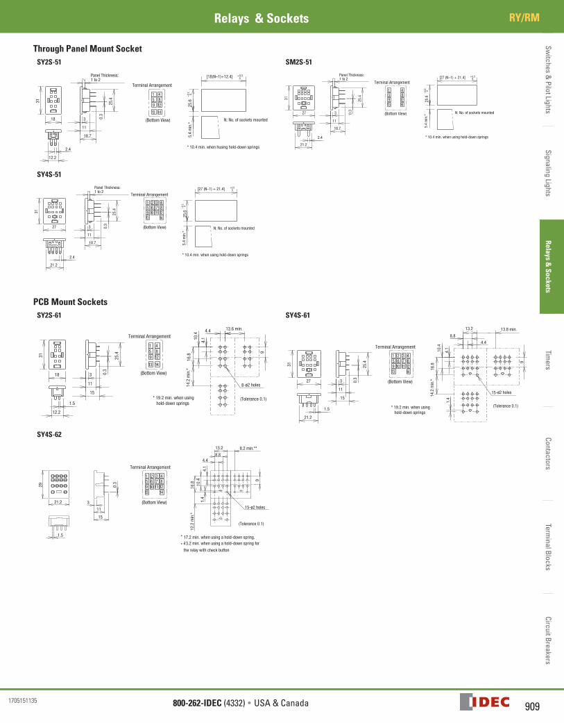
Switches &
Pilot LightsSignaling Lights
Relays & Sockets
Timers
ContactorsTerm
inal BlocksCircuit Breakers
909800-262-IDEC (4332) • USA & Canada
RY/RMRelays & Sockets
1705151135
Through Panel Mount Socket SY2S-51 SM2S-51
3
11
18.7
18
31
2.4
12.2
25.4
Panel Thickness:1 to 2
13
159
14
4812
Terminal Arrangement
* 10.4 min. when husing hold-down springs
+0.
20
+0.50[18(N–1)+12.4]
5.4
min
.*25
.6
N: No. of sockets mounted0.3
(Bottom View)
3
11
18.7
27
31
0.3
25.4
2.4
21.2
13 14
159 12
84
Terminal Arrangement
25.6
0+0.5
+0.
20
* 10.4 min. when using hold-down springs
[27 (N–1) + 21.4]
5.4
min
.*
N: No. of sockets mounted
Panel Thickness:1 to 2
(Bottom View)
SY4S-51
27
31
2.4
21.2
3
11
18.7
25.4
Panel Thickness:1 to 2
107
13 14
159
3
1284
62
11
Terminal Arrangement
25.6
0+0.5
+0.
20
* 10.4 min. when using hold-down springs
[27 (N–1) + 21.4]5.
4 m
in.*
N: No. of sockets mounted0.3
(Bottom View)
PCB Mount Sockets SY2S-61 SY4S-61
3
11
15
18
31
12.2
25.4
1.5
4.4 13.6 min.
9
8-ø2 holes
(Tolerance 0.1)* 19.2 min. when using hold-down springs
14.2
min
.*16
.8
4.110
.4
13
159
14
4812
Terminal Arrangement
0.3
(Bottom View)
27
31
21.2
3
11
15
0.3
25.4
1.5
107
13 14
159
3
1284
62
11
Terminal Arrangement
* 19.2 min. when using hold-down springs
(Bottom View)
4.4
13.8 min.
9
15-ø2 holes
(Tolerance 0.1)
14.2
min
.*
16.8
4.110
.4
8.8
13.2
1.4
SY4S-62
1.5
3
11
15
21.2
29 0.3
4.1
10.4
16.8
1.4
12.2
min
.*
(Tolerance 0.1)
13.2 8.2 min.**
4.48.8
15-ø2 holes
9
107
13 14
159
3
1284
62
11
Terminal Arrangement
13.2 min. when using a hold-down spring for
the relay with check button
17.2 min. when using a hold-down spring.*
* *
(Bottom View)
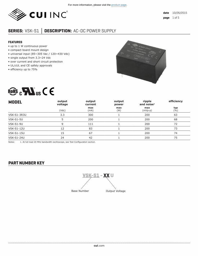
cui.com
date 10/26/2015
page 1 of 5
SERIES: VSK-S1 DESCRIPTION: AC-DC POWER SUPPLY
MODEL output voltage
output current
output power
rippleand noise1
efficiency
(Vdc)max(mA)
max(W)
max(mVp-p)
typ(%)
VSK-S1-3R3U 3.3 300 1 200 63
VSK-S1-5U 5 200 1 200 68
VSK-S1-9U 9 111 1 200 72
VSK-S1-12U 12 83 1 200 73
VSK-S1-15U 15 67 1 200 74
VSK-S1-24U 24 42 1 200 75Notes: 1.Atfullload20MHzbandwidthoscilloscope,seeTestConfigurationsection.
PART NUMBER KEY
VSK-S1 - XX U
BaseNumber OutputVoltage
FEATURES•upto1Wcontinuouspower•compactboardmountdesign•universalinput(85~305Vac/120~430Vdc)•singleoutputfrom3.3~24Vdc•overcurrentandshortcircuitprotection•UL/cULandCEsafetyapprovals•efficiencyupto75%
For more information, please visit the product page.
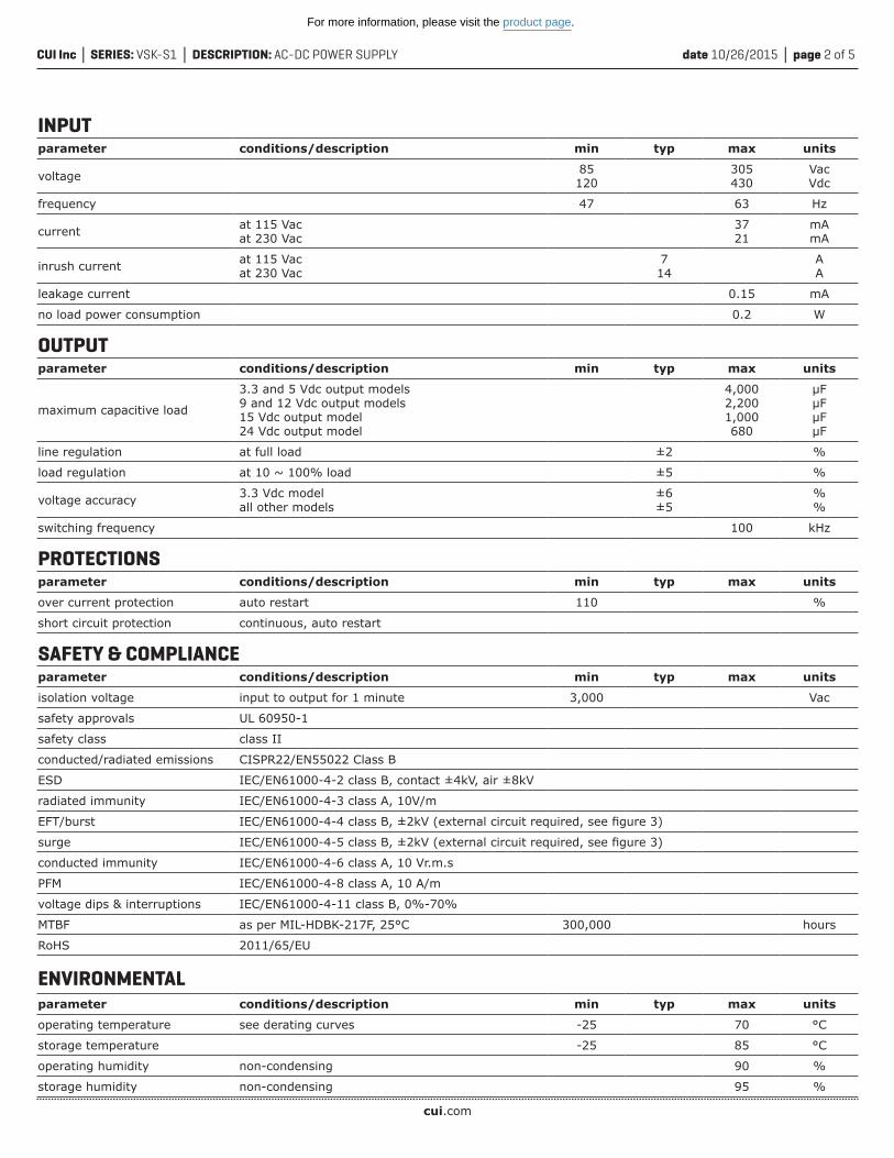
cui.com
date 10/26/2015 page 2 of 5CUI Inc SERIES: VSK-S1 DESCRIPTION: AC-DC POWER SUPPLY
INPUTparameter conditions/description min typ max units
voltage 85120
305430
VacVdc
frequency 47 63 Hz
current at 115 Vacat 230 Vac
3721
mAmA
inrushcurrent at 115 Vacat 230 Vac
714
AA
leakagecurrent 0.15 mA
noloadpowerconsumption 0.2 W
OUTPUTparameter conditions/description min typ max units
maximum capacitive load
3.3 and 5 Vdc output models9 and 12 Vdc output models15 Vdc output model24 Vdc output model
4,0002,2001,000680
μFμFμFμF
lineregulation at full load ±2 %
loadregulation at10~100%load ±5 %
voltageaccuracy 3.3 Vdc modelallothermodels
±6±5
%%
switchingfrequency 100 kHz
PROTECTIONSparameter conditions/description min typ max units
overcurrentprotection autorestart 110 %
shortcircuitprotection continuous,autorestart
SAFETY & COMPLIANCEparameter conditions/description min typ max units
isolationvoltage inputtooutputfor1minute 3,000 Vac
safetyapprovals UL 60950-1
safetyclass class II
conducted/radiatedemissions CISPR22/EN55022ClassB
ESD IEC/EN61000-4-2classB,contact±4kV,air±8kV
radiatedimmunity IEC/EN61000-4-3classA,10V/m
EFT/burst IEC/EN61000-4-4classB,±2kV(externalcircuitrequired,seefigure3)
surge IEC/EN61000-4-5classB,±2kV(externalcircuitrequired,seefigure3)
conductedimmunity IEC/EN61000-4-6classA,10Vr.m.s
PFM IEC/EN61000-4-8classA,10A/m
voltagedips&interruptions IEC/EN61000-4-11classB,0%-70%
MTBF asperMIL-HDBK-217F,25°C 300,000 hours
RoHS 2011/65/EU
ENVIRONMENTALparameter conditions/description min typ max units
operatingtemperature seederatingcurves -25 70 °C
storagetemperature -25 85 °C
operatinghumidity non-condensing 90 %
storagehumidity non-condensing 95 %
For more information, please visit the product page.
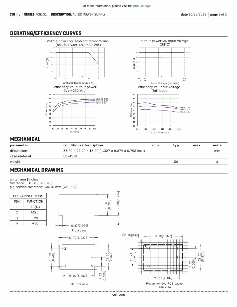
cui.com
date 10/26/2015 page 3 of 5CUI Inc SERIES: VSK-S1 DESCRIPTION: AC-DC POWER SUPPLY
DERATING/EFFICIENCY CURVES
Front view
Bottom view
2
1 3
4
∅1.10[0.43]
1
2
4
3
Recommended PCB LayoutTop View
MECHANICAL DRAWING
MECHANICALparameter conditions/description min typ max units
dimensions 33.70 x 22.20 x 18.00 (1.327 x 0.874 x 0.708 inch) mm
casematerial UL94V-0
weight 20 g
units: mm [inches]tolerance:±0.50[±0.020]pinsectiontolerance:±0.10mm[±0.004]
PINCONNECTIONS
PIN FUNCTION
1 AC(N)
2 AC(L)
3 -Vo
4 +Vo
~ ~~ ~100
80
60
40
20
Ambient Temperature (°C)
Load
(%
)
50
-25 -10 55 70
Input Voltage (Vac/Vdc)
~ ~~ ~
100
80
60
40
20
85120
100140
305430
Load
(%
)
50
55
60
65
70
75
80
85
90
85 120 220 240 264 305
10
20
30
40
50
60
70
80
90
10 20 30 40 50 60 70 80 90 100
VSK-S1-5UVSK-S1-12UVSK-S1-24U
VSK-S1-5UVSK-S1-12UVSK-S1-24U
Load (%)
Effic
ienc
y (%
)
Input Voltage (Vac)Ef
ficie
ncy
(%)
outputpowervs.ambienttemperature(85~305Vac;120~430Vdc)
efficiencyvs.outputpower(Vin=230 Vac)
efficiencyvs.inputvoltage(full load)
outputpowervs.inputvoltage(25°C)
For more information, please visit the product page.
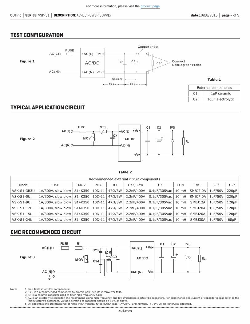
cui.com
date 10/26/2015 page 4 of 5CUI Inc SERIES: VSK-S1 DESCRIPTION: AC-DC POWER SUPPLY
TYPICAL APPLICATION CIRCUIT
TEST CONFIGURATION
EMC RECOMMENDED CIRCUIT
LCM
C2
C X
C
M OV
AC (L)
AC (N)
R1AC (L)
AC (N)
+Vo
-Vo
+
C1
RL
TVSFUSE
AC / DC
Y3
CY4
Figure 2
Figure 3
Figure 1
Table 2
Table 1
Externalcomponents
C1 1μFceramic
C2 10μFelectrolytic
Notes: 1.SeeTable2forEMCcomponents. 2.TVSisarecommendedcomponenttoprotectpost-circuitsifconverterfails. 3.C1isaceramiccapacitorusedtofilterhighfrequencynoise. 4.C2isanelectrolyticcapacitor.Werecommendusinghighfrequencyandlowimpedenceelectrolyticcapacitors.Forcapacitanceandcurrentofcapacitorpleaserefertothe manufacture’sdatasheet.Voltagederatingofcapacitorshouldbe80%orabove. 5.Allspecificationsaremeasuredatratedinputvoltage,ratedoutputload,TA=25°C,andhumidity<75%unlessotherwisespecified.
C2
M OV
AC (L)
AC (N)
NTCAC (L)
AC (N)
+Vo
-Vo
+
C1
RL
TVSFUSE
AC / DCCX
AC/DC
+Vo
-Vo
FUSEAC(L)
AC(N)
25. 4m m 25. 4m m
C 1 C 2
12. 7m m
Copper sheet
ConnectOscillograph ProbeLoad
AC(L)
AC(N)
Recommendedexternalcircuitcomponents
Model FUSE MOV NTC R1 CY3, CY4 CX LCM TVS1 C12 C23
VSK-S1-3R3U 1A/300V,slowblow S14K350 10D-11 47Ω/3W 2.2nF/400V 0.4μF/305Vac 10 mH SMBJ7.0A 1μF/50V 220μF
VSK-S1-5U 1A/300V,slowblow S14K350 10D-11 47Ω/3W 2.2nF/400V 0.1μF/305Vac 10 mH SMBJ7.0A 1μF/50V 220μF
VSK-S1-9U 1A/300V,slowblow S14K350 10D-11 47Ω/3W 2.2nF/400V 0.1μF/305Vac 10 mH SMBJ12A 1μF/50V 120μF
VSK-S1-12U 1A/300V,slowblow S14K350 10D-11 47Ω/3W 2.2nF/400V 0.1μF/305Vac 10 mH SMBJ20A 1μF/50V 120μF
VSK-S1-15U 1A/300V,slowblow S14K350 10D-11 47Ω/3W 2.2nF/400V 0.1μF/305Vac 10 mH SMBJ20A 1μF/50V 120μF
VSK-S1-24U 1A/300V,slowblow S14K350 10D-11 47Ω/3W 2.2nF/400V 0.1μF/305Vac 10 mH SMBJ30A 1μF/50V 68μF
For more information, please visit the product page.
date 10/26/2015 page 5 of 5CUI Inc SERIES: VSK-S1 DESCRIPTION: AC-DC POWER SUPPLY
CUIoffersatwo(2)yearlimitedwarranty.Completewarrantyinformationislistedonourwebsite.
CUIreservestherighttomakechangestotheproductatanytimewithoutnotice.InformationprovidedbyCUIisbelievedtobeaccurateandreliable.However,noresponsibilityisassumedbyCUIforitsuse,norforanyinfringementsofpatentsorotherrightsofthirdpartieswhichmayresultfromitsuse.
CUIproductsarenotauthorizedorwarrantedforuseascriticalcomponentsinequipmentthatrequiresanextremelyhighlevelofreliability.Acriticalcomponentisanycomponentofalifesupportdeviceorsystemwhosefailuretoperformcanbereasonablyexpectedtocausethefailureofthelifesupportdeviceorsystem,ortoaffectitssafetyoreffectiveness.
Headquarters20050 SW 112th Ave.Tualatin, OR 97062800.275.4899
rev. description date
1.0 initialrelease 06/04/20121.01 pictureupdated 09/06/20121.02 updatedderatingcurvesandspec 11/12/20131.03 internalinductor&PCBstructurechanged 10/26/2015
Therevisionhistoryprovidedisforinformationalpurposesonlyandisbelievedtobeaccurate.
REVISION HISTORY
For more information, please visit the product page.
Actual Size
(4,15 mm x 4,15 mm)www.ti.com
FEATURES DESCRIPTION
APPLICATIONS
SW
C110 µF
L1
6.8 µH
R1
R2
VBAT
VOUT
FB
C22.2 µF
C3100 µF
LBO
PGND
LBI
SYNC
EN
GND
TPS6109x
e.g. 5 V up to500 mA
Low BatteryOutput
R3
R4 R5
1.8 V to 5 VInput
TPS61090TPS61091, TPS61092
SLVS484A–JUNE 2003–REVISED APRIL 2004
SYNCHRONOUS BOOST CONVERTERWITH 2A SWITCH
• Synchronous (96% Efficient) Boost Converter The TPS6109x devices provide a power supplyWith 500-mA Output Current From 1.8-V Input solution for products powered by either a one-cell
Li-Ion or Li-polymer, or a two-cell alkaline, NiCd or• Available in a 16-Pin QFN 4 x 4 PackageNiMH battery and required supply currents up to or• Device Quiescent Current: 20-µA (Typ)higher than 1 A. The converter generates a stable
• Input Voltage Range: 1.8-V to 5.5-V output voltage that is either adjusted by an externalresistor divider or fixed internally on the chip. It• Adjustable Output Voltage Up to 5.5-V Fixedprovides high efficient power conversion and isOutput Voltage Optionscapable of delivering output currents up to 0.5 A at 5• Power Save Mode for Improved Efficiency at V at a supply voltage down to 1.8 V. The im-
Low Output Power plemented boost converter is based on a fixed• Low Battery Comparator frequency, pulse-width- modulation (PWM) controller
using a synchronous rectifier to obtain maximum• Low EMI-Converter (Integrated Antiringingefficiency. Boost switch and rectifier switch are con-Switch)nected internally to provide the lowest leakage induct-
• Load Disconnect During Shutdown ance and best EMI behavior possible. The maximum• Over-Temperature Protection peak current in the boost switch is limited to a value
of 2500 mA.
The converter can be disabled to minimize battery• All Single Cell Li or Dual Cell Battery, or USB drain. During shutdown, the load is completely dis-
Powered Operated Products as MP-3 Player, connected from the battery. A low-EMI mode isPDAs, and Other Portable Equipment implemented to reduce ringing and, in effect, lower
radiated electromagnetic energy when the converterenters the discontinuous conduction mode.
The output voltage can be programmed by an exter-nal resistor divider or is fixed internally on the chip.
The device is packaged in a 16-pin QFN 4 x 4 mm(16 RSA) package.
Please be aware that an important notice concerning availability, standard warranty, and use in critical applications of TexasInstruments semiconductor products and disclaimers thereto appears at the end of this data sheet.
PRODUCTION DATA information is current as of publication date. Copyright © 2003–2004, Texas Instruments IncorporatedProducts conform to specifications per the terms of the TexasInstruments standard warranty. Production processing does notnecessarily include testing of all parameters.
www.ti.com
ABSOLUTE MAXIMUM RATINGS
RECOMMENDED OPERATING CONDITIONS
ELECTRICAL CHARACTERISTICS
TPS61090TPS61091, TPS61092
SLVS484A–JUNE 2003–REVISED APRIL 2004
These devices have limited built-in ESD protection. The leads should be shorted together or the device placed in conductive foamduring storage or handling to prevent electrostatic damage to the MOS gates.
AVAILABLE OUTPUT VOLTAGE OPTIONS (1)
OUTPUT VOLTAGETA PACKAGE Part Number (2)
DC/DC
Adjustable 16-Pin QFN 4x4mm TPS61090RSA
40°C to 85°C 3.3 V 16-Pin QFN 4x4mm TPS61091RSA
5 V 16-Pin QFN 4x4mm TPS61092RSA
(1) Contact the factory to check availability of other fixed output voltage versions.(2) The RSA package is available taped and reeled. Add R suffix to device type (e.g., TPS61090RSAR) to order quantities of 3000 devices
per reel.
over operating free-air temperature range (unless otherwise noted) (1)
TPS6109x
Input voltage range on LBI -0.3 V to 3.6 V
Input voltage range on SW, VOUT, LBO, VBAT, SYNC, EN, FB -0.3 V to 7 V
Operating free air temperature range TA -40°C to 85°C
Maximum junction temperature TJ 150°C
Storage temperature range Tstg -65°C to 150°C
(1) Stresses beyond those listed under "absolute maximum ratings" may cause permanent damage to the device. These are stress ratingsonly, and functional operation of the device at these or any other conditions beyond those indicated under "recommended operatingconditions" is not implied. Exposure to absolute-maximum-rated conditions for extended periods may affect device reliability.
MIN NOM MAX UNIT
Supply voltage at VBAT, VI 1.8 5.5 V
Inductance, L 2.2 6.8 µH
Input, capacitance, Ci 10 µF
Output capacitance, Co 22 100 µF
Operating free air temperature, TA -40 85 °C
Operating virtual junction temperature, TJ -40 125 °C
over recommended free-air temperature range and over recommended input voltage range (typical values are at an ambienttemperature range of 25°C) (unless otherwise noted)
DC/DC STAGE
PARAMETER TEST CONDITIONS MIN TYP MAX UNIT
VI Input voltage range 1.8 5.5 V
VO TPS61090 output voltage range 1.8 5.5 V
VFB TPS61090 feedback voltage 490 500 510 mV
f Oscillator frequency 500 600 700 kHz
Frequency range for synchronization 500 700 kHz
ISW Switch current limit VOUT= 5 V 2000 2200 2500 mA
Start-up current limit 0.4 x ISW mA
Boost switch on resistance VOUT= 5 V 55 mΩ
Rectifying switch on resistance VOUT= 5 V 55 mΩ
Total accuracy -3% 3%
Line regulation 0.6%
2
www.ti.com
PIN ASSIGNMENTS
RSA Package(Top View)
LBOVOUT
VO
UT
EN
SYNC
LBI
NC
SW
SW
VO
UT
FB
GN
D
PG
ND
VB
AT
PG
ND
PG
ND
TPS61090TPS61091, TPS61092
SLVS484A–JUNE 2003–REVISED APRIL 2004
Electrical Characteristics (continued)
over recommended free-air temperature range and over recommended input voltage range (typical values are at an ambienttemperature range of 25°C) (unless otherwise noted)
DC/DC STAGE
PARAMETER TEST CONDITIONS MIN TYP MAX UNIT
Load regulation 0.6%
into IO = 0 mA, VEN = VBAT = 1.8 V, VOUT =5 V 10 25 µAVBATQuiescent current
into IO = 0 mA, VEN = VBAT = 1.8 V, VOUT = 5 V 10 20 µAVOUT
Shutdown current VEN= 0 V, VBAT = 2.4 V 0.1 1 µA
CONTROL STAGE
PARAMETER TEST CONDITIONS MIN TYP MAX UNIT
VUVLO Under voltage lockout threshold VLBI voltage decreasing 1.5 V
VIL LBI voltage threshold VLBI voltage decreasing 490 500 510 mV
LBI input hysteresis 10 mV
LBI input current EN = VBAT or GND 0.01 0.1 µA
LBO output low voltage VO = 3.3 V, IOI = 100 µA 0.04 0.4 V
LBO output low current 100 µA
LBO output leakage current VLBO = 7 V 0.01 0.1 µA
VIL EN, SYNC input low voltage 0.2 × VBAT V
VIH EN, SYNC input high voltage 0.8 × VBAT V
EN, SYNC input current Clamped on GND or VBAT 0.01 0.1 µA
Overtemperature protection 140 °C
Overtemperature hysteresis 20 °C
Terminal Functions
TERMINALI/O DESCRIPTION
NAME NO.
EN 11 I Enable input. (1/VBAT enabled, 0/GND disabled)
FB 14 I Voltage feedback of adjustable versions
3
www.ti.com
FUNCTIONAL BLOCK DIAGRAM
Anti-Ringing
GateControl
PGND
Regulator
PGND
Control Logic
Oscillator
TemperatureControl
VOUT
PGND
FB
SW
VBAT
EN
SYNC
GND
LBILBO
_
+
100 k
10 pF
_+VREF = 0.5 V
GND
Error Amplifier
_+
_+
GND
VREF = 0.5 V
Low Battery Comparator
TPS61090TPS61091, TPS61092
SLVS484A–JUNE 2003–REVISED APRIL 2004
Pin Assignments (continued)
Terminal Functions (continued)
TERMINALI/O DESCRIPTION
NAME NO.
GND 13 I/O Control/logic ground
LBI 9 I Low battery comparator input (comparator enabled with EN)
LBO 12 O Low battery comparator output (open drain)
NC 2 Not connected
SYNC 10 I Enable/disable power save mode (1: VBAT disabled, 0: GND enabled, clock signal forsynchronization)
SW 3, 4 I Boost and rectifying switch input
PGND 5, 6, 7 I/O Power ground
VBAT 8 I Supply voltage
VOUT 1, 15, 16 O DC/DC output
PowerPAD™ Must be soldered to achieve appropriate power dissipation. Should be connected to PGND.
4
www.ti.com
PARAMETER MEASUREMENT INFORMATION
SW
C110 µF
PowerSupply
L1
6.8 µH
R1
R2
VBAT
VOUT
FB
C22.2 µF
C3100 µF
LBO
PGND
LBI
SYNC
EN
GND
TPS6109xList of Components:U1 = TPS6109xRSAL1 = Sumida CDRH103R-6R8C1, C2 = X7R/X5R CeramicC3 = Low ESR Tantalum
VOUTBoost Output
Low BatteryOutput
R3
R4 R5
TPS61090TPS61091, TPS61092
SLVS484A–JUNE 2003–REVISED APRIL 2004
5
www.ti.com
TYPICAL CHARACTERISTICS
0
0.5
1
1.5
2
2.5
1.8 2.2 2.6 3 3.4 3.8 4.2 4.6 5
VI - Input Voltage - V
Max
imu
m O
utp
ut C
urr
ent
- A
TPS61091MAXIMUM OUTPUT CURRENT
vsINPUT VOLTAGE
0
0.5
1
1.5
2
2.5
1.8 2.2 2.6 3 3.4 3.8 4.2 4.6 5
VI - Input Voltage - V
Max
imu
m O
utp
ut C
urr
ent
- A
TPS61092MAXIMUM OUTPUT CURRENT
vsINPUT VOLTAGE
TPS61090TPS61091, TPS61092
SLVS484A–JUNE 2003–REVISED APRIL 2004
Table of Graphs
DC/DC Converter Figure
Maximum output current vs Input voltage 1, 2
vs Output current (TPS61090) (VO = 2.5 V, VI = 1.8 V, VSYNC = 0 V) 3
vs Output current (TPS61091) (VO = 3.3 V, VI = 1.8 V, 2.4 V, VSYNC = 0 V) 4
Efficiency vs Output current (TPS61092) (VO = 5.0 V, VI = 2.4 V, 3.3 V, VSYNC = 0 V) 5
vs Input voltage (TPS61091) (IO = 10 mA, 100 mA, 500 mA, VSYNC = 0 V) 6
vs Input voltage (TPS61092) (IO = 10 mA, 100 mA, 500 mA, VSYNC = 0 V) 7
vs Output current (TPS61091) (VI = 2.4 V) 8Output voltage
vs Output current (TPS61092) (VI = 3.3 V) 9
No-load supply current into VBAT vs Input voltage (TPS61092) 10
No-load supply current into VOUT vs Input voltage (TPS61092) 11
Output voltage in continuous mode (TPS61092) 12
Output voltage in power save mode (TPS61092) 13
Waveforms Load transient response (TPS61092) 14
Line transient response (TPS61092) 15
DC/DC converter start-up after enable (TPS61092) 16
Figure 1. Figure 2.
6
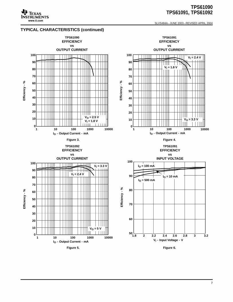
www.ti.com
VI = 1.8 V
VI = 2.4 V
0
10
20
30
40
50
60
70
80
90
100
1 10 100 1000 10000
Eff
icie
ncy
- %
TPS61091EFFICIENCY
vsOUTPUT CURRENT
IO - Output Current - mA
VO = 3.3 V
0
10
20
30
40
50
60
70
80
90
100
1 10 100 1000 10000
Eff
icie
ncy
- %
TPS61090EFFICIENCY
vsOUTPUT CURRENT
IO - Output Current - mA
VO = 2.5 VVI = 1.8 V
50
80
90
100
Eff
icie
ncy
- %
TPS61091EFFICIENCY
vsINPUT VOLTAGE
VI - Input Voltage - V
IO = 10 mA
IO = 100 mA
1.8 2 2.6 2.8 32.2 2.4 3.2
60
IO = 500 mA
70
0
10
20
30
40
50
60
70
80
90
100
1 10 100 1000 10000
VI = 2.4 V
VI = 3.3 V
VO = 5 V
Eff
icie
ncy
- %
IO - Output Current - mA
TPS61092EFFICIENCY
vsOUTPUT CURRENT
TPS61090TPS61091, TPS61092
SLVS484A–JUNE 2003–REVISED APRIL 2004
TYPICAL CHARACTERISTICS (continued)
Figure 3. Figure 4.
Figure 5. Figure 6.
7
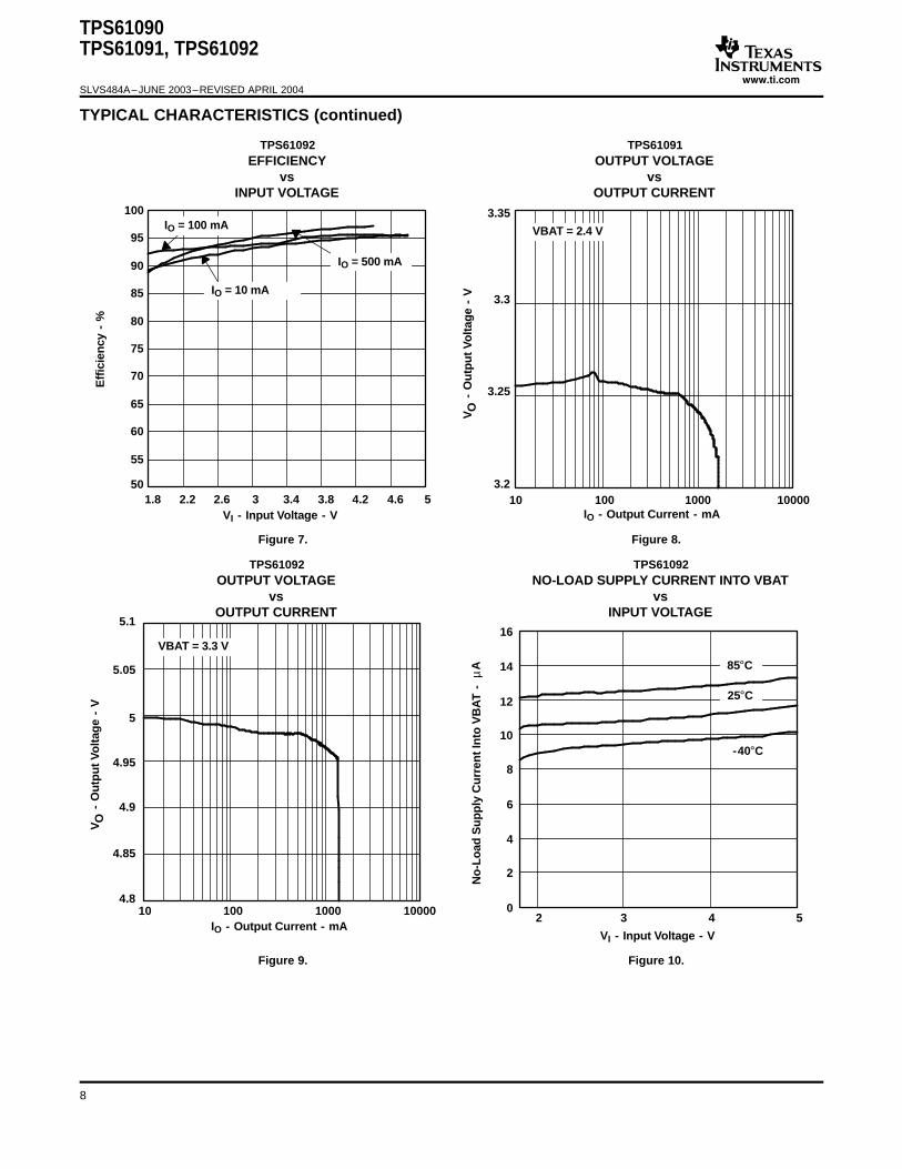
www.ti.com
3.2
3.25
3.3
3.35
10 100 1000 10000
- O
utp
ut
Vo
ltag
e -
V
TPS61091OUTPUT VOLTAGE
vsOUTPUT CURRENT
IO - Output Current - mA
VO
VBAT = 2.4 V
50
55
60
65
70
75
80
85
90
95
100
1.8 2.2 2.6 3 3.4 3.8 4.2 4.6 5
Eff
icie
ncy
- %
TPS61092EFFICIENCY
vsINPUT VOLTAGE
VI - Input Voltage - V
IO = 100 mA
IO = 500 mA
IO = 10 mA
4.8
4.85
4.9
4.95
5
5.05
5.1
10 100 1000 10000
- O
utp
ut
Vo
ltag
e -
V
TPS61092OUTPUT VOLTAGE
vsOUTPUT CURRENT
IO - Output Current - mA
VO
VBAT = 3.3 V
0
2
4
6
8
10
12
14
16
2 3 4 5
TPS61092NO-LOAD SUPPLY CURRENT INTO VBAT
vsINPUT VOLTAGE
VI - Input Voltage - V
-40°C
85°C
25°C
Aµ
No
-Lo
ad S
up
ply
Cu
rren
t In
to V
BA
T -
TPS61090TPS61091, TPS61092
SLVS484A–JUNE 2003–REVISED APRIL 2004
TYPICAL CHARACTERISTICS (continued)
Figure 7. Figure 8.
Figure 9. Figure 10.
8
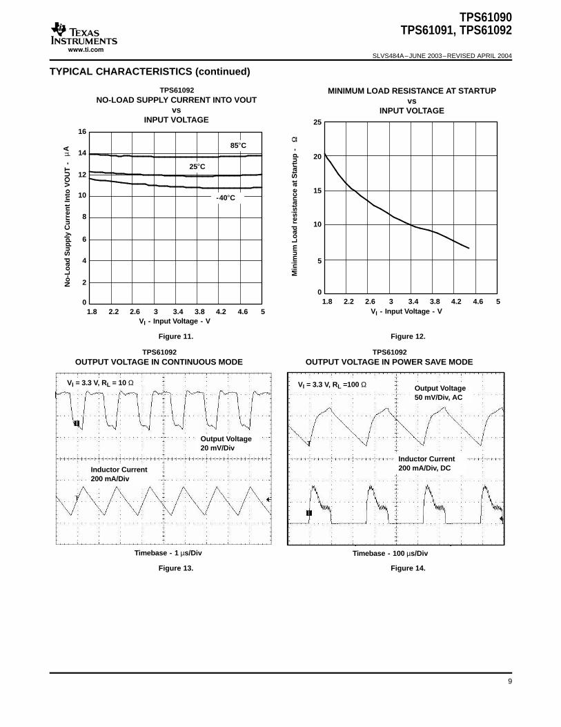
www.ti.com
0
5
10
15
20
25
1.8 2.2 2.6 3 3.4 3.8 4.2 4.6 5M
inim
um
Lo
ad r
esis
tan
ce a
t Sta
rtu
p -
MINIMUM LOAD RESISTANCE AT STARTUPvs
INPUT VOLTAGE
VI - Input Voltage - V
TPS61092NO-LOAD SUPPLY CURRENT INTO VOUT
vsINPUT VOLTAGE
VI - Input Voltage - V
-40°C
85°C
25°C
Aµ
No
-Lo
ad S
up
ply
Cu
rren
t In
to V
OU
T -
0
2
4
6
8
10
12
14
16
1.8 2.2 2.6 3 3.4 3.8 4.2 4.6 5
Inductor Current200 mA/Div
Output Voltage20 mV/Div
Timebase - 1 µs/Div
TPS61092OUTPUT VOLTAGE IN CONTINUOUS MODE
VI = 3.3 V, RL = 10 Ω
Inductor Current200 mA/Div, DC
Output Voltage50 mV/Div, AC
TPS61092OUTPUT VOLTAGE IN POWER SAVE MODE
Timebase - 100 µs/Div
VI = 3.3 V, RL =100 Ω
TPS61090TPS61091, TPS61092
SLVS484A–JUNE 2003–REVISED APRIL 2004
TYPICAL CHARACTERISTICS (continued)
Figure 11. Figure 12.
Figure 13. Figure 14.
9

www.ti.com
Output Voltage20 mV/Div, AC
Input Voltage500 mV/Div, DC
TPS61092LINE TRANSIENT RESPONSE
Timebase - 2 ms/Div
VI = 2.2 V to 2.7 V, RL =50 Ω
Output Voltage50 mV/Div, AC
Output Current500 mA/Div, DC
TPS61092LOAD TRANSIENT RESPONSE
Timebase - 2 ms/Div
VI = 2.5 V, IL =200 mA to 400 mA
Output Voltage2 V/Div, DC
Inductor Current500 mA/Div, DC
Enable5 V/Div, DC
Voltage at SW2 V/Div, DC
TPS61092DC/DC CONVERTER START-UP AFTER ENABLE
Timebase - 200 µs/Div
VI = 2.4 V,RL =50 Ω
TPS61090TPS61091, TPS61092
SLVS484A–JUNE 2003–REVISED APRIL 2004
TYPICAL CHARACTERISTICS (continued)
Figure 15. Figure 16.
Figure 17.
10
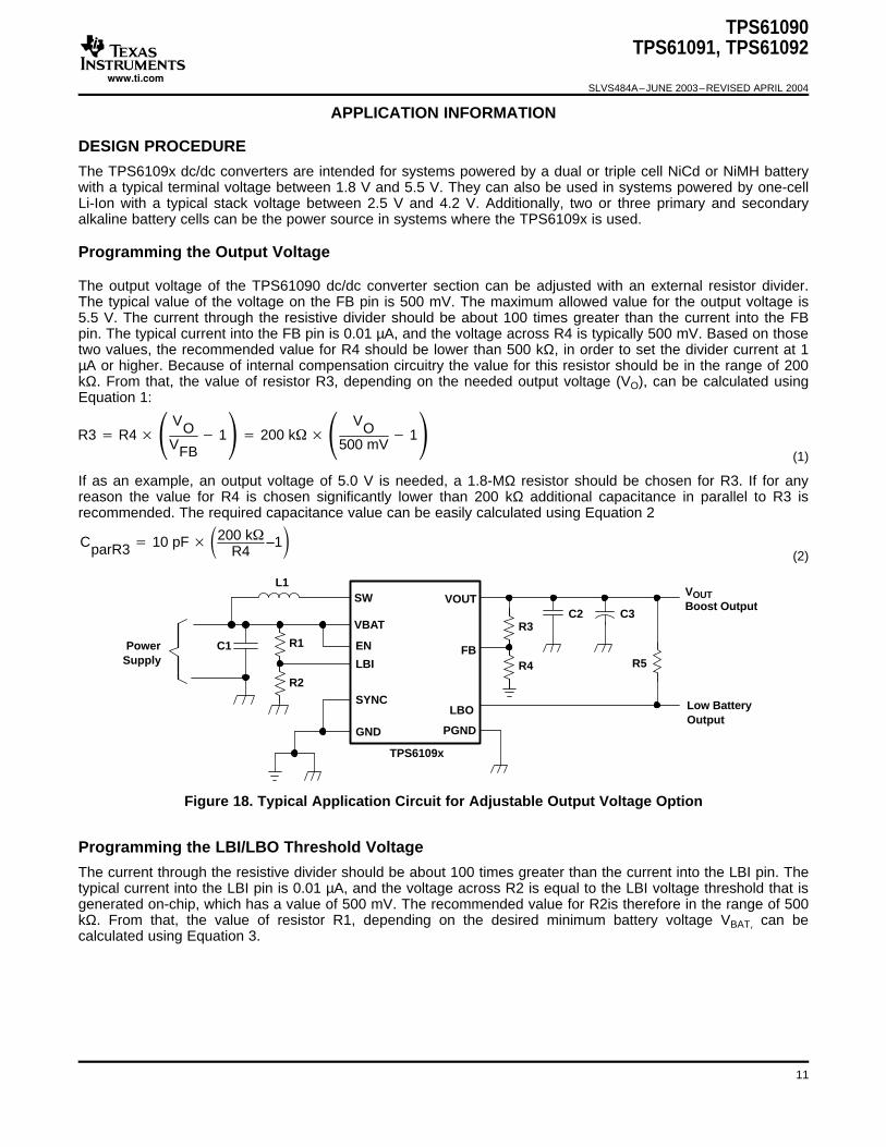
www.ti.com
APPLICATION INFORMATION
DESIGN PROCEDURE
Programming the Output Voltage
R3 R4 VOVFB
1 200 k VO500 mV
1(1)
CparR3 10 pF 200 kR4
–1(2)
SW
C1PowerSupply
L1
R1
R2
VBAT
VOUT
FB
C2 C3
LBO
PGND
LBI
SYNC
EN
GND
TPS6109x
VOUTBoost Output
Low BatteryOutput
R3
R4 R5
Programming the LBI/LBO Threshold Voltage
TPS61090TPS61091, TPS61092
SLVS484A–JUNE 2003–REVISED APRIL 2004
The TPS6109x dc/dc converters are intended for systems powered by a dual or triple cell NiCd or NiMH batterywith a typical terminal voltage between 1.8 V and 5.5 V. They can also be used in systems powered by one-cellLi-Ion with a typical stack voltage between 2.5 V and 4.2 V. Additionally, two or three primary and secondaryalkaline battery cells can be the power source in systems where the TPS6109x is used.
The output voltage of the TPS61090 dc/dc converter section can be adjusted with an external resistor divider.The typical value of the voltage on the FB pin is 500 mV. The maximum allowed value for the output voltage is5.5 V. The current through the resistive divider should be about 100 times greater than the current into the FBpin. The typical current into the FB pin is 0.01 µA, and the voltage across R4 is typically 500 mV. Based on thosetwo values, the recommended value for R4 should be lower than 500 kΩ, in order to set the divider current at 1µA or higher. Because of internal compensation circuitry the value for this resistor should be in the range of 200kΩ. From that, the value of resistor R3, depending on the needed output voltage (VO), can be calculated usingEquation 1:
If as an example, an output voltage of 5.0 V is needed, a 1.8-MΩ resistor should be chosen for R3. If for anyreason the value for R4 is chosen significantly lower than 200 kΩ additional capacitance in parallel to R3 isrecommended. The required capacitance value can be easily calculated using Equation 2
Figure 18. Typical Application Circuit for Adjustable Output Voltage Option
The current through the resistive divider should be about 100 times greater than the current into the LBI pin. Thetypical current into the LBI pin is 0.01 µA, and the voltage across R2 is equal to the LBI voltage threshold that isgenerated on-chip, which has a value of 500 mV. The recommended value for R2is therefore in the range of 500kΩ. From that, the value of resistor R1, depending on the desired minimum battery voltage VBAT, can becalculated using Equation 3.
11

www.ti.com
R1 R2 VBATVLBIthreshold
1 390 k VBAT500 mV
1(3)
Inductor Selection
IL IOUT
VOUTVBAT 0.8
(4)
L VBAT VOUT–VBAT
IL ƒ VOUT (5)
TPS61090TPS61091, TPS61092
SLVS484A–JUNE 2003–REVISED APRIL 2004
APPLICATION INFORMATION (continued)
The output of the low battery supervisor is a simple open-drain output that goes active low if the dedicatedbattery voltage drops below the programmed threshold voltage on LBI. The output requires a pullup resistor witha recommended value of 1 MΩ. The maximum voltage which is used to pull up the LBO outputs should notexceed the output voltage of the dc/dc converter. If not used, the LBO pin can be left floating or tied to GND.
A boost converter normally requires two main passive components for storing energy during the conversion. Aboost inductor and a storage capacitor at the output are required. To select the boost inductor, it isrecommended to keep the possible peak inductor current below the current limit threshold of the power switch inthe chosen configuration. For example, the current limit threshold of the TPS6109x's switch is 2500 mA at anoutput voltage of 5 V. The highest peak current through the inductor and the switch depends on the output load,the input (VBAT), and the output voltage (VOUT). Estimation of the maximum average inductor current can be doneusing Equation 4:
For example, for an output current of 500 mA at 5 V, at least 1750 mA of average current flows through theinductor at a minimum input voltage of 1.8 V.
The second parameter for choosing the inductor is the desired current ripple in the inductor. Normally, it isadvisable to work with a ripple of less than 20% of the average inductor current. A smaller ripple reduces themagnetic hysteresis losses in the inductor, as well as output voltage ripple and EMI. But in the same way,regulation time at load changes rises. In addition, a larger inductor increases the total system costs. With thoseparameters, it is possible to calculate the value for the inductor by using Equation 5:
Parameter f is the switching frequency and ∆IL is the ripple current in the inductor, i.e., 20% × IL. In this example,the desired inductor has the value of 5.5 µH. With this calculated value and the calculated currents, it is possibleto choose a suitable inductor. Care has to be taken that load transients and losses in the circuit can lead tohigher currents as estimated in equation 4. Also, the losses in the inductor caused by magnetic hysteresis lossesand copper losses are a major parameter for total circuit efficiency.
The following inductor series from different suppliers have been used with the TPS6109x converters:
List of Inductors
VENDOR INDUCTOR SERIES
CDRH6D28
Sumida CDRH6D38
CDRH103R
Wurth Elektronik WE-PD type L
WE-PD type XL
EPCOS B82464G
12
www.ti.com
Capacitor Selection
Input Capacitor
Output Capacitor DC/DC Converter
Cmin IOUT VOUT VBAT
ƒ V VOUT (6)
VESR IOUT RESR (7)
Small Signal Stability
AREG d
VFBAREG
d5(R3 R4)R4 (1 i 2.3 s)
(8)
LAYOUT CONSIDERATIONS
TPS61090TPS61091, TPS61092
SLVS484A–JUNE 2003–REVISED APRIL 2004
At least a 10-µF input capacitor is recommended to improve transient behavior of the regulator and EMI behaviorof the total power supply circuit. A ceramic capacitor or a tantalum capacitor with a 100-nF ceramic capacitor inparallel, placed close to the IC, is recommended.
The major parameter necessary to define the minimum value of the output capacitor is the maximum allowedoutput voltage ripple in steady state operation of the converter. This ripple is determined by two parameters ofthe capacitor, the capacitance and the ESR. It is possible to calculate the minimum capacitance needed for thedefined ripple, supposing that the ESR is zero, by using equation Equation 6:
Parameter f is the switching frequency and ∆V is the maximum allowed ripple.
With a chosen ripple voltage of 10 mV, a minimum capacitance of 53 µF is needed. The total ripple is larger dueto the ESR of the output capacitor. This additional component of the ripple can be calculated using Equation 7:
An additional ripple of 40 mV is the result of using a tantalum capacitor with a low ESR of 80 mΩ. The total rippleis the sum of the ripple caused by the capacitance and the ripple caused by the ESR of the capacitor. In thisexample, the total ripple is 50 mV. Additional ripple is caused by load transients. This means that the outputcapacitance needs to be larger than calculated above to meet the total ripple requirements. The output capacitorhas to completely supply the load during the charging phase of the inductor. A reasonable value of the outputcapacitance depends on the speed of the load transients and the load current during the load change. With thecalculated minimum value of 53 µF and load transient considerations, a reasonable output capacitance value isin a 100 µF range. For economical reasons this usually is a tantalum capacitor. Because of this the control loophas been optimized for using output capacitors with an ESR of above 30 mΩ.
When using output capacitors with lower ESR, like ceramics, it is recommended to use the adjustable voltageversion. The missing ESR can be easily compensated there in the feedback divider. Typically a capacitor in therange of 10 pF in parallel to R3 helps to obtain small signal stability with lowest ESR output capacitors. For moredetailed analysis the small signal transfer function of the error amplifier and regulator, which is given isEquation 8, can be used.
As for all switching power supplies, the layout is an important step in the design, especially at high peak currentsand high switching frequencies. If the layout is not carefully done, the regulator could show stability problems aswell as EMI problems. Therefore, use wide and short traces for the main current path and for the power groundtracks. The input capacitor, output capacitor, and the inductor should be placed as close as possible to the IC.Use a common ground node for power ground and a different one for control ground to minimize the effects ofground noise. Connect these ground nodes at any place close to one of the ground pins of the IC.
The feedback divider should be placed as close as possible to the control ground pin of the IC. To lay out thecontrol ground, it is recommended to use short traces as well, separated from the power ground traces. Thisavoids ground shift problems, which can occur due to superimposition of power ground current and controlground current.
13
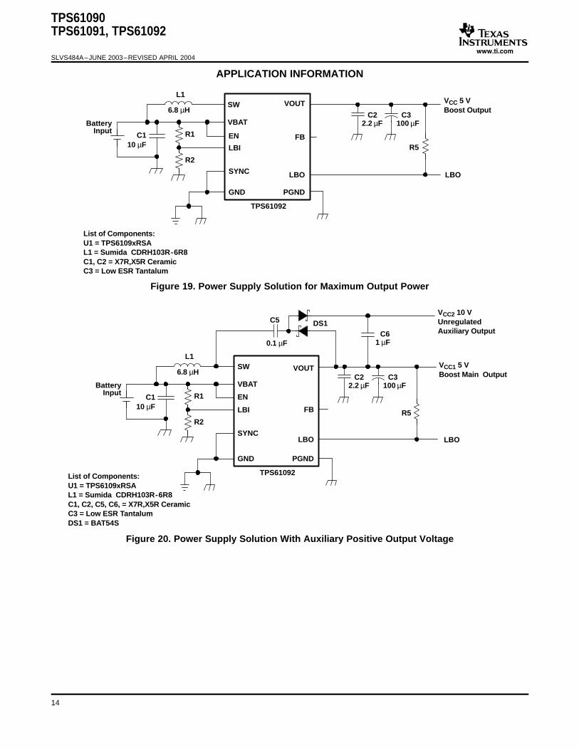
www.ti.com
APPLICATION INFORMATION
SW
C110 µF
L1
6.8 µH
R1
R2
VBAT
VOUT
FB
C22.2 µF
C3100 µF
LBO
PGND
LBI
SYNC
EN
GND
TPS61092
List of Components:U1 = TPS6109xRSAL1 = Sumida CDRH103R-6R8C1, C2 = X7R,X5R CeramicC3 = Low ESR Tantalum
VCC 5 VBoost Output
LBO
R5
BatteryInput
SW
C110 µF
L1
6.8 µH
R1
R2
VBAT
VOUT
R5
C22.2 µF
C3100 µF
LBO
PGND
LBI
SYNC
EN
GND
TPS61092List of Components:U1 = TPS6109xRSAL1 = Sumida CDRH103R-6R8C1, C2, C5, C6, = X7R,X5R CeramicC3 = Low ESR TantalumDS1 = BAT54S
LBO
C5
0.1 µF
DS1C6
1 µF
VCC2 10 VUnregulatedAuxiliary Output
BatteryInput
FB
VCC1 5 VBoost Main Output
TPS61090TPS61091, TPS61092
SLVS484A–JUNE 2003–REVISED APRIL 2004
Figure 19. Power Supply Solution for Maximum Output Power
Figure 20. Power Supply Solution With Auxiliary Positive Output Voltage
14
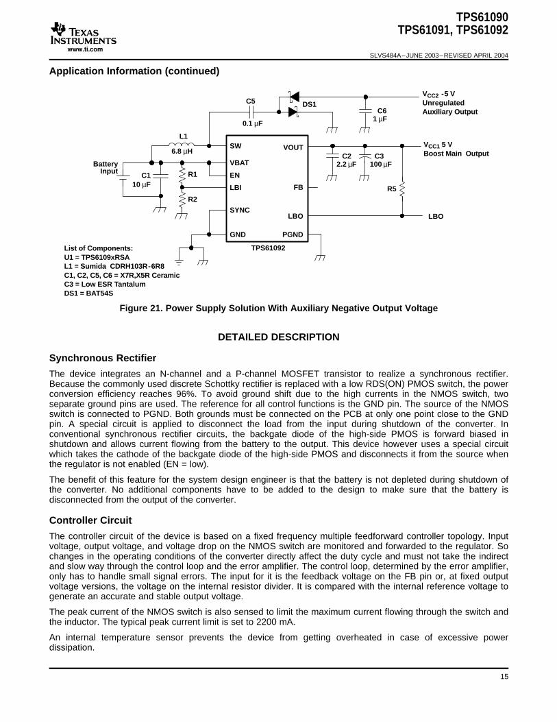
www.ti.com
SW
C110 µF
L1
6.8 µH
R1
R2
VBAT
VOUT
R5
C22.2 µF
C3100 µF
LBO
PGND
LBI
SYNC
EN
GND
TPS61092List of Components:U1 = TPS6109xRSAL1 = Sumida CDRH103R-6R8C1, C2, C5, C6 = X7R,X5R CeramicC3 = Low ESR TantalumDS1 = BAT54S
LBO
C5
0.1 µF
DS1C6
1 µF
VCC2 -5 VUnregulatedAuxiliary Output
BatteryInput
FB
VCC1 5 VBoost Main Output
DETAILED DESCRIPTION
Synchronous Rectifier
Controller Circuit
TPS61090TPS61091, TPS61092
SLVS484A–JUNE 2003–REVISED APRIL 2004
Application Information (continued)
Figure 21. Power Supply Solution With Auxiliary Negative Output Voltage
The device integrates an N-channel and a P-channel MOSFET transistor to realize a synchronous rectifier.Because the commonly used discrete Schottky rectifier is replaced with a low RDS(ON) PMOS switch, the powerconversion efficiency reaches 96%. To avoid ground shift due to the high currents in the NMOS switch, twoseparate ground pins are used. The reference for all control functions is the GND pin. The source of the NMOSswitch is connected to PGND. Both grounds must be connected on the PCB at only one point close to the GNDpin. A special circuit is applied to disconnect the load from the input during shutdown of the converter. Inconventional synchronous rectifier circuits, the backgate diode of the high-side PMOS is forward biased inshutdown and allows current flowing from the battery to the output. This device however uses a special circuitwhich takes the cathode of the backgate diode of the high-side PMOS and disconnects it from the source whenthe regulator is not enabled (EN = low).
The benefit of this feature for the system design engineer is that the battery is not depleted during shutdown ofthe converter. No additional components have to be added to the design to make sure that the battery isdisconnected from the output of the converter.
The controller circuit of the device is based on a fixed frequency multiple feedforward controller topology. Inputvoltage, output voltage, and voltage drop on the NMOS switch are monitored and forwarded to the regulator. Sochanges in the operating conditions of the converter directly affect the duty cycle and must not take the indirectand slow way through the control loop and the error amplifier. The control loop, determined by the error amplifier,only has to handle small signal errors. The input for it is the feedback voltage on the FB pin or, at fixed outputvoltage versions, the voltage on the internal resistor divider. It is compared with the internal reference voltage togenerate an accurate and stable output voltage.
The peak current of the NMOS switch is also sensed to limit the maximum current flowing through the switch andthe inductor. The typical peak current limit is set to 2200 mA.
An internal temperature sensor prevents the device from getting overheated in case of excessive powerdissipation.
15
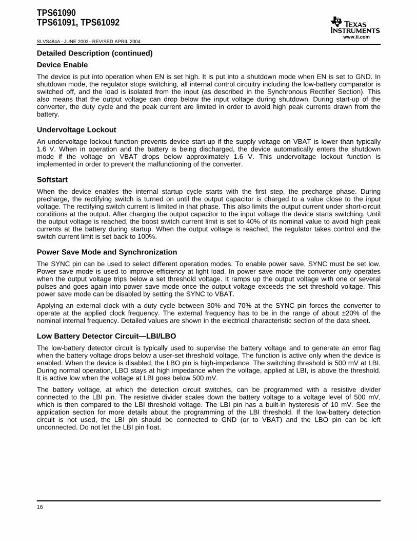
www.ti.com
Device Enable
Undervoltage Lockout
Softstart
Power Save Mode and Synchronization
Low Battery Detector Circuit—LBI/LBO
TPS61090TPS61091, TPS61092
SLVS484A–JUNE 2003–REVISED APRIL 2004
Detailed Description (continued)
The device is put into operation when EN is set high. It is put into a shutdown mode when EN is set to GND. Inshutdown mode, the regulator stops switching, all internal control circuitry including the low-battery comparator isswitched off, and the load is isolated from the input (as described in the Synchronous Rectifier Section). Thisalso means that the output voltage can drop below the input voltage during shutdown. During start-up of theconverter, the duty cycle and the peak current are limited in order to avoid high peak currents drawn from thebattery.
An undervoltage lockout function prevents device start-up if the supply voltage on VBAT is lower than typically1.6 V. When in operation and the battery is being discharged, the device automatically enters the shutdownmode if the voltage on VBAT drops below approximately 1.6 V. This undervoltage lockout function isimplemented in order to prevent the malfunctioning of the converter.
When the device enables the internal startup cycle starts with the first step, the precharge phase. Duringprecharge, the rectifying switch is turned on until the output capacitor is charged to a value close to the inputvoltage. The rectifying switch current is limited in that phase. This also limits the output current under short-circuitconditions at the output. After charging the output capacitor to the input voltage the device starts switching. Untilthe output voltage is reached, the boost switch current limit is set to 40% of its nominal value to avoid high peakcurrents at the battery during startup. When the output voltage is reached, the regulator takes control and theswitch current limit is set back to 100%.
The SYNC pin can be used to select different operation modes. To enable power save, SYNC must be set low.Power save mode is used to improve efficiency at light load. In power save mode the converter only operateswhen the output voltage trips below a set threshold voltage. It ramps up the output voltage with one or severalpulses and goes again into power save mode once the output voltage exceeds the set threshold voltage. Thispower save mode can be disabled by setting the SYNC to VBAT.
Applying an external clock with a duty cycle between 30% and 70% at the SYNC pin forces the converter tooperate at the applied clock frequency. The external frequency has to be in the range of about ±20% of thenominal internal frequency. Detailed values are shown in the electrical characteristic section of the data sheet.
The low-battery detector circuit is typically used to supervise the battery voltage and to generate an error flagwhen the battery voltage drops below a user-set threshold voltage. The function is active only when the device isenabled. When the device is disabled, the LBO pin is high-impedance. The switching threshold is 500 mV at LBI.During normal operation, LBO stays at high impedance when the voltage, applied at LBI, is above the threshold.It is active low when the voltage at LBI goes below 500 mV.
The battery voltage, at which the detection circuit switches, can be programmed with a resistive dividerconnected to the LBI pin. The resistive divider scales down the battery voltage to a voltage level of 500 mV,which is then compared to the LBI threshold voltage. The LBI pin has a built-in hysteresis of 10 mV. See theapplication section for more details about the programming of the LBI threshold. If the low-battery detectioncircuit is not used, the LBI pin should be connected to GND (or to VBAT) and the LBO pin can be leftunconnected. Do not let the LBI pin float.
16
www.ti.com
Low-EMI Switch
THERMAL INFORMATION
PD(MAX) TJ(MAX) TA
RJA
150°C 85°C38.1 kW
1700 mW
TPS61090TPS61091, TPS61092
SLVS484A–JUNE 2003–REVISED APRIL 2004
The device integrates a circuit that removes the ringing that typically appears on the SW node when theconverter enters discontinuous current mode. In this case, the current through the inductor ramps to zero and therectifying PMOS switch is turned off to prevent a reverse current flowing from the output capacitors back to thebattery. Due to the remaining energy that is stored in parasitic components of the semiconductor and theinductor, a ringing on the SW pin is induced. The integrated antiringing switch clamps this voltage to VBAT andtherefore dampens ringing.
Implementation of integrated circuits in low-profile and fine-pitch surface-mount packages typically requiresspecial attention to power dissipation. Many system-dependent issues such as thermal coupling, airflow, addedheat sinks and convection surfaces, and the presence of other heat-generating components affect thepower-dissipation limits of a given component.
Three basic approaches for enhancing thermal performance are listed below.• Improving the power dissipation capability of the PCB design• Improving the thermal coupling of the component to the PCB• Introducing airflow in the system
The maximum junction temperature (TJ) of the TPS6109x devices is 150°C. The thermal resistance of the 16-pinQFN PowerPAD package (RSA) isRΘJA = 38.1 °C/W, if the PowerPAD is soldered and the board layout isoptimized. Specified regulator operation is assured to a maximum ambient temperature TA of 85°C. Therefore,the maximum power dissipation is about 1700 mW. More power can be dissipated if the maximum ambienttemperature of the application is lower.
If designing for a lower junction temperature of 125°C, which is recommended, maximum heat dissipation islower. Using the above equation (8) results in 1050 mW power dissipation.
17
PACKAGE OPTION ADDENDUM
www.ti.com 17-May-2014
Addendum-Page 1
PACKAGING INFORMATION
Orderable Device Status(1)
Package Type PackageDrawing
Pins PackageQty
Eco Plan(2)
Lead/Ball Finish(6)
MSL Peak Temp(3)
Op Temp (°C) Device Marking(4/5)
Samples
TPS61090RSAR ACTIVE QFN RSA 16 3000 Green (RoHS& no Sb/Br)
CU NIPDAU Level-2-260C-1 YEAR -40 to 85 TPS61090
TPS61090RSARG4 ACTIVE QFN RSA 16 3000 Green (RoHS& no Sb/Br)
CU NIPDAU Level-2-260C-1 YEAR -40 to 85 TPS61090
TPS61091RSAR ACTIVE QFN RSA 16 3000 Green (RoHS& no Sb/Br)
CU NIPDAU Level-2-260C-1 YEAR -40 to 85 TPS61091
TPS61091RSARG4 ACTIVE QFN RSA 16 TBD Call TI Call TI -40 to 85
TPS61092RSAR ACTIVE QFN RSA 16 3000 Green (RoHS& no Sb/Br)
CU NIPDAU Level-2-260C-1 YEAR -40 to 85 TPS61092
TPS61092RSARG4 ACTIVE QFN RSA 16 3000 Green (RoHS& no Sb/Br)
CU NIPDAU Level-2-260C-1 YEAR -40 to 85 TPS61092
(1) The marketing status values are defined as follows:ACTIVE: Product device recommended for new designs.LIFEBUY: TI has announced that the device will be discontinued, and a lifetime-buy period is in effect.NRND: Not recommended for new designs. Device is in production to support existing customers, but TI does not recommend using this part in a new design.PREVIEW: Device has been announced but is not in production. Samples may or may not be available.OBSOLETE: TI has discontinued the production of the device.
(2) Eco Plan - The planned eco-friendly classification: Pb-Free (RoHS), Pb-Free (RoHS Exempt), or Green (RoHS & no Sb/Br) - please check http://www.ti.com/productcontent for the latest availabilityinformation and additional product content details.TBD: The Pb-Free/Green conversion plan has not been defined.Pb-Free (RoHS): TI's terms "Lead-Free" or "Pb-Free" mean semiconductor products that are compatible with the current RoHS requirements for all 6 substances, including the requirement thatlead not exceed 0.1% by weight in homogeneous materials. Where designed to be soldered at high temperatures, TI Pb-Free products are suitable for use in specified lead-free processes.Pb-Free (RoHS Exempt): This component has a RoHS exemption for either 1) lead-based flip-chip solder bumps used between the die and package, or 2) lead-based die adhesive used betweenthe die and leadframe. The component is otherwise considered Pb-Free (RoHS compatible) as defined above.Green (RoHS & no Sb/Br): TI defines "Green" to mean Pb-Free (RoHS compatible), and free of Bromine (Br) and Antimony (Sb) based flame retardants (Br or Sb do not exceed 0.1% by weightin homogeneous material)
(3) MSL, Peak Temp. - The Moisture Sensitivity Level rating according to the JEDEC industry standard classifications, and peak solder temperature.
(4) There may be additional marking, which relates to the logo, the lot trace code information, or the environmental category on the device.
(5) Multiple Device Markings will be inside parentheses. Only one Device Marking contained in parentheses and separated by a "~" will appear on a device. If a line is indented then it is a continuationof the previous line and the two combined represent the entire Device Marking for that device.
PACKAGE OPTION ADDENDUM
www.ti.com 17-May-2014
Addendum-Page 2
(6) Lead/Ball Finish - Orderable Devices may have multiple material finish options. Finish options are separated by a vertical ruled line. Lead/Ball Finish values may wrap to two lines if the finishvalue exceeds the maximum column width.
Important Information and Disclaimer:The information provided on this page represents TI's knowledge and belief as of the date that it is provided. TI bases its knowledge and belief on informationprovided by third parties, and makes no representation or warranty as to the accuracy of such information. Efforts are underway to better integrate information from third parties. TI has taken andcontinues to take reasonable steps to provide representative and accurate information but may not have conducted destructive testing or chemical analysis on incoming materials and chemicals.TI and TI suppliers consider certain information to be proprietary, and thus CAS numbers and other limited information may not be available for release.
In no event shall TI's liability arising out of such information exceed the total purchase price of the TI part(s) at issue in this document sold by TI to Customer on an annual basis.
TAPE AND REEL INFORMATION
*All dimensions are nominal
Device PackageType
PackageDrawing
Pins SPQ ReelDiameter
(mm)
ReelWidth
W1 (mm)
A0(mm)
B0(mm)
K0(mm)
P1(mm)
W(mm)
Pin1Quadrant
TPS61090RSAR QFN RSA 16 3000 330.0 12.4 4.3 4.3 1.5 8.0 12.0 Q2
TPS61091RSAR QFN RSA 16 3000 330.0 12.4 4.3 4.3 1.5 8.0 12.0 Q2
TPS61092RSAR QFN RSA 16 3000 330.0 12.4 4.3 4.3 1.5 8.0 12.0 Q2
PACKAGE MATERIALS INFORMATION
www.ti.com 26-Jan-2013
Pack Materials-Page 1
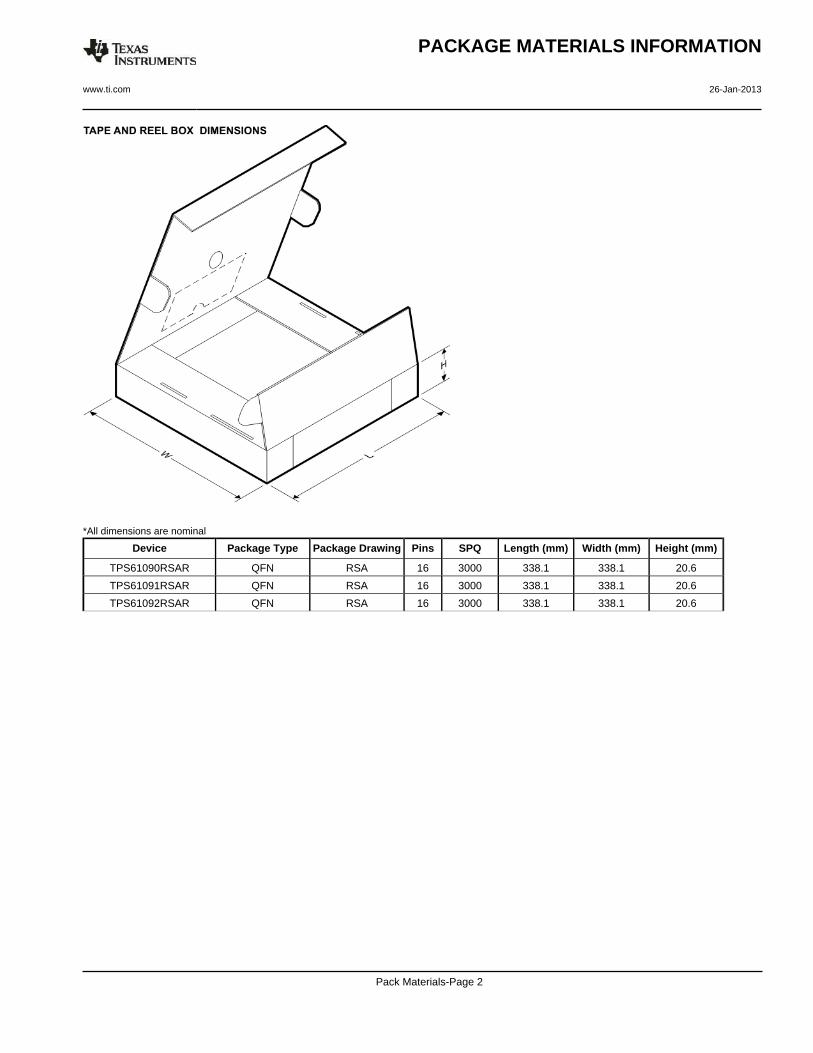
*All dimensions are nominal
Device Package Type Package Drawing Pins SPQ Length (mm) Width (mm) Height (mm)
TPS61090RSAR QFN RSA 16 3000 338.1 338.1 20.6
TPS61091RSAR QFN RSA 16 3000 338.1 338.1 20.6
TPS61092RSAR QFN RSA 16 3000 338.1 338.1 20.6
PACKAGE MATERIALS INFORMATION
www.ti.com 26-Jan-2013
Pack Materials-Page 2
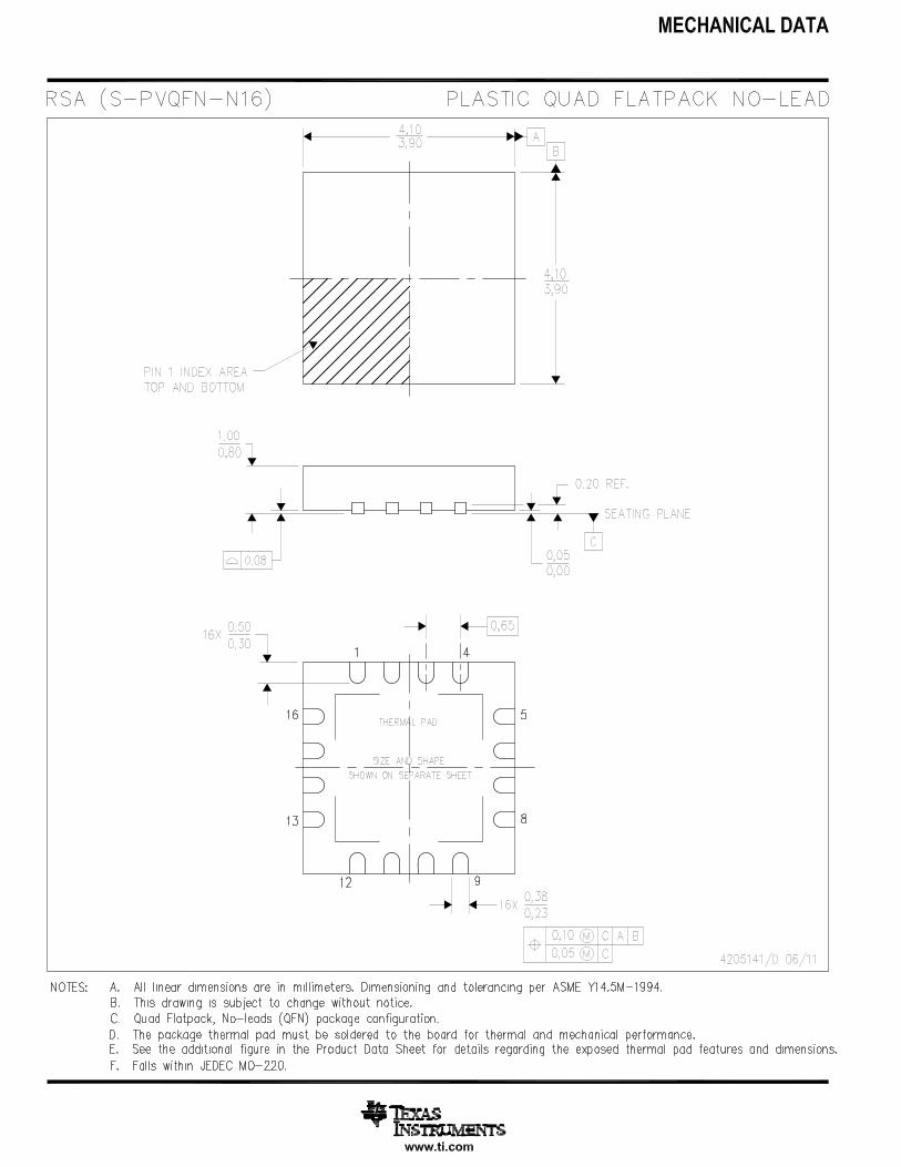

IMPORTANT NOTICETexas Instruments Incorporated and its subsidiaries (TI) reserve the right to make corrections, enhancements, improvements and otherchanges to its semiconductor products and services per JESD46, latest issue, and to discontinue any product or service per JESD48, latestissue. Buyers should obtain the latest relevant information before placing orders and should verify that such information is current andcomplete. All semiconductor products (also referred to herein as “components”) are sold subject to TI’s terms and conditions of salesupplied at the time of order acknowledgment.TI warrants performance of its components to the specifications applicable at the time of sale, in accordance with the warranty in TI’s termsand conditions of sale of semiconductor products. Testing and other quality control techniques are used to the extent TI deems necessaryto support this warranty. Except where mandated by applicable law, testing of all parameters of each component is not necessarilyperformed.TI assumes no liability for applications assistance or the design of Buyers’ products. Buyers are responsible for their products andapplications using TI components. To minimize the risks associated with Buyers’ products and applications, Buyers should provideadequate design and operating safeguards.TI does not warrant or represent that any license, either express or implied, is granted under any patent right, copyright, mask work right, orother intellectual property right relating to any combination, machine, or process in which TI components or services are used. Informationpublished by TI regarding third-party products or services does not constitute a license to use such products or services or a warranty orendorsement thereof. Use of such information may require a license from a third party under the patents or other intellectual property of thethird party, or a license from TI under the patents or other intellectual property of TI.Reproduction of significant portions of TI information in TI data books or data sheets is permissible only if reproduction is without alterationand is accompanied by all associated warranties, conditions, limitations, and notices. TI is not responsible or liable for such altereddocumentation. Information of third parties may be subject to additional restrictions.Resale of TI components or services with statements different from or beyond the parameters stated by TI for that component or servicevoids all express and any implied warranties for the associated TI component or service and is an unfair and deceptive business practice.TI is not responsible or liable for any such statements.Buyer acknowledges and agrees that it is solely responsible for compliance with all legal, regulatory and safety-related requirementsconcerning its products, and any use of TI components in its applications, notwithstanding any applications-related information or supportthat may be provided by TI. Buyer represents and agrees that it has all the necessary expertise to create and implement safeguards whichanticipate dangerous consequences of failures, monitor failures and their consequences, lessen the likelihood of failures that might causeharm and take appropriate remedial actions. Buyer will fully indemnify TI and its representatives against any damages arising out of the useof any TI components in safety-critical applications.In some cases, TI components may be promoted specifically to facilitate safety-related applications. With such components, TI’s goal is tohelp enable customers to design and create their own end-product solutions that meet applicable functional safety standards andrequirements. Nonetheless, such components are subject to these terms.No TI components are authorized for use in FDA Class III (or similar life-critical medical equipment) unless authorized officers of the partieshave executed a special agreement specifically governing such use.Only those TI components which TI has specifically designated as military grade or “enhanced plastic” are designed and intended for use inmilitary/aerospace applications or environments. Buyer acknowledges and agrees that any military or aerospace use of TI componentswhich have not been so designated is solely at the Buyer's risk, and that Buyer is solely responsible for compliance with all legal andregulatory requirements in connection with such use.TI has specifically designated certain components as meeting ISO/TS16949 requirements, mainly for automotive use. In any case of use ofnon-designated products, TI will not be responsible for any failure to meet ISO/TS16949.Products ApplicationsAudio www.ti.com/audio Automotive and Transportation www.ti.com/automotiveAmplifiers amplifier.ti.com Communications and Telecom www.ti.com/communicationsData Converters dataconverter.ti.com Computers and Peripherals www.ti.com/computersDLP® Products www.dlp.com Consumer Electronics www.ti.com/consumer-appsDSP dsp.ti.com Energy and Lighting www.ti.com/energyClocks and Timers www.ti.com/clocks Industrial www.ti.com/industrialInterface interface.ti.com Medical www.ti.com/medicalLogic logic.ti.com Security www.ti.com/securityPower Mgmt power.ti.com Space, Avionics and Defense www.ti.com/space-avionics-defenseMicrocontrollers microcontroller.ti.com Video and Imaging www.ti.com/videoRFID www.ti-rfid.comOMAP Applications Processors www.ti.com/omap TI E2E Community e2e.ti.comWireless Connectivity www.ti.com/wirelessconnectivity
Mailing Address: Texas Instruments, Post Office Box 655303, Dallas, Texas 75265Copyright © 2014, Texas Instruments Incorporated
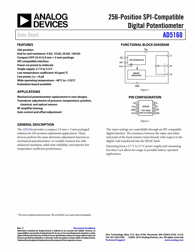
256-Position SPI-Compatible Digital Potentiometer
Data Sheet AD5160
Rev. C Document Feedback Information furnished by Analog Devices is believed to be accurate and reliable. However, no responsibility is assumed by Analog Devices for its use, nor for any infringements of patents or other rights of third parties that may result from its use. Specifications subject to change without notice. No license is granted by implication or otherwise under any patent or patent rights of Analog Devices. Trademarks and registered trademarks are the property of their respective owners.
One Technology Way, P.O. Box 9106, Norwood, MA 02062-9106, U.S.A.Tel: 781.329.4700 ©2003–2014 Analog Devices, Inc. All rights reserved. Technical Support www.analog.com
FEATURES 256-position End-to-end resistance: 5 kΩ, 10 kΩ, 50 kΩ, 100 kΩ Compact SOT-23-8 (2.9 mm × 3 mm) package SPI-compatible interface Power-on preset to midscale Single supply: 2.7 V to 5.5 V Low temperature coefficient: 45 ppm/°C Low power, IDD = 8 μA Wide operating temperature: –40°C to +125°C Evaluation board available
APPLICATIONS Mechanical potentiometer replacement in new designs Transducer adjustment of pressure, temperature, position,
chemical, and optical sensors RF amplifier biasing Gain control and offset adjustment
FUNCTIONAL BLOCK DIAGRAM
SPI INTERFACE
WIPERREGISTER
CS
SDI
CLK
GND
VDD
A
W
B
Figure 1.
PIN CONFIGURATION
A
B
CS
SDI
1234 5
8
76
W
VDD
GND
CLKTOP VIEW
(Not to Scale)
AD5160
Figure 2.
GENERAL DESCRIPTION The AD5160 provides a compact 2.9 mm × 3 mm packaged solution for 256-position adjustment applications. These devices perform the same electronic adjustment function as mechanical potentiometers1 or variable resistors but with enhanced resolution, solid-state reliability, and superior low temperature coefficient performance.
The wiper settings are controllable through an SPI-compatible digital interface. The resistance between the wiper and either end point of the fixed resistor varies linearly with respect to the digital code transferred into the RDAC latch.
Operating from a 2.7 V to 5.5 V power supply and consuming less than 5 μA allows for usage in portable battery-operated applications.
1 The terms digital potentiometer, VR, and RDAC are used interchangeably.
AD5160 Data Sheet
TABLE OF CONTENTS Features .............................................................................................. 1 Applications ....................................................................................... 1 Functional Block Diagram .............................................................. 1 Pin Configuration ............................................................................. 1 General Description ......................................................................... 1 Revision History ............................................................................... 2 Specifications ..................................................................................... 3
Electrical Characteristics—5 kΩ Version .................................. 3 10 kΩ, 50 kΩ, 100 kΩ Versions .................................................. 4 Timing Characteristics—All Versions ....................................... 5
Absolute Maximum Ratings ............................................................ 6 ESD Caution .................................................................................. 6
Pin Configuration and Function Descriptions ............................. 7
Typical Performance Characteristics ..............................................8 Test Circuits ..................................................................................... 12 SPI Interface .................................................................................... 13 Theory of Operation ...................................................................... 14
Programming the Variable Resistor ......................................... 14 Programming the Potentiometer Divider ............................... 15 SPI-Compatible 3-Wire Serial Bus ........................................... 15 ESD Protection ........................................................................... 15 Power-Up Sequence ................................................................... 15 Layout and Power Supply Bypassing ....................................... 15
Outline Dimensions ....................................................................... 16 Ordering Guide .......................................................................... 16
REVISION HISTORY 11/14—Rev. B to Rev. C
Changes to Ordering Guide .......................................................... 16
5/09—Rev. A to Rev. B
Changes to Ordering Guide .......................................................... 16
1/09—Rev. 0 to Rev. A
Deleted Shutdown Supply Current Parameter and Endnote 7, Table 1 ............................................................................ 3 Changes to Resistor Noise Voltage Density Parameter, Table 1 ................................................................................................ 3 Deleted Shutdown Supply Current Parameter and Endnote 7, Table 2 ............................................................................ 4 Changes to Resistor Noise Voltage Density Parameter, Table 2 ................................................................................................ 4 Added Endnote to Table 3 ............................................................... 5 Changes to Table 4 ............................................................................ 6 Changes to the Rheostat Operation Section ............................... 14 Deleted Terminal Voltage Operating Range Section and Figure 41, Renumbered Figures Sequentially ............................. 13 Changes to Figure 40 and Figure 41 ............................................. 15 Changes to Ordering Guide .......................................................... 16
5/03—Revision 0: Initial Version
Rev. C | Page 2 of 16
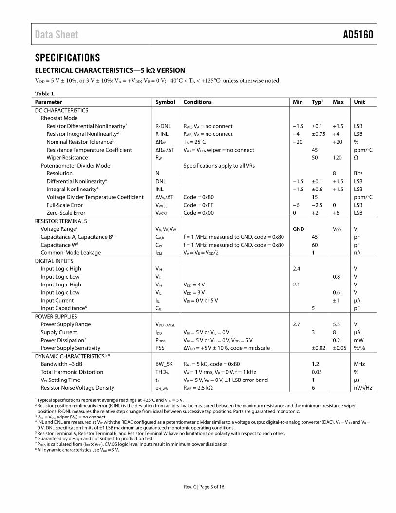
Data Sheet AD5160
SPECIFICATIONS ELECTRICAL CHARACTERISTICS—5 kΩ VERSION VDD = 5 V ± 10%, or 3 V ± 10%; VA = +VDD; VB = 0 V; –40°C < TA < +125°C; unless otherwise noted.
Table 1. Parameter Symbol Conditions Min Typ1 Max Unit DC CHARACTERISTICS
Rheostat Mode Resistor Differential Nonlinearity2 R-DNL RWB, VA = no connect −1.5 ±0.1 +1.5 LSB Resistor Integral Nonlinearity2 R-INL RWB, VA = no connect −4 ±0.75 +4 LSB Nominal Resistor Tolerance3 ∆RAB TA = 25°C −20 +20 % Resistance Temperature Coefficient ∆RAB/∆T VAB = VDD, wiper = no connect 45 ppm/°C Wiper Resistance RW 50 120 Ω
Potentiometer Divider Mode Specifications apply to all VRs Resolution N 8 Bits Differential Nonlinearity4 DNL −1.5 ±0.1 +1.5 LSB Integral Nonlinearity4 INL −1.5 ±0.6 +1.5 LSB Voltage Divider Temperature Coefficient ∆VW/∆T Code = 0x80 15 ppm/°C Full-Scale Error VWFSE Code = 0xFF −6 −2.5 0 LSB Zero-Scale Error VWZSE Code = 0x00 0 +2 +6 LSB
RESISTOR TERMINALS Voltage Range5 VA, VB, VW GND VDD V Capacitance A, Capacitance B6 CA,B f = 1 MHz, measured to GND, code = 0x80 45 pF Capacitance W6 CW f = 1 MHz, measured to GND, code = 0x80 60 pF Common-Mode Leakage ICM VA = VB = VDD/2 1 nA
DIGITAL INPUTS Input Logic High VIH 2.4 V Input Logic Low VIL 0.8 V Input Logic High VIH VDD = 3 V 2.1 V Input Logic Low VIL VDD = 3 V 0.6 V Input Current IIL VIN = 0 V or 5 V ±1 µA Input Capacitance6 CIL 5 pF
POWER SUPPLIES Power Supply Range VDD RANGE 2.7 5.5 V Supply Current IDD VIH = 5 V or VIL = 0 V 3 8 µA Power Dissipation7 PDISS VIH = 5 V or VIL = 0 V, VDD = 5 V 0.2 mW Power Supply Sensitivity PSS ∆VDD = +5 V ± 10%, code = midscale ±0.02 ±0.05 %/%
DYNAMIC CHARACTERISTICS6, 8 Bandwidth –3 dB BW_5K RAB = 5 kΩ, code = 0x80 1.2 MHz Total Harmonic Distortion THDW VA = 1 V rms, VB = 0 V, f = 1 kHz 0.05 % VW Settling Time tS VA = 5 V, VB = 0 V, ±1 LSB error band 1 µs Resistor Noise Voltage Density eN_WB RWB = 2.5 kΩ 6 nV/√Hz
1 Typical specifications represent average readings at +25°C and VDD = 5 V. 2 Resistor position nonlinearity error (R-INL) is the deviation from an ideal value measured between the maximum resistance and the minimum resistance wiper
positions. R-DNL measures the relative step change from ideal between successive tap positions. Parts are guaranteed monotonic. 3 VAB = VDD, wiper (VW) = no connect. 4 INL and DNL are measured at VW with the RDAC configured as a potentiometer divider similar to a voltage output digital-to-analog converter (DAC). VA = VDD and VB =
0 V. DNL specification limits of ±1 LSB maximum are guaranteed monotonic operating conditions. 5 Resistor Terminal A, Resistor Terminal B, and Resistor Terminal W have no limitations on polarity with respect to each other. 6 Guaranteed by design and not subject to production test. 7 PDISS is calculated from (IDD × VDD). CMOS logic level inputs result in minimum power dissipation. 8 All dynamic characteristics use VDD = 5 V.
Rev. C | Page 3 of 16
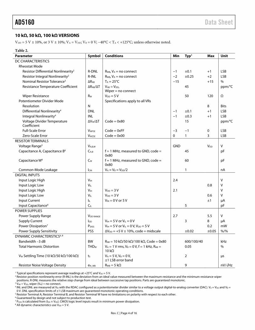
AD5160 Data Sheet
10 kΩ, 50 kΩ, 100 kΩ VERSIONS VDD = 5 V ± 10%, or 3 V ± 10%; VA = VDD; VB = 0 V; −40°C < TA < +125°C; unless otherwise noted.
Table 2. Parameter Symbol Conditions Min Typ1 Max Unit DC CHARACTERISTICS
Rheostat Mode Resistor Differential Nonlinearity2 R-DNL RWB, VA = no connect −1 ±0.1 +1 LSB Resistor Integral Nonlinearity2 R-INL RWB, VA = no connect −2 ±0.25 +2 LSB Nominal Resistor Tolerance3 ∆RAB TA = 25°C −15 +15 % Resistance Temperature Coefficient ∆RAB/∆T VAB = VDD,
Wiper = no connect 45 ppm/°C
Wiper Resistance RW VDD = 5 V 50 120 Ω Potentiometer Divider Mode Specifications apply to all VRs
Resolution N 8 Bits Differential Nonlinearity4 DNL −1 ±0.1 +1 LSB Integral Nonlinearity4 INL −1 ±0.3 +1 LSB Voltage Divider Temperature Coefficient
∆VW/∆T Code = 0x80 15 ppm/°C
Full-Scale Error VWFSE Code = 0xFF −3 −1 0 LSB Zero-Scale Error VWZSE Code = 0x00 0 1 3 LSB
RESISTOR TERMINALS Voltage Range5 VA,B,W GND VDD V Capacitance A, Capacitance B6 CA,B f = 1 MHz, measured to GND, code =
0x80 45 pF
Capacitance W6 CW f = 1 MHz, measured to GND, code = 0x80
60 pF
Common-Mode Leakage ICM VA = VB = VDD/2 1 nA DIGITAL INPUTS
Input Logic High VIH 2.4 V Input Logic Low VIL 0.8 V Input Logic High VIH VDD = 3 V 2.1 V Input Logic Low VIL VDD = 3 V 0.6 V Input Current IIL VIN = 0 V or 5 V ±1 µA Input Capacitance6 CIL 5 pF
POWER SUPPLIES Power Supply Range VDD RANGE 2.7 5.5 V Supply Current IDD VIH = 5 V or VIL = 0 V 3 8 µA Power Dissipation7 PDISS VIH = 5 V or VIL = 0 V, VDD = 5 V 0.2 mW Power Supply Sensitivity PSS ∆VDD = +5 V ± 10%, code = midscale ±0.02 ±0.05 %/%
DYNAMIC CHARACTERISTICS6, 8 Bandwidth –3 dB BW RAB = 10 kΩ/50 kΩ/100 kΩ, Code = 0x80 600/100/40 kHz Total Harmonic Distortion THDW VA = 1 V rms, VB = 0 V, f = 1 kHz, RAB =
10 kΩ 0.05 %
VW Settling Time (10 kΩ/50 kΩ/100 kΩ) tS VA = 5 V, VB = 0 V, ±1 LSB error band
2 µs
Resistor Noise Voltage Density eN_WB RWB = 5 kΩ 9 nV/√Hz
1 Typical specifications represent average readings at +25°C and VDD = 5 V. 2 Resistor position nonlinearity error (R-INL) is the deviation from an ideal value measured between the maximum resistance and the minimum resistance wiper
positions. R-DNL measures the relative step change from ideal between successive tap positions. Parts are guaranteed monotonic. 3 VAB = VDD, wiper (VW) = no connect. 4 INL and DNL are measured at VW with the RDAC configured as a potentiometer divider similar to a voltage output digital-to-analog converter (DAC). VA = VDD and VB =
0 V. DNL specification limits of ±1 LSB maximum are guaranteed monotonic operating conditions. 5 Resistor Terminal A, Resistor Terminal B, and Resistor Terminal W have no limitations on polarity with respect to each other. 6 Guaranteed by design and not subject to production test. 7 PDISS is calculated from (IDD × VDD). CMOS logic level inputs result in minimum power dissipation. 8 All dynamic characteristics use VDD = 5 V.
Rev. C | Page 4 of 16
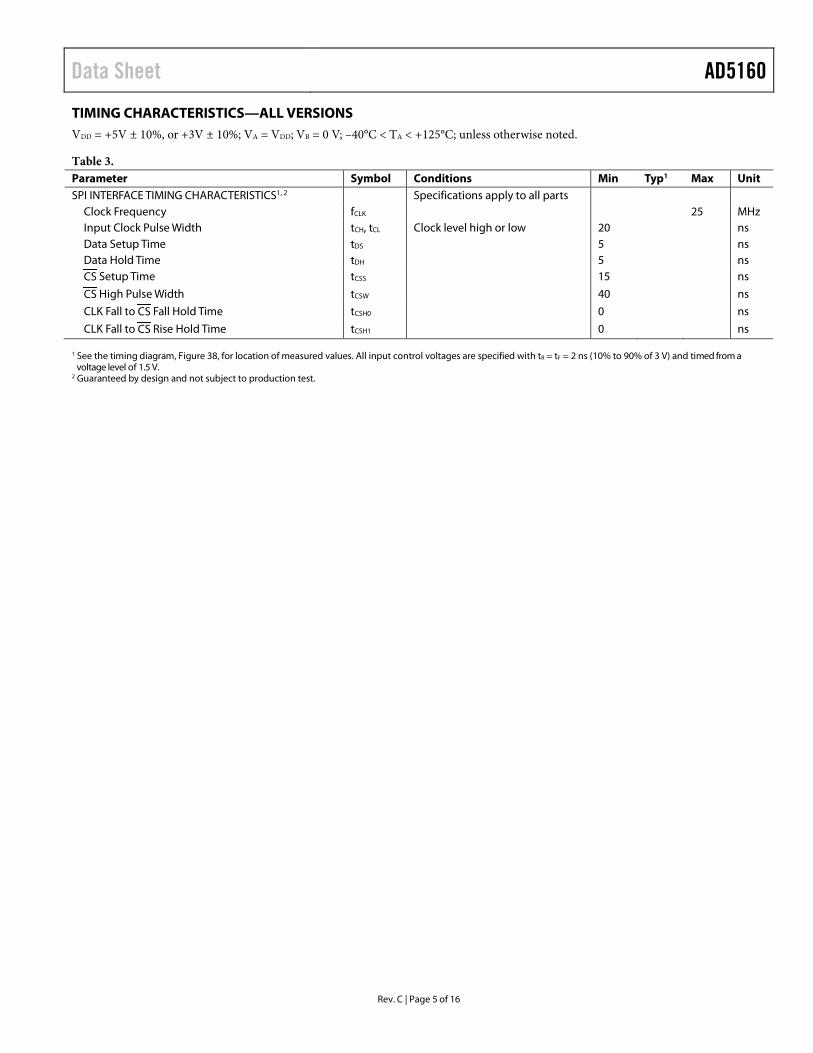
Data Sheet AD5160
TIMING CHARACTERISTICS—ALL VERSIONS VDD = +5V ± 10%, or +3V ± 10%; VA = VDD; VB = 0 V; –40°C < TA < +125°C; unless otherwise noted.
Table 3. Parameter Symbol Conditions Min Typ1 Max Unit SPI INTERFACE TIMING CHARACTERISTICS1, 2 Specifications apply to all parts
Clock Frequency fCLK 25 MHz Input Clock Pulse Width tCH, tCL Clock level high or low 20 ns Data Setup Time tDS 5 ns Data Hold Time tDH 5 ns CS Setup Time tCSS 15 ns
CS High Pulse Width tCSW 40 ns
CLK Fall to CS Fall Hold Time tCSH0 0 ns
CLK Fall to CS Rise Hold Time tCSH1 0 ns
1 See the timing diagram, Figure 38, for location of measured values. All input control voltages are specified with tR = tF = 2 ns (10% to 90% of 3 V) and timed from a voltage level of 1.5 V.
2 Guaranteed by design and not subject to production test.
Rev. C | Page 5 of 16

AD5160 Data Sheet
ABSOLUTE MAXIMUM RATINGS TA = +25°C, unless otherwise noted.
Table 4. Parameter Rating VDD to GND −0.3 V to +7 V VA, VB, VW to GND VDD Maximum Current IMAX
1 IWB, IWA Pulsed ±20 mA IWB, IWA Continuous
5 kΩ, 10 kΩ 4.7 mA 50 kΩ 0.95 mA 100 kΩ 0.48 mA
Digital Inputs and Output Voltage to GND 0 V to +7 V Temperature
Operating Temperature Range −40°C to +125°C Maximum Junction Temperature (TJMAX) 150°C Storage Temperature −65°C to +150°C
Thermal Resistance (SOT-23 Package)2 θJA Thermal Impedance 206ºC/W θJC Thermal Impedance 91°C/W
Reflow Soldering (Pb-Free) Peak Temperature 260°C Time at Peak Temperature 10 sec to 40 sec
1 Maximum terminal current is bounded by the maximum current handling of the switches, maximum power dissipation of the package, and applied voltage across any two of the A, B, and W terminals at a given resistance.
2 Package power dissipation = (TJMAX − TA)/θJA.
Stresses at or above those listed under Absolute Maximum Ratings may cause permanent damage to the product. This is a stress rating only; functional operation of the product at these or any other conditions above those indicated in the operational section of this specification is not implied. Operation beyond the maximum operating conditions for extended periods may affect product reliability.
ESD CAUTION
Rev. C | Page 6 of 16
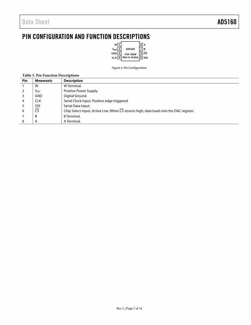
Data Sheet AD5160
Rev. C | Page 7 of 16
PIN CONFIGURATION AND FUNCTION DESCRIPTIONS A
B
CS
SDI
1234 5
8
76
W
VDD
GND
CLKTOP VIEW
(Not to Scale)
AD5160
Figure 3. Pin Configuration
Table 5. Pin Function Descriptions Pin Mnemonic Description 1 W W Terminal. 2 VDD Positive Power Supply. 3 GND Digital Ground. 4 CLK Serial Clock Input. Positive edge triggered. 5 SDI Serial Data Input. 6 CS Chip Select Input, Active Low. When CS returns high, data loads into the DAC register.
7 B B Terminal. 8 A A Terminal.
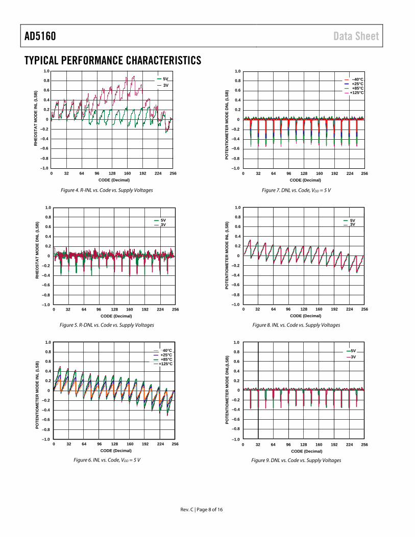
AD5160 Data Sheet
TYPICAL PERFORMANCE CHARACTERISTICS
CODE (Decimal)
–1.0
–0.8
–0.6
–0.4
–0.2
0
0.2
0.4
0.6
1.0
320 9664 128 160 192 224 256
RH
EOST
AT
MO
DE
INL
(LSB
)
0.8 5V3V
Figure 4. R-INL vs. Code vs. Supply Voltages
5V3V
–1.0
–0.8
–0.6
–0.4
–0.2
0
0.2
0.4
0.6
1.0
RH
EOST
AT
MO
DE
DN
L (L
SB)
0.8
CODE (Decimal)320 9664 128 160 192 224 256
Figure 5. R-DNL vs. Code vs. Supply Voltages
_40°C+25°C+85°C
+125°C
–1.0
–0.8
–0.6
–0.4
–0.2
0
0.2
0.4
0.6
1.0
POTE
NTI
OM
ETER
MO
DE
INL
(LSB
)
0.8
CODE (Decimal)320 9664 128 160 192 224 256
Figure 6. INL vs. Code, VDD = 5 V
CODE (Decimal)
–1.0
–0.8
–0.6
–0.4
–0.2
0
0.2
0.4
0.6
1.0
320 9664 128 160 192 224 256
POTE
NTI
OM
ETER
MO
DE
DN
L (L
SB)
0.8 –40°C+25°C+85°C
+125°C
Figure 7. DNL vs. Code, VDD = 5 V
–1.0
–0.8
–0.6
–0.4
–0.2
0
0.2
0.4
0.6
1.0
POTE
NTI
OM
ETER
MO
DE
INL
(LSB
)
0.8
CODE (Decimal)320 9664 128 160 192 224 256
5V3V
Figure 8. INL vs. Code vs. Supply Voltages
5V3V
CODE (Decimal)
–1.0
–0.8
–0.6
–0.4
–0.2
0
0.2
0.4
0.6
0.8
320 9664 128 160 192 224 256
POTE
NTI
OM
ETER
MO
DE
DN
L(LS
B)
1.0
Figure 9. DNL vs. Code vs. Supply Voltages
Rev. C | Page 8 of 16
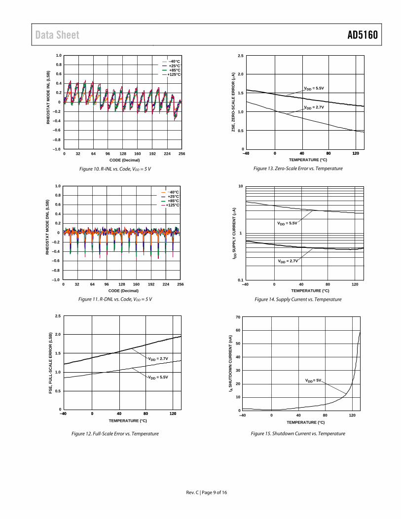
Data Sheet AD5160
–1.0
–0.8
–0.6
–0.4
–0.2
0
0.2
0.4
0.6
1.0
RH
EOST
AT
MO
DE
INL
(LSB
)
0.8
CODE (Decimal)320 9664 128 160 192 224 256
°C+25°C+85°C
+125°C
–40
Figure 10. R-INL vs. Code, VDD = 5 V
–1.0
–0.8
–0.6
–0.4
–0.2
0
0.2
0.4
0.6
1.0
RH
EOST
AT
MO
DE
DN
L (L
SB)
0.8
CODE (Decimal)320 9664 128 160 192 224 256
_40°C+25°C+85°C
+125°C
Figure 11. R-DNL vs. Code, VDD = 5 V
TEMPERATURE (°C)
0 40 80 120–400
1.5
FSE,
FU
LL-S
CA
LE E
RR
OR
(LSB
)
0 40 80 120–40
1.0
2.5
VDD = 5.5V
VDD = 2.7V
2.0
0.5
Figure 12. Full-Scale Error vs. Temperature
0 40 80 120–400
1.5
ZSE,
ZER
O-S
CA
LE E
RR
OR
(µA
)
TEMPERATURE (°C)0 40 80 120–40
1.0
2.5
VDD = 5.5V
VDD = 2.7V
2.0
0.5
Figure 13. Zero-Scale Error vs. Temperature
TEMPERATURE (°C)0 40 80 120–40
0.1
1
10
I DD
SUPP
LY C
UR
REN
T (µ
A)
VDD = 5.5V
VDD = 2.7V
Figure 14. Supply Current vs. Temperature
I ASH
UTD
OW
N C
UR
REN
T (n
A)
TEMPERATURE (°C)
00
70
20
10
30
40
50
60
40 80 120–40
VDD = 5V
Figure 15. Shutdown Current vs. Temperature
Rev. C | Page 9 of 16
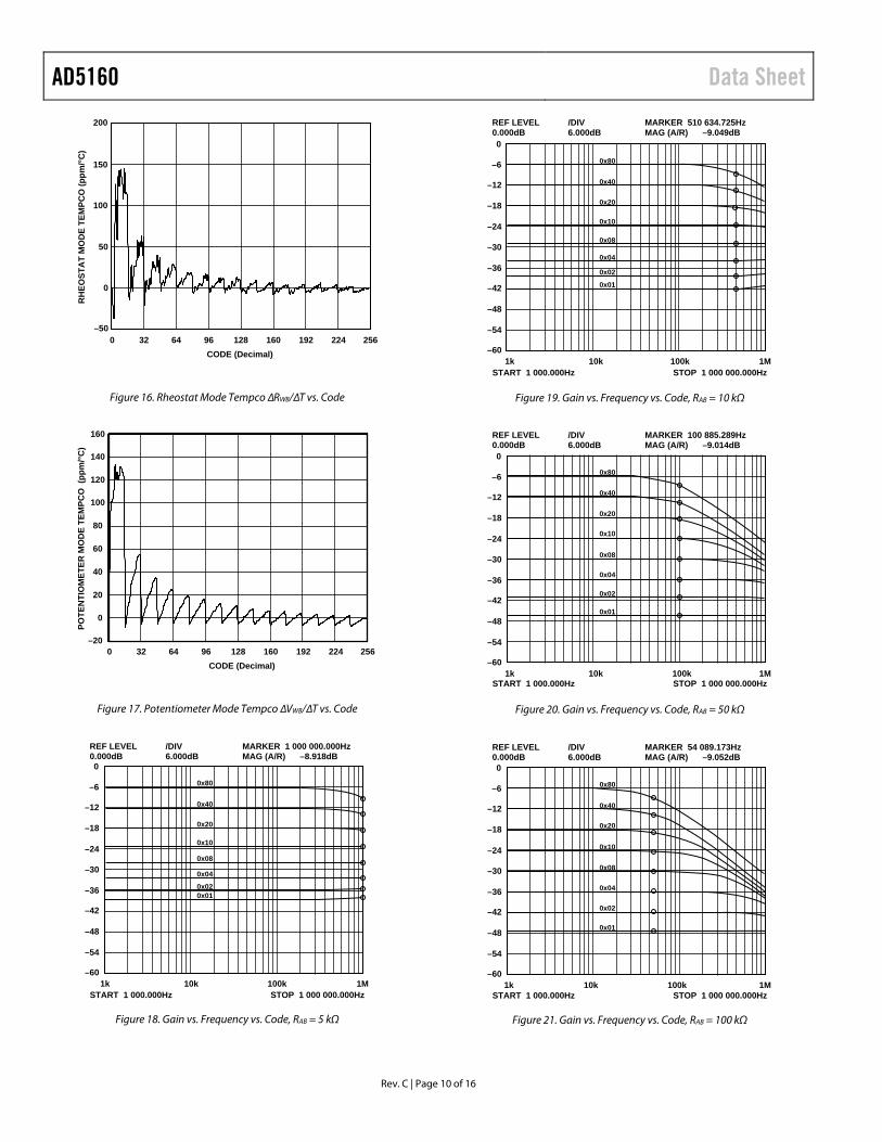
AD5160 Data Sheet
CODE (Decimal)
–50
0
50
100
150
200
320 9664 128 160 192 224 256
RH
EOST
AT
MO
DE
TEM
PCO
(ppm
/°C)
Figure 16. Rheostat Mode Tempco ∆RWB/∆T vs. Code
CODE (Decimal)
–20
0
20
40
60
80
100
120
140
160
320 9664 128 160 192 224 256
POTE
NTI
OM
ETER
MO
DE
TEM
PCO
(ppm
/°C)
Figure 17. Potentiometer Mode Tempco ∆VWB/∆T vs. Code
1k 10k 100k 1M
0
–6
–12
–18
–24
–30
–36
–42
–48
–54
–60
0x80
0x40
0x20
0x10
0x08
0x040x020x01
REF LEVEL0.000dB
/DIV6.000dB
MARKER 1 000 000.000HzMAG (A/R) –8.918dB
START 1 000.000Hz STOP 1 000 000.000Hz
Figure 18. Gain vs. Frequency vs. Code, RAB = 5 kΩ
1k 10k 100k 1M
0
–6
–12
–18
–24
–30
–36
–42
–48
–54
–60
0x80
0x40
0x20
0x10
0x08
0x04
0x02
0x01
REF LEVEL0.000dB
/DIV6.000dB
MARKER 510 634.725HzMAG (A/R) –9.049dB
START 1 000.000Hz STOP 1 000 000.000Hz
Figure 19. Gain vs. Frequency vs. Code, RAB = 10 kΩ
1k 10k 100k 1M
0
–6
–12
–18
–24
–30
–36
–42
–48
–54
–60
0x80
0x40
0x20
0x10
0x08
0x04
0x02
0x01
REF LEVEL0.000dB
/DIV6.000dB
MARKER 100 885.289HzMAG (A/R) –9.014dB
START 1 000.000Hz STOP 1 000 000.000Hz
Figure 20. Gain vs. Frequency vs. Code, RAB = 50 kΩ
1k 10k 100k 1M
0
–6
–12
–18
–24
–30
–36
–42
–48
–54
–60
0x80
0x40
0x20
0x10
0x08
0x04
0x02
0x01
REF LEVEL0.000dB
/DIV6.000dB
MARKER 54 089.173HzMAG (A/R) –9.052dB
START 1 000.000Hz STOP 1 000 000.000Hz
Figure 21. Gain vs. Frequency vs. Code, RAB = 100 kΩ
Rev. C | Page 10 of 16
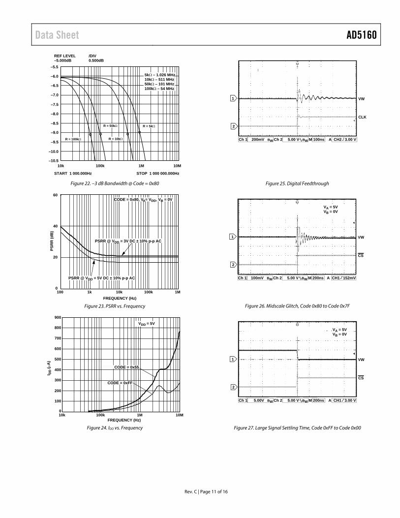
Data Sheet AD5160
Rev. C | Page 11 of 16
10k 100k 1M 10M
–5.5
–6.0
–6.5
–7.0
–7.5
–8.0
–8.5
–9.0
–9.5
–10.0
–10.5
REF LEVEL–5.000dB
/DIV0.500dB
START 1 000.000Hz STOP 1 000 000.000Hz
R = 5k
R = 10k
R = 50k
R = 100k
5k – 1.026 MHz10k – 511 MHz50k – 101 MHz100k – 54 MHz
Figure 22. –3 dB Bandwidth @ Code = 0x80
FREQUENCY (Hz)10k100 100k 1M1k
0
20
40
60
PSR
R (d
B)
CODE = 0x80, VA= VDD, VB = 0V
PSRR @ VDD = 3V DC ± 10% p-p AC
PSRR @ VDD = 5V DC ± 10% p-p AC
Figure 23. PSRR vs. Frequency
I DD
(A
)
FREQUENCY (Hz)10k
800
700
600
500
400
300
900
200
100
100k 1M 10M0
CODE = 0x55
CODE = 0xFF
VDD = 5V
Figure 24. IDD vs. Frequency
VW
CLK
Ch 1 200mV BW Ch 2 5.00 V BW M 100ns A CH2 3.00 V
1
2
Figure 25. Digital Feedthrough
VW
CS
Ch 1 100mV BW Ch 2 5.00 V BW M 200ns A CH1 152mV
1
2
VA = 5VVB = 0V
Figure 26. Midscale Glitch, Code 0x80 to Code 0x7F
VW
CS
Ch 1 5.00V BW Ch 2 5.00 V BW M 200ns A CH1 3.00 V
1
2
VA = 5VVB = 0V
Figure 27. Large Signal Settling Time, Code 0xFF to Code 0x00
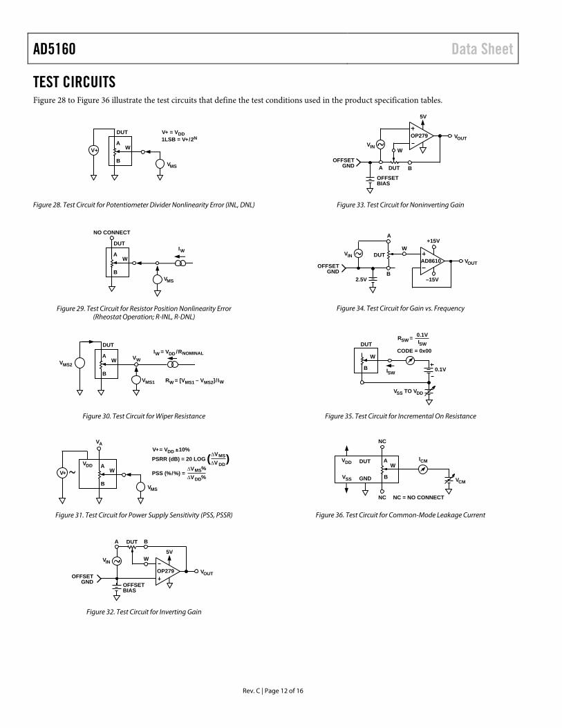
AD5160 Data Sheet
TEST CIRCUITS Figure 28 to Figure 36 illustrate the test circuits that define the test conditions used in the product specification tables.
VMS
AW
B
DUT V+ = VDD1LSB = V+/2N
V+
Figure 28. Test Circuit for Potentiometer Divider Nonlinearity Error (INL, DNL)
NO CONNECT
IW
VMS
AW
B
DUT
Figure 29. Test Circuit for Resistor Position Nonlinearity Error
(Rheostat Operation; R-INL, R-DNL)
VMS1
IW = VDD /RNOMINAL
VMS2VW
RW = [VMS1 – VMS2]/ IW
AW
B
DUT
Figure 30. Test Circuit for Wiper Resistance
∆V∆V
∆V∆VMS%
DD%PSS (%/%) =
V+ = VDD 10%PSRR (dB) = 20 LOG MS
DD( )VDD
VA
VMS
AW
B
V+
Figure 31. Test Circuit for Power Supply Sensitivity (PSS, PSSR)
OP279
W5V
B
VOUTOFFSETGND OFFSET
BIAS
A DUT
VIN
Figure 32. Test Circuit for Inverting Gain
BA
VIN
OP279
W
5V
VOUT
OFFSETGND
OFFSETBIAS
DUT
Figure 33. Test Circuit for Noninverting Gain
+15V
–15V
W
A
2.5VB
VOUTOFFSETGND
DUTAD8610
VIN
Figure 34. Test Circuit for Gain vs. Frequency
W
B
VSS TO VDD
DUT
ISW
CODE = 0x00
RSW = 0.1VISW
0.1V
Figure 35. Test Circuit for Incremental On Resistance
W
B VCM
ICMA
NC
GND
NC
VSS
VDD DUT
NC = NO CONNECT
Figure 36. Test Circuit for Common-Mode Leakage Current
Rev. C | Page 12 of 16
Data Sheet AD5160
Rev. C | Page 13 of 16
SPI INTERFACE Table 6. Serial Data-Word Format B7 B6 B5 B4 B3 B2 B1 B0 D7 D6 D5 D4 D3 D2 D1 D0 MSB LSB 27 20
SDI
CLK
CS
VOUT
1
0
1
0
1
0
1
0
D7 D6 D5 D4 D3 D2 D1 D0
RDAC REGISTER LOAD
Figure 37. SPI Interface Timing Diagram
(VA = 5 V, VB = 0 V, VW = VOUT)
tCSHOtCSS
tCL
tCH
tDS
tCSW
tS
tCS1
tCSH1
tCH
SDI
CLK
CS
VOUT
1
0
1
0
1
0
VDD
0±1LSB
(DATA IN) Dx Dx
Figure 38. SPI Interface Detailed Timing Diagram (VA = 5 V, VB = 0 V, VW = VOUT)
AD5160 Data Sheet
Rev. C | Page 14 of 16
THEORY OF OPERATION The AD5160 is a 256-position digitally controlled variable resistor (VR) device.
An internal power-on preset places the wiper at midscale during power-on, which simplifies the fault condition recovery at power-up.
PROGRAMMING THE VARIABLE RESISTOR Rheostat Operation
The nominal resistance of the RDAC between Terminal A and Terminal B is available in 5 kΩ, 10 kΩ, 50 kΩ, and 100 kΩ. The final two or three digits of the model number as listed in the Ordering Guide section determine the nominal resistance value, for example, in model AD5160BRJZ10, the 10 represents 10 kΩ; and in AD5160BRJZ50, the 50 represents 50 kΩ.
The nominal resistance (RAB) of the VR has 256 contact points accessed by the wiper terminal, plus the B terminal contact. The 8-bit data in the RDAC latch is decoded to select one of the 256 possible settings.
Assuming a 10 kΩ part is used, the first connection of the wiper starts at the B terminal for Data 0x00. Because there is a 60 Ω wiper contact resistance, such connection yields a minimum of 60 Ω resistance between Terminal W and Terminal B.
The second connection is the first tap point, which corresponds to 99 Ω (RWB = RAB/256 + RW = 39 Ω + 60 Ω) for Data 0x01.
The third connection is the next tap point, representing 138 Ω (2 × 39 Ω + 60 Ω) for Data 0x02, and so on. Each LSB data value increase moves the wiper up the resistor ladder until the last tap point is reached at 9961 Ω (RAB − 1 LSB + RW). Figure 39 shows a simplified diagram of the equivalent RDAC circuit where the last resistor string is not accessed; therefore, there is 1 LSB less of the nominal resistance at full scale in addition to the wiper resistance.
B
RDAC
LATCHAND
DECODER
W
A
RS
RS
RS
RS
D7D6
D4D5
D2D3
D1D0
Figure 39. Equivalent RDAC Circuit
The general equation determining the digitally programmed output resistance between W and B is
WABWB RRDDR 256
)( (1)
where: D is the decimal equivalent of the binary code loaded in the 8-bit RDAC register. RAB is the end-to-end resistance. RW is the wiper resistance contributed by the on resistance of the internal switch.
In summary, if RAB = 10 kΩ and the A terminal is open circuited, the following output resistance RWB is set for the indicated RDAC latch codes.
Table 7. Codes and Corresponding RWB Resistance D (Dec.) RWB (Ω) Output State 255 9961 Full Scale (RAB − 1 LSB + RW) 128 5060 Midscale 1 99 1 LSB 0 60 Zero Scale (Wiper Contact Resistance)
Note that in the zero-scale condition, a finite wiper resistance of 60 Ω is present. Take care to limit the current flow between W and B in this state to a maximum pulse current of no more than 20 mA. Otherwise, degradation or possible destruction of the internal switch contact can occur.
Similar to the mechanical potentiometer, the resistance of the RDAC between the Wiper W and Terminal A also produces a digitally controlled complementary resistance (RWA). When these terminals are used, the B terminal can be opened. Setting the resistance value for RWA starts at a maximum value of resistance and decreases as the data loaded in the latch increases in value. The general equation for this operation is
WABWA RRDDR
256
256)( (2)
For RAB = 10 kΩ and the B terminal is open circuited, the following output resistance RWA is set for the indicated RDAC latch codes.
Table 8. Codes and Corresponding RWA Resistance D (Dec.) RWA (Ω) Output State 255 99 Full Scale 128 5060 Midscale 1 9961 1 LSB 0 10,060 Zero Scale
Typical device-to-device matching is process lot dependent and may vary by up to ±30%. Because the resistance element is processed in thin film technology, the change in RAB with temperature has a very low 45 ppm/°C temperature coefficient.
Data Sheet AD5160
Rev. C | Page 15 of 16
PROGRAMMING THE POTENTIOMETER DIVIDER Voltage Output Operation
The digital potentiometer easily generates a voltage divider at wiper-to-B and wiper-to-A proportional to the input voltage at A-to-B. Unlike the polarity of VDD to GND, which must be positive, voltage across A to B, W to A, and W to B can be at either polarity.
If ignoring the effect of the wiper resistance for approximation, connecting the A terminal to 5 V and the B terminal to ground produces an output voltage at the wiper-to-B starting at 0 V up to 1 LSB less than 5 V. Each LSB of voltage is equal to the voltage applied across Terminal A and Terminal B divided by the 256 positions of the potentiometer divider. The general equation defining the output voltage at VW with respect to ground for any valid input voltage applied to Terminal A and Terminal B is
BAW VDVDDV256
256256
)(
(3)
For a more accurate calculation, which includes the effect of wiper resistance, VW can be found as
BWA
AWB
W VDR
VDR
DV256
)(256
)()( (4)
Operation of the digital potentiometer in the divider mode results in a more accurate operation over temperature. Unlike the rheostat mode, the output voltage is dependent mainly on the ratio of the internal resistors (RWA and RWB) and not the absolute values. Therefore, the temperature drift reduces to 15 ppm/°C.
SPI-COMPATIBLE 3-WIRE SERIAL BUS The AD5160 contains a 3-wire SPI-compatible digital interface (SDI, CS, and CLK). The 8-bit serial word must be loaded MSB first. The format of the word is shown in Table 6.
The positive-edge sensitive CLK input requires clean transitions to avoid clocking incorrect data into the serial input register. Standard logic families work well. If mechanical switches are used for product evaluation, they should be debounced by a flip-flop or other suitable means. When CS is low, the clock loads data into the serial register on each positive clock edge (see Figure 37).
The data setup and data hold times in the specification table determine the valid timing requirements. The AD5160 uses an 8-bit serial input data register word that is transferred to the internal RDAC register when the CS line returns to logic high. Extra MSB bits are ignored.
ESD PROTECTION All digital inputs are protected with a series input resistor and parallel Zener ESD structures are shown in Figure 40 and Figure 41. This applies to SDI, CLK, and CS, which are the digital input pins.
LOGIC340Ω
GND Figure 40. ESD Protection of Digital Pins
A,B,W
GND Figure 41. ESD Protection of Resistor Terminals
POWER-UP SEQUENCE Because the ESD protection diodes limit the voltage compliance at the A, B, and W terminals, it is important to power VDD/GND before applying any voltage to the A, B, and W terminals; otherwise, the diode forward biases such that VDD is powered unintentionally and may affect the rest of the user’s circuit. The ideal power-up sequence is in the following order: GND, VDD, digital inputs, and then VA/B/W. The relative order of powering VA, VB, VW, and the digital inputs is not important as long as they are powered after VDD/GND.
LAYOUT AND POWER SUPPLY BYPASSING It is a good practice to employ compact, minimum lead length layout design. Keep the leads to the inputs as direct as possible with a minimum conductor length. Ground paths should have low resistance and low inductance.
Similarly, it is also a good practice to bypass the power supplies with quality capacitors for optimum stability. Bypass supply leads to the device with disc or chip ceramic capacitors of 0.01 μF to 0.1 μF. To minimize any transient disturbance and low frequency ripple, apply low ESR 1 μF to 10 μF tantalum or electrolytic capacitors at the supplies (see Figure 42). To minimize the ground bounce, join the digital ground remotely to the analog ground at a single point.
AD5160
VDD
C1C3
GND
10F 0.1F+
VDD
Figure 42. Power Supply Bypassing
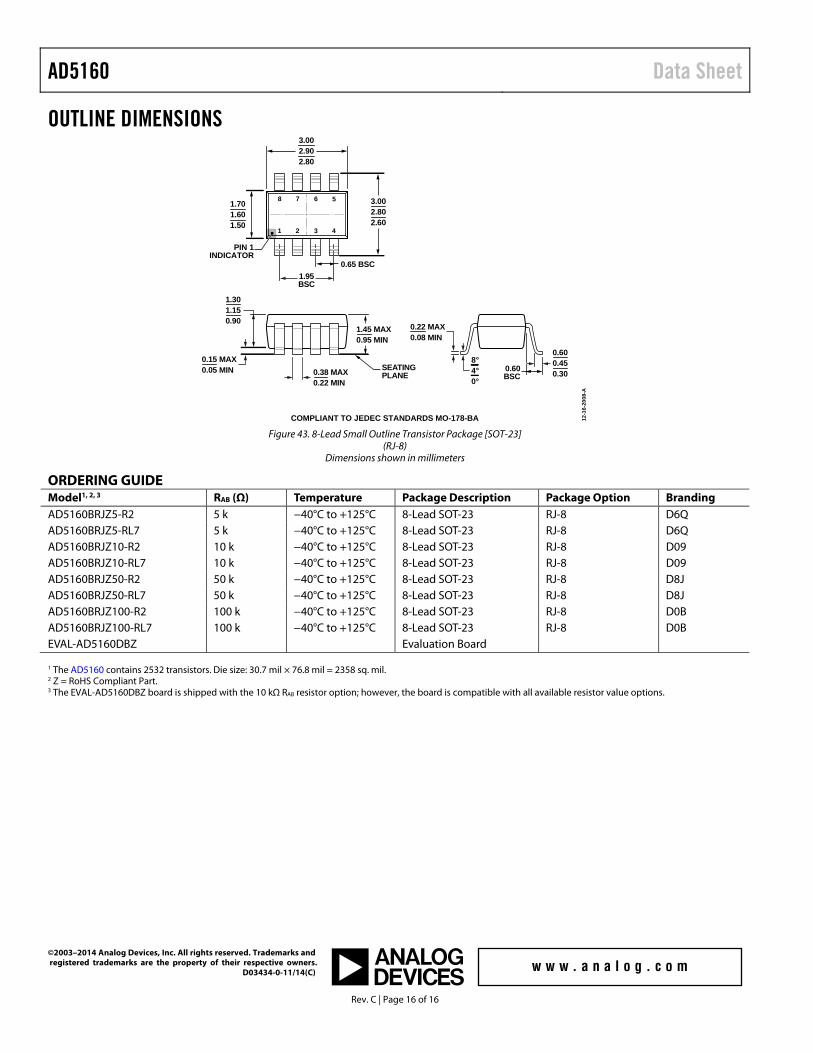
AD5160 Data Sheet
Rev. C | Page 16 of 16
OUTLINE DIMENSIONS
COMPLIANT TO JEDEC STANDARDS MO-178-BA
8°4°0°
SEATINGPLANE
1.95BSC
0.65 BSC
0.60BSC
7 6
1 2 3 4
5
3.002.902.80
3.002.802.60
1.701.601.50
1.301.150.90
0.15 MAX0.05 MIN
1.45 MAX0.95 MIN
0.22 MAX0.08 MIN
0.38 MAX0.22 MIN
0.600.450.30
PIN 1INDICATOR
8
12-1
6-20
08-A
Figure 43. 8-Lead Small Outline Transistor Package [SOT-23]
(RJ-8) Dimensions shown in millimeters
ORDERING GUIDE Model1, 2, 3 RAB (Ω) Temperature Package Description Package Option Branding AD5160BRJZ5-R2 5 k −40°C to +125°C 8-Lead SOT-23 RJ-8 D6Q AD5160BRJZ5-RL7 5 k −40°C to +125°C 8-Lead SOT-23 RJ-8 D6Q AD5160BRJZ10-R2 10 k −40°C to +125°C 8-Lead SOT-23 RJ-8 D09 AD5160BRJZ10-RL7 10 k −40°C to +125°C 8-Lead SOT-23 RJ-8 D09 AD5160BRJZ50-R2 50 k −40°C to +125°C 8-Lead SOT-23 RJ-8 D8J AD5160BRJZ50-RL7 50 k −40°C to +125°C 8-Lead SOT-23 RJ-8 D8J AD5160BRJZ100-R2 100 k −40°C to +125°C 8-Lead SOT-23 RJ-8 D0B AD5160BRJZ100-RL7 100 k −40°C to +125°C 8-Lead SOT-23 RJ-8 D0B EVAL-AD5160DBZ Evaluation Board 1 The AD5160 contains 2532 transistors. Die size: 30.7 mil × 76.8 mil = 2358 sq. mil. 2 Z = RoHS Compliant Part. 3 The EVAL-AD5160DBZ board is shipped with the 10 kΩ RAB resistor option; however, the board is compatible with all available resistor value options.
©2003–2014 Analog Devices, Inc. All rights reserved. Trademarks and registered trademarks are the property of their respective owners. D03434-0-11/14(C)
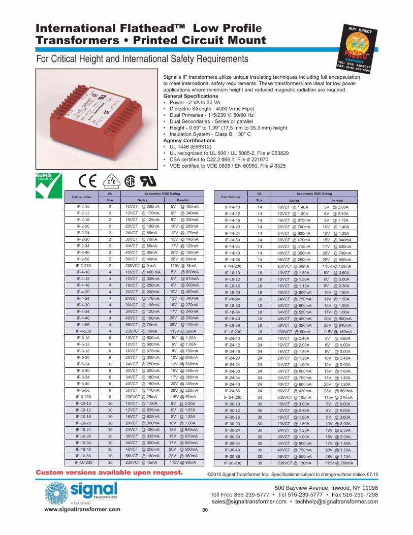
500 Bayview Avenue, Inwood, NY 11096Toll Free 866-239-5777 Tel Fax 516-239-7208
30
For Critical Height and International Safety Requirements
e
IF-2-10 2IF-2-12 2IF-2-16 2IF-2-20 2
2IF-2-30 2
22
IF-2-56 2IF-2-230 2
IF-6-10 6IF-6-12 6IF-6-16 6IF-6-20 6
6IF-6-30 6
66
IF-6-56 6IF-6-230 6IF-10-10 10IF-10-12 10IF-10-16 10IF-10-20 10
10IF-10-30 10
1010
IF-10-56 10IF-10-230 10
IF-18-10 18IF-18-12 18IF-18-16 18IF-18-20 18
18IF-18-30 18
1818
IF-18-56 18IF-18-230 18
IF-30-10 30IF-30-12 30IF-30-16 30IF-30-20 30
30IF-30-30 30
3030
IF-30-56 30IF-30-230 30
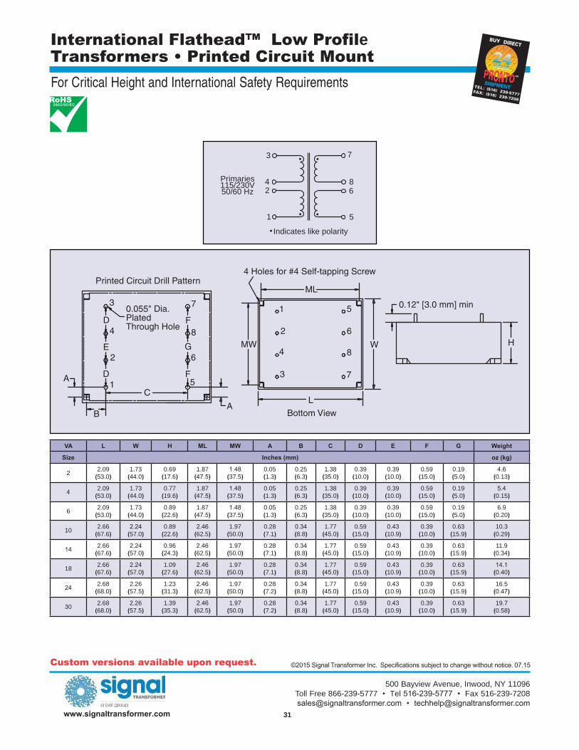
500 Bayview Avenue, Inwood, NY 11096Toll Free 866-239-5777 Tel Fax 516-239-7208
31
For Critical Height and International Safety Requirements
e
2 2.0953.0
1.73 0.6917.6
1.8737.5
0.051.3
0.256.3
1.3835.0
0.3910.0
0.3910.0
0.5915.0
0.195.0 0.13
2.0953.0
1.73 0.7719.6
1.8737.5
0.051.3
0.256.3
1.3835.0
0.3910.0
0.3910.0
0.5915.0
0.195.0 0.15
6 2.0953.0
1.73 0.8922.6
1.8737.5
0.051.3
0.256.3
1.3835.0
0.3910.0
0.3910.0
0.5915.0
0.195.0
6.90.20
10 2.6667.6 57.0
0.8922.6 62.5
1.9750.0
0.287.1 8.8
1.77 0.5915.0 10.9
0.3910.0
0.6315.9
10.30.29
2.6667.6 57.0
0.9662.5
1.9750.0
0.287.1 8.8
1.77 0.5915.0 10.9
0.3910.0
0.6315.9
11.9
18 2.6667.6 57.0
1.0927.6 62.5
1.9750.0
0.287.1 8.8
1.77 0.5915.0 10.9
0.3910.0
0.6315.9
2.6868.0
2.2657.5
1.2331.3 62.5
1.9750.0
0.287.2 8.8
1.77 0.5915.0 10.9
0.3910.0
0.6315.9
16.5
30 2.6868.0
2.2657.5
1.3935.3 62.5
1.9750.0
0.287.2 8.8
1.77 0.5915.0 10.9
0.3910.0
0.6315.9
19.70.58
1
Indicates like polarity
Primaries115/230V50/60 Hz
5
68
73
42