
Unequal Termination Impedances Microwave Filter Synthesis
163
Ph.D Dissertation Unequal Termination Impedances Microwave Filter Synthesis 비대칭 종단 임피던스 마이크로파 여파기 회로 합성 2017. 02. 22 Graduate School of Chonbuk National University Division of Electronics and Information Engineering Phirun Kim
-
Upload
khangminh22 -
Category
Documents
-
view
3 -
download
0
Transcript of Unequal Termination Impedances Microwave Filter Synthesis
Ph.D Dissertation
Unequal Termination Impedances
Microwave Filter Synthesis
비대칭 종단 임피던스 마이크로파 여파기
회로 합성
2017. 02. 22
Graduate School of
Chonbuk National University
Division of Electronics and Information Engineering
Phirun Kim
Unequal Termination Impedances
Microwave Filter Synthesis
비대칭 종단 임피던스 마이크로파 여파기
회로 합성
2017. 02. 22
Graduate School of
Chonbuk National University
Division of Electronics and Information Engineering
Phirun Kim
Unequal Termination Impedances
Microwave Filter Synthesis
Academic Advisor: Professor Yongchae Jeong
A Dissertation Submitted In Partial Fulfillment of the
Requirements for the Degree of
Doctor of Philosophy
2016. 09. 26
Graduate School of
Chonbuk National University
Division of Electronics and Information Engineering
Phirun Kim

The Ph.D dissertation of Phirun Kim
is approved by
Chair, Professor, Hae-Won Son
Chonbuk National University
Vice Chair, Professor, Jongsik Lim
Soonchunhyang University
Professor, Hee-Yong Hwang
Kangwon National University
Professor, Donggu Im
Chonbuk National University
Advisor, Professor, Yongchae Jeong
Chonbuk National University
2016. 12. 16
Graduate School of
Chonbuk National University
Phirun
Stamp
Phirun
Stamp
Phirun
Group
Phirun
Stamp
Phirun
Stamp
Phirun
Sticky Note
Unmarked set by Phirun
Phirun
Sticky Note
Unmarked set by Phirun
Phirun
Sticky Note
Unmarked set by Phirun
Phirun
Sticky Note
Unmarked set by Phirun
Phirun
Sticky Note
Unmarked set by Phirun

To my beloved wife and families

ACKNOWLEDGEMENTS
First of all, I am great honor to thank God for his impact to my study
and life. Moreover, I would like to show a gratitude to my academic
advisor Prof. Yongchae Jeong who I regard and respect him as my
father. This is not an accident that I studied under him throughout
master and PhD program. With his support and profession, I can know
the world and share my knowledge through international conferences
and Journal publications. I gratefully acknowledge Prof. Hae-Won Son,
Prof. Jongsik Lim, Prof. Hee-Yong Hwang, and Prof. Donggu Im for
serving on my defense committee. Moreover, I would like to appreciate
to all the people who have been involved and helped me finishing this
dissertation. I also thank the current and previous members of
Microwave Circuits Design Laboratory, Dr. G. Chaudhary, Dr. N. Ryu,
J. Jeong, J. Park, J. Kim, Q. Wang, S. Lee, S. Jeong, J. Koo, and B. An,
for their assistance, cooperation and encouragement.
I appreciate Prof. Dae-Hwan Bae for his support and driven my
education go higher and lead me to know God. I thanks to God that
introduces to me a kindness people such as elder Hosoo Haan and his
family for helping me while I stay in this country. I also thank to
BK21+ for support me throughout Master and PhD program. Also
thanks to brother T. Tharoeun and other WE&C members who is my
good family in Christ and always encourage and give me a hope.
Moreover, I would like to thank to my lovely wife (Leanghorn Ky)
who means to my life with her sweet and pure love. Thank for your
understanding of my busy time in laboratory. I do love you with no end.
Finally, I would like to give thanks to my warm family that they
always provided me a strong support and encouragement. I am indebted
to my parent for providing me a good attitude and support me from the
childhood. I do love all of you in my heart.
i
TABLE OF CONTENTS
TABLE OF CONTENTS . . . . . . . . . . . . . . . . . . . . . .
LIST OF FIGURES . . . . . . . . . . . . . . . . . . . . . . . . . .
LIST OF TABLES . . . . . . . . . . . . . . . . . . . . . . . . . .
ABSTRACT . . . . . . . . . . . . . . . . . . . . . . . . . . . . . . . .
ABBREVIATIONS . . . . . . . . . . . . . . . . . . . . . . . . . .
CHAPTER 1
DISSERTATION OVERVIEW
1.1 Introduction . . . . . . . . . . . . . . . . . . . . . . . . . . . . . . . . . .
1.2 Literature Review . . . . . . . . . . . . . . . . . . . . . . . . . . . . .
1.3 Dissertation Overview . . . . . . . . . . . . . . . . . . . . . . . . . .
CHAPTER 2
FUNDAMENTAL THEORIES OF MICROWAVE FILTER
2.1 Lossless Transmission Lines . . . . . . . . . . . . . . . . . . .
2.2 Two-Port Network Parameters . . . . . . . . . . . . .
2.2.1 Scattering Parameters. . . . . . . . . . . . . . . . . .
2.2.2 Impedance and Admittance Parameters . . . . . .
2.2.3 The Transmission (ABCD) Parameters . . . . . .
2.2.4 Even- and odd-mode Network Analysis. . . . . .
2.2.5 Image Impedance. . . . . . . . . . . . . . . . . .
i
v
x
xii
xiii
1
1
4
6
8
8
10
11
13
16
ii
2.3 Microwave Filters . . . . . . . . . . . . . . . . . . . . . . . . . . . .
2.3.1 Maximally Flat Low-pass Prototype. . . . . . . . .
2.3.2 Chebyshev (Equal-Ripple) Low-pass Prototype
2.4 Impedance and Frequency Transformation Filters. . . . . .
2.4.1 Frequency Scaling for Low-pass Filters . . . . . .
2.4.2 Frequency Scaling for Low-pass to High-Pass
Filters. . . . . . . . . . . . . . . . . . . . . . . . . . . . . . . . .
2.4.3 Frequency Scaling for Low-pass to Bandpass
Filters. . . . . . . . . . . . . . . . . . . . . . . . . . . . . . . . .
2.4.4 Frequency Scaling for Low-pass to Bandstop
Filters. . . . . . . . . . . . . . . . . . . . . . . . . . . . . . . . .
2.5 Impedance and Admittance Inverters . . . . . . . . . . . . . . .
CHAPTER 3
DESIGN OF ULTRA-HIGH TRANSFORMING RATIOS
COUPLED LINE IMPEDANCE TRANSFORMER WITH
BANDPASS RESPONSES
3.1 Design Theory . . . . . . . . . . . . . . . . . . . . . . . .
3.1.1 S-parameter analysis . . . . . . . . . . . . . . . . .
3.1.2 Design Procedure of IT Network. . . . . . . . . . . .
3.2 The Simulation and Experimental Results . . . . . . . . .
3.3 Summary and Discussion. . . . . . . . . . . . . . . . . . .
18
19
21
22
23
25
25
28
29
33
35
42
42
44
iii
CHAPTER 4
DESIGN OF LUMPED ELEMENTS BANDPASS FILTER
WITH AIRBITRARY TERMINATION IMPEDANCE
4.1 Coupled-Resonator Filter . . . . . . . . . . . . . . . . . . . . .
4.1.1 Capacitive of Coupled Resonators. . . . . . . . . . .
4.1.2 Compensation of Complex Termination . . . . . .
4.2 Simulation . . . . . . . . . . . . . . . . . . . . . . . . . . . . . . . . .
4.3 Summary and Discussion . . . . . . . . . . . . . . . . . . . . . . .
CHAPTER 5
DISTRIBUTED UNEQUAL TERMINATION IMPEDANCE
λ/4 COUPLED LINE BANDPASS FILTER
5.1 Theory and Design Equations . . . . . . . . . . . . . . . . . . . .
5.1.1 Low-pass Prototype Ladder Network . . . . . . . .
5.1.2 Inverter Coupled Arbitrary Termination
Impedance BPF . . . . . . . . . . . . . . . . . . . . . . . . .
5.1.3 Arbitrary Termination Impedance Coupled Line
BPF . . . . . . . . . . . . . . . . . . . . . . . . .
5.2 Filter Implementation . . . . . . . . . . . . . . . . . . . . . . . . .
5.2.1 Three Stages Coupled Line BPF . . . . . . . . . . . .
5.2.2 Four Stages Coupled Line BPF. . . . . . . . . . . . .
5.3 Summary and Discussion . . . . . . . . . . . . . . . . . .
46
50
53
58
62
63
63
65
71
84
84
87
89
iv
CHAPTER 6
DISTRIBUTED UNEQUAL TERMINATION COUPLED LINE
STEPPED IMPEDANCE RESONATOR BANDPASS FILTER
6.1 Theory and Design Equations . . . . . . . . . . . . . . . . . . . . .
6.1.1 Stepped Impedance Resonator . . . . . . . . . . . . .
6.1.2 Slope Parameter and J-inverter of SIR . . . . . . .
6.2 Simulation and Measurement . . . . . . . . . . . . . . .
6.2.1 Two Stages Chebyshev Response. . . . . . . . . . .
6.2.2 Three Stages Chebyshev Response. . . . . . . . . .
6.2.3 Three Stages Butterworth Response. . . . . . . . .
6.3 Summary and Discussion . . . . . . . . . . . . . . . . . . . . . . .
CHAPTER 7
CONCLUSION AND FUTURE WORKS
7.1 Conclusion . . . . . . . . . . . . . . . . . . . . . . . . . . . . .
7.2 Future Research Direction . . . . . . . . . . . . . . . . .
REFERENCES . . . . . . . . . . . . . . . . . . . . . . . . . . . . . .
ABSTRACT IN KOREAN . . . . . . . . . . . . . . . . . . . .
APPENDIX . . . . . . . . . . . . . . . . . . . . . . . . . . . . .
CURRICULUM VITAE . . . . . . . . . . . . . . . . . . . . . . . . . . . . . . .
PUBLICATIONS . . . . . . . . . . . . . . . . . . . . . . . . . . . . .
91
94
98
110
111
113
114
116
117
118
120
127
128
137
139
v
LIST OF FIGURES
Figure 2.1 A transmission line terminated with a load impedance
ZL. . . . . . . . . . . . . . . . . . . . . . . . . . . . . . . . . . . . . . . . . . .
Figure 2.2 A transmission line terminated with (a) short and (b)
open circuits. . . . . . . . . . . . . . . . . . . . . . . . . . . . . . . . . . .
Figure 2.3 A two-port network . . . . . . . . . . . . . . . . . . . . . . . . . . . . .
Figure 2.4 (a) A two-port network and (b) a cascade connection of
two-port networks. . . . . . . . . . . . . . . . . . . . . . . . . . . . . .
Figure 2.5 Symmetrical two-port network . . . . . . . . . . . . . . . . . . .
Figure 2.6 Two-port networks: (a) two networks in cascade and (b)
two-port network with perfectly matched. . . . . . . . . . . .
Figure 2.7 Ladder circuits for low-pass filter prototype and their
element: (a) prototype beginning with a shunt element
and (b) prototype beginning with a series element . . . .
Figure 2.8 A Maximally flat low-pass attenuation characteristic . . .
Figure 2.9 Chebyshev low-pass attenuation characteristic . . . . . . .
Figure 2.10 Frequency scaling for low-pass filters and
transformation to high pass response: (a) low-pass filter
prototype response, (b) frequency scaling for low-pass
response, and (c) transformation to high pass response. .
Figure 2.11 Frequency transformation from low-pass to bandpass
filter . . . . . . . . . . . . . . . . . . . . . . . . . . . . . . . . . . . . . . . .
Figure 2.12 Transformation from low-pass filter to bandstop
response . . . . . . . . . . . . . . . . . . . . . . . . . . . . . . . . . . . . .
Figure 2.13 Impedance inverter . . . . . . . . . . . . . . . . . . . . . . . . . . . . .
6
8
9
12
14
18
19
20
22
24
26
29
30
vi
Figure 2.14 Admittance inverter . . . . . . . . . . . . . . . . . . . . . . . . . . . .
Figure 3.1 Proposed impedance transformer for ultra-high
impedance transforming ratio . . . . . . . . . . . . . . . . . . . . .
Figure 3.2 Frequency responses of transformer for three different
matched regions . . . . . . . . . . . . . . . . . . . . . . . . . . . . . . .
Figure 3.3 Design graph according to Z0o and different r: (a) C1,
(b) 20 dB return loss (RL) FBW of under-matched
region, (c) C2, and (d) 20 dB RL FBW of perfectly
matched region . . . . . . . . . . . . . . . . . . . . . . . . . . . . . . . .
Figure 3.4 (a) EM simulation layout and (b) photograph of
fabricated PCB (Wi1 = 2.4, Li1 = 2, Wi2 = 1.35, Li2 = 22.7,
Si2 = 0.3, Wi3 = 2.4, Li3 = 17.2, Si3 = 0.65, and Li4 = 3)
(unit: mm) . . . . . . . . . . . . . . . . . . . . . . . . . . . . . . . . . . . .
Figure 3.5 EM simulation and measurement results . . . . . . . . . . . .
Figure 4.1 Capacitive coupled lumped elements filter . . . . . . . . . . .
Figure 4.2 Lumped elements ladder network for low-pass
prototype. . . . . . . . . . . . . . . . . . . . . . . . . . . . . . . . . . . .
Figure 4.3 Bandpass filter with admittance inverters.. . . . . . . . . . . .
Figure 4.4 (a) J-inverter and (b) implementation using capacitor
networks. . . . . . . . . . . . . . . . . . . . . . . . . . . . . . . . . . . . . .
Figure 4.5 (a) transformed J-inverter from coupling capacitor and
(b) equivalent circuit of coupled resonator bandpass
filter. . . . . . . . . . . . . . . . . . . . . . . . . . . . . . . . . . . . . . . . .
Figure 4.6 (a) Capacitive coupled BPF with equivalent J-inverter
and (b) its equivalent circuit . . . . . . . . . . . . . . . . . . . . . .
Figure 4.7 (a) Source termination with a series capacitor and (b)
equivalent source termination with J-inverter. . . . . . . . .
30
34
41
41
43
44
47
47
49
51
52
52
53
vii
Figure 4.8 (a) Load termination with a series capacitor and (b)
load termination with J-inverter. . . . . . . . . . . . . . . . . . . .
Figure 4.9 Equivalent circuit of (a) coupled resonator with new
termination and (b) new elements of first and last
resonators. . . . . . . . . . . . . . . . . . . . . . . . . . . . . . . . . . . . .
Figure 4.10 S-parameter characteristic of coupled resonator
bandpass filter with Chebyshev response: (a) narrow
and (b) broad bands . . . . . . . . . . . . . . . . . . . . . . . . . . . . .
Figure 4.11 S-parameter characteristic of coupled resonator
bandpass filter with Butterworth response (a) narrow
and (b) broad band characteristics . . . . . . . . . . . . . . . .
Figure 5.1 Ladder circuits for low-pass filter prototype and their
element: (a) prototype beginning with a shunt element
and (b) prototype beginning with a series element. . . . .
Figure 5.2 Arbitrary termination impedance low-pass [19-42] and
frequency transformed arbitrary termination impedance
bandpass filters . . . . . . . . . . . . . . . . . . . . . . . . . . . . . . . .
Figure 5.3 Generalized arbitrary termination impedance bandpass
filter with (a) impedance and (b) admittance inverters . .
Figure 5.4 Frequency response of a bandpass filter with (a)
Chebyshev (or equal-ripple) and (b) Butterworth (or
maximally flat) responses . . . . . . . . . . . . . . . . . . . . . . .
Figure 5.5 S-parameter characteristics of arbitrary termination
impedance BPF using J- and K-inverters according to
order of filter: (a) Chebyshev and (b) Butterworth
responses. . . . . . . . . . . . . . . . . . . . . . . . . . . . . . . . . . . . .
Figure 5.6 Parallel coupled line bandpass filter . . . . . . . . . . . . . . . .
Figure 5.7 (a) Single parallel coupled line and (b) its equivalent
55
56
60
61
64
65
67
67
70
72
viii
circuit . . . . . . . . . . . . . . . . . . . . . . . . . . . . . . . . . . . . . . .
Figure 5.8 (a) Equivalent circuit of the parallel couple line
bandpass filter and (b) equivalent circuit model of (a) . .
Figure 5.9 S-parameters of Chebyshev coupled line BPF with
different (a) n, (b) Z1, and (c) r. . . . . . . . . . . . . . . . . . . .
Figure 5.10 S-parameters of Butterworth coupled line BPF with
different (a) n, (b) Z1, and (c) r. . . . . . . . . . . . . . . . . . . .
Figure 5.11 Variation of coupling coefficients according to image
impedance Z1 for (a) n = 2 and (b) n = 4. . . . . . . . . . . . .
Figure 5.12 Layout and photograph of fabricated bandpass filter 1. .
Figure 5.13 Simulation and measurement results of arbitrary
termination impedance bandpass filter 1 with (a)
narrow and (b) broad bands. . . . . . . . . . . . . . . . . . . . . .
Figure 5.14 Layout and photograph of fabricated bandpass filter 2. .
Figure 5.15 Simulation and measurement results of arbitrary
termination impedance bandpass filter 2 with (a)
narrow and (b) broad bands . . . . . . . . . . . . . . . . . . . .
Figure 6.1 Coupled line bandpass filters with stepped impedance
resonators: (a) conventional and (b) proposed structure.
Figure 6.2 Equivalent circuits of parallel coupled line stepped
impedance resonators: (a) conventional circuit and (b)
proposed circuit. . . . . . . . . . . . . . . . . . . . . . . . . . . . . . .
Figure 6.3 Equivalent circuit Fig. 6.2 (b) of proposed SIR BPF . . .
Figure 6.4 Configuration of a stepped impedance resonator . . . . . .
Figure 6.5 Spurious resonant frequencies according to impedance
ratio of SIR. . . . . . . . . . . . . . . . . . . . . . . . . . . . . . . . . .
Figure 6.6 Variation of Z1 and total electrical length of SIR
72
73
78
81
83
85
86
87
88
92
93
94
95
97
ix
according to impedance ration of SIR and Z2. . . . . . . . .
Figure 6.7 (a) parallel coupled-line with two open terminations
and (b) equivalent circuit has a J-inverter with two
transmission line sections. . . . . . . . . . . . . . . . . . . . . .
Figure 6.8 Variation of coupling coefficients according to image
impedance Z2 for Chebyshev and Butterworth
responses with (a) RS=20, RL=50, K=0.7 and (b) RS=15,
RL=90, K=1.5. . . . . . . . . . . . . . . . . . . . . . . . . . . . . . . . . .
Figure 6.9 S-parameters characteristics of Chebyshev response
with different (a) n and (b) K. . . . . . . . . . . . . . . . . . . . .
Figure 6.10 S-parameters characteristics of Chebyshev response
with different (a) Z2 and (b) termination impedances . . .
Figure 6.11 S-parameters of Butterworth response with different (a)
n and (b) K . . . . . . . . . . . . . . . . . . . . . . . . . . . . . . . . . .
Figure 6.12 S-parameters characteristics of Butterworth with
different of (a) Z2 and (b) termination impedances . . . . .
Figure 6.13 Two stage SIR BPF: (a) layout and (b) photograph of
fabricated circuit . . . . . . . . . . . . . . . . . . . . . . . . . . . . . . .
Figure 6.14 Simulation and measurement results of two stage SIR
BPF with Chebyshev response. . . . . . . . . . . . . . . . . . .
Figure 6.15 Three stages SIR BPF: (a) layout and (b) photograph of
fabricated circuit . . . . . . . . . . . . . . . . . . . . . . . . . . . . . .
Figure 6.16 Simulation and measurement results of three stages SIR
BPF with Chebyshev response . . . . . . . . . . . . . . . . . . . .
Figure 6.17 Three stages SIR BPF: (a) layout and (b) photograph of
fabricated circuit. . . . . . . . . . . . . . . . . . . . . . . . . . . . . . .
Figure 6.18 Simulation and measurement results of three stages SIR
BPF with Butterworth response . . . . . . . . . . . . . . . . . .
98
100
102
103
105
108
109
111
112
113
114
115
116
x
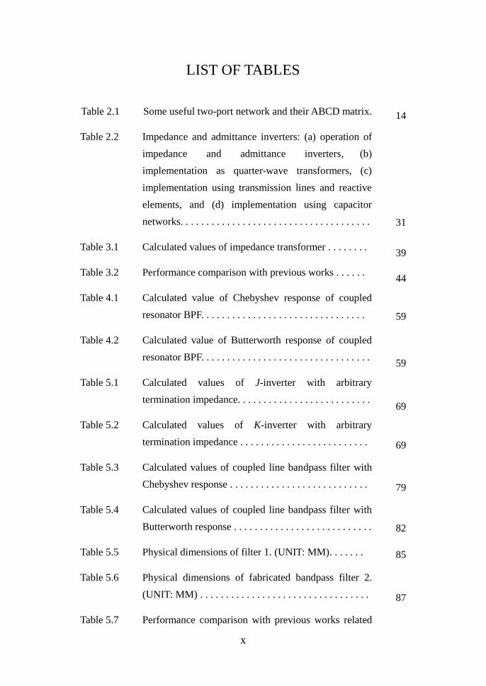
LIST OF TABLES
Table 2.1 Some useful two-port network and their ABCD matrix.
Table 2.2 Impedance and admittance inverters: (a) operation of
impedance and admittance inverters, (b)
implementation as quarter-wave transformers, (c)
implementation using transmission lines and reactive
elements, and (d) implementation using capacitor
networks. . . . . . . . . . . . . . . . . . . . . . . . . . . . . . . . . . . . .
Table 3.1 Calculated values of impedance transformer . . . . . . . .
Table 3.2 Performance comparison with previous works . . . . . .
Table 4.1 Calculated value of Chebyshev response of coupled
resonator BPF. . . . . . . . . . . . . . . . . . . . . . . . . . . . . . . .
Table 4.2 Calculated value of Butterworth response of coupled
resonator BPF. . . . . . . . . . . . . . . . . . . . . . . . . . . . . . . . .
Table 5.1 Calculated values of J-inverter with arbitrary
termination impedance. . . . . . . . . . . . . . . . . . . . . . . . . .
Table 5.2 Calculated values of K-inverter with arbitrary
termination impedance . . . . . . . . . . . . . . . . . . . . . . . . .
Table 5.3 Calculated values of coupled line bandpass filter with
Chebyshev response . . . . . . . . . . . . . . . . . . . . . . . . . . .
Table 5.4 Calculated values of coupled line bandpass filter with
Butterworth response . . . . . . . . . . . . . . . . . . . . . . . . . . .
Table 5.5 Physical dimensions of filter 1. (UNIT: MM). . . . . . .
Table 5.6 Physical dimensions of fabricated bandpass filter 2.
(UNIT: MM) . . . . . . . . . . . . . . . . . . . . . . . . . . . . . . . . .
Table 5.7 Performance comparison with previous works related
14
31
39
44
59
59
69
69
79
82
85
87
xi
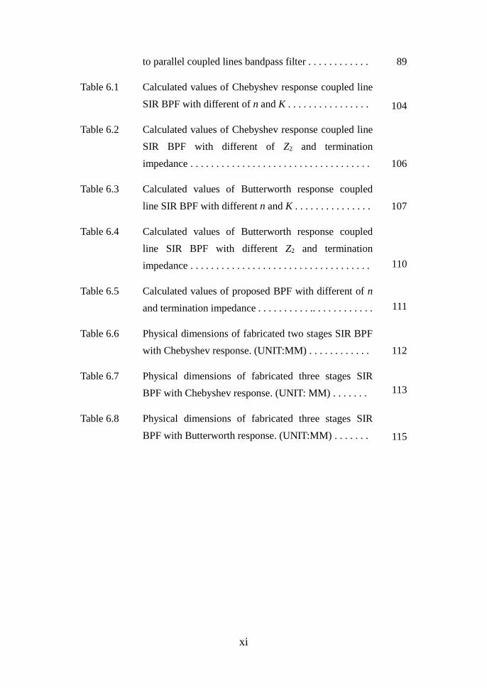
to parallel coupled lines bandpass filter . . . . . . . . . . . .
Table 6.1 Calculated values of Chebyshev response coupled line
SIR BPF with different of n and K . . . . . . . . . . . . . . . .
Table 6.2 Calculated values of Chebyshev response coupled line
SIR BPF with different of Z2 and termination
impedance . . . . . . . . . . . . . . . . . . . . . . . . . . . . . . . . . . .
Table 6.3 Calculated values of Butterworth response coupled
line SIR BPF with different n and K . . . . . . . . . . . . . . .
Table 6.4 Calculated values of Butterworth response coupled
line SIR BPF with different Z2 and termination
impedance . . . . . . . . . . . . . . . . . . . . . . . . . . . . . . . . . . .
Table 6.5 Calculated values of proposed BPF with different of n
and termination impedance . . . . . . . . . . .. . . . . . . . . . . .
Table 6.6 Physical dimensions of fabricated two stages SIR BPF
with Chebyshev response. (UNIT:MM) . . . . . . . . . . . .
Table 6.7 Physical dimensions of fabricated three stages SIR
BPF with Chebyshev response. (UNIT: MM) . . . . . . .
Table 6.8 Physical dimensions of fabricated three stages SIR
BPF with Butterworth response. (UNIT:MM) . . . . . . .
89
104
106
107
110
111
112
113
115
xii
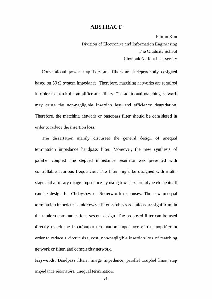
ABSTRACT
Phirun Kim
Division of Electronics and Information Engineering
The Graduate School
Chonbuk National University
Conventional power amplifiers and filters are independently designed
based on 50 system impedance. Therefore, matching networks are required
in order to match the amplifier and filters. The additional matching network
may cause the non-negligible insertion loss and efficiency degradation.
Therefore, the matching network or bandpass filter should be considered in
order to reduce the insertion loss.
The dissertation mainly discusses the general design of unequal
termination impedance bandpass filter. Moreover, the new synthesis of
parallel coupled line stepped impedance resonator was presented with
controllable spurious frequencies. The filter might be designed with multi-
stage and arbitrary image impedance by using low-pass prototype elements. It
can be design for Chebyshev or Butterworth responses. The new unequal
termination impedances microwave filter synthesis equations are significant in
the modern communications system design. The proposed filter can be used
directly match the input/output termination impedance of the amplifier in
order to reduce a circuit size, cost, non-negligible insertion loss of matching
network or filter, and complexity network.
Keywords: Bandpass filters, image impedance, parallel coupled lines, step
impedance resonators, unequal termination.
xiii
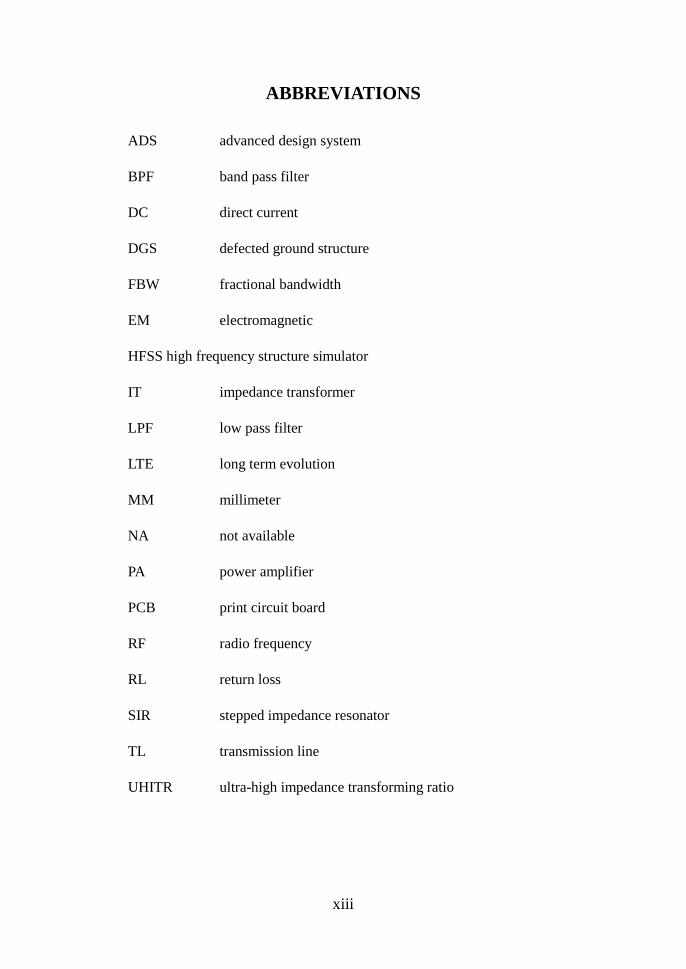
ABBREVIATIONS
ADS advanced design system
BPF band pass filter
DC direct current
DGS defected ground structure
FBW fractional bandwidth
EM electromagnetic
HFSS high frequency structure simulator
IT impedance transformer
LPF low pass filter
LTE long term evolution
MM millimeter
NA not available
PA power amplifier
PCB print circuit board
RF radio frequency
RL return loss
SIR stepped impedance resonator
TL transmission line
UHITR ultra-high impedance transforming ratio
1
CHAPTER 1
DISSERTATION OVERVIEW
1.1 Introduction
The RF/microwave filter is a key circuit which play an important role in mobile
and satellite communications, radar, and remote sensing systems operating at high
frequencies. In general, the performances of the filter are described in terms of
insertion loss, return loss, frequency-selectivity (or attenuation at rejection band),
group-delay variation in the passband, and so on. Filters are required to have small
insertion loss, high return loss, good out-of-band suppression, and high frequency-
selectivity to prevent an interference of signals in the passband.
As well known, the direct-coupled microwave filter can be obtained from
Butterworth (or maximally flat magnitude filter) and Chebyshev (or equal ripple
magnitude filter) frequency responses. Since Chebyshev response filter has better
frequency selectivity than Butterworth response filter, it has been widely used in
the filter design.
1.2 Literature Review
The bandpass filter (BPF) with arbitrary termination impedances have been
analyzed in order to reduce circuit size, loss, complex circuit, and provide an out-
of-band suppression. Typically, the general BPFs were started to analyze and
design with equal termination impedances (50-to-50 ) [1]-[5]. In [1], the general
equations of parallel coupled line BPF were derived for Chebyshev and
2
Butterworth responses. After that, a new analysis of parallel coupled line BPF was
introduced in [2] with arbitrary image impedance, and the new analysis were able
to control the coupling coefficient of coupled lines. Moreover, a modified coupled
line BPF using defected ground structure (DGS) and additional stubs were
introduced in [3] and [4] with wide stopband characteristics. In [5], a new design
equations of parallel coupled line BPF were derived up to nine stages (n = 9) base
on the composite ABCD matrices with wide passband characteristics. An
impedance transformer is one of the arbitrary termination impedance circuits that
can transform one termination impedance to the specific impedance. Actually, a
quarter wavelength transmission line (TL) is well known the impedance
transformer and widely used. However, this network has some limitations such as
difficulty in realization for very high impedance transforming ratio [6] and poor
out-of-band suppression [7]. In order to overcome these limitations, various types
coupled line transformers were presented in [8]-[16].
In [8], a coupled three-line was used to get a wide passband response for an
impedance transforming ratio (r) of 3.4. However, the out-of-band suppression is
poor with the restricted in r. In [9], a single open-circuit coupled line was
introduced as the impedance transformer, and it was able to control the coupling
coefficient of coupled line. In [10]-[12], a coupled line with a shunt TL and its
application with power divider and high efficiency power amplifier were
demonstrated. The shunt open stub TL was used to produce transmission zeros at
the stopband and enhance r. As well, the impedance transformer analyzed in [13]
was able to obtain sharper and higher r compared to [10], but it was limited by a
3
number of stages (n) as two. On the other hand, a short-ended coupled-line
impedance transformer with higher r was designed with a suitable for large load
impedance (50-1000 ) [14]. In [15], a design of multi-section parallel coupled
line BPF was presented as an impedance matching network using an optimizing
process.
Typically, microwave circuits are independently designed with 50
termination impedance and then operate together. It is quite a challenge to design
the BPF with arbitrary termination impedances and apply as the matching network
of other microwave circuits to reduce the non-negligible insertion loss of normal
matching networks. In [16]-[18], the input and output matching networks of
amplifier were designed by optimization from the ladder network of arbitrary
termination low-pass filter by using a design technique of [19]. However, the
stopband of the low frequencies (close to DC) were poor characteristics and the
attenuation at center frequency is varied according to r. Moreover, the BPF with
one [20], two [21], and three [22] poles were analyzed using coupling matrix to
directly match with the output impedance of amplifier. The co-design method
might reduce the circuit size and provide a higher overall efficiency. The general
synthesis approach of coupling matrix was briefly explained in [23] without any
fabrication for validations.
A new design techniques have been subjects of requirements for circuit size,
cost, ease of fabrication, and multi-functions to use in modern wireless
communication systems. Although, an arbitrary image impedance of parallel
coupled line BPF was introduced a new design equation in [2] with a controllable
4
coupling of coupled line, however, the spurious responses are produced at higher
frequencies such as 2f0 and 3f0. In order to improve the harmonic suppression
characteristic, there are many methods by using such as modified coupled line
structure, DGS, and shunt stub TL were analyzed and introduced with wide
stopband characteristics. Besides the additional DGS and shunt stub TL, parallel
coupled line stepped impedance resonators (SIRs) were proposed in [24]-[31] and
its characteristic impedances of coupled line can be calculated by using a low-pass
prototype values. Typically, the general SIR BPFs were analyzed and designed with
equal termination impedances (50-to-50 ) with an image impedance of 50 . The
SIR structure is able to control the spurious frequency by varying an impedance
ratios and it can also obtain more compact size with multistage structure. However,
the image impedance (Z2) of a coupled line must be chosen equal to the termination
impedance to avoid mismatched.
1.3 Dissertation Overview
The main object of the dissertation is focused on the derivation of new
synthesis of unequal termination impedances BPF. A new design equations are able
to design the BPF with n-resonators, arbitrary termination impedance, arbitrary
image impedance of coupled line, and controllable a spurious frequency. The
design equations were derived base on a multistage coupled lines theory. These
new equations can make a significant impact on the advanced wireless systems.
The dissertation is organized as follows. Chapter 2 describes a relevant
fundamental theories of microwave filters. The purpose of this chapter is to give a
5
brief basic transmission line theory, two-port microwave network, and other
relevant theories that would be useful in the design of microwave filters.
Chapter 3 describes the design of two stages coupled line impedance
transformer with BPF response. In this chapter, the design equations are explained
with the simulation and measurement to show validity.
Chapter 4 presents the design of unequal termination impedance BPF with
lumped elements. In this chapter, the design formulas are all explicitly derived
step-by-step to clearly describe a design procedure. Moreover, the ideal simulations
are done with arbitrary termination impedance.
Chapter 5 describes new design equations for unequal termination impedances
parallel coupled line BPF. With new design formulas, the parallel coupled line
BPFs might be calculated and design with n-resonators, arbitrary termination
impedance, and arbitrary image impedance of coupled line by using low-pass
prototype elements values.
In Chapter 6, the general design formulas of arbitrary termination impedances
SIR BPF are analyzed in detail with simulation and measurement validation.
Similar to Chapter 5, the new design equations are applicable on n-resonators,
arbitrary termination impedance, and arbitrary image impedance of coupled line.
However, in this chapter the spurious frequencies are able to control variously in
the higher stopband.
Finally, Chapter 7 of the dissertation presents the conclusion and future work.
The significance and contributions of the dissertation is summarized in this chapter.
6
CHAPTER 2
FUNDAMENTAL THEORIES OF MICROWAVE FILTER
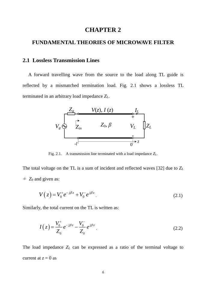
2.1 Lossless Transmission Lines
A forward travelling wave from the source to the load along TL guide is
reflected by a mismatched termination load. Fig. 2.1 shows a lossless TL
terminated in an arbitrary load impedance ZL.
Vg
Zg
ZLVL
+
-
Z0, β Zin
V(z), I (z) IL
-l 0z
Fig. 2.1. A transmission line terminated with a load impedance ZL.
The total voltage on the TL is a sum of incident and reflected waves [32] due to ZL
≠ Z0 and given as:
0 0
j z j zV z V e V e . (2.1)
Similarly, the total current on the TL is written as:
0 0
0 0
j z j zV VI z e e
Z Z
. (2.2)
The load impedance ZL can be expressed as a ratio of the terminal voltage to
current at z = 0 as
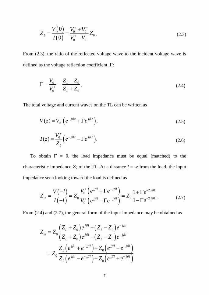
7
0 0
0
0 0
0
0L
V V VZ Z
I V V
. (2.3)
From (2.3), the ratio of the reflected voltage wave to the incident voltage wave is
defined as the voltage reflection coefficient, :
0 0
0 0
L
L
V Z Z
V Z Z
. (2.4)
The total voltage and current waves on the TL can be written as
0( ) ,j z j zV z V e e (2.5)
0
0
( ) .j z j zVI z e e
Z
(2.6)
To obtain = 0, the load impedance must be equal (matched) to the
characteristic impedance Z0 of the TL. At a distance l = -z from the load, the input
impedance seen looking toward the load is defined as
20
in 0 0 2
0
1
1
j l j l j l
j lj l j l
V e eV l eZ Z Z
I l eV e e
. (2.7)
From (2.4) and (2.7), the general form of the input impedance may be obtained as
0 0
in 0
0 0
0
0
0
j l j l
L L
j l j l
L L
j l j l j l j l
L
j l j l j l j l
L
Z Z e Z Z eZ Z
Z Z e Z Z e
Z e e Z e eZ
Z e e Z e e
8
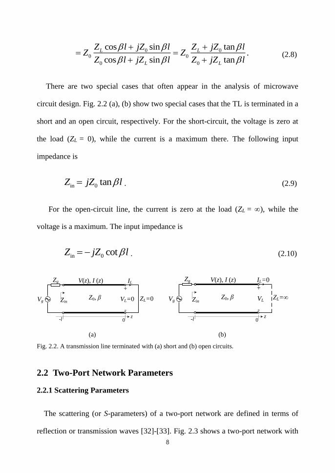
0 0
0 0
0 0
cos sin tan.
cos sin tan
L L
L L
Z l jZ l Z jZ lZ Z
Z l jZ l Z jZ l
(2.8)
There are two special cases that often appear in the analysis of microwave
circuit design. Fig. 2.2 (a), (b) show two special cases that the TL is terminated in a
short and an open circuit, respectively. For the short-circuit, the voltage is zero at
the load (ZL = 0), while the current is a maximum there. The following input
impedance is
in 0 tanZ jZ l . (2.9)
For the open-circuit line, the current is zero at the load (ZL = ), while the
voltage is a maximum. The input impedance is
in 0 cotZ jZ l . (2.10)
Vg
Zg
ZL=0VL=0
+
-
Z0, β Zin
V(z), I (z) IL
-l 0z
Vg
Zg
ZL= VL
+
-
Z0, β Zin
V(z), I (z) IL=0
-l 0z
(a) (b)
Fig. 2.2. A transmission line terminated with (a) short and (b) open circuits.
2.2 Two-Port Network Parameters
2.2.1 Scattering Parameters
The scattering (or S-parameters) of a two-port network are defined in terms of
reflection or transmission waves [32]-[33]. Fig. 2.3 shows a two-port network with
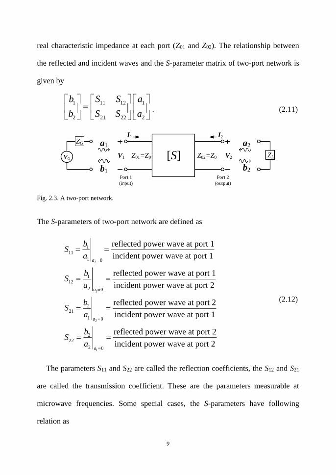
9
real characteristic impedance at each port (Z01 and Z02). The relationship between
the reflected and incident waves and the S-parameter matrix of two-port network is
given by
1 11 12 1
2 21 22 2
b S S a
b S S a
. (2.11)
[S]a1 a2
b1 b2
V1 V2
I1 I2
ZG
Z02=Z0
Port 1
(input)
Port 2
(output)
Z01=Z0VGZL
Fig. 2.3. A two-port network.
The S-parameters of two-port network are defined as
2
1
2
111
1 0
112
2 0
221
1 0
reflected power wave at port 1
incident power wave at port 1
reflected power wave at port 1
incident power wave at port 2
reflected power wave at port 2
incident powe
a
a
a
bS
a
bS
a
bS
a
1
222
2 0
r wave at port 1
reflected power wave at port 2
incident power wave at port 2a
bS
a
(2.12)
The parameters S11 and S22 are called the reflection coefficients, the S12 and S21
are called the transmission coefficient. These are the parameters measurable at
microwave frequencies. Some special cases, the S-parameters have following
relation as
10
12 21S S (For reciprocal network) (2.13a)
11 22S S (For symmetrical network) (2.13b)
2 2 2 2
21 11 12 221, 1S S S S (For lossless passive network). (2.13c)
2.2.2 Impedance and Admittance Parameters
The impedance parameters (Z-parameters) and its matrix for two-port network is
probably the most common [32]-[34]. The relationship between the current, voltage
at each port and the Z matrix is given by
1 11 12 1
2 21 22 2
V Z Z I
V Z Z I
. (2.14)
From (2.14), the Z-parameters of two-port network are defined as
2
111
1 0I
VZ
I
(2.15a)
1
112
2 0I
VZ
I
(2.15b)
2
221
1 0I
VZ
I
(2.15c)
1
222
2 0
.
I
VZ
I
(2.15d)
The Z-parameters are known as the open-circuit impedance parameters [35],
and [Z] is called an open-circuit impedance matrix. The [Z] is often employed in
the calculation of series network connection [32-33]. In case of Z12 = Z21, the
network is reciprocal network. If network are symmetrical, then Z12 = Z21 and Z11 =
Z22. For a lossless network, the Z-parameter are all purely imaginary.
For the parallel network connection, the admittance matrix [Y] has to be
adopted for the convenience, which is known as a short-circuit admittance matrix
11
[Y]. The relationship between the voltage and current at each port and Y-parameter
matrix is given by
1 11 12 1
2 21 22 2
I Y Y V
I Y Y V
. (2.16)
From (2.16), the Z-parameters of two-port network are defined as
2
111
1 0V
IY
V
(2.17a)
1
112
2 0V
IY
V
(2.17b)
2
221
1 0V
IY
V
(2.17c)
1
222
2 0V
IY
V
. (2.17d)
Similarly, in case of Y12 = Y21, the network is reciprocal network. Moreover, if
the network is symmetrical, then Y11 = Y22. For a lossless network, the Y-parameters
are all purely imaginary. The relation of impedance and admittance matrix can be
written as
1
Y Z
. (2.18)
2.2.3 The Transmission (ABCD) Parameters
The advantage of the ABCD matrix is that the cascaded two-port networks can
be characterized by simply multiplying their ABCD matrices. The ABCD matrix is
defined for a two-port network in terms of the port voltages and currents [32] as
shown in Fig. 2.4(a) and can be defined as
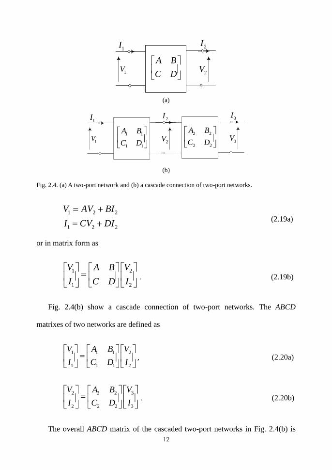
12
1V
1I
A B
C D
2V
2I
(a)
1V
1I
1 1
1 1
A B
C D
2V
2I
2 2
2 2
A B
C D
3V
3I
(b)
Fig. 2.4. (a) A two-port network and (b) a cascade connection of two-port networks.
1 2 2
1 2 2
V AV BI
I CV DI
(2.19a)
or in matrix form as
1 2
1 2
V VA B
I IC D
. (2.19b)
Fig. 2.4(b) show a cascade connection of two-port networks. The ABCD
matrixes of two networks are defined as
1 1 1 2
1 1 1 2
V A B V
I C D I
, (2.20a)
32 2 2
32 2 2
VV A B
II C D
. (2.20b)
The overall ABCD matrix of the cascaded two-port networks in Fig. 2.4(b) is
13
defined as
31 1 1 2 2
31 1 1 2 2
VV A B A B
II C D C D
, (2.21)
which shows that a cascaded connection of two-port networks is equivalent to a
single two-port network containing a product of the ABCD matrices. The properties
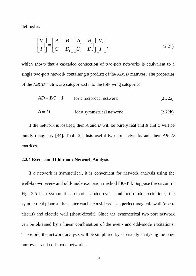
of the ABCD matrix are categorized into the following categories:
1AD BC for a reciprocal network (2.22a)
A D for a symmetrical network (2.22b)
If the network is lossless, then A and D will be purely real and B and C will be
purely imaginary [34]. Table 2.1 lists useful two-port networks and their ABCD
matrices.
2.2.4 Even- and Odd-mode Network Analysis
If a network is symmetrical, it is convenient for network analysis using the
well-known even- and odd-mode excitation method [36-37]. Suppose the circuit in
Fig. 2.5 is a symmetrical circuit. Under even- and odd-mode excitations, the
symmetrical plane at the center can be considered as a perfect magnetic wall (open-
circuit) and electric wall (short-circuit). Since the symmetrical two-port network
can be obtained by a linear combination of the even- and odd-mode excitations.
Therefore, the network analysis will be simplified by separately analyzing the one-
port even- and odd-mode networks.
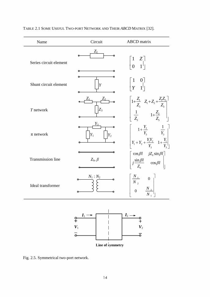
14
TABLE 2.1 SOME USEFUL TWO-PORT NETWORK AND THEIR ABCD MATRIX [32].
ZL
Y
Z3
Z2Z1
Y2
Y3
Y1
Z0, β
N1 : N2
1
0 1
Z
1 0
1Y
1 1 21 2
3 3
2
3 3
1
11
Z Z ZZ Z
Z Z
Z
Z Z
2
3 3
1 2 11 2
3 3
11
1
Y
Y Y
YY YY Y
Y Y
0
0
cos sin
sincos
l jZ l
lj l
Z
1
2
2
1
0
0
N
N
N
N
Series circuit element
Shunt circuit element
T network
π network
Transmission line
Ideal transformer
Circuit ABCD matrixName
V1 V2
I1 I2
Line of symmetry
Fig. 2.5. Symmetrical two-port network.
15
For the one-port even- and odd-mode S-parameters are
11e
e
e
bS
a (2.23a)
11o
o
o
bS
a (2.23b)
where the subscripts e and o stand for even- and odd-mode, respectively. For the
symmetrical network, the relationships of wave variables are
1 e oa a a (2.24a)
2 e oa a a (2.24b)
1 e ob b b (2.24b)
2 e ob b b . (2.24b)
Letting a2 = 0, the equation (2.23) and (2.24) can be written as
1 2 2e oa a a (2.25a)
1 11 11e e o ob S a S a (2.25b)
2 11 11e e o ob S a S a . (2.25c)
From (2.12), the two-port S-parameters are
2
111 11 11
1 0
1
2e o
a
bS S S
a
(2.26a)
2
221 11 11
1 0
1
2e o
a
bS S S
a
(2.26b)
16
For a symmetrical network, S11 = S22 and S21 = S12 can be obtained. Suppose Zine
and Zino represent one-port input impedance of even- and odd-mode networks,
respectively. The reflection coefficients of one-port can be obtained as
in 0
11
in 0
ee
e
Z ZS
Z Z
(2.27a)
in 0
11
in 0
oo
o
Z ZS
Z Z
. (2.27b)
Substituting (2.26) and (2.27) into (2.25), the S-parameters can be obtained as
2
in in 011 22
in 0 in 0
e o
e o
Z Z ZS S
Z Z Z Z
(2.28a)
in 0 in 021 12
in 0 in 0
e o
e o
Z Z Z ZS S
Z Z Z Z
(2.28b)
2.2.5 Image Impedance
The image impedance method is commonly used for analysis and design of
filter consisting of parallel-coupled TL and building of matching network. For the
uniform TL, the characteristic impedance of the TL is also its image impedance.
The image parameters can be used not only on symmetrical network, but also on
asymmetrical network [33]. The equations for the image impedance can be derived
from the circuit shown in Fig. 2.6 with a termination impedance ZL.
In case ZL is equal to ZI1, the input impedance Zin of the circuit will also be
equal to ZI1. Thus, the network is symmetric with a plane of (S-S’), and the input
impedance of Zin is defined as an image impeance ZI1 at port 1. Therefore, the total
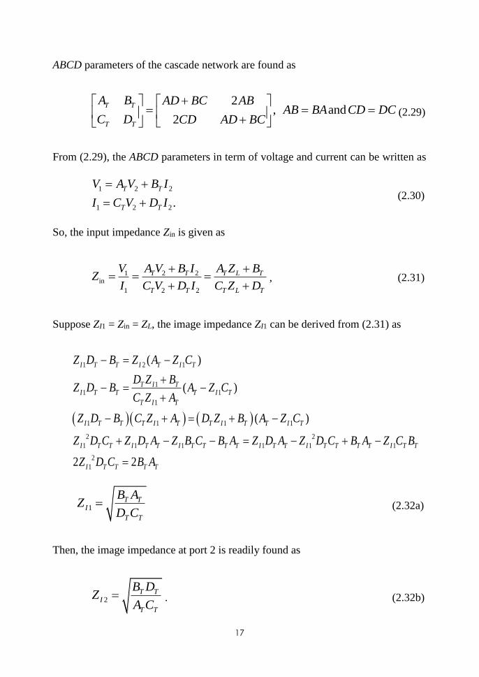
17
ABCD parameters of the cascade network are found as
2
, and2
T T
T T
A B AD BC ABAB BA CD DC
C D CD AD BC
(2.29)
From (2.29), the ABCD parameters in term of voltage and current can be written as
1 2 2
1 2 2.
T T
T T
V A V B I
I C V D I
(2.30)
So, the input impedance Zin is given as
1 2 2
in
1 2 2
T T T L T
T T T L T
V A V B I A Z BZ
I C V D I C Z D
, (2.31)
Suppose ZI1 = Zin = ZL, the image impedance ZI1 can be derived from (2.31) as
1 2 1
11 1
1
1 1 1 1
2 2
1 1 1 1 1 1
2
1
( )
( )
( )
2 2
I T T I T I T
T I TI T T T I T
T I T
I T T T I T T I T T I T
I T T I T T I T T T T I T T I T T T T I T T
I T T T T
Z D B Z A Z C
D Z BZ D B A Z C
C Z A
Z D B C Z A D Z B A Z C
Z D C Z D A Z B C B A Z D A Z D C B A Z C B
Z D C B A
1T T
I
T T
B AZ
D C (2.32a)
Then, the image impedance at port 2 is readily found as
2T T
I
T T
B DZ
A C . (2.32b)
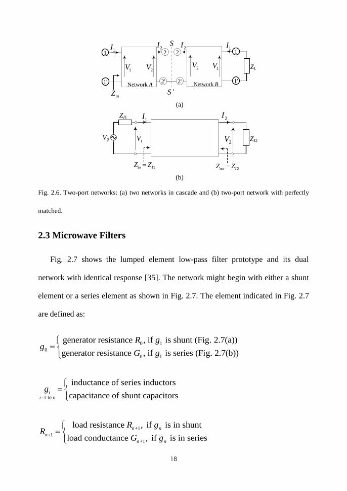
18
1I2
'S
2V
1IS
1V1V 2V
2'
2
2'Network A Network B
ZL
2I2I1
1'
1
1'
inZ
(a)
1V
1I
2V
2I
ZI2
1in IZ Z
Vg
ZI1
2out IZ Z
(b)
Fig. 2.6. Two-port networks: (a) two networks in cascade and (b) two-port network with perfectly
matched.
2.3 Microwave Filters
Fig. 2.7 shows the lumped element low-pass filter prototype and its dual
network with identical response [35]. The network might begin with either a shunt
element or a series element as shown in Fig. 2.7. The element indicated in Fig. 2.7
are defined as:
0 1
0
0 1
generator resistance , if is shunt (Fig. 2.7(a))
generator resistance , if is series (Fig. 2.7(b))
R gg
G g
1 to
inductance of series inductors
capacitance of shunt capacitorsi
i n
g
+1
1
+1
load resistance , if is in shunt
load conductance , if is in series
n n
n
n n
R gR
G g
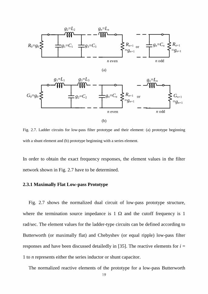
19
n even n odd
orR0=g0 g1=C1
g2=L2 gn=Ln
Rn+1
=gn+1
gn=Cn Rn+1
=gn+1
g3=C3
(a)
n even n odd
orG0=g0
g1=L1
g2=C2
g3=L3
gn=CnRn+1
=gn+1
gn=Ln
Gn+1
=gn+1
(b)
Fig. 2.7. Ladder circuits for low-pass filter prototype and their element: (a) prototype beginning
with a shunt element and (b) prototype beginning with a series element.
In order to obtain the exact frequency responses, the element values in the filter
network shown in Fig. 2.7 have to be determined.
2.3.1 Maximally Flat Low-pass Prototype
Fig. 2.7 shows the normalized dual circuit of low-pass prototype structure,
where the termination source impedance is 1 and the cutoff frequency is 1
rad/sec. The element values for the ladder-type circuits can be defined according to
Butterworth (or maximally flat) and Chebyshev (or equal ripple) low-pass filter
responses and have been discussed detailedly in [35]. The reactive elements for i =
1 to n represents either the series inductor or shunt capacitor.
The normalized reactive elements of the prototype for a low-pass Butterworth
20
response by using terminations g0 = gn+1 = 1 are computed as
2 1
2sin for = 1,2,...,2
i
ig i n
n
. (2.33)
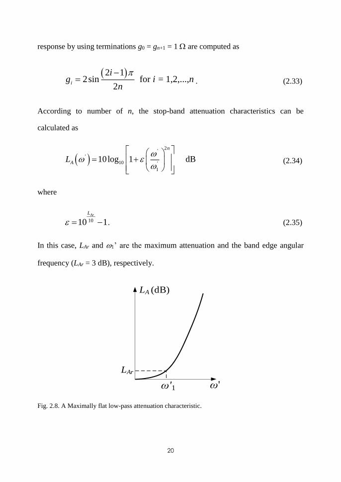
According to number of n, the stop-band attenuation characteristics can be
calculated as
2
''
10 '
1
10log 1 dB
n
AL
(2.34)
where
1010 1ArL
. (2.35)
In this case, LAr and 1’ are the maximum attenuation and the band edge angular
frequency (LAr = 3 dB), respectively.
ω'ω'1
LAr
LA (dB)
Fig. 2.8. A Maximally flat low-pass attenuation characteristic.
21
2.3.2 Chebyshev (Equal-ripple) Low-pass Prototype
The elements of the prototype for a low-pass Chebyshev response having pass-
band ripple LAr dB and g0 = 1 are computed as
1
1
2ag
(2.36a)
1
1 1
4, 2,3, ,i i
i
i i
a ag i n
b g
(2.36b)
1 2
1 for odd
coth for even4
i
n
gn
(2.36c)
where
ln coth ,17.37
ArL
(2.37a)
2 1
sin , 1,2, ,2
i
ia i n
n
(2.37b)
2 2sinh sin
2i
ib
n n
. (2.37c)
Similar to Butterworth response, the stop-band attenuation characteristics can by
calculated according to the number of n.
'
' 2 1 ' '
10 1'
1
10log 1 cos cos , for AL n
(2.38a)
22
'
' 2 1 ' '
10 1'
1
10log 1 cosh cosh , for AL n
(2.38b)
where
1010 1ArL
. (2.39)
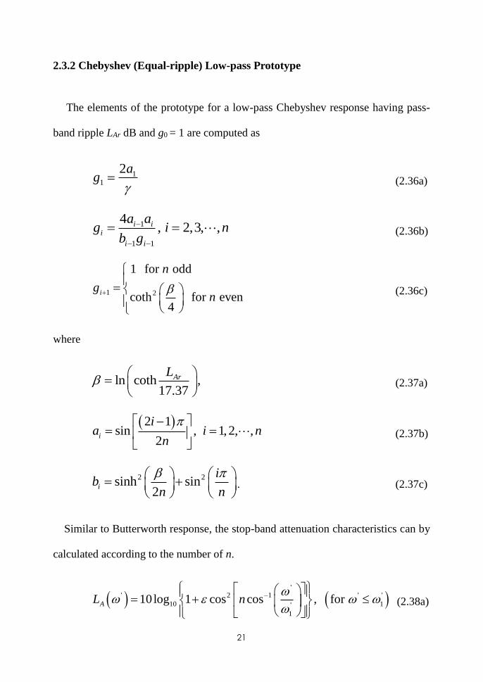
Fig. 2.9 shows Chebyshev low-pass attenuation characteristic.
ω'1 ω'
LAr
LA (dB)
Fig. 2.9. Chebyshev low-pass attenuation characteristic.
The Butterworth and Chebyshev low-pass filter responses have terminated
resistors of equal or nearly equal at each termination. In practice, the low-pass
filters must be designed with same termination impedance (typically R0 = Rn+1 = 50
) and different operating frequency bands. Therefore, the impedance and
frequency scalings are required. The transformation from low-pass filter to
highpass, bandpass, and bandstop filters are presented in [32]-[34].
2.4 Impedance and Frequency Transformation Filters
The low-pass filter prototypes of the previous section were normalized designs
23
with a termination impedance of 1 and a cutoff frequency of c = 1 rad/sec. In
the practical, the frequency characteristics and the element values are applied
frequency and impedance transformations of the low-pass prototype. Also, the
practical low-pass, highpass, bandpass, and band-stop microwave filters are
designed from an initial low-pass prototype filter through the transformation from
prototype low-pass filter impedance and frequency scalings. The frequency
transformation causes an effect on all the reactive elements accordingly, but no
effect on the resistive elements. The termination impedances are chosen arbitrarily
with equal (RS = RL) or unequal terminations (RS RL). The impedance
transformation can be done by scaling the normalized generator impedance or
conductance to a desired impedance, Z0, or admittance, Y0. The scalings of
frequency and impedance will have no effect on the response shape [38]. Thus, the
impedance transformation provide the new filter component values as
"
0L R L (2.40a)
"
0
,C
CR
(2.40b)
"
0 ,SR R (2.40c)
"
0L LR R R . (2.40d)
2.4.1 Frequency scaling for low-pass filters
To scale the cutoff frequency of a low-pass prototype from unity to c,
frequency scaled low-pass response can be obtained. Fig. 2.10 (a) and (b) shows
24
the frequency scaling from a low-pass prototype to a practical low-pass filter
having a cutoff frequency ωc. The frequency scaling is simply given as
C
2
2'
21 21
C
S j S j
. (2.41)
So the scaled values are obtained as
" 1
C
j L j L
(2.42a)
"
1 1
1
C
jC
j C
. (2.42b)
1
[dB]AL
01 C
[dB]AL
0C C
[dB]AL
0C
Fig. 2.10. Frequency scaling for low-pass filters and transformation to highpass response: (a) low-
pass filter prototype response, (b) frequency scaling for low-pass response, and (c) transformation to
highpass response.
Thus, the both impedance and frequency scaling are obtained as
" 0
C
R LL
(2.43a)
"
0 C
CC
R . (2.43b)
25
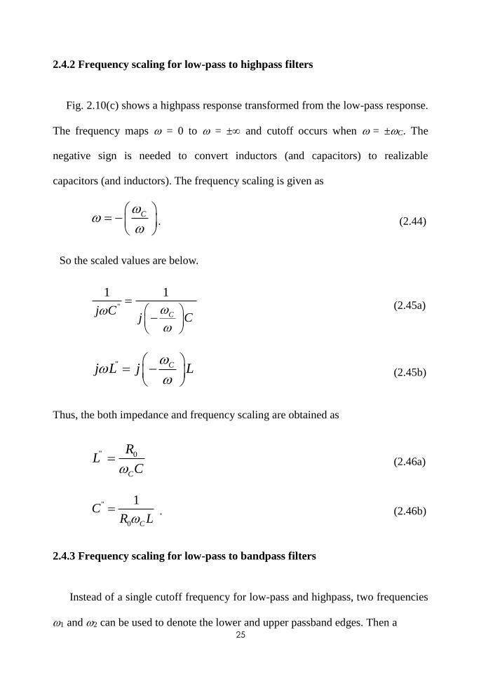
2.4.2 Frequency scaling for low-pass to highpass filters
Fig. 2.10(c) shows a highpass response transformed from the low-pass response.
The frequency maps = 0 to = ± and cutoff occurs when = ±C. The
negative sign is needed to convert inductors (and capacitors) to realizable
capacitors (and inductors). The frequency scaling is given as
C
. (2.44)
So the scaled values are below.
"
1 1
Cj Cj C
(2.45a)
" Cj L j L
(2.45b)
Thus, the both impedance and frequency scaling are obtained as
" 0
C
RL
C (2.46a)
"
0
1
C
CR L
. (2.46b)
2.4.3 Frequency scaling for low-pass to bandpass filters
Instead of a single cutoff frequency for low-pass and highpass, two frequencies
1 and 2 can be used to denote the lower and upper passband edges. Then a
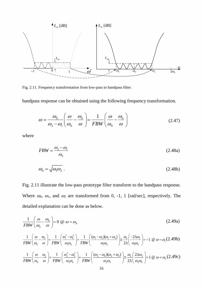
26
1
ArL
[dB]AL
01 2
ArL
[dB]AL
01 02
Fig. 2.11. Frequency transformation from low-pass to bandpass filter.
bandpass response can be obtained using the following frequency transformation.
0 0 0
2 1 0 0
1
FBW
(2.47)
where
2 1
0
FBW
(2.48a)
0 1 2 . (2.48b)
Fig. 2.11 illustrate the low-pass prototype filter transform to the bandpass response.
Where 0, 1, and 2 are transformed from 0, -1, 1 [rad/sec], respectively. The
detailed explanation can be done as below.
00
0
10 @
FBW
(2.49a)
2 2
0 1 0 1 0 1 0 0 11
0 1 0 1 0 1 0
( )( ) 21 1 11 @
2FBW FBW FBW
(2.49b)
2 2
0 2 0 2 0 2 0 0 22
0 2 0 2 0 2 0
( )( ) 21 1 11 @
2FBW FBW FBW
(2.49c)
27
where ω0 and FBW denotes the center angular frequency and the fractional
bandwidth, respectively. Using this frequency transformation, the reactive element
of the highpass can be obtained
0 0
0 0
1 1 ggj g j g j
FBW FBW j FBW
. (2.50)
Then
" "
0 00
0 0
0
" "0
0 0 0 0
0
1 1 1 1,
1 1 1
1 1 1, ,
P P
S S
FBWC C L
j C FBW Cj C j C
FBW FBW FBWj
C
FBW Lj L j L j L C L
FBW FBW L FBWFBWj
L
which implies that inductive/capacitive elements in the low-pass prototype will be
transformed to series/parallel LC resonant circuit in the BPF. The elements for the
series LC resonator in the BPF are
"
0
1SL L
FBW
(2.51a)
"
0
1S
FBWC
L
. (2.51b)
with impedance scaling, the elements for the series LC resonator in the BPF are
" 0
0
S
R LL
FBW
(2.52a)
"
0 0
1S
FBWC
R L
. (2.52b)
28
Similarly, the elements for the shunt LC resonator in the BPF are
"
0
1P
FBWL
C
(2.53a)
"
0
1PC C
FBW
. (2.53b)
with impedance scaling, the elements for the shunt LC resonator in the BPF.
" 0
0
P
RFBWL
C (2.54a)
"
0 0
P
CC
FBW R (2.54b)
2.4.4 Frequency scaling for low-pass to bandstop filters
Fig. 2.12 shows the transformation of low-pass to bandstop response. The
inverse transformation of the bandpass response can be used to obtained a band-
stop response.
0
0
FBW
. (2.55)
The angular frequencies 0, 1, -1 of the low-pass are mapped to , 1, 2,
respectively.
1 20 , 1 , 1
Then
0 0
0 0
1
C
FBWj L j L
jj FBWL FBW L
0
00
0
1 1 1 1 1j
FBWj C FBW CFBWj C j C
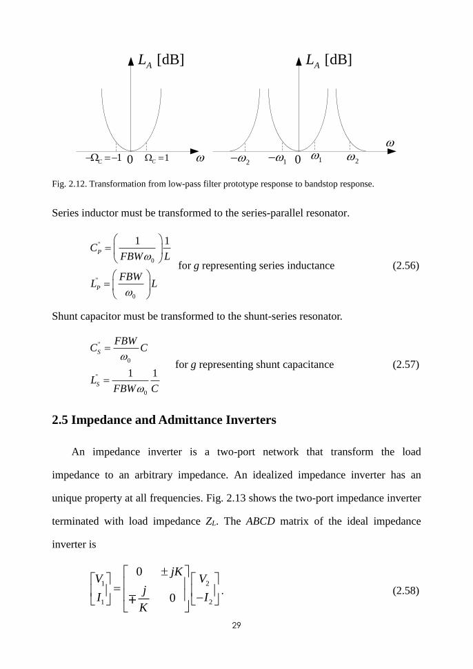
29
1C
[dB]AL
01C 1
[dB]AL
01 22
Fig. 2.12. Transformation from low-pass filter prototype response to bandstop response.
Series inductor must be transformed to the series-parallel resonator.
"
0
"
0
1 1P
P
CFBW L
FBWL L
for g representing series inductance (2.56)
Shunt capacitor must be transformed to the shunt-series resonator.
"
0
"
0
1 1
S
S
FBWC C
LFBW C
for g representing shunt capacitance (2.57)
2.5 Impedance and Admittance Inverters
An impedance inverter is a two-port network that transform the load
impedance to an arbitrary impedance. An idealized impedance inverter has an
unique property at all frequencies. Fig. 2.13 shows the two-port impedance inverter
terminated with load impedance ZL. The ABCD matrix of the ideal impedance
inverter is
1 2
1 2
0
0
jKV V
jI I
K
. (2.58)
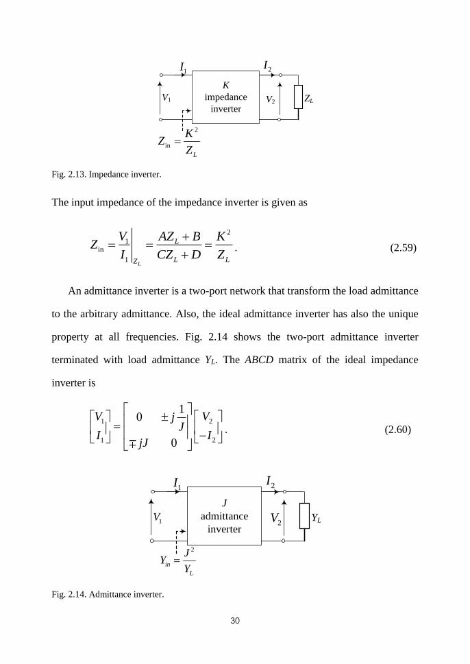
30
1I
K
impedance
inverter
2I
ZL
2
in
L
KZ
Z
V2V1
Fig. 2.13. Impedance inverter.
The input impedance of the impedance inverter is given as
2
1in
1L
L
L LZ
V AZ B KZ
I CZ D Z
. (2.59)
An admittance inverter is a two-port network that transform the load admittance
to the arbitrary admittance. Also, the ideal admittance inverter has also the unique
property at all frequencies. Fig. 2.14 shows the two-port admittance inverter
terminated with load admittance YL. The ABCD matrix of the ideal impedance
inverter is
1 2
1 2
10
0
V VjJ
I IjJ
. (2.60)
1V
1I
J
admittance
inverter2V
2I
YL
2
in
L
JY
Y
Fig. 2.14. Admittance inverter.
31
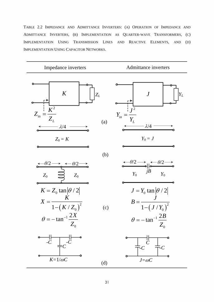
TABLE 2.2 IMPEDANCE AND ADMITTANCE INVERTERS: (A) OPERATION OF IMPEDANCE AND
ADMITTANCE INVERTERS, (B) IMPLEMENTATION AS QUARTER-WAVE TRANSFORMERS, (C)
IMPLEMENTATION USING TRANSMISSION LINES AND REACTIVE ELEMENTS, AND (D)
IMPLEMENTATION USING CAPACITOR NETWORKS.
ZL
Z0 = K
Admittance invertersImpedance inverters
K YLJ
l/4
Y0 = J
l/4
Z0
jB
θ/2
Y0Y0Z0
θ/2θ/2 θ/2
0 tan / 2K Z
2
01 /
KX
K Z
1
0
2tan
X
Z
0 tan / 2J Y
2
01 /
JB
J Y
1
0
2tan
B
Z
C-C-C
K=1/C
-CC
J=C
-C
(a)
(b)
(c)
(d)
2
in
L
KZ
Z
2
in
L
JY
Y
32
The input admittance of the admittance inverter is given as
2
1 2 2in
1 2 2L
L L
L L LY
I CV DY V C DY JY
V AV BY V A BY Y
. (2.61)
As seen from (2.58) and (2.60), impedance and admittance inverters have the
ability to transform the load impedance or admittance to the arbitrary input
impedance and admittance.
Table 2.2 shows the conceptual operation of two-port impedance or admittance
inverters. The inverter can be used to transform series-connected elements to shunt-
connected elements, or vice versa. The impedance or admittance inverter can be
constructed using a quarter-wavelength TL of the appropriate characteristic
impedance as shown in Fig. 2.15(b). Fig. 2.15 (c) and (d) show the
implementations using TL and reactive elements and capacitor networks
33
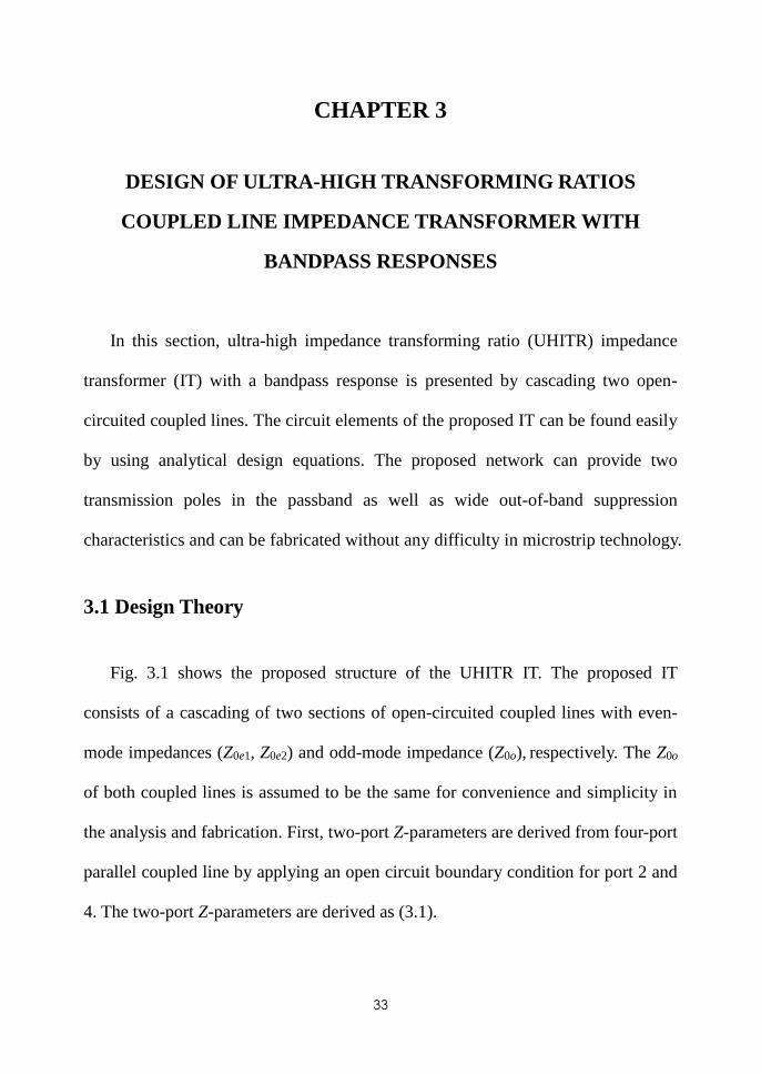
CHAPTER 3
DESIGN OF ULTRA-HIGH TRANSFORMING RATIOS
COUPLED LINE IMPEDANCE TRANSFORMER WITH
BANDPASS RESPONSES
In this section, ultra-high impedance transforming ratio (UHITR) impedance
transformer (IT) with a bandpass response is presented by cascading two open-
circuited coupled lines. The circuit elements of the proposed IT can be found easily
by using analytical design equations. The proposed network can provide two
transmission poles in the passband as well as wide out-of-band suppression
characteristics and can be fabricated without any difficulty in microstrip technology.
3.1 Design Theory
Fig. 3.1 shows the proposed structure of the UHITR IT. The proposed IT
consists of a cascading of two sections of open-circuited coupled lines with even-
mode impedances (Z0e1, Z0e2) and odd-mode impedance (Z0o), respectively. The Z0o
of both coupled lines is assumed to be the same for convenience and simplicity in
the analysis and fabrication. First, two-port Z-parameters are derived from four-port
parallel coupled line by applying an open circuit boundary condition for port 2 and
4. The two-port Z-parameters are derived as (3.1).
34
Z0e1, Z0o, θ
①
② ③
④
ZS
Z0e2, Z0o, θ
①
② ③
④ ZL
Fig. 3.1. Proposed impedance transformer for ultra-high impedance transforming ratio.
0 0
11 cot cot ,2 2
piei oZZ Z
Z j j
(3.1a)
0 0
13 csc csc ,2 2
ei o miZ Z ZZ j j
(3.1b)
0 0
31 csc csc ,2 2
ei o miZ Z ZZ j j
(3.1c)
0 0
33 cot cot ,2 2
piei oZZ Z
Z j j
(3.1d)
where
0 0 , 1 and 2mi ei oZ Z Z i (3.2a)
0 0pi ei oZ Z Z . (3.2b)
Then two-port Z-parameters are converted into ABCD-parameters and they are
given as
cospi
i
mi
ZA
Z (3.3a)
2 2 2cos
2 sin
mi pi
i
mi
Z ZB j
Z
(3.3b)

35
2sin
i
mi
C jZ
(3.3c)
cospi
i
mi
ZD
Z . (3.3d)
The total ABCD-parameters of the cascaded coupled lines are given as (3.4)
1 1 2 2 1 2 1 2 1 2 1 2
1 1 2 2 1 2 1 2 1 2 1 2
A B A B A A B C A B B DA B
C D C D C A D C C B D DC D
(3.4)
where
2 2
1 2 1 1
1 2
cosp p p m
m m
Z Z Z ZA
Z Z
(3.5a)
2 2 2
1 2 1 2 1 2 1 2
1 2
coscot
2
p m m p p p p p
m m
Z Z Z Z Z Z Z ZB j
Z Z
(3.5b)
1 2
1 2
2sin cos p p
m m
Z ZC j
Z Z
(3.5c)
2 2
1 2 2 2
1 2
cosp p p m
m m
Z Z Z ZD
Z Z
. (3.5d)
And the electrical length (θ) is π/2 at the center frequency (f0).
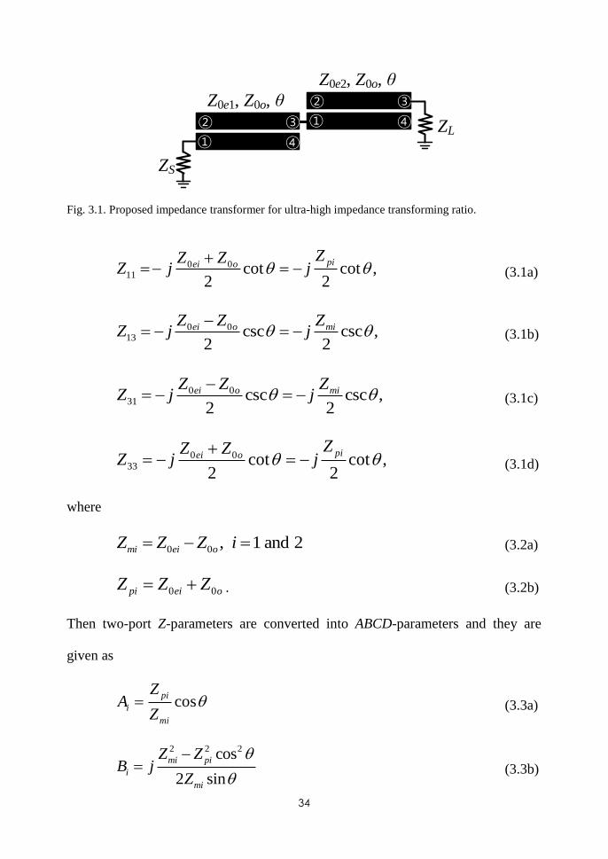
3.1.1 S-parameters analysis
The S-parameters of the proposed circuit can be found as (3.6) from the overall
ABCD-parameters of cascaded coupled lines [33-34].
2
11 2
L L Lt
L L L
AZ B CrZ DrZS
AZ B CrZ DrZ
(3.6a)
36
21 2
2 Lt
L L L
Z rS
AZ B CrZ DrZ
(3.6b)
where
S
L
Zr
Z . (3.7)
At f0, S11t of the proposed circuit is reduced to (3.8).
0
2 2
1 211 2 2
1 2f f
m mt
m m
Z rZS
Z rZ
. (3.8)
In (3.8), S11t depends on even- and odd-mode impedances of coupled lines. From
(3.8), three different matched regions are categorized [7], depending on the values
of Zm1 and Zm2, which are given as (3.9).
2 2
1 2m mZ rZ : over-matched region (3.9a)
2 2
1 2m mZ rZ : under-matched region (3.9b)
2 2
1 2m mZ rZ : perfectly matched region (3.9c)
For the over-matched region with the specific S11t, the value of Z0e2 can be
calculated as (3.10) using (3.8).
0 2 0 1 0 1e e oZ Z M Z M (3.10)
where
37
0
0
11
11
1
1
t f f
t f f
SM
r S
. (3.11)
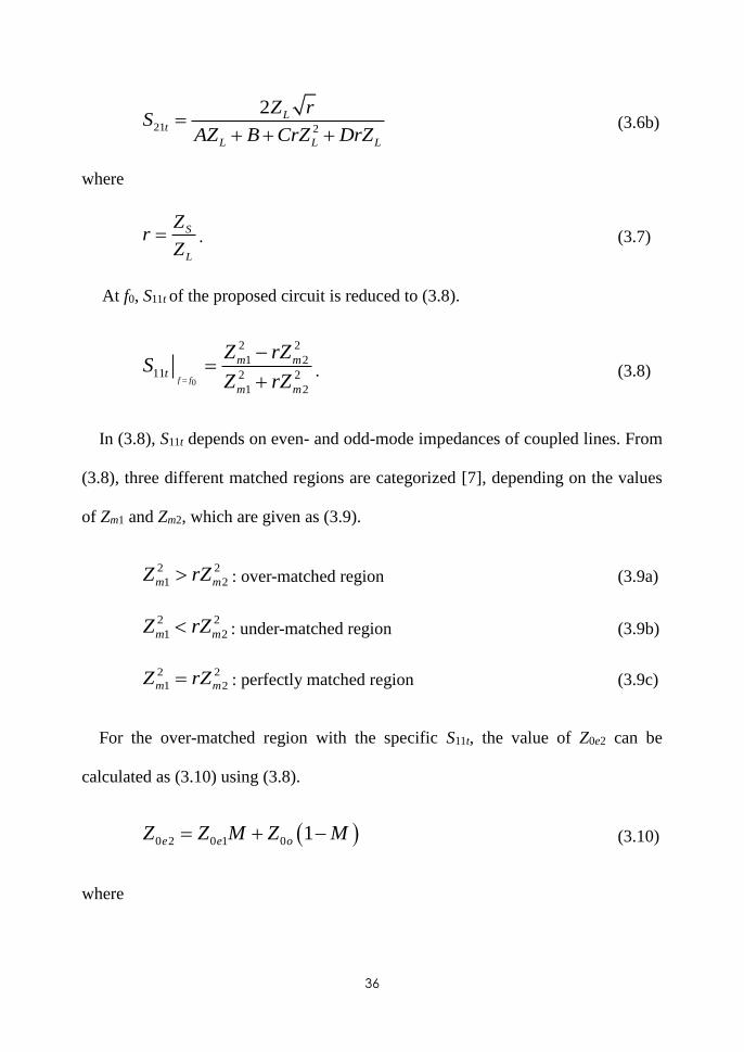
The value of Z0e1 can be derived as (3.12) using (3.6a), (3.9a), and (3.10) for the
assumed Z0o by designer.
3 2
0 1 1 0 1 2 0 1 3 4 0e o e o e o oZ X Z X Z X X (3.12)
where
1 1oX M M (3.13a)
2
2 0 2 3o oX Z M M (3.13b)
2 2 2
3 03 4 4 1o o LX M M Z rZ M (3.13c)
3 2 2
4 0 02 4 3o o L oX Z M M rZ Z M . (3.13d)
The negative and minimum positive root of (3.12) are not realizable for coupled
line application (Z0e1 < Z0o). So the proper Z0e1 is the maximum real positive root of
(3.12).
Similarly, for the under-matched region with the specific S11t, the value of Z0e2
can be found as (3.14).
0 2 0 1 0 1e e oZ Z N Z N (3.14)
where
0
0
11
11
1
1
t f f
t f f
SN
r S
(3.15)
38
From (3.6a), (3.9b), and (3.14), the value of Z0e1 for the under-matched region is
derived as (3.16).
3 2
0 1 1 0 1 2 0 1 3 4 0e u e u e u uZ Y Z Y Z Y Y (3.16)
where
1 1uY N N (3.17a)
2
2 0 2 3u oY Z N N (3.17b)
2 2 2
3 03 4 4 1u o LY N N Z rZ N (3.17c)
3 2 2
4 0 02 4 3u o L oY Z N N rZ Z N . (3.17d)
Similar to over-matched region, the proper Z0e1 among the three Z0e1 values is
the maximum real positive root of (3.16).
For the perfectly matched region, S11t becomes zero, such that the value of Z0e2
can be found as (3.18).
0 1
0 2 0
11e
e o
ZZ Z
r r
(3.18)
From (3.6a), (3.9c), and (3.18), the value of Z0e1 for the perfectly matched region
can be derived as (3.19).
3 2
0 1 1 0 1 2 0 1 3 4 0e p e p e p pZ W Z W Z W W (3.19)
where
39
1
1 1pW
r r (3.20a)
2 0
1 32p oW Z
r r
(3.20b)
2 2
3 0
3 1 14 4 1p o LW Z rZ
rr r
(3.20c)
3 2
4 0 0
1 1 12 4 3p o L oW Z rZ Z
r r r
. (3.20d)
Also, the proper Z0e1 is the maximum real positive root of (3.19).
The coupling coefficients (Ci) of coupled lines can be determined as (3.21).
0 0
0 0
ei oi
ei o
Z ZC
Z Z
(3.21)
where i is 1 and 2 for the coupled line 1 and 2, respectively.
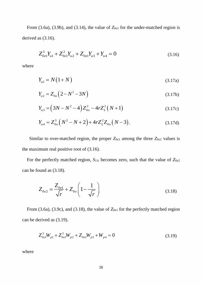
To illustrate the design equations (3.10)-(3.21) of the UHITR IT, the required
Z0e1 and Z0e2 are calculated by specifying S11t|f0 = -20 dB, Z0o = 40 Ω, r = 10, and ZS
= 50 Ω at f0. The calculated values are given in Table 3.1. Using the calculated
TABLE 3.1. CALCULATED VALUES OF IMPEDANCE TRANSFORMER
Match regions
Z0o=40 Ω S11t|f=fo=-20 dB, ZS=50 Ω, r=10
Z0e1 (Ω) Z0e2 (Ω)
Under
Over
Perfect
C1 (dB) C2 (dB)
84.57
86.02
85.34
55.58
53.16
54.34
-8.9
-8.7
-8.8
-15.7
-17
-16.4
fp1/f0 fp2/f0
0.9687 1.0313
40
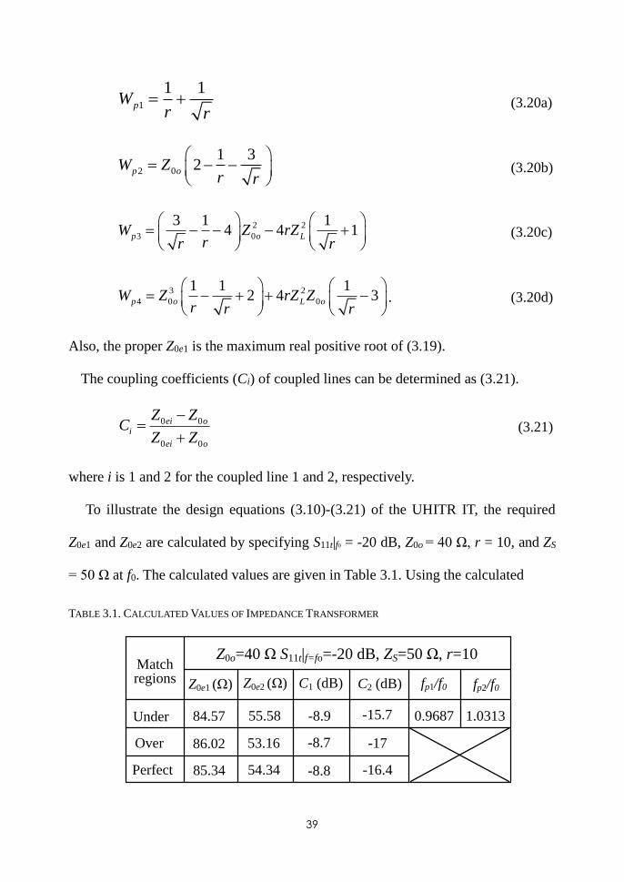
values, the frequency responses are plotted in Fig. 3.2 for different matched regions.
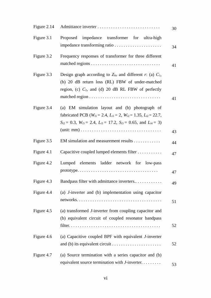
As seen in Fig. 3.2, a bandpass filtering response is obtained. The magnitude of
return loss (S11t|f0) is exactly 20 dB at the f0 in case of under- and over-matched
regions. While two transmission poles are observed in the passband for the under-
matched region, only one transmission pole at f0 is observed in the cases of over-
and perfectly matched regions. Thus, the under-matched region is preferable for its
wide return loss bandwidth characteristic. The normalized transmission pole
frequencies observed in the under-matched region can be found as (3.22) using
(3.6a).
2 21 1 2
1, 2 0
2 1 1 2
21 1 cos m m
p p
p p p p
Z rZf f
Z Z Z rZ
(3.22)
where fp1 and fp2 are the lower and upper transmission pole frequencies,
respectively.
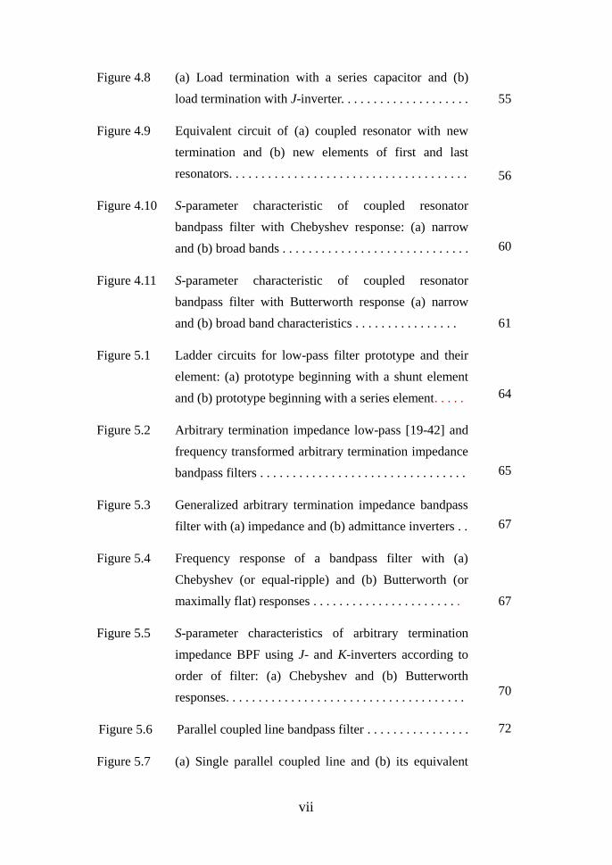
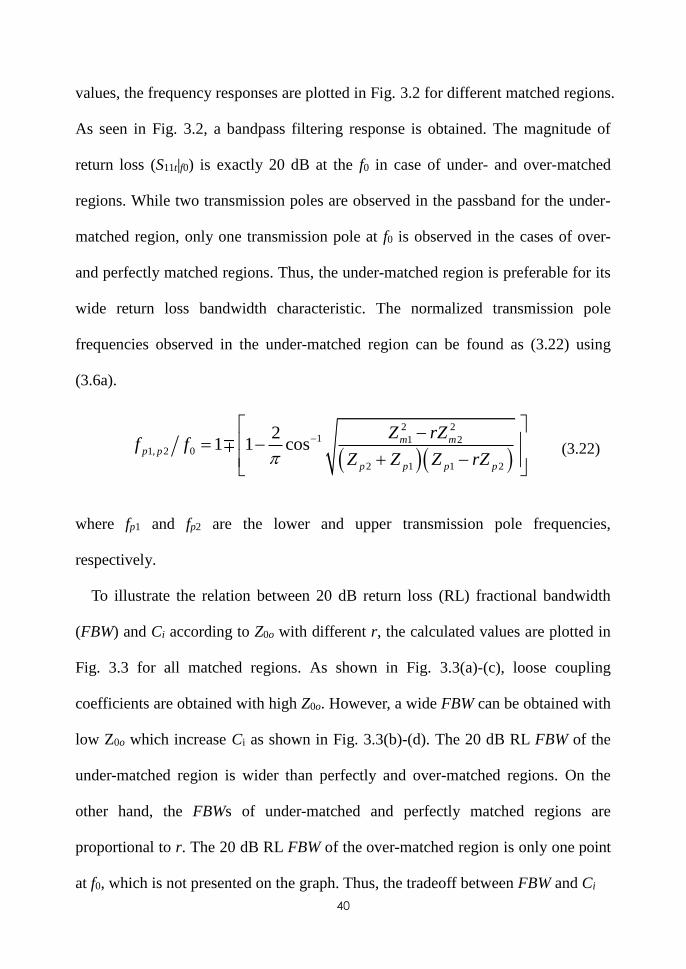
To illustrate the relation between 20 dB return loss (RL) fractional bandwidth
(FBW) and Ci according to Z0o with different r, the calculated values are plotted in
Fig. 3.3 for all matched regions. As shown in Fig. 3.3(a)-(c), loose coupling
coefficients are obtained with high Z0o. However, a wide FBW can be obtained with
low Z0o which increase Ci as shown in Fig. 3.3(b)-(d). The 20 dB RL FBW of the
under-matched region is wider than perfectly and over-matched regions. On the
other hand, the FBWs of under-matched and perfectly matched regions are
proportional to r. The 20 dB RL FBW of the over-matched region is only one point
at f0, which is not presented on the graph. Thus, the tradeoff between FBW and Ci
41
should be considered.
0.0 0.4 0.8 1.2 1.6 2.0 2.4 2.8
-50
-40
-30
-20
-10
0
r=10
Z0o
=40
ZS=50
S11t
|f0
=-20 dB
Und. S11t
Und. S21t
Per. S11t
Per. S21t
Ove. S11t
Ove. S21t
S-p
ara
met
er (
dB
)
Normalized frequency f/f0
Fig. 3.2. Frequency responses of transformer for three different matched regions.
-35
-30
-25
-20
-15
-10
-5
0
3
6
9
12
15
18
-20
-16
-12
-8
-4
0
Per. r=25
Ove. r=10
Ove. r=15
Ove. r=25
Per. r=10
Per. r=15
Und. r=10
Und. r=15
Und. r=25
C2 (
dB
)
C1 (
dB
)
10 20 30 40 50 60 70 80 90 1000
5
10
15
20
25
(d)
(c)
(b)
Und. r=10
Und. r=15
Und. r=25
20 d
B R
L F
BW
(%
)
20 d
B R
L F
BW
(%
)
Z0o
()
(a)
10 20 30 40 50 60 70 80 90 100
S11t
= -20 dB ZS=50
ZS=50
S11t
= -20 dB
ZS=50
S11t
= -20 dB
Z0o
()
ZS=50
S11t
= -20 dB
Und. r=25
Ove. r=10
Ove. r=15
Ove. r=25
Per. r=10
Per. r=15
Per. r=25
Und. r=10
Und. r=15
Per. r=10
Per. r=15
Per. r=25
Fig. 3.3. Design graph according to Z0o and different r: (a) C1, (b) 20 dB return loss FBW of under-
matched region, (c) C2, and (d) 20 dB return loss FBW of perfectly matched region.

42
3.1.2 Design procedure of IT network
The design procedure of IT is summarized as follows.
a) First, specify the ZS, ZL, Z0o, f0, and |S11t| at f0 for all matched regions.
b) For the over-matched region, calculate Z0e1 using (3.11), (3.12), and (3.13).
After obtaining Z0e1, calculate Z0e2 using (3.10).
c) For the under-matched region, calculate Z0e1 using (3.15), (3.16), and (3.17).
Then calculate Z0e2 using (3.14).
d) For the perfectly matched region, calculate Z0e1 using (3.19) and (3.20). Then
Z0e2 is obtained by (3.18).
e) Finally, obtain the physical dimensions of coupled lines according to PCB
substrate from the LineCalc of Advanced Design System (ADS) and optimize
using EM simulator.
3.2 The Simulation and Experimental Results
For the verification, a 5-to-50 Ω (r = 10, ZS = 50 Ω) UHITR IT was designed,
simulated, and fabricated at f0 = 2.6 GHz. The MATLAB tool was used to calculate
the elements values (see appendix A). For this purpose, the values of S11t and Z0o
are chosen as -20 dB and 40 Ω at f0, respectively. In this design, the under-matched
region was chosen. The calculated values are shown in Table 3.1. The EM
simulation was performed using Ansoft’s HFSS v13.
43
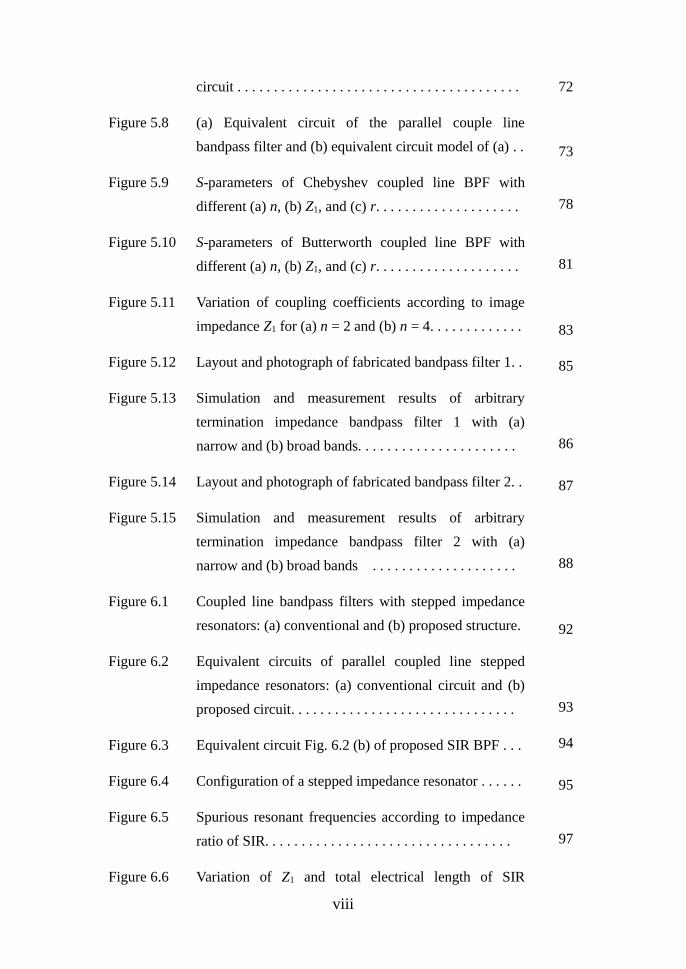
Li2
Li3
Wi2
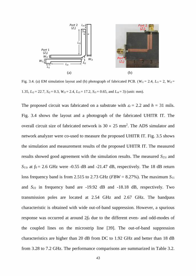
Si3
Wi3
Li4
Wi1
Li1
Si2
Port 1(ZS)
Port 2(ZL)
Port 1(ZS)
Port 2(ZL)
Li2
Li3
Wi2
Si3
Wi3
Li4
Wi1
Li1
Si2
Port 1(ZS)
Port 2(ZL)
Port 1(ZS)
Port 2(ZL)
(a) (b)
Fig. 3.4. (a) EM simulation layout and (b) photograph of fabricated PCB. (Wi1 = 2.4, Li1 = 2, Wi2 =
1.35, Li2 = 22.7, Si2 = 0.3, Wi3 = 2.4, Li3 = 17.2, Si3 = 0.65, and Li4 = 3) (unit: mm).
The proposed circuit was fabricated on a substrate with r = 2.2 and h = 31 mils.
Fig. 3.4 shows the layout and a photograph of the fabricated UHITR IT. The
overall circuit size of fabricated network is 30 25 mm2. The ADS simulator and
network analyzer were co-used to measure the proposed UHITR IT. Fig. 3.5 shows
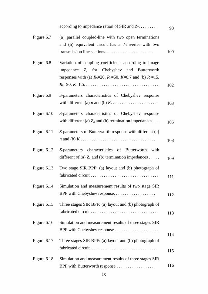
the simulation and measurement results of the proposed UHITR IT. The measured
results showed good agreement with the simulation results. The measured S21t and
S11t at f0 = 2.6 GHz were -0.55 dB and -21.47 dB, respectively. The 18 dB return
loss frequency band is from 2.515 to 2.73 GHz (FBW = 8.27%). The maximum S11
and S22 in frequency band are -19.92 dB and -18.18 dB, respectively. Two
transmission poles are located at 2.54 GHz and 2.67 GHz. The bandpass
characteristic is obtained with wide out-of-band suppression. However, a spurious
response was occurred at around 2f0 due to the different even- and odd-modes of
the coupled lines on the microstrip line [39]. The out-of-band suppression
characteristics are higher than 20 dB from DC to 1.92 GHz and better than 18 dB
from 3.28 to 7.2 GHz. The performance comparisons are summarized in Table 3.2.
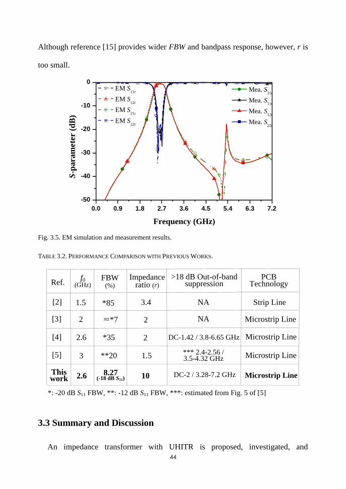
44
Although reference [15] provides wider FBW and bandpass response, however, r is
too small.
0.0 0.9 1.8 2.7 3.6 4.5 5.4 6.3 7.2
-50
-40
-30
-20
-10
0
Mea. S21t
Mea. S11t
Mea. S12t
Mea. S22t
EM S11t
EM S12t
EM S21t
EM S22t
S
-para
mete
r (
dB
)
Frequency (GHz)
Fig. 3.5. EM simulation and measurement results.
TABLE 3.2. PERFORMANCE COMPARISON WITH PREVIOUS WORKS.
[3]
[2]
Thiswork
Impedanceratio (r)
>18 dB Out-of-bandsuppression
FBW(%)
8.27(-18 dB S11)
*85
*7
f0 (GHz)
2.6 10
3.4
NA
NA
22
1.5
Ref.PCB
Technology
Microstrip Line
Microstrip Line
Strip Line
[4] DC-1.42 / 3.8-6.65 GHz Microstrip Line22.6 *35
[5] *** 2.4-2.56 / 3.5-4.32 GHz Microstrip Line1.53 **20
DC-2 / 3.28-7.2 GHz
*: -20 dB S11 FBW, **: -12 dB S11 FBW, ***: estimated from Fig. 5 of [5]
3.3 Summary and Discussion
An impedance transformer with UHITR is proposed, investigated, and

45
fabricated in this chapter. The UHITR can be obtained by controlling coupling
coefficients of coupled lines. The proposed circuit is fabricated without difficulty
with microstrip line technology. By choosing the properly matched region of
coupled lines, two transmission poles are obtained in the passband. A low insertion
loss is obtained with high impedance transforming ratio and provide a bandpass
response.
46
CHAPTER 4
DESIGN OF LUMPED ELEMENTS BANDPASS
FILTER WITH AIRBITRARY TERMINATION
IMPEDANCE
In this chapter, the general design equations of unequal termination impedance
bandpass filters (BPFs) using lumped elements is presented. The design equations
for specific filters are derived step-by-step in detail and validated with simulations.
4.1 Coupled-Resonator Filter
Fig. 4.1 shows the capacitive coupled-resonator BPF using lumped element
[35]. The termination impedances may have any values, and may be equal or
unequal of pure resistance or complex impedance, as the desired. The inductors Lri
of resonators may be selected any values. The formulas for the individual elements
utilize the values g1, g2, g3, ···, gn of the low-pass prototype filter, which are
computed from the formulas in Section 2.3 for Chebyshev or Butterworth
responses. The bandpass response is obtained from the prototype elements by
transforming the frequency scaling that already discuss in Section 2.4.
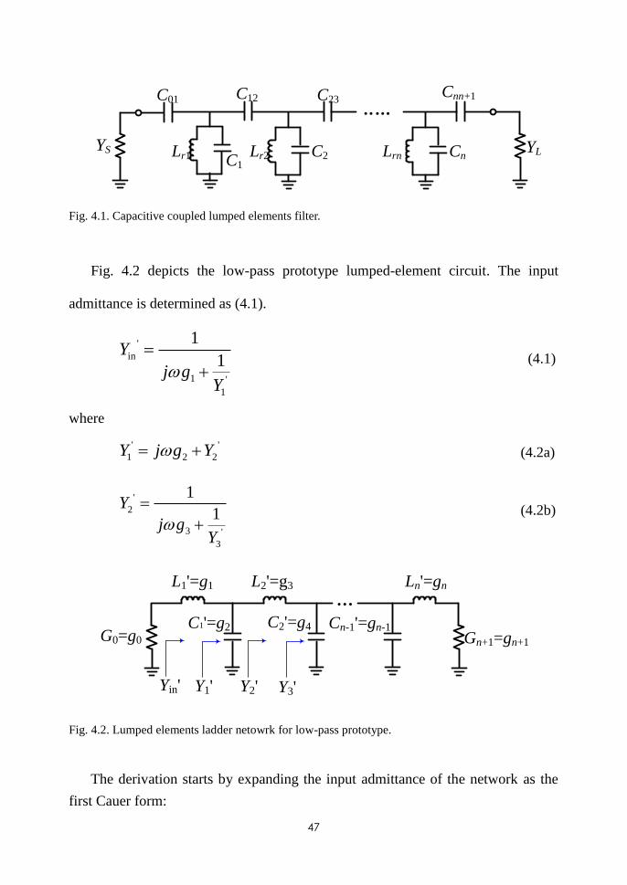
47
YS Lr1 C1Lr2 C2
YL
C01 C12 Cnn+1C23
·····
Lrn Cn
Fig. 4.1. Capacitive coupled lumped elements filter.
Fig. 4.2 depicts the low-pass prototype lumped-element circuit. The input
admittance is determined as (4.1).
'
in
1 '
1
1
1Y
j gY
(4.1)
where
' '
1 2 2Y j g Y (4.2a)
'
2
3 '
3
1
1Y
j gY
(4.2b)
G0=g0
L1'=g1
C1'=g2
L2'=g3
C2'=g4
Ln'=gn
Gn+1=gn+1
···Cn-1'=gn-1
Y2'Y1'Yin' Y3'
Fig. 4.2. Lumped elements ladder netowrk for low-pass prototype.
The derivation starts by expanding the input admittance of the network as the
first Cauer form:
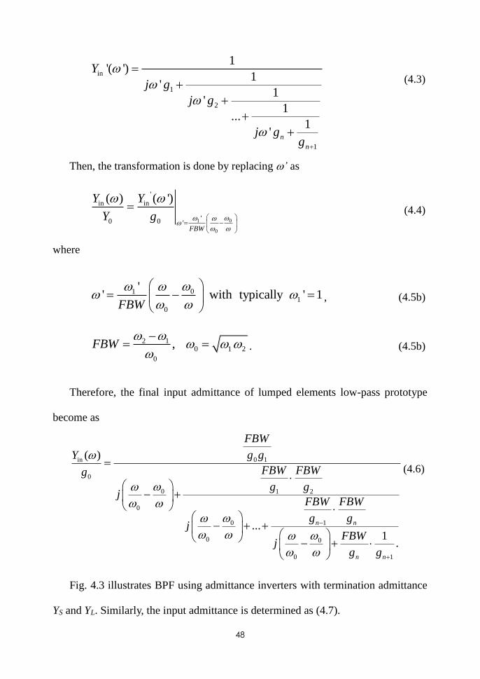
48
in
1
2
1
1'( ')
1'
1'
1...
1' n
n
Y
j g
j g
j gg
(4.3)
Then, the transformation is done by replacing ’ as
01
0
'
in in
'0 0 '
( ) ( ')
FBW
Y Y
Y g
(4.4)
where
01
1
0
'' with typically ' 1
FBW
, (4.5b)
2 1
0 1 2
0
,FBW
. (4.5b)
Therefore, the final input admittance of lumped elements low-pass prototype
become as
0 1in
0
0 1 2
0
0 1
0 0
0 1
( )
...1
.
n n
n n
FBW
g gY
FBW FBWg
g gj
FBW FBW
g gj
FBWj
g g
(4.6)
Fig. 4.3 illustrates BPF using admittance inverters with termination admittance
YS and YL. Similarly, the input admittance is determined as (4.7).
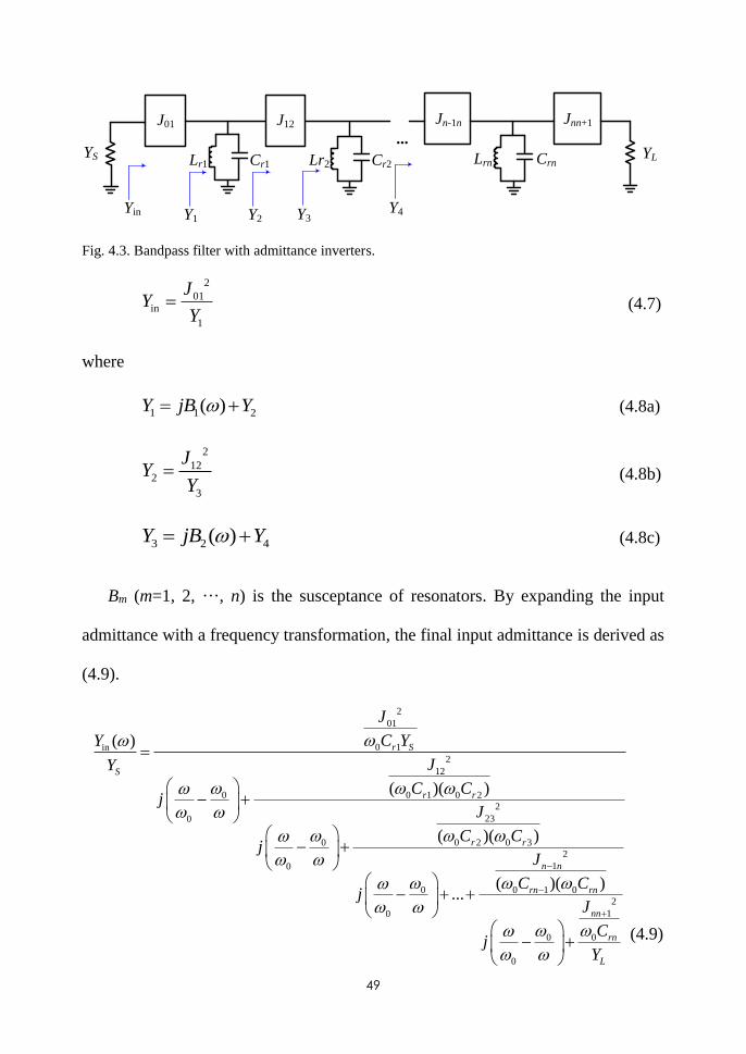
49
···
J12 Jn-1n Jnn+1J01
YS YLLr1 Lr2 LrnCr1 Cr2 Crn
Y2Y1Yin Y3
Y4
Fig. 4.3. Bandpass filter with admittance inverters.
2
01in
1
JY
Y (4.7)
where
1 1 2( )Y jB Y (4.8a)
2
122
3
JY
Y (4.8b)
3 2 4( )Y jB Y (4.8c)
Bm (m=1, 2, ···, n) is the susceptance of resonators. By expanding the input
admittance with a frequency transformation, the final input admittance is derived as
(4.9).
2
01
0 1in
2
12
0 0 1 0 2
2
230
0 0 2 0 3
2
10
0 0 1 0
2
10
0 0
0
( )
( )( )
( )( )
( )( )...
r S
S
r r
r r
n n
rn rn
nn
rn
L
J
C YY
JY
C Cj
J
C Cj
J
C Cj
J
Cj
Y
(4.9)
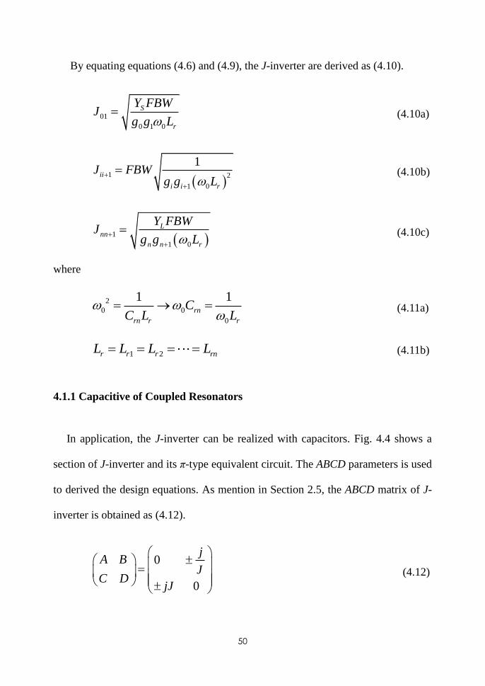
50
By equating equations (4.6) and (4.9), the J-inverter are derived as (4.10).
01
0 1 0
S
r
Y FBWJ
g g L (4.10a)
1 2
1 0
1ii
i i r
J FBWg g L
(4.10b)
1
1 0
Lnn
n n r
Y FBWJ
g g L
(4.10c)
where
2
0 0
0
1 1rn
rn r r
CC L L
(4.11a)
1 2r r r rnL L L L (4.11b)
4.1.1 Capacitive of Coupled Resonators
In application, the J-inverter can be realized with capacitors. Fig. 4.4 shows a
section of J-inverter and its π-type equivalent circuit. The ABCD parameters is used
to derived the design equations. As mention in Section 2.5, the ABCD matrix of J-
inverter is obtained as (4.12).
0
0
jA B
JC D
jJ
(4.12)
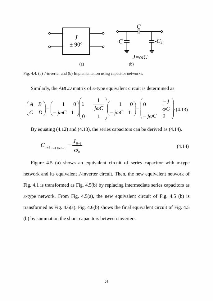
51
J
± 90°-C
C
-C2
J=ωC
(a) (b)
Fig. 4.4. (a) J-inverter and (b) Implementation using capacitor networks.
Similarly, the ABCD matrix of π-type equivalent circuit is determined as
111 0 1 0 0
.1 1
00 1
jA B
j C CC D j C j C
j C
(4.13)
By equating (4.12) and (4.13), the series capacitors can be derived as (4.14).
1
1 1 to 1
0
iiii i n
JC
(4.14)
Figure 4.5 (a) shows an equivalent circuit of series capacitor with π-type
network and its equivalent J-inverter circuit. Then, the new equivalent network of
Fig. 4.1 is transformed as Fig. 4.5(b) by replacing intermediate series capacitors as
π-type network. From Fig. 4.5(a), the new equivalent circuit of Fig. 4.5 (b) is
transformed as Fig. 4.6(a). Fig. 4.6(b) shows the final equivalent circuit of Fig. 4.5
(b) by summation the shunt capacitors between inverters.
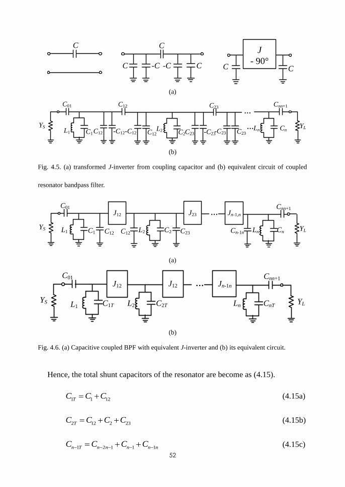
52
-C -C
C
CC
J
- 90°
C
C C
(a)
···
YS YLL1
L2 LnC1 C2Cn
C12
-C12 C12-C12C12
C23
-C23 C23-C23C23···
C01 Cnn+1
(b)
Fig. 4.5. (a) transformed J-inverter from coupling capacitor and (b) equivalent circuit of coupled
resonator bandpass filter.
···J12 Jn-1,n
LnL2L1 C1 C2 CnYS
Cnn+1
YL
J23
C01
C12 C12 C23 Cn-1n
(a)
···J12 Jn-1n
LnL2L1 C1T C2T CnTYS
Cnn+1
YL
J12
C01
(b)
Fig. 4.6. (a) Capacitive coupled BPF with equivalent J-inverter and (b) its equivalent circuit.
Hence, the total shunt capacitors of the resonator are become as (4.15).
1 1 12TC C C (4.15a)
2 12 2 23TC C C C (4.15b)
1 2 1 1 1n T n n n n nC C C C (4.15c)
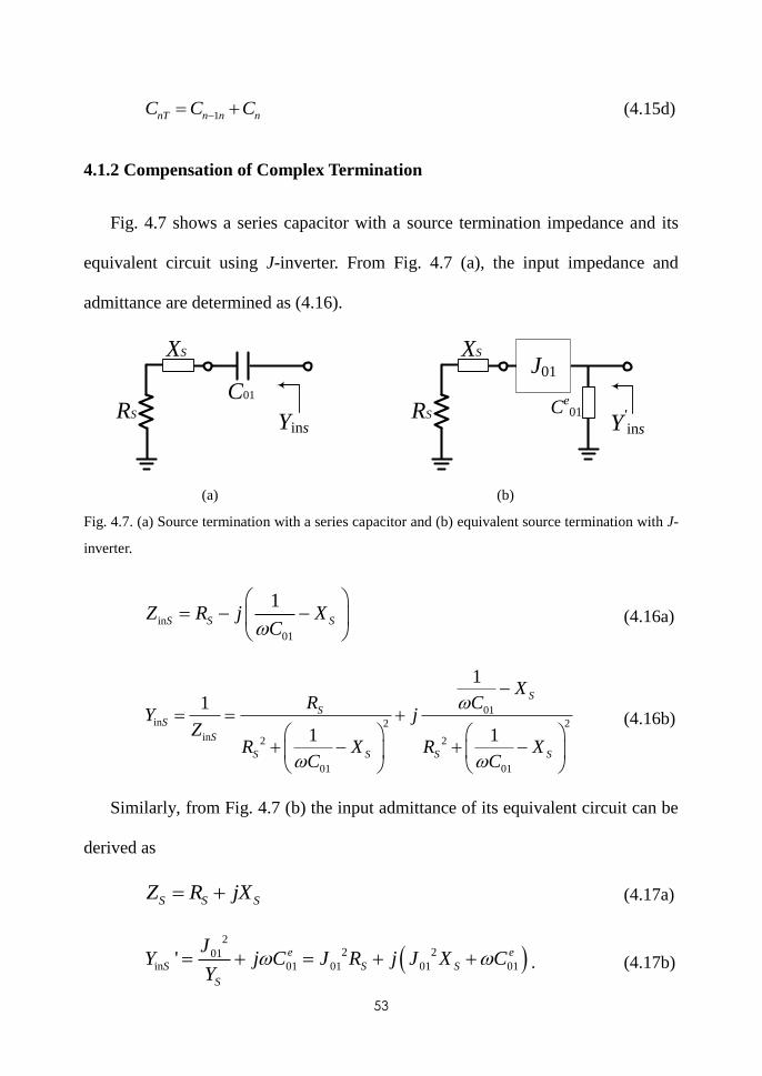
53
1nT n n nC C C (4.15d)
4.1.2 Compensation of Complex Termination
Fig. 4.7 shows a series capacitor with a source termination impedance and its
equivalent circuit using J-inverter. From Fig. 4.7 (a), the input impedance and
admittance are determined as (4.16).
RS
XS
C01
Yins
RS
XS
Y'ins
J01
Ce01
(a) (b)
Fig. 4.7. (a) Source termination with a series capacitor and (b) equivalent source termination with J-
inverter.
in
01
1S S SZ R j X
C
(4.16a)
01
in 2 2
in 2 2
01 01
1
1
1 1
S
SS
S
S S S S
XR C
Y jZ
R X R XC C
(4.16b)
Similarly, from Fig. 4.7 (b) the input admittance of its equivalent circuit can be
derived as
S S SZ R jX (4.17a)
2
2 201in 01 01 01 01' e e
S S S
S
JY j C J R j J X C
Y . (4.17b)
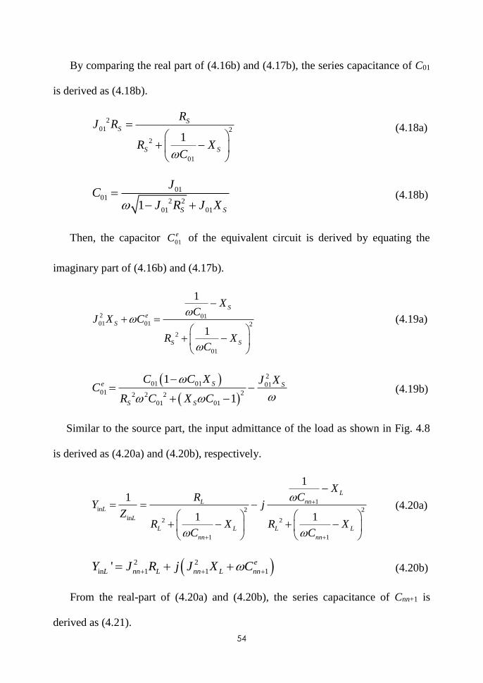
54
By comparing the real part of (4.16b) and (4.17b), the series capacitance of C01
is derived as (4.18b).
2
01 2
2
01
1
SS
S S
RJ R
R XC
(4.18a)
01
012 2
01 011 S S
JC
J R J X
(4.18b)
Then, the capacitor 01
eC of the equivalent circuit is derived by equating the
imaginary part of (4.16b) and (4.17b).
2 0101 01 2
2
01
1
1
S
e
S
S S
XC
J X C
R XC
(4.19a)
201 01 01
01 22 2 2
01 01
1
1
Se S
S S
C C X J XC
R C X C
(4.19b)
Similar to the source part, the input admittance of the load as shown in Fig. 4.8
is derived as (4.20a) and (4.20b), respectively.
1in 2 2
in 2 2
1 1
1
1
1 1
L
nnLL
L
L L L L
nn nn
XCR
Y jZ
R X R XC C
(4.20a)
2 2
in 1 1 1' e
L nn L nn L nnY J R j J X C (4.20b)
From the real-part of (4.20a) and (4.20b), the series capacitance of Cnn+1 is
derived as (4.21).
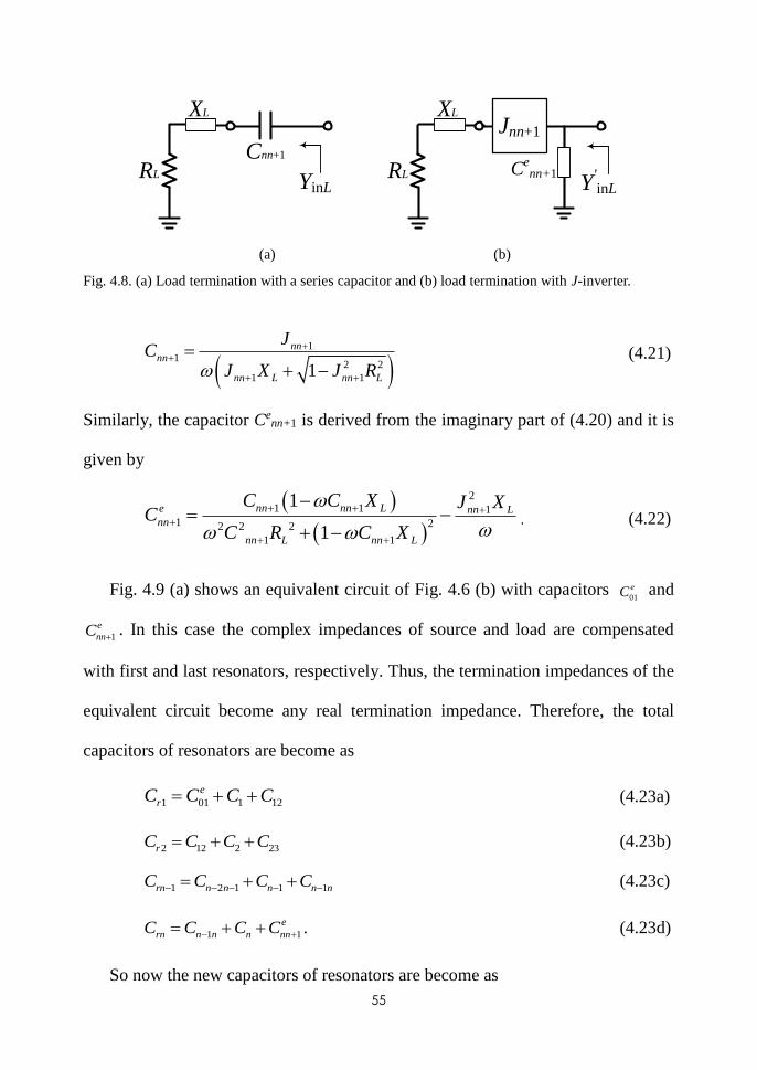
55
RL
XL
Cnn+1
YinL
RL
XL
Y'inL
Jnn+1
Cenn+1
(a) (b)
Fig. 4.8. (a) Load termination with a series capacitor and (b) load termination with J-inverter.
1
12 2
1 11
nnnn
nn L nn L
JC
J X J R
(4.21)
Similarly, the capacitor Cenn+1 is derived from the imaginary part of (4.20) and it is
given by
21 1 1
1 22 2 2
1 1
1
1
nn nn Le nn Lnn
nn L nn L
C C X J XC
C R C X
. (4.22)
Fig. 4.9 (a) shows an equivalent circuit of Fig. 4.6 (b) with capacitors 01
eC and
1
e
nnC . In this case the complex impedances of source and load are compensated
with first and last resonators, respectively. Thus, the termination impedances of the
equivalent circuit become any real termination impedance. Therefore, the total
capacitors of resonators are become as
1 01 1 12
e
rC C C C (4.23a)
2 12 2 23rC C C C (4.23b)
1 2 1 1 1rn n n n n nC C C C (4.23c)
1 1
e
rn n n n nnC C C C . (4.23d)
So now the new capacitors of resonators are become as
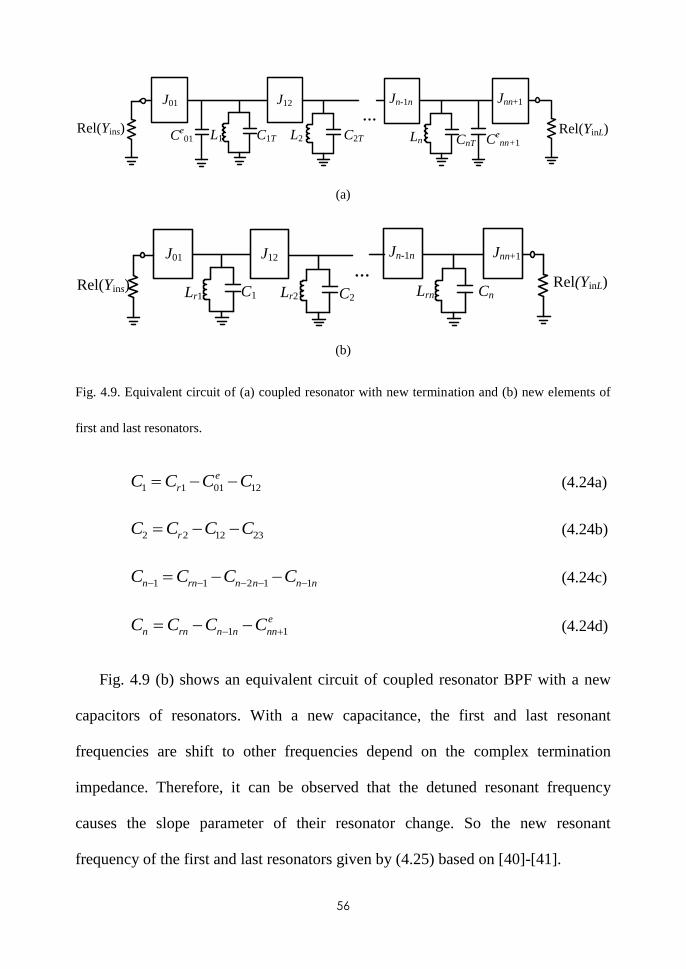
56
···
J12 Jn-1n Jnn+1J01
Rel(Yins) Rel(YinL)L1 L2 LnC1T C2T CnTCe
01 Cenn+1
(a)
···
J12 Jn-1n Jnn+1J01
Rel(Yins) Lr1 Lr2 LrnC1 C2Cn
Rel(YinL)
(b)
Fig. 4.9. Equivalent circuit of (a) coupled resonator with new termination and (b) new elements of
first and last resonators.
1 1 01 12
e
rC C C C (4.24a)
2 2 12 23rC C C C (4.24b)
1 1 2 1 1n rn n n n nC C C C (4.24c)
1 1
e
n rn n n nnC C C C (4.24d)
Fig. 4.9 (b) shows an equivalent circuit of coupled resonator BPF with a new
capacitors of resonators. With a new capacitance, the first and last resonant
frequencies are shift to other frequencies depend on the complex termination
impedance. Therefore, it can be observed that the detuned resonant frequency
causes the slope parameter of their resonator change. So the new resonant
frequency of the first and last resonators given by (4.25) based on [40]-[41].
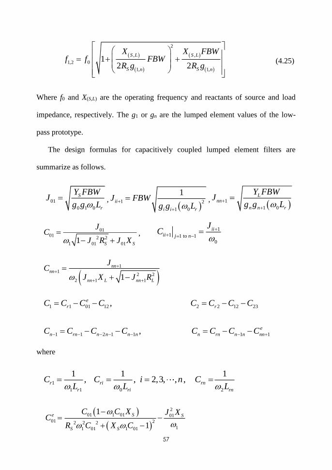
57
2
, ,
1,2 0
1, 1,
12 2
S L S L
S Sn n
X X FBWf f FBW
R g R g
(4.25)
Where f0 and X(S,L) are the operating frequency and reactants of source and load
impedance, respectively. The g1 or gn are the lumped element values of the low-
pass prototype.
The design formulas for capacitively coupled lumped element filters are
summarize as follows.
01
0 1 0
S
r
Y FBWJ
g g L ,
1 2
1 0
1ii
i i r
J FBWg g L
,
1
1 0
Lnn
n n r
Y FBWJ
g g L
01
012 2
1 01 011 S S
JC
J R J X
,
11 1 to 1
0
iiii j n
JC
1
12 2
2 1 11
nnnn
nn L nn L
JC
J X J R
1 1 01 12 2 2 12 23
1 1 2 1 1 1 1
,
,
e
r r
e
n rn n n n n n rn n n nn
C C C C C C C C
C C C C C C C C
where
1
1 1 0 2
1 1 1, , 2,3, , ,r ri rn
r ri rn
C C i n CL L L
201 1 01 01
01 22 2 211 01 1 01
1
1
Se S
S S
C C X J XC
R C X C
58
21 2 1 1
1 22 2 222 1 2 1
1
1
nn nn Le nn Lnn
nn L nn L
C C X J XC
C R C X
2
, ,
1,2 0
1, 1 1, 1
12 2
S L S L
S Sn n
X X FBWf f FBW
R g R g
4.2 Simulation
To verify the analytical analysis of the proposed BPF, the real and complex
unequal termination impedance BPFs were designed with a Chebyshev and
Butterworth responses. The calculations have been done using Matlab R2016a (see
appendix B). The Advanced Design System 2016.1 was used to simulate the
proposed circuit. Table 4.1 and 4.2 are shown the calculated values of coupled
resonator BPF with Chebyshev and Butterworth responses, respectively. The
specification of the proposed are shown in the tables. The inductors of shunt
resonators are chosen to be 4 nH for all resonators. The S-parameter characteristic
of the Chebyshev response in Fig. 4.10 (a) and (b) are shown the narrow and broad-
band characteristic responses, respectively. Thus, as is indicated in Fig. 4.10(a), the
S-parameter characteristics of real and complex impedance are good agreement.
Three transmission poles are occurred in the passband. The fractional bandwidth of
the passband edge is obtained 5% for equal ripple response. Fig. 4.10(b) shows a
broad-band S-parameter characteristic with a wide stopband. Fig. 4.11 is shown S-
parameter comparison of different termination BPF with Butterworth response.
Similar to the equal ripple response, the characteristics of equal and unequal
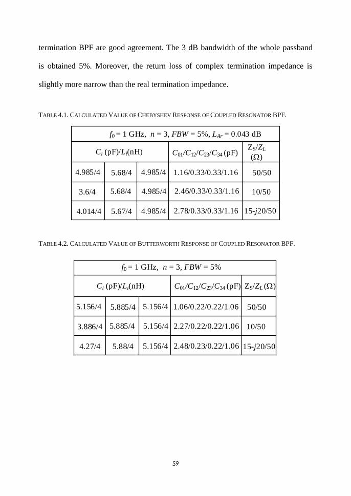
59
termination BPF are good agreement. The 3 dB bandwidth of the whole passband
is obtained 5%. Moreover, the return loss of complex termination impedance is
slightly more narrow than the real termination impedance.
TABLE 4.1. CALCULATED VALUE OF CHEBYSHEV RESPONSE OF COUPLED RESONATOR BPF.
f0 = 1 GHz, n = 3, FBW = 5%, LAr = 0.043 dB
Ci (pF)/Li(nH
4.985/4 5.68/4 4.985/4
3.6/4 5.68/4 4.985/4
4.014/4 5.67/4 4.985/4
C01/C12/C23/C34 (pF)
1.16/0.33/0.33/1.16
ZS/ZL
()
50/50
10/50
15-j20/50
2.46/0.33/0.33/1.16
2.78/0.33/0.33/1.16
TABLE 4.2. CALCULATED VALUE OF BUTTERWORTH RESPONSE OF COUPLED RESONATOR BPF.
Ci (pF)/Li(nH
5.156/4 5.885/4 5.156/4
3.886/4 5.885/4 5.156/4
4.27/4 5.88/4 5.156/4
C01/C12/C23/C34 (pF)
1.06/0.22/0.22/1.06
ZS/ZL ()
50/50
10/50
15-j20/50
2.27/0.22/0.22/1.06
2.48/0.23/0.22/1.06
f0 = 1 GHz, n = 3, FBW = 5%
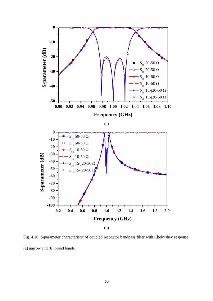
60
0.90 0.92 0.94 0.96 0.98 1.00 1.02 1.04 1.06 1.08 1.10
-50
-40
-30
-20
-10
0
S21
50-50
S11
50-50
S21
10-50
S11
10-50
S21
15-j20-50
S11
15-j20-50
S-p
aram
ete
r (
dB
)
Frequency (GHz)
(a)
0.2 0.4 0.6 0.8 1.0 1.2 1.4 1.6 1.8 2.0
-100
-90
-80
-70
-60
-50
-40
-30
-20
-10
0 S
21 50-50
S11
50-50
S21
10-50
S11
10-50
S21
15-j20-50
S11
15-j20-50
S-p
ara
mete
r (
dB
)
Frequency (GHz)
(b)
Fig. 4.10. S-parameter characteristic of coupled resonator bandpass filter with Chebyshev response:
(a) narrow and (b) broad bands.
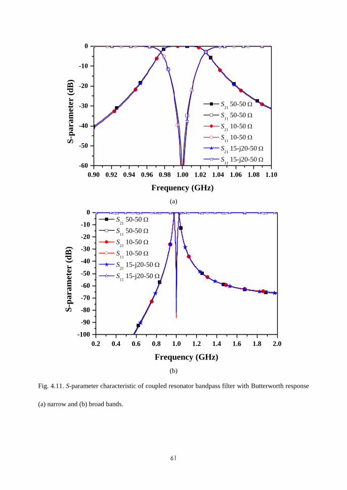
61
0.90 0.92 0.94 0.96 0.98 1.00 1.02 1.04 1.06 1.08 1.10
-60
-50
-40
-30
-20
-10
0
S21
50-50
S11
50-50
S21
10-50
S11
10-50
S21
15-j20-50
S11
15-j20-50
S-p
ara
mete
r (
dB
)
Frequency (GHz)
(a)
0.2 0.4 0.6 0.8 1.0 1.2 1.4 1.6 1.8 2.0
-100
-90
-80
-70
-60
-50
-40
-30
-20
-10
0 S
21 50-50
S11
50-50
S21
10-50
S11
10-50
S21
15-j20-50
S11
15-j20-50
S-p
ara
mete
r (
dB
)
Frequency (GHz)
(b)
Fig. 4.11. S-parameter characteristic of coupled resonator bandpass filter with Butterworth response
(a) narrow and (b) broad bands.

62
4.3 Summary and Discussion
In this chapter, the new design equations of unequal termination impedance
coupled resonators bandpass filter were demonstrated. The theoretical analysis and
simulations were presented to validate the proposed design equations. The new
analysis is able to design coupled resonator bandpass filter with real or complex
termination impedance using lumped elements resonators.
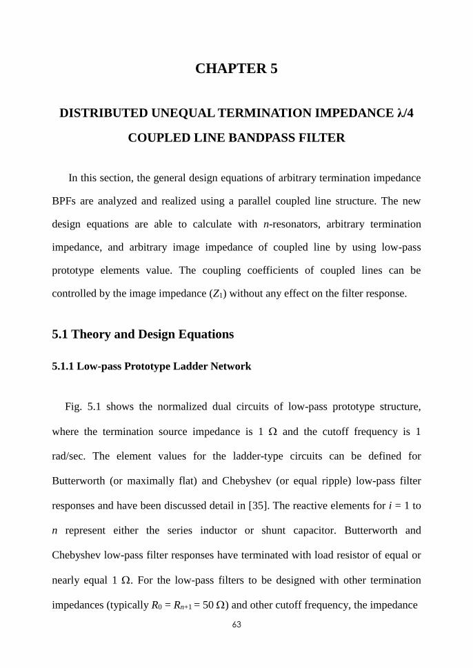
63
CHAPTER 5
DISTRIBUTED UNEQUAL TERMINATION IMPEDANCE λ/4
COUPLED LINE BANDPASS FILTER
In this section, the general design equations of arbitrary termination impedance
BPFs are analyzed and realized using a parallel coupled line structure. The new
design equations are able to calculate with n-resonators, arbitrary termination
impedance, and arbitrary image impedance of coupled line by using low-pass
prototype elements value. The coupling coefficients of coupled lines can be
controlled by the image impedance (Z1) without any effect on the filter response.
5.1 Theory and Design Equations
5.1.1 Low-pass Prototype Ladder Network
Fig. 5.1 shows the normalized dual circuits of low-pass prototype structure,
where the termination source impedance is 1 and the cutoff frequency is 1
rad/sec. The element values for the ladder-type circuits can be defined for
Butterworth (or maximally flat) and Chebyshev (or equal ripple) low-pass filter
responses and have been discussed detail in [35]. The reactive elements for i = 1 to
n represent either the series inductor or shunt capacitor. Butterworth and
Chebyshev low-pass filter responses have terminated with load resistor of equal or
nearly equal 1 . For the low-pass filters to be designed with other termination
impedances (typically R0 = Rn+1 = 50 ) and other cutoff frequency, the impedance
64
1 1g C
2 2g L
0 0R g 1
1
n
n
G
g
3 3g C 1
1
n
n
R
g
n ng C
n ng L
n even n odd
or
(a)
1 1g L
2 2g C0 0G g
n even n odd
n ng L
1
1
n
n
G
g
n ng L
1
1
n
n
R
g
n ng C or
(b)
Fig. 5.1. Ladder circuits for low-pass filter prototype and their element: (a) prototype beginning
with a shunt element and (b) prototype beginning with a series element.
and frequency scalings are required. Also, the conversion from low-pass filter to
highpass, bandpass, or bandstop filters are also presented in [32]-[34].
In the case of the ladder network discussed in [19] and [42], the terminating
resistors may be chosen arbitrary (R0 Rn+1). However, the transmission
characteristics of both Chebyshev [19] and Butterworth [42] filters in the passband
are deteriorated around zero frequency. The deterioration at zero frequency is
varied according to the impedance transformation ratio (r). The main difference
between a new low-pass filter and conventional low-pass filter is that new low-pass
filter can be designed with arbitrary termination impedance. However, the
deterioration at zero frequency in low-pass filter will cause the center frequency
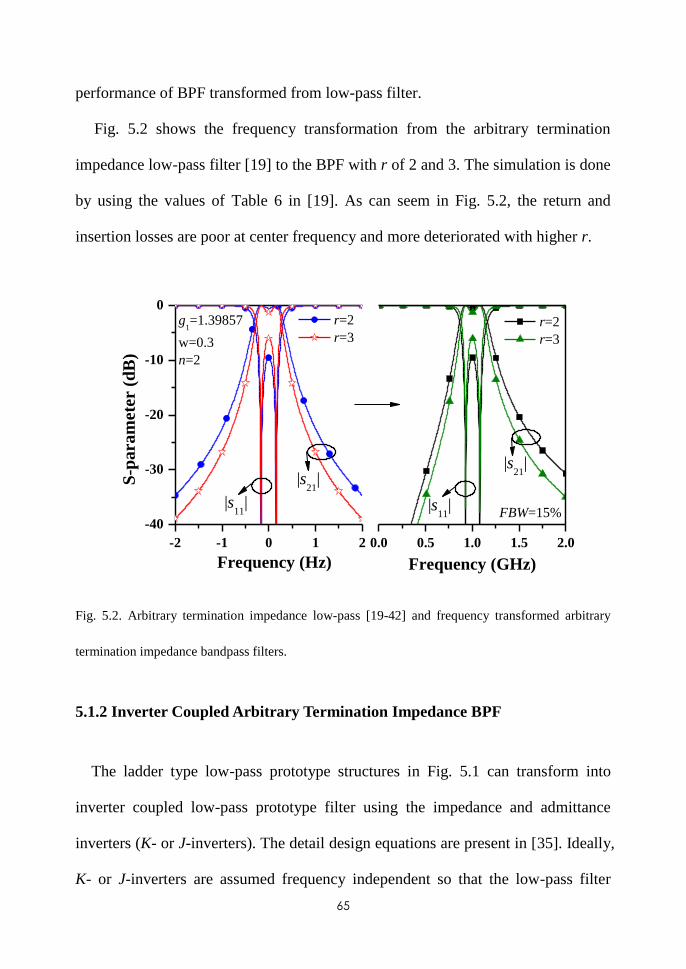
65
performance of BPF transformed from low-pass filter.
Fig. 5.2 shows the frequency transformation from the arbitrary termination
impedance low-pass filter [19] to the BPF with r of 2 and 3. The simulation is done
by using the values of Table 6 in [19]. As can seem in Fig. 5.2, the return and
insertion losses are poor at center frequency and more deteriorated with higher r.
-2 -1 0 1 2
-40
-30
-20
-10
0
FBW=15%|s
11|
r=2
r=3
S-p
ara
mete
r (
dB
)
Frequency (Hz)
|s21
||s
21|
|s11
|
g1=1.39857
w=0.3
n=2
0.0 0.5 1.0 1.5 2.0
r=2
r=3
Frequency (GHz)
Fig. 5.2. Arbitrary termination impedance low-pass [19-42] and frequency transformed arbitrary
termination impedance bandpass filters.
5.1.2 Inverter Coupled Arbitrary Termination Impedance BPF
The ladder type low-pass prototype structures in Fig. 5.1 can transform into
inverter coupled low-pass prototype filter using the impedance and admittance
inverters (K- or J-inverters). The detail design equations are present in [35]. Ideally,
K- or J-inverters are assumed frequency independent so that the low-pass filter
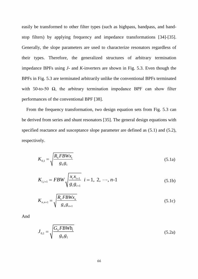
66
easily be transformed to other filter types (such as highpass, bandpass, and band-
stop filters) by applying frequency and impedance transformations [34]-[35].
Generally, the slope parameters are used to characterize resonators regardless of
their types. Therefore, the generalized structures of arbitrary termination
impedance BPFs using J- and K-inverters are shown in Fig. 5.3. Even though the
BPFs in Fig. 5.3 are terminated arbitrarily unlike the conventional BPFs terminated
with 50-to-50 Ω, the arbitrary termination impedance BPF can show filter
performances of the conventional BPF [38].
From the frequency transformation, two design equation sets from Fig. 5.3 can
be derived from series and shunt resonators [35]. The general design equations with
specified reactance and susceptance slope parameter are defined as (5.1) and (5.2),
respectively.
1
0,1
0 1
SR FBWxK
g g (5.1a)
1
, 1
1
1, 2, , -1i ii i
i i
x xK FBW i n
g g
(5.1b)
, 1
1
L nn n
n n
R FBWxK
g g
(5.1c)
And
1
0,1
0 1
SG FBWbJ
g g (5.2a)
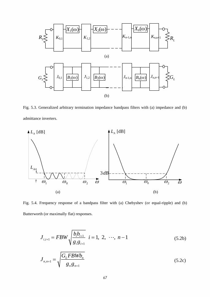
67
LRK0,1 K1,2Kn,n+1Kn-1,n
SR
X1() X2() Xn()
(a)
LGJ0,1 J1,2 Jn,n+1SG B1() B2() Jn-1,n Bn()
(b)
Fig. 5.3. Generalized arbitrary termination impedance bandpass filters with (a) impedance and (b)
admittance inverters.
2
ArL
[dB]AL
01 2
3dB
[dB]AL
01
(a) (b)
Fig. 5.4. Frequency response of a bandpass filter with (a) Chebyshev (or equal-ripple) and (b)
Butterworth (or maximally flat) responses.
1
, 1
1
1, 2, , 1i ii i
i i
b bJ FBW i n
g g
(5.2b)
, 1
1
L nn n
n n
G FBWbJ
g g
(5.2c)
68
where gi represents the low-pass prototype values, GS = 1 / RS and GL = 1 / RL. The
fractional bandwidth (FBW) is defined as
2 1
0
FBW
. (5.3)
The angular frequencies 1 and 2 denote the lower and upper passband edge
frequencies in case of Chebyshev response and 3-dB cut-off frequencies in case of
Butterworth response [33], respectively, as shown in Fig. 5.4.
For series resonators with reactance Xi(), the reactance slope parameters are
defined in [33] and [35] as
0
0 ( ), 1, 2, ,
2
ii
dXx i n
d
. (5.4)
For shunt resonators with susceptance Bi(), the susceptance slope parameters
are defined as
0
0 ( ), 1, 2, ,
2
ii
dBb i n
d
. (5.5)
To validate the theory, the BPFs are designed with arbitrary termination
impedances and different responses. The designed BPF is composed of shunt
parallel and series LC resonators for J- and K-inverters, respectively. From [33],
the reactance slope parameters of series resonators are defined as xi = 0L”
si and
suceptance slop parameters of shunt resonators are defined as bi = 0C”
pi. The
subscript s and p stand for series and parallel, respectively. Under the resonant
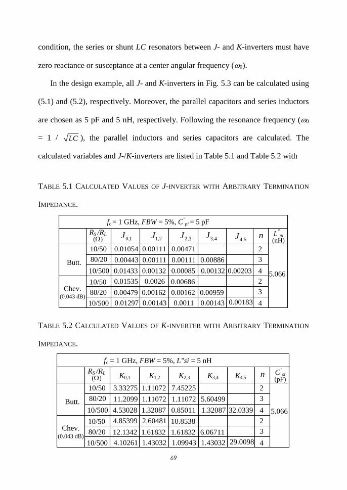
69
condition, the series or shunt LC resonators between J- and K-inverters must have
zero reactance or susceptance at a center angular frequency (0).
In the design example, all J- and K-inverters in Fig. 5.3 can be calculated using
(5.1) and (5.2), respectively. Moreover, the parallel capacitors and series inductors
are chosen as 5 pF and 5 nH, respectively. Following the resonance frequency (0
= 1 / LC ), the parallel inductors and series capacitors are calculated. The
calculated variables and J-/K-inverters are listed in Table 5.1 and Table 5.2 with
TABLE 5.1 CALCULATED VALUES OF J-INVERTER WITH ARBITRARY TERMINATION
IMPEDANCE.
fc = 1 GHz, FBW = 5%, C"pi = 5 pF
0,1J 1,2J 2,3J 3,4J
0.01054 0.00111 0.00471
RS /RL (
Butt.
Chev.(0.043 dB)
10/50
L"pi
(nH)
5.066
80/20 0.00111 0.008860.001110.00443
10/500 0.00143 0.001430.00110.01297
80/20 0.00162 0.009590.001620.00479
0.01535 0.0026 0.0068610/50
4,5J
0.00203
n
2
3
410/500 0.00132 0.001320.000850.01433
2
3
40.00183
TABLE 5.2 CALCULATED VALUES OF K-INVERTER WITH ARBITRARY TERMINATION
IMPEDANCE.
fc = 1 GHz, FBW = 5%, L"si = 5 nH
3.33275 1.11072 7.45225
RS /RL (
Butt.
Chev.(0.043 dB)
10/50
C"si
(pF)
5.066
80/20 1.11072 5.604991.1107211.2099
10/500 1.43032 1.430321.099434.10261
80/20 1.61832 6.067111.6183212.1342
4.85399 2.60481 10.853810/50
32.0339
n
2
3
410/500 1.32087 1.320870.850114.53028
2
3
429.0098
K0,1 K1,2 K2,3 K3,4 K4,5
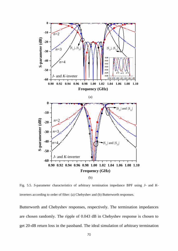
70
0.90 0.92 0.94 0.96 0.98 1.00 1.02 1.04 1.06 1.08 1.10
-60
-50
-40
-30
-20
-10
0
J- and K-inveter
n=2
n=3
S-p
ara
met
er (
dB
)
Frequency (GHz)
n=4
|S11
|, |S22
| |S21
|, |S12
|
(a)
0.90 0.92 0.94 0.96 0.98 1.00 1.02 1.04 1.06 1.08 1.10
-60
-50
-40
-30
-20
-10
0
n=4
n=2
n=3
|S21
| and |S12
|
S-p
aram
en
ter (
dB
)
Frequency (GHz)
|S11
| and |S22
|
J- and K-inverter
(b)
Fig. 5.5. S-parameter characteristics of arbitrary termination impedance BPF using J- and K-
inverters according to order of filter: (a) Chebyshev and (b) Butterworth responses.
Butterworth and Chebyshev responses, respectively. The termination impedances
are chosen randomly. The ripple of 0.043 dB in Chebyshev response is chosen to
get 20-dB return loss in the passband. The ideal simulation of arbitrary termination
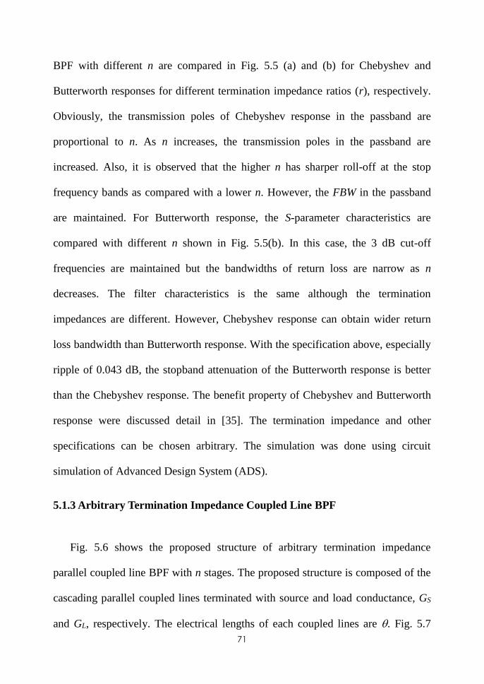
71
BPF with different n are compared in Fig. 5.5 (a) and (b) for Chebyshev and
Butterworth responses for different termination impedance ratios (r), respectively.
Obviously, the transmission poles of Chebyshev response in the passband are
proportional to n. As n increases, the transmission poles in the passband are
increased. Also, it is observed that the higher n has sharper roll-off at the stop
frequency bands as compared with a lower n. However, the FBW in the passband
are maintained. For Butterworth response, the S-parameter characteristics are
compared with different n shown in Fig. 5.5(b). In this case, the 3 dB cut-off
frequencies are maintained but the bandwidths of return loss are narrow as n
decreases. The filter characteristics is the same although the termination
impedances are different. However, Chebyshev response can obtain wider return
loss bandwidth than Butterworth response. With the specification above, especially
ripple of 0.043 dB, the stopband attenuation of the Butterworth response is better
than the Chebyshev response. The benefit property of Chebyshev and Butterworth
response were discussed detail in [35]. The termination impedance and other
specifications can be chosen arbitrary. The simulation was done using circuit
simulation of Advanced Design System (ADS).
5.1.3 Arbitrary Termination Impedance Coupled Line BPF
Fig. 5.6 shows the proposed structure of arbitrary termination impedance
parallel coupled line BPF with n stages. The proposed structure is composed of the
cascading parallel coupled lines terminated with source and load conductance, GS
and GL, respectively. The electrical lengths of each coupled lines are . Fig. 5.7
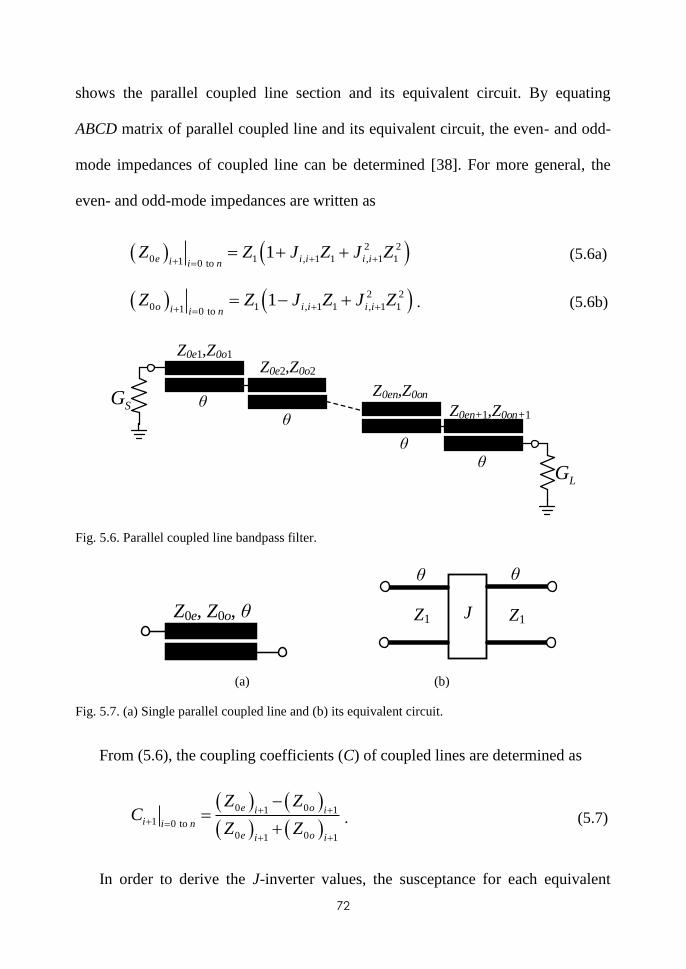
72
shows the parallel coupled line section and its equivalent circuit. By equating
ABCD matrix of parallel coupled line and its equivalent circuit, the even- and odd-
mode impedances of coupled line can be determined [38]. For more general, the
even- and odd-mode impedances are written as
2 2
0 1 , 1 1 , 1 11 0 to 1e i i i ii i n
Z Z J Z J Z (5.6a)
2 2
0 1 , 1 1 , 1 11 0 to 1o i i i ii i n
Z Z J Z J Z . (5.6b)
Z0e1,Z0o1 Z0e2,Z0o2
SG
LG
Z0en+1,Z0on+1
Z0en,Z0on
θ θ
θ θ
Fig. 5.6. Parallel coupled line bandpass filter.
Z0e, Z0o, θ
JZ1 Z1
θ θ
(a) (b)
Fig. 5.7. (a) Single parallel coupled line and (b) its equivalent circuit.
From (5.6), the coupling coefficients (C) of coupled lines are determined as
0 01 1
1 0 to
0 01 1
e oi ii i n
e oi i
Z ZC
Z Z
. (5.7)
In order to derive the J-inverter values, the susceptance for each equivalent
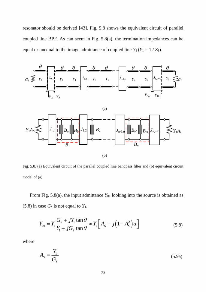
73
resonator should be derived [43]. Fig. 5.8 shows the equivalent circuit of parallel
coupled line BPF. As can seem in Fig. 5.8(a), the termination impedances can be
equal or unequal to the image admittance of coupled line Y1 (Y1 = 1 / Z1).
J0,1 J1,2
Y01Y1L
Jn,n+1Jn-1,n
YAYAL
Y1Y1 Y1Y1Y1 Y1Y1GS GL
θ θ θ θ θ θ θ θ
Y1
(a)
Ba
B1
Bb Jn-1,n Jn,n+1B2J0,1 J1,2 Bbl
Bn
BalY1AS Y1AL
(b)
Fig. 5.8. (a) Equivalent circuit of the parallel coupled line bandpass filter and (b) equivalent circuit
model of (a).
From Fig. 5.8(a), the input admittance Y01 looking into the source is obtained as
(5.8) in case GS is not equal to Y1.
2101 1 1
1
tan1
tan
SS S
S
G jYY Y Y A j A a
Y jG
(5.8)
where
1
S
S
YA
G (5.9a)
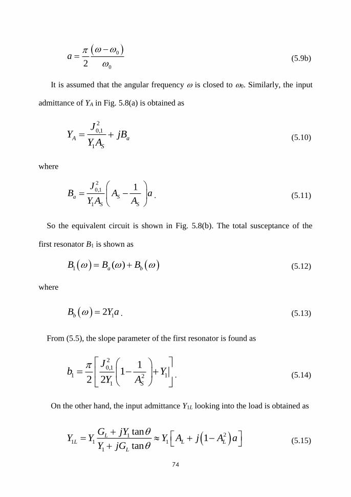
74
0
02a
(5.9b)
It is assumed that the angular frequency is closed to 0. Similarly, the input
admittance of YA in Fig. 5.8(a) is obtained as
2
0,1
1
A a
S
JY jB
Y A (5.10)
where
2
0,1
1
1a S
S S
JB A a
Y A A
. (5.11)
So the equivalent circuit is shown in Fig. 5.8(b). The total susceptance of the
first resonator B1 is shown as
1 ( )a bB B B (5.12)
where
12bB Y a . (5.13)
From (5.5), the slope parameter of the first resonator is found as
2
0,1
1 12
1
11
2 2 S
Jb Y
Y A
. (5.14)
On the other hand, the input admittance Y1L looking into the load is obtained as
211 1 1
1
tan1
tan
LL L L
L
G jYY Y Y A j A a
Y jG
(5.15)
75
where
1
L
L
YA
G . (5.16)
Similarly, the input admittance YAL in Fig. 5.8(a) is obtained as
2
0,1
1
AL al
L
JY jB
Y A (5.17)
where
2
, 1
1
1n n
al L
L L
JB A a
Y A A
. (5.18)
Similarly, the total susceptance of the last resonator Bn is shown as
( )n al blB B B (5.19)
where
bl bB B (5.20)
Also, the slope parameter of the last resonator is found as
2
, 1
12
1
11
2 2
n n
n
L
Jb Y
Y A
. (5.21)
Beside the first and last susceptance resonators, the susceptances of the
intermediate resonators are equal to Bb and the slope parameters are obtained as
1 @ 2, 3, , 12
mb Y m n
. (5.22)
From (5.2a)-(5.2c), the J-inverters of arbitrary termination impedance and image
admittance (Y1) are derived as
76
0,1 1
0 1
2
1
4
S
S
S
A FBW
J Y
g g A FBWA
(5.23a)
1
1,2 1
1 22
NJ Y FBW
g g
(5.23b)
, 1 1
1
1, 2, 3, , 2
2i i
i i
J Y FBW i ng g
(5.23c)
1, 1
12
Ln n
n n
NJ Y FBW
g g
(5.23d)
, 1 1
1
2
1
4
L
n n
n n L
L
A FBW
J Y
g g A FBWA
(5.23e)
where
2
0,1
1 2
1
11 1
2 S
JN
Y A
(5.24a)
2
, 1
2
1
11 1
2
n n
L
L
JN
Y A
. (5.24b)
In case of n = 2, the first and the last J-inverters are the same to (5.23a) and
(5.23e), respectively. However, the J1,2 is found as (5.25).
1
1,2 1
1 22
LN NJ FBWY
g g
(5.25)
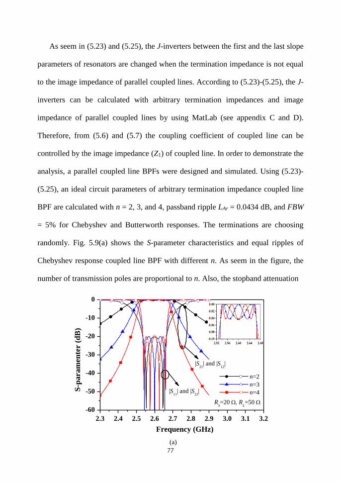
77
As seem in (5.23) and (5.25), the J-inverters between the first and the last slope
parameters of resonators are changed when the termination impedance is not equal
to the image impedance of parallel coupled lines. According to (5.23)-(5.25), the J-
inverters can be calculated with arbitrary termination impedances and image
impedance of parallel coupled lines by using MatLab (see appendix C and D).
Therefore, from (5.6) and (5.7) the coupling coefficient of coupled line can be
controlled by the image impedance (Z1) of coupled line. In order to demonstrate the
analysis, a parallel coupled line BPFs were designed and simulated. Using (5.23)-
(5.25), an ideal circuit parameters of arbitrary termination impedance coupled line
BPF are calculated with n = 2, 3, and 4, passband ripple LAr = 0.0434 dB, and FBW
= 5% for Chebyshev and Butterworth responses. The terminations are choosing
randomly. Fig. 5.9(a) shows the S-parameter characteristics and equal ripples of
Chebyshev response coupled line BPF with different n. As seem in the figure, the
number of transmission poles are proportional to n. Also, the stopband attenuation
2.3 2.4 2.5 2.6 2.7 2.8 2.9 3.0 3.1 3.2
-60
-50
-40
-30
-20
-10
0
n=2
n=3
n=4
RS=20 R
L=50
|S11
| and |S22
|
S-p
aram
en
ter (
dB
)
Frequency (GHz)
|S21
| and |S12
|
(a)
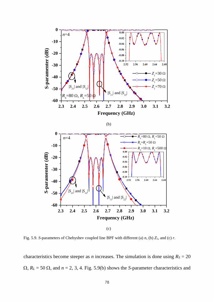
78
2.3 2.4 2.5 2.6 2.7 2.8 2.9 3.0 3.1 3.2
-60
-50
-40
-30
-20
-10
0
RS=80 , R
L=50
Z1=30
Z1=50
Z1=70
|S11
| and |S22
|
n=4
S-p
ara
men
ter
(dB
)
Frequency (GHz)
|S21
| and |S12
|
(b)
2.3 2.4 2.5 2.6 2.7 2.8 2.9 3.0 3.1 3.2
-60
-50
-40
-30
-20
-10
0 R
S=80 R
L=50
RS=R
L=50
RS=10 R
L=500
|S11
| and |S22
|
n=4
S-p
aram
en
ter (
dB
)
Frequency (GHz)
|S21
| and |S12
|
(c)
Fig. 5.9. S-parameters of Chebyshev coupled line BPF with different (a) n, (b) Z1, and (c) r.
characteristics become steeper as n increases. The simulation is done using RS = 20
, RL = 50 , and n = 2, 3, 4. Fig. 5.9(b) shows the S-parameter characteristics and
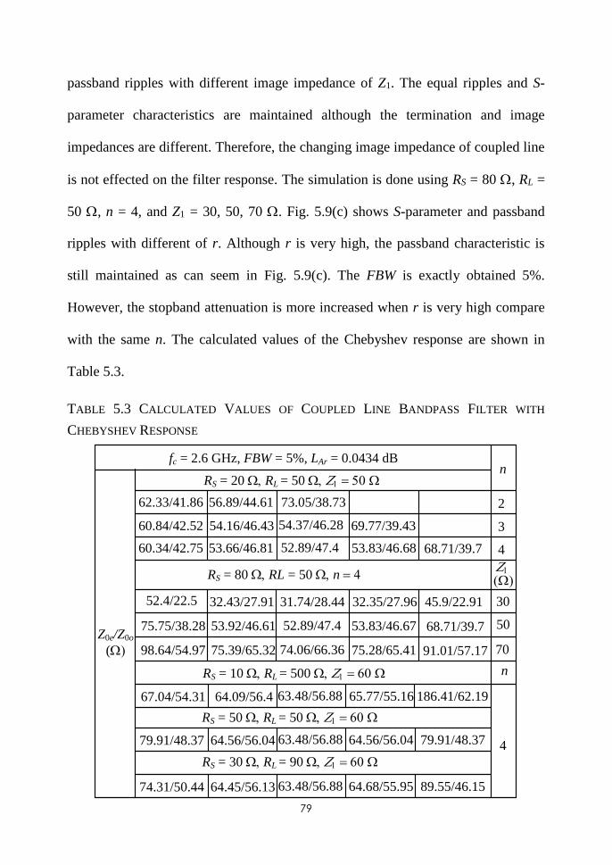
79
passband ripples with different image impedance of Z1. The equal ripples and S-
parameter characteristics are maintained although the termination and image
impedances are different. Therefore, the changing image impedance of coupled line
is not effected on the filter response. The simulation is done using RS = 80 , RL =
50 , n = 4, and Z1 = 30, 50, 70 . Fig. 5.9(c) shows S-parameter and passband
ripples with different of r. Although r is very high, the passband characteristic is
still maintained as can seem in Fig. 5.9(c). The FBW is exactly obtained 5%.
However, the stopband attenuation is more increased when r is very high compare
with the same n. The calculated values of the Chebyshev response are shown in
Table 5.3.
TABLE 5.3 CALCULATED VALUES OF COUPLED LINE BANDPASS FILTER WITH
CHEBYSHEV RESPONSE
fc = 2.6 GHz, FBW = 5%, LAr = 0.0434 dB
Z0e/Z0o
(
RS = 20 RL = 50 Z150
62.33/41.86 56.89/44.61 73.05/38.73
60.84/42.52 54.16/46.43 54.37/46.28 69.77/39.43
60.34/42.75 53.66/46.81 52.89/47.4 53.83/46.68 68.71/39.7
n
2
3
4
RS = 80 RL = 50 n 4Z1
30
50
70
52.4/22.5 32.43/27.91 31.74/28.44 32.35/27.96 45.9/22.91
75.75/38.28 53.92/46.61 52.89/47.4 53.83/46.67 68.71/39.7
98.64/54.97 75.39/65.32 74.06/66.36 75.28/65.41 91.01/57.17
67.04/54.31 64.09/56.4 63.48/56.88 65.77/55.16 186.41/62.19
RS = 10 RL = 500 Z160
79.91/48.37 64.56/56.04 63.48/56.88 64.56/56.04 79.91/48.37
RS = 50 RL = 50 Z160
n
4
74.31/50.44 64.45/56.13 63.48/56.88 64.68/55.95 89.55/46.15
RS = 30 RL = 90 Z160
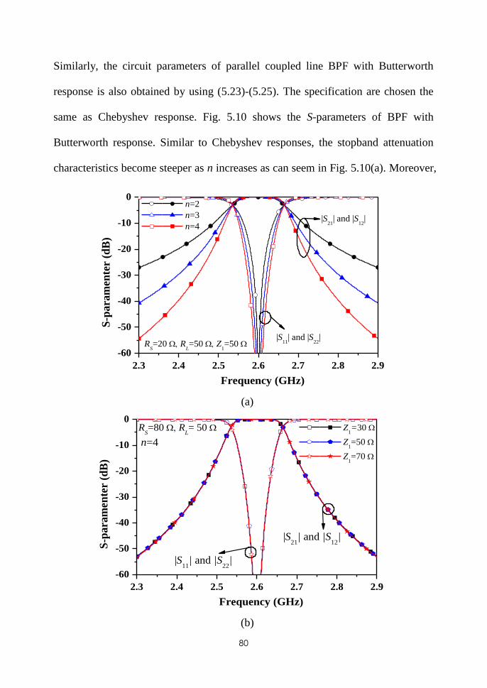
80
Similarly, the circuit parameters of parallel coupled line BPF with Butterworth
response is also obtained by using (5.23)-(5.25). The specification are chosen the
same as Chebyshev response. Fig. 5.10 shows the S-parameters of BPF with
Butterworth response. Similar to Chebyshev responses, the stopband attenuation
characteristics become steeper as n increases as can seem in Fig. 5.10(a). Moreover,
2.3 2.4 2.5 2.6 2.7 2.8 2.9
-60
-50
-40
-30
-20
-10
0 n=2
n=3
n=4
RS=20 R
L=50 Z
1=50
|S11
| and |S22
|
S-p
ara
men
ter
(dB
)
Frequency (GHz)
|S21
| and |S12
|
(a)
2.3 2.4 2.5 2.6 2.7 2.8 2.9
-60
-50
-40
-30
-20
-10
0R
S=80 R
L= 50
|S21
| and |S12
|
Z1=30
Z1=50
Z1=70
S-p
ara
men
ter
(dB
)
Frequency (GHz)
n=4
|S11
| and |S22
|
(b)
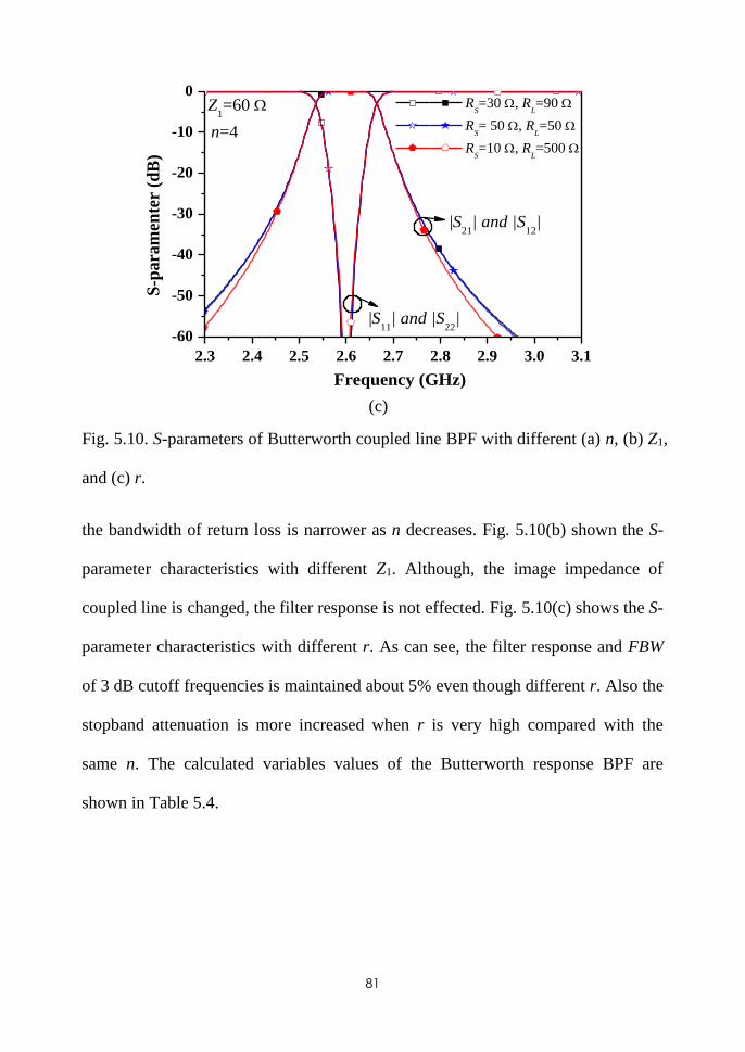
81
2.3 2.4 2.5 2.6 2.7 2.8 2.9 3.0 3.1
-60
-50
-40
-30
-20
-10
0Z
1=60
|S21
| and |S12
|
RS=30 , R
L=90
RS= 50 , R
L=50
RS=10 , R
L=500
S-p
ara
men
ter
(dB
)
Frequency (GHz)
n=4
|S11
| and |S22
|
(c)
Fig. 5.10. S-parameters of Butterworth coupled line BPF with different (a) n, (b) Z1,
and (c) r.
the bandwidth of return loss is narrower as n decreases. Fig. 5.10(b) shown the S-
parameter characteristics with different Z1. Although, the image impedance of
coupled line is changed, the filter response is not effected. Fig. 5.10(c) shows the S-
parameter characteristics with different r. As can see, the filter response and FBW
of 3 dB cutoff frequencies is maintained about 5% even though different r. Also the
stopband attenuation is more increased when r is very high compared with the
same n. The calculated variables values of the Butterworth response BPF are
shown in Table 5.4.
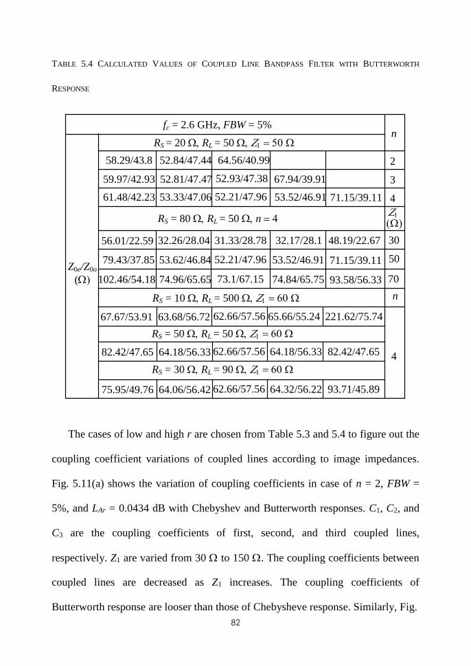
82
TABLE 5.4 CALCULATED VALUES OF COUPLED LINE BANDPASS FILTER WITH BUTTERWORTH
RESPONSE
fc = 2.6 GHz, FBW = 5%
Z0e/Z0o
(
RS = 20 RL = 50 Z150n
2
3
4
RS = 80 RL = 50 n 4Z1
30
50
70
56.01/22.59 32.26/28.04 31.33/28.78 32.17/28.1 48.19/22.67
79.43/37.85 53.62/46.84 52.21/47.96 53.52/46.91 71.15/39.11
102.46/54.18 74.96/65.65 73.1/67.15 74.84/65.75 93.58/56.33
RS = 10 RL = 500 Z160
82.42/47.65 64.18/56.33 62.66/57.56 64.18/56.33 82.42/47.65
RS = 50 RL = 50 Z160
n
4
75.95/49.76 64.06/56.42 62.66/57.56 64.32/56.22 93.71/45.89
RS = 30 RL = 90 Z160
58.29/43.8 52.84/47.44 64.56/40.99
59.97/42.93 52.81/47.47 52.93/47.38 67.94/39.91
61.48/42.23 53.33/47.06 52.21/47.96 53.52/46.91 71.15/39.11
67.67/53.91 63.68/56.72 62.66/57.56 65.66/55.24 221.62/75.74
The cases of low and high r are chosen from Table 5.3 and 5.4 to figure out the
coupling coefficient variations of coupled lines according to image impedances.
Fig. 5.11(a) shows the variation of coupling coefficients in case of n = 2, FBW =
5%, and LAr = 0.0434 dB with Chebyshev and Butterworth responses. C1, C2, and
C3 are the coupling coefficients of first, second, and third coupled lines,
respectively. Z1 are varied from 30 to 150 . The coupling coefficients between
coupled lines are decreased as Z1 increases. The coupling coefficients of
Butterworth response are looser than those of Chebysheve response. Similarly, Fig.
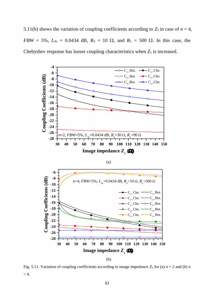
83
5.11(b) shows the variation of coupling coefficients according to Z1 in case of n = 4,
FBW = 5%, LAr = 0.0434 dB, RS = 10 , and RL = 500 . In this case, the
Chebyshev response has looser coupling characteristics when Z1 is increased.
30 40 50 60 70 80 90 100 110 120 130 140 150
-28
-26
-24
-22
-20
-18
-16
-14
-12
-10
-8
-6
-4 C
1_But.
C2_But.
C3_But.
Cou
pli
ng C
oef
fici
ents
(d
B)
Image impedance Z1 (
C1_Che.
C2_Che.
C3_Che.
n=2, FBW=5%, LAr
=0.0434 dB, RS=30 , R
L=90
(a)
30 40 50 60 70 80 90 100 110 120 130 140 150
-28
-26
-24
-22
-20
-18
-16
-14
-12
-10
-8
-6
C1_But.
C2_But.
C3_But.
C4_But.
C5_But.
C1_Che.
C2_Che.
C3_Che.
C4_Che.
C5_Che.
Cou
pli
ng C
oef
fici
ents
(d
B)
Image impedance Z1 (
n=4, FBW=5%, LAr
=0.0434 dB, RS=10 , R
L=500
(b)
Fig. 5.11. Variation of coupling coefficients according to image impedance Z1 for (a) n = 2 and (b) n
= 4.
84
However, the coupling coefficient of last coupled line is increased when Z1 are
varied from 30 to 65 and decreased when Z1 are varied from 65 to 150 . The
coupling coefficients of intermediate coupled lines are constant when Z1 vary from
30 to 150 . As r is high, the coupling coefficients of the coupled line is tight.
Therefore, the image impedance of coupled line can be used to control coupling
coefficient of coupled line without effecting the passband response. Thus, the
proposed design equations of the coupled line BPF can be used to design BPF with
any arbitrary termination and image impedances. The higher Z1 is preferable for
looser coupling of coupled lines.
5.2 Filter Implementation
For the experimental validation, the arbitrary termination impedance BPFs
were designed, simulated, and fabricated at an operating center frequency of f0 =
2.6 GHz. The designed filters are specified as RS = 20 , 80 , RL = 50 , FBW =
5%, and LAr = 0.0434 dB (S11 = -20 dB in the passband). The calculated elements
values for Chebyshev and Butterworth are already shown in Table 5.3 and 5.4,
respectively.
The proposed circuits were fabricated on a substrate RT/Duroid 5880 with a
dielectric constant (r) of 2.2 and thickness (h) of 31 mils. The electromagnetic
(EM) simulation was performed using ANSYS HFSS.
5.2.1 Three stages Coupled Line BPF
The first BPF was designed with Chebyshev response with RS = 20 and RL =
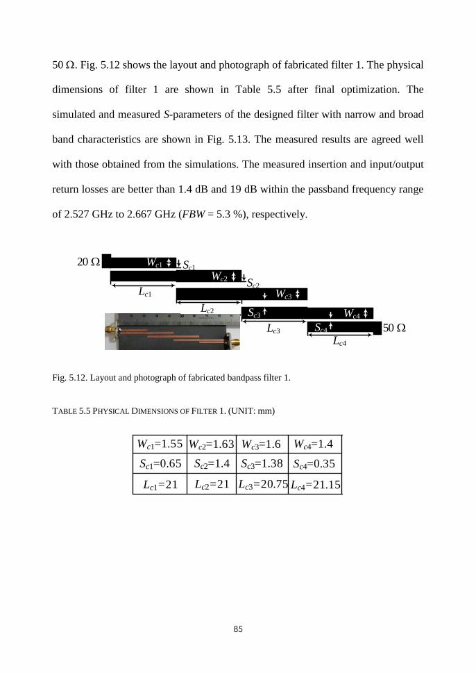
85
50 . Fig. 5.12 shows the layout and photograph of fabricated filter 1. The physical
dimensions of filter 1 are shown in Table 5.5 after final optimization. The
simulated and measured S-parameters of the designed filter with narrow and broad
band characteristics are shown in Fig. 5.13. The measured results are agreed well
with those obtained from the simulations. The measured insertion and input/output
return losses are better than 1.4 dB and 19 dB within the passband frequency range
of 2.527 GHz to 2.667 GHz (FBW = 5.3 %), respectively.
Wc1
Wc2
Wc3
Wc4
Sc1
Sc2
Sc3
Sc4
Lc1
Lc2
Lc3
Lc4
50
20
Fig. 5.12. Layout and photograph of fabricated bandpass filter 1.
TABLE 5.5 PHYSICAL DIMENSIONS OF FILTER 1. (UNIT: mm)
Wc1=1.55
Sc1=0.65
Lc1=21
Wc2=1.63
Sc2=1.4
Lc2=21
Wc3=1.6
Sc3=1.38
Lc3=20.75
Wc4=1.4
Sc4=0.35
Lc4=21.15
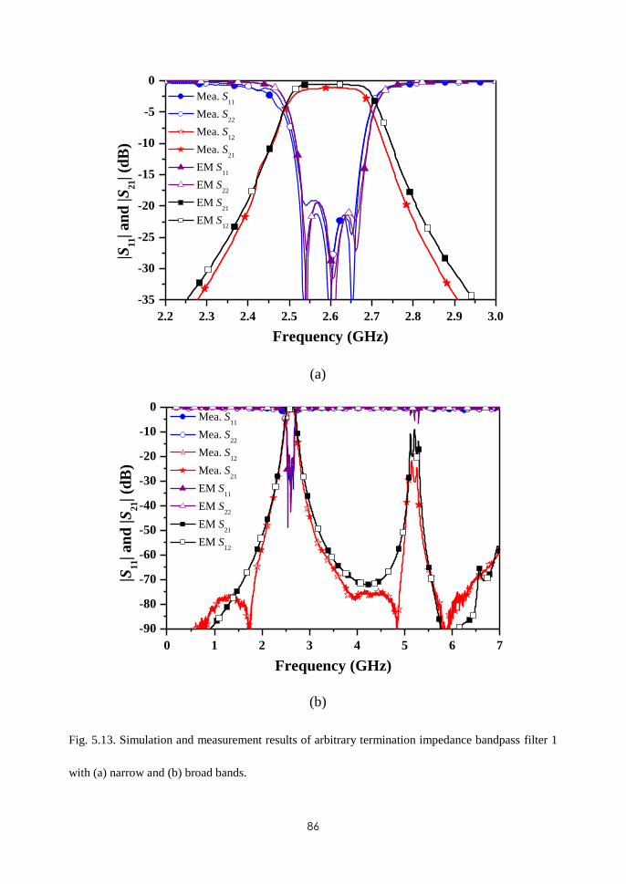
86
2.2 2.3 2.4 2.5 2.6 2.7 2.8 2.9 3.0
-35
-30
-25
-20
-15
-10
-5
0
Mea. S11
Mea. S22
Mea. S12
Mea. S21
EM S11
EM S22
EM S21
EM S12
|S11| an
d |S
21| (d
B)
Frequency (GHz)
(a)
0 1 2 3 4 5 6 7
-90
-80
-70
-60
-50
-40
-30
-20
-10
0 Mea. S
11
Mea. S22
Mea. S12
Mea. S21
EM S11
EM S22
EM S21
EM S12
|S11| an
d |S
21| (d
B)
Frequency (GHz)
(b)
Fig. 5.13. Simulation and measurement results of arbitrary termination impedance bandpass filter 1
with (a) narrow and (b) broad bands.
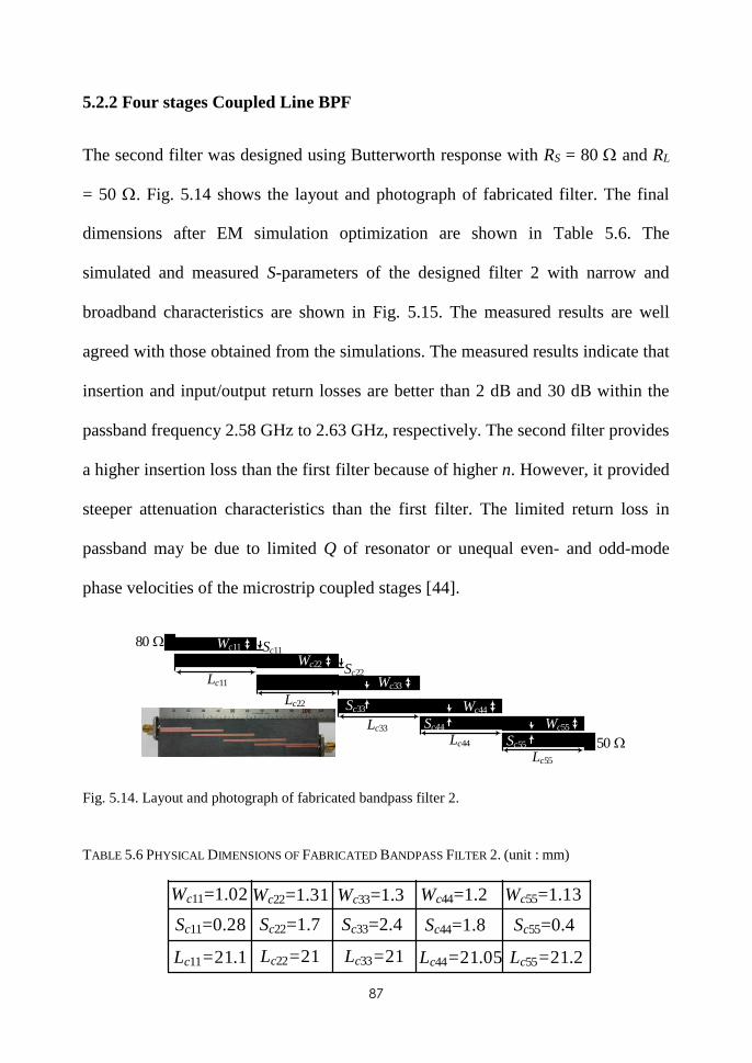
87
5.2.2 Four stages Coupled Line BPF
The second filter was designed using Butterworth response with RS = 80 and RL
= 50 . Fig. 5.14 shows the layout and photograph of fabricated filter. The final
dimensions after EM simulation optimization are shown in Table 5.6. The
simulated and measured S-parameters of the designed filter 2 with narrow and
broadband characteristics are shown in Fig. 5.15. The measured results are well
agreed with those obtained from the simulations. The measured results indicate that
insertion and input/output return losses are better than 2 dB and 30 dB within the
passband frequency 2.58 GHz to 2.63 GHz, respectively. The second filter provides
a higher insertion loss than the first filter because of higher n. However, it provided
steeper attenuation characteristics than the first filter. The limited return loss in
passband may be due to limited Q of resonator or unequal even- and odd-mode
phase velocities of the microstrip coupled stages [44].
Wc11
Wc22
Wc33
Wc44
Sc11
Sc22
Sc33
Sc44
Lc11
Lc22
Lc33
Lc44
Wc55
Sc55
Lc55
50
80
Fig. 5.14. Layout and photograph of fabricated bandpass filter 2.
TABLE 5.6 PHYSICAL DIMENSIONS OF FABRICATED BANDPASS FILTER 2. (unit : mm)
Wc11=1.02
Sc11=0.28
Lc11=21.1
Wc22=1.31
Sc22=1.7
Lc22=21
Wc33=1.3
Sc33=2.4
Lc33=21
Wc44=1.2
Sc44=1.8
Lc44=21.05
Wc55=1.13
Sc55=0.4
Lc55=21.2
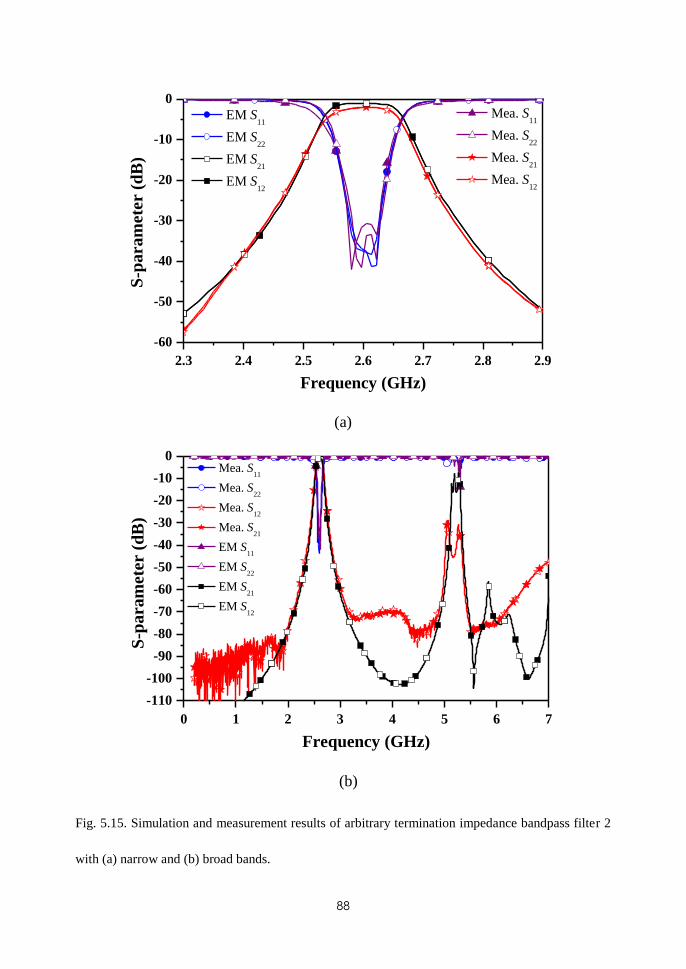
88
2.3 2.4 2.5 2.6 2.7 2.8 2.9
-60
-50
-40
-30
-20
-10
0 Mea. S
11
Mea. S22
Mea. S21
Mea. S12
EM S11
EM S22
EM S21
EM S12
S-p
aram
ete
r (
dB
)
Frequency (GHz)
(a)
0 1 2 3 4 5 6 7
-110
-100
-90
-80
-70
-60
-50
-40
-30
-20
-10
0 Mea. S
11
Mea. S22
Mea. S12
Mea. S21
EM S11
EM S22
EM S21
EM S12
S-p
ara
mete
r (d
B)
Frequency (GHz)
(b)
Fig. 5.15. Simulation and measurement results of arbitrary termination impedance bandpass filter 2
with (a) narrow and (b) broad bands.
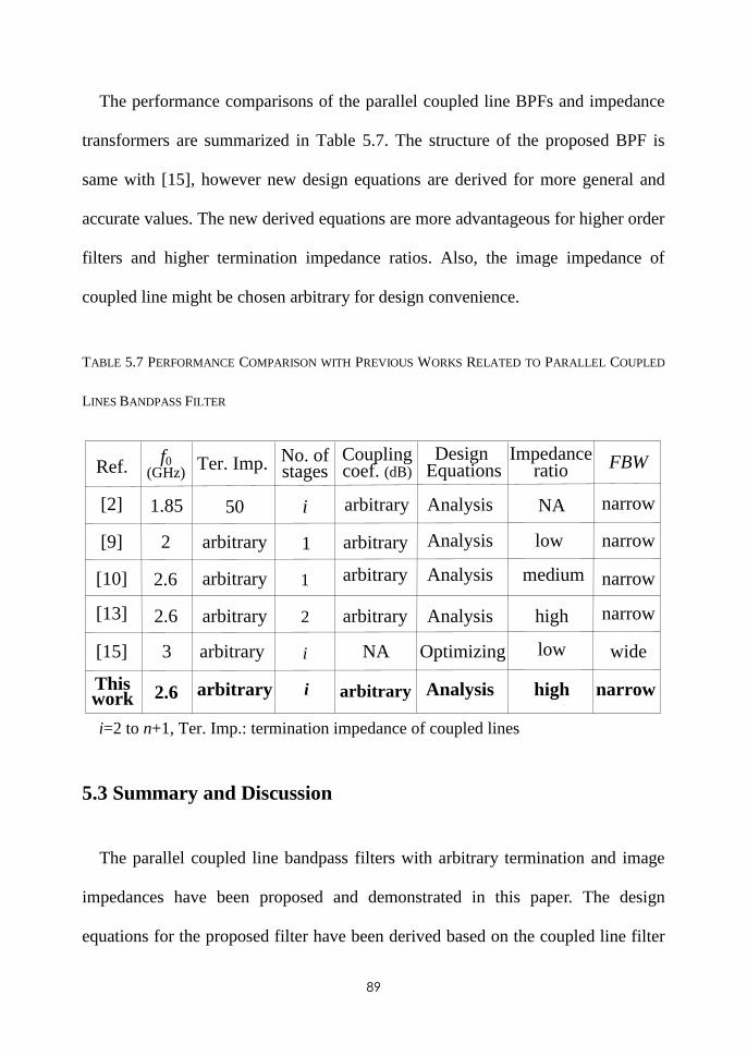
89
The performance comparisons of the parallel coupled line BPFs and impedance
transformers are summarized in Table 5.7. The structure of the proposed BPF is
same with [15], however new design equations are derived for more general and
accurate values. The new derived equations are more advantageous for higher order
filters and higher termination impedance ratios. Also, the image impedance of
coupled line might be chosen arbitrary for design convenience.
TABLE 5.7 PERFORMANCE COMPARISON WITH PREVIOUS WORKS RELATED TO PARALLEL COUPLED
LINES BANDPASS FILTER
[9]
[2]
Thiswork
Ter. Imp. No. ofstages
Design Equations
f0 (GHz)
2.6 arbitrary
50
1
i
arbitrary2
1.85
Ref.Coupling coef. (dB)
arbitrary
arbitrary
[10] 1 arbitraryarbitrary2.6
[13] 2 arbitraryarbitrary2.6
i
i=2 to n+1, Ter. Imp.: termination impedance of coupled lines
[15]
Using parallel coupled line
i
arbitrary
NAarbitrary3
Analysis
Analysis
Analysis
Analysis
Optimizing
Analysis
Impedanceratio
NA
low
medium
high
low
high
FBW
narrow
narrow
narrow
narrow
wide
narrow
5.3 Summary and Discussion
The parallel coupled line bandpass filters with arbitrary termination and image
impedances have been proposed and demonstrated in this paper. The design
equations for the proposed filter have been derived based on the coupled line filter

90
theory. In order to show the validity of the proposed design equations, two design
examples of coupled line BPF with Chebyshev and Butterworth responses have
been fabricated and measured. The simulation and measurement results are well
agreed with the analysis. The new derived equations will be advantage in many
applications such as power divider, matching network, and power amplifier design.
Furthermore, the new design equations can provide more accurately and faster
design.
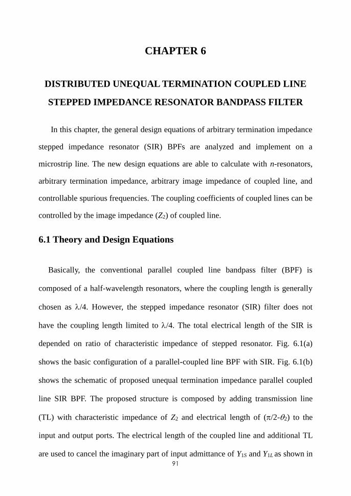
91
CHAPTER 6
DISTRIBUTED UNEQUAL TERMINATION COUPLED LINE
STEPPED IMPEDANCE RESONATOR BANDPASS FILTER
In this chapter, the general design equations of arbitrary termination impedance
stepped impedance resonator (SIR) BPFs are analyzed and implement on a
microstrip line. The new design equations are able to calculate with n-resonators,
arbitrary termination impedance, arbitrary image impedance of coupled line, and
controllable spurious frequencies. The coupling coefficients of coupled lines can be
controlled by the image impedance (Z2) of coupled line.
6.1 Theory and Design Equations
Basically, the conventional parallel coupled line bandpass filter (BPF) is
composed of a half-wavelength resonators, where the coupling length is generally
chosen as l/4. However, the stepped impedance resonator (SIR) filter does not
have the coupling length limited to l/4. The total electrical length of the SIR is
depended on ratio of characteristic impedance of stepped resonator. Fig. 6.1(a)
shows the basic configuration of a parallel-coupled line BPF with SIR. Fig. 6.1(b)
shows the schematic of proposed unequal termination impedance parallel coupled
line SIR BPF. The proposed structure is composed by adding transmission line
(TL) with characteristic impedance of Z2 and electrical length of (/2-2) to the
input and output ports. The electrical length of the coupled line and additional TL
are used to cancel the imaginary part of input admittance of Y1S and Y1L as shown in
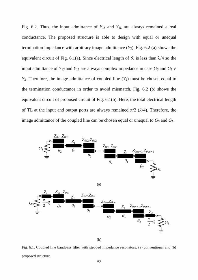
92
Fig. 6.2. Thus, the input admittance of Y1S and Y1L are always remained a real
conductance. The proposed structure is able to design with equal or unequal
termination impedance with arbitrary image admittance (Y2). Fig. 6.2 (a) shows the
equivalent circuit of Fig. 6.1(a). Since electrical length of 2 is less than l/4 so the
input admittance of Y1S and Y1L are always complex impedance in case GS and GL
Y2. Therefore, the image admittance of coupled line (Y2) must be chosen equal to
the termination conductance in order to avoid mismatch. Fig. 6.2 (b) shows the
equivalent circuit of proposed circuit of Fig. 6.1(b). Here, the total electrical length
of TL at the input and output ports are always remained /2 (l/4). Therefore, the
image admittance of the coupled line can be chosen equal or unequal to GS and GL.
Z0e1,Z0o1 Z0e2,Z0o2
Z0en+1,Z0on+1
Z0en,Z0on
θ2 θ2 θ1
θ2 θ2 θ1
Z1
Z1
GL
GS
(a)
Z0e1,Z0o1 Z0e2,Z0o2
Z0en+1,Z0on+1
Z0en,Z0on
θ2 θ2 θ1
θ2 θ2 θ1
Z1
Z1 Z2
22
22
Z2
GL
GS
(b)
Fig. 6.1. Coupled line bandpass filter with stepped impedance resonators: (a) conventional and (b)
proposed structure.
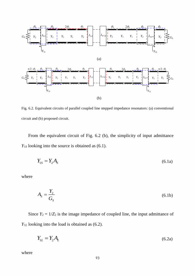
93
J0,1 J1,2
Y1s
Y1Y2Y2 Y2Y1
Y1L
Y2Y1Y2 Y2Y1
Jn-1,n Jn,n+1
2 22 2 2 2
GS GL
21 21
(a)
J0,1 J1,2
Y1S
Y1Y2Y2 Y2Y1
Y1L
Y2Y1Y2 Y2Y1
Jn-1,n Jn,n+1
2 21 22 2 21 2 2
GS GLY2
/22
Y2
/22
(b)
Fig. 6.2. Equivalent circuits of parallel coupled line stepped impedance resonators: (a) conventional
circuit and (b) proposed circuit.
From the equivalent circuit of Fig. 6.2 (b), the simplicity of input admittance
Y1S looking into the source is obtained as (6.1).
1 2S SY Y A (6.1a)
where
2
S
S
YA
G (6.1b)
Since Y2 = 1/Z2 is the image impedance of coupled line, the input admittance of
Y1L looking into the load is obtained as (6.2).
1 2L LY Y A (6.2a)
where
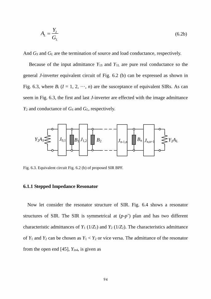
94
2
L
L
YA
G (6.2b)
And GS and GL are the termination of source and load conductance, respectively.
Because of the input admittance Y1S and Y1L are pure real conductance so the
general J-inverter equivalent circuit of Fig. 6.2 (b) can be expressed as shown in
Fig. 6.3, where Bi (I = 1, 2, ···, n) are the susceptance of equivalent SIRs. As can
seem in Fig. 6.3, the first and last J-inverter are effected with the image admittance
Y2 and conductance of GS and GL, respectively.
B1 Jn-1,n Jn,n+1B2J0,1 J1,2 BnY2AS Y2AL
Fig. 6.3. Equivalent circuit Fig. 6.2 (b) of proposed SIR BPF.
6.1.1 Stepped Impedance Resonator
Now let consider the resonator structure of SIR. Fig. 6.4 shows a resonator
structures of SIR. The SIR is symmetrical at (p-p’) plan and has two different
characteristic admittances of Y1 (1/Z1) and Y2 (1/Z2). The characteristics admittance
of Y1 and Y2 can be chosen as Y1 < Y2 or vice versa. The admittance of the resonator
from the open end [45], Yin4, is given as
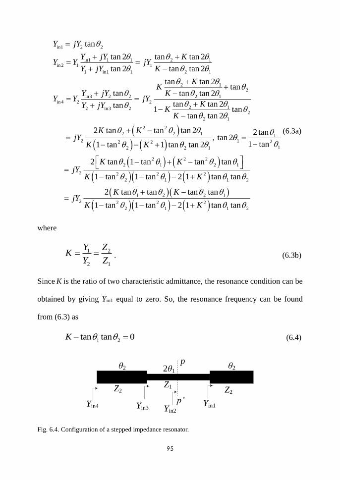
95
in1 2 2
in1 1 1 2 1in 2 1 1
1 in1 1 2 1
2 12
in3 2 2 2 1in 4 2 2
2 12 in3 22
2 1
2
2
2
tan
tan 2 tan tan 2
tan 2 tan tan 2
tan tan 2tan
tan tan tan 2
tan tan 2tan1 tan
tan tan 2
2 tan tan
Y jY
Y jY KY Y jY
Y jY K
KK
Y jY KY Y jY
KY jYK
K
K KjY
2
2 1 11 22 2
12 2 1
2 2 2
2 1 2 1
2 2 2 2
2 1 1 2
1 2 2 1
2 2 2 2
2 1 1 2
tan 2 2 tan, tan 2
1 tan1 tan 1 tan tan 2
2 tan 1 tan tan tan
1 tan 1 tan 2 1 tan tan
2 tan tan tan tan
1 tan 1 tan 2 1 tan tan
K K
K KjY
K K
K KjY
K K
(6.3a)
where
1 2
2 1
Y ZK
Y Z . (6.3b)
Since K is the ratio of two characteristic admittance, the resonance condition can be
obtained by giving Yin1 equal to zero. So, the resonance frequency can be found
from (6.3) as
1 2tan tan 0K (6.4)
Yin1Yin2Yin3
Yin4
Z2 Z2Z1
θ2 2θ1θ2
p’
p
Fig. 6.4. Configuration of a stepped impedance resonator.
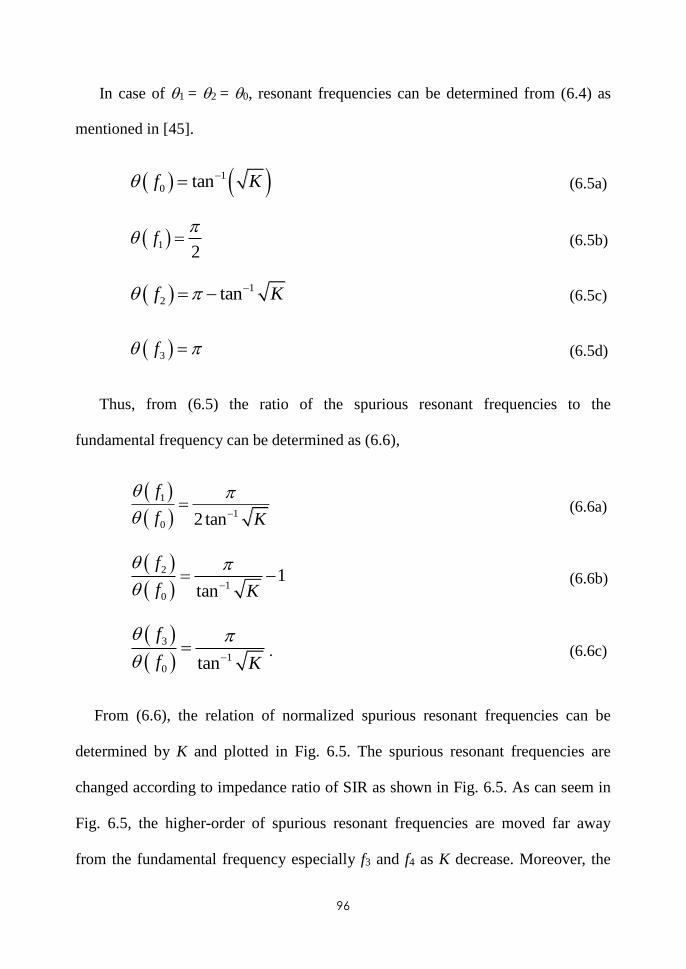
96
In case of 1 = 2 = 0, resonant frequencies can be determined from (6.4) as
mentioned in [45].
1
0 tanf K (6.5a)
12
f
(6.5b)
1
2 tanf K (6.5c)
3f (6.5d)
Thus, from (6.5) the ratio of the spurious resonant frequencies to the
fundamental frequency can be determined as (6.6),
1
10 2 tan
f
f K
(6.6a)
2
10
1tan
f
f K
(6.6b)
3
10 tan
f
f K
. (6.6c)
From (6.6), the relation of normalized spurious resonant frequencies can be
determined by K and plotted in Fig. 6.5. The spurious resonant frequencies are
changed according to impedance ratio of SIR as shown in Fig. 6.5. As can seem in
Fig. 6.5, the higher-order of spurious resonant frequencies are moved far away
from the fundamental frequency especially f3 and f4 as K decrease. Moreover, the
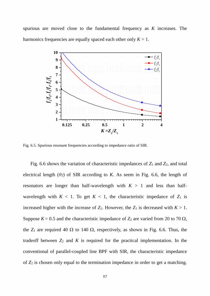
97
spurious are moved close to the fundamental frequency as K increases. The
harmonics frequencies are equally spaced each other only K = 1.
0.125 0.25 0.5 1 2 4
1
2
3
4
5
6
7
8
9
10
f 2
/f1, f 3
/f1, f 4
/f1
K =Z2/Z
1
f2/f
1
f3/f
1
f4/f
1
Fig. 6.5. Spurious resonant frequencies according to impedance ratio of SIR.
Fig. 6.6 shows the variation of characteristic impedances of Z1 and Z2, and total
electrical length (θT) of SIR according to K. As seem in Fig. 6.6, the length of
resonators are longer than half-wavelength with K > 1 and less than half-
wavelength with K < 1. To get K < 1, the characteristic impedance of Z1 is
increased higher with the increase of Z2. However, the Z1 is decreased with K > 1.
Suppose K = 0.5 and the characteristic impedance of Z2 are varied from 20 to 70 ,
the Z1 are required 40 to 140 , respectively, as shown in Fig. 6.6. Thus, the
tradeoff between Z2 and K is required for the practical implementation. In the
conventional of parallel-coupled line BPF with SIR, the characteristic impedance
of Z2 is chosen only equal to the termination impedance in order to get a matching.
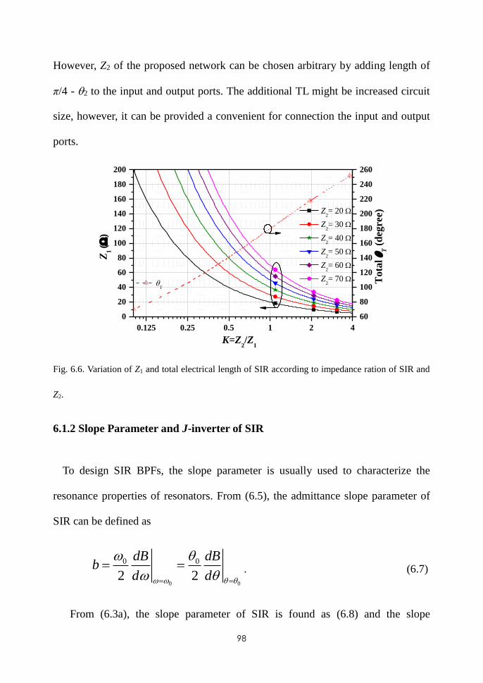
98
However, Z2 of the proposed network can be chosen arbitrary by adding length of
π/4 - 2 to the input and output ports. The additional TL might be increased circuit
size, however, it can be provided a convenient for connection the input and output
ports.
0.125 0.25 0.5 1 2 4
0
20
40
60
80
100
120
140
160
180
200
60
80
100
120
140
160
180
200
220
240
260
Tota
l
T (
deg
ree)
Z1 (
)
K=Z2/Z
1
Z2= 20
Z2= 30
Z2= 40
Z2= 50
Z2= 60
Z2= 70
Fig. 6.6. Variation of Z1 and total electrical length of SIR according to impedance ration of SIR and
Z2.
6.1.2 Slope Parameter and J-inverter of SIR
To design SIR BPFs, the slope parameter is usually used to characterize the
resonance properties of resonators. From (6.5), the admittance slope parameter of
SIR can be defined as
0 0
0 0
2 2
dB dBb
d d
. (6.7)
From (6.3a), the slope parameter of SIR is found as (6.8) and the slope
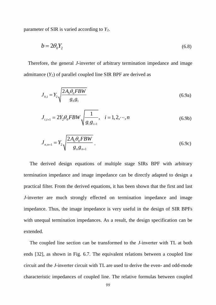
99
parameter of SIR is varied according to Y2.
0 22b Y (6.8)
Therefore, the general J-inverter of arbitrary termination impedance and image
admittance (Y2) of parallel coupled line SIR BPF are derived as
0
0,1 2
0 1
2 SA FBWJ Y
g g
(6.9a)
, 1 2 0
1
12 , 1,2, ,i i
i i
J Y FBW i ng g
(6.9b)
0
, 1 2
1
2 Ln n
n n
A FBWJ Y
g g
. (6.9c)
The derived design equations of multiple stage SIRs BPF with arbitrary
termination impedance and image impedance can be directly adapted to design a
practical filter. From the derived equations, it has been shown that the first and last
J-inverter are much strongly effected on termination impedance and image
impedance. Thus, the image impedance is very useful in the design of SIR BPFs
with unequal termination impedances. As a result, the design specification can be
extended.
The coupled line section can be transformed to the J-inverter with TL at both
ends [32], as shown in Fig. 6.7. The equivalent relations between a coupled line
circuit and the J-inverter circuit with TL are used to derive the even- and odd-mode
characteristic impedances of coupled line. The relative formulas between coupled
100
line and the J-inverter in Fig. 6.7 can be derived from the ABCD matrix. For more
general, the even- and odd-mode impedances can be written as (6.10) with a
various of electrical length.
2 2
, 1 2 , 1 2
0 2 2 2 21 0 to , 1 2
1 csc
1 cot
i i i i
e i i ni i
J Z J ZZ Z
J Z
(6.10a)
2 2
, 1 2 , 1 2
0 2 2 2 21 0 to , 1 2
1 csc
1 cot
i i i i
o i i ni i
J Z J ZZ Z
J Z
. (6.10b)
From (6.10), the coupling coefficients (C) of coupled lines are determined as
0 01 1
1 0 to
0 01 1
e oi ii i n
e oi i
Z ZC
Z Z
. (6.11)
Z0e, Z0o, θ
Ji,i+1Z2 Z2
θ θ
(a) (b)
Fig. 6.7. (a) parallel coupled-line with two open terminations and (b) equivalent circuit has a J-
inverter with two transmission line sections.
In order to demonstrate the analysis, SIR parallel coupled line BPF with
arbitrary termination and image impedances were designed and simulated. The
design formulas of (6.9) and (6.10) for an n-resonator are used to calculated the
even- and odd-mode characteristic impedances of coupled line (see appendix E).
The element values g1, g2, , gn of the prototype low-pass filter (see appendix C),
101
which may be calculated for either Butterworth or Chebyshev responses [35]. The
design examples are done with n = 2, 3, and 4 and FBW = 5% for Butterworth and
Chebyshev responses (ripple = 0.0434 dB). The passband bandwidths of
Chebyshev and Butterworth responses are determined from the passband edge
frequencies and 3-dB cutoff frequencies [35], respectively.
Fig. 6.8 (a) shows the variation of coupling coefficients and Z1 in case of n = 4,
FBW = 5%, RS = 20 Ω, RL = 50 Ω, and K = 0.7 with Chebyshev and Butterworth
responses. Ci (i = 1, 2, ···, n) are the coupling coefficients of the coupled lines.
As can seem in Fig. 6.8(a), the first and last coupled line are required stronger
coupling than the intermediate coupled line. As Z2 increase from 5 to 100 Ω, the
coupling of first and last coupled lines are become looser, however, the Z1 is
increased from 7.14 to 142.85 Ω. Also, the intermediate coupled line are constant
with Z2 increasing. Moreover, the couplings of coupled line of the Butterworth
response are looser than the Chebyshev response. Fig. 6.8(b) shows the variation of
coupling coefficients and Z1 in case of n = 4, FBW = 5%, RS = 15 , RL = 90 , and
K = 1.5. In this case, the coupling coefficient of the first and last coupled lines are
looser than Fig. 6.8(a). As Z2 increase from 5 to 150, the Z1 is increased from 3.33
to 100 Ω, while the intermediate coupling of coupled lines are constant.
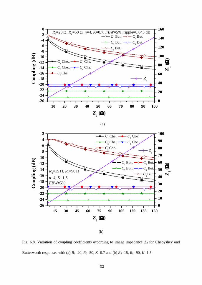
102
10 20 30 40 50 60 70 80 90 100
-26
-24
-22
-20
-18
-16
-14
-12
-10
-8
-6
-4
-2
0
0
20
40
60
80
100
120
140
160
C1 But., C
2 But.
C3 But., C
4 But.
C5 But.
Z1 (
)
C1 Che., C
2 Che.
C3 Che., C
4 Che.
C5 Che.
Cou
pli
ng (
dB
)
Z2 ()
RS=20 , R
L=50 n=4, K=0.7, FBW=5%, ripple=0.043 dB
Z1
(a)
15 30 45 60 75 90 105 120 135 150
-26
-24
-22
-20
-18
-16
-14
-12
-10
-8
-6
-4
-2
0
10
20
30
40
50
60
70
80
90
100
C1 But., C
2 But.
C3 But., C
4 But.
C5 But. Z
1 (
)
C1 Che., C
2 Che.
C3 Che., C
4 Che.
C5 Che.
Cou
pli
ng (
dB
)
Z2 ()
RS=15 , R
L=90
n=4, K=1.5
FBW=5%
Z1
(b)
Fig. 6.8. Variation of coupling coefficients according to image impedance Z2 for Chebyshev and
Butterworth responses with (a) RS=20, RL=50, K=0.7 and (b) RS=15, RL=90, K=1.5.
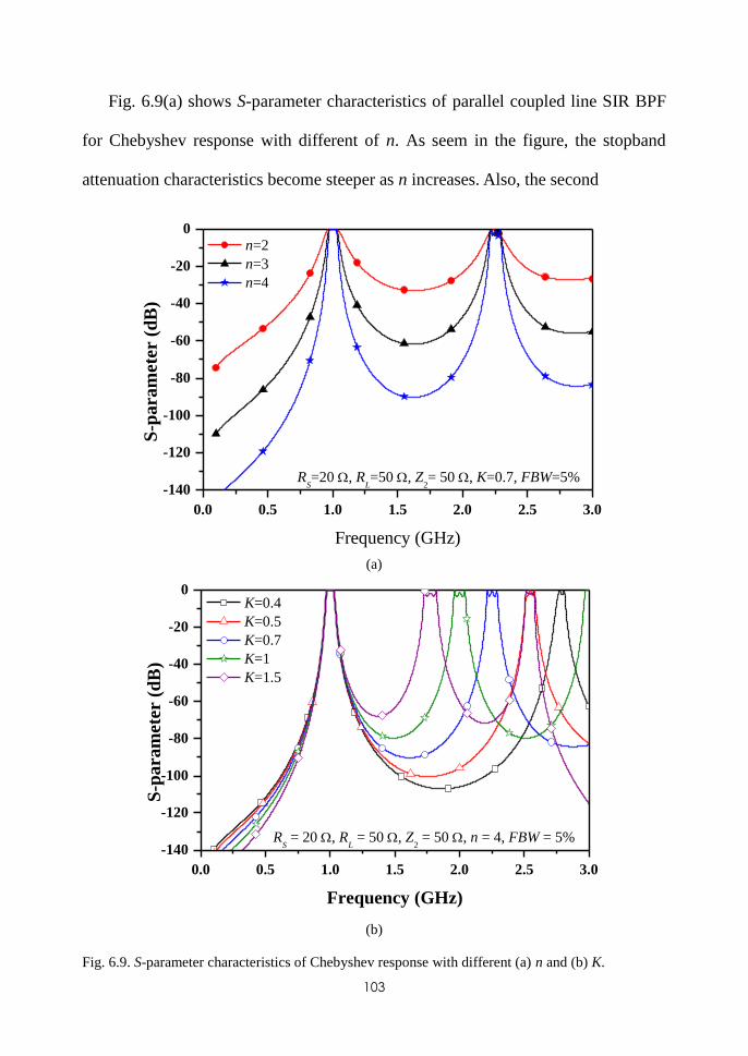
103
Fig. 6.9(a) shows S-parameter characteristics of parallel coupled line SIR BPF
for Chebyshev response with different of n. As seem in the figure, the stopband
attenuation characteristics become steeper as n increases. Also, the second
0.0 0.5 1.0 1.5 2.0 2.5 3.0
-140
-120
-100
-80
-60
-40
-20
0
n=2
n=3
n=4
S-p
ara
mete
r (
dB
)
Frequency (GHz)
RS=20 , R
L=50 , Z
2= 50 , K=0.7, FBW=5%
(a)
0.0 0.5 1.0 1.5 2.0 2.5 3.0
-140
-120
-100
-80
-60
-40
-20
0 K=0.4
K=0.5
K=0.7
K=1
K=1.5
S-p
ara
mete
r (d
B)
Frequency (GHz)
RS = 20 , R
L = 50 , Z
2 = 50 , n = 4, FBW = 5%
(b)
Fig. 6.9. S-parameter characteristics of Chebyshev response with different (a) n and (b) K.
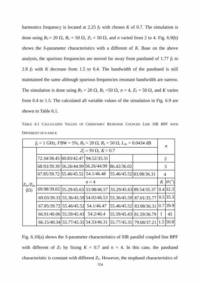
104
harmonics frequency is located at 2.25 f0 with chosen K of 0.7. The simulation is
done using RS = 20 , RL = 50 , Z2 = 50 , and n varied from 2 to 4. Fig. 6.9(b)
shows the S-parameter characteristics with a different of K. Base on the above
analysis, the spurious frequencies are moved far away from passband of 1.77 f0 to
2.8 f0 with K decrease from 1.5 to 0.4. The bandwidth of the passband is still
maintained the same although spurious frequencies resonant bandwidth are narrow.
The simulation is done using RS = 20 , RL =50 , n = 4, Z2 = 50 , and K varies
from 0.4 to 1.5. The calculated all variable values of the simulation in Fig. 6.9 are
shown in Table 6.1.
TABLE 6.1 CALCULATED VALUES OF CHEBYSHEV RESPONSE COUPLED LINE SIR BPF WITH
DIFFERENT OF n AND K
f0 = 1 GHz, FBW = 5%, RS = 20 RL = 50 LAr = 0.0434 dB
Z0e/Z0o
(
Z250K = 0.7
72.34/38.45 60.83/42.47 94.52/35.31
68.93/39.39 56.26/44.99 56.26/44.99 86.42/36.02
67.85/39.72 55.46/45.52 54.1/46.48 55.46/45.52 83.98/36.31
n
2
3
4
n = 4 K
0.4
0.5
0.7
69.98/39.02 55.29/45.63 53.98/46.57 55.29/45.63 89.54/35.37
69.03/39.33 55.36/45.59 54.02/46.53 55.36/45.59 87.01/35.77
67.85/39.72 55.46/45.52 54.1/46.47 55.46/45.52 83.98/36.31
166.91/40.06 55.59/45.43 54.2/46.4 55.59/45.43 81.59/36.79
1.566.15/40.34 55.77/45.31 54.33/46.31 55.77/45.31 79.68/37.21
o
32.3
35.3
39.9
45
50.8
Fig. 6.10(a) shows the S-parameter characteristics of SIR parallel coupled line BPF
with different of Z2 by fixing K = 0.7 and n = 4. In this case, the passband
characteristic is constant with different Z2. However, the stopband characteristics of
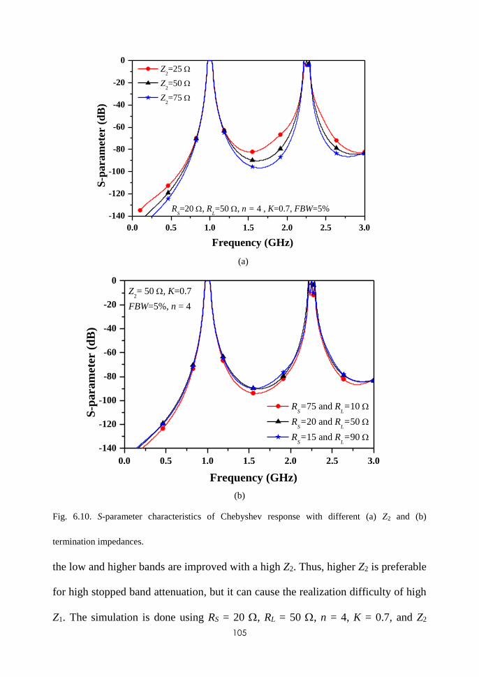
105
0.0 0.5 1.0 1.5 2.0 2.5 3.0
-140
-120
-100
-80
-60
-40
-20
0 Z
2=25
Z2=50
Z2=75
S-p
ara
mete
r (
dB
)
Frequency (GHz)
RS=20 , R
L=50 , n = 4 , K=0.7, FBW=5%
(a)
0.0 0.5 1.0 1.5 2.0 2.5 3.0
-140
-120
-100
-80
-60
-40
-20
0
RS=75 and R
L=10
RS=20 and R
L=50
RS=15 and R
L=90
S-p
ara
mete
r (
dB
)
Frequency (GHz)
Z2= 50 , K=0.7
FBW=5%, n = 4
(b)
Fig. 6.10. S-parameter characteristics of Chebyshev response with different (a) Z2 and (b)
termination impedances.
the low and higher bands are improved with a high Z2. Thus, higher Z2 is preferable
for high stopped band attenuation, but it can cause the realization difficulty of high
Z1. The simulation is done using RS = 20 , RL = 50 , n = 4, K = 0.7, and Z2
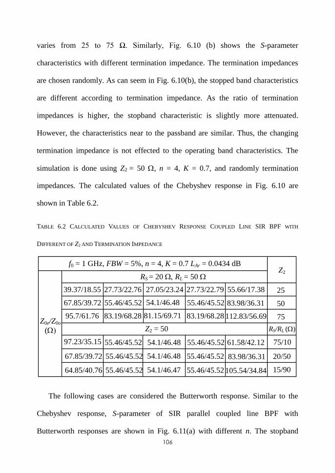
106
varies from 25 to 75 Ω. Similarly, Fig. 6.10 (b) shows the S-parameter
characteristics with different termination impedance. The termination impedances
are chosen randomly. As can seem in Fig. 6.10(b), the stopped band characteristics
are different according to termination impedance. As the ratio of termination
impedances is higher, the stopband characteristic is slightly more attenuated.
However, the characteristics near to the passband are similar. Thus, the changing
termination impedance is not effected to the operating band characteristics. The
simulation is done using Z2 = 50 , n = 4, K = 0.7, and randomly termination
impedances. The calculated values of the Chebyshev response in Fig. 6.10 are
shown in Table 6.2.
TABLE 6.2 CALCULATED VALUES OF CHEBYSHEV RESPONSE COUPLED LINE SIR BPF WITH
DIFFERENT OF Z2 AND TERMINATION IMPEDANCE
f0 = 1 GHz, FBW = 5%, n = 4, K = 0.7 LAr = 0.0434 dB
Z0e/Z0o
(
RS = 20 RL = 50
39.37/18.55 27.73/22.76 27.05/23.24
95.7/61.76 83.19/68.28 81.15/69.71 83.19/68.28 112.83/56.69
25
50
75
Z2 = 50
75/1097.23/35.15 55.46/45.52 54.1/46.48 55.46/45.52 61.58/42.12
67.85/39.72 55.46/45.52 54.1/46.48 55.46/45.52 83.98/36.31
64.85/40.76 55.46/45.52 54.1/46.47 55.46/45.52 105.54/34.84
RS/RL ()
Z2
27.73/22.79 55.66/17.38
67.85/39.72 55.46/45.52 54.1/46.48 55.46/45.52 83.98/36.31
20/50
15/90
The following cases are considered the Butterworth response. Similar to the
Chebyshev response, S-parameter of SIR parallel coupled line BPF with
Butterworth responses are shown in Fig. 6.11(a) with different n. The stopband
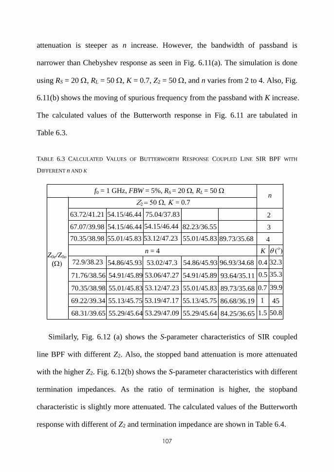
107
attenuation is steeper as n increase. However, the bandwidth of passband is
narrower than Chebyshev response as seen in Fig. 6.11(a). The simulation is done
using RS = 20 , RL = 50 , K = 0.7, Z2 = 50 , and n varies from 2 to 4. Also, Fig.
6.11(b) shows the moving of spurious frequency from the passband with K increase.
The calculated values of the Butterworth response in Fig. 6.11 are tabulated in
Table 6.3.
TABLE 6.3 CALCULATED VALUES OF BUTTERWORTH RESPONSE COUPLED LINE SIR BPF WITH
DIFFERENT n AND K
f0 = 1 GHz, FBW = 5%, RS = 20 RL = 50
Z0e/Z0o
(
Z250K = 0.7
63.72/41.21 54.15/46.44 75.04/37.83
67.07/39.98 54.15/46.44 54.15/46.44 82.23/36.55
70.35/38.98 55.01/45.83 53.12/47.23 55.01/45.83 89.73/35.68
n
2
3
4
n = 4 K
0.4
0.5
0.7
72.9/38.23 54.86/45.93 53.02/47.3 54.86/45.93 96.93/34.68
71.76/38.56 54.91/45.89 53.06/47.27 54.91/45.89 93.64/35.11
70.35/38.98 55.01/45.83 53.12/47.23 55.01/45.83 89.73/35.68
169.22/39.34 55.13/45.75 53.19/47.17 55.13/45.75 86.68/36.19
1.568.31/39.65 55.29/45.64 53.29/47.09 55.29/45.64 84.25/36.65
o
32.3
35.3
39.9
45
50.8
Similarly, Fig. 6.12 (a) shows the S-parameter characteristics of SIR coupled
line BPF with different Z2. Also, the stopped band attenuation is more attenuated
with the higher Z2. Fig. 6.12(b) shows the S-parameter characteristics with different
termination impedances. As the ratio of termination is higher, the stopband
characteristic is slightly more attenuated. The calculated values of the Butterworth
response with different of Z2 and termination impedance are shown in Table 6.4.
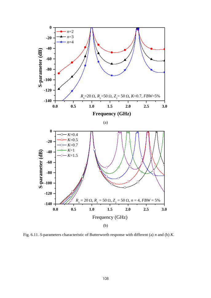
108
0.0 0.5 1.0 1.5 2.0 2.5 3.0
-140
-120
-100
-80
-60
-40
-20
0 n=2
n=3
n=4
S-p
ara
mete
r (d
B)
Frequency (GHz)
RS=20 , R
L=50 , Z
2= 50 , K=0.7, FBW=5%
(a)
0.0 0.5 1.0 1.5 2.0 2.5 3.0
-140
-120
-100
-80
-60
-40
-20
0 K=0.4
K=0.5
K=0.7
K=1
K=1.5
S-p
ara
met
er (
dB
)
Frequency (GHz)
RS = 20 , R
L = 50 , Z
2 = 50 , n = 4, FBW = 5%
(b)
Fig. 6.11. S-parameters characteristic of Butterworth response with different (a) n and (b) K.
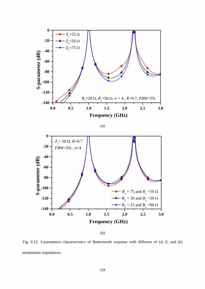
109
0.0 0.5 1.0 1.5 2.0 2.5 3.0
-140
-120
-100
-80
-60
-40
-20
0 Z
2=25
Z2=50
Z2=75
S-p
ara
mete
r (
dB
)
Frequency (GHz)
RS=20 , R
L=50 , n = 4 , K=0.7, FBW=5%
(a)
0.0 0.5 1.0 1.5 2.0 2.5 3.0
-140
-120
-100
-80
-60
-40
-20
0
RS = 75 and R
L =10
RS = 20 and R
L =50
RS = 15 and R
L =90
S-p
ara
met
er (
dB
)
Frequency (GHz)
Z2= 50 , K=0.7
FBW=5% , n=4
(b)
Fig. 6.12. S-parameters characteristics of Butterworth response with different of (a) Z2 and (b)
termination impedances.
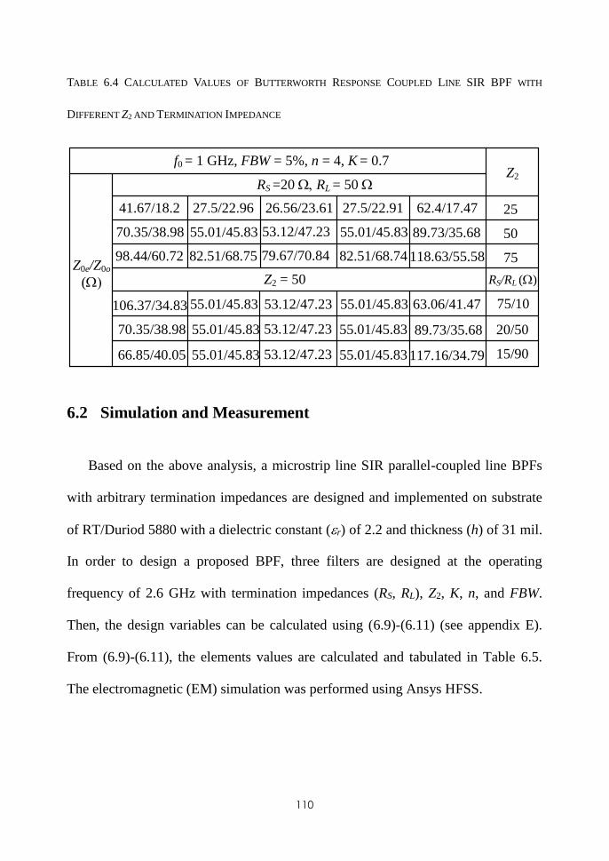
110
TABLE 6.4 CALCULATED VALUES OF BUTTERWORTH RESPONSE COUPLED LINE SIR BPF WITH
DIFFERENT Z2 AND TERMINATION IMPEDANCE
f0 = 1 GHz, FBW = 5%, n = 4, K = 0.7
Z0e/Z0o
(
RS =20 RL = 50
41.67/18.2 27.5/22.96 26.56/23.61
98.44/60.72 82.51/68.75 79.67/70.84 82.51/68.74 118.63/55.58
25
50
75
Z2 = 50
75/10106.37/34.83 55.01/45.83 53.12/47.23 55.01/45.83 63.06/41.47
70.35/38.98 55.01/45.83 53.12/47.23 55.01/45.83 89.73/35.68
66.85/40.05 55.01/45.83 53.12/47.23 55.01/45.83 117.16/34.79
RS/RL ()
Z2
27.5/22.91 62.4/17.47
70.35/38.98 55.01/45.83 53.12/47.23 55.01/45.83 89.73/35.68
20/50
15/90
6.2 Simulation and Measurement
Based on the above analysis, a microstrip line SIR parallel-coupled line BPFs
with arbitrary termination impedances are designed and implemented on substrate
of RT/Duriod 5880 with a dielectric constant (r) of 2.2 and thickness (h) of 31 mil.
In order to design a proposed BPF, three filters are designed at the operating
frequency of 2.6 GHz with termination impedances (RS, RL), Z2, K, n, and FBW.
Then, the design variables can be calculated using (6.9)-(6.11) (see appendix E).
From (6.9)-(6.11), the elements values are calculated and tabulated in Table 6.5.
The electromagnetic (EM) simulation was performed using Ansys HFSS.
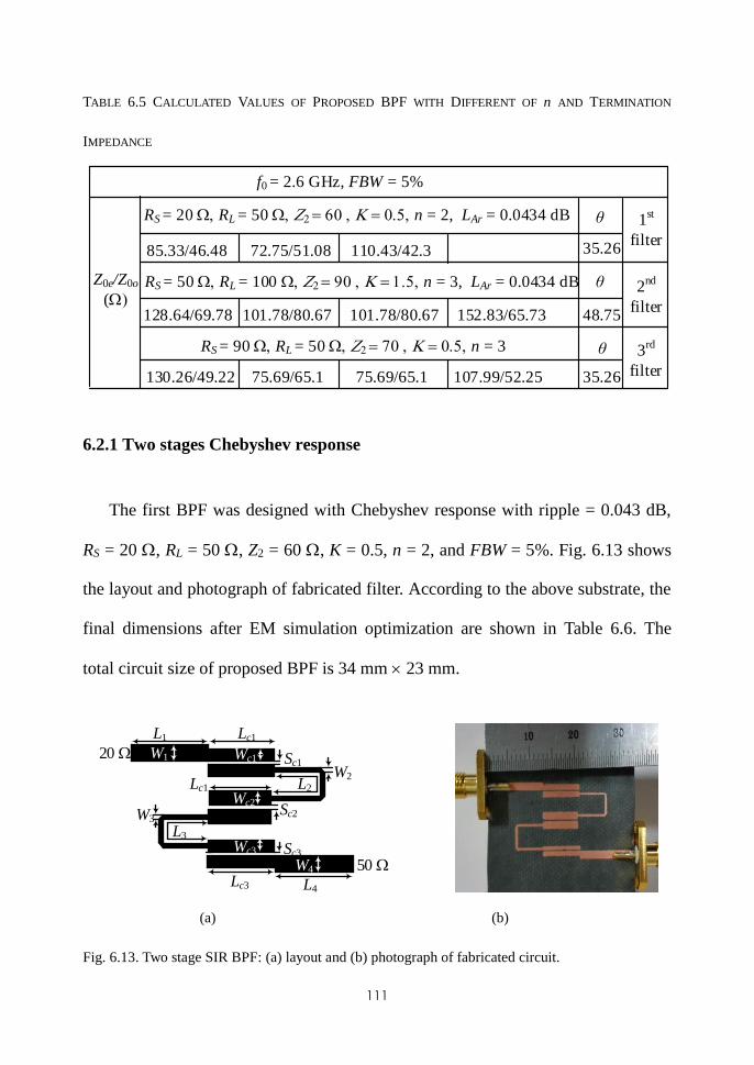
111
TABLE 6.5 CALCULATED VALUES OF PROPOSED BPF WITH DIFFERENT OF n AND TERMINATION
IMPEDANCE
f0 = 2.6 GHz, FBW = 5%
Z0e/Z0o
(
RS = 20 RL = 50 Z260K0.5n = 2, LAr = 0.0434 dB
85.33/46.48 72.75/51.08 110.43/42.3
128.64/69.78 101.78/80.67 101.78/80.67 152.83/65.73
RS = 50 RL = 100 Z290K1.5n = 3, LAr = 0.0434 dB
RS = 90 RL = 50 Z270K0.5n = 3
130.26/49.22 75.69/65.1 75.69/65.1 107.99/52.25
1st
filter
2nd
filter
3rd
filter
θ
θ
θ
35.26
35.26
48.75
6.2.1 Two stages Chebyshev response
The first BPF was designed with Chebyshev response with ripple = 0.043 dB,
RS = 20 , RL = 50 , Z2 = 60 , K = 0.5, n = 2, and FBW = 5%. Fig. 6.13 shows
the layout and photograph of fabricated filter. According to the above substrate, the
final dimensions after EM simulation optimization are shown in Table 6.6. The
total circuit size of proposed BPF is 34 mm 23 mm.
Wc1 Sc1
Lc1
20
Wc2Sc2
Lc1
Wc3 Sc3
L2
W2
Lc3
L3
W3
L1
W1
L4
W4 50
(a) (b)
Fig. 6.13. Two stage SIR BPF: (a) layout and (b) photograph of fabricated circuit.
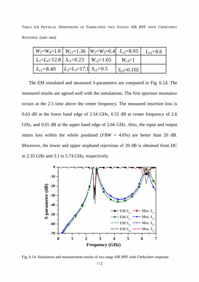
112
TABLE 6.6 PHYSICAL DIMENSIONS OF FABRICATED TWO STAGES SIR BPF WITH CHEBYSHEV
RESPONSE. (unit: mm)
W1=W4=1.8
L1=L4=12.8
Lc1=8.49
Wc1=1.36
Sc1=0.23
L2=L3=17.1
W2=W3=0.4
Wc2=1.65
Sc2=0.5
Lc2=8.05
Wc3=1
Sc3=0.102
Lc3=8.6
The EM simulated and measured S-parameters are compared in Fig. 6.14. The
measured results are agreed well with the simulations. The first spurious resonance
occurs at the 2.5 time above the center frequency. The measured insertion loss is
0.63 dB at the lower band edge of 2.54 GHz, 0.55 dB at center frequency of 2.6
GHz, and 0.65 dB at the upper band edge of 2.66 GHz. Also, the input and output
return loss within the whole passband (FBW = 4.6%) are better than 20 dB.
Moreover, the lower and upper stopband rejections of 20 dB is obtained from DC
to 2.35 GHz and 3.1 to 5.74 GHz, respectively.
0 1 2 3 4 5 6 7
-70
-60
-50
-40
-30
-20
-10
0
EM S11
EM S12
EM S21
EM S22
Mea. S11
Mea. S12
Mea. S21
Mea. S22
S-p
aram
ete
r (
dB
)
Frequency (GHz)
Fig. 6.14. Simulation and measurement results of two stage SIR BPF with Chebyshev response.
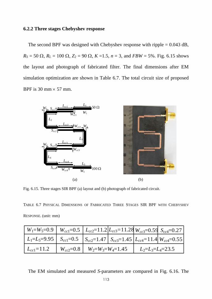
113
6.2.2 Three stages Chebyshev response
The second BPF was designed with Chebyshev response with ripple = 0.043 dB,
RS = 50 , RL = 100 , Z2 = 90 , K =1.5, n = 3, and FBW = 5%. Fig. 6.15 shows
the layout and photograph of fabricated filter. The final dimensions after EM
simulation optimization are shown in Table 6.7. The total circuit size of proposed
BPF is 30 mm 57 mm.
Scc1
Lcc1 50
Wcc2
Scc2
Lcc2
Wcc3
Scc3
L2
W2
Lcc3
L3
W3
L1
W1
L5
W5100
L4
W4
Lcc4
Scc4
Wcc1
Wcc4
(a) (b)
Fig. 6.15. Three stages SIR BPF (a) layout and (b) photograph of fabricated circuit.
TABLE 6.7 PHYSICAL DIMENSIONS OF FABRICATED THREE STAGES SIR BPF WITH CHEBYSHEV
RESPONSE. (unit: mm)
W1=W5=0.9
L1=L5=9.95
Lcc1=11.2
Wcc1=0.5
Scc1=0.5
L2=L3=L4=23.5W2=W3=W4=1.45Wcc2=0.8
Scc2=1.47
Lcc2=11.2
Lcc4=11.4
Wcc3=0.59
Scc3=1.45
Lcc3=11.28
Wcc4=0.55
Scc4=0.27
The EM simulated and measured S-parameters are compared in Fig. 6.16. The
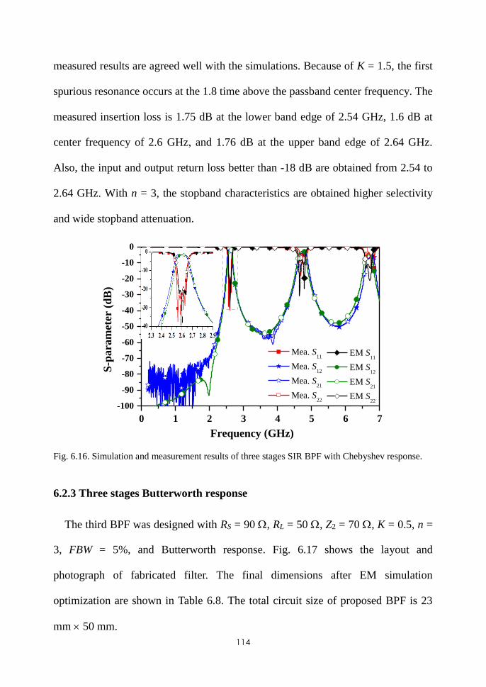
114
measured results are agreed well with the simulations. Because of K = 1.5, the first
spurious resonance occurs at the 1.8 time above the passband center frequency. The
measured insertion loss is 1.75 dB at the lower band edge of 2.54 GHz, 1.6 dB at
center frequency of 2.6 GHz, and 1.76 dB at the upper band edge of 2.64 GHz.
Also, the input and output return loss better than -18 dB are obtained from 2.54 to
2.64 GHz. With n = 3, the stopband characteristics are obtained higher selectivity
and wide stopband attenuation.
0 1 2 3 4 5 6 7
-100
-90
-80
-70
-60
-50
-40
-30
-20
-10
0
EM S11
EM S12
EM S21
EM S22
Mea. S11
Mea. S12
Mea. S21
Mea. S22
S-p
ara
met
er (
dB
)
Frequency (GHz)
Fig. 6.16. Simulation and measurement results of three stages SIR BPF with Chebyshev response.
6.2.3 Three stages Butterworth response
The third BPF was designed with RS = 90 , RL = 50 , Z2 = 70 , K = 0.5, n =
3, FBW = 5%, and Butterworth response. Fig. 6.17 shows the layout and
photograph of fabricated filter. The final dimensions after EM simulation
optimization are shown in Table 6.8. The total circuit size of proposed BPF is 23
mm 50 mm.
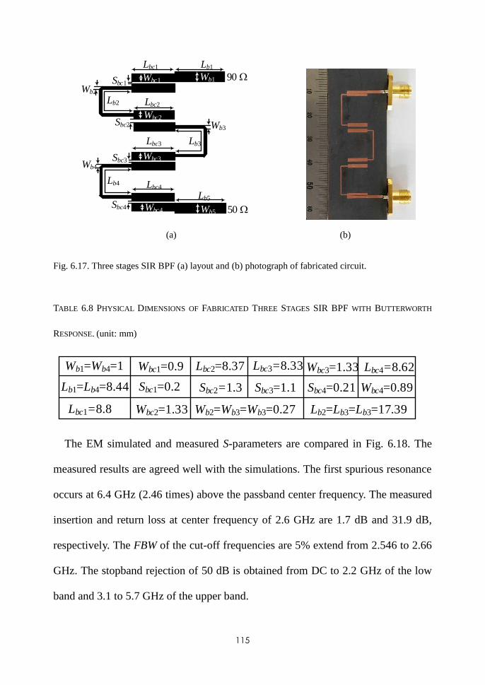
115
Wbc1Sbc1
Lbc1
90
Wbc2Sbc2
Lbc2
Wbc3Sbc3
Lb2
Wb2
Lbc3 Lb3
Wb3
Lb1
Wb1
Lb5
Wb5 50
Lb4
Wb4
Lbc4
Sbc4 Wbc4
(a) (b)
Fig. 6.17. Three stages SIR BPF (a) layout and (b) photograph of fabricated circuit.
TABLE 6.8 PHYSICAL DIMENSIONS OF FABRICATED THREE STAGES SIR BPF WITH BUTTERWORTH
RESPONSE. (unit: mm)
Wb1=Wb4=1
Lb1=Lb4=8.44
Lbc1=8.8
Wbc1=0.9
Sbc1=0.2
Lb2=Lb3=Lb3=17.39Wb2=Wb3=Wb3=0.27Wbc2=1.33
Sbc2=1.3
Lbc2=8.37 Lbc4=8.62Wbc3=1.33
Sbc3=1.1
Lbc3=8.33
Wbc4=0.89Sbc4=0.21
The EM simulated and measured S-parameters are compared in Fig. 6.18. The
measured results are agreed well with the simulations. The first spurious resonance
occurs at 6.4 GHz (2.46 times) above the passband center frequency. The measured
insertion and return loss at center frequency of 2.6 GHz are 1.7 dB and 31.9 dB,
respectively. The FBW of the cut-off frequencies are 5% extend from 2.546 to 2.66
GHz. The stopband rejection of 50 dB is obtained from DC to 2.2 GHz of the low
band and 3.1 to 5.7 GHz of the upper band.
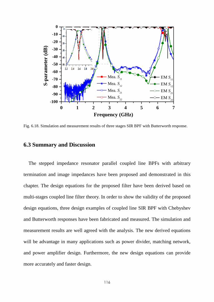
116
0 1 2 3 4 5 6 7
-100
-90
-80
-70
-60
-50
-40
-30
-20
-10
0
EM S11
EM S12
EM S21
EM S22
Mea. S11
Mea. S12
Mea. S21
Mea. S22
S-p
ara
mete
r (
dB
)
Frequency (GHz)
Fig. 6.18. Simulation and measurement results of three stages SIR BPF with Butterworth response.
6.3 Summary and Discussion
The stepped impedance resonator parallel coupled line BPFs with arbitrary
termination and image impedances have been proposed and demonstrated in this
chapter. The design equations for the proposed filter have been derived based on
multi-stages coupled line filter theory. In order to show the validity of the proposed
design equations, three design examples of coupled line SIR BPF with Chebyshev
and Butterworth responses have been fabricated and measured. The simulation and
measurement results are well agreed with the analysis. The new derived equations
will be advantage in many applications such as power divider, matching network,
and power amplifier design. Furthermore, the new design equations can provide
more accurately and faster design.
117
CHAPTER 7
CONCLUSION AND FUTURE WORKS
This chapter presents the conclusion of this dissertation and some future
research directions of unequal termination impedance bandpass filters with a high
selectivity characteristics.
7.1 Conclusion
The dissertation presents design and synthesis of general coupled line unequal
termination impedance BPF. Within six chapters, one of them was achieved with
the original contribution that presented in journals and conference proceedings. The
works are listed in the "publication" section in this dissertation.
In chapter 2, the general theory of two-ports network was presented. The
described theories are frequently used to analyze the RF/microwave BPFs.
In chapter 3, the design of impedance transformer with ultra-high transforming
ration were presented based on two cascade coupled lines. The analytical design
equations are derived with different matching regions. By choosing the properly
matched region, two transmission poles in the passband and a frequency selective
transmission characteristics are obtained.
The chapter 4 presented the arbitrary termination impedance BPF using lumped
elements. The design equations were derived from the prototype of the
conventional low-pass filters.
118
Chapter 5 presented the new analysis of unequal termination impedance parallel
coupled line BPF. The new design formulas are able to design parallel coupled line
BPF with n-resonator, real-to-real arbitrary termination impedance, and arbitrary
image impedance by using low-pass prototype elements value. The BPF with
Chebyshev and Butterworth responses were designed, simulated, and fabricated at
the operating center frequency of f0 = 2.6 GHz.
In chapter 6, a new analysis BPF using parallel coupled stepped impedance
resonators was presented. The new design equations were able to calculated with n-
resonators, arbitrary termination impedance, arbitrary image impedance of coupled
line, and control spurious frequencies. Three design examples of SIR coupled line
BPF with Chebyshev and Butterworth responses have been fabricated and
measured. The new derived equations are more advantage in many applications
such as power divider, matching network, and power amplifier. These new analyses
are significant impact on the modern wireless communication systems.
7.2 Direction to Future Research
The methodology and structure presented in this dissertation could be applied
to design the higher stage filters with unequal termination impedance. Further, the
design method presented in chapter 6 of this dissertation is much significant on
controllable spurious frequency of unequal termination impedance BPF. Moreover,
a high selectivity characteristic can be obtained by increasing number of stages.
However, a circuit size and insertion loss were enlarged and high when the number
of stages increase. Therefore, a size reduction, low insertion loss, and high
119
selectivity are important in the view of design cost and performance. Thus, a
miniaturized structure and high performance technology could be considered for
this purpose.
The dual-band and multi-band filter with unequal termination impedance is one
of research topics. So the resonators would be modified and designed with multi-
mode resonators. A dual-band of unequal termination impedance BPF can directly
matched the input/output termination impedance of an amplifier with dual-band
operation without matching network.
120
REFERENCES
[1] S. B. Cohn, “Parallel-coupled transmission-line resonator filters,” IEEE Trans.
Microwave Theory Tech., vol. 6, no. 4, pp. 223-231, Apr. 1958.
[2] D. Ahn, C. Kim, M. Chung, D. Lee, D. Lew, and H. Hong, “The design of
parallel coupled line filter with arbitrary image impedance,” IEEE International
Microwave Symposium Digest, pp. 909-912, 1998.
[3] J. Park, J. Yun, and D. Ahn, “A design of the novel coupled-line bandpass filter
using defected ground structure with wide stopband performance,” IEEE Trans.
Microwave Theory Tech., vol. 50, no. 9, pp. 2037-2043, Sep. 2002.
[4] P. Cheong, S. Fok, and K. Tam, “Miniaturized parallel coupled-line bandpass
filter with spurious-response suppression,” IEEE Trans. Microwave Theory
Tech., vol. 53, no. 5, pp. 1810-1816, May 2005.
[5] K. Chin, Y. Chiou, and J. Kuo, “New synthesis of parallel-coupled line
bandpass filter with Chebyshev responses,” IEEE Trans. Microwave Theory
Tech., vol. 56, no. 7, pp. 1516-1523, Jul. 2008.
[6] R. Levy, “Synthesis of mixed lumped and distributed impedance-transforming
filters,” IEEE Trans. Microwave Theory Tech., vol. 20, no. 3, pp. 223-233, Mar.
1972.
[7] P. Kim, G. Chaudhary, and Y. Jeong, “Wideband impedance transformer with
out-of-band suppression characteristics,” Microwave Optic. Techno. Lett., vol.
56, no. 11, pp. 2612-2616, Nov. 2014.
121
[8] H. Nguyen, K. Ang, and G. Ng, “Design of coupled three-line impedance
transformers,” IEEE Microwave Wireless Compon. Lett., vol. 24, no. 2, pp. 84-
86, Feb. 2014.
[9] H. Ahn and T. Itoh, “Impedance-transforming symmetric and asymmetric DC
blocks,” IEEE Trans. Microwave Theory Tech., vol. 58, no. 9, pp. 2463-2474,
Sep. 2010.
[10] P. Kim, G. Chaudhary, and Y. Jeong, “Enhancement impedance transforming
ratios of coupled line impedance transformer with wide out-of-band
suppression characteristics,” Microwave Optic. Techno. Lett., vol. 57, no. 7, pp.
1600-1603, Jul. 2015.
[11] P. Kim, J. Jeong, G. Chaudhary, and Y. Jeong, “A design of unequal
termination impedance power divider with filtering and out-of-band
suppression characteristics,” Proceedings of the 45th European Microwave
Conf., pp. 123-126, Sep. 2015.
[12] J. Jeong, P. Kim, and Y. Jeong, “High efficiency power amplifier with
frequency band selective matching networks,” Microwave Optic. Techno. Lett.,
vol. 57, no. 9, pp. 2031-2034, Sep. 2015.
[13] P. Kim, G. Chaudhary, and Y. Jeong, “Ultra-high transforming ratio coupled
line impedance transformer with bandpass response,” IEEE Microwave
Wireless Compon. Lett., vol. 25, no. 7, pp. 445-447, Jul. 2015.
[14] Q. Wu, and L. Zhu, “Short-ended coupled-line impedance transformers with
ultrahigh transforming ration and bandpass selectivity suitable for large load
122
impedances,” IEEE Trans. Compon. Packag. Manuf. Tech., vol. 6, no. 5, pp. -
767-774, May 2016.
[15] H. Oraizi, M. Moradian, and K. Hirasawa, “Design and optimization of
microstrip parallel-coupled line bandpass filters incorporating impedance
matching,” IEICE Trans. Commun., vol. E89-B, no. 11, pp. 2982-2988, Nov.
2006.
[16] K. Chen and D. Peroulis, “Design of broadband highly efficient harmonic
tuned power amplifier using in-band continuous Class-F-1/F mode
transferring,” IEEE Trans. Microwave Theory Tech., vol. 60, no. 12, pp. 4107-
4116, Dec. 2012.
[17] M. Yang, J. Xia, Y. Guo, and A. Zhu, “Highly efficient broadband continuous
inverse class-F power amplifier design using modified elliptic low-pass
filtering matching network,” IEEE Trans. Microwave Theory Tech., vol. 64, no.
5, pp. 1515-1525, May. 2016.
[18] K. Chen and D. Peroulis “Design of highly efficient broadband class-E power
amplifier using synthesized low-pass matching networks,” IEEE Trans.
Microwave Theory Tech., vol. 59, no. 12, pp. 3162-3173, Dec. 2011.
[19] G. L. Matthaei, “Tables of Chebyshev impedance-transformation networks of
low-pass filter form,” IEEE Proceedings, vol. 52, no. 8, pp. 939–963, Aug.
1964.
[20] K. Chen, X. Liu, W. Chappell, and D. Peroulis, “Co-design of power amplifier
and narrowband filter using high-Q evanescent-mode cavity resonator as the
123
output matching network,” IEEE International Microwave Symposium Digest,
pp. 1-4, 2011.
[21] K. Chen, J. Lee, W. Chappell, and D. Peroulis, “Co-design of highly efficient
power amplifier and high-Q output bandpass filter,” IEEE Trans. Microwave
Theory Tech., vol. 61, no. 11, pp. 3940-3950, Nov. 2013.
[22] K. Chen, T. Lee, and D. Peroulis, “Co-design of multi-band high-efficient
power amplifier and three-pole high-Q tunable filter,” IEEE Microwave
Wireless Compon. Lett., vol. 23, no. 12, pp. 647-649, Dec. 2013.
[23] C. Ge, X. Zhu, X. Jiang, and X. Xu, “A general synthesis approach of coupling
matrix with arbitrary reference impedances,” IEEE Microwave Wireless
Compon. Lett., vol. 25, no. 6, pp. 349-351, Jun. 2015.
[24] M. Makimoto and S. Yamashita, “Bandpass filter using parallel coupled
stripline stepped impedance resonators,” IEEE Trans. Microwave Theory Tech.,
vol. MTT-28, no. 12, pp. 1413-1417, Dec. 1980.
[25] A. Worapishet, K. Srisathit, and W. Surakampontorn, “Stepped-impedance
coupled resonators for implementation of parallel coupled microstrip filter
with spurious band suppression,” IEEE Trans. Microwave Theory Tech., vol.
60, no. 6, pp. 1540-1548, Jun. 2012.
[26] K. U-yen, E. J. Wollack, T. Doiron, J. Papapolymerou, and J. Laskar, “The
design of a compact, wide spurious-suppression bandwidth bandpass filter
using stepped impedance resonators,” 35th European Microwave Conf., pp. 3-7,
Oct. 2005.
124
[27] M. Makimoto and S. Yamashita, “Bandpass filters using parallel coupled strip-
line stepped impedance resonators,” IEEE MTT-S International Microwave
Symposium Digest, pp.141-143, 1980.
[28] Y. Chiou, J. Kuo, and E. Cheng, “Broadband quasi-Chebyshev bandpass filters
with multimode stepped-impedance resonators (SIRs),” IEEE Trans.
Microwave Theory Tech., vol. 54, no. 8, pp. 3352-3358, Aug. 2006.
[29] M. Makimoto and S. Yamashita, “Compact bandpass filters using stepped
impedance resonators,” IEEE Proceedings, vol. 67, no. 1, pp. 16-19, Jan. 1979.
[30] M. Makimoto and S. Yamashita, “correction to compact bandpass filters using
stepped impedance resonators,” IEEE Proceedings, vol. 67, no. 11, pp. 1568-
1568, Nov. 1979.
[31] J. Kuo and E. Shih, “Microstip stepped impedance resonator bandpass filter
with an extended optimal rejection bandwidth,” IEEE Trans. Microwave
Theory Tech., vol. 51, no. 5, pp. 1554-1559, May 2003.
[32] D. M. Pozar, Microwave Engineering, 4th ed., John Wiley & Sons, New York,
2012.
[33] L. Zhu, S. Sun, and R. Li, Microwave bandpass filters for wideband
communications, John Wiley & Sons, 2012.
[34] J. Hong, Microstrip filters for RF/Microwave applications, 2nd ed., John Wiley
& Sons, New Jersey, 2011.
[35] G. L. Matthaei, L. Young, and E. M. T. Jones, Microwave Filter, Impedance-
Matching Networks, and Coupling Structures. New York, NY, USA: McGraw-
Hill, 1964.
125
[36] H. Ahn, Asymmetric Passive Components in Microwave Integrated Circuits.
John Wiley & Sons, Inc., 2006.
[37] G. Gonzalez, Microwave Transistor Amplifiers Analysis and Design, 2nd edition,
Prentice-Hall, Inc., 1997.
[38] P. Jarry and J. Beneat, Advanced design techniques and realizations of
microwave and RF filters, John Wiley & Sons, 2008.
[39] E. G. Cristal and S. Frankel, “Hairpin-line and hybrid hairpin-line/half-wave
parallel-coupled-line filters,” IEEE Trans. Microwave Theory Tech., vol. 20, no.
11, pp. 719-728, Nov. 1972.
[40] T. Lee, J. Lee, and D. Peroulis, “Dynamic bandpass filter shape and
interference cancellation control utilizing bandpass-bandstop filter cascade,”
IEEE Trans. Microwave Theory Tech., vol. 63, no. 8, pp. 2526-2539, Aug.
2015.
[41] D. Swanson and G. Macchiarella, “Microwave filter design by synthesis and
optimization,” IEEE Microwave Magazine, vol. 8, no. 2, pp. 55–69, Apr. 2007.
[42] E. Cristal, “Tables of maximally flat impedance-transformation networks of
low-pass filter form,” IEEE Trans. Microwave Theory Tech., vol. 13, no. 5, pp.
693-695, Sep. 1965.
[43] G. L. Matthaei, “Design of parallel-coupled resonator filters,” IEEE Microwave
Magazine, vol. 8, no. 5, pp. 78-87, Oct. 2007.
[44] K. Chin and J. Kuo, “Insertion loss function synthesis of maximally flat
parallel-coupled line bandpass filters,” IEEE Trans. Microwave Theory Tech.,
vol. 53, no. 10, pp. 3161-3168, Oct. 2005.

126
[45] M. Makimoto and S. Yamashita, Microwave Resonators and Filters for
Wireless Communication, Springer-Verlag Berlin Heidelberg 2001.

127
요약
일반적으로 기존의 전력증폭기와 여파기는 50 의 임피던스를 기준하여
독립적으로 설계 된다. 따라서 전력증폭기와 여파기의 임피던스 정합을 위한
추가적인 정합회로가 필요하고, 이 정합회로의 추가적인 삽입손실은
전력증폭기의 출력과 효율저하를 일으킨다. 따라서 전력증폭기 정합회로 및
여파기는 삽입손실을 최소화 하는 방안을 고려해야 한다.
본 논문은 비대칭 종단 임피던스를 갖는 대역통과 여파기의 설계 방법을
제시한다. 또한 스퓨리어스 주파수를 조정하기 위해 새로운 병렬 결합선로
다단 임피던스 공진기 합성법을 제시한다. 제안하는 여파기는 저역통과 프로토
타입의 소자값을 이용해 다단 또는 임의의 이미지 임피던스로 변환시킬 수
있으며, Chebyshev 또는 Butterworth 여파기의 응답 특성을 구현할 수도 있다.
또한 새롭게 제시된 구조를 현대의 통신시스템에서 응용하기 위한 수식들도
제시된다. 제안하는 여파기는 전력증폭기의 비용 및 크기를줄이고, 기존의
정합회로와 여파기의 삽입손실을 줄이기 위해 입/출력 측에 사용될 수 있다.
키워드 : 대역 통과 여파기, 다단 임피던스 공진기, 병렬 결합선로, 영상
임피던스, 종단 임피던스.

128
APPENDIX A: MatLab Coding %%% Impedance Transformer filter (ZS>ZL)
clc; clear all;
%% Insert variable
f=linspace(0.1,2.9,16001); % Vary the frequencies
f0=1; % Center frequency
theta=0.5*pi*f/f0; % Theta depending on varying
frequencies
ZS=input('input load impedance ZS=');
ZL=input('input load impedance ZL=');
r=ZS/ZL
Z0oe1=input('input load impedance Z0o='); % Setting value of Z0o
of both coupled line
%% Find Z0e2
S11_dB1=input('Input load Magnetude S11 (dB)=');
S11_L=10^(-S11_dB1/20);
w=input('1=over-,2=under-,3=perpectly-matching:');
for x=w
if x==1
%% For over-matching
M=sqrt((1-S11_L)/(r*(1+S11_L)));
A=M^2+M; B=Z0oe1*(2-M^2-3*M); C=(3*M-M^2-4)*Z0oe1^2-
(M+1)*4*r*ZL^2; D=(Z0oe1^3*(2-M+M^2))+(4*r*ZL^2*Z0oe1*(M-3));
Z0e_1=[A B C D]; Z0e1=roots(Z0e_1);
% Z0ee1=Z0e1(2)
Z0ee1=max(Z0e1)
Z0ee2=Z0ee1*M+Z0oe1*(1-M)
end
if x==2
%% For under-matching
N=sqrt(1/r*(1+S11_L)/(1-S11_L)); % equation (10)
An=N^2+N; Bn=Z0oe1*(2-N^2-3*N); Cn=(3*N-N^2-4)*Z0oe1^2-
(N+1)*4*r*ZL^2; Dn=(Z0oe1^3*(2-N+N^2))+(4*r*ZL^2*Z0oe1*(N-3));
Z0e1_u1=[An Bn Cn Dn]; Z0e1_u=roots(Z0e1_u1);
129
% Z0ee1=Z0e1_u(2)
Z0ee1=max(Z0e1_u)
Z0ee2=Z0ee1*N+Z0oe1*(1-N)
end
if x==3
%% For perfeclty-matching
Ap=(1/r)+(1/sqrt(r)); Bp=Z0oe1*(2-1/r-3/sqrt(r));
Cp=(3/sqrt(r)-1/r-4)*Z0oe1^2-(((1/sqrt(r))+1)*4*r*ZL^2);
Dp=(Z0oe1^3*(2-
1/sqrt(r)+1/r))+(4*r*ZL^2*Z0oe1*(1/sqrt(r)-3));
Z0e1_u1=[Ap Bp Cp Dp]; Z0e1_u=roots(Z0e1_u1);
% Z0ee1=Z0e1_u(2)
Z0ee1=max(Z0e1_u)
Z0ee2=Z0ee1/sqrt(r)+Z0oe1*(1-1/sqrt(r))
end
end
%% Substitute
Zm1=Z0ee1-Z0oe1; Zp1=Z0ee1+Z0oe1;
Zm2=Z0ee2-Z0oe1; Zp2=Z0ee2+Z0oe1;
%% find transmission zero frequency and bandwidth
f1=(2/pi)*acos(sqrt((Zm1^2-(r*Zm2^2))/((Zp1+Zp2)*(Zp1-(r*Zp2)))))
f2=2-(2/pi)*acos(sqrt((Zm1^2-(r*Zm2^2))/((Zp1+Zp2)*(Zp1-(r*Zp2)))))
Z0e1=Z0ee1; Z0e2=Z0ee2;
C1_dB=20*log10((Z0e1-Z0oe1)/(Z0e1+Z0oe1))
C2_dB=20*log10((Z0e2-Z0oe1)/(Z0e2+Z0oe1))
FBW=(f2-f1)/f0*100
% odd-mode equations
for a=1:length(theta)
Z11=-j*(Zp1/2)*cot(theta(a));
Z33=Z11; Z44=Z11; Z14=-j*(Zp1/2)*csc(theta(a));
Z41=Z14; Z13=-j*(Zm1/2)*csc(theta(a)); Z31=Z13;
Z43=-j*(Zm1/2)*cot(theta(a)); Z34=Z43;
%% even-mode equation
Aet=((Zp2+Zp1)*Zp1*(cos(theta(a)))^2-Zm1^2)/(Zm1*Zm2);
130
Bet=j*cos(theta(a))*(((Zp1*Zm2^2)+(Zm1^2*Zp2)-
(Zp2+Zp1)*Zp1*Zp2*(cos(theta(a)))^2)/(2*Zm1*Zm2*sin(theta(a))));
Cet=j*((2*sin(theta(a))*cos(theta(a)))*(Zp2+Zp1))/(Zm1*Zm2);
Det=((Zp1+Zp2)*Zp2*(cos(theta(a)))^2-Zm2^2)/(Zm1*Zm2);
%% S-parameter of the full circuit
S11e=(Aet*ZL+Bet-Cet*r*ZL^2-
(Det*r*ZL))/(Aet*ZL+Bet+Cet*r*ZL^2+(Det*r*ZL));
S11e_dB(a)=20*log10(abs(S11e));
S21e=((2*ZL*sqrt(r))/(Aet*ZL+Bet+Cet*r*ZL^2+(Det*r*ZL)));
S21e_dB(a)=20*log10(abs(S21e));
S21=S21e/sqrt(2);
S21_dB(a)=20*log10(abs(S21));
S22e=((-Aet*ZL)+Bet-
(Cet*r*ZL^2)+(Det*r*ZL))/(Aet*ZL+Bet+Cet*r*ZL^2+(Det*r*ZL));
S22e_dB(a)=20*log10(abs(S22e));
end
% plot
plot(f, S11e_dB,f, S22e_dB, f, S21e_dB,'linewidth', 3);
axis([0.1 2.9*f0 -60 0]) % limited display
legend('S_1_1_e','S_2_2_e','S_2_1_e');
ylabel('|S_i_j| (dB)','fontsize',16);
xlabel('Normalized frequency (f/f_0)','fontsize',16);
grid on;

131
APPENDIX B : MatLab Coding for Unequal Termination Impedance
Lumped Elements Coupled Resonator BPF
%% Chapter 3
clc; clear all; format long
disp('*LUMPED ELEMENTS COUPLED RESONATOR BANDPASS FILTER*')
disp('* PROGRAMER: PHIRUN KIM *')
%% Calculating Value
g0=1; f0=1*1e9;
RS=input('Input Source Impedance RS(ohm) =');
XS=input('Input Source admittance XS(ohm) =');
RL=input('Input Load Impedance RL(ohm) =');
XL=input('Input Source admittance XL(ohm) =');
FBW=0.05;%input('Input fractional bandwidth FBW(%) =');
GA=1/RS; GB=1/RL; W0=2*pi*f0;
%% Calculate the shifting frequencies
f1=f0*(sqrt(1+(XS*FBW/(RS*2*g(1)))^2)+(FBW*XS/(2*RS*g(1))))
W1=2*pi*f1;
f2=f0*(sqrt(1+(XL*FBW/(RL*2*g(n)))^2)+(FBW*XL/(2*RL*g(n))))
W2=2*pi*f2;
%% Setting Inductance of resonators
Lr1=4*1e-9; Lr2=4*1e-9; Lr3=Lr2;
%% Calculate Capacitance of resonator
Cr(1)=1/(Lr1*W1^2);
for k=2:n-1
Cr(k)=1/(Lr2*W0^2);
end
Cr(n)=1/(Lr2*W2^2);
%% Calculate J-inverter
J(1)=sqrt((GA*W1*Cr(1)*FBW)/(g0*g(1)));
J(2)=FBW*sqrt((Cr(1)*W1*Cr(2)*W0)/(g(1)*g(2)));
for k=3:n-1
J(k)=W0*FBW*sqrt(Cr(k-1)*Cr(k)/(g(k-1)*g(k))); %Calculate J2,3
end
132
J(n)=FBW*sqrt((Cr(n-1)*W0*Cr(n)*W2)/(g(n-1)*g(n)));
J(n+1)=sqrt((GB*W2*Cr(n)*FBW)/(g(n)*g(n+1)));
%% Calculated Series Capacitance
CS(1)=J(1)/(W0*((sqrt(1-(J(1)*RS)^2))+(XS*J(1))));
for k=2:n
CS(k)=J(k)/W0;
end
CS(n+1)=J(n+1)/(W0*((sqrt(1-(J(n+1)*RL)^2))+(XL*J(n+1))));
%% Calculated the additional Capacitor
C01e=((CS(1)*(1-(W0*CS(1)*XS)))/((RS^2*(W0*CS(1))^2)+(1-
W0*CS(1)*XS)^2))-((J(1)^2*XS)/W0);
Cne=((CS(n+1)*(1-(W0*CS(n+1)*XL)))/((RL^2*(W0*CS(n+1))^2)+(1-
(W0*CS(n+1)*XL))^2))-(((J(n+1))^2*XL)/W0);
%% Calculated Capacitance of Shunt Resonators
C(1)=Cr(1)-C01e-CS(2);
for k=2:n-1
C(k)=Cr(k)-CS(k)-CS(k+1);
end
C(n)=Cr(n)-CS(n)-Cne;
%% Disply values
CS(n); C(n) ;
disp('Resonator Capacitance(pF)'); disp(CS*1e12);
disp('Series Capacitor value(pF)'); disp(C*1e12);

133
APPENDIX C: MatLab Coding for LPF Prototype Value
%% coding to find value of g0, g1, g2 ... to gn
RLo=input('input the passband Return loss S11(dB)='); % |S11|
Lar=-10*log10(1-10^(0.1*RLo)); %Passband Ripple
H=input('Chebyshev (1) and Butterworth (2)=');
n=input('Insert number of stang n='); % input number of stages
for W=H
if W==1
beta=log(coth(Lar/17.37)); Gamma=sinh(beta/2/n);
%% Calculated value of lowpass prototype
for k=1:n
a(k)=sin((2*k-1)*pi/2/n); b(k)=Gamma^2+(sin(k*pi/n))^2;
end
for k=1:n+1
if k==1
g(k)=2*a(k)/Gamma;
elseif k==n+1
if mod(n,2)==0
g(k)=(coth(beta/4))^2;
else
g(k)=1;
end
else
g(k)=4*a(k-1)*a(k)/b(k-1)/g(k-1);
end
end
end
if W==2
%% Calculated value of Butterworth
for k=1:n
g(k)=2*sin((((2*k)-1)*pi)/(2*n)); g(n+1)=1;
end
end
end

134
APPENDIX D : MatLab Coding for Unequal Termination Impedance
Parallel Coupled Line BPF
clc; clear all; format long
disp('*UNEQUAL TERMINATION PARALLEL COUPLED LINE BANDPASS FILTER*')
disp('* PROGRAMER: PHIRUN KIM *')
RS=input('Input Source Impedance RS(ohm) =');
RL=input('Input Load Impedance RL(ohm) =');
FBW=input('Input the fractional bandwidth FBW=');
Z0=input('Input the Image impedance of coupled line Z0=');
g0=1; GS=1/RS; Y0=1/Z0; GL=1/RL;
AS=Y0/GS; AL=Y0/GL;
%% Calculate J-inverter
for x=n
if x==2
m1=AS*(pi/2)*FBW; m2=(g0*g(1))-((pi/4)*FBW*(AS-
(1/AS)));
J(1)=Y0*sqrt(m1/m2); % Calculate J0,1
J(3)=Y0*sqrt((AL*(pi/2)*FBW)/((g(2)*g(3))-((pi*FBW/4)*(AL-
(1/AL))))); % Calculate J2,3
J(2)=FBW*Y0*(pi/2)*sqrt(((((J(1)^2/(2*Y0^2))*(1-
(1/AS^2)))+1)*(((J(3)^2/(2*Y0^2))*(1-
(1/AL^2)))+1))/(g(1)*g(2))); % Calculate J1,2
else
m1=AS*(pi/2)*FBW; m2=(g0*g(1))-((pi/4)*FBW*(AS-
(1/AS)));
J(1)=Y0*sqrt(m1/m2); % Calculate J0,1
m3=(((J(1)^2/(2*Y0^2))*(1-(1/AS^2)))+1);
J(2)=((FBW*pi*Y0)/2)*sqrt(m3/(g(1)*g(2))); % Calculate J1,2
J(n+1)=Y0*sqrt((AL*(pi/2)*FBW)/((g(n)*g(n+1))-
((pi*FBW/4)*(AL-(1/AL))))); % Calculate Jn,n+1
J(n)=((pi*Y0*FBW)/2)*sqrt((((J(n+1)^2/(2*Y0^2))*(1-
(1/AL^2)))+1)/(g(n-1)*g(n))); % Calculate Jn-1,n
for k=3:n-1
135
J(k)=((pi*Y0*FBW)/2)*sqrt(1/(g(k-1)*g(k)));
end
end
end
%% Calculate Even- and odd-mode impedance
for k=1:n+1
Z0e(k)=Z0*(1+(J(k)*Z0)+(J(k)*Z0)^2);
Z0o(k)=Z0*(1-(J(k)*Z0)+(J(k)*Z0)^2);
end
A=[g
J
Z0e
Z0o];
disp(A)

136
APPENDIX E : MatLab Coding for Unequal Termination Impedance
Parallel Coupled Line SIR BPF
clc; clear all; format long
disp('*UNEQUAL TERMINATION PARALLEL COUPLED SIR BPF*')
disp('* PROGRAMER: PHIRUN KIM *')
%%
RS=input('Input Source Impedance RS(ohm) =');
RL=input('Input Source Impedance RL(ohm) =');
FBW=input('Input Source Impedance FBW(%) =');
Z2=input('Input Source Impedance Z2(ohm) =');
RZ=input('Input Impedance Ratio RZ=Z2/Z1 =');
g0=1; GS=1/RS; Y2=1/Z2; GL=1/RL;
theta0=atan(sqrt(RZ));
Y1=Y2*RZ; Z1=1/Y1; L=theta0*(180/pi) % length of TL
AS=Y2/GS; AL=Y2/GL;
%% Calculate J-inverter
for k=2:n
J(1)=Y2*sqrt((AS*2*theta0*FBW)/(g0*g(1))); % Calculate J0,1
J(k)=(2*theta0*Y2*FBW)*sqrt(1/(g(k-1)*g(k)));
J(n+1)=Y2*sqrt((2*AL*theta0*FBW)/(g(n)*g(n+1))); % Calculate Jn,n+1
end
%% Calculate Even- and odd-mode impedance
for k=1:n+1
Z0e(k)=(Z2*(1+(J(k)*Z2*csc(theta0))+(J(k)*Z2)^2))/(1-
(J(k)^2*Z2^2*cot(theta0)^2));
Z0o(k)=(Z2*(1-(J(k)*Z2*csc(theta0))+(J(k)*Z2)^2))/(1-
(J(k)^2*Z2^2*cot(theta0)^2));
end
disp(J)
disp(Z0e)
disp(Z0o)

137
CURRICULUM VITAE
Phirun Kim
#7304, Division of Electronics and Information Engineering, Chonbuk National University, 567 Baeje-
daero, Jeonju-si, Chollabuk-do, 561-756, Republic of Korea
Mobile Phone : +82-10-6868-2458
E-mail : [email protected], [email protected]
RESEARCH INTERESTS
RF passive/active circuits design such as matching network, impedance transformer, balun, power
divider, filters, and amplifier.
EDUCATION
Ph.D., Electronic and Information Engineering, 2013-present
Chonbuk National University, Korea
Academic Advisor : Professor Yongchae Jeong
M.E., Electronic and Information Engineering, 2011-2013
Chonbuk National University, Korea
Academic Advisor : Professor Yongchae Jeong
B.E., Electronic Engineering, 2006-2011
National Polytechnic Institute of Cambodia, Phnom Penh, Cambodia
AWARDS AND HONORS
Outstanding graduate student award 2015
In recognition of contribution to the principles of
graduate research while in pursuit of the Doctoral
degree in Division of Electronics and Information Engineering
Electronics Award 2009
(sponsored by National Polytechnic Institute of Cambodia,
Phnom Penh, Cambodia)

138
REFERENCES
Yongchae Jeong, Ph.D
Professor, Academic Advisor (Senior Member, IEEE)
#7304, Division of Electronics and Information Engineering,
Chonbuk National University,
567 Baekje-daero, Jeonju-si, Chollabuk-do, 54896, Republic of Korea
Phone : +82-63-270-2458
Fax : +82-63-270-2394
E-mail : [email protected]
Jongsik Lim, Ph.D
Professor, (Senior Member, IEEE)
Department of Electrical Engineering,
Soonchunhyang University,
22 SoonChunghyang-ro, Shinchang-myeon, Asan-si, Chungcheongnam-do, 31538, Republic of Korea
Phone : +82-41-530-1332
Fax : +82-41-530-1548
E-mail : [email protected]
139
PUBLICATIONS
INTERNATIONAL PEER-REVIEWED JOURNALS
[1] Girdhari Chaudhary, Phirun Kim, Yongchae Jeong, and Jae-Hun Yoon,
“Design of high efficiency RF-DC conversion circuit using novel termination
networks for RF energy harvesting system,” Microwave Optic. Techno. Lett.,
vol. 54, no. 10, pp. 1729-1732, Oct. 2012.
[2] Phirun Kim, Girdhari Chaudhary, and Yongchae Jeong, “A dual-band RF
energy havesting using frequency limited dual-band impedance matching,”
Progress in Electromag. Research, vol. 141, pp. 443-461, 2013.
[3] Phirun Kim, Girdhari Chaudhary, and Yongchae Jeong, “Analysis and Design
of a Branch-line Balun with High-isolation Wideband Characteristics,”
Microwave Optic. Techno. Lett., vol. 57, no. 7, pp. 1228-1234, Sep 2014.
[4] Phirun Kim, Girdhari Chaudhary, and Yongchae Jeong, “Wideband impedance
transformer with out-of-band suppression characteristics,” Microwave Optic.
Techno. Lett., vol. 56, no. 11, pp. 2612-2616, Nov. 2014.
[5] Phirun Kim, Girdhari Chaudhary, and Yongchae Jeong, “Ultra-high
Transforming Ratio Coupled Line Impedance Transformer with Bandpass
Response,” IEEE Microwave Wireless Compon. Letter, vol. 25, no. 7, pp. 445-
447, July 2015.
140
[6] Phirun Kim, Girdhari Chaudhary, and Yongchae Jeong, “Enhancement
Impedance Transforming Ratios of Coupled Line Impedance Transformer with
Wide Out-of-band Suppression Characteristics,” Microwave Optic. Techno.
Lett., vol. 57, no. 7, pp. 1600-1603, May 2015.
[7] Junhyung Jeong, Phirun Kim, Yongchae Jeong, “High Efficiency Power
Amplifier With Frequency Band Selective Matching Networks,” Microwave
Optic. Techno. Lett., vol. 57, no. 9, pp. 2031-2034, Sep. 2015.
[8] Phirun Kim, Girdhari Chaudhary, and Yongchae Jeong, “Unequal Termination
Branch-Line Balun With High-Isolation Wideband Characteristics,” Microwave
Optic. Techno. Lett., vol. 58, no. 8, pp. 1775-1778, Aug. 2016.
[9] Phirun Kim, Girdhari Chaudhary, and Yongchae Jeong, “An Ultra-Wideband
Bandpass Filter with High Return Loss and Controllable Notch Band,”
Microwave Optic. Techno. Lett., vol. 58, no. 12, pp. 2922-2926, Dec. 2016.
DOMESTIC JOURNALS
[1] Girdhari Chaudhary, Junhyung Jeong, Phirun Kim, Yongchae Jeong,
“Negative Group Delay Circuit with Improved Signal Attenuation and Multiple
Pole Characteristics,” Journal of Electromagnetic Engineering and Science, vol.
15, no. 2, pp. 76-81, Apr. 2015.
[2] Phirun Kim, Junsik Park, Junhyung Jeong, Seungho Jeong, Girdhari
Chaudhary, and Yongchae Jeong, “High Selectivity Coupled Line Impedance
141
Transformer with Second Harmonic Suppression,” Journal of Electromagnetic
Engineering and Science, vol. 16, no. 1, pp. 13-18, Jan. 2016.
INTERNATIONAL CONFERENCE PRESENTATIONS
[1] Girdhari Chaudhary, Phirun Kim, Yongchae Jeong, Jongsik Lim and Jaehoon
Lee, "Analysis and circuit modeling method for defected microstrip structure
in planar transmission lines," Proc. Asia-Pacific Microwave Conf., pp. 999-
1002, 2011.
[2] Girdhari Chaudhary, Phirun Kim, Yongche Jeong, and Jongsik Lim, "Dual-
mode bandpass filter with independently tunable center frequency and
bandwidth," IEEE Radio-frequency integration technology symposium, pp. 56-
58, Nov. 2012.
[3] Phirun Kim, Girdhari Chaudhary, Yongchae Jeong, and Jongsik Lim, "Dual-
band Impedance Matching Network with Transmission Zeros Using
Resonators," Progress in Electromag. Research Sympos., pp. 627, Aug. 2013.
[4] Girdhari Chaudhary, Phirun Kim, Yongchae Jeong, and Jongsik Lim, "A
Design of Multi-harmonics Load Network for Class-S Power Amplifier,"
Progress in Electromag. Research Sympos., pp. 1636, Aug. 2013.
[5] Girdhari Chaudhary, Junhyung Jeong, Phirun Kim, Yongchae Jeong and
Jongsik Lim, “Compact Negative Group Delay Circuit Using Defected Ground
Structure,” Asia-Pacific Microwave Conf., pp. 22-24, Nov. 2013.

142
[6] Girdhari Chaudhary, Phirun Kim, Jaeyeon Kim, and Yongchae Jeong,
“Coupled line negative group delay circuits with Very Low Signal Attenuation
and Multiple-poles Characteristics,” European Microwave Conf., pp. 25-27,
Oct. 2014.
[7] Jongsik Lim, Junhyung Jeong, Phirun Kim, Yongchae Jeong, Sang-Min Han,
and Dal Ahn, “4-way Power Divider Using Common DGS and Stacked-
substrate Structure,” Progress in Electromag. Research Sympos., pp. 934, Aug.
2014.
[8] Phirun Kim, Qi Wang, Girdhari Chaudhary, and Yongchae Jeong, “Freuency
Selective Coupled Lines Impedance Transformer,” International Symposium on
Information Technology Convergence, vol. 3, no. 2, pp. 559-560, Oct. 2014.
[9] Junsik Park, Jaeyeon Kim, Seungwook Lee, Phirun Kim, and Yongchae Jeong,
“CMOS RF Energy Harvesting Rectifier using Parasitic Capacitance
Compensation Technique and Low-Pass Filter,” International SoC Design
Conference, Nov. 2014.
[10] Jaeyeon Kim, Junsik Park, Seungwook Lee, Phirun Kim, and Yongchae
Jeong, “Fully Integrated Negative Group Delay Circuit Using CMOS
Amplifier and Boding-wire,” International SoC Design Conference, Nov.
2014.
[11] Girdhari Chaudhary, Junhyung Jeong, Phirun Kim, and Yongchae Jeong,
“Transmission line Negative Group Delay Circuit with Multiple-poles
143
Characteristics,” 2014 Korea-Japan Microwave Workshop, pp. 137-138, Dec.
2014.
[12] Girdhari Chaudhary, Phirun Kim, Junhyung Jeong, Yongchae Jeong, Jongsik
Lim, “Dual-Band Negative Group Delay Circuit Using Defected Microstrip
Structure,” IEEE Radio & Wireless Week, pp. 129-131, Jan. 2015.
[13] Phirun Kim, Girdhari Chaudhary, Junsik Park, Yongchae Jeong, and Jongsik
Lim, “High Frequency-Selectivity Impedance Transformer,” IEEE Radio &
Wireless Week, pp. 135-137, Jan. 2015.
[14] Phirun Kim, Junhyung Jeong, Girdhari Chaudhary, Yongchae Jeong, and
Jongsik Lim, “Bandpass-to-allstop switchable filter with broadband harmonics
suppression,” Progress in Electromag. Research Sympos., pp. 1755, Jul. 2015.
[15] Girdhari Chaudhary, Seungho Jeong, Phirun Kim, and Yongchae Jeong,
“Coupled Line Power Divider with Multiple-pole Negative Group Delay
Characteristics,” Progress in Electromag. Research Sympos., pp. 2033, Jul.
2015.
[16] Phirun Kim, Junhyung Jeong, Girdhari Chaudhary, and Yongchae Jeong, “A
Design of Unequal Termination Impedance Power Divider with Filtering and
Out-of-band Suppression Characteristics,” European Microwave Conf., pp.
123-126, Sep. 2015.
144
[17] Qi Wang, Junhyung Jeong, Phirun Kim, and Yongchae Jeong, “Analysis and
Design of Conventional Wideband Branch Line Balun,” International
Symposium on Information Technology Convergence, pp. 386-389, Oct. 2015.
[18] Girdhari Chaudhary, Phirun Kim, Junhyung Jeong, Yongchae Jeong, Jongsik
Lim, “Power Divider with Tunable Positive and Negative Group Delays Using
Parasitic Compensated PIN Diode,” 2016 Radio and Wireless Symposium, pp.
4-6, Jan. 2016.
[19] Girdhari Chaudhary, Phirun Kim, Junhyung Jeong, Yongchae Jeong, Jongsik
Lim, “A Design of Negative Group Delay Power Divider: Coupling Matrix
Approach with Finite Unloaded-Q Resonators,” 2016 IEEE International
Microwave Symposium, May 2016.
[20] Seungho Jeong, Boram An, Phirun Kim, Yongchae Jeong, and Jongsik Lim,
“A Design of Phase Shifter with Constant Insertion Loss,” Progress in
Electromag. Research Sympos., Aug. 2016.
[21] Girdhari Chaudhary, Phirun Kim, Junhyung Jeong, and Yongchae Jeong, “A
Power Divider with Positive and Negative Group Delay Characteristics,” 2016
URSI Asia-Pacific Radio Science Conf., pp. 1195-1197, Aug. 2016.
[22] Phirun Kim, Girdhari Chaudhary, and Yongchae Jeong, “A Compact Ultra-
wideband Bandpass Filter with High Return Loss Characteristic,” Asia-Pacific
Microwave Conf., 2016.