
Understanding the Effect of Process Variations on the Delay of Static and Domino Logic
14
IEEE TRANSACTIONS ON VERY LARGE SCALE INTEGRATION (VLSI) SYSTEMS, VOL. 18, NO. 5, MAY 2010 697 Understanding the Effect of Process Variations on the Delay of Static and Domino Logic Massimo Alioto, Senior Member, IEEE, Gaetano Palumbo, Fellow, IEEE, and Melita Pennisi, Member, IEEE Abstract—In this paper, the effect of process variations on delay is analyzed in depth for both static and dynamic CMOS logic styles. Analysis allows for gaining an insight into the delay dependence on fan-in, fan-out, and sizing in sub-100-nm technologies. Simple but reasonably accurate models are derived to capture the basic de- pendences. The effect of process variations in transistor stacks is analytically modeled and analyzed in detail. The impact of both interdie and intradie variations is evaluated and discussed. Inter- estingly, the input capacitance of static and dynamic logic is shown to be rather insensitive to variations. The delay variability was also shown to be a weak function of the input rise/fall time and load. Analysis shows that domino logic circuits suffer from a doubled variability as compared to the static CMOS logic style. The posi- tive feedback associated with the keeper transistor is shown to be responsible for the variability increase, which, in turn, limits the speed performance. This adds to the well-known speed degrada- tion due to the current contention associated with the keeper tran- sistor. Monte Carlo simulations on a 90-nm technology, including layout parasitics, are performed to validate the results. Index Terms—Interdie variations, intradie variations, modeling, process variations, timing, variability, VLSI. I. INTRODUCTION V ARIABILITY is recognized to be a major challenge in sub-100-nm integrated circuits (ICs) [1]–[3]. Indeed, the wide delay/power deviations due to process and environmental variations make it difficult to meet the tight bounds imposed by requirements, thereby degrading the yield [4]–[8]. For this reason, models, design techniques, and CAD tools are needed that take delay variations into account from the beginning, rather than as an afterthought. In the following, analysis is focused on the effect of process variations on delay. According to process variations’ dependence on space, two kinds of process variations can be identified: interdie and in- tradie variations [4], [5]. The former ones determine an equal random shift in the mean value of every device/interconnect parameter, i.e., interdie variations impact all devices (intercon- nects) within the same chip in the same way. On the other hand, intradie variations affect different devices (interconnects) within Manuscript received June 13, 2008; revised December 14, 2008 and February 06, 2009. First published July 21, 2009; current version published April 23, 2010. M. Alioto is with the Dipartimento di Ingegneria dellInformazione (DII), Uni- versità di Siena, 53100 Siena, Italy (e-mail: [email protected]). G. Palumbo and M. Pennisi are with the Dipartimento di Ingegneria Elettrica Elettronica e dei Sistemi (DIEES), Università di Catania, 95125 Catania, Italy (e-mail: [email protected]; [email protected]). Digital Object Identifier 10.1109/TVLSI.2009.2015455 the same chip in a different way. In a smaller scale, intradie vari- ations can be classified into random and systematic. Random in- tradie variations affect transistors (interconnects) in a different way even if they are relatively close (for example, random in- tradie variations account for doping variations throughout the chip); systematic intradie variations affect close devices (tran- sistors) in the same way according to layout-pattern-dependent factors (e.g., proximity effect, metal density, and so on) [8]. Until now, a significant research effort has been spent on mod- eling variability at the device and gate levels of abstraction. At the device level, a large number of results have been published on the statistical modeling of fundamental physical, geometric, and electrical parameters (e.g., dopant density, channel length and width, and threshold voltage) and their impact on device parameters (e.g., mobility and threshold voltage) [8]–[14]. On the other hand, at the gate level of abstraction, various gate- level variability models have been proposed that target statis- tical static timing analysis (SSTA) of complex circuits [1], [2], [15]–[20]. Most of the timing models for SSTA are empirical and introduce fitting coefficients to achieve a desired accuracy. Reference [20] is an exception in that an analytical approach is followed to model variations at the circuit level, although in this paper there is no information on the effect of circuit design pa- rameters (e.g., transistor size, topology, fan-in, and fan-out). Unfortunately, much less understanding has been gained at the intermediate circuit level of abstraction, at which designers are accustomed to tune circuit parameters like currents, capaci- tances, and transistor sizes. From a circuit perspective, it would be much more useful to understand the dependence of circuit pa- rameter variability on circuit knobs and topology (e.g., number of stacked transistors), rather than using variability models that are empirical or based on process parameters. Indeed, a deep un- derstanding of the dependence of variability on circuit param- eters is needed to help the circuit designer to develop an intu- itive understanding of variability, which, in turn, is a necessary premise to the development of variability-aware circuit design techniques. In this paper, the effect of process variations on the delay of static and dynamic CMOS logic gates is analyzed in depth as a function of circuit-level parameters. The main contribution of this paper is a detailed analysis of the delay variability depen- dence on circuit parameters like the number of stacked transis- tors (i.e., the fan-in), their size, the load capacitance (i.e., the fan-out), and the circuit topology (static versus dynamic logic). To this aim, simple models are developed for both interdie and intradie variations, and the main variability sources are iden- tified for each of them. Interestingly, the analysis shows that the variations in the input capacitance of logic gates are quite 1063-8210/$26.00 © 2009 IEEE Authorized licensed use limited to: University of Catania. Downloaded on May 04,2010 at 07:17:13 UTC from IEEE Xplore. Restrictions apply.
-
Upload
independent -
Category
Documents
-
view
2 -
download
0
Transcript of Understanding the Effect of Process Variations on the Delay of Static and Domino Logic

IEEE TRANSACTIONS ON VERY LARGE SCALE INTEGRATION (VLSI) SYSTEMS, VOL. 18, NO. 5, MAY 2010 697
Understanding the Effect of Process Variations on theDelay of Static and Domino Logic
Massimo Alioto, Senior Member, IEEE, Gaetano Palumbo, Fellow, IEEE, and Melita Pennisi, Member, IEEE
Abstract—In this paper, the effect of process variations on delayis analyzed in depth for both static and dynamic CMOS logic styles.Analysis allows for gaining an insight into the delay dependence onfan-in, fan-out, and sizing in sub-100-nm technologies. Simple butreasonably accurate models are derived to capture the basic de-pendences. The effect of process variations in transistor stacks isanalytically modeled and analyzed in detail. The impact of bothinterdie and intradie variations is evaluated and discussed. Inter-estingly, the input capacitance of static and dynamic logic is shownto be rather insensitive to variations. The delay variability was alsoshown to be a weak function of the input rise/fall time and load.Analysis shows that domino logic circuits suffer from a doubledvariability as compared to the static CMOS logic style. The posi-tive feedback associated with the keeper transistor is shown to beresponsible for the variability increase, which, in turn, limits thespeed performance. This adds to the well-known speed degrada-tion due to the current contention associated with the keeper tran-sistor. Monte Carlo simulations on a 90-nm technology, includinglayout parasitics, are performed to validate the results.
Index Terms—Interdie variations, intradie variations, modeling,process variations, timing, variability, VLSI.
I. INTRODUCTION
V ARIABILITY is recognized to be a major challenge insub-100-nm integrated circuits (ICs) [1]–[3]. Indeed, the
wide delay/power deviations due to process and environmentalvariations make it difficult to meet the tight bounds imposedby requirements, thereby degrading the yield [4]–[8]. For thisreason, models, design techniques, and CAD tools are neededthat take delay variations into account from the beginning, ratherthan as an afterthought. In the following, analysis is focused onthe effect of process variations on delay.
According to process variations’ dependence on space, twokinds of process variations can be identified: interdie and in-tradie variations [4], [5]. The former ones determine an equalrandom shift in the mean value of every device/interconnectparameter, i.e., interdie variations impact all devices (intercon-nects) within the same chip in the same way. On the other hand,intradie variations affect different devices (interconnects) within
Manuscript received June 13, 2008; revised December 14, 2008 and February06, 2009. First published July 21, 2009; current version published April 23,2010.
M. Alioto is with the Dipartimento di Ingegneria dellInformazione (DII), Uni-versità di Siena, 53100 Siena, Italy (e-mail: [email protected]).
G. Palumbo and M. Pennisi are with the Dipartimento di Ingegneria ElettricaElettronica e dei Sistemi (DIEES), Università di Catania, 95125 Catania, Italy(e-mail: [email protected]; [email protected]).
Digital Object Identifier 10.1109/TVLSI.2009.2015455
the same chip in a different way. In a smaller scale, intradie vari-ations can be classified into random and systematic. Random in-tradie variations affect transistors (interconnects) in a differentway even if they are relatively close (for example, random in-tradie variations account for doping variations throughout thechip); systematic intradie variations affect close devices (tran-sistors) in the same way according to layout-pattern-dependentfactors (e.g., proximity effect, metal density, and so on) [8].
Until now, a significant research effort has been spent on mod-eling variability at the device and gate levels of abstraction. Atthe device level, a large number of results have been publishedon the statistical modeling of fundamental physical, geometric,and electrical parameters (e.g., dopant density, channel lengthand width, and threshold voltage) and their impact on deviceparameters (e.g., mobility and threshold voltage) [8]–[14]. Onthe other hand, at the gate level of abstraction, various gate-level variability models have been proposed that target statis-tical static timing analysis (SSTA) of complex circuits [1], [2],[15]–[20]. Most of the timing models for SSTA are empiricaland introduce fitting coefficients to achieve a desired accuracy.Reference [20] is an exception in that an analytical approach isfollowed to model variations at the circuit level, although in thispaper there is no information on the effect of circuit design pa-rameters (e.g., transistor size, topology, fan-in, and fan-out).
Unfortunately, much less understanding has been gained atthe intermediate circuit level of abstraction, at which designersare accustomed to tune circuit parameters like currents, capaci-tances, and transistor sizes. From a circuit perspective, it wouldbe much more useful to understand the dependence of circuit pa-rameter variability on circuit knobs and topology (e.g., numberof stacked transistors), rather than using variability models thatare empirical or based on process parameters. Indeed, a deep un-derstanding of the dependence of variability on circuit param-eters is needed to help the circuit designer to develop an intu-itive understanding of variability, which, in turn, is a necessarypremise to the development of variability-aware circuit designtechniques.
In this paper, the effect of process variations on the delay ofstatic and dynamic CMOS logic gates is analyzed in depth asa function of circuit-level parameters. The main contribution ofthis paper is a detailed analysis of the delay variability depen-dence on circuit parameters like the number of stacked transis-tors (i.e., the fan-in), their size, the load capacitance (i.e., thefan-out), and the circuit topology (static versus dynamic logic).To this aim, simple models are developed for both interdie andintradie variations, and the main variability sources are iden-tified for each of them. Interestingly, the analysis shows thatthe variations in the input capacitance of logic gates are quite
1063-8210/$26.00 © 2009 IEEE
Authorized licensed use limited to: University of Catania. Downloaded on May 04,2010 at 07:17:13 UTC from IEEE Xplore. Restrictions apply.

698 IEEE TRANSACTIONS ON VERY LARGE SCALE INTEGRATION (VLSI) SYSTEMS, VOL. 18, NO. 5, MAY 2010
small, and the variations in the output parasitic capacitance oflogic gates have a minor impact on delay variability. A compar-ative analysis of static and domino logic gates shows that thelatter ones suffer from a significantly worse delay variability.This variability degradation is analyzed in depth, and the maincauses are identified. In particular, the role that is played by thepositive feedback in domino logic gates is thoroughly analyzed.
This paper is structured as follows. In Section II, consid-erations on process variations and the simulation setup arereported. A simple timing model of delay variability is dis-cussed in Section III. The model is then applied to static logicin Section IV and validated with Monte Carlo simulations.The analysis is extended to domino logic gates in Section V,where comparison with static logic gates and a deep analysis ofthe impact of the positive feedback in domino logic gates arealso included. Finally, remarks and conclusions are reported inSection VI.
II. BASIC CONSIDERATIONS AND SIMULATION FRAMEWORK
A. Effect of Interdie and Intradie Variations on Delay
To introduce the basic notation, let us consider the genericparameter having a nominal value and a standard deviation
. The amount of variations in parameter is usually measuredby its variability, which is defined as .
Let be the standard deviation ofwhen only interdie (intradie) variations are considered. Todeeply understand variability issues in a logic style, the twokinds of variations must be analyzed separately. Nevertheless,the results obtained for each kind of variation can be combinedas in (1) to evaluate the overall standard deviation of [4]
(1)
where it was considered that interdie and intradie variationsaffect through different physical mechanisms, so the corre-sponding variations of are statistically independent, accordingto the usual assumption [4].
In general, process variations impact both transistors and in-terconnects. In regard to transistors, both interdie and intradievariations give a significant contribution to their variability [3].In particular, intradie variations are a very important sourceof variability and can even be higher than interdie variations[3]–[5], [20]–[22]. The greater importance of intradie comparedto interdie variations is even emphasized considering that thelatter ones can be compensated by resorting to proper adaptivebody biasing and dynamic supply voltage schemes [23], [24],whereas no methodology has been proposed until now to sys-tematically counteract intradie variations.
On the other hand, interconnect variations are dominated byintradie systematic variations [9]–[11] since their interdie andrandom components of intradie variations are negligible in prac-tical circuits [2], [8]–[12]. Unfortunately, intradie systematicvariations of interconnects are not modeled in real design kits,as these variations strongly depend on the layout of blocks thatare close to the considered one, i.e., on the specific circuit underdesign. Since the main goal of this paper is the evaluation of
Fig. 1. Simulation framework to measure (a) delay variations and (b) inputcapacitance variations.
the impact of process variations on each logic style, it is rea-sonable to consider all effects that are directly influenced bythe logic style while keeping the effect of parameters that arenot directly related to the logic style as small as possible. Forthis reason, in the following, we will consider only intercon-nects that do not significantly depend on the layout of a specificcircuit (i.e., only interconnects that are inside a cell or that con-nect the nearby cells). Nevertheless, since variations in longerinterconnects translate into a variation of the gate load, they canbe easily accounted for by resorting to the same procedure as inSection III.B.
B. Simulation Framework
In the following sections, the impact of variations is evaluatedvia Monte Carlo simulations on a proper circuit structure. Asshown in Fig. 1(a), the delay variations of the logic gate undertest are evaluated by driving it with an identical gate (but notaffected by variations) to provide a realistic input waveform. Itsload capacitance is set to a multiple of the input capacitance of aminimum static inverter , which is equal to 520 aF in theconsidered 90-nm CMOS technology. Variations in input capac-itance are evaluated from the rise/fall time at the input node bydriving it with a constant current source, as shown in Fig. 1(b).
It is worth noting that the effect of intradie variations is alsoaffected by interdie variations, so a proper simulation strategymust be adopted to separately analyze the effect of interdie andintradie variations. This can be easily understood consideringthat an assigned intradie variation leads to a delay (input capac-itance) variation, which also depends on the mean value of de-vice parameters, due to the nonlinear delay dependence on thelatter ones. Since the mean value of device parameters is im-pacted by interdie variations, the in (1) must be evalu-ated when interdie variations are superimposed. For this reason,intradie variations were evaluated by also introducing interdievariations in the test circuit. The effect of the former ones wasthen separated by considering the difference of the delay (inputcapacitance) between two nominally equal circuits, which areaffected by the same interdie but different intradie variations, as
Authorized licensed use limited to: University of Catania. Downloaded on May 04,2010 at 07:17:13 UTC from IEEE Xplore. Restrictions apply.

ALIOTO et al.: ALIOTO ET AL.: UNDERSTANDING THE EFFECT OF PROCESS VARIATIONS 699
Fig. 2. Simulation framework to measure delay variation under intradie varia-tions.
Fig. 3. Schematization of general static logic gates.
shown in Fig. 2. In this way, interdie effects cancel out, and onlyintradie effects are measured.
The number of trials in Monte Carlo simulations was setto achieve a sufficient accuracy in the estimation of the meanvalue and standard deviation of the delay (input capacitance).In our simulations, was set to 2 000 to ensure a lower than4% inaccuracy in the standard deviation, which is adequate forpractical purposes.
III. ANALYSIS OF STATIC CMOS GATES
In this section, delay and input capacitance variations in staticCMOS gates are analyzed in the presence of interdie and in-tradie sources of variations.
A. Simple Timing Models to Evaluate Variability
To analytically evaluate the delay variations in static CMOSlogic gates, let us simplify the pull-down (pull-up) network as asingle nMOS (pMOS) equivalent transistor, as is usually doneunder nominal conditions (see Fig. 3). A widely used model ofthe delay is [27]
(2)
where is the current provided by the equivalent transistor tothe load capacitance and is the power supply.
Assuming that and are affected by process variations,featured by nominal values and (standard deviation
and ), respectively, and that the supply voltage is
not affected by process variations1, from (2), the variability isgiven by
(3)
where and are the delay nominal value and the stan-dard deviation, respectively, and variations in and wereassumed to be statistically independent (this assumption will bediscussed at the end of this section). Equation (3) was obtainedby performing the well-known sensitivity analysis [28], i.e.,under the assumption that and .
According to (3), delay variations are mainly determined byvariations in the load capacitance and the current . Inparticular, accounts mainly for the input capacitance of thesubsequent gates, as well as for the wiring capacitance and theoutput capacitance of the considered gate. As a matter of fact,in practical cases, the gate output capacitance gives a negligiblecontribution to the delay variability. Indeed, well-optimized cir-cuits have a load that is significantly greater than their para-sitic capacitances; otherwise, the excessive self-loading leads topower-inefficient designs [27] (this consideration will be shownto agree with the simulation results in Section IV.A). Accord-ingly, variations in in (3) are approximately independent ofthe gate output capacitance (and, hence, of the specific logic gateconsidered and its sizing) but depend only on the variability ofthe input capacitance of the subsequent gate and the intercon-nect capacitance.
On the other hand, intrinsically depends on the drivingcapability of the considered gate, i.e., on its topology and size.Consequently, the intradie and interdie variations of the deviceswithin the logic gate under consideration affect its delay vari-ations mainly through variations in , whereas variations in
are essentially determined by the subsequent logic gates. Forthis reason, the two variability sources are separately analyzedin the following sections.
B. Effect of Variations in
The load capacitance in (2) accounts for the input ca-pacitance of the subsequent gate and the wiring capacitance. Inregard to the first contribution, it was found that the variationof the input capacitance of a static logic gate is typically verysmall. This was shown through extensive Monte Carlo simula-tions on several gates with different sizing. The relative variation
in the input capacitance was always found to be lower than0.5% under interdie and/or intradie variations. As an example,Fig. 4(a)–(c) shows the statistical distribution of the input ca-pacitance of a minimum-sized inverter gate under interdie, in-tradie, and both interdie/intradie variations, respectively. As ex-pected, the relative variation for the nonminimum-sized inverterand other kinds of logic gates was found to be even lower.
From the aforementioned considerations, the input capaci-tance of static CMOS gates is only weakly affected by processvariations. This can be intuitively justified by considering thatthe input capacitance of a static gate is equal to the capacitance
1� is usually considered an environmental source of variation, which isout of the scope of this paper.
Authorized licensed use limited to: University of Catania. Downloaded on May 04,2010 at 07:17:13 UTC from IEEE Xplore. Restrictions apply.

700 IEEE TRANSACTIONS ON VERY LARGE SCALE INTEGRATION (VLSI) SYSTEMS, VOL. 18, NO. 5, MAY 2010
Fig. 4. Statistical distribution of the input capacitance of a minimum-sized in-verter under different kinds of variations. (a) Interdie. (b) Intradie. (c) Both in-terdie and intradie.
seen from the gate terminal of the driven transistors. Thevariations of are mainly determined by the variations in itsphysical dimensions, i.e., the effective channel width , thechannel length , and the oxide thickness [1]–[5]. Amongthese dimensions, the effective channel length has by far thelargest variation [1], [2], which leads to a significant uncertaintyin the size of the gate–drain and gate–source overlap regions[1]–[5]. This uncertainty has a negligible effect on since thelatter consists of the channel contribution(with being the gate capacitance per unit area) and the
TABLE ITECHNOLOGY DATA ON WIRE VARIABILITY (90-NM CMOS
PROCESS—MINIMUM WIDTH)
overlap contribution . Hence, the sum of the twocomponents is not affected by the variation
in the channel length.In regard to , a given variation in the physical
dimension has a significantly reduced effect on the effec-tive oxide thickness that determines the value of
. Indeed, is well known to besignificantly greater than in sub-100-nm technologies dueto the additional contribution of the gate depletion thicknessand the nonzero channel-to-oxide distance associated withquantum effects [1], [2]. As for , its absolute variations aremuch lower than those of [25], and their impact on relativevariations is also quite low, as the nominal is usually greaterthan the minimum allowed size, in contrast to .
From the aforesaid considerations, the variations in , ,and are expected to have minor impact on , which agreeswith the results presented earlier. Hence, load capacitance vari-ations are dominated by wire capacitance variations, which arestrongly layout dependent and can be modeled, as discussed inSection II. Variability in the wire parasitic capacitance of fewlayers in a 90-nm CMOS technology is reported in Table I. Fromthis table, it is apparent that local interconnects suffer from smallvariations, in accordance to the usual belief [8]. These resultsalso justify why and were assumed to be statisticallyindependent in (3). To show this, let us analyze all the capac-itive contributions of . In regard to the gate output capac-itance, this contribution is usually negligible compared to theothers, as was discussed in Section III.A. In regard to the inputcapacitance of the subsequent gates, it clearly gives a signifi-cant contribution to the nominal delay, but its variations wereshown to be extremely small and, hence, negligible. Regardingthe wire contribution, this capacitance has a quite small varia-tion; in addition, interconnect capacitance variations arise fromphysical mechanisms that are completely different from thoseobserved in devices [4]. Accordingly, the three contributions of
are either negligible or arise from physical mechanisms thatare independent of those observed in transistors (i.e., in ).This justifies why and in (3) are assumed to be statisti-cally independent.
C. Effect of Variations in
In this section, we consider the contribution in (2) due to thevariations in the current that is delivered by static CMOSgates, assuming a nominal load . The current drawn by aMOS transistor having width can be expressed according tothe well-known Sakurai model [29]
(4)
where is a technology-dependent transconductance coef-ficient, is the threshold voltage, and is the velocity
Authorized licensed use limited to: University of Catania. Downloaded on May 04,2010 at 07:17:13 UTC from IEEE Xplore. Restrictions apply.

ALIOTO et al.: ALIOTO ET AL.: UNDERSTANDING THE EFFECT OF PROCESS VARIATIONS 701
saturation index ranging between one and two. For sub-100-nmtechnologies, is close to one (i.e., the carrier velocity is al-most saturated), and thus, the effect of variations in the channellength is negligible since is independent of [27], [29].
From the sensitivity analysis of (4), the relative current vari-ation assuming is easily found to be
(5)
where and were assumedand the variations in and were assumed to be approx-imately independent. It is worth noting that the assumption ofstatistical independence of and is well satisfied fortransistors with channel width that is greater than the minimumvalue allowed by the adopted technology [4]. However,when , this assumption is not perfectly correctand can lead to an underestimation of the threshold voltagevariability by 10% [30]. In other words, theterm in (5) weakly depends on the transistor size
. However, since the term in (5) islower than unity in practical cases, this small dependence of
on is expected to have a minor impact on thecurrent variability in a single transistor (and, hence,delay variability from (3)). In Section IV.A, it will be shownthat this agrees very well with simulation results.
In order to simplify the analysis developed in the following,we can assume the relative variation of to be due to only avariation in by properly increasing its standard deviation toalso account for variations. Indeed, substituting with
defined as , relation-ship (5) can be rewritten as
(6)
The variability in logic circuits with stacked transistors wasqualitatively discussed in [16], [17]. However, the analysis inthose papers, rather than a circuit analysis, was based on the sen-sitivity constant method that uses simulations under given loadconditions and transition times. Hence, the approach in [16] and[17] does not allow for understanding the impact of variabilityin practical topologies.
Let us consider the general case of stacked transistorshaving width (with ), which can be schema-tized by a single transistor with equivalent width given by[27]
(7)
Due to process variations, the variation of each around itsnominal value determines a variation of around itsnominal value . By applying again the sensitivity analysisassuming (with being the standard devia-tion of ) and equally sized transistors, performing simple but
tedious manipulations of (7) leads to the following expressionof the variability of
(8)
with being the correlation coefficient between and. Relationship (8) is general and can be applied to the anal-
ysis of interdie and intradie variations, as discussed in the fol-lowing section.
IV. EXPLICIT ANALYSIS OF INTERDIE AND INTRADIE
VARIATIONS IN STATIC CMOS GATES
In this section, the effect of the variability in the current thatis delivered by static CMOS gates expressed by (6) is analyzedin detail. Obviously, variations in load capacitance can be easilyaccounted for by using (3).
A. Interdie Variations
Interdie variations determine transistor width variationsacross different dies with a distribution that can be assumed tobe normal. In particular, all devices in the same die have thesame variation, i.e., the correlation coefficient between
and is equal to unity. Hence, (8) can be rewritten as
(9)
By assuming that stacked transistors have the same mean valueand standard deviation , (9) becomes
(10)
which means that the variability in is equal to the vari-ability in the same transistor. This agrees with intuition, as in-terdie variations impact all transistors in the same way and,hence, also the equivalent width in their stack.
As was discussed in Section III.C, the delay variability in (7)can be thought of as the result of the variation of only andis equal to its variability, so (10) leads to
(11)
It is worth noting that the variability of in (11) is inde-pendent of the number of stacked transistors. This means thatinterdie variations impact the delay variability of static CMOSgates in the same way, regardless of their topology and fan-in.This result is confirmed by the data shown in Fig. 5, where delayvariations due to interdie variations have been plotted versusthe load capacitance for various static logic gates, i.e., inverter,
Authorized licensed use limited to: University of Catania. Downloaded on May 04,2010 at 07:17:13 UTC from IEEE Xplore. Restrictions apply.

702 IEEE TRANSACTIONS ON VERY LARGE SCALE INTEGRATION (VLSI) SYSTEMS, VOL. 18, NO. 5, MAY 2010
Fig. 5. Simulated delay variability due to interdie variations.
NAND2, and NAND3 gates and different sizing (1 and 4 ). Asexpected, all these gates have approximately the same delayvariability, regardless of fan-in.
It is worth noting that sizing does not have a significant impacton variability, as confirmed by Fig. 5, where the gates underconsideration are analyzed in their minimum-size version (1 )and in the case of 4 sizing. This result agrees well with thequalitative considerations in Section III-C, where it was shownthat the nominal transistor size has a minor impact on thevariability of the current (or, equivalently, of ) in a singletransistor.
Fig. 5 also shows that the delay variability is a very weakfunction of the nominal load for practical values of that area few times greater than the input capacitance of a min-imum-sized inverter. On the other hand, for unrealistically lowvalues of on the order of , the variability tends toslightly increase because of the variability of the output capac-itance . This is easily explained by considering thatis in parallel to , so the overall variability of the equivalentcapacitance under a nominal load is ,where and are the standard deviation and the meanvalue of . On the other hand, in realistic cases where
, the gate output capacitance variations have a minor im-pact on delay. Indeed, in these cases, the variability of ismasked by and can thus be neglected. In other words, thedelay variability of a static logic gate with a fixed load (i.e.,with no variations) under interdie variations does not dependon , which agrees with (11). This explains why the outputcapacitance variations were neglected in Section III.A. This isan interesting result that allows the designer to isolate the mainsource of variability at the circuit level. Indeed, delay variationsare essentially due to variations in the output current of a gate,whereas the effect of the output capacitance variations is in-significant.
Summarizing, the delay variability caused by interdie varia-tions is approximately independent of the load, circuit topology(i.e., fan-in), and sizing. In particular, for the specific manufac-turing process considered, the delay variability can be assumedequal to 4.0%, regardless of gate fan-in, transistor width, and
load capacitance. The maximum error of the variability modelwith respect to simulations is less than 18%, and is only 7% onaverage, which is adequate for modeling purposes.
B. Intradie Variations
Under random intradie variations, the ’s in (8) are statisti-cally independent, so the correlation coefficient is equalto zero. Thus, assuming stacked transistors to have the samestandard deviation and mean value , the variability of
in (8) can be rewritten as
(12)
Relationship (12) shows that the effect of variability ofstacked transistors is reduced by . This is due to the inde-pendent variations in stacked transistors that tend to averageout, thereby reducing the overall variability (the same effect isobserved when considering the variations of threshold voltage,as discussed in Section III.C).
It is worth noting that Pelgrom’s model applies to the varia-tions in stacked transistors (12) since they are uncorrelated [14],so the variability is roughly proportional to the recip-rocal of the square root of the channel width (assuming a min-imum channel length). Analytically, this means that (12) can berewritten as
(13)
where constant is a technology-dependent parameter to becalibrated [14].
As was discussed in Section III.C, the current variability in(6) can be thought of as the result of the variation due to only
, whose variability is given by (13). Hence, (3) becomes
(14)
where the variability contribution of was not considered,as previously discussed. The parameter in (14) is a tech-nology-dependent factor that can be extracted from the statis-tical characterization of gate delay through Monte Carlo simu-lations. Observe that factor is independent of the gate consid-ered, so the model in (14) has a general validity. For the consid-ered 90-nm technology, from simulations, factor was foundto be equal to .
The simple model in (14) was validated by evaluating thedelay variability due to the intradie variations of stacked tran-sistors. In particular, the inverter, NAND2, and NAND3 gates wereconsidered since they have one, two, and three stacked transis-tors, respectively, in their pull-down network (PDN). Their sizewas also varied to assess the square-root dependence in (14).The resulting delay variability from Monte Carlo simulationsis shown in Fig. 6 versus the equivalent transistor width .This figure shows the expected dependence on the gate fan-inand device size in (14). Simulations confirmed that delay vari-ations are independent of under a nominal load, so curvesfor different values of are omitted. Apparently, the model in(14) agrees well with simulations, as its maximum error is 20%,
Authorized licensed use limited to: University of Catania. Downloaded on May 04,2010 at 07:17:13 UTC from IEEE Xplore. Restrictions apply.

ALIOTO et al.: ALIOTO ET AL.: UNDERSTANDING THE EFFECT OF PROCESS VARIATIONS 703
Fig. 6. Delay variabilities due to intradie variations simulated and predicted by(14).
and its average error is only 9%, which is adequate for designpurposes.
In summary, under random intradie variations, the delay vari-ations in logic gates with higher fan-in tend to be significantlyreduced (by a factor ) due to the averaging effect of stackedtransistors. Analogously, the delay variations are reduced by in-creasing the transistor sizes (by a factor ) as a direct con-sequence of the transistor area increase that is explained by Pel-grom’s model [14].
C. Joint Effect of Rise Time and Load Capacitance
The statistical models developed in the previous sectionswere derived by assuming that the input waveform has a rise/falltime that is equal to that at the output node, according to theschema in Fig. 1. In this section, the effect of the input rise/falltime on delay variability is discussed.
To understand if the input rise/fall time significantlyimpacts variability, we performed extensive Monte Carlo sim-ulations under values of that widely ranged from 15 to120 ps. The resulting delay of the aforementioned consideredlogic gates was evaluated under a load of , ,
, , , and , as before. Simulationresults show that delay variability has a very weak dependenceon rise/fall time (as well as load capacitance, as discussed inSections IV.A and IV.B) in the case of both interdie and intradievariations. As an example, the simulated delay variability ofa NAND2 gate under interdie (intradie) variations is shown inFig. 7(a) and (b) versus for different values of . FromFig. 7(a) and (b), it is apparent that delay variability is almostindependent of and . From these figures, a significantdependence of variability on and is observed only forimpractically low values of (i.e., ) and high valuesof ( ps, i.e., more than for the consideredtechnology). Hence, in practical cases, the dependence of delayvariability on and is weak. Accordingly, it is expectedthat the proposed models developed in Sections IV.A and IV.Bhave a reasonable accuracy even if it does not account for thedependence on . This is confirmed by the good agreementwith simulations, as shown in Fig. 7(a) and (b). From these
Fig. 7. Simulated and predicted delay variabilities for a symmetric NAND2 gatefor different values of � under (a) interdie and (b) intradie variations.
figures, for realistic values of and (i.e., discarding thecases with and ps), the maximum errorof the model under interdie (intradie) variations is 12% (13%),whereas the average error is only 10% (8%). Very similarresults were found for the other considered logic gates.
For the sake of completeness, the proposed models werealso compared to the well-known gate-level timing modelbased on lookup tables, which are usually adopted in com-mercial CAD tools [4]. In these table-based models, the delayvariability is evaluated by means of Monte Carlosimulations under different values of the load capacitanceand input transition time . Then, a table is built such thateach entry represents the value of obtained forthe corresponding value of used for that table row(column). Usually, a 6 6 table is built to characterize CMOSstandard cells [4]. For other values of and , the CAD toolperforming SSTA linearly interpolates the values reported inthe table. Although these models exhibit a good accuracy, theyare purely empirical and do not have any physical meaning.Hence, in contrast to the proposed model, they permit one tounderstand neither the dependence of variability on circuit-levelparameters nor the impact of topology and logic style.
The accuracy of the proposed model was compared to thatof the model based on a 6 6 table (built with that is
Authorized licensed use limited to: University of Catania. Downloaded on May 04,2010 at 07:17:13 UTC from IEEE Xplore. Restrictions apply.

704 IEEE TRANSACTIONS ON VERY LARGE SCALE INTEGRATION (VLSI) SYSTEMS, VOL. 18, NO. 5, MAY 2010
Fig. 8. Schematic diagram of an� -stage circuit.
Fig. 9. Schematic diagram of the multistage path simulated.
Fig. 10. Simulated and predicted delay variabilities for tapered buffers versusthe number of stages.
Fig. 11. Simulated and predicted delay variabilities for the multistage path inFig. 9 versus the output node (1–4).
equal to 15, 30, 50, 70, 100, and 120 ps, and that is equalto , , , , , and ). Themaximum error of the table-based model for interdie (intradie)variations is 14% (10%) under realistic values of and(i.e., discarding the cases that were discarded for the proposedmodel), whereas the average error is 4% (4%). Accordingly, theerror of the table-based model is typically lower than the pro-posed model, as expected.
Summarizing, the proposed model provides reasonably accu-rate results for realistic values of and , although it does
not account for the effect of the input rise/fall time. This is be-cause the delay variability depends very weakly on the inputrise/fall time. The accuracy of the proposed model is worse thanthat of table-based timing models, but it is adequate for practicalpurposes.
D. Examples of Multistage Circuits
Although the proposed delay model was introduced for singleCMOS gates, it can be immediately extended to multistage cir-cuits by resorting to theoretical results on multistage circuits re-ported in the literature [4], [5].
Let us consider the generic multistage path in Fig. 8 con-sisting of cascaded gates. When interdie variations are con-sidered, the delays of these gates are fully correlated, so thestandard deviation of the path delay is equal to the sumof the standard deviations ’s of the stages’ delay (with
) [4], [26]. Hence, the path delay variability is
(15)
where is the mean value of the path delay and is themean value of the generic stage delay . According to (11),
is almost the same for all gates within the path, so (15)becomes
(16)
which is equal to 4% for the considered technology, as was dis-cussed in Section IV.B.
As a first example of multistage circuits, a tapered buffer witha tapering factor of four and a number of stages ranging from 1to 4 was analyzed. The simulated and predicted variabilities areplotted versus the number of stages in Fig. 10. This figure con-firms the good agreement of the predicted value of 4% with sim-ulations. As a second example of multistage circuits, the com-binational path in Fig. 9 was simulated by considering the inputtransition that leads to the worst case delay (i.e., a transition inIN1, when and ),assuming a load capacitance of 5.5 fF (i.e., ). The sim-ulated and predicted variabilities (4%) are shown in Fig. 11 forall output nodes (from 1 to 4), which confirms the good agree-ment of predicted and simulated results.
When only intradie variations are considered, the delays’s of the stages are uncorrelated, so the path delay vari-
ance is equal to the sum of the stage delay variances ’s[4], [26]. Thus, the path delay variability can be written as
(17)
where the variability of each stage is given by (14). Ac-cording to (17), the delay variability due to intradie variations isthe weighted sum of the delay variabilities of all stages, with theweights being the ratio between the nominal delay of each stage
Authorized licensed use limited to: University of Catania. Downloaded on May 04,2010 at 07:17:13 UTC from IEEE Xplore. Restrictions apply.

ALIOTO et al.: ALIOTO ET AL.: UNDERSTANDING THE EFFECT OF PROCESS VARIATIONS 705
Fig. 12. Domino circuit.
and the total path delay. For the tapered buffer and the multi-stage circuit of Fig. 9, the resulting simulated and predicted vari-abilities are shown in Figs. 10 and 11, respectively. From thesefigures, the predicted variability agrees well with simulations.From the same figures, the model accuracy is even better thanthat of a single gate and improves when considering a greaternumber of stages.
V. ANALYSIS AND COMPARISON OF DYNAMIC LOGIC
A. Analysis of Dynamic Logic
The generic domino logic gate in Fig. 12 consists of an nMOSPDN inserted between the precharge transistor and theevaluation transistor . The dynamic node at the outputof the PDN drives a static output inverter and, in the evaluationphase, it is kept at by the keeper transistor whenthe PDN is off.
Due to the strong impact of transistor sizing on delay vari-ations, a well-defined and reasonable strategy was adopted tosize transistors. In particular, transistors in the PDN and thestatic inverter circuits were sized by adopting the logical effortmethod under the assigned load capacitance [31]. The keepertransistor was sized so that its saturation current is equal to 10%of the current provided by the PDN, in order to ensure a reason-able noise immunity of the dynamic node without excessivelyslowing down its discharge transient [27]. The output inverteris a high-skewed inverter with a pMOS size that is wider thanthe nMOS one by a factor of four, and an evaluation transistorhaving a width that is equal to 1.5 times that of the equivalentwidth of the PDN, as a compromise between the speed (whichrequires to be wide) and the clock load (since the clockmust drive the gate capacitance of ).
Now, let us analyze the effect of variations on the speed per-formance of domino gates, i.e., in the delay evaluated in theevaluation phase. At a first glance, the PDN in the dynamicblock in Fig. 12 is apparently affected by variations exactly inthe same way as static logic. However, the delay variation ofdomino gates is different from that of static logic gates due tothe further contribution of the other transistors. For example,since the domino delay is the sum of the dynamic stage delayand that of the output inverter, the latter is another potentialsource of variations. To be more specific, being a static gate,the output buffer delay can be modeled again as in (2), andits variation evaluated with Monte Carlo simulations for variousloading conditions is reported in Table II. In this table, the loadcapacitance was assumed to be equal to 1 , 5 , and 30 with
TABLE IIMEAN, STANDARD DEVIATION, AND RELATIVE VARIATION IN
THE DELAY OF A DOMINO GATE
TABLE IIIMEAN, STANDARD DEVIATION, AND RELATIVE VARIATION IN THE
DELAY OF A DOMINO GATE WITH A NOMINAL OUTPUT INVERTER
(NO VARIATION IN THE OUTPUT INVERTER)
respect to the reference input capacitance of a minimum-sizedstatic inverter , and the transistor in the PDN is sizedwith nm/100 nm. From Table II, the mean value ofdelay increases as the load increases, as expected.
It is worth noting that the standard deviation of the inverterdelay increases so that the relative variation in the propagationdelay is practically constant, regardless of the load. Since
was intentionally set to a fixed value (i.e., without varia-tions), this means that the variation in the output parasitic ca-pacitance of the inverter gives a negligible effect to delay vari-ations. As a consequence, the only possible source of inverterdelay variations in (2) is associated with the current that is de-livered by transistors. To understand its variability contribution,let us compare the simulation results in Table II with those inTable III, where the output inverter transistors are not subjectto variations (the other transistors exhibit variations as before).From Tables II and III, the output inverter delay is the same,regardless of whether its transistors exhibit variations or not.Moreover, analogous results were obtained in many other gateswith different sizing. Hence, the output inverter current does notgive a significant contribution to delay variations.
Another source of variations is the keeper transistorin Fig. 12, which is affected by variations in its parasitic capac-itance and current. The contribution of the parasitic capacitanceis expected to be negligible since is small sized com-pared to other transistors, as was previously discussed. To un-derstand the contribution of the keeper current variations, let uscompare the simulation results in Table II with those in Table IV,where no variations are applied to . The comparison ofthese tables shows that neither the mean nor the standard devia-tion has a noticeable variation compared with the values listed inTable II, as was also observed in many other gates with differentsizing. Hence, variations in the keeper transistor do not signifi-cantly contribute to the variability of the output inverter delay.Finally, another source of variations is the precharge transistor
, which may contribute to delay variations through varia-tions in its parasitic capacitance (its current is almost zero inthe evaluation phase). Nevertheless, the impact of the prechargetransistor on delay variations is expected to be negligible due toits very small size. This agrees with simulation results where
Authorized licensed use limited to: University of Catania. Downloaded on May 04,2010 at 07:17:13 UTC from IEEE Xplore. Restrictions apply.

706 IEEE TRANSACTIONS ON VERY LARGE SCALE INTEGRATION (VLSI) SYSTEMS, VOL. 18, NO. 5, MAY 2010
TABLE IVDELAY MEAN, STANDARD DEVIATION, AND VARIABILITY IN A
DOMINO GATE WITH A NOMINAL KEEPER TRANSISTOR
(NO VARIATIONS IN THE KEEPER TRANSISTOR)
TABLE VDELAY MEAN, STANDARD DEVIATION, AND VARIABILITY FROM
THE INPUT TO THE X NODE OF A DOMINO GATE
(ALL TRANSISTORS EXPERIENCE VARIATIONS)
is not subject to variations (not shown for the sake ofbrevity), which are again very close to those in Table II.
Summarizing, the dynamic stage is mainly responsible forthe delay variations in domino gates, as the output inverter, theprecharge transistor, and the keeper transistor give a negligiblevariability contribution. This is also confirmed by the simula-tion results in Table V, which reports the delay variability at theoutput of the dynamic stage (i.e., from the input to node ). In-deed, the comparison of data in Tables II and V shows that thestandard deviation of the delay measured at the dynamic nodeand that at the output node are almost the same. Obviously, theratio at the dynamic node is greater than that at the outputsince the mean value of the delay at the former is lower than thatat the latter.
B. Comparison Between Domino Gates and Static Logic
In this section, domino logic gates are compared to staticcounterparts to gain an insight into their delay variability. Thiscomparison is justified by the fact that static CMOS logic is agood reference to evaluate the variability of a given logic styledue to the widespread adoption of the former one and the nu-merous results that are available in the literature. In addition, thePDN of static logic is very similar to that of domino gates, sostatic logic circuits are also a good reference to understand theadditional mechanisms that determine the variability in dominologic.
From a topological point of view, during high-to-low transi-tion, the only difference between the dynamic stage in Fig. 12and the PDN of a static logic gate is the presence of the keeperand the evaluation transistor. Despite this similarity, dominologic gates have significantly greater delay variability comparedto static logic. To perform a fair comparison, let us analyze astatic CMOS NAND2 gate and a domino inverter since they havethe same PDN topology. As shown in Fig. 13, the switchinginput is applied to the nearest transistor to the output in bothgates. Simulation results are reported in Table VI for both logicstyles. By inspection of the last columns of Table VI, the vari-ability of the domino gate is worse than that of the static
Fig. 13. Static NAND gate and dynamic stage of the domino inverter.
TABLE VIMEAN, STANDARD DEVIATION, AND RELATIVE VARIATION IN THE DELAY OF A
NAND2 STATIC CMOS (FROM THE INPUT TO THE OUT NODE) AND A DOMINO
INVERTER (FROM THE INPUT TO THE X NODE)
TABLE VIIMEAN, STANDARD DEVIATION, AND RELATIVE VARIATION IN THE DELAY
FROM THE INPUT TO THE X NODE OF A DOMINO INVERTER WITHOUT A
KEEPER TRANSISTOR
gate by a factor of two under the same load. Nevertheless, it isapparent that the only structural difference between domino andstatic logic gates in Fig. 13 is the presence of the keeper tran-sistor. Hence, the keeper transistor is the only additional sourceof variability in domino logic. This is also confirmed by simu-lation results, which show a very similar variability in the staticgate and the dynamic stage without a keeper transistor. Morespecifically, some of the results obtained for the domino gatewithout a keeper transistor are reported in Table VII, which arevery close to the variability parameters of the static counterpartin Table VI.
From the previous considerations, the keeper transistor isthe only potential cause for the increased variability in dominogates, although this seems to be counterintuitive since, inSection V, it was shown that variability in the keeper transistorhas a minor impact on delay. The significant impact of thekeeper on variability in Domino gates can be understood byanalyzing the positive feedback mechanism that is associatedwith the keeper transistor.
C. Effect of Positive Feedback
The positive feedback amplifies the intrinsic relative delayvariability of a PDN. This can be understood by analyzingthe discharge transient of static and dynamic gates, which areschematized as two equivalent circuits in Fig. 14(a) and (b),
Authorized licensed use limited to: University of Catania. Downloaded on May 04,2010 at 07:17:13 UTC from IEEE Xplore. Restrictions apply.
ALIOTO et al.: ALIOTO ET AL.: UNDERSTANDING THE EFFECT OF PROCESS VARIATIONS 707
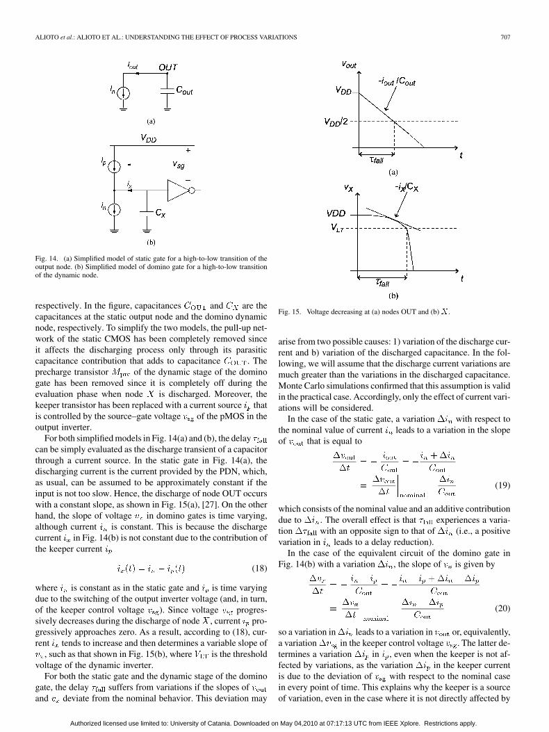
Fig. 14. (a) Simplified model of static gate for a high-to-low transition of theoutput node. (b) Simplified model of domino gate for a high-to-low transitionof the dynamic node.
respectively. In the figure, capacitances and are thecapacitances at the static output node and the domino dynamicnode, respectively. To simplify the two models, the pull-up net-work of the static CMOS has been completely removed sinceit affects the discharging process only through its parasiticcapacitance contribution that adds to capacitance . Theprecharge transistor of the dynamic stage of the dominogate has been removed since it is completely off during theevaluation phase when node is discharged. Moreover, thekeeper transistor has been replaced with a current source thatis controlled by the source–gate voltage of the pMOS in theoutput inverter.
For both simplified models in Fig. 14(a) and (b), the delaycan be simply evaluated as the discharge transient of a capacitorthrough a current source. In the static gate in Fig. 14(a), thedischarging current is the current provided by the PDN, which,as usual, can be assumed to be approximately constant if theinput is not too slow. Hence, the discharge of node OUT occurswith a constant slope, as shown in Fig. 15(a), [27]. On the otherhand, the slope of voltage in domino gates is time varying,although current is constant. This is because the dischargecurrent in Fig. 14(b) is not constant due to the contribution ofthe keeper current
(18)
where is constant as in the static gate and is time varyingdue to the switching of the output inverter voltage (and, in turn,of the keeper control voltage ). Since voltage progres-sively decreases during the discharge of node , current pro-gressively approaches zero. As a result, according to (18), cur-rent tends to increase and then determines a variable slope of
, such as that shown in Fig. 15(b), where is the thresholdvoltage of the dynamic inverter.
For both the static gate and the dynamic stage of the dominogate, the delay suffers from variations if the slopes ofand deviate from the nominal behavior. This deviation may
Fig. 15. Voltage decreasing at (a) nodes OUT and (b) � .
arise from two possible causes: 1) variation of the discharge cur-rent and b) variation of the discharged capacitance. In the fol-lowing, we will assume that the discharge current variations aremuch greater than the variations in the discharged capacitance.Monte Carlo simulations confirmed that this assumption is validin the practical case. Accordingly, only the effect of current vari-ations will be considered.
In the case of the static gate, a variation with respect tothe nominal value of current leads to a variation in the slopeof that is equal to
(19)
which consists of the nominal value and an additive contributiondue to . The overall effect is that experiences a varia-tion with an opposite sign to that of (i.e., a positivevariation in leads to a delay reduction).
In the case of the equivalent circuit of the domino gate inFig. 14(b) with a variation , the slope of is given by
(20)
so a variation in leads to a variation in or, equivalently,a variation in the keeper control voltage . The latter de-termines a variation in , even when the keeper is not af-fected by variations, as the variation in the keeper currentis due to the deviation of with respect to the nominal casein every point of time. This explains why the keeper is a sourceof variation, even in the case where it is not directly affected by
Authorized licensed use limited to: University of Catania. Downloaded on May 04,2010 at 07:17:13 UTC from IEEE Xplore. Restrictions apply.

708 IEEE TRANSACTIONS ON VERY LARGE SCALE INTEGRATION (VLSI) SYSTEMS, VOL. 18, NO. 5, MAY 2010
Fig. 16. Variation of currents and voltages in the domino gate.
Fig. 17. Results of Monte Carlo simulations of the voltage at node OUT forthe static NAND2 gate and at node � for the domino inverter without and witha keeper transistor.
variations (as discussed in Section V.B). Now, it is possible tounderstand why the keeper transistor tends to increase the vari-ability, which is equivalent to show that and in (20)have opposite signs. To this aim, let us consider thecase, as shown in Fig. 16, which, from (20), leads to an initiallygreater slope of with respect to the nominal case. In turn, thisleads to a lower value of at any point of time, compared tothe nominal case, so voltage is lower comparedto the nominal case, and the keeper transistor therefore deliversa lower current . Hence, the dynamic variationhas an opposite sign to in (20), or equivalently, the keepertransistor tends to increase the variability since current willhave a deviation that is greater than that due to , accordingto (20). In other words, the feedback loop implemented by thekeeper significantly increases the delay variability. This is alsoexpected from feedback theory since it is well known that posi-tive feedback increases the circuit sensitivity to parameter vari-ations. Of course, the same considerations are also valid for anegative deviation.
The previously described effect is evident in the simulatedwaveforms in Fig. 17 of the voltage at nodes OUT and forthe static and dynamic gates, respectively, with ,where multiple waveforms result from various Monte Carlosimulations. As expected, the feedback structure of the dominogate determines an increase in the delay variations (see thewaveform value around voltage ) with respect to that ofthe static CMOS and domino gate without a keeper.
Summarizing, the positive feedback loop implemented by thekeeper tends to amplify the delay variations determined by thePDN, even in the ideal case where the keeper is not subjectto variations. The keeper is responsible for the two times vari-ability increase in domino gates with respect to their static coun-terparts, which translates into a speed penalty. Moreover, thekeeper introduces also a well-known second-order effect thatfurther degrades the speed, even in ideal circuits with no varia-tions at all. Indeed, the keeper determines a current contentionwith the PDN, which tends to reduce the speed of the switchingtransient at the dynamic node [3], [27]. Accordingly, the neg-ative impact of the keeper on the speed performance is evenemphasized in nanometer technologies and is expected to fur-ther increase in next-generation technology nodes due to the in-creased variability. Hence, it limits the performance of high-speed domino gates, thereby making their design more chal-lenging.
VI. CONCLUSION
In this paper, the effect of process variations on the delay ofstatic and dynamic CMOS logic have been analyzed. Simplemodels of delay variability as a function of circuit parameters(e.g., fan-in, fan-out, and number of stacked transistors) andlogic style have been derived. Analysis has shown that delayvariations are mainly due to the variations in the current deliv-ered by logic gates, whereas the impact of variations of parasiticcapacitances is negligible.
The impact of interdie and intradie variations has been an-alyzed in depth. In regard to interdie variations, it has beenshown that the current variability of stacked transistors is ap-proximately the same as that of a single transistor. As for in-tradie variations, it has been demonstrated that delay variabilityis reduced when the number of transistors and their size are in-creased, according to a square-root law.
Analysis has also shown that delay variability is almost inde-pendent of the input rise/fall time and load capacitanceunder practical values of and . Accordingly, the proposedmodel has a reasonable accuracy even if it does not explicitlyaccount for the dependence on . In particular, the proposedmodels have been shown to exhibit an adequate accuracy (typ-ically 8%–10%), regardless of the input rise/fall time and loadcapacitance. The models were extended to multistage circuitsby resorting to the results that are available in the literature.
The proposed models were also compared with table-basedmodels, which are currently used in commercial CAD tools andare unsuitable for gaining an insight into the dependence of thedelay variability circuit. Even though the proposed model is lessaccurate than the table-based ones, its accuracy is adequate formodeling purposes.
Analysis of domino logic gates has shown that their vari-ability is almost doubled compared to that of static logic due tothe presence of the keeper transistor. For the first time in the lit-erature, it is shown that the keeper transistor degrades the speedperformance of domino logic due to not only the current con-tention with the PDN (as already occurred in older technolo-gies) but also the increase in variability. This means that thespeed degradation due to the positive feedback associated withthe keeper transistor is an even more critical issue in sub-100-nm
Authorized licensed use limited to: University of Catania. Downloaded on May 04,2010 at 07:17:13 UTC from IEEE Xplore. Restrictions apply.

ALIOTO et al.: ALIOTO ET AL.: UNDERSTANDING THE EFFECT OF PROCESS VARIATIONS 709
technologies due to the increasing variability. Extensive MonteCarlo simulations on a 90-nm CMOS technology have been per-formed to justify and validate the results.
REFERENCES
[1] J. A. Croon, W. Sansen, and H. E. Maes, Matching Properties of DeepSub-Micron MOS Transistors. New York: Springer-Verlag, 2005.
[2] A. Srivastava, D. Sylvester, and D. Blaauw, Statistical Anal-ysis and Optimization for VLSI: Timing and Power. New York:Springer-Verlag, 2005.
[3] K. Bernstein, K. M. Carrig, C. M. Durham, P. R. Hansen, D. Hogen-miller, E. J. Nowak, and N. J. Rohrer, High Speed CMOS DesignStyles. Norwell, MA: Kluwer, 1999.
[4] M. Orshansky, S. Nassif, and D. Boning, Design for Manufacturabilityand Statistical Design. New York: Springer-Verlag, 2008.
[5] M. Eisele, J. Berthold, D. Schmitt-Landsiedel, and R. Mahnkopf, “Theimpact of intra-die device parameter variations on path delays and onthe design for yield of low voltage digital circuits,” IEEE Trans. VeryLarge Scale Integr. (VLSI) Syst., vol. 5, no. 4, pp. 360–368, Dec. 1997.
[6] J.-J. Liou, A. Krstic, Y.-M. Jiang, and K.-T. Cheng, “Modeling, testing,and analysis for delay defects and noise effects in deep submicron de-vices,” IEEE Trans. Comput.-Aided Design Integr. Circuits Syst., vol.22, no. 6, pp. 756–769, Jun. 2003.
[7] M. Alioto and G. Palumbo, “Impact of supply voltage variations on fulladder delay: Analysis and comparison,” IEEE Trans. Very Large ScaleIntegr. (VLSI) Syst., vol. 14, no. 12, pp. 1322–1335, Dec. 2006.
[8] H. Masuda and S. Okawa, “Approach for physical design in sub-100nm era,” in Proc. ISCAS, 2005, pp. 5934–5937.
[9] Y. Liu, S. R. Nassif, L. T. Pileggi, and A. J. Strojwas, “Impact of inter-connect variations on the clock skew of a gigahertz microprocessor,”in Proc. DAC, 2000, pp. 168–171.
[10] N. Shigyo, “Tradeoff between interconnect capacitance and RC delayvariations induced by process fluctuations,” IEEE Trans. Electron De-vices, vol. 47, no. 9, pp. 1740–1744, Sep. 2000.
[11] B. Stine, D. Boning, and J. Chung, “Analysis and decomposition of spa-tial variation in integrated circuit processes and devices,” IEEE Trans.Semicond. Manuf., vol. 10, no. 1, pp. 24–41, Feb. 1997.
[12] A. Chandrakasan, W. Bowhill, and F. Fox, Design of High-Perfor-mance Microprocessor Circuits. Piscataway, NJ: IEEE Press, 2001.
[13] K. Lakshmikumar, R. Hadaway, and M. Copeland, “Characterizationand modeling of mismatch in MOS transistors for precision analog de-sign,” IEEE J. Solid-State Circuits, vol. SSC-21, no. 6, pp. 1057–1066,Dec. 1986.
[14] M. Pelgrom, A. Duinmaijer, and A. Welbers, “Matching propertiesof MOS transistors,” IEEE J. Solid-State Circuits, vol. 24, no. 5, pp.1433–1439, Oct. 1989.
[15] K. Okada, K. Yamaoka, and H. Onodera, “A statistical gate delay modelfor intra-chip and inter-chip variabilities,” in Proc. ASP-DAC, 2003, pp.31–36.
[16] A. Agarwal, D. Blaauw, V. Zolotov, S. Sundareswaran, M. Zhao, K.Gala, and R. Panda, “Statistical delay computation considering spatialcorrelations,” in Proc. ASP-DAC, 2003, pp. 271–276.
[17] A. Agarwal, D. Blaauw, and V. Zolotov, “Statistical timing analysis forintra-die process variations with spatial correlations,” in Proc. ICCAD,2003, pp. 900–907.
[18] K. Okada, K. Yamaoka, and H. Onodera, “A statistical gate-delaymodel considering intra-gate variability,” in Proc. ICCAD, 2003, pp.908–913.
[19] K. Okada, K. Yamaoka, and H. Onodera, “Statistical modeling of gate-delay variation with consideration of intra-gate variability,” in Proc.ISCAS, 2003, pp. 513–516.
[20] Y. Cao and L. T. Clark, “Mapping statistical process variations towardcircuit performance variability: An analytical modeling approach,”IEEE Trans. Comput.-Aided Design Integr. Circuits Syst., vol. 26, no.10, pp. 1866–1873, Oct. 2007.
[21] W. Dai and H. Ji, “Timing analysis taking into account interconnectprocess variation,” in Proc. IWSM, 2001, pp. 51–53.
[22] M. Orshansky, C. Spanos, and H. Chenming, “Circuit performancevariability decomposition,” in Proc. IWSM, 1999, pp. 10–13.
[23] J. Tschanz, S. Narendra, R. Nair, and V. De, “Effectiveness of adaptivesupply voltage and body bias for reducing impact of parameter varia-tions in low power and high performance microprocessors,” IEEE J.Solid-State Circuits, vol. 38, no. 5, pp. 826–829, May 2003.
[24] J. W. Tschanz, J. T. Kao, S. G. Narendra, R. Nair, D. A. Antoniadis, A.P. Chandrakasan, and V. De, “Adaptive body bias for reducing impactsof die-to-die and within-die parameter variations on microprocessorfrequency and leakage,” IEEE J. Solid-State Circuits, vol. 37, no. 11,pp. 1396–1402, Nov. 2002.
[25] S. R. Nassif, “Modeling and forecasting of manufacturing variations,”in Proc. ASP-DAC, 2001, pp. 145–150.
[26] R. E. Walpole, R. H. Myers, S. L. Myers, and K. Ye, Probability &Statistics for Engineers & Scientists. Englewood Cliffs, NJ: Prentice-Hall, 2006.
[27] J. Rabaey, A. Chandrakasan, and B. Nikolic, Digital Integrated Circuits(A Design Perspective). Englewood Cliffs, NJ: Prentice-Hall, 2003.
[28] R. Shaumann and M. E. Van Valkenburg, Design of Analog Filters.New York: Oxford Univ. Press, 2001.
[29] T. Sakurai and R. Newton, “Alpha-power law MOSFET model andits applications to CMOS inverter delay and other formulas,” IEEE J.Solid-State Circuits, vol. 25, no. 2, pp. 584–594, Apr. 1990.
[30] J. Gu, S. S. Sapatnekar, and C. Kim, “Width-dependent statisticalleakage modeling for random dopant induced threshold voltage shift,”in Proc. DAC, San Diego, CA, Jun. 2007, pp. 87–92.
[31] I. Sutherland, B. Sproull, and D. Harris, Logical Effort. Designing FastCMOS Circuits. San Mateo, CA: Morgan Kaufmann, 1999.
Massimo Alioto (M’01–SM’07) was born inBrescia, Italy, in 1972. He received the Laureadegree in electronics engineering and the Ph.D.degree in electrical engineering from the Universityof Catania, Catania, Italy, in 1997 and 2001, respec-tively.
In 2002, he joined the Dipartimento di IngegneriadellInformazione (DII), University of Siena, Siena,Italy, as a Research Associate and in the same yearas an Assistant Professor. In 2005, he was appointedAssociate Professor of Electronics, and was engaged
in the same faculty in 2006. In the summer of 2007, he was a Visiting Professorwith EPFL-Lausanne, Lausanne, Switzerland. In 2009-2010, he was a VisitingProfessor with BWRC University of California, Berkeley, doing research onultra-low power circuits and sensor nodes. Since 2001 he has been teaching un-dergraduate and graduate courses on advanced VLSI digital design, microelec-tronics and basic electronics. He has authored or coauthored 130 publicationson journals (over 45, mostly IEEE Transactions) and conference proceedings.Two of them are among the 25 most downloaded TVLSI papers in 2007 (re-spectively, 10th and 13th). He is coauthor of the book Model and Design ofBipolar and MOS Current-Mode Logic: CML, ECL and SCL Digital Circuits(Springer, 2005). His primary research interests include the modeling and theoptimized design of CMOS high-performance, low-power and ultra low-powerdigital circuits, arithmetic and cryptographic circuits, interconnect modeling,design/modeling for variability-tolerant and lowleakage VLSI circuits, circuittechniques for emerging technologies. He is the director of the Electronics Lab,University of Siena (site of Arezzo).
Prof. Alioto is a member of the HiPEAC Network of Excellence. He is theChair Elect of the VLSI Systems and Applications Technical Committee of theIEEE Circuits and Systems Society, for which he is also a Distinguished Lec-turer. He is regularly invited to give talks to academic institutions and con-ferences throughout the world. He has served as a member of various con-ference technical program committees (ISCAS, PATMOS, ICM, ICCD, CSIE)and Track Chair (ICECS, ISCAS). He serves as Associate Editor of the IEEETRANSACTIONS ON VERY LARGE SCALE INTEGRATION (VLSI) SYSTEMS, as wellas of the Microelectronics Journal, the Integration The VLSI journal and theJournal of Circuits, Systems, and Computers. He is Guest Editor of the SpecialIssue on Advances in oscillator analysis and design of the Journal of Circuits,Systems, and Computers (2009).
Gaetano Palumbo (F’07) was born in Catania, Italy,in 1964. He received the Laurea degree in electricalengineering and the Ph.D. degree from the Universityof Catania, Catania, Italy, in 1988 and 1993, respec-tively.
Since 1993, he conducts courses on ElectronicDevices, Electronics for Digital Systems and basicElectronics. In 1994, he joined the DipartimentoElettrico Elettronico e Sistemistico (DEES), nowDipartimento di Ingegneria Elettrica Elettronica edei Sistemi (DIEES), at the University of Catania
Authorized licensed use limited to: University of Catania. Downloaded on May 04,2010 at 07:17:13 UTC from IEEE Xplore. Restrictions apply.
710 IEEE TRANSACTIONS ON VERY LARGE SCALE INTEGRATION (VLSI) SYSTEMS, VOL. 18, NO. 5, MAY 2010
as a researcher, subsequently becoming Associate Professor in 1998. Since2000, he is a full Professor with the same department. His primary researchinterest has been analog circuits with particular emphasis on feedback circuits,compensation techniques, current-mode approach, low-voltage circuits. Then,his research has also embraced digital circuits with emphasis on bipolar andMOS current-mode digital circuits, adiabatic circuits, and high-performancebuilding blocks focused on achieving optimum speed within the constraint oflow power operation. In all these fields he is developing some the researchactivities in collaboration with STMicroelectronics of Catania. He was thecoauthor of three books CMOS Current Amplifiers (Kluwer, 1999), FeedbackAmplifiers: Theory and Design (Kluwer, 2001), and Model and Design ofBipolar and MOS Current-Mode Logic (CML, ECL, and SCL Digital Circuits)(Kluwer, 2005), and a textbook on electronic device in 2005. He is the authorof 340 scientific papers on referred international journals (over 140) and inconferences. Moreover, he is coauthor of several patents.
Dr. Palumbo was a recipient of the Darlington Award in 2003. Since June1999 to the end of 2001 and since 2004 to 2005, he served as an Associated Ed-itor of the IEEE TRANSACTIONS ON CIRCUITS AND SYSTEMS—PART I: REGULAR
PAPERS for the topic analog circuits and filters and digital circuits and systems,respectively. Since 2006 to 2007, he served as an Associated Editor of the IEEETRANSACTIONS ON CIRCUITS AND SYSTEMS—PART II: BRIEF PAPERS. Since2008, he is serving as an Associated Editor of the IEEE TRANSACTIONS ON
CIRCUITS AND SYSTEMS—PART I: REGULAR PAPERS. In 2005 he was one of
the 12 panelists in the scientific-disciplinare area 09 - industrial and informa-tion engineering of the CIVR (Committee for Evaluation of Italian Research),which has the aim to evaluate the Italian research in the above area for the period2001-2003.
Melita Pennisi (M’07) was born in Catania, Italy, in1980. She received the Laurea degree in electronicsengineering and the Ph.D. degree in electronicsand automatic engineering from the University ofCatania, Catania, Italy, in 2004 and 2008, respec-tively.
Since 2008, she has been a Researcher with the Di-partimento di Ingegneria Elettrica Elettronica e deiSistemi (DIEES), University of Catania. She is coau-thor of more than 15 publications on internationaljournals and conference proceedings. Her primary re-
search interests include the modeling and the optimized design of CMOS highperformance, analysis of analog nonlinear circuits, behavioral modeling of com-plex mixed-signal circuits, design/modeling for variability-tolerant and low-leakage VLSI circuits.
Authorized licensed use limited to: University of Catania. Downloaded on May 04,2010 at 07:17:13 UTC from IEEE Xplore. Restrictions apply.