Ultra-Efficient Processing In-Memory for Data Intensive ...
6
Ultra-Eicient Processing In-Memory for Data Intensive Applications Mohsen Imani, Saransh Gupta and Tajana Rosing CSE Department, UC San Diego, La Jolla, CA 92093, USA {moimani, sgupta, tajana}@ucsd.edu ABSTRACT Recent years have witnessed a rapid growth in the domain of Inter- net of Things (IoT ). This network of billions of devices generates and exchanges huge amount of data. The limited cache capacity and memory bandwidth make transferring and processing such data on traditional CPUs and GPUs highly inefficient, both in terms of energy consumption and delay. However, many IoT applications are statistical at heart and can accept a part of inaccuracy in their compu- tation. This enables the designers to reduce complexity of processing by approximating the results for a desired accuracy. In this paper, we propose an ultra-efficient approximate processing in-memory ar- chitecture, called APIM, which exploits the analog characteristics of non-volatile memories to support addition and multiplication inside the crossbar memory, while storing the data. The proposed design eliminates the overhead involved in transferring data to processor by virtually bringing the processor inside memory. APIM dynamically configures the precision of computation for each application in or- der to tune the level of accuracy during runtime. Our experimental evaluation running six general OpenCL applications shows that the proposed design achieves up to 20× performance improvement and provides 480× improvement in energy-delay product, ensuring ac- ceptable quality of service. In exact mode, it achieves 28× energy savings and 4.8× speed up compared to the state-of-the-art GPU cores. CCS CONCEPTS •Hardware → Emerging architectures; Non-volatile memory; KEYWORDS Processing in-memory, Non-volatile memory, Emerging computing ACM Reference format: Mohsen Imani, Saransh Gupta and Tajana Rosing. 2016. Ultra-Efficient Processing In-Memory for Data Intensive Applications. In Proceedings of ACM conference, Austin, Texas USA, June 2017 (DAC ’17), 6 pages. DOI: http://dx.doi.org/10.1145/3061639.3062337 1 INTRODUCTION Today’s IoT applications often analyze raw data by running machine learning algorithms such as classification or neural networks in data centers [1, 2]. Sending the entire data to cloud for processing is not scalable and cannot guarantee the required real-time response [3]. Running data intensive workloads with large datasets on traditional cores results in high energy consumption and slow processing speed, majorly due to the large amount of data movement between memory and processing units [4, 5]. The idea of near-data computing aims to address this problem. Near-data computing puts the processing Permission to make digital or hard copies of part or all of this work for personal or classroom use is granted without fee provided that copies are not made or distributed for profit or commercial advantage and that copies bear this notice and the full citation on the first page. Copyrights for third-party components of this work must be honored. For all other uses, contact the owner/author(s). DAC ’17, Austin, Texas USA © 2016 Copyright held by the owner/author(s). 978-1-4503-4927-7/17/06. . . $15.00 DOI: http://dx.doi.org/10.1145/3061639.3062337 units close to the main memory, which accelerates the computation by avoiding the memory/cache bottleneck [4, 6, 7]. Although this idea improves performance, it may consume more energy due to the extra computing units added to the memory. A more efficient way of addressing data movement issue is to process data within the memory, thus improving both performance and energy efficiency [5, 8]. On the other hand, most of the algorithms running on today’s sensors’ data are statistical in nature, and thus do not require ex- act answers [9, 10]. Similarly, in audio and video processing we have long exploited the fact that humans do not perceive all the colors or sounds equally well. Approximate computing is an ef- fective way of improving the energy and performance by trading some accuracy. Much of the prior work seeks to exploit this fact in order to build faster and more energy efficient systems which are capable of responding to our needs with just good enough quality of response [11–13]. However, most of the existing techniques pro- vide less energy or performance efficiency due to considerable data movement and lack of configurable accuracy. Non-volatile memories (NVMs) are promising candidates for data intensive in-memory computations, where the an NVM cell can be used for both storing data and processing it [14–17]. Resistive random access memory (RRAM) is one such memory which stores data in form of its resistance. Owing to its low energy requirements, high switching speeds, and scalability, RRAM can be used to develop high capacity memories with great performance. These memories are compatible with the current CMOS fabrication process [18] which enables their easy integration with the existing technology. In this paper, we propose a configurable approximate process- ing in-memory architecture, called APIM, which supports addition and multiplication operations inside the non-volatile RRAM-based memory. APIM exploits the analog characteristic of the memristor devices to enable basic bitwise computation and then, extend it to fast and configurable addition and multiplication within memory. This would make processing machine learning and data analysis algorithms more efficient since most of them use addition and mul- tiplication aggressively. We propose a blocked crossbar memory which introduces flexibility in executing operations and facilitates shift operations in memory. Then, we introduce a novel approach for fast addition in memory. Finally, we design an in-memory multiplier using the proposed memory unit and fast adder. For each application, APIM can dynamically tune the level of approximation in order to trade the accuracy of computation while improving energy and performance. Our experimental evaluation over six general OpenCL applications shows that the proposed design improves the perfor- mance by 20× and provides 480× improvement in energy-delay product while ensuring less than 10% average relative error. 2 RELATED WORK AND BACKGROUND Processing in-memory (PIM) can accelerate computation by re- ducing the overhead of data movement [5, 8]. Early PIM designs integrate high performance CMOS logic and memory on the same die. They predominantly designed a custom processing unit next to the sense amplifiers of main memory to support basic bitwise
-
Upload
khangminh22 -
Category
Documents
-
view
5 -
download
0
Transcript of Ultra-Efficient Processing In-Memory for Data Intensive ...
Ultra-Eicient Processing In-Memory for Data IntensiveApplications
Mohsen Imani, Saransh Gupta and Tajana RosingCSE Department, UC San Diego, La Jolla, CA 92093, USA
moimani, sgupta, [email protected]
ABSTRACTRecent years have witnessed a rapid growth in the domain of Inter-net of Things (IoT). This network of billions of devices generatesand exchanges huge amount of data. The limited cache capacityand memory bandwidth make transferring and processing such dataon traditional CPUs and GPUs highly inefficient, both in terms ofenergy consumption and delay. However, many IoT applications arestatistical at heart and can accept a part of inaccuracy in their compu-tation. This enables the designers to reduce complexity of processingby approximating the results for a desired accuracy. In this paper,we propose an ultra-efficient approximate processing in-memory ar-chitecture, called APIM, which exploits the analog characteristics ofnon-volatile memories to support addition and multiplication insidethe crossbar memory, while storing the data. The proposed designeliminates the overhead involved in transferring data to processor byvirtually bringing the processor inside memory. APIM dynamicallyconfigures the precision of computation for each application in or-der to tune the level of accuracy during runtime. Our experimentalevaluation running six general OpenCL applications shows that theproposed design achieves up to 20× performance improvement andprovides 480× improvement in energy-delay product, ensuring ac-ceptable quality of service. In exact mode, it achieves 28× energysavings and 4.8× speed up compared to the state-of-the-art GPUcores.
CCS CONCEPTS•Hardware→ Emerging architectures; Non-volatile memory;
KEYWORDSProcessing in-memory, Non-volatile memory, Emerging computingACM Reference format:Mohsen Imani, Saransh Gupta and Tajana Rosing. 2016. Ultra-EfficientProcessing In-Memory for Data Intensive Applications. In Proceedings ofACM conference, Austin, Texas USA, June 2017 (DAC ’17), 6 pages.DOI: http://dx.doi.org/10.1145/3061639.3062337
1 INTRODUCTIONToday’s IoT applications often analyze raw data by running machinelearning algorithms such as classification or neural networks in datacenters [1, 2]. Sending the entire data to cloud for processing is notscalable and cannot guarantee the required real-time response [3].Running data intensive workloads with large datasets on traditionalcores results in high energy consumption and slow processing speed,majorly due to the large amount of data movement between memoryand processing units [4, 5]. The idea of near-data computing aimsto address this problem. Near-data computing puts the processing
Permission to make digital or hard copies of part or all of this work for personal orclassroom use is granted without fee provided that copies are not made or distributedfor profit or commercial advantage and that copies bear this notice and the full citationon the first page. Copyrights for third-party components of this work must be honored.For all other uses, contact the owner/author(s).DAC ’17, Austin, Texas USA© 2016 Copyright held by the owner/author(s). 978-1-4503-4927-7/17/06. . . $15.00DOI: http://dx.doi.org/10.1145/3061639.3062337
units close to the main memory, which accelerates the computationby avoiding the memory/cache bottleneck [4, 6, 7]. Although thisidea improves performance, it may consume more energy due tothe extra computing units added to the memory. A more efficientway of addressing data movement issue is to process data within thememory, thus improving both performance and energy efficiency [5,8].
On the other hand, most of the algorithms running on today’ssensors’ data are statistical in nature, and thus do not require ex-act answers [9, 10]. Similarly, in audio and video processing wehave long exploited the fact that humans do not perceive all thecolors or sounds equally well. Approximate computing is an ef-fective way of improving the energy and performance by tradingsome accuracy. Much of the prior work seeks to exploit this fact inorder to build faster and more energy efficient systems which arecapable of responding to our needs with just good enough qualityof response [11–13]. However, most of the existing techniques pro-vide less energy or performance efficiency due to considerable datamovement and lack of configurable accuracy.
Non-volatile memories (NVMs) are promising candidates fordata intensive in-memory computations, where the an NVM cell canbe used for both storing data and processing it [14–17]. Resistiverandom access memory (RRAM) is one such memory which storesdata in form of its resistance. Owing to its low energy requirements,high switching speeds, and scalability, RRAM can be used to develophigh capacity memories with great performance. These memoriesare compatible with the current CMOS fabrication process [18]which enables their easy integration with the existing technology.
In this paper, we propose a configurable approximate process-ing in-memory architecture, called APIM, which supports additionand multiplication operations inside the non-volatile RRAM-basedmemory. APIM exploits the analog characteristic of the memristordevices to enable basic bitwise computation and then, extend it tofast and configurable addition and multiplication within memory.This would make processing machine learning and data analysisalgorithms more efficient since most of them use addition and mul-tiplication aggressively. We propose a blocked crossbar memorywhich introduces flexibility in executing operations and facilitatesshift operations in memory. Then, we introduce a novel approach forfast addition in memory. Finally, we design an in-memory multiplierusing the proposed memory unit and fast adder. For each application,APIM can dynamically tune the level of approximation in orderto trade the accuracy of computation while improving energy andperformance. Our experimental evaluation over six general OpenCLapplications shows that the proposed design improves the perfor-mance by 20× and provides 480× improvement in energy-delayproduct while ensuring less than 10% average relative error.
2 RELATED WORK AND BACKGROUNDProcessing in-memory (PIM) can accelerate computation by re-ducing the overhead of data movement [5, 8]. Early PIM designsintegrate high performance CMOS logic and memory on the samedie. They predominantly designed a custom processing unit nextto the sense amplifiers of main memory to support basic bitwise
b0'
b2'
b3'
b0'
b2'
b3'
b0'
b2'
b3'
b0'
b2'
b3'
in1 in2 inn out
V0 GND
in1 in2 inn
out
in1
in2
inn
out
GND
in1 in2 inn
V0
out
V0
V0
A2[n:1]A1[n:1] A4[n:1]A3[n:1] A6[n:1]A5[n:1] A8[n:1]A7[n:1] A9[n:1]
+
+
+
+ +
+
1-bit FA
S4[n] C4[n]
S3[1]
1-bit FA
S4[1] C4[1]
C3[1] C2[1]
+
S C
n-bit Adders
(n+1)-bit Adders
(n+2)-bit Adder
(n+3)-bit Adder
M1,1 M1,2 M1,n
Column Decoder and Voltage Controllers
M2,n-1
Mk,1 Mk,2 Mk,n
M2,2M2,1 M2,n
M1,n-1
Mk,n-1
Data Block 1
Processing
Block 1
Configurable Interconnect
Data Block 2
Processing
Block 2
Processing
Block n
Column Decoder and Controller
Sense Amplifiers
Ro
w D
eco
der a
nd
Co
ntr
oll
er
M2 M1
R1>x
M3P2 P1
Current
Mirror
Vdd
R2>2MAJ
Bitwise
M4
MAJ/F1
F1
F1
MA
J
MUX
Carry Save
Adder
Bitwise Read
Configurable Interconnect
Controller
C2n-2C2n-1
R2>2C 1C 2n
Majority
P1P2n-1P2n P2n-2
M2
0M
2n
-2M
2n
-1
M1
0M
1n
-2M
1n
-1
SA
M2x=1
Copy M1
Nex
t bit
S11C11
Carry Save
Adder
S12C12
Carry Save
Adder
C1h C1h
Carry Save
Adder
S21C21
Carry Save
Adder
C2[2h/3]
Configurable Interconnect
Carry Save
Adder
ST1CT1
S2[2h/3]
S2n-2
C 2n-2
S0
C0
S2n-1
C 2n-1
(b) Partial Product
Generation
(d) Final Product Generation
(c) Fast Adder
(a) APIM Overall Structure
Crossbar
Memory
b0
b1
b2
b3
b4 b5 b6
b'0 b'1 b'2 b'3
s0
s1
s2
s3
Different interconnect modes
(a) (b)
SA
SA
SA
SA
Propagation Stage
Partial Product 0
Partial Product 1
SASASA
a1 a0a2a3
b1'
b1'
b1'
b1'
1-bit FA
S[n]
1-bit FA
S[1]S[n+1]
S3[n] C3[n] C2[n]
Configurable Interconnect Configurable Interconnect
(a) (b)
Configurable Interconnect
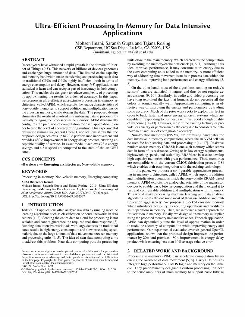
Figure 1: (a) The overall structure of APIM consisting of several data and processing blocks. (b) the APIM controller and parallelproduct generator. (c) Fast adder three structure consisting of Carry save adder and configurable interconnects. (d) Final productgenerator to ripple the carry bits of tree structure.
operations. However, to support other advance functionality (e.g.addition, multiplication), they added dedicated CMOS-based pro-cessing cores, making the manufacturing process complicated andcostly.
High density, low-power consumption, and CMOS-compatibilityof emerging non-volatile memories (NVMs), in particular memristordevices, make them appropriate candidates for both memory andcomputing unit [14, 15, 19, 20]. Many logic families have beenproposed for computation inside memristive crossbar. Some ofthem implement logic purely in memory such as stateful implicationlogic [21, 22], and Memristor Aided loGIC (MAGIC) [23].The workin [24] presents schemes for addition in memristive crossbar memory.The direct application of these schemes in data intensive processingis limited largely due to the linear dependency of latency of executionon the size of data. While [25] presents a very fast adder, the areaoverhead involved in arrayed addition grows significantly for dataintensive workloads.
We use MAGIC NOR [23] to execute logic functions in memorydue to its simplicity and independence of execution from data inmemory. An execution voltage, V0, is applied to the bitlines of theinputs (in case of NOR in a row) or wordlines of the outputs (in caseof NOR in a column) in order to evaluate NOR, while the bitlines of theoutputs (NOR in a row) or wordlines of the inputs (NOR in a column)are grounded. The work in [24] extends this idea to implement adderin a crossbar. It executes a pattern of voltages in order to evaluatesum (S) and carry (Cout ) bits of 1-bit full addition (inputs beingA,B,C) given by
Cout = ((A+B)′ + (B+C)′ + (C+A)′)′. (1a)
S = (((A′ +B′ +C′)′ + ((A+B+C)′ +Cout )′)′)′. (1b)
This design takes 12N + 1 cycles to add two N-bit numbers. Wedefine a cycle time (= 1.1ns) as the time taken to implement oneMAGIC NOR operation.
In contract, we propose a novel processing in-memory architec-ture which supports fast and efficient addition and multiplicationoperations. Our design supports approximation and configures itdynamically depending upon the requirements of different applica-tions.
3 PROPOSED APIMThis section presents the design flow and techniques used to exe-cute addition and multiplication in memory. Figure 1(a) shows thememory unit. It is a simple crossbar memory divided into differentblocks further explained in Section 3.1. Section 3.2 proposes a fastadder, Figure 1(c), which uses a tree structure in the memory unitto add large number of operands with minimum delay. Section 3.3describes a multiplier, Figure 1(b)-(d), which utilises the fast adderalong with the modified sense amplifiers of the memory unit toobtain product in an efficient manner. We also propose approxima-tion techniques in Section 3.4 which speed up multiplication whileensuring high accuracy.
3.1 APIM Architectural OverviewA typical crossbar memory is an array of unit memory cells. In caseof RRAM, these cells are made of resistive switching elements suchas memristors. Each cell in the memory is accessed by activatingthe corresponding wordline and bitline. MAGIC makes executionof operations in a crossbar memory simple. It also allows easycopying of data provided the source and destination are in the samecolumn/row. While being acceptable in many cases, this memorystructure limits the performance of instructions which involve a lot ofshifting and asymmetric movement of data. One such instruction ismultiplication where the multiplicand is shifted and added. Multiplecopy operations can emulate a shift operation. However, such anapproach is impractical when the number to be shifted is large sinceit requires shifting each and every bit individually. The problem isaggravated when multiple such numbers are to be shifted.
We hence propose the use of a blocked memory structure asshown in Figure 1(a). The crossbar is divided into blocks. Anynew data which is loaded into the memory is stored in the datablock. Whenever there is a request to process data, it is copied tothe processing block and computation is done. The two blocks arestructurally the same and can be used interchangeably. These blocksare connected by configurable interconnects. The interconnectssupport shift operations inherently such that ith bitline of one blockcan be connected to (i+ j)th bitline of another block. The availability

of interconnects allows the memory to shift data while copying itfrom one block to another without introducing any latency overhead.This makes shifting an efficient operation since the entire string ofdata can be shifted at once, unlike shifting each bit individually.
3.2 Fast Addition in APIMThe design in [24] is good for small numbers but as the length ofnumbers increases, time taken increases linearly. A N×M multipli-cation requires addition of M partial products, each of size N bits, togenerate a (N +M)-bit product. This takes (M−1) · (12(N−1)+1)cycles to obtain the final product.
In order to optimize latency of addition, we propose a fast adderfor memristive memories. Our design is based on the idea of carrysave addition (CSA) and adapts it for in-memory computation. Fig-ure 2(a) shows carry save addition. Here, S1[n] and C1[n] are the sumand carry-out bits, respectively of 1-bit addition of A1[n], A2[n], andA3[n]. The 1-bit adders do not propagate the carry bit and generatetwo outputs. This makes the n additions independent of each other.The proposed adder exploits this property of CSA. Since, MAGICexecution scheme doesn’t depend upon the operands of addition,multiple addition operations can execute in parallel if the inputsare mapped correctly. The design utilises the proposed memoryunit, which supports shifting operations, to implement CSA likebehaviour. The latency of this 3:2 reduction, 3 inputs to 2 outputs,is same as that of a 1-bit addition (i.e., 13 cycles) irrespective ofthe size of operands. The two numbers can then be added serially,consuming 12N +1 cycles. This totals to 12N +14 cycles while theprevious adder would take 24N−22 cycles. The difference increaseslinearly with the size of inputs.
We use a Wallace-tree inspired structure leveraging the fast 3:2reduction of our new adder design, as shown in Figure 2(b), to addmultiple numbers (9 n-bit numbers in this case). At every stage ofexecution, the available addends are divided in groups of three. Theaddends are then added using a separate adder (as described above)for each group, generating two outputs per group. The additionsin the same stage of execution are independent and can occur inparallel to each other. Our configurable interconnect arranges theoutputs of this stage in groups of three for addition in the next stage.This structure takes a total of four stages for 9:2 reduction, havingthe same delay as that of four 1-bit additions. At the end of thetree structure we are left with two (N + 3)-bit numbers which canthen be added serially. The tree-structured addition reduces thedelay substantially as carry propagation happens only in the laststage, unlike the conventional approach where carry is propagatedat every step of addition. Although this speed up comes at the costof increased energy consumption and number of writes in memory,it is acceptable because the latency is reduced by large margins asshown in Section 4.
3.3 Multiplication in APIMThe process of multiplication can be divided into three stages, partialproduct generation, fast addition, and final product generation asshown in Figure 1. The partial product generation stage createspartial products of a N×N multiplication. These partial products canthen be added serially (inefficient) or by the fast adder introducedin Section 3.2. The fast addition reduces N numbers to 2. Thefinal product generation stage adds two numbers generated by theprevious stage and outputs the product of N×N multiplication.
A partial product is the result of ANDing the multiplicand (M1)with a bit of the multiplier (M2). Hence, N ×N multiplicationgenerates N (size of M2) partial products of size N-bits (size ofM1). AND operation can be implemented as a series of three NOR
b0'
b2'
b3'
b0'
b2'
b3'
b0'
b2'
b3'
b0'
b2'
b3'
in1 in2 inn out
V0 GND
in1 in2 inn
out
in1
in2
inn
out
GND
in1 in2 inn
V0
out
V0
V0
A2[n:1]A1[n:1] A4[n:1]A3[n:1] A6[n:1]A5[n:1] A8[n:1]A7[n:1] A9[n:1]
+
+
+
+ +
+
1-bit FA
S4[n] C4[n]
S3[1]
1-bit FA
S4[1] C4[1]
C3[1] C2[1]
+
S C
n-bit Adders
(n+1)-bit Adders
(n+2)-bit Adder
(n+3)-bit Adder
M1,1 M1,2 M1,n
Column Decoder and Voltage Controllers
M2,n-1
Mk,1 Mk,2 Mk,n
M2,2M2,1 M2,n
M1,n-1
Mk,n-1
Data Block 1
Processing
Block 1
Configurable Interconnect
Data Block 2
Processing
Block 2
Processing
Block n
Column Decoder and Controller
Sense Amplifiers
Ro
w D
eco
der a
nd
Co
ntr
oll
er
M2 M1
R1>x
M3P2 P1
Current
Mirror
Vdd
R2>2MAJ
Bitwise
M4
MAJ/F1
F1
F1
MA
J
MUX
Carry Save
Adder
Bitwise Read
Configurable Interconnect
Controller
C2n-2C2n-1
R2>2C 1C 2n
Majority
P1P2n-1P2n P2n-2
M2
0M
2n
-2M
2n
-1
M1
0M
1n
-2M
1n
-1
SA
M2x=1
Copy M1
Nex
t bit
S11C11
Carry Save
Adder
S12C12
Carry Save
Adder
C1h C1h
Carry Save
Adder
S21C21
Carry Save
Adder
C2[2h/3]
Configurable Interconnect
Carry Save
Adder
ST1CT1
S2[2h/3]
S2n-2
C 2n-2
S0
C0
S2n-1
C 2n-1
(b) Partial Product
Generation
(d) Final Product Generation
(c) Fast Adder
(a) APIM Overall Structure
Crossbar
Memory
b0
b1
b2
b3
b4 b5 b6
b'0 b'1 b'2 b'3
s0
s1
s2
s3
Different interconnect modes
(a) (b)
SA
SA
SA
SA
Propagation Stage
Partial Product 0
Partial Product 1
SASASA
a1 a0a2a3
b1'
b1'
b1'
b1'
1-bit FA
S[n]
1-bit FA
S[1]S[n+1]
S3[n] C3[n] C2[n]
Configurable Interconnect Configurable Interconnect
(a) (b)
Configurable Interconnect
Figure 2: (a) Carry save addition (b) Tree structured additionof 9 n-bit numbersoperations as given by,
F = AND (A,B) = NOR (NOR(A), NOR(B)) (2)
This requires three cycles given that the inputs A & B and outputF are in the same row or column. In the case of in-memory com-putation, even if we assume that the numbers to be multiplied arelocated adjacent to each other, we would require an empty crossbarrow/column of length NN which is quite large even for N = 16. Thiswould be expensive not only in terms of area but also in latency,requiring 3NN cycles.
We propose the use of sense amplifiers to develop a faster partialproduct generator as shown in Figure 1(b). In order to avoid thetime and area overhead involved in transposing and creating multiplecopies of multiplier, we read-out the multiplier. The design exploitsthe fact that the partial product is the multiplicand itself if multiplierbit is ’1’ and 0 otherwise. M2 is read bit-wise using the senseamplifier. If the read bit is ’1’, M1 is copied, while nothing is donewhen the bit is ’0’. We achieve this by modifying the multiplexerin the controller, incorporating the sensed bit in the select signals.In this way, we avoid writing data when the bit is zero, thus savingenergy. A copy operation is equivalent to two successive NOToperations. This result is used for all successive copy operations,limiting the worst case delay of copying to N +1 cycles. The actualdelay would vary depending upon the number of ’1s’ in M2.
Although this is a huge improvement in latency from the initialdesign, we have not yet considered the cost of shifting the partialproducts for add operation. Shift operation in a normal memorycrossbar can only be done bitwise, which would be quite large giventhe number and size of operands to be shifted. The blocked memoryarchitecture introduced in Section 3.1 proves advantageous in thisscenario. If the above operations are performed in a blocked memorycrossbar, the latency of shifting would actually reduce to zero. Shiftoperation can be clubbed with copy operation and hence, shiftedpartial products can be obtained in the processing block at no extradelay.
The fast adder discussed in Section 3.2 reduces the generatedpartial products to 2, owing to its N:2 reduction. Since a step inthe fast adder involves parallel additions, it requires that the threeaddends of a 3 : 2 adder are present in the same columns (rows) andall such groups in a step are present in the same rows (columns).Interestingly, arranging the partial products in this manner involvesno added latency as this arrangement can be done while shifting andcopying the data in the partial product generation stage. Instead ofwriting the partial products one below the other, the interconnectsare set such that the partial products are arranged in the requiredway. After the first step of 3 : 2 reduction, we again need to arrangethe intermediate results into groups of three. This can be done bymoving these results to the data block, performing the next 3 : 2
a1' a0'a2'a3'
b1'
b0'
b2'
b3'
b1'
b0'
b2'
b3'
b1'
b0'
b2'
b3'
b1'
b0'
b2'
b3'
in1 in2 inn out
V0 GND
in1 in2 inn
out
in1
in2
inn
out
GND
in1 in2 inn
V0
out
V0
V0
A2[n:1]A1[n:1] A4[n:1]A3[n:1] A6[n:1]A5[n:1] A8[n:1]A7[n:1] A9[n:1]
+
+
+
+ +
+A1[n]
1-bit FA
S1[n] C1[n]
A2[n] A3[n] A1[1]
1-bit FA
S1[1] C1[1]
A2[1] A3[1]
+
S C
n-bit Adders
(n+1)-bit Adders
(n+2)-bit Adder
(n+3)-bit Adder
M1,1 M1,2 M1,n
Column Decoder and Voltage Controllers
M2,n-1
Mk,1 Mk,2 Mk,n
M2,2M2,1 M2,n
M1,n-1
Mk,n-1
Data Block 1
Processing
Block 1
Interconnect
Data Block 2
Processing
Block 2
Interconnect
Processing
Block n
Interconnect
Column Decoder and Controller
Sense Amplifiers
Ro
w D
eco
der a
nd
Co
ntr
oll
er
M2 M1
R1>x
M3P2 P1
Current
Mirror
Vdd
R2>2MAJ
Bitwise
M4
MAJ/F1
F1
F1
MA
J
MUX
Carry Save
Adder
Bitwise Read
Interconnect
Controller Interconnect
C2n-2C2n-1
R2>2C 1C 2n
MAJ
P1P2n-1P2n P2n-2
M2
0M
2n
-2M
2n
-1
M1
0M
1n
-2M
1n
-1
SA
M2x=1
Copy M1
Nex
t bit
ShiftS11C11
Carry Save
AdderS12C12
Carry Save
AdderC1h C1h
Carry Save
Adder S21C21
Carry Save
AdderC2[2h/3]
Interconnect
Carry Save
Adder
ST1CT1
S2[2h/3]
S2n-2
SASA
C 2n-2
SA
S0
C0
S2n-1
C 2n-1
(b) Partial Product
Generation (d) Final Product Generation
(c) Fast Adder
(a) APIM Overall Structure
Crossbar
Memory
b0
b1
b2
b3
b4 b5 b6
b'0 b'1 b'2 b'3
s0
s1
s2
s3
Different interconnect modes
(a) (b)
SA
SA
SA
SA
Final Product Generator
Partial Product 0
Partial Product 1
We need to open
RCA block here
Figure 3: The circuit of (a) an interconnect (b) a sense amplifier.reduction there (blocks being functionally the same), and comingback to the current block for the following reduction. In this way,N : 2 reduction can be efficiently executed by utilising only 2 blocksof the memory, toggling between them at every step. However, ifthe data block is specifically reserved for storing data and bars logicexecution, a 3-level memory (with 2 processing blocks per datablock) can be used. The reduction is done until only 2 addendsremain.
The major advantage of reduction addition is that the time takenby this adder is independent of the size of the operands i.e., N×32multiplication takes the same time in this stage for any value of N.It varies only by the number of operands to be added. Moreover,since we only generate a partial product when the multiplier bitsare 1, the actual number of operands to be added is quite small. Forinstance, with a random input data, there would be only 16 additionson average for 32×32 multiplication. The final product generationstage adds the two outputs of the previous stage to generate therequired product.
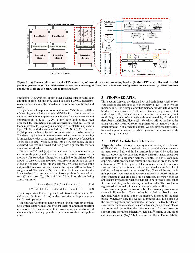
Figure 3(a) shows the configurable interconnect used in our de-sign. It can be visualized as a collection of switches, similar toa barrel shifter, which connects the bitlines of the two blocks. bnand b′n are bitlines coming into and going out of the interconnectrespectively. The select signals, sn control the amount of shift. Theseinterconnects can connect cells with different bitlines together. Forexample, they can connect bn,bn+1,bn+2, ... incoming bitlines to, say,b′n+4,b
′n+5,b
′n+6, ... outgoing bitlines, respectively, hence enabling
the flow of current between the cells on different bitlines of blocks.This kind of a structure makes shifting operations energy efficientand fast, having the latency same as that of a normal copy operation.It also allows for inter-column MAGIC NOR operations between thetwo blocks. If inputs are stored on nth bitline of one block, the outputof NOR operation can be stored on, say, (n+4)th bitline of anotherblock. This can be extended to multiple NOR operations in parallel.The shift select signals, sn, are controlled by the memory controllerpresent at the periphery of memory unit. It is important to note thatall of these blocks still share the same row and column controllersand decoders. So, the area and logic overhead introduced by theproposed memory unit is restricted to the interconnect circuit and itscontrol logic.
3.4 APIM ApproximationThe individual additions in the final stage cannot occur in parallelsince they require the propagation of carry in order to generate the
0 0.2 0.4 0.6 0.8 1 1.2 1.4 1.6 1.8 2
x 10−16
10−20
10−15
10−10
10−5
100
105
EDP (J.s × 10−16
)
% E
rror
(Log S
cale
)
Last Stage Approximation
First Stage Approximation
Low Accuracy
Computation High Accurate
Computation
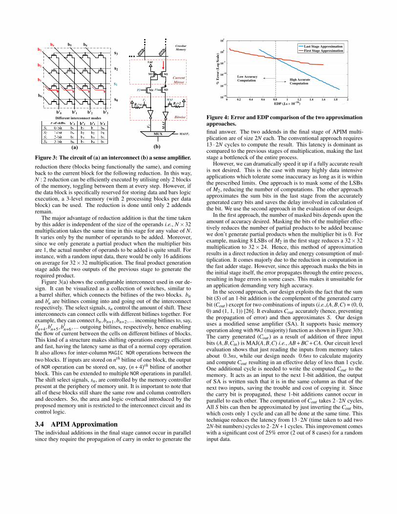
Figure 4: Error and EDP comparison of the two approximationapproaches.final answer. The two addends in the final stage of APIM multi-plication are of size 2N each. The conventional approach requires13 · 2N cycles to compute the result. This latency is dominant ascompared to the previous stages of multiplication, making the laststage a bottleneck of the entire process.
However, we can dramatically speed it up if a fully accurate resultis not desired. This is the case with many highly data intensiveapplications which tolerate some inaccuracy as long as it is withinthe prescribed limits. One approach is to mask some of the LSBsof M2, reducing the number of computations. The other approachapproximates the sum bits in the last stage from the accuratelygenerated carry bits and saves the delay involved in calculation ofthe bit. We use the second approach in the evaluation of our design.
In the first approach, the number of masked bits depends upon theamount of accuracy desired. Masking the bits of the multiplier effec-tively reduces the number of partial products to be added becausewe don’t generate partial products when the multiplier bit is 0. Forexample, masking 8 LSBs of M2 in the first stage reduces a 32×32multiplication to 32× 24. Hence, this method of approximationresults in a direct reduction in delay and energy consumption of mul-tiplication. It comes majorly due to the reduction in computation inthe fast adder stage. However, since this approach masks the bits inthe initial stage itself, the error propagates through the entire process,resulting in huge errors in some cases. This makes it unsuitable foran application demanding very high accuracy.
In the second approach, our design exploits the fact that the sumbit (S) of an 1-bit addition is the complement of the generated carrybit (Cout ) except for two combinations of inputs (i.e.,(A,B,C) = (0, 0,0) and (1, 1, 1)) [26]. It evaluates Cout accurately (hence, preventingthe propagation of error) and then approximates S. Our designuses a modified sense amplifier (SA). It supports basic memoryoperation along with MAJ (majority) function as shown in Figure 3(b).The carry generated (Cout ) as a result of addition of three inputbits (A,B,Cin) is MAJ(A,B,C) i.e., AB+BC+CA. Our circuit levelevaluation shows that just reading the inputs from memory takesabout 0.3ns, while our design needs 0.6ns to calculate majorityand compute Cout resulting in an effective delay of less than 1 cycle.One additional cycle is needed to write the computed Cout to thememory. It acts as an input to the next 1-bit addition, the outputof SA is written such that it is in the same column as that of thenext two inputs, saving the trouble and cost of copying it. Sincethe carry bit is propagated, these 1-bit additions cannot occur inparallel to each other. The computation of Cout takes 2 ·2N cycles.All S bits can then be approximated by just inverting the Cout bits,which costs only 1 cycle and can all be done at the same time. Thistechnique reduces the latency from 13 ·2N (time taken to add two2N-bit numbers) cycles to 2 ·2N+1 cycles. This improvement comeswith a significant cost of 25% error (2 out of 8 cases) for a randominput data.

32M 64M 128M 256M 512M 1G0
10
20
30
40
Dataset Size
En
ergy I
mp
rovem
ent
(GP
U=
1)
0
2
4
6
8
Sp
eed
up
(G
PU
=1)
(a) Sobel
32M 64M 128M 256M 512M 1G0
10
20
30
40
Dataset Size
En
ergy I
mp
rovem
ent
(GP
U=
1)
0
2
4
6
8
Sp
eed
up
(G
PU
=1)
(b) Robert
32M 64M 128M 256M 512M 1G0
10
20
30
40
Dataset Size
En
ergy I
mp
rovem
ent
(GP
U=
1)
0
2
4
6
8
Sp
eed
up
(G
PU
=1)
(c) FFT
32M 64M 128M 256M 512M 1G0
10
20
30
40
Dataset Size
En
ergy I
mp
rovem
ent
(GP
U=
1)
0
2
4
6
8
Sp
eed
up
(G
PU
=1)
(d) DwtHaar1DFigure 5: Energy consumption and speedup of exact APIM normalized to GPU vs different dataset sizes.
The accuracy can be improved substantially by approximatingjust a part of the final product while accurately calculating the rest ofthe product. The design improves accuracy by dividing the productinto two groups of size k and m bits such that k+m = 2N. The kbits are calculated using the conventional approach which consumes13k cycles and produces k accurate bits in the product. On the otherhand, m bits are approximated using the technique described above,which takes a total of 2m+ 1 cycles. This increases the accuracysince the k accurate bits are generally the most significant bits andany error in the m least significant bits has less effect on the result,as shown in Section 4.3. The proposed technique implements thefinal stage with a latency of 13k+ 2m+ 1 cycles. The appropriatevalues of k and m depend upon the application in hand. Section 4.3talks about different applications and selecting these values in orderto obtain acceptable results.
While approximation in the last stage reduces the latency, it isstill slower that the first approach in which approximation is done inthe first stage. The first approach is more energy efficient too since itreduces the size of multiplication and uses less resources. However,unlike the first approach, second approach introduces error only inthe final stage of the process. This approach can thus achieve verylow error rates making it suitable for applications requiring preciseresults. Figure 4 presents a comparison between the two approachesfor 32×32 multiplication. While, approximation in the first stageis convenient for error tolerant applications, approximation in thelast stage can guarantee very high accuracies for similar EDPs. Forexample, for 32×32 multiplication and an EDP of 1.4×10⁻¹⁶, theerror rate for the second approach is less by 5 orders of magnitudeas compared to the first approach.
4 RESULTS4.1 Experimental SetupWe compare the efficiency of the proposed APIM design with state-of-the-art processor AMD Radeon R9 390 GPU with 8GB memory.In order to avoid the disk communication in the comparison, all thedata used in the experiments is preloaded into 64GB, 2.1GHz DDR4DIMMs. We used Hioki 3334 power meter to measure the powerconsumption of GPU. We implement the APIM functionality bychanging the multi2sim [27], cycle-accurate CPU-GPU processor.Performance and energy consumption of proposed hardware areobtained from circuit level simulations for a 45nm CMOS processtechnology using Cadence Virtuoso. We use VTEAM memristormodel [28] for our memory design simulation with RON and ROFFof 10kΩ and 10MΩ respectively.
We compare the efficiency of APIM and GPU by running sixgeneral OpenCL applications including: Sobel, Robert, Fast Fouriertransform (FFT), DwHaar1D, Sharpen and Quasi Random. For im-age processing we use random images from Caltech 101 [29] library,while for non-image processing applications inputs are generated
randomly. Majority of these applications consists of additions andmultiplications. The other common operations such as square roothas been approximated by these two functions in OpenCL code. Toevaluate the computation accuracy in approximate mode, our frame-work compares the approximate output file of each application withthe golden output from calculating exactly. For image processing ap-plications, we accept 30dB peak signal-to-noise ratio as an accuracymetric. For other applications, the acceptable accuracy is definedby having less than 10% average relative error. To find a properlevel of accuracy, our framework computes APIM at the maximumlevel of approximation (32 relax bits). In case of large inaccuracy,it increases the level of accuracy in 4-bit steps until ensuring theacceptable quality of service.
4.2 Exact APIM & Dataset SizeFigure 5 shows the energy savings and performance improvementsof running applications on APIM exact, normalized to GPU energyand performance. For each application, the size of input datasetincreases from 1Kb to 1GB. In traditional cores, the energy andperformance of computation consists of two terms: computationand data movement. In small dataset (˜KB), the computation costis dominant, while running applications with large datasets (˜GB),the energy and performance of consumption are bound by the datamovement rather than computation cost. This data movement is dueto small cache size of transitional core which increases the numberof cache miss. Consecutively, this degrades the energy consumptionand performance of data movement between the memory and caches.In addition, large number of cache misses, significantly slows downthe computation in traditional cores. In contrast, in proposed APIMarchitecture the dataset is already stored in the memory and com-putation is major cost. Therefore, regardless of dataset size (thedataset can fit on APIM), the APIM energy and performance ofincreases linearly by the dataset size. Although the memory-basedcomputation in the APIM is slower than transitional CMOS-basedcomputation (i.e. floating point units in GPU), in processing thelarge dataset, the APIM works significantly faster than GPU. Interms of energy, the memory-based operations in APIM is moreenergy efficient than GPU. Our evaluation shows that for most appli-cations using datasets larger than 200MB (which is true for manyIoT applications), APIM is much faster and more energy efficientthan GPU. With 1GB dataset, the APIM design can achieve 28×energy savings, 4.8× performance improvement as compared toGPU architecture.
Figure 6 compares the performance efficiency of the proposeddesign with the state-of-the-art prior work [24, 25]. The work in [24]computes addition in-memory using MAGIC logic family, while thework in [25] uses the complementary resistive switching to performaddition inside the crossbar memory. Our evaluation comparingthe energy and performance of addition of N operands of lengthN bits each shows that the APIM can achieve at least 2× speed

Table 1: Quality of loss and EDP improvement of the proposed APIM compared to GPU in different level of approximation.
Applications 0 bit 4 bits 8 bits 16 bits 24 bits 32 bitsEDP Imp. QoL EDP Imp. QoL EDP Imp. QoL EDP Imp. QoL EDP Imp. QoL EDP Imp. QoL
Sobel 94× 0% 164× 1.3% 235× 3.1% 305× 6.9% 376× 11.4% 446× 15.6%Robert 177× 0% 311× 1.2% 444× 2.9% 577× 4.8% 711× 6.8% 844× 9.1%FFT 203× 0% 356× 2.2% 509× 3.7% 662× 5.8% 815× 8.6% 968× 13.5%
DwHaar1D 90× 0% 157× 0.9% 225× 2.6% 293× 5.7% 361× 7.9% 428× 10.6%Sharpen 104× 0% 149× 3.4% 206× 5.1% 273× 8.1% 340× 12.5% 410× 18.4%QuasiR 69× 0% 127× 2.1% 198× 3.5% 258× 5.8% 310× 9.3% 386× 15.7%
(a11asuu[uP18Ba-dBC1a-eBC1a-e
a aB
!"
#
]3]
]3-
]3d
]3e
a a0'#a@9
e N ]- ]4 -3 -e -N d-
Figure 6: Performance comparison of the proposed design withprevious work for addition of N operands, each sized N bitsup compared to previous designs in exact mode. APIM can be atleast 6× faster with 99.9% accuracy. The proposed design is evenbetter since the calculations for previous work do not include thelatency involved in shift operations. This improvement comes atthe expense of the overhead of interconnect circuitry and its controllogic. However, the next best adder, i.e., the PC-Adder [25] usesmultiple arrays each having different wordline and bitline controllers,introducing a lot of area overhead. This overhead is not present inour design since all the blocks share the same controllers.
4.3 Approximate APIMTable 1 shows the energy consumption and performance of theapplications running on APIM in different approximation level. Aswe explained in Section 3.4, APIM approximates m least significantbits of the product in the final product generation stage. The valueof m has an important impact on the computation accuracy andperformance of multiplication in APIM design. As Table 1 shows,large number of approximate LSBs (m) significantly improve energy-delay product of APIM, at the expense of increased computationinaccuracy. Similarly, small m makes the computation more accuratewith small benefit. We observed that different applications satisfy therequired accuracy for different values of m. Therefore, our designdetects the application at runtime and then sets the pre-calculatedvalue of m that is obtained offline to ensure the acceptable qualityof computation. Using this adaptive design, our design can achieve480× energy-delay product improvement as compared to APIM inthe exact mode.
5 CONCLUSIONIn this paper, we propose a configurable processing in-memory archi-tecture which enables addition and multiplication operations insidethe memory, while storing data. The design addresses the ineffi-ciency involved in moving data by enabling computations withinmemory. The performance of the design is further enhanced byapproximating results with high accuracies. Our evaluation showsthat increasing the dataset size significantly improves the energyefficiency of APIM. In addition, by enabling tunable approximationduring the runtime, our design can tune the level of approximationto trade energy/performance with accuracy. Our evaluation running
four OpenCL application shows that in approximate mode (exactmode), the APIM can achieve up to 480× (123×) energy-delayproduct improvement compared to recent GPU architecture ensuringthe acceptable quality of service.
6 ACKNOWLEDGMENTThis work was supported by NSF grant #1527034 and Jacobs Schoolof Engineering UCSD Powell Fellowship.
REFERENCES[1] J. Gubbi et al., “Internet of things (IoT): A vision, architectural elements, and
future directions,” Future Generation Computer Systems, vol. 29, no. 7, pp. 1645–1660, 2013.
[2] M. Samragh et al., “Looknn: Neural network with no multiplication,” inIEEE/ACM DATE, 2017.
[3] K. Hwang et al., Distributed and cloud computing: from parallel processing tothe internet of things. Morgan Kaufmann, 2013.
[4] R. Balasubramonian et al., “Near-data processing: Insights from a micro-46workshop,” Microarchitecture, vol. 34, no. 4, pp. 36–42, 2014.
[5] G. Loh et al., “A processing-in-memory taxonomy and a case for studying fixed-function pim,” in WoNDP, 2013.
[6] M. Imani et al., “Mpim: Multi-purpose in-memory processing using configurableresistive memory,” in IEEE ASP-DAC, pp. 757–763, IEEE, 2017.
[7] S. Pugsley et al., “Comparing implementations of near-data computing with in-memory mapreduce workloads,” Microarchitecture, vol. 34, no. 4, pp. 44–52,2014.
[8] A. M. Aly et al., “M3: Stream processing on main-memory mapreduce,” in ICDE,pp. 1253–1256, IEEE, 2012.
[9] J. Han et al., “Approximate computing: An emerging paradigm for energy-efficient design,” in ETS, pp. 1–6, IEEE, 2013.
[10] M. Imani et al., “Efficient neural network acceleration on gpgpu using contentaddressable memory,” in IEEE/ACM DATE, 2017.
[11] M. Imani et al., “Resistive configurable associative memory for approximatecomputing,” in DATE, pp. 1327–1332, IEEE, 2016.
[12] V. Gupta et al., “Impact: imprecise adders for low-power approximate computing,”in ISLPED, pp. 409–414, IEEE, 2011.
[13] M. Imani et al., “Masc: Ultra-low energy multiple-access single-charge tcam forapproximate computing,” in IEEE/ACM DATE, pp. 373–378, IEEE, 2016.
[14] Q. Guo et al., “Ac-dimm: associative computing with stt-mram,” in ISCA, vol. 41,pp. 189–200, ACM, 2013.
[15] Q. Guo et al., “A resistive tcam accelerator for data-intensive computing,” inMicroarchitecture, pp. 339–350, ACM, 2011.
[16] M. Imani et al., “Exploring hyperdimensional associative memory,” in IEEEHPCA, IEEE, 2017.
[17] X. Yin et al., “Design and benchmarking of ferroelectric fet based tcam,” inIEEE/ACM DATE, IEEE, 2017.
[18] J. Borghetti et al., “A hybrid nanomemristor/transistor logic circuit capable ofself-programming,” PNAS, vol. 106, no. 6, pp. 1699–1703, 2009.
[19] M. Imani et al., “Acam: Approximate computing based on adaptive associativememory with online learning,” in IEEE/ACM ISLPED, pp. 162–167, 2016.
[20] L. Yavits et al., “Resistive associative processor,” IEEE Computer ArchitectureLetters, vol. 14, no. 2, pp. 148–151, 2015.
[21] J. Borghetti et al., “Memristive switches enable stateful logic operations viamaterial implication,” Nature, vol. 464, no. 7290, pp. 873–876, 2010.
[22] S. Kvatinsky, G. Satat, N. Wald, E. G. Friedman, A. Kolodny, and U. C. Weiser,“Memristor-based material implication (IMPLY) logic: design principles andmethodologies,” TVLSI, vol. 22, no. 10, pp. 2054–2066, 2014.
[23] S. Kvatinsky et al., “MAGIC – memristor-aided logic,” TCAS II, vol. 61, no. 11,pp. 895–899, 2014.
[24] N. Talati et al., “Logic design within memristive memories using memristor-aidedloGIC (MAGIC),” IEEE TNano, vol. 15, pp. 635–650, jul 2016.
[25] A. Siemon et al., “A complementary resistive switch-based crossbar array adder,”JETCAS, vol. 5, no. 1, pp. 64–74, 2015.
[26] V. Gupta et al., “Low-power digital signal processing using approximate adders,”TCAD, vol. 32, no. 1, pp. 124–137, 2013.
[27] R. Ubal et al., “Multi2sim: a simulation framework for cpu-gpu computing,” inPACT, pp. 335–344, ACM, 2012.
[28] S. Kvatinsky et al., “Vteam: a general model for voltage-controlled memristors,”TCAS II, vol. 62, no. 8, pp. 786–790, 2015.
[29] “Caltech Library.” http://www.vision.caltech.edu/Image Datasets/Caltech101/.