The use of nanotube structures in reducing the turn-on voltage in micro-discharges and micro-gas...
15
The use of nanotube structures in reducing the turn-on voltage in micro-discharges and micro-gas sensors. Mark Tweedie 1 , Navneet Soin 1 , Puja Kumari 1 , Susanta S. Roy 1 , Ashish Mathur 1 , Charles Mahony 1 , Pagona Papakonstantinou 1 , James A. D. McLaughlin 1,2 1.Nanotechnology and Integrated BioEngineering Centre (NIBEC), University of Ulster, Shore Road, Newtownabbey, Belfast, Co. Antrim, BT37 0QB. 2.Sensor Technology and Devices (ST&D) Ltd., 4, Heron Road, Belfast, Co. Antrim, BT3 9LE. ABSTRACT This paper will evaluate the usefulness of two nanostructuring techniques in order to grow low turn-on voltage electrodes for use in micro-discharge plasma applications such as the ST+D Ltd e-nose device. These devices are based on micro- plasma technology and currently operate at around 150V (at 10 -2 Torr) or 3KV at atmosphere utilising a propriety power source. The application of such technology is the qualitative and qualitative detection of NOx with detection capabilities as low as 5 parts per billion. The e-nose patented device has undergone basic trials in a clinical environment and it is currently demonstrating 50ppb sensitivities, with an ultimate aim of moving this to parts per trillion. Keywords: Carbon nanotubes, ZnO nanotubes, nanostructures, nanoneedles, micro-plasma, micro-discharge, gas sensor, electronic nose. 1. INTRODUCTION In recent years there has been increasing interest in artificial or electronic nose applications [1, 2], for identification and quantification of a range of gases in the exhaled breath of patients for diagnosis of medical conditions. Acetone, for example, is medically important in the diagnosis of several pathologies [3], and nitric oxide is believed to be useful in the correct diagnosis of asthma, this being still problematic [4]. Naturally, comparisons are needed in preliminary clinical evaluations of prototype equipment, between known healthy and asthmatic subjects. Gas discharge spectroscopy can be a very useful technique as it provides a large amount of quantitative and qualitative information concerning the composition of the gas sample. Moreover, spectral data are suitable for advanced chemometric techniques, which can be very powerful for associative analytical tasks [5-8]. This paper examines the use of a prototype micro-plasma gas discharge device, or electronic nose, for nitric oxide measurement by optical spectroscopy of the plasma, for a preliminary sample of subjects, and then explores how the device may be improved by nanostructuring the cathode, so allowing lower turn-on voltages, with higher maximum operating current. Such improvements potentially increase the dynamic range of the device, and so allow greater sensitivity to low concentrations of gas analytes. The nanostructuring concentrates the electric field at the tip of the nanostructures, such as carbon nanotubes (CNTs), or ZnO nanoneedles, and this is expected to yield lower turn-on voltages compared to microstructured metal tips, since the electric field density is higher. Anode nanostructuring using CNTs has been demonstrated for gas ionization detection in conjunction with a gas chromatograph to separate the sample component gases prior to detection [9]. The advantage of using plasma spectroscopy is that sample component separation by gas chromatography is not required prior to detection, making the device more suitable for healthcare use. The techniques used to achieve nanostructuring of the cathode are described, images of the nanostructures are shown, and test results, using the nanostructures in a test rig in vacuum, showing improved breakdown voltages are presented. Consideration is, also, given to optimization of the plasma electrical bias, and the problems associated with plasma ablation of nanostructures is discussed. Also, presented is a novel planarisation technique for removing catalyst from CNT tips, and opening the tops of the nanotubes, which promises to permit a greater operating current per nanotube, with potential improvements in device sensitivity. Invited Paper Carbon Nanotubes and Associated Devices, edited by Manijeh Razeghi, Didier Pribat, Young Hee Lee Proc. of SPIE Vol. 7037, 70370Z, (2008) · 0277-786X/08/$18 · doi: 10.1117/12.799592 Proc. of SPIE Vol. 7037 70370Z-1 2008 SPIE Digital Library -- Subscriber Archive Copy
Transcript of The use of nanotube structures in reducing the turn-on voltage in micro-discharges and micro-gas...

The use of nanotube structures in reducing the turn-on voltage in micro-discharges and micro-gas sensors.
Mark Tweedie1, Navneet Soin1, Puja Kumari1, Susanta S. Roy1, Ashish Mathur1, Charles Mahony1,
Pagona Papakonstantinou1, James A. D. McLaughlin1,2 1.Nanotechnology and Integrated BioEngineering Centre (NIBEC), University of Ulster, Shore
Road, Newtownabbey, Belfast, Co. Antrim, BT37 0QB. 2.Sensor Technology and Devices (ST&D) Ltd., 4, Heron Road, Belfast, Co. Antrim, BT3 9LE.
ABSTRACT
This paper will evaluate the usefulness of two nanostructuring techniques in order to grow low turn-on voltage electrodes for use in micro-discharge plasma applications such as the ST+D Ltd e-nose device. These devices are based on micro-plasma technology and currently operate at around 150V (at 10-2 Torr) or 3KV at atmosphere utilising a propriety power source. The application of such technology is the qualitative and qualitative detection of NOx with detection capabilities as low as 5 parts per billion. The e-nose patented device has undergone basic trials in a clinical environment and it is currently demonstrating 50ppb sensitivities, with an ultimate aim of moving this to parts per trillion.
Keywords: Carbon nanotubes, ZnO nanotubes, nanostructures, nanoneedles, micro-plasma, micro-discharge, gas sensor, electronic nose.
1. INTRODUCTION
In recent years there has been increasing interest in artificial or electronic nose applications [1, 2], for identification and quantification of a range of gases in the exhaled breath of patients for diagnosis of medical conditions. Acetone, for example, is medically important in the diagnosis of several pathologies [3], and nitric oxide is believed to be useful in the correct diagnosis of asthma, this being still problematic [4]. Naturally, comparisons are needed in preliminary clinical evaluations of prototype equipment, between known healthy and asthmatic subjects. Gas discharge spectroscopy can be a very useful technique as it provides a large amount of quantitative and qualitative information concerning the composition of the gas sample. Moreover, spectral data are suitable for advanced chemometric techniques, which can be very powerful for associative analytical tasks [5-8].
This paper examines the use of a prototype micro-plasma gas discharge device, or electronic nose, for nitric oxide measurement by optical spectroscopy of the plasma, for a preliminary sample of subjects, and then explores how the device may be improved by nanostructuring the cathode, so allowing lower turn-on voltages, with higher maximum operating current. Such improvements potentially increase the dynamic range of the device, and so allow greater sensitivity to low concentrations of gas analytes. The nanostructuring concentrates the electric field at the tip of the nanostructures, such as carbon nanotubes (CNTs), or ZnO nanoneedles, and this is expected to yield lower turn-on voltages compared to microstructured metal tips, since the electric field density is higher. Anode nanostructuring using CNTs has been demonstrated for gas ionization detection in conjunction with a gas chromatograph to separate the sample component gases prior to detection [9]. The advantage of using plasma spectroscopy is that sample component separation by gas chromatography is not required prior to detection, making the device more suitable for healthcare use.
The techniques used to achieve nanostructuring of the cathode are described, images of the nanostructures are shown, and test results, using the nanostructures in a test rig in vacuum, showing improved breakdown voltages are presented. Consideration is, also, given to optimization of the plasma electrical bias, and the problems associated with plasma ablation of nanostructures is discussed. Also, presented is a novel planarisation technique for removing catalyst from CNT tips, and opening the tops of the nanotubes, which promises to permit a greater operating current per nanotube, with potential improvements in device sensitivity.
Invited Paper
Carbon Nanotubes and Associated Devices, edited by Manijeh Razeghi, Didier Pribat, Young Hee Lee Proc. of SPIE Vol. 7037, 70370Z, (2008) · 0277-786X/08/$18 · doi: 10.1117/12.799592
Proc. of SPIE Vol. 7037 70370Z-12008 SPIE Digital Library -- Subscriber Archive Copy

Recognition System
Gas 1
Gas 2 Spectrum
2. BACKGROUND INFORMATION The electronic nose system developed by the University of Ulster, as part of a multi-partner EU funded project (DesygnIt), with input from ST&D Ltd., consists of an addressable plasma device, with up to 100 plasma nodes, where the optical spectrum of the plasma is captured by a CCD spectrometer. A general schematic is shown in Fig. 2, where it is illustrated that the optical spectrum is analysed by custom algorithms for peak recognition at predetermined wavelengths, relevant to the presence of specific gases, followed by the use of a self-training Artificial Neural Network to identify the gases present.
Due to the intricate nature of the underlying physical phenomena and the complexities involved in measuring the spectra, the interpretation of the resulting spectra is a non-trivial task. Artificial neural networks have been shown to be robust and reliable classifiers and pattern-recognisers in situations where data is complex and noisy [7]. Using an artificial neural network as classifier for the detection of gases in plasma emission spectra leads to the system architecture depicted in Fig 1.
Fig. 1 Schematic of the electronic nose microplasma system, with feature extraction, and Artificial Neural Network for
gaseous component identification.
3. EXPERIMENTAL SET-UP
3.1 The electronic nose prototype micro-plasma device.
The system has been designed in order to give the maximum possible flexibility. Fig. 2 shows the system hardware, highlighting the main parts.
HM2000
Val
ve
Pump
Mass FlowController
Mass FlowController
PlasmaDevice
Programmable MFCMKS 647B
Gas2
Gas1
DAQ
Spectrometer
DC
PressureGauge
AC
SpectraAcquisition
System
Gas FlowControl System
Driving CircuitEectronics
OpticalFibre
Electricalcable
Pipe
Proc. of SPIE Vol. 7037 70370Z-2

nasa
l ii 4
0
Figure 2 – Overall view of the electronic nose experimental set-up The overall hardware can be subdivided in four main subsystems: plasma device, gas flow control system, driving circuit electronics and spectra acquisition system, described as follows: (i) Plasma device - Using a standard photolithography process, two glass substrates coated with indium tin oxide (ITO) were patterned to give parallel lines of ITO strips forming the electrodes on each substrate. The ITO lines on the top glass substrate are orientated at right angles to those on the bottom, so that with 8 electrode lines per side, there are 64 overlapping pixels are present. The voltage can be applied to each single electrode line so that the plasma forms over the desired pixel. A spacer separates the two glass substrates and two holes were drilled in the top glass for the gas inlet and outlet (Fig. 3). Ni deposition on patterned ITO lines, as well as the finished electronic nose device, is shown in Fig. 4.
Fig. 3. 3D schematic of the three parts which form the micro chamber (plasma device). Black stripes are the electrodes and
the gas inlet and outlet are shown
Fig. 4. Ni patterned on ITO lines (left) and the electronic nose micro-plasma device (right). The spacer is made of a soft silicone rubber with vacuum adhesive applied on each side. This allows adequate sealing to reach the desired working pressure, although the silicone rubber displays some compressibility, which means that to achieve the same gap spacing, the same pressure must be maintained for each measurement. Electrical properties of the tin oxide strips have been measured and connections on the device are by means of flexible cables attached with clips. These connections have shown very good contact and strength. Optical input to the CCD spectrometer is achieved by positioning an optical fibre on one side of the device, over the electrode under test. (ii) Gas flow control system - The outlet of the plasma device is pumped with a rotary and differential vacuum pump. An on-line pressure gauge (a Baratron® capacitance manometer) and valve allow monitoring of the micro-chamber pressure. The pressure gauge has a full-scale range of 1000 mmHg with an accuracy of 0.25% of reading. The valve is needed to control the output flow to the pump so that the desired pressure can be maintained. The gas inlet of the device is piped to two mass flow controllers (MFCs), which regulate the mass and concentration of two different gases. A multichannel gas
Proc. of SPIE Vol. 7037 70370Z-3

flow and pressure controller controls the two MFCs and reads the pressure from the Baratron® manometer. This device allows entering flow set points and gas concentrations that will be kept automatically. (iii) Drive circuit electronics - The drive circuit (HM 2000 in Fig.2) can supply a voltage in the range of 0-700 Volts DC. When connected to a signal generator it can deliver AC signals oscillating in the range –300 to 300 Volts. It can control separately all the electrode strips and connect variable resistors (0-10 MΩ) in series to provide current limiting. The drive circuit has a PC interface, running LabView®, which allows the measurement of voltage applied, voltage at the device electrodes, and the current. The applied voltage is controllable either from the front panel of the HM 2000 or from the PC. A DAQ card with no output is used, so that the applied voltage has to be controlled manually. (iv) Spectra acquisition system - An optical fibre in close proximity to the plasma node at the device feeds the optical emission into a solid state spectrometer (PC1000 PC Plug-in Spectrometer by Ocean Optics). This is a miniature spectrometer that fits in standard ISA-bus slot of a PC. It has spectral range of 350-850 nm and a blaze wavelength at 500 nm. Software, OOIBase, is provided together with the spectrometer to acquire data and perform basic processing operations, such as background removal and signal integration. Some other functions, such as data smoothing, to filter out noise, are also possible. The spectrometer should be self-calibrated, but occasionally some line shift may occur. An additional calibration can be easily performed with the 632.8 nm line of a helium neon laser.
Optical emission spectral lines are not discrete, but have a shape and width determined by the different processes taking place in the plasma. The resolving power of the spectrometer and the entrance slit affect linewidth and line shape. As well as the resolution limit of the spectrometer, there are also line broadening effects in the plasma. At high density, the broadening is due to more frequent collisions, this being known as pressure broadening. A high ion population also leads to radiation from atoms which perturb the system by means of the Stark effect. Furthermore, the broadening of discrete transitions may occur, due to Zeeman effect, which involves interactions with the magnetic field. Finally, the Doppler effect causes a broadening of the lines which arises from the high velocities of the particles in the plasma.
The discussion of some of the physics involved in steady state plasmas has illustrated the complexities of the underlying phenomena. Emission from plasma involves a variety of factors; radiation itself depends on parameters such as plasma density, temperature, and even the geometry of the vacuum chamber. Due to the number of factors involved, and their interdependency, the interpretation of the resulting plasma optical emission spectra is a non-trivial task. Therefore, additional processing, via feature extraction, and an artificial neural network, is required to correctly identify the gaseous components with sufficient accuracy.
3.2 Growth and characterization equipment for CNTs and ZnO. A Microwave Plasma CVD (MPCVD) system, is available for growing vertically aligned CNTs, using feed gases such as Methane – it, also, has an Ultra High Vacuum (UHV) Electron Cyclotron Resonance (ECR) mode (which will be relevant later). Furthermore, a Field Emission test system has been designed and built at UU, for testing of the field emission enhancement factor, β, produced by various different nanostructured materials – both types of equipment are shown in Fig. 5.
Fig. 5 MPCVD reactor for vertically aligned CNT growth (left), with Field Emission system (centre) and a close-up of the anode-cathode adjustable gap for field emission testing (right).
Proc. of SPIE Vol. 7037 70370Z-4

hodehdd
uI - - - -
:pee1ov,
A test rig was built for operation in a purpose-built vacuum chamber, having suitable electrical lead-throughs, for testing of microplasma currents, and breakdown voltages, and for plasma electrical bias optimization, using nanostructured cathodes, compared to unstructured cathodes. A schematic diagram is shown below, in Fig 6, followed by an annotated image of the test rig. The anode to cathode separation is controlled by adjustment of the fine pitch screw which forms the anode.
Fig. 6. Schematic diagram of the test rig (left), with actual image (right) for nanostructured cathode testing.
4. METHODOLOGY
There are several different methodologies associated with the electronic nose project, firstly, testing of the prototype device for nitric oxide measurement, then growth of CNT and ZnO samples, and testing of the breakdown voltage and field emission characteristics, and plasma optimization in a test rig designed for use in a vacuum system, with nanostructured cathodes. 4.1 Asthma diagnosis tests with the prototype electronic nose device.
Asthmatic subjects and healthy subjects were asked to breathe into balloons. The collected respiration gases were then conveyed into the micro-chamber through the mass flow controller. Flow rate was set to 0.8 sccm for Argon and 20 sccm for breath samples. Initially, sets of respiration gases were taken from one severe asthmatic patient, a mild asthmatic patient and a healthy subject. Differences are clearly shown by the spectra – see Results.
4.2 Carbon nanotube growth
Co layers, of thickness between 0.5 nm to 5.0 nm, were sputter coated, in a Moorfield MiniLab, onto Si wafer
segments at room temperature. The thickness was monitored by an internal thickness gauge, during the deposition. A check on a 50 nm test sample, as measured by the thickness gauge, was made using a DekTak stylus profilometer, and found to be correct.
The samples were placed in the MPCVD chamber, on a Mo sample holder, and the stage temperature was raised to 700°C. A nitrogen plasma pre-treatment was used to break up the catalyst into nano-islands, to encourage the growth of good quality CNTs. Nitrogen was fed in at a flow rate of 20 sccm, for an initial chamber target pressure setting of 7 mTorr, and when this was reached, the flow rate was reduced to 10 sccm.
A forward plasma turn-on power of 230 – 250 W was required, with the reflected power back into the microwave transmission cavity manually tuned to near zero, using the 3-stub tuner. The target chamber pressure was then set to 20 mTorr, and the flow rate increased to 40 sccm.
The forward power was increased in stages to 850W, while continually tuning the reflected power to ~ zero, during 5 minutes of nitrogen plasma pre-treatment. Methane was then introduced at a flow rate of 10 sccm, with the nitrogen flow rate maintained at 40 sccm, and the pressure set point fixed at 20 mTorr. The growth period was timed from the moment of methane introduction. The MFC for methane was reset to zero at the desired end of the growth period.
Proc. of SPIE Vol. 7037 70370Z-5

An extra investigation was carried out into thermal growth of vertically aligned multi-walled CNTs from a gaseous source (Toluene), with a gaseous catalyst (Ferrocene), on bare Si and quartz, and with an additional Co catalyst also on Si. Reaction time was 20 minutes, and temperature was 750°C. Dense and long (up to 500 µm) vertically aligned CNT growth was observed, and imaged by SEM (see Results) –this is useful, particularly, for providing comparative CNT test samples for plasma breakdown testing, since thermal growth is relatively easily achieved, compared to MPCVD growth, the latter being critically dependent on catalyst pre-treatment for nano-islands formation. It is envisaged that deposition of an aligned gold layer in the interelectrode gaps, with ITO electrodes, followed by thermal CNT growth, then gold chemical etch, may provide a route to achieving patterned thermal CNT growth, aligned to the ITO electrodes.
4.3 ZnO nanostructure growth Thermal CVD equipment, with an alumina ceramic tube forming the reaction chamber, with the substrates centrally located therein, in quartz boats, and gases fed in from one end, and extracted from the other, was used for ZnO nanostructure growth experiments. ZnO nanoneedles were grown on gold-coated Si(100) substrates, and on patterned gold islands, at a growth temperature of approximately 960°C, by heating mixed ZnO and graphite powder in a flow of Ar, with the substrates downstream from the source powder mix. The graphite decomposes ZnO to Zn, and CO/CO2, with subsequent ZnO growth on the substrates. Successful ZnO nanoneedle growth was demonstrated – see Results.
4.4 Plasma and Field Emission testing of CNT and ZnO nanostructured cathodes. The test rig as described was used in a vacuum chamber, with the distance between the cathode and anode adjusted in advance by a fine pitch screw thread (1.25 mm per turn), where the screw formed the anode, and the cathode was fixed – for bulk samples, such as the planar Si control this was relatively easy, as the anode was advanced to make contact with the cathode, and then the screw thread backed off by the required angle to set the distance. Good control of the nanostructured cathode was exercised, to make sure that direct contact did not occur with the anode, to avoid damage to the nanostructures. (For example, calibrated shims may be used at the edge to confirm the distance after setting.) A circuit diagram for the test rig is shown in Fig. 7, where the measurement resistance, RM was 10KΩ (fixed) , the DC power supply, U, had a max. of 3KV , the ballast resistance RL was variable (0.5 – 3 MΩ) , and the cathode-anode distance is indicated as d.
Fig. 7. Circuit diagram for the CNT microplasma test rig. The base pressure was 3x10⁻² Torr, the working pressure was 1-50 Torr, and the gas was Argon. The ballast resistance was adjusted in a series of experiments, to determine the optimum value (see Results). The field emission measurements for CNTs were carried out in the purpose-built equipment shown previously. The Fowler-Nordheim equation was used to derive the field enhancement factors, β, from plotted graphs of Ln (J/E2) against 1/E, where J is the current density and E is the electric field, by applying a straight line fit to the data – note that often, there are 2 distinct gradients in the data, so that the data limits for the straight line fit have to be chosen manually, as can be seen in the results section.
Proc. of SPIE Vol. 7037 70370Z-6

J = ____/IV
The Fowler-Nordheim equation is represented as:
Note that to have comparison measurements for the CNTs, field emission was, also, measured from other nanostructures grown by MPCVD, such as carbon microcones (CMCs), and carbon nanowalls (CNWs). The data with derived field enhancement factors, β, are shown in Results.
5. RESULTS 5.1 Nitric oxide measurements for asthmatic versus non-asthmatic subjects.
Sample measurements for the three different cases of the severe asthmatic, a mild asthmatic, and a healthy individual are shown in fig. 4 – this illustrates a significantly detectable change around 391 nm, which is related to the change in nitric oxide concentration.
0
0.005
0.01
0.015
0.02
0.025
0.03
370 380 390 400 410 420 430Wavelength (nm)
Nor
mal
ised
Inte
nsity
(cou
nts)
Severe Asthmatic Mild Asthmatic Healthy
Figure 8. Spectral emission of respiration gas samples from a severe asthmatic, a mild asthmatic and a healthy subject.
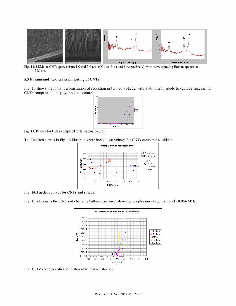
5.2 Catalyst patterning and CNT growth The following images show, respectively, Co islands on Si, CNTs on patterned Co on Si, self-assembled polystyrene nanospheres without and with metal catalyst, and partially vertically aligned CNTs grown from the nanoparticles remaining after the polystyrene beads are dissolved away – following these are images of Co nano-islands, formed by nitrogen plasma pre-treatment, the CNTs grown from these, and Raman spectra for the CNTs at 785nm, showing the disorder, D, and graphitic, G’, peaks.
Proc. of SPIE Vol. 7037 70370Z-7

Fig. 9. Co islands on Si, with vertically aligned CNTs grown on the Co islands
Fig. 10. Polystyrene nanospheres (left), with ~ 73 nm interbead gaps (where there are no dislocations), with Fe catalyst deposited on top of the nanospheres (centre), then CNTs grown from residual nano particles after the polystyrene bead template is removed (right).
Fig. 11. SEMs (top) and AFMs (bottom) of Co nanoparticles, for 0.5, 1.0, and 3.0nm Co thickness, respectively (left to right).
Proc. of SPIE Vol. 7037 70370Z-8
Wavenumber (cm-i) Wavenumber (cm-i)
//
Comparison of Paschen curves
• Si 200 microns
• CNl200microns
R61 MG
RM 10KG
CNTs BaseFressure 3xlO2TorrGas: Argon
03 035
650
2450
350
250
150 p-I0 0.05 0.1 0.15 0.2 0.25
Pd (Torr cm)
VI charact eristicsw ith duff Ball ast resistances
I .OOE-049.OOE-06 — x -8.OOE-06 — - ——7 ODE-OS . 8 . _____________
ci S4Mohm6.00 E-O6 —
• I 98 Mo h m
6.00 E-O6 — -———— 2.8 Mo h m
4 ODE-OS — — .448 Mo h m
8 8 8S4Mohm3.00 E-OS
2 ODE-OS ..-.— •..3o:: dbII230 240 280 280 270 280 290 300 310
Vcalhsde(V)
Fig. 12. SEMs of CNTs grown from 1.0 and 3.0 nm of Co on Si (a and b respectively), with corresponding Raman spectra at
785 nm. 5.3 Plasma and field emission testing of CNTs. Fig. 13 shows the initial demonstration of reduction in turn-on voltage, with a 50 micron anode to cathode spacing, for CNTs compared to the p-type silicon control.
Fig. 13. IV data for CNTs compared to the silicon control. The Paschen curves in Fig. 14 illustrate lower breakdown voltage for CNTs compared to silicon.
Fig. 14. Paschen curves for CNTs and silicon. Fig. 15. illustrates the effects of changing ballast resistance, showing an optimum at approximately 0.854 MΩs.
Fig. 15. IV characteristics for different ballast resistances.
Proc. of SPIE Vol. 7037 70370Z-9

Applied field (V/gm)
-3.0 -
-45
-6.0
-7.5
-9.0
-ias
-12.0
-ias
0.1
4248
p1=2094
CNTs= 690
p1 = 362
CNWs
0.2 0.3 0.4 0.5 0.6 0.7 0.8
l/E (xmN)
E j—
stft(-1)
&
11111 1111 TIll 4_BthJ—— #4'w9& øs1- 4—\. 0—
The lower breakdown voltage for CNTs compared to CMCs (Carbon Micro Cones) and CNWs (Carbon NanoWalls) is illustrated in figure 16, where CNTs show a clearly lower turn-on voltage.
Fig. 16. Emission current density versus apply field for CNTs, CMCs, and CNWs. Fowler-Nordheim curves for CNTs, CMCs, and CNWs are shown in figure 17 – the field enhancements factors, β1 and β2, for CNTs are significantly higher than for CMCs and CNWs.
Fig. 17. Fowler-Nordheim curves for CNTs, CMCs, and CNWs. 5.4 Plasma ablation of CNTs It became apparent that the nanotubes are quickly damaged by plasma ablation, since they are in very close proximity to the plasma, in the micro-plasma device. The CNTs can only survive for a matter of seconds, which means that spectra optical must be acquired quickly in a functioning device, and that the electrodes must be poled to progressively move from one plasma node to the other, for sequential measurements. Sample images of CNTs before and after use in the micro-plasma device, with associated Raman spectra, are shown below. The Raman spectra at 514.5 nm confirm that the CNTs are more disordered after plasma exposure – see Fig. 18.
Fig. 18 SEM images of CNTs before (left) and after (centre) use in the micro-plasma device, with associated Raman spectra (right).
Proc. of SPIE Vol. 7037 70370Z-10

* 4S S• *..• * — S *a • a * a -a * a* S a a a —• a • • -* a a * - - aa a S * - aS a a a -a - a -a aa 5 a* S a a S* a a • •
SE 06-6b--07 60530 W011.2 5.0kv ,SOk S0S1
2 ntn
5.6 ZnO nanostructure growth A range of partially vertically aligned thermally grown ZnO nanotubes were produced, with diameters ranging from ~ 30 nm in some samples, to ~ 90 nm or more in other samples, as shown in the SEMs in Fig19. Growth of ZnO nanostructures on patterned gold is shown in Fig. 20, where the nanoneedles show an interplanar distance of 0.25 nm (Fig. 21) – nanowires can, also, be seen at the tip of the nanoneedles (Fig. 22).
Fig 19. SEM images of thermally grown ZnO nanotubes.
Fig. 20. SEMs of PLD patterned gold (left), and ZnO nanostructures grown on the gold islands.
Fig. 21. TEM (left) and HRTEM (right) of ZnO nanostructures, where the latter shows an inter-planar distance of
0.25 nm.
Fig. 22. SEMs of ZnO nanoneedles with nanowires at the tip.
Proc. of SPIE Vol. 7037 70370Z-11

0.10
008
000
004
0E002 II
1
Electric Field (V/urn)
In (JIE 2)
a28730.12 0.16 0.20 0.24 0.26 0.32
lIE
Q&t
C--SiSi
5.7 Plasma and field emission testing of ZnO nanostructures Electric fields turn-on value of 5.07 V/µm is illustrated in fig. 23 for ZnO nanostructures, while the Fowler-Nordheim curves in Fig. 24 show high values of the field enhancement factor, β, similar to those seen for vertically aligned CNTs.
Fig. 23. Current density vs. Electric field for ZnO nanostructures.
Fig. 24. Fowler-Nordheim data for ZnO nanostructures.
5.8 Thermal CVD growth of long vertically aligned CNTs with gaseous catalyst. Several hundred micron lengths of dense vertically aligned CNTs were produced, on Si, quartz, and Co-on-Si, as follows, with the Raman spectra confirming that the grown structures have CNT characteristics in all cases.
Fig. 25. Thermal CVD CNT growth from vapour phase catalyst on Si (left), and Quartz (centre), with Raman spectra (right). 5.9 Catalyst removal and CNT nanotube opening by ECR planarization. The process of catalyst removal and nanotube opening by removing the tips of the CNTs, was realized by planarising the CNTs in ECR mode, as shown in fig.26.
Proc. of SPIE Vol. 7037 70370Z-12

Fig. 26. CNTs before planarization (left), with metal catalyst present, and afterwards (right), with the CNTs clearly opened.
6. DISCUSSION
Firstly, regarding the asthma diagnostic assessment, the severe asthmatic subject presents a very high peak around 390 nm. At the same wavelength the spectrum related to the mild asthmatic has a lower peak and the lowest value (trough) is for the healthy subject’s spectrum. Considering that in this spectral range nitrogen-related peaks can be usually found, the results would tend to confirm the relationship between exhaled nitric oxide and asthma (atomic nitrogen is originated by nitric oxide dissociation) [4]. Consequently, the technique presented seems to be suitable for asthma diagnosis. It is believed that a more accurate sample acquisition together with clinical details of the subjects would enhance the diagnostic potential in a clinical environment [5-8]. (As with all medical devices, the diagnosis is made and confirmed by the clinician, by assessing the test results, and patient clinical history with current presentation, together – no single test device yields a single definitive diagnosis by itself.)
Secondly, it has been demonstrated that vertically aligned CNTs may be grown by MPCVD, from catalyst patterned by photolithography, and by templating using polystyrene nanospheres. Nitrogen plasma catalyst pre-treatment has been shown to create sufficient small nano-islands for nucleation of vertically aligned CNT growth in MPCVD. These multi-walled CNT samples have been shown to have good field emission enhancement factors, averaging ~ 3000, similar to single-walled CNTs, and to give lower breakdown voltage in micro-gas plasmas, as anticipated. The multi-walled CNTs have, also, been shown to be measurably superior to CMCs and CNWs regarding lowering the breakdown voltage, and similarly superior in terms of field enhancement factors. Thermal growth of several hundred micron length, dense, vertically aligned multi-walled CNTs was, also, demonstrated, using a gaseous source (toluene) and gaseous catalyst (ferrocene), on various substrates. This could be useful for providing alternative CNT samples, for comparative analysis. Further, patterned vertically aligned thermal CNT growth should be possible, if, for example, interelectrode gaps are covered by gold, in a second mask process, using aligned photolithography. The CNTs will grow predominantly on the exposed ITO, and to a much lesser extent on the gold, but chemical etch of the gold should lift off any CNTs there, leaving the CNTs patterned on the ITO electrodes. Furthermore, thermal growth of ZnO on both unpatterned and patterned gold-on-Si has been demonstrated to yield nanotubes, and nanoneedles. The turn-on voltage for the ZnO nanostructures is higher than expected at about 5.1 V/µm, but the field enhancement factors, averaging ~ 3500, are again similar to single walled CNTs, and to the multi-walled CNTs tested here. Ballast resistance variation was investigated for the micro-plasma test device. It was shown that the resistance could be optimized to give a significantly greater operating current range for the device. CNT ablation has been observed due to the close proximity of the micro-plasma. Realistically, this implies that there can only be one diagnostic test per node in the electronic nose device, when using a nanostructured cathode, so obviously,
Proc. of SPIE Vol. 7037 70370Z-13

ItIb
the more nodes incorporated within the device the better. This may imply some mm scale structuring of the glass substrates to physically restrict the sideways spread of the plasma, to prevent erosion of adjacent nanostructured nodes, and this could drive up cost of manufacture. However, the potential significant gains in sensitivity compared to the planar cathodes may well be worthwhile. Finally, the use of an ECR plasma has been demonstrated to planarise the CNTs, removing the catalyst at the tips, and opening the nanotubes. The opened CNTs have the potential to allow greater total current per nanotube, because the tubes presently burn-out due to the high current density at the tip. In turn, an increase in the maximum current density could lead to increased dynamic range, and increased device sensitivity.
7. CONCLUSIONS This work has demonstrated that an average reduction of 30% in turn-on voltages, to between 100V to 250V, is possible for the micro-plasma electronic nose device, by nanostructuring the cathode, using CNTs or ZnO nanoneedles. Importantly, it has further been demonstrated that the ballast resistance in the micro-plasma device can be optimized by tuning the resistance value, significantly increasing the operating current of the device, and the dynamic range. CNT degradation by plasma ablation has been studied and although this presently limits testing to one measurement per node of the plasma device array (currently 64 nodes/device), the potential gain in sensitivity is such for a nanostructured cathode that the engineering trade-off of sensitivity against device longevity and cost is likely to be worthwhile. This electronic nose system has been licensed to Sensor Technology &Devices (ST&D) Ltd., and is currently undergoing basic clinical trials. A patent has been awarded on this device in the USA and EU, and an atmospheric pressure device, using a custom pulsed power supply at 3kV, has recently been demonstrated by ST&D Ltd.. Micro-plasmas operating at atmospheric pressure has been demonstrated by other groups [10], and is useful because the complex pumping mechanism with MFCs is no longer required, greatly simplifying the system design.
8. FUTURE WORK It is intended to develop the test rig further to investigate optical spectrum output, from the micro-gas plasma, by inserting an optical fibre close to the plasma position, as shown in the diagram below – see Fig 27. Furthermore, it is anticipated that investigations will be carried out on the use of ECR-planarised nanotubes, to determine how the maximum current per tube increases, how the opened tubes affect turn-on voltage, and to what extent the ultimate sensitivity of the device may be improved.
Fig. 27. Schematic showing fibre optic inserted close to plasma position, for optical output to spectrometer.
Proc. of SPIE Vol. 7037 70370Z-14

Plasma current analysis may, also, be investigated in combination with optical emission spectroscopy, to determine if any diagnostic gains may be made by combining the 2 techniques. More in-depth pre-clinical trials are anticipated on test versions of the electronic nose, incorporating the nanostructured cathodes.
ACKNOWLEDGEMENTS.
The EU-funded DesygnIt partnership, and Sensor Technology &Devices Ltd..
REFERENCES
[1] H. T. Nagle, R. Gutierrez-Osuna and S. S. Schiffman, “The how and why of electronic noses”, IEEE Spectrum, 35, pp. 22-34, 1998.
[2] J. W. Gardner and P. N. Bartlett, “Performance definition and standardization of electronic noses”, Sensors and Actuators B, 33, pp. 60-67, 1996.
[3] G. G. Lockwood, “Monitoring the breathing system”, IEE Seminar Low Flow Anaesthesia, 1999. [4] J. K. Robinson, M. J. Bollinger and J. W. Birks, “Luminol/H2O2 Chemiluminescence Detector for the Analysis of
Nitric Oxide in Exhaled Breath”, Analytical Chemistry, 71, pp. 5131-5136, 1999. [5] W. Dubitzky, D. Mariotti, M. Hyland and J. McLaughlin, “A Neural Network Approach to Plasma Emission
Interpretation”, Proceedings of the ISCA 11th International Conference, pp. 47-51, 1998. [6] W. Dubitzky, D. Mariotti, M. Hyland, J. McLaughlin and P. Maguire, “Analysing Plasma Emission Spectra Using
Neural Networks”, International Journal of Computers and Their Applications, 6, pp. 88-94, 1999 [7] W. L. Morgan, J. T. Larsen and W. H. Goldstein, “The use of artificial neural networks in plasma spectroscopy”,
Journal of Quantitative Spectroscopy and Radiative Transfer, 51, pp. 247-253, 1994. [8] J. Zupan, M. Novic and I. Ruisanchez, “Kohonen and counterpropagation artificial neural networks in analytical
chemistry”, Chemometrics and Intelligent Laboratory Systems, 38, pp. 1-23, 1997. [9] Ashish Modi, Nikhil Koratkar, Eric Lass, Bingqing Wei, Pulickel M. Ajayan, Miniaturized gas ionization sensors
using carbon nanotubes”, Nature, Vol. 424, 10th July 2003, pp 171 - 174. [10] J. Hopwood, F. Iza1, S. Coy and D. B. Fenner, “A microfabricated atmospheric-pressure microplasma source
operating in air”, 20 May 2005, IOP Publishing Ltd..
Proc. of SPIE Vol. 7037 70370Z-15