The Pennsylvania State University The Graduate School ...
309
The Pennsylvania State University The Graduate School CHARACTERIZATION AND APPLICATIONS OF HYBRID CMOS DETECTORS IN X-RAY ASTRONOMY A Dissertation in Astronomy and Astrophysics by Stephen Bongiorno c 2013 Stephen Bongiorno Submitted in Partial Fulfillment of the Requirements for the Degree of Doctor of Philosophy August 2013
-
Upload
khangminh22 -
Category
Documents
-
view
0 -
download
0
Transcript of The Pennsylvania State University The Graduate School ...

The Pennsylvania State University
The Graduate School
CHARACTERIZATION AND APPLICATIONS OF HYBRID CMOS
DETECTORS IN X-RAY ASTRONOMY
A Dissertation in
Astronomy and Astrophysics
by
Stephen Bongiorno
c© 2013 Stephen Bongiorno
Submitted in Partial Fulfillment
of the Requirements
for the Degree of
Doctor of Philosophy
August 2013

The dissertation of Stephen Bongiorno was reviewed and approved∗ by the follow-
ing:
Abraham Falcone
Senior Research Associate and Associate Professor of Astronomy
Dissertation Advisor, Chair of Committee
David Burrows
Professor of Astronomy
Larry Ramsey
Professor of Astronomy
Mike Eracleous
Professor of Astronomy
Stephane Coutu
Professor of Physics
Donald Schneider
Professor of Astronomy
Department Head
∗Signatures are on file in the Graduate School.

Abstract
The hybrid CMOS detector (HCD) is a powerful focal plane array (FPA) archi-tecture that has begun to benefit the visible-infrared astronomical community andis poised to do the same for X-ray astronomy. Since Servicing Mission 4 in 2009,an HCD has given the Hubble Space Telescope’s Wide-field Camera 3 improvedimaging capability in the near-infrared. HCDs have been specified to operate atthe focal plane of every science instrument on board the James Webb Space Tele-scope. A major goal of the Penn State X-ray Detector Group has been to modifythe flexible HCD architecture to create high performance X-ray detectors that willachieve the currently unmet FPA requirements set by next-generation telescopes.These devices already exceed the radiation hardness, micrometeoroid tolerance,and high speed noise characteristics of current-generation X-ray charge coupleddevices (CCDs), and they are on track to make a breakthrough in high count rateperformance.
This dissertation will begin with a presentation of background material on thedetection of X-rays with semiconductor devices. The physics relevant to photondetection will be discussed and a review of the detector development history thatled to the current state of the art will be presented. Next, details of the HCDs thatour group has developed will be presented, followed by noise, energy resolution,and interpixel capacitance measurements of these detectors. A large part of mywork over the past several years has consisted of designing, building, and carryingout tests with a laboratory apparatus that measures the quantum efficiency ofHCDs. Details of this design process as well as the successful measurements thatresulted will be presented. The topic of discussion will then broaden to the HCD’scurrent and future roles in X-ray astronomy. The dissertation will close withthe presentation of a successful project that used Swift XRT data to confirm thebinary nature of the TeV emitting object HESS J0632+057, making it one of fiveconfirmed TeV high mass X-ray binaries.
iii

Table of Contents
List of Figures viii
List of Tables xii
Acknowledgments xiii
Chapter 1The Detection of X-rays with Silicon Devices 11.1 The Interaction of Radiation With Silicon . . . . . . . . . . . . . . 3
1.1.1 Photon Absorption and Charge Generation . . . . . . . . . . 41.1.1.1 Photon-matter Interaction Mechanisms . . . . . . . 51.1.1.2 Consequences of the Solid State . . . . . . . . . . . 6
1.1.2 Charge Collection . . . . . . . . . . . . . . . . . . . . . . . . 71.1.3 Charge Transfer and Readout . . . . . . . . . . . . . . . . . 11
1.2 CCDs . . . . . . . . . . . . . . . . . . . . . . . . . . . . . . . . . . 131.2.1 Basic Operation . . . . . . . . . . . . . . . . . . . . . . . . . 131.2.2 Advantages . . . . . . . . . . . . . . . . . . . . . . . . . . . 141.2.3 Disadvantages . . . . . . . . . . . . . . . . . . . . . . . . . . 15
1.2.3.1 Destructive Readout . . . . . . . . . . . . . . . . . 151.2.3.2 Power Consumption . . . . . . . . . . . . . . . . . 161.2.3.3 Radiation Hardness . . . . . . . . . . . . . . . . . . 161.2.3.4 Pile-up . . . . . . . . . . . . . . . . . . . . . . . . 18
1.3 CMOS: A New Competitor in the X-ray . . . . . . . . . . . . . . . 191.3.1 Monolithic CMOS . . . . . . . . . . . . . . . . . . . . . . . 22
1.3.1.1 CTE and Radiation Hardness . . . . . . . . . . . . 221.3.2 Sensitivity . . . . . . . . . . . . . . . . . . . . . . . . . . . . 231.3.3 Hybrid CMOS Devices . . . . . . . . . . . . . . . . . . . . . 23
iv

1.3.3.1 The PIN diode . . . . . . . . . . . . . . . . . . . . 261.3.3.2 HCDs: The Good and the Bad . . . . . . . . . . . 27
Chapter 2PSU Detector Hardware 302.1 TIS HAWAII Arrays . . . . . . . . . . . . . . . . . . . . . . . . . . 30
2.1.1 Reference Pixels . . . . . . . . . . . . . . . . . . . . . . . . . 332.1.2 Bare MUX . . . . . . . . . . . . . . . . . . . . . . . . . . . . 342.1.3 Anti-Reflection Coating . . . . . . . . . . . . . . . . . . . . 352.1.4 Filter Deposition . . . . . . . . . . . . . . . . . . . . . . . . 35
2.2 TIS SIDECARTM
. . . . . . . . . . . . . . . . . . . . . . . . . . . . 37
Chapter 3Data Reduction and Measurements of HCD Characteristics 413.1 Test Stand . . . . . . . . . . . . . . . . . . . . . . . . . . . . . . . . 41
3.1.1 Temperature Control . . . . . . . . . . . . . . . . . . . . . . 413.1.2 Vacuum Chamber . . . . . . . . . . . . . . . . . . . . . . . . 423.1.3 X-ray Sources . . . . . . . . . . . . . . . . . . . . . . . . . . 42
3.2 Data Acquisition . . . . . . . . . . . . . . . . . . . . . . . . . . . . 433.2.1 Readout Schemes . . . . . . . . . . . . . . . . . . . . . . . . 433.2.2 FET Leakage Current . . . . . . . . . . . . . . . . . . . . . 443.2.3 Row Noise Correction . . . . . . . . . . . . . . . . . . . . . 453.2.4 Substrate Bias Optimization . . . . . . . . . . . . . . . . . . 47
3.3 Grading . . . . . . . . . . . . . . . . . . . . . . . . . . . . . . . . . 493.4 System Gain . . . . . . . . . . . . . . . . . . . . . . . . . . . . . . . 51
3.4.0.1 Preamplifier Gain Optimization . . . . . . . . . . . 523.4.0.2 Gain Measurement . . . . . . . . . . . . . . . . . . 53
3.5 Interpixel Capacitance . . . . . . . . . . . . . . . . . . . . . . . . . 543.5.1 Deconvolution . . . . . . . . . . . . . . . . . . . . . . . . . . 613.5.2 IPC Discussion . . . . . . . . . . . . . . . . . . . . . . . . . 62
3.6 Read Noise . . . . . . . . . . . . . . . . . . . . . . . . . . . . . . . 643.7 Energy Resolution . . . . . . . . . . . . . . . . . . . . . . . . . . . 653.8 Permanent Threshold Shift . . . . . . . . . . . . . . . . . . . . . . . 69
Chapter 4Measurements of HCD quantum efficiency 734.1 Motivation . . . . . . . . . . . . . . . . . . . . . . . . . . . . . . . . 734.2 Various Methodologies . . . . . . . . . . . . . . . . . . . . . . . . . 78
4.2.1 NIR and Optical QE . . . . . . . . . . . . . . . . . . . . . . 794.2.2 UV and X-ray QE . . . . . . . . . . . . . . . . . . . . . . . 80
v

4.3 Experimental Design . . . . . . . . . . . . . . . . . . . . . . . . . . 844.3.1 Vacuum System . . . . . . . . . . . . . . . . . . . . . . . . . 854.3.2 Cryogenics and Temperature Control . . . . . . . . . . . . . 934.3.3 Laboratory X-ray Sources . . . . . . . . . . . . . . . . . . . 1014.3.4 Gas Flow Proportional Counter . . . . . . . . . . . . . . . . 1154.3.5 Detector Alignment . . . . . . . . . . . . . . . . . . . . . . . 135
4.4 Experimental Result . . . . . . . . . . . . . . . . . . . . . . . . . . 1374.4.1 Window Calibration Result . . . . . . . . . . . . . . . . . . 1374.4.2 QE Data Acquisition . . . . . . . . . . . . . . . . . . . . . . 1384.4.3 H1RG QE Data Reduction . . . . . . . . . . . . . . . . . . . 1424.4.4 Proportional Counter Data Reduction . . . . . . . . . . . . 1454.4.5 QE Result . . . . . . . . . . . . . . . . . . . . . . . . . . . . 1474.4.6 QE Error Analysis . . . . . . . . . . . . . . . . . . . . . . . 150
4.5 Modeling HCD Quantum Efficiency . . . . . . . . . . . . . . . . . . 1534.6 Future QE Measurements . . . . . . . . . . . . . . . . . . . . . . . 155
Chapter 5The future use of HCDs in X-ray astronomy 1565.1 Small Missions . . . . . . . . . . . . . . . . . . . . . . . . . . . . . 1565.2 Large Missions . . . . . . . . . . . . . . . . . . . . . . . . . . . . . 157
Chapter 6The X-ray Confirmation of HESS J0632+057 as a γ-ray Binary 1586.1 Introduction . . . . . . . . . . . . . . . . . . . . . . . . . . . . . . . 1586.2 The Observations . . . . . . . . . . . . . . . . . . . . . . . . . . . . 1606.3 Analysis . . . . . . . . . . . . . . . . . . . . . . . . . . . . . . . . . 1616.4 Results . . . . . . . . . . . . . . . . . . . . . . . . . . . . . . . . . . 162
6.4.1 Peak Fitting . . . . . . . . . . . . . . . . . . . . . . . . . . . 1636.4.2 Lomb-Scargle . . . . . . . . . . . . . . . . . . . . . . . . . . 1646.4.3 Autocorrelation . . . . . . . . . . . . . . . . . . . . . . . . . 1656.4.4 Significance of the Period . . . . . . . . . . . . . . . . . . . 166
6.5 Discussion & Conclusions . . . . . . . . . . . . . . . . . . . . . . . 168
Appendix AMechanical Drawings 172A.1 Introduction . . . . . . . . . . . . . . . . . . . . . . . . . . . . . . . 172
Appendix BElectronics Schematics 189B.1 Introduction . . . . . . . . . . . . . . . . . . . . . . . . . . . . . . . 189
vi

B.2 QE Test Stand . . . . . . . . . . . . . . . . . . . . . . . . . . . . . 189B.2.1 Heater Power Supply . . . . . . . . . . . . . . . . . . . . . . 189B.2.2 RTD Current Source . . . . . . . . . . . . . . . . . . . . . . 195
Appendix CCode 201C.1 Introduction . . . . . . . . . . . . . . . . . . . . . . . . . . . . . . . 201C.2 Data Reduction . . . . . . . . . . . . . . . . . . . . . . . . . . . . . 201C.3 QE Teststand . . . . . . . . . . . . . . . . . . . . . . . . . . . . . . 234C.4 Thesis . . . . . . . . . . . . . . . . . . . . . . . . . . . . . . . . . . 274
Bibliography 276
vii

List of Figures
1.1 Energy level splitting . . . . . . . . . . . . . . . . . . . . . . . . . . 71.2 Energy levels of a solid . . . . . . . . . . . . . . . . . . . . . . . . . 81.3 Semiconductors used in photon detectors . . . . . . . . . . . . . . . 91.4 CCD operation . . . . . . . . . . . . . . . . . . . . . . . . . . . . . 141.5 Passive and active pixel sensors . . . . . . . . . . . . . . . . . . . . 211.6 APS apmlifiers . . . . . . . . . . . . . . . . . . . . . . . . . . . . . 211.7 HyViSI
TMcutaway schematic . . . . . . . . . . . . . . . . . . . . . 24
1.8 PN junction band structure . . . . . . . . . . . . . . . . . . . . . . 27
2.1 H1RG-125 picture . . . . . . . . . . . . . . . . . . . . . . . . . . . . 322.2 Simplified HxRG electronics schematic . . . . . . . . . . . . . . . . 352.3 Suzaku OBF transmission . . . . . . . . . . . . . . . . . . . . . . . 372.4 Chandra OBF transmission . . . . . . . . . . . . . . . . . . . . . . . 382.5 JWST SIDECAR
TM. . . . . . . . . . . . . . . . . . . . . . . . . . . 39
3.1 Cube chamber picture . . . . . . . . . . . . . . . . . . . . . . . . . 433.2 SIDECAR
TMsignal chain . . . . . . . . . . . . . . . . . . . . . . . . 46
3.3 Row noise subtraction . . . . . . . . . . . . . . . . . . . . . . . . . 473.4 Simulation of charge cloud spreading as a function of bias voltage . 483.5 Measurement of charge cloud spreading as a function of bias voltage 493.6 Percent split histogram . . . . . . . . . . . . . . . . . . . . . . . . . 513.7 Low secondary threshold spectrum . . . . . . . . . . . . . . . . . . 543.8 Event pixel number distribution . . . . . . . . . . . . . . . . . . . . 553.9 Line emission peak position as a function of energy . . . . . . . . . 563.10 Schematic of the 5 pixel IPC model . . . . . . . . . . . . . . . . . . 573.11 Copper L and Manganese K X-ray images showing charge spreading
and IPC . . . . . . . . . . . . . . . . . . . . . . . . . . . . . . . . . 583.12 IPC deconvolution . . . . . . . . . . . . . . . . . . . . . . . . . . . 633.13 Aluminum, chlorine, and manganese combined spectrum . . . . . . 673.14 Energy resolution as a function of energy . . . . . . . . . . . . . . . 683.15 Optimized secondary event thresholds as a function of energy . . . . 69
viii

3.16 Manganese spectrum optimized for energy resolution . . . . . . . . 703.17 Permanent threshold shift . . . . . . . . . . . . . . . . . . . . . . . 71
4.1 Example optical QE(E) for an H2RG . . . . . . . . . . . . . . . . . 754.2 Density of states in silicon . . . . . . . . . . . . . . . . . . . . . . . 764.3 Reflectance and absorption coefficient for silicon as a function of
energy . . . . . . . . . . . . . . . . . . . . . . . . . . . . . . . . . . 784.4 Silicon photodiodes from IRD . . . . . . . . . . . . . . . . . . . . . 814.5 Synchrotron X-ray light source facility layout . . . . . . . . . . . . . 834.6 QE measurement apparatus used by Kenter et al. . . . . . . . . . . 844.7 Drawing of the QE test-stand in the PSU vacuum chamber . . . . . 854.8 X-ray transmission through air, vacuum, and helium . . . . . . . . 874.9 Sublimation curve on the phase diagram of water . . . . . . . . . . 884.10 Routing layout of the QE test-stand . . . . . . . . . . . . . . . . . . 944.11 Mechanical drawing of the QE test-stand . . . . . . . . . . . . . . . 984.12 Picture of the disassembled cryostat cold strap . . . . . . . . . . . . 1024.13 Temperature data of the test-stand dewar and H1RG during QE
data acquisition . . . . . . . . . . . . . . . . . . . . . . . . . . . . . 1034.14 Electronic transitions that produce X-ray emission . . . . . . . . . . 1044.15 X-ray generation, active layer self-attenuation, and sealant layer
attenuation in the VZ-2937 55Fe source . . . . . . . . . . . . . . . . 1084.16 55Mn Kβ/Kα line ratio plotted as a function of angle with respect
to the source normal . . . . . . . . . . . . . . . . . . . . . . . . . . 1094.17 Exploded diagram of the 55Fe source holder . . . . . . . . . . . . . 1104.18 Schematic of a simple α particle fluorescent X-ray source . . . . . . 1114.19 Technical drawing of a Henke tube X-ray source . . . . . . . . . . . 1124.20 Diagram of a typical Manson X-ray tube . . . . . . . . . . . . . . . 1134.21 Cross-section view of a coil of filament wire . . . . . . . . . . . . . . 1154.22 Cross-section schematic detailing the gas flow proportional counter
theory of operation . . . . . . . . . . . . . . . . . . . . . . . . . . . 1174.23 Typical gas gain and count rate behavior as a function of propor-
tional counter anode voltage . . . . . . . . . . . . . . . . . . . . . . 1204.24 Oscilloscope measurements of proportional counter output . . . . . 1244.25 Results of the proportional counter dead time experiment . . . . . . 1254.26 Mechanical failure of a proportional counter window . . . . . . . . . 1304.27 Comparison of PSU X-ray transmission and cross section code out-
put to NIST and LBNL code outputs . . . . . . . . . . . . . . . . . 1334.28 Vector diagram of the detector alignment parameters . . . . . . . . 1374.29 Pixel value distribution of the center (brightest) pixel of events
detected with a primary threshold of 40 DN . . . . . . . . . . . . . 143
ix

4.30 Energy spectrum of the total charge in events, summed using a 39DN secondary threshold . . . . . . . . . . . . . . . . . . . . . . . . 144
4.31 Combined H1RG data set . . . . . . . . . . . . . . . . . . . . . . . 1454.32 Background subtracted proportional counter spectra acquired dur-
ing QE data acquisition . . . . . . . . . . . . . . . . . . . . . . . . 1474.33 QE error analysis Monte-Carlo result . . . . . . . . . . . . . . . . . 1524.34 Slab model of QE as a function of X-ray energy . . . . . . . . . . . 154
6.1 Background-subtracted X-ray light curve of XMMU J063259.3+054801from Swift-XRT observations . . . . . . . . . . . . . . . . . . . . . . 167
6.2 Lomb-Scargle periodogram of Swift-XRT data . . . . . . . . . . . . 1686.3 z-transformed discrete correlation function as a function of time lag 1696.4 X-ray light curve of XMMU J063259.3+054801 folded over the pro-
posed period of 321 days . . . . . . . . . . . . . . . . . . . . . . . . 170
A.1 Carriage frame from Ralph A. Hiller Company . . . . . . . . . . . . 173A.2 Detector module frame from Ralph A. Hiller Company. . . . . . . . 174A.3 Detector module breadboard. . . . . . . . . . . . . . . . . . . . . . 175A.4 Detector pedestal bottom plate. . . . . . . . . . . . . . . . . . . . . 176A.5 Detector pedestal side strut. . . . . . . . . . . . . . . . . . . . . . . 177A.6 Detector pedestal top plate. . . . . . . . . . . . . . . . . . . . . . . 178A.7 Liquid nitrogen vessel . . . . . . . . . . . . . . . . . . . . . . . . . . 179A.8 Henke tube source port plate . . . . . . . . . . . . . . . . . . . . . . 180A.9 Port plate containing all of the QE test stand feedthroughs . . . . . 181A.10 Spacers that allow attaching the fluorescent target wheel to the
Henke tube source port plate . . . . . . . . . . . . . . . . . . . . . . 183A.11 Top, the source port plate. Bottom, the source shutter. . . . . . . . 184A.12 The source holder rod and shutter rotational feedthrough shaft. . . 185A.13 The source shield. . . . . . . . . . . . . . . . . . . . . . . . . . . . . 186A.14 An exploded view of the source plate. . . . . . . . . . . . . . . . . . 187A.15 Proportional counter window plate. . . . . . . . . . . . . . . . . . . 188
B.1 Schematic of the 4-channel heater power supply. . . . . . . . . . . . 192B.2 Heater power amplifier top surface silk screen. . . . . . . . . . . . . 193B.3 Heater power amplifier top copper trace deposition. . . . . . . . . . 193B.4 Heater power amplifier upper inner power plane. . . . . . . . . . . . 194B.5 Heater power amplifier lower inner ground plane. . . . . . . . . . . 194B.6 Heater power amplifier bottom copper trace deposition. . . . . . . . 195B.7 Difference amplifier configuration . . . . . . . . . . . . . . . . . . . 196B.8 Schematic of the 6-channel RTD current source. . . . . . . . . . . . 197
x

B.9 Current source top surface silk screen. . . . . . . . . . . . . . . . . 198B.10 Current source top layer copper deposition. . . . . . . . . . . . . . . 198B.11 Current source top inner copper layer. . . . . . . . . . . . . . . . . 199B.12 Current source bottom inner copper layer. . . . . . . . . . . . . . . 199B.13 Current source bottom layer copper deposition. . . . . . . . . . . . 200
xi

List of Tables
1.1 Definition of the electromagnetic spectrum . . . . . . . . . . . . . . 2
2.1 Penn State HCDs . . . . . . . . . . . . . . . . . . . . . . . . . . . . 31
3.1 Fluorescent X-ray line sources . . . . . . . . . . . . . . . . . . . . . 533.2 Second brightest pixel and standard deviation measured IPC results 593.3 Paired pixel IPC results . . . . . . . . . . . . . . . . . . . . . . . . 60
4.1 A definition of vacuum regimes . . . . . . . . . . . . . . . . . . . . 864.2 Outgassing rates of common vacuum materials . . . . . . . . . . . . 914.3 X-ray emission line energies of materials commonly used as X-ray
sources. . . . . . . . . . . . . . . . . . . . . . . . . . . . . . . . . . 1054.4 Alignment rangefinder data for both the H1RG and proportional
counter . . . . . . . . . . . . . . . . . . . . . . . . . . . . . . . . . . 1364.5 Summary of data taken to calibrate the proportional counter window 1394.6 Summary of H1RG quantum efficiency data . . . . . . . . . . . . . 1414.7 Summary of proportional counter quantum efficiency data . . . . . 1414.8 Summarized metrology of the measured parameters that enter into
the H1RG QE calculation and their associated 1σ uncertainties . . 151
xii

Acknowledgments
Thank you, Abe Falcone, for allowing me the freedom to solve problems my ownway and for being generous with your time when my direction wandered astray ofa productive path and required adjustment. I promise to always do a back of theenvelope calculation before I spend 2 weeks writing a numerical simulation.
Thank you, Dave Burrows, for happily sharing your encyclopedic knowledge ofdetector hardware with me.
Thank you, Mom and Dad, for supporting my interest in science from an earlyage and for your unwavering support as I pursued a career path with questionableemployment prospects.
Thank you, Jing Liang, for your love, support, and technical advice while Icompleted this work. While we both completed our dissertations, our relationshipdeepened and somehow we both managed to get more yoked at the same time. Iaspire to live in the present as you do.
xiii

Chapter 1The Detection of X-rays with Silicon
Devices
For as long as humans have possessed an observant eye and inquisitive mind, we
have been gazing upwards at the sky, wondering what governed the behavior of
the sun and moon, what were the seemingly unchanging points and swaths of
light visible at night, and how far the darkness reached. Considering the mil-
lennia over which these questions have been posed, the human eye was the only
detector at our disposal for the vast majority of this study. While the eye is
a fantastic, highly functional piece of biological machinery, it makes for a fickle
scientific photodetector. The brain does a marvelous job of concealing the fact
that our eyes have varying spatial response (blind spots, off-axis intensity/color
sensitivity variation), non-uniform energy response, and saturation limits with sig-
nificant persistence effects. This, coupled with the subjectivity of our ability to
accurately quantify phenomena observed by eye, limited progress in the study of
astrophysics for many centuries. Over the past 150 years, there has been an ex-
plosively productive symbiotic relationship between technological innovation and
scientific progress. Astronomers now have at their disposal a vast array of highly
optimized and ever-improving detectors with their combined sensitivities covering
much of the electromagnetic spectrum, from radio waves to γ-rays. See Table 1.1
for a definition of electromagnetic radiation energy regimes. The performance of
some of these detectors is approaching limits that are set not by manufacturing
precision or design ingenuity, but by physics. Amazingly, it can almost be taken

2
for granted that for every advancement in instrument capability, some existing
questions will be answered and new ones will be inspired.
Regime Frequency Wavelength Energy
Radio<<<100 kHz > 3 km < 4 · 10−10 eV
Microwave1 GHz 30 cm 4 · 10−6 eV
Sub-mm0.3 THz 1 mm 1.2 · 10−3 eV
Infrared3 THz 100 µµµm 1.2 · 10−2 eV
Optical4 · 1014 Hz 750 nm 1.65 eV
Ultra-violet0.75 · 1015 Hz 400 nm 3.1 eV
Soft X-ray2.4 · 1016 Hz 12.4 A 0.1 keV
Hard X-ray2.4 · 1018 Hz 1.2 A 10 keV
γ-ray2.4 · 1019 Hz 1.2 · 10−11 m 100 keV
VHE γ-ray2.4 · 1025 Hz 1.2 · 10−17 m 100 GeV
> 3 · 1026 Hz < 1 · 10−18 m >>>1 TeV
Table 1.1: Despite the electromagnetic energy spectrum being continuous, it hasbeen divided into regimes to aid in communicating about different energies of ra-diation. Shown here is a definition of the electromagnetic radiation energy regimesthat concentrates on high energy and ignores the many sub-divisions of the radio,microwave, sub-mm, and infrared bands. Since this dissertation will deal solelywith soft X-ray detectors, the regime has been highlighted. The left-most col-umn’s vertical offset indicates that each number is the dividing point between theregimes above and below it. Some of the boundary definitions are arbitrary whilesome are due to particular generation/detection mechanisms/technologies that ap-ply only to certain energy ranges. While the frequency, wavelength, and energyof a photon are all interchangeable terms, the quantities shown in bold are thosemost commonly used in the literature. VHE abbreviates Very High Energy.
A detector can be broadly defined as any device that produces an observable
response when it is exposed to radiation. Most generally, detectors can be cat-
egorized as either photon, thermal, or coherent, based on how that response is
produced. In photon detectors, bound states absorb and are altered by the energy
of incident photons. In the eye or a photographic emulsion these are chemical
states, while in electronic detectors, they are charge carrier states. In thermal
detectors, incident photon energy is absorbed into the detector material, raising

3
its temperature. In coherent receivers, the oscillating electric field of an incom-
ing electromagnetic wave produces a voltage signal that, when combined with the
signal of a local oscillator, can be directly detected. This dissertation will cover
the performance characterization and relevant astrophysics applications of novel
variants on a specific type of photon detector, an X-ray sensitive device made from
an array of silicon PIN diodes hybridized to a CMOS readout circuit. The device is
called the Hybrid CMOS detector (HCD). The goal of this body of work has been
to test a batch of these detectors and further the technology’s long-term develop-
ment toward astrophysics applications. It will be shown that HCDs are already an
efficient choice for small X-ray missions, due to their low power consumption, and
that they may become the optimal detector for future large-aperture telescopes,
due to their novel readout capabilities.
This dissertation will be arranged as follows. The remainder of this introduc-
tory chapter contains a general discussion of the history and physics associated
with detecting X-rays with silicon array devices. Chapter 2 presents details of the
readout device and prototype HCDs tested in the project. A description of the
data reduction pipeline developed specifically for these detectors will be included.
Chapter 3 contains the results of the detector characterization, specifically read
noise, energy resolution, and inter-pixel capacitance. Chapter 4 details the design
and fabrication of, and results obtained from, an apparatus built for measuring
the quantum efficiency of HCDs. Chapter 5 outlines the existing and potential
science applications of these devices. Chapter 6 concludes the dissertation with a
presentation of the X-ray data and analysis that led to the discovery of a new TeV
γ-ray binary, HESS J0632+057. The work was accomplished with data acquired
with the Swift observatory. A brief discussion of how similar work may be carried
out in the future using HCDs will conclude Chapter 6.
1.1 The Interaction of Radiation With Silicon
Modern, silicon-based semiconductor device fabrication is arguably the most ad-
vanced technology ever developed by humans. Ultra-high resistivity silicon in the
ingots used for electronics manufacturing is the purest commercially produced
material, with impurity concentrations approaching 0.1 parts per trillion. The in-
4
dustry achieved its current state because the broad prospective appeal of silicon
devices fueled the justification of further developmental research, which yielded
new scientific discovery and even broader prospective appeal. The story of sili-
con photodetectors, like many advanced technologies, draws from the success of
a mountain of prior research. From Becquerel’s 1885 observation of the photo-
voltaic effect, to Einstein’s 1910 theoretical explanation of the photoelectric ef-
fect, to Czochralski’s 1916 invention of a single crystal silicon growth method,
to Nishizawa’s 1955 invention of the PIN diode, to Wanlass’s 1967 invention of
CMOS circuitry, the development of the HCD has certainly been a long time in
the making. Before narrowing the focus of this chapter to the HCDs themselves, it
might be instructive to first explore the details of how radiation detection occurs
in depleted semiconductor devices.
Any biased-semiconductor photon detector has to perform four main functions
in order to detect light: photon absorption and charge generation, charge collection,
charge transfer, and charge readout.
1.1.1 Photon Absorption and Charge Generation
The detection process begins when a photon enters a detector’s active volume.
In order for charge to be generated, the photon must interact with the material
in some way and transfer at least a fraction of its energy to the material in the
process. The probability that an interaction will occur depends on the energy of
the photon, the composition of the material, and the physical mechanism through
which the interaction occurs. The three mechanisms available in the photon-matter
interaction are bound state absorption, Compton scattering, and pair production.
The chance that an incident photon will interact with an atom via a particular
mechanism is characterized by the cross section, σ(E,Z), of that mechanism. Cross
section is defined as an area, although it is commonly written as cross section per
quantity of matter, usually cm2 gram−1 or barns atom−1 and is dependent on both
photon energy, E, and the atomic number, Z, of the absorbing atomic species.
5
1.1.1.1 Photon-matter Interaction Mechanisms
In the pair production mechanism, a photon interacts with the strong field of an
atomic nucleus, transforming into a positron and an electron with total kinetic
energy hν− (me− +me+)c2, where me− and me+ are the rest masses of an electron
and a positron, respectively. This mechanism is only available if the photon’s
energy is greater than the electron-positron pair’s rest mass (1.022 MeV) and
therefore only has an effect in γ-ray detection.
Compton scattering occurs when a photon scatters off of either a bound or
free electron, imparting a fraction of its energy to the electron in the process.
After the interaction, both propagate in directions that conserve momentum. This
mechanism only begins to dominate the total cross section for incident photon
energies greater than 100 keV and for absorption in very light atomic species
where the photoelectric cross section is small.
Photoelectric absorption occurs when an incident photon’s energy is completely
absorbed by a bound electron. It is the dominant cross section for photon energies
in the soft X-ray and below. When photon energy equals the energy of a transition,
be that transition between two bound electron states, molecular energy state, or
the binding energy of an electronic state, the cross section of this level is at its
maximum. As photon energy increases past the transition energy, the cross section
of this particular transition drops. A relevant consequence of this concept is that
low-energy electronic transitions dominate the photoelectric cross section for low-
energy photon illumination, and inner-shell ionizations dominate the cross section
for photons in the keV range. For the remainder of the text, when I speak of cross
sections, unless otherwise noted, it is the photoelectric cross section that is being
implied due to its dominance in the soft X-ray and optical bands.
Since the contribution of scattering and stimulated emission are negligible and
absorption will dominate the interaction of soft X-rays with the detector, the ra-
diative transfer equation simplifies to I/I0 = exp(−σ(E,Z) d n), where I/I0 is the
ratio of the intensity at penetration depth, d, to the initial intensity, the cross
section, σ, per unit atom has units cm2 atom−1, and n is the number density
of absorbers. I/I0 is also known as the transmission fraction. This leads to the
greatest number of absorptions per unit depth occurring at the surface. Math-
ematically, this can be shown by differentiating the transmission equation with
6
respect to depth, which results in another exponential. Qualitatively, it can be
justified by noting that if the absorbing material is divided into differential slabs
normal to the surface and the incident beam is only attenuated, the flux entering
subsequent slabs, and therefore the amount of absorption that occurs in the slab,
will progressively decrease. For high cross section interactions, this leads to most
of the absorptions occurring near the front surface of the volume. For low cross
section interactions, the number density of absorptions will approach a uniform
distribution as a function of depth through the volume.
1.1.1.2 Consequences of the Solid State
When photons illuminate a solid instead of isolated atoms, the picture changes
slightly. As two atoms are brought closer together, their respective electric fields
begin to perturb the other atom’s energy levels and cause them to split, as shown
in Figure 1.1. When many atoms are arranged closely together as in a solid, the
discrete energy levels become pseudo-continuous bands due to the splitting action
of the many atoms in the solid, which lie at a range of distances. Figure 1.2 shows
the band structure of a solid. Generally speaking, electrical insulators are solids
where the valence band is nearly filled and the energy gap between the valence and
conduction bands, called the band gap, is large. Since the valence electrons in such
a solid cannot gain any energy in their crowded band and rarely have enough energy
to jump the large band gap, they cannot gain the kinetic energy required to move
and form a current, which results in the solid being a poor electrical conductor. If
the valence band is unfilled or the conduction band overlaps with the valence band,
there will be many allowed energies that an electron can take, and the material
is a good electrical conductor. Semiconductors are special materials where the
valence band and conduction band are separated in energy by a small band gap.
These materials can be made into excellent detectors because photons with energies
greater than the band gap excite electrons into an empty conduction band where
they are mobile and can physically move through the solid to a collection point
and be read as a voltage. While there are a number of compounds that can
be coaxed into behaving like semiconductors, a more difficult problem is finding
semiconductor materials with amenable physical properties. For example, exotic
semiconductors can be extremely brittle, difficult to grow with high purity, or

7
difficult to bond with metal contacts and integrate with electronics. A variety
of semiconductors that have been successfully fabricated into detector devices are
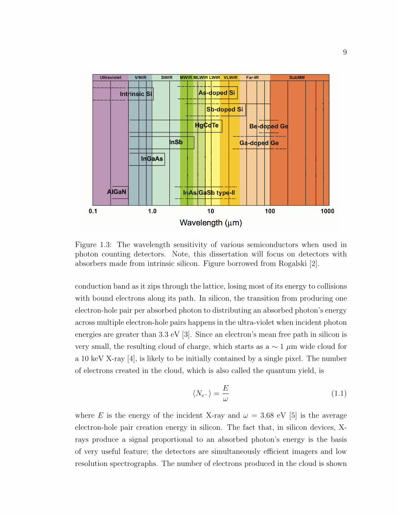
shown in Figure 1.3.
Figure 1.1: Shown is the effect where as the separation between two atoms de-creases, the splitting of their energy levels increases. When many atoms arebrought close together, the split levels form semicontinuous bands. Figure bor-rowed from Astrophysical Techniques [1].
1.1.2 Charge Collection
With design features that vary between styles of detectors, semiconductor detectors
are able to collect the charge generated by photoelectric absorption by creating an
active region. The active region is depleted of free charge carriers by an electric
field that fills the region, permeating the semiconductor’s bulk. Accordingly, this
region is called the depletion region and it is where the detector is most readily able
to detect photons. The charge carrier concentrations of a particular material are
determined by its intrinsic properties or doping level. An intrinsic semiconductor is
a pure semiconductor where the number and polarity of charge carriers in the bands
is a property of the material. n-doped semiconductors are intrinsic materials that
have been doped, or mixed in very small amounts, with an element that has one
or more valence electrons than the element(s) in the intrinsic material. p-doped
semiconductors are intrinsic materials doped with an element that has one or

8
Figure 1.2: The energy level diagram for a solid. Figure borrowed from Astrophys-ical Techniques [1].
fewer electrons than the intrinsic material. n-doped and p-doped semiconductors
are so-named because their majority charge carriers are negative and positive,
respectively. Positive charge carriers in a semiconductor are called holes. Most
literally, they are an unoccupied space in a sea of electrons that fills the valence
band, but they can be treated like a positively charged particle with an effective
mass and effective mobility in the solid.
The electric field in the depletion region applies a force to free charge carriers
generated in the bulk and confines them in a potential well where there are no
opposite polarity carriers to recombine with them. When a Near-IR or optical
photon is absorbed by a valence electron in the depletion region, it promotes the
electron into the conduction band where it is now a free charge carrier, capable
of drifting into the potential well. For an ideal detector with linear response,
the number of electrons in the well is proportional to the flux incident on the
pixel. When an X-ray is absorbed by an inner-shell electron in the depletion
region, the electron has enough kinetic energy to excite other electrons into the
9
Figure 1.3: The wavelength sensitivity of various semiconductors when used inphoton counting detectors. Note, this dissertation will focus on detectors withabsorbers made from intrinsic silicon. Figure borrowed from Rogalski [2].
conduction band as it zips through the lattice, losing most of its energy to collisions
with bound electrons along its path. In silicon, the transition from producing one
electron-hole pair per absorbed photon to distributing an absorbed photon’s energy
across multiple electron-hole pairs happens in the ultra-violet when incident photon
energies are greater than 3.3 eV [3]. Since an electron’s mean free path in silicon is
very small, the resulting cloud of charge, which starts as a ∼ 1 µm wide cloud for
a 10 keV X-ray [4], is likely to be initially contained by a single pixel. The number
of electrons created in the cloud, which is also called the quantum yield, is
〈Ne−〉 =E
ω(1.1)
where E is the energy of the incident X-ray and ω = 3.68 eV [5] is the average
electron-hole pair creation energy in silicon. The fact that, in silicon devices, X-
rays produce a signal proportional to an absorbed photon’s energy is the basis
of very useful feature; the detectors are simultaneously efficient imagers and low
resolution spectrographs. The number of electrons produced in the cloud is shown
10
as an average number in Equation 1.1 because there is an inherent uncertainty
in the number of electron-hole pairs created by a photon. In an over-simplified
picture of X-ray absorption, all of the photon’s energy would be transformed into
the generation of electron-hole pairs and there would be no uncertainty. However,
complexities of solid state physics, such as electron-phonon interaction, lead to
the spurious addition or subtraction of energy from the process of converting a
high-energy electron’s kinetic energy into electron-hole pair creation. The discrete
pair generation process is not entirely random, in which case the variance would
be proportional to the number of pairs as with a Poisson distribution, nor is it
deterministic, where the variance would be zero. The Fano factor, F , is a number
between 0 and 1 that characterizes the fractional randomness of a particular pair
generation process in a particular medium [6]. Although it was initially developed
to characterize the uncertainty in electron-ion pair generation in particle counters,
the theory applies just as well to the case of X-ray absorption in silicon. In this
case, the factor characterizes electrons generating electron-hole pairs in a silicon
lattice and has been experimentally measured to be 0.158 [6, 7]. The variance in
the number of electron-hole pairs in the cloud due to this effect, the so-called Fano
noise, is
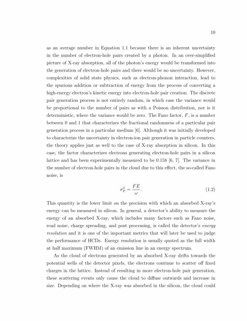
σ2F =
FE
ω. (1.2)
This quantity is the lower limit on the precision with which an absorbed X-ray’s
energy can be measured in silicon. In general, a detector’s ability to measure the
energy of an absorbed X-ray, which includes many factors such as Fano noise,
read noise, charge spreading, and post processing, is called the detector’s energy
resolution and it is one of the important metrics that will later be used to judge
the performance of HCDs. Energy resolution is usually quoted as the full width
at half maximum (FWHM) of an emission line in an energy spectrum.
As the cloud of electrons generated by an absorbed X-ray drifts towards the
potential wells of the detector pixels, the electrons continue to scatter off fixed
charges in the lattice. Instead of resulting in more electron-hole pair generation,
these scattering events only cause the cloud to diffuse outwards and increase in
size. Depending on where the X-ray was absorbed in the silicon, the cloud could

11
be split between two or more pixels, creating what is called a split event. Split
events require that the signal, and its associated noise, from more than one pixel
be summed to reconstruct the total energy deposited in the detector.
Irrespective of the details of a detector’s construction, electric field strength,
or bias voltage levels, there are electron-hole pairs being spontaneously created
and recombining continually in any given volume of semiconductor. The energy to
create these pairs comes from phonons, the quanta of lattice vibration energy that
are buzzing around in any solid with a temperature above absolute zero. Pairs
thermally created in the depletion region will drift into the potential well, just as
if they were created by photon absorption. This contaminant signal is called dark
current and not only does it produce a signal that can cause detectors to saturate,
but the charge carriers it adds into the potential well also give it an associated
Poisson distributed noise term that cannot be subtracted out. As with any noise
source, it is usually best to minimize dark current. A higher temperature in the
material is equivalent to a higher energy phonon energy distribution, which leads
to an increased rate of electron-hole pair creation in the bulk, making dark current
correlated to detector temperature. In addition to the bulk dark current, which can
be generated both in and outside of the depletion region since some charge carriers
will diffuse into the depletion region by chance, dark current is also generated at
band gap deformation sites called surface states. At the boundary between the
depleted bulk and the material that borders it (usually an oxide), irregularities in
the lattice cause irregularities in the band structure, which can severely leak dark
current if they are not addressed with special design techniques.
1.1.3 Charge Transfer and Readout
After being collected in the potential well, photo-charge is then transferred to the
readout node, a component that functions like a capacitor, allowing the charge to
be converted into a voltage signal. The uncertainty in this pixel voltage measure-
ment is referred to as read noise, and is another important detector performance
characteristic. When the readout electronics are reset between pixel reads, the
value at which they settle has some uncertainty to it that is known as reset noise.
This uncertainty can be reduced by a technique known as correlated double sam-

12
pling (CDS). In this technique, the output signal is sampled during reset, sampled
a second time after the read pixel’s value is transferred to the output node, and
the two values are subtracted to yield the final output. This can be implemented
through various circuit designs, including analog sample and hold and dual slope
digitization, and also accomplished digitally in post-processing.
After the pixel charge is converted to a voltage, the signal is amplified and then
digitized by an analog to digital converter (ADC). The integer output of the ADC,
a unit referred to as a digital number (DN), is then recorded by a computer. The
conversion gain, G [e−/DN], is a number that accounts for the total gain of the
detection process, from charge, to voltage, to amplified signal, to digital number.
Note that this gain convention is the inverse of the typical sense, where increased
gain usually results in greater output for a given input.
Combining detector performance characteristics and including instrument and
light source properties, one can estimate an upper limit for the signal to noise ratio
(S/N) of the data. In the near-IR and optical bands, where the quantum yield of
silicon is unity, the signal to noise ratio in a given pixel will be
S
N=
Fobj QE t√[(Fobj + Fsky + Fbg)QE +D] t+ σ2
R + (G2
)2
√npix, (1.3)
where Fobj is the photon flux of the object, Fsky is the photon flux of the sky,
Fbg is the photon flux of the background, QE is the quantum efficiency of the
detector, t is the integration time, D is the dark current count rate in e− s−1,
σR read noise of the detector in electrons, npix is the number of pixels used to
record the object’s flux, and the (G/2)2 factor is quantization noise. While it may
not seem necessary to distinguish between sky and background flux, in the case
of mid-IR observations the difference is important because thermal emission from
instrument optics contributes significantly to the background. In the X-ray band,
where the quantum yield is much greater than 1, it is more useful to calculate S/N
for individual X-ray events. In this case, the S/N expression must be multiplied
by a factor of√E/ω to correctly account for the number of electrons that are
generated by the absorbed X-ray. Also in this case, npix refers to the number of
pixels covered by each event, leading to the dependence of S/N on event geometry.
This effect will be further discussed in Chapter 3.
13
1.2 CCDs
1.2.1 Basic Operation
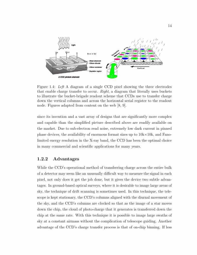
The charge-coupled device (CCD) was the first widely-successful pixellated solid
state detector. Very generally, the device is built by patterning an array of metal-
oxide-semiconductor (MOS) capacitors onto a p- or n-type silicon substrate with
photolithographic techniques. A schematic of the CCD’s structure is shown in
Figure 1.4. When a voltage is applied to the surface electrode (also called the
gate), the mobile charge carriers in the doped substrate are driven away from the
surface, creating a depletion region below the electrode.
The process of photon absorption described in the previous section adequately
describes how light is absorbed in a CCD, but this process is not unique to the CCD
since it describes the light absorption process in all biased semiconductor devices.
However, the process that is unique to the CCD, and the feature from which its
name is derived, is the method by which the charge is read out. The CCD measures
the charge in each pixel by transferring the packets of charge in each pixel through
the bulk of the detector to one or more readout amplifiers positioned near the
edge of the array. As seen in Figure 1.4, electrodes deposited on the surface of the
substrate, usually three per pixel, form a potential well in each pixel when they are
positively biased. The electrode-induced well confines charge along the direction
of the column. The columns are separated by p+ doped (heavily doped) borders,
called channel stops, which confine the charge in the direction perpendicular to the
column direction. Slow, synchronous clocking of the three electrodes transfers the
charge in each pixel vertically down each column, in parallel, to a horizontal serial
register row at the bottom of the chip. The serial row is then quickly clocked so
that once per fast clock cycle, a pixel’s charge is transferred to the output node,
where it is converted into a voltage. A cartoon that visualizes this so-called bucket-
brigade charge transfer and readout is shown in Figure 1.4 The output signal is
then amplified and digitized off-chip. Once per column clock cycle (slow), a new
row of pixel charge is transferred to the serial register.
Following the invention of the CCD in 1970 [10, 11] and the first report of the
CCD’s sensitivity to X-rays in 1977 [12], Burrows et al. were the first to use a CCD
for X-ray astronomy in 1989 [13]. The device has undergone extensive development
14
Figure 1.4: Left A diagram of a single CCD pixel showing the three electrodesthat enable charge transfer to occur. Right, a diagram that literally uses bucketsto illustrate the bucket-brigade readout scheme that CCDs use to transfer chargedown the vertical columns and across the horizontal serial register to the readoutnode. Figures adapted from content on the web [8, 9].
since its invention and a vast array of designs that are significantly more complex
and capable than the simplified picture described above are readily available on
the market. Due to sub-electron read noise, extremely low dark current in pinned
phase devices, the availability of enormous format sizes up to 10k×10k, and Fano-
limited energy resolution in the X-ray band, the CCD has been the optimal choice
in many commercial and scientific applications for many years.
1.2.2 Advantages
While the CCD’s operational method of transferring charge across the entire bulk
of a detector may seem like an unusually difficult way to measure the signal in each
pixel, not only does it get the job done, but it gives the device two subtle advan-
tages. In ground-based optical surveys, where it is desirable to image large areas of
sky, the technique of drift scanning is sometimes used. In this technique, the tele-
scope is kept stationary, the CCD’s columns aligned with the diurnal movement of
the sky, and the CCD’s columns are clocked so that as the image of a star moves
down the chip, the cloud of photo-charge that it generates is transferred down the
chip at the same rate. With this technique it is possible to image large swaths of
sky at a constant airmass without the complication of telescope guiding. Another
advantage of the CCD’s charge transfer process is that of on-chip binning. If less

15
spatial resolution is required of a detector in a particular application, perhaps due
to the optical point spread function (PSF) being oversampled or the desire for
faster frame rates, the array clocking patterns can be altered so that charge from
multiple pixels is combined (binned) on-chip before it is read out. Binning charge
on-chip is essentially noiseless, so it eliminates the addition of extra read noise due
to extra pixel reads required to bin digitally. Also, it eliminates the extra read time
required to measure the voltage in those pixels that would have eventually been
added together in a computer. In the Hobby Eberly Telescope’s High Resolution
Spectrograph, variable on-chip binning is used to efficiently match the detectors’
spatial resolutions to the variety of dispersions produced by different operational
modes of the spectrograph. Additionally, since the spectrograph is fiber fed, spa-
tial resolution perpendicular to the dispersion direction is marginally useful. There
exists the option to bin in this direction to decrease readout time and the size of
data products. On the Swift XRT, pixel binning is used to achieve higher frame
rates in the instrument’s windowed timing mode.
1.2.3 Disadvantages
Despite the many strengths of CCD technology, its inherent weaknesses, such as
high power consumption, destructive charge readout, limited radiation hardness,
and pile-up in X-ray applications, have left room for new technologies to replace
it.
1.2.3.1 Destructive Readout
The readout of a CCD is a destructive process, where once the charge in a pixel
has been transferred to the readout node, sampled, and the next pixel clocked into
the readout node, the original pixel’s charge is gone and cannot be sampled again.
A consequence of this is that during an exposure, which in optical astronomy
can be up to an hour or two in length, the observer is unable to know anything
about what is happening on the chip. In addition to missing out on practical, mid-
exposure information like the saturation of a target, the CCD’s destructive readout
prevents knowing any temporal information about the science target. Time-series
data could be acquired with a CCD by taking N short exposures, but then the

16
advantage of performing a long integration would be lost. When the many short,
destructively read exposures are co-added, the resulting data will contain a factor
of√N more read noise than a single integration of the same duration.
1.2.3.2 Power Consumption
A CCD camera, which consists of the CCD and the electronics required to bias,
clock, and read out the array, is a relatively power-hungry system, with a typical
device requiring 25 W during readout [14]. Since some of that power is deposited
directly into the chip, additional power will be required to remove it in order
to maintain a constant detector temperature. On ground-based telescopes, such
power requirements are inconsequential, but in space they can drastically increase
the power requirements and mass of a satellite, which eventually translate into
increased mission cost.
1.2.3.3 Radiation Hardness
In reality, the operation of transferring charge between pixels of a CCD during
readout is imperfect. As photo-charge is pushed through the crystal lattice, small
amounts of charge get caught in undesirable potential wells called traps. In a
perfect lattice, the band structure is uniform and traps do not exist. However,
real materials have defects in the periodic lattice that create local minima in the
energy band structure. Once caught in a trap, a charge carrier is held fixed for
some amount of time, before being released and becoming mobile again. The
trouble with this effect is that the charge carrier is sometimes freed after the
charge packet from which it originated has been transferred to the next pixel. The
so-called charge transfer efficiency (CTE), the average fraction of a charge packet
that will remain after one transfer, is usually on the order of 0.99999-0.999995 for a
science grade CCD. While a CTE of “five nines” might seem so close to unity that
the difference can be considered negligible, the 2048 transfers that a maximally
distant charge packet must make on its way to the readout node of a modest size
2048×2048 CCD amounts to a degradation factor of CTE2048, which equals ∼ 2%.
For detectors operating in the harsh environment of space, despite radiation
shields, the steady accumulation of damage due to ionizing radiation is unavoid-

17
able. This ionizing radiation is collectively known as space weather and consists of
the high-energy protons and electrons that make up the solar wind and very-high-
energy heavy-ion radiation originating from cosmic sources. Detectors operating
in laboratories or at ground-based observatories are largely protected from radi-
ation damage because of attenuation by the Earth’s atmosphere and deflection
by its magnetic field. Satellites in low-Earth orbit experience between 0.2 and
10 krad (Si) year−1 total ionizing dose (TID), depending on orbital inclination
[15]. JWST’s focal plane arrays are expected to experience up to a 50 krad (Si)
lifetime TID [16]. On orbit, these particles bombard a detector and cause displace-
ment defects (a non-ionizing damage effect typically caused by protons) or massive
charge carrier deposition (an ionzing damage effect typically caused by electrons
and gamma-rays) where they are absorbed by the semiconductor lattice. Although
any given chunk of silicon will accrue the same number of radiation induced defects
regardless of the type of detector it is in, detectors do not respond identically to
radiation damage. Due to the way that CCDs transfer charge across the width of
the detector, they are inherently disadvantaged when it comes to resisting radia-
tion damage. Radiation hardness is the detector performance metric that indicates
the radiation dose that a detector can receive before it is damaged to the point
that it can no longer function within nominal specifications. A CCD’s CTE is
sensitive to radiation dose because lattice defects not only affect photo-charge de-
posited in the damaged pixel, but the charge deposited in all pixels upstream of
it in the read direction. Reduced CTE leads to degraded energy resolution and
position-dependent gain. Also, the occurrence of a radiation induced lattice defect
in an optimally bad location can cause a large increase in dark current such that
a pixel or even an entire column may become non-functional.
To cite an example, it was estimated that the Swift XRT would be exposed to
a total 10 MeV equivalent proton dose of 109 protons cm−2 during the first 6 years
of its mission [17]. On orbit, the exposure led to a 50% increase in emission line
widths. Bi-annual efforts to map charge traps in the XRT detectors and incorporate
correction factors into the detector gain file have recovered a significant fraction of
the initial energy resolution, but the stochastic nature of the trap release process
adds an intrinsic noise into the system that cannot be corrected with calibration
[18]. In the end, the use of radiation hard devices will ensure the best long-term

18
mission performance.
1.2.3.4 Pile-up
In X-ray applications, the issue of pile-up [19, 20] puts further limitations on the
CCD’s utility. The nominal operation mode of an X-ray CCD is known as photon
counting, where the entire array is continually clocked out at some chosen frame
rate as X-rays pepper the surface of the array, depositing clouds of charge into
the silicon. If two X-rays land in the same or adjacent pixels during one read
frame they are said to be piled-up because they can no longer be distinguished
from one another. Increasing the frame rate will reduce pile-up, but doing so
requires that the pixels be read faster, which increases read noise and reduces
CTE. Commercially available, deep depletion CCDs from an industry front-runner
like E2V are limited to read rates of about 5 Mpixels s−1. Pile-up is a problem for
photon counting because when two or more X-rays fall in the same pixel, it is not
possible to distinguish whether the resulting signal in the detector was generated
by two or more low-energy photons or one high-energy photon. If left untreated,
pile-up will artificially harden an observed X-ray spectrum, decreasing the apparent
low-energy flux and increasing the apparent high-energy contribution, and decrease
the observed count rate relative to its true value. While it is possible to reduce
pile-up by increasing the effective frame rate of a CCD with creative clocking
or windowed readout modes, all of these methods involve making concessions in
spatial resolution, imaging area, or read noise. Defocusing has been used to reduce
focused X-ray pile-up in laboratory testing [21], but this is not a practical solution
for most orbiting observatories where angular resolution is important and the use
of large-travel mechanical stages is a high-risk design choice.
Taking a few operating X-ray satellites as an example, the Swift XRT CCD’s
two typical modes of operation are Windowed Timing and Photon-Counting (600
× 600 pixels). The maximum unpiled-up source fluxes for these modes are 600
and 1 mCrab, respectively [22] given the instrument’s 110 cm2 effective area at 1.5
keV. The XMM EPIC-pn CCD’s Timing, Small window, Large window, and Full
frame (376×384 pixels) modes can acquire unpiled-up data on 160, 14, 1.3, and 0.9
mCrab point sources, respectively, given the instrument’s 1300 cm2 effective area
[23]. Current designs of the XEUS mission concept predict that the telescope will

19
have 3 m2 of effective area at this energy. These large optics will impose a much
higher performance requirement on the observatory’s detectors, a factor of > 20
increase in effective frame rate, so that they can process all of the photons.
1.3 CMOS: A New Competitor in the X-ray
As was already mentioned, CMOS technology has been around since 1967, but
the CMOS imager’s rise to prominence is only just beginning. The mechanism
through which photo-charge is generated in CMOS detectors and CCDs is identical.
The most significant difference between the two architectures is in their operation,
where in CMOS chips, photo-charge is not transferred from pixel to pixel on its way
to the readout node as with CCDs, but instead each pixel is individually addressed
with digital logic circuitry and its charge directly transferred to an output amplifier.
The CMOS detector design is very similar to that of solid state memory devices,
but instead of reading digital information from an array of memory locations, the
analog signal from an array of photodiodes is read out.
One might wonder why CCDs have shown performance characteristics superior
to CMOS for so many years. In truth, the fantastic performance of CCDs is
not entirely attributable to inherent advantages of the technology, but rather the
enormous development effort that has been invested in the CCD since its invention.
Early CCD sensors had performance advantages like reduced fixed pattern noise,
large open area due to simple pixel design, and easy scalability to small pixels
(and therefore lighter optics) that gave developers good reason to channel their
effort and funding towards the improvement of CCDs. However since that era,
the steady, computer industry-led march towards smaller CMOS feature sizes has
enabled solutions to many of the problems encountered with early CMOS devices.
A good historical review of the development differences between CCDs and CMOS
devices was given by Fossum [24].
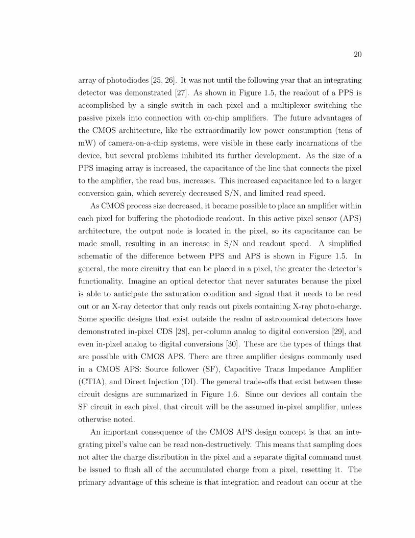
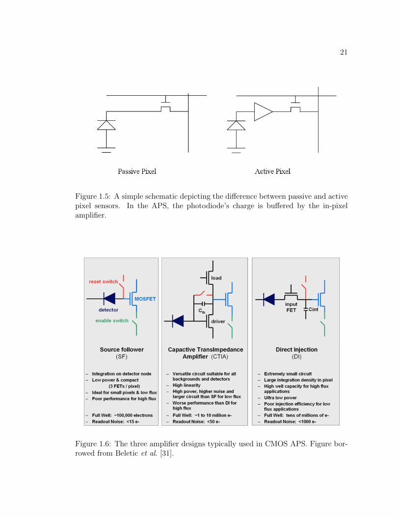
Early CMOS imaging devices were passive pixel sensors (PPS), meaning that
there was no active signal buffering or amplification happening in the pixel. In fact,
early incarnations of the design were not integrating detectors; the first CMOS-like
photo-detector was demonstrated in 1965 and used high gain electronics to amplify
instantaneous measurements of the photocurrents being generated in a monolithic
20
array of photodiodes [25, 26]. It was not until the following year that an integrating
detector was demonstrated [27]. As shown in Figure 1.5, the readout of a PPS is
accomplished by a single switch in each pixel and a multiplexer switching the
passive pixels into connection with on-chip amplifiers. The future advantages of
the CMOS architecture, like the extraordinarily low power consumption (tens of
mW) of camera-on-a-chip systems, were visible in these early incarnations of the
device, but several problems inhibited its further development. As the size of a
PPS imaging array is increased, the capacitance of the line that connects the pixel
to the amplifier, the read bus, increases. This increased capacitance led to a larger
conversion gain, which severely decreased S/N, and limited read speed.
As CMOS process size decreased, it became possible to place an amplifier within
each pixel for buffering the photodiode readout. In this active pixel sensor (APS)
architecture, the output node is located in the pixel, so its capacitance can be
made small, resulting in an increase in S/N and readout speed. A simplified
schematic of the difference between PPS and APS is shown in Figure 1.5. In
general, the more circuitry that can be placed in a pixel, the greater the detector’s
functionality. Imagine an optical detector that never saturates because the pixel
is able to anticipate the saturation condition and signal that it needs to be read
out or an X-ray detector that only reads out pixels containing X-ray photo-charge.
Some specific designs that exist outside the realm of astronomical detectors have
demonstrated in-pixel CDS [28], per-column analog to digital conversion [29], and
even in-pixel analog to digital conversions [30]. These are the types of things that
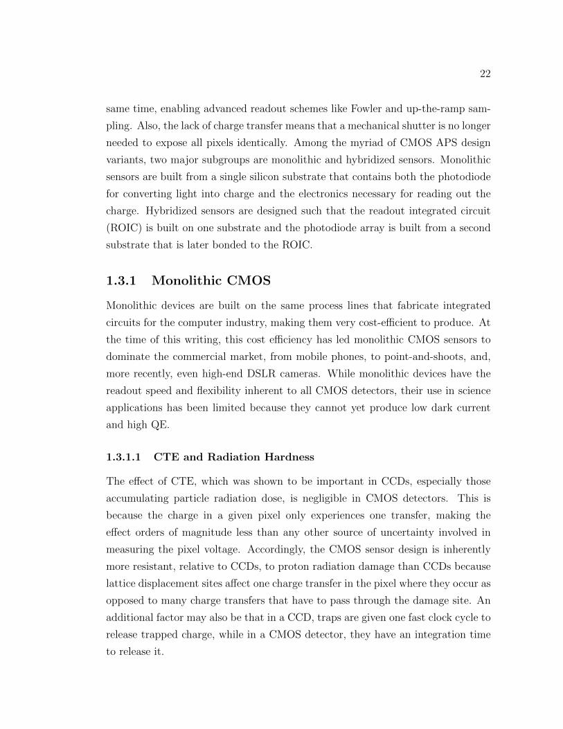
are possible with CMOS APS. There are three amplifier designs commonly used
in a CMOS APS: Source follower (SF), Capacitive Trans Impedance Amplifier
(CTIA), and Direct Injection (DI). The general trade-offs that exist between these
circuit designs are summarized in Figure 1.6. Since our devices all contain the
SF circuit in each pixel, that circuit will be the assumed in-pixel amplifier, unless
otherwise noted.
An important consequence of the CMOS APS design concept is that an inte-
grating pixel’s value can be read non-destructively. This means that sampling does
not alter the charge distribution in the pixel and a separate digital command must
be issued to flush all of the accumulated charge from a pixel, resetting it. The
primary advantage of this scheme is that integration and readout can occur at the
21
Figure 1.5: A simple schematic depicting the difference between passive and activepixel sensors. In the APS, the photodiode’s charge is buffered by the in-pixelamplifier.
Figure 1.6: The three amplifier designs typically used in CMOS APS. Figure bor-rowed from Beletic et al. [31].
22
same time, enabling advanced readout schemes like Fowler and up-the-ramp sam-
pling. Also, the lack of charge transfer means that a mechanical shutter is no longer
needed to expose all pixels identically. Among the myriad of CMOS APS design
variants, two major subgroups are monolithic and hybridized sensors. Monolithic
sensors are built from a single silicon substrate that contains both the photodiode
for converting light into charge and the electronics necessary for reading out the
charge. Hybridized sensors are designed such that the readout integrated circuit
(ROIC) is built on one substrate and the photodiode array is built from a second
substrate that is later bonded to the ROIC.
1.3.1 Monolithic CMOS
Monolithic devices are built on the same process lines that fabricate integrated
circuits for the computer industry, making them very cost-efficient to produce. At
the time of this writing, this cost efficiency has led monolithic CMOS sensors to
dominate the commercial market, from mobile phones, to point-and-shoots, and,
more recently, even high-end DSLR cameras. While monolithic devices have the
readout speed and flexibility inherent to all CMOS detectors, their use in science
applications has been limited because they cannot yet produce low dark current
and high QE.
1.3.1.1 CTE and Radiation Hardness
The effect of CTE, which was shown to be important in CCDs, especially those
accumulating particle radiation dose, is negligible in CMOS detectors. This is
because the charge in a given pixel only experiences one transfer, making the
effect orders of magnitude less than any other source of uncertainty involved in
measuring the pixel voltage. Accordingly, the CMOS sensor design is inherently
more resistant, relative to CCDs, to proton radiation damage than CCDs because
lattice displacement sites affect one charge transfer in the pixel where they occur as
opposed to many charge transfers that have to pass through the damage site. An
additional factor may also be that in a CCD, traps are given one fast clock cycle to
release trapped charge, while in a CMOS detector, they have an integration time
to release it.

23
1.3.2 Sensitivity
Utilizing the cost-effectiveness of existing CMOS fabrication facilities means that
most monolithic devices are fabricated on low-resistivity silicon. As will be shown
in the next section, this gives them poor red-optical and X-ray sensitivity. Re-
cent efforts to use high-resistivity, epitaxial silicon in monolithic sensors have seen
laboratory success with soft X-ray detection [32]. However these detectors are
currently limited to a depletion depth of 15 µm, giving them poor hard X-ray
sensitivity. Front-illuminated (FI) devices will always have lower QE compared
to back-illuminated (BI) devices, but the QE of both devices is limited due to
relatively short depletion depths.
While increasing the complexity of pixel circuit design clearly enables increased
functionality and performance, for front-side illuminated monolithic sensors, the
added circuitry blocks incident light, decreasing the area of the pixel capable of
detecting incident photons. Commercial optical sensors use lenslet arrays, with
one lens for each pixel, to focus light between the surface circuitry and improve
QE. However, this technique is not generally used in scientific detectors because
it induces non-uniform spatial response, blurring, and decreased angular response
[33]. The use of lenslets yields no benefit to the QE of an X-ray detector because
conventional refractive optics only absorb and do not refract X-rays. Backside
thinning, that is, removing material from the silicon substrate’s back surface by
mechanical polishing and chemical etching, is currently being pursued to produce
BI monolithic sensors [32]. In such sensors, the readout circuitry does not block
incident light because they’re illuminated from the bare back-side, enhancing QE.
At the time of this writing, these detectors are still in active development and
while they have shown good soft X-ray QE and read noise characteristics, they
still exhibit poor high-energy X-ray response. Some of these issues are currently
addressed by an alternative CMOS design, the hybrid CMOS detector (HCD).
1.3.3 Hybrid CMOS Devices
As the name implies, HCDs are constructed by connecting, or hybridizing, a ded-
icated semiconductor absorber array substrate to a ROIC. A schematic depicting
HCD construction is shown in Figure 1.7. The absorber layer is patterned with

24
one photodiode per pixel and nothing else, giving the detector 100% open area.
The ROIC, positioned below the absorber, is not illuminated and has the sole duty
of reading out the photo-charge integrated on the photodiode. As will be shown,
the key advantage of this design is that the performance of both the absorber and
ROIC can be individually optimized with regard to their respective functions.
Figure 1.7: A cutaway schematic showing the basic design of the HyViSITM
HCD.The silicon absorber on top is patterned with an array of p-doped intrinsic n-doped(PIN) diodes formed between the top-side, heavily n-doped layer, the heavily p-doped implants below, and the intervening lightly n-doped (nearly intrinsic) silicon.The indium bump bonds connect each absorber pixel to its corresponding readoutpixel in the ROIC below. Shown are X-rays being absorbed at two different depthsin the detector. The charge carrier cloud formed by absorbed X-rays will diffuselaterally as it moves toward the potential wells on top of each implant. X-raysabsorbed higher up will tend to diffuse more and produce signal in more than onepixel. On top of the absorber, and shown partially covering it, is the depositedaluminum optical blocking filter (Al OBF).
An introduction of the HCD would not be complete without noting that the
development of this architecture was primarily motivated and, more importantly,
funded not by the curiosity-driven research of astronomy, but instead by its utility
in advancing room-temperature thermal emission and night vision imagers with
military applications. Interestingly, researching the origins of adaptive optics tells
25
a similar story [34]. While the concept of adaptive optics originated in astronomy,
the majority of the technology’s development was accomplished by the military in-
dustrial complex. This delicate interplay between the advancement of pure science
and military technology is not a new phenomenon and will likely continue to play
an important role in the advancement of astronomy as a whole.
The HCD design was developed in the late 1970s [35] in response to the need for
better forward looking infrared (FLIR) camera detectors. In the original design,
the ROIC was positioned in front of the absorber and window cutouts in the ROIC
allowed radiation to penetrate through it, to the low band gap, semiconductor
absorber array bonded below it. During the 1980s, the design evolved into the
current configuration where the absorber array is positioned in front, and flip-
chip bonded to the silicon ROIC. A number of manufacturers currently produce
large-format hybridized arrays, including Goodrich Corporation, Raytheon Vision
Systems, Teledyne Imaging Sensors (TIS), Sofradir, Selex, IAM, SCD, and DRS
Technologies [2].
The astronomical X-ray detector development projects at Penn State have fo-
cused on developing hardware through an ongoing collaboration with TIS. Using
very similar architectures, TIS produces HCDs with two different absorber sub-
strates so that the sensors can be used in different wavelength regimes. For mid
and short-wavelength infrared sensing, HgCdTe substrates are grown via molecu-
lar beam epitaxy on CdZnTe substrates. In recent designs the CdZnTe substrate
has been removed to improve response. As with CCDs and monolithic CMOS
sensors, TIS uses silicon to absorb radiation in the near-IR, optical, and X-ray.
The absorber is made from thick (50− 350µm [36]), high-resistivity silicon and is
called HyViSITM
for “Hybrid Visible Silicon Imager” [37]. From this point forward,
references to the HCD will be referring to variants of the TIS HyViSITM
silicon
p-doped intrinsic n-doped (PIN) diode hybrid imager that have been optimized for
X-ray detection. A detailed description of these detectors will follow in Chapter
2, but it will be useful to first understand how the PIN diode works since HCDs
are based on this device and draw their performance advantages from it.

26
1.3.3.1 The PIN diode
The PIN diode’s design is an extension of one of the most basic semiconductor
devices, the PN diode. The PN diode is a two terminal device that consists of
a single semiconductor in which a p-doped region is created directly next to an
n-doped region. The electronic transport properties of the junction between these
alternatively doped regions are different than either the p or n components alone.
The hallmark characteristic of the PN junction is its asymmetric transport, mean-
ing it will allow current to flow across the boundary in one direction, but not the
other. By itself, this device is a diode and can be used as an AC rectifier, for
over-voltage protection, or, as in our case, a photodiode. Creating an intrinsic
region between the p- and n-type regions turns the device into a PIN diode, the
properties of which are similar to the PN junction. The diode’s behavior depends
on the voltage placed across its two terminals, the bias voltage, leading to three
general performance regimes (See Figure 1.8):
1. Terminals disconnected (floating) - holes from the p-type region and elec-
trons from the n-type region diffuse across the junction boundary, into the
intrinsic semiconductor, creating a depletion region. When electrons recom-
bine with holes this leaves behind an immobile space charge in the doped
regions, positive ions in the n-region and negative ions in the p-region. The
coulomb force from this space charge prevents more free charge carriers on
both sides from diffusing across the boundary, resulting in the development
of an equilibrium condition. With no external voltage or photon excitation,
there will be a non-zero voltage across the diode, the built-in voltage.
2. Forward Bias - When an external positive voltage,Vsub, is applied to the p-
type substrate, the diode is said to be forward biased. The electric field
created in the solid imparts energy to the charge carriers, making it possible
for them to overcome the space charge coulomb barrier and flow across the
junction. In this regime, the diode is highly conductive.
3. Reverse Bias - When an external positive voltage is applied to the n-type side
of the diode, the depletion region increases in size with increased voltage.
This increase in the depletion depth makes reverse bias the operation regime
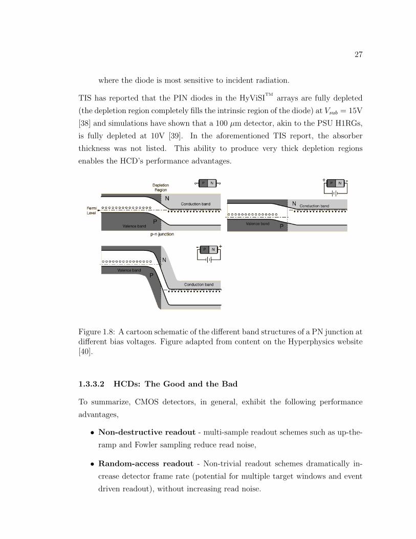
27
where the diode is most sensitive to incident radiation.
TIS has reported that the PIN diodes in the HyViSITM
arrays are fully depleted
(the depletion region completely fills the intrinsic region of the diode) at Vsub = 15V
[38] and simulations have shown that a 100 µm detector, akin to the PSU H1RGs,
is fully depleted at 10V [39]. In the aforementioned TIS report, the absorber
thickness was not listed. This ability to produce very thick depletion regions
enables the HCD’s performance advantages.
Figure 1.8: A cartoon schematic of the different band structures of a PN junction atdifferent bias voltages. Figure adapted from content on the Hyperphysics website[40].
1.3.3.2 HCDs: The Good and the Bad
To summarize, CMOS detectors, in general, exhibit the following performance
advantages,
• Non-destructive readout - multi-sample readout schemes such as up-the-
ramp and Fowler sampling reduce read noise,
• Random-access readout - Non-trivial readout schemes dramatically in-
crease detector frame rate (potential for multiple target windows and event
driven readout), without increasing read noise.

28
• Read speed - Free from the limitations of transferring charge through semi-
conductor, CMOS architecture is less fundamentally limited in its pixel rate
than CCDs.
• Low power - CMOS electronics are inherently low power due to low switch-
ing and standby power consumption. Additionally, CMOS detectors compare
favorably to CCDs in this regard because they do not use high clock voltages
to transfer charge across the chip.
• Radiation hardness - The hybrid design is inherently radiation hard. HyViSITM
H2RGs have been shown to withstand 90 krad (Si) total ionizing dose [41],
which greatly exceeds the lifetime JWST dosage requirement and corresponds
to a ∼ 9 year mission lifetime in a low-inclination, low-earth orbit.
and CMOS detectors exhibit the following disadvantages,
• Read noise - The slow pixel rate (100 kHz) read noise of the 3T source
follower pixel design used in TIS HxRG detectors is currently limited at
≈ 7 e−, making it higher than that found in the best CCDs. However,
at MHz readout rates, HCDs have lower read noise than CCDs operated at
similarly high rates [37]. Detectors employing a 4T design, known as a pinned
photodiodes, have achieved read noise levels below 1 e−, which is comparable
to the performance of CCDs.
• Dark Current - Multi-pinned phase (MPP) CCDs exhibit extremely low
dark current, making it difficult for CMOS to compete in this metric. Dark
currents of 5-10 nA/cm2 have been achieved in 3T HyViSITM
HCDs at 298 K
[36], 3T monolithic sensors from TIS have produced 200-500 pA cm−2 [42],
and pinned photodiode 4T monolithic sensors from TIS have produced 1-10
pA cm−2 at unspecified temperatures [42]. Modern production MPP CCDs
from E2V show ∼ 200 e−s−1pixel−1 in 20 micron devices (8 pA cm−2) at 298
K.
The separate absorbing and readout layers in the HCD design enable several
performance advantages over monolithic CMOS detectors. Specifically, HCDs have
the following advantages,

29
• Deep Depletion - depletion depths up to 350 µm have been achieved in
HCDs compared to a few tens of microns in monolithic CMOS and 50 µm in
CCDs [43]. This leads to improved red optical and hard X-ray QE.
• Fill factor - HyViSITM
HCDs are back illuminated giving them 100% fill
factor.
• Micrometeoroid resistant - HCDs are expected to be more robust than FI
CMOS and CCD imagers because the gate structures are protected behind
the absorber array. Should pixel-level damage occur, its effect would be
localized, and not result in blooming across the detector. Suzaku, XMM,
and Swift have all experienced damage on orbit that has been likely due to
micrometeoroid damage.
A notable disadvantage of current HyViSITM
HCD designs is that they are suscep-
tible to inter-pixel capacitance, where nearby pixels are coupled to one another by
an unintended, parasitic capacitance. The end-result of this capacitive coupling is
that signal is spread into adjacent pixels, i.e., the detector’s modulation transfer
function is degraded. Details of this effect and our characterization of it will be
presented in Chapter 3.

Chapter 2PSU Detector Hardware
The Penn State X-ray Astronomy Detector Lab is actively engaged in a collabo-
ration with TIS (originally Rockwell Scientific) to produce next generation HCD
X-ray detectors. A distinct advantage of collaborating with TIS stems from the
large amount of development that their product line has undergone in order to
produce focal plane arrays for the James Webb Space Telescope’s fine guidance
sensor, NIRCam, and NIRSpec [44] instruments. The Penn State X-ray group has
taken the results of this effort as a starting point and begun our own development
of the TIS HCD optimized for X-ray astronomy. In this chapter I will discuss
the design specifications of the particular devices that PSU received from TIS in
addition to the hardware and software required for their operation.
2.1 TIS HAWAII Arrays
To date, five X-ray TIS HyViSITM
HCDs have been tested at PSU. All devices are
HxRGs (HAWAII x×x pixels with Reference pixels and Guide mode). The device
serial numbers, as well as a summary of the TIS test reports for the devices, are
summarized in Table 2.1. Fabrication of the four listed H1RG (1024×1024 pixel)
devices was commissioned in 2006 and funded by the PSU X-ray group. The H2RG
(2048×2048 pixel) was designed and built for a different TIS client and was loaned
to PSU for testing.
The H1RGs are devices with an 18 µm pitch absorber array bump bonded to an
18 µm pitch ROIC with indium interconnects. A picture of the full device is shown
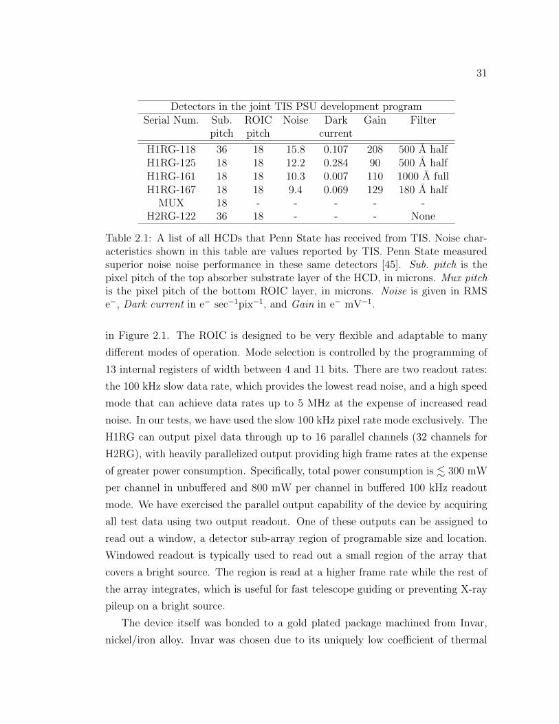
31
Detectors in the joint TIS PSU development programSerial Num. Sub. ROIC Noise Dark Gain Filter
pitch pitch current
H1RG-118 36 18 15.8 0.107 208 500 A halfH1RG-125 18 18 12.2 0.284 90 500 A halfH1RG-161 18 18 10.3 0.007 110 1000 A fullH1RG-167 18 18 9.4 0.069 129 180 A half
MUX 18 - - - - -H2RG-122 36 18 - - - None
Table 2.1: A list of all HCDs that Penn State has received from TIS. Noise char-acteristics shown in this table are values reported by TIS. Penn State measuredsuperior noise noise performance in these same detectors [45]. Sub. pitch is thepixel pitch of the top absorber substrate layer of the HCD, in microns. Mux pitchis the pixel pitch of the bottom ROIC layer, in microns. Noise is given in RMSe−, Dark current in e− sec−1pix−1, and Gain in e− mV−1.
in Figure 2.1. The ROIC is designed to be very flexible and adaptable to many
different modes of operation. Mode selection is controlled by the programming of
13 internal registers of width between 4 and 11 bits. There are two readout rates:
the 100 kHz slow data rate, which provides the lowest read noise, and a high speed
mode that can achieve data rates up to 5 MHz at the expense of increased read
noise. In our tests, we have used the slow 100 kHz pixel rate mode exclusively. The
H1RG can output pixel data through up to 16 parallel channels (32 channels for
H2RG), with heavily parallelized output providing high frame rates at the expense
of greater power consumption. Specifically, total power consumption is . 300 mW
per channel in unbuffered and 800 mW per channel in buffered 100 kHz readout
mode. We have exercised the parallel output capability of the device by acquiring
all test data using two output readout. One of these outputs can be assigned to
read out a window, a detector sub-array region of programable size and location.
Windowed readout is typically used to read out a small region of the array that
covers a bright source. The region is read at a higher frame rate while the rest of
the array integrates, which is useful for fast telescope guiding or preventing X-ray
pileup on a bright source.
The device itself was bonded to a gold plated package machined from Invar,
nickel/iron alloy. Invar was chosen due to its uniquely low coefficient of thermal

32
Figure 2.1: H1RG-125 attached to the cold finger mount. The flex cable can beseen protruding from the bottom of the detector package.
expansion (α = 1.3 · 10−6 K−1), which is relatively well matched to the thermal
expansion of the silicon (α = 2.7·10−6 K−1) in the HCD. Closely matching the ther-
mal expansion coefficients of materials that are bonded to one another is critically
important in both device package design as well as the design of the device itself.
Significant mismatch in thermal expansion can lead to strain induced failures that
occur when the device is cooled to cryogenic temperatures. For laboratory tests
and ground-based operation, Invar represents a good compromise between cost and
performance. For flight applications, where a material with high rigidity per mass
is needed, in addition to good thermal conduction and low thermal expansion, the
packages are typically cast from sintered silicon carbide. In our devices, the gold
coating is applied to the package to decrease the thermal IR emissivity, making
it possible to maintain the device at cryogenic operating temperatures with less
cooling power. Fully packaged H2RG devices are 3-side abuttable, with clearance
necessary on the fourth side for signal lines to be routed to the underside of the
package via wirebonds. Our H1RG devices are not abuttable because they were

33
designed for detector development.
All bias voltage, clock, and signal lines enter and exit the HCD through a series
of 92 pads located in a straight line along the top edge of the ROIC substrate.
These pads are wire bonded to a breakout PCB mounted on the package. The
signal lines are routed, via a second set of wire bonds, from the breakout PCB
to a ceramic connector that wraps around the top and underside of the package.
This connector terminates at an array of 92 pins underneath the package. Lines
are then routed off chip by a flexible circuit cable (flex cable) that terminates at
a 92 contact Hirose connector. The Invar package, the breakout PCB, ceramic
connector, and the flex cable are designed and fabricated by Gerry Lupino at GL
Scientific.
2.1.1 Reference Pixels
The arrays themselves consist of a 1016×1016 pixel active area surrounded by four
columns of reference pixels on the left and right and four rows of reference pixels
on the top and bottom, to form a 1024×1024 array. The reference pixels are stan-
dard ROIC pixels that are not connected to photodiodes in the absorber array,
but instead connected to capacitors with value Cpix = 40 fF, a value chosen to be
similar to the detector capacitance. However, in reality the effective capacitance
of the reference pixels will be ∼ 60 fF due to the parasitic capacitances of other
components in the signal chain such as amplifiers and switches. These pixels were
designed for tracking sensitivity variations in the signal chain due to temperature
variations or bias voltage drift. They are sampled with each image and can there-
fore be used during data post processing to remove row offsets. However, they can
be used most effectively by sampling their values mid-data stream, a scheme that
can be implemented natively using the ROIC’s programable readout capability.
Also, at the top of the array, there is an additional row of reference pixels that
are connected to capacitors with a range of values. The capacitors have values of
Cpix = 10, 20, 40, 80 fF. This row is intended to be used for testing and diagnostics,
and is automatically deactivated during normal readout.
An additional reference and calibration feature of the H1RG is the inclusion
of temperature sensors directly on the ROIC substrate. Two long, thin, line-

34
structures of aluminum metal deposited around the ROIC perimeter form two
individual resistive thermal device (RTD) temperature sensors. In our devices, the
temperature sensors have not been wire bonded to the output and therefore cannot
be used. If they were bonded, the sensors would be used in the usual way, where
a small constant current is passed through the sensor, the voltage drop across
the sensor is measured, and its resistance calculated. Using such a method, there
is always a tradeoff between temperature resolution and self heating. For large
currents, the voltage drop across the sensor will be large and easily measurable,
but self-heating due to Joule heating will be non-negligible. For small currents, the
voltage drop will be small and difficult to measure. A current of 1 mA is suggested.
The ROIC pixel is a seven-transistor design patterned using a 250 nm CMOS
process. A simplified schematic of the pixel, with the various reset and read con-
trols, is shown in Figure 2.2. The schematic shows individual horizontal and verti-
cal pixel reset logic lines, indicating that single pixels can be individually reset, in
addition to the more standard row and global chip resets. This is useful because,
unlike with global or row reset, where pixels at the end of a row or end of the
frame integrate for longer times, it allows for a constant integration time between
the reset and readout of each pixel. Also, with row and global resets, the smallest
achievable integration time is limited to the row and full frame read time, respec-
tively. With single pixel reset, the minimum pixel integration time is limited by
the readout clock speed. In all of our tests we use the default row reset clocking
mode. The small, 512/100 kHz = 5.12 msec, increase in integration time of the
pixels at the end of a row is minor in comparison to the 10242/(1/100 kHz) =
5.24 sec integration time of the pixels. Additional transistors, not shown in the
diagram, enable the detector’s guide mode feature.
2.1.2 Bare MUX
With the original shipment of detectors, we also received a fully packaged, bare
ROIC device known as the Mux. Such devices have packages and ROICs identical
to the real HCDs, which gives them digital, thermal, and mechanical properties
very similar to the fully-functioning devices. Since the ROIC has not been flip-chip
bonded to an absorber, they are significantly cheaper than full devices. Obviously,

35
Figure 2.2: A simplified electronic schematic of an HxRG pixel.
they will not respond to radiation like an HCD, but their similarities and low cost
made the Mux excellent for electronic and thermal system validation testing.
2.1.3 Anti-Reflection Coating
Traditionally, HyViSITM
detectors have an Anti-Reflection (AR) coating applied
to the front surface of the absorber substrate. The coating is intended for optical
spectrum applications, where it reduces the fraction of photons that are reflected
from the absorber’s surface. This improves transmittance through the boundary
between the vacuum and the silicon bulk and, therefore, improves the detector’s
quantum efficiency. However, in the X-ray regime, where the reflectance of surfaces
is negligible at all but extremely small angles of incidence, the AR coating provides
no benefit and only attenuates the incident flux. Consequently, we specified that
all of the PSU devices be fabricated without an AR coating.
2.1.4 Filter Deposition
Regardless of whether the focal plane array of an X-ray telescope is a CCD or
CMOS device, in both cases the active region of the detector consists of biased sil-
icon. Due to silicon’s 1.17 eV band gap at detector operating temperatures, biased
silicon is sensitive to near infrared, optical, soft X-ray, higher energy electromag-

36
netic radiation, and cosmic rays. In order to isolate the signal of interest, which in
this case is soft X-rays, all sources of background must somehow be prevented from
reaching the detector or removed after detection. On board the Chandra satellite,
low energy (< 100 keV) electrons focused by the X-ray mirror are prevented from
reaching the focal plane by a magnetic baffle and unfocused X-rays are blocked by
tantalum baffles. Shielding cosmic rays is very difficult, requiring either a powerful
magnetic field to redirect or a heavy shield to absorb the particle radiation. Since
cosmic rays generate a detector response that is both unique in its size and geome-
try, the background signal is instead removed from X-ray satellite data during post
processing. Near-infrared and optical photons, which are both efficiently focused
by X-ray optics, cannot be effectively removed with post processing, necessitating
an optical blocking filter (OBF) in the telescope design.
On Suzaku, XMM, Chandra, and ASCA the OBFs consist of aluminum de-
posited onto a thin polymer film. In this design, the aluminum heavily attenuates
optical light and the polymer film acts as a deposition substrate and mechani-
cal support. While these filters have been shown to work very well in space, a
drawback of the design is that the filter’s mechanical support does not contribute
to blocking optical light, but it increases X-ray attenuation, especially near the
support material’s absorption edges. On Suzaku, photoelectric absorption due to
carbon (284.2 eV), nitrogen (409.9 eV), and oxygen (543.1 eV) in the polyimide
(C22H10N2O5) OBF substrate produces clearly visible edges in the measured soft
X-ray transmission of the filters [46] (Figure 2.3). On Chandra, the filter’s spec-
tral response is well fit by a model that includes significant absorption edges from
carbon and oxygen in the Lexan (C16H14O3) OBF [47] (Figure 2.4). The ultimate
observatory sensitivity loss due to these edges is localized to energies in the vicinity
above the absorption edges and can be significant, with up to 20% transmission
loss in the carbon edge. The PSU X-ray group has developed a new technique for
filtering background optical light that avoids absorption from the polymer filter
component; the aluminum filter is instead applied directly to the surface of the
detector. This technique was not practical in the past because X-ray CCDs were
primarily front-illuminated detectors. Such detectors have exposed gate structures
on their front surfaces, which would have to be electrically insulated from a di-
rectly applied metallic optical blocking filter and would complicate the process of

37
depositing a uniform OBF film. Our HCDs on the other hand, have a uniform SiO2
front-side surface, which readily accepts the deposition of an aluminum OBF. We
successfully experimented with front-side deposited OBF thicknesses of 180, 500,
and 1000 A.
Figure 2.3: Measured soft X-ray transmission of six OBFs built for Suzaku. Notethe carbon, nitrogen, and oxygen absorption edges from the OBF substrate at284.2, 409.9, and 543.1 eV, respectively. [46]
2.2 TIS SIDECARTM
The SIDECARTM
(System for Image Digitization, Enhancement, Control and Re-
trieval) is an application specific integrated circuit (ASIC) designed and sold by
TIS for the express purpose of controlling HxRG detector hardware. The operation

38
Figure 2.4: A model fit to the soft X-ray transmission profile of two Chandra OBFs.The left plot shows data and model fit for an imaging filter and the right plot fora spectroscopic filter. Note the strong attenuation above the carbon edge. [47]
of any imaging detector is no simple task. Many digital clock signals and analog
bias voltages are required as inputs and the data-containing analog video signal
that the detector outputs needs to be amplified, digitized, and buffered before it
can be permanently stored by the data acquisition (DAQ) system on a computer.
In the past, discrete-component circuit boards powered by bench top power sup-
plies were used for clock driving and video signal processing. It is not uncommon
for science cameras to be powered by custom designed electronics. Astronomical
Research Cameras (ARC) is a private company that develops high quality camera
controllers that have been variously known as “Leach controllers”, “ARC con-
trollers”, as well as “SDSU controllers” due to their origins at the San Diego State
University. While these controllers perform very well, they are relatively large,
heavy, and power-hungry devices. Altering the way that they function sometimes
requires physically swapping circuit boards or soldering new components into the
controller. To address the need for a small, low-power, flexible detector control
solution, TIS developed the SIDECARTM
.
The SIDECARTM
combines all of the various driver and signal chain electron-
ics required to operate an HxRG detector onto a single 22×14 mm die. Shown in
Figure 2.5, the SIDECARTM
is available in multiple packaging variants. For labo-
ratory use, the land grid array (LGA) package is available in both cryogenic and
room-temperature development kits. All of the X-ray data shown in this disserta-
tion was acquired with a room-temperature SIDECARTM
development kit. With

39
creative mount design, we were able to run the room-temperature SIDECARTM
with the cryogenic detector and connect the two with a short flex cable to reduce
noise pickup. Besides the USB connection, the only other electronic lines required
to run the camera are an external Vsub (substrate bias) and a 5 V bias power line
that bypasses the USB power. Both of these voltages are supplied externally to
reduce noise.
Figure 2.5: The flight-ready JWST SIDECARTM
package and the laboratory LGApackaging options.
Regarding operation, our room-temperature development kit SIDECARTM
was
mounted to a circuit board that interfaces the device with a computer through

40
a USB connection. With the SIDECARTM
Interactive Development Environment
(IDE) software running on the computer, assembly code is compiled and uploaded
to the SIDECARTM
to begin every power-up procedure. Both the IDE and the
assembly code give the user full access to the plethora of tuning knobs and reconfig-
uration options designed into the SIDECARTM
. Upon power-up, the SIDECARTM
will program the H1RG registers (memory locations). The TIS JAC is an IDL GUI
that automates many operations in the SIDECARTM
and gives the user simplified,
high-level control of the data acquisition process.

Chapter 3Data Reduction and Measurements
of HCD Characteristics
The measurement of a detector’s performance characteristics is a critical step in
evaluating its suitability for science applications. As discussed earlier in Chapter
1, the noise characteristics of a focal plane array play an important role in de-
termining the final sensitivity of, and therefore the science accessible to, a given
instrument. In this chapter, I will discuss the progress that we have made in mea-
suring and understanding the noise, energy resolution, and interpixel capacitance
in TIS HCDs. I will discuss the mechanisms that have been found to dominate
noise in these devices as well as the digital post-processing that we have developed
to reduce the noise contributed by some of these mechanisms. Methods for opti-
mizing energy resolution with post-processing event selection will be shown. Many
of the results shown in this chapter have been published in Bongiorno et al. [48]
and Bongiorno et al. [49] and have been reproduced with permission of the SPIE.
3.1 Test Stand
3.1.1 Temperature Control
In principle, HyViSITM
detectors can be run at room temperature. However, in
practice, room temperature operation is limited to electronics connectivity testing
and not acquiring data from the imaging array. At room temperature, the detec-

42
tor’s output signal is dominated by dark current, making it difficult to measure the
detector characteristics that dominate in the high-performance regime where it is
capable of making scientific measurements. To prevent dark current from saturat-
ing the detector, all H1RG data presented in this chapter were acquired with the
detector held at 150 K. The temperature was measured with a Lakeshore Cryotron-
ics platinum RTD sensor mounted with a screw fastener to the detector package.
Temperature control was achieved with a proportional integral derivative (PID)
control loop modulating the duty cycle of a liquid nitrogen (LN2) pulsing system.
The LN2 was pulsed into a cavity built into the detector’s mount. At 100% duty
cycle, the detector reached ∼90 K. A LabVIEW virtual instrument (VI) controlled
a National Instruments DAQ to perform temperature measurement with the RTD
and operate the LN2 pulsing relay. The LabVIEW VI also ran the PID loop.
3.1.2 Vacuum Chamber
Operating at low temperature required that the detector be maintained in an
environment free of condensable gasses. At 150 K, water vapor is the most readily
condensable gas and the best way to avoid it is to operate inside a vacuum chamber.
All tests were made with the detector mounted to a LN2 cooled cold finger inside a
light-tight, stainless steel vacuum chamber. The chamber was evacuated to ∼ 10−6
mbar by a turbomolecular pump backed by a diaphragm pump.
3.1.3 X-ray Sources
X-rays were produced by a source mounted to a flange on the chamber wall opposite
to the detector, at a distance of ∼ 10 cm. The primary X-ray source was the
radioactive isotope 55Fe, which emits 55Mn Kα (5.89 keV) and Kβ (6.49 keV)
X-rays. Additionally, a source that excited fluorescent emission in target samples
with 210Po α-particle emission was also used for testing. Neither source was focused
or collimated in any way. This so-called “cube” chamber is shown in Figure 3.1.
For a much more thorough description of vacuum chamber, cryogenic dewar, and
X-ray source design, see Chapter 4, where I describe a different test stand that I
designed and built.
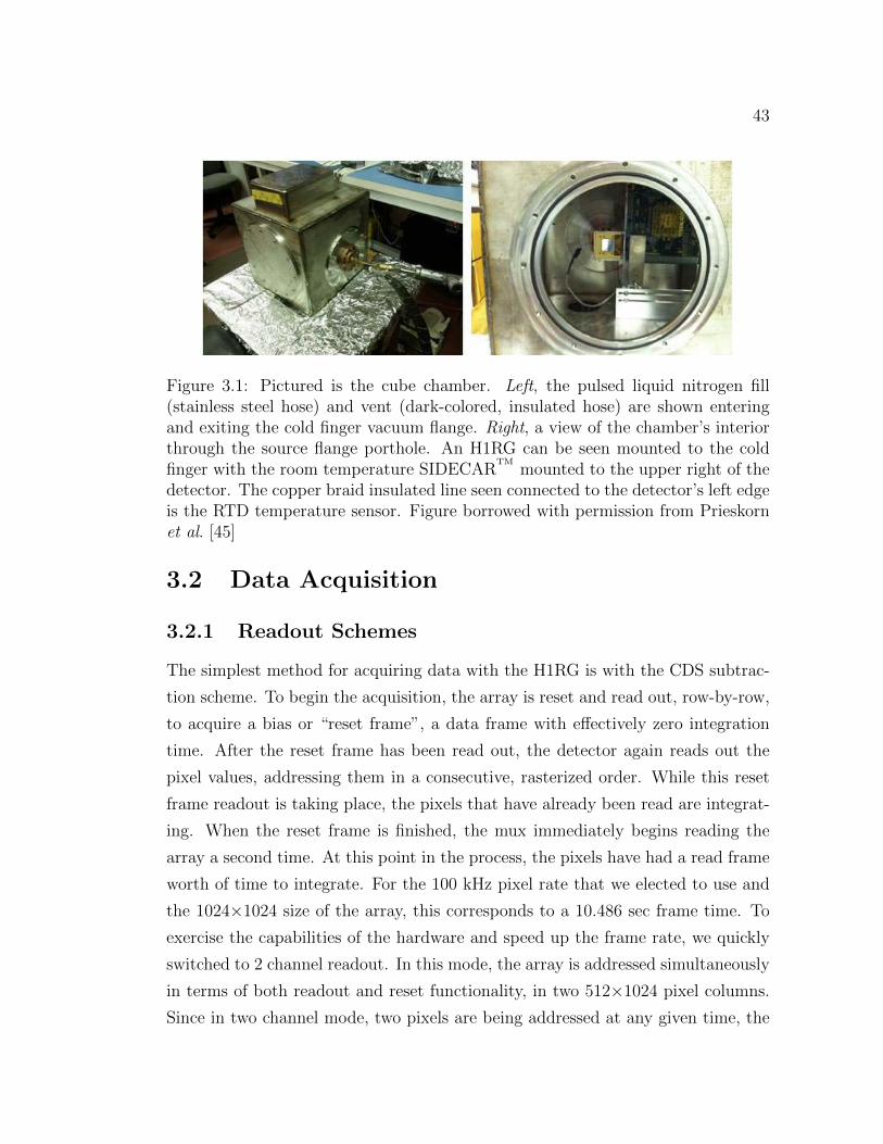
43
Figure 3.1: Pictured is the cube chamber. Left, the pulsed liquid nitrogen fill(stainless steel hose) and vent (dark-colored, insulated hose) are shown enteringand exiting the cold finger vacuum flange. Right, a view of the chamber’s interiorthrough the source flange porthole. An H1RG can be seen mounted to the coldfinger with the room temperature SIDECAR
TMmounted to the upper right of the
detector. The copper braid insulated line seen connected to the detector’s left edgeis the RTD temperature sensor. Figure borrowed with permission from Prieskornet al. [45]
3.2 Data Acquisition
3.2.1 Readout Schemes
The simplest method for acquiring data with the H1RG is with the CDS subtrac-
tion scheme. To begin the acquisition, the array is reset and read out, row-by-row,
to acquire a bias or “reset frame”, a data frame with effectively zero integration
time. After the reset frame has been read out, the detector again reads out the
pixel values, addressing them in a consecutive, rasterized order. While this reset
frame readout is taking place, the pixels that have already been read are integrat-
ing. When the reset frame is finished, the mux immediately begins reading the
array a second time. At this point in the process, the pixels have had a read frame
worth of time to integrate. For the 100 kHz pixel rate that we elected to use and
the 1024×1024 size of the array, this corresponds to a 10.486 sec frame time. To
exercise the capabilities of the hardware and speed up the frame rate, we quickly
switched to 2 channel readout. In this mode, the array is addressed simultaneously
in terms of both readout and reset functionality, in two 512×1024 pixel columns.
Since in two channel mode, two pixels are being addressed at any given time, the
44
frame time is cut in half. Therefore our working frame time for all data acquisition
was 5.243 s. Regardless of the number of readout channels, the reset frame was
digitally subtracted from the read frame during post-processing to produce a CDS
subtracted frame. This process removes fixed pattern noise (FPN), a manageable
defect that is common to all CMOS detectors. FPN is not noise in the typical
sense because as the name indicates, it is a fixed pattern across the detector that
is highly correlated from one frame to the next. In our HyViSITM
HCDs, the FPN
is approximately 1,400 RMS e− and the digital CDS subtraction removes it.
The more capable readout scheme that we quickly adopted for all standard
data acquisition is known as up-the-ramp sampling. In this mode, the detector
first resets the array a programmable number of times to flush charge that may
have accumulated in traps from the pixels. After the final reset, the array non-
destructively reads out a programmed number of data frames without any resets.
In optical and infrared data acquisition, the pixel values will steadily increase due
to the gradual accumulation of photons. This pattern in the pixel intensity as a
function of frame number looks like a ramp with constant slope, giving the readout
scheme its name, since sampling happens up the ramp at evenly spaced intervals.
Compared to an equivalent number of CDS reads, up-the-ramp sampling saves a
factor of ∼ 2Nframes/(Nframes + 1) on read time, where Nframes is the number of
data frames. While the efficiency improves with increasing Nframes, the technique
cannot be used with reckless abandon because the pixels will eventually saturate
and, thereafter, become unresponsive. This readout scheme was baselined for the
H2RGs in the JANUS mission concept XCAT instrument [50].
For our data analysis pipeline, I wrote the IDL procedure ramp_cds.pro to
perform the filename parsing and image subtraction necessary for simple CDS and
up-the-ramp CDS data reduction.
3.2.2 FET Leakage Current
When the H1RG was first plugged into the SIDECARTM
and run with the default
machine code, we observed an extreme gradient pattern in the image data instead
of the expected image of a noisy background speckled with X-rays. After consult-
ing the literature and finding no indication of the source of the problem, we spoke

45
with TIS engineers and discovered that the pattern was due to current leakage onto
the input of a FET in the SIDECARTM
preamplifiers. The FET leakage current
is pertinent to a discussion of detector noise characteristics because it results in
an offset of the pixel signals, which decreases dynamic range. See Figure 3.2 for
an electronics schematic that shows the relevant circuitry. In the preamplifiers, a
reference voltage is compared to the input signal. When the SIDECARTM
is run at
room temperature, thermally excited charge carriers accumulate on Cfb, the feed-
back capacitor, altering the preamplifier’s reference voltage level. This current’s
temperature dependence follows the Shockley diode equation, where IL ∝ e(1/T ),
which indicates that the effect should be negligible when the SIDECARTM
is run at
cryogenic temperatures. TIS confirmed through private communication that FET
leakage current is negligible at cryogenic temperatures, however, we were not able
to take advantage of this because this PSU SIDECARTM
can only be run at room
temperature (note, there is a cryogenic version of the SIDECARTM
). With the
SIDECARTM
at room temperature, we observed that enough charge was accumu-
lating on Cfb to shift the ADC output by thousands of DN. The solution, which
was implemented on existing hardware, was to alter the SIDECARTM
assembly
code such that the preamplifier FET’s input capacitor was reset before each row
of the detector was read out.
3.2.3 Row Noise Correction
Despite the marked improvement in the data after the row-by-row FET reset
scheme was implemented, we were still left with horizontal artifacts, or “row noise”,
in the images after the CDS subtraction. This horizontal banding is uncorrelated
between different rows and different frames. TIS has stated that it is due to un-
certainty in the amount of charge left on the preamplifier feedback capacitor after
reset. Attempts were made to subtract off the row noise by using the H1RG’s ref-
erence pixels. The reference pixels are a four pixel wide border of Mux pixels that
surround the imaging array and are connected to passive capacitors rather than
a PIN photo-diode. Such methods did not provide optimal solutions because, as
seen in Figure 3.17 at the end of this chapter, the row noise is not constant across
a row. To solve the problem, a specialized boxcar filter function, pixcal.pro, was

46
Figure 3.2: Electronics schematic of a preamplifier in the SIDECARTM
. Each ofthe SIDECAR
TM’s 32 channels contains an entire signal chain, including the shown
preamplifier circuitry.
developed. A 1 row ×15 column boxcar moves across each row, subtracting a value
calculated with the boxcar function from the center pixel. We experimented with
multiple boxcar functions, including the 15 pixel mean, median, and the robust
mean. The robust mean, an algorithm that rejects outliers before averaging a set
of numbers, was chosen because its value was not skewed by pixels containing X-
ray signal (unlike the mean) and did not significantly alter the noise distribution
(unlike the median). The boxcar function treats each detector output channel
individually because there is a discontinuity in the row noise at the channel bor-
der. This technique was successful, producing images free of horizontal artifacts.
Figure 3.3 shows an early demonstration of the median filter subtraction, which
was eventually replaced with robust mean filtering. Note, the only reason that
this technique works is because all X-ray data consists of very small (3×3 pixel)
regions of high signal overlaid on top of a flat, low-signal background.
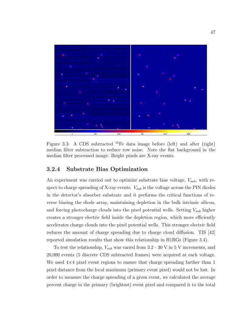
47
Figure 3.3: A CDS subtracted 55Fe data image before (left) and after (right)median filter subtraction to reduce row noise. Note the flat background in themedian filter processed image. Bright pixels are X-ray events.
3.2.4 Substrate Bias Optimization
An experiment was carried out to optimize substrate bias voltage, Vsub, with re-
spect to charge spreading of X-ray events. Vsub is the voltage across the PIN diodes
in the detector’s absorber substrate and it performs the critical functions of re-
verse biasing the diode array, maintaining depletion in the bulk intrinsic silicon,
and forcing photocharge clouds into the pixel potential wells. Setting Vsub higher
creates a stronger electric field inside the depletion region, which more efficiently
accelerates charge clouds into the pixel potential wells. This stronger electric field
reduces the amount of charge spreading due to charge cloud diffusion. TIS [42]
reported simulation results that show this relationship in H1RGs (Figure 3.4).
To test the relationship, Vsub was varied from 3.2 - 30 V in 5 V increments, and
20,000 events (5 discrete CDS subtracted frames) were acquired at each voltage.
We used 4×4 pixel event regions to ensure that charge spreading farther than 1
pixel distance from the local maximum (primary event pixel) would not be lost. In
order to measure the charge spreading of a given event, we calculated the average
percent charge in the primary (brightest) event pixel and compared it to the total
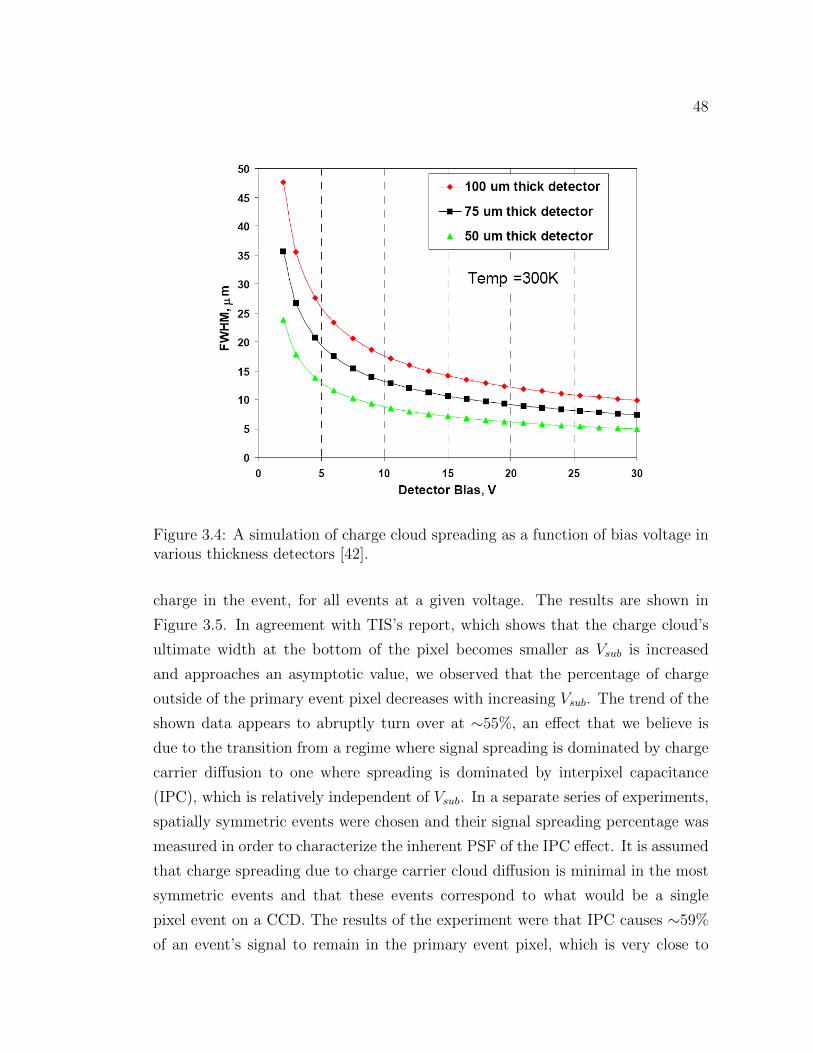
48
Figure 3.4: A simulation of charge cloud spreading as a function of bias voltage invarious thickness detectors [42].
charge in the event, for all events at a given voltage. The results are shown in
Figure 3.5. In agreement with TIS’s report, which shows that the charge cloud’s
ultimate width at the bottom of the pixel becomes smaller as Vsub is increased
and approaches an asymptotic value, we observed that the percentage of charge
outside of the primary event pixel decreases with increasing Vsub. The trend of the
shown data appears to abruptly turn over at ∼55%, an effect that we believe is
due to the transition from a regime where signal spreading is dominated by charge
carrier diffusion to one where spreading is dominated by interpixel capacitance
(IPC), which is relatively independent of Vsub. In a separate series of experiments,
spatially symmetric events were chosen and their signal spreading percentage was
measured in order to characterize the inherent PSF of the IPC effect. It is assumed
that charge spreading due to charge carrier cloud diffusion is minimal in the most
symmetric events and that these events correspond to what would be a single
pixel event on a CCD. The results of the experiment were that IPC causes ∼59%
of an event’s signal to remain in the primary event pixel, which is very close to
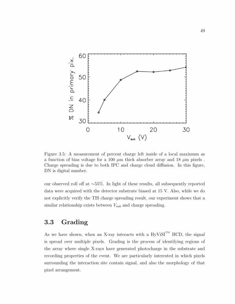
49
Figure 3.5: A measurement of percent charge left inside of a local maximum asa function of bias voltage for a 100 µm thick absorber array and 18 µm pixels .Charge spreading is due to both IPC and charge cloud diffusion. In this figure,DN is digital number.
our observed roll off at ∼55%. In light of these results, all subsequently reported
data were acquired with the detector substrate biased at 15 V. Also, while we do
not explicitly verify the TIS charge spreading result, our experiment shows that a
similar relationship exists between Vsub and charge spreading.
3.3 Grading
As we have shown, when an X-ray interacts with a HyViSITM
HCD, the signal
is spread over multiple pixels. Grading is the process of identifying regions of
the array where single X-rays have generated photocharge in the substrate and
recording properties of the event. We are particularly interested in which pixels
surrounding the interaction site contain signal, and also the morphology of that
pixel arrangement.

50
Our first step in event grading is to identify events. In order to be considered
an event, we require that a pixel satisfy a primary threshold value that is set
≈ 4σ above the noise floor. Additionally, the pixel must also be a local maximum,
greater in value than its 8 surrounding pixels. Next, we identify which of the 8
pixels in the surrounding 3×3 region contain significant signal by requiring that
they satisfy a 3σ secondary event threshold in order to be counted in the event
sum. Setting the secondary threshold as high as possible allows fewer surrounding
pixels to be counted towards the sum and minimizes the read noise affecting the
event sum. However, setting the secondary threshold too high causes signal to
be excluded from the event sum. These parameters must be tuned. The IDL
procedures event_detect.pro and make_evtlist.pro were written to accomplish
these tasks.
In X-ray CCDs, events are also assigned a number according to their morphol-
ogy. The IDL procedure grade_evts.pro was written to perform this task. This
grade number indicates which pixels in the event satisfy the secondary threshold
and are used to separate good events from bad detections. However, due to the
≈ 30% charge spreading effect of IPC in our HCD, the direct application of mor-
phology grades has not proven to be as useful for HCD analysis as it has been for
X-ray CCDs. Instead, to quantify event morphology, we calculate the fraction of
the primary event pixel contained in the second brightest pixel; simply the value
of the second brightest pixel in an event divided by the value of the brightest pixel.
We have named this quantity the “percent split”. Note that despite being named
percent split, the quantity is always shown as a fraction.
During the hardware and software development process it was very useful to
be able to the visualize the large numbers (∼ 106) of events in the event list
data products. The IDL procedure disp_evts.pro takes event list data as input
and outputs a FITS image where the events have been arranged in a regular grid
pattern for easy visual inspection. The intentional inclusion or exclusion of X-
ray events from post-processing analysis based on various criteria, something we
call “filtering”, has proven to be very useful for improving energy resolution. The
highly vectorized IDL function evt_filter.pro was written to accomplish this
task.
To visualize what the percent split of all events looks like, we plot a histogram
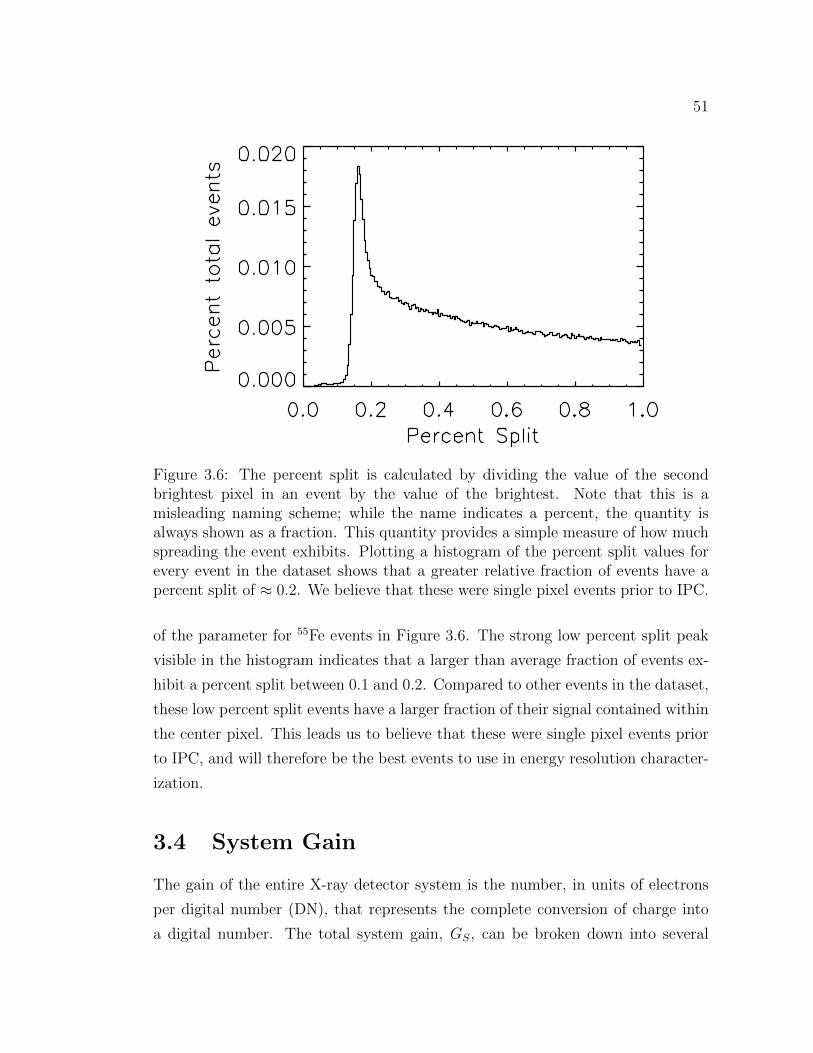
51
Figure 3.6: The percent split is calculated by dividing the value of the secondbrightest pixel in an event by the value of the brightest. Note that this is amisleading naming scheme; while the name indicates a percent, the quantity isalways shown as a fraction. This quantity provides a simple measure of how muchspreading the event exhibits. Plotting a histogram of the percent split values forevery event in the dataset shows that a greater relative fraction of events have apercent split of ≈ 0.2. We believe that these were single pixel events prior to IPC.
of the parameter for 55Fe events in Figure 3.6. The strong low percent split peak
visible in the histogram indicates that a larger than average fraction of events ex-
hibit a percent split between 0.1 and 0.2. Compared to other events in the dataset,
these low percent split events have a larger fraction of their signal contained within
the center pixel. This leads us to believe that these were single pixel events prior
to IPC, and will therefore be the best events to use in energy resolution character-
ization.
3.4 System Gain
The gain of the entire X-ray detector system is the number, in units of electrons
per digital number (DN), that represents the complete conversion of charge into
a digital number. The total system gain, GS, can be broken down into several

52
factors,
1
GS
[DN
e−
]=
1
C
[V
e−
]GE GADC
[DN
V
]. (3.1)
When the charge in a pixel is read, the capacitance, C, of the output node deter-
mines the voltage signal produced by a given amount of charge in the pixel. Finally,
this voltage is amplified by an electronics gain, GE and digitized by an ADC that
outputs a digital number DNSAR. The ADC has its own gain, GADC . We measure
the total system gain by producing graded event spectra and observing the DN
value of the 55Mn Kα 5.9 keV X-ray line.
All measurements in this dissertation were taken with the 16-bit successive
approximation (SAR) ADCs. The approximate digital number output of the elec-
tronics, DNSAR, as a function of input voltage Vin, is
DNSAR = 32768 GVin − VrefVRP − VRN
+ 32768 (3.2)
[39], where Vref = 1.29228, VRP = 1.81417, and VRN = 0.123167 are bias volt-
ages that were used to acquire all data and G = 8 is the SIDECARTM
preamp
gain. These quoted bias voltages are nominal DAC output values reported by the
SIDECARTM
control software. Their precision is not known. Later it will be useful
to know the shift, in DN of the ADC output for a given change, in mV, at the
analog input, something I will refer to as the ADC gain. This number is calculated
by differentiating the expression for DNSAR with respect to Vin, which results in
32768 G/(VRP −VRN) = 443.286 DN mV−1. Removing the preamplifier gain gives
an ADC gain of 55.411 DN mV−1.
3.4.0.1 Preamplifier Gain Optimization
With register programming, the preamplifier gain can be set to one of 16 different
settings separated by 3 dB, ranging from −3 dB to 27 dB. To optimize the gain,
dark images were taken with a 150 K detector at successive gain values and exam-
ined for saturation. In order to leave additional dynamic range headroom for dark
current and X-ray signal, gain setting 11, which corresponds to G = 8, was chosen
and used in all successive data acquisition.
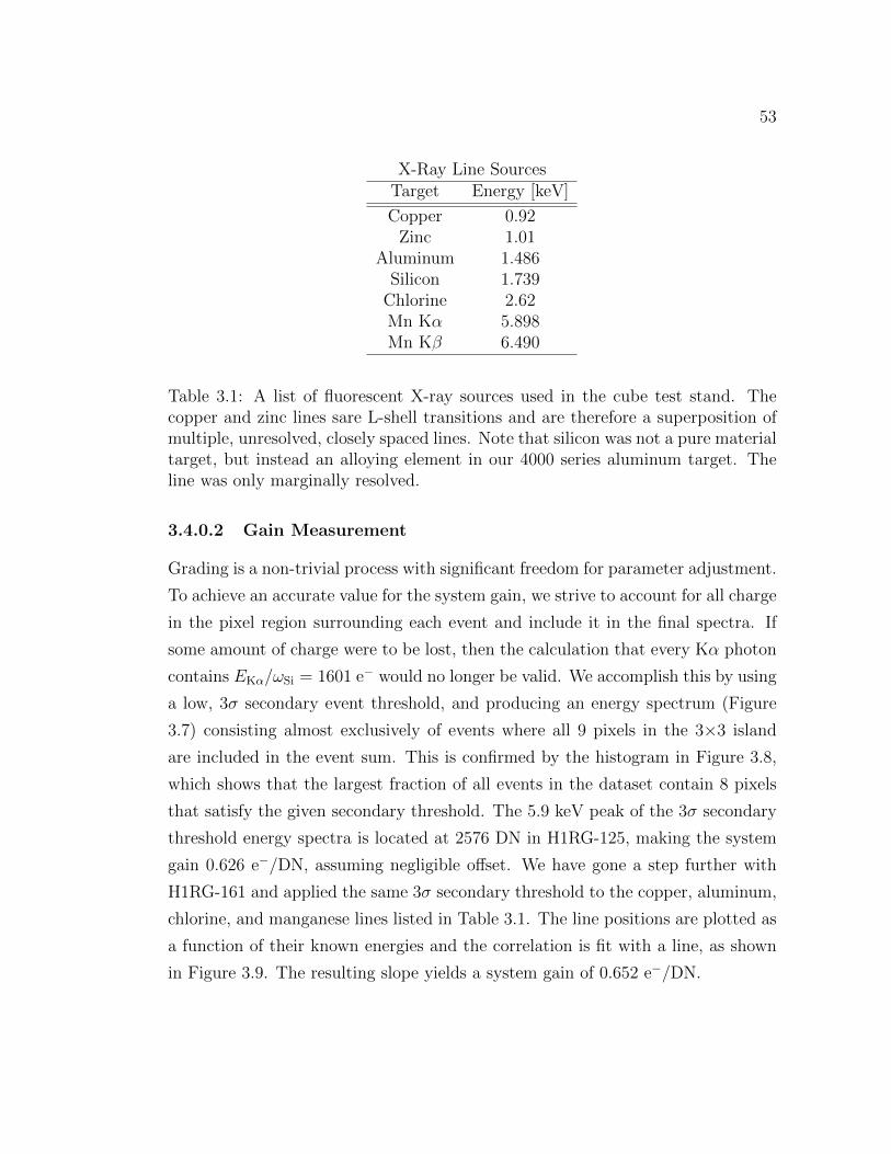
53
X-Ray Line SourcesTarget Energy [keV]
Copper 0.92Zinc 1.01
Aluminum 1.486Silicon 1.739
Chlorine 2.62Mn Kα 5.898Mn Kβ 6.490
Table 3.1: A list of fluorescent X-ray sources used in the cube test stand. Thecopper and zinc lines sare L-shell transitions and are therefore a superposition ofmultiple, unresolved, closely spaced lines. Note that silicon was not a pure materialtarget, but instead an alloying element in our 4000 series aluminum target. Theline was only marginally resolved.
3.4.0.2 Gain Measurement
Grading is a non-trivial process with significant freedom for parameter adjustment.
To achieve an accurate value for the system gain, we strive to account for all charge
in the pixel region surrounding each event and include it in the final spectra. If
some amount of charge were to be lost, then the calculation that every Kα photon
contains EKα/ωSi = 1601 e− would no longer be valid. We accomplish this by using
a low, 3σ secondary event threshold, and producing an energy spectrum (Figure
3.7) consisting almost exclusively of events where all 9 pixels in the 3×3 island
are included in the event sum. This is confirmed by the histogram in Figure 3.8,
which shows that the largest fraction of all events in the dataset contain 8 pixels
that satisfy the given secondary threshold. The 5.9 keV peak of the 3σ secondary
threshold energy spectra is located at 2576 DN in H1RG-125, making the system
gain 0.626 e−/DN, assuming negligible offset. We have gone a step further with
H1RG-161 and applied the same 3σ secondary threshold to the copper, aluminum,
chlorine, and manganese lines listed in Table 3.1. The line positions are plotted as
a function of their known energies and the correlation is fit with a line, as shown
in Figure 3.9. The resulting slope yields a system gain of 0.652 e−/DN.
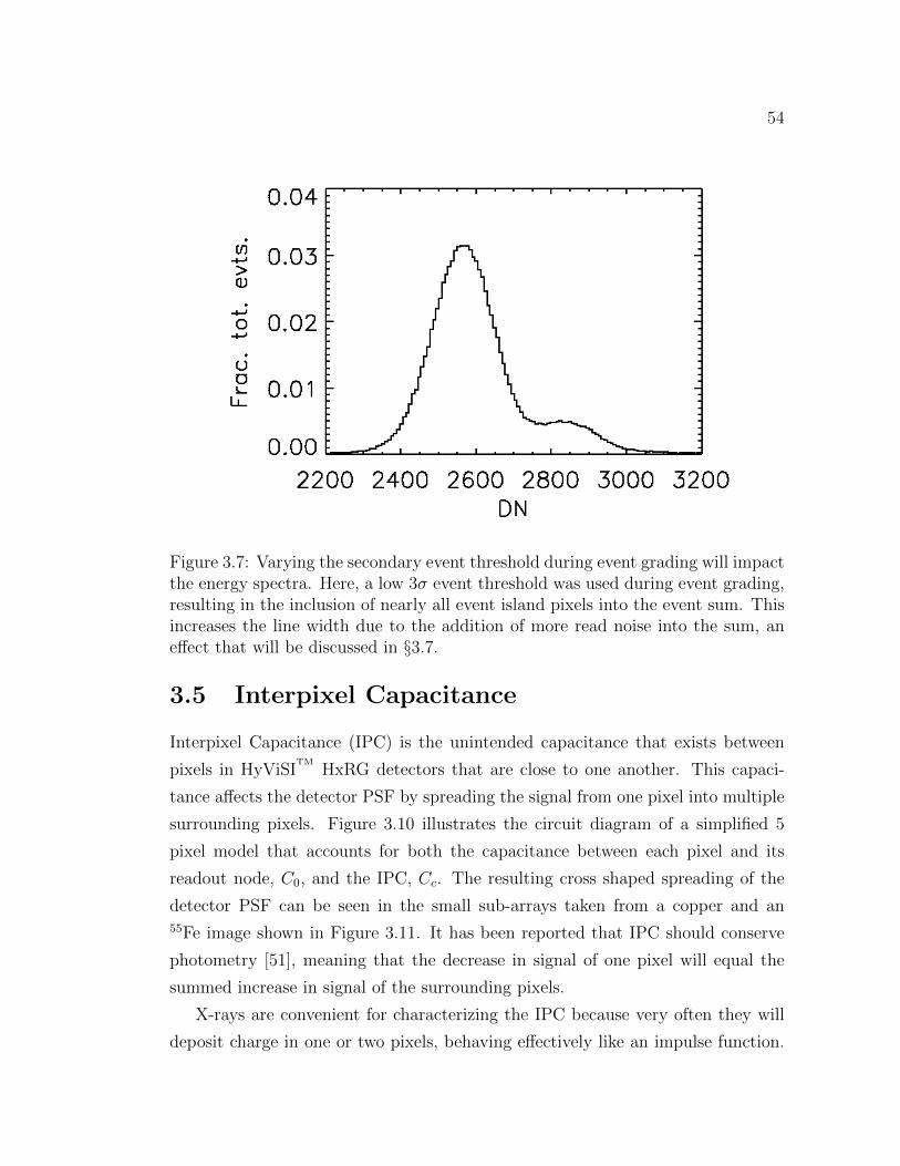
54
Figure 3.7: Varying the secondary event threshold during event grading will impactthe energy spectra. Here, a low 3σ event threshold was used during event grading,resulting in the inclusion of nearly all event island pixels into the event sum. Thisincreases the line width due to the addition of more read noise into the sum, aneffect that will be discussed in §3.7.
3.5 Interpixel Capacitance
Interpixel Capacitance (IPC) is the unintended capacitance that exists between
pixels in HyViSITM
HxRG detectors that are close to one another. This capaci-
tance affects the detector PSF by spreading the signal from one pixel into multiple
surrounding pixels. Figure 3.10 illustrates the circuit diagram of a simplified 5
pixel model that accounts for both the capacitance between each pixel and its
readout node, C0, and the IPC, Cc. The resulting cross shaped spreading of the
detector PSF can be seen in the small sub-arrays taken from a copper and an55Fe image shown in Figure 3.11. It has been reported that IPC should conserve
photometry [51], meaning that the decrease in signal of one pixel will equal the
summed increase in signal of the surrounding pixels.
X-rays are convenient for characterizing the IPC because very often they will
deposit charge in one or two pixels, behaving effectively like an impulse function.

55
Figure 3.8: Every X-ray that interacts with our detector spreads charge over mul-tiple pixels. When we want to calculate the system gain, we set the secondaryevent threshold low (3σ) to ensure that we catch most of the charge in each event.This histogram shows the fraction of events in the dataset where some number ofpixels satisfied the secondary event threshold. With a conservatively set secondarythreshold, most of the pixels in each event island are included in the sum.
However, in reality this characterization process is not trivial. The effects of charge
spreading and IPC combine to create events that are both split and blurred across
multiple pixels. The HCD charge carrier diffusion simulations by Bai et al. , cited
earlier in the bias voltage optimization analysis, predict that a charge carrier cloud
will diffuse to a FWHM of ∼15 µm in a 100 µm detector biased at 15 V. Even
though these results were calculated for a 300 K detector and the charge cloud
size will decrease for a colder detector, this suggests that most X-ray events will
exhibit some degree of charge splitting in a detector with 18 µm pixels. X-rays
that interact deep in the absorber or along the pixel’s center axis will exhibit the
least charge spreading. A more thorough analysis, which is beyond the scope of
this chapter, could better predict the split fraction by accounting for the energy
dependent exponential X-ray absorption depth distribution and the complex 3D
geometry of the electric field near the base of the absorber layer. It is likely that
the field geometry at the base of the pixel will strongly influence how charge clouds
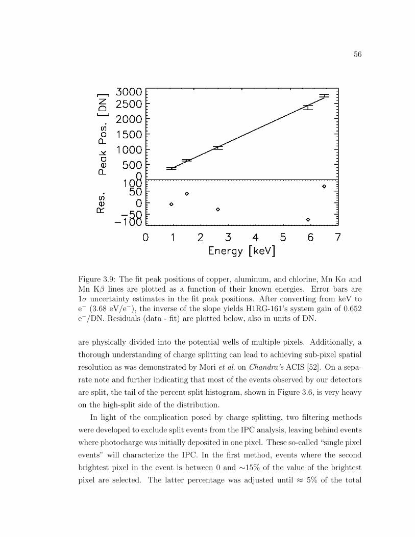
56
Figure 3.9: The fit peak positions of copper, aluminum, and chlorine, Mn Kα andMn Kβ lines are plotted as a function of their known energies. Error bars are1σ uncertainty estimates in the fit peak positions. After converting from keV toe− (3.68 eV/e−), the inverse of the slope yields H1RG-161’s system gain of 0.652e−/DN. Residuals (data - fit) are plotted below, also in units of DN.
are physically divided into the potential wells of multiple pixels. Additionally, a
thorough understanding of charge splitting can lead to achieving sub-pixel spatial
resolution as was demonstrated by Mori et al. on Chandra’s ACIS [52]. On a sepa-
rate note and further indicating that most of the events observed by our detectors
are split, the tail of the percent split histogram, shown in Figure 3.6, is very heavy
on the high-split side of the distribution.
In light of the complication posed by charge splitting, two filtering methods
were developed to exclude split events from the IPC analysis, leaving behind events
where photocharge was initially deposited in one pixel. These so-called “single pixel
events” will characterize the IPC. In the first method, events where the second
brightest pixel in the event is between 0 and ∼15% of the value of the brightest
pixel are selected. The latter percentage was adjusted until ≈ 5% of the total
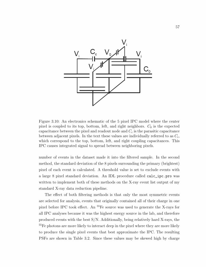
57
Figure 3.10: An electronics schematic of the 5 pixel IPC model where the centerpixel is coupled to its top, bottom, left, and right neighbors. C0 is the expectedcapacitance between the pixel and readout node and Cc is the parasitic capacitancebetween adjacent pixels. In the text these values are individually referred to as Ci,which correspond to the top, bottom, left, and right coupling capacitances. ThisIPC causes integrated signal to spread between neighboring pixels.
number of events in the dataset made it into the filtered sample. In the second
method, the standard deviation of the 8 pixels surrounding the primary (brightest)
pixel of each event is calculated. A threshold value is set to exclude events with
a large 8 pixel standard deviation. An IDL procedure called calc_ipc.pro was
written to implement both of these methods on the X-ray event list output of my
standard X-ray data reduction pipeline.
The effect of both filtering methods is that only the most symmetric events
are selected for analysis, events that originally contained all of their charge in one
pixel before IPC took effect. An 55Fe source was used to generate the X-rays for
all IPC analyses because it was the highest energy source in the lab, and therefore
produced events with the best S/N. Additionally, being relatively hard X-rays, the55Fe photons are more likely to interact deep in the pixel where they are more likely
to produce the single pixel events that best approximate the IPC. The resulting
PSFs are shown in Table 3.2. Since these values may be skewed high by charge

58
Figure 3.11: Two image sub-arrays showing charge spreading effects in 5.98/6.49keV 55Fe (left) and ∼0.9 keV fluoresced copper L (right) X-ray events. In a CCD,X-ray events are typically confined to one or two pixels. However, in HyViSI
TM
H1RG arrays, events typically spread to 8 or 9 pixels. IPC spreading is less visiblein copper X-Rays because they are ≈ 6 times less energetic than 55Fe X-rays andsignal from charge spread into adjacent pixels falls below the detector noise floor.
splitting, they should be considered as upper limits.
Prieskorn et al. [45] used a third approach, termed the “Paired Pixel” method
to vet X-ray events that included charge spreading. Instead of calculating the
standard deviation of all eight pixels surrounding the central pixel, this technique
calculates the standard deviation of the two pixels above/below and to the left-
/right of the central pixel individually. If either of these two values is larger than
1σ of the noise floor, the event is considered asymmetric and rejected. Compared
to the eight pixel standard deviation method, this technique is more sensitive to
asymmetry, and consequently, more sensitive to charge spreading. The IPC in four
HCDs was measured with this method using 55Fe data. The results are shown in
Table 3.3
The IPC of HyViSITM
H1RG detectors has been characterized by Finger et
al. [51], though their method is different and involves producing an inverse IPC
pattern by continually resetting a 1 pixel window region in an array under uniform
illumination. Their result, shown in Table 3.2, has been truncated to a normalized
3×3 region so that it can be directly compared to our work.
With the measured IPC and the assumption that IPC conserves photometry,

59
Second BrightestH1RG-125
0.013 0.047 0.0120.076 0.701 0.0680.014 0.049 0.013
Second BrightestH1RG-161
0.012 0.046 0.0120.072 0.712 0.0710.012 0.047 0.012
Window Reset0.022 0.060 0.0210.069 0.668 0.0580.021 0.056 0.021
Standard DeviationH1RG-125
0.013±0.009 0.070±0.027 0.020±0.0110.070±0.024 0.630±0.140 0.024±0.0240.024±0.019 0.070±0.019 0.013±0.013
Standard DeviationH1RG-161
0.008±0.010 0.063±0.020 0.009±0.0090.067±0.022 0.71±0.14 0.061±0.0200.011±0.013 0.064±0.022 0.008±0.009
Standard DeviationH1RG-167
0.017±0.037 0.077±0.010 0.018±0.0040.082±0.009 0.610±0.049 0.081±0.0020.017±0.004 0.080±0.014 0.018±0.004
Standard DeviationH2RG-122
0.007±0.010 0.016±0.009 0.007±0.0110.017±0.009 0.905±0.110 0.017±0.0100.007±0.010 0.017±0.009 0.007±0.011
Table 3.2: Top: the 3×3 IPC PSF obtained by averaging symmetrical events se-lected with the second brightest pixel method in our detectors H1RG-125 andH1RG-161 and the IPC PSF of a different HyViSI
TMH1RG using a 1×1 pixel
window reset method [51]. The remainder of the table presents results for differentdetectors with the standard deviation method from Griffith et al. [53]. Quoteduncertainties were calculated individually for each pixel position in the 3×3 grid.The standard deviation of each set of values was calculated and scaled by the nor-malization to yield the uncertainty. Both read noise and the unintended inclusionof charge spreading are represented in the uncertainties.
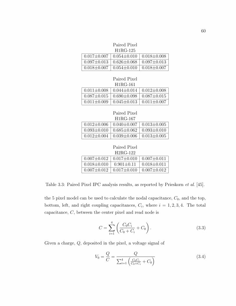
60
Paired PixelH1RG-125
0.017±0.007 0.054±0.010 0.018±0.0080.097±0.013 0.626±0.068 0.097±0.0130.018±0.007 0.054±0.010 0.018±0.007
Paired PixelH1RG-161
0.011±0.008 0.044±0.014 0.012±0.0080.087±0.015 0.690±0.098 0.087±0.0150.011±0.009 0.045±0.013 0.011±0.007
Paired PixelH1RG-167
0.012±0.006 0.040±0.007 0.013±0.0050.093±0.010 0.685±0.062 0.093±0.0100.012±0.004 0.039±0.006 0.013±0.005
Paired PixelH2RG-122
0.007±0.012 0.017±0.010 0.007±0.0110.018±0.010 0.901±0.11 0.018±0.0110.007±0.012 0.017±0.010 0.007±0.012
Table 3.3: Paired Pixel IPC analysis results, as reported by Prieskorn et al. [45].
the 5 pixel model can be used to calculate the nodal capacitance, C0, and the top,
bottom, left, and right coupling capacitances, Ci, where i = 1, 2, 3, 4. The total
capacitance, C, between the center pixel and read node is
C =4∑i=1
(C0CiC0 + Ci
+ C0
). (3.3)
Given a charge, Q, deposited in the pixel, a voltage signal of
V0 =Q
C=
Q∑4i=1
(C0CiC0+Ci
+ C0
) (3.4)

61
will be produced in the center pixel and
Vi = V0 −Qi
Ci=
Q CiC0+Ci∑4
i=1
(C0CiC0+Ci
+ C0
) (3.5)
will be produced in each of the four adjacent pixels. An average 55Fe X-ray will
produce Q =(
5.89r1+r
+ 6.491+r
)1ωSi
= 1621 e− in the detector, where r = 6.79 is the
Kα/Kβ line intensity ratio that will be derived in Chapter 4 §4.3.3. This signal
level, in number of electrons, can be converted to DN with the measured gain of
0.652 e− DN−1. To find the single pixel voltage, V , of an average 55Fe X-ray, the
DN value is divided by the ADC gain from §3.4 and the preamp gain. This number,
multiplied by the normalized IPC values, yields V0 and Vi. Solving for C0 and the
four Ci values with IDL’s Newton algorithm yields values of C0 = 8.1 ·10−15 F and
Ci = 9.4 · 10−16, 6.5 · 10−16, 1.1 · 10−15, and 6.9 · 10−16 F, which correspond to the
right, top, left, and bottom components of the IPC, respectively. Alternatively,
the DN values of a set of averaged X-ray events that have been filtered to include
only those with minimal asymmetry (charge spreading) could be divided by the
ADC gain and preamp gain to calculate Vi and V0.
3.5.1 Deconvolution
We performed a pathfinder study to evaluate the potential benefits of deconvo-
lution techniques for mitigating the negative effect that IPC has on HCD X-ray
performance. In our tests, we used the IDL Astronomy User’s Library’s maxi-
mum likelihood estimator, max_likelihood.pro. The algorithm performs Lucy-
Richardson (LR) deconvolution to iteratively solve for the maximum probability
latent image, given an observed image and a convolution kernel. In any detector
system, the latent, or ideal, unblurred image is convolved with the detector sys-
tem’s response, or PSF, to form the observed image. The PSF characterizes the
output image’s departure from the ideal at each point in the detector plane. In
optics, it includes factors such as blurring caused by diffraction, distortion inherent
to the optical prescription, and additional distortion due to misshapen optics. In
the case of an H1RG detecting unfocused X-rays, the PSF is dominated by IPC
and charge spreading.
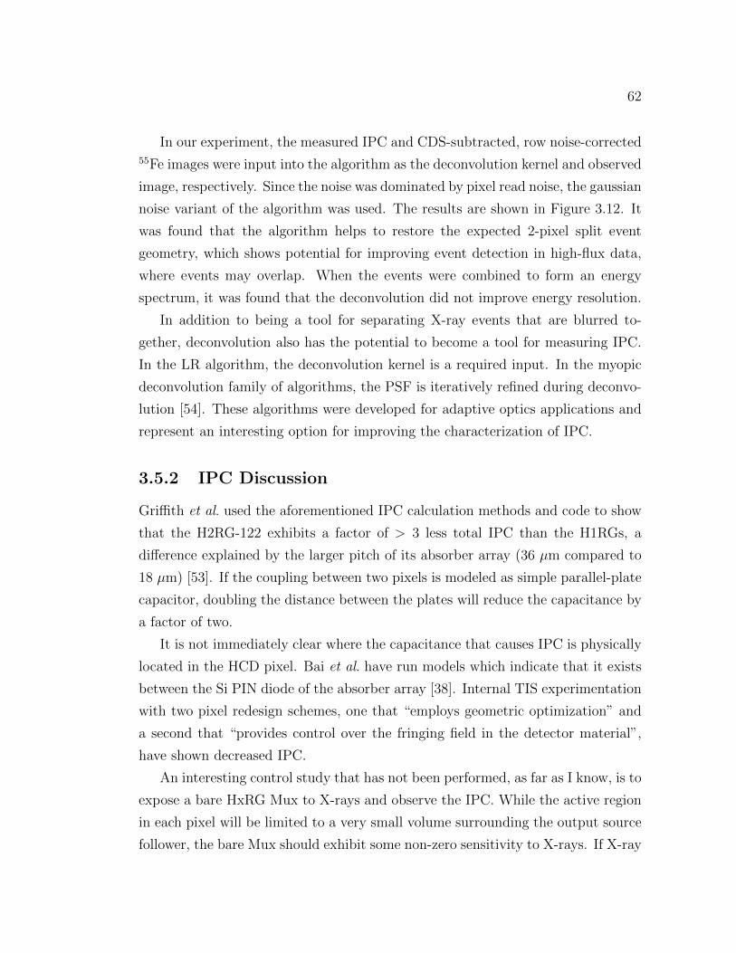
62
In our experiment, the measured IPC and CDS-subtracted, row noise-corrected55Fe images were input into the algorithm as the deconvolution kernel and observed
image, respectively. Since the noise was dominated by pixel read noise, the gaussian
noise variant of the algorithm was used. The results are shown in Figure 3.12. It
was found that the algorithm helps to restore the expected 2-pixel split event
geometry, which shows potential for improving event detection in high-flux data,
where events may overlap. When the events were combined to form an energy
spectrum, it was found that the deconvolution did not improve energy resolution.
In addition to being a tool for separating X-ray events that are blurred to-
gether, deconvolution also has the potential to become a tool for measuring IPC.
In the LR algorithm, the deconvolution kernel is a required input. In the myopic
deconvolution family of algorithms, the PSF is iteratively refined during deconvo-
lution [54]. These algorithms were developed for adaptive optics applications and
represent an interesting option for improving the characterization of IPC.
3.5.2 IPC Discussion
Griffith et al. used the aforementioned IPC calculation methods and code to show
that the H2RG-122 exhibits a factor of > 3 less total IPC than the H1RGs, a
difference explained by the larger pitch of its absorber array (36 µm compared to
18 µm) [53]. If the coupling between two pixels is modeled as simple parallel-plate
capacitor, doubling the distance between the plates will reduce the capacitance by
a factor of two.
It is not immediately clear where the capacitance that causes IPC is physically
located in the HCD pixel. Bai et al. have run models which indicate that it exists
between the Si PIN diode of the absorber array [38]. Internal TIS experimentation
with two pixel redesign schemes, one that “employs geometric optimization” and
a second that “provides control over the fringing field in the detector material”,
have shown decreased IPC.
An interesting control study that has not been performed, as far as I know, is to
expose a bare HxRG Mux to X-rays and observe the IPC. While the active region
in each pixel will be limited to a very small volume surrounding the output source
follower, the bare Mux should exhibit some non-zero sensitivity to X-rays. If X-ray

63
Figure 3.12: Top, A progression from left to right of 0, 1, 3, 5, 10, and 15 iter-ations of the LR algorithm. It is necessary to view this figure in color in orderto best see the how the deconvolution effectively reverses IPC signal spreading.Bottom, testing LR signal conservation. One single-pixel event was monitored asdeconvolution progressed. The central pixel (red, middle), surrounding 8 pixels(blue, bottom), and 9 pixel total (black, top) values are plotted as a function ofLR iteration number. In this application the algorithm stabilizes very quickly at∼ 9 iterations.

64
events detected in a bare Mux exhibited undetectable spreading, the ROIC could
be definitively ruled out as a source of IPC.
Future detectors, notably those with the TIS Speedster architecture, are being
built with capacitive trans-impedance amplifiers (CTIAs) in place of the source
followers. Since these amplifiers maintain a constant potential at the sense node,
it is expected that they will eliminate IPC. It should be noted that the CTIA
architecture is not a blanket solution to the IPC problem because they have the
design tradeoff of requiring more pixel real estate than the source follower design.
However, since eliminating IPC means that fewer pixels will need to be summed
to reconstruct the energy of an X-ray, devices with CTIAs will likely exhibit bet-
ter energy resolution because they minimize the read noise contribution to event
energy.
3.6 Read Noise
We have measured the CDS noise in each frame of our dataset of X-ray images by
measuring the FWHM of the noise peak in a histogram computed from image pixel
values. This quantity is not skewed high by bright pixels containing X-ray charge
and provides a measurement of the noise as data are being taken. Assuming that
the noise is normally distributed allows us to calculate the noise RMS from the pixel
histogram FWHM. Using the previously calculated system gains we calculate the
CDS noise for H1RG-125 and H1RG-161 to be 7.48 and 8.87 e− RMS respectively.
In detector test reports, Teledyne calculates H1RG-125 and H1RG-161’s mean
CDS noise at 150K to be 12.2 and 10.3 e− RMS. Differing array readout, offset
correction (such as the row noise correction), noise calculation, or conversion gain
may account for the difference.
An interesting idea that takes advantage of the CMOS sensor’s ability to non-
destructively read pixels, is to perform what amounts to Fowler sampling of the
X-rays during post-processing. Low-energy event detection and overall energy res-
olution can be improved by processing the pixel values as a function of frame
number with a time series pattern matching algorithm as opposed to the simple
pixel value differencing and threshold detection approach taken in our CDS sub-
traction scheme. Once an event is detected, pixels in the surrounding region could

65
be fit with step functions, effectively decreasing the read noise with multiple reads.
Since such a scheme derives its advantage from the X-ray arrival times being sepa-
rated by multiple pixel sample periods, it would not do well for flux rates that are
approaching the pileup limit. Similarly, in a detector such as the Speedster, which
contains an in-pixel comparator, perhaps the absorption of an X-ray could trigger
a series of fast reads that would eventually be averaged.
3.7 Energy Resolution
Among the most useful features of X-ray HCDs is that they are imaging spec-
trographs; they have the ability to do simultaneous imaging and non-dispersive
spectroscopy since the energy and location of every X-ray event is recorded by the
detector. The ability of a detector to measure the energy of an incident photon is
described by its energy resolution: R = ∆E/E. The fundamental limit of energy
resolution is set by Fano [6, 7] noise and a detector that performs at this level is
said to be Fano limited. The noise originates in the uncertainty in the number of
electrons generated when an X-ray interacts with a silicon detector. The variance
is
σ2F =
FE
ω, (3.6)
where F is the Fano factor (0.113 for Si), E is the X-ray energy, and ω is the
average electron-hole pair generation energy (3.68 eV for Si). Inserting numbers,
Fano limited performance at 5.898 keV is 0.116 keV, corresponding to an energy
resolution of 2%. Due to the complicated details of solid state physics that they
contain, both F and ω are always measured empirically.
In H1RG HCDs, energy resolution is strongly influenced by the combined effects
of read noise, IPC, and charge spreading. As we have shown, IPC spreads signal
in an event into N pixels, where N depends on the level of IPC in the particular
device. Therefore, in order to fully reconstruct the signal from an event, N pixels
must be summed, and their associated read noise must be summed in quadrature.
If all events were spatially symmetric, we could avoid this significant addition of
noise by reading only each event’s central pixel value and accounting for the missed

66
adjacent pixel charge with a constant factor that would be absorbed into our
measurement of the system gain. Unfortunately this method, and similar variants,
fail because many events are asymmetric because of electron cloud diffusion charge
spreading. To improve energy resolution, we first specify a low percent split range,
essentially picking out only the most symmetric events, events that will require
the fewest read pixels to accurately measure charge content. Second, we tune
the secondary threshold to find a balance between excluding low signal pixels
that contribute more noise than signal to the total energy and including pixels
that contribute asymmetrically distributed charge that cannot be accounted for
by constant factors in the system gain.
The spectrum that results from this method is shown in Figure 3.13 and the
measured energy resolutions are plotted as a function of energy in Figure 3.14.
We have found that the optimal secondary threshold increases with energy and we
have shown this measured relationship in Figure 3.15. This relationship is expected
since the height of each event’s spatial profile will scale with total energy. If we
expect to use the secondary threshold to cutoff a constant fraction of dim pixels to
maintain ≈ 5 pixels in each event, the secondary threshold will have to scale with
energy.
In our system energy resolution is dependent on particular parameters used in
data reduction. The choice of primary and secondary event thresholds and event
morphology strongly affect the energy resolution. Using events with a split percent
between 0 and 0.2, and specifying a very large 9σ secondary event threshold, we
obtain the spectrum in Figure 3.16, which has ∆E/E = 4.2%. Specifying such
a high event threshold is simply a roundabout method for choosing a particular
shape for summing pixels in the events. 95% of the events were cross shaped
after specifying such a high threshold, implying a centralized X-ray hit with IPC
inducing signal in pixels above, below, and to the sides of the center pixel. Such
filtering produces a well resolved spectrum because we require that the events be
single or nearly single pixel events before IPC and then effectively choose to sum
only the top, bottom, left, right and center pixels. The method is minimizing the
number of pixel reads required to get an accurate measurement of event energy.
In general, the nondispersive X-ray energy resolution of a photon detector (in-

67
Figure 3.13: A combined aluminum, chlorine, and manganese Kα/Kβ energy spec-trum generated by selecting events with low percent split and tuning secondaryevent threshold for each energy. This spectrum has ∆E/E=4.2% at 5.9 keV.
cluding proportional counters, CCDs, and HCDs) can be expressed as
∆E
E(FWHM) =
2.354ω
E
√FE
ω+ σ2, (3.7)
where σ is the total noise associated with the detection and 2.354 is the conversion
factor between 1σ and FWHM. In the case of first-generation HyViSITM
X-ray
HCDs, the IPC necessitates summing charge from more than one pixel to recon-
struct the X-ray energy. This leads to σ =√NpixσRN , where Npix is the number
of pixels that are summed per event in an event list and σRN is the single-pixel
read noise. Noting the peak at ∼ 8 pixels in the Npix distribution for H1RG-125
with a 3σ secondary threshold on a 55Fe source, which was shown in Figure 3.8,
and the 7.48 e− single-pixel read noise quoted for that detector in §3.6, we can
predict that the energy resolution should be 3.9%. However, looking back at the
unfiltered 3σ secondary threshold 55Fe data shown in Figure 3.7, the spectrum

68
Figure 3.14: The measured ∆E/E of copper, aluminum, chlorine, and manganeseKα lines as a function of line energy. The diamond data points were calculatedusing H1RG-161 data (7.0%) and the triangle data point was calculated usingH1RG-125 data (4.2%). The very small vertical error bars represent the 1σ un-certainty in ∆E/E calculated from uncertainty in the emission line peak width.Scatter in the trend is therefore not due to fitting error and is likely caused bythresholding. The solid line is the Fano limit.
shows ∆EE
(FWHM) = 7.2%. If the increase in measured energy resolution was
due to missing charge during event recognition as a result of using too small of a
region, the added distribution width would manifest as a low energy tail on the
emission line. While some line asymmetry exists (See §4.4.3), it does not dominate
the width. Two untested effects that may account for the diminished energy reso-
lution are that IPC may not conserve signal and the pixel-to-pixel gain may vary.
If the 1% RMS pixel-to-pixel gain variation typically quoted by TIS is informally
included in the energy resolution estimate by adding a factor of (0.01E/ω)2 under
the square root in Equation 3.7, the resulting predicted energy resolution is 4.5%.
69
Figure 3.15: The optimized secondary thresholds for copper, zinc, aluminum, chlo-rine, and manganese Kα are shown here to increase as a function of energy. Theunit for the secondary threshold is DN.
3.8 Permanent Threshold Shift
It is critical to note that while a reduction in charge spreading from the use of a
large Vsub may seem like a good idea, operating the H1RG at high substrate bias
voltage is potentially dangerous to the H1RG under certain conditions. Teledyne
reported [42] that it is possible to damage the CMOS ROIC if the array is exposed
to room light while the substrate is biased at greater than 5.2 V. The damage
occurs because as a pixel becomes saturated, voltage at the pixel’s sense node (a
source follower gate) will approach Vsub. CMOS process electronics are designed
to withstand ∼5.2 V. Therefore, if Vsub is set greater than 5.2 V and the array
is allowed to saturate, the gate oxide will be stressed and the source follower’s
response will be permanently altered.
After acquiring the large amount of 55Fe data presented in this work and while

70
Figure 3.16: An 55Fe energy spectrum generated by selecting events with percentsplit less than 0.2, approximately equivalent to selecting single pixel events prior toIPC spreading, and setting the secondary event threshold to 99 DN. This spectrumhas ∆E/E = 4.2%.
attempting to acquire additional X-ray line data, we unknowingly exposed the
powered H1RG-125 to room light, causing a permanent threshold shift in the
unfiltered half of the array. The aluminum-coated half of the array was relatively
protected from damage. The effect can be seen in the raw (pre-CDS subtraction)
column data plotted in Figure 3.17. These plots correspond to before and after
the threshold shift damage occurred. Note that most of the noise and structure
seen in the background of these plots is fixed pattern noise. These artifacts appear
in all raw images and cleanly subtract out with the CDS subtraction. In fact,
the threshold shift is constant enough that it also subtracts out with the CDS
subtraction, however the effect still decreases dynamic range and produces excess
noise in the entire chip. Prior to the threshold shift H1RG-125 exhibited a total
noise of 12 DN RMS. After the threshold shift, the affected region showed noise of
20 DN RMS.
It has been suggested by TIS that room temperature annealing may slowly fix
the permanent threshold shift over time. The array will be tested in the future
to evaluate whether or not any change is taking place. Finally, we note that this

71
Figure 3.17: A vertical cut through a raw (pre-CDS subtraction) image before (top)and after (bottom) the permanent threshold shift damage occurred. In this device,the aluminum OBF covers the array for pixel numbers & 560, which explains thesharp drop in threshold shift seen in the bottom plot.

72
sensitivity to array saturation at high bias voltage is only present in ROICs that
use source follower sense nodes. Future detectors will be built with CTIAs, a
technology that will eliminate both permanent threshold shift and IPC by holding
the sense node at a constant potential.

Chapter 4Measurements of HCD quantum
efficiency
Using a multi-purpose test-stand that I designed and built for this project, I have
measured the X-ray quantum efficiency (QE) of a Teledyne HCD at X-ray energies
of 5.89 and 6.49 keV. This chapter will begin with a definition of QE and an
explanation of why it is a useful quantity to measure, followed by a description
of physical mechanisms that influence the QE of an HCD. Next, there will be
a description of various methods that can be used to measure this quantity. I
will then describe the method that we chose for this particular QE measurement
experiment, give a detailed description of the test-stand that was used to make
the measurement, and explain the many design decisions that influenced how the
test-stand was built. The design and operation principles of the laboratory X-ray
sources that are useful for QE measurements will be described. Finally, our QE
test results will be presented at the end of the chapter, accompanied by a Monte
Carlo error simulation. The results will be compared to a physical model that
predicts the QE of an HCD device.
4.1 Motivation
The QE of a detector is the fraction of incident radiation, at a particular energy,
that registers a response in a detector. As I described earlier in Chapter 1, Equa-
tion 1.3, it is one of the parameters that contributes significantly to the overall

74
performance of an instrument. In conjunction with the energy dependent response
of the other parts of an instrument, such as optics and filters, the noise and dark
current properties of the detector, and the source/background flux, the QE deter-
mines the instrument’s final sensitivity limit. Regardless of whether the goal is
to allow a camera phone’s 1.5 µm CMOS pixels to take crisp photos in a dimly
lit bar or enable new science by improving the flux limit of a survey telescope,
detector designers strive to build detectors with high QE. Doing so enables the de-
sign of instruments with improved sensitivity without incurring the usual tradeoff
penalties, such as the increased cost of a larger aperture instrument. Detector QE
is, therefore, a quantity that must be measured and maximized during detector
design and seriously considered during the instrument design process.
During the process of developing a detector itself, measuring the QE enables
one to infer and verify the sometimes uncertain parameters of a detector’s physical
structure. In the case of our HCD, deposited filter thickness, top-surface dead layer
thickness, and depletion depth can be constrained by fitting the measured QE with
models where layer thicknesses are the only free parameters. Finally, measuring
the QE of science instruments during commissioning calibrations enables future
investigators to make absolute flux measurements of on-sky science sources. Our
QE test-stand was designed to accommodate a variety of future detector calibration
measurements. In order to guide the design process and ensure that our engineering
effort produced a test-stand large enough for generalized use, we designed it to be
capable of calibrating the flight detector modules from the X-ray Coded Aperture
Telescope instrument proposed in the JANUS mission concept. This means that
a mosaic of four H1RGs can be tested simultaneously with the detectors held
at a temperature setpoint between 150 and 200 K, with better than ±0.05 K
temperature stability.
The QE is often highly dependent on incident photon energy due to the com-
bined effect of the various physical energy dependent mechanisms that impact the
detector’s response to light. In the specific case of a photo detector that is built
from biased silicon, low-energy response begins at Eγ ≈ 1.1 eV (hc/Eγ = λ ≈1.1µm), shown in Figure 4.1. At this energy the silicon changes from being largely
transparent to partially absorptive because a mechanism for absorption has be-
come available; the incident photons have enough energy to promote an electron
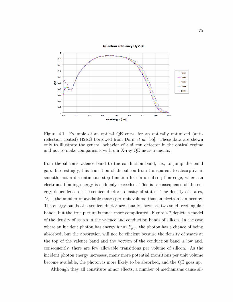
75
Figure 4.1: Example of an optical QE curve for an optically optimized (anti-reflection coated) H2RG borrowed from Dorn et al. [55]. These data are shownonly to illustrate the general behavior of a silicon detector in the optical regimeand not to make comparisons with our X-ray QE measurements.
from the silicon’s valence band to the conduction band, i.e., to jump the band
gap. Interestingly, this transition of the silicon from transparent to absorptive is
smooth, not a discontinuous step function like in an absorption edge, where an
electron’s binding energy is suddenly exceeded. This is a consequence of the en-
ergy dependence of the semiconductor’s density of states. The density of states,
D, is the number of available states per unit volume that an electron can occupy.
The energy bands of a semiconductor are usually shown as two solid, rectangular
bands, but the true picture is much more complicated. Figure 4.2 depicts a model
of the density of states in the valence and conduction bands of silicon. In the case
where an incident photon has energy hν ≈ Egap, the photon has a chance of being
absorbed, but the absorption will not be efficient because the density of states at
the top of the valence band and the bottom of the conduction band is low and,
consequently, there are few allowable transitions per volume of silicon. As the
incident photon energy increases, many more potential transitions per unit volume
become available, the photon is more likely to be absorbed, and the QE goes up.
Although they all constitute minor effects, a number of mechanisms cause sil-

76
Figure 4.2: A theoretical representation of silicon’s density of states. While thisfunction is very complicated, the feature to note is the behavior of the functionnear 0 eV. The function drops smoothly down to zero at 0 eV, where the valenceband ends, and becomes non-zero again at ≈1.1 eV, the band gap energy. Here,instead of being plotted as number volume−1, the density of states is shown asnumber atom−1 eV−1. Figure was borrowed from Chelikowsky [56].
icon to exhibit very limited, but non-zero, response to photon energies below the
quoted band gap. Exciton states are energy levels that exist slightly below the
valence band and give the detector a small response below the band gap energy.
Phonon + photon interaction with electrons can cause response below the band
gap. Also, warmer silicon has better response near the band gap energy because
the more energetic phonon distribution gives valence electrons the momentum they
need to jump the material’s indirect band gap. This effect is visible in the H2RG
QE data shown in Figure 4.1.
As shown in Figure 4.1, the QE continues to rise when incident photon wave-
length decreases from 1.1 µm to ∼600 nm, since photons no longer have trouble
creating electron-hole pairs in silicon. However, two major problems begin to arise
that will limit the detector’s response to blue and UV light: surface reflectance
and shallow absorption. Figure 4.3 shows the opposing nature of these two effects.
Surface reflectance increases towards the blue and ultraviolet end of the spectrum,
which leads to a decrease in QE. To mitigate the problem, detector designers will
often apply anti-reflection coatings to the detector’s surface. When a blue (∼500

77
nm) or UV (< 400nm) photon does penetrate into the silicon bulk, its penetra-
tion depth will be very small because of silicon’s increasing absorption coefficient
with shorter wavelength. This does not directly cause a drop in QE, but practical
issues with detector construction cause the reduced absorption depth of blue and
UV light to correlate with lowered response. In front-illuminated CCDs, the gate
structures that partially cover the illuminated surface heavily absorb blue and UV
photons. In back-illuminated CCDs, electron-hole pairs produced very close to
the illuminated surface have a low probability of making it into the pixel’s po-
tential well because of recombination and surface traps, decreasing QE. In HCDs,
charge carriers must diffuse through the top-side n-doped layer, where they are
more likely to recombine, before reaching the depletion region. For this reason,
the layer is made as thin as possible. In both cases, detector coatings like our alu-
minum optical blocking filter and the native oxide that forms on the front surface
will significantly attenuate radiation with short penetration depth.
As the incident photon energy increases from the UV into the soft X-ray (100
eV), surface reflection drops to zero and penetration depth again increases, reduc-
ing response problems associated with the front surface. When incident photons
have sufficient energy to induce ionizations in silicon, the absorption coefficient
increases abruptly and detector response improves. Silicon has L-shell binding en-
ergies of 100 and 150 eV and a K-shell binding energy of 1,839 eV. In the X-ray,
these silicon inner-shell ionizations are the dominant absorption mechanism. For
hard X-rays ( 2 keV), the photoelectric cross section continues to decrease, caus-
ing photons to over-penetration through the detector’s depleted bulk and leading
to a drop in the detector’s response. Increasing the detector’s depletion depth is
the only way to improve the hard X-ray response, but this improvement comes
at the expense of elongating the pixel aspect ratio, increasing the bias voltage re-
quired for full depletion, increased dark current due the increased volume of biased
silicon per pixel, and increased cosmic ray background on orbit. The thickest PIN
diode arrays are currently ∼ 350 µm.

78
Figure 4.3: The left plot shows the energy dependence of surface reflectance inpure polished silicon at 300 K. High reflection in the UV makes efficient photondetection difficult. The right plot shows the wavelength dependence of the absorp-tion coefficient in silicon at a variety of temperatures. The rise in the coefficienttoward smaller wavelengths causes the absorption depth to decrease, leading todifficulties in detecting blue/UV photons. Figures were borrowed from Green [57].
4.2 Various Methodologies
Quantum efficiency is an inherently difficult parameter to measure because, unlike
the characterization of read noise, dark current, and energy resolution, which are
all calibrated by the known energy of X-ray emission lines, the measurement of QE
requires the absolute measurement of the X-ray flux. This can be accomplished
using one of two general strategies; either by observing the test detector’s response
to illumination by a calibrated source of radiation or by using a second detector
with a known or calculable response to calibrate the radiation source and compare
it to the test detector’s response. The first strategy relies upon the precision
of the source’s luminosity calibration as well as understanding uncertainties in
geometry, the contribution of radiation scattered into the detector from off-axis
angles, and attenuation of the source beam due to intervening material. In the
second strategy, the systematic effects of source calibration uncertainty, scattering,
beam attenuation, and illumination can be made negligible, so long as the detectors
are located close to one another, relative to the source. Due to these advantages,
we have chosen the latter method. In order to provide context and motivate our
decision to measure the QE of HCDs in this way, I will first review some of the
most popular methods for making the measurement.

79
4.2.1 NIR and Optical QE
In the near-infrared (5 µm - 700 nm) and optical (700 - 400 nm) wavelength
regimes, it is possible to create a calibrated source of radiation using a blackbody
oven, narrowband filters with known transmission, and a pinhole. McCullogh et
al. [58] have used this experiment configuration to measure the QE of a Teledyne
HgCdTe HCD. In this experiment, the blackbody source produces a predictable
specific intensity spectrum that follows the Planck function
Bν(T ) =2hν3/c2
ehν/kT − 1, (4.1)
where B has units of energy time−1 area−1 solid angle−1 frequency−1, where h is
Planck’s constant, ν is frequency, c is the speed of light, k is Boltzmann’s constant,
and T is the blackbody temperature. Since the source spectrum varies strongly
as a function of the blackbody temperature, it is necessary to measure it with a
calibrated sensor and control its value. With the source temperature known and
constant, the source will produce a known number of photons per area per solid
angle per time. The narrowband filter, which must be cooled to reduce back-
ground in the case of infrared measurements, is placed in front of the source to
limit transmission to a narrow range of frequencies. This is done so that the QE’s
wavelength dependence can be measured. Integrating Bν over the narrowband
frequency range yields the number of photons per solid angle per area per time.
Finally, a calibrated pinhole is placed in front of the filter for two reasons. First
and foremost, it significantly reduces the large photon flux that reaches the highly
sensitive astronomical detector. Without the pinhole, most detectors would satu-
rate. Second, it limits detector illumination to a small, on-axis solid angle and a
known area of emitting source material. Knowing the distance from the source to
detector and the Airy pattern produced by a pinhole camera allows one to calcu-
late the photon flux in the plane of the detector. Also, while an ideal blackbody is
a Lambertian emitter [59], no real-world material behaves ideally. Restricting the
detector’s illumination to a small solid angle of source with the pinhole reduces
non-Lambertian off-axis illumination by the source.
The blackbody narrowband filter method is limited to wavelengths at which
a calibrated filter is available. To address the problem and extend the measure-
80
ments to a continuous wavelength range, McCullogh et al. use a PbSe diode with
NIST-traceable calibration and an incandescent lamp behind a monochromator
to calibrate their HCD. Additionally, the PbSe diode was used to verify that the
specific intensity of the blackbody oven was within experimental error of the cal-
culated Planck function prediction. The choice of the PbSe diode over a silicon
diode was motivated by the need to perform measurements out to the HgCdTe
HCD’s long wavelength response limit of approximately 5 µm, a region of the
spectrum where no silicon detector has any response. Note that the quoted long
wavelength response limit of the HgCdTe array in McCullogh’s experiment is not
true for all HgCdTe arrays. The band gap can be tuned by changing the material’s
composition ratios during growth, thus changing the long wavelength response [60].
4.2.2 UV and X-ray QE
In the UV (400 - 25 nm) and X-ray (25nm or 50 eV - 10 keV) regimes, black-
body ovens are no longer practical, laboratory sources. The general strategy for
measuring the QE of a test detector remains the same as with the PbSe diode: a
calibrating detector of known response is moved in and out of a radiation beam and
its response is compared to that of the test detector. It is important to note that
in the UV and X-ray, air has a high photoelectric cross section and consequently
absorbs a significant fraction of the radiation. The entire experimental apparatus
must, therefore, be contained within a chamber evacuated to high vacuum. For
UV detector efficiency experiments [61] , silicon photodiodes with UV optimized
anti-reflection coatings and a NIST-traceable calibration serve as the detector of
known response. A differentially-pumped hollow-cathode UV light source, which
produces both line and continuum emission, optically coupled to a monochromator
is often used to produce the necessary radiation. [62]
In the soft X-ray, the problem becomes somewhat more tractable due to the
availability of sources and detectors. Calibrated silicon photodiodes make excel-
lent X-ray calibration detectors because they are compact, low cost, low noise,
have adequate response through the soft X-ray regime, and do not require high
voltage. See Figure 4.4 for examples. When exposed to optical or UV photons, a
reverse biased photodiode produces a voltage across its output that is proportional
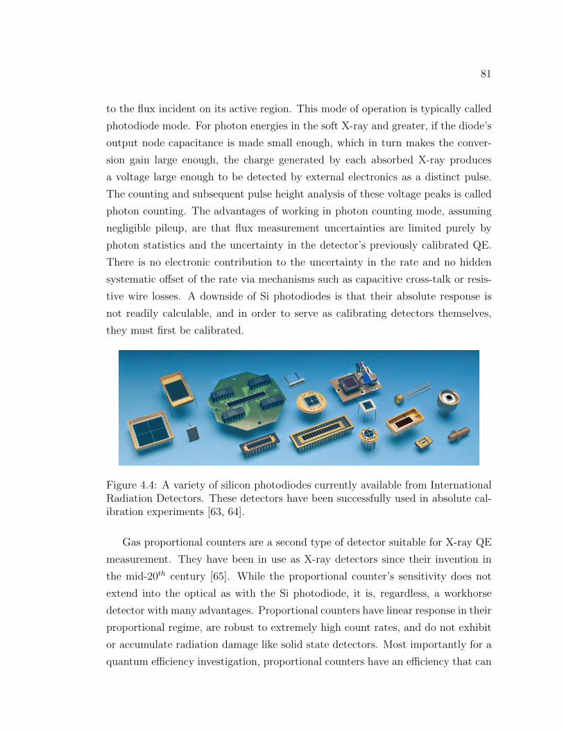
81
to the flux incident on its active region. This mode of operation is typically called
photodiode mode. For photon energies in the soft X-ray and greater, if the diode’s
output node capacitance is made small enough, which in turn makes the conver-
sion gain large enough, the charge generated by each absorbed X-ray produces
a voltage large enough to be detected by external electronics as a distinct pulse.
The counting and subsequent pulse height analysis of these voltage peaks is called
photon counting. The advantages of working in photon counting mode, assuming
negligible pileup, are that flux measurement uncertainties are limited purely by
photon statistics and the uncertainty in the detector’s previously calibrated QE.
There is no electronic contribution to the uncertainty in the rate and no hidden
systematic offset of the rate via mechanisms such as capacitive cross-talk or resis-
tive wire losses. A downside of Si photodiodes is that their absolute response is
not readily calculable, and in order to serve as calibrating detectors themselves,
they must first be calibrated.
Figure 4.4: A variety of silicon photodiodes currently available from InternationalRadiation Detectors. These detectors have been successfully used in absolute cal-ibration experiments [63, 64].
Gas proportional counters are a second type of detector suitable for X-ray QE
measurement. They have been in use as X-ray detectors since their invention in
the mid-20th century [65]. While the proportional counter’s sensitivity does not
extend into the optical as with the Si photodiode, it is, regardless, a workhorse
detector with many advantages. Proportional counters have linear response in their
proportional regime, are robust to extremely high count rates, and do not exhibit
or accumulate radiation damage like solid state detectors. Most importantly for a
quantum efficiency investigation, proportional counters have an efficiency that can

82
be reliably calculated. The efficiency depends only on the number of gas particle
absorbers in the counter’s active volume and the window transmission, which are
both measurable quantities. For these reasons and also because of the heritage of
hardware already existing in our lab, we chose to perform QE measurements with
a proportional counter.
There is a large variety of soft X-ray sources suitable for measuring the QE of
a detector, ranging from simple pieces of radioactive material to highly complex
$100 million facilities. Monochromatic soft X-rays are, in general, produced in the
laboratory by creating atomic K, L, or M-shell vacancies in a source material so that
higher level electrons will fill the vacancies and emit X-ray photons. Ionizing these
inner shell electrons is one way to create a vacancy and initiate a transition. The
ionization can be produced in a target material by bombarding it with electrons
or alpha particles or by irradiating it with higher energy X-rays. The vacancy can
also be spontaneously produced in certain materials by the radioactive decay of the
atom’s nucleus. Continuum emission is commonly produced via bremsstrahlung
radiation by colliding electrically accelerated electrons with some target anode in
an X-ray tube. There are a number of tube sources commercially available that can
generate both line and continuum emission. Those and the line emission sources
directly relevant to our work will be discussed in greater detail in §4.3.3.
Outside of academic laboratories, special X-ray light source facilities exist at
nationally funded labs to provide controlled X-ray radiation to a large variety
of research fields including materials research, biological protein analysis, and,
occasionally, astrophysics. An illustrative cutaway diagram of such a facility is
shown in Figure 4.5. The synchrotron beams at the Advanced Light Source (ALS)
at the Lawrence Berkeley National Lab (LBNL) [66], the Synchrotron Radiation
Source (SRS) in Daresbury, UK [67], BESSY I at PTB Helmholtz-Zentrum Berlin
[68], and Soleil at Orsay [69], enable astronomical X-ray instruments to undergo
end to end absolute calibration. These facilities typically have test chambers large
enough to fit an entire instrument, collimated beams, and tunable beam intensities
that can be varied over many orders of magnitude. They employ double Bragg
crystal monochromators to produce very pure photon energy distributions when
narrowband flux is required. While not a synchrotron, the PANTER X-ray tube
beamline at Max Planck Munchen has played a role in calibrating nearly every

83
X-ray astronomical satellite from ROSAT [70] to Astro E2 [71] and Swift [72].
Figure 4.5: A diagram showing the basic layout of a synchrotron X-ray light sourcefacility. The central circular structure is the electron storage ring, a continuousvacuum space where electrons moving at relativistic speeds are kept in pseudo-circular orbit via the bending action of magnets placed around the ring. Tangentto each magnet, evacuated tubes allow beamed synchrotron radiation to propagateinto one of multiple laboratories situated along the ring’s periphery. Figure is fromBiomolecular Crystallography: Principles, Practice, and Application to StructuralBiology [73].
Concerning laboratory QE measurement methods, Kenter et al. [74] have used
a proportional counter and an X-ray tube mounted in a split chamber, shown in
Figure 4.6, to measure the QE of early-stage HCD prototypes. Their measurement
technique relies upon the assumption that both detectors, which are illuminated
by the X-ray tube’s anode from different viewing angles, through different chamber
pipes, and through different continuum filters, receive identical illumination. In our
QE analysis we do not need to make these assumptions, thanks to the availability
of a vacuum chamber large enough to mount both the test and calibration detectors
side by side at the end of a long path length. In the following section I will describe
the design and construction of the PSU system in detail.

84
Figure 4.6: The experimental apparatus used by Kenter et al. to measure the QEof an early HyViSI
TMHCD. The X-rays are created by a Manson Model 5 source
at the lower left of the diagram, after which they propagate down both tubes of thechamber and illuminate the test and calibration detectors simultaneously. Figureis from the original paper [74].
4.3 Experimental Design
As indicated previously, there is more than one way to measure the X-ray QE
of a detector. We chose to make the measurement by placing the test detector,
a Teledyne H1RG HCD, and the calibration detector, a heritage, custom-built,
gas flow proportional counter, side by side so that they could both measure the
flux of the same source, simultaneously. The illuminated-side surface normals
of both detectors were aligned with the X-ray source and the source was placed
as far away from the detectors as the chamber allowed. In this arrangement,
shown in Figure 4.7, small errors in detector alignment translate into negligibly
small differences between the illumination of each detector. With a distance, d,
between the detectors and the source, the approximate fractional contribution of
the distance error, δd, to the flux normalization is δd/d. Assuming a positioning

85
Figure 4.7: Overhead drawing of the QE test-stand in the PSU vacuum chamber.The proportional counter (PC) and H1RG are aligned so that their center normalsare pointed at the source, which is mounted in the source flange. The clean tentkeeps the bench and area around the door free of airborne particle contamination.For reference, the source-detector distance is 256 cm in the final experimentalaparatus.
error of δd = 0.1 cm (See §4.4.6 for more details on error analysis) and a tolerable
fractional error of 10−3, this requires that d > 100cm. Beginning with these basic
design premises in the following sections, I will motivate and explain the choices
that led to the final, working design.
4.3.1 Vacuum System
The entire experimental apparatus needed to be contained inside of a vacuum
chamber. A vacuum chamber is any sealed, enclosed space built with rigidity
sufficient to resist the 14.69 psi compressive force of the Earth’s atmosphere and
equipped with the necessary hardware to evacuate gas from inside the chamber.
It is not possible to create a perfect vacuum. Fortunately, even the most sensitive
laboratory experiments do not require a perfect vacuum and some require only a
very small degree of vacuum. Table 4.1 lists standard terms that have been coined
to identify ranges in pressure below one atmosphere.
Our entire experiment apparatus needed to be contained within a vacuum
chamber for two reasons. First, as seen in Figure 4.8 an air path length of d > 100

86
Vacuum regime Pressure [mbar] Experimental examples
Coarse Vacuum 1000 - 1 Exploding marshmallows, radiometersRough Vacuum 1 - 10−3 First cathode ray experimentsHigh Vacuum 10−4 - 10−8 Sputtering, CVD, cryogenicsUltra High Vacuum 10−9 - 10−12 MBE, semiconductor, accelerators
Table 4.1: A definition of vacuum regimes. An important note; as pressure de-creases, flow switches from the continuum to the molecular regime. In continuum(or viscous) flow, the mean free path of gas particles is small compared to thesize of the chamber, and these interactions dominate the behavior of the flow. Inthe molecular regime, the mean free path of gas particles is large compared to thesize of the chamber. A significant consequence of this transition is that a givenchamber geometry’s resistance to flow increases with decreasing pressure.
cm, the required source-detector separation, heavily absorbs soft X-rays. Evacu-
ating the chamber to 10−5 mbar results in < 0.01% absorption in all regions of the
bandpass, which is small enough to be ignored. A quick aside: An alternative solu-
tion to the problem of X-ray absorption by the air is to fill a simpler chamber with
helium instead of spending money on building a rigid, sealed chamber and evacu-
ating it. As Figure 4.8 shows, such a setup would have good transmission above 1
keV. However, this strategy would fail in our experiment, primarily because of our
second reason for using a vacuum chamber; the H1RG detector needs to be cold.
Helium would not condense or freeze on a detector at our 150 K test temperature,
but convective heat transfer from 1000 mbar of helium would make keeping the
detector at 150 K a problem. Also, a significant amount of helium would need to
flow through the chamber in order to prevent the buildup of contamination and
the temperature gradient would make calculation of the intervening helium column
density prone to systematic errors.
Concentrating again on vacuum design, water vapor is the enemy of good per-
formance at high and ultra high vacuum. When a chamber is at atmosphere, it
readily sticks to all surfaces inside the chamber and diffuses into the metal walls
through grain boundary pores and into the bulk of any hygroscopic material in the
chamber. At vacuum, water’s high surface area coverage and low vapor pressure
mean that it presents a long lasting gas load that begins to dominate pumping
in the high vacuum regime. In our apparatus, the formation of water ice on the
cold detector drives the vacuum requirement more than the X-ray transmission.

87
Figure 4.8: Assuming a path length of 100 cm, shown are the 0.5 - 10 keV trans-mission curves for 300 K air at atmospheric pressure (solid line, left vertical axis),300 K air at high vacuum (dotted line, plotted with right vertical axis), and 300 Khelium at atmospheric pressure (dashed line, left vertical axis). Air at atmosphericpressure has poor soft X-ray transmission, while air at vacuum transmits very well.Helium has > 50% transmission above 1 keV, making it a reasonable choice forsome work. The composition of air is 78.08% N2, 20.94% O2, and 0.93% Ar. Thesevalues were calculated from partial pressures given in The Art of Cryogenics [75].This is a conservative estimate since high vacuum pumps preferentially removeheavy elements and would therefore alter the gas composition in favor of greatersoft X-ray transmission. The IDL procedure gas_trans.pro (see Appendix C)and Henke’s cross sections [76] were used to generate the transmission curves.
Figure 4.9 shows the sublimation curve for water extrapolated to 100 K. For a
given detector temperature, this line represents the water vapor partial pressure
at which ice will begin to form on the cold surface. Extrapolating the sublimation
curve psubl down to 150 K, the partial pressure of water in the chamber needs to be
below 10−7 mbar in order to prevent icing. Given the high partial pressure of water
at high vacuum, in an ideal case, the total pressure should be nearly the same.

88
In the field of vacuum research, attempts to reduce water adsorption with surface
passivation (Au or TiN coating) or cleaning procedures have not been successful
[77]. The only reliable method for improving chamber wall water vapor desorption
is by heating (baking) the entire chamber; the warmer the better. Unfortunately,
we are not prepared to bake a vacuum chamber at this time. Next, I will discuss
guidelines for designing a chamber that can produce the required pressure.
Figure 4.9: Sublimation curve on the phase diagram of water. The locus of pointswas plotted using the phenomenological fit ln[psubl/pt] = a1(1−θ−1.5)+a2(1−θ−1.25)where θ = T/Tt, Tt = 273.16 K, pt = 611.657, a1 = −13.9281690, a2 = 34.7078238and has been shown to match experimental data to within 0.001 mbar over thetemperature range 190 K≤ T ≤ 273.16 K [78]. TP is the triple point.
The PSU X-ray group owns a cylindrical chamber that is 76.2 cm inner diameter
and 282.2 cm long that will hereafter be referred to as the caterpillar (see Figure
4.7 for a sketch and Appendix A.1 for mechanical drawings). The caterpillar’s
length satisfied the source-detector distance requirement and its inner diameter
allowed for enough space to mount both detectors, making it an excellent choice
for the QE measurement apparatus. In reality, the caterpillar’s vacuum system was
refurbished, but not designed from the ground up for this project. The assembly

89
was completed by working with pump components that were available in the lab
at the time. For the sake of completeness, I will show a more formal justification
of the pump system’s specifications.
The first step of the vacuum design process is to estimate the size of the pump
system that will be able to evacuate the chamber to the required pressure in a spec-
ified amount of time. Following the notation of O’Hanlon [79], the basic equation
of vacuum system design is
Pult =Q
Sc, (4.2)
where Sc [liters second−1] is the effective pumping rate at the mouth of the cham-
ber’s pump flange, Q [millibar liter second−1] is the total gas load entering the
chamber space, either from leaks or outgassing, and Pult [millibar] is the ultimate
pressure achieved in the chamber. All materials release gasses from their surface
and/or interiors, into the surrounding environment. If you have ever smelled rubber
from a new tire or detected any smell for that matter, then you are already familiar
with the fact that materials expel volatile compounds. This is called outgassing
and some materials do it significantly more than others. The above equation
describes the vacuum equilibrium where the rate of gas entering the chamber due
to outgassing (gas load) divided by the volumetric rate of gas removal results in the
ultimate chamber pressure. Since this pumping speed is characterized by volume
of gas removed per time and the speed does not vary with pressure over the pump’s
usable range, the rate of removing gas particles from the chamber is proportional
to the number density of particles and therefore proportional to the pressure. This
leads to the pressure as a function of time taking the exponential form,
P (t) = (Pinit − Pult)e−SctV + Pult (4.3)
where Pinit is the initial chamber pressure, typically atmosphere, Pult is the ultimate
chamber pressure, where pumping and outgassing are in equilibrium, Sc is the
pumping speed at the chamber’s pump flange (not the same as the pump’s rated
speed), t is time, and V is the volume of the chamber. To aid in system design,
commercial vacuum pumps are rated by their volumetric pumping rate, in L sec−1.

90
However, the pump’s rated speed, Sp is calculated by running the pump with inlet
capped, severely over-estimating the pumping speed in a real chamber. The pump
speed and the chamber speed are related by
1
Sp=
1
C+
1
Sc(4.4)
where C [liters second−1] is the conductance of the connection between the chamber
and the pump. Long thin tubes present resistance to the flow of gas and have a
low conductance. However, even if the pump is connected directly to the chamber,
there will still be some resistance to the flow due to the inlet’s finite area. In reality,
the conductance of a conduit drops with pressure, leveling off as the system enters
into the molecular flow regime. To simplify vacuum calculations and make a more
conservative estimate, the molecular flow conductance will always be assumed.
Combining Equations 4.3 and 4.4 and solving for Sp,
Sp =
[[−Vt
ln
(Pc − PultPinit − Pult
)]−1
+1
C
]−1
(4.5)
To calculate pump size, the quantities in the above equation were estimated:
chamber volume, V = 1.2 · 106 cm2, pump down time t ≡ 86.4 ks (1 day), ini-
tial pressure Pinit = 1000 mbar, and final chamber pressure, Pc = 10−6 mbar.
The ultimate pressure, Equation 4.2, is a function of outgassing and the chamber
pumping speed, so the solution must be solved iteratively. The surface outgassing
rates, in mbar liter sec−1 cm−2, of common materials are known and tabulated in
vacuum handbooks. However, in the high vacuum regime, pumping is dominated
by water desorption from the chamber’s surface and not the actual outgassing of
the chamber. Given the chamber surface area of ∼ 7.6 · 104 cm2 and taking the
water desorption outgassing rate from Table 4.2, the chamber surface will produce
3 · 10−2 mbar L sec−1 of gas load.
Using the quasi-Newton iterative non-linear solver built into IDL, the required
pump speed estimate is 790 L sec−1. The code can be found in pumpspeed.pro
in Appendix C. Since a 500 L sec−1 pump was available, we worked with what
we had and the system’s performance was satisfactory. Given that at 50% relative
humidity the partial pressure fraction of water in air is ≈ 5%, and that the fraction

91
of water in the vacuum environment will increase due to differential pumping speed,
and finally that our measured ultimate pressure is 9 · 10−6 mbar, we are probably
causing some minor icing on the detector. In an apparatus similar to ours, Jacquot
et al. attributed an unexpected drop in UV QE as a function of time to icing of
the detector’s front surface [80]. Since soft X-rays are far more penetrating than
UV photons, our application was not sensitive to this minor icing and we deemed
the effect negligible.
Material Outgassing10−10[mbar centimeter−2 liters sec−1]
Aluminum (fresh) 84.0Aluminum (anodized) 3,679.0
Brass 5,332.0Copper (fresh) 533.0
Copper OHFC (fresh) 251.0Steel (nickel-plated) 368.0
Stainless steel 192.0Zinc 2,946.0
PTFE 4,000Silicone 93,000
Viton A (unbaked) 15,200Viton A (12 h 200C) 2.7
Water desorption 4,000
Table 4.2: Outgassing rates for common vacuum materials. Metals are listedabove the partition and elastomers/polymers are listed below it. Values have beenconverted using the factor mbar centimeter−2 liters sec−1 = 10−3· Pascals meterssec−1. In-situ baking can reduce these values by up to 4 orders of magnitude. Allvalues except water were taken from O’Hanlon’s text [79]. The value for water wastaken from Li & Dylla [81] and is an estimate of the desorption of water from anunbaked stainless steel surface at the beginning of a pump cycle after the chamberwas exposed to ambient air.
With the pump size established, the next order of business is to pick a type
of pump. Throughout the history of vacuum technology, many different types of
pumps have been invented to solve the problem of removing gas particles from a
sealed chamber volume. In the most general sense, vacuum pumps fall into two
categories: gas transfer and gas capture. Gas capture pumps use special surfaces to
immobilize gas particles. Examples include cryogenic sorption, cryogenic, and ion
92
pumps. Advantages of gas capture pumps are that they are dry, meaning that they
use no oil, and retain their pumping speed at ultra high vacuum. Disadvantages are
that they need to be periodically regenerated and they require moderate to high
backing vacuum. Gas transfer pumps force gas particles in a preferred direction via
a mechanical action, either positive displacement or momentum transfer. Positive
displacement pumps seal a volume of gas from the chamber, reduce its size, and
vent the compressed volume to atmosphere. Examples include diaphragm, rotary
vane, piston, scroll, and roots pumps. The pumping speeds of these pumps all drop
off severely in the rough vacuum regime, so their use is limited to rough vacuum
applications and being placed in series with high vacuum pumps that require low
backing pressure. Momentum transfer pumps impart a preferential momentum on
gas particles to redirect them out of the chamber. Examples include diffusion and
turbomolecular pumps (TMPs).
In the range of 500 L sec−1 pumps, TMPs can maintain pumping speed into
the high vacuum and are dry and safe. The risk of damaging the contents of a
vacuum chamber is an issue with diffusion pumps, because they will spray oil into
the chamber in the event of power loss, the development of a vacuum leak, or a
mechanical pump failure causing the backing pressure to rise. A 500 L sec−1 TMP
was our high vacuum pump of choice. TMPs require a backing pressure of < 10−1
mbar, so we place a dry and reliable scroll pump in series, behind the TMP. The
caterpillar system routinely achieves vacuum in the low 10−6 mbar range when
empty and in the high 10−6 mbar range when filled with equipment, after ∼ 72
hours of pumping.
Cleanliness and electrostatic discharge (ESD) safety are two important factors
that must be considered when working with delicate detectors and test hardware.
Environmental contamination in the form of airborne dust, machining oils, or
pieces of human (skin dander, hair, skin oils, and even bits of saliva) can degrade
the vacuum with their outgassing, cause sensitive components to malfunction,
and/or give rise to systematic error via unintended X-ray absorption. A clean tent
that surrounds the caterpillar’s main access door, shown in Figure 4.7, was built so
that components could be cleaned and assembled and detectors could be removed
from their protective packaging in a clean environment before installation. The air
is filtered with a HEPA filter. Tests with a laser air particle counter showed no

93
detectable > 5 µm particle contamination on the workbench and < 500 particles
foot−3 in the main area. All of the silicon based detectors that we test contain very
thin gate structures with breakdown voltages in the realm of tens of volts. The
simple action of shuffling one’s feet on the floor can generate tens of thousands
of volts potential difference between the body and a work surface, creating the
potential for catastrophic ESD detector damage. To combat the problem, the tent
is constructed with ESD PVC plastic, the tent’s work surface is covered with an
ESD dissipative mat, and the tent’s workstation is outfitted with ESD ground
monitors and straps that are worn on the user’s wrist.
4.3.2 Cryogenics and Temperature Control
All of the H1RG measurements that our lab is likely to make in the near future will
be made with the detector in the 150-220 K temperature range. The lower end of
the range is defined approximately as a temperature at which detector performance
does not continue to improve with further cooling. The upper end of the range is
determined by the noise characteristics of these devices, which make meaningful
soft X-ray measurements difficult above 220 K. A search for a commercially manu-
factured solution for cooling and controlling the detector in this temperature range
was carried out, but due to the significant cost of adapting those systems to our
chamber, we chose to custom design and build a temperature controlled cryostat
to accomplish the design requirement. The general strategy of our cryostat design
is to cool the detector by physically affixing it to a cold object (cold sink) with
a flexible device of known conductance (cold strap), and then use a closed loop
controller consisting of a temperature sensor, a variable power heater, and a digital
control algorithm to maintain the detector’s temperature at a desired setpoint. In
traditional cryostat design, a dewar filled with cryogenic liquid, either nitrogen
(77 K) or helium (4.2 K) depending on the required temperature, is the cold sink.
Using a dewar has low up-front cost, no maintenance cost, and moderate con-
sumable cost (cryogen). Cold head refrigerators (CryoTiger R© is a commonly used
model), and more recently Stirling coolers, are a popular cooling option because
their closed-cycle designs do not require dewar filling to run continuously and they
recoup their high initial cost after a few years of operation [82]. Multi-stage Peltier

94
Figure 4.10: (Continued on the following page.)
coolers are a very low-cost, low-maintenance cooling option if a process requires
moderately low temperatures (∼220 K) with low heat load (<5 watts)[83]. For
our QE measurement, I chose to build a liquid nitrogen (LN2) dewar due to the
low up-front cost, high heat load handling capability, and the cryogen’s ability to
cool significantly below our desired setpoint. The basic system design is shown in
Figure 4.10.
The most common options for fabricating an LN2 dewar are welded stainless
steel, welded aluminum, and silver soldered copper. Tungsten inert gas (TIG)
welded stainless steel has excellent tensile and joint strength, and is easy to weld.
However steel is heavy and has low thermal conductivity. When fastening stainless
steel bolts to threaded stainless steel, either different alloys must be chosen or
vacuum grade anti-seize compound must be applied to the fasteners to prevent
thread galling/seizing. TIG welded aluminum is a lightweight dewar design option
that also has good thermal conductivity, but the welds are prone to warping and

95
Figure 4.10: Routing layout of the QE test-stand. The large gray circle at rightrepresents the caterpillar vacuum chamber. Inside the chamber the QE test ap-paratus components are shown in their approximate orientations. Note that theproportional counter (PC) and H1RGs are positioned below the chamber centerlinebecause the X-ray source pipe is offset below the centerline. The hollow lines rep-resent tubes: 1/8 inch copper tube with Ultra-torr fittings for the PC fill/vent and1/4 inch hydroformed corrugated stainless steel tube with VCR fittings for the liq-uid nitrogen (LN2) dewar. The barometer (Baro.) is shown in the position whereit was used to measure the proportional counter gas (P-10) line pressure. Thepressure of gas was regulated first by a standard Harris cylinder regulator, then bya 0-5 psi Belofram regulator (Bel.). The flow was measured and regulated with aflowmeter (Flow). The proportional counter’s two electrical connections are an HVand BNC signal cable. The signal line passes out of the chamber, through a pream-plifier (Preamp) and into a shaping amplifier (Shape) before being split between asingle channel analyzer (SCA) and counter combination and a multi-channel an-alyzer (MCA) that outputs to a computer. The computer runs a Labview dataacquisition (DAQ) device that controls both the heater and RTD temperature sen-sor power supplies. The heater and RTD power supplies are powered by externalDC power supplies (DC PS). The H1RGs are programmed, clocked, and read outby the SIDECAR
TM, which has two DC power inputs coming from the DC PS and
one USB output that connects directly to the computer. The cold strap can beseen connecting the dewar to the H1RGs. In the lab, the various electrical andfluid lines are fed into the caterpillar through a single large feedthrough plate, butare shown scattered in this diagram, for the sake of clarity. Arrows indicate thedirection of gas, fluid, data, or power flow.
also tend to develop porosity. Warpage is more common in aluminum because
its high conductivity requires the use of more heat to maintain adequate weld
pool temperature. Also, unless the joint is carefully preheated, small bubbles
can develop in the weld and eventually lead to vacuum leaks. Silver soldered
copper has high conductivity, but is an expensive material that is difficult to solder
well. Additionally, the material and its joints have the lowest strength among
the available choices. Both aluminum and copper require thread inserts to avoid
tearing out threads in the high torque fastener connections that are necessary
to make good thermal contact between components. We concluded that welded
stainless steel was the best choice for the dewar because of its previously listed
advantages and also because it was straightforward to attach cryogenic vacuum
tube fittings. The material’s weight issue was addressed by avoiding the use of thick
96
stock material and the poor thermal conductivity was improved by minimizing the
distance between the cryogen and the cold strap attachment point.
As seen in Figure 4.10 the dewar was placed inside the chamber and required
a detachable tube fitting to run the LN2 fill and vent lines from the cryogenic-
liquid vacuum-feedthrough into the dewar. SwagelokTMbrand compression fittings
are ubiquitous in the laboratory because the connections are cheap and easy to
make. After trial and error in the lab, I found that it is possible to make a
vacuum tight connection with these fittings, but it is difficult to get a consistent seal
when reattaching the same fitting more than once. This alone makes the fittings
unsuitable for the QE apparatus, but in addition they are also not rated to work
below 230 K. Industry research led me to SwagelokTMVCR fittings and Conflat
(CF) vacuum flanges. Both fittings are rated for cryogenic temperatures and ultra
high vacuum, but the VCR metal gasket fittings were eventually chosen due to
their compact form factor. Stainless steel gaskets were chosen over copper and
nickel because the stainless gasket’s coefficient of thermal expansion match with
the fitting body insured that the fitting’s vacuum seal would maintain integrity
over the course of many thermal cycles.
A good cryostat design should be efficient, meaning that heat input from any
source other than the test detector should be minimized. In that vein, the dewar
design seeks to maximize the thermal resistance between the dewar’s cryoliquid
contents and the warm 300 K environment. The primary design goal for our de-
war was for it to have a hold time of 12 hours, which is long enough to enable
continuous, 24 hour operation of the QE apparatus. Since there is no significant
convective heat transfer inside the vacuum chamber, radiation and conductive heat
transfer dominate the thermal dynamics. The only source of conductive trans-
fer will be through the dewar’s mechanical supports. Materials with high tensile
strength per thermal conductivity are the most appropriate choice. Making the
support longer, with a smaller cross section, and from a lower thermal conductance
material will all improve overall performance. G10 is a composite material created
by laminating layers of woven glass with epoxy. The material has high tensile
strength, low thermal conductivity, and is low outgassing and non-hygroscopic.
Complex, cut-away strut designs can dramatically reduce the conductivity of an
element while retaining stiffness. Strut design can be further improved with pre-
97
tensioning. Pre-tensioned struts can be designed to have the same stiffness as a
non-tensioned strut, except with the use of less material. In the end, I opted for
simple, solid rectangle struts made from 3/32 inch sheets of G10 because they
can be fabricated very easily (and cheaply) with a shear and a drill. Complicated
machining of G10 is unusually costly for two reasons: its glass filler quickly dulls
cutters and machining of the glass filler produces a dust with health hazards sim-
ilar to asbestos. In the laboratory setting, the mass-performance ratio is not as
critical as it would be in an aerospace application. Therefore, complex strut design
was not worth the added cost. Properly designed mechanical supports contribute
a negligible efficiency loss to the cryostat.
On the other hand, radiative heat transfer from the warm vacuum chamber
walls to the cold dewar is a significant problem that is worth spending effort to
mitigate. The percent of radiation absorbed by a material is proportional to its
surface emissivity, ε. Emissivity is the fraction of energy that an object radiates
compared to an ideal blackbody at the same temperature. High emissivity surfaces
are flat black and both very good absorbers and good radiators. Low emissivity
surfaces tend to be mirror-like and are both good reflectors and good radiative
insulators. Flat black coffee cups may be stylish, but they are a bad idea if you
want to minimize the radiative cooling of your delicious hot beverage. If the
surface of a dewar is polished, it will reflect a larger percent of incident radiation
and heat up slower. If we were to put a second reflective surface between the
warm chamber and the cold dewar, radiative conductivity into the dewar would
be further reduced by a factor of ∼ ε so long as the surfaces do not touch and
thermally short to one another. The continuation of this concept leads to the
idea of a thermal blanket or multi-layer insulation (MLI). Multiple layers of thin
(∼0.001 inch) plastics that have been vacuum deposited with metal (aluminum or
gold) are interleaved with thermally insulating mesh, also made from either woven
glass fiber or plastic. For our MLI, I made a 6 layer stack of alternating metallized
Mylar R© and 1.5 mm pitch PTFE (Polytetrafluoroethylene) mesh that was sourced
from a medical supply company. Note that PTFE is often casually referred to as
Teflon R©, but this is not entirely accurate since Teflon R© is a registered trademark of
the DuPontTM
company. Officially, only DuPontTM
fluoropolymers can be referred
to as Teflon R©. The stack was sewn together by hand along the perimeter with
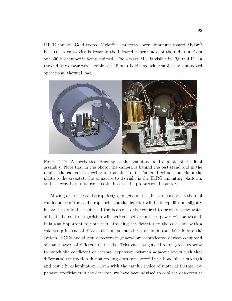
98
PTFE thread. Gold coated Mylar R© is preferred over aluminum coated Mylar R©
because its emissivity is lower in the infrared, where most of the radiation from
our 300 K chamber is being emitted. The 4 piece MLI is visible in Figure 4.11. In
the end, the dewar was capable of a 15 hour hold time while subject to a standard
operational thermal load.
Figure 4.11: A mechanical drawing of the test-stand and a photo of the finalassembly. Note that in the photo, the camera is behind the test-stand and in therender, the camera is viewing it from the front. The gold cylinder at left in thephoto is the cryostat, the armature to its right is the H1RG mounting platform,and the gray box to its right is the back of the proportional counter.
Moving on to the cold strap design, in general, it is best to choose the thermal
conductance of the cold strap such that the detector will be in equilibrium slightly
below the desired setpoint. If the heater is only required to provide a few watts
of heat, the control algorithm will perform better and less power will be wasted.
It is also important to note that attaching the detector to the cold sink with a
cold strap instead of direct attachment introduces an important failsafe into the
system. HCDs and silicon detectors in general are complicated devices composed
of many layers of different materials. Teledyne has gone through great expense
to match the coefficient of thermal expansion between adjacent layers such that
differential contraction during cooling does not exceed layer bond shear strength
and result in delamination. Even with the careful choice of material thermal ex-
pansion coefficients in the detector, we have been advised to cool the detectors at

99
< 2 K min−1. If the detectors are directly attached to the cold sink, the heater is
the only mechanism that regulates their cooling rate. If the heater were to fail, as
things in a laboratory often do, the cooling rate would exceed its maximum and
the detector could be damaged.
Estimating the detector’s equilibrium temperature for a particular strap config-
uration was best accomplished with experimentation. To reach a desired equilib-
rium temperature, we started with a thin strap and added more straps as needed.
Theoretical estimation of the equilibrium temperature is a complicated calculation
which relies heavily on two parameters that are difficult to estimate: contact resis-
tances and surface emissivities. While the conductive heat transfer through a solid
is easily calculable, the thermal contact resistances between the many components
in the apparatus vary strongly with surface roughness as well as the compressive
force fastening the surfaces together. Radiative heat transfer is also calculable in
principle, but the precision of that calculation depends strongly on good estimates
of the emissivity of both the absorbing and emitting surfaces. Surface oxidation
and RMS roughness both have a drastic effect on emissivity, making the calculation
of radiative heat transfer worthwhile in only the most demanding applications.
The cold strap itself is constructed from 12 inch lengths of 0.005 inch thick, 1
inch wide oxygen free copper foil. I chose to make the strap instead of buying a
prefabricated foil stack or braid because we wanted the flexibility to optimize the
strap’s conductivity for different temperature regimes. Oxygen free copper was
chosen due to its superior vacuum outgassing rate. Aluminum and graphite are
also popular cold strap materials. While it was cheaper, aluminum’s lower conduc-
tivity and higher tensile strength would make the strap thicker and less flexible.
The graphite was prohibitively expensive. Graphite straps are used primarily in
aerospace applications where it is important to maximize a strap’s conductivity
mass−1 ratio. Choosing the 0.005 inch copper foil thickness involved balancing
strap flexibility with build practicality. Given two straps with the same total
thickness, the one made from thinner foil will be more flexible. However, the foils
cannot be made too thin because of the difficulty of sourcing exceedingly thin
material and the added complexity of aligning and assembling a strap made from
many thin foils.
Various methods for assembling the ends of the strap were tested, including sol-
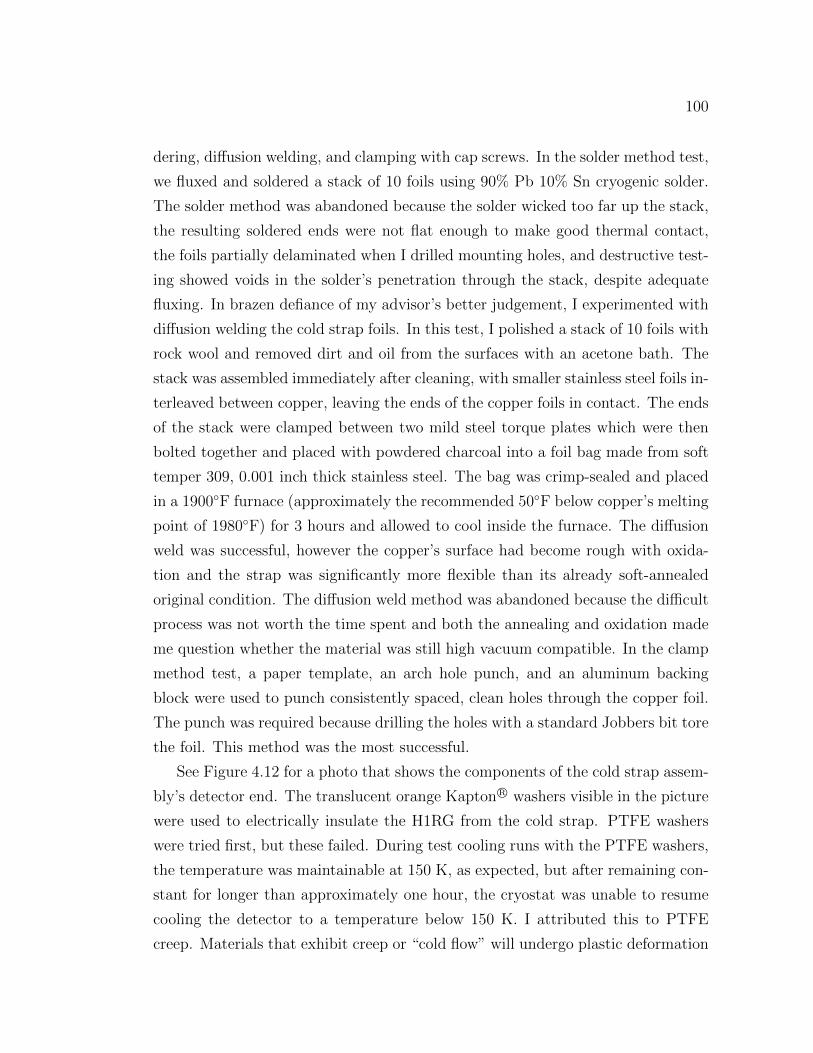
100
dering, diffusion welding, and clamping with cap screws. In the solder method test,
we fluxed and soldered a stack of 10 foils using 90% Pb 10% Sn cryogenic solder.
The solder method was abandoned because the solder wicked too far up the stack,
the resulting soldered ends were not flat enough to make good thermal contact,
the foils partially delaminated when I drilled mounting holes, and destructive test-
ing showed voids in the solder’s penetration through the stack, despite adequate
fluxing. In brazen defiance of my advisor’s better judgement, I experimented with
diffusion welding the cold strap foils. In this test, I polished a stack of 10 foils with
rock wool and removed dirt and oil from the surfaces with an acetone bath. The
stack was assembled immediately after cleaning, with smaller stainless steel foils in-
terleaved between copper, leaving the ends of the copper foils in contact. The ends
of the stack were clamped between two mild steel torque plates which were then
bolted together and placed with powdered charcoal into a foil bag made from soft
temper 309, 0.001 inch thick stainless steel. The bag was crimp-sealed and placed
in a 1900F furnace (approximately the recommended 50F below copper’s melting
point of 1980F) for 3 hours and allowed to cool inside the furnace. The diffusion
weld was successful, however the copper’s surface had become rough with oxida-
tion and the strap was significantly more flexible than its already soft-annealed
original condition. The diffusion weld method was abandoned because the difficult
process was not worth the time spent and both the annealing and oxidation made
me question whether the material was still high vacuum compatible. In the clamp
method test, a paper template, an arch hole punch, and an aluminum backing
block were used to punch consistently spaced, clean holes through the copper foil.
The punch was required because drilling the holes with a standard Jobbers bit tore
the foil. This method was the most successful.
See Figure 4.12 for a photo that shows the components of the cold strap assem-
bly’s detector end. The translucent orange Kapton R© washers visible in the picture
were used to electrically insulate the H1RG from the cold strap. PTFE washers
were tried first, but these failed. During test cooling runs with the PTFE washers,
the temperature was maintainable at 150 K, as expected, but after remaining con-
stant for longer than approximately one hour, the cryostat was unable to resume
cooling the detector to a temperature below 150 K. I attributed this to PTFE
creep. Materials that exhibit creep or “cold flow” will undergo plastic deformation
101
when subjected to even a small force if the force is applied for a long amount of
time. The initial cold strap bolt torque caused the PTFE to creep and thermal
contraction exacerbated the effect. As the washers deformed, thermal conductance
between the strap and the H1RG reduced and detector could no longer be cooled.
The Kapton R© washers that replaced the PTFE did not exhibit creep and, with
these washers, the cryostat worked as designed. Figure 4.13 shows an example
of the cryostat cooling down, maintaining temperature for an extended time, and
resuming cooling.
In order to achieve this control, custom temperature control and heater power
electronics were designed and built. Heater power for up to four detectors is
provided by a 4-channel low-gain power amplifier circuit. Up to six temperature
sensors are powered by a 6-channel, 0.988 mA differential-amplifier current-source
circuit. Both circuits were designed and the boards laid out and printed using
ExpressPCB R© software. Detailed schematics and layout diagrams are shown in
Appendix B.2. Using prewritten LabVIEW proportional integral derivative (PID)
control application control interfaces (APIs), a larger virtual instrument (VI) was
written to handle the temperature measurement, heater power, and temperature
control of the detector(s). The VI also records dewar and detector temperature
data in a file. Through experimentation, it was found that the best method for
achieving good temperature control is to allow the detector to cool at the maximum
rate, which is set by the choice of cold strap thickness, and with control loop
parameters P = 3.0, I = 1.0, and D = 0.0, initiate the PID as the temperature
nears the setpoint. In order to control the detector at 150 K, the heater needed to
produce 1.2 watts.
4.3.3 Laboratory X-ray Sources
The ideal X-ray source for the QE experiment would be collimated, of known inten-
sity, monochromatic, and tunable in photon energy. Since we do not have access to
such a source, we have to make accommodations to get the desired result. Placing
a source far away from the detector and making simultaneous measurements with
a gas flow proportional counter provides both a sufficient substitute for collimation
and a reference that enables source calibration. As discussed in §4.2.2 there are

102
Figure 4.12: The cold strap’s detector end, disassembled to illustrate the assem-bly’s components. As described in the text, the design goal of the strap end wasto provide an easily detachable high thermal conductivity, electrically insulatingmechanical connection between the strap and the detector mounting plate (notshown). The top half inch of two 0.75 inch 10-32 18-8 stainless steel cap screwswas wrapped with PTFE shrink tube to prevent it from contacting the strap.Two Kapton R© washers were used to electrically insulate the screws from the strap.Stainless washers were included in the stack so that the cap screw heads did nottear the Kapton R© washers. The stainless steel plate was included so that the heav-ily torqued bolts applied even pressure to the entire end of the strap. Shown is the20 foil stack used in our experiments. The solid copper standoff to the right wascovered with acrylic adhesive Kapton R© tape to prevent it from electrically con-tacting the strap. Since the tape is so thin, it imposes minimal thermal resistance.In fact, the film may have improved heat transfer. In the heat sink industry, thinpolymer films are often used to improve thermal conduction between metal sur-faces because their softness allows them to conform to irregularities in the matingmetal surfaces, increasing contact area.

103
Figure 4.13: Temperature data from the dewar and detector during the December17, 2012 QE data run. Time data are shown as the number of hours elapsed afterthe 14:06:57 start of the run. The inset plot shows small variations in the detectortemperature data and has the same units as the larger plot. The thermal controlis shown to be stable to within a few tenths of a degree around the 150 K setpointover both long and short time intervals. In this run, the dewar was filled at 14:37and began to warm at 05:29 the next morning, making for a 14 hour 52 minutehold time. The ∼ 20 K drop in detector temperature that occurred 10 hours afterthe dewar fill (23:30 local time) was due to the detector heater being turned offas a safety precaution. Note that, with the same thermal strap, controlling thedetector at a higher temperature or for a longer time period will decrease the holdtime.
sources that can produce nearly monochromatic tunable emission, but we do not
have access to such sources in the lab. We concentrate on producing monochro-
matic emission by producing K-shell electron vacancies in various materials, which
causes the production of X-rays when the vacancy is filled by an electron falling
from a higher energy level. To a lesser extent, L and M-shell transitions can also be
used, but they are less spectrally pure since they are composed of multiple tightly
grouped lines. See Figure 4.14 for an illustration of the allowed transitions that
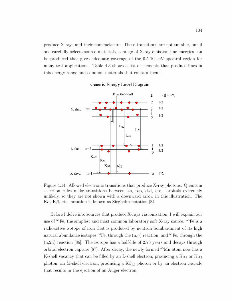
104
produce X-rays and their nomenclature. These transitions are not tunable, but if
one carefully selects source materials, a range of X-ray emission line energies can
be produced that gives adequate coverage of the 0.5-10 keV spectral region for
many test applications. Table 4.3 shows a list of elements that produce lines in
this energy range and common materials that contain them.
Figure 4.14: Allowed electronic transitions that produce X-ray photons. Quantumselection rules make transitions between s-s, p-p, d-d, etc. orbitals extremelyunlikely, so they are not shown with a downward arrow in this illustration. TheKα, Kβ, etc. notation is known as Siegbahn notation.[84]
Before I delve into sources that produce X-rays via ionization, I will explain our
use of 55Fe, the simplest and most common laboratory soft X-ray source. 55Fe is a
radioactive isotope of iron that is produced by neutron bombardment of its high
natural abundance isotopes 54Fe, through the (n,γ) reaction, and 56Fe, through the
(n,2n) reaction [86]. The isotope has a half-life of 2.73 years and decays through
orbital electron capture [87]. After decay, the newly formed 55Mn atom now has a
K-shell vacancy that can be filled by an L-shell electron, producing a Kα1 or Kα2
photon, an M-shell electron, producing a Kβ1,3 photon or by an electron cascade
that results in the ejection of an Auger electron.
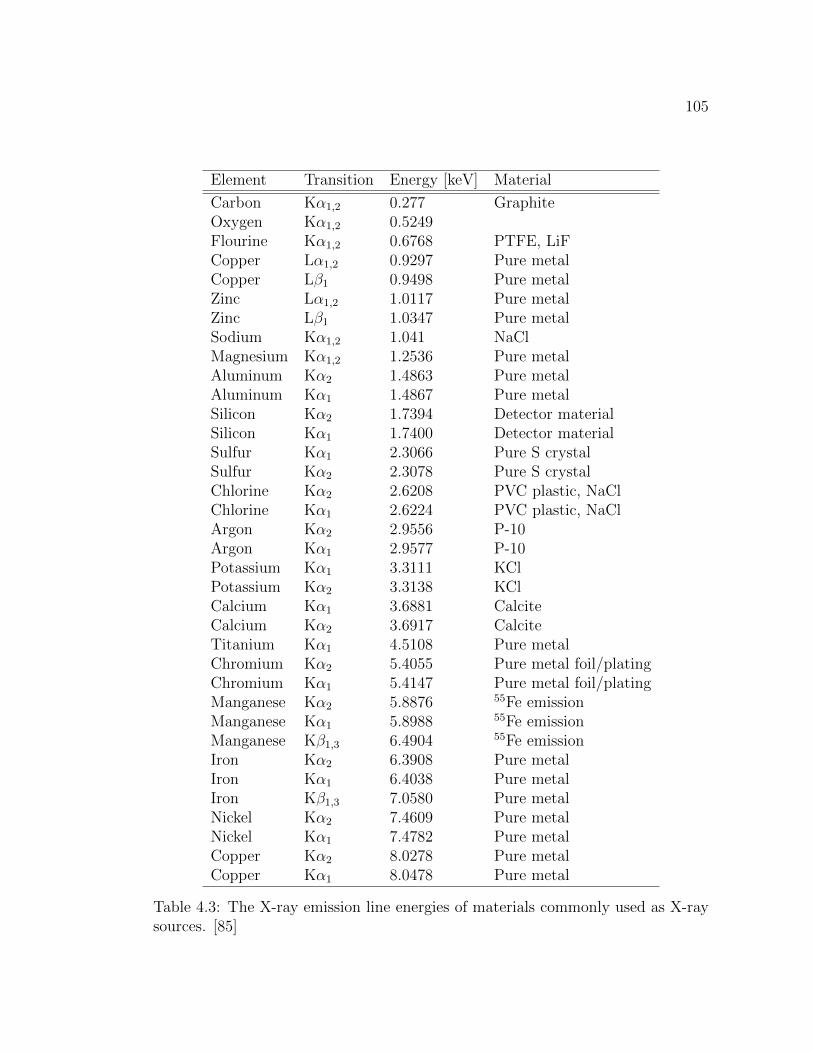
105
Element Transition Energy [keV] Material
Carbon Kα1,2 0.277 GraphiteOxygen Kα1,2 0.5249Flourine Kα1,2 0.6768 PTFE, LiFCopper Lα1,2 0.9297 Pure metalCopper Lβ1 0.9498 Pure metalZinc Lα1,2 1.0117 Pure metalZinc Lβ1 1.0347 Pure metalSodium Kα1,2 1.041 NaClMagnesium Kα1,2 1.2536 Pure metalAluminum Kα2 1.4863 Pure metalAluminum Kα1 1.4867 Pure metalSilicon Kα2 1.7394 Detector materialSilicon Kα1 1.7400 Detector materialSulfur Kα1 2.3066 Pure S crystalSulfur Kα2 2.3078 Pure S crystalChlorine Kα2 2.6208 PVC plastic, NaClChlorine Kα1 2.6224 PVC plastic, NaClArgon Kα2 2.9556 P-10Argon Kα1 2.9577 P-10Potassium Kα1 3.3111 KClPotassium Kα2 3.3138 KClCalcium Kα1 3.6881 CalciteCalcium Kα2 3.6917 CalciteTitanium Kα1 4.5108 Pure metalChromium Kα2 5.4055 Pure metal foil/platingChromium Kα1 5.4147 Pure metal foil/platingManganese Kα2 5.8876 55Fe emissionManganese Kα1 5.8988 55Fe emissionManganese Kβ1,3 6.4904 55Fe emissionIron Kα2 6.3908 Pure metalIron Kα1 6.4038 Pure metalIron Kβ1,3 7.0580 Pure metalNickel Kα2 7.4609 Pure metalNickel Kα1 7.4782 Pure metalCopper Kα2 8.0278 Pure metalCopper Kα1 8.0478 Pure metal
Table 4.3: The X-ray emission line energies of materials commonly used as X-raysources. [85]

106
Commercial 55Fe sources are available in different activity levels, so the first
step in procuring one is to calculate the optimal activity level. If the source were
too warm (high activity), there would be a greater fraction of piled up X-ray events
and the source would be needlessly hazardous and expensive. If the source were
not warm enough, excessively long integration times would be required to achieve
adequate statistical significance in the analysis. Long data runs are undesirable
because they increase the likelihood of accumulating systematic errors, such as
temperature drift effects, in the data. In earlier experiments, we used a 55Fe
source that, from logbook records, had a 0.767 mCi activity level in 1999. With
this source the data showed ∼3500 events per 5.242 second integration frame at a
source-detector distance of 6 inches, which ended up producing a very desirable X-
ray filling fraction that I wanted to replicate in the caterpillar. Using the relation
for a source’s activity
At = A0
(1
2
)t/t1/2(4.6)
where At is the activity at time t, t1/2 is the half-life, and A0 is the activity at time
t = 0, and projecting 12 years forward from 1999, the source had an activity level of
0.036 mCi when the data were taken in 2011. Given the caterpillar’s approximate
source-detector distance of 100 inches, we needed a factor of (100/6)2 increase in
source activity to maintain the same desirable X-ray occupancy fraction in the
H1RG data. This results in a necessary activity of 10 mCi. We purchased a VZ-
2937 source (10 mCi nickel-sealed 55Fe) from Eckert & Ziegler Isotope Products in
Valencia, CA.
The intrinsic Kβ/Kα line intensity ratio for 55Mn is 0.1195 [88]. This is a theo-
retical estimate based on relativistic Hartree-Slater theory. To calculate the ratio,
the probabilities of transitions from the M1−5 subshells (dominated by M2 and M3
which correspond to the degenerate Kβ1 and Kβ3, respectively) are summed and
divided by the summed probability of transitions from the L1−3 subshells (domi-
nated by the L2 and L3 which correspond to Kα2 and Kα3 respectively). This ratio
holds true for an isolated manganese atom, not a close arrangement of many atoms
with non-negligible thickness. To calculate the line ratio for our particular source,
I began with the transmission fraction of radiation through a material, considering

107
only absorption,I
I0
= e−σns, (4.7)
where I is the intensity, in units of photons per second, σ is the atomic cross
section, in units of cm2, n is the number density of the absorbers (atoms) in the
material, in units of cm−3, and s is the path length through the material, in cm. In
our source, photons are produced through the decay process at random locations
throughout the sFe = 17.5 ± 2.5 µm thick active iron layer. See Figure 4.15 for
an illustration of the source in cross-section. The active layer will self-attenuate
and, in doing so, change the emitted line ratio because low-energy photons will be
preferentially absorbed. I solved for the average transmission fraction of a photon
produced at a random depth in the iron,⟨I
I0
⟩Fe
=cos θ
sFe
∫ sFe/ cos θ
0
e−σFe(E) nFe s ds (4.8)
=cos θ
sFe
(e−σFe(E) nFesFe
−σFe(E) nFe
+1
σFe(E) nFe
)(4.9)
=cos θ
σFe(E) nFes
[1− eσFe(E) nFesFe/ cos θ
](4.10)
where the cos θ factor accounts for the increased projected thickness of the layer
when the source is viewed at an angle, θ. This is done individually for the Kα and
Kβ photon energies. On their way out to the surface of the source, the photons
are then further attenuated by the sNi = 4 ± 1µm sealant layer that covers the
iron. Again for both energies,⟨I
I0
⟩Fe+Ni
=
⟨I
I0
⟩Fe
e−σNi(E) nNi sNi/ cos θ (4.11)
Taking the ratio of the transmission at the Kα energy and the Kβ energy and
dividing by the initial Kβ/Kα ratio, I arrived at the final Kα/Kβ ratios plotted in
Figure 4.16. At zero angle with respect to the source’s surface normal, Kα/Kβ =
8.36, 7.46, and 6.79 for the intrinsic, 17.6 µm Fe, and the 17.6 µm Fe + 4 µm Ni
cases, respectively.
A dedicated housing was designed and used to mount and shutter the 55Fe
source in the caterpillar. Although handling this sealed, moderate-activity source

108
Figure 4.15: Cartoon depicting X-ray generation, active layer self-attenuation, andsealant layer attenuation in the VZ-2937 55Fe source. As the viewing angle, θ, be-comes larger, the projected thickness of the layers becomes larger. As shown inthe figure, for a bare 55Fe film, when the radioactive layer’s projected thicknessincreases past the 1/(σρ) ∼ 40− 50µm average absorption length of both energies,the line ratio asymptotes. This is because X-rays produced deep within the mate-rial rarely escape the material’s surface. For the actual nickel plated source, theline ratio continues to harden with increased projected thickness. In reality, usingthe source at high viewing angle would be impractical because the intensity dropsoff severely.
for short periods of time is not considered hazardous since the X-rays are heavily
absorbed by clothing and a person’s outer layer of dead skin, the housing was
nonetheless designed to minimize a person’s exposure during servicing. Shown in
Figure 4.17, the source mounts to a handling rod with a set screw and slides under
the shielding block. Mounted in this way, the operator does not need to place any
part of their body in front of the source and the operator’s fingers will always be
> 3 inches from the source. The circular source locates to a consistent position
every time the plate is assembled by contacting two pins that are press fit into
the flange plate, underneath the shield. A 0.25 inch aluminum plate attached to a
steel rod that is fed outside of the vacuum through an O-ring rotary feedthrough

109
Figure 4.16: The 55Mn Kβ/Kα line ratio plotted as a function of angle with respectto the source normal. The intrinsic ratio is valid for isolated atoms, the Fe ratiocurve for a 17 µm thick source, and the Fe+Ni for a 17 µm thick source coveredby 4 µm Ni.
is used to shutter the source. The transmission of 0.1-10 keV X-rays through 0.25
inches of aluminum is < 10−18.
I will now move on to the discussion of laboratory sources that produce X-
rays with ionization. Ionizing low-level, bound electrons can be accomplished with
either particle or photon radiation. In either case, the ionizing radiation must
have an energy greater than the electron binding energy. The simplest design of
this type is that of the α-particle fluorescent source, shown in Figure 4.18. In
such a source, a radioactive α emitter is positioned over a specially chosen sample
of target material. The alpha particles ionize atoms in the target, causing them
to emit fluorescent X-rays characteristic of the elements that are present in the
chosen material. Since most elements have only one or two useful fluorescent lines
in the soft X-ray range, multiple targets are typically mounted on a wheel inside
the source so that a variety of lines can be produced without breaking the vacuum.
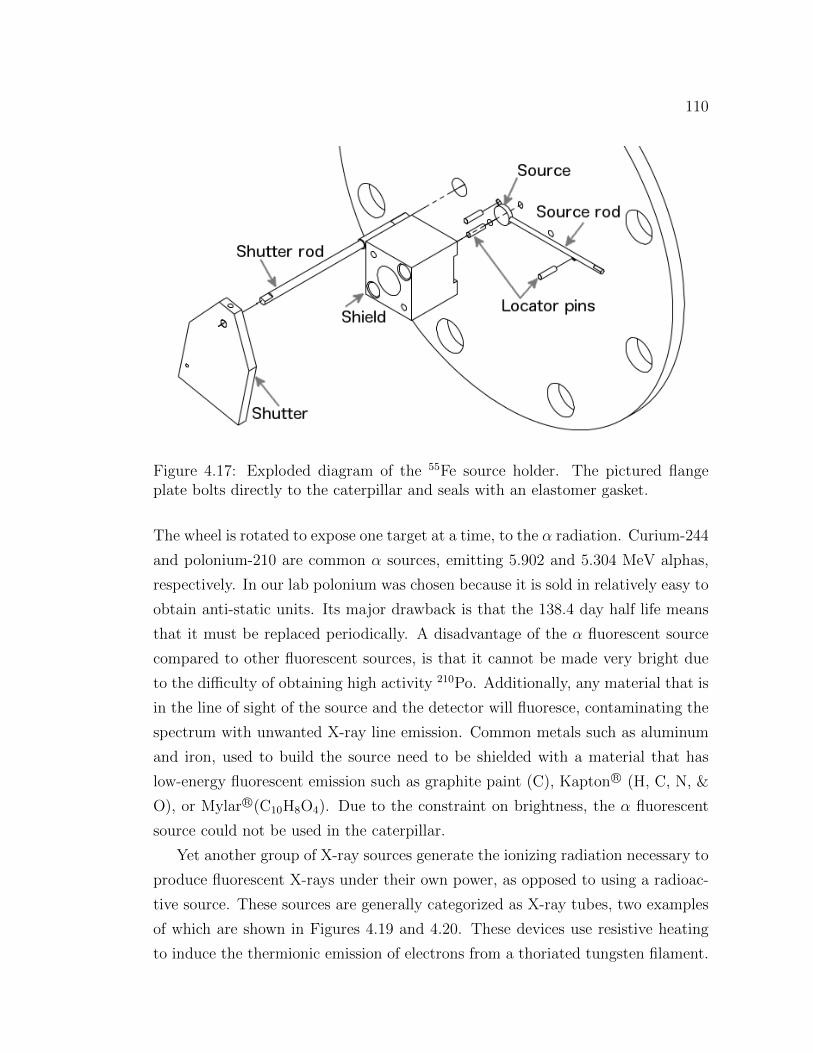
110
Figure 4.17: Exploded diagram of the 55Fe source holder. The pictured flangeplate bolts directly to the caterpillar and seals with an elastomer gasket.
The wheel is rotated to expose one target at a time, to the α radiation. Curium-244
and polonium-210 are common α sources, emitting 5.902 and 5.304 MeV alphas,
respectively. In our lab polonium was chosen because it is sold in relatively easy to
obtain anti-static units. Its major drawback is that the 138.4 day half life means
that it must be replaced periodically. A disadvantage of the α fluorescent source
compared to other fluorescent sources, is that it cannot be made very bright due
to the difficulty of obtaining high activity 210Po. Additionally, any material that is
in the line of sight of the source and the detector will fluoresce, contaminating the
spectrum with unwanted X-ray line emission. Common metals such as aluminum
and iron, used to build the source need to be shielded with a material that has
low-energy fluorescent emission such as graphite paint (C), Kapton R© (H, C, N, &
O), or Mylar R©(C10H8O4). Due to the constraint on brightness, the α fluorescent
source could not be used in the caterpillar.
Yet another group of X-ray sources generate the ionizing radiation necessary to
produce fluorescent X-rays under their own power, as opposed to using a radioac-
tive source. These sources are generally categorized as X-ray tubes, two examples
of which are shown in Figures 4.19 and 4.20. These devices use resistive heating
to induce the thermionic emission of electrons from a thoriated tungsten filament.

111
Figure 4.18: Schematic of a simple α particle fluorescent X-ray source. The par-ticle emitter is positioned such that it irradiates the target material, but not thedetector (left). The target is positioned so that X-rays generated within its surfaceilluminate the detector. Figure adapted from Scientific Charge-Coupled Devices[14].
An interesting aside; the wire is “thoriated” (the tungsten is alloyed with ∼ 1−2%
thorium) to reduce the filament material’s work function (the energy required for
an electron to exit the surface of the solid). When the tungsten is heated, the
thorium migrates outward through the wire, along the metal’s grain boundaries,
and settles on the wire surface [89]. A decreased work function allows the filament
to emit more thermionic electrons for a given wire temperature, yielding better
performance. Returning to the operation of the X-ray tube, in the tube’s vacuum
environment, the electrons produced by the filament are accelerated by the electric
field produced by holding the target anode at a positive high-voltage (∼ 10 kV at
∼ 3 mA). The electrons collide with the anode and these collisions produce X-rays
through two mechanisms: first, the electrons themselves emit bremsstrahlung radi-
ation as their trajectories are altered by the influence of atomic nuclei in the target

112
and second, the electrons ionize target atoms inducing them to emit fluorescent
X-rays. Popular variants of this design are the Manson tube and the Henke tube.
As seen in the figures, the two differ only in the geometric arrangement of the
anode and filament cathode. In the Henke tube, the cathode is positioned behind
the anode and electrons are accelerated toward and collide with the opposite side
of the anode because of its sharp, triangular shape. In the Manson tube, the elec-
trons are accelerated along a straight path before striking the anode, which can
viewed at a 45 angle from either side.
Figure 4.19: A technical drawing of a Henke tube X-ray source. The importantparts are labeled in the diagram: the filament (17), anode (122), window (71),vacuum seal (61), and cooling water plumbing (52, 53, 59, and 63). The U-shapedwires (146) help to shape the electric field and guide more electrons around andto the other side of the anode. Figure is taken from the original 1961 US patentapplication, by Burton Henke for an “Ultra-soft X-ray Source” [90].
In some applications the continuum bremsstrahlung emission that both of these
tubes produce is considered desirable, but for calibration purposes, it is a contam-
inant. This broadband emission can be attenuated by using a foil filter made
from the same material as the anode. This technique works because a filter made
from anode material will always have an absorption edge just above the line emis-
sion energy. This causes it to transmit well at the emission line energy, while
heavily attenuating above the edge and, most importantly, at low energy, where
the bremsstrahlung continuum is the most intense. A method that eliminates all
of the bremsstrahlung continuum from an X-ray tube source involves using the
tube’s X-ray emission to stimulate fluorescent emission from a target material.
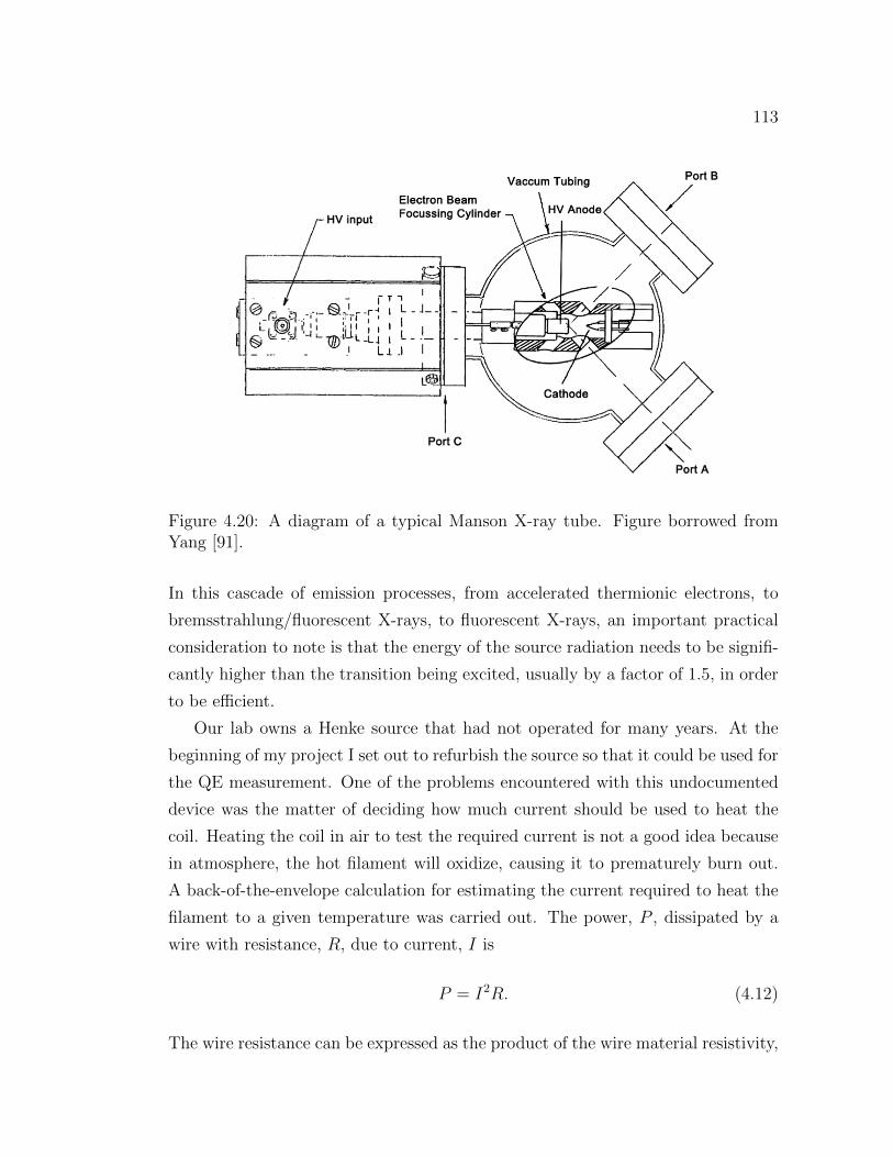
113
Figure 4.20: A diagram of a typical Manson X-ray tube. Figure borrowed fromYang [91].
In this cascade of emission processes, from accelerated thermionic electrons, to
bremsstrahlung/fluorescent X-rays, to fluorescent X-rays, an important practical
consideration to note is that the energy of the source radiation needs to be signifi-
cantly higher than the transition being excited, usually by a factor of 1.5, in order
to be efficient.
Our lab owns a Henke source that had not operated for many years. At the
beginning of my project I set out to refurbish the source so that it could be used for
the QE measurement. One of the problems encountered with this undocumented
device was the matter of deciding how much current should be used to heat the
coil. Heating the coil in air to test the required current is not a good idea because
in atmosphere, the hot filament will oxidize, causing it to prematurely burn out.
A back-of-the-envelope calculation for estimating the current required to heat the
filament to a given temperature was carried out. The power, P , dissipated by a
wire with resistance, R, due to current, I is
P = I2R. (4.12)
The wire resistance can be expressed as the product of the wire material resistivity,
114
ρ, multiplied by the ratio of wire length, l, to the wire’s cross-sectional area,
π(t/2)2, resulting in
P = I2ρl
π(t/2)2, (4.13)
where t is the wire thickness. According to the Stefan-Boltzmann law, the power
emitted by a body at temperature, T , with emissivity, ε, and surface area, A, in
an environment of temperature, Te, is
P = εσA(T 4 − T 4e ), (4.14)
where σ is the Stefan-Boltzmann constant. Equating the two expressions for power
and solving for I,
I =
√σεπ2t3(T 4 − T 4
e )
4ρ(4.15)
This works for a straight wire, but like many filaments, ours is coiled and will par-
tially illuminate itself, leading to an effective emitting surface area that is smaller
than the true wire surface area. The wire’s surface area can be roughly corrected
with a self-illumination factor,
F = 1− t
2sε, (4.16)
where Figure 4.21 shows the definition of the coil separation distance, s. The ratio
of t/s characterizes the open fraction of the coil winding. For high emissivity, the
factor ranges from 0.5 to 1 because s can never be less than t. The emissivity
is factored into the self-illumination because, for a highly reflective surface (low
emissivity), the material would not efficiently self-illuminate. For this calculation
a wire temperature of 2400 K, comfortably below the 3687 K melting temperature
of tungsten will be assumed. At this temperature the most intense emitted wave-
length is λ = 0.2898/T = 1.2 µm and, at this wavelength, the emissivity can be
roughly estimated to be ε = 0.4 [92]. With a wire thickness of t = 0.02 inches,
s = 0.5 cm, tungsten resistivity at 2400 K being ρ = 70.39·10−6 Ω−cm, the current

115
required to produce the given temperature wire is I = 29 amps.
Figure 4.21: Cross-section view of a coil of filament wire. The wire thickness, t, andthe coil separation distance, s, both contribute to the filament’s self-illumination.
Due to time constraints, the QE measurement project had to be descoped by
putting the Henke tube refurbishing project on hold. While the test-stand was
built to accommodate either the 55Fe source or the Henke tube, the H1RG QE was
measured using the two X-ray lines emitted by the 55Fe source.
4.3.4 Gas Flow Proportional Counter
We chose to use a gas flow proportional counter to make our absolute source
calibration measurement. The counter’s theory of operation is illustrated in Figure
4.22. The device is basically a hollow, gas-filled, electrically conductive cavity with
a conductive wire strung down the middle. The wire and cavity wall are insulated
from one another so that when a positive voltage is placed on the wire, an electric
field fills the counter’s cavity. Any radiation, charged particle or electromagnetic,
that makes it into the cavity and has enough energy to ionize an atom in the gas,
will have a finite probability of being detected. Focusing the discussion on X-rays,
if a photon with energy greater than the binding energy of a gas atom electron,
Eb, enters the counter and ionizes a gas atom, an electron with kinetic energy

116
Ee− = (hν)X−ray−Eb and an unstable gas atom ion will be produced. The two do
not recombine because the counter’s electric field drives the charged particles in
opposite directions and the electron is moving fast enough that it quickly becomes
very far from the ion. After the initial ionization, the unstable gas ion will de-excite
through a radiative (fluorescent X-ray emission) or non-radiative process. While
the relatively heavy ion slowly moves towards the outer wall of the proportional
counter, where it will eventually recombine with an electron, the original ionized
electron, with its initial kick and additional energy imparted by the electric field,
moves quickly through the gas. As it moves, it ionizes other gas atoms along the
way, losing speed with each interaction, until its kinetic energy is fully absorbed
through ionizations of the counter gas. As shown in the figure, each of these
electrons will move toward the wire and produce a charge pulse in the conductor.
To help explain the remarkable performance characteristics of the proportional
counter, allow me to first indulge in a back-of-the-envelope calculation. In our
counter we used a common proportional counter gas called P-10, a mixture of
90% argon and 10% methane. This choice of the gas will be motivated later in
this section. Let us assume for a moment that the previously mentioned charge
pulse in the wire consists only of electrons that were ionized by the initial high-
energy electron that was liberated by the incident X-ray. If all of the energy of
an incident Mn Kα photon were to go towards generating electron-ion pairs, there
will be EMn Kα/ωP10 = 225 e− produced. In this equation EMn Kα = 5.98 keV
is the energy of the Mn Kα photon and ωP10 = 26.6 eV is the average electron-
ion creation energy for P-10. Assuming a cylindrical proportional counter with a
round wire, the detector will have a capacitance C = ε2πl/ ln(b/a) = 17.03 cm
= 1.89 · 10−11F, where the dielectric permittivity of P-10 is εP10 ≈ ε0 ≈ 1 [93],
l ≈ 10 cm is the length of the wire, b ≈ 2 cm is the radius of the cavity, and
a ≈ 12.5 µm is the radius of the wire. Given this capacitance, the voltage pulse
produced will be 225[e−](1/6.24 · 1018)/C = V = 1.9 · 10−6 V. A signal of this
amplitude would be lost in the noise of the readout electronics. Something more is
going on in the proportional counter and to explain why, I will derive the equation
for the electric field as a function of position within the cavity.
As before, assuming a cylindrical chamber of radius, r = b, a proportional
counter wire of radius, r = a, a permittivity of the intervening gas ε, and a voltage,
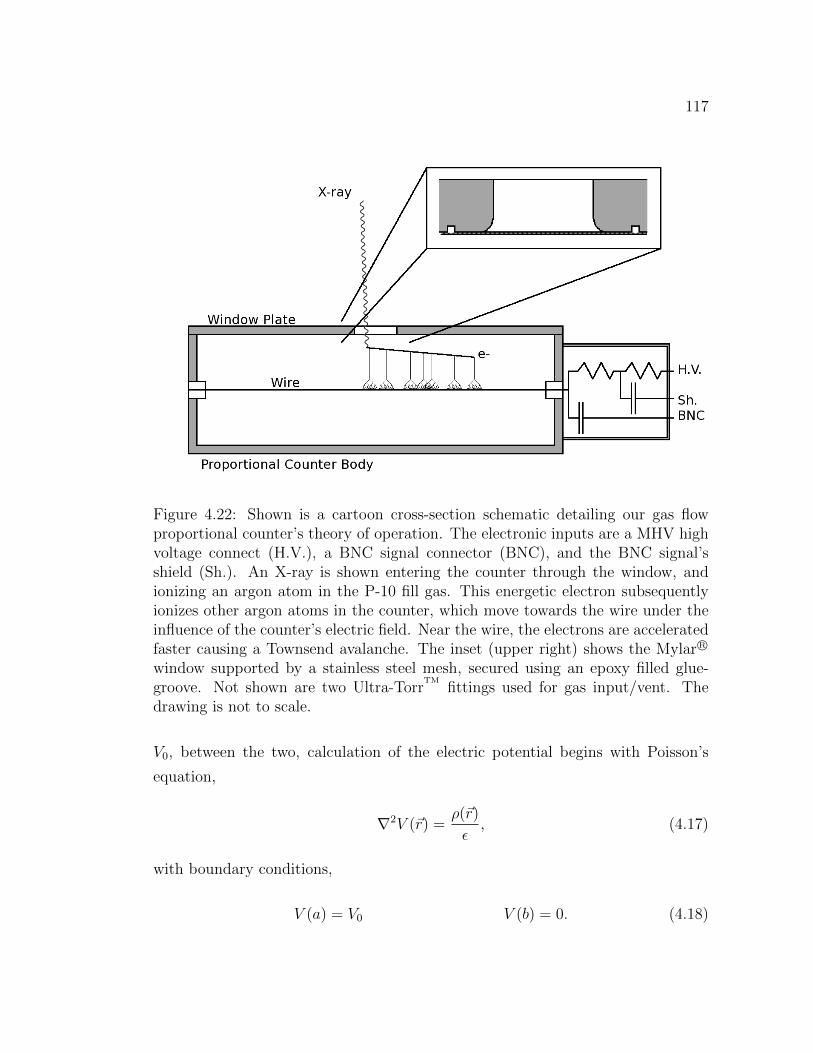
117
Figure 4.22: Shown is a cartoon cross-section schematic detailing our gas flowproportional counter’s theory of operation. The electronic inputs are a MHV highvoltage connect (H.V.), a BNC signal connector (BNC), and the BNC signal’sshield (Sh.). An X-ray is shown entering the counter through the window, andionizing an argon atom in the P-10 fill gas. This energetic electron subsequentlyionizes other argon atoms in the counter, which move towards the wire under theinfluence of the counter’s electric field. Near the wire, the electrons are acceleratedfaster causing a Townsend avalanche. The inset (upper right) shows the Mylar R©
window supported by a stainless steel mesh, secured using an epoxy filled glue-groove. Not shown are two Ultra-Torr
TMfittings used for gas input/vent. The
drawing is not to scale.
V0, between the two, calculation of the electric potential begins with Poisson’s
equation,
∇2V (~r) =ρ(~r)
ε, (4.17)
with boundary conditions,
V (a) = V0 V (b) = 0. (4.18)
118
In the gas, where a < r < b, there is no free charge, so Poisson’s equation reduces
to Laplace’s equation,
∇2V (~r) = 0. (4.19)
Since this special case has cylindrical symmetry, we know that the potential will
not be a function of azimuthal angle or distance along the wire, so the potential can
be reduced to a function of r. Using the cylindrical coordinate system Laplacian
operator identity, the equation becomes
1
r
∂
∂r
(r∂V (r)
∂r
)= 0 (4.20)∫
∂
∂r
(r∂V (r)
∂r
)dr =
∫dr (4.21)
r∂V (r)
∂r= C1 (4.22)∫
∂V (r)
∂r=
∫C1
r(4.23)
V (r) = C1 ln(r) + C2 (4.24)
Since V (a) = V0 and V (b) = 0,
C1 = − V0
ln(b/a)C2 =
V0 ln(b)
ln(b/a)(4.25)
Solving for the electric field between the wire’s surface and the counter walls,
E(~r) = −∇V (~r) =V0
ln(b/a)
1
rr (4.26)
The most important point is that the electric field becomes very large close to
the wire. For a small wire diameter, usually a few tens of microns, and sufficient
V0, usually ∼ 1500 V, close to the wire, the electric field is strong enough that
the electrons it is accelerating can now ionize other gas atoms. Those liberated
electrons go on to be accelerated and ionize more gas atoms. The number of
ionizations continues to grow exponentially until the so called Townsend avalanche
of electrons reaches the wire where it becomes a voltage pulse. The gas ion created

119
in that first interaction with the incident X-ray has some chance of emitting a
fluorescent X-ray when it de-excites. If that photon is absorbed in the counter, the
avalanches that it produces will sum together with the avalanches produced by the
initial ionized electron into one large pulse. If the fluorescent X-ray is not absorbed
in the gas because it penetrated through the counter gas and was absorbed by one
of the counter’s walls, it is said to have escaped. The avalanches created by the
initial ionized electron will result in a smaller pulse and form a separate peak in
the spectrum at energy E = hν−Eb, which is called the escape peak. This energy
is the same as the kinetic energy of the initial ionized electron.
If V0 is large enough to prevent recombination and create a detectable avala-
nche, but not so large that electrons ionize more than one gas atom per collision,
the counter’s voltage output will be proportional to the energy of the incident X-
ray, hence the name proportional counter. This amplification effect, where a small
number of electrons are converted into tens of thousands of electrons is called gas
gain and is usually on the order of 105 − 106. Figure 4.23 shows the different
response regimes that become apparent when gas gain is plotted as a function of
wire voltage. In the context of the QE test-stand, it was desirable to operate the
counter in the proportional regime, but not stray into the Geiger regime where
the response becomes non-linear. We know that our counter is operating in the
proportional regime because the energy spectrum data presented in §4.4 show that
the position of the escape peak and the fully absorbed 55Mn Kα emission line have
the correct ratio.
Like the detection of photons in semiconductor detectors, the process of con-
verting the energy of an incident X-ray to a proportional counter wire voltage
contains inherent sources of uncertainty. Electron-ion pair creation in propor-
tional counters is subject to the same Fano noise that affects electron-hole pair
creation in silicon detectors, though the problem is much worse in proportional
counters. Since Fano noise variance is inversely proportional to the detector’s av-
erage electron-ion pair generation energy (ωSi = 3.7 eV [95] and ωAr = 26.3 eV [96])
and proportional to the detector material’s Fano factor (FSi = 0.158, FAr = 0.16
[96]), optimal proportional counter line widths are a factor of ∼ 10 greater than in
silicon detectors. Care should be taken when using these numbers in calculations.
In argon, electron-hole/ion pair creation energies vary with temperature. Also, the
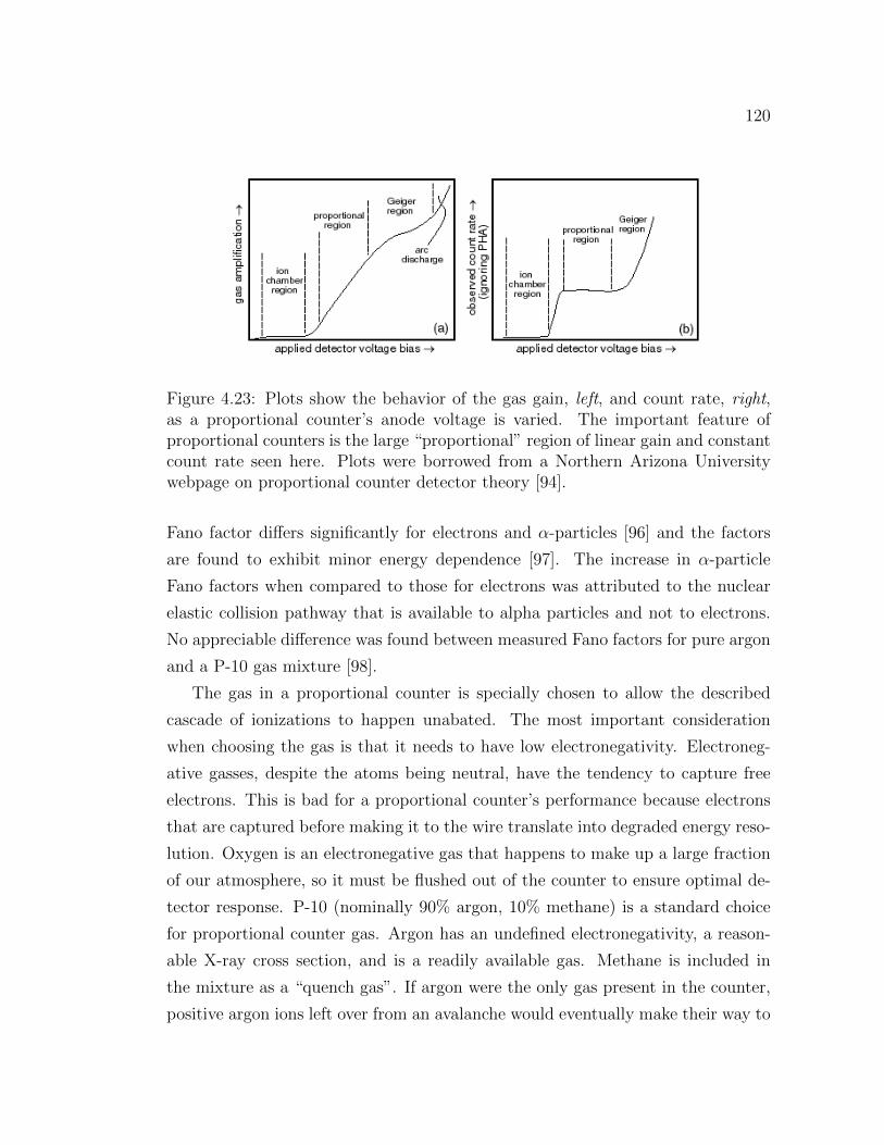
120
Figure 4.23: Plots show the behavior of the gas gain, left, and count rate, right,as a proportional counter’s anode voltage is varied. The important feature ofproportional counters is the large “proportional” region of linear gain and constantcount rate seen here. Plots were borrowed from a Northern Arizona Universitywebpage on proportional counter detector theory [94].
Fano factor differs significantly for electrons and α-particles [96] and the factors
are found to exhibit minor energy dependence [97]. The increase in α-particle
Fano factors when compared to those for electrons was attributed to the nuclear
elastic collision pathway that is available to alpha particles and not to electrons.
No appreciable difference was found between measured Fano factors for pure argon
and a P-10 gas mixture [98].
The gas in a proportional counter is specially chosen to allow the described
cascade of ionizations to happen unabated. The most important consideration
when choosing the gas is that it needs to have low electronegativity. Electroneg-
ative gasses, despite the atoms being neutral, have the tendency to capture free
electrons. This is bad for a proportional counter’s performance because electrons
that are captured before making it to the wire translate into degraded energy reso-
lution. Oxygen is an electronegative gas that happens to make up a large fraction
of our atmosphere, so it must be flushed out of the counter to ensure optimal de-
tector response. P-10 (nominally 90% argon, 10% methane) is a standard choice
for proportional counter gas. Argon has an undefined electronegativity, a reason-
able X-ray cross section, and is a readily available gas. Methane is included in
the mixture as a “quench gas”. If argon were the only gas present in the counter,
positive argon ions left over from an avalanche would eventually make their way to
121
the counter wall, long after the avalanche pulse was detected and recombine with
electrons donated by the wall material. This recombination would emit a photon
that has a good chance of ionizing a counter gas atom. The electrons produced
from these ionizations would cause distinct avalanches that would contaminate the
energy spectrum. The quench gas stops this from happening by donating an elec-
tron to the positive argon ion before it can reach the counter’s wall. Instead of
releasing a photon itself, the quench gas molecule dissociates. This consumption of
the quench gas is not a problem in our counter because we operate in flow mode,
where the quench gas is continually replenished.
Our particular counter was originally built from a solid rectangular bar of
aluminum that was end milled to create a 6 inch long × 2 inch wide × 2.125 inch
deep rectangular cavity. The wire had already been strung through the counter,
tensioned and soldered between two glass HV feedthroughs, co-linear with counter’s
long center axis. In our counter, on the left end the wire is left electrically floating
in the HV feedthrough and on the other end, it is connected to a simple electronic
circuit shown in Figure 4.22. The counter wire is connected to a NIM-BIN Tennelec
0-5 kV power supply outside of the vacuum chamber with an MHV connector on
the counter body through very large current-limiting resistors. The HV is routed
into the chamber with a floating-shield feedthrough. The BNC signal output is
AC coupled to the counter wire via a HV capacitor. Only the time-transient signal
pulse will transmit through the capacitor, not the HV DC offset. The BNC shield
is capacitively coupled to the HV. The rectangular shape of our counter’s interior
actually distorts the electric field, departing from the cylindrical ideal, but for
our application, this is not a problem. Our small window restricts illumination to
the central region of the counter, where the electric field is most uniform and the
energy resolution and QE will be the most predictable. Also, as indicated by the
functional form of the electric field inside the counter, the geometry of the wire
is far more important than the geometry of the cavity. Bends, kinks, or surface
irregularities in the wire cause electric field variance in the high-field region, close
to the wire, where it matters. For example, a longitudinal surface crack, a common
defect in die-drawn tungsten wires, would create a significantly higher field near
the rim of the crack compared to the smooth surface next to it. Signal electrons
that travel through the high field region would experience higher gain than those

122
that did not, degrading the energy resolution.
The counter was found in its native laboratory environment mounted with a
non-vacuum compatible window and the electronics potted in a solid wax block,
most likely to prevent high voltage corona/shorts. In order to prepare the instru-
ment for vacuum use, the window had to be replaced and the vacuum suitability
of the wax had to be investigated. Given the uncertain composition of the wax,
and that paraffin, a common wax, is a material with outgassing characteristics
unacceptable for high vacuum applications, the block was removed. First, the ma-
jority of the wax was melted away with a heat gun. Next, the remaining wax was
dissolved with a 3 day xylene bath, followed by an acetone rinse, and finished with
an ethanol rinse. All of the electronics shown in Figure 4.22, were replaced with
new parts to avoid the risk of future malfunctions resulting from the harsh solvent
baths. The resistors are 10±1% MΩ 10 kV 2.5 W thick film type and the capaci-
tors are 2.2±20% nF 6kV ceramic type. Great care was taken not to desolder the
counter wire from the feedthrough during the electronics replacement. Stringing
a thin proportional counter wire is a delicate process that requires enough tension
on the wire to eliminate kinks, but not so much that the wire breaks.
After the signal exits the proportional counter it travels through a Kapton R©
shield coaxial cable, into a floating-shield vacuum feedthrough, and out of the
chamber via standard 50Ω coaxial cable. The signal is fed into an Ortec 142A
charge-sensitive preamplifier at the usual input, inverted, amplified, and exits
through the E terminal as positive voltage pulses. For 5.89 keV photons, the
output pulses will be V0 = QD/Cf ≈ 0.35 V in height, where QD is the charge
deposited in the detector wire by the incident photon, and Cf ≈ 1pF is the am-
plifier’s feedback capacitance. In this equation QD = EGe−/ωP10, where E is the
energy of the incident photon and G ≈ 104 is the gas gain. Figure 4.24 shows
that we see 0.45 V pulses from the preamp on an oscilloscope. Since the HV bias
had already been removed from the detector signal and the preamp’s maximum
bias voltage is 1 kV, we did not run the HV through the preamp. In this config-
uration, it was found that the preamplifier output will be extremely noisy unless
the T and BIAS shields are well connected to the preamp’s chassis. Since the
chassis was painted, the paint had to be scraped off and creative taping methods
were used to affix copper braid and make the electrical connection between the
123
shields. Typically, it is best to connect the preamplifier close to the detector to
reduce input capacitance, microphonic (wire vibration) noise and radio frequency
pickup. In our apparatus, it was not possible to make the amplifier and its power
cable vacuum safe, so the unit had to be wired into the signal chain outside of the
chamber. After exiting the preamplifier, the inverted, amplified signal was then
fed into a NIM-BIN Tennelec 244 shaping amplifier with the gain set to 20, the
pileup rejector turned off, and a peaking time of 12 µs. The signal was then fed
into an Ortec 8k multi-channel analyzer (MCA) and recorded by Ortec’s Maestro
software running on a Windows XP PC. The data were collected in 256 channel
mode. When tuning the proportional counter’s electronics parameters, it is im-
portant to maximize proportional regime gas gain and use only enough shaping
amplifier gain to fully utilize the 0-10 V input range of the MCA. This minimizes
the width of the noise peak, allowing for the best low-energy sensitivity.
Commissioning data runs were taken with the MCA’s internal high and low
discriminators set to their default values of 0 and 255, respectively. However, it was
found that running with this settings configuration caused a discrepancy between
count rates measured with the MCA and count rates measured with single channel
analyzer (SCA). I suspected that the problem had to do with dead time correction.
Most generally, dead time is the short period of time following the detection of an
event where the system is unable to detect new events. In proportional counters,
there is a small dead time associated with the detector itself, where the electric
field requires time to reconfigure after a pulse occurs in the wire. The MCA also
has dead time because the input ADCs require ∼2 µs to convert an incoming
analog pulse into a digital number. Note that the SCA has effectively no dead
time, which is why I used it to make an unbiased comparison. Since the MCA’s
documentation contained insufficient detail on the subject of dead time and Ortec
engineers adamantly, and incorrectly, assured me that changing the discriminator
values would have no effect on dead time, I carried out my own investigation.
To perform the dead time test, the signal coming out of the preamplifier was
split and routed to an Ortec 551 SCA and Ortec 715 counting module wired in
series and the MCA so that the count rates could be compared directly. The SCA’s
lower discriminator was set below the oscilloscope-measured 55Fe pulse heights and
the upper discriminator to the 10 V maximum so that all 55Fe pulses would make it

124
Figure 4.24: A photograph of oscilloscope output showing the proportional counterpreamplifier output (positive, green pulses, bottom trace) and the shaping amplifieroutput (bipolar, purple pulses, upper trace). The green trace’s scale is 100 mV/div.and the purple trace’s scale is 2 V/div. The timing scale is 1 msec/div.
into the counting module and noise pulses would be filtered out. On the MCA, the
dead time test data runs were taken with the lower discriminator level stepped from
channel 0 to channel 27. The experiment proved to be very useful in interpreting
the MCA’s outputs. The counter outputs a two column energy spectrum in units
of counts and channel number. It also reports real time and live time numbers for
the data run. Real time is the time that a stopwatch would record for the length
of time between the beginning and end of a data run. Live time is a number
calculated by the MCA software that estimates the amount of time during the real
time interval that the MCA was sensitive to new events. This is not trivial and

125
the MCA employs the Gedcke-Hale method [99] to make the estimate.
Figure 4.25 shows the results of our investigation. It was found that the
MCA is outputting dead time corrected counts, not raw counts, evidenced by the
counts/(real time) curve more closely approximating the SCA count rate than the
counts/(live time) curve. For large dead times above 35%, the live time estimate
begins to increasingly underestimate the count rate. It was found that increasing
the MCA’s internal lower level discriminator to channel 30 completely removes the
low-energy noise peak, which was contributing to the vast majority of the dead
time, without preventing the detection of any real X-rays.
Figure 4.25: Results of the proportional counter dead time experiment. The SCAmeasured count rate was plotted with a dashed line to guide the eye.
As previously indicated, the proportional counter needed new windows. New
window plates were fabricated from 0.25 inch aluminum plates that were carefully
faced with a fly-cutter to produce a smooth surface finish. In previous window plate
design iterations, it was found that a standard mill finish is not smooth enough to
form a sealing surface with a Viton O-ring. The new plates’ mounting hole pattern
was simply designed to match the proportional counter body’s blind tapped hole
126
pattern. The window cutout in the window plate, designed to be covered by the
window and transmit X-rays, was centered on the proportional counter wire, where
the interior electric field is most uniform, the energy resolution will be the best,
and the response will be most predictable. In order to reduce systematic errors
in the QE measurement due to the proportional counter and the H1RG having
different active area geometries, the window cutout was sized to match the active
area of the H1RG detector and approximate its square geometry with a rounded
corner square. The cutout had straight edge to straight edge length l, that was
easily machinable with a common d = 0.125 inch diameter end mill:
(18 µm · 1024 pixels)2 = 0.5265 inch2 (4.27)
A = l2 − [(d)2 − π(d/2)2] (4.28)
Solving for l, the straight edge to straight edge length was 0.727 inches. A
0.0625 inch radius fillet was machined into the inside edge of the window cutout
to increase the bend radius of, and reduce mechanical stresses on, the window
when gas pressure inside the counter causes the window to bulge outwards during
operation. A shallow (0.0625 inch) glue groove was machined into the interior
surface of the window plate so that extra epoxy, used to attach the window to
the window plate, would not puddle at the window’s edge during curing. Detailed
drawings can be found in Appendix A.1.
Moving on to the design of the window itself, the window had to be sturdy
enough to withstand the 1 atmosphere (14.69 psi) of differential pressure between
the inside of the counter and the chamber’s vacuum space, but also as thin as pos-
sible so that it would transmit a large fraction of soft X-rays. The design iteration
process was begun by building a previously tested design from the literature. It
consisted of a 0.5 µm Mylar R© film mechanically supported by a 0.001 inch thick,
0.01 inch pitch stainless steel mesh [100]. While 0.001 inch (50 µm) Mylar R© films
are extremely common as a result of their use in the food packing industry, thinner
films are more difficult to purchase. I purchased 2.5, 3.5, and 6 µm films sold as
X-ray fluorescence target holder films from Premier Lab supply. I purchased sam-
ples of 50 and 100 thread per inch (TPI) (0.02 inch and 0.01 inch pitch) stainless
steel woven wire mesh from TWP Inc. that is sold for use as industrial filter ma-

127
terial. I chose Epo-tek R© H20E silver filled, electrically conductive, low outgassing
heat cure epoxy to bond the window to the window plate. Conductive epoxy was
chosen to ensure good electrical contact between the window and the proportional
counter body and therefore a uniform electric field inside the counter. In that vein,
the inner surface of the Mylar R© window needed to be made conductive to prevent
charge accumulation and subsequent electric field distortion. A thin sputtered
layer of aluminum or gold or a deposition of electroless nickel would have been
ideal for meeting this requirement, but thin, metallized Mylar R© was not commer-
cially available and we did not have the capability to apply such a coating. The
application of colloidal carbon (graphite) paint was investigated as a solution to
the problem. Two types were tested: a brush-applied liquid paint, Dag R© and an
aerosol paint, Aero-Dag R© G. The liquid paint was difficult to apply evenly, even
after dilution as recommended by the manufacturer. The aerosol adhered well to
the Mylar R© and was used in the final build process. The optimal build procedure
was:
1. Cut a large piece of heavy duty aluminum foil and taped a ∼ 1 foot long
sheet of the 6 µm Mylar R© to the foil sheet.
2. Applied ∼ 50 very light coats of Aero-Dag R© from a distance of ∼ 15 inches
to achieve the thinnest possible continuous-coverage conductive carbon layer
on the Mylar R© film. It was found that applying thick layers of the carbon
paint caused it to pool up and drip very easily, resulting in uneven cover-
age. Coverage was verified in three ways: visible light penetration (check by
eye with room lights), resistivity measurement ( ∼kΩ with standard digital
multimeter), and observation of static dissipation (film no longer clings to
itself).
3. Surprisingly, the thin Mylar R© was very difficult to cut with scissors. The
coated Mylar R© film was cut into 4 sections, ∼1 inch by 2 inches each, using
a new razor to cut through the Mylar R© into the aluminum foil backing. This
only worked when the angle between the knife and Mylar R© is kept small, or
else the Mylar R© will tear. The 4 sections were used for the two active-use
windows plus one spare for each.

128
4. According to company instructions, the H20E epoxy was prepared by pre-
mixing each component individually, then mixing a minimum batch size of
3g (1.5g part A, 1.5g part B) on a piece of stainless steel foil, using stainless
steel spatulas. According to the manufacturer, the epoxy can be removed
by heating the epoxy to 500 C (it will turn to ash) or soaking in a strong
solvent such as dichloromethane (methylene chloride also known as Freon
30).
5. An epoxy syringe was used to fill the glue groove with mixed epoxy. The
epoxy was thick and did not drip or wick at room temperature. However,
its viscosity drops severely during the heat cure, enabling it to easily wick
into places it should not be. Therefore, it is important to use the smallest
amount necessary.
6. A scissor was used to cut ∼1.5 inch by 1.5 inch sections of the 100 TPI
stainless mesh.
7. Tweezers were used to position the mesh so that it symmetrically covered the
window cutout. The 50 TPI mesh was difficult to handle because it bowed
and required pre-clamping; the 100 TPI mesh did not.
8. The painted Mylar R© sections were difficult to position on the window plate
because they tended to roll up. Handling them from the edges with tweezers,
the sections were positioned, carbon side up (facing the inside of the counter)
in the center of the window plate.
9. In order to produce a good vacuum seal and mechanical bond around the
perimeter of the window, a deformable material was needed to compress
the Mylar R©/mesh stack during the epoxy’s oven cure. Polymer foams are
deformable but most are made from either polystyrene or polyethylene. Poly-
styrene foam (Styrofoam R©) begins to flow above 100C and polyethyene foam
melts at ∼ 105C, making them both unsuitable for this application. Silicone
is a soft and strong elastomer that nominally retains its mechanical properties
up to 400F. Silicone sheet was procured and sample testing verified the
material’s suitability for use in the cure oven. For heat testing the sample was
placed in the cure oven set at 160C, 10 C above the epoxy cure temperature,

129
for 4 hours, one hour longer than the total cure time. The material performed
as expected.
10. The window plate, epoxy, mesh, painted Mylar R©, and silicone sheet stack
were clamped between two aluminum plates using two C-clamps. The stack
was stage cured by placing it in a room temperature oven and ramping the
temperature up to 150C over the course of 3 hours. The staged cure helps to
prevent the epoxy from wicking out of the glue groove by initiating a partial
cure at low temperature, which raises epoxy viscosity, before the cure reaches
its final high temperature.
11. Peeling open the stack revealed that the silicone cleanly peeled away from
the carbon painted Mylar R© and the bond looks good.
12. Using P-10, the proportional counter’s fill gas, the windows were pressure
tested by mounting them to the counter and slowly pressurizing it up to 1.5
atmospheres (22 psi) on the lab bench. During the pressure test, the window
underwent a small amount of permanent deformation, forming a smooth
spheroid shape.
Notable failures during the development of the working window design were the
catastrophic (and loud) mechanical failure of both components in a nickel mesh
and 2.5 µm Mylar R© window and the failure of the mechanical support mesh in
the nickel mesh and 6 µm Mylar R© without an accompanying failure of the Mylar R©
layer (Figure 4.26). The tested nickel support mesh was an electro-formed 70 lines
per inch grid, produced by the Buckbee-Mears company for cathode ray tubes.
Also, in the 50 TPI SS mesh with 2.5 µm Mylar R© test, the combination withstood
pressure testing, as Priestly and Phelan reported, but the thin Mylar R© was too
permeable to the P-10 counter fill gas and caused the vacuum to rise to 10−3 mbar,
which was unacceptable. Note that the final windows are not expected to have
sufficient transmission to make measurements in the soft (< 1 keV) X-ray. A
workable soft X-ray window could be fabricated with the 2.5 µm Mylar R© paired
with the 100 TPI stainless steel mesh. The Mylar’s R© inner surface would need to
be made conductive with a thin metal film. Aluminum would be an ideal choice
for the film because of its low density and low X-ray cross section.

130
Figure 4.26: Microscope photograph of a pressure tested proportional counterwindow showing the mechanical failure of the electro-formed nickel mesh withouta complete window blowout. Mylar R© is a high tensile strength polymer.
The P-10 gas input and vent in the proportional counter were originally routed
from 1/4 inch polyethylene tubes into the counter with NPT- Swagelok adapters.
As in the previously discussed search for cryogenic tube fittings, it was found that
Swagelok fittings can not produce a repeatable vacuum seal and the connectors
were replaced with Ultra-torr R© fittings. These fittings contain an O-ring that
is compressed against the tube’s outer surface, forming a repeatable high vac-
uum seal with no tools. The 1/4 inch tubes were replaced with similarly flexible,
low-outgassing 1/8 inch copper tubes. The smaller tube diameter did not cause
problems because the gas flow rate in this application is so low that the smaller
diameter does not present a significant resistance to the gas flow. On the topic
of vacuum seals, it was found that it is difficult to make a high vacuum seal with

131
national pipe taper (NPT) thread connections. NPT connections are an attractive
design option because they’re cheap to machine and easy to include in a design.
However, despite a number of attempts using a varying number of PTFE tape
wraps and varying amounts of torque, every NPT connection in the apparatus had
to be semi-permanently sealed with Torr-Seal R© in order to achieve a leak-free seal.
Torr-Seal R© has a consistency similar to toothpaste and it can be difficult to apply
precisely without the epoxy finding its way into places that it should not be. I
found it useful to mix the epoxy quickly (its viscosity increases noticeably within
10-15 minutes of mixing) and apply it with a syringe fitted with a large gauge
needle.
Moving on to the absorption of X-rays in the proportional counter, a counter
of this depth will allow a non-negligible fraction of incident X-rays to completely
penetrate the gas and be absorbed by the chamber’s back wall, without ever being
detected. Since the detector had an absorption fraction less than unity, it had to
be carefully calculated. The QE of the proportional counter is calculated with
QE(E) = T (E)(1−S∏s=1
e−dσs(E)ns), (4.29)
where T (E) is the transmission of the window, s indexes the atomic species present
in the counter gas, d is the depth of the gas, σs is the X-ray cross section of species
s, and ns is the number density of species s. The product of a sequence combines
the transmission of each atomic species independently, and (1 − T ) is the total
X-ray absorption fraction. Taking P-10 as an example, the counter QE equation
takes the transmission through a depth of argon atoms and multiplies it by the
transmission through an equivalent depth of methane, with the number densi-
ties adjusted according to the gas mixture fractions, to get the total transmission
through the gas. Each atom acts like an opaque sphere with a projected area σ
and the expression combines the effect of the total area presented by all of the
atoms in the gas column. The total number density is solved for with the ideal gas
law
n =P
kT, (4.30)
132
where P is gas pressure, T is the gas temperature, and k is the Boltzmann constant.
The number density of a particular atomic species, ns, is solved for by multiplying
the total number density by the fraction of atoms per gas particle, ns = nfs.
P-10 gas is nominally 90% argon 10% methane (CH4) by volume, which makes
the number of atoms per gas particle 0.9, 0.1, and 0.4, for argon, carbon, and
hydrogen, respectively. This notation accounts for varying gas mixtures and gas
molecule composition at the same time. An equivalent method, used for the sake
of brevity in the code, is to calculate an effective cross section,
σ =S∑s=1
σsfs, (4.31)
and use that to calculate the QE with
QE(E) = T (E)e−dσ(E)n. (4.32)
The X-ray cross section values were taken from Henke et al. [76], which is cur-
rently the standard source for elemental cross sections in the range of 10-30,000
eV. A package of IDL procedures and functions was written to perform these cal-
culations for causal estimates, but, more importantly, to seamlessly perform the
same calculations in the Monte Carlo error simulations that will be presented
later in this chapter. The package is fully documented in Appendix C. The main
components of the package are mucal.pro, which retrieves elemental cross sections
from McMaster [101], sb_henke.pro, which retrieves elemental cross sections from
Henke [76], and filter_trans.pro/gas_trans.pro, which calculate the transmis-
sion of a filter or gas volume using either the Henke or McMaster cross sections.
Figure 4.27 shows the validation of the IDL package with the Lawrence Berkeley
National Lab (LBNL) Center for X-ray Optics (http://henke.lbl.gov/optical_
constants/) and National Institute for Standards and Technology (NIST) XCOM
(http://www.nist.gov/pml/data/xcom/index.cfm) web applets. The discrep-
ancy between our code and the LBNL code is negligible at the energies of our
measurement, however we cannot explain the discrepancy between our cross sec-
tions and the NIST numbers.
Estimating the remaining parameters in the gas absorption expression amounts
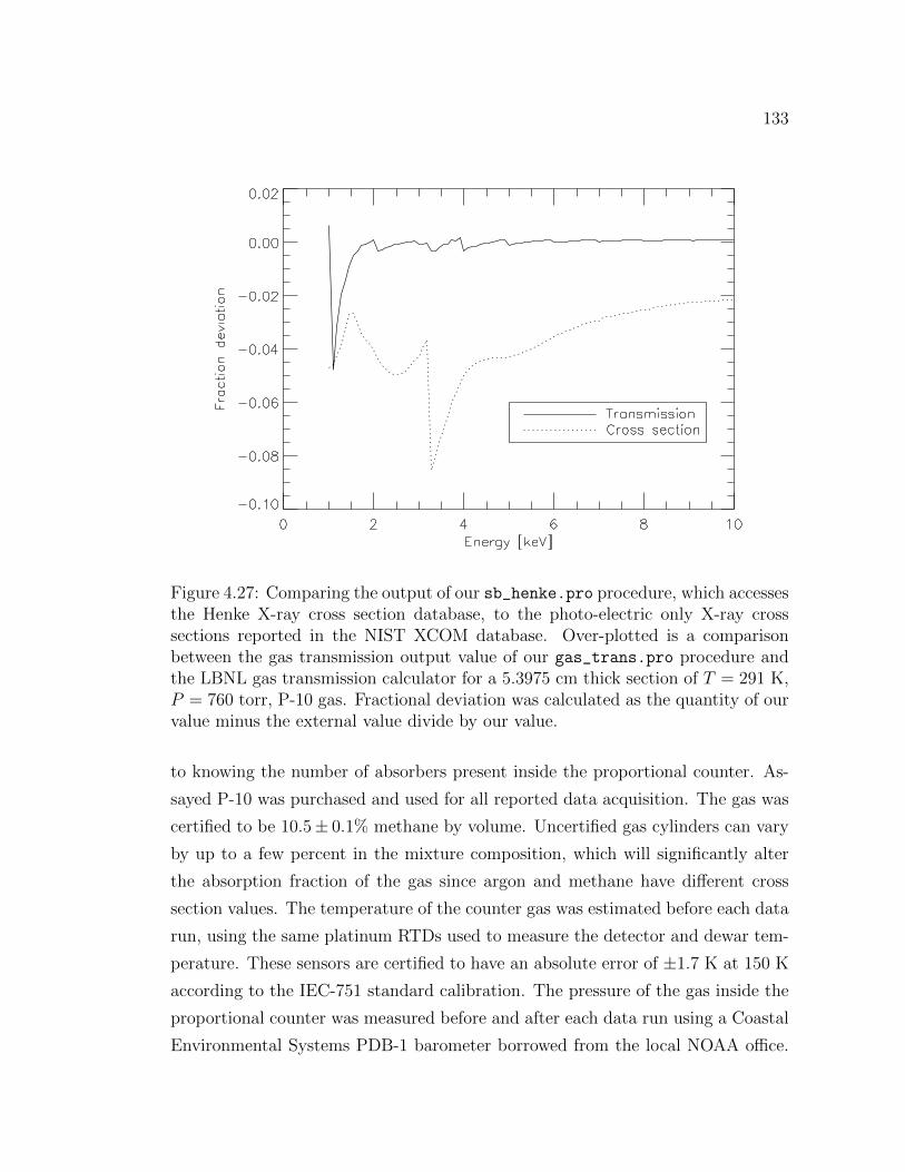
133
Figure 4.27: Comparing the output of our sb_henke.pro procedure, which accessesthe Henke X-ray cross section database, to the photo-electric only X-ray crosssections reported in the NIST XCOM database. Over-plotted is a comparisonbetween the gas transmission output value of our gas_trans.pro procedure andthe LBNL gas transmission calculator for a 5.3975 cm thick section of T = 291 K,P = 760 torr, P-10 gas. Fractional deviation was calculated as the quantity of ourvalue minus the external value divide by our value.
to knowing the number of absorbers present inside the proportional counter. As-
sayed P-10 was purchased and used for all reported data acquisition. The gas was
certified to be 10.5± 0.1% methane by volume. Uncertified gas cylinders can vary
by up to a few percent in the mixture composition, which will significantly alter
the absorption fraction of the gas since argon and methane have different cross
section values. The temperature of the counter gas was estimated before each data
run, using the same platinum RTDs used to measure the detector and dewar tem-
perature. These sensors are certified to have an absolute error of ±1.7 K at 150 K
according to the IEC-751 standard calibration. The pressure of the gas inside the
proportional counter was measured before and after each data run using a Coastal
Environmental Systems PDB-1 barometer borrowed from the local NOAA office.
134
Measuring the pressure of the gas in the counter is simple if the counter is operated
with no gas flow. With the barometer connected to the gas system, the counter
is filled, sealed off, and pressure measurements are taken while data are acquired.
Despite this method’s simplicity, I chose to run the counter in flow mode. Without
gas flow, the fill gas mixture components will permeate the window at different
rates, altering the gas composition, and thus the counter’s QE, as a function of
time. Also, outgassing from the counter interior and atmospheric gas contamina-
tion will accumulate and potentially change the counter’s energy resolution over
the course of an observation. In order to measure the pressure inside the chamber
while gas was flowing, the length of the P-10 fill tube, d1, and vent tube, d2, were
measured to be 251.0 cm and 207.1 cm, respectively. The pressure at the vent
(room pressure, Pr) and at the fill line, Pl, were measured at the beginning and
end of each data acquisition run. Assuming low-velocity flow, the pressure drop
in a long narrow tube with fluid flowing through it scales linearly with the length
of the tube. Accordingly, the pressure in the proportional counter was calculated
with
P = Pl − (Pl − Pr)d1
d1 + d2
. (4.33)
In addition to the non-unity gas absorption affecting the proportional counter
QE, the window will transmit a non-unity fraction, T (E), of incident X-ray pho-
tons. The window Mylar R© is 6 µm thick, the Aero-Dag carbon paint forms an 8
µm film according to the manufacturer, and the woven mesh is 100 TPI 0.001inch
stainless steel. While these parameters could be used to calculate the window
transmission with reasonable precision, since the transmission was a measurable
quantity, it was measured. The windows were designed so that they could be
stacked on top of one another while attached to the proportional counter. While
stacked, the two windows are separated by a set of stainless steel washers placed
between the plates at each mounting screw. This prevents the top surface of the
bottom window from contacting and marring the bottom surface of the top window
plate, where the window has been epoxied. If all six screws or all six washers are
not used, it has been found that the window plate will not seal. Calibration data
were taken with window #1 attached to the counter, then with window #2 stacked
135
on top of window #1. For the observed count rates, C, (C1&2)/C1 = T2, where
T2 is the transmission of window #2. Since transmission is a function of energy
this calibration procedure has to be performed once for every new source used in
the chamber. While this process may appear excessively time consuming, consider
the uncertainties in estimating the effective thickness of a woven grid and a stack
of thin films bulging under pressure. Additionally, for solids such as the window
materials, X-ray transmission can be very difficult to predict near absorption edges
due to X-ray absorption fine structure.
The double window calibration method is subject to error due to misalignment
of the window stack. If the misalignment error were significant, strategies to pre-
cisely locate the plates with respect to one another could be considered. To place
a rough upper limit on the misalignment error, I assume that all misalignment
occurs due to the mounting bolts being off-center with respect to their slightly
oversized mounting holes and that the plates remain parallel. Given that a 4-40
screw has a 0.112 inch OD and assuming that the holes have been reamed to their
correct 0.116 inch specification, the bolt-hole error circle has a radius of r = 0.002
inches. The maximum decrease in total area occurs when the windows are maxi-
mally misaligned by r/√
2 in the horizontal and vertical directions. Assuming, for
simplicity, that the windows cutouts are squares with edge length l = 0.727, then
the misaligned window stack will have (l− r/√
2)2/0.72792 = 99.6% the open area
of a perfectly aligned stack. This is small enough to be considered negligible.
During window construction, no effort was intentionally made to align the
stainless mesh support grids with respect to the window plates. This ensures that
the two mesh grids do not, by chance, during some assemblies of the window stack,
accidentally align such that they overlap. Accidental alignment of this variety
would skew the measured transmission too high during window calibration.
4.3.5 Detector Alignment
The solid angles subtended by the active areas of the proportional counter and the
H1RG were designed to be equal. Alignment of the detectors and the measurement
of their true positions in the caterpillar was performed with a Leica Disto D210XT
handheld laser rangefinder. The rangefinder is designed to measure the distance

136
to a laser-illuminated region on an optically thick surface more than 5 cm and less
than and 70 m from the device. Typically, it is used for building construction layout
and not precision metrology, but the device’s ±1.5 mm precision was sufficient for
the task of positioning detectors in the caterpillar. The rangefinder is built with
flat surfaces on the chassis that are normal and parallel to the beam. Using these
surfaces, the rangefinder was clamped to the proportional counter and the H1RG
mounts. The observed position of the beam was then used to adjust the detectors’
positions such that their center normals were in line with the X-ray source at the
opposite end of the chamber. It is expected that with this method, the detectors
were aligned to roughly within the 0.5 cm diameter of the rangefinder’s laser beam,
or 2 mrad at the 255 cm source-detector distance.
Next, the caterpillar’s source flange was removed, the rangefinder mounted
at the source position, and the distances to three points of known location on
the front surface of each detector were ranged. These three ranging aim-points
were arranged to form the vertices of a right triangle, making it more convenient
to use their ranged distance to calculate both the source-detector distances and
the angular deviation of each detector’s central normal from alignment with the
source. To increase the sensitivity of the angular measurement, the three points
were spread out on each detector’s respective surface to make the largest triangles
possible. Table 4.4 summarizes the ranging results.
Coordinates (x, y) Ranged distance[inches] [cm]
H1RG(0.00, 0.00) 254.8(1.10, 0.00) 254.8(0.00, 1.40) 254.8
Proportional Counter(0.00, 0.00) 256.9(2.80, 0.00) 256.8(0.00, 5.50) 256.9
Table 4.4: Alignment rangefinder data for both the H1RG and proportionalcounter. The rangefinder aim-point coordinates are in the planes of the detec-tors. The values listed under Coordinates will later be referred to as d1 and d2 andthose under Ranged distance as l1, l2, and l3.

137
The three aim-points were used to calculate the angle, θ, between each de-
tector’s center surface normal, ~dn, and the vector that points from the source to
the detector’s center, ~lc. Reference Figure 4.28 for a definition of the angles and
vectors.
l1,2,3 = lc − dc1,2,3 (4.34)
θ = sin−1
(l2cy − l2cx√l2cx + l2cy + l2cz
)(4.35)
Figure 4.28: A vector diagram of the detector alignment parameters. The vectors~l1,~l2, and ~l3 connect the source and the three range points on the detector. Vectors~d1 and ~d2 connect the three range points on the detector and span the detectorplane. The vector ~dn is the detector surface normal and ~lc connects the source andthe detector center point.
4.4 Experimental Result
4.4.1 Window Calibration Result
The windows were calibrated with 55Fe data acquired on December 7-8, 2012.
The data are summarized in Table 4.5. Proportional counter X-ray energy spec-
138
tra were reduced by subtracting background spectra that were scaled by the ra-
tio of data integration to background integration time. The total number of
counts in the line was determined by summing all channel data inside the re-
gion where the line flux was distinctly separated from background noise. Mea-
suring the combined transmission of windows #1 and #2, there were 560742 ±755 background subtracted counts between channel 44 and channel 199 of the
PC_2012-12-07_TIME_17_40.Spe and PC_2012-12-07_TIME_19_08.Spe calibra-
tion and background run. Given the data integration time of 4247 seconds, this
yielded a count rate of 132.0 ± 0.18 counts per second. Measuring the trans-
mission of window #2, there were 530789 ± 734 background subtracted counts
between channel 49 and channel 207 of the PC_2012-12-08_TIME_22_28.Spe and
PC_2012-12-08_TIME_21_33.Spe calibration and background run. Given the data
integration time of 3210 seconds, this yielded a count rate of 165.35± 0.23 counts
per second. Taking the ratio of these two count rates, window #1 was found to
transmit 79.8± 0.24% of the 55Fe energy X-rays incident on its surface.
Since modeling predicts that the window transmission is not appreciably differ-
ent for the Mn Kα and Kβ line energies, this transmission value was assumed for
both energies. Most of the window attenuation comes from the steel mesh, which
is almost entirely opaque to X-rays. A back-of-the-envelope estimate for the 0.001
inch wire, 100 TPI mesh’s open area yields(
1/100−0.0011/100
)2
= 81%. The combined
transmission of 6 µm of Mylar R© on top of 8 µm of colloidal graphite at 5.89 and
6.49 keV is 96.6% and 97.5%, which, when weighted with the source line ratio and
multiplied by the mesh open area, yields an expected transmission of 78.3%. The
fact that this rough calculation leads to a value that is very close to our measured
value bolsters our confidence in the measurement.
4.4.2 QE Data Acquisition
The QE measurement data were acquired for H1RG-167 over the course of an after-
noon on December 17, 2012. This detector was chosen because it is representative
of the lot of detectors, having standard read noise and dark current characteristics.
Its half-aluminized OBF allowed for the opportunity to probe the filter’s attenu-
ation more directly than with QE measurements alone. In all of these data, the
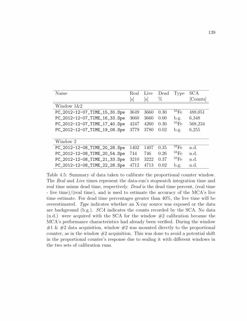
139
Name Real Live Dead Type SCA[s] [s] % [Counts]
Window 1&2PC_2012-12-07_TIME_15_30.Spe 3649 3660 0.30 55Fe 488,051PC_2012-12-07_TIME_16_33.Spe 3660 3660 0.00 b.g. 6,348PC_2012-12-07_TIME_17_40.Spe 4247 4260 0.30 55Fe 568,234PC_2012-12-07_TIME_19_08.Spe 3779 3780 0.02 b.g. 6,255
Window 2PC_2012-12-08_TIME_20_28.Spe 1402 1407 0.35 55Fe n.d.PC_2012-12-08_TIME_20_54.Spe 744 746 0.26 55Fe n.d.PC_2012-12-08_TIME_21_33.Spe 3210 3222 0.37 55Fe n.d.PC_2012-12-08_TIME_22_28.Spe 4712 4713 0.02 b.g. n.d.
Table 4.5: Summary of data taken to calibrate the proportional counter window.The Real and Live times represent the data-run’s stopwatch integration time andreal time minus dead time, respectively. Dead is the dead time percent, (real time- live time)/(real time), and is used to estimate the accuracy of the MCA’s livetime estimate. For dead time percentages greater than 40%, the live time will beoverestimated. Type indicates whether an X-ray source was exposed or the dataare background (b.g.). SCA indicates the counts recorded by the SCA. No data(n.d.) were acquired with the SCA for the window #2 calibration because theMCA’s performance characteristics had already been verified. During the window#1 & #2 data acquisition, window #2 was mounted directly to the proportionalcounter, as in the window #2 acquisition. This was done to avoid a potential shiftin the proportional counter’s response due to sealing it with different windows inthe two sets of calibration runs.

140
55Fe source was used to generate X-rays because of its stability and operational
simplicity. Throughout the data acquisition, the H1RG was stabilized at 150 K
and the proportional counter was sealed with window #1.
Three sets of data were taken, two sets with X-rays with one set with back-
ground in between the two X-ray data sets. Proportional counter and H1RG data
were acquired simultaneously. Details of the data acquisition and results of the
analysis (description to follow) are shown in Table 4.6 and 4.7.

141
Nam
eT
yp
eT
otal
Kα
Kβ
2012-12-17_TIME_17_03.fits
55F
e1,
170,
712
966,
700
158,
746
2012-12-17_TIME_19_01.fits
b.g
.2,
494
--
2012-12-17_TIME_20_39.fits
55F
e1,
171,
860
970,
745
154,
620
Tab
le4.
6:A
sum
mar
yof
H1R
Gquan
tum
effici
ency
dat
a.A
sb
efor
eT
ype
iden
tifies
whet
her
the
X-r
ayso
urc
ew
asex
pos
edor
the
dat
aar
ebac
kgr
ound
(b.g
.).
Tot
alis
the
unfilt
ered
sum
ofal
lco
unts
inth
edat
ase
t.Kα
and
Kβ
are
the
num
eric
ally
inte
grat
ednum
ber
ofco
unts
inth
em
ult
i-ga
uss
ian
leas
t-sq
uar
esfit
ofea
chre
spec
tive
line.
For
this
table
,th
edat
ase
tsw
ere
fit
indiv
idual
ly.
The
ener
gysp
ectr
aar
esh
own
and
the
inte
grat
ion
des
crib
edin§4
.4.3
.
Nam
eT
yp
eL
ive
Dea
dSC
AM
CA
Rat
ePl,s
Pl,e
Pr
[s]
[%]
[c]·1
03[c
s−1]
[mbar
][m
bar
][m
bar
]
PC_2012-12-17_TIME_17_03.Spe
55F
e68
150.
3716
3.8±
0.2
163.
8±0.
21,
005.
231,
004.
2696
0.24
PC_2012-12-17_TIME_19_01.Spe
b.g
.32
100.
029.
42±
0.1
-1,
004.
121,
003.
0395
9.19
PC_2012-12-17_TIME_20_39.Spe
55F
e10
223
0.36
1,69
1±1
163.
6±0.
11,
003.
171,
000.
9595
7.10
Tab
le4.
7:A
sum
mar
yof
pro
por
tion
alco
unte
rquan
tum
effici
ency
dat
a.A
sb
efor
e,L
ive,
Dea
d,an
dS
CA
are
the
live
tim
e,dea
dti
me
per
cent,
and
the
SC
Aco
unts
reco
rded
duri
ng
the
dat
aru
n,
resp
ecti
vely
.M
CA
Rat
eis
the
bac
kgr
ound
subtr
acte
dra
teca
lcula
ted
for
each
run.
The
pre
ssure
sPl,s,Pl,e,
andPr
repre
sent
the
P-1
0in
put
line
pre
ssure
atth
est
art
and
end
ofth
eru
nan
dth
eam
bie
nt
room
pre
ssure
,re
spec
tive
ly.
Pro
por
tion
alco
unte
ren
ergy
spec
tra
are
show
nan
dth
eem
issi
online
bou
ndin
gdes
crib
edin§4
.4.4

142
4.4.3 H1RG QE Data Reduction
The H1RG image data were acquired, archived, and reduced with the same IDL
procedures discussed earlier in §3.3. During the creation of the event list data
products, a primary event threshold of 500 DN was used to screen the images
for potential X-ray events. This threshold is justified by the shape of the center
pixel value distribution shown in Figure 4.29. The distribution of center pixel
values determines the optimal primary threshold because it is this value that de-
termines whether a pixel will be considered for event detection. The distribution
was made by processing two ramps from the 2012-12-17_TIME_19_01 X-ray data
set and two ramps from the 2012-12-17_TIME_17_03 background data set with
make_evtlist.pro. The primary event detection threshold was set unusually low,
at 40 DN, which is close to the 1σ noise floor. The center pixel value of each event
was then used to calculated the plotted distributions. The figure shows that there
is a clear boundary between the noise peak below 500 DN and the X-rays that
begin to appear at 500 DN, indicating that the 500 DN primary event threshold
is not filtering out a significant fraction of genuine X-ray events. The secondary
threshold was set at the image median absolute deviation (39 DN) to balance
photo-charge collection with unwanted noise pickup in each event. The count rate
is unaffected by the choice of secondary threshold.
Figure 4.30 shows a spectrum of all X-rays detected in the summed 2012-12-17
_TIME_19_01 and 2012-12-17_TIME_20_39 data sets with the insignificant 2012
-12-17_TIME_17_03 background over-plotted. Interesting features to note in this
spectrum are the large Mn Kα and Kβ peaks located at 2600 and 2800 DN re-
spectively. The small peak at 1600 DN is the silicon escape peak. This signal is
produced when the fluorescent silicon X-rays that are emitted by the de-excitation
of the first silicon atoms to absorb and be ionized by incident X-rays escape the
detector material. The silicon escape peak location LSi esc., compared to the loca-
tion of the main peak associated with it Lmain, will be Lmain−LSi, where LSi is the
location of the silicon Kα emission line. In this case, the escape peak has compo-
nents from both the Mn Kα and the Kβ peaks, but they are not resolvable. The
peak at 5200 DN is a pileup peak where two Kα/β X-rays were absorbed by the
same pixel during a read-frame. The high-energy continuum between the Kα/β
peaks is likely due to pileup near misses, where two events are located close enough

143
Figure 4.29: Pixel value distribution of the center (brightest) pixel of events de-tected with a primary threshold of 40 DN. With the primary threshold set thislow, the algorithm will detect both noise (the large low level peak in the distribu-tion) and true X-rays (the large, wide peak above 500 DN). The total distributionshows that the noise contribution cuts off and the X-ray distribution begins at 500DN. The over-plotted background spectrum, which was produced with the samedata reduction parameters, disappears above 500 DN indicating that the largedistribution above 500 DN is X-rays.
that their signals contaminate one another. The observed rise in the continuum
towards lower energy can be explained by the increased chance of two events land-
ing near one another at larger separation distances. These large-distance near miss
events exhibit lower total energy because the increased distance caused less signal
to be summed with the 3 × 3 event detection region. The low-energy continuum
below the Kα/β peaks is the result of incomplete signal summing due to an event’s
extension beyond the 3× 3 detection region. While this spectrum looks messy, all
features outside of the main peaks total less than 3% of total events.
The number of events recorded in the H1RG spectrum will be defined in two
ways. First, the Total number of events, listed in Table 4.6, is the number of events
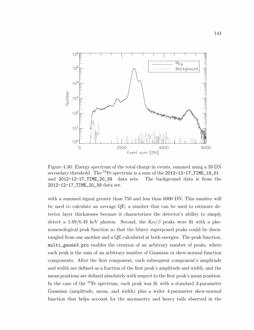
144
Figure 4.30: Energy spectrum of the total charge in events, summed using a 39 DNsecondary threshold. The 55Fe spectrum is a sum of the 2012-12-17_TIME_19_01and 2012-12-17_TIME_20_39 data sets. The background data is from the2012-12-17_TIME_20_39 data set.
with a summed signal greater than 750 and less than 6000 DN. This number will
be used to calculate an average QE, a number that can be used to estimate de-
tector layer thicknesses because it characterizes the detector’s ability to simply
detect a 5.89/6.49 keV photon. Second, the Kα/β peaks were fit with a phe-
nomenological peak function so that the blurry superposed peaks could be disen-
tangled from one another and a QE calculated at both energies. The peak function,
multi_gauss3.pro enables the creation of an arbitrary number of peaks, where
each peak is the sum of an arbitrary number of Gaussian or skew-normal function
components. After the first component, each subsequent component’s amplitude
and width are defined as a fraction of the first peak’s amplitude and width, and the
mean positions are defined absolutely with respect to the first peak’s mean position.
In the case of the 55Fe spectrum, each peak was fit with a standard 3-parameter
Gaussian (amplitude, mean, and width) plus a wider 4-parameter skew-normal
function that helps account for the asymmetry and heavy tails observed in the

145
data. Least-squares fitting was performed with Craig Markwardt’s excellent IDL
package, MPFITFUN [102]. In the fit, the second component’s parameters were
tied together so that for both peaks, the smaller and wider skew-normal compo-
nent was the same relative to the first peak, giving both peaks the same general
shape. The result of numerically integrating these peaks individually is shown in
Table 4.6 under Kα and Kβ. When the two X-ray data sets were combined, there
were 1,934,824 events in the Kα peak and 317,549 events in the Kβ peak. Figure
4.31 shows the result of the fit, which yielded a reduced chi-squared, χ2r = 3.21.
Figure 4.31: The top panel shows the combined H1RG data set. Data excludedfrom the fit are plotted with a dotted line and the included data are plotted witha solid line. The fit is over-plotted with a smooth, solid line. In the bottom panel,the fit residuals are shown, with a
√N error contour over-plotted.
4.4.4 Proportional Counter Data Reduction
Following QE data acquisition, the proportional counter data were archived as
spectra in ASCII text files so that they could be easily read by programs other than
the MCA software that created them. The first step in turning the raw data into

146
a spectrum was to read the data and relevant parameters into memory. This was
accomplished by the IDL procedure pc_read_spectrum.pro. Given a filename, the
procedure will read raw spectral data (dead time corrected counts), live integration
time, real integration time, and the MCA channel range into memory. Next, using
the IDL procedure pc_extract_counts.pro, the scaled background spectrum was
subtracted from the X-ray spectra. The scaling factor is the ratio of the live times.
In the same procedure, a channel region that bounds the X-ray lines was chosen
such that all counts in the line were included, but added noise was excluded. All
background subtracted counts within the region were then summed, divided by
the live time, and outputted as the count rate. The uncertainty in the count rate
was calculated by first adding, in quadrature, the counting uncertainties from each
channel of the X-ray spectrum to the scaled uncertainties from each channel of the
background spectrum. The background subtracted uncertainties from all channels
in the user-chosen bounding region were then summed in quadrature and divided
by the live time to yield the uncertainty in the count rate.
In the PC_2012-12-17_TIME_17_03/PC_2012-12-17_TIME_19_01 calibration
and background data set, there were 1,116,418±1,064 background subtracted counts
between channel 41 and channel 212 of the spectrum. Given the data integration
time of 6,815 seconds, this yielded a count rate of 163.8±0.2 counts per second.
In the PC_2012-12-17_TIME_20_39/PC_2012-12-17_TIME_19_01 calibration and
background data set, there were 1,673,336±1,303 background subtracted counts
between channel 43 and channel 215 of the spectrum. Given the data integration
time of 10,223 seconds, this yields a count rate of 163.6±0.1 counts per second.
Figure 4.32 shows the two background-subtracted proportional counter spectra.
Since the there are no artifacts or a significant gain or count rate shift between
the two spectra, the two were combined to increase signal to noise. To account for
the barometric pressure change that occurred as the data were taken, the counter
pressure before and after each run was averaged and taken in ratio, Pc1/Pc2, to
yield a correction factor of 1.0026 for the second count rate. The combined count
rate was 163.9±0.1 c s−1.
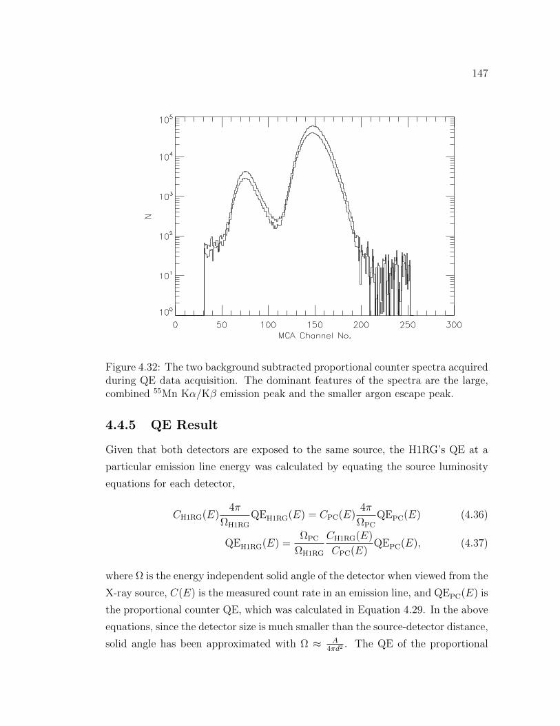
147
Figure 4.32: The two background subtracted proportional counter spectra acquiredduring QE data acquisition. The dominant features of the spectra are the large,combined 55Mn Kα/Kβ emission peak and the smaller argon escape peak.
4.4.5 QE Result
Given that both detectors are exposed to the same source, the H1RG’s QE at a
particular emission line energy was calculated by equating the source luminosity
equations for each detector,
CH1RG(E)4π
ΩH1RG
QEH1RG(E) = CPC(E)4π
ΩPC
QEPC(E) (4.36)
QEH1RG(E) =ΩPC
ΩH1RG
CH1RG(E)
CPC(E)QEPC(E), (4.37)
where Ω is the energy independent solid angle of the detector when viewed from the
X-ray source, C(E) is the measured count rate in an emission line, and QEPC(E) is
the proportional counter QE, which was calculated in Equation 4.29. In the above
equations, since the detector size is much smaller than the source-detector distance,
solid angle has been approximated with Ω ≈ A4πd2
. The QE of the proportional

148
counter is the product of the window transmission and the gas absorption. As
discussed in §4.4.1, the window transmission is assumed to be the same for both55Fe energies. The energy dependent gas absorption is calculated following the
method from §4.3.4.
In the above paragraph, note the careful use of language in the description of
C(E). These energy dependent count rate terms are not the same as the count
rate as a function of energy, otherwise known as an energy spectrum. Instead it
is the count rate in a line of energy E. To make a general argument where source
emission is allowed to be broadband and C(E) is treated as an energy spectrum,
the detector’s energy dependent response function would be included. That is
an endeavor beyond the scope of this project and this analysis will only consider
narrow-line emission. In the case of the Kα line, the QE equation becomes
QEH1RG Kα =ΩPC
ΩH1RG
CH1RG Kα
CPC Kα
QEPC Kα. (4.38)
However, a complication arises here in that we cannot directly measure CPC Kα
since the proportional counter does not have sufficient energy resolution to dis-
tinguish between the source’s two emission lines. We can only measure CPCFe =
CPC Kα + CPC Kβ, the count rate due to the two combined lines of the source. To
solve for the proportional counter count rate in each line, we use the calculated
line ratio from §4.3.3, to solve
QEPC Kβ
QEPC Kα
CPC Kα
CPC Kβ
= 6.79. (4.39)
Solving the above equation for CPC Kα and substituting into Equation 4.38, the QE
equation then becomes
QEH1RG Kα =ΩPC
ΩH1RG
CH1RG Kα
CPC Fe
(1 +
QEPCKβ
6.79 QEPCKα
)−1 QEPC Kα (4.40)
and the equation for QEH1RG Kβ similarly becomes
QEH1RG Kβ =ΩPC
ΩH1RG
CH1RG Kβ
CPC Fe
(1 + 6.79 QEPCKα
QEPCKβ
)−1 QEPC Kβ. (4.41)
149
The data show that, for events detected in the emission lines, QEH1RG Kα =
0.91±0.05 and QEH1RG Kβ = 1.0±0.05. The error analysis that lead to the quoted
uncertainties will be explained in the following section. Such quantum efficiencies
represent the probability that an incident X-ray of a certain energy will be detected
in its line profile, as defined by the above fitting process, of the H1RG spectrum.
These are useful quantities to know when considering the detector’s spectroscopic
performance in a science application. Note that it is not possible to use these QEs
to meaningfully probe layer thicknesses in the detector itself. To do this would
require a physical detector model that accounts for the complex factors like IPC,
charge diffusion, and lattice traps, which remove signal from an event, or near-miss
pileups which can add charge to it. Calculation of the emission line QEs incurs a
systematic error due to the discrepancy between the fit emission line model and
the data. Note that these QEs do not include events that are piled-up, in the
escape peak, or poorly resolved.
To address this shortcoming of the emission line QE analysis, I calculated the
average QE for the 55Fe source using the total count rates from both detectors and
solving for the H1RG’s QE,
QEH1RG Fe =ΩPC
ΩH1RG
CH1RG Fe
CPC Fe
QEPC Fe, (4.42)
where a weighted average of the proportional counter QE is calculated with
QEPC Fe = QEPC Kα
6.79
7.79+ QEPC Kβ
1
7.79. (4.43)
Here, CPC Fe and QEH1RG Fe are the total count rates integrated over the entire
spectrum of the respective detectors, while exposed to the iron source. The data
show that the source-averaged QE is QEH1RG Fe = 0.97±0.05. As with the emission
line QEs, the error analysis that led to the quoted uncertainty will be explained in
the next section. Unlike the emission line QEs, the averaged QE number can be
meaningfully compared with the weighted average values of a detector QE model
at 5.89 and 6.49 keV because it includes all detected X-rays. This comparison
will be made in §4.5. Note that the average QE number is not simply an average
of the two emission line QEs weighted with the line ratio. Since piled-up, poorly
resolved, and escape peak events are included in the average QE, its value is a few

150
percent larger than the emission line QE weighted average.
4.4.6 QE Error Analysis
Since the detector QE is a complicated function of many parameters, a Monte
Carlo simulation was designed to estimate the uncertainty in its measurement.
A generalized Monte Carlo simulator, sim_error.pro, was written in IDL for
this project. As input, the procedure takes nominal parameter values, parameter
uncertainties, and a function that runs these values through the QE equations
above (h1rg_qe.pro), and calculates the probability distribution function of the
function’s output. Table 4.8 lists all of the measured parameters that enter into
the QE calculation and their estimated 1σ uncertainties. In the simulation, all
input uncertainties are assumed to be normally distributed.
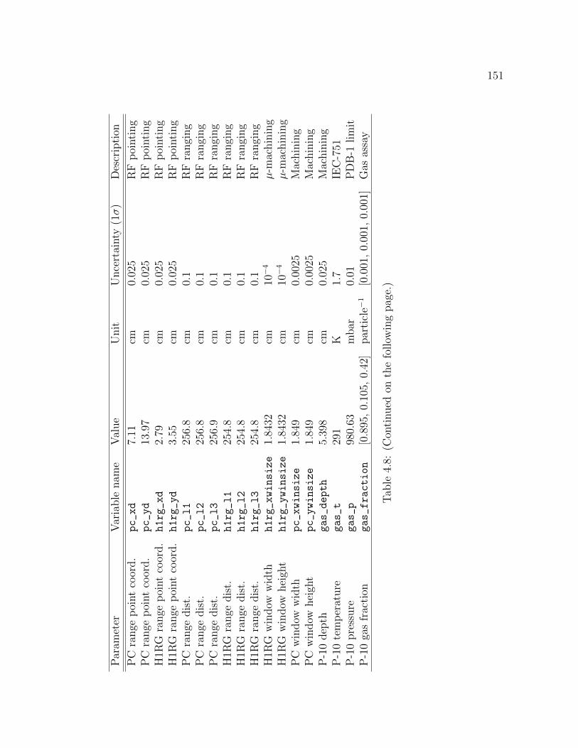
151
Par
amet
erV
aria
ble
nam
eV
alue
Unit
Unce
rtai
nty
(1σ
)D
escr
ipti
on
PC
range
poi
nt
coor
d.
pc_xd
7.11
cm0.
025
RF
poi
nti
ng
PC
range
poi
nt
coor
d.
pc_yd
13.9
7cm
0.02
5R
Fp
ointi
ng
H1R
Gra
nge
poi
nt
coor
d.
h1rg_xd
2.79
cm0.
025
RF
poi
nti
ng
H1R
Gra
nge
poi
nt
coor
d.
h1rg_yd
3.55
cm0.
025
RF
poi
nti
ng
PC
range
dis
t.pc_l1
256.
8cm
0.1
RF
rangi
ng
PC
range
dis
t.pc_l2
256.
8cm
0.1
RF
rangi
ng
PC
range
dis
t.pc_l3
256.
9cm
0.1
RF
rangi
ng
H1R
Gra
nge
dis
t.h1rg_l1
254.
8cm
0.1
RF
rangi
ng
H1R
Gra
nge
dis
t.h1rg_l2
254.
8cm
0.1
RF
rangi
ng
H1R
Gra
nge
dis
t.h1rg_l3
254.
8cm
0.1
RF
rangi
ng
H1R
Gw
indow
wid
thh1rg_xwinsize
1.84
32cm
10−
4µ
-mac
hin
ing
H1R
Gw
indow
hei
ght
h1rg_ywinsize
1.84
32cm
10−
4µ
-mac
hin
ing
PC
win
dow
wid
thpc_xwinsize
1.84
9cm
0.00
25M
achin
ing
PC
win
dow
hei
ght
pc_ywinsize
1.84
9cm
0.00
25M
achin
ing
P-1
0dep
thgas_depth
5.39
8cm
0.02
5M
achin
ing
P-1
0te
mp
erat
ure
gas_t
291
K1.
7IE
C-7
51P
-10
pre
ssure
gas_p
980.
63m
bar
0.01
PD
B-1
lim
itP
-10
gas
frac
tion
gas_fraction
[0.8
95,
0.10
5,0.
42]
par
ticl
e−1
[0.0
01,
0.00
1,0.
001]
Gas
assa
y
Tab
le4.
8:(C
onti
nued
onth
efo
llow
ing
pag
e.)

152
Table 4.8: Summarized metrology of the measured parameters that enter into theH1RG QE calculation and their associated 1σ uncertainties. When applicable,the method of measurement and/or source of uncertainty is listed. RF abbrevi-ates rangefinder. The gas fraction unit of particle−1 represents the fraction of aparticular atomic species per gas particle in the mixture.
Error distributions were generated for the three measured QE values and are
shown in Figure 4.33. The simulations show that, for events detected in the emis-
sion lines, QEH1RG Kα = 0.91 ± 0.05 and QEH1RG Kβ = 1.0 ± 0.05. The source-
averaged number is QEH1RG Fe = 0.97 ± 0.05. While one might expect the higher
intensity Kα line’s uncertainty to be lower than the Kβ uncertainty, such is not
the case because all of the errors are dominated by systematic errors. Counting
error due to the number of X-rays in the data sets is a small component of the
total uncertainty.
Figure 4.33: The three simulated probability density functions for the H1RG QEmeasured at 5.89 keV, 6.49 keV and an effective average QE that uses the 1:6.79weighted average of incident photon flux. Even though the distributions are notGaussian, the 68.26% confidence interval is plotted to provide a standard measureof the width.
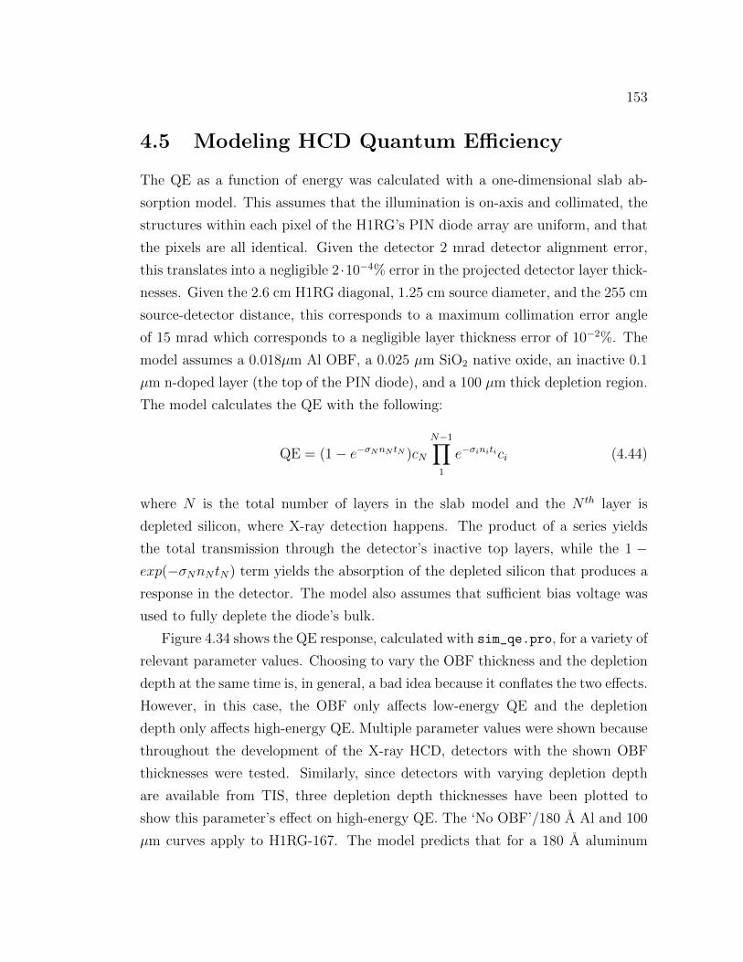
153
4.5 Modeling HCD Quantum Efficiency
The QE as a function of energy was calculated with a one-dimensional slab ab-
sorption model. This assumes that the illumination is on-axis and collimated, the
structures within each pixel of the H1RG’s PIN diode array are uniform, and that
the pixels are all identical. Given the detector 2 mrad detector alignment error,
this translates into a negligible 2 ·10−4% error in the projected detector layer thick-
nesses. Given the 2.6 cm H1RG diagonal, 1.25 cm source diameter, and the 255 cm
source-detector distance, this corresponds to a maximum collimation error angle
of 15 mrad which corresponds to a negligible layer thickness error of 10−2%. The
model assumes a 0.018µm Al OBF, a 0.025 µm SiO2 native oxide, an inactive 0.1
µm n-doped layer (the top of the PIN diode), and a 100 µm thick depletion region.
The model calculates the QE with the following:
QE = (1− e−σNnN tN )cN
N−1∏1
e−σinitici (4.44)
where N is the total number of layers in the slab model and the N th layer is
depleted silicon, where X-ray detection happens. The product of a series yields
the total transmission through the detector’s inactive top layers, while the 1 −exp(−σNnN tN) term yields the absorption of the depleted silicon that produces a
response in the detector. The model also assumes that sufficient bias voltage was
used to fully deplete the diode’s bulk.
Figure 4.34 shows the QE response, calculated with sim_qe.pro, for a variety of
relevant parameter values. Choosing to vary the OBF thickness and the depletion
depth at the same time is, in general, a bad idea because it conflates the two effects.
However, in this case, the OBF only affects low-energy QE and the depletion
depth only affects high-energy QE. Multiple parameter values were shown because
throughout the development of the X-ray HCD, detectors with the shown OBF
thicknesses were tested. Similarly, since detectors with varying depletion depth
are available from TIS, three depletion depth thicknesses have been plotted to
show this parameter’s effect on high-energy QE. The ‘No OBF’/180 A Al and 100
µm curves apply to H1RG-167. The model predicts that for a 180 A aluminum
154
OBF and 100 µm of depleted silicon, the line ratio weighted QE average,
QEH1RG Fe = QEH1RG Kα
6.79
7.79+ QEH1RG Kβ
1
7.79, (4.45)
for the two emission lines in our 55Fe source will be 0.966, which is in excellent
agreement with our QEH1RG Fe = 0.97± 0.05 measured estimate. This is the most
meaningful comparison that can be made between the data and the model since
the model does not predict which events will be detected in the line profile and
which will not.
Figure 4.34: Slab 1-dimensional model of QE as a function of X-ray energy forvariations of a nominal H1RG’s OBF thickness and depletion layer depth. Notablefeatures in all curves include the low-energy drop-off due to absorption from allof the overlying inactive layers, the O (0.5431 keV), Al (1.5596 keV, not presentin ’No OBF’ model), and Si (1.839 keV) absorption edges, and the high-energydrop-off due to the increasing over-penetration of high-energy X-rays through thedepletion region.
155
4.6 Future QE Measurements
The depth of the absorption edges and the location of the high/low-energy rolloff
feature in the H1RG QE models depend on the thickness of the layers that produce
those features in the detector model. Variation of these layer thicknesses tends to
affect the detector QE in localized energy regions, directly above the transition
energy in the case of absorption edges, and above ∼6 keV in the case of the 100
µm depletion depth. Accordingly, measuring the QE in these regions, where the
QE tends to vary the most, is the most effective method for probing the detector
layer thicknesses. Measuring QE with the 8.0 keV copper Kα line would effectively
probe the depletion depth of the detector. Measuring the QE at the 2.3 keV
sulfur, 1.7 keV silicon, and 1.4 keV aluminum lines would be the best line choices
for constraining the silicon and aluminum edge depths. Such measurements are
planned to be included in future detector calibrations.

Chapter 5The future use of HCDs in X-ray
astronomy
HCDs are currently poised to overtake CCDs as the prime focal plane array candi-
date on next-generation, X-ray space telescopes. In this chapter I will discuss how
the competitive characteristics of HCDs have already enabled access to new science
capabilities on smaller missions and are on track to do the same for large-aperture,
focused X-ray telescopes as HCD technology develops.
5.1 Small Missions
The X-ray Coded Aperture Telescope (XCAT) [50] on the Joint Astrophysics
Nascent Universe Satellite (JANUS) mission concept has shown that current-
generation HyViSITM
HCDs are the superior FPA choice for a coded aperture mask
X-ray telescope on a Small Explorer (SMEX) class mission. In order to achieve
its baseline 3.9 sr field of view and monitor the X-ray sky for high-z gamma-ray
bursts, the XCAT design required 40 detectors. HCDs were the optimal choice
because of their extremely low power consumption compared to CCDs. Operating
an equivalent number of CCDs would have dramatically increased the satellite’s
power budget, making the proposed design completely unfeasible with the bud-
getary limitations of a SMEX mission.

157
5.2 Large Missions
In addition to being viable for small missions, the current-generation of X-ray
HyViSITM
FPAs are also a stepping stone on a technology development path that
is leading to more capable FPAs. Within the coming decade, this path will likely
produce detectors that satisfy the mission requirements of next-generation large-
aperture X-ray telescopes. Achieving International X-ray Observatory (IXO) sci-
ence, which was prioritized in the 2010 Decadal Survey, will require a large aperture
(several times 104 cm2) X-ray telescope. Such a large aperture represents more than
an order of magnitude increase in effective area compared with the current gener-
ation of telescopes, which will result in a similar increase in per pixel count rates
at the focal plane, given similar plate scales. Mission concepts such as SMART-X,
ATHENA, and the canceled IXO all included wide field imager instruments that
required a soft X-ray imager with fast read speed, low noise, small pixel sizes, and
moderately large format sizes.
Next-generation HCDs will eliminate the IPC of HyViSITM
detectors with CTIA
amplifiers. They will pioneer X-ray event-driven array readout, where in-pixel
comparator circuitry will initiate pixel readout instead of the less efficient raster
format that CCDs will always need to use. Smart readout schemes such as this will
enable the detector to operate free of pile-up at significantly higher count rates and
with higher time resolution, for a given pixel read speed. In-pixel CDS circuitry
will reduce read noise. Fitting all of this circuitry into a small (∼ 15 µm) pixel
pitch is feasible, but will require development work.
These capabilities will enable the spatial and temporal resolution of lower flux
objects with moderate energy resolution. If these advanced missions are realized,
black hole and active galactic nuclei surveys will probe deeper than ever before,
spatially resolved spectra of clusters will advance precision cosmology on large
scale structure, AGN iron lines will be time-resolved, the spin of black holes in
the range 0 < z . 3 will be measured, spectra will be obtained for black holes at
z ∼ 10, and the neutron star equation of state will be probed.

Chapter 6The X-ray Confirmation of HESS
J0632+057 as a γ-ray Binary
6.1 Introduction
As discussed in Chapter 5, the HCD will soon become a competitive contender
in the race to fulfill the FPA requirements set forth by next-generation X-ray
telescopes. CCDs, however, are currently operating on all major X-ray satellite
observatories. The Swift satellite has employed CCDs at the heart of its X-ray
telescope for the past seven years with enormous success [103]. In this chapter I
will present scientific work done using CCDs on the Swift X-Ray Telescope. The
work has already been published [104] and has been reproduced by permission of
the AAS.
There are currently three confirmed TeV gamma-ray binaries; PSR B1259-63
[105], LS 5039 [106], and LS I+61 303 [107, 108, 109] as well as a fourth new GeV
gamma-ray binary recently detected by Fermi [110] that could have associated TeV
emission. Evidence at the 4.1σ level for Very High Energy (VHE) emission from
the stellar mass black hole candidate Cyg X-1 has been reported by Albert et al.
[111] during a single short flaring episode. Contained within each of these sources,
a young and massive O or B star is orbited by a compact object, either a neutron
star or a black hole. The VHE emission in TeV binary systems is powered either
by pulsar winds driving shock acceleration or by mass accretion onto the compact

159
object driving a microquasar jet. The compact physical size of the emission region
leads TeV binaries to be one of the few classes of Galactic VHE sources which
appear point-like to TeV instruments. Following the discovery of several TeV
objects with no identified counterparts, HESS J0632+057 was suggested to be a
possible member of this exotic class of TeV/X-ray binaries [112, 113]. We are
testing this hypothesis by using X-ray data to search for periodicity from orbital
flux modulation.
HESS J0632+057 was first detected using 13.5 hr of data collected between
2004 March and 2006 March as part of the HESS Galactic Plane Survey [112]. In
these data, the source has a peak significance of 7.1σ and a post-trials significance
of 5.3σ, after accounting for trials associated with searching the entire field of
view. Located on the edge of the Rosette Nebula within the Monoceros Loop
region at R.A. 06h 32’ 58.3”, Dec. +05 48’ 20” (± 28” stat., 20” sys.), the spatial
distribution of the source is consistent with that of a point source (rms size < 2’
at 95% confidence) [112]. The source is located on the edge of the 99% contour of
the EGRET unidentified object 3EG J0634+0521, but no object at the position
of HESS J0632+057 is listed in the Fermi LAT point source catalog. MWC 148,
a B0pe star, is positionally coincident with the centroid of the HESS position.
Hinton et al. [113] observed the region surrounding HESS J0632+057 on 2007
September 17 with XMM, obtaining 26 ks of good data. The observation resulted
in the identification of point source XMMU J063259.3+054801, which is position-
ally coincident with both MWC 148 and HESS J0632+057, and within the 99%
error circle of 1RXS J063258.3+054857. The source showed significant variability,
declining from ∼130 c/ksec to ∼90 c/ksec over the course of the relatively short
observation (≈ 7.2 hours). During this observation the source showed a mean
deabsorbed flux of (5.3 ± 0.4) ·10−13 erg cm−2 s−1 in the 1-10 keV range. The
spectrum was well fit by an absorbed power-law model with a photon index of
1.26± 0.04 and a column density of NH = 3.1± 0.3 · 1021 cm−2.
Beginning 2009 January 26, Falcone et al. [114] initiated a campaign to observe
XMMU J063259.3+054801 with the Swift X-ray telescope (XRT; Burrows et al.
[115]), reporting significant variability in 0.3-10 keV flux. While flux variability was
measured on day to month-long timescales, Falcone et al. [114] found no evidence
for periodicity and concluded that if periodicity was present, it was likely with

160
P > 54 days. Additionally, the X-ray source has shown no evidence of short
timescale periodic or quasi-periodic variability in the range 0.005 - 800 Hz [116].
During December 2006 - January 2007 and December 2008 - January 2009
Acciari et al. [117] performed follow-up observations of HESS J0632+057 above
1 TeV with VERITAS, yielding flux upper limits well below the values published
by HESS. Together, the VERITAS and HESS observations provide evidence for
variability of the gamma-ray flux on time scales of months. More recently, both
VERITAS and MAGIC have detected elevated TeV gamma-ray emission [118, 119]
during the time period of elevated X-ray flux reported by Falcone et al. [120] in
February 2011.
We find no report of optical flux modulation in the literature although Arag-
ona et al. [121] report temporal variations in the Hα emission line profile. HESS
J0632+057 has shown a radio spectral index of αr = 0.6± 0.2 and significant vari-
ability at 5 GHz on month-long time scales around a mean flux of 0.3 mJy [122],
however no periodic variability could be detected in these data. This radio flux is
much lower than the typical radio flux expected from a TeV blazar, making such a
potential interpretation improbable. Recently, Moldon et al. [123] announced the
1.6 GHz detection of a milliarcsecond scale source coincident with MWC 148.
The point-like nature of the detected TeV source, the excellent positional co-
incidence with MWC 148 (chance coincidence of ∼ 10−4 according to Aharonian
et al. [112]), the location on the Galactic plane with a low radio flux, the X-ray
binary-like spectral index, and the variable X-ray and gamma-ray emission are
all facts that argue in favor of an X-ray binary in association with MWC 148.
Confirmation of HESS J0632+057/MWC 148 as a TeV binary would add a new
member to this short list of objects; whereas, refutation of the binary hypothesis
would establish an equally interesting class of TeV source. The most direct way
to test this binary hypothesis is to search for periodic emission signatures. In this
chapter, we report on recent monitoring data taken with Swift-XRT.
6.2 The Observations
The X-ray Telescope (XRT; Burrows et al. [115]) on the Swift observatory [124] was
used to obtain sensitive observations in the 0.3-10 keV energy band. The typical

161
observation duration was ∼ 5 ks with ∼ 1 week spacing between most observations.
The semi-regular cadence of the observations was due to Swift’s need to account for
Gamma-ray burst and supernova targets of opportunity, spacecraft temperature,
and Moon, Earth, and Sun constraints when scheduling science target pointings.
This cadence worked very well for our science objective because it sampled, and
therefore allowed us to probe, many different temporal periods in the source. From
16 May 2009 - 15 August 2009 and 10 May 2010 - 21 August 2010 the source was
unobservable due to its close proximity to the Sun. The total Swift-XRT data set
includes 463 ks of observations, extending from 2009 January 26 (MJD 54857.1) to
2011 March 27 (MJD 55647.6), representing a baseline of T = 790.5 days. All of
the observations were obtained in photon counting (PC) mode. All observations
beyond MJD 54965 are being reported here for the first time.
6.3 Analysis
We used the most recent versions of the standard Swift tools and the most recent
calibration files available at the time of data processing. In particular, we utilized
Swift Software version 3.7, FTOOLS version 6.10, and XSPEC version 12.6.0q.
Light curves were generated using xrtgrblc version 1.5.
Source and background regions, bad CCD detector column correction, and
point spread function corrections, and filtering of data were all performed as de-
scribed in Falcone et al. [114]. Circular and annular regions are used to describe
the source and background areas respectively, and the radii of both regions depend
on the measured count rate. In order to handle cases where the sources land on
bad CCD detector columns, point spread function correction is handled using xrtl-
ccorr. Since these observations always resulted in XRT count rates ∼0.01–0.08 c/s,
there was no significant pile-up, which occurs in photon counting mode at count
rates above ∼0.5 c/s. The full light curves use a bin size of one observation per
bin (observations were typically 4-6 ksec duration). In order to avoid systematics
due to mode switching and to yield comparable photon statistics in all bins, we
removed observations with integration times less than 700 seconds, which results
in an inconsequential loss of 4 observations. All error bars are reported at the
1-sigma level, unless otherwise specified.

162
Spectral fitting was done with an absorbed power-law, with the NH set to the
value found by Hinton et al. [113] with XMM. Following the technique of Falcone
et al. [114], we calculated rate-to-flux conversion factors for groups of observations,
defining the groups such that they contained enough counts to enable good spectral
fits and isolated a single flux state of the source. Following this temporal binning,
each observation group was fit spectrally using a minimum energy binning ratio of
16 photons/bin, and in most cases the binning ratio was 20 photons/bin. Assuming
that the observed energy spectrum does not change significantly while the source is
in a particular flux state, the rate-to-flux conversion will apply for all observations
in each group. Once the spectral fits were obtained, the flux was calculated. These
flux values, which were calculated for each of the temporally binned data segments,
were then used to calculate a flux-to-rate ratio during that time period. The time-
dependent flux-rate ratio was then applied to the rate light curve, shown in Figure
6.1(a). We also fit the entire combined data set with an absorbed power law to
obtain time averaged spectral parameters. Error bars represent the count-rate
error scaled by the rate-to-flux conversion factor.
6.4 Results
A spectral fit of the combined data set finds that the data is well fit by an ab-
sorbed power-law spectrum with column density set to the XMM value (NH =
3.1 ± 0.3 · 1021 cm−2). This results in an average spectral index of 1.58 ± 0.06, a
normalization constant of 2.4±0.1·10−4, and χ2 = 57.9 with 39 degrees of freedom.
This time averaged spectrum is consistent with the results of Falcone et al. [114]
and other TeV binaries such as LS I+61 303 [125]. The X-ray light curve, con-
structed from the entire data set, is shown in Figure 6.1. Given the observations,
we define five different feature types in the variability; low level quiescent emission
of ∼ 10−12 erg cm−2 s−1, large emission peaks, which are 4-5 times brighter than
the quiescent emission, small precursor peaks, which are approximately 2 times
brighter than the quiescent emission and precede each large peak, small mid-phase
peaks, which are approximately 2.5 times brighter than quiescent emission and
appear approximately half way between the large peaks, and dips, which succeed
each large peak and represent a decrease in emission by a factor of ∼ 1/3 below

163
quiescent. By eye, these emission features appear to be spaced at regular intervals,
leading us to believe that their positions reveal an underlying periodicity in the
source. To confirm the presence of periodic modulation, we apply an autocorre-
lation analysis. The period of the modulation is determined with a peak fitting
method, and its statistical significance is established using Monte Carlo light curve
simulations.
6.4.1 Peak Fitting
Peak fitting is a simple and robust method for measuring periodicities in data, such
as these, where modulation is readily characterized by isolated peaks of enhanced
and suppressed emission superimposed upon a quiescent state. We model the light
curve with a sum of 10 Gaussians (one for each peak feature) and a constant (for
the quiescent emission). This results in 31 free parameters. To obtain the best-
fit parameter values, we perform chi-square minimization between the model and
data. The final fit is shown as a solid line in Figure 6.1 and resulted in χ2 =
207.5 for 79 degrees of freedom. The large χ2 is evidence that additional, small-
scale variability is present in the light curve and/or that Gaussians do not ideally
describe the flares. While the entire light curve is not ideally fit by this model,
it provides a reasonable characterization of the variability and, more importantly,
allows us to characterize the timing of the primary features in the light curve.
We propose that the large peaks (MJD 54966.2, 55283.3, and 55601.3) and the
dips (MJD 55303.4 and 55630.0) most accurately characterize periodic behavior
in the light curve. The small precursor peaks that precede each large peak are
unsuitable for measuring the period because they are observed to have variable
shape, position (with respect to the large peaks), and height and because their
significance above quiescence is small. The small mid-phase peaks are also unsuit-
able for measuring the period because the second peak, centered at MJD 55431.8,
is poorly sampled, yielding an unreliable peak position estimate. Averaging the
separations between peak centers, using large peaks and dips, we calculate a period
of 321 days. We conservatively estimate the error to be ±5 days, the approximate
average sampling rate during the large peaks and dips. Using this period, we have
plotted the phase-folded light curve in Figure 6.4. This shows a strong similarity
164
between modulation observed during different phases, particularly during the large
peaks and dips.
6.4.2 Lomb-Scargle
The Lomb-Scargle periodogram [126] is a standard tool used to search unevenly
sampled, univariate data for periodic variation. The algorithm samples a pre-
determined grid of temporal frequencies, the test frequencies, and calculates the
spectral power in the data at each frequency. Spectral power is the equivalent of
an empirical reduction of the sum of the squared difference between the data and
a sinusoid model of the sampled frequency. Therefore, peaks in a plot of spectral
power as a function of test frequency, also called a periodogram, indicate potential
periodicities in the data. In the special case of gaussian noise, sinusoidal data
variation, and reasonably uniform sampling density, Horne & Baliunas [127] show
that the periodogram height, z, is related to the likelihood that a peak is due to
noise, F , as
F = 1− [1− e−z]Ni , (6.1)
where Ni is the number of independent frequencies, found via Monte Carlo simu-
lations to be related to the number of data points, N0 as
Ni = −6.362 + 1.193N0 + 0.00098N20 . (6.2)
The normalized Lomb-Scargle periodogram of our X-ray light curve is shown in
Figure 6.2. The periodogram is sampled Ni times between the inverse of the total
time baseline for all observations and twice the mean Nyquist frequency, 〈fn〉. The
most significant peaks have periods of 300.3, 156.0, 75.9, and 63.9 days and false
alarm probabilities of 4.11·10−4, 1.61·10−5, 9.19·10−5, and 3.22·10−5, respectively.
The repetition of the unique, large peak dip structure in the light curve leads us
to believe that the ∼ 320 day period is the true binary modulation and that the
higher frequency periodogram peaks are either, in the case of the 156.0 and 75.9 day
periods, harmonics of the orbital frequency or, in the case of the 63.9 day period,
the Lomb-Scargle algorithm triggering on the characteristic timescale defined by

165
the time between the middle of the large peak and the middle of the dip. Since
the HESS J0632+057 light curve is highly non-sinusoidal, it is characterized better
by the peak fitting method than by the Lomb-Scargle analysis. Furthermore, the
non-sinusoidal light curve violates one of the assumptions of Horne & Baliunas
[127] and the false alarm probability estimates calculated in this way should be
viewed as upper limits presented to motivate further investigation of the period’s
significance. Due to these shortcomings we chose to disregard the Lomb-Scargle
results and pursued a more appropriate algorithm for periodicity and periodicity
significance estimation.
6.4.3 Autocorrelation
Instead of measuring the similarity of the light curve to some assumed, purely
mathematical, periodic function (a sinusoid in the case of Lomb-Scargle), an alter-
native approach is to compare the data to other data. In general, this is known as
correlation analysis. If one wishes to measure the degree of similarity between two
different sets of data, cross correlation is used. If one wishes to measure a signal’s
similarity to itself, comparing its current behavior to past behavior in a search for
repeating patterns, autocorrelation is used [128, 129]. The general procedure for
both methods is to compare the data at two different points in time, separated by
a time lag τ . For evenly sampled data, this is trivial, since all points in the data
set align with one another. However, in the case of unevenly sampled data, addi-
tional steps must be taken to calculate the cross correlation function (CCF). One
solution is to interpolate between data points and resample the data at locations
necessary for calculating the CCF.
An autocorrelation analysis is often used as a test for repeating patterns in
astronomical time series, as it requires no prior assumptions about the lightcurve
profile [128, 129]. The Discrete Auto-Correlation Function (DACF), in particular,
can be used to study the level of auto-correlation in unevenly sampled datasets
without any interpolation or addition of artificial data points [130].
Figure 6.3 shows the result of applying the z-transformed DACF [131] to the
Swift-XRT dataset. We show both the autocorrelation value, and the autocorre-
lation divided by its error, which provides an estimate of the significance of the
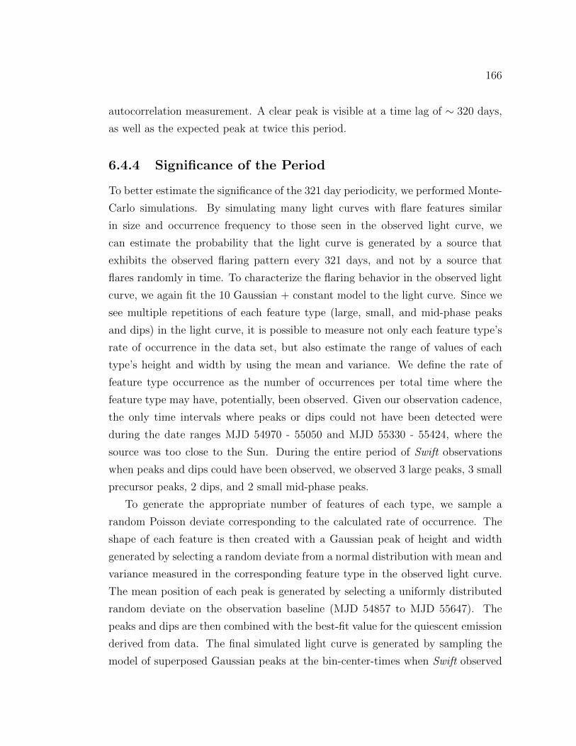
166
autocorrelation measurement. A clear peak is visible at a time lag of ∼ 320 days,
as well as the expected peak at twice this period.
6.4.4 Significance of the Period
To better estimate the significance of the 321 day periodicity, we performed Monte-
Carlo simulations. By simulating many light curves with flare features similar
in size and occurrence frequency to those seen in the observed light curve, we
can estimate the probability that the light curve is generated by a source that
exhibits the observed flaring pattern every 321 days, and not by a source that
flares randomly in time. To characterize the flaring behavior in the observed light
curve, we again fit the 10 Gaussian + constant model to the light curve. Since we
see multiple repetitions of each feature type (large, small, and mid-phase peaks
and dips) in the light curve, it is possible to measure not only each feature type’s
rate of occurrence in the data set, but also estimate the range of values of each
type’s height and width by using the mean and variance. We define the rate of
feature type occurrence as the number of occurrences per total time where the
feature type may have, potentially, been observed. Given our observation cadence,
the only time intervals where peaks or dips could not have been detected were
during the date ranges MJD 54970 - 55050 and MJD 55330 - 55424, where the
source was too close to the Sun. During the entire period of Swift observations
when peaks and dips could have been observed, we observed 3 large peaks, 3 small
precursor peaks, 2 dips, and 2 small mid-phase peaks.
To generate the appropriate number of features of each type, we sample a
random Poisson deviate corresponding to the calculated rate of occurrence. The
shape of each feature is then created with a Gaussian peak of height and width
generated by selecting a random deviate from a normal distribution with mean and
variance measured in the corresponding feature type in the observed light curve.
The mean position of each peak is generated by selecting a uniformly distributed
random deviate on the observation baseline (MJD 54857 to MJD 55647). The
peaks and dips are then combined with the best-fit value for the quiescent emission
derived from data. The final simulated light curve is generated by sampling the
model of superposed Gaussian peaks at the bin-center-times when Swift observed
167
HESS J0632+057. We then calculate the χ2 between the simulated light curve
and the model that best fit the observed data. The fraction of simulated light
curves with calculated χ2 less than that of the data represents the probability of
generating the observed light curve with a source that is stochastically flaring (with
flares having the observed size and rate of occurrence). In this way, we created 109
simulated light curves with randomly distributed flares and dips, none of which
resulted in a χ2 value less than that of the actual light curve, relative to the fit.
Therefore, we find the false alarm probability for finding this periodic light curve
from similar-sized stochastic flaring to be P < 1 · 10−9.
Figure 6.1: The background-subtracted X-ray light curve of XMMUJ063259.3+054801 from the Swift-XRT observations in the 0.3-10 keV band. Fig-ure 6.1(a) shows only the data and the time bin boundaries that were used forspectral fitting. Figure 6.1(b) shows the same data with the best fit of 10 Gaus-sians + constant model plotted as a solid line. Had the source been observablearound MJD 55000, we hypothesize that it would have exhibited a dip state. Toshow this, we phase the best-fit model in the region of the MJD 55635 dip back-wards by two periods and plot it as a dotted line. We also phase forward the XMMdata taken on 2007 September 17 (MJD 54360) [113] by two periods and plot itserror (dominated by period uncertainty) as a gray shaded box.

168
Figure 6.2: The Lomb-Scargle periodogram of Swift-XRT data sampled at Ni fre-quencies from fmin = 1/T to fmax = 2〈fn〉. The horizontal dashed lines are a seriesof false alarm probability levels, F = 0.1, 0.05, 0.01, 0.005, 0.001, 0.0005, 0.0001,representing the probability that a given peak is due to random fluctuation in thedata and not a periodic signal. The most significant periodicities detected are theproposed 320 day period and its higher frequency harmonics. The peak at 60 dayslikely shows high significance because, as seen in the folded light curve (Figure6.4), this is the characteristic timescale of the large peak followed by a small dipfeature in the light curve.
6.5 Discussion & Conclusions
We have detected a 321±5 day period in the 0.3-10 keV light curve of the uniden-
tified TeV object HESS J0632+057. The observed periodicity has been shown to
be significant by estimating the chance probability that the observed light curve
periodicity is due to stochastic flaring of the source, resulting in a false alarm
probability of P < 1 · 10−9. This implies a binary nature of HESS J0632+057,
making it the fourth confirmed TeV binary (there are now 5 confirmed gamma-ray
binaries, if one includes the recent announcement by Corbet et al. [110] of GeV

169
Figure 6.3: The z-transformed discrete correlation function as a function of timelag, plotted with error bars (bottom) and divided by error bars (top), to give anestimate of significance.
emission from 1FGL J1018.6-5856). The 321± 5 day period makes the system one
of the longest period Be star TeV/X-ray binaries and observations by Skilton et
al. [122] show that HESS J0632+057 may have an unusually low luminosity.
Figure 6.4 shows that the hardness does not vary significantly throughout most
of the orbit, but it does reach a significant maximum when the light curve exhibits
a dip feature. A constant line fit of the hardness data results in χ2 = 55.4 (with 7
dof), which shows that spectral variability is present, particularly during the flux
dip. This is consistent with the harder photon index measured by Hinton et al. [113]
at a time corresponding to a dip feature in the light curve, phased forward by two
periods (Figure 6.1). This hardening of the X-ray spectrum during a flux decrease
may be due to increased absorption of the soft X-rays in the source region, or it
could be due to an orbital modulation of acceleration site parameters. If increased
absorption due to a partial eclipse of the X-ray emission region is the origin of this

170
Figure 6.4: The X-ray light curve of XMMU J063259.3+054801 folded over theproposed period of 321 days. Zero phase has been arbitrarily defined as the dateof first observation (MJD 54857). The three phase cycles that result from thisfolding are designated with diamond, X, and square symbols, respectively. Thelower panel shows the hardness ratio (2.0-10.0 keV)/(0.3-2.0 keV), folded over thesame period and binned at 25 day intervals to improve the signal to noise ratio.The shown hardness data were fit with a constant (red dashed line), resulting inχ2 = 55.4 for 7 degrees of freedom, thus confirming variability.
spectral hardening, then it argues for a geometry of the binary system that allows
the Be star and/or its equatorial disk to pass between the X-ray emission region
and our line-of-sight. This would imply that the binary orbit is highly inclined and
that the emission region is small enough to be eclipsed. However, this would likely
be associated with an increase in NH , which is not observed in these data. An
alternative, and more likely, explanation is that the spectral hardening during the
flux dip is unrelated to absorption and instead caused by a change in acceleration
site parameters, such as electron injection energies and cooling timescales, as a
function of orbital phase.

171
In addition to the flux dip feature discussed above, the dominant features of
the periodic phased X-ray light curve are a large flux peak with a factor of 5-6
flux increase over quiescent flux and a moderate flux peak with a factor of ∼ 2.5
flux increase over quiescent flux. These peaks are separated in time by about one
half period. The flux dip immediately follows the large flux peak. Each of these
features lasts roughly ∼ 4 weeks. The recent increase in TeV flux reported by Ong
et al. [118] and Mariotti et al. [119] coincides with the time of the recent large X-
ray peak, which could imply related mechanisms such as synchrotron and inverse
Compton emission. By analogy with known X-ray binaries, it is reasonable to
assert that the peaks are the result of orbital modulation, but the system geometry
and X-ray generation mechanism are not well understood. If the spectral hardening
discussed above is due to absorption from the Be star and the surrounding region,
then the geometry would be most easily solved if the large flux peak were due to
periastron passage. However, studies to-date have not found evidence for optical
radial velocity shifts in the optical counterpart MWC 148 [121, 132]. Additional,
radial velocity measurements are required to understand the system’s geometry.
While the light curve is not sampled identically in each orbital cycle, making
orbit-to-orbit variability difficult to assess, it appears that some variation exists,
particularly in the regions preceding each large X-ray flare. This may indicate the
presence of other variability timescales related to inhomogeneity in the Be star
disk/wind. Other X-ray binaries, e.g., LS I+61 303 [125, 133], show sporadic flar-
ing behavior with a variety of timescales superposed on the binary orbit timescale,
and this should be considered as a possible source of orbit-to-orbit variations for
HESS J0632+057. Short timescale flaring analysis provides a way to probe the
size of the emission region, as well as the power of the engine that must be feeding
the associated acceleration site. If the dips indeed represent partial eclipses of the
compact object by the donor star, this effect may also be used to constrain the size
of the emission region and/or the size of a region of X-ray absorption. In principle,
short timescale variability could also be used to probe different temporal signa-
tures expected from Be star wind-driven shock models, binary interaction region
models, and accretion-driven microquasar jet models.

Appendix AMechanical Drawings
A.1 Introduction
This appendix contains mechanical drawings of components that were fabricated
for the QE teststand. All drawings except Figures A.1 and A.2 were produced
with Solidworks 2012.

173
Fra
me
Rev
ised
.pd
f
Figure A.1: Carriage frame from Ralph A. Hiller Company. The joints were ar-ranged in this way so that the carriage floor could be raised and/or the arm sepa-ration narrowed, if necessary.
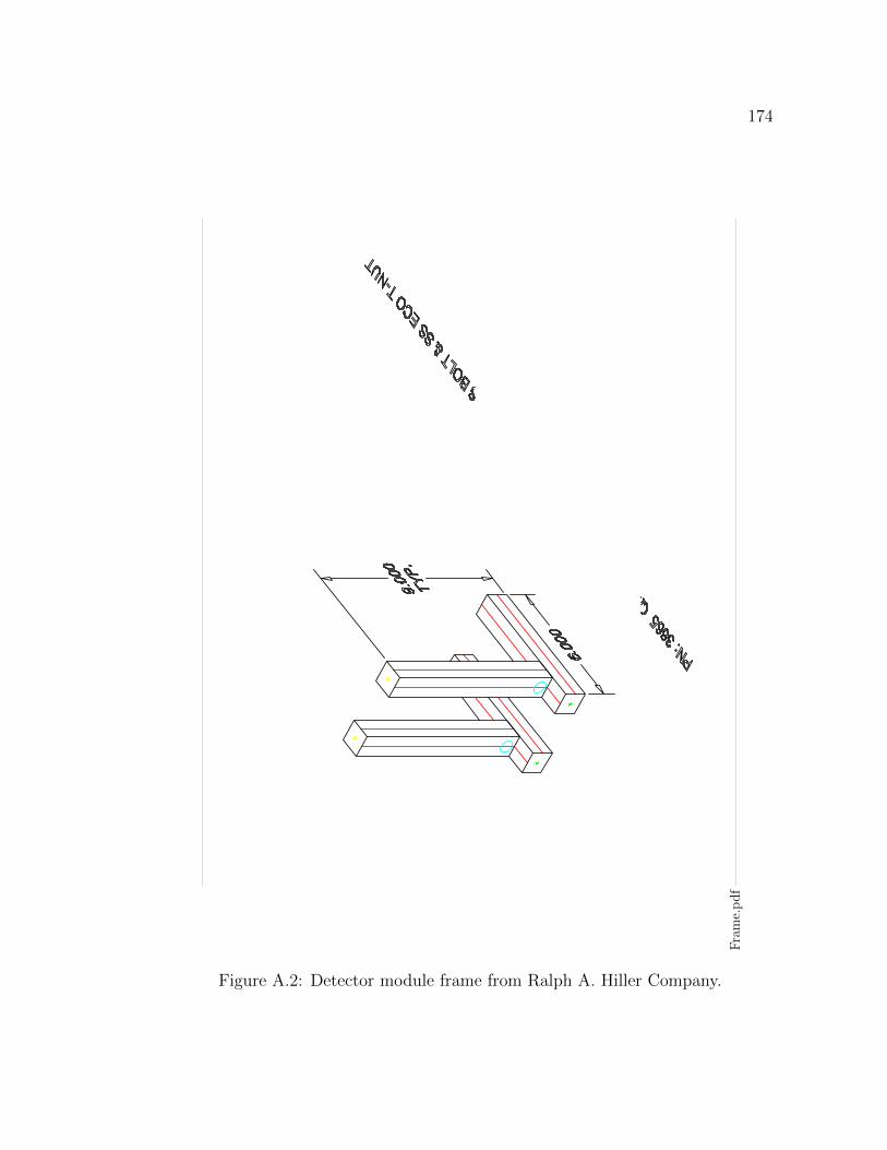
174
Fra
me.
Figure A.2: Detector module frame from Ralph A. Hiller Company.

175
10-3
2 UN
F T
HRU
16X
.159
THR
U
4X
.196
THR
U A
LL
3.62
5
5.75
0
2.00
0.5
00
2.00
0.5
001.
375
.313
1.00
0
1.00
0
#10
-32
Tapp
ed H
ole
0.25
" Alu
min
um
B C D
12
A
32
14
BA
56
DRA
WN
CHK
'D
APP
V'D
MFG
Q.A
UNLE
SS O
THER
WIS
E SP
ECIF
IED
:D
IMEN
SIO
NS
ARE
IN M
ILLIM
ETER
SSU
RFA
CE
FIN
ISH:
TOLE
RAN
CES
:
LINEA
R:
AN
GUL
AR:
FINIS
H:D
EBUR
AN
D
BREA
K SH
ARP
ED
GES
NA
ME
SIG
NA
TURE
DA
TE
MA
TERI
AL:
DO
NO
T SC
ALE
DRA
WIN
GRE
VISI
ON
TITLE
:
DW
G N
O.
SCA
LE:1
:2SH
EET 1
OF
1
A4
C
WEI
GHT
:
back
plat
e
Figure A.3: Detector module breadboard.

176
.125
.125
.125
.500
#4-
40 T
appe
d H
ole
1.75
0
1.50
0
1.00
0
1.00
0
.250
.500
.5
00
#4-
40 T
appe
d H
ole
4X
.196
THR
U A
LL
4-40
UN
C
.220
4X
.089
.3
50
2X
.089
.3
504-
40 U
NC
.2
20
Alu
min
um
#4-
40 T
appe
d H
ole
B C D
12
A
32
14
BA
56
DRA
WN
CHK
'D
APP
V'D
MFG
Q.A
UNLE
SS O
THER
WIS
E SP
ECIF
IED
:D
IMEN
SIO
NS
ARE
IN M
ILLIM
ETER
SSU
RFA
CE
FIN
ISH:
TOLE
RAN
CES
:
LINEA
R:
AN
GUL
AR:
FINIS
H:D
EBUR
AN
D
BREA
K SH
ARP
ED
GES
NA
ME
SIG
NA
TURE
DA
TE
MA
TERI
AL:
DO
NO
T SC
ALE
DRA
WIN
GRE
VISI
ON
TITLE
:
DW
G N
O.
SCA
LE:1
:1SH
EET 1
OF
1
A4
C
WEI
GHT
:
pede
stal
_bot
tom
plat
e
Figure A.4: Detector pedestal bottom plate.

177
0.750
0.125 0
.125
2.0
00
Make 4
pedestal_sideplate_smallWEIGHT:
A4
SHEET 1 OF 1SCALE:1:1
DWG NO.
TITLE:
REVISIONDO NOT SCALE DRAWING
MATERIAL:
DATESIGNATURENAME
DEBUR AND BREAK SHARP EDGES
FINISH:UNLESS OTHERWISE SPECIFIED:DIMENSIONS ARE IN MILLIMETERSSURFACE FINISH:TOLERANCES: LINEAR: ANGULAR:
Q.A
MFG
APPV'D
CHK'D
DRAWN
Figure A.5: Detector pedestal side strut.

178
.250
.125
.125
4-40
UN
C
.220
4X
.089
.3
50
.125
1.75
0
1.50
0.9
88
1.18
1
.500
.500
.750
.125
THR
U A
LL
.125
2X
.089
.3
504-
40 U
NC
.2
20 .1
88
.235
4X
.125
THR
U A
LL
TAP
FOR
#10
-32
HEL
ICO
IL IN
SERT
= 1
.0 *
DIA
. .2
34 X
120
°, N
EAR
SID
E4X
.2
01 T
HRU
ALL
Oxy
gen
Free
Cop
per
B C D
12
A
32
14
BA
56
DRA
WN
CHK
'D
APP
V'D
MFG
Q.A
UNLE
SS O
THER
WIS
E SP
ECIF
IED
:D
IMEN
SIO
NS
ARE
IN M
ILLIM
ETER
SSU
RFA
CE
FIN
ISH:
TOLE
RAN
CES
:
LINEA
R:
AN
GUL
AR:
FINIS
H:D
EBUR
AN
D
BREA
K SH
ARP
ED
GES
NA
ME
SIG
NA
TURE
DA
TE
MA
TERI
AL:
DO
NO
T SC
ALE
DRA
WIN
GRE
VISI
ON
TITLE
:
DW
G N
O.
SCA
LE:1
:1SH
EET 1
OF
1
A4
C
WEI
GHT
:
pede
stal
_top
plat
e_fla
t
Figure A.6: Detector pedestal top plate.
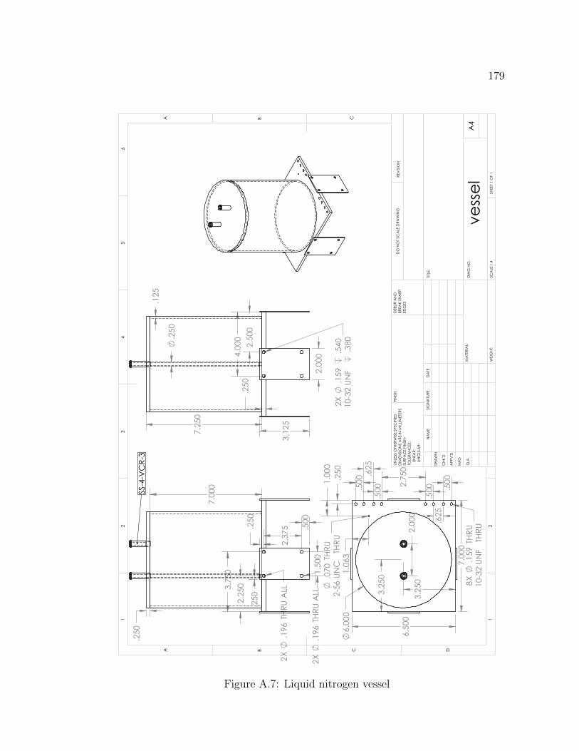
179
.250
7.00
0
1.50
0
2.37
5 .500
.250
.2502.25
03.75
0
2X
.196
THR
U A
LL
2X
.196
THR
U A
LL
SS-4
-VC
R-3
6.00
0
3.25
0
3.25
06.
500
7.00
0
1.06
3
1.00
0
.500
.500
.500 .5
00.6
25
.625
2.75
0
.250
2.00
0
10-3
2 UN
F T
HRU
8X
.159
THR
U
2-56
UN
C T
HRU
.070
THR
U2.
000
3.12
5
2.50
04.
000
.250
7.25
0
.125
.250
10-3
2 UN
F
.380
2X
.159
.5
40
B C D
12
A
32
14
BA
56
DRA
WN
CHK
'D
APP
V'D
MFG
Q.A
UNLE
SS O
THER
WIS
E SP
ECIF
IED
:D
IMEN
SIO
NS
ARE
IN M
ILLIM
ETER
SSU
RFA
CE
FIN
ISH:
TOLE
RAN
CES
:
LINEA
R:
AN
GUL
AR:
FINIS
H:D
EBUR
AN
D
BREA
K SH
ARP
ED
GES
NA
ME
SIG
NA
TURE
DA
TE
MA
TERI
AL:
DO
NO
T SC
ALE
DRA
WIN
GRE
VISI
ON
TITLE
:
DW
G N
O.
SCA
LE:1
:4SH
EET 1
OF
1
A4
C
WEI
GHT
:
vess
el
Figure A.7: Liquid nitrogen vessel
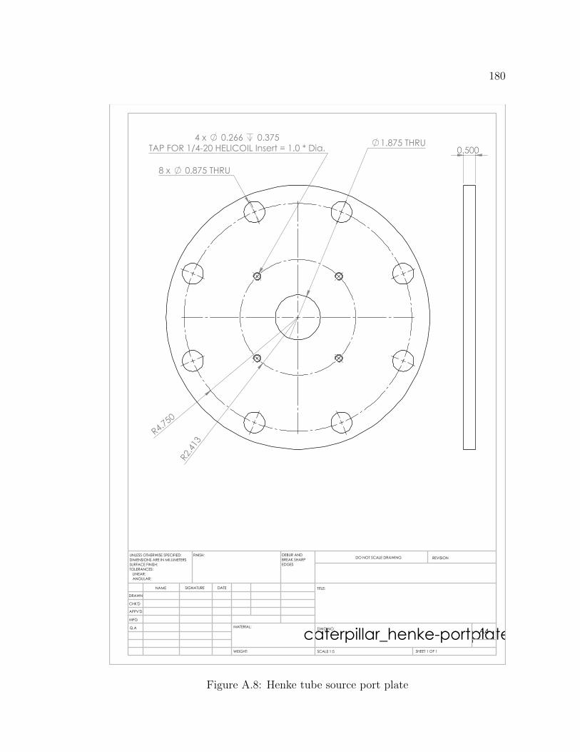
180
8 x 0.875 THRU
4 x 0.266 0.375TAP FOR 1/4-20 HELICOIL Insert = 1.0 * Dia. 1.875 THRU
R4.750
R2.4
13
0.500
caterpillar_henke-portplateWEIGHT:
A4
SHEET 1 OF 1SCALE:1:5
DWG NO.
TITLE:
REVISIONDO NOT SCALE DRAWING
MATERIAL:
DATESIGNATURENAME
DEBUR AND BREAK SHARP EDGES
FINISH:UNLESS OTHERWISE SPECIFIED:DIMENSIONS ARE IN MILLIMETERSSURFACE FINISH:TOLERANCES: LINEAR: ANGULAR:
Q.A
MFG
APPV'D
CHK'D
DRAWN
Figure A.8: Henke tube source port plate

181
R3.000
2 x 0.703 THRU ALL1/2 NPT
1.500 THRU
1.000 THRU
1.000 THRU1.500 0.750
1.000 THRU
1.500 0.750
2 x 0.438 THRU1/4 NPT
1.000
caterpillar_portplate1aWEIGHT:
A4
SHEET 1 OF 1SCALE:1:5
DWG NO.
TITLE:
REVISIONDO NOT SCALE DRAWING
MATERIAL:
DATESIGNATURENAME
DEBUR AND BREAK SHARP EDGES
FINISH:UNLESS OTHERWISE SPECIFIED:DIMENSIONS ARE IN MILLIMETERSSURFACE FINISH:TOLERANCES: LINEAR: ANGULAR:
Q.A
MFG
APPV'D
CHK'D
DRAWN
Figure A.9: (Continued on the following page.)

182
Figure A.9: Port plate containing all of the QE test stand feedthroughs. Thetwo 1/2 inch NPT were used for the HV coaxial feedthrough that carried theproportional counter high voltage and the coaxial feedthrough that carried theproportional counter signal. The 1/4 inch NPTs are the proportional counter gasinput and vent. The two large holes are for circular bayonet connectors.

183
1.0
00
0.
750
0.257 THRU
0.250
0.250
caterpillar_henke-florescentspacersWEIGHT:
A4
SHEET 1 OF 1SCALE:2:1
DWG NO.
TITLE:
REVISIONDO NOT SCALE DRAWING
MATERIAL:
DATESIGNATURENAME
DEBUR AND BREAK SHARP EDGES
FINISH:UNLESS OTHERWISE SPECIFIED:DIMENSIONS ARE IN MILLIMETERSSURFACE FINISH:TOLERANCES: LINEAR: ANGULAR:
Q.A
MFG
APPV'D
CHK'D
DRAWN
Figure A.10: Spacers that allow attaching the fluorescent target wheel to the Henketube source port plate
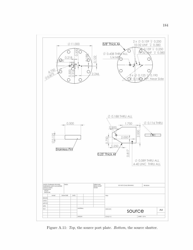
184
1.500
2.246
11.000
0.1
22
0.1
88
0.5
00
0.218
0.5
00
0.2
18
0.875 4.750
0.438 THRU ALL1/4 NPT
3 x 0.125 0.190 0.150 X 90°, Near Side
2 x 0.159 0.25010-32 UNF 0.380
0.159 0.25010-32 UNF 0.380
3/8" Thick Al
0.500
0.
125
Stainless Pin
0.500
2.000 2.0
00
1.750
0.7
50
1.250
0.8
17
0.188 THRU ALL
0.089 THRU ALL4-40 UNC THRU ALL
0.25" Thick Al
0.116 THRU
sourceWEIGHT:
A4
SHEET 1 OF 4SCALE:1:5
DWG NO.
TITLE:
REVISIONDO NOT SCALE DRAWING
MATERIAL:
DATESIGNATURENAME
DEBUR AND BREAK SHARP EDGES
FINISH:UNLESS OTHERWISE SPECIFIED:DIMENSIONS ARE IN MILLIMETERSSURFACE FINISH:TOLERANCES: LINEAR: ANGULAR:
Q.A
MFG
APPV'D
CHK'D
DRAWN
Figure A.11: Top, the source port plate. Bottom, the source shutter.
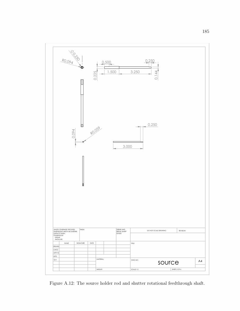
185
0.250 R0.094
1.500 3.250
0.500 0.250
0.2
25
0.1
44
R0.059
0.0
94
0.250
3.000
sourceWEIGHT:
A4
SHEET 2 OF 4SCALE:1:5
DWG NO.
TITLE:
REVISIONDO NOT SCALE DRAWING
MATERIAL:
DATESIGNATURENAME
DEBUR AND BREAK SHARP EDGES
FINISH:UNLESS OTHERWISE SPECIFIED:DIMENSIONS ARE IN MILLIMETERSSURFACE FINISH:TOLERANCES: LINEAR: ANGULAR:
Q.A
MFG
APPV'D
CHK'D
DRAWN
Figure A.12: The source holder rod and shutter rotational feedthrough shaft.

186
2 x 0.196 THRU ALL 0.375 1.140
0.425 X 90°, Near Side
2 x 0.159 0.75010-32 UNF 0.380
0.750 2.000
1.500 1
.500
0.125
0.2
50
0.250
sourceWEIGHT:
A4
SHEET 3 OF 4SCALE:1:5
DWG NO.
TITLE:
REVISIONDO NOT SCALE DRAWING
MATERIAL:
DATESIGNATURENAME
DEBUR AND BREAK SHARP EDGES
FINISH:UNLESS OTHERWISE SPECIFIED:DIMENSIONS ARE IN MILLIMETERSSURFACE FINISH:TOLERANCES: LINEAR: ANGULAR:
Q.A
MFG
APPV'D
CHK'D
DRAWN
Figure A.13: The source shield.

187
sourceWEIGHT:
A4
SHEET 4 OF 4SCALE:1:5
DWG NO.
TITLE:
REVISIONDO NOT SCALE DRAWING
MATERIAL:
DATESIGNATURENAME
DEBUR AND BREAK SHARP EDGES
FINISH:UNLESS OTHERWISE SPECIFIED:DIMENSIONS ARE IN MILLIMETERSSURFACE FINISH:TOLERANCES: LINEAR: ANGULAR:
Q.A
MFG
APPV'D
CHK'D
DRAWN
Figure A.14: An exploded view of the source plate.

188
3.000
8.0
00
2.750 0.1
16
R0.063 0.728
0.063
1.500
Plate is 0.225" AluminumFace plate to thickness on the grooved sideGrooved side must have excellent surface finish;it is a sealing surface.
window4WEIGHT:
A4
SHEET 1 OF 1SCALE:1:2
DWG NO.
TITLE:
REVISIONDO NOT SCALE DRAWING
MATERIAL:
DATESIGNATURENAME
DEBUR AND BREAK SHARP EDGES
FINISH:UNLESS OTHERWISE SPECIFIED:DIMENSIONS ARE IN MILLIMETERSSURFACE FINISH:TOLERANCES: LINEAR: ANGULAR:
Q.A
MFG
APPV'D
CHK'D
DRAWN
Figure A.15: Proportional counter window plate.

Appendix BElectronics Schematics
B.1 Introduction
This appendix contains the schematics, layouts, and design notes for two electronics
boxes that were designed and built for the QE test stand. The circuit boards
are 4 layer boards designed with the proprietary software from and fabricated by
www.expresspcb.com. Board layers are shown in the same order in which they
are stacked in the board.
B.2 QE Test Stand
B.2.1 Heater Power Supply
The board takes four analog signals produced by the NI DAQ analog outputs
(AOs) as input and outputs four lines that each power a Watlow Firerod 0.125 inch
diameter by 1.25 inch long cartridge heater. The board is powered by an external
+36 V and 0 V from a DC power supply. This circuit consists of four parallel,
low-gain, high-power amplifiers, shown in Figure B.1. Each of the four amplifier
circuits is built around an OPA 548 operational amplifier (opamp). Amplifiers are
divided into classes A-D based on how they function. Class A-C amplifiers operate
by using the input voltage to alter the rail voltage’s conduction to the output.
Class A are always on, making them low-distortion, high-frequency amplifiers that
have very poor efficiency. Class B and C improve efficiency by turning the amplifier
190
off for portions of the input signal’s cycle, but this results in increased distortion.
The OPA 548 is the Class-D variety, which is also known as a switching amplifier.
Such devices work by switching the rail’s conduction to the output on and off very
quickly with a duty cycle controlled by the input voltage. The output is passed
through a low-pass filter removes the fast swings in the switched voltage, producing
a smooth output. These amplifiers have high efficiency because the amplifier itself
is either on or off and spends very little time in transition between the two states.
Therefore they are useful for producing small, high power circuits, such as this
heater power supply.
Although the OPA 548 is capable of producing 3 A when attached to an ap-
propriately large heat sink, I limited the output near 2 A to add a margin of safety
for the amplifiers. The current limit resistor, called RCL in the OPA 548 appli-
cation notes, was set at 20 kΩ so that each circuit would be current limited at
approximately ILIM ≈ 2.1 A, according to
RCL =15000 · 4.75
ILIM− 13750Ω. (B.1)
The shown capacitors, known in this configuration as decoupling capacitors,
conduct electromagnetic interference (EMI) and power supply noise to ground,
leaving only the DC voltage. The capacitor values of C1 = 10 µF, C2 = 0.1 µF,
and C3 = 0.01 µF were chosen according to the application note’s suggestions and
provide effective noise suppression over a range of frequencies.
On the advice of Fred Hearty, the heater was designed to operate in the range
of 5 W, and I chose to overbuild it to a 25 W capability. The choice of R2 = 6 kΩ
and R1 = 1 kΩ yields a gain, G = 7, according to
G = 1 +R2
R1
. (B.2)
Given this gain, the intentionally restricted 0-5 V output swing of the DAQ AOs,
and the heater (load) resistance of RL = 51 Ω, the heater is capable of generating
between 0 and 25.4 W. Since the heaters are 0.125 inch diameter cylinders that
are 1.25 inches long, this leads to a Watt density of 25.4/1.25 · 0.1252π = 25.9
W/in2, which is far less than the heater’s specified maximum Watt density of 400
W/in2. However, these numbers are contingent on good thermal contact with the

191
material to be heated. I attempted to make a dry connection with high contact
area between the cartridge heater and the detector mounting plate with a press fit.
A Watlow R© representative assured me that this was a good idea. Unfortunately,
due to measured irregularities in the heater’s outer diameter on the order of 0.0005
inches, and the relative fragility of the heaters, we destroyed one while trying to
perform a press fit. Despite cooling the heater in LN2 and heating the block with a
hot air heat gun, which added ∼ 0.0005 inches of clearance, the press fit failed. We
later drilled the heater hole in the detector mounting plate so that the heater freely
fit, and made good thermal contact between the two components with Apiezon R©
N grease. Since the coefficient of thermal expansion of copper is larger than that of
the heater’s stainless steel sheath, the fit will get tighter at cryogenic temperatures.
This eliminates the possibility of a runaway cooling scenario, where as the detector
assembly cools, thermal contact between the heater and detector mounting plate
decreases, reducing the heater’s ability to transfer heat to the detector.
The amplifier’s heat sink requirement was calculated according to
TJ = TA + PDθJA, (B.3)
where θJA = θJC+θCH+θHA. In this equation TJ is the junction temperature (C),
TA is the ambient temperature (C), PD is the power dissipated (W), θJC is the
junction-to-case thermal resistance (C/W), θCH is the case-to-heat sink thermal
resistance (C/W), θHA is the heat sink-to-ambient thermal resistance (C/W),
and θJA is the junction-to-air thermal resistance (C/W). Interestingly, the power
dissipated by the OPA 548 does not depend linearly on the output voltage, but
instead goes as PD = IL(VS−VO), where VS is the supply voltage, VO is the output
voltage, and IL = VO/RL is the load (output) current. The power dissipation
into the amplifier component starts low for low output, reaches a maximum of
5 W per amplifier when VO = 18 (half of the supply), and then becomes small
again when for large output. Choosing a maximum amplifier junction temperature
TJ < 125 C (150 C minus a 25 C safety margin), a maximum expected ambient
air temperature of TA < 40 C, known θJC = 2.5 C/W, a typical value of θCH = 1C/W for a TO-220 package, we can solve for the heat sink size, θHA. Given 4
amplifiers running at maximum PD, θHA < 3 C/W is required. For heat sink

192
ratings, a smaller thermal resistance number corresponds to a larger heat sink. A
1.9 C/W heat sink was purchased to provide a margin of safety. With the supply
voltage set to 36 V, the heaters will never draw more than 0.7 A, which is well
within the amplifiers’ safe operating range.
Figure B.1: Schematic of the 4-channel heater power supply.
Thus far, the design has performed very well. With one heater running, the
heat sink is hardly warm to the touch. Note that with all heaters running, the unit
should be oriented so that the heat sink fins are vertical, which results in maximum
convective heat dissipation. Regarding future improvements to the system, it is
a bit weird that I used analog lines as an input to the whole amplifier circuit.
Analog lines are susceptible to noise pickup between the NI DAQ and the heater
power supply box and this is exactly why digital communication was invented. The
trouble is that it is a serious hassle to design a way for the computer communicate
with a bench top box, either by the serial port of the computer itself, the computer’s

193
Figure B.2: Heater power amplifier top surface silk screen.
Figure B.3: Heater power amplifier top copper trace deposition.
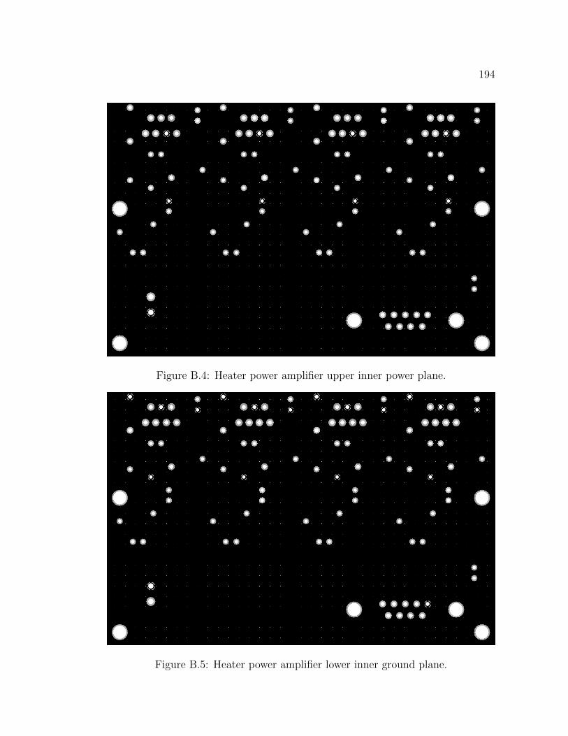
194
Figure B.4: Heater power amplifier upper inner power plane.
Figure B.5: Heater power amplifier lower inner ground plane.
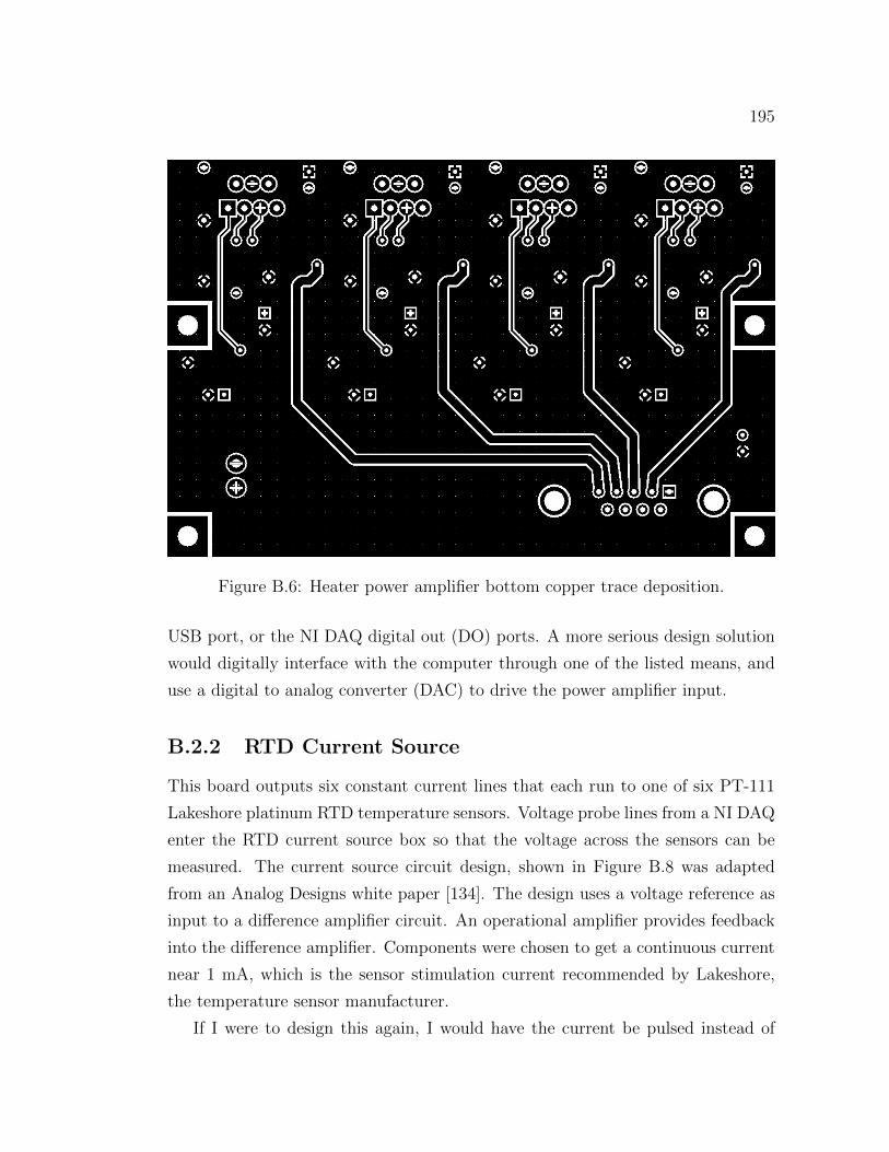
195
Figure B.6: Heater power amplifier bottom copper trace deposition.
USB port, or the NI DAQ digital out (DO) ports. A more serious design solution
would digitally interface with the computer through one of the listed means, and
use a digital to analog converter (DAC) to drive the power amplifier input.
B.2.2 RTD Current Source
This board outputs six constant current lines that each run to one of six PT-111
Lakeshore platinum RTD temperature sensors. Voltage probe lines from a NI DAQ
enter the RTD current source box so that the voltage across the sensors can be
measured. The current source circuit design, shown in Figure B.8 was adapted
from an Analog Designs white paper [134]. The design uses a voltage reference as
input to a difference amplifier circuit. An operational amplifier provides feedback
into the difference amplifier. Components were chosen to get a continuous current
near 1 mA, which is the sensor stimulation current recommended by Lakeshore,
the temperature sensor manufacturer.
If I were to design this again, I would have the current be pulsed instead of

196
Figure B.7: The chosen difference amplifier configuration. This circuit creates anaccurate current source for output currents less than 15 mA, the drive capabilityof the AD8276.
continuous. In the pulsed case, the average wattage deposited into the RTD can
be kept the same as in the continuous current case (0.988 mA 50Ω = 49 mW), but
a higher current can be used. This will produce a larger voltage drop that will be
result in a higher S/N measurement at the DAQ. This could be implemented by
generating a clock at a digital output of the DAQ with the temperature control VI.
If the temperature clock were taken as an input to the current source, the DAQ’s
voltage measurement, which is controlled by the VI, and the current pulse could
be synchronized.

197
Figure B.8: Schematic of the 6-channel RTD current source.
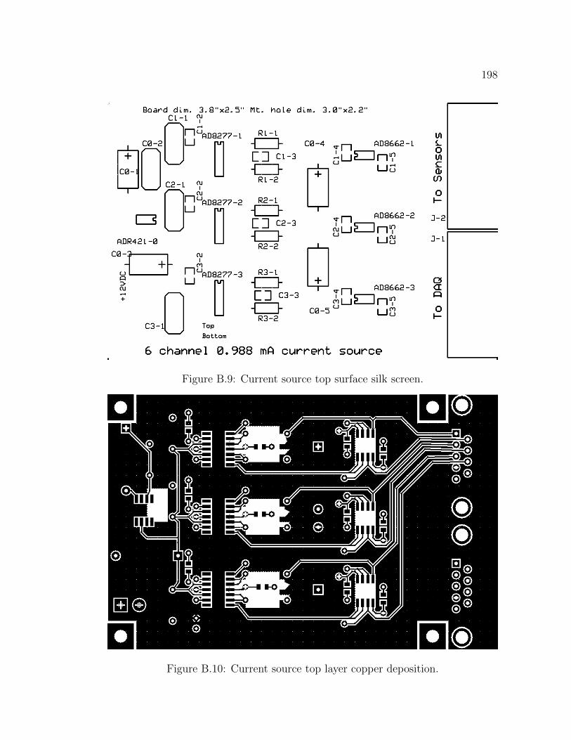
198
Figure B.9: Current source top surface silk screen.
Figure B.10: Current source top layer copper deposition.

199
Figure B.11: Current source top inner copper layer.
Figure B.12: Current source bottom inner copper layer.

200
Figure B.13: Current source bottom layer copper deposition.

Appendix CCode
C.1 Introduction
All original codes used in this thesis are listed here, grouped into three categories:
Data reduction (Chapter 3), which were used to reduce and visualize X-ray HyViSI
data, QE Teststand (Chapter 4), which were used to process and reduce data pro-
duced by the QE test stand, and Thesis, which were used to make demonstrative
calculations presented in this thesis. In each section, the codes are listed in alpha-
betical order.
C.2 Data Reduction
• calc_ipc.pro
• disp_evts.pro
• event_detect.pro
• evt_filter.pro
• grade_evts.pro
• make_evtlist.pro
• pixcal.pro

202
• ramp_cds.pro
• spectrum.pro
; $Id: calc_ipc.pro, v1.0 2010/01/15 sdb$pro calc_ipc, events, m1th = m1th, m2th = m2th $
, m3th = m3th, m4par = m4par, save = save $, help = help
;+;; Name:; calc_ipc;; Category:; X-ray data reduction;; Syntax:; calc_ipc, events, [m1th];; Description:; Calculates and prints the InterPixel Capacitance (IPC)
kernel given event list data;; Mandatory Arguments:; events : (input) event list structure;; Optional Arguments:; m1th : (input) the secondary pixel standard
deviation below which events; will be allowed into the IPC kernel
averaging sample.; This is the maximum threshold that
will be tested. zero; is the minimum.; m2th : (input) the brightest secondary pixel
threshold below which events; will be allowed into the IPC kernel
averaging sample.;; m3th : (input) the brightest secondary pixel
percent threshold below which; events will be allowed into the IPC
kernel averaging sample.;; m4par : (input) parameters associated with running
Laurent Moniers; mistral code to derrive IPC with
myopic deconvolution; [not working];; Flags:

203
; save : saves plots to file. [not working];-ntest = 100 ; number of points to test thresholdsevents = evt_filter(events,cpixrange=[1200,4000]) ;only use iron data
for IPC measurement
if not keyword_set(m1th) then m1th = 150 ; standard deviationthreshold
if not keyword_set(m2th) then m2th = 60 ;constant 2nd brightest pixthreshhold
if not keyword_set(m3th) then m3th = 0.05 ;fraction 2nd brightest pixthreshold
;;;;;;;;;;;;;;;;;;;;;;;;;;;;;;;;;;;;;;;;;;;;;;;;;;;;;;;;;;;;;;;;;;;;;print, "Calculating method 1----------------------------------------"ipc = dblarr(9,ntest)m1th = dindgen(ntest)*m1th/(ntest-1) ; turning the max m1th into the
array of m1th to testn_evts = lindgen(ntest)for j=0,ntest-1 do begin
counter,j,ntest-1dev = dblarr(9,n_elements(events.x))sum=lonarr(n_elements(events.x))
; finding average of all secondary pixels in each event andstoring it in vector ’ave’
for i=0,8 do if i ne 4 then sum=sum+events.island[i] ; skippingcenter pix
ave=sum/8.
; finding the squared deviation from average, summing, and takingsquare root. this is standard devaition.
for i=0,8 do dev[i,*]=(events.island[i]-ave)^2sum=lonarr(n_elements(events.x))for i=0,8 do if i ne 4 then sum=sum+dev[i,*] ; skipping center
pixstandev=sqrt(sum/8.)
; for events with secondary pixel standard deviation less thanthe m1th, averaging all events
index = where(standev lt m1th[j])for i=0,8 do ipc[i,j]=total(events[index].island[i])/n_elements(
index)n_evts[j] = n_elements(index); normalizing the kernel to 1ipc[*,j] = ipc[*,j]/total(ipc[*,j])
endfor
window,/freeplot, m1th,n_evts,xtitle=’Standard Deviation Threshold [DN]’,ytitle=’
Number of events used’,/ylog,title=’Method 1’,ystyle=8,xmargin=[10,10]
axis, yrange=[0,1.1],yaxis=1,/save,ytitle=’% charge outside center pix.’oplot,m1th,sum/(sum+ipc[4,*])
204
window,/freesum = ipc[0,*]for i=1,8 do if i ne 4 then sum = sum+ipc[i,*]plot, m1th,sum/(sum+ipc[4,*]),xtitle=’Standard Deviation Threshold [DN]’
,ytitle=’percent charge outside center pixel’,title=’Method 1’read, ’What method 1 threshold do you want to use to calculate IPC? ’,xtemp = min(abs(m1th-x),best) ;finding the m1th value closest to what the
user typed into x; printing the result;;;;;;;;;;;;;;;;;;;;;;;;;;;;;;;;;;;;;;;;;;;;;;;;;;;;;;;;;;;;;;;;;;;;;print, "Method 1 - Secondary pixel standard deviation limit --------"print, "Used "+strcompress(string(n_evts[best]))+" events to calculate:print, ""print, reform(ipc[*,best],3,3)print, "The nodal capacitance calculated from this IPC kernel is: ",print, "Up capacitance: ",print, "Down capacitance: ",print, "Left capacitance: ",print, "Right capacitance: ",print, "------------------------------------------------------------"
if keyword_set(save) then beginprintplotsetplot, m1th,n_evts,xtitle=’Standard Deviation Threshold [DN]’,
ytitle=’Number of events used’,/ylog,title=’Method 1’plot, m1th,sum/(sum+ipc[4,*]),xtitle=’Standard Deviation
Threshold [DN]’,ytitle=’percent charge outside center pixel’,title=’Method 1’
printplot, /normalendif
print, ’Calculating Method 2 --------------------------------------’ipc = dblarr(9,ntest)m2th = dindgen(ntest)*m2th/(ntest-1) ; turning the max m1th into the
array of m1th to testn_evts = lindgen(ntest)
for j=0,ntest-1 do begincounter,j,ntest-1
;finding the brightest secondary pixel in each eventbrightest=events.island[0]island = events.island[[0,1,2,3,5,6,7,8]] ; skipping the center
pixelfor i=1,7 do begin
pick = where(island[i,*] gt brightest,count)if count ne 0 then brightest[pick] = island[i,pick]
endfor; Do i use a constant DN threshold for m2th or should it be a
fraction of the primary pixel?
205
; here I try a constant threshold. note it will only apply forone energy xray since a different energy primary will put adifferent amount of charge into the secondary pixels.
index = where(brightest lt m2th)for i=0,8 do ipc[i,j]=total(events[index].island[i])/n_elements(
index)n_evts[j] = n_elements(index); normalizing the kernel to 1ipc[*,j] = ipc[*,j]/total(ipc[*,j])
endfor
window,/freeplot, m1th,n_evts,xtitle=’2nd Brightest Pixel Threshold [DN]’,ytitle=’
Number of events used’,/ylog,title=’Method 2’
window,/freesum = ipc[0,*]for i=1,8 do if i ne 4 then sum = sum+ipc[i,*]plot, m1th,sum/(sum+ipc[4,*]),xtitle=’2nd Brightest Pixel Threshold [DN]
’,ytitle=’percent charge outside center pixel’,title=’Method 2’read, ’What method 2 threshold do you want to use to calculate IPC? ’,xtemp = min(abs(m1th-x),best) ;finding the m1th value closest to where
you clicked
; printing the resultprint, "Method 2 - brightest secondary pixel limit ----------------"print, "Used "+strcompress(string(n_evts[best]))+" events to calculate:print, ""print, reform(ipc[*,best],3,3)print, "-----------------------------------------------------------"
if keyword_set(save) then beginprintplotsetplot, m1th,n_evts,xtitle=’2nd Brightest Pixel Threshold [DN]’,
ytitle=’Number of events used’,/ylog,title=’Method 1’plot, m1th,sum/(sum+ipc[4,*]),xtitle=’2nd Brightest Pixel
Threshold [DN]’,ytitle=’percent charge outside center pixel’,title=’Method 1’
printplot, /normalendif
print, "Calculating Method 3 --------------------------------------"ipc = dblarr(9,ntest)m3th = dindgen(ntest)*m3th/(ntest-1) ; turning the max m1th into the
array of m1th to testn_evts = lindgen(ntest)
for j=0,ntest-1 do begin

206
counter, j,ntest-1
;finding the brightest secondary pixel in each eventbrightest=events.island[0]island = events.island[[0,1,2,3,5,6,7,8]] ; skipping the center
pixelfor i=1,7 do begin
pick = where(island[i,*] gt brightest,count)if count ne 0 then brightest[pick] = island[i,pick]
endfor
; Do i use a constant DN threshold for m2th or should it be afraction of the primary pixel?
; Here I use the percentage. Like mark bautz said, i am biasingthe sample since i am saying what ipc is allowed into thesample used for calculating ipc.
index = where(brightest lt m3th*events.island[4])
for i=0,8 do ipc[i,j]=total(events[index].island[i])/n_elements(index)
; normalizing the kernel to 1ipc[*,j] = ipc[*,j]/total(ipc[*,j])
endfor
window,/freeplot, m1th,n_evts,xtitle=’2nd Brightest % Pixel Threshold [DN]’,ytitle=’
Number of events used’,/ylog,title=’Method 3’
window,/freesum = ipc[0,*]for i=1,8 do if i ne 4 then sum = sum+ipc[i,*]plot, m1th,sum/(sum+ipc[4,*]),xtitle=’2nd Brightest % Pixel Threshold [
DN]’,ytitle=’percent charge outside center pixel’,title=’Method 3’read, ’What method 3 threshold do you want to use to calculate IPC? ’,xtemp = min(abs(m1th-x),best) ;finding the m1th value closest to where
you clicked
; printing the resultprint, "Method 3 - brightest secondary % pixel limit ---------------"print, "Used "+strcompress(string(n_evts[best]))+" events to calculate:print, ""print, reform(ipc,3,3)print, "------------------------------------------------------------"
if keyword_set(save) then beginprintplotset_plot, ’ps’device, filename=’’plot, m1th,n_evts,xtitle=’2nd Brightest % Pixel Threshold [DN]’,
ytitle=’Number of events used’,/ylog,title=’Method 1’

207
device, /closedevice, filename=’’plot, m1th,sum/(sum+ipc[4,*]),xtitle=’2nd Brightest % Pixel
Threshold [DN]’,ytitle=’percent charge outside center pixel’,title=’Method 1’
device, /closeset_plot, ’x’printplot, /normal
endif
; Method 4 ---------------------------------------------------------; myopic deconvolution
end
PRO disp_evts, events, index=index, evt_list=evt_list, output_name=output_name, quad=quad
; takes an IDL structure of events as input and produces a fits fileshowing the morphology of all of the events arraged for viewing
; index = [low index,high index] allows you to specify which events inthe array you want to stick in the file.
; evt_list = an array of indicies in events that you want to show withdisp_evts
; output_name = the name given to the output fits file.; quad = a switch that causes the use of 5x5 event regions instead of
the usual 3x3
;;;;;;;;;;;;;;;;;;;;; initializing stuff;;;;;;;;;;;;;;;;;;;;
IF KEYWORD_SET(index) THEN events = events[index(0):index(1)]
IF KEYWORD_SET(evt_list) THEN events = events[evt_list]
num_evts = N_ELEMENTS(events.x)PRINT, num_evts
num_width = FLOOR(SQRT(num_evts))
;;;;;;;;;;;;;;;;;;;;;;;;;;;;;;;;;;;;;;;;;;;;;;; assigning event islands into the image array;;;;;;;;;;;;;;;;;;;;;;;;;;;;;;;;;;;;;;;;;;;;;;IF KEYWORD_SET(quad) THEN BEGIN
array = FLTARR(num_width*6+1,(num_width+2)*6+1)FOR i=0L,num_evts-1 DO BEGIN
temp = DBLARR(5,5)temp[*,0] = events[i].reef[0:4]temp[0,1] = events[i].reef[5]temp[1:3,1] = events[i].island[0:2]temp[4,1] = events[i].reef[6]

208
temp[0,2] = events[i].reef[7]temp[1:3,2] = events[i].island[3:5]temp[4,2] = events[i].reef[8]temp[0,3] = events[i].reef[9]temp[1:3,3] = events[i].island[6:8]temp[4,3] = events[i].reef[10]temp[*,4] = events[i].reef[11:15]
array[6*(i MOD num_width)+2-2:6*(i MOD num_width)+2+2,6*FLOOR(i/num_width)+2-2:6*FLOOR(i/num_width)+2+2] = temp
ENDFORENDIF ELSE BEGIN
array = FLTARR(num_width*4+1,(num_width+2)*4+1)FOR i=0L,num_evts-1 DO array[4*(i MOD num_width)+2-1:4*(i MOD
num_width)+2+1,4*FLOOR(i/num_width)+2-1:4*FLOOR(i/num_width)+2+1] = events[i].island
ENDELSE
;;;;;;;;;;;;;;;;;;;;;;;;;;;;;;;;;;;;;;;;;;;;;;;;;;;;;;;;;;;;;;;;;;;;;; figuring out business with the filename, whether or not to overwrite
an existing file and whatnot;;;;;;;;;;;;;;;;;;;;;;;;;;;;;;;;;;;;;;;;;;;;;;;;;;;;;;;;;;;;;;;;;;;;;IF KEYWORD_SET(output_name) THEN BEGIN
splitname = STRSPLIT(output_name,’.’,/extract)output_name_noext = STRJOIN(splitname[0:N_ELEMENTS(splitname)-2],
’.’)ENDIF ELSE BEGIN
output_name_noext = ’disp_evts’output_name = ’disp_evts.fits’
ENDELSE
SPAWN, ’ls ’+output_name,tempWHILE temp EQ output_name DO BEGIN
response1=’’READ, response1, PROMPT = ’The event list ’ + output_name + ’
aleady exists. Choose (o) to overwrite it, (a) to appendsomething to the new filename, or (s) to stop running: ’
IF response1 EQ ’o’ THEN BEGINSPAWN, ’rm -rf ’+output_nametemp = ’’
ENDIFIF response1 EQ ’a’ THEN BEGIN
response2 = ’’READ, response2, PROMPT = ’Type what you want to append to
the filename so that it becomes unique: ’output_name = output_name_noext + response2 + ’.fits’SPAWN, ’ls ’ + output_name,temp
ENDIFIF response1 EQ ’s’ THEN BEGIN
PRINT, "Ok fine, then I am going to stop running."temp = ’’STOP

209
ENDIFIF ((response1 NE ’o’) AND (response1 NE ’a’) AND (response1 NE ’
s’)) THEN PRINT, ’Hey buddy, type o for overwrite, a forappend, or s to stop running.’
ENDWHILE
WRITEFITS, output_name, arrayEND
FUNCTION event_detect, image, th1=th1, side=side; event detection algorithm that does any size event boxes.; OUTPUT structure with tags x:0, y:0, island:DBLARR(side^2), sum:DOUBLE
(0), grade_asca:0, grade_acis:0, event_num:0, image_num:0; this function DOES NOT do the grading so those struture tages are left
as 0s;THERES A BUG IN THIS CODE! when there are no events detected in a frame
, the function returns a single event at x=0,y=0. discovered thiswhen doing background ramps and was getting counts below the primarythreshold.
;;;;;;;;;;;;;;;;;;;;;;;;;;;;;;;;;;;;;;;;;;;;;;;;;;;;;;;;;;;;;;;;;;;;;; Calculating the noise in the frame and corresponding primary event
threshold. Using the mad will eliminate bias of xrays.;;;;;;;;;;;;;;;;;;;;;;;;;;;;;;;;;;;;;;;;;;;;;;;;;;;;;;;;;;;;;;;;;;;;;
noise_sigma =1.4826 * MAD(image)IF NOT KEYWORD_SET(th1) THEN BEGIN
th1 = 5*noise_sigmaPRINT, ’Primary event threshold calculated to be ’, th1
ENDIF
imsize = SIZE(image)chipx = imsize[1]chipy = imsize[2]
;;;;;;;;;;;;;;;;;;;;;;;;;;;;;;;;;;;;;;;;;;;;;;;;;;;;;;;;;;;;;;;;;;;;;; Creating p_thresh_pix, an array of 1d pixel indicies that are greater
than primary event threshold;;;;;;;;;;;;;;;;;;;;;;;;;;;;;;;;;;;;;;;;;;;;;;;;;;;;;;;;;;;;;;;;;;;;;
p_thresh_pix = WHERE(image GT th1,N_p_thresh_pix)
;;;;;;;;;;;;;;;;;;;;;;;;;;;;;;;;;;;;;;;;;;;;;;;;;;;;;;;;;;;;;;;;;;;;;; Initializing local_max_pix, an array of 1d pixel indicies whos pixel
value is greater than primary event threshold and is also localmaxima.
; the second column of local_max_pix will be a number 0-3 indicating theposition of the brightest pixel
;;;;;;;;;;;;;;;;;;;;;;;;;;;;;;;;;;;;;;;;;;;;;;;;;;;;;;;;;;;;;;;;;;;;;
local_max_pix = LONARR(N_ELEMENTS(p_thresh_pix),2)
;;;;;;;;;;;;;;;;;;;;;;;;;;;;;;;;;;;;;;;;;;;;;;;
210
; Generating the array of event pixel locations;;;;;;;;;;;;;;;;;;;;;;;;;;;;;;;;;;;;;;;;;;;;;;;
j=0L ; counter to see how many elements get inserted into local_max_pixIF N_p_thresh_pix GT 0 THEN BEGIN
FOR i=0L,N_ELEMENTS(p_thresh_pix)-1 DO BEGINIF TOTAL(image(BOX1D(p_thresh_pix[i],chipx)) GT image(
p_thresh_pix[i])) EQ 0. THEN BEGIN ; testing for alocal maxima
local_max_pix[j,0] = p_thresh_pix[i]IF (LONG(side)/2 EQ LONG(side)/2.) THEN BEGIN ; if
side is even you have to do this stuff todetermine which way the event will shift
local_max_pix[j,1] = CHOOSE_SHIFT(image[BOX1D(local_max_pix[j,0],chipx)])
ENDIFj=j+1
ENDIFENDFOR
;;;;;;;;;;;;;;;;;;;;;;;;;;;;;;;;;;;;;;;;;;;;;;;;;;;;;;;;;;;;;;;;;;;;;; trimming local_max_pix down to the correct size. this should be faster
than concatenating each step of the way;;;;;;;;;;;;;;;;;;;;;;;;;;;;;;;;;;;;;;;;;;;;;;;;;;;;;;;;;;;;;;;;;;;;;
local_max_pix = local_max_pix[0:j-1,*]
ENDIF ELSE BEGIN
PRINT, ’Event detect found no pixels greater than th1 in thisimage’
ENDELSE
;;;;;;;;;;;;;;;;;;;;;;;;;;;;;;;;;;;;;;;;;;;;;;;;;;;;;;;; Initializing the structure for storing the event list;;;;;;;;;;;;;;;;;;;;;;;;;;;;;;;;;;;;;;;;;;;;;;;;;;;;;;;
num_evts = N_ELEMENTS(local_max_pix[*,0])events = REPLICATE(x:0, y:0, island:DBLARR(side^2), reef:DBLARR((side
+2)^2-side^2), sum:DOUBLE(0), grade_asca:0, grade_acis:0, event_num:0, noise_sigma:0, image_num:0, num_evts)
;;;;;;;;;;;;;;;;;;;;;;;;;;;;;;;;;;;;; Assigning values to the event list;;;;;;;;;;;;;;;;;;;;;;;;;;;;;;;;;;;;
FOR i=0L,num_evts-1 DO BEGIN
events[i].x = local_max_pix[i,0] MOD chipx ; event x coord.events[i].y = FLOOR(local_max_pix[i,0]/chipx) ; event y coord.events[i].island = image[BOX1D(local_max_pix[i,0],chipx,/center,
quadrant=local_max_pix[i,1],side=side)] ; all of the pixelvalues in the event
211
events[i].reef = image[ELEMENT(BOX1D(local_max_pix[i,0],chipx,/center,quadrant=local_max_pix[i,1],side=side+2),[0,1,2,3,4,5,9,10,14,15,19,20,21,22,23,24])]
events[i].event_num = i ; event index. starts at 0events[i].noise_sigma = noise_sigma
ENDFOR
RETURN, eventsEND
FUNCTION evt_filter, events, evt_list=evt_list, xrange=xrange, yrange=yrange, cpixrange=cpixrange, sumrange=sumrange,$
spixrange=spixrange, asca=asca, acis=acis, grade_include=grade_include,grade_reject=grade_reject, splitrange=splitrange, negs=negs, old_th2=old_th2,$
new_th2=new_th2,no_corners=no_corners,imrange=imrange,sp_reject=sp_reject
;takes an event list structure as input and returns an index list or newevent structure containing events with specified properties.
;note that each of the filtering methods are ANDed with one another
;evt_list - takes an existing event index list as input so that it canbe further pared down.
;xrange yrange - a range of the form [low,high] that removes eventsoutside of a specified pixel range on the chip.
;cpixrange - a range of the form [low,high] that removes events with acenter pixel value outside of the specified range.
;sumrange - a range of the form [low,high] that removes events outsideof a specified range of event sum. This corresponds to a range on thespectrum.
;spixrange - a range of the form [low,high] that removes events withsecondary threshold pixels outside of the specified range.
;grade_include/reject - an array containing grade numbers to be includedor rejected in the returned structure.
;asca/acis - specifies the grade number format. acis is default.;splitrange - a range of the form [low%,high%] that removes events with
a second brightest pixel that is not within a specified rangepercentage of the primary event pixel
;negs - in non-deconvolved data all pix should be above zero. Specifyingthis keyword filters out those that, for some reason, are not.
;th2 - lets you respecify a secondary event threshold for quick plotting.
;no_corners = when doing splitrange filtering, set this keyword toexclude corners of a 3x3 event since IPC should never put charnge inthese pixels.
;imrage - a range of the form [low,high] that removes events outside ofa specified range of image_num (image numbers.
new_events=events
num_evts = N_ELEMENTS(new_events.x)

212
IF KEYWORD_SET(acis) and KEYWORD_SET(asca) THEN BEGINprint, "You cannot use acis and asca grade formats at the same
time."stop
ENDIF
IF NOT KEYWORD_SET(acis) and NOT KEYWORD_SET(asca) THEN acis=1
IF KEYWORD_SET(evt_list) THEN BEGINevt_list_bool = REPLICATE(0,num_evts)evt_list_bool[evt_list] = 1
ENDIF ELSE evt_list_bool = REPLICATE(1,num_evts)
IF KEYWORD_SET(xrange) THEN evt_list_bool = evt_list_bool AND ((new_events.x GT xrange[0]) AND (new_events.x LT xrange[1]))
IF KEYWORD_SET(yrange) THEN evt_list_bool = evt_list_bool AND ((new_events.y GT yrange[0]) AND (new_events.y LT yrange[1]))
IF KEYWORD_SET(cpixrange) THEN evt_list_bool = evt_list_bool AND ((new_events.island[4] GT cpixrange[0]) AND (new_events.island[4] LTcpixrange[1]))
IF KEYWORD_SET(imrange) THEN evt_list_bool = evt_list_bool AND ((new_events.image_num GE imrange[0]) AND (new_events.image_num LEimrange[1]))
IF KEYWORD_SET(old_th2) THEN BEGINgrades = INTARR(num_evts)rosetta = [32,64,128,8,0,16,1,2,4]FOR i=0L,num_evts-1 DO BEGIN
new_events[i].sum = TOTAL(new_events[i].island[WHERE(new_events[i].island GE old_th2)])
new_events[i].grade_acis = TOTAL(rosetta[WHERE(new_events[i].island GT old_th2)])
new_events[i].grade_asca = acis2asca(new_events[i].grade_acis)
ENDFORENDIF
IF KEYWORD_SET(new_th2) THEN BEGINnew_events.grade_acis = transpose((new_events.island GT new_th2)
##[32,64,128,8,0,16,1,2,4])new_events.sum = total((new_events.island GT new_th2)*new_events.
island,1)ENDIF
IF KEYWORD_SET(sumrange) THEN evt_list_bool = evt_list_bool AND ((new_events.sum GT sumrange[0]) and (new_events.sum LT sumrange[1]))
IF KEYWORD_SET(asca) THEN BEGINtemp_evt_list_bool = REPLICATE(0,num_evts)IF KEYWORD_SET(grade_include) THEN BEGIN
213
FOR i=0,N_ELEMENTS(grade_include)-1 DO temp_evt_list_bool= temp_evt_list_bool OR (new_events.grade_asca EQgrade_include[i])
evt_list_bool = evt_list_bool AND temp_evt_list_boolENDIFIF KEYWORD_SET(grade_reject) THEN BEGIN
FOR i=0,N_ELEMENTS(grade_reject)-1 DO temp_evt_list_bool =temp_evt_list_bool OR (new_events.grade_asca EQgrade_reject[i])
evt_list_bool = NOT ((NOT evt_list_bool) ORtemp_evt_list_bool)
ENDIFENDIF
IF KEYWORD_SET(acis) THEN BEGINtemp_evt_list_bool = REPLICATE(0,num_evts)IF N_ELEMENTS(grade_include) GT 0 THEN BEGIN
FOR i=0,N_ELEMENTS(grade_include)-1 DO temp_evt_list_bool= temp_evt_list_bool OR (new_events.grade_acis EQgrade_include[i])
evt_list_bool = evt_list_bool AND temp_evt_list_boolENDIFIF KEYWORD_SET(grade_reject) THEN BEGIN
FOR i=0,N_ELEMENTS(grade_reject)-1 DO temp_evt_list_bool =temp_evt_list_bool OR (new_events.grade_acis EQgrade_reject[i])
evt_list_bool = NOT ((NOT evt_list_bool) ORtemp_evt_list_bool)
ENDIFENDIF
IF KEYWORD_SET(splitrange) THEN BEGINIF KEYWORD_SET(no_corners) THEN sort_evts = DBLARR(5,num_evts)
ELSE sort_evts = DBLARR(9,num_evts)FOR i=0L,num_evts-1 DO BEGIN
IF KEYWORD_SET(no_corners) THEN BEGINtemp_island = new_events[i].island[[1,3,4,5,7]]sort_evts[*,i] = REVERSE(temp_island[SORT(
temp_island)])ENDIF ELSE BEGIN
sort_evts[*,i] = REVERSE(new_events[i].island[SORT(new_events[i].island)]) ;sort() outputs lowestto highest, but reverse() turns this highest tolowest so that i can conveniently subscriptwith 0 and 1 to get highest and second highestelements.
ENDELSEENDFORevt_list_bool = evt_list_bool AND ( ((sort_evts[1,*]/sort_evts
[0,*]) GT splitrange[0]/100.) AND ((sort_evts[1,*]/sort_evts[0,*]) LT splitrange[1]/100.))
ENDIF

214
IF KEYWORD_SET(negs) THEN BEGINno_negs = INTARR(num_evts)FOR i=0L,num_evts-1 DO no_negs[i] = TOTAL(new_events[i].island LE
0) EQ 0evt_list_bool = evt_list_bool AND no_negs
ENDIF
IF KEYWORD_SET(sp_reject) THEN BEGINsalt = bytarr(1)FOR i = 0, MAX(new_events.image_num)-1
;get indices of all events in the left column and all events inthe right column
left_evt_list_index = WHERE(new_events.x LT 512 AND new_evts.image_num EQ i)
right_evt_list_index = WHERE(new_events.x GE 512 AND new_evts.image_num EQ i)
;get number of events in each list. should be roughly equaln_left = n_elements(left_evt_list_index)n_right = n_elements(right_evt_list_index)
;magicsomething = $rebin(fix(new_events[left_evt_list_index].image_num),n_left,
n_right) eq rebin(transpose(fix(new_events[right_evt_list_index].image_num)),n_left,n_right) $
and $rebin(fix(new_events[left_evt_list_index].y),n_left,n_right) eq
rebin(transpose(fix(new_events[right_evt_list_index].y)),n_left,n_right)$
and $rebin(fix(new_events[left_evt_list_index].x),n_left,n_right) eq
rebin(transpose(1024 - fix(new_events[left_evt_list_index].x)),n_left,n_right)
;the answeranswer = array_indices([n_left,n_right],where(something),/
dimensions)salt = bytarr(n_elements(answer[0,*]))salt[[answer[0,*],answer[1,*]]] = 1
evt_list_bool = evt_list_bool and saltENDIF
PRINT, ’There were ’+STRCOMPRESS(STRING(num_evts))+’ new_events pre-filtering and ’+STRCOMPRESS(STRING(N_ELEMENTS(WHERE(evt_list_bool))))+’ events post-filtering. This is a ’+STRCOMPRESS(STRING(DOUBLE(N_ELEMENTS(WHERE(evt_list_bool)))/num_evts*100.))+’ % cut.’
RETURN, new_events[WHERE(evt_list_bool)]
215
END
PRO grade_evts, filename, th2=th2, quad=quad,deconvolve=deconvolve,iter=iter
; procedure grades filename according to thershold procedures orsettings. it fills in the grade column of a fits table or overwritesit if it exists.
; if no filename is specified, grade_evts looks for an event table withthe default name scheme
; it adds threshold tags to the fits file.; quad = a switch that, when set, compares pixel information in "island"
and in "reef" against the given th2 to find a summed total eventenergy. this is like setting side=5 but I never made that work. Theevent grades will be wrong but who cares we do not use those anyway.
; deconvolve = a switch that performs deconvolution on every event.average the low split thresh events to get a kernel. use gaussiannoise mode in max_likelihood because it should be correct AND becauseit should conserve flux. insert new fields into event binary table.
; iter = number of LR iterations to perform (10 is standard)
; the speed of this pro can be improved by doing the vectorized gradinglike in evt_filter
t1 = LONG(STRSPLIT(ELEMENT(STRSPLIT(SYSTIME(0),/extract),3),’:’,/extract))
IF KEYWORD_SET(deconvolve) AND NOT KEYWORD_SET(iter) THEN iter=10 ;default number of LR iterations.
IF NOT KEYWORD_SET(filename) THEN BEGINSPAWN, ’pwd’, dirnamefilename = STRMID(dirname,STRPOS(dirname,’/’,/reverse_search)+1,
STRLEN(dirname)-STRPOS(dirname,’/’,/reverse_search)-1)+’.fits’events = MRDFITS(filename,1,pheader)
ENDIF ELSE BEGINevents = MRDFITS(filename,1,pheader)
ENDELSE
IF KEYWORD_SET(deconvolve) THEN BEGINfilename_noext = STRSPLIT(filename,’.fit’,/extract,/regex)filename_noext = filename_noext[0]+’_deconv’+’_iter’+STRING(iter,
format=’(I02)’)filename = filename_noext+’.fits’;;;;;;;;;;;;;;;;;;;;;;;;;;;;;;;;;;;;;;;;;;;;;;;;; deleting the event file if it’s already there.;;;;;;;;;;;;;;;;;;;;;;;;;;;;;;;;;;;;;;;;;;;;;;;;
SPAWN, ’ls ’+filename,tempprint, temp, filename
WHILE temp EQ filename DO BEGINresponse1=’’READ, response1, PROMPT = ’The event list ’ + filename + ’
aleady exists. Choose (o) to overwrite it, (a) to
216
append something to make the filenames unique, or (s)to stop running: ’
IF response1 EQ ’o’ THEN BEGINSPAWN, ’rm -rf ’+filename+’.fits’temp = ’’
ENDIFIF response1 EQ ’a’ THEN BEGIN
response2 = ’’READ, response2, PROMPT = ’Type what you want to
append to the filenames so that it becomesunique: ’
filename = + filename_noext + response2 + ’.fits’SPAWN, ’ls ’ + filename,temp
ENDIFIF response1 EQ ’s’ THEN BEGIN
PRINT, "Ok fine, then I am going to stop running."temp = ’’STOP
ENDIFIF ((response1 NE ’o’) AND (response1 NE ’a’) AND (
response1 NE ’s’)) THEN PRINT, ’Hey buddy, type o foroverwrite, a for append, or s to stop running.’
ENDWHILEENDIF
side = FXPAR(pheader,’SIDE’)
IF side EQ 3 THEN rosetta = [32,64,128,8,0,16,1,2,4]IF side EQ 4 THEN rosetta =
[2048,4096,8192,16348,128,256,512,1024,8,16,32,64,0,1,2,4] ; matrixused for assigning event events
; use the noise array in the events structure to do the calculation
; find thresholdsIF NOT KEYWORD_SET(th2) THEN BEGIN
th2 = 3*events[1].noise_sigmaprint, ’Secondary threshold calculated to be ’, th2
ENDIF
; reading grade translation file into memory; old path on linux machine ’/astro/grads/sdb210/abe_research/analysis/
hcd_reduce/grade_translation.txt’; i need to make this work on any machine. this will work so long as
there’s a copy of grade_translation.txt in the same dir as every copyof grade_evts.pro. there should be only one copy though.’
findpro, ’grade_evts’,/noprint,dirlist=dirlistgrade_trans_path = dirlist[0]+’grade_translation.txt’READCOL, grade_trans_path,acis_grades,ac0,ac1,ac2,ac3,ac4,ac5,ac6,ac7,
ac8,$asca_grades,as0,as1,as2,as3,as4,as5,as6,as7,as8,delimiter=’,’,comment=’;
’,format=’I,I,I,I,I,I,I,I,I,I,I,I,I,I,I,I,I,I,I,I’,/silentas_island=intarr(3,3,n_elements(asca_grades))

217
ac_island=intarr(3,3,n_elements(asca_grades))FOR i=0,N_ELEMENTS(asca_grades)-1 DO BEGIN
as_island[0:2,0:2,i] = [[as0[i],as1[i],as2[i]],[as3[i],as4[i],as5[i]],[as6[i],as7[i],as8[i]]]
ac_island[0:2,0:2,i] = [[ac0[i],ac1[i],ac2[i]],[ac3[i],ac4[i],ac5[i]],[ac6[i],ac7[i],ac8[i]]]
ENDFOR
FXADDPAR, pheader, ’TH2’, th2
num_evts = N_ELEMENTS(events.x)
IF KEYWORD_SET(deconvolve) THEN BEGINprint, ’Filtering events to produce the kernel...’kernel_events = evt_filter(events,splitrange=[10,20])kernel_data = [[[events.reef[0:4]]],[[TRANSPOSE(events.reef[5]),
events.island[0:2],TRANSPOSE(events.reef[6])]],[[TRANSPOSE(events.reef[7]),events.island[3:5],TRANSPOSE(events.reef[8])]],[[TRANSPOSE(events.reef[9]),events.island[6:8],TRANSPOSE(events.reef[10])]],[[events.reef[11:15]]]] ; i should not usethe mean here. the ipc distribution in each non central pixel(what i am after) will be skewed towards higher counts becauseof real charge splitting. maybe the mode (hist peak) is abetter distribution central tendency estimator. With the modeyou must do avepixcal during make_evtlist because otherwisethe zero peak will always be the mode.
kernel = lonarr(5,5)
print, ’Creating the kernel...’FOR i=0,4 DO BEGIN
FOR j=0,4 DO BEGINhist = HISTOGRAM(kernel_data[i,*,j],locations=
locations,min=-100,max=2000)hist[WHERE(locations eq 0)] = hist[WHERE(locations
eq 0)+1] ; patching the zero peak with thehistogram element to the right of zero.
temp = MAX(hist,max_subscript)kernel[i,j] = locations[max_subscript];kernel[i,j] = MODE(DOUBLE(kernel_data[i,*,j])) ;
this way would work great if the zero peak wasnot a problem with medpixcal3
ENDFORENDFORkernel = DOUBLE(kernel)/total(kernel)print, ’Performing deconvolution and grading...’FOR i=0L,num_evts-1 do begin
FOR j=0,iter-1 DO MAX_LIKELIHOOD,[[events[i].reef[0:4]],[events[i].reef[5],events[i].island[0:2],events[i].reef[6]],[events[i].reef[7],events[i].island[3:5],events[i].reef[8]],[events[i].reef[9],events[i].island[6:8],events[i].reef[10]],[events[i].reef[11:15]]],kernel,deconv, Re_conv,/gaussian ; do deconv with 4x4 event
218
regionevents[i].reef = [deconv[0:5],deconv[9:10],deconv[14:15],
deconv[19:24]]deconv = deconv[1:3,1:3] ; cut the event down to a 3x3
region after it has been deconvolved for eventcharacterization
events[i].grade_acis = TOTAL(rosetta[WHERE(deconv GE th2)])
events[i].grade_asca = asca_grades[WHERE(acis_grades EQevents[i].grade_acis)]
events[i].sum = TOTAL(deconv * as_island[*,*,WHERE(acis_grades EQ events[i].grade_acis)]) ; using properdetouched corner rejection
events[i].island = deconv[0:8]ENDFORFXADDPAR, pheader, ’DECONV’, ’yes’
ENDIF ELSE BEGINprint, ’Performing grading...’FOR i=0L,num_evts-1 DO BEGIN
events[i].grade_asca = acis2asca(TOTAL(rosetta[WHERE(events[i].island GE th2)])) ;acis2asca(TOTAL(grade[WHERE(image[BOX1D(second(i,0),chipx,/center,quadrant=second(i,1),side=4)] GT th2)])) ; event grade
events[i].grade_acis = TOTAL(rosetta[WHERE(events[i].island GE th2)]) ;TOTAL(grade[WHERE(image[BOX1D(second[i,0],chipx,/center,quadrant=second[i,1],side=4)] GT th2)])
IF NOT KEYWORD_SET(quad) THEN events[i].sum = TOTAL(events[i].island[WHERE(events[i].island GE th2)])
IF KEYWORD_SET(quad) THEN BEGINevents[i].sum = TOTAL(events[i].island[WHERE(events[i].
island GE th2)])IF ELEMENT(WHERE(events[i].reef GE th2),0) NE -1 THEN
events[i].sum = events[i].sum + TOTAL(events[i].reef[WHERE(events[i].reef GE th2)])
ENDIF
; the old stuff...TOTAL( image[WHERE( image[BOX1D(local_max_pix[i,0],chipx,side=side,/center,quadrant=local_max_pix[i,1])] GT th2 ) +local_max_pix[i,0] - FLOOR(side^2/2.) + (LONG(side)/2 EQ LONG(side)/2.)*((local_max_pix[i,1] GE 2)*(side/2+local_max_pix[i,1]-2) + (local_max_pix[i,1] LT 2)*(-side/2-local_max_pix[i,1]+1) - 1)] ) ; youneed to add all of this fucking shit to make it work with an off-center, even-sided event box. it all equals 4 when side=3
ENDFORENDELSEprint, ’Writing fits file...’IF KEYWORD_SET(deconvolve) THEN BEGIN
MWRFITS, events, filename, pheaderENDIF ELSE BEGIN
SPAWN, ’rm -rf ’ + filenameMWRFITS, events, filename, pheader
219
ENDELSE
t2 = LONG(STRSPLIT(ELEMENT(STRSPLIT(SYSTIME(0),/extract),3),’:’,/extract))
dt = (t2[0]*3600+t2[1]*60+t2[2])-(t1[0]*3600+t1[1]*60+t1[2])dt = LONG([FLOOR(dt/3600.), FLOOR((dt/3600.-FLOOR(dt/3600.))*60), ((dt
/3600.-FLOOR(dt/3600.))*60-FLOOR((dt/3600.-FLOOR(dt/3600.))*60))*60])print, ’This took ’+STRCOMPRESS(STRING(dt[0]))+’h ’+STRCOMPRESS(STRING(
dt[1]))+’m ’+STRCOMPRESS(STRING(dt[2]))+’s to run.’END
; $Id: make_evtlist.pro,v 1.1 2011/01/23 sdb210 $PRO make_evtlist, th1=th1, side=side, ramps=ramps, ramprange=ramprange $
, output_fname=output_fname, smoothing_func=smoothing_func
;+; NAME : make_evtlist; CATEGORY: HCD X-ray data reduction; SYNTAX: make_evtlist,;; RUN make_evtlist FROM INSIDE THE DIRECTORY CONTAINING ALL OF THE
IMAGES OF THE RUN YOU WANT TO REDUCE. IT WILL GENERATE A FITS EVENTLIST.
; deconvolve - set keyword to deconvolve the images; th1 - the primary event threshold to use for event detection; side - the width (in pixels) of the event detection box; ramps - set keyword to treat data taken in ramp style.; if ramp keword is set then keyword ramprange can be used to specify
which ramps are used in reduction.; output_name = the desired output evtlist filename; smoothing_func - a scalar string naming the function to be used in row
noise correction. robust_mean is default. used in non-ramp (cds)style data acquisition since the data has not yet been pseudo cdssubtracted or rownoise corrected yet
;salt_reject - keyword that prevents grade zeros from making it into theevent list. these are spurrious salt noise events and only clog upthe dataset.
iter=15 ; number of ML deconvolution iterations
IF NOT KEYWORD_SET(side) THEN side=3IF KEYWORD_SET(deconvolve) THEN kernel = DOUBLE(READFITS(’/users/grads/
sdb210/abe_research/analysis/redux/psf_hyvisi_fixed.fits’))
;;;;;;;;;;;;;;;;;;;;;;;;;;;;;;;;;;;;;;;;;;;;;;;;;;;;;;;;;;;;;;;;;;;;;; generate image directory list and check to see if you are in a run
directory with image directories inside of it. works for ramps andCDS
;;;;;;;;;;;;;;;;;;;;;;;;;;;;;;;;;;;;;;;;;;;;;;;;;;;;;;;;;;;;;;;;;;;;;
IF KEYWORD_SET(ramps) THEN BEGINSPAWN, ’ls image*.fits’,filenamesIF STRLEN(filenames[0]) EQ 0 THEN BEGIN
220
PRINT, "You are not in a directory with Janus ramp styleCDS subtracted images. I am going to stop, you aregonna go into a directory with image directories, andthen we will try again."
STOPENDIFn_files = N_ELEMENTS(filenames)
;;;;;;;;;;;;;;;;;;;;;;;;;;;;;;;;;;;; Parsing the filenames string array;;;;;;;;;;;;;;;;;;;;;;;;;;;;;;;;;;;
fname_st = prefix:’’,rstr:’’,R:0,mstr:’’,M:0,nstr:’’,N:0,suffix:’’ ; filenames structure
fname_st = REPLICATE(fname_st,n_files)
FOR i=0,n_files-1 DO BEGINr_pos = STRPOS(filenames[i],’_R’)m_pos = STRPOS(filenames[i],’_M’)n_pos = STRPOS(filenames[i],’_N’)suf_pos = STRPOS(filenames[i],’.fits’)len = STRLEN(filenames[i])fname_st[i].prefix = STRMID(filenames[i],0,r_pos)fname_st[i].rstr = STRMID(filenames[i],r_pos,m_pos-r_pos)fname_st[i].r = FIX(STRMID(filenames[i],r_pos+2,m_pos-
r_pos-2))fname_st[i].mstr = STRMID(filenames[i],m_pos,n_pos-m_pos)fname_st[i].m = FIX(STRMID(filenames[i],m_pos+2,n_pos-
m_pos-2))fname_st[i].nstr = STRMID(filenames[i],n_pos,suf_pos-n_pos
)fname_st[i].n = FIX(STRMID(filenames[i],n_pos+2,suf_pos-
n_pos-2))fname_st[i].suffix = STRMID(filenames[i],suf_pos,5)
ENDFOR
;;;;;;;;;;;;;;;;;;;;;;;;;;;;;;;;;;;;;;; ordering the parsed string structure;;;;;;;;;;;;;;;;;;;;;;;;;;;;;;;;;;;;;;good_forder = SORT(fname_st.r*LONG(10000)+fname_st.m*LONG(100)+
fname_st.n*LONG(1))fname_st = fname_st[good_forder]filenames = filenames[good_forder]
; generating ramp number parametersn_ramps = LONG(N_ELEMENTS(UNIQ(fname_st[SORT(fname_st.r)].r))) ;
number of unique numbers in the ramp number array. input touniq() must be sorted for it to work. this allows for skippedrun numbers
; generating frame number parametersn_frames = LONG(N_ELEMENTS(UNIQ(fname_st[SORT(fname_st.n)].n)))

221
; allowing only ramps specified with ramprangeIF KEYWORD_SET(ramprange) THEN filenames = filenames[WHERE(
fname_st.r GE ramprange[0] AND fname_st.r LE ramprange[1])]
ENDIF ELSE BEGINSPAWN, ’ls -d */’,filenamesIF STRMID(filenames[0],11,4) NE ’TIME’ THEN BEGIN ; this checks
to see if the string TIME is in the first element of filenameswhich should be the directories with files.
PRINT, "You are not in a directory with CDS imagedirectories that I know how to read. I am going to stop, you are going to go into a directory with imagedirectories, and then we will try again."
STOPENDIF
ENDELSE
;;;;;;;;;;;;;;;;;;;;;;;;;;;;;;;;;;;;;;;;;;;;;;;;;;;;;;;;; generate output_name, the name of the output fits file;;;;;;;;;;;;;;;;;;;;;;;;;;;;;;;;;;;;;;;;;;;;;;;;;;;;;;;;IF NOT KEYWORD_SET(output_name) THEN BEGIN
SPAWN, ’pwd’,current_pathcurrent_path = STRSPLIT(current_path,’/’,/EXTRACT)current_dir = current_path[N_ELEMENTS(current_path)-1]filename_noext = current_dirIF KEYWORD_SET(deconvolve) THEN filename_noext = filename_noext +
’_deconv’output_name = filename_noext + ’.fits’
ENDIF
;IF KEYWORD_SET(deconvolve) AND KEYWORD_SET(output_name) THENfilename_noext = STRSPLIT(filename,STRPOS(output_name,’.fit’));;;;;;;;;;;;FIX THIS!!!!!!!!!!
;;;;;;;;;;;;;;;;;;;;;;;;;;;;;;;;;;;;;;;;;;;;;;;;; deleting the event file if it is already there.;;;;;;;;;;;;;;;;;;;;;;;;;;;;;;;;;;;;;;;;;;;;;;;;
SPAWN, ’ls ’+output_name,tempWHILE temp EQ output_name DO BEGIN
response1=’’READ, response1, PROMPT = ’The event list ’ + output_name + ’
aleady exists. Choose (o) to overwrite it, (a) to appendsomething to make the filenames unique, or (s) to stop running: ’
IF response1 EQ ’o’ THEN BEGINSPAWN, ’rm -rf ’+output_nametemp = ’’
ENDIFIF response1 EQ ’a’ THEN BEGIN
response2 = ’’

222
READ, response2, PROMPT = ’Type what you want to append tothe filenames so that it becomes unique: ’
output_name = filename_noext + response2 + ’.fits’SPAWN, ’ls ’ + output_name,temp
ENDIFIF response1 EQ ’s’ THEN BEGIN
PRINT, "Ok fine, then I am going to stop running."temp = ’’STOP
ENDIFIF ((response1 NE ’o’) AND (response1 NE ’a’) AND (response1 NE ’
s’)) THEN PRINT, ’Hey buddy, type o for overwrite, a forappend, or s to stop running.’
ENDWHILE
;;;;;;;;;;;;;;;;;;;;;;;;;;;;;;;;;;;;;;;;;;;;;;;;;;;;;;;;;;;;;;;;;;;;;; Create an empty "primary FITS header". Add whatever FITS keywords are
desired.;;;;;;;;;;;;;;;;;;;;;;;;;;;;;;;;;;;;;;;;;;;;;;;;;;;;;;;;;;;;;;;;;;;;;
;FXHMAKE, theader, /INITIALIZE, /EXTEND, /DATEFXADDPAR, pheader, ’CREATOR’, ’PSU HCD Data Reduce Package’IF KEYWORD_SET(deconvolve) THEN FXADDPAR, pheader, ’DECONV’, ’yes’ ELSE
FXADDPAR, pheader, ’DECONV’, ’no’FXADDPAR, pheader, ’SIDE’, sideIF NOT KEYWORD_SET(th1) THEN FXADDPAR, pheader, ’TH1’,100 ELSE FXADDPAR,
pheader, ’TH1’, th1
GET_DATE, date_today, /TIMETAGFXADDPAR, pheader, ’DATE’, date_todayFXADDPAR, pheader, ’EXTNAME’, ’EVENTS’
;;;;;;;;;;;;;;;;;;;;;;;;;;;;;;;;;;;;;;;;;;;;;;;;;;;;; writing the actual fits file with data = 0 (empty);;;;;;;;;;;;;;;;;;;;;;;;;;;;;;;;;;;;;;;;;;;;;;;;;;;;
WRITEFITS, output_name, 0, pheader
;;;;;;;;;;;;;;;;;;;;;;;;;;;;;;;;;;;;;;;;;;;;;;;;;;;;;;;;;;;;;;;;;;;;;; Looping through directories and performing the deconvolution/event
detection;;;;;;;;;;;;;;;;;;;;;;;;;;;;;;;;;;;;;;;;;;;;;;;;;;;;;;;;;;;;;;;;;;;;;
events = x:0, y:0, island:DBLARR(side^2), reef:DBLARR((side+2)^2-side^2), sum:DOUBLE(0), grade_asca:0, grade_acis:0, event_num:0,noise_sigma:0, image_num:0
FOR i=0L,N_ELEMENTS(filenames)-1 DO BEGIN
IF KEYWORD_SET(ramps) THEN BEGIN

223
image = LONG(READFITS(filenames[i])) ; note this data hasalready had ramp_cds run on it.
IF KEYWORD_SET(smoothing_func) THEN FXADDPAR, pheader, ’PIXCAL’, smoothing_func ELSE FXADDPAR, pheader, ’PIXCAL’, ’robust_mean’
ENDIF ELSE BEGINCD, filenames[i]IF KEYWORD_SET(smoothing_func) THEN BEGIN
image = PIXCAL(LONG(READFITS(’SCAH1RG-C001-IR25-SC2-B-010-JWST_R01_M01_N02.fits’))-LONG(READFITS(’SCAH1RG-C001-IR25-SC2-B-010-JWST_R01_M01_N01.fits’)),smoothing_func=smoothing_func)
FXADDPAR, pheader, ’PIXCAL’, smoothing_funcENDIF ELSE BEGIN
image = PIXCAL(LONG(READFITS(’SCAH1RG-C001-IR25-SC2-B-010-JWST_R01_M01_N02.fits’))-LONG(READFITS(’SCAH1RG-C001-IR25-SC2-B-010-JWST_R01_M01_N01.fits’)),smoothing_func=’robust_mean’)
FXADDPAR, pheader, ’PIXCAL’, ’robust_mean’ENDELSECD, ’..’
ENDELSE
IF KEYWORD_SET(deconvolve) THEN BEGINPRINT, ’deconvolving ’+filenames(i)FOR j=0,iter DO MAX_LIKELIHOOD,image,kernel,deconv,FT_PSF=
psf_ftimage = deconv
ENDIF
PRINT, ’grading ’+filenames[i]old_events = eventsnew_events = EVENT_DETECT(image,th1=th1,side=side)new_events.image_num = REPLICATE(i,N_ELEMENTS(new_events.
image_num))
num_evts = N_ELEMENTS(new_events.x)+N_ELEMENTS(old_events.x)events = REPLICATE(x:0, y:0, island:DBLARR(side^2), reef:DBLARR
((side+2)^2-side^2), sum:DOUBLE(0), grade_asca:0, grade_acis:0, event_num:0, noise_sigma:0, image_num:0, num_evts)
events.x = [old_events.x,new_events.x]events.y = [old_events.y,new_events.y]events.island = [[old_events.island],[new_events.island]]events.reef = [[old_events.reef],[new_events.reef]]events.sum = [old_events.sum,new_events.sum]events.grade_asca = [old_events.grade_asca,new_events.grade_asca]events.grade_acis = [old_events.grade_acis,new_events.grade_acis]events.event_num = [old_events.event_num,new_events.event_num]events.noise_sigma = [old_events.noise_sigma,new_events.
noise_sigma]events.image_num = [old_events.image_num,new_events.image_num]

224
ENDFOR
;;;;;;;;;;;;;;;;;;;;;;;;;;;;;;;;;;;;;;;;;;;;;;;;;;;;;;;;;;;;;;;;;;;;;; Removing the first row of each tag used to initialize the structure
and writing some header stuff and the structure to a fits table;;;;;;;;;;;;;;;;;;;;;;;;;;;;;;;;;;;;;;;;;;;;;;;;;;;;;;;;;;;;;;;;;;;;;
events = events[1:*]
FXADDPAR, pheader, ’CHIPX’, N_ELEMENTS(image[*,0])FXADDPAR, pheader, ’CHIPY’, N_ELEMENTS(image[0,*])FXADDPAR, pheader, ’FRAMES’, N_ELEMENTS(filenames)MWRFITS, events, output_name, pheader
END
FUNCTION pixcal, image, width=width,cal_frame=cal_frame,smoothing_func=smoothing_func,forecast=forecast
;uses boxcar robust_mean filter
; width - integer specifying the number of points used in boxcarfiltering
; smoothing_func - scalar string naming the function to use for rownoisesubtraction, default is robust_mean but other possibilities aremedian, mean, medave, ref_pix_mean, ref_pix_med
; cal_frame - set this keyword to a variable name that will contain thenumber that gets subtracted off of the data frame. this can be usedfor testing
; forecast - a keyword that tells the boxcar filter to use time seriesforecasting (does not apply to refference pixel subtraction options)
imsize = SIZE(image)
IF NOT KEYWORD_SET(smoothing_func) THEN BEGINsmoothing_func=’robust_mean’print, ’Using robust_mean smoothing by default.’
ENDIF
IF smoothing_func EQ ’robust_mean’ THEN param_string=’3’ ; sigma cutofffor outlier rejection
IF smoothing_func EQ ’medave’ THEN param_string=’10’ ;ave window size inpixels
IF smoothing_func EQ ’robust_mean’ OR smoothing_func EQ ’mean’ ORsmoothing_func EQ ’medave’ OR smoothing_func EQ ’ref_pix_mean’ THENimage2 = DOUBLE(image)
IF smoothing_func EQ ’ref_pix_med’ OR smoothing_func EQ ’median’ THENimage2 = image
IF KEYWORD_SET(cal_frame) THEN cal_frame = DBLARR(imsize[1],imsize[2])IF NOT KEYWORD_SET(width) THEN width = 21; & print, ’Using a boxcar
width of ’+STRING(width,format=’(I03)’),’ pixels by default.’

225
FOR i=4,imsize[2]-5 DO BEGIN ;goes from row to rowIF smoothing_func EQ ’ref_pix_mean’ OR smoothing_func EQ ’
ref_pix_med’ THEN BEGINimage2[5:imsize[1]/2-1,i] = image2[5:imsize(1)/2-1,i] -
mean(image[0:4])image2[imsize[1]/2:imsize[1]-5,i] = image[imsize[1]/2:
imsize[1]-5,i] - mean(image[imsize[1]-6:imsize[1]-1])ENDIFIF smoothing_func EQ ’robust_mean’ OR smoothing_func EQ ’mean’ OR
smoothing_func EQ ’median’ OR smoothing_func EQ ’medave’ THENBEGIN
left_cal = BOXCAR(image[5:imsize[1]/2-1,i],width,smoothing_func,param_string=param_string,poly_forecast=forecast)
right_cal = BOXCAR(image[imsize[1]/2:imsize[1]-5,i],width,smoothing_func,param_string=param_string,poly_forecast=forecast)
image2[5:imsize[1]/2-1,i] = image[5:imsize[1]/2-1,i] -left_cal ;left channel
image2[imsize[1]/2:imsize[1]-5,i] = image[imsize[1]/2:imsize[1]-5,i] - right_cal ;right channel
IF KEYWORD_SET(cal_frame) THEN BEGINcal_frame[5:imsize[1]/2-1,i] = left_calcal_frame[imsize[1]/2:imsize[1]-5,i] = right_cal
ENDIFENDIF
ENDFOR
RETURN, image2END
PRO ramp_cds, smoothing_func=smoothing_func,append=append,cal_frame=cal_frame,noforecast=noforecast,everyother=everyother
; program produces cds subtracted data from data read in a ramp style. e.g. reset-read read read read...x(n-frames)
; n_frames = the number of dataframes after the initial reset-read frametaken in the ramp
; run this program inside the directory containing the ramp fits files; dc_pixcal - if you are going to use the run to calculate dark current,
then pixcal will completely take out the dark current signal and thecds will make for non pretty ramps. specify this keyword to usedcpixcal
; also in normal mode the algorithm will subtract frame 2-1,3-2,4-3 etcto produce the final images. in dc_pixcal mode it will subtract2-1,3-1,4-1 etc
; smoothing_func - scalar string naming the function to use for rownoisesubtraction, default is robust_mean but other possibilities aremedian, mean, medave, ref_pix_mean, ref_pix_med
; append - a scalar string that will be added to filenames right beforethe .fits. this is for saving multiple sets of reduced images withdifferent medpixcal settings.
; cal_frame - a keyword switch to indicate that you want ramp_cds toproduce an additional set of images containing the numbers that

226
pixcal subtracts off of each data image pixel.; everyother - a keyword switch that activates contracting the images by
deleting every other pixel. added on 2010_11_29 to reduce h2rg-122data.
; 2010_06_19 - added header copying.
IF NOT KEYWORD_SET(append) THEN append = ’’IF NOT KEYWORD_SET(noforecast) THEN forecast=1IF NOT KEYWORD_SET(smoothing_func) THEN smoothing_func=’robust_mean’
filename = FILE_SEARCH(’SCA*.fits’)n_files = N_ELEMENTS(filename)
IF n_files EQ 0 THEN BEGIN ; this checks to see if the first element offilename had anything written to it. if not then there were no rampfiles found.
PRINT, "You are not in a directory with ramp images that I knowhow to read. I am going stop, you are going to go into adirectory with ramp images, and then we will try again."
STOPENDIF
;;;;;;;;;;;;;;;;;;;;;;;;;;;;;;;;;;;; Parsing the filename string array;;;;;;;;;;;;;;;;;;;;;;;;;;;;;;;;;;;
fname_st = prefix:’’,rstr:’’,R:0,mstr:’’,M:0,nstr:’’,N:0,suffix:’’ ;filename structure
fname_st = REPLICATE(fname_st,n_files)
FOR i=0,n_files-1 DO BEGINr_pos = STRPOS(filename[i],’_R’)m_pos = STRPOS(filename[i],’_M’)n_pos = STRPOS(filename[i],’_N’)suf_pos = STRPOS(filename[i],’.fits’)len = STRLEN(filename[i])fname_st[i].prefix = STRMID(filename[i],0,r_pos)fname_st[i].rstr = STRMID(filename[i],r_pos,m_pos-r_pos)fname_st[i].r = FIX(STRMID(filename[i],r_pos+2,m_pos-r_pos-2))fname_st[i].mstr = STRMID(filename[i],m_pos,n_pos-m_pos)fname_st[i].m = FIX(STRMID(filename[i],m_pos+2,n_pos-m_pos-2))fname_st[i].nstr = STRMID(filename[i],n_pos,suf_pos-n_pos)fname_st[i].n = FIX(STRMID(filename[i],n_pos+2,suf_pos-n_pos-2))fname_st[i].suffix = STRMID(filename[i],suf_pos,5)
ENDFOR
;;;;;;;;;;;;;;;;;;;;;;;;;;;;;;;;;;;;;;; ordering the parsed string structure;;;;;;;;;;;;;;;;;;;;;;;;;;;;;;;;;;;;;;
227
good_forder = SORT(fname_st.r*LONG(10000)+fname_st.m*LONG(100)+fname_st.n*LONG(1))
fname_st = fname_st[good_forder]filename = filename[good_forder]
; generating ramp number parametersn_ramps = LONG(N_ELEMENTS(UNIQ(fname_st[SORT(fname_st.r)].r))) ; number
of unique numbers in the ramp number array. input to uniq() must besorted for it to work. this allows for skipped run numbers
; generating frame number parametersn_frames = LONG(N_ELEMENTS(UNIQ(fname_st[SORT(fname_st.n)].n)))
; manually setting bitpix fits header keyword to avoid warning messages.IF smoothing_func EQ ’robust_mean’ OR smoothing_func EQ ’mean’ OR
smoothing_func EQ ’medave’ OR smoothing_func EQ ’ref_pix_mean’ THENbitpix = -64
IF smoothing_func EQ ’ref_pix_med’ OR smoothing_func EQ ’median’ THENbitpix = 32
;;;;;;;;;;;;;;;;;;;;;;;;; doing the subtractions;;;;;;;;;;;;;;;;;;;;;;;;
FOR i=0,n_ramps-1 DO BEGINFOR j=1,n_frames-1 DO BEGIN
z = LONG(i*n_frames+j)image2 = LONG(READFITS(fname_st[z].prefix+fname_st[z].rstr
+fname_st[z].mstr+fname_st[z].nstr+fname_st[z].suffix,header2))
image1 = LONG(READFITS(fname_st[z-1].prefix+fname_st[z-1].rstr+fname_st[z-1].mstr+fname_st[z-1].nstr+fname_st[z-1].suffix,header1))
acqtime = SXPAR(header1,’ACQTIME’)new_acqtime = TENV(long(strmid(acqtime,0,2)),long(strmid(
acqtime,3,2)),long(strmid(acqtime,6,6)))+TENV(0,0,5.28384/2.)
new_acqtime = SIXTY(new_acqtime)new_acqtime = string(new_acqtime[0],format=’(I02)’)+’:’+
string(new_acqtime[1],format=’(I02)’)+’:’+string(new_acqtime[2],format=’(F06.3)’)
SXADDPAR,header1,’ACQTIME’,new_acqtime ;UTC time at theend of each read frame. this makes the ramp cds acqtimehalfway between the 2nd exposure.
inttime = SXPAR(header1,’INTTIME’)new_inttime = STRING(inttime+5.28384/2.,format=’(F10.5)’)SXADDPAR,header1,’INTTIME’,new_inttime ;total integration
time during a ramp at the end of an exposure. thismakes the ramp cds inttime half way through the secondexposure
SXADDPAR,header1,’BITPIX’,bitpixIF smoothing_func NE ’ref_pix_med’ AND smoothing_func NE ’
median’ THEN BEGIN ; removing these two keywords for

228
cases where the values pixel values will be integers.they cause every pixel to be offset by 32,768.Documented in wiki on 100908
SXDELPAR,header1,’BSCALE’SXDELPAR,header1,’BZERO’
ENDIFIF keyword_set(everyother) then image3=CONTRACT_OLD(image2
-image1,offset=[1,1]) else image3=image2-image1WRITEFITS, ’image’+fname_st[z].rstr+fname_st[z].mstr+
fname_st[z].nstr+append+fname_st[z].suffix,PIXCAL(image3,cal_frame=cal_frame,smoothing_func=smoothing_func,forecast=forecast),header1
IF KEYWORD_SET(cal_frame) THEN WRITEFITS, ’cal_frame’+fname_st[z].rstr+fname_st[z].mstr+fname_st[z].nstr+append+fname_st[z].suffix,cal_frame,header1
print, ’I used ’+smoothing_funcprint, ’i did ’ + fname_st[z].prefix+fname_st[z].rstr+
fname_st[z].mstr+fname_st[z].nstr+fname_st[z].suffix +’minus ’+fname_st[z-1].prefix+fname_st[z-1].rstr+fname_st[z-1].mstr+fname_st[z-1].nstr+fname_st[z-1].suffix + ’ and called it ’ + ’image’+fname_st[z].rstr+fname_st[z].mstr+fname_st[z].nstr+fname_st[z].suffix
ENDFORENDFOR
END
PRO spectrum, events=events, xrange=xrange, yrange=yrange, xtitle=xtitle, xstyle=xstyle, ytitle=ytitle, ystyle=ystyle, title=title,xlog=xlog,ylog=ylog, binsize=binsize, output_name=output_name, error=error,save=save,$
cross=cross, brightest=brightest, fraction=fraction, ecal=ecal, fitgauss=fitgauss,spectrum_y=spectrum_y,spectrum_x=spectrum_x,n_events=n_events,min=min,max=max,unfiltered_events=unfiltered_events,thick=thick,xthick=xthick,ythick=ythick,charthick=charthick, multi_parinfo=multi_parinfo, multi_functargs=multi_functargs
; takes an IDL event structure as input and plots the energy spectrum.
; xrange = x axis range of the output plot; yrange = y axis range of the output plot; xtitle = x axis title of the output plot; ytitle = y axis title of the output plot; title = title of the output plot; binsize = the binsize, in DN, used when computing the spectra
histogram; output_name = name of the output postscript file if keyword /save is
set; error = keyword set to include poisson error bars in the output plot; save = keyword set to save a postscript copy of the plot; brightest = integer ranging from 1-9 indicating which indicates the
number of brightest pixels in each event to include in the event sum.ex. brightest = 2

229
; indicates to plot the two brightest pixels in each event.; fraction = make the y axis in units of fraction of total events
instead of number of events.; to plot spectra of a certain grade of event, use evt_filter.pro to the
event structure that gets input to spectrum.pro.; ecal = set this keyword to do an interactive energy calibration.
spectrum.pro uses gain units of keV/DN to convert the x axis toenergy
; fitgauss = a range in abcissa coordinates over which to fit a singlegaussian. this is for doing accurate peak width and centermeasurement. if you want to fit multiple peaks, specify the abcissaranges like [[low1,high1],[low2,high2],[low3,high3]]
; multi_parinfo = fill this keyword with a parinfo structure that willbe passed to mpfitfun if you want to do a multipeak fit withmulti_gauss3.
; multi_functargs - functargs array to pass to multi_gauss3.; spectrum_x = keyword set to variable that you want to contain the
spectrum histogram. use this for fitting with mpfitfun or makingcomposite spectra.
; spectrum_y = keyword set to variable taht you want to contain thespectrum histograms locations. use this for fitting with mpfitfun ormaking composite spectra.
; n_events = set to a variable that will contain the number of events inthe output plot.
; min = min value to be considered in the histogram used to create thespectrum
; max = max value to be considered in the histogram used to create thespectrum
;;;;;;;;;;;;;;;;;;;;;;;;;;;;;;;;;;;;;;;;;;;;;;;;;;;;;;;;;;;;;;;;;;;;;; accepts an IDL event structure into keyword events and plots the
spectrum; if keyword events not is not supplied, spectrum looks for an event
list in the current directory;;;;;;;;;;;;;;;;;;;;;;;;;;;;;;;;;;;;;;;;;;;;;;;;;;;;;;;;;;;;;;;;;;;;;
;SPAWN, ’pwd’, dirnameCD, Current=dirname ;this is doing a pwd. for some reason spawn pwd
started giving a syntax error on 20101212...
IF NOT KEYWORD_SET(events) THEN BEGINevents = MRDFITS(STRMID(dirname,STRPOS(dirname,’/’,/
reverse_search)+1,STRLEN(dirname)-STRPOS(dirname,’/’,/reverse_search)-1)+’.fits’,1,header)
ENDIF
num_evts = N_ELEMENTS(events.x)
IF NOT KEYWORD_SET(title) THEN title = STRMID(dirname,STRPOS(dirname,’/’,/reverse_search)+1,STRLEN(dirname)-STRPOS(dirname,’/’,/reverse_search)-1)+’.fits’
IF NOT KEYWORD_SET(xtitle) AND NOT KEYWORD_SET(ecal) THEN xtitle = ’DN’
230
IF NOT KEYWORD_SET(xtitle) AND KEYWORD_SET(ecal) THEN xtitle = ’Energy [keV]’
IF NOT KEYWORD_SET(ytitle) AND KEYWORD_SET(fraction) THEN ytitle = ’Frac. tot. evts.’
IF NOT KEYWORD_SET(ytitle) AND NOT KEYWORD_SET(fraction) THEN ytitle = ’N_events.’
IF NOT KEYWORD_SET(xrange) THEN xrange=[0,3000]
IF KEYWORD_SET(brightest) THEN BEGIN;sorted = DBLARR(9,num_evts)new_events=eventssorted = sort_nd(new_events.island,1)new_events.sum = total(new_events.island[sorted[9-brightest
:8,*]]);FOR i=0L,num_evts-1 DO BEGIN; new_events=events; sorted[*,i] = SORT(new_events[i].island); new_events[i].sum = TOTAL(new_events[i].island[sorted[9-
brightest:8,i]]);END
ENDIF
IF KEYWORD_SET(new_events) THEN hist = HISTOGRAM(new_events.sum, binsize=binsize,locations=locations,min=min,max=max) $
ELSE hist = HISTOGRAM(events.sum, binsize=binsize,locations=locations,min=min,max=max)
IF KEYWORD_SET(ecal) THEN BEGINi=0 ; while loop counterWHILE N_ELEMENTS(response_coef) EQ 0 DO BEGIN
PLOT, locations,hist,psym=10, xtitle=’DN’, xrange=[0,3500], ytitle=’Num. Evts.’, title=title
IF i EQ 0 THEN BEGINPRINT,"You chose to do energy calibration. Click on
the peak of the lowest energy line that youwould like to include in the calibration..."
cursor,x,y,4,/dataline_coef = MPFITFUN(’gaussian’,locations,hist,sqrt
(hist)+1.,[y,x,70.],yfit=yfit,/quiet)oplot, locations,yfit,thick=2READ, "What is the energy of the line that you just
clicked in keV? ",energyENDIF ELSE BEGIN
answer=’’READ,’Would you like to add another line to the
energy calibration (a) or perform thecalibration (p): ’,answer
CASE answer OF’a’:BEGINPRINT, "Click on the peak of the line that
you would like to add to the calibration..."
cursor,x,y,4,/data
231
line_coef = [[line_coef],[MPFITFUN(’gaussian’,locations,hist,sqrt(hist)+1.,[y,x,70.],yfit=yfit,/quiet)]]
oplot, locations,yfit,thick=2read, "What is the energy of the line that
you just clicked in keV? ",tempenergy=[energy,temp]END’p’:BEGIN
IF i EQ 0 THEN response_coef=linfit([0,line_coef[1]],[0,energy],yfit=yfit) ELSE response_coef=linfit(line_coef[1,*],energy,yfit=yfit)
ENDELSE: PRINT, "You did not type in ’a’ or ’p’."ENDCASE
ENDELSEi=i+1ENDWHILE
;window,3;plot, [coef1[1],coef2[1]],[answer1,answer2],psym=5,xtitle=’DN’,ytitle=’
Energy’,title=’Linearity’;oplot, dindgen(100)*3500./99.,dindgen(100)*3500./99.*(answer2-answer1)
/(coef2[1]-coef1[1])+(answer1-coef1[1]*(answer2-answer1)/(coef2[1]-coef1[1]))
;window,4;locations=locations*(answer2-answer1)/(coef2[1]-coef1[1])+(
answer1-coef1[1]*(answer2-answer1)/(coef2[1]-coef1[1]))locations=locations*response_coef[1]+response_coef[0]WINDOW,/free
PLOT, line_coef[1,*],energy[*],xtitle=’DN’,ytitle=’Energy’,title=’Linearity’,psym=5
OPLOT, line_coef[1,*],yfitprint, ’Conversion gain linear fit paramters: ’,response_coef
ENDIF
IF KEYWORD_SET(fraction) THEN hist = hist/DOUBLE(num_evts)window,/freePLOT, locations,hist,psym=10,xrange=xrange, yrange=yrange, xtitle=xtitle
, ytitle=ytitle, title=title,xstyle=xstyle,ystyle=ystyle,xlog=xlog,ylog=ylog
n_events = TOTAL(hist[WHERE(locations GT xrange[0] AND locations LTxrange[1])])
PRINT, ’There are ’ + STRCOMPRESS(STRING(n_events)) + ’ events shown inthis plot.’
IF KEYWORD_SET(unfiltered_events) and KEYWORD_SET(fitgauss) THEN BEGIN ;taking a stab at calculating how many events were filtered out of agiven line.

232
n_gauss = N_ELEMENTS(fitgauss)/2.unfiltered_hist = HISTOGRAM(unfiltered_events.sum, binsize=
binsize,locations=unfiltered_locations,min=min,max=max)FOR i=0,n_gauss-1 DO BEGIN
unfiltered_gauss_locations = unfiltered_locations[WHERE(unfiltered_locations GE fitgauss[0,i] ANDunfiltered_locations LE fitgauss[1,i])]
unfiltered_gauss_hist = unfiltered_hist[WHERE(unfiltered_locations GE fitgauss[0,i] ANDunfiltered_locations LE fitgauss[1,i])]
unfiltered_yfit = GAUSSFIT(unfiltered_gauss_locations,unfiltered_gauss_hist,unfiltered_coef,nterms=5,sigma=unfiltered_sigma)
n_unfiltered_events = total(GAUSSIAN(unfiltered_locations,unfiltered_coef[0:2]))
ENDFOR
ENDIF
IF n_elements(multi_parinfo) gt 0 and n_elements(multi_functargs) gt 0THEN BEGIN
print, multi_parinfo.fixedmultifit = mpfitfun(’multi_gauss3’, locations, hist, weights=1./(
double(hist)+1d-1), parinfo=multi_parinfo, yfit=yfit,functargs=multi_functargs)
;dof=dof, bestnorm=bestnormoplot, locations, yfit, thick=2print, chisqprint, ’integral of each line’print, ’This fit missed ’,total(hist-yfit),’ counts. This is ’,
total(hist-yfit)/double(hist)*100., ’ percent of the totalnumber of the events.’
ENDIF
IF KEYWORD_SET(fitgauss) THEN BEGINn_gauss = N_ELEMENTS(fitgauss)/2.FOR i=0,n_gauss-1 DO BEGIN
gauss_locations = locations[WHERE(locations GE fitgauss[0,i] AND locations LE fitgauss[1,i])]
gauss_hist = hist[WHERE(locations GE fitgauss[0,i] ANDlocations LE fitgauss[1,i])]
yfit = GAUSSFIT(gauss_locations,gauss_hist,coef,nterms=5,sigma=sigma)
n_filtered_events = total(GAUSSIAN(locations,coef[0:2]))OPLOT, gauss_locations,yfitPRINT, ’Gaussian fit number ’ + STRING(i,FORMAT=’(I02)’) +
’ results: Amplitude = ’+STRCOMPRESS(STRING(coef[0]))+’+/-’+STRCOMPRESS(STRING(sigma[0]))+’ mu = ’+STRCOMPRESS(STRING(coef[1]))+’ +/-’+STRCOMPRESS(STRING(sigma[1]))+’ sigma = ’+STRCOMPRESS(STRING(coef[2]))+’+/-’+STRCOMPRESS(STRING(sigma[2]))
PRINT, ’ ’+’ Delta E/E = ’+STRCOMPRESS(STRING(coef[2]*2.354/coef[1]))

233
IF KEYWORD_SET(unfiltered_events) THEN PRINT, ’’+’ Approximate fraction of true
X-rays in this line remaining after filtering: ’+STRCOMPRESS(STRING(n_filtered_events/n_unfiltered_events))
ENDFORENDIF
IF KEYWORD_SET(error) THEN ERRPLOT, locations,hist-SQRT(hist)/2.,hist+SQRT(hist)/2.
IF KEYWORD_SET(save) THEN BEGINset_plot, ’ps’IF NOT KEYWORD_SET(output_name) THEN device, filename=’spectrum’+
STRMID(dirname,STRPOS(dirname,’/’,/reverse_search)+1,STRLEN(dirname)-STRPOS(dirname,’/’,/reverse_search)-1)+’.ps’ ELSEdevice, filename=output_name
printplot
PLOT, locations,hist,psym=10,xrange=xrange, yrange=yrange, xtitle=xtitle, ytitle=ytitle, title=title,xstyle=xstyle,ystyle=ystyle,thick=thick,xthick=xthick,ythick=ythick,charthick=charthick
IF KEYWORD_SET(fitgauss) THEN BEGIN ; the refitting needs to behere so that more than one line fit can be oplotted. you couldalways save the fits to an array but this is simpler.
n_gauss = N_ELEMENTS(fitgauss)/2.FOR i=0,n_gauss-1 DO BEGIN
gauss_locations = locations[WHERE(locations GEfitgauss[0,i] AND locations LE fitgauss[1,i])]
gauss_hist = hist[WHERE(locations GE fitgauss[0,i]AND locations LE fitgauss[1,i])]
yfit = GAUSSFIT(gauss_locations,gauss_hist,coef,nterms=5,sigma=sigma)
OPLOT, gauss_locations,yfitENDFOR
ENDIFIF KEYWORD_SET(error) THEN ERRPLOT, locations,hist-SQRT(hist)/2.,
hist+SQRT(hist)/2.DEVICE, /close
set_plot, ’x’printplot, /normal
ENDIF
spectrum_y = histspectrum_x = locations
END
234
C.3 QE Teststand
• gas_trans.pro
• h1rg_qe.pro
• mucal.pro
• multi_gauss3.pro
• pc_extract_counts.pro
• pc_read_spectrum.pro
• sb_henke.pro
• sb_read_henke.pro
• sim_error.pro
• sim_qe.pro
function gas_trans, energy, gas_depth, gas_temperature, gas_pressure, z=z, fraction=fraction, en_weights=en_weights, xsec=xsec, use_mucal=use_mucal
; behavior
; (dtp - depth temperature pressure); when en is a scalar and dtp are scalars, returns a single transmission
.
; It is not recommended to use gas_trans in this way inside of a loop. This will be slow. Take advantage of the vectorization features.
; when en is a scalar, and #dtp gt 1, returns #dtp of results in avertical vector
; Useful for a source with one energy and many variants of dtp.; when en is a vector, and #dtp gt 1, returns #dpt of results and
assumes that you want each energy to apply to each dtp. #en and #dtpmust be the same.
; Useful for different energies and different dtp states; when en is a vector and #dtp eq 1, returns # en results.
; Useful for constructing an energy transmission spectrum.; when en is a vector and en_weights is set, assumes that energies are
from a single source and should be averaged together.

235
; Useful for a source with multiple energies.; when z is a scalar, one element is used for all iterations.; when z is a horizontal array, it is assumed that all elements are
present in all iterations.
; when xsec is set, mucal/henke are bypassed and the specified crosssections are used instead. if #en=1 then x dimension of xsec mustequal #z and #fraction. if #en >1 and #z or #fraction >1 thenxdimension of xsec is for z and y dimension is for en. if #en >1 and#z or #fraction =1 then x dimension of xsec must equal #z and #fraction. XSEC MUST BE INPUT IN UNITS OF BARNES PER ATOM!!!
; Note that at the moment, mucal cannot deal with a new set of z valuesfor each iteration but eventually i’d like to use the verticaldirection of the z array to enable this capability.
; outputs the fraction x-ray transmission through a volume of gas
; en - x-ray photon energy in [keV]; depth - depth of absorbing gas in [cm]; temperature - temperature of absorbing gas in [kelvin]; pressure - pressure of absorbing gas in [atm]; z - atomic number of absorbing gas species; fraction - the number of each species PER GAS PARTICLE. Note that this
is weird. p10 is z=[18,6,1] and fraction=[.9,.1,.4]. Nitrogen wouldbe [5] [2] because it is diatomic. Pure argon would be [18] [1]. Puremethane would be [6,1] [1,4].
; en_weights - a keyword that needs to be used if there is more than oneenergy X-ray photon entering the gas. It specifies the ratio of theenergies.
; use_mucal - keyword switch that uses mucal.pro to look up x-ray crosssecitons instead of the default henke.pro
en=energy ; do this so that the changed energy array does not getpassed back out of the function and mess up the standard idl session.
depth = gas_depthtemperature = gas_temperaturepressure = gas_pressure
;ERROR CHECKINGif keyword_set(en_weights) then begin
if n_elements(en) ne n_elements(en_weights) then beginprint, ’gas_trans.pro says that the number of energies and
the number of energy weights must agree.’stop
endifif total(en_weights) ne 1. then begin
print, ’gas_trans.pro says that the energy weights werenot normalized so I normalized them.’
en_weights = en_weights/total(en_weights)endif
endif

236
n_depth = n_elements(depth)n_temperature = n_elements(temperature)n_pressure = n_elements(pressure)if (n_depth ne n_temperature and lnot(n_depth eq 1 or n_temperature eq 1
)) or (n_depth ne n_pressure and lnot(n_depth eq 1 or n_pressure eq1)) then begin
print, "gas_trans.pro says that the number of elements in depth,temperature, and pressure either need to be the same or thenon identical arrays number of elements must be equal to one."
stopendif
k= 1.3806488d-16 ; boltzman constant in cgs; if energy is a scalar, then just make it a 1 element 1d vector to make
idl happy.if (size(en))(0) eq 0 then en = [en]n_en = n_elements(en) ;number of elements in the energy arrayif keyword_set(z) then n_el = n_elements(z) else n_el = n_elements(
fraction) ;number of elements present in the gasn_iter = n_elements(depth) ; number of ’dtp iterations’ of the system
to calculate
; convert pressure from atm to the cgs unit bayre (not bar!!!)pressure = pressure * 1013250.
;fixing arrays to always be a horizontal array. vertical vs horizontalusually does not matter when doing array manipulations but it mattershere because of the array inflation
p_size = size(pressure)t_size = size(temperature)d_size = size(depth)if p_size[0] eq 2 then pressure = transpose(pressure)if t_size[0] eq 2 then temperature = transpose(temperature)if d_size[0] eq 2 then depth = transpose(depth)
if not keyword_set(xsec) then begin; looking up cross sections using mucal.if not keyword_set(fraction) then begin
if not keyword_set(z) then beginprint, ’gas_trans.pro says that if you do not set
xsec, I need to know the element(s)’stop
endifif n_elements(z) gt 1 then begin
print, ’gas_trans.pro says that if you do not setxsec, I need to know element fractions.’
stopendifif n_elements(z) eq 1 then fraction =[1.]
endifif n_elements(z) ne n_elements(fraction) then begin
237
print, ’gas_trans.pro says that the number of elements andthe number of element fractions must agree.’
stopendif; took out normalizing because it is wrong. this prevents there
from being more than one atom per gas particle.;if total(fraction) ne 1. then begin; print, ’gas_trans.pro says that the element fractions were
not normalized so I normalized them.’; fraction = fraction/total(fraction);endif
if keyword_set(use_mucal) then beginprint, en, z
; using my mucal codemucal, en, z, xsec
endif else begin; using my henke codesb_henke,en,z,xsec; chris jacobsens henke.pro is not vectorized for energy,
z, or density so we have to feed it one at a time.;f2_out = dblarr(n_elements(z),n_en)
;for i = 0,n_en-1 do begin; for j=0,n_elements(z)-1 do begin; density=1 ; dummy density. the f1 f2
will be accurate but delta and beta will not.; energy = en*1000.; henke,z2element(z[j]),density,energy[i],f1,
f2,delta,beta; beta and delta can be easily used to
calculate the abs coef using abs_coef =4.*!dpi*beta*en/(h*c), but it is a painto go backwards to the xsec. it iseasier to go from f1 and f2 to the xsec,which will then be used to go to theabs coef.
; f2_out[j,i]=f2; endfor;endfor;h = 6.62606957d-27;c = 2.99792458d10;EVperERG = 6.2414503832469d11;ANGperCM = 1d8;RE=2.817938070d-13 ; radius of the electron in cm;xsec = 2*f2_out*RE*1d-16*h*c*(EVperERG*ANGperCM)^2/rebin(
reform(energy,1,n_en),3,n_en)endelse;print, xsec
endif else begin; using the specified cross sectionsif (size(xsec))(0) eq 1 and n_elements(en) eq 1 and n_elements(
xsec) ne n_elements(fraction) then begin
238
print, ’gas_trans.pro says that the number of elements infraction array must be equal to the number of rows inxsec array.’
stopendifif (size(xsec))(0) eq 1 and n_elements(xsec) ne n_elements(en)
then beginprint, ’gas_trans.pro says that the number of elements in
en array must be equal to the number of rows in xsecarray.’
stopendif
if keyword_set(xsec) and (size(xsec))(0) eq 2 then beginprint, ’xsec is being interpreted with species in the
first dimension and energies in the second dimension.’endif
; if cross sections are supplied as a sum for multiple species weneed to expand xsec to match the output from mucal, which
lists xsec vertically by energy and horizontally by individualspecies. When you supply xsec this way, you are supplying
total cross section at a given energy.if keyword_set(xsec) and (size(xsec))(0) eq 1 and n_en gt 1 then
beginxsec = [transpose(xsec),dblarr(n_el-1,n_en)]
endifif keyword_set(xsec) and (size(xsec))(0) eq 1 and n_el gt 1 then
begin
endif;if #en=1 then x dimension of xsec must equal #z and #fraction.
if #en >1 and #z or #fraction >1 then xdimension of xsec isfor z and y dimension is for en. if #en >1 and #z or #fraction=1 then x dimension of xsec must equal #z and #fraction.
endelse
; figure out the partial pressures (pressure*fraction) to get therespective n numbers of each species n = P/(kT)
;n = rebin([pressure],n_iter,n_en,n_el)*rebin(transpose(reform(fraction,n_el,1,1),[2,1,0]),n_iter,n_en,n_el)/(k*rebin([temperature],n_iter,n_en,n_el))
; NEW!!!!!!!!!!!this method does not use partial pressuresn = rebin([pressure],n_iter,n_en,n_el)/(k*rebin([temperature],n_iter,
n_en,n_el))
depth = rebin([depth],n_iter,n_en,n_el)
; had problems multiplying this rebinned n array by other arrays when itis only one element in size. when en was an array, it would onlymultiply the first element of en. this necessitates the followingline

239
if n_elements(n) eq 1 then beginn = n[0]depth = depth[0]
endif
;index = reform(indgen(n_el,n_en),n_en,n_el)xsec = rebin(transpose(reform(xsec,n_el,n_en,1),[2,1,0]),n_iter,n_en,
n_el)
; NEWW!!!!!!!!!!!!!!!alculate an effective cross section based on theelement species present. This should yield a cross section per gasparticle.
xsec = total(xsec*rebin(transpose(reform(fraction,n_el,1,1),[2,1,0]),n_iter,n_en,n_el),3)
; the absorption coefficient (cm^-1) used in formula I=I_0*exp(-xsec[5]*1d-24*n*thickness)
; obviously xsec[5] is only correct for one energy. This is for xsec inunits of barnes/atom. For cm^2/g, the formula should be I_0*exp(-xsec[5]*density*thickness)
;I/I_0 = exp(-(total xsec [cm^2/gm]) * converstion factor [gm barn /atom cm^2] * [cm^2/barn] * [1/cm^3] * [cm] )
; note: absorption coefficients should be in units of barns per atom bydefault.
; use IDLs built in product of a sequence function product() tomultiplicativly combine the effects of the different species
if keyword_set(en_weights) then begin; perform a weighted average of the transmission with the
en_weights (combining the action from different photons to getthe average transmission.)
; perform a product of a sequence to combine terms from differentspecies (these are acting at the same time on the same photonand get multiplied to combine their effect)
;return, total(product(exp(-xsec*1d-24*n*depth),3)*rebin(reform(en_weights,1,n_en),n_iter,n_en),2)
; new!!!!!!!!!!!!!!!!!!!!return, total(exp(-xsec*1d-24*n*depth)*rebin(reform(en_weights,1,
n_en),n_iter,n_en),2)
endif else begin;return, product(exp(-xsec*1d-24*n*depth),3); new!!!!!!!!!!!!!!!!!!!; do not need to do the product thing because you’ve calculated
an effective cross section for all species.return, exp(-xsec*1d-24*n*depth)
endelse
end
function h1rg_qe, $
240
pc_d1, pc_d2, h1rg_d1, h1rg_d2, pc_l1, pc_l2, pc_l3, h1rg_l1, h1rg_l2,h1rg_l3,$
h1rg_xwinsize, h1rg_ywinsize, pc_xwinsize, pc_ywinsize, $pc_countrate, h1rg_counts, n_frames, $countrate_twowin, countrate_onewin, $gas_depth, gas_t, gas_p, gas_fraction=gas_fraction, gas_z=gas_z, energy=
energy, en_weights=en_weights,$p_results=p_results, nominal=nominal
; there are 25 random variables; PURPOSE; function takes the QE test stand’s many parameters as input and
outputs the h1rg’s qe
;KEYWORDS; pc and h1rg d1 and d2 - these are the distances between the
measurement points on the proportional counter and H1rg, respectively. There are three points in the shape of a right triangle and d1 andd2 measure the length of the legs. Error in the position of thesepoints is assumed to be machining error (~0.001") which is negligible.
; pc and h1rg l1, l2, and l3 - these are the distances from the sourceto the three measurement points on the proportional counter and h1rg,respectively.
; h1rg and pc x and y winsize - the x and y size of the of the h1rgdetector and the pc window.
;l1 and l2 span d2. l2 and l3 span d1.
; pc_countrate - the deadtime corrected countrate recorded during a datarun in the proportional counter
; h1rg_counts - number of counts recorded during the data run in theH1rg detector
; n_frames - the number of h1rg data frames in the data run (used tocalculate total h1rg live time)
; energy - the line energy(ies) of the photons in keV; en_weights - the fraction of photons that the current source produces
at the corresponding energy. when there are multiple line energiesthings get weird. If there are multiple energies present and youassume nothing about the smoothness of the QE(E) function, which weprobably shouldn’t since this function can be jagged and weird, allthat we can do is calculate a weighted average of the QE at the givenenergies. If the proportional counter had enough energy resolutionto separate the energies and produce a countrate within each givenline, then we could calculate a QE value at each energy.Unfortunately, the PC has terrible energy resolution and it’sphysically impossible to separate the Mn kalpha and kbeta lines.
; a better way to do this would be to take a calibrated PC spectrum, asopposed to simple countrates, as input. this could help account forlow energy bremstrahlung from a Henkey tube.
; UPDATE I HAVE DEACTIVATED THIS KEYWORD - i’ll take care of this when igenerate the random input to this function using sim_error.pro
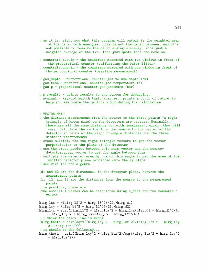
241
; as it is, right now what this program will output is the weighted meanof the qe at both energies. this is not the qe in between, and it’snot possible to resolve the qe at a single energy. it’s just aweighted average of the two. lets just quote that and move on.
; countrate_twowin - the countrate measured with two windows in front ofthe proportional counter (calibrating the outer filter)
; countrate_onewin - the countrate measured with one window in front ofthe proportional counter (baseline measurement)
; gas_depth - proportional counter gas volume depth (cm); gas_temp - proportional counter gas temperature (K); gas_p - proportional counter gas pressure (bar)
; p_results - prints results to the screen for debugging.; nominal - keyword switch that, when set, prints a bunch of ratios to
help you see where the qe took a hit during the calculation
; VECTOR MATH; the distance measurement from the source to the three points (a right
triangle of known size) on the detectors are vectors. Nominally,these are all the same distance but with measurement error, they willvary. Calculate the vector from the source to the center of thedetector in terms of the right triangle distances and the threedistance measurements.
; cross multiply the two right triangle vectors to get the vectorperpindicular to the plane of the detector
; use the cross product between this norm vector and the source-detectorcenter vector to get the angle between them
; multiply the detector area by cos of this angle to get the area of theshifted detector plane projected onto the xy plane.
; see wiki for the algebra
;d1 and d2 are the distances, in the detector plane, between themeasurement points
;l1, l2, and l3 are the distances from the source to the measurementpoints
; in practice, these are;the nominal l values can be calculated using c_dist and the measured d
values
h1rg_lcx = -(h1rg_l2^2 - h1rg_l3^2)/(2.*h1rg_d1)h1rg_lcy = (h1rg_l1^2 - h1rg_l2^2)/(2.*h1rg_d2)h1rg_lcz = sqrt(h1rg_l1^2 - h1rg_lcx^2 + h1rg_lcx*h1rg_d1 - h1rg_d1^2/4.
- h1rg_lcy^2 + h1rg_lcy*h1rg_d2 - h1rg_d2^2/4.); i think the below line is wrong...;h1rg_theta = asin(sqrt((h1rg_lcy^2 - h1rg_lcx^2)/(h1rg_lcx^2 + h1rg_lcy
^2 + h1rg_lcz^2))); it should be the following...h1rg_theta = asin((h1rg_lcy^2 - h1rg_lcx^2)/sqrt(h1rg_lcx^2 + h1rg_lcy^2
+ h1rg_lcz^2))

242
h1rg_c_dist = sqrt(h1rg_lcx^2 + h1rg_lcy^2 + h1rg_lcz^2); this is justthe combination of the xyz components that we just calculated
h1rg_eff_area = cos(h1rg_theta)*h1rg_xwinsize*h1rg_ywinsize
pc_lcx = -(pc_l2^2 - pc_l3^2)/(2.*pc_d1)pc_lcy = (pc_l1^2 - pc_l2^2)/(2.*pc_d2)pc_lcz = sqrt(pc_l1^2 - pc_lcx^2 + pc_lcx*pc_d1 - pc_d1^2/4. - pc_lcy^2
+ pc_lcy*pc_d2 - pc_d2^2/4.); i think the below line is wrong...;pc_theta = asin(sqrt((pc_lcy^2 - pc_lcx^2)/(pc_lcx^2 + pc_lcy^2 +
pc_lcz^2)))pc_theta = asin((pc_lcy^2 - pc_lcx^2)/sqrt(pc_lcx^2 + pc_lcy^2 + pc_lcz
^2))pc_c_dist = sqrt(pc_lcx^2 + pc_lcy^2 + pc_lcz^2)pc_eff_area = cos(pc_theta)*pc_xwinsize*pc_ywinsize
; this is the general way to do the filter calculation;supportive mesh;pc_countrate = pc_countrate / filter_trans(energy, thickness1, density1
, composition1 = composition1) * blocked_fraction1 + (1.-blocked_fraction1)
;window material;pc_countrate = pc_countrate / filter_trans(energy, thickness2, density2
, composition2 = composition2) * blocked_fraction2 + (1.-blocked_fraction2)
;gas detection medium
; this is the easy, empirical way to do the filter transmissioncalculation
; countrate_twowin/countrate_onewin is the transmission fraction throughthe window that was present in one of the calibration runs. Note, it’s probably better if the same window is on the inside in both runsto keep any electric field effects from the inner surface of thewindow constant
pc_countrate_win = pc_countrate / (countrate_twowin/countrate_onewin); P-10 is 90% argon 10% methane by volume. Methane’s chemical formula is
CH_4. Therefore, the number fraction of the gas is [90/(90+10*5),10/140, 40/140] = [0.642857, 0.0714286, 0.285714] (% by volume is thesame as number percentage of gas particles due to PV = nkT. Imaginetwo plastic bags filled to the same volume with different gasses. Thebags are not taut so P = 1atm, the volume is the same by design, andT is the same because the systems are allowed to equilibrate.Therefore n is the same inside the bags. The only thing different isthat the heavier gas atoms will be moving slower.) and the z numbersare [18, 6, 1]
;gas_fraction = [0.642857, 0.0714286, 0.285714];gas_z = [18, 6, 1]
gas_transmission = gas_trans(energy, gas_depth, gas_t, gas_p, z=gas_z,fraction=gas_fraction, en_weights=en_weights)
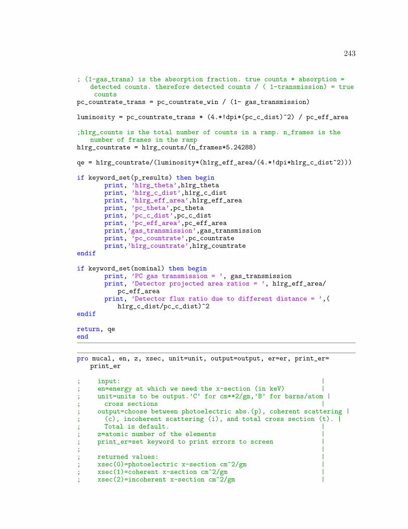
243
; (1-gas_trans) is the absorption fraction. true counts * absorption =detected counts. therefore detected counts / ( 1-transmission) = truecounts
pc_countrate_trans = pc_countrate_win / (1- gas_transmission)
luminosity = pc_countrate_trans * (4.*!dpi*(pc_c_dist)^2) / pc_eff_area
;h1rg_counts is the total number of counts in a ramp. n_frames is thenumber of frames in the ramp
h1rg_countrate = h1rg_counts/(n_frames*5.24288)
qe = h1rg_countrate/(luminosity*(h1rg_eff_area/(4.*!dpi*h1rg_c_dist^2)))
if keyword_set(p_results) then beginprint, ’h1rg_theta’,h1rg_thetaprint, ’h1rg_c_dist’,h1rg_c_distprint, ’h1rg_eff_area’,h1rg_eff_areaprint, ’pc_theta’,pc_thetaprint, ’pc_c_dist’,pc_c_distprint, ’pc_eff_area’,pc_eff_areaprint,’gas_transmission’,gas_transmissionprint, ’pc_countrate’,pc_countrateprint,’h1rg_countrate’,h1rg_countrate
endif
if keyword_set(nominal) then beginprint, ’PC gas transmission = ’, gas_transmissionprint, ’Detector projected area ratios = ’, h1rg_eff_area/
pc_eff_areaprint, ’Detector flux ratio due to different distance = ’,(
h1rg_c_dist/pc_c_dist)^2endif
return, qeend
pro mucal, en, z, xsec, unit=unit, output=output, er=er, print_er=print_er
; input: |; en=energy at which we need the x-section (in keV) |; unit=units to be output.’C’ for cm**2/gm,’B’ for barns/atom |; cross sections |; output=choose between photoelectric abs.(p), coherent scattering |; (c), incoherent scattering (i), and total cross section (t). |; Total is default. |; z=atomic number of the elements |; print_er=set keyword to print errors to screen |; |; returned values: |; xsec(0)=photoelectric x-section cm^2/gm |; xsec(1)=coherent x-section cm^2/gm |; xsec(2)=incoherent x-section cm^2/gm |

244
; xsec(3)=total x-section cm^2/gm |; xsec(4)=conversion factor unitless barnes/atom = C * (cm^2/gm) |; barn = 10^-24 cm^2 |; xsec(5)=absorption coefficient cm^-1 |; xsec(6)=atomic weight gm/mol |; xsec(7)=density gm/cm^3 |; xsec(8)=l2-edge jump |; xsec(9)=l3-edge jump |; |; energy(0)=k-edge energy |; energy(1)=l1-edge energy |; energy(2)=l2-edge energy |; energy(3)=l3-edge energy |; energy(4)=m-edge energy |; energy(5)=k-alpha1 |; energy(6)=k-beta1 |; energy(7)=l-alpha1 |; energy(8)=l-beta1 |; |; fly(0)= k fluorescence yield
|; fly(1)= l1 fluorescence yield
|; fly(2)= l2 fluorescence yield
|; fly(3)= l3 fluorescence yield
|; |; er=error code |; |; error codes: |; er=1: energy input is zero |; er=3: no documentation for given element (z<94) |; er=4: no documentation for given element (z>94) |; er=5: l-edge calculation may be wrong for z<30 as mcmaster |; uses l1 only. |; er=6: energy at the middle of edge |; er=7: no z supplied |
; HOW THIS THING IS VECTORIZED; if en is an array, the output will be cross sections for different
energies; if z is a horizontal array, it’s assumed that it specifies the output
will be cross sections for different z; if both are arrays, the output will be cross sections for different e; on the y axis and z on the x axis of the array.; NOTE: this means that right now you can only calculate for one set of
z’s at a time; eventually i’d like to allow for submitting a 2d z array where
the x axis is different elements, and the; y axis is for different energies
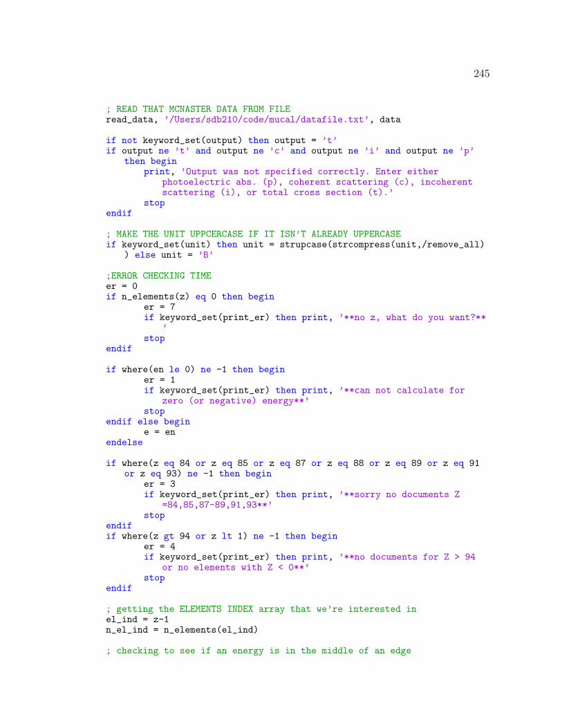
245
; READ THAT MCNASTER DATA FROM FILEread_data, ’/Users/sdb210/code/mucal/datafile.txt’, data
if not keyword_set(output) then output = ’t’if output ne ’t’ and output ne ’c’ and output ne ’i’ and output ne ’p’
then beginprint, ’Output was not specified correctly. Enter either
photoelectric abs. (p), coherent scattering (c), incoherentscattering (i), or total cross section (t).’
stopendif
; MAKE THE UNIT UPPCERCASE IF IT ISN’T ALREADY UPPERCASEif keyword_set(unit) then unit = strupcase(strcompress(unit,/remove_all)
) else unit = ’B’
;ERROR CHECKING TIMEer = 0if n_elements(z) eq 0 then begin
er = 7if keyword_set(print_er) then print, ’**no z, what do you want?**
’stop
endif
if where(en le 0) ne -1 then beginer = 1if keyword_set(print_er) then print, ’**can not calculate for
zero (or negative) energy**’stop
endif else begine = en
endelse
if where(z eq 84 or z eq 85 or z eq 87 or z eq 88 or z eq 89 or z eq 91or z eq 93) ne -1 then begin
er = 3if keyword_set(print_er) then print, ’**sorry no documents Z
=84,85,87-89,91,93**’stop
endifif where(z gt 94 or z lt 1) ne -1 then begin
er = 4if keyword_set(print_er) then print, ’**no documents for Z > 94
or no elements with Z < 0**’stop
endif
; getting the ELEMENTS INDEX array that we’re interested inel_ind = z-1n_el_ind = n_elements(el_ind)
; checking to see if an energy is in the middle of an edge

246
if total((e lt data[el_ind].ek and e gt data[el_ind].ek - 0.001) or $(e lt data[el_ind].el and e gt data[el_ind].el - 0.001) or $(e lt data[el_ind].em and e gt data[el_ind].em - 0.001)) gt 0 then
begin
er = 6if keyword_set(print_er) then print, ’**at least one energy is at the
middle of an edge. using pre-edge fit results may be wrong.**’endif
; STARTING THE CALCULATION
n_e = n_elements(en)
;INITIALIZE vars
bsum = dblarr(1,n_e,n_el_ind)sum = bsumchs = bsumcsum = bsumcis = bsumcisum = bsum
; inflating the exponents arrayexponents = rebin(indgen(4),4,n_e,n_el_ind)
; inflating the energy arraye = rebin(reform(en,1,n_e),4,n_e,n_el_ind)
;which energies to include in this calculation;calc = where(e ge rebin(reform(data[el_ind].ek,1,1,n_el_ind),4,n_e,
n_el_ind),count)calc2d = where(e[0,*,*] ge rebin(reform(data[el_ind].ek,1,1,n_el_ind),1,
n_e,n_el_ind),count) ; i think that i need this 2d index to useafter total has been used to go from 3 to 2d.
;summing...if count gt 0 then sum[calc2d] = sum[calc2d] + (total(rebin(reform(data[
el_ind].ak[0:3],4,1,n_el_ind),4,n_e,n_el_ind)*alog(e)^exponents,1))(calc2d)
;calc = where(e lt rebin(reform(data[el_ind].ek,1,1,n_el_ind),4,n_e,n_el_ind) and e ge rebin(reform(data[el_ind].l3,1,1,n_el_ind),4,n_e,n_el_ind),count)
calc2d = where(e[0,*,*] lt rebin(reform(data[el_ind].ek,1,1,n_el_ind),1,n_e,n_el_ind) and e[0,*,*] ge rebin(reform(data[el_ind].l3,1,1,n_el_ind),1,n_e,n_el_ind),count)
if count gt 0 then sum[calc2d] = sum[calc2d] + (total(rebin(reform(data[el_ind].al[0:3],4,1,n_el_ind),4,n_e,n_el_ind)*alog(e)^exponents,1))(calc2d)
;calc = where(e lt rebin(reform(data[el_ind].l3,1,1,n_el_ind),4,n_e,n_el_ind) and e ge rebin(reform(data[el_ind].em,1,1,n_el_ind),4,n_e,

247
n_el_ind),count)calc2d = where(e[0,*,*] lt rebin(reform(data[el_ind].l3,1,1,n_el_ind),1,
n_e,n_el_ind) and e[0,*,*] ge rebin(reform(data[el_ind].em,1,1,n_el_ind),1,n_e,n_el_ind),count)
if count gt 0 then beginsum[calc2d] = sum[calc2d] + (total(rebin(reform(data[el_ind].am
[0:3],4,1,n_el_ind),4,n_e,n_el_ind)*alog(e)^exponents,1))(calc2d)
if total(z le 29) gt 0 then beginer = 5if keyword_set(print_er) then print, ’**WARNING:McNaster
uses L1 edge results. May be imprecise for Z < 30 **’endif
endif
;calc = where(e lt rebin(reform(data[el_ind].em,1,1,n_el_ind),4,n_e,n_el_ind),count)
calc2d = where(e[0,*,*] lt rebin(reform(data[el_ind].em,1,1,n_el_ind),1,n_e,n_el_ind),count)
if count gt 0 then sum[calc2d] = sum[calc2d] + (total(rebin(reform(data[el_ind].an[0:3],4,1,n_el_ind),4,n_e,n_el_ind)*alog(e)^exponents,1))(calc2d)
bax = exp(sum)
calc = z gt 29if total(calc) gt 0 then begin
calc1 = e ge rebin(reform(data[el_ind].l3,1,1,n_el_ind),4,n_e,n_el_ind) and e lt rebin(reform(data[el_ind].l2,1,1,n_el_ind),4,n_e,n_el_ind)
if total(calc and calc1) gt 0 then bax[where(calc and calc1)] =bax[where(calc and calc1)]/(lj1*lj2)
calc2 = e ge rebin(reform(data[el_ind].l2,1,1,n_el_ind),4,n_e,n_el_ind) and e lt rebin(reform(data[el_ind].el,1,1,n_el_ind),4,n_e,n_el_ind)
if total(calc and calc2) gt 0 then bax[where(calc and calc2)] =bax[where(calc and calc2)]/lj1
endif
;calc = e eq 1calc2d_bin = e[0,*,*] eq 1.calc2d = where(calc2d_bin)calc2dnot_bin = lnot(e[0,*,*] eq 1.)calc2dnot = where(calc2dnot_bin)if total(calc2d) gt 0 then chs[calc2d] = chs[calc2d] + (total(rebin(
reform(data[el_ind].coh[0:3],4,1,n_el_ind),4,n_e,n_el_ind),1))(calc2d) $
else chs[calc2dnot] = chs[calc2dnot] + (total(rebin(reform(data[el_ind].coh[0:3],4,1,n_el_ind),4,n_e,n_el_ind)*alog(e)^exponents,1))(calc2dnot)
bcox = exp(chs)

248
;calc = e eq 1.calc2d_bin = e[0,*,*] eq 1.calc2d = where(calc2d_bin)calc2dnot_bin = lnot(e[0,*,*] eq 1.)calc2dnot = where(calc2dnot_bin)if total(calc2d) gt 0 then cis[calc2d] = cis[calc2d] + (total(rebin(
reform(data[el_ind].coh[0:3],4,1,n_el_ind),4,n_e,n_el_ind),1))(calc2d) $
else cis[calc2dnot] = cis[calc2dnot] + (total(rebin(reform(data[el_ind].coh[0:3],4,1,n_el_ind),4,n_e,n_el_ind)*alog(e)^exponents,1))(calc2dnot)
binx = exp(cis)
btox = bax + bcox + binx
; in the below section, reforming the btox matrix puts the array in thecorrect size, but the elements are in the wrong order.
; i need to create a new array (named index) to rearrange themindex = transpose(indgen(n_e,n_el_ind))
; choose which type of output you want.case output of
; my new output variable’t’:begin
case unit of’C’: xsec = (reform(btox,n_el_ind,n_e))(index)*
rebin(data[el_ind].den,n_el_ind,n_e)/rebin(data[el_ind].cf,n_el_ind,n_e)
’B’: xsec = (reform(btox,n_el_ind,n_e))(index)endcase
end’p’:begin
case unit of’C’: xsec = (reform(bax,n_el_ind,n_e))(index)*
rebin(data[el_ind].den,n_el_ind,n_e)/rebin(data[el_ind].cf,n_el_ind,n_e)
’B’: xsec = (reform(bax,n_el_ind,n_e))(index)endcase
end’c’:begin
case unit of’C’: xsec = (reform(bcox,n_el_ind,n_e))(index)*
rebin(data[el_ind].den,n_el_ind,n_e)/rebin(data[el_ind].cf,n_el_ind,n_e)
’B’: xsec = (reform(bcox,n_el_ind,n_e))(index)endcase
end’i’:begin
case unit of’C’: xsec = (reform(binx,n_el_ind,n_e))(index)*
rebin(data[el_ind].den,n_el_ind,n_e)/rebin(data

249
[el_ind].cf,n_el_ind,n_e)’B’: xsec = (reform(binx,n_el_ind,n_e))(index)
endcaseend
endcase
end
FUNCTION multi_gauss3, x, input_pars, npeaks=npeaks, nterms=nterms,ncomponents=ncomponents
; calculates a sum of multiple gaussians to make a multi peaked output.Each peak can be composed of a sum of gaussian components, each witha variable number of terms
; F = par(0)*EXP(-Z^2/2) + par(3) + par(4)*X + par(5)*X^2; Z = (X-par(1))/par(2); par 0 - A; 1 - mu; 2 - sigma; 3 - skewnormal factor; 4 - continuum offset; 5 - continuum linear slope; 6 - continuum parabolic curvature
; x is the independent variable; pars is an array filled with all of the gaussian parameters with the
parameters from subsequent gaussian components and subsequent peaksconcatenated end to end.
; npeaks is a scalar, the number of peaks that will be generated in theoutput
; ncomponenets is a vector with one element for each peak produced inthe output. It determines the number of gaussians components thatwill be summed to make up the final peak. The first gaussian hasstandard units. The subsequent gaussian amplitudes and widths arespecified as ratios with respect to the first gaussian in the peak.All mu parameters for components after the first should be specifiedin units with respect to the first component’s mu.
; nterms is a vector with one element for each gaussian used in thefunction. that element specifies the number of terms to used in thatgaussian.
; examples:; x = dindgen(500)/499*40-20; plot, x, multi_gauss3(x, [5,0,1,0,0,0,-1, 4,2,1, .5,-1,1.5,
7,1,2,0,6], npeaks=3,nterms=[7,3,3,5], ncomponents=[1,2,1]) ;produces3 peaks, one with two components, each with a different number ofterms.
; plot, x, multi_gauss3(x, [10,-10,2, .5,2,2, .25,4,2, 10,10,2, .5,2,2,.25,4,2], npeaks=2,nterms=[3,3,4, 3,3,4], ncomponents=[3,3]) ;showcases that all component parameter values after the first arerelative to the first one.
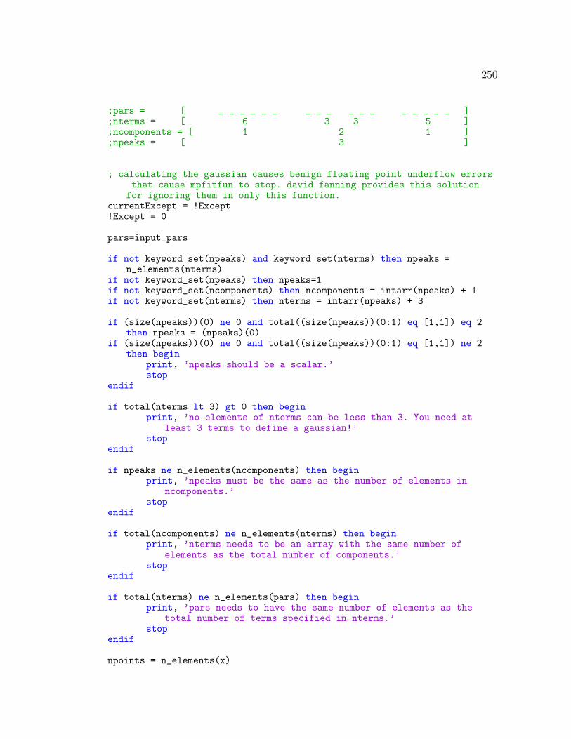
250
;pars = [ _ _ _ _ _ _ _ _ _ _ _ _ _ _ _ _ _ ];nterms = [ 6 3 3 5 ];ncomponents = [ 1 2 1 ];npeaks = [ 3 ]
; calculating the gaussian causes benign floating point underflow errorsthat cause mpfitfun to stop. david fanning provides this solutionfor ignoring them in only this function.
currentExcept = !Except!Except = 0
pars=input_pars
if not keyword_set(npeaks) and keyword_set(nterms) then npeaks =n_elements(nterms)
if not keyword_set(npeaks) then npeaks=1if not keyword_set(ncomponents) then ncomponents = intarr(npeaks) + 1if not keyword_set(nterms) then nterms = intarr(npeaks) + 3
if (size(npeaks))(0) ne 0 and total((size(npeaks))(0:1) eq [1,1]) eq 2then npeaks = (npeaks)(0)
if (size(npeaks))(0) ne 0 and total((size(npeaks))(0:1) eq [1,1]) ne 2then begin
print, ’npeaks should be a scalar.’stop
endif
if total(nterms lt 3) gt 0 then beginprint, ’no elements of nterms can be less than 3. You need at
least 3 terms to define a gaussian!’stop
endif
if npeaks ne n_elements(ncomponents) then beginprint, ’npeaks must be the same as the number of elements in
ncomponents.’stop
endif
if total(ncomponents) ne n_elements(nterms) then beginprint, ’nterms needs to be an array with the same number of
elements as the total number of components.’stop
endif
if total(nterms) ne n_elements(pars) then beginprint, ’pars needs to have the same number of elements as the
total number of terms specified in nterms.’stop
endif
npoints = n_elements(x)

251
y = dblarr(npoints)for i=0,npeaks-1 do begin
for j=0,ncomponents[i]-1 do begin
par0 = total(nterms[0:total(ncomponents[0:i])-ncomponents[i]+j])-nterms[total(ncomponents[0:i])-ncomponents[i]+j]
if j eq 0 then comp0par0 = par0 ; when you pass the firstcomponent, save it’s par0 so that you can use it laterwhen you calculate subsequent components parametervalues relative to the first’s
;par0 = (total(nterms[0:])-nterms[])*ncomponenets[0:i-1]); the index of par 0 inside pars for the current term.
if j gt 0 then begin ; need to adjust pars so that they’re relative to first component in the peak.
pars[par0] = pars[comp0par0]*pars[par0]pars[par0+1] = pars[comp0par0+1]+pars[par0+1]pars[par0+2] = pars[comp0par0+2]*pars[par0+2]
endif
if pars[par0+2] ne 0.0 then begin ; make sure that sigmaisn’t zero
z = (x-pars[par0+1])/pars[par0+2] ; then calculatez
ez = exp(-z^2/2.) ; and gaussian part as normal.endif else begin
ez = dblarr(npoints) ; This condition prevents adivision by zero explosion and just returns allzeros instead of the less useful nan.
endelse
case nterms[total(ncomponents[0:i])-ncomponents[i]+j] of; this mess just gets a steadily increasing index fornterms
3: f = pars[par0]*ez4: f = pars[par0]*ez*(1.+erf(pars[par0+3]*z/sqrt
(2.)))5: f = pars[par0]*ez*(1.+erf(pars[par0+3]*z/sqrt
(2.))) + pars[par0+4]6: f = pars[par0]*ez*(1.+erf(pars[par0+3]*z/sqrt
(2.))) + pars[par0+4] + pars[5]*x7: f = pars[par0]*ez*(1.+erf(pars[par0+3]*z/sqrt
(2.))) + pars[par0+4] + pars[5]*x + pars[6]*x^2endcase;f[where(y+f eq y)] = 0d ; this is an attempt to
remove underflow errory = y + f
endforendfor
252
; this block of code reports any non floatingpoint underflow math errorsand turns math error reporting back on before exiting the function.
floating_point_underflow = 32status = Check_Math() ; Get status and reset accumulated math error
register.;IF(status AND NOT floating_point_underflow) NE 0 THEN Message, ’IDL
Check_Math() error: ’ + StrTrim(status, 2)!Except = currentExcept
return, yend
PRO pc_extract_counts, spec_data, spec_bg, data_int_time, bg_int_time,data_range, extract_range=extract_range, countrate=countrate,err_countrate=err_countrate, counts=counts, err_counts=err_counts
;spec_data - vector containing spectrum data;spec_bg - vector containing spectrum background (use as long of a
background as possible);data_int_time - scalar double indicating the integration time of the
data spectrum. use the live time.;bg_int_time - scalar double indicating the integration time of the
background. use the live time.;data_range - a two element vector that indicates how many bins are in
the data. this gets extracted from the .spe data file.;extract_range - a two element vector keyword with elements indicating
the left and right MCA bins to bound the data that will be extracted.If this keyword is not set, the program will prompt you to enter thevalues by clicking on the plot.
;countrate - output keyword;err_countrate - output keyword;counts - output keyword;err_counts - output keyword
; takes MCA spectra as input, removes background and; it might be valuable to implement a "flat fielding" function. From the
look of the spectrum, it seems that some channels might be "narrower" than others. I say narrower because i do not think channels withlow counts are have a lower gain; that would imply that counts arebeing missed. I think that the range of pulse heights that fall intothat bin might be slightly smaller so it will register fewer counts.This would throw off a spectral analysis but I am not concerned withthat. All I hvae to do is add up counts in a large range. One couldcalibrate this out with a pulse generator or by taking a very highcount data run and fitting the data with a spline. As the number ofcounts per bin increases, the signal to noise should increase,however if the bins are unevenly spaced, there will be a source ofnoise that grows linearly with the signal instead of as sqrt(signal).Divide the spline fit by the data to determine the relative binwidth. Then use this to define your non uniform bin widths. It shouldbe possible to resample the histogram to arrive at a uniform binspacing.
253
ndata = n_elements(spec_data)
scale_factor = double(data_int_time)/double(bg_int_time)
mca = indgen(ndata)+1 ; an array of the mca channel numbers
cutoff = floor(25/255.*data_range[1]) ; a cutoff defined to avoidplotting the noise peak. UPDATE: the noise peak should not exist inthe data. Use the discriminator built into the MCA. I usually use alower level cutoff of 30 in 255 bin mode.
; plot the data, ignoring the noise peakwindow, 1plot, mca, spec_data, psym=10, title = ’Data and background’,xtitle=’MCA
Channel No.’, ytitle=’No. Counts’, yrange = [1,max(spec_data[cutoff:ndata-1])],/ylog
oplot, spec_bg *scale_factor, psym=10
err_data = sqrt(spec_data)err_bg = sqrt(spec_bg)
; subtract the background
spec_bgsub = spec_data-spec_bg*(scale_factor)
; plot the background subtracted data, ignoring the noise peak.window,2plot, mca, spec_bgsub, psym=10, title=’Background subtracted spectrum’,
xtitle=’MCA Channel No.’, ytitle=’No. Counts’, /ylog, yrange=[1,max(spec_bgsub[cutoff:ndata-1])]
; calculate error by summing in quadriture and scaling by the same scalefactor as with the data
err_bgsub = sqrt(err_data^2 + (scale_factor)*err_bg^2)
if n_elements(extract_range) eq 0 then beginprint, "Click a left bound on the background subtracted plot to
define the range of counts that you would like to sum"
cursor,x_1, y_1,4,/data
print, "Click a right bound on the background subtracted plot todefine the range of counts that you would like to sum"
cursor,x_2, y_2,4,/dataendif else begin
if n_elements(extract_range) ne 2 then beginprint, ’extract_range is supposed to be a 2 element vector
.’stop
endifx_1 = extract_range[0]

254
x_2 = extract_range[1]endelse
; if left and right are backwards, swap themif x_1 gt x_2 then begin
x_temp = x_1x_1 = x_2x_2 = x_temp
endif
if x_2 gt data_range[1] then x_2 = data_range[1]
; the x value returned by cursor will be a number between 0 anddatarange[1]. All we have to do is convert that number to an integerto get the index.
x_1 = floor(x_1)x_2 = floor(x_2)
counts = total(spec_bgsub[x_1:x_2]); sum the errors in quadritureerr_counts = total(err_bgsub[x_1:x_2]^2)^.5
countrate = counts/data_int_timeerr_countrate = (countrate)*sqrt((err_counts/counts)^2+(.5/data_int_time
)^2)
print, ’There are’+strcompress(string(counts))+’ +\-’+strcompress(string(err_counts))+’ background subtracted counts between channel’+strcompress(string(x_1))+’ and channel’+strcompress(string(x_2))+’ ofthe spectrum. Given the data integration time of’+strcompress(string(data_int_time)) +’ seconds, this yields a countrate of’+strcompress(string(countrate)) +’ +/-’+strcompress(string(err_countrate)) + ’counts per second.’
; error is calculated by using the usual division error propagation ruleto combine the poisson error in the number of counts with the timingerror of 0.5 seconds. (counts/data_int_time) * sqrt((err_counts/counts)^2+(.5/data_int_time)^2)
;if you need to distinguish overlapping peaks, you need to do amultigauss fit instead of the simple left right ranging. if the peaksdo not ahve to be separated, just use a simple sum. it will not addin any non gaussianity fitting error.
;result = mpfitfun(’multi_gauss’, indgen(npoints), spec_peakbgsub,err_peakbgsub, parinfo = tied:1,functargs = ngauss:k,nterms:3)
end
255
PRO pc_read_spectrum, filename, spec_data, live_time=live_time,real_time=real_time, data_range=data_range
; Reads a spectrum file (*.Spe format), generated by the Ortec MCA, intomemory.
; filename - the name of the file to be read.; spec_data - output containing the spectrum data, which is in units of
counts THAT ALREADY DEADTIME CORRECTED.; live_time - optional ouptut containing the estimated total time that
the MCA spent sensitive to pulses. Time is in seconds.; real_time - optional output containing the time elapsed between the
start and end of the data run. real_time = live_time + dead_time Dueto the MCA outputting deadtime corrected counts, this is nominallyused as the integration time. WARNING: if the dead time percentage ishigh, this will be wrong.
; data_range - the channel (bin) range of the data file.; note that in the data file $MEAS_TIM is the integration time, in
seconds. the two numbers represent the stopwatch integration time andthe actual live time (stopwatch time minus deadtime)
nlines = FILE_LINES(filename)
spec_data = lonarr(nlines)data_range = lonarr(2)openr, lun, filename, /get_lun
for i=0,nlines[0]-1 do begintemp = ’ ’readf, lun, temp
case 1 of(i eq 9):times = long(strsplit(temp,’ ’,/extract))(i eq 11):data_range = long(strsplit(temp,’ ’,/extract))(i ge 12 and i le data_range[1]+12):spec_data[i-12] = long
(temp)else:
endcaseendforlive_time = times[0]real_time = times[1]spec_data = spec_data[0:data_range[1]]
close,/all
if (real_time-live_time)/real_time gt .4 then print, ’WARNING: Dead timepercentage is larger than 40%. There will be error in the countrateestimate.’
end; before i realized the case statement is faster.; if i eq 9 then times = long(strsplit(temp,’ ’,/extract)); if i eq 11 then data_range = long(strsplit(temp,’ ’,/extract))
256
; if i ge 12 and i le data_range[1]+12 then spec_data[i-12] = long(temp)
pro sb_henke, input_energy, input_z, xsec, unit=unit, sum=sum, quadratic=quadratic
; energy - incident photon energy in keV.; z - atomic number. Can be a scalar or vector.; xsec - output variable for the cross section(s).; unit - specify either ’b’ for barns/atom or ’c’ for cm^2/g.; sum - sums the contributions from multiple elements instead of
outputting multiple cross sections.
if n_elements(input_energy) le 0 then beginprint, ’sb_henke.pro says that the energy array needs to have
more than zero elements’stop
endif
en = input_energy*1000 ; converting to eV to match Henke data tables.Do the variable change so that the changed energy array doesn’t getpassed back out of the function and mess up the standard idl session.
if not keyword_set(unit) then unit= ’b’ ; barns/atom is the defaultoutput unit
if unit ne ’b’ and unit ne ’c’ then beginprint, ’You specified some illegal value for unit’stop
endif
restore, ’/Users/sdb210/code/qe_teststand/sb_henke_data.sav’ ; restoringvariables: table_z, table_name, table_symbol, table_atwt,table_density, energy, f1, and f2 arrays from file for ALL elements.This file was created by sb_henke_read.pro
h = 6.62606957d-27 ; plancks constant in cgsc = 2.99792458d10 ; speed of light in cm/sr_electron = 2.8179403267d-13 ; classical electron radius in cmn_avogadro = 6.02214129d23 ; avogadro’s constantergev = 1.602176565d-12 ; erg per ev
;CRC constants
ind = input_z-1 ; indices of the elements that you want returnedenergy = energy[*,ind]f2 = f2[*,ind]
; summing together the contributions from various elementsif keyword_set(sum) then f2 = total(f2,2)
f2_interpol = dblarr(n_elements(f2[0,*]),n_elements(en))
for i=0,n_elements(f2[0,*])-1 do begin
257
f2_interpol[i,*] = interpol(f2[where(finite(f2[*,i])),i],energy[where(finite(f2[*,i])),i],en,quadratic=quadratic)
endforcase unit of
’b’: xsec = 2*f2_interpol*r_electron*h*c/(rebin(transpose(en),n_elements(f2_interpol[*,0]),n_elements(en))*ergev)*1d24 ;calculating xsec in barns/atom
’c’: xsec = 2*n_avogadro/rebin(table_atwt[ind],n_elements(f2_interpol[*,0]),n_elements(en))*f2_interpol*r_electron*h*c/(rebin(transpose(en),n_elements(f2_interpol[*,0]),n_elements(en))*ergev) ; calculating xsec cm^2/g
endcase
end
pro sb_henke_read
; this program uses the henke 93 ascii data files available on the LBNLwebsite to create a sb_henke.sav file that contains element z, name,symbol, atomic weight, density, an energy grid (in eV) and the f1 andf2 values at each energy.
cd, ’/Users/sdb210/code/qe_teststand’readcol, ’periodic_table.txt’,table_name,table_symbol,table_z,table_atwt
,table_density,delimiter=’, ’,format=’A,A,I,D,D’
sort_ind = sort(table_z) ; the z sorted indices for the full periodictable
table_z = table_z[sort_ind]table_name = table_name[sort_ind]table_symbol = table_symbol[sort_ind]table_atwt = table_atwt[sort_ind]table_density = table_density[sort_ind]
henke_sort_ind = sort((table_z[where(table_z le 92)])(sort(table_symbol[where(table_z le 92)]))) ; the symbol alphabetized indices forelements 1-92 (ie the henke list)
prefix = ’/Users/sdb210/code/xrdata/henke_data/’
filenames = [’ac.nff’, ’ag.nff’, ’al.nff’, ’ar.nff’, ’as.nff’, ’at.nff’,’au.nff’, ’b.nff’, ’ba.nff’, ’be.nff’, ’bi.nff’, ’br.nff’, ’c.nff’,’ca.nff’, ’cd.nff’, ’ce.nff’, ’cl.nff’, ’co.nff’, ’cr.nff’, ’cs.nff’,’cu.nff’, ’dy.nff’, ’er.nff’, ’eu.nff’, ’f.nff’, ’fe.nff’, ’fr.nff’,’ga.nff’, ’gd.nff’, ’ge.nff’, ’h.nff’, ’he.nff’, ’hf.nff’, ’hg.nff’,’ho.nff’, ’i.nff’, ’in.nff’, ’ir.nff’, ’k.nff’, ’kr.nff’, ’la.nff’,’li.nff’, ’lu.nff’, ’mg.nff’, ’mn.nff’, ’mo.nff’, ’n.nff’, ’na.nff’,’nb.nff’, ’nd.nff’, ’ne.nff’, ’ni.nff’, ’o.nff’, ’os.nff’, ’p.nff’, ’pa.nff’, ’pb.nff’, ’pd.nff’, ’pm.nff’, ’po.nff’, ’pr.nff’, ’pt.nff’,’ra.nff’, ’rb.nff’, ’re.nff’, ’rh.nff’, ’rn.nff’, ’ru.nff’, ’s.nff’,’sb.nff’, ’sc.nff’, ’se.nff’, ’si.nff’, ’sm.nff’, ’sn.nff’, ’sr.nff’,’ta.nff’, ’tb.nff’, ’tc.nff’, ’te.nff’, ’th.nff’, ’ti.nff’, ’tl.nff’
258
, ’tm.nff’, ’u.nff’, ’v.nff’, ’w.nff’, ’xe.nff’, ’y.nff’, ’yb.nff’, ’zn.nff’, ’zr.nff’]
; sort list by zfilenames = prefix + filenames[henke_sort_ind]nfiles = n_elements(filenames)
nen = 1000 ; there are a variable number of data points for eachelement so lets just make the energy array larger and fill the restin with nans.
energy = dblarr(nen,nfiles) + !values.d_nanf1 = dblarr(nen,nfiles) + !values.d_nanf2 = dblarr(nen,nfiles) + !values.d_nan
for i=0,nfiles-1 do beginprint, ’Reading ’+filenames[i]+’...’readcol,filenames[i],energy_temp,f1_temp,f2_temp,delimiter=’ ’,
format=’D,D,D’energy[0:n_elements(energy_temp)-1,i] = energy_tempf1[0:n_elements(f1_temp)-1,i] = f1_tempf2[0:n_elements(f2_temp)-1,i] = f2_temp
endfor
f1[where(f1 eq -9999)] = !values.d_nanf2[where(f2 eq -9999)] = !values.d_nan
save,table_z,table_name,table_symbol,table_atwt,table_density,energy,f1,f2,filename=’/Users/sdb210/code/qe_teststand/sb_henke_data.sav’
end
pro sim_error, myfunc,ind_var=ind_var, pars=pars, parerrors=parerrors,parnames=parnames, spars=spars, spar_positions=spar_positions,spar_ratios=spar_ratios, parinfo=parinfo,$
input_percentiles=input_percentiles, input_confint=input_confint, n_iter=n_iter, pdf_min=pdf_min, pdf_max=pdf_max, n_bins=n_bins, lotsoplots=lotsoplots, method=method,$
pdf_dist=pdf_dist, pdf_locations=pdf_locations, exact_soln=exact_soln,dist_med=dist_med, output_confint=output_confint, output_percentiles=output_percentiles, cdf = cdf, cor = cor, slope=slope, u_slope=u_slope, ind_slope=ind_slope, u_ind_slope=u_ind_slope,$
keyword1=keyword1, keyword2=keyword2, keyword3=keyword3, keyword4=keyword4, keywordnames=keywordnames,$
save_plots=save_plots
; MANDATORY INPUTS; myfunc - a string containing the name of the function for which you
will be calculating simulated errors. Do not include the ".pro"extension. Parameters must be passed as variables, not keywords, orarrays of parameters. The function must be able to take vectors asinputs.

259
; ind_var - a vector of the independent variable. Essentially one batchof simulations will be performed for each independent variable point.If there is no independent variable in the function that you areusing, then set ind_var equal to any scalar number. The independentvariable is something like time in an RV curve. In other applicationsthere may be no independent variable so this loop will only run once. Instead of generating a 2d contour plot, we can simply generate a 1d plot of the PDF.
; pars - the exact parameters for the function. These values will beperturbed.
; parerrors - the one sigma error for pars
;the following spars crap should eventually all be lumped into parinfo.doing it this way is stupid and just a quick fix. shuffling is notreally different than the gaussian distributed parameters, it is arandom number selected from a distribution with discrete values withspecified weights, rather than a continuous set of values withcontinuously varying gaussian weights.
; spars - shuffle parameters. make the horizontal axis of this arraydifferent parameters and the vertical axis, the possible values thatthese parameters can take. If there are multiple parameters withdifferent possible values, make the empty array elements !VALUES.F_NAN. For example, I created this to generate arrays of Fe55 photonenergy values. The array needed to contain a randomly shuffledassortment of 6.4 and 5.9 keV photon energies in a 1:~8 ratio.
; spar_positions - the position in the gaussian par array to insert theshuffle parameter
; spar_ratios - same array format as spars array, horizontal axis is forseparate parameters, vertical axis corresponds to the ratio in whichthe different possible values should occur.
; parinfo - NOT FUNCTIONAL YET. Will enable extra options for eachparameter.
; OPTIONAL INPUTS - the program will only calculate these if you specifythem.
; input_percentiles - the desired percentile locations (in units offraction. one needs only specify the left set of percentiles ie 5%and not 5% and 95%). The 20th percentile is the location below which20% of the measurements fall. This measurement has no regard for theshape (peaks, tails, etc.) of the distribution.
;input_confint - the desired confidence interval locations (in units offraction). These values represent the probability that a value willbe contained within the interval.
; OPTIONAL PDF/BOOTSTRAP RELATED INPUTS; n_iter - the number of iterations for each call to the function. This
number should be higher when there are more parameters. One mustadequately sample all permutations of the randomly distributedparameters.
; pdf_min - minimum sampled PDF value. It is desirable to tightly boundthe PDF with pdf_max and pdf_min so that the number of bins samplesthe montecarloed points somewhat optimally.

260
; pdf_max - maximum sampled PDF value; n_bins - the number of bins to use when making the PDF from
montecarloed points
; OUTPUTS; pdf_dist - insert a variable here that will contain the probability
density function upon output... aka the distribution. has do changethis from pdf to pdf_dist because idl thought it was an ambiguouskeyword.
; pdf_locations - insert a variable here that will contain the pdf x-axis.
; exact_soln - insert a variable here that will contain the exactsolution.
; output_percentiles - the location of the desired percentiles (on boththe left and right sides of the distirbution)
;output_confint - the location of the desired confidence intervals;dist_med - the median of the distribution. whether this is relevant or
not is up to you.; cor - NOT WORKING YET. the correllation coefficients.
; KEYWORD SWITCHES; lotsoplots - set this keyword to include a 1d plot of the PDF at each
independent variable value.; method - set this keyword to either ’old’, ’new’, or ’pinfo’ to choose
a method for running the MC.; ADD THIS FEATURE!!!! if variance is zero then sim_error should skip
over the variable and pass only the nominal value
; keyword1...2...3...4 - keywords to pass onto the function. theirvalues will not be randomized. more keywords can be added ifnecessary. make sure to modify the line where n_key is defined sothat it counts the new keywords.
; keywordnames - string array defining the names of the keywords to pass.
; PARINFO STRUCTURE TAGS; parinfo.pars; parinfo.parerrors; parinfo.type - gaussian or discreet. maybe poisson too?; parinfo.prate - if i implement poisson, this is the poisson rate.; parinfo.dvalues - discrete values. if multiples, they must be the same
size array. pad with !VALUES.F_NAN; parinfo.dweights - discrete weights. if multiples, they must be the
same size array. pad with !VALUES.F_NAN
; TROUBLESHOOTING; if there is noise in the distribution or the distribution is shaped
strangely, this code does not do well at finding confidence intervals.
; Written by Steve Bongiorno 1/16/2012 - Pat Broos helped with decidingon the execute() function instead of call_function.

261
if n_elements(ind_var) eq 0 then beginind_var = [0]ind_var_name = ’XX’
endif else beginind_var_name = string(ind_var,format = ’(E8.2)’)
endelse
if n_elements(parinfo) eq 0 and (n_elements(pars) eq 0 or n_elements(parerrors) eq 0) then begin
print, ’You have to set either parinfo or (pars and parerrors)’stop
endifif n_elements(method) eq 0 then method = ’new’if n_elements(parinfo) ne 0 and method ne ’parinfo’ then begin
print, ’You set parinfo but chose a method other than parinfo.WTF man? I am going to use parinfo.’
method = ’pinfo’endif;if not keyword_set(input_percentiles) then begin; input_percentiles = [.001, .021, .136]; print, "You did not supply any input percentiles or confidence
intervals so I am going to use 1, 2, and 3 sigma.";endif
;if keyword_set(input_confint) then begin; input_confint = [.5,.95,.99]; print, "You did not supply any input confidence intervals so I am
going to use 50, 95, and 99 percent. By the way the 50th percentileis the median."
;endif
if n_elements(n_bins) eq 0 then n_bins=100if n_elements(n_iter) eq 0 then n_iter=10000Lif keyword_set(pars) then n_pars = n_elements(pars) else n_pars = 0if keyword_set(spars) then n_spars = n_elements(spars[*,0]) else n_spars
= 0if keyword_set(keywordnames) then n_key = n_elements(keywordnames) else
n_key = 0 ; the number of keywords that have been set
result = dblarr(n_iter)n_ind_var = n_elements(ind_var)ind_result = dblarr(n_pars+n_spars,long(n_iter/10))
; initializing the arrays. These will contain one column for eachindependent variable and two rows for each percentile/confidenceinterval.
if n_elements(input_percentiles) gt 0 then beginif n_elements(ind_var) gt 0 then begin
output_percentiles = dblarr(n_elements(ind_var),n_elements(input_percentiles)*2)
endif else begin
262
output_percentiles = dblarr(1,n_elements(input_percentiles)*2)
endelseendifif n_elements(input_confint) gt 0 then begin
if n_elements(ind_var) gt 0 then beginoutput_confint = dblarr(n_elements(ind_var),n_elements(
input_confint)*2)endif else begin
output_confint = dblarr(1,n_elements(input_confint)*2)endelse
endifpdf = dblarr(n_ind_var,n_bins)cdf = dblarr(n_ind_var,n_bins)
; For some reason FSC_COLOR is no longer working. Error message sayssome license issue.
;lineColor = FSC_COLOR("Red", !D.Table_Size);contourColor = FSC_COLOR("Green", !D.Table_Size)
; Looping through each X-axis (independent variable) indexfor j=0L,n_ind_var-1 do begin
case method of’old’:begin; The old method Monte-Carlo loopfor i=0L,n_iter-1 do begin
thrown_pars = pars+randomn(j*n_ind_var+i,n_pars)*parerrors
result[i] = call_function(myfunc, ind_var[j],thrown_pars)
endforend’new’:begin; The new method Monte-Carlo loopthrown_pars = rebin(pars,n_pars,n_iter) + randomn(seed,
n_pars,n_iter)*rebin(parerrors,n_pars,n_iter); This is a n_pars x n_iter size array filled with thrown
pars. Note that sequential permutations of this 2dthrown_pars matrix are also valid, new random sets ofparameters. Unfortunately I do not know how tosequentially shift this matrix without a for loop. Inthis case I think it is faster to generate more randomnumbers and hold them in memory than to use someprocessor to efficiently reuse the random numbers thathave already been generated and are already in memory.
;result = call_function(myfunc, ind_var[j], thrown_pars); If sim_error was vectorized like this, the functions you
use must be written to accept parameters in this funnyway. It would be faster than looping, but it is notvery general due to the way that the functions must bewritten.
263
; this is a crappy way to code the shuffle thing . willhave to be more elegant later when i implement parinfo
if n_elements(spars) gt 0 then beginfor i=0,n_elements(spars[*,0])-1 do begin
values = spars[i,where(finite(spars[i,*]))];strip the nans
weights = spar_ratios[i,where(finite(spar_ratios[i,*]))]
; concatenate the new array into the thrownpars array in the correct position
thrown_pars = [thrown_pars[0:spar_positions[i]-2,*],transpose(randomd(seed,values,weights,n_iter)),thrown_pars[spar_positions[i]-1:*,*]]
endforendif
; Generating the string input to the execute function.if n_ind_var gt 1 then begin
exstring = ’result = ’ + myfunc + ’(replicate(ind_var[j],n_iter)’
for i=0,n_pars+n_spars-1 do exstring = exstring + ’,thrown_pars[’ + strcompress(string(i,format=’(I)’),/remove_all) + ’,*]’
; creates a string that looks like:; result = myfunc(ind_var[j],thrown_pars[0,*],
thrown_pars[1,*])
; creating the independent exstring where only onepar is tweaked at a time. (I AM TESTING THEIDEA OF USING A SCALAR FOR THE IND_VAR INSTEADOF USING REPLICATE LIKE I DO IN THE LINES ABOVE.
ind_exstring = strarr(n_pars+n_spars)for k=0,n_pars+n_spars-1 do begin
ind_exstring[k] = ’ind_result[’+strcompress(string(k,format=’(I)’),/remove_all)+’,*]= ’ +myfunc + ’(ind_var[j],’
for i=0,k-1 do ind_exstring[k] =ind_exstring[k] + ’transpose(replicate(pars[’ + strcompress(string(i,format=’(I)’),/remove_all) + ’],long(n_iter/10))),’
ind_exstring[k] = ind_exstring[k] + ’thrown_pars[’ + strcompress(string(i,format=’(I)’),/remove_all) + ’,0:long(n_iter/10)-1],’
for i=k+1,n_pars+n_spars-1 do ind_exstring[k] = ind_exstring[k] + ’transpose(replicate(pars[’ + strcompress(string(i,format=’(I)’),/remove_all) + ’],long(

264
n_iter/10))),’; remove the trailing commaind_exstring[k] = strmid(ind_exstring[k],0,
strlen(ind_exstring[k])-1)endfor
endif else beginexstring = ’result = ’ + myfunc + ’(’for i=0,n_pars+n_spars-2 do exstring = exstring + ’
thrown_pars[’ + strcompress(string(i,format=’(I)’),/remove_all) + ’,*],’
exstring = exstring + ’thrown_pars[’ + strcompress(string(n_pars+n_spars-1,format=’(I)’),/remove_all) + ’,*]’
; this creates a string that looks like:; result = myfunc(thrown_pars[0,*],thrown_pars
[1,*])
ind_exstring = strarr(n_pars+n_spars)for k=0,n_pars+n_spars-1 do begin
ind_exstring[k] = ’ind_result[’+strcompress(string(k,format=’(I)’),/remove_all)+’,*]= ’ +myfunc + ’(’
for i=0,k-1 do ind_exstring[k] =ind_exstring[k] + ’transpose(replicate(pars[’ + strcompress(string(i,format=’(I)’),/remove_all) + ’],long(n_iter/10))),’
ind_exstring[k] = ind_exstring[k] + ’thrown_pars[’ + strcompress(string(i,format=’(I)’),/remove_all) + ’,0:long(n_iter/10)-1],’
for i=k+1,n_pars+n_spars-1 do ind_exstring[k] = ind_exstring[k] + ’transpose(replicate(pars[’ + strcompress(string(i,format=’(I)’),/remove_all) + ’],long(n_iter/10))),’
;remove the trailing commaind_exstring[k] = strmid(ind_exstring[k],0,
strlen(ind_exstring[k])-1)endfor
endelse;add on the keyword business, if needed.if n_key gt 0 then begin
for i = 0,n_key-1 do beginexstring = exstring + ’,’ + keywordnames[i]+
’=keyword’+strcompress(string(i+1,format=’(I)’),/remove_all)
ind_exstring = ind_exstring + ’,’ +keywordnames[i]+’=keyword’+strcompress(string(i+1,format=’(I)’),/remove_all)
endfor

265
endif
exstring = exstring + ’)’ind_exstring = ind_exstring + ’)’
; starting the calculationstatus = execute(exstring)
if status eq 0 then beginprint, ’The normal execute command did not compile
or run properly’print, ’The execute string when a failure occured
was: ’print, exstringwhatstop
endifif keyword_set(lotsoplots) then begin
for i=0,n_pars+n_spars-1 do beginprint, ’Calculating result’+strcompress(
string(i))+’...’status = execute(ind_exstring[i])if status eq 0 then begin
print, ’The independent par.analysis execute command did notcompile or run properly’
stopendif
endforendifend
;endelse’pinfo’:begin; PUT THE PARINFO STUFF HERE;for i
endelse:beginprint, ’You specified an unknown method’stopend
endcase; remove nans and print the number of themnot_nans = where(result ne !values.d_nan and result ne -!values.
d_nan and result ne !values.d_infinity and result ne -!values.d_infinity)
print, ’There were: ’,n_iter-n_elements(not_nans),’ nans or infsin the Monte Carlo result out of’, n_iter,’ iterations. I havetaken them out because IDL can not handle them on its own.’
result = result[not_nans]; histograms location array elements define the left edge of each
bin. The left edge of the first bin starts at min and the

266
right edge of the last bin stops at max + binsize. binsize = (max-min)/(nbins-1)
if not keyword_set(pdf_max) then pdf_max = max(result,/nan)if not keyword_set(pdf_min) then pdf_min = min(result,/nan)binsize = (pdf_max-pdf_min)/double(n_bins-1)
; calculating the PDFpdf[j,*] = double(histogram(result,locations=pdf_locations,min=
pdf_min, max=pdf_max,nbins=n_bins,/nan))dist_med = median(result); normalizing the PDFpdf[j,*] = pdf[j,*]/total(double(pdf[j,*])); calculating the cumlative distribution functioncdf[j,*] = total(pdf[j,*],/cumulative)
; This finds the locations that correspond to given percentiles. Thisalso does an array concatenation to generate the complimentary
set of percentiles; ie .05, .10, .50 will result in .05, .10,.50, .95, .90, and .50.
if keyword_set(input_percentiles) then output_percentiles[j,*] =pdf_locations[value_locate(cdf,[input_percentiles,1.-input_percentiles])]
if keyword_set(input_confint) then begin; This section of code finds the locations that correspond
to the input confidence interval.
; Sorting the pdf array and reversing the result so thatwe get an array that starts with the indices of the pdfpeak(s) and then goes into the wings simultaneously (and evenly).
inv_ind = reverse(sort(pdf)); using the inverse indices to get the pdf and location
values in this special "starting at the peak and goingdown the slope" ordering.
inv_pdf = pdf[inv_ind]inv_loc = pdf_locations[inv_ind]
; calculating the cumulative distribution function usingthis "peak down" ordering
cum_inv_pdf = total(inv_pdf,/cumulative)
; looping through the input confidence intervals one at atime.
for i=0,n_elements(input_confint)-1 do begin; Find all of the locations in confidence interval
i.conf_int_loc = inv_loc(where(cum_inv_pdf lt
input_confint[i])); These points are out of order so we sort them.conf_int_loc = conf_int_loc[sort(conf_int_loc)]; If the distribution is noisy or has more than one
peak we will have identified multiple groups

267
of points in the previous lines. The followingline finds any x axis (locations) gap largerthan the expected binsize, which is known andcalculated above. This gets rid of multiplegroups due to noise but not due to multiplelarge scale peaks in the distribution. (shift-1 means moving to the left)
;NEW lets try to find the boundaries of the largechunk of elements in conf_int_ind that areequal to binsize. These correspond to theconfidence interval. This line checks to makesure that there are three values in a row equalto binsize, which should correspond to thecenter of the peak. Noise on the outside of thepeak will only have one or two elements in arow where the conf_int_ind is equal to binsize.
;interval = where(conf_int_ind eq binsize and shift(conf_int_ind,-1) eq binsize and shift(conf_int_ind,-2) eq binsize)
conf_int_dif = (conf_int_loc-shift(conf_int_loc,1))(1:*) lt 1.01*binsize
;NEWinterval = dblarr(2)interval[0] = conf_int_loc[(where(conf_int_dif and
shift(conf_int_dif,-1) and shift(conf_int_dif,-2)))(0)]
n_conf_int = n_elements(where(conf_int_dif andshift(conf_int_dif,1) and shift(conf_int_dif,2)))
interval[1] = conf_int_loc[(where(conf_int_dif andshift(conf_int_dif,1) and shift(conf_int_dif,2)))(n_conf_int-1)]
; NEW assume that the distribution has one peak andpick off the first and last element. I add 2to the second part to adjust the location tothe actual right edge due to the two shifts inthe above statement.
;interval = interval[0,n_elements(interval)-1];interval[1] = interval[1] + 2output_confint[j,i*2:i*2+1] = interval
endforendif
if keyword_set(exact_soln) then beginif n_ind_var gt 1 then begin
exact_soln = call_function(myfunc, ind_var[j], pars)
endif else beginexact_soln = call_function(myfunc,pars)
endelseendif
268
if keyword_set(lotsoplots) then beginif (n_ind_var gt 1) then begin
window,jplot, pdf_locations, pdf[j,*]oplot, pdf_locations, pdf[j,*],psym=4if keyword_set(exact_soln) then oplot, [exact_soln,
exact_soln], [0,1],thick=2;, color=lineColorif keyword_set(input_confint) then for k=0,
n_elements(output_confint)-1 do oplot, [output_confint[j,k],output_confint[j,k]],[0,pdf[value_locate(pdf_locations,output_confint[j,k])]]
if keyword_set(input_percentiles) then for k=0,n_elements(output_percentiles)-1 do oplot, [output_percentiles[j,k],output_percentiles[j,k]],[0,1];,color=contourColor, thick=2
endifif n_elements(parnames) eq 0 then begin
print, ’Parameter names were not set so I autonamed them by their numbers in the plot’
parnames = ’Par. No. ’+strcompress(string(indgen(n_pars)),/remove_all)
endiffor m = 0,n_pars-1 do begin
print, ’Plotting result’+strcompress(string(m))+’...’
cd, ’.’,current=current_dirprintplotset_plot, ’ps’device, filename=current_dir+timestamp(12)+’/
ind_par_’+parnames[m]+’plot_ind_var_’+ind_var_name[j]+’.ps’
; calculate the 2d density function of thescatterplot points
mx1 = max(thrown_pars[m,*],min=mn1,/nan)mx2 = max(result,min=mn2,/nan)er = 0bn1 = fd_binsize(thrown_pars[m,*],er=er1)bn2 = fd_binsize(result,er=er2)n1 = floor((mx1-mn1)/bn1)n2 = floor((mx2-mn2)/bn2); if the er flag is flipped, do not try to
calculate a contour because it will have zerosize.
if er1 eq 0 and er2 eq 0 then beginfinite_index = where(finite(result))result_hist = hist_2d(thrown_pars[m,
finite_index],result[finite_index],bin1=bn1,bin2=bn2,min1=mn1,min2=mn2,max1=mx1,
269
max2=mx2); calculate locations of the 100 hist_2d bin
centerslocations1 = (dindgen(n1+1)+.5)*bn1 + mn1locations2 = (dindgen(n2+1)+.5)*bn2 + mn2; the levels, in percent of total points, to
contour on the plot. contour requiresthat the input levels are low to high sothat means these values must be high tolow.
levels = [90,75,50,25]; sort the 2d hist, reverse this so that it
is big to smallsort_result_hist = result_hist[reverse(sort(
result_hist))]; create a 1-d cumulative distribution
function, then use value_locate to seewhere the desired percentages fall onthis cdf. then use this to index thesorted histogram. this will give thehist value at which the percentageoccurs.
levels_values = sort_result_hist[value_locate(total(sort_result_hist,/cumulative)/total(result_hist),levels/100.)]
x_index = where(result_hist gt levels[0])mod n_elements(result_hist[*,0]) ;notused right now
y_index = floor(where(result_hist gtlevels_values[0]) / n_elements(result_hist[*,0]))
yrange = [min(locations2[y_index])*(1-.1),max(locations2[y_index])*(1+.1)]
contour,result_hist,locations1,locations2,levels=levels_values,yrange=yrange,ytitle=’Ind. Var.’,xtitle=parnames[m]
; overplot the original huge and messy data;oplot, thrown_pars[m,*],result,psym=3
endif else beginoplot, thrown_pars[m,*],result,psym=2
endelse; calculate the slope of the independent datafit_ind_result = linfit(thrown_pars[m,where(finite(
ind_result[m,*]))],ind_result[m,where(finite(ind_result[m,*]))],sigma=sig,yfit=yfit)
; oplot the fit to the independent result so thatit is underneath the data
xrange = [min(thrown_pars[m,*],/nan),max(thrown_pars[m,*],/nan)]
oplot, xrange,fit_ind_result[1]*xrange +fit_ind_result[0],linestyle=2

270
; oplot the result with all other pars heldconstant.
oplot, thrown_pars[m,*],ind_result[m,*],psym=3xyouts, .175,.86,’Contours encircle ’+strjoin(
string(levels,format=’(I2)’),’, ’) + ’ percentof the points.’,/normal,charsize=.5
xyouts, .175,.84,’Independent result linear fit hasa slope of ’+string(fit_ind_result[1])+’ +/- ’+string(sig[1]),/normal, charsize=.5
xyouts, .175,.82,’Given the ’+parnames[m]+’uncertainty of ’ +string(parerrors[m])
device, /closeset_plot, ’x’printplot, /normal
endforendif
endfor
; calculating and printing the slope and correlation coeficient for eachparameter wrt the QE.
cor = dblarr(n_pars+n_spars)slope = dblarr(n_pars+n_spars)u_slope = dblarr(n_pars+n_spars)ind_slope = dblarr(n_pars+n_spars)u_ind_slope = dblarr(n_pars+n_spars)
for i=0,n_elements(thrown_pars[*,0])-1 do begin;print, [thrown_pars[i,*],result]; had a problem where sometimes the result would be NaN due to a
semi-gaussian parameter receiving a random result that is outof its range. Getting rid of the NanNs is a way to essentiallytruncate the parameter to its allowable range. To do better
parameter ranging, finish the parinfo keyword.index = where(finite(result))cor[i] = correlate(thrown_pars[i,index],result[index])fit_result = linfit(thrown_pars[i,index],result[index],sigma=sig)slope[i] = fit_result[1]u_slope[i] = sig[1]index = where(finite(ind_result[i,*]))fit_ind_result = linfit(thrown_pars[i,index],ind_result[i,index],
sigma=sig)ind_slope[i] = fit_ind_result[1]u_ind_slope[i] = sig[1]
endfor
if (n_ind_var gt 1) and keyword_set(lotsoplots) then beginwindow,j+1plot, ind_var, exact_soln, color=lineColor, thick=2for i=0,n_elements(output_percentiles)-1 do oplot, ind_var,
output_percentiles[i,*];, color=contourColor, thick=2endif

271
pdf_dist = pdf ; needed to call this pdf_dist instead of pdf because idlsaid it was an ambiguous keyword when i call sim_error with it
end
function sim_qe, energy, thickness, density, amu=amu, coverage =coverage, xsec=xsec, z=z, use_mucal=use_mucal, saveplots=saveplots
; returns qe as a function of energy.
; This is a 1d quantum efficiency calculator that only accounts fortotal attenuation from top layers and photoelectric absorption in thedepletion region.
; For a more effective estimation, the pixel must be simulated in full 3d and semiconductor effects (especially electric field shapes) takeninto account.
; It is assumed that all photoelectric absorption that happens in thedepleted layer results in a detected X-ray.
; right now the code does not work for compounds. a kludgy way to makeit do compounds is to split the compound up into a layer for eachspecies. use the same thickness and density and effective, summed amufor each level, so that the number density ends up the same, butspecify a different z for each layer.
; energy - in keV, the independent variable. can be scalar or vector; thickness - array containing thickness of each layer (microns); density - array containing density of each layer (g cm^-3); amu - the atomic weight of the element in each layer; coverage - array of coverage fraction for each attenuating layer (
fraction).; xsec - if you want to bypass the automatic cross section lookup, then
specify cross sections here. xsec must contain the same number ofelements as energy.
; z - the atomic number of the element in each layer.; saveplots - save the plots to file; use_mucal - keyword switch that uses mucal.pro instead of sb_henke.pro
for cross sections.; it is assumed that the last layer in the stack is the depleted silicon
that does the charge generation.
; xsec - for specifying the cross section of each layer (barns/atom); z - for specifying the atomic number of the species in each layer.
n_a = 6.02214129d23 ; avagadros number
nlayers = n_elements(thickness)
if not keyword_set(coverage) then coverage = dblarr(nlayers)+1.if total(coverage lt 1 or coverage lt 0) gt 0 then begin
print, "Coverage numbers must be fractions less than 1 andgreater than 0."
stopendif

272
if nlayers ne n_elements(coverage) or nlayers ne n_elements(density)then begin
print, ’coverage, density, and thickness must all have the samenumber of elements. ie the number of layers in this detector.’
stopendifif keyword_set(xsec) then begin
if n_elements(xsec) ne n_elements(energy) then beginprint, ’Number of elements in xsec must equal number of
elements in energy.’stop
endifendifif total(energy eq 0) gt 0 then begin
print, ’The energy cannot be zero.’stop
endif
if keyword_set(xsec) then use_mucal = 0 else use_mucal = 1
if keyword_set(saveplots) then beginpenergy = dindgen(1000)/999.*9.8+.2pqe = sim_qe(penergy,thickness,density,amu=amu, coverage =
coverage, xsec=xsec, z=z, use_mucal=use_mucal)plot, penergy, pqe, xtitle=’Energy [keV]’,ytitle=’QE’set_plot, ’ps’device, filename=’sim_qe.eps’,/encapsulatedprintplotplot, penergy, pqe, xtitle=’Energy [keV]’,ytitle=’QE’printplot, /normaldevice, /closeset_plot, ’x’
endif
n = n_a/amu*densityqe = dblarr(n_elements(energy))+1.
; add up total transmission from all layers except the last onefor i=0,nlayers-2 do begin
if keyword_set(use_mucal) then beginmucal,energy,z[i],xsec,output=’t’
endif else beginsb_henke,energy,z[i],xsec
endelse
qe = qe*exp(-xsec*1d-24*n[i]*thickness[i]*1d-4)*coverage[i]endfor
; calculate photoelectric absoption from the last layerif keyword_set(use_mucal) then begin
mucal,energy,z[i],xsec,output=’p’

273
endif else beginsb_henke,energy,z[i],xsec
endelse
qe = qe*(1.-exp(-xsec*1d-24*n[i]*thickness[i]*1d-4))*coverage[i]
return, qe
end
;h1rg-167; ALUMINUM NATIVE OXIDE? probably too thin to matter at all.
; ALUMINUM BLOCKING FILTER; .0180 um aluminum = 180 Angstroms; 2.70 g/cm^3; atomic weight is 26.9815386
; SILICON NATIVE OXIDE; .025-.028 um SiO2 (word of mouth from Yibin via Dave); 2.648 g/cm^3; atomic weight is 15.9994*2+28.0855
; N DOPED SILICON; fraction of um Si n doped layer; 2.3290 g/cm^3; atomic weight is 28.0855
; DEPLETION REGION; 150 um Si depletion depth; 2.3290 g/cm^3; atomic weight is 28.0855
; [Al Si O O Si(n) Si(i)];thickness = [0.018, 0.025, 0.025, 0.025, 1d-1, 150] ; took guesses
for n doped depth based on yibins estimate of a "fraction of a micron"
;density = [2.7, 2.648,2.648,2.648, 2.3290, 2.3290];amu = [26.9815386, 15.9994*2+28.0855,
15.9994*2+28.0855,15.9994*2+28.0855, 28.0855, 28.0855];z = [13, 14, 8, 8, 14, 14]; energy = dindgen(1001)/1000.*9.8+.2; qe=sim_qe(energy,thickness, density,z=z, amu=amu)
;daves thicknesses;talfil = 1000. ; aluminum optical blocking filter;tsigat = 0. ; Poly silicon gate;tsio2g = 0. ; sio2 intergate insulator;tsiogp = 0. ; sio2 intergate insulator 2;tsi3n4 = 0. ; nitride insulator (si3n4);tsio2 = 200. ; oxide insulator (si02);tsi = 200. ; silicon depletion depth
274
;tsio2p = 0.
; some of daves constants that I do not need;pixsyz = 18. ; pixel size (microns);rms = 50.0 ; readnoise RMS;fano = 0.12 ; fano factor for silicon;conv = 3.65 ;
; fwhm of energy resolution at 5.9 keV (eV);fwhm = conv*2.354*sqrt((fano*5890/conv)+rms*rms); readnoise floor (eV);floor = rms*conv*2.354
C.4 Thesis
• pumpspeed.pro
• solve_ipc.pro
function spfunc,varspult = vars[0]sp = vars[1]
v = 1.2d6 ; volume in cubic cmt=86.4d3 ;time in secondspinit=1000.*1d3 ; atmospheric initial pressure in mbar converted to
baryepc =1d-6*1d3 ; chamber pressure at time t in mbar converted to baryeq = 3d-2*1d3*1d3 ; caterpillar water gas load mbar l/s converted to
barye cm^3/s
k = 1.38064d-16 ; boltzmann’s constant in cgsm = 28.014*1.6605d-24 ; atomic mass of n2 in gramstemp = 291 ; temperature in kelvinnu = sqrt(8*k*temp/(!dpi*m)) ; mean particle velocity cm/s
area = (8*2.54/2)^2*!dpi; pump entrance orifice area 8" ID in cm^2c = nu/4.*area; conductance to from chamber to pump cc/s
return, [ ( ( -(v/t) * alog((pc-pult)/(pinit-pult)) )^(-1) + (1/c) )^(-1) - sp, pult-q/sp]
end
pro pumpspeed
pult = 1d-7*1d3; ultimate pressure guess in mbar converted to baryesp = 800*1d3; pumping speed guess in cc per second

275
result = newton([pult,sp],’spfunc’)
print, ’Given the guesses pult=’+strcompress(pult)+ ’ barye and sp=’+strcompress(sp)+’ cc per second, the results were pult=’+strcompress(result[0])+’ barye and sp=’ strcompress(result[1]) + ’ barye persecond.’
end
function ipc_newton, cq = 2.4113d-16v = [3.93160,0.381382, 0.263602, 0.426251, 0.274819]; 0.244729,
0.395732, 0.255143]
return, [-v[0] + q/(total(c[0]*c[1:4]/(c[1:4]+c[0]))+c[0]),$-v[1] + (q*c[1]/(c[0]+c[1]))/(total(c[0]*c[1:4]/(c[1:4]+c[0]))+c[0]),$-v[2] + (q*c[2]/(c[0]+c[2]))/(total(c[0]*c[1:4]/(c[1:4]+c[0]))+c[0]),$-v[3] + (q*c[3]/(c[0]+c[3]))/(total(c[0]*c[1:4]/(c[1:4]+c[0]))+c[0]),$-v[4] + (q*c[4]/(c[0]+c[4]))/(total(c[0]*c[1:4]/(c[1:4]+c[0]))+c[0])]end
pro solve_ipc
c = [2.2d-14, 3.2d-15,2.3-15,3.2d-15,2.3d-15]
result = newton(c,’ipc_newton’,/double,itmax=10000,stepmax=10)print, ’The initial capacitance values are ’, cprint, ’The solved capacitances are ’, result
end

Bibliography
[1] Kitchin, C. R. (2003) Astrophysical Techniques, Taylor and Francis Group.
[2] Rogalski, A. (2012) “Progress in focal plane array technologies,” Progressin Quantum Electronics, 36, pp. 342 – 473.URL http://www.sciencedirect.com/science/article/pii/
S0079672712000183
[3] Geist, J. and C. S. Wang (1983) “New calculations of the quantum yieldof silicon in the near ultraviolet,” Phys. Rev. B, 27, pp. 4841–4847.URL http://link.aps.org/doi/10.1103/PhysRevB.27.4841
[4] Holland, A. D., A. D. T. Short, G. W. Fraser, and M. L. J. Turner(1995) “The X-ray polarization sensitivity of CCDs,” NIM Phys. Res. A,355, pp. 526–531.
[5] Fraser, G., A. Abbey, A. Holland, K. McCarthy, A. Owens,and A. Wells (1994) “The X-ray energy response of silicon Part A.Theory,” Nuclear Instruments and Methods in Physics Research Section A:Accelerators, Spectrometers, Detectors and Associated Equipment, 350, pp.368 – 378.URL http://www.sciencedirect.com/science/article/pii/
0168900294911851
[6] Fano, U. (1947) “Ionization Yield of Radiation. II. The Fluctuations of theNumber of Ions,” Phys. Rev., 72, pp. 26–29.
[7] Owens, A., G. W. Fraser, and K. J. McCarthy (2002) “On the exper-imental determination of the Fano factor in Si at soft X-ray wavelengths,”Nuc. Inst. and Meth. in Phys. Res. A, 491, pp. 437–443.
[8] (2013), “,” http://www.securitycameraworld.com/images/
Technical-Articles/ccdconcept.gif.

277
[9] (2013), “CMOS PRIMER,” http://www.siliconimaging.com/ARTICLES/
CMOS%20PRIMER/image015.jpg.
[10] Boyle, W. and G. Smith (1970) “Charge Coupled Semiconductor De-vices,” Bell System Technical Journal, 49, pp. 587–593.
[11] Amelio, G., M. Tompsett, and G. Smith (1970) “Experimental Con-firmation of the Charge Coupled Device Concept,” Bell System TechnicalJournal, 49, pp. 593–600.
[12] Koppel, L. N. (1977) “Direct soft x-ray response of a charge-coupled imagesensor,” Review of Scientific Instruments, 48(6), pp. 669–672.URL http://link.aip.org/link/?RSI/48/669/1
[13] Burrows, D. N., J. A. Nousek, G. D. Berthiaume, and G. P.Garmire (1989) “Search for soft X-ray emission from SN 1987A with aCCD X-ray imaging spectrometer,” ApJ, 347, pp. 1114–1118.
[14] Janesick, J. R. (2001) Scientific Charged Coupled Devices, SPIE Press,Bellingham, Washington.
[15] Harkins, W. (1999) “Space Radiation Effects on Electronic Componentsin Low-Earth Orbit,” NASA Public Lessons Learned, 0824.URL http://www.nasa.gov/offices/oce/llis/0824.html
[16] McKelvey, M. E., K. A. Ennico, R. R. Johnson, P. W. Mar-shall, R. E. McMurray, Jr., C. R. McCreight, J. C. Pickel, andR. A. Reed (2004) “Radiation environment performance of JWST proto-type FPAs,” in Society of Photo-Optical Instrumentation Engineers (SPIE)Conference Series (T. J. Grycewicz and C. R. McCreight, eds.), vol. 5167of Society of Photo-Optical Instrumentation Engineers (SPIE) ConferenceSeries, pp. 223–234.
[17] Short, A. “Swift XRT: proton environment and CCD degradation,” Swiftproject document, SWIFT-LUX-RE-001/1.
[18] Pagani, C., A. P. Beardmore, A. F. Abbey, C. Mountford, J. P.Osborne, M. Capalbi, M. Perri, L. Angelini, D. N. Burrows,S. Campana, G. Cusumano, P. A. Evans, J. A. Kennea, A. Moretti,K. L. Page, and R. L. C. Starling (2011) “Recovering Swift-XRT energyresolution through CCD charge trap mapping,” AAp, 534, A20, 1108.5049.
[19] Davis, J. E. (2001) “Event Pileup in Charge-coupled Devices,” The Astro-physical Journal, 562(1), p. 575.URL http://stacks.iop.org/0004-637X/562/i=1/a=575
278
[20] Vaughan, S., M. R. Goad, A. P. Beardmore, P. T. OBrien, J. P.Osborne, K. L. Page, S. D. Barthelmy, D. N. Burrows, S. Cam-pana, J. K. Cannizzo, M. Capalbi, G. Chincarini, J. R. Cummings,G. Cusumano, P. Giommi, O. Godet, J. E. Hill, S. Kobayashi,P. Kumar, V. L. Parola, A. Levan, V. Mangano, P. Mszros,A. Moretti, D. C. Morris, J. A. Nousek, C. Pagani, D. M.Palmer, J. L. Racusin, P. Romano, G. Tagliaferri, B. Zhang, andN. Gehrels (2006) “Swift Observations of the X-Ray-Bright GRB 050315,”The Astrophysical Journal, 638(2), p. 920.URL http://stacks.iop.org/0004-637X/638/i=2/a=920
[21] Nousek, J. (2013), “HRMA/ACIS Effective Area and Energy Resolu-tion: Analysis technique,” http://www2.astro.psu.edu/xray/docs/cal_
report/node200.html.
[22] for Swift, M. O. C. (2013), “Swift XRT Software: Read out modes,”http://www.swift.psu.edu/xrt/software.html.
[23] Agency, E. S. (2013), “XMM-Newton Users’ Handbook: 3.3.2 Sciencemodes of the EPIC cameras,” http://xmm.esac.esa.int/external/xmm_
user_support/documentation/uhb_2.2/node28.html#2800.
[24] Fossum, E. (1995) “Low power camera-on-a-chip using CMOS active pixelsensor technology,” in Low Power Electronics, 1995., IEEE Symposium on,pp. 74–77.
[25] Schuster, M. and G. Strull (1965) “A monolithic mosaic of photonsensors for solid state imaging applications,” in Electron Devices Meeting,1965 International, vol. 11, pp. 20–21.
[26] ——— (Dec) “A monolithic mosaic of photon sensors for solid-state imagingapplications,” Electron Devices, IEEE Transactions on, 13(12), pp. 907–912.
[27] Weckler, G. (1967) “Operation of p-n Junction Photodetectors in a Pho-ton Flux Integrating Mode,” Solid-State Circuits, IEEE Journal of, 2(3), pp.65–73.
[28] Ahooie, M. and S. Kleinfelder (2006) “Monolithic Sensors for Charged-Particle Imaging using Per-Pixel Correlated Double Sampling,” in NuclearScience Symposium Conference Record, 2006. IEEE, vol. 1, pp. 54–58.
[29] Kleinfelder, S., L. Jin, and X. Nguyen-Huu (2009) “A high-performance charged-particle CMOS image sensor with per-column A/Dconversion,” in Nuclear Science Symposium Conference Record (NSS/MIC),2009 IEEE, pp. 37–41.

279
[30] Kleinfelder, S., Y. Chen, K. Kwiatkowski, and A. Shah (2004)“High-speed CMOS image sensor circuits with in situ frame storage,” NuclearScience, IEEE Transactions on, 51(4), pp. 1648–1656.
[31] Beletic, J. W., R. Blank, D. Gulbransen, D. Lee, M. Loose, E. C.Piquette, T. Sprafke, W. E. Tennant, M. Zandian, and J. Zino(2008) “Teledyne Imaging Sensors: infrared imaging technologies for astron-omy and civil space,” in Society of Photo-Optical Instrumentation Engineers(SPIE) Conference Series, vol. 7021 of Society of Photo-Optical Instrumen-tation Engineers (SPIE) Conference Series.
[32] Kenter, A. T., R. Kraft, and S. S. Murray (2012) “Developmentof monolithic CMOS detectors as x-ray imaging spectrometers,” in Societyof Photo-Optical Instrumentation Engineers (SPIE) Conference Series, vol.8453 of Society of Photo-Optical Instrumentation Engineers (SPIE) Confer-ence Series.
[33] Vaillant, J. and F. Hirigoyen (2004) “Optical simulation for CMOSimager microlens optimization,” in Society of Photo-Optical Instrumenta-tion Engineers (SPIE) Conference Series (B. Culshaw, A. Mignani, andR. Riesenberg, eds.), vol. 5459 of Society of Photo-Optical InstrumentationEngineers (SPIE) Conference Series.
[34] Marquet, L. and J. Hardy (1978) “Historical Review Of Adaptive OpticsTechnology,” in Society of Photo-Optical Instrumentation Engineers (SPIE)Conference Series, vol. 0141, pp. 2–10.URL +http://dx.doi.org/10.1117/12.956505
[35] Thom, R. (1977) “High density infrared detector array,” US Patent4039833.
[36] Bai, Y., W. Tennant, S. Anglin, A. Wong, M. Farris, M. Xu,E. Holland, D. Cooper, J. Hosack, K. Ho, T. Sprafke, R. Kopp,B. Starr, R. Blank, J. W. Beletic, and G. A. Luppino (2012) “4K x4K format 10 micron pixel pitch H4RG-10 hybrid CMOS silicon visible focalplane array for space astronomy,” in Society of Photo-Optical Instrumen-tation Engineers (SPIE) Conference Series, vol. 8453 of Society of Photo-Optical Instrumentation Engineers (SPIE) Conference Series.
[37] Bai, Y., G. Bernd, J. R. Hosack, M. C. Farris, and J. T. Bajaj(2004) “Hybrid CMOS Focal Plane Array with Extended UV and NIR Re-sponse for Space Applications,” vol. 5167 of Proc. SPIE, p. 83.

280
[38] Bai, Y., M. C. Farris, A. K. Petersen, and J. W. Beletic(2007) “Inter-Pixel Capacitance in Fully-Depleted Silicon Hybrid CMOS Fo-cal Plane Arrays,” in Society of Photo-Optical Instrumentation Engineers(SPIE) Conference Series, vol. 6690 of Proc. SPIE.
[39] Simms, L. (2007) HYBRID CMOS SIPIN DETECTORS AS ASTRONOM-ICAL IMAGERS, Ph.D. thesis, Stanford University.
[40] Nave, R. (2013), “P-N Energy Bands,” http://hyperphysics.phy-astr.
gsu.edu/hbase/solids/pnjun2.html#c1.
[41] Warren, P., S. DeWalt, and M. Blouke (2005) “Total ionizing doseresponse of the Hawaii-2RG focal plane array,” in Society of Photo-OpticalInstrumentation Engineers (SPIE) Conference Series, vol. 5902 of Societyof Photo-Optical Instrumentation Engineers (SPIE) Conference Series, pp.59020N–59020N–9.URL +http://dx.doi.org/10.1117/12.621736
[42] Bai, Y., J. T. Bajaj, J. W. Beletic, M. C. Faris, A. Joshi, S. Laux-termann, A. Petersen, and G. Williams (2008) “Teledyne ImagingSensors: Silicon CMOS imaging technologies for X-ray, UV, Visible and NearInfrared,” vol. 7021 of Proc. SPIE.
[43] Robbins, M., P. Mistry, and P. Jorden (2011) “Detailed characterisa-tion of a new large area CCD manufactured on high resistivity silicon,” inSociety of Photo-Optical Instrumentation Engineers (SPIE) Conference Se-ries, vol. 7875, pp. 787507–787507–12.URL +http://dx.doi.org/10.1117/12.876627
[44] Bagnasco, G., M. Kolm, P. Ferruit, K. Honnen, J. Koehler,R. Lemke, M. Maschmann, M. Melf, G. Noyer, P. Rumler, J.-C. Salvignol, P. Strada, and M. Te Plate (2007) “Overview of thenear-infrared spectrograph (NIRSpec) instrument on-board the James WebbSpace Telescope (JWST),” in Society of Photo-Optical Instrumentation En-gineers (SPIE) Conference Series, vol. 6692 of Society of Photo-Optical In-strumentation Engineers (SPIE) Conference Series.
[45] Prieskorn, Z., C. V. Griffith, S. D. Bongiorno, A. D. Falcone, andD. N. Burrows (2013) “Characterization of Si Hybrid CMOS Detectorsfor use in the Soft X-ray Band,” ArXiv e-prints, 1303.6666.
[46] Kitamoto, S., T. Kohmura, N. Yamamoto, H. Takano, H. Saito,K. Suga, H. Sekiguchi, S. Chiba, I. Okamoto, K. Hayashida,H. Katayama, T. Enoguchi, Y. Nakashima, T. Shiroshouji,

281
Y. Tawara, A. Furuzawa, and T. Tanaka (2004) “Soft x-ray trans-mission of optical blocking filters for x-ray CCD camera onboard Astro-E2,”in Society of Photo-Optical Instrumentation Engineers (SPIE) ConferenceSeries (O. Citterio and S. L. O’Dell, eds.), vol. 5168 of Society of Photo-Optical Instrumentation Engineers (SPIE) Conference Series, pp. 376–385.
[47] Townsley, L. K., F. R. Powell, J. F. Mackay, M. G. Lagally,J. A. Nousek, and G. P. Garmire (1996) “Transmission maps of the ACISUV/optical blocking filters,” in Society of Photo-Optical Instrumentation En-gineers (SPIE) Conference Series (R. B. Hoover and A. B. Walker, eds.), vol.2805 of Society of Photo-Optical Instrumentation Engineers (SPIE) Confer-ence Series, pp. 134–145.
[48] Bongiorno, S. D., A. D. Falcone, D. N. Burrows, and R. Cook(2009) “Measurements of Si hybrid CMOS x-ray detector characteristics,”vol. 7435 of Proc. SPIE.
[49] ——— (2010) “Measurements of Si hybrid CMOS x-ray detector character-istics,” vol. 7742 of Proc. SPIE.
[50] Falcone, A. D. and D. N. Burrows (2010) “The X-ray coded aperturetelescope on the JANUS Mission,” in Society of Photo-Optical Instrumenta-tion Engineers (SPIE) Conference Series, vol. 7732 of Proc. SPIE.
[51] Finger, G., R. Dorn, M. Meyer, and L. Mehrgan (2006) “InterpixelCapacitance in Large Format CMOS Hybrid Arrays,” vol. 6276 of Proc.SPIE.
[52] Mori, K., H. Tsunemi, E. Miyata, C. J. Baluta, D. N. Burrows,G. P. Garmire, and G. Chartas (2001) “Improvement of the ChandraACIS Spatial Resolution by Selecting the Split Pixel Events,” in New Centuryof X-ray Astronomy (H. Inoue and H. Kunieda, eds.), vol. 251 of Astronom-ical Society of the Pacific Conference Series, p. 576.
[53] Griffith, C. V., S. D. Bongiorno, D. N. Burrows, A. D. Falcone,and Z. R. Prieskorn (2012) “Characterization of an x-ray hybrid CMOSdetector with low interpixel capacitive crosstalk,” in Society of Photo-OpticalInstrumentation Engineers (SPIE) Conference Series, vol. 8453 of Society ofPhoto-Optical Instrumentation Engineers (SPIE) Conference Series, 1207.6317.
[54] Conan, J.-M., T. Fusco, L. M. Mugnier, E. Kersale, and V. Michau(1999) “Deconvolution of Adaptive Optics Images with Imprecise Knowl-edge of the Point Spread Function: Results on Astronomical Objects,”in European Southern Observatory Conference and Workshop Proceedings
282
(D. Bonaccini, ed.), vol. 56 of European Southern Observatory Conferenceand Workshop Proceedings, p. 121.
[55] Dorn, R. J., S. Eschbaumer, G. Finger, L. Mehrgan, M. Meyer,and J. Stegmeier (2006) “A CMOS visible silicon imager hybridized to aRockwell 2RG multiplexer as a new detector for ground based astronomy,” inSociety of Photo-Optical Instrumentation Engineers (SPIE) Conference Se-ries, vol. 6276 of Society of Photo-Optical Instrumentation Engineers (SPIE)Conference Series.
[56] Chelikowsky, J., D. J. Chadi, and M. L. Cohen (1973) “CalculatedValence-Band Densities of States and Photoemission Spectra of Diamondand Zinc-Blende Semiconductors,” Phys. Rev. B, 8, pp. 2786–2794.URL http://link.aps.org/doi/10.1103/PhysRevB.8.2786
[57] Green, M. A. (2008) “Self-consistent optical parameters of intrinsic siliconat 300 K including temperature coefficients,” Solar Energy Materials andSolar Cells, 92(11), pp. 1305 – 1310.URL http://www.sciencedirect.com/science/article/pii/
S0927024808002158
[58] McCullough, P. R., M. Regan, L. Bergeron, and K. Lindsay (2008)“Quantum Efficiency and Quantum Yield of an HgCdTe Infrared SensorArray,” Publications of the Astronomical Society of the Pacific, 120, pp.759–776.
[59] Melvin, M. A. (1955) “Blackbody Radiation and Lambert’s Law,” Amer-ican Journal of Physics, 23, pp. 508–510.
[60] Rogalski, A. (2005) “HgCdTe infrared detector material: history, statusand outlook,” Reports on Progress in Physics, 68, pp. 2267–2336.
[61] Davis, M. W., T. K. Greathouse, K. D. Retherford, G. S. Win-ters, Y. Bai, and J. W. Beletic (2012) “Far ultraviolet sensitivity of sil-icon CMOS sensors,” in Society of Photo-Optical Instrumentation Engineers(SPIE) Conference Series, vol. 8453 of Society of Photo-Optical Instrumen-tation Engineers (SPIE) Conference Series.
[62] Danzmann, K., M. Gunther, J. Fischer, M. Kuhne, and M. Kock(1988) “High current hollow cathode as a radiometric transfer standardsource for the extreme vacuum ultraviolet,” Applied Optics, 27, pp. 4947–4951.
283
[63] Idzorek, G. C. and R. J. Bartlett (1997) “Silicon photodiode charac-terization from 1 eV to 10 keV,” in Society of Photo-Optical Instrumenta-tion Engineers (SPIE) Conference Series (O. H. Siegmund and M. A. Gum-min, eds.), vol. 3114 of Society of Photo-Optical Instrumentation Engineers(SPIE) Conference Series, pp. 349–356.
[64] Keister, J. W. (2007) “Silicon photodiodes for absolute soft x-ray radiom-etry,” in Society of Photo-Optical Instrumentation Engineers (SPIE) Confer-ence Series, vol. 6689 of Society of Photo-Optical Instrumentation Engineers(SPIE) Conference Series.
[65] Curran, S. C. (1958) “The Proportional Counter as Detector and Spec-trometer,” Handbuch der Physik, 45, pp. 174–221.
[66] Failor, B. H., E. M. Gullikson, N. G. Link, J. C. Riordan, andB. C. Wilson (2012) “Sensitivity of an image plate system in the XUV (60eV < E < 900 eV),” Journal of Instrumentation, 7, p. 4011, 1202.1197.
[67] Bootsma, T. M. V., E. J. van Zwet, A. C. Brinkman, J. W. denHerder, L. de Jong, P. de Korte, and S. M. Olsthoorn (2000)“Synchrotron calibration and response modelling of back-illuminated XMM-RGS CCDs,” Nuclear Instruments and Methods in Physics Research A, 439,pp. 575–581.
[68] Bautz, M. W., M. J. Pivovaroff, S. E. Kissel, G. Y. Prigozhin,T. Isobe, S. E. Jones, G. R. Ricker, R. Thornagel, S. Kraft,F. Scholze, and G. Ulm (2000) “Absolute calibration of ACIS x-rayCCDs using calculable undispersed synchrotron radiation,” in Society ofPhoto-Optical Instrumentation Engineers (SPIE) Conference Series (J. E.Truemper and B. Aschenbach, eds.), vol. 4012 of Society of Photo-OpticalInstrumentation Engineers (SPIE) Conference Series, pp. 53–67.
[69] Marty, P. and J.-P. Bernard (2001) “EPIC/XMM calibrations,” X-rayAstronomy: Stellar Endpoints, AGN, and the Diffuse X-ray Background,599, pp. 750–753.
[70] Aschenbach, B. (1988) “Design, construction, and performance of theRosat high-resolution X-ray mirror assembly,” Applied Optics, 27, pp. 1404–1413.
[71] Itoh, K., H. Kunieda, Y. Maeda, K. Misaki, P. J. Serlemitsos,R. Shibata, B. Budau, W. Burkert, M. J. Freyberg, G. Hartner,K.-W. Chan, Y. Haba, A. Hayakawa, R. Iizuka, C. Inoue, H. Inoue,M. Ishida, A. Itoh, J. P. Lehan, H. Mori, M. Naitou, S. Okada,
284
T. Okajima, T. Shimizu, Y. Soong, and Y. Yokoyama (2004) “Ground-based x-ray calibration of the Astro-E2 x-ray telescope: II. With divergingbeam at PANTER,” in Society of Photo-Optical Instrumentation Engineers(SPIE) Conference Series (G. Hasinger and M. J. L. Turner, eds.), vol. 5488of Society of Photo-Optical Instrumentation Engineers (SPIE) ConferenceSeries, pp. 85–92.
[72] Tagliaferri, G., A. Moretti, S. Campana, A. F. Abbey, R. M. Am-brosi, L. Angelini, A. P. Beardmore, H. W. Brauninger, W. Burk-ert, D. N. Burrows, M. Capalbi, G. Chincarini, O. Citterio,G. Cusumano, M. J. Freyberg, P. Giommi, G. D. Hartner, J. E.Hill, K. Mori, D. C. Morris, K. Mukerjee, J. A. Nousek, J. P.Osborne, A. D. T. Short, F. Tamburelli, D. J. Watson, and A. A.Wells (2004) “Swift XRT effective area measured at the Panter end-to-endtests,” in Society of Photo-Optical Instrumentation Engineers (SPIE) Con-ference Series (K. A. Flanagan and O. H. W. Siegmund, eds.), vol. 5165of Society of Photo-Optical Instrumentation Engineers (SPIE) ConferenceSeries, pp. 241–250.
[73] Rupp, B. (2005) Biomolecular Crystallography: Principles, Practice, andApplication to Structural Biology, Garland Science.
[74] Kenter, A. T., R. Kraft, S. Nulsen, G. Meehan, and S. S. Murray(2005) “Rockwell CMOS hybrid imager as a soft x-ray imaging spectrome-ter,” in Society of Photo-Optical Instrumentation Engineers (SPIE) Confer-ence Series (O. H. W. Siegmund, ed.), vol. 5898 of Society of Photo-OpticalInstrumentation Engineers (SPIE) Conference Series, pp. 479–489.
[75] Ventura, V. and L. Risegari (2007) The Art of Cryogenics, Elsevier.
[76] Henke, B. L., E. M. Gullikson, and J. C. Davis (1993) “X-Ray In-teractions: Photoabsorption, Scattering, Transmission, and Reflection at E= 50-30,000 eV, Z = 1-92,” Atomic Data and Nuclear Data Tables, 54, pp.181–342.
[77] Dylla, H. F. (2006) “The Development of UHV and XHV for PhysicsResearch,” CERN Accelerator School, Platja D’Aro, Spain.URL \urlhttp://cas.web.cern.ch/cas/Spain-2006/PDFs/Dylla-3.
[78] Wagner, A., W.and Saul and P. A. (1994) “International Equationsfor the Pressure Along the Melting and Along the Sublimation Curve ofOrdinary Water Substance,” Journal of Physical and Chemical ReferenceData, 23(3), pp. 515–527.URL http://link.aip.org/link/?JPR/23/515/1

285
[79] O’Hanlon, J. (2003) A User’s Guide to Vacuum Technology, Wiley-Interscience.
[80] Jacquot, B. C., S. P. Monacos, M. E. Hoenk, F. Greer, T. J.Jones, and S. Nikzad (2011) “A system and methodologies for absolutequantum efficiency measurements from the vacuum ultraviolet through thenear infrared,” Review of Scientific Instruments, 82(4), 043102.URL http://link.aip.org/link/?RSI/82/043102/1
[81] Li, M. and H. F. Dylla (1993) “Model for the outgassing of water frommetal surfaces,” vol. 11, AVS, pp. 1702–1707.URL http://link.aip.org/link/?JVA/11/1702/1
[82] Inc., S. (2013), “Stirling Coolers,” http://www.sunpower.com/.
[83] TE Technology Inc. (2013), “Multi-Stage Modules,” http:
//www.tetech.com/Peltier-Thermoelectric-Cooler-Modules/
Multi-Stage.html.
[84] LBNL (2013), “Viewing the Periodic Table of the Elements with X-rays,”http://ie.lbl.gov/xray/xrf.htm.
[85] Thompson, A. C. and D. Vaughan (2001) “X-ray Data Booklet,”Lawrence Berkeley National Laboratory, University of California.URL \urlhttp://xdb.lbl.gov
[86] Preston, A. (1970) “Iron-55 in fish from the North Atlantic,” MarineBiology, 6, pp. 345–349.
[87] Haynes, W. (2013) Handbook of Chemistry and Physics, 93 ed., CRC.
[88] Scofield, J. H. (1974) “Relativistic Hartree-Slater Values for K and LX-ray Emission Rates,” Atomic Data and Nuclear Data Tables, 14, pp. 121–137.
[89] Langmuir, I. (1934) “Thoriated tungsten filaments,” Journal of theFranklin Institute, 217(5), pp. 543 – 569.URL http://www.sciencedirect.com/science/article/pii/
S0016003234903483
[90] Henke, B. L. (1961) “Ultra-soft X-ray Source,” US Patent 3138729.
[91] Yang, Y., Z. Shi, Z. Fei, X. Jin, J. Xiao, R. Hutton, and Y. Zou(2011) “Configuration and calibration of a flat field grating spectrometer inthe wavelength range 760A with a Manson ultrasoft x-ray source,” PhysicaScripta, 2011(T144), p. 014064.
286
[92] Larrabee, R. D. (1957) “The Spectral Emissivity and Optical Propertiesof Tungsten,” MIT Research Laboratory of Electronics, (328).
[93] Schmidt, J. and M. Moldover (2003) “Dielectric Permittivity of EightGasses Measured with Cross Capacitors,” International Journal of Thermo-physics, 24.
[94] Wittke, J. H. (2013), “3.5.5.2 Detector Theory,” http://www4.nau.edu/
microanalysis/microprobe/WDS-DetectorTheory.html.
[95] Mazziotta, M. (2008) “Electron-hole pair creation energy and Fano factortemperature dependence in silicon,” Nuclear Instruments and Methods inPhysics Research Section A: Accelerators, Spectrometers, Detectors andAssociated Equipment, 584(2-3), pp. 436 – 439.URL http://www.sciencedirect.com/science/article/pii/
S0168900207022668
[96] Doke, T., N. Ishida, and M. Kase (1992) “Fano factors in rare gasesand their mixtures,” Nuclear Instruments and Methods in Physics ResearchSection B: Beam Interactions with Materials and Atoms, 63(4), pp. 373 –376.URL http://www.sciencedirect.com/science/article/pii/
0168583X92952078
[97] Tawara, H., N. Ishida, J. Kikuchi, and T. Doke (1987) “Measurementsof the W values in argon, nitrogen, and methane for 0.93 to 5.3 MeV alphaparticles,” Nuclear Instruments and Methods in Physics Research SectionB: Beam Interactions with Materials and Atoms, 29(3), pp. 447 – 455.URL http://www.sciencedirect.com/science/article/pii/
0168583X87900553
[98] Kase, M., T. Akioka, H. Mamyoda, J. Kikuchi, and T. Doke (1984)“Fano factor in pure argon,” Nuclear Instruments and Methods in PhysicsResearch Section A: Accelerators, Spectrometers, Detectors and AssociatedEquipment, 227(2), pp. 311 – 317.URL http://www.sciencedirect.com/science/article/pii/
0168900284901396
[99] Gedcke, D. A., R. M. Keyser, and T. R. Twomey, “A NewMethod for Counting Loss Correction with Uncertainty in GammaSpectroscopy Applications,” http://www.ortec-online.com/download/
Innovative-Method-Dead-Time-Correction-Nuclear-Spectroscopy%
20.pdf.

287
[100] Priestley, E. and H. Phelan (1971) “A stainless steel support gridfor flow-proportional counter windows,” Nuclear Instruments and Methods,96(2), pp. 235 – 236.URL http://www.sciencedirect.com/science/article/pii/
0029554X71903107
[101] McMaster, W. H., N. K. Del Grande, J. H. Mallett, and J. H.Hubbell (1969) “Compilation of X-ray cross sections,” Lawrence LivermoreNational Laboratory Report, UCRL-50174.
[102] Markwardt, C. B. (2009) “Non-linear Least-squares Fitting in IDL withMPFIT,” in Astronomical Data Analysis Software and Systems XVIII (D. A.Bohlender, D. Durand, and P. Dowler, eds.), vol. 411 of Astronomical Societyof the Pacific Conference Series, p. 251, 0902.2850.
[103] Boggs, S., J. Bregman, D. Carlstrom, J. Daou, M. Donahue,F. Gies, D. andLockman, D. McCammon, J. Pipher, D. Pollacco,S. Ridgway, and R. Stern (2012) “2012 Senior Review of Operating Mis-sions in the NASA Astrophysics Division,” NASA.
[104] Bongiorno, S. D., A. D. Falcone, M. Stroh, J. Holder, J. L. Skil-ton, J. A. Hinton, N. Gehrels, and J. Grube (2011) “A New TeVBinary: The Discovery of an Orbital Period in HESS J0632+057,” ApJL,737, L11, 1104.4519.
[105] Aharonian, F., A. G. Akhperjanian, K.-M. Aye, A. R. Bazer-Bachi, M. Beilicke, W. Benbow, D. Berge, P. Berghaus,K. Bernlohr, C. Boisson, O. Bolz, I. Braun, F. Breitling, A. M.Brown, J. Bussons Gordo, P. M. Chadwick, L.-M. Chounet,R. Cornils, L. Costamante, B. Degrange, A. Djannati-Ataı,L. O’C. Drury, G. Dubus, D. Emmanoulopoulos, P. Espigat,F. Feinstein, P. Fleury, G. Fontaine, Y. Fuchs, S. Funk,Y. A. Gallant, B. Giebels, S. Gillessen, J. F. Glicenstein,P. Goret, C. Hadjichristidis, M. Hauser, G. Heinzelmann,G. Henri, G. Hermann, J. A. Hinton, W. Hofmann, M. Holleran,D. Horns, O. C. de Jager, S. Johnston, B. Khelifi, J. G. Kirk,N. Komin, A. Konopelko, I. J. Latham, R. Le Gallou, A. Lemiere,M. Lemoine-Goumard, N. Leroy, O. Martineau-Huynh, T. Lohse,A. Marcowith, C. Masterson, T. J. L. McComb, M. de Nau-rois, S. J. Nolan, A. Noutsos, K. J. Orford, J. L. Osborne,M. Ouchrif, M. Panter, G. Pelletier, S. Pita, G. Puhlhofer,M. Punch, B. C. Raubenheimer, M. Raue, J. Raux, S. M. Rayner,I. Redondo, A. Reimer, O. Reimer, J. Ripken, L. Rob, L. Rolland,G. Rowell, V. Sahakian, L. Sauge, S. Schlenker, R. Schlickeiser,

288
C. Schuster, U. Schwanke, M. Siewert, O. Skjæraasen, H. Sol,R. Steenkamp, C. Stegmann, J.-P. Tavernet, R. Terrier, C. G.Theoret, M. Tluczykont, G. Vasileiadis, C. Venter, P. Vincent,H. J. Volk, and S. J. Wagner (2005) “Discovery of the binary pulsar PSRB1259-63 in very-high-energy gamma rays around periastron with HESS,”Astronomy and Astrophysics, 442, pp. 1–10, arXiv:astro-ph/0506280.
[106] Aharonian, F., A. G. Akhperjanian, K.-M. Aye, A. R. Bazer-Bachi, M. Beilicke, W. Benbow, D. Berge, P. Berghaus,K. Bernlohr, C. Boisson, O. Bolz, V. Borrel, I. Braun, F. Bre-itling, A. M. Brown, J. B. Gordo, P. M. Chadwick, L.-M.Chounet, R. Cornils, L. Costamante, B. Degrange, H. J. Dickin-son, A. Djannati-Ataı, L. O. Drury, G. Dubus, D. Emmanoulopou-los, P. Espigat, F. Feinstein, P. Fleury, G. Fontaine, Y. Fuchs,S. Funk, Y. A. Gallant, B. Giebels, S. Gillessen, J. F. Gli-censtein, P. Goret, C. Hadjichristidis, M. Hauser, G. Heinzel-mann, G. Henri, G. Hermann, J. A. Hinton, W. Hofmann,M. Holleran, D. Horns, A. Jacholkowska, O. C. de Jager,B. Khelifi, N. Komin, A. Konopelko, I. J. Latham, R. Le Gallou,A. Lemiere, M. Lemoine-Goumard, N. Leroy, T. Lohse, A. Mar-cowith, J.-M. Martin, O. Martineau-Huynh, C. Masterson,T. J. L. McComb, M. de Naurois, S. J. Nolan, A. Noutsos, K. J.Orford, J. L. Osborne, M. Ouchrif, M. Panter, G. Pelletier,S. Pita, G. Puhlhofer, M. Punch, B. C. Raubenheimer, M. Raue,J. Raux, S. M. Rayner, A. Reimer, O. Reimer, J. Ripken, L. Rob,L. Rolland, G. Rowell, V. Sahakian, L. Sauge, S. Schlenker,R. Schlickeiser, C. Schuster, U. Schwanke, M. Siewert, H. Sol,D. Spangler, R. Steenkamp, C. Stegmann, J.-P. Tavernet, R. Ter-rier, C. G. Theoret, M. Tluczykont, G. Vasileiadis, C. Venter,P. Vincent, H. J. Volk, and S. J. Wagner (2005) “Discovery of VeryHigh Energy Gamma Rays Associated with an X-ray Binary,” Science, 309,pp. 746–749, arXiv:astro-ph/0508298.
[107] Albert, J., E. Aliu, H. Anderhub, P. Antoranz, A. Ar-mada, M. Asensio, C. Baixeras, J. A. Barrio, M. Bartelt,H. Bartko, D. Bastieri, S. R. Bavikadi, W. Bednarek, K. Berger,C. Bigongiari, A. Biland, E. Bisesi, R. K. Bock, P. Bordas,V. Bosch-Ramon, T. Bretz, I. Britvitch, M. Camara, E. Car-mona, A. Chilingarian, S. Ciprini, J. A. Coarasa, S. Com-michau, J. L. Contreras, J. Cortina, V. Curtef, V. Danielyan,F. Dazzi, A. De Angelis, R. de los Reyes, B. De Lotto,E. Domingo-Santamarıa, D. Dorner, M. Doro, M. Errando,M. Fagiolini, D. Ferenc, E. Fernandez, R. Firpo, J. Flix, M. V.

289
Fonseca, L. Font, M. Fuchs, N. Galante, M. Garczarczyk,M. Gaug, M. Giller, F. Goebel, D. Hakobyan, M. Hayashida,T. Hengstebeck, D. Hohne, J. Hose, C. C. Hsu, P. G. Isar,P. Jacon, O. Kalekin, R. Kosyra, D. Kranich, M. Laatiaoui,A. Laille, T. Lenisa, P. Liebing, E. Lindfors, S. Lombardi,F. Longo, J. Lopez, M. Lopez, E. Lorenz, F. Lucarelli, P. Ma-jumdar, G. Maneva, K. Mannheim, O. Mansutti, M. Mariotti,M. Martınez, K. Mase, D. Mazin, C. Merck, M. Meucci, M. Meyer,J. M. Miranda, R. Mirzoyan, S. Mizobuchi, A. Moralejo, K. Nils-son, E. Ona-Wilhelmi, R. Orduna, N. Otte, I. Oya, D. Paneque,R. Paoletti, J. M. Paredes, M. Pasanen, D. Pascoli, F. Pauss,N. Pavel, R. Pegna, M. Persic, L. Peruzzo, A. Piccioli, M. Poller,G. Pooley, E. Prandini, A. Raymers, W. Rhode, M. Ribo, J. Rico,B. Riegel, M. Rissi, A. Robert, G. E. Romero, S. Rugamer,A. Saggion, A. Sanchez, P. Sartori, V. Scalzotto, V. Scapin,R. Schmitt, T. Schweizer, M. Shayduk, K. Shinozaki, S. N. Shore,N. Sidro, A. Sillanpaa, D. Sobczynska, A. Stamerra, L. S. Stark,L. Takalo, P. Temnikov, D. Tescaro, M. Teshima, N. Tonello,A. Torres, D. F. Torres, N. Turini, H. Vankov, V. Vitale, R. M.Wagner, T. Wibig, W. Wittek, R. Zanin, and J. Zapatero (2006)“Variable Very-High-Energy Gamma-Ray Emission from the Microquasar LSI +61 303,” Science, 312, pp. 1771–1773, arXiv:astro-ph/0605549.
[108] Acciari, V. A., M. Beilicke, G. Blaylock, S. M. Bradbury, J. H.Buckley, V. Bugaev, Y. Butt, K. L. Byrum, O. Celik, A. Ce-sarini, L. Ciupik, Y. C. K. Chow, P. Cogan, P. Colin, W. Cui,M. K. Daniel, C. Duke, T. Ergin, A. D. Falcone, S. J. Fegan, J. P.Finley, P. Fortin, L. F. Fortson, D. Gall, K. Gibbs, G. H. Gillan-ders, J. Grube, R. Guenette, D. Hanna, E. Hays, J. Holder,D. Horan, S. B. Hughes, C. M. Hui, T. B. Humensky, P. Kaaret,D. B. Kieda, J. Kildea, A. Konopelko, H. Krawczynski, F. Kren-nrich, M. J. Lang, S. LeBohec, K. Lee, G. Maier, A. McCann,M. McCutcheon, J. Millis, P. Moriarty, R. Mukherjee, T. Nagai,R. A. Ong, D. Pandel, J. S. Perkins, F. Pizlo, M. Pohl, J. Quinn,K. Ragan, P. T. Reynolds, H. J. Rose, M. Schroedter, G. H.Sembroski, A. W. Smith, D. Steele, S. P. Swordy, J. A. Toner,L. Valcarcel, V. V. Vassiliev, R. Wagner, S. P. Wakely, J. E.Ward, T. C. Weekes, A. Weinstein, R. J. White, D. A. Williams,S. A. Wissel, M. Wood, and B. Zitzer (2008) “VERITAS Observationsof the γ-Ray Binary LS I +61 303,” The Astrophysical Journal, 679, pp.1427–1432, 0802.2363.
[109] Acciari, V. A., E. Aliu, T. Arlen, M. Bautista, M. Beilicke,

290
W. Benbow, M. Bottcher, S. M. Bradbury, V. Bugaev, Y. Butt,Y. Butt, K. Byrum, A. Cannon, A. Cesarini, Y. C. Chow,L. Ciupik, P. Cogan, P. Colin, W. Cui, M. Daniel, R. Dickher-ber, T. Ergin, A. Falcone, S. J. Fegan, J. P. Finley, P. Fortin,L. Fortson, A. Furniss, D. Gall, G. H. Gillanders, J. Grube,R. Guenette, G. Gyuk, D. Hanna, E. Hays, J. Holder, D. Horan,C. M. Hui, T. B. Humensky, P. Kaaret, N. Karlsson, D. Kieda,J. Kildea, A. Konopelko, H. Krawczynski, F. Krennrich, M. J.Lang, S. LeBohec, G. Maier, A. McCann, M. McCutcheon, J. Mil-lis, P. Moriarty, R. Mukherjee, T. Nagai, R. A. Ong, A. N.Otte, D. Pandel, J. S. Perkins, J. S. Perkins, M. Pohl, J. Quinn,K. Ragan, L. C. Reyes, P. T. Reynolds, E. Roache, H. JoachimRose, M. Schroedter, G. H. Sembroski, A. W. Smith, D. Steele,M. Stroh, S. Swordy, M. Theiling, J. A. Toner, A. Varlotta,V. V. Vassiliev, R. G. Wagner, S. P. Wakely, J. E. Ward, T. C.Weekes, A. Weinstein, R. J. White, D. A. Williams, S. Wissel,M. Wood, and B. Zitzer (2009) “Multiwavelength Observations of LS I+61deg 303 with Veritas, Swift, and RXTE,” The Astrophysical Journal,700, pp. 1034–1041, 0904.4422.
[110] Corbet, R. H. D., C. C. Cheung, M. Kerr, R. Dubois, D. Donato,G. A. Caliandro, M. J. Coe, P. G. Edwards, M. D. Filipovic, J. L.Payne, and J. Stevens (2011) “1FGL J1018.6-5856: a New Gamma-rayBinary,” The Astronomer’s Telegram, 3221, p. 1.
[111] Albert, J., E. Aliu, H. Anderhub, P. Antoranz, A. Armada,C. Baixeras, J. A. Barrio, H. Bartko, D. Bastieri, J. K. Becker,W. Bednarek, K. Berger, C. Bigongiari, A. Biland, R. K. Bock,P. Bordas, V. Bosch-Ramon, T. Bretz, I. Britvitch, M. Ca-mara, E. Carmona, A. Chilingarian, J. A. Coarasa, S. Com-michau, J. L. Contreras, J. Cortina, M. T. Costado, V. Curtef,V. Danielyan, F. Dazzi, A. De Angelis, C. Delgado, R. delos Reyes, B. De Lotto, E. Domingo-Santamarıa, D. Dorner,M. Doro, M. Errando, M. Fagiolini, D. Ferenc, E. Fernandez,R. Firpo, J. Flix, M. V. Fonseca, L. Font, M. Fuchs, N. Galante,R. J. Garcıa-Lopez, M. Garczarczyk, M. Gaug, M. Giller,F. Goebel, D. Hakobyan, M. Hayashida, T. Hengstebeck, A. Her-rero, D. Hohne, J. Hose, C. C. Hsu, P. Jacon, T. Jogler,R. Kosyra, D. Kranich, R. Kritzer, A. Laille, E. Lindfors,S. Lombardi, F. Longo, J. Lopez, M. Lopez, E. Lorenz, P. Ma-jumdar, G. Maneva, K. Mannheim, O. Mansutti, M. Mariotti,M. Martınez, D. Mazin, C. Merck, M. Meucci, M. Meyer,J. M. Miranda, R. Mirzoyan, S. Mizobuchi, A. Moralejo,

291
D. Nieto, K. Nilsson, J. Ninkovic, E. Ona-Wilhelmi, N. Otte,I. Oya, M. Panniello, R. Paoletti, J. M. Paredes, M. Pasa-nen, D. Pascoli, F. Pauss, R. Pegna, M. Persic, L. Peruzzo,A. Piccioli, E. Prandini, N. Puchades, A. Raymers, W. Rhode,M. Ribo, J. Rico, M. Rissi, A. Robert, S. Rugamer, A. Sag-gion, T. Saito, A. Sanchez, P. Sartori, V. Scalzotto, V. Scapin,R. Schmitt, T. Schweizer, M. Shayduk, K. Shinozaki, S. N. Shore,N. Sidro, A. Sillanpaa, D. Sobczynska, A. Stamerra, L. S. Stark,L. Takalo, P. Temnikov, D. Tescaro, M. Teshima, D. F. Tor-res, N. Turini, H. Vankov, V. Vitale, R. M. Wagner, T. Wibig,W. Wittek, F. Zandanel, R. Zanin, and J. Zapatero (2007) “VeryHigh Energy Gamma-Ray Radiation from the Stellar Mass Black Hole Bi-nary Cygnus X-1,” The Astrophysical Journal Letters, 665, pp. L51–L54,0706.1505.
[112] Aharonian, F. A., A. G. Akhperjanian, A. R. Bazer-Bachi,B. Behera, M. Beilicke, W. Benbow, D. Berge, K. Bernlohr,C. Boisson, O. Bolz, V. Borrel, I. Braun, E. Brion, A. M.Brown, R. Buhler, I. Busching, T. Boutelier, S. Carrigan,P. M. Chadwick, L.-M. Chounet, G. Coignet, R. Cornils,L. Costamante, B. Degrange, H. J. Dickinson, A. Djannati-Ataı,W. Domainko, L. O’C. Drury, G. Dubus, K. Egberts, D. Em-manoulopoulos, P. Espigat, C. Farnier, F. Feinstein, A. Fias-son, A. Forster, G. Fontaine, S. Funk, S. Funk, M. Fußling,Y. A. Gallant, B. Giebels, J. F. Glicenstein, B. Gluck, P. Goret,C. Hadjichristidis, D. Hauser, M. Hauser, G. Heinzelmann,G. Henri, G. Hermann, J. A. Hinton, A. Hoffmann, W. Hof-mann, M. Holleran, S. Hoppe, D. Horns, A. Jacholkowska,O. C. de Jager, E. Kendziorra, M. Kerschhaggl, B. Khelifi,N. Komin, K. Kosack, G. Lamanna, I. J. Latham, R. Le Gal-lou, A. Lemiere, M. Lemoine-Goumard, T. Lohse, J. M. Martin,O. Martineau-Huynh, A. Marcowith, C. Masterson, G. Maurin,T. J. L. McComb, E. Moulin, M. de Naurois, D. Nedbal, S. J.Nolan, A. Noutsos, J.-P. Olive, K. J. Orford, J. L. Osborne,M. Panter, G. Pedaletti, G. Pelletier, P.-O. Petrucci, S. Pita,G. Puhlhofer, M. Punch, S. Ranchon, B. C. Raubenheimer,M. Raue, S. M. Rayner, O. Reimer, J. Ripken, L. Rob, L. Rol-land, S. Rosier-Lees, G. Rowell, J. Ruppel, V. Sahakian, A. San-tangelo, L. Sauge, S. Schlenker, R. Schlickeiser, R. Schroder,U. Schwanke, S. Schwarzburg, S. Schwemmer, A. Shalchi, H. Sol,D. Spangler, R. Steenkamp, C. Stegmann, G. Superina, P. H.Tam, J.-P. Tavernet, R. Terrier, M. Tluczykont, C. van Eldik,
292
G. Vasileiadis, C. Venter, J. P. Vialle, P. Vincent, H. J. Volk,S. J. Wagner, M. Ward, Y. Moriguchi, and Y. Fukui (2007) “Discov-ery of a point-like very-high-energy γ-ray source in Monoceros,” Astronomyand Astrophysics, 469, pp. L1–L4, 0704.0171.
[113] Hinton, J. A., J. L. Skilton, S. Funk, J. Brucker, F. A. Aharonian,G. Dubus, A. Fiasson, Y. Gallant, W. Hofmann, A. Marcowith,and O. Reimer (2009) “HESS J0632+057: A New Gamma-Ray Binary?”The Astrophysical Journal Letters, 690, pp. L101–L104, 0809.0584.
[114] Falcone, A. D., J. Grube, J. Hinton, J. Holder, G. Maier,R. Mukherjee, J. Skilton, and M. Stroh (2010) “Probing the Natureof the Unidentified TeV Gamma-Ray Source Hess J0632+057 with Swift,”The Astrophysical Journal Letters, 708, pp. L52–L56, 0912.0941.
[115] Burrows, D. N., J. E. Hill, J. A. Nousek, J. A. Kennea, A. Wells,J. P. Osborne, A. F. Abbey, A. Beardmore, K. Mukerjee, A. D. T.Short, G. Chincarini, S. Campana, O. Citterio, A. Moretti,C. Pagani, G. Tagliaferri, P. Giommi, M. Capalbi, F. Tamburelli,L. Angelini, G. Cusumano, H. W. Brauninger, W. Burkert, andG. D. Hartner (2005) “The Swift X-Ray Telescope,” Space Science Re-views, 120, pp. 165–195, arXiv:astro-ph/0508071.
[116] Rea, N. and D. F. Torres (2011) “The TeV Binary HESS J0632+057 inthe Low and High X-Ray State,” The Astrophysical Journal Letters, 737,L12, 1105.0601.
[117] Acciari, V. A., E. Aliu, T. Arlen, M. Beilicke, W. Ben-bow, D. Boltuch, S. M. Bradbury, J. H. Buckley, V. Bugaev,K. Byrum, A. Cannon, A. Cesarini, A. Cesarini, Y. C. Chow,L. Ciupik, P. Cogan, R. Dickherber, C. Duke, T. Ergin, A. Fal-cone, S. J. Fegan, J. P. Finley, G. Finnegan, P. Fortin,L. Fortson, A. Furniss, K. Gibbs, G. H. Gillanders, J. Grube,R. Guenette, G. Gyuk, D. Hanna, J. Holder, D. Horan, C. M. Hui,T. B. Humensky, A. Imran, P. Kaaret, N. Karlsson, M. Kertzman,D. Kieda, J. Kildea, A. Konopelko, H. Krawczynski, F. Kren-nrich, M. J. Lang, S. LeBohec, S. LeBohec, G. Maier, A. McCann,M. McCutcheon, J. Millis, J. Millis, P. Moriarty, R. Mukher-jee, R. A. Ong, A. N. Otte, D. Pandel, J. S. Perkins, D. Petry,M. Pohl, J. Quinn, K. Ragan, L. C. Reyes, P. T. Reynolds, H. J.Rose, M. Schroedter, G. H. Sembroski, A. W. Smith, D. Steele,S. Swordy, M. Theiling, J. A. Toner, A. Varlotta, V. V. Vas-siliev, S. Vincent, R. G. Wagner, S. P. Wakely, J. E. Ward, T. C.

293
Weekes, A. Weinstein, T. Weisgarber, D. A. Williams, S. Wis-sel, and M. Wood (2009) “Evidence for Long-Term Gamma-Ray and X-Ray Variability from the Unidentified TeV Source HESS J0632+057,” TheAstrophysical Journal Letters, 698, pp. L94–L97, 0905.3139.
[118] Ong, R. A. (2011) “VERITAS Reports Increased Activity of HESSJ0632+057 in Very High Energy Gamma Rays,” The Astronomer’s Tele-gram, 3153, p. 1.
[119] Mariotti, M. (2011) “MAGIC confirms VHE gamma-ray emission fromHESS J0632+057 between 7-9 Feb 2011,” The Astronomer’s Telegram, 3161,p. 1.
[120] Falcone, A., S. Bongiorno, M. Stroh, and J. Holder (2011) “In-creased X-ray activity and likely binary period of HESS J0632+057 Observedby Swift-XRT,” The Astronomer’s Telegram, 3152, p. 1.
[121] Aragona, C., M. V. McSwain, and M. De Becker (2010) “HD 259440:The Proposed Optical Counterpart of the γ-ray Binary HESS J0632+057,”The Astrophysical Journal, 724, pp. 306–312, 1009.2100.
[122] Skilton, J. L., M. Pandey-Pommier, J. A. Hinton, C. C. Cheung,F. A. Aharonian, J. Brucker, G. Dubus, A. Fiasson, S. Funk,Y. Gallant, A. Marcowith, and O. Reimer (2009) “The radio coun-terpart of the likely TeV binary HESSJ0632+057,” Monthly Notices of theRoyal Astronomical Society, 399, pp. 317–322.
[123] Moldon, J., M. Ribo, and J. M. Paredes (2011) “Detection of radioemission at mas scales from HESS J0632+057 with the e-EVN,” The As-tronomer’s Telegram, 3180, p. 1.
[124] Gehrels, N., G. Chincarini, P. Giommi, K. O. Mason, J. A. Nousek,A. A. Wells, N. E. White, S. D. Barthelmy, D. N. Burrows,L. R. Cominsky, K. C. Hurley, F. E. Marshall, P. Meszaros,P. W. A. Roming, L. Angelini, L. M. Barbier, T. Belloni, S. Cam-pana, P. A. Caraveo, M. M. Chester, O. Citterio, T. L. Cline,M. S. Cropper, J. R. Cummings, A. J. Dean, E. D. Feigelson, E. E.Fenimore, D. A. Frail, A. S. Fruchter, G. P. Garmire, K. Gen-dreau, G. Ghisellini, J. Greiner, J. E. Hill, S. D. Hunsberger,H. A. Krimm, S. R. Kulkarni, P. Kumar, F. Lebrun, N. M. Lloyd-Ronning, C. B. Markwardt, B. J. Mattson, R. F. Mushotzky,J. P. Norris, J. Osborne, B. Paczynski, D. M. Palmer, H.-S. Park,A. M. Parsons, J. Paul, M. J. Rees, C. S. Reynolds, J. E. Rhoads,T. P. Sasseen, B. E. Schaefer, A. T. Short, A. P. Smale, I. A.Smith, L. Stella, G. Tagliaferri, T. Takahashi, M. Tashiro, L. K.

294
Townsley, J. Tueller, M. J. L. Turner, M. Vietri, W. Voges,M. J. Ward, R. Willingale, F. M. Zerbi, and W. W. Zhang (2004)“The Swift Gamma-Ray Burst Mission,” The Astrophysical Journal, 611,pp. 1005–1020.
[125] Smith, A., P. Kaaret, J. Holder, A. Falcone, G. Maier, D. Pan-del, and M. Stroh (2009) “Long-Term X-Ray Monitoring of the TeV Bi-nary LS I +61 303 With the Rossi X-Ray Timing Explorer,” The Astrophys-ical Journal, 693, pp. 1621–1627.
[126] Press, W. H., S. A. Teukolsky, W. T. Vetterling, and B. P. Flan-nery (2007) Numerical Recipes in C: The Art of Scientific Computing, Cam-bridge University Press.
[127] Horne, J. H. and S. L. Baliunas (1986) “A prescription for period anal-ysis of unevenly sampled time series,” The Astrophysical Journal, 302, pp.757–763.
[128] Ciprini, S., L. O. Takalo, G. Tosti, C. M. Raiteri, M. Fiorucci,M. Villata, G. Nucciarelli, L. Lanteri, K. Nilsson, and J. A. Ros(2007) “Ten-year optical monitoring of PKS 0735+178: historical compari-son, multiband behavior, and variability timescales,” Astronomy and Astro-physics, 467, pp. 465–483, arXiv:astro-ph/0701420.
[129] Xie, G., T. Yi, H. Li, S. Zhou, and L. Chen (2008) “Periodicity Anal-ysis of the Radio Curve of PKS 1510-089 and Implications for its CentralStructure,” The Astronomical Journal, 135, pp. 2212–2216.
[130] Edelson, R. A. and J. H. Krolik (1988) “The discrete correlation func-tion - A new method for analyzing unevenly sampled variability data,” TheAstrophysical Journal, 333, pp. 646–659.
[131] Alexander, T. (1997) “Is AGN Variability Correlated with Other AGNProperties? ZDCF Analysis of Small Samples of Sparse Light Curves,” inAstronomical Time Series (D. Maoz, A. Sternberg, and E. M. Leibowitz,eds.), vol. 218 of Astrophysics and Space Science Library, p. 163.
[132] Casares, J., M. Ribo, J. M. Paredes, A. Herrero, I. Negueruela,and F. Vilardell (2011) “Absence of radial velocity variations in MWC 148during the recent activity of HESS J0632+057,” The Astronomer’s Telegram,3209, p. 1.
[133] Li, J., D. F. Torres, S. Zhang, Y. Chen, D. Hadasch, P. S. Ray,P. Kretschmar, N. Rea, and J. Wang (2011) “Long-term X-Ray Moni-toring of LS I +61deg303: Analysis of Spectral Variability and Flares,” TheAstrophysical Journal, 733, 89, 1103.4205.

295
[134] Zhao, N., R. Malik, and W. Liao (2013), “Difference Amplifier FormsHeart of Precision Current Source,” http://www.analog.com/library/
analogDialogue/archives/43-09/current_source.html.

Vita
Stephen Bongiorno
Contact Information
Phone: (862) 207-1132E-mail: [email protected]
Education and Work
• The Pennsylvania State University (2006 – 2013) Ph.D. Astronomy, August2012. M.S. Astronomy, May 2008. Dissertation: Characterization and Ap-plications of Hybrid CMOS Detectors in X-ray Astronomy Thesis Advisor:Dr. Abe Falcone.
• The Pennsylvania State University 2006 Research assistant working on thePrecision Radial Velocity Spectrograph Pathfinder. Supervisor: Prof. LawrenceRamsey
• The Pennsylvania State University (2001 – 2005) B.S. Physics B.S. Astron-omy
Research Interests
1. The application of new physics, especially nano-fabrication techniques, tothe design of next generation focal plane arrays.
2. The use of new and exotic materials to improve instrument performance.
3. The application of statistical techniques and novel algorithms to improvethe performance of scientific data processing. I am also interested in theuse of finite-element and opto-thermal-mechanical simulations to optimizeinstrument design.
4. The study of extreme astrophysical environments, such as black hole binaries,as a probe of new physics and particle acceleration mechanisms.