
The new PWO Crystal Generation and Concepts for the ...
193
-
Upload
khangminh22 -
Category
Documents
-
view
6 -
download
0
Transcript of The new PWO Crystal Generation and Concepts for the ...
The new PWO Crystal Generation andConcepts for the Performance
Optimisation of the PANDA EMC
Dissertation zur Erlangung des Doktorgrades (Dr. rer. nat.)
im Fachgebiet Experimentalphysik
Prof. Dr. Volker Metag
II. Physikalisches Institut
Universität Gieÿen
vorgelegt von
Dipl.-Phys. Tobias Eiÿner
aus Ortenberg
Gieÿen, 2013

Contents
Abstract 3
Zusammenfassung 5
1 Introduction and Motivation 71.1 The PANDA Experiment . . . . . . . . . . . . . . . . . . . . . . . . . . 9
1.1.1 Physics Program . . . . . . . . . . . . . . . . . . . . . . . . . . 101.2 The PANDA Detector . . . . . . . . . . . . . . . . . . . . . . . . . . . 14
1.2.1 Target Spectrometer . . . . . . . . . . . . . . . . . . . . . . . . 151.2.2 Forward Spectrometer . . . . . . . . . . . . . . . . . . . . . . . 20
1.3 Electromagnetic Calorimeter . . . . . . . . . . . . . . . . . . . . . . . . 231.3.1 Physics of the EMC . . . . . . . . . . . . . . . . . . . . . . . . . 24
1.3.1.1 Interaction of charged Particles with Matter . . . . . . 241.3.1.2 Interaction of Photons with Matter . . . . . . . . . . . 271.3.1.3 Electromagnetic Shower . . . . . . . . . . . . . . . . . 27
1.3.2 Requirements . . . . . . . . . . . . . . . . . . . . . . . . . . . . 321.3.3 Scintillator Material . . . . . . . . . . . . . . . . . . . . . . . . 331.3.4 Photo Detectors . . . . . . . . . . . . . . . . . . . . . . . . . . . 35
1.3.4.1 LAAPD . . . . . . . . . . . . . . . . . . . . . . . . . . 351.3.4.2 VPT/VPTT . . . . . . . . . . . . . . . . . . . . . . . 38
1.3.5 Electronics . . . . . . . . . . . . . . . . . . . . . . . . . . . . . . 391.3.5.1 ASIC . . . . . . . . . . . . . . . . . . . . . . . . . . . 401.3.5.2 Low Noise and Low Power Charge Preamplier . . . . 40
2 Quality Control of PbWO4 Crystals for PANDA 432.1 Improvement of Lead Tungstate Crystals . . . . . . . . . . . . . . . . . 432.2 Crystal Requirements . . . . . . . . . . . . . . . . . . . . . . . . . . . . 46
2.2.1 Longitudinal Transmission . . . . . . . . . . . . . . . . . . . . . 462.2.2 Transversal Transmission . . . . . . . . . . . . . . . . . . . . . . 492.2.3 Geometry . . . . . . . . . . . . . . . . . . . . . . . . . . . . . . 492.2.4 Light Yield . . . . . . . . . . . . . . . . . . . . . . . . . . . . . 512.2.5 Scintillation Kinetics . . . . . . . . . . . . . . . . . . . . . . . . 512.2.6 Radiation Hardness . . . . . . . . . . . . . . . . . . . . . . . . . 53
2.3 Procedure of Quality Control . . . . . . . . . . . . . . . . . . . . . . . 54
III
Contents
2.3.1 Quality Control at BTCP and CERN . . . . . . . . . . . . . . . 552.3.2 Quality Control at Gieÿen . . . . . . . . . . . . . . . . . . . . . 57
2.3.2.1 Transmission and Radiation Hardness Measurements . 582.3.2.2 Light Yield Measurements . . . . . . . . . . . . . . . . 61
2.4 Results Quality Control . . . . . . . . . . . . . . . . . . . . . . . . . . 632.4.1 Transmission . . . . . . . . . . . . . . . . . . . . . . . . . . . . 632.4.2 Geometry . . . . . . . . . . . . . . . . . . . . . . . . . . . . . . 652.4.3 Light Yield . . . . . . . . . . . . . . . . . . . . . . . . . . . . . 662.4.4 Transversal Transmission . . . . . . . . . . . . . . . . . . . . . . 672.4.5 Radiation Hardness . . . . . . . . . . . . . . . . . . . . . . . . . 692.4.6 Correlations between the Test Facilities . . . . . . . . . . . . . . 70
2.5 Status and Outlook of Crystal Delivery . . . . . . . . . . . . . . . . . . 732.5.1 SICCAS - A potential Crystal Manufacturer . . . . . . . . . . . 75
2.5.1.1 Results of the tested Parameters . . . . . . . . . . . . 77
3 Beamtimes with PROTO60 813.1 PROTO60 . . . . . . . . . . . . . . . . . . . . . . . . . . . . . . . . . . 81
3.1.1 Mechanical Structure . . . . . . . . . . . . . . . . . . . . . . . . 833.1.2 Cooling and Electronics . . . . . . . . . . . . . . . . . . . . . . 853.1.3 Readout and Data Acquisition . . . . . . . . . . . . . . . . . . . 863.1.4 Signal Treatment of SADC data . . . . . . . . . . . . . . . . . . 88
3.2 Experimental Setups . . . . . . . . . . . . . . . . . . . . . . . . . . . . 933.2.1 MAMI . . . . . . . . . . . . . . . . . . . . . . . . . . . . . . . . 94
3.2.1.1 RTMs and HDSM . . . . . . . . . . . . . . . . . . . . 953.2.1.2 The Glasgow Photon Tagging Spectrometer . . . . . . 973.2.1.3 Beamtimes in 2009 and 2010 . . . . . . . . . . . . . . 98
3.2.2 CERN-SPS . . . . . . . . . . . . . . . . . . . . . . . . . . . . . 1013.2.2.1 Setup for Beamtime 2011 . . . . . . . . . . . . . . . . 102
3.2.3 Beamtime Procedures . . . . . . . . . . . . . . . . . . . . . . . 103
4 Time Resolution 1054.1 Energy Calibration . . . . . . . . . . . . . . . . . . . . . . . . . . . . . 105
4.1.1 Noise Determination and Dynamic Range Adjustments . . . . . 1084.2 Triggerless Readout of PANDA . . . . . . . . . . . . . . . . . . . . . . 1094.3 Time Resolution Requirement and Limit . . . . . . . . . . . . . . . . . 110
4.3.1 Time-Walk Eect . . . . . . . . . . . . . . . . . . . . . . . . . . 1134.3.2 Pile-Up Recovery . . . . . . . . . . . . . . . . . . . . . . . . . . 1154.3.3 Scintillation Tiles . . . . . . . . . . . . . . . . . . . . . . . . . . 117
4.4 Time Resolution at MAMI 2009 and 2010 . . . . . . . . . . . . . . . . 1184.4.1 Beamtime MAMI 2009 . . . . . . . . . . . . . . . . . . . . . . . 118
4.4.1.1 Time-Walk Correction . . . . . . . . . . . . . . . . . . 1214.4.1.2 Time Resolution . . . . . . . . . . . . . . . . . . . . . 126
IV
Contents
4.4.2 Beamtime MAMI 2010 . . . . . . . . . . . . . . . . . . . . . . . 1284.5 Time Resolution at CERN 2011 . . . . . . . . . . . . . . . . . . . . . . 132
4.5.1 Position Dependence . . . . . . . . . . . . . . . . . . . . . . . . 1324.5.2 Time Resolution . . . . . . . . . . . . . . . . . . . . . . . . . . 136
5 Higher Order Energy Correction 1395.1 Position Dependence of the reconstructed Energy . . . . . . . . . . . . 1395.2 Correction Algorithm . . . . . . . . . . . . . . . . . . . . . . . . . . . . 143
5.2.1 ln(E2
E1
)-Method . . . . . . . . . . . . . . . . . . . . . . . . . . . 143
5.2.1.1 Energy Dependence . . . . . . . . . . . . . . . . . . . 1505.2.1.2 Impact on Energy Resolution . . . . . . . . . . . . . . 153
6 Discussion & Outlook 1576.1 Quality Control . . . . . . . . . . . . . . . . . . . . . . . . . . . . . . . 157
6.1.1 Further Aspects . . . . . . . . . . . . . . . . . . . . . . . . . . . 1606.1.2 Comparison to CMS-type PWO crystals . . . . . . . . . . . . . 1616.1.3 Outlook with SICCAS crystals . . . . . . . . . . . . . . . . . . . 163
6.2 Time Resolution . . . . . . . . . . . . . . . . . . . . . . . . . . . . . . 1646.2.1 Obtained Time Resolution of the CMS EMC . . . . . . . . . . . 1656.2.2 Outlook on Time Resolution for PANDA . . . . . . . . . . . . . 167
6.3 Higher Order Energy Correction . . . . . . . . . . . . . . . . . . . . . . 168
6.3.1 Alternatives to the ln(E2
E1
)-Method . . . . . . . . . . . . . . . . 169
List of Figures V
List of Tables IX
Bibliography XI
Acronyms XV
1


Abstract
The nally achievable performance of the PANDA EMC, which was aiming for an ex-tremely compact and radiation hard calorimeter, covering for the rst time an energyregime from 15 GeV down to a few MeV, strongly relies on the quality parameters ofthe PbWO4 crystals. Therefore a very complex test procedure was elaborated, whichbasically consists of three stages of quality control at the locations BTCP, CERNand Gieÿen. The obtained data of 9, 336 crystals was analysed with respect to thespecication limits. Furthermore, correlations and discrepancies between the dier-ent facilities, mainly caused due to the dierent treatment of crystal geometries, arediscussed in detail. Finally, an outlook of the still mission fraction of crystals for thePANDA EMC is given. The SICCAS company at China is a promising manufacturerof PbWO4 experienced by the production of a signicant fraction of crystals for theCMS experiment. Here, the quality of 50 test samples were tested and compared, inparticular with respect to the dierent growing technology. The obtained results arepromising, but all parameters scatter over too wide distribution and a more homoge-neous quality is expected from a pre-production run.A sucient time resolution for the EMC is necessary to provide an accurate time stampfor the detected physics events synchronously with the time distribution system SODAof PANDA and for the rejection of background events. The time-walk corrected reso-lution under dierent conditions and digitisation procedures was determined at threeseparate beamtimes and compared to results from the CMS experiment. The achieve-ments presented in this work represent an upper limit for the nal time resolution,since the foreseen APFEL ASIC with two dynamically adjustable and independentgain branches will further improve the timing performance.As additional aspect of this thesis, a possible energy sum correction algorithm is in-troduced. Due to the presence of passive material between the crystals, the energyreconstruction is signicantly reduced, if the point of impact is located close to theedge of a crystal. The so called ln(E2/E1)-method considers the shape of the lateralshower distribution and was successfully exploited for showers initiated by positronsand photons, as well. Especially for hits in between two crystals a signicant improve-ment has been achieved.
3

Zusammenfassung
Das Designziel des EMC des zukünftigen PANDA Detektors ist, einen möglichst kom-pakten und strahlungsresistenten Detektor zu entwickeln, der es erstmalig ermöglicht,einen Energiebereich von 15 GeV bis einigen MeV abzudecken. Dessen endgültigeEzienz und Präzision hängt stark von den Qualitätsparametern der verwendetenPbWO4 Szintillationskristalle ab. Dies wird durch eine dreistuge Prozedur bei BTCP,CERN und Gieÿen realisiert. Die gesammelten Daten von 9.336 Kristallen wurden mitHinblick auf die gestellten Anforderungen analysiert. Desweiteren werden in dieserArbeit Korrelationen und Diskrepanzen der einzelnen Teststationen, die hauptsäch-lich auf die unterschiedliche Handhabung der Kristallgeometrien zurückzuführen sind,diskutiert. Letztendlich wird ein Überblick über den noch nicht produzierten An-teil der benötigten Kristalle gegeben. Das Unternehmen SICCAS in China ist einvielversprechender Hersteller von PbWO4 und produzierte bereits einen signikantenAnteil der Kristalle für das CMS Experiment. 50 Testkristalle von SICCAS wurdengetestet und ausgewertet gemäÿ ihrer Brauchbarkeit und unter Anbetracht des un-terschiedlichen Wachstumsprozesses im Vergleich zu BTCP. Die erhaltenen Resultatesprechen für eine Verwendung im PANDA Detektor, aber nichtsdestotrotz gilt es dieHomogenität des Herstellungsprozesses weiter zu optimieren.Eine ausreichende Zeitauösung für das EMC ist notwendig, um eine genaue Zeitmes-sung zu liefern und um die physikalischen Ereignisse mit Hilfe des Zeitverteilungssys-tems SODA zuzuordnen. Die time-walk korrigierte Auösung unter verschiedenenBedingungen und Digitalisierungsverfahren wurde bei drei seperaten Strahlzeiten bes-timmt und mit den Resultaten des CMS Experiments verglichen. Die in dieser Arbeitaufgeführten Resultate, bezüglich der Zeitauösung, sind als eine obere Grenze anzuse-hen. Mit der Einführung des APFEL ASIC mit zwei regelbaren Verstärkungskanälen,ist eine weitere Verbesserung der Zeitbestimmung zu erwarten.Ein zusätzlicher Aspekt dieser Arbeit ist die Anwendung eines Algorithmus zur Korrek-tur der gemessenen Gesamtenergie. Durch das Vorhandensein des passiven Materialszwischen den Kristallen, wird die Energierekonstruktion signikant verschlechtert, fallsder Auftrepunkt des einfallenden Teilchens nahe der Kristallkante liegt. Die sogenan-nte ln(E2/E1)-Methode berücksichtigt die transversale Ausbreitung des elektromag-netischen Schauers und wurde erfolgreich für Positronen und Photonen angewendet.Speziell im Falle eines Strahls, der zwischen zwei Kristalle gerichtet ist, lässt sich eineerhebliche Verbesserung der Energieauösung erzielen.
5


Chapter 1
Introduction and Motivation
The planned FAIR1 facility in Darmstadt is a new and unique international accelera-tor facility for the research with ions and antiprotons. The concept of FAIR has beendeveloped in cooperation with an international community of 45 countries and about2,500 scientists and engineers. The accelerator and storage ring structure is capable ofsimultaneously providing high-intensity and -energy beams for various experiments.
Figure 1.1: Existing GSI (blue) with planned FAIR facility (red) [1].
1Facility for Antiproton and Ion Research
7

Chapter 1 Introduction and Motivation
The existing accelerator facility of GSI2 (compare Fig. 1.1) consists of a multi-purposelinear accelerator UNILAC3, a heavy-ion synchrotron SIS4 and a storage ring ESR5.All these constituents were built from 1975 to 1990 and are able to accelerate andstore nuclei of all elements in the periodic system up to 90% of the speed of light.For the FAIR accelerator framework, the SIS18 will act as an injector. The centralcomponent of the new accelerator system are two superconducting synchrotron ringswith maximum magnetic rigidities of 100 Tm and 300 Tm called SIS100 and SIS300,respectively. Both rings have an identical circumference of almost 1, 100 m. For theproduction of antiprotons, the SIS100 provides pulsed proton beams in the order of1013 protons per bunch with an energy up to 30 GeV which will impinge on a metaltarget. Antiprotons are subsequently accumulated and cooled down to 3.8 GeV/c andinjected either in the HESR6 or the NESR7.The experiments of the FAIR facility will help to understand a large amount of un-solved physical issues, which basically can be subdivided in three aspects:
structure and properties of matter
evolution of the universe
technology and applied research
Tab. 1.1 summarises the four main experiments focussing on various topics.
Experiment Topic
APPA Atomic, Plasma Physics and Applications
CBM Compressed, Baryonic Matter
NUSTAR NUclear STructure, Astrophysics and Reactions
PANDA AntiProton Annihilation at DArmstadt
Table 1.1: FAIR experiments [2]
This thesis invariably focus on the PANDA experiment, in particular the technicalperformance of one designated subdetector: the EMC8.
2Gesellschaft für Schwerionenforschung GmbH3Universal Linear Accelerator4Schwer Ionen Synchrotron5Experimental Storage Ring6High Energy Storage Ring7New Experimental Storage Ring8Electromagnetic Calorimeter
8

1.1 The PANDA Experiment
1.1 The PANDA Experiment
PANDA9 is a state-of-the-art experiment to study various aspects of the strong inter-action in the momentum range up to 15GeV/c and is located as an internal detectorat the HESR (shown in Fig. 1.2). The HESR is designed as a racetrack shaped ringand exploits dierent cooling methods to ensure unprecedented beam quality and pre-cision. Two dierent operation modes are available (Tab. 1.2).
High resolution modeluminosity 2 · 1031 cm−1s−1
momentum spread ∆p/p 10−5
p momentum range 1.5 - 9GeV/c
High luminosity modeluminosity 2 · 1032 cm−1s−1
momentum spread ∆p/p 10−4
p momentum range 1.5 - 15GeV/c
Table 1.2: Parameters for the two operation modes of the HESR.
This section is intended to describe a selected fraction of the physics program, thePANDA detector and the EMC, focussing on its main components and readout chain.
Figure 1.2: Schematic view of the HESR [3]. The electron cooler is placed in thecentre of one of the straight sections. For the stochastic cooling, pick-up andkicker devices are also located in the straight sections opposite to each other. Themaximum beam rigidity of 50Tm will be achieved by dipole magnets, indicatedin red. Lateral beam focussing elements are quadrupole and sextuple magnetscoloured in blue and green, respectively.
9Anti-Proton Annihilation at Darmstadt
9

Chapter 1 Introduction and Motivation
1.1.1 Physics Program
PANDA aims to study fundamental questions of the strong force using the interactionof high energetic antiprotons with nucleons and nuclei. In this momentum range of1.5 to 15GeV/c strange and charmed quarks, as well as hybrids and glueballs will beaccessible. An overview of the potentially produced particles for PANDA is shown inFig. 1.3.
Figure 1.3: The accessible mass range in correlation with the required momentumof the antiproton beam for hybrids, glueballs, light and heavy mesons [1].
The established theory of the strong interaction is QCD10, which is well understoodat high energies, where the coupling constant becomes small and perturbation cal-culations can be applied. But the experimental knowledge in the non-perturbativeregime is rather limited. Therefore, studies of bound states are of particular impor-tance for the understanding of QCD. Fig. 1.4 gives an overview of expected states forvarious particle congurations with respect to simulations and previous experiments.In that context, the spectroscopy of the so called charmonium (cc), which describesa bound state of a charm quark and its antiparticle, is one of the major topics ofPANDA. The rst excited state (called J/Ψ) was independently discovered in 1974by two dierent groups. For the rst approximation, the relatively high mass of a cquark (mc ≈ 1.5 GeV/c2) allows a non-relativistic description. The charmonium isalso known as the "molecule of strong interaction" and its characteristics, especially
10Quantum Chromo Dynamics
10
1.1 The PANDA Experiment
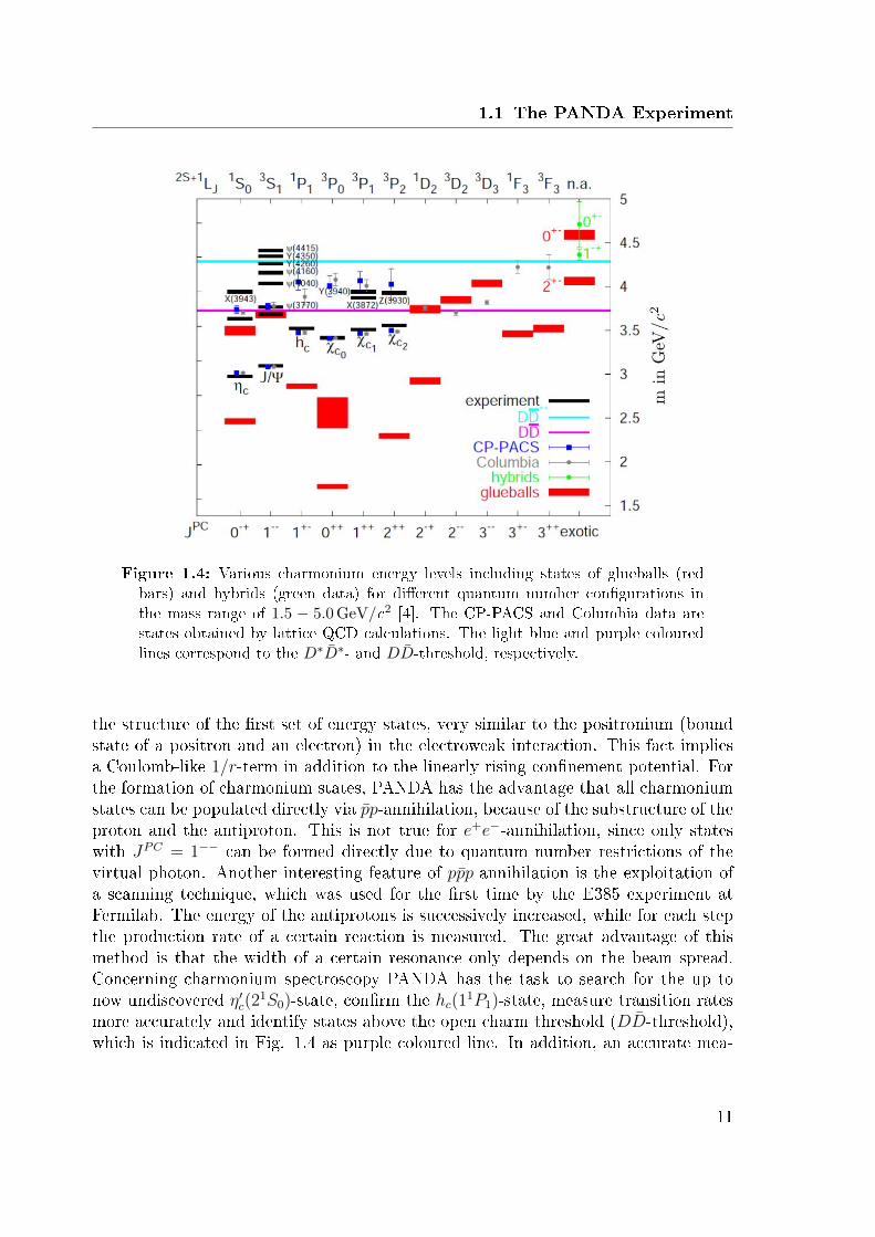
Figure 1.4: Various charmonium energy levels including states of glueballs (redbars) and hybrids (green data) for dierent quantum number congurations inthe mass range of 1.5 − 5.0 GeV/c2 [4]. The CP-PACS and Columbia data arestates obtained by lattice QCD calculations. The light blue and purple colouredlines correspond to the D∗D∗- and DD-threshold, respectively.
the structure of the rst set of energy states, very similar to the positronium (boundstate of a positron and an electron) in the electroweak interaction. This fact impliesa Coulomb-like 1/r-term in addition to the linearly rising connement potential. Forthe formation of charmonium states, PANDA has the advantage that all charmoniumstates can be populated directly via pp-annihilation, because of the substructure of theproton and the antiproton. This is not true for e+e−-annihilation, since only stateswith JPC = 1−− can be formed directly due to quantum number restrictions of thevirtual photon. Another interesting feature of ppp-annihilation is the exploitation ofa scanning technique, which was used for the rst time by the E385 experiment atFermilab. The energy of the antiprotons is successively increased, while for each stepthe production rate of a certain reaction is measured. The great advantage of thismethod is that the width of a certain resonance only depends on the beam spread.Concerning charmonium spectroscopy PANDA has the task to search for the up tonow undiscovered η′c(2
1S0)-state, conrm the hc(11P1)-state, measure transition ratesmore accurately and identify states above the open charm threshold (DD-threshold),which is indicated in Fig. 1.4 as purple coloured line. In addition, an accurate mea-
11

Chapter 1 Introduction and Motivation
surement of the hC and the χC1 energy levels will give important information on thespin contribution, since both states have the same quantum numbers, except the spin.The search for glueballs and hybrids are further important topics for PANDA. Glue-balls are colour neutral objects which only consist of gluons. Former experiments (e.g.Crystal Barrel experiment at LEAR11) brought up various glueball candidates. For in-stance, the mass of the found f0(1500)-resonance is close to the theoretical predictionof the ground state mass, but on the other hand there are also discrepancies due tothe non-avour blind decay mode. The expected glueball spectrum for the mass rangeof 1.5 − 5.0 GeV/c2 shows up relatively narrow and almost non-overlapping states,which is advantageous for their spectroscopy with PANDA. In the case of hybrids, onehas to distinguish between light quark and charmed hybrids. Basically, hybrids arecomposed objects of two quarks and an excited gluon (qqgexcited). The following showsa possible decay chain of the X(1−+)-hybrid.
pp→ X + η︸︷︷︸γγ
→ χc1︸︷︷︸J/Ψ+γ
+ π0︸︷︷︸γγ
+ π0︸︷︷︸γγ
+γγ → J/Ψ︸︷︷︸e+e−
+7γ → e+e− + 7γ
Another interesting aspect of the PANDA physics program is the in-medium modi-cation of hadrons in pA reactions. An expected lowering of the D-meson mass inthe nuclear medium would have the consequence, that the Ψ′ is kinematically able todecay in DD and other branching ratios would change as well. Also a suppression ofthe J/Ψ in antiproton heavy ion collisions is considered to be a signal for the forma-tion of a quark-gluon plasma. Therefore, the e+e−/π+π− discrimination capability ofthe PANDA detector has to be on a sucient level to discriminate against the mostdominant pp → π+π− background channel. Hyperon - antihyperon pairs can also beformed in pA collisions, which allows a direct comparison of baryon and antibaryonpotentials. The production and detection of double hypernuclei becomes possible, butrequires a further modication of the PANDA detector in a later stage. The backwardcalorimeter and the innermost tracking detector (MVD12) have to be replaced by Ger-manium semiconductor detectors (Fig. 1.5b), to provide keV energy resolution for thespectroscopy of γ-decays of excited nuclei down in the MeV range. The productionand detection strategy for double hypernuclei is illustrated in Fig. 1.5a.All the mentioned physics topics of the PANDA experiment strongly rely on the
performance of the electromagnetic calorimeter (EMC). Especially the accurate re-construction of multiple neutral mesons by the obtained energy signal and momentumof the decay photons, like it was exemplary shown for the X(1−+)-hybrid, underlinesthe important role of the EMC over a large dynamic range.
11Low Energy Antiproton Ring12Micro Vertex Detector
12

1.1 The PANDA Experiment
KaonsTrigger
atomic
transition
(a) The Ξ− which is produced via pp→ Ξ−Ξ+, rescatters in the primary 12C target nucleusand is stopped in a secondary target. After an atomic transition two Λ's are produced bythe following reaction: Ξ−p → ΛΛ. γ-spectroscopy gives information about the structureof the double hypernucleus. The produced Ξ+ and kaons serve as an external trigger.
(b) Germanium detectors for the implementation in backward direction.
Figure 1.5: Hypernuclei spectroscopy.
13
Chapter 1 Introduction and Motivation
1.2 The PANDA Detector
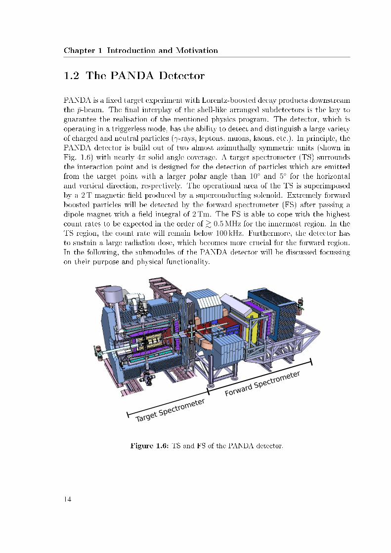
PANDA is a xed target experiment with Lorentz-boosted decay products downstreamthe p-beam. The nal interplay of the shell-like arranged subdetectors is the key toguarantee the realisation of the mentioned physics program. The detector, which isoperating in a triggerless mode, has the ability to detect and distinguish a large varietyof charged and neutral particles (γ-rays, leptons, muons, kaons, etc.). In principle, thePANDA detector is build out of two almost azimuthally symmetric units (shown inFig. 1.6) with nearly 4π solid angle coverage. A target spectrometer (TS) surroundsthe interaction point and is designed for the detection of particles which are emittedfrom the target point with a larger polar angle than 10 and 5 for the horizontaland vertical direction, respectively. The operational area of the TS is superimposedby a 2 T magnetic eld produced by a superconducting solenoid. Extremely forwardboosted particles will be detected by the forward spectrometer (FS) after passing adipole magnet with a eld integral of 2 Tm. The FS is able to cope with the highestcount rates to be expected in the order of & 0.5 MHz for the innermost region. In theTS region, the count rate will remain below 100 kHz. Furthermore, the detector hasto sustain a large radiation dose, which becomes more crucial for the forward region.In the following, the submodules of the PANDA detector will be discussed focussingon their purpose and physical functionality.
Figure 1.6: TS and FS of the PANDA detector.
14
1.2 The PANDA Detector
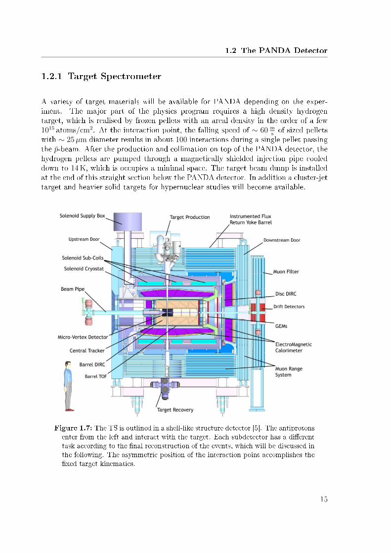
1.2.1 Target Spectrometer
A variety of target materials will be available for PANDA depending on the exper-iment. The major part of the physics program requires a high density hydrogentarget, which is realised by frozen pellets with an areal density in the order of a few1015 atoms/cm2. At the interaction point, the falling speed of ∼ 60 m
sof sized pellets
with ∼ 25µm diameter results in about 100 interactions during a single pellet passingthe p-beam. After the production and collimation on top of the PANDA detector, thehydrogen pellets are pumped through a magnetically shielded injection pipe cooleddown to 14 K, which is occupies a minimal space. The target beam dump is installedat the end of this straight section below the PANDA detector. In addition a cluster-jettarget and heavier solid targets for hypernuclear studies will become available.
Figure 1.7: The TS is outlined in a shell-like structure detector [5]. The antiprotonsenter from the left and interact with the target. Each subdetector has a dierenttask according to the nal reconstruction of the events, which will be discussed inthe following. The asymmetric position of the interaction point accomplishes thexed target kinematics.
15

Chapter 1 Introduction and Motivation
The MVD is the innermost tracking detector surrounding the target region in a cylin-drical shape. Its extension along the beam axis is roughly ±23 cm with respect to thenominal interaction point with a radius of 15 cm. It is composed of silicon pixel andstrip sensors (shown in Fig.1.8) with a thickness of 100µm and 280µm, respectively[6].
Figure 1.8: Schematic layout of the MVD. The barrel shaped innermost modules(red, 1-2) and the rst set of discs in forward direction (dark-red, 1-4) are equippedwith silicon hybrid pixel sensors (100×100µm2) with a channel granularity of 11Mchannels per 0.13 m2. The outer two modules (green) solely consist of double sidedsilicon strip sensors with 200k channels per 0.5 m2. Discs 5 and 6 are composedof both, pixels and strips.
An important requirement to the MVD besides the spatial resolution (≤ 100µm), isthe minimum material budget. The total amount of material in units of radiationlength should be kept below X/X0 = 4% to minimize pair production due to photonconversion. A charged particle propagating through the active material of the MVDloses energy due to ionisation and produces electron-hole pairs along its trajectory.This eect can be described by the Bethe-Bloch equation (Eq. 1.3). For thin ab-sorbers, the mean energy loss is uctuating and follows a Landau-distribution. Theproduced charge is collected applying an external voltage. MIPs13 (βγ ≈ 3) havean average energy loss in 300µm silicon of 90 keV which corresponds to ∼ 25, 000electron-hole pairs [7]. The position and energy loss information is subsequently usedfor the track reconstruction and particle identication. A necessary feature of theMVD is the reconstruction of secondary decay vertices. The detection eciency of
13Minimum Ionising Particles
16

1.2 The PANDA Detector
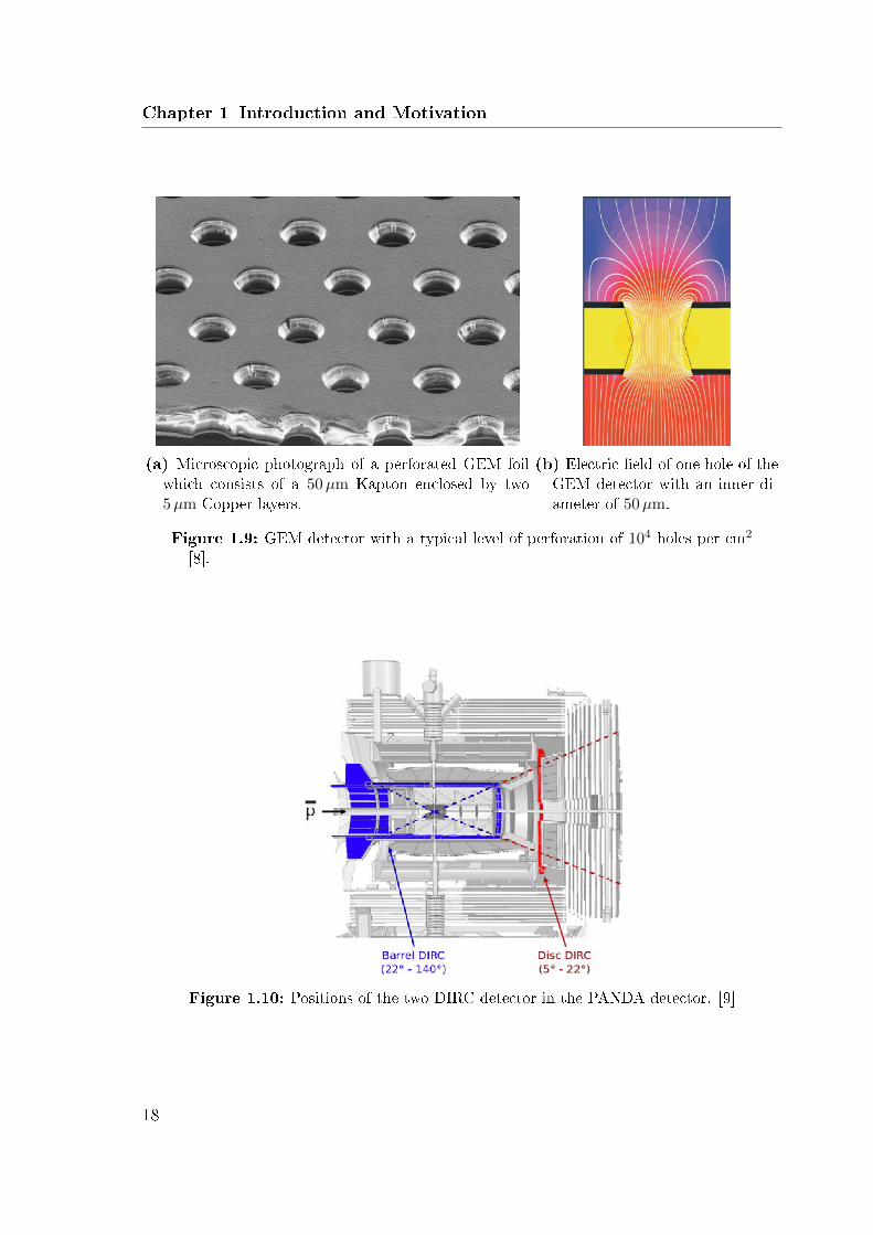
weak-interacting decay modes e.g. of charmed hadrons with a decay length in the or-der of 100µm, can additionally be improved by adding two so called "Lambda-discs"made of Si-pixels further downstream at 40 cm and 60 cm from the target point. Thisscenario is currently under discussion.Another tracking detector, which encloses the MVD, is the STT14 with an overalllength of 1.5 m and a radial extension of 15.0 cm ≤ r ≤ 41.8 cm with respect to thebeam line [5]. The main task of the STT is the precise spatial reconstruction of thebent trajectories of charged particles in a magnetic eld. The principle of the morethan 4600 cylindrical straw tubes of the STT is very similar to a conventional wirechamber. A charged particle passing one of the gas-lled tubes produces electron ionpairs along its path. The produced charge is subsequently collected and amplied bythe applied voltage of a few kV between the coaxial wire (anode) and the conduc-tive inner layer (cathode) of the straw tube. Due to secondary gas ionisations onecan achieve an amplication of about 104 − 105 of the primary signal. Furthermore,the STT is able to determine the particle specic energy loss dE/dx. The positioninformation along the tube can be obtained by the runtime of the signal. The STThas a low material budget of X/X0 ≈ 0.05% and a high rate capability, because ofimproved drift properties of the gas. A further tracking detector for covering the polarangle from 3 to 20 are the GEM15-discs. In the present version of the disc layouts,three GEM-discs are placed at 117 cm, 153 cm and 189 cm from the target (Fig 1.7,coloured in red). Fig. 1.9 shows a microscopic photograph of a perforated GEM foiland the structure of the electric eld for one hole. The applied voltage between thepair of Cu layers is in the order of ∼ 400 V. Under these conditions the primar-ily produced electrons undergo an avalanche multiplication due to the strong electriceld within the holes. With three GEM stacks one can achieve an overall gain of ∼ 104.
The eect of emitted Cherenkov light, while a charged particle propagates through amedium with a certain index of refraction n, is used by two dierent detector modulesin the TS. The Barrel DIRC16 covers the polar angle between 22 and 140 and theDisc DIRC the forward direction (Fig. 1.10). If a charged particle has a velocitylarger than c/n, Cherenkov radiation is emitted at an emission angle with respect tothe particle direction of
ΘC = arccos
(1
nβ
)(1.1)
While the Cherenkov photons propagating through the active material of the DIRCthe initial emission angle ΘC is conserved due to total reections at the media tran-sitions. Therefore, the velocity of the particle is determinable according to Eq. 1.1.
14Straw Tube Tracker15Gaseous Electron Multipliers16Detection of Internally Reected Cherenkov light
17
Chapter 1 Introduction and Motivation
(a) Microscopic photograph of a perforated GEM foilwhich consists of a 50µm Kapton enclosed by two5µm Copper layers.
(b) Electric eld of one hole of theGEM detector with an inner di-ameter of 50µm.
Figure 1.9: GEM detector with a typical level of perforation of 104 holes per cm2
[8].
Figure 1.10: Positions of the two DIRC detector in the PANDA detector. [9]
18
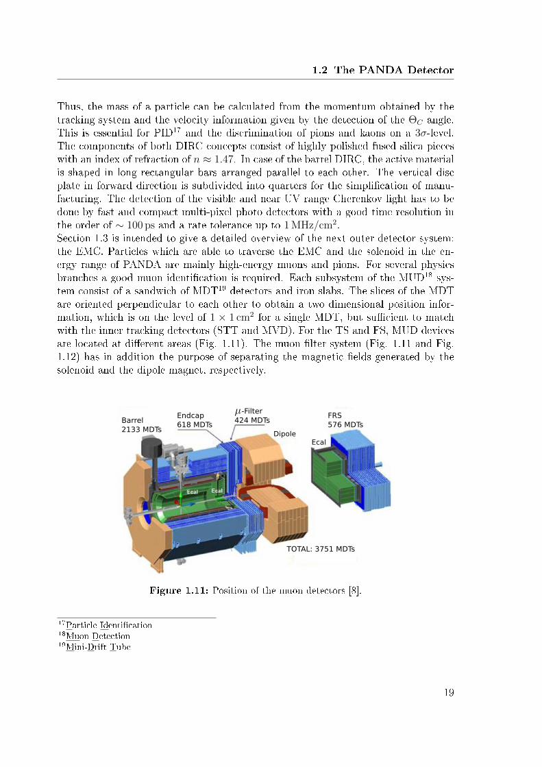
1.2 The PANDA Detector
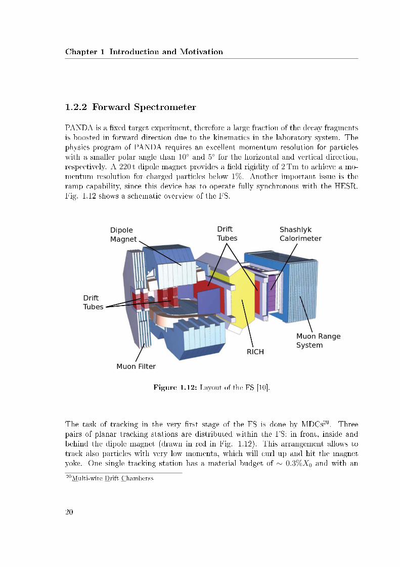
Thus, the mass of a particle can be calculated from the momentum obtained by thetracking system and the velocity information given by the detection of the ΘC angle.This is essential for PID17 and the discrimination of pions and kaons on a 3σ-level.The components of both DIRC concepts consist of highly polished fused silica pieceswith an index of refraction of n ≈ 1.47. In case of the barrel DIRC, the active materialis shaped in long rectangular bars arranged parallel to each other. The vertical discplate in forward direction is subdivided into quarters for the simplication of manu-facturing. The detection of the visible and near UV range Cherenkov light has to bedone by fast and compact multi-pixel photo detectors with a good time resolution inthe order of ∼ 100 ps and a rate tolerance up to 1 MHz/cm2.Section 1.3 is intended to give a detailed overview of the next outer detector system:the EMC. Particles which are able to traverse the EMC and the solenoid in the en-ergy range of PANDA are mainly high-energy muons and pions. For several physicsbranches a good muon identication is required. Each subsystem of the MUD18 sys-tem consist of a sandwich of MDT19 detectors and iron slabs. The slices of the MDTare oriented perpendicular to each other to obtain a two dimensional position infor-mation, which is on the level of 1 × 1 cm2 for a single MDT, but sucient to matchwith the inner tracking detectors (STT and MVD). For the TS and FS, MUD devicesare located at dierent areas (Fig. 1.11). The muon lter system (Fig. 1.11 and Fig.1.12) has in addition the purpose of separating the magnetic elds generated by thesolenoid and the dipole magnet, respectively.
Figure 1.11: Position of the muon detectors [8].
17Particle Identication18Muon Detection19Mini-Drift Tube
19
Chapter 1 Introduction and Motivation
1.2.2 Forward Spectrometer
PANDA is a xed target experiment, therefore a large fraction of the decay fragmentsis boosted in forward direction due to the kinematics in the laboratory system. Thephysics program of PANDA requires an excellent momentum resolution for particleswith a smaller polar angle than 10 and 5 for the horizontal and vertical direction,respectively. A 220 t dipole magnet provides a eld rigidity of 2 Tm to achieve a mo-mentum resolution for charged particles below 1%. Another important issue is theramp capability, since this device has to operate fully synchronous with the HESR.Fig. 1.12 shows a schematic overview of the FS.
Figure 1.12: Layout of the FS [10].
The task of tracking in the very rst stage of the FS is done by MDCs20. Threepairs of planar tracking stations are distributed within the FS: in front, inside andbehind the dipole magnet (drawn in red in Fig. 1.12). This arrangement allows totrack also particles with very low momenta, which will curl up and hit the magnetyoke. One single tracking station has a material budget of ∼ 0.3%X0 and with an
20Multi-wire Drift Chamberss
20
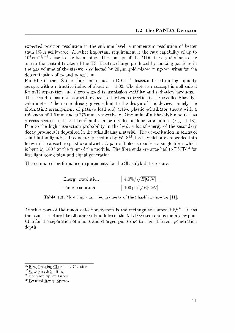
1.2 The PANDA Detector
expected position resolution in the sub-mm level, a momentum resolution of betterthan 1% is achievable. Another important requirement is the rate capability of up to104 cm−2s−1 close to the beam pipe. The concept of the MDC is very similar to theone in the central tracker of the TS. Electric charge produced by ionizing particles inthe gas volume of the straws is collected by 20µm gold plated tungsten wires for thedetermination of x- and y-position.For PID in the FS it is foreseen to have a RICH21 detector based on high qualityaerogel with a refractive index of about n = 1.02. The detector concept is well suitedfor π/K separation and shows a good transmission stability and radiation hardness.The second to last detector with respect to the beam direction is the so called Shashlykcalorimeter. The name already gives a hint to the design of this device, namely thealternating arrangement of passive lead and active plastic scintillator sheets with athickness of 1.5 mm and 0.275 mm, respectively. One unit of a Shashlyk module hasa cross section of 11 × 11 cm2 and can be divided in four submodules (Fig. 1.13).Due to the high interaction probability in the lead, a lot of energy of the secondarydecay products is deposited in the scintillating material. The de-excitation in terms ofscintillation light is subsequently picked up by WLS22 bres, which are embedded intoholes in the absorber/plastic sandwich. A pair of holes is read via a single bre, whichis bent by 180 at the front of the module. The bre ends are attached to PMTs23 forfast light conversion and signal generation.
The estimated performance requirements for the Shashlyk detector are:
Energy resolution 4.0%/√E[GeV]
Time resolution 100 ps/√E[GeV]
Table 1.3: Most important requirements of the Shashlyk detector [11].
Another part of the muon detection system is the rectangular shaped FRS24. It hasthe same structure like all other submodules of the MUD system and is mainly respon-sible for the separation of muons and charged pions due to their dierent penetrationdepth.
21Ring Imaging Cherenkov Counter22Wavelength Shifting23Photomultiplier Tubes24Forward Range System
21

Chapter 1 Introduction and Motivation
(a) Technical drawing of a Shashlyk module.
(b) Photograph of a prototype without photo sensors.
Figure 1.13: Shashlyk module [11].
22

1.3 Electromagnetic Calorimeter
1.3 Electromagnetic Calorimeter
As it was pointed out in Sec. 1.1.1, the EMC is the most important subdevice of thePANDA detector for the detection of electromagnetic probes in various benchmarkchannels of the physics program. The EMC can be subdivided in three parts for thecoverage of dierent polar angles (Fig. 1.14). For clarity, the nomenclature introducedin Tab. 1.4 is used for the remainder of this thesis.
EMC part Nomenclature Polar angle range
Forward End Cap EMC FEC ≥ 5
Barrel EMC Barrel ≥ 22
Backward End Cap EMC BEC ≥ 140
Table 1.4: Nomenclature and angular coverage of the EMC components.
This section explains the physics of such a kind of calorimeter, summarise the require-ments and highlights dierent components of the EMC readout chain.
Figure 1.14: Layout of the PANDA EMC including Barrel and FEC [12].
23

Chapter 1 Introduction and Motivation
1.3.1 Physics of the EMC
The active material of the PANDA EMC consists of an inorganic scintillator: Leadtungstate (PbWO4). Basically, a scintillator converts deposited energy into visiblescintillation light, which is subsequently readout by appropriate photo sensors. Ideally,the nal energy information scales with the incident energy, but there can also beinhomogeneities depending on the kind of detected particle, energy region and usedscintillator material. In the following the dierent interaction modes of electromagneticradiation and charged particles with matter will be discussed.
1.3.1.1 Interaction of charged Particles with Matter
Several eects contribute to the overall energy loss of a charged particle propagatingthrough a certain medium (listed in Eq. 1.2; [1, 13]). The relative fraction dependson type of particle, type of medium and energy of the impinging particle. Moreover,one has to distinguish between two groups of particles: heavy particles starting frommuons, pions up to nuclei, and electrons and positrons.(
dE
d(%x)
)=
(dE
d(%x)
)︸ ︷︷ ︸inelasticscattering
+
(dE
d(%x)
)︸ ︷︷ ︸elasticscattering
+
(dE
d(%x)
)︸ ︷︷ ︸Cherenkovradiation
+
(dE
d(%x)
)︸ ︷︷ ︸nuclearreactions
+
(dE
d(%x)
)︸ ︷︷ ︸brems-strahlung
(1.2)
The heavier the particle, the more important is the energy loss due to inelasticscattering. In a collision of the impinging particle with a lattice atom, a certainfraction of the kinetic energy is transferred, causing an ionization or excitation of thesystem, called hard or soft collision, respectively. If a hard collision produces freeelectrons, which are able to ionise further atoms, these electrons are called δ-electrons.The energy loss per pathlength can be calculated by the Bethe-Bloch equation.
− dE
dx∼ %
Z
A
z2
β2
[ln
(2meγ
2c2Wmax
Iβ2γ2
)− 2β2 − δ − 2
C
Z
](1.3)
with
me: electron mass %: density of absorbing materialI: mean excitation potential z: charge of incident particle in units of eZ: atomic number of absorber β = v/c of the incident particleA: atomic weight of absorbing material γ = 1/
√1− β2
δ: density correction C: shell correctionWmax: maximum energy transfer in a single collision
24

1.3 Electromagnetic Calorimeter
The parameter I is correlated with the atomic number Z and is in the order of hundredsof eV . δ and C are, in principle, extensions to the original Bethe-Bloch equation andbecome more important for very low and relativistic energies. Further improvementsof Eq. 1.3, like e.g. taking into account the substructure of the incoming particleor higher order eects, are negligible up to 1%. At lower energies the energy loss byionisation is dominated by the β−2-term. As a direct result, a charged particle loosesmore energy at the end of its path. This can be visualised by the so called Bragg-Peak.For momenta of βγ = p
Mc≈ 3, which corresponds to a velocity of ∼ 0.96c, Eq. 1.3
reaches a minimum (compare Fig. 1.15).In this region particles are called MIPs and lose the same amount of energy per pathlength, namely∼ 2 MeV
g/cm2 , if they have a charge of±e. At very high energies the ionisingprobability rises again due to the attening of the electric eld of the incoming particle.The characteristic energy loss dE/dx as a function of energy is usually exploited forPID. One assumption in the derivation of Eq. 1.3 is that the incoming particle remainsundeected while ionising and penetrating through matter. This does not hold forelectrons and positrons and certain modications of Eq. 1.3 have to be considered forthe applicability to this kind of particle.The contribution of elastic scattering o the nuclei gets signicant at very lowvelocities of β < 10−3 and plays a major role for the detection of neutrons.The Cherenkov eect itself was already discussed in Sec. 1.2.1 and causes an energyloss via emission of light. For PWO, a small fraction of the nal detected energyinformation originates from Cherenkov radiation. Eq. 1.5 leads with a typicalspectral sensitivity of a PMT from 350 nm to 550 nm, an incoming particle with z = 1and β ≈ 1, and an averaged index of refraction of PWO to 385 photons per cm. Thiscorresponds to ∼ 21% of the overall light output at +18 C for a MIP in 1 cm PWO.
d2N
dλdx=
2πz2
137λ2
(1− 1
β2n2(λ)
)(1.4)
dN
dx= 2πz2α sin2(ΘC)
∫ 550 nm
350 nm
dλ
λ2= 475z2 sin2(ΘC)photons/cm (1.5)
A nuclear reaction occurs if a particle is able to overcome the Coulomb barrier andsubsequently strikes a target nucleus. In general, the cross section for a nuclear inter-action is small compared to electromagnetic processes. Therefore the free mean pathof the nuclear reaction ΛNR is larger than the radiation length X0, introduced in Eq.1.8.Energy loss via bremsstrahlung plays a major role in the development of an elec-tromagnetic shower. In a typical energy range up to 100 GeV for high-energy exper-iments, this eect basically only becomes relevant for electrons and positrons, sincethe cross section of bremsstrahlung scales with m−2. Bremsstrahlung occurs mainlyin the Coulomb eld of the nucleus and therefore, strongly depends on the screeningcaused by atomic electrons. Eq. 1.6 describes the energy loss of a particle with initialenergy E0 and mass m, number of atoms per cm3 N and the atomic number of the
25

Chapter 1 Introduction and Motivation
1
2
3
4
5
6
8
10
1.0 10 100 1000 10 0000.1
Pion momentum (GeV/c)
Proton momentum (GeV/c)
1.0 10 100 10000.1
1.0 10 100 10000.1
1.0 10 100 1000 10 0000.1
−dE/dx (
MeV
g−1cm
2)
βγ = p/Mc
Muon momentum (GeV/c)
H2 liquid
He gas
CAl
FeSn
Pb
Figure 1.15: Visualisation of the Bethe Bloch equation for dierent particles andvarious materials. The dierences between the curves originate from the ratios ofZ/A for the plotted material.
26

1.3 Electromagnetic Calorimeter
material Z.
dE
dx=
4NE0Z2r2e
137
ln(
2E0mec2
)− 1
3 − f(Z), for mec2 E0 137mec
2Z−1/3
ln(183Z−1/3
)+ 1
18 − f(Z), for E0 137mec2Z−1/3
(1.6)
f(Z) represents a Coulomb correction for the emitting electron in the eld of thenucleus. The distinction of both cases in Eq. 1.6 is due to screening of the atomicelectrons. The initial particle with a higher energy E0 (lower case) "sees" a moreeective eld conguration of the whole atom, whereas for smaller energies (uppercase) the sensitivity to the electric eld of the nucleus is more pronounced. In addition,bremsstrahlung also occurs in the eld of the atomic electrons, but here one has toreplace Z2 with Z(Z + 1) in Eq. 1.6.
1.3.1.2 Interaction of Photons with Matter
A photon has several possibilities for the interaction with matter: Photoeect, Rayleigh-Scattering, Compton-Scattering, and pair production in the electric eld of the nucleusor of the electrons. Fig. 1.16 shows the energy dependence for the mentioned eects forlead tungstate. In the energy range of PANDA only Photoeect, Compton-Scatteringand pair production in the eld of the nucleus are important. These eects also showa signicant dependence on the atomic number Z (compare Tab. 1.5).
Photon Interaction Dependence
Photo Eect ∼ Z4−5E−3.5
Compton Eect ∼ ZE−1
Pair Production ∼ Z2 lnE
Table 1.5: Dependence on the photon Energy E and the atomic number Z fordierent interactions of photons with matter. At higher energies screening of thenucleus eld results in a suppression of the pair production cross-section whichgoes with ∼ Z2 lnZ [15].
1.3.1.3 Electromagnetic Shower
The listed eects lead to a development of an electromagnetic shower (Fig. 1.17).Such a shower can be subdivided into generations in which each generation producesa factor of around 2 more particles, whereupon the initial energy is fragmented and
27

Chapter 1 Introduction and Motivation
Energy in MeV
310 210 110 1 10 210
310 410
510
g2
cm
Ma
ss A
tte
nu
atio
n C
oe
ffic
ien
t in
510
410
310
210
110
1
10
210
310
410
Total
Coherent Scattering
Incoherent Scattering
Photo Effect
Pair Production (Nucleus)
Pair Production (Electron)
ato
mb
arn
sC
ross S
ectio
n in
710
510
310
110
10
Figure 1.16: Mass attenuation coecient and cross-section in terms of cm2/g andbarns/atom, respectively, for the dierent interaction options with PbWO4 (dataobtained by [14]). Coherent scattering and pair production in the electron shellplay only a minor role in the energy regime of PANDA. At lower energies thephoto eect is dominant, but decreases with energy according to the dependenciesin Tab. 1.5. At higher energies the pair production in the electric eld of nucleusis the main contribution to the total interaction cross section.
28

1.3 Electromagnetic Calorimeter
follows statistical uctuations. An average energy of the produced particles in eachgeneration can thereby be calculated by:
< E > =E0
2nwith E0: Initial energy; n: Shower generation (1.7)
An important parameter for the scale length of such kind of shower is the radiationlength X0. This parameter has two meanings and can be calculated with Eq. 1.8
X0 is the mean distance over which a high energetic electron losses up to 1/e ofits energy via bremsstrahlung
79X0 is the free path for pair production by a high-energy photon
A useful approximation of the radiation length X0 for a given material can be calcu-lated by Eq. 1.8 [13].
X0 =716.4 g
cm2 · A
Z(Z + 1) ln(
287/√Z) (1.8)
withA: atomic weight of absorber Z: atomic number of absorber
The continuation of the electromagnetic shower process stops if the cross section ofthe electron/positron for ionisation processes overcomes the one for bremsstrahlungcharacterised by the critical energy EC . In rst order this threshold energy can beparametrised in solids and liquids as follows [16]:
EC =610 MeV
Ze + 1.24(1.9)
For PbWO4 with Ze = 75.6 the critical energy is of approximately 7.94 MeV.
The geometrical expansion of an electromagnetic shower can be characterised by twoparameters: y = E
ECand t = x
X0. Tab. 1.6 summarises the longitudinal expansion for
an electron and a photon.
Incident electron Incident photon
Peak of shower, tmax/X0 1.0 · (ln y − 1) 1.0 · (ln y − 0.5)Centre of gravity, tmed/X0 tmax + 1.4 tmax + 1.7
Table 1.6: Parameters for a longitudinal development of an electromagnetic shower.
The transverse dimensions caused primarily by multiple scattering of the electrons
29
Chapter 1 Introduction and Motivation
Photo-
effect
Compton-
effect
Bre
mss
trahlung
Ionisation
Brem
sstrahlung
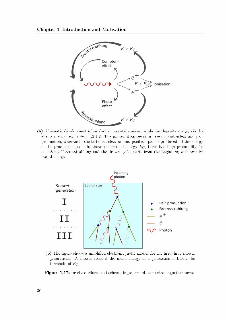
(a) Schematic development of an electromagnetic shower. A photon deposits energy via theeects mentioned in Sec. 1.3.1.2. The photon disappears in case of photoeect and pairproduction, whereas in the latter an electron and positron pair is produced. If the energyof the produced leptons is above the critical energy EC , there is a high probability foremission of bremsstrahlung and the drawn cycle starts from the beginning with smallerinitial energy.
Bremsstrahlung
Scintillator
Pair production
Photon
incoming
photon
Shower-
generation
I
II
III
(b) The gure shows a simplied electromagnetic shower for the rst three showergenerations. A shower stops if the mean energy of a generation is below thethreshold of EC .
Figure 1.17: Involved eects and schematic process of an electromagnetic shower.
30

1.3 Electromagnetic Calorimeter
are given by the Molière radius RM , which is dened as the radius of a cylindercontaining 90% of the energy deposition. RM scales proportional to X0 is essential forthe geometrical design of calorimeter modules. Fig. 1.18 a) and b) show the typicalexpansion of an electromagnetic shower in a Caesium iodide crystal (CsI) caused byphotons.
(a) Transversal shower prole. (b) Longitudinal shower prole.
Figure 1.18: Expansion of an electromagnetic shower in CsI caused by photonswith various energies [17].
31

Chapter 1 Introduction and Motivation
1.3.2 Requirements
The layout of the EMC is driven by the requirements of the physics program and theavailable budget. In the case of PANDA, the EMC is divided in three parts which arelabelled in the following according to Tab. 1.4. The main task of an EMC is the e-cient detection of electromagnetic probes, like photons, electrons and positrons. Thecoverage of the solid angle and the chosen energy threshold should be appropriate toreject background, mostly originating from π0 and η rich states. The acceptance fore± and γ can be approximated by (Ω/4π)n, in which Ω is the covered solid angle andn is the number of electromagnetic particles in the nal state.The relevant observables for the EMC are energy, point of impact (position) and time.An accurate measurement of the latter one is mandatory and serves as a time stampfor the triggerless PANDA readout and to discriminate background not related tothe detected event. Sec. 4 will describe the achievable time resolution of the wholedetection chain, ranging from the generation of scintillation light up to the nal digi-tisation, which has to cope with the nal annihilation rate of 107 Hz. Another crucialrequirement of the EMC regarding the nancial point of view is the compactness. Theprice for the scintillators and the surrounding magnet scales with the cube of theirdimensions. Finally, Tab. 1.7 summarises the most important requirements based ona luminosity of 2 · 1032 cm−1s−1 [18].
General property Required performance value
energy resolution ≤ 1%⊕ ≤2%√E/GeV
energy threshold (cluster) 10 MeVenergy threshold (single crystal) 3 MeVenergy equivalent of noise 1 MeVangular coverage 99% of 4π
subdetector specicationsBEC Barrel FEC≥ 140 ≥ 22 ≥ 5
energy range with respect to energy threshold 0.7GeV 7.3GeV 14.6GeVspatial resolution 0.5 0.3 0.1maximum rate capability 100 kHz 500 kHzshaping time 400 ns 100 nsdose per year 10 Gy 125 Gy
Table 1.7: Requirements of the EMC.
32

1.3 Electromagnetic Calorimeter
1.3.3 Scintillator Material
Lead tungstate, PbWO4 (PWO) was chosen as scintillator material for the PANDAEMC after becoming the dominant material in high-energy application. PWO has anegative birefringent nature and due to its high Z-materials the radiation length X0 isin the order of 0.89 cm, which is short compared to other potential candidates such asBGO with 1.12 cm. This is mandatory for a compact design of the calorimeter. Fig.1.19 shows the tetragonal symmetric crystal structure of PWO. The optimisation andlarge scale production was initiated by the stringent requirement, on fast response,compactness and radiation hardness to design the electromagnetic calorimeter of theCMS detector at the LHC25.
(a) Crystal Structure of PWOalong the long crystal axis.
(b) Cross section of PWO crystal structureperpendicular to the long crystal axis.
Figure 1.19: The pictures show the microscopic crystal structure of PWO for twoorientations. The hue of the atoms gives an impression of the spatial depth. Thethree optical axes are perpendicular to each other, whereas two axes are identicaldue to the birefringent nature. The dimensions for the unit cell are given andresult in a volume of approximately 360, 92 A3 [19].
25Large Hadron Collider
33
Chapter 1 Introduction and Motivation
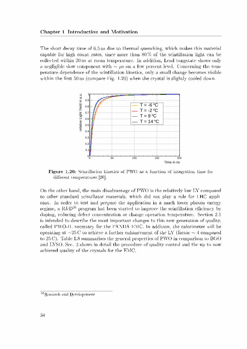
The short decay time of 6.5 ns due to thermal quenching, which makes this materialcapable for high count rates, since more than 80 % of the scintillation light can becollected within 20 ns at room temperature. In addition, Lead tungstate shows onlya negligible slow component with ∼ µs on a few percent level. Concerning the tem-perature dependence of the scintillation kinetics, only a small change becomes visiblewithin the rst 50 ns (compare Fig. 1.20) when the crystal is slightly cooled down.
Time in ns
0 50 100 150 200
rela
tive
Lig
ht Y
ield
in
a.u
.
0
0.1
0.2
0.3
0.4
0.5
0.6
0.7
0.8
0.9
1
C ° T = 6 C° T = 2
C° T = 9
C° T = 14
Figure 1.20: Scintillation kinetics of PWO as a function of integration time fordierent temperatures [20].
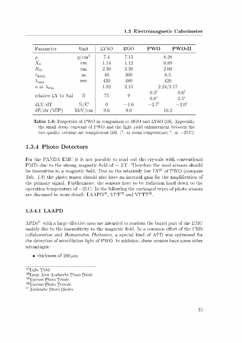
On the other hand, the main disadvantage of PWO is the relatively low LY comparedto other standard scintillator materials, which did not play a role for LHC appli-cant. In order to test and prepare the application in a much lower photon energyregime, a R&D26 program hat been started to improve the scintillation eciency bydoping, reducing defect concentration or change operation temperature. Section 2.1is intended to describe the most important changes to this new generation of quality,called PWO-II, necessary for the PANDA EMC. In addition, the calorimeter will beoperating at −25 C to achieve a further enhancement of the LY (factor ∼ 4 comparedto 25 C). Table 1.8 summarises the general properties of PWO in comparison to BGOand LYSO. Sec. 2 shows in detail the procedure of quality control and the up to nowachieved quality of the crystals for the EMC.
26Research and Developement
34
1.3 Electromagnetic Calorimeter
Parameter Unit LYSO BGO PWO PWO-II
ρ g/cm3 7.4 7.13 8.28X0 cm 1.14 1.12 0.89RM cm 2.30 2.30 2.00τdecay ns 40 300 6.5λmax nm 420 480 420n at λmax 1.82 2.15 2.24/2.17
relative LY to NaI % 75 90.3† 0.6†
0.8∗ 2.5∗
dLY/dT %/C 0 −1.6 −2.7† −3.0†
dE/dx (MIP) MeV/cm 9.6 9.0 10.2
Table 1.8: Properties of PWO in comparison to BGO and LYSO [18]. Especiallythe small decay constant of PWO and the light yield enhancement between thetwo quality versions are conspicuous [18]. (†: at room temperature; ∗: at −25 C)
1.3.4 Photo Detectors
For the PANDA EMC it is not possible to read out the crystals with conventionalPMTs due to the strong magnetic eld of ∼ 2 T. Therefore the used sensors shouldbe insensitive to a magnetic eld. Due to the relatively low LY27 of PWO (compareTab. 1.8) the photo sensor should also have an internal gain for the amplication ofthe primary signal. Furthermore, the sensors have to be radiation hard down to theoperation temperature of −25 C. In the following the envisaged types of photo sensorsare discussed in more detail: LAAPD28, VPT29 and VPTT30.
1.3.4.1 LAAPD
APDs31 with a large eective area are intended to readout the barrel part of the EMCmainly due to the insensitivity to the magnetic eld. In a common eort of the CMScollaboration and Hamamatsu Photonics, a special kind of APD was optimised forthe detection of scintillation light of PWO. In addition, these sensors have some otheradvantages:
thickness of 200µm
27Light Yield28Large Area Avalanche Photo Diode29Vaccum Photo Triode30Vaccum Photo Tetrode31Avalanche Photo Diodes
35

Chapter 1 Introduction and Motivation
thin conversion layer
high QE32 in the wavelength range of PWO (∼ 80%)
insensitive to magnetic eld
low cost for mass production
Fig. 1.21 shows the general structure of an APD which is operating in reversed volt-age.
Figure 1.21: The APD structure consists of various layers of doped silicon. p andn corresponds to the kind and the number of + to the level of doping. The chosendoping prole leads to a strong electric eld close to the junction. This results intoan avalanche of the primarily produced charge carriers and nally to an internalamplication. After drifting, the nal charge collection takes place in the n++
electrode. The additional layer of silicon nitride (Si3N4) on the entrance facereduces loss of the light due to reections.
The gain of an APD strongly depends on applied voltage and temperature. There-fore, to ensure the performance of the photo sensors, temperature and applied biasvoltage have to be kept stable within an accuracy of ∆T = ±0.1 C and ∆U = ±0.1 V.Therefore the characteristics of an individual APD has to be known. For determiningthe gain M , dark current Id and photo current Iill are recorded while illuminating
32Quantum Eeciency
36

1.3 Electromagnetic Calorimeter
the sensitive area of a xed wavelength (Tmax/PbWO4 = 420 nm). The obtained signalamplication is derived from the relation to the M = 1 equivalent, according to Eq.1.10. Fig. 1.22 shows the dependencies of gain, dark current and applied voltage of arandomly chosen APD for dierent temperatures.
M =Iill(U)− Id(U)
Iill(M = 1)− Id(M = 1)(1.10)
290 300 310 320 330 340 350 360 370 380 0
50
100
150
200
250
300
350
400
450
500
550
600
650
700
+18 ˚C
-25 ˚C
ga
in
Reverse Voltage / V
Figure 1.22: Correlation of gain and applied voltage of an APD for two dierenttemperatures. The shape corresponds to the characteristic curve of a diode.
The obtained gain M is a result of the avalanche process within the APD. Such astatistical process also brings up uncertainties caused by uctuations which enter inthe nal performance. This can be expressed by the Excess Noise Factor F and isbasically connected to the broadening of produced photoelectrons Npe and contributesto the energy resolution by:
σEE
=1√E·
√F
Npe(1.11)
With respect to the PANDA EMC, a further R&D step was necessary. The relativelylow envisaged energy threshold of 10 MeV requires to collect as much scintillation lightas possible. This can be achieved by increasing the area of the APD, which leads toanother generation called LAAPD. The eective area was enhanced from 0.25 cm2 to1 cm2. The rectangular shape allows to equip two APDs on one crystal and therefore
37

Chapter 1 Introduction and Motivation
to improve the energy resolution by another factor of√
2. Two sensors per crystalbring another advantage, namely the rejection of fake events caused by neutrons, forthe rst time realized by the CMS experiment. There is a non-zero probability thata neutron crossing the volume of an APD creates a physically unusual high energysignal due to spallation. Those events can be identied by comparing the signal ofboth sensors for one event. Another eects, which leads to a worsening of the energyresolution, occurs if a charged particle reaches the silicon layers of the APD andproduces electron hole pairs (∼ 100 e/h pairs per µm) in addition to the signal causedby the PWO scintillation light (NCE33). This eect is more crucial for PANDA, sincethe relative signal contribution is higher due the lower energy regime, compared toCMS. Therefore it is advantageous to have a thin conversion layer.
1.3.4.2 VPT/VPTT
The functionality of a VPT or a VPTT is very similar to the principle of a conventionalPMT except the number of dynodes. A schematic layout of both kind of sensors isdisplayed in Fig. 1.23. The photo cathode serves as a converter from photons toelectrons which will then be accelerated to the mesh anode and afterwards to thedynode where the amplication takes place. The produced secondary electrons willsubsequently be accelerated backwards and collected by the anode. In case of a VPTT,an additional mesh dynode is placed between cathode and anode. On the one handthis results in an additional gain, but on the other hand the tube gets more sensitive tothe magnetic eld. Both types of sensors have a typical quantum eciency of bialkaliphoto cathodes in the order of ∼ 20 %.
(a) High voltage setting for the VPT:Cathode at −1000 V, anode on groundand dynode at −200 V.
(b) High voltage setting for the VPTT:Cathode on ground, rst dynode on500 V, anode at 1200 V, second dynodeat 1000 V.
Figure 1.23: Schematic layout and high voltage settings for VPT and VPTT [21].
33Nuclear Counter Eect
38

1.3 Electromagnetic Calorimeter
This kind of photo detector will read out the crystals of the FEC, since they aremore capable for higher rates (up to 500 kHz in the FEC) and show a better radiationhardness. In the outermost region of the FEC, the angle between sensor axis andmagnetic eld is∼ 18 , which reduces the gain due to the Lorentz force on the electrons.Current studies [22] show a degradation of a VPTT gain up to 45 % for a magneticeld of 1.2 T.
1.3.5 Electronics
Several requirements are dictated to the readout electronics to achieve the designatedperformance of the PANDA EMC. A dynamic range of 12, 000 is necessary to coverthe energy range from the low energy threshold of 1 MeV and the maximum expectedenergy deposition in a single crystal of 12 GeV. Furthermore, the limited availablespace should be occupied as eciently as possible. Therefore, the geometry of thepreampliers should t into the EMC cooling compartment to be as close as possibleto the crystal sensors (compare Fig. 1.24). This will have a positive impact onthe analogue circuits and decrease the probability of pick-up noise. A low powerconsumption of the electronics is mandatory as well, to guarantee the homogeneity ofcooling along the 20 cm long crystals. Two dierent concepts were developed and will
Figure 1.24: Schematic readout chain of the PANDA EMC [23]. The ampliedsignals are forwarded to digitiser modules which consist of SADC-chips and digitallogics for the evaluation of the necessary informations (explained in Sec. 3.1.4).The digitiser modules are at a distance of 20 − 30 cm and 90 − 100 cm for thebarrel and FEC, respectively, away from the cold EMC volume. Via an opticallink (drawn in red) the data stream reaches the stage of the data concentrator,where diverse algorithms are applied to the data. A general time distribution ofthe PANDA detectors provides a clock. Finally, the obtained values are collectedby the computing node.
39

Chapter 1 Introduction and Motivation
be presented in the following subsections. On the one hand an ASIC34 for the signalprocessing in the barrel part and on the other hand a Low Noise/Low Power ChargePreamplier (LNP-P) in the FEC.
1.3.5.1 ASIC
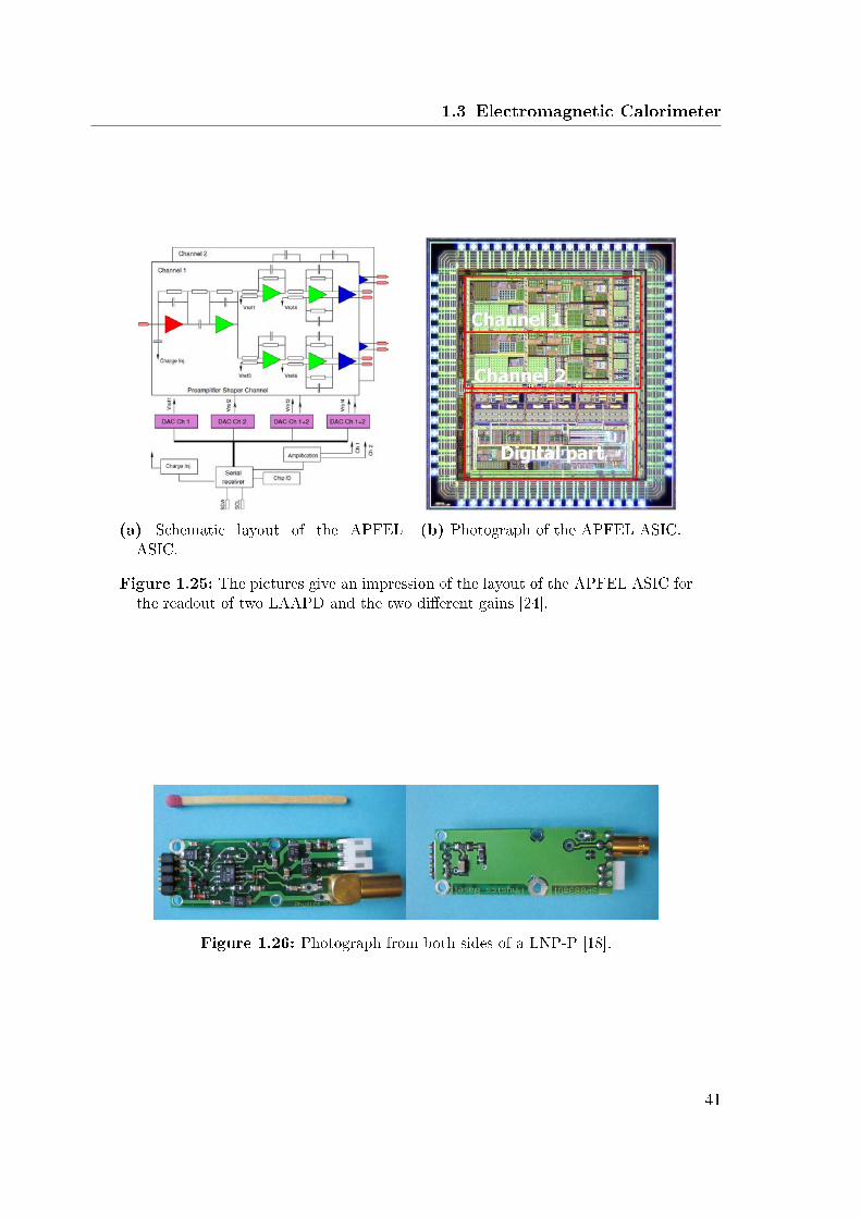
Each crystal of the barrel EMC is equipped with two LAAPD which are read outsimultaneously by one ASIC, called APFEL35. This chip will split up the input of asingle LAAPD and provide two channels with dierent gains. In the current version(1.4.) the ratio between these two gain branches is programmable between 16 and32. Further prototype tests will show which factor gives the best compromise. Due tothe increased capacity of the LAAPDs and therefore higher contribution to the darkcurrent, the preamplier should have, among the already mentioned requirements, alow noise level. The maximum input charge is in the order of 8 pC and results with anENC36 of 0.74 fC (4625 e−) to a dynamic range of more then 10, 000. Concerning ratecapability, this ASIC is able to handle event rates up to 500 kHz (barrel max. rate100 kHz), which is a design trade-o between noise issues and pile-up. The power con-sumption per APFEL is approximately 55 mW. All the provided data of the APFEL1.4. was determined at room temperature [24]. Fig. 1.25 shows a block diagram anda photograph of the APFEL.
1.3.5.2 Low Noise and Low Power Charge Preamplier
A LNP-P37 has been developed for the adaptation of the VPTs for the FEC basedon J-FET38 technology. In a former stage of the development this preamplier isimplemented in a barrel EMC prototype detector (compare Sec. 3.1). The inputcharge of the preamplier is linearly converted to a positive output voltage. Theoverall power consumption of the preamplier depends on the event rate and registeredphoton energy and ranges for PANDA from 45 mW to 90 mW. Concerning noise issues,the anode capacitance of a VPT is one order of magnitude less compared to a LAAPDwhich results in a signicantly lower dark current (∼ 1 nA). The maximum positiveoutput voltage of 2 V is caused by the charge sensitivity of 0.5 V/pC and the maximumsingle pulse input charge of 4 pC at 50 Ω. Fig. 1.26 shows a photograph of the topand bottom side of single-channel LNP-P prototype.
34Application Specic Integrated Circuit35ASIC for PANDA Front-end Electronics36Equivalent Noise Charge37Low Noise and Low Power Charge Preamplier38Junction Field Eect Transistor
40
1.3 Electromagnetic Calorimeter
(a) Schematic layout of the APFELASIC.
(b) Photograph of the APFEL ASIC.
Figure 1.25: The pictures give an impression of the layout of the APFEL ASIC forthe readout of two LAAPD and the two dierent gains [24].
Figure 1.26: Photograph from both sides of a LNP-P [18].
41


Chapter 2
Quality Control of PbWO4 Crystals
for PANDA
For securing the dened quality requirements of the crystals for PANDA, an appro-priate test procedure has to be dened. The relevant properties of each individualcrystal are measured and tested by three independent facilities: BTCP, CERN andthe university of Gieÿen. Therefore, dierent ways of measuring, which can give rise toinconsistencies, should be taken into account. Up to now, all crystals were produced byBTCP, where also the rst stage of quality control takes place. At BTCP, the crystalswere grown using the so called Czochralski method (Fig. 2.1a). A small seed crystal ispulled out of melted raw material with a purity level close to 6N1. The purication wasachieved by several steps before such as the appropriate mixture of raw material toreach the nal stochiometric ratio considering losses due to evaporation. In additiona pre-crystallisation was used to separate impurities with a dierent segregation coef-cient. This procedure results in 25 cm long ingots with elliptical cross-section shownin Fig. 2.1b, which will be subsequently cut into the PANDA geometries adjustingthe nal surfaces parallel to the main crystal axis. This chapter has the intention toexplain the relevant parameters and the procedure of the performed quality control.Finally, the obtained results will be summarised and discussed, also with regard tothe status of the remaining crystals.
2.1 Improvement of Lead Tungstate Crystals
Lead tungstate was mainly chosen by the PANDA collaboration due to its high ratecapability and radiation hardness. But the relatively low light yield (compare Tab.1.8) required further steps, especially for the ecient detection of low energetic probesdown to 10 MeV. At rst, the overall light yield of PWO was enhanced by a collab-orative R&D development by the PANDA collaboration and BTCP [25] funded by
1purity level of ≥ 99.9999%
43

Chapter 2 Quality Control of PbWO4 Crystals for PANDA
(a) Czochralski method. (b) Uncutted PbWO4 ingots.
Figure 2.1: Manufacturing of PWO crystals.
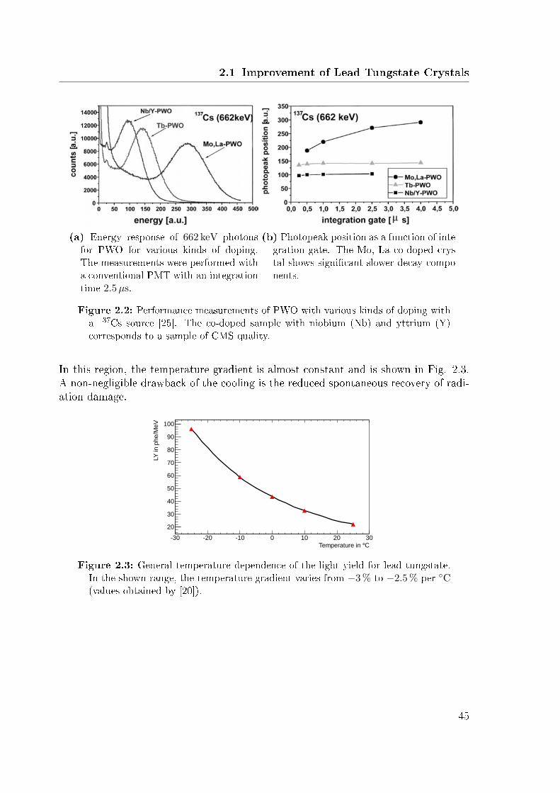
the EU2 project "Hadron Physics". In a rst iteration of research, dierent dopingcompositions consisting of molybdenum (Mo) and another series of pure terbium (Tb)were tested. The performed measurements for low energetic photons from a 137Cssource showed a signicant improvement of the light output (Fig. 2.2a). A certaindoping combination of Mo (500 ppm) and lanthanum (La) (100 ppm) even resulted ina light yield a few times higher as compared to CMS3 type crystals. But there are acouple of drawbacks, since a higher level of Mo-doping causes an increase of the decaytime which limits the application at higher rates (compare Fig. 2.2b). In addition,the crystal structure is less radiation hard and the maximum of the scintillation lightis shifted towards the green region (∼ 500 nm) [26]. The situation is rather similarfor Tb doped crystal. Here the light yield increases by lowering the Tb-concentration,but unfortunately the radiation hardness is degrading as well.An additional enhancement of the light yield of 30 % − 50 % can be achieved by a
reduction of the La- and Y-concentration down to a level of ∼ 40 ppm, which leadsto a degradation of deep traps in the crystal structure. This is possible due to animproved control of the stoichiometric composition of the melt. La and Y have dier-ent distribution coecients, which lead to dierent concentration gradients within thecrystal while pulling out of the melt. To avoid this imbalance, the doping elements canbe introduced in dierent stages during the crystal growing process. The mentionedinnovations result in a signicant lower number of vacancies in the crystal structure.Altogether, this new type of PWO, called PWO-II, shows an increased light yield inthe order of 80 % compared to CMS-type quality. Concerning timing issues, this nextgeneration of PWO shows a clear dominance of the fast decay component of 97 % anda decay time in the single-digit ns-region, measured at room temperature.On top of the already increased light yield, the whole calorimeter is cooled down to atemperature of −25 C, which results in an additional enhancement of the light yieldby a factor ∼ 4 compared to room temperature due to the thermal quenching eect.
2European Union3Compact Muon Solenoid
44
2.1 Improvement of Lead Tungstate Crystals
(a) Energy response of 662 keV photonsfor PWO for various kinds of doping.The measurements were performed witha conventional PMT with an integrationtime 2.5µs.
(b) Photopeak position as a function of inte-gration gate. The Mo, La co-doped crys-tal shows signicant slower decay compo-nents.
Figure 2.2: Performance measurements of PWO with various kinds of doping witha 137Cs source [25]. The co-doped sample with niobium (Nb) and yttrium (Y)corresponds to a sample of CMS quality.
In this region, the temperature gradient is almost constant and is shown in Fig. 2.3.A non-negligible drawback of the cooling is the reduced spontaneous recovery of radi-ation damage.
C°Temperature in 30 20 10 0 10 20 30
LY in p
he/M
eV
20
30
40
50
60
70
80
90
100
Graph
Figure 2.3: General temperature dependence of the light yield for lead tungstate.In the shown range, the temperature gradient varies from −3 % to −2.5 % per C(values obtained by [20]).
45

Chapter 2 Quality Control of PbWO4 Crystals for PANDA
2.2 Crystal Requirements
To guarantee the nal performance and the long term stability of the EMC, the PWOcrystals have to have sucient quality. Based on the physical goals and also forthe mechanical integration, the crystals should reach minimum requirements. Thiscan be characterised by dierent properties, which will be described in the followingsubsections in more detail. The limit for each parameter was chosen with respectto previous experiences and detailed studies. Another aspect are the Gaussian-likedistributed parameters due to the manufacturing of large quantities. Therefore acertain fraction of crystals can belong to a tail with insucient quality, but on theother hand those statistical variations can also bring up crystals with excellent quality.All xed requirements concerning quality control are summarised in Tab. 2.1.
Property Unit Limit
longitudinal transmission at 360 nm % ≥ 35longitudinal transmission at 420 nm % ≥ 60longitudinal transmission at 620 nm % ≥ 70non-uniformity of transversal transmission at T= 50% nm ≤ 3
LY at T= 18 C phe/MeV ≥ 16.0LY(100 ns)/LY(1µs) ≥ 0.9
induced absorption coecient ∆k at room temperature,m−1 ≤ 1.1
integral dose 30 Gymean value of ∆k distribution for each lot of delivery m−1 ≤ 0.75
Table 2.1: Relevant specications of the crystals for the PANDA EMC.
2.2.1 Longitudinal Transmission
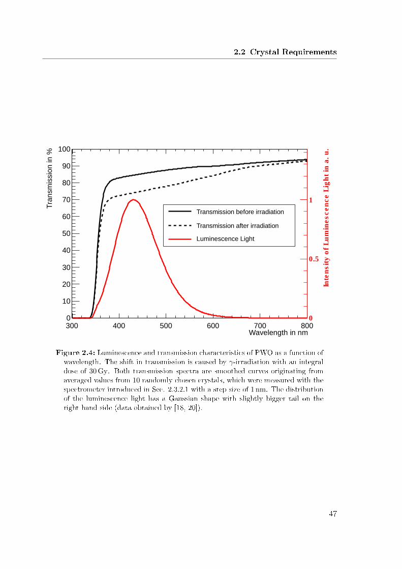
A reasonable transmission of a crystal is important for the propagation of the pro-duced luminescence light of the scintillation process. The almost Gaussian distributedscintillation light of PWO is peaking at around 420 nm with a FWHM4 of ∼ 40 nm.Fig. 2.4 shows the luminescence light and the natural transmission of an unharmedand an irradiated PWO crystal.
In order to judge whether a crystal has sucient longitudinal transmission, one has tocompare the measured values with the specication limits at three selected and very
4Full Width at Half Maximum
46
2.2 Crystal Requirements
Wavelength in nm300 400 500 600 700 800
Tra
nsm
issio
n in
%
0
10
20
30
40
50
60
70
80
90
100
Transmission before irradiation
Transmission after irradiation
Luminescence Light
Inte
nsit
y o
f L
um
inescen
ce L
igh
t in
a. u
.0
0.5
1
Figure 2.4: Luminescence and transmission characteristics of PWO as a function ofwavelength. The shift in transmission is caused by γ-irradiation with an integraldose of 30 Gy. Both transmission spectra are smoothed curves originating fromaveraged values from 10 randomly chosen crystals, which were measured with thespectrometer introduced in Sec. 2.3.2.1 with a step size of 1 nm. The distributionof the luminescence light has a Gaussian shape with slightly bigger tail on theright hand side (data obtained by [18, 20]).
47

Chapter 2 Quality Control of PbWO4 Crystals for PANDA
sensitive wavelengths: 360, 420 and 620 nm. With the discovery of PWO as scintil-lator, it was desired to shift the fundamental absorption edge to lower wavelengthsvia doping, as well as reduction of defects. The required transmission at 360 nm waschosen to avoid a cutting into the emission spectrum and to provide an optimum cov-erage. In addition, the transmission at 360 nm shows a useful correlation with the lightyield, which could be exploited later on for a rst order relative energy calibration ofthe crystals among each other. A requirement at the peaking wavelength of 420 nm isself-evident. 620 nm is chosen as longest relevant wavelength in order to avoid absorp-tion bands caused by any kind of complexes in the crystal matrix. In each stage ofthe quality control the longitudinal transmission is measured via a light beam whichenters the crystal in one end face perpendicularly, proceeds along the long crystal axisand leaves the sample at the other end face. This way of measurement already causeslosses due to reections at media transitions. The reected and transmitted fractionr and t of a certain light intensity for one surface transition with dierent indices ofreection n1 and n2 can be calculated by:
r =
(n1 − n2
n1 + n2
)2
(2.1)
t = 1− r (2.2)
Fig. 2.5 illustrates the individual contributions to the overall transmitted light inten-sity.
Figure 2.5: The picture shows the propagation for multiple reected photons in anoptical system. The relative intensities are marked for the individual light beamsaccording to Eq. 2.1 and 2.2.
By summing up all fractions, one can determine the theoretical limit for the longitu-dinal transmission which is achievable for this method.
Tmax = 100% · t2 · (1 + r2 + r4 + . . .) (2.3)
= 100% · 1− r1 + r
These considerations, with the mentioned importance at the relevant wavelengths,lead to the requirements for the longitudinal transmission.
48

2.2 Crystal Requirements
2.2.2 Transversal Transmission
The homogeneity of a crystal is a crucial aspect for the nal performance of the EMCand is mainly determined by the quality of the crystal growing process. Therefore, anearly constant transversal transmission along the crystal is mandatory. For PANDA,the spectrum in the relevant wavelength range is measured perpendicular to the 20 cmlong crystal axis at equidistant positions. For each position, the wavelength, wherethe 50 % threshold is passed, is recorded. From the largest and smallest obtainedwavelength, one can characterise the homogeneity of the crystal by the so called ∆λ-parameter:
∆λ = λmax/50 % − λmin/50 %. (2.4)
This parameter should not exceed 3 nm.
2.2.3 Geometry
In general, a crystal has the geometry of a truncated pyramid with a length of 20 cm.In order to achieve a hermetically closed barrel part of the EMC, 11 dierently taperedcrystal shapes are used. In addition, each of these shapes is produced in two versionssymmetric to one of the side faces. All the crystals in the barrel region are symmet-rically aligned to a plane, which contains the target point and is perpendicular to thebeam. This mirror symmetry allows the reduction of necessary shapes from originally18 to 11. Moreover, two additional shapes are foreseen for the mounting in FEC andBEC. A schematic drawing of the crystal model for the explanation of the geometryparameters and the values for each shape is given in Fig. 2.6 and Tab. 2.2.
For the mounting of the calorimeter, the crystals are not pointing directly to the nalvertex point in order to prevent energy deposition in dead material. The crystals in-cluding wrapping have to t into carbon alveoles. Therefore each geometry parametershould not exceed the desired limits of Tab. 2.2. On the other hand, the deviationshould be less than 0.1 mm. The roughness is a parameter which is not explicitlymeasured for the quality control. This parameter should be below or equal 0.02µmand 0.5µm for the polished crystal surfaces and the edges, respectively. Furthermore,in a case of doubt, no crystal with cracks deeper than 0.5 mm is allowed.
49

Chapter 2 Quality Control of PbWO4 Crystals for PANDA
Figure 2.6: Schematic drawing of a PANDA crystal including the denition of thegeometry parameters. All crystals have a right angle corner in order to simplifymanufacturing.
TypeVolume AF BF CF AR BR CRcm3 mm
1 126.86 21.21 21.28 21.27 29.04 28.75 29.122 126.56 21.18 21.28 21.39 28.78 28.75 29.073 125.79 21.17 21.28 21.51 28.36 28.75 28.814 120.85 21.17 21.28 21.60 27.90 27.22 28.455 119.69 21.17 21.28 21.69 27.35 27.22 28.016 118.35 21.19 21.28 21.78 26.72 27.22 27.477 112.90 21.22 21.28 21.86 26.23 25.47 26.998 111.75 21.23 21.28 21.91 25.70 25.47 26.519 110.52 21.23 21.28 21.95 25.14 25.47 26.0010 107.01 21.25 21.28 22.00 24.70 24.42 25.5611 106.25 21.25 21.28 22.02 24.35 24.42 25.23EC 126.88 24.38 24.38 24.38 26.00 26.00 26.00EC-R 118.58 24.35 24.35 24.35 24.35 24.35 24.35
Table 2.2: Denition of the geometrical parameters of the lead tungstate crystals.The EC and EC-R geometry corresponds to crystals for the FEC and the BEC,respectively.
50

2.2 Crystal Requirements
2.2.4 Light Yield
The LY is an important quality parameter, since it describes the ability of a crystal toconvert deposited energy into scintillation light and has a signicant contribution tothe stochastic term of the energy resolution. For the quality control of PANDA, theLY is determined by conventional bialkali PMTs and therefore, the LY is characterisedin terms of photoelectrons per MeV (phe/MeV) and can be calculated by:
LY[phe/MeV] =ppSource − ppPedestalppSEP − ppPedestal
· 1
Eγ. (2.5)
pp : peak position
SEP : Single Electron Peak
Eγ : Energy of photon in MeV
The position of the pedestal ppPedestal corresponds to the zero level of the signal. A SEPoccurs if only one electron is emitted from the photocathode due to thermal excitationand getting amplied by the dynod structure of the PMT. For quality control it wouldnot be economical to cool each crystal down to the nal operating temperature of−25 C. Fortunately, there is a well established linear correlation between the LY atdierent temperatures [27]. Therefore, the measurements of the LY-parameter areperformed at +18 C. The minimum LY-requirement is 16 phe/MeV, which is onlycrucial for the less tapered crystals of both end caps. This will be explained andfurther discussed in Sec. 2.4.3.
2.2.5 Scintillation Kinetics
The kinetics of the scintillation mechanism describes the necessary time for the collec-tion of a certain amount of scintillation light and can be expressed as decay times ofthe scintillation components. For mass quality inspection, the ratio of the collected LYwithin 100 ns and 1µs gives a feedback about the kinetics of a scintillator. This ratioshould be above or equal 90 % and is measured at +18 C. This property is by far notexpected to become problematic, since for the majority of crystals this requirement iseven fullled at −25 C. For a small set of randomly chosen crystals, this parameterwas remeasured +18 C and −25 C to conrm the uncrucial situation with respect torejection (Fig. 2.7). Therefore this parameter is not further discussed in the analysisof the quality control.
51
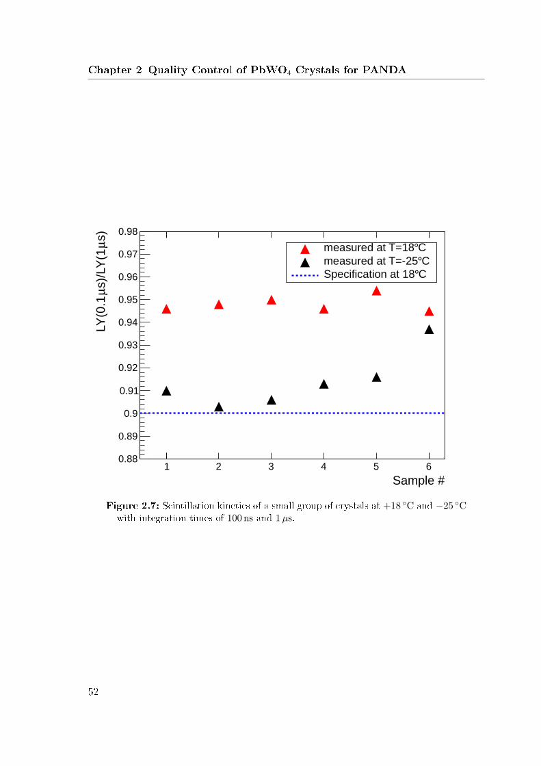
Chapter 2 Quality Control of PbWO4 Crystals for PANDA
Sample #1 2 3 4 5 6
s)
µs)/
LY
(1
µLY
(0.1
0.88
0.89
0.9
0.91
0.92
0.93
0.94
0.95
0.96
0.97
0.98
C°measured at T=18
C°measured at T=25C°Specification at 18
Figure 2.7: Scintillation kinetics of a small group of crystals at +18 C and −25 Cwith integration times of 100 ns and 1µs.
52
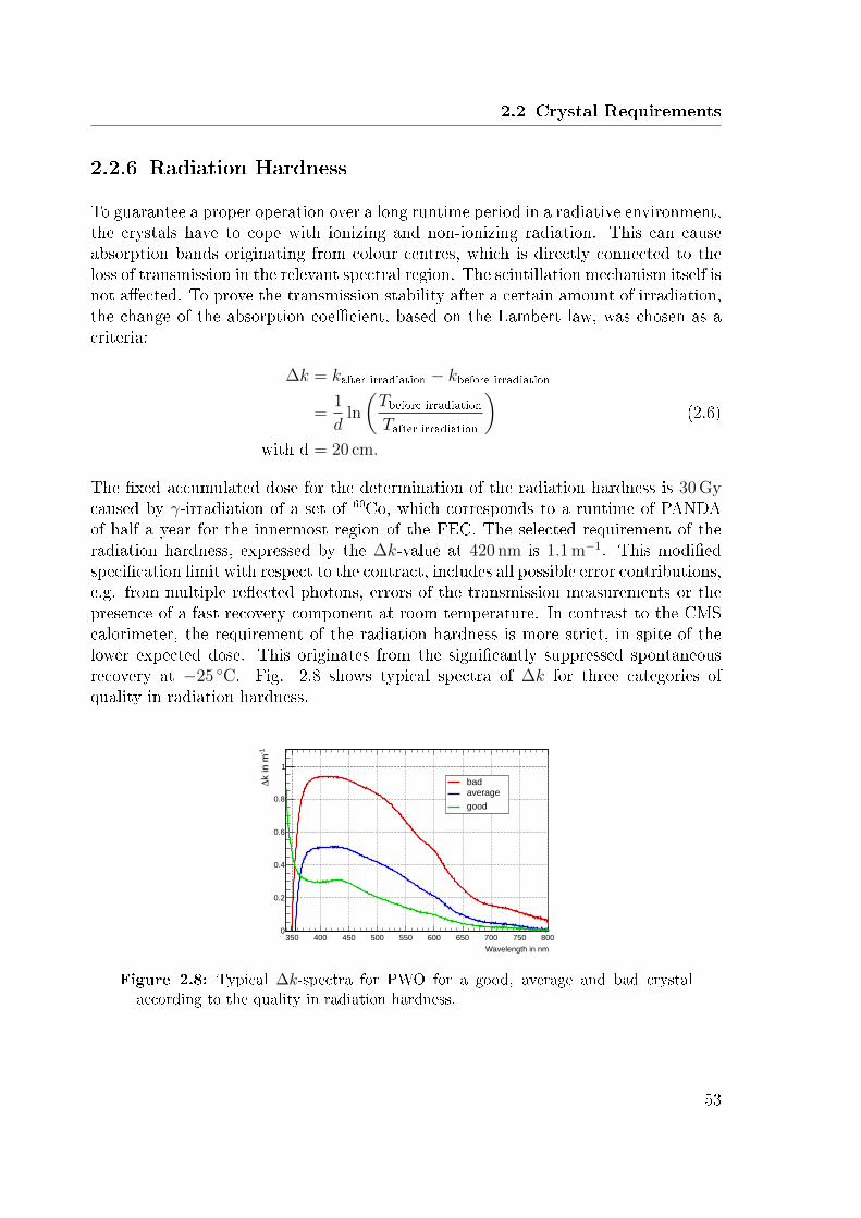
2.2 Crystal Requirements
2.2.6 Radiation Hardness
To guarantee a proper operation over a long runtime period in a radiative environment,the crystals have to cope with ionizing and non-ionizing radiation. This can causeabsorption bands originating from colour centres, which is directly connected to theloss of transmission in the relevant spectral region. The scintillation mechanism itself isnot aected. To prove the transmission stability after a certain amount of irradiation,the change of the absorption coecient, based on the Lambert law, was chosen as acriteria:
∆k = kafter irradiation − kbefore irradiation
=1
dln
(Tbefore irradiationTafter irradiation
)(2.6)
with d = 20 cm.
The xed accumulated dose for the determination of the radiation hardness is 30 Gycaused by γ-irradiation of a set of 60Co, which corresponds to a runtime of PANDAof half a year for the innermost region of the FEC. The selected requirement of theradiation hardness, expressed by the ∆k-value at 420 nm is 1.1 m−1. This modiedspecication limit with respect to the contract, includes all possible error contributions,e.g. from multiple reected photons, errors of the transmission measurements or thepresence of a fast recovery component at room temperature. In contrast to the CMScalorimeter, the requirement of the radiation hardness is more strict, in spite of thelower expected dose. This originates from the signicantly suppressed spontaneousrecovery at −25 C. Fig. 2.8 shows typical spectra of ∆k for three categories ofquality in radiation hardness.
Wavelength in nm
350 400 450 500 550 600 650 700 750 800
1k in m
∆
0
0.2
0.4
0.6
0.8
1
bad average
good
Figure 2.8: Typical ∆k-spectra for PWO for a good, average and bad crystalaccording to the quality in radiation hardness.
53

Chapter 2 Quality Control of PbWO4 Crystals for PANDA
2.3 Procedure of Quality Control
The securing of the necessary quality of the crystals is a common task of three teststations. The rst quality check of the crystals is performed by the manufacturerBTCP, in order to avoid the delivery of crystals with insucient quality. Afterwards,each lot is shipped to CERN to pass the next iteration of quality control. Finally, thelast and deciding quality check is done at Gieÿen, where also the storage until the nalmounting of PANDA takes place. Fig. 2.9 shows the path of the crystals from theirproduction to dierent test stages. This subsection describes the test procedures andsetups for the individual stages.
Figure 2.9: The dened procedure for securing the minimum quality of the crystals.
Not all parameters are measured by each facility, therefore Tab. 2.3 gives an overviewbetween test facility and corresponding quality parameter.
Property BTCP CERN Gieÿen
geometries X X ×longitudinal transmission X X Xtransversal transmission X X ×light yield X X (X)scintillation kinetics X X ×radiation hardness X × X
Table 2.3: Overview of the quality control of the crystals and where they are tested.Only for a few random crystals of each lot and geometry the LY was measured inGieÿen to determine the calibration coecients (Sec. 2.3.2.2).
54

2.3 Procedure of Quality Control
2.3.1 Quality Control at BTCP and CERN
The test procedure of BTCP and CERN are very similar, both using a special devicefor handling a larger number (up to 30) of crystals simultaneously. This device is theso called ACCOS5 machine (Fig. 2.10) and was in both cases already used for testingcrystals of the CMS calorimeter, ECAL6.
Figure 2.10: The moveable server of the ACCOS machine has a diameter of 1.1 mand is able to carry several crystals, including reference crystals, at the same time.
The ACCOS machine is a composed system of devices for the single quality measure-ments [28]. A 3D-laser system7 measures the geometry with a precision of 5µm. Forthe determination of the crystal edges, each crystal face is reconstructed by measuringa certain number of points (15 for lateral faces; 9 for one end face). The transmissionalong and perpendicular to the long crystal axis is in each case measured by a compactspectrometer using a 20 W halogen lamp. But here only a set of discrete wavelengths,chosen from 330− 700 nm for the best recognition of the absorption edge and possibleabsorption bands, is measured and realized by narrow band pass lters. The detectionof the transmitted light is done by a large area UV-extended pin photodiode. Theobtained data are subsequently tted with a four parametric function to minimise thetime for one transmission measurement:
T (λ) = e−e−(λ−P0)P1 ·P2·(1−P3e−λ/92 nm). (2.7)
5Automatic Crystal quality Control System6Electromagnetic Calorimeter7Johansson Topaz 7
55

Chapter 2 Quality Control of PbWO4 Crystals for PANDA
In case of the transversal transmission, the measurement is performed as explained inFig. 2.11, for equidistant points.
Figure 2.11: Schematic process of the transversal transmission measurement per-formed by the ACCOS machine. The sample and reference beam pass the lterwheel circulating with 50 Hz in sequence. Finally, both beams are guided by col-lecting mirrors to the photo diode, which is operating fully synchronous with thelter wheel.
The setup for the simultaneous measurement of the light yield, light yield kinetics andthe dependence on the point of impact along the crystal axis is shown in Fig. 2.12.The exploited method is called delayed coincidence and is performed at 18 C. A 22Na(< 105 Bq) source is being moved along the crystal and emits positrons which directlyannihilate with surrounding electrons. The two emerging photons are emitted back-to-back and are separately registered by a BaF2 and the tested PWO crystal, respectively.The former one has a xed connection to its PMT and provides a start signal, whereasthe PWO crystal has a certain distance from the readout sensor to attenuate thescintillation light to single photon level. In addition, the PWO crystal delivers thestop signal for this method. A time stamp is only stored in the time spectrum ofthe TDC8 if there is a matching of start and stop signal. The entries of this timespectrum, which represents for the matching eciency, directly scales with the lightyield of the scintillator. The coincidence measurement allows a clear identication ofthe scintillation light caused by the 511 keV photons via timing. Radioactive sourceand BaF2 crystal are moved along the crystal in equidistant steps. This method ispractical for a scintillator with low light yield, measured by a fully automatic deviceand has no necessity of wrapping or an optical coupling, which would lead to a furthererror contribution due to the lack of reproducibility. The nal calibration of these
8Time-to-Digital-Converter
56

2.3 Procedure of Quality Control
values is done at Gieÿen and will be explained in Sec. 2.3.2.2. To get data of thekinetics of a crystal, the mentioned routine is evaluated for time gates of 0.1µs and1µs out of the TDC-information. With this, the ratio of the light yield for bothintegration times can be derived. For each cycle of measurements, reference crystalsserve as comparison and subsequent correction due to variations caused by e.g. thermaleects.
Figure 2.12: Principle of the light yield measurement of the ACCOS machine.A start signal is provided by the BaF2 crystal. The rst arriving signal abovethreshold of the PWO crystal initialises the stop signal.
The radiation hardness is measured by BTCP by checking the transmission before andafter an exposure to a cobalt source with an overall dose of 30 Gy. This irradiationfacility was installed for the mass production for the CMS detector with technicalassistance of RINP9, which is described in more detail in [8, 27]. The time betweenirradiation and the second transmission measurement is not documented and wasnot xed in the contract with BTCP. This duration is a source of inconsistenciesbetween the measurements of the radiation hardness at Gieÿen and BTCP due to thespontaneous recovery of PWO at room temperature (compare Fig. 2.15).
2.3.2 Quality Control at Gieÿen
The longitudinal transmission and the radiation hardness are remeasured at Gieÿen.Concerning the light yield, only a small set of crystals is remeasured to determine thecalibration coecients. Both experimental setups, including arising error contribu-tions, will be discussed in detail in the following.
9Research Institute for Nuclear Problems of Belarussian State University
57

Chapter 2 Quality Control of PbWO4 Crystals for PANDA
2.3.2.1 Transmission and Radiation Hardness Measurements
The measurement of the longitudinal transmission is done by a conventional doublebeam spectrometer10 (Fig. 2.13a). According to the measured range from 325−900 nmwith a sampling rate of 0.5 nm, only a halogen bulb is used. But for the quality con-trol of the PANDA crystals, the light path of the sample beam has to be modied. Aspecial optics setup (Fig. 2.13b) consisting of mirrors and lenses has to be adapted tothe spectrometer, so that the light can be guided almost perfectly parallel across thefull length of the crystal. A drawback of this modication is the signicant intensityloss of the sample beam, but this can be compensated by a baseline correction (mea-surement without sample). With a scan rate of 300 nm/min, one measurement overthe relevant wavelength range takes almost 3 min.There are several uncertainties of the measurement, which have to be estimated. The
(a) Photo spectrometer. (b) Additional optics by [29].
Figure 2.13: VARIAN spectrometer.
probably most obvious error contribution is due to the non-perfectly reproduceablecrystal position in the spectrometer. Moreover, the transmission can shift caused bythermal eects. For the quality control, the transmission is remeasured from time totime without sample to check the stability. It was decided to recalibrate the spec-trometer after a deviation of 0.1% from 100%. By measuring the same crystal severaltimes in a row, one can get an upper limit for both error contributions at the relevantwavelengths: ∆T (620 nm) = ∆T (420 nm) = 0.4% and ∆T (360 nm) = 0.8%. Themeasurements for the radiation hardness are performed with the same spectrometer,which is placed at the irradiation facility at the Gieÿen Strahlenzentrum. Between themeasurements, a crystal is put into the moveable compartment (shown in Fig. 2.14)
10Cary 4000, supplied by VARIAN
58

2.3 Procedure of Quality Control
for irradiation with photons from a 60Co source.
Figure 2.14: A compartment, which is installed in a circular moveable for irradiat-ing dierent kind of samples. After a rotation of 180 the samples are exposed toa 60Co source.
The duration of irradiation is in the order of 8 min and is frequently adapted accordingto the life time and loss of activity. Concerning the homogeneous illumination, 5 atdosimeters were put into the corners and the centre of this compartment [27]. Afteran exposure to the cobalt source of 140 min, the dosimeters were analysed by KHG11.With an averaged integral dose of 500 Gy, the homogeneity was conrmed to be on alevel of 3.6Gy/min. Several error contributions for ∆k have to be taken into account.One error already originates from the error of the transmission measurements and canbe evaluated at 420 nm by:
∆(∆k) =
√(∂(∆k)
∂TB∆TB
)2
+
(∂(∆k)
∂TA∆TA
)2
=1
0.2 m
√(∆TB
TB
)2
+
(∆TA
TA
)2
. (2.8)
With ordinary values of the transmission before irradiation (TB) and after irradiation(TA), and transmission errors of 0.4% at 420 nm one gets a relative error of ∼ 4%.Another error contribution could be caused by dierent points in time for the remea-surement after irradiation. Fig. 2.15 shows the recovery of the harmed crystal asa function of time. Due to this strong dependence on time, especially in the rstminutes, the duration between irradiation and second transmission measurement wasxed to 30 min for all crystals.
Furthermore, in each measurement there arises an error, because of multiple reectedphotons. The determination of ∆k is based on the pure exponential behaviour ofthe transmission, described by Eq. 2.6. In principle, the presence of these multiplereected photons worsens the ∆k, since photons which pass the damaged crystal acouple of times, have an even higher probability to get absorbed. For estimating the
11Kerntechnische Hilfedienst GmbH
59

Chapter 2 Quality Control of PbWO4 Crystals for PANDA
Time in min
0 10 20 30 40 50 60 70 80 90
m1 in
420 n
m k
∆
0.76
0.78
0.8
0.82
0.84
0.86
0.88
/ ndf 2χ 1.376e05 / 26
1A 0.0009697± 0.04986
1τ 0.2722± 6.307
2A 0.0005257± 0.8134
2τ 169.9± 3989
/ ndf 2χ 1.376e05 / 26
1A 0.0009697± 0.04986
1τ 0.2722± 6.307
2A 0.0005257± 0.8134
2τ 169.9± 3989
)2τexp(t/
2) + A
1τexp(t/
1 (t) = A420 nm k∆
Graph
Figure 2.15: Spontaneous recovery for PWO at room temperature. A very fastrecovery component gets visible with a constant of 6.3 min.
nal contribution to the ∆(∆k), LITRANI12 simulations were performed. As an in-put parameter, the absorption length of crystals with dierent quality was deducedby experimentally determined transmission according to Eq. 2.9 (from [30]).
labs =
−1
d· ln
−t2 +√t4 + 4T 2
Expr2
2TExpr2
−1
(2.9)
This procedure is explained in detail in [27] and results in a maximum relative error of3.7%. To take into account all the mentioned errors of the measurement, the originalspecication limit of 1 m−1 was increased by 10% to 1.1 m−1.
12Light Transmission in Anisotropic media / http://gentitfx.fr/litrani/
60

2.3 Procedure of Quality Control
2.3.2.2 Light Yield Measurements
For each crystal type 10 randomly chosen crystals per lot are remeasured at Gieÿento obtain the calibration factor C for the CERN data according to Eq. 2.10.
LY[phe/MeV] = C · LYCERN[a.u.] (2.10)
The used setup is shown in Fig. 2.16. Each test crystal is wrapped in eight layersof teon and an aluminum-foil to optimize the light collection for photons, which arenot totally reected and escape the crystal. After wrapping, the crystal is attachedwith optical grease to a conventional PMT13 with fused silica window and bialkaliphotocathode with a typical quantum eciency of 20% at 420 nm. The excitation ofthe crystal is done by 662 keV photons from a 137Cs from the top.
Figure 2.16: Setup for LY calibration at Gieÿen in a climate chamber for a stabletemperature of 18 C. The whole setup comprises two identical readout chains,where two crystals can be measured simultaneously.
This energy is well suited for the light yield determination of PWO, since it does
13Hamamatsu R2059-01
61

Chapter 2 Quality Control of PbWO4 Crystals for PANDA
not overlap with the intrinsic activity of α-emitters which create signal amplitudecorresponding to 1.2 − 1.4 MeV photon energy due to quenching of the scintillationlight. The PMT signal above an appropriate threshold is integrated in time gatesof 100 ns and 1, 000 ns, respectively, and digitised by a QDC14. The positions of thephotopeak, SEP15 and pedestal are determined by Gaussian functions, whereas thelight yield is evaluated with Eq. 2.5.
14Charge-to-Digital-Converter, CAMAC, Le Croy 2249W15Single Electron Peak
62

2.4 Results Quality Control
2.4 Results Quality Control
Up to now, 9, 336 crystals were produced by BTCP16, subdivided in 10 lots, comprisingall crystals for FEC and BEC and 6 geometries for the barrel EMC. In an earlier stage,an 800 crystal preproduction lot, consisting of all 11 PANDA shapes for the barrelpart, proved the ability for mass production with constant quality. In the followingsubsections, the obtained results with respect to the specications will sequentially bepresented and discussed. Moreover, Sec. 2.4.6 is intended to expose several discrep-ancies between the dierent test facilities and a summary of the quality control willbe provided. At the end of this section, SICCAS17, a potential manufacturer for theremaining crystals, will be introduced by testing a small amount of test samples.
2.4.1 Transmission
The transmission is an uncrucial parameter with respect to rejection. There is nodependence on the crystal geometry, since the used spectrometers have a negligiblebeam deviation and pass through the two parallel end faces of the crystals. There-fore, no dependencies caused by dierent crystal types in Fig. 2.18 becomes visible.Furthermore, no signicant shift in absolute transmission with production date canbe found by plotting the mean of the obtained values at Gieÿen versus the lot number(Fig. 2.17). Altogether, only 15 crystals show an insucient transmission.
Lot
1 2 3 4 5 6 7 8 9 10
Tran
sm
iss
ion
/ %
45
50
55
60
65
70
75
80
Figure 2.17: Transmission as a function of delivered lot for the three relevantwavelengths: 620 nm (blue), 420 nm (green) and 360 nm (red).
16Bogoroditsk Techno Chemical Plant17Shanghai Institute of Ceramics, Chinese Academy of Sciences
63

Chapter 2 Quality Control of PbWO4 Crystals for PANDA
Figure 2.18: Distribution of transmission values for the three test stations. Thespecication requirements are marked as dashed lines with corresponding colour.Only a handful of crystals show an insucient transmission, mostly at 360 nm.
64
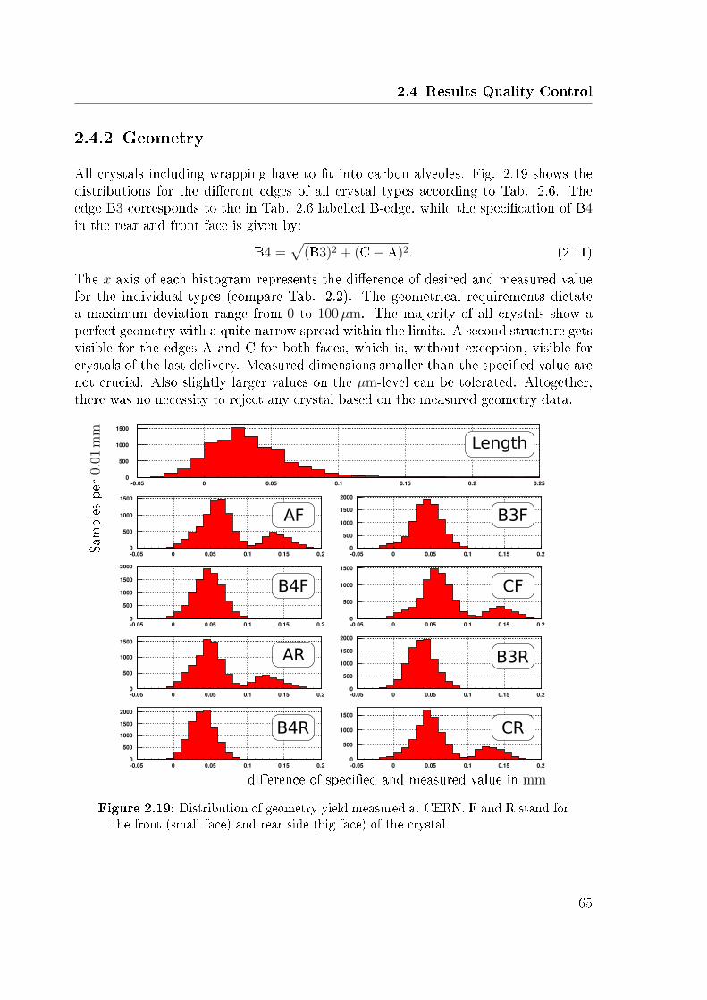
2.4 Results Quality Control
2.4.2 Geometry
All crystals including wrapping have to t into carbon alveoles. Fig. 2.19 shows thedistributions for the dierent edges of all crystal types according to Tab. 2.6. Theedge B3 corresponds to the in Tab. 2.6 labelled B-edge, while the specication of B4in the rear and front face is given by:
B4 =√
(B3)2 + (C− A)2. (2.11)
The x-axis of each histogram represents the dierence of desired and measured valuefor the individual types (compare Tab. 2.2). The geometrical requirements dictatea maximum deviation range from 0 to 100µm. The majority of all crystals show aperfect geometry with a quite narrow spread within the limits. A second structure getsvisible for the edges A and C for both faces, which is, without exception, visible forcrystals of the last delivery. Measured dimensions smaller than the specied value arenot crucial. Also slightly larger values on the µm-level can be tolerated. Altogether,there was no necessity to reject any crystal based on the measured geometry data.
dierence of specied and measured value in mm
Samples
per
0.01
mm
Figure 2.19: Distribution of geometry yield measured at CERN. F and R stand forthe front (small face) and rear side (big face) of the crystal.
65

Chapter 2 Quality Control of PbWO4 Crystals for PANDA
2.4.3 Light Yield
Fig. 2.21 shows the measured light yield data measured at CERN18 and calibratedat Gieÿen. The shown data is distinguished by the level of tapering and starts in thetop row with the least tapered shape: the crystals for the BEC. The spectra showa clear correlation of the obtained values with the crystal geometry. The larger thelevel of tapering, the higher the light yield output. This fact can be explained by theso called NUF19-eect in light collection. For the performed method of calibration,explained in Sec. 2.3.2, the energy deposition occurs in the front part of the crystal,far away from the photo sensor. This non-uniformity is caused by an interplay oflight focussing and absorption, illustrated in Fig. 2.20. Possible corrections of thisNUF-eect and impact on the energy resolution of the EMC are discussed in [31] indetail. The specication concerning light yield is only crucial for crystals for both endcaps, which are almost completely cuboid-shaped. The light yield is the second mostcrucial rejection parameter and 78 crystals show an insucient light output below16 phe
MeV.
CrystalPMT
Light
yield
Distance to
photo-detector
Focusing
Absorption
Figure 2.20: Schematic explanation of the NUF-eect. The further away from thephoto sensor the scintillation light is produced, the higher the nal light output.This originates from focussing, which guides the light towards the sensor. Thenal shape of the NUF-eect is a result of focussing and self absorption of thecrystal. CMS-type crystals with worse quality, have a more U-shaped curve, dueto the higher contribution of absorption.
18European laboratory for particle physics19Non-Uniformity in light collection
66
2.4 Results Quality Control
14 16 18 20 22 24 26 28 30050100150
14 16 18 20 22 24 26 28 300
500
1000
14 16 18 20 22 24 26 28 300
10
20
14 16 18 20 22 24 26 28 300
20
40
14 16 18 20 22 24 26 28 300
50
100
14 16 18 20 22 24 26 28 300
50
100
14 16 18 20 22 24 26 28 30050100150
14 16 18 20 22 24 26 28 300
100
200
EC-R
EC
11
10
9
3
2
1
Light Yield in phe−
MeV
Samples
per
0.5
ph
e−
MeV
Figure 2.21: Distribution of light yield values sorted by the degree of tapering forthe dierent denoted crystal geometries. Only for crystals of both end caps thespecication limit of 16 phe/MeV becomes crucial.
2.4.4 Transversal Transmission
The transversal transmission of a crystal gives an important information about thehomogeneity of a crystal along its axis and is presented in Fig. 2.22 in terms of the∆λ-value (compare Eq. 2.4). The discrepancy between the distributions of CERNand BTCP will be analysed in Sec. 2.4.6. The majority of the shown data are farbelow the requirement of 3 nm, which is strongly related to the improved process ofmanufacturing. 19 crystals do not full the specication.
67
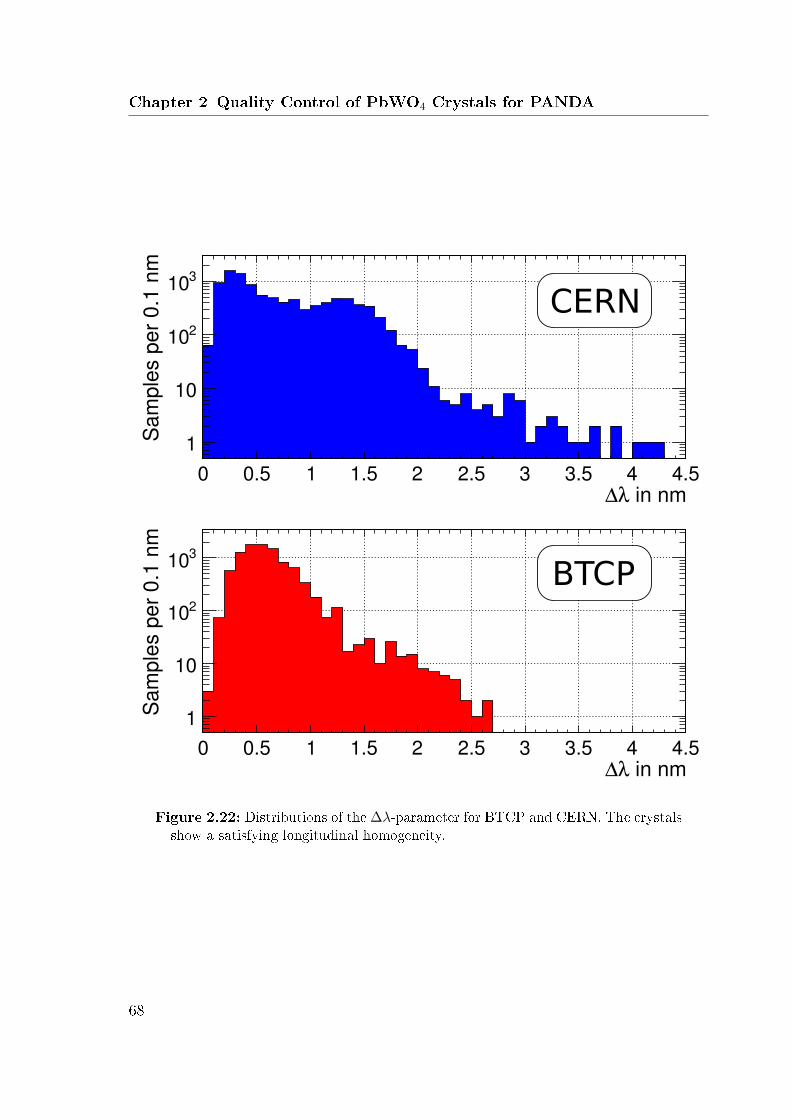
Chapter 2 Quality Control of PbWO4 Crystals for PANDA
Figure 2.22: Distributions of the ∆λ-parameter for BTCP and CERN. The crystalsshow a satisfying longitudinal homogeneity.
68

2.4 Results Quality Control
2.4.5 Radiation Hardness
Fig. 2.23 shows the values for radiation hardness from BTCP and Gieÿen. No notice-able substructure becomes visible due to dierent geometries. For the nal judgementof the quality, the measurements of Gieÿen are deciding. A signicant tail on theright comprises 553 crystals, which have a ∆k above 1.1 m−1. With this value, theradiation hardness is the most crucial parameter with respect to rejection. But on theother side, also very radiation resistive crystals show up. The overall quality in termsof ∆k has been improved by ∼ 30% with respect to CMS-type PWO crystals, whichset the an rejection limit to 1.5 m−1.
Figure 2.23: Distribution of radiation hardness for BTCP and Gieÿen. In average,the data from Gieÿen is slightly shifted compared to the BTCP data (Sec. 2.4.6)
.
69
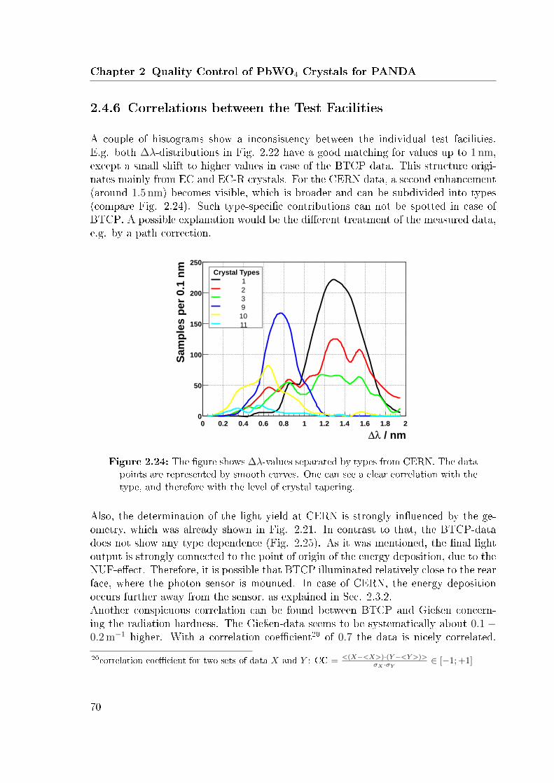
Chapter 2 Quality Control of PbWO4 Crystals for PANDA
2.4.6 Correlations between the Test Facilities
A couple of histograms show a inconsistency between the individual test facilities.E.g. both ∆λ-distributions in Fig. 2.22 have a good matching for values up to 1 nm,except a small shift to higher values in case of the BTCP data. This structure origi-nates mainly from EC and EC-R crystals. For the CERN data, a second enhancement(around 1.5 nm) becomes visible, which is broader and can be subdivided into types(compare Fig. 2.24). Such type-specic contributions can not be spotted in case ofBTCP. A possible explanation would be the dierent treatment of the measured data,e.g. by a path correction.
/ nmλ∆0 0.2 0.4 0.6 0.8 1 1.2 1.4 1.6 1.8 2
Sa
mp
les
pe
r 0
.1 n
m
0
50
100
150
200
250
Crystal Types
1
2
3
9
10
11
Figure 2.24: The gure shows ∆λ-values separated by types from CERN. The datapoints are represented by smooth curves. One can see a clear correlation with thetype, and therefore with the level of crystal tapering.
Also, the determination of the light yield at CERN is strongly inuenced by the ge-ometry, which was already shown in Fig. 2.21. In contrast to that, the BTCP-datadoes not show any type dependence (Fig. 2.25). As it was mentioned, the nal lightoutput is strongly connected to the point of origin of the energy deposition, due to theNUF-eect. Therefore, it is possible that BTCP illuminated relatively close to the rearface, where the photon sensor is mounted. In case of CERN, the energy depositionoccurs further away from the sensor, as explained in Sec. 2.3.2.Another conspicuous correlation can be found between BTCP and Gieÿen concern-ing the radiation hardness. The Gieÿen-data seems to be systematically about 0.1 −0.2 m−1 higher. With a correlation coecient20 of 0.7 the data is nicely correlated.
20correlation coecient for two sets of data X and Y : CC = <(X−<X>)·(Y−<Y>)>σX ·σY
∈ [−1; +1]
70

2.4 Results Quality Control
MeV
phe in CERNLY
14 16 18 20 22 24 26 28 30
MeV
phe
in
BT
CP
LY
15
16
17
18
19
20
21
22
23
0
20
40
60
80
100
120
Figure 2.25: Light Yield correlation between BTCP and CERN. Only the CERNdata shows a strong type dependence.
Such a constant shift is caused by the not fully identical test procedure. Possiblevariation could occur by the dose rate or the time between irradiation and the secondtransmission measurement. This duration was not xed in the contract with BTCP.The latter one has a big impact on the measured ∆k due to the existence of a fastrecovery component at room temperature (Fig. 2.15). This parameter was initiallynot xed in the contract for the crystal delivery.
1 / m
Giessenk∆
0 0.2 0.4 0.6 0.8 1 1.2 1.4 1.6
1 / m
BT
CP
k∆
0
0.2
0.4
0.6
0.8
1
0
10
20
30
40
50
60
Figure 2.26: ∆k correlation at 420 nm between BTCP and Gieÿen.
A further point is the longitudinal transmission for all facilities of the relevant wave-lengths (Fig. 2.27). The data from Gieÿen and CERN are in relatively good agreement,whereas the correlation to BTCP is much smaller. Moreover, the particular distribu-tions from Gieÿen are broader (compare Fig. 2.18). This is probably connected to thenon-perfect reproducibility of the crystal position in the photospectrometer.It can be concluded, that the main contribution to the discrepancies, is mainly caused
71

Chapter 2 Quality Control of PbWO4 Crystals for PANDA
at 360 nm in %Giessen
T
42 44 46 48 50 52 54
at 360 n
m in %
BT
CP
T
42
44
46
48
50
52
54
0
5
10
15
20
25
30
35
CC = 0.097
at 360 nm in %Giessen
T
42 44 46 48 50 52 54
at 360 n
m in %
CE
RN
T
42
44
46
48
50
52
54
0
5
10
15
20
25
30
35
40
CC = 0.518
at 420 nm in %Giessen
T
66 68 70 72 74
at 420 n
m in %
BT
CP
T
66
68
70
72
74
0
20
40
60
80
100
120
CC = 0.076
at 420 nm in %Giessen
T
66 68 70 72 74
at 420 n
m in %
CE
RN
T
66
68
70
72
74
0
20
40
60
80
100
120
CC = 0.267
at 620 nm in %Giessen
T
72 73 74 75 76 77 78
at 620 n
m in %
BT
CP
T
72
74
76
78
80
82
0
20
40
60
80
100
120
CC = 0.021
at 620 nm in %Giessen
T
72 73 74 75 76 77 78
at 620 n
m in %
CE
RN
T
72
74
76
78
80
82
0
20
40
60
80
100
120
140
CC = 0.027
Figure 2.27: The left column shows the correlation between BTCP and Gieÿendata for the three relevant wavelengths. In the right column, the measured valuesfrom CERN and Gieÿen are compared. The latter ones are more correlated thanthe data sets in the left column. The general correlation gets worse at 620 nm,since here the values are distributed much narrower.
72
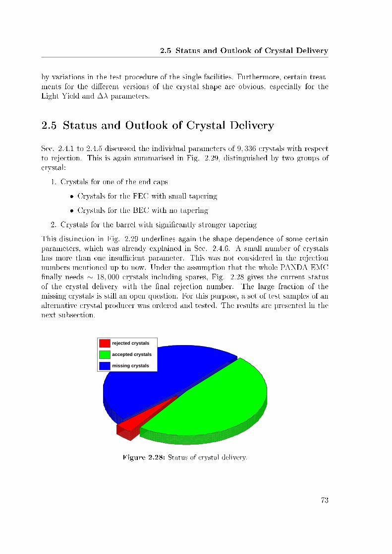
2.5 Status and Outlook of Crystal Delivery
by variations in the test procedure of the single facilities. Furthermore, certain treat-ments for the dierent versions of the crystal shape are obvious, especially for theLight Yield and ∆λ parameters.
2.5 Status and Outlook of Crystal Delivery
Sec. 2.4.1 to 2.4.5 discussed the individual parameters of 9, 336 crystals with respectto rejection. This is again summarised in Fig. 2.29, distinguished by two groups ofcrystal:
1. Crystals for one of the end caps
Crystals for the FEC with small tapering
Crystals for the BEC with no tapering
2. Crystals for the barrel with signicantly stronger tapering
This distinction in Fig. 2.29 underlines again the shape dependence of some certainparameters, which was already explained in Sec. 2.4.6. A small number of crystalshas more than one insucient parameter. This was not considered in the rejectionnumbers mentioned up to now. Under the assumption that the whole PANDA EMCnally needs ∼ 18, 000 crystals including spares, Fig. 2.28 gives the current statusof the crystal delivery with the nal rejection number. The large fraction of themissing crystals is still an open question. For this purpose, a set of test samples of analternative crystal producer was ordered and tested. The results are presented in thenext subsection.
rejected crystals
accepted crystals
missing crystals
Pie with radial labels
Figure 2.28: Status of crystal delivery.
73

Chapter 2 Quality Control of PbWO4 Crystals for PANDA
accepted Transmission TransversalTransmission
Light Yield RadiationHardness
0
50
100
150
200
250
300
4500
4800
5100
Am
ount
of c
ryst
als
Reason for rejection
EC+ECR-Crystals≈ 92.8%
≈ 0.2% 0%
≈ 1.5%
≈ 5.7%
(a) A summary of all crystals of both end caps of the EMC, which comprise 5, 100 crys-tals. These crystals have specic problems for the LY, since the focussing eect is lesspronounced (compare Sec. 2.4.3).
accepted Transmission TransversalTransmission
Light Yield RadiationHardness
0
50
100
150
200
250
300
3900
4200
Am
ount
of c
ryst
als
Reason for rejection
Barrel Crystals≈ 93.2%
≈ 0.1%≈ 0.45% 0%
≈ 6.2%
(b) A summary of all crystals of the barrel part of the EMC, which comprise 4, 236 crystals.As it was shown in Sec. 2.4.6, there is a type dependence for the measurements of the ∆λand this parameter gets worse for more tapered crystals.
Figure 2.29: Summary of the reason of rejection for altogether 9, 336 crystals, dis-tinguished by less tapered (EC and EC-R) and strong tapered crystals for thebarrel. The marked information in percent does not consider any overlappingbetween the reasons of rejection. One can see, that the transmission and the ra-diation hardness are rejected to the same fraction and no geometrical dependencebecomes visible.
74
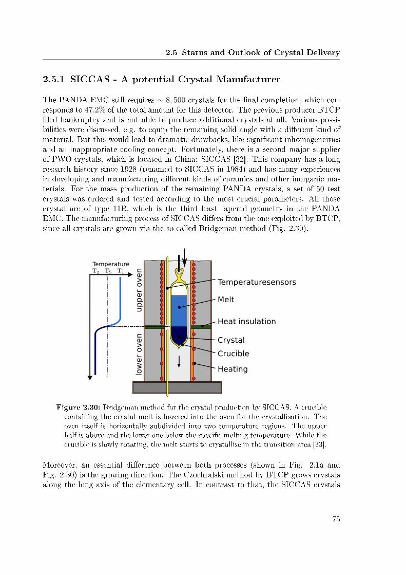
2.5 Status and Outlook of Crystal Delivery
2.5.1 SICCAS - A potential Crystal Manufacturer
The PANDA EMC still requires ∼ 8, 500 crystals for the nal completion, which cor-responds to 47.2% of the total amount for this detector. The previous producer BTCPled bankruptcy and is not able to produce additional crystals at all. Various possi-bilities were discussed, e.g. to equip the remaining solid angle with a dierent kind ofmaterial. But this would lead to dramatic drawbacks, like signicant inhomogeneitiesand an inappropriate cooling concept. Fortunately, there is a second major supplierof PWO crystals, which is located in China: SICCAS [32]. This company has a longresearch history since 1928 (renamed to SICCAS in 1984) and has many experiencesin developing and manufacturing dierent kinds of ceramics and other inorganic ma-terials. For the mass production of the remaining PANDA crystals, a set of 50 testcrystals was ordered and tested according to the most crucial parameters. All thosecrystal are of type 11R, which is the third least tapered geometry in the PANDAEMC. The manufacturing process of SICCAS diers from the one exploited by BTCP,since all crystals are grown via the so called Bridgeman method (Fig. 2.30).
Figure 2.30: Bridgeman method for the crystal production by SICCAS. A cruciblecontaining the crystal melt is lowered into the oven for the crystallisation. Theoven itself is horizontally subdivided into two temperature regions. The upperhalf is above and the lower one below the specic melting temperature. While thecrucible is slowly rotating, the melt starts to crystallise in the transition area [33].
Moreover, an essential dierence between both processes (shown in Fig. 2.1a andFig. 2.30) is the growing direction. The Czochralski method by BTCP grows crystalsalong the long axis of the elementary cell. In contrast to that, the SICCAS crystals
75

Chapter 2 Quality Control of PbWO4 Crystals for PANDA
are grown along the small crystal axis, which has a dierent index of refraction. Thedierent indices of refraction and the connected maximum transmission according toEq. 2.3 for ordinary and extraordinary direction are displayed in Fig. 2.31.
Wavelength in nm400 450 500 550 600 650 700
Tra
nsm
issio
n in
%
66
68
70
72
74
76
78
80
Index of refraction ordinary axis
Index of refraction extraordinary axis
ordinary axismaxT
extraordinary axismaxT
Ind
ices o
f refr
acti
on
2.1
2.2
2.3
2.4
2.5
Figure 2.31: Indices of refraction for PWO for ordinary and extraordinary direction.The large dierence between the indices already causes a signicant change inthe maximum transmission without absorption. The values for the indices wereobtained by [30].
In the following, the results for the 50 test samples are presented and discussed forthe longitudinal transmission, LY, homogeneity of the transversal transmission andthe radiation hardness.
76

2.5 Status and Outlook of Crystal Delivery
2.5.1.1 Results of the tested Parameters
The longitudinal transmission for the crystals from SICCAS was independently mea-sured by CERN and Gieÿen (Fig. 2.32).
Figure 2.32: Longitudinal transmission for the 50 test samples from SICCAS mea-sured at CERN and Gieÿen. The specication limits are drawn in correspondingcolour.
The data from both facilities is nicely correlated, whereas the measurements fromGieÿen show the typical wider spread. One can directly see that the transmissionvalues are signicantly lower compared to crystals from BTCP (compare Fig. 2.18).This does not need to be an indication for reduced quality. As it was explained before,SICCAS grows crystals along the extraordinary direction, which has a higher index ofrefraction. This circumstance directly leads to a reduction of the longitudinal trans-mission.The homogeneity of the transversal transmission in terms of ∆λ was only measuredat CERN. The values are distributed much broader, compared to the presented datain Fig. 2.22, but here one has to take into account the tapered shape of the type 11crystals and the type-dependence on the ∆λ-values measured by CERN. Neverthe-less, 16% of the crystals are above the specication limit of 3 nm, which is a signicant
77
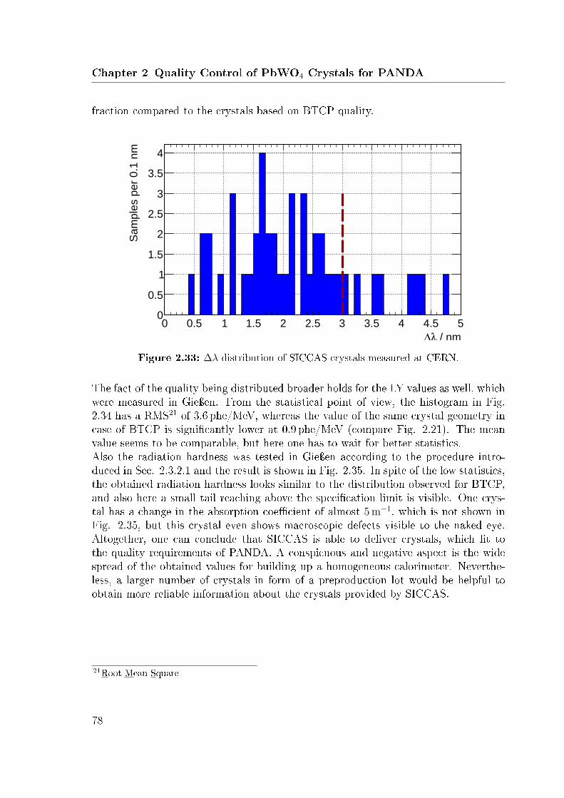
Chapter 2 Quality Control of PbWO4 Crystals for PANDA
fraction compared to the crystals based on BTCP quality.
/ nmλ∆
0 0.5 1 1.5 2 2.5 3 3.5 4 4.5 5
Sam
ple
s p
er
0.1
nm
0
0.5
1
1.5
2
2.5
3
3.5
4
Figure 2.33: ∆λ distribution of SICCAS crystals measured at CERN.
The fact of the quality being distributed broader holds for the LY values as well, whichwere measured in Gieÿen. From the statistical point of view, the histogram in Fig.2.34 has a RMS21 of 3.6 phe/MeV, whereas the value of the same crystal geometry incase of BTCP is signicantly lower at 0.9 phe/MeV (compare Fig. 2.21). The meanvalue seems to be comparable, but here one has to wait for better statistics.Also the radiation hardness was tested in Gieÿen according to the procedure intro-duced in Sec. 2.3.2.1 and the result is shown in Fig. 2.35. In spite of the low statistics,the obtained radiation hardness looks similar to the distribution observed for BTCP,and also here a small tail reaching above the specication limit is visible. One crys-tal has a change in the absorption coecient of almost 5 m−1, which is not shown inFig. 2.35, but this crystal even shows macroscopic defects visible to the naked eye.Altogether, one can conclude that SICCAS is able to deliver crystals, which t tothe quality requirements of PANDA. A conspicuous and negative aspect is the widespread of the obtained values for building up a homogeneous calorimeter. Neverthe-less, a larger number of crystals in form of a preproduction lot would be helpful toobtain more reliable information about the crystals provided by SICCAS.
21Root Mean Square
78

2.5 Status and Outlook of Crystal Delivery
MeV
pheLY in
10 12 14 16 18 20 22 24 26 28
MeV
phe
Sam
ple
s p
er
0.5
0
1
2
3
4
5
Figure 2.34: LY distribution of SICCAS crystals measured in Gieÿen.
1k / m∆
0 0.2 0.4 0.6 0.8 1 1.2 1.4 1.6
1S
am
ple
s p
er
0.1
m
0
1
2
3
4
5
6
7
8
9
Figure 2.35: ∆k distribution of SICCAS crystals measured in Gieÿen.
79


Chapter 3
Beamtimes with PROTO60
To verify the envisaged performance, mechanical stability and the thermal robust-ness of the EMC (listed in Tab. 1.7), a rst real-size prototype was build up, calledPROTO60, which comes very close to the nal conception. Several response mea-surements were carried out at MAMI1 and CERN with photons, leptons and muonsfocussing on dierent aspects. This chapter serves as an introduction to the achievedresults, presented in Sec. 4 and 5. At rst, the setup of PROTO60 is presented,including geometrical arrangement and used materials for the single parts, as well asthe used readout chain and the signal extraction. Furthermore, the individual teststations at MAMI and CERN will be shown with a detailed outlook on the aims forthese particular runs.
3.1 PROTO60
The rst real-size prototype of the future PANDA EMC is the PROTO60 and consistsof 60 PWO crystals, arranged in 10 columns and 6 rows. All implemented crystals havetype 6 geometry (compare Tab. 2.2), which corresponds to a polar angle of roughly45 (135 ) in the barrel region. The barrel part represented by the PROTO60 ismarked in red in Fig. 3.1, with the small dierence, that the PROTO60 has 6 rowswith the same geometry. This is not true for the nal EMC, since maximum 4 rowswith the same shape are grouped together. In the following subsections dierent as-pects of the construction of this prototype are discussed in more detail, ranging fromthe mechanical structure up to the realised data acquisition (based on [34]).
1Mainzer Mikrotron
81

Chapter 3 Beamtimes with PROTO60
Figure 3.1: The barrel part covers the polar angle region from 22 to 140 andconsists of 16 slices. Each slice is composed of 710 crystals, arranged in a 10× 71matrix. The long axis of one slice is divided in 6 subgroups, indicated with dashedrounded rectangles, containing crystal types with appropriate tapering. In orderto minimise energy deposition in dead material, all crystals are pointing o thevertex point by about 4 , which is also true for the azimuthal direction. The partof the slice framed in red in the upper part of the picture is represented by thePROTO60.
82

3.1 PROTO60
3.1.1 Mechanical Structure
At rst, a single crystal has to be wrapped properly with a foil in order to optimise thelight collection in it and to avoid optical cross talk. In case of PANDA, VM2000 (alsoknown as ESR2-lm) was chosen, which is quite mirror-like with a reection coecientat 440 nm of 0.944 and a thickness of 65µm [35]. Moreover, VM2000 is non-metallicand basically a multilayer polymer. Altogether, the crystals including geometricaluncertainties and wrapping have to t into carbon alveoles. Fig. 3.2 illustrates theexpected occupied space between two crystals.
Figure 3.2: Each crystal has a geometrical tolerance of +0/ − 100µm. The gapof 150µm considers mechanical tolerances (50µm) and deformation of the alve-oles (100µm). Altogether the distance between the borders of two neighbouringcrystals is in the order of 680µm [34].
After wrapping, the back side of a crystal is outtted with an LAAPD. The couplingbetween crystal and sensor is realised by optical grease with an index of refractionclose to 1.5 at 420 nm. This has the purpose to avoid an air gap, which would causean additional reduction of the collected scintillation light. In contrast to the nalenvisaged rectangular shape of the LAAPD, the crystals of PROTO60 are equippedwith quadratic LAAPDs with an eective area of 1 cm2. Furthermore, the LAAPDsare xed in central position by black capsules made of plastic. For the connectionto the preampliers, shielded twisted pair wires are fed through an opening of thecapsules. Two pairs of left and right crystals are grouped to a subunit of four crystals(Fig. 3.3a), which is subsequently placed into the carbon alveoles including aluminiuminserts Fig. 3.3b.The aluminium inserts are mandatory for the mechanical stability of the prototype.They are glued to the alveoles and have to carry the weight of the 6 × 10 matrix ofcrystals with ∼ 1 kg each. Moreover, the aluminium structure integrates the coolingsystem, the electronics and the possibility of a monitoring system to control the prop-erties of the PWO crystals by constant light pulses fed in via optical bres. All the
2Enhanced Specular Reector
83

Chapter 3 Beamtimes with PROTO60
(a)
(b)
Figure 3.3: (a) A packed subgroup of four crystals including wrapping, photo sensorplus capsule and connection to the outside. (b) Carbon alveole assembly withaluminium inserts for mounting and holding the packs of crystals in Fig. 3.3a.
84

3.1 PROTO60
mentioned elements are mounted on a support frame, which simplies the transporta-tion to various test experiments. In addition, the whole prototype including supportstructure can be placed on a so called x − y-table for a two-dimensional alignmentrelative to the impinging beam.
3.1.2 Cooling and Electronics
As it was mentioned in Sec. 1.3, the whole calorimeter will be cooled down to a tem-perature of −25 C. Therefore, also the prototype has to be cooled to come as close aspossible to the nal condition in order to gain experiences with cooling stability andthe actual performance. The cooling itself is realised by a chiller3 for achieving therequired thermal power of 80 W. The chiller recirculates the cooling uid, which owsin copper serpentine through the prototype. The whole prototype, except the frontpart, is thermally insulated with a 4 cm thick styrene foam layer and in addition sur-rounded with a gas-tight plastic skin to avoid ice formation (compare Fig. 3.4). Thefront part of the prototype is enclosed vacuum tight by a prototype insulation panel,composed of a sandwich-like structure of two skins of aluminium and one carbon-brelayer. The applied vacuum of ∼ 2 · 10−2 mbar within this structure has a conductioncoecient of lower than 2 ·10−2 mW
mKand allows a reduction of the insulation from 4 cm
to 2 cm. A set of 13 thermocouple elements controls and records the temperature atdierent selected positions within the prototype. It is veried that the temperaturevariation of the crystals stays within ±0.05 C.Each crystal of the PROTO60 is equipped with one quadratic LAAPD of type S8664-1010SPL. The technical data for this type of photo sensor is given in Tab. 3.1.
Parameter
eective area 100 mm2
spectral response range 320− 1000 nmQE at 420 nm 70 %capacitance 270 pFmaximum gain ∼ 500operating voltage ∼ 350 V
Table 3.1: LAAPD properties in PROTO60 [36].
The signals from the LAAPDs are forwarded to the LNP-P type preampliers (com-pare Sec. 1.3.5.2), where four items are grouped together on one PCB4 and screwed
3supplied by Julabo4Printed Circuit Board
85

Chapter 3 Beamtimes with PROTO60
on the inserts. Supply voltage for photo sensors and preampliers, as well as signallines, are provided by additional back-PCBs, which traverse the transition of cold andwarm volume via narrow slights.
Figure 3.4: Back view of PROTO60 with all mounted crystals and some par-tially mounted components marked and labelled with corresponding colours. Twocolumns of the PROTO60 comprising 12 crystals are covered by one back-PCB.
3.1.3 Readout and Data Acquisition
The intention of this subsection is to illustrate the path of the obtained primary signalof the photo sensor to the digitisation. In all beamtimes, performed at MAMI andCERN, the readout chain was slightly modied due to trigger aspects and the digiti-sation procedure and will be discussed in more detail. At rst, the scintillation lightof the PWO is converted by the LAAPD to a charge pulse and subsequently ampli-ed by one of the LNP-P preamplier. For the beamtime at MAMI, the subsequentprocessing of the signals is displayed in Fig. 3.5 and the used components are listed
86

3.1 PROTO60
in Tab. 3.2.
Figure 3.5: Readout chain PROTO60 at Mainz in 2010.
Each crystal of the PROTO60 is equipped with one quadratic LAAPD of type S8664-1010SPL. The technical data for this type of photo sensor is given in Tab. 3.1. Theindividual signals of crystal and LAAPD are amplied, shaped and discriminated byan spectroscopy amplier (MSCF16). The shaped and amplied trace output is pro-cessed by PS-ADCs5, where the amplitude is determined and digitised for the energyinformation. The time stamp is obtained by an internal CFD6 of the spectroscopyamplier and is digitised by TDCs. Furthermore, a binary trigger signal is provided,which is in principle created by an OR of all crystals and contributes to the nalcoincidence condition (beamtime Mainz 2010). An overview of the trigger conditionsfor all beamtimes, obtained by the detectors, is provided in Tab. 3.3. The secondbranch for the coincidence originates from the tagger, which delivers a logical OR ofthe responding tagger channels. Moreover, a time stamp is digitised and recorded bymeans of a TDC. Functionality and setup of the tagger is described in Sec. 3.2.1.After the AND of the coincidence requirement, an additional OR module allows theplug in of a pulser for test purposes or further detectors for calibration purposes, e.g.via cosmic radiation. If the combined logical signal is true, a xed time gate for the
5Peak Sensing - Analogue to Digital Converters6Constant-Fraction Discriminator
87
Chapter 3 Beamtimes with PROTO60
Component Quantity Type
ECL/NIM 4 LeCroy 4616FAN IN / FAN OUT 2 LeCroy 429ADual Gate Generator 1 LeCroy 222Octal Discriminator 1 LeCroy 623BQuad Coincidence Unit 1 LeCroy 622Spectroscopy Amplier 4 Mesytec MSCF-16Discriminator 1 LeCroy 4413Delay 6 GSI 1610PS-ADC 4 CAEN V785TDC 3 CAEN V775
Table 3.2: Components of the PROTO60 readout.
readout of the PS-ADCs and TDCs is initiated. A special IOL7-module blocks thereadout for a certain time window and waits for the next trigger afterwards.For the CERN beamtime in 2011, the existing readout chain was signicantly modied.The trigger was provided by an external detector, which is shown in Sec. 3.2.2. TDCsand PS-ADCs were exchanged with a 16-bit SADCs (SIS3302) supplied by Struck. Incontrast to the PS-ADCs, a SADCs records the response for a predened time win-dow. The converting of the stored SADC signals (or the so called traces) for obtainingtime and energy information is explained in 3.1.4. In the mode used for this SADC,the input range is in the order of 5 V, for signals arriving from the preamplier. Thesampling rate was chosen to 50 MHz, which corresponds to a time fragmentation of20 ns and is proven to be sucient for achieving the required time resolution.
3.1.4 Signal Treatment of SADC data
In the nal stage of the readout chain for the PANDA EMC, the digitised signalsfrom the ADCs8 will be processed by FPGAs9, for the extraction of time and energyinformation. This has to be realised by a fast and robust algorithm, the so calledfeature-extraction algorithm. Fig. 3.6 explains schematically the path from the rawdata, obtained by the LNP-P preamplier, to the relevant observables energy andtime.
For test purposes, the data from the SADC was stored and analysed oine with animplementation of the mentioned algorithm via software. The following shows the
7Input Output Logic8Analogue to Digital Converters9Field Programmable Gate Arrayss
88

3.1 PROTO60
Figure 3.6: Schematic explanation of feature extraction. After the MWD-step theobtained trace is modied for extracting the energy and time separately.
single steps and how the relevant information is extracted. The chosen values for theinput parameters of M , τ , L, D and R for this algorithm are based on [37] and willbe explained in the relevant sections of the algorithm.The signal of a crystal for one event is displayed exemplary in Fig. 3.7 and consistsof 250 time bins with a single width of 20 ns. Due to the relatively long decay time ofthe LNP-P preamplier signal in the order of ∼ 25µs, it has to be shaped to reducethe pile-up probability of signals occurring in a short time sequence. This is done bythe rst step of the feature extraction algorithm, which is called MWD10 and can bedetermined by Eq. 3.1, in which x(n) is the bin content of channel n and xMWD(n)the output of the MWD-step for channel n. M denes the nal length of the outputpulse and should be larger than the rising part of the raw signal. This was chosen to20 corresponding to 400 ns. τ is the decay constant of the LNP-P preamplier signaland has a value of 1, 250 channels (25µs).
xMWD(n) = x(n)− x(n−M) +ln(2)
τ
n−1∑i=n−M
x(i) (3.1)
Fig. 3.8 shows a comparison of the same data like in 3.7, before and after applyingthe MWD-step.The obtained trace, shown in Fig. 3.8b, is the initial point for the next iterations
of the feature extraction. The next step, called MA11, is responsible for reducing thenoise level with the smoothing length L. For each channel with the index n, the newcontent is calculated by summing up the channels ranging from n− L to n:
xMA(n) =n∑
i=n−L
xMWD(i). (3.2)
10Moving Window Deconvolution11Moving Average
89

Chapter 3 Beamtimes with PROTO60
FADC_raw28
Channel Number
0 50 100 150 200 250
Sig
na
l H
eig
ht
in a
.u.
10000
15000
20000
25000
30000
35000
FADC_raw28
Figure 3.7: Raw data of an SADC for a randomly chosen crystal with a highenergy deposition of 10 GeV via positrons. The shown data corresponds to thedirect output of the LNP-P preamplier. The supply voltage of the LAAPD wasadjusted in such a way that the highest signals to be expected signals t into thedynamic range of the SADC of 40, 000. Each channel on the horizontal axis hasa size of 20 ns, which results in an overall time window of 5µs.
FADC_raw28
Channel Number100 110 120 130 140 150
Sig
nal H
eig
ht in
a.u
.
10000
15000
20000
25000
30000
35000
FADC_raw28
(a)
FADC_mwd28
Entries 250Mean 128RMS 5.377
Channel Number
100 110 120 130 140 150
Sig
nal H
eig
ht in
a.u
.
0
5000
10000
15000
20000
25000
FADC_mwd28
Entries 250Mean 128RMS 5.377
(b)
Figure 3.8: Visualisation of the MWD-step for a zoomed region of the SADC. (a)Unshaped output signal of the LNP-P preamplier. (b) Shaped output signal ofthe LNP-P preamplier according to Eq. 3.1.
90

3.1 PROTO60
Only for low energetic signals, with a small signal to noise ratio, the MA-step becomesmandatory. For a high-energetic signal the actual shape stays almost identical (com-pare 3.8b and g:masignal), except the amplitude.The maximum amplitude of Fig. 3.9, which linearly scales with the detected energy,
Figure 3.9: Shaped and smoothed signal of the LNP-P preamplier. The baseline,which is represented by the dotted red line in the bottom part of the gure, isdetermined by averaging the channels in the range from 40 to 100. The solid linestands for the determined maximum amplitude of the signal and is subsequentlyused as energy information.
is nally determined with a simple software algorithm. For Fig. 3.9, the obtainedamplitude with respect to the baseline is in the order of ∼ 38, 000 a.u.. For getting astatement of the corresponding energy in terms of eV, the amplitude has to be cali-brated (compare Sec. 4.1).For getting a time information of the single event, the data of Fig. 3.8b has to betreated in a dierent way, independently from the MA-step. Therefore, the basic func-tionality of a conventional CFD-module is simulated by the CFT12-step (Eq. 3.3). Thesignal out of the MWD-step is delayed by D = 5 channels = 100 ns, scaled by a certainfactor R and subtracted from the original signal. It turned out, that R = 0.45 is anoptimal value [34].
xCFT(n) = xMWD(n−D)−R · xMWD(n) (3.3)
12Constant-Fraction Timing
91
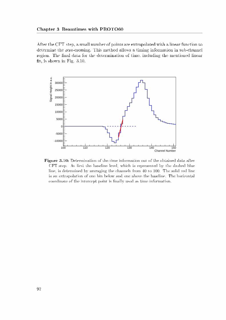
Chapter 3 Beamtimes with PROTO60
After the CFT-step, a small number of points are extrapolated with a linear function todetermine the zero-crossing. This method allows a timing information in sub-channelregion. The nal data for the determination of time, including the mentioned lineart, is shown in Fig. 3.10.
FADC_mwd_ma_cft28
Entries 250Mean 133.7RMS 6.244
Channel Number100 110 120 130 140 150
Sig
na
l H
eig
ht
in a
.u.
10000
5000
0
5000
10000
15000
20000
25000
30000
FADC_mwd_ma_cft28
Entries 250Mean 133.7RMS 6.244
Figure 3.10: Determination of the time information out of the obtained data afterCFT-step. At rst the baseline level, which is represented by the dashed blueline, is determined by averaging the channels from 40 to 100. The solid red lineis an extrapolation of one bin below and one above the baseline. The horizontalcoordinate of the intercept point is nally used as time information.
92
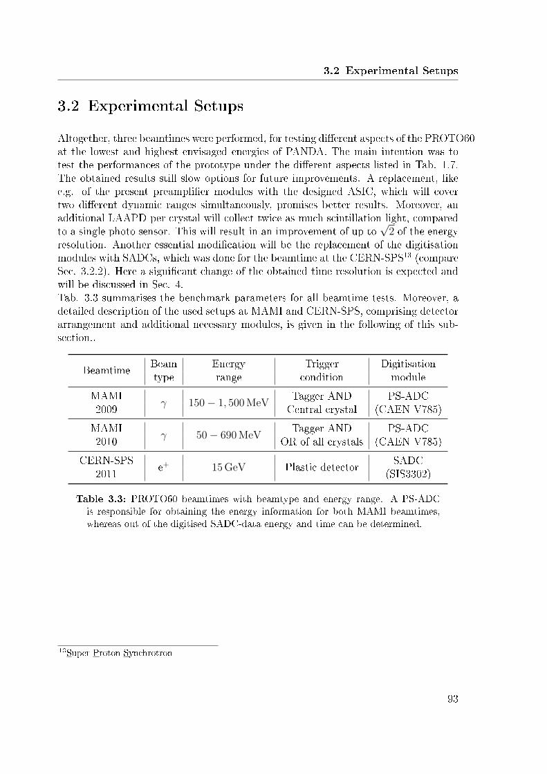
3.2 Experimental Setups
3.2 Experimental Setups
Altogether, three beamtimes were performed, for testing dierent aspects of the PROTO60at the lowest and highest envisaged energies of PANDA. The main intention was totest the performances of the prototype under the dierent aspects listed in Tab. 1.7.The obtained results still slow options for future improvements. A replacement, likee.g. of the present preamplier modules with the designed ASIC, which will covertwo dierent dynamic ranges simultaneously, promises better results. Moreover, anadditional LAAPD per crystal will collect twice as much scintillation light, comparedto a single photo sensor. This will result in an improvement of up to
√2 of the energy
resolution. Another essential modication will be the replacement of the digitisationmodules with SADCs, which was done for the beamtime at the CERN-SPS13 (compareSec. 3.2.2). Here a signicant change of the obtained time resolution is expected andwill be discussed in Sec. 4.Tab. 3.3 summarises the benchmark parameters for all beamtime tests. Moreover, adetailed description of the used setups at MAMI and CERN-SPS, comprising detectorarrangement and additional necessary modules, is given in the following of this sub-section..
BeamtimeBeam Energy Trigger Digitisationtype range condition module
MAMIγ 150− 1, 500 MeV
Tagger AND PS-ADC2009 Central crystal (CAEN V785)
MAMIγ 50− 690 MeV
Tagger AND PS-ADC2010 OR of all crystals (CAEN V785)
CERN-SPSe+ 15 GeV Plastic detector
SADC2011 (SIS3302)
Table 3.3: PROTO60 beamtimes with beamtype and energy range. A PS-ADCis responsible for obtaining the energy information for both MAMI beamtimes,whereas out of the digitised SADC-data energy and time can be determined.
13Super Proton Synchrotron
93

Chapter 3 Beamtimes with PROTO60
3.2.1 MAMI
In 2009 and 2010, the rst two beamtime tests were carried out at the A2 experimentalhall in the Institut für Kernphysik of the Johannes Gutenberg University in Mainz,Germany. An energy tagged bremsstrahlung photon beam is produced by the MAMIelectron accelerator, in combination with the Glasgow Tagged Photon Spectrometer(Tagger). Both constituents will be discussed in the following and can be found onthe oor plan of the facility (Fig. 3.11). Basically, the MAMI facility consists of an
Figure 3.11: Floor plan of the MAMI accelerator facility at Mainz comprising theexperimental halls A1, A2, A3 and X1. The position of the PROTO60 for bothbeamtimes and the Tagger system are marked.
injector LINAC14 and three RTMs15, providing electron beams of 100µA up to anenergy of 1.5 GeV since 1991. At rst, the LINAC supplies electrons with an energyof 3.97 MeV which are accelerated stepwise by the single RTMs, according to Tab.
14Linear Accelerator15Race Track Microtrons
94

3.2 Experimental Setups
3.4. In 2006, an upgrade of the existing facility was realised by a fourth stage of theaccelerator structure, the HDSM16. Thus, energies up to 1.5 GeV became available.MAMI supplies continuous electron beams of the experimental halls (A1, A2, A4, X1),situated at the research facility in Fig. 3.11.
3.2.1.1 RTMs and HDSM
The MAMI acceleration facility comprises three RTMs with a similar functionality.Fig. 3.12 shows the basic setup of a RTM. An electron beam with a certain energyis injected and recirculates several times through the RTM. In each cycle, the beampasses RF17-cavities, in which the energy is increased stepwise by ∆E. Here thedierence in time between each recirculation loop has to be an exact integer multipleof the period of the RF supply. In Fig. 3.12 the grey coloured areas correspond to aconstant magnetic eld (∆B/B ≤ 10−4) for bending the beam back to the RTM. Due
Figure 3.12: General layout of a RTM. The electron beam enters the RTM withan energy EInj and leaves it after N cycles with EExt. In each cycle, the energygain is ∆E, while passing the cavities.
to the unchanged magnetic eld B the bending radius R of the beam with velocity
16Harmonic Double-Sided Microtron17Radio Frequency
95
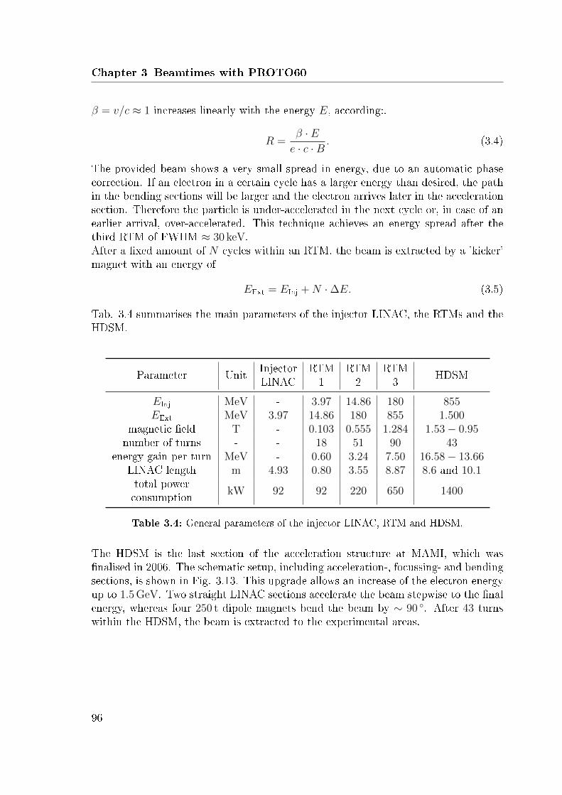
Chapter 3 Beamtimes with PROTO60
β = v/c ≈ 1 increases linearly with the energy E, according:.
R =β · Ee · c ·B
. (3.4)
The provided beam shows a very small spread in energy, due to an automatic phasecorrection. If an electron in a certain cycle has a larger energy than desired, the pathin the bending sections will be larger and the electron arrives later in the accelerationsection. Therefore the particle is under-accelerated in the next cycle or, in case of anearlier arrival, over-accelerated. This technique achieves an energy spread after thethird RTM of FWHM ≈ 30 keV.After a xed amount of N cycles within an RTM, the beam is extracted by a 'kicker'magnet with an energy of
EExt = EInj +N ·∆E. (3.5)
Tab. 3.4 summarises the main parameters of the injector LINAC, the RTMs and theHDSM.
Parameter UnitInjector RTM RTM RTM
HDSMLINAC 1 2 3
EInj MeV - 3.97 14.86 180 855EExt MeV 3.97 14.86 180 855 1.500
magnetic eld T - 0.103 0.555 1.284 1.53− 0.95number of turns - - 18 51 90 43
energy gain per turn MeV - 0.60 3.24 7.50 16.58− 13.66LINAC length m 4.93 0.80 3.55 8.87 8.6 and 10.1total powerconsumption
kW 92 92 220 650 1400
Table 3.4: General parameters of the injector LINAC, RTM and HDSM.
The HDSM is the last section of the acceleration structure at MAMI, which wasnalised in 2006. The schematic setup, including acceleration-, focussing- and bendingsections, is shown in Fig. 3.13. This upgrade allows an increase of the electron energyup to 1.5 GeV. Two straight LINAC sections accelerate the beam stepwise to the nalenergy, whereas four 250 t dipole magnets bend the beam by ∼ 90 . After 43 turnswithin the HDSM, the beam is extracted to the experimental areas.
96

3.2 Experimental Setups
Figure 3.13: Schematic layout of the HDSM. Four dipole magnets bend the beamabout 90 , whereas two LINACs are responsible for the stepwise acceleration.
3.2.1.2 The Glasgow Photon Tagging Spectrometer
The tagging system of the MAMI acceleration facility (Fig. 3.14) converts the electronbeam into a continuous and collimated photon beam [38]. The electrons with energiesof up to 1.5 GeV impinge on an exchangeable radiator made out of copper or diamondfor the production of bremsstrahlung photons, according to the process explained inSec. 1.3.1.1. The electrons are subsequently bent by a magnetic eld of a dipolemagnet with a ux of B = 1.8 T and detected in the focal plane, which basicallyconsists of 353 overlapping plastic detectors. The higher the bending radius of theelectrons, the lower is the energy of the created photon. With the knowledge of theinitial energy E0 and the bending radius r of the electrons in the dipole magnet, theenergy of the resulting photon beam is determined due to energy conservation:
Eγ = E0 − Ee− (3.6)
with Ee− =√
(qBcr)2 + (m0c2)2 ∼ r,
where q and m0 is the charge and the mass at rest of an electron, respectively, and cthe speed of light. The energy range of the tagging system depends on the maximumoperating energy of the accelerator. If the HDSM is included, energy marked photonsup to 1.5 GeV are available with an accuracy of 4 MeV. In the low energy regionup to 820 MeV, the error bars of the tagger are reduce to 2 MeV depending on themomentum range of the individual plastic scintillator covering the focal plane. Thereadout of the focal plane detectors is done by conventional Hamamatsu PMTs, withinthe stray eld (∼ 0.01 T) of the dipole magnet. The obtained signal is discriminated
97
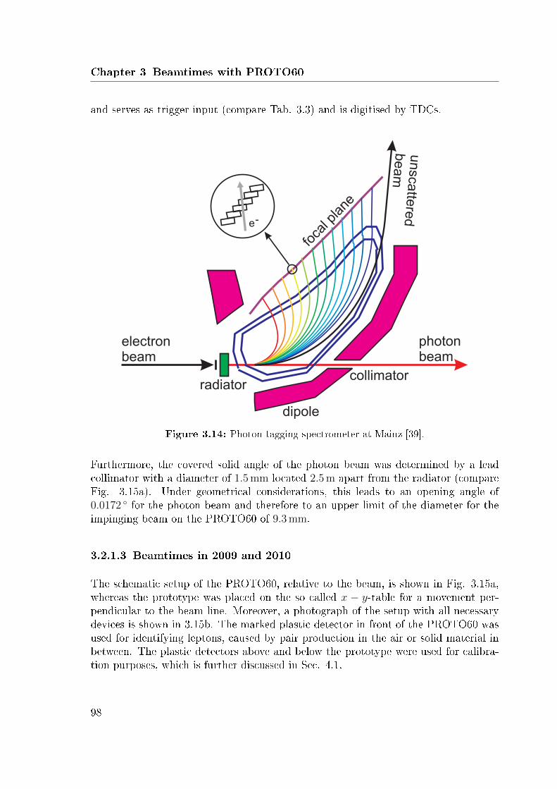
Chapter 3 Beamtimes with PROTO60
and serves as trigger input (compare Tab. 3.3) and is digitised by TDCs.
photonbeam
dipole
radiatorcollimator
electronbeam
unscatte
red
beam
e-
foca
l plane
Figure 3.14: Photon tagging spectrometer at Mainz [39].
Furthermore, the covered solid angle of the photon beam was determined by a leadcollimator with a diameter of 1.5 mm located 2.5 m apart from the radiator (compareFig. 3.15a). Under geometrical considerations, this leads to an opening angle of0.0172 for the photon beam and therefore to an upper limit of the diameter for theimpinging beam on the PROTO60 of 9.3 mm.
3.2.1.3 Beamtimes in 2009 and 2010
The schematic setup of the PROTO60, relative to the beam, is shown in Fig. 3.15a,whereas the prototype was placed on the so called x − y-table for a movement per-pendicular to the beam line. Moreover, a photograph of the setup with all necessarydevices is shown in 3.15b. The marked plastic detector in front of the PROTO60 wasused for identifying leptons, caused by pair production in the air or solid material inbetween. The plastic detectors above and below the prototype were used for calibra-tion purposes, which is further discussed in Sec. 4.1.
98

3.2 Experimental Setups
In both beamtimes at the MAMI accelerator facility, 16 photon energy channels ofthe tagging system were selected via software, summarised in Tab. 3.5). For the
Beamtimes at MAMI
TDC ChannelPhoton Energy in MeV
2009 2010
1 1441.06 685.582 1356.89 650.813 1257.31 601.774 1156.56 579.105 1057.70 509.886 956.16 443.777 857.98 387.388 756.58 339.679 657.34 269.9510 556.97 200.3511 456.26 152.7212 355.88 107.9813 256.41 93.9714 158.31 84.6715 - 61.5416 187.99 52.34
Table 3.5: Selected tagger channels at both MAMI beamtimes. In 2009, one channelwas broken and two channels were exchanged from the hardware point of view.
beamtime in 2009, the output of the individual detector modules was adjusted withan appropriate high voltage setting to a dynamic range of 200 MeV, except the centralcrystal, where the beam was impinging. Here, the direct output of the preamplierwas reduced by a passive attenuator of 15 dB, to cover the envisaged dynamic range.The assumption of the dynamic range is based on the expected energy deposition inthe central crystal of ∼ 70 % of the initial energy. In 2010, with a maximum photonenergy of 685 MeV, an attenuator with 6 dB was chosen. All LAAPDs were operatedwith estimated gain of 150. All details, concerning adjustments of the dynamic rangeand noise levels of the three beamtimes, are listed in Tab. 4.1 in Sec. 4.
99

Chapter 3 Beamtimes with PROTO60
(a) Schematic setup of the PROTO60 at the MAMI beamtimes.
(b) Photograph of the PROTO60 setup at Mainz. A: PROTO60, B: HV-supply, C: Plastic, D: Plastic detector for identifying converted photons, E:x− y-table, F: Vacuum pump, G: Nitrogen supply.
Figure 3.15: PROTO60 setup at MAMI beamtimes.
100

3.2 Experimental Setups
3.2.2 CERN-SPS
The latest test beamtime of the PROTO60 was performed at the SPS of the CERNaccelerator complex (compare Fig. 3.16). This accelerator is able to handle manydierent kinds of particles, like e.g. positrons, electrons, protons and antiprotons withenergies up to 450 GeV partly as secondary beams. It has a circumference of 7 km andserves as an input stage for the LHC. Furthermore, the stored beam at the SPS canbe provided to a separated experimental area (called North Area), which is designatedfor dierent experimental purposes of external users. In case of the PROTO60, thetest beamtime was carried out with a 15GeV/c positron and a 150GeV/c muon beam.For the production of the beam, dierent scenarios can be chosen, depending on thetype of necessary particles. For the bunched positron beam, the output of the SPS wasused and additionally collimated to an estimated momentum spread of ∆p/p ≈ 0.7 %.In case of the muon beam for calibration purposes, a high energetic proton beamstrikes a beryllium target and produces a hotchpotch of particles. The originatedcharged pions decay to almost 100 % via π+ → µ+νµ or π− → µ−νµ, respectively. Theremaining pions are absorbed by an additional beryllium absorber, whereas the µ+
are subsequently momentum selected and accumulated.
Figure 3.16: Schematic layout of the CERN accelerator complex [40]. ThePROTO60 was located at the experimental area of the SPS, which is labelledhere as North Area. The picture is not to scale.
101
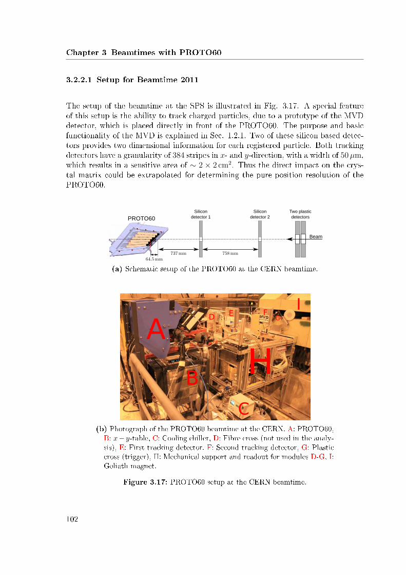
Chapter 3 Beamtimes with PROTO60
3.2.2.1 Setup for Beamtime 2011
The setup of the beamtime at the SPS is illustrated in Fig. 3.17. A special featureof this setup is the ability to track charged particles, due to a prototype of the MVDdetector, which is placed directly in front of the PROTO60. The purpose and basicfunctionality of the MVD is explained in Sec. 1.2.1. Two of these silicon based detec-tors provides two dimensional information for each registered particle. Both trackingdetectors have a granularity of 384 stripes in x- and y-direction, with a width of 50µm,which results in a sensitive area of ∼ 2 × 2 cm2. Thus the direct impact on the crys-tal matrix could be extrapolated for determining the pure position resolution of thePROTO60.
(a) Schematic setup of the PROTO60 at the CERN beamtime.
(b) Photograph of the PROTO60 beamtime at the CERN. A: PROTO60,B: x− y-table, C: Cooling chiller, D: Fibre cross (not used in the analy-sis), E: First tracking detector, F: Second tracking detector, G: Plasticcross (trigger), H: Mechanical support and readout for modules D-G, I:Goliath magnet.
Figure 3.17: PROTO60 setup at the CERN beamtime.
102

3.2 Experimental Setups
3.2.3 Beamtime Procedures
This subsection gives an overview of the performed program, with respect to thealignment of beam and prototype, for the three beamtimes. In the 2009 beamtime atMAMI, altogether four runs were performed with dierent points of impact. The mainintention of this beamtime was to study the detector resolution, in which one detectoris hit centrally, as well as the loss of energy information, when the beam is pointedin between two crystals and a signicant energy fraction is deposited in non-sensitivematerial. Fig. 3.18 shows the four points of impact on a schematic crystal map of thePROTO60.
Figure 3.18: Schematic crystal map of the PROTO60 at MAMI. The gure corre-sponds to the point of view from the direction of the photon beam. The red crosscorresponds to the point of impact of the rst and fourth run in this beamtime,whereas the black one belongs to the run in which the beam hits in between twocrystals. One run had the intention to ll the area in between the other onesand is marked with a blue cross. The internal PROTO60 coordinate system isindicated with a y- and x-axis and has its origin in the centre of this graphic.
In the MAMI beamtime of 2010, only the outcome of a particular run will be presentedin this thesis. Here the photon beam hits centrally one crystal, which is labelled with
103
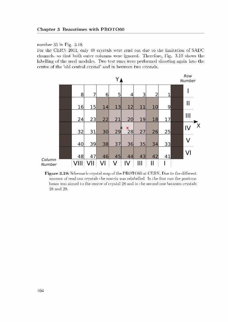
Chapter 3 Beamtimes with PROTO60
number 35 in Fig. 3.18.For the CERN 2011, only 48 crystals were read out due to the limitation of SADCchannels, so that both outer columns were ignored. Therefore, Fig. 3.19 shows thelabelling of the used modules. Two test runs were performed shooting again into thecentre of the 'old central crystal' and in between two crystals.
Figure 3.19: Schematic crystal map of the PROTO60 at CERN. Due to the dierentamount of read out crystals the matrix was relabelled. In the rst run the positronbeam was aimed to the centre of crystal 28 and in the second one between crystals28 and 29.
104

Chapter 4
Time Resolution
An accurate determination of the time information of a signal is mandatory to allo-cate a time stamp to the registered energy signal. For the barrel part of the EMC thereadout chain has to cope with interaction rates up to 100 kHz. This chapter presentsthe achieved time resolutions, obtained by the PROTO60, with respect to the de-sired limits specied in [18]. Furthermore, the dierence between the two digitisationprocedures, explained in Sec. 3.1, and inhomogeneities caused by electronics will bediscussed. The analysis in the following chapters was carried out with the softwarepackage ROOT1 and is based on the programming language C++.
4.1 Energy Calibration
There are dierent possibilities to calibrate a detector, so that an obtained pulse heightsignal in terms of voltage is converted into energy. Therefore, an appropriate methodhas to be established in order to get a linear scaling for the envisaged energy range. Anenergy calibration is composed of dierent iterative steps, like relative and absolutecalibration.
Ecal = Cabs ·∑i
Si(t) · ci · Ei/uncal (4.1)
In a relative calibration, the signal from each crystal, which corresponds to the sameenergy deposition, is normalized to a reference, e.g. the signal of the central crystalvia a factor ci. Finally, the energy sum of the detector has to be calibrated to thereal deposited energy with Cabs in order to convert the signal in terms of MeV. Atime dependent factor Si(t) is introduced to take signal loss due to radiation dam-age into account. For beamtimes with a duration of a few days and an irradiationon a reasonably low dose level Si(t) can be assumed as constant. In this thesis, the
1http://root.cern.ch
105
Chapter 4 Time Resolution
calibration scenarios for the mentioned beamtimes are listed in the following withoutfurther discussion. Dierences and inconsistencies of the listed methods and possiblealternatives are discussed in detail in [41].
MAMI 2009 In the rst beamtime with photon energies up to 1.5 GeV, the pro-totype was calibrated via cosmic radiation (see Fig. 4.1a). Here the muons, whichare produced in the atmosphere, are assumed to be MIPs and deposit on average10.2 MeV per cm in PbWO4. Due to the trigger condition, one can assume that themuons cross the full width of the crystals in one column and the energy deposition isalmost constant. For a relative calibration, the signal of each crystal caused by cosmicradiation is divided by the response of the central crystal. An absolute calibration isachieved by setting the new peak position to the corresponding energy according toEq. 4.2. Here an average path through a single crystal of 2.4 cm was assumed. A ma-jor uncertainty for this method is the impact of the non-uniformity in light collection(explained in Sec. 2.4.3).
EChannel =24.5 MeV
ppµ − ppPedestal(4.2)
pp : peak position
MAMI 2010 In 2010 an alternative calibration method was tested in addition.The prototype was turned about 90 , so that the muons can propagate through thecomplete length of each crystal. This can be ensured by requiring only one respondingcrystal. On the one hand this method delivers a larger lever arm with a referencepoint of ∼ 204 MeV, but on the other hand this method gives an integral of thelight collection eciency. It turned out that both methods dier about ∼ 7 % dueto dierent reasons [42]. In the frame of this thesis, the energy was calibrated like in2009, where the PROTO60 is in horizontal position and the cosmic muons traverseperpendicular to the longitudinal crystal axis.
CERN 2011 A muon beam with a momentum of 150GeV/c was exploited to cali-brate the detectors relatively to each other. For the absolute calibration several optionswere tested. Finally it turned out that the best reconstruction of the energy couldbe achieved based on a GEANT42 simulation. There, a 15GeV/c positron beam wassimulated, which impinges on the implemented PROTO60 matrix. The obtained en-ergy response was subsequently assigned to the energy sum of the experimental data(compare Fig. 4.1b).
2Toolkit for the simulation of the passage of particles through matter / http://geant4.cern.ch/
106

4.1 Energy Calibration
energysum_cal
Entries 2319411
Mean 495.3
RMS 371.4
energy / MeV0 200 400 600 800 1000 1200 1400
co
un
ts p
er
1 M
eV
0
2000
4000
6000
8000
10000
12000
14000
16000
energysum_cal
Entries 2319411
Mean 495.3
RMS 371.4
energysum_cal
(a) Calibrated energy sum of the 15 selected photon energies in 2009 accordingto Tab. 3.5. The spectrum shows the typical energy dependence.
energysum_cal
Entries 102844
Mean 14.2
RMS 0.7655
/ GeVe+E8 9 10 11 12 13 14 15 16
co
un
ts p
er
50
Me
V
0
1000
2000
3000
4000
5000
6000
7000
8000
energysum_cal
Entries 102844
Mean 14.2
RMS 0.7655
energysum_cal
(b) Calibrated energy sum of 15GeV/c positrons during the CERN beamtime.
Figure 4.1: Calibrated energy sum of the read out modules. In both spectra theenergy threshold of a single crystal was set to 1 MeV.
107
Chapter 4 Time Resolution
4.1.1 Noise Determination and Dynamic Range Adjustments
Since the nal time resolution does depend strongly on noise and the available dynamicrange of the particular readout chain, Tab. 4.1 serves as an summary of the relevantvalues for all beamtimes. As mentioned before, on a case to case basis, the crystalswith the highest expected energy deposition were set to a lower gain by loweringthe APD operating voltage or plugging adequate passive attenuators in series. Thisdirectly results in an enhancement of the dynamic range. This approach is advisableand comes close to the nal readout strategy, since the envisaged ASIC will have twoindependent gain channels per APD, in order to have an optimum covering of signalsin two overlapping energy ranges. The listed noise values in Tab. 4.1 were derivedfrom the width of the pedestal and the corresponding calibration factor ci (compareEq. 4.3). The dynamic range of the used 12-bit PS-ADC was estimated according toEq. 4.4. The calculated energy loss Eµ in MeV for a muon with an average path lengthof 2.4 cm is determined to be 24.5 MeV and serves as a reference for the 4, 096 availablechannels of the PS-ADC. The values given in the "Other"-column are average values,determined for a couple of modules.
σNoise = σPedestal · ci (4.3)
Emax =ADC-Rangein channels − Pedestalin channels
µ-peakin channels − Pedestalin channels· Eµ in MeV (4.4)
BeamtimeNoise in MeV Dynamic range in MeV
Center Other Center Other
MAMI 2009 0.5101 0.2251 1576 200
MAMI 2010 0.3031 0.2761 936 400
CERN-SPS2011
2.5682 0.9701 12500 4500
Table 4.1: Noise and dynamic range adjustments of the PROTO60. 1 APD gain≈ 150. 2 APD gain ≈ 50. For the CERN beamtime, the given values for thedynamic range represent a rough extrapolation.
108

4.2 Triggerless Readout of PANDA
4.2 Triggerless Readout of PANDA
The developed readout concept for the EMC was already shown in Fig. 1.24 andcontains digitiser modules, DCON3 and a DAQ4. The PANDA experiment will be op-erated without a general hardware trigger and will collect constantly about 100 GBytesof data per second from more than a thousand front-end modules [43]. At rst, theindividual detectors of PANDA get self-triggered by the attached FEE5. For this pur-pose, these subdetectors have to have a general time distribution system (SODA6),which shares the time information via optical connections. The developed time dis-tribution system SODA aims to provide a common reference time with a RMS betterthan 20 ps [43].The motivation of a triggerless readout is the exibility to select dierent criteria forthe event selection, adjusted to a specic physics case by an individual software trig-ger. A major drawback is the signicantly higher data rate. For interaction rates upto 30 MHz the stored data for a single event can reach 20 kB. Fig. 4.2 shows schemat-ically treatment of the obtained data by any subdetector of PANDA.
DetectorSelf triggered
FEE
Readout
buffer
Time
stamp
SwitchCompute
node
Stored
data
Time
Stamp
Sofware
trigger
Figure 4.2: General signal treatment of PANDA. The obtained signals of the in-dividual detectors get triggered by FEE, obtain a time stamp and are forwardedto the readout buer. A switching network serves as an interface between thebuered data to the computing node. Depending on the physics case, a modi-able software trigger can be applied to select the relevant data set.
3Data Concentrator4Data-Acquisition5Front-End Electronics6Synchronisation of Data Acquisition
109
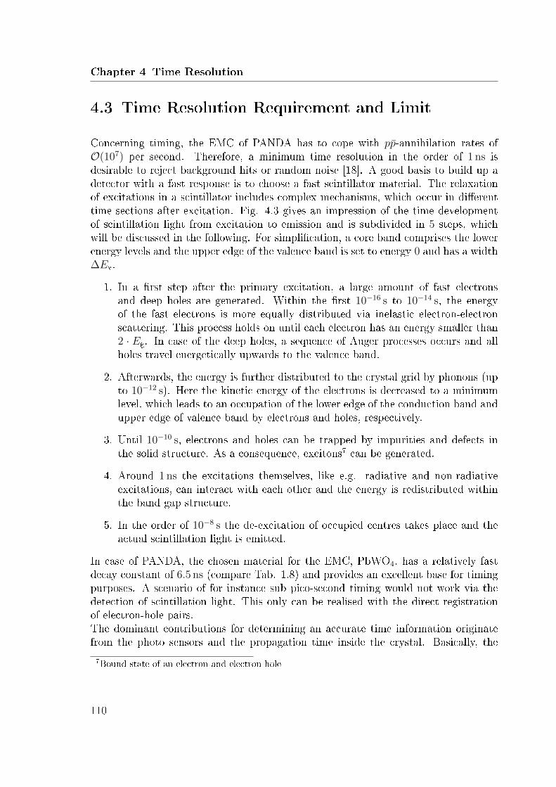
Chapter 4 Time Resolution
4.3 Time Resolution Requirement and Limit
Concerning timing, the EMC of PANDA has to cope with pp-annihilation rates ofO(107) per second. Therefore, a minimum time resolution in the order of 1 ns isdesirable to reject background hits or random noise [18]. A good basis to build up adetector with a fast response is to choose a fast scintillator material. The relaxationof excitations in a scintillator includes complex mechanisms, which occur in dierenttime sections after excitation. Fig. 4.3 gives an impression of the time developmentof scintillation light from excitation to emission and is subdivided in 5 steps, whichwill be discussed in the following. For simplication, a core band comprises the lowerenergy levels and the upper edge of the valence band is set to energy 0 and has a width∆Ev.
1. In a rst step after the primary excitation, a large amount of fast electronsand deep holes are generated. Within the rst 10−16 s to 10−14 s, the energyof the fast electrons is more equally distributed via inelastic electron-electronscattering. This process holds on until each electron has an energy smaller than2 · Eg. In case of the deep holes, a sequence of Auger processes occurs and allholes travel energetically upwards to the valence band.
2. Afterwards, the energy is further distributed to the crystal grid by phonons (upto 10−12 s). Here the kinetic energy of the electrons is decreased to a minimumlevel, which leads to an occupation of the lower edge of the conduction band andupper edge of valence band by electrons and holes, respectively.
3. Until 10−10 s, electrons and holes can be trapped by impurities and defects inthe solid structure. As a consequence, excitons7 can be generated.
4. Around 1 ns the excitations themselves, like e.g. radiative and non-radiativeexcitations, can interact with each other and the energy is redistributed withinthe band gap structure.
5. In the order of 10−8 s the de-excitation of occupied centres takes place and theactual scintillation light is emitted.
In case of PANDA, the chosen material for the EMC, PbWO4, has a relatively fastdecay constant of 6.5 ns (compare Tab. 1.8) and provides an excellent base for timingpurposes. A scenario of for instance sub pico-second timing would not work via thedetection of scintillation light. This only can be realised with the direct registrationof electron-hole pairs.The dominant contributions for determining an accurate time information originatefrom the photo sensors and the propagation time inside the crystal. Basically, the
7Bound state of an electron and electron hole
110
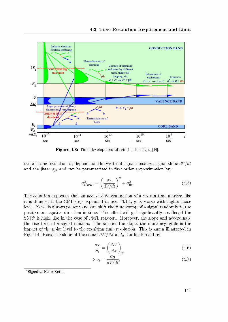
4.3 Time Resolution Requirement and Limit
Figure 4.3: Time development of scintillation light [44].
overall time resolution σt depends on the width of signal noise σN, signal slope dV/dtand the jitter σjit and can be parametrised in rst order approximation by:
σ2t/total =
(σN
dV/dt
)2
+ σ2jit. (4.5)
The equation expresses that an accurate determination of a certain time marker, likeit is done with the CFT-step explained in Sec. 3.1.4, gets worse with higher noiselevel. Noise is always present and can shift the time stamp of a signal randomly to thepositive or negative direction in time. This eect will get signicantly smaller, if theSNR8 is high, like in the case of PMT readout. Moreover, the slope and accordinglythe rise time of a signal matters. The steeper the slope, the more negligible is theimpact of the noise level to the resulting time resolution. This is again illustrated inFig. 4.4. Here, the slope of the signal ∆V/∆t at t0 can be derived by
σNσt
=
(∆V
∆t
)t0
(4.6)
⇒ σt =σN
dV/dt, (4.7)
8Signal-to-Noise Ratio
111

Chapter 4 Time Resolution
Figure 4.4: Dependencies of the time resolution on the noise level and rise time ofthe rising part of a recorded signal.
which directly leads to the mentioned dependencies described in Eq. 4.7. This partof the contribution gets worse for LAAPD readout, since here the noise level is higherand the SNR is signicantly smaller, due to the relatively low gain. In the followingsections of this thesis, the obtained time resolution measured with LAAPDs will bepresented. Worse results compared to PMT readout are to be expected because ofthe mentioned reasons. Furthermore, the stability of the arrival time of the signal,called jitter, contributes to the time resolution via σjit and is connected to the intrinsicresolution of the digitiser module. Due to the independence of both mentioned errorcontributions, they are added quadratically in Eq. 4.5.
112
4.3 Time Resolution Requirement and Limit
4.3.1 Time-Walk Eect
The time-walk eect occurs due to the dependence of the rise time on the height of thesignal, which is illustrated in Fig. 4.5a. For a xed trigger threshold, the time-walk ismore pronounced. This can be corrected by several methods. One relatively intuitivemethod is called High-Low-Coincidence (compare Fig. 4.5b). Here two thresholds areset: one very close to the noise and the second one on an appropriate higher level. Ifthe coincidence between both levels becomes true, the time marker of the low thresh-old will be used as time information. This allows to discriminate real signals fromnoise and therefore keep the time-walk on a reasonably low level.The more convenient and conventional way to correct the time-walk eect is theConstant-Fraction-Discrimination, which was basically used in all beamtimes anal-ysed in this thesis. In contrast to the method mentioned before, the trigger thresholdis not on a xed level, but dynamically generated, according to the height of the in-coming pulse. A time stamp is recorded, when the pulse passes a certain fraction R ofits maximum amplitude (compare Fig. 4.5c). In practice, the pulse gets rescaled by afactor R < 1 and subsequently subtracted from the original pulse. For the nal timeinformation, the zero-crossing has to be determined. The value of R has to be adaptedto specic applications and is realised dierently for the performed beamtimes. Forthe MAMI beamtimes, the signals were discriminated by conventional CFDs, origi-nally used in the TAPS9 experiment at Mainz. With a delay of 3 ns and R = 0.3 asCFD input parameters, which corresponds to the standard values of the TAPS exper-iment, no further adaption was done for the prototype test. The very short delay of3 ns is tuned to the fast PMT readout of the TAPS experiment.In case of the CERN beamtime, the discrimination is simulated oine by the CFT-step explained in Sec. 3.1.4. For this signal treatment, a delay of 100 ns and R = 0.45were chosen.In general, this method does not guarantee a completely walk-free performance, butsuppresses it signicantly down to an acceptable level. Another iteration to minimizethis time-walk eect can be done oine via software and will be introduced in Sec.4.4 and 4.5, since none of the collected data shows a completely walk-free behaviour.
9Two Arm Photon Spectrometer
113

Chapter 4 Time Resolution
(a) (b)
(c) (d)
Figure 4.5: (a) Schematic illustration of the time-walk eect. Signals with dierentamplitudes show dierent rise times. In spite of the same starting time, theregistered time diers by ∆t after passing a certain threshold. (b) A possibleimprovement to ∆tc < ∆t can be achieved with the High-Low-Coincidence, inwhich THH and THL correspond to the high and low threshold, respectively. (c) Inan ideal case, the time-walk eect disappears, if the time information is extractedwith a dynamic threshold (Constant-Fraction-Discrimination) and both signalsare assigned to the same time t0. (d) Pulse shapes for both signals after applyingthe CFD algorithm.
114

4.3 Time Resolution Requirement and Limit
4.3.2 Pile-Up Recovery
Pile-up occurs if two or more signals arrive almost simultaneously in a very shorttime window. This eect deteriorates the direct determination of the energy and timeinformation with the extraction algorithm described in Sec. 3.1.4. With a nominalhit rate of 500 kHz at the smallest polar angles, one can expect a pile-up probabilityof ∼ 13 % [45]. A pile-up event will be identied in the digitiser module if the ratioof integral and amplitude exceeds a certain threshold. The following describes twomethods, which allow the successful recovery of two signals with a time dierence notshorter than 50 ns, which is in detail described in [46].Fig. 4.6 shows two signals with dierent amplitudes and a time dierence of ∼ 200 ns.
Time (ns)
0 200 400 600 800 1000 1200
Am
pli
tude
(mV
)
0
50
100
150
200
250
Time difference
totI
1A
2A
Figure 4.6: Principle of pile-up recovery of energy information [46]. The two digi-tised signals are generated by LED pulsers with amplitudes of A1 ≈ 250 mV andA2 ≈ 140 mV, respectively.
The integral I of a signal corresponds to the input charge and scales linearly withthe amplitude A, according to I = k · A. With the knowledge of the constant k, thisproportionality can be exploited for the recovery of overlapping signals. If two signalsare close to each other, the total integral Itot and the amplitude of the rst pulse A1
in Eq. 4.8 is detected. Thus the relevant energy information of the second pulse A2
115
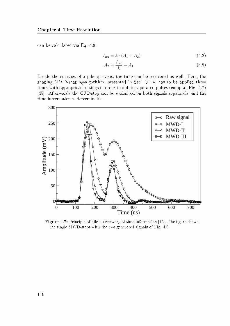
Chapter 4 Time Resolution
can be calculated via Eq. 4.9.
Itot = k · (A1 + A2) (4.8)
A2 =Itotk− A1 (4.9)
Beside the energies of a pile-up event, the time can be recovered as well. Here, theshaping MWD-shaping-algorithm, presented in Sec. 3.1.4, has to be applied threetimes with appropriate settings in order to obtain separated pulses (compare Fig. 4.7)[45]. Afterwards the CFT-step can be evaluated on both signals separately and thetime information is determinable.
0 100 200 300 400 500 600 700
Time (ns)
0
50
100
150
200
250
300
Am
pli
tude
(mV
)
Raw signal
MWD-I
MWD-II
MWD-III
Figure 4.7: Principle of pile-up recovery of time information [46]. The gure showsthe single MWD-steps with the two generated signals of Fig. 4.6.
116

4.3 Time Resolution Requirement and Limit
4.3.3 Scintillation Tiles
Due to the extended physics program of PANDA, there is a demand for an additionaldetector with respect to timing purposes: SciTil10 [47]. Such a tile itself has roughly asize of the order of 2× 2× 0.5 cm3 and is made out of an organic scintillator materialwith fast rise time and high light output. Studies about the optimum material with anacceptable radiation hardness are presently ongoing. One tile should be in front of eachcrystal of the barrel EMC. The readout is envisaged with SiPMs11, which is basicallyan array of small Avalanche photo diode pixels with excellent timing properties sincethey are operated in Geiger-Mode delivering extremely short rise-times. An additionalSciTil detector would have the following benets due to the desired time resolution of100 ps:
a start detector for TOF measurements of muons and pions (PID)
improved relative timing for a better correlation between reaction fragments ofone event in the barrel and the forward part of the PANDA detector
ability to identify photons converted via pair production within the DIRC
The nal design is not accomplished yet, but in the present status it is foreseen toread out one tile with two SiPMs (compare Fig. 4.8a). This has the advantages of ahigher number of collected photons, less light path uctuations and higher detectioneciency. One quad module (Fig. 4.8b) consists of four SciTils and the signals areforwarded to an ASIC to be developed (Fig. 4.8c).
(a) (b) (c)
Figure 4.8: (a) Basic layout of a SciTil module read out from two positions. (b)Quad module. (c) The signals of one quad module are further processed by anASIC.
10Scintillating Tile11Silicon Photomultipliers
117

Chapter 4 Time Resolution
4.4 Time Resolution at MAMI 2009 and 2010
The data obtained in the beamtimes at MAMI in 2009 and 2010 are basically treated inthe same way. But there are some dierences due to the dierent trigger conditions,which were already listed in Tab. 3.3. In 2009, a coincidence between tagger andcentral crystal was required, whereas in 2010 a logical OR of all crystals replacedthe trigger branch from the prototype. Therefore, the individual time spectra of thecorresponding modules have to be interpreted dierently. In order to obtain the bestpossible time resolution, the main focus was set to the runs, where the beam impingedin between two adjacent crystals, corresponding to the black cross in Fig. 3.18. Underthese conditions similar signal amplitudes are recorded in the coincident detector dueto symmetric energy sharing. Some further results will be presented for comparisonand discussion. In most of the cases, only events were accepted where the depositedenergy of both crystals were similar within a certain range. In each case, the timereference is plotted and analysed with regard to calibration, time-walk eect and timeresolution. All achieved results will be compared and discussed in Sec. 6.2. Theenergy calibration of the shown data will not be discussed further and was done likeexplained in Sec. 4.1.
4.4.1 Beamtime MAMI 2009
A logical AND of tagger and central crystal signals triggered the readout chain and allmodules were read out simultaneously. The timing of the ECL12 signals was adjustedin a way that the rising edge of the tagger arrives earlier than the one of the centralcrystal. Therefore, the central crystal is the time-determining component. The wholereadout had a common start and was stopped individually by the crystals themselves.Due to that reason, the time spectrum of the central crystal only consists of a spike(Fig. 4.9a), the position is equal to the generated eective time gate of approximately405 ns. The time information of the central crystal is contained in the digitised dataof the corresponding tagger channels and is shown in Fig. 4.9b. Here an additionalsmearing of the tagger resolution can be neglected due to the fact that the plasticscintillators of the tagger are read out by PMTs.To guarantee a similar energy deposition in both detectors, labelled as number 35 and36 in Fig. 3.18, Eq. 4.10 was set as requirement in the software:
E35 > E36 · 0.8 and E36 > E35 · 0.8. (4.10)
To get an information about the resolution of the central crystal, the data, shown inFig. 4.9c, has to be calibrated relatively by shifting the separate data sets of each
12Emitter Coupled Logic
118
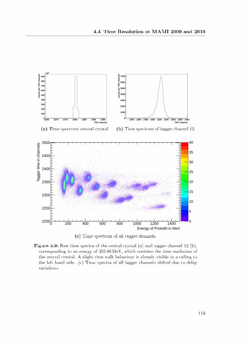
4.4 Time Resolution at MAMI 2009 and 2010
TIME_raw35
Entries 1518410
Mean 2380
RMS 0.5934
TDC channel
2365 2370 2375 2380 2385 2390 2395
co
un
ts p
er
TD
C c
ha
nn
el
0
100
200
300
400
500
600
700
800
900
310×
TIME_raw35
Entries 1518410
Mean 2380
RMS 0.5934
(a) Time spectrum central crystal.
TAGGER_raw12
Entries 141376
Mean 2321
RMS 11.41
TDC channel
2240 2260 2280 2300 2320 2340 2360 2380 2400c
ou
nts
pe
r T
DC
ch
an
ne
l0
1000
2000
3000
4000
5000
6000
7000
TAGGER_raw12
Entries 141376
Mean 2321
RMS 11.41
(b) Time spectrum of tagger channel 12.
Energy of Proto60 in MeV
0 200 400 600 800 1000 1200 1400
Tagger
time in c
hannels
2200
2250
2300
2350
2400
2450
2500
TimeRaw_Tagger_allEntries 106190Mean x 408.5
Mean y 2340RMS x 295.2RMS y 29.26
TimeRaw_Tagger_allEntries 106190Mean x 408.5
Mean y 2340RMS x 295.2RMS y 29.26
0
5
10
15
20
25
30
35
40
TimeRaw_Tagger_all
(c) Time spectrum of all tagger channels.
Figure 4.9: Raw time spectra of the central crystal (a) and tagger channel 12 (b),corresponding to an energy of 355.88 MeV, which contains the time resolution ofthe central crystal. A slight time-walk behaviour is already visible in a tailing tothe left hand side. (c) Time spectra of all tagger channels shifted due to delayvariations.
119

Chapter 4 Time Resolution
tagger channel relatively to each other. The absolute timing signals of the tagger arenot compensated for variations of transmission times in the PMTs or cables, respec-tively. Starting with the tagger channel corresponding to the highest energy, the dataof a small energy range was selected, projected to the time axis and tted with aGaussian function. The same procedure, with the same energy range, was applied forthe next lower tagger channel and the obtained dierence of the Gaussian functiongives relative shift in time. This procedure was repeated pairwise down to the taggerchannel of the lowest energy. This method is exemplary illustrated in Fig. 4.10 fortagger channels 9 and 10, respectively.
Energy of Proto60 in MeV
200 250 300 350 400 450 500 550 600
Tagger
tim
e in c
hannels
2260
2280
2300
2320
2340
2360
2380
2400
TimeRaw_Tagger_10
Entries 8113Mean x 428.7Mean y 2366RMS x 32.3RMS y 8.376
TimeRaw_Tagger_10
Entries 8113Mean x 428.7Mean y 2366RMS x 32.3RMS y 8.376
0
2
4
6
8
10
12
14
16
18
TimeRaw_Tagger_10
(a) Time spectrum tagger channel 9.
Energy of Proto60 in MeV
200 250 300 350 400 450 500 550 600
Tagg
er
tim
e in
ch
an
nels
2260
2280
2300
2320
2340
2360
2380
2400
TimeRaw_Tagger_11
Entries 11227Mean x 339.6Mean y 2317RMS x 32.81RMS y 9.391
TimeRaw_Tagger_11
Entries 11227Mean x 339.6Mean y 2317RMS x 32.81RMS y 9.391
0
2
4
6
8
10
12
14
16
18
20
22
24
TimeRaw_Tagger_11
(b) Time spectrum tagger channel 10.TimeRaw_Tagger_10_py
Entries 597
Mean 2365
RMS 10.13
Tagger time in channels
2300 2320 2340 2360 2380 2400
Num
ber
of E
ntr
ies
0
5
10
15
20
25
30
TimeRaw_Tagger_10_py
Entries 597
Mean 2365
RMS 10.13
ProjectionY of binx=[385,404]
(c) Gaussian t tagger channel 9.
TimeRaw_Tagger_11_py
Entries 126
Mean 2320
RMS 14.04
Tagger time in channels
2260 2280 2300 2320 2340 2360 2380 2400
Num
ber
of E
ntr
ies
0
1
2
3
4
5
6
7
8
9
TimeRaw_Tagger_11_py
Entries 126
Mean 2320
RMS 14.04ProjectionY of binx=[370,389]
(d) Gaussian t tagger channel 10.
Figure 4.10: Example of the relative time calibration for tagger channels 9 and 10.The selected data within the overlap region of both tagger channels, 370−390 MeV,are projected and tted with a Gaussian function, in which the dierence of thepeak position corresponds to the relative shift in time.
The absolute shifts of the tagger channels are not visible in the time spectrum of thedierence between the central crystal and its neighbour. Here, the regarded time ref-
120
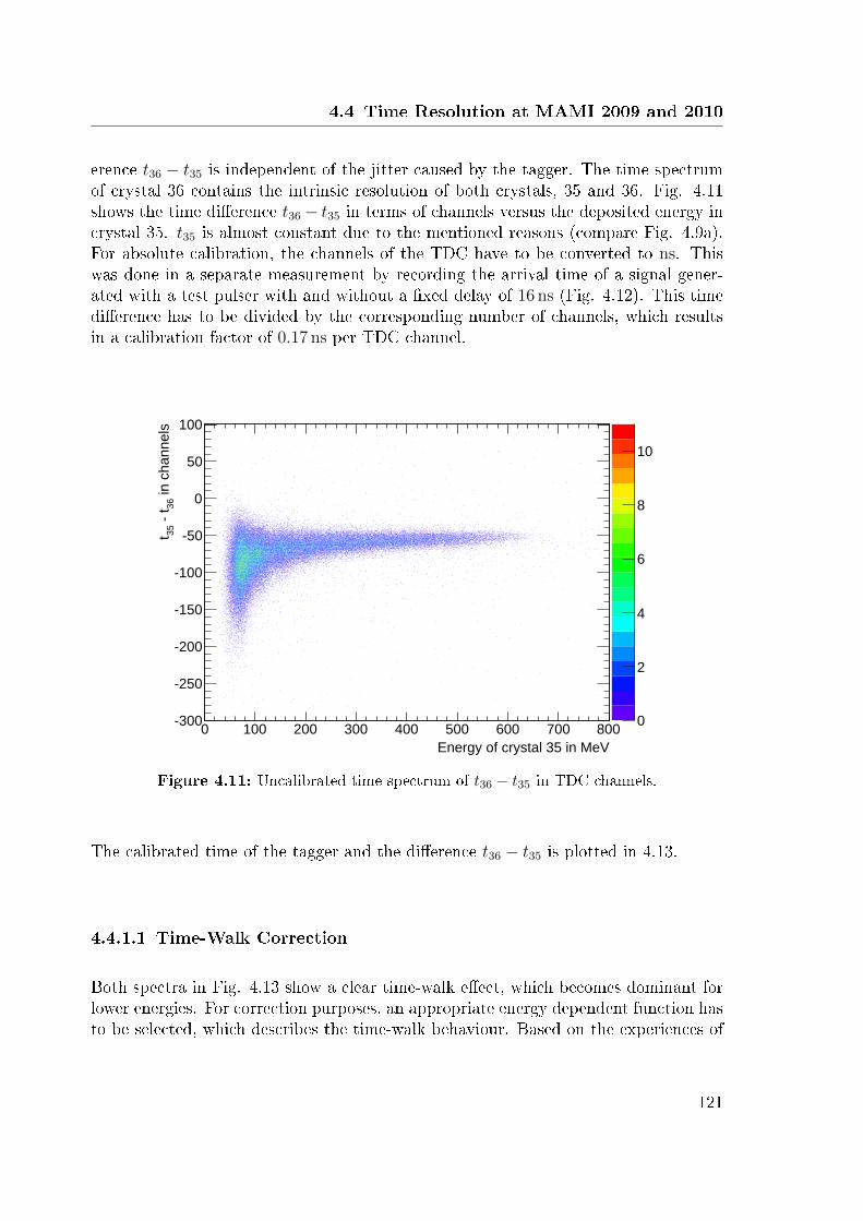
4.4 Time Resolution at MAMI 2009 and 2010
erence t36 − t35 is independent of the jitter caused by the tagger. The time spectrumof crystal 36 contains the intrinsic resolution of both crystals, 35 and 36. Fig. 4.11shows the time dierence t36− t35 in terms of channels versus the deposited energy incrystal 35. t35 is almost constant due to the mentioned reasons (compare Fig. 4.9a).For absolute calibration, the channels of the TDC have to be converted to ns. Thiswas done in a separate measurement by recording the arrival time of a signal gener-ated with a test pulser with and without a xed delay of 16 ns (Fig. 4.12). This timedierence has to be divided by the corresponding number of channels, which resultsin a calibration factor of 0.17 ns per TDC channel.
Energy of crystal 35 in MeV
0 100 200 300 400 500 600 700 800
in c
hannels
36
t
35
t
300
250
200
150
100
50
0
50
100
time_diff_vs_E35_rawEntries 104417Mean x 174.3
Mean y 75.87RMS x 128.5RMS y 27.36
time_diff_vs_E35_rawEntries 104417Mean x 174.3
Mean y 75.87RMS x 128.5RMS y 27.36
0
2
4
6
8
10
time_diff_vs_E35_raw
Figure 4.11: Uncalibrated time spectrum of t36 − t35 in TDC channels.
The calibrated time of the tagger and the dierence t36 − t35 is plotted in 4.13.
4.4.1.1 Time-Walk Correction
Both spectra in Fig. 4.13 show a clear time-walk eect, which becomes dominant forlower energies. For correction purposes, an appropriate energy dependent function hasto be selected, which describes the time-walk behaviour. Based on the experiences of
121

Chapter 4 Time Resolution
TP
Entries 100201
Mean 2848
RMS 47.71
TDCChannels
2800 2820 2840 2860 2880 2900
Co
un
ts
10
210
310
410
TP
Entries 100201
Mean 2848
RMS 47.71
16 ns
Figure 4.12: Absolute time calibration of the TDC channels.
the TAPS group Gieÿen [48], Eq. 4.11 was chosen, in which A, B, C and D representfree parameters.
t(E) = A · eB·√E+C·E +D (4.11)
For the application of t(E), the content of the corresponding spectrum has to be con-verted into discrete points. This is done by subdividing the histogram in slices withequal width along the energy axis. Each slice is subsequently projected on to thetime axis and tted with a Gaussian function. As a result, the mean values, includingstandard deviation, are plotted. This procedure was applied to both spectra of 4.10aand 4.10b, and is exemplary shown for the latter one in Fig. 4.14. In order to getproper results, in both cases the spectra were rebinned in groups of ve neighbouringbins and only slices with an minimum content of 25 counts were tted. The t resultscan be looked up in Tab. 4.2. The chosen t function shows a satisfying descriptionof the data points within the t range. Data points with extremely large error barssuer from low statistics and should be suppressed by the mentioned requirements toa reasonable level. Above 550 MeV no data points are available due to the low numberof counts and the t is extrapolated to 800 MeV.In a next step, the time values have to be corrected with the obtained time-walk cor-rection function. Therefore, each data point has to be subtracted from the correctionfunction t(E), in which E represents again the deposited energy in crystal 35. This isdisplayed for both scenarios in Fig. 4.15 for all energies.
122
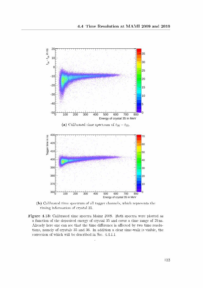
4.4 Time Resolution at MAMI 2009 and 2010
Energy of crystal 35 in MeV
0 100 200 300 400 500 600 700 800
in n
s35
t
36
t
50
40
30
20
10
0
10
20
time_diff_vs E35
Entries 104417Mean x 174.3
Mean y 12.89RMS x 128.6
RMS y 4.675
time_diff_vs E35
Entries 104417Mean x 174.3
Mean y 12.89RMS x 128.6
RMS y 4.675
0
5
10
15
20
25
30
35
time_diff_vs E35
(a) Calibrated time spectrum of t36 − t35.
Energy of crystal 35 in MeV
0 100 200 300 400 500 600 700 800
Tag
ger
tim
e in n
s
360
370
380
390
400
410
420
430
Ti me Ra w _Tag ge r_ al l_ rel ca li b
Entries 104417
Mean x 174.4
Mean y 398.9
RMS x 128.6
RMS y 2.683
Ti me Ra w _Tag ge r_ al l_ rel ca li b
Entries 104417
Mean x 174.4
Mean y 398.9
RMS x 128.6
RMS y 2.683
0
10
20
30
40
50
60
70
TimeRaw_Tagger_all_relcalib
(b) Calibrated time spectrum of all tagger channels, which represents thetiming information of crystal 35.
Figure 4.13: Calibrated time spectra Mainz 2009. Both spectra were plotted asa function of the deposited energy of crystal 35 and cover a time range of 70 ns.Already here one can see that the time dierence is aected by two time resolu-tions, namely of crystals 35 and 36. In addition a clear time-walk is visible, thecorrection of which will be described in Sec. 4.4.1.1
.
123

Chapter 4 Time Resolution
hpxpy_1
Entries 103
Mean 288.3
RMS 150.5
Energy of crystal 35 in MeV
0 100 200 300 400 500 600 700 800
Ta
gge
r tim
e in
ns
360
370
380
390
400
410
420
430
hpxpy_1
Entries 103
Mean 288.3
RMS 150.5
Fitted value of par[1]=Mean
Figure 4.14: Application of time-walk function t(E) for the spectrum in Fig. 4.10b.Each tted slice in the energy direction has a width of 5 MeV and a minimumcontent of 25 events was required. Only a handful of slices deliver improperresults with respect to the time-walk correction.
Spectrum Correction function t(E) χ2/NDF
t36 − t35t(E) = −42.08 ns · e−2.41·10−1·
√E/MeV−3.02·10−3·E/MeV − 8.44 ns 22.42
(Fig. 4.10a)
Tagger timet(E) = −9.31 ns · e−6.47·10−3·
√E/MeV−2.16·10−3·E/MeV + 405.05 ns 25.04
(Fig. 4.10b)
Table 4.2: Fit results time-walk correction.
124
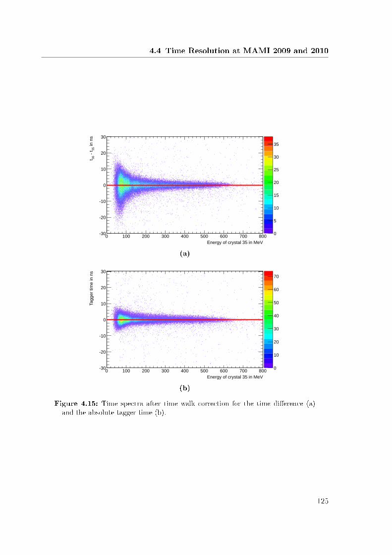
4.4 Time Resolution at MAMI 2009 and 2010
Energy of crystal 35 in MeV
0 100 200 300 400 500 600 700 800
in n
s35
t
36
t
30
20
10
0
10
20
30
time_diff_vs E35 twCor
Entries 104417Mean x 174.3Mean y 0.1347RMS x 128.5RMS y 3.97
0
5
10
15
20
25
30
35
time_diff_vs E35 twCor
Entries 104417Mean x 174.3Mean y 0.1347RMS x 128.5RMS y 3.97
time_diff_vs E35twCor
(a)
Energy of crystal 35 in MeV
0 100 200 300 400 500 600 700 800
Tagg
er
tim
e in n
s
30
20
10
0
10
20
30
TimeRaw_Tagger_all_relcalib twCorEntries 104417Mean x 174.4Mean y 0.01489RMS x 128.6RMS y 2.148
0
10
20
30
40
50
60
70
TimeRaw_Tagger_all_relcalib twCorEntries 104417Mean x 174.4Mean y 0.01489RMS x 128.6RMS y 2.148TimeRaw_Tagger_all_relcalibtwCor
(b)
Figure 4.15: Time spectra after time walk correction for the time dierence (a)and the absolute tagger time (b).
125
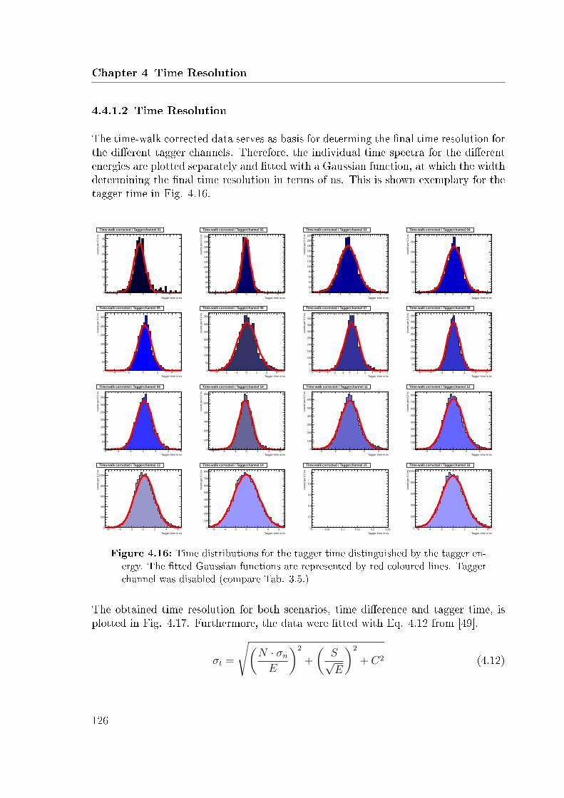
Chapter 4 Time Resolution
4.4.1.2 Time Resolution
The time-walk corrected data serves as basis for determing the nal time resolution forthe dierent tagger channels. Therefore, the individual time spectra for the dierentenergies are plotted separately and tted with a Gaussian function, at which the widthdetermining the nal time resolution in terms of ns. This is shown exemplary for thetagger time in Fig. 4.16.
Tagger time in ns
4 2 0 2 4
counts
per
0.2
ns
0
5
10
15
20
25
30
35
Timewalk corrected / Taggerchannel 01
Tagger time in ns
6 4 2 0 2 4 6
counts
per
0.2
ns
0
20
40
60
80
100
120
140
160
180
200
220
Timewalk corrected / Taggerchannel 02
Tagger time in ns
3 2 1 0 1 2 3
counts
per
0.2
ns
0
20
40
60
80
100
120
140
160
180
200
220
Timewalk corrected / Taggerchannel 03
Tagger time in ns
4 3 2 1 0 1 2 3 4
counts
per
0.2
ns
0
50
100
150
200
250
Timewalk corrected / Taggerchannel 04
Tagger time in ns
4 2 0 2 4
counts
per
0.2
ns
0
50
100
150
200
250
300
Timewalk corrected / Taggerchannel 05
Tagger time in ns
3 2 1 0 1 2 3
counts
per
0.2
ns
0
50
100
150
200
250
300
350
Timewalk corrected / Taggerchannel 06
Tagger time in ns
5 4 3 2 1 0 1 2 3 4 5
counts
per
0.2
ns
0
50
100
150
200
250
300
350
400
Timewalk corrected / Taggerchannel 07
Tagger time in ns
6 4 2 0 2 4 6
counts
per
0.2
ns
0
50
100
150
200
250
300
350
400
450
Timewalk corrected / Taggerchannel 08
Tagger time in ns
6 4 2 0 2 4 6
counts
per
0.2
ns
0
50
100
150
200
250
300
350
Timewalk corrected / Taggerchannel 09
Tagger time in ns
6 4 2 0 2 4 6
counts
per
0.2
ns
0
100
200
300
400
500
600
Timewalk corrected / Taggerchannel 10
Tagger time in ns
4 2 0 2 4
counts
per
0.2
ns
0
100
200
300
400
500
600
Timewalk corrected / Taggerchannel 11
Tagger time in ns
4 2 0 2 4
counts
per
0.2
ns
0
100
200
300
400
500
600
700
800
Timewalk corrected / Taggerchannel 12
Tagger time in ns
6 4 2 0 2 4 6
counts
per
0.2
ns
0
200
400
600
800
1000
Timewalk corrected / Taggerchannel 13
Tagger time in ns
6 4 2 0 2 4 6
counts
per
0.2
ns
0
100
200
300
400
500
600
700
800
Timewalk corrected / Taggerchannel 14
Tagger time in ns
0 0.05 0.1 0.15 0.2 0.25
counts
per
0.2
ns
0
0.2
0.4
0.6
0.8
1
Timewalk corrected / Taggerchannel 15
Tagger time in ns
6 4 2 0 2 4 6
counts
per
0.2
ns
0
200
400
600
800
1000
Timewalk corrected / Taggerchannel 16
Figure 4.16: Time distributions for the tagger time distinguished by the tagger en-ergy. The tted Gaussian functions are represented by red coloured lines. Taggerchannel was disabled (compare Tab. 3.5.)
The obtained time resolution for both scenarios, time dierence and tagger time, isplotted in Fig. 4.17. Furthermore, the data were tted with Eq. 4.12 from [49].
σt =
√(N · σnE
)2
+
(S√E
)2
+ C2 (4.12)
126

4.4 Time Resolution at MAMI 2009 and 2010
The free parametersN , S and C represent the contribution caused by noise, stochastic,and systematic eects, respectively. E is the measured deposited energy and σn thenoise level, which was determined to ∼ 0.25 MeV.
Energy crystal 35 in MeV
100 200 300 400 500 600
Tim
e r
esolu
tion in n
s
0.5
1
1.5
2
2.5
3
3.5
4
Time Resolution
2) / 35
t36
(t
2 + (0.43 ns)
2
E
0.00 ns +
2
E
0.25 MeV⋅1.03 ns = σ
tagger time
2 + (0.54 ns)
2
E
0.49 ns +
2
E
0.25 MeV⋅0.31 ns = σ
Figure 4.17: Time resolution for the time dierence and tagger time as a functionof the deposited energy in the central crystal including ts with correspondingcolour. The values for the energy axis were extracted by tting the relevantenergy distributions with Eq. 5.1.
In case of the time dierence, it was assumed that both crystals contribute equallyto the nal time resolution. Therefore, to get the resolution for a single module, theoverall resolution was divided by
√2 (compare Eq. 4.13), which is already included in
127

Chapter 4 Time Resolution
Fig. 4.17.
σ2time dierence = σ2
36 + σ235
σ2time dierence = 2 · σ2 , for σ36 = σ35 = σ
⇒ σ =σtime dierence√
2(4.13)
The time resolution, deduced by the timing dierence of two crystals, is signicantlyworse at energies below 200 MeV and becomes slightly better at higher energies. Ex-tracted by the t, the N -parameter, which symbolises the noise contribution, is almostthree times larger than the one obtained by a single unit. Furthermore, the parameterrepresenting the stochastic term of the time dierence has a value 1.42 · 10−4 ns
√MeV
and is negligible. This is reasonable, since the applied requirement in Eq. 4.10 de-mands an almost equal sharing of the deposited energy. In case of the tagger time,which represents for the mentioned reasons the time of crystal 35, a clear statistics-dependence could be extracted. The constant term of the parametrisation dictatesthe achievable time resolution at higher energies with the described readout.
4.4.2 Beamtime MAMI 2010
In order to cover the low energy region of PANDA down to 50 MeV, the time resolutionwas as well evaluated for the beamtime at MAMI in 2010. The same data was alreadyanalysed in [42], but here the nal time resolution was determined without correctingthe time-walk and only setting a sharp cut on the energy for the single tagger channels.Only data for photon beams impinging centrally on one crystal are available. Dataacquisition was running in a common start mode, in which a logical AND between thetagger channels and all crystals of the PROTO60 served as a trigger for the readout.For both responding modules, the registered time of the rising edge is digitised byTDCs and subsequently stored. The timing was, like in 2009, set in a way that theNIM13 signals from the tagger arrive earlier than the ones from the crystals. Therefore,the responding crystal is again the time determining component. As a time reference,the dierence between central crystal and tagger channel was chosen:
t = tcentral crystal − tresponding tagger channel. (4.14)
A typical time spectrum of the tagger is shown in Fig. 4.18, in which the dottedlines in red correspond to the sharp cut on the relevant events. The application ofthis cut has to be tuned for each tagger channel. For the determination of the timeresolution, the time reference t has to be corrected, due to delay variations of thetagger channels. This was done like explained in Fig. 4.10 and the result is shown in
13Nuclear Instrumentation Methods
128
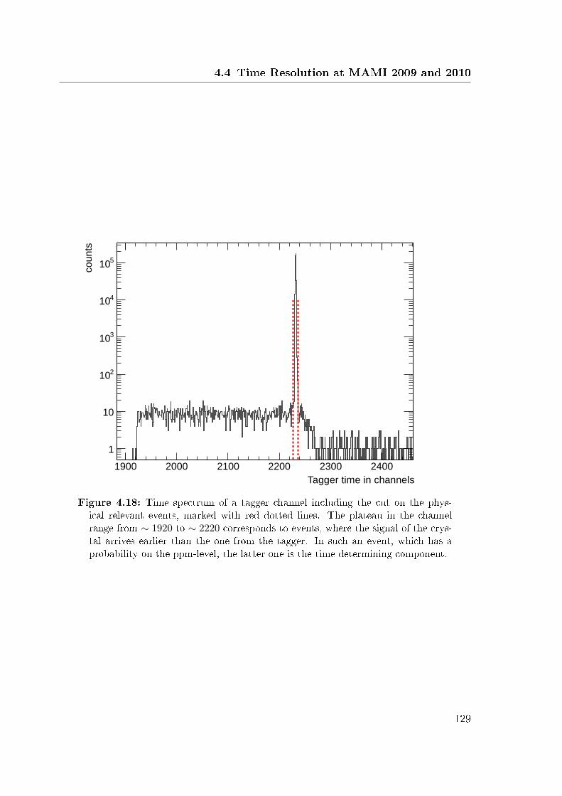
4.4 Time Resolution at MAMI 2009 and 2010
Tagged_Time_10
Entries 2777940Mean 2231
RMS 15.37
Tagger time in channels
1900 2000 2100 2200 2300 2400
counts
1
10
210
310
410
510
Tagged_Time_10
Entries 2777940Mean 2231
RMS 15.37
Tagged_Time_10
Figure 4.18: Time spectrum of a tagger channel including the cut on the phys-ical relevant events, marked with red dotted lines. The plateau in the channelrange from ∼ 1920 to ∼ 2220 corresponds to events, where the signal of the crys-tal arrives earlier than the one from the tagger. In such an event, which has aprobability on the ppm-level, the latter one is the time determining component.
129

Chapter 4 Time Resolution
Fig. 4.19. Furthermore, the relatively shifted time spectra have to be walk-correctedaccording to Eq. 4.11. The dierence between the data in Fig. 4.19 and the obtainedcorrection function for the time-walk is plotted in arbitrary units in Fig. 4.20.
Energy of PROTO60 in MeV
0 100 200 300 400 500 600 700
in c
hannels
tagger
t
35
t
820
840
860
880
900
920
940
TimeRaw_Crystal35_all_shifted
Entries 5191894
Mean x 140
Mean y 889.4
RMS x 137.3
RMS y 11.85
TimeRaw_Crystal35_all_shifted
Entries 5191894
Mean x 140
Mean y 889.4
RMS x 137.3
RMS y 11.85
1
10
210
310
TimeRaw_Crystal35_all_shifted
Figure 4.19: Relatively calibrated time spectrum. A clear time-walk is visible. Forbetter visualisation of the data the z-axis is plotted in logarithmic scale. Thex-axis shows the deposited energy in the whole PROTO60.
Like in Fig. 4.16 for the beamtime in 2009, the time spectra are plotted separately foreach tagger channel and tted with a Gaussian function in order to determine the naltime resolution. The deduced results are shown as function of the deposited energy inFig. 4.21 and tted with Eq. 4.12.
130

4.4 Time Resolution at MAMI 2009 and 2010
Energy of Crystal 35 in MeV
0 100 200 300 400 500 600 700
in a
.u.
tagger
t
35
t
820
840
860
880
900
920
940
hpxpyEntries 5191894Mean x 115.2Mean y 888
RMS x 113.2RMS y 12.77
hpxpyEntries 5191894Mean x 115.2Mean y 888
RMS x 113.2RMS y 12.77
1
10
210
310
TimeRaw_Crystal35_all_shifted
Figure 4.20: Time spectrum as function of the deposited energy in the regardedcrystal including time-walk correction function marked in black.
Energy crystal 35 in MeV100 200 300 400 500
Tim
e r
eso
lutio
n in
ns
0.6
0.8
1
1.2
1.4
1.6
1.8
2
Time Resolution
35t
2 + (0.37 ns)
2
E
0.37 ns +
2
E
0.25 MeV⋅0.16 ns = σ
Figure 4.21: Results for the time resolution from the MAMI beamtime in 2010.
131
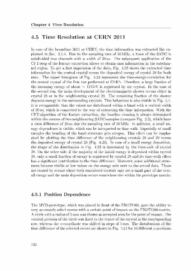
Chapter 4 Time Resolution
4.5 Time Resolution at CERN 2011
In case of the beamtime 2011 at CERN, the time information was extracted like ex-plained in Sec. 3.1.4. Due to the sampling rate of 50 MHz, a trace of the SADC issubdivided into channels with a width of 20 ns. The subsequent application of theCFT-step of the feature extraction allows to obtain time information in the subchan-nel region. To get a rst impression of the data, Fig. 4.22 shows the extracted timeinformation for the central crystal versus the deposited energy of crystal 28 for bothruns. The upper histogram of Fig. 4.22 represents the time-energy-correlation forthe central crystal of the rst run performed at CERN. Therefore, a large fraction ofthe incoming energy of about ∼ 12 GeV is registered by the crystal. In the case ofthe second run, the main development of the electromagnetic shower occurs either incrystal 28 or in the neighbouring crystal 29. The remaining fraction of the showerdeposits energy in the surrounding crystals. This behaviour is also visible in Fig. 5.1.It is recognisable, that the values are distributed within a band with a vertical widthof 20 ns, which is connected to the way of extracting the time information. With theCFT-algorithm of the feature extraction, the baseline crossing is always determinedwithin the centres of two neighbouring SADC-samples (compare Fig. 3.3), which havea time dierence of 20 ns due the sampling rate of 50 MHz. In addition, a small en-ergy dependence is visible, which can be interpreted as time walk. Especially at smallenergies the bending of the band structure gets steeper. This eect can be empha-sised by plotting the time dierence of the neighbouring crystals 28 and 29 versusthe deposited energy of crystal 28 (Fig. 4.23). In case of a small energy deposition,the shape of the distribution in Fig. 4.23 is dominated by the time-walk of crystal28. On the other side, if the majority of the initial energy is deposited within crystal28, only a small fraction of energy is registered by crystal 29 and its time-walk eecthas a signicant contribution to the time dierence. Moreover, some additional struc-tures become visible at low values on the energy axis next to the actual data. Thoseare caused by events where both considered crystals only see a small part of the over-all energy and the main deposition occurs somewhere else within the prototype matrix.
4.5.1 Position Dependence
The MVD-prototype, which was placed in front of the PROTO60, gave the ability tovery accurately select events with a certain point of impact on the PROTO60-matrix.A circle with a radius of 5 mm was chosen as accepted area for the point of impact. Thevertical position of the circle was xed to the centre of the crystal in the correspondingrow, whereas the x-coordinate was shifted in steps of 1 mm. The distributions of thetime dierence of the selected events are shown in Fig. 4.24 for 10 dierent x-positions
132

4.5 Time Resolution at CERN 2011
in MeV28
Energy
0 2000 4000 6000 8000 10000 12000
in n
s28
tim
e
2460
2480
2500
2520
2540
2560
Ti me27_E nergy27
Entries 238948
Mean x 8783
Mean y 2492
RMS x 3375
RMS y 7.637
0
5
10
15
20
25
30
35
40
Ti me27_E nergy27
Entries 238948
Mean x 8783
Mean y 2492
RMS x 3375
RMS y 7.637
Run 1
(a)
in MeV28
Energy
0 2000 4000 6000 8000 10000 12000
in n
s28
tim
e
2460
2480
2500
2520
2540
2560
Time27_Ener gy27
Entries 214547
Mean x 5822
Mean y 2494
RMS x 3811
RMS y 8.342
0
2
4
6
8
10
12
14
16
18
20
Time27_Ener gy27
Entries 214547
Mean x 5822
Mean y 2494
RMS x 3811
RMS y 8.342
Run 2
(b)
Figure 4.22: Extracted time spectra of the central crystal as a function of thedeposited energy in crystal 28 for run 1 (a) and run 2 (b).
133
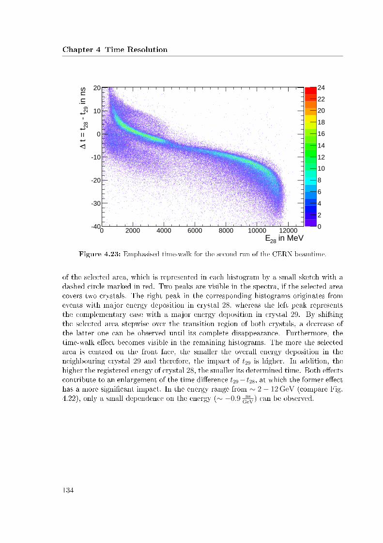
Chapter 4 Time Resolution
in MeV28
E
0 2000 4000 6000 8000 10000 12000
in
ns
29
t
28
t =
t∆
40
30
20
10
0
10
20
TimeWalkEntries 206333
Mean x 5855Mean y 8.624
RMS x 3794RMS y 10.36
TimeWalkEntries 206333
Mean x 5855Mean y 8.624
RMS x 3794RMS y 10.36
0
2
4
6
8
10
12
14
16
18
20
22
24
TimeWalk
Figure 4.23: Emphasised time-walk for the second run of the CERN beamtime.
of the selected area, which is represented in each histogram by a small sketch with adashed circle marked in red. Two peaks are visible in the spectra, if the selected areacovers two crystals. The right peak in the corresponding histograms originates fromevents with major energy deposition in crystal 28, whereas the left peak representsthe complementary case with a major energy deposition in crystal 29. By shiftingthe selected area stepwise over the transition region of both crystals, a decrease ofthe latter one can be observed until its complete disappearance. Furthermore, thetime-walk eect becomes visible in the remaining histograms. The more the selectedarea is centred on the front face, the smaller the overall energy deposition in theneighbouring crystal 29 and therefore, the impact of t29 is higher. In addition, thehigher the registered energy of crystal 28, the smaller its determined time. Both eectscontribute to an enlargement of the time dierence t29− t28, at which the former eecthas a more signicant impact. In the energy range from ∼ 2− 12 GeV (compare Fig.4.22), only a small dependence on the energy (∼ −0.9 ns
GeV) can be observed.
134

4.5 Time Resolution at CERN 2011
in ns28
t29
t = t∆5 0 5 10 15 20 25 30
Counts
0
100
200
300
400
500
in ns28
t29
t = t∆5 0 5 10 15 20 25 30
Counts
0
100
200
300
400
500
in ns28
t29
t = t∆5 0 5 10 15 20 25 30
Counts
0
100
200
300
400
500
in ns28
t29
t = t∆5 0 5 10 15 20 25 30
Counts
0
100
200
300
400
500
in ns28
t29
t = t∆5 0 5 10 15 20 25 30
Counts
0
100
200
300
400
500
in ns28
t29
t = t∆5 0 5 10 15 20 25 30
Counts
0
100
200
300
400
500
in ns28
t29
t = t∆5 0 5 10 15 20 25 30
Counts
0
100
200
300
400
500
in ns28
t29
t = t∆5 0 5 10 15 20 25 30
Counts
0
100
200
300
400
500
in ns28
t29
t = t∆5 0 5 10 15 20 25 30
Counts
0
100
200
300
400
500
in ns28
t29
t = t∆5 0 5 10 15 20 25 30
Counts
0
100
200
300
400
500
Figure 4.24: Position dependence of the timing.
135

Chapter 4 Time Resolution
4.5.2 Time Resolution
In order to overcome the time-walk eect and the dominance of a particular detectorin rst approximation, a similar requirement like in Eq. 4.10 for the correspondingcrystals were set. But here the condition between the neighbouring modules is morestrict (Eq. 4.15) and the remaining data is shown in Fig. 4.25. Furthermore, the timeresolution is only evaluated for a certain range of the deposited energy in crystal 28from 5, 000 MeV to 6, 000 MeV. Here one can be sure that the main portion of theincoming energy of ∼ 15 GeV is almost equally shared between the crystals.
E28 > E29 · 0.9 and E29 > E28 · 0.9 (4.15)
For a nal time resolution, the distribution of the events left over after the mentionedcut is displayed in Fig. 4.26. Due to the fact, that the eect of time-walk can beneglected, a symmetric distribution arises. The width is determined with a Gaussianfunction and results in σ(∆t) = (623.86 ± 20.97) ps. It is assumed, that crystals 28and 29 contribute equally to the obtained resolution, since both were operating withthe same gain. Therefore, to extract the resolution of a single module, σ(∆t) has to bedivided by
√2 (compare Eq. 4.13). Finally the time resolution at a mean deposited
energy of 5.5 GeV for a single crystal can be deduced to
σ28/time = σ29/time =σ(∆t)√
2= (441.14± 14.83) ps. (4.16)
136

4.5 Time Resolution at CERN 2011
in MeV28
E
0 1000 2000 3000 4000 5000 6000 7000
in n
s2
9
t2
8 t =
t∆
15
10
5
0
5
10
15
TimeWalk_Cut_10percentEntries 6663
Mean x 3792
Mean y 5.448
RMS x 2082RMS y 2.244
TimeWalk_Cut_10percentEntries 6663
Mean x 3792
Mean y 5.448
RMS x 2082RMS y 2.244
0
1
2
3
4
5
6
7
8
9
10
TimeWalk_Cut_10percent
(a)TimeWalk_Cut_px
Entries 10617Mean 3857RMS 2102
in MeV28
E
0 1000 2000 3000 4000 5000 6000 7000
Nu
mb
er
of
En
trie
s
0
20
40
60
80
100
120
TimeWalk_Cut_pxEntries 10617Mean 3857RMS 2102ProjectionX of biny=[82,2000]
(b)
Figure 4.25: Time dierence with energy cut.
137

Chapter 4 Time Resolution
TimeD iff_ Cut
Entries 2161
Mean 5.964
RMS 1.318
in ns29
t28
t
15 10 5 0 5
Eve
nts
pe
r 0
.2 n
s
0
50
100
150
200
250
TimeD iff_ Cut
Entries 2161
Mean 5.964
RMS 1.318
TimeDiff_Cut
σ(∆t) = (623.86± 20.97) ps
Figure 4.26: Achieved time distribution with the mentioned requirements on thedeposited energy of the corresponding crystals.
138
Chapter 5
Higher Order Energy Correction
Usually the cross section of the individual detector modules of an electromagneticcalorimeter is driven by the Molière radius RM of the used scintillator material. Incase of PANDA and PWO with RM = 0.89 cm, crystals with an entrance face of a littlebit more than 2×2 cm2 were produced for all crystal geometries. The major energy ofan impinging particle is deposited within the crystal by an initialised electromagneticshower, if the point of impact occurs in the centre of the front face. Nonethelessa small fraction of the shower leaks laterally out of the crystal and enters eitherthe neighbouring crystal or the energy information is lost in the passive material inbetween. This eect becomes more crucial the closer the initial particle impinges to thecrystal border. The following analysis studies this eect for the PANDA peak energyat 15 GeV (CERN 2011) for positrons and the discrete energies from 160 to 1, 440 MeVat MAMI (2009) for photons. A possible correction methods for a more homogeneousenergy response will be presented with respect to energy dependence and resultingenergy resolution. Unfortunately only data sets are available where the prototype wasshifted horizontally. An extended experimental programme at the acceleration facilityELSA1 at Bonn is envisaged to move the prototype along the vertical y-axis. Herethe eect of staggered crystal rows can be studied, which is completely ignored inthe analyses of this thesis, since the front faces of all crystals in one row are almostparallel to each other. Moreover, one has to state that all corrections performed inthis thesis were done along the x-axis, whereas in the nal PANDA experiment theapplied correction will be a function of the spherical coordinates ϑ and φ.
5.1 Position Dependence of the reconstructed
Energy
As it was mentioned, a small fraction of the initial energy gets lost due to energydeposition in the so called 'dead material' in between the crystals, which basically1Elektronen-Stretcher-Anlage
139

Chapter 5 Higher Order Energy Correction
consists of holding structure and wrapping material (compare Fig. 3.2). To get animpression of the lost energy, Fig. 5.1 shows the reconstructed energy while shootingin between two crystals, namely 28 and 29 (black cross in Fig. 3.19). The shown datawere recorded in the beamtime in 2011 at CERN with a 15 GeV positron beam. xSicorresponds to the x-coordinate of the extrapolated point of impact on the PROTO60based on the tracking information of both silicon detectors. For the extrapolation, theentry face of the PROTO60 is approximated as plane.Fig. 5.1a and 5.1b show typical distributions of the deposited energy of two singlecrystals. If the major energy deposition occurs in the neighbour, a signicant fractionof the initial energy is leaking to the crystal itself, which becomes visible in a long tailin both cases. By adding up all crystals of the PROTO60 matrix the energy responseis almost constant except of a remaining substructure at the gap of both crystals.Here a non-negligible portion of the initial energy gets lost and directly worsens theenergy resolution. The same is true for the data collected in the MAMI beamtime of2009 with an energy range of 160 to 1, 440 MeV.Another proof of a non-homogeneous detector performance could be extracted withthe aid of the tracking detectors. The two silicon-based tracking modules in the CERNbeamtime give the ability for an accurate selection of positrons with a certain pointof impact on the prototype. Therefore, various data sets were selected, where each ofthem belong to dierent circular areas with a xed diameter of 2 mm. The centre ofall circles are on the same vertical position and are shifted in steps of 1 mm. For eachdata set the distribution of the deposited energy of the prototype was tted with aNovosibirsk function:
f(E) = A · e−ln[1−Λτ(E−E0)]2
2τ2 +τ2
, (5.1)
with Λ =sinh(τ
√ln 4)
στ√
ln 4,
in which A, E0, σ and τ are free parameters. This function takes into account theasymmetric shape of the obtained line shape due to leakage by the tailing parameterτ . The maximum amplitude is represented by A, whereas the energy resolution isgiven by the ratio of width σ and mean value E0. The particular obtained resolutionsfor each circle are shown against the x-coordinate of the circle centre in Fig. 5.2. Asexpected, the worst energy resolution is obtained for the data at the transition of thecrystals and is peaking around 3.3%. In the case of an impinging particle in one ofthe crystal centres, the resolution saturates at around 1.5%. One has to state that thegiven absolute values for the energy resolution strongly depend on the chosen diameterof the selected area.The aim of the introduced correction algorithms in Sec. 5.2 is to correct the energyvalues close to the gap to a more uniform level and thereby getting a more homogeneousenergy response of the detector.
140

5.1 Position Dependence of the reconstructed Energy
in mmSix
10 5 0 5 10
Energ
y o
f cry
sta
l 29 in G
eV
0
2
4
6
8
10
12
pLGvsXPos1
Entries 115341
Mean x 1.286
Mean y 4.427RMS x 3.928
RMS y 3.4
pLGvsXPos1
Entries 115341
Mean x 1.286
Mean y 4.427RMS x 3.928
RMS y 3.4
0
20
40
60
80
100
120
LGvsXPos
(a)
in mmSix
10 5 0 5 10
Energ
y o
f cry
sta
l 28 in G
eV
0
2
4
6
8
10
12
pLGvsXPos0Entries 115341Mean x 1.285
Mean y 5.882RMS x 3.928RMS y 3.641
pLGvsXPos0Entries 115341Mean x 1.285
Mean y 5.882RMS x 3.928RMS y 3.641
0
10
20
30
40
50
60
LGvsXPos
(b)
in mmSix
10 5 0 5 10
En
erg
y o
f P
RO
TO
60
in
Ge
V
10
11
12
13
14
15
16
pLGSumvsXPosEntries 115341
Mean x 1.285Mean y 13.76
RMS x 3.939
RMS y 0.6799
pLGSumvsXPosEntries 115341
Mean x 1.285Mean y 13.76
RMS x 3.939
RMS y 0.6799
0
10
20
30
40
50
60
70
LGSumvsXPos
(c)
Figure 5.1: Energy spectrum in dependence of xSi for (a) crystal 29, (b) crystal 28,and (c) the PROTO60. The position 0 on the xSi-axis corresponds to the gap ofthe neighbouring crystal.
141

Chapter 5 Higher Order Energy Correction
Deviation from Crystal Center in mm
18 16 14 12 10 8 6 4 2 0 2
/E in
%σ
En
erg
y R
eso
lutio
n
0
0.5
1
1.5
2
2.5
3
3.5
4
Crystal Border
Run 1
Run 2
Figure 5.2: Position sensitivity of the energy resolution, in which both runs wereincluded. At the point of transition between the crystals (∼ −11 mm) a clearworsening of the energy resolution becomes visible.
142
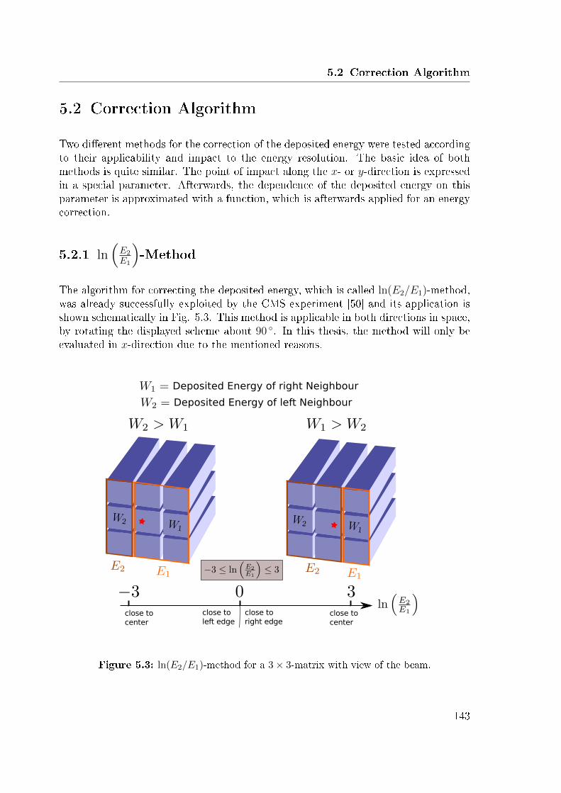
5.2 Correction Algorithm
5.2 Correction Algorithm
Two dierent methods for the correction of the deposited energy were tested accordingto their applicability and impact to the energy resolution. The basic idea of bothmethods is quite similar. The point of impact along the x- or y-direction is expressedin a special parameter. Afterwards, the dependence of the deposited energy on thisparameter is approximated with a function, which is afterwards applied for an energycorrection.
5.2.1 ln(E2
E1
)-Method
The algorithm for correcting the deposited energy, which is called ln(E2/E1)-method,was already successfully exploited by the CMS experiment [50] and its application isshown schematically in Fig. 5.3. This method is applicable in both directions in space,by rotating the displayed scheme about 90 . In this thesis, the method will only beevaluated in x-direction due to the mentioned reasons.
Figure 5.3: ln(E2/E1)-method for a 3× 3-matrix with view of the beam.
143

Chapter 5 Higher Order Energy Correction
In the following, the ln(E2/E1)-method is explained step by step with respect to Fig.5.3 and the software implementation. For the important steps, the relevant picturesare shown with the obtained data from the CERN beamtime. In order to simplify theapplication of the ln(E2/E1)-method, only events with a maximum energy depositionin crystal 28 were analysed.The registered energy of the direct neighbours, which are labelled W1 and W2 corre-sponding to the right and the left neighbour, respectively, are compared. This alreadygives a rough information about the point of impact and is marked in Fig. 5.3 with ared star. According to the distinction of cases forW1 andW2, the 3×3 detector matrixis subdivided in two subarrays with summarised energies E1 and E2. Afterwards thenatural logarithm of the ratio E2/E1 gives the nal information about the point ofimpact along the regarded direction at the crystal with maximum energy deposition.The choice of the natural logarithm is connected with the lateral shower spread ofthe electromagnetic shower. Due to the fact, that the value of ln(E2/E1) is not veryintuitive, the axis in the bottom part of Fig. 5.3 shows the corresponding positionat the crystal front face. ln(E2/E1) ranging from −3 to 3, whereas | ln(E2/E1)| ≈ 3belongs to events with a centrally striking incident particle. In case of ln(E2/E1) ≈ 0,the energy is almost perfectly shared between the two subarrays and belongs to animpinging particle close to one of the crystal borders. The correlation of the ln(E2/E1)-parameter with the impact position along the x-axis is shown for both performed runsin Fig. 5.4. Here, it was distinguished between the reconstructed point of impact bythe EMC with a logarithmical point of gravity algorithm (compare Eq. 5.2) and theextrapolated track by the silicon based tracking detectors.
xreconstructed by EMC =
∑i
wi · xi∑i
wi(5.2)
with wi =
0, W0 + ln(EiET≤ 0)
W0 + ln(EiET
), else;
xi : implemented coordinate of crystal i
W0 : weighting parameter
ET =∑i
Ei
Furthermore, the similarity of the associated histograms in Fig. 5.4 underlines eectiveoperation of reconstruction algorithm of the point of impact (Eq. 5.2), since it deliversan almost perfect linear correlation with values obtained by the tracking units.In a next step, the obtained distribution of the ln(E2/E1)-parameter of the second run(shown in Fig. 5.5a) is subdivided into 50 equal slices ranges from −3 to 3 with a widthof 0.12. Here, no explicit cut on the tracking system was set, since the whole algorithmis based only on the information obtained by the EMC. For the events of the i-th slice,
144

5.2 Correction Algorithm
1E2E
ln
4 3 2 1 0 1 2 3 4
in m
mre
co
nstr
ucte
d b
y E
MC
x
5
0
5
10
15
20
25
x_reconstructed_vs_ln(E2/E1)Entries 97874Mean x 0.6392
Mean y 9.108RMS x 2.325RMS y 3.915
x_reconstructed_vs_ln(E2/E1)Entries 97874Mean x 0.6392
Mean y 9.108RMS x 2.325RMS y 3.915
0
5
10
15
20
25
30
35
x_reconstructed_vs_ln(E2/E1)
(a)
1E2E
ln
4 3 2 1 0 1 2 3 4
in m
mtr
acke
d b
y S
id
ete
cto
rsx
5
0
5
10
15
20
25
x_tracked_vs_ln(E2/E1)
Entries 97874
Mean x 0.6411
Mean y 8.814
RMS x 2.329
RMS y 4.206
x_tracked_vs_ln(E2/E1)
Entries 97874
Mean x 0.6411
Mean y 8.814
RMS x 2.329
RMS y 4.206
0
5
10
15
20
25
x_tracked_vs_ln(E2/E1)
(b)
1E2E
ln
4 3 2 1 0 1 2 3 4
in m
mre
co
nstr
ucte
d b
y E
MC
x
5
0
5
10
15
20
25
x_reconstructed_vs_ln(E2/E1)Entries 61269Mean x 1.403Mean y 3.349RMS x 0.6967RMS y 2.251
x_reconstructed_vs_ln(E2/E1)Entries 61269Mean x 1.403Mean y 3.349RMS x 0.6967RMS y 2.251
0
5
10
15
20
25
30
x_reconstructed_vs_ln(E2/E1)
(c)
1E2E
ln
4 3 2 1 0 1 2 3 4
in m
mtr
acke
d b
y S
id
ete
cto
rsx
5
0
5
10
15
20
25
x_tracked_vs_ln(E2/E1)Entries 61269
Mean x 1.405Mean y 3.958
RMS x 0.6922RMS y 2.634
x_tracked_vs_ln(E2/E1)Entries 61269
Mean x 1.405Mean y 3.958
RMS x 0.6922RMS y 2.634
0
2
4
6
8
10
12
14
16
18
20
22
24
x_tracked_vs_ln(E2/E1)
(d)
Figure 5.4: Correlation between ln(E2/E1) and the x-coordinate of the point ofimpact. For a better comparison, only events with an unambiguous reconstructedtrack of the impinging particle by the tracking devices are shown. Figures (a)and (b) belong to the performed run, where the beam was aimed to the centre ofcrystal 28 and (c) and (d) to the one in between crystals 28 and 29. Furthermore,the columns correspond to the x coordinates obtained by the pure EMC energyinformation (according to Eq. 5.2) and the reconstructed track by the trackingdetectors. The position 0 corresponds in all cases to the transition of crystal 28and 29.
145
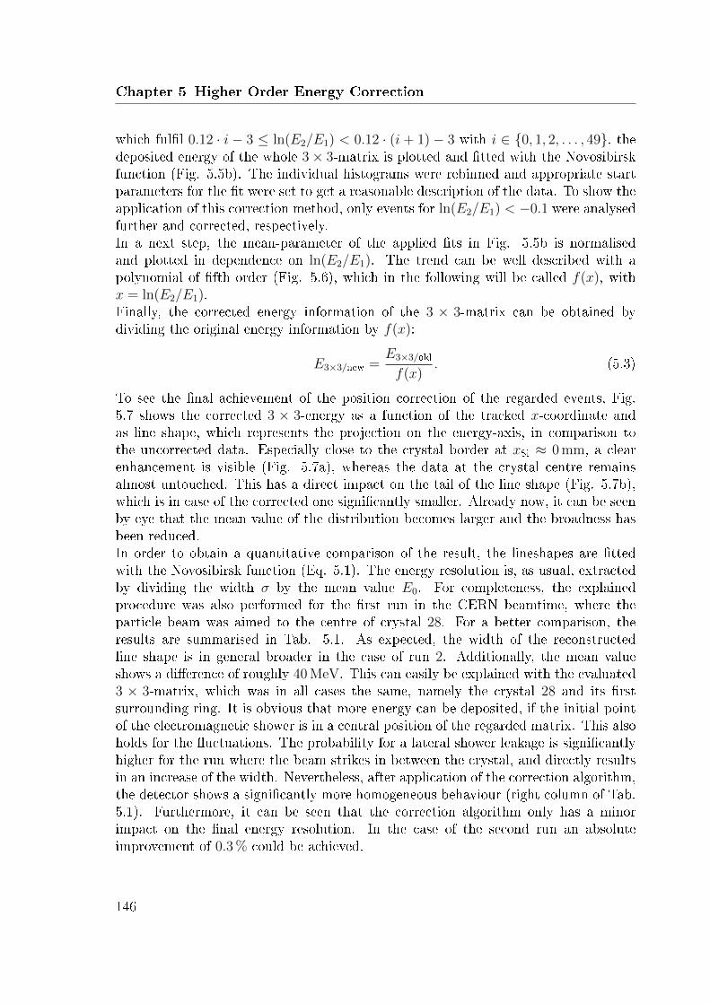
Chapter 5 Higher Order Energy Correction
which full 0.12 · i − 3 ≤ ln(E2/E1) < 0.12 · (i + 1) − 3 with i ∈ 0, 1, 2, . . . , 49, thedeposited energy of the whole 3× 3-matrix is plotted and tted with the Novosibirskfunction (Fig. 5.5b). The individual histograms were rebinned and appropriate startparameters for the t were set to get a reasonable description of the data. To show theapplication of this correction method, only events for ln(E2/E1) < −0.1 were analysedfurther and corrected, respectively.In a next step, the mean-parameter of the applied ts in Fig. 5.5b is normalisedand plotted in dependence on ln(E2/E1). The trend can be well described with apolynomial of fth order (Fig. 5.6), which in the following will be called f(x), withx = ln(E2/E1).Finally, the corrected energy information of the 3 × 3-matrix can be obtained bydividing the original energy information by f(x):
E3×3/new =E3×3/old
f(x). (5.3)
To see the nal achievement of the position correction of the regarded events, Fig.5.7 shows the corrected 3 × 3-energy as a function of the tracked x-coordinate andas line shape, which represents the projection on the energy-axis, in comparison tothe uncorrected data. Especially close to the crystal border at xSi ≈ 0 mm, a clearenhancement is visible (Fig. 5.7a), whereas the data at the crystal centre remainsalmost untouched. This has a direct impact on the tail of the line shape (Fig. 5.7b),which is in case of the corrected one signicantly smaller. Already now, it can be seenby eye that the mean value of the distribution becomes larger and the broadness hasbeen reduced.In order to obtain a quantitative comparison of the result, the lineshapes are ttedwith the Novosibirsk function (Eq. 5.1). The energy resolution is, as usual, extractedby dividing the width σ by the mean value E0. For completeness, the explainedprocedure was also performed for the rst run in the CERN beamtime, where theparticle beam was aimed to the centre of crystal 28. For a better comparison, theresults are summarised in Tab. 5.1. As expected, the width of the reconstructedline shape is in general broader in the case of run 2. Additionally, the mean valueshows a dierence of roughly 40 MeV. This can easily be explained with the evaluated3 × 3-matrix, which was in all cases the same, namely the crystal 28 and its rstsurrounding ring. It is obvious that more energy can be deposited, if the initial pointof the electromagnetic shower is in a central position of the regarded matrix. This alsoholds for the uctuations. The probability for a lateral shower leakage is signicantlyhigher for the run where the beam strikes in between the crystal, and directly resultsin an increase of the width. Nevertheless, after application of the correction algorithm,the detector shows a signicantly more homogeneous behaviour (right column of Tab.5.1). Furthermore, it can be seen that the correction algorithm only has a minorimpact on the nal energy resolution. In the case of the second run an absoluteimprovement of 0.3 % could be achieved.
146

5.2 Correction Algorithm
Distr. of ln(E2/E1) in x
Entries 109400
Mean 1.32
RMS 1.145
1E
2E
ln
4 3 2 1 0 1 2 3 4
co
un
ts
0
200
400
600
800
1000
1200
1400
1600
1800
2000Distr. of ln(E2/E1) in x
Entries 109400
Mean 1.32
RMS 1.145
Distr. of ln(E2/E1) in x
(a)
110001150012000125001300013500140001450015000
0
50
100
150
200
250
110001150012000125001300013500140001450015000
0
100
200
300
400
500
110001150012000125001300013500140001450015000
0
100
200
300
400
500
600
700
800
110001150012000125001300013500140001450015000
0
200
400
600
800
1000
110001150012000125001300013500140001450015000
0
200
400
600
800
1000
110001150012000125001300013500140001450015000
0
200
400
600
800
1000
1200
110001150012000125001300013500140001450015000
0
200
400
600
800
1000
1200
1400
110001150012000125001300013500140001450015000
0
200
400
600
800
1000
1200
1400
1600
110001150012000125001300013500140001450015000
0
200
400
600
800
1000
1200
1400
110001150012000125001300013500140001450015000
0
200
400
600
800
1000
1200
1400
1600
1100011500120001250013000135001400014500150000
200
400
600
800
1000
1200
1400
1100011500120001250013000135001400014500150000
200
400
600
800
1000
1200
1400
1600
1100011500120001250013000135001400014500150000
200
400
600
800
1000
1200
1400
1100011500120001250013000135001400014500150000
200
400
600
800
1000
1200
1100011500120001250013000135001400014500150000
200
400
600
800
1000
1200
1400
1100011500120001250013000135001400014500150000
200
400
600
800
1000
1200
1100011500120001250013000135001400014500150000
200
400
600
800
1000
1200
1100011500120001250013000135001400014500150000
200
400
600
800
1000
1100011500120001250013000135001400014500150000
100
200
300
400
500
600
700
800
900
1100011500120001250013000135001400014500150000
100
200
300
400
500
600
700
800
900
11000115001200012500130001350014000145000
200
400
600
800
1000
1200
1400
11000115001200012500130001350014000145000
200
400
600
800
1000
11000115001200012500130001350014000145000
100
200
300
400
500
600
700
800
900
11000115001200012500130001350014000145000
100
200
300
400
500
600
700
800
11000115001200012500130001350014000145000
50
100
150
200
250
300
350
400
450
11000115001200012500130001350014000145000
10
20
30
40
50
11000115001200012500130001350014000145000
1
2
3
4
5
6
11000115001200012500130001350014000145000
1
2
3
4
5
11000115001200012500130001350014000145000
0.5
1
1.5
2
2.5
3
3.5
4
11000115001200012500130001350014000145000
0.5
1
1.5
2
2.5
3
3.5
4
11000115001200012500130001350014000145000
0.5
1
1.5
2
2.5
3
3.5
4
11000115001200012500130001350014000145000
1
2
3
4
5
11000115001200012500130001350014000145000
2
4
6
8
10
11000115001200012500130001350014000145000
1
2
3
4
5
6
7
8
9
11000115001200012500130001350014000145000
1
2
3
4
5
6
7
8
11000115001200012500130001350014000145000
1
2
3
4
5
6
7
8
9
11000115001200012500130001350014000145000
2
4
6
8
10
12
14
11000115001200012500130001350014000145000
2
4
6
8
10
12
14
16
18
20
22
24
1100011500120001250013000135001400014500150000
2
4
6
8
10
12
14
16
1100011500120001250013000135001400014500150000
5
10
15
20
25
1100011500120001250013000135001400014500150000
2
4
6
8
10
12
14
16
18
1100011500120001250013000135001400014500150000
5
10
15
20
25
30
35
1100011500120001250013000135001400014500150000
10
20
30
40
50
1100011500120001250013000135001400014500150000
10
20
30
40
50
60
1100011500120001250013000135001400014500150000
10
20
30
40
50
60
70
80
1100011500120001250013000135001400014500150000
10
20
30
40
50
60
70
80
90
1100011500120001250013000135001400014500150000
20
40
60
80
100
120
140
160
180
1100011500120001250013000135001400014500150000
50
100
150
200
250
1100011500120001250013000135001400014500150000
50
100
150
200
250
1100011500120001250013000135001400014500150000
20
40
60
80
100
120
140
160
180
200
220
(b)
Figure 5.5: (a) Distribution of 109, 400 events as function of the ln(E2/E1)-parameter. For the majority of events, the incident particle impinges on theleft half of the crystal. (b) Subsections of the ln(E2/E1)-parameters tted withthe Novosibirsk function (Eq. 5.1) marked with red lines.
147

Chapter 5 Higher Order Energy Correction
1E2E
ln3 2.5 2 1.5 1 0.5 0
no
rma
lis
ed
en
erg
y o
f 3
x3
ma
trix
0.92
0.94
0.96
0.98
1
1.02
/ ndf 2χ 15.73 / 18
p0 0.002433± 0.9344
p1 0.01341± 0.1265
p2 0.0241± 0.1358
p3 0.01878± 0.08029
p4 0.006578± 0.02313
p5 0.0008488± 0.002526
/ ndf 2χ 15.73 / 18
p0 0.002433± 0.9344
p1 0.01341± 0.1265
p2 0.0241± 0.1358
p3 0.01878± 0.08029
p4 0.006578± 0.02313
p5 0.0008488± 0.002526
x_Correction
Figure 5.6: Dependence of the ln(E2/E1)-parameter of the deposited energy withinthe 3 × 3-matrix. The tted function f(x) is marked in red and shows a gooddescription of the data points.
Run Parameter Uncorrected Corrected
1
Width σ/MeV 227.20 221.87
Mean value E0/MeV 13, 979.50 13, 994.60
Energy resolution1.625 1.585σ
E0/%
2
Width σ/MeV 257.12 230.31
Mean value E0/MeV 13, 562.00 13, 644.10
Energy resolution1.896 1.688σ
E0/%
Table 5.1: Achieved results for the 3× 3-matrix of the ln(E2/E1)-method for bothruns at CERN. For the listed results, the correction method was only appliedalong the horizontal x-direction.
148

5.2 Correction Algorithm
in mmSi
x
2 0 2 4 6 8 10
3x3
En
erg
y in
Ge
V
10
11
12
13
14
15
16
0
5
10
15
20
25
30
35
40
Uncorrected energy sum of 3x3matrix
in mmSi
x
2 0 2 4 6 8 10
3x3
En
erg
y in
Ge
V
10
11
12
13
14
15
16
0
5
10
15
20
25
30
35
40
Corrected energy sum of 3x3matrix
(a)
Energy of 3x3matrix in MeV
11000 11500 12000 12500 13000 13500 14000 14500 15000
Counts
per
10 M
eV
0
500
1000
1500
2000
2500
3000
3500
Uncorrected
Corrected
Corrected EnergySum in x
(b)
Figure 5.7: Results position correction for run 2 for events with a maximum energydeposition in crystal 28.
149
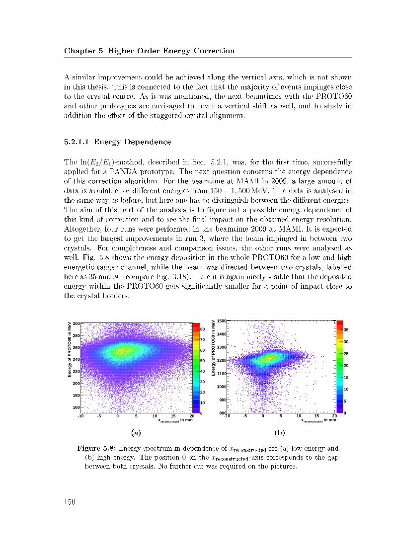
Chapter 5 Higher Order Energy Correction
A similar improvement could be achieved along the vertical axis, which is not shownin this thesis. This is connected to the fact that the majority of events impinges closeto the crystal centre. As it was mentioned, the next beamtimes with the PROTO60and other prototypes are envisaged to cover a vertical shift as well, and to study inaddition the eect of the staggered crystal alignment.
5.2.1.1 Energy Dependence
The ln(E2/E1)-method, described in Sec. 5.2.1, was, for the rst time, successfullyapplied for a PANDA prototype. The next question concerns the energy dependenceof this correction algorithm. For the beamtime at MAMI in 2009, a large amount ofdata is available for dierent energies from 150− 1, 500 MeV. The data is analysed inthe same way as before, but here one has to distinguish between the dierent energies.The aim of this part of the analysis is to gure out a possible energy dependence ofthis kind of correction and to see the nal impact on the obtained energy resolution.Altogether, four runs were performed in the beamtime 2009 at MAMI. It is expectedto get the largest improvements in run 3, where the beam impinged in between twocrystals. For completeness and comparison issues, the other runs were analysed aswell. Fig. 5.8 shows the energy deposition in the whole PROTO60 for a low and highenergetic tagger channel, while the beam was directed between two crystals, labelledhere as 35 and 36 (compare Fig. 3.18). Here it is again nicely visible that the depositedenergy within the PROTO60 gets signicantly smaller for a point of impact close tothe crystal borders.
in mmreconstructedx10 5 0 5 10 15 20
En
erg
y o
f P
RO
TO
60
in
MeV
160
180
200
220
240
260
280
300
pLGSumvsXPos_low_energy_in_crystal_34
Entries 216920
Mean x 2.616
Mean y 249.1
RMS x 5.104
RMS y 15.6
pLGSumvsXPos_low_energy_in_crystal_34
Entries 216920
Mean x 2.616
Mean y 249.1
RMS x 5.104
RMS y 15.6
0
10
20
30
40
50
60
70
80
LGvsXPos
(a)
in mmreconstructedx10 5 0 5 10 15 20
En
erg
y o
f P
RO
TO
60 i
n M
eV
800
900
1000
1100
1200
1300
1400
1500
pLGSumvsXPos_high_energy_in_crystal_34
Entries 24372
Mean x 1.501
Mean y 1192
RMS x 3.281
RMS y 65.35
pLGSumvsXPos_high_energy_in_crystal_34
Entries 24372
Mean x 1.501
Mean y 1192
RMS x 3.281
RMS y 65.35
0
5
10
15
20
25
30
35
LGvsXPos
(b)
Figure 5.8: Energy spectrum in dependence of xreconstructed for (a) low energy and(b) high energy. The position 0 on the xreconstructed-axis corresponds to the gapbetween both crystals. No further cut was required on the pictures.
150

5.2 Correction Algorithm
For correcting the data, the ln(E2/E1)-method was applied separately for the dierentenergies. The get the best possible starting point of the analysis concerning statistics,the data of all four runs were summed up. At each incident energy, the ln(E2/E1)parameter was subdivided in to 50 bins with equal width and is shown exemplaryfor the tagger channel 12 with an incident photon energy of 355.88 MeV in Fig. 5.9.In order to get appropriate ts of the individual subsections, only bins with at least1, 000 events were considered and analysed. The tagger channel selections the highestenergy was completely excluded due to the insucient amount of events.
Entries 15216
240 260 280 300 320 340 360 380
0
200
400
600
800
1000
1200
1400
1600
Entries 15216 Entries 16551
240 260 280 300 320 340 360 380
0
200
400
600
800
1000
1200
1400
1600
Entries 16551 Entries 17821
240 260 280 300 320 340 360 380
0
200
400
600
800
1000
1200
1400
1600
1800
Entries 17821 Entries 18202
240 260 280 300 320 340 360 380
0
200
400
600
800
1000
1200
1400
1600
1800
Entries 18202 Entries 18802
240 260 280 300 320 340 360 380
0
200
400
600
800
1000
1200
1400
1600
1800
Entries 18802 Entries 18000
240 260 280 300 320 340 360 380
0
200
400
600
800
1000
1200
1400
1600
1800
Entries 18000 Entries 17627
240 260 280 300 320 340 360 380
0
200
400
600
800
1000
1200
1400
1600
1800
Entries 17627 Entries 16715
240 260 280 300 320 340 360 380
0
200
400
600
800
1000
1200
1400
1600
Entries 16715 Entries 15695
240 260 280 300 320 340 360 380
0
200
400
600
800
1000
1200
1400
1600
Entries 15695 Entries 14329
240 260 280 300 320 340 360 380
0
200
400
600
800
1000
1200
1400
Entries 14329
Entries 13242
240 260 280 300 320 340 360 3800
200
400
600
800
1000
1200
Entries 13242 Entries 11906
240 260 280 300 320 340 360 3800
200
400
600
800
1000
1200
Entries 11906 Entries 10920
240 260 280 300 320 340 360 3800
200
400
600
800
1000
Entries 10920 Entries 9804
240 260 280 300 320 340 360 3800
200
400
600
800
1000
Entries 9804 Entries 8902
240 260 280 300 320 340 360 3800
100
200
300
400
500
600
700
800
900
Entries 8902 Entries 8181
240 260 280 300 320 340 360 3800
100
200
300
400
500
600
700
800
Entries 8181 Entries 7552
240 260 280 300 320 340 360 3800
100
200
300
400
500
600
700
Entries 7552 Entries 6998
240 260 280 300 320 340 360 3800
100
200
300
400
500
600
Entries 6998 Entries 6340
240 260 280 300 320 340 360 3800
100
200
300
400
500
Entries 6340 Entries 5598
240 260 280 300 320 340 360 3800
100
200
300
400
500
Entries 5598
Entries 5249
240 260 280 300 320 340 360 3800
100
200
300
400
500
Entries 5249 Entries 4871
240 260 280 300 320 340 360 3800
50
100
150
200
250
300
350
400
Entries 4871 Entries 4369
240 260 280 300 320 340 360 3800
50
100
150
200
250
300
350
400
Entries 4369 Entries 3929
240 260 280 300 320 340 360 3800
50
100
150
200
250
300
350
Entries 3929 Entries 2819
240 260 280 300 320 340 360 3800
20
40
60
80
100
120
140
160
180
200
220
240
Entries 2819 Entries 1319
240 260 280 300 320 340 360 3800
20
40
60
80
100
Entries 1319 Entries 648
240 260 280 300 320 340 360 3800
10
20
30
40
50
Entries 648 Entries 532
240 260 280 300 320 340 360 3800
5
10
15
20
25
30
35
40
Entries 532 Entries 656
240 260 280 300 320 340 360 3800
5
10
15
20
25
30
35
40
Entries 656 Entries 839
240 260 280 300 320 340 360 3800
10
20
30
40
50
60
Entries 839
Entries 988
240 260 280 300 320 340 360 3800
10
20
30
40
50
60
70
80
Entries 988 Entries 1189
240 260 280 300 320 340 360 3800
10
20
30
40
50
60
70
80
90
Entries 1189 Entries 1455
240 260 280 300 320 340 360 3800
20
40
60
80
100
120
Entries 1455 Entries 1797
240 260 280 300 320 340 360 3800
20
40
60
80
100
120
140
Entries 1797 Entries 2201
240 260 280 300 320 340 360 3800
20
40
60
80
100
120
140
160
180
Entries 2201 Entries 2768
240 260 280 300 320 340 360 3800
50
100
150
200
250
Entries 2768 Entries 3435
240 260 280 300 320 340 360 3800
50
100
150
200
250
300
Entries 3435 Entries 4390
240 260 280 300 320 340 360 3800
50
100
150
200
250
300
350
400
Entries 4390 Entries 5308
240 260 280 300 320 340 360 3800
100
200
300
400
500
Entries 5308 Entries 6643
240 260 280 300 320 340 360 3800
100
200
300
400
500
600
Entries 6643
Entries 8002
240 260 280 300 320 340 360 3800
100
200
300
400
500
600
700
800
Entries 8002 Entries 9621
240 260 280 300 320 340 360 3800
200
400
600
800
1000
Entries 9621 Entries 11078
240 260 280 300 320 340 360 3800
200
400
600
800
1000
Entries 11078 Entries 12312
240 260 280 300 320 340 360 3800
200
400
600
800
1000
1200
Entries 12312 Entries 13930
240 260 280 300 320 340 360 3800
200
400
600
800
1000
1200
1400
Entries 13930 Entries 14836
240 260 280 300 320 340 360 3800
200
400
600
800
1000
1200
1400
Entries 14836 Entries 15462
240 260 280 300 320 340 360 3800
200
400
600
800
1000
1200
1400
1600
Entries 15462 Entries 15505
240 260 280 300 320 340 360 3800
200
400
600
800
1000
1200
1400
1600
Entries 15505 Entries 15412
240 260 280 300 320 340 360 3800
200
400
600
800
1000
1200
1400
1600
Entries 15412 Entries 14584
240 260 280 300 320 340 360 3800
200
400
600
800
1000
1200
1400
1600
Entries 14584
Figure 5.9: Energy distribution in MeV for dierent ln(E2/E1)-parameter (MAMI2009) for a single tagger channel. The red curves correspond to the applied twith a Novosibirsk function for histograms with more than 1, 000 events.
In Fig. 5.10a the obtained mean values of the performed ts are plotted as a functionof the ln(E2/E1)-parameter including the corresponding polynomials. The higher theenergy, the smaller the amount of available data. For a better comparison, the obtainedcorrection polynomials are plotted separately and normalised to the ln(E2/E1)-valueof −3 and 3, respectively.On the right hand side of Fig. 5.10a less data points are available, especially for thehighest energies. Therefore the t range, or correction range, respectively, is ratherlimited. The shapes of all correction curves are similar and getting smaller close tothe crystal border at ln(E2/E1) ≈ 0. In a relative view in Fig. 5.10b, only very smalldeviations in the order of 1% are visible. Here, no correlation with the energy couldbe registered. By comparing to the obtained correction function at 15 GeV (Fig. 5.6),there is no signicant dierence. As an additional remark, the shift at ln(E2/E1) ≈ 0
151

Chapter 5 Higher Order Energy Correction
1E2E
ln
3 2 1 0 1 2 3
Deposited E
nerg
y in 3
x3 M
atr
ix / M
eV
200
400
600
800
1000
1200
Position Correction for xDirection
(a)
1E
2E
ln
3 2 1 0 1 2 3
Corr
ection function in a
.u.
0.93
0.94
0.95
0.96
0.97
0.98
0.99
1
Position Correction for xDirection
(b)
Figure 5.10: (a) Correction functions of all energies (MAMI 2009). (b) Correctionfunctions for all energies normalised to the energy deposition at ln(E2/E1) = −3.
152

5.2 Correction Algorithm
for the both curves from the left and right hand side, respectively, might be caused bya non-perfect alignment of the crystal with respect to the beam axis.
5.2.1.2 Impact on Energy Resolution
In order to see the nal achievement concerning the most important observable, theresolution of the uncorrected and corrected energy was determined. Therefore thedata was channel-wise corrected using the correction functions as displayed in Fig.5.10. For the third run (shooting in between crystal 35 and 36), where the majorimpact of the correction is expected, the lineshapes of the 3 × 3-matrix are plottedfor all energies in Fig. 5.11. The tagger channel with an energy of 1441.06 MeV wasexcluded due to insucient statistics.
LG_tagged_UNCorrected_1
Entries 2237
Mean 1338
RMS 39.14
deposited energy / MeV1200 1250 1300 1350 1400 1450
co
un
ts /
1 M
eV
0
5
10
15
20
25
30
LG_tagged_UNCorrected_1
Entries 2237
Mean 1338
RMS 39.14
Tagged Lineshapes 1441.06 MeV LG_tagged_UNCorrected_2
Entries 13609
Mean 1267
RMS 36.44
deposited energy / MeV1150 1200 1250 1300 1350
co
un
ts /
1 M
eV
0
20
40
60
80
100
120
140
160
180
LG_tagged_UNCorrected_2
Entries 13609
Mean 1267
RMS 36.44
Tagged Lineshapes 1356.89 MeV LG_tagged_UNCorrected_3
Entries 12626
Mean 1177RMS 34.1
deposited energy / MeV1060 1080 1100 1120 1140 1160 1180 1200 1220 1240 1260
co
un
ts /
1 M
eV
0
20
40
60
80
100
120
140
160
180
LG_tagged_UNCorrected_3
Entries 12626
Mean 1177RMS 34.1
Tagged Lineshapes 1257.31 MeV LG_tagged_UNCorrected_4
Entries 19708
Mean 1083
RMS 32.87
deposited energy / MeV980 1000 1020 1040 1060 1080 1100 1120 1140 1160
co
un
ts /
1 M
eV
0
50
100
150
200
250
LG_tagged_UNCorrected_4
Entries 19708
Mean 1083
RMS 32.87
Tagged Lineshapes 1156.56 MeV
LG_tagged_UNCorrected_5
Entries 22356
Mean 991.4
RMS 31.26
deposited energy / MeV900 920 940 960 980 1000 1020 1040 1060 1080
co
un
ts /
1 M
eV
0
50
100
150
200
250
300
LG_tagged_UNCorrected_5
Entries 22356
Mean 991.4
RMS 31.26
Tagged Lineshapes 1057.70 MeV LG_tagged_UNCorrected_6
Entries 27739
Mean 896.6
RMS 29.97
deposited energy / MeV800 820 840 860 880 900 920 940 960 980
co
un
ts /
1 M
eV
0
50
100
150
200
250
300
350
400
LG_tagged_UNCorrected_6
Entries 27739
Mean 896.6
RMS 29.97
Tagged Lineshapes 956.16 MeV LG_tagged_UNCorrected_7
Entries 33264
Mean 806.1
RMS 27.81
deposited energy / MeV720 740 760 780 800 820 840 860 880
co
un
ts /
1 M
eV
0
100
200
300
400
500
LG_tagged_UNCorrected_7
Entries 33264
Mean 806.1
RMS 27.81
Tagged Lineshapes 857.98 MeV LG_tagged_UNCorrected_8
Entries 41721Mean 712.6
RMS 26.01
deposited energy / MeV640 660 680 700 720 740 760 780
co
un
ts /
1 M
eV
0
100
200
300
400
500
600
700
LG_tagged_UNCorrected_8
Entries 41721Mean 712.6
RMS 26.01
Tagged Lineshapes 756.58 MeV
LG_tagged_UNCorrected_9
Entries 40021
Mean 620.1
RMS 23.96
deposited energy / MeV560 580 600 620 640 660 680
co
un
ts /
1 M
eV
0
100
200
300
400
500
600
700
LG_tagged_UNCorrected_9
Entries 40021
Mean 620.1
RMS 23.96
Tagged Lineshapes 657.34 MeV LG_tagged_UNCorrected_10
Entries 60256
Mean 526.2
RMS 22.08
deposited energy / MeV460 480 500 520 540 560 580 600
co
un
ts /
1 M
eV
0
200
400
600
800
1000
LG_tagged_UNCorrected_10
Entries 60256
Mean 526.2
RMS 22.08
Tagged Lineshapes 556.97 MeV LG_tagged_UNCorrected_11
Entries 71279
Mean 431.3
RMS 20.27
deposited energy / MeV360 380 400 420 440 460 480 500
co
un
ts /
1 M
eV
0
200
400
600
800
1000
1200
1400
LG_tagged_UNCorrected_11
Entries 71279
Mean 431.3
RMS 20.27
Tagged Lineshapes 456.26 MeV LG_tagged_UNCorrected_12
Entries 97388
Mean 337.3
RMS 18.71
deposited energy / MeV280 300 320 340 360 380 400 420
co
un
ts /
1 M
eV
0
500
1000
1500
2000
2500
LG_tagged_UNCorrected_12
Entries 97388
Mean 337.3
RMS 18.71
Tagged Lineshapes 355.88 MeV
LG_tagged_UNCorrected_13
Entries 151586
Mean 244RMS 17.04
deposited energy / MeV180 200 220 240 260 280 300 320
co
un
ts /
1 M
eV
0
500
1000
1500
2000
2500
3000
3500
4000
4500
LG_tagged_UNCorrected_13
Entries 151586
Mean 244RMS 17.04
Tagged Lineshapes 256.41 MeV LG_tagged_UNCorrected_14
Entries 159587
Mean 184.6
RMS 15.91
deposited energy / MeV120 140 160 180 200 220 240 260 280
co
un
ts /
1 M
eV
0
1000
2000
3000
4000
5000
LG_tagged_UNCorrected_14
Entries 159587
Mean 184.6
RMS 15.91
Tagged Lineshapes 187.99 MeV LG_tagged_UNCorrected_15
Entries 156770
Mean 153.3
RMS 15.43
deposited energy / MeV80 100 120 140 160 180 200 220 240
co
un
ts /
1 M
eV
0
1000
2000
3000
4000
5000
LG_tagged_UNCorrected_15
Entries 156770
Mean 153.3
RMS 15.43
Tagged Lineshapes 158.31 MeV
Figure 5.11: Uncorrected (black) and corrected (red) lineshapes of the 3×3-matrixwith a threshold of 1 MeV. For the highest energy no correction was possible dueto the insucient statistics.
Afterwards, the lineshapes were tted with the Novosibirsk function, in which theenergy resolution is given by the ratio of width and most probable value. For ttingpurposes, appropriate start values for E0 and σ were set, namely mean value and RMS
153

Chapter 5 Higher Order Energy Correction
of the particular histogram, respectively. This promises a stable and automatic ttingprocedure. For the run where the major impact is expected, the lineshapes for theuncorrected and corrected values are shown in Fig. 5.11. The nal results for two runs(centrally hitting crystal 35, and in between 35 and 36) of the 2009 beamtime at MAMIare presented as a function of the impinging energy. In addition, the obtained trendof the data points is tted with the typical three parametric function for describingthe energy resolution of an EMC:
σ
E=
√(a√E
)2
+
(b
E
)2
+ c (5.4)
(5.5)
The free parameter a stands for photon statistics and has a 1/√E-dependence. b
is usually smaller compared to the other parameters and describes the contribu-tion caused by electronics. This term decreases faster with the energy with a 1/E-dependence. The constant term c includes several systematical eects, like e.g. cal-ibration issues or the inhomogeneous collection of the scintillation light within thecrystal. The individual terms are summed up quadratically, since one can, in rstorder, assume their independence. The result of a t using Eq. 5.4 gives a roughimpression of the discussed eects. For all performed ts of the trend of the energyresolution, the data points were weighted equally. The vertical error bars were deter-mined with the usual error propagation method (compare Eq. 5.6), but are not visiblein the chosen y-range in Fig. 5.12 and 5.13. For the x-direction a constant uncertaintyof 2 MeV was assumed.
∆( σE
)=
√(1
E
)2
· (∆σ)2 +( σE2
)2
· (∆E)2 (5.6)
The energy resolutions of the rst run are shown in Fig. 5.12.As expected, an overall correction of the deposited energies only has a small impact onthe nal energy resolution. Furthermore, the displayed t parameters according to Eq.5.4 do not dier much for both scenarios. Nevertheless, a slight improvement is visiblealong the full energy range. The dierence (σ/EPeak)uncorrected − (σ/EPeak)corrected isranging from 0.11 % to 0.04 % from the smallest to the highest energy, respectively.However, in the case of shooting in between crystals, the energy correction leads toa signicant improvement. In Fig. 5.13 the obtained results are again plotted versusthe incident photon energy.
A signicant dierence between the shown curves becomes visible and is uctuatingaround an absolute value of 0.25 %. This improvement is comparable to the resultobtained at the CERN beamtime with 0.3 % at an initial positron energy of 15 GeV.
154
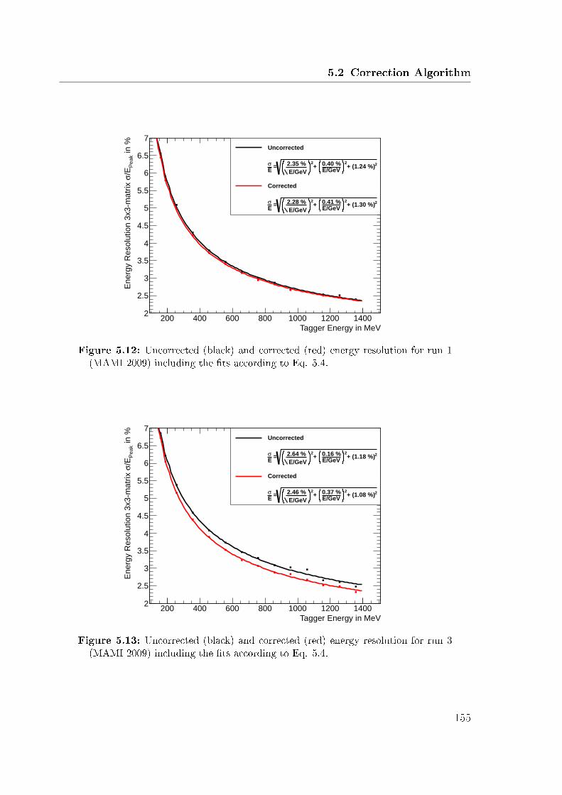
5.2 Correction Algorithm
Tagger Energy in MeV200 400 600 800 1000 1200 1400
in
%P
ea
k/E
σE
ne
rgy R
eso
lutio
n 3
x3
ma
trix
2
2.5
3
3.5
4
4.5
5
5.5
6
6.5
7
Energy Resolution Run4 (Center #35)
Uncorrected
2+ (1.24 %)2
E/GeV0.40 %+
2
E/GeV
2.35 % = Eσ
Corrected
2+ (1.30 %)2
E/GeV0.41 %+
2
E/GeV
2.28 % = Eσ
Figure 5.12: Uncorrected (black) and corrected (red) energy resolution for run 1(MAMI 2009) including the ts according to Eq. 5.4.
Tagger Energy in MeV200 400 600 800 1000 1200 1400
in
%P
ea
k/E
σE
ne
rgy R
eso
lutio
n 3
x3
ma
trix
2
2.5
3
3.5
4
4.5
5
5.5
6
6.5
7
Energy Resolution Run4 (Center #35)
Uncorrected
2+ (1.18 %)2
E/GeV0.16 %+
2
E/GeV
2.64 % = Eσ
Corrected
2+ (1.08 %)2
E/GeV0.37 %+
2
E/GeV
2.46 % = Eσ
Figure 5.13: Uncorrected (black) and corrected (red) energy resolution for run 3(MAMI 2009) including the ts according to Eq. 5.4.
155

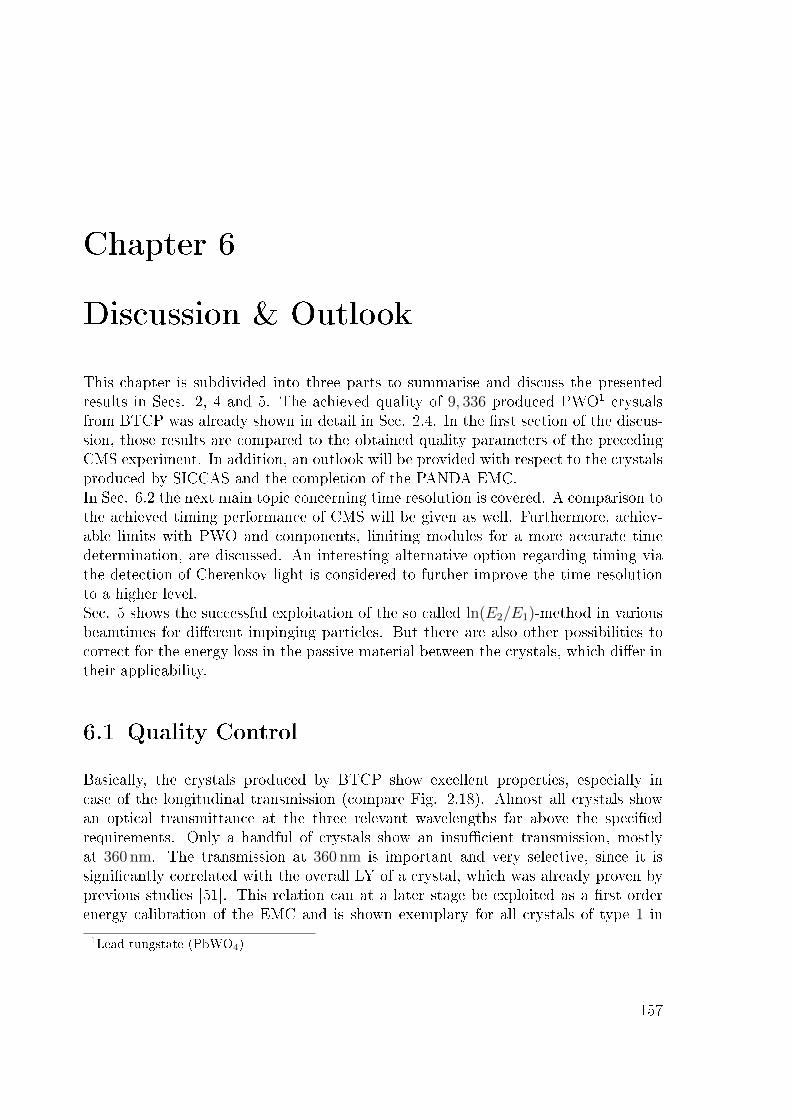
Chapter 6
Discussion & Outlook
This chapter is subdivided into three parts to summarise and discuss the presentedresults in Secs. 2, 4 and 5. The achieved quality of 9, 336 produced PWO1 crystalsfrom BTCP was already shown in detail in Sec. 2.4. In the rst section of the discus-sion, those results are compared to the obtained quality parameters of the precedingCMS experiment. In addition, an outlook will be provided with respect to the crystalsproduced by SICCAS and the completion of the PANDA EMC.In Sec. 6.2 the next main topic concerning time resolution is covered. A comparison tothe achieved timing performance of CMS will be given as well. Furthermore, achiev-able limits with PWO and components, limiting modules for a more accurate timedetermination, are discussed. An interesting alternative option regarding timing viathe detection of Cherenkov light is considered to further improve the time resolutionto a higher level.Sec. 5 shows the successful exploitation of the so called ln(E2/E1)-method in variousbeamtimes for dierent impinging particles. But there are also other possibilities tocorrect for the energy loss in the passive material between the crystals, which dier intheir applicability.
6.1 Quality Control
Basically, the crystals produced by BTCP show excellent properties, especially incase of the longitudinal transmission (compare Fig. 2.18). Almost all crystals showan optical transmittance at the three relevant wavelengths far above the speciedrequirements. Only a handful of crystals show an insucient transmission, mostlyat 360 nm. The transmission at 360 nm is important and very selective, since it issignicantly correlated with the overall LY of a crystal, which was already proven byprevious studies [51]. This relation can at a later stage be exploited as a rst orderenergy calibration of the EMC and is shown exemplary for all crystals of type 1 in
1Lead tungstate (PbWO4)
157

Chapter 6 Discussion & Outlook
Fig. 6.1.
at 360 nm in %GiessenT
42 44 46 48 50 52 54 56
in p
he/M
eV
CE
RN
LY
20
21
22
23
24
25
26
27
28
Corr _LY_T3 60 nm_ CER N
Entries 1340
Mean x 49.74
Mean y 24.09
RMS x 1.776
RMS y 1.034
Corr _LY_T3 60 nm_ CER N
Entries 1340
Mean x 49.74
Mean y 24.09
RMS x 1.776
RMS y 1.034
0
2
4
6
8
10
12
Corr_LY_T360nm_CERN
Figure 6.1: Correlation between light yield and transmission at 360 nm for allcrystals of type 1 with a correlation coecient of 0.591.
The parameter LY(0.1µs)/LY(1µs), which guarantees a suciently fast scintillationkinetics of each crystal, was not selective, since this parameter was considered nevera reason for rejection (compare Fig. 2.7). In a similar manner, the geometry of thecrystals is not being problematic, in spite of the fact that there are some tails of thedisplayed distributions (Fig. 2.19) which exceed the rejection limit of 0/ − 100 mm.Deviations in the order of tens of µm from the desired size can easily be compensatedby an appropriate wrapping. Especially the distribution of the length of the crystalshows a signicantly large tail towards a shorter length. Here one has furthermore theoption to compensate this imbalance with a reduction of the thickness of the opticalglue. Overall, there is no urgent necessity to suspend crystals, which slightly fail therequirements with respect to geometry, but shows, on the other hand, satisfying results.For the geometry parameters labelled with AF, CF, AR and CR, some additionalsubstructures are visible at values larger than 0.1 mm, which originate exclusively fromcrystals of the last lot. These structures are not visible in the test values provided byBTCP. There are dierent possible explanations, like for instance a systematic changeof the 3D-laser device of the ACCOS machine at CERN, probably caused by the longtime interval between testing lot 9 and 10. As another explanation, these crystals
158

6.1 Quality Control
might have been cut in a dierent way, since the mentioned geometrical imperfectionsonly refer to one surface of a crystal. Nevertheless, as mentioned before, there aredierent possibilities to compensate those geometrical defects.The next critical requirement concerning quality control is the homogeneity of thetransversal transmission, which is quantied by the ∆λ-parameter (dened in Eq.2.4). Here, the relevant distributions can be found in Fig. 2.22, in which the majorityof crystals shows a ∆λ-parameter well below the limit of 3 nm. From that point ofview, one can conrm an excellent longitudinal homogeneity due to the Czochralskimethod exploited by BTCP. The dierent shapes of the distributions from BTCPand CERN originate from a dierent measurement concept of crystal geometries asclaried in Sec. 2.4.6.The probably most important performance parameter is the light yield which wasdetermined as explained in Secs. 2.3.1 and 2.3.2 via irradiation with low energyphotons from a radioactive source. During the analysis of the rst delivered lots,which contained primarily crystal types with a large dierence in tapering, namelytype 1 and EC, a strong correlation with the crystal geometry could be observed andis also visible in Fig. 2.21. This dependency is due to an interplay between absorptionand focussing of the generated scintillation light and is known as NUF-eect. It has asignicant impact on the nal performance of the EMC, especially in case of energyand position resolution. Those aspects, including possible uniformity methods, are indetail evaluated and discussed in [31]. With the knowledge of the NUF-eect, it isastonishing that in Fig. 2.21, the less tapered crystal geometries, like e.g. type 2 and3 have a higher light yield than type 1, which represents the most tapered versionof the used PANDA geometries. But this could be addressed to a by far later dateof delivery. The later the date of delivery, the higher the light output of the crystal,since the supplier gathers more experience in the composition of the crystal melt,the purication, and the growing process. The result of an enhanced light yield forcrystals, which were delivered at a later stage, is also visible in the case of crystalsof type 10. In the corresponding distribution in Fig. 2.21, two structures are presentrelated to crystals part of lot 8 and 10, respectively. In case of the LY, it can besummarised that only the least tapered crystals for both end caps can come close tothe rejection limit of 16 phe/MeV. This is documented in Fig. 2.29.To guarantee the long term stability of the EMC, a sucient radiation hardness ismandatory. In order to judge if a crystal has a sucient transmittance and is ableto cope with the induced radiation dose, the change of the absorption coecient ∆kfor a given integral dose of 30 Gy was determined. This is the most crucial parameterwith respect to the rejection limit of 1.1 m−1 leading to an overall rejection rate ofapproximately 6 %, independent of the crystal geometry. However, the most radiationhard crystals were found among the EC-geometry. This oers the possibility to selectthose for the inner part of the FEC which will be exposed to the highest expectedradiation dose.A summary of the absolute rejection numbers distinguished by the dierent relevant
159
Chapter 6 Discussion & Outlook
parameters is given in Tab. 6.1.
PropertyRejection Rejection
Percentagelimit number
longitudinal transmission1
T(360 nm) ≥ 35 % 15 1.61 hT(420 nm) ≥ 60 % 3 0.32 hT(620 nm) ≥ 70 % 2 0.21 h
transversal transmission2 ∆λ ≤ 3 nm 19 2.04 hlight yield2 LY ≥ 16 phe/MeV 95 1.02 %radiation hardness1 ∆k ≤ 1.1 m−1 553 5.92 %
Total rejection number 651 6.97 %
Table 6.1: Rejection summary of the rst 10 lots. 1: measured at Gieÿen; 2:measured at CERN. The total rejection number considers possible overlaps amongthe parameters.
6.1.1 Further Aspects
Test facilities deliver partially uncorrelated results. These dierences mainly originatefrom dierent treatments of the crystals within the test procedure, which were notcompletely xed in the contract with the supplier BTCP. Sources of uncertainty arefor instance the time after irradiation for the determination of the ∆k-parameter.Here variations can occur due to the presence of a fast recovery component (compareFig. 2.15). Furthermore, the strong impact of the explained NUF-eect on the chosenway of measuring the LY was not taken into account, which is of course connected tothe fact that in case of low energy photons the major scintillation light is generatedclose to the front face of the crystal. The NUF-eect leads to a deviation between theextreme crystal geometries of ∼ 40 % in collected light. For quality control, either theset limit on the LY should be adapted to the crystal shape. The experimental setupis in general independent of the measured crystal shape. In the future, the trendprobably goes to crystals with a more uniform response including the compromisewith the covered solid angle, since the NUF-eect deteriorates the homogeneity of thedetector and worsens the energy resolution especially at higher energies. Dierences inthe distributions could also be observed for the ∆λ-parameter for BTCP and CERN,but also here a type-specic variation could be observed (Fig. 2.24).
160
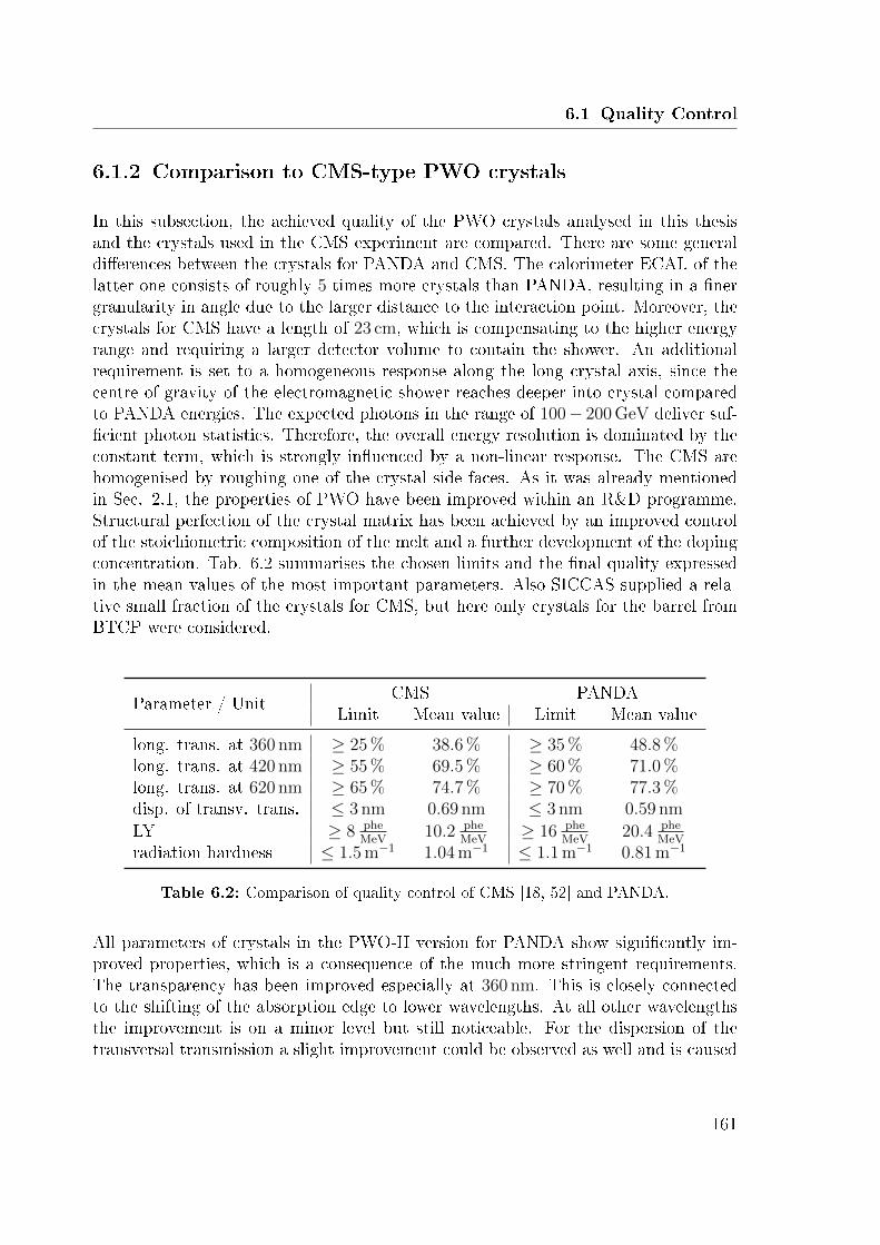
6.1 Quality Control
6.1.2 Comparison to CMS-type PWO crystals
In this subsection, the achieved quality of the PWO crystals analysed in this thesisand the crystals used in the CMS experiment are compared. There are some generaldierences between the crystals for PANDA and CMS. The calorimeter ECAL of thelatter one consists of roughly 5 times more crystals than PANDA, resulting in a nergranularity in angle due to the larger distance to the interaction point. Moreover, thecrystals for CMS have a length of 23 cm, which is compensating to the higher energyrange and requiring a larger detector volume to contain the shower. An additionalrequirement is set to a homogeneous response along the long crystal axis, since thecentre of gravity of the electromagnetic shower reaches deeper into crystal comparedto PANDA energies. The expected photons in the range of 100− 200 GeV deliver suf-cient photon statistics. Therefore, the overall energy resolution is dominated by theconstant term, which is strongly inuenced by a non-linear response. The CMS arehomogenised by roughing one of the crystal side faces. As it was already mentionedin Sec. 2.1, the properties of PWO have been improved within an R&D programme.Structural perfection of the crystal matrix has been achieved by an improved controlof the stoichiometric composition of the melt and a further development of the dopingconcentration. Tab. 6.2 summarises the chosen limits and the nal quality expressedin the mean values of the most important parameters. Also SICCAS supplied a rela-tive small fraction of the crystals for CMS, but here only crystals for the barrel fromBTCP were considered.
Parameter / UnitCMS PANDA
Limit Mean value Limit Mean value
long. trans. at 360 nm ≥ 25 % 38.6 % ≥ 35 % 48.8 %long. trans. at 420 nm ≥ 55 % 69.5 % ≥ 60 % 71.0 %long. trans. at 620 nm ≥ 65 % 74.7 % ≥ 70 % 77.3 %disp. of transv. trans. ≤ 3 nm 0.69 nm ≤ 3 nm 0.59 nm
LY ≥ 8 pheMeV
10.2 pheMeV
≥ 16 pheMeV
20.4 pheMeV
radiation hardness ≤ 1.5 m−1 1.04 m−1 ≤ 1.1 m−1 0.81 m−1
Table 6.2: Comparison of quality control of CMS [18, 52] and PANDA.
All parameters of crystals in the PWO-II version for PANDA show signicantly im-proved properties, which is a consequence of the much more stringent requirements.The transparency has been improved especially at 360 nm. This is closely connectedto the shifting of the absorption edge to lower wavelengths. At all other wavelengthsthe improvement is on a minor level but still noticeable. For the dispersion of thetransversal transmission a slight improvement could be observed as well and is caused
161
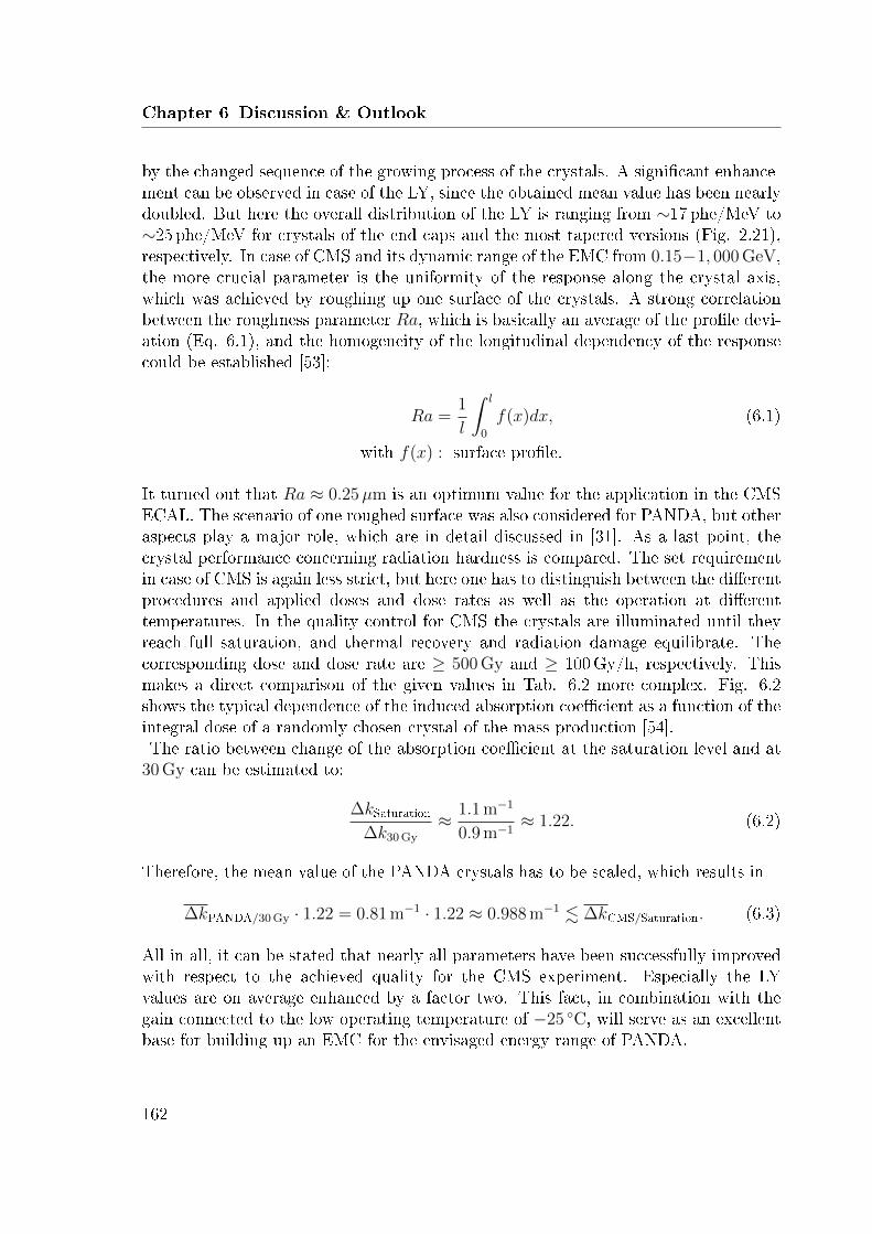
Chapter 6 Discussion & Outlook
by the changed sequence of the growing process of the crystals. A signicant enhance-ment can be observed in case of the LY, since the obtained mean value has been nearlydoubled. But here the overall distribution of the LY is ranging from ∼17 phe/MeV to∼25 phe/MeV for crystals of the end caps and the most tapered versions (Fig. 2.21),respectively. In case of CMS and its dynamic range of the EMC from 0.15−1, 000 GeV,the more crucial parameter is the uniformity of the response along the crystal axis,which was achieved by roughing up one surface of the crystals. A strong correlationbetween the roughness parameter Ra, which is basically an average of the prole devi-ation (Eq. 6.1), and the homogeneity of the longitudinal dependency of the responsecould be established [53]:
Ra =1
l
∫ l
0
f(x)dx, (6.1)
with f(x) : surface prole.
It turned out that Ra ≈ 0.25µm is an optimum value for the application in the CMSECAL. The scenario of one roughed surface was also considered for PANDA, but otheraspects play a major role, which are in detail discussed in [31]. As a last point, thecrystal performance concerning radiation hardness is compared. The set requirementin case of CMS is again less strict, but here one has to distinguish between the dierentprocedures and applied doses and dose rates as well as the operation at dierenttemperatures. In the quality control for CMS the crystals are illuminated until theyreach full saturation, and thermal recovery and radiation damage equilibrate. Thecorresponding dose and dose rate are ≥ 500 Gy and ≥ 100Gy/h, respectively. Thismakes a direct comparison of the given values in Tab. 6.2 more complex. Fig. 6.2shows the typical dependence of the induced absorption coecient as a function of theintegral dose of a randomly chosen crystal of the mass production [54].The ratio between change of the absorption coecient at the saturation level and at
30 Gy can be estimated to:
∆kSaturation∆k30 Gy
≈ 1.1 m−1
0.9 m−1≈ 1.22. (6.2)
Therefore, the mean value of the PANDA crystals has to be scaled, which results in
∆kPANDA/30 Gy · 1.22 = 0.81 m−1 · 1.22 ≈ 0.988 m−1 . ∆kCMS/Saturation. (6.3)
All in all, it can be stated that nearly all parameters have been successfully improvedwith respect to the achieved quality for the CMS experiment. Especially the LYvalues are on average enhanced by a factor two. This fact, in combination with thegain connected to the low operating temperature of −25 C, will serve as an excellentbase for building up an EMC for the envisaged energy range of PANDA.
162
6.1 Quality Control
Integral dose in Gy
0 20 40 60 80 100 120 140 160 180 200 220
1 in
m4
20
nm
k∆
0
0.2
0.4
0.6
0.8
1
1.2
Graph
Figure 6.2: Correlation induced change of the absorption coecient and the integraldose. The dashed blue line corresponds to an estimated saturation level of 1.1 m−1,whereas the blue arrow marks the value at 30 Gy [20].
6.1.3 Outlook with SICCAS crystals
Fig. 2.28 shows the current production status of the PANDA EMC. Due to the factthat BTCP is out of business to deliver additional crystals missing, an alternativesupplier has to be found. The most probable and promising candidate is SICCAS,another large crystal producer who is able to handle PWO. Already in the course of theCMS experiment, this company produced a relatively small fraction of 1, 825 crystals.For PANDA, 50 crystals of type 11 geometry were produced by SICCAS and testedby the facilities at CERN and Gieÿen, according to the most relevant parameters. Asit was pointed out in Sec. 2.5.1, the birefringent crystals are produced by the so calledBridgeman method and have therefore a dierent growing axis, namely the ordinaryaxis. Here the index of refraction and the absorption coecient are appreciably highercompared to the extraordinary direction, which implies a reduction of the achievablelongitudinal transmission (compare Fig. 2.31). This is directly visible in a shift of theobtained transmission distributions in Fig. 2.32, which is extremely pronounced at360 nm. Tab. 6.3 provides a direct comparison of the transmission parameters at thethree relevant wavelengths for CMS and PANDA.The tendency shown in Tab. 6.3 conrms the expectation of a lower longitudinaltransmission due to the mentioned reasons. Another interesting conclusion can be
163

Chapter 6 Discussion & Outlook
wavelength CMS PANDA
TBTCP − TSICCAS
360 nm 11.3 % 18.2 %420 nm 3.7 % 6.0 %620 nm 1.4 % 0.1 %
Table 6.3: Comparison of mean values T in longitudinal transmission of crystalsfrom BTCP and SICCAS. The data was taken from [52] and from the qualitycontrol at Gieÿen for CMS and PANDA, respectively.
drawn by comparing the homogeneity in transversal transmission for both suppliers.In case of crystals for CMS produced by SICCAS, the mean value of the ∆λ-parameteris about 1.71 nm larger compared to the one from BTCP (by [52]). A similar trendis observed in the case of PANDA, but here a quantitative statement is not possibledue to the explained sensitivity on geometry (compare Fig. 2.24). Nevertheless, thecrystals produced by the Czochralski method (Fig. 2.1a) are denitely much morehomogeneous along the long crystal axis, compared to the Bridgeman method (Fig.2.30).The situation is contrary for the determined LY. Here the crystals from SICCAS showan excellent performance except the overall homogeneity of the production. The 50 testsamples from SICCAS are broadly distributed from ∼ 12 phe/MeV to ∼ 27 phe/MeVwith a mean value of 19.1 phe/MeV, which is high in spite of the type 11-geometry andthe less pronounced NUF-eect. A clear negative aspect is the large RMS of 3.6 phe
MeV
which might be connected to the instability of the growing process. Concerning theradiation hardness of the SICCAS crystals (Fig. 2.35), no noteworthy deviation to theBTCP crystals could be observed. In the context of the quality parameter of PWO-IIwith respect to the comparison of both suppliers, similar results were obtained by [51].After the analysis of the 50 test samples and the gained experiences by CMS, SICCAScrystals are suitable for application in the PANDA EMC. A larger number of crystalsas preproduction lot is ordered and should serve as a further reference point for theachievable quality and its spread as well as the production eciency of the producer.
6.2 Time Resolution
The time resolution of the PROTO60 was determined in Sec. 4 for dierent readoutchains and energy ranges. In the rst two beamtimes in 2009 and 2010 at the ac-celeration facility MAMI at Mainz, the time information was extracted with TDCs,whereas in the CERN beamtime the time stamps were determined oine with theexplained feature extraction algorithm (compare Sec. 3.1.4). In all data sets, a clearenergy dependent time-walk eect was visible. For a subsequent oine correction, the
164
6.2 Time Resolution
particular shape of the time distribution as a function of the deposited energy wasdescribed and corrected with Eq. 4.11. The absolute calibration was, in case of TDCbased readout, achieved by digitised time spectra of a test pulser with and withoutdelay. Using SADC readout, the time calibration is directly given by the samplingfrequency of 50 MHz.In both MAMI test beamtimes, a time resolution below 1 ns for the processed scenar-ios above 250 MeV could be achieved. The obtained data for the time resolution wasdescribed by a three parametric function (Eq. 4.12). This allows an extrapolation ofthe time resolution to an energy of 1 GeV, which results in 430 ps for a single module,extracted from two adjacent crystals with similar energy deposition. Conspicuous arethe resulting t parameters in Fig. 4.17. For the regarded time dierence, the stochas-tic term (represented by the
√E−1-term) disappears, because of the narrow window
on the deposited energy. The same behaviour was already conrmed in [49] for similarcircumstances. Furthermore, in case of the noise term, the situation is inverted, sincehere the noise of the crystals contributes.In the beamtime of 2010, an up to now unexplained structure arises at the mediumenergies (visible in Fig. 4.21). Currently it is assumed that this anomaly originatesfrom an internal software problem of the tagger readout, which nally results in amixing of tagger channels. This can in addition be seen in Fig. 4.20 in an unusualbroadening in the relevant energy range and could already be observed in [42] and[55]. For the CERN beamtime in 2011, a nal time resolution of 441 ps could be de-termined, again by using the time dierence of neighbouring crystals with a showershared equally corresponding to a mean energy of 5.5 GeV each. The dynamic rangefor this beamtime was set to cover the expected energy range (compare Tab. 4.1).Therefore, no signicant improvement compared to the MAMI beamtimes could beexpected due to a similar SNR.The obtained time resolutions are mainly limited by the LAAPDs due to the reasonsmentioned in Sec. 4.3. Measurements with a 3 × 3 PWO crystal matrix read out byPMTs achieved a single unit time resolution of 130 ps for an incident electron energyof 855MeV [56].
6.2.1 Obtained Time Resolution of the CMS EMC
The operation mode of the EMC of the CMS experiment is in many aspects similarto the one of the PANDA EMC. Therefore, a direct comparison focussing on timingpurposes is advisable. Nevertheless, there are dierences concerning the extraction ofthe time information and will be explained in the following. The pulses are digitisedwith a sampling frequency of 40 MHz, which implies a channel width of 25 ns of theSADC [49]. Fig. 6.3a shows a typical normalised pulse shape containing 10 pedestalsubtracted SADC samples. A possible way for a representation of the pulse shape
165
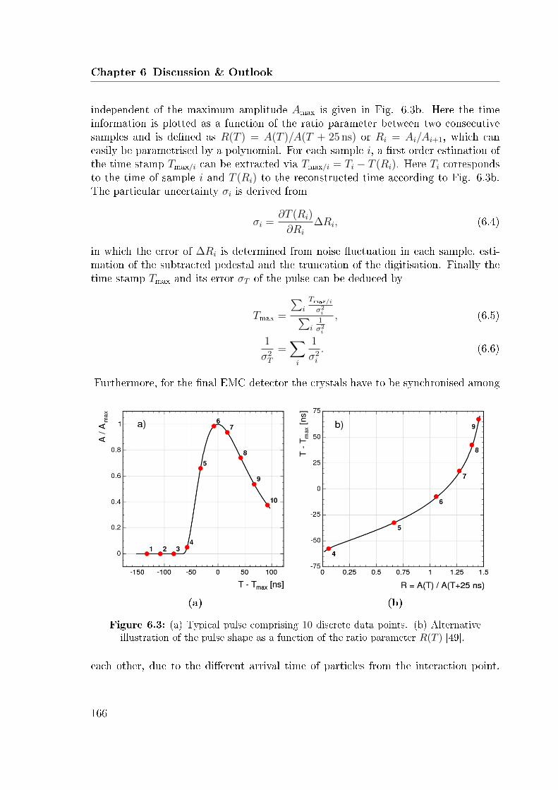
Chapter 6 Discussion & Outlook
independent of the maximum amplitude Amax is given in Fig. 6.3b. Here the timeinformation is plotted as a function of the ratio parameter between two consecutivesamples and is dened as R(T ) = A(T )/A(T + 25 ns) or Ri = Ai/Ai+1, which caneasily be parametrised by a polynomial. For each sample i, a rst order estimation ofthe time stamp Tmax/i can be extracted via Tmax/i = Ti − T (Ri). Here Ti correspondsto the time of sample i and T (Ri) to the reconstructed time according to Fig. 6.3b.The particular uncertainty σi is derived from
σi =∂T (Ri)
∂Ri
∆Ri, (6.4)
in which the error of ∆Ri is determined from noise uctuation in each sample, esti-mation of the subtracted pedestal and the truncation of the digitisation. Finally thetime stamp Tmax and its error σT of the pulse can be deduced by
Tmax =
∑i
Tmax/iσ2i∑
i1σ2i
, (6.5)
1
σ2T
=∑i
1
σ2i
. (6.6)
Furthermore, for the nal EMC detector the crystals have to be synchronised among
(a) (b)
Figure 6.3: (a) Typical pulse comprising 10 discrete data points. (b) Alternativeillustration of the pulse shape as a function of the ratio parameter R(T ) [49].
each other, due to the dierent arrival time of particles from the interaction point.
166

6.2 Time Resolution
Here, the corresponding solid angle of the particular crystals plays a major role, sincethe time of ight can vary by a few ns. In case of CMS, this is done by a beam-splashcomposed of muons [57].It could be shown that, with a carefully calibrated and synchronised detector, a timeresolution below 100 ps ([49]) is possible for large energies corresponding to 20 GeVand 100 GeV in barrel and endcaps, respectively. Here, the time dierence betweentwo adjacent crystals with similar energy deposition caused by electrons serves as atime stamp. The constant term of Eq. 4.12 is almost negligible, but as a drawback, thenoise term limits the time resolution at smaller energies. At 1 GeV deposited energy,a time resolution of 1.5 ns is expected in the barrel part (σnoise ∼ 140 MeV).For unsynchronised data, a time resolution determined with cosmic ray muons athigher energies is limited by the constant term of ∼ 380 ps, which is consistent withthe applied synchronisation correction and with the results obtained in this thesis.
6.2.2 Outlook on Time Resolution for PANDA
The time resolution deduced in this thesis is not the nal one and should be seen as anupper limit regarding timing purposes. As it was explained in the previous sections,the time resolution dramatically depends on the applied gain of the photo sensors.As a next step, with the implementation of the newest version of the ASIC with twoseparate gain branches, covering the lower and upper part of the energy range, anotherimprovement of the time resolution can be expected. This will be the case in the nextgenerations of EMC prototypes.Another point is the necessity of a signicantly improved time resolution of the EMCat least for charged particles due to the planned SciTil modules in front of the crystals.Latest test results of a SciTil prototype show an achieved time resolution of 210 ps[47]. An additional prototype including both, EMC and SciTil modules, is planned tostudy and learn more about the interplay of both components. The impact of the Sc-iTil plates in addition to the fused silica bars of the DIRC detector of pair productionon the EMC performance is currently under investigation.As it was mentioned before, with the detection of scintillation light, the time deter-mination is limited to the order of tens of ps. In course of the development in PET2
technologies in medical science it could be shown that the timing can signicantlybe improved with the detection of Cherenkov light [58]. In contrast to the generatedscintillation light, the Chrerenkov light is produced prompt, but on the other handthere is a comparably low detection yield (for PWO compare 1.3.1.1). Therefore, theQE of the photo sensors has to have a sucient coverage of the blue to the UV3-lightand an adequate discrimination ability. Nevertheless, as well in high energy physics
2Positron Electron Tomography3Ultraviolet
167

Chapter 6 Discussion & Outlook
the up to now achieved limits can be overcome via the detection of the Cherenkovcomponent.
6.3 Higher Order Energy Correction
In order to account for the energy loss in the passive material between the crystals orenhanced shower leakage, the obtained energy of for instance a 3× 3 cluster has to becorrected. Therefore the given equation for calibration 4.1 has to be extended by anadditional position dependent correction factor:
E∗cal = Fγ/e± · Cabs ·∑i
Si(t) · ci · Ei/uncal. (6.7)
The additional factor Fγ/e± is introduced, which is in principle a function of the spher-ical coordinates ϑ and ϕ. Moreover, in case of electromagnetic probes one has todistinguish between photons and electrons or positrons, respectively, because of theslightly dierent way of interaction and the resulting shower prole (compare Tab.1.6). In this thesis, the factor Fγ/e± was determined with the so called ln(E2/E1)-method (explained in Sec. 5.2.1), in which the value of ln(E2/E1) gives a rst orderinformation about the point of impact for a single event. With the knowledge of Fγ/e±the detected energy is subsequently corrected according to Eq. 5.3. For the analysedbeamtimes, this kind of correction function was only determined for a particular tran-sition from one crystal to another in horizontal direction in space, corresponding tothe ϕ-direction. As it was mentioned, a further analysis is planned to apply this cor-rection also to the vertical direction, especially to gain information about the impactof the staggering of the crystals rows.Tab. 5.1 gives a quantitative summary of the results achieved in the CERN beam-time in both performed runs. Especially in the second run, with an impinging beamin between the crystals, an absolute improvement from 1.896 % to 1.688 % could beachieved. Furthermore Fig. 5.7a underlines the necessity of the application of theln(E2/E1)-method to get an uniform detector response. As expected, the more cen-tralised the photons were impinging on the front face of the crystal, the smaller theapplied correction and consequently the improvement. In a further analysis for photonenergies from 150 − 1, 500 MeV at the MAMI facility at Mainz, an independence ofthe energy could be evaluated. Also, the achieved lowering of the energy resolution isalmost constant over the full energy range and amounts to 0.25 % for the run shoot-ing in between the crystals. This value is slightly worse but still comparable to theachievements of the CERN beamtime.
168
6.3 Higher Order Energy Correction
6.3.1 Alternatives to the ln(E2
E1
)-Method
Sec. 5 documents the successful application of the ln(E2/E1)-method for dierentcircumstances. But there are a handful of alternatives, which were partially used inother experiments. One possible option would be the determination of a correctionfunction Fγ/e± via simulations. But for this strategy one has to fully understandthe input and the outcome of such a simulation. Based on the past experiences aperfect agreement between simulation and experiment was up to now not achievedand deviates signicantly. Therefore, a correction with a full reliability on a non-perfectly understood simulation is not advisable.
169


List of Figures
1.1 FAIR facility . . . . . . . . . . . . . . . . . . . . . . . . . . . . . . . . 71.2 HESR . . . . . . . . . . . . . . . . . . . . . . . . . . . . . . . . . . . . 91.3 Range of hadron masses and antiproton momenta . . . . . . . . . . . . 101.4 Spectra of charmonium, hybrids and glueballs . . . . . . . . . . . . . . 111.5 Hypernuclei spectroscopy . . . . . . . . . . . . . . . . . . . . . . . . . . 131.6 The PANDA detector . . . . . . . . . . . . . . . . . . . . . . . . . . . . 141.7 Target spectrometer . . . . . . . . . . . . . . . . . . . . . . . . . . . . 151.8 MVD and target system . . . . . . . . . . . . . . . . . . . . . . . . . . 161.9 GEM detector . . . . . . . . . . . . . . . . . . . . . . . . . . . . . . . . 181.10 DIRC detectors . . . . . . . . . . . . . . . . . . . . . . . . . . . . . . . 181.11 Muon detectors . . . . . . . . . . . . . . . . . . . . . . . . . . . . . . . 191.12 Forward spectrometer . . . . . . . . . . . . . . . . . . . . . . . . . . . . 201.13 Shashlyk module . . . . . . . . . . . . . . . . . . . . . . . . . . . . . . 221.14 PANDA EMC . . . . . . . . . . . . . . . . . . . . . . . . . . . . . . . . 231.15 Visualisation of the Bethe Bloch equation . . . . . . . . . . . . . . . . 261.16 Photon cross-section of lead tungstate . . . . . . . . . . . . . . . . . . . 281.17 Development of an electromagnetic shower . . . . . . . . . . . . . . . . 301.18 Expansion of an electromagnetic shower . . . . . . . . . . . . . . . . . 311.19 Microscopic crystal structure of PWO . . . . . . . . . . . . . . . . . . . 331.20 PWO scintillation kinetics . . . . . . . . . . . . . . . . . . . . . . . . . 341.21 Structure of an APD . . . . . . . . . . . . . . . . . . . . . . . . . . . . 361.22 Correlation of gain and applied voltage of an APD . . . . . . . . . . . . 371.23 Schematic layout of VPT and VPTT . . . . . . . . . . . . . . . . . . . 381.24 EMC readout chain . . . . . . . . . . . . . . . . . . . . . . . . . . . . . 391.25 Layout of the APFEL ASIC . . . . . . . . . . . . . . . . . . . . . . . . 411.26 LNP-P . . . . . . . . . . . . . . . . . . . . . . . . . . . . . . . . . . . . 41
2.1 Manufacturing of PWO crystals . . . . . . . . . . . . . . . . . . . . . . 442.2 Measurements of PWO with various kinds of doping . . . . . . . . . . . 452.3 Temperature dependence of the light yield of lead tungstate . . . . . . 452.4 Luminescence and transmission characteristics of PWO . . . . . . . . . 472.5 Multiple reected photons . . . . . . . . . . . . . . . . . . . . . . . . . 482.6 Schematic drawing of a PANDA crystal . . . . . . . . . . . . . . . . . . 502.7 Scintillation kinetics . . . . . . . . . . . . . . . . . . . . . . . . . . . . 52
V

List of Figures
2.8 Typical ∆k spectra for PWO . . . . . . . . . . . . . . . . . . . . . . . 532.9 Procedure of quality control . . . . . . . . . . . . . . . . . . . . . . . . 542.10 Photograph ACCOS machine . . . . . . . . . . . . . . . . . . . . . . . 552.11 Transversal transmission measurement by ACCOS machine . . . . . . . 562.12 Light yield measurement of ACCOS machine . . . . . . . . . . . . . . . 572.13 VARIAN spectrometer . . . . . . . . . . . . . . . . . . . . . . . . . . . 582.14 Compartment for Co irradiation . . . . . . . . . . . . . . . . . . . . . . 592.15 Spontaneous recovery at room temperature . . . . . . . . . . . . . . . . 602.16 Setup for LY calibration . . . . . . . . . . . . . . . . . . . . . . . . . . 612.17 Transmission versus lot number . . . . . . . . . . . . . . . . . . . . . . 632.18 Distribution of transmission values . . . . . . . . . . . . . . . . . . . . 642.19 Distribution of geometry values . . . . . . . . . . . . . . . . . . . . . . 652.20 Non-Uniformity eect . . . . . . . . . . . . . . . . . . . . . . . . . . . . 662.21 Distribution of LY values . . . . . . . . . . . . . . . . . . . . . . . . . . 672.22 Distribution of ∆λ . . . . . . . . . . . . . . . . . . . . . . . . . . . . . 682.23 Distribution of ∆k . . . . . . . . . . . . . . . . . . . . . . . . . . . . . 692.24 ∆λ for dierent types . . . . . . . . . . . . . . . . . . . . . . . . . . . . 702.25 LY correlation between BTCP and CERN . . . . . . . . . . . . . . . . 712.26 ∆k correlation between BTCP and Gieÿen . . . . . . . . . . . . . . . . 712.27 Longitudinal transmission correlation . . . . . . . . . . . . . . . . . . . 722.28 Status of crystal delivery . . . . . . . . . . . . . . . . . . . . . . . . . . 732.29 Rejection summary . . . . . . . . . . . . . . . . . . . . . . . . . . . . . 742.30 Bridgeman method . . . . . . . . . . . . . . . . . . . . . . . . . . . . . 752.31 Indices of refraction of PWO . . . . . . . . . . . . . . . . . . . . . . . . 762.32 Longitudinal transmission of SICCAS crystals . . . . . . . . . . . . . . 772.33 ∆λ distribution of SICCAS crystals . . . . . . . . . . . . . . . . . . . . 782.34 LY distribution of SICCAS crystals . . . . . . . . . . . . . . . . . . . . 792.35 ∆k distribution of SICCAS crystals . . . . . . . . . . . . . . . . . . . . 79
3.1 Represented subsection of the PROTO60 . . . . . . . . . . . . . . . . . 823.2 Space occupancy between crystals in PROTO60 . . . . . . . . . . . . . 833.3 PROTO60 assambly . . . . . . . . . . . . . . . . . . . . . . . . . . . . 843.4 Back view of PROTO60 . . . . . . . . . . . . . . . . . . . . . . . . . . 863.5 Readout chain PROTO60 at Mainz . . . . . . . . . . . . . . . . . . . . 873.6 Schematic explanation of the feature extraction . . . . . . . . . . . . . 893.7 Raw data of SADC . . . . . . . . . . . . . . . . . . . . . . . . . . . . . 903.8 Visualisation MWD . . . . . . . . . . . . . . . . . . . . . . . . . . . . . 903.9 Shaped and smoothed signal of the LNP-P . . . . . . . . . . . . . . . . 913.10 Determination of the time information . . . . . . . . . . . . . . . . . . 923.11 Floor plan MAMI at Mainz . . . . . . . . . . . . . . . . . . . . . . . . 943.12 RTM layout . . . . . . . . . . . . . . . . . . . . . . . . . . . . . . . . . 953.13 Schematic layout of the HDSM . . . . . . . . . . . . . . . . . . . . . . 97
VI
List of Figures
3.14 Photon tagging spectrometer at Mainz . . . . . . . . . . . . . . . . . . 983.15 PROTO60 setup at MAMI beamtimes . . . . . . . . . . . . . . . . . . 1003.16 CERN accelerator complex . . . . . . . . . . . . . . . . . . . . . . . . . 1013.17 PROTO60 setup at CERN beamtimes . . . . . . . . . . . . . . . . . . 1023.18 Schematic crystal map of PROTO60 at MAMI . . . . . . . . . . . . . . 1033.19 Schematic crystal map of PROTO60 at CERN . . . . . . . . . . . . . . 104
4.1 Calibrated energy sum . . . . . . . . . . . . . . . . . . . . . . . . . . . 1074.2 General signal treatment of PANDA . . . . . . . . . . . . . . . . . . . 1094.3 Time development of scintillation light . . . . . . . . . . . . . . . . . . 1114.4 Major dependencies of time resolution . . . . . . . . . . . . . . . . . . 1124.5 Time-walk eect . . . . . . . . . . . . . . . . . . . . . . . . . . . . . . 1144.6 Pile-up recovery of energy information . . . . . . . . . . . . . . . . . . 1154.7 Pile-up recovery of time information . . . . . . . . . . . . . . . . . . . . 1164.8 SciTil . . . . . . . . . . . . . . . . . . . . . . . . . . . . . . . . . . . . 1174.9 Raw time spectra Mainz 2009 . . . . . . . . . . . . . . . . . . . . . . . 1194.10 Example relative time calibration . . . . . . . . . . . . . . . . . . . . . 1204.11 Uncalibrated time spectrum of t36 − t35 . . . . . . . . . . . . . . . . . . 1214.12 Absolute time calibration . . . . . . . . . . . . . . . . . . . . . . . . . . 1224.13 Calibrated time spectra Mainz 2009 . . . . . . . . . . . . . . . . . . . . 1234.14 Application time-walk function . . . . . . . . . . . . . . . . . . . . . . 1244.15 Time spectra after time walk correction . . . . . . . . . . . . . . . . . . 1254.16 Time distributions for the tagger time distinguished by the tagger energy1264.17 Time resolution for the time dierence and tagger time (MAMI 2009) . 1274.18 Time spectrum of a tagger channel . . . . . . . . . . . . . . . . . . . . 1294.19 Relatively calibrated time spectrum . . . . . . . . . . . . . . . . . . . . 1304.20 Time-walk correction function . . . . . . . . . . . . . . . . . . . . . . . 1314.21 Results time resolution (MAMI 2010) . . . . . . . . . . . . . . . . . . . 1314.22 Time spectra central crystal CERN (2011) . . . . . . . . . . . . . . . . 1334.23 Emphasised time-walk (CERN 2011) . . . . . . . . . . . . . . . . . . . 1344.24 Position dependence of the timing (CERN 2011) . . . . . . . . . . . . . 1354.25 Time dierence with energy cut (CERN 2011) . . . . . . . . . . . . . . 1374.26 Time resolution (CERN 2011) . . . . . . . . . . . . . . . . . . . . . . . 138
5.1 Energy dependence on point of impact CERN 2011 . . . . . . . . . . . 1415.2 Position sensitivity of the energy resolution . . . . . . . . . . . . . . . . 1425.3 ln(E2/E1)-method . . . . . . . . . . . . . . . . . . . . . . . . . . . . . 1435.4 Correlation between ln(E2/E1) and point of impact . . . . . . . . . . . 1455.5 Distribution of the ln(E2/E1)-parameter . . . . . . . . . . . . . . . . . 1475.6 ln(E2/E1) correction function . . . . . . . . . . . . . . . . . . . . . . . 1485.7 Results position correction . . . . . . . . . . . . . . . . . . . . . . . . . 1495.8 Energy dependence on point of impact MAMI 2009 . . . . . . . . . . . 150
VII

List of Figures
5.9 Energy distribution for dierent ln(E2/E1)-parameters (MAMI 2009) . 1515.10 Correction functions of all tagger channels (MAMI 2009) . . . . . . . . 1525.11 Uncorrected and corrected lineshapes (MAMI 2009) . . . . . . . . . . . 1535.12 Uncorrected and corrected energy resolution for run 1 (MAMI 2009) . . 1555.13 Uncorrected and corrected energy resolution for run 3 (MAMI 2009) . . 155
6.1 Correlation between light yield and longitudinal transmission . . . . . . 1586.2 Correlation induced change of the absorption coecient and the integral
dose . . . . . . . . . . . . . . . . . . . . . . . . . . . . . . . . . . . . . 1636.3 Pulse shape CMS . . . . . . . . . . . . . . . . . . . . . . . . . . . . . . 166
VIII
List of Tables
1.1 FAIR experiments . . . . . . . . . . . . . . . . . . . . . . . . . . . . . . 81.2 Operation modes of HESR . . . . . . . . . . . . . . . . . . . . . . . . . 91.3 Requirements of the Shashlyk detector . . . . . . . . . . . . . . . . . . 211.4 EMC components . . . . . . . . . . . . . . . . . . . . . . . . . . . . . . 231.5 Photon interaction cross-section . . . . . . . . . . . . . . . . . . . . . . 271.6 Parameters for a longitudinal shower development . . . . . . . . . . . . 291.7 Requirements EMC . . . . . . . . . . . . . . . . . . . . . . . . . . . . . 321.8 Properties of PWO . . . . . . . . . . . . . . . . . . . . . . . . . . . . . 35
2.1 Specications for the crystals of the EMC . . . . . . . . . . . . . . . . 462.2 Denition of geometrical parameters . . . . . . . . . . . . . . . . . . . 502.3 Connection between properties and test stations . . . . . . . . . . . . . 54
3.1 Properties of used LAAPD in PROTO60 . . . . . . . . . . . . . . . . . 853.2 Components of the PROTO60 readout . . . . . . . . . . . . . . . . . . 883.3 PROTO60 beamtimes . . . . . . . . . . . . . . . . . . . . . . . . . . . 933.4 Performance parameter of accelerator units at MAMI . . . . . . . . . . 963.5 Selected tagger channels at both MAMI beamtimes . . . . . . . . . . . 99
4.1 Noise and dynamic range adjustments of the PROTO60 . . . . . . . . . 1084.2 Fit results time-walk correction . . . . . . . . . . . . . . . . . . . . . . 124
5.1 Results of ln(E2/E1)-method for CERN beamtimes . . . . . . . . . . . 148
6.1 Rejection summary . . . . . . . . . . . . . . . . . . . . . . . . . . . . . 1606.2 Comparison of quality control CMS and PANDA . . . . . . . . . . . . 1616.3 Comparison transmission BTCP and SICCAS . . . . . . . . . . . . . . 164
IX

Bibliography
[1] V. Metag, Group lecture, 2008.
[2] http://www.fair-center.de.
[3] R. Maier, ed., The high-energy storage ring (HESR). 2011. Particle AcceleratorConference.
[4] PANDA Collaboration, Physics Performance Report for PANDA, (2009) ,arXiv:0903.3905v1.
[5] PANDA Collaboration, Technical Design Report for the: PANDA Straw TubeTracker, (2012) , arXiv:205.5441v2 [physics.ins-det].
[6] PANDA Collaboration, Technical Design Report for the: PANDA MicroVertex Detector, (2012) , arXiv:1207.6581v2 [physics.ins-det].
[7] L. Ackermann, Charakterisierung von Silizium-Streifensensoren für denPANDA Micro-Vertex-Detektor, Diplomarbeit , Technische UniversitätDresden, 2009.
[8] PANDA Collaboration, Public technical progress report, 2005.
[9] J. Schwiening, The Barrel DIRC for the PANDA Experiment at FAIR, 2011.HIC for FAIR Detector Systems Networking Workshop.
[10] http://www-panda.gsi.de/framework/content/detector/det_forward.html.
[11] S. Diehl, Ansprechverhalten eines Shashlyk-Kalorimeters für hochenergetischePhotonen im Energiebereich von 100 MeV bis 770 MeV, Master's thesis, JustusLiebig Universität Gieÿen, 2012.
[12] H. Löhner, 2012. Talk, PANDA Meeting.
[13] W. Leo, Techniques for Nuclear and Particle Physics Experiments. Springer,1994.
[14] M. Berger et al., XCOM: Photo Cross Sections Database.http://www.nist.gov/pml/data/xcom/index.cfm.
[15] R. Novotny, Messmethoden der Kern- und Teilchenphysik.. Lecture.
XI

Bibliography
[16] PDG, Particle Physics Booklet, p. 238. 2010.
[17] H. Koch, C. Amsler, E. Aker, and T. Armstrong, Proposal: the crystal barrel,Tech. Rep. CERN-PSCC-85-56. PSCC-P-90, CERN, Geneva, 1985.
[18] PANDA Collaboration, Technical Design Report for PANDA ElectromagneticCalorimeter (EMC), (2008) , arXiv:0810.1216v1 [physics.ins-det].
[19] http://webmineral.com/.
[20] D. V. Ivanovich, Lead tungstate scintilation crystals for the electromagneticcalorimeter of the PANDA experiment. PhD thesis, Institute for NuclearProblems, Belrussian State University, Minsk, 2008.
[21] M. Leyhe, Tests zur Auslese von PWO-Szintillatoren, Master's thesis,Ruhr-Universität Bochum, 2010.
[22] P. Schneider, Messung der magnetfeldabhängigen Verstärkung vonVakuum-Phototetroden, Bachelor's Thesis (Studienarbeit), Ruhr-UniverstitätBochum, 2011.
[23] M. Kavatsyuk, Trigger-less readout system with pulse pile-up recovery for thepanda electromagnetic calorimeter, 2013.
[24] P. Wieczorek, 2012. Talk, PANDA Meeting.
[25] A. Annenkov, Improved light yield of lead tungstate scintillators, NuclearInstruments and Methods in Physics Research Section A: Accelerators,Spectrometers, Detectors and Associated Equipment 450 no. 1, 71 74.
[26] M. Böhm, Inuence of Mo Impurity on the Spectroscopic and ScintillationProperties of PWO Crystals , physica status solidi (a) (1998) .
[27] T. Eiÿner, Quality Control of PWO-Crystals for the PANDA Detector,Diplomarbeit , Justus Liebig Universität Gieÿen, 2009.
[28] E. Auray, Performance of ACCOS, an Automatic Crystal quality ControlSystem for the PWO crystals of the CMS calorimeter, Nuclear Instruments andMethods in Physics Research Section A: Accelerators, Spectrometers, Detectorsand Associated Equipment 456 no. 3, (2001) 325 341.
[29] http://www.hund.de/.
[30] S. Baccaro, Ordinary and extraordinary complex refractive index of the leadtungstate (pbwo4) crystal,.
[31] D. Bremer, TBA. PhD thesis, Justus Liebig Universität Gieÿen, 2013.
[32] http://english.sic.cas.cn/.
XII

Bibliography
[33] http://commons.wikimedia.org/wiki/File:Bridgman-Stockbarger-Verfahren.svg.
[34] M. Kavatsyuk, D. Bremer, V. Dormenev, P. Drexler, T. Eissner, W. Erni,E. Guliyev, T. Hennino, B. Krusche, B. Lewandowski, H. Löhner, M. Moritz,R. Novotny, K. Peters, J. Pouthas, P. Rosier, M. Steinacher, G. Tambave, andA. Wilms, Performance of the prototype of the electromagnetic calorimeter forPANDA,.
[35] M. Janecek and W. W. Moses, Optical reectance measurements for commonlyused reectors, Nuclear Science, IEEE Transactions on 55 no. 4, (2008)24322437.
[36] http://www.hamamatsu.com/resources/pdf/ssd/s8664_series_kapd1012e04.pdf.
[37] M. Kavatsyuk, Private communications..
[38] J. McGeorge, J. Kellie, J. Annand, J. Ahrens, I. Anthony, A. Clarkson,D. Hamilton, P. Lumsden, E. McNicoll, R. Owens, G. Rosner, and A. Thomas,Upgrade of the glasgow photon tagging spectrometer for mainz mami-c, TheEuropean Physical Journal A 37 no. 1, (2008) 129137.http://dx.doi.org/10.1140/epja/i2007-10606-0.
[39] http://www.kph.uni-mainz.de/mami.php.
[40] http://home.web.cern.ch/.
[41] M. Moritz, Measurements and improvements of the response of thePANDA-EMC prototype PROTO60 to high energetic particles and photons inaccelerator experiments. PhD thesis, Justus Liebig Universität Gieÿen, 2013.
[42] W. Lippert, Konzepte der Kalibration eines Protoyps des EM-Kalorimeters fürPANDA, Bachelor's Thesis (Studienarbeit), Universtität Gieÿen, 2010.
[43] I. Konorov, H. Angerer, A. Mann, and S. Paul, Soda: Time distribution systemfor the panda experiment, in Nuclear Science Symposium Conference Record(NSS/MIC), 2009 IEEE, pp. 18631865. 2009.
[44] P. Lecoq, Inorganic Scintillators for Detector Systems, p. 83. Springer, 2006.
[45] G. Tambave, Pulse pile-up recovery for the front-end electronics of the pandaelectromagnetic calorimeter, iopscience .
[46] G. Tambave, M. Kavatsyuk, E. Guliyev, F. Schreuder, H. Moeini, andH. Löhner, Pulse pile-up recovery for the front-end electronics of the pandaelectromagnetic calorimeter, Journal of Instrumentation 7 no. 11, (2012)P11001. http://stacks.iop.org/1748-0221/7/i=11/a=P11001.
[47] C. Schwarz, 2013. Talk, XLIV PANDA Meeting.
XIII

Bibliography
[48] B. Lemmer, Measurement of the Excitation Function of OmegaPhotoproduction on Carbon and Niobium, Diplomarbeit , Justus LiebigUniversität Gieÿen, 2009.
[49] CMS Collaboration, Time Reconstruction and Performance of the CMSElectromagnetic Calorimeter, (2009) , arXiv:0911.4044v2.
[50] Periodic position dependence of the energy measured in the cmselectromagnetic calorimeter,.http://inspirehep.net/record/713920/les/NOTE2006_045.pdf.
[51] F. Yang, R. Mao, L. Zhang, and R.-Y. Zhu, A study on radiation damage inbgo and pwo-ii crystals, Journal of Physics: Conference Series 404 no. 1,(2012) 012025. http://stacks.iop.org/1742-6596/404/i=1/a=012025.
[52] E. Auray, Overview of the 63,000 pwo barrel crystals for cms ecal production,Nuclear Science, IEEE Transactions on (2008) .
[53] J. Descamps and P. Jarry, Development of a Uniformisation Procedure for thePWO Crystals of the CMS Electromagnetic Calorimeter,.CERN-CMS-NOTE-2001-004.
[54] D. V. Ivanovich, Private communications..
[55] D. Bremer, Reconstruction of Electromagnetic Showers and Determination ofthe Postion Resolution of a Prototype of the PANDA ElectromagneticCalorimeter, Diplomarbeit , Justus Liebig Universität Gieÿen, 2010.
[56] R. Novotny, W. Döring, K. Mengel, V. Metag, and C. Pienne, Response of apbwo4-scintillator array to electrons in the energy regime below 1 gev, NuclearPhysics B - Proceedings Supplements 61 no. 3, (1998) 613 618.http://www.sciencedirect.com/science/article/pii/S0920563297006270.
[57] G. Franzoni, Performance of cms ecal with rst lhc data, Nuclear Instrumentsand Methods in Physics Research Section A: Accelerators, Spectrometers,Detectors and Associated Equipment 628 no. 1, (2011) 90 94.http://www.sciencedirect.com/science/article/pii/S0168900210014816.
[58] S. E. Brunner. Talk, SCINT 2013, Shanghai.
XIV
Acronyms
6N purity level of ≥ 99.9999%. 43
ACCOS Automatic Crystal quality Control System. 55, 158
ADC Analogue to Digital Converter. 88
APD Avalanche Photo Diode. 3538, 108
APFEL ASIC for PANDA Front-end Electronics. 3, 5, 40
APPA Atomic Plasma Physics and Application. 8
ASIC Application Specic Integrated Circuit. 3, 5, 40, 93, 108, 117, 167
BGO Bi4Ge3O12. 3335
BTCP Bogoroditsk Techno Chemical Plant. IX, 3, 5, 43, 54, 55, 57, 63, 6772, 75,77, 78, 157161, 163, 164
CBM Compressed, Baryonic Matter. 8
CERN European laboratory for particle physics. VII, IX, 3, 5, 43, 54, 55, 61, 6568,7072, 77, 81, 86, 93, 101, 102, 104, 107, 108, 113, 132, 134, 139, 140, 144, 146,148, 154, 158160, 163165, 168
CFD Constant-Fraction Discriminator. 87, 91, 113, 114
CFT Constant-Fraction Timing. 91, 92, 111, 113, 116, 132
charmonium a bound state of a charm quark and its antiparticle. 10
CMS Compact Muon Solenoid. VIII, IX, 1, 3, 5, 35, 38, 44, 53, 55, 57, 66, 69, 143,157, 161165, 167
DAQ Data-Acquisition. 109
DCON Data Concentrator. 109
DIRC Detection of Internally Reected Cherenkov light. 1719, 117, 167
XV

Acronyms
ECAL Electromagnetic Calorimeter. 55, 161, 162
ECL Emitter Coupled Logic. 88, 118
ELSA Elektronen-Stretcher-Anlage. 139
EMC Electromagnetic Calorimeter. 1, 3, 5, 8, 9, 12, 19, 23, 34, 37, 46, 81, 88, 105,109, 110, 117, 144, 145, 154, 157, 159, 162167
ENC Equivalent Noise Charge. 40
ESR Enhanced Specular Reector. 83
ESR Experimental Storage Ring. 8
EU European Union. 44
FAIR Facility for Antiproton and Ion Research. 7, 8
FEE Front-End Electronics. 109
FPGA Field Programmable Gate Arrays. 88
FRS Forward Range System. 21
FS Forward Spectrometer. 14, 1921
FWHM Full Width at Half Maximum. 46, 96
GEANT4 Toolkit for the simulation of the passage of particles through matter /http://geant4.cern.ch/. 106
GEM Gaseous Electron Multipliers. 17, 18
GSI Gesellschaft für Schwerionenforschung GmbH. 7, 8
HDSM Harmonic Double-Sided Microtron. VI, 9597
HESR High Energy Storage Ring. 8, 9, 20
IOL Input Output Logic. 88
J-FET Junction Field Eect Transistor. 40
LAAPD Large Area Avalanche Photo Diode. 35, 37, 40, 41, 83, 8587, 90, 93, 99,112, 165
LEAR Low Energy Antiproton Ring. 12
XVI

Acronyms
LED Light Emitting Diode. 115
LHC Large Hadron Collider. 33, 34, 101
LINAC Linear Accelerator. 94, 96, 97
LITRANI Light Transmission in Anisotropic media / http://gentitfx.fr/litrani/. 60
LNP-P Low Noise and Low Power Charge Preamplier. VI, 40, 85, 86, 8891
LY Light Yield. 34, 35, 51, 157, 159162, 164
LYSO Lu2(1−x)Y2xSiO5. 34, 35
MA Moving Average. 89, 91
MAMI Mainzer Mikrotron. VIIIX, 81, 86, 9397, 99, 100, 103, 108, 113, 118, 128,139, 140, 150152, 154, 164, 165, 168
MDC Multi-wire Drift Chambers. 20, 21
MDT Mini-Drift Tube. 19
MIP Minimum Ionising Particle. 16, 25, 106
MUD Muon Detection. 19, 21
MVD Micro Vertex Detector. 12, 16, 17, 19, 102, 132
MWD Moving Window Deconvolution. 8991, 116
NCE Nuclear Counter Eect. 38
NESR New Experimental Storage Ring. 8
NIM Nuclear Instrumentation Methods. 88, 128
NUF Non-Uniformity in light collection. 66, 159, 160, 164
NUSTAR Nuclear Structure, Astrophysics and Reactions. 8
PANDA Anti-Proton Annihilation at Darmstadt. IX, 1, 3, 5, 812, 14, 15, 1820,34, 37, 38, 40, 43, 46, 49, 54, 88, 93, 109, 110, 117, 128, 139, 150, 157, 159,161165, 167
PCB Printed Circuit Board. 85, 86
PET Positron Electron Tomography. 167
PID Particle Identication. 19, 21, 25, 117
XVII
Acronyms
PMT Photomultiplier Tube. 21, 25, 35, 38, 45, 51, 56, 61, 62, 97, 111113, 118, 120,165
PS-ADC Peak Sensing - Analogue to Digital Converter. 87, 88, 93, 108
PWO Lead tungstate (PbWO4). 1, 33, 35, 43, 44, 86, 139, 157, 161, 163165, 167
QCD Quantum Chromo Dynamics. 10, 11
QDC Charge-to-Digital-Converter, CAMAC, Le Croy 2249W. 62
QE Quantum Eeciency. 36, 85, 167
R&D Research and Developement. 34, 37, 43, 161
RF Radio Frequency. 95
RICH Ring Imaging Cherenkov Counter. 21
RINP Research Institute for Nuclear Problems of Belarussian State University. 57
RMS Root Mean Square. 78, 109, 153, 164
RTM Race Track Microtron. 9496
SADC Sampling Analogue to Digital Converter. 39, 88, 90, 93, 104, 132, 165
SciTil Scintillating Tile. 117, 167
SEP Single Electron Peak. 51, 62
SICCAS Shanghai Institute of Ceramics, Chinese Academy of Sciences. IX, 1, 3, 5,63, 75, 78, 157, 161, 163, 164
SiPM Silicon Photomultiplier. 117
SIS Schwer Ionen Synchrotron. 8
SNR Signal-to-Noise Ratio. 111, 112, 165
SODA Synchronisation of Data Acquisition. 3, 5, 109
SPS Super Proton Synchrotron. 93, 101, 102, 108
STT Straw Tube Tracker. 17, 19
TAPS Two Arm Photon Spectrometer. 113, 122
TDC Time-to-Digital-Converter. 56, 57, 87, 88, 98, 121, 122, 128, 164, 165
TOF Time of Flight. 117
XVIII

Acronyms
TS Target Spectrometer. 14, 17, 19, 21
UNILAC Universal Linear Accelerator. 8
UV Ultraviolet. 167
VPT Vaccum Photo Triode. 35, 38, 40
VPTT Vaccum Photo Tetrode. 35, 38, 39
WLS Wavelength Shifting. 21
XIX


Acknowledgements
Zuallererst vielen lieben Dank an meine beiden Chefs Volker und Rainer, die es mirermöglicht haben, an solch einem Projekt wie dem PANDA Detektor dabei zu sein undaktiv mitwirken zu dürfen. Beiden lag es immer sehr nahe eine angenehme Arbeit-satmosphäre zu schaen, in der man sich jederzeit selbstorganisiert bewegen konnte.Zurückblickend kann ich sagen, dass ich mich damals, vor meiner Diplomzeit, für diefür mich richtige Arbeitsgruppe entschieden habe. Ein dickes Dankeschön geht natür-lich auch an meine Bürokollegen Daniel, Markus und Till. Ich denke wir waren immerein super Team, welches gut zusammen harmoniert hat. Nicht zu vergessen die an-deren Jungs und Mädels: Marcelle, Marianna, René, Marcel, Christoph, Stefan undStefan. Ein ganz besonderer Dank geht auch an unsere Post-Docs, Valera und Peter,die mir bei allen möglichen (auch fachfremden) Fragen stets hilfreich zur Verfügungstanden. Ebenfalls vielen Dank an Jürgen und Werner, die speziell in der Anfangs-und Eingewöhnungszeit für alle Fragen immer ein oenes Ohr hatten. Karoly, thanksa lot for helping me in any kind of computer related issue. Nicht zu vergessen sinddie neu dazu gewonnen Bonner Jungs: Kai, Tommaso, Robert, Hans, Andi und Eric.Danke auch an blau-weiss Uli. Es war mir immer eine Ehre mit dir zu fachsimpeln.Liebe Anita, danke für das weitestgehende Abnehmen der bürokratischen Formal-itäten. Weiterhin möchte ich nicht vergessen: HGS-HIRe und die MTA-Schule...Allen zusammen, danke für alles!
XXI

Erklärung der Urheberschaft
Ich erkläre: Ich habe die vorgelegte Dissertation selbständig und ohne unerlaubtefremde Hilfe und nur mit den Hilfen angefertigt, die ich in der Dissertation angegebenhabe.Alle Textstellen, die wörtlich oder sinngemäÿ aus veröentlichten Schriften entnom-men sind, und alle Angaben, die auf mündlichen Auskünften beruhen, sind als solchekenntlich gemacht.Bei den von mir durchgeführten und in der Dissertation erwähnten Untersuchungenhabe ich die Grundsätze guter wissenschaftlicher Praxis, wie sie in der "Satzungder Justus-Liebig-Universität Gieÿen zur Sicherung guter wissenschaftlicher Praxis"niedergelegt sind, eingehalten.
Tobias EiÿnerGieÿen, im November 2013
XXIII