the memory system
30
1 | Page THE MEMORY SYSTEM Programs and the data they operate on are held in the memory of the computer. In this chapter, we discuss how this vital part of the computer operates. By now, the reader appreciates that the execution speed of programs is highly dependent on die speed with which instructions and data can be transferred between the processor and the memory. It is also important to have a large memory to facilitate execution of programs that are large and deal with huge amounts of data. Ideally, the memory would be fast, large, and inexpensive. Unfortunately, it is impossible to meet all three of these requirements simultaneously. Increased speed and size are achieved at increased cost. To solve this problem, much work has gone into developing clever structures that improve the apparent speed and size of the memory, yet keep the cost reasonable. First, the most common components and organizations used to implement the memory are described. Then memory speed and how the apparent speed of the memory can be increased by means of caches are explained. Next, the virtual memory concept is presented, which increases the apparent size of the memory. Finally, the secondary storage devices are discussed, which provide much larger storage capability. Basic Concepts The maximum size of the memory that can be used in any computer is determined by the addressing scheme. For example, a 16-bit computer that generates 16-bit addresses is capable of addressing up to 216= 64K memory locations. Similarly, machines whose instructions generate 32-bit addresses can utilize a memory that contains up to 2^32 =4G (giga) memory locations, whereas machines with 40-bit addresses can access up to 2^40 = 1 T (tera) locations. The number of locations represents the size of the address space of the computer. Most modern computers are byte addressable. Figure 2.7 shows the possible address assignments for a byte- addressable 32-bit computer. The ARM architecture can be configured to use either arrangement As far as the memory structure is concerned, there is no substantial difference between the two schemes. The memory is usually designed to store and retrieve data in word- length quantities. In fact, the number of bits actually stored or retrieved in one memory access is the most common definition of the word length of a computer. Consider, for example, a byte addressable computer whose instructions generate 32-bit addresses. When a 32-bit address is sent from the processor to the memory unit, the high-order 30 bits determine which word will be accessed. If a byte quantity is specified, the low-order 2 bits of the address specify which byte location is involved. In a Read operation, other bytes may be fetched from the memory, but they are ignored by the processor. If the byte operation is a Write, however, the control circuitry of the memory must ensure that the contents of other bytes of the same word are not changed. From the system standpoint, we can view the memory unit as a black box. Data transfer between the memory and the processor takes place through the use of two processor registers, usually called MAR (memory address register) and MDR (memory data register). If MAR is k bits long and MDR is n bits long, then the memory unit may contain up to 2 k addressable
-
Upload
khangminh22 -
Category
Documents
-
view
3 -
download
0
Transcript of the memory system

1 | P a g e
THE MEMORY SYSTEM
Programs and the data they operate on are held in the memory of the computer. In this chapter,
we discuss how this vital part of the computer operates. By now, the reader appreciates that the
execution speed of programs is highly dependent on die speed with which instructions and
data can be transferred between the processor and the memory. It is also important to have a
large memory to facilitate execution of programs that are large and deal with huge amounts of
data.
Ideally, the memory would be fast, large, and inexpensive. Unfortunately, it is impossible to
meet all three of these requirements simultaneously. Increased speed and size are achieved at
increased cost. To solve this problem, much work has gone into developing clever structures
that improve the apparent speed and size of the memory, yet keep the cost reasonable.
First, the most common components and organizations used to implement the memory are
described. Then memory speed and how the apparent speed of the memory can be increased by
means of caches are explained. Next, the virtual memory concept is presented, which increases
the apparent size of the memory. Finally, the secondary storage devices are discussed, which
provide much larger storage capability.
Basic Concepts
The maximum size of the memory that can be used in any computer is determined by the
addressing scheme. For example, a 16-bit computer that generates 16-bit addresses is capable of
addressing up to 216= 64K memory locations. Similarly, machines whose instructions generate
32-bit addresses can utilize a memory that contains up to 2^32 =4G (giga) memory locations,
whereas machines with 40-bit addresses can access up to 2^40 = 1 T (tera) locations. The
number of locations represents the size of the address space of the computer. Most modern
computers are byte addressable. Figure 2.7 shows the possible address assignments for a byte-
addressable 32-bit computer. The ARM architecture can be configured to use either
arrangement As far as the memory structure is concerned, there is no substantial difference
between the two schemes. The memory is usually designed to store and retrieve data in word-
length quantities.
In fact, the number of bits actually stored or retrieved in one memory access is the most
common definition of the word length of a computer. Consider, for example, a byte addressable
computer whose instructions generate 32-bit addresses. When a 32-bit address is sent from the
processor to the memory unit, the high-order 30 bits determine which word will be accessed. If
a byte quantity is specified, the low-order 2 bits of the address specify which byte location is
involved. In a Read operation, other bytes may be fetched from the memory, but they are
ignored by the processor. If the byte operation is a Write, however, the control circuitry of the
memory must ensure that the contents of other bytes of the same word are not changed.
From the system standpoint, we can view the memory unit as a black box. Data transfer
between the memory and the processor takes place through the use of two processor registers,
usually called MAR (memory address register) and MDR (memory data register). If MAR is k
bits long and MDR is n bits long, then the memory unit may contain up to 2k addressable
2 | P a g e
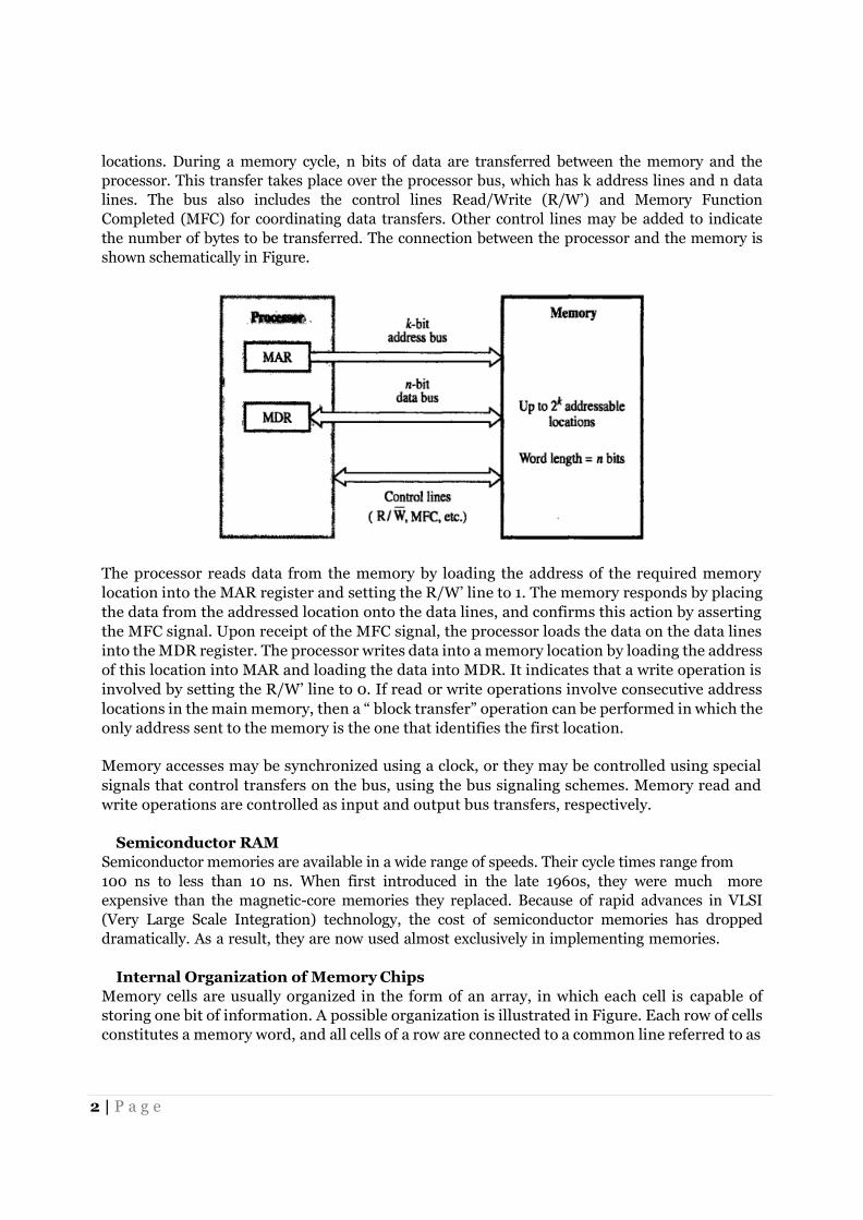
locations. During a memory cycle, n bits of data are transferred between the memory and the
processor. This transfer takes place over the processor bus, which has k address lines and n data
lines. The bus also includes the control lines Read/Write (R/W’) and Memory Function
Completed (MFC) for coordinating data transfers. Other control lines may be added to indicate
the number of bytes to be transferred. The connection between the processor and the memory is
shown schematically in Figure.
The processor reads data from the memory by loading the address of the required memory
location into the MAR register and setting the R/W’ line to 1. The memory responds by placing
the data from the addressed location onto the data lines, and confirms this action by asserting
the MFC signal. Upon receipt of the MFC signal, the processor loads the data on the data lines
into the MDR register. The processor writes data into a memory location by loading the address
of this location into MAR and loading the data into MDR. It indicates that a write operation is
involved by setting the R/W’ line to 0. If read or write operations involve consecutive address
locations in the main memory, then a “ block transfer” operation can be performed in which the
only address sent to the memory is the one that identifies the first location.
Memory accesses may be synchronized using a clock, or they may be controlled using special
signals that control transfers on the bus, using the bus signaling schemes. Memory read and
write operations are controlled as input and output bus transfers, respectively.
Semiconductor RAM
Semiconductor memories are available in a wide range of speeds. Their cycle times range from
100 ns to less than 10 ns. When first introduced in the late 1960s, they were much more
expensive than the magnetic-core memories they replaced. Because of rapid advances in VLSI
(Very Large Scale Integration) technology, the cost of semiconductor memories has dropped
dramatically. As a result, they are now used almost exclusively in implementing memories.
Internal Organization of Memory Chips
Memory cells are usually organized in the form of an array, in which each cell is capable of
storing one bit of information. A possible organization is illustrated in Figure. Each row of cells
constitutes a memory word, and all cells of a row are connected to a common line referred to as

3 | P a g e
the word line, which is driven by the address decoder on the chip. The cells in each column are
connected to a Sense/Write circuit by two bit lines. The Sense/Write circuits are connected to
the data input/output lines of the chip. During a Read operation, these circuit sense, or read,
the information stored in the cells selected by a word line and transmit this information to the
output data lines. During a Write operation, the Sense/Write circuits receive input information
and store it in the cells of die selected word. An example of a very small memory chip
consisting of 16 words of 8 bits each is shown in Figure. This is referred to as a 16 x 8
organization. The data input and the data output of each Sense/Write circuit are connected to a
single bidirectional data line that can be connected to the data bus of a computer. Two control
lines, R/W and CS, are provided in addition to address and data lines. The R/W (Read/Write)
input specifies the required operation, and the CS (Chip Select) input selects a given chip in a
multichip memory system.
The memory circuit in Figure stores 128 bits and requires 14 external connections for address,
data, and control lines. Of course, it also needs two lines for power supply and ground
connections. Consider now a slightly larger memory circuit, one that has 1 K (1024) memory
cells. This circuit can be organized as a 128 x 8 memory, requiring a total of 19 external
connections. Alternatively, the same number of cells can be organized into a 1 K x 1 format. In
this case, a 10-bit address is needed, but there is only one data line, resulting in 15 external
connections. Figure shows such an organization. The required 10-bit address is divided into two
groups of 5 bits each to form the row and column addresses for the cell array. A row address
selects a row of 32 cells, all of which are accessed in parallel. However, according to the column
address, only one of these cells is connected to the external data line by the output multiplexer
and input demultiplexer.

4 | P a g e
Commercially available memory chips contain a much larger number of memory cells than the
examples shown in Figures. We use small examples to make the figures easy to understand.
Large chips have essentially the same organization as Figure but use a larger memory cell array
and have more external connections. For example, a 4M-bit chip may have a 512 K x 8
organization, in which case 19 address and 8 data input/output pins are needed. Chips with a
capacity of hundreds of megabits are now available.
STATIC MEMORIES
Memories that consist of circuits capable of retaining their state as long as power is applied are
known as static memories. Figure illustrates how a static RAM (SRAM) cell may be
implemented. Two inverters are cross-connected to form a latch. The latch is connected to two
bit lines by transistors T1 and T2. These transistors act as switches that can be opened or closed
under control of the word line. When the word line is at ground level, the transistors are turned
off and the latch retains its state. For example, let us assume that the cell is in state 1 if the logic
value at point X is 1 and at point Y is 0. This state is maintained as long as the signal on the
word line is at ground level.
Read Operation: In order to read the state of the SRAM cell, the word line is activated to close
switches T1 and T2. If the cell is in state 1, the signal on bit line b is high and the signal on bit
line b' is low. The opposite is true if the cell is in state 0. Thus, b and b’ are complements of each
other. Sense/Write circuits at the end of the bit lines monitor the state of b and b’ and set the
output accordingly.
Write Operation: The state of the cell is set by placing the appropriate value on bit line b and its
complement on b’ and then activating the word line. This forces the cell into the corresponding
state. The required signals on the bit lines are generated by the Sense/Write circuit.

5 | P a g e
ASYNCHRONOUS DRAMS
Static RAMs are fast, but they come at a high cost because their cells require several transistors.
Less expensive RAMs can be implemented if simpler cells are used. However, such cells do not
retain their state indefinitely; hence, they are called dynamic RAMs (DRAMs). Information is
stored in a dynamic memory cell in the form of a charge on a capacitor, and this charge can be
maintained for only tens of milliseconds. Since the cell is required to store information for a
much longer time, its contents must be periodically refreshed by restoring the capacitor charge
to its full value. An example of a dynamic memory cell that consists of a capacitor, C, and a
transistor, T, is shown in Figure. In order to store information in this cell, transistor Tis turned
on and an appropriate voltage is applied to the bit line. This causes a known amount of charge
to be stored in the capacitor.
After the transistor is turned off, the capacitor begins to discharge. This is caused by the
capacitor’s own leakage resistance and by the fact that the transistor continues to conduct a tiny
amount of current, measured in Pico amperes, after it is turned off. Hence, the information
stored in the cell can be retrieved correctly only if it is read before the charge on the capacitor

6 | P a g e
drops below some threshold value. During a Read operation, the transistor in a selected cell is
turned on. A sense amplifier connected to the bit line detects whether the charge stored on the
capacitor is above the threshold value. If so, it drives the bit line to a foil voltage that represents
logic value 1. This voltage recharges the capacitor to the full charge that corresponds to logic
value 1. If the sense amplifier detects that the charge on the capacitor is below the threshold
value, it pulls foe bit line to ground level, which ensures that the capacitor will have no charge,
representing logic value 0. Thus, reading foecontents of foecell automatically refreshes its
contents. All cells in a selected row are read at foe same time, which refreshes the contents of for
entire row.
A 16-megabit DRAM chip, configured as 2M x 8, is shown in Figure. The cells are organized in
the form of a 4K x 4K array. The 4096 cells in each row are divided into 512 groups of 8, so that a
row can store 512 bytes of data. Therefore, 12 address bits are needed to select a row. Another 9
bits are needed to specify a group of 8 bits in the selected row. Thus, a 21-bit address is needed
to access a byte in this memory. The high-order 12 bits and the low-order 9 bits of foe address
constitute the row and column addresses of a byte, respectively.
To reduce the number of pins needed for external connections, the row and column addresses
are multiplexed on 12 pins. During a Read or a Write operation, the row address is applied first.
It is loaded into the row address latch in response to a signal pulse on the Row Address Strobe
(RAS) input of the chip. Then a Read operation is initiated, in which all cells on the selected row
are read and refreshed. Shortly after the row address is loaded, the column address is applied to
the address pins and loaded into the column address latch under control of the Column

7 | P a g e
Address Strobe (CAS) signal. The information in this latch is decoded and the appropriate
group of 8 Sense/Write circuits are selected. If the R/W control signal indicates a Read
operation, the output values of the selected circuits are transferred to the data lines, D7_0. For a
Write operation, the information on the D7_0 lines is transferred to the selected circuits. This
information is then used to overwrite the contents of the selected cells in the corresponding 8
columns. We should note that in commercial DRAM chips, the RAS and CAS control signals are
active low so that they cause the latching of addresses when they change from high to low. To
indicate this fact, these signals are shown on diagrams as RAS and CAS. Applying a row
address causes all cells on the corresponding row to be read and refreshed during both Read
and Write operations. To ensure that the contents of a DRAM are maintained, each row of cells
must be accessed periodically. A refresh circuit usually performs this function automatically.
Many dynamic memory chips incorporate a refresh facility within the chips themselves. In this
case, the dynamic nature of these memory chips is almost invisible to the user.
In the DRAM described in this section, the timing of the memory device is controlled
asynchronously. A specialized memory controller circuit provides the necessary control signals,
RAS and CAS that govern the timing. The processor must take into account the delay in the
response of the memory. Such memories are referred to as asynchronous DRAMs. Because of
their high density and low cost, DRAMs are widely used in the memory units of computers.
Available chips range in size from 1M to 256M bits, and even larger chips are being developed.
To reduce the number of memory chips needed in a given computer, a DRAM chip is organized
to read or write a number of bits in parallel, as indicated in Figure 5.7. To provide flexibility in
designing memory systems, these chips are manufactured in different organizations. For
example, a 64-Mbit chip may be organized as 16M x 4, 8M x 8, or 4M x 16.
SYNCHRONOUS DRAMS
More recent developments in memory technology have resulted in DRAMs whose operation is
directly synchronized with a clock signal. Such memories are known as synchronous DRAMs
(SDRAMs). Figure indicates the structure of an SDRAM. The cell array is the same as in
asynchronous DRAMs. The address and data connections are buffered by means of registers.
We should particularly note that the output of each sense amplifier is connected to a latch.
A Read operation causes the contents of all cells in the selected row to be loaded into these
latches. But, if an access is made for refreshing purposes only, it will not change the contents of
these latches; it will merely refresh the contents of the cells. Data held in the latches that
correspond to the selected column(s) are transferred into the data output register, thus
becoming available on the data output pins. SDRAMs have several different modes of
operation, which can be selected by writing control information into a mode register. For
example, burst operations of different lengths can be specified. The burst operations use the
block transfer capability described above as the fast page mode feature. In SDRAMs, it is not
necessary to provide externally generated pulses on the CAS line to select successive columns.
The necessary control signals are provided internally using a column counter and the clock
signal. New data can be placed on the data lines in each clock cycle. All actions are triggered by
the rising edge of the clock. SDRAMs have built-in refresh circuitry. A part of this circuitry is a
refresh counter, which provides the addresses of the rows that are selected for refreshing. In a
typical SDRAM, each row must be refreshed at least every 64 ms.

8 | P a g e
Double-Data-Rate SDRAM (DDR) In the continuous quest for improved performance, a faster version of SDRAM has been
developed. The standard SDRAM performs all actions on the rising edge of the clock signal. A
similar memory device is available, which accesses the cell array in the same way, but transfers
data on both edges of the clock. The latency of these devices is the same as for standard
SDRAMs. But, since they transfer data on both edges of the clock, their bandwidth is essentially
doubled for long burst transfers. Such devices are known as double-data-rate SDRAMs (DDR
SDRAMs). To make it possible to access the data at a high enough rate, the cell array is
organized in two banks. Each bank can be accessed separately. Consecutive words of a given
block are stored in different banks. Such interleaving of words allows simultaneous access to
two words that are transferred on successive edges of the clock.
STRUCTURE OF LARGER MEMORIES
We have discussed the basic organization of memory circuits as they may be implemented on a
single chip. Next, we should examine how memory chips may be connected to form a much
larger memory.
9 | P a g e
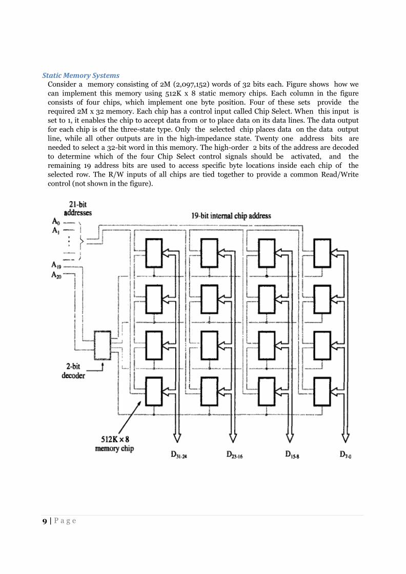
Static Memory Systems Consider a memory consisting of 2M (2,097,152) words of 32 bits each. Figure shows how we
can implement this memory using 512K x 8 static memory chips. Each column in the figure
consists of four chips, which implement one byte position. Four of these sets provide the
required 2M x 32 memory. Each chip has a control input called Chip Select. When this input is
set to 1, it enables the chip to accept data from or to place data on its data lines. The data output
for each chip is of the three-state type. Only the selected chip places data on the data output
line, while all other outputs are in the high-impedance state. Twenty one address bits are
needed to select a 32-bit word in this memory. The high-order 2 bits of the address are decoded
to determine which of the four Chip Select control signals should be activated, and the
remaining 19 address bits are used to access specific byte locations inside each chip of the
selected row. The R/W inputs of all chips are tied together to provide a common Read/Write
control (not shown in the figure).

Dynamic Memory Systems The organization of large dynamic memory systems is essentially the same as the memory
shown in Figure. However, physical implementation is often done more conveniently in the
form of memory modules.
Modem computers use very large memories; even a small personal computer is likely to have at
least 32M bytes of memory. Typical workstations have at least 128M bytes of memory. A large
memory leads to better performance because more of the programs and data used in processing
can be held in the memory, thus reducing the frequency of accessing the information in
secondary storage. However, if a large memory is built by placing DRAM chips directly on the
main system printed-circuit board that contains the processor, often referred to as a
motherboard, it will occupy an unacceptably large amount of space on the board. Also, it is
awkward to provide for future expansion of the memory, because space must be allocated and
wiring provided for the maximum expected size. These packaging considerations have led to
the development of larger memory units known as SIMMs (Single In-line Memory Modules)
and DIMMs (Dual In-line Memory Modules).Such a module is an assembly of several memory
chips on a separate small board that plugs vertically into a single socket on the motherboard.
SIMMs and DIMMs of different sizes are designed to use the same size socket. For example, 4M
x 32, 16M x 32, and 32M x 32 bit DIMMs all use the same 100-pin socket. Similarly, 8M x 64, 16M
x 64, 32M x 64, and 64M x 72 DIMMs use a 168-pin socket. Such modules occupy a smaller
amount of space on a motherboard, and they allow easy expansion by replacement if a larger
module uses the same socket as the smaller one.
READ-ONLY MEMORIES
Both SRAM and DRAM chips are volatile, which means that they lose the stored information if
power is turned off. There are many applications that need memory devices which retain the
stored information if power is turned off. For example, in a typical computer a hard disk drive
is used to store a large amount of information, including the operating system software. When a
computer is turned on, the operating system software has to be loaded from the disk into the
memory. This requires execution of a program that “boots” the operating system. Since the boot
program is quite large, most of it is stored on the disk. The processor must execute some
instructions that load the boot program into the memory. If the entire memory consisted of only
volatile memory chips, the processor would have no means of accessing these instructions. A
practical solution is to provide a small amount of nonvolatile memory that holds the
instructions whose execution results in loading the boot program from the disk. Nonvolatile
memory is used extensively in embedded systems. Such systems typically do not use disk
storage devices. Their programs are stored in nonvolatile semiconductor memory devices.
Different types of nonvolatile memory have been developed. Generally, the contents of such
memory can be read as if they were SRAM or DRAM memories. But, a special writing process is
needed to place the information into this memory. Since its normal operation involves only
reading of stored data, a memory of this type is called read-only memory (ROM).
ROM
Figure shows a possible configuration for a ROM cell. A logic value 0 is stored in the cell if the
transistor is connected to ground at point P; otherwise, a 1 is stored. The bit line is connected
through a resistor to the power supply. To read the state of the cell, the word line is activated.
Thus, the transistor switch is closed and the voltage on the bit line drops to near zero if there is
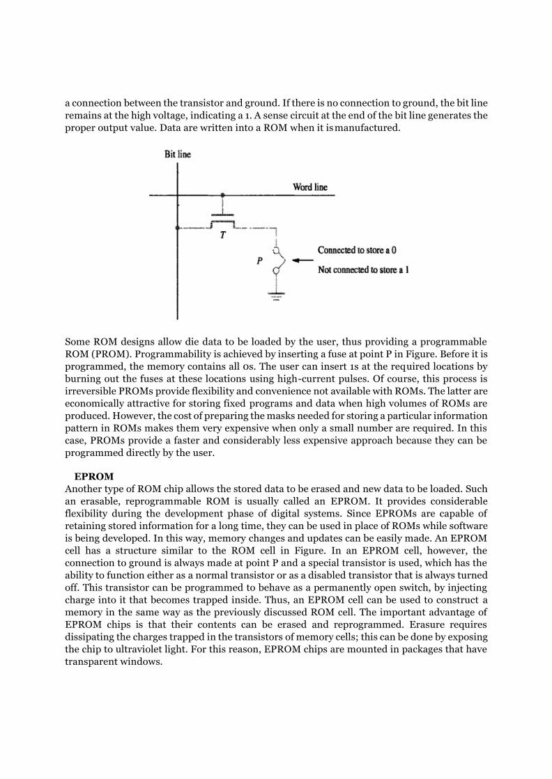
a connection between the transistor and ground. If there is no connection to ground, the bit line
remains at the high voltage, indicating a 1. A sense circuit at the end of the bit line generates the
proper output value. Data are written into a ROM when it is manufactured.
Some ROM designs allow die data to be loaded by the user, thus providing a programmable
ROM (PROM). Programmability is achieved by inserting a fuse at point P in Figure. Before it is
programmed, the memory contains all 0s. The user can insert 1s at the required locations by
burning out the fuses at these locations using high-current pulses. Of course, this process is
irreversible PROMs provide flexibility and convenience not available with ROMs. The latter are
economically attractive for storing fixed programs and data when high volumes of ROMs are
produced. However, the cost of preparing the masks needed for storing a particular information
pattern in ROMs makes them very expensive when only a small number are required. In this
case, PROMs provide a faster and considerably less expensive approach because they can be
programmed directly by the user.
EPROM
Another type of ROM chip allows the stored data to be erased and new data to be loaded. Such
an erasable, reprogrammable ROM is usually called an EPROM. It provides considerable
flexibility during the development phase of digital systems. Since EPROMs are capable of
retaining stored information for a long time, they can be used in place of ROMs while software
is being developed. In this way, memory changes and updates can be easily made. An EPROM
cell has a structure similar to the ROM cell in Figure. In an EPROM cell, however, the
connection to ground is always made at point P and a special transistor is used, which has the
ability to function either as a normal transistor or as a disabled transistor that is always turned
off. This transistor can be programmed to behave as a permanently open switch, by injecting
charge into it that becomes trapped inside. Thus, an EPROM cell can be used to construct a
memory in the same way as the previously discussed ROM cell. The important advantage of
EPROM chips is that their contents can be erased and reprogrammed. Erasure requires
dissipating the charges trapped in the transistors of memory cells; this can be done by exposing
the chip to ultraviolet light. For this reason, EPROM chips are mounted in packages that have
transparent windows.
EEPROM
A significant disadvantage of EPROMs is that a chip must be physically removed from the
circuit for reprogramming and that its entire contents are erased by the ultraviolet light. It is
possible to implement another version of erasable PROMs that can be both programmed and
erased electrically. Such chips, called EEPROMs, do not have to be removed for erasure.
Moreover, it is possible to erase the cell contents selectively. The only disadvantage of
EEPROMs is that different voltages are needed for erasing, writing, and reading the stored data.
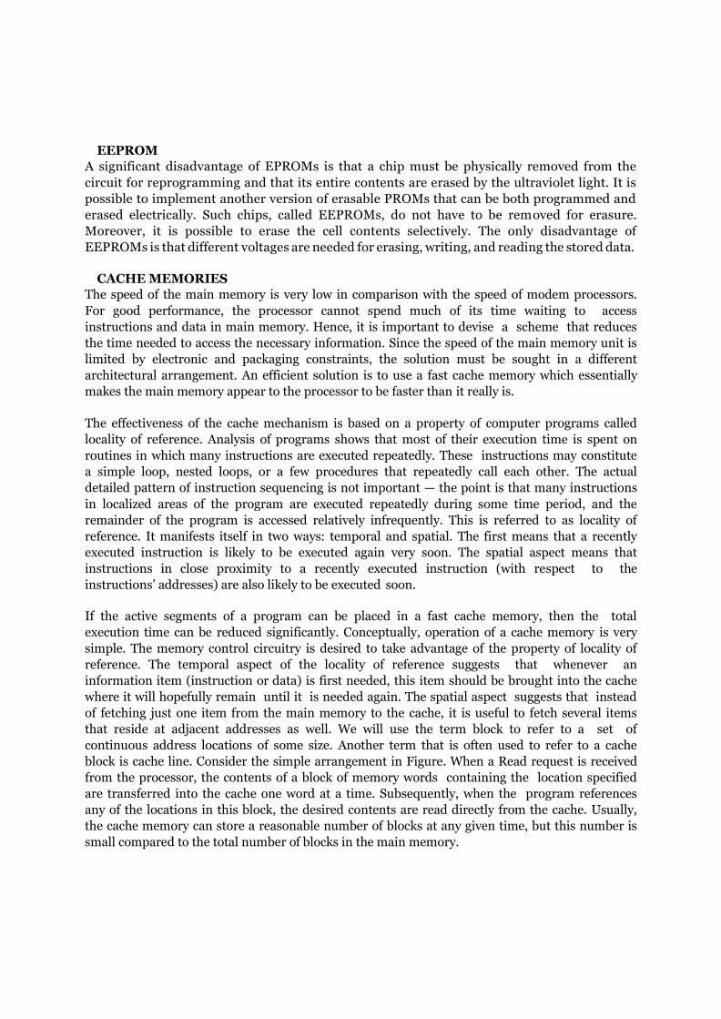
CACHE MEMORIES
The speed of the main memory is very low in comparison with the speed of modem processors.
For good performance, the processor cannot spend much of its time waiting to access
instructions and data in main memory. Hence, it is important to devise a scheme that reduces
the time needed to access the necessary information. Since the speed of the main memory unit is
limited by electronic and packaging constraints, the solution must be sought in a different
architectural arrangement. An efficient solution is to use a fast cache memory which essentially
makes the main memory appear to the processor to be faster than it really is.
The effectiveness of the cache mechanism is based on a property of computer programs called
locality of reference. Analysis of programs shows that most of their execution time is spent on
routines in which many instructions are executed repeatedly. These instructions may constitute
a simple loop, nested loops, or a few procedures that repeatedly call each other. The actual
detailed pattern of instruction sequencing is not important — the point is that many instructions
in localized areas of the program are executed repeatedly during some time period, and the
remainder of the program is accessed relatively infrequently. This is referred to as locality of
reference. It manifests itself in two ways: temporal and spatial. The first means that a recently
executed instruction is likely to be executed again very soon. The spatial aspect means that
instructions in close proximity to a recently executed instruction (with respect to the
instructions’ addresses) are also likely to be executed soon.
If the active segments of a program can be placed in a fast cache memory, then the total
execution time can be reduced significantly. Conceptually, operation of a cache memory is very
simple. The memory control circuitry is desired to take advantage of the property of locality of
reference. The temporal aspect of the locality of reference suggests that whenever an
information item (instruction or data) is first needed, this item should be brought into the cache
where it will hopefully remain until it is needed again. The spatial aspect suggests that instead
of fetching just one item from the main memory to the cache, it is useful to fetch several items
that reside at adjacent addresses as well. We will use the term block to refer to a set of
continuous address locations of some size. Another term that is often used to refer to a cache
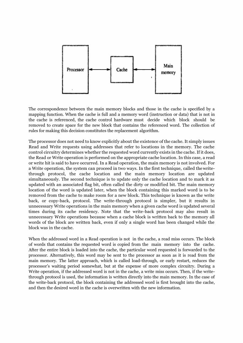
block is cache line. Consider the simple arrangement in Figure. When a Read request is received
from the processor, the contents of a block of memory words containing the location specified
are transferred into the cache one word at a time. Subsequently, when the program references
any of the locations in this block, the desired contents are read directly from the cache. Usually,
the cache memory can store a reasonable number of blocks at any given time, but this number is
small compared to the total number of blocks in the main memory.
The correspondence between the main memory blocks and those in the cache is specified by a
mapping function. When the cache is full and a memory word (instruction or data) that is not in
the cache is referenced, the cache control hardware must decide which block should be
removed to create space for the new block that contains the referenced word. The collection of
rules for making this decision constitutes the replacement algorithm.
The processor does not need to know explicitly about the existence of the cache. It simply issues
Read and Write requests using addresses that refer to locations in the memory. The cache
control circuitry determines whether the requested word currently exists in the cache. If it does,
the Read or Write operation is performed on the appropriate cache location. In this case, a read
or write hit is said to have occurred. In a Read operation, the main memory is not involved. For
a Write operation, the system can proceed in two ways. In the first technique, called the write-
through protocol, the cache location and the main memory location are updated
simultaneously. The second technique is to update only the cache location and to mark it as
updated with an associated flag bit, often called the dirty or modified bit. The main memory
location of the word is updated later, when the block containing this marked word is to be
removed from the cache to make room for a new block. This technique is known as the write
back, or copy-back, protocol. The write-through protocol is simpler, but it results in
unnecessary Write operations in the main memory when a given cache word is updated several
times during its cache residency. Note that the write-back protocol may also result in
unnecessary Write operations because when a cache block is written back to the memory all
words of the block are written back, even if only a single word has been changed while the
block was in the cache.
When the addressed word in a Read operation is not in the cache, a read miss occurs. The block
of words that contains the requested word is copied from the main memory into the cache.
After the entire block is loaded into the cache, the particular word requested is forwarded to the
processor. Alternatively, this word may be sent to the processor as soon as it is read from the
main memory. The latter approach, which is called load-through, or early restart, reduces the
processor’s waiting period somewhat, but at the expense of more complex circuitry. During a
Write operation, if the addressed word is not in the cache, a write miss occurs. Then, if the write-
through protocol is used, the information is written directly into the main memory. In the case of
the write-back protocol, the block containing the addressed word is first brought into the cache,
and then the desired word in the cache is overwritten with the new information.

MAPPING FUNCTIONS
To discuss possible methods for specifying where memory blocks are placed in the cache, we
use a specific small example. Consider a cache consisting of 128 blocks of 16 words each, for a
total of 2048 (2K) words, and assume that the main memory is addressable by a 16-bit address.
The main memory has 64K words, which we will view as 4K blocks of 16 words each. For
simplicity, we will assume that consecutive addresses refer to consecutive words.
Direct Mapping
The simplest way to determine cache locations in which to store memory blocks is the direct-
mapping technique. In this technique, block j of the main memory maps onto block j modulo
128 of the cache, as depicted in Figure.
Thus, whenever one of the main memory blocks 0,128, 256 ... is loaded in the cache, it is stored
in cache block 0. Blocks 1, 129, 257 ... are stored in cache block 1, and so on. Since more than one
memory block is mapped onto a given cache block position, contention may arise for that
position even when the cache is not full. For example, instructions of a program may start in

block 1 and continue in block 129, possibly after a branch. As this program is executed, both of
these blocks must be transferred to the block-1 position in the cache. Contention is resolved by
allowing the new block to overwrite the currently resident block. In this case, the replacement
algorithm is trivial.
Placement of a block in the cache is determined from the memory address. The memory address
can be divided into three fields, as shown in Figure. The low-order 4 bits select one of 16 words
in a block. When a new block enters the cache, the 7-bit cache block field determines the cache
position in which this block must be stored. The high-order 5 bits of the memory address of the
block are stored in 5 tag bits associated with its location in the cache. They identify which of the
32 blocks that are mapped into this cache position are currently resident in the cache. As
execution proceeds, the 7-bit cache block field of each address generated by the processor points
to a particular block location in the cache. The high-order 5 bits of the address are compared
with the tag bits associated with that cache location. If they match, then the desired word is in
that block of the cache. If there is no match, then the block containing the required word must
first be read from the main memory and loaded into the cache. The direct-mapping technique is
easy to implement, but it is not very flexible.
Associative Mapping
Figure shows a much more flexible mapping method, in which a main memory block can be
placed into any cache block position. In this case, 12 tag bits are required to identify a memory
block when it is resident in the cache.

The tag bits of an address received from the processor are compared to the tag bits of each block
of the cache to see if the desired block is present. This is called the associative-mapping
technique. It gives complete freedom in choosing the cache location in which to place the
memory block. Thus, the space in the cache can be used more efficiently. A new block that has
to be brought into the cache has to replace (eject) an existing block only if the cache is full. In
this case, we need an algorithm to select the block to be replaced. Many replacement algorithms
are possible. The cost of an associative cache is higher than the cost of a direct-mapped cache
because of the need to search all 128 tag patterns to determine whether a given block is in the
cache. A search of this kind is called an associative search. For performance reasons, the tags
must be searched in parallel.
Set Associative Mapping
A combination of the direct- and associative-mapping techniques can be used. Blocks of the
cache are grouped into sets, and the mapping allows a block of the main memory to reside in
any block of a specific set. Hence, the contention problem of the direct method is eased by
having a few choices for block placement. At the same time, the hardware cost is reduced by
decreasing the size of the associative search. An example of this set-associative-mapping
technique is shown in Figure for a cache with two blocks per set. In this case, memory blocks 0,
64, 128, ... 4032 map into cache set 0, and they can occupy either of the two block positions
within this set. Having 64 sets means that the 6-bit set field of the address determines which set
of the cache might contain the desired block. The tag field of the address must then be
associatively compared to the tags of the two blocks of the set to check if the desired block is
present. This two-way associative search is simple to implement.
The number of blocks per set is a parameter that can be selected to suit the requirements of a
particular computer. For the main memory and cache sizes in Figure 5.17, four blocks per set
can be accommodated by a 5-bit set field, eight blocks per set by a 4-bit set field, and so on. The
extreme condition of 128 blocks per set requires no set bits and corresponds to the fully
associative technique, with 12 tag bits. The other extreme of one block per set is the direct-
mapping method. A cache that has k blocks per set is referred to as a k-way set-associative
cache.
One more control bit, called the valid bit, must be provided for each block. This bit indicates
whether the block contains valid data. It should not be confused with the modified, or dirty, bit
mentioned earlier. The dirty bit, which indicates whether the block has been modified during its
cache residency, is needed only in systems that do not use the write-through method. The valid
bits are all set to0 when power is initially applied to the system or when the main memory is
loaded with new programs and data from the disk. Transfers from the disk to the main memory
are carried out by a DMA mechanism. Normally, they bypass the cache for both cost and
performance reasons. The valid bit of a particular cache block is set to 1 the first time this block
is loaded from the main memory. Whenever a main memory block is updated by a source that
bypasses the cache, a check is made to determine whether the block being loaded is currently in
die cache. If it is, its valid bit is cleared to 0. This ensures that stale data will not exist in the
cache.

A similar difficulty arises when a DMA transfer is made from die main memory to the disk, and
the cache uses the write-back protocol. In this case, the data in the memory might not reflect the
changes that may have been made in the cached copy.
One solution to this problem is to flush the cache by forcing the dirty data to be written back to the memory before the DMA transfer takes place. The operating system can do this easily, and it does not affect performance greatly, because such disk transfers do not occur often. This need to ensure that two different entities (the processor and DMA subsystems in this case) use the same copies of data is referred to as a cache-coherence problem.

VIRTUAL MEMORIES
In most modem computer systems, the physical main memory is not as large as the address
space spanned by an address issued by the processor. For example, a processor that issues 32-
bit addresses has an addressable space of 4G bytes. The size of the main memory in a typical
computer ranges from a few hundred megabytes to 1G bytes. When a program does not
completely fit into the main memory, the parts of it not currently being executed are stored on
secondary storage devices, such as magnetic disks. Of course, all parts of a program that are
eventually executed are first brought into the main memory. When a new segment of a program
is to be moved into a full memory, it must replace another segment already in the memory. In
modem computers, the operating system moves programs and data automatically between the
main memory and secondary storage. Thus, the application programmer does not need to be
aware of limitations imposed by the available main memory.
Techniques that automatically move program and data blocks into the physical main memory
when they are required for execution are called virtual-memory techniques. Programs, and
hence the processor, reference an instruction and data space that is independent of the available
physical main memory space. The binary addresses that the processor issues for either
instructions or data are called virtual or logical addresses. These addresses are translated into
physical addresses by a combination of hardware and software components. If a virtual address
refers to a part of the program or data space that is currently in the physical memory, then the
contents of the appropriate location in the main memory are accessed immediately. On the
other hand, if the referenced address is not in the main memory, its contents must be brought
into a suitable location in the memory before they can be used.
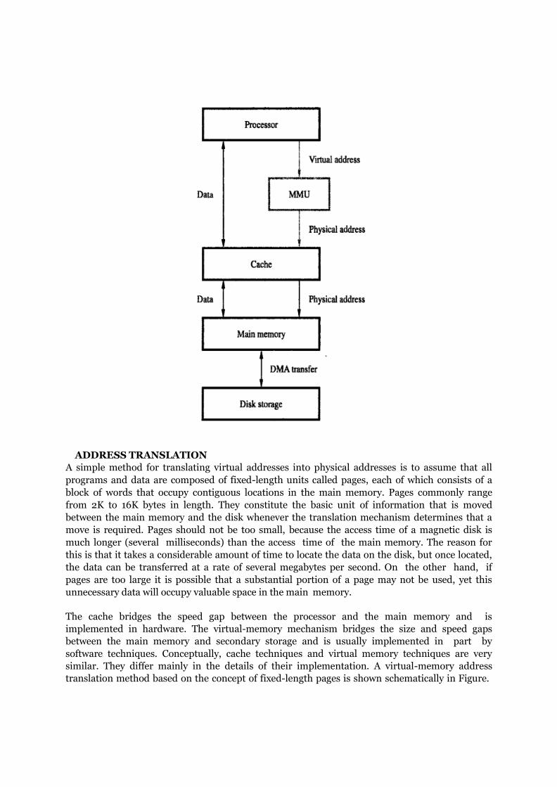
Figure shows a typical organization that implements virtual memory. A special hardware unit,
called the Memory Management Unit (MMU), translates virtual addresses into physical
addresses. When the desired data (or instructions) are in the main memory, these data are
fetched as described in our presentation of the cache mechanism. If the data are not in the main
memory, the MMU causes the operating system to bring the data into the memory from the
disk. Transfer of data between the disk and the main memory is performed using the DMA
scheme.
ADDRESS TRANSLATION
A simple method for translating virtual addresses into physical addresses is to assume that all
programs and data are composed of fixed-length units called pages, each of which consists of a
block of words that occupy contiguous locations in the main memory. Pages commonly range
from 2K to 16K bytes in length. They constitute the basic unit of information that is moved
between the main memory and the disk whenever the translation mechanism determines that a
move is required. Pages should not be too small, because the access time of a magnetic disk is
much longer (several milliseconds) than the access time of the main memory. The reason for
this is that it takes a considerable amount of time to locate the data on the disk, but once located,
the data can be transferred at a rate of several megabytes per second. On the other hand, if
pages are too large it is possible that a substantial portion of a page may not be used, yet this
unnecessary data will occupy valuable space in the main memory.
The cache bridges the speed gap between the processor and the main memory and is
implemented in hardware. The virtual-memory mechanism bridges the size and speed gaps
between the main memory and secondary storage and is usually implemented in part by
software techniques. Conceptually, cache techniques and virtual memory techniques are very
similar. They differ mainly in the details of their implementation. A virtual-memory address
translation method based on the concept of fixed-length pages is shown schematically in Figure.

Each virtual address generated by the processor, whether it is for an instruction fetch or an
operand fetch/store operation, is interpreted as a virtual page number (high-order bits)
followed by an offset (low-order bits) that specifies the location of a particular byte (or word)
within a page. Information about the main memory location of each page is kept in a page table.
This information includes the main memory address where the page is stored and the current
status of the page. An area in the main memory that can hold (me page is called a page frame.
The starting address of the page table is kept in a page table base register. By adding the virtual
page number to the contents of this register, the address of the corresponding entry in the page
table is obtained. The contents of this location give the starting address of the page if that page
currently resides in the main memory. Each entry in the page table also includes some control
bits that describe the status of the page while it is in the main memory. One bit indicates the
validity of the page, that is, whether the page is actually loaded in the main memory. This bit
allows the operating system to invalidate the page without actually removing it. Another bit
indicates whether the page has been modified during its residency in the memory. As in cache
memories, this information is needed to determine whether the page should be written back to
the disk before it is removed from the main memory to make room for another page. Other
control bits indicate various restrictions that may be imposed on accessing the page. For

example, a program may be given M read and write permission, or it may be restricted to read
accesses only. The page table information is used by the MMU for every read and write access,
so ideally, the page table should be situated within the MMU. Unfortunately, the page table
may be rather large, and since the MMU is normally implemented as part of the processor chip
(along with the primary cache), it is impossible to include a complete page table on this chip.
Therefore, the page table is kept in the main memory. However, a copy of a small portion of the
page table can be accommodated within the MMU. This portion consists of the page table
entries that correspond to the most recently accessed pages. A small cache, usually called the
Translation Lookaside Buffer (TLB) is incorporated into the MMU for this purpose. The
operation of the TLB with respect to the page table in the main memory is essentially the same
as the operation we have discussed in conjunction with the cache memory. In addition to the
information that constitutes a page table entry, the TLB must also include the virtual address of
the entry. Address translation proceeds as follows. Given a virtual address, the MMU looks in
the TLB for the referenced page. If the page table entry for this page is found in the TLB, the
physical address is obtained immediately. If there is a miss in the TLB, then the required entry
is obtained from the page table in the main memory and the TLB is updated. When a program
generates an access request to a page that is not in the main memory, a page fault is said to have
occurred. The whole page must be brought from the disk into the memory before access can
proceed. When it detects a page fault, the MMU asks the operating system to intervene by
raising an exception (interrupt). Processing of the active task is interrupted, and control is
transferred to the operating system. The operating system then copies the requested page from
the disk into the main memory and returns control to the interrupted task. Because a long delay
occurs while the page transfer takes place, the operating system may suspend execution of the
task that caused the page fault and begin execution of another task whose pages are in the main
memory.
It is essential to ensure that the interrupted task can continue correctly when it resumes
execution. A page fault occurs when some instruction accesses a memory operand that is not in
the main memory, resulting in an interruption before the execution of this instruction is
completed. Hence, when the task resumes, either the execution of the interrupted instruction
must continue from the point of interruption, or the instruction must be restarted. The design of
a particular processor dictates which of these options should be used. If a new page is brought
from the disk when the main memory is full, it must replace one of the resident pages. The
problem of choosing which page to remove is just as critical here as it is in a cache, and the idea
that programs spend most of their time in a few localized areas also applies. Because main
memories are considerably larger than cache memories, it should be possible to keep relatively
larger portions of a program in the main memory. This will reduce the frequency of transfers to
and from the disk. Concepts similar to the LRU replacement algorithm can be applied to page
replacement, and the control bits in the page table entries can indicate usage. One simple
scheme is based on a control bit that is set to 1 whenever the corresponding page is referenced
(accessed). The operating system occasionally clears this bit in all page table entries, thus
providing a simple way of determining which pages have not been used recently. A modified
page has to be written back to the disk before it is removed from the main memory. It is
important to note that the write-through protocol, which is useful in the framework of cache
memories, is not suitable for virtual memory. The access time of the disk is so long that it does
not make sense to access it frequently to write small amounts of data.
MULTIPROCESSORS
CHARACTERISTICS OF MULTIPROCESSORS
Although some large-scale computers include two or more CPUs in their microprocessor
overall system, it is the emergence of the microprocessor that has been the major motivation for
multiprocessor systems. The fact that microprocessors take very little physical space and are
very inexpensive brings about the feasibility of interconnecting a large number of
microprocessors into one composite system. Very-large-scale integrated circuit technology has
reduced the cost of computer components to such a low level that the concept of applying
multiple processors to meet system performance requirements has become an attractive design
possibility. Multiprocessing improves the reliability of the system so that a failure or error in
one part has a limited effect on the rest of the system. If a fault causes one processor to fail, a
second processor can be assigned to perform the functions of the disabled processor. The
system as a whole can continue to function correctly with perhaps some loss in efficiency.
The benefit derived from a multiprocessor organization is an improved system performance.
The system derives its high performance from the fact that computations can proceed in parallel
in one of two ways.
1. Multiple independent jobs can be made to operate in parallel.
2. A single job can be partitioned into multiple parallel tasks.
An overall function can be partitioned into a number of tasks that each processor can handle
individually. System tasks may be allocated to special-purpose processors whose design is
optimized to perform certain types of processing efficiently. An example is a computer system
where one processor performs the computations for an industrial process control while others
monitor and control the various parameters, such as temperature and flow rate. Another
example is a computer where one processor performs high-speed floating-point mathematical
computations and another takes care of routine data-processing tasks.
Multiprocessing can improve performance by decomposing a program into parallel executable
tasks. This can be achieved in one of two ways. The user can explicitly declare that certain tasks
of the program be executed in parallel. This must be done prior to loading the program by
specifying the parallel executable segments. Most multiprocessor manufacturers provide an
operating system with programming language constructs suitable for specifying parallel
processing. The other, more efficient way is to provide a compiler with multiprocessor software
that can automatically detect parallelism in a user's program. The compiler checks for data
dependency in the program. If a program depends on data generated in another part, the part
yielding the needed data must be executed first. However, two parts of a program that do not
use data generated by each can run concurrently. The parallelizing compiler checks the entire
program to detect any possible data dependencies. These that have no data dependency are
then considered for concurrent scheduling on different processors.
Multiprocessors are classified by the way their memory is organized. A multiprocessor system
with common shared memory is classified as a shared-memory or tightly coupled
multiprocessor. This does not preclude each processor from having its own local memory. In
fact, most commercial tightly coupled multiprocessors provide a cache memory with each CPU.

In addition, there is a global common memory that all CPUs can access. Information can
therefore be shared among the CPUs by placing it in the common global memory.
An alternative model of microprocessor is the distributed-memory or loosely coupled system.
Each processor element in a loosely coupled system has its own private local memory. The
processors are tied together by a switching scheme designed to route information from one
processor to another through a message-passing scheme. The processors relay program and
data to other processors in packets. A packet consists of an address, the data content, and some
error detection code. The packets are addressed to a specific processor or taken by the first
available processor, depending on the communication system used. Loosely coupled systems
are most efficient when the interaction between tasks is minimal, whereas tightly coupled
systems can tolerate a higher degree of interaction between tasks.
INTERCONNECTION STRUCTURES
The components that form a multiprocessor system are CPUs, IOPs connected to input-output
devices, and a memory unit that may be partitioned into a number of separate modules. The
interconnection between the components can have different physical configurations, depending
on the number of transfer paths that are available between the processors and memory in a
shared memory system or among the processing elements in a loosely coupled system. There
are several physical forms available for establishing an interconnection network. Some of these
schemes are presented in this section:
1. Time-shared common bus
2. Multiport memory
3. Crossbar switch
4. Multistage switching network
5. Hypercube system
Time-Shared Common Bus
A common-bus multiprocessor system consists of a number of processors connected through a
common path to a memory unit. A time-shared common bus for five processors is shown in
Figure. Only one processor can communicate with the memory or another processor at any
given time.

Transfer operations are conducted by the processor that is in control of the bus at the time. Any
other processor wishing to initiate a transfer must first determine the availability status of the
bus, and only after the bus becomes available can the processor address the destination unit to
initiate the transfer. A command is issued to inform the destination unit what operation is to be
performed. The receiving unit recognizes its address in the bus and responds to the control
signals from the sender, after which the transfer is initiated. The system may exhibit transfer
conflicts since one common bus is shared by all processors. These conflicts must be resolved by
incorporating a bus controller that establishes priorities among the requesting units.
A single common-bus system is restricted to one transfer at a time. This means that when one
processor is communicating with the memory, all other processors are either busy with internal
operations or must be idle waiting for the bus. As a consequence, the total overall transfer rate
within the system is limited by the speed of the single path. The processors in the system can be
kept busy more often through the implementation of two or more independent buses to permit
multiple simultaneous bus transfers. However, this increases the system cost and complexity.
A more economical implementation of a dual bus structure is depicted in Figure. Here we have
a number of local buses each connected to its own local memory and to one or more processors.
Each local bus may be connected to a CPU, an IOP, or any combination of processors. A system
bus controller links each local bus to a common system bus. The I/O devices connected to the
local IOP, as well as the local memory, are available to the local processor. The memory
connected to the common system bus is shared by all processors. If an IOP is connected directly
to the system bus, the I/O devices attached to it may be made available to all processors. Only
one processor can communicate with the shared memory and other common resources through
the system bus at any given time. The other processors are kept busy communicating with their
local memory and I/O devices. Part of the local memory may be designed as a cache memory
attached to the CPU. In this way, the average access time of the local memory can be made to
approach the cycle time of five CPU to which it is attached.

Multiport Memory
A multiport memory system employs separate buses between each memory module and each
CPU. This is shown in Figure for four CPUs and four memory modules (MMs). Each processor
bus is connected to each memory module. A processor bus consists of the address, data, and
control lines required to communicate with memory. The memory module is said to have four
ports and each port accommodates one of the buses. The module must have internal control
logic to determine which port will have to memory at any given time. Memory access conflicts
are resolved by assigning fixed priorities to each memory port. The priority for memory access
associated with each processor may be established by the physical port position that its bus
occupies in each module. Thus CPU 1 will have priority over CPU 2, CPU 2 will have priority
over CPU 3, and CPU 4 will have the lowest priority. The advantage of the multiport memory
organization is the high transfer rale that ca n b e achieved because of the multiple paths
between processors and memory, The disadvantage is that it requires expensive memory
control logic and a large number of cables and connectors. As a consequence, this
interconnection structure is usually appropriate for systems with a small number of processors.
Crossbar Switch
The crossbar switch organization consists of a number of cross points that are placed at
intersections between processor buses and memory module paths. Figure shows a crossbar
switch interconnection between four CPUs and four memory modules. The small square in each
cross point is a switch that determines the path from a processor to a memory module. Each
switch point has control logic to set up the transfer path between a processor and memory.

It examines the address that is placed in the bus to determine whether its particular module is
being addressed. It also resolves multiple requests for access to the same memory module on a
predetermined priority basis. Figure shows the functional design of a crossbar switch connected
to one memory module.

The circuit consists of multiplexers that select the data, address, and control from one CPU for
communication with the memory module. Priority levels are established by the arbitration logic
to select one CPU when two or more CPUs attempt to access the same memory. The multiplex
are controlled with the binary code that is generated by a priority encoder within the arbitration
logic. A crossbar switch organization supports simultaneous transfers from memory modules
because there is a separate path associated with each memory module. However, the hardware
required to implement the switch can become quite large and complex.
Multistage Switching Network
The basic component of a multistage network is a two-input, two-output interchange switch. As
shown in Figure, the 2x2 switch has two input labeled A and B, and two outputs, labeled 0 and
1. There are control sign (not shown) associated with the switch that establish the
interconnection between the input and output terminals. The switch has the capability of
connecting input A to either of the outputs. Terminal B of the switch behaves in a similar
fashion. The switch also has the capability to arbitrate between conflicting requests. If inputs A
and B both request the same output terminal only one of them will be connected; the other will
be blocked.
Using the 2x2 switch as a building block, it is possible to build the multistage network to control
the communication between a number of sources and destinations. To see how this is done,
consider the binary tree shown in Figure. The two processors Pi and P 2 are connected through
switches to each memory modules marked in binary from 000 through 111. The path from
source to a destination is determined from the binary bits of the destination number. The first
bit of the destination number determines the switch output in the first level. The second bit
specifies the output of the switch in the second level, and the third bit specifies the output of the
switch in the third level. For example, to connect P x to memory 101, it is necessary to form a
path from Pi to output 1 in the first-level switch, output 0 in the second-level switch, and output
1 in the third-level switch. It is clear that either P x or P 2 can be connected to any one of the
eight memories. Certain request patterns, however, cannot be satisfied simultaneously. For
example, if Pi is connected to one of the destinations 000 through Oil, P 2 can be connected to
only one of the destinations 100 through 111. Many different topologies have been proposed for
multistage switching networks to control processor-memory communication in a tightly
coupled multiprocessor system or to control the communication between the processing
elements in a loosely coupled system.
One such topology is the omega switching network shown in Figure. In this configuration, there
is exactly one path from each source to any particular destination. Some request patterns,
however, cannot be connected simultaneously.

For example, any two sources cannot be connected simultaneously to destinations 000 and 001.
A particular request is initialed in the switching network by the source, which sends a 3-bit
pattern representing the destination number. As the binary pattern moves through the network,
each level examines a different bit to determine the 2x2 switch setting. Level 1 inspects the most
significant bit, level 2 inspects the middle bit, and level 3 inspects the least significant bit. When
the request arrives on either input of the 2x2 switch, it is routed to the upper output if the
specified bit is 0 or lo the lower output if die bit is 1. In a tightly coupled multiprocessor system,
the source is a processor and the destination is a memory module. The first pass through the
network sets up the path. Succeeding passes are used to transfer the address into memory and
then transfer the data in either direction, depending on whether the request is a read or a write.
In a loosely coupled multiprocessor system, both the source and destination are processing
elements. After the path is established, the source processor transfers a message to the
destination processor.
Hypercube Interconnection
The hypercube or binary n-cube multiprocessor structure is a loosely coupled system composed
of N = 2n processors interconnected in an n -dimensional binary cube. Each processor forms a
node of the cube. Although it is customary to refer to each node as having a processor, in effect
it contains not only a CPU but also local memory and I/O interface. Each processor has direct
communication paths to n other neighbor processors. These paths correspond to the edges of
the cube. There are 2" distinct n-bit binary addresses that can be assigned to the processors.
Each processor address differs from that of each of its n neighbors by exactly one bit position.
Figure shows the hypercube structure for n = 1, 2, and 3. A one-cube structure has n = 1 and 21 =
2. It contains two processors interconnected by a single path. A two-cube structure has n = 2
and 22 = 4. It contains four nodes interconnected as a square. A three-cube structure has eight
nodes interconnected as a cube. An n-cube structure has 2n nodes with a processor residing in
each node. Each node is assigned a binary address in such a way that the addresses of two
neighbors differ in exactly one bit position. For example, the three neighbors of the node with
address 100 in a three-cube structure are 000, 110, and 101. Each of these binary numbers differs
from address 100 by one bit value.

Routing messages through an n-cube structure may take from one to n links from a source
node to a destination node. For example, in a three-cube structure, node 000 can
communicate directly with node 001. It must cross at least two links to communicate with
011 (from 000 to 001 to 011 or from 000 to 010 to 01l). It is necessary to go through at least
three links to communicate from node 000 to node 111. A routing procedure can be
developed by computing the exclusive- OR of the source node address with the destination
node address. The resulting binary value will have 1 bits corresponding to the axes on
which the two nodes differ. The message is then sent along any one of the axes. For
example, in a three-cube structure, a message at 010 going to 001 produces an exclusive-OR
of the two addresses equal to 011. The message can be sent along the second axis to 000
and then through the third axis to 001.
A representative of the hypercube architecture is the Intel iPSC computer complex. It consists
of 128 (n = 7) microcomputers connected through communication channels. Each node
consists of a CPU, a floating-point processor, local memory, and serial communication
interface units. The individual nodes operate independently on data stored in local memory
according to resident programs. The data and programs to each node come through a
message-passing system from other nodes or from a cube manager. Application programs are
developed and compiled on the cube manager and then downloaded to the individual nodes.
Computations are distributed through the system and executed concurrently.