The Future of Nanocomputing
10
0018-9162/03/$17.00 © 2003 IEEE 44 Computer COVER FEATURE Published by the IEEE Computer Society The Future of Nanocomputing criteria we will need to apply to bring these early research efforts into the realm of high-volume manufacturing. LOOKING BACK Much of the microelectronics technology we rely on today rests on fundamental scientific break- throughs made in the 1930s and 1940s associated with government-funded efforts to develop solid- state radar detectors during World War II. Of these, three stand out: • the band structure concept, • the effect of impurities on semiconductor prop- erties, and • advances in producing high-quality crystal interfaces in silicon and germanium. Beginning in about 1946, researchers began to uti- lize this knowledge base, and most of the basic semiconductor devices used over the past half-cen- tury were developed within the next 15 years: • 1948: bipolar transistors; • 1953: field-effect transistors (FETs); • 1955: light-emitting diodes (LEDs); • 1957: tunnel diodes; • 1959: integrated circuits; and • 1962: semiconductor lasers. Reviewing the lessons learned in the semiconductor industry over the past few decades can help us better understand the novel technologies that are beginning to emerge from the research community. George Bourianoff Intel Corp. W e’re all familiar with the silicon super- highway and the ITRS Roadmap 1 that has tracked technological pro- gress in the semiconductor industry since 1992. We’re also very aware of the projected end of scaled CMOS around 2016. Hence, the interest in emerging alternative tech- nologies—and, in particular, the so-called nano- technologies—that promise to extend Moore’s law beyond 2016. I say so-called because the semiconductor indus- try had already entered the nanotechnology world in 2000 with the introduction of the 130-nm node with a 70-nm gate-length feature size, followed by the 90-nm node featuring a critical dimension of 50 nm in 2002. We in the industry are confident that we can continue this CMOS scaling for another 12 to 15 years. We are equally confident that from the novel alternative architectures and devices being proposed today, new scalable technologies—hope- fully not too many, so that we can reap the benefits of incrementalism—will emerge that will take us through multiple processor generations for another 30 or so years. Reviewing the lessons learned in the semicon- ductor industry over the past few decades can help us better understand the confusing array of tech- nologies that are beginning to emerge from the research community. This experience suggests some
-
Upload
khangminh22 -
Category
Documents
-
view
4 -
download
0
Transcript of The Future of Nanocomputing

0018-9162/03/$17.00 © 2003 IEEE44 Computer
C O V E R F E A T U R E
P u b l i s h e d b y t h e I E E E C o m p u t e r S o c i e t y
The Future ofNanocomputing
criteria we will need to apply to bring these earlyresearch efforts into the realm of high-volume manufacturing.
LOOKING BACKMuch of the microelectronics technology we rely
on today rests on fundamental scientific break-throughs made in the 1930s and 1940s associatedwith government-funded efforts to develop solid-state radar detectors during World War II. Of these,three stand out:
• the band structure concept,• the effect of impurities on semiconductor prop-
erties, and• advances in producing high-quality crystal
interfaces in silicon and germanium.
Beginning in about 1946, researchers began to uti-lize this knowledge base, and most of the basicsemiconductor devices used over the past half-cen-tury were developed within the next 15 years:
• 1948: bipolar transistors;• 1953: field-effect transistors (FETs);• 1955: light-emitting diodes (LEDs);• 1957: tunnel diodes;• 1959: integrated circuits; and• 1962: semiconductor lasers.
Reviewing the lessons learned in the semiconductorindustry over the past few decades can help us betterunderstand the novel technologies that are beginning to emerge from the research community.
GeorgeBourianoffIntel Corp. W e’re all familiar with the silicon super-
highway and the ITRS Roadmap1
that has tracked technological pro-gress in the semiconductor industrysince 1992. We’re also very aware of
the projected end of scaled CMOS around 2016.Hence, the interest in emerging alternative tech-nologies—and, in particular, the so-called nano-technologies—that promise to extend Moore’s lawbeyond 2016.
I say so-called because the semiconductor indus-try had already entered the nanotechnology worldin 2000 with the introduction of the 130-nm nodewith a 70-nm gate-length feature size, followed bythe 90-nm node featuring a critical dimension of 50 nm in 2002. We in the industry are confidentthat we can continue this CMOS scaling for another12 to 15 years. We are equally confident that fromthe novel alternative architectures and devices beingproposed today, new scalable technologies—hope-fully not too many, so that we can reap the benefitsof incrementalism—will emerge that will take usthrough multiple processor generations for another30 or so years.
Reviewing the lessons learned in the semicon-ductor industry over the past few decades can helpus better understand the confusing array of tech-nologies that are beginning to emerge from theresearch community. This experience suggests some
August 2003 45
From the many material systems then being pro-posed, silicon became predominant because of thequality of the Si/SiO2 interface and its scaling prop-erties. Combining silicon with the elegance of theFET structure has allowed us to simultaneouslymake devices smaller, faster, and cheaper—themantra that has driven the modern semiconductormicroelectronics industry.
Looking forward: The red brick wallThe ITRS Roadmap contains many tables with
columns defined by dates and node numbers androws describing the various technical requirementsnecessary to meet the design goals associated withthat node by that date.1 Green cells in the Roadmaprepresent known technology solutions being prac-ticed; yellow, known but not yet being reduced topractice; and red, no known technology solutions.Hence, the term red brick wall.
Currently, the red brick wall that separates whatwe know from what we don’t know will occur some-time around 2007-2008. That’s not to say we won’tget to the other side—only that we don’t know howyet. But we’re confident that we’ll be able to con-tinue scaling current CMOS technology along thesame three axes that have gotten us to where we are:
• new materials,• improved processes, and• new geometries.
The semiconductor industry has already enteredthe nanotechnology world with the introduction of90-nm fabrication processes and 50-nm criticaldimensions, and researchers have already fabri-cated 15-nm working transistors.
Since the 1960s, when semiconductor productswere basically silicon, silicon dioxide, and alu-minum, numerous new materials—copper, tita-nium, and tungsten, among others—have enabledscaling to continue. Going forward, we will con-tinue to see the introduction of new
• high-κ gate dielectrics and gate materials,• structures and channel materials such as sili-
con germanium or strained silicon,• source-drain materials, and• dopants.
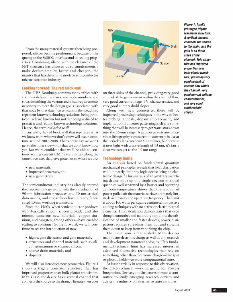
We will also introduce new geometries. Figure 1shows a trigate transistor structure that hasimproved properties over bulk-planar transistors.In this case, the device has a vertical channel thatconnects the source to the drain. The gate then goes
on three sides of the channel, providing very goodcontrol of the gate current within the channel flow,very good current-voltage (I-V) characteristics, andvery good subthreshold slopes.
Along with new geometries, there will beimproved processing techniques in the way of bet-ter etching, anneals, dopant emplacement, andimplantation. But better patterning is clearly some-thing that will be necessary to get transistors downinto the 15-nm range. A prototype extreme ultra-violet lithography exposure tool currently in use atthe Berkeley labs can print 50-nm lines, but becauseit uses light with a wavelength of 13 nm, it’s fairlyclear we can get to the 15-nm range.
Technology limitsAn analysis based on fundamental quantum
mechanical principles reveals that heat dissipationwill ultimately limit any logic device using an elec-tronic charge.2 This analysis of an arbitrary switch-ing device made up of a single electron in a dualquantum well separated by a barrier and operatingat room temperature shows that the amount ofpower pulled off the material surface ultimately lim-its device density and operation frequency. That limitis about 100 watts per square centimeter for passivecooling techniques with no active or electrothermalelements. This calculation demonstrates that eventhough nanotubes and nanodots may allow the fab-rication of smaller and faster devices, power dissi-pation requires spreading them out and slowingthem down to keep from vaporizing the chip.
The conclusion is that scaled CMOS devicesmanipulate electronic charge as well as any researchand development nanotechnologies. This funda-mental technical limit has increased interest inadvanced alternative technologies that rely onsomething other than electronic charge—like spinor photon fields—to store computational state.
At least partially in response to this observation,the ITRS technical working group for ProcessIntegration, Devices, and Structures formed a com-mittee to study emerging research devices andadvise the industry on alternative state variables.1
Drain
Source
Gate
Silicon
Figure 1. Intel’s prototype trigatetransistor structure.A vertical channelconnects the sourceto the drain, and thegate is on threesides of thechannel. This struc-ture has improvedproperties overbulk-planar transi-tors, providing verygood control of current flow withinthe channel, verygood current voltagecharacteristics, and very good subthresholdslopes.

46 Computer
NANOCOMPUTING AND BEYONDA Semiconductor Research Corporation task
force working on Emerging Reseach Devices deter-mined that a taxonomy was needed to give someorganization to this growing field of research inwhich the problem domains have not yet been welldifferentiated. To categorize the rather confusing col-lection of research efforts shown in Figure 2, it helpsto ask, Is it a device or an architecture? Does it intro-duce a new state variable or data representation?
The working group proposed a hierarchy con-sisting of four levels: devices, architectures, statevariables, and data representations. Using a famil-iar example, a basic CMOS device such as a FETuses Boolean logic gates (AND/OR gates, XNORgates, and so forth) in a Boolean architecture, andthe state variable is associated with the presence orabsence of electric charge differentiating the 1 and0 state in a binary digital data representation.
Categorizing the devices, architectures, variables,and data representations that populate this spaceof emerging alternative technologies is even morechallenging. Although it is likely to undergo numer-ous revisions, this taxonomy provides a startingpoint for developing an organizational structure toframe future discussions.
DevicesDevices are the lowest level in the taxonomy and
are the most tangible entities. You can look at a sin-gle device through a microscope, put probes on it, and define its operation in terms of inputs andoutputs.
Researchers are actively exploring the use of mol-ecular materials such as carbon nanotubes (CNTs)and silicon nanowires in prototype molecular elec-tronics devices such as FETs. Such materials areattractive to researchers because their small mole-cular structures will conceivably enable scaling(miniaturization) beyond what even the mostadvanced lithographic techniques permit. Whilethis approach may offer some advantages for someapplications—for example, memory—the funda-mental limit calculation reveals that potential mol-ecular or CNT devices would have to operate moreslowly than scaled CMOS if they are smaller thanscaled CMOS.
Carbon nanotubes. To form carbon nanotubes, anatomic planar sheet of carbon atoms is bondedtogether into an array of hexagons and rolled up toform molecular tubes or cylinders with 1 to 20 nmdiameters and ranging from 100 nm to severalmicrons in length. The details of fabrication (the chi-rality) determine a nanotube’s electronic proper-ties—that is, whether it is a semiconductor or ametal.1 Researchers at several institutions have fab-ricated CNT-FET device structures with the stan-dard source, drain, and gate, but with a CNTreplacing the silicon channel as Figure 3 shows.
Recent studies at Cornell show that it is possibleto form a low-leakage gate dielectric by atomiclayer deposition of a zirconium dioxide thin-film(8 nm) high-κ gate material on top of an array ofCNT-FETs.3 The zirconium dioxide gate insulationprovides high capacitance, allowing efficient charge
Architecture
Devices
State variables
Data representations
Time
Carbonnanotube
FETs Molecular Spintronics Quantum
Cellular nonlinearnetworks Crossbar Quantum
Boolean
Molecularstate
Spinorientation
Flux quanta Quantumstate Electric charge
AssociativePatterns
Analog
Digital
ScaledCMOS
Probabilities
HierarchyBiotech Memory devices Sensors
Figure 2. Emergingdevices taxonomy.The taxonomy con-sists of a four-levelhierarchy composedof devices,architectures, statevariables, and datarepresentations,and it is populatedwith several prototypicaldevices.
Top gate
DrainSource
Zirconium dioxide
Silicon dioxide
Silicon
Figure 3. PrototypeCNT-FET device. ACNT connectingsource, drain, andhigh-κ zirconiumdioxide insulationprovide performancecharacteristics thatapproach theoreti-cal limits.

injection and reducing current leakage. Per-formance characteristics for this prototype deviceshow good switching characteristics as measuredby the subthreshold slope. The subthreshold slopeof 70 mV per decade for the p-type transistorsapproaches the room-temperature theoretical limitof 60 mV. Subthreshold swing is a key parameterfor transistor miniaturization since it measures howwell a small swing in gate voltage can cut off cur-rent flow. Low cutoff current directly translates intolow standby power—a major challenge for end-of-the Roadmap devices.
The availability of a deterministic supply of bulkCNT materials limits CNT devices. All the knownprocesses for producing CNT materials produceCNTs of all types and sizes mixed together. Tomake devices, the nanotubes must be separatedinto groups of similar size and chirality. Currently,a laborious manual process using a scanning tun-neling microscope is the only way to separate thetubes. The other significant issue with fabricatingCNT devices is the problem of contact resistance.Right now, this represents a serious problem rela-tive to more conventional CMOS devices. Even thetheoretically “best” value of 6 kOhms is high andwill limit the maximum current.
Clearly, such prototype devices show promise,although whether they can actually become com-petitive remains to be seen.
Silicon nanowires. Recent experimental results,although not conclusive, give some indication thatquantum confinement in the transverse directionof silicon nanowires results in greater mobilitiesthan in bulk silicon.4 Although the effect is notwell understood, it seems to be related to thequantum-confined nature of the wire, which limits the density of available phonon states andhence reduces the probability of an electronphonon-scattering event—that is, it reduces drag.Coupling this observation with the desirable char-acteristics and vast experience base associatedwith silicon makes using silicon nanowires as areplacement for bulk silicon channels an attrac-tive option.
Silicon nanowire devices have been fabricated inseveral geometries. Figure 4 shows three nanowiredevices with silicon nanowire connecting the sourceand drain contact points, but with different gatestructures: a back gate, a metallic gating structureseparated by an oxide, and a coaxial structure. TheI-V characteristics of the back gate device have val-ues of 250 to 500 mV/decade, which is under-standable because a very thick gate oxide was usedin the studies.4 Experiments are under way to mea-
sure the I-V characteristics of coaxial structureswith oxide thicknesses of a few nanometers, andthese are expected to have I-V characteristics thatare much closer to the theoretical limit.
In addition to offering some advantages com-pared to bulk silicon in the fabrication of FETstructures, silicon nanowires also can be used inother structures that may be better suited to thecharacteristics of nanowires such as length-to-diameter ratio. Cross-bar arrays are one exampleof these alternative structures. In such structures,one array of parallel nanowires is overlaid on a sec-ond array of nanowires oriented at right angles tothe first array. The cross-points of the arrays canbe used to either store or switch informationdepending on the device details.5,6
In Figure 5, the crossed nanowires (or nanotubes)act as a switch with bistable positions open orclosed. The mechanical equilibrium of the wiresmaintains the neutral (open) position. Applyingopposite charges to the wires pulls them towardeach other until they touch, at which time molec-ular forces hold them in the closed position.
August 2003 47
Back gate
Top gate
Coaxial gate
G
G
G SiSiO2
D
D
D
S
S
S
D DrainS SourceG GateSiO2 Silicon dioxideSi Silicon
(a)
(b)
(c)
Figure 4. Nanowiredevices: (a) backgate, (b) metallicgating structureseparated by anoxide, and (c) coaxial structure.Silicon nanowireconnects the source and draincontact points in the different gatestructures.
“Disconnected”junction
“Connected”junctionSuspended NT
Lower conductor (NW or NT)
Support
Figure 5. Suspendednanotube switchedconnection. Onearray of parallelnanowires is over-laid on a secondarray oriented atright angles to thefirst. Depending onthe device details,the cross-points ofthe arrays can eitherstore or switchinformation.

48 Computer
Applying similar charges to the two wiresforces them apart, resetting them to the ini-tial position.
The performance of these isolated devicescannot in general compete with scaled silicon on speed. Their potential lies inachieving increased density and reducing fab-rication costs. Proponents of cross-bar archi-tectures argue that arrays of these devices canbe “self-assembled” using fluidic assemblyand Langmuir-Blodgett techniques. The
major problems are in providing the gain necessaryfor signal restoration and fan out and to connectthe self-assembled modules to global control lines.This area currently is attracting a great deal of inter-est, and the next few years will determine if the real-ity compares with the promise.
Other novel devices. NEC has introduced a room-temperature single-electron transistor (SET) thatimplements an “island” surrounded by TiOx bar-riers—a quantum dot—where the presence orabsence of a single electron controls the currentflow from source to drain via the Coulomb block-ade effect. Connected through tunneling barriers,the conductance of the dot exhibits strong oscilla-tions as the voltage of a gate electrode is varied.Each successive conductance maximum corre-sponds to the discrete addition of a single electronto the dot. This prototype device currently hasproblems associated with stray charges in the sub-strates, but there may be ways to handle that. Inaddition, several concepts of single-electron mem-ory have been experimentally demonstrated,7
including a SET/FET hybrid.8 Two major disad-vantages of all single-electron memories reportedso far are very low operating temperature of 4.2-20 K and background charges.
Another novel device is a molecular switch con-structed by Mark Reed’s group at Yale.9 Molecularmemory is a broad term combining different pro-posals for using individual molecules as buildingblocks of memory cells in which one bit of infor-mation can be stored in the space of an atom, mol-ecule, or cell. Placing 100 or so molecules betweenthe source and drain actually changes their mole-cular state and thus their I-V characteristics. Thismolecular memory stores data by applying exter-nal voltage that causes the transition of the mole-cule into one of two possible conduction states.The molecular memory reads the data by measur-ing resistance changes in the molecular cell. Thisoperational characteristic is frequently representedas a hysteresis plot with voltage on the horizontalaxis and resistance on the vertical axis.
All of these devices use electrons as their statevariables, but it is possible to envision devices thatmanipulate other state variables. For example, thespin resonance transistor proposed by EliYablanovitch at the University of California, LosAngeles, uses the gate voltage to manipulate thespin of electrons bound to two phosphorousnuclei, embedded in an engineered gate stack thathas a variable G factor.10 Readout is accomplishedby applying a time-varying magnetic field to thestack and creating an electron spin resonance whenexactly the right frequency is applied. This is oneexample of how to control something other thanelectronic charge—in this case, nuclear spin.
ArchitecturesThe architecture, a computer’s fundamental
organizational structure, constitutes the next levelup in the taxonomy, and is just slightly moreabstract than devices. Although manufacturers varythe microarchitectural implementations, mostmicroprocessors use the Intel x86 instruction setarchitecture, which remains constant across allimplementations.
As alternative devices are introduced, radicallynew architectures will be required to support them.Table 1 lists the characteristics of six of these emerg-ing research architectures.
3D heterogeneous integration. The integration ofsemiconductor devices in 3D arrays is being dri-ven from two distinct directions. The first is asso-ciated with the need to integrate dissimilartechnologies on a common platform to deliver anoptimum information processing solution.
It is clear that emerging technologies beyondscaled CMOS offer the potential for greatlyimproved performance by mixing and matchingtechnologies for particular applications. The com-bination of technologies requires the 3D integrationof functionally dissimilar technologies beginningwith microprocessors, ASICs, and DRAMs andextending to RF, analog, optical, and MEMS. Thesedissimilar technologies may later include 3D inte-gration of molecular, plastic, rapid single-flux quantum superconductors and other emerging tech-nologies directly on to silicon platforms.
The other principal driver for 3D integration isthe need to reduce global interconnect delays to maximize system performance. In certain ideal-ized circumstances, 3D superposition of devices will decrease interconnect delays by substantialamounts t relative to an equivalent number of tran-sistors arranged in a planar arrangement.11,12 Inprinciple, either low-temperature wafer bonding or
The potential ofnanotubes lies in achieving
increased densityand reducing
fabrication costs.

monolithic integration on a common substrate canachieve 3D integration. Wafer bonding has signif-icant limitations because of alignment issues and iscurrently limited to accuracies of 1 to 5 microns. A host of typical material integration issues pose a challenge to monolithic integration. All 3D inte-gration implementations must deal with issues ofheat removal because 3D integrations have lowersurface-to-volume ratios than planar circuits. Themost promising application of 3D integrationappears to be combining memory with micro-processors.
Quantum cellular automata. In the QCA paradigm,a locally interconnected architecture consists of aregular array of cells containing several quantumdots. Electrostatic interactions, not wires, providethe coupling between the cells. When we inject anelectron pair into the cell, this electron pair’s ori-entation defines the cell’s state. Two bistable statesrepresenting 1 and 0 align themselves in one of twodirections, with the electrons populating the oppo-site corner of the cell. Although electronic QCAsare predominant, magnetic QCAs are anotherrecent development for which the performance can-not yet be assessed. Combining these QCAs allowsperforming circuit functions that are quite differ-ent from using Boolean logic gates.
Archetypal QCA straddles the line between beinga new architecture and a new device, clearlydemonstrating that new architectures may berequired to support new devices. If the cells arearranged in a regular square grid, long-establishedcellular automata theory can be applied, togetherwith its extension, cellular nonlinear (or neural)network (CNN) theory, to describe the informa-tion processing algorithm. This allows applying alarge body of theory directly to QCA architectures.1
Regular EQCA grids can solve certain types of dif-fusion and wave equations.13 Also, it is theoreticallypossible to use them to solve arbitrary digital logic
problems, but such systems would be extraordinar-ily inefficient in terms of area. However, by depart-ing from the regular grid structure, it is possible to design EQCA structures that could carry out universal computing with moderate efficiency.
In addition to a nonuniform layout, EQCAs needa spatially nonuniform “adiabatic clocking field,”which controls the switching of the cells from onestate to another and allows them to evolve rela-tively rapidly to a stable end state. Using clockingadds to the complexity of pure EQCA circuits butgreatly extends their possible range of applications.It is possible to construct a complete set of Booleanlogic gates with EQCA cells and to design arbitrarycomputing structures. However, current device andcircuit analyses indicate that the speed of EQCAcircuits will be limited to less than about 10MHz.14,15
Defect-tolerant architecture. The possibility of fab-ricating nanometer-scale elements that probably willnot satisfy the tolerance and reliability requirementstypical of larger-scale systems creates the need fordefect-tolerant hardware. Systems consisting ofmolecular-size components are likely to have manyimperfections, and a computing system designed ona conventional zero-defect basis would not work.For a conventional integrated circuit, designersdescribe the chip function, then they construct thehardware.
The general idea behind defect-tolerant architec-tures is conceptually the opposite: Designers fabri-cate a generic set of wires and switches, then theyconfigure the resources by setting switches that linkthem together to obtain the desired functionality.16
A cornerstone of defect-tolerant systems is redun-dancy of hardware resources—switches, memorycells, and wires—which implies very high integra-tion density. Fabrication could potentially be veryinexpensive if researchers can actualize a chemicalself-assembly and attach global interconnects.
August 2003 49
Table 1. Emerging research architectures.
Architecture Implementations Advantages Challenges Maturity
3D integration CMOS with dissimilar Less interconnect delay; enables Heat removal; no design tools; Demonstrationmaterial systems mixed technology solutions difficult test and measurement
Quantum cellular Arrays of quantum dots High functional density; no Limited fan out; dimensional Demonstrationautomata interconnects in signal path control (low-temperature operation);
sensitive to background charge Defect-tolerant Intelligently assembles Supports hardware with defect Requires precomputing testing Demonstration
nanodevices densities > 50 percent Molecular Molecular switches and Supports memory-based Limited functionality Concept
memories computing Cellular nonlinear Single-electron array Supports memory-based Subject to background noise; Demonstrationnetworks architectures computing tight tolerances Quantum computing Spin resonance transistors, Exponential performance Extreme application limitation; Concept
NMR devices, single-flux scaling, but can break current extreme technology quantum devices cryptography

50 Computer
However, such a circuit would require a labo-rious testing process, implying a significantoverhead cost.
It is important to differentiate betweendefect-tolerant and fault-tolerant architec-tures. Fault-tolerant systems are designed todeal with transient faults and usually requiresome form of redundancy checking. Bothdefect-tolerant and fault-tolerant systems havean upper limit to the number of defects orfaults they can handle before the correctionprocess dominates the overall calculation eff-icency. The numerical limit appears to be 20 to
25 percent bad elements or defective calculations.Phase logic. Although phase logic is strictly
defined as an architecture, the term is closely asso-ciated with the use of phase as a state variable. Theconcept is generally credited to Richard Feynman,who received a patent for what he called theParameteron in the 1950s. Feynman postulatedthat it is possible to store information as the rela-tive phase of two oscillating analog signals in atank oscillator circuit. One signal is labeled as thereference signal, and the other is labeled as the con-trol signal. Changing the phase of the control sig-nal relative to the reference signal “changes state”and logic. If the circuit has only two allowed rela-tive phases, it is possible to implement both binaryand multivalued logic.
Tunneling phase logic is a more recent imple-mentation of the same concept proposed byRichard Kiehl and colleagues at the University ofMinnesota.17 In a TPL circuit, a resonant tunnel-ing diode and an RC circuit produce the referencesignal. The more conventional oscillator circuitproduces the control signal, but the circuit stillstores information as the relative phase betweenthe two signals. Implementing TPLs presents manyproblems, primarily associated with manufactur-ing uniform tunneling diodes and stray backgroundcharge.
Quantum computing. Quantum computers are char-acterized as something between a device and anarchitecture. There are many different ways toinstantiate quantum computing, including a solid-state proposal by Bruce Kane and colleagues at theUniversity of Maryland.18 Other options includeliquid state, nuclear magnetic resonance, linear iontraps, or quantum dots. There are numerous imple-mentation methods, but clearly manipulatingquantum information will require novel archi-tectures.
Coherent quantum devices rely on the phaseinformation of the quantum wave function to store
and manipulate information. A qubit, the phaseinformation of any quantum state, is extremely sen-sitive to its external environment. A qubit is easilyconnected or entangled with the quantum states ofparticles in the local environment, and no physicalsystem can ever be completely isolated from itsenvironment. The same sensitivity, however, can beused to entangle adjacent qubits in ways that phys-ical gates can control.
The core idea of quantum information processingor quantum computing is that each individual com-ponent of an infinite superposition of wave functionsis manipulated in parallel, thereby achieving a mas-sive speedup relative to conventional computers. Thechallenge is to manipulate the wave functions so thatthey perform a useful function and then to find away to read the result of the calculation.
Essentially, three different approaches have beentaken to the implementation of quantum computers:
• bulk resonance quantum implementationsincluding NMR,19 linear optics,20 and cavityquantum electrodynamics;21
• atomic quantum implementations includingtrapped ions22 and optical lattices;23 and
• solid-state quantum implementations includ-ing semiconductors18 and superconductors.24
This discussion focuses on solid-state quantum com-puting because these implementations appear tooffer the highest promise for scaling the complexityof quantum computing for commercial applications.
The qubit concept parallels the bit in conventionalcomputation, but offers a much broader set of rep-resentations. Rather than a finite dimensional binaryrepresentation for information, the qubit is a mem-ber of a two-dimensional Hilbert space containinga continuum of quantum states. Thus, quantumcomputers operate in a much richer space thanbinary computers.
Researchers have defined many sets of elemen-tary quantum gates based on the qubit concept thatperform mappings from the set of input quantumregisters to a set of output quantum registers. A sin-gle gate can entangle the qubits stored in two adja-cent quantum registers, and combinations of gatescan be used to perform more complex computa-tions. Just as in Boolean computation, there areminimal sets of quantum gates that are completewith respect to the set of computable functions.
Theoretically, quantum computers are not infe-rior to standard computers of similar complexityand speed of operation. More interesting is the factthat for some important classes of problems, the
Quantum computers are characterized as something
between a device and
an architecture.

quantum computer is superior to its standard coun-terpart. In particular, Peter W. Schor demonstratedthat a quantum computer can determine the twoprime factors of a number in time proportional toa polynomial in the number of digits in the num-ber.25 This truly remarkable result showed that forthis particular class of problems, the quantum com-puter is at least exponentially better than a stan-dard computer.
The key to this result is the capability of a quan-tum computer to efficiently compute the quantumFourier transform. This result has immediate appli-cation in cryptography since it would allow thequick determination of keys to codes such as RSA.It is estimated that a few thousand quantum gateswould be sufficient to solve a representative RSAcode containing on the order of 100 digits. Thereare several other applications that are variants ofthe factorization problem.26
State variables In this context, the term state variables refers to
the notion of the finite state machine introduced byAlan Turing in the 1930s. The idea is that there arenumerous ways to store computational informa-tion or state to manipulate and store it. The earli-est example of a finite-state storage device was theabacus, which represents numerical data by theposition of beads on a string. In this example, thestate variable is simply a physical position, and theoperator accomplishes readout by looking at theabacus. The operator’s fingers physically move thebeads to perform the data manipulations.
Thermal effects will ultimately limit dimensionalscaling of any logic device that manipulates elec-tric charge as a state variable. The corollary of thisobservation is that the search for alternative logicdevices must embrace the concept of using statevariables other than electric charge.
Early core memories used the orientation ofmagnetic dipoles to store state. Similarly, papertapes and punch cards used the presence orabsence of holes to store state. Recent researchactivities in alternative state variables that seemto be the most prevalent in the research literatureinclude
• molecular state,• spin orientation,• electric dipole orientation,• photon intensity or polarization,• quantum state,• phase state, and• mechanical state.
The development of research devices thatuse alternative state variables makes it desir-able to include state variables as one of thefour major categories that constitute thenanocomputing taxonomy.
Data representationsRecent advances in computational power
and the anticipated increase in the near futurehave led to the paradoxical situation that wecan generate far more data than we can useor interpret effectively. The goal of currentresearch into alternative data representationsis to compactly represent key features of adata set that are useful for a particular application.Image compression using edge-finding and raster-scanning techniques involves scanning an image ofbinary data generated by some other means andextracting the compressed data. As we encounteralternative devices, architectures, and state vari-ables, adopting alternative data representations inwhich to manipulate, store, and visualize informa-tion may be advantageous.
The best analogy to illustrate this point is the useof Fourier transforms to analyze time series. It isobvious that a Fourier decomposition of a randomtime sequence offers a compact way to represent alarge quantity of data. It is also true that it is possi-ble to work entirely in transform space and, in somecases, to achieve significant numerical efficiencies.
The concept of alternative state variables is a gen-eralization of this concept that can be applied effec-tively to more general types of problems such asfeature recognition, hierarchical data reductions,and multipole expansions. As such, it constitutesthe fourth and most abstract category in the pro-posed nanocomputing taxonomy.
REASONABLENESS CRITERIAWe can’t predict which of the devices, architec-
tures, state variables, or data representations willevolve into the next scalable computing technology.However, we can propose some set of reasonable-ness criteria that will help differentiate betweenwhat might actually make its way into high-volumemanufacturing and what might not.
Economic criteriaWe can confidently predict that scaling will con-
tinue as long as we can meet the economic imper-ative that incremental cost divided by incrementalperformance gain must be less than it would be foralternative technologies.
Although this economic relevance criterion is very
August 2003 51
Adopting alternative data representations
in which to manipulate, store,
and visualize information may
be advantageous.

52 Computer
easy to state, it is very hard to calculate. To say thatthe risk of adjusted return on investment of any newtechnology must exceed that of silicon is trivially true,but as Herb Kroemer, recipient of the 2000 NobelPrize in physics, cautions, sufficiently advanced tech-nologies will create their own applications. To esti-mate the total ROI for an emerging technology, inaddition to markets that exist today, we also mustanticipate future markets—and that’s tough.
Technology criteria The other criteria are technical in nature. CMOS
compatibility and energy efficiency are the domi-nant issues when incorporating any alternativetechnology in high-volume manufacturing. Otherkey technology concerns include scalability, per-formance, architectural compatibility, sensitivity toparametric variation, room-temperature operation,and reliability.
If we can apply the huge CMOS manufacturinginfrastructure that we already know how to manip-ulate, we can make up for the deficit in some otherareas. I would recommend applying lessons learnedfrom the experience in this area to help guide futureresearch in the university community.
GOING FORWARDThe types of scientific breakthroughs we need to
see going forward have strong connections to thework done in the 1940s and 1950s. These futurebreakthroughs must occur in three areas:
• the bulk band structure of solids needs to bereplaced by geometry-dependent energeticstructures of nanostructures, requiring us toanalyze their stability and their basic quantummechanical energy levels;
• doping, a bulk process, needs to be replacedby the precise manipulation and placement ofindividual atoms; and
• crystal growth, another bulk process, needs tobe replaced by the self-organization of matterand self-assembly of complex structures.
As we move to nanotechnology, one of the chal-lenges we face is the integration of hard stuff thatis very precise and well defined with stuff that’s soft,wet, squishy, and subject to fault tolerance andlarge variations in capabilities.
T here are many good reasons to believe thatCMOS will continue to scale for another 12to 15 years. Beyond that, the details are fuzzy,
but it is clear that new scalable technologies willbegin to emerge and will be integrated on CMOSby about 2015. These technologies represent solu-tions to meet specific needs and will hopefullypoint the way to radically new scalable tech-nologies that will take us into the middle of thecentury.
For either of these things to happen, nano-science research is needed to enable the new tech-nologies. �
AcknowledgmentI would like to acknowledge my colleagues at the
Semiconductor Research Corporation, RalphCavin, Jim Hutchby, and Victor Zhirnov, for muchof the material and many of the views expressed inthis article.
References1. International Sematech, The International Technol-
ogy Roadmap for Semiconductors, 2001 Edition,2001; http://public.itrs.net/Files/2001ITRS/Home.htm.
2. V.V. Zhirnov et al., “Limits to Binary Logic SwitchScaling—A Gedanken Model,” to be published inProc. IEEE, Sept. 2003.
3. A. Javey et al., “High-κ Dielectrics for Advanced Car-bon-Nanotube Transistors and Logic Gates,” NatureMaterials; http://www.lassp.cornell.edu/lassp_data/mceuen/homepage/nmat7691.pdf.
4. Y. Cul and C.M. Lieber, “Functional Nanoscale Elec-tronic Devices Assembled Using Silicon NanowireBuilding Blocks,” Science, Feb. 2001, pp. 851-853.
5. A. DeHon, “Array-Based Architecture for FET-BasedNanoscale Electronics,” IEEE Trans. Nanotechnol-ogy, Mar. 2003, pp. 23-32.
6. Y. Huang et al, “Logic Gates and Computation fromAssembled Nanowire Building Blocks,” Science, vol.294, Nov. 2001, pp. 1313-1317.
7. N.J. Stone and H. Ahmed, “Silicon Single ElectronMemory Cell,” Applied Physics Letters, Oct. 1998,pp. 2134-2136.
8. H. Mizuta et al., “Nanoscale Coulomb BlockadeMemory and Logic Devices,” Nanotechnology, vol.12, 2001, pp. 155-159.
9. M.A. Reed et al., “Molecular Random Access Mem-ory Cell,” Applied Physics Letters, vol. 78, 2001, pp.3735-3737.
10. H.W. Jiang and E. Yablonovitch, “Gate-ControlledElectron Spin Resonance in GaAs/AlxGa1—xAs Het-erostructures,” Physical Rev. B, July 2001, vol. 64,no. 4, pp. 041307/1-4.

11. J.A. Davis et al., “Interconnect Limits on GigascaleIntegration (GSI) in the 21st Century,” Proc. IEEE,vol. 89, 2001, pp. 305-324.
12. K. Banerjee et al., “3-D ICs: A Novel Chip Designfor Improving Deep-Submicrometer InterconnectPerformance and Systems-on-Chip Integration,”Proc. IEEE, vol. 89, 2001, pp. 602-633.
13. W. Porod et al., “Quantum-Dot Cellular Automata:Computing with Coupled Quantum Dots,” Int’l J.Electronics, vol. 86, 1999, pp. 549-590.
14. L. Bonci, G. Iannaccone, and M. Macucci, “Perfor-mance Assessment of Adiabatic Quantum CellularAutomata,” J. Applied Physics, vol. 89, 2001, pp.6435-6443.
15. K. Nikolic, D. Berzon, and M. Forshaw, “RelativePerformance of Three Nanoscale Devices—CMOS,RTDs and QCAs—against a Standard ComputingTask,” Nanotechnology, vol. 12, 2001, pp. 38-43.
16. J.R. Heath et al., “A Defect-Tolerant ComputerArchitecture: Opportunities for Nanotechnology,”Science, vol. 280, 1998, pp. 1716-1721.
17. T. Yang, R.A. Kiehl, and L.O. Chua, “TunnelingPhase Logic Cellular Nonlinear Networks,” Int’l J.Bifurcation and Chaos, vol. 11, no. 12, 2001, pp.2895-2911.
18. B.E. Kane, “A Silicon-Based Nuclear Spin QuantumComputer,” Nature, vol. 393, 1998, pp. 133-137.
19. M. Steffen, L.M.K. Vandersypen, and I.L. Chuang,“Toward Quantum Computation: A Five-QubitQuantum Processor,” IEEE Micro, vol. 21, no. 2,2001, pp. 24-34.
20. S. Takeuchi, “Experimental Demonstration of aThree-Qubit Quantum Computation AlgorithmUsing a Single Photon and Linear Optics,” PhysicalRev. A, vol. 62, no. 3, 2000, 032301.
21. P. Grangier, G. Reymond, and N. Schlosser, “Imple-mentations of Quantum Computing Using CavityQuantum Electrodynamics,” Progress of Physics,vol. 48, 2000, pp. 859-874.
22. C. Monroe et al., “Demonstration of a FundamentalQuantum Logic Gate,” Physics Rev. Letters, vol. 75,1995, pp. 4714-4717.
23. G.J. Milburn, “Quantum Computing Using a Neu-tral Atom Optical Lattice: An Appraisal,” Progressof Physics, vol. 48, 2000, pp. 957-964.
24. D.V. Averin, “Quantum Computation and QuantumCoherence in Mesoscopic Josephson Junctions,” J. LowTemperature Physics, vol. 118, 2000, pp. 781-793.
25. P.W. Shor, “Algorithms for Quantum Computation:Discrete Logarithms and Factoring,” Proc. 35th Ann.Symp. Foundations of Computer Science, IEEE CSPress, 1994, pp. 124-134.
26. C.P. Williams and S.H. Clearwater, Explorations inQuantum Computing, Springer-Verlag, 1998.
George Bourianoff is a senior program manager inthe Strategic Research Group at Intel Corp. Hisresearch interests include quantum computing,advanced devices, and optoelectronics. Bourianoffreceived a PhD in physics from the University of Texas at Austin. Contact him at [email protected].
ArchitecturesSupport Services
Algorithm/Protocol Design and AnalysisMobile Environments
Mobile Communication SystemsApplications
Emerging Technologies
IEEE Transactions onMobile Computing
revolutionary new quarterly journal that seeks out and delivers the very best peer-reviewed research results on mobility of users, systems, data, computing information
organization and access, services, management, and applications.IEEE Transactions on Mobile Computing gives you remarkablebreadth and depth of coverage...
A
To subscribe:http://
computer.org/tmcor call
USA and CANADA:
+1 800 678 4333WORLDWIDE:
+1 732 981 0060
SubscribeNOW!