Thank you for purchasing iG5A Series DeviceNet Communication ...
96
-
Upload
khangminh22 -
Category
Documents
-
view
2 -
download
0
Transcript of Thank you for purchasing iG5A Series DeviceNet Communication ...


Safety Precautions
I
Thank you for purchasing S100 Series Extension I/O. SAFETY PRECAUTIONS
Always follow safety instructions to prevent accidents and potential hazards
from occurring. Safety precautions are classified into “WARNING” and “CAUTION” and their
meanings are as follows:
WARNING Improper operation may result in serious personal injury or death.
CAUTION Improper operation may result in slight to medium personal injury or property damage
The indicated illustrations on the product and in the manual have the following meanings.
Danger may be present. Read the message and follow the instructions carefully.
Particular attention should be paid because danger of an electric shock may be present.
Keep operating instructions handy for quick reference. Read the operating instructions carefully to fully understand the functions of
the S100 series and to use it properly.
CAUTION Be cautious, when handling the CMOS components of the
communication module. Static may lead to malfunctioning of the product.
Turn off the inverter power, when changing the communication cable. Otherwise, you may damage the module or a communication error may occur.
Make sure to insert the Option board connector to the inverter precisely. Otherwise, you may damage the module or a communication error may occur.
Check the parameter unit before setting up the parameter. Otherwise, a communication error may occur.

Table of Contents
ii
Table of Contents Chapter 1. Basic Information & Precautions .......................................................................................................................... 1
1.1 Characteristics ............................................................................................................................................................................................. 1
1.2 Components ................................................................................................................................................................................................ 1 Chapter 2. Specifications .............................................................................................................................................. 2
2.1 External Dimension ................................................................................................................................................................................... 2
2.2 Input and Output Specification .............................................................................................................................................................. 3 Chapter 3. Installation ................................................................................................................................................. 4
3.1 Installation of S100 Extension I/O .......................................................................................................................................................... 4
3.2 Control Terminal Wiring ............................................................................................................................................................................ 6
3.3 Signal (Control) Cable Specifications .................................................................................................................................................... 8 Chapter 4. Basic Features ........................................................................................................................................... 11
4.1 Basic function ............................................................................................................................................................................................ 11
4.2 Setting Frequency Reference ................................................................................................................................................................ 11
4.2.1 V3 Terminal as the Source ................................................................................................................................................. 11
4.2.2 Setting a Frequency Reference with Input Voltage (Terminal I4) ........................................................................... 17
4.3 Analog Output .......................................................................................................................................................................................... 18
Voltage and Current Analog Output .................................................................................................................................................... 18
4.4 Digital Output ........................................................................................................................................................................................... 20
4.4.1 Multi-function Output Terminal and Relay Settings .................................................................................................. 20
4.4.2 Fault Trip Output using Multi-Function Output Terminal and Relay .................................................................................. 23
4.4.3 Multi-function Output Terminal Delay Time Settings ......................................................................................................... 24
4.5 Setting Multi-step Frequency ............................................................................................................................................................... 25
4.6 Multi-step Acc/Dec Time Configuration ............................................................................................................................................. 27
4.7 Stopping the Acc/Dec Operation ......................................................................................................................................................... 28
4.8 Multi-function Input Terminal Control ................................................................................................................................................ 29 Chapter 5. Table of Functions ...................................................................................................................................... 30
5.1 Operation Group ...................................................................................................................................................................................... 30
5.2 Drive group (PAR→dr) ............................................................................................................................................................................. 31
5.3 Basic Function group (PAR→bA) .......................................................................................................................................................... 35
5.4 Expanded Function group (PAR→Ad) ................................................................................................................................................. 38
5.5 Control Function group (PAR→Cn) ...................................................................................................................................................... 43
5.6 Input Terminal Block Function group (PAR→In) ............................................................................................................................... 47
5.7 Output Terminal Block Function group (PAR→OU) ......................................................................................................................... 51
5.8 Communication Function group (PAR→CM) .................................................................................................................................... 55
5.9 Application Function group (PAR→AP) .............................................................................................................................................. 59
5.10 Extension I/O Function Group(PAR→AO) ................................................................................................................................ 61
5.11 Protection Function group (PAR→Pr) ....................................................................................................................................... 63
5.12 2nd Motor Function group (PAR→M2) .................................................................................................................................... 68
5.13 User Sequence group (US) .......................................................................................................................................................... 70
5.14 User Sequence Function group(UF) ......................................................................................................................................... 72
5.15 Groups for LCD Keypad Only ...................................................................................................................................................... 88
5.15.1 Trip Mode (TRP Last-x) ........................................................................................................................................................... 88
5.15.2 Config Mode (CNF) ................................................................................................................................................................. 89

Chapter 1. Basic Information & Precautions
1
Chapter 1. Basic Information & Precautions
Before installation of S100 Extension I/O, this chapter explains basic information and precautions (The Extension I/O is supported by the product S/W V2.1 or higher.)
1.1 Characteristics
Additional terminals Digital Input : 3ea Digital Output : 2ea(1FormC) Analog Input : 2ea Analog Output : 1ea
1.2 Components
S100 Extension I/O consists of following items. S100 Extension I/O : 1ea User manual : 1ea Brass supporter(M3xL17.3) : 1ea Brass supporter(M3xL23) : 1ea Screw(M3xL8) : 2ea Other parts If you find damaged or missing parts, please contact LS ELECTRIC office(refer to the end of this manual).
Chapter 2. Specifications
2
Chapter 2. Specifications
2.1 External Dimension

Chapter 2. Specifications
3
2.2 Input and Output Specification
Function Label Name Description
IN PUT
Multi-function terminal configuration
P8 ~ P10
Multi-function Input 8~10 Configurable for multi-function input terminals.
CM Common Sequence Common terminal for analog terminal inputs and outputs.
Analog input configuration
V3 Voltage input for frequency reference input
Used to setup or modify a frequency reference via analog voltage input terminal. • Unipolar: 0–10V (12V Max.) • Bipolar: -10–10V (±12V Max.)
I4
Voltage/current input for frequency reference input
Used to setup or modify a frequency reference via analog voltage or current input terminals. Switch between voltage (V4) and current (I4) modes using a control board switch (SW2). V4 Mode: • Unipolar: 0–10V (12V Max.) I4 Mode • Input current: 4–20mA • Maximum Input current: 24mA • Input resistance: 249Ω
OUTPUT
Analog Output AO3 Voltage/Curren
t Output
devices: output frequency, output current, output voltage, or a DC voltage. Operate switch (SW3) to select the signal output type (voltage or current) at the AO terminal. Output Signal Specifications: • Output voltage: 0–10V • Maximum output voltage/current: 12V/10mA • Output current: 0–20mA • Maximum output current: 24mA • Factory default output: Frequency
Digital Output
CM Common Sequence
Common terminal for analog terminal inputs and outputs.
A3, C3, B4
Fault signal output
Sends out alarm signals when the inverter’s safety features are activated (AC 250V <1A, DC 30V < 1A). Fault condition: A3 and C3 contacts are connected (B3 and C3 open connection) Normal operation: B3 and C3 contacts are connected (A3 and C3 open connection)
A4, C4, B4
Fault signal output
Sends out alarm signals when the inverter’s safety features are activated (AC 250V <1A, DC 30V < 1A). Fault condition: A4 and C3 contacts are connected (B4 and C4 open connection) Normal operation: B4 and C4 contacts are connected (A4 and C4 open connection)

Chapter 3. Installation
4
(1)
(2)
Chapter 3. Installation
3.1 Installation of S100 Extension I/O
Warning) Connect a communication network after the power supply of the S100 inverter must be off. If the power supply is plugged when Extension I/O is removed, the S100 inverter will be damaged entirely. Take off Extension I/O from the product after the power supply is totally discharged.
In case of LSLV0004S100-2EXNNS, LSLV0008S100-2EXNNS, LSLV0004S100-4EXFNS, LSLV0008S100-4EXFNS, it is impossible to do wiring of main source after assembly of Extension I/O. Please assemble Extension I/O after wiring of main source. If you need to using built-in I/O terminals, please do wiring of the terminals before assembly of extension I/O
■ Take off the power supply cover
and the I/O cover((1), (2)) from a dedicated S100 inverter for communication.
■ Take off the keypad (3).
■ Loosen a screw from
the I/O board and fasten the prepared brass bar (M3xL23) to (4), and (M3xL17.3) to (5).
(3)
(4) (5)

Chapter 3. Installation
5
■ Mount the Extension I/O(6) and fasten
the removed screw(7) and the included screw(8).
■ Install the keypad (9) at first and
the Extension I/O cover(10) in order.
■ Install the power supply cover(11) again
And the installation is completed.
(10)
(9)
(11)
(6) (7)
(8)

Chapter 3. Installation
6
3.2 Control Terminal Wiring
■ NPN(Sink)/PNP(Source) Mode Selection The S100 Extension I/O supports both PNP (Source) and NPN (Sink) modes for sequence inputs at the terminal. Select an appropriate mode to suit requirements using the PNP/NPN selection switch (SW1) on the control board. Refer to the following information for detailed applications.

Chapter 3. Installation
7
▪ NPN Mode (Sink)
Select NPN using the PNP/NPN selection switch (SW1). Note that the factory default setting is NPN mode. CM is is the common ground terminal for all analog inputs at the terminal, and P12 is 12V internal source.

Chapter 3. Installation
8
▪ PNP Mode (Source)
Select PNP using the PNP/NPN selection switch (SW1). Note that the factory default setting is NPN mode. CM is is the common ground terminal for all analog inputs at the terminal, and P12 is 12V internal source. If you are using an external Voltage source, build a circuit that connects the external source (-) and the CM terminal In case of PNP, you should apply more than 3V source for on-state and less than 2V for off-state.
3.3 Signal (Control) Cable Specifications
Terminals
Signal Cable
Without Crimp Terminal Connectors (Bare Wire)
With Crimp Terminal Connectors (Bootlace Ferrule))
mm2 AWG mm2 AWG
P8~P10/CM/V3/I4 /AO3 0.75 18 0.5 20 A3/B3/C3 A4/B4/C4 1.0 17 1.5 15

Chapter 3. Installation
9
▪ Preinsulated Crimp Terminal Connectors (Bootlace Ferrule) .
Use preinsulated crimp terminal connectors to increase reliability of the control terminal wiring. Refer to the specifications below to determine the crimp terminals to fit various cable sizes.
P/N Cable Spec Dimensions (inches/mm)
Manufacturer AWG mm2 L* P d1 D
CE002506 26 0.25
10.4 0.4 / 6.0 0.04 / 1.1 0.1 / 2.5 JEONO
(Jeono Electric, http://www.jeono.com/)
CE002508 12.4 0.5 / 8.0 CE005006 22 0.50 12.0 0.45 / 6.0 0.05 / 1.3 0.125 / 3.2 CE007506 20 0.75 12.0 0.45 / 6.0 0.06 / 1.5 0.13 / 3.4 * If the length (L) of the crimp terminals exceeds 0.5” (12.7mm) after wiring, the control terminal cover may not
close fully.
To connect cables to the control terminals without using crimp terminals, refer to the following illustration detailing the correct length of exposed conductor at the end of the control cable.

Chapter 3. Installation
10
Note
While making wiring connections at the control terminals, ensure that the total cable length does not exceed 165ft (50m).
Ensure that the length of any safety related wiring does not exceed 100ft (30m). Ensure that the cable length between an LCD keypad and the inverter does not exceed 10ft
(3.04m). Cable connections longer than 10ft (3.04m) may cause signal errors. Use ferrite material to protect signal cables from electro-magnetic interference. Take care when supporting cables using cable ties, to apply the cable ties no closer than 6 inches
from the inverter. This provides sufficient access to fully close the front cover. When making control terminal cable connections, use a small flat-tip screw driver (0.1in wide
(2.5mm) and 0.015in thick (0.4mm) at the tip).
Chapter 4. Basic Features
11
Chapter 4. Basic Features
4.1 Basic function
Basic Fundtion Example
Frequency reference source configuration for the terminal block (input voltage)
Configures the inverter to allow input voltages at the terminal block (V3, V4) and to setup or modify a frequency reference.
Frequency reference source configuration for the terminal block (input current)
Configures the inverter to allow input currents at the terminal block (I4) and to setup or modify a frequency reference.
Multi-step speed (frequency) configuration
Configures multi-step frequency operations by receiving an input at the terminals defined for each step frequency.
Multi-stage Acc/Dec time configuration using the multi-function terminal
Configures multi-stage acceleration and deceleration times for a motor based on defined parameters for the multi-function terminals.
Command source configuration for terminal block inputs
Configures the inverter to accept inputs at the FX/RX terminals.
Multi-function input terminal control configuration
Enables the user to improve the responsiveness of the multi-function input terminals.
4.2 Setting Frequency Reference
Group Code Name LCD Display Parameter Setting Setting Range Unit
Operation Frq Frequency reference source Ref Freq Src
0 KeyPad-1
0–16 -
1 KeyPad-2 2 V1 4 V2 5 I2 6 Int 485 8 Field Bus 12 Pulse 13 V3 15 V4 16 I4
4.2.1 V3 Terminal as the Source
You can set and modify a frequency reference by setting voltage inputs when using the V3 terminal. Use voltage inputs ranging from 0 to 10V (unipolar) for forward only operation. Use voltage inputs ranging from -10 to +10V (bipolar) for both directions, where negative voltage inputs are used reverse operations.

Chapter 4. Basic Features
12
Setting a Frequency Reference for 0–10V Input
Set the Frq (Frequency reference source) code in the Operation group to 13 (V3), and then set code 02
(V3 Polarity) to 0 (unipolar) in the AO group . Use a voltage output from an external source or use the
voltage output from the VR terminal(Standard I/O) to provide inputs to V3. Refer to the diagrams below
for the wiring required for each application.
Group Code Name LCD Display Parameter Setting Setting Range Unit
Operation Frq Frequency reference source
Freq Ref Src 13 V3 0–16 -
In 01 Frequency at maximum analog input Freq at 100% Maximum frequency 0.00–
Max. Frequency Hz
Ao
01 V3 input monitor V3 Monitor [V] 0.00 0.00–12.00 V 02 V3 polarity options V3 Polarity 0 Unipolar 0–1 -
03 V3 input filter time constant V3 Filter 10 0–10000 ms
04 V3 minimum input voltage V3 volt x1 0.00 0.00–10.00 V
05 V3 output at minimum voltage (%) V3 Perc y1 0.00 0.00–100.00 %
06 V3 maximum input voltage V3 Volt x2 10.00 0 .00– 12.00 V
07 V3 output at maximum voltage (%) V3 Perc y2 100.00 0–100 %
08 Rotation direction options V3 Inverting 0 No 0–1 -
09 V3 Quantizing level V3 Quantizing 0.04 0.00*, 0.04–10.00 %
* Quantizing is disabled if ‘0’ is selected.
[External source application]
Chapter 4. Basic Features
13
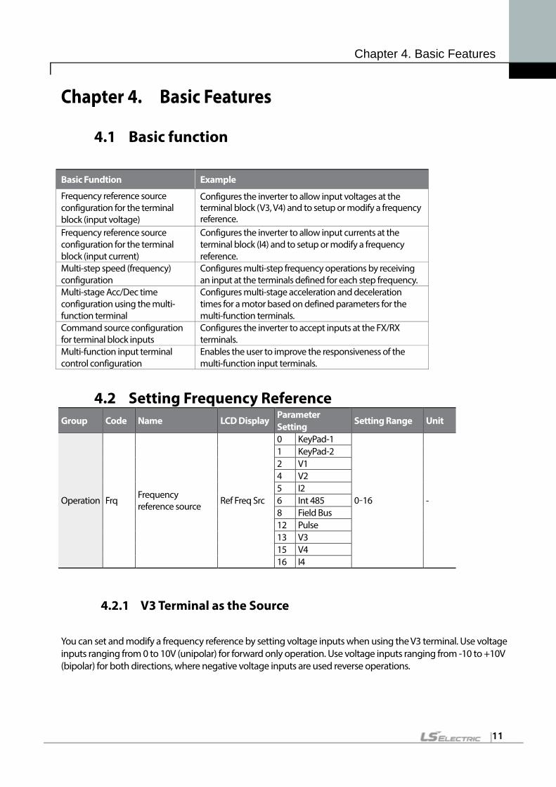
0–10V Input Voltage Setting Details
Code Description
In.01 Freq at 100%
Configures the frequency reference at the maximum input voltage when a potentiometer is connected to the control terminal block. A frequency set with code In.01 becomes the maximum frequency only if the value set in code Ao.07 (or Ao.13) is 100(%). • Set code In.01 to 40.00 and use default values for codes Ao.01–Ao.09. Motor
will run at 40.00Hz when a 10V input is provided at V3 • Set code Ao.07 to 50.00and use default values for codes In.01, Ao.01–Ao.09.
Motor will run at 30.00Hz (50% of the default maximum frequency–60Hz) when a 10V input is provided at V3.
Ao.01 V3 Monitor[V] Configures the inverter to monitor the input voltage at V3.
Ao.03 V3 Filter
V3 Filter may be used when there are large variations between reference frequencies. Variations can be mitigated by increasing the time constant, but this will require an increased response time. The value t (time) indicates the time required for the frequency to reach 63% of the reference, when external input voltages are provided in multiple steps.
[V3 Filter ]
Ao.04 V3 Volt x1– Ao.07 V3 Perc y2
These parameters are used to configure the gradient level and offset values of the Output Frequency, based on the Input Voltage.
[Volt x1–Ao.07 V3 Perc y2]
Chapter 4. Basic Features
14
Code Description
Ao.08 V3 Inverting Inverts the direction of rotation. Set this code to 1 (Yes) if you need the motor to run in the opposite direction from the current rotation.
Ao.09.V3 Quantizing
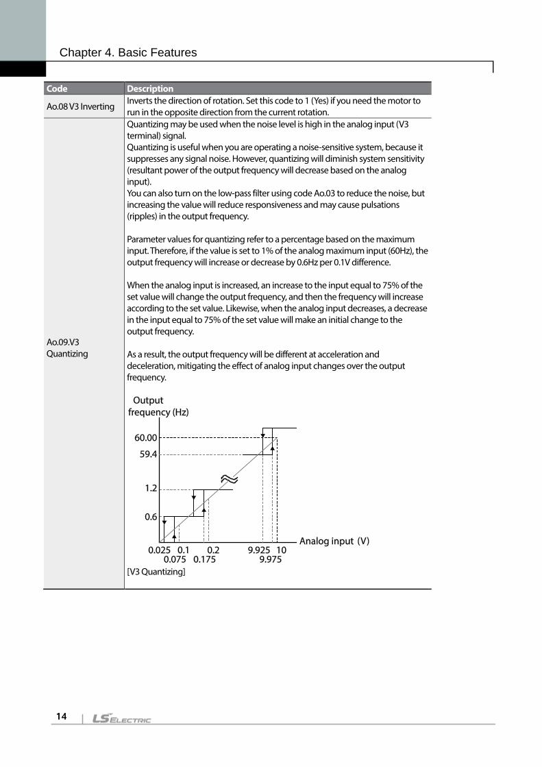
Quantizing may be used when the noise level is high in the analog input (V3 terminal) signal. Quantizing is useful when you are operating a noise-sensitive system, because it suppresses any signal noise. However, quantizing will diminish system sensitivity (resultant power of the output frequency will decrease based on the analog input). You can also turn on the low-pass filter using code Ao.03 to reduce the noise, but increasing the value will reduce responsiveness and may cause pulsations (ripples) in the output frequency. Parameter values for quantizing refer to a percentage based on the maximum input. Therefore, if the value is set to 1% of the analog maximum input (60Hz), the output frequency will increase or decrease by 0.6Hz per 0.1V difference. When the analog input is increased, an increase to the input equal to 75% of the set value will change the output frequency, and then the frequency will increase according to the set value. Likewise, when the analog input decreases, a decrease in the input equal to 75% of the set value will make an initial change to the output frequency. As a result, the output frequency will be different at acceleration and deceleration, mitigating the effect of analog input changes over the output frequency.
[V3 Quantizing]

Chapter 4. Basic Features
15
Setting a Frequency Reference for -10–10V Input
Set the Frq (Frequency reference source) code in the Operation group to 13 (V3), and then set code 02 (V3 Polarity) to 1 (bipolar) in the APO group (Ao). Use the output voltage from an external source to provide input to V3
[V3 terminal wiring]
[Bipolar input voltage and output frequency]
Group Code Name LCD Display Parameter Setting
Setting Range
Unit
Operation Frq Frequency reference source Freq Ref Src 13 V3 0–16 -
In 01 Frequency at maximum analog input
Freq at 100% 60.00 0– Max Frequency Hz
Ao
01 V3 input monitor V3 Monitor 0.00 0.00–12.00V V 02 V3 polarity options V3 Polarity 1 Bipolar 0–1 -
10 V3 minimum input voltage V3- volt x1 0.00 10.00–0.00V V
11 V3 output at minimum voltage (%) V3- Perc y1 0.00 -100.00–0.00% %
12 V3maximum input voltage V3- Volt x2 -10.00 -12.00 –0.00V V
13 V3 output at maximum voltage (%) V3- Perc y2 -100.00 -100.00–0.00% %

Chapter 4. Basic Features
16
Rotational Directions for Different Voltage Inputs
Command / Voltage Input
Input voltage 0–10V -10–0V
FWD Forward Reverse REV Reverse Forward
-10–10V Voltage Input Setting Details
Code Description
Ao.10 V3- volt x1– Ao.13 V1- Perc y2
Sets the gradient level and off-set value of the output frequency in relation to the input voltage. These codes are displayed only when Ao.02 is set to 1 (bipolar). As an example, if the minimum input voltage (at V3) is set to -2 (V) with 10% output ratio, and the maximum voltage is set to -8 (V) with 80% output ratio respectively, the output frequency will vary within the range of 6 - 48 Hz.
[Ao.10 V3-volt X1–Ao.13 V3 Perc y] For details about the 0–+10V analog inputs, refer to the code descriptions Ao.10 V3 volt x1–Ao.13 V1 Perc y2..
Setting a Reference Frequency using Input Current (I4)
You can set and modify a frequency reference using input current at the I4 terminal after selecting current input at SW 2. Set the Frq (Frequency reference source) code in the Operation group to 16 (I4) and apply 4–20mA input current to I4.
Group Code Name LCD Display Parameter Setting Setting Range Unit
Operation Frq Frequency reference source Freq Ref Src 16 I4 0–16 -
In 01 Frequency at maximum analog input Freq at 100% 60.00
0– Maximum Frequency
Hz
Ao
22 I4 input monitor I4 Monitor 0.00 0.00–24.00 mA
23 I4 input filter time constant I4 Filter 10 0–10000 ms
24 I4 minimum input current I4 Curr x1 4.00 0.00–20.00 mA

Chapter 4. Basic Features
17
Group Code Name LCD Display Parameter Setting Setting Range Unit
25 I4 output at minimum current (%) I4 Perc y1 0.00 0–100 %
26 I4 maximum input current I4 Curr x2 20.00 0.00–24.00 mA
27 I4 output at maximum current (%) I4 Perc y2 100.00 0.00–100.00 %
28 I4 rotation direction options I4 Inverting 0 No 0–1 - 29 I4 Quantizing level I4 Quantizing 0.04 0*, 0.04–10.00 %
* Quantizing is disabled if ‘0’ is selected.
Input Current (I4) Setting Details
Code Description
In.01 Freq at 100%
Configures the frequency reference for operation at the maximum current (when Ao.27 is set to 100%). • If In.01 is set to 40.00Hz, and default settings are used for Ao.24–27, 20mA
input current (max) to I4 will produce a frequency reference of 40.00Hz. • If Ao.27 is set to 50.00 (%), and default settings are used for In.01 (60Hz) and
Ao.24–26, 20mA input current (max) to I4 will produce a frequency reference of 30.00Hz (50% of 60Hz).
Ao.22 I4 Monitor Used to monitor input current at I4.
Ao.23 I4 Filter Configures the time for the operation frequency to reach 63% of target frequency based on the input current at I4.
In.24 I4 Curr x1–In.27 I4 Perc y2
Configures the gradient level and off-set value of the output frequency.
[Gradient and off-set configuration based on output frequency]
4.2.2 Setting a Frequency Reference with Input Voltage (Terminal I4)
Set and modify a frequency reference using input voltage at I4 (V4) terminal by setting SW2 to V4. Set the Frq (Frequency reference source) code in the Operation group to 15 (V4) and apply 0–12V input voltage to I4 (=V4, Analog current/voltage input terminal). Codes Ao.14–21 will not be displayed when I4 is set to receive current input (Frq code parameter is set to 16).

Chapter 4. Basic Features
18
Group Code Name LCD Display Parameter Setting
Setting Range Unit
Operation Frq Frequency reference source
Freq Ref Src 15 V4 0–16 -
Ao
14 V4 input display V4 Monitor 0.00 0.00–12.00 V
15 V4 input filter time constant V4 Filter 10 0–10000 ms
16 Minimum V4 input voltage V4 Volt x1 0.00 0.00–10.00 V
17 Output% at minimum V4 voltage
V4 Perc y1 0.00 0.00–100.00 %
18 Maximum V4 input voltage V4 Volt x2 10.00 0.00–10.00 V
19 Output% at maximum V4 voltage
V4 Perc y2 100.00 0.00–100.00 %
20 Invert V4 rotational direction V4 Inverting 0 No 0–1 -
21 V4 quantizing level V4 Quantizing 0.04 0.00*, 0.04–10.00 %
* Quantizing is disabled if ‘0’ is selected.
4.3 Analog Output An analog output terminal provides output of 0–10V voltage, 4–20mA current.
Voltage and Current Analog Output An output size can be adjusted by selecting an output option at AO3(Analog Output3) terminal. Set the analog voltage/current output terminal setting switch (SW3) to change the output type (voltage/current).
Group
Code Name LCD Display Parameter Setting
Setting Range Unit
Ao
30 Analog output3 AO3 Mode 0 Frequency 0–15 - 31 Analog output3 gain AO3 Gain 100.0 -1000.0–1000.0 % 32 Analog output3 bias AO3 Bias 0.0 -100.0–100.0 % 33 Analog output3 filter AO3 Filter 5 0–10000 ms
34 Analog constant output3 AO3 Const % 0.0 0.0–100.0 %
35 Analog output3 monitor AO3 Monitor 0.0 0.0–1000.0 %

Chapter 4. Basic Features
19
Voltage and Current Analog Output Setting Details
Code Description
AO.30 AO3 Mode
Select a constant value for output. The following example for output voltage setting.
Setting Function 0 Frequency Outputs operation frequency as a standard. 10V output is
made from the frequency set at dr.20(Max Freq) 1 Output
Current 10V output is made from 200% of inverter rated current (heavy load).
2 Output Voltage
Sets the outputs based on the inverter output voltage. 10V output is made from a set voltage in bA.15 (Rated V). If 0V is set in bA.15, 200V/400V models output 10V based on the actual input voltages ( 240V and 480V respectively).
3 DC Link Volt Outputs inverter DC link voltage as a standard. Outputs 10V when the DC link voltage is 410Vdc for 200V models, and 820Vdc for 400V models.
4 Torque Outputs the generated torque as a standard. Outputs 10V at 250% of motor rated torque.
5 Ouput Power Monitors output wattage. 200% of rated output is the maximum display voltage (10V).
6 Idse Outputs the maximum voltage at 200% of no load current.
7 Iqse Outputs the maximum voltage at 250% of rated torque current
𝑟𝑟𝑟𝑟𝑟𝑟𝑟𝑟𝑟𝑟 𝑟𝑟𝑡𝑡𝑟𝑟𝑡𝑡𝑡𝑡𝑟𝑟 𝑐𝑐𝑡𝑡𝑟𝑟𝑟𝑟𝑟𝑟𝑐𝑐𝑟𝑟= � 𝑟𝑟𝑟𝑟𝑟𝑟𝑟𝑟𝑟𝑟 𝑐𝑐𝑡𝑡𝑟𝑟𝑟𝑟𝑟𝑟𝑐𝑐𝑟𝑟2 − 𝑐𝑐𝑡𝑡 𝑙𝑙𝑡𝑡𝑟𝑟𝑟𝑟 𝑐𝑐𝑡𝑡𝑟𝑟𝑟𝑟𝑟𝑟𝑐𝑐𝑟𝑟2
8 Target Freq Outputs set frequency as a standard. Outputs 10V
at the maximum frequency (dr.20). 9 Ramp Freq Outputs frequency calculated with Acc/Dec
function as a standard. May vary with actual output frequency. Outputs 10V.
12 PID Ref Value Outputs command value of a PID controller as a standard. Outputs approximately 6.6V at 100%.
13 PID Fdk Value Outputs feedback volume of a PID controller as a standard. Outputs approximately 6.6V at 100%.
14 PID Output Outputs output value of a PID controller as a standard. Outputs approximately 10V at 100%.
15 Constant Outputs OU.05 (AO1 Const %) value as a standard.
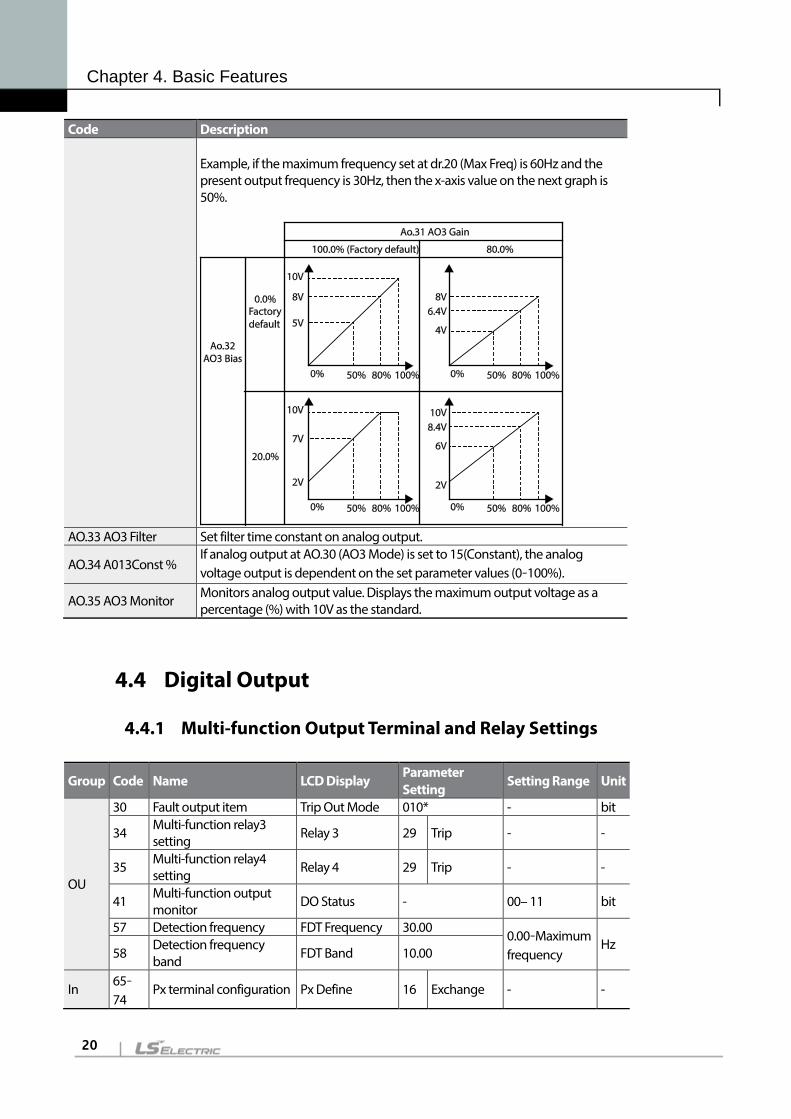
AO.31 AO3 Gain, AO.32 AO3 Bias
Adjusts output value and offset. If frequency is selected as an output item, it will operate as shown below.
𝐴𝐴𝐴𝐴3 =𝐹𝐹𝑟𝑟𝑟𝑟𝑡𝑡𝑡𝑡𝑟𝑟𝑐𝑐𝑐𝑐𝐹𝐹𝑀𝑀𝑟𝑟𝑀𝑀𝐹𝐹𝑟𝑟𝑟𝑟𝑡𝑡
× 𝐴𝐴𝐴𝐴3 𝐺𝐺𝑟𝑟𝐺𝐺𝑐𝑐 + 𝐴𝐴𝐴𝐴3 𝐵𝐵𝐺𝐺𝑟𝑟𝐵𝐵
The graph below illustrates the analog voltage output (AO3) changes depend on Ao.31 (AO3 Gain) and Ao.32 (AO3 Bias) values. Y-axis is analog output voltage (0–10V), and X-axis is % value of the output item.
Chapter 4. Basic Features
20
Code Description Example, if the maximum frequency set at dr.20 (Max Freq) is 60Hz and the present output frequency is 30Hz, then the x-axis value on the next graph is 50%.
AO.33 AO3 Filter Set filter time constant on analog output.
AO.34 A013Const % If analog output at AO.30 (AO3 Mode) is set to 15(Constant), the analog voltage output is dependent on the set parameter values (0–100%).
AO.35 AO3 Monitor Monitors analog output value. Displays the maximum output voltage as a percentage (%) with 10V as the standard.
4.4 Digital Output
4.4.1 Multi-function Output Terminal and Relay Settings
Group Code Name LCD Display Parameter Setting
Setting Range Unit
OU
30 Fault output item Trip Out Mode 010* - bit
34 Multi-function relay3 setting Relay 3 29 Trip - -
35 Multi-function relay4 setting Relay 4 29 Trip - -
41 Multi-function output monitor DO Status - 00– 11 bit
57 Detection frequency FDT Frequency 30.00 0.00–Maximum frequency
Hz 58
Detection frequency band FDT Band 10.00
In 65–
74 Px terminal configuration Px Define 16 Exchange - -

Chapter 4. Basic Features
21
*Displayed as on the keypad. Multi-function Output Terminal and Relay Setting Details Code Description OU.34 Relay3 Set relay (Relay 3) output options. OU.35 Relay4 Set relay (Relay 4) output options.
OU.41 DO Status
Set output terminal and relay functions according to OU.57 FDT (Frequency), OU.58 (FDT Band) settings and fault trip conditions.
Setting Function 0 None No output signal. 1 FDT-1 Detects inverter output frequency reaching the user set
frequency. Outputs a signal when the absolute value (set frequency–output frequency) < detected frequency width/2. When detected frequency width is 10Hz, FDT-1 output is as shown in the graph below.
2 FDT-2 Outputs a signal when the user set frequency and detected frequency (FDT Frequency) are equal, and fulfills FDT-1 condition at the same time. [Absolute value (set frequency-detected frequency) < detected frequency width/2]&[FDT-1] Detected frequency width is 10Hz. When the detected frequency is set to 30Hz, FDT-2 output is as shown in the graph below.
3 FDT-3 Outputs a signal when the Absolute value (output frequency–operation frequency) < detected frequency width/2. Detected frequency width is 10Hz. When detected frequency is set to 30Hz, FDT-3 output is as shown in

Chapter 4. Basic Features
22
Code Description the graph below.
4 FDT-4 Output signal can be separately set for acceleration and deceleration conditions. • In acceleration: Operation frequency≧ Detected
frequency • In deceleration: Operation frequency>(Detected
frequency–Detected frequency width/2) Detected frequency width is 10Hz. When detected frequency is set to 30Hz, FDT-4 output is as shown in the graph below.
5 Overload Outputs a signal at motor overload. 6 IOL Outputs a signal when a fault is triggered from a
protective function operation by inverter overload inverse proportion.
7 Underload Outputs a signal at load fault warning. 8 Fan Warning Outputs a signal at fan fault warning. 9 Stall Outputs a signal when a motor is overloaded and
stalled. 10 Over voltage Outputs a signal when the inverter DC link voltage rises
above the protective operation voltage. 11 Low Voltage Outputs a signal when the inverter DC link voltage
drops below the low voltage protective level. 12 Over Heat Outputs signal when the inverter overheats. 13 Lost command Outputs a signal when there is a loss of analog input
terminal and RS-485 communication command at the terminal block. Outputs a signal when communication power and expansion an I/O power card is installed, and also outputs a signal when losing analog input and communication power commands.
14 RUN Outputs a signal when operation command is entered and the inverter outputs voltage. No signal output during DC braking.

Chapter 4. Basic Features
23
Code Description
15 Stop Outputs a signal at operation command off, and when there is no inverter output voltage.
16 Steady
Outputs a signal in steady operation.
17 Inverter line Outputs a signal while the motor is driven by the inverter line.
18 Comm line Outputs a signal while the motor is driven by a commercial power source..
19 Speed search Outputs a signal during inverter speed search operation.
22 Ready Outputs signal when the inverter is in stand by operation and ready to receive an external operation command.
28 Timer Out A timer function to operate terminal output after a certain time by using multi-function terminal block input..
29 Trip Outputs a signal after a fault trip 31 DB Warn %ED In case of exceeding DB resistor usage rate, the signal
changes to on-state. 34 On/Off Control Outputs a signal using an analog input value as a
standard.
35 BR Control Outputs a brake release signal.
4.4.2 Fault Trip Output using Multi-Function Output Terminal and Relay
The inverter can output fault trip state using multi-function output terminal (Q1) and relay (Relay 3, 4).
Group Code Name LCD Display
Parameter Setting Setting Range Unit
OU
30 Fault trip output mode Trip Out Mode 010 - bit
34 Multi-function relay3 setting Relay 3 29 Trip - -
35 Multi-function relay4 setting Relay 4 29 Trip - -
53 Fault trip output on delay TripOut OnDly 0.00 0.00–100.00 sec 54 Fault trip output off delay TripOut OffDly 0.00 0.00–100.00 sec
Chapter 4. Basic Features
24
Fault Trip Output by Multi-function Output Terminal and Relay - Setting Details
Code Description
OU.30 Trip Out Mode
Fault trip relay operates based on the fault trip output settings.
Item bit on bit off Keypad
LCD keypad
Select fault trip output terminal/relay and select 29(Trip Mode) at codes OU. 34, 35. When a fault trip occurs in the inverter, the relevant terminal and relay will operate. Depending on the fault trip type, terminal and relay operation can be configured as shown in the table below.
Setting Function bit3 bit2 bit1 Operates when low voltage fault trips occur Operates when fault trips other than low voltage
occur Operates when auto restart fails (Pr. 08–09)
OU.34 Relay3 Set relay output (Relay 3).
OU.35 Relay4 Set relay output (Relay 4).
OU.53 TripOut On Dly, OU.54 TripOut OffDly
If a fault trip occurs, trip relay or multi-function output operates after the time delay set in OU.53. Terminal is off with the input initialized after the time delay set in OU.54.
4.4.3 Multi-function Output Terminal Delay Time Settings
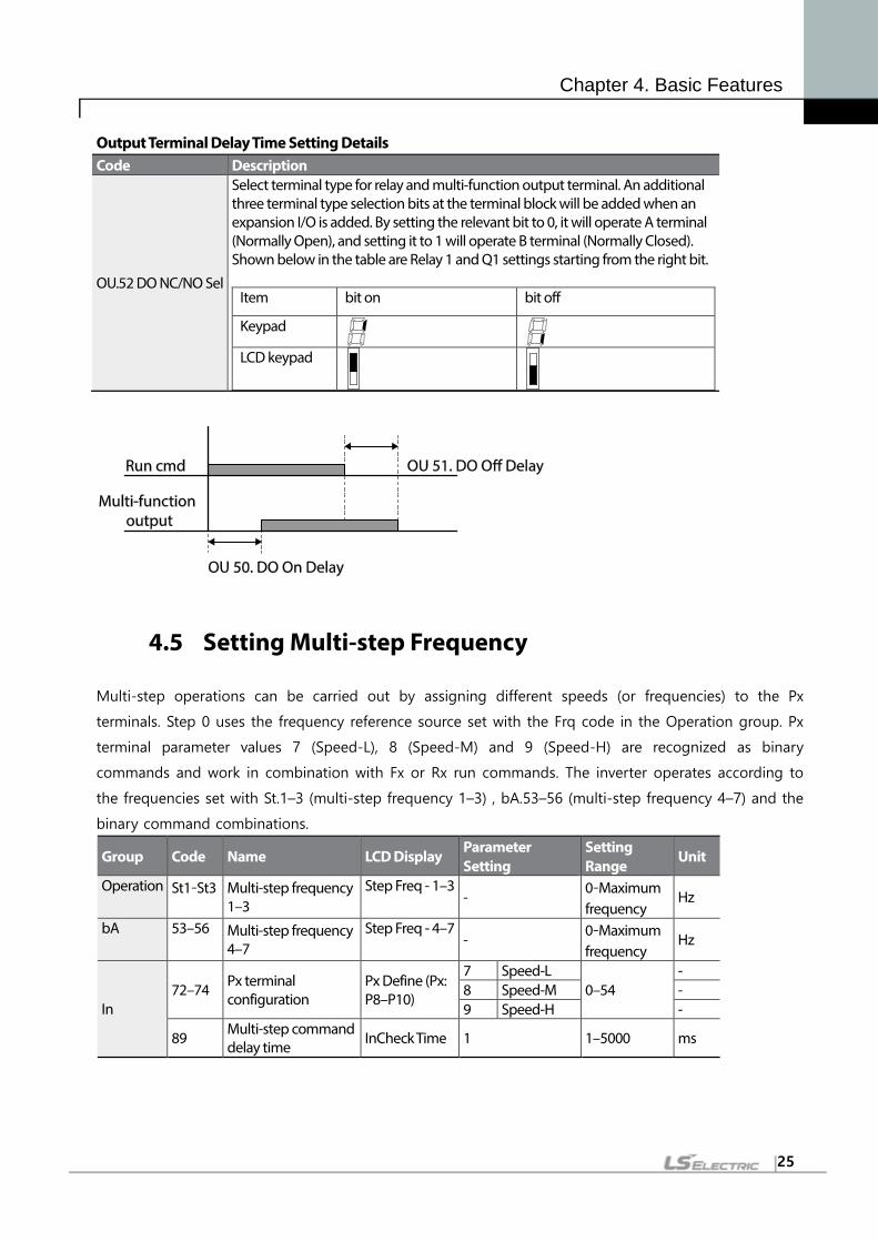
Set on-delay and off-delay times separately to control the output terminal and relay operation times. The delay time set at codes OU.50–51 applies to multi-function output terminal (Q1), relay (Relay 1, 3, 4), except when the multi-function output function is in fault trip mode.
Group Code Name LCD Display Parameter Setting
Setting Range
Unit
OU
50 Multi-function output On delay DO On Delay 0.00 0.00–100.00 s
51 Multi-function output Off delay DO Off Delay 0.00 0.00–100.00 s
52 Select multi-function output terminal DO NC/NO Sel 00* 00–11 bit
* Displayed as on keypad. On the 7-seg screen of multi-function output contact
parameter, clicking of left/right key switches between extension I/O and built-in I/O 7-seg screen.
is extension I/O 7-seg screen.
Chapter 4. Basic Features
25
Output Terminal Delay Time Setting Details Code Description
OU.52 DO NC/NO Sel
Select terminal type for relay and multi-function output terminal. An additional three terminal type selection bits at the terminal block will be added when an expansion I/O is added. By setting the relevant bit to 0, it will operate A terminal (Normally Open), and setting it to 1 will operate B terminal (Normally Closed). Shown below in the table are Relay 1 and Q1 settings starting from the right bit.
Item bit on bit off
Keypad
LCD keypad
4.5 Setting Multi-step Frequency
Multi-step operations can be carried out by assigning different speeds (or frequencies) to the Px
terminals. Step 0 uses the frequency reference source set with the Frq code in the Operation group. Px
terminal parameter values 7 (Speed-L), 8 (Speed-M) and 9 (Speed-H) are recognized as binary
commands and work in combination with Fx or Rx run commands. The inverter operates according to
the frequencies set with St.1–3 (multi-step frequency 1–3) , bA.53–56 (multi-step frequency 4–7) and the
binary command combinations.
Group Code Name LCD Display Parameter Setting
Setting Range
Unit
Operation St1–St3 Multi-step frequency 1–3
Step Freq - 1–3 -
0–Maximum frequency
Hz
bA 53–56 Multi-step frequency 4–7
Step Freq - 4–7 -
0–Maximum frequency
Hz
In 72–74 Px terminal
configuration Px Define (Px: P8–P10)
7 Speed-L 0–54
- 8 Speed-M - 9 Speed-H -
89 Multi-step command delay time InCheck Time 1 1–5000 ms

Chapter 4. Basic Features
26
Multi-step Frequency Setting Details
Code Description Operation group St 1–St3 Step Freq - 1–3
Configure multi-step frequency1–3. If an LCD keypad is in use, bA.50–52 is used instead of St1–St3 (multi-step frequency 1–3).
bA.53–56 Step Freq - 4–7
Configure multi-step frequency 4–7.
In.72–74 Px Define
Choose the terminals to setup as multi-step inputs, and then set the relevant codes (In.72–74) to 7(Speed-L), 8(Speed-M), or 9(Speed-H). Provided that terminals P3, P4 and P5 have been set to Speed-L, Speed-M and Speed-H respectively, the following multi-step operation will be available.
[An example of a multi-step operation]
Speed Fx/Rx P5 P4 P3 0 - - - 1 - - 2 - - 3 - 4 - - 5 - 6 - 7
In.89 InCheck Time
Set a time interval for the inverter to check for additional terminal block inputs after receiving an input signal. After adjusting In.89 to 100ms and an input signal is received at P8, the inverter will search for inputs at other terminals for 100ms, before proceeding to accelerate or decelerate based on P8’s configuration.
Chapter 4. Basic Features
27
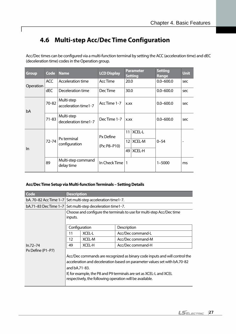
4.6 Multi-step Acc/Dec Time Configuration
Acc/Dec times can be configured via a multi-function terminal by setting the ACC (acceleration time) and dEC (deceleration time) codes in the Operation group.
Group Code Name LCD Display Parameter Setting
Setting Range
Unit
Operation ACC Acceleration time Acc Time 20.0 0.0–600.0 sec
dEC Deceleration time Dec Time 30.0 0.0–600.0 sec
bA
70–82 Multi-step acceleration time1–7
Acc Time 1–7 x.xx 0.0–600.0 sec
71–83 Multi-step deceleration time1–7
Dec Time 1–7 x.xx 0.0–600.0 sec
In
72–74 Px terminal configuration
Px Define
(Px: P8–P10)
11 XCEL-L
0–54 - 12 XCEL-M
49 XCEL-H
89 Multi-step command delay time
In Check Time 1 1–5000 ms
Acc/Dec Time Setup via Multi-function Terminals – Setting Details
Code Description bA. 70–82 Acc Time 1–7 Set multi-step acceleration time1–7.
bA.71–83 Dec Time 1–7 Set multi-step deceleration time1–7.
In.72–74 Px Define (P1–P7)
Choose and configure the terminals to use for multi-step Acc/Dec time inputs.
Configuration Description 11 XCEL-L Acc/Dec command-L 12 XCEL-M Acc/Dec command-M 49 XCEL-H Acc/Dec command-H
Acc/Dec commands are recognized as binary code inputs and will control the acceleration and deceleration based on parameter values set with bA.70–82 and bA.71–83. If, for example, the P8 and P9 terminals are set as XCEL-L and XCEL respectively, the following operation will be available.

Chapter 4. Basic Features
28
Code Description
Acc/Dec time P5 P4 0 - - 1 - 2 - 3
In.89 In Check Time
Set the time for the inverter to check for other terminal block inputs. If In.89 is set to 100ms and a signal is supplied to the P8 terminal, the inverter searches for other inputs over the next 100ms. When the time expires, the Acc/Dec time will be set based on the input received at P8.
4.7 Stopping the Acc/Dec Operation
Configure the multi-function input terminals to stop acceleration or deceleration and operate the inverter at a fixed frequency.
Group Code Name LCD Display Parameter Setting
Setting Range
Unit
In 65–71 Px terminal configuration
Px Define(Px: P1– P7)
25 XCEL Stop 0–54 -
Chapter 4. Basic Features
29
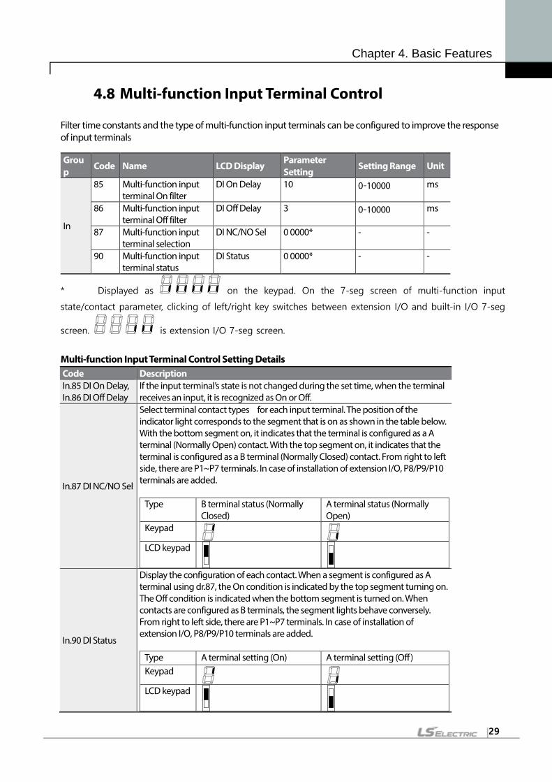
4.8 Multi-function Input Terminal Control
Filter time constants and the type of multi-function input terminals can be configured to improve the response of input terminals
Group
Code Name LCD Display Parameter Setting
Setting Range Unit
In
85 Multi-function input terminal On filter
DI On Delay 10 0–10000 ms
86 Multi-function input terminal Off filter
DI Off Delay 3 0–10000 ms
87 Multi-function input terminal selection
DI NC/NO Sel 0 0000* - -
90 Multi-function input terminal status
DI Status 0 0000* - -
* Displayed as on the keypad. On the 7-seg screen of multi-function input
state/contact parameter, clicking of left/right key switches between extension I/O and built-in I/O 7-seg
screen. is extension I/O 7-seg screen.
Multi-function Input Terminal Control Setting Details Code Description In.85 DI On Delay, In.86 DI Off Delay
If the input terminal’s state is not changed during the set time, when the terminal receives an input, it is recognized as On or Off.
In.87 DI NC/NO Sel
Select terminal contact types for each input terminal. The position of the indicator light corresponds to the segment that is on as shown in the table below. With the bottom segment on, it indicates that the terminal is configured as a A terminal (Normally Open) contact. With the top segment on, it indicates that the terminal is configured as a B terminal (Normally Closed) contact. From right to left side, there are P1~P7 terminals. In case of installation of extension I/O, P8/P9/P10 terminals are added.
Type B terminal status (Normally Closed)
A terminal status (Normally Open)
Keypad
LCD keypad
In.90 DI Status
Display the configuration of each contact. When a segment is configured as A terminal using dr.87, the On condition is indicated by the top segment turning on. The Off condition is indicated when the bottom segment is turned on. When contacts are configured as B terminals, the segment lights behave conversely. From right to left side, there are P1~P7 terminals. In case of installation of extension I/O, P8/P9/P10 terminals are added.
Type A terminal setting (On) A terminal setting (Off) Keypad
LCD keypad
Chapter 5. Table of Functions
30
Chapter 5. Table of Functions
This chapter lists all the function settings for S100 series inverter. Set the parameters required according to the following references. If a set value input is out of range, the following messages will be displayed on the keyboard. In these cases, the inverter will not operate with the [ENT] key.
• Set value not allocated: rd • Set value repetition (multi-function input, PID reference, PID feedback related): OL • Set value not allowed (select value, V2, I2): no
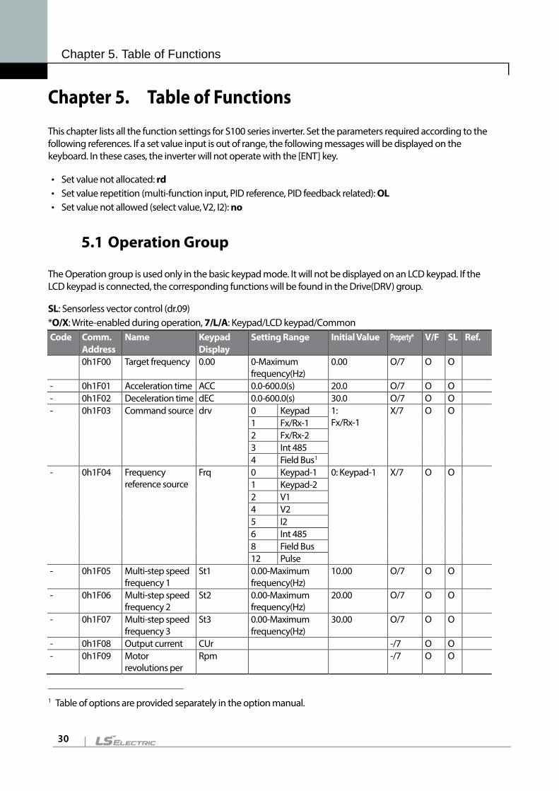
5.1 Operation Group
The Operation group is used only in the basic keypad mode. It will not be displayed on an LCD keypad. If the LCD keypad is connected, the corresponding functions will be found in the Drive(DRV) group.
SL: Sensorless vector control (dr.09) *O/X: Write-enabled during operation, 7/L/A: Keypad/LCD keypad/Common Code Comm.
Address Name Keypad
Display Setting Range Initial Value Property* V/F SL Ref.
0h1F00 Target frequency 0.00 0-Maximum frequency(Hz)
0.00 O/7 O O
- 0h1F01 Acceleration time ACC 0.0-600.0(s) 20.0 O/7 O O - 0h1F02 Deceleration time dEC 0.0-600.0(s) 30.0 O/7 O O - 0h1F03 Command source drv 0 Keypad 1:
Fx/Rx-1 X/7 O O
1 Fx/Rx-1 2 Fx/Rx-2 3 Int 485 4 Field Bus1
- 0h1F04 Frequency reference source
Frq 0 Keypad-1 0: Keypad-1 X/7 O O 1 Keypad-2 2 V1 4 V2 5 I2 6 Int 485 8 Field Bus 12 Pulse
- 0h1F05 Multi-step speed frequency 1
St1 0.00-Maximum frequency(Hz)
10.00 O/7 O O
- 0h1F06 Multi-step speed frequency 2
St2 0.00-Maximum frequency(Hz)
20.00 O/7 O O
- 0h1F07 Multi-step speed frequency 3
St3 0.00-Maximum frequency(Hz)
30.00 O/7 O O
- 0h1F08 Output current CUr -/7 O O - 0h1F09 Motor
revolutions per Rpm -/7 O O
1 Table of options are provided separately in the option manual.

Chapter 5. Table of Functions
31
Code Comm. Address
Name Keypad Display
Setting Range Initial Value Property* V/F SL Ref.
minute - 0h1F0A Inverter direct
current voltage dCL - - -/7 O O
- 0h1F0B Inverter output voltage
vOL -/7 O O
- 0h1F0C Out of order signal
nOn -/7 O O
- 0h1F0D Select rotation direction
drC F Forward run F O/7 O O r Reverse run
5.2 Drive group (PAR→dr)
In the following table, data shaded in grey will be displayed when the related code has been selected.
SL: Sensorless vector control (dr.09) *O/X: Write-enabled during operation, 7/L/A: Keypad/LCD keypad/Common Code Comm.
Address Name LCD Display Setting Range Initial
value Property* V/F SL Ref.
00 - Jump Code Jump Code 1-99 9 O/A O O 012 0h1101 Target frequency Cmd Frequency Start frequency -
Maximum frequency(Hz)
0.00 O/L O O
02 0h1102 Torque command
Cmd Torque -180~180[%] 0.0 O/A X O
032 0h1103 Acceleration time
Acc Time 0.0-600.0(s) 20.0 O/L O O
042 0h1104 Deceleration time
Dec Time 0.0-600.0(s) 30.0 O/L O O
062 0h1106 Command source
Cmd Source 0 Keypad 1: Fx/Rx-1
X/L O O 1 Fx/Rx-1 2 Fx/Rx-2 3 Int 485 4 Field Bus
072 0h1107 Frequency reference source
Freq Ref Src 0 Keypad-1 0: Keypad-1 X/L O O 1 Keypad-2 2 V1 4 V2 5 I2 6 Int 485 8 Field Bus 12 Pulse
08 0h1108 Torque reference setting
Trq Ref Src 0 Keypad-1 0: Keypad-1 X/A X O 1 Keypad-2 2 V1 4 V2
2 Displayed when an LCD keypad is in use.

Chapter 5. Table of Functions
32
Code Comm. Address
Name LCD Display Setting Range Initial value
Property* V/F SL Ref.
5 I2 6 Int 485 8 FieldBus 12 Pulse
09 0h1109 Control mode Control Mode 0 V/F 0: V/F X/A O O 2 Slip
Compen 4 IM
Sensorless 10 0h110A Torque Control Torque Control 0 No 0: No X/A X O
1 Yes 11 0h110B Jog frequency Jog Frequency 0.00, Start
frequency-Maximum frequency(Hz)
10.00 O/A O O
12 0h110C Jog run acceleration time
Jog Acc Time 0.0-600.0(s) 20.0 O/A O O
13 0h110D Jog run deceleration time
Jog Dec Time 0.0-600.0(s) 30.0 O/A O O
14 0h110E Motor capacity Motor Capacity 0: 0.2kW, 1: 0.4kW 2: 0.75kW, 3: 1.1kW 4: 1.5kW, 5: 2.2kW 6: 3.0kW, 7: 3.7kW 8: 4.0kW, 9: 5.5kW 10: 7.5kW, 11: 11.0kW 12: 15.0kW, 13: 18.5kW 14: 22.0kW, 15: 30.0kW
Varies by Motor capacity
X/A O O
15 0h110F Torque boost options
Torque Boost 0 Manual 0: Manual X/A O X 1 Auto
163 0h1110 Forward Torque boost
Fwd Boost 0.0-15.0(%) 2.0 X/A O X
173 0h1111 Reverse Torque boost
Rev Boost 0.0-15.0(%) 2.0 X/A O X
18 0h1112 Base frequency Base Freq 30.00-400.00(Hz) 60.00 X/A O O 19 0h1113 Start frequency Start Freq 0.01-10.00(Hz) 0.50 X/A O O 20 0h1114 Maximum
frequency Max Freq 40.00-
400.00(Hz)[V/F, Slip Compen] 40.00-
60.00 X/A O O
3 Displayed when dr.15 is set to 0 (Manual)

Chapter 5. Table of Functions
33
Code Comm. Address
Name LCD Display Setting Range Initial value
Property* V/F SL Ref.
120.00(Hz)[IM Sensorless]
21 0h1115 Select speed unit Hz/Rpm Sel 0 Hz Display 0:Hz Display
O/L O O 1 Rpm Display
224 0h1116 (+)Torque gain (+)Trq Gain 50.0 ~ 150.0[%] 100.0 O/A X O 234 0h1117 (-)Torque gain (-)Trq Gain 50.0 ~ 150.0[%] 80.0 O/A X O 244 0h1118 (-)Torque gain 0 (-)Trq Gain0 50.0 ~ 150.0[%] 80.0 O/A X O 254 0h1119 (-)Torque offset (-)Trq Offset 0.0 ~ 100.0[%] 40.0 O/A X O 805 0h1150 Select ranges at
power input - Select ranges
inverter displays at power input
0: run frequency
O/7 O O
0 Run frequency
1 Acceleration time
2 Deceleration time
3 Command source
4 Frequency reference source
5 Multi-step speed frequency1
6 Multi-step speed frequency2
7 Multi-step speed frequency3
8 Output current
9 Motor RPM 10 Inverter DC
voltage 11 User select
signal (dr.81) 12 Currently out
of order 13 Select run
direction 14 output
current2 15 Motor RPM2
4 Displayed when dr.10 is set to 1 (YES) 5 Will not be displayed when an LCD keypad is in use

Chapter 5. Table of Functions
34
Code Comm. Address
Name LCD Display Setting Range Initial value
Property* V/F SL Ref.
16 Inverter DC voltage2
17 User select signal2 (dr.81)
815 0h1151 Select monitor code
- Monitors user selected code
0: output voltage
O/7 O O
0 Output voltage(V)
1 Output electric power(kW)
2 Torque(kgf m)
895 0h03E3 Display changed parameter
- 0 View All 0: View All
O/7 O O 1 View
Changed 905 0h115A [ESC] key
functions - 0 Move to
initial position
0: None
X/7 O O
1 JOG Key 2 Local/Remot
e 935 0h115D Parameter
initialization - 0 No 0:No X/7 O O
1 All Grp 2 dr Grp 3 bA Grp 4 Ad Grp 5 Cn Grp 6 In Grp 7 OU Grp 8 CM Grp 9 AP Grp 12 Pr Grp 13 M2 Grp 16 run Grp
945 0h115E Password registration
0-9999
O/7 O O
955 0h115F Parameter lock settings
0-9999
O/7 O O
975 0h1161 Software version - -/7 O O 98 0h1162 Display I/O
board version IO S/W Ver -/A O O
99 0h1163 Display I/O board H/W version
IO H/W Ver 0 Multiple IO Standard IO -/A O O 1 Standard IO 2 Standard IO
(M)
Chapter 5. Table of Functions
35
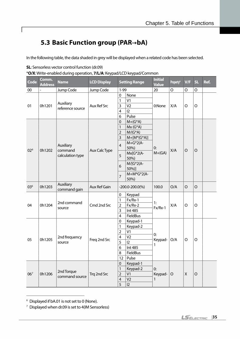
5.3 Basic Function group (PAR→bA)
In the following table, the data shaded in grey will be displayed when a related code has been selected.
SL: Sensorless vector control function (dr.09) *O/X: Write-enabled during operation, 7/L/A: Keypad/LCD keypad/Common
Code Comm. Address Name LCD Display Setting Range Initial
Value Property* V/F SL Ref.
00 - Jump Code Jump Code 1-99 20 O O O
01 0h1201 Auxiliary reference source Aux Ref Src
0 None
0:None X/A O O 1 V1 3 V2 4 I2 6 Pulse
026 0h1202 Auxiliary command calculation type
Aux Calc Type
0 M+(G*A)
0: M+(GA) X/A O O
1 Mx (G*A) 2 M/(G*A) 3 M+[M*(G*A)]
4 M+G*2(A-50%)
5 Mx[G*2(A-50%)
6 M/[G*2(A-50%)]
7 M+M*G*2(A-50%)
036 0h1203 Auxiliary command gain Aux Ref Gain -200.0-200.0(%) 100.0 O/A O O
04 0h1204 2nd command source Cmd 2nd Src
0 Keypad
1: Fx/Rx-1 X/A O O
1 Fx/Rx-1 2 Fx/Rx-2 3 Int 485 4 FieldBus
05 0h1205 2nd frequency source Freq 2nd Src
0 Keypad-1
0: Keypad-1
O/A O O
1 Keypad-2 2 V1 4 V2 5 I2 6 Int 485 8 FieldBus 12 Pulse
067 0h1206 2nd Torque command source Trq 2nd Src
0 Keypad-1 0: Keypad-1
O X O 1 Keypad-2 2 V1 4 V2 5 I2
6 Displayed if bA.01 is not set to 0 (None). 7 Displayed when dr.09 is set to 4(IM Sensorless)

Chapter 5. Table of Functions
36
Code Comm. Address Name LCD Display Setting Range
Initial Value Property* V/F SL Ref.
6 Int 485 8 FieldBus 12 Pulse
07 0h1207 V/F pattern options
V/F Pattern
0 Linear 0: Linear
X/A O X 1 Square 2 User V/F 3 Square 2
08 0h1208 Acc/dec standard frequency
Ramp T Mode 0 Max Freq 0:
Max Freq
X/A O O 1 Delta Freq
09 0h1209 Time scale settings Time Scale
0 0.01 sec 1:0.1 sec X/A O O 1 0.1 sec
2 1 sec
10 0h120A Input power frequency 60/50 Hz Sel
0 60Hz 0:60Hz X/A O O
1 50Hz
11 0h120B Number of motor poles Pole Number 2-48
Dependent on motor setting
X/A O O
12 0h120C Rated slip speed Rated Slip 0-3000(Rpm) X/A O O
13 0h120D Motor rated current Rated Curr 1.0-1000.0(A) X/A O O
14 0h120E Motor noload current Noload Curr 0.0-1000.0(A) X/A O O
15 0h120F Motor rated voltage Rated Volt 170-480(V) 0 X/A O O
16 0h1210 Motor efficiency Efficiency 70-100(%)
Dependent on motor setting
X/A O O
17 0h1211 Load inertia rate Inertia Rate 0-8 X/A O O
18 0h1212 Trim power display Trim Power % 70-130(%) O/A O O
19 0h1213 Input power voltage AC Input Volt 170-480V 220/380
V O/A O O
20 - Auto Tuning Auto Tuning
0 None
0:None X/A X O
1 All (Rotation type)
2 ALL (Static type)
3 Rs+Lsigma (Rotation type)
6 Tr (Static type) 21 - Stator resistance Rs
Dependent on motor setting
Dependent on motor setting
X/A X O
22 - Leakage inductance Lsigma X/A X O
23 - Stator inductance Ls X/A X O
247 - Rotor time constant Tr 25-5000(ms) - X/A X O
257 - Stator inductance scale Ls Scale 50 ~ 150[%] 100 X/A X O

Chapter 5. Table of Functions
37
Code Comm. Address Name LCD Display Setting Range
Initial Value Property* V/F SL Ref.
267 - Rotor time constant scale
Tr Scale 50 ~ 150[%] 100 X/A X O
317 Regeneration inductance scale Ls Regen Scale 70 ~ 100[%] 80 X/A X O
418 0h1229 User frequency1 User Freq 1 0.00-Maximum frequency(Hz) 15.00 X/A O X
428 0h122A User voltage1 User Volt 1 0-100(%) 25 X/A O X
438 0h122B User frequency2 User Freq 2 0.00-0.00- Maximum frequency(Hz)
30.00 X/A O X
448 0h122C User voltage2 User Volt 2 0-100(%) 50 X/A O X
458 0h122D User frequency3 User Freq 3 0.00-Maximum frequency(Hz) 45.00 X/A O X
468 0h122E User voltage3 User Volt 3 0-100(%) 75 X/A O X
478 0h122F User frequency4 User Freq 4 0.00-Maximum frequency(Hz)
Maximum frequency
X/A O X
488 0h1230 User voltage4 User Volt 4 0-100(%) 100 X/A O X
509 0h1232 Multi-step speed frequency1 Step Freq-1 0.00-Maximum
frequency(Hz) 10.00 O/L O O
519 0h1233 Multi-step speed frequency2 Step Freq-2 0.00-Maximum
frequency(Hz) 20.00 O/L O O
529 0h1234 Multi-step speed frequency3 Step Freq-3 0.00-Maximum
frequency(Hz) 30.00 O/L O O
5310 0h1235 Multi-step speed frequency4 Step Freq-4 0.00-Maximum
frequency(Hz) 40.00 O/A O O
5410 0h1236 Multi-step speed frequency5
Step Freq-5 0.00-Maximum frequency(Hz)
50.00 O/A O O
5510 0h1237 Multi-step speed frequency6 Step Freq-6 0.00-Maximum
frequency(Hz)
Maximum frequency
O/A O O
5610 0h1238 Multi-step speed frequency7
Step Freq-7 0.00-Maximum frequency(Hz)
Maximum frequency
O/A O O
70 0h1246 Multi-step acceleration time1
Acc Time-1 0.0-600.0(s) 20.0 O/A O O
71 0h1247 Multi-step deceleration time1
Dec Time-1 0.0-600.0(s) 20.0 O/A O O
7211 0h1248 Multi-step Acc Time-2 0.0-600.0(s) 30.0 O/A O O
8 Displayed if either bA.07 or M2.25 is set to 2 (User V/F). 9 Displayed when an LCD keypad is in use. 10 Displayed if one of In.65-71 is set to Speed–L/M/H
11 Displayed one of In.65-71 is set to Xcel–L/M/H.

Chapter 5. Table of Functions
38
Code Comm. Address Name LCD Display Setting Range
Initial Value Property* V/F SL Ref.
acceleration time2
7311 0h1249 Multi-step deceleration time2
Dec Time-2 0.0-600.0(s) 30.0 O/A O O
7411 0h124A Multi-step acceleration time3
Acc Time-3 0.0-600.0(s) 40.0 O/A O O
7511 0h124B Multi-step deceleration time3
Dec Time-3 0.0-600.0(s) 40.0 O/A O O
7611 0h124C Multi-step acceleration time4
Acc Time-4 0.0-600.0(s) 50.0 O/A O O
7711 0h124D Multi-step deceleration time4
Dec Time-4 0.0-600.0(s) 50.0 O/A O O
7811 0h124E Multi-step acceleration time5
Acc Time-5 0.0-600.0(s) 40.0 O/A O O
7911 0h124F Multi-step deceleration time5
Dec Time-5 0.0-600.0(s) 40.0 O/A O O
8011 0h1250 Multi-step acceleration time6
Acc Time-6 0.0-600.0(s) 30.0 O/A O O
8111 0h1251 Multi-step deceleration time6
Dec Time-6 0.0-600.0(s) 30.0 O/A O O
8211 0h1252 Multi-step acceleration time7
Acc Time-7 0.0-600.0(s) 20.0 O/A O O
8311 0h1253 Multi-step deceleration time7
Dec Time-7 0.0-600.0(s) 20.0 O/A O O
5.4 Expanded Function group (PAR→Ad)
In the following table, the data shaded in grey will be displayed when a related code has been selected.
SL: Sensorless vector control (dr.09) *O/X: Write-enabled during operation, 7/L/A: Keypad/LCD keypad/Common
Code Comm. Address
Name LCD Display Setting Range Initial Value
Property* V/F SL Ref.
00 - Jump Code Jump Code 1-99 24 O/A O O
01 0h1301 Acceleration pattern Acc Pattern 0 Linear
0: Linear X/A O O
02 0h1302 Deceleration Dec Pattern 1 S-curve X/A O O

Chapter 5. Table of Functions
39
Code Comm. Address Name LCD Display Setting Range
Initial Value Property* V/F SL Ref.
pattern
0312 0h1303 S-curve acceleration start point gradient
Acc S Start 1-100(%) 40 X/A O O
0412 0h1304 S-curve acceleration end point gradient
Acc S End 1-100(%) 40 X/A O O
0513 0h1305 S-curve deceleration start point gradient
Dec S Start 1-100(%) 40 X/A O O
0613 0h1306 S-curve deceleration end point gradient
Dec S End 1-100(%) 40 X/A O O
07 0h1307 Start Mode Start Mode 0 Acc
0:Acc X/A O O 1 DC-Start
08 0h1308 Stop Mode Stop Mode
0 Dec
0:Dec X/A O O 1 DC-Brake 2 Free-Run
4 Power Braking
09 0h1309 Selection of prohibited rotation direction
Run Prevent 0 None
0: None X/A O O 1 Forward Prev 2 Reverse Prev
10 0h130A Starting with power on
Power-on Run 0 No
0:No O/A O O 1 Yes
1214 0h130C DC braking time at startup DC-Start Time 0.00-60.00(s) 0.00 X/A O O
13 0h130D Amount of applied DC DC Inj Level 0-200(%) 50 X/A O O
1415 0h130E Output blocking time before DC braking
DC-Block Time 0.00- 60.00(s) 0.10 X/A O O
1515 0h130F DC braking time DC-Brake Time 0.00- 60.00(s) 1.00 X/A O O
1615 0h1310 DC braking rate DC-Brake Level 0-200(%) 50 X/A O O
1715 0h1311 DC braking frequency DC-Brake Freq Start frequency-
60Hz 5.00 X/A O O
20 0h1314 Dwell frequency on acceleration Acc Dwell Freq
Start frequency- Maximum frequency(Hz)
5.00 X/A O O
21 0h1315 Dwell operation time on acceleration
Acc Dwell Time 0.0-60.0(s) 0.0 X/A O O
22 0h1316 Dwell frequency Dec Dwell Start frequency- 5.00 X/A O O
12 Displayed when Ad. 01 is set to 1 (S-curve). 13 Displayed when Ad. 02 is set to 1 (S-curve). 14 Displayed when Ad. 07 is set to 1 (DC-Start). 15 Displayed when Ad. 08 is set to 1 (DC-Brake).

Chapter 5. Table of Functions
40
Code Comm. Address Name LCD Display Setting Range
Initial Value Property* V/F SL Ref.
on deceleration Freq Maximum frequency(Hz)
23 0h1317 Dwell operation time on deceleration
Dec Dwell Time 0.0-60.0(s) 0.0 X/A O O
24 0h1318 Frequency limit Freq Limit 0 No
0:No X/A O O 1 Yes
2516 0h1319 Frequency lower limit value Freq Limit Lo 0.00-Upper limit
frequency(Hz) 0.50 O/A O O
2616 0h131A Frequency upper limit value Freq Limit Hi
Lower limit frequency-Maximum frequency(Hz)
maximum frequency
X/A O O
27 0h131B Frequency jump Jump Freq 0 No
0:No X/A O O 1 Yes
2817 0h131C Jump frequency lower limit1 Jump Lo 1
0.00-Jump frequency upper limit1(Hz)
10.00 O/A O O
2917 0h131D Jump frequency upper limit1 Jump Hi 1
Jump frequency lower limit1-Maximum frequency(Hz)
15.00 O/A O O
3017 0h131E Jump frequency lower limit2 Jump Lo 2
0.00-Jump frequency upper limit2(Hz)
20.00 O/A O O
3117 0h131F Jump frequency upper limit2 Jump Hi 2
Jump frequency lower limit2-Maximum frequency(Hz)
25.00 O/A O O
3217 0h1320 Jump frequency lower limit3 Jump Lo 3
0.00-Jump frequency upper limit3(Hz)
30.00 O/A O O
3317 0h1321 Jump frequency upper limit3
Jump Hi 3
Jump frequency lower limit3-Maximum frequency(Hz)
35.00 O/A O O
4118 0h1329 Brake release current BR Rls Curr 0.0-180.0(%) 50.0 O/A O O
4218 0h132A Brake release delay time BR Rls Dly 0.00-10.00(s) 1.00 X/A O O
4418 0h132C Brake release Forward frequency
BR Rls Fwd Fr 0.00-Maximum frequency(Hz) 1.00 X/A O O
4518 0h132D Brake release Reverse frequency
BR Rls Rev Fr 0.00-Maximum frequency(Hz)
1.00 X/A O O
16 Displayed when Ad. 24 is set to 1 (Yes). 17 Displayed when Ad. 27 is set to 1 (Yes). 18 Displayed if either OU.31 or OU.33 is set to 35 (BR Control).

Chapter 5. Table of Functions
41
Code Comm. Address Name LCD Display Setting Range
Initial Value Property* V/F SL Ref.
4618 0h132E Brake engage delay time
BR Eng Dly 0.00-10.00(s) 1.00 X/A O O
4718 0h132F Brake engage frequency BR Eng Fr
0.00-Maximum frequency(Hz) 2.00 X/A O O
50 0h1332 Energy saving operation E-Save Mode
0 None 0:None X /A O X 1 Manual
2 Auto
5119 0h1333 Energy saving level Energy Save 0-30(%) 0 O/A O X
60 0h133C Acc/Dec time transition frequency
Xcel Change Fr
0.00-Maximum frequency(Hz) 0.00 X/A O O
64 0h1340 Cooling fan control FAN Control
0 During Run 0:During Run O/A O O 1 Always ON
2 Temp Control
65 0h1341 Up/down operation frequency save
U/D Save Mode
0 No 0:No O/A O O
1 Yes
66 0h1342 Output contact On/Off control options
On/Off Ctrl Src
0 None
0:None X/A O O 1 V1 3 V2 4 I2 6 Pulse
67 0h1343 Output contact On level On-Ctrl Level Output contact off
level- 100.00% 90.00 X/A O O
68 0h1344 Output contact Off level
Off-Ctrl Level -100.00-output contact on level (%)
10.00 X/A O O
70 0h1346 Safe operation selection Run En Mode
0 Always Enable 0:Alway
s Enable X/A O O 1
DI Dependent
7120 0h1347 Safe operation stop options
Run Dis Stop
0 Free-Run 0:Free-Run
X/A O O 1 Q-Stop
2 Q-Stop Resume
7220 0h1348 Safe operation deceleration time Q-Stop Time 0.0-600.0(s) 5.0 O/A O O
74 0h134A
Selection of regeneration evasion function for press
RegenAvd Sel
0 No
0:No X/A O O 1 Yes
75 0h134B Voltage level of regeneration evasion motion
RegenAvd Level
200V : 300-400V 350 X/A O O
400V : 600-800V 700
19 Displayed if Ad.50 is not set to 0 (None). 20 Displayed when Ad.70 is set to 1 (DI Dependent).

Chapter 5. Table of Functions
42
Code Comm. Address Name LCD Display Setting Range
Initial Value Property* V/F SL Ref.
for press
7621 0h134C
Compensation frequency limit of regeneration evasion for press
CompFreq Limit 0.00- 10.00Hz 1.00 X/A O O
7721 0h134D Regeneration evasion for press P gain
RegenAvd Pgain 0.0- 100.0% 50.0 O/A O O
7821 0h134E Regeneration evasion for press I gain
RegenAvd Igain
20-30000(ms) 500 O/A O O
80 0h1350 Fire mode selection
Fire Mode Sel
0 None
0:None X/A O X 1 Fire Mode
2 Fire Mode Test
8122 0h1351 Fire mode frequency
Fire Mode Freq 0.00~60.00(Hz] 60.00 X/A O X
8222 0h1352
Fire mode direction
Fire Mode Dir 0 Forward 0:
Forward X/A O X
1 Reverse
8322 Fire Mode Count Fire Mode Cnt Can not be modified
21 Displayed when Ad.74 is set to 1 (Yes). 22 Displayed when Ad.80 is set to 1 (Yes).

Chapter 5. Table of Functions
43
5.5 Control Function group (PAR→Cn)
In the following table, the data shaded in grey will be displayed when a related code has been selected.
SL: Sensorless vector control (dr.09) *O/X: Write-enabled during operation, 7/L/A: Keypad/LCD keypad/Common
Code
Comm. Address
Name LCD Display Setting Range Initial Value
Property* V/F SL Ref.
00 - Jump Code Jump Code 1-99 4 O/A O O
04 0h1404 Carrier frequency Carrier Freq
Heavy Duty
V/F: 1.0- 15.0(kHz) 23 SL: 2.0-15.0(kHz)
3.0 O/A O O
Normal Duty
V/F: 1.0- 5.0 (kHz) 24 SL: 2.0-5.0(kHz)
2.0
05 0h1405 Switching mode PWM Mode 0 Normal PWM
0:Normal PWM
X/A O O
1 Lowleakage PWM
09 0h1409 Initial excitation time PreExTime 0.00-60.00(s) 1.00 X/A X O
10 0h140A
Initial excitation amount Flux Force 100.0-300.0(%) 100.0 X/A X O
11 0h140B Continued operation duration
Hold Time 0.00-60.00(s) 0.00 X/A X O
20 0h1414 Sensorless 2nd gain display setting
SL2 G View Sel 0 No
0:No O/A X O 1 Yes
21 0h1415
Sensorless speed controller proportional gain1
ASR-SL P Gain1 0-5000(%) Depen
dent on motor setting
O/A X O
22 0h1416 Sensorless speed controller integral gain1
ASR-SL I Gain1 10-9999(ms) O/A X O
2325 0h1417
Sensorless speed controller proportional gain2
ASR-SL P Gain2 1.0-1000.0(%)
Dependent on motor
O/A X O
23 In case of 0.4~4.0kW, the setting range is 2.0~15.0(kHz). 24 In case of 0.4~4.0kW, the setting range is 2.0~5.0(kHz). 25 Displayed when dr.09 is set to 4 (IM Sensorless) and Cn.20 is set to 1 (YES).

Chapter 5. Table of Functions
44
Code
Comm. Address
Name LCD Display Setting Range Initial Value
Property* V/F SL Ref.
2425 0h1418 Sensorless speed controller integral gain2
ASR-SL I Gain2 1.0-1000.0(%) setting
O/A X O
2525 0h1419 Sensorless speed controller integral gain 0
ASR-SL I Gain0 1.0~999.9(ms) O/A X O
2625 0h141A
Flux estimator proportional gain Flux P Gain 10-200(%) O/A X O
2725 0h141B Flux estimator integral gain Flux I Gain 10-200(%) O/A X O
2825 0h141C Speed estimator proportional gain S-Est P Gain1 0-32767 O/A X O
2925 0h141D
Speed estimator integral gain1 S-Est I Gain1 100-1000 O/A X O
3025 0h141E Speed estimator integral gain2 S-Est I Gain2 100-10000 O/A X O
3125 0h141F Sensorless current controller proportional gain
ACR SL P Gain
10-1000 O/A X O
3225 0h1420 Sensorless current controller integral gain
ACR SL I Gain 10 -1000 O/A X O
48 - Current controller P gain ACR P Gain 0-10000 1200 O/A X O
49 - Current controller I gain ACR I Gain 0-10000 120 O/A X O
52 0h1434 Torque controller output filter Torque Out LPF 0-2000(ms) 0 X/A X O
53 0h1435 Torque limit setting options
Torque Lmt Src
0 Keypad-1
0: Keypad-1
X/A X O
1 Keypad-2 2 V1 4 V2 5 I2 6 Int 485 8 FieldBus 12 Pulse
5426 0h1436 Positive-direction reverse torque limit
FWD +Trq Lmt 0.0-200.0(%) 180 O/A X O
5526 0h1437 Positive-direction regeneration torque limit
FWD –Trq Lmt 0.0-200.0(%) 180 O/A X O
5626 0h1438 Negative-direction reverse torque limit
REV +Trq Lmt 0.0-200.0(%) 180 O/A X O
5726 0h1439 Negative- REV –Trq Lmt 0.0-200.0(%) 180 O/A X O
26 Displayed when dr.09 is set to 4 (IM Sensorless). This will change the initial value of the parameter at Ad.74
(Torque limit) to 150%.

Chapter 5. Table of Functions
45
Code
Comm. Address
Name LCD Display Setting Range Initial Value
Property* V/F SL Ref.
direction regeneration torque limit
6226 0h143E Speed limit Setting Speed Lmt Src
0 Keypad-1
0: Keypad-1
X/A X O
1 Keypad-2 2 V1 4 V2 5 I2 6 Int 485 7 FieldBus
6326 0h143F Positive-direction speed limit FWD Speed Lmt
0.00~ Maximum frequency (Hz) 60.00 O/A X O
6426 0h1440 Negative-direction speed limit
REV Speed Lmt 0.00~ Maximum frequency (Hz) 60.00 O/A X O
6526 0h1441 Speed limit operation gain Speed Lmt Gain 100~5000[%] 500 O/A X O
70 0h 1446
Speed search mode selection SS Mode
0 Flying Start-127 0: Flying Start-1
X/A O O 1 Flying Start-2
71 0h1447 Speed search operation selection
Speed Search
bit 0000- 1111
000028 X/A O O
0001
Selection of speed search on acceleration
0010
When starting on initialization after fault trip
0100
When restarting after instantaneous power interruption
1000
When starting with power on
7229 0h1448 Speed search reference current SS Sup-Current 80-200(%) 150 O/A O O
7330 0h1449 Speed search proportional gain SS P-Gain 0-9999
Flying Start-1 : 100
O/A O O Flying Start-2 : 60031
27 Will not be displayed if dr.09 is set to 4 (IM Sensorless).
28 The initial value 0000 will be displayed on the keypad as . 29 Displayed when any of the Cn.71 code bits are set to 1 and Cn70 is set to 0 (Flying Start-1). 30 Displayed when any of the Cn.71 code bits are set to 1. 31 The initial value is 1200 when the motor-rated capacity is less than 7.5 kW

Chapter 5. Table of Functions
46
Code
Comm. Address
Name LCD Display Setting Range Initial Value
Property* V/F SL Ref.
7430 0h144A
Speed search integral gain SS I-Gain 0-9999
Flying Start-1 : 200
O/A O O Flying Start-2 : 1000
7530 0h144B Output blocking time before speed search
SS Block Time 0.0-60.0(s) 1.0 X/A O O
7630 0h144C Speed search Estimator gain
Spd Est Gain 50-150(%) 100 O/A O O
77 0h144D
Energy buffering selection KEB Select
0 No 0:No X/A O O
1 Yes
7832 0h144E Energy buffering start level KEB Start Lev 110.0-140.0(%) 125.0 X/A O O
7932 0h144F Energy buffering stop level KEB Stop Lev 125.0-145.0(%) 130.0 X/A O O
8032 0h1450 Energy buffering gain KEB Gain 1-20000 1000 O/A O O
8533 0h1455 Flux estimator proportional gain1
Flux P Gain1 100-700 370 O/A X O
8633 0h1456 Flux estimator proportional gain2
Flux P Gain2 0-100 0 O/A X O
8733 0h1457 Flux estimator proportional gain3
Flux P Gain3 0-500 100 O/A X O
8833 0h1458 Flux estimator integral gain1 Flux I Gain1 0-200 50 O/A X O
8933 0h1459 Flux estimator integral gain2 Flux I Gain2 0-200 50 O/A X O
9033 0h145A
Flux estimator integral gain3 Flux I Gain3 0-200 50 O/A X O
9133 0h145B Sensorless voltage compensation1
SL Volt Comp1 0-60 Dependent on motor setting
O/A X O
9233 0h145C Sensorless voltage compensation2
SL Volt Comp2 0-60 O/A X O
9333 0h145D
Sensorless voltage compensation3
SL Volt Comp3 0-60 O/A X O
9433 0h145E Sensorless field weakening start frequency
SL FW Freq 80.0-110.0(%) 100.0 X/A X O
32 Displayed when Cn.77 is set to 1 (Yes). 33 Displayed when Cn.20 is set to 1 (Yes).

Chapter 5. Table of Functions
47
Code
Comm. Address
Name LCD Display Setting Range Initial Value
Property* V/F SL Ref.
9533 0h145F Sensorless gain switching frequency
SL Fc Freq 0.00-8.00(Hz) 2.00 X/A X O
5.6 Input Terminal Block Function group (PAR→In)
In the following table, the data shaded in grey will be displayed when a related code has been selected.
SL: Sensorless vector control (dr.09) *O/X: Write-enabled during operation, 7/L/A: Keypad/LCD keypad/Common
Code Comm. Address
Name LCD Display Setting Range Initial Value
Property* V/F SL Ref.
00 - Jump Code Jump Code 1-99 65 O/A O O
01 0h1501 Frequency for maximum analog input
Freq at 100% Start frequency- Maximum frequency(Hz)
Maximum frequency
O/A O O
02 0h1502 Torque at maximum analog input
Torque at100% 0.0-200.0(%) 100.0 O/A X X
05 0h1505 V1 input voltage display V1 Monitor(V) -12.00-12.00(V) 0.00 -/A O O
06 0h1506 V1 input polarity selection
V1 Polarity 0 Unipolar 0:
Unipolar
X/A O O 1 Bipolar
07 0h1507 Time constant of V1 input filter V1 Filter 0-10000(ms) 10 O/A O O
08 0h1508 V1 Minimum input voltage V1 Volt x1 0.00-10.00(V) 0.00 O/A O O
09 0h1509 V1 output at Minimum voltage (%)
V1 Perc y1 0.00-100.00(%) 0.00 O/A O O
10 0h150A V1 Maximum input voltage V1 Volt x2 0.00-12.00(V) 10.00 O/A O O
11 0h150B V1 output at Maximum voltage (%)
V1 Perc y2 0.00-100.00(%) 100.00 O/A O O
1234 0h150C V1 Minimum input voltage
V1 –Volt x1’ -10.00- 0.00(V) 0.00 O/A O O
1334 0h150D V1output at Minimum voltage (%)
V1 –Perc y1’ -100.00-0.00(%) 0.00 O/A O O
1434 0h150E V1 Maximum input voltage
V1 –Volt x2’ -12.00- 0.00(V) -10.00 O/A O O
34 Displayed when In.06 is set to 1 (Bipolar).

Chapter 5. Table of Functions
48
Code Comm. Address Name LCD Display Setting Range
Initial Value Property* V/F SL Ref.
1534 0h150F V1 output at Maximum voltage (%)
V1 –Perc y2’ -100.00-0.00(%) -100.00 O/A O O
16 0h1510 V1 rotation direction change V1 Inverting
0 No 0: No O/A O O
1 Yes
17 0h1511 V1 quantization level V1 Quantizing 0.0035, 0.04-10.00(%) 0.04 X/A O O
3536 0h1523 V2 input voltage display V2 Monitor(V) 0.00-12.00(V) 0.00 -/A O O
3736 0h1525 V2 input filter time constant V2 Filter 0-10000(ms) 10 O/A O O
3836 0h1526 V2 Minimum input voltage
V2 Volt x1 0.00-10.00(V) 0.00 O/A X X
3936 0h1527 V2 output at Minimum voltage (%)
V2 Perc y1 0.00-100.00(%) 0.00 O/A O O
4036 0h1528 V2 Maximum input voltage V2 Volt x2 0.00-10.00(V) 10 O/A X X
4136 0h1529 V2 output at Maximum voltage (%)
V2 Perc y2 0.00-100.00(%) 100.00 O/A O O
4636 0h152E V2 rotation direction change
V2 Inverting 0 No
0:No O/A O O 1 Yes
4736 0h152F V2 quantization level V2 Quantizing 0.0035, 0.04- 10.00(%) 0.04 O/A O O
5037 0h1532 I2 input current display I2 Monitor (mA) 0-24(mA) 0.00 -/A O O
5237 0h1534 I2 input filter time constant I2 Filter 0-10000(ms) 10 O/A O O
5337 0h1535 I2 minimum input current I2 Curr x1 0.00-20.00(mA) 4.00 O/A O O
5437 0h1536 I2 output at Minimum current (%)
I2 Perc y1 0.00-100.00(%) 0.00 O/A O O
5537 0h1537 I2 maximum input current I2 Curr x2 0.00-24.00(mA) 20.00 O/A O O
5637 0h1538 I2 output at Maximum current (%)
I2 Perc y2 0.00-100.00(%) 100.00 O/A O O
6137 0h153D Changing rotation direction of I2
I2 Inverting 0 No
0:No O/A O O 1 Yes
6237 0h153E I2 quantization level I2 Quantizing 0.0035,0.04-10.00(%) 0.04 O/A O O
65 0h1541 P1 terminal P1 Define 0 None 1:Fx X/A O O
35 Quantizing is not used when set to 0. 36 Displayed when V is selected on the analog current/voltage input circuit selection switch (SW2). 37 Displayed when I is selected on the analog current/voltage input circuit selection switch (SW2).
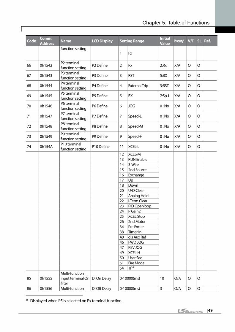
Chapter 5. Table of Functions
49
Code Comm. Address Name LCD Display Setting Range
Initial Value Property* V/F SL Ref.
function setting 1 Fx
66 0h1542 P2 terminal function setting P2 Define 2 Rx 2:Rx X/A O O
67 0h1543 P3 terminal function setting P3 Define 3 RST 5:BX X/A O O
68 0h1544 P4 terminal function setting P4 Define 4 External Trip 3:RST X/A O O
69 0h1545 P5 terminal function setting P5 Define 5 BX 7:Sp-L X/A O O
70 0h1546 P6 terminal function setting P6 Define 6 JOG 0 : No X/A O O
71 0h1547 P7 terminal function setting P7 Define 7 Speed-L 0 : No X/A O O
72 0h1548 P8 terminal function setting P8 Define 8 Speed-M 0 : No X/A O O
73 0h1549 P9 terminal function setting P9 Define 9 Speed-H 0 : No X/A O O
74 0h154A P10 terminal function setting P10 Define 11 XCEL-L 0 : No X/A O O
12 XCEL-M
13 RUN Enable 14 3-Wire 15 2nd Source 16 Exchange 17 Up 18 Down 20 U/D Clear 21 Analog Hold 22 I-Term Clear 23 PID Openloop 24 P Gain2 25 XCEL Stop 26 2nd Motor 34 Pre Excite 38 Timer In 40 dis Aux Ref 46 FWD JOG 47 REV JOG 49 XCEL-H 50 User Seq 51 Fire Mode 54 TI38
85 0h1555 Multi-function input terminal On filter
DI On Delay 0-10000(ms) 10 O/A O O
86 0h1556 Multi-function DI Off Delay 0-10000(ms) 3 O/A O O
38 Displayed when P5 is selected on Px terminal function.

Chapter 5. Table of Functions
50
Code Comm. Address Name LCD Display Setting Range
Initial Value Property* V/F SL Ref.
input terminal Off filter
87 0h1557 Multi-function input contact selection
DI NC/NO Sel P7 – P1
0 000039 X/A O O 0 A contact (NO)
1 B contact (NC)
89 0h1559 Multi-step command delay time
InCheck Time 1-5000(ms) 1 X/A O O
90 0h155A Multi-function input terminal status
DI Status P7 – P1
0 000039
-/A O O 0 release(Off) 1 Connection (On)
91 0h155B Pulse input amount display
Pulse Monitor (kHz) 0.00-50.00(kHz) 0.00 -/A O O
92 0h155C TI input filter time constant TI Filter 0-9999(ms) 10 O/A O O
93 0h155D TI Minimum input pulse TI Pls x1 0.00-32.00(kHz) 0.00 O/A O O
94 0h153E TI output at Minimum pulse (%)
TI Perc y1 0.00-100.00(%) 0.00 O/A O O
95 0h155F TI Maximum input pulse TI Pls x2 0.00-32.00(kHz) 32.00 O/A O O
96 0h1560 TI Output at Maximum pulse (%)
TI Perc y2 0-100(%) 100.00 O/A O O
97 0h1561 TI rotation direction change
TI Inverting 0 No
0:No O/A O O 1 Yes
98 0h1562 TI quantization level TI Quantizing 0.0035, 0.04-10.00(%) 0.04 O/A O O
99 0h1563
SW1(NPN/PNP)
SW2(V1/V2[I2])
status
IO SW State
Bit 00~11
00 -/A O O 00 V2, NPN 01 V2, PNP 10 I2, NPN 11 I2, PNP
39 The initial value 0000 will be displayed on the keypad as . The 7-seg screen of extension I/O
displays in case of clicking left and right key

Chapter 5. Table of Functions
51
5.7 Output Terminal Block Function group (PAR→OU)
In the following table, the data shaded in grey will be displayed when a related code has been selected.
SL: Sensorless vector control (dr.09) *O/X: Write-enabled during operation, 7/L/A: Keypad/LCD keypad/Common
Code Comm. Address Name LCD Display Setting Range Initial
Value Property* V/F SL Ref.
00 - Jump Code JumpCode 1-99 30 O/A O O
01 0h1601 Analog output 1 item AO1 Mode
0 Frequency
0:Frequency O/A O O
1 Output Current 2 Output Voltage 3 DCLink Voltage 4 Torque 5 Output Power 6 Idse 7 Iqse 8 Target Freq 9 Ramp Freq 10 Speed Fdb 12 PID Ref Value 13 PID Fdb Value 14 PID Output 15 Constant
02 0h1602 Analog output 1 gain AO1 Gain -1000.0-1000.0(%) 100.0 O/A O O
03 0h1603 Analog output 1 bias AO1 Bias -100.0-100.0(%) 0.0 O/A O O
04 0h1604 Analog output 1 filter AO1 Filter 0-10000(ms) 5 O/A O O
05 0h1606 Analog constant output 1 AO1 Const % 0.0-100.0(%) 0.0 O/A O O
06 0h1606 Analog output 1 monitor AO1 Monitor 0.0-1000.0(%) 0.0 -/A O O
30 0h161E Fault output item Trip Out Mode
bit 000-111
01040 O/A O O
1 Low voltage
2 Any faults other than low voltage
3 Automatic restart final failure
31 0h161F Multi-function relay 1 item Relay 1
0 None
29:Trip O/A O O
1 FDT-1 2 FDT-2
3 FDT-3
4 FDT-4
40 The initial value 0010 will be displayed on the keypad as .

Chapter 5. Table of Functions
52
Code Comm. Address Name LCD Display Setting Range
Initial Value Property* V/F SL Ref.
5 Over Load 6 IOL 7 Under Load 8 Fan Warning 9 Stall 10 Over Voltage 11 Low Voltage 12 Over Heat 13 Lost Command 14 Run 15 Stop 16 Steady 17 Inverter Line 18 Comm Line 19 Speed Search 22 Ready 28 Timer Out 29 Trip 31 DB Warn%ED 34 On/Off Control 35 BR Control 36 CAP.Warning 37 FAN Exchange 38 Fire Mode
33 0h1621 Multi-function output1 item Q1 Define
0 None
14:Run O/A O O
1 FDT-1 2 FDT-2 3 FDT-3 4 FDT-4 5 Over Load 6 IOL 7 Under Load 8 Fan Warning 9 Stall 10 Over Voltage 11 Low Voltage 12 Over Heat 13 Lost Command 14 Run 15 Stop 16 Steady 17 Inverter Line 18 Comm Line 19 Speed Search 22 Ready 28 Timer Out 29 Trip 31 DB Warn%ED 34 On/Off Control

Chapter 5. Table of Functions
53
Code Comm. Address Name LCD Display Setting Range
Initial Value Property* V/F SL Ref.
35 BR Control 36 CAP.Warning 37 FAN Exchange 38 Fire Mode 39 TO
34 0h1622 Multi-function relay 3 item
Relay 3
0 None
1 FDT-1 2 FDT-2 3 FDT-3 4 FDT-4 5 Over Load 6 IOL 7 Under Load 8 Fan Warning 9 Stall 10 Over Voltage 11 Low Voltage 12 Over Heat 13 Lost Command 14 Run 15 Stop 16 Steady 17 Inverter Line 18 Comm Line 19 Speed Search 22 Ready 28 Timer Out 29 Trip 31 DB Warn%ED 34 On/Off Control 35 BR Control 36 CAP.Warning 37 FAN Exchange 38 Fire Mode
35 0h1623 Multi-function relay 4 item
Relay 4
0 None
1 FDT-1 2 FDT-2 3 FDT-3 4 FDT-4 5 Over Load 6 IOL 7 Under Load 8 Fan Warning 9 Stall 10 Over Voltage 11 Low Voltage 12 Over Heat 13 Lost Command 14 Run

Chapter 5. Table of Functions
54
Code Comm. Address Name LCD Display Setting Range
Initial Value Property* V/F SL Ref.
15 Stop 16 Steady 17 Inverter Line 18 Comm Line 19 Speed Search 22 Ready 28 Timer Out 29 Trip 31 DB Warn%ED 34 On/Off Control 35 BR Control 36 CAP.Warning 37 FAN Exchange 38 Fire Mode
41 0h1629 Multi-function output monitor DO Status - 00 -/A - -
50 0h1632 Multi-function output On delay
DO On Delay 0.00-100.00(s) 0.00 O/A O O
51 0h1633 Multi-function output Off delay
DO Off Delay 0.00-100.00(s) 0.00 O/A O O
52 0h1634 Multi-function output contact selection
DO NC/NO Sel
Q1, Relay1 0041 X/A O O
0 A contact (NO)
1 B contact (NC)
53 0h1635 Fault output On delay TripOut OnDly 0.00-100.00(s) 0.00 O/A O O
54 0h1636 Fault output Off delay TripOut OffDly 0.00-100.00(s) 0.00 O/A O O
55 h1637 Timer On delay TimerOn Delay 0.00-100.00(s) 0.00 O/A O O
56 0h1638 Timer Off delay TimerOff Delay 0.00-100.00(s) 0.00 O/A O O
57 0h1639 Detected frequency FDT Frequency 0.00-Maximum
frequency(Hz) 30.00 O/A O O
58 0h163A Detected frequency band FDT Band 0.00-Maximum
frequency(Hz) 10.00 O/A O O
61 0h163D Pulse output gain TO Mode
0 Frequency
0: Frequency
O/A O O
1 Output Current 2 Output Voltage 3 DCLink Voltage 4 Torque 5 Output Power
41 The initial value 0000 will be displayed on the keypad as . The 7-seg screen of extension I/O
displays in case of clicking left and right key

Chapter 5. Table of Functions
55
Code Comm. Address Name LCD Display Setting Range
Initial Value Property* V/F SL Ref.
6 Idse 7 Iqse 8 Target Freq 9 Ramp Freq 10 Speed Fdb 12 PID Ref Value 13 PID Fdb Value 14 PID Output 15 Constant
62 0h163E Pulse output gain TO Gain -1000.0-1000.0(%) 100.0 O/A O O 63 0h163F Pulse output bias TO Bias -100.0-100.0(%) 0.0 O/A O O 64 0h1640 Pulse output filter TO Filter 0-10000(ms) 5 O/A O O
65 0h1641 Pulse output constant output 2 TO Const % 0.0-100.0(%) 0.0 O/A O O
66 0h1642 Pulse output monitor TO Monitor 0.0-1000.0(%) 0.0 -/A O O
5.8 Communication Function group (PAR→CM)
In the following table, the data shaded in grey will be displayed when a related code has been selected.
SL: Sensorless vector control (dr.09) *O/X: Write-enabled during operation, 7/L/A: Keypad/LCD keypad/Common
Code Comm. Address Name LCD Display Setting Range
Initial Value Property* V/F SL Ref.
00 - Jump Code Jump Code 1-99 20 O/A O O
01 0h1701 Built-in communication inverter ID
Int485 St ID 1-250 1 O/A O O
0242 0h1702 Built-in communication protocol
Int485 Proto 0 ModBus RTU 0: ModBus
RTU O/A O O 2 LS Inv 485
0342 0h1703 Built-in communication speed
Int485 BaudR
0 1200 bps
3: 9600 bps
O/A O O
1 2400 bps 2 4800 bps 3 9600 bps 4 19200 bps 5 38400 bps 6 56 Kbps 7 115 Kbps43
0442 0h1704 Built-in communication frame setting
Int485 Mode
0 D8/PN/S1 0: D8/PN/S1
O/A O O 1 D8/PN/S2 2 D8/PE/S1 3 D8/PO/S1
0542 0h1705 Transmission Resp Delay 0-1000(ms) 5ms O/A O O
42 Will not be displayed when P2P and MultiKPD is set. 43 115,200bps
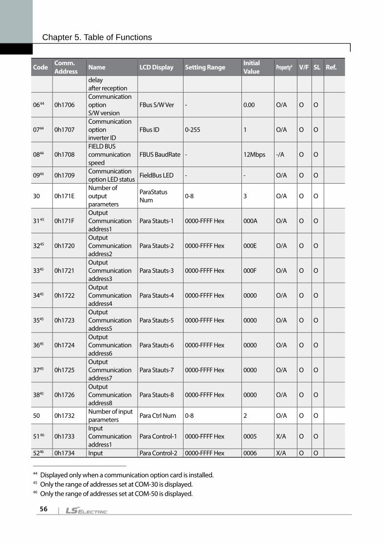
Chapter 5. Table of Functions
56
Code Comm. Address Name LCD Display Setting Range
Initial Value Property* V/F SL Ref.
delay after reception
0644 0h1706 Communication option S/W version
FBus S/W Ver - 0.00 O/A O O
0744 0h1707 Communication option inverter ID
FBus ID 0-255 1 O/A O O
0844 0h1708 FIELD BUS communication speed
FBUS BaudRate - 12Mbps -/A O O
0944 0h1709 Communication option LED status FieldBus LED - - O/A O O
30 0h171E Number of output parameters
ParaStatus Num 0-8 3 O/A O O
3145 0h171F Output Communication address1
Para Stauts-1 0000-FFFF Hex 000A O/A O O
3245 0h1720 Output Communication address2
Para Stauts-2 0000-FFFF Hex 000E O/A O O
3345 0h1721 Output Communication address3
Para Stauts-3 0000-FFFF Hex 000F O/A O O
3445 0h1722 Output Communication address4
Para Stauts-4 0000-FFFF Hex 0000 O/A O O
3545 0h1723 Output Communication address5
Para Stauts-5 0000-FFFF Hex 0000 O/A O O
3645 0h1724 Output Communication address6
Para Stauts-6 0000-FFFF Hex 0000 O/A O O
3745 0h1725 Output Communication address7
Para Stauts-7 0000-FFFF Hex 0000 O/A O O
3845 0h1726 Output Communication address8
Para Stauts-8 0000-FFFF Hex 0000 O/A O O
50 0h1732 Number of input parameters Para Ctrl Num 0-8 2 O/A O O
5146 0h1733 Input Communication address1
Para Control-1 0000-FFFF Hex 0005 X/A O O
5246 0h1734 Input Para Control-2 0000-FFFF Hex 0006 X/A O O
44 Displayed only when a communication option card is installed. 45 Only the range of addresses set at COM-30 is displayed. 46 Only the range of addresses set at COM-50 is displayed.

Chapter 5. Table of Functions
57
Code Comm. Address Name LCD Display Setting Range
Initial Value Property* V/F SL Ref.
Communication address2
5346 0h1735 Input Communication address3
Para Control-3 0000-FFFF Hex 0000 X/A O O
5446 0h1736 Input Communication address4
Para Control-4 0000-FFFF Hex 0000 X/A O O
5546 0h1737 Input Communication address5
Para Control-5 0000-FFFF Hex 0000 X/A O O
5646 0h1738 Input Communication address6
Para Control-6 0000-FFFF Hex 0000 X/A O O
5746 0h1739 Input Communication address7
Para Control-7 0000-FFFF Hex 0000 X/A O O
5846 0h173A Input Communication address8
Para Control-8 0000-FFFF Hex 0000 X/A O O
68 0h1744 Field bus data swap FBus Swap Sel
0 No 0 X/A O O
1 Yes
70 0h1746 Communication multi-function input 1
Virtual DI 1 0 None 0:None O/A O O
71 0h1747 Communication multi-function input 2
Virtual DI 2 1 Fx 0:None O/A O O
72 0h1748 Communication multi-function input 3
Virtual DI 3 2 Rx 0:None O/A O O
73 0h1749 Communication multi-function input 4
Virtual DI 4 3 RST 0:None O/A O O
74 0h174A Communication multi-function input 5
Virtual DI 5 4 External Trip 0:None O/A O O
75 0h174B Communication multi-function input 6
Virtual DI 6 5 BX 0:None O/A O O
76 0h174C Communication multi-function input 7
Virtual DI 7 6 JOG 0:None O/A O O
77 0h174D Communication multi-function input 8
Virtual DI 8
7 Speed-L
0:None O/A O O
8 Speed-M 9 Speed-H 11 XCEL-L 12 XCEL-M 13 RUN Enable 14 3-Wire

Chapter 5. Table of Functions
58
Code Comm. Address Name LCD Display Setting Range
Initial Value Property* V/F SL Ref.
15 2nd Source 16 Exchange 17 Up 18 Down 20 U/D Clear 21 Analog Hold 22 I-Term Clear 23 PID Openloop 24 P Gain2 25 XCEL Stop 26 2nd Motor 34 Pre Excite 38 Timer In 40 dis Aux Ref 46 FWD JOG 47 REV JOG 49 XCEL-H
86 0h1756 Communication multi-function input monitoring
Virt DI Status - 0 X/A O O
90 0h175A
Selection of data frame communication monitor
Comm Mon Sel
0 Int485
0 O/A O O 1 KeyPad
91 0h175B Data frame Rev count
Rcv Frame Num 0~65535 0 O/A O O
92 0h175C Data frame Err count Err Frame Num 0~65535 0 O/A O O
93 0h175D NAK frame count NAK Frame Num
0~65535 0 O/A O O
9447 - Communication data upload Comm Update
0 No 0:No -/A O O
1 Yes
95 0h1760 P2P communication selection
Int 485 Func
0 Disable All 0: Disable All X/A O O
1 P2P Master 2 P2P Slave 3 KPD-Ready
9648 - DO setting selection P2P OUT Sel
Bit 000~111
0:No O/A O O
001 Analog output
010 Multi-function relay
100 Multi-function output
47 Displayed only when a communication option card is installed. 48 Displayed when AP.01 is set to 2 (Proc PID).

Chapter 5. Table of Functions
59
5.9 Application Function group (PAR→AP)
In the following table, the data shaded in grey will be displayed when a related code has been selected.
SL: Sensorless vector control (dr.09) *O/X: Write-enabled during operation, 7/L/A: Keypad/LCD keypad/Common
Code Comm. Address Name LCD Display Setting Range Initial
Value Property* V/F SL Ref.
00 - Jump Code Jump Code 1-99 20 O/A O O
01 0h1801 Application function selection App Mode
0 None 0: None X/A O O 1 -
2 Proc PID
02 - Enable user sequence User Seq En
0 No 0:No X/A O O
1 Yes
1649 0h1810 PID output monitor PID Output (%) 0.00 -/A O O
1749 0h1811 PID reference monitor PID Ref Value (%) 50.00 -/A O O
1849 0h1812 PID feedback monitor PID Fdb Value (%) 0.00 -/A O O
1949 0h1813 PID reference setting PID Ref Set -100.00-
100.00(%) 50.00 O/A O O
2049 0h1814 PID reference source
PID Ref Source
0 Keypad
0: Keypad X/A O O
1 V1 3 V2 4 I2 5 Int 485 7 FieldBus 11 Pulse
2149 0h1815 PID feedback source
PID F/B Source
0 V1
0:V1 X/A O O
2 V2 3 I2 4 Int 485 6 FieldBus 10 Pulse
2249 0h1816 PID controller proportional gain PID P-Gain 0.0-1000.0(%) 50.0 O/A O O
2349 0h1817 PID controller integral time PID I-Time 0.0-200.0(s) 10.0 O/A O O
2449 0h1818 PID controller differentiation time
PID D-Time 0-1000(ms) 0 O/A O O
2549 0h1819
PID controller feed-forward compensation gain
PID F-Gain 0.0-1000.0(%) 0.0 O/A O O
2649 0h181A Proportional gain scale P Gain Scale 0.0-100.0(%) 100.0 X/A O O
49 Displayed when AP.01 is set to 2 (Proc PID).

Chapter 5. Table of Functions
60
Code Comm. Address Name LCD Display Setting Range
Initial Value Property* V/F SL Ref.
2749 0h181B PID output filter PID Out LPF 0-10000(ms) 0 O/A O O
2849 0h181C PID Mode PID Mode 0 Process
PID 0 X/A O O
1 Normal PID
2949 0h181D PID upper limit frequency PID Limit Hi
PID lower limit frequency-300.00(Hz)
60.00 O/A O O
3049 0h181E PID lower limit frequency PID Limit Lo
-300.00 -PID upper limit frequency(Hz)
-60.00 O/A O O
3149 0h181F PID output inverse PID Out Inv 0 No
0:No X/A O O 1 Yes
3249 0h1820 PID output scale PID Out Scale 0.1-1000.0(%) 100.0 X/A O O
3449 0h1822 PID controller motion frequency Pre-PID Freq
0.00- Maximum frequency(Hz)
0.00 X/A O O
3549 0h1823 PID controller motion level Pre-PID Exit 0.0-100.0(%) 0.0 X/A O O
3649 0h1824 PID controller motion delay time Pre-PID Delay 0-9999(s) 600 O/A O O
3749 0h1825 PID sleep mode delay time PID Sleep DT 0.0-999.9(s) 60.0 O/A O O
3849 0h1826 PID sleep mode frequency
PID Sleep Freq
0.00- Maximum frequency(Hz)
0.00 O/A O O
3949 0h1827 PID wake-up level PIDWakeUp Lev 0-100(%) 35 O/A O O
4049 0h1828 PID wake-up mode setting
PID WakeUp Mod
0 Below Level
0:Below Level O/A O O 1 Above
Level
2 Beyond Level
4249 0h182A PID controller unit selection PID Unit Sel
0 %
0:% O/A O O
1 Bar 2 mBar 3 Pa 4 kPa 5 Hz 6 rpm 7 V 8 I 9 kW 10 HP 11 ℃
12 ℉ 4349 0h182B PID unit gain PID Unit Gain 0.00-300.00(%) 100.00 O/A O O
4449 0h182C PID unit scale PID Unit Scale
0 x100 2:x 1 O/A O O
1 x10

Chapter 5. Table of Functions
61
Code Comm. Address Name LCD Display Setting Range
Initial Value Property* V/F SL Ref.
2 x 1 3 x 0.1 4 x 0.01
4549 0h182D PID 2nd proportional gain PID P2-Gain 0.0-1000.0(%) 100.0 X/A O O
5.10 Extension I/O Function Group(PAR→AO)
In the following table, the data shaded in grey will be displayed when a related code has been selected.
SL: Sensorless vector control (dr.09) *O/X: Write-enabled during operation, 7/L/A: Keypad/LCD keypad/Common 코드 통신 번지 명칭 LCD 표시 설정 범위 초기 값 속성* V/F SL 참조 00 - Jum Code Jump Code 1~99 0 O/A O O
01 0h1A01 V3 input voltage display
V3 Monitor[V] -12.00 ~ 12.00[V] 0.00 -/A O O
02 0h1A02 V3 input polarity selection V3 Polarity
0 Unipolar 0:Unipolar X/A O O
1 Bipolar
03 0x1A03 Time constant of V3 input filter V3 Filter 0 ~ 10000[ms] 10 O/A O O
04 0x1A04 V3 Minimum input voltage
V3 Volt x1 0.00 ~ 10.00[V] 0.00 O/A O O
05 0x1A05 V3 output at Minimum voltage (%)
V3 Perc y1 0.00 ~ 100.00[%] 0.00 O/A O O
06 0x1A06 V3 Maximum input voltage V3 Volt x2 0.00 ~ 12.00[V] 10.00 O/A O O
07 0x1A07 V3 output at Maximum voltage (%)
V3 Perc y2 0.00 ~ 100.00[%] 100.00 O/A O O
08 0x1A08 V3 rotation direction change
V3 Inverting 0 No
0:No O/A O O 1 Yes
09 0x1A09 V3 quantization level V3 Quantizing
0.00 , 0.04 ~ 10.00[%] 0.04 X/A O O
10 0x1A0A V3 Minimum input voltage V3 –Volt x1’ -10.00~ 0.00[V] 0.00 O/A O O
11 0x1A0B V3 output at Minimum voltage (%)
V3 –Perc y1’ -100.00 ~ 0.00[%] 0.00 O/A O O
12 0x1A0C V3 Maximum input voltage V3 –Volt x2’ -12.00~ 0.00[V] -10.00 O/A O O
13 0x1A0D V3 output at Maximum voltage (%)
V3 –Perc y2’ -100.00 ~ 0.00[%] -100.00 O/A O O
14 0x1A0E V4 input voltage display
V4 Monitor[V] 0.00 ~ 12.00[V] 0.00 -/A O O

Chapter 5. Table of Functions
62
코드 통신 번지 명칭 LCD 표시 설정 범위 초기 값 속성* V/F SL 참조
15 0x1A0F Time constant of V4 input filter V4 Filter 0 ~ 10000[ms] 10 O/A O O
16 0x1A10 V4 Minimum input voltage V4 Volt x1 0.00 ~ 10.00[V] 0.00 O/A X X
17 0x1A11 V4 output at Minimum voltage (%)
V4 Perc y1 0.00 ~ 100.00[%] 0.00 O/A O O
18 0x1A12 V4 Maximum input voltage V4 Volt x2 0.00 ~ 10.00[V] 10 O/A X X
19 0x1A13 V4 output at Maximum voltage (%)
V4 Perc y2 0.00 ~ 100.00[%] 100.00 O/A O O
20 0x1A14 V4 rotation direction change V4 Inverting
0 No 0:No O/A O O
1 Yes
21 0x1A15 V4 quantization level V4 Quantizing 0.0050, 0.04~
10.00[%] 0.04 O/A O O
22 0x1A16 I4 input current display I4 Monitor[mA] 0 ~ 24[mA] 0.00 -/A O O
23 0x1A17 I4 input filter time constant I4 Filter 0 ~ 10000[ms] 10 O/A O O
24 0x1A18 I4 minimum input current I4 Curr x1 0.00 ~ 20.00[mA] 4.00 O/A O O
25 0x1A19 I4 output at Minimum current (%)
I4 Perc y1 0.00 ~ 100.00[%] 0.00 O/A O O
26 0x1A1A I4 maximum input current
I4 Curr x2 0.00 ~ 24.00[mA] 20.00 O/A O O
27 0x1A1B I4 output at Maximum current (%)
I4 Perc y2 0.00 ~ 100.00[%] 100.00 O/A O O
28 0x1A1C Changing rotation direction of I4 I4 Inverting
0 No 0:No O/A O O
1 Yes
29 0x1A1D I4 quantization level I4 Quantizing 0.0051, 0.04 ~ 10.00[%] 0.04 O/A O O
30 0x1A1E Analog output 3 item AO3 Mode
0 Frequency
0: Frequency
O/A O O
1 Output Current
2 Output Voltage
3 DCLink Voltage
4 Torque
5 Output Power
6 Idse 7 Iqse 8 Target Freq 9 Ramp Freq
50 0을 설정 하면 Quantizing 사용하지 않습니다. 51 0을 설정 하면 Quantizing 사용하지 않습니다.

Chapter 5. Table of Functions
63
코드 통신 번지 명칭 LCD 표시 설정 범위 초기 값 속성* V/F SL 참조 10 Speed Fdb
12 PID Ref Value
13 PID Fdb Value
14 PID Output 15 Constant
31 0x1A1F Analog output 5 gain AO5 gain -1000.0 ~
1000.0[%] 100.0 O/A O O
32 0x1A20 Analog output 5 bias AO5 Bias -100.0 ~
100.0[%] 0.0 O/A O O
33 0x1A21 Analog output 5 filter AO5 Filter 0 ~ 10000[ms] 5 O/A O O
34 0x1A22 Analog constant output 5 AO5 Const % 0.0 ~ 100.0[%] 0.0 O/A O O
35 0x1A23 Analog output 5 monitor AO5 Monitor 0.0 ~ 1000.0[%] 0.0 -/A O O
36 0x1A24 Ext IO Switch Ext IO Switch
00 NPN,V4
01 -/A - - 01 NPN,I4 10 PNP,V4 11 PNP,I4
37 0x1A25 Ext I/O SW Ver Ext I/O SW Ver - 1.00 -/A - -
5.11 Protection Function group (PAR→Pr)
In the following table, the data shaded in grey will be displayed when a related code has been selected.
SL: Sensorless vector control (dr.09) *O/X: Write-enabled during operation, 7/L/A: Keypad/LCD keypad/Common
Code Comm. Address
Name LCD Display Setting Range Initial Value
Property* V/F SL Ref.
00 - Jump Code Jump Code 1-99 40 O/A O O
04 0h1B04 Load level setting Load Duty 0 Normal Duty 1:Heavy
Duty X/A O O
1 Heavy Duty
05 0h1B05 Input/output open-phase protection
Phase Loss Chk
bit 00-11
0052 X/A O O 01 Output open
phase
10 Input open phase
52 The initial value 0000 will be displayed on the keypad as .

Chapter 5. Table of Functions
64
Code Comm. Address Name LCD Display Setting Range
Initial Value Property* V/F SL Ref.
06 0h1B06 Input voltage range during open-phase
IPO V Band 1-100(V) 15 X/A O O
07 0h1B07 Deceleration time at fault trip Trip Dec Time 0.0-600.0(s) 3.0 O/A O O
08 0h1B08 Selection of startup on trip reset
RST Restart
0 No
0:No O/A O O 1 Yes
09 0h1B09 Number of automatic restarts Retry Number 0-10 0 O/A O O
1053 0h1B0A Automatic restart delay time Retry Delay 0.0-60.0(s) 1.0 O/A O O
12 0h1B0C Motion at speed command loss
Lost Cmd Mode
0 None
0:None O/A O O
1 Free-Run 2 Dec 3 Hold Input 4 Hold Output 5 Lost Preset
1354 0h1B0D Time to decide speed command loss
Lost Cmd Time 0.1-120(s) 1.0 O/A O O
1454 0h1B0E
Operation frequency at speed command loss
Lost Preset F Start frequency- Maximum frequency(Hz)
0.00 O/A O O
1554 0h1B0F Analog input loss decision level AI Lost Level
0 Half x1 0:Half of x1 O/A O O
1 Below x1
17 0h1B11 Overload warning selection
OL Warn Select 0 No
0:No O/A O O 1 Yes
18 0h1B12 Overload alarm level
OL Warn Level 30-180(%) 150 O/A O O
19 0h1B13 Overload warning time OL Warn Time 0.0-30.0(s) 10.0 O/A O O
20 0h1B14 Motion at overload fault OL Trip Select
0 None 1:Free-Run O/A O O 1 Free-Run
2 Dec
53 Displayed when Pr.09 is set higher than 0. 54 Displayed when Pr.12 is not set to 0 (NONE).
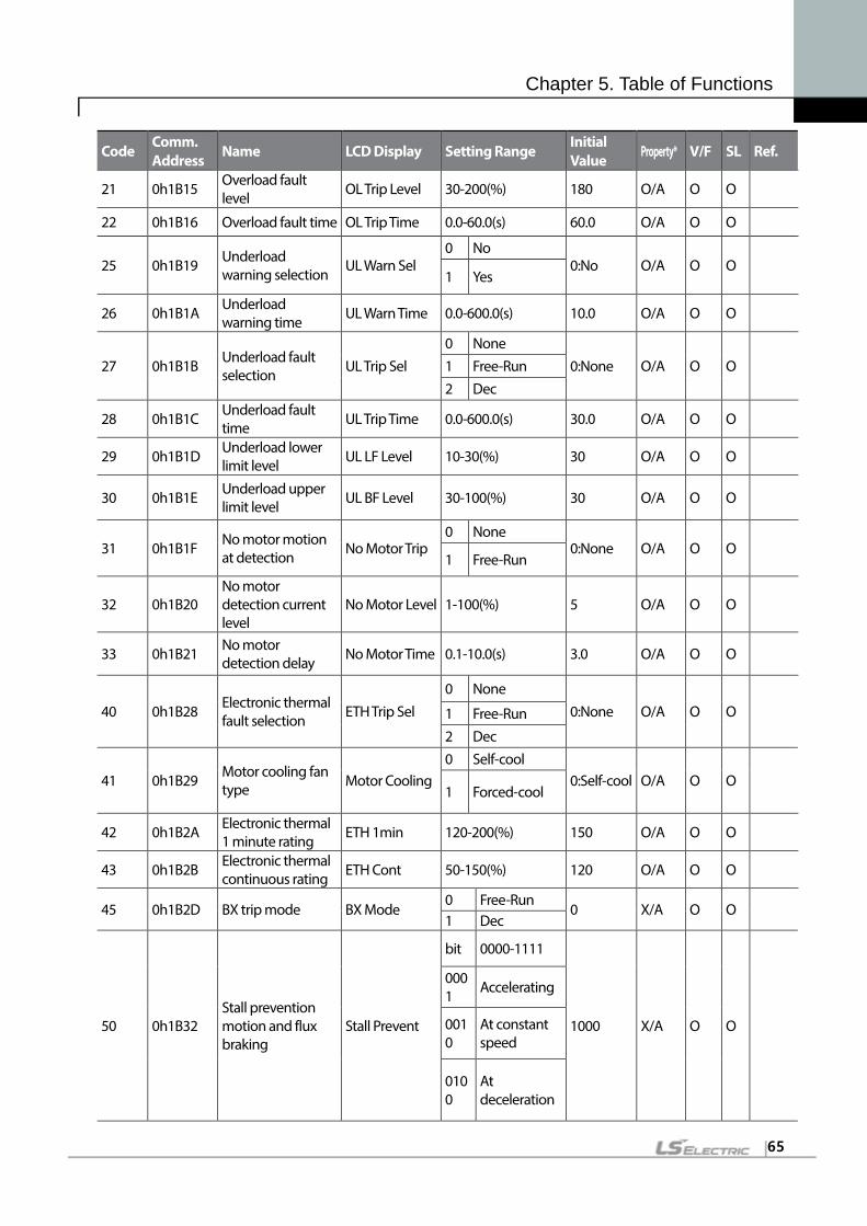
Chapter 5. Table of Functions
65
Code Comm. Address Name LCD Display Setting Range
Initial Value Property* V/F SL Ref.
21 0h1B15 Overload fault level
OL Trip Level 30-200(%) 180 O/A O O
22 0h1B16 Overload fault time OL Trip Time 0.0-60.0(s) 60.0 O/A O O
25 0h1B19 Underload warning selection
UL Warn Sel 0 No
0:No O/A O O 1 Yes
26 0h1B1A Underload warning time UL Warn Time 0.0-600.0(s) 10.0 O/A O O
27 0h1B1B Underload fault selection UL Trip Sel
0 None 0:None O/A O O 1 Free-Run
2 Dec
28 0h1B1C Underload fault time UL Trip Time 0.0-600.0(s) 30.0 O/A O O
29 0h1B1D Underload lower limit level UL LF Level 10-30(%) 30 O/A O O
30 0h1B1E Underload upper limit level UL BF Level 30-100(%) 30 O/A O O
31 0h1B1F No motor motion at detection No Motor Trip
0 None 0:None O/A O O
1 Free-Run
32 0h1B20 No motor detection current level
No Motor Level 1-100(%) 5 O/A O O
33 0h1B21 No motor detection delay No Motor Time 0.1-10.0(s) 3.0 O/A O O
40 0h1B28 Electronic thermal fault selection
ETH Trip Sel 0 None
0:None O/A O O 1 Free-Run 2 Dec
41 0h1B29 Motor cooling fan type Motor Cooling
0 Self-cool 0:Self-cool O/A O O
1 Forced-cool
42 0h1B2A Electronic thermal 1 minute rating ETH 1min 120-200(%) 150 O/A O O
43 0h1B2B Electronic thermal continuous rating ETH Cont 50-150(%) 120 O/A O O
45 0h1B2D BX trip mode BX Mode 0 Free-Run
0 X/A O O 1 Dec
50 0h1B32 Stall prevention motion and flux braking
Stall Prevent
bit 0000-1111
1000 X/A O O
0001 Accelerating
0010
At constant speed
0100
At deceleration

Chapter 5. Table of Functions
66
Code Comm. Address Name LCD Display Setting Range
Initial Value Property* V/F SL Ref.
1000 FluxBraking
51 0h1B33 Stall frequency1 Stall Freq 1 Start frequency- Stall frequency2(Hz)
60.00 O/A O O
52 0h1B34 Stall level1 Stall Level 1 30-250(%) 180 X/A O O
53 0h1B35 Stall frequency2 Stall Freq 2 Stall frequency1- Stall frequency3(Hz)
60.00 O/A O O
54 0h1B36 Stall level2 Stall Level 2 30-250(%) 180 X/A O O
55 0h1B37 Stall frequency3 Stall Freq 3 Stall frequency2- Stall frequency4(Hz)
60.00 O/A O O
56 0h1B38 Stall level3 Stall Level 3 30-250(%) 180 X/A O O
57 0h1B39 Stall frequency4 Stall Freq 4 Stall frequency3- Maximum frequency(Hz)
60.00 O/A O O
58 0h1B3A Stall level4 Stall Level 4 30-250(%) 180 X/A O O
59 0h1B3B Flux braking gain Flux Brake Kp 0 ~ 150[%] 0 O/A O O
60 0h1B3C CAP diagnosis level CAP. Diag Perc 10 ~ 100[%] 0 O/A O O
6155 0h1B3D CAP diagnosis
mode CAP. Diag
0 None
0 X/A O 1 Ref Diag 2 Pre Diag 3 Init Diag
6255 0h1B3E CAP Exchange Level
CAP Exchange Level 50.0 ~ 95.0[%] 0 X/A O O
6355 0h1B3F CAP Diag Level CAP Diag Level 0.0~100.0[%] 100.0 -/A O O
66 0h1B42 DB resistor warning level DB Warn %ED 0-30(%) 0 O/A O O
73 0h1B22 Speed deviation trip Speed Dev Trip
0 No 0:No O/A O O
1 Yes
74 0h1B23 Speed deviation band Speed Dev Band 1 ~ 20 5 O/A O O
75 0h1B24 Speed deviation time Speed Dev Time 0 ~ 120 60 O/A O O
79 0h1B4F Cooling fan fault selection FAN Trip Mode
0 Trip 0:Trip O/A O O
1 Warning
80 0h1B50 Motion selection at option trip Opt Trip Mode
0 None 1:Free-Run O/A O O 1 Free-Run
2 Dec
55 The Pr.61-63 codes are displayed when the Pr.60(CAP.DiagPrec) is set to more than 0.

Chapter 5. Table of Functions
67
Code Comm. Address Name LCD Display Setting Range
Initial Value Property* V/F SL Ref.
81 0h1B51 Low voltage fault decision delay time
LVT Delay 0.0-60.0(s) 0.0 X/A O O
82 0h1B52 LV2 Selection LV2 Enable 0 No
0 X/A O O 1 Yes
86 0h1B56 Accumulated percent of fan usage
Fan Time Perc 0.0~100.0[%] 0.0 -/A O O
87 0h1B57 Fan exchange warning level
Fan Exchange level 0.0~100.0[%] 90.0 O/A O O
8856 0h1B58 Fan reset time Fan Time Rst 0 No
0 X/A O O 1 Yes
89 0h1B59 CAP, FAN Status CAP, FAN State
Bit 00~10
0 -/A O O 00 - 01 CAP Warning 10 FAN Warning
9056 0h1B5A Warning information - - - -/7 O O
9156 0h1B5B Fault history 1 - - - -/7 O O
9256 0h1B5C Fault history 2 - - - -/7 O O
9356 0h1B5D Fault history 3 - - - -/7 O O
9456 0h1B5E Fault history 4 - - - -/7 O O
9556 0h1B5F Fault history 5 - - - -/7 O O
9656 0h1B60 Fault history deletion -
0 No 0:No -/7 O O
1 Yes
56 Will not be displayed when an LCD keypad is in use.
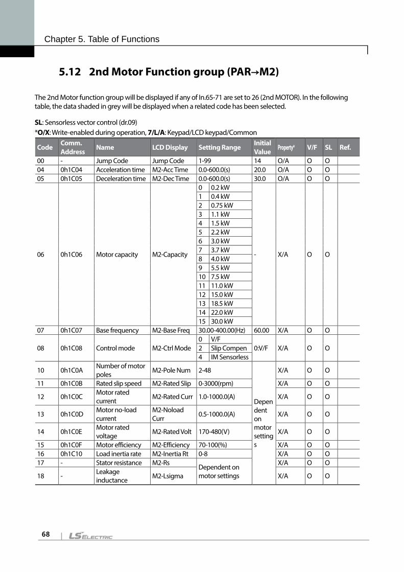
Chapter 5. Table of Functions
68
5.12 2nd Motor Function group (PAR→M2)
The 2nd Motor function group will be displayed if any of In.65-71 are set to 26 (2nd MOTOR). In the following table, the data shaded in grey will be displayed when a related code has been selected.
SL: Sensorless vector control (dr.09) *O/X: Write-enabled during operation, 7/L/A: Keypad/LCD keypad/Common
Code Comm. Address
Name LCD Display Setting Range Initial Value
Property* V/F SL Ref.
00 - Jump Code Jump Code 1-99 14 O/A O O 04 0h1C04 Acceleration time M2-Acc Time 0.0-600.0(s) 20.0 O/A O O 05 0h1C05 Deceleration time M2-Dec Time 0.0-600.0(s) 30.0 O/A O O
06 0h1C06 Motor capacity M2-Capacity
0 0.2 kW
- X/A O O
1 0.4 kW 2 0.75 kW 3 1.1 kW 4 1.5 kW 5 2.2 kW 6 3.0 kW 7 3.7 kW 8 4.0 kW 9 5.5 kW 10 7.5 kW 11 11.0 kW 12 15.0 kW 13 18.5 kW 14 22.0 kW 15 30.0 kW
07 0h1C07 Base frequency M2-Base Freq 30.00-400.00(Hz) 60.00 X/A O O
08 0h1C08 Control mode M2-Ctrl Mode 0 V/F
0:V/F X/A O O 2 Slip Compen 4 IM Sensorless
10 0h1C0A Number of motor poles M2-Pole Num 2-48
Dependent on motor settings
X/A O O
11 0h1C0B Rated slip speed M2-Rated Slip 0-3000(rpm) X/A O O
12 0h1C0C Motor rated current
M2-Rated Curr 1.0-1000.0(A) X/A O O
13 0h1C0D Motor no-load current
M2-Noload Curr
0.5-1000.0(A) X/A O O
14 0h1C0E Motor rated voltage
M2-Rated Volt 170-480(V) X/A O O
15 0h1C0F Motor efficiency M2-Efficiency 70-100(%) X/A O O 16 0h1C10 Load inertia rate M2-Inertia Rt 0-8 X/A O O 17 - Stator resistance M2-Rs
Dependent on motor settings
X/A O O
18 - Leakage inductance M2-Lsigma X/A O O

Chapter 5. Table of Functions
69
Code Comm. Address Name LCD Display Setting Range
Initial Value Property* V/F SL Ref.
19 - Stator inductance M2-Ls X/A O O
2057 - Rotor time constant
M2-Tr 25-5000(ms) X/A O O
25 0h1C19 V/F pattern M2-V/F Patt
0 Linear 0: Linear X/A O O 1 Square
2 User V/F
26 0h1C1A Forward Torque boost M2-Fwd Boost 0.0-15.0(%)
2.0 X/A O O
27 0h1C1B Reverse Torque boost M2-Rev Boost 0.0-15.0(%) X/A O O
28 0h1C1C Stall prevention level M2-Stall Lev 30-150(%) 150 X/A O O
29 0h1C1D Electronic thermal 1 minute rating
M2-ETH 1min 100-200(%) 150 X/A O O
30 0h1C1E Electronic thermal continuous rating
M2-ETH Cont 50-150(%) 100 X/A O O
57 Displayed when M2.08 is set to 4 (IM Sensorless).

Chapter 5. Table of Functions
70
5.13 User Sequence group (US)
This group appears when AP.02 is set to 1 (Yes) or CM.95 is set to 2 (P2P Master). The parameter cannot be changed while the user sequence is running.
SL: Sensorless vector control function (dr.09) *O/X: Write-enabled during operation, 7/L/A: keypad/LCD keypad/common Code Comm.
Address Name LCD Display Setting
Range Initial Value
Property* V/F SL Ref.
00 - Jump code Jump Code 1-99 31 O/A O O 01 0h1D01 User sequence
operation command User Seq Con 0 Stop 0:Stop X/A O O
1 Run 2 Digital In
Run 02 0h1D02 User sequence
operation loop time US Loop Time 0 0.01s 1:0.02s X/A O O
1 0.02s 2 0.05s 3 0.1s 4 0.5s 5 1s
11 0h1D0B Output address link1 Link UserOut1 0-0xFFFF 0 X/A O O 12 0h1D0C Output address link2 Link UserOut2 0-0xFFFF 0 X/A O O 13 0h1D0D Output address link3 Link UserOut3 0-0xFFFF 0 X/A O O 14 0h1D0E Output address link4 Link UserOut4 0-0xFFFF 0 X/A O O 15 0h1D0F Output address link5 Link UserOut5 0-0xFFFF 0 X/A O O 16 0h1D10 Output address link6 Link UserOut6 0-0xFFFF 0 X/A O O 17 0h1D11 Output address link7 Link UserOut7 0-0xFFFF 0 X/A O O 18 0h1D12 Output address link8 Link UserOut8 0-0xFFFF 0 X/A O O 19 0h1D13 Output address link9 Link UserOut9 0-0xFFFF 0 X/A O O 20 0h1D14 Output address
link10 Link UserOut10 0-0xFFFF 0 X/A O O
21 0h1D15 Output address link11
Link UserOut11 0-0xFFFF 0 X/A O O
22 0h1D16 Output address link12
Link UserOut12 0-0xFFFF 0 X/A O O
23 0h1D17 Output address link13
Link UserOut13 0-0xFFFF 0 X/A O O
24 0h1D18 Output address link14
Link UserOut14 0-0xFFFF 0 X/A O O
25 0h1D19 Output address link15
Link UserOut15 0-0xFFFF 0 X/A O O
26 0h1D1A Output address link16
Link UserOut16 0-0xFFFF 0 X/A O O
27 0h1D1B Output address link17
Link UserOut17 0-0xFFFF 0 X/A O O
28 0h1D1C Output address link18
Link UserOut18 0-0xFFFF 0 X/A O O
31 0h1D1F Input constant setting1
Void Para1 -9999-9999 0 X/A O O
32 0h1D20 Input constant setting2
Void Para2 -9999-9999 0 X/A O O

Chapter 5. Table of Functions
71
Code Comm. Address
Name LCD Display Setting Range
Initial Value
Property* V/F SL Ref.
33 0h1D21 Input constant setting3
Void Para3 -9999-9999 0 X/A O O
34 0h1D22 Input constant setting4
Void Para4 -9999-9999 0 X/A O O
35 0h1D23 Input constant setting5
Void Para5 -9999-9999 0 X/A O O
36 0h1D24 Input constant setting6
Void Para6 -9999-9999 0 X/A O O
37 0h1D25 Input constant setting7
Void Para7 -9999-9999 0 X/A O O
38 0h1D26 Input constant setting8
Void Para8 -9999-9999 0 X/A O O
39 0h1D27 Input constant setting9
Void Para9 -9999-9999 0 X/A O O
40 0h1D28 Input constant setting10
Void Para10 -9999-9999 0 X/A O O
41 0h1D29 Input constant setting11
Void Para11 -9999-9999 0 X/A O O
42 0h1D2A Input constant setting12
Void Para12 -9999-9999 0 X/A O O
43 0h1D2B Input constant setting13
Void Para13 -9999-9999 0 X/A O O
44 0h1D2C Input constant setting14
Void Para14 -9999-9999 0 X/A O O
45 0h1D2D Input constant setting15
Void Para15 -9999-9999 0 X/A O O
46 0h1D2E Input constant setting16
Void Para16 -9999-9999 0 X/A O O
47 0h1D2F Input constant setting17
Void Para17 -9999-9999 0 X/A O O
48 0h1D30 Input constant setting18
Void Para18 -9999-9999 0 X/A O O
49 0h1D31 Input constant setting19
Void Para19 -9999-9999 0 X/A O O
50 0h1D32 Input constant setting20
Void Para20 -9999-9999 0 X/A O O
51 0h1D33 Input constant setting21
Void Para21 -9999-9999 0 X/A O O
52 0h1D34 Input constant setting22
Void Para22 -9999-9999 0 X/A O O
53 0h1D35 Input constant setting23
Void Para23 -9999-9999 0 X/A O O
54 0h1D36 Input constant setting24
Void Para24 -9999-9999 0 X/A O O
55 0h1D37 Input constant setting25
Void Para25 -9999-9999 0 X/A O O
56 0h1D38 Input constant setting26
Void Para26 -9999-9999 0 X/A O O
57 0h1D39 Input constant setting27
Void Para27 -9999-9999 0 X/A O O

Chapter 5. Table of Functions
72
Code Comm. Address
Name LCD Display Setting Range
Initial Value
Property* V/F SL Ref.
58 0h1D3A Input constant setting28
Void Para28 -9999-9999 0 X/A O O
59 0h1D3B Input constant setting29
Void Para29 -9999-9999 0 X/A O O
60 0h1D3C Input constant setting30
Void Para30 -9999-9999 0 X/A O O
80 0h1D50S Analog input 1 P2P In V1 0-12,000 -/A O O 81 0h1D51 Analog input2 P2P In I2 -12,000-12,000 -/A O O 82 0h1D52 Digital input P2P In DI 0-0x7F -/A O O 85 0h1D55 Analog output P2P OutAO1 0-10,000 0 X/A O O 88 0h1D58 Digital output P2P OutDO 0-0x03 0 X/A O O
5.14 User Sequence Function group(UF)
This group appears when AP.02 is set to 1 (Yes) or CM.95 is set to 2 (P2P Master). The parameter cannot be changed while the user sequence is running.
SL: Sensorless vector control function (dr.09) *O/X: Write-enabled during operation, 7/L/A: keypad/LCD keypad/common Code Comm.
Address Name LCD
Display Setting Range Initial
Value Property* V/F SL Ref.
00 - Jump code Jump Code
1-99 41 O/A O O
01 0h1E01 User function1 User Func1 0 NOP 0:NOP X/A O O 1 ADD 2 SUB 3 ADDSUB 4 MIN 5 MAX 6 ABS 7 NEGATE 8 MPYDIV 9 REMAINDER 10 COMPARE-GT 11 COMPARE-GEQ
12 COMPARE-EQUAL
13 COMPARE-NEQUAL
14 TIMER 15 LIMIT 16 AND 17 OR 18 XOR

Chapter 5. Table of Functions
73
Code Comm. Address
Name LCD Display
Setting Range Initial Value
Property* V/F SL Ref.
19 ANDOR 20 SWITCH 21 BITTEST 22 BITSET 23 BITCLEAR 24 LOWPASSFILTER
25 PI_CONTORL 26 PI_PROCESS 27 UPCOUNT 28 DOWNCOUNT
02 0h1E02 User function input1-A User Input1-A
0-0xFFFF 0 X/A O O
03 0h1E03 User function input1-B User Input1-B
0-0xFFFF 0 X/A O O
04 0h1E04 User function input1-C User Input1-C
0-0xFFFF 0 X/A O O
05 0h1E05 User function output1 User Output1
-32767-32767 0 -/A O O
06 0h1E06 User function 2 User Func2 0 NOP 0:NOP X/A O O 1 ADD 2 SUB 3 ADDSUB 4 MIN 5 MAX 6 ABS 7 NEGATE 8 MPYDIV 9 REMAINDER 10 COMPARE-GT 11 COMPARE-GEQ
12 COMPARE-EQUAL
13 COMPARE-NEQUAL
14 TIMER 15 LIMIT 16 AND 17 OR 18 XOR 19 ANDOR 20 SWITCH 21 BITTEST 22 BITSET
23 BITCLEAR

Chapter 5. Table of Functions
74
Code Comm. Address
Name LCD Display
Setting Range Initial Value
Property* V/F SL Ref.
24 LOWPASSFILTER
25 PI_CONTORL 26 PI_PROCESS 27 UPCOUNT 28 DOWNCOUNT
07 0h1E07 User function input2-A User Input2-A
0-0xFFFF 0 X/A O O
08 0h1E08 User function input2-B User Input2-B
0-0xFFFF 0 X/A O O
09 0h1E09 User function input2-C User Input2-C
0-0xFFFF 0 X/A O O
10 0h1E0A User function output2 User Output2
-32767-32767 0 -/A O O
11 0h1E0B User function3 User Func3 0 NOP 0:NOP X/A O O 1 ADD 2 SUB 3 ADDSUB 4 MIN 5 MAX 6 ABS 7 NEGATE 8 MPYDIV 9 REMAINDER 10 COMPARE-GT 11 COMPARE-GEQ
12 COMPARE-EQUAL
13 COMPARE-NEQUAL
14 TIMER 15 LIMIT 16 AND 17 OR 18 XOR
19 ANDOR 20 SWITCH 21 BITTEST 22 BITSET 23 BITCLEAR 24 LOWPASSFILTER
25 PI_CONTORL 26 PI_PROCESS 27 UPCOUNT 28 DOWNCOUNT

Chapter 5. Table of Functions
75
Code Comm. Address
Name LCD Display
Setting Range Initial Value
Property* V/F SL Ref.
12 0h1E0C User function input3-A User Input3-A
0-0xFFFF 0 X/A O O
13 0h1E0D User function input3-B User Input3-B
0-0xFFFF 0 X/A O O
14 0h1E0E User function input3-C User Input3-C
0-0xFFFF 0 X/A O O
15 0h1E0F User function output3 User Output3
-32767-32767 0 -/A O O
16
0h1E10
User function4 User Func4 0 NOP 0:NOP X/A O O 1 ADD 2 SUB 3 ADDSUB 4 MIN 5 MAX 6 ABS 7 NEGATE 8 MPYDIV 9 REMAINDER 10 COMPARE-GT 11 COMPARE-GEQ
12 COMPARE-EQUAL
13 COMPARE-NEQUAL
14 TIMER 15 LIMIT 16 AND 17 OR 18 XOR 19 ANDOR 20 SWITCH 21 BITTEST 22 BITSET 23 BITCLEAR 24 LOWPASSFILTER
25 PI_CONTORL 26 PI_PROCESS 27 UPCOUNT 28 DOWNCOUNT
17 0h1E11 User function input4-A User Input4-A
0-0xFFFF 0 X/A O O
18 0h1E12 User function input4-B User Input4-B
0-0xFFFF 0 X/A O O
19 0h1E13 User function input4-C User Input4-C
0-0xFFFF 0 X/A O O

Chapter 5. Table of Functions
76
Code Comm. Address
Name LCD Display
Setting Range Initial Value
Property* V/F SL Ref.
20 0h1E14 User function output4 User Output4
-32767-32767 0 -/A O O
21
0h1E15
User function5 User Func5 0 NOP 0:NOP X/A O O 1 ADD 2 SUB 3 ADDSUB 4 MIN 5 MAX 6 ABS 7 NEGATE 8 MPYDIV 9 REMAINDER
10 COMPARE-GT 11 COMPARE-GEQ 12 COMPARE-EQUAL
13 COMPARE-NEQUAL
14 TIMER 15 LIMIT 16 AND 17 OR 18 XOR 19 ANDOR 20 SWITCH 21 BITTEST 22 BITSET 23 BITCLEAR 24 LOWPASSFILTER
25 PI_CONTORL 26 PI_PROCESS 27 UPCOUNT 28 DOWNCOUNT
22 0h1E16 User function input5-A User Input5-A
0-0xFFFF 0 X/A O O
23 0h1E17 User function input5-B
User Input5-B
0-0xFFFF 0 X/A O O
24 0h1E18 User function input5-C
User Input5-C
0-0xFFFF 0 X/A O O
25 0h1E19 User function output5
User Output5
-32767-32767 0 -/A O O
26
0h1E1A
User function6 User Func6 0 NOP 0:NOP X/A O O 1 ADD 2 SUB 3 ADDSUB

Chapter 5. Table of Functions
77
Code Comm. Address
Name LCD Display
Setting Range Initial Value
Property* V/F SL Ref.
4 MIN 5 MAX 6 ABS
7 NEGATE 8 MPYDIV 9 REMAINDER 10 COMPARE-GT
11 COMPARE-GEQ
12 COMPARE-EQUAL
13 COMPARE-NEQUAL
14 TIMER 15 LIMIT 16 AND 17 OR 18 XOR 19 ANDOR 20 SWITCH 21 BITTEST 22 BITSET 23 BITCLEAR 24 LOWPASSFILTER
25 PI_CONTORL 26 PI_PROCESS 27 UPCOUNT 28 DOWNCOUNT
27 0h1E1B User function input6-A
User Input6-A
0-0xFFFF 0 X/A O O
28 0h1E1C User function input6-B
User Input6-B
0-0xFFFF 0 X/A O O
29 0h1E1D User function input6-C
User Input6-C
0-0xFFFF 0 X/A O O
30 0h1E1E User function output6
User Output6
-32767-32767 0 -/A O O
31
0h1E1F
User function7 User Func7 0 NOP 0:NOP X/A O O 1 ADD
2 SUB
3 ADDSUB 4 MIN 5 MAX 6 ABS 7 NEGATE

Chapter 5. Table of Functions
78
Code Comm. Address
Name LCD Display
Setting Range Initial Value
Property* V/F SL Ref.
8 MPYDIV 9 REMAINDER 10 COMPARE-GT 11 COMPARE-GEQ
12 COMPARE-EQUAL
13 COMPARE- 14 TIMER
15 LIMIT 16 AND 17 OR 18 XOR 19 ANDOR 20 SWITCH 21 BITTEST 22 BITSET 23 BITCLEAR 24 LOWPASSFILTER
25 PI_CONTORL 26 PI_PROCESS 27 UPCOUNT 28 DOWNCOUNT
32 0h1E20 User function input7-A
User Input7-A
0-0xFFFF 0 X/A O O
33 0h1E21 User function input7-B
User Input7-B
0-0xFFFF 0 X/A O O
34 0h1E22
User function input7-C
User Input7-C
0-0xFFFF 0 X/A O O
35 0h1E23 User function output7
User Output7
-32767-32767 0 -/A O O
36
0h1E24
User function8 User Func8 0 NOP 0:NOP X/A O O 1 ADD 2 SUB 3 ADDSUB 4 MIN 5 MAX 6 ABS 7 NEGATE 8 MPYDIV 9 REMAINDER 10 COMPARE-GT 11 COMPARE-GEQ
12 COMPARE-EQUAL

Chapter 5. Table of Functions
79
Code Comm. Address
Name LCD Display
Setting Range Initial Value
Property* V/F SL Ref.
13 COMPARE-NEQUAL
14 TIMER 15 LIMIT 16 AND 17 OR 18 XOR 19 ANDOR 20 SWITCH 21 BITTEST 22 BITSET 23 BITCLEAR 24 LOWPASSFILTER
25 PI_CONTORL 26 PI_PROCESS 27 UPCOUNT 28 DOWNCOUNT
37 0h1E25
User function input8-A
User Input8-A
0-0xFFFF 0 X/A O O
38 0h1E26 User function input8-B
User Input8-B
0-0xFFFF 0 X/A O O
39 0h1E27 User function input8-C
User Input8-C
0-0xFFFF 0 X/A O O
40 0h1E28 User function output8 User Output8
-32767-32767 0 -/A O O
41
0h1E29
User function9 User Func9 0 NOP 0:NOP X/A O O 1 ADD 2 SUB 3 ADDSUB 4 MIN 5 MAX 6 ABS 7 NEGATE 8 MPYDIV 9 REMAINDER 10 COMPARE-GT 11 COMPARE-GEQ
12 COMPARE-EQUAL
13 COMPARE-NEQUAL
14 TIMER 15 LIMIT 16 AND
Chapter 5. Table of Functions
80
Code Comm. Address
Name LCD Display
Setting Range Initial Value
Property* V/F SL Ref.
17 OR 18 XOR 19 ANDOR 20 SWITCH 21 BITTEST 22 BITSET 23 BITCLEAR 24 LOWPASSFILTER
25 PI_CONTORL 26 PI_PROCESS 27 UPCOUNT 28 DOWNCOUNT
42 0h1E2A User function input9-A
User Input9-A
0-0xFFFF 0 X/A O O
43 0h1E2B User function input9-B
User Input9-B
0-0xFFFF 0 X/A O O
44 0h1E2C User function input9-C
User Input9-C
0-0xFFFF 0 X/A O O
45 0h1E2D User function output9
User Output9
-32767-32767 0 -/A O O
46
0h1E2E
User function10 User Func10
0 NOP 0:NOP X/A O O 1 ADD 2 SUB 3 ADDSUB 4 MIN 5 MAX 6 ABS 7 NEGATE 8 MPYDIV 9 REMAINDER 10 COMPARE-GT 11 COMPARE-GEQ
12 COMPARE-EQUAL
13 COMPARE-NEQUAL
14 TIMER 15 LIMIT 16 AND 17 OR 18 XOR 19 ANDOR 20 SWITCH 21 BITTEST

Chapter 5. Table of Functions
81
Code Comm. Address
Name LCD Display
Setting Range Initial Value
Property* V/F SL Ref.
22 BITSET 23 BITCLEAR 24 LOWPASSFILTER
25 PI_CONTORL 26 PI_PROCESS 27 UPCOUNT 28 DOWNCOUNT
47 0h1E2F User function input10-A
User Input10-A
0-0xFFFF 0 X/A O O
48 0h1E30 User function input10-B
User Input10-B
0-0xFFFF 0 X/A O O
49 0h1E31 User function input10-C
User Input10-C
0-0xFFFF 0 X/A O O
50 0h1E32 User function output10
User Output10
-32767-32767 0 -/A O O
51
0h1E33
User function11 User Func11
0 NOP 0:NOP X/A O O 1 ADD 2 SUB 3 ADDSUB 4 MIN 5 MAX 6 ABS 7 NEGATE 8 MPYDIV 9 REMAINDER 10 COMPARE-GT 11 COMPARE-GEQ 12 COMPARE-EQUAL
13 COMPARE-NEQUAL
14 TIMER 15 LIMIT 16 AND 17 OR 18 XOR 19 ANDOR 20 SWITCH 21 BITTEST 22 BITSET 23 BITCLEAR 24 LOWPASSFILTER
25 PI_CONTORL 26 PI_PROCESS
Chapter 5. Table of Functions
82
Code Comm. Address
Name LCD Display
Setting Range Initial Value
Property* V/F SL Ref.
27 UPCOUNT 28 DOWNCOUNT
52 0h1E34 User function input11-A
User Input11-A
0-0xFFFF 0 X/A O O
53 0h1E35 User function input11-B
User Input11-B
0-0xFFFF 0 X/A O O
54 0h1E36 User function input11-C
User Input11-C
0-0xFFFF 0 X/A O O
55 0h1E37 User function output11
User Output11
-32767-32767 0 -/A O O
56
0h1E38
User function12 User Func12
0 NOP 0:NOP X/A O O 1 ADD 2 SUB 3 ADDSUB 4 MIN 5 MAX 6 ABS 7 NEGATE 8 MPYDIV 9 REMAINDER 10 COMPARE-GT 11 COMPARE-GEQ
12 COMPARE-EQUAL
13 COMPARE-NEQUAL
14 TIMER 15 LIMIT 16 AND 17 OR 18 XOR 19 ANDOR 20 SWITCH 21 BITTEST 22 BITSET 23 BITCLEAR 24 LOWPASSFILTER
25 PI_CONTORL 26 PI_PROCESS 27 UPCOUNT 28 DOWNCOUNT
57 0h1E39 User function input12-A
User Input12-A
0-0xFFFF 0 X/A O O
58 0h1E3A User function User 0-0xFFFF 0 X/A O O

Chapter 5. Table of Functions
83
Code Comm. Address
Name LCD Display
Setting Range Initial Value
Property* V/F SL Ref.
input12-B Input12-B
59 0h1E3B User function input12-C
User Input12-C
0-0xFFFF 0 X/A O O
60 0h1E3C
User function output12
User Output12
-32767-32767 0 -/A O O
61
0h1E3D
User function13 User Func13
0 NOP 0:NOP X/A O O 1 ADD 2 SUB 3 ADDSUB 4 MIN 5 MAX 6 ABS 7 NEGATE 8 MPYDIV 9 REMAINDER 10 COMPARE-GT 11 COMPARE-GEQ
12 COMPARE-EQUAL
13 COMPARE-NEQUAL
14 TIMER 15 LIMIT 16 AND 17 OR 18 XOR 19 ANDOR 20 SWITCH 21 BITTEST 22 BITSET 23 BITCLEAR 24 LOWPASSFILTER
25 PI_CONTORL 26 PI_PROCESS 27 UPCOUNT 28 DOWNCOUNT
62 0h1E3E User function input13-A
User Input13-A
0-0xFFFF 0 X/A O O
63 0h1E3F User function input13-B
User Input13-B
0-0xFFFF 0 X/A O O
64 0h1E40 User function input13-C
User Input13-C
0-0xFFFF 0 X/A O O
65 0h1E41 User function output13
User Output13
-32767-32767 0 -/A O O

Chapter 5. Table of Functions
84
Code Comm. Address
Name LCD Display
Setting Range Initial Value
Property* V/F SL Ref.
66
0h1E42
User function14 User Func14
0 NOP 0:NOP X/A O O 1 ADD 2 SUB 3 ADDSUB 4 MIN 5 MAX 6 ABS 7 NEGATE 8 MPYDIV 9 REMAINDER 10 COMPARE-GT 11 COMPARE-GEQ
12 COMPARE-EQUAL
13 COMPARE-NEQUAL
14 TIMER 15 LIMIT 16 AND 17 OR 18 XOR 19 ANDOR 20 SWITCH 21 BITTEST 22 BITSET 23 BITCLEAR 24 LOWPASSFILTER
25 PI_CONTORL 26 PI_PROCESS 27 UPCOUNT 28 DOWNCOUNT
67 0h1E43
User function input14-A
User Input14-A
0-0xFFFF 0 X/A O O
68 0h1E44
User function input14-B
User Input14-B
0-0xFFFF 0 X/A O O
69 0h1E45
User function input14-C
User Input14-C
0-0xFFFF 0 X/A O O
70 0h1E46
User function output14
User Output14
-32767-32767 0 -/A O O
71
0h1E47
User function15 User Func15
0 NOP 0:NOP X/A O O 1 ADD 2 SUB 3 ADDSUB 4 MIN
Chapter 5. Table of Functions
85
Code Comm. Address
Name LCD Display
Setting Range Initial Value
Property* V/F SL Ref.
5 MAX 6 ABS 7 NEGATE 8 MPYDIV 9 REMAINDER 10 COMPARE-GT 11 COMPARE-GEQ
12 COMPARE-EQUAL
13 COMPARE-NEQUAL
14 TIMER 15 LIMIT 16 AND 17 OR 18 XOR 19 ANDOR 20 SWITCH 21 BITTEST 22 BITSET 23 BITCLEAR 24 LOWPASSFILTER
25 PI_CONTORL 26 PI_PROCESS 27 UPCOUNT 28 DOWNCOUNT
72 0h1E48 User function input15-A
User Input15-A
0-0xFFFF 0 X/A O O
73 0h1E49 User function input15-B
User Input15-B
0-0xFFFF 0 X/A O O
74 0h1E4A User function input15-C
User Input15-C
0-0xFFFF 0 X/A O O
75 0h1E4B User function output15
User Output15
-32767-32767 0 -/A O O
76
0h1E4C
User function 16 User Func16
0 NOP 0:NOP X/A O O 1 ADD 2 SUB 3 ADDSUB 4 MIN 5 MAX 6 ABS 7 NEGATE 8 MPYDIV 9 REMAINDER
Chapter 5. Table of Functions
86
Code Comm. Address
Name LCD Display
Setting Range Initial Value
Property* V/F SL Ref.
10 COMPARE-GT 11 COMPARE-GEQ
12 COMPARE-EQUAL
13 COMPARE-NEQUAL
14 TIMER 15 LIMIT 16 AND 17 OR 18 XOR 19 ANDOR 20 SWITCH 21 BITTEST 22 BITSET 23 BITCLEAR 24 LOWPASSFILTER
25 PI_CONTORL 26 PI_PROCESS 27 UPCOUNT 28 DOWNCOUNT
77 0h1E4D
User function input16-A
User Input16-A
0-0xFFFF 0 X/A O O
78 0h1E4E
User function input16-B
User Input16-B
0-0xFFFF 0 X/A O O
79 0h1E4F
User function input16-C
User Input16-C
0-0xFFFF 0 X/A O O
80 0h1E50
User function output16
User Output16
-32767-32767 0 -/A O O
81
0h1E51
User function 17 User Func17
0 NOP 0:NOP X/A O O 1 ADD 2 SUB 3 ADDSUB 4 MIN 5 MAX 6 ABS 7 NEGATE 8 MPYDIV 9 REMAINDER 10 COMPARE-GT 11 COMPARE-GEQ
12 COMPARE-EQUAL
13 COMPARE-NEQUAL

Chapter 5. Table of Functions
87
Code Comm. Address
Name LCD Display
Setting Range Initial Value
Property* V/F SL Ref.
14 TIMER 15 LIMIT 16 AND 17 OR 18 XOR 19 ANDOR 20 SWITCH 21 BITTEST 22 BITSET 23 BITCLEAR 24 LOWPASSFILTER
25 PI_CONTORL 26 PI_PROCESS 27 UPCOUNT 28 DOWNCOUNT
82 0h1E52 User function input17-A
User Input17-A
0-0xFFFF 0 X/A O O
83 0h1E53 User function input17-B
User Input17-B
0-0xFFFF 0 X/A O O
84 0h1E54 User function input17-C
User Input17-C
0-0xFFFF 0 X/A O O
85 0h1E55 User function output17
User Output17
-32767-32767 0 -/A O O
86
0h1E56
User function 18 User Func18
0 NOP 0:NOP X/A O O 1 ADD 2 SUB 3 ADDSUB 4 MIN 5 MAX 6 ABS 7 NEGATE 8 MPYDIV 9 REMAINDER 10 COMPARE-GT 11 COMPARE-GEQ
12 COMPARE-EQUAL
13 COMPARE-NEQUAL
14 TIMER 15 LIMIT 16 AND 17 OR 18 XOR

Chapter 5. Table of Functions
88
Code Comm. Address
Name LCD Display
Setting Range Initial Value
Property* V/F SL Ref.
19 ANDOR 20 SWITCH 21 BITTEST 22 BITSET 23 BITCLEAR 24 LOWPASSFILTER
25 PI_CONTORL 26 PI_PROCESS 27 UPCOUNT 28 DOWNCOUNT
87 0h1E57 User function input18-A
User Input18-A
0-0xFFFF 0 X/A O O
88 0h1E58 User function input18-B
User Input18-B
0-0xFFFF 0 X/A O O
89 0h1E59 User function input18-C
User Input18-C
0-0xFFFF 0 X/A O O
90 0h1E5A User function output18
User Output18
-32767-32767 0 -/A O O
5.15 Groups for LCD Keypad Only
5.15.1 Trip Mode (TRP Last-x)
Code Name LCD Display Setting Range Initial Value Ref.
00 Trip type display Trip Name(x) - - -
01 Frequency reference at trip Output Freq - - -
02 Output current at trip Output Current - - -
03 Acceleration/Deceleration state at trip Inverter State - - -
04 DC section state DCLink Voltage - - - 05 NTC temperature Temperature - - - 06 Input terminal state 단자대
DI Status - 0000 0000 - 07 Output terminal state DO Status - 000 - 08 Trip time after Power on Trip On Time - 0/00/00 00:00 - 09 10
Trip time after operation start Trip Run Time - 0/00/00 00:00 -
10 Delete trip history Trip Delete? 0 No
1 Yes

Chapter 5. Table of Functions
89
5.15.2 Config Mode (CNF)
Code Name LCD Display Setting Range Initial Value Ref. 00 Jump code Jump Code 1-99 42 01 Keypad language selection Language Sel 0 : English 0 : English
02 LCD constrast adjustment LCD Contrast - -
03 Multi keypad ID Multi KPD ID 3-99 3 10 Inverter S/W version Inv S/W Ver - - 11 LCD keypad S/W version Keypad S/W Ver - - 12 LCD keypad title version KPD Title Ver - -
20 Status window display item Anytime Para 0 Frequency 0: Frequency
21 Monitor mode display item1 Monitor Line-1 1 Speed 0: Frequency
22 Monitor mode display item2 Monitor Line-2 2 Output Current 2:Output Current
23 Monitor mode display item3 Monitor Line-3
3 Output Voltage
3:Output Voltage
4 Output Power 5 WHour Counter 6 DCLink Voltage 7 DI State 8 DO State 9 V1 Monitor(V) 10 V1 Monitor(%) 13 V2 Monitor(V) 14 V2 Monitor(%) 15 I2 Monitor(mA) 16 I2 Monitor(%) 17 PID Output 18 PID Ref Value 19 PID Fdb Value 20 Torque 21 Torque Limit 23 Speed Limit
24 Monitor mode initialization Mon Mode Init 0 No
0:No 1 Yes
30 Option slot 1 type display Option-1 Type 0 None 0:None 31 Option slot 2 type display Option-2 Type 6 Ethernet 0:None 32 Option slot 3 type display Option-3 Type 9 CANopen 0:None
40 Parameter initialization Parameter Init
0 No
1 All Grp 2 DRV Grp 3 BAS Grp

Chapter 5. Table of Functions
90
Code Name LCD Display Setting Range Initial Value Ref. 4 ADV Grp 5 CON Grp 6 IN Grp 7 OUT Grp 8 COM Grp 9 APP Grp 12 PRT Grp 13 M2 Grp
41 Display changed Parameter Changed Para 0 View All
0:View All 1 View Changed
42 Multi key item Multi Key Sel
0 None
0:None
1 JOG Key 2 Local/Remote
3 UserGrp SelKey
4 Multi KPD
43 Macro function item Macro Select 0 None 0:None
44 Trip history deletion Erase All Trip 0 No
0:No 1 Yes
45 User registration code deletion UserGrp AllDel
0 No 0:No
1 Yes
46 Read parameters Parameter Read 0 No
0:No 1 Yes
47 Write parameters Parameter Write
0 No 0: No
1 Yes
48 Save parameters Parameter Save 0 No
0:No 1 Yes
50 Hide parameter mode View Lock Set 0-9999 Un-locked
51 Password for hiding parameter mode View Lock Pw 0-9999 Password
52 Lock parameter edit Key Lock Set 0-9999 Un-locked
53 Password for locking parameter edit Key Lock Pw 0-9999 Password
60 Additional title update Add Title Up 0 No
0:No 1 Yes
61 Simple parameter setting Easy Start On 0 No
1:Yes 1 Yes
62 Power consumption initialization WHCount Reset
0 No 0:No
1 Yes
70 Accumulated inverter motion time On-time
Year/month/day hour:minute -
71 Accumulated inverter operation time Run-time Year/month/day
hour:minute -

Chapter 5. Table of Functions
91
Code Name LCD Display Setting Range Initial Value Ref.
72 Accumulated inverter operation time initialization
Time Reset
0 No 0:No
1 Yes
74 Accumulated cooling fan operation time
Fan Time Year/month/day hour:minute
-
75 Reset of accumulated cooling fan operation time Fan Time Rst
0 No
0:No 1 Yes


Warranty
A
Maker LS ELECTRIC Co., Ltd. Installation Date
Model No. S100 Extension I/O Warranty Period
Customer Information
Name Address
Tel.
Sales Office (Distributor)
Name Address
Tel.
Warranty period is 12 months after installation or 18 months after manufactured when the installation date is unidentified. However, the guarantee term may vary on the sales term.
IN-WARRANTY service information If the defective part has been identified under normal and proper use within the guarantee term, contact your local authorized LS distributor or LS Service center. OUT-OF WARRANTY service information The guarantee will not apply in the following cases, even if the guarantee term has not expired. Damage was caused by misuse, negligence or accident. Damage was caused by abnormal voltage and peripheral devices’ malfunction
(failure). Damage was caused by an earthquake, fire, flooding, lightning, or other natural
calamities. When LS nameplate is not attached. When the warranty period has expired.
Warranty