tesis doctoral - E-Prints Complutense
295
UNIVERSIDAD COMPLUTENSE DE MADRID FACULTAD DE CIENCIAS FÍSICAS Departamento de Física Aplicada III (Electricidad y Electrónica) TESIS DOCTORAL Uso de fotomultiplicadores de silicio para medidas de alta velocidad y baja intensidad luminosa Use of silicon photomultipliers for high speed and low and intensity measurements MEMORIA PARA OPTAR AL GRADO DE DOCTOR PRESENTADA POR José Manuel Yebras Rivera Director José Miguel Miranda Pantoja Madrid, 2013 © José Manuel Yebras Rivera, 2012
-
Upload
khangminh22 -
Category
Documents
-
view
1 -
download
0
Transcript of tesis doctoral - E-Prints Complutense

UNIVERSIDAD COMPLUTENSE DE MADRID
FACULTAD DE CIENCIAS FÍSICAS
Departamento de Física Aplicada III (Electricidad y Electrónica)
TESIS DOCTORAL
Uso de fotomultiplicadores de silicio para medidas de alta velocidad y baja intensidad luminosa
Use of silicon photomultipliers for high speed and low and intensity measurements
MEMORIA PARA OPTAR AL GRADO DE DOCTOR
PRESENTADA POR
José Manuel Yebras Rivera
Director
José Miguel Miranda Pantoja
Madrid, 2013 © José Manuel Yebras Rivera, 2012

Universidad Complutense de Madrid
FACULTAD DE CIENCIAS FÍSICAS
DEPARTAMENTO DE FÍSICA APLICADA III
Use of Silicon Photomultipliers for high speed and
low light intensity measurements
Thesis presented by
José Manuel Yebras Rivera
For the degree of Doctor
by the Universidad Complutense de Madrid
Thesis advisor
Dr. José Miguel Miranda Pantoja
June 2012, Madrid

Universidad Complutense de Madrid
FACULTAD DE CIENCIAS FÍSICAS
DEPARTAMENTO DE FÍSICA APLICADA III
Uso de Fotomultiplicadores de Silicio para medidas
de alta velocidad y baja intensidad luminosa
Tesis presentada por
José Manuel Yebras Rivera
Para optar al grado de Doctor
por la Universidad Complutense de Madrid
Director de la tesis
Dr. José Miguel Miranda Pantoja
Madrid, junio de 2012

Abstract
Page i
Abstract This thesis is devoted to the study of novel high sensitivity photodetectors known as
Silicon Photomultipliers (SiPMs). An extensive bibliographic revision related with these
devices has been developed for getting base knowledge in relation with their fundamentals,
properties, dependences, phenomena and applications. Experimental measurements for
SiPM characterization has been done using incoherent light sources. There results together
with the revision developed on relation with SiPM modeling have led to obtain an equivalent
circuit for the device which has been validated by comparison of simulated and experimental
results. Shortening of the photodetection output pulse has provided good results for
enhancing the capability of the SiPM to resolve and count single photons. Several figures of
merit have been proposed to demonstrate the improvement achieved in the Single Photon
Counting pattern reachable with the SiPM. Dependency with the temperature of these
patterns has been analyzed and results show that shortening might be an interesting
alternative to the traditional photodetector cooling. Active quenching strategies have been
analyzed and assayed for attempting a fast reactivation of the photodetector and to do
possible its use in applications where very high optical rates are needed.
Keywords: Silicon Photomultiplier, SiPM, Geiger-mode Avalanche Photo-Diode, GAPD,
photomultiplier tube, PMT, photodetector, photodiode, photoconductor, avalanche
photodiode, APD, hybrid photodetector, HPD, quantum-dot, superconductivity, SQUID,
superconducting single-photon detector, SSPD, up-conversion, fluorescence, fluorophore,
fluorochrome, gamma-ray astronomy, Cherenkov radiation, breakdown voltage, quantum
efficiency, photon detection efficiency, darkcounts, dark current, recovery time, optical
crosstalk, afterpulsing, pulse shortening, reflectometry, cooling, temperature dependence,
passive quenching, active quenching, gated quenching.

Resumen
Page ii
Resumen Esta tesis está dedicada al estudio de los nuevos fotodetectores de alta sensibilidad
conocidos como fotomultiplicadores de silicio (SiPMs). Se ha desarrollado una extensa
revisión bibliográfica relacionada con estos dispositivos orientada a conocer sus
fundamentos, propiedades, dependencias, fenómenos y aplicaciones. Se han realizado
medidas experimentales para la caracterización del fotomultiplicador de silicio utilizando
para ello fuentes de luz incoherentes. Estos resultados, junto con la revisión realizada sobre
modelado de SiPMs, ha permitido obtener un circuito equivalente para el dispositivo que ha
sido validado comparando simulaciones y resultados experimentales. El acortamiento del
pulso de detección ha proporcionado buenos resultados en la mejora de la capacidad del
fotodetector para discriminar y contar fotones individuales. Varias figuras de mérito han sido
propuestas para demostrar las mejoras logradas en el patrón de conteo de fotones
individuales alcanzable con el SiPM. La dependencia con la temperatura de estos patrones
también ha sido analizada y los resultados obtenidos muestran que el acortamiento podría
ser una alternativa interesante a la tradicional refrigeración aplicada al fotodetector. También
se han analizado y ensayado estrategias de quenching activo para tratar de lograr una
reactivación rápida del fotodetector y hacer posible su uso en aplicaciones en las que es
necesario trabajar con una alta tasa de repetición óptica.
Palabras clave: fotomultiplicador de silicio, SiPM, fotodiodo de avalancha en modo Geiger,
GAPD, tubo fotomultiplicador, PMT, fotodetector, fotodiodo, fotoconductor, fotodiodo de
avalancha, APD, fotodetector híbrido, HPD, punto cuántico, superconductividad, SQUID,
detector superconductor de fotón individual, SSPD, up-conversion, fluorescencia, fluoróforo,
fluorocromo, astronomía de rayos gamma, radiación Cherenkov, voltaje de ruptura en
avalancha, eficiencia cuántica, eficiencia de fotodetección, cuentas de oscuridad, corriente
de oscuridad, tiempo de recuperación, entrecruzamiento óptico, pospulso, acortamiento de
pulso, reflectometría, refrigeración, dependencia con la temperatura, quenching pasivo,
quenching activo.

Page iii
A Inma, mi compañera de viaje.
A mis padres Dolores y Paco, a mis cuatro hermanos y a
mis queridos sobrinos Sonia y Fran.
A todos aquellos que en cualquier lugar del mundo y en
cualquier época han trabajado para proteger la vida
humana.
A todos los que en un momento dado de su vida deciden,
por fin, hacer algo.

Page iv
"La verdadera ciencia enseña, sobre todo, a dudar y a ser ignorante".
Miguel de Unamuno (1864-1936; escritor y filósofo)
"Estoy absolutamente convencido de que la ciencia y la paz triunfarán sobre la ignorancia y la guerra, que las
naciones se unirán a la larga no para destruir sino para edificar, y que el futuro pertenece a aquellos que han
hecho mucho por el bien de la humanidad".
Louis Pasteur (1822-1895; descubridor de la isomería óptica y desarrollador de la pasteurización y de la teoría germinal de las enfermedades)

Agradecimientos
Page v
Agradecimientos
En primer lugar me gustaría dar las gracias a mi director de tesis, José Miguel Miranda
Pantoja, por haber confiado en mí y haberme dado la oportunidad de trabajar en su grupo.
En numerosas ocasiones se ha visto obligado a romper mi aislamiento para proporcionarme
una ayuda y unas recomendaciones que no siempre he seguido. También debo mostrar mi
agradecimiento a mi compañero de laboratorio, Pedro Antoranz Canales, por muchos
motivos. Sin su concienzuda y desinteresada ayuda no habrían sido posible muchas de las
tareas reflejadas en esta tesis.
Cómo no acordarme de los otros compañeros que pueblan el laboratorio, Julio, Nacho y
Nacho, Ricardo, Teo, Carlos, Marta... Gracias a vuestra presencia nuestro laboratorio es un
lugar menos caluroso y en el que se respiran aires mejores. Para los que andáis por esos
mundos de Dios, un cariñoso saludo y mucha suerte en todo lo que emprendáis.
También debo agradecer a Juan Abel Barrio, José Luis Contreras y Luis Ángel Tejedor,
investigadores del departamento de Física Atómica, Molecular y Nuclear de la facultad, la
inmensa paciencia que tuvieron conmigo en los comienzos al permitirme trabajar en sus
instalaciones.
A special greeting for Michael Punch, Mounira Benallou and Corinne Juffroy (Laboratoire
Astroparticle et Cosmologie, Université Paris 7 Denis Diderot) for receiving me so kindly and
providing me a suitable place for working during my stay in Paris. And also for all the people
in l’APC, specially for Cedric Champion and Laurent Grandsire who gave me shelter in their
office. Thank you.
I am indebted to Sagrario Muñoz (Universidad Complutense de Madrid, Spain), Simonetta
Gentile (Università degli Studi di Roma “La Sapienza”, Italy), Raquel de Los Reyes (Max
Planck Institut für Kernphysik from Heidelberg, Germany) and Nepomuk Otte (Georgia
Institute of Technology, USA) for their kind and disinterested revisions of this thesis.
Comments and suggestions of Mr. Otte have been very useful to enhance the document and
to better understand many questions in this work. Thank you very much to all.
Finalmente, un recuerdo para todos los estudiantes e investigadores que conocí en el
Colegio de España de París y para sus trabajadores y directivos. Muchos de ellos han
contribuido a configurar mi actual forma de ver el mundo de la investigación.

Table of contents
Page vi
Table of contents
ABSTRACT ..................................................................................................................................................... I
RESUMEN ..................................................................................................................................................... II
AGRADECIMIENTOS ................................................................................................................................. V
TABLE OF CONTENTS ............................................................................................................................. VI
LIST OF FIGURES ..................................................................................................................................... IX
LIST OF TABLES ...................................................................................................................................... XX
ABBREVIATIONS ................................................................................................................................... XXI
1. INTRODUCTION ...................................................................................................................................... 1
1.1. NEW HIGH SENSITIVITY PHOTODETECTORS ............................................................................................ 1 1.2. OBJECTIVES ........................................................................................................................................... 2 1.3. STRUCTURE OF THIS THESIS ................................................................................................................... 3
1. INTRODUCCIÓN ...................................................................................................................................... 5
1.1. NUEVOS FOTODETECTORES DE ALTA SENSIBILIDAD ............................................................................... 5 1.2. OBJETIVOS ............................................................................................................................................. 6 1.3. ESTRUCTURA DE LA TESIS ...................................................................................................................... 8
2. RESEARCH FIELDS WHERE THIS THESIS COULD BE USEFUL .............................................. 10
2.1. FLUORESCENCE FOR BIOMEDICAL PURPOSES ....................................................................................... 10 2.1.1. Luminescence............................................................................................................................... 11 2.1.2. Fluorescence and phosphorescence ............................................................................................ 13 2.1.3. Fluorophores ............................................................................................................................... 15
2.1.3.1. Natural fluorophores ......................................................................................................................... 16 2.1.3.2. Extrinsic fluorophores ...................................................................................................................... 19
2.1.4. Techniques based on fluorescence ............................................................................................... 21 2.1.5. Biomedical applications of fluorescence ..................................................................................... 27
2.2. GAMMA-RAY ASTRONOMY .................................................................................................................. 31 2.2.1. From cosmic rays to Cherenkov telescopes ................................................................................. 31 2.2.2. Cherenkov radiation .................................................................................................................... 32 2.2.3. Instruments for detecting Cherenkov radiation ........................................................................... 38 2.2.4. MAGIC telescopes: the success of the PMT ................................................................................ 39 2.2.5. FACT telescope: the success of the SiPM .................................................................................... 41
3. PHOTODETECTORS ............................................................................................................................. 43
3.1. INTRODUCTION .................................................................................................................................... 43 3.2. PHOTOMULTIPLIERS ............................................................................................................................. 44 3.3. PHOTOCONDUCTORS ............................................................................................................................ 47
3.3.1. Working principles ...................................................................................................................... 47 3.3.2. Figures of merit ........................................................................................................................... 50 3.3.3. Noise in photoconductors ............................................................................................................ 52 3.3.4. Other figures of merit .................................................................................................................. 54
3.4. PIN PHOTODIODES ............................................................................................................................... 55 3.4.1. Working principles ...................................................................................................................... 55 3.4.2. Frequency response and equivalent circuit ................................................................................. 59 3.4.3. Noise in PIN photodiodes ............................................................................................................ 62 3.4.4. Advantages of PIN versus photoconductors ................................................................................ 63
3.5. AVALANCHE PHOTODIODES ................................................................................................................. 64 3.5.1. Working principles ...................................................................................................................... 64 3.5.2. Structure with guard rings ........................................................................................................... 69 3.5.3. Noise in APD photodiodes ........................................................................................................... 70
3.6. SCHOTTKY BARRIER ............................................................................................................................. 75

Table of contents
Page vii
4. SILICON PHOTOMULTIPLIERS ........................................................................................................ 78
4.1. WORKING PRINCIPLES .......................................................................................................................... 78 4.2. PHOTON DETECTION EFFICIENCY ......................................................................................................... 82 4.3. TECHNOLOGIES FOR SIPMS ................................................................................................................. 85 4.4. FEATURES AND PHENOMENA IN SIPMS ................................................................................................ 90
4.4.1. Darkcounts and dark current ....................................................................................................... 90 4.4.2. Recovery time .............................................................................................................................. 92 4.4.3. Crosstalk phenomenon ................................................................................................................ 93 4.4.4. Afterpulsing phenomenon ............................................................................................................ 94 4.4.5. Noise a function of gain ............................................................................................................... 95 4.4.6. Temperature-dependent parameters ............................................................................................ 96 4.4.7. Effect of radiations on SiPMs ...................................................................................................... 98
4.5. RECENT TRENDS ON SIPMS .................................................................................................................. 99 4.6. OTHER ADVANCED HIGH SENSITIVITY DETECTORS ..............................................................................101
5. EXPERIMENTAL CONSIDERATIONS .............................................................................................106
5.1. SELECTED SILICON PHOTOMULTIPLIERS ..............................................................................................106 5.2. SILICON PHOTOMULTIPLIER BIAS CIRCUIT ...........................................................................................108 5.3. PRELIMINARY MEASUREMENTS ...........................................................................................................109 5.4. THE STATISTICAL NATURE OF THE WEAK LIGHT ..................................................................................113 5.5. INCOHERENT LIGHT SOURCES ..............................................................................................................115 5.6. REGISTERING EQUIPMENTS .................................................................................................................116 5.7. AMPLIFICATION CHAIN .......................................................................................................................117
5.7.1. BGA616 amplifier .......................................................................................................................117 5.7.2. ZPUL-21 and ZPUL-30P amplifiers ...........................................................................................121 5.7.3. Behavior of amplifiers at low frequency .....................................................................................123 5.7.4. Attenuators for coupling stages ..................................................................................................124 5.7.5. Dynamic range of the amplifiers ................................................................................................126 5.7.6. Configurations for the gain chain ...............................................................................................128
6. PARASITICS AND DEVICE MODELING .........................................................................................132
6.1. BREAKDOWN VOLTAGE AS A FUNCTION OF THE TEMPERATURE ..........................................................132 6.2. GAIN AND CAPACITANCES ...................................................................................................................133 6.3. QUENCHING RESISTOR ........................................................................................................................134 6.4. CROSSTALK, AFTERPULSING AND DARKCOUNTS .................................................................................135 6.5. EXCESS NOISE FACTOR .......................................................................................................................141 6.6. PHOTON DETECTION EFFICIENCY .......................................................................................................142 6.7. INFLUENCE OF SHORTENING ................................................................................................................145 6.8. MODELING OF AN APD (ONE CELL) ....................................................................................................147 6.9. MODELING OF THE SIPM (MANY CELLS) .............................................................................................157 6.10. SIMULATIONS ....................................................................................................................................162
7. SIPM PULSE SHAPING ........................................................................................................................167
7.1. INTRODUCTION ...................................................................................................................................167 7.2. EXPERIMENTAL SETUP ........................................................................................................................168 7.3. RESULTS AND DISCUSSION ..................................................................................................................170 7.4. SUMMARY ...........................................................................................................................................177

Table of contents
Page viii
8. PHOTON COUNTING OPTIMIZATION ...........................................................................................178
8.1. THE PHOTON COUNTING PATTERN .......................................................................................................178 8.2. SHORTENING SYSTEMS FOR PHOTON COUNTING ..................................................................................180
8.2.1. Introduction ................................................................................................................................180 8.2.2. Experimental setup .....................................................................................................................180 8.2.3. Results and discussion ................................................................................................................181 8.2.4. Summary .....................................................................................................................................189
8.3. SHORTENING SYSTEMS AS AN ALTERNATIVE TO COOLING FOR PHOTON COUNTING .............................190 8.3.1. Introduction ................................................................................................................................190 8.3.2. Experimental setup .....................................................................................................................190 8.3.3. Results and discussion ................................................................................................................193 8.3.4. Summary .....................................................................................................................................202
9. ACTIVE QUENCHING TECHNIQUES ..............................................................................................203
9.1. ACTIVE QUENCHING ............................................................................................................................203 9.2. GATED QUENCHING.............................................................................................................................209 9.3. EXPERIMENTAL RESULTS ....................................................................................................................213
9.3.1. Introduction ................................................................................................................................213 9.3.2. Results for quenching .................................................................................................................214 9.3.3. Results for reset ..........................................................................................................................226 9.3.4. Summary .....................................................................................................................................236
10. CONCLUSIONS ....................................................................................................................................237
10. CONCLUSIONES .................................................................................................................................240
ANNEXE 1 ...................................................................................................................................................243
REFERENCES ............................................................................................................................................257

List of Figures
Page ix
List of Figures
Figure 1 Molecular relaxation by radiative and non-radiative processesn [31]Jiménez-2008. ..................................... 12 Figure 2 Energetic transitions on fluorescence and phosphorescence................................................................... 14 Figure 3 Fluorescence lifetime images showing self-fluorescence in human skin cells when
exciting with wavelength of 405 nm and detecting with wavelength ranging from 400 nm to 587 nm [39]Becker-2009. ............................................................................................................. 17
Figure 4 Amino-acids with intrinsic fluorescence. ............................................................................................... 17 Figure 5 Coenzymes showing self-fluorescence. .................................................................................................. 18 Figure 6 (a) Aequorea Victoria jellyfish and (b) molecular structure of the GFP fluorescent
protein [43]Tsien-2008. ................................................................................................................................ 19 Figure 7 (a) Molecular structure of the fluorescein and (b) its absorption-emission spectra. ............................... 20 Figure 8 Voltage-sensitive fluorescent dyes [49]Invitrogen-2010. ................................................................................ 21 Figure 9 Main techniques for measuring fluorescence decay (TRFS) [31]Jiménez-2008. ........................................... 23 Figure 10 General layout of a typical TCSPC system. .......................................................................................... 24 Figure 11 Operation modes in TCSPC [53]EILtd-2000. ............................................................................................. 25 Figure 12 mRNA monitorization by means of FLIM [19]Knemeyer-2007. .................................................................. 25 Figure 13 Overlapping of donor emission and acceptor excitation spectra in FRET [57]Nikon-
2010. .......................................................................................................................................................... 26 Figure 14 Image for human cancer cell obtained with immuno-fluorescence (Qdot
fluorochromes); several antibodies and fluorophores are used for separating cellular structures: mitochondria (red fluorescence), Golgi’s apparatus (yellow fluorescence), tubulin (green fluorescence), nucleus (purple fluorescence) [71]Invitrogen-2010. ....................................................................................................................................... 28
Figure 15 DNA microarray based on fluorescence [73]Davidson-2001. ....................................................................... 29 Figure 16 (a) Fluorescence microscope fundamentals and (b) fluorescence microscope
model Olympus BX61. ........................................................................................................................... 29 Figure 17 Experimental setup for studying cell kinetics by fluorescence [20]Tkaczyk-2008. ..................................... 30 Figure 18 Fluorescence intensity images for two cancer cell types (MCF-7 and MDA-MB-
435) after 48 hours from being incorporated to the living organism [20]Tkaczyk-2008. .............................. 30 Figure 19 MAGIC telescopes at the Roque de Los Muchachos Observatory (La Palma,
Spain). Mirrors have a diameter of 17 m and a surface of about 240 m2. .............................................. 32 Figure 20 Schematic representation of atmospheric showers created by (a) a gamma-ray
and (b) a charged particle [74]Antoranz-2009. ............................................................................................... 33 Figure 21 (a) Cherenkov wave front generation by coherence. (b) Geometry of the
Cherenkov radiation problem [74]Antoranz-2009. ......................................................................................... 34 Figure 22 Atmospheric transmittance up to a wavelength of 3 m (a). It is possible to
observe that combination of the atmospheric transmittance curve and the pattern of the Cherenkov radiated energy in the high atmosphere (red trace) provides the spectrum shown in (b) for Cherenkov radiation near surface [74]Antoranz-2009. ......................................... 36
Figure 23 Cherenkov radiation. (a) Fuel assemblies cooled in a water pond at the french nuclear complex at La Hague. (b) Cherenkov radiation glowing in the core of the Advanced Test Reactor at the Idaho National Laboratory...................................................................... 37
Figure 24 Cherenkov light wave fronts originated during an atmospheric shower induced by cosmic rays. ............................................................................................................................................ 37
Figure 25 Cherenkov light formes elliptical shapes in the IACT camera whose parameters are related with the shower induced by cosmic rays [74]Antoranz-2009. ...................................................... 38
Figure 26 Comparing energy resolution of modern photodetectors. (a) PMT model Electron Tubes ET 9116A [91]Ostankov-2000. (b) HPD model R9792U-40 [92]Saito-2007. (c) SiPM model Hamamatsu S10362-11-025U [16]Hamamatsu-2009. ................................................................ 39
Figure 27 Camera structure for (a) MAGIC I and (b) MAGIC II. Details of the photomultipliers tubes used in these cameras are shown [74]Antoranz-2009. ............................................... 40
Figure 28 Front (a) and (b) bottom of the MAGIC I camera. The total weight of the camera is about 500 kg. ...................................................................................................................................... 40
Figure 29 Random showers recorded during the night of November 1, 2011 with the FACT telescope. ................................................................................................................................................ 41

List of Figures
Page x
Figure 30 (a) FACT camera during its testing. (b) Single SiPM (pixel) glued to its light concentrator. ........................................................................................................................................... 42
Figure 31 FACT telescope at the Roque de Los Muchachos Observatory (La Palma, Spain)14. .................................................................................................................................................. 42
Figure 32 Internal structure and working fundamentals of the photomultiplier tube. ........................................... 44 Figure 33 Photomultiplier tubes. (a) Hamamatsu R928, QE: 25 % @ 260 nm; (b)
Hamamatsu R1463-03, QE: 19 % @ 290nm; (c) ETL 9357 KFLB, QE: 18 % @ 420 nm. ................................................................................................................................................... 45
Figure 34 Quantum efficiency for three Hamamatsu photomultipliers [111]Buller-2010. .......................................... 46 Figure 35 Microchannel plate (MCP) schematic and working fundamentals [111]Buller-2010. ................................ 46 Figure 36 Working principle of the photoconductive detector [114]Kasap-2001. ...................................................... 47 Figure 37 (a) Direct and (b) indirect gap semiconductors [114]Kasap-2001. .............................................................. 49 Figure 38 Absorption coefficient as a function of wavelength for several semiconductor
materials [114]Kasap-2001. .......................................................................................................................... 50 Figure 39 Spectral noise distribution in a photoconductive detector [118]Bhattacharya-1997. ...................................... 53 Figure 40 Photoconductor noise equivalent circuit [118]Bhattacharya-1997. ................................................................. 54 Figure 41 Detectivity as a function of wavelength for different photoconductor materials
[119]Sze-1969. ............................................................................................................................................ 55 Figure 42 Basic structure of a PIN photodiode, distributions of space charge and electric
field and working principle [114]Kasap-2001. ............................................................................................. 57 Figure 43 Shift velocity for carriers as a function of the intensity of the electric field in the
PIN structure [114]Kasap-2001. ................................................................................................................... 57 Figure 44 PIN photodiode in (a) photovoltaic mode, (b) short-circuited mode and (c)
reverse bias mode [116]Saleh-1991. ............................................................................................................. 58 Figure 45 Frequency response of the PIN photodiode. ......................................................................................... 60 Figure 46 Equivalent circuit for the PIN photodiode [118]Bhattacharya-1997. .............................................................. 60 Figure 47 Spectral response of an InGaAs PIN photodiode for several widths of the
intrinsic region [118]Bhattacharya-1997. ......................................................................................................... 61 Figure 48 Spectral response (magnitude and phase) of a PIN photodiode [119]Sze-1969. ....................................... 62 Figure 49 Noise equivalent circuit for a PIN photodiode [118]Bhattacharya-1997. ....................................................... 63 Figure 50 Structure and working principle of an APD and charge and electric field
distributions along the device [114]Kasap-2001. .......................................................................................... 64 Figure 51 Principle of the avalanche multiplication phenomenon [114]Kasap-2001. ................................................. 66 Figure 52 Gain as a function of the width of the avalanche region for several values of the
ionization relation [116]Saleh-1991. ............................................................................................................ 67 Figure 53 Linear amplification and Geiger-mode regions [5]Haba-2008, [7]Stewart-2006. .............................................. 69 Figure 54 Structure of an APD with guard rings [122]Pellion-2009. ........................................................................... 69 Figure 55 Equivalent circuit for an avalanche photodiode [119]Sze-1969. ............................................................... 71 Figure 56 Signal and noise powers as a function of the multiplication factor in an APD
photodetector [119]Sze-1969. ...................................................................................................................... 72 Figure 57 SNR dependence in an APD with the signal processing circuitry noise [116]Saleh-
1991. .......................................................................................................................................................... 73 Figure 58 Comparing SNR on an APD and on a photodiode with no gain [116]Saleh-1991. .................................... 74 Figure 59 SNR dependence in an APD with the gain factor [116]Saleh-1991. ........................................................... 75 Figure 60 Bands diagram for the Schottky barrier [119]Sze-1969. ............................................................................ 75 Figure 61 Working modes in the Schottky barrier [119]Sze-1969. ............................................................................ 77 Figure 62 Structure of the MRS device [117]Golovin-2004. ........................................................................................ 79 Figure 63 Layout of the MRS cells in a SiPM [7]Stewart-2006. .................................................................................. 80 Figure 64 (a) Structure and (b) photograph of a SiPM of area 1 mm2 and 400 cells [5]Haba-
2008. .......................................................................................................................................................... 80 Figure 65 Saturation effect on SiPMs with different number of cells [130]Britvitch-2007. ......................................... 81 Figure 66 PDE of several Hamamatsu SiPMs (a) and of model SSPM_0710G9MM from
Photonique/CPTA [16]Hamamatsu-2009 (b) as a function of wavelength [4]Renker-2009. .................................. 83 Figure 67 Photodetection efficiency (a) and darkcount rate and dark current of Hamamatsu
MPPC-33-050C (b) as a function of the bias voltage [4]Renker-2009. ......................................................... 84 Figure 68 Sensitivity mapping around one pixel in a SiPM [5]Haba-2008. ................................................................ 84 Figure 69 Structure of the basic APD element proposed in [147]Sadygov-2003.......................................................... 86 Figure 70 Gain of the APD+MOSFET device as a function of drain and gate voltages
[147]Sadygov-2003. ....................................................................................................................................... 87

List of Figures
Page xi
Figure 71 Quantum efficiency as a function of wavelength for the APD proposed in [147]Sadygov-2003. ....................................................................................................................................... 87
Figure 72 Cs-137 spectra obtained with scintillator+APD and scintillator+PMT [147]Sadygov-
2003. .......................................................................................................................................................... 88 Figure 73 MAPD with individual surface resistors [13]Sadygov-2006. ....................................................................... 88 Figure 74 Other designs similar to the MAPD proposed in [13]Sadygov-2006. .......................................................... 89 Figure 75 MAPD with surface drift of charge carriers [13]Sadygov-2006. .................................................................. 89 Figure 76 MAPD with deep individual micro-wells [13]Sadygov-2006. ..................................................................... 90 Figure 77 Darkcounts rate as a function of the detection threshold in the readout electronics
[130]Britvitch-2007. ....................................................................................................................................... 91 Figure 78 Darkcounts of the SiPM Hamamatsu S10362 as a function of the bias voltage
[16]Hamamatsu-2009. ...................................................................................................................................... 91 Figure 79 Dependence of dark current with temperature for (a) SiPM Hamamatsu S2382
[150]Hamamatsu-2001 and (b) SiPM Hamamatsu S10362-33-100C [147]Ahmed-2009. ...................................... 92 Figure 80 Recovery time of a SiPM as a function of its bias voltage [1]Renker-2006. ............................................... 93 Figure 81 Photon-assisted crosstalk in a SiPM [1]Renker-2006. ................................................................................. 94 Figure 82 Afterpulsing phenomenon. (a) SiPM response when afterpulsing happens [5]Haba-
2008 and (b) probability density for afterpulsing as a function of time [1]Renker-2006. ............................... 95 Figure 83 Excess noise factor as a function of the gain for the series S2381-S2385 of
Hamamatsu [150]Hamamatsu-2001. ................................................................................................................ 96 Figure 84 Darkcounts rate of a SiPM as a function of overvoltage for several temperatures
[5]Haba-2008. ............................................................................................................................................... 96 Figure 85 Dependence of the gain with the temperature for the SiPM Hamamatsu S6045
[150]Hamamatsu-2001. .................................................................................................................................... 97 Figure 86 Variation of the gain of the SiPM Hamamatsu S10362 as a function of the
temperature for constant bias voltage [16]Hamamatsu-2009. .......................................................................... 97 Figure 87 Breakdown voltage correlation with temperature in a SiPM [135]Huding-2011. ........................................ 98 Figure 88 Effect of ionizing radiation on the SiPM capability for resolving photons [5]Haba-
2008. .......................................................................................................................................................... 99 Figure 89 (a) Resistive network for making an array of 4 x 4 SiPMs. (b) Scintillation map
acquired when that SiPMs array is covered with another array of LSO scintillation crystals and irradiation with a 22Na source is applied [164]Roncali-2011. .................................................. 100
Figure 90 Maps obtained by simulation when all the elements in an array of 5 x 5 SiPMs are excited. Several values for the network resistor are used. (a) Rnetwork = 150 , (b) Rnetwork = 1 k, (c) Rnetwork = 50 k, (d) Rnetwork = 200 k [166]Stapels-2009. ..................................... 100
Figure 91 Self-assembly growth of InAs quantum dots on a GaAs substrate [111]Buller-2010. .............................. 102 Figure 92 (a) Atomic force microscopy (AFM) image of quantum dots in a planar sample
and (b) scanning electron microscope (SEM) image of a quantum dot microcavity [111]Buller-2010. ........................................................................................................................................ 102
Figure 93 Cross section of the quantum dot field effect transistor used for single photon detection in [173]Kardynal-2007. ................................................................................................................. 103
Figure 94 (a) Single photon detection in a superconducting nanowire and (b) scanning electron microscope (SEM) of a meander type SSPD [111]Buller-2010. ................................................... 104
Figure 95 Photodetection efficiency for the SiPM Hamamatsu S10362-33-05C [181]Hamamatsu-2009. .................................................................................................................................. 107
Figure 96 Hamamatsu SiPM, S10362-33 series [181]Hamamatsu-2009. (a) Appearance of the device. (b) Microphotography showing the matrix of cells. (c) Registered waveforms for the model S10362-33-050C using oscilloscope persistence and a gain factor of 120. It is also shown the characteristic pattern extracted from persistence for resolving the number of received photons. .................................................................. 108
Figure 97 Hamamatsu SiPM, S10362-11 series [182]Hamamatsu-2010. (a) Appearance of different models in the series. (b) Registered waveforms for the model S10362-11-050U using oscilloscope persistence and a gain factor of 120. It is also shown the characteristic pattern extracted from persistence for resolving the number of received photons. .................................................................................................................................. 108
Figure 98 SiPM bias circuit as recommended by the manufacturer. ................................................................... 109 Figure 99 Different SiPM bias boards used in this work. ................................................................................... 109 Figure 100 Detail of inner space of the isolation box (a) and alignment between the SiPM
and the optical fibre (b). ....................................................................................................................... 110

List of Figures
Page xii
Figure 101 Behavior of the SiPM model S10362-33-100C as a function of the laser intensity for several bias voltages. ........................................................................................................ 111
Figure 102 Behavior of the SiPM model S10362-33-100C as a function of the bias voltage for several laser intensities. .................................................................................................................. 111
Figure 103 Output voltage provided by the SiPM model S10362-33-100C for a bias voltage of 70.1 V and several laser intensities, without amplification and with a gain factor of 20 dB. ............................................................................................................................................... 112
Figure 104 Output voltage provided by the SiPM model S10362-33-100C for a laser intensity of 4.3 r.u. and several bias voltages. ...................................................................................... 112
Figure 105 Emission spectral range for selected LEDs together with the photodetection efficiency curve of the Hamamatsu S10362-33 family [181]Hamamatsu-2009. ........................................... 116
Figure 106 Oscilloscope Tektronix TDS3052B [190]Tektronix-2006. ....................................................................... 116 Figure 107 Oscilloscope Agilent Infiniium DSO81204B [206]Agilent-2006. ........................................................... 117 Figure 108 BGA616 MMIC amplifier bias network. .......................................................................................... 118 Figure 109 Simplified electric diagram of the BGA616 amplifier, pin configuration and
layout of the board used for biasing it using SMD components. .......................................................... 119 Figure 110 Magnitude (a) and phase (b) of the S21 parameter (gain) of the amplifier
BGA616 up to a frequency of 10 GHz as measured with the network analyzer HP8720C. ............................................................................................................................................. 119
Figure 111 Magnitude of the parameter S21 for the amplifier BGA616 as offered by its manufacturer (gray curve) and as it was experimentally determined with the network analyzer HP8720C (black curve). ........................................................................................... 120
Figure 112 Comparison between manufacturer data and experimental determination of reflection parameters with the amplifier BGA616. (a) Input reflection parameter (S11), (b) output reflection parameter (S22). .......................................................................................... 120
Figure 113 Magnitude (a) and phase (b) of the S21 parameter (gain) of the amplifier ZPUL-21 up to a frequency of 2 GHz as measured with the network analyzer HP8720C. Red traces are extensions obtained according to other low frequency measurements. ...................................................................................................................................... 121
Figure 114 Magnitude (a) and phase (b) of the S21 parameter (gain) of the amplifier ZPUL-30P up to a frequency of 2 GHz as measured with the network analyzer HP8720C. Red traces are extensions obtained according to other low frequency measurements. ...................................................................................................................................... 122
Figure 115 Reflection parameters up to a frequency of 2 GHz of amplifiers ZPUL-21 (a) and ZPUL-30P (b) as measured with the network analyzer HP8720C. ................................................ 122
Figure 116 Gain parameter up to a frequency of 240 MHz for the amplifiers BGA616, ZPUL-21 and ZPUL-30P. .................................................................................................................... 123
Figure 117 Aspect of fixed attenuators of families MiniCircuits K1-VAT+ and K2-VAT+ and electrical schematic [215]MiniCircuits-2009. .......................................................................................... 124
Figure 118 Variation of attenuation factor with the frequency for attenuators VAT-10+ [215]MiniCircuits-2009 (a) and VAT-20+ [216]MiniCircuits-2009 (b). Comparisons between data provided by the manufacturer and data network analyzer HP8720C are shown. .................................................................................................................................................. 125
Figure 119 Comparing the behavior of the VAT-10+ attenuator for (a) magnitude and (b) phase when input is the female pole and output is the male pole (gray curves) and vice versa (black curves). ..................................................................................................................... 125
Figure 120 Reflection coefficients at female pole (S11, black curve) and at male pole (S22, gray curve) for the VAT-10+ attenuator. .............................................................................................. 126
Figure 121 Dynamic range of the BGA616 amplifier measured using rectangular short pulses (10 ns, 50 ns and 100 ns) and two different repetition frequencies (100 kHz, 1 MHz). ................................................................................................................................................ 127
Figure 122 Dynamic range of MiniCircuits amplifiers ZPUL-21 (a) and ZPUL-30P (b) measured using rectangular short pulses (10 ns, 100 ns) for a repetition frequency of 100 kHz. ........................................................................................................................................... 127
Figure 123 Linearity of the SiPM response as a function of the optical illumination (i.e. excitation pulse voltage applied to the LED source) for two SiPM bias voltages. ............................... 129
Figure 124 Gain chain with three amplifiers used in the experiments. ............................................................... 129 Figure 125 (a) SiPM dark current as a function of the bias voltage for several temperatures.
(b) Breakdown voltage as a function of the temperature. SiPM model S10362-33-050C. .................................................................................................................................................... 132

List of Figures
Page xiii
Figure 126 Gain (a) and 1 pe charge (b) for the SiPM model S10362-11-050C as a function of the bias voltage and the temperature. ............................................................................................... 133
Figure 127 Gain (a) and 1 pe charge (b) for the SiPM model S10362-33-050C at the temperature 0 ºC. .................................................................................................................................. 134
Figure 128 Current versus bias voltage curves in direct mode for the SiPMs models S10362-33-050C (a) and S10362-11-050C (b). ................................................................................... 135
Figure 129 Effect of crosstalk on the single photon counting pattern of the SiPM model S10362-11-050C at 25 ºC. The pattern was obtained with a total of 5000 registered signals. ................................................................................................................................. 136
Figure 130 Crosstalk factor as a function of the SiPM bias voltage and the temperature. SiPM model S10362-11-050C. ............................................................................................................ 137
Figure 131 Crosstalk-afterpulsing factors of type 1 (a) and type 2 (b) as a function of the bias voltage and the temperature. SiPM model S10362-11-050C. ....................................................... 138
Figure 132 Crosstalk-afterpulsing factor of type 1 as a function of the temperature. SiPM model S10362-11-050C........................................................................................................................ 138
Figure 133 Darkcounts as a function of the detection threshold for several bias voltages. SiPM model S10362-11-050C. (a) At a temperature of 25 ºC. (b) At a temperature of - 5 ºC. ............................................................................................................................................... 139
Figure 134 Darkcounts as a function of the detection threshold for several bias voltages. SiPM model S10362-33-050C. (a) When no shortening is used. (b) When reflectometric shortening scheme is used. ............................................................................................ 139
Figure 135 Crosstalk probability as a function of bias voltage and temperature for the SiPM model S10362-11-050C. Comparison between definitions given in equations 76 and 77. .................................................................................................................................................. 140
Figure 136 (a) Output pulse tails for the SiPM model S10362-11-050C at several overvoltages. (b) Afterpulsing factor is extracted by comparing tail heights at two different points. .................................................................................................................................... 141
Figure 137 Excess Noise Factor (ENF) for the SiPM model S10362-11-050C as a function of the bias voltage and the temperature. ............................................................................................... 142
Figure 138 PDE1 relation as a function of the bias voltage and the temperature for the SiPM model S10362-11-050C. (a) When darkcounts are taken as real detections. (b) When darkcounts are separated from real detections. ..................................................................... 144
Figure 139 PDE2 relation as a function of the bias voltage and the temperature for the SiPM model S10362-11-050C. (a) When darkcounts are taken as real detections. (b) When darkcounts are separated from real detections. ..................................................................... 144
Figure 140 Crosstalk-afterpulsing factors of type 1 (a) and type 2 (b) for the SiPM model S10362-11-050C with and without output pulse shortening. ............................................................... 145
Figure 141 (a) Crosstalk-afterpulsing factors when shortening is used together with the SiPM model S10362-33-050C. (b) Comparison of crosstalk-afterpulsing factors when that SiPM is used alone or together with the reflectometric shortening scheme. ................................................................................................................................................. 146
Figure 142 Photodetection efficiency as a function of bias voltage with and without shortening subsystem for the SiPM model S10362-33-050C. (a) PDE of type 1 is used. (b) PDE of type 2 is used. ........................................................................................................... 147
Figure 143 Simulation of the current provided by the APD according to the model proposed in [224]Pellion-2006. ................................................................................................................................... 149
Figure 144 Equivalent circuit for the APD proposed in [224]Pellion-2006. .............................................................. 149 Figure 145 Equivalent circuit for the APD proposed in [225]Zappa-2009 and [226]Dalla Mora-2007. ............................. 150 Figure 146 Equivalent circuit of the passively quenched APD during the first instants of the
avalanche process. ................................................................................................................................ 151 Figure 147 Small signal model for the equivalent circuit of the APD during the quenching
process. ................................................................................................................................................. 152 Figure 148 Equivalent circuit of the APD during the recovery phase. ................................................................ 153 Figure 149 Dynamic behavior of the APD during passive quenching and recovery. ......................................... 154 Figure 150 Experimental measurements of voltage on APD and corresponding
photodetection current during the quenching period [225]Zappa-2009. ..................................................... 154 Figure 151 Extension of the APD equivalent circuit for simulation with Spice [225]Zappa-2009. .......................... 155
List of Figures
Page xiv
Figure 152 Dependence of junction capacitance with reverse bias voltage. (a) Dependence provided by Hamamatsu for several models of SiPM [150]Hamamatsu-2001. (b) Experimental dependence obtained with an APD by Zappa et al [225]Zappa-2009 (red: total capacitance between anode and cathode, i.e. C1; blue: capacitance associated with the junction, i.e. CAC). ................................................................................................. 156
Figure 153 Comparison between measurements and simulations for passive quenching with the APD equivalent circuit proposed by Zappa et al [225]Zappa-2009, [226]Dalla Mora-
2007. ........................................................................................................................................................ 157 Figure 154 Electrical model for the SiPM proposed in [227]Spanoudaki-2011. .......................................................... 158 Figure 155 Electrical model for the SiPM proposed in [227]Spanoudaki-2011. .......................................................... 159 Figure 156 Comparison between 50 measured pulses (top) using the oscilloscope
persistence and 25 simulated pulses (bottom) [227]Spanoudaki-2011. ......................................................... 160 Figure 157 (top) Comparison between the mean responses over 50 measured pulses (black)
and 25 simulated pulses (blue) and (bottom) the difference between the those mean signals [227]Spanoudaki-2011. ............................................................................................................ 160
Figure 158 Electrical model for the SiPM proposed in [153]Collazuol-2009. ............................................................ 161 Figure 159 Dependencies in the current pulse for a fired GM-APD [153]Collazuol-2009. ........................................ 161 Figure 160 Time constants determining the photocurrent decay in the SiPM. ................................................... 162 Figure 161 Model of the SiPM used for PSpice simulations. ............................................................................. 163 Figure 162 Comparison between experimental output photopulses (a) and simulated ones
(b) for the SiPM model S10362-11-050C under several biasing conditions. ....................................... 164 Figure 163 Detail of the agreement between experimental and simulated photopulses for the
SiPM model S10362-11-050C. (a) For bias voltage of 71 V. (b) For bias voltage of 71.6 V. (c) For bias voltage of 71.9 V. ............................................................................................. 164
Figure 164 (a) Effect of the width of the optical excitation pulse on the SiPM output pulse. (b) Effect of the optical repetition frequency on the amplitude of the SiPM output pulse. Several widths for the optical excitation pulse were used. SiPM model S10362-33-100C. ................................................................................................................................. 165
Figure 165 The individual pulses from each microcell (solid lines) arrive asynchronously and are summed in the sensing resistor to form the SiPM pulse (dashed lines) as a result of their effective pile-up [227]Spanoudaki-2011.................................................................................. 165
Figure 166 Pulse shortening system based on reflectometry (a) and on subtractor fed with stubs of different lengths (b). ................................................................................................................ 169
Figure 167 Complete subtractor circuit scheme. ................................................................................................. 169 Figure 168 Pulse shortening adding a band-pass filter at the end of the processing chain.
Incoming excitation pulses have FWHM of 10 ns. (a) Pulse without filtering, (b) pulse with band-pass filtering. .............................................................................................................. 170
Figure 169 Comparison of original output pulse with output using (a) the reflectometric shortening scheme, and (b) the shortening system based on the subtractor with stubs of different lengths. In (b) the original signal has been multiplied by 1/2 for better comparison with the other traces. For both cases, the input pulse FWHM is 10 ns. Length of the coaxial short-circuited stub in (a): 102 cm. Difference in length between incoming stubs to subtractor in (b): 102 cm. ............................................................... 171
Figure 170 Width of shortened output pulse as a function of short-circuited stub length (for shortening system based on reflectometry, (a)) and of difference of length between input stubs (for shortening system based on subtractor, (b)). Input pulse width of 10 ns were used. ................................................................................................................................... 172
Figure 171 System response as a function of the input LED pulse amplitude. (a) Only SiPM was used, for two different bias voltages (70 V, 72 V). (b) SiPM and amplification (circles); SiPM, amplification and reflectometry-based shortener (squares); SiPM, amplification and shortener with Schottky diode (diamonds). (c) SiPM, amplification and subtractor-based shortener (squares); SiPM, amplification and shortener with Schottky diode (diamonds). In all measurements shown in (b) and (c) the SiPM bias voltage was 70 V. .................................................................................................... 173
Figure 172 Pulse height spectra obtained when no shortening is used (dashed line) and when reflectometric shortening scheme is used (solid line). The SiPM bias voltage in both cases was 71.5 V. ..................................................................................................................... 173

List of Figures
Page xv
Figure 173 Fit of the probability density function obtained when shortening is used (gray line) by means of the convolution of a gaussian function with a Poisson distribution (black line). The function that fits the mountain created by the overlapping of the peaks in the spectrum is also shown (dashed line). ................................................ 174
Figure 174 (a) Fit of the probability density function obtained when shortening is used (gray line) by means of the sum (black solid line) of gaussian functions (dashed line). (b) Areas causing detection error for the case of 2 photoelectrons. ............................................ 176
Figure 175 SiPM response for optical pulses corresponding to different number of impinging photons. (a) Pulses for 1 and 2 photons [16]Hamamatsu-2009. (b) Superposition of detection signals using persistence and corresponding photon counting pattern [181]Hamamatsu-2009. ....................................................................................................... 179
Figure 176 . Single Photon Counting patterns obtained by Monte Carlo simulations for a SiPM of 25 microcells. The same optical illumination is considered in all cases. The gain dispersion between pixels and the crosstalk probability are varied. (a) Reference pattern. (b) Effect of incrementing the crosstalk probability. (c) Effect of reducing the gain dispersion [236]Privitera-2008. ................................................................................... 179
Figure 177 SPC pattern obtained with high gain (43 dB nominal) and with no pulse shortening system. SiPM model S10362-33-100C (3 mm x 3 mm). Bias voltage: 70 V. Incoming excitation pulses with width of 10 ns and wavelength of 400 nm. ............................. 181
Figure 178 SPC pattern obtained by means of band-pass passive filtering (bandpass: 60 MHz–230 MHz). SiPM model S10362-33-100C (3 mm x 3 mm). Bias voltage: 70 V. Incoming excitation pulses with width of 10 ns and wavelength of 400 nm. .................................. 182
Figure 179 SPC pattern obtained when reflectometric shortening system is used (short circuited coaxial stub length: 52 cm) with low gain in the preceding chain (18 dB). SiPM model S10362-33-100C (3 mm x 3 mm). Bias voltage: 70 V. Incoming excitation pulses with width of 10 ns, wavelength of 400 nm and pulse amplitude for black trace 1 % higher than amplitude for gray trace. .................................................................... 183
Figure 180 SPC patterns obtained with reflectometric shortening system (short circuited coaxial stub length: 102 cm) showing the influence of bias voltage. SiPM model S10362-33-100C (3 mm x3 mm). Bias voltage: 70.2 V (gray), 70.4 V (black). Incoming excitation pulses with width of 10 ns and wavelength of 400 nm. ....................................... 183
Figure 181 (a) Influence of short-circuited stub length on SPC when reflectometry based shortening system is used. (b) Influence of difference in length between the incoming inputs to the subtractor on SPC when subtractor based shortening system is used. SiPM model S10362-33-100C (3 mm x 3 mm). Incoming excitation pulses with width of 10 ns and wavelength of 400 nm. ....................................................... 184
Figure 182 Influence of sensing resistor value on SPC pattern. (a) Influence when resistor value is raised from a low value (50 ohm). (b) Influence when resistor value is raised from a medium value (1.2 kohm). Reflectometry based system, short-circuited coaxial stub length: 102 cm. SiPM model S10362-33-100C (3 mm x 3 mm). Bias voltage: 70 V. Incoming excitation pulses with width of 10 ns and wavelength of 400 nm. ......................................................................................................................... 186
Figure 183 SPC obtained when no shortening is used (gray) and when reflectometric shortening scheme is used (black, short-circuited coaxial stub length: 52 cm). SiPM model S10362-11-050C (1 mm x 1 mm). Bias voltage: 71.8 V. Incoming excitation pulses with width of 6 ns and wavelength of 650 nm. Improvements on behavior are found with the shortening system even with SiPM of small active area. ...................................................................................................................................................... 187
Figure 184 (a) With shortening it is possible to obtain a SiPM detection pulse comparable with the one provided by PMT. PMT model R10408. SiPM model S10362-33-100C (3 mm x 3 mm). PMT bias voltage: 1200 V. SiPM bias voltage: 70 V. Reflectometry based shortening with short-circuited coaxial stub length: 102 cm. Incoming excitation pulses with width of 10 ns and wavelength of 400 nm. (b) Shortening is able to reduce the influence of darkcounts when using SiPM. For every threshold, darkcounts were registered during 10 seconds using a time window of 80 microseconds. SiPM model S10362-33-100C (3 mm x 3 mm). With and without shortening (short-circuited coaxial stub length: 102 cm) for both bias voltages: 70 V and 70.5 V. Nominal gain in amplification chain is 56 dB. ......................................... 188

List of Figures
Page xvi
Figure 185 Comparing SPC patterns obtained using Photomultiplier (PMT, gray) and Silicon Photomultiplier (SiPM, black) under the same conditions. PMT model R10408. SiPM model S10362-33-100C (3 mm x 3 mm). PMT bias voltage: 1200 V. SiPM bias voltage: 70 V. SiPM equipped with reflectometry based shortening (short-circuited coaxial stub length: 102 cm). Incoming excitation pulses with width of 10 ns and wavelength of 400 nm. ........................................................................................... 189
Figure 186 Experimental setup including SiPM bias circuit, gain chain (44 dB nominal) and pulse shortening system based on reflectometry. ................................................................................. 191
Figure 187 Pulse shapes (a) and SPC patterns (b) for PMTs and SiPM with and without shortening. (a) This figure shows that shortening allows obtaining widths for SiPM detection pulses comparable with the ones provided by PMT. (b) This figure illustrates that SiPM photodetection using shortening also provides important improvements in SPC as compared with PMT or SiPM alone. For all cases: PMT model R10408; SiPM model S10362-33-100C; PMT bias voltage: 1200 V; SiPM bias voltage: 70 V; nominal gain of amplification chain: 44 dB; shortening based on reflectometry with short-circuited coaxial stub of length 102 cm; incoming exciting pulse with width of 10 ns and wavelength of 400 nm. ........................................................... 192
Figure 188 Darkcounts as a function of SiPM bias voltage and taking detection threshold as a parameter. (a) SiPM model S10362-33-100C using shortening subsystem. (b) SiPM model S10362-33-050C with and without shortening subsystem. In both cases shortening is based on reflectometry with short-circuited coaxial stub of length 102 cm. ...................................................................................................................................... 194
Figure 189 Reduction in temperature and corresponding increase of S10362-33-050C SiPM intrinsic gain. (a) This behavior is observed with and without photopulse shortening; SiPM bias voltage: 71.5 V. (b) The gain increment when the device is cooled is not linear; SiPM bias voltage: 72 V. The following conditions apply to all cases: shortening based on reflectometry with a 52 cm short-circuited coaxial stub, incoming light pulse with width of 10 ns and wavelength of 400 nm. ........................................ 195
Figure 190 Darkcounts as a function of detection threshold and taking temperature as a parameter. (a) When no shortening system is used. (b) When shortening subsystem based on reflectometry with short-circuited coaxial stub of length 52 cm is used. For all cases SiPM model S10362-33-050C was used and SiPM bias voltage was 72 V. ................................................................................................................................. 196
Figure 191 Darkcounts of SiPM model S10362-33-050C as a function of temperature, with and without shortening, for fixed detection threshold of 1 V and fixed SiPM bias voltage of 72 V. Shortening subsystem is based on reflectometry with short-circuited coaxial stub of length 52 cm. ................................................................................................. 197
Figure 192 Darkcounts of SiPM model S10362-33-050C as a function of SiPM bias voltage for several temperatures. (a) When no shortening system is used. (b) When shortening system based on reflectometry with short-circuited coaxial stub of length 52 cm is used. For all cases detection threshold was set to 1 V. ................................................ 198
Figure 193 SPC patterns obtained with SiPM model S10362-33-050C working alone (i.e. with no shortening subsystem). For both cases the nominal gain of amplification chain is 44 dB and incoming exciting pulse with width of 10 ns and wavelength of 400 nm is used. ..................................................................................................................................... 199
Figure 194 SPC patterns obtained with SiPM model S10362-33-050C when shortening subsystem based on reflectometry with short-circuited coaxial stub of length 52 cm is used. (a) Pattern worsening when temperature is reduced with no corresponding biasing voltage correction. (b) Pattern enhancement when temperature and bias voltage are both taken into account. The incident light pulse has a width of 10 ns and a wavelength of 400 nm. ............................................................................... 200
Figure 195 Best SPC patterns obtained with SiPM model S10362-33-050C. (a) When no shortening subsystem is used. (b) When shortening subsystem based on reflectometry with short-circuited coaxial stub of length 52 cm is used. ............................................. 201
Figure 196 Simplified active quenching circuit proposed in [229]Zappa-2003. ........................................................ 203 Figure 197 Quenching and reset phases on the model proposed in [229]Zappa-2003............................................... 204 Figure 198 Analysis of the sensing module in the active quenching circuit for steady-state
conditions [229]Zappa-2003. ...................................................................................................................... 205 Figure 199 Analysis of the sensing module in the active quenching circuit during the
avalanche quenching phase [229]Zappa-2003. ........................................................................................... 205

List of Figures
Page xvii
Figure 200 Analysis of the sensing module in the active quenching circuit during the recovery phase [229]Zappa-2003. ............................................................................................................... 205
Figure 201 Active quenching circuit proposed in [228]Gallivanoni-2006. .................................................................. 206 Figure 202 Simplified scheme of the TIMING stage used in the modified active quenching
circuit proposed in [228]Gallivanoni-2006. ................................................................................................... 206 Figure 203 Pulses obtained on sensing stage (counting OUT) and timing stage (timing
OUT) for overvoltages of 5 V and 10 V when SPAD with active area diameter of 50 m is used [228]Gallivanoni-2006. ........................................................................................................... 207
Figure 204 Simplified scheme of the active load used in the modified active quenching circuit proposed in [228]Gallivanoni-2006. ................................................................................................... 208
Figure 205 Cathode voltage recovery at the end of the reset phase when passive and active loads are used [228]Gallivanoni-2006. .......................................................................................................... 208
Figure 206 Comparing experimental data and simulations for a detection process when the active quenching circuit proposed in [228]Gallivanoni-2006 is used. Simulations were done taking into account the APD equivalent circuit proposed by the same authors that provide the comparison shown in this figure [225]Zappa-2009. .......................................................... 209
Figure 207 (a) Gated quenching schematics and (b) gating signal for biasing the APD [158]Viana-Ramos-2003. ................................................................................................................................ 210
Figure 208 Gated quenching circuit for small signal together with the APD equivalent circuit proposed in [158]Viana-Ramos-2003. ................................................................................................. 211
Figure 209 Simulation signals for gated quenching when time for gating is lower than passive quenching time constant (Tw < gq). Green: gating signal, reed: voltage between cathode and anode, blue: detection signal. (a) Triggering the avalanche in the middle of the gating pulse. (b) triggering the avalanche at the end of the gating pulse [158]Viana-Ramos-2003. ....................................................................................................................... 211
Figure 210 Simulation signals for gated quenching when time for gating is higher than passive quenching time constant (Tw > gq). Green: gating signal, reed: voltage between cathode and anode, blue: detection signal [158]Viana-Ramos-2003. ............................................... 212
Figure 211 Gated quenching operation with a SPAD [225]Zappa-2009. (a) Gating circuit used for experiments and simulations. (b) Experimental and simulated results when a photoinduced avalanche happens inside the gating period; blue: gate pulse, red: simulated output signal, black: experimental output signal. ................................................................. 212
Figure 212 Behavior of the SiPM model S10362-33-100C with the optical repetition frequency for several widths in the exciting pulse. Amplitude of exciting pulse: 5 V. No amplification chain is used. ....................................................................................................... 213
Figure 213 Comparison between results obtained with passive quenching and active quenching in an idealized scheme. Evolution in effective bias voltage and output pulses are shown. .................................................................................................................................. 214
Figure 214 Quenching scheme 1: quenching in cathode and no reset. Excitation signal: Aexc: amplitude of the exciting pulse, exc: width of the exciting pulse. Quenching signal: Aq: amplitude of the quenching pulse, q: width of the quenching pulse, q: delay of the quenching pulse regarding to the exciting pulse. .............................................................. 215
Figure 215 Quenching scheme 1. (a) Original output pulse and pulse when quenching is acting. (b) Corresponding drops in the cathode voltage. Aexc: 3 V, exc: 500 ns, Aq: 2 V, q: 50 ns, q: 150 ns. ..................................................................................................................... 216
Figure 216 Quenching scheme 1. Quenching action for several amplitudes of the LED exciting pulse. exc: 500 ns, Aq: 1.9 V, q: 50 ns, q: 150 ns. ................................................................ 216
Figure 217 Quenching scheme 1. Effect of varying the quenching pulse width. (a) Output pulses obtained when no quenching is applied and when quenching pulses of 30 ns and 50 ns are used. (b) Output pulses obtained when quenching pulses of 50 ns, 80 ns and 150 ns are used. Aexc: 2 V, exc: 100 ns, Aq: 2 V, q: 30 ns. ...................................................... 217
Figure 218 Quenching scheme 1. Schottky diode MMBD770T1 ends the photopulse processing chain. (a) Quenching in the middle of a long excitation pulse. Aexc: 3 V, exc: 500 ns, Aq: 2 V, q: 50 ns, q: 150 ns. (b) Quenching for a shorter excitation pulse. Aexc: 3 V, exc: 100 ns, q: 50 ns, q: 30 ns, Aq: 2.5 V. ............................................... 218
Figure 219 Quenching scheme 1. Schottky diode MMBD770T1 ends the photopulse processing chain. Effect of quenching pulses of different widths. Aexc: 3 V, exc: 100 ns, Aq: 2 V, q: 30 ns. .................................................................................................................... 218

List of Figures
Page xviii
Figure 220 Quenching scheme 1. Quenching resistor notably changes the transition between OFF and ON states in the transistor (a) and the slope in the cathode signal (b). ........................................................................................................................................................ 219
Figure 221 Quenching scheme 1. Diode MMBD770T1 ends the photopulse processing chain. Effect of varying the value of the quenching resistor. Aexc: 3 V, exc: 100 ns, Aq: 2 V, q: 50 ns, q: 30 ns. ................................................................................................................. 219
Figure 222 Quenching scheme 2: quenching, reset and sensing in anode. .......................................................... 220 Figure 223 Quenching scheme 2. Voltage on the anode of the SiPM is controlled by means
of the quenching pulse. ......................................................................................................................... 221 Figure 224 Quenching scheme 2. Quenching on anode (a) applied outside the
photodetection pulse and (b) applied on the middle of the photodetection pulse. Aexc: 4 V, exc: 1 s, Aq: 1.9 V, q: 400 ns, q: 2.5 s (for (a)) or 300 ns (for (b)). ............................... 221
Figure 225 Quenching scheme 3: quenching and reset in anode, sensing in cathode. ........................................ 222 Figure 226 Quenching scheme 3. Signals on different points of the quenching subsystem. ............................... 222 Figure 227 Quenching scheme 3. (a) Quenching pulse in the middle of a long photopulse.
(b) Voltage on anode. Aexc: 5 V, exc: 4 s, Aq: 1.9 V, q: 1 s, q: 1.5 s. .......................................... 223 Figure 228 Quenching scheme 3. Diode BAT17 ends the photosignal processing chain.
Good clipping and photopulses with programmable width are possible. Aexc: 5 V, exc: 4 s, Aq: 1.9 V, q: 500 ns. (a) q: 1.5 s, (b) q: 300 ns, (c) q: 80 ns. ....................................... 223
Figure 229 Quenching scheme 3. A capacitor of 47 nF is placed in parallel with resistor R3. (a) Output pulses for several quenching bias voltages when quenching is applied in the middle of the photodetection pulse. (b) Corresponding voltages on the anode of the SiPM. Aexc: 4 V, exc: 5 s, Aq: 2 V, q: 2 s, q: 1 s. .................................................... 224
Figure 230 Quenching scheme 3. A capacitor of 94 nF is placed in parallel with R3. Influence of the bias voltage of the quenching subsystem. (a) Clipped output pulses at two different bias voltages. Black curve corresponds to quenching a long excitation pulse with low bias voltage (Aexc: 4 V, exc: 3 s, Aq: 2 V, q: 5 s, q: 100 ns). Gray curve corresponds to quenching a short excitation pulse with higher bias voltage (Aexc: 2 V, exc: 100 ns, Aq: 2 V, q: 2 s, q: 10 ns). (b) Corresponding anode voltages. ............................................................................................................ 225
Figure 231 Quenching scheme 3. Effect of reset pulse. (a) Reset pulse is applied inside the quenching pulse. (b) Reset pulse is applied once the quenching pulse has finished. In both cases: q: 2 s, r: 500 ns. ......................................................................................................... 226
Figure 232 Quenching-Reset scheme. ................................................................................................................. 227 Figure 233 Results for quenching-reset scheme. The reset pulse with duration of 200 ns is
launched 100 ns after the photonic detection. (a) Evolution of the SiPM cathode voltage. (b) Corresponding photodetection signals obtained with no gain stage. ................................. 228
Figure 234 Evolution of cathode voltage (a) and photodetection signal (b) for different values of the guarding resistor RL. ....................................................................................................... 229
Figure 235 Evolution of cathode voltage (a) and photodetection signal (b) with and without reset when resistor RL is reduced to 100 . The reset pulse with duration of 20 ns is launched 20 ns after the photonic detection. ..................................................................................... 229
Figure 236 Frequency response of the SiPM with and without the quenching-reset scheme. The reset pulse with a duration of 200 ns is launched 100 ns after the photonic detection. The pulse width for the exciting LED is 10 ns. .................................................................... 230
Figure 237 Reset scheme with no quenching stage. ............................................................................................ 230 Figure 238 Signals for different points in the circuit of Figure 237 (I). (a) Signal that feds
the transistor Q1. (b) Signal that feds the transistor Q2. (c) Signals at drain of Q1 (black) and at drain of Q2 (gray). The reset pulse has a width of 3.1 s. .............................................. 231
Figure 239 Signals for different points in the circuit of Figure 237 (II). (a) Signal that feds the transistor Q1. (b) Signal that feds the transistor Q2. (c) Signals at drain of Q1 (black) and at drain of Q2 (gray). The reset pulse has a width of 3.1 s and the bias voltage for the reset circuit is 72 V. ...................................................................................................... 231
Figure 240 Cathode voltages (a) and output signals (b) obtained with and without reset when a reset circuit bias voltage of 73.4 V is used. The reset pulse with duration of 250 ns is launched 200 ns after the photonic detection. ....................................................................... 232

List of Figures
Page xix
Figure 241 Cathode voltage evolution when the reset pulse is applied with different delays after the photonic detection (a) and when different pulse widths are used (b). Reset circuit bias voltage is 73.4 V. The reset pulse width is 800 ns in (a) and the pulse delay is 200 ns in (b). ........................................................................................................................... 233
Figure 242 Frequency response of the SiPM with and without the reset scheme shown in Figure 237. The reset pulse with duration of 100 ns or 200 ns is launched just after the photonic detection. The pulse width for the exciting LED is 10 ns. ............................................... 233
Figure 243 Cathode voltages (a) and output signals (b) obtained when the guarding resistor RL is low (1.2 k). The reset pulse with duration of 30 ns or 100 ns is triggered immediately after the photonic detection. ............................................................................................ 234
Figure 244 Frequency response of the SiPM with and without reset when the guarding resistor RL is reduced to 1.2 k. The reset pulse with duration of 30 ns or 100 ns is launched right after the photonic detection. The pulse width for the exciting LED is 10 ns. ........................................................................................................................................ 235
Figure 245 Cathode voltages (a) and output signals (b) obtained when drain of Q2 is connected to the current mirror. The reset pulse with duration of 100 ns is launched at 0 s or 1 s after the photonic detection. The guarding resistor RL is 9 k and the reset circuit bias voltage is 74 V. ....................................................................................... 235
Figure 246 Frequency response of the SiPM with and without reset when drain of Q2 is connected to the current mirror. The reset pulse with duration of 100 ns is launched just after the photonic detection. The pulse width for the exciting LED is 10 ns. .................................................................................................................................................... 236

List of Tables
Page xx
List of Tables
Table 1 Fluorescent emission features of amino-acids. ......................................................................................... 17 Table 2 Main features of several models of Hamamatsu SiPMs in the family S10362. ..................................... 106 Table 3 Amplitude propagation in the gain chain when amplifiers are used in different
order. In both cases total gain factor is about 46 dB (200 n.u.) and only the low part of the SiPM linear range is covered. ............................................................................................. 130
Table 4 Amplitude propagation in the chain when the last gain stage is not used. Up: third stage would be ZPUL-30P. This option allows covering the whole SiPM linear range for several overvoltages. Down: third stage would be ZPUL-21. This option only allows working on the low part of the SiPM linear range for low overvoltage. ........................... 131
Table 5 Figures of merit for the case of using the SiPM with no shortening and when it is used with the reflectometry based shortening subsystem. The improvement obtained when using shortening is provided for all the cases. .............................................................. 177

Abbreviations
Page xxi
Abbreviations
ADC
ANEP
APD
AQC
BER
CB
CFD
CT
CTA
DBR
DC
DNA
EGRET
ENF
FACT
FALI
FCS
FET
FLIM
FRAP
FRET
FWHM
GAPD
GFP
GPC
HESS
HPD
HPLC
IACT
LED
LIDAR
LYSO
MAGIC
MAPD
Analog to Digital Converter
Amino - Naphthyl - Ethenyl - Pyridinium
Avalanche PhotoDetector
Active Quenching Circuit
Bit Error Rate
Conduction Band
Constant Fraction Discriminator
Computed Tomography
Cherenkov Telescope Array
Distributed Bragg Reflector
Direct Current
Deoxyribonucleic Acid
Energetic Gamma Ray Experiment Telescope
Excess Noise Factor
First G-APD Cherenkov Telescope
Fluorophore Assisted Light Inactivation
Fluorescence Correlation Spectroscopy
Field-Effect Transistor
Fluorescence Lifetime Imaging Microscopy
Fluorescence Recovery After Photobleaching
Förster Resonant Energy Transfer
Full Width at Half Maximum
Geiger-mode Avalanche PhotoDiode
Green Fluorescent Protein
Gated Photon Counting
High Energy Stereoscopic System
Hybrid Photon Detector
High Performance Liquid Chromatography
Imaging Air Cherenkov Telescopes
Light Emitting Diode
Light Detection and Ranging
Lutetium-Yttrium OxyorthoSilicate
Major Atmospheric Gamma-Ray Imaging Cherenkov Telescopes
Micro-Pixel Avalanche Photodiode

Abbreviations
Page xxii
MCP
MCS
MOS
MPPC
MPPD
MRI
MRS
NEP
OSO
PCR
PDE
PET
PIN
PMT
PPLN
QE
QKD
RMS
SIGMA
SiPM
SMA
SNR
SPAD
SPC
SQUID
SRD
SSPD
SSPM
TCSPC
TLC
TRFA
TRFS
VB
VERITAS
VLPC
MicroChannel Plates
Multichannel Scaling
Metal-Oxide-Semiconductor
Multi-Pixel Photon Counter
Multi-Pixel Photon Detector
Magnetic Resonance Imaging
Metal-Resistive layer-Semiconductor
Noise Equivalent Power
Orbital Solar Observatory
Polymerase Chain Reaction
Photon Detection Efficiency
Positron Emission Tomography
P-Intrinsic-N
Photomultiplier Tube
Periodically Poled Lithium Niobate
Quantum Efficiency
Quantum Key Distribution
Root Mean Square
Système d'Imagerie Gamma à Masque Alèatoire
Silicon Photomultiplier
SubMiniature version A
Signal To Noise Ratio
Single Photon Avalanche Diode
Single Photon Counting
Superconducting Quantum-Interference Device
Step Recovery Diode
Superconducting Single-Photon Detector
Solid State Photomultiplier
Time Correlated Single Photon Counting
Thin Layer Chromatography
Time-Resolved Fluorescence Anisotropy
Time Resolved Fluorescence Spectroscopy
Valence Band
Very Energetic Radiation Imaging Telescope Array System
Visible Light Photon Counter

Chapter 1. Introduction
Page 1
1. Introduction
1.1. New high sensitivity photodetectors Silicon Photomultipliers (SiPMs), also known as Geiger-mode Avalanche Photo-Diodes
(GAPDs) are a new generation of photodetectors that provide very high sensitivity (even only one photon can be detected) and show several advantages as compared to more traditional devices (e.g. photomultipliers) [1]Renker-2006, [2]Kovaltchouk-2005, [3]Buzhan-2001. SiPMs present high gain and speed, low consumption level and polarization voltage, small size, robustness, immunity against magnetic fields and an important potential for low cost production following standard MOS processes [4]Renker-2009, [5]Haba-2008, [6]Renker-2007, [7]Stewart-2006. All of these facts allow postulating SiPMs as very interesting devices for photon detection applications in which high frequency and very low light intensity are involved [8]Kataoka-2005, [9]Johnson-2009, [10]Otte-2006, [11]Korpar-2008. However, they also show drawbacks: slow photopulse downfall even for short exciting pulses (< 10 ns), limited dynamic range, strong influence of darkcounts and dependence of the majority of SiPM parameters with the temperature [4]Renker-2009, [5]Haba-2008, [6]Renker-2007, [7]Stewart-2006, [12]Otte-2006.
The SiPM is a matrix device where each cell is an Avalanche Photodetector (APD)
working in Geiger mode that includes a quenching resistor [4]Renker-2009, [5]Haba-2008, [13]Sadygov-
2006. That resistor is in charge of collapsing the avalanche process in each single APD a short time after it starts. As all the cells in the device are connected to a common metallic grid, the total photocurrent is proportional to the number of incident photons (that is, to the number of fired cells). The typical response of the SiPM to an incoming light pulse is a very fast rising edge (avalanche is happening) followed by a slow downfall (avalanche has been quenched) [5]Haba-2008, [7]Stewart-2006. The amplitude of the peak in the response is proportional to the intensity of the exciting pulse [5]Haba-2008. This fact, together with the high sensitivity of the device (an avalanche process can be started even with only one incoming photon), allows for counting the number of photons reaching the photodetector. A large enough number of
events will enable discrimination between n and n 1 photons, that is, for tracing the Single
Photon Counting (SPC) pattern of the system [14]O'keeffe-2007, [15]Jackson-2005, [16]Hamamatsu-2009,
[17]Bellis-2006, [18]Hamamatsu-2001. On the other hand, even for very short light pulses ( 10 ns), and depending on the features of the detector, the SiPM pulse is usually too wide (even tens or hundreds of ns). This is a disadvantage whose solution will be discussed in this thesis.
SiPMs have application in several scientific fields. For example, they have direct
application in fluorescence detection with biomedical purposes: single molecule detection [19]Knemeyer-2007, fluoro-labelled cells detection for flow cytometry [20]Tkaczyk-2008, nuclear medicine [21]Herbert-2007, [22]Braem-2008, radioimmunoassay, gene expression, study of biochemical cycles, etc. Furthermore, SiPMs can help to create the long sought scanner which combines PET (Positron Emission Tomography) and Magnetic Resonance, due their high quantum efficiency and insensitivity to magnetic fields [23]Pichler-2008. Their reduced size can also lead them to replace Photomultipliers Tubes (PMTs) in all portable gamma ray

Chapter 1. Introduction
Page 2
monitors such as intra-operative hand-held gamma cameras or field radiometers. Other technological fields can take benefit from these photon counting systems. The exploitation of the quantum properties of photons for quantum cryptography and other quantum information processing techniques, for instance, is critically dependent on single photon detection [24]Clarke-2011. SiPMs have also found an emerging application field in astroparticle physics experiments [10]Otte-2006, [12]Otte-2006, [25]Teshima-2007, [26]Mirzoyan-2007.
Some recently published works demonstrate that SiPMs compete very well with PMTs for
applications in which high photonic resolution is needed [27]Feng-2011. Besides, new models, analysis tools and applications are being developed. For example, SiPM is being used for providing real-time dosimetry in mammography [28]Risigo-2009. Other authors report models to express photon number resolution of the device in analytical form taking into account crosstalk and afterpulsing phenomena [29]Vinogradov-2011. Ramilli et al propose tools to describe the operation of SiPM and to model darkcounts and crosstalk processes taking into account the SPC patterns [30]Ramilli-2010.
1.2. Objectives This thesis is focused on providing a framework for working with the high sensitivity
photodetectors known as Silicon Photomultipliers. To know their working principles, features and dependences and to explore solutions for enhancing the photodetection signal and the behavior of the detector itself are objectives in this work.
The main objectives successfully reached during the PhD period can be summarized as
following:
Extensive bibliographic revision related with photodetectors specially focused on the Silicon Photomultipliers. This task provides an important base knowledge not only for the author of this thesis, but also for other researchers in his group, for using these novel devices and for being in the know of the current state of the art.
Extensive bibliographic revision related with two of the most successful and promising fields of application for these photodetectors: fluorescence for biomedical purposes and gamma-ray astronomy. This task is essential for extending our research to very interesting and productive fields in a near future.
Development of experimental work for characterizing several models of SiPMs. This task covers the study of different parameters that influence the typical response of the device, the measurement of characteristics curves and features, the verification of processes and phenomena announced in the literature, etc. This experimental knowledge is essential to properly use these photodetectors, now and in the future.
Tasks of design, implementation, characterization and verification of properly working for the electronic chain used for processing the signal provided by the photodetectors.
Revision of equivalent electrical models proposed in the literature for both the single microcell and the SiPM as a matrix of microcells.

Chapter 1. Introduction
Page 3
Electrical modeling and simulation of our SiPMs and evaluation of the correspondence between the simulated results and the experimentally obtained results.
Design, implementation and experimental verification of subsystems devoted to shortening the photodetection pulses provided by SiPMs.
Use of these shortening subsystems for optimizing the processes of single photon resolving and counting.
Evaluating the degree of dependence with the temperature for both the photodetection signals as well as the single photon counting pattern provided by the SiPM, with and without shortening subsystem.
Revision of several strategies proposed in the literature for developing active quenching on the Silicon Photomultiplier.
Study, design, implementation and verification of active quenching schemes for the fast reactivation of SiPMs. This is a very important task, with a great future projection, because it could provide effective strategies for doing viable the use of SiPMs at very high optical repetition frequencies. High optical rates would allow us to easily extend our research to the previously mentioned applied fields, which are in the forefront of current applied physics.
1.3. Structure of this thesis According to the previous premises, this thesis has been organized as following: Chapter 2 is dedicated to show the fundamentals of two of the most interesting scientific
fields where the SiPM could become the preferred photodetector in a next future. These are on the one hand, fluorescence and techniques based on fluorescence with biomedical purposes, and on the other hand, gamma-ray astronomy based on detection of Cherenkov radiation from ground. One of the objectives of this thesis is to provide a body of theoretical and experimental knowledge to successfully apply SiPMs to these fields.
Chapter 3 presents a revision of the main photodetectors preceding the development of
SiPMs. This study is done from a historical perspective and taking into account the evolution in complexity and performance.
Chapter 4 shows a complete state of the art in relation with the SiPMs. Working
principles, figures of merit, features and phenomena, manufacturing technologies, recent developments and current applications are discussed in detail.
Chapter 5 provides a description of devices and instruments used in the experimental
work: SiPM models, light sources, registering equipments and amplification chain. Measurements for characterizing devices and preliminary results with SiPMs are shown.
Chapter 6 is devoted to develop an experimental characterization of the SiPM and to
review some equivalent circuits proposed for modeling the single avalanche photodetector

Chapter 1. Introduction
Page 4
and also the SiPM (a big set of avalanche cells). Results obtained by means of simulation and their correspondence with experimental results are shown.
Chapter 7 is devoted to explain the strategies followed for enhancing the SiPM output
pulse by shortening. Results are shown for three suggested schemes: passive filtering, reflectometry based system and analog subtraction scheme. The important enhancement caused by shortening in the capability of the SiPM to resolve and count single photons is shown and several figures of merit are proposed to properly characterize the improvements.
Chapter 8 goes deep in the potential that shortening subsystems show for enhancing the
photon counting capabilities of large area SiPMs. The influence of several experimental parameters is studied and comparison with PMT is shown. Also, dependence of photon counting capabilities on the temperature is reported. Experimental results have shown that pulse shortening strategies are a simple and cheap alternative to cooling for enhancing the SiPM behavior.
Chapter 9 reviews some active quenching techniques proposed in the literature for using
the SiPM with high optical repetition frequencies. Experimental results obtained using different quenching and reset circuits are shown and discussed.
Finally, chapter 10 provides a summary of the main results and conclusions achieved in
this thesis.

Capítulo 1. Introducción
Page 5
1. Introducción
1.1. Nuevos fotodetectores de alta sensibilidad Los fotomultiplicadores de silicio (Silicon Photomultipliers, SiPMs), también conocidos
como fotodiodos de avalancha en modo Geiger (Geiger-mode Avalanche Photo-Diodes, GAPDs) son una nueva generación de fotodetectores que proporcionan muy alta sensibilidad (es posible la detección de incluso un único fotón) y que ofrecen numerosas ventajas en comparación con otros dispositivos tradicionales (e.g. tubos fotomultiplicadores, Photomultiplier tubes, PMTs) [1]Renker-2006, [2]Kovaltchouk-2005, [3]Buzhan-2001. Los SiPMs presentan alta ganancia y velocidad de respuesta, bajos niveles de consumo y de voltaje de polarización, pequeño tamaño, robustez, inmunidad frente a campos magnéticos y un importante potencial para su producción a bajo coste siguiente procesos MOS estándar [4]Renker-2009, [5]Haba-2008, [6]Renker-2007, [7]Stewart-2006. Todos estos hechos permiten postular los SiPMs como dispositivos de muy alto interés para aplicaciones de fotodetección en las que requerimientos de alta frecuencia y ultra baja intensidad luminosa están involucrados [8]Kataoka-2005, [9]Johnson-2009, [10]Otte-2006, [11]Korpar-2008. Sin embargo, también presentan algunos inconvenientes: lenta caída de la señal de fotodetección incluso para pulsos de excitación cortos (< 10 ns), limitado rango dinámico, fuerte influencia de las cuentas de oscuridad (darkcounts) y fuerte dependencia de la mayor parte de sus parámetros con la temperatura [4]Renker-2009, [5]Haba-2008, [6]Renker-2007, [7]Stewart-2006, [12]Otte-2006.
El SiPM es un dispositivo matricial en el que cada celda que lo compone es un
fotodetector de avalancha (Avalanche Photodetector, APD) trabajando en modo Geiger y que incluye un resistor de colapso de avalancha (quenching resistor) [4]Renker-2009, [5]Haba-2008, [13]Sadygov-2006. Dicho resistor está encargado de colapsar el proceso de avalancha en cada APD individual transcurrido un tiempo corto desde que se inició. Como todas las celdas del dispositivo están conectadas en paralelo a través de un mallado metálico común, la fotocorriente total es directamente proporcional al número de fotones incidentes (esto es, al número de celdas disparadas). La respuesta típica del SiPM ante un pulso de luz incidente está compuesta por un flanco de subida muy rápido (la avalancha se está desarrollando) seguido de una lenta caída (la avalancha ha sido colapsada) [5]Haba-2008, [7]Stewart-2006. La amplitud del pico en la respuesta es proporcional a la intensidad del pulso óptico de excitación [5]Haba-2008. Este hecho, junto con la alta sensibilidad que ofrece el dispositivo (incluso un único fotón incidente puede iniciar un proceso de avalancha) permite contar el número de fotones que alcanzan el fotodetector. Un número suficientemente elevado de
eventos permitirá la discriminación entre n y n 1 fotones, esto es, la obtención del patrón
de conteo de fotones individuales del sistema (Single Photon Counting pattern, SPC) [14]O'keeffe-2007, [15]Jackson-2005, [16]Hamamatsu-2009, [17]Bellis-2006, [18]Hamamatsu-2001. Por otra parte,
incluso para pulsos de excitación muy cortos ( 10 ns), y dependiendo de las características propias de cada fotodetector, el pulso proporcionado por el SiPM es normalmente demasiado ancho (incluso decenas o centenas de nanosegundos). Esta es una desventaja cuya solución será abordada en esta tesis.

Capítulo 1. Introducción
Page 6
Los SiPMs tienen aplicación en varios campos científicos. Por ejemplo, tienen aplicación directa en detección de fluorescencia con propósitos biomédicos: detección de molécula única [19]Knemeyer-2007, detección de células fluoro-etiquetadas para citometría de flujo [20]Tkaczyk-2008, medicina nuclear [21]Herbert-2007, [22]Braem-2008, radioinmunoensayo, expresión génica, estudio de ciclos bioquímicos, etc. Además, los SiPMs pueden ayudar a implementar el largamente esperado escáner que combine tomografía por emisión de positrones (Positron Emission Tomography, PET) y resonancia magnética nuclear (Nuclear Magnetic Resonance, NMR) gracias a su alta eficiencia cuántica y a su insensibilidad a los campos magnéticos [23]Pichler-2008. Su reducido tamaño puede llevarles a reemplazar a los tubos fotomultiplicadores en los sistemas de monitorización portátiles de radiación gamma, tales como las cámaras de mano intraoperatorias o los radiómetros de campo. Otros campos tecnológicos pueden obtener ventajas de estos sistemas para el conteo de fotones. Por ejemplo, la explotación de las propiedades cuánticas de los fotones en criptografía cuántica, así como en otras técnicas de procesamiento de la información a nivel cuántico, dependen críticamente de la detección de fotones individuales [24]Clarke-2011. Los SiPMs han encontrado también un importante campo de aplicación en vanguardistas experimentos de física de astropartículas y de altas energías [10]Otte-2006, [12]Otte-2006, [25]Teshima-2007, [26]Mirzoyan-2007.
Algunos trabajos publicados recientemente demuestran que los SiPMs compiten
perfectamente con los tubos fotomultiplicadores en aquellas aplicaciones en las que es imprescindible una alta resolución fotónica [27]Feng-2011. Además, nuevos modelos, herramientas de análisis y campos de aplicación están saliendo a la luz. Por ejemplo, el SiPM está siendo empleado para proporcionar dosimetría en tiempo real en mamografía [28]Risigo-2009. Otros autores ofrecen modelos para expresar la resolución fotónica del dispositivo en forma analítica tomando en consideración los fenómenos de entrecruzamiento (crosstalk) y pospulso (afterpulsing) [29]Vinogradov-2011. Ramilli et al proponen herramientas que permiten describir el funcionamiento del SiPM y modelar las cuentas de oscuridad y el entrecruzamiento en base a los patrones de conteo de fotones [30]Ramilli-2010.
1.2. Objetivos Esta tesis está enfocada a proporcionar un marco teórico-experimental que facilite el
trabajo con los fotodetectores de alta sensibilidad conocidos como fotomultiplicadores de silicio. El conocimiento de sus principios de funcionamiento, características y dependencias, así como la exploración de soluciones para la mejora de la señal de fotodetección y del propio funcionamiento del fotodetector son los objetivos de este trabajo.
Los objetivos principales, satisfactoriamente alcanzados durante el periodo de tesis
doctoral, se pueden resumir de la forma siguiente:
Extensa revisión bibliográfica relacionada con fotodetectores, habiendo prestado especial atención a los fotomultiplicadores de silicio. Esta tarea proporciona un importante conocimiento básico, no solo para el autor de esta tesis, sino también

Capítulo 1. Introducción
Page 7
para otros investigadores de su grupo de cara a utilizar estos novedosos dispositivos y para estar al tanto del estado del arte actual.
Extensa revisión bibliográfica relacionada con dos de los más exitosos y prometedores campos de aplicación para estos fotodetectores: fluorescencia con propósitos biomédicos y astronomía de rayos gamma. Esta tarea se revela como esencial para extender nuestra investigación a campos muy interesantes y productivos en un futuro próximo.
Desarrollo de trabajo experimental para la caracterización de varios modelos de SiPMs. Esta tarea incluye el estudio de diferentes parámetros que afectan a la respuesta típica del dispositivo, la obtención de curvas y rasgos característicos, la verificación de procesos y fenómenos anunciados en la literatura, etc. Este conocimiento experimental es esencial para el adecuado manejo de estos fotodetectores, ahora y en el futuro.
Tareas relacionadas con el diseño, implementación, caracterización y verificación de funcionamiento de la cadena electrónica utilizada para el procesamiento de la señal proporcionada por los fotodetectores.
Revisión de modelos eléctricos equivalentes propuestos en la literatura tanto para la microcelda individual como para el SiPM como un conjunto de microceldas.
Modelado eléctrico y simulación de nuestros SiPMs y evaluación de la correspondencia obtenida entre las simulaciones y los resultados obtenidos experimentalmente.
Diseño, implementación y verificación experimental de subsistemas orientados a proporcionar un acortamiento de los pulsos de fotodetección proporcionados por los SiPMs.
Empleo de dichos subsistemas acortadores en la optimización de los procesos de resolución y conteo de fotones individuales.
Evaluación del grado de dependencia con la temperatura tanto de la fotoseñal como del patrón de conteo de fotones, con y sin subsistema acortador.
Revisión de varias estrategias propuestas en la literatura para la mejora de funcionamiento del SiPM mediante quenching activo.
Estudio, diseño, implementación y verificación de varios esquemas de quenching activo para la reactivación rápida de SiPMs. Esta es una tarea importante y con gran proyección de futuro, ya que podría proporcionar estrategias que hicieran viable el uso de los SiPMs a muy altas frecuencias de repetición óptica. Dichas altas tasas ópticas nos permitirían extender fácilmente nuestra investigación a los campos de aplicación mencionados anteriormente, los cuales están a la vanguardia de la física aplicada.

Capítulo 1. Introducción
Page 8
1.3. Estructura de la tesis De acuerdo con las premisas anteriores, esta tesis se ha organizado como se describe a
continuación: El capítulo 2 está dedicado a mostrar los fundamentos de dos de los más interesantes
campos científicos en los que los SiPMs podrían llegar a convertirse en los fotodetectores de elección en un futuro cercano. Por una parte, fluorescencia y técnicas basadas en fluorescencia con propósitos biomédicos. Por otra parte, astronomía de rayos gamma basada en detección de radiación Cherenkov a nivel de tierra. Uno de los objetivos de esta tesis es proporcionar un cuerpo de conocimiento teórico-experimental que permita la exitosa aplicación de los SiPMs a estos campos.
El capítulo 3 presenta una revisión de los principales fotodetectores usados con
anterioridad a la aparición de los SiPMs. Este estudio se lleva a cabo desde una perspectiva histórico y teniendo en cuenta la evolución en complejidad y rendimiento.
El capítulo 4 muestra un completo estado del arte en relación con los SiPMs. Principios
de funcionamiento, figuras de mérito, características y fenómenos, tecnologías de fabricación, desarrollos recientes y aplicaciones actuales son discutidos en detalle.
El capítulo 5 proporciona una descripción de la instrumentación y dispositivos empleados
en el trabajo experimental: modelos de SiPMs, fuentes de luz, equipos de registro y monitorización y cadena de amplificación. Se muestran y discuten las medidas realizadas para caracterizar ciertos dispositivos y se presentan algunos resultados preliminares.
El capítulo 6 está dedicado a desarrollar una caracterización experimental del SiPM y a
revisar algunos circuitos equivalentes propuestos para la modelización del fotodetector de avalancha y del SiPM. Se muestran los resultados obtenidos por medio de simulaciones y su correspondencia con los obtenidos experimentalmente.
El capítulo 7 explica las estrategias seguidas para la mejora de la fotoseñal del SiPM
empleando técnicas de acortamiento de pulso. Se muestran los resultados obtenidos para tres propuestas: filtrado pasivo, sistema reflectométrico y esquema basado en restador analógico. Se demuestra la importantísima mejora que ofrece el acortamiento en la capacidad del SiPM para resolver y contar fotones individuales y se proponen varias figuras de mérito para cuantificar adecuadamente dicha mejora.
El capítulo 8 profundiza en el potencial que ofrecen los subsistemas acortadores para la
mejora de las capacidades de conteo de fotones en SiPMs de área extensa. Se estudia la influencia de varios parámetros experimentales y se muestra una comparación con un fotomultiplicador convencional. También se informa de la dependencia de la capacidad de conteo fotónico con la temperatura. Los resultados experimentales han mostrado que quizás las estrategias de acortamiento pudieran ser una alternativa sencilla y barata a la refrigeración del dispositivo de cara a optimizar el funcionamiento del SiPM.

Capítulo 1. Introducción
Page 9
El capítulo 9 revisa algunas técnicas de quenching activo propuestas en la literatura para tratar de usar el SiPM con altas frecuencias de repetición. Se muestran y discuten los resultados experimentales obtenidos mediante varios esquemas de quenching y reset.
Finalmente, el capítulo 10 proporciona un resumen de los principales resultados y
conclusiones alcanzados en esta tesis.
Chapter 2. Research fields where this thesis could be useful
Page 10
2. Research fields where this thesis could be useful
High-speed and high sensitivity photodetectors are required in a number of fields, like
optical telecommunications, biomedical instrumentation or large scale scientific experiments. This chapter does not aim to cover any application of these devices, but it is rather focused on two research fields presently conducted by the group where the author of this thesis is currently working: fluorescence techniques for biomedical applications and Cherenkov telescopes. These working fields have different scope but share common experimental procedures and demand photodetectors requiring similar specifications.
2.1. Fluorescence for biomedical purposes Fluorescence is the property exhibited by some molecules consisting on going to an
excited state by absorption of electromagnetic radiation and relaxing afterwards releasing the excess of energy also as photons, but with larger wavelength than the exciting radiation. Strategies for wavelength filtering and tuning allows separating the incident radiation and reflects from the fluorescence radiation.
The importance of fluorescence in biological and biomedical sciences lies in the
possibility of linking fluorescent molecules to many different types of molecules of biochemical interest. This process is known as fluorescent labelling. Exciting a culture with the suitable radiation and recovering the fluorescence light generated by the sample offers a wide range of analytical possibilities. Some applications can be mentioned: evaluation of the proximity or coupling degree between biological molecules, DNA sequencing, monitorization of the activity of important coenzymes that mediates the cellular metabolism, location and quantification of membrane receptors for a great number of antibodies, determination of the cellular ultra-structure, proteins inactivation, separation of solutions into their constituent cellular types, evaluation of the viscosity degree in fluids and biological membranes, evaluation of molecular diffusivity, etc.
Parameters that allow extracting information about the state of molecules or their
environment are several: fluorescence intensity, fluorescence lifetime, resonant energy transfer between molecules, anisotropy or depolarization of the fluorescent emission, etc. Taking into account these criteria, a good number of techniques for biomedical investigation have been developed along the last half century. Some of them will be briefly discussed later.

Chapter 2. Research fields where this thesis could be useful
Page 11
2.1.1. Luminescence When a molecule absorbs energy in form of light and goes on to an excited electronic
state, it tends to come back to its lower energy base state by different ways which can be classified in three main groups [31]Jiménez-2008, [32]Sauer-2011 (see Figure 1):
1. Non-radiative processes. The molecule goes onto a lower energy electronic or
vibrational state releasing the excess of energy as heat.
a. Vibrational relaxation. The molecule reduces its vibrational energy but remains in the same electronic state.
b. Internal conversion. The molecule suffers a transition between electronic states with the same spin multiplicity (transition in singlet state) normally followed by vibrational relaxation.
c. Inter-systems crossing. A transition between electronic states with different spin multiplicity happens (transition from singlet state to triplet state1). Normally, it also implies vibrational relaxation.
2. Radiative processes. The molecule decays to a lower energy electronic state
releasing the excess of energy as electromagnetic radiation. a. Fluorescence. Radiation emission due to a transition between electronic
states with the same spin multiplicity. b. Phosphorescence. Radiation emission due to a transition between electronic
states with different spin multiplicity.
3. Other inactivation processes. The excited molecule can trigger physical or chemical reactions when it releases its excess of energy. One molecular entity A is transformed in another entity when radiation released by the molecular entity called photosensitizer (PS) is absorbed.
PS + h· PS*
Photophysical reaction: PS* + A PS + A*
Photochemical reaction: PS* + A PS’ + B
1 A molecule is in singlet state when its two outest electrons are matched, that is, when their spin
quantum numbers are opposite (anti-parallel spins). On the other hand, a molecule is in triplet state when its two outest electrons are unmatched, that is, when their spin quantum numbers are equal (parallel spins). The base state in the majority of molecules has singlet character, whereas excited states can be singlet or triplet. A singlet excited state has higher energy than its corresponding triplet excited state due to the matching energy required for setting the outest electrons with anti-parallel orientation [33]García-2005. An electron has a spin quantum number ½, so that the total spin quantum number in a singlet state is 0 (ST = Se1 + Se2 = + 1/2 - 1/2 = 0) and 1 in a triplet state (ST = Se1 + Se2 = 1/2 1/2 = 1). The spin multiplicity degree Ms indicates the number of possible orientations for the spin vector when it is under the influence of a magnetic field and it is given by the following expression: MS = 2·S + 1. As a consequence, the spin multiplicity degree in a singlet state is 1 and in a triplet state is 3. This is the reason for using those names [34]Griffiths-2004.

Chapter 2. Research fields where this thesis could be useful
Page 12
When the molecular oxygen is implied in photosensitization the process is known as photodynamic action, where two mechanisms are possible [31]Jiménez-2008:
a. Photodynamic mechanism of type I. The excited photosensitizer (in singlet or
triplet state) reacts with a substrate releasing free radicals which react with oxygen to create peroxide radicals.
b. Photodynamic mechanism of type II. The excited photosensitizer (normally in triplet state) transfers its energy to molecular oxygen (which is in the base state). The result is the photosensitizer in the base state and the oxygen in the singlet state, which is a very reactive species.
PS + h· PS*
PS* + 3O2 PS + 1O2
In biological media, the photodynamic effect can produce photo-oxidation of relevant biomolecules such as amino-acids, nucleic acids or lipids which can cause damage on proteins, DNA and membranes and the cell dead by necrosis or apoptosis. This phenomenon can be used for eradicating cancer cells (photodynamic therapy).
Figure 1 Molecular relaxation by radiative and non-radiative processesn [31]Jiménez-2008.
Processes that release photons in the visible range of the electromagnetic spectrum at
low temperatures are known as luminescence processes. Luminescence has several origins, so that the following classification is possible:
1. Chemiluminescence. Luminescence generated during a chemical reaction. 2. Thermoluminescence. Luminescence generated when a material is heated. 3. Sonoluminescence. Luminescence caused by imploding bubbles in a liquid when it is
excited by sound. 4. Radioluminescence. Luminescence generated in a material when it is bombarded
with ionizing radiation.
Chapter 2. Research fields where this thesis could be useful
Page 13
5. Electroluminescence. Light emission caused by an electric current. This phenomenon is used in LED sources (Light Emitting Diode) unlike conventional bulbs that use the incandescence.
a. Cathodoluminescence. An electron beam impacts on a luminescent material (known as phosphor) causing the emission of visible light. This phenomenon is used in the cathodic ray tubes for getting the image persistence between the electronic beam scans.
6. Crystalloluminescence. Luminescence generated during a crystallization process. 7. Mechanoluminescence. Luminescence originated as a result of a mechanical action
on a solid. a. Triboluminescence. It is generated when bonds on a material are broken when
the material is scratched, crushed or rubbed. b. Fractoluminescence. It is generated when bonds are broken by fractures on
the solid. c. Piezoluminescence. It is produced by the action of pressure on certain solids.
8. Photoluminescence. Absorption and emission of photons. Emitted photons are of lower energy (higher wavelength) that those absorbed.
a. Fluorescence. Emission happens nearly simultaneously with excitation and only while excitation remains.
b. Phosphorescence. Emission happens also when excitation has finished; it is delayed emission.
9. Bioluminescence. Luminescence originated by living organisms.
2.1.2. Fluorescence and phosphorescence Fluorescence consists on light emission during fast relaxation of molecules previously
excited by light absorption. At room temperature, fluorescent molecules are in rest energetic state, in both electronic and vibrational senses (S0). An energy source is required for exciting the molecule to a higher electronic and vibrational state (S1). When a photon is absorbed, the molecule tends rapidly to relax to a lower vibrational state in the same excited state. This phenomenon is known as internal conversion and it normally happens in picoseconds. Later relaxations are always originated from the lowest vibrational state of S1 and they can consist on fluorescence, non-radiative relaxations or phosphorescence (see Figure 2) [35]UniOvi-2002.
Fluorescence emission happens when a molecule on an activated singlet state relaxes by
emitting one photon. There are two important properties related with the fluorescence. On the one hand, the Stoke deviation says that the energy of the emitted photon is lower than the energy of the absorbed photon [36]Lakowicz-2006. That is, emission happens at higher wavelength than absorption and it is caused by the internal conversion mechanisms. On the other hand, the emission spectrum is caused by the multiple possible transitions between the lowest vibrational state in S1 to the different rest vibrational states in S0. Furthermore, the spectrum is independent of the exciting energy and it might be considered that the fluorescence emission spectrum of a molecule is the mirror image of its absorption spectrum.

Chapter 2. Research fields where this thesis could be useful
Page 14
Phosphorescence or intersystem crossing happens when a molecule in singlet excited state relaxes to a triplet excited state and from this one to the rest state by generating one photon. The major differences with fluorescence are that phosphorescent emission remains once the excitation has finished and that it happens in a continuous way and during a very larger period of time (from milliseconds to hours). Phosphorescence is less intense than fluorescence, because non-radiative relaxation phenomena are more probable in transitions triplet-singlet. A very common phosphorescent material is the zinc sulfide. For generating a metastable state, some Zn+ ions must be replaced by another cations. Those cations provide the characteristic colour to phosphorescence: Ag+ - blue, Mn+ - orange, Cu+ - green.
Figure 2 Energetic transitions on fluorescence and phosphorescence.
Fluorescence lifetime () is the mean time that a molecule remains in the excited state
prior to return to its non-excited base state. If is the fluorescence emission rate and knf is
the relaxation rate due to non-radiative mechanisms and phosphorescence, the fluorescence lifetime is given by the following expression [36]Lakowicz-2006:
1
nfk
(1)
Taking into account preceding definitions, Fluorescence efficiency (Q) can be defined as
following [36]Lakowicz-2006:
nf
Qk
(2)

Chapter 2. Research fields where this thesis could be useful
Page 15
The time evolution of the number of molecules in excited state (N) is given by the equation (3). Contribution of vibrational relaxations in the excited state (k1) can be considered as negligible because they happen during picoseconds whereas fluorescence happens in a period of time of nanoseconds [32]Sauer-2011.
nf
dNk N
dt (3)
Solution of this differential equation confirms the experimentally observed exponential
decay of fluorescence [32]Sauer-2011.
( ) nf
tk t
o oN t N e N e
(4)
Fluorescence lifetime, like the lifetime in a radioactive substance, is the time needed to
reduce in a factor 1/e the number of activated molecules, or equivalently, to reduce in that factor the optical intensity of the fluorescence emission. Lifetime in the majority of fluorochromes is only a few nanoseconds and depends on the molecule, the solvent and other environmental factors. Fluorochromes with the same emission spectrum but with different fluorescence lifetimes can be distinguished in the same sample by using fluorescence lifetime microscopy. Because of lifetime highly depends on the environment, it can be used as a sensor for exploring local conditions, like the pH or ions concentration. Besides, lifetime is independent of the concentration of the fluorochrome, so that measurements in tissues where fluorophore is not homogeneously distributed do not add extra errors.
Fluorescent molecules are not greatly consistent in the sense that after a number of
excitations they lose their capability to emit photons. This photobleaching is highly dependent on the molecule itself and the exciting intensity and it is caused by irreversible chemical reactions. One of the most effective ways for reducing photobleaching is to compensate the reduction on illumination intensity by enhancing the detection sensitivity [36]Lakowicz-2006. Thus, very high sensitivity photodetectors capable to detect only a few fluorescence photons must be used. Photomultiplier tube has been the most successful device during decades for implementing fluorescence microscopy. Silicon Photomultipliers (SiPMs) are hardly emerging during the last years and they are configuring as the high sensitivity photodetector for the next future.
2.1.3. Fluorophores The introduction of different fluorescent probes in vivo constitutes an unique way for
investigating the cellular physiology. A fluorochrome (also known as fluorophore) is a component in a molecule that causes that the whole complex was a fluorescent source. The

Chapter 2. Research fields where this thesis could be useful
Page 16
whole complex is normally known as fluorophore. These molecules are associated to proteins or antibodies for their use and they are normally small organic molecules, proteins or quantum dots2. Desirable features in a fluorophore are summarized as following [35]UniOvi-
2002: 1. It must show high specificity for the structure of interest. 2. It must be non-toxic. 3. Its brightness must be as high as possible. 4. It must not suffer premature photobleaching. 5. It must remain in the cell for enough time. Specificity for the target and compatibility with the excitation source are the most
important parameters for selecting a fluorochrome. Nowadays laser is used as excitation source due to its high capability for providing high intensity monochromatic beams. Xenon and mercury lamps and quartz-tungsten halogen lamps have been also used for exciting fluorescence.
2.1.3.1. Natural fluorophores Some proteins or small biological molecules show natural fluorescence. This
phenomenon, known as intrinsic fluorescence or self-fluorescence (see Figure 3) is present in chlorophyl, in certain amino-acids (tryptophan, thyrosine, phenylalanine; see chemical structure in Figure 4 and emission features in Table 1) and in coenzymes so important for the metabolism as NADH and FAD3 (see Figure 5). NADH has a fluorescence lifetime of about 0.4 ns when it is free and of 1.2 ns when it is linked to protein. FAD, on the contrary, has a fluorescence lifetime of several nanoseconds when it is free, reducing to a few hundreds of picoseconds when it is linked to another molecule. Dependence of the fluorescence features of coenzymes on their oxidation and linking states is a good tool for monitoring metabolic changes [37]Chance-1976, [38]Chance-1979. Organic fluorophores emit light thanks to the electronic delocation happening in the conjugated systems4.
2 A quantum dot is a semiconductor nanostructure that confines the movement in the three spatial
directions for electrons in the conduction band (CB), for holes in the valence band (VB) and for excitons (pairs formed by one electron in CB and one hole in VB linked by electrostatic attraction). A material with quantum dots has the aspect of a substrate over which small mountains have grown, each one of them formed by a few hundreds of thousands of atoms and containing a finite number of fundamental electric charges. One of the most interesting properties of the quantum dot is that it generates a fluorescence intensity highly dependent on its size: the lower the quantum dot, the lower the wavelength and more important the quantic properties of the emitted light. Thus, in principle, it is possible to design quantum dots for emitting fluorescence in any desired wavelength.
3 Coenzymes implicated in the mechanisms for transferring electrons in the cellular metabolism [40]Curtis-2006.
4 A conjugated system is a structure in which single and double bounds are alternated generating a ring structure. That ring is conformed as a region in which one electron is shared by a group of atoms [40]Curtis-2006, [41]Voet-2006.
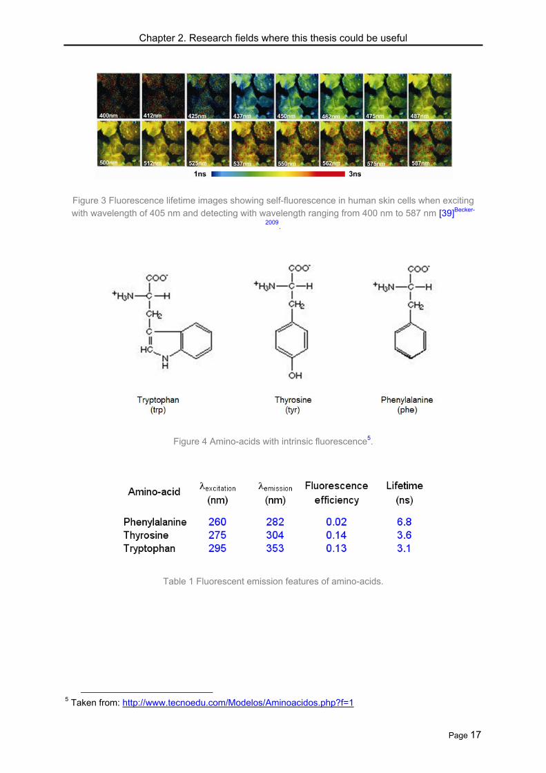
Chapter 2. Research fields where this thesis could be useful
Page 17
Figure 3 Fluorescence lifetime images showing self-fluorescence in human skin cells when exciting with wavelength of 405 nm and detecting with wavelength ranging from 400 nm to 587 nm [39]Becker-
2009.
Figure 4 Amino-acids with intrinsic fluorescence5.
Table 1 Fluorescent emission features of amino-acids.
5 Taken from: http://www.tecnoedu.com/Modelos/Aminoacidos.php?f=1

Chapter 2. Research fields where this thesis could be useful
Page 18
Figure 5 Coenzymes showing self-fluorescence6.
Green Fluorescent Protein (GFP) is a protein produced by the Aequorea Victoria jellyfish
that emits luminescence in the green region of the visible spectrum [35]UniOvi-2002. The gene that encodes this protein is isolated and it is commonly used in molecular biology. In the decade of 1960 Osamu Shimomura, when working with this jellyfish, was able to isolate a calcium-dependent protein emitting in the blue region of the visible spectrum which was called aequorine. During his works he discovered another protein (GFP) emitting green fluorescence when it is illuminated with ultraviolet light [42]Shimomura-2008. Both proteins work together: the jellyfish releases calcium ions that activate the blue emission of the aequorine which is absorbed by the GFP, going to activated state and providing green fluorescence on relaxation. GFP is formed by 238 amino-acid elements grouped in 11 beta-sheets forming a cylinder whose center is occupied by an alfa-helix (see Figure 6). GFP has two exciting peaks at 395 nm and 475 nm and one emission peak at 509 nm [35]UniOvi-2002. Osamu Shimomura, Martin Chalfie and Roger Tsien received the Nobel Price in 2008 for the discovery and development of the GFP.
6 Taken from: http://es.wikipedia.org/wiki/Archivo:NAD%2B_phys.svg and http://educa.madrid.org/

Chapter 2. Research fields where this thesis could be useful
Page 19
(a) (b)
Figure 6 (a) Aequorea Victoria jellyfish7 and (b) molecular structure of the GFP fluorescent protein
[43]Tsien-2008.
2.1.3.2. Extrinsic fluorophores Extrinsic fluorochromes are molecules of design that provide fluorescence. Fluorophore
will be able to link to some type of molecule of biological interest and to reveal useful information thanks to fluorescence emission. They can be used for detecting the presence or location of certain molecules (e.g. labelling the mRNA it is possible to monitor the expression of a certain gene), the degree of interaction between different types of molecules (e.g. antigen-antibody link), the features of a biological medium (e.g. fluorescence changes due to pH or ions concentration), biological membrane evaluation (e.g. fluorescence changes due to changes in the fluidity of the membrane), etc.
Fluorescein (see Figure 7) is a water-soluble yellow dye that generates intense green
fluorescence in alkaline solutions. With pH of 8 fluorescein provides the maximum intensity of fluorescence. This molecule is used for examining the eyeball vascularization by means of a technique known as angiofluoresceinography.
7 Taken from: http://sandwalk.blogspot.com/2009/01/nobel-laureate-osamu-shimomura.html

Chapter 2. Research fields where this thesis could be useful
Page 20
(a) (b)
Figure 7 (a) Molecular structure of the fluorescein8 and (b) its absorption-emission spectra9.
There are certain fluorophores capable to anchor to the cell membrane and to response
to a change in the membrane potential with a variation in the features of the emitted fluorescence (e.g. spectral shift or intensity change). These molecules (molecular weight at about 500 Da, length of about 20 Å [44]Grinvald-2004) are known as voltage sensitive probes and are an unique tool for studying the electrical behavior of cells and the transmission of the action potentials. Some of the most interesting applications of these probes can be found, for example, in the monitorization of myocardiac electric activity [45]Nokáková-2008, [46]Dumas-2005 or in neural connectivity and physiology [44]Grinvald-2004, [47]Zecevic-2003, [48]Chemla-2010. There are two types of voltage sensitive dyes [49]Invitrogen-2010. The fast-response probes suffer changes - directed by electric field - on their intramolecular charge distributions so that spectral shifts or fluorescence intensity variations happen. These molecules are anchored to the surface of the cellular membrane. Meanwhile, slow-response probes are lipophilic anions that suffer a translocation through the membrane by means of an electrophoresis10 mechanism. Changes on fluorescence are associated with redistribution of anions on inner and outer parts of the membrane (see Figure 8).
8 Taken from: http://commons.wikimedia.org/wiki/File:Fluoresceina.png 9 Taken from: http://upload.wikimedia.org/wikipedia/en/8/8a/Fluorescein_spectra.jpg 10 Technique used for separating molecules according to their movility degree in an electric field.

Chapter 2. Research fields where this thesis could be useful
Page 21
Figure 8 Voltage-sensitive fluorescent dyes [49]Invitrogen-2010.
Fluorophores ANEP (Amino - Naphthyl - Ethenyl - Pyridinium) [50]Invitrogen-2006 are one of
the most sensitive and fast voltage-sensitive probes (time response in the order of milliseconds). Di-4-ANEPPS probe anchors rapidly to the cell and it is recommended for short duration experiments. Di-8-ANEPPS is another very common fast probe. Both probes are non-toxic and they show good photostability. Like other fluorophores, ANEP probes are non-fluorescent in water-solutions and they show spectral properties hardly dependent on the micro-environment. For example, in a lipidic layer Di-4-ANEPPS and Di-8-ANEPPS have exciting peaks at wavelengths of 475 nm and 467 nm and emission peaks at wavelengths of 617 nm and 631 nm respectively. The change in the fluorescence intensity for fast-response probes is low, only 2-10 % by each 100 mV of variation in the membrane voltage. However, their response is fast enough for detecting voltage transients in the order of milliseconds in excitable cells (i.e. neurons, cardiac cells, muscle cells). The magnitude of the optical response in slow probes is much higher: they show a typical change in the fluorescence intensity of about 1 % by each mV of variation in the membrane voltage. These probes are recommended for detecting mean variations in the membrane voltage of non-excitable cells (e.g. respiratory activity, ionic channels permeability, bonding of drugs to membrane receptors, etc.).
2.1.4. Techniques based on fluorescence Photon counting allows implementing important experimental techniques based on
fluorescence with application to the biomedical sciences, as those shown following. Thorough and complete discussions about fluorescence techniques can be found in [32]Sauer-
2011 and [36]Lakowicz-2006.

Chapter 2. Research fields where this thesis could be useful
Page 22
TCSPC: Time Correlated Single Photon Counting. TRFS: Time Resolved Fluorescence Spectroscopy. TRPL: Time Resolved Photo Luminescence. TIRF: Total Internal Reflection Fluorescence. FLIM: Fluorescence Lifetime Imaging Microscopy. SMD: Single Molecule Detection. TPFC: Two-Photon Flow Cytometry. FRET: Förster Resonant Energy Transfer. FCS: Fluorescence Correlation Spectroscopy. PRFL: Polarization Resolved Fluorescence Lifetime. TRPD: Time Resolved Phosphorescence Detection. FALI: Fluorophore Assisted Light Inactivation. FLIP: Fluorescence Loss In Photobleaching. FRAP: Fluorescence Recovery After Photobleaching. PFRAP: Polarized Fluorescence Recovery After Photobleaching. FACS: Fluorescence Activated Cell Sorting.
Time-Resolved Fluorescence Spectroscopy (TRFS) are techniques for determining the
fluorescence decay of a sample. Several strategies may be used for this purpose: Time Correlated Single Photon Counting (TCSPC), Gated Photon Counting (GPC) and Multichannel Scaling (MCS) [31]Jiménez-2008. All methods are based on illuminating the fluorescent sample with a periodical optical signal and detecting the generated fluorescence photons. Their working principles are shown in Figure 9. TCSPC is based on detection of, at the most, one photon on each period of exciting signal. That signal is so weak that probability of detecting only one photon in one period is very low. So, in many experiments no photon will be detected and only in some of the experiments one photon will be detected. Probability that several photons were detected in the same period is so low that it may be considered as negligible. On each period the photon arrival time is registered and a counter associated with that time slot is incremented. After a large number of periods (typically > 105) the histogram of arrival times will allow developing the probability density function of the fluorescence phenomenon under study [51]BEC-2008. This approach provides the best temporal resolution (channel width may be of only several ps) at the expenses of higher acquisition times. In GPC, exciting signal intensity is higher so that many fluorescence photons are generated on each experiment. On each period all photons arriving to photodetector inside a shifting temporal window are counted and the counter associated with the location of that window is incremented in many units as photons are detected. The window is shifted along the experiments covering all possible arrival times. Number of experiments for making the fluorescence decay with this approach is much lower than in TCSPC (typically around one hundred) but at the expense of a much lower temporal resolution (about 500 ps). MCS technique, by its own, allows making the fluorescence profile in only one experiment, although the mean of several experiments provides a better result. In this case all photons arriving to photodetector are registered. The time needed for one experiment (one period) is divided into slots and counter for each slot is updated according to the number of photons received in that time interval. Temporal resolution in MCS depends on total dead time in the system and it is normally associated with loss of photons. MSC allows making a fluorescence

Chapter 2. Research fields where this thesis could be useful
Page 23
profile quite precise in a fast way but requiring an high performance system. That is the reason that makes TCSPC the preferred option for TRFS [52]EILtd-2001: the best temporal resolution is obtained assuming a moderated acquisition time and using a system with moderated performance.
Figure 9 Main techniques for measuring fluorescence decay (TRFS) [31]Jiménez-2008.
In Figure 10 the main elements of a typical TCSPC system are shown. The system
behaves as a clock that is controlled with two inputs: the START signal starts the count and the STOP signal stops it. Initially consider that START coincides with the sample exciting optical pulse and that STOP is generated when fluorescence photons are detected (on the contrary that it is shown in Figure 10). Modules CFD (Constant Fraction Discriminator) are able to detect that the signal has reached a predetermined fraction of its maximum amplitude. In this way, the time in which the CFD launches the detection shaped pulse does not depend on the amplitude of the signal provided by the photodetector (that is, the number of detected photons).

Chapter 2. Research fields where this thesis could be useful
Page 24
Figure 10 General layout of a typical TCSPC system11.
START signal (shaped pulse launched by CFD) triggers the TAC module (Time to
Amplitude Converter) and an increasing ramp starts. When STOP signal arrives, the ramp stops so that height of the ramp is directly proportional to the time elapsed between START and STOP. The amplitude reached in the ramp is amplified and digitalized: the ramp amplitude is transformed into a digital word. That word is used for indexing a memory: the memory piece indexed by that word holds the counter for the corresponding time slot. Resolution of the Analog to Digital Converter (ADC) defines the number of time slots in the system (that is, its temporal resolution) [53]EILtd-2000. This is the way how arrival time for all photons may be quantified. After a lot of experiments (many exciting periods) the memory directly contains the histogram that reveals the sample fluorescence decay.
There are two operation modes in TCSPC as shown in Figure 11. In the direct mode,
START is launched by photodetector that senses triggering of exciting pulses. Pulses rate related with this signal is much higher than the one corresponding to random pulses coming from fluorescence photodetector and that generate the STOP signal. Then TAC module is activated in all exciting cycles and, because one fluorescence photon arrival is anecdotal, TAC resetting due to saturation is a continuous operation to be done. Electronics is busy much more time than necessary and it could limit the reachable counts rate. This situation may be avoided with the inverse mode (START and STOP are exchanged). In this case, START has the lowest rate, the TAC module only activates when one fluorescence photon has been detected. Drawback in this mode is that it is mandatory to apply a fix and long delay to reference pulses so that they reach TAC later than fluorescence pulses.
Integration of TCSPC systems on scanning microscopes has allowed the development of
Fluorescence Lifetime Imaging Microscopy (FLIM) [54]BEC-2008. In [55]Becker-2001 it is described a TCSPC system that implements FLIM through a laser scanning microscope. TCSPC module and the scanning head of the microscope provide, for each received photon, its arrival time and the location inside the scanned area in which it was generated. The result may be interpreted as a two-dimensional matrix of fluorescence decay curves or as a sequence of fluorescence images for several instants after the exciting pulse. [19]Knemeyer-2007 and [56]Tinnefeld-2001 describe a FLIM system for intracellular level molecular investigation. With this
11 Taken from: http://microscopy.tw/molweb/experiment/MOL_FLIM_FRET/FLIMofPrinciple.html

Chapter 2. Research fields where this thesis could be useful
Page 25
system authors are able to detect mRNA chains during protein manufacturing in cellular cytoplasm (see Figure 12). There are several manufacturers that provide systems for making TCSPC, FLIM and other fluorescence techniques, as for example, PicoQuant12, Becker & & Hickl GmbH13, Horiba Scientific14 or SciMedia15.
Figure 11 Operation modes in TCSPC [53]EILtd-2000.
Figure 12 mRNA monitorization by means of FLIM [19]Knemeyer-2007.
12 PicoQuant: http://www.picoquant.com/ 13 Becker & Hickl: http://www.becker-hickl.de/products_new.htm 14 Horiba Scientific: http://www.horiba.com/scientific/products/fluorescence- spectroscopy/lifetime/tcspc-components/ 15 SciMedia: http://www.scimedia.com/

Chapter 2. Research fields where this thesis could be useful
Page 26
Förster Resonance Energy Transfer (FRET) consists typically on the transference of energy between a donor fluorophore and a near acceptor fluorophore which has an exciting spectrum that overlaps with the donor emission spectrum (see Figure 13). In most applications, both donor and acceptor are fluorescent molecules and energy transfer is manifested as a reduction in the donor fluorescence intensity and lifetime together with an increase in the acceptor fluorescence intensity [39]Becker-2009, [57]Nikon-2010.
Figure 13 Overlapping of donor emission and acceptor excitation spectra in FRET [57]Nikon-2010.
Detection of fluorescence in the acceptor emission wavelength range indicates that
resonant energy transfer has happened. This process may be useful for detecting when two molecular types (proteins, nucleic acids, etc) are in contact which may provide important physiologic or metabolic information. Also it is possible to see when a doubly fluoro-labelled molecule is hydrolysed. When the molecule is broken, donor and acceptor are separated so that acceptor fluorescence intensity reduces whereas donor fluorescence intensity increases. In [58]Koberling-2004 FRET is applied to the analysis of free diffusion of poly-peptides in water. Other authors uses FRET for implementing FLIM due to the fact that the presence of the acceptor reduces donor fluorescence lifetime [59]Lakowicz-1994, [60]Elangovan-2002. In [61]Duncan-2004 authors uses a multi-dimensional TCSPC system for realizing FLIM and where FRET on a medium charged with cyan and yellow fluorescent proteins is quantified. Another example can be found in [62]Fruhwirth-2010 where authors use TCSPC for registering fluorescence lifetime and for measuring FRET with an endoscopic methodology.
Active techniques in which the sample under study is altered are also possible using
fluorescence. Fluorophore Assisted Light Inactivation (FALI) is a technique that inactivates specific proteins for a period from seconds to minutes using coherent of diffuse light [63]Guo-
2006. In FALI, a fluorophore is bonded to the target protein directly or through an intermediate molecule. After Fluorophore illumination it transfers energy to molecular oxygen which generates highly reactive species in the medium (oxygen in singlet state, 1O2). These species react with amino-acids near fluorophore providing a functional inactivation of the target protein [64]Davies-2003. Fluorescence Recovery After Photobleaching (FRAP) is a technique used in fluorescence microscopy for examining molecule diffusion in biological

Chapter 2. Research fields where this thesis could be useful
Page 27
membranes. It has been used, for example, for characterizing the mobility degree of lipids on the cell membrane [65]Axelrod-1976. Consider that the cell membrane has been uniformly labelled with a fluorescent dye. Photobleaching16 is induced over a certain region through a fast and intense light pulse. Fluorescence monitoring along time in that region allows observing a gradual recovery on emission intensity. That recovery is directly related with input of non-bleached molecules in the region and with output of bleached molecules from the region. That is, fluorescence intensity recovery time is directly proportional to membrane rigidity [66]Sprague-2004. Also, an static structure can be discovered if original fluorescence intensity is not completely recovered.
There are more techniques for analyzing molecular diffusion using fluorescence. In Time-
Resolved Fluorescence Anisotropy (TRFA) the polarized emission of a fluorophore previously excited with polarized light is exploited. The depolarization degree of that fluorescent emission (also known as fluorescence anisotropy) depends directly on the rotational diffusion degree of the fluoro-labelled molecule. And that diffusivity is a function of the molecular size and viscosity in the environment [67]Yvon-2007, [68]Suhling-2004. In [67]Yvon-2007 several biomedical uses of the fluorescence anisotropy are discussed. For example, it is possible to identify the instant in which a fluoro-labelled RNA chain is broken by the action of a ribonuclease enzyme. Also, phase transitions depending on temperature can be seen on a lipid membrane or an estimation of the cellular cytoplasm viscosity can be done by registering fluorescence depolarization. Another technique for studying molecular diffusion is known as Fluorescence Correlation Spectroscopy (FCS). In this technique, the self-
correlation function indicates the probability of detecting one photon at instant t+ when one photon has been already detected at instant t. If the volume under study is small and the fluorophore concentration is low, the registered fluorescence intensity will be highly oscillating along time. It is due to the continuous input and output of fluorophores in the analysed volume. When a tagged molecule is inside the detection volume there is high probability to detect consecutive fluorescence photons coming from that molecule. That is, the fluorescence signal is highly time self-correlated. Thus, self-correlation signal reduces when tagged molecules tends to leave the detection volume (i.e. as the time is higher). The higher the diffusion of tagged molecules the faster the fluorescence self-correlation is lost. Any process that modifies the diffusion coefficient could be analysed with FCS technique [69]Dertinger-2011, [70]Buschmann-2009. Fluorescence correlation spectra may be obtained through hardware correlators or by registering single photon arrival times with TCSPC and by calculating FCS curves with specific software tools.
2.1.5. Biomedical applications of fluorescence Previously described fluorescence techniques and others have highly contributed to the
progress in biochemistry, molecular biology and biomedicine. In Analytical Chemistry it is possible to detect fluorescence for separating compounds using techniques as High Performance Liquid Chromatography (HPLC) and Thin Layer Chromatography (TLC). In
16 Photochemical destruction of fluorophores in that region.
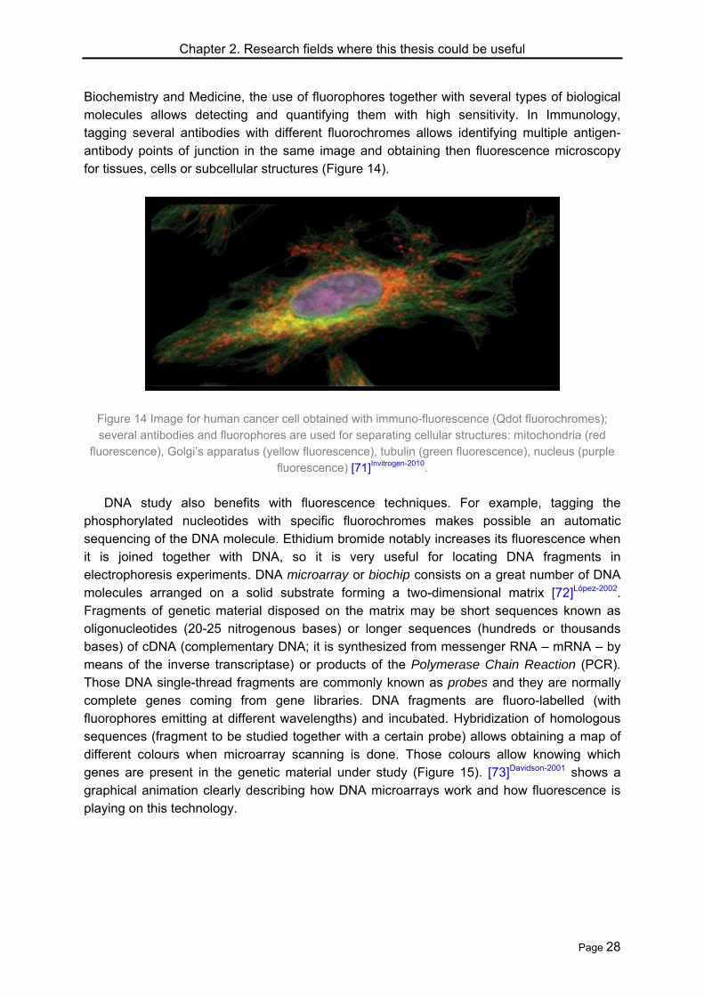
Chapter 2. Research fields where this thesis could be useful
Page 28
Biochemistry and Medicine, the use of fluorophores together with several types of biological molecules allows detecting and quantifying them with high sensitivity. In Immunology, tagging several antibodies with different fluorochromes allows identifying multiple antigen-antibody points of junction in the same image and obtaining then fluorescence microscopy for tissues, cells or subcellular structures (Figure 14).
Figure 14 Image for human cancer cell obtained with immuno-fluorescence (Qdot fluorochromes); several antibodies and fluorophores are used for separating cellular structures: mitochondria (red
fluorescence), Golgi’s apparatus (yellow fluorescence), tubulin (green fluorescence), nucleus (purple fluorescence) [71]Invitrogen-2010.
DNA study also benefits with fluorescence techniques. For example, tagging the
phosphorylated nucleotides with specific fluorochromes makes possible an automatic sequencing of the DNA molecule. Ethidium bromide notably increases its fluorescence when it is joined together with DNA, so it is very useful for locating DNA fragments in electrophoresis experiments. DNA microarray or biochip consists on a great number of DNA molecules arranged on a solid substrate forming a two-dimensional matrix [72]López-2002. Fragments of genetic material disposed on the matrix may be short sequences known as oligonucleotides (20-25 nitrogenous bases) or longer sequences (hundreds or thousands bases) of cDNA (complementary DNA; it is synthesized from messenger RNA – mRNA – by means of the inverse transcriptase) or products of the Polymerase Chain Reaction (PCR). Those DNA single-thread fragments are commonly known as probes and they are normally complete genes coming from gene libraries. DNA fragments are fluoro-labelled (with fluorophores emitting at different wavelengths) and incubated. Hybridization of homologous sequences (fragment to be studied together with a certain probe) allows obtaining a map of different colours when microarray scanning is done. Those colours allow knowing which genes are present in the genetic material under study (Figure 15). [73]Davidson-2001 shows a graphical animation clearly describing how DNA microarrays work and how fluorescence is playing on this technology.

Chapter 2. Research fields where this thesis could be useful
Page 29
Figure 15 DNA microarray based on fluorescence [73]Davidson-2001.
Nowadays there are a number of techniques based on fluorescence usually used on
biochemistry, biology, medicine and other related sciences. Many of them are based on using fluorescence microscopes (Figure 16). These instruments use high intensity light sources (mercury or xenon lamps, LEDs, lasers) for inducing fluorescence on samples under study. Using optical filters it is possible to separate the emitted fluorescence light from the light used for exciting the sample. A two-dimensional scanning system and a registering camera allows generating fluorescence microscopy images.
(a) (b)
Figure 16 (a) Fluorescence microscope fundamentals and (b) fluorescence microscope model
Olympus BX61.
Because fluorescence microscopes are complex and expensive instruments, some
researchers still prefer to implement their own and easier fluorescence imaging systems, however obtaining good results. For example, in [20]Tkaczyk-2008 a two-channel cytometry

Chapter 2. Research fields where this thesis could be useful
Page 30
system (see Figure 17) is proposed for in vivo quantifying of two different flowing cancer cell populations under time-varying physiological conditions. In Figure 18 fluorescence intensity images obtained with that system for both cellular types are shown.
Figure 17 Experimental setup for studying cell kinetics by fluorescence [20]Tkaczyk-2008.
Figure 18 Fluorescence intensity images for two cancer cell types (MCF-7 and MDA-MB-435) after 48 hours from being incorporated to the living organism [20]Tkaczyk-2008.

Chapter 2. Research fields where this thesis could be useful
Page 31
2.2. Gamma-ray astronomy
2.2.1. From cosmic rays to Cherenkov telescopes V. F. Hess in 1911 discovered the existence of an extraterrestrial source of ionizing
radiation, later confirmed by Millikan in 1921 who gave it the name of Cosmic Rays. Millikan proposed that this radiation should be formed by high energy gamma-rays, but in 1927 Clay demonstrated that cosmic rays were mainly composed by charged particles (this radiation is influenced by the Earth's magnetic field). In the decade of 1930 atmospheric showers were discovered. When cosmic rays interact with particles in the atmosphere secondary particles are generated which produce new interactions. So, showers of particles are created by the incidence of cosmic rays [74]Antoranz-2009.
The development of the spatial career in the decade of 1960 made possible that
instruments for investigating cosmic rays were boarded on satellites. This way, extra-atmospheric cosmic rays research could be done. Several discoveries rapidly arrived. In 1967, satellites of Vella Network detected the first gamma ray bust in the history. In 1972, the OSO-VII17 discovered spectral lines of annihilation (511 MeV) and nuclear interactions at 4.4 MeV and 6.1 MeV in the solar flares. At that time, diffuse cosmic ray background was also discovered. The french SIGMA experiment18 discovered around 30 sources in the central region of our galaxy emitting in the range between X rays and gamma rays (30 keV - 1 MeV). The American EGRET experiment19 was able to detect more than 270 gamma ray sources in a range between 30 MeV and 30 GeV [75]Fichtel-1994.
However, the study of cosmic rays from the Earth's surface remained interesting for
scientists. The atmosphere plays an important role on transmission of cosmic rays up to the Earth's surface: cosmic rays are attenuated and the flux is severely reduced at ground level. In these conditions, the only way to study gamma-ray sources is by means of the showers of particles created by the interaction of cosmic rays with the particles in the atmosphere. However, it is difficult to distinguish between the showers produced by charged particles and the showers produced by gamma rays. The first ones provide no useful information about the source of the radiation due to the interaction of charged particles with the Earth's magnetic field. However, because of gamma rays conserve the original trajectory from the source to the detector, they provide information to astrophysicist for investigating cosmic objects. Cherenkov radiation produced in the showers allowed that Hillas, in 1985, developed a method for distinguishing both types of phenomena [76]Hillas-1985. The shape created by the Cherenkov light on the telescope makes possible to discriminate the type of particle that initiated the interaction. Thus, all interactions initiated by charged particles can be easily rejected. This discovery led to the evolution of the Imaging Air Cherenkov Telescopes (IACTs). The first IACT was Whipple, with a 10 m reflector and covering an energy detection
17 Orbital Solar Observatory: http://heasarc.nasa.gov/docs/oso7/oso7.html 18 Système d'Imagerie Gamma à Masque Alèatoire http://hea.iki.rssi.ru/en/index.php?page=sigma 19 Energetic Gamma Ray Experiment Telescope: http://heasarc.gsfc.nasa.gov/docs/cgro/cossc/cgro/egret.html

Chapter 2. Research fields where this thesis could be useful
Page 32
range from 100 GeV to 10 TeV. Since then, several more IACTs have been implemented: Cangaroo20 in Australia, VERITAS21 in the United States, HESS22 in Namibia and MAGIC23 in Spain. MAGIC collaboration treated to construct the biggest and fastest telescope possible. The result was a fast-moving telescope with a 17 m reflector and energy range up to tens of GeV (see Figure 19). The CTA24 project, currently under development, proposes arrays of telescopes in both hemispheres for exploring galactic and extragalactic sources within an energy range from 10 GeV up to 100 TeV25.
Figure 19 MAGIC telescopes at the Roque de Los Muchachos Observatory (La Palma, Spain)26. Mirrors have a diameter of 17 m and a surface of about 240 m2.
2.2.2. Cherenkov radiation When a gamma-ray interacts with an atomic nucleus in the atmosphere, the pair creation
phenomena happens. Both new particles (electron and positron) lose a fraction of kinetic energy by Bremsstrahlung when they interact with the electric field of the nuclei with which they collide. Those interactions generate new lower energy gamma rays that can start again the process (see Figure 20 (a)). The shower finished when the generated gamma rays have so low energy that they cannot produce new pairs (energy threshold at 1.02 MeV). Charged particles in these showers are able to cause the emission of Cherenkov radiation (see Figure 20 (b)). In the late XIX century O. Heaviside predicted that a particle passing through a medium faster than the speed of light in that medium ought to emit radiation. Cherenkov radiation was first observed by Mary and Pierre Curie at the beginning of the XX century
20 Collaboration of Australia and Nippon for a GAmma Ray Observatory in the Outback: http://icrhp9.icrr.u-tokyo.ac.jp/ 21 Very Energetic Radiation Imaging Telescope Array System: http://veritas.sao.arizona.edu/ 22 High Energy Stereoscopic System:http://www.mpi-hd.mpg.de/hfm/HESS/pages/about/telescopes/ 23 Major Atmospheric Gamma-Ray Imaging Cherenkov Telescopes:
http://magic.mppmu.mpg.de/gallery/index.html 24 Cherenkov Telescope Array: http://www.cta-observatory.org/ 25 A complete list with references for cosmic ray, gamma ray, neutrino and similar experiments can
be found in: http://www.mpi-hd.mpg.de/hfm/CosmicRay/CosmicRaySites.html 26 Taken from: http://magic.mppmu.mpg.de/gallery/pictures/

Chapter 2. Research fields where this thesis could be useful
Page 33
when they began their research on radioactivity, but they were not able to explain its nature [77]Watson-2010. In the decade of 1930, the experimental works of P. A. Cherenkov and S.I. Wawilow [78]Bolotovskii-2009 and the theoretical interpretation of I. E. Tamm and I. M. Frank [79]Tamm-1937, [80]Tamm-1939 allowed a complete characterization of the phenomenon. Cherenkov, Frank and Tamm share the Nobel Price in Physics in 1958 for their contributions to explain this new type of luminescence [81]Cherenkov-1958, [82]Tamm-1958, [83]Frank-1958. In 1953, Galbraith and Jelley registered light pulses from the night sky for the first time in the history. This event inaugurates the search for Cherenkov radiation in the atmosphere.
(a) (b)
Figure 20 Schematic representation of atmospheric showers created by (a) a gamma-ray and (b) a
charged particle [74]Antoranz-2009.
Cherenkov radiation is an electromagnetic radiation emitted when a charged particle
travels in a dielectric medium with a velocity higher than the phase velocity of light in that medium. It is well known that the theory of relativity says that the speed of light in vacuum (c
3·108 m·s-1) is the upper limit of velocity for any entity. However, the speed at which light
propagates in a material may be significantly lower than c, because it depends on the refractive index of the medium (vmedium = c/n). On the other hand, matter can be accelerated beyond this speed (but always lower than c) during, for example, nuclear reactions. The electromagnetic field of the moving charged particle excites atoms in the medium which turn back to their ground state once the disturbing particle has passed. In that relaxation, atoms of the material release photons in the blue-ultraviolet range of wavelengths. In normal circumstances these photons destructively interfere with each other and no radiation can be detected. However, when the charged particle that causes disruption of the local electromagnetic field travels with speed higher than the velocity of light in that medium, emitted photons constructively interfere. The process can be compared with the sonic boom caused by a bullet or a supersonic aircraft.

Chapter 2. Research fields where this thesis could be useful
Page 34
Consider that the charged particle is moving in the medium of diffractive index n() with a
velocity vparticle higher than the velocity of generated light waves vemission = c/n(). It is
common to refer the velocity of the particle to the velocity of light in vacuum ( = vparticle / c).
Then, the parameter is lower than the unity. It is verified the following relation:
ccvncv particleemission )(/ (5)
At a certain time t, the particle has travelled a distance xparticle and a certain wave front
has advanced a distance xemission.
tn
ctvx
tctvx
emissionemission
particleparticle
)(
(6)
In all positions along the distance xparticle light waves are released, their wave-fronts
overlap and constructive interference is possible at a certain angle when all waves add coherently (Figure 21 (a)). Interference generates a shock wave that propagates in a
direction forming an angle with the propagation direction of the particle [84]Cherenkov-1937 (see
Figure 21 (b)).
)(
1)(cos
ntc
tn
c
x
x
particle
emission
(7)
(a) (b) Figure 21 (a) Cherenkov wave front generation by coherence27. (b) Geometry of the Cherenkov
radiation problem [74]Antoranz-2009.
27 Taken from: http://scientopia.org/blogs/skullsinthestars/2009/11/20/reversing-optical-shockwaves-
using-metamaterials/
Chapter 2. Research fields where this thesis could be useful
Page 35
Cherenkov radiation happens in a cone behind the particle defined by the angle T given
by the following expression:
)(
1arccos22
222
nT (8)
Equation (7) has several implications [85]Oña-2001. First, there is a threshold velocity below
which no radiation takes place. At this critical velocity the direction of the radiation coincides
with the direction of the particle ( = 0).
)()(
11
)(
1cos0 min,min
n
cv
nn particle
(9)
Second, radiation in restricted to the wavelength range for which n() > 1 (visible and
near visible regions of the spectrum). For getting radiation it must be satisfied that cos() < 1,
so taking into account that < 1:
11
)(1)(
1cos
1|
nn
(10)
For getting coherence two other conditions must be satisfied. On the one hand, and for
avoiding that diffraction effects become dominant, the length of the track of the particle in the medium must be larger than the wavelength of the radiation. On the other hand, the velocity of the particle must be constant during its passage through the medium. Since a non-accelerated charged particle does not irradiate, the radiation generated in these conditions cannot be originated by the particle. That is, the radiation must have its origin in the medium which is being disturbed by the moving particle. So, it is clear that this type of radiation is different from Bremsstrahlung, where radiation is released by the particle when it is being decelerated in the medium [85]Oña-2001. The radiated energy per unit length of path is given by the Frank and Tamm formula:
1
222
2 11
n
dnc
e
dl
dE
(11)
The condition ·n > 1 is equivalent to vparticle > c/n. This equation can be expressed in an
alternative way:
1223
2
1223
2
2
2
1222
2
2
1)(
112
)(
11
12
)(
11;2;22
nn
n
dn
edn
cc
e
dnc
e
dl
dEd
cd
c
(12)

Chapter 2. Research fields where this thesis could be useful
Page 36
This result says that the Cherenkov spectrum is proportional to 1/3, which implies that it
increases in the direction of short wavelengths [81]Cherenkov-1958. However, the atmospheric absorption (Figure 22 (a)) modulates this spectrum leading to a peak at about 330 nm for low altitudes [86]Döring-2001 (Figure 22 (b)). Unlike fluorescence spectra, Cherenkov radiation does not have characteristic peaks, but it is a continuous radiation.
(a)
(b)
Figure 22 Atmospheric transmittance up to a wavelength of 3 m (a)28. It is possible to observe that
combination of the atmospheric transmittance curve and the pattern of the Cherenkov radiated energy in the high atmosphere (red trace) provides the spectrum shown in (b) for Cherenkov radiation near
surface [74]Antoranz-2009.
This is the reason that explains that Cherenkov radiation was mainly concentrated in the
ultraviolet and visible blue region of the electromagnetic spectrum (see Figure 23).
28 Taken from: http://speclab.cr.usgs.gov/PAPERS.refl-mrs/giff/300dpi/fig3a3.gif

Chapter 2. Research fields where this thesis could be useful
Page 37
(a) (b)
Figure 23 Cherenkov radiation. (a) Fuel assemblies cooled in a water pond at the french nuclear complex at La Hague29. (b) Cherenkov radiation glowing in the core of the Advanced Test Reactor at
the Idaho National Laboratory30.
The Cherenkov light generated by a gamma ray induced shower is of low intensity (only
hundreds of photons per square meter) and of very short duration (the wave front lasts between one to several nanoseconds, depending on the particle originating the shower). An scheme of the process can be seen in Figure 24.
Figure 24 Cherenkov light wave fronts originated during an atmospheric shower induced by cosmic rays31.
29 Taken from: http://spectrum.ieee.org/energy/nuclear/nuclear-wasteland 30 Taken from: http://www.telegraph.co.uk/science/6546462/The-10-weirdest-physics-facts-from-
relativity-to-quantum-physics.html 31 Taken from: http://astrum.frm.utn.edu.ar/CTA-Argentina/?p=1001

Chapter 2. Research fields where this thesis could be useful
Page 38
2.2.3. Instruments for detecting Cherenkov radiation Thus, to detect a light flash of these characteristics, IACTs must use very sensitive and
fast photodetectors. The light produced by the shower is reflected by the mirror of the telescope and focused into the camera (i.e. the arrange of photodetectors). By analyzing the properties of the elliptical shapes formed by the Cherenkov light it is possible to extract information about the associated atmospheric shower (see Figure 25).
Figure 25 Cherenkov light formes elliptical shapes in the IACT camera whose parameters are related with the shower induced by cosmic rays [74]Antoranz-2009.
Some instruments were used for detecting cosmic rays prior to the development of the
PMT, such as the electroscope, the Geiger counter or the cloud chamber [87]DasGupta-1946. However, the photomultiplier has been the most successful and important photodetector used in experimental particle physics. Even nowadays is the common light detector used in all IACT experiments. Although the time resolution of the PMT is as low as several nanoseconds, its capability for resolving single photons is quite limited. The development of Solid State Physics in the second half of the XX century allowed that new photodetectors based on Silicon and Germanium were made. As it will be shown in next chapters, these structures have evolved from the first photoconductors up to the avalanche photodetectors (APDs) and the very sensitive and promising Geiger-mode APDs (GAPDs) also known as Silicon Photomultipliers (SiPMs). SiPMs are very high sensitive devices that allow much better photon counting capability than PMTs. However, they have several drawbacks for using as detectors in IACTs, like high darkcount rates, optical crosstalk between pixels and very small detection areas. One attempt to combine advantages of PMTs and APDs is the Hybrid Photon Detector (HPD) [88]D'Ambrosio-2003, [89]Ferenc-2000. Photoelectrons generated in a photocathode (included in a vacuum tube) are accelerated and focused on an APD. On the one hand, these devices have much better energy resolution and sensitivity than PMTs. Also, they have detection areas bigger than solid state devices and time response comparable to PMTs. On the other hand, they show many drawbacks: ageing of the photocathode, high rates of afterpulses and darkcounts, high dependence on temperature, etc. Some attempts to use these devices in MAGIC telescopes have been recently done

Chapter 2. Research fields where this thesis could be useful
Page 39
[90]Saito-2009. Figure 26 shows a comparison of the energy resolution for the previously mentioned photodetectors.
(a)
(b) (c)
Figure 26 Comparing energy resolution of modern photodetectors. (a) PMT model Electron Tubes ET 9116A [91]Ostankov-2000. (b) HPD model R9792U-40 [92]Saito-2007. (c) SiPM model Hamamatsu S10362-
11-025U [16]Hamamatsu-2009.
2.2.4. MAGIC telescopes: the success of the PMT An example of the success of PMTs in astroparticle physics can be seen in MAGIC
telescopes. The camera of MAGIC I telescope (see Figure 27 (a)) is composed of 577 photomultipliers arranged in two patterns. The inner part is composed of 397 photomultipliers model Electron Tubes ET9116A, each one with 1 inch diameter and 0.1 º field of view. The outer part is composed of 180 photomultipliers model Electron Tubes ET9117A, each one with 1.5 inches diameter and 0.2 º field of view. The total field of view of the camera is about 3.5 º. The photocathode is optimized for the blue region of the spectrum (quantum efficiency

Chapter 2. Research fields where this thesis could be useful
Page 40
peaks 25 % at a wavelength of 350 nm). On top of each PMT a Winston cone is used for maximizing the detecting area of the camera. Front and bottom parts of the MAGIC I camera can be seen in Figure 28.
(a) (b)
Figure 27 Camera structure for (a) MAGIC I and (b) MAGIC II. Details of the photomultipliers tubes
used in these cameras are shown [74]Antoranz-2009.
(a) (b)
Figure 28 Front (a) and (b) bottom of the MAGIC I camera32. The total weight of the camera is about 500 kg.
32 Taken from: http://magic.mppmu.mpg.de/gallery/pictures/

Chapter 2. Research fields where this thesis could be useful
Page 41
The camera in MAGIC II has a different design (see Figure 27 (b)). The size and field of view are the same than in MAGIC I, but in this case there are 1039 identical PMTs (model Hamamatsu R10408, which provides a maximum quantum efficiency at about 35 %). The pixels are grouped in clusters of seven units. These clusters can be extracted independently, thus increasing the modularity of the system. Also, a big cooling plate is in contact with every cluster to refrigerate it and reduce noise.
2.2.5. FACT telescope: the success of the SiPM However, nowadays SiPMs are the most promising tools for enhancing the features of
the IACTs [93]Otte-2008, [94]Biland-2008. In October 2011, the First G-APD Cherenkov Telescope33 (FACT) recorded flashes of Cherenkov light from atmospheric showers induced by cosmic rays. Some examples are shown in Figure 29.
Figure 29 Random showers recorded during the night of November 1, 2011 with the FACT telescope34.
The camera of FACT consists on 1440 SiPMs model Hamamatsu S10362-33-050C (size of 3 x 3 mm2) grouped in clusters of 9 devices (see Figure 30 (a)). To better concentrate the light reflected by the telescope mirror, rejecting at the same time background light from outside the mirror area (9.5 m2) solid light concentrators were coupled to all SiPMs. The entrance window of each cone has hexagonal shape with a diameter of 9.5 mm and a square exit window of 2.8 x 2.8 mm2 (see Figure 30 (b)). The field of view for each SiPM is 0.1 º and a field of view of 4.5 º was achieved for the whole camera. FACT was installed on the Roque de los Muchachos Observatory (La Palma, Spain) at an altitude of 2200 m, next to the MAGIC telescopes and demonstrates that SiPMs are a viable alternative to PMTs in Cherenkov telescopes (Figure 31).
33 Impressions from FACT: http://fact.ethz.ch/first/ 34 Taken from: http://fact.ethz.ch/first/

Chapter 2. Research fields where this thesis could be useful
Page 42
(a)
(b)
Figure 30 (a) FACT camera during its testing. (b) Single SiPM (pixel) glued to its light concentrator35.
Figure 31 FACT telescope at the Roque de Los Muchachos Observatory (La Palma, Spain)14.
35 Taken from: http://fact.ethz.ch/first/

Chapter 3. Photodetectors
Page 43
3. Photodetectors
3.1. Introduction This chapter presents a revision of the main photodetectors used for long before the
development of SiPMs. This study follows a historical perspective and takes into account the evolution in complexity and performance.
The study starts with the photodetector most widely used when high sensitivity and high
speed light measurements are needed: the photomultiplier tube. A revision of the main solid state photodetectors follows, starting with the photoconductor device. A discussion about the first photodiode (PIN) opens the way to the very important avalanche photodetector (APD) which is the heart of the very promising SiPM. Finally, the Schottky barrier is discussed because it is a very interesting structure that provides versatility for working in a wide range of wavelengths by combining different working modes.
Other photodetectors successfully used during decades in the important field of
thermographic and infrared imaging are not included in this study. However, they deserve some lines here not only because of their relevance, but also because they are closely related to relevant work previously made by the author of this thesis during several years.
Thermic detectors as bolometers, photoconductor and photovoltaic detectors based on
PbSe, PbS, InSb, HgCdTe, GaP and GaAs and quantum well devices with structures GaAs/AlGaAs have led to very sensitive and powerful thermographic imaging devices [95]Dereniak-1996-[101]Jha-2000. These infrared cameras are extensively used for building maintenance, industrial inspection, development of non-destructive assays and even biomedical purposes. The author of this thesis has developed some work related with calibration of infrared cameras and their use for making radiometry studies. Also, a complete system using infrared cameras was designed and implemented by him with the purpose of providing a methodology for the inspection, evaluation and certification of thermal blankets used for repairing aeronautic pieces. This system includes the calibration of the camera and the development of a software for controlling the camera and for getting, managing and processing the images in order to do an automatic thermal analysis that provides a very fast and easy to do blanket certification process. This system was first patented in Spain [102]López and Yebras et al-2006, and the patent was subsequently extended to the whole European space [103]López andYebras et al-2005 and to the United States of America [104]López and Yebras et al-2008. The author of this thesis also applied infrared techniques for analyzing flames and combustions [105]Aranda-2003, for remote gases detection [106]Yebras-2003 and for discovering faults in ducts and tanks by means of gas leaks [107]Yebras-2003. All this experience gave the author a basic knowledge on photodetection and its applications, which was useful for developing the work presented in this thesis and for finding future applications for it.

Chapter 3. Photodetectors
Page 44
3.2. Photomultipliers The photomultiplier tube (PMT) has probably been the most commonly used high
sensitivity photodetector since decades. There is no doubt about its importance for developing low light intensity detection: description and study of these devices is done in many classical references [108]Leo-1987, [109]Knoll-1979, [110]Cherry-1980. They have been for a long time the most important detector in many different scientific fields: nuclear and particle physics (e.g. the use of PMTs with scintillator materials is a standard in nuclear experiments), high energy physics, astrophysics, nuclear medicine, fluorescence spectroscopy, etc.
The photomultiplier is formed from a vacuum tube with a photocathode at the entrance
followed by a series of dynodes arranged prior to the final anode (Figure 32).
Figure 32 Internal structure and working fundamentals of the photomultiplier tube. (taken from http://learn.hamamatsu.com/articles/photomultipliers.html)
Figure 33 shows several models of photomultipliers tubes where it is possible to see
certain details of the inner structure. The PMT is able to detect light at varying wavelengths depending on the material of the photocathode. Normally it is formed by a thin layer of alkali metal compounds and several elements in group V. When photocathode is fabricated from InGaAs it is possible to extend the spectrum of operation up to near-infrared wavelength
(1700 nm). Each dynode is biased to a higher positive potential than the preceding one. So,
there is an increasing electric field along the structure (i.e. the electric field existent between dynodes n-1 and n is lower than the one between dynodes n and n+1). When a photon impacts on the photocathode, a photoelectron is released. The electric field created between photocathode and the first anode accelerates the electron and forces its impact on the dynode. This process releases more electrons that are again accelerated and oriented towards the second dynode. The process is repeated through the rest of dynodes in the structure. Each dynode generated more electrons than the preceding one. The final result is that a great number of electrons arrive to the anode: one only photon has caused that up to
millions of electrons reach the anode. If is the electron emission coefficient for each

Chapter 3. Photodetectors
Page 45
dynode (i.e. the mean number of electrons generated as a consequence of the impact of one electron in the dynode) and there are N dynodes in the structure, then the multiplication
factor provided by the photomultiplier is M = N, where typical values are = 4, N = 10 and
M104-107 [111]Buller-2010.
(a) (b) (c)
Figure 33 Photomultiplier tubes. (a) Hamamatsu R928, QE: 25 % @ 260 nm36; (b) Hamamatsu
R1463-03, QE: 19 % @ 290nm37; (c) ETL 9357 KFLB, QE: 18 % @ 420 nm38.
Afterpulsing is caused in PMTs by ion feedback or by luminescence in dynodes and the
glass of the tube. A charged particle can go back to a previous dynode and retrigger the device with an additional electronic multiplication. Also, photons originated in dynodes or in the glass can travel and impact on other dynodes or in the photocathode and retrigger the chain reaction. The result output signal is not a single pulse but a pulse with one main peak and one or several false detection peaks. The PMT can also be triggered in darkness, when no photon has been detected. Darkcounts are normally generated by thermionic generation and typical darkcounts rates are in the order of kHz or even MHz. Cooling is the best option for reducing darkcounts influence.
The large area photocathode in PMTs are an advantage for collecting light coming from
extended optical sources. This area may be even 1000 times larger than in semiconductor photon detectors. However, PMT have several drawbacks: large physical packages, poor mechanical stability, very high bias voltages (typically in the order of kV), low single photon detection efficiency (lower than 10 %; see Figure 34), relatively high timing jitter (typically 1 ns; time delay between reception of a photon and the appearance of the detection pulse), danger of permanent damage when the device is accidentally illuminated, strong influence on its behavior in the presence of external magnetic fields, etc.
36 Taken from: http://www.decadecounter.com/vta/tubepage.php?item=26 37 Taken from: http://www.electricstuff.co.uk/Photocell.html 38 Taken from: http://cafpe10.ugr.es/cafpe_new/LaboratoryResults/PMTs-criogenia.html

Chapter 3. Photodetectors
Page 46
Figure 34 Quantum efficiency for three Hamamatsu photomultipliers [111]Buller-2010.
There is a variant of PMT technology known as Microchannel Plates (MCP), which is an
array of thin glass capillaries (diameter10 m) arranged into a disc (see Figure 35). The inner wall of each capillary is coated with a photo-emissive material. Biasing each capillary at both ends it acts as a continuous dynode [111]Buller-2010. That is, MCP would be an array of multiple little PMTs. MCPs need bias voltage in the order 1-3 kV but they do not provide such high multiplication factors as conventional PMTs. Experiments developed by Becker [112]Becker-2005 show that some MCP do not exhibit any afterpulsing effects at timescales of up to 150 ns and that quite low timing jitter can be obtained (20-30 ps) [113]Becker-2002. These devices could be useful for certain imaging systems (e.g. image intensifiers) or for time-of-flight laser-ranging systems [111]Buller-2010.
Figure 35 Microchannel plate (MCP) schematic and working fundamentals [111]Buller-2010.
Solid state technologies have evolved a lot in recent decades and the development of
new high sensitivity semiconductor devices is a reality nowadays. In fact, current Silicon

Chapter 3. Photodetectors
Page 47
Photomultipliers (SiPMs) are replacing PMTs in many fields, and probably, they will not have rival in a next future. Along the way towards SiPM several important devices can be discovered. In the following paragraphs a description and study of the behavior and features of several of them is offered. Next chapter will be dedicated to the study of the silicon photomultipliers, which are the target photodetectors of this work.
3.3. Photoconductors
3.3.1. Working principles Photoconductive are the photodetectors with the simplest structure. Two electrodes are
anchored to the semiconductor and also connected to an external battery. Impinging photons are absorbed in the semiconductor generating electron-hole pairs (Figure 36). The result is an increment on the semiconductor conductivity and, as a consequence, an increment on the external photocurrent (Iph). Electrons have higher mobility than holes and it is the cause that several electrons penetrates the material from the negative electrode and cross and leave it towards the positive pole of the battery in the time required by a hole for travelling in the opposite direction (towards the negative electrode). Thus, photocurrent consists on a flux of many electrons by each absorbed photon and it is a gain. That gain depends on the mobility, the carriers transit times and the mean time for recombination [114]Kasap-2001, [115]Singh-1994.
Figure 36 Working principle of the photoconductive detector [114]Kasap-2001.

Chapter 3. Photodetectors
Page 48
1 1 1e h hphotoconductive
e h e e e e e
t vG
t t t v t t
(13)
: Mean time for recombination of charge carriers. te, th: Transit time for electrons and holes through the semiconductor. ve, vh: Shift velocity for electrons and holes.
e, h: Mobility for electrons and holes. Relation between velocity and
mobility is given by: vi = i·E, where E is the electric field inside the semiconductor.
The semiconductor gap determines the cutoff wavelength (g) of absorbable photons.
One photon whose wavelength is higher than g does not have enough energy to surpass
the energetic barrier that the semiconductor imposes and it will not be able to promote electrons from the valence band (VB) to the conduction band (CB). For example, for Si: Eg,Si
= 1.12 eV, g,Si = 1.11 m and for Ge: Eg,Ge = 0.66 eV y g,Ge = 1.87 m. Si photoconductors
can not be used for optical communications in the 1.3-1.5 m band, whereas there are Ge
photodiodes in the market working in that spectral range.
1.24[ ]
[ ]gg
mE eV
(14)
g: Cutoff wavelength for the photoconductive detector.
Any photon whose > g will not be able to generate electron-hole pairs.
Eg: Bandgap energy of the semiconductor. [eV]
Two types of semiconductors can be distinguished taking into account the type of gap. In
the direct gap semiconductors, like type III-V (e.g. GaAs, InAs, InP, GaSb) and their alloys (e.g. InGaAs, GaAsSb) the absorption of the photon is a process that does not require vibrational contributions from the lattice. In their energy-momentum diagram the lower border of the conduction band is located just above the upper border of the valence band (Figure 37). Transition of one electron from VB to CB (absorbing one photon) assures preservation of the momentum without the involvement of additional particles. However in the indirect gap semiconductors, such as Si and Ge, it is necessary the presence of phonons which are the particles that quantize lattice vibrations. In this case, promotion of one electron from VB to CB requires both energy and momentum contributions. Photon provides the energy required by the electron for surpassing the energetic barrier imposed by the semiconductor bandgap. However, because the momentum of the photon is very low, the main momentum contribution comes from a vibrational phonon.

Chapter 3. Photodetectors
Page 49
BC BVk k K (15)
kBC: Electron wave vector in the conduction band.
BCk is the electron momentum in the conduction band.
kBV: Electron wave vector in the valence band.
BVk is the electron momentum in the valence band.
K: Wave vector of the vibrational wave.
K is the momentum of the phonon.
(a) (b)
Figure 37 (a) Direct and (b) indirect gap semiconductors [114]Kasap-2001.
In the absorption of one photon in an indirect gap semiconductor one phonon must be
absorbed or emitted. So, the minimum energy for the photon must be in the neighbourhood
of Eg, but it is not mandatory to be exactly Eg (h·phonon0.1 eV). Thus, cutoff wavelength for
indirect gap semiconductors is not so sharp than in direct gap semiconductors (comparison in Figure 38).
;photon g phonon photon g phononE E E h E h (16)
Ephoton: Energy of the absorbed photon. Eg: Bandgap energy of the semiconductor. Ephonon: Energy of the vibrational phonon.
photon: Frequency of the absorbed photon.
phonon: Frequency of the absorbed or emitted phonon.

Chapter 3. Photodetectors
Page 50
Figure 38 Absorption coefficient as a function of wavelength for several semiconductor materials [114]Kasap-2001.
3.3.2. Figures of merit
Not all impinging photons generate electron-hole pairs. The Quantum Efficiency (QE, ) of a photodetector is defined as the relation between the number of electron-hole pairs generated and collected and the number of impinging photons, that is, the probability that one incident photon generates one detectable electron-hole pair. On the other hand, responsivity (R) is a parameter that allows characterizing the performance of the photodetector relating the generated photocurrent with the incident optical power that causes it.
;
1.24
ph
pairs ph ph
ophotons o o
ph
o
IN I Ihe R
PN P e Ph
I e e eR
cP h h ch
(17)
: Photodetector quantum efficiency. [Dimensionless.] R: Photodetector responsivity. [A·W-1] Npairs: Number of generated e-h pairs. Nphotons: Number of impinging photons.

Chapter 3. Photodetectors
Page 51
Iph: Generated photocurrent. [A] e: Charge of the electron. e = 1.602·10-19 C. Po: Incident optical power. [W]
: Frequency of the incident radiation. [Hz]
: Wavelength of the incident radiation. [m]
In [116]Saleh-1991, [117]Golovin-2004 the following equation is provided for estimating in an
analytical way the quantum efficiency of a photoconductive detector.
( )( ) ( ) 1 1 dQE e (18)
: Photoconductor quantum efficiency. [Dimensionless]
: Reflectivity in the photoconductor surface. [Dimensionless]
: Ratio of e-h pairs that contribute to the photocurrent. [Dimensionless]
: Semiconductor absorption coefficient. [m-1] d: Photodetector deep. [m]
: Wavelength taken into account. [m]
It is easy to see that photocurrent generated when static optical power is provided is
given by the following expression:
phe
P PI e G e G e
h h t
(19)
Where is the incident photonic flux (measured in [fot·s-1]) and P is the optical power
(measured in [W]). In previous equation it has been assumed that e h and thus G /te. In
[118]Bhattacharya-1997 it is shown that photocurrent generated by an intensity-modulated optical
signal of the type 1i t
inc oP P P e can be expressed as:
1 11
i
ph o oie e
eI e P e P I I
h t h t e
(20)
The root mean square (RMS) value for this current is:
1
2 2
1
2 1ph
e
e PI
h t
(21)
One of the most important figures of merit for photodetectors is the Signal to Noise Ratio
(SNR). For estimating SNR it is necessary to take into account the noise components in the detector.

Chapter 3. Photodetectors
Page 52
3.3.3. Noise in photoconductors The Johnson noise (also known as thermal noise or resistive noise) is caused by random
thermal agitation of charge carriers. A resistor R at a certain temperature T shows a random electric current whose spectral power density is:
4( )
1B
i h
k T
hS
Re
(22)
When frequency is low, power density can be approximated as:
(6.25 ) :
44 4( )
1 11B
Broom
Bi h
k T
B
k TTHz at T
hk Th h
ShR R R
e k T
(23)
Integrating all noise contributions for all frequencies in the bandwidth of the device
[116]Saleh-1991:
2
0
4 4BB B
J
k T k T Bi d
R R
(24)
<iJ
2>: Johnson noise for a resistor R at a temperature T. kB: Boltzmann constant. kB = 1.38·10-23 J·K-1. B: Bandwidth of the device. [Hz]
The shot noise (also known as generation-recombination noise) is caused by the discrete
nature of the charge carriers that generate the photocurrent. When the number of carriers is low, little fluctuations in the signal happen. Fluctuations in the generation and recombination processes randomizes the arrival of electrons to the collection region. Electron-hole pairs
thermogeneration increases with temperature in the form exp / 2g BE k T . As a
consequence, photoconductor cooling is able to reduce the shot noise. In [118]Bhattacharya-1997 and [119]Sze-1969 this noise component is quantified as:
22 2
4
1ph
GR
e G I Bi
(25)
In other texts, e.g. [114]Kasap-2001, it is usual to work with a frequency-independent
expression that is only valid for frequencies below the so called shot noise equivalent
bandwidth, fc, which is found for the condition · = 1:

Chapter 3. Photodetectors
Page 53
22 2
11 ; 2 1 ;
24
21 c
c c
phGR ph
f f
f f
e G I Bi e G I B
(26)
fc establishes a border in the spectral behavior of the shot noise. When f << fc, shot noise
is nearly frequency independent, but when f > fc the shot noise is reduced with 1/f2 dependency. As a consequence, the main noise at high frequency is the Johnson noise [118]Bhattacharya-1997.
Flicker noise becomes important only for very low frequency (<1 kHz). This noise has its
origin on surface defects, interfaces and traps existing in the semiconductor material that capture and release electrons and holes. Figure 39 shows the dominant noise type for each frequency range.
2 1fi
f (27)
Figure 39 Spectral noise distribution in a photoconductive detector [118]Bhattacharya-1997.
Using the previous equations it is possible to calculate SNR for the photoconductive
device.
2
12 2 2
,
2 2
2 2
1
2 144
1
ph rms efotoconductor
phBJ GR
e PI h t
SNRe G I Bk T Bi i
R
(28)
Reordering and operating it is possible to reach the following final expression
[118]Bhattacharya-1997 (in other texts other equivalent equations are given, e.g. [119]Sze-1969):

Chapter 3. Photodetectors
Page 54
21
2 2
8
1 1
ofotoconductor
B c
o
PGh B P
SNRk T G
q G I
(29)
G: Photoconductor gain. Gc: Photodetector equivalent conductance. Io: Photocurrent continuous component. Po: Incident optical power continuous component. P1: Modulation amplitude of the incident optical power.
Signal and noise components are modelled as current sources in the photoconductor
noise equivalent circuit (Figure 40).
Figure 40 Photoconductor noise equivalent circuit [118]Bhattacharya-1997.
The most important thing to observe is that SNR is inversely proportional to the
photodetector bandwidth. This fact reveals one the most important limitations in these devices: a good signal to noise ratio implies necessarily a reduced bandwidth and consequently a poor response speed. If it is desired a fast device, then the quality of the signal is compromised. As a summary, it is not possible to obtain a big amplitude signal and a fast response simultaneously. A typical value for the G·B product would be around 109 [116]Saleh-1991.
3.3.4. Other figures of merit Other common figures of merit are Noise Equivalent Power (NEP), Detectivity (D) and the
Corrected Detectivity (D*). NEP is defined as the optical power required for generating a photocurrent equal to the total noise current in the detector (i.e. SNR=1) for a given wavelength and for an unitary bandwidth [114]Kasap-2001. Detectivity is defined as the inverse of NEP and corrected detectivity takes into account photodetector area (A) and its bandwidth (B) [119]Sze-1969:
1; *
A BD D
NEP NEP
(30)
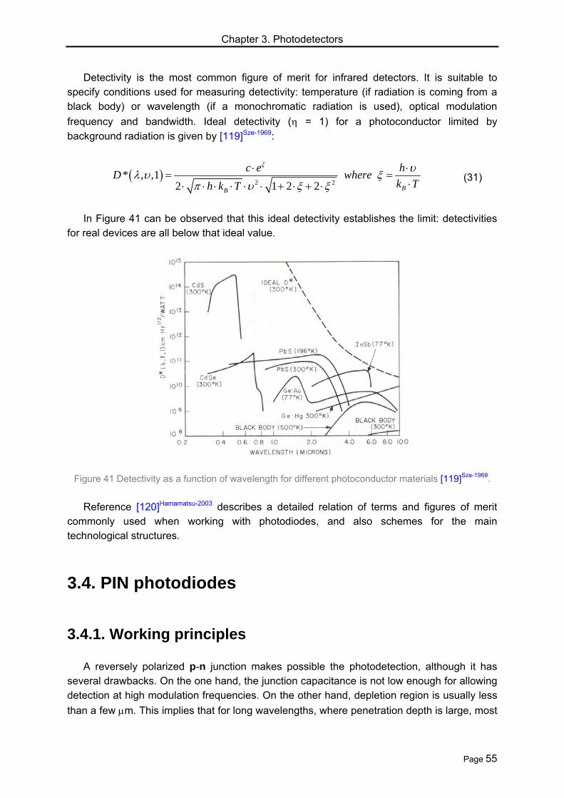
Chapter 3. Photodetectors
Page 55
Detectivity is the most common figure of merit for infrared detectors. It is suitable to specify conditions used for measuring detectivity: temperature (if radiation is coming from a black body) or wavelength (if a monochromatic radiation is used), optical modulation
frequency and bandwidth. Ideal detectivity ( = 1) for a photoconductor limited by
background radiation is given by [119]Sze-1969:
2 2
* , ,12 1 2 2 BB
c e hD where
k Th k T
(31)
In Figure 41 can be observed that this ideal detectivity establishes the limit: detectivities
for real devices are all below that ideal value.
Figure 41 Detectivity as a function of wavelength for different photoconductor materials [119]Sze-1969.
Reference [120]Hamamatsu-2003 describes a detailed relation of terms and figures of merit
commonly used when working with photodiodes, and also schemes for the main technological structures.
3.4. PIN photodiodes
3.4.1. Working principles A reversely polarized p-n junction makes possible the photodetection, although it has
several drawbacks. On the one hand, the junction capacitance is not low enough for allowing detection at high modulation frequencies. On the other hand, depletion region is usually less
than a few m. This implies that for long wavelengths, where penetration depth is large, most

Chapter 3. Photodetectors
Page 56
of the photons are absorbed out of the depletion region. In this region there is not electric field that allows separating and shifting the electron-hole pairs. As a consequence, quantum efficiency is reduced for those wavelengths. The PIN photodiode overcomes these drawbacks.
The term PIN refers to a semiconductor device with a p+ - intrinsic - n+ structure (Figure
42). Intrinsic layer is actually not intrinsic, but has a doping level much lower than the other
layers and it is much wider (typically between 5 and 50 m). In this structure holes and electrons are diffused towards the intrinsic zone from p+ and n+ regions, respectively. These carriers penetrate in the intrinsic region and suffer recombination. Draining of majority carriers in the outer regions generates little exposed charge layers to both sides of the intrinsic region. In the p+ layer a fringe of negative charges is created just in the border with the intrinsic region. Similarly, a fringe of positive charge is created at the border of the n+ layer with the central region. Those charged fringes generate an approximately uniform electric field in the intrinsic region, Eo, which is opposite to the carrier diffusion. The structure resembles the plane-parallel plates capacitor. The junction capacitance, Cdep, is very low because of the relatively large distance between charges being around a few pF. This makes possible a reduced time constant and a good dynamic response of the photodiode. Furthermore, since separation between charges is essentially the width of the intrinsic region, the corresponding capacitance is independent on the applied voltage. This makes the device behavior rather different than that of the p-n junction where the intrinsic capacitance strongly depends on the applied voltage.
The high conductivities of p+ and n+ regions make the external voltage (Vr) to drop
almost completely in the intrinsic region, where a electric field is directly proportional to the applied voltage.
r ro
V VE E
W W (32)
The PIN structure is designed in such a way that most of the photons are absorbed in the
intrinsic region. Electrons and holes generated in the intrinsic region create an external photocurrent that is detected as a voltage drop on a load resistor. Dynamic response of the photodiode is determined by transit times of photogenerated carriers along the width W of intrinsic region. Thus, by incrementing W it is possible to obtain a higher photon absorption rate (and thus an higher quantum efficiency), but at the expense of worsening the device speed. One might consider incrementing the electric field to reduce the transit time, because
ve = e·E and vh = h·E. However, these relations are only valid for low electric field
intensities. Carriers reach a saturation velocity when the field is high enough (e.g. vsat 105
m·s-1 for fields higher than 106 V·m-1 at room temperature in Si [114]Kasap-2001, see Figure 43).
For a Si intrinsic region of W = 10 m and with carriers drifting at saturation velocities, the
transit time is about 0.1 ns, which is higher than the time constant R·Cdep (50 ps) [114]Kasap-
2001. Therefore, transit time of carriers through intrinsic region is the limiting factor for speed in the PIN photodiodes.

Chapter 3. Photodetectors
Page 57
Figure 42 Basic structure of a PIN photodiode, distributions of space charge and electric field and working principle [114]Kasap-2001.
Figure 43 Shift velocity for carriers as a function of the intensity of the electric field in the PIN structure [114]Kasap-2001.
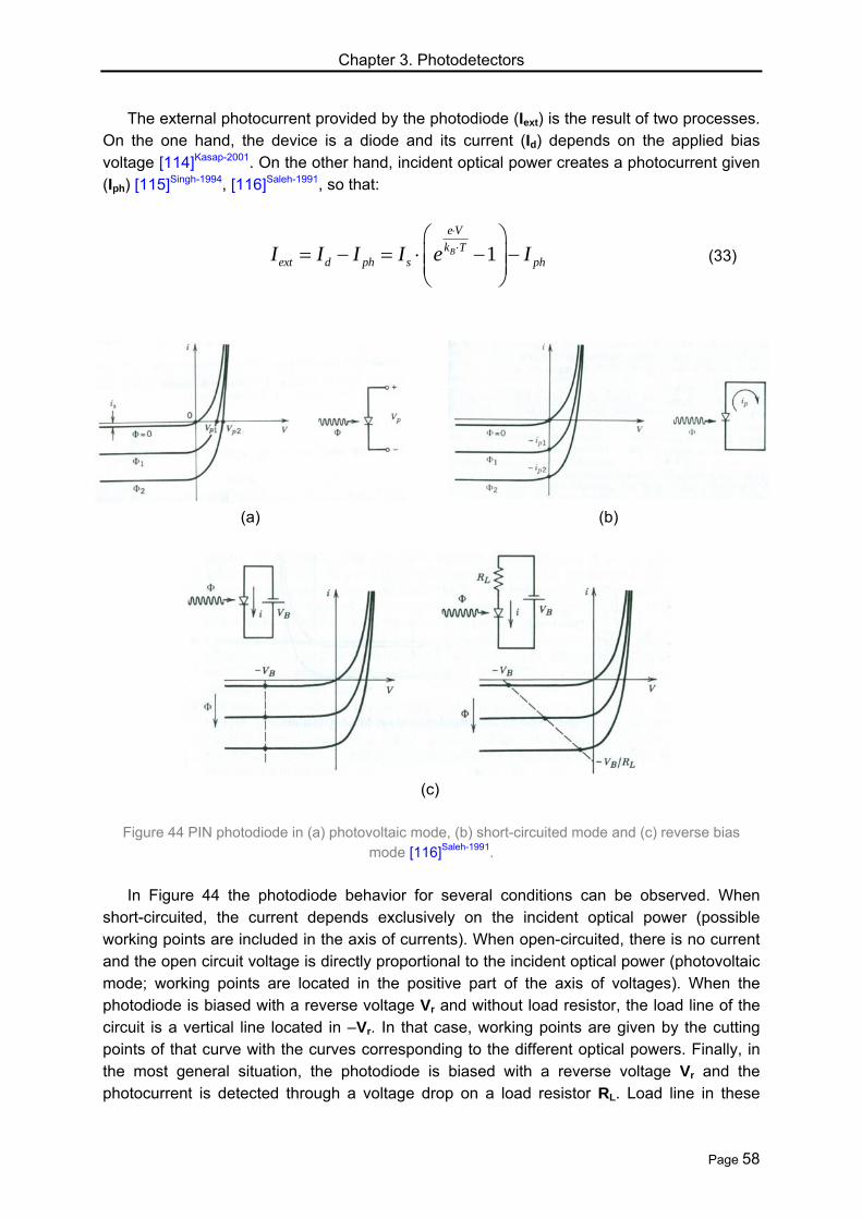
Chapter 3. Photodetectors
Page 58
The external photocurrent provided by the photodiode (Iext) is the result of two processes. On the one hand, the device is a diode and its current (Id) depends on the applied bias voltage [114]Kasap-2001. On the other hand, incident optical power creates a photocurrent given (Iph) [115]Singh-1994, [116]Saleh-1991, so that:
1B
e V
k Text d ph s phI I I I e I
(33)
(a) (b)
(c)
Figure 44 PIN photodiode in (a) photovoltaic mode, (b) short-circuited mode and (c) reverse bias
mode [116]Saleh-1991.
In Figure 44 the photodiode behavior for several conditions can be observed. When
short-circuited, the current depends exclusively on the incident optical power (possible working points are included in the axis of currents). When open-circuited, there is no current and the open circuit voltage is directly proportional to the incident optical power (photovoltaic mode; working points are located in the positive part of the axis of voltages). When the photodiode is biased with a reverse voltage Vr and without load resistor, the load line of the circuit is a vertical line located in –Vr. In that case, working points are given by the cutting points of that curve with the curves corresponding to the different optical powers. Finally, in the most general situation, the photodiode is biased with a reverse voltage Vr and the photocurrent is detected through a voltage drop on a load resistor RL. Load line in these

Chapter 3. Photodetectors
Page 59
conditions is an oblique line that sets working points in which the voltage on the device is reduced and the current on the circuit is increased as the device is illuminated with increasing optical power.
3.4.2. Frequency response and equivalent circuit [118]Bhattacharya-1997 describes in detail the frequency response of the PIN photodiode.
Starting with equations for continuity and current density for electrons and holes, taking into account the following considerations and applying the Ampere law, the author obtains a complex expression for the current density as a function of the modulation frequency of the incident optical signal. The main assumptions are:
1. The transit time for carriers is much lower than the mean time for recombination. It
is possible to consider recombination terms as negligible. 2. The electric field is large, so that it is possible to consider carrier diffusion terms as
negligible.
3. Photonic flux is intensity modulated. i tinc o o e
4. Each absorbed photon generates one electron-hole pair. The resulting current density is given by the following expression:
11( )
1 1
h
e
i tWW
o oh h h
i t W
o oe e e
e eeJ e W e W
W W i t i t W i t
e ee W e W
i t W i t W W i t
(34)
: Absorption coefficient of the semiconductor for the
considered frequency.
o: Amplitude of the incident optical oscillation. W: Width of the intrinsic region in the photodiode. th, te: Transit times for holes and electrons through the intrinsic
region.
This equation expresses only the current source of the PIN photodiode equivalent circuit
(Figure 46) and provides the intrinsic frequency response of the detector. The frequency response for the diode capacitance and for the extrinsic circuital elements (that is, the rest of
elements in the equivalent circuit) can be grouped together in a transference function H() (Figure 45) so that the final current can be expressed as following:
outJ J H (35)

Chapter 3. Photodetectors
Page 60
Figure 45 Frequency response of the PIN photodiode.
Figure 46 Equivalent circuit for the PIN photodiode [118]Bhattacharya-1997.
The analysis of the equivalent circuit provides the following transference function H():
2 2D
S D L
S L P S S L D j L D P
S S P D j
D j S L P S S S P D P S
RH
a i b c d
a R R R
b R R C L R R R C R R C
c R L C R C
d R C R R C L R L C R C L
(36)
i: Intrinsic response of the photodiode: I(). Cj: Junction capacitance, due to the separation of charges caused by the
intrinsic region. CP: Parasitic capacitance. It includes the capacitance between electrodes and
the capacitance associated with the device shield. RS: Serial resistance. It is the sum of the contact resistance and the
resistances of the neutral zones. RD: Junction resistance. It models the behavior of the device as a pure diode.
When reverse-biased, RD is high (current through the diode is the saturation reverse current, Is). When direct-biased, RD is much lower and it creates the typical direct current Id exponentially dependent on the bias voltage.

Chapter 3. Photodetectors
Page 61
LS: Total inductance, created mainly in the electrodes. It models a certain direct proportionality between electrodes impedance and the frequency
(remember that ZL = i··L).
In Figure 47 it can be seen the absolute value of Jout as a function of the frequency for
several widths of the intrinsic region.
Figure 47 Spectral response of an InGaAs PIN photodiode for several widths of the intrinsic region [118]Bhattacharya-1997.
In [119]Sze-1969 it is also developed the calculus of the current density through PIN
photodiode using an equivalent procedure to the one previously mentioned. The current density obeys the following expression:
1
1 ri ti ts
Tr
i V eJ e e
W i t
(37)
s: Relative permittivity of the semiconductor. V: Photodiode bias voltage. W: Width of the intrinsic region.
1: Optical modulation amplitude. tr: Carrier transit time through the intrinsic region.
The graphical representation of this expression (Figure 48) is equivalent to the Figure 47,
but offering more information. Both the modulus and the phase have a periodical behavior. An increase on the optical frequency results into an increase of the phase shift between the photonic flux and the generated photocurrent and also into a reduction in the magnitude of the last one. A relevant issue for optical communication applications is the fact that for

Chapter 3. Photodetectors
Page 62
certain exciting frequencies it is not possible to obtain photocurrent when using a PIN photodiode.
Figure 48 Spectral response (magnitude and phase) of a PIN photodiode [119]Sze-1969.
3.4.3. Noise in PIN photodiodes For calculating the SNR of a PIN photodiode we consider that the photocurrent has an
RMS value:
,;2
inc incph inc ph rms
e
P Pe eI e P I
h t h h
(38)
There is a background radiation that causes a low parasitic photocurrent (IB). Besides,
there is also a dark current (Idark) caused by electron-hole pairs thermogeneration in the intrinsic region. These components are random, fact that originates an equivalent shot noise:
2 2S ph B darki e I I I B (39)
Resistances in the PIN photodiode equivalent circuit (RS, RD, RL) generate thermal noise.
Assuming that the photodiode is equipped with an amplifier whose input impedance is Ri, it is observed that Ri is in parallel with RL and with Rs + RD. Rs is low in comparison with the value of RD for reverse bias and it is possible to neglect it. The Johnson noise associated with the final equivalent resistance will be:
2 41 1 1 1; B
Jeq D L i eq
k T Bi
R R R R R
(40)

Chapter 3. Photodetectors
Page 63
Figure 49 shows the noise equivalent circuit for the PIN photodiode, where Cp and Ls are not included because they do not contribute to the noise.
Figure 49 Noise equivalent circuit for a PIN photodiode [118]Bhattacharya-1997.
Taking into account previous expressions, SNR and NEP corresponding to the PIN
photodiode are obtained:
2
2
2 2
,
2
12
42
1 1 :
411 2
2
22
inc
ph eqPIN
BS J eqph B dark
eq
inc rms PIN
inc BPIN ph B dark
eq
incph B da
e PI R h
SNRk T Bi i R e I I I B
R
NEP is P for SNR with B Hz
e P k T BSNR e I I I B
h R
P ee I I I
h
1/ 2
4
412 [ ]
2
Brk
eq
inc BPIN ph B dark
eq
k TB
R
P k ThNEP e I I I W Hz
e RB
(41)
For enhancing the photodiode sensitivity (low NEP; remember that NEP is a
measurement of the minimum detectable signal) it is desired that both and Req have high values. For an high value of Req it is possible to act on RL and Ri. Ri and RD are in the order
of M, so that RL is the element that determines the final value of Req. Thus, it will be
desirable that RL was also in the order of M.
3.4.4. Advantages of PIN versus photoconductors [119]Sze-1969 provides two important reasons that justify superiority of photodiodes versus
photoconductors. On the one hand, photodiode delivers a power to the load about 106 times higher than the one provided by the photoconductor. On the other hand, although for high
optical intensities SNRphotoconductor SNRPIN, it is verified for low intensities that SNRPIN >>
SNRphotoconductor. However, the nearly unity gain in PIN photodiodes and the fact that several hundreds of photons are needed to generate an appropriate photosignal have led to develop new high gain devices (e.g. APDs).

Chapter 3. Photodetectors
Page 64
3.5. Avalanche Photodiodes
3.5.1. Working principles Figure 50 shows the basic structure (called reach-through) of an avalanche photodiode
(APD) which is an evolution of the PIN configuration.
Figure 50 Structure and working principle of an APD and charge and electric field distributions along the device [114]Kasap-2001.
The n+ region is thin and it is located in the side through which the optical radiation is
coming. The p layers with different doping levels allow modifying the electric field in a
convenient way along the structure. The layer is very wide and it is slightly doped with acceptor atoms (it is nearly intrinsic). Fringes of negative charges on the edges of p and p+
layers bordering on layer are produced. The charge density on p+ layer is higher than in p
layer due to its higher doping level. A depletion region between n+ layer and p layer results, with the corresponding accumulation of negative charge on the p side and positive charge on

Chapter 3. Photodetectors
Page 65
the n side. With high enough reverse bias voltage the depletion region extends over the p
region and deeply penetrates on the layer (it is the reason for naming this structure as
reach-through). Integration of charge density allows obtaining electric field distribution along the structure. Electric field is higher around p-n+ junction because it is the zone where the charge density is higher. The intrinsic region field is nearly constant and lower than in the junction due to its lower charge density. In neutral regions of p+ and n+ layers the electric field quickly drops to zero.
The reverse bias voltage drops mainly on p and regions due to the high conductances
of p+ and n+ regions. In addition, the field on intrinsic region and the peak of field around the p-n+ junction are higher as the reverse bias voltage increases. Photon absorption is mainly
produced on region. In dark conditions, layer is completely empty of free charge carriers. When a photon is absorbed, an electron-hole pair is produced and the constant electric field is capable to separate and drag carriers on opposite directions at the saturation velocity. Electrons penetrate on the so called avalanche region where they suffer a growing electric field intensity. In this way, electrons obtain enough kinetic energy for causing impact ionization. Electron carries an energy considerably higher than the band gap of the semiconductor (Eg) so that it reduces its energy by generating an electron-hole pair in the avalanche region. The primary electron has reduced its energy to a value close to the energy of the beginning of the conduction band (Ec). The secondary electron has been promoted from the valence band, so that its initial energy is also close to Ec. Threshold energies for impact ionization in electrons and holes are given by following expressions [118]Bhattacharya-1997:
* *
* *
2* *
*
1 ; 12 2
21 1 3. ,
2
e hie g ih g
h e
BCe h ie ih g
e o g
m mE E E E
m m
pwhere If m m E E E
m m E
(42)
Eie, Eih: Energy thresholds for impact ionization for electrons and holes. me*, mh*: Effective masses for electron and hole. Eg: Semiconductor band-gap energy. pBC: Momentum of the electron on conduction band. mo: Mass of the free electron.
Both electrons are subjected to the same process. As they penetrate on n+ region they
experiment a more intense electric field, so that a high energetic state is quickly reached. Thus, new impact ionizations are possible. After two ionization processes, a primary electron has produced four electrons, each one of them will be able to generate new ionization processes. A chain reaction called avalanche breakdown or avalanche multiplication (Figure 51) results. The APD has a mechanism of high intrinsic gain thanks to which the absorption of one only photon generates a great number of electron-hole pairs. Photocurrent provided
by APD on avalanche condition corresponds to > 1 [114]Kasap-2001. Holes generated on each
impact ionization are also able to launch new ionizations, although this is not desirable because it makes the response of the device slower. The hole acquires energy during its

Chapter 3. Photodetectors
Page 66
travel through the intrinsic region so that, in the worst case, it could launch an ionization just in the border of the avalanche region. The electron in the generated pair must travel the whole avalanche region to the n+ layer. Along this path it can launch new ionizations which, by its own, will launch more new ionizations. Because the photodiode response does not finish until all the avalanche processes are extinguished, ionization by holes makes slower the operation of the device.
Figure 51 Principle of the avalanche multiplication phenomenon [114]Kasap-2001.
Each type of carrier has an ionizing capability which depends on the semiconductor
material. This capability is quantified in terms of the impact ionization coefficient e, h
(probability for ionizing by length unit, [cm-1]). As examples, in GaAs h e, in Si h e/30
and in Ge h e/5. The relation of ionization coefficients for a certain material, kr = h / e
[118]Bhattacharya-1997, is a key factor for achieving optimal operating conditions. When kr tends to
an extreme value (0 or ) secondary charge carriers arise each time nearer the collection zone, so that the maximum transit time (the time that limits the device speed) would be the
time needed by the primary carrier for crossing the avalanche region. However, when kr 1
(electrons and holes ionize alike) secondary carriers are generated all over the avalanche region in any moment. Although the primary carrier has reached the collection zone, a great number of electrons and holes able to ionize in both opposite senses can exist in the avalanche region. The resulting avalanche is more intense (the gain factor is higher) but the time needed for completing the process is notably stretched. Here it is shown one of the main drawbacks of photodetectors: it is not possible to reach high gain and speed simultaneously. The gain-bandwidth product is maximized in those devices in which kr tends to an extreme value, that is, when the avalanche process is limited to the carrier with the
highest ionization faculty (in the case of Si it is the electron, kr 0). The APD bias voltage makes possible that only electrons were able to ionize. For the Si, the intensity of the electric field that establishes the threshold for impact ionization for electrons is around 1.75·105 V·cm-1, whereas is around 2.5·105 V·cm-1 for holes [4]Renker-2009.
Using the standard differential equations that provide the electron and hole current
densities during the avalanche multiplication and applying the electroneutrality condition it is possible to obtain the following expression for the gain factor (also known as multiplication factor) [116]Saleh-1991. In [115]Singh-1994 the author reaches a similar equation.
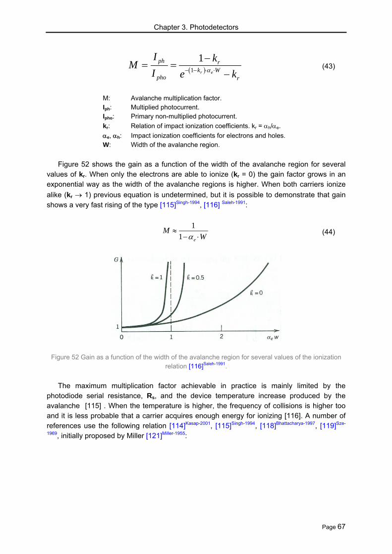
Chapter 3. Photodetectors
Page 67
1
1r e
ph rk W
pho r
I kM
I e k
(43)
M: Avalanche multiplication factor. Iph: Multiplied photocurrent. Ipho: Primary non-multiplied photocurrent.
kr: Relation of impact ionization coefficients. kr = h/e.
e, h: Impact ionization coefficients for electrons and holes. W: Width of the avalanche region.
Figure 52 shows the gain as a function of the width of the avalanche region for several
values of kr. When only the electrons are able to ionize (kr = 0) the gain factor grows in an exponential way as the width of the avalanche regions is higher. When both carriers ionize
alike (kr 1) previous equation is undetermined, but it is possible to demonstrate that gain shows a very fast rising of the type [115]Singh-1994, [116] Saleh-1991:
1
1 e
MW
(44)
Figure 52 Gain as a function of the width of the avalanche region for several values of the ionization relation [116]Saleh-1991.
The maximum multiplication factor achievable in practice is mainly limited by the
photodiode serial resistance, Rs, and the device temperature increase produced by the avalanche [115] . When the temperature is higher, the frequency of collisions is higher too and it is less probable that a carrier acquires enough energy for ionizing [116]. A number of references use the following relation [114]Kasap-2001, [115]Singh-1994, [118]Bhattacharya-1997, [119]Sze-
1969, initially proposed by Miller [121]Miller-1955:

Chapter 3. Photodetectors
Page 68
1
1n
BR
MV I R
V
(45)
M: Avalanche multiplication factor. V: Reverse bias voltage applied to the photodiode. I: Current provided by the photodiode. It includes the photocurrent
and the dark current. I = Iph + Idark. R: Total resistance of the photodiode. It includes the serial resistance
and the resistance of the space charge region. R = RS + Rj. VBR: Breakdown voltage. It depends on the temperature. n: Parameter that depends on: semiconductor type, doping profile,
incident wavelength and temperature. It ranges between 1 and 4.
The breakdown voltage (VBR) is a threshold voltage for developing an uncontrolled
avalanche multiplication process, which can cause the device rupture if no contention is provided. This situation happens when the electric field intensity in the depletion region is higher than a certain critical field ECR, which is related to VBR according to [118]Bhattacharya-1997:
2
2S o
BR CRD
V Ee N
(46)
VBR: Breakdown voltage.
S: Relative permittivity of the semiconductor.
o: Permittivity of the air. ND: Doping density in the n+ region with donor atoms. ECR: Critical electric field that triggers the uncontrolled
avalanche process.
An APD operates with bias voltage lower than VBR (between 100 and 200 V [5]Haba-2008) in
a linear amplification mode (Figure 53). The gain is proportional to the bias voltage and usually reaches values between 50 and 200 [4]Renker-2009 . However, it is possible to reach values near 1000 [6]Renker-2007 or even higher [4]Renker-2009. In order to do so, bias voltage and temperature must be controlled with high accuracy because the APD must work very near VBR. Although detection of single photons is possible with APDs, it does not result neither efficient nor practical [12]Otte-2006. Normally, tens of photons are needed to obtain a detectable signal. To detect single photons, the suitable solid state devices are the so called Silicon Photomultipliers (SiPM), also known as GAPD (Geiger mode APD).
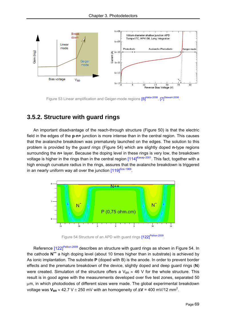
Chapter 3. Photodetectors
Page 69
Figure 53 Linear amplification and Geiger-mode regions [5]Haba-2008, [7]Stewart-2006.
3.5.2. Structure with guard rings An important disadvantage of the reach-through structure (Figure 50) is that the electric
field in the edges of the p-n+ junction is more intense than in the central region. This causes that the avalanche breakdown was prematurely launched on the edges. The solution to this problem is provided by the guard rings (Figure 54) which are slightly doped n-type regions surrounding the n+ layer. Because the doping level in these rings is very low, the breakdown voltage is higher in the rings than in the central region [114]Kasap-2001. This fact, together with a high enough curvature radius in the rings, assures that the avalanche breakdown is triggered in an nearly uniform way all over the junction [119]Sze-1969.
Figure 54 Structure of an APD with guard rings [122]Pellion-2009.
Reference [122]Pellion-2009 describes an structure with guard rings as shown in Figure 54. In
the cathode N++ a high doping level (about 10 times higher than in substrate) is achieved by As ionic implantation. The substrate P (doped with B) is the anode. In order to prevent border effects and the premature breakdown of the device, slightly doped and deep guard rings (N)
were created. Simulation of the structure offers a VBR 46 V for the whole structure. This
result is in good agree with the measurements developed over five test zones, separated 50
m, in which photodiodes of different sizes were made. The global experimental breakdown
voltage was VBR 42.7 V 250 mV with an homogeneity of V = 400 mV/12 mm2.

Chapter 3. Photodetectors
Page 70
3.5.3. Noise in APD photodiodes Although APDs are affected by the same noise components than PIN diodes, the main
noise source in APDs is the avalanche process itself. Not all carriers travel the same distance before causing impact ionization. Furthermore, ionization is not produced in an uniform way all over the multiplication region, but it is more common in the zones in which a more intense electric field is present. The result is that multiplication factor oscillates around a mean value. The fact that impact ionization was an stochastic process imposes an excess noise, also known as avalanche noise [114]Kasap-2001, which limits the useful range of gain. Materials with an extreme value of kr show lower avalanche noise, so that higher gain values
can be used (as comparing with materials in which kr 1). As it will be shown later, avalanche noise dominates over the other noise sources when high values for the amplification factor M are used. And in those conditions, an increment in gain only provides a worsening of the signal to noise ratio [118]Bhattacharya-1997.
Avalanche gain affects not only the photocurrent but also amplifies the dark current and
the background current. Noise components in the APD are:
,2
incph rms
PeI M
h
(47)
2 22S ph B darki e I I I B F M (48)
2 4 1 1 1 1;B
Jeq eq D L i
k T Bi
R R R R R
(49)
Shot noise components are enhanced by the multiplication factor (term
2 ph B darke I I I B M ) and these amplified components cause even higher excess
oscillations (additional factor F·M). Thermal noise is caused by thermal agitation of carriers, so it depends on the temperature but not on the gain factor. Taking into account previous relations, it is possible to obtain following expressions for SNR and NEP of an APD device [118]Bhattacharya-1997:
2
2
2 1/ 2
12
42
412 [ ]
2
inc
APDB
ph B darkeq
inc BAPD ph B dark
eq
e P M
hSNR
k T Be I I I B F M
R
P k ThNEP e I I I F M W Hz
e M RB
(50)
At the sight of NEP expression it is possible to understand why a high gain factor
substantially enhances sensitivity in APDs. Among photodetectors, avalanche diodes have shown the best sensitivity. This high sensitivity provides benefits in the quality of the optical

Chapter 3. Photodetectors
Page 71
communication systems by reducing the Bit Error Rate (BER), which is highly dependent on the photodetector SNR.
The Excess Noise Factor (ENF) is different for each type of carrier. [118]Bhattacharya-1997
provides the following analytical expressions for determining these factors (Me and Mh are multiplication factors associated with electrons and holes respectively).
2 2
1 111 1 ; 1 1e h
e e r h he r h
M MF M k F M
M k M
(51)
However, a simpler formulation as given in [114]Kasap-2001 is more common:
xF M (52)
x is a factor that depends on the type of semiconductor, the APD structure and the type
of carrier that starts the avalanche process. It ranges between 0.3 and 0.5 for Si and between 0.7 and 1 for Ge and III-V semiconductors (e.g. InGaAs). Excess noise factor in APDs is higher than 2 [12]Otte-2006.
Figure 55 Equivalent circuit for an avalanche photodiode [119]Sze-1969.
In Figure 55 it is shown the noise equivalent circuit for an APD device. Sze justifies that
signal and noise powers delivered to the load obey the following expressions [119]Sze-1969:
2 2
, ,2 22 2 2 2
2( );
1 1
pp LS L
S avg N avg
j S L j S L
e I B M RI M RP P
C R R C R R
(53)
Ip corresponds to the primary non-amplified photocurrent and p is a parameter ranging
from 2 and 4 (typically 3). Figure 56 shows graphical representation of signal and noise powers as a function of the gain factor M.
It is easy to verify that SNRAPD is inversely proportional to the multiplication factor. In the
case of the figure, maximum SNR is obtained for a gain factor 4. As it was previously
announced, an increase in the multiplication factor has negative consequences, in spite of what one could think originally. One of the main drawbacks in APD is its limited amplification

Chapter 3. Photodetectors
Page 72
capability with a moderated SNR [119]Sze-1969. Additionally, other drawbacks must be taken into account, such as the need for high bias voltages and the low reliability as compared to PIN photodiodes. It may also be necessary to use circuitry for controlling the temperature. One single carrier crossing the avalanche region can trigger the multiplication process. That carrier may come from a photogenerated electron-hole pair or may be a thermogenerated carrier. That is the reason for darkness false fires in avalanche photodiodes [115]Singh-1994.
2 2 2
,
3,
( ) ( ) 1
2 2S avg S L S
APDN avg p L p
P I M R ISNR
P e I B M R e B I M
(54)
Figure 56 Signal and noise powers as a function of the multiplication factor in an APD photodetector [119]Sze-1969.
In [116]Saleh-1991 it is shown a very convenient analysis of noise in avalanche photodiodes
for explaining SNR dependency on several parameters. Author reaches the following expression for SNR:
2 2
2 2q
m GSNR
m G F
22 4
; ; ;2 2
r Bq r
L
G k T Bm F
B G B e R
(55)

Chapter 3. Photodetectors
Page 73
<m>: Mean number of detected photons in a time period T. <G>: Mean gain of the photodiode. <G2>: Variance of the gain of the photodiode. F: Excess noise factor.
q: Dimensionless parameter that expresses the noise contribution of the circuit that comes with the photodiode.
r: Noise component added by the circuit. It depends on the features of the circuit, bandwidth, temperature, etc. When photocurrent is sensed on a resistor RL whose thermal noise is much higher than any other circuital
noise contribution, r may be approximated as given above.
: Photodetector quantum efficiency.
: Incident photonic flux. B: Device bandwidth.
Following figures allow observing how the circuitry noise may notably degrade the
receptor quality as a whole (Figure 57) and that the use of APDs is clearly advantageous for low photonic intensities (Figure 58).
Figure 57 SNR dependence in an APD with the signal processing circuitry noise [116]Saleh-1991.

Chapter 3. Photodetectors
Page 74
Figure 58 Comparing SNR on an APD and on a photodiode with no gain [116]Saleh-1991.
Taking into account the expression for excess noise factor on an APD it is possible to
reach an equation for SNR that depends on the mean gain factor and on the relation between ionization coefficients for both types of carriers [116]Saleh-1991.
2 2 2
2 222
2
23 2
11 2 ;
1 2
hAPD r r r
e
APDqq
qr r
F k G k kG
m G m GSNR
m G FG F
m
m G
k G k G Gm
(56)
Figure 59 shows the graphical representation of previous expression for several values of
the parameter kr. It is observed that, generally, there is an optimum gain value whose
overcoming only provides worsening in the SNR. It is also verified that when kr 0, that is, when only electrons are able to cause impact ionization, high gain values are possible with no harm in the SNR. The really interesting thing is the procurement of the highest possible SNR, so that no real advantages are obtained by using very high gain values.

Chapter 3. Photodetectors
Page 75
Figure 59 SNR dependence in an APD with the gain factor [116]Saleh-1991.
3.6. Schottky barrier A Schottky barrier is a device that may be used as an high efficiency photodetector,
mainly on the ultraviolet range [119]Sze-1969, [123]Tyagi-1991. The basic structure consists on a very thin metallic layer with an anti-reflecting coating on its outer side and bonded to an n-type semiconductor on the other side. The metal thickness must be selected to ensure sufficient optical transmission. For example, a thin layer of gold of 100 Å thickness transmits up to 95% of the incident light in the infrared. Rear-face illumination is also possible by using transparent substrates, like sapphire.
Figure 60 shows the energy band diagram of the junction under equilibrium conditions. The application of a negative voltage between the semiconductor and the metal electrode has the effect of reverse-bias the Schottky junction, which increases the height of the effective barrier and the width of the space charge region. This last effect is favorable for photodetection because photon absorption happens mainly in the depletion region.
Figure 60 Bands diagram for the Schottky barrier [119]Sze-1969.

Chapter 3. Photodetectors
Page 76
Figure 61 shows the device working modes for different energies of the incident photon
energy. In all cases the device is reverse-biased. Bn is the reverse bias voltage, q·Bn is the
height of the energy barrier formed by the metal and the semiconductor and Eg is the bandgap energy in the semiconductor.
If Efotón < q·Bn the photon absorption is not possible and therefore no photocurrent can be generated.
If q·Bn < Efotón < Eg (Figure 61 (a)) the photo-excited electrons gain enough energy to
surpass the junction barrier, and an external photocurrent results. If Efotón > Eg (Figure 61 (b)) photons have enough energy to enable two different
processes: the flow of electrons from the metal to the semiconductor and the generation of electron-hole pairs inside the semiconductor. The second process is much more probable than the first one. Under these conditions the device essentially behaves as a PIN photodiode.
When Efotón > Eg and V VBR (Figure 61 (c)) promoted electrons may cause impact
ionizations, so that the device is able to work as an avalanche photodiode. For short wavelengths (e.g. ultraviolet) the Schottky barrier shows very high sensitivity.
Schottky barrier is a versatile photodetector that works for a wide range of wavelengths
by combining different working modes. In fact, it may be the preferred device when optical radiation is very polychromatic.
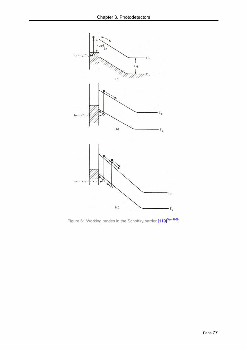
Chapter 3. Photodetectors
Page 77
Figure 61 Working modes in the Schottky barrier [119]Sze-1969.

Chapter 4. Silicon Photomultipliers
Page 78
4. Silicon Photomultipliers The aim of this chapter is to merge the available relevant information on SiPMs into a
single reference which can be used as a working document for practical purposes. This revision, although of course incomplete, will provide the body of theoretical knowledge needed to face the experimental work.
Thus, in this chapter the state of the art in SiPMs is described. Working principles, figures
of merit, features and phenomena, manufacturing technologies and advanced structures are discussed in detail.
4.1. Working principles When an APD is biased with a voltage higher than the breakdown voltage (VBR)
extremely high avalanches can happen as a result of the absorption of only one photon.
These processes can provide multiplication factors as high as 105 or 106 (over a 50 load the voltage is in the range of mV) [6]Renker-2007. The result is a very sharp photocurrent peak which could destroy the photodiode if avalanche quenching is not provided in a short time after starting the process. The way of reaching that collapse is reducing the photodiode bias voltage below the breakdown voltage. In these conditions, carriers in the structure have energies which are low enough to avoid new impact ionizations. The simplest way to produce the photocurrent quenching is by adding a resistor between the bias voltage and the photodiode. The very fast photocurrent peak causes a very fast voltage on the quenching
resistor (typical value 500 k [124]Buzhan-2003), so that the effective bias voltage on the
photodiode is drastically reduced in a very short time after starting the multiplication (typically a few ps [12]Otte-2006).
When the APD is biased above VBR, both electrons and holes are implied on ionizing
processes [12]Otte-2006. Otherwise (linear gain mode) the electric field in the structure is only higher than the ionizing threshold for electrons. However, when VBR is surpassed in only a few volts (typical bias voltage is 10-15 % than breakdown voltage [124]Buzhan-2003) the electric field is high enough for enabling both carrier types to generate electron-hole pairs. In this case the avalanche is not generated only in one direction (from p zone to n+ zone) but secondary avalanches are produced all over the multiplication region (Figure 51). The result is an auto-sustained rising of the number of circulating carriers (i.e. very high gain factor). The positive feedback process happening in Geiger mode avoids that avalanche extinguishes alone and an external collapse is mandatory for preventing the device destruction [4]Renker-2009.
Former work on avalanche photodiodes published by the sixties made use of bias
voltages above VBR, see for example [125]McIntyre-1961 (RCA company) and Haitz [126]Haitz-1964 (Shockley laboratories). The main problem they had was that for this biasing condition only small Si volumes can be kept free from carriers during the time needed for making the diode
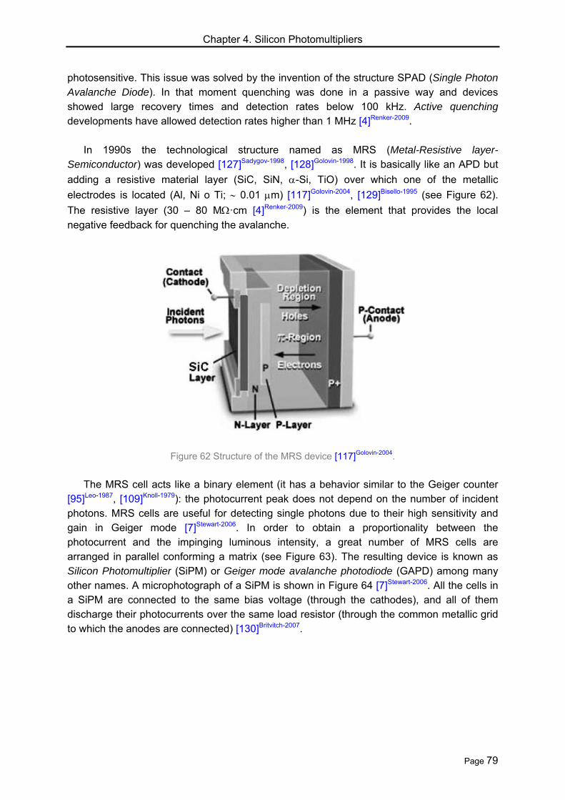
Chapter 4. Silicon Photomultipliers
Page 79
photosensitive. This issue was solved by the invention of the structure SPAD (Single Photon Avalanche Diode). In that moment quenching was done in a passive way and devices showed large recovery times and detection rates below 100 kHz. Active quenching developments have allowed detection rates higher than 1 MHz [4]Renker-2009.
In 1990s the technological structure named as MRS (Metal-Resistive layer-
Semiconductor) was developed [127]Sadygov-1998, [128]Golovin-1998. It is basically like an APD but
adding a resistive material layer (SiC, SiN, -Si, TiO) over which one of the metallic
electrodes is located (Al, Ni o Ti; 0.01 m) [117]Golovin-2004, [129]Bisello-1995 (see Figure 62).
The resistive layer (30 – 80 M·cm [4]Renker-2009) is the element that provides the local
negative feedback for quenching the avalanche.
Figure 62 Structure of the MRS device [117]Golovin-2004.
The MRS cell acts like a binary element (it has a behavior similar to the Geiger counter
[95]Leo-1987, [109]Knoll-1979): the photocurrent peak does not depend on the number of incident photons. MRS cells are useful for detecting single photons due to their high sensitivity and gain in Geiger mode [7]Stewart-2006. In order to obtain a proportionality between the photocurrent and the impinging luminous intensity, a great number of MRS cells are arranged in parallel conforming a matrix (see Figure 63). The resulting device is known as Silicon Photomultiplier (SiPM) or Geiger mode avalanche photodiode (GAPD) among many other names. A microphotograph of a SiPM is shown in Figure 64 [7]Stewart-2006. All the cells in a SiPM are connected to the same bias voltage (through the cathodes), and all of them discharge their photocurrents over the same load resistor (through the common metallic grid to which the anodes are connected) [130]Britvitch-2007.

Chapter 4. Silicon Photomultipliers
Page 80
Figure 63 Layout of the MRS cells in a SiPM [7]Stewart-2006.
(a) (b) Figure 64 (a) Structure and (b) photograph of a SiPM of area 1 mm2 and 400 cells [5]Haba-2008.
In the last decades several technological improvements have led to devices able to
resolve single photons, with lower bias voltages than APD and using MOS standard manufacturing processes [4]Renker-2009. When few photons arrive to the photodetector, avalanche processes are usually triggered on different cells of the device. This way, total photocurrent is the sum of photocurrents provided by the different fired cells, and thus, the voltage on a load resistor is directly proportional to the incident luminous intensity. For example, assuming that n photons are detected on n different cells and that IMRS is the photocurrent generated by one cell, total photocurrent is n·IRMS. So, this matrix structure made with binary elements (MRS cells) acts as the desired analog device. However, this linear proportionality is not obtained for any incident illumination. When photonic density is
high, in the order of the density of cells in the detector (102 - 104 cells·mm-2 [130]Britvitch-2007)
there is high probability that several photons fall simultaneously on the same pixel. Because the response of the MRS cell is the same whatever the number of impinging photons, under these circumstances the total photocurrent is not proportional to the number of arriving

Chapter 4. Silicon Photomultipliers
Page 81
photons. Returning to the example, when m cells of the n fired cells receive 3 simultaneous photons, total photocurrent remains n·IRMS whereas the number of impinging photons is: 1·(n-m) + 3·m = n + 2·m. That is, photocurrent informs about the number of fired cells but not about the total number of received photons. This phenomenon is called SiPM saturation effect [6]Renker-2007 (Figure 65). When the number of photons exceeds 50% of available cells, a deviation from linearity up to 20% can be observed [12]Otte-2006. And actually, linear relation is only valid for fast optical excitement: when signals extended in time are used, late arriving photons can impact on cells which are in the recovery phase [12]Otte-2006. The high sensitivity that offers the SiPM is achieved at the expense of saturation for relatively low light intensities
( tens of pW; PIN and APD photodetectors saturate with higher intensities, from nW up to
W) [14]O’Keeffe-2007.
Figure 65 Saturation effect on SiPMs with different number of cells [130]Britvitch-2007.
With moderated illumination the SiPM behavior is similar to the PMT [95]Leo-1987, [109]Knoll-
1979, the traditional photodetector preferred during decades for high sensitivity applications (e.g. nuclear medicine, cosmic radiation detection, etc.). During last years, predominance of PMT has been challenged by advances on solid state technology. One representative example is found on single photon counting applications [15]Jackson-2005. Plenty of reasons explain this trend. Unlike the PMT, a SiPM offers lower bias voltage, consumption and size, as well as higher gain. Furthermore, SiPMs are insensitivity to magnetic fields and cannot be damaged by direct exposure to room illumination [2]Kovaltchouk-2005, [130]Britvitch-2007. As compared with PIN and APD photodiodes SiPMs also show interesting advantages. PIN structures offer very weak signals, which lead to poor signal to noise ratios. Additionally, the slow carrier displacement limits the speed of these devices. Although APD is a structure that offers intrinsic gain, it is restricted to low values. This fact, however, has not obstructed its use as an alternative to PMT in some fields (PET for small animals [131]Moehrs-2006, high energy
physics, etc.) due to its high quantum efficiency ( 80 %), small size and immunity against

Chapter 4. Silicon Photomultipliers
Page 82
magnetic fields. SiPM is advantageous as compared to PIN and APD due to its very high gain with lower bias voltage, higher speed and lower excess noise and sensitivity to harmful collateral effects [1]Renker-2006, [6]Renker-2007, [130]Britvitch-2007. But the most important reason is that SiPMs are really able to detect only one photon, while PINs and APDs require at least tens of photons.
The SiPM is a novel high gain multi-cell structure with performance enhanced as
compared with PMT and that surpasses limitations of more traditional photodiodes (PIN, APD) [7]Stewart-2006. Several acronyms for this photodetector can be found in the literature [12]Otte-2006: SPM or SiPM (Silicon PhotoMultiplier), SSPM (Solid State PhotoMultiplier), MRS-APD (Metal-Resistor-Semiconductor Avalanche PhotoDiode), MPPC (Multi-Pixel Photon Counter), MPPD (Multi-Pixel Photon Detector), MAPD (Micro-Pixel Avalanche Photodiode), VLPC (Visible Light Photon Counter), etc. In early 1990s the first results with these structures were published and since then continuous enhancement efforts have been done [3]Buzhan-2001, [117]Golovin-2004, [132]Bondarenko-2000, [133]Saveliev-2000.
4.2. Photon detection efficiency Photon Detection Efficiency (PDE) is a magnitude more interesting than quantum
efficiency for characterizing the sensitivity of this type of photodetector. The reason is that PDE takes into account the effect of geometry and the fact that avalanche is triggered by photogenerated carriers. Figure 66 shows PDE as a function of wavelength for several SiPMs. PDE can be expressed by the following equation [6]Renker-2007, [130]Britvitch-2007:
tan( ) ( ) Geiger geometry transmit cePDE QE (57)
PDE: Photon Detection Efficiency. It depends on wavelength of
impinging radiation. QE: Quantum Efficiency. Number of photogenerated carriers divided by
the number of impinging photons. It is usually in a range 30 – 80 %. It also depends on wavelength.
Geiger: Probability that a carrier triggers a Geiger process. It is an efficiency associated with charge carriers and it strongly depends on the electric field strength in the junction [12]Otte-2006.
geometry: Geometric efficiency. Fraction of the total sensor area effectively occupied by cells, that is, fraction of the total area that is really an active area. It is usually in the range of 20 – 60 %.
transmittance: Transmittance efficiency. It is related with the transport of impinging photons into the active volume.
For photons having energies above the band gap of the semiconductor (1.12 eV in Si)
QE is unity and it increases above 1 if energy is enough for causing impact ionization (energy higher than 3.6 eV in Si). Short wavelength photons will be mostly absorbed just
beneath the surface (penetration deep 100 nm). If photon is absorbed in the highly doped

Chapter 4. Silicon Photomultipliers
Page 83
top layer, the generated electron-hole pair will be probably lost because recombination time in that region is very short. Thus, development of very shallow highly doped top layers is a challenging task for enhancing blue-ultraviolet photon detectors. On the other hand, long wavelength photons (i.e. red-infrared wavelengths) penetrate deeply into the structure and could be absorbed in the non-depleted bulk or even it could cross the device without interaction. This is the reason for using thick depletion layers in long wavelength detecting devices [12]Otte-2006.
The active area in the SiPM is notably reduced due to the presence of quenching
resistors on detector surface. Existing devices have effective areas ranging from 25 % up to 60 % [12]Otte-2006. A back-illuminated SiPM does not suffer from this effect and geometric efficiencies near 100 % can be obtained [134]Mirzoyan-2007. Using anti-reflective coatings (e.g. Si3N4 [12]Otte-2006) the light transmission (i.e. transmittance efficiency) to the active volume can be more than 80-90 % [134]Mirzoyan-2007.
(a) (b)
Figure 66 PDE of several Hamamatsu SiPMs (a) and of model SSPM_0710G9MM from
Photonique/CPTA [16]Hamamatsu-2009 (b) as a function of wavelength [4]Renker-2009.
Maximum PDE could surpass 40 %. In fact, Mirzoyan et al assure that using realistic
values for parameters in the previous formula, one could expect a PDE even up to 60-65 % for front-illuminated SiPMs and 80-85 % for the back-illuminated type [134]Mirzoyan-2007. This magnitude is taken into account for estimating the number of fired cells Nfired-cells for a certain photonic flux [1]Renker-2006, [6]Renker-2007, [130]Britvitch-2007:
1photons
total cells
NPDE
N
fired cells total cellsN N e
(58)
Nfired cells: Number of fired cells. Ntotal cells: Total number of cells in the device. Nphotons: Total number of impinging photons. PDE: Photon detection efficiency of the device.

Chapter 4. Silicon Photomultipliers
Page 84
In Figure 67 it is shown how photon detection efficiency is influenced by photodiode bias voltage. PDE increases with bias voltage due to the higher probability of Geiger discharge [135]Huding-2011. Although PDE improves with high gain (high bias voltage) it will be necessary to use a compromise value because in those conditions dark current and darkcounts could be very high and the optical crosstalk increases too [4]Renker-2009. Mirzoyan et al show that both crosstalk and afterpulsing phenomena (described later) disturb the real PDE of the device: depending on the used PDE measuring method, the contribution of these processes could be as big as the real PDE itself [136]Mirzoyan-2011. Because PDE saturates with increasing bias voltage, some authors suggest that breakdown probabilities close to 100 % can be achieved for photogenerated carriers emerging in front of the multiplication region [12]Otte-2006.
(a) (b)
Figure 67 Photodetection efficiency (a) and darkcount rate and dark current of Hamamatsu MPPC-33-
050C (b) as a function of the bias voltage [4]Renker-2009.
The best occupation degree in the device could be achieved using a small number of big
cells [1]Renker-2006. This solution could accomplish the necessity of space for individual quenching resistors and the reduction of the crosstalk effect (discussed later) but getting a good geometric efficiency. Buzhan et al assure that the technologically possible density of pixels is likely 2-3·103 mm-2 [124]Buzhan-2003.
Figure 68 Sensitivity mapping around one pixel in a SiPM [5]Haba-2008.

Chapter 4. Silicon Photomultipliers
Page 85
Figure 68 shows an experimental determination of the sensitivity of one SiPM pixel by means of laser scanning [5]Haba-2008. It is easy to see that the higher the density of pixels the lower the geometric efficiency, due to non-scalability of the insensitive area around each pixel.
4.3. Technologies for SiPMs Single Photon Avalanche Diodes (SPAD) based on Si technology could be classified into
two main groups. Thin Si-SPADs [137]Lacaita-1989 are planar devices with depletion layers of
only a few m, low VBR (15-40V), high detection efficiency ( 45 % at wavelength 500 nm)
and excellent time resolution or timing jitter (tens of ps; FWHM 20 ps with a diameter for
the active area 10 m [138]Sciacca-2003). Thick Si-SPADs [139]Dautet-1993 use reach-through
structure with depletion layers of tens of m, high VBR (250 – 450 V), very good detection
efficiency (> 50 % for wavelengths in the range 540-850 nm) and moderated timing jitter
(FWHM 520 ps in a 200 m diameter active area [140]Rech-2006). The reduction in the thickness of the junction leads to a reduction in the timing jitter but at
the expense of a reduction in the detection efficiency: thin devices usually have lower single-photon detection efficiency than thick ones [111]Buller-2010. Also, the long interaction length of
thick structures leads to improved PDE in the near infrared (e.g. PDE70 % at wavelength of
800 nm [141]Cova-1996). Typical values of NEP for Si-based devices are in the order of 10-17-10-
18 W·Hz-1/2 [111]Buller-2010. Enhancement of PDE can be obtained allocating the SPAD onto a resonant cavity. The cavity can be implemented through a Distributed Bragg Reflector (DBR; it consists on several GaAs/AlGaAs successive layers) and using the air/semiconductor interface at the top [111]Buller-2010. This configuration may be especially interesting for thin devices because higher PDE could be obtained but not disturbing the timing jitter. Guioni et al show that an improvement in PDE from 10 % to 34 % at a wavelength of 850 nm was obtained using a thin device and a cavity based on silicon-on-insulator [142]Guioni-2007. Darkcounts rate is proportional to the diameter of the active area. As the device is cooled, the probability of thermally generated carriers reduces and the darkcounts rate falls. Some
numbers demonstrate both facts. Guioni et al provide for active area diameters of 50 m, 100
m and 200 m darkcounts rates of 700 c·s-1, 3.000 c·s-1 and 40.000 c·s-1 respectively at a
temperature of 20 ºC and 5 c·s-1, 50 c·s-1 and 1.500 c·s-1 at a temperature of -25 ºC [142]Guioni-2007.
Ge based SPADs were available in the mid-1990s and show good behavior for the
infrared range of wavelengths. For example, cut-off wavelength up to 1500 nm was obtained,
with single PDE 10 % and timing jitter lower than 100 ps [111]Buller-2010. However, these devices showed high darkcounts rates (correctible in a way through cooling) and high level of afterpulsing. Another step towards low-noise APDs was the use of separate hetero-structures for absorption and multiplication. Devices in which absorption is made in a Si/Si1-
xGex layer and multiplication on a Si layer were developed and showed clear improvements on quantum efficiency for the near infrared.

Chapter 4. Silicon Photomultipliers
Page 86
But the most promising candidate for resolving photons at near-room temperature are
indium-phosphide-based separate absorption and multiplication diodes, particularly InGaAs/InP devices [143]Hiskett-2000. These devices show inherently high darkcounts rates, subnanosecond timing jitter and long trap lifetimes. High afterpulsing rates can only be reduced by having a bias voltage below breakdown voltage after each event in order to empty the traps without resulting in an avalanche pulse. Very rapid gated quenching (the bias voltage is only increased above the breakdown voltage for the duration of the period in which a photon is expected) have been used for reducing the effect of afterpulsing at a temperature of 223 K [144]Namekata-2006. Ungated operation has also been obtained using rapid active quenching for telecom wavelengths and at a temperature of 210 K [145]Thew-2007. Further improvements in sensitivity were obtained with the introduction of longer InP multiplication regions. These devices, used at low bias and without electrical gating, have
provided NEP 10-15 W·Hz-1/2 at room temperature and 5·10-17 W·Hz-1/2 at 210 K with
moderated darkcount rates 106 c·s-1 [146]Warburton-2009.
In [147]Sadygov-2003 it is proposed an wide area SiPM based on conventional MOSFET
technology. The basic structure (Figure 69) combines avalanche multiplication with a field effect transistor [148]Sadygov-1996. Charge carriers generated in the avalanche process are collected in drain through the surface drift layer and the interface Si-SiO2. The voltage drop on interface Si-SiO2 is the responsible of avalanche quenching only a few ns from its start. Carriers are transferred to drain in a time of about 100 ns after starting the avalanche.
Figure 69 Structure of the basic APD element proposed in [147]Sadygov-2003.

Chapter 4. Silicon Photomultipliers
Page 87
Figure 70 Gain of the APD+MOSFET device as a function of drain and gate voltages [147]Sadygov-2003.
Figure 70 shows the photocurrent gain as a function of drain voltage, taking gate voltage
as the control parameter. It can be observed that the avalanche process is totally determined by the gate voltage; in the range Vg > Vd (plane zones in curves) the device gain only depends on Vg. The ability for controlling the device behavior just varying Vg and Vd allows manufacturing a new avalanche multi-element CCD device. The intrinsic gain would be an alternative to the signal integration. On these basis a wide area APD was made (2.7 x 2.7 mm2). Among other interesting features, authors highlight the high quantum efficiency achieved, whose maximum is higher than 80 % in a wavelength range of 550-650 nm (Figure 71) [147]Sadygov-2003.
Figure 71 Quantum efficiency as a function of wavelength for the APD proposed in [147]Sadygov-2003.
Figure 72 shows the spectrum obtained for a 137Cs source by attaching this new APD to
an LSO scintillator (4 x 4 x 10 mm3) which acts as the radiation detector. For comparison,
the same spectrum was taken with the same scintillator and the Hamamatsu R5600U photomultiplier. The fact that both spectra are quite similar confirms the advantage of using such proposed device, solid state technology against photomultipliers: lower size and consumption and immunity against external magnetic fields.
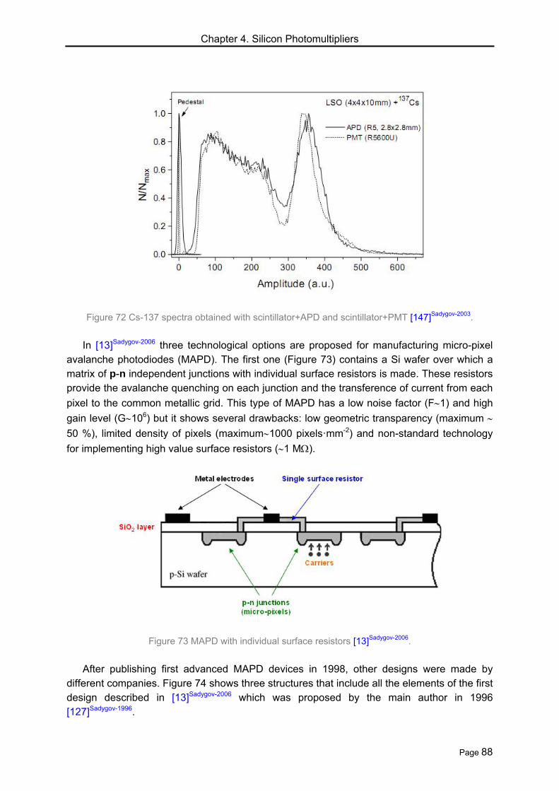
Chapter 4. Silicon Photomultipliers
Page 88
Figure 72 Cs-137 spectra obtained with scintillator+APD and scintillator+PMT [147]Sadygov-2003.
In [13]Sadygov-2006 three technological options are proposed for manufacturing micro-pixel
avalanche photodiodes (MAPD). The first one (Figure 73) contains a Si wafer over which a matrix of p-n independent junctions with individual surface resistors is made. These resistors provide the avalanche quenching on each junction and the transference of current from each
pixel to the common metallic grid. This type of MAPD has a low noise factor (F1) and high
gain level (G106) but it shows several drawbacks: low geometric transparency (maximum
50 %), limited density of pixels (maximum1000 pixels·mm-2) and non-standard technology
for implementing high value surface resistors (1 M).
Figure 73 MAPD with individual surface resistors [13]Sadygov-2006.
After publishing first advanced MAPD devices in 1998, other designs were made by
different companies. Figure 74 shows three structures that include all the elements of the first design described in [13]Sadygov-2006 which was proposed by the main author in 1996 [127]Sadygov-1996.

Chapter 4. Silicon Photomultipliers
Page 89
Figure 74 Other designs similar to the MAPD proposed in [13]Sadygov-2006.
The second design (Figure 75) is an avalanche photodiode with independent micro-pixels
in which local avalanche quenching is obtained thanks to the low conductivity of the individual surface conduction channels along the Si-SiO2 interface (this design was advanced in [147]Sadygov-2003). This option is taken as a prototype for the future development of an ultra-fast avalanche CCD matrix able to work in the single photon mode.
Figure 75 MAPD with surface drift of charge carriers [13]Sadygov-2006.
The third design (Figure 76) consists on a deep matrix of pixels with individual avalanche
quenching through independent vertical channels. This design offers good photoresponse linearity, high sensitivity in visible and ultraviolet ranges and the maximum geometric
transparency (100 %). This option requires more sophisticated technological resources than previous ones, such as epitaxial growing with high purity Si wafers and deep ionic implantation with several types of impurities.
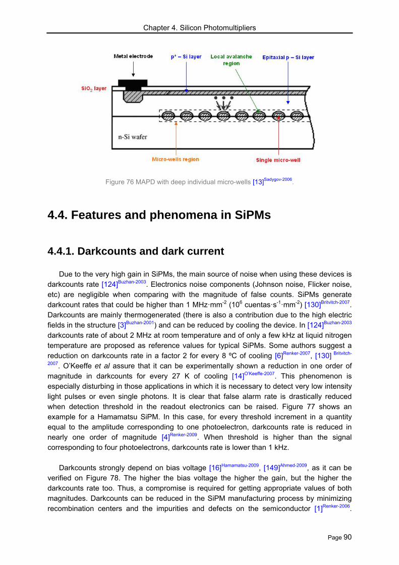
Chapter 4. Silicon Photomultipliers
Page 90
Figure 76 MAPD with deep individual micro-wells [13]Sadygov-2006.
4.4. Features and phenomena in SiPMs
4.4.1. Darkcounts and dark current Due to the very high gain in SiPMs, the main source of noise when using these devices is
darkcounts rate [124]Buzhan-2003. Electronics noise components (Johnson noise, Flicker noise, etc) are negligible when comparing with the magnitude of false counts. SiPMs generate darkcount rates that could be higher than 1 MHz·mm-2 (106 cuentas·s-1·mm-2) [130]Britvitch-2007. Darkcounts are mainly thermogenerated (there is also a contribution due to the high electric fields in the structure [3]Buzhan-2001) and can be reduced by cooling the device. In [124]Buzhan-2003 darkcounts rate of about 2 MHz at room temperature and of only a few kHz at liquid nitrogen temperature are proposed as reference values for typical SiPMs. Some authors suggest a reduction on darkcounts rate in a factor 2 for every 8 ºC of cooling [6]Renker-2007, [130] Britvitch-
2007. O’Keeffe et al assure that it can be experimentally shown a reduction in one order of magnitude in darkcounts for every 27 K of cooling [14]O’Keeffe-2007. This phenomenon is especially disturbing in those applications in which it is necessary to detect very low intensity light pulses or even single photons. It is clear that false alarm rate is drastically reduced when detection threshold in the readout electronics can be raised. Figure 77 shows an example for a Hamamatsu SiPM. In this case, for every threshold increment in a quantity equal to the amplitude corresponding to one photoelectron, darkcounts rate is reduced in nearly one order of magnitude [4]Renker-2009. When threshold is higher than the signal corresponding to four photoelectrons, darkcounts rate is lower than 1 kHz.
Darkcounts strongly depend on bias voltage [16]Hamamatsu-2009, [149]Ahmed-2009, as it can be
verified on Figure 78. The higher the bias voltage the higher the gain, but the higher the darkcounts rate too. Thus, a compromise is required for getting appropriate values of both magnitudes. Darkcounts can be reduced in the SiPM manufacturing process by minimizing recombination centers and the impurities and defects on the semiconductor [1]Renker-2006.

Chapter 4. Silicon Photomultipliers
Page 91
There is also a weak dark current originated by the reverse photodiode biasing, whose dependency with the temperature can be seen in Figure 79.
Figure 77 Darkcounts rate as a function of the detection threshold in the readout electronics [130]Britvitch-2007.
Figure 78 Darkcounts of the SiPM Hamamatsu S10362 as a function of the bias voltage [16]Hamamatsu-
2009.
The SiPM matrix structure, besides offering a response directly proportional to the
incident intensity, has other advantages. On the one hand, the gain is intrinsically high. On the other hand, the noise level is low. The main source of noise is carrier thermogeneration in the active volume. For a little noisy device, the probability that two or more cells were fired simultaneously by thermal effects is very low. So, it would be possible to eliminate all the

Chapter 4. Silicon Photomultipliers
Page 92
noise in the system by setting the detection threshold just above the level corresponding to one photoelectron [149]Ahmed-2009.
(a) (b)
Figure 79 Dependence of dark current with temperature for (a) SiPM Hamamatsu S2382 [150]Hamamatsu-
2001 and (b) SiPM Hamamatsu S10362-33-100C [147]Ahmed-2009.
4.4.2. Recovery time The recovery time of a cell in the SiPM depends mainly on the time constant given by the
cell capacitance (Ccell, directly proportional to its size; typically 50-100 fF [124]Buzhan-2003) and by its integrated quenching resistor (Rs) [130]Britvitch-2007, [151]Wangerin-2008.
covre ery s cellT R C (59)
SiPM have recovery times ranging from tens of ns up to hundreds of s [1]Renker-2006. Typically up to 1 % of cells in the device are always in state of recovery, so that the number of fully operative cells is reduced [12]Otte-2006. When a large number of cells are in the recovery phase simultaneously, the saturation effect previously mentioned is intensified. Thus, both detection efficiency and saturation effect are affected by recovery. And as it was previously mentioned, recovery affects on the linearity of the device with higher weight for long optical exciting signals [12]Otte-2006.
Detection rate reachable with a SiPM is roughly the inverse of the recovery time. For
example, if the recovery time was lower than 1 s, it would be possible to expect a maximum
detection rate higher than 1 MHz [130]Britvitch-2007. Britvitch et al proposed a methodology for the precise measurement of the recovery time and it is highlighted the strong dependence of this parameter with the temperature and the bias voltage of the device (Figure 80) [152]Britvitch-
2006. Authors assure that recovery time is inversely proportional to the temperature [153]Collazuol-2009. The reason for this behavior is an inverse proportionality of the resistivity in

Chapter 4. Silicon Photomultipliers
Page 93
the quenching polysilicon resistors with the temperature [152]Britvitch-2006. As an example, a
SiPM from Hamamatsu shows a recovery time of 190 s at 0 ºC while it is reduced to 98 s
at room temperature. By its own, the quenching resistor changes its value from 200 k at
room temperature to about 1700 k at the temperature of liquid nitrogen [4]Renker-2009. It could
be advantageous replacing polysilicon by a metallic alloy with high resistivity (like FeCr) [4]Renker-2009. Recovery time also rises as a consequence of the afterpulsing phenomenon [1]Renker-2006.
Figure 80 Recovery time of a SiPM as a function of its bias voltage [1]Renker-2006.
4.4.3. Crosstalk phenomenon Normally, Si diodes operating on Geiger mode emit light when they are reverse polarized.
Emission rate is approximately in the range 1-3·10-5 photons (with energy higher than 1.14 eV) by each carrier crossing the p-n junction [154]Otte-2009, [155]Piemonte-2011. Thus, crosstalk is directly proportional to the charge crossing the avalanche region. Photons generated by one cell can travel through the material, arrive to a neighbour cell and trigger there an avalanche process (Figure 81). This phenomenon is known as photon-assisted crosstalk and it provides a little but not negligible contribution to the SiPM signal. Some authors talk about even two types of crosstalk: prompt crosstalk, caused when a photon travels to a neighbour active region and triggers an avalanche (like an external photon) and slow crosstalk, when a photon induces charge into the bulk of a neighbour cell that subsequently migrates into its active region [156]Miyamoto-2009. Crosstalk effects are of stochastic nature and they rise the excess noise of the SiPM up to a value between 1.1 and 1.2 [130]Britvitch-2007. Crosstalk also contributes to the SiPM saturation.
Crosstalk depends on the number of carriers crossing the junction. So, one could think in
lightening crosstalk effects by reducing the gain (i.e. reducing the SiPM bias voltage). However, the strong dependence of PDE with bias voltage advice against this solution [12]Otte-2006. Reducing parasitic capacitances associated with the cell also contributes to limit the amount of crossing carriers. But, at the same time, capacitances have influence on the output signal amplitude. So, in most devices, capacitance is adjusted for obtaining a

Chapter 4. Silicon Photomultipliers
Page 94
compromise between optical crosstalk and PDE [12]Otte-2006. One possible way for reducing the influence of crosstalk is providing optical isolation between pixels with metallic coatings [157]Kindt-1998. Mirzoyan et al propose three ways to limit the influence of crosstalk: trenches, a second junction for isolating the bulk from the active region and prompt optical crosstalk suppression using Si damaged by ion implantation [136]Mirzoyan-2011.
Figure 81 Photon-assisted crosstalk in a SiPM [1]Renker-2006.
Crosstalk probability can be quantified using the following expression [5]Haba-2008:
'xtalk cN PDE (60)
xtalk: Crosstalk probability. Nc: Number of photogenerated carriers. PDE’: Equivalent PDE for the photon that is causing the
crosstalk phenomenon.
Since PDE = QE · geometry · Geiger, it is easy to see that a compromise in relation with the
geometric efficiency is needed. If geometric efficiency is high, detection efficiency will be enhanced but at the expense of higher crosstalk distortion.
4.4.4. Afterpulsing phenomenon Another limiting feature in SiPMs is the so called afterpulsing. This phenomenon happens
when some of the carriers generated in the avalanche remain trapped on defects of the
lattice and are released later (even several s [1]Renker-2006). As a result the avalanche process is re-trigger during the recovery phase (Figure 82) whose consequence is a stretching of the dead time and/or the appearing of a later secondary pulse which corresponds with a false detection. Afterpulsing probability (probability density as a function of time in Figure 82) is given by the following equation [5]Haba-2008, [155]Piemonte-2011:
( )trap
t
ap c t Geigertrap
eP t N P P
(61)

Chapter 4. Silicon Photomultipliers
Page 95
Pap: Probability of afterpulsing in a time t after the initial Geiger discharge.
Nc: Number of carriers generated in the initial avalanche process. Pt: Probability that carriers are trapped on defects of the lattice. PGeiger: Probability that Geiger discharge was triggered by only one
carrier.
trap: Lifetime in the trap; time that the carrier remain trapped on a defect of the lattice.
(a) (b)
Figure 82 Afterpulsing phenomenon. (a) SiPM response when afterpulsing happens [5]Haba-2008 and (b) probability density for afterpulsing as a function of time [1]Renker-2006.
One factor that significantly affects the development of this phenomenon is the
photodiode capacitance. One way for reducing the total capacitance and its influence on afterpulsing is integrating the signal processing electronics together with the SiPM [157]Kindt-
1998. Since the number of trapped carriers is proportional to the number of carriers crossing the junction, afterpulsing is also proportional to the excess bias voltage [158]Viana-Ramos-2003. The temperature also affects: the lower the temperature the higher the trap lifetime [158]Viana-
Ramos-2003. Taking into account the previous equation it is possible to see that cooling could increase the afterpulsing probability.
4.4.5. Noise a function of gain Figure 83 shows the dependence of the excess noise factor with the intrinsic gain for the
series S2381-S2385 of Hamamatsu. The higher the device gain the higher the fluctuations in the avalanche process (the higher the excess noise component), with the corresponding reduction in the signal to noise ratio.

Chapter 4. Silicon Photomultipliers
Page 96
Figure 83 Excess noise factor as a function of the gain for the series S2381-S2385 of Hamamatsu [150]Hamamatsu-2001.
4.4.6. Temperature-dependent parameters The behavior of the SiPM is strongly dependent on the temperature. It was previously
mentioned that recovery time and darkcounts rate show inverse and direct proportionality with the temperature respectively.
Figure 84 Darkcounts rate of a SiPM as a function of overvoltage for several temperatures [5]Haba-2008.
The fact that the noise increases with the temperature (Figure 84) can be understood
taking into account the following relation for the number of thermogenerated carriers [5]Haba-
2008:

Chapter 4. Silicon Photomultipliers
Page 97
3 22gap
B
E
k TcarrierN T e
(62)
Ncarrier: Thermogenerated carriers. T: Temperature at which it is subjected the SiPM. Egap: Bandgap energy of the semiconductor material. kB: Boltzmann constant.
SiPM gain shows an important dependence with temperature as it can be observed in Figure 85 and Figure 86.
Figure 85 Dependence of the gain with the temperature for the SiPM Hamamatsu S6045 [150]Hamamatsu-2001.
Figure 86 Variation of the gain of the SiPM Hamamatsu S10362 as a function of the temperature for constant bias voltage [16]Hamamatsu-2009.

Chapter 4. Silicon Photomultipliers
Page 98
For stable operation the temperature should be controlled with an accuracy lower than 1 ºC. The alternative consists on correcting the bias voltage in a correlated way with the temperature drift. The idea is to maintain the same response level (the same gain) in any moment, so that a certain temperature drift was compensated with the corresponding bias voltage variation (e.g. in [4]Renker-2009 it is estimated for a Hamamatsu SiPM a voltage
correction factor VBIAS + 50 mV for each degree of heating). Thermal equalization in the
SiPM could be achieved with a circuit that senses the temperature and reacts applying the suitable pre-programmed correction. Several authors have shown a clear direct proportionality between breakdown voltage and the temperature, as can be seen in [135]Huding-2011, [147]Ahmed-2009, [159]Otono-2007, [160]Kaplan-2008, [161]Para-2009.
Figure 87 Breakdown voltage correlation with temperature in a SiPM [135]Huding-2011.
4.4.7. Effect of radiations on SiPMs
Many researchers have provided data showing that ionizing radiations (, , protons, neutrons, etc.) may cause effects on Si or in Si/SiO2 interfaces. As a consequence, some of the SiPM parameters like VBR, dark current and darkcounts, gain or detection efficiency may be altered during and after irradiation. Nevertheless, Otte assures that, despite these secondary effects, SiPMs have low nuclear counter effect: even a heavy ionizing particle would only cause an output signal equivalent to one incoming photon [12]Otte-2006.
The most early effect of exposition to ionizing radiations is an increase in the dark current
which disturbs the detector efficiency for resolving single photons [5]Haba-2008. In Figure 88 can be observed that the needed dose for disturbing the features of the device are relatively high. However, the use of these devices in medical applications can justify such high doses and higher, so that the effect of radiations on photodetectors must be taken into account. In [162]Matsubara-2007 it was observed that, after exposing the SiPM Hamamatsu T2K-11-100C to
-radiation coming from a 60Co source, the device showed an increment in its dark current
and darkcounts whose amplitudes were in the range of the amplitude corresponding to more than 10 photoelectrons.
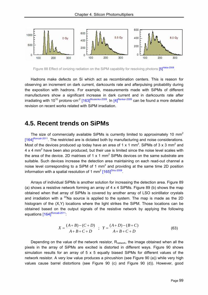
Chapter 4. Silicon Photomultipliers
Page 99
Figure 88 Effect of ionizing radiation on the SiPM capability for resolving photons [5]Haba-2008.
Hadrons make defects on Si which act as recombination centers. This is reason for
observing an increment on dark current, darkcounts rate and afterpulsing probability during the exposition with hadrons. For example, measurements made with SiPMs of different manufacturers show a significant increase in dark current and in darkcounts rate after irradiating with 1010 protons·cm-2 [163]Musienko-2009. In [4]Renker-2009 can be found a more detailed revision on recent works related with SiPM irradiation.
4.5. Recent trends on SiPMs The size of commercially available SiPMs is currently limited to approximately 10 mm2
[164]Roncali-2011. The restricted are is dictated both by manufacturing and noise considerations. Most of the devices produced up today have an area of 1 x 1 mm2. SiPMs of 3 x 3 mm2 and 4 x 4 mm2 have been also produced, but their use is limited since the noise level scales with the area of the device. 2D matrixes of 1 x 1 mm2 SiPMs devices on the same substrate are suitable. Such devices increase the detection area maintaining on each read-out channel a noise level corresponding to a SiPM of 1 mm2 and providing at the same time 2D position information with a spatial resolution of 1 mm2 [165]Dinu-2009.
Arrays of individual SiPMs is another solution for increasing the detection area. Figure 89
(a) shows a resistive network forming an array of 4 x 4 SiPMs. Figure 89 (b) shows the map obtained when that array of SiPMs is covered by another array of LSO scintillator crystals and irradiation with a 22Na source is applied to the system. The map is made as the 2D histogram of the (X,Y) locations where the light strikes the SiPM. Those locations can be obtained based on the output signals of the resistive network by applying the following equations [164]Roncali-2011:
DCBA
CBDAY
DCBA
DCBAX
)()(
;)()(
(63)
Depending on the value of the network resistor, Rnetwork, the image obtained when all the
pixels in the array of SiPMs are excited is distorted in different ways. Figure 90 shows simulation results for an array of 5 x 5 equally biased SiPMs for different values of the network resistor. A very low value produces a pincushion (see Figure 90 (a)) while very high values cause barrel distortions (see Figure 90 (c) and Figure 90 (d)). However, good

Chapter 4. Silicon Photomultipliers
Page 100
reconstructions of the position are possible when the value of the network resistor is around
1 k (see Figure 90 (b)) [166]Stapels-2009.
Figure 89 (a) Resistive network for making an array of 4 x 4 SiPMs. (b) Scintillation map acquired when that SiPMs array is covered with another array of LSO scintillation crystals and irradiation with a
22Na source is applied [164]Roncali-2011.
Figure 90 Maps obtained by simulation when all the elements in an array of 5 x 5 SiPMs are excited.
Several values for the network resistor are used. (a) Rnetwork = 150 , (b) Rnetwork = 1 k, (c) Rnetwork =
50 k, (d) Rnetwork = 200 k [166]Stapels-2009.
Chapter 4. Silicon Photomultipliers
Page 101
Recently, new approaches to enhance the use of SiPMs have been developed, as for example the digital SiPM. In such detector, each detection is converted to a digital signal containing information on the number of fired cells. Active quenching built into each cell provides a short recovery time and a static memory allows enabling or disabling each individual cell in the device. This way, cells with an excessive dark current date, for instance, can be switched off [167]Frank-2010.
Several authors are focusing on the application of SiPMs to the biomedical field. So, for
example, Barrio et al have developed a matrix of 8 x 8 SiPMs (each one with 840 microcells) for making a small animals PET scanner. Also, a matrix of 4 x 4 SiPMs of large area (3 x 3 mm2) allows them to make a system for dose monitoring in hadron therapy [168]Barrio-2010. Tao develops the complete design, simulation and experimental characterization of a gamma-camera based on SiPMs [169]Tao-2012.
4.6. Other advanced high sensitivity detectors In the hybrid photodetector (HPD) an avalanche diode is placed in a vacuum tube with a
photocathode at the optical input. Photoelectrons generated at the photocathode are focused onto the avalanche diode that provides the detectable current pulse [111]Buller-2010. These detectors provide lower timing jitter than PMTs, good sensitivity and could be particularly suitable for applications requiring large detection areas. Zhang et al reported a HPD with a
NEP 5.9·10-17 W·Hz-1/2 when illuminated with wavelength of 600 nm. An additional up-conversion strategy (using a periodically-poled lithium niobate waveguide; see later) did not allow enhancing its behavior: darkcount rate was increased and quantum efficiency was
reduced in such a way that NEP of the combined device was 7.8·10-16 W·Hz-1/2 [170]Zhang-
2009. HPDs need however large bias voltages, which are of the order of several kVs. Devices based on quantum-dots are also possible for detecting single photons. A
quantum dot is a structure that confines electrons in three dimensions, leading to a quantization of the energy for carriers similar to that of a single atom [111]Buller-2010: a series of discrete Lorentzian shaped energies in the density of states happens. The wavefunctions of the electrons in the quantum dot are fully constrained within the dot, which behaves like a single atom, even though it is made up to many atoms. A quantum dot can be seen as a nanometre dimensioned island of low band gap semiconductor material surrounded by higher band gap material. There are a number of techniques for manufacturing quantum dots, but the method which produces the best results is the Stranski-Krastanow growth, also known as self-assembly [171]Markov-1987. Over a semiconductor substrate (e.g. GaAs) at least two layers of a different semiconductor (e.g. InAs) with a slight mismatch in the lattice parameter are grown. The mismatch in the lattice parameter leads to strain that will lead to the formation of small islands in the semiconductor surface to relieve the strain (Figure 91). These islands are the quantum dots [111]Buller-2010.
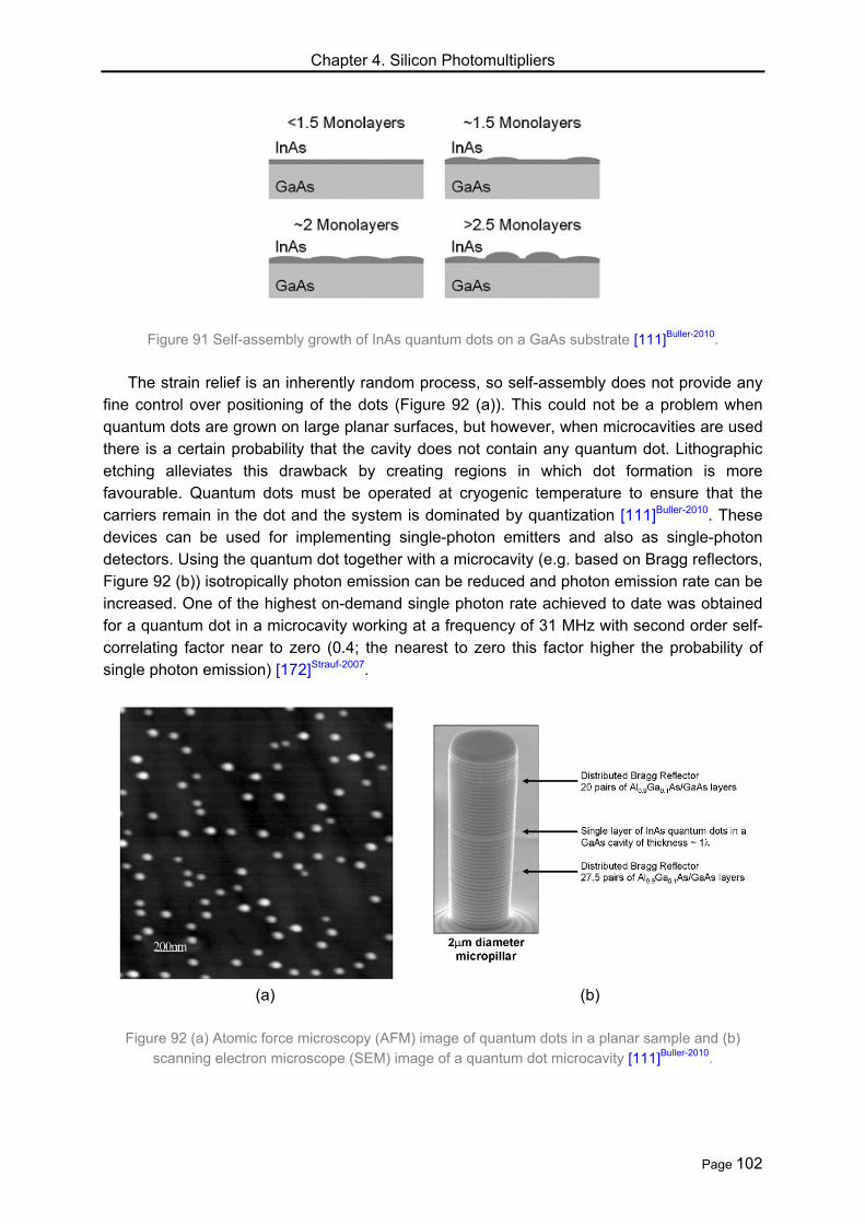
Chapter 4. Silicon Photomultipliers
Page 102
Figure 91 Self-assembly growth of InAs quantum dots on a GaAs substrate [111]Buller-2010.
The strain relief is an inherently random process, so self-assembly does not provide any
fine control over positioning of the dots (Figure 92 (a)). This could not be a problem when quantum dots are grown on large planar surfaces, but however, when microcavities are used there is a certain probability that the cavity does not contain any quantum dot. Lithographic etching alleviates this drawback by creating regions in which dot formation is more favourable. Quantum dots must be operated at cryogenic temperature to ensure that the carriers remain in the dot and the system is dominated by quantization [111]Buller-2010. These devices can be used for implementing single-photon emitters and also as single-photon detectors. Using the quantum dot together with a microcavity (e.g. based on Bragg reflectors, Figure 92 (b)) isotropically photon emission can be reduced and photon emission rate can be increased. One of the highest on-demand single photon rate achieved to date was obtained for a quantum dot in a microcavity working at a frequency of 31 MHz with second order self-correlating factor near to zero (0.4; the nearest to zero this factor higher the probability of single photon emission) [172]Strauf-2007.
(a) (b)
Figure 92 (a) Atomic force microscopy (AFM) image of quantum dots in a planar sample and (b)
scanning electron microscope (SEM) image of a quantum dot microcavity [111]Buller-2010.

Chapter 4. Silicon Photomultipliers
Page 103
Kardynal et al demonstrated that a quantum dot used together with a FET transistor (GaAs/Al0.33Ga0.67As) was able to detect single photons (Figure 93) [173]Kardynal-2007. The gating in this device is provided by the layer of quantum dots. One incident photon generates a photoelectron that is subsequently captured by a dot. This capture changes the shape of the electric field in the structure and thus generates a measurable change in the drain-source
current [111]Buller-2010. Cooling at 77 K the results are quite poor: PDE 0.9 % at a wavelength
of 650 nm and NEP 2·10-6 W·Hz-1/2. Rowe et al reported a PDE 2-3 % operating a quantum dot FET (GaAs/Al0.20Ga0.80As) at a wavelength of 800 nm and at a temperature of 4 K [174]Rowe-2006. In 2007 Blakesley et al demonstrated the quantum dot resonant tunnelling diode [175]Blakesley-2005. When a photo-excited hole is generated, it is captured by a quantum dot lowering its potential and changing the diode tunnelling conditions in such a way that a measurable signal happens [111]Buller-2010. Detection efficiency of about 12.5 % and very good
NEP 2·10-19 W·Hz-1/2 were reported, using a temperature of 4 K and wavelength of 550 nm. However, timing jitter of these devices is large (150 ns). For applications such as long distance Quantum Key Distribution (QKD) it is preferable to have detectors working at wavelengths around 1300 nm or 1550 nm (low-loss windows for conventional optical fibres). However, reported results on the infrared range are quite limited: an InP based quantum dot resonant tunnelling diode described by Li et al only reached a detection efficiency of 0.35 % (working at a wavelength of 1300 nm and at a temperature of 4.5 K) [176]Li-2007.
Figure 93 Cross section of the quantum dot field effect transistor used for single photon detection in [173]Kardynal-2007.
Superconductivity has demonstrated its utility for detecting extremely low light intensities.
Transition edge sensors are a form of extremely sensitive calorimeters. Ideal materials for using with these devices (e.g. tungsten) are characterized by a sharp transition between the temperature at which they show superconductivity and the temperatures at which they behave as normal conductors [111]Buller-2010. When a photon is absorbed in a superconducting stripe (cooled below the superconducting transition temperature) the photoelectron generated is capable to increase the temperature. That temperature increase breaks the superconductivity condition and the resistance stripe rises. That fact can be sensed as a current change by means of a Superconducting Quantum-Interference Device (SQUID).
These detectors offer very good detection efficiencies (PDE 88 % at a wavelength of 1550
nm and NEP 6·10-19 W·Hz-1/2), wide operating wavelength range (480 nm – 780 nm), low

Chapter 4. Silicon Photomultipliers
Page 104
darkcount rates (tens of counts per second) and provide photon resolving capability. However, they offer poor timing jitter, of about 90 ns [111]Buller-2010.
In Figure 94 it is shown the working fundamentals of Niobium-nitride superconducting
nanowires. The nanowire is biased with a current below the critical current for superconductivity. A photon impinging on the nanowire induces a temperature increase in a hot spot. This spot grows and generates a resistive barrier across the width of the nanowire which produces a voltage drop on the contacts of the device [111]Buller-2010. Because nanowires have widths of about 100 nm, there is low probability that an impinging photon impact on it and thus, early designs provided very low detection efficiencies. For enhancing detection efficiency one could think in incrementing the nanowire area, but it is not a good option because the hot spot formed by one only photon has little dimensions. The solution is implemented by a very long superconducting nanowire arranged in a meander way. This device is known as superconducting single-photon detector (SSPD).
(a) (b)
Figure 94 (a) Single photon detection in a superconducting nanowire and (b) scanning electron
microscope (SEM) of a meander type SSPD [111]Buller-2010.
Typical NEPs for SSPDs go from 3·10-18 W·Hz-1/2 to 3·10-16 W·Hz-1/2 for wavelengths
ranging from 400 nm to 1550 nm [111]Buller-2010. Features of SSPD devices make them good candidates for a range of applications, as for example, quantum key distribution at long distance and with conventional optical fibres. Collins et al were able to transmit safe key over a channel with losses of 55 dB which is equivalent to a distance of 25 km of fibre at the used wavelength (850 nm) [177]Collins-2007. Searching of materials for operating SSPDs at higher temperatures is a current research issue. In 2007 a ceramic material (Hg1−xTlxBa2(Ca1−ySry)2Cu3O8+δ) with transition temperature of 138 K was reported [111]Buller-
2010. The technique known as up-conversion makes possible the detection of long wavelength
photons using a photodetector suitable for shorter wavelengths. For example, single photons at 1550 nm (for optical communications) can be detected with SPADs working in the range

Chapter 4. Silicon Photomultipliers
Page 105
600-700 nm. Up-conversion is produced because a quadratic nonlinear medium (e.g. a Periodically Poled Lithium Niobate crystal, PPLN) is capable of producing a sum frequency under excitation with a strong pump beam (also known as escort beam). If the pump beam
and the target beam (both incoming to the nonlinear material) have frequencies pump and
inc respectively, the resulting beam (outgoing the nonlinear material) has a frequency out and the following relations are verified [111]Buller-2010:
;
1 1 1;
out inc pump out inc pump
out inc pump out inc pump
E E E h h h
c c ch h h
(64)
As a function of the pump beam power, detection efficiencies up to 90 % can be
achieved. This technique suffers from a problem with darkcounts generated by the escort beam, i.e. the photodetector really detects photons although they are not the target photons but lost photons from the escort beam [111]Buller-2010. Stretching of detection range of wavelengths in this approach is possible using a spectrally tuneable pump laser [178]Thew-2008. Using up-conversion Albota and Wong were able to detect incident photons at 1548 nm by means of photons at a wavelength of 631 nm (detection with a short wavelength SPAD) and using an escort beam at 980 nm [179]Albota-2004. Diamanti et al used this approach for converting a light beam at 1550 nm to another one at 713 nm using an escort beam at a wavelength of 1320 nm. Beam at 1550 nm allowed secure transmission in a QKD system at 166 b·s-1 for a distance of about 100 km and up-conversion made easy its detection using short wavelength single-photon detector [180]Diamanti-2006.

Chapter 5. Experimental considerations
Page 106
5. Experimental considerations This chapter provides a description of devices and instruments used in the experimental
work described in later chapters. Selection of SiPMs and light sources is discussed, registering equipments are briefly shown and the amplification chain is carefully characterized. Also, some preliminary measurements are shown, as for example, the dependence of the photodetection amplitude with the intensity of the exciting light pulse or with the SiPM bias voltage.
5.1. Selected silicon photomultipliers Several models of SiPMs included in the Hamamatsu S10362 family have been used in
this work. Table 2 shows their main features [181]Hamamatsu-2009, [182]Hamamatsu-2010. It is important to note that all of them cover a wide spectral range (from 320 nm to 900 nm) showing the maximum photodetection efficiency around 440 nm (see Figure 95) and providing very high intrinsic gain (in the order of 105 – 106). However, an important drawback to take into account when using these detectors is the fact that darkcount rates are in the order of MHz. Data in Table 2 show that darkcount rate is directly related with the number of cells in the device and with the pixel size. Terminal capacitance is proportional to the effective active area because it is related with the common conductor grid that connects all the cells in the device.
Table 2 Main features of several models of Hamamatsu SiPMs in the family S10362.
In spite of the nominal values given in datasheets, the manufacturer provides particular
data for each specific product. Sometimes, these particular values considerably differ from nominal ones, particularly in relation with darkcount rate. For our first sample of the model S10362-33-100C the following specific features were provided: operating voltage: 69.57 V, intrinsic gain: 2.41·106 and darkcount rates of 2.794 Mcps and 685 kcps for detection

Chapter 5. Experimental considerations
Page 107
thresholds of 0.5 and 1.5 photoelectrons respectively (measured at 10 ºC with exciting wavelength of 655 nm). For models S10362-33-050C and S10362-11-050C Hamamatsu recommends slightly higher bias voltages (71.25 V and 71.2 V respectively) and provides intrinsic gains near the nominal values (7.5·105 and 7.52·105 respectively) and darkcount rates higher than nominal (7.6 Mcps and 569 kcps respectively, both measured at 25 ºC with a detection threshold of 0.5 photoelectrons).
Figure 95 Photodetection efficiency for the SiPM Hamamatsu S10362-33-05C [181]Hamamatsu-2009.
Figure 96 and Figure 97 allow observing the appearance of different models in the
S10362 family and also the typical waveforms obtained with these SiPMs when signal provided by the photodetector is processed with additional high gain. Oscilloscope persistence provides superposition of photodetection pulses, so that it is possible to obtain an amplitude histogram when enough registering time has elapsed. Because of modern oscilloscopes usually have the histogram functionality, it is easy to obtain the characteristic pattern that provides the set of thresholds for counting the number of received photons for a given photodetection pulse amplitude. Another strategy for knowing the number of received photons consists on calculating the total charge delivered to the load, and then comparing it with the charge delivered when only one photon has been received. However, we prefer the first strategy because it is easier to apply and it could even be implemented in a fixed hardware configuration.

Chapter 5. Experimental considerations
Page 108
Figure 96 Hamamatsu SiPM, S10362-33 series [181]Hamamatsu-2009. (a) Appearance of the device. (b) Microphotography showing the matrix of cells. (c) Registered waveforms for the model S10362-33-
050C using oscilloscope persistence and a gain factor of 120. It is also shown the characteristic pattern extracted from persistence for resolving the number of received photons.
Figure 97 Hamamatsu SiPM, S10362-11 series [182]Hamamatsu-2010. (a) Appearance of different models in the series. (b) Registered waveforms for the model S10362-11-050U using oscilloscope persistence
and a gain factor of 120. It is also shown the characteristic pattern extracted from persistence for resolving the number of received photons.
5.2. Silicon photomultiplier bias circuit The SiPM bias circuit used in the experiments is designed according to its manufacturer
recommendation and can be seen in Figure 98. RL is a limiting resistor for guarding the device, RS is the photocurrent sensing resistor and CO is a blocking capacitor whose aim is to remove any DC component from photodetection signal. Ccat has the double purpose of removing spurious high frequency components in the SiPM bias voltage and enhancing separability between output amplitudes corresponding to different number of received photons.

Chapter 5. Experimental considerations
Page 109
Figure 98 SiPM bias circuit as recommended by the manufacturer.
Figure 99 shows the layout of different boards used in this work for biasing the SiPMs
where SMD components and standard SMA connectors were used for implementing them. A good number of connections between top and bottom ground planes were also distributed over the board for optimum grounding at high frequencies.
Figure 99 Different SiPM bias boards used in this work.
The bias voltage is provided by the high accuracy power source Keithley model 6487
[183]Keithley-2009-[186]Keithley-2002. This equipment also includes a nanoammeter which connected in series with the voltage source allows us to determine the typical current-voltage curve of the SiPM.
5.3. Preliminary measurements Some preliminary measurements for evaluating the SiPM behavior with respect to bias
voltage and illumination intensity were done. The SiPM was illuminated with short pulses coming from a laser [187]PicoQuant-2010. The laser driver allows us to vary the intensity of the pulses but it does not have an adequate calibration, so that intensity was referred to its
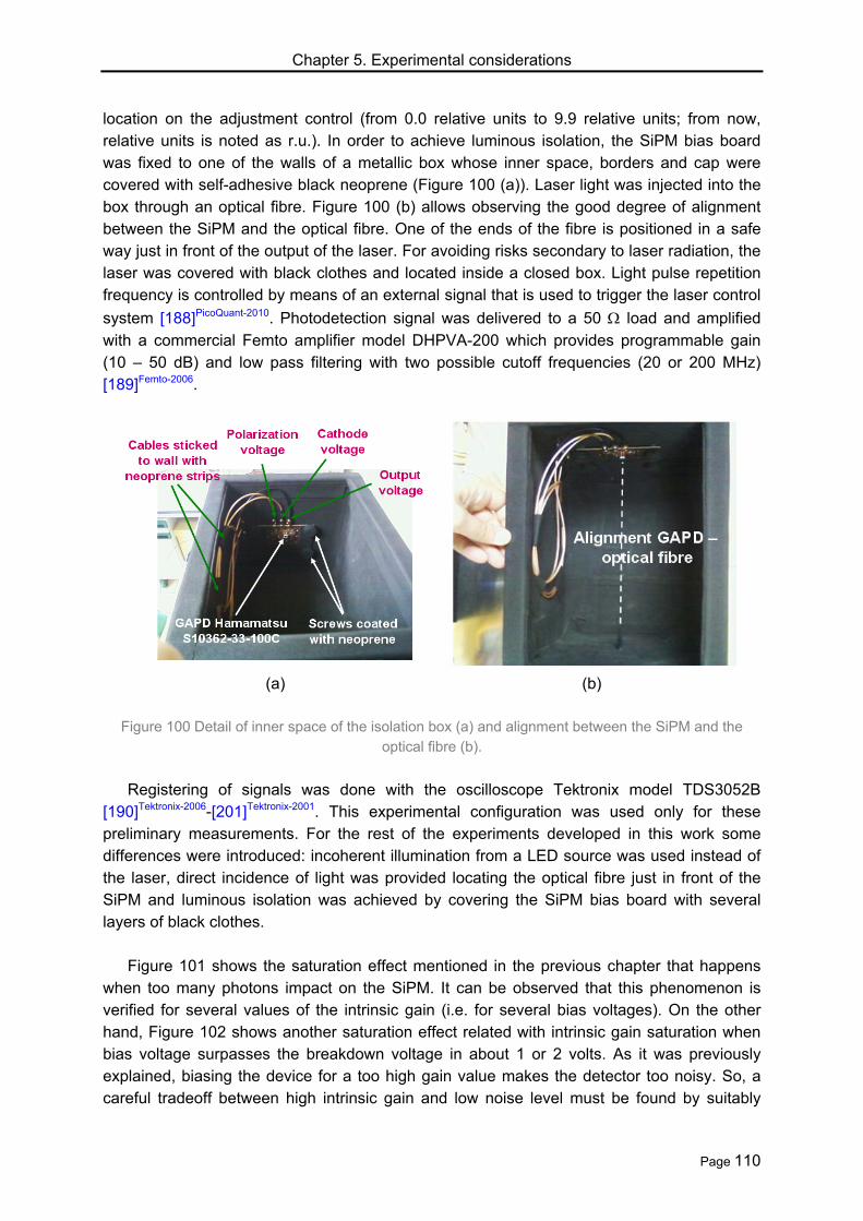
Chapter 5. Experimental considerations
Page 110
location on the adjustment control (from 0.0 relative units to 9.9 relative units; from now, relative units is noted as r.u.). In order to achieve luminous isolation, the SiPM bias board was fixed to one of the walls of a metallic box whose inner space, borders and cap were covered with self-adhesive black neoprene (Figure 100 (a)). Laser light was injected into the box through an optical fibre. Figure 100 (b) allows observing the good degree of alignment between the SiPM and the optical fibre. One of the ends of the fibre is positioned in a safe way just in front of the output of the laser. For avoiding risks secondary to laser radiation, the laser was covered with black clothes and located inside a closed box. Light pulse repetition frequency is controlled by means of an external signal that is used to trigger the laser control
system [188]PicoQuant-2010. Photodetection signal was delivered to a 50 load and amplified with a commercial Femto amplifier model DHPVA-200 which provides programmable gain (10 – 50 dB) and low pass filtering with two possible cutoff frequencies (20 or 200 MHz) [189]Femto-2006.
(a) (b)
Figure 100 Detail of inner space of the isolation box (a) and alignment between the SiPM and the
optical fibre (b).
Registering of signals was done with the oscilloscope Tektronix model TDS3052B
[190]Tektronix-2006-[201]Tektronix-2001. This experimental configuration was used only for these preliminary measurements. For the rest of the experiments developed in this work some differences were introduced: incoherent illumination from a LED source was used instead of the laser, direct incidence of light was provided locating the optical fibre just in front of the SiPM and luminous isolation was achieved by covering the SiPM bias board with several layers of black clothes.
Figure 101 shows the saturation effect mentioned in the previous chapter that happens
when too many photons impact on the SiPM. It can be observed that this phenomenon is verified for several values of the intrinsic gain (i.e. for several bias voltages). On the other hand, Figure 102 shows another saturation effect related with intrinsic gain saturation when bias voltage surpasses the breakdown voltage in about 1 or 2 volts. As it was previously explained, biasing the device for a too high gain value makes the detector too noisy. So, a careful tradeoff between high intrinsic gain and low noise level must be found by suitably

Chapter 5. Experimental considerations
Page 111
selecting the bias voltage. Taking into account Figure 101 it is possible to say that an appropriate bias voltage could be between 70.5 V and 71 V. That is, slightly higher than the breakdown voltage. Above 71 V the intrinsic gain saturation effect is evident. Figure 102 also allows verifying the previous assertion. A bias voltage between 70.5 V and 71 V provides the best separation between curves corresponding to different illumination levels without going into the saturation region.
Figure 101 Behavior of the SiPM model S10362-33-100C as a function of the laser intensity for
several bias voltages.
Figure 102 Behavior of the SiPM model S10362-33-100C as a function of the bias voltage for several laser intensities.

Chapter 5. Experimental considerations
Page 112
The following figures show typical responses of the SiPM when a short pulse is received. Figure 103 allows observing how an increasing light intensity causes an increase in the SiPM output pulse. Two additional results of interest can be observed. First, comparing curves for 3.5 r.u. and 4.0 r.u. (with or without additional gain) it is possible to verify that saturation effect is already playing a role. Second, using an amplifier with enough bandwidth the shape of the pulse is not disturbed, nor in rising edge neither on falling edge or amplitude.
Figure 103 Output voltage provided by the SiPM model S10362-33-100C for a bias voltage of 70.1 V and several laser intensities, without amplification and with a gain factor of 20 dB.
Figure 104 Output voltage provided by the SiPM model S10362-33-100C for a laser intensity of 4.3 r.u. and several bias voltages.

Chapter 5. Experimental considerations
Page 113
Meanwhile, Figure 104 allows observing the direct proportionality between the intrinsic gain and the bias voltage. Both figures show that rising edge duration is very low and nearly independent on illumination level and intrinsic gain. Also it is possible to see that falling proportion for a certain time after the peak is the same whatever the illumination level or the bias voltage. This fact is important because it says that the falling time constant does not vary and thus the elements that implement the equivalent circuit of the SiPM do not depend on those external magnitudes.
5.4. The statistical nature of the weak light An expression can be obtained for describing the statistical nature of the weak light
arriving to a photodetector. For this calculation, the detector efficiency is considered ideal and parasitic effects are not taken into account. The probability of obtaining one count in a
short period of time t is given by the following expression, where is the photon rate (photons per second):
ttP ),1( (65)
During a period of time T there is a number of N intervals of time whose duration is t: T =
N·t. During each of these elemental intervals one photon can be detected or not. It is
assumed that the intensity of the light is so weak that the probability of getting more than one
detection during a certain interval t is zero. So, probability of registering one count during t
is ·t and the probability of not registering any counts at all is (1-·t). The result of the statistical experiment happening on a certain interval can be considered as independent of all the others. Thus, the probability of registering n counts during the period of time T (i.e. N intervals) is the probability of registering one count on each one of n intervals and no counts on the rest of the intervals:
nNn ttTnP 1)*,( (66)
However, it must be taken into account the fact that those n counts can be obtained in
many different ways. That is, the n intervals (among the total of N intervals) in which there are counts can be arranged in M ways, as given by the following expression:
!!
!
nNn
N
n
NM
(67)
So, finally, the final probability of getting n counts during the period of time T is:
nNn ttnNn
NTnPMTnP
1
!!
!)*,(),( (68)

Chapter 5. Experimental considerations
Page 114
The limit when N can be applied for ending the infinitesimal notation. It is convenient
to transform the expression remembering that T = N·t.
N
nNn
nN
nN
n
n
nN
n
n
nNn
n
n
nNn
N
TNT
n
N
NN
TN
N
T
n
N
N
tNN
N
tN
n
N
tN
Nt
N
N
n
N
ttn
NTnP
)(
)(
1
1),(
(69)
Applying the limit when N the well-known expression for the Poisson distribution is obtained [111]Buller-2010, [202]Stapels-2006.
TnN
N
n
N
nN
NN
n
N
nNn
N
N
nNn
NN
en
T
N
TN
n
T
N
TN
nNn
NT
N
TNT
nNn
N
N
TNT
n
NTnP
!lim
!
)(lim
)!(!
!lim
)(
)!(!
!lim
)(lim),(lim
(70)
In the previous calculation the following well-known identity has been used:
xN
Ne
N
xN
lim (71)
Demonstration of the following properties for the Poisson distribution can be found
elsewhere. First, mean (n) and variance (n2) are equal:
Tnn 2 (72)

Chapter 5. Experimental considerations
Page 115
Second, the Poisson distribution tends to the Gauss distribution when the number of
events is very high (n ). That is, the higher the intensity of the light the higher the
tendency of the emission-detection distribution to be Gauss-type instead of Poisson-type.
5.5. Incoherent light sources After preliminary tests with laser illumination, our interest is focused on developing
strategies for enhancing the SiPM behavior when incoherent light is used. Light provided by LED devices is a simple and cheap mean of getting incoherent light pulses. After searching ultraviolet photoemitters among several manufacturers, the models Optosource 260019 [203]Optosource-2000 and Hero Electronics HUVL400-5x0B [204]Hero-2002 were selected. Model
260019 is a LED whose central wavelength is 370 nm and its full width at half maximum
is 12 nm. The optical power provided is up to 1 mW, the typical operating voltage is around
3.9 V (with a current of 10 mA) and its viewing angle is 55 º. Initially it was thought that a wide viewing angle would be interesting for assuring photon
detection with no need of an accurate alignment between emitter and detector. But it was not really necessary because light pulses were conducted to the SiPM by means of an optical fibre located and fixed close near the detector. The model HUVL400 emits in a central wavelength of 400 nm and has a bandwidth of 20 nm. It provides an optical power up to 2.2
mW, with a viewing angle of 20 º and is typically biased with 3.2 V and 20 mA. Both
photodiodes emit radiations quite far from ultraviolet B (280 nm – 320 nm) so that their use in laboratory is safe.
The excitation pulses are obtained directly feeding the ultraviolet LED with the function
generator Tektronix AFG3252 (2 GS/s, 240 MHz) and using rectangular short pulses (from 5 ns) of low amplitude (from about 2 V) for providing very weak illumination to the photodetector. SiPM photodetection efficiency for the emission spectral range of these LEDs is near its maximum (40 – 50 %, see Figure 105). Some experiments were done using the model Honeywell HFE4224 which is a GaAlAs LED whose central emission wavelength is 850 nm [205]Honeywell-2008. This LED has a bandwidth of 50 nm and is typically biased with 1.7 V and 60 mA. As can be seen in Figure 105, SiPM detection efficiency in the spectral range of this LED is very low (< 10 %). This photoemitter allows us to check the SiPM behavior at wavelengths quite far from its optimum working point, where photodetection is much less probable. However, as it will be shown later, good detection pulses and counting patterns have been obtained even in these extreme conditions.

Chapter 5. Experimental considerations
Page 116
Figure 105 Emission spectral range for selected LEDs together with the photodetection efficiency curve of the Hamamatsu S10362-33 family [181]Hamamatsu-2009.
5.6. Registering equipments Oscilloscopes normally used in the experiments have been the models Tektronix
TDS3052B [190]Tektronix-2006-[201]Tektronix-2001 and Agilent Infiniium DSO81204B [206]Agilent-2006. The first one (Figure 106) provides two measurement channels, bandwidth up to 500 MHz,
maximum sample rate of 5 GS/s and selectable input impedance (50 or 1 M) and
suppression of DC components. Maximum rms voltage for any channel when input
impedance is 1 M is 150 V. So, this equipment is especially interesting for measurements in which high voltages related with the SiPM bias voltage (around 70 V) must be registered
(e.g. for active quenching circuits). Also, the high input impedance of 1 M makes easy the
monitorization of critical points in circuits with minimum disturbance.
Figure 106 Oscilloscope Tektronix TDS3052B [190]Tektronix-2006.

Chapter 5. Experimental considerations
Page 117
The second oscilloscope (Figure 107) provides four measurement channels with a fixed
50 input impedance, maximum input voltage limited to 5 V, bandwidth selectable up to 12
GHz and maximum sample rate of 40 GS/s. In addition to the previous excellent features, this equipment provides many interesting options that make it the preferred instrument for the experimental work: screen information can be saved to the most common image files, all types of waveforms can be saved in ascii files, particular configurations can be saved and reloaded, a very useful tool for tracing histograms is provided, signals can be real-time processed by means of a great variety of mathematical operations (including combination of them), preprogrammed actions can be done when the equipment is triggered (e.g. saving a waveform), etc.
Figure 107 Oscilloscope Agilent Infiniium DSO81204B [206]Agilent-2006.
5.7. Amplification chain The amplitude of the pulse provided by the SiPM is in the order of a few millivolts, so
several gain stages must be added for obtaining amplitudes of hundreds of millivolts or even volts. Because it is necessary to preserve the fast rising edge on SiPM output pulse, which is in the order of ns, broad bandwidth amplifiers will be used. Bandpass of these amplifiers must respect our frequency range of interest which is in the order of hundreds of MHz (< 1 GHz).
5.7.1. BGA616 amplifier The SiGe broadband MMIC gain block BGA616 (Infineon Technologies) has been used
to design the typical first gain stage. This amplifier is typically biased with 5 V and 50 mA, is
unconditionally stable and offers an input impedance of 50 and a noise figure comprised between 2.5 dB and 2.9 dB for frequencies between 100 MHz and 2 GHz [207]Infineon-2001. Our group has enough experience with this device and strong efforts were devoted to optimise its bias network (see Figure 108) [74]Antoranz-2009. Some remarks are worth to mention. On the one hand, several elements (inductors and resistors) are used for providing a low impedance path for the bias DC voltage and, at the same time, high impedance path for the outgoing

Chapter 5. Experimental considerations
Page 118
high frequency signal. It must be taken into account that BGA616 provides the bias input and
the high frequency output through the same pin. Resistor of 15 helps to reduce current
dependence on bias voltage and it also attenuates the current sensitivity with temperature variations. By means of simulations it is possible to show that a resistor in parallel with the high value inductor provides a better behavior of the circuit. The value that offers an optimum
result is 560 [74]Antoranz-2009. On the other hand, capacitors C1-C3 provide a simple and efficient way of removing spurious components coming from the DC voltage. This is done by avoiding strong resonances in a single frequency. In order to do so, 3 or 4 bias capacitors with quite different values having resonant peaks located at well-separated frequencies are connected in parallel. The result is an overall large bias capacitance without a sharp resonance.
Figure 108 BGA616 MMIC amplifier bias network.
Figure 109 shows the internal electric configuration of the BGA616 amplifier (Darlington
pair), its pin configuration and the layout of the board used for biasing the amplifier according to the previously described bias network and using SMD components. Capacitors of 100 nF are used to prevent the DC coupling at both amplifier ports. Scattering parameters for the different amplifiers used in this work were obtained using the network analyzer Hewlett Packard 8720C [208]HP-1992, [209]HP-1995. This equipment allows obtaining all S parameters for networks of 1 or 2 ports in a range from 50 MHz up to 20 GHz.

Chapter 5. Experimental considerations
Page 119
Figure 109 Simplified electric diagram of the BGA616 amplifier, pin configuration and layout of the board used for biasing it using SMD components.
Figure 110 shows the magnitude and phase of the direct gain parameter (S21) for the
amplifier BGA616 using the complete range of the network analyzer HP8720C. Figure 110 (b) shows that this amplifier has an inverting behavior (phase difference of 180 º) for the typical low frequencies used in the experiments in this work (100 kHz – 200 kHz).
(a) (b)
Figure 110 Magnitude (a) and phase (b) of the S21 parameter (gain) of the amplifier BGA616 up to a
frequency of 10 GHz as measured with the network analyzer HP8720C.
Figure 111 shows a comparison between the experimental transfer function obtained in
the laboratory and the one provided by the manufacturer. In both cases the gain factor is quite stable in the frequency range below 1 GHz. Although gain factor difference is very low at low frequency (< 1 dB) there is a discrepancy of about 1 GHz on the 3 dB cutoff frequency. These discrepancies are reasonable since the manufacturer use to provide the measurements with a TRL calibration, where the influence of the connectors is removed, whereas the measurements made here used a full SOLT calibration.

Chapter 5. Experimental considerations
Page 120
Figure 111 Magnitude of the parameter S21 for the amplifier BGA616 as offered by its manufacturer (gray curve) and as it was experimentally determined with the network analyzer HP8720C (black
curve).
Figure 112 shows a comparison between the reflection parameters provided by the
manufacturer and those obtained experimentally. Reflection losses are very low (< -15 dB) for the low frequency range in both cases, but the discrepancy is evident for the high frequency range. The influence of the connectors in these parameters are more important at the highest frequencies. The previously observed difference between manufacturer and experimental cutoff frequencies (Figure 111) is caused by a gain curve that starts its decay at lower frequencies. And this behavior is influenced by the great difference in losses at the input of the amplifier (S11) for frequencies higher than 400 – 500 MHz (see Figure 112 (a)).
(a) (b)
Figure 112 Comparison between manufacturer data and experimental determination of reflection parameters with the amplifier BGA616. (a) Input reflection parameter (S11), (b) output reflection
parameter (S22).

Chapter 5. Experimental considerations
Page 121
5.7.2. ZPUL-21 and ZPUL-30P amplifiers Two other commercial pulse amplifiers are commonly used in the gain chain for the
experiments in this work. These are ZPUL-21 (inverting [210]MiniCircuits-2010) and ZPUL-30P (non-inverting [211]MiniCircuits-2010) both from Mini-Circuits. These amplifiers are typically biased
with 24 V and 350 mA, offer input and output impedances of 50 and provide noise figures
around 7 dB (ZPUL-21) and 7.2 dB (ZPUL-30P) for a frequency range up to 1 GHz. Figure 113 and Figure 114 show experimental magnitude and phase of the direct gain parameter (S21) for the ZPUL-21 and ZPUL-30P respectively. Magnitude data provided by the manufacturer are included for comparison.
In relation with ZPUL-21, although manufacturer offers a gain factor ranging from 24 dB
to 27 dB for the frequency range from DC to 1 GHz, experimental data offers a much lower gain factor, ranging from 15 dB to 10 dB for the same frequency range (Figure 113 (a)). Extension of the phase of S21 to the lowest frequencies (red trace in Figure 113 (b)) shows that ZPUL-21 behaves as an inverting amplifier. All experimental measurements made in this work with this amplifier have shown this inverting behavior whatever the features of the exciting signal.
(a) (b)
Figure 113 Magnitude (a) and phase (b) of the S21 parameter (gain) of the amplifier ZPUL-21 up to a frequency of 2 GHz as measured with the network analyzer HP8720C. Red traces are extensions
obtained according to other low frequency measurements.
Concordance between nominal and experimental data for ZPUL-30P is better than for
ZPUL-21: Figure 114 (a) shows that experimental gain factor at low frequency is around 36 dB while nominal value is around 33 dB. Figure 114 (b) demonstrates that ZPUL-30P acts as a non-inverting amplifier for the low frequency range. All experimental measurements developed in this work with this amplifier have shown this non-inverting behavior whatever the features of the exciting signal. Experimental data provide 3 dB cutoff frequencies of about 900 MHz and 600 MHz for models ZPUL-21 and ZPUL-30P respectively, something different from the typical value of 700 MHz provided by the manufacturer.

Chapter 5. Experimental considerations
Page 122
(a) (b)
Figure 114 Magnitude (a) and phase (b) of the S21 parameter (gain) of the amplifier ZPUL-30P up to a frequency of 2 GHz as measured with the network analyzer HP8720C. Red traces are extensions
obtained according to other low frequency measurements.
Figure 115 shows that input reflection coefficient in ZPUL-30P is much lower than in
ZPUL-21 for the frequency range of interest: only when frequency is higher than 1 GHz S11 coefficients for both amplifiers are around – 12 dB.
(a) (b)
Figure 115 Reflection parameters up to a frequency of 2 GHz of amplifiers ZPUL-21 (a) and ZPUL-30P (b) as measured with the network analyzer HP8720C.
It is possible to summarize the features of the amplifiers used in this work as following.
BGA616 shows mean gain factor ranging between 16 dB and 18 dB and perfect inverting behavior in the frequency range of interest, its 3 dB cutoff frequency is around 1.5 GHz, has input reflection losses below -17 dB and shows a noise figure of about 3.8 dB (previously measured by our group [74]Antoranz-2009, [212]Vegas-2008). ZPUL-21 shows – for the frequency range of interest – a gain factor ranging between 10 dB and 15 dB (about 10-12 dB lower than nominal data provided by the manufacturer), perfect inverting behavior, 3 dB cutoff

Chapter 5. Experimental considerations
Page 123
frequency at about 900 MHz and input reflection coefficient around – 11 dB. Meanwhile and also for the low frequency range, ZPUL-30P shows a stable gain factor of 36 dB (higher than nominal value, 33 dB), perfect non-inverting behavior, 3 dB cutoff frequency at about 600 MHz and very low input reflection losses (|S11| < - 25 dB for frequencies lower than 200 MHz). Both Minicircuits amplifiers exhibit a noise figure in excess of 7 dB, considerably higher than our BGA616.
5.7.3. Behavior of amplifiers at low frequency The network analyzer HP8720C works in a frequency range from 50 MHz up to 20 GHz.
Due to this limitation, low frequency characterization of amplifiers (i.e. magnitude of the transfer function) has been obtained by registering output signal amplitudes corresponding to different input signal frequencies. A symmetric sine-wave signal with constant amplitude of 50 mVpp and variable frequency from 10 kHz up to 240 MHz (upper frequency provided by the function generator Tektronix AFG3252) was used as test signals.
Figure 116 Gain parameter up to a frequency of 240 MHz for the amplifiers BGA616, ZPUL-21 and ZPUL-30P.
Figure 116 shows the results obtained for the previously mentioned amplifiers. At it can
be observed, ZPUL-21 and ZPUL-30P provide very flat curves with mean gain factors at about 15 dB and 36 dB respectively. However, BGA616 transfer function shows an ascending behavior with the frequency up to 1 MHz (typical slope of about 6 dB/decade). Above 1 MHz the gain curve is quite flat and a mean gain factor of 18 dB is obtained. These results are in agreement with those obtained by means of the network analyzer for

Chapter 5. Experimental considerations
Page 124
frequencies higher than 50 MHz. Amplifiers in this work are used for enhancing detection pulses with typical times in the order of nanosecond which results into characteristic frequencies in the order of hundred of MHz. Thus, it is appropriate to consider a typical gain factor of 18 dB for the BGA616.
5.7.4. Attenuators for coupling stages The gain chain used for enhancing the SiPM detection signal usually includes all
previously described amplifiers. Attenuators have been inserted between them with a triple purpose: impedance matching, ringing reduction and dynamic range optimization. Attenuators used belong to the MiniCircuits families K1-VAT+ [213]MiniCircuits-2007 and K2-VAT+ [214]MiniCircuits-2010. These fixed attenuators cover a wide spectral range (from DC to 6 GHz),
provide input and output impedances of 50 , use standard SMA ports and can support an input power up to 1 W. Combination of nominal attenuation factors in these families (from 1 dB to 10 dB with an increment of 1 dB, 20 dB and 30 dB) provide a wide variety of final
attenuation factors. High accuracy passive networks (see Figure 117) are used for
providing quite stable attenuation factors.
Figure 117 Aspect of fixed attenuators of families MiniCircuits K1-VAT+ and K2-VAT+ and electrical schematic [215]MiniCircuits-2009.
Figure 118 allows comparing manufacturer and experimental deviations in the attenuation
factor up to 6 GHz for a 10 dB attenuator (VAT-10+, Figure 118 (a)) and a 20 dB attenuator (VAT-20+, Figure 118 (b)). Maximum variations over band for VAT10+ are 0.55 dB and 0.53 dB for manufacturer and experimental results respectively which are in good agree with nominal flatness provided by the manufacturer (0.7 dB). Correspondence between manufacturer and experimental curves is good as it is demonstrated by the small difference between both curves over the whole band (0.32 dB). Variations for VAT20+ are higher, 1.69 dB and 1.83 dB for manufacturer and experimental results respectively. These values are also in agreement with nominal flatness provided by the manufacturer for this device (1.7 dB). In this case, correspondence between manufacturer and experimental data only happens at low frequency: the difference between curves goes up to 3.2 dB at a frequency of 5 GHz. However, taking into account the typical frequency range of interest in our experiments it is possible to say that attenuation factors are in perfect agree with nominal values provided by the manufacturer. For both devices and for frequencies below 1 GHz, the

Chapter 5. Experimental considerations
Page 125
maximum deviation between manufacturer and experimental data is lower than 0.2 dB and the maximum deviation between experimental and nominal values is below 0.4 dB.
(a) (b)
Figure 118 Variation of attenuation factor with the frequency for attenuators VAT-10+ [215]MiniCircuits-2009 (a) and VAT-20+ [216]MiniCircuits-2009 (b). Comparisons between data provided by the manufacturer and
data network analyzer HP8720C are shown.
Figure 119 illustrates a well known fact that attenuators are reciprocal two-port networks.
The small magnitude difference between both transmission parameters (< 0.03 dB, Figure 119 (a)) is due to the network analyzer calibration error. The fact that S21 was always below S12 with approximately the same difference makes to think in a difference between reflection coefficients.
(a) (b)
Figure 119 Comparing the behavior of the VAT-10+ attenuator for (a) magnitude and (b) phase when input is the female pole and output is the male pole (gray curves) and vice versa (black curves).
Figure 120 shows the reflection coefficient for both ports. In the frequency range of
interest is extremely low ( -45 dB). Reflection coefficient associated with the female pole
(S11) is slightly higher than the one associated with the male pole (S22) for the most part of

Chapter 5. Experimental considerations
Page 126
the frequency range. It could justify that the transmission parameter obtained when input is the female pole (S21) was lower (i.e. higher attenuation) than in the complementary case.
Figure 120 Reflection coefficients at female pole (S11, black curve) and at male pole (S22, gray curve) for the VAT-10+ attenuator.
5.7.5. Dynamic range of the amplifiers The values of attenuators used for coupling the amplifiers must be selected depending on
their dynamic ranges. Figure 121 shows dynamic range measurements for the BGA616 amplifier under several exciting conditions. Note that output voltage is given in magnitude (this is an inverting amplifier). It can be observed that repetition frequency is not a critical fact and that input dynamic range is slightly restricted when pulse width is very short. In general, linearity for this amplifier can be assumed for input voltages up to 300 mV. Saturation output voltage ranges from 2 V to 2.2 V approximately and it is very stable for a given frequency and pulse width.

Chapter 5. Experimental considerations
Page 127
Figure 121 Dynamic range of the BGA616 amplifier measured using rectangular short pulses (10 ns, 50 ns and 100 ns) and two different repetition frequencies (100 kHz, 1 MHz).
Figure 122 shows dynamic range measurements for both MiniCircuits pulse amplifiers.
According to Figure 122 (a), input voltage range for linearity on ZPUL-21 can be extended up to 1.2 V with corresponding output voltages up to 4.2 V. Meanwhile, Figure 122 (b) allows setting input voltage range of ZPUL-30P up to 100 mV with corresponding output voltage up to 4.1 V. Saturation output voltages for both amplifiers are quite stable, at about 4.5 V and 4.8 V for ZPUL-21 and ZPUL-30P respectively.
(a) (b)
Figure 122 Dynamic range of MiniCircuits amplifiers ZPUL-21 (a) and ZPUL-30P (b) measured using rectangular short pulses (10 ns, 100 ns) for a repetition frequency of 100 kHz.
Calculating gain as the slope of the linear region in previous figures, real gain factors
obtained when using short pulses are notably lower than those obtained when network

Chapter 5. Experimental considerations
Page 128
analyzer is used. New gain factors are 6 n.u. (16 dB), 3.3 n.u (10 dB) and 37 n.u. (31 dB) for BGA616, ZPUL-21 and ZPUL-30P respectively. Compare these values with the ones obtained by means of the network analyzer: 8 n.u. (18 dB), 5.6 n.u. (15 dB) and 63 n.u. (36 dB) for BGA616, ZPUL-21 and ZPUL-30P respectively. Reductions of 2 dB and 5 dB are found for BGA616 and MiniCircuits amplifiers respectively. This difference might be explained taking into account that network analyzer scans the frequency behavior of the circuit by applying sine-wave signals of different frequencies. The circuit response is registered for each input individual frequency in the programmed spectral range. That is, it is obtained a collection of responses corresponding to pseudo-monochromatic excitations. However, as it is well known, a pulsed signal involves many high frequency components. Each one of these components is affected by a different gain factor, as it is shown taking into account the transference function of the circuit: the higher the frequency the lower the gain factor (see Figure 111, Figure 113 and Figure 114). Because of pulses are composed of many high frequency components, it is clear that global gain affecting the pulse is lower than the gain obtained for a sine-wave signal in the low frequency range. Considering that the typical SiPM response involves high frequency components (rising edge) and low frequency components (falling edge) it can be understood that it is not easy to estimate the gain factor provided to the SiPM pulse as a whole. Experimental measurements are needed.
5.7.6. Configurations for the gain chain Two facts justify the use of a gain chain with these three amplifiers. On the one hand, a
non-inverted signal is desired. If an inverting amplifier is used, another inverting amplifier must be connected in the gain chain. On the other hand, a gain factor notably higher than the one provided by any of the individual amplifiers is needed. Several combinations using the previous amplifiers and the appropriate attenuators are possible. Attenuators must assure that the output amplitude of a certain stage does not surpass the input dynamic range of the subsequent stage. For example, if two BGA616 amplifiers are used in cascade it would be possible, in principle, to reach a total gain of 32 dB (40 n.u.). This configuration would be non-inverting because both amplifiers are inverting. As shown in Figure 123, the response of the SiPM as a function of the optical illumination is pseudo-linear up to a voltage of about 80 mV (for low overvoltage). Consider a low SiPM amplitude corresponding to the low part of the linear range (e.g. 20 mV). This input voltage allows using both BGA616 amplifiers with no attenuator between them in order to respect the input dynamic range of the second amplifier. So, final gain would be around 32 dB that is approximately the same gain obtained when only the ZPUL-30P is used. The use of two ZPUL-21 amplifiers in cascade is disposable from the start because of the low total gain obtained (20 dB). Two ZPUL-30P amplifiers could provide very high gain, even up to 62 dB (1259 n.u.) if there were no problems related with dynamic ranges. Taking into account the amplitude of 20 mV provided by the SiPM and the very low input dynamic range of the ZPUL-30P amplifier (100 mV), an attenuator of at least 16 dB should be used for proper operation. The resulting gain would be around 44 dB (200 n.u.).

Chapter 5. Experimental considerations
Page 129
Figure 123 Linearity of the SiPM response as a function of the optical illumination (i.e. excitation pulse voltage applied to the LED source) for two SiPM bias voltages.
The same result can be obtained by means of the three amplifiers configuration shown in
Figure 124. In this case, the 1 dB attenuator located between BGA616 and ZPUL-21 is used for assuring better impedance matching between both amplifiers. It is clear that if it is desired to cover the whole SiPM linear range or higher overvoltages, these configurations are not valid. In those cases, a much lower total gain factor must be accepted or a processing chain with much more gain stages would be required for obtaining a similar global gain. However, our interest is the detection of very low light intensities so that these configurations are valid for proper operation. Nevertheless, sometimes a lower gain factor has been used, by adjusting the attenuation factor between both MiniCircuits amplifiers, for working with higher SiPM overvoltage.
Figure 124 Gain chain with three amplifiers used in the experiments.
The high gain of the ZPUL-30P advises against its use as the first stage: a very high
attenuation factor should be used for respecting the input dynamic range of the subsequent

Chapter 5. Experimental considerations
Page 130
stage. For the same reason, and taking into account the other two amplifiers, it seems appropriate to use the amplifier with the lowest input dynamic range as the first stage. So, final configurations could be BGA616 - ZPUL21 - ZPUL30P and BGA616 - ZPUL30P - ZPUL21. Both configurations have very similar behaviors, as it can be observed in Table 3.
Table 3 Amplitude propagation in the gain chain when amplifiers are used in different order. In both cases total gain factor is about 46 dB (200 n.u.) and only the low part of the SiPM linear range is
covered.
The fact that the dynamic range in the first configuration (Figure 124) was not restricted
until the third stage is a reason for preferring it. Renouncing to the third stage, the whole SiPM linear range could be covered with a gain factor of 25 dB even for higher overvoltages. However, the other configuration would only cover the very low part of the SiPM linear range and for low overvoltages. Previous assertions are demonstrated in Table 4. The selected three stages configuration is also advantageous when comparing with the configuration ZPUL30P - ZPUL30P. Input dynamic range in the selected chain is three times higher than the one obtained with the two stages configuration. The SiPM amplitude is not early restricted, thus allowing the use of more intense illuminations or higher overvoltages.

Chapter 5. Experimental considerations
Page 131
Table 4 Amplitude propagation in the chain when the last gain stage is not used. Up: third stage would be ZPUL-30P. This option allows covering the whole SiPM linear range for several overvoltages. Down: third stage would be ZPUL-21. This option only allows working on the low part of the SiPM
linear range for low overvoltage.

Chapter 6. Parasitics and device modeling
Page 132
6. Parasitics and device modeling This chapter is devoted to develop an experimental characterization of the SiPM. The
objective is to obtain as much information about the SiPM as possible using incoherent light sources. Dependencies of the SiPM parameters with the bias voltage and the temperature have been explored. Many results have been obtained by means of Single Photon Counting patterns which are discussed in detail later (see chapters 7-8). Besides, some equivalent circuits proposed for modeling the single avalanche photodetector and also the SiPM are revised. Results obtained by means of simulation and their correspondence with experimental results are shown.
6.1. Breakdown voltage as a function of the temperature
It is possible to obtain the evolution of the characteristic SiPM breakdown voltage with the
temperature by measuring the dark current as a function of the bias voltage at several temperatures. In Figure 125 (a) it can be observed the current-voltage curves for temperatures from -10 ºC to 60 ºC when the SiPM is placed inside the BOD-150 incubator [217], [218]MRC-2010. Breakdown voltage can be obtained by extending the straight part of the curve until to cross the bias voltage axis. In Figure 125 (b) is plotted the breakdown voltage as a function of the temperature, revealing its characteristics linear reduction as the temperature decreases [147]Ahmed-2009, [159]Otono-2007-[161]Para-2009.
Figure 125 (a) SiPM dark current as a function of the bias voltage for several temperatures. (b) Breakdown voltage as a function of the temperature. SiPM model S10362-33-050C.

Chapter 6. Parasitics and device modeling
Page 133
6.2. Gain and capacitances Another calculation can provide an estimation of the breakdown voltage and other useful
information. Taking into account the charge delivered to the sensing resistor by one cell (i.e. by one detected photon) the gain of the SiPM can be calculated by means of the following equation [3]Buzhan-2001, [135]Huding-2011. Cd and Cq are the junction capacitance and the capacitance associated with the quenching resistor in one cell of the SiPM, respectively (see paragraph 6.8):
1 BIAS BR d qpeV V C CQ
Ge e
(73)
Exciting the SiPM by a weak optical illumination a Poisson distribution is governing the
process. When a large number of detections are saved, there are a lot of photosignals corresponding to different numbers of detected photons (i.e. 1 pe, 2 pe, 3 pe, etc). The SPC pattern of the process can provide the limits of voltage or charge corresponding to each photopeak in the pattern (see spcmaxintegral.m, annexe 1). A Matlab program uses these limits to decide for each registered signal how many photons have been detected. This way it is possible to make a mean photosignal corresponding to the one detected photon. And by integrating this signal the charge corresponding to one photoelectron can be obtained [151]Wangerin-2008. Repeating this process for several bias voltages at the same temperature and for several temperatures, the dependence of the gain of the SiPM as a function of these two parameters is obtained.
Figure 126 Gain (a) and 1 pe charge (b) for the SiPM model S10362-11-050C as a function of the bias
voltage and the temperature.
Figure 126 shows this evolution for the gain and the charge of one photoelectron for the
SiPM model S10362-11-050C. As expected, the gain shows a direct proportionality with the bias voltage and an inverse proportionality with the temperature [16]Hamamatsu-2009, [219]España-
2008, [220]Yamamoto-2007. The obtained experimental gain is close to the one provided by the manufacturer (at about 7.5·105) [181]Hamamatsu-2009. Extension of the charge curve until it

Chapter 6. Parasitics and device modeling
Page 134
crosses the bias voltage axis provides the breakdown voltage, as it can be observed in Figure 126 (b) [151]Wangerin-2008. The direct proportionality of breakdown voltage with temperature is also observed; breakdown voltage ranges from 68.2 V to 69.5 V for temperatures from -5 ºC to 25 ºC.
Figure 127 (b) provides a value of 67.7 V for the breakdown voltage of the SiPM model
S10362-33-050C at 0 ºC, value quite different from the one obtained by means of the dark current measurements (71.6 V, see Figure 125). Because of real detections are obtained with bias voltages below those obtained by mean of dark current measurements, it is more likely that breakdown voltages were near those obtained by means of the charge versus voltage curves. Simulations provided later support this assumption. Again, the experimental gain is according to the one provided by the manufacturer (7.5·105, [182]Hamamatsu-2010). Charge versus voltage curve also provides the single cell capacitance of the SiPM [151]Wangerin-2008. For the SiPM model S10362-11-050C capacitances of 123 fF, 115 fF and 104 fF are estimated for the temperatures -5 ºC, 10 ºC and 25 ºC. The capacitance of the SiPM model S10362-33-050C at 0 ºC is around 45 fF.
Figure 127 Gain (a) and 1 pe charge (b) for the SiPM model S10362-33-050C at the temperature 0 ºC.
6.3. Quenching resistor When the SiPM is forwardly biased, the capacitances of the cells in the matrix are
negligible. This way, the current versus bias voltage characteristics provides the total resistance acting on the direct mode. Taking into account that the N cells in the matrix are in parallel, this total resistance is the parallel of the N identical quenching resistors [151]Wangerin-
2008. Thus, the single cell quenching resistor is given by the following equation:
,sin , ,q gle q total directR N R (74)

Chapter 6. Parasitics and device modeling
Page 135
Figure 128 shows these curves for the SiPMs models S10362-33-050C and S10362-11-
050C. In the first case, single cell quenching resistor is 157 k at 25 ºC and 170 k at 10 ºC,
resulting in a temperature coefficient of about – 870 ·ºC-1. This behavior is in accordance with the inverse proportionality of the resistivity in the quenching polysilicon resistors with the temperature, as it was observed by some authors [151]Britvitch-2006. By its own, experimental results offer a value for the quenching resistor of the model S10362-11-050C of about 120
k.
Figure 128 Current versus bias voltage curves in direct mode for the SiPMs models S10362-33-050C (a) and S10362-11-050C (b).
6.4. Crosstalk, afterpulsing and darkcounts Several measurements can be done for estimating the influence of crosstalk and
afterpulsing phenomena. Stapels et al state that the crosstalk effect increases the mean value and the typical deviation of the photon counting pattern and that it reduces the height of the photopeaks [202]Stapels-2006. Figure 129 shows the single photon counting pattern of the SiPM model S10362-11-050C at 25 ºC for two close bias voltages and the same optical excitation. The shift of the pattern to higher voltages when the bias voltage is higher can be explained by the expected increase in the SiPM gain. But it is also observed an increment on the number of distinguishable photopeaks and of the relative height of the photopeaks corresponding to more than 2 pe. If crosstalk is acting, photopeaks corresponding to low number of detected photons reduce their heights in favour of those corresponding to higher number of photons. For example, if two photons are detected but crosstalk triggers two other avalanches in neighbour cells, that detection does not contribute to the 2 pe photopeak but to the 4 pe photopeak. Also, the height of the whole spectrum is lower because all the photopeaks are less probable when crosstalk is acting. And the noisy baseline distribution is higher because much more photosignals corresponding to high number of detected photons are registered when crosstalk is acting. However, even so, no photopeaks for high number of photons are distinguishable because their probabilities are low and because the photopeak dispersion is quite higher in this case than in the peaks corresponding to low number of

Chapter 6. Parasitics and device modeling
Page 136
photons. All the previous assertions can be observed in the Figure 129. This figure also allows anticipating that the crosstalk effect will be of higher importance as the bias voltage increases.
Figure 129 Effect of crosstalk on the single photon counting pattern of the SiPM model S10362-11-050C at 25 ºC. The pattern was obtained with a total of 5000 registered signals.
SPC patterns were obtained at several SiPM bias voltages for several temperatures but
maintaining the same optical excitation. This way, deviations in patterns are attributable to the crosstalk effect. Matlab programs were developed to allow calculating the mean value and the typical deviation for every spectrum and the mean charge corresponding to the 1 photoelectron for every pair bias voltage-temperature. Expressing the mean and the deviation of the spectrum as values relative to the 1 photoelectron charge, the previously mentioned increment in the SiPM gain does not affect in the experiment. Taking the lower bias voltage at the higher temperature as the reference value, the crosstalk effect can be quantified by means of the crosstalk factors defined as following.
, ,;i ixt mean xt dev
ref ref
F F
(75)
i, i: Mean value and typical deviation of the spectrum for the i-th pair bias voltage-temperature.
ref, ref: Mean value and typical deviation of the spectrum for the reference
conditions. Figure 130 shows both types of crosstalk factors for the SiPM model S10362-11-050C as
a function of the bias voltage and the temperature. It can be observed that both factors

Chapter 6. Parasitics and device modeling
Page 137
quantify the crosstalk approximately in the same way and that crosstalk effect increases with the bias voltage and decreases with the temperature. Crosstalk is directly proportional to the charge crossing the avalanche region, and thus directly proportional to the gain, or in other terms, to the overvoltage to which the SiPM is subjected [154]Otte-2009.
Figure 130 Crosstalk factor as a function of the SiPM bias voltage and the temperature. SiPM model S10362-11-050C.
It is also possible to consider that thermogenerated darkcounts are those in the range of
voltage or charge corresponding to the 1 photoelectron and that all other counts detected in darkness are due to a combination of crosstalk and afterpulsing phenomena [27]Feng-2011. This way, two crosstalk-afterpulsing factors can be defined using voltage or charge thresholds (Fxt,ap type 1 [221]Ramilli-2008) and counts in the SPC pattern (Fxt,ap type 2):
1
2
8.0
5.1
)2(,
)1(,
photopeaksforpatternSPCinDarkcounts
photopeaksforpatternSPCinDarkcountsF
pethresholdforDarkcounts
pethresholdforDarkcountsF
apxt
apxt
(76)
A Matlab program was implemented to obtain both types of factors for several
temperatures at several voltages (see crosstalk_afterpulsing.m, annexe 1). Figure 131 shows that both factors arise with the increment on bias voltage [27]Feng-2011 and with the reduction in temperature and that factor of type 2 is always higher than the other one. Both phenomena, crosstalk and afterpulsing, are directly proportional to the overvoltage to which the SiPM is subjected. Parasitic light emission and the number of trapped carriers in the cells

Chapter 6. Parasitics and device modeling
Page 138
of the SiPM are higher as the number of carriers crossing the junction increases, thus, as the overvoltage is higher [154]Otte-2009, [158]Viana-Ramos-2003.
Figure 131 Crosstalk-afterpulsing factors of type 1 (a) and type 2 (b) as a function of the bias voltage and the temperature. SiPM model S10362-11-050C.
Figure 132 shows the observed experimental dependence for the crosstalk-afterpulsing
factor of type 1 with the temperature. By the one hand, Viana-Ramos et al sustain that the lower the temperature the higher the trap lifetime [158]Viana-Ramos-2003. This can lead to an increment on afterpulsing probability when temperature decreases. On the other hand, a temperature reduction results in a reduction of the breakdown voltage and that, for a fixed bias voltage, leads to an increment on darkcounts. Taking into account the narrow range of bias voltages used here, that increment on darkcounts may be the cause of the increase on crosstalk-afterpulsing factor. So, darkcounts, afterpulsing and crosstalk are not clearly separable and thus this factor is a parameter that quantifies all the secondary effects on SiPM rather than only either crosstalk or afterpulsing.
Figure 132 Crosstalk-afterpulsing factor of type 1 as a function of the temperature. SiPM model
S10362-11-050C.

Chapter 6. Parasitics and device modeling
Page 139
Darkcounts as a function of detection threshold provides another way to estimate the crosstalk in the device. Figure 133 shows those curves for several bias voltages at two temperatures for the SiPM model S10362-11-050C.
Figure 133 Darkcounts as a function of the detection threshold for several bias voltages. SiPM model S10362-11-050C. (a) At a temperature of 25 ºC. (b) At a temperature of - 5 ºC.
Figure 134 Darkcounts as a function of the detection threshold for several bias voltages. SiPM model S10362-33-050C. (a) When no shortening is used. (b) When reflectometric shortening scheme is
used.
The typical staircase form clearly shows the transition between pedestal and 1 pe and
between 1 pe and 2 pe. Also, as expected, darkcounts increases when the overvoltage rises [27]Feng-2011, [220]Yamamoto-2007. Figure 134 demonstrates that it is nearly impossible to resolve photons when the large area SiPM model S10362-33-050C is used alone and that the shortening scheme proposed in this thesis allows correcting that situation. Crosstalk probability can be defined as following:

Chapter 6. Parasitics and device modeling
Page 140
petoingcorrespondstepforCounts
petoingcorrespondstepforCountsXtalk
1
2 (77)
Taking into account the flat form of steps in the darkcounts versus threshold curve, this
equation is quite similar to the definition given for Fxt,ap(1) in equation 76. Thus, it must provide
similar results and it really happens, as can be observed in the comparison shown in Figure 135.
Figure 135 Crosstalk probability as a function of bias voltage and temperature for the SiPM model S10362-11-050C. Comparison between definitions given in equations 76 and 77.
Some authors have observed that high overvoltages on the SiPM, leading to an
increment on the afterpulsing phenomena, is manifested by means of higher tails in the output pulses [151]Wangerin-2008. Figure 136 (a) shows this phenomenon for the SiPM model S10362-11-050C, where signals have been obtained by means of averaging 1000 successive counts. This way afterpulses contribute to make longer the falling tail. Figure 136 (b) shows the proportionality between afterpulsing and overvoltage by using a relative factor. This factor is calculated as the quotient of the height of the tail for a certain overvoltage at a certain time and the height of the tail for an overvoltage taken as the reference (in this case 71.5 V).

Chapter 6. Parasitics and device modeling
Page 141
Figure 136 (a) Output pulse tails for the SiPM model S10362-11-050C at several overvoltages. (b) Afterpulsing factor is extracted by comparing tail heights at two different points.
6.5. Excess Noise Factor The Excess Noise Factor (ENF) can also be calculated from the SPC pattern. This
parameter provides a procedure to evaluate the photon counting capability of the photodetector. The ENF describes the grade that the single photoelectron resolution is spoiled by the fluctuation in the charge multiplication process [27]Feng-2011. By considering the definition given by the following equation [3]Buzhan-2001 , [29]Vinogradov-2011, [222]Musienko-2009 it is possible to characterize the 1 pe photopeak in the pattern for several temperatures and voltages obtaining the results shown in Figure 137.
21
21
21
21
2
2111
pe
pe
pe
pe
Q
Q
e
Q
e
Q
Gain
GainENF
(78)
It can be observed that ENF is always near the ideal value (ENF = 1) and that it is lower
than the typical values obtained for PMTs (ENF 1.2, [27]Feng-2011). The very small ENF of
SiPMs is mainly due to the Geiger mode operation of each microcell which avoids large avalanche fluctuations. It is not the case of APDs (operated in proportional mode) or PMTs, where the gain of the first dynode considerably limits the ENF of the device [27]Feng-2011.

Chapter 6. Parasitics and device modeling
Page 142
Figure 137 Excess Noise Factor (ENF) for the SiPM model S10362-11-050C as a function of the bias voltage and the temperature.
6.6. Photon Detection Efficiency
The Photon Detection Efficiency (PDE) responds to the following equation, where is the
mean value of the Poisson distribution that approximates the photon counting pattern:
phNphotonsimpingingofNumber
photonsectedofNumberPDE
det (79)
Taking into account the probability of n events in the Poisson distribution it can be
calculated the probability of zero events which provides the mean of the distribution [223]Musienko-2006.
)0(ln;!0
)0(;!
)(0
Pee
Pn
enP
n
(80)
Probability of zero events can be easily calculated from the experimental photon counting
pattern.
total
ped
n
n
patternSPConcountsTotal
patternSPCofpedestalinCountsP )0( (81)
From the previous expressions and considering the effect of darkcounts, the mean value
of the Poisson distribution can be expressed as following [135]Huding-2011:

Chapter 6. Parasitics and device modeling
Page 143
lighttotal
lightped
darktotal
darkped
darklightdarklightn
n
n
nPP lnln)0(ln)0(ln (82)
When no calibrated photodetector is available to accurately know the number of
impinging photons, relative measurements of PDE can be done. Being PDE(ref) the detection efficiency for certain reference measurement conditions (i.e. bias voltage, temperature) the PDE for other conditions PDE(i) can be known as a relative measurement. Following relation (PDE of type 1, PDE1) is valid only if the optical excitation for the SiPM is constant (i.e. Nph is the same for both situations).
)(
)(
)(
)(
)(
)(
)(
)(
)(
)(
)(
)(
)(
)(
)(
)(
)(
)(
lnln
lnln
lnln1
lnln1
reflighttotal
reflightped
refdarktotal
refdarkped
ilighttotal
ilightped
idarktotal
idarkped
reflighttotal
reflightped
refdarktotal
refdarkped
ph
ilighttotal
ilightped
idarktotal
idarkped
ph
ref
i
n
n
n
n
n
n
n
n
n
n
n
n
N
n
n
n
n
N
PDE
PDE (83)
For getting this relation SPC patterns in darkness and with optical illumination are
needed. By means of Matlab programs the patterns are made for several temperatures and bias voltages and counts in the spectra and in pedestals are obtained. Another equivalent calculation is based on using the mean values of the different spectra (PDE of type 2, PDE2).
)()(
)()(
)(
)(
)(
)(
)(
)(
refdark
reflight
idark
ilight
ref
i
ph
refph
i
ref
i
N
N
PDE
PDE
(84)
The set of registered signals for the conditions (i) allows obtaining the histogram of the
process, i.e. the SPC pattern. That histogram h(x) can be converted to the corresponding probability density function f(x) normalizing by the integral of the histogram.
1
)()(
)(:
;1)(:)(;)(
)(;)(
K
K
K
dxxh
dxK
xhdxxfThen
dxxfifpdfisxfK
xhxfKdxxhBeing
(85)
When the probability density function is available, the mean value of that distribution is
obtained by the well known equation:

Chapter 6. Parasitics and device modeling
Page 144
dxxfx )( (86)
Several Matlab programs have been designed for making all those calculations (see
calculatepde.m and calculatelogparameter.m, annexe 1). Figure 138 and Figure 139 show the relation of PDE1 and PDE2 respectively for the SiPM model S10362-11-050C as a function of the bias voltage and the temperature. A bias voltage of 71 V and a temperature of 25 ºC are used as the reference conditions (i.e. unitary PDE relation).
Figure 138 PDE1 relation as a function of the bias voltage and the temperature for the SiPM model S10362-11-050C. (a) When darkcounts are taken as real detections. (b) When darkcounts are
separated from real detections.
Figure 139 PDE2 relation as a function of the bias voltage and the temperature for the SiPM model S10362-11-050C. (a) When darkcounts are taken as real detections. (b) When darkcounts are
separated from real detections.

Chapter 6. Parasitics and device modeling
Page 145
In general, and as expected, there is an increment on the photodetection efficiency when the bias voltage increases and the temperature decreases. Both factors contribute to increment the gain and there is a well known proportionality between PDE and gain [4]Renker-
2009, [135]Huding-2011. This behavior is better reflected when the PDE2 is used, as it can be observed by comparing both figures. PDE2 provides more regular and coherent results. For example, Figure 139 (a) shows an expected increment on the PDE for any temperature and bias voltage when the effect of darkcounts is not separated from the real detections; that improvement in the PDE is a false improvement. However, that behavior does not happen when PDE1 is used. Also, calculation of PDE2 is easier and repeatable than PDE1. Thus, calculation of type 2 will be preferable to the type 1 for getting PDE relations.
6.7. Influence of shortening It is believed that one of the most relevant contributions of this thesis is the use of
strategies for shortening the SiPM output pulse, which has a clear benefit on the capability of the photodetector to resolve single photons (see chapters 7-8). This fact is reflected into an improvement on the crosstalk-afterpulsing factor but not in the photodetection efficiency. Figure 140 shows that crosstalk-afterpulsing factors are nearly the same when the SiPM model S10362-11-050C is used alone or together with the reflectometric shortening subsystem. It is a reasonable result, because the shortening scheme does not provide clear benefits for small area SiPMs. However, the benefit is evident when a large area SiPM is used (see Figure 141 (b)).
Figure 140 Crosstalk-afterpulsing factors of type 1 (a) and type 2 (b) for the SiPM model S10362-11-
050C with and without output pulse shortening.

Chapter 6. Parasitics and device modeling
Page 146
Figure 141 (a) Crosstalk-afterpulsing factors when shortening is used together with the SiPM model S10362-33-050C. (b) Comparison of crosstalk-afterpulsing factors when that SiPM is used alone or
together with the reflectometric shortening scheme.
Figure 142 allows observing a worsening on the PDE when the shortening subsystem is
used, whatever the type of PDE calculation used, although more pronounced for the type 2. Shortening causes that peaks in the SPC pattern were narrower and much better defined. PDE1 is calculated by counting the number of events in the pattern. This way, narrower peaks can provide lower number of counts in pedestal and the whole spectrum that can contribute to reduce the PDE curve. On the other hand, better definition of peaks provides a spectrum more correlated with the real impinging photon distribution. Heights of the peaks are not so similar like in the case when no shortening is used. So, the spectrum is more correlated with the photonic Poisson distribution and its mean value tends to be a little lower. This fact seems to be the reason for getting lower curves for PDE2.
This reduction in PDE when shortening is used could lead us to erroneously conclude
that shortening is a bad option; it is clear that shortening is providing very interesting improvements for SPC patterns, as it is explained in detail in other chapters of this work. Thus, perhaps it would be desirable to use extra figures of merit (like those proposed in chapter 7) for a complete characterization of the SiPM performance. Conventional figures of merit like PDE do not provide enough information for knowing the SiPM behavior as a photon counter. However, figures of merit like peak-valley-peak relation (PVPR), quality parameter (QP), form factor (FF) or detection error probability (DEP) as defined in chapter 7 are specifically defined to quantify that capability.

Chapter 6. Parasitics and device modeling
Page 147
Figure 142 Photodetection efficiency as a function of bias voltage with and without shortening subsystem for the SiPM model S10362-33-050C. (a) PDE of type 1 is used. (b) PDE of type 2 is used.
6.8. Modeling of an APD (one cell) Pellion et al describe GM-APD dynamics by means of a physical model through which
they propose an equivalent circuit for the device [224]Pellion-2006. Consider that the photodiode is biased with VBIAS > VBR. Arrival of a photon will trigger an avalanche phenomenon with a very high multiplication factor, around 108-109 electrons per photon. If n charge carriers of charge q drift with velocity v across the avalanche region with width w, external generated current obeys the following expression:
/
Q n q vi n q
t w v w
(87)
If is the probability per unit displacement that a carrier generates an electron-hole pair (i.e. ionization coefficient for that type of carrier) then intrinsic gain can be expressed as M =
·w, i.e. the gain is the mean number of pairs generated by one carrier along its
displacement along the avalanche region. The fact that intrinsic gain was directly proportional
to the bias voltage is justified because the coefficient is a function of the electric field in the structure. Carrier dynamics in the junction obeys a differential equation: the increase on carriers due to ionization processes depends on the current number of carriers.
( )( )
dn xn x
dx (88)
This equation is verified in any space point in the avalanche region and in any time
instant during the multiplication process. So, developing the equation and including the expressions for the gain and the external current shown above:

Chapter 6. Parasitics and device modeling
Page 148
; ; ;dn dn dn
n n n vdx v dt dtdn w v v q M
n v n M n M idt w w w q q
(89)
Observing the evolution on time for the external current and using the previous
expression:
v di dn v M v vi n q q i q i M
w dt dt w q w w (90)
Evolution in time for carriers has evolved to a differential equation providing the evolution
in time of the external current as a function of the current external current. Solving the equation:
0
'; ; ' ;
'
ln ' ; ln ; ( )
o
o
i t
i
vM ti w
oio
di v di v di vi M M dt M dt
dt w i w i w
v i vi M t M t i t i e
w i w
(91)
It can be seen that the current follows an exponential growth with time and that it is
directly proportional to the amplification factor and drift velocity of carriers and inversely proportional to the width of the avalanche region. Considering normal values for M: 106, v:
105 m·s-1 and w: 10 m, the factor M·v/w results extremely high (> 1015 s-1). This justifies the
strong increase in the current when the avalanche is at the beginning of its development. The release of carriers as an external current is interpreted by Pellion et al as the discharge of a capacitor. During the discharge the voltage drop on the capacitor (i.e. the voltage on the junction) reduces towards the characteristic breakdown voltage. Remembering that the gain factor M is directly proportional to the voltage drop on the junction, it is easy to see that gain will show a gradual decrease. And considering this reduction in the final expression for the current, it is possible to see that a gradual decay in current will happen after the initial sharp increase. Figure 143 shows the evolution of the current according with this model. Good agreement with typical responses of common APDs is verified.

Chapter 6. Parasitics and device modeling
Page 149
Figure 143 Simulation of the current provided by the APD according to the model proposed in [224]Pellion-2006.
According to the previous description, authors propose the equivalent electrical circuit for
the APD shown in Figure 144. The capacitance Cd together with the associate resistance Rd model the depletion of carriers. The inductance Ld is associated with the strong current increase when the avalanche is starting. The switch allows simulating the starting of the avalanche (i.e. photon arrival; switch status: close) and its finalization (i.e. current very low, voltage on APD near VBR; switch status: open). The presence of the battery VBR assures that the voltage on the device tends to VBR when the capacitance is discharging.
Figure 144 Equivalent circuit for the APD proposed in [224]Pellion-2006.
Several authors have recently continued the ideas proposed by Cova et al [141]Cova-1996 in
1990s in relation with APD modeling and active quenching [225]Zappa-2009, [226]Dalla Mora-2007. The basic equivalent circuit for the APD proposed in those works can be seen in Figure 145. The device is modeled with a resistor RD that accumulates resistances of the space charge region and of the neutral regions and with three capacitances, CAC corresponding to the junction where the avalanche happens and CAS and CCS for the parasitic capacitances anode-substrate and cathode-substrate respectively. The circuit is completed with a DC voltage source whose value is the characteristic breakdown voltage of the device (VB) and with a switch (MOS transistor) that simulates darkness condition (open) and the arrival of a light pulse (close). APD is biased with a voltage VA (15-20 % higher than VB) through the
ballast resistor RL and photocurrent is sensed by means of a 50 resistor RS.

Chapter 6. Parasitics and device modeling
Page 150
Figure 145 Equivalent circuit for the APD proposed in [225]Zappa-2009 and [226]Dalla Mora-2007.
RD could range from around 400 for thick depletion regions (10-30 m) up to thousands
of ohms for thin depletion regions (0.5-1 m). In steady-state there is no current across the device (ID = 0) and voltage drop on the APD (VD) is equal to the bias voltage (VA). Then capacitors CAC and CCS remain charged to voltage VA. Arrival of a photon (switch closing) causes a very sharp current increment across the device. This current tends to a maximum value that depends on the excess bias voltage on the APD and on the low resistance of the structure under avalanche conditions:
,max,
D B excessA BD peak
D D D
V V VV VI
R R R
(92)
This initial current, whose linear behavior in time simulates the start of the avalanche
process, flows by the left branch of the model and is deviated to the sensing resistor (see Figure 146).
A little time afterwards (few hundreds of ps) an increasing voltage drop in the ballast
resistor RL starts. As a consequence, the effective voltage on the APD gradually decreases and it leads to the corresponding gradual reduction in gain and current. This process (called avalanche quenching) can be seen as the discharge of the capacitances mainly through the branch containing the resistor RD (because RD << RL). Quenching ends when capacitors do not discharge any more. So, current tends to a final value (If) that responds to the following expression.
,excessA B A B
D final fD L L L
VV V V VI I
R R R R
(93)
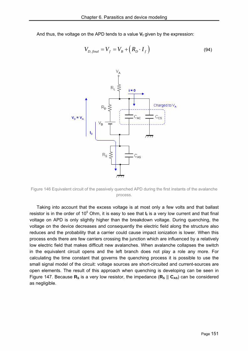
Chapter 6. Parasitics and device modeling
Page 151
And thus, the voltage on the APD tends to a value Vf given by the expression:
,D final f B D fV V V R I (94)
Figure 146 Equivalent circuit of the passively quenched APD during the first instants of the avalanche process.
Taking into account that the excess voltage is at most only a few volts and that ballast
resistor is in the order of 105 Ohm, it is easy to see that If is a very low current and that final voltage on APD is only slightly higher than the breakdown voltage. During quenching, the voltage on the device decreases and consequently the electric field along the structure also reduces and the probability that a carrier could cause impact ionization is lower. When this process ends there are few carriers crossing the junction which are influenced by a relatively low electric field that makes difficult new avalanches. When avalanche collapses the switch in the equivalent circuit opens and the left branch does not play a role any more. For calculating the time constant that governs the quenching process it is possible to use the small signal model of the circuit: voltage sources are short-circuited and current-sources are open elements. The result of this approach when quenching is developing can be seen in Figure 147. Because RS is a very low resistor, the impedance (RS || CAS) can be considered as negligible.

Chapter 6. Parasitics and device modeling
Page 152
Figure 147 Small signal model for the equivalent circuit of the APD during the quenching process.
The effect of discharge is dominant and the time constant responds to the following
expression and approximation:
|| || D Lq T T D L AC CS AC CS D AC CS
D L
R RR C R R C C C C R C C
R R
(95)
Depletion region has been notably reduced along quenching. In order to provide a good
detection signal (i.e. signal with enough amplitude) for the subsequent incoming photonic pulse it is necessary that depletion region have the maximum extension according to the provided bias voltage. There is a recovery process during which the increasing reverse bias voltage on the APD (from Vf to VA) forces a drift of majority carriers towards the highly doped regions n+ and p+ (see Figure 50). During the recovery time, the depletion region stretches to its maximum extension which implies a very low current on the circuit. This process can be seen as the recharge of the capacitances CAC and CCS through the ballast resistor RL (see Figure 148). It is clear that the time constant for this process is given by:
||r T T L AC CS L AC CSR C R C C R C C (96)
Because RL >> RD the recovery process is much slower than the quenching process. As
an example, for the values shown in Figure 145 a recovery time around one hundred larger
than the quenching time is obtained (q 5 ns and r 500 ns [225]Zappa-2009).

Chapter 6. Parasitics and device modeling
Page 153
Figure 148 Equivalent circuit of the APD during the recovery phase.
Figure 149 resumes the evolution of voltage on APD and corresponding photodetection
current for both the quenching and the recovery phases. Figure 150, by its own, shows experimental evolution for both magnitudes during the quenching period [225]Zappa-2009. When a new photopulse arrives to the detector during the recovery phase the amplitude of the detection signal is lower than it should be. That is, the recovery time is not a dead time but it is a period in which photodetection efficiency of the APD is reduced. For using the APD with high PDE at high optical rates it would be necessary to drive voltage on APD from Vf to VA in a short time. Besides, if quenching time is long enough, a fast transition of this voltage below the breakdown voltage would be necessary too. When voltage on APD is rapidly reduced below VBR, avalanches are extinguished and carriers are collected in a very short time. Both operations are part of the active quenching strategy.
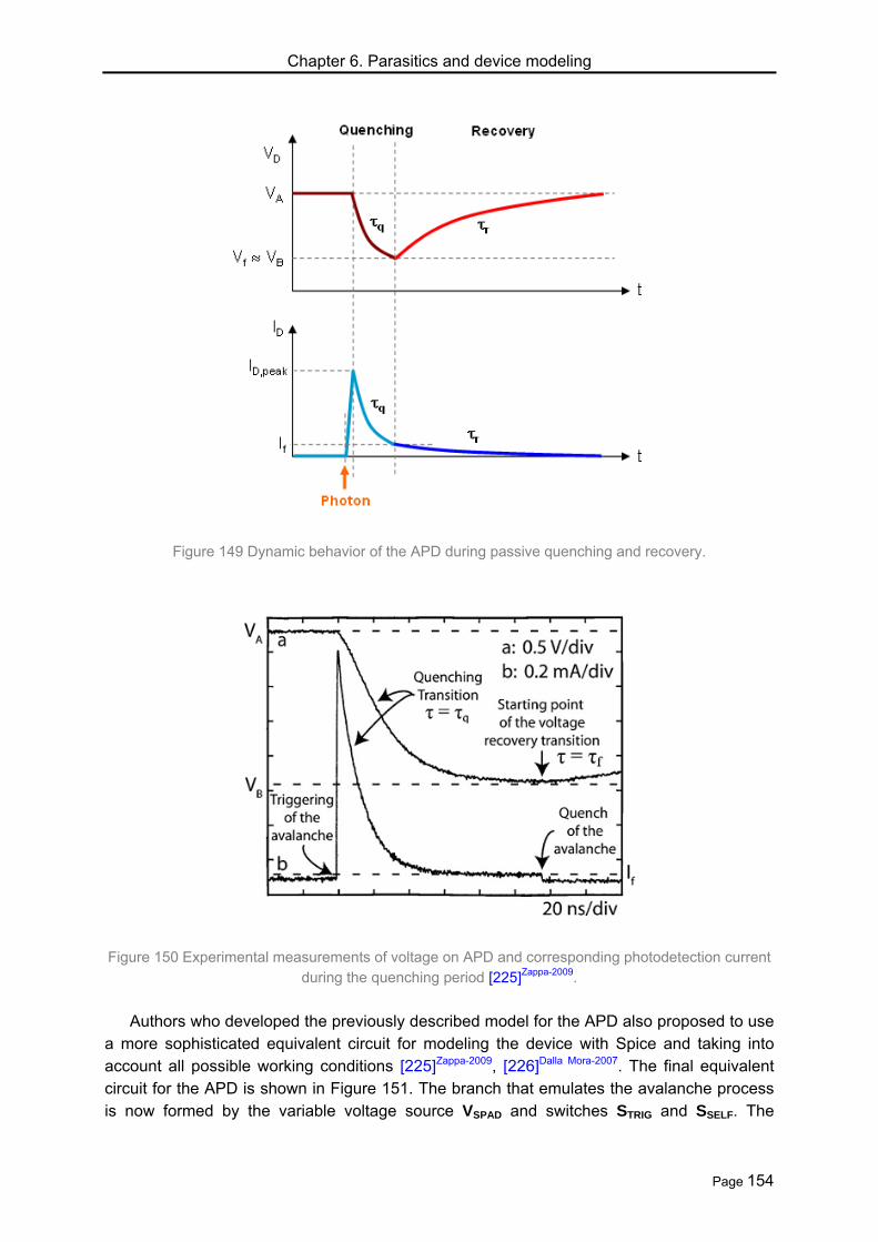
Chapter 6. Parasitics and device modeling
Page 154
Figure 149 Dynamic behavior of the APD during passive quenching and recovery.
Figure 150 Experimental measurements of voltage on APD and corresponding photodetection current during the quenching period [225]Zappa-2009.
Authors who developed the previously described model for the APD also proposed to use
a more sophisticated equivalent circuit for modeling the device with Spice and taking into account all possible working conditions [225]Zappa-2009, [226]Dalla Mora-2007. The final equivalent circuit for the APD is shown in Figure 151. The branch that emulates the avalanche process is now formed by the variable voltage source VSPAD and switches STRIG and SSELF. The

Chapter 6. Parasitics and device modeling
Page 155
voltage of the source VSPAD depends on the voltage on the APD itself and it is programmed according to the experimental current-voltage curve of the device. Resistors R1 and R2 allow simulating the luminous stimulus as a voltage pulse or as a current pulse. In steady state, previously mentioned switches are open. When a light pulse comes, the voltage on positive pole of STRIG is higher than its pre-programmed threshold, this switch closes and the avalanche process starts. The avalanche current flowing through SSELF rapidly surpasses its
threshold ( 100 A) and this switch closes. So, avalanche process is maintained even when
STRIG switches to open (i.e. the light pulse has finished). The model is completed with other two branches, one for simulating the forward bias (branch SF, VF, RF) and another for simulating the second reverse breakdown due to border effects (branch SR, VR, RR). These branches only play a role when the voltage on the device forces it. SR closes when VCA > VR
(VR 35 V, corresponding to the second breakdown; the first breakdown is VB 22 V) and SF
closes when VAC > VF (VF 0.6 – 0.9 V, corresponding to the forward biasing of the diode). Finally, switches S1 and S2 are used for enabling and disabling the photonic stimulus
according to the device biasing condition. Thresholds for S1 and S2 are set to VB 22 V and
VR 35 V respectively. S1 assures that ignition only happens when the reverse bias voltage is higher than VB: when VCA < VB the switch S1 is closed, STRIG is short-circuited and ignition is not possible because any photon arrival is ignored. S2 assures that photonic input was ignored when the diode is in second breakdown condition: if VCA > VR the switch S2 is closed, no photon stimulus reaches STRIG and the device is in permanent breakdown (SR is closed).
Figure 151 Extension of the APD equivalent circuit for simulation with Spice [225]Zappa-2009.
Resistors and capacitances in the model can be determined empirically. On the one
hand, slopes of current-voltage curves for forward and second breakdown regimes provide the values of RF and RR. On the other hand, three different capacitances can be measured using a capacitance meter.

Chapter 6. Parasitics and device modeling
Page 156
Measuring between anode and cathode: 1 || , CS ASAC CS AS AC
CS AS
C CC C C C C
C C
(97)
Measuring between cathode and substrate: 2 || , AC ASCS AC AS CS
AC AS
C CC C C C C
C C
(98)
Measuring between anode and substrate: 3 || , AC CSAS AC CS AS
AC CS
C CC C C C C
C C
(99)
It is a system of three equations with three unknown variables. Knowing the capacitances
C1, C2 and C3 by means of experimental measurements, it is possible to determine the capacitances CAC, CCS and CAS. CCS and CAS are associated with the metallic grid and their values do not depend on the APD bias voltage. However, CAC is the junction capacitance and its value is inversely proportional to the bias voltage. This dependence is usually reported by manufacturers. For example, in Figure 152 (a) Hamamatsu provides terminal capacitance of several models of SiPM as a function of the reverse bias voltage. In Figure 152 (b) the experimental behavior obtained by Zappa et al it is shown [225]Zappa-2009. Because the value of CAC does not significantly vary around the APD bias voltage, authors do not include this dependence on the model.
(a) (b)
Figure 152 Dependence of junction capacitance with reverse bias voltage. (a) Dependence provided by Hamamatsu for several models of SiPM [150]Hamamatsu-2001. (b) Experimental dependence obtained with an APD by Zappa et al [225]Zappa-2009 (red: total capacitance between anode and cathode, i.e. C1;
blue: capacitance associated with the junction, i.e. CAC).
Figure 153 shows a comparison between experimental and simulated output pulses for
several overvoltages [225]Zappa-2009, [226]Dalla Mora-2007. Although in general there is a good agreement between simulations and measurements, simulations offer a certain underestimation in the magnitude of the avalanche peak.

Chapter 6. Parasitics and device modeling
Page 157
Figure 153 Comparison between measurements and simulations for passive quenching with the APD equivalent circuit proposed by Zappa et al [225]Zappa-2009, [226]Dalla Mora-2007.
6.9. Modeling of the SiPM (many cells) Spanoudaki and Levin proposes a model for the SiPM as shown in Figure 154
[227]Spanoudaki-2011. Each cell is modeled as a current source (that ideally would produce a delta-type charge spike) in parallel with the cell capacitance Cdiode and in series with corresponding passive quenching elements (Rquench, Cquench). The SiPM is formed as the parallel connection of N identical cells (3600 cells). The load resistor for sensing the SiPM output signal (Rload) and the readout trace parasitic capacitance (Ctrace) are also included in the model. Spanoudaki and Levin take into account that other authors model the avalanche origin as a voltage source in series with a resistor where the process is triggered by a controlled switch. Despite the different information that could be obtained on each approach, they consider that both solutions are equivalent.
For considering the finite duration of the avalanche process (breakdown and quenching)
the current source is described as a piece-wise linear function instead of as a delta function. For making that function several parameters must be considered. toptical photon is the time in which the photon impacts on the cell triggering a current pulse. t*optical photon is a pseudo-
infinitesimally shifted version of toptical photon ( 1ps) and it emulates the instant avalanche current generation. tavalanche takes into account the duration of the avalanche process. Information for knowing the arrival time of photons to the different cells is provided by performing an optical tracking simulation on a certain number n of scintillation photons (14.000 photons). The path of each simulated photon is tracked and the time elapsed from its generation to its detection (on any of the 3600 cells) is registered. Optical simulation was made with the Monte Carlo-based simulation package DETECT2000. Ipeak is determined taking into account: (1) the total amount of charge delivered to the load on the avalanche process (Q), and (2) previous published results on the duration of the avalanche process in

Chapter 6. Parasitics and device modeling
Page 158
Si (tavalanche). Taking into account that VBIAS and VBR are the SiPM bias voltage and the cell breakdown voltage respectively, Ipeak can be calculated with the following equation.
diode quench BIAS BR
peakavalanche avalanche
C C V VQI
t t
(100)
Typical values for simulations (with software Ltspice) were the following. Ipeak: 1.5 mA,
tavalanche: 100 ps, Cdiode: 2.4-120 fF, Cquench: 0.8-40 fF, Rquench: 300 k, Rload: 50 , Ctrace: 55 pF, VBIAS: 71 V, VBR: 69 V.
Figure 154 Electrical model for the SiPM proposed in [227]Spanoudaki-2011.
According to Spanoudaki and Levin, the decay time of the single photon pulse for a
passively quenched SiPM may consist of two components, decay,1 and decay,2 given by the
following expressions.
,1
,2
quench diodedecay load trace
quench diode
decay quench quench diode
C CR C N
C C
R C C
(101)
decay,1 is associated with the total impedance seen by each microcell and decay,2 is
associated with the cell recovery time. For typical values of the passive elements decay,2 >>

Chapter 6. Parasitics and device modeling
Page 159
decay,1 and decay,2 dominates the output pulse decay. However, depending on the values of
Cdiode and Cquench the situation might be inverted. Validation of the model with experimental results was made by means of an experimental
setup as shown in Figure 155. Annihilation photons generated in a 22Na source are detected with a complex scintillator-SiPM. A LSO scintillator co-doped with 0.4 % Ca concentration of 3 x 3 x 20 mm3 was used. The photodetector was a Hamamatsu Si-based, blue-enhanced, 3 x 3 mm2 SiPM consisting of 3600 microcells. Simulations only take into account the photons that impact on the center of the LSO crystal. For assuring the same in the experimental setup another complex LSO-SiPM is used. In this case, the second LSO crystal has lower size (3 x 3 x 5 mm3). Both complexes are conveniently aligned. Annihilation photons coming from the 22Na source are directed in opposite directions. So, when a photon is detected by means of the small LSO it is sure that the simultaneous detection in the other complex has been caused by a photon impacting around the center of the big LSO.
Figure 155 Electrical model for the SiPM proposed in [227]Spanoudaki-2011.
Experimental results are in excellent agreement with simulations made with the proposed
optical-electrical model. Figure 156 shows good correspondence between individual measured and simulated signals. Figure 157 allows verifying that mean measured and simulated signals are nearly coincident; the mean difference between them is close to zero in
any considered instant. Maximum pulse heights are 76.6 2.5 mV for the mean measured
signal and 76.1 1.8 mV for the mean simulated signal. Rise times (measured as the time
elapsed from 10 % to 90 % of the maximum signal height) are 11.1 1.1 ns and 11.1 0.9 ns for measured and simulated signals respectively. Decay times (measured as the time
elapsed from 90 % to 10 % of the maximum signal height) are 35.8 2.2 ns and 36.5 1.8
ns for measured and simulated signals, respectively.

Chapter 6. Parasitics and device modeling
Page 160
Figure 156 Comparison between 50 measured pulses (top) using the oscilloscope persistence and 25 simulated pulses (bottom) [227]Spanoudaki-2011.
Figure 157 (top) Comparison between the mean responses over 50 measured pulses (black) and 25 simulated pulses (blue) and (bottom) the difference between the those mean signals [227]Spanoudaki-2011.
Collazuol proposes the same model for the SiPM than Spanoudaki and Levin [153]Collazuol-
2009 but grouping all non-triggered cells as an unique equivalent cell (see Figure 158).

Chapter 6. Parasitics and device modeling
Page 161
Figure 158 Electrical model for the SiPM proposed in [153]Collazuol-2009.
The values of the elements in this equivalent cell are obtained assuming that it is possible
to consider all identical elements in parallel. So, for example, if the SiPM has N total cells and only n cells are triggered simultaneously, there would be N-n quenching resistors in parallel. The same is valid for capacitances, so equivalences would be:
, |
, |
, |
|| ||
|| ||
|| ||
qq eq n triggered cells q q q N n times
q eq n triggered cells q q q qN n times
d eq n triggered cells d d d dN n times
RR R R R
N n
C C C C N n C
C C C C N n C
(102)
Collazuol proposes certain functional dependencies for leading and trailing edges in the
photocurrent for an isolated GM-APD cell (as it is schematized in Figure 159). Time
constants for leading and trailing edges respond to the following expressions respectively: d
= Rs·Cd and q = Rq·Cd. Because Rq is in the order of hundreds of k and Rs is only a few
ohms, it is verified that d << q. This is the reason for a very fast rising edge as comparing
with the slow falling edge. Total recovery of the cell would be reached for a time in the order
5·q.
Figure 159 Dependencies in the current pulse for a fired GM-APD [153]Collazuol-2009.

Chapter 6. Parasitics and device modeling
Page 162
The gain in the SiPM can be calculated as the number of carriers generated when only one cell fires and this can be obtained as the total charge transferred to the load normalized to the elemental charge. So, gain would be expressed as following:
1 BIAS BR d qcell triggersV V C CQ
Ge e
(103)
In [153]Collazuol-2009 like also in [227]Spanoudaki-2011 two time constants for explaining the decay
in the SiPM current pulse are mentioned (i.e. taking into account N cells). First, a fast
component 1, given by the discharge of all capacitances in the circuit through the sensing
resistor Rs. Second, a slow component 2, given by the recharge of the cell capacitances in
the fired cells through their quenching resistors Rq. Cd and Cq are in the order of tens of fF and normally Cq < Cd. Cg is the parasitic capacitance associated with the common metallic
grid and is in the order of tens of pF. The lower Rs the lower the fast time constant 1 and the faster the collection of charge on the sensing resistor.
1
2
d qs total s g eq s g
d q
q d q
C CR C R C C R C N
C C
R C C
(104)
Figure 160 shows the period in which both time constants are dominating on a typical
photocurrent pulse.
Figure 160 Time constants determining the photocurrent decay in the SiPM.
6.10. Simulations An estimation for the resistor RD in the SiPM model, which accumulates the resistances
of the space charge region and of the neutral regions, can be done by using the photosignal rising edge. The photovoltage signal during that period can be modelled as following [155]Piemonte-2011:

Chapter 6. Parasitics and device modeling
Page 163
dDdDdD
CR
t
CR
Vslopet
CR
V
CR
tVeVtV dD
maxmax
maxmax :;111)( (105)
By measuring the rise time, rise, that resistor can be estimated as following:
d
riseD
dDriserise CR
CR
VVVSlope
;;: maxmaxmax (106)
The measured rise time of 3.1 ns together with the capacitance of 114 fF determined by
means of the charge versus bias voltage curve provide a value of about 27 k for the resistor RD.
Figure 161 Model of the SiPM used for PSpice simulations.
Figure 161 shows the SiPM model used for PSpice simulations. It is considered that only
one cell is triggered, so that the branch formed by Rqeq, Cqeq and Cdeq simulates the N-1 non triggered cells. These values are related with the values Rq, Cq and Cd for the single cell as following:
1;1;1
NCCNCCN
RR ddeqqqeq
qqeq (107)
The capacitor Cg provides the readout trace parasitic capacitance and its value is taken
as the terminal capacitance provided by the manufacturer. In the case of the SiPM model S10362-11-050C is around 30 pF. It is also considered that the capacitance in parallel with
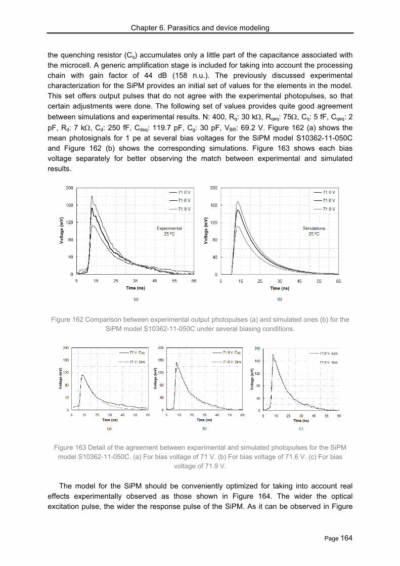
Chapter 6. Parasitics and device modeling
Page 164
the quenching resistor (Cq) accumulates only a little part of the capacitance associated with the microcell. A generic amplification stage is included for taking into account the processing chain with gain factor of 44 dB (158 n.u.). The previously discussed experimental characterization for the SiPM provides an initial set of values for the elements in the model. This set offers output pulses that do not agree with the experimental photopulses, so that certain adjustments were done. The following set of values provides quite good agreement
between simulations and experimental results. N: 400, Rq: 30 k, Rqeq: 75, Cq: 5 fF, Cqeq: 2
pF, Rd: 7 k, Cd: 250 fF, Cdeq: 119.7 pF, Cg: 30 pF, VBR: 69.2 V. Figure 162 (a) shows the mean photosignals for 1 pe at several bias voltages for the SiPM model S10362-11-050C and Figure 162 (b) shows the corresponding simulations. Figure 163 shows each bias voltage separately for better observing the match between experimental and simulated results.
Figure 162 Comparison between experimental output photopulses (a) and simulated ones (b) for the
SiPM model S10362-11-050C under several biasing conditions.
Figure 163 Detail of the agreement between experimental and simulated photopulses for the SiPM model S10362-11-050C. (a) For bias voltage of 71 V. (b) For bias voltage of 71.6 V. (c) For bias
voltage of 71.9 V.
The model for the SiPM should be conveniently optimized for taking into account real
effects experimentally observed as those shown in Figure 164. The wider the optical excitation pulse, the wider the response pulse of the SiPM. As it can be observed in Figure

Chapter 6. Parasitics and device modeling
Page 165
164 (a), when short excitation pulses are used the SiPM reacts with a very sharp rising edge followed by a slow falling flank. When the excitation pulse width rises two facts happen. First, the amplitude of the output pulse initially rises but if the excitation pulse width continue rising then the output pulse saturates and tends to lower amplitudes. Second, the rising edge of the output pulse is every time slower.
Figure 164 (a) Effect of the width of the optical excitation pulse on the SiPM output pulse. (b) Effect of the optical repetition frequency on the amplitude of the SiPM output pulse. Several widths for the
optical excitation pulse were used. SiPM model S10362-33-100C.
These effects are explained by Spanoudaki and Levin as the cumulative effect of
activating a large number of microcells [227]Spanoudaki-2011. It is clear that the wider the optical excitation pulse the higher the number of microcells that will be triggered one after the other. Because microcells are activated in different times, the combined signal provides a rising profile that is the result of a piling-up process of the individual pulses (see Figure 165).
Figure 165 The individual pulses from each microcell (solid lines) arrive asynchronously and are
summed in the sensing resistor to form the SiPM pulse (dashed lines) as a result of their effective pile-up [227]Spanoudaki-2011.

Chapter 6. Parasitics and device modeling
Page 166
On the other hand, a very long excitation pulse causes that a high density of photons impacts on the SiPM and the saturation effect plays a role. When a large number of photons impact on the SiPM there is a high probability that every activated microcell is triggered by several photons rather than by only one. Remember that the microcell reacts with the same amplitude no matter how many photons impinge on it. Besides, the wider the excitation pulse the higher the number of cells that are in recovery phase in every time instant. So, as the real efficiency of the photodetector reduces, much lower number of cells are available to react with the highest sensitivity and the already activated cells can react only with a small fraction of its maximum capability. These reasons justify that a low number of incident photons causes a global response better than the one generated by a much higher intense excitation.
Figure 164 (b) shows the experimental response of the SiPM model S10362-33-100C to
an increasing optical repetition frequency. If one photonic pulse arrives to the SiPM during the recovery period of a previous detection, the photodetector is able to react to this new pulse but with lower amplitude. During that period the SiPM is remaking the junction and the effective bias voltage is slowly returning to the optimal value. Every time a detection is triggered during the recovery time, a new avalanche is generated, the effective voltage on the SiPM decreases and the recovery process has to start again. As the new pulse is closer to the previous one, the gain with which the SiPM is able to react becomes lower (the difference between the current voltage and the optimal bias voltage is higher) and this reduces the amplitude of the new detection. In other words, the higher the optical repetition frequency the lower the amplitude of the resulting pulse. Besides, it has been also observed that the lower the width of the optical excitation pulse the higher the maximum optical repetition frequency that allows us a good discrimination between subsequent detections. For example, when a pulse width of 6 ns is used, an optical repetition frequency up to 50 MHz is reachable with good separability between photodetection pulses. However, using a pulse width of 50 ns, resolving pulses is hard beyond 15 MHz.

Chapter 7. SiPM pulse shaping
Page 167
7. SiPM pulse shaping
7.1. Introduction The SiPM is a matrix device where each cell is an avalanche photodetector (APD)
working in Geiger mode that includes a quenching resistor [4]Renker-2009, [5]Haba-2008, [13]Sadygov-
2006. That resistor is in charge of collapsing the avalanche process in each single APD a short time after it starts. As all the cells in the device are connected to a common metallic grid, the total photocurrent is proportional to the number of fired cells. The typical response of the SiPM to an incoming light pulse is a very fast rising edge (avalanche is happening) followed by a slow downfall (avalanche has been quenched) [5]Haba-2008, [7]Stewart-2006.
The amplitude in the SiPM response signal is proportional to the number of impinging
photons [5]Haba-2008. In other words, the amplitude of the current signal provided by the photodetector is amplitude modulated by the intensity of the optical exciting signal. This fact, together with the high sensitivity of the device (an avalanche process can be started even with only one incoming photon), allows for counting the number of photons reaching the photodetector. A large enough number of events will enable discrimination between n and n
1 photons, that is, for tracing the Single Photon Counting (SPC) pattern of the system [14]O'keeffe-2007, [15]Jackson-2005, [16]Hamamatsu-2009, [17]Bellis-2006. This can be done by tracing the pulse height spectrum taking into account the voltage or current signal provided by the SiPM. Also, those signals can be integrated and a spectrum expressed as the charge released by the detector as a function of the number of detected photons can be obtained. Both types of spectra are useful tools for comparing the performance of different detectors and for evaluating the benefit of photosignal processing techniques. In this work, pulse height spectra are used for demonstrating that photopulse shortening subsystems improve the SiPM capability for resolving photons.
Even for short light pulses ( 10 ns), and depending on the features of the detector, the
SiPM pulse width ranges from tens to hundreds of nanoseconds. This is a consequence of the long time constant provided by the micro-cell capacitance together with its high value quenching resistor. Those long photopulses are inconvenient because they lead to pile-up and reduce the maximum allowable optical repetition frequency. The long tail in the photosignal is developed during the detector recovery time which is not strictly a dead time. During that period, the SiPM is able to response to new detections but with lower sensitivity. The way to solve this problem with no loss in sensitivity requires the use of active quenching techniques which, on the other hand, have to fight against parasitic signals that pollute the photosignal of interest [225]Zappa-2009, [228]Gallivanoni-2006, [229]Zappa-2003. In a passive quenching scheme for low optical repetition frequencies, shortening of photopulses is advantageous. Because of the informative content of the photosignal is in the amplitude, the long tail in the pulse is unnecessary. Still more, it is convenient to eliminate it for getting concentrated pulses that lead to good time-separation between consecutive pulses. Also, concentrated pulses are preferable for subsequent processing operations. For example, if an active quenching subsystem is planned for reducing the photodetector dead time, it is advisable to

Chapter 7. SiPM pulse shaping
Page 168
trigger it with short pulses. The major advantage of shortening strategies discussed in this work is not the pulse concentration itself. Shortening is providing a sort of signal filtering that results in a better separation between photosignal amplitudes corresponding to different number of impinging photons. As a consequence, the pulse height spectrum and the capability of the photodetector for resolving photons clearly improve. Comparison of SPC spectra with and without shortening shown later corroborates these facts and allows using several figures of merit for measuring the improvement provided by shortening.
Results shown in this chapter have generated a publication in the journal Optical
Engineering [230]Yebras-2012 (SPIE journal included in ISI Web of Knowledge, Journal Citation Reports, impact factor for 2010: 0.822, impact factor for last 5 years: 0.843).
7.2. Experimental setup Three different strategies for shortening the SiPM output pulse have been explored. All
options use the common setup described in the previous chapter. The bias circuit for the SiPM used in these experiments (S10362-33-100C [150]Hamamatsu-2001, [181]Hamamatsu-2009) is designed according to its manufacturer recommendation (see Figure 98). The bias voltage is provided by the high accuracy power source Keithley model 6487 [183]Keithley-2009-[186]Keithley-
2002. The excitation pulse is obtained feeding the ultraviolet LED model HUVL400-5x0B (400
nm 20 nm) [204]Hero-2002 by means of the function generator Tektronix AFG3252 (2 GS/s, 240 MHz) [231]Tektronix-2008. One end point of an optical fibre is properly connected to the LED and the other end point is connected to the SiPM. Both connections are properly made through plastic hoods that assure the mechanical fit and that provide luminous isolation. A deeper luminous isolation of the SiPM (for reducing as much as possible background events) is achieved covering the whole SiPM bias board with several layers of black tissues. The processing chain provides a gain factor of 44 dB (200 n.u.) and can be seen in Figure 124.
The first shortening option consists on using a band-pass filter which removes the lowest
frequency components of the signal, which are responsible of the slow falling edge [232]Eraerds-2007. This filter will be included at the end of the processing chain. The second option proposes a reflectometric scheme, which can be seen in Figure 166 (a). Previous reported studies of our group used similar strategies for pulse conformation in the scope of nanosecond-range pulse generators. In those works, wide pulse generators are used in combination with SRD (Step Recovery Diode) and a short-circuited stub for obtaining subnanosecond pulses [74]Antoranz-2009, [233]Antoranz-2010. The amplified signal coming from the SiPM is injected into a signal splitter and one of its stubs is connected to a short-circuited stub. The stub provides an inverted and delayed version of the original signal, so that the combination of both signals will be present in the free stub of the splitter. This signal should be fairly shorter than the original, but the fact that new peaks and ringing could appear must be taken into account. The third solution is similar to the previous one, but replacing the short-circuited stub by an analog subtractor circuit as shown in Figure 166 (b). The idea is to divide the signal coming from the photodetector and to apply a delay to one of the resulting signals. This way, one of the incoming signals to the subtractor is a delayed version (with no
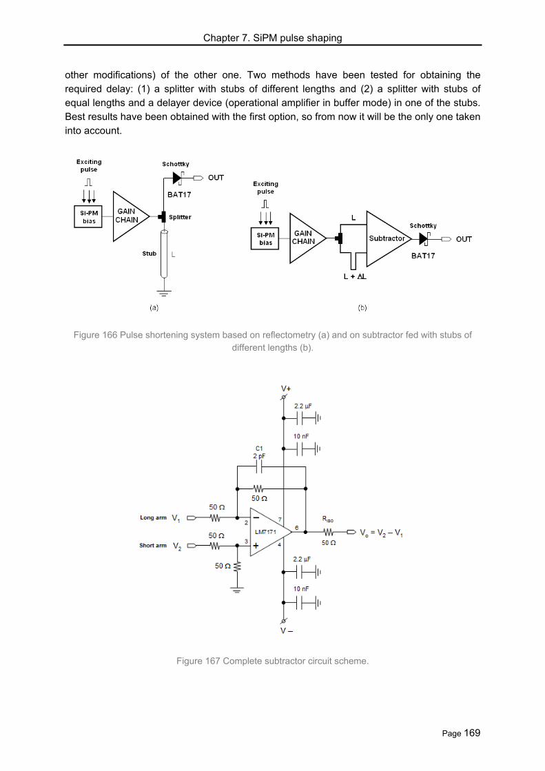
Chapter 7. SiPM pulse shaping
Page 169
other modifications) of the other one. Two methods have been tested for obtaining the required delay: (1) a splitter with stubs of different lengths and (2) a splitter with stubs of equal lengths and a delayer device (operational amplifier in buffer mode) in one of the stubs. Best results have been obtained with the first option, so from now it will be the only one taken into account.
Figure 166 Pulse shortening system based on reflectometry (a) and on subtractor fed with stubs of different lengths (b).
Figure 167 Complete subtractor circuit scheme.

Chapter 7. SiPM pulse shaping
Page 170
The operational amplifier LM7171 was selected for the subtractor circuit (the complete
scheme is shown in Figure 167) due to its very high speed operation (slew rate 4100 V/s)
[234]National-2006. Capacitor C1 cancels the pole formed by the combination of the opamp input capacitance and the gain level setting resistors. Not cancelling this pole could cause instabilities in the circuit. Other possible causes for oscillation are the capacitive charges. For solving the problem, an isolating resistor RISO can be added at the output. That resistor, joint with the capacitive charge, makes a new pole that tends to stabilize the system. Capacitors in biasing lines have the same filtering purpose previously mentioned.
7.3. Results and discussion The result of adding a passive band-pass filter (whose 3 dB cutoff frequencies were 60
MHz and 230 MHz) at the end of the processing chain is shown in Figure 168, where it can be compared with the corresponding signal obtained without filtering. As it can be seen, the filter provides a noticeable reduction in pulse width (a compression relation of 10:1 was got) respect to its sharp rising edge. But, at the same time, a reduction higher than 90 % in the amplitude of the pulse happens. Despite this inconvenience, it is an interesting result because it demonstrates that a simple passive filtering is able to provide a substantial improvement in pulse conformation (pulses as short as 3 ns can be achieved). For avoiding so weak final amplitudes higher gain or enhanced filtering could be provided. However, more sophisticated and flexible shortening schemes were used in order to overcome the limitations of this first approach.
Figure 168 Pulse shortening adding a band-pass filter at the end of the processing chain. Incoming excitation pulses have FWHM of 10 ns. (a) Pulse without filtering, (b) pulse with band-pass filtering.
Figure 169 (a) illustrates the significant pulse compression and good shaping provided by
the reflectometric shortening system (scheme in Figure 166 (a)) when comparing with the pulse obtained without shortening (scheme in Figure 124). Also in this figure the positive effect of inserting an appropriate Schottky diode as final element in the processing chain can be observed: the pulse is slightly shorter and undesirable slow negative parts in the signal are removed. Good compression relations near 3:1 were obtained, and in spite of a reduction

Chapter 7. SiPM pulse shaping
Page 171
of 40 % in the amplitude, it is good enough for pulse manipulation. Figure 169 (b) shows results obtained with the shortening system based on subtractor fed with stubs of different lengths. In this case, a compression relation near 6:1 is obtained, but with an undesirable loss of amplitude of around 80 %. Also, a little distortion of the rising edge can be observed. Although compression is higher with subtractor based system, the facts that the amplitude was reduced so much and the rising edge was distorted a little are good reasons for preferring the reflectometric system.
Figure 169 Comparison of original output pulse with output using (a) the reflectometric shortening scheme, and (b) the shortening system based on the subtractor with stubs of different lengths. In (b)
the original signal has been multiplied by 1/2 for better comparison with the other traces. For both cases, the input pulse FWHM is 10 ns. Length of the coaxial short-circuited stub in (a): 102 cm.
Difference in length between incoming stubs to subtractor in (b): 102 cm.
A reduction of the stub length (or the difference in length between the input stubs to the
subtractor) produces a reduction of the pulse FWHM. However, an excessive width reduction can lead to a decrease in the intrinsic amplitude of the detected pulse, and therefore a sensitivity loss. After several SPC experiments with these shortening systems, a good

Chapter 7. SiPM pulse shaping
Page 172
tradeoff was found when using coaxial stub lengths between 80 cm an 100 cm. Figure 170 shows typical pulse shapes for different stub lengths.
Figure 170 Width of shortened output pulse as a function of short-circuited stub length (for shortening system based on reflectometry, (a)) and of difference of length between input stubs (for shortening
system based on subtractor, (b)). Input pulse width of 10 ns were used.
Figure 171 shows the output pulse amplitude as a function of the voltage of the electric
pulses used for feeding the LED source. Figure 171 (a) depicts the response of the SiPM (with no amplification stage) for two different bias voltages. When the photonic density is high, there is higher probability that several photons fall simultaneously on the same pixel. This leads to a saturation effect that is clearly visible in Figure 171 (a). The extra electronic circuitry in the subtractor based shortening scheme reduces the linear dynamic range of the system. This can be verified by comparing Figure 171 (b) and (c) which show the response of the overall system with extra amplification and different shortening stages. The fact that the Schottky diode is not destroying the linearity of the system can also be observed in these figures.

Chapter 7. SiPM pulse shaping
Page 173
Figure 171 System response as a function of the input LED pulse amplitude. (a) Only SiPM was used, for two different bias voltages (70 V, 72 V). (b) SiPM and amplification (circles); SiPM, amplification and reflectometry-based shortener (squares); SiPM, amplification and shortener with Schottky diode
(diamonds). (c) SiPM, amplification and subtractor-based shortener (squares); SiPM, amplification and shortener with Schottky diode (diamonds). In all measurements shown in (b) and (c) the SiPM bias
voltage was 70 V.
The high frequency digital oscilloscope Agilent Infiniium DSO81204B (12 GHz, 40 GSa/s)
allows tracing and saving amplitude histograms [206]Agilent-2006. Its histogram utility works like a multichannel analyzer. Figure 172 shows the pulse height spectra obtained when no shortening and the reflectometric shortening scheme are used. The improvement provided by the shortening subsystem is evident. More photopeaks are distinguishable and they are narrower and more intense. This last fact is a demonstration that shortening, as it was previously mentioned, is being able to reduce the amplitude dispersion on pulses corresponding to the same number of detected photons. The consequence of this, as it is clearly shown in Figure 172, is that separability of peaks is also much more accurate when shortening is used.
Figure 172 Pulse height spectra obtained when no shortening is used (dashed line) and when reflectometric shortening scheme is used (solid line). The SiPM bias voltage in both cases was 71.5 V.

Chapter 7. SiPM pulse shaping
Page 174
Several figures of merit can be used for comparing both spectra and for characterizing the photodetector capability to resolve photons in both cases. The weak photon emission and detection must reveal a Poisson distribution [30]Ramilli-2010. Although the crosstalk effect increments the height of the peaks corresponding to several number of photons, its influence is not so important that a pseudo-Poisson type distribution was not expected. So, the first figure of merit might be the degree of fitting of the experimental histogram by means of a distribution resulting from the convolution of a gaussian function (simulating the non-ideal peak in the spectrum) with a Poisson distribution. For implementing the simulation it was taken into account that the mean value of the n-th peak in the spectrum must be n times the mean value for the 1 photoelectron peak and that the typical deviation of the n-th peak is approximately the typical deviation corresponding to the 1 photoelectron peak multiplied by the square root of n [235]Saveliev-2006. The fit of the pattern obtained when shortening is used can be seen in Figure 173. In this figure, the experimental histogram has been replaced by its corresponding probability density function. Simulation says that the mean voltage corresponding to the single photoelectron is 65 mV, with a typical deviation of 13 mV, and that a number of 2.2 photoelectrons are being detected on average (this value corresponds to the parameter of the final Poisson distribution that best fits the experimental data). Despite of the underestimation of the pedestal peak, quite accurate fit is possible when shortening is used. However, the fit of the spectrum when no shortening is used does not provide an acceptable result: neither the peaks are correctly located nor their heights can be properly adjusted.
Figure 173 Fit of the probability density function obtained when shortening is used (gray line) by
means of the convolution of a gaussian function with a Poisson distribution (black line). The function that fits the mountain created by the overlapping of the peaks in the spectrum is also shown (dashed
line).
The figure of merit named as peak-valley-peak relation (PVPR) provides a measurement
of the proportion in which a certain peak is above the baseline mountain caused by the

Chapter 7. SiPM pulse shaping
Page 175
overlapping of the different peaks. It is a dimensionless quantity whose ideal value is 1. The valley value for a certain peak is the highest one flanking its maximum.
10:Re
1:;.].[max
max
PVPRal
PVPRIdealunimumPeak
valleyPeakimumPeakPVPR
(108)
The so called quality parameter (QP) is a measurement of the width of the peaks in the
pattern. The full width at half maximum (FWHM) of the peak is referred to the voltage corresponding to the single photoelectron. Thus, QP expresses the width of the peaks in terms of number of photoelectrons and its ideal value is 0. As QP grows towards 1, the overlapping of peaks in the spectrum is quite notable.
0:Re;0:;][1
QPalQPIdealpepeforVoltage
deviationPeakQP (109)
It is possible to fit the baseline mountain created by the overlapping of the peaks in the
spectrum by means of a polynomial function m(V). This function m(V), where V is the photosignal voltage, has validity for almost the entire pattern, between a low voltage L and a high voltage H, both empirically determined. The so called form factor (FF) of the pattern is defined as the relation between the integral of the spectrum above the baseline mountain referred to the whole integral of the spectrum. It is a measurement that quantifies the relevance of that overlapping on limiting the photon resolution of the system. Being h(V) the function that expresses the probability density function corresponding to the experimental histogram, the form factor, whose ideal value is 1, is defined as shown in following equation (see Matlab program formfactor.m, annexe 1).
10:Re;1:;
)(
)()(
FFalFFIdeal
dVVh
dVVmdVVh
FFH
L
H
L
H
L (110)
But perhaps the most informative figure of merit might be the detection error probability,
defined as the probability of deciding the detection of n 1 photons when n photons have really been detected. Figure 174 (a) shows the fit of the experimental histogram when shortening is used by means of gaussian functions simulating each peak (see Matlab program createtheoreticalhistogram.m, annexe 1). Individual gaussian functions are depicted as dashed lines whereas their sum is shown as a solid line that fits quite well the experimental probability density. Figure 174 (b) shows the portion of the gaussian function corresponding to 2 photoelectrons that is providing detection error. Naming as Lerror and Herror the points in which the gaussian function for n photoelectrons, gn(V), coincides with the gaussian functions corresponding to n-1 and n+1 photoelectrons, gn-1(V) and gn+1(V)

Chapter 7. SiPM pulse shaping
Page 176
respectively, the detection error probability (DEP) for the n-th peak is defined as shown in following equation (see Matlab program calculateerror.m, annexe 1):
0:Re;0:;
)(
)()(
DEPalDEPIdeal
dVVg
dVVgdVVg
DEP
n
Hn
L
n
rrore
error
(111)
Figure 174 (a) Fit of the probability density function obtained when shortening is used (gray line) by means of the sum (black solid line) of gaussian functions (dashed line). (b) Areas causing detection
error for the case of 2 photoelectrons.
Table 5 summarizes all the previous figures of merit for both cases, when no shortening
is used and when shortening based on reflectometry is used. Also, the improvement obtained thanks to the shortening subsystem referred to the case of no shortening is included in the table. All parameters demonstrate the great enhancement in the SPC pattern got when shortening is used. But, perhaps, the most interesting and comprehensive result obtained is that the detection error probability has been reduced in one order of magnitude. The notable error probability happening when using the SiPM alone (from 33 % to 80 %) has been reduced to less than 8 % for any number of photoelectrons.

Chapter 7. SiPM pulse shaping
Page 177
Table 5 Figures of merit for the case of using the SiPM with no shortening and when it is used with the reflectometry based shortening subsystem. The improvement obtained when using shortening is
provided for all the cases.
7.4. Summary In this chapter three strategies for shortening the output pulse provided by a silicon
photomultiplier have been discussed. The first solution is based on applying a simple band-pass filtering to the amplified signal. It has been shown that a compression relation of 10:1 can be obtained, but at the cost of an unacceptable loss in pulse amplitude. Two other options have been tested, reflectometry based shortening system and subtractor based shortening system. They provide good compression relations up to 6:1. Best results, taking into account pulse duration, negative parts and ringing suppression, pulse shaping, dynamic range and capability for tracing well defined SPC patterns was obtained with the reflectometric shortening system using a coaxial short-circuited stub in the order of 50-100 cm. In addition, the losses in the reflectometric system are 50% lower than in the subtractor system.
The most interesting result obtained when using pulse shortening is the improvement
achieved for resolving photons with SiPMs of large area which provide poor counting results when working alone. Several figures of merit have been used for characterizing SPC patterns and shortening has provided an important enhancement for all of them. Shortening is offering a photopulse much shorter than the original SiPM pulse, which is an useful fact for signal processing and for feeding other subsystems that will act on the SiPM behavior (e.g. active quenching circuits). In addition, the photon resolving capability of the photodetector has been enhanced a lot. Patterns obtained by means of shortening, on the contrary than when the SiPM is used alone, are adjustable by means of Poisson distributions, have clearly defined and separable photopeaks and provide a very important reduction in the detection error probability. DEP when the SiPM is used alone ranges from 30 % to 80 %, depending on the considered photopeak, but it is lower than 8 % for any photopeak when the shortening subsystem is used.

Chapter 8. Photon Counting optimization
Page 178
8. Photon counting optimization This chapter discusses the potential that previously explained shortening subsystems
show for enhancing the photon counting capabilities of large area SiPMs. The influence of several experimental parameters are studied, comparison with PMT is shown and dependences with the temperature are reported.
8.1. The photon counting pattern Consider a typical experiment for detecting ionizing radiation. A scintillator material is
used for transforming ionizing particles into light. This light, of higher intensity as higher the energy and intensity of ionizing radiation, is detected with a photodetector like, for example, a photomultiplier (in [219]España-2008 authors use a SiPM together with a LYSO crystal (Lutetium-Yttrium OxyorthoSilicate) for characterizing radiation coming from a 22Na source). Photodetector provides an output pulse amplitude directly proportional to the impinging light intensity. So, registering the photodetector response for each light pulse by means of a multichannel analyser, it is possible to obtain the energetic spectrum of the original radiation [95]Leo-1987, [109]Knoll-1979. The higher the energy of the ionizing radiation the higher the scintillation light intensity and the higher the output pulse amplitude. The analyzer has a series of channels, each one associated to a certain amplitude range for the sensed signal. The instrument provides a counter for each channel, so that reception of a signal in the range
[Vk, Vk+V] increments in one unit the count associated with the channel k. That is, the analyzer allows making a representative histogram of the incident radiation; in x-axis is provided a magnitude related with the energy of the original radiation (e.g. output current or voltage drop caused in a load) and in y-axis is given the relative frequency for each possible value of that magnitude. Amplitude distribution of the sensed magnitude is related with the scintillation photons distribution and also with the energy distribution of the original ionizing radiation. It is possible to associate a certain range of amplitudes in the output magnitude
with a certain number of detected photons. For example, Vo V would correspond to
detection of 1 photon, 2·Vo V would correspond to detection of 2 photons and in general
n·Vo V would be associated with the detection of n photons. And the number of detected
photons allows establishing a relation with the energy of the particles in the ionizing radiation. Figure 175 demonstrates the potential of modern SiPMs for developing photon counting
in a simple way and providing several advantages when comparing with more traditional photodetectors (e.g. photomultipliers). For example, Haba shows that photon counting patterns achieved using SiPMs are better than those obtained when conventional photomultipliers are used [5]Haba-2008.

Chapter 8. Photon Counting optimization
Page 179
(a) (b)
Figure 175 SiPM response for optical pulses corresponding to different number of impinging photons. (a) Pulses for 1 and 2 photons [16]Hamamatsu-2009. (b) Superposition of detection signals using
persistence and corresponding photon counting pattern [181]Hamamatsu-2009.
Monte Carlo simulations can help to know how the Single Photon Counting pattern is
affected by the different SiPM parameters. Privitera et al are able to extract the SPC pattern of a SiPM from simulated photopulses by using a Monte Carlo model in which the gain dispersion between pixels, the crosstalk probability and the darkcounts rate are adjustable [236]Privitera-2008. Figure 176 clearly shows that an increment on crosstalk reduces the resolution of peaks (lower peak-valley relations and wider photopeaks are obtained, compare Figure 176 (a) and (b)) and increments the baseline noise distribution. When gain between pixels in the SiPM is more homogeneous, the spectrum is enhanced (compare Figure 176 (a) and (c)): photopeaks are narrower, much higher peak-valley relations are obtained and the baseline noise distribution nearly disappears.
Figure 176 . Single Photon Counting patterns obtained by Monte Carlo simulations for a SiPM of 25 microcells. The same optical illumination is considered in all cases. The gain dispersion between
pixels and the crosstalk probability are varied. (a) Reference pattern. (b) Effect of incrementing the crosstalk probability. (c) Effect of reducing the gain dispersion [236]Privitera-2008.
Chapter 8. Photon Counting optimization
Page 180
8.2. Shortening systems for photon counting
8.2.1. Introduction Nowadays, SiPMs have a wide range of applications in many different fields and it is
related with their ability to resolve single photons. APD and SiPMs have been used for implementing calorimeters in high energy physics [237] Lewandowski-2005, [238]Andreev-2005 and on high resolution spectroscopy: ionizing particles [147]Sadygov-2003, X-rays with energies of several hundreds of keV [239]Moszynski-2002 and with energies between 2 and 20 keV [8]Kataoka-
2005, as well as X-ray temporal correlation spectroscopy [9]Johnson-2009. Important research activities are under development for using SiPMs as detectors in Cherenkov telescopes [10]Otte-2006, [11]Korpar-2008, [240]Martínez-2010 and also for large scope experiments for detecting neutrinos [241]Kudenko-2009. Other physical applications of SiPMs can be found on high speed optical communications [242]Singh-1994, quantum cryptography [243]Baig-2001 and systems for distance ranging (Light Detection and Ranging, LIDAR) [244]Spinhirne-1993. Fluorescence measurement in the biomedical field is another important application field, as for example, for single-molecule detection [19]Knemeyer-2007, [245]Li-1993 or for cellular kinetics and cytometry in blood flow [20]Tkaczyk-2008. High sensitivity of SiPMs and its low size and immunity against external magnetic fields make them appropriate devices for implementing multimodality medical imaging, that is, techniques for getting functional imaging (Positron Emission Tomography, PET) together with morphological imaging (Magnetic Resonance Imaging, MRI, Computed Tomography, CT) [21]Herbert-2007, [22]Braem-2008, [23]Pichler-2008, [246]Bérard-2007.
In many of these applications it is interesting to increase the active area of the
photodetector with the objective of collecting more light. Hence, perhaps the wide area SiPMs were the most interesting devices. However, an increase on the active area leads to higher intrinsic capacitance in the SiPM and consequently to a worse time response. Some collateral effects that degrade the SPC pattern are also potentiated when large area devices are used. Thus, it seems reasonable to concentrate efforts to make easier the use of these devices. In the present chapter it is shown the potential of photodetection pulse shortening systems for improving the photon counting capabilities of these large area SiPMs.
Results shown in this chapter have generated a publication in the Journal of the
European Optical Society - Rapid Publications [247]Yebras-2012 (journal included in ISI Web of Knowledge, Journal Citation Reports, impact factor for 2010: 1.044, impact factor for last 5 years: 0.967).
8.2.2. Experimental setup The experimental setup for obtaining photon counting patterns is the system already
described in the previous chapters. The bias circuit for the SiPM (S10362-33-100C [150]Hamamatsu-2001, [181]Hamamatsu-2009) is designed according to its manufacturer

Chapter 8. Photon Counting optimization
Page 181
recommendation (see Figure 98). The processing chain provides a gain factor of 46 dB (200 n.u.) and can be seen in Figure 124. Two LED models were used in these experiments: first, the ultraviolet LED model HUVL400-5x0B [204]Hero-2002 operating at a central wavelength of 400 nm and second, the red AlGaInP laser diode ADL-65074TR [248]Laser-2005 operated in LED mode, whose central emission wavelength is located at 655 nm.
For tracing the SPC patterns, two ways were explored. The high frequency digital
oscilloscope Agilent Infiniium DSO81204B (12 GHz, 40 GSa/s) allows to trace and save amplitude histograms [206]Agilent-2006. The histogram utility works like a multichannel analyzer. In the other option, a Matlab program was developed for calculating SPC from event counts. The program calculates, for each event, the peak voltage or the charge of the signal and histograms based on signal maxima or charge integration are traced. Both options provide good results, but the first one was selected by clear reasons: time for tracing the SPC is much shorter than with Matlab option, it is possible to observe real-time the formation of the pattern and no extra computational charge or manipulation of large amount of data files are needed. For better observing the pulses and SPC the oscilloscope bandwidth was reduced to 1 GHz. Also, patterns were processed with a mobile mean tool for making them less noisy.
8.2.3. Results and discussion Figure 177 shows that it is hard to obtain clear SPC patterns by applying only high gain
(44 dB nominal) to photodetection pulses. Pattern is affected by a strong base distribution caused by the excess noise in the SiPM and by secondary effects in the device, like crosstalk and darkcounts, resulting that photopeaks are poorly defined (low differences between peaks and valleys). Often, it is not even possible to reach this weak result and it is obtained a distribution with a Poisson-type profile but with no distinguishable peaks.
Figure 177 SPC pattern obtained with high gain (43 dB nominal) and with no pulse shortening system. SiPM model S10362-33-100C (3 mm x 3 mm). Bias voltage: 70 V. Incoming excitation pulses with
width of 10 ns and wavelength of 400 nm.

Chapter 8. Photon Counting optimization
Page 182
By filtering the photodetection signal (for the result shown in Figure 178 it was used a passive band-pass filter with cutoff frequencies of 60 MHz and 230MHz) it is possible to enhance the pattern, being able to distinguish up to five peaks. Also, peak-valley distances reveal a better Poisson-type distribution which is attributed to the type of exciting illumination. However, peaks remain mounted on a large mountain that makes difficult to establish clear
thresholds for separating between the arrival of n and n 1 photons.
Figure 178 SPC pattern obtained by means of band-pass passive filtering (bandpass: 60 MHz–230 MHz). SiPM model S10362-33-100C (3 mm x 3 mm). Bias voltage: 70 V. Incoming excitation pulses
with width of 10 ns and wavelength of 400 nm.
As it is shown in Figure 179, the use of the reflectometric shortening scheme, even with
low gain (16 dB, only BGA616 amplifier) provides better results than before. An example of the photodetection signal shortening can be seen in Figure 184 (a) for a higher gain factor. Patterns shown in Figure 179 reveal a Poisson distribution, as it was expected [30]Ramilli-2010. When exciting pulse amplitude is near the limit for direct LED excitation (Figure 179-gray) the pattern shows up to six clearly distinguishable peaks in a Poisson-type configuration. When the exciting pulse is slightly higher (1 %, Figure 179-black) the pattern, as it was expected, is significantly distorted: the mean of the pattern is shifted to higher voltages, shape of peaks tends to be gaussian, more peaks appear and base distribution is greater. Note that the distance between peaks in Figure 179 is roughly 1 mV. This extremely low value suggests the use of additional gain stages, so that amplitude thresholds corresponding to different number of arriving photons can be clearly resolved, and channels in a single photon counter can be easily set.
One could think that an alternative to higher gain in the processing chain would be to
enhance the intrinsic gain of the SiPM (i.e.: multiplication factor) by increasing its bias voltage. However, this idea is not so good. As it can be seen in Figure 180, it is true that even with a slight increase in bias voltage it is possible to separate significantly the peaks in the pattern, but it also happens that peaks are wider (because the excess noise factor in SiPM is directly related with intrinsic gain) and the influence of darkcounts and false fires is

Chapter 8. Photon Counting optimization
Page 183
much greater. When an excess voltage (voltage above the breakdown voltage of the SiPM) of 1 or 2 V is provided, false events clearly compete with true counts and the SPC pattern goes quite distorted, in a Gauss-type distribution with very bad resolution for the peaks. So, for getting clear patterns it is convenient to use a SiPM bias voltage not so high (excess voltage below 1 V), not too short pulses (e.g.: between 4–10 ns), exciting pulse amplitude as low as possible and enough gain factor but not extremely large (for avoiding restrictions in dynamic range).
Figure 179 SPC pattern obtained when reflectometric shortening system is used (short circuited
coaxial stub length: 52 cm) with low gain in the preceding chain (18 dB). SiPM model S10362-33-100C (3 mm x 3 mm). Bias voltage: 70 V. Incoming excitation pulses with width of 10 ns, wavelength
of 400 nm and pulse amplitude for black trace 1 % higher than amplitude for gray trace.
Figure 180 SPC patterns obtained with reflectometric shortening system (short circuited coaxial stub length: 102 cm) showing the influence of bias voltage. SiPM model S10362-33-100C (3 mm x3 mm).
Bias voltage: 70.2 V (gray), 70.4 V (black). Incoming excitation pulses with width of 10 ns and wavelength of 400 nm.

Chapter 8. Photon Counting optimization
Page 184
Figure 181 shows two important facts. In first place, both shortening schemes (reflectometry based, Figure 181 (a), and subtractor based, Figure 181 (b)) are useful for getting sharp patterns. Subtractor based shortening scheme provides better defined peaks (higher relation peak-valley) with lower base corrupting distribution. However, pattern is shifted to lower voltages, which is a disadvantage. Nevertheless it could be corrected by providing additional gain in the subtractor itself or using an additional final gain stage. But in that case, it would be necessary to check if resulting base distribution remains lower than the one obtained when reflectometric shortening scheme is used.
Figure 181 (a) Influence of short-circuited stub length on SPC when reflectometry based shortening system is used. (b) Influence of difference in length between the incoming inputs to the subtractor on
SPC when subtractor based shortening system is used. SiPM model S10362-33-100C (3 mm x 3 mm). Incoming excitation pulses with width of 10 ns and wavelength of 400 nm.

Chapter 8. Photon Counting optimization
Page 185
In second place, Figure 181 clearly shows that it exists an optimal length or an optimal range of lengths for the short-circuited stub in the reflectometric scheme and for the difference in length between the incoming inputs to the subtractor. When that length (or difference in length) is too short, detection pulses are significantly shortened, more than necessary, and a certain loss of the information that goes on the amplitude of photodetection peaks happens and consequently the SPC pattern is corrupted. On the contrary, when that length is excessive, pulses are needlessly wide and better definition of the pattern does not accompany that pulse stretching. Experimental results suggest that for SiPM model S10362-33-100C (3 mm x 3 mm) the optimal range of lengths, when coaxial lines are used, could be between 80 and 100 cm.
There are other factors that have influence on SPC pattern. When exciting illumination
wavelength is not near the maximum PDE of SiPM it is observed a reduction in the number of counts, and consequently, it is obtained a pattern with lower photopeaks and with higher pedestal (peak corresponding to zero photons). Nevertheless, counts and good SPC patterns were obtained even for exciting wavelengths quite far from central wavelength for detection (e.g.: for SiPM model S10362-33-100C, whose central wavelength is around 450 nm, sharp SPC patterns were obtained even with exciting wavelength of 800 nm). The exciting pulse repetition frequency is also a parameter to be taken into account. According to the well-known degradation of photodetection signal as optical repetition frequency increases, the SPC pattern is also degraded accordingly: the number of photopeaks is lower, contribution of crosstalk is more important and peaks are wider and worst defined. Capacitor on SiPM cathode has a relevant influence on SPC pattern. Although its value is not so important (good and comparable patterns were obtained for values ranging from 47 nF to 300 nF) its presence or absence is a critical issue. Only when this capacitor is acting on cathode and shortening is used it is possible to obtain correct SPC patterns (if not, pseudo-Gauss distribution with no distinguishable peaks are obtained). These two elements provide together a transformation in photodetection amplitude modulation, in such a way that amplitudes corresponding to a certain number of photons are now confined to a range better separated from neighbours. Also, sensing resistor plays an important role. As it is shown in Figure 182 (a), when sensing resistor value increases moderately starting from a low value, enhancement of SPC pattern is evident. However, it is not possible to assert that a higher value of sensing resistor leads to a better pattern definition. On the contrary, when sensing resistor increases a lot, pattern suffers a contraction (Figure 182 (b)). This fact can be explained by taking into account that a very high value for the sensing resistor causes a notable voltage drop on it. This important voltage drop reduces the effective bias voltage on the SiPM and consequently a reduction on the intrinsic gain is expected. So, sensing resistor and different capacitors involved in the first stage of detection (cathode capacitor, output blocking capacitor, intrinsic SiPM capacitances) provide a frequency range that must be taken into account for enhancing single photon counting experiments.

Chapter 8. Photon Counting optimization
Page 186
Figure 182 Influence of sensing resistor value on SPC pattern. (a) Influence when resistor value is raised from a low value (50 ohm). (b) Influence when resistor value is raised from a medium value (1.2 kohm). Reflectometry based system, short-circuited coaxial stub length: 102 cm. SiPM model S10362-
33-100C (3 mm x 3 mm). Bias voltage: 70 V. Incoming excitation pulses with width of 10 ns and wavelength of 400 nm.
SiPMs with small active area are not so influenced by crosstalk and it is possible to obtain
well-defined SPC patterns only through amplification. The gray curve in Figure 183 shows a pattern obtained with SiPM model S10362-11-050C (1 mm x 1 mm). Shortening is not essential in that case, but as it can be observed in Figure 183, its use even with small area SiPMs is suitable: peaks are narrower and their enhanced heights allow better resolution
between n and n 1 photons.

Chapter 8. Photon Counting optimization
Page 187
Figure 183 SPC obtained when no shortening is used (gray) and when reflectometric shortening
scheme is used (black, short-circuited coaxial stub length: 52 cm). SiPM model S10362-11-050C (1 mm x 1 mm). Bias voltage: 71.8 V. Incoming excitation pulses with width of 6 ns and wavelength of 650 nm. Improvements on behavior are found with the shortening system even with SiPM of small
active area.
The advantage of shortening techniques is evident when large active area devices are
used (compare Figure 177 and Figure 182). These devices could be especially interesting for applications in which it is necessary to cover a relatively large detection area with the lowest number of photodetectors as possible (e.g.: for detection in telescopes oriented to astroparticles like CTA). Devices that have been used traditionally for low intensity light detection (e.g.: Cherenkov telescopes, fluorescence spectroscopy, etc.) are photomultiplier tubes (PMT). These devices provide very short detection pulses (around 2–3 ns) and they are not so much influenced by darkcounts. However, they have also several drawbacks: big size, fragility, high voltage for operation (around 1000 V), danger of damage when accidental illumination happens, strong influence of magnetic fields that limits their applicability in several fields, etc. SiPMs, on the contrary, are little and robust devices, immune to magnetic fields, require low bias voltage (< 100 V) and are easy for manipulation and for making matrix ensembles. Main drawbacks of SiPMs are the great influence of darkcounts (due to its semiconductor nature) and the slow photodetection pulse falling edge. Shortening is able to reduce photodetection pulse width making it comparable with PMT pulse (see Figure 184 (a)). PMT model used for this comparison was Hamamatsu R10408 [249]Hamamatsu-2007 (spectral response from 185 nm to 650 nm, maximum quantum efficiency of 33 %, gain of 2.5·104 and time responses below 3 ns). Furthermore, experimental results show that shortening also attenuates significantly the influence of darkcounts (Figure 184 (b)). But, with no doubt, the main advantage when using SiPM is its ability to resolve photons. Although there are modern PMTs able to count photons, the model of PMT used here (which is currently used in an important scientific installation, the MAGIC II telescope, see section 2.2.4) is able to detect extremely low light intensities, but it is not able to discriminate how many photons have arrived (Figure 185-gray). However, setting appropriate thresholds it is

Chapter 8. Photon Counting optimization
Page 188
perfectly possible to perform this task when SiPM signal is shortened with strategies previously shown (Figure 185-black).
Figure 184 (a) With shortening it is possible to obtain a SiPM detection pulse comparable with the one provided by PMT. PMT model R10408. SiPM model S10362-33-100C (3 mm x 3 mm). PMT bias
voltage: 1200 V. SiPM bias voltage: 70 V. Reflectometry based shortening with short-circuited coaxial stub length: 102 cm. Incoming excitation pulses with width of 10 ns and wavelength of 400 nm. (b)
Shortening is able to reduce the influence of darkcounts when using SiPM. For every threshold, darkcounts were registered during 10 seconds using a time window of 80 microseconds. SiPM model S10362-33-100C (3 mm x 3 mm). With and without shortening (short-circuited coaxial stub length: 102
cm) for both bias voltages: 70 V and 70.5 V. Nominal gain in amplification chain is 56 dB.

Chapter 8. Photon Counting optimization
Page 189
Figure 185 Comparing SPC patterns obtained using Photomultiplier (PMT, gray) and Silicon Photomultiplier (SiPM, black) under the same conditions. PMT model R10408. SiPM model S10362-33-100C (3 mm x 3 mm). PMT bias voltage: 1200 V. SiPM bias voltage: 70 V. SiPM equipped with reflectometry based shortening (short-circuited coaxial stub length: 102 cm). Incoming excitation
pulses with width of 10 ns and wavelength of 400 nm.
8.2.4. Summary The experiments presented in this chapter show the usefulness of pulse shortening
systems in the measurement of SPC patterns with large active area SiPMs. The advantage has been obtaining well defined SPC patterns, in a short time and using SiPMs that are not able to provide clear patterns working alone. Influence of several parameters on SPC patterns has been studied: incoming exciting pulse amplitude and wavelength, optical repetition frequency, SiPM bias voltage, sensing resistor value, etc. It has been shown that it exists an optimal range of lengths for the short-circuited stub in the reflectometric scheme and for the difference in length between the two inputs to the subtractor in the subtractor based scheme which, for the SiPM used, could be located between 80 and 100 cm when coaxial lines are used. It was shown that, although the principal benefit is obtained for large active area SiPMs, shortening schemes also enhance small area SiPMs patterns. Finally, it was demonstrated one of the advantages of using SiPMs instead of PMTs. Shortening (using either reflectometric system or subtractor based system) can provide SiPM photodetection pulses as short as those provided by the PMT and allows us to obtain real photon counting patterns. Both devices are able to detect very weak intensity illumination, but only SiPM is really able to discriminate the number of received photons. Although this statement is only valid for SiPM and PMT models used here, our comparison demonstrates the fact that to count the number of simultaneously impinging photons by mean of PMTs has been a difficult task along time and that it can be done in a relatively easy way by mean of SiPMs. An important issue in this work is that all experiments and results were made by exciting SiPM with incoherent light, using for that cheap LED devices and feeding them with a digital

Chapter 8. Photon Counting optimization
Page 190
function generator. Although these shortening schemes do not reduce the dead time of a photodetector, they are useful tools for conforming photodetection pulses for subsequent operations. It is likely that shortening is also an appropriate pre-stage for feeding active quenching systems in order to enhance SiPM dead time.
8.3. Shortening systems as an alternative to cooling for photon counting
8.3.1. Introduction Silicon Photomultipliers are photodetectors that provide very high sensitivity (even only
one photon can be detected) and show several advantages as compared to more traditional devices (e.g. photomultipliers, PMTs) [1]Renker-2006, [2]Kovaltchouk-2005, [3]Buzhan-2001. Some of the beneficial features of SiPMs are: robustness, high intrinsic gain, low consumption level, low polarization voltage, small size, immunity against magnetic fields [219]España-2008, etc. However, they also show drawbacks: slow photopulse downfall even for short exciting pulses (< 10 ns), limited dynamic range, strong influence of darkcounts and dependence of the majority of SiPM parameters on temperature [4]Renker-2009, [5]Haba-2008, [6]Renker-2007, [7]Stewart-2006, [12]Otte-2006.
Taking into account that darkcounts are correlated with thermogenerated charge carriers
[5]Haba-2008, some authors have focused their efforts on studying the influence of cooling in the reduction of darkcounts [6]Renker-2007, [12]Otte-2006, [14]O'keeffe-2007. Another approach for reducing darkcounts is to minimize recombination centers, impurities and crystal defects during the SiPM manufacturing process [1]Renker-2006. Intrinsic gain, darkcount rate, excess noise factor, recovery time, breakdown voltage, etc., are SiPM parameters that depend on temperature and bias voltage. In this section it will be shown how photodetection pulse shortening systems could help to enhance SPC, offering improvements in sensitivity which are in many aspects equivalent to those which are typically obtained by means of cooling. We also study temperature and bias voltage dependences of the SiPM sensitivities in order to establish quantitatively the equivalence between cooling and pulse shortening for SPC experiments.
8.3.2. Experimental setup The experimental setup for the next measurements was described in Chapter 5. Two
different SiPMs have been used: S10362-33-100C with breakdown voltage around 69.5 V and S10362-33-050C with breakdown voltage around 71.5 V, both with an active area of 3 x 3 mm2 [150]Hamamatsu-2001, [181]Hamamatsu-2009. The exciting source has been the ultraviolet LED model HUVL400-5x0B [204]Hero-2002 operating at a central wavelength of 400 nm. When measurements depending on temperature are made, the SiPM biasing board is introduced

Chapter 8. Photon Counting optimization
Page 191
into the BOD-150 incubator (from MRC Lab.) that covers a temperature range from 0 ºC to 60 ºC. This equipment has PID-based temperature control, temperature uniformity of 1 ºC, temperature constancy of 0.1 ºC and volume for 150 litres [217], [218]MRC-2010. Electrical cables and optical fibre can go out the incubator without disturbing the inner temperature thanks to the flexibility of the big rubber insulator which makes the contact between the door and the rest of the incubator. The key element for getting good photodetection pulses (reducing width from tens of ns to around 10 ns and preserving the pulse amplitude modulation) and SPC patterns is the pulse shortening subsystem. For these measurements, only the reflectometric scheme has been used. A Schottky diode could end the processing chain (e.g. BAT17 [250]NXP-2003). We verified that this diode is useful for removing negative signals, for reducing ringing and for narrowing detection pulses a little more. However, for SPC experiments is not essential and it was not used. A complete scheme of the setup configuration it is shown in Figure 186.
Figure 186 Experimental setup including SiPM bias circuit, gain chain (44 dB nominal) and pulse shortening system based on reflectometry.
The high frequency digital oscilloscope Agilent Infiniium DSO81204B (12 GHz, 40 GSa/s
[206]Agilent-2006) has been used for tracing and saving amplitude histograms. Its histogram utility allows us real-time pattern observation and good patterns formation can be obtained in a short time. For better observing pulses and SPCs, oscilloscope bandwidth was reduced to 1 GHz and patterns were processed with a mobile mean tool for making them less noisy.
Figure 187 illustrates the benefit of using shortening for getting clear SPC patterns when
using SiPMs. The advantage has been obtaining well defined patterns, in a short time and using SiPMs that hardly provide clear patterns working alone. Although experimental conditions for SiPM patterns in Figure 187 (b) are the same, effective SiPM illumination is slightly lower when shortening is used. Meanwhile, Figure 187 (a) demonstrates the advantage of using SiPMs against PMTs. Shortening can provide SiPM photodetection

Chapter 8. Photon Counting optimization
Page 192
pulses as short as those provided by PMT (Hamamatsu PMT model R10408 [249]Hamamatsu-
2007) and allows obtaining real photon counting patterns. Both devices are able to detect very weak intensity illumination, but only the SiPM is really able to discriminate the number of received photons. Although this statement is only valid for SiPM and PMT models used here, our comparison demonstrates the fact that to count the number of simultaneously impinging photons by mean of PMTs has been a difficult task along time and that it can be done in a relatively easy way by mean of SiPMs
Figure 187 Pulse shapes (a) and SPC patterns (b) for PMTs and SiPM with and without shortening. (a) This figure shows that shortening allows obtaining widths for SiPM detection pulses comparable with the ones provided by PMT. (b) This figure illustrates that SiPM photodetection using shortening also provides important improvements in SPC as compared with PMT or SiPM alone. For all cases:
PMT model R10408; SiPM model S10362-33-100C; PMT bias voltage: 1200 V; SiPM bias voltage: 70 V; nominal gain of amplification chain: 44 dB; shortening based on reflectometry with short-circuited
coaxial stub of length 102 cm; incoming exciting pulse with width of 10 ns and wavelength of 400 nm.

Chapter 8. Photon Counting optimization
Page 193
8.3.3. Results and discussion Darkcounts as a function of SiPM bias voltage, at room temperature, and taking detection
threshold as a parameter were first studied. Darkcounts were measured as the number of pulses above a certain threshold along a time window of 80 microseconds and for an observation time of 10 seconds. As it can be seen in Figure 188 the behavior is the same for two different models of SiPM. On the one hand, a higher bias voltage directly results into a higher number of observed darkcounts. This is a consequence of the increase in both the intrinsic gain and darkcount rate, as predicted by the manufacturer datasheet [16]Hamamatsu-2009 and the results provided by other authors [147]Ahmed-2009, [221]Ramilli-2008. On the other hand, a higher detection threshold reduces the number of darkcounts, no matter which bias voltage is applied. Figure 188 (b) also shows that shortening mitigates the negative influence of darkcounts on photodetection. Although shortening does not reduce the noise in the photodetector, it reduces the number of darkcounts with enough amplitude to exceed the detection threshold. So, for example, for detection threshold at 1000 mV and for low overvoltage, a reduction of even two orders of magnitude in passing darkcounts is reached. Darkcounts reduction directly results into an improved SPC pattern: base distribution over which photopeaks are mounted is drastically reduced when shortening is used (see Figure 187 (b)).
Nevertheless, the same tendency with bias voltage happens in both cases, with and
without shortening. This fact shows that shortening does not change noticeably the behavior of the detection system. Another proof in this sense was previously obtained and is related to the response linearity (see chapter 6). When overvoltage is large enough darkcount curves corresponding to different thresholds are closer. It is a saturation effect on SiPM which differs from the one induced by an excess of incoming illumination. In this last case an excess of impinging photons noticeably increases the probability that several photons excite the same cell. As a result, the proportionality between incoming photons and total photocurrent is affected. The other saturation effect occurs because high overvoltage implies high intrinsic gain, in such a way that almost all generated darkcounts reach enough amplitude to surpass the established threshold.
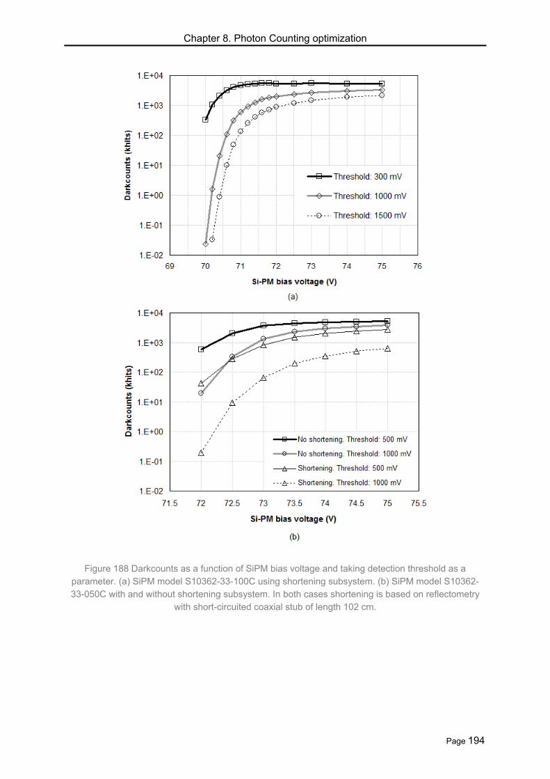
Chapter 8. Photon Counting optimization
Page 194
Figure 188 Darkcounts as a function of SiPM bias voltage and taking detection threshold as a
parameter. (a) SiPM model S10362-33-100C using shortening subsystem. (b) SiPM model S10362-33-050C with and without shortening subsystem. In both cases shortening is based on reflectometry
with short-circuited coaxial stub of length 102 cm.

Chapter 8. Photon Counting optimization
Page 195
Figure 189 Reduction in temperature and corresponding increase of S10362-33-050C SiPM intrinsic gain. (a) This behavior is observed with and without photopulse shortening; SiPM bias voltage: 71.5 V. (b) The gain increment when the device is cooled is not linear; SiPM bias voltage: 72 V. The following conditions apply to all cases: shortening based on reflectometry with a 52 cm short-circuited coaxial
stub, incoming light pulse with width of 10 ns and wavelength of 400 nm.
Figure 189 shows the classical and most visible phenomenon that happens when
temperature is reduced. For both configurations used in this work (with and without shortening) it can be observed an increment on intrinsic SiPM gain as temperature reduces (Figure 189 (a)) [16]Hamamatsu-2009, [219]España-2008. Figure 189 (b) also shows that SiPM gain increment is proportional to temperature reduction, but not linear: gain increment when temperature is reduced from 30 ºC to 20 ºC is roughly twice the one obtained when temperature goes from 20 ºC to 10 ºC.

Chapter 8. Photon Counting optimization
Page 196
Figure 190 Darkcounts as a function of detection threshold and taking temperature as a parameter. (a) When no shortening system is used. (b) When shortening subsystem based on reflectometry with
short-circuited coaxial stub of length 52 cm is used. For all cases SiPM model S10362-33-050C was used and SiPM bias voltage was 72 V.
Figure 190 shows darkcounts as a function of threshold taking the temperature as a
parameter. As expected, downward feature is observed as threshold increases, both with and without shortening. Curves do not show the characteristic stair-case form reported by some authors for darkcounts rate [130]Britvitch-2007 because ranging and sampling used here are not restricted to the lower values covering the reception of only a few photons (another example can be found in [251]Musienko-2011). The comparison of Figure 190 (a) and Figure 190 (b) shows again that although shortening does not reduce noise in the photodetector, it

Chapter 8. Photon Counting optimization
Page 197
provides a notable reduction on the impact of darkcounts on the detection system at all the operating temperatures.
Taking into account that most of false events in darkness are thermogenerated, it is clear
that cooling reduces the darkcount rate [16]Hamamatsu-2009, [221]Ramilli-2008. Also, several authors report evidence of direct proportionality between breakdown voltage and temperature [147]Ahmed-2009, [159]Otono-2007-[161]Para-2009. In this way, when temperature is reduced maintaining bias voltage at a fixed value (as in Figure 190), overvoltage increases and consequently intrinsic gain increases too. Although darkcount rate is lower, the important increase in gain related with temperature causes that the amount of darkcounts whose amplitude is higher than current threshold is inversely proportional to temperature. Therefore, in order to take benefit from cooling it is necessary to consider the variation of the gain with the operating temperature when selecting the SiPM bias voltage. In Figure 191 can be seen that variation of darkcounts with temperature when keeping constant the bias voltage is not fixed: the lower the temperature, the higher the increment in observed darkcounts for a certain temperature reduction (both with and without shortening).
Figure 191 Darkcounts of SiPM model S10362-33-050C as a function of temperature, with and without shortening, for fixed detection threshold of 1 V and fixed SiPM bias voltage of 72 V. Shortening
subsystem is based on reflectometry with short-circuited coaxial stub of length 52 cm.
As it was previously advanced, Figure 192 shows the necessity of taking into account
temperature and SiPM bias voltage as a whole for getting a good behavior in relation with darkcounts and for getting clear SPC patterns. For a fixed SiPM bias voltage a reduction in temperature causes that higher darkcounts surpass the threshold. However, the opposite happens if a certain reduction in temperature is accompanied with the proper reduction in SiPM bias voltage. Figure 192 also shows that cooling is not so critical when pulse shortening is used. Comparable darkcount levels can be obtained at room temperature and at lower temperatures with a proper selection of the bias voltage.
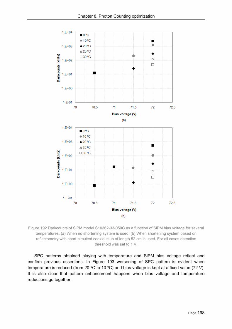
Chapter 8. Photon Counting optimization
Page 198
Figure 192 Darkcounts of SiPM model S10362-33-050C as a function of SiPM bias voltage for several temperatures. (a) When no shortening system is used. (b) When shortening system based on reflectometry with short-circuited coaxial stub of length 52 cm is used. For all cases detection
threshold was set to 1 V.
SPC patterns obtained playing with temperature and SiPM bias voltage reflect and
confirm previous assertions. In Figure 193 worsening of SPC pattern is evident when temperature is reduced (from 20 ºC to 10 ºC) and bias voltage is kept at a fixed value (72 V). It is also clear that pattern enhancement happens when bias voltage and temperature reductions go together.

Chapter 8. Photon Counting optimization
Page 199
Figure 193 SPC patterns obtained with SiPM model S10362-33-050C working alone (i.e. with no shortening subsystem). For both cases the nominal gain of amplification chain is 44 dB and incoming
exciting pulse with width of 10 ns and wavelength of 400 nm is used.
The same behavior in relation with SPC patterns is observed when shortening is used. On
the one hand, Figure 194 (a) shows the strong pattern worsening obtained when temperature is notably reduced with no corresponding biasing correction: peaks corresponding to different number of received photons are poorly defined and base distribution over which photopeaks are mounted [124]Buzhan-2003 remains important and is even extended. At the same time, the shift of peaks to higher voltages is a consequence of higher intrinsic gain obtained when temperature decreases. On the other hand, Figure 194 (b) shows an important reduction in the disturbing base noise but preserving well-defined photopeaks when both temperature and bias voltage are decreased. A reduction in bias voltage yields to an apparent compression of the SPC pattern, which is consistent with the decrease of the intrinsic SiPM gain.

Chapter 8. Photon Counting optimization
Page 200
Figure 194 SPC patterns obtained with SiPM model S10362-33-050C when shortening subsystem based on reflectometry with short-circuited coaxial stub of length 52 cm is used. (a) Pattern worsening
when temperature is reduced with no corresponding biasing voltage correction. (b) Pattern enhancement when temperature and bias voltage are both taken into account. The incident light pulse
has a width of 10 ns and a wavelength of 400 nm.
Figure 195 (a) demonstrates the benefits of SiPM cooling when no shortening is used.
Base noise is significantly reduced due to both lower darkcounts and lower bias voltage and photopeaks show a higher peak to valley difference.

Chapter 8. Photon Counting optimization
Page 201
Figure 195 Best SPC patterns obtained with SiPM model S10362-33-050C. (a) When no shortening subsystem is used. (b) When shortening subsystem based on reflectometry with short-circuited
coaxial stub of length 52 cm is used.
Figure 195 (b) shows two important facts related with shortening. First, comparing with
Figure 195 (a) one can see that shortening is providing, whatever the temperature is, much better photopulses and counting patterns than SiPM working alone. It must be taken into account that patterns shown in Figure 195 are the best ones obtained at both 30 ºC and 0 ºC, with and without shortening. Second, despite it is clear that SPC pattern is enhanced at low temperature, results obtained when shortening is used both at room temperature and at 0 ºC are quite similar. Thus, perhaps it would be possible - in certain applications - to replace the complex and expensive cooling by a simpler and much cheaper shortening scheme.

Chapter 8. Photon Counting optimization
Page 202
8.3.4. Summary The experiments presented in this chapter have illustrated the potential of different
strategies for optimizing SPC patterns when SiPMs are used: cooling, biasing voltage optimization, threshold level adjustment and photopulse shortening. Shortening based on reflectometry has helped to significantly mitigate the negative impact of darkcounts on the detection system: in some cases a reduction of up two orders of magnitude on passing darkcounts was obtained. Results reported for darkcounts are compatible with direct proportionality between characteristic SiPM breakdown voltage and temperature, providing an inverse relation between darkcounts influence on detection and temperature. It has also been shown that in order to take maximum benefit of cooling it is necessary to properly optimize the SiPM bias voltage. Comparable darkcount levels are obtained between 0 ºC and 30 ºC if SiPM bias voltage is optimized at each temperature. Although the best SPC patterns are always achieved when temperature is reduced (and bias voltage is conveniently optimized) cooling improvements are significantly more apparent when photopulses are not shortened. On the other hand, pulse shortening with reflectometry always improves the SPC pattern, no matter at which operating temperature is the measurement made. Taking into account the previous fact and the great similarity obtained between SPC patterns at room temperature and at 0 ºC when shortening is used, it would be possible - in certain applications - to propose the replacement of cooling by a simpler and cheaper shortening scheme. Although experiments presented in this chapter were done using two SiPM models of only one manufacturer, arguments for explaining results enable us to reasonably assume a wide degree of applicability for them. We expect that pulse shortening will be a powerful tool for optimizing SPC pattern for any SiPM, especially when devices of large active area are used or when cooling is not practical.

Chapter 9. Active quenching techniques
Page 203
9. Active quenching techniques In this chapter some active quenching techniques proposed in the literature for using the
SiPM with high optical repetition frequencies are reviewed. Experimental results obtained using different quenching and reset circuits are shown and discussed.
9.1. Active quenching The method used in this work up to now for collapsing the avalanche process is known as
passive quenching. A high value ballast resistor (RL, hundreds of k) supports a voltage drop when photocurrent is generated. That voltage drop reduces the photodetector bias voltage in such a way that when it is near the breakdown voltage the avalanche tends to stop. Taking into account the low level currents delivered by the detector, this resistor must be of high value for enabling an enough voltage drop. However, at the same time, this high value resistance is the reason of the extremely slow recovery process. Thus, main drawback in passive quenching is that it does not allow us to operate the avalanche photodetector at high optical repetition rates. Several active quenching strategies have been developed for improving the dynamic behavior of the APD [17]Bellis-2006, [141]Cova-1996, [157]Kindt-1998, [252]Regan-
1993, [253]Spinelli-1996, [254]Rochas-2004. The basic idea is to detect the fast rising of the output pulse (i.e. to detect the start of the avalanche) and react forcing the discharge and recharge of the APD in a very short time (a few ns) [225]Zappa-2009. Quenching is important because it acts on photodetector dead time allowing the implementation of very low intensity and very high speed photon detection techniques.
Figure 196 shows the Active Quenching Circuit (AQC) proposed by Zappa et al [229]Zappa-
2003.
Figure 196 Simplified active quenching circuit proposed in [229]Zappa-2003.

Chapter 9. Active quenching techniques
Page 204
In steady-state, the current through the photodetector is null (ID = 0), the SPAD is biased with the highest voltage (VD = VHIGH - VLOW) and switches SQUENCH and SRESET are open. When a luminous stimulus arrives, ID linearly increases (start of the avalanche) and immediately RB starts its passive quenching function (1). Shortly after photonic excitation the SENSING module is able to detect the voltage drop on cathode. This module reacts closing SQUENCH and making CONTROL LOGIC module to generate a very short TTL signal (called OUT). This signal is useful for detection purposes but not for resolving the number of received photons. Fast transition on cathode voltage rapidly stops the avalanche but it also generates a strong inverse parasitic current pulse (2). The OUT signal inputs on the DELAY module
whose role is to toggle the output of the RESET module a certain time delay after photonic excitation (4). In that moment, SRESET closes, SQUENCH opens and cathode is connected to VHIGH again. Reset transition causes a new parasitic current pulse in the opposite sense than for the quenching transition (5). During phase (3) the low level current generated through ballast resistor RB flows to ground without crossing the APD. Figure 197 shows the whole process in a graphical way.
Figure 197 Quenching and reset phases on the model proposed in [229]Zappa-2003.
In summary, active quenching phase (2) rapidly stops the avalanche and provides carrier
evacuation. As a consequence, the typical slow falling edge in photodetection pulse is abruptly shortened. Afterwards, reset phase (5) prepares the photodetector for new detections with no damage neither on photodetection efficiency nor on intrinsic gain. Quenching phase is useful for narrowing the output pulse, but its main objective is to empty the diode from carriers that could retrigger avalanches when voltage on cathode is restored to VHIGH. If no quenching is applied prior to reset, photodetection pulse could go accompanied with even several subsequent parasitic pulses. It is also clear that the presence of parasitic pulses is a very important drawback. For getting clean detection pulses at high optical repetition rates, the parasitic pulses caused by fast transitions on bias voltage must be eliminated or at least attenuated.

Chapter 9. Active quenching techniques
Page 205
The analysis of the circuit proposed by Zappa et al for the SENSING module is shown in the following figures [229]Zappa-2003. Figure 198 illustrates the steady-state condition (VMONO = VHIGH, VIN = VHIGH), Figure 199 shows the development of the quenching phase (VMONO = VHIGH, VIN < VHIGH) and Figure 200 explains the recovery phase (VMONO = 0 V, VIN = 0 V).
Figure 198 Analysis of the sensing module in the active quenching circuit for steady-state conditions [229]Zappa-2003.
Figure 199 Analysis of the sensing module in the active quenching circuit during the avalanche
quenching phase [229]Zappa-2003.
Figure 200 Analysis of the sensing module in the active quenching circuit during the recovery phase [229]Zappa-2003.

Chapter 9. Active quenching techniques
Page 206
Gallivanoni et al proposed two modifications on the previous active quenching circuit [228]Gallivanoni-2006. Figure 201 allows observing these modifications: an active load and a new fast timing stage.
Figure 201 Active quenching circuit proposed in [228]Gallivanoni-2006.
Figure 202 Simplified scheme of the TIMING stage used in the modified active quenching circuit
proposed in [228]Gallivanoni-2006.
The first modification consists on a fast timing stage for getting short detection pulses that
make possible high resolution photon timing. Integration of the avalanche current on photodetector capacitances provides a low pass filtering that stretches the very first part of the avalanche. So, it is not possible to obtain very short detection pulses based on the cathode voltage evolution. Although voltage on cathode is still used for detecting avalanche and triggering quenching, authors propose the use of a linear network (formed by Rs, CC and RC) for sensing the current while applying a high pass filtering. Time constant of this coupling

Chapter 9. Active quenching techniques
Page 207
network must be longer than the typical rise time of the avalanche current and, at the same time, shorter than the average interval between pulses (i.e. the reciprocal of the repetition rate). Voltage signal developed on this network is fed to a TIMING stage configured as a fast switching voltage comparator and based on previous works of Kim et al [255]Kim-1992, [256]Cho-
2002. Figure 202 shows a simplified scheme of this stage where M5 and M6 are configured as current sources, M1-M3 and M2-M4 act as differential pairs and TH is the threshold level to surpass on IN for getting well shaped detection pulses on OUT.
Experimental results show that, although for small area devices there is no advantage in
using the fast timing stage, for medium and large area devices the advantage is evident. For
example, when a SPAD with active area diameter of 50 m is used, output pulses obtained in TIMING stage (timing OUT) are 60-70 % shorter than those obtained when using the sensing stage (counting OUT). For larger devices, compression ratio is worst: with an active
area diameter of 100 m pulses on timing stage are only 20-40 % shorter than pulses on
counting stage. A comparison of pulses on both outputs for different overvoltages is shown in Figure 203.
Figure 203 Pulses obtained on sensing stage (counting OUT) and timing stage (timing OUT) for
overvoltages of 5 V and 10 V when SPAD with active area diameter of 50 m is used [228]Gallivanoni-2006.
The transistor used for applying reset (SR) together with the high value ballast resistor
(RL) cause overshoots on cathode voltage that decay with a long time constant (product of load resistor and photodiode capacitances). At high counting rates, the random superposition of such overshoots causes a shift on photodetector bias voltage that degrades its timing performance. This problem could be attenuated using a lower value for RL, but it is
inconvenient because hundreds of k are needed for getting the initial passive quenching. The second modification proposed by Gallivanoni et al on the active quenching circuit consists on using an active load for attenuating this problem. A simplified scheme of the active load is shown in Figure 204.

Chapter 9. Active quenching techniques
Page 208
Figure 204 Simplified scheme of the active load used in the modified active quenching circuit
proposed in [228]Gallivanoni-2006.
When avalanche starts, voltage on cathode decreases and transistor M2 enters into
saturation region. Then the circuit behaves like a current mirror offering high output impedance that develops the initial passive quenching. Overshoot on cathode when reset is applied allows setting transistor M2 into the reverse ohmic region where MOS channel resistance is quite small. So, the time constant for returning to quiescent state from overshoot is much shorter than using the fix high value resistor RL. Figure 205 shows the clear advantage obtained when using the active load: time constants for recovery after
voltage overshoot are around 100 ns and 1 s for active and passive loads respectively.
Figure 205 Cathode voltage recovery at the end of the reset phase when passive and active loads are used [228]Gallivanoni-2006.
Figure 206 shows a complete detection process when using the active quenching circuit
previously described and shown in Figure 201. Experimental determinations of voltage on cathode and photocurrent for two different overvoltages together with corresponding simulations are shown. Simulations were done using the APD equivalent circuit proposed by Zappa et al [225]Zappa-2009 which was described in a previous chapter (see Figure 151). Agreement between experimental data and simulations is quite good. However, the

Chapter 9. Active quenching techniques
Page 209
underestimation of parasitic currents on the reset phase does not allow the simulations to predict the overshoots on the cathode voltage.
Figure 206 Comparing experimental data and simulations for a detection process when the active quenching circuit proposed in [228]Gallivanoni-2006 is used. Simulations were done taking into account the APD equivalent circuit proposed by the same authors that provide the comparison shown in this figure
[225]Zappa-2009.
9.2. Gated quenching In gated quenching the SiPM bias voltage is higher than the characteristic breakdown
voltage (VBR) only during the period of time in which a photon is expected. This approach is suitable for quantum key distribution systems in which the arrival times of photons can be predicted with enough accuracy [111]Buller-2010. Between two consecutive gate pulses VBIAS < VBR and an avalanche can not be triggered [158]Viana-Ramos-2003. The main advantage of gated quenching is that both darkcounts and afterpulsing phenomena are reduced. For reducing afterpulsing, time between successive gate pulses must be sufficiently large for allowing all

Chapter 9. Active quenching techniques
Page 210
traps to be released [158]Viana-Ramos-2003. Figure 207 shows a simple circuit for gated quenching and the bias voltage signal acting on the APD [158]Viana-Ramos-2003.
(a) (b)
Figure 207 (a) Gated quenching schematics and (b) gating signal for biasing the APD [158]Viana-Ramos-
2003.
Figure 208 shows the APD equivalent circuit with the rest of the elements for gated
quenching. Rd is the internal APD resistance when avalanche is happening, Cd is the capacitance of the junction and Cs is the stray capacitance associated with metallic grid. When the gate pulse width (Tw) is very large, passive quenching is provided by RL and corresponding time constant is given by:
||gq L d g d s d g d sR R C C C R C C C (112)
The recovery time is the time required for the APD for being totally operative. With this
approach, recovery happens between gating pulses (the switch in the APD equivalent circuit is open) so that the characteristic time constant will be:
gr L g d sR C C C (113)
Simulations were done using the following values for the different elements in the model:
R: 25 , Cg: 100 pF, RL: 330 k, Rd: 1 k, Cd: 0.5 pF, Rs: 50 , Cs: 0.5 pF, Vexcess: 3 V, Tw: 8.4 ns. Figure 209 shows two simulations for different moments along the gating pulse for triggering the avalanche. Here it is verified that time for gating is lower than the characteristic
passive quenching time constant (Tw < gq). Even without avalanche there are undesirable
pulses in the signal caused by the fast transitions of the gate signal in the capacitances. Although authors say that these peaks must not be taken into account, and thus following stage for processing the output signal must be able to discard it, they do not propose any solution [158]Viana-Ramos-2003.

Chapter 9. Active quenching techniques
Page 211
Figure 208 Gated quenching circuit for small signal together with the APD equivalent circuit proposed in [158]Viana-Ramos-2003.
(a) (b) Figure 209 Simulation signals for gated quenching when time for gating is lower than passive
quenching time constant (Tw < gq). Green: gating signal, reed: voltage between cathode and anode, blue: detection signal. (a) Triggering the avalanche in the middle of the gating pulse. (b) triggering the
avalanche at the end of the gating pulse [158]Viana-Ramos-2003.
Figure 210 shows another simulation in which time for gating is higher than passive
quenching time constant (Tw > gq). Values for the different elements in the model remain
constant except RL that is changed to 50 . This is done for reaching the condition Tw > gq with no change in the gating signal width. In this case, voltage on the APD decreases continually during the gate pulse (due to the fast charge of Cg through the low value resistor RL), a fact that reflects in the same way on the sensing signal while switch SW is closed. It is important to take into account this behavior for setting the appropriate threshold in a QKD detector. Authors do not provide experimental results for comparison with simulations [158]Viana-Ramos-2003

Chapter 9. Active quenching techniques
Page 212
Figure 210 Simulation signals for gated quenching when time for gating is higher than passive
quenching time constant (Tw > gq). Green: gating signal, reed: voltage between cathode and anode, blue: detection signal [158]Viana-Ramos-2003.
(a) (b)
Figure 211 Gated quenching operation with a SPAD [225]Zappa-2009. (a) Gating circuit used for
experiments and simulations. (b) Experimental and simulated results when a photoinduced avalanche happens inside the gating period; blue: gate pulse, red: simulated output signal, black: experimental
output signal.
Zappa et al shows experimental and simulated data for a SPAD operated in gated mode
[225]Zappa-2009. When no photon is expected the device is biased below the breakdown voltage (i.e. VA: 21 V since VBR: 21.54 V). When a photon is expected the bias voltage is quickly enabled above the breakdown level by applying a steep pulse (edges in the order of ns). Figure 211 (a) shows the gated circuit proposed for both experiments and simulations and Figure 211 (b) shows the results obtained when a photoinduced avalanche happens during the gating period. The APD model used for simulations is the equivalent circuit proposed by Zappa et al which was described previously (see Figure 151). A good agreement between

Chapter 9. Active quenching techniques
Page 213
experimental and simulated data is obtained. Furthermore, these results show that the APD model is able to accurately predict not only the avalanche trigger, but also the two parasitic couplings due to the fast edges of the gate signal.
9.3. Experimental results
9.3.1. Introduction Figure 212 shows the experimental response of the SiPM model S10362-33-100C to an
increasing optical repetition frequency. This downward characteristics is the cause of that SiPM, despite its fast response capability, has limited use nowadays for very high rates applications.
Figure 212 Behavior of the SiPM model S10362-33-100C with the optical repetition frequency for several widths in the exciting pulse. Amplitude of exciting pulse: 5 V. No amplification chain is used.
If one photonic pulse arrives to the SiPM during the recovery period of a previous
detection, the photodetector is able to react to this new pulse but with lower amplitude. During that period the SiPM is remaking the junction and the effective bias voltage is slowly returning to the optimal value. Every time a detection is triggered during the recovery time a new avalanche is generated, the effective voltage on the SiPM decreases and the recovery process has to start again. As the new pulse is closer to the previous one, the gain with which the SiPM is able to react is lower (the higher the difference between the current voltage and the optimal bias voltage) and this reduces the amplitude of the new detection. In

Chapter 9. Active quenching techniques
Page 214
other words, the higher the optical repetition frequency the lower the amplitude of the resulting pulse. The long recovery time happens because the SiPM is dominated by the passive quenching generated by the high value quenching resistor. The solution to this problem can be carried out by means of active quenching techniques. The idea is quickly to reduce the effective SiPM bias voltage once a detection is triggered. This step collapses the avalanche faster than the intrinsic passive quenching. And afterwards, a fast reset step is required for returning the SiPM to the optimal bias voltage. This way, the long recovery time is avoided and new detections could be developed with the highest response capability. Figure 213 schematizes these ideas.
Figure 213 Comparison between results obtained with passive quenching and active quenching in an idealized scheme. Evolution in effective bias voltage and output pulses are shown.
9.3.2. Results for quenching Several active quenching schemes have been tested. Quenching and reset stages
should be triggered by the arrival of a photonic pulse. Delay and duration of quenching and reset pulses should be preprogrammed to provide the best results. To trigger these signals once an optical pulse has been detected and to define delays and durations implies the development of auxiliary circuitry. However, for a first approach, quenching and reset signals have been provided by means of a functions generator. So, it is possible to test in a

Chapter 9. Active quenching techniques
Page 215
convenient way the influence of the different parameters of those signals, i.e. amplitude, delay and duration.
Figure 214 shows the first quenching scheme that was assayed. SiPM is illuminated by
means of the UV LED model Hero Electronics HUVL400-5x0B [204]Hero-2002 fed with electrical
pulses of amplitude Aexc and width exc. The quenching signal Q tries to reduce the voltage on
the SiPM cathode in such a way that the avalanche quickly collapses. A N-channel MOSFET transistor (ZXMN10A07F) was selected for this circuit. This device supports high drain-
source voltages (100 V) and provides good switching features (ton 3.3 ns, toff 6.2 ns)
[257]Diodes-2003.
Figure 214 Quenching scheme 1: quenching in cathode and no reset. Excitation signal: Aexc: amplitude
of the exciting pulse, exc: width of the exciting pulse. Quenching signal: Aq: amplitude of the quenching
pulse, q: width of the quenching pulse, q: delay of the quenching pulse regarding to the exciting pulse.
Figure 215 shows the effect of quenching on the output pulse and on the cathode
voltage. Activation of the short quenching signal (q: 50 ns) in the middle of the long
photopulse (exc: 500 ns) really collapses the avalanche: the output pulse quickly drops when quenching is activated (see Figure 215 (a)). This fast transition causes a significant negative overshoot which is affected by a long time constant when the quenching signal disappears. Quenching activation is reflected as a change in the slope of the falling cathode voltage, as it can be observed in Figure 215 (b).

Chapter 9. Active quenching techniques
Page 216
Figure 215 Quenching scheme 1. (a) Original output pulse and pulse when quenching is acting. (b)
Corresponding drops in the cathode voltage. Aexc: 3 V, exc: 500 ns, Aq: 2 V, q: 50 ns, q: 150 ns.
Figure 216 allows observing that quenching correctly works for a great range of
amplitudes for the LED exciting pulse. That is, quenching action only depends on the parameters of the quenching subsystem. It is an expected and desirable result.
Figure 216 Quenching scheme 1. Quenching action for several amplitudes of the LED exciting pulse.
exc: 500 ns, Aq: 1.9 V, q: 50 ns, q: 150 ns.

Chapter 9. Active quenching techniques
Page 217
Figure 217 Quenching scheme 1. Effect of varying the quenching pulse width. (a) Output pulses
obtained when no quenching is applied and when quenching pulses of 30 ns and 50 ns are used. (b)
Output pulses obtained when quenching pulses of 50 ns, 80 ns and 150 ns are used. Aexc: 2 V, exc:
100 ns, Aq: 2 V, q: 30 ns.
Parameters of the quenching subsystem (Aq, q: amplitude and width of the quenching
pulse respectively) greatly affect the result. Both parameters cause a similar behavior when are independently modified. On the one hand, a low value for the parameter causes a non-complete quenching action. This fact can be observed in Figure 217 (a) by comparing signals when no quenching is applied and when a quenching pulse of only 30 ns is used. The same effect is observed when a wide enough quenching pulse is applied but with low amplitude
(e.g. below 2 V). On the other hand, the higher the value of the parameter (Aq or q) the higher the negative overshoot (as it is clearly shown in Figure 217 (b)) and as a consequence, the higher the subsequent positive overshoot caused by the recovery process. This last overshoot is an important inconvenience because it can reach an amplitude comparable to the one of the photodetection pulse itself. Thus, both quenching parameters have quite narrow ranges of values for providing good quenching results (i.e. complete pulse shortening without positive overshoot).
The negative overshoot can be cancelled using an appropriate rectifier diode. Good
results have been obtained when the Schottky diode models BAT17 [250]NXP-2003 and MMBD770T1 [258]Motorola-1996 were used. Figure 218 shows the clipping in the photodetection pulse for long and short excitation pulses when the diode MMBD770T1 is ending the photosignal processing chain. When the quenching parameters are not too high, quenching clips the photopulse with only a little negative overshoot (see Figure 218 (a)). When those parameters increase, the quenching becomes steeper, that is, the falling slope in the photopulse is higher. The result is that the negative overshoot has quite higher amplitude (see Figure 218 (b)) although it maintains its reduced width. Also, and for the same reasons previously discussed, an important positive overshoot happens.

Chapter 9. Active quenching techniques
Page 218
Figure 218 Quenching scheme 1. Schottky diode MMBD770T1 ends the photopulse processing chain.
(a) Quenching in the middle of a long excitation pulse. Aexc: 3 V, exc: 500 ns, Aq: 2 V, q: 50 ns, q: 150
ns. (b) Quenching for a shorter excitation pulse. Aexc: 3 V, exc: 100 ns, q: 50 ns, q: 30 ns, Aq: 2.5 V.
The rectifier diode is changing the behavior in relation with the secondary positive
overshoot. Figure 219 shows the effect of increasing the width of the quenching pulse when the diode MMBD770T1 is used. By comparing these results with those shown in Figure 217 (b) it is possible to note that the diode is causing an important increase in the positive overshoot. Now the positive overshoot can become quite higher than the desired
photodetection pulse. In fact, when q: 150 ns the photodetection pulse has been shortened
in excess causing an amplitude distortion.
Figure 219 Quenching scheme 1. Schottky diode MMBD770T1 ends the photopulse processing chain.
Effect of quenching pulses of different widths. Aexc: 3 V, exc: 100 ns, Aq: 2 V, q: 30 ns.

Chapter 9. Active quenching techniques
Page 219
Another possibility to optimize this scheme is to play with the quenching resistor located between the drain of the transistor and the cathode of the SiPM (do not confuse with the inner quenching resistor that collapses the avalanche on each SiPM microcell). Figure 220 (a) shows that the lower the quenching resistor the sharper the transition between the ON and OFF states. These signals have been obtained when the quenching resistor is disconnected from the cathode and is biased with 20 V. Figure 220 (b) shows how the slope in the cathode voltage is affected when quenching is applied by means of different values of that resistor.
Figure 220 Quenching scheme 1. Quenching resistor notably changes the transition between OFF and ON states in the transistor (a) and the slope in the cathode signal (b).
Taking into account all the previous assertions, it is easy to understand that the higher
the quenching resistor the lower the overshoots that happen when quenching is applied, as it can be observed in Figure 221. However, the disadvantage in this approach is that the higher the quenching resistor the softer the clipping of the photodetection pulse (see Figure 221 (b)).
Figure 221 Quenching scheme 1. Diode MMBD770T1 ends the photopulse processing chain. Effect of
varying the value of the quenching resistor. Aexc: 3 V, exc: 100 ns, Aq: 2 V, q: 50 ns, q: 30 ns.

Chapter 9. Active quenching techniques
Page 220
Although this simple scheme provides good clipping results, the fact that narrow ranges for the quenching parameters are mandatory has led the author of this thesis to explore other solutions. Nevertheless, this scheme offers potential to be recovered in a future for combining it with a proper reset subsystem.
Figure 222 shows a first quenching scheme by acting on the anode of the SiPM. The
quenching subsystem (formed by transistors Q1 and Q2) tries to reduce the SiPM bias voltage by applying a voltage on the anode that ranges up to tens of volts. While no quenching pulse is applied, both transistors are at cut-off because gate-source voltages are near zero. When a quenching pulse arrives, Q1 tends to the saturation state. This fact notably reduces the voltage in the gate of Q2. When the voltage Vcc2 is high enough, the voltage source-gate in Q2 puts this transistor in saturation. Thus, a voltage near Vcc2 is placed on the anode of the SiPM (see Figure 223). This way, the effective bias voltage drops below the breakdown voltage forcing the collapse of the avalanche under development. Meanwhile, transistor Q3 will try to recover the original bias voltage once the avalanche has been quenched.
Figure 222 Quenching scheme 2: quenching, reset and sensing in anode.
Figure 223 shows that switching speed of transistors is an important fact for making the
quenching and reset subsystems. High speed devices are required for minimizing the oscillating regime caused by fast transitions. These oscillations might have negative effects on the photopulse clipping and shaping. Together with the previously mentioned N-channel transistor ZXMN10A07F, the P-channel transistor ZXMP10A13F was selected following the same criteria than for the other one (VDS: 100 V, ton: 3.7 ns, toff: 9.2 ns) [259]Diodes-2005.

Chapter 9. Active quenching techniques
Page 221
Figure 223 Quenching scheme 2. Voltage on the anode of the SiPM is controlled by means of the quenching pulse.
Figure 224 demonstrates that this scheme does not provide the good expected results.
When the voltage near 20 V is placed on the anode of the SiPM the avalanche quenches. However, this voltage drops on the resistors RL and RS what causes a very intense current peak. That current peak originates a very important voltage pulse on the sensing resistor that completely masks the clipping of the photopulse. Still more, when the anode pulse ceases, an important negative overshoot happens followed in addition by a long recovery process.
Figure 224 Quenching scheme 2. Quenching on anode (a) applied outside the photodetection pulse
and (b) applied on the middle of the photodetection pulse. Aexc: 4 V, exc: 1 s, Aq: 1.9 V, q: 400 ns, q:
2.5 s (for (a)) or 300 ns (for (b)).

Chapter 9. Active quenching techniques
Page 222
Figure 225 Quenching scheme 3: quenching and reset in anode, sensing in cathode.
Figure 225 shows a modified scheme that tries to solve this problem. The idea is to apply
on the anode the high voltage for quenching the avalanche but to sense the photocurrent in the side of the cathode.
Figure 226 shows signals on different points of the quenching subsystem when
quenching pulse is applied. As it can be noted, voltage on Q1-drain only reduces to about 12 V, but it is more than enough for saturating transistor Q2. It can also be observed that there is a non-negligible delay between the quenching pulse and the high voltage pulse on the anode. Currently, width and delay of the quenching pulse can be selected at convenience. However, this delay should be taken into account when a quenching circuit triggered by photopulse is adopted.
Figure 226 Quenching scheme 3. Signals on different points of the quenching subsystem.
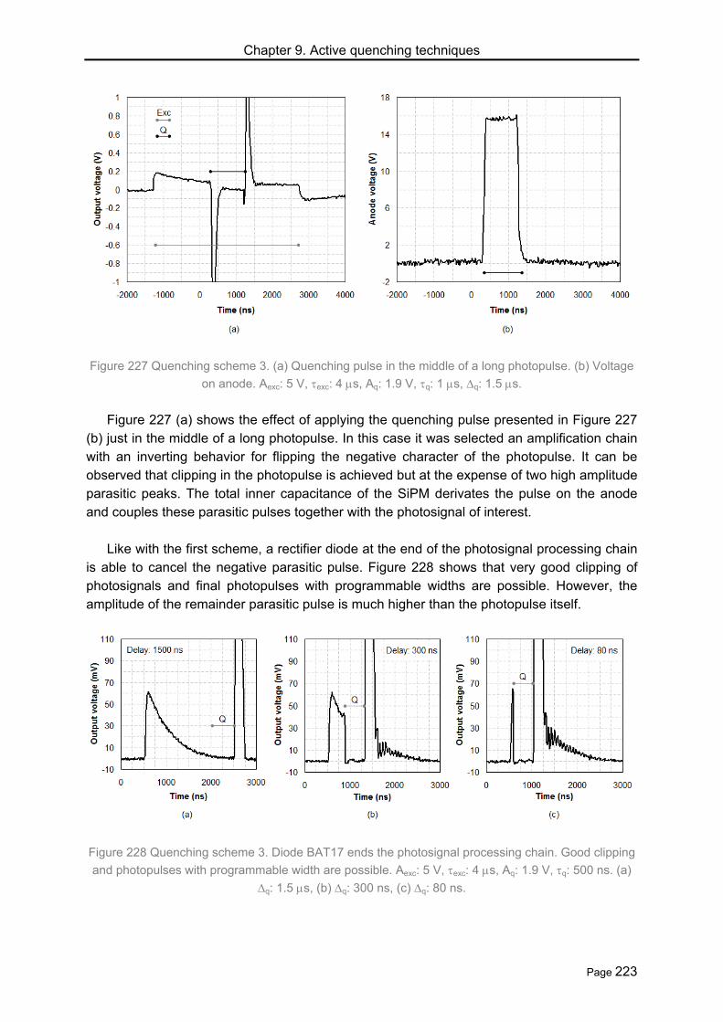
Chapter 9. Active quenching techniques
Page 223
Figure 227 Quenching scheme 3. (a) Quenching pulse in the middle of a long photopulse. (b) Voltage
on anode. Aexc: 5 V, exc: 4 s, Aq: 1.9 V, q: 1 s, q: 1.5 s.
Figure 227 (a) shows the effect of applying the quenching pulse presented in Figure 227
(b) just in the middle of a long photopulse. In this case it was selected an amplification chain with an inverting behavior for flipping the negative character of the photopulse. It can be observed that clipping in the photopulse is achieved but at the expense of two high amplitude parasitic peaks. The total inner capacitance of the SiPM derivates the pulse on the anode and couples these parasitic pulses together with the photosignal of interest.
Like with the first scheme, a rectifier diode at the end of the photosignal processing chain
is able to cancel the negative parasitic pulse. Figure 228 shows that very good clipping of photosignals and final photopulses with programmable widths are possible. However, the amplitude of the remainder parasitic pulse is much higher than the photopulse itself.
Figure 228 Quenching scheme 3. Diode BAT17 ends the photosignal processing chain. Good clipping
and photopulses with programmable width are possible. Aexc: 5 V, exc: 4 s, Aq: 1.9 V, q: 500 ns. (a)
q: 1.5 s, (b) q: 300 ns, (c) q: 80 ns.
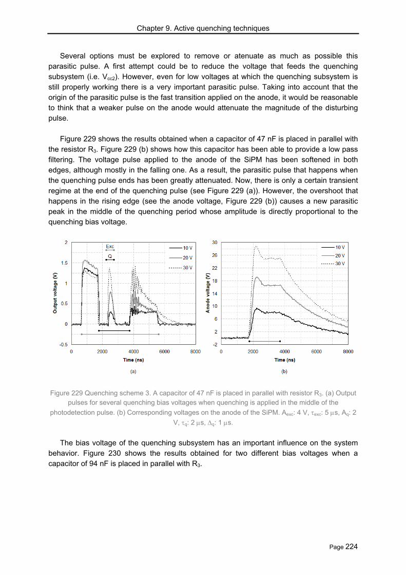
Chapter 9. Active quenching techniques
Page 224
Several options must be explored to remove or atenuate as much as possible this parasitic pulse. A first attempt could be to reduce the voltage that feeds the quenching subsystem (i.e. Vcc2). However, even for low voltages at which the quenching subsystem is still properly working there is a very important parasitic pulse. Taking into account that the origin of the parasitic pulse is the fast transition applied on the anode, it would be reasonable to think that a weaker pulse on the anode would attenuate the magnitude of the disturbing pulse.
Figure 229 shows the results obtained when a capacitor of 47 nF is placed in parallel with
the resistor R3. Figure 229 (b) shows how this capacitor has been able to provide a low pass filtering. The voltage pulse applied to the anode of the SiPM has been softened in both edges, although mostly in the falling one. As a result, the parasitic pulse that happens when the quenching pulse ends has been greatly attenuated. Now, there is only a certain transient regime at the end of the quenching pulse (see Figure 229 (a)). However, the overshoot that happens in the rising edge (see the anode voltage, Figure 229 (b)) causes a new parasitic peak in the middle of the quenching period whose amplitude is directly proportional to the quenching bias voltage.
Figure 229 Quenching scheme 3. A capacitor of 47 nF is placed in parallel with resistor R3. (a) Output pulses for several quenching bias voltages when quenching is applied in the middle of the
photodetection pulse. (b) Corresponding voltages on the anode of the SiPM. Aexc: 4 V, exc: 5 s, Aq: 2
V, q: 2 s, q: 1 s.
The bias voltage of the quenching subsystem has an important influence on the system
behavior. Figure 230 shows the results obtained for two different bias voltages when a capacitor of 94 nF is placed in parallel with R3.

Chapter 9. Active quenching techniques
Page 225
Figure 230 Quenching scheme 3. A capacitor of 94 nF is placed in parallel with R3. Influence of the bias voltage of the quenching subsystem. (a) Clipped output pulses at two different bias voltages.
Black curve corresponds to quenching a long excitation pulse with low bias voltage (Aexc: 4 V, exc: 3 s, Aq: 2 V, q: 5 s, q: 100 ns). Gray curve corresponds to quenching a short excitation pulse with
higher bias voltage (Aexc: 2 V, exc: 100 ns, Aq: 2 V, q: 2 s, q: 10 ns). (b) Corresponding anode voltages.
As it was expected, the higher the capacitor the slower the rising edge in the anode
voltage (compare Figure 230 (b) and Figure 229 (b)). This fact helps to reduce the influence of the parasitic pulses. Besides, the lower the bias voltage the lower the slope of the rising edge in the anode voltage (compare both curves in Figure 230 (b)). So, parasitic pulses will have still less importance. However, bias voltage can not be reduced too much. For example, black curve in Figure 230 (a) shows that with a low bias voltage the photopulse clipping is not complete. On the one hand, the falling edge in the photopulse when quenching starts its action shows a slow slope (i.e. clipped photopulse is worst shaped). On the other hand, the pulse returns to its original evolution although it should be at zero during the whole quenching pulse. When the bias voltage is incremented, photopulse is completely clipped and better shaped, but at the expense of appearance of parasitic pulses directly proportional to the bias voltage. Despite these limitations, the scheme could provide good results when short excitation pulses and medium-low bias voltages are used.
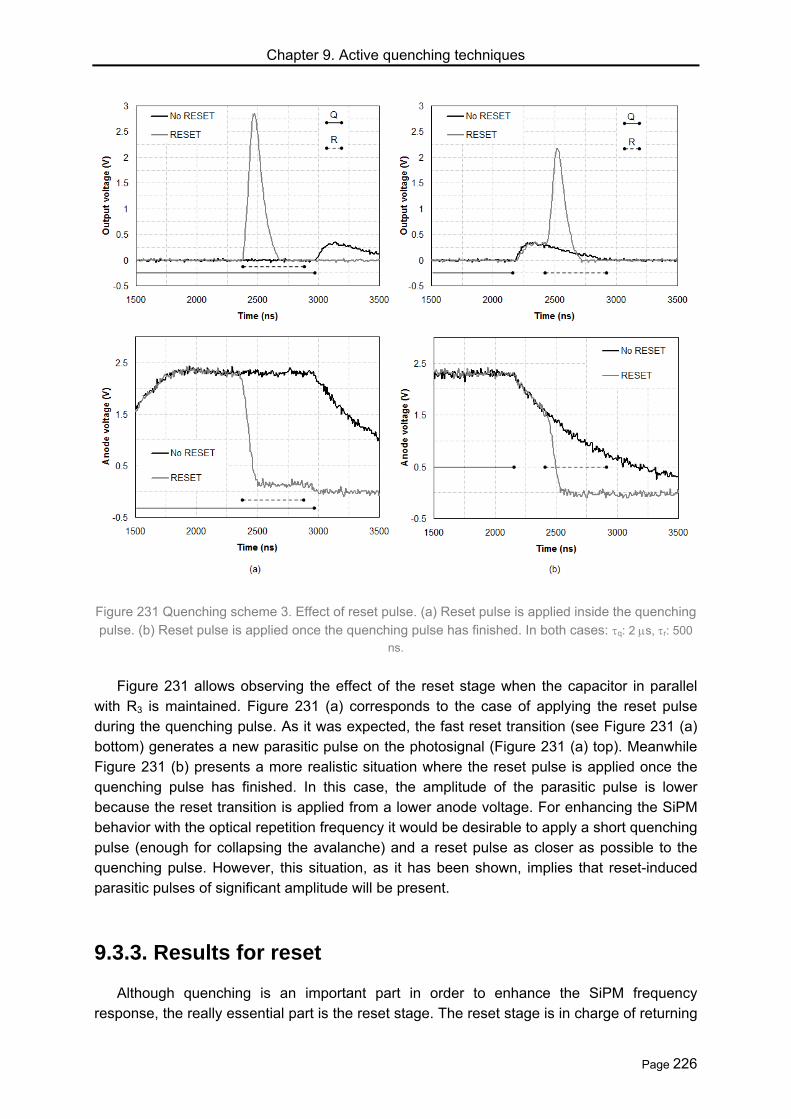
Chapter 9. Active quenching techniques
Page 226
Figure 231 Quenching scheme 3. Effect of reset pulse. (a) Reset pulse is applied inside the quenching pulse. (b) Reset pulse is applied once the quenching pulse has finished. In both cases: q: 2 s, r: 500
ns.
Figure 231 allows observing the effect of the reset stage when the capacitor in parallel
with R3 is maintained. Figure 231 (a) corresponds to the case of applying the reset pulse during the quenching pulse. As it was expected, the fast reset transition (see Figure 231 (a) bottom) generates a new parasitic pulse on the photosignal (Figure 231 (a) top). Meanwhile Figure 231 (b) presents a more realistic situation where the reset pulse is applied once the quenching pulse has finished. In this case, the amplitude of the parasitic pulse is lower because the reset transition is applied from a lower anode voltage. For enhancing the SiPM behavior with the optical repetition frequency it would be desirable to apply a short quenching pulse (enough for collapsing the avalanche) and a reset pulse as closer as possible to the quenching pulse. However, this situation, as it has been shown, implies that reset-induced parasitic pulses of significant amplitude will be present.
9.3.3. Results for reset Although quenching is an important part in order to enhance the SiPM frequency
response, the really essential part is the reset stage. The reset stage is in charge of returning

Chapter 9. Active quenching techniques
Page 227
the effective bias voltage in the SiPM to the maximum value after a detection process. This way the photodetector will be able to react to a subsequent detection with the maximum gain and efficiency. This section will show some results obtained by means of two reset schemes.
Figure 232 shows the first reset scheme. Transistors Q3 and Q4 act like a current mirror
providing a current to the load controlled by the variable resistor P1. Voltages on drains of these transistors are close to Vcc2. The high value resistor between drain of Q3 and ground is used for collecting the current while Q2 is open and for deriving it to the SiPM when Q2 closes. When transistor Q2 closes this current should be derived to the SiPM helping to quickly recharge its intrinsic capacitance and to return the SiPM bias voltage to the steady state value. Configuration for transistor Q1 allows switching the transistor Q2 by means of the R (reset) signal. When R signal is low, Q1 is open and gate-source voltage in Q2 is close to zero. This way Q2 is open and the unique active part is the SiPM bias circuit. When R signal is high, Q1 closes, the voltage on the gate of Q2 reduces and this transistor closes. That voltage reduction on the gate of Q2 will be derived to the drain which is connected to the SiPM cathode. So, a voltage reduction on the SiPM cathode is expected prior to return to the maximum value corresponding to the steady state. In other words, quenching and reset come one after the other.
Figure 232 Quenching-Reset scheme.
Figure 233 shows the results obtained when a reset pulse is launched close after the
photonic detection. Figure 233 (a) allows observing a reduction on the cathode voltage which acts like a quenching step. Corresponding negative overshoot in the photodetection signal can be observed in Figure 233 (b). The fast recharge of the SiPM capacitance does not

Chapter 9. Active quenching techniques
Page 228
happen during the reset pulse. However, the overshoot caused when the reset pulse ends provides a faster recovery to the steady state. This way, a little enhancement in the photodetector frequency response is expected when this scheme is used.
Figure 233 Results for quenching-reset scheme. The reset pulse with duration of 200 ns is launched 100 ns after the photonic detection. (a) Evolution of the SiPM cathode voltage. (b) Corresponding
photodetection signals obtained with no gain stage.
Figure 234 (a) shows the effect of the resistor RL on the recovery of the cathode voltage.
It was explained in chapter 6.9 that the time constant for the recovery of one cell in the SiPM
depends on its quenching resistor, which is in the order of hundreds of k. Normally only a few cells in the SiPM will be fired, so that the quenching resistors of the non-fired cells behave like resistors in parallel. This way, the global resistance that takes part on the recharge of the intrinsic capacitance is in the order of hundreds of ohm. Thus, the external resistor RL, which is connected in series with this parallel resistance, plays an important role on the recovery of the photodetector. Figure 234 (a) allows observing that a low value for this resistor helps to provide a faster return to the steady state but with a transient regime that is translated to the photodetection signal as overshoots (see Figure 234 (b)). Also in this case it is expected an enhancement in the photodetector frequency response.

Chapter 9. Active quenching techniques
Page 229
Figure 234 Evolution of cathode voltage (a) and photodetection signal (b) for different values of the guarding resistor RL.
When a low value for the resistor RL is used no improvements are obtained by using the
quenching-reset scheme. This can be observed by comparing cathode recovery with and without reset in Figure 235. When RL is low the current flowing by the SiPM tends to be high.
For avoiding damage on the photodetector it is advisable a value of several k for RL which
provides a moderated current through the SiPM. This is the recommendation of the manufacturer of the SiPM. Taking into account this recommendation the reset schemes seem to be useful for enhancing the photodetector frequency response.
Figure 235 Evolution of cathode voltage (a) and photodetection signal (b) with and without reset when
resistor RL is reduced to 100 . The reset pulse with duration of 20 ns is launched 20 ns after the photonic detection.

Chapter 9. Active quenching techniques
Page 230
Figure 236 allows observing that the use of the quenching-reset scheme shown in Figure 232 effectively provides an enhancement in the frequency response of the photodetector. However, new schemes will be used for trying to obtain a better performance.
Figure 236 Frequency response of the SiPM with and without the quenching-reset scheme. The reset pulse with a duration of 200 ns is launched 100 ns after the photonic detection. The pulse width for the
exciting LED is 10 ns.
Figure 237 shows the second reset scheme in which no quenching stage is provided.
Transistor Q2 is replaced by the N channel MOSFET of type ZVN3310F. Drain of Q2 is connected either to Vcc2 or to the previously explained current mirror. For properly switching Q2 transistor Q1 must be switched by means of an inverted version of the reset signal.
Figure 237 Reset scheme with no quenching stage.

Chapter 9. Active quenching techniques
Page 231
Figure 238 Signals for different points in the circuit of Figure 237 (I). (a) Signal that feds the transistor Q1. (b) Signal that feds the transistor Q2. (c) Signals at drain of Q1 (black) and at drain of Q2 (gray).
The reset pulse has a width of 3.1 s.
Figure 239 Signals for different points in the circuit of Figure 237 (II). (a) Signal that feds the transistor Q1. (b) Signal that feds the transistor Q2. (c) Signals at drain of Q1 (black) and at drain of Q2 (gray).
The reset pulse has a width of 3.1 s and the bias voltage for the reset circuit is 72 V.

Chapter 9. Active quenching techniques
Page 232
Figure 238 and Figure 239 show signals at different points in this reset circuit. Figure 239 (b) allows observing that the cathode voltage increases during the reset pulse but the same trend in the voltage remains meanwhile. In addition, cathode voltage returns to its original behavior when the reset pulse ends. This behavior is desirable but additional requirements are needed. It is necessary that the voltage goes up to the highest value and remains there once the reset pulse ceases. The amplitude of the signal that feds to transistor Q1 influences the transient regime in the cathode voltage. In order to reduce this transient regime a variable resistor has been included after the NAND logic gate.
The reset circuit bias voltage provides the required increase and permanence in the
cathode voltage. It can be seen in Figure 240 that a value of 73.4 V for Vcc2 provides a fast return in the cathode voltage to the steady state value after the photonic detection. It is clearly noticeable the achieved enhancement by comparing cathode signals with and without reset. Thus, an important enhancement in the response of the photodetector with the repetition frequency is expected when reset was applied. Figure 240 (b) shows that the amplitude for the photodetection signal is enhanced when reset is applied and that the parasitic pulse originated by the fast transition in the cathode has much lower amplitude than the photopeak itself. This fact would make easy its suppression in a subsequent stage. The reset circuit bias voltage has to be carefully adjusted. An excessive value causes that the cathode voltage surpasses the steady state voltage and a descending regime towards that value happens after the reset pulse.
Figure 240 Cathode voltages (a) and output signals (b) obtained with and without reset when a reset circuit bias voltage of 73.4 V is used. The reset pulse with duration of 250 ns is launched 200 ns after
the photonic detection.
Figure 241 (b) shows that the recovery in the cathode voltage is not complete when the
reset pulse is too short. An appropriate value might be around 100 ns. Although higher widths provide better recoveries, they also provide higher overshoots and increasing limitations in relation with the reachable repetition frequency. Figure 241 (a) shows that

Chapter 9. Active quenching techniques
Page 233
adequate recoveries are obtained with a wide reset pulse applied at different delays after the photonic detection.
Figure 241 Cathode voltage evolution when the reset pulse is applied with different delays after the photonic detection (a) and when different pulse widths are used (b). Reset circuit bias voltage is 73.4
V. The reset pulse width is 800 ns in (a) and the pulse delay is 200 ns in (b).
Figure 242 Frequency response of the SiPM with and without the reset scheme shown in Figure 237. The reset pulse with duration of 100 ns or 200 ns is launched just after the photonic detection. The
pulse width for the exciting LED is 10 ns.
As it was previously announced, Figure 242 confirms the important improvement in the
frequency response of the photodetector when the reset circuit is used. No gain stage has been used for not disturbing the real SiPM frequency behavior. The amplitude of the

Chapter 9. Active quenching techniques
Page 234
photodetection pulse when the reset circuit is used remains at high values for the whole explored frequency range. Meanwhile, the amplitude of the photodetection pulse when the photodetector is not assisted by the reset circuit shows a continuous and important dropping. A difference higher than one order of magnitude is obtained for high frequencies. The results shown in Figure 242 demonstrate the concept of reset for enhancing the performance of the SiPM. For achieving higher frequency ranges, faster and more complex circuits as well as laser excitation should be used.
Figure 243 shows the cathode voltage evolution and the photodetection signal obtained
when the guarding resistor RL is reduced to 1.2 k. In this case there is not a noticeable improvement in the cathode recovery when reset is used. However, Figure 244 shows that the frequency response of the SiPM is clearly improved by using reset even for very short reset pulses. By comparing Figure 242 and Figure 244 it is possible to note that the SiPM responses when reset is used are quite similar (i.e. the value of RL is not so important). On the contrary, the photodetection pulse and the frequency response is clearly influenced by the value of RL when the SiPM is not helped by reset. Thus, the apparent improvement attributable to a low value of RL has been clearly surpassed by using the reset scheme.
Figure 243 Cathode voltages (a) and output signals (b) obtained when the guarding resistor RL is low
(1.2 k). The reset pulse with duration of 30 ns or 100 ns is triggered immediately after the photonic detection.

Chapter 9. Active quenching techniques
Page 235
Figure 244 Frequency response of the SiPM with and without reset when the guarding resistor RL is
reduced to 1.2 k. The reset pulse with duration of 30 ns or 100 ns is launched right after the photonic detection. The pulse width for the exciting LED is 10 ns.
Finally, it was tested the performance when the drain of transistor Q2 is connected to the
current mirror. The system behavior is quite similar to the case of connecting a constant voltage. Figure 245 (a) shows that also in this case the recovery of the cathode voltage is enhanced with respect to the case of not using reset. The frequency response when reset is used is also clearly enhanced, as it is shown in Figure 246. However, there is higher transient regime which is translated to the photodetection signal as parasitic pulses (see Figure 245 (b)).
Figure 245 Cathode voltages (a) and output signals (b) obtained when drain of Q2 is connected to the
current mirror. The reset pulse with duration of 100 ns is launched at 0 s or 1 s after the photonic
detection. The guarding resistor RL is 9 k and the reset circuit bias voltage is 74 V.

Chapter 9. Active quenching techniques
Page 236
Figure 246 Frequency response of the SiPM with and without reset when drain of Q2 is connected to the current mirror. The reset pulse with duration of 100 ns is launched just after the photonic detection.
The pulse width for the exciting LED is 10 ns.
9.3.4. Summary Results shown in this chapter have demonstrated that the frequency response of the
SiPM can be enhanced by using circuits for resetting the photodetector right after the photonic detection. Nevertheless, more work should be developed in a next future. For example, quenching circuits have shown important limitations due to the presence of disturbing parasitic pulses. It would be desirable to properly combine any quenching strategy with the successful reset circuit currently achieved. Also, an extended frequency range might be searched, which would imply the use of laser technology and faster and more complex quenching-reset circuits. And finally, there is an important task not considered in these experiments but essential for an independent and fully operative system. Circuitry has to be made for providing appropriate quenching and reset signals, with suitable widths, amplitudes and signal synchronization.

Chapter 10. Conclusions
Page 237
10. Conclusions This work has tried to show the great potential that novel photodetectors known as Silicon
Photomultipliers present for applications where high sensitivity, speed and frequency are needed.
The extensive bibliographic revision has covered the majority of the important aspects
related with these photodetectors. Working fundamentals, properties and dependencies, secondary and collateral phenomena, technologies for implementation and new trends and current developments have been studied. Modeling of this type of photodetector and active quenching techniques for enhancing its behavior at high optical repetition rates have also been analysed. Furthermore, important and forefront fields of application of these devices have been extensively revised. Fluorescence with biomedical purposes and gamma ray astronomy ground based might take benefit in a next future of these new photodetectors. As it has been shown, SiPMs show a lot of advantages respect to all the other high sensitivity photodetectors. This way, SiPMs might be in the next decade the preferred device for applications in which detection of ultra-low light intensities and high frequencies are needed.
A great deal of experimental work and analysis has been done for characterizing the
SiPM. One of the objectives was to obtain as much information about the SiPM as possible by using common and affordable laboratory equipment. Many informative parameters of the SiPM were obtained: internal gain and its dependency with the bias voltage and the temperature, estimations for the elements that constitute the SiPM equivalent circuit, relative quantification for the photon detection efficiency and for effects like crosstalk and afterpulsing (also taking into account the bias voltage and temperature), etc.
Pulse shortening based on passive filtering, analog subtractor and reflectometric
techniques were tested. Best results in terms of pulse duration, ringing suppression, pulse shaping, dynamic range and capability for tracing well defined Single Photon Counting (SPC) patterns were obtained with the reflectometric shortening system. The advantage has been obtaining well-defined SPC patterns, in a short time and using SiPMs that are not able to provide clear patterns working alone. Influence of several parameters on SPC patterns has been studied: incoming exciting pulse amplitude and wavelength, optical repetition frequency, SiPM bias voltage, sensing resistor value, etc. An optimal range of lengths for the short-circuited stub have been found in the reflectometric scheme, as well as for the difference in length between the two input lines for the subtractor in the subtractor based scheme.
It is believed that the most interesting result obtained by means of pulse shortening is the
dramatic improvement achieved for resolving single photons when SiPMs of large area are used. Several figures of merit have been used for characterizing SPC patterns and we have demonstrated that shortening achieves noticeable improvements in all of them. The proposed reflectometric technique considerably reduces the pulse width with a marginal reduction of the amplitude. This accomplishment is useful for signal processing and for

Chapter 10. Conclusions
Page 238
feeding other subsystems that will act on the SiPM behavior (e.g. active quenching circuits). Patterns obtained by means of shortening, unlike those measured when the SiPM is used alone, are adjustable by means of simple Poisson-type distributions, have clearly defined and separable photopeaks and provide a very important reduction in the detection error probability (DEP). When the SiPM is used alone DEP ranges from 30 % to 80 %, depending on the considered photopeak, but it is lower than 8 % for any photopeak when the shortening subsystem is used. Besides, it was shown the important benefit of using SiPMs instead of PMTs. Shortening can provide SiPM photodetection pulses as short as those provided by PMT and allows us to obtain real photon counting patterns. Both devices are able to detect very weak intensity illumination, but only SiPM is really able to discriminate the number of received photons. Although this statement is only valid for SiPM and PMT models used here, our comparison demonstrates the fact that to count the number of simultaneously impinging photons by mean of PMTs has been a difficult task along time and that it can be done in a relatively easy way by mean of SiPMs. The dependence of this photon counting capability with the temperature was also studied. Photon counting pattern when shortening is used is less influenced by intrinsic noise and is less sensitive to temperature variations. The set of thresholds for counting photons obtained when shortening is used is more reliable and easy to implement, mainly at the commonly used room temperature. These results show that it might be possible - in certain applications - to replace the SiPM cooling by a simpler and more affordable shortening scheme.
Electrical modeling for both the single microcell and the whole SiPM was studied in the
literature and an equivalent circuit was simulated and successfully adjusted to the experimental results. Nevertheless, modeling optimization should be done to properly take into account the effects caused by wide excitation pulses and by high optical repetition frequencies.
Active quenching techniques were also revised and promising preliminary results were
achieved by using several schemes. It has been demonstrated that the frequency response of the SiPM can be enhanced by using circuits for resetting the photodetector just after the photonic detection. Nevertheless, more work should be developed in a next future. More complex circuits should be used for properly combine quenching and reset and for extending the good SiPM behavior to higher optical repetition frequencies. Also, all the auxiliary circuitry for getting quenching and reset signals with the proper synchronization between them should be developed. It is foreseeable that the SiPM frequency behavior will be enhanced considerably when all problems related to parasitic signals were solved. This way SiPM will be able to act as a real ultrasensitive and fast photodetector for very high frequency applications.
The work developed in this thesis has found a good acceptance in the scientific
community. Two publications in prestigious international scientific journals guarantee the interest of the optical engineering community for our results [230]Yebras-2012, [247]Yebras-2012. On the one hand, the SPIE journal Optical Engineering (impact factor for 2010: 0.822, impact factor for last 5 years: 0.843). On the other hand, the Journal of the European Optical Society - Rapid Publications (impact factor for 2010: 1.044, impact factor for last 5 years: 0.967).

Chapter 10. Conclusions
Page 239
Although the SiPM shows several drawbacks, they are not important enough to reduce its unique and extremely relevant advantage. No other photodetector is able nowadays to compete with the SiPM in detection and counting of single photons. It is our opinion that this fact, together with the other advantages that this device offers (i.e. high gain and speed, low size and manageability, low consumption and bias voltage, immunity to magnetic fields, etc.), as well as the potential for its production at low cost following standard MOS processes, will make SiPM the preferred photodetector for ultra-low light detection applications.

Capítulo 10. Conclusiones
Page 240
10. Conclusiones Este trabajo ha tratado de mostrar el gran potencial que los nuevos fotodetectores
conocidos como fotomultiplicadores de silicio presentan para aplicaciones en las que se requieren excepcionales características en sensibilidad, velocidad y frecuencia de repetición.
La extensa revisión bibliográfica realizada ha cubierto la mayor parte de los aspectos
importantes relacionados con estos fotodetectores. Principios de funcionamiento, propiedades y dependencias, fenómenos colaterales y de segundo orden, tecnologías para su fabricación y nuevas tendencias y desarrollos recientes han sido discutidos en detalle. También ha sido analizado el modelado de este tipo de fotodetectores así como ciertas técnicas de quenching activo para la mejora de su comportamiento con altas frecuencias de repetición óptica. Además, importantes y vanguardistas campos de aplicación para estos dispositivos han sido ampliamente discutidos. La fluorescencia con propósitos biomédicos y la astronomía de rayos gamma desde tierra podrían beneficiarse de estos fotodetectores en los próximos años. Como se ha mostrado, los SiPMs presentan numerosas ventajas frente a todos los demás fotodetectores de alta sensibilidad. De esta forma, los SiPMs podrían convertirse en la próxima década en los dispositivos de elección para aplicaciones en las que la detección de intensidades de luz muy débiles y altas frecuencias son requisitos críticos.
Se ha desarrollado una gran cantidad de trabajo experimental para la caracterización del
SiPM. Uno de los objetivos era obtener tanta información del SiPM como fuera posible empleando para ello equipamiento de laboratorio común y barato. Se han obtenido numerosos parámetros informativos del SiPM: ganancia interna y su dependencia con el voltaje de polarización y la temperatura, estimaciones para los elementos constituyentes del circuito equivalente del SiPM, cuantificación relativa de la eficiencia de detección fotónica y de efectos tales como el afterpulsing y el entrecruzamiento óptico (también tomando en consideración el voltaje de polarización y la temperatura), etc.
Se ensayó el acortamiento del pulso de detección en base a filtrado pasivo, restador
analógico y técnicas reflectométricas. Los mejores resultados en términos de duración de pulso, supresión de transitorios, conformación de pulso, rango dinámico y capacidad para el trazado de patrones de conteo de fotones bien definidos se obtuvieron con el sistema acortador basado en reflectometría. La ventaja ha sido poder obtener patrones de conteo de fotones bien definidos, en un tiempo corto y empleando SiPMs que difícilmente son capaces de proporcionar patrones claros trabajando en solitario. Se ha estudiado la influencia de varios parámetros en los patrones de conteo de fotones: amplitud del pulso de excitación y su longitud de onda, frecuencia de repetición, voltaje de polarización del SiPM, valor del resistor de sensado, etc. Se ha mostrado que existe un rango de longitudes óptimo tanto para el brazo cortocircuitado (al emplear el esquema reflectométrico) como para la diferencia de longitud existente entre las entradas del restador (al usar el esquema basado en restador analógico) y que podría estar comprendido entre 80 y 100 cm cuando se emplean líneas de transmisión coaxiales.

Capítulo 10. Conclusiones
Page 241
Se piensa que el resultado más interesante obtenido con el acortamiento del pulso de detección es la dramática mejora alcanzada en la capacidad de los SiPMs de área extensa para discriminar fotones individuales. Se han usado varias figuras de mérito para caracterizar los patrones de conteo de fotones y se ha demostrado que el acortamiento proporciona notables mejoras en todos ellos. El acortador reflectométrico reduce considerablemente la anchura del pulso con una reducción marginal de su amplitud. Este hecho es útil de cara al procesamiento de la señal así como atacar a otros subsistemas que actuarán en el comportamiento del SiPM (e.g. circuitos de quenching activo). Los patrones obtenidos mediante acortamiento, al contrario que los medidos cuando el SiPM trabaja en solitario, son ajustables mediante distribuciones de Poisson, tienen fotopicos claramente definidos y separables y ofrecen una importantísima reducción de la probabilidad de error de detección (detection error probability, DEP). Cuando el SiPM se emplea en solitario la probabilidad de error de detección varía desde un 30 % a un 80 %, dependiendo del fotopico considerado, pero es inferior al 8 % para cualquier fotopico cuando se emplea conjuntamente con el acortador de pulso. Además, se mostró el importante beneficio obtenido al usar SiPMs en lugar de fotomultiplicadores convencionales (PMTs). El acortamiento puede proporcionar pulsos de fotodetección en el SiPM tan cortos como los ofrecidos por el PMT y permite, además, obtener patrones de conteo de fotones reales. Ambos dispositivos son capaces de detectar muy bajas intensidades lumínicas, pero solo el SiPM es realmente capaz de discriminar el número de fotones recibidos. Aunque esta afirmación solo es válida para los modelos de SiPM y PMT usados aquí, nuestra comparación demuestra el hecho de que contar el número de fotones que inciden simultáneamente usando PMTs ha sido una tarea difícil a lo largo del tiempo, la cual puede ser llevada a cabo de forma relativamente sencilla por medio de SiPMs. La dependencia de esta capacidad con la temperatura también fue estudiada. El patrón de conteo de fotones resulta menos influenciado por el ruido y es menos sensible a las variaciones de temperatura cuando se usa el SiPM junto con el subsistema acortador. El conjunto de umbrales para el conteo de fotones obtenido con acortamiento es más fiable y fácil de implementar, sobre todo a la temperatura ambiente. Estos resultados muestran que, quizás, sería posible - en algunas aplicaciones - reemplazar la estrategia de estabilización del SiPM basada en refrigeración por un esquema más sencillo y barato basado en acortamiento de pulso.
El modelado eléctrico, tanto para la microcelda individual como para el SiPM en
conjunto, fue revisado en la literatura. Se simuló un circuito equivalente para el SiPM y se ajustó satisfactoriamente a los resultados experimentales. No obstante, el modelo debería ser optimizado para tomar en consideración de forma adecuada los efectos causados por los pulsos de excitación largos y por las altas tasas de repetición.
También se revisaron técnicas de quenching activo y se obtuvieron resultados
preliminares prometedores empleando distintos esquemas. Se ha demostrado que la respuesta en frecuencia del SiPM puede ser mejorada utilizando circuitos que faciliten la reanudación rápida del fotodetector justo tras una detección fotónica. No obstante, más trabajo tendrá que ser llevado a cabo en un futuro cercano. Será necesario el empleo de circuitos más complejos de cara a combinar adecuadamente las fases de quenching y reset

Capítulo 10. Conclusiones
Page 242
y para extender el buen comportamiento del SiPM a una mayor frecuencia de repetición óptica. Además, también tendrá que desarrollarse toda la circuitería auxiliar requerida para obtener señales de quenching y reset con la sincronización adecuada entre ellas. Es previsible que el comportamiento frecuencial del SiPM se vea excepcionalmente mejorado cuando todos los problemas relacionados con las señales parásitas puedan ser resueltos. De esta forma el SiPM será capaz de actuar como un fotodetector ultrarrápido y ultrasensible útil para aplicaciones de muy alta frecuencia.
El trabajo desarrollado en esta tesis ha encontrado una buena aceptación en la
comunidad científica. Dos publicaciones en revistas científicas de prestigio internacional demuestran el interés de los investigadores en el campo de la ingeniería óptica por nuestros resultados [230]Yebras-2012, [247]Yebras-2012. Por una parte, la revista Optical Engineering del SPIE (factor de impacto en 2010: 0.822, factor de impacto de los últimos 5 años: 0.843). Por otra parte, la revista Journal of the European Optical Society - Rapid Publications (factor de impacto en 2010: 1.044, factor de impacto de los últimos 5 años: 0.967).
Aunque el SiPM presenta algunos inconvenientes, ninguno es capaz de desmerecer su
única y extremadamente importante ventaja. Ningún otro fotodetector es capaz a día de hoy de competir con el SiPM en detección y conteo de fotones individuales. Es nuestra opinión que este hecho, junto con las otras ventajas que ofrecen estos dispositivos (i.e. alta ganancia y velocidad, pequeño tamaño y manejabilidad, bajo consumo y voltaje de polarización, inmunidad frente a los campos magnéticos, etc.) y el potencial para su producción a bajo coste siguiendo procesos MOS estándar, harán del SiPM el fotodetector preferido para aplicaciones de ultra alta sensibilidad.

Annexe 1
Page 243
Annexe 1 The code of only a few of the many Matlab functions developed for characterizing the
SiPM are provided following.
function spcmaxintegral(numtrains, numcounts, bins) % -------------------------------------------------------------------- % % spcmaxintegral.m % % José Manuel Yebras. May - 2012. % Microwaves group. Physics Faculty. % Universidad Complutense de Madrid. % % Function for calculating Single Photon Counting (SPC). % % % DESCRIPTION: This program calculates the Single Photon Counting % spectra for a certain photodetection experiment. % Each detection (count) is captured with a digital % oscilloscope and saved into a "*.csv" file (two % columns, first for time, second for voltage). The % oscilloscope can save only a certain number of % consecutive counts (e.g. 1000). This group of % consecutive counts is called a train. This program % calculates maximum and integral in all counts % contained in all trains, develops several % operations with these values and results in % histograms that reveals photon counting % capabilities. % % USE: spcmaxintegral(numtrains, numcounts, bins) % % ARGUMENTS: % % numtrains: Number of trains with counts for calculating SPC. % Each train must be located in one specific % directory named "train<i>" where <i> is 1, 2, 3... % (i.e. train1, train2, train3, ...) located in the % same directory that this function. A train is a % collection of counts from photodetector, each % count stored in a "Waveform<xyz>.csv" file where % <xyz> is 000, 001,..., 999 (i.e. Waveform001.csv, % Waveform002.csv,..., Waveform999.csv). % % numcounts: Number of counts inside each train. All trains % must have the same number of counts. From 0 to % 999. % % bins: Number of bins for partitioning the horizontal % axis in the histogram. % % EXAMPLE: spcmax(20, 1000, 100) % % 20 trains, each one with 1000 counts (total: 20000 % counts)and 100 bins for horizontal axis in % histogram. % % --------------------------------------------------------------------

Annexe 1
Page 244
Fontsize = 10; Fonttitle = 10; % Values of the sensing resistor and of the processing chain gain. sensing_resistor = 50; %ohms processing_gain = 158; % Natural units. % Welcome message. commonmessage('SPC_MAX_INTEGRAL', numtrains, numcounts, bins, 0); disp('Calculating maxima and integrals...'); % Making a vector for holding maximum and integral for every count. maxima = zeros(1, numcounts * numtrains); integrals = zeros(1, numcounts * numtrains); % Making a vector for holding the histogram. histogram_maxima = zeros(1, bins); histogram_integrals = zeros(1, bins); % For every train of counts... for m=1 : 1 : numtrains, % Making name for current train of counts. train_name = sprintf('.//train%d//', m); % For every count (signal file)... for i=1 : 1 : numcounts-1, % Printing a progress indication. if i==100 || i==200 || i==300 || i==400 || i==500 || i==600 || i==700 || i==800 || i==900 || i==1000 commonmessage('SPC_MAX_INTEGRAL', numtrains, numcounts, bins, 0); disp(sprintf('Calculated maxima and integral up to: train # %d - count # %d...', m, i)); end % Making corresponding file name. initial_name = 'waveform'; if i < 10 file_number = sprintf('00%d.csv', i); elseif i < 100 file_number = sprintf('0%d.csv', i); elseif i < 1000 file_number = sprintf('%d.csv', i); end prefinal_name = strcat(initial_name, file_number); final_name = strcat(train_name, prefinal_name); % Checking if the file includes a header. If the file includes % a header, that header is eliminated. preparefile(m, prefinal_name); % Loading corresponding file. mydata = load(final_name); % Calculating corresponding integral. res = integratesignal(final_name, sensing_resistor, processing_gain); integrals(((m - 1)*numcounts) + i) = res; % fC. % Getting corresponding voltage vector. voltage_vector = mydata(:,2) * 1000; % Conversion to mV.

Annexe 1
Page 245
% Calculating corresponding maximum. res = max(voltage_vector); maxima(((m - 1)*numcounts) + i) = res; % mV. end disp(sprintf('Finished: train # %d', m)); end commonmessage('SPC_MAX_INTEGRAL', numtrains, numcounts, bins, 0); disp('Updating histograms...'); % Finding minimum difference. min_maxima = min(maxima); min_integrals = min(integrals); % Finding maximum difference. max_maxima = max(maxima); max_integrals = max(integrals); % Calculating step. maxima_step = (max_maxima - min_maxima) / bins; integrals_step = (max_integrals - min_integrals) / bins; % Calculating histograms. for j=1:1:length(maxima), % Calculating corresponding bin for MAXIMA. index = round((maxima(j) - min_maxima) / maxima_step); if index == 0 index = 1; end % Updating corresponding bin for MAXIMA. histogram_maxima(index) = histogram_maxima(index) + 1; % Calculating corresponding bin for INTEGRALS. index = round((integrals(j) - min_integrals) / integrals_step); if index == 0 index = 1; end % Updating corresponding bin for MAXIMA. histogram_integrals(index) = histogram_integrals(index) + 1; end % Making vectors for horizontal axis in plots. horizontal_maxima = min_maxima+maxima_step:maxima_step:max_maxima; horizontal_integrals = min_integrals+integrals_step :integrals_step:max_integrals; % Finish message. commonmessage('SPC_MAX_INTEGRAL', numtrains, numcounts, bins, 0); disp('Showing Single Photon Counting Histograms...'); disp(' '); disp(sprintf('Maxima step: %g mV.',maxima_step)); disp(sprintf('Integrals step: %g fC.',integrals_step)); disp(' '); disp('END.'); disp(' '); disp(' ');

Annexe 1
Page 246
% Showing final histogram for MAXIMA. figure(1); plot(horizontal_maxima, histogram_maxima, 'r-'); xlabel('Maxima (mV)', 'Fontsize', Fontsize); ylabel('Counts (n.u.)', 'Fontsize', Fontsize); axis([min_maxima max_maxima 0 max(histogram_maxima)+2]); title(sprintf('SPCMAX. Trains: %d. Counts: %d. Bins: %d.', numtrains, numcounts, bins), 'Fontsize', Fonttitle); % Showing final histogram for INTEGRALS. figure(2); plot(horizontal_integrals, histogram_integrals, 'r-'); xlabel('Integral (fC)', 'Fontsize', Fontsize); ylabel('Counts (n.u.)', 'Fontsize', Fontsize); axis([min_integrals max_integrals 0 max(histogram_integrals)+2]); title(sprintf('SPCINTEGRAL. Trains: %d. Counts: %d. Bins: %d.', numtrains, numcounts, bins), 'Fontsize', Fonttitle); % Saving histograms to ASCII files. saving_histogram_maxima = [horizontal_maxima', histogram_maxima']; save -ascii histogram_maxima.dat saving_histogram_maxima; saving_histogram_integrals = [horizontal_integrals', histogram_integrals']; save -ascii histogram_integrals.dat saving_histogram_integrals; function crosstalk_afterpulsing(filename,peak_one_mean, peak_one_low,peak_one_high) % -------------------------------------------------------------------- % % crosstalk_afterpulsing.m % % José Manuel Yebras. May - 2012. % Microwaves group. Physics Faculty. % Universidad Complutense de Madrid. % % Function for calculating the crosstalk-afterpulsing factors. For % that, the histogram of darkcounts is used. Type 1: total counts % whose amplitude is higher or equal to 1.5 pe is divided by the total % counts whose amplitude is higher or equal to 0.8 pe. Type 2: total % counts whose amplitude is in the range of 2 pe or higher is divided % by the total counts in the spectrum. % % USE: crosstalk_afterpulsing(filename,peak_one_mean, % peak_one_low,peak_one_high) % % ARGUMENTS: % % filename: Name of the file that contains the % histogram of darkcounts. % % peak_one_mean: Mean value for the one photoelectron % peak (mV). % % peak_one_low: Lower limit for the one photoelectron % peak (mV). % % peak_one_high: Upper limit for the one photoelectron % peak (mV). % % -------------------------------------------------------------------- % Loading file. filedata = load(filename);

Annexe 1
Page 247
% Recovering charge and counts vectors from the file. filedata_x = filedata(:,1); % Voltage (mV). filedata_y = filedata(:,2); % Counts, n.u. % Initializing the counters for type 1. counts_1pe_type1 = 0; counts_2pe_type1 = 0; % Getting the index for the value 0.8 pe and 1.5 pe. half_peak_one_index = find(filedata_x >= (peak_one_mean * 0.8)); half_peak_two_index = find(filedata_x >= (peak_one_mean * 1.5)); % Calculating total darkcounts whose amplitude is higher than 0.8 pe. for i=half_peak_one_index:1:length(filedata_x), counts_1pe_type1 = counts_1pe_type1 + filedata_y(i); end for i=half_peak_two_index:1:length(filedata_x), counts_2pe_type1 = counts_2pe_type1 + filedata_y(i); end % Initializing the counters for type 2. counts_1pe_type2 = 0; counts_2pe_type2 = 0; % Getting the index for the lower limit and upper limit for the one photoelectron peak. peak_one_low_index = find(filedata_x >= peak_one_low); peak_one_high_index = find(filedata_x >= peak_one_high); % Calculating total darkcounts whose amplitude is in the range of 1 pe or higher. for i=peak_one_low_index:1:length(filedata_x), counts_1pe_type2 = counts_1pe_type2 + filedata_y(i); end for i=peak_one_high_index:1:length(filedata_x), counts_2pe_type2 = counts_2pe_type2 + filedata_y(i); end % Showing final results. disp(' '); disp(' '); disp(sprintf('Type 1. Counts >= 0.8 pe: %d.',counts_1pe_type1)); disp(sprintf('Type 1. Counts >= 1.5 pe: %d.',counts_2pe_type1)); disp(' '); disp(sprintf('Type 2. Counts >= 1 pe: %d.',counts_1pe_type2)); disp(sprintf('Type 2. Counts >= 2 pe: %d.',counts_2pe_type2)); disp(' '); disp(sprintf('Crosstalk-afterpulsing factor type 1: %.4f.', counts_2pe_type1/counts_1pe_type1)); disp(sprintf('Crosstalk-afterpulsing factor type 2: %.4f.', counts_2pe_type2/counts_1pe_type2)); disp(' '); disp(sprintf('Crosstalk-afterpulsing factor type 1: %.1f %%.', (counts_2pe_type1/counts_1pe_type1)*100)); disp(sprintf('Crosstalk-afterpulsing factor type 2: %.1f %%.', (counts_2pe_type2/counts_1pe_type2)*100)); disp(' '); disp(' ');

Annexe 1
Page 248
function calculatepde(including_darkcounts) % -------------------------------------------------------------------- % % calculatepde.m % % José Manuel Yebras. May - 2012. % Microwaves group. Physics Faculty. % Universidad Complutense de Madrid. % % Function for calculating the PDE relation for a set of SiPM bias % voltages. % % USE: calculatepde(including_darkcounts) % % ARGUMENTS: % % including_darkcounts: % 1 - Darkcounts are separated from real detections. % 0 - Darkcounts are taken as real detections. % % -------------------------------------------------------------------- % Setting filename and features for the reference. filename_light_reference = 'histogram_maxima_reference.dat'; filename_dark_reference = 'histogram_maxima_reference_dark.dat'; pedestal_limit_light_reference = 29; pedestal_limit_dark_reference = 0; mean_1pe_light_reference = 62; mean_1pe_dark_reference = 0; % Setting filenames for the different histogram files. filename_light_1 = 'histogram_maxima_71V.dat'; filename_light_2 = 'histogram_maxima_71.2V.dat'; filename_light_3 = 'histogram_maxima_71.5V.dat'; filename_light_4 = 'histogram_maxima_71.8V.dat'; filename_dark_1 = 'histogram_maxima_69.5V_dark.dat'; filename_dark_2 = 'histogram_maxima_70V_dark.dat'; filename_dark_3 = 'histogram_maxima_70.5V_dark.dat'; filename_dark_4 = 'histogram_maxima_71V_dark.dat'; % Setting limits for pedestal in light and darkness conditions for the % different bias voltages. pedestal_limit_light_1 = 39; pedestal_limit_light_2 = 43; pedestal_limit_light_3 = 28; pedestal_limit_light_4 = 25; pedestal_limit_dark_1 = 0; pedestal_limit_dark_2 = 0; pedestal_limit_dark_3 = 0; pedestal_limit_dark_4 = 0; % Setting voltages for 1 pe for the different bias voltages. mean_1pe_light_1 = 73; mean_1pe_light_2 = 82; mean_1pe_light_3 = 97; mean_1pe_light_4 = 110; mean_1pe_dark_1 = 0; mean_1pe_dark_2 = 0; mean_1pe_dark_3 = 0; mean_1pe_dark_4 = 0;

Annexe 1
Page 249
%--------------------------------------------------------------------- % Calculating PDE type 1 %--------------------------------------------------------------------- % Calculating references values (for bias 1). if including_darkcounts == 1 parameter_C = calculatelogparameter(filename_dark_reference, pedestal_limit_dark_reference); else parameter_C = 0; end parameter_D = calculatelogparameter(filename_light_reference, pedestal_limit_light_reference); % Calculating values and relation of PDE for bias 1. if including_darkcounts == 1 parameter_A = calculatelogparameter(filename_dark_1, pedestal_limit_dark_1); else parameter_A = 0; end parameter_B = calculatelogparameter(filename_light_1, pedestal_limit_light_1); relation_type1_bias_1 = (parameter_A - parameter_B) / (parameter_C - parameter_D); % Calculating values and relation of PDE for bias 2. if including_darkcounts == 1 parameter_A = calculatelogparameter(filename_dark_2, pedestal_limit_dark_2); else parameter_A = 0; end parameter_B = calculatelogparameter(filename_light_2, pedestal_limit_light_2); relation_type1_bias_2 = (parameter_A - parameter_B) / (parameter_C - parameter_D); % Calculating values and relation of PDE for bias 3. if including_darkcounts == 1 parameter_A = calculatelogparameter(filename_dark_3, pedestal_limit_dark_3); else parameter_A = 0; end parameter_B = calculatelogparameter(filename_light_3, pedestal_limit_light_3); relation_type1_bias_3 = (parameter_A - parameter_B) / (parameter_C - parameter_D); % Calculating values and relation of PDE for bias 4. if including_darkcounts == 1 parameter_A = calculatelogparameter(filename_dark_4, pedestal_limit_dark_4); else parameter_A = 0; end parameter_B = calculatelogparameter(filename_light_4, pedestal_limit_light_4); relation_type1_bias_4 = (parameter_A - parameter_B) / (parameter_C - parameter_D);

Annexe 1
Page 250
%--------------------------------------------------------------------- % Calculating PDE type 2 %--------------------------------------------------------------------- % Calculating references values. parameter_C = getdistributionmean(filename_light_reference) / mean_1pe_light_reference; if including_darkcounts == 1 parameter_D = getdistributionmean(filename_dark_reference) / mean_1pe_dark_reference; else parameter_D = 0; end % Calculating values and relation of PDE for bias 2. parameter_A = getdistributionmean(filename_light_1) / mean_1pe_light_1; if including_darkcounts == 1 parameter_B = getdistributionmean(filename_dark_1) / mean_1pe_dark_1; else parameter_B = 0; end relation_type2_bias_1 = (parameter_A - parameter_B) / (parameter_C - parameter_D); % Calculating values and relation of PDE for bias 2. parameter_A = getdistributionmean(filename_light_2) / mean_1pe_light_2; if including_darkcounts == 1 parameter_B = getdistributionmean(filename_dark_2) / mean_1pe_dark_2; else parameter_B = 0; end relation_type2_bias_2 = (parameter_A - parameter_B) / (parameter_C - parameter_D); % Calculating values and relation of PDE for bias 3. parameter_A = getdistributionmean(filename_light_3) / mean_1pe_light_3; if including_darkcounts == 1 parameter_B = getdistributionmean(filename_dark_3) / mean_1pe_dark_3; else parameter_B = 0; end relation_type2_bias_3 = (parameter_A - parameter_B) / (parameter_C - parameter_D); % Calculating values and relation of PDE for bias 4. parameter_A = getdistributionmean(filename_light_4) / mean_1pe_light_4; if including_darkcounts == 1 parameter_B = getdistributionmean(filename_dark_4) / mean_1pe_dark_4; else parameter_B = 0; end relation_type2_bias_4 = (parameter_A - parameter_B) / (parameter_C - parameter_D);

Annexe 1
Page 251
%--------------------------------------------------------------------- % Showing final results %--------------------------------------------------------------------- disp(' '); disp(' '); disp(sprintf('Type 1. PDE(1)/PDE(ref): %.4f.',relation_type1_bias_1)); disp(sprintf('Type 1. PDE(2)/PDE(ref): %.4f.',relation_type1_bias_2)); disp(sprintf('Type 1. PDE(3)/PDE(ref): %.4f.',relation_type1_bias_3)); disp(sprintf('Type 1. PDE(4)/PDE(ref): %.4f.',relation_type1_bias_4)); disp(' '); disp(sprintf('Type 2. PDE(1)/PDE(ref): %.4f.',relation_type2_bias_1)); disp(sprintf('Type 2. PDE(2)/PDE(ref): %.4f.',relation_type2_bias_2)); disp(sprintf('Type 2. PDE(3)/PDE(ref): %.4f.',relation_type2_bias_3)); disp(sprintf('Type 2. PDE(4)/PDE(ref): %.4f.',relation_type2_bias_4)); disp(' '); disp(' '); function log_parameter = calculatelogparameter(filename, pedestal_limit) % -------------------------------------------------------------------- % % calculatelogparameter.m % % José Manuel Yebras. May - 2012. % Microwaves group. Physics Faculty. % Universidad Complutense de Madrid. % % Function for calculating the log parameter in the PDE relation. % % USE: log_parameter = calculatelogparameter(filename, % pedestal_limit) % % ARGUMENTS: % % filename: name of the file that contains the histogram. % % pedestal_limit: limit of the pedestal in the SPC % pattern. % % log_parameter: result of the calculation given by % ln(counts in pedestal / counts in % pattern). % % -------------------------------------------------------------------- counts_pedestal = 0; counts_total = 0; % Loading file and recovering voltage and counts vectors from the % file. filedata = load(filename); filedata_x = filedata(:,1); % Voltage (mV). filedata_y = filedata(:,2); % Counts, n.u. % Finding the index of the pedestal limit. pedestal_limit_index = max(find(filedata_x < pedestal_limit)); % Getting the counts in the pedestal. for i=1:1:pedestal_limit_index, counts_pedestal = counts_pedestal + filedata_y(i); end % Getting the counts in the whole pattern. for i=pedestal_limit_index:1:length(filedata_x), counts_total = counts_total + filedata_y(i); end

Annexe 1
Page 252
% Calculating the log parameter. log_parameter = log(counts_pedestal / counts_total); % -------------------------------------------------------------------- % % formfactor.m % % José Manuel Yebras. April - 2010. % Microwaves group. Physics Faculty. % Universidad Complutense de Madrid. % % Function for showing the histogram contained in the file given by % filename, for calculating its integral, for showing the theoretical % function that fit the mountain of noise and for calculating the form % factor (integral of the histogram above the mountain of noise % related to integral of the whole spectrum). The coefficients of the % theoretical function that fits the mountain of noise is obtained % with the function "fitfunction". % % USE: formfactor(filename, figurenumber) % % ARGUMENTS: % % filename: Name of the file that contains the % histogram. % % figurenumber: Number of the figure for representing the % histogram. % % -------------------------------------------------------------------- % Defining limits for the x axis. It is mandatory to limit the x axis, % because the function that fits the mountain of noise is a polynomial % of high order and thus, it provides non-controlled form outside the % range of x values for which it has been fit. % SHORTENING. %x_low_limit = -40; % mV. %x_high_limit = 500; % mV. % NO SHORTENING. x_low_limit = -100; % mV. x_high_limit = 800; % mV. % Parameters for plotting. Fontsize = 10; Fonttitle = 10; % Loading file. filedata = load(filename); % Recovering voltage and counts vectors from the file. filedata_x = filedata(:,1) * 1000; % Voltage, mV. filedata_y = filedata(:,2); % Counts, n.u. % Calculating the integral of the histogram. histogram_integral = integration(filedata_x,filedata_y); % Making the probability density function. experimental_density = filedata_y / histogram_integral; % Selecting the range of x values for integration. xdata = filedata_x(filedata_x < x_high_limit); xdata = xdata(xdata > x_low_limit);

Annexe 1
Page 253
% Getting fitted data for the same range of x data but with higher % precision. new_xdata = xdata(1):1:xdata(length(xdata)); % Calculating the integral of the experimental density. experimental_density_integral = integration(xdata,experimental_density); % Defining the coefficients for the theoretical fit of the low part of % the histogram. % SHORTENING. coefficients = [1.7019e-5 -1.10425e-7 2.21563e-10 -1.71638e-13 4.20849e-17 0.000858415]; % NO SHORTENING. %coefficients = [9.0005e-6 -3.54067e-8 4.32761e-12 7.54317e-14 -5.77736e-17 0.00124012]; % Getting the theoretical function. fitted_ydata = myfitfunction(coefficients,new_xdata); % Calculating integral of the theoretical function. theoretical_integral = integration(new_xdata',fitted_ydata'); % Calculating the form factor. form_factor = (experimental_density_integral - theoretical_integral) / experimental_density_integral; % Showing final results. disp(' '); disp(' '); disp(sprintf('Integral of experimental: %g (counts·mV-1).', experimental_density_integral)); disp(sprintf('Integral of theoretical: %g (counts·mV-1).', theoretical_integral)); disp(' '); disp(sprintf('FORM FACTOR: %g (n.u.).',form_factor)); disp(' '); disp(' '); % Saving the theoretical function. saving_theoretical_function = [new_xdata', fitted_ydata']; save -ascii theoretical_function.dat saving_theoretical_function; % Representing the experimental and theoretical probability density functions. figure(figurenumber); clf; plot(filedata_x,experimental_density, 'r-'); grid on; hold on; plot(new_xdata,fitted_ydata,'b-'); xlabel('Charge (fC)', 'Fontsize', Fontsize); ylabel('Probability density (x1)', 'Fontsize', Fontsize); axis([min(filedata_x) x_high_limit min(experimental_density) max(experimental_density)]); title(sprintf('Probability density function for %s', filename), 'Fontsize', Fonttitle);

Annexe 1
Page 254
function createtheoreticalhistogram(filename, figurenumber) % -------------------------------------------------------------------- % % createtheoreticalhistogram.m % % José Manuel Yebras. April - 2010. % Microwaves group. Physics Faculty. % Universidad Complutense de Madrid. % % Function for showing the histogram contained in the file given by % filename and for fitting it by means of gaussian functions. The sum % of the gaussian functions enable that the mountain of noise appears. % Using this function it is possible to obtain the final parameters % that provides a good fit between the experimental histogram and the % theoretical distribution. % % USE: createtheoreticalhistogram(filename, figurenumber) % % ARGUMENTS: % % filename: Name of the file that contains the % histogram. % % figurenumber: Number of the figure for representing the % histogram. % % -------------------------------------------------------------------- % Defining the parameters for the gaussian functions. mean_peak_ped = 2; dev_peak_ped = 12; correction_peak_ped = 0.18; mean_peak_1pe = 65; dev_peak_1pe = 16; correction_peak_1pe = 0.315; mean_peak_2pe = 130; dev_peak_2pe = 17; correction_peak_2pe = 0.26; mean_peak_3pe = 195; dev_peak_3pe = 17; correction_peak_3pe = 0.15; mean_peak_4pe = 260; dev_peak_4pe = 22; correction_peak_4pe = 0.1; % Defining point in which the gaussian functions overlap. point_ped_1pe = 28; point_1pe_2pe = 98; point_2pe_3pe = 165; point_3pe_4pe = 227; % Parameters for plotting. Fontsize = 10; Fonttitle = 10; % Loading file. filedata = load(filename); % Recovering voltage and counts vectors from the file. filedata_x = filedata(:,1) * 1000; % Voltage, mV. filedata_y = filedata(:,2); % Counts, n.u.

Annexe 1
Page 255
% Calculating the integral of the histogram. histogram_integral = integration(filedata_x,filedata_y); % Making the probability density function. experimental_density = filedata_y / histogram_integral; % Getting a new x vector with higher precision. new_xdata = filedata_x(1):1:filedata_x(length(filedata_x)); % Making the gaussian functions. gauss_ped = pdf('norm',new_xdata,mean_peak_ped,dev_peak_ped) * correction_peak_ped; gauss_1pe = pdf('norm',new_xdata,mean_peak_1pe,dev_peak_1pe) * correction_peak_1pe; gauss_2pe = pdf('norm',new_xdata,mean_peak_2pe,dev_peak_2pe) * correction_peak_2pe; gauss_3pe = pdf('norm',new_xdata,mean_peak_3pe,dev_peak_3pe) * correction_peak_3pe; gauss_4pe = pdf('norm',new_xdata,mean_peak_4pe,dev_peak_4pe) * correction_peak_4pe; % Making the theoretical histogram. theoretical_density = gauss_ped + gauss_1pe + gauss_2pe + gauss_3pe + gauss_4pe; % Saving the experimental density. saving_experimental_density = [filedata_x, experimental_density]; save -ascii experimental_density.dat saving_experimental_density; % Saving the theoretical density. saving_theoretical_density = [new_xdata', theoretical_density']; save -ascii theoretical_density.dat saving_theoretical_density; % Calculating errors for the different photoelectrons. error_1pe = calculateerror(new_xdata,gauss_1pe,point_ped_1pe, point_1pe_2pe); error_2pe = calculateerror(new_xdata,gauss_2pe,point_1pe_2pe, point_2pe_3pe); error_3pe = calculateerror(new_xdata,gauss_3pe,point_2pe_3pe, point_3pe_4pe); % Showing final results. disp(' '); disp(' '); disp(sprintf('Detection error for 1 pe: %.1f [%%].', error_1pe)); disp(sprintf('Detection error for 2 pe: %.1f [%%].', error_2pe)); disp(sprintf('Detection error for 3 pe: %.1f [%%].', error_3pe)); disp(' '); disp(' '); % Representing the experimental and theoretical probability density functions. figure(figurenumber); clf; plot(filedata_x,experimental_density, 'r-'); grid on; hold on; plot(new_xdata,theoretical_density,'b-'); xlabel('Voltage (mV)', 'Fontsize', Fontsize); ylabel('Probability density (x1)', 'Fontsize', Fontsize); axis([min(filedata_x) 800 min(experimental_density) max(experimental_density)]); title(sprintf('Probability density function for %s', filename), 'Fontsize', Fonttitle);

Annexe 1
Page 256
function error = calculateerror(vectorx, vectory, low_limit, high_limit) % -------------------------------------------------------------------- % % calculateerror.m % % José Manuel Yebras. May - 2012. % Microwaves group. Physics Faculty. % Universidad Complutense de Madrid. % % Function for calculating the detection error probability due to the % overlapping of photopeaks in the SPC pattern. % % USE: error = calculateerror(vectorx, vectory, low_limit, % high_limit) % % ARGUMENTS: % % vectorx: vector that holds the horizontal axis of the % function (i.e. voltage). % % vectory: vector that holds the vertical axis of the % function (i.e. counts). % % low_limit: limit in which the photopeak n overlaps % with the photopeak n-1. % % high_limit: limit in which the photopeak n overlaps % with the photopeak n+1. % % error: detection error probability, calculated taken % into account the overlap of the photopeak n with % the photopeaks n-1 and n+1. % % -------------------------------------------------------------------- % Calculating the integral of the whole gaussian function. complete_integral = integration(vectorx, vectory); % Getting the new x and y vectors for the low part of the function. vectorx_low = vectorx(vectorx <= low_limit); low_limit_index = max(find(vectorx <= low_limit)); vectory_low = vectory(1:low_limit_index); % Calculating the integral of the part of the function below the low % limit. low_integral = integration(vectorx_low, vectory_low); % Getting the new x and y vectors for the high part of the function. vectorx_high = vectorx(vectorx >= high_limit); high_limit_index = min(find(vectorx >= high_limit)); vectory_high = vectory(high_limit_index:length(vectory)); % Calculating the integral of the part of the function below the low % limit. high_integral = integration(vectorx_high, vectory_high); % Calculating the error [%]. error = ((low_integral + high_integral) * 100) / complete_integral;

References
Page 257
References [1] Renker D, "Geiger-mode avalanche photodiodes, history, properties and problems", Nucl. Instrum. Meth.
A, vol. 567 (1), pp. 48-56 (2006). doi: 10.1016/j.nima.2006.05.060 [2] Kovaltchouk V, Lolos G, Papandreou Z and Wolbaum K, "Comparison of a silicon photomultiplier to a
traditional vacuum photomultiplier", Nucl. Instrum. Meth. A, vol. 538 (1-3), pp. 408-415 (2005). doi: 10.1016/j.nima.2004.08.136 [3] Buzhan P, Dolgoshein B, Ilyin A, Kantserov V et al, "An Advanced Study of Silicon Photomultiplier", ICFA
Instrumentation Bulletin (2001). http://www.slac.stanford.edu/pubs/icfa/fall01/paper3/paper3.pdf [4] Renker D and Lorenz E, "Advances in solid state photon detectors", J. Instrum., vol. 4, no. P04004 (2009). doi: 10.1088/1748-0221/4/04/P04004 [5] Haba J, "Status and perspectives of Pixelated Photon Detector (PPD)", Nucl. Instrum. Meth. A, vol. 595
(1), pp. 154-160 (2008). doi: 10.1016/j.nima.2008.07.061 [6] Renker D, "New trends on photodetectors", Nucl. Instrum. Meth. A, vol. 571 (1-2), pp. 1-6 (2007). doi: 10.1016/j.nima.2006.10.016 [7] Stewart A, Greene-O’Sullivan E, Herbert D, Saveliev V et al, "Study of the Properties of New SPM
Detectors", Proc. SPIE, vol. 6119, no. 61190A (2006). doi: 10.1117/12.645649 [8] Kataoka J, Saito T, Kuramoto Y, Ikagawa T et al, "Recent progress of avalanche photodiodes in high-
resolution X-rays and Gamma-rays detection", Nucl. Instrum. Meth. A, vol. 541 (1-2), pp. 398-404 (2005). doi: 10.1016/j.nima.2005.01.081 [9] Johnson I, Sadygov Z, Bunk O, Menzel A et al, "A Geiger-mode avalanche photodiode array for X-ray
photon correlation spectroscopy", J. Synchrotron Radiat., vol. 16, pp. 105-109 (2009). doi: 10.1107/S0909049508034365 [10] Otte N, Dolgoshein B, Hose J, Klemin S et al, "The Potential of SiPM as Photon Detector in Astroparticle
Physics Experiments like MAGIC and EUSO", Nucl. Phys. B, vol. 150, pp. 144-149 (2006). doi: 10.1016/j.nuclphysbps.2004.10.084 [11] Korpar S, Dolenec R, Hara K, Iijima T et al, "Silicon photomultiplier as a detector of Cherenkov photons",
Nucl. Instrum. Meth. A, vol. 595 (1), pp. 161-164 (2008). doi: 10.1016/j.nima.2008.07.013 [12] Otte N, "The Silicon Photomultiplier - A new device for High Energy Physics, Astroparticle Physics,
Industrial and Medical Applications", Singapore National Institute of Chemistry SNIC symposium, Stanford, California, USA, april 3-6 (2006).
http://www.slac.stanford.edu/econf/C0604032/papers/0018.pdf [13] Sadygov Z, Olshevski A, Chirikov I, Zheleznykh I and Novikov A, "Three advanced designs of micro-pixel
avalanche photodiodes: Their present status, maximum possibilities and limitations", Nucl. Instrum. Meth. A, vol. 567 (1), pp. 70-73 (2006).
doi: 10.1016/j.nima.2006.05.215 [14] O’Keeffe J, Jackson C and Brüggemann H, "New developments in photon counting modules", Photonik
International, pp. 36-39 (2007). http://www.photonik.de/index.php?id=112&seitenid=11&fachid=546&readpdf=Photonik_Intl_2007_036.pdf&L=1
[15] Jackson J and Mathewson A, "Improvements in silicon photon counting modules", Proc. SPIE, vol. 5726, pp. 69-76 (2005).
doi: 10.1117/12.592972 [16] Hamamatsu, "MPPC Multi-Pixel Photon Counter", technical note (2009). http://sales.hamamatsu.com/assets/applications/SSD/mppc_kapd9003e02.pdf [17] Bellis S, Wilcock R and Jackson C, "Photon counting imaging: the DigitalAPD", Proc. SPIE, vol. 6068, no.
60680D (2006). doi: 10.1117/12.642755

References
Page 258
[18] Hamamatsu, "Photon Counting Using Photomultiplier Tubes", technical information (2001). http://sales.hamamatsu.com/assets/applications/ETD/PMT_photoncounting.pdf [19] Knemeyer J, Marmé N and Hoheisel J, "Spectrally resolved fluorescence lifetime imaging microscopy
(SFLIM) – an appropiate method for imaging single molecules in living cells", Anal. Bioanal. Chem., vol. 387 (1), pp. 37-40 (2007).
doi: 10.1007/s00216-006-0762-1 [20] Tkaczyk E, Frank Zhong C, Yong Ye J, Myc A et al, "In Vivo Monitoring of Multiple Circulating Cell
Populations Using Two-photon Flow Cytometry", Opt. Commun., vol. 281 (4), pp. 888-894 (2008). doi: 10.1016/j.optcom.2007.10.106 [21] Herbert D, Moehrs S, D’Ascenzo N, Belcari N et al, "The Silicon Photomultiplier for application to high-
resolution Positron Emission Tomography", Nucl. Instrum. Meth. A, vol. 573 (1-2), pp. 84-87 (2007). doi: 10.1016/j.nima.2006.11.020 [22] Braem A, Chesi E, Joram C, Rudge A et al, "Wavelength shifter strips and G-APD arrays for the read-out
of the z-coordinate in axial PET modules", Nucl. Instrum. Meth. A, vol. 586 (2), pp. 300-308 (2008). doi: 10.1016/j.nima.2007.11.022 [23] Pichler B, Wehrl H, Kolb A and Judenhofer M, "Positron emission tomography/magnetic resonance
imaging: the next generation of multimodality imaging?", Semin. Nucl. Med., vol. 38 (3), pp. 199-208 (2008).
doi: 10.1053/j.semnuclmed.2008.02.001 [24] Clarke PJ, Collins RJ, Hiskett PA, García-Martínez MJ et al, "Analysis of detector performance in a
gigahertz clock rate quantum key distribution system", New. J. Phys., vol. 13, no. 075008 (2011). doi: 10.1088/1367-2630/13/7/075008 [25] Teshima M, Dolgoshein B, Mirzoyan R, Nincovic J and Popova E, "SiPM development for Astroparticle
Physics Applications", Proc. 30th Int. Cosmic Ray Conf., vol. 5, pp. 985-988 (2007). http://arxiv.org/PS_cache/arxiv/pdf/0709/0709.1808v1.pdf [26] Mirzoyan R, Dolgoshein B, Holl P, Klemin S et al, "SiPM and ADD as advanced detectors for astro-particle
physics", Nucl. Instrum. Meth. A, vol. 572 (1), pp. 493-494 (2007). doi: 10.1016/j.nima.2006.10.151 [27] Feng S, Jun-Guang L, Hong L, Huan-Yu W, et al, "Comparative studies of silicon photomultipliers and
traditional vacuum photomultiplier tubes", Chinese Physics C, vol. 35 (1), pp. 50-55 (2011). doi: 10.1088/1674-1137/35/1/011 [28] Risigo F, Bulgheroni A, Caccia M, Cappellini C et al, "SiPM technology applied to radiation sensor
development", Nucl. Instrum. Meth. A, vol. 607 (1), pp. 75-77 (2009). doi: 10.1016/j.nima.2009.03.209 [29] Vinogradov S, Vinogradova T, Shubin V, Shushakov D and Sitarsky K, "Efficiency of Solid State
Photomultipliers in Photon Number Resolution", IEEE Trans. Nucl. Sci., vol. 58 (1), pp. 9-16 (2011). doi: 10.1109/TNS.2010.2096474 [30] Ramilli M, Allevi A, Chmill V, Bondani M et al, "Photon-number statistics with silicon photomultipliers", J.
Opt. Soc. Am. B, vol. 27 (5), pp. 852-862 (2010). doi: 10.1364/JOSAB.27.000852 [31] Jiménez AM, "New Insights in Photodynamic Therapy: Production, Diffusion and Reactivity of Singlet
Oxygen in Biological Systems", PhD thesis, Escuela Técnica Superior IQS, Universitat Ramon Llull (2008). http://www.tesisenxarxa.net/TDX/TDX_URL/TESIS/AVAILABLE/TDX-0429108-
171532//AnaJimenezBanzo_TesisDoctoral.pdf [32] Sauer M, Hofkens J and Enderlein J, "Handbook of Fluorescence Spectroscopy and Imaging", Germany:
Wiley-VCH (2011). doi: 10.1002/9783527633500 [33] García D, “Fotosensibilización y el sensibilizador: síntesis, propiedades y limitaciones” in “Posibilidades
para la Provisión de Agua Segura Usando Nuevas Tecnologías”, chapter 14 (2005). http://www.psa.es/webesp/projects/solarsafewater/curso.php [34] Griffiths D, “Introduction to Quantum Mechanics”, 2nd edition, Prentice Hall (2004). [35] "Fluorocromos y Fluorescencia", Microscopía Fotónica y Proceso de Imágenes, Universidad de Oviedo
(2002). http://www10.uniovi.es/spi/plaza%20confocal/fluorocromos.pdf

References
Page 259
[36] Lakowicz JR, "Principles of fluorescence spectroscopy", 3rd ed., USA: Springer (2006). doi: 10.1007/978-0-387-46312-4_1 http://books.google.es/books?id=-
PSybuLNxcAC&pg=PA1&hl=es&source=gbs_toc_r&cad=4#v=onepage&q&f=false [37] Chance B, “Pyridine nucleotide as an indicator of the oxygen requirements for enegy-linked functions of
mitochondria”, Circ. Res., vol. 38 (5), pp. 131-138 (1976). http://www.ncbi.nlm.nih.gov/pubmed/178460 [38] Chance B, Schoener B, Oshino R, Itshak F and Nakase Y, “Oxidation-reduction ratio studies of
mitochondria in freeze-trapped samples. NADH and flavoprotein fluorescence signals”, J. Biol. Chem., vol. 254 (11), pp. 4764-4771 (1979).
http://www.jbc.org/content/254/11/4764.full.pdf [39] Becker & Hickl GmbH, "DCS-120 Confocal Scanning FLIM Systems" (2009). http://www.becker-hickl.de/pdf/dcs-appnote3.pdf [40] Curtis H et al, “Biología”, 6th edition, Spain: Ed. Médica Panamericana (2006). [41] Voet D and Voet J, “Bioquímica”, 3th edition, Argentina: Ed. Médica Panamericana (2006). [42] Shimomura O, "Discovery of Green Fluorescent Protein, GFP", Nobel Lecture, december 8 (2008). http://www.nobelprize.org/nobel_prizes/chemistry/laureates/2008/shimomura_lecture.pdf [43] Tsien RY, "Constructing and exploiting the Fluorescent Protein paintbox", Nobel Lecture, december 8
(2008). http://www.nobelprize.org/nobel_prizes/chemistry/laureates/2008/tsien_lecture.pdf [44] Grinvald A and Hidesheim R, “VSDI: a new era in functional imaging of cortical dynamics”, Nature Reviews
Neuroscience, vol. 5, pp. 874-885 (2004). doi: 10.1038/nrn1536
[45] Nováková M, Nogová K, Bardonová J and Provazník I, "Comparison of Two Procedures of Loading with Voltage-Sensitive Dye Di-4-ANEPPS in Rabbit Isolated Heart", Computers in Cardiology, vol. 35, pp. 1081-1084 (2008).
doi: 10.1109/CIC.2008.4749233 [46] Dumas J and Kinisley S, "Two-Photon Excitation of di-4-ANEPPS for Optical Recording of Action
Potentials in Rabbit Heart", Annals of Biomedical Engineering, vol. 33 (12), pp. 1802-1807 (2005). doi: 10.1007/s10439-005-8466-9 [47] Zecevic D, Djurisic M, Cohen L, Antic S et al, "Imaging Nervous System Activity with Voltage-Sensitive
Dyes", Curr. Protoc. Neurosci., unit 6.17, John Wiley & Sons (2003). doi: 10.1002/0471142301.ns0617s23 [48] Chemla S and Chavane F, "Voltage-sensitive dye imaging: Technique review and models", Journal of
Physiology-Paris, vol. 104 (1-2), pp. 40-50 (2010). doi: 10.1016/j.jphysparis.2009.11.009 [49] Invitrogen, "Probes for Membrane Potential" in "Molecular Probes: The Handbook" (2010). http://www.invitrogen.com/site/us/en/home/References/Molecular-Probes-The-Handbook/Probes-for-
Membrane-Potential.html [50] Invitrogen Detection Technologies, "Potential-Sensitive ANEP Dyes", data sheet for molecular probes
(2006). http://probes.invitrogen.com/media/pis/mp01199.pdf
[51] Boston Electronics Corporation / Becker & Hickl GmbH, "What is Time Correlated Single Photon Counting?", technical note (2008).
http://www.boselec.com/products/documents/BH-WhatisTimeCorrelatedSinglePhotonCounting12.28.09.pdf [52] Edinburgh Instruments Ltd., "Why TCSPC for Fluorescence Lifetime Measurements?", technical note
(2001). http://www.edinburghphotonics.com/files/file/TN1%20Why%20TCSPC.pdf [53] Edinburgh Instruments Ltd., "What is TCSPC? (Time Correlated Single Photon Counting)", technical note
(2000). http://www.edinburghphotonics.com/files/file/TN2%20What%20is%20TCSPC.pdf [54] Boston Electronics Corporation / Becker & Hickl GmbH, "TCSPC for FLIM and FRET in Microscopy",
technical note (2008). http://boselec.com/products/documents/TCSPCforMicroscopy11-24-08.pdf

References
Page 260
[55] Becker W, Bergmann A, König K and Tirlapur U, "Picosecond Fluorescence Lifetime Microscopy by TCSPC Imaging", SPIE BIOS, San Jose, California, USA, january 20-26 (2001).
http://optecbb.de/2_schwerpunkte/inhalt/pdf_biomed/spcpwest.pdf [56] Tinnefeld P, Herten D and Sauer M, "Photophysical Dynamics of Single Molecules Studied by Spectrally-
Resolved Fluorescence Lifetime Imaging Microscopy (SFLIM)", J. Phys. Chem. A, vol. 105 (34), pp. 7989-8003 (2001).
doi: 10.1021/jp010365l [57] Nikon Microscopy, "Fundamental Principles of Förster Resonance Energy Transfer (FRET): Microscopy
with Fluorescent Proteins", Fluorescence Microscopy Tutorial (2000). http://www.microscopyu.com/articles/fluorescence/fret/fretintro.html [58] Koberling F, "FRET analysis of freely diffusing molecules using the MicroTime 200", application note,
PicoQuant (2004). http://www.optonlaser.com/IMG/pdf/AppNote_FRET.pdf [59] Lakowicz J, Szmacinski H, Nowaczyk K, Lederer W et al, "Fluoresce lifetime imaging of intracellular
calcium in COS cells using Quin-2", Cell Calcium, vol. 15, pp. 7-27 (1994). http://mljohnson.pharm.virginia.edu/pdfs/213.pdf [60] Elangovan M, Day R and Periasamy A, "Nanosecond fluorescence resonance energy transfer-
fluorescence lifetime imaging microscopy to localize the protein interactions in a single living cell", J. Microsc., vol. 205, pp. 3-14 (2002).
http://ppi.fli-leibniz.de/PPI_PDF_restricted/elangovan2002.pdf [61] Duncan R, Bergmann A, Cousin M, Apps D and Shipston M, "Multi-Dimensional Time-Correlated Single
Photon Counting (TCSPC) Fluorescence Lifetime Imaging Microscopy (FLIM) to Detect FRET in Cells", J. Microsc., vol. 215 (1), pp. 1-12 (2004).
doi: 10.1111/j.0022-2720.2004.01343.x [62] Fruhwirth G, Ameer-Beg S, Cook R, Watson T et al, "Fluorescence lifetime endoscopy using TCSPC for
the measurement of FRET in live cells", Opt. Express, vol. 18 (11), pp. 11148 - 11158 (2010). doi: 10.1364/OE.18.011148 [63] Guo J, Chen H, Puhl H and Ikeda S, "Fluophore-asisted light inactivation produces both targeted and
collateral effects on N-type calcium channel modulation in rat sympathetic neurons", J. Physiol., vol. 576 (2), pp. 477-492 (2006).
doi: 10.1113/jphysiol.2006.113068 [64] Davies M, "Singlet oxygen-mediated damage to proteins and its consequences", Biochem. Biophys. Res.
Commun., vol. 305 (3), pp. 761-770 (2003). doi: 10.1016/S0006-291X(03)00817-9 [65] Axelrod D, Koppel D, Schlessinger J, Elson E and Webb W, "Mobility measurement by analysis of
fluorescence photobleaching recovery kinetics", Biophysical Journal, vol. 16 (9), pp. 1055-1069 (1976). doi: 10.1016/S0006-3495(76)85755-4 [66] Sprague B, Pego R, Stavreva D and McNally J, "Analysis of Binding Reactions by Fluorescence Recovery
after Photobleaching", Biophysical Journal, vol. 86 (6), pp. 3473-3495 (2004). doi: 10.1529/biophysj.103.026765 [67] Yvon J, "Fluorescence Anisotropy Studies", technical note, Horiba (2007). http://www.horiba.com/fileadmin/uploads/Scientific/Documents/Fluorescence/Anisotropy_FL-3.pdf [68] Suhling K, Siegel J, Lanigan P, Lévêque-Fort S et al, "Time-resolved fluorescence anisotropy imaging
applied to live cells", Opt. Lett., vol. 29 (6), pp. 584-586 (2004). doi: 10.1364/OL.29.000584 [69] Dertinger T, Ewers B, Hocht I and Enderlein J, "Dual-Focus Fluorescence Correlation Spectroscopy",
application note, PicoQuant (2011). http://www.picoquant.com/technotes/appnote_2ffcs.pdf [70] Buschmann V, Krämer B, Koberling F, MacDonald R et al, "Quantitative FCS: Determination of the
Confocal Volume by FCS and Bead Scanning with the MicroTime 200", application note, PicoQuant GmbH (2009).
http://www.picoquant.com/technotes/appnote_quant_fcs.pdf

References
Page 261
[71] Invitrogen, "Antifades and Other Tools for Fluorescence Applicaltions" in "Molecular Probes: The Handbook" (2010).
http://www.invitrogen.com/site/us/en/home/References/Molecular-Probes-The-Handbook/Tools-for-Fluorescence-Applications-Including-Reference-Standards-and-Optical-Filters/Fluorescence-Microscopy-Reference-Standards-and-Antifade-Reagents.html
[72] López M, Mallorquín P and Vega M, "Microarrays y Biochips de ADN. Informe de Vigilancia Tecnológica", Fundación Española para el Desarrollo de la Investigación en Genómica y Proteómica / Fundación General de la Universidad Autónoma de Madrid (2002).
http://www.cecalc.ula.ve/bioinformatica/BIOTUTOR/Microarrays.pdf [73] Department of Biology, Davidson College, "DNA Microarray Methodology", flash animation (2001). http://www.bio.davidson.edu/courses/genomics/chip/chip.html [74] Antoranz P, "Contributions to the high frequency electronics of MAGIC II Gamma Ray Telescope", PhD
thesis, Universidad Complutense de Madrid (2009). http://eprints.ucm.es/10587/ [75] Fichtel CE, Bertsch DL, Chiang J, Dingus BL et al, "The first energetic gamma-ray experiment telescope
(EGRET) source catalog", The Astrophysical Journal Supplement Series, vol. 94 (2), pp. 551-581 (1994). http://adsabs.harvard.edu/full/1994ApJS...94..551F [76] Hillas AM, "Electromagnetic and muonic structure of showers initiated by gamma-rays and by hadrons",
Proceedings of the 19th International Cosmic Ray Conference, vol. 7, pp. 231-234 (1985). http://articles.adsabs.harvard.edu/cgi-bin/nph-
iarticle_query?1985ICRC....7..231H&data_type=PDF_HIGH&whole_paper=YES&type=PRINTER&filetype=.pdf
[77] Watson AA, "The discovery of Cherenkov radiation and its use in the detection of extensive air showers", Cosmic Ray International Seminar "100 years of Cosmic Ray Physics [...]", Catania, Italy, 13-17 september (2010).
http://arxiv.org/ftp/arxiv/papers/1101/1101.4535.pdf [78] Bolotovskii BM, “Vavilov-Cherenkov radiation: its discovery and application”, Physics-Uspekhi, vol. 52 (11),
pp. 1099-1110 (2009). doi: 10.3367/UFNr.0179.200911c.1161
[79] Tamm IE and Frank IM, Doklady Akad. Nauk SSSR, vol. 14, p. 107 (1937). [80] Tamm IE, J. Phys. USSR, vol. 1, p. 439 (1939). [81] Cherenkov PA, “Radiation of particles moving at a velocity exceeding that of light, and some of the
possibilities for their use in experimental physics”, Nobel Lecture, december 11 (1958). http://www.nobelprize.org/nobel_prizes/physics/laureates/1958/cerenkov-lecture.pdf [82] Tamm IE, “General characteristics of radiations emitted by systems moving with super-light velocities with
some applications to plasma physics”, Nobel Lecture, december 11 (1958). http://www.nobelprize.org/nobel_prizes/physics/laureates/1958/tamm-lecture.pdf [83] Frank IM, “Optics of light sources moving in refractive media”, Nobel Lecture, december 11 (1958). http://www.nobelprize.org/nobel_prizes/physics/laureates/1958/frank-lecture.pdf [84] Cherenkov PA, “Visible Radiation Produced by Electrons Moving in a Medium with Velocities Exceeding
that of Light”, Phys. Rev., vol. 52, pp. 378-379 (1937). doi: 10.1103/PhysRev.52.378 http://web.ihep.su/dbserv/compas/src/cerenkov37/eng.pdf
[85] Oña-Wilhelmi E, "Separación Gamma/Hadrón con el telescopio MAGIC", degree thesis, Universidad Complutense de Madrid (2001).
http://www.gae.ucm.es/~emma/docs/tesina/tesina.html [86] Döring M, Bernlöhr K, Hermann G, Hofmann W and Lampeitl H, "Measurement of the Cherenkov light
spectrum and of the polarization with the HEGRA-IACT-system", Proceedings of the 27th International Cosmic Ray Conference, Hamburg, Germany, 8-15 august (2001).
http://arxiv.org/pdf/astro-ph/0107149v2.pdf [87] Das Gupta NN and Ghosh SK, "A Report on the Wilson Cloud Chamber and Its Application in Physics",
Reviews of Modern Physics, vol. 18 (2), pp. 225-290 (1946). http://hep.ucsb.edu/people/hnn/cloud/articles/rmp1949.pdf [88] D'Ambrosio C and Leutz H, "Hybrid photon detectors", Nucl. Instrum. Meth. A, vol. 501 (2-3), pp. 463-498
(2003). doi: 10.1016/S0168-9002(03)00431-5

References
Page 262
[89] Ferenc D, Lorenz E and Mirzoyan R, "A LEGO Hybrid Photon Detector - assembled from standard mass-produced vacuum components", Nucl. Instrum. Meth. A, vol. 442 (1-3), pp. 124-127 (2000).
doi: 10.1016/S0168-9002(99)01209-7 [90] Saito TY, Bernardini E, Bose D, Fonseca MV et al, "Very high QE HPDs with a GaAsP photocathode for
the MAGIC telescope project", Nucl. Instrum. Meth. A, vol. 610 (1), pp. 258-261 (2009). doi: 10.1016/j.nima.2009.05.075 [91] Ostankov A, Paneque D, Lorenz E, Martinez M and Mirzoyan R, “A study of the new hemispherical 6-
dynodes PMT from electron tubes”, Nucl. Instrum. Meth. A, vol. 442 (1-3), pp. 117-123 (2000). doi: 10.1016/S0168-9002(99)01208-5
[92] Saito T, Hayashida M, Mirzoyan R, Schweizer T et al, “Favorable properties of HPD R9792U-40 for the MAGIC telescope project”, International workshop on new photon-detectors PD07, Kobe, Japan, june 27-29 (2007).
http://pos.sissa.it/archive/conferences/051/041/PD07_041.pdf [93] Otte AN, Britvich I, Biland A, Goebel F et al, “Detection of Cherenkov light from air showers with Geiger-
APDs”, Proceedings of the 30th International Cosmic Ray Conference, vol. 3, pp. 1523-1526 (2008). http://indico.nucleares.unam.mx/getFile.py/access?contribId=1070&sessionId=108&resId=0&materialId=p
aper&confId=4 [94] Biland A, Britvich I, Lorenz E, Otte N et al, “First detection of air shower Cherenkov light by Geigermode-
Avalanche Photodiodes”, Nucl. Instrum. Meth. A, vol. 595 (1), pp. 165-168 (2008). doi: 10.1016/j.nima.2008.07.097
[95] Dereniak EL and Boreman GD, “Infrared Detectors and Systems”, John Wiley & Sons Inc. (1996). [96] Dereniak EL and Crowe DG, “Optical Radiation Detectors”, John Wiley & Sons (1984). [97] Hudson RD, “Infrared System Engineering”, John Wiley & Sons (1969). [98] Runciman HM, “Thermal Imaging”, CRC Press LLC (2000). [99] Holst GC, “Testing and Evaluation of Infrared Imaging Systems”, SPIE Optial Engineering Press. (1998). [100] Wolfe WL, “Introduction to infrared system design”, SPIE Optical Engineering Press. (1996). [101] Jha AR, “Infrared technology: applications to electrooptics, photonic devices and sensors”, John Wiley &
Sons (2000). [102] López F, Yebras JM, Meléndez J, De Castro A and Aranda JM, “Procedimiento para la certificación de
mantas térmicas mediante termografía infrarroja”, req. no.: 200400599, req. date: march 11 (2004), pub. no.: ES 2 244 319, pub. date: june 16 (2006).
[103] López F, Yebras JM, Meléndez J, De Castro A and Aranda JM, “Method for the certification of heater blankets by means of infrared thermography”, patent no. EP 1 574 831 A2, app. no.: 05381008.1, priority: 11-03-2004 ES 200400599, pub. date: september 14 (2005).
[104] López F, Yebras JM, Meléndez J, De Castro A and Aranda JM, “Method for the certification of heater blankets by means of infrared thermography”, app. no.: 11/071,056, priority: march 11, 2004 (ES) 200400599, pub. no.: US 2008/0068590 A1, pub. date: march 20 (2008).
[105] Aranda JM, Lerma AM, Yebras JM, Briz S, et al, “Infrared Spectral Imaging for Analysis of flames and Combustions”, 4th Chemical, Industry and Environment Conference EMChIE 2003, Las Palmas de Gran Canaria, Las Palmas, Spain, february 12-14 (2003).
[106] Yebras JM, Aranda JM, Lerma AM, De Castro A, et al, “Remote gas detection by means of spectral imaging techniques in the infrared”, 3th Spanish Meeting in Optoelectronics Optoel’03, Leganés, Madrid, Spain, july 14-16 (2003).
[107] Yebras JM, Aranda JM, Lerma AM, De Castro A, et al, “Gas Analysis by Infrared Spectral Imaging: Application to Leak Detection in Ducts and Tanks”, 4th Chemical, Industry and Environment Conference EMChIE 2003, Las Palmas de Gran Canaria, Las Palmas, Spain, february 12-14 (2003).
[108] Leo WR, "Techniques for Nuclear and Particle Physics Experiments", Germany: Springer-Verlag (1987). [109] Knoll GF, "Radiation Detection and Measurement", USA: John Wiley and Sons (1979). [110] Cherry SR, Sorenson JA and Phelps ME, "Physics in Nuclear Medicine", USA: Elsevier (1980). [111] Buller GS and Collins RJ, "Single-photon generation and detection", Meas. Sci. Technol., vol. 21 (1), no.
012002 (2010). doi: 10.1088/0957-0233/21/1/012002 [112] Becker W, "Advanced Time-Correlated Single Photon Counting Techniques", Germany: Springer (2005). [113] Becker W and Bergmann A, "Detectors for High-Speed Photon Counting", application note, Becker & Hickl
(2002). http://www.becker-hickl.de/pdf/spcdetect1.pdf

References
Page 263
[114] Kasap SO, "Optoelectronics and photonics: Principles and Practices", USA: Prentice Hall (2001). [115] Singh J, "Optoelectronic Devices: Photons to Electrons" in Singh J, "Semiconductor Devices: An
Introduction", Singapore: McGraw-Hill Int. Ed., Electrical Engineering Series (1994). [116] Saleh B and Teich M, "Semiconductor Photon Detectors" in Saleh B and Teich M, "Fundamentals of
Photonics", USA: John Wiley & Sons (1991). [117] Golovin V and Saveliev V, "Novel type of avalanche photodetector with Geiger mode operation", Nucl.
Instrum. Meth. A, vol. 518 (1-2), pp. 560-565 (2004). doi: 10.1016/j.nima.2003.11.085 [118] Bhattacharya P, "Semiconductor Optoelectronic Devices", 2nd edition, USA: Prentice Hall (1997). [119] Sze S, "Physics of Semiconductor Devices", USA: John Wiley & Sons (1969). [120] Hamamatsu, "Photodiode Technical Information" (2003). http://sales.hamamatsu.com/assets/applications/SSD/photodiode_technical_information.pdf [121] Miller S, "Avalanche Breakdown in Germanium", Phys. Rev., vol. 99 (4), pp. 1234-1241 (1955). doi: 10.1103/PhysRev.99.1234 [122] Pellion D, Jradi K, Moutier F, Oms F et al, "APD photodetectors in the Geiger photon counter mode", Nucl.
Instrum. Meth. A, vol. 610 (1), pp. 410-414 (2009). doi: 10.1016/j.nima.2009.05.180 [123] Tyagi M, "Optoelectronic Devices" in Tyagi M, "Introduction to semiconductor materials and devices",
United Kingdom: John Wiley & Sons (1991). [124] Buzhan P, Dolgoshein B, Filatov L, Ilyin A et al, "Silicon photomultiplier and its possible applications", Nucl.
Instrum. Meth. A, vol. 504 (1-3), pp. 48-52 (2003). doi: 10.1016/S0168-9002(03)00749-6 [125] McIntyre R, "Theory of microplasma instability in silicon", J. Appl. Phys., vol. 32 (6), pp. 983-995 (1961). doi: 10.1063/1.1736199 [126] Haitz R, "Model for the electrical behavior of a microplasma", J. Appl. Phys., vol. 35 (5), pp. 1370-1376
(1964). doi: 10.1063/1.1713636 [127] Sadygov Z, "Avalanche Detector", Russian Agency for Patents and Trademarks, patent no. RU 2102820
(1998). Priority of october 10, 1996. [128] Golovin V, "Avalanche Photodetector", Russian Agency for Patents and Trademarks, patent no. RU
2142175 (1998). [129] Bisello D, Paccagnella A, Pantano D, Gotra Y et al, "Metal–Resistive layer–Silicon (MRS) avalanche
detectors with negative feedback", Nucl. Instrum. Meth. A, vol. 360 (1-2), pp. 83-86 (1995). doi: 10.1016/0168-9002(94)01708-5 [130] Britvitch I, Johnson I, Renker D, Stoykov A and Lorenz E, "Characterisation of Geiger-mode avalanche
photodiodes for medical imaging applications", Nucl. Instrum. Meth. A, vol. 571 (1-2), pp. 308-311 (2007). doi: 10.1016/j.nima.2006.10.089 [131] Moehrs S, Del Guerra A, Herbert D and Mandelkern M, "A detector head design for small animal PET with
Silicon Photomultiplier (SiPM)", Phys. Med. Biol., vol. 51 (5), pp. 1113-1127 (2006). doi: 10.1088/0031-9155/51/5/004 [132] Bondarenko G, Buzhan P, Dolgoshein B, Golovin V et al, "Limited Geiger-mode microcell silicon
photodiode: new results", Nucl. Instrum. Meth. A, vol. 442 (1-3), 187-192 (2000). doi: 10.1016/S0168-9002(99)01219-X [133] Saveliev V and Golovin V, "Silicon avalanche photodiodes on the base of metal-resistor-semiconductor
(MRS) structures", Nucl. Instrum. Meth. A, vol. 442 (1-3), pp. 223-229 (2000). doi: 10.1016/S0168-9002(99)01225-5 [134] Mirzoyan R, Dolgoshein B, Holl P, Klemin S et al, "SiPM and ADD as advanced detectors in astro-particle
physics", Nucl. Instrum. Meth. A, vol. 572 (1), pp. 493-494 (2007). doi: http://dx.doi.org/10.1016/j.nima.2006.10.151 [135] Huding N, Charon Y, Duval M-A, Lefebvre F et al, "Characterization and Optimization of Silicon
Photomultipliers for the Development of Intraoperative Beta Probes", 6th International Conference on New Developments in Photodetection, Lyon, France, july 4-8 (2011).
http://ndip.in2p3.fr/ndip11/AGENDA/AGENDA-by-DAY/Presentations/Posters/SessionI/ID107_Hudin.pdf [136] Mirzoyan R, Buzhan P, Dolgoshein B, Kaplin V et al, "SiPM: on the Way at Becoming an Ideal Low Light
Level Sensor", CTA meeting, Barcelona, Spain (2011).

References
Page 264
[137] Lacaita A, Ghioni M and Cova S, "Double epitaxy improves single-photon avalanche diode performance", Electron. Lett., vol. 25 (13), pp. 841-843 (1989).
doi: 10.1049/el:19890567 [138] Sciacca E, Giudice A, Sanfilippo D, Zappa F et al, "Silicon planar technology for single-photon optical
detectors", IEEE Trans. Electron Devices, vol. 50 (4), pp. 918-925 (2003). doi: 10.1109/TED.2003.812095 [139] Dautet H, Deschampes P, Dion B, MacGregor A et al, "Photon counting techniques with silicon avalanche
photodiodes", Appl. Opt., vol. 32 (21), pp. 3894-3900 (1993). doi: 10.1364/AO.32.003894 [140] Rech I, Labanca I, Ghioni M and Cova S, "Modified single photon counting modules for optimal timing
performance", Rev. Sci. Instrum., vol. 77 (3), no. 033104 (2006). doi: 10.1063/1.2183299 [141] Cova S, Ghioni M, Lacaita A, Samori C and Zappa F, "Avalanche photodiodes and quenching circuits for
single-photon detection", Appl. Opt., vol. 35 (12), pp. 1956-1976 (1996). doi: 10.1364/AO.35.001956 [142] Guioni M, Gulinatti A, Rech I, Zappa F and Cova S, "Progress in silicon single-photon avalanche diodes",
IEEE J. Sel. Top. Quantum Electron., vol. 13 (4), pp. 852-862 (2007). doi: 10.1109/JSTQE.2007.902088 [143] Hiskett PA, Buller GS, Smith JM, Loudon AY et al, "Performance and design of InGaAs/InP photodiodes for
single-photon counting at 1.55 m", Appl. Opt., vol. 39 (36), pp. 6818-6829 (2000). doi: 10.1364/AO.39.006818 [144] Namekata N, Sasamori S and Inoue S, "800 MHz single-photon detection at 1550 nm using an InGaAs/InP
avalanche photodiode operated with a sine wave gating", Opt. Express, vol. 14 (21), pp. 10043-10049 (2006).
doi: 10.1364/OE.14.010043 [145] Thew RT, Stucki D, Gautier JD, Zbinden H and Rochas A, "Free-running InGaAs/InP avalanche
photodiode with active quenching for single photon counting at telecom wavelengths", Appl. Phys. Lett., vol. 91 (20), no. 201114 (2007).
doi: 10.1063/1.2815916 [146] Warburton RE, Itzler MA and Buller GS, "Improved free-running InGaAs/InP single photon avalanche diode
detectors operating at room temperature", Electron. Lett., vol. 45 (19), pp. 996-997 (2009). doi: 10.1049/el.2009.1508 [147] Sadygov Z, Jejer V, Musienko Y, Sereda T et al, "Super-sensitive avalanche silicon photodiode with
surface transfer of charge carriers", Nucl. Instrum. Meth. A, vol. 504 (1-3), pp. 301-303 (2003). doi: 10.1016/S0168-9002(03)00783-6 [148] Sadygov Z, Russian Agency for Patents and Trademarks, patent no. RU 2086027. Application on may 30,
1996. [149] Ahmed G, Marton J, Schafhauser M, Suzuki K and Bühler P, "Studies of GM-APD (SiPM) properties", J.
Inst., vol. 4, no. P09004 (2009). doi: 10.1088/1748-0221/4/09/P09004 [150] Hamamatsu, "Characteristics and use of SiAPD (Avalanche Photodiode)", technical note (2001). http://sales.hamamatsu.com/assets/applications/SSD/Characteristics_and_use_of_SI_APD.pdf [151] Wangerin KA, Wang G, Kim C and Danon Y, "Passive Electrical Model of Silicon Photomultipliers", IEEE
Nuclear Science Symposium Conference Record, pp. 4906-4913, Dresden, Germany, october 19-25 (2008).
http://ieeexplore.ieee.org/stamp/stamp.jsp?tp=&arnumber=4774341 [152] Britvitch I and Renker D, "Measurements of the recovery time of Geiger-mode avalanche photodiodes",
Nucl. Instrum. Meth. A, vol. 567 (1), pp. 260-263 (2006). doi: 10.1016/j.nima.2006.05.109 [153] Collazuol G, “Silicon photo-multipliers as readout for the CEDAR Cherenkov counter of the NA62
experiment at CERN”, Advancements in Nuclear Instrumentation, Measurement Methods and their Applications, Marseille, France, june 7-10 (2009).
http://www.animma.com/conference/ANIMMA_09_oraux_a_telecharger/1-1_Morgiou/Paper_035_Gianmaria_COLLAZUOL.pdf

References
Page 265
[154] Otte N, "Photo-Detectors in Astroparticle Physics Experiments", Accelerators and Detectors at the Technology Frontier, Physikzentrum Bad Honnef, Bonn, Germany, april 26-29 (2009).
http://heraeus-technology.desy.de/e8/e44910/OttePhoto-detectors_in_astroparticlephysics.pdf [155] Piemonte C, "Development of Silicon Photomultipliers at IRST", Fermi National Accelerator Laboratory,
Research Techniques Seminar, january 26 (2011). http://www-ppd.fnal.gov/EPPOffice-W/Research_Techniques_Seminar/Talks/PiemonteFNAL2.pdf
[156] Miyamoto H, Teshima M, Dolgoshein B, Mirzoyan R et al, "SiPM development and application for astroparticle physics experiments", Proceedings of the 31th International Cosmic Ray Conference, Lódz, Poland, july 7-15 (2009).
http://icrc2009.uni.lodz.pl/proc/pdf/icrc1320.pdf [157] Kindt W and de Langen K, "Integrated Readout Electronics for Geiger Mode Avalanche Photodiodes",
Proc. 24th Eur. Solid-State Circuits Conf., pp. 216-219 (1998). doi: 10.1109/ESSCIR.1998.186247 [158] Viana R and Pereira G, "Single-Photon Detectors for Quantum Key Distribution in 1550 nm: Simulations
and Experimental Results", Microw. Opt. Techn. Let., vol. 37 (2), pp. 136-139 (2003). doi: 10.1002/mop.10847 [159] Otono H, Yamashita S, Yoshioka T, Oide H et al, "Study of MPPC at Liquid Nitrogen Temperature",
International Workshop on new Photon-Detectors, Kobe, Japan, june 27-29 (2007). http://pos.sissa.it/archive/conferences/051/007/PD07_007.pdf [160] Kaplan A, "Correction of Voltage and Temperature Dependence of Silicon-Photomultipliers", 5th
International Conference on New Developments in Photodetection, Aix-les-Bains, France, june 15-20 (2008).
http://www.desy.de/~kaplan/talks/kaplan_ndip08.pdf [161] Para A, "Characterization of MPPC/SiPM/GMAPD’s", Fermi National Accelerator Laboratory, Particle
Physics Division (2009). http://www-ppd.fnal.gov/DivOffice/internal_rd/Reviews_files/SIPM_2008/Characterization_of_MPPC.pdf [162] Matsubara T, Tanaka H, Nitta K and Kuze M, "Radiation damage of MPPC by gamma-ray irradiation with
60Co", International Workshop on new Photon-Detectors, Kobe, Japan, june 27-29 (2007). http://www-conf.kek.jp/PD07/Conference-PD07/Oral/34-slides-0-PD07_matsubara.pdf [163] Musienko Y, Renker D, Charifoulline Z, Deiters K et al, "Study of radiation damage induced by 82 MeV
protons on multi-pixel Geiger-mode avalanche photodiodes", Nucl. Instrum. Meth. A, vol. 610 (1), pp. 87-92 (2009).
doi: 10.1016/j.nima.2009.05.052 [164] Roncali E and Cherry SR, "Application of Silicon Photomultipliers to Positron Emission Tomography",
Annals of Biomedical Engineering, vol. 39 (4), pp. 1358-1377 (2011). doi: 10.1007/s10439-011-0266-9 [165] Dinu N, Barrillon P, Bazin C, Belcari N, et al, "Characteristics of a prototype matrix of Silicon
Photomultipliers (SiPM)", J. Inst., vol. 4, P03016 (2009). doi: 10.1088/1748-0221/4/03/P03016 [166] Stapels CJ, Barton P, Johnson EB, Wehe DK, et al, "Recent developments with CMOS SSPM
photodetectors", Nucl. Instrum. Meth. A, vol. 610, pp. 145-149 (2009). doi: 10.1016/j.nima.2009.05.120 [167] Frank T and Fiedler K, "Digital silicon photomultiplier for TOF-PET", patent no. US 7723694 (2010). [168] Barrio J, "Detectors development based on continuous crystals and silicon photomultipliers for medical
applications", II PCI workshop, Valencia, Spain, november 19 (2010). http://indico.ific.uv.es/indico/getFile.py/access?contribId=12&resId=0&materialId=slides&confId=388 [169] Tao AT, "Development of a Silicon Photomultiplier Based Gamma Camera", Master Thesis, McMaster
University, Canada (2012). http://digitalcommons.mcmaster.ca/opendissertations/6415/ [170] Zhang Q, Takesue H, Honjo T, Wen K et al, "Megabits secure key rate quantum key distribution", New J.
Phys., vol. 11, no. 045010 (2009). doi: 10.1088/1367-2630/11/4/045010 [171] Markov I and Stoyanov S, "Mechanism of epitaxial growth", Contemp. Phys., vol. 28 (3), pp. 267-320
(1987). doi: 10.1080/00107518708219073

References
Page 266
[172] Strauf S, Stoltz NG, Rakher MT, Coldren LA et al, "High-frequency single-photon source with polarization control", Nat. Photonics, vol. 1, pp. 704-708 (2007).
doi: 10.1038/nphoton.2007.227 http://web.physics.ucsb.edu/~quopt/sin_pho.pdf [173] Kardynal BE, Hees SS, Shields AJ, Nicoll C et al, "Photon number resolving detector based on a quantum
dot field effect transistor", Appl. Phys. Lett., vol. 90 (18), no. 181114 (2007). doi: 10.1063/1.2735281 [174] Rowe MA, Ganser EJ, Greene M, Hadfield RH et al, "Single-photon detection using a quantum dot optically
gated field-effect transistor with high internal quantum efficiency", Appl. Phys. Lett., vol. 89 (25), no. 253505 (2006).
doi: 10.1063/1.2403907 [175] Blakesley JC, See P, Shields AJ, Kardynal BE et al, "Efficient single photon detection by quantum dot
resonant tunnelling diodes", Phys. Rev. Lett., vol. 94 (6), no. 067401 (2005). doi: 10.1103/PhysRevLett.94.067401 [176] Li HW, Kardynal BE, See P, Shields AJ et al, "Quantum dot resonant tunnelling diode for
telecommunication wavelength single photon detection", Appl. Phys. Lett., vol. 91 (7), no. 073516 (2007). doi: 10.1063/1.2768884 [177] Collins RJ, Hadfield RH, Fernandez V, Nam SW and Buller GS, "Low timing jitter detector for gigahertz
quantum key distribution", Electron. Lett., vol. 43 (3), pp. 180-181 (2007). http://www.nist.gov/customcf/get_pdf.cfm?pub_id=32559 [178] Thew RT, Zbinden H and Gisin N, "Tunable upconversion photon detector", Appl. Phys. Lett., vol. 93 (7),
no. 071104 (2008). doi: 10.1063/1.2969067
[179] Albota MA and Wong FN, "Efficient single-photon counting at 1.55 m by means of frequency upconversion", Opt. Lett., vol. 29 (13), pp. 1449-1451 (2004).
doi: 10.1364/OL.29.001449 [180] Diamanti E, Takesue H, Langrock C, Fejer MM and Yamamoto Y, "100 km differential phase shift quantum
key distribution experiment with low jitter up-conversion detectors", Opt. Express, vol. 14 (26), pp. 13073-13082 (2006).
doi: 10.1364/OE.14.013073 [181] Hamamatsu, "MPPC - S10362-33 series - S10931 series", data sheet (2009). http://sales.hamamatsu.com/assets/pdf/parts_S/s10362-33series_kapd1023e05.pdf [182] Hamamatsu, "MPPC S10362-11 series", data sheet (2010). http://sales.hamamatsu.com/assets/pdf/parts_S/s10362-11series_kapd1022e05.pdf [183] Keithley Instruments Inc., "Model 6487 Picoammeter/Voltage source", data sheet (2009). http://www.keithley.com/data?asset=10756 [184] Keithley Instruments Inc., "Model 6487 Picoammeter/Voltage source", reference manual (2002). http://www.keithley.com/data?asset=11844 [185] Keithley Instruments Inc., "Model 6485 Picoammeter, Model 6487 Picoammeter/Voltage Source", user's
manual (2003). http://www.keithley.com/data?asset=15843 [186] Keithley Instruments Inc., "6487 Picoammeter Specifications. Revision A.", technical specification (2002). http://www.keithley.com/data?asset=11773 [187] PicoQuant, “LDH Series, Picosecond Laser Diode Heads for PDL 800-B / -D / 808 / 828”, technical
specification (2010). http://www.picoquant.com/datasheets/laser/LDH_Series.pdf [188] PicoQuant, “PDL 800-B, Picosecond Pulsed Diode Laser Driver”, technical specification (2010). http://www.picoquant.com/datasheets/laser/PDL800-B.pdf [189] Femto Messtechnik GmbH, "DHPVA-200, Variable Gain 200 MHz Wideband Voltage Amplifier", data sheet
(2006). http://www.femto.de/datasheet/DE-DHPVA-200_20.pdf [190] Tektronix, "Digital Phosphor Oscilloscopes, TDS3000B Series", data sheet (2006). http://www.tequipment.net/pdf/tektronix/TDS3000B_datasheet.pdf [191] Tektronix, "TDS3000B Series, Digital Phosphor Oscilloscopes, 071-0957-03", user's manual (2005). http://www.tequipment.net/pdf/tektronix/TDS3000B_UserManual.pdf

References
Page 267
[192] Tektronix, "TDS3000B Series, Digital Phosphor Oscilloscopes, 071-0972-04", service manual (2005). http://www.tequipment.net/pdf/tektronix/TDS3000B_ServiceManual.pdf [193] Tektronix, "TDS3000 & TDS3000B Operator Training Kit Manual, 071-1051-00", service manual (2002). http://www.tequipment.net/pdf/tektronix/TDS3000_TrainingManual.pdf [194] Tektronix, "TDS3000 & TDS3000B Series, Digital Phosphor Oscilloscopes, 071-0381-02", programmer
manual (2001). http://www.tequipment.net/pdf/tektronix/TDS3000_Programmer.pdf [195] Tektronix, "TDS3000B Series, Digital Phosphor Oscilloscopes, 071-0923-00", reference manual (2009). http://www.tequipment.net/pdf/tektronix/TDS3000B_Reference.pdf [196] Tektronix, "Memory Erasure and Nonvolatile Memory Parts List, TDS3000 & TDS3000B Series, Digital
Phosphor Oscilloscopes, 071-1722-00", instructions (2005). http://www.tequipment.net/pdf/tektronix/TDS3000_PartsList.pdf [197] Tektronix, "TDS3000 & TDS3000B Series, Application Module, Installation Instructions, 071-0944-01",
installation instructions (2002). http://www.testequipmentdepot.com/tektronix/pdf/tds3000b_installation_manual.pdf [198] Tektronix, "Troubleshooting Your Design with the TDS3000B Series Oscilloscope", technical note (2007). http://www.testequipmentdepot.com/tektronix/pdf/tds3000b_troubleshoot.pdf [199] Tektronix, "Tektronix Digital Real-Time (DRT) Sampling Technology", technical note (2007). http://www.testequipmentdepot.com/tektronix/pdf/drt.pdf [200] Tektronix, "The DPO Breakthrough", technical note (1998). http://www.testequipmentdepot.com/tektronix/pdf/dpo.pdf [201] Tektronix, "XYZs of oscilloscopes", technical note (2001). http://www.testmart.com/webdata/appnote/1603.PDF [202] Stapels CJ, Lawrence WG, Christian JF and Augustine FL, “CMOS Solid-State Photomultiplier for
Detecting Scintillation Light in Harsh Environments”, SNIC Symposium, Stanford, CA, USA, 3-6 april (2006).
http://www.slac.stanford.edu/econf/C0604032/papers/0218.PDF [203] Optosource, "260019 series. Discrete LED 5 mm Ultra-violet", data sheet (2000). http://www.elfa.spb.ru/uploads/tdpdf/07500366.pdf [204] Hero Electronics, "HUVL400-5x0B. High Power Ultraviolet LEDs", data sheet (2002). http://common.leocom.jp/datasheets/153506_9741.pdf [205] Honeywell, "HFE4224 Next Generation High Power LEDs, Metal ST Package", data sheet (2008). http://www.datasheetarchive.com/dl/Datasheets-12/DSA-227909.pdf [206] Agilent Technologies, "DSA80000B Digital Signal Analyzer 2 GHz to 13 GHz Oscilloscope Measurement
Systems", data sheet (2006). http://cp.literature.agilent.com/litweb/pdf/5989-5811EN.pdf [207] Infineon Technologies, "BGA616 Silicon Germanium Broadband MMIC Amplifier", data sheet (2001). http://www.datasheetcatalog.org/datasheet/infineon/1-bga616_1.pdf [208] Hewlett Packard, "HP8719C, HP8720C, HP8722C Network Analyzer. Technical Data" (1992). http://www.testequipmentconnection.com/specs/AGILENT-HP_8720C-001-010.PDF [209] Hewlett Packard, "HP8719C, HP8720C, HP8722C Network Analyzer. Operating Manual" (1995). http://www.eglink.co.kr/uploads/boards/data/08720-90135.pdf
[210] MiniCircuits, "ZPUL-21 Coaxial Pulse Amplifier-50 inverting-0.0025 to 700 MHz", data sheet (2010).
http://www.minicircuits.com/pdfs/ZPUL-21.pdf
[211] MiniCircuits, "ZPUL-30P Coaxial Pulse Amplifier-50 non-inverting-0.0025 to 700 MHz", data sheet (2010).
http://www.minicircuits.com/pdfs/ZPUL-30P.pdf [212] Vegas I, Antoranz P, Miranda JM and Fonseca MV, "Design and performance of an ultra low noise
multichannel VCSEL pulser for MAGIC II receiver board testing", MAGIC - TDAS 08-04 (2008), unpublished results.
[213] MiniCircuits, “Fixed attenuators, designer’s kit K1-VAT+, DC to 6 GHz”, data sheet (2007). http://www.minicircuits.com/pdfs/K1-VAT+.pdf [214] MiniCircuits, “Fixed attenuators, designer’s kit K2-VAT+, DC to 6 GHz”, data sheet (2010). http://www.minicircuits.com/pdfs/K2-VAT+.pdf [215] MiniCircuits, “Coaxial SMA fixed attenuator, VAT-10+, DC to 6000 MHz”, data sheet (2009). http://www.minicircuits.com/pdfs/VAT-10+.pdf

References
Page 268
[216] MiniCircuits, “Coaxial SMA fixed attenuator, VAT-20+, DC to 6000 MHz”, data sheet (2009). http://www.minicircuits.com/pdfs/VAT-20+.pdf [217] MRC, "BOD-150 and BOD-500 incubators", datasheet (2010). http://www.mrclab.com/Media/Uploads/CD/IncubatorsBOD-SPEC.pdf [218] MRC, "Instruction manual for incubators BOD series", user manual (2010). http://www.mrclab.com/Media/Uploads/CD/BOD-Series-OPR.pdf [219] España S, Tapias G, Fraile L, Herraiz J et al, "Performance Evaluation of SiPM Detectors for PET Imaging
in the Presence of Magnetic Fields", IEEE Nucl. Sci. Conf. R., pp. 3591-3595 (2008). http://nuclear.fis.ucm.es/webgrupo_2007/publicaciones/PDFS%20PUBLICACIONES%202008/IEEE_2008
_1.pdf [220] Yamamoto K, Yamamura K, Sato K, Kamakura S, et al, "Newly developed semiconductor detectors by
Hamamatsu", International workshop on new photon-detectors PD07, Kobe, Japan, june 27-29 (2007). http://pos.sissa.it/archive/conferences/051/004/PD07_004.pdf [221] Ramilli M, "Characterization of SiPM: temperature dependencies", IEEE Nucl. Sci. Conf. R., pp. 2467-
2470, Dresden, Germany, october 19-25 (2008). doi: 10.1109/NSSMIC.2008.4774854 [222] Musienko Y, "Advances in multipixel Geiger-mode avalanche photodiodes (silicon photomultipliers)", Nucl.
Instrum. Meth. A, vol. 598, pp. 213-216 (2009). doi: 10.1016/j.nima.2008.08.031 [223] Musienko Y, Reucroft S and Swain J, "The gain, photon detection efficiency and excess noise factor of
multi-pixel Geiger-mode avalanche photodiodes", Nucl. Instrum. Meth. A, vol. 567, pp. 57-61 (2006). doi: 10.1016/j.nima.2006.05.214 [224] Pellion D, Borrel V, Esteve D, Therez F et al, "APD photodetectors in the Geiger photon counter mode",
Nucl. Instrum. Meth. A, vol. 567 (1), pp. 41-44 (2006). doi: 10.1016/j.nima.2006.05.056 [225] Zappa F, Tosi A, Dalla Mora A and Tisa S, "SPICE modeling of single photon avalanche diodes", Sens.
Actuators A, vol. 153 (2), pp. 197-204 (2009). doi: 10.1016/j.sna.2009.05.007 [226] Dalla Mora A, Tosi A, Tisa S and Zappa F, "Single-Photon Avalanche Diode Model for Circuit Simulations",
IEEE Photon. Technol. Lett., vol. 19 (23), pp. 1922-1924 (2007). doi: 10.1109/LPT.2007.908768 [227] Spanoudaki VC and Levin CS, "Scintillation induced response in passively-quenched Si-based single
photon counting avalanche diode arrays", Opt. Express, vol. 19 (2), pp. 1665-1679 (2011). doi: 10.1364/OE.19.001665 [228] Gallivanoni A, Rech I, Resnati D, Ghioni M and Cova S, "Monolithic active quenching and picosecond
timing circuit suitable for large-area single-photon avalanche diodes", Opt. Express, vol. 14 (12), pp. 5021-5030 (2006).
doi: 10.1364/OE.14.005021 [229] Zappa F, Lotito A, Giudice A, Cova S and Ghioni M, "Monolithic Active-Quenching and Active-Reset Circuit
for Single-Photon Avalanche Detectors", IEEE J. Solid-St. Circ., vol. 38 (7), pp. 1298-1301 (2003). doi: 10.1109/JSSC.2003.813291 [230] Yebras JM, Antoranz P and Miranda JM, "Strategies for shortening the output pulse of Silicon
Photomultipliers", Optical Engineering, vol. 51 (7), no. 074004 (2012). doi: 10.1117/1.OE.51.7.074004 [231] Tektronix, "Arbitrary Function Generators AFG3011 / AFG3021B / AFG3022B / AFG3102 / AFG3251 /
AFG3252", data sheet (2008). http://www.tequipment.net/pdf/tektronix/AFG3000_datasheet.pdf [232] Eraerds P, Legré M, Rochas A, Zbinden H and Gisin N, "SiPM used as fast Photon-Counting Module and
for Multiphoton Detection", Opt. Express, vol. 15 (22), pp. 14539-14549 (2007). doi: 10.1364/OE.15.014539 [233] Antoranz P, Vegas I and Miranda JM, "A 4 V, ns-range pulse generator for the test of Cherenkov
Telescopes readout electronics", Nucl. Instrum. Meth. A, vol. 620 (2-3), pp. 456-461 (2010). doi: 10.1016/j.nima.2010.03.113 [234] National Semiconductor, "LM7171 Very High Speed, High Output Current, Voltage Feedback Amplifier",
data sheet (2006). http://www.national.com/ds/LM/LM7171.pdf

References
Page 269
[235] Saveliev V, “Silicon Photomultipliers: Development and Application,” MSFC /NSSTC Space Science Colloquia, Huntsville, Alabama, USA, may 19 (2006).
http://f64.nsstc.nasa.gov/colloquia/abstracts_spring06/presentations/VSaveliev.pdf [236] Privitera S, Tudisco S, Lanzanò L, Musumeci F, et al, "Single Photon Avalanche Diodes: Towards the
Large Bidimensional Arrays", Sensors, vol. 8, pp. 4636-4655 (2008). doi: 10.3390/s8084636 [237] Lewandowski B, "A fast and compact electromagnetic calorimeter for the PANDA detector at GSI", Nucl.
Instrum. Meth. A, vol. 537 (1-2), pp. 349-352 (2005). doi: 10.1016/j.nima.2004.08.041 [238] Andreev V, Balagura V, Bobchenko B, Buzhan P et al, "A high granularity scintillator calorimeter readout
with silicon photomultipliers", Nucl. Instrum. Meth. A, vol. 540 (2-3), pp. 368-380 (2005). doi: 10.1016/j.nima.2004.12.002 [239] Moszynski M, Szawlowski M, Kapusta M and Balcerzyk M, "Large area avalanche photodiodes in
scintillation and X-rays detection", Nucl. Instrum. Meth. A, vol. 485 (3), pp. 504-521 (2002). doi: 10.1016/S0168-9002(01)02117-9 [240] Martínez M, Ostankov A, Lorenz E and Mirzoyan R, "Constraints in using APDs in Air-Cherenkov-
Telescopes for astronomy", Nucl. Instrum. Phys. A, vol. 442 (1-3), pp. 209-215 (2000). doi: 10.1016/S0168-9002(99)01223-1 [241] Kudenko Y, "The near neutrino detector for the T2K experiment", Nucl. Instrum. Meth. A, vol. 598 (1), pp.
289-295 (2009). doi: 10.1016/j.nima.2008.08.029 [242] Singh J, "Optical Communication Systems: Device Needs" in Singh J, "Semiconductor Devices: An
Introduction", Singapore: McGraw-Hill Int. Ed., Electrical Engineering Series (1994). [243] Baig M, "Criptografía Cuántica", IX Escuela de Otoño de Física Teórica, Santiago de Compostela (2001). http://giq.ifae.es/EducationalMaterial/Cripto.pdf [244] Spinhirne J, "Micro Pulse Lidar", IEEE Trans. Geosci. Rem. Sensing, vol. 31 (1), pp. 48-55 (1993). doi: 10.1109/36.210443 [245] Li L and Davis L, "Single photon avalanche diode for single molecule detection", Rev. Sci. Instrum., vol. 64
(6), pp. 1524-1529 (1993). doi: 10.1063/1.1144463 [246] Bérard P, Riendeau J, Pepin C, Rouleau D et al, "Investigation of the LabPETTM detector and electronics
for photon-counting CT imaging", Nucl. Instrum. Meth. A, vol. 571 (1-2), pp. 114-117 (2007). doi: 10.1016/j.nima.2006.10.041 [247] Yebras JM, Antoranz P and Miranda JM, “Single Photon Counting with Silicon Photomultipliers, shortening
systems and incoherent illumination”, J. Europ. Opt. Soc. Rap. Public., vol. 7, no. 12014 (2012). doi: 10.2971/jeos.2012.12014
[248] Laser Components, "AlGaInP Visible Laser Diode ADL-65074TR", data sheet (2005). http://www.lasercomponents.com/fileadmin/user_upload/home/Datasheets/divers-vis/ari/655nm/adl-
65074tr.pdf [249] Hamamatsu, "Photosensor module R10408", data sheet (2007). http://www.mpp.mpg.de/~haberer/projects/MAGIC/misc/photo_multiplier/hamamatsu_specs/02_R10408%2
0for%20MAGIC%20DATA%2020060824.pdf [250] NXP-Philips, "BAT17 Schottky barrier diode", data sheet (2003). http://www.nxp.com/documents/data_sheet/BAT17.pdf [251] Musienko Y, "State of the art in SiPM's", SiPM workshop, CERN, february 16 (2011). http://indico.cern.ch/getFile.py/access?contribId=11&sessionId=7&resId=0&materialId=slides&confId=1174
24 [252] Regan T, Fenker H, Thomas J and Oliver J, "A method to quench and recharge avalanche photo diodes for
use in high rate situations", Nucl. Instrum. Meth. A, vol. 326 (3), pp. 570-573 (1993). doi: 10.1016/0168-9002(93)90860-K [253] Spinelli A, Davis L and Dautet H, "Actively quenched single-photon avalanche diode for high repetition rate
time-gated photon counting", Rev. Sci. Instrum., vol. 67 (1), pp. 55-61 (1996). doi: 10.1063/1.1146551 [254] Rochas A, Besse P and Popovic R, "Actively recharged single photon counting avalanche photodiode
integrated in an industrial CMOS process", Sens. Actuators A, vol. 110 (1-3), pp. 124-129 (2004). doi: 10.1016/j.sna.2003.08.003

References
Page 270
[255] Kim D, Kwon O and Bang J, "The design of the high speed amplifier circuit for using in the analog subsystems", Proc. 35th Midwest Symposium on Circuits and Systems, vol. 1, pp. 485-488, Washington DC, USA (1992).
doi: 10.1109/MWSCAS.1992.271357 [256] Cho S, Bang J and Kim D, "Design of a New High Speed Amplifier Circuit for the Analog Subsystems",
Analog Integr. Circ. Sig. Process., vol. 33 (1), pp. 57-63 (2002). doi: 10.1023/A:1020385113159 [257] Diodes Inc., "ZXMN10A07F 100 V N-channel enhancement mode MOSFET", datasheet (2003). http://www.diodes.com/datasheets/ZXMN10A07F.pdf [258] Motorola, "MMBD110T1 MMBD330T1 MMBD770T1 Schottky Barrier Diodes", datasheet (1996).
http://pdf1.alldatasheet.es/datasheet-pdf/view/4894/MOTOROLA/MMBD770T1.html [259] Diodes Inc., "ZXMP10A13F 100 V P-channel enhancement mode MOSFET", datasheet (2005). http://www.diodes.com/datasheets/ZXMP10A13F.pdf