Technology Focus Electronics/Computers Software Materials ...
48
Technology Focus Electronics/Computers Software Materials Mechanics/Machinery Manufacturing Bio-Medical Physical Sciences Information Sciences Books and Reports 07-09 July 2009
-
Upload
khangminh22 -
Category
Documents
-
view
0 -
download
0
Transcript of Technology Focus Electronics/Computers Software Materials ...

Technology Focus
Electronics/Computers
Software
Materials
Mechanics/Machinery
Manufacturing
Bio-Medical
Physical Sciences
Information Sciences
Books and Reports
07-09 July 2009


NASA Tech Briefs, July 2009 1
INTRODUCTIONTech Briefs are short announcements of innovations originating from research and develop-
ment activities of the National Aeronautics and Space Administration. They emphasize information considered likely to be transferable across industrial, regional, or disciplinary linesand are issued to encourage commercial application.
Availability of NASA Tech Briefs and TSPsRequests for individual Tech Briefs or for Technical Support Packages (TSPs) announced herein shouldbe addressed to
National Technology Transfer CenterTelephone No. (800) 678-6882 or via World Wide Web at www2.nttc.edu/leads/
Please reference the control numbers appearing at the end of each Tech Brief. Infor mation on NASA’s Innovative Partnerships Program (IPP), its documents, and services is also available at the same facility oron the World Wide Web at http://ipp.nasa.gov.
Innovative Partnerships Offices are located at NASA field centers to provide technology-transfer access toindustrial users. Inquiries can be made by contacting NASA field centers listed below.
Ames Research CenterLisa L. Lockyer(650) [email protected]
Dryden Flight Research CenterGregory Poteat(661) [email protected]
Glenn Research CenterKathy Needham(216) [email protected]
Goddard Space Flight CenterNona Cheeks(301) [email protected]
Jet Propulsion LaboratoryAndrew Gray(818) [email protected]
Johnson Space Centerinformation(281) [email protected]
Kennedy Space CenterDavid R. Makufka(321) [email protected]
Langley Research CenterBrian Beaton(757) [email protected]
Marshall Space Flight CenterJim Dowdy(256) [email protected]
Stennis Space CenterRamona Travis(228) 688-3832 [email protected]
Carl Ray, Program ExecutiveSmall Business Innovation Research (SBIR) & Small Business Technology Transfer (STTR) Programs(202) [email protected]
Doug Comstock, DirectorInnovative Partnerships Program Office(202) [email protected]
NASA Field Centers and Program Offices


5 Technology Focus: Sensors5 Dual Cryogenic Capacitive Density Sensor5 Hail Monitor Sensor6 Miniature Six-Axis Load Sensor for
Robotic Fingertip6 Improved Blackbody Temperature Sensors for a
Vacuum Furnace 7 Wrap-Around Out-the-Window Sensor
Fusion System7 Wide-Range Temperature Sensors With
High-Level Pulse Train Output8 Terminal Descent Sensor Simulation8 A Robust Mechanical Sensing System for
Unmanned Sea Surface Vehicles
9 Electronics9 Additive for Low-Temperature Operation of
Li-(CF)n Cells10 Li/CFx Cells Optimized for Low-Temperature
Operation10 Number Codes Readable by
Magnetic-Field-Response Recorders11 Determining Locations by Use of Networks
of Passive Beacons 12 Superconducting Hot-Electron
Submillimeter-Wave Detector13 Large-Aperture Membrane Active
Phased-Array Antennas 14 Optical Injection Locking of a VCSEL in an OEO15 Measuring Multiple Resistances Using
Single-Point Excitation15 Improved-Band width Trans impedance Amplifier15 Inter-Symbol Guard Time for Synchronizing
Optical PPM
17 Manufacturing & Prototyping17 Novel Materials Containing Single-Wall Carbon
Nanotubes Wrapped in Polymer Molecules17 Light-Curing Adhesive Repair Tapes18 Thin-Film Solid Oxide Fuel Cells19 Zinc Alloys for the Fabrication of
Semiconductor Devices
21 Mechanics/Machinery21 Small, Lightweight, Collapsible Glove Box 21 Radial Halbach Magnetic Bearings 22 Aerial Deployment and Inflation System for
Mars Helium Balloons
23 Steel Primer Chamber Assemblies for Dual Initiated Pyrovalves
23 Voice Coil Percussive Mechanism Concept forHammer Drill
23 Inherently Ducted Propfans and Bi-Props
25 Materials25 Silicon Nanowire Growth at Chosen Positions
and Orientations26 Detecting Airborne Mercury by Use of
Gold Nanowires 26 Detecting Airborne Mercury by Use of
Palladium Chloride
29 Physical Science29 Micro Electron MicroProbe and Sample Analyzer 30 Nanowire Electron Scattering Spectroscopy 31 Electron-Spin Filters Would Offer Spin
Polarization >132 Subcritical-Water Extraction of Organics From
Solid Matrices33 A Model for Predicting Thermoelectric Properties
of Bi2Te3
34 Integrated Miniature Arrays of Optical Biomole-cule Detectors
35 Information Sciences35 A Software Rejuvenation Framework for
Distributed Computing35 Kurtosis Approach to Solution of a Nonlinear
ICA Problem36 Robust Software Architecture for Robots37 R4SA for Controlling Robots37 Bio-Inspired Neural Model for Learning
Dynamic Models38 Evolutionary Computing Methods for
Spectral Retrieval39 Monitoring Disasters by Use of Instrumented
Robotic Aircraft 40 Complexity for Survival of Living Systems
43 Books & Reports43 Using Drained Spacecraft Propellant Tanks
for Habitation43 Connecting Node43 Electrolytes for Low-Temperature Operation of
Li-CFx Cells
NASA Tech Briefs, July 2009 3
vThis document was prepared under the sponsorship of the National Aeronautics and Space Administration. Neither the United States Government nor any person acting on behalf of the United States Government assumes any liability resulting from the use of the information con-tained in this document, or warrants that such use will be free from privately owned rights.
07-09 July 2009


NASA Tech Briefs, July 2009 5
Technology Focus: Sensors
Dual Cryogenic Capacitive Density SensorJohn F. Kennedy Space Center, Florida
vA dual cryogenic capacitive densitysensor has been developed. The devicecontains capacitive sensors that monitortwo-phase cryogenic flow density towithin ±1% accuracy, which, if tempera-ture were known, could be used to deter-mine the ratio of liquid to gas in theline. Two of these density sensors, lo-cated a known distance apart, comprisethe sensor, providing some informationon the velocity of the flow.
This sensor was constructed as a pro-posed mass flowmeter with high dataacquisition rates. Without movingparts, this device is capable of detect-ing the density change within a two-
phase cryogenic flow more than 100times a second. Detection is enabledby a series of two sets of five parallelplates with stainless steel, cryogenicallyrated tubing. The parallel plates formthe two capacitive sensors, which aremeasured by electrically isolated digi-tal electronics. These capacitors moni-tor the dielectric of the flow — essen-tially the density of the flow — and canbe used to determine (along with tem-perature) the ratio of cryogenic liquidto gas. Combining this informationwith the velocity of the flow can, withcare, be used to approximate the totaltwo-phase mass flow.
The sensor can be operated at moder-ately high pressures and can be loweredinto a cryogenic bath. The electronicshave been substantially improved overthe older sensors, incorporating a bettermicroprocessor, elaborate ground loopprotection and noise limiting circuitry,and reduced temperature sensitivity. Atthe time of this writing, this design hasbeen bench tested at room temperature,but actual cryogenic tests are pending
This work was done by Robert Youngquistof Kennedy Space Center and Carlos Mata,Peter Vokrot, and Robert Cox of ASRC Aero-space Corporation. Further information is con-tained in a TSP (see page 1). KSC-13058
Figure 1 shows damage to the spaceshuttle’s external tank (ET) that waslikely caused by a pea-sized hailstone.Because of the potential damage to theET while exposed to the weather, it is im-portant to remotely monitor the hail fallin the vicinity of the shuttle pad. If hailof sufficient size and quantity is detectedby a hail-monitoring system, the ETwould be subsequently thoroughly in-spected for damage.
An inexpensive and simple hail mon-itor design has been developed that hasa single piezoelectric ceramic disc anduses a metal plate as a sounding board.The structure is durable and able towithstand the launch environment.This design has several advantages overa multi-ceramic sensor, including re-duced cost and complexity, increaseddurability, and improvement in impactresponse uniformity over the active sur-face. However, the most importantcharacteristic of this design is the po-tential to use frequency discriminationbetween the spectrum created fromraindrop impact and a hailstone im-pact. The sound of hail hitting a metalplate is distinctly different from thesound of rain hitting the same plate.
Laser Calibration Spots
Hail Damage
0.084 [in]
Figure 1. This Example of Hail Damage on the surface of the shuttle’s external tank likely was causedby a pea-sized hailstone.
Hail Monitor SensorThis method of hail monitoring would be useful for the military and the commercial airline industry.John F. Kennedy Space Center, Florida

6 NASA Tech Briefs, July 2009
This fortuitous behavior of the pyramidsensor may lead to a signal processingstrategy, which is inherently more reli-able than one depending on amplitudeprocessing only.
The initial concept has beenim proved by forming a shallowpyramid structure so that hail isencouraged to bounce awayfrom the sensor so as not to becounted more than once. Thesloped surface also discourageswater from collecting. Addition-ally, the final prototype versionincludes a mounting box for thepiezo-ceramic, which is offsetfrom the pyramid apex, thushelping to reduce non-uniformresponse (see Figure 2).
The frequency spectra from asingle raindrop impact and asingle ice ball impact have beencompared. The most notablefeature of the frequency reso-nant peaks is the ratio of the 5.2kHz to 3.1 kHz components. Inthe case of a raindrop, this ratio
is very small. But in the case of an iceball, the ratio is roughly one third. Thisfrequency signature of ice balls shouldprovide a robust method for discrimi-nating raindrops from hailstones.
Considering that hail size distribu-tions (HSDs) and fall rates are roughly1 percent that of rainfall, hailstone sizesrange from a few tenths of a centimeterto several centimeters. There may beconsiderable size overlap between largerain and small hail. As hail occurs infre-quently at KSC, the ideal HSD measure-ment sensor needs to have a collectionarea roughly 100 times greater than araindrop-size distribution sensor or dis-drometer. The sensitivity should besuch that it can detect and count verysmall hail in the midst of intense rain-fall consisting of large raindrop sizes.The dynamic range and durabilityshould allow measurement of thelargest hail sizes, and the operation andcalibration strategy should consider theinfrequent occurrence of hail fall overthe KSC area.
This work was done by Robert Youngquistof Kennedy Space Center; William Haskell ofSierra Lobo, Inc.; and Christopher Immer,Bobby Cox, and John Lane of ASRC Aero-space. Further information is contained in aTSP (see page 1). KSC-12594
Figure 2. The prototype of the Hall Monitor Sensor uses asingle piezoelectric ceramic disc with a metal plate as asounding board. The concept was improved by forming ashallow pyramid structure so that hail would bounce awayfrom the sensor and not be counted more than once.
Improved Blackbody Temperature Sensors for a Vacuum FurnaceThrough proper selection of materials, it is possible to satisfy severe requirements.Marshall Space Flight Center, Alabama
Some improvements have been madein the design and fabrication of black-body sensors (BBSs) used to measure thetemperature of a heater core in a vac-uum furnace. Each BBS consists of a ringof thermally conductive, high-melting-temperature material with two tantalum-sheathed thermocouples attached at dia-metrically opposite points. The name“blackbody sensor” reflects the basic
principle of operation. Heat is trans-ferred between the ring and the furnaceheater core primarily by blackbody radia-tion, heat is conducted through the ringto the thermocouples, and the tempera-ture of the ring (and, hence, the temper-ature of the heater core) is measured byuse of the thermocouples.
Two main requirements have guidedthe development of these BBSs:
(1) The rings should have as high anemissivity as possible in order to maximizethe heat-transfer rate and thereby maxi-mize temperature-monitoring perform-ance and (2) the thermocouples must bejoined to the rings in such a way as to en-sure long-term, reliable intimate thermalcontact. The problem of fabricating a BBSto satisfy these requirements is compli-cated by an application-specific prohibi-
Miniature Six-Axis Load Sensor for Robotic FingertipLyndon B. Johnson Space Center, Houston, Texas
A miniature load sensor has been de-veloped as a prototype of tactile sensorsthat could fit within fingertips of an-thropomorphic robot hands. The sen-sor includes a force-and-torque trans-ducer in the form of a springinstrumented with at least six semicon-ductor strain gauges. The strain-gaugewires are secured to one side of an inter-face circuit board mounted at the baseof the spring. This board protects thestrain-gauge wires from damage that
could otherwise occur as a result of fin-ger motions.
On the opposite side of the interfaceboard, cables routed along the neutralaxis of the finger route the strain-gaugeoutput voltages to an analog-to-digitalconverter (A/D) board. The A/D boardis mounted as close as possible to thestrain gauges to minimize electromag-netic noise and other interference ef-fects. The outputs of the A/D board arefed to a controller, wherein, by means of
a predetermined calibration matrix, thedigitized strain-gauge output voltagesare converted to three vector compo-nents of force and three of torque ex-erted by or on the fingertip.
This work was done by Myron A. Diftlerand Toby B. Martin of Johnson Space Cen-ter, Michael C. Valvo and Dagoberto Ro-driguez of Lockheed Martin Corp., andMars W. Chu of Metrica, Inc. Further infor-mation is contained in a TSP (see page 1).MSC-23910-1
NASA Tech Briefs, July 2009 7
tion against overheating and therebydamaging nearby instrumentation leadsthrough the use of conventional furnacebrazing or any other technique that in-volves heating the entire BBS and its sur-roundings. The problem is further com-plicated by another application-specificprohibition against damaging the thintantalum thermocouple sheaths throughthe use of conventional welding to jointhe thermocouples to the ring.
The first BBS rings were made ofgraphite. The tantalum-sheathed ther-mocouples were attached to the graphiterings by use of high-temperature graphitecements. The ring/thermocouple bondsthus formed were found to be weak andunreliable, and so graphite rings andgraphite cements were abandoned.
Now, each BBS ring is made from oneof two materials: either tantalum or a
molybdenum/titanium/zirconium alloy.The tantalum-sheathed thermocouplesare bonded to the ring by laser brazing.The primary advantage of laser brazingover furnace brazing is that in laser braz-ing, it is possible to form a brazed con-nection locally, without heating nearbyparts to the flow temperature of thebrazing material. Hence, it is possible tocomply with the prohibition againstoverheating nearby instrumentationleads. Also, in laser brazing, unlike infurnace brazing, it is possible to exertcontrol over the thermal energy to sucha high degree that it becomes possible tobraze the thermocouples to the ringwithout burning through the thin tanta-lum sheaths on the thermocouples.
The brazing material used in the laserbrazing process is a titanium-boronpaste. This brazing material can with-
stand use at temperatures up to about1,400°C. In thermal-cycling tests per-formed thus far, no debonding betweenthe rings and thermocouples has beenobserved. Emissivity coatings about0.001 in. (≈0.025 mm) thick applied tothe interior surfaces of the rings havebeen found to improve the perform-ance of the BBS sensors by raising theapparent emissivities of the rings. Inthermal-cycling tests, the coatings werefound to adhere well to the rings.
This work was done by Jeff Farmer andChris Coppens of Marshall Space FlightCenter and J. Scott O’Dell, Timothy N.McKechnie, and Elizabeth Schofield ofPlasma Processes Inc. For further informa-tion, contact Sammy Nabors, MSFC Com-mercialization Assistance Lead, [email protected]. Refer to MFS-32095-1.
Wrap-Around Out-the-Window Sensor Fusion SystemLyndon B. Johnson Space Center, Houston, Texas
The Advanced Cockpit EvaluationSystem (ACES) includes communica-tion, computing, and display subsys-tems, mounted in a van, that synthe-size out-the-window views toapproximate the views of the outsideworld as it would be seen from thecockpit of a crewed spacecraft, aircraft,or remote control of a ground vehicleor UAV (unmanned aerial vehicle).The system includes five flat-panel dis-play units arranged approximately in asemicircle around an operator, likecockpit windows. The scene displayedon each panel represents the viewthrough the corresponding cockpit
window. Each display unit is driven bya personal computer equipped with avideo-capture card that accepts liveinput from any of a variety of sensors(typically, visible and/or infraredvideo cameras).
Software running in the computersblends the live video images with syn-thetic images that could be generated,for example, from heads-up-display out-puts, waypoints, corridors, or from satel-lite photographs of the same geo-graphic region. Data from a GlobalPositioning System receiver and an iner-tial navigation system aboard the re-mote vehicle are used by the ACES soft-
ware to keep the synthetic and live viewsin registration. If the live image were tofail, the synthetic scenes could still bedisplayed to maintain situational aware-ness.
This work was done by Jeffrey Fox, Eric A.Boe, and Francisco Delgado of Johnson SpaceCenter; James B. Secor II of Barrios Technol-ogy, Inc.; Michael R. Clark and Kevin D.Ehlinger of Jacobs Sverdrup; and Michael F.Abernathy of Rapid Imaging Software, Inc.Further information is contained in a TSP (seepage 1).
Rapid Imaging Software, Inc. has re-quested permission to assert copyright for thesoftware code. MSC-24020-1
Wide-Range Temperature Sensors With High-Level Pulse Train OutputJohn H. Glenn Research Center, Cleveland, Ohio
Two types of temperature sensors havebeen developed for wide-range tempera-ture applications. The two sensors meas-ure temperature in the range of –190 to+200 °C and utilize a thin-film platinumRTD (resistance temperature detector)as the temperature-sensing element.Other parts used in the fabrication ofthese sensors include NPO (negative-positive-zero) type ceramic capacitorsfor timing, thermally-stable film or wire-
wound resistors, and high-temperaturecircuit boards and solder.
The first type of temperature sensoris a relaxation oscillator circuit usingan SOI (silicon-on-insulator) opera-tional amplifier as a comparator. Theoutput is a pulse train with a periodthat is roughly proportional to the tem-perature being measured. The voltagelevel of the pulse train is high-level, forexample 10 V. The high-level output
makes the sensor less sensitive to noiseor electromagnetic interference. Theoutput can be read by a frequency orperiod meter and then converted intoa temperature reading.
The second type of temperature sen-sor is made up of various types of mul-tivibrator circuits using an SOI type555 timer and the passive componentsmentioned above. Three configura-tions have been developed that were

The need for autonomous navigationand intelligent control of unmanned seasurface vehicles requires a mechanicallyrobust sensing architecture that is water-tight, durable, and insensitive to vibra-tion and shock loading. The sensing sys-tem developed here comprises fourblack and white cameras and a singlecolor camera. The cameras are rigidlymounted to a camera bar that can be re-configured to mount multiple vehicles,and act as both navigational cameras andapplication cameras. The cameras are
housed in watertight casings to protectthem and their electronics from mois-ture and wave splashes.
Two of the black and white camerasare positioned to provide lateral vision.They are angled away from the front ofthe vehicle at horizontal angles to pro-vide ideal fields of view for mapping andautonomous navigation. The other twoblack and white cameras are positionedat an angle into the color camera’s fieldof view to support vehicle applications.These two cameras provide an overlap, as
well as a backup to the front camera. Thecolor camera is positioned directly in themiddle of the bar, aimed straight ahead.This system is applicable to any sea-goingvehicle, both on Earth and in space.
This work was done by Eric A. Kulczycki,Lee J. Magnone, Terrance Huntsberger,Hrand Aghazarian, Curtis W. Padgett,David C. Trotz, and Michael S. Garrett ofCaltech for NASA’s Jet Propulsion Labora-tory. For more information, contact [email protected]
A Robust Mechanical Sensing System for Unmanned SeaSurface Vehicles NASA’s Jet Propulsion Laboratory, Pasadena, California
8 NASA Tech Briefs, July 2009
Terminal Descent Sensor SimulationNASA’s Jet Propulsion Laboratory, Pasadena, California
Sulcata software simulates the opera-tion of the Mars Science Laboratory(MSL) radar terminal descent sensor(TDS). The program models TDS radarantennas, RF hardware, and digital pro-cessing, as well as the physics of scatter-ing from a coherent ground surface.This application is specific to this sensorand is flexible enough to handle end-to-end design validation. Sulcata is a high-fidelity simulation and is used for per-formance evaluation, anomalyresolution, and design validation.
Within the trajectory frame, almostall internal vectors are represented inwhatever coordinate system is used to
represent platform position. The tra-jectory frame must be planet-fixed.The platform body frame is specifiedrelative to arbitrary reference pointsrelative to the platform (spacecraft ortest vehicle). Its rotation is a functionof time from the trajectory coordinatesystem specified via dynamics input(file for open loop, callback for closedloop). Orientation of the frame rela-tive to the body is arbitrary, but con-stant over time.
The TDS frame must have a constantrotation and translation from the plat-form body frame specified at run time.The DEM frame has an arbitrary, but
time-constant, rotation and translationwith respect to the simulation framespecified at run time. It has the same ori-entation as sigma0 frame, but is possiblytranslated. Surface sigma0 has the samearbitrary rotation and translation asDEM frame.
This work was done by Curtis W. Chenof Caltech for NASA’s Jet Propulsion Lab-oratory. Further information is containedin a TSP (see page 1).
This software is available for commer-cial licensing. Please contact Karina Ed-monds of the California Institute of Tech-nology at (626) 395-2322. Refer toNPO-46161.
based on the technique of chargingand discharging a capacitor through aresistive element to create a train ofpulses governed by the capacitor-resis-tor time constant.
Both types of sensors, which oper-ated successfully over the wide temper-
ature range, have potential use in ex-treme temperature environments in-cluding jet engines and space explo-ration missions.
This work was done by Richard L. Patter-son of Glenn Research Center and AhmadHammoud of ASRC Aerospace Corp. Further
information is contained in a TSP (see page1). Inquiries concerning rights for the commer-cial use of this invention should be addressedto NASA Glenn Research Center, InnovativePartnerships Office, Attn: Steve Fedor, MailStop 4–8, 21000 Brookpark Road, Cleveland,Ohio 44135. Refer to LEW-18350-1.

NASA Tech Briefs, July 2009 9
Electronics/Computers
Some progress has been reported incontinuing research on the use of anion-receptor compounds as electrolyte addi-tives to increase the sustainable rates ofdischarge and, hence, the discharge ca-pacities, of lithium-poly(carbon mono-fluoride) [Li-(CF)n, where n >1] primaryelectrochemical power cells. Some re-sults of this research at a prior stage weresummarized in “Increasing DischargeCapacities of Li(CF)n Cells” (NPO-42346), NASA Tech Briefs, Vol. 32, No. 2(February 2008), page 37. A major dif-ference between the present and previ-ously reported results is that now there issome additional focus on improving per-formance at temperatures from ambientdown to as low as –40 °C.
To recapitulate from the cited prior ar-ticle: During the discharge of a Li-(CF)ncell, one of the electrochemical reactionscauses LiF to precipitate at the cathode.LiF is almost completely insoluble in mostnon-aqueous solvents, including thoseused in the electrolyte solutions of Li-(CF)n cells. LiF is electrochemically inac-
tive and can block the desired transport ofelectrons at the cathode, and, hence, theprecipitation of LiF can form an ever-thickening film on the cathode that limitsthe rate of discharge. An anion-receptorelectrolyte additive helps to increase thedischarge capacity in two ways:• It renders LiF somewhat soluble in the
non-aqueous electrolyte solution,thereby delaying precipitation until ahigh concentration of LiF in solutionhas been reached.
• When precipitation occurs, it pro-motes the formation of large LiFgrains that do not conformally coat thecathode.The net effect is to reduce the block-
age caused by precipitation of LiF,thereby maintaining a greater degree ofaccess of electrolyte to the cathode andgreater electronic conductivity.
The anion-receptor compounds stud-ied in this line of research have been flu-orinated boron-based compounds. Thespecific compound mentioned in thecited prior article, in which there was no
special focus on low-temperature per-formance, was tris(hexafluoroisopropyl)borate. The anion-receptor compoundused in the more-recent research re-ported here — tris(2,2,2-trifluoroethyl)borate — was selected because of an ex-pectation that it would reduce the viscos-ity of the electrolyte, thereby increasingthe low-temperature conductivity and,consequently, increasing the low-temper-ature discharge-rate capability. One com-plicating observation made in this re-search was that tris(2,2,2-trifluoroethyl)borate does not improve the low-temper-ature performance of a cell containing afully fluorinated (CF)n cathode, but doesimprove the low-temperature perform-ance of a cell containing a sub-fluori-nated (CF)n cathode — that is, a cathodemade of (CFx)n [where x<1].
The improvement in low-temperatureperformance can be considerable. Forexample, in one set of tests at a temper-ature of –40 °C, a pair of cells that didnot contain the present anion-receptoradditive and another pair of cells thatdid contain this additive were dis-charged at a current of C/2.5 (where Cis the magnitude of the current, inte-grated for one hour, that would amountto the nominal charge capacity of a cell).The results of the tests (see figure)showed that the cells containing the ad-ditive performed much better than didthe cells without the additive.
This work was done by William West andJay Whitacre of Caltech for NASA’s Jet Propul-sion Laboratory. Further information is con-tained in a TSP (see page 1).
In accordance with Public Law 96-517,the contractor has elected to retain title to thisinvention. Inquiries concerning rights for itscommercial use should be addressed to:
Innovative Technology Assets ManagementJPLMail Stop 202-2334800 Oak Grove DrivePasadena, CA 91109-8099(818) 354-2240E-mail: [email protected] to NPO-43579, volume and number
of this NASA Tech Briefs issue, and thepage number.
Additive for Low-Temperature Operation of Li-(CF)n CellsTris(2,2,2-trifluoroethyl) borate as an electrolyte additive increases low-temperature capacity.NASA’s Jet Propulsion Laboratory, Pasadena, California
Two Pairs of Li-(CFx)n Cells containing an electrolyte in the form of 0.5 M LiBF4 in a non-aqueous sol-vent were discharged at a rate C/2.5 at a temperature of –40 °C. The cells not containing the elec-trolyte additive were essentially nonfunctional; those containing the additive were functional, retain-ing approximately half of their room-temperature discharge capacities.
0 0.5
1.0
1.5
2.0
2.5
3.0
100 200 Depth of Discharge in Units of Specific Capacity, mA·h/g
300 400 500
Cel
l Po
ten
tial
, V
With Additive
Without Additive

10 NASA Tech Briefs, July 2009
Some developments reported in priorNASA Tech Briefs articles on primary elec-trochemical power cells containinglithium anodes and fluorinated carbona-ceous (CFx) cathodes have been com-bined to yield a product line of cells op-timized for relatively-high-currentoperation at low temperatures at whichcommercial lithium-based cells becomeuseless. These developments have in-volved modifications of the chemistry ofcommercial Li/CFx cells and batteries,which are not suitable for high-currentand low-temperature applications be-cause they are current-limited and theirmaximum discharge rates decrease withdecreasing temperature.
One of two developments that consti-tute the present combination is, itself, acombination of developments: (1) theuse of sub-fluorinated carbonaceous(CFx wherein x<1) cathode material,(2) making the cathodes thinner thanin most commercial units, and (3)using non-aqueous electrolytes formu-
lated especially to enhance low-temper-ature performance. This combinationof developments was described in moredetail in “High-Energy-Density, Low-Temperature Li/CFx Primary Cells”(NPO-43219), NASA Tech Briefs, Vol. 31,No. 7 (July 2007), page 43. The otherdevelopment included in the presentcombination is the use of an anion re-ceptor as an electrolyte additive, as de-scribed in the immediately precedingarticle, “Additive for Low-TemperatureOperation of Li-(CF)n Cells” (NPO-43579).
A typical cell according to the presentcombination of developments containsan anion-receptor additive solvated inan electrolyte that comprises LiBF4 dis-solved at a concentration of 0.5 M in amixture of four volume parts of 1,2dimethoxyethane with one volume partof propylene carbonate. The propor-tion, x, of fluorine in the cathode insuch a cell lies between 0.5 and 0.9. Thebest of such cells fabricated to date have
exhibited discharge capacities as large as0.6 A·h per gram at a temperature of –50°C when discharged at a rate of C/5(where C is the magnitude of the cur-rent, integrated for one hour, that wouldamount to the nominal charge capacityof a cell).
This work was done by William West, Mar-shall Smart, Jay Whitacre, RatnakumarBugga, and Rachid Yazami of Caltech forNASA’s Jet Propulsion Laboratory.
In accordance with Public Law 96-517,the contractor has elected to retain title to thisinvention. Inquiries concerning rights for itscommercial use should be addressed to:
Innovative Technology Assets ManagementJPLMail Stop 202-2334800 Oak Grove DrivePasadena, CA 91109-8099(818) 354-2240E-mail: [email protected] to NPO-43585, volume and number
of this NASA Tech Briefs issue, and thepage number.
Li/CFx Cells Optimized for Low-Temperature OperationSeveral prior developments are combined.NASA’s Jet Propulsion Laboratory, Pasadena, California
Number Codes Readable by Magnetic-Field-ResponseRecordersWhere useable, these codes offer advantages over conventional optical bar codes. Langley Research Center, Hampton, Virginia
A method of encoding and readingnumbers incorporates some of the fea-tures of conventional optical bar codingand radio-frequency identification (RFID)tagging, but overcomes some of the disad-vantages of both: (1) Unlike in conven-tional optical bar coding, numbers can beread without having a line of sight to a tag;and (2) the tag circuitry is simpler thanthe circuitry used in conventional RFID.
The method is based largely on theprinciples described in “Magnetic-Field-Response Measurement-Acqui -sition System” (LAR-16908), NASA TechBriefs, Vol. 30, No. 6 (June 2006) page28. To recapitulate: A noncontact sys-tem includes a monitoring unit that ac-quires measurements from sensors atdistances of the order of several meters.Each sensor is a passive radio-frequency(RF) resonant circuit in the form ofone or more inductor(s) and capaci-
tor(s). The monitoring unit — a hand-held unit denoted a magnetic field re-sponse recorder (MFRR) — generatesan RF magnetic field that excites oscil-lations in the resonant circuits resultingin the sensors responding with theirown radiated magnetic field. The reso-nance frequency of each sensor is madeto differ significantly from that of theother sensors to facilitate distinctionamong the responses of different sen-sors. The MFRR measures selected as-pects of the sensor responses: in a typi-cal application, the sensors aredesigned so that their resonance fre-quencies vary somewhat with the sensedphysical quantities and, accordingly,the MFRR measures the resonance fre-quencies and variations thereof as indi-cations of those quantities.
In the present method, the resonancecircuits are not used as sensors. Instead,
the circuits are made to resonate at fixedfrequencies that correspond to digits tobe encoded. The number-encodingscheme is best explained by means of ex-amples in which each resonant circuitconsists of a spiral trace inductor electri-cally connected to a set of parallel-con-nected capacitors in the form of interdig-itated electrode pairs (see figure). Theinductor and capacitor(s) in each reso-nant circuit can be fabricated as a pat-terned thin metal film by means of estab-lished metal-deposition and -patterningtechniques. The capacitance and, hence,the resonance frequency, depends onthe number of interdigitated electrodesconnected to the inductor. In a similarmanner, sets of electrodes could be used.
Initially, in each resonant circuit asfabricated, the number (N) of interdigi-tated electrode pairs equals the base(e.g., 10) of the number system of the

NASA Tech Briefs, July 2009 11
digit to be represented by that circuit. Nelectrode pairs represent the digit 0 withthe corresponding resonance frequencyhaving the lowest assigned value. To en-code a given nonzero digit (m), onepunches a hole or makes a cut in theelectrode pattern so as to disconnect mof the electrode pairs (or, sets of elec-trode pairs) from the inductor, reducingthe capacitance and thereby increasingthe resonance frequency to a value as-signed to represent the digit m. The re-sulting frequency, ωm, becomes (the ca-pacitance for each electrode pair or setof electrode pairs is C)
In the example shown at the left side ofthe figure, to encode the digit 6, onedisconnects the electrodes of the low-ermost 6 of 10 electrode pairs. If thereis a need to encode more than onedigit (e.g., three digits as in the figure),then one can fabricate the correspon-ding number of resonant circuits hav-ing the same capacitor arrangementbut having inductance values (L1, L2,L3) that differ sufficiently so that theirresonance-frequency ranges do notoverlap.
This method offers the following ad-vantages in addition to the ones men-tioned above:• A number can be read, irrespective of the
orientation of a tag containing the reso-nant circuits that encode the number.
• Numbers can be read at distancesgreater than the maximum readingdistances of optical bar-code readers.
• A tag can be embedded or enclosed inelectrically nonconductive material.
• A tag is secure in the sense that onceit is embedded or enclosed in a pro-tective material, there is no way to alter the encoded number in nor-mal use.
• The method cannot store or acquireinformation providing ease of mind toconsumers when used in retail.This work was done by Stanley E. Woodard
of NASA Langley Research Center andBryant D. Taylor of Swales Aerospace forLangley Research Center. Further informa-tion is contained in a TSP (see page 1).LAR-16483-1
ωπ
miN m L C
=−
1
2 ( )
L1 L2 L3
Opening in Circuit
Opening in Circuit
10 Total Number of Capacitors-4 Number of Capacitors Connected to Inductor= 6 Number Represented
10 Total Number of Capacitors-1 Number of Capacitors Connected to Inductor= 9 Number Represented
10 Total Number of Capacitors-3 Number of Capacitors Connected to Inductor= 7 Number Represented
Three Resonant Circuits contain interdigitated-electrode capacitors that can be trimmed to encode digits between 0 to 9. In this case, they have beentrimmed to encode the number 697.
Determining Locations by Use of Networks of Passive Beacons This method could be an alternative to GPS in some situations. NASA’s Jet Propulsion Laboratory, Pasadena, California
Networks of passive radio beaconsspanning moderate-sized terrain areashave been proposed to aid navigation ofsmall robotic aircraft that would be usedto explore Saturn’s moon Titan. Suchnetworks could also be used on Earth toaid navigation of robotic aircraft, landvehicles, or vessels engaged in explo-ration or reconnaissance in situations orlocations (e.g., underwater locations) inwhich Global Positioning System (GPS)signals are unreliable or unavailable.
Prior to use, it would be necessary topre-position the beacons at known loca-tions that would be determined by use ofone or more precise independent globalnavigation system(s). Thereafter, whilenavigating over the area spanned by agiven network of passive beacons, an ex-ploratory robot would use the beaconsto determine its position precisely rela-tive to the known beacon positions (seefigure). If it were necessary for the robotto explore multiple, separated terrain
areas spanned by different networks ofbeacons, the robot could use a long-haul, relatively coarse global navigationsystem for the lower-precision positiondetermination needed during transit be-tween such areas.
The proposed method of precise de-termination of position of an ex-ploratory robot relative to the positionsof passive radio beacons is based partlyon the principles of radar and partly onthe principles of radio-frequency identi-

12 NASA Tech Briefs, July 2009
fication (RFID) tags. The robot wouldtransmit radarlike signals that would bemodified and reflected by the passivebeacons. The distance to each beaconwould be determined from the round-trip propagation time and/or round-trip
phase shift of the signal returning fromthat beacon. Signals returned from dif-ferent beacons could be distinguishedby means of their RFID characteristics.Alternatively or in addition, the antennaof each beacon could be designed to ra-
diate in a unique pattern that could beidentified by the navigation system. Also,alternatively or in addition, sets of iden-tical beacons could be deployed inunique configurations such that the nav-igation system could identify theirunique combinations of radio-frequencyreflections as an alternative to leverag-ing the uniqueness of the RFID tags.
The degree of dimensional accuracywould depend not only on the locationsof the beacons but also on the numberof beacon signals received, the numberof samples of each signal, the motion ofthe robot, and the time intervals be-tween samples. At one extreme, a singlesample of the return signal from a singlebeacon could be used to determine thedistance from that beacon and hence todetermine that the robot is locatedsomewhere on a sphere, the radius ofwhich equals that distance and the cen-ter of which lies at the beacon. In a lessextreme example, the three-dimen-sional position of the robot could be de-termined with fair precision from a sin-gle sample of the signal from each ofthree beacons. In intermediate cases,position estimates could be refinedand/or position ambiguities could be re-solved by use of supplementary readingsof an altimeter and other instrumentsaboard the robot.
This work was done by Clayton Okino, An-drew Gray, and Esther Jennings of Caltech forNASA’s Jet Propulsion Laboratory. For more in-formation, contact [email protected]
A Robotic Exploratory Aircraft (e.g., a miniature blimp) would transmit a radarlike signal to interro-gate passive radio beacons on the ground. The navigation system of the aircraft would store theknown locations of the beacons and would utilize the signals returning from the beacons to deter-mine its precise position relative to the network of beacons. The navigation system would also synthe-size a navigation map from a combination of the stored beacon location data and from prior and pres-ent coarse and fine position estimates.
Antenna for Long-Haul Coarse Navigation Link
Beacon C
Beacon A
Beacon B
Beacon DBeacon E
Beacon F
Superconducting Hot-Electron Submillimeter-Wave DetectorSensitivity and speed are increased beyond those of related prior devices.NASA’s Jet Propulsion Laboratory, Pasadena, California
A superconducting hot-electron bolo -meter has been built and tested as a pro-totype of high-sensitivity, rapid-responsedetectors of submillimeter-wavelengthradiation. There are diverse potentialapplications for such detectors, a few ex-amples being submillimeter spec-troscopy for scientific research; detec-tion of leaking gases; detection ofexplosive, chemical, and biologicalweapons; and medical imaging.
This detector is a superconducting-tran-sition-edge device. Like other such devices,it includes a superconducting bridge thathas a low heat capacity and is maintained ata critical temperature (Tc) at the lower endof its superconducting-transition tempera-
ture range. Incident photons cause tran-sient increases in electron temperaturethrough the superconducting-transitionrange, thereby yielding measurable in-creases in electrical resistance. In this case,Tc = 6 K, which is approximately the upperlimit of the operating-temperature range ofsilicon-based bolometers heretofore usedroutinely in many laboratories. However,whereas the response speed of a typical sili-con-based laboratory bolometer is charac-terized by a frequency of the order of a kilo-hertz, the response speed of the presentdevice is much higher — characterized by afrequency of the order of 100 MHz.
For this or any bolometer, a useful fig-ure of merit that one seeks to minimize is
(NEP)τ1/2, where NEP denotes thenoise-equivalent power (NEP) and τ theresponse time. This figure of merit de-pends primarily on the heat capacityand, for a given heat capacity, is approxi-mately invariant. As a consequence ofthis approximate invariance, in design-ing a device having a given heat capacityto be more sensitive (to have lowerNEP), one must accept longer responsetime (slower response) or, conversely, indesigning it to respond faster, one mustaccept lower sensitivity. Hence, further,in order to increase both the speed of re-sponse and the sensitivity, one mustmake the device very small in order tomake its heat capacity very small; this is

NASA Tech Briefs, July 2009 13
the approach followed in developing thepresent device.
In the present device, the superconductingbridge having the Tc of 6 K is a thin film of nio-bium on a silicon substrate (see figure). Thisfilm is ≈1 µm wide, ≈1 µm long, and between10 and 25 nm thick. A detector so small couldlose some sensitivity if thermal energy were al-lowed to diffuse rapidly from the bridge intothe contacts at the ends of the bridge. To min-imize such diffusion, the contacts at the endsof the bridge are made from a 150-nm-thickniobium film that has a higher Tc(8.6 K). Theinterfaces between the bridge and the con-tacts constitute an energy barrier of sortswhere Andreev reflection occurs. As a result,the sensitivity of the device depends primarilyon thermal coupling between electrons andthe crystal lattice in the Nb bridge. For this de-vice, (NEP) = 2 × 10–14 W/Hz1/2 and the re-sponse time is about 0.5 ns.
In order to obtain high quantum effi-ciency, a planar spiral gold antenna is con-nected to the niobium contacts. The an-tenna enables detection of radiationthrough out the frequency range from about100 GHz to several terahertz. In operation,radiation is incident from the underside ofthe silicon substrate, and an antireflection-coated silicon lens (not shown in the figure)glued to the underside of the substrate fo-cuses the radiation on the bridge (thisarrangement is appropriate because siliconis transparent at submillimeter wavelengths).
This work was done by Boris Karasik,William McGrath, and Henry Leduc of Caltechfor NASA’s Jet Propulsion Laboratory. Further
information is contained in a TSP (see page1).NPO-43619
0
5
5 6 7 8 9 10
10
15
20
25
Temperature, K
Res
ista
nce
, Ω
Au AntennaElement
Nb BridgeHaving Tc = 6 K
Nb Contacts Having Tc = 8.6 K(Andreev Contacts)
Au AntennaElement
Silicon SubstrateSilicon SubstrateSilicon Substrate
CROSS SECTION OF DEVICE (NOT TO SCALE)
TEMPERATURE RESPONSE OF DEVICE
Transition in Bridge
Transition in Andreev Contacts
A Thin Nb Bridge having Tc = 6 K lies between thicker Nb contacts having Tc = 8.6 K that, in turn,are connected to an antenna that couples submillimeter-wavelength radiation into the device.
Large-aperture phased-array mi-crowave antennas supported by mem-branes are being developed for use inspaceborne interferometric synthetic-aperture radar systems. There may alsobe terrestrial uses for such antennas sup-ported on stationary membranes, largeballoons, and blimps. These antennasare expected to have areal mass densitiesof about 2 kg/m2, satisfying a need forlightweight alternatives to conventionalrigid phased-array antennas, which havetypical areal mass densities between 8and 15 kg/m2. The differences in arealmass densities translate to substantialdifferences in total mass in contem-
plated applications involving apertureareas as large as 400 m2.
A membrane phased-array antenna in-cludes patch antenna elements in a re-peating pattern. All previously reportedmembrane antennas were passive anten-nas; this is the first active membrane an-tenna that includes transmitting/receiv-ing (T/R) electronic circuits as integralparts. Other integral parts of the an-tenna include a network of radio-fre-quency (RF) feed lines (more specifi-cally, a corporate feed network) and ofbias and control lines, all in the form offlexible copper strip conductors on flex-ible polymeric membranes.
Each unit cell of a prototype an-tenna (see Figure 1) contains a patchantenna element and a compact T/Rmodule that is compatible with flexi-ble membrane circuitry. There aretwo membrane layers separated by a12.7-mm air gap. Each membranelayer is made from a commerciallyavailable flexible circuit material that,as supplied, comprises a 127-µm-thickpolyimide dielectric layer clad onboth sides with 17.5-µm-thick copperlayers. The copper layers are pat-terned into RF, bias, and control con-ductors. The T/R module is locatedon the back side of the ground plane
Large-Aperture Membrane Active Phased-Array Antennas Large arrays are constructed as mosaics of smaller ones. NASA’s Jet Propulsion Laboratory, Pasadena, California

14 NASA Tech Briefs, July 2009
and is RF-coupled to the patch ele-ment via a slot. The T/R module is ahybrid multilayer module assembledand packaged independently and at-tached to the membrane array. At thetime of reporting the information forthis article, an 8×16 passive array (notincluding T/R modules) and a 2×4 ac-tive array (including T/R modules)had been demonstrated, and it was planned to fabricate and test larger arrays.
Because of limitations of availablematerials and equipment, the largestarray that can be constructed as a sin-gle unit of the prototype design is a2×8 array, which has dimensions of0.28 m by 1.14 m. To construct a largerarray, it is necessary to seam together2×8 or smaller arrays. Figure 2 depictsselected aspects of the seamingprocess. Adjacent panels containingarrays to be seamed together arealigned using alignment marks on thepanels and temporary tape. After theentire array has been aligned with tem-porary tape, the seams are match cutusing an electric cutter. Finally, the cutpanels are aligned, mechanicallyjoined using a permanent adhesiveand electrically joined using a combi-nation of electrically conductive tapeand soldered copper foil jumpers forthe aforementioned conductive traces.
This work was done by Alina Moussessian,Mark Zawadzki, Ubaldo Quijano, Linda DelCastillo, and Etai Weininger of Caltech forNASA’s Jet Propulsion Laboratory.
For more information, [email protected]. NPO-45152
Figure 1. A Unit Cell of a phased-array antenna contains active and passive circuitry supported on twopolyimide membrane layers.
0.5 in.
Layer 1
Slot
Copper Microstrip
Polyimide
Polyimide
CopperGround Plane
Copper Patch Antenna Element
Layer 2
T/R Module
PatchSlot
Microstrip
T/R Module
SIDE VIEW
TOP VIEW
Figure 2. Aligned Adjacent Panels containing small (in this case, 1×2) membrane phased arrays are cut,then seamed together at the common cut line.
Cutting Blade
AlignmentMarks
TOP VIEW
SIDE VIEW
ElectricallyConductive Tape
Soldered CuJumper
Optical Injection Locking of a VCSEL in an OEOCompact, low-power atomic clocks could be developed.NASA’s Jet Propulsion Laboratory, Pasadena, California
Optical injection locking has beendemonstrated to be effective as ameans of stabilizing the wavelength oflight emitted by a vertical-cavity sur-face-emitting laser (VCSEL) that is anactive element in the frequency-controlloop of an opto-electronic oscillator(OEO) designed to implement anatomic clock based on an electromag-netically-induced-transparency reso-nance. This particular optical-injec-tion-locking scheme is expected toenable the development of small, low-power, high-stability atomic clocks thatwould be suitable for use in applica-
tions involving precise navigationand/or communication.
In one essential aspect of operation ofan OEO of the type described above, amicrowave modulation signal is coupledinto the VCSEL. Heretofore, it has beenwell known that the wavelength of lightemitted by a VCSEL depends on its tem-perature and drive current, necessitatingthorough stabilization of these opera-tional parameters. Recently, it was discov-ered that the wavelength also depends onthe microwave power coupled into theVCSEL. Inasmuch as the microwavepower circulating in the frequency-con-
trol loop is a dynamic frequency-controlvariable (and, hence, cannot be stabi-lized), there arises a need for anothermeans of stabilizing the wavelength.
The present optical-injection-lockingscheme satisfies the need for a means tostabilize the wavelength against mi-crowave-power fluctuations. It is also ex-pected to afford stabilization against tem-perature and current fluctuations. In anexperiment performed to demonstratethis scheme, wavelength locking was ob-served when about 200 µW of the outputpower of a commercial tunable diodelaser was injected into a commercial

NASA Tech Briefs, July 2009 15
In a proposed method of determiningthe resistances of individual DC electri-cal devices (e.g., batteries or fuel-cellstacks containing multiple electrochemi-cal cells) connected in a series or paral-lel string, no attempt would be made toperform direct measurements on indi-vidual devices. Instead, (1) the deviceswould be instrumented by connectingreactive circuit components in paralleland/or in series with the devices, as ap-propriate; (2) a pulse or AC voltage exci-tation would be applied at a single pointon the string; and (3) the transient or
AC steady-state current response of thestring would be measured at that pointonly. Each reactive component(s) associ-ated with each device would be distinctin order to associate a unique time-de-pendent response with that device.
Using the known time-varying voltageexcitation, the known values of induc-tance and/or capacitance, and the stan-dard equation predicting the responsefor the known circuit configuration, thetime-varying current response would besubjected to nonlinear regression analy-sis. In essence, this analysis would yield in-
dividual device resistances that result in abest fit between the predicted and actualtime-varying current responses.
This work was done by Dan Hall of Lock-heed Martin Corp. and Frank Davies of Her-nandez Engineering, Inc. for Johnson SpaceCenter. Further information is contained ina TSP (see page 1).
This invention is owned by NASA, and apatent application has been filed. Inquiries con-cerning nonexclusive or exclusive license for itscommercial development should be addressed tothe Patent Counsel, Johnson Space Center,(281) 483-1003. Refer to MSC-23623-1.
Measuring Multiple Resistances Using Single-Point ExcitationLyndon B. Johnson Space Center, Houston, Texas
Improved-Band width Trans impedance AmplifierNASA’s Jet Propulsion Laboratory, Pasadena, California
The widest available operational ampli-fier, with the best voltage and currentnoise characteristics, is considered fortransimpedance amplifier (TIA) applica-tions where wide bandwidth is requiredto handle fast rising input signals (as fortime-of-flight measurement cases). Theadded amplifier inside the TIA feedback
loop can be configured to have slightlylower voltage gain than the bandwidth re-duction factor (the ratio of the input ca-pacitance plus the feedback capacitanceto the feed capacitance). This innovationenables the optimization of design basedon suitable space-approved operationalamplifiers and provides better, stronger
performance under radiation and widetemperature variations. In many cases,this approach can eliminate the need toqualify new amplifiers.
This work was done by Jacob Chapsky of Cal-tech for NASA’s Jet Propulsion Laboratory. Formore information, contact [email protected]
VCSEL, designed to operate in the wave-length range of 795±3 nm, that was gen-erating about 200 µW of optical power.(The use of relatively high injection
power levels is a usual practice in injec-tion locking of VCSELs.)
This work was done by Dmitry Strekalov,Andrey Matsko, Anatoliy Savchenkov, Nan
Yu, and Lute Maleki of Caltech for NASA’s JetPropulsion Laboratory. Further informationis contained in a TSP (see page 1).
NPO-43454
An inter-symbol guard time has beenproposed as a means of synchronizingthe symbol and slot clocks of an opticalpulse-position modulation (PPM) re-ceiver with the symbol and slot periods ofan incoming optical PPM signal. (Suchsynchronization is necessary for correctidentification of received symbols.) Theproposal is applicable to the low-flux casein which the receiver photodetector op-erates in a photon-counting mode andthe count can include contributions fromincidental light sources and dark current.The use of the inter-symbol guard timewould be an alternative to a prior syn-
chronization method based on the peri-odic transmission of a fixed pilot symbol.
The proposal involves a modificationof conventional M-ary optical PPM, inwhich each successive symbol period is di-vided into M time slots (0, 1, 2, ..., M-1),each slot being of duration Ts. Each timeslot represents a different symbol in an al-phabet of up to M symbols. At the trans-mitter, during each time slot, a laser ei-ther transmits a pulse or no pulse,depending on which symbol is to be sent.Synchronization of the receiver symboland slot clocks is necessary because thetask of the receiver is to determine which
of the M possible symbols has been re-ceived by observing the photon countsaccumulated during each of the M timeslots of a symbol period.
In both the prior method and themethod now proposed, the basic idea isto estimate the symbol and slot timingboundaries of the received signal by cor-relating the received-signal counts with aknown component of the transmittedsignal while taking account of the factthat the received-signal counts are re-lated to the received-signal intensitythrough a Poisson distribution. In theprior method, the known component of
Inter-Symbol Guard Time for Synchronizing Optical PPMThis method would involve less computation than does the pilot-symbol method.NASA’s Jet Propulsion Laboratory, Pasadena, California

16 NASA Tech Briefs, July 2009
the transmitted signal is the pilot sym-bol, transmitted in place of an informa-tion symbol at intervals of R symbol peri-ods. The pilot symbol is embodied as apulse in the M/2th time slot of each af-fected Rth symbol period. In order to ac-quire the symbol and slot timing of thepilot signal, the receiver can correlatethe received signal with variously de-layed replicas of the pilot signal andchoose the delay offset that yields themaximum correlation. The number ofdifferent correlations at increments ofTs is limited to MR; a coarse offset canthus be identified as whichever of theseoffsets yields the greatest correlation.Once the coarse offset has been deter-mined, a finer estimate can be made byuse of an early-late method with the ad-jacent correlation statistics.
In the method now proposed, therewould be no pilot symbol. Instead, succes-
sive symbol periods would be separatedby the aforementioned inter-symbolguard time, equal to one time slot Ts, dur-ing which no pulse would be transmitted.In effect, each symbol period would be di-vided into M + 1 time slots, of which thefirst M would be reserved for data pulsesand the M + 1st, containing no pulse,would be used for synchronization. Inthis method, to acquire the symbol andslot timing of the received signal, onecould seek either (1) the maximum cor-relation between the received signal anda synthetic signal consisting of pulses inall the data time slots or (2) the mini-mum correlation between the receivedsignal and a synthetic signal consistingonly of the inter-symbol guard time. In ei-ther case, the number of different corre-lations at increments of Ts would be lim-ited to M + 1. As in the prior method,once the coarse offset had been deter-
mined, a finer estimate could be made byuse of an early-late method with the adja-cent correlation statistics.
Because fewer correlations would beneeded to determine the coarse timing inthe proposed method than are needed inthe prior method, the proposed methodcould be implemented in a receiver bymeans of simpler, lower-power, less-mas-sive computational circuitry, which is con-sidered an acceptable trade-off to theslightly increased estimation error. An-other advantage would be that unlike inthe prior method, no energy would be ex-pended in transmitting pilot symbols.
This work was done by William Far,Jonathan Gin, and Meera Srinivasan of Cal-tech and Kevin Quirk of Northrop GrummanInformation Technology for NASA’s JetPropulsion Laboratory. For further informa-tion, cintact [email protected]
NASA Tech Briefs, July 2009 17
Manufacturing & Prototyping
Novel Materials Containing Single-Wall Carbon NanotubesWrapped in Polymer MoleculesCoating carbon nanotubes in polymer molecules creates a new class of materials with enhancedmechanical properties for printed circuit boards, antenna arrays, and optoelectronics.Lyndon B. Johnson Space Center, Houston, Texas
In this design, single-wall carbon nan-otubes (SWNTs) have been coated inpolymer molecules to create a new typeof material that has low electrical con-ductivity, but still contains individualnanotubes, and small ropes of individualnanotubes, which are themselves goodelectrical conductors and serve as smallconducting rods immersed in an electri-cally insulating matrix. The polymer isattached through weak chemical forcesthat are primarily non-covalent in na-ture, caused primarily through polariza-tion rather than the sharing of valenceelectrons. Therefore, the electronicstructure of the SWNT involved is sub-stantially the same as that of free, indi-vidual (and small ropes of) SWNT. Theirhigh conductivity makes the individualnanotubes extremely electrically polariz-able, and materials containing these in-dividual, highly polarizable moleculesexhibit novel electrical properties in-cluding a high dielectric constant.
The polymer coating, however,greatly inhibits the Van der Waals at-traction normally observed betweenseparate, or small ropes of, SWNT. Thepolymer coating also interacts with sol-vents. The combination of the Van derWaals inhibition and the polymer-sol-vent interaction causes the wrappednanotubes to be more readily sus-
pended in solvents at high concentra-tions, which in turn substantially en-ables the manipulation of SWNT intomany kinds of bulk materials includingfilms, fibers, solids, and other types ofcomposites. Also, the polymer-coatedSWNT can be treated for the removal ofthe polymer molecules, restoring theSWNT to a pristine state.
Aggregations of the polymer-coatedSWNT are substantially aligned and pro-vide a new form of electrically-conduct-ing rod composite, where the conduct-ing rods have cross sectional dimensionson the nanometer scale and lengths ofhundreds of nanometers or more. Theelectrical properties of the compositeare highly anisotropic.
This innovation can be made com-patible with matrices of other materialsto facilitate fabrication of composites.Composite materials with polymer-coated SWNTs suspended in a polymermatrix have a novel structure of a sus-pended nanotube being smaller in itscross-sectional dimensions than thetypical scale length of the individualpolymer molecules in the matrix. Thismicroscopic, dimensional compatibil-ity minimizes the propensity of thecomposite to fail mechanically at theinterface between the matrix and theSWNT, producing a composite material
with enhanced properties such asstrain-to-failure, toughness, and resist-ance to mechanical fatigue. These ma-terials also serve as the active elementfor a range of transducers because theycan change their physical dimensionsin response to applied electric andmagnetic fields. If treated with certainchemicals, the material can alsochange dimensionally and electroni-cally in response to adsorption ofchemicals on the nanotube surface,and can serve as chemical sensors and transducers.
This work was done by Richard E. Smalleyand Michael J. O’Connell of Rice Universityand Kenneth Smith and Daniel T. Colbert ofCarbon Nanotechnologies, Inc. for JohnsonSpace Center. For further information, contactthe JSC Innovation Partnerships Office at(281) 483-3809.
In accordance with Public Law 96-517,the contractor has elected to retain title to thisinvention. Inquiries concerning rights for itscommercial use should be addressed to:
William M. Rice UniversityOffice of Technology Transfer6100 Main StreetHouston, TX 77005Phone No.: (713) 348-6188Refer to MSC-24070-1, volume and number
of this NASA Tech Briefs issue, and the pagenumber.
Adhesive tapes, the adhesive resinsof which can be cured (and therebyrigidized) by exposure to ultravioletand/or visible light, are being devel-oped as repair patch materials. Thetapes, including their resin compo-nents, consist entirely of solid, low-out-gassing, nonhazardous or minimally
hazardous materials. They can be usedin air or in vacuum and can be curedrapidly, even at temperatures as low as–20 °C. Although these tapes were orig-inally intended for use in repairingstructures in outer space, they can alsobe used on Earth for quickly repairinga wide variety of structures. They can
be expected to be especially useful insituations in which it is necessary torigidize tapes after wrapping themaround or pressing them onto the partsto be repaired.
As now envisioned, when fully devel-oped, the tapes would be tailored to spe-cific applications and would be pack-
Light-Curing Adhesive Repair TapesAdhesive resins in tapes are rigidized in place by exposure to light.Marshall Space Flight Center, Alabama

18 NASA Tech Briefs, July 2009
The development of thin-film solidoxide fuel cells (TFSOFCs) and amethod of fabricating them have pro-gressed to the prototype stage. A TF-SOFC consists of the following:• A fuel electrode (anode) of nickel or
other suitable metal, about 10 microm-eters thick, made porous in a requiredpattern as described below;
• A solid electrolyte deposited on theanode of 0.5- to 2-micrometer thick-ness;
• An oxidizer electrode (cathode) in theform of a layer of a mixed ionic-elec-tronic conductive oxide deposited to atypical thickness between 1 and 10 mi-crometers on the solid-electrolyte faceopposite that of the anode; and
• An electrically insulating structure thatencloses the aforementioned compo-nents and includes manifolds for thedelivery of fuel to the anode, deliveryof air or other oxidizing gas mixture tothe cathode, and removal of combus-tion products.The porosity of the anode in a TF-
SOFC is necessary to enable delivery ofthe fuel to the anode side of the solidelectrolyte. The cathode is required tobe porous or at least permeable to theoxidizer to enable delivery of oxygento the cathode side of the solid elec-trolyte. The solid electrolyte layer is re-
quired to be dense and free of defectsso that neither the fuel nor the oxi-dizer leaks through it. The relativelysmall thickness of the electrolyte alsomakes it possible to operate the TF-SOFC at temperature lower than isnecessary for a thicker-electrolyte fuelcell of older design. In turn, operationat lower temperature increases the re-liability and enables a wider choice ofmaterials for constructing the TFSOFC.
In the fabrication of a TFSOFC,nickel foil to be used as the anode ma-terial can be rolled or otherwiseprocessed to produce an ordered crys-tal structure so that subsequent epitax-ial deposition of the solid electrolytematerial on the anode will cause thesolid electrolyte to be also crystallo-graphically ordered and, therefore, tobe dense and relatively free of defects,as required. The epitaxial depositionof the solid electrolyte and the deposi-tion of the electronically and ionicallyconductive cathode layer on the elec-trolyte can be effected by any of sev-eral established processes for deposi-tion of thin oxide films. Afterdeposition of the solid electrolyte, therequired porosity is introduced intothe nickel by photolithographic pat-terning and etching.
The cathode layer can be deposited ei-ther before or after patterning of theanode. Optionally, to enhance the activ-ity of the porous anode structure, amixed-ionic-and-electronic-conductorfilm can be deposited on the anode pat-terning and etching.
Typically, the total thickness of theanode/solid electrolyte/cathode sand-wich of a TFSOFC is only about 15–25micrometers. Operating at a tempera-ture between 450 and 500 °C, a TF-SOFC can utilize hydrogen or methaneas a fuel. The power density of a TF-SOFC can exceed 10 W/cm3 (10kW/liter), while the power per unitmass is ≈3 W/g (or ≈3 kW/kg). Relativeto older thicker-electrolyte fuel-cell de-signs, TFSOFC designs can reducecosts of materials and reduce the vol-umes and masses of fuel cells capableof a generating a given amount of elec-tric power.
This work was done by Xin Chen, Nai-Juan Wu, and Alex Ignatiev of the Univer-sity of Houston for Marshall Space Flight Center.
For further information, contact SammyNabors, MSFC Commercialization AssistanceLead, at [email protected]. Refer toMFS-32513-1
Thin-Film Solid Oxide Fuel CellsMass, volume, and the cost of materials can be reduced for a given power level.Marshall Space Flight Center, Alabama
aged in light- and radiation-resistant,easy-to-use dispensers. The resins in thetapes would be formulated to be curableby low-power light at specific wave-lengths that could be generated bylight-emitting diodes (LEDs). Each suchtape dispenser would be marketed aspart of a repair kit that would also in-clude a companion battery-poweredLED source operating at the requiredwavelength.
Each tape consists of a fine-weavefabric impregnated by a resin. On oneside of the tape there is a cover ply thatprevents the tape from sticking to itselfwhen it is rolled up as in a dispenser.Depending on the specific intendedapplication, the cover ply and resin canbe selected such that the cover ply canbe either released from the tape orcured in place as an integral part of arepair patch.
The feasibility of the light-curingtapes was demonstrated in experimentsin which tapes were made from fiber-glass fabric impregnated, variously, with(1) cationic epoxy resins plus a sensitizerthat preferentially absorbs light at awavelength of 380 nm, (2) free-radicalcuring acrylate resins, or (3) blends ofresins of both types. Methods of incorpo-rating adducts into the epoxies to tailortheir viscosities were developed. Thetapes were applied to aluminum and car-bon/epoxy composite substrates thathad been prepared by sanding and wip-ing with alcohol. The resins were curedby 380-nm light from LEDs. The blendsof resins of both types were found to beadvantageous in that during exposure tothe light, their acrylate components con-tributed rapid buildup of strength, whiletheir epoxy components contributed ad-hesion and longer-term strength.
Poly(ethylene terephthalate) backingfilms were shown to pass the needed380-nm light and, when prepared withcorona treatment, to adhere well asparts of cured tapes. Peel tests con-firmed generally high degrees of adhe-sion to aluminum substrates. Demon-strations of repairs were made,including bonding pipes of various ma-terials together, patching burst pipes,and patching punctures. A 1-in. (2.54-cm) patch over a 1/2-in. (1.27-cm)-di-ameter hole was pressurized to 120 psi(≈0.83 MPa) without failure or delami-nation.
This work was done by Ronald Allred andAndrea Hoyt Haight of Adherent Technologies,Inc. for Marshall Space Flight Center. For fur-ther information, contact Sammy Nabors,MSFC Commercialization Assistance Lead, [email protected]. Refer to MFS-32532-1.

NASA Tech Briefs, July 2009 19
ZnBeO and ZnCdSeO alloys have beendisclosed as materials for the improve-ment in performance, function, and ca-pability of semiconductor devices. The al-loys can be used alone or in combinationto form active photonic layers that canemit over a range of wavelength values.
Materials with both larger andsmaller band gaps would allow for thefabrication of semiconductor het-erostructures that have increased func-tion in the ultraviolet (UV) region ofthe spectrum. ZnO is a wide band-gapmaterial possessing good radiation-re-sistance properties. It is desirable tomodify the energy band gap of ZnO tosmaller values than that for ZnO and tolarger values than that for ZnO for usein semiconductor devices. A materialwith band gap energy larger than thatof ZnO would allow for the emission atshorter wavelengths for LED (light
emitting diode) and LD (laser diode)devices, while a material with band gapenergy smaller than that of ZnO wouldallow for emission at longer wave-lengths for LED and LD devices.
The amount of Be in the ZnBeO alloysystem can be varied to increase the en-ergy bandgap of ZnO to values largerthan that of ZnO. The amount of Cdand Se in the ZnCdSeO alloy system canbe varied to decrease the energy bandgap of ZnO to values smaller than that ofZnO. Each alloy formed can be un-doped or can be p-type doped using se-lected dopant elements, or can be n-typedoped using selected dopant elements.
The layers and structures formedwith both the ZnBeO and ZnCdSeOsemiconductor alloys — including un-doped, p-type-doped, and n-type-dopedtypes — can be used for fabricatingphotonic and electronic semiconductor
devices for use in photonic and elec-tronic applications. These devices canbe used in LEDs, LDs, FETs (field effecttrasnstors), PN junctions, PIN junc-tions, Schottky barrier diodes, UV de-tectors and transmitters, and transistorsand transparent transistors. They alsocan be used in applications for light-emitting display, backlighting for dis-plays, UV and visible transmitters anddetectors, high-frequency radar, bio-medical imaging, chemical compoundidentification, molecular identificationand structure, gas sensors, imaging sys-tems, and for the fundamental studiesof atoms, molecules, gases, vapors, and solids.
This work was done by Yungryel Ryu, TaeS. Lee, and Henry W. White of MOXtronicsfor Goddard Space Flight Center. Further in-formation is contained in a TSP (see page1). GSC-15634-1
Zinc Alloys for the Fabrication of Semiconductor DevicesMaterials improve the performance of semiconductor devices. Goddard Space Flight Center, Greenbelt, Maryland


NASA Tech Briefs, July 2009 21
Mechanics/Machinery
A small, lightweight, collapsible glovebox enables its user to perform small exper-iments and other tasks. Originally intendedfor use aboard a space shuttle or the Inter-national Space Station (ISS), this glove boxcould also be attractive for use on Earth insettings in which work space or storagespace is severely limited and, possibly, inwhich it is desirable to minimize weight.
The development of this glove box wasprompted by the findings that in the origi-nal space-shuttle or ISS setting, (1) it wasnecessary to perform small experiments ina large general-purpose work station, so
that, in effect, they occupied excessivespace; and it took excessive amounts oftime to set up small experiments. The de-sign of the glove box reflects the need tominimize the space occupied by experi-ments and the time needed to set up ex-periments, plus the requirement to limitthe launch weight of the box and the spaceneeded to store the box during transportinto orbit.
To prepare the glove box for use, the as-tronaut or other user has merely to inserthands through the two fabric glove portsin the side walls of the box and move two
hinges to a locking vertical position (seefigure). The user could do this whileseated with the glove box on the user’s lap.When stowed, the glove box is flat and hasapproximately the thickness of two piecesof 8-in. (≈20 cm) polycarbonate.
This work was done by Jerry James of Lock-heed Martin for Ames Research Center. Fur-ther information is contained in a TSP (seepage 1).
Inquiries concerning rights for the commer-cial use of this invention should be addressedto the Ames Technology Partnerships Divisionat (650) 604-2954. Refer to ARC-15179-1.
Small, Lightweight, Collapsible Glove Box The box is easily prepared for performing experiments in limited work space.Ames Research Center, Moffett Field, California
Only Simple Motions are needed to prepare the glove box for use.
Radial Halbach Magnetic Bearings Complex active control systems are not necessary for stable levitation. John H. Glenn Research Center, Cleveland, Ohio
Radial Halbach magnetic bearingshave been investigated as part of an ef-fort to develop increasingly reliable non-contact bearings for future high-speedrotary machines that may be used insuch applications as aircraft, industrial,and land-vehicle power systems and insome medical and scientific instrumen-tation systems. Radial Halbach magneticbearings are based on the same princi-ple as that of axial Halbach magneticbearings, differing in geometry as thenames of these two types of bearings sug-gest. Both radial and axial Halbach mag-netic bearings are passive in the sensethat unlike most other magnetic bear-
ings that have been developed in recentyears, they effect stable magnetic levita-tion without need for complex activecontrol.
Axial Halbach magnetic bearings weredescribed in “Axial Halbach MagneticBearings” (LEW-18066-1), NASA TechBriefs, Vol. 32, No. 7 (July 2008), page 85.In the remainder of this article, the de-scription of the principle of operationfrom the cited prior article is recapitu-lated and updated to incorporate thepresent radial geometry.
In simplest terms, the basic principleof levitation in an axial or radial Hal-bach magnetic bearing is that of the re-
pulsive electromagnetic force between(1) a moving permanent magnet and(2) an electric current induced in a sta-tionary electrical conductor by the mo-tion of the magnetic field. An axial or ra-dial Halbach bearing includes multiplepermanent magnets arranged in a Hal-bach array (“Halbach array” is definedbelow) in a rotor and multiple conduc-tors in the form of wire coils in a stator,all arranged so the rotary motion pro-duces an axial or radial repulsion that issufficient to levitate the rotor.
A basic Halbach array (see Figure 1)consists of a row of permanent magnets,each oriented so that its magnetic field is

22 NASA Tech Briefs, July 2009
at a right angle to that of the adjacentmagnet, and the right-angle turns are se-quenced so as to maximize the magni-tude of the magnetic flux density on oneside of the row while minimizing it onthe opposite side. The advantage of thisconfiguration is that it makes it possible
to approach the theoretical maximumforce per unit area that could be exertedby a given amount of permanent-magnetmaterial. The configuration is namedafter physicist Klaus Halbach, who con-ceived it for use in particle accelerators.Halbach arrays have also been studied
for use in magnetic-levitation (“maglev”)railroad trains.
In a radial Halbach magnetic bearing,the basic Halbach arrangement is modi-fied into a symmetrical arrangement ofsector-shaped permanent magnetsmounted on the outer cylindrical sur-face of a drum rotor (see Figure 2). Themagnets are oriented to concentrate themagnetic field on their radially outer-most surface. The stator coils aremounted in a stator shell surroundingthe rotor.
At a given radial position on the outerrotor magnet surface, the magnetic fluxalong any given direction varies approxi-mately sinusoidally with the circumferen-tial coordinate. When the disk rotates, thetemporal variation of the magnetic fieldintercepted by the stator coils induceselectric currents, thereby generating a re-pulsive electromagnetic force. The circuitsof the stator coils are typically closed by in-ductors, the values of which are chosen tomodify the phase shifts of voltage and cur-rents so as to maximize the radial repul-sion. Above a critical speed that dependson the specific design, the repulsive forceis sufficient to levitate the rotor. Duringstartup, shutdown, and other events inwhich the rate of rotation falls below thecritical speed, the rotor comes to rest onan auxiliary mechanical bearing.
This work was done by Dennis J. Eichenberg,Christopher A. Gallo, and William K. Thomp-son of Glenn Research Center. Further informa-tion is contained in a TSP (see page 1).
Inquiries concerning rights for the com-mercial use of this invention should be ad-dressed to NASA Glenn Research Center, In-novative Partnerships Office, Attn: SteveFedor, Mail Stop 4–8, 21000 BrookparkRoad, Cleveland, Ohio 44135. Refer toLEW-18239-1.
Magnetic Flux Minimized on This Side
Magnetic Flux Maximized on
This Side
Motion
Wire Coil
Permanent Magnets onOuter Surface of Rotor
Figure 1. A Basic Halbach Array consists of permanent magnets oriented in a sequence of quarterturns chosen to concentrate the magnetic field on one side. The motion of the array along a wirecoil gives rise to an electromagnetic repulsion that can be exploited for levitation.
Figure 2. The Rotor in a Radial Halbach Magnetic Bearing has an outer layer consisting of a cylindri-cal version of the Halbach array of Figure 1. The bearing also includes multiple coils in a stator (omit-ted from this view) surrounding the rotor.
A method is examined for safely de-ploying and inflating helium balloonsfor missions at Mars. The key for makingit possible to deploy balloons that arelight enough to be buoyant in the thin,Martian atmosphere is to mitigate thetransient forces on the balloon thatmight tear it.
A fully inflated Mars balloon has a di-ameter of 10 m, so it must be folded upfor the trip to Mars, unfolded upon ar-
rival, and then inflated with helium gasin the atmosphere. Safe entry into theMartian atmosphere requires the use ofan aeroshell vehicle, which protectsagainst severe heating and pressureloads associated with the hypersonicentry flight. Drag decelerates theaeroshell to supersonic speeds, then twoparachutes deploy to slow the vehicledown to the needed safe speed of 25 to35 m/s for balloon deployment. The
parachute system descent dynamic pres-sure must be approximately 5 Pa orlower at an altitude of 4 km or moreabove the surface.
At this point, a pyrotechnic device willbreak the retaining mechanism andopen the balloon container. The para-chute force will pull the balloon up-wards out of the container while simulta-neously the payload module (containingthe helium tanks and flow control sys-
Aerial Deployment and Inflation System for Mars Helium Balloons Various factors are considered to ensure mission success. NASA’s Jet Propulsion Laboratory, Pasadena, California

NASA Tech Briefs, July 2009 23
A hammer drill design of a voice coil lin-ear actuator, spring, linear bearings, and ahammer head was proposed. The voicecoil actuator moves the hammer head toproduce impact to the end of the drill bit.The spring is used to store energy on theretraction and to capture the rebound en-ergy after each impact for use in the next
impact. The maximum actuator stroke is20 mm with the hammer mass being 200grams. This unit can create impact energyof 0.4 J with 0.8 J being the maximum.
This mechanism is less complex thanprevious devices meant for the sametask, so it has less mass and less volume.Its impact rate and energy are easily tun-
able without changing major hardwarecomponents. The drill can be driven bytwo half-bridges. Heat is removed fromthe voice coil via CO2 conduction.
This work was done Avi Okon of Caltech forNASA’s Jet Propulsion Laboratory. For more in-formation, contact [email protected]
tem) freefalls and pulls the bottom ofthe balloon down. This causes the bal-loon to stretch out to its maximumlength. Transient shock loads are gener-ated in the balloon when its maximumlength is reached. These shock loads areheld to safe values by ripstitch elementsin the flight train that break at a pre-scribed force and dissipate energy. Aftera short delay, a valve opens to start thehelium flow into the bottom of the bal-loon through a flexible hose connector.Pyrotechnic cutting devices fire at theend of inflation to stop the helium flow
and to separate the parachute and pay-load module from the balloon. By de-sign, the balloon ends inflation below itsnominal float altitude to avoid over-pres-surization. It will then rise to its nominalfloat altitude, typically 2 km or moreabove the surface, before leveling off.This may require some venting of excess helium through a pressure re-lief valve.
At the time of this reporting, thistechnology is at the prototype testingstage. Further development is needed,particularly with end-to-end flight tests
showing the balloon surviving deploy-ment and floating afterward, as well asincreasing the size of the balloon fromits current 10-m diameter to an ultimatesize of 20 m in order to support equato-rial Mars missions.
This work was done by Tim Lachenmeier ofNear Space Corp.; Debora Fairbrother andChris Shreves of NASA-Wallops; and JefferyL. Hall, Viktor V. Kerzhanovich, Michael T.Pauken, Gerald J. Walsh, and Christopher V.White of Caltech for NASA’s Jet PropulsionLaboratory. For more information, [email protected]. NPO-44688
Steel Primer Chamber Assemblies for Dual Initiated Pyrovalves NASA’s Jet Propulsion Laboratory, Pasadena, California
A solution was developed to mitigatethe potential risk of ignition failuresand burn-through in aluminum primerchamber assemblies on pyrovalves.This was accomplished by changing theassembly material from aluminum tosteel, and reconfiguration of flamechannels to provide more direct paths
from initiators to boosters. With thegeometric configuration of the chan-nels changed, energy is more effi-ciently transferred from the initiatorsto the boosters. With the alloy changeto steel, the initiator flame channels donot erode upon firing, eliminating thepossibility of burn-through. Flight
qualification tests have been success-fully passed.
This work was done by Carl S. Guernseyand Masashi Mizukami of Caltech, Zac Zenzof Conax Florida Corp., and Adam A. Penderof Lockheed Martin Corp. for NASA’s JetPropulsion Laboratory. For more information,contact [email protected]. NPO-46302
The terms “inherently ducted prop-fan” (IDP) and “inherently ducted bi-prop” (IDBP) denote members of a pro-posed class of propfan engines thatwould be quieter and would weigh lessthan do other propfan engines that gen-erate equal amounts of thrust. The de-signs of these engines would be based onnovel combinations of previously estab-lished aerodynamic-design concepts, in-cluding those of counter-rotating prop-
fans, swept-back and swept-forward fixedwings, and ducted propfans.
Heretofore, noise-reducing propfandesigns have provided for installation ofshrouds around the blades. A single pro-peller surrounded by such a shroud isdenoted an advanced ducted propeller(ADP); a pair of counter-rotating pro-pellers surrounded by such a shroud isdenoted a counter-rotating integratedshrouded propeller (CRISP). In addi-
tion to adding weight, the shrouds en-gender additional undesired rotor/sta-tor interactions and cascade effects, andcontribute to susceptibility to choking.
An IDP or IDBP would offer someshielding against outward propagationof noise, similar to shielding by ashroud, but without the weight andother undesired effects associated withshrouds. An IDP would include a pairof counter-rotating propellers. The
Inherently Ducted Propfans and Bi-PropsNoise would be reduced without the weight and other disadvantages of shrouds.Langley Research Center, Hampton, Virginia
Voice Coil Percussive Mechanism Concept for Hammer DrillNASA’s Jet Propulsion Laboratory, Pasadena, California

24 NASA Tech Briefs, July 2009
blades of the upstream propeller wouldbe swept back, while those of the down-stream propeller would be swept for-ward (see figure). The downstreamblades would have a geometric twistsuch that their forward-swept tips couldact as winglets extending over the tips ofthe upstream blades. In principle, theresulting periodic coverage of the up-stream-blade tips by the downstream-blade tips would suppress outward prop-agation of noise, as though a shortnoise-shielding duct were present. Fur-thermore, it is anticipated that an IDPwould be less susceptible to some of theoperational limitations of a CRISP dur-ing asymmetric flow conditions or re-verse thrust operation.
An IDBP would be based on the sameprinciples as those of an IDP, except forone major difference: In an IDBP, to en-hance structural integrity, pairs of theblades of the downstream propellerwould be connected by the winglets. Thisarrangement is particularly suitable forhigh solidity installations and can reduceoverall weight and drag as compared to arotating shroud concept.
This work was done by M. A. Takallu ofLangley Research Center. For further informa-tion, contact the Langley Innovative Partner-ships Office at (757) 864-4015.LAR-15031-1
An IDP Would Be a Counter-Rotating Propfan with scimitar type blade design. The propellers could belocated forward or aft, relative to the wing.
Wing
Wing
Incident AirflowRelative to
Wing and Engine
Counter-RotatingPropellers
Counter-RotatingPropellers
Incident AirflowRelative to
Wing and Engine
FRONT-MOUNTED
AFT-MOUNTED

NASA Tech Briefs, July 2009 25
Materials
It is now possible to grow siliconnanowires at chosen positions and orien-tations by a method that involves a com-bination of standard microfabricationprocesses. Because their positions andorientations can be chosen with unprece-dented precision, the nanowires can beutilized as integral parts of individually
electronically addressable devices indense arrays.
Nanowires made from silicon and per-haps other semiconductors hold sub-stantial promise for integration intohighly miniaturized sensors, field-effecttransistors, optoelectronic devices, andother electronic devices. Like bulk semi-
conductors, inorganic semiconductingnanowires are characterized by elec-tronic energy bandgaps that renderthem suitable as means of modulating orcontrolling electronic signals throughelectrostatic gating, in response to inci-dent light, or in response to moleculesof interest close to their surfaces. Thereis now potential for fabricating arrays ofuniform, individually electronically ad-dressable nanowires tailored to specificapplications.
The method involves formation ofmetal catalytic particles at the desired po-sitions on a substrate, followed by heat-ing the substrate in the presence ofsilane gas. The figure illustrates an exam-ple in which a substrate includes a silicondioxide surface layer that has beenetched into an array of pillars and thecatalytic (in this case, gold) particleshave been placed on the right-facingsides of the pillars. The catalytic thermaldecomposition of the silane to siliconand hydrogen causes silicon columns(the desired nanowires) to grow outwardfrom the originally catalyzed spots on thesubstrate, carrying the catalytic particlesat their tips. Thus, the position and ori-entation of each silicon nanowire is de-termined by the position of its originallycatalyzed spot on the substrate surface,and the orientation of the nanowire isperpendicular to the substrate surface atthe originally catalyzed spot.
The diameter of the nanowire is deter-mined by the diameter of its catalyticparticle. In principle, using this tech-nique, the diameter of the siliconnanowire can be controlled precisely bythe dimensions of the surface pillar. Inthe example of the figure, the positionsand diameter of the catalytic particlesare determined as follows: The right-fac-ing pillar surfaces are coated with goldin a directional evaporative depositionprocess. The deposition thickness is cho-sen in conjunction with the area of thepillar faces so that the amount of goldon each face is such that if the gold wereaggregated into a hemisphere at thecenter of each face, the diameter of thehemisphere would equal the desired di-
Silicon Nanowire Growth at Chosen Positions and OrientationsThere are numerous potential applications in highly miniaturized sensors and electronic devices.Goddard Space Flight Center, Greenbelt, Maryland
Gold Particles on substrate surfaces catalyze the growth of silicon nanowires by chemical vapor dep-osition. The nanowires grow outward, carrying the gold particles at their tips. The nanowires can begrown across gaps to form nanobridges.
Silicon Dioxide
Silicon Back Gate
Au
Silicon
Silicon Dioxide
Silicon Back Gate
Au
Start:Class 10 Clean Room
Define Box Structure:Photo and Electron-Beam Lithography Wet and Dry Etching
Deposit Au Catalyst:Thin-Film Deposition
Anneal in Nitrogen:Tube Furnace
Deposit Electrodes:Photo and Electron-Beam LithographyThin-Film Deposition
SiNW Growth:Low-Pressure CVD

26 NASA Tech Briefs, July 2009
ameter of the nanowires to be grownfrom the pillar faces. The aggregation iseffected by heating the workpiece in aninert atmosphere.
The pillar array can then be used as areference mark for straightforward de-vice fabrication in a process called align-ment. Knowing the position of the sili-con nanowires avoids the present
difficulties of working with random orsemi-random distributions of siliconnanowires. In an important class of po-tential applications, nanobridges wouldbe coated with biomolecules (e.g., anti-gens) that bind to other biomolecules ofinterest (e.g., the antibodies correspon-ding to the antigens) to enable highlysensitive detection of the molecules of
interest. Sensors comprising arrays ofmultiplexed nanobridges functionalizedfor detection of proteins symptomatic ofcancer have already been demonstratedto be feasible.
This work was done by Stephanie A Getty ofGoddard Space Flight Center. Further infor-mation is contained in a TSP (see page 1).GSC-15368-1
Palladium chloride films have beenfound to be useful as alternatives to thegold films heretofore used to detect air-borne elemental mercury at concentra-tions of the order of parts per billion(ppb). Somewhat more specifically,when suitably prepared palladium chlo-
ride films are exposed to parts-per-billionor larger concentrations of airbornemercury, their electrical resistanceschange by amounts large enough to beeasily measurable. Because airbornemercury adversely affects health, it is de-sirable to be able to detect it with high
sensitivity, especially in enclosed environ-ments in which there is a risk of leakageof mercury from lamps or other equip-ment.
The detection of mercury by use ofgold films involves the formation ofgold/mercury amalgam. Gold films
Detecting Airborne Mercury by Use of Palladium ChlorideThese sensors can be regenerated under relatively mild conditions. NASA’s Jet Propulsion Laboratory, Pasadena, California
Detecting Airborne Mercury by Use of Gold Nanowires Mercury has been detected at concentrations as low as 2 ppb. NASA’s Jet Propulsion Laboratory, Pasadena, California
Like the palladium chloride (PdCl2)films described in the immediately pre-ceding article, gold nanowire sensorshave been found to be useful for detect-ing airborne elemental mercury at con-centrations on the order ofparts per billion (ppb). Alsolike the PdCl2 films, goldnanowire sensors can be re-generated under conditionsmuch milder than those nec-essary for regeneration ofgold films that have beenused as airborne-Hg sensors.The interest in nanowire sen-sors in general is promptedby the expectation thatnanowires of a given materialcovering a given surface mayexhibit greater sensitivitythan does a film of the samematerial because nanowireshave a greater surface area.
In preparation for experi-ments to demonstrate thissensor concept, sensors werefabricated by depositing goldnanowires, variously, on microhotplate ormicroarray sensor substrates. In the ex-periments, the electrical resistances were
measured while the sensors were exposedto air at a temperature of 25 °C and rela-tive humidity of about 30 percent contain-ing mercury at various concentrationsfrom 2 to 70 ppb (see figure). The results
of this and other experiments have beeninterpreted as signifying that sensors ofthis type can detect mercury at ppb con-
centrations in room-temperature air andcan be regenerated by exposure to cleanflowing air at temperatures <40 °C.
The responses of the experimental sen-sors were found to be repeatable over a
period of about 4 months, tovary approximately linearlywith concentration from 2 to20 ppb, and to vary somewhatnonlinearly with concentra-tion above 20 ppb. Althoughmercury concentrations werefound to be measurable downto 2 ppb, the limit of sensitiv-ity may be lower than 2 ppb:Experiments at lower concen-trations had not yet been per-formed at the time of report-ing the information for thisarticle.
This work was done by Mar-garet Ryan, Abhijit Shevade,Adam Kisor, and Margie Homerof Caltech; Jessica Soler of Glen-dale City College; and NosangMyung and Megan Nix of theUniversity of California, River-
side, for NASA’s Jet Propulsion Laboratory.Further information is contained in a TSP (seepage 1). NPO-44787
0.007
0.006
0.005
0.004
0.003
0.002
0.001
0.000
–0.001
–0.0020 100 200 300 400 500 600 700 800
Time, Minutes
0
5
10
15
20
25
30
35
Co
nce
ntr
atio
n o
f H
g, p
pb
Sen
sor
Res
po
nse
, Fra
ctio
nal
Ch
ang
e in
Res
ista
nce
Four Gold-Nanowire-Mat Sensors were exposed to various concentrations ofHg in air at a temperature of 25 °C and a relative humidity of about 30 per-cent.
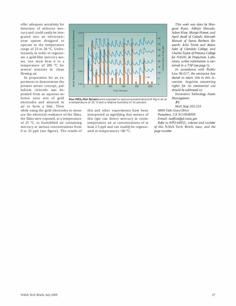
NASA Tech Briefs, July 2009 27
offer adequate sensitivity fordetection of airborne mer-cury and could easily be inte-grated into an electronic-nose system designed tooperate in the temperaturerange of 23 to 28 °C. Unfor-tunately, in order to regener-ate a gold-film mercury sen-sor, one must heat it to atemperature of 200 °C forseveral minutes in cleanflowing air.
In preparation for an ex-periment to demonstrate thepresent sensor concept, pal-ladium chloride was de-posited from an aqueous so-lution onto sets of goldelectrodes and sintered inair to form a film. Thenwhile using the gold electrodes to meas-ure the electrical resistance of the films,the films were exposed, at a temperatureof 25 °C, to humidified air containingmercury at various concentrations from0 to 35 ppb (see figure). The results of
this and other experiments have beeninterpreted as signifying that sensors ofthis type can detect mercury in room-temperature air at concentrations of atleast 2.5 ppb and can readily be regener-ated at temperatures <40 °C.
This work was done by Mar-garet Ryan, Abhijit Shevade,Adam Kisor, Margie Homer, andApril Jewell of Caltech; KennethManatt of Santa Barbara Re-search; Julia Torres and JessicaSoler of Glendale College; andCharles Taylor of Pomona Collegefor NASA’s Jet Propulsion Labo-ratory. urther information is con-tained in a TSP (see page 1).
In accordance with PublicLaw 96-517, the contractor haselected to retain title to this in-vention. Inquiries concerningrights for its commercial useshould be addressed to:
Innovative Technology AssetsManagement
JPLMail Stop 202-233
4800 Oak Grove DrivePasadena, CA 91109-8099E-mail: [email protected] to NPO-44955, volume and number
of this NASA Tech Briefs issue, and thepage number.
0.00
0.05
0.10
0.15
0.20
0 200 400 600 800 1000
Time, Minutes
0
5
10
15
20
25
30
35
40
Co
nce
ntr
atio
n o
f H
g, p
pb
Sen
sor
Res
po
nse
, Fra
ctio
nal
Ch
ang
e in
Ele
ctri
cal R
esis
tan
ce
Four PdCl2-Film Sensors were exposed to various concentrations of Hg in air ata temperature of 25 °C and a relative humidity of 31 percent.


NASA Tech Briefs, July 2009 29
Physical Sciences
Micro Electron MicroProbe and Sample Analyzer EDX and high-resolution microscopy could be performed in the field. NASA’s Jet Propulsion Laboratory, Pasadena, California
A proposed, low-power, backpack-sizedinstrument, denoted the micro electronmicroprobe and sample analyzer(MEMSA), would serve as a means ofrapidly performing high-resolution mi-croscopy and energy-dispersive x-rayspectroscopy (EDX) of soil, dust, androck particles in the field. The MEMSAwould be similar to an environmentalscanning electron microscope (ESEM)but would be much smaller and designedspecifically for field use in studying ef-fects of geological alteration at the mi-crometer scale. Like an ESEM, theMEMSA could be used to examine un-coated, electrically nonconductive speci-mens. In addition to the difference insize, other significant differences be-tween the MEMSA and an ESEM lie inthe mode of scanning and the nature ofthe electron source.
The MEMSA (see figure) would in-clude an electron source that wouldfocus a beam of electrons onto a smallspot on a specimen, which would bemounted on a three-axis translationstage in a partly evacuated sample-ex-change chamber. Whereas the electronsources in other SEMs typically containthermionic cathodes, the electronsource in the MEMSA would contain afield-emission cathode containing aplanar array of bundles of carbon nan-
otubes (CNTs). Cathodes of this typeare capable of high current densities(tens of amperes per square centime-ter) at very low fields (8 to 10 V/µm),and the arrays of bundles of CNTs inthem are amenable to fabricationwithin designated areas of the order ofa few square nanometers, making itpossible to focus electron beams tosmall spots using simplified electron-beam optics. Another advantage ofCNT field-emission cathodes is thatthey can tolerate operation in relativelypoor vacuums [pressures of 10–5 to10–4 torr (about 0.013 to 0.13 Pa)],which can be maintained by relativelysmall turbopumps, in contrast to themultistage pumps needed to maintainhigh vacuums required for thermioniccathodes.
As in an ESEM, the MEMSA would in-clude a gaseous secondary-electron de-tector (GSED) for detecting secondaryelectrons excited by impingement of theelectron beam on the specimen. Electri-cal charging of an electrically noncon-ductive specimen by the electron beamwould be neutralized by impingement,on the specimen, of positive ions of theresidual gas in the chamber. A PositiveIntrinsic Negative (PIN) diode would beused as detector for energy-dispersiveanalysis of x rays generated in the im-
pingement of the electron beam on thespecimen.
Unlike in ESEMs and other SEMs, theelectron beam would not be raster-scanned across the specimen. Instead,the electron beam would be focused ona fixed spot, through which the speci-men would be moved in small steps byuse of the translation stage to effectscanning. The amplified output of theGSED acquired at each step would bestored, along with the translation coordi-nates, in a digital memory, so that animage of the specimen could be recon-structed after completion of the scan.Omitted from the figure for the sake ofsimplicity is a context imager — essen-tially, a relatively-low-magnification elec-tronic camera that would facilitate initialcoarse positioning of the specimen in ornear the electron-beam spot in prepara-tion for scanning.
As in an ESEM, the sample-exchangechamber and the interior volume of theelectron source would be separated bypressure-limiting apertures (PLAs),which are small apertures throughwhich the electron beam passes on itsway to the specimen. As in an ESEM, thePLAs would be sized to retard the flow ofresidual gas from the sample-exchangechamber to the electron source side soas to mainain the desired lower pressure
The Micro Electron Probe and Sample Analyzer would function similarly to an environmental scanning electron microscope but would differ in the natureof the electron source and the mode of scanning.
Address
Translation Coordinates
Analog-to-DigitalConverter
DigitalSignal
OperationalAmplifier
GasSecondary-Electron
Detector
Pressure-LimitingApertures
ElectronSource
X-Ray Analysis
X-RayDetector
Specimen
TranslationStage
Digital MemoryStoring Image Data

30 NASA Tech Briefs, July 2009
on the electron source side and the de-sired higher pressure in the sample-ex-change chamber. In the original in-tended application of the MEMSA, thePLAs would be four platinum disks con-taining apertures of ≈0.5-mm diameter,chosen to maintain a pressure between 5and 7 torr (about 0.67 to 0.93 kPa) ofresidual Martian atmospheric gas com-prising primarily CO2.
The MEMSA is expected to be capableof imaging at a spatial resolution of 40nm or finer without EDX, or imaging atsomewhat coarser resolution (of the
order of 200 nm) with EDX in the en-ergy range from 100 to 20 keV. Thecoarsening of resolution in the case ofEDX would be a consequence of theneed to use higher electron current.The maximum power demand of theMEMSA during operation has been esti-mated to be ≈5 W.
This work was done by Harish Manohara,Gregory Bearman, Susanne Douglas,Michael Bronikowski, Eduardo Urgiles, andRobert Kowalczyk, of Caltech and CharlesBryson of Apperati, Inc. for NASA’s JetPropulsion Laboratory.
In accordance with Public Law 96-517,the contractor has elected to retain title to thisinvention. Inquiries concerning rights for itscommercial use should be addressed to:
Innovative Technology Assets ManagementJPLMail Stop 202-2334800 Oak Grove DrivePasadena, CA 91109-8099E-mail: [email protected] to NPO-45389, volume and number
of this NASA Tech Briefs issue, and thepage number.
Nanowire electron scattering spec-troscopy (NESS) has been proposed asthe basis of a class of ultra-small, ultra-low-power sensors that could be used todetect and identify chemical com-pounds present in extremely smallquantities. State-of-the-art nanowirechemical sensors have already beendemonstrated to be capable of detect-ing a variety of compounds in femtomo-lar quantities. However, to date, chemi-cally specific sensing of molecules usingthese sensors has required the use ofchemically functionalized nanowireswith receptors tailored to individualmolecules of interest. While potentiallyeffective, this functionalization requireslabor-intensive treatment of manynanowires to sense a broad spectrum ofmolecules. In contrast, NESS wouldeliminate the need for chemical func-tionalization of nanowires and wouldenable the use of the same sensor to de-tect and identify multiple compounds.
NESS is analogous to Raman spec-troscopy, the main difference beingthat in NESS, one would utilize inelasticscattering of electrons instead of pho-tons to determine molecular vibra-tional energy levels. More specifically,in NESS, one would exploit inelasticscattering of electrons by low-lying vi-brational quantum states of moleculesattached to a nanowire or nanotube(see figure). The energy of the elec-trons is set by the voltage bias appliedacross the nanowire. When the electronenergies correspond to particular mo-lecular vibrational levels, enhancedelectronic scattering will lead to a
change in the differential conductance(dI/dV, where I is current and V is volt-age) at that voltage. Thus changes inthe conductance provide a direct read-out of molecular vibrational energies,to enable spectroscopic identificationof the attached molecules.
To realize a practical chemical sensorbased on NESS, one would need a nar-row-energy-band electron source, effi-cient coupling between the electronsand the molecules of interest, and thenarrow vibrational bands in the mole-cules of interest. A carbon nanotube(CNT) provides a nearly ideal structurefor satisfying the electron-source andcoupling requirements for the follow-ing reasons: Even at room temperature,the energy bands in one dimensionalcarbon nanotubes are narrow, and low-
energy electrons travel ballistically overdistances of the order of a micron, sothat injected electrons can have anearly uniform kinetic energy. Becausesingle-walled CNTs are essentially all“surface,” there is strong coupling be-tween electrons and molecules on theirsurfaces.
Other than CNTs, nanowires of siliconand perhaps other materials may yieldusable NESS signals, though the signalsare expected to be smaller than thosefrom CNT-based sensors. One mightneed non-CNT nanowire NESS sensorsto detect molecules that do not readilybind to CNTs.
In order to simplify the interpretationof a complex spectrum from a mixtureof compounds, a NESS-based sensorcould be integrated with a microfluidic
Nanowire Electron Scattering Spectroscopy Multiple chemical compounds could be sensed, without the need to chemically functionalize nanowires. NASA’s Jet Propulsion Laboratory, Pasadena, California
V
I
Electrode Electrode Electrode Electrode Electrode Electrode
Molecule Nanotube
e–
Inelastic Scattering of Electrons by molecules on the surface of a nanotube would affect the current-versus-voltage characteristic of the nanotube.

NASA Tech Briefs, July 2009 31
separation column. The column wouldenable separation and concentration ofindividual species, which would then bedetected and identified at the columnoutlet by use of NESS.
This work was done by Brian Hunt,Michael Bronikowsky, Eric Wong, Paul VonAllmen, and Fabiano Oyafuso of Caltech for
NASA’s Jet Propulsion Laboratory. Further in-formation is contained in a TSP (see page 1).
In accordance with Public Law 96-517,the contractor has elected to retain title to thisinvention. Inquiries concerning rights for itscommercial use should be addressed to:
Innovative Technology Assets ManagementJPL
Mail Stop 202-2334800 Oak Grove DrivePasadena, CA 91109-8099(818) 354-2240E-mail: [email protected] to NPO-42251, volume and number
of this NASA Tech Briefs issue, and thepage number.
A proposal has been made to developdevices that would generate spin-polar-ized electron currents characterized bypolarization ratios having magnitudes inexcess of 1. Heretofore, such devices(denoted, variously, as spin injectors,spin polarizers, and spin filters) havetypically offered polarization ratios hav-ing magnitudes in the approximaterange of 0.01 to 0.1. The proposed de-vices could be useful as efficient sourcesof spin-polarized electron currents forresearch on spintronics and develop-ment of practical spintronic devices.
The polarization ratio in question —denoted the current spin polarization —is a standard measure of efficiency of aspin-polarizing device. It is defined interms of current densities along a givencoordinate axis, by means of the follow-ing equation:
PJ = (J↑ – J↓)/(J↑ + J↓),where J↑ is current density of electronsin the “up” spin state and J↓ is the cur-rent density of electrons in the “down”spin state. If J↑ and J↓ can be made tohave opposite signs — in other words, ifelectrons in opposite spin states can bemade to move in opposite directions —then, as desired, it is possible to obtain|PJ|>1. By making |PJ|>1, one would makeit possible to obtain a net spin flux withlittle net electric current.
A spin-polarizing device according tothe proposal would be based largely onthe same principles as those of the de-vices described in “Electron-Spin FiltersBased on the Rashba Effect” (NPO-30635), NASA Tech Briefs, Vol. 28, No. 10(October 2004), page 58. To recapitu-late: The Rashba effect is an energy split-ting, of what would otherwise be degen-erate quantum states, caused by aspin-orbit interaction in conjunctionwith interfacial electric fields in an asym-metrical semiconductor heterostruc-ture. The magnitude of the energy split
is proportional to the electron wavenumber. Theoretically, electron-energystates would be split by the Rashba ef-fect, and spin-polarized currents wouldbe extracted by resonant quantum-me-chanical tunneling. Accordingly, a spin-polarizing device based on these princi-ples would be denoted an asymmetricresonant interband (or intraband, as thecase may be) tunneling diode [a-RITD].
One possible structure of a device ac-cording to the present proposal wouldbe similar to the a-RITD structure de-scribed previously: The device wouldcomprise an asymmetric compositeInAs-GaSb well, sandwiched betweenAlSb barriers and degenerately-n-doped InAs emitter and collector elec-trodes (see figure). Unpolarized elec-trons from the conduction band of theInAs emitter electrode would tunnelthrough one AlSb barrier and travel
through an asymmetric InAs-GaSbquantum well, where Rashba spin split-ting would occur; they would then tun-nel through the other AlSb barrier intothe conduction band of the InAs col-lector electrode. The device would beoperated in an intraband-tunnelingregime, in which no bias would be ap-plied through the thickness of thestack of layers. A lateral electric (anelectric field parallel to the planes ofthe layers) would be applied to emitterlayer. With appropriately chosen thick-nesses of layers and an appropriatevalue of the applied lateral electricfield, it should be possible to achieve|PJ|>1.
This work was done by David Z. Ting ofCaltech for NASA’s Jet Propulsion Laboratory.Further information is contained in a TSP (seepage 1). NPO-30670
Electron-Spin Filters Would Offer Spin Polarization >1Net spin flux could be generated with little net electric current.NASA’s Jet Propulsion Laboratory, Pasadena, California
Electrons Transmittedvia Resonant Tunneling
Incident UnpolarizedElectrons
Spin Aligned WithQuasi-Bound State
GaSb
AlsbAlsb
InAsEmitter Electrode
InAs InAsCollector Electrode
ConductionBand
ValenceBand
ConductionBand
Electron-Energy-Band Alignments depicted here schematically are those of a proposed InAs/GaSb/AlSba-RITD device for achieving current spin polarization >1. The shaded and cross-hatched regions repre-sent bandgaps.

32 NASA Tech Briefs, July 2009
Subcritical-Water Extraction of Organics From Solid MatricesAn environmentally benign solvent is used in a simple extraction process.NASA’s Jet Propulsion Laboratory, Pasadena, California
An apparatus for extracting organiccompounds from soils, sands, and othersolid matrix materials utilizes water at sub-critical temperature and pressure as a sol-vent. The apparatus, called subcriticalwater extractor (SCWE), is a prototype ofsubsystems of future instrumentation sys-tems to be used in searching for organiccompounds as signs of past or present lifeon Mars. An aqueous solution generatedby an apparatus like this one can be ana-lyzed by any of a variety of establishedchromatographic or spectroscopic meansto detect the dissolved organic com-pound(s). The apparatus can be used onEarth: indeed, in proof-of-concept experi-ments, SCWE was used to extract aminoacids from soils of the Atacama Desert(Chile), which was chosen because thedryness and other relevant soil conditionsthere approximate those on Mars.
The design of the apparatus is basedpartly on the fact that the relative permit-
tivity (also known as the dielectric con-stant) of liquid water varies with temper-ature and pressure. At a temperature of30 °C and a pressure of 0.1 MPa, the rel-ative permittivity of water is 79.6, due tothe strong dipole-dipole electrostatic in-teractions between individual moleculardipoles. As the temperature increases, in-creasing thermal energy causes increas-ing disorientation of molecular dipoles,with a consequent decrease in relativepermittivity. For example, water at a tem-perature of 325 °C and pressure of 20MPa has a relative permittivity of 17.5,which is similar to the relative permittivi-ties of such nonpolar organic solvents as1-butanol (17.8). In the operation of thisapparatus, the temperature and pressureof water are adjusted so that the watercan be used in place of commonly usedorganic solvents to extract compoundsthat have dissimilar physical and chemi-cal properties.
Heretofore, laboratory extractions oforganic compounds have involved theuse, variously, of toxic organic solventsin Soxhlet extraction, strong acids inamino acid vapor-phase hydrolysis, orcarbon dioxide as a solvent at supercriti-cal temperature and pressure. Supercrit-ical CO2 is effective as a solvent for ex-tracting lipids and other very nonpolarorganic compounds because its relativepermittivity is 1.4 and does not vary sig-nificantly with pressure in the range of 7to 21 MPa or with temperature in therange of 25 to 200 °C. However, super-critical CO2 is often inadequate as a sol-vent for extraction of other nonpolarand polar organics. Frequently, it is nec-essary to mix supercritical CO2 withmethanol or other more-polar organicsolvents to obtain an extraction solventhaving a greater relative permittivity.
The apparatus (see figure) includes asample cell, into which a solid sample is
In this Subcritical-Water Extraction Apparatus, water at controlled pressure and temperature is pumped through a sample cell that contains a solid matrixmaterial (e.g., a soil) from which organic compounds are to be extracted: (a) SCWE diagram, (b) portable SCWE apparatus, (c) close-up of the sample celland filtration system, and (d) sample cell.
(a)
(b) (c) (d)
SCWEController Unit
Water Pump
Preheating Coil
SampleCell
Water Lines
CollectionVial
Electrical Connection
FilterAnalyte ValveSupply Valves

NASA Tech Briefs, July 2009 33
A Model for Predicting Thermoelectric Properties of Bi2Te3A compromise between accuracy and computational efficiency is made.NASA’s Jet Propulsion Laboratory, Pasadena, California
A parameterized orthogonal tight-binding mathematical model of thequantum electronic structure of the bis-muth telluride molecule has been de-vised for use in conjunction with a semi-classical transport model in predictingthe thermoelectric properties of dopedbismuth telluride. This model is ex-pected to be useful in designing and an-alyzing Bi2Te3 thermoelectric devices,including ones that contain such nano -structures as quantum wells and wires. Inaddition, the understanding gained inthe use of this model can be expected tolead to the development of better mod-els that could be useful for developingother thermoelectric materials and de-vices having enhanced thermoelectric
properties.Bi2Te3 is one of the best bulk thermo-
electric materials and is widely used incommercial thermoelectric devices.Most prior theoretical studies of thethermoelectric properties of Bi2Te3 haveinvolved either continuum models or ab-initio models. Continuum models arecomputationally very efficient, but donot account for atomic-level effects. Ab-initio models are atomistic by definition,but do not scale well in that computa-tion times increase excessively with in-creasing numbers of atoms. The presenttight-binding model bridges the gap be-tween the well-scalable but non-atom-istic continuum models and the atom-istic but poorly scalable ab-initio models:
The present tight-binding model isatomistic, yet also computationally effi-cient because of the reduced (relative toan ab-initio model) number of basis or-bitals and flexible parameterization ofthe Hamiltonian.
The present tight-binding model in-cludes atomistic descriptions of theHamiltonian with sp3d5s* basis orbitals,nearest-neighbor interactions, and spin-orbit coupling. For the purposes of themodel, within each primitive cell ofBi2Te3, two of the Te atoms are denotedTeI and one is denoted TeII. The differ-ence between TeI and TeII is that thenearest neighbors of TeI are three Teatoms and three Bi atoms, while those ofTeII are six Bi atoms. To capture the dif-ference, separate tight-binding parame-ters are assigned to TeI and TeII.
Altogether, the tight-binding modelincorporates 71 independent parame-ters, which are determined by fitting thecomputed band structure to a first-prin-ciples band structure obtained by use ofa submodel based on a screened-ex-change local-density approximation.The first-principles band structure pre-dicts the energy gap, the degeneracy ofthe edges of the conduction and va-lence bands, and the effective masses ofthese two bands, in good agreementwith experimental results. In the fittingprocess, a higher priority is given to thehighest valence and the lowest conduc-tion bands than to the rest of the bandstructure, inasmuch as these two bandsare mainly responsible for the thermo-electric properties of lightly dopedBi2Te3. Moreover, the locations, ener-gies, and effective masses of the twoband edges are emphasized, as theylargely determine the accuracy of the
Calculated and Experimental Values of the thermoelectric figure of merit and the electronic thermalconductivity of Bi2Te3 were found in fairly close agreement across a broad range of electrical conduc-tivity.
1.5
1.0
0.5
0.0
0.8
0.6
0.4
0.2
0.00 500 1,000 1,500 2,000
n-Doped, Calculated
p-Doped, Calculated
n-Doped, Experimental
p-Doped, Experimental
Ther
mo
elec
tric
Fi
gu
re o
f M
erit
, ZT
Elec
tro
nic
Th
erm
al
Co
nd
uct
ivit
y, W
m-1
K-1
placed. During a typical extraction,water is pumped to the required highpressure through supply valves, a pre-heating coil, the sample cell, and an an-alyte valve into a collection vial. The fil-ters, at various positions downstream ofthe sample cell, prevent contaminationof analytical instruments by particles ofthe sample solid matrix.
Relative to prior methods and appara-tuses used to extract organic com-pounds, the present apparatus and the
method of its operation offer several ad-vantages:• The solvent (water) is environmentally
benign;• The relative permittivity of the sol-
vent can be adjusted to the valuesneeded to selectively extract, withhigh efficiency, organic compoundsthat have different physical andchemical properties;
• The basic principle of operation is simple;• The apparatus can be highly automated;
• Whereas Soxhlet and hydrolysis extrac-tions often take many hours, an extrac-tion by use of this apparatus takes only minutes.This work was done by Xenia
Amashukeli, Frank Grunthaner, StevenPatrick, James Kirby, Donald Bickler,Peter Willis, Christine Pelletier, andCharles Bryson of Caltech for NASA’s JetPropulsion Laboratory. Further informa-tion is contained in a TSP (see page 1).NPO-44144

34 NASA Tech Briefs, July 2009
thermoelectric properties predicted byuse of this model.
The semiclassical transport modelwith which this tight-binding model iscoupled is a solution of Boltzmann’stransport equation in the constant-relax-
ation-time approximation. The combi-nation of models has been found toyield calculated values of thermoelectricproperties within a few percent of exper-imentally determined values (for exam-ple, see figure).
This work was done by Seungwon Lee andPaul Von Allmen of Caltech for NASA’s JetPropulsion Laboratory. For more information,contact [email protected]
Integrated Miniature Arrays of Optical Biomolecule DetectorsMany biochemical species could be detected simultaneously.NASA’s Jet Propulsion Laboratory, Pasadena, California
Integrated miniature planar arrays ofoptical sensors for detecting specific bio-chemicals in extremely small quantitieshave been proposed. An array of this typewould have an area of about 1 cm2. Eachelement of the array would include anoptical microresonator that would have ahigh value of the resonance quality factor(Q ≈ 107). The surface of each microres-onator would be derivatized to make itbind molecules of a species of interest,and such binding would introduce ameasurable change in the optical proper-ties of the microresonator. Because each
microresonator could be derivatized fordetection of a specific biochemical differ-ent from those of the other microres-onators, it would be possible to detectmultiple specific biochemicals by simulta-neous or sequential interrogation of allthe elements in the array. Moreover, thederivatization would make it unnecessaryto prepare samples by chemical tagging.
Such interrogation would be effectedby means of a grid of row and columnpolymer-based optical waveguides thatwould be integral parts of a chip on whichthe array would be fabricated. The row
and column polymer-based optical wave-guides would intersect at the elements ofthe array (see figure). At each intersec-tion, the row and column waveguideswould be optically coupled to one of themicroresonators. The polymer-basedwaveguides would be connected via opti-cal fibers to external light sources andphotodetectors. One set of waveguidesand fibers (e.g., the row waveguides andfibers) would couple light from thesources to the resonators; the other set ofwaveguides and fibers (e.g., the columnwaveguides and fibers) would couple lightfrom the microresonators to the photode-tectors. Each microresonator could be ad-dressed individually by row and columnfor measurement of its optical transmis-sion. Optionally, the chip could be fabri-cated so that each microresonator wouldlie inside a microwell, into which a micro-scopic liquid sample could be dispensed.
This work was done by Vladimir Iltchenko,Lute Maleki, Ying Lin, and Thanh Le ofCaltech for NASA’s Jet Propulsion Laboratory.
In accordance with Public Law 96-517,the contractor has elected to retain title to thisinvention. Inquiries concerning rights for itscommercial use should be addressed to:
Innovative Technology Assets ManagementJPLMail Stop 202-2334800 Oak Grove DrivePasadena, CA 91109-8099E-mail: [email protected] to NPO-43164, volume and number
of this NASA Tech Briefs issue, and thepage number.
Derivatized Optical Microresonators in an array would address optically via row and column opticalwaveguides.
Optical Fibers From
Light Sources
Polymer-Based Optical
Waveguides
Optical Fibers to Photodetectors
Chip
Derivatized Optical
Microresonators

NASA Tech Briefs, July 2009 35
A performability-oriented conceptualframework for software rejuvenation hasbeen constructed as a means of increas-ing levels of reliability and performancein distributed stateful computing. Asused here, “performability-oriented” sig-nifies that the construction of the frame-work is guided by the concept of analyz-ing the ability of a given computingsystem to deliver services with gracefullydegradable performance. The frame-work is especially intended to supportapplications that involve stateful replicasof server computers.
Software rejuvenation has been recog-nized as a simple yet effective means ofpreventing accumulation of software er-rors that, if allowed to accumulate, coulddegrade the capacity or cause failure ofa computer system. When a software sys-tem is voluntarily rebooted, with highprobability, errors accumulated duringprevious execution are eliminated andthe system regains its full capacity. Al-though software rejuvenation has beeninvestigated extensively, it has not, untilnow, been considered for stateful appli-cations that involve server replicas. Theproblem of software rejuvenation insuch applications is complicated by the
following considerations: When softwarerejuvenation temporarily stops a long-running replica server, R, the post-reju-venation performance of R may be re-duced because the stoppage may causethe state of R to become inconsistentwith the nominal state of other replicas.In that case, R would be unable to pro-vide services at its full capacity until con-sistency with the states of the other repli-cas was restored.
The present performability-orientedframework is based on three buildingblocks: a rejuvenation algorithm, a set ofperformability metrics, and a performa-bility model. The performability metricsand model both take account of the re-duced nature of post-rejuvenation per-formance pending restoration of consis-tency. The performability model alsotakes account of the possibility that post-rejuvenation consistency-restorationprocesses could be vulnerable to failuresbecause of the potential performancestress caused by service requests accumu-lated during rejuvenation.
The basic version of the rejuvena-tion algorithm uses pattern-matchingmechanisms to detect pre-failure con-ditions. To compensate for the inabil-
ity of pattern-matching mechanisms todetect pre-failure-condition patternsother than those known a priori, an en-hanced version of the algorithm ac-commodates a random timer and pro-vides for synergistic coordination ofboth detection-triggered and timer-triggered rejuvenation. It has beendemonstrated, via model-based evalua-tion, that this performability-orientedframework enables error-accumula-tion-prone distributed applications tocontinuously deliver gracefully degrad-able services at the best possible per-formance levels, even in environmentsin which the affected systems arehighly vulnerable to failures. It hasalso been shown that software rejuve-nation can be realized as an integralpart of the infrastructures in statefuldistributed computing applicationsthat guarantee eventual consistency ofthe states of server replicas.
This work was done by Savio Chau of Cal-tech for NASA’s Jet Propulsion Laboratory.
The software used in this innovation isavailable for commercial licensing. Pleasecontact Karina Edmonds of the California In-stitute of Technology at (626) 395-2322.Refer to NPO-42352.
Information Sciences
A Software Rejuvenation Framework for Distributed ComputingThis framework supports graceful degradation of services at best possible performance levels.NASA’s Jet Propulsion Laboratory, Pasadena, California
An algorithm for solving a particularnonlinear independent-component-analysis (ICA) problem, that differs fromprior algorithms for solving the sameproblem, has been devised. The problemin question — of a type known in the artas a post nonlinear mixing problem — isa useful approximation of the problemposed by the mixing and subsequentnonlinear distortion of sensory signalsthat occur in diverse scientific and engi-neering instrumentation systems.
Prerequisite for describing this partic-ular post nonlinear ICA problem is a de-
scription of the post nonlinear mixingand unmixing models depicted schemat-ically in the figure. The mixing modelconsists of a linear mixing part followedby a memoryless invertible nonlineartransfer part. The unmixing model con-sists of a nonlinear inverse transfer partfollowed by a linear unmixing part. Thesource signals are recovered if each op-eration in the unmixing sequence is theinverse of the corresponding operationin the mixing sequence.
More specifically, in the models, s(n) = [s1(n),s2(n),...sN(n)]T
is an N×1 column vector representing Nindependent source signals at time n thatone seeks to estimate. This vector is mul-tiplied by A, an initially unknown N×Nmatrix that represents the linear mixingof the source signals. The N signals re-sulting from the mixing are representedby N×1 column vector
v(n) = [v1(n),v 2(n),...vN(n)]T.Each of these signals is then subjected tononlinear distortion represented by afunction that is initially unknown andcould differ from the functions that rep-resent the distortions of the other sig-
Kurtosis Approach to Solution of a Nonlinear ICA ProblemA gradient-descent algorithm minimizes the kurtosis of an output vector.NASA’s Jet Propulsion Laboratory, Pasadena, California

36 NASA Tech Briefs, July 2009
nals. For the ith mixture signal, the dis-torted signal is given by xi = fi(vi), wherefi is one of the initially unknown nonlin-ear functions. Thus, the vector
x(n) = [x1(n),x2(n),...xN(n)]T
represents instrumentation signals pre-sented for analysis. The distortion in sig-nal xi is removed by means of a corre-sponding initially unknown inversenonlinear function gi. Finally, the signalsare unmixed by means of initially un-
known matrix W to obtain output vector u(n) = [u 1(n),u2(n),...uN(n)]T.
In the ideal case, W would be the inverseof A and the output vector u would equalthe vector, s, of source signals.
The particular nonlinear ICA problemis to calculate the nonlinear inverse func-tions gi and matrix W such that u calcu-lated by use of them is a close approxima-tion of s. For the purpose of the presentalgorithm for solving this problem, it is
assumed that the inverse nonlinear func-tions gi are smooth and can be approxi-mated by polynomials. The algorithmfinds the components of the unmixingmatrix W and the coefficients of the poly-nomial approximations of gi by a gradi-ent-descent method. This algorithm uti-lizes the kurtosis of the components ofthe output vector u as an objective func-tion (in effect, an error measure) that itseeks to minimize. In using the kurtosis,this algorithm stands in contrast to prioralgorithms that utilize other objectivefunctions, including statistical functionsother than the kurtosis.
This work was done by Vu Duong andAllen Stubberud of Caltech for NASA’s JetPropulsion Laboratory.
In accordance with Public Law 96-517,the contractor has elected to retain title to thisinvention. Inquiries concerning rights for itscommercial use should be addressed to:
Innovative Technology Assets ManagementJPLMail Stop 202-2334800 Oak Grove DrivePasadena, CA 91109-8099(818) 354-2240E-mail: [email protected] to NPO-43088, volume and number
of this NASA Tech Briefs issue, and thepage number.
f1v1s1 g1
x1 u1
f2v2s2 g2
x2 u2
fNvNsN gN
xN uN
A W
Mixing Model Unmixing Model
Mixing and Distortion Operations and their inverses are represented in these block-diagram represen-tations of mixing and unmixing models.
“Robust Real-Time ReconfigurableRobotics Software Architecture”(“R4SA”) is the name of both a softwarearchitecture and software that embodiesthe architecture. The architecture wasconceived in the spirit of current prac-tice in designing modular, hard, real-time aerospace systems. The architec-ture facilitates the integration of newsensory, motor, and control softwaremodules into the software of a given ro-botic system. R4SA was developed forinitial application aboard exploratorymobile robots on Mars, but is adaptableto terrestrial robotic systems, real-timeembedded computing systems in gen-eral, and robotic toys.
The R4SA software, written in cleanANSI C, establishes an onboard, real-time computing environment. TheR4SA architecture features three lay-ers: The lowest is the device-driverlayer, the highest is the application
layer, and the device layer lies at themiddle (see figure).
The device-driver layer handles allhardware dependencies. It completely
hides the details of how a device works.Activities directed by users are performedby means of well-defined interfaces. Eachtype of device driver is equipped with itsown well-defined interface. For example,the device-driver interface for an analog-to-digital converter differs from that for adigital-to-analog converter.
The device layer provides the meansfor abstracting the high-level software inthe application layer from the hardwaredependencies. The device layer providesall motion-control computations, includ-ing those for general proportional + in-tegral + derivative controllers, profilers,controllers for such mechanical compo-nents as wheels and arms, coordinate-system transformations for odometryand inertial navigation, vision process-ing, instrument interfaces, communica-tion among multiple robots, and kine-matics for a multiple-wheel ormultiple-leg robot.
Robust Software Architecture for RobotsGeneralized software can be readily tailored for specific applications.NASA’s Jet Propulsion Laboratory, Pasadena, California
The R4SA Architecture features three levelscorrespond ing to different levels of abstraction.
Device Driver Layer
Hardware
Device Layer
Application Layer
SYSTEM

NASA Tech Briefs, July 2009 37
The application layer provides applica-tion programs that a robot can execute.Examples of application programs in-clude those needed to perform such pre-scribed maneuvers as avoiding obstacleswhile moving from a specified startingpoint to a specified goal point or turninga robot in place through a specified az-imuthal angle. Each robot is providedwith application software representing itsown unique set of commands. The soft-ware establishes a graphical user inter-face (GUI) for exchanging command in-formation with external computingsystems. Via the GUI and its supportinginterface software, a user can select andassemble, from the aforementioned set,commands appropriate to the task athand and send the commands to the
robot for execution. System software thatinteracts with the R4SA software at allthree levels establishes a synchronizedcontrol environment.
The R4SA software features twomodes of execution: before real time(BRT) and real time (RT). In the BRTmode, a text configuration file is read in(each robot has its own unique file) andthen device-driver-layer, device-layer,and application-layer initialization func-tions are executed. If execution is suc-cessful, then the system jumps into theRT mode, in which the system is ready toreceive and execute commands.
One goal in developing the R4SA ar-chitecture was to provide one computercode for many robots. The unique exe-cutable code for each robot is built by
use of a configuration feature file. Theset of features for a given robot is se-lected from a feature database on thebasis of the hardware and mechanicalcapabilities of that robot. Recompilationof code is straightforward: modificationscan readily be performed in the field byuse of simple laptop-computer develop-ment and debugging software tools.
This work was done by Hrand Aghazar-ian, Eric Baumgartner, and Michael Garrettof Caltech for NASA’s Jet Propulsion Labora-tory. Further information is contained in aTSP (see page 1).
The software used in this innovation isavailable for commercial licensing. Pleasecontact Karina Edmonds of the California In-stitute of Technology at (626) 395-2322.Refer to NPO-41796.
R4SA for Controlling RobotsNASA’s Jet Propulsion Laboratory, Pasadena, California
The R4SA GUI mentioned in the im-mediately preceding article is a user-friendly interface for controlling one ormore robot(s). This GUI makes it possi-ble to perform meaningful real-timefield experiments and research in robot-ics at an unmatched level of fidelity,within minutes of setup. It provides suchpowerful graphing modes as that of adigitizing oscilloscope that displays up to250 variables at rates between 1 and 200Hz. This GUI can be configured as mul-tiple intuitive interfaces for acquisitionof data, command, and control to en-
able rapid testing of subsystems or an en-tire robot system while simultaneouslyperforming analysis of data.
The R4SA software establishes an intu-itive component-based design environ-ment that can be easily reconfigured forany robotic platform by creating or edit-ing setup configuration files. The R4SAGUI enables event-driven and condi-tional sequencing similar to those ofMars Exploration Rover (MER) opera-tions. It has been certified as part of theMER ground support equipment and,therefore, is allowed to be utilized in
conjunction with MER flight hardware.The R4SA GUI could also be adapted touse in embedded computing systems,other than that of the MER, for com-manding and real-time analysis of data.
This work was done by Hrand Aghazarianof Caltech for NASA’s Jet Propulsion Labora-tory. Further information is contained in aTSP (see page 1).
The software used in this innovation isavailable for commercial licensing. Pleasecontact Karina Edmonds of the California In-stitute of Technology at (626) 395-2322.Refer to NPO-41797.
Bio-Inspired Neural Model for Learning Dynamic ModelsThis model could be a basis for fast speech- and image-recognition computers.NASA’s Jet Propulsion Laboratory, Pasadena, California
A neural-network mathematicalmodel that, relative to prior such mod-els, places greater emphasis on some ofthe temporal aspects of real neuralphysical processes, has been proposedas a basis for massively parallel, distrib-uted algorithms that learn dynamicmodels of possibly complex externalprocesses by means of learning rulesthat are local in space and time. The al-gorithms could be made to performsuch functions as recognition and pre-diction of words in speech and of ob-jects depicted in video images. The ap-
proach embodied in this model is saidto be “hardware-friendly” in the follow-ing sense: The algorithms would beamenable to execution by special-pur-pose computers implemented as very-large-scale integrated (VLSI) circuitsthat would operate at relatively highspeeds and low power demands.
It is necessary to present a largeamount of background information togive meaning to a brief summary of thepresent neural-network model:• A dynamic model to be learned by the
present neural-network model is of a
type denoted an internal model or pre-dictor. In simplest terms, an internalmodel is a set of equations that pre-dicts future measurements on the basisof past and current ones. Internalmodels have been used in controllingindustrial plants and machines (in-cluding robots).
• One of the conclusions drawn fromPavlov’s famous experiments was theobservation that reinforcers of learn-ing (basically, rewards and punish-ments) become progressively less effi-cient for causing adaptation of

38 NASA Tech Briefs, July 2009
behavior as their predictability growsduring the course of learning. The dif-ference between the actual occurrenceand the prediction of the reinforcer isdenoted as the reinforcement predic-tion error signal. In what is known inthe art as the temporal-differencemodel (TD model) of Pavlovian learn-ing, the reinforcement predictionerror signal is used to learn a rein-forcement prediction signal. The de-sired reinforcement prediction signalis defined as a weighted sum of futurereinforcement signals wherein rein-forcements are progressively dis-counted with increasing time into thefuture. The reinforcement predictionerror signal progressively decreasesduring learning as the reinforcementprediction signal becomes more simi-lar to the desired reinforcement pre-diction signal.
• Algorithms based on the TD model(“TD algorithms”) have been analyzedand shown to be implementations of avariant of dynamic programming. Ma-chine-learning studies have shown thatTD algorithms are powerful means ofsolving reinforcement learning prob-lems that involve delayed reinforce-
ment. Examples of such problems in-clude board games, which involve de-layed rewards (winning) or punish-ments (losing).
• Mid-brain dopamine neurons are sonamed because they modulate the lev-els of activity of other neurons bymeans of the neurotransmitter chemi-cal dopamine. The cell bodies ofdopamine neurons are located in thebrain stem and their axons project tomany brain areas. Activities ofdopamine neurons have been foundto be strikingly similar to the predic-tion error signals of the TD model.
• Real neural signals include spikelikepulses, the times of occurrence of whichare significant. The term “biologicalspike coding” denotes, essentially, tem-poral labeling of such pulses in real neu-rons or in a neural-network model.This concludes the background infor-
mation.The present neural-network model
incorporates biological spike codingalong with some basic principles of thelearning by synapses in the cortex ofthe human brain. According to thelearning rule of the model, synapticweights are adapted when pre- and
postsynaptic spikes occur within shorttime windows. In simplified terms, for agiven synapse and time window, thesynaptic strength is increased in thelong term if the presynaptic spike pre-cedes the postsynaptic spike or is de-creased in the long term if the presy-naptic spike follows the postsynapticspike. This learning rule has beenshown to minimize prediction errors,indicating that the neural networklearns an optimal dynamic model of anexternal process.
This work was done by Tuan Duong, VuDuong, and Roland Suri of Caltech forNASA’s Jet Propulsion Laboratory.
In accordance with Public Law 96-517,the contractor has elected to retain title to thisinvention. Inquiries concerning rights for itscommercial use should be addressed to:
Innovative Technology Assets ManagementJPLMail Stop 202-2334800 Oak Grove DrivePasadena, CA 91109-8099(818) 354-2240E-mail: [email protected] to NPO-41691, volume and number
of this NASA Tech Briefs issue, and thepage number.
A methodology for processing spec-tral images to retrieve information onunderlying physical, chemical, and/orbiological phenomena is based on evolu-tionary and related computationalmethods implemented in software. In atypical case, the solution (the informa-tion that one seeks to retrieve) consistsof parameters of a mathematical modelthat represents one or more of the phe-nomena of interest.
The methodology was developed forthe initial purpose of retrieving thedesired information from spectralimage data acquired by remote-sens-ing instruments aimed at planets (in-cluding the Earth). Examples of infor-mation desired in such applicationsinclude trace gas concentrations, tem-perature profiles, surface types,day/night fractions, cloud/aerosolfractions, seasons, and viewing angles.The methodology is also potentiallyuseful for retrieving information on
chemical and/or biological hazards interrestrial settings.
In this methodology, one utilizes an it-erative process that minimizes a fitnessfunction indicative of the degree of dis-similarity between observed and syn-thetic spectral and angular data. Theevolutionary computing methods that lieat the heart of this process yield a popu-lation of solutions (sets of the desired pa-rameters) within an accuracy repre-sented by a fitness-function valuespecified by the user. The evolutionarycomputing methods (ECM) used in thismethodology are Genetic Algorithmsand Simulated Annealing, both of whichare well-established optimization tech-niques and have also been described inprevious NASA Tech Briefs articles. Theseare embedded in a conceptual frame-work, represented in the architecture ofthe implementing software, that enablesautomatic retrieval of spectral and angu-lar data and analysis of the retrieved solu-
tions for uniqueness. This framework iscomposed of three modules (see figure):1. The central core, which consists of the
aforementioned ECM;2. The synthetic-spectra generator,
which, coupled with the ECM, gener-ates a population of automatically re-trieved spectral solutions; and
3. The synthetic-spectra degeneracy ana-lyzer (“degeneracy” is used here inthe mathematical sense of signifyingthe existence of multiple equally validsolutions for a given set of data anduser-defined accuracy), which appliesseveral well-established mathematicalmethods to characterize the unique-ness (or the degeneracy, which is es-sentially the lack of uniqueness) ofthe solutions within the population.One advantage afforded by this ECM-
based methodology over traditional spec-tral retrieval methods is the ability to per-form an automatic, unbiased search forall solutions within the entire parameter
Evolutionary Computing Methods for Spectral RetrievalSolutions to the inverse problem of spectral retrieval are found in a computationally efficientprocess.NASA’s Jet Propulsion Laboratory, Pasadena, California

NASA Tech Briefs, July 2009 39
space, using criteria that make searchingcomputationally far more economicalthan in complete-enumeration (“bruteforce”), Monte Carlo, or random
searches. (As used here, “unbiased” char-acterizes a search that does not dependon initial ad hoc guesses by experts.)Other advantages include the following:
• Optimal solutions are found;• Better interpretations of planetary spec-
tral and angular data are possible, andinitial tests have shown these interpreta-tions to be consistent with groundtruth; and
• The methodology is not limited to spe-cific problems, and can be extended tosolve problems of greater complexity.This work was done by Richard Terrile, Wolf-
gang Fink, Terrance Huntsberger, Seungwon Lee,Edwin Tisdale, Paul Von Allmen, and GiovannaTinetti of Caltech for NASA’s Jet Propulsion Labo-ratory. Further information is contained in aTSP (see page 1).
In accordance with Public Law 96-517,the contractor has elected to retain title to thisinvention. Inquiries concerning rights for itscommercial use should be addressed to:
Innovative Technology Assets ManagementJPLMail Stop 202-2334800 Oak Grove DrivePasadena, CA 91109-8099(818) 354-2240E-mail: [email protected] to NPO-42564, volume and number
of this NASA Tech Briefs issue, and the pagenumber.
This Conceptual Framework for Spectral Retrieval, and the software that implements it, comprisesthree modules that interact in an iterative process.
Scientific Answers With Degrees of Degeneracy and Uncertainty
Synthetic Spectra Retrieved
Solutions Parameters
Synthetic- Spectra
Generator
Synthetic- Spectra
Degeneracy Analyzer
ECM
Spectral Images and Targeted Scientific Questions
Monitoring Disasters by Use of Instrumented Robotic Aircraft Real-time synoptic data would help in coordinating and planning responses. Ames Research Center, Moffett Field, California
Efforts are under way to develop data-acquisition, data-processing, and data-communication systems for monitoringdisasters over large geographic areas byuse of uninhabited aerial systems (UAS)— robotic aircraft that are typically pi-loted by remote control. As integralparts of advanced, comprehensive disas-ter-management programs, these sys-tems would provide (1) real-time datathat would be used to coordinate re-sponses to current disasters and (2)recorded data that would be used tomodel disasters for the purpose of miti-gating the effects of future disasters andplanning responses to them.
The basic idea is to equip UAS withsensors (e.g., conventional video camerasand/or multispectral imaging instru-ments) and to fly them over disasterareas, where they could transmit data byradio to command centers. Transmissioncould occur along direct line-of-sightpaths and/or along over-the-horizonpaths by relay via spacecraft in orbitaround the Earth. The initial focus is on
demonstrating systems for monitoringwildfires; other disasters to which thesedevelopments are expected to be applica-ble include floods, hurricanes, tornadoes,earthquakes, volcanic eruptions, leaks oftoxic chemicals, and military attacks.
The figure depicts a typical system formonitoring a wildfire. In this case, instru-ments aboard a UAS would generate cal-ibrated thermal-infrared digital imagedata of terrain affected by a wildfire. Thedata would be sent by radio via satellite toa data-archive server and image-process-ing computers. In the image-processingcomputers, the data would be rapidlygeo-rectified for processing by one ormore of a large variety of geographic-in-formation-system (GIS) and/or image-analysis software packages. After process-ing by this software, the data would beboth stored in the archive and distrib-uted through standard Internet connec-tions to a disaster-mitigation center, aninvestigator, and/or command center atthe scene of the fire.
Ground assets (in this case, firefighters
and/or firefighting equipment) wouldalso be monitored in real time by use ofGlobal Positioning System (GPS) unitsand radio communication links betweenthe assets and the UAS. In this scenario,the UAS would serve as a data-relay sta-tion in the sky, sending packets of infor-mation concerning the locations of assetsto the image-processing computer,wherein this information would be incor-porated into the geo-rectified images andmaps. Hence, the images and mapswould enable command-center person-nel to monitor locations of assets in realtime and in relation to locations affectedby the disaster. Optionally, in case of a dis-aster that disrupted communications, theUAS could be used as an airborne com-munication relay station to partly restorecommunications to the affected area.
A prototype of a system of this type wasdemonstrated in a project denoted theFirst Response Experiment (ProjectFiRE). In this project, a controlled out-door fire was observed by use of a ther-mal multispectral scanning imager on a

40 NASA Tech Briefs, July 2009
UAS that delivered image data to aground station via a satellite uplink/downlink telemetry system. At theground station, the image data were geo-rectified in nearly real time for distribu-tion via the Internet to firefighting man-agers. Project FiRE was deemed a successin demonstrating several advances essen-
tial to the eventual success of the contin-uing development effort.
This work was done by Steven S. Wegener, Donald V. Sullivan, Steven E.Dunagan, and James A. Brass of Ames Re-search Center; Vincent G. Ambrosia of California State University — Monterey Bay;Sally W. Buechel of Terra-Mar Resource Infor-
mation Services; Jay Stoneburner of GeneralAtomics-Aeronautical Systems, Inc.; andSusan M. Schoenung of Longitude 122 West,Inc. For further information, accesshttp://geo.arc.nasa.gov/sge/UAVFiRE/whitepaper.html or contact the Ames TechnologyPartnerships Division at (650) 604-2954.ARC-14999-1.
Command Center
Ground Assets
Investigator
Data-Archive Server and Image-Processing
Computer
Disaster-Mitigation Center
UAS
Over-the-Horizon Relay
Internet
Monitoring by Instruments Aboard a UAS would provide information to coordinate actions of ground assets at the scene of a disaster. The UAS and oneor more satellite(s) would also serve as communication relays.
A logical connection between the sur-vivability of living systems and the com-plexity of their behavior (equivalently,mental complexity) has been estab-lished. This connection is an importantintermediate result of continuing re-search on mathematical models thatcould constitute a unified representa-tion of the evolution of both living andnon-living systems. Earlier results of thisresearch were reported in several priorNASA Tech Briefs articles, the two mostrelevant being “Characteristics of Dy-namics of Intelligent Systems” (NPO-21037), NASA Tech Briefs, Vol. 26, No. 12(December 2002), page 48; and “Self-Su-
pervised Dynamical Systems” (NPO-30634) NASA Tech Briefs, Vol. 27, No. 3(March 2003), page 72.
As used here, “living systems” is synony-mous with “active systems” and “intelli-gent systems.” The quoted terms can sig-nify artificial agents (e.g., suitablyprogrammed computers) or natural bio-logical systems ranging from single-cellorganisms at one extreme to the whole ofhuman society at the other extreme. Oneof the requirements that must be satisfiedin mathematical modeling of living sys-tems is reconciliation of evolution of lifewith the second law of thermodynamics.In the approach followed in this research,
this reconciliation is effected by means ofa model, inspired partly by quantum me-chanics, in which the quantum potentialis replaced with an information potential.The model captures the most fundamen-tal property of life — the ability to evolvefrom disorder to order without any exter-nal interference.
The model incorporates the equa-tions of classical dynamics, includingNewton’s equations of motion and equa-tions for random components caused byuncertainties in initial conditions and byLangevin forces. The equations of classi-cal dynamics are coupled with corre-sponding Liouville or Fokker-Planck
Complexity for Survival of Living SystemsInteractions between systems and their mental images enable unlimited increase of complexity.NASA’s Jet Propulsion Laboratory, Pasadena, California

NASA Tech Briefs, July 2009 41
equations that describe the evolutions ofprobability densities that represent theuncertainties. The coupling is effectedby fictitious information-based forcesthat are gradients of the information po-tential, which, in turn, is a function ofthe probability densities. The probabilitydensities are associated with mental im-ages — both self-image and nonself im-ages (images of external objects that caninclude other agents). The evolution ofthe probability densities represents men-tal dynamics. Then the interaction be-tween the physical and metal aspects ofbehavior is implemented by feedback
from mental to motor dynamics, as rep-resented by the aforementioned ficti-tious forces.
The interaction of a system with its selfand nonself images affords unlimited ca-pacity for increase of complexity. Thereis a biological basis for this model ofmental dynamics in the discovery of mir-ror neurons that learn by imitation. Thelevels of complexity attained by use ofthis model match those observed in liv-ing systems. To establish a mechanismfor increasing the complexity of dynam-ics of an active system, the model en-ables exploitation of a chain of reflec-
tions exemplified by questions of theform, “What do you think that I thinkthat you think...?” Mathematically, eachlevel of reflection is represented in theform of an attractor performing the cor-responding level of abstraction withmore details removed from higher lev-els. The model can be used to describethe behaviors, not only of biological sys-tems, but also of ecological, social, andeconomics ones. a
This work was done by Michail Zak of Caltechfor NASA’s Jet Propulsion Laboratory. For moreinformation contact [email protected]


NASA Tech Briefs, July 2009 43
Books & Reports
Using Drained SpacecraftPropellant Tanks for Habita-tion
A document proposes that futurespacecraft for planetary and space ex-ploration be designed to enable reuseof drained propellant tanks for occu-pancy by humans. This proposal wouldenable utilization of volume and massthat would otherwise be unavailableand, in some cases, discarded. Such uti-lization could enable reductions incost, initial launch mass, and numberof launches needed to build up a habit-able outpost in orbit about, or on thesurface of, a planet or moon. Accord-ing to the proposal, the large propel-lant tanks of a spacecraft would be con-figured to enable crews to gain accessto their interiors.
The spacecraft would incorporatehatchways, between a tank and the crewvolume, that would remain sealed whilethe tank contained propellant and couldbe opened after the tank was purged byventing to outer space and then refilledwith air. The interior of the tank wouldbe pre-fitted with some habitation fix-tures that were compatible with the pro-pellant environment. Electrical feed-throughs, used originally for gaugingpropellants, could be reused to supplyelectric power to equipment installed inthe newly occupied space. After a smallamount of work, the tank would beready for long-term use as a habitationmodule.
This work was done by Andrew S. W.Thomas of Johnson Space Center. Further in-formation is contained in a TSP (see page 1).MSC-24236-1
Connecting NodeA paper describes the Octanode, a
connecting node that facilitates the in-tegration of multiple docking mecha-nisms, hatches, windows, and internaland external systems with the use offlat surfaces. The Octanode is a 26-faced Great RhombicuboctahedronArchi medean solid with six octagon-shaped panels, eight hexagon-shaped
panels, and 12 square panels usingthree unique, simple, flat shapes toconstruct a spherical approximation.Each flat shape can be constructed witha variety of material and manufactur-ing techniques, such as honeycombcomposite panels or a pocketed skin-stringer configuration, using conven-tional means.
The flat shapes can be connected to-gether and sealed to create a pressuriz-able volume by the use of any conven-tional means including welding orfastening devices and sealant. Thenode can then be connected to otherelements to allow transfer betweenthose elements, or it could serve as anairlock. The Octanode can be manu-factured on the ground and can be in-tegrated with subsystems includinghatches and ports. The node can thenbe transported to its intended location,whether on orbit or on surface. Any ofthe flat panels could be replaced bycurved ones, turning the node into acopula.
Windows may be placed on flat paneswith optimal viewing angles that are notblocked by large connecting nodes. Theadvantage of using flat panels to repre-sent a spherical approximation is thatthis allows for easier integration of sub-systems and design features.
This work was done by Christopher J. John-son, Jasen L. Raboin, and Gary R. Spexarthfor Johnson Space Center. Further informa-tion is contained in a TSP (see page 1).
This invention is owned by NASA, and apatent application has been filed. Inquiriesconcerning nonexclusive or exclusive licensefor its commercial development should be ad-dressed to the Patent Counsel, Johnson SpaceCenter, (281) 483-1003. Refer to MSC-24216-1.
Electrolytes for Low-Tem-perature Operation of Li-CFx Cells
A report describes a study of elec-trolyte compositions selected as candi-dates for improving the low-tempera-ture performances of primaryelectrochemical cells that contain
lithium anodes and fluorinated car-bonaceous (CFx) cathodes. This studycomplements the developments re-ported in “Additive for Low-Tempera-ture Operation of Li-(CF)n Cells” (NPO-43579) and Li/CFx Cells Opti mized forLow-Temperature Oper ation (NPO-43585), which appear elsewhere in thisissue of NASA Tech Briefs.
Similar to lithium-based electrolytesdescribed in several previous NASA TechBriefs articles, each of these electrolytesconsisted of a lithium salt dissolved in anonaqueous solvent mixture. Each suchmixture consisted of two or more of thefollowing ingredients: propylene car-bonate (PC); 1,2-dimethoxyethane(DME); trifluoropropylene carbonate;bis(2,2,2-trifluoroethyl) ether; diethylcarbonate; dimethyl carbonate; andethyl methyl carbonate. The report de-scribes the physical and chemical princi-ples underlying the selection of the com-positions (which were not optimized)and presents results of preliminary testsmade to determine effects of the compo-sitions upon the low-temperature capa-bilities of Li-CFx cells, relative to a base-line composition of LiBF4 at aconcentration of 1.0 M in a solvent com-prising equal volume parts of PC andDME.
This work was done by Marshall C. Smart,Jay F. Whitacre, and Ratnakumar V. Buggaof Caltech; and G. K. Surya Prakash, PoojaBhalla, and Kiah Smith of the Loker Hydro-carbon Institute at the University of SouthernCalifornia for NASA’s Jet Propulsion Labora-tory. Further information is contained in aTSP (see page 1).
In accordance with Public Law 96-517,the contractor has elected to retain title to thisinvention. Inquiries concerning rights for itscommercial use should be addressed to:
Innovative Technology Assets ManagementJPLMail Stop 202-2334800 Oak Grove DrivePasadena, CA 91109-8099(818) 354-2240E-mail: [email protected] to NPO-43587, volume and number
of this NASA Tech Briefs issue, and thepage number.


National Aeronautics andSpace Administration