Systematic methodology for designing low power direct digital frequency synthesisers
12
Systematic methodology for designing low power direct digital frequency synthesisers M. Kesoulis, D. Soudris, C. Koukourlis and A. Thanailakis Abstract: The overall operation of a direct digital frequency synthesiser (DDFS) is based on a look-up table method, which performs functional mapping from phase to sine amplitude. The spec- tral purity of the conventional DDFS is determined by the resolution of the values stored in the sine table ROM. However, large ROM storage means higher power consumption, increased silicon area, lower reliability, lower speed and increased costs. A novel systematic design methodology for implementing a DDFS architecture with reduced memory size is introduced. Describing the pro- posed architecture using the hardware description language VHDL, it is possible to generate a plethora of alternative realisations in terms of the number of input and output bits, the memory size, the number of gates, the memory segmentation parameters and the spectral purity. In other words, the designer can perform extensive architecture exploration to reach an optimal solution. The experimental results prove that the new DDFS architecture can be realised with a smaller hard- ware complexity and total power consumption and improved performance compared to many exist- ing approaches. 1 Introduction Modern communication systems place increasing demands on the resolution and bandwidth of frequency synthesiser subsystems. The generation of many different frequencies from a single source can be achieved with analogue circuits or combinations of analogue and digital circuits (PLLs). However, spread spectrum applications, radio applications, radar systems, electronic imaging processing, ad hoc wireless networks [1] and so on, impose an extremely stringent set of specifications on a frequency synthesiser, which includes the achievement of extremely fast switching time over a wide bandwidth while being compact, reliable and easily reprodu- cible. In order to meet these demanding requirements, many designers are exploring the use of the direct digital approach to frequency synthesis. A direct digital frequency synthesiser (DDFS) is characterised by fast switching speed, continuous phase switching, high frequency resolution, small size and low power; and due to the enormous evolution of digital technologies, DDFS is established as a fundamental and important signal generation discipline [2]. In this paper, a novel design methodology for implement- ing efficient DDFSs is introduced. Based on a new tech- nique for reducing the required ROM size, the derived architecture exhibits lower hardware complexity (i.e. a smaller number of gates) and power consumption than many existing implementations [3–8]. With the proposed methodology, we can derive DDFS architectures with spur- ious free dynamic range (SFDR) ranging from small to large values (e.g. in dBc), depending on the input constraints and system specifications. The whole design methodology was implemented using reusable VHDL code [9]. In the case of a specific DDFS implementation, a designer should provide the appropriate values in a certain very small file (package in VHDL), ignoring the remaining code. Therefore a designer can easily derive alternative DDFS architectures. Furthermore, we developed the VHDL code in such a way that it can be ‘re-used’ by other designers within their design as an intellectual property (IP). Obviously, an IP-based design approach can derive novel telecom products within the shortest design time cost. Furthermore, since different optimal DDFS architectures can be derived, a designer can store the corresponding reconfiguration bit-streams realising a reconfigurable system-on-chip, which allows the use, for instance, of a wireless system for a wide variety of frequency bands, by mapping to the reconfigurable part of it a DDFS with speci- fications appropriate for the selected frequency band. Extensive comparisons among existing algorithmic tech- niques and the proposed one were carried out. Two specific DDFSs, with input wordlengths W ¼ 12 and W ¼ 18 and output wordlengths D ¼ 10 and D ¼ 16, were designed and measured in terms of several hardware features. All the designs were implemented using the hardware description language VHDL [9] and were mapped in Xilinx FPGAs [10]. We proved that the proposed DDFS is characterised by better features than the existing ones, in terms of hardware complexity, and it exhibits very good spectral purity. The goal of the proposed research work is not to design a new DDFS architecture with specific characteristics, but to introduce a design framework for implementing efficient DDFS architectures, where a designer can set the required specifications. In other words, the developed design method- ology can be considered as a design space exploration tool. 2 Related work The basic DDFS architecture was proposed by Tierney et al. [11] and consists of two main blocks: (i) a phase accumulator and (ii) a phase-to-sinusoid amplitude converter, which is # The Institution of Engineering and Technology 2007 doi:10.1049/iet-cds:20060029 Paper first received 24th January and in revised form 19th September 2006 The authors are with VLSI Design and Testing Center, Microelectronics Laboratory, Deptartment of Electrical and Computer Engineering, Democritus University of Thrace, Xanthi 67100, Greece C. Koukourlis is also with Telecommunication Systems Laboratory, Department of Electrical and Computer Engineering, Democritus University of Thrace, 67100 Xanthi, Greece E-mail: [email protected] IET Circuits Devices Syst., 2007, 1, (4), pp. 293–304 293
Transcript of Systematic methodology for designing low power direct digital frequency synthesisers

Systematic methodology for designing low powerdirect digital frequency synthesisers
M. Kesoulis, D. Soudris, C. Koukourlis and A. Thanailakis
Abstract: The overall operation of a direct digital frequency synthesiser (DDFS) is based on alook-up table method, which performs functional mapping from phase to sine amplitude. The spec-tral purity of the conventional DDFS is determined by the resolution of the values stored in the sinetable ROM. However, large ROM storage means higher power consumption, increased silicon area,lower reliability, lower speed and increased costs. A novel systematic design methodology forimplementing a DDFS architecture with reduced memory size is introduced. Describing the pro-posed architecture using the hardware description language VHDL, it is possible to generate aplethora of alternative realisations in terms of the number of input and output bits, the memorysize, the number of gates, the memory segmentation parameters and the spectral purity. In otherwords, the designer can perform extensive architecture exploration to reach an optimal solution.The experimental results prove that the new DDFS architecture can be realised with a smaller hard-ware complexity and total power consumption and improved performance compared to many exist-ing approaches.
1 Introduction
Modern communication systems place increasing demandson the resolution and bandwidth of frequency synthesisersubsystems. The generation of many different frequenciesfrom a single source can be achieved with analogue circuitsor combinations of analogue and digital circuits (PLLs).However, spread spectrum applications, radio applications,radar systems, electronic imaging processing, ad hocwirelessnetworks [1] and so on, impose an extremely stringent set ofspecifications on a frequency synthesiser, which includes theachievement of extremely fast switching time over a widebandwidth while being compact, reliable and easily reprodu-cible. In order to meet these demanding requirements, manydesigners are exploring the use of the direct digital approachto frequency synthesis. A direct digital frequency synthesiser(DDFS) is characterised by fast switching speed, continuousphase switching, high frequency resolution, small size andlow power; and due to the enormous evolution of digitaltechnologies, DDFS is established as a fundamental andimportant signal generation discipline [2].In this paper, a novel design methodology for implement-
ing efficient DDFSs is introduced. Based on a new tech-nique for reducing the required ROM size, the derivedarchitecture exhibits lower hardware complexity (i.e. asmaller number of gates) and power consumption thanmany existing implementations [3–8]. With the proposedmethodology, we can derive DDFS architectures with spur-ious free dynamic range (SFDR) ranging from small to largevalues (e.g. in dBc), depending on the input constraints and
# The Institution of Engineering and Technology 2007
doi:10.1049/iet-cds:20060029
Paper first received 24th January and in revised form 19th September 2006
The authors are with VLSI Design and Testing Center, MicroelectronicsLaboratory, Deptartment of Electrical and Computer Engineering, DemocritusUniversity of Thrace, Xanthi 67100, Greece
C. Koukourlis is also with Telecommunication Systems Laboratory,Department of Electrical and Computer Engineering, Democritus Universityof Thrace, 67100 Xanthi, Greece
E-mail: [email protected]
IET Circuits Devices Syst., 2007, 1, (4), pp. 293–304
system specifications. The whole design methodology wasimplemented using reusable VHDL code [9]. In the caseof a specific DDFS implementation, a designer shouldprovide the appropriate values in a certain very small file(package in VHDL), ignoring the remaining code.Therefore a designer can easily derive alternative DDFSarchitectures. Furthermore, we developed the VHDL codein such a way that it can be ‘re-used’ by other designerswithin their design as an intellectual property (IP).Obviously, an IP-based design approach can derive noveltelecom products within the shortest design time cost.Furthermore, since different optimal DDFS architecturescan be derived, a designer can store the correspondingreconfiguration bit-streams realising a reconfigurablesystem-on-chip, which allows the use, for instance, of awireless system for a wide variety of frequency bands, bymapping to the reconfigurable part of it a DDFS with speci-fications appropriate for the selected frequency band.Extensive comparisons among existing algorithmic tech-
niques and the proposed one were carried out. Two specificDDFSs, with input wordlengths W ¼ 12 and W ¼ 18 andoutput wordlengths D ¼ 10 and D ¼ 16, were designed andmeasured in terms of several hardware features. All thedesigns were implemented using the hardware descriptionlanguage VHDL [9] and were mapped in Xilinx FPGAs[10]. We proved that the proposed DDFS is characterisedby better features than the existing ones, in terms of hardwarecomplexity, and it exhibits very good spectral purity.The goal of the proposed research work is not to design a
new DDFS architecture with specific characteristics, but tointroduce a design framework for implementing efficientDDFS architectures, where a designer can set the requiredspecifications. In other words, the developed design method-ology can be considered as a design space exploration tool.
2 Related work
The basic DDFS architecture was proposed by Tierney et al.[11] and consists of two main blocks: (i) a phase accumulatorand (ii) a phase-to-sinusoid amplitude converter, which is
293

usually implemented in digital circuitry followed by alow-pass filter and a digital-to-analogue converter. The mostpopular technique for direct digital frequency synthesis isthe sine look-up table method [4]. Nyquist’s theorem statesthat any signal having a band-limited spectrum (i.e. thesignal has no energy at frequencies above a specific vo) canbe represented by its discrete samples in time, provided thatthe sampling rate is at least 2fo, where fo ¼ vo/2p. Thismethod synthesises a sine waveform by successively scanningthrough a look-up table stored in a read-only memory (ROM)and converting the recalled sine samples to an analogue wave-form via a digital-to-analogue converter, whose output feeds alow-pass filter for removing all the aliasing frequencies. Inevery clock period, one sample of the sine waveform isrecalled from the ROM and each of these samples differsfrom the previous one by a constant phase increment, whichcorresponds to the frequency control word (FCW). The con-stant phase increment is normally implemented by accumulat-ing the binary FCWs, using a standard adder and register.Such a device is a digital integrator and produces a linearoutput ramp, whose slope (rate of change) is given byFCW. This device is used to generate the phase vt or in thesampling data FCW . n . T, where T is the sampling timedepending on the clock at which the accumulator runs. Thephase information is related with the ROM’s function,which converts vt to sin vt or w to sinw. The output of theaccumulator is used for addressing the ROM and representsthe sine waveform phase and the associated output frequency,Fout, can be obtained by
Fout ¼FCLK � FCW
2Nð1Þ
where N is the accumulator length and T is the clock period.For all practical purposes, FCW, 2N21, because 2N21
corresponds to the Nyquist frequency. The resolution of thesmallest frequency increment, or step size, is given by
Fres ¼FCW
2Nð2Þ
Since the proposed design concerns the digital part of aDDFS, we will focus our description on the accumulatorand ROM. Moreover, the accumulator is usually a largecircuit due to the adder size and because the memory size islimited. Only a small number of the accumulator output bitsare directly connected to the ROM. This truncation of bitsintroduces spurious signals in the output spectrumof aDDFS.The common goal of many important existing DDFS
approaches is the issue of memory size reduction. Theimpact of memory size on the power consumption andsilicon area is very critical for implementing integratedcircuits and embedded systems [12, 13]. Compression algor-ithms have been developed to reduce the size, because it isimportant for low- and high-speed DDFS applications[3–8, 14–16], whose corresponding advantages/drawbacksare discussed below. The ROM size reduction based tech-niques can be divided into three groups: (i) angular decompo-sition techniques, (ii) amplitude compression techniques and(iii) polynomial approximation techniques [3, 17, 18].The most elementary method of sine compression that
reduces the memory size by more than 75% is the quadrantcompression [4], which exploits the symmetry of the sinewaveform between the range [p, 2p] and [p/2, p]. Themost significant output bit (MSB) of the accumulator deter-mines the sign of the result, the second MSB (i.e. MSB2 1)determines whether the absolute value of the amplitude isincreasing or decreasing, whereas the remaining W22 bitsare used to address the one quadrant ROM.
294
Hutchison [5] suggested the angular decompositionprocedure of memory compression. Reduction of memorysize of ’50% compared with the quadrant method wasachieved. The sine waveform is mapped into two smallerROMs, where the first ROM (coarse ROM) represents thetotal ROM with fewer addresses and the second ROM(fine ROM) performs the interpolation operation.A modification of Hutchison’s procedure was suggested
by Nicholas [6, 7] and is based on numerical optimisation.The phase address of the quarter of sine waveform canbe decomposed to w ¼ a þ b þ c with a , p/2, b,(p/2) . 22A and c , (p/2) . 22(A þ B), where the wordlengthsof the variables a, b and c are A, B and C, respectively. Thesine waveform in the interval [0, p/2] is divided into 2A
different regions, where in each of these 2B samples are speci-fied, which are stored in coarse ROM. The fine ROM samplesare chosen to be the difference between the value of the sinefunction and the value of the error bars, directly below orabove the point specified by the coarse ROM.Several techniques have been developed in recent years
that utilise linear approximation of the sine waveform inorder to reduce the amplitude of the coarse ROM. Themost elementary method is the sine phase difference, aswas suggested by Nicholas et al. [6, 7]. The basic idea isnot to store the sin(x), but rather to generate an auxiliaryfunction f(x) [4], then to approximate the sin(x)2 f (x) andadd the outputs of sin(x)2 f(x) and f(x) correspondingROMs, deriving the waveform sin(x). The main advantageof this technique is the maximum amplitude reduction ofthe function to be stored in coarse ROM [19, 20]. Thismethod can reduce the look-up table storage requirementsby 2 bits. In addition, Yamagishi et al. [8] proposed thedouble trigonometric approximation technique, whichdecreased the output of ROM by 3 bits.Liao’s method [14] utilised the linear segments and sine/
cosine symmetry for sine waveform generation and ROM inorder to store the approximation errors. This techniquesaves 4 bits of the output coarse ROM. In Langlois’s tech-nique [15], the first quadrant of the sine waveform isapproximated by a number of linear segments, while aROM is used to compensate the approximation errors.This technique can save a desired number of output bitsdepending on the number of linear segments, n. However,for practical architectures, four output bits were saved.Finally, another method of sine approximation is the para-bolic approximation proposed by Sodagar and Lahiji [16].A small ROM look-up table is used to correct the approxi-mation error. With this technique, the memory outputwordlength is reduced by 4 bits.Considering a Taylor-series-based linear interpolation
scheme, Bellaouar et al. [3] proposed a technique formapping the phase value u to sin u and cos u, using asmall look-up table (ROM). The linear interpolation isused between consecutive points stored in the ROM, such as
sinðuÞ ¼ sinðuiÞ þ aðu� uiÞ þ dsin ð3Þ
cosðuÞ ¼ cosðuiÞ þ bðu� uiÞ þ dcos ð4Þ
where u [ (ui, uiþ1). The interpolation coefficients a, b, forsine and cosine, are also stored in the ROM. The number ofstored ROM samples increases only as the inverse squareroot of the output accuracy, contrary to the conventionalschemes [3]. Recently, two relevant research works werepublished by De Caro and Strollo [17, 18]. More specifi-cally, in their work [17] the whole theoretical analysis andframework, as well as tradeoff results of alternativedesigns and comparisons with existing approaches were
IET Circuits Devices Syst., Vol. 1, No. 4, August 2007

presented, and based on the technique reported in [17], twodetailed circuit designs and physical implementations of12-bit output DDFS were presented in the work [18].Although the research works [17, 18] were essential contri-butions in the field of designing efficient DDFS, they werenot developed keeping the design methodology in mind,though the design methodology is very critical for IP design.Apart from the above-mentioned ROM-based techniques,
another very important category for designing DDFS isbased on the ROM-less techniques. Typical examples arebased on the CORDIC algorithm [21, 22], on analogueinterpolation [23] and on the second-order parabolicapproximation [24]. Although the angular-rotation-basedtechniques [21, 22] can achieve very high sample accuracy,they exhibit increased tuning latency and require rathercomplex arithmetic circuits for a long chain of rotationstages. In the work of McEwan and Collins [23], the effi-ciency of DDFS circuits came from the analogue interp-olation within a nonlinear DAC allowing the number ofcurrent sources to be reduced without any compromise inSFDR of the system. However, the corresponding DDFSdesign is robust for clock frequencies up to 100 MHz onlywith SFDR values around 270 dBc.Finally, Langlois and Al-Khalili [25] presented an excel-
lent extensive review of phase to sine amplitude conversiontechniques for designing DDFS. Among others, a systema-tic classification of many existing design techniques wasprovided. This survey may be useful for tutorial purposesor for further reading by an interested reader.
3 Proposed approach
3.1 Basic concept
According to the most elementary technique for ROMcompression, only the samples of the quarter of the sinewaveform are stored in ROM. Fig. 1 represents thequarter of the sine waveform. As it is shown, the amplitudeof the sample’s value is quite large, which means that itrequires a significant number of bits in order to be storedin ROM. Thus, the first existing technique applied in theproposed algorithm is the quadrant compression.The next existing technique applied is the modification of
Hutchison’s approach as was suggested by Nicholas [6],where the quarter of the sine waveform is divided into 2A
regions. In each of these regions, 2B samples are specified,which are stored in coarse ROM. The fine ROM samples are
Fig. 1 Proposed algorithm; reduction of the dynamic range ofsin(x) using the auxiliary function
IET Circuits Devices Syst., Vol. 1, No. 4, August 2007
chosen to be the difference between the value of the sinefunction and the value of the errors bars, below or abovethe point specified by the coarse ROM (Fig. 2).The basic concept of the proposed algorithm is the gener-
ation of auxiliary function f(x), which is easily implementedwith the help of complex hardware. This function approxi-mates the sine waveform. Function f (x) consists of twosub-functions g(x) and q(x). Sub-function g(x) is an existingfunction, based on the sine–phase algorithm [6, 17], and itis the output of the phase accumulator (linear ramp). Thebasic idea of the sine–phase algorithm is to store thesamples of the sin(x)2 q(x) waveform and then to add theoutputs of sin(x)–q(x) and q(x) deriving the waveformsin(x). As shown in Fig. 1, the amplitude of the samplevalues is reduced or the dynamic range of the sin(x) wave-form is reduced, which means that a smaller number of bitshave to be stored in coarse ROM for each sample, since thefine ROM samples were defined previously.Continuing further, it is possible to reduce even more the
dynamic range of derived function sin(x)2 g(x) by takingits symmetry into account. This can be realised by generat-ing the second sub-function q(x), which is decomposed torectilinear segments L1, L2, L3 and L4, as shown inFig. 1. Function q(x) can be described by
qðxÞ ¼
1
2x; 0 � x �
1
4L1 segment
1
8þ1
4x �
1
4
� �;
1
4� x �
1
2L2 segment
1
8þ
1
16�1
4x �
1
2
� �;
1
2� x �
3
4L3 segment
1
8�1
2x �
1
2�1
4
� �;
3
4� x � 1 L4 segment
8>>>>>>>>>>><>>>>>>>>>>>:
ð5Þ
These segments are implemented by reusing function q(x),with the proper slope factors, in order to approximatefunction sin(p/2x)2 x much closer than in the previouscase. By storing, in a coarse ROM table, the samples ofthe differences between the above-derived function andthe values of the segments at each point (i.e. sin(p/2x) 2g(x)2 q(x)), we can further reduce the memory size fromthat previously ascertained (reducing amplitude of thesamples). Eventually, this algorithm saves 4 bits of thevalues stored in the coarse ROM, as follows
max sinp
2x
� �� gðxÞ � qðxÞ
h i’ 0:0538 ð6Þ
Sub-function q(x) is the new innovative approach of the pro-posed algorithm. This sub-function approximates not thesine waveform but the sin(x)2 q(x) waveform, as it isderived from the sine–phase algorithm. Function q(x) isdecomposed into rectilinear segments L1, L2, L3 and L4as shown in Fig. 1 and (5). In this case, the samples of the[sin(x)2 g(x)2 q(x)] waveform are stored in coarseROM. From Fig. 1, it is obvious that the dynamic rangeof the sin(x) waveform is further reduced. This results infewer stored bits in coarse ROM. As it is proved in (6),the new algorithm saves 4 bits for each sample valuestored in coarse ROM.In conclusion, the samples of the [sin(x)2 g(x)2 q(x)]
waveform are stored in coarse ROM. The fine ROMsamples are defined by the modification of Hutchison’sapproach and sub-functions g(x) and q(x) are derived bythe architecture of the DDFS as described in Section 3.2.The proposed algorithm achieves higher compression
levels, when the length of the accumulator is increased
295

Fig. 2 Coarse–fine segmentation of phase
(i.e. increased number of bits N). Also, reducing thememory size, we can reduce even more the power consump-tion of the DDFS [11].
3.2 Proposed DDFS architecture
Fig. 3 illustrates the proposed DDFS architecture. Thedashed line indicates the additional logic for realising thenew technique. This additional logic consists of a shift reg-ister, a complementor (chain of XOR gates) and a simpleXOR gate that provides the offset constant values of (5).The N-bit phase accumulator, whose length depends onthe frequency resolution, is used for controlling the phase.The W most significant bits of the accumulator’s outputare used to address the ROM and to generate auxiliary func-tion f(x). The output sine waveform is D-bits long and acommon rule of thumb is that W . D þ 2 (usuallyW ¼ D þ 2). In particular, the first two MSBs of the W-bitinput word are used to decode the quadrant, whereas theremaining W22 bits are used to address the coarse andfine ROMs. The total memory size of both fine and coarse
296
ROM is equal to
Memtot ¼ 2A� ð2B
� L þ 2C� MÞ bits ð7Þ
where L and M are the output wordlengths of the coarse andfine ROM, respectively.
W23 MSBs are used to generate the sub-functiong(x) ¼ x, since W 2 3 ¼ D 2 1 bits, which represent themaximum absolute output value of the sine waveform.Then, W24 MSBs (division by 2, x/2) are used for realisingthe function q(x). Q1 and Q2 represent the first and secondMSBs of the W 2 4-bit word (Q1Q2 ¼ Q1 XOR Q2) andare used to control the offset constant values as referred.More specifically, for the rectilinear segment L1
(q(x) ¼ 1/2x, 0 � x � 1/4), Q1 ¼ 0, Q2 ¼ 0 andQ1Q2 ¼ 0, so the (W 2 4)-bit input word is used ‘as is’through the additional logic. Then, the Q1Q2 control bit isconcatenated to the most significant bit of the output wordand since Q1Q2 ¼ 0, which does not affect the actualoutput value. Moreover, for the rectilinear segment L2(q(x) ¼ 1/8þ 1/4(x 2 1/4), 1/4 � x � 1/2), Q1 ¼ 0,Q2 ¼ 1 and Q1Q2 ¼ 1, so the (W 2 4)-bit input word is
W
L
MFineRom
CoarseRom
B
A
C
AXOR
XOR ShiftReg
g(x) = x
D
Additionallogic
W-5
W-3
W-2
q(x)
W-4
XOR XORΣ(1)
x/2
N
Acc
umul
ator
Q1Q2
Q1Q2
Q1 Overflow bit
W-4
D-1
Fig. 3 Proposed DDFS architecture
IET Circuits Devices Syst., Vol. 1, No. 4, August 2007

shifted down by 1 bit. Then, the Q1Q2 ¼ 1 control bit isconcatenated to the output word and provides the necessaryoffset constant value. The remaining segments L3 andL4 can be reproduced using the chain of XOR gates,since they are symmetric with L1 and L2. Thus, for1/2 � x � 1, Q1 ¼ 1 and the (W 2 4)-bit input word iscomplemented.Finally, the adder S(1) is used to sum up all the output
values of the two ROMs and the additional logic [i.e. func-tions g(x) and q(x)] and, since L . M and g(x) . q(x), theinputs of the adder are zero-padded. In order to compensatethe error produced when the adder overflows meaning falseamplitude output values, the adder is followed by anotherchain of XOR gates. In each overflow of the S(1) adder,the output data are complemented and the error minimises.Furthermore, it was determined by simulation that the
optimal segmentations of the address word of the coarseand fine ROMs should have values of B and C, whichdiffer by at most one. Moreover, values of B . C result inbetter spectral purity than values of B , C, and thereforethe optimal wordlengths A, B and C are B ¼ C orB ¼ C þ 1 [7]. Also, as the value of A increases, the totalROM-size increases. Under these constraints, the spuriousresponses of the possible segmentations were simulatedfor the case W ¼ 12 and D ¼ 10 (Fig. 4a), and for thecase W ¼ 18 and D ¼ 16 (Fig. 4b). The results show themagnitude of the worst-case noise to carrier in the spectrumand the corresponding memory size plotted against the wor-dlength A, B and C. Given a certain spectrum specification,a designer has the ability to choose, among alternativeimplementations, the one with the smallest memory size.For example as it is shown in Fig. 4a, choosing the values
A ¼ 1, B ¼ 5 and C ¼ 4, spectral purity of –59.67 dBc witha corresponding memory size of 448 bits is achieved,whereas for A ¼ 1, B ¼ 4 and C ¼ 5, the associated calcu-lations of spectral purity and memory size are 2 52.15 dBcand 480 bits, respectively. Despite the fact that the lattercase has a larger number of samples of the sine waveformstored in ROMs, it results in worse SFDR. Similar resultsare shown in Fig. 4b, for the cases f2,8,6g and f2,7,7g.Furthermore, as the segmentation bits A, B and C increase,the spectral purity increases, as for instance in the cases
IET Circuits Devices Syst., Vol. 1, No. 4, August 2007
(6,5,5) and (7,5,4). Summarising the proposed algorithmderives more efficient implementations in terms of the com-pression ratio of memory ROM, as the number of input bits,W, and output bits, D, increases.The fundamental principles of the proposed technique for
implementing DDFS can also be applied iteratively to thecurve of q(x) resulting into a new generated curve (i.e. thecurve closest to horizontal axis of Fig. 1), which exhibitsnon-symmetrical shape, in contrast to the shape of thecurve derived by the sine-phase algorithm.
3.3 Spectrum refining techniques
The next paragraphs describe three techniques, where the firstof them is new and the remaining two are reported in theliterature, which can improve the output spectrum (i.e. thespectral purity) achieving slight spectral purity improvement,(in dBcs), with a very small hardware cost. Consequently,the ‘refining techniques’ may be applied where the designershouldmeet a certain spectral purity value, which is not poss-ible from the above-mentioned technique due to quantisationeffects. These techniques can be applied separately or as acombination of them. Careful design exploration is required,in order to determinewhich technique is themost suitable onefor the specific DDFS architecture.
3.3.1 Use of OR logic gate chain: It was mentioned thatthe value of variable A (number of bits), which divides thesine waveform into 2A different regions, is a crucial factorfor the overall operation of the DDFS. Lower values of Aresult in smaller memory sizes, but in degraded spectralpurity, whereas higher values result in larger memorysizes and, eventually, in better signal-to-noise ratios. ThisSFDR degradation is a consequence of the fact thatsmaller amount of error bars with the appropriate numberof bits is stored in ROM (e.g. for A ¼ 1, only 2 errorbars). Each error bar, in each different region, does nothave the ability to accomplish the smooth transition fromsample to sample of the coarse ROM in the entire rangeof the specific region. Therefore glitches appear to affectthe sine waveform, especially at the upper bounds
-61.62-58.64
-62.48-60.58-60.34
-60 -60.15
-61.03
-52.15-59.67-70-60-50-40
-30-20-10
0
(1 ,5 ,4 )(1 ,4 ,5 )(2 , 4 ,4 )(2 ,5 ,3 )(2 , 3 ,5 )(3 ,4 , 3)(4 , 3 , 3 )(4 ,4 ,1 )(5 , 3 , 2 )(6 ,2 ,2 )
A,B,C (in bits)
448 480 576736 800 832
1024
14081536
1792
0200400600800
100012001400160018002000
1 2 3 4 5 6 7 8 9 10a b
Noi
se to
car
rier
(dB
c)M
emor
y Si
ze (b
its)
- 9 6 . 5 9
- 9 6 . 4
- 9 6 . 6 2
- 9 7 , 2
- 9 6 . 5 8
- 9 4 . 9 7
- 9 5 . 1 3
- 8 9 . 6 5
- 8 3 . 4 4
- 7 6 . 8 5- 6 1 , 2
-110
-100
-90
-80
-70
-60
-50
-40
-30
-20
-10
0
( 1, 8 , 7 )
( 2 , 8 , 6 )( 2
, 7 , 7 )( 3 , 6 , 7 )( 3
, 7 , 6 )( 4
, 6 , 6 )( 5 , 6 , 5 )( 6 , 5 , 5 )( 7
, 5 , 4 )( 7 , 4 , 5 )( 7 , 6 , 3 )
A, B, C (in bits)
742412800 9216 12800 14336 17408
2764832768
5324843008
93184
0100002000030000400005000060000700008000090000
100000
1 2 3 4 5 6 7 8 9 10 11
Noi
se to
car
rier
(dB
c)M
emor
y Si
ze (b
its)
Fig. 4 Worst case spurious response and memory size for different phase segmentations
a (W ¼ 12, D ¼ 10)b (W ¼ 18, D ¼ 16)
297
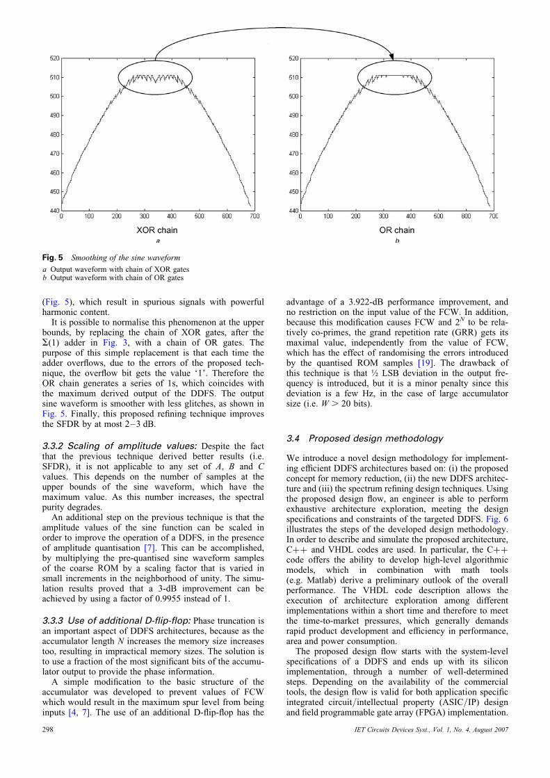
Fig. 5 Smoothing of the sine waveform
a Output waveform with chain of XOR gatesb Output waveform with chain of OR gates
(Fig. 5), which result in spurious signals with powerfulharmonic content.It is possible to normalise this phenomenon at the upper
bounds, by replacing the chain of XOR gates, after theS(1) adder in Fig. 3, with a chain of OR gates. Thepurpose of this simple replacement is that each time theadder overflows, due to the errors of the proposed tech-nique, the overflow bit gets the value ‘1’. Therefore theOR chain generates a series of 1s, which coincides withthe maximum derived output of the DDFS. The outputsine waveform is smoother with less glitches, as shown inFig. 5. Finally, this proposed refining technique improvesthe SFDR by at most 2–3 dB.
3.3.2 Scaling of amplitude values: Despite the factthat the previous technique derived better results (i.e.SFDR), it is not applicable to any set of A, B and Cvalues. This depends on the number of samples at theupper bounds of the sine waveform, which have themaximum value. As this number increases, the spectralpurity degrades.An additional step on the previous technique is that the
amplitude values of the sine function can be scaled inorder to improve the operation of a DDFS, in the presenceof amplitude quantisation [7]. This can be accomplished,by multiplying the pre-quantised sine waveform samplesof the coarse ROM by a scaling factor that is varied insmall increments in the neighborhood of unity. The simu-lation results proved that a 3-dB improvement can beachieved by using a factor of 0.9955 instead of 1.
3.3.3 Use of additional D-flip-flop: Phase truncation isan important aspect of DDFS architectures, because as theaccumulator length N increases the memory size increasestoo, resulting in impractical memory sizes. The solution isto use a fraction of the most significant bits of the accumu-lator output to provide the phase information.A simple modification to the basic structure of the
accumulator was developed to prevent values of FCWwhich would result in the maximum spur level from beinginputs [4, 7]. The use of an additional D-flip-flop has the
298
advantage of a 3.922-dB performance improvement, andno restriction on the input value of the FCW. In addition,because this modification causes FCW and 2N to be rela-tively co-primes, the grand repetition rate (GRR) gets itsmaximal value, independently from the value of FCW,which has the effect of randomising the errors introducedby the quantised ROM samples [19]. The drawback ofthis technique is that ½ LSB deviation in the output fre-quency is introduced, but it is a minor penalty since thisdeviation is a few Hz, in the case of large accumulatorsize (i.e. W . 20 bits).
3.4 Proposed design methodology
We introduce a novel design methodology for implement-ing efficient DDFS architectures based on: (i) the proposedconcept for memory reduction, (ii) the new DDFS architec-ture and (iii) the spectrum refining design techniques. Usingthe proposed design flow, an engineer is able to performexhaustive architecture exploration, meeting the designspecifications and constraints of the targeted DDFS. Fig. 6illustrates the steps of the developed design methodology.In order to describe and simulate the proposed architecture,Cþþ and VHDL codes are used. In particular, the Cþþ
code offers the ability to develop high-level algorithmicmodels, which in combination with math tools(e.g. Matlab) derive a preliminary outlook of the overallperformance. The VHDL code description allows theexecution of architecture exploration among differentimplementations within a short time and therefore to meetthe time-to-market pressures, which generally demandsrapid product development and efficiency in performance,area and power consumption.The proposed design flow starts with the system-level
specifications of a DDFS and ends up with its siliconimplementation, through a number of well-determinedsteps. Depending on the availability of the commercialtools, the design flow is valid for both application specificintegrated circuit/intellectual property (ASIC/IP) designand field programmable gate array (FPGA) implementation.
IET Circuits Devices Syst., Vol. 1, No. 4, August 2007

4 Hardware implementation and simulationresults
4.1 Qualitative comparison studies
Table 1 demonstrates qualitative comparison studies amongexisting techniques and the proposed one. The table revealsthe effectiveness of the proposed technique in comparisonwith the existing ones. In particular, the ROM size inNicholas’s and Yamagishi’s techniques is much higherthan the proposed technique, whereas in Bellaouar’s tech-nique, even if the ROM size and the achieved SNR arealmost the same with the proposed technique, the hard-ware’s architecture is very complex. Furthermore, Liao’stechnique, Sodagar’s and Lahiji’s method (parabolicapproximation) and Langlois’ technique save 4 bits of thesine amplitude as the proposed technique. Particularly,Liao’s technique calculates both the cosine and sine wave-form, needs seven adders (three for sine and four for cosinegeneration), and also decreases the total speed of the DDFS
IF simulation
IF SFDR
YES
NO
Choose alltechniques
Utilize proposed“optimization techniques”
Calculate the output spectrum,SFDR
OK
Run the simulation for the VHDLcode of the DDFS
Execute C++ code to generate thegeneral package and the packages
for the Coarse and Fine ROM
Specify the number of input andoutput bits W, D and the
segmentation bits A, B, C
Identify DDFS specifications
Re-Specify DDFSarchitecture charactestics
YES
NO
OK
NO
YES
Synthesize and ImplementDDFS
IF area, speed,power consumption
END
Utilize VLSI optimizationtechniques
Run simulation of “new”VHDL code
OK
YES
NO
Fig. 6 Flow chart of the proposed algorithm
IET Circuits Devices Syst., Vol. 1, No. 4, August 2007
due to three extra stages of adders. Furthermore, parabolicapproximation requires a full multiplier, a 2’s complemen-tor and an extra adder, whereas Langlois’ technique usestwo extra adders and two MUXes but it requires additionalcontrol logic.
4.2 DDFS implementation and simulation results
To prove the effectiveness of the proposed technique and,eventually, its impact on the DDFS architecture, we per-formed a plethora of measurements for various design fea-tures. For comparison, many existing DDFS designs [3–8]and the proposed one were described by the hardwaredescription language VHDL. In order to ensure accuratecomparison among the different approaches, all hardwaremodules, for instance memory, adder and so on, weredescribed/implemented exactly in the same way. All theimplementations have been synthesised and mapped inXilinx FPGA modules [10]. The number of slices theyreported were from the Xilinx synthesis tools, as wellas from the Xilinx FPGA device (i.e. SPARTAN II,VIRTEX II). The power consumption was measured at50-MHz operation frequency using the XPower tool,while the data-path delay and the maximum operationfrequency were calculated by the timing analyser tool ofXilinx [10]. More specifically, FPGA technology is anexcellent solution for rapid prototyping implementation dueto significantly lower cost than integrated circuits and canbe used to perform exhaustive architecture level exploration,where critical high-level designs are made. The frequencyclock was set at 50 MHz, and area optimisation techniqueswere used for reducing the size of each module.All the implementations have been analysed with no
phase truncation (i.e. the phase accumulator output bitsequal the number of input bits in ROM) and the fineROM symmetry technique has not been utilised, in orderto avoid additional control logic hardware. Furthermore,for the proposed algorithm all the refining techniqueshave been utilised in order to derive better results. TheFCW was chosen to produce the least frequency, since thespurious spectrum due to all system nonlinearities can begenerated from a permutation of another spectrum, whenGCD(Dw, 2j) ¼ 1 for all Dw, because its spectrum differsonly in the position of the spurs but not in the magnitude[6, 20].Tables 2 and 3 demonstrate the results after extensive
comparative studies among the existing approaches andthe proposed one, in terms of the ROM size, SFDR,additional hardware complexity, area, power consumption,delay and maximum frequency operation. The memorycompression techniques have been applied to design aDDFS with an accumulator length of W ¼ 12 bits and anoutput of D ¼ 10 bits (Table 2), and a DDFS with an accu-mulator length of W ¼ 18 bits and an output of D ¼ 16 bits(Table 3). Furthermore, all the measurements in Table 2were performed under the assumption that A ¼ 1, B ¼ 5and C ¼ 4, whereas in Table 3 the segmentation bits areA ¼ 3, B¼7 and C ¼ 6. Applying the procedure given inSection 3.2, the values of A, B and C were chosen to meetthe spectral purity specification with the minimal memorysize-cost. The output spectra for the two implementationswith W ¼ 12, D ¼ 10 and W ¼ 18, D ¼ 16, are shown inFig. 7a and b, respectively.As it is shown in Table 3, for the uncompressed memory
method, the ROM size is 41 kbits (212 � 10 bits), which canbe reduced using the appropriate compression algorithms,that is the existing and the proposed one. In particular,Hutchison’s [5] and Yamagishi’s [8] methods need almost
299

Table 1: Qualitative comparison of the existing and proposed techniques
Method Sine approximation
function
Saved bits
ROM size
Additional
hardware
Low power
–high speed techniques
SNR,
dBc
Architecture
characteristics
A sin(u) — — — — —
B x, 0 , x , 1 2 output bits
3072 bits ROM
2 adders, 1’s
complementor
† 8-level pipelined
accumulator
290.3 † input bits: 13
† output bits: 11
† max. freq: 150 MHz
† power:
950 mW/100 MHz
† supply voltage: 5 V,
† process 1.25-mm
rad-hard DLM CMOS
C sin(ui ) þ a(u2 ui ) þ d sin
d sin ¼ 21/2 sin us(u2 ui )2
cos(ui ) þ b(u2 ui ) þ d cos
d cos ¼ 21/2 cos us(u2 ui )2,
u [ [ui,uiþ 1]
2 input bits
416 bits ROM
1 adder/subtractor,
1 multiplier,
2 MUXes, control
logic
† 3 pipeline stages 260 † input bits: 12
† output bits:10
† power:
9.5 mW/30 MHz
† supply voltage: 5 V
† process:
0.8-mm CMOS
D x/4, 0 , x , 0.5
14 2 x/4, 0.5 , x , 1
3 output bits
6144 bits ROM
2 adders, 1’s
complementor
† low voltage D/A
converter
† image supression
up converters
253.7 † input bits: 12
† output bits:10
† max. freq: 1.9 GHz
† power:
157 mW/1.9 GHz
† internal DAC
† supply voltage: 2 V
† process: CMOS and
Si-bipolar
E 3/2x, 0 , x , 5/16
xþ 5/32, 5/16 , x , 3/4
1/2xþ 1/2, 3/4 , x , 1
4 output bits
4096 bits ROM
2 adders,
2 MUXes,
control logic
— † 12 input bits
† 8 output bits
F (2x)(1 2 x/2), 0 , x , 1 4 output bits
0 bits ROM
1 adder,
1 multiplier,
2’s complementor
† 8-level pipelined
accumulator
228.4 † 12 input bits
† 10 output bits
† supply voltage: 3.3 V
† process: 0.6-mm
CMOS
G 1.375x, 0 , x , 0.5 for sin(p/2x)
1 2 xþ 0.375 þ g(x) for cos(p/2x)
g(x) ¼ 0.25x, x , 0.25
g(x) ¼ 0.125–0.25x, x . 0.25
4 output bits
1664 bits ROM
3 adders for sine,
4 adders for cosine,
2�1’s
complementors,
2 MUXes
† static conventional
CMOS gates
† TSPC (true signal
phase clocking
scheme)
† 4-level pipelined
accumulator
† 15 pipeline stages
280 † 14 input bits
† 12 output bits
† max. freq: 100 MHz
† power:
32 mW/100 MHz
† supply voltage: 2 V
† process: 0.6-mm
SPDM CMOS
Hsin
p
4x
� �
’ykþ1 �mk ðxkþ1 � xÞ k even
ykþ1 þmk ðx � xk Þ k odd
�
cosp
4x
� �
’hkþ1 � mk ðxkþ1 � xÞ k even
hkþ1 þ mk ðx � xk Þ k odd
�
30% of total
area of DDFS
1 multiplier,
memory for cosine
† standard cell design
† gate level
optimisation
62.3 † 11 input bits
† 9 output bits
† max. freq: 224 MHz
† power: 39.3 mW/MHz
† supply voltage: 2.5 V
† process: 0.25-mm
CMOS
I 1/2 x, 0 , x , 1/4 1/8 þ 1/
4(x2 1/4), 1/4 , x , 1/2
1/8 þ 1/16 2 1/4(x2 1/2),
1/2 , x , 3/4 1/8 2 12(x2 1/
2 2 1/4), 3/4 , x , 1
4 output bits
448 bits ROM
2 XOR, 1 OR
3 adders,
shift register
† 2 pipeline stages
† carry save adders
† double edge
triggered flip-flops
2 63.12 † 12 input bits
† 10 output bits
† max. freq: 221 MHz
† power:
109 mW/50 MHz
A: Uncompressed memory; B: Nicholas – sine phase difference [19]; C: Bellaouar [3]; D: Yamagishi [8]; E: Langlois [15]; F: Sodagar andLahiji [16]; G: Liao’s technique [14]; H: Caro and Strollo [17]; I: proposed technique
IET Circuits Devices Syst., Vol. 1, No. 4, August 2007300
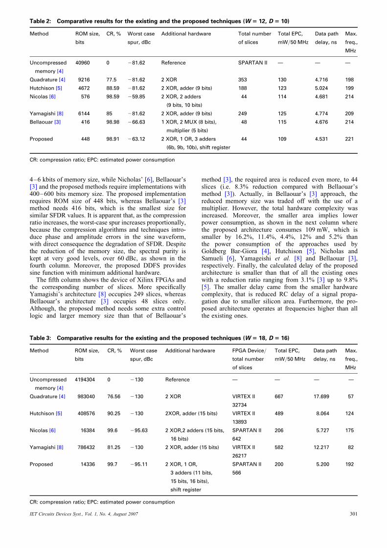
Table 2: Comparative results for the existing and the proposed techniques (W 5 12, D 5 10)
Method ROM size,
bits
CR, % Worst case
spur, dBc
Additional hardware Total number
of slices
Total EPC,
mW/50 MHz
Data path
delay, ns
Max.
freq.,
MHz
Uncompressed
memory [4]
40960 0 281.62 Reference SPARTAN II — — —
Quadrature [4] 9216 77.5 281.62 2 XOR 353 130 4.716 198
Hutchison [5] 4672 88.59 281.62 2 XOR, adder (9 bits) 188 123 5.024 199
Nicolas [6] 576 98.59 259.85 2 XOR, 2 adders
(9 bits, 10 bits)
44 114 4.681 214
Yamagishi [8] 6144 85 281.62 2 XOR, adder (9 bits) 249 125 4.774 209
Bellaouar [3] 416 98.98 266.63 1 XOR, 2 MUX (8 bits),
multiplier (5 bits)
48 115 4.676 214
Proposed 448 98.91 263.12 2 XOR, 1 OR, 3 adders
(6b, 9b, 10b), shift register
44 109 4.531 221
CR: compression ratio; EPC: estimated power consumption
4–6 kbits of memory size, while Nicholas’ [6], Bellaouar’s[3] and the proposed methods require implementations with400–600 bits memory size. The proposed implementationrequires ROM size of 448 bits, whereas Bellaouar’s [3]method needs 416 bits, which is the smallest size forsimilar SFDR values. It is apparent that, as the compressionratio increases, the worst-case spur increases proportionally,because the compression algorithms and techniques intro-duce phase and amplitude errors in the sine waveform,with direct consequence the degradation of SFDR. Despitethe reduction of the memory size, the spectral purity iskept at very good levels, over 60 dBc, as shown in thefourth column. Moreover, the proposed DDFS providessine function with minimum additional hardware.The fifth column shows the device of Xilinx FPGAs and
the corresponding number of slices. More specificallyYamagishi’s architecture [8] occupies 249 slices, whereasBellaouar’s architecture [3] occupies 48 slices only.Although, the proposed method needs some extra controllogic and larger memory size than that of Bellaouar’s
IET Circuits Devices Syst., Vol. 1, No. 4, August 2007
method [3], the required area is reduced even more, to 44slices (i.e. 8.3% reduction compared with Bellaouar’smethod [3]). Actually, in Bellaouar’s [3] approach, thereduced memory size was traded off with the use of amultiplier. However, the total hardware complexity wasincreased. Moreover, the smaller area implies lowerpower consumption, as shown in the next column wherethe proposed architecture consumes 109 mW, which issmaller by 16.2%, 11.4%, 4.4%, 12% and 5.2% thanthe power consumption of the approaches used byGoldberg Bar-Giora [4], Hutchison [5], Nicholas andSamueli [6], Yamageishi et al. [8] and Bellaouar [3],respectively. Finally, the calculated delay of the proposedarchitecture is smaller than that of all the existing oneswith a reduction ratio ranging from 3.1% [3] up to 9.8%[5]. The smaller delay came from the smaller hardwarecomplexity, that is reduced RC delay of a signal propa-gation due to smaller silicon area. Furthermore, the pro-posed architecture operates at frequencies higher than allthe existing ones.
Table 3: Comparative results for the existing and the proposed techniques (W 5 18, D 5 16)
Method ROM size,
bits
CR, % Worst case
spur, dBc
Additional hardware FPGA Device/
total number
of slices
Total EPC,
mW/50 MHz
Data path
delay, ns
Max.
freq.,
MHz
Uncompressed
memory [4]
4194304 0 2130 Reference — — — —
Quadrature [4] 983040 76.56 2130 2 XOR VIRTEX II 667 17.699 57
32734
Hutchison [5] 408576 90.25 2130 2XOR, adder (15 bits) VIRTEX II 489 8.064 124
13893
Nicolas [6] 16384 99.6 295.63 2 XOR,2 adders (15 bits,
16 bits)
SPARTAN II
642
206 5.727 175
Yamagishi [8] 786432 81.25 2130 2 XOR, adder (15 bits) VIRTEX II 582 12.217 82
26217
Proposed 14336 99.7 295.11 2 XOR, 1 OR,
3 adders (11 bits,
15 bits, 16 bits),
shift register
SPARTAN II
566
200 5.200 192
CR: compression ratio; EPC: estimated power consumption
301

Table 3 shows the simulated/calculated results of theDDFS architecture with W ¼ 18, D ¼ 16. Some interestingpoints are that the ROM size for the uncompressed memoryis 4 Mbits (218 � 16), whereas Nicholas [6] needs 16 kbitsand the proposed one needs 14 kbits (15% reduction com-pared to that in the work of Nicholas and Samueli [6]).Additionally, the spectral purity is kept over 90 dBc, whichmeets all the telecommunications standards. Area, powerconsumption and maximum frequency for the proposedtechnique improve on those of all the existing approaches.Comparing Tables 2 and 3, the main conclusion is: the
larger is the DDFS architecture with respect to input andoutput bitwidth (i.e. W, D), the larger are the gains from
Fig. 7 Output spectrum of the proposed DDFS
a W ¼ 12, D ¼ 10b W ¼ 18, D ¼ 10
302
the memory size reduction, the power savings, the hardwarecomplexity reduction and the maximum frequency operationincrease. For instance, the larger power savings are16.2% and 70% for Tables 2 and 3, respectively. Also, itcan be seen that the larger is the SFDR, the larger thegains in area, delay and power consumption, comparing thedesigned DDFS circuits with the existing ones. The increasedgains stem from the increased compression ratio of memorysize. Since the memory area occupies a large portion of thetotal chip area, increasing the size of memory reductionratio, the critical design parameters (i.e. area, delay, powerconsumption and throughput) are improved significantly.Furthermore, in Tables 2 and 3, the slices used for ROM
implementation are 26% (SFDR 63.12 dBc) and 14%(SFDR 99.7 dBc), respectively, of the total area, takinginto account FPGA implementation. It was reported thatthe sine–cosine generator requires area around 30% (SFDR60 dBc) of the total DDFS, considering IC implementation[17]. Thus, the proposed design requires less area than thecorresponding one [17], although it is realised in FPGAwhich is not the most area-efficient design technology.
4.3 VLSI optimisation technique studies
Depending on the specific constraints of a certain DDFSdesign, it might be necessary to employ additional VLSIdesign techniques for meeting DDFS features. The impactof these techniques is larger on IC-based realisations, buthere we provide results for the FPGA-based DDFS.However, the presented results prove the effectiveness ofthe used techniques even in FPGA platforms. In particular,Tables 4 and 5 show the calculations using different adderimplementations [26] and double-edge triggered flip-flops[27], respectively.Table 4 demonstrates the results for W ¼ 12 and D ¼ 10,
considering ripple-carry, carry-lookahead and carry-saveadders, as well as the customised adder for Xilinx environ-ment. It can be seen that the DDFS implementation, with theXilinx optimised adder, exhibits slightly better results interms of area, delay, power consumption and frequencythan the remaining adders. This fact is true only forFPGA-based implementations, but not for integratedcircuit (IC) realisations. However, these calculations areidentical qualitatively with the computer arithmetic theory[26]. More specifically, a ripple-carry adder exhibits thesmallest area and power and the largest delay, whereasthe carry-lookahead adder, the largest area and power andthe smallest delay. Finally, a carry-save adder is a goodcompromise between the adders mentioned earlier.Consequently, a designer can choose the appropriate adder,which meets his/her specifications after careful exploration.A well-established low power VLSI technique is the use
of double-edge triggered flip-flops [27]. Such flip-flops cansave power in the clock distribution network as the clockfrequency is halved for fixed throughput, compared tosingle-edge triggered flip-flops. Table 5 demonstrates the
Table 4: Comparison of different adder implementations (W 5 12, D 5 10)
Adder Total number
of slices
Total estimated power
consumption, mW/50 MHz
Data path
delay, ns
Maximum
frequency, MHz
Ripple-carry 48 115 4.682 214
Carry lookahead 51 116 4.569 219
Carry-save 50 116 4.646 215
Xilinx’s adder 44 109 4.531 221
IET Circuits Devices Syst., Vol. 1, No. 4, August 2007
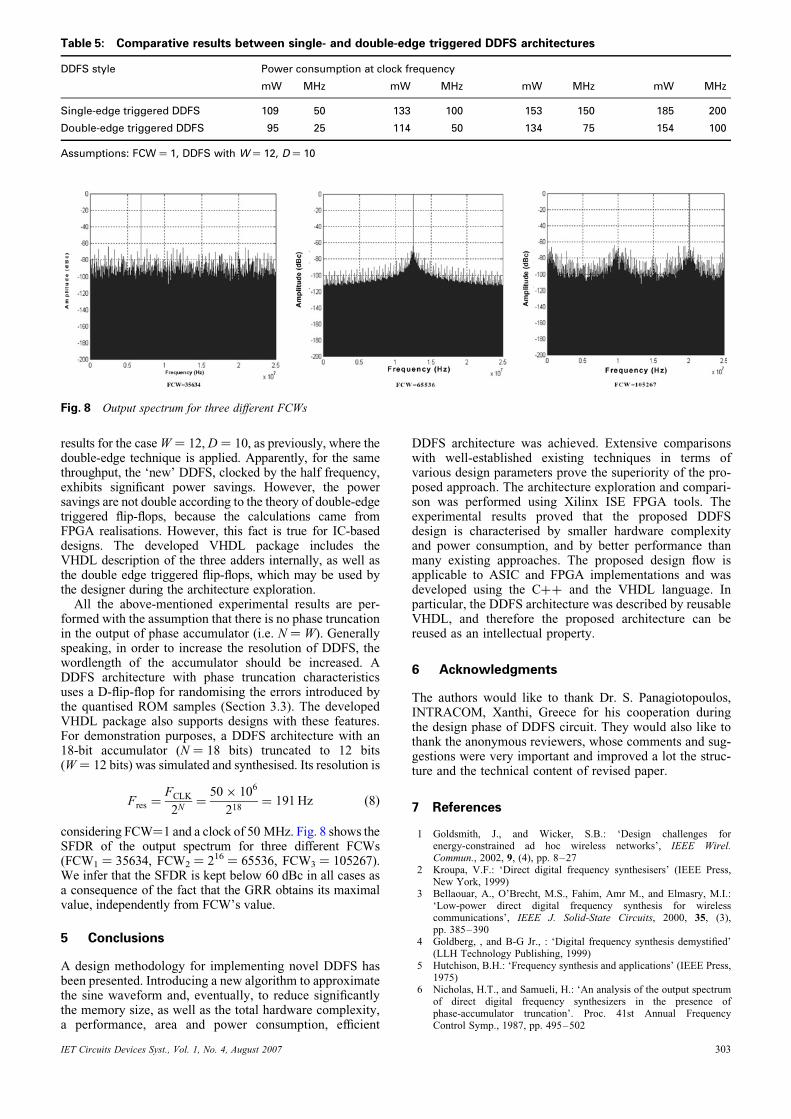
Table 5: Comparative results between single- and double-edge triggered DDFS architectures
DDFS style Power consumption at clock frequency
mW MHz mW MHz mW MHz mW MHz
Single-edge triggered DDFS 109 50 133 100 153 150 185 200
Double-edge triggered DDFS 95 25 114 50 134 75 154 100
Assumptions: FCW ¼ 1, DDFS with W ¼ 12, D ¼ 10
Fig. 8 Output spectrum for three different FCWs
results for the case W ¼ 12, D ¼ 10, as previously, where thedouble-edge technique is applied. Apparently, for the samethroughput, the ‘new’ DDFS, clocked by the half frequency,exhibits significant power savings. However, the powersavings are not double according to the theory of double-edgetriggered flip-flops, because the calculations came fromFPGA realisations. However, this fact is true for IC-baseddesigns. The developed VHDL package includes theVHDL description of the three adders internally, as well asthe double edge triggered flip-flops, which may be used bythe designer during the architecture exploration.All the above-mentioned experimental results are per-
formed with the assumption that there is no phase truncationin the output of phase accumulator (i.e. N ¼ W). Generallyspeaking, in order to increase the resolution of DDFS, thewordlength of the accumulator should be increased. ADDFS architecture with phase truncation characteristicsuses a D-flip-flop for randomising the errors introduced bythe quantised ROM samples (Section 3.3). The developedVHDL package also supports designs with these features.For demonstration purposes, a DDFS architecture with an18-bit accumulator (N ¼ 18 bits) truncated to 12 bits(W ¼ 12 bits) was simulated and synthesised. Its resolution is
Fres ¼FCLK
2N¼
50� 106
218¼ 191Hz ð8Þ
considering FCW¼1 and a clock of 50 MHz. Fig. 8 shows theSFDR of the output spectrum for three different FCWs(FCW1 ¼ 35634, FCW2 ¼ 216 ¼ 65536, FCW3 ¼ 105267).We infer that the SFDR is kept below 60 dBc in all cases asa consequence of the fact that the GRR obtains its maximalvalue, independently from FCW’s value.
5 Conclusions
A design methodology for implementing novel DDFS hasbeen presented. Introducing a new algorithm to approximatethe sine waveform and, eventually, to reduce significantlythe memory size, as well as the total hardware complexity,a performance, area and power consumption, efficient
IET Circuits Devices Syst., Vol. 1, No. 4, August 2007
DDFS architecture was achieved. Extensive comparisonswith well-established existing techniques in terms ofvarious design parameters prove the superiority of the pro-posed approach. The architecture exploration and compari-son was performed using Xilinx ISE FPGA tools. Theexperimental results proved that the proposed DDFSdesign is characterised by smaller hardware complexityand power consumption, and by better performance thanmany existing approaches. The proposed design flow isapplicable to ASIC and FPGA implementations and wasdeveloped using the Cþþ and the VHDL language. Inparticular, the DDFS architecture was described by reusableVHDL, and therefore the proposed architecture can bereused as an intellectual property.
6 Acknowledgments
The authors would like to thank Dr. S. Panagiotopoulos,INTRACOM, Xanthi, Greece for his cooperation duringthe design phase of DDFS circuit. They would also like tothank the anonymous reviewers, whose comments and sug-gestions were very important and improved a lot the struc-ture and the technical content of revised paper.
7 References
1 Goldsmith, J., and Wicker, S.B.: ‘Design challenges forenergy-constrained ad hoc wireless networks’, IEEE Wirel.Commun., 2002, 9, (4), pp. 8–27
2 Kroupa, V.F.: ‘Direct digital frequency synthesisers’ (IEEE Press,New York, 1999)
3 Bellaouar, A., O’Brecht, M.S., Fahim, Amr M., and Elmasry, M.I.:‘Low-power direct digital frequency synthesis for wirelesscommunications’, IEEE J. Solid-State Circuits, 2000, 35, (3),pp. 385–390
4 Goldberg, , and B-G Jr., : ‘Digital frequency synthesis demystified’(LLH Technology Publishing, 1999)
5 Hutchison, B.H.: ‘Frequency synthesis and applications’ (IEEE Press,1975)
6 Nicholas, H.T., and Samueli, H.: ‘An analysis of the output spectrumof direct digital frequency synthesizers in the presence ofphase-accumulator truncation’. Proc. 41st Annual FrequencyControl Symp., 1987, pp. 495–502
303

7 Nicholas, H.T., Samueli, H., and Kim, B.: ‘The optimization of directdigital frequency performance in the presence of finite word lengtheffects’. Proc. 42nd Annual Frequency Control Symp., 1988,pp. 357–363
8 Yamagishi, A., Ishikawa, M., Tsukahara, T., and Date, S.: ‘A 2-V,2-GHz low-power direct digital frequency synthesizer chip-set forwireless communication’, IEEE J. Solid-State Circuits, 1998, 33,(2), pp. 210–217
9 Bricaud, P., and Keating, M.: ‘Reuse methodology, manual forsystem-on-a-chip designs’ (Kluwer Academic Publishers, Boston,2003, 2nd edn.)
10 http://www.xilinx.com, Xilinx, Inc.11 Tierney, J., Rader, C.M., and Gold, B.: ‘A digital frequency
synthesizer’, IEEE Trans. Audio Electroacoust., 1971, AU-19,pp. 48–57
12 Rabaey, J.M., and Pedram, M.: ‘Low power design methodologies’(Kluwer Academic Publishers, Boston, 1996)
13 Cathoor, F., et al.: ‘Data access and storage management forembedded programmable processors’ (Kluwer Academic Publishers,Boston, 2002)
14 Liao, S., and Chen, L.-G.: ‘A low-power low-voltage direct digitalfrequency synthesizer’. Proc. Int. Symp. VLSI Technology,Systems, and Applications, June 1997, pp. 265–269
15 Langlois, J.M.P., and Al-Khalili, D.: ‘Novel approach to the design ofdirect digital frequency synthesizers based on linear interpolation’,IEEE Trans. Circuits Syst. II, 2003, 50, pp. 567–578
16 Sodagar, A.M., and Lahiji, G.R.: ‘Mapping from phase tosine-amplitude in direct digital frequency synthesizers usingparabolic approximation’, IEEE Trans. Circuits Syst. II, AnalogDigit. Signal Process., 2000, 47, (12), pp. 1452–1457
17 De Caro, D., and Strollo, A.G.M.: ‘High-performance direct digitalfrequency synthesizers using piecewise-polynomial approximation’,IEEE Trans. Circuits Syst. I, 2005, 52, (2), pp. 324– 337
304
18 De Caro, D., and Strollo, A.G.M.: ‘High-performance direct digitalfrequency synthesizers using in 0.25um CMOS using dual-slopeapproximation’, IEEE J. Solid-State Circuits, 2005, 40, (11),pp. 2220–2227
19 Nicholas, H.T., and Samueli, H.: ‘A 150-MHz direct digital frequencysynthesizer in 1.25-mm CMOS with 290 dBc spurious performance’,IEEE J. Solid-State Circuits, 1991, 26, (12), pp. 1959–1969
20 Vankka, J.: ‘Methods of mapping from phase to sine amplitude indirect digital synthesis’, IEEE Trans. Ultrason. Ferroelectr. Freq.Control, 1997, 44, (2), pp. 526–534
21 Kang, C.Y., and Swartzlander, E.E., Jr: ‘An analysis of the CORDICalgorithm for direct digital frequency synthesis’. Proc. IEEE Int. Conf.Application-Specific Systems, Architectures and Processors, 2002,pp. 111–119
22 Madisetti, A., Kwentus, A.Y., and Willson, Jr., A.N.: ‘A 100-MHz,16-b, direct digital frequency synthesizer with a 100-dBcspurious-free dynamic range’, IEEE J. Solid-State Circuits, 1999,34, (8), pp. 1034–1043
23 McEwan, A., and Collins, S.: ‘Analogue interpolation based directdigital frequency synthesis’. Proc. IEEE Int. Symp. Circuits andSystems (ISCAS ’03), 2003, vol. 1, pp. I-621–I-624
24 Sodagar, A.M., and Lahiji, G.R.: ‘A pipelined ROM-less architecturefor sine-output direct digital frequency synthesizers using thesecond-order parabolic approximation’, IEEE Trans. Circuits Syst.II, Analog Digit. Signal Process., 2001, 48, (9), pp. 850–857
25 Langlois, J.M.P., and Al-Khalili, D.: ‘Phase to sinusoid amplitudeconversion techniques for direct digital frequency synthesis’, IEEProc., Circuits Devices Syst., 2004, 151, (6), pp. 519–528
26 Parhami, B.: ‘Computer arithmetic: algorithms and hardware designs’(Oxford University Press, 2000)
27 Strollo, A.G.M., Napoli, E., and Cimino, C.: ‘Analysis of powerdissipation in double edge-triggered flip-flops’, IEEE Trans. VLSISyst., 2000, 8, (5), pp. 624–629
IET Circuits Devices Syst., Vol. 1, No. 4, August 2007