Zed-Full Key Programmer Obd Applications Price List Jan 2021
Upload
khangminh22Category
view
2download
0
November 2019 UM2448 Rev 3 1/34
1
UM2448User manual
STLINK-V3SET debugger/programmer for STM8 and STM32
Introduction
The STLINK-V3SET is a stand-alone modular debugging and programming probe for the STM8 and STM32 microcontrollers. This product is composed of the main module and the complementary adapter board. It supports the SWIM and JTAG/SWD interfaces for the communication with any STM8 or STM32 microcontroller located on an application board.
The STLINK-V3SET provides a Virtual COM port interface allowing the host PC to communicate with the target microcontroller through one UART. It also provides bridge interfaces to several communication protocols allowing, for instance, the programming of the target through the bootloader.
The STLINK-V3SET can provide a second Virtual COM port interface allowing the host PC to communicate with the target microcontroller through another UART (called bridge UART). Bridge UART signals, including optional RTS and CTS, are available on the adapter board only (MB1440). The second Virtual COM port activation is done through a reversible firmware update, which also disables the mass storage interface (used for Drag-and-drop flash programming).
The modular architecture of STLINK-V3SET enables to extend its main features through additional modules such as the adapter board.
Figure 1. STLINK-V3SET product top view
Picture is not contractual.
www.st.com

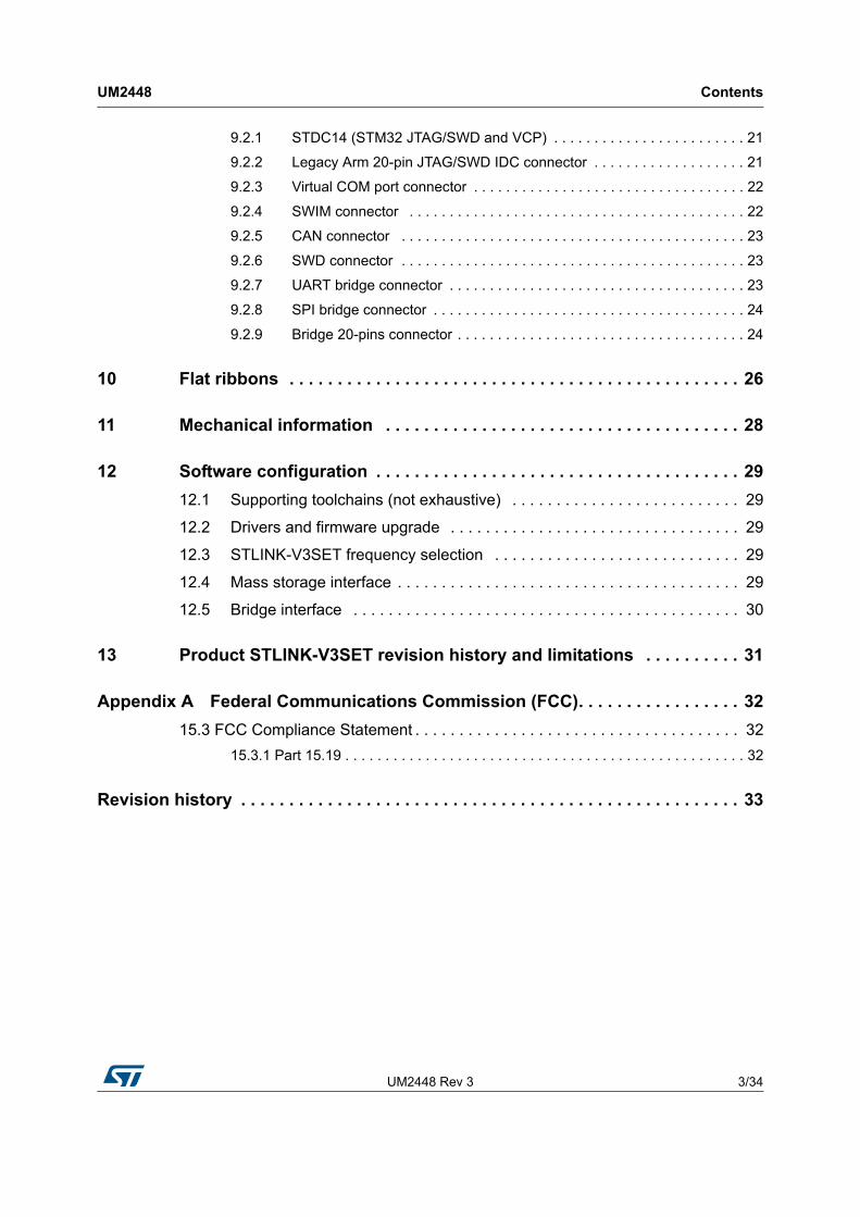
Contents UM2448
2/34 UM2448 Rev 3
Contents
1 Features . . . . . . . . . . . . . . . . . . . . . . . . . . . . . . . . . . . . . . . . . . . . . . . . . . . 6
2 General information . . . . . . . . . . . . . . . . . . . . . . . . . . . . . . . . . . . . . . . . . 6
3 System requirements . . . . . . . . . . . . . . . . . . . . . . . . . . . . . . . . . . . . . . . . 7
4 Development toolchains . . . . . . . . . . . . . . . . . . . . . . . . . . . . . . . . . . . . . . 7
5 Ordering information . . . . . . . . . . . . . . . . . . . . . . . . . . . . . . . . . . . . . . . . 7
6 Conventions . . . . . . . . . . . . . . . . . . . . . . . . . . . . . . . . . . . . . . . . . . . . . . . . 7
7 Quick start . . . . . . . . . . . . . . . . . . . . . . . . . . . . . . . . . . . . . . . . . . . . . . . . . 8
8 STLINK-V3SET functional description . . . . . . . . . . . . . . . . . . . . . . . . . . 9
8.1 STLINK-V3SET overview . . . . . . . . . . . . . . . . . . . . . . . . . . . . . . . . . . . . . . 9
8.1.1 Main module for high performance . . . . . . . . . . . . . . . . . . . . . . . . . . . . . 9
8.1.2 Adapter configuration for added functions . . . . . . . . . . . . . . . . . . . . . . . 10
8.1.3 How to build the adapter configuration for added functions . . . . . . . . . . 11
8.2 Hardware layout . . . . . . . . . . . . . . . . . . . . . . . . . . . . . . . . . . . . . . . . . . . . 12
8.3 STLINK-V3SET functions . . . . . . . . . . . . . . . . . . . . . . . . . . . . . . . . . . . . . 16
8.3.1 SWD with SWV . . . . . . . . . . . . . . . . . . . . . . . . . . . . . . . . . . . . . . . . . . . 16
8.3.2 JTAG . . . . . . . . . . . . . . . . . . . . . . . . . . . . . . . . . . . . . . . . . . . . . . . . . . . 17
8.3.3 SWIM . . . . . . . . . . . . . . . . . . . . . . . . . . . . . . . . . . . . . . . . . . . . . . . . . . . 17
8.3.4 Virtual COM port (VCP) . . . . . . . . . . . . . . . . . . . . . . . . . . . . . . . . . . . . . 17
8.3.5 Bridge functions . . . . . . . . . . . . . . . . . . . . . . . . . . . . . . . . . . . . . . . . . . . 17
8.3.6 LEDs . . . . . . . . . . . . . . . . . . . . . . . . . . . . . . . . . . . . . . . . . . . . . . . . . . . 18
8.4 Jumper configuration . . . . . . . . . . . . . . . . . . . . . . . . . . . . . . . . . . . . . . . . 19
9 Board connectors . . . . . . . . . . . . . . . . . . . . . . . . . . . . . . . . . . . . . . . . . . 20
9.1 Connectors on MB1441 board . . . . . . . . . . . . . . . . . . . . . . . . . . . . . . . . . 20
9.1.1 USB Micro-B . . . . . . . . . . . . . . . . . . . . . . . . . . . . . . . . . . . . . . . . . . . . . 20
9.1.2 STDC14 (STM32 JTAG/SWD and VCP) . . . . . . . . . . . . . . . . . . . . . . . . 21
9.2 Connectors on MB1440 board . . . . . . . . . . . . . . . . . . . . . . . . . . . . . . . . . 21
UM2448 Rev 3 3/34
UM2448 Contents
3
9.2.1 STDC14 (STM32 JTAG/SWD and VCP) . . . . . . . . . . . . . . . . . . . . . . . . 21
9.2.2 Legacy Arm 20-pin JTAG/SWD IDC connector . . . . . . . . . . . . . . . . . . . 21
9.2.3 Virtual COM port connector . . . . . . . . . . . . . . . . . . . . . . . . . . . . . . . . . . 22
9.2.4 SWIM connector . . . . . . . . . . . . . . . . . . . . . . . . . . . . . . . . . . . . . . . . . . 22
9.2.5 CAN connector . . . . . . . . . . . . . . . . . . . . . . . . . . . . . . . . . . . . . . . . . . . 23
9.2.6 SWD connector . . . . . . . . . . . . . . . . . . . . . . . . . . . . . . . . . . . . . . . . . . . 23
9.2.7 UART bridge connector . . . . . . . . . . . . . . . . . . . . . . . . . . . . . . . . . . . . . 23
9.2.8 SPI bridge connector . . . . . . . . . . . . . . . . . . . . . . . . . . . . . . . . . . . . . . . 24
9.2.9 Bridge 20-pins connector . . . . . . . . . . . . . . . . . . . . . . . . . . . . . . . . . . . . 24
10 Flat ribbons . . . . . . . . . . . . . . . . . . . . . . . . . . . . . . . . . . . . . . . . . . . . . . . 26
11 Mechanical information . . . . . . . . . . . . . . . . . . . . . . . . . . . . . . . . . . . . . 28
12 Software configuration . . . . . . . . . . . . . . . . . . . . . . . . . . . . . . . . . . . . . . 29
12.1 Supporting toolchains (not exhaustive) . . . . . . . . . . . . . . . . . . . . . . . . . . 29
12.2 Drivers and firmware upgrade . . . . . . . . . . . . . . . . . . . . . . . . . . . . . . . . . 29
12.3 STLINK-V3SET frequency selection . . . . . . . . . . . . . . . . . . . . . . . . . . . . 29
12.4 Mass storage interface . . . . . . . . . . . . . . . . . . . . . . . . . . . . . . . . . . . . . . . 29
12.5 Bridge interface . . . . . . . . . . . . . . . . . . . . . . . . . . . . . . . . . . . . . . . . . . . . 30
13 Product STLINK-V3SET revision history and limitations . . . . . . . . . . 31
Appendix A Federal Communications Commission (FCC). . . . . . . . . . . . . . . . . 32
15.3 FCC Compliance Statement . . . . . . . . . . . . . . . . . . . . . . . . . . . . . . . . . . . . . 32
15.3.1 Part 15.19 . . . . . . . . . . . . . . . . . . . . . . . . . . . . . . . . . . . . . . . . . . . . . . . . . . 32
Revision history . . . . . . . . . . . . . . . . . . . . . . . . . . . . . . . . . . . . . . . . . . . . . . . . . . . . 33
List of tables UM2448
4/34 UM2448 Rev 3
List of tables
Table 1. Ordering information . . . . . . . . . . . . . . . . . . . . . . . . . . . . . . . . . . . . . . . . . . . . . . . . . . . . . . . 7Table 2. ON/OFF convention . . . . . . . . . . . . . . . . . . . . . . . . . . . . . . . . . . . . . . . . . . . . . . . . . . . . . . . 7Table 3. MB1441 jumper configuration. . . . . . . . . . . . . . . . . . . . . . . . . . . . . . . . . . . . . . . . . . . . . . . 19Table 4. MB1440 jumper configuration. . . . . . . . . . . . . . . . . . . . . . . . . . . . . . . . . . . . . . . . . . . . . . . 19Table 5. USB Micro-B connector pinout CN5 . . . . . . . . . . . . . . . . . . . . . . . . . . . . . . . . . . . . . . . . . . 20Table 6. STDC14 connector pinout CN1 . . . . . . . . . . . . . . . . . . . . . . . . . . . . . . . . . . . . . . . . . . . . . 21Table 7. Legacy Arm 20-pin JTAG/SWD IDC connector CN2 . . . . . . . . . . . . . . . . . . . . . . . . . . . . . 22Table 8. Virtual COM port connector CN3 . . . . . . . . . . . . . . . . . . . . . . . . . . . . . . . . . . . . . . . . . . . . 22Table 9. SWIM connector CN4 . . . . . . . . . . . . . . . . . . . . . . . . . . . . . . . . . . . . . . . . . . . . . . . . . . . . . 22Table 10. CAN connector CN5 . . . . . . . . . . . . . . . . . . . . . . . . . . . . . . . . . . . . . . . . . . . . . . . . . . . . . . 23Table 11. SWD (wires) connector CN6. . . . . . . . . . . . . . . . . . . . . . . . . . . . . . . . . . . . . . . . . . . . . . . . 23Table 12. UART bridge connector CN7 . . . . . . . . . . . . . . . . . . . . . . . . . . . . . . . . . . . . . . . . . . . . . . . 24Table 13. SPI bridge connector CN8 . . . . . . . . . . . . . . . . . . . . . . . . . . . . . . . . . . . . . . . . . . . . . . . . . 24Table 14. Bridge connector CN9 . . . . . . . . . . . . . . . . . . . . . . . . . . . . . . . . . . . . . . . . . . . . . . . . . . . . 24Table 15. ARM10-compatible connector pinout (target side) . . . . . . . . . . . . . . . . . . . . . . . . . . . . . . . 26Table 16. ARM20-compatible connector pinout (target side) . . . . . . . . . . . . . . . . . . . . . . . . . . . . . . . 26Table 17. Toolchain versions supporting STLINK-V3SET . . . . . . . . . . . . . . . . . . . . . . . . . . . . . . . . . 29Table 18. Product STLINK-V3SET revision history and limitations . . . . . . . . . . . . . . . . . . . . . . . . . . 31Table 19. Document revision history . . . . . . . . . . . . . . . . . . . . . . . . . . . . . . . . . . . . . . . . . . . . . . . . . 33
UM2448 Rev 3 5/34
UM2448 List of figures
5
List of figures
Figure 1. STLINK-V3SET product top view . . . . . . . . . . . . . . . . . . . . . . . . . . . . . . . . . . . . . . . . . . . . . 1Figure 2. Probe top side. . . . . . . . . . . . . . . . . . . . . . . . . . . . . . . . . . . . . . . . . . . . . . . . . . . . . . . . . . . . 9Figure 3. Connections . . . . . . . . . . . . . . . . . . . . . . . . . . . . . . . . . . . . . . . . . . . . . . . . . . . . . . . . . . . . 10Figure 4. Probe with adapter . . . . . . . . . . . . . . . . . . . . . . . . . . . . . . . . . . . . . . . . . . . . . . . . . . . . . . . 10Figure 5. Operating mode to change the configuration . . . . . . . . . . . . . . . . . . . . . . . . . . . . . . . . . . . 11Figure 6. Hardware board MB1441 . . . . . . . . . . . . . . . . . . . . . . . . . . . . . . . . . . . . . . . . . . . . . . . . . . 12Figure 7. Hardware board MB1440 . . . . . . . . . . . . . . . . . . . . . . . . . . . . . . . . . . . . . . . . . . . . . . . . . . 13Figure 8. MB1441 top layout . . . . . . . . . . . . . . . . . . . . . . . . . . . . . . . . . . . . . . . . . . . . . . . . . . . . . . . 14Figure 9. MB1441 bottom layout . . . . . . . . . . . . . . . . . . . . . . . . . . . . . . . . . . . . . . . . . . . . . . . . . . . . 14Figure 10. MB1440 top layout . . . . . . . . . . . . . . . . . . . . . . . . . . . . . . . . . . . . . . . . . . . . . . . . . . . . . . . 15Figure 11. MB1441 mechanical drawing . . . . . . . . . . . . . . . . . . . . . . . . . . . . . . . . . . . . . . . . . . . . . . . 15Figure 12. MB1441 mechanical drawing . . . . . . . . . . . . . . . . . . . . . . . . . . . . . . . . . . . . . . . . . . . . . . . 16Figure 13. Firmware selection for a second Virtual COM port . . . . . . . . . . . . . . . . . . . . . . . . . . . . . . . 18Figure 14. USB Micro-B connector CN5 (front view) . . . . . . . . . . . . . . . . . . . . . . . . . . . . . . . . . . . . . . 20Figure 15. MB1440 mechanical dimensions (in millimeters) . . . . . . . . . . . . . . . . . . . . . . . . . . . . . . . . 28
Features UM2448
6/34 UM2448 Rev 3
1 Features
• Stand-alone probe with modular extensions
• Self-powered through a USB connector (Micro-B)
• USB 2.0 high-speed compatible interface
• Direct firmware update support (DFU)
• JTAG / serial wire debugging (SWD) specific features:
– 3 V to 3.6 V application voltage support and 5 V tolerant inputs
– Flat cables STDC14 to MIPI10 / STDC14 / MIPI20 (connectors with 1.27 mm pitch)
– JTAG communication support
– SWD and serial wire viewer (SWV) communication support
• SWIM specific features (only available with adapter board MB1440):
– 1.65 V to 5.5 V application voltage support
– SWIM header (2.54 mm pitch)
– SWIM low-speed and high-speed modes support
• Virtual COM port (VCP) specific features:
– 3 V to 3.6 V application voltage support on the UART interface and 5 V tolerant inputs
– VCP frequency up to 15 MHz
– Available on STDC14 debug connector (not available on MIPI10)
• Multi-path bridge USB to SPI/UART/I2C/CAN/GPIOs specific features:
– 3 V to 3.6 V application voltage support and 5 V tolerant inputs
– Signals available on adapter board only (MB1440)
• Drag-and-drop flash programming of binary files
• Two-color LEDs: communication, power
Note: The STLINK-V3SET product does not provide power supply to the target application.
2 General information
The STLINK-V3SET embeds an STM32 32-bit microcontroller based on the Arm®(a) Cortex®-M processor.
a. Arm is a registered trademark of Arm Limited (or its subsidiaries) in the US and or elsewhere.

UM2448 Rev 3 7/34
UM2448 System requirements
33
3 System requirements
• Windows® OS (7, 8 and 10), Linux® 64-bit, or macOS®(a)
• USB Type-A to Micro-B cable
4 Development toolchains
• Keil® MDK-ARM(b)
• IAR™ EWARM(b)
• GCC-based IDEs
5 Ordering information
To order the STLINK-V3SET, refer to Table 1.
6 Conventions
Table 2 provides the conventions used for the ON and OFF settings in the present document.
a. macOS® is a trademark of Apple Inc. registered in the U.S. and other countries.
b. On Windows® only.
Table 1. Ordering information
Order code Description
STLINK-V3SETSTLINK-V3 modular in-circuit debugger and programmer for STM8 and STM32.
Table 2. ON/OFF convention
Convention Definition
Jumper JPx ON Jumper fitted
Jumper JPx OFF Jumper not fitted
Jumper JPx [1-2] Jumper should be fitted between Pin 1 and Pin 2
Solder bridge SBx ON SBx connections closed by 0 ohm resistor
Solder bridge SBx OFF SBx connections left open
Quick start UM2448
8/34 UM2448 Rev 3
7 Quick start
This section describes how to start development quickly using the STLINK-V3SET.
Before installing and using the product, accept the Evaluation Product License Agreement from the www.st.com/epla web page.
The STLINK-V3SET is a stand-alone modular debugging and programming probe for STM8 and STM32 microcontrollers.
• It support protocols SWIM, JTAG and SWD to communicate with any STM8 or STM32 microcontroller.
• It provides a Virtual COM port interface allowing the host PC to communicate with the target microcontroller through one UART
• It provides bridge interfaces to several communication protocols allowing, for instance, the programming of the target through the bootloader.
To start using this board, follow the steps below:
1. Check that all items are available inside the box (V3S + 3 flat cables + adapter board and its guide).
2. Install/update the IDE/STM32CubeProgrammer to support the STLINK-V3SET (drivers).
3. Choose a flat cable and connect it between the STLINK-V3SETand the application.
4. Connect a USB Type-A to Micro-B cable between the STLINK-V3SETand the PC.
5. Check that the PWR LED is green and the COM LED is red.
6. Open the development toolchain or STM32CubeProgrammer software utility.
For more details, refer to the www.st.com/stlink-v3set web site.

UM2448 Rev 3 9/34
UM2448 STLINK-V3SET functional description
33
8 STLINK-V3SET functional description
8.1 STLINK-V3SET overview
The STLINK-V3SET is a stand-alone modular debugging and programming probe for the STM8 and STM32 microcontrollers. This product supports many functions and protocols for debugging, programming or communicating with one or several targets. The STLINK-V3SET package includes complete hardware with the main module for high performance and an adapter board for added functions to connect with wires or flat cables anywhere into the application.
This module is fully powered by the PC. If the COM LED blinks red, refer to the Overview of ST-LINK derivatives technical note (TN1235) for details.
8.1.1 Main module for high performance
This configuration is the preferred one for high performance. It only supports STM32 microcontrollers. The working voltage range is from 3 V to 3.6 V.
Figure 2. Probe top side
The protocols and functions supported are:
• SWD with SWO (up to 24 MHz)
• JTAG (up to 21 MHz)
• VCP (from 720 bps to 15 Mbps)
A 2x7-pin male connector with 1.27 mm pitch is located in the STLINK-V3SET for connection to the application target. Three different flat cables are included in the packaging
STLINK-V3SET functional description UM2448
10/34 UM2448 Rev 3
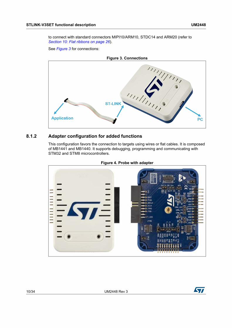
to connect with standard connectors MIPI10/ARM10, STDC14 and ARM20 (refer to Section 10: Flat ribbons on page 26).
See Figure 3 for connections:
Figure 3. Connections
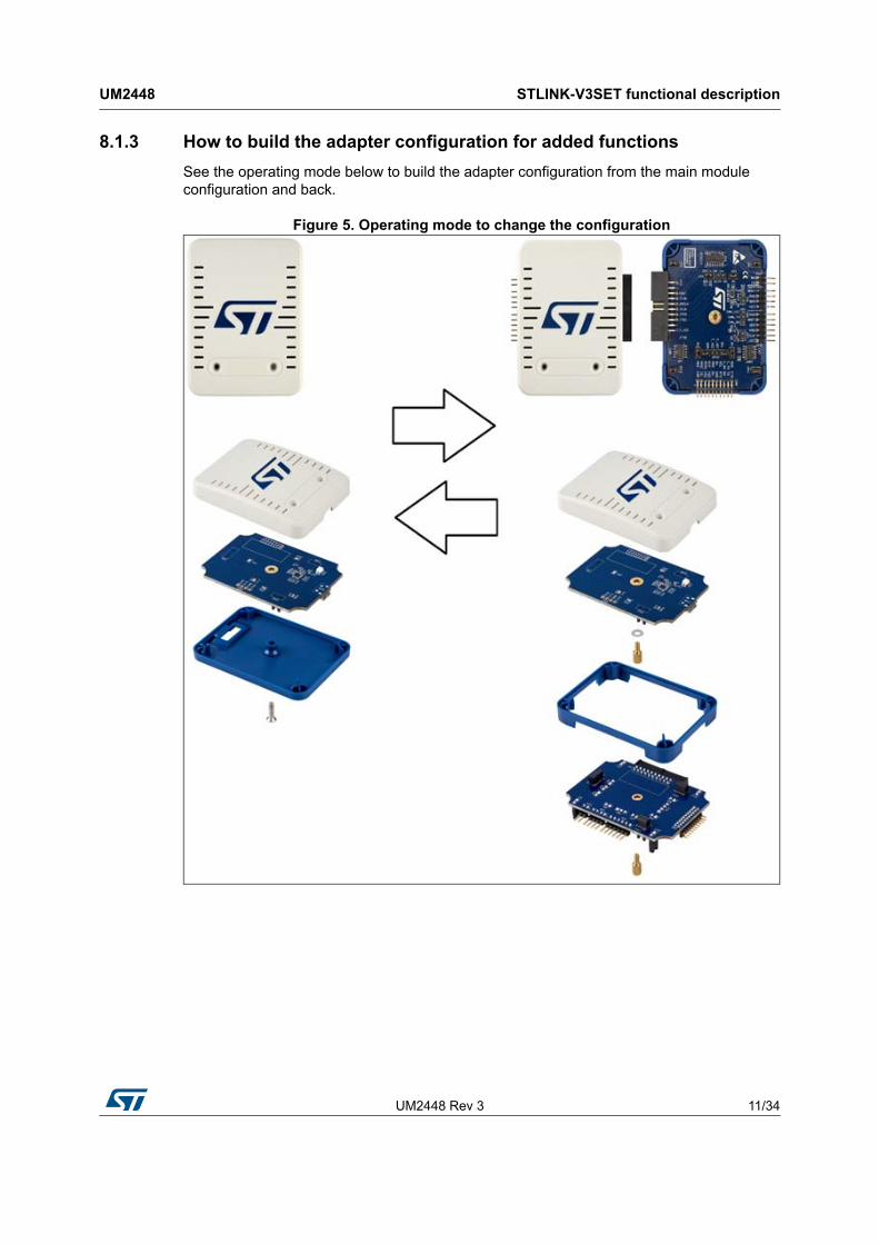
8.1.2 Adapter configuration for added functions
This configuration favors the connection to targets using wires or flat cables. It is composed of MB1441 and MB1440. It supports debugging, programming and communicating with STM32 and STM8 microcontrollers.
Figure 4. Probe with adapter
UM2448 Rev 3 11/34
UM2448 STLINK-V3SET functional description
33
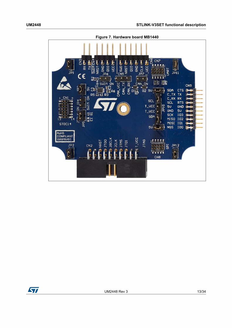
8.1.3 How to build the adapter configuration for added functions
See the operating mode below to build the adapter configuration from the main module configuration and back.
Figure 5. Operating mode to change the configuration

STLINK-V3SET functional description UM2448
12/34 UM2448 Rev 3
8.2 Hardware layout
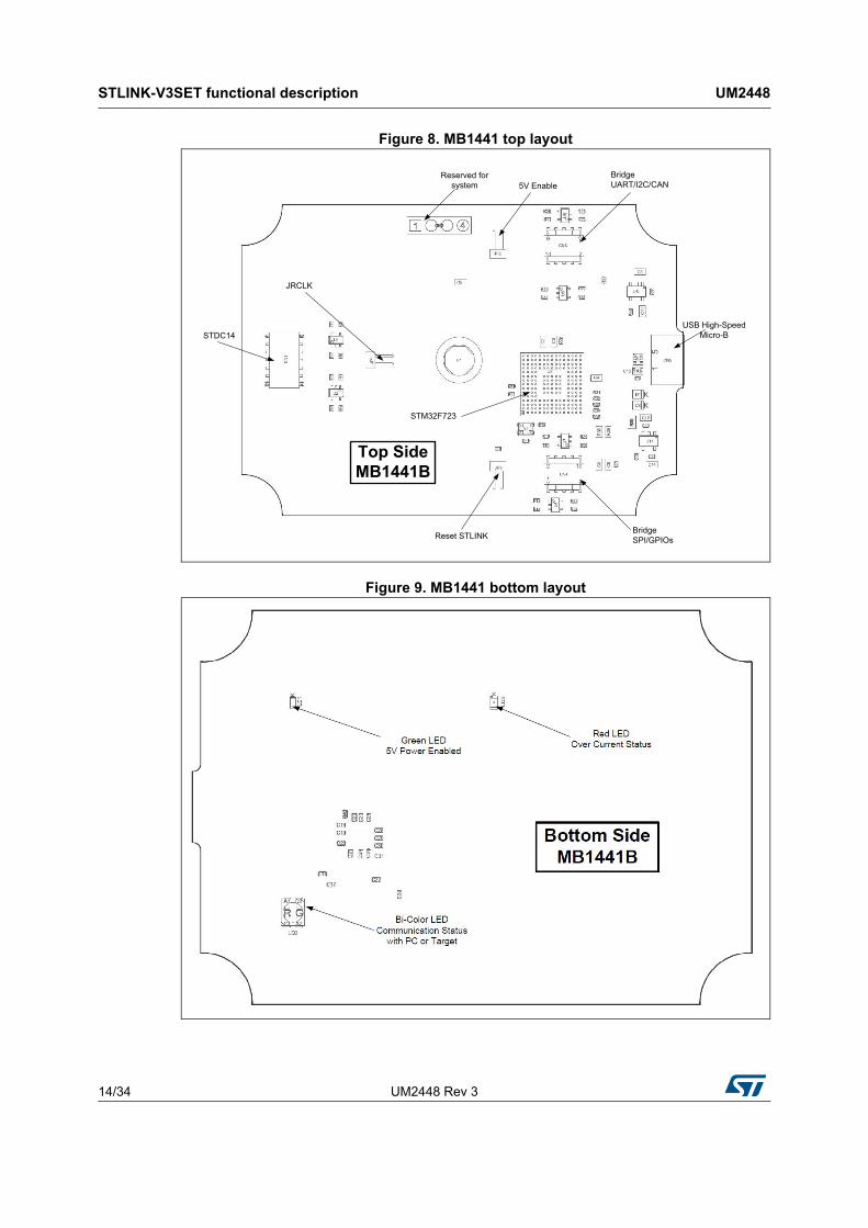
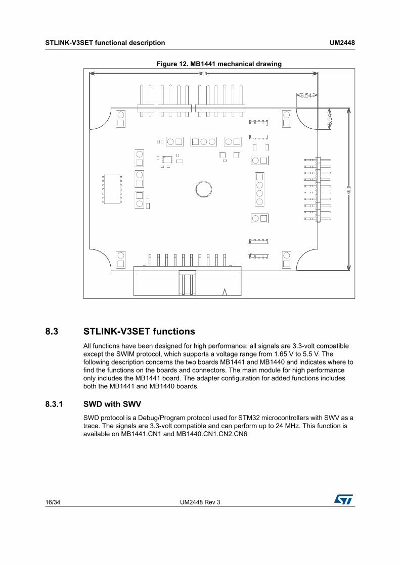
The STLINK-V3SET product is designed around the STM32F723 microcontroller (176-pin in UFBGA package). The hardware board pictures (Figure 6 and Figure 7) show the two boards included in the package in their standard configurations (components and jumpers). Figure 8, Figure 9 and Figure 10 help users locate the features on the boards. The mechanical dimensions of the STLINK-V3SET product are shown in Figure 11 and Figure 12.
Figure 6. Hardware board MB1441
UM2448 Rev 3 13/34
UM2448 STLINK-V3SET functional description
33
Figure 7. Hardware board MB1440
STLINK-V3SET functional description UM2448
14/34 UM2448 Rev 3
Figure 8. MB1441 top layout
Figure 9. MB1441 bottom layout
������
���
� ���������� � ���
� ��������
���������� ���!�"����
#$�%&'()��������*�+�,�+�*�
�������-�+.-�/
��!0,12,0
��������� ��

UM2448 Rev 3 15/34
UM2448 STLINK-V3SET functional description
33
Figure 10. MB1440 top layout
Figure 11. MB1441 mechanical drawing
$�-
�3�!���'���
.��
.�� .��
.��
�3����'���
#$�������
#$������2
#$������4
�3�!�/�
���
������
�3�!�/�
��*.,5
�*����'����*��/�
�*��������
�-��������
��������-�+�*�+�,�+�*�+.-�/
�,�+��*�-�
�,�+���-���������� ��
STLINK-V3SET functional description UM2448
16/34 UM2448 Rev 3
Figure 12. MB1441 mechanical drawing
8.3 STLINK-V3SET functions
All functions have been designed for high performance: all signals are 3.3-volt compatible except the SWIM protocol, which supports a voltage range from 1.65 V to 5.5 V. The following description concerns the two boards MB1441 and MB1440 and indicates where to find the functions on the boards and connectors. The main module for high performance only includes the MB1441 board. The adapter configuration for added functions includes both the MB1441 and MB1440 boards.
8.3.1 SWD with SWV
SWD protocol is a Debug/Program protocol used for STM32 microcontrollers with SWV as a trace. The signals are 3.3-volt compatible and can perform up to 24 MHz. This function is available on MB1441.CN1 and MB1440.CN1.CN2.CN6
UM2448 Rev 3 17/34
UM2448 STLINK-V3SET functional description
33
8.3.2 JTAG
JTAG protocol is a Debug/Program protocol used for STM32 microcontrollers. The signals are 3.3-volt compatible and can perform up to 21 MHz. This function is available on MB1441.CN1 and MB1440.CN1.CN2.
The STLINK-V3SET does not support the chaining of devices in JTAG (daisy chain).
8.3.3 SWIM
SWIM protocol is a Debug/Program protocol used for STM8 microcontrollers. JP4 and JP6 on the MB1440 board must be ON in order to activate the SWIM protocol. The signals are available on the MB1440.CN4 connector and a voltage range from 1.65 V to 5.5 V is supported.
8.3.4 Virtual COM port (VCP)
The serial interface VCP is directly available as a Virtual COM port of the PC, connected to STLINK-V3SET USB connector CN5. This function can be used for STM32 and STM8 microcontrollers. The signals are 3.3-volt compatible and can perform from 720 bps to 15 Mbps. This function is available on MB1441.CN1 and MB1440.CN1.CN3. T_VCP_RX (or RX) signal is the RX for the target (TX for the STLINK-V3SET), T_VCP_TX (or TX) signal is the TX for the target (RX for the STLINK-V3SET).
A second Virtual COM port may be activated, as detailed later in Section 8.3.5 (Bridge UART).
8.3.5 Bridge functions
The STLINK-V3SET provides a proprietary USB interface allowing communication with any STM8 or STM32 target with several protocols: SPI, I2C, CAN, UART and GPIOs. This interface may be used to communicate with the target bootloader, but may also be used for customized needs through its public software interface.
All bridge signals can be accessed on CN9 in a simple and easy way by means of wire clips, with the risk that signal quality and performance are lowered, especially for SPI and UART. This depends for instance on the quality of the wires used, on the fact that the wires are shielded or not, and on the layout of the application board.
Bridge SPI
SPI signals are available on MB1440.CN9 and MB1440.CN8. In order to reach high SPI frequency, it is recommended to use a flat ribbon on MB1440.CN8 with all unused signals tied to the ground on the target side.
Bridge I2C
I2C signals are available on MB1440.CN9 and MB1440.CN7. The adapter module also provides optional 680-ohm pull-ups, which can be activated by closing JP10 jumpers. In that case, the target voltage (T_VCC) must be provided to any of the MB1440 connector accepting it (CN1, CN2, CN6, or JP10 jumpers).

STLINK-V3SET functional description UM2448
18/34 UM2448 Rev 3
Bridge CAN
CAN logic signals (Rx/Tx) are available on MB1440.CN9, they can be used as input for an external CAN transceiver. It is also possible to connect directly the CAN target signals to MB1440.CN5 (target Tx to CN5.Tx, target Rx to CN5.Rx), provided that:
1. JP7 is closed (CAN ON),
2. CAN voltage is provided to CN5.CAN_VCC.
Bridge UART
UART signals with hardware flow control (CTS/RTS) are available on MB1440.CN9 and MB1440.CN7. They need a dedicated firmware to be programmed on the main module before being used. With this firmware, a second Virtual COM port is available and the mass storage interface (used for Drag-and-drop flash programming) disappears. The firmware selection is reversible and is done by STLinkUpgrade applications as shown in Figure 13. The hardware flow control may be activated by physically connecting UART_RTS and/or UART_CTS signals to the target. If not connected, the second virtual COM port works without hardware flow control. Note that the hardware flow control activation/deactivation cannot be configured by software from the host side on a virtual COM port; consequently configuring a parameter related to that on the host application has no effect on the system behavior.
In order to reach high UART frequency, it is recommended to use a flat ribbon on MB1440.CN7 with all unused signals tied to the ground on the target side.
Figure 13. Firmware selection for a second Virtual COM port
Bridge GPIOs
Four GPIO signals are available on MB1440.CN9 and MB1440.CN8. Basic management is provided by the public ST bridge software interface.
8.3.6 LEDs
PWR LED: red light indicates that 5 V is enabled (only used when a daughterboard is plugged).
COM LED: refer to the Overview of ST-LINK derivatives technical note (TN1235) for details.
UM2448 Rev 3 19/34
UM2448 STLINK-V3SET functional description
33
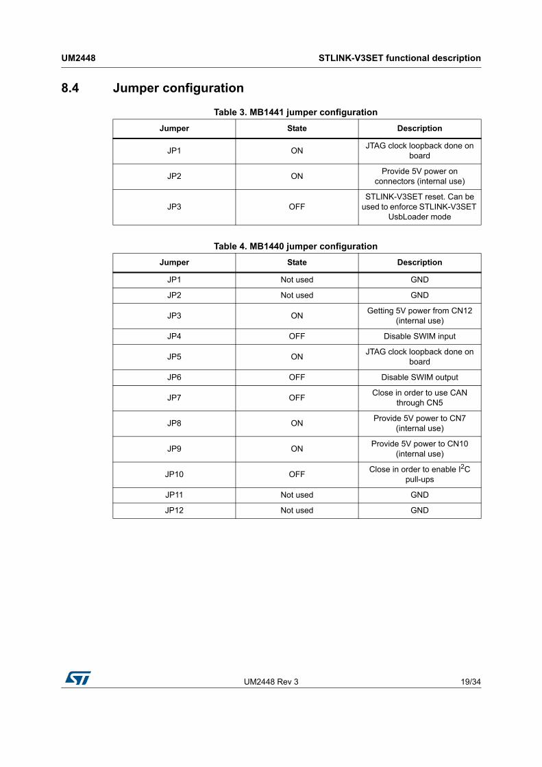
8.4 Jumper configuration
Table 3. MB1441 jumper configuration
Jumper State Description
JP1 ONJTAG clock loopback done on
board
JP2 ONProvide 5V power on
connectors (internal use)
JP3 OFFSTLINK-V3SET reset. Can be
used to enforce STLINK-V3SET UsbLoader mode
Table 4. MB1440 jumper configuration
Jumper State Description
JP1 Not used GND
JP2 Not used GND
JP3 ONGetting 5V power from CN12
(internal use)
JP4 OFF Disable SWIM input
JP5 ONJTAG clock loopback done on
board
JP6 OFF Disable SWIM output
JP7 OFFClose in order to use CAN
through CN5
JP8 ONProvide 5V power to CN7
(internal use)
JP9 ONProvide 5V power to CN10
(internal use)
JP10 OFFClose in order to enable I2C
pull-ups
JP11 Not used GND
JP12 Not used GND
Board connectors UM2448
20/34 UM2448 Rev 3
9 Board connectors
11 user connectors are implemented on the STLINK-V3SET product and are described in this paragraph:
• 2 user connectors are available on the MB1441 board:
– CN1: STDC14 (STM32 JTAG/SWD and VCP)
– CN5: USB Micro-B (connection to the host)
• 9 user connectors are available on the MB1440 board:
– CN1: STDC14 (STM32 JTAG/SWD and VCP)
– CN2: Legacy Arm 20-pin JTAG/SWD IDC connector
– CN3: VCP
– CN4: SWIM
– CN5: bridge CAN
– CN6: SWD
– CN7, CN8, CN9: bridge
Other connectors are reserved for internal use and are not described here.
9.1 Connectors on MB1441 board
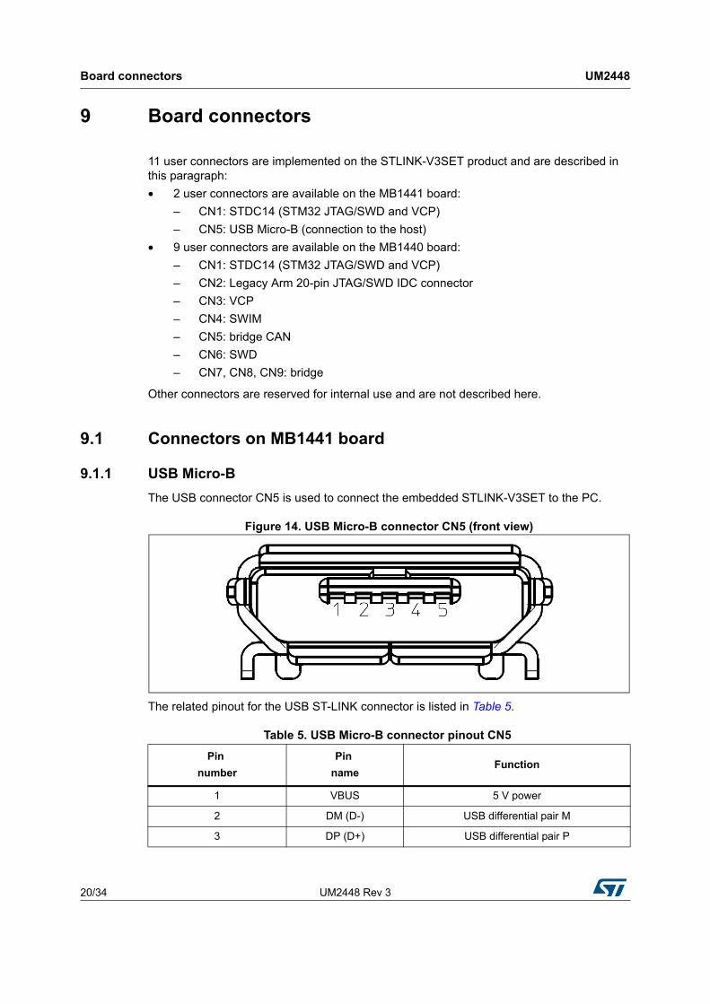
9.1.1 USB Micro-B
The USB connector CN5 is used to connect the embedded STLINK-V3SET to the PC.
Figure 14. USB Micro-B connector CN5 (front view)
The related pinout for the USB ST-LINK connector is listed in Table 5.
Table 5. USB Micro-B connector pinout CN5
Pin
number
Pin
nameFunction
1 VBUS 5 V power
2 DM (D-) USB differential pair M
3 DP (D+) USB differential pair P

UM2448 Rev 3 21/34
UM2448 Board connectors
33
9.1.2 STDC14 (STM32 JTAG/SWD and VCP)
The STDC14 CN1 connector allows the connection to an STM32 target by means of the JTAG or SWD protocol, respecting (from pin 3 to pin 12) the ARM10 pinout (Arm Cortex debug connector). But it also advantageously provides two UART signals for the Virtual COM port. The related pinout for the STDC14 connector is listed in Table 6.
The used connector is SAMTEC FTSH-107-01-L-DV-K-A.
9.2 Connectors on MB1440 board
9.2.1 STDC14 (STM32 JTAG/SWD and VCP)
The STDC14 CN1 connector on MB1440 replicates the STDC14 CN1 connector from the MB1441 board. Refer to Section 9.1.2 for details.
9.2.2 Legacy Arm 20-pin JTAG/SWD IDC connector
The CN2 connector allows the connection to an STM32 target in the JTAG or SWD mode. Its pinout is listed in Table 7. It is compatible with the pinout of ST-LINK/V2.
4 ID -
5 GND GND
Table 5. USB Micro-B connector pinout CN5 (continued)
Pin
number
Pin
nameFunction
Table 6. STDC14 connector pinout CN1
Pin No. Description Pin No. Description
1 Reserved(1)
1. Do not connect on target.
2 Reserved(1)
3 T_VCC(2)
2. Input for STLINK-V3SET.
4 T_JTMS/T_SWDIO
5 GND 6 T_JCLK/T_SWCLK
7 GND 8 T_JTDO/T_SWO(3)
3. SWO is optional, required only for Serial Wire Viewer (SWV) trace.
9 T_JRCLK(4)/NC(5)
4. Optional loopback of T_JCLK on the target side, required if loopback removed on the STLINK-V3SET side.
5. NC means not required for the SWD connection.
10 T_JTDI/NC(5)
11 GNDDetect(6)
6. Connect to GND on target, may be used by STLINK-V3SET for detection of connection.
12 T_NRST
13 T_VCP_RX(7)
7. Output for STLINK-V3SET
14 T_VCP_TX(2)

Board connectors UM2448
22/34 UM2448 Rev 3
9.2.3 Virtual COM port connector
The CN3 connector allows the connection of a target UART for Virtual COM port function. The debug connection (through JTAG/SWD or SWIM) is not required at the same time. However, a GND connection between STLINK-V3SET and target is required and must be ensured in some other way in case no debug cable is plugged. The related pinout for the VCP connector is listed in Table 8.
9.2.4 SWIM connector
The CN4 connector allows the connection to an STM8 SWIM target. The related pinout for the SWIM connector is listed in Table 9.
Table 7. Legacy Arm 20-pin JTAG/SWD IDC connector CN2
Pin number Description Pin number Description
1 T_VCC(1)
1. Input for STLINK-V3SET.
2 NC
3 NC 4 GND(2)
2. At least one of these pins must be connected to the ground on the target side for correct behavior (connecting all is recommended for noise reduction on the ribbon).
5 T_JTDI/NC(3)
3. NC means not required for the SWD connection.
6 GND(2)
7 T_JTMS/T_SWDIO 8 GND(2)
9 T_JCLK/T_SWCLK 10 GND(2)
11 T_JRCLK(4)/NC(3)
4. Optional loopback of T_JCLK on the target side, required if loopback removed on the STLINK-V3SET side.
12 GND(2)
13 T_JTDO/T_SWO(5)
5. SWO is optional, required only for Serial Wire Viewer (SWV) trace.
14 GND(2)
15 T_NRST 16 GND(2)
17 NC 18 GND(2)
19 NC 20 GND(2)
Table 8. Virtual COM port connector CN3
Pin number Description Pin number Description
1 T_VCP_TX(1)
1. Input for STLINK-V3SET. Must be connected to UART_TX on target.
2 T_VCP_RX(2)
2. Output for STLINK-V3SET. Must be connected to UART_RX on target.
Table 9. SWIM connector CN4
Pin number Description
1 T_VCC(1)
2 SWIM_DATA

UM2448 Rev 3 23/34
UM2448 Board connectors
33
9.2.5 CAN connector
The CN5 connector allows the connection to a CAN target without a CAN transceiver. The related pinout for this connector is listed in Table 10.
9.2.6 SWD connector
The CN6 connector allows the connection to an STM32 target in SWD mode through wires. It is not recommended for high performance. The related pinout for this connector is listed in Table 11.
9.2.7 UART bridge connector
Some bridge functions are provided on a 2x5-pin connector with 1.27 mm pitch CN7. The related pinout is listed in Table 12.
3 GND
4 T_NRST
1. Input for STLINK-V3SET.
Table 9. SWIM connector CN4 (continued)
Pin number Description
Table 10. CAN connector CN5
Pin number Description
1 T_CAN_VCC(1)
1. Input for STLINK-V3SET.
2 T_CAN_TX
3 T_CAN_RX
Table 11. SWD (wires) connector CN6
Pin number Description
1 T_VCC(1)
1. Input for STLINK-V3SET.
2 T_SWCLK
3 GND
4 T_SWDIO
5 T_NRST
6 T_SWO(2)
2. Optional, required only for Serial Wire Viewer (SWV) trace.

Board connectors UM2448
24/34 UM2448 Rev 3
9.2.8 SPI bridge connector
Some bridge functions are provided on a 2x5-pin connector with 1.27 mm pitch CN8. The related pinout is listed in Table 13.
9.2.9 Bridge 20-pins connector
All bridge functions are provided on a 2x10-pin connector with a 2.0 mm pitch CN9. The related pinout is listed in Table 14.
Table 12. UART bridge connector CN7
Pin number Description Pin number Description
1 UART_CTS 2 I2C_SDA
3 UART_TX(1)
1. TX signals are outputs for STLINK-V3SET, inputs for the target.
4 CAN_TX(1)
5 UART_RX(2)
2. RX signals are inputs for STLINK-V3SET, outputs for the target.
6 CAN_RX(2)
7 UART_RTS 8 I2C_SCL
9 GND 10 Reserved(3)
3. Do not connect on the target.
Table 13. SPI bridge connector CN8
Pin number Description Pin number Description
1 SPI_NSS 2 Bridge_GPIO0
3 SPI_MOSI 4 Bridge_GPIO1
5 SPI_MISO 6 Bridge_GPIO2
7 SPI_SCK 8 Bridge_GPIO3
9 GND 10 Reserved(1)
1. Do not connect on the target.
Table 14. Bridge connector CN9
Pin number Description Pin number Description
1 SPI_NSS 11 Bridge_GPIO0
2 SPI_MOSI 12 Bridge_GPIO1
3 SPI_MISO 13 Bridge_GPIO2
4 SPI_SCK 14 Bridge_GPIO3
5 GND 15 Reserved(1)
6 Reserved(1) 16 GND
7 I2C_SCL 17 UART_RTS
8 CAN_RX(2) 18 UART_RX(2)
UM2448 Rev 3 25/34
UM2448 Board connectors
33
9 CAN_TX(3) 19 UART_TX(3)
10 I2C_SDA 20 UART_CTS
1. Do not connect on target.
2. RX signals are inputs for STLINK-V3SET, outputs for the target.
3. TX signals are outputs for STLINK-V3SET, inputs for the target.
Table 14. Bridge connector CN9 (continued)
Pin number Description Pin number Description
Flat ribbons UM2448
26/34 UM2448 Rev 3
10 Flat ribbons
The STLINK-V3SET provides three flat cables allowing the connection from the STDC14 output to:
• STDC14 connector (1.27 mm pitch) on target application: pinout detailed in Table 6. Reference Samtec FFSD-07-D-05.90-01-N-R.
• ARM10-compatible connector (1.27 mm pitch) on target application: pinout detailed in Table 15. Reference Samtec ASP-203799-02.
• ARM20-compatible connector (1.27 mm pitch) on target application: pinout detailed in Table 16. Reference Samtec ASP-203800-02.
Table 15. ARM10-compatible connector pinout (target side)
Pin No. Description Pin No. Description
1 T_VCC(1)
1. Input for STLINK-V3SET.
2 T_JTMS/T_SWDIO
3 GND 4 T_JCLK/T_SWCLK
5 GND 6 T_JTDO/T_SWO(2)
2. SWO is optional, required only for Serial Wire Viewer (SWV) trace.
7 T_JRCLK(3)/NC(4)
3. Optional loopback of T_JCLK on the target side, required if loopback removed on the STLINK-V3SET side.
4. NC means not required for the SWD connection.
8 T_JTDI/NC(4)
9 GNDDetect(5)
5. Connect to GND on target, may be used by STLINK-V3SET for detection of connection.
10 T_NRST
Table 16. ARM20-compatible connector pinout (target side)
Pin No. Description Pin No. Description
1 T_VCC(1)
1. Input for STLINK-V3SET.
2 T_JTMS/T_SWDIO
3 GND 4 T_JCLK/T_SWCLK
5 GND 6 T_JTDO/T_SWO(2)
2. SWO is optional, required only for Serial Wire Viewer (SWV) trace.
7 T_JRCLK(3)/NC(4)
3. Optional loopback of T_JCLK on the target side, required if loopback removed on the STLINK-V3SET side.
4. NC means not required for the SWD connection.
8 T_JTDI/NC(4)
9 GNDDetect(5) 10 T_NRST
11 NC 12 NC
13 NC 14 NC
15 NC 16 NC
17 NC 18 NC
19 NC 20 NC
UM2448 Rev 3 27/34
UM2448 Flat ribbons
33
5. Connect to GND on target, may be used by STLINK-V3SET for detection of connection.
Mechanical information UM2448
28/34 UM2448 Rev 3
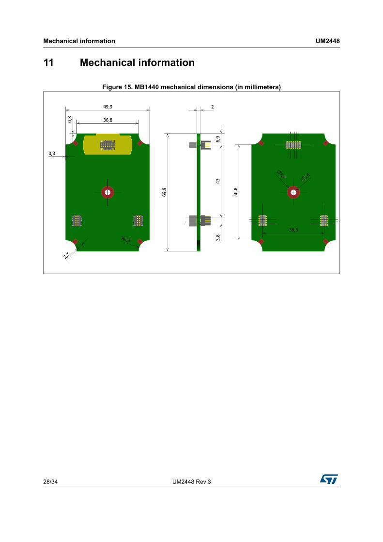
11 Mechanical information
Figure 15. MB1440 mechanical dimensions (in millimeters)

UM2448 Rev 3 29/34
UM2448 Software configuration
33
12 Software configuration
12.1 Supporting toolchains (not exhaustive)
Table 17 gives a list of the first toolchain version supporting the STLINK-V3SET product.
Note: Some of the very first toolchain versions supporting the STLINK-V3SET (in runtime) may not install the complete USB driver for STLINK-V3SET (especially the STLINK-V3SET bridge USB interface description may miss). In that case, either the user switches to a more recent version of the toolchain, or updates the ST-LINK driver from www.st.com (see Section 12.2).
12.2 Drivers and firmware upgrade
The STLINK-V3SET requires drivers to be installed on Windows and embeds a firmware which needs to be updated from time to time in order to benefit from new functionality or corrections. Refer to the Overview of ST-LINK derivatives technical note (TN1235) for details.
12.3 STLINK-V3SET frequency selection
The STLINK-V3SET can run internally at 3 different frequencies:
• high-performance frequency
• standard frequency, compromising between performance and consumption
• low-consumption frequency
By default, the STLINK-V3SET starts in high-performance frequency. It is the responsibility of the toolchain provider to propose or not the frequency selection at the user's level.
12.4 Mass storage interface
The STLINK-V3SET implements a virtual mass storage interface allowing the programming of an STM32 target flash memory with drag-and-drop action of a binary file from a file explorer. This ability requires the STLINK-V3SET to identify the connected target before
Table 17. Toolchain versions supporting STLINK-V3SET
Toolchain DescriptionMinimum Version
STM32CubeProgrammer ST Programming tool for ST microcontrollers 1.1.0
SW4STM32 Free IDE on Windows, Linux and macOS 2.4.0
IAR EWARM Third-party debugger for STM32 8.20
Keil MDK-ARM Third-party debugger for STM32 5.26
STVP ST Programming tool for ST microcontrollers 3.4.1
STVD ST Debugging tool for STM8 4.3.12
Software configuration UM2448
30/34 UM2448 Rev 3
enumerating on the USB host. As a consequence, this functionality is available only if the target is connected to the STLINK-V3SET before the STLINK-V3SET is plugged to the host. This functionality is not available for STM8 targets.
The ST-Link firmware programs the dropped binary file, at the beginning of the flash, only if it is detected as a valid STM32 application according to the following criteria:
• the reset vector points to an address in the target flash area,
• the stack pointer vector points to an address in any of the target RAM area.
If all these conditions are not respected, the binary file is not programmed and the target flash keeps its initial contents.
12.5 Bridge interface
The STLINK-V3SET implements a USB interface dedicated to bridging functions from USB to SPI/I2C/CAN/UART/GPIOs of the ST microcontroller target. This interface is firstly used by STM32CubeProgrammer in order to allow target programming through SPI/I2C/CAN bootloader.
A host software API is provided in order to extend the use cases.

UM2448 Rev 3 31/34
UM2448 Product STLINK-V3SET revision history and limitations
33
13 Product STLINK-V3SET revision history and limitations
Table 18 presents the history and limitations of the product.
Table 18. Product STLINK-V3SET revision history and limitations
Product finish good
Product version
Board VersionRevision details
Known
limitations
LKV3SET$AT1 1MB1440
MB1441
B-01
B-01- -

Federal Communications Commission (FCC) UM2448
32/34 UM2448 Rev 3
Appendix A Federal Communications Commission (FCC)
15.3 FCC Compliance Statement
15.3.1 Part 15.19
Part 15.19
This device complies with Part 15 of the FCC Rules. Operation is subject to the following two conditions: (1) this device may not cause harmful interference, and (2) this device must accept any interference received, including interference that may cause undesired operation.
Part 15.21
Any changes or modifications to this equipment not expressly approved by STMicroelectronics may cause harmful interference and void the user's authority to operate this equipment.
Part 15.105
This equipment has been tested and found to comply with the limits for a Class B digital device, pursuant to part 15 of the FCC Rules. These limits are designed to provide reasonable protection against harmful interference in a residential installation. This equipment generates uses and can radiate radio frequency energy and, if not installed and used in accordance with the instruction, may cause harmful interference to radio communications. However, there is no guarantee that interference will not occur in a particular installation. If this equipment does cause harmful interference to radio or television reception which can be determined by turning the equipment off and on, the user is encouraged to try to correct interference by one or more of the following measures:
• Reorient or relocate the receiving antenna.
• Increase the separation between the equipment and receiver.
• Connect the equipment into an outlet on circuit different from that to which the receiver is connected.
• Consult the dealer or an experienced radio/TV technician for help.
Note: Use a USB cable with length lower than 0.5m and added ferrite on the PC's side.
Other certifications
• EN 55032 (2012) / EN 55024 (2010)
• CFR 47, FCC Part 15, Subpart B (Class B Digital Device) and Industry Canada ICES-003 (Issue 6/2016)
• Electrical Safety qualification for CE marking: EN 60950-1 (2006+A11/2009+A1/2010+A12/2011+A2/2013)
• IEC 60650-1 (2005+A1/2009+A2/2013)
Note: The sample examined must be powered by a power supply unit or auxiliary equipment complying with standard EN 60950-1: 2006+A11/2009+A1/2010+A12/2011+A2/2013, and must be Safety Extra Low Voltage (SELV) with limited power capability.

UM2448 Rev 3 33/34
UM2448 Revision history
33
Revision history
Table 19. Document revision history
Date Revision Changes
6-Sep-2018 1 Initial release.
8-Feb-2019 2
Updated:
Section 8.3.4: Virtual COM port (VCP),
Section 8.3.5: Bridge functions,
Section 9.1.2: STDC14 (STM32 JTAG/SWD and VCP),
Section 9.2.3: Virtual COM port connector explaining how Virtual COM ports are connected to target.
20-Nov-2019 3
Added:
Second Virtual COM port chapter in Introduction, Figure 13 in Section 8.3.5 Bridge UART and
Figure 15 in the new section of Mechanical information.
UM2448
34/34 UM2448 Rev 3
IMPORTANT NOTICE – PLEASE READ CAREFULLY
STMicroelectronics NV and its subsidiaries (“ST”) reserve the right to make changes, corrections, enhancements, modifications, and improvements to ST products and/or to this document at any time without notice. Purchasers should obtain the latest relevant information on ST products before placing orders. ST products are sold pursuant to ST’s terms and conditions of sale in place at the time of order acknowledgement.
Purchasers are solely responsible for the choice, selection, and use of ST products and ST assumes no liability for application assistance or the design of Purchasers’ products.
No license, express or implied, to any intellectual property right is granted by ST herein.
Resale of ST products with provisions different from the information set forth herein shall void any warranty granted by ST for such product.
ST and the ST logo are trademarks of ST. For additional information about ST trademarks, please refer to www.st.com/trademarks. All other product or service names are the property of their respective owners.
Information in this document supersedes and replaces information previously supplied in any prior versions of this document.
© 2019 STMicroelectronics – All rights reserved
Copyright © 2022 FDOKUMEN