Smashing the Implementation Records of AES S-box
39
Smashing the Implementation Records of AES S-box Arash Reyhani-Masoleh, Mostafa Taha and Doaa Ashmawy Department of Electrical and Computer Engineering Western University, London, Ontario, Canada {areyhani,mtaha9,dashmawy}@uwo.ca Abstract. Canright S-box has been known as the most compact S-box design since its introduction back in CHES’05. Boyar-Peralta proposed logic-minimization heuristics that could reduce the gate count of Canright S-box from 120 gates to 113 gates, however synthesis results did not reflect much improvement. In CHES’15, Ueno et al. proposed an S-box that has a slightly higher area, but significantly faster than the previous designs, hence it was the most efficient (measured by area×delay) S-box implementation to date. In this paper, we propose two new designs for the AES S-box. One design has a smaller implementation area than both Canright and the 113-gate S-boxes. Hence, our first design is the smallest AES S-box to date, breaking the 13 years implementation record of Canright. The second design is faster and smaller than the Ueno S-box. Hence, our second design is both the fastest and the most efficient S-box design to date. While doing so, we also propose new logic- minimization heuristics that outperform the previous algorithms of Boyar-Peralta. Finally, we conduct an exhaustive evaluation of each and every block in the S-box circuit, using both structural and behavioral HDL modeling, to reach the optimum synergy between theoretical algorithms and technology-supported optimization tools. We show that involving the technology-supported CAD tools in the analysis results in several counter-intuitive results. Keywords: AES S-box · Composite/Tower Field Arithmetic · Logic-Minimization Heuristics 1 Introduction The Advanced Encryption Standard (AES) [FIP01] is a block cipher algorithm that was adopted by the National Institute of Standards and Technology (NIST) as a replacement of the Data Encryption Standard (DES) algorithm back in 2001. AES is essentially a subset of the Rijndael [DR02] algorithm which was the winner of a five-year competition among fifteen block cipher algorithms. AES works as a substitution-permutation network with four main operations: SubBytes, ShiftRows, MixColumns, and AddRoundKey. The SubBytes operation uses the Rijndael S-box which is the main non-linear substitution step of AES. The S-box depends on performing an inversion over the GF (2 8 ) field of AES, as defined over the irreducible polynomial (x 8 + x 4 + x 3 + x + 1), followed by an affine transformation and addition with a constant. The S-box circuit can be implemented using look-up tables, or using field arithmetic. The focus of this paper is to implement the AES S-box circuit using field arithmetic. Satoh et al. proposed the first tower field inversion using polynomial basis over GF (((2 2 ) 2 ) 2 )[SMTM01]. This means that an input element from the AES field in GF (2 8 ) is first converted to two elements in polynomial basis (PB) over GF (((2 2 ) 2 ) 2 ), where Licensed under Creative Commons License CC-BY 4.0. IACR Transactions on Cryptographic Hardware and Embedded Systems ISSN 2569-2925, Vol. 2018, No. 2, pp. 298–336 DOI:10.13154/tches.v2018.i2.298-336
-
Upload
khangminh22 -
Category
Documents
-
view
1 -
download
0
Transcript of Smashing the Implementation Records of AES S-box

Smashing the Implementation Recordsof AES S-box
Arash Reyhani-Masoleh, Mostafa Taha and Doaa Ashmawy
Department of Electrical and Computer EngineeringWestern University, London, Ontario, Canada
{areyhani,mtaha9,dashmawy}@uwo.ca
Abstract. Canright S-box has been known as the most compact S-box design since itsintroduction back in CHES’05. Boyar-Peralta proposed logic-minimization heuristicsthat could reduce the gate count of Canright S-box from 120 gates to 113 gates,however synthesis results did not reflect much improvement. In CHES’15, Ueno etal. proposed an S-box that has a slightly higher area, but significantly faster thanthe previous designs, hence it was the most efficient (measured by area×delay) S-boximplementation to date. In this paper, we propose two new designs for the AESS-box. One design has a smaller implementation area than both Canright and the113-gate S-boxes. Hence, our first design is the smallest AES S-box to date, breakingthe 13 years implementation record of Canright. The second design is faster andsmaller than the Ueno S-box. Hence, our second design is both the fastest andthe most efficient S-box design to date. While doing so, we also propose new logic-minimization heuristics that outperform the previous algorithms of Boyar-Peralta.Finally, we conduct an exhaustive evaluation of each and every block in the S-boxcircuit, using both structural and behavioral HDL modeling, to reach the optimumsynergy between theoretical algorithms and technology-supported optimization tools.We show that involving the technology-supported CAD tools in the analysis resultsin several counter-intuitive results.Keywords: AES S-box · Composite/Tower Field Arithmetic · Logic-MinimizationHeuristics
1 IntroductionThe Advanced Encryption Standard (AES) [FIP01] is a block cipher algorithm that wasadopted by the National Institute of Standards and Technology (NIST) as a replacementof the Data Encryption Standard (DES) algorithm back in 2001. AES is essentially asubset of the Rijndael [DR02] algorithm which was the winner of a five-year competitionamong fifteen block cipher algorithms. AES works as a substitution-permutation networkwith four main operations: SubBytes, ShiftRows, MixColumns, and AddRoundKey. TheSubBytes operation uses the Rijndael S-box which is the main non-linear substitution stepof AES.
The S-box depends on performing an inversion over the GF (28) field of AES, as definedover the irreducible polynomial (x8 +x4 +x3 +x+ 1), followed by an affine transformationand addition with a constant. The S-box circuit can be implemented using look-up tables,or using field arithmetic. The focus of this paper is to implement the AES S-box circuitusing field arithmetic.
Satoh et al. proposed the first tower field inversion using polynomial basis overGF (((22)2)2) [SMTM01]. This means that an input element from the AES field in GF (28)is first converted to two elements in polynomial basis (PB) over GF (((22)2)2), where
Licensed under Creative Commons License CC-BY 4.0.IACR Transactions on Cryptographic Hardware and Embedded Systems ISSN 2569-2925,Vol. 2018, No. 2, pp. 298–336DOI:10.13154/tches.v2018.i2.298-336

Arash Reyhani-Masoleh, Mostafa Taha and Doaa Ashmawy 299
the actual inversion happens, then the result is converted back to the AES field GF (28).Canright implemented tower field inversion using normal basis, instead of polynomialbasis [Can05b]. In Addition, he conducted an exhaustive search through all the subfieldrepresentations (a total of 432 fields) to reduce the overall implementation area. Sincethen, the research community has proposed many S-box circuits targeting lower-area,lower-delay, and/or higher efficiency (measured by area×delay) than Canright S-box.
In the track of lightweight S-boxes, Boyar, Peralta, along with others proposed severallogic-minimization heuristics to reduce the gate count of Canright S-box [BP10, BMP13,VSP17]. Here, they did not explore substantially different subfields, but they focused onreducing the number of gates that are needed to implement the Canright circuit itself.They proposed a reduction in the gate count of the S-box circuit from 120 gates in Canrightcircuit to 115 gates in [BP10, BMP13], to 114 gates in [VSP17], and to 113 gates in [Boy16].This 113-gate design, which was recently used by the CHES’17 ‘bit-sliding’ paper [JMPS17],is the currently smallest design, as expressed in terms of gate count.
The design of Canright S-box did not target fast application [Can05b]. Hence, thetrack of high-speed/higher-efficiency S-boxes received more research focus. [RDJ+01,JKL10, NNT+10, NNI12, UHS+15] are some papers that fall nicely in this latter category.Boyar et al. also proposed low-depth circuits for Canright S-box using delay-controlledlogic-minimization heuristics [BP12, BFP17]. It is worth mentioning that the CHES’15design by Ueno et al. [UHS+15] is the currently fastest and most-efficient S-box design, tothe best of our knowledge.
Canright also proposed a combined S-box/inverse S-box architecture, where one slightlybigger circuit can be used to compute the S-box output for the AES encryption-pathor the inverse S-box output for the AES decryption-path. This line of research receivedlittle research attention, except for [FWR05, JKL10, AH13] where no significant improve-ments in the area or delay were proposed. Recently, Reyhani-Masoleh et al. proposed acombined S-box/inverse S-box architecture over the tower field architecture of Canright(i.e., GF (((22)2)2)) while using different irreducible polynomials constructing the towerfields than Canright, and hence redesigning the corresponding internal blocks [RTA18].The proposed architecture in [RTA18] has a lower space and time complexities than theCanright combined S-box/inverse S-box scheme. Note that, in this paper, we use thecomposite field architecture over GF ((24)2) not the tower field over GF (((22)2)2).
The current trend in designing S-box circuits separates between the theoretical analysisand the technology-supported CAD tools. In other words, the common design goal oftheoretical analysis is to reduce the gate-count and/or the circuit-depth, both expressed inindistinctive number of gates, neglecting the fact that logic gates have different implemen-tation area/delay. In addition, theoretical analysis ignores the availability of compoundgates in almost any technology library (e.g., the OR-AND-Invert gate), which may performbetter in a given circuit. This separation led to many pitfalls as we explain below.
While testing the supposedly most compact S-box circuit (the 113-gate S-box in [Boy16]),we found that the actual implementation area is, in fact, higher than the original Canrightdesign, as we detail in Table 12. This was not readily obvious as Canright providedonly behavioral code of the combined S-box/inverse S-box core. We used the equationsto write an S-box-only core, in structural modeling, supported by the space complexityprovided in the report [Can05a] (also in Table 10), and the circuit was indeed smaller thanthe 113-gate circuit in [Boy16]. The reason for this counter-intuitive result is that theoptimization goal of Boyar-Peralta is to minimize the multiplicative complexity, expressedas the number of GF (2) multiplication operations in the circuit. Then, they directlygenerated the circuit using the most-commonly used gate for GF (2) multiplication; theAND gate. However, most of the current CMOS technology libraries (e.g., STM, TSMCand NanGate) implement an AND gate as a NAND followed by a NOT gate. Hence, ANDgates require higher implementation area and longer delay than the NAND gates that were

300 Smashing the Implementation Records of AES S-box
used in the original circuit by Canright. Therefore, the improvement brought by reducingthe number of gates was lost by using more expensive (in terms of area and delay) gates.In other words, logic gates should not be treated equally in comparing different circuits.
This pitfall was also introduced in the CHES’15 S-box design by Ueno et al. [UHS+15](and used in the CHES’16 paper [UMHA16]), and by the low-depth S-box circuits in [BP12]and [BFP17], where AND gates were extensively used throughout the circuit instead ofthe more efficient NAND gates.
Note that the typical use of CAD tools cannot solve this problem as the logic-minimization algorithms implemented within the CAD tool are lacking what is available inresearch. Hence, although the CAD tools will use more efficient gates, the overall circuitmay require a much higher number of gates. In Sec. 8.1, we improve the 113-gate S-boxof [Boy16] to use NAND gates instead of AND gates, resulting in the first S-box circuit tohave an actual lower implementation area than the one proposed by Canright (not just thegate count), breaking a 13-years implementation record. We also improve the CHES’15S-box [UHS+15] and the low-depth circuits of [BP12, BFP17].
In order to avoid the aforementioned pitfall, we follow a unique design approachthroughout this paper. We use all the available logic-minimization methods, supportedwith Boolean algebra, Karnough maps and De Morgan’s laws to derive optimum circuits foreach block of the S-box circuit. Then, we invoke the CAD tools with behavioral modeling,under different optimization goals and different levels of circuit-segmentation, to investigateif the CAD tools can bring any smaller and/or faster circuits. At the end, we hand-pick thebest circuits in each block of the S-box under the two design criteria (lightweight and fast).While doing so, we also propose several improvements to the underlying logic-minimizationalgorithms.
As a result, we propose two new S-box circuits. Our first S-box circuit achieves animplementation area that is smaller than Canright S-box, the 113-gate S-box, and ourown improved version of these circuits. This lightweight circuit sets a new record for theimplementation area of the AES S-box. Our second circuit achieves higher-speed and higher-efficiency than the CHES’15 design [UHS+15], the low-depth circuits of [BP12, BFP17],and our improved versions of [BP12, BFP17]. Our fast circuit has a very similar delay tothe improved version of [UHS+15] (as proposed in this paper), while having a much higherefficiency.
The rest of the paper is organized as follows. Sec. 2 reviews some mathematicalbackground about multiplicative inversion using composite field arithmetics. Sec. 3introduces the overall architecture of the proposed S-box designs. The following twosections provide details on the underlying blocks within the S-box circuit. The input andoutput transformation blocks are discussed in Sec. 4, along with the new logic-minimizationheuristics. The design blocks of the composite field inversion (exponentiation, subfieldinversion, and multipliers) are discussed in Sec. 5. Other plausible design options that weconsidered, but did not lead to better results, are discussed in Sec. 6. Further optimizationbrought by the technology-supported CAD tools are discussed in Sec. 7. The hardwareresults of our designs are introduced in Sec. 8. In this section, we also propose improvementsto the previous contributions and comparison against our designs. We conclude the paperin Sec. 9.
2 PreliminariesIn this section, we briefly discuss the preliminaries regarding the used finite fields. Specifi-cally, we talk about different representations used in this paper, namely the polynomialbasis (PB) representation used in the binary field GF (28) and the normal basis (NB)representation in the composite field GF ((24)2). Let us assume that the input to theS-box is g, where g is an element in GF (28) generated by the irreducible polynomial

Arash Reyhani-Masoleh, Mostafa Taha and Doaa Ashmawy 301
q(x) = x8 + x4 + x3 + x+ 1. Let α be a root of q(x), then g = (g7, · · · , g1, g0) ∈ GF (28)is represented in the PB representation as g =
∑7i=0 giα
i, gi ∈ GF (2), 0 ≤ i ≤ 7, where gi
is the coordinates of g ∈ GF (28). For convenience, these coordinates will be denoted invector notation as g = [g7, · · · , g1, g0]tr, where tr denotes the transposition.
2.1 S-box ComputationLet f = (f7, · · · , f1, f0) ∈ GF (28) be the multiplicative inverse (or inverse in short)of the non-zero S-box input, i.e., f × g = 1, where g 6= 0. Then, the first step inthe S-box computation is to find the inverse f = g−1 for g 6= 0. For g = 0, f = 0. Lets = (s7, · · · , s1, s0) ∈ GF (28) be the S-box output. Then s = [s7, · · · , s1, s0]tr = Mf⊕h,i.e.,
s =
s7s6s5s4s3s2s1s0
=
1 1 1 1 1 0 0 00 1 1 1 1 1 0 00 0 1 1 1 1 1 00 0 0 1 1 1 1 11 0 0 0 1 1 1 11 1 0 0 0 1 1 11 1 1 0 0 0 1 11 1 1 1 0 0 0 1
f7f6f5f4f3f2f1f0
⊕
01100011
, (1)
where M is an affine transformation, h is a constant, and ⊕ is the modulo 2 addition(XOR).
2.2 Composite Field Inverse in Normal BasisThe implementation of AES S-boxes using composite fields reduces the chip area for theS-box computation. Two types of composite fields, namely GF (((22)2)2) and GF ((24)2)are typically used. In this paper, we use the composite field GF ((24)2) which is referred toas the composite field. We also refer to the GF (((22)2)2) field as the tower field in orderto distinguish it from the composite field GF ((24)2) used in this paper.
In the proposed scheme, we convert the elements to an isomorphic composite fieldGF ((24)2). The irreducible polynomial over GF (24), namely
p(y) = y2 + µy + ν = (y + γ)(y + γ16), (2)
is used to construct the composite field. In (2), γ is its root and the subfield elementsµ, ν ∈ GF (24) should be chosen so that this polynomial is irreducible over GF (24).Then, {γ, γ16} is the normal basis and every element g in GF (28) can be mapped to itscomposite field representation over GF (24) as g = Aγ +Bγ16, where A = (a0a1a2a3) andB = (b0b1b2b3) are subfield elements in GF (24) and ai and bi are their binary coordinates,respectively. In this paper, the subfield GF (24) is generated using the irreducible all-one-polynomial (AOP) with degree four, i.e.,
r(t) = t4 + t3 + t2 + t+ 1. (3)
Let β be a root of r(t), i.e., r(β) = 0. Then, we use the type-I optimal normal basis(ONB-I) {β, β2, β22
, β23} to represent field elements and their efficient computations overGF (24) [RH03]. Then, any field element A = (a0a1a2a3) ∈ GF (24) can be represented asA = a0β + a1β
2 + a2β22 + a3β
23 .The inverse of g = Aγ + Bγ16 in the composite field GF ((24)2) can be written
as [IT88], [Paa94], g−1 = (gr)−1gr−1, where r = 24×2−124−1 = 17. Then, g−1 = (g× g16)−1g16

302 Smashing the Implementation Records of AES S-box
4
4
5
4 4
5
Subfield Inverter
A
B
D E
W
Z
2
1
Figure 1: The architecture for GF((24)2) inversion using the NB representation at the
inputs and the redundant normal basis (RNB) representation at the outputs.
can be computed as
g−1 = [(Aγ +Bγ16)(Bγ +Aγ16)]−1(Bγ +Aγ16)= [AB(γ + γ16)2 + (A+B)2γγ16]−1(Bγ +Aγ16)= EBγ + EAγ16 = Wγ + Zγ16,
(4)
whereE = D−1 = [g17]−1 = [AB(γ + γ16)2 + (A+B)2γγ16]−1, (5)
W = EB ∈ GF (24) and Z = EA ∈ GF (24). Since γ and γ16 are roots of (2), one canobtain γ + γ16 = µ and γγ16 = ν. Thus, D = g17 ∈ GF (24) in (5) is simplified to
D = ABµ2 + (A+B)2ν. (6)
For simplicity and low complexity implementations, we choose µ = 1 ∈ GF (24) andthen (2) and (6) would respectively become
p(y) = y2 + y + ν = (y + γ)(y + γ16), (7)
andD = AB + (A+B)2ν. (8)
Figure 1 shows an architecture to implement (8) and (4). Note that the underlyingarithmetic operations in Figure 1, i.e., an addition, a squaring, three multiplicationsand multiplication by the constant ν (scaling), are implemented over subfield GF (24).In [Can05b, Can05a], Canright used the tower field GF ((22)2) and chose µ = 1 for thenormal basis scheme. Then, the same architecture as shown in Figure 1 was derived usinga similar approach.
2.3 Subfield MultiplierIn this paper, we use type-I optimal normal basis (ONB-I) multiplication scheme proposedin [RH03] over GF (2m) for m = 4. A number of generic multiplication schemes areproposed in [RH03]. Specifically, we use equation (36) and the corresponding Algorithm 3from [RH03] for the multiplication over GF (24) generated by the AOP.
Lemma 1. [RH03] Let A = (a0a1a2a3) ∈ GF (24) and B = (b0b1b2b3) ∈ GF (24) berepresented in the ONB-I {β, β2, β22
, β23}. Then, the coordinates of their multiplication,

Arash Reyhani-Masoleh, Mostafa Taha and Doaa Ashmawy 303
Subfield Inverter
NAND-XOR
NAND-XOR
10
5
5
10
6
6
8 20
4
6
4
Input Transformation
4 4
ExponentiationComputation
6XOR
10 8
Output Transformation
Output Multipliers
8(2 )GF
inT20g
4 2((2 ) )GF
jkA
A
B
jkB
17g
4(2 )GF 4(2 )GF
, jkA A
, jkB B 4 2((2 ) )GF
outT
8(2 )GF
jkE10fD E
W
Z
g s
4 2((2 ) ) GF Inversion
Figure 2: The proposed S-box architecture.
i.e., C = AB =∑3
i=0 ciβ2i + c4 ∈ GF (24), represented in the redundant normal basis
(RNB) {β, β2, β22, β23
, 1}, can be calculated as follows:
c0 = a0b0 ⊕ a12b12c1 = a1b1 ⊕ a23b23c2 = a2b2 ⊕ a30b30c3 = a3b3 ⊕ a01b01c4 = a02b02 ⊕ a13b13,
(9)
where ajk = aj ⊕ ak and bjk = bj ⊕ bk for 0 ≤ j, k ≤ 3, and j 6= k.
We use this multiplier for the two output multipliers and the one at the beginning ofthe GF
((24)2) inversion in Figure 1.
3 Proposed AES S-box ArchitectureThe overall architecture of the proposed S-box circuits is highlighted in Figure 2. The inputand output transformation blocks are responsible for converting elements between theAES binary field GF (28) and the corresponding elements in the composite field GF ((24)2).The input transformation block accepts an 8-bit element g from the GF (28) field, andgenerates two 4-bit field elements A and B, and the mod-2 addition between every twobits in each of the two elements of A and B, i.e., Ajk and Bjk, where Ajk is a set thatcontains aj ⊕ ak, and Bjk contains bj ⊕ bk, both for 0 ≤ j, k ≤ 3, and j 6= k. The outputtransformation block accepts the result of the two subfield multipliers; W and Z (5 bitseach, following (9)), and generates the corresponding element s, i.e., the S-box output, inthe AES GF (28) field. More details about generating, optimizing, and implementing thetransformation blocks, targeting lightweight and fast applications, are discussed in Sec. 4.
The composite field inversion is composed of three sub-blocks; the exponentiation block,the subfield inverter, and the output multipliers. The exponentiation block is responsiblefor computing D = g17 as expressed in (8). The subfield inverter accepts g17 and generatesE = (g17)−1. The output multipliers perform the multiplication between (g17)−1 and g16
to represent the output in the redundant normal basis (RNB). The exact circuits that weuse in the implementations of each of these blocks are introduced in Sec. 5.
4 Input and Output TransformationsThe conversion between corresponding elements in two different field representations isrealized by a binary transformation matrix. We denote the matrix that is used to convert

304 Smashing the Implementation Records of AES S-box
from GF (28) to GF((24)2) as X−1, and the matrix that is used to convert in the other
way around, after its product with M, as MX, where M is the affine transformation in theS-box. We use the same notation that was used by Canright [Can05b] for less confusion.
The mapping realized by the transformation matrices should preserve additive, as wellas, multiplicative isomorphisms. In other words, addition (or multiplication) between twoelements in one field should be equivalent to mapping the two elements to the new field,performing the addition (or multiplication) under the laws of that new field, and mappingthe result back to the original field.
In this section, we briefly review how to generate these matrices, along with theexisting logic-minimization algorithms which are used to minimize the number of logicgates in their implementations. Thereafter, we highlight possible improvements in theexisting logic-minimization algorithms and propose new ones. We conclude this sectionwith lightweight and fast circuits for the selected input and the corresponding outputtransformation matrices.
4.1 Generating Transformation MatricesA generator φ, as the name implies, can be used to generate all the non-zero field elementsby raising it to a positive integer power φi, i ∈ [0, n−2], where n is the size of the field. Letφ1 be a generator in the GF (28) field of AES, and φ2 be a generator in the new GF ((24)2)field that we need to use. An input transformation matrix works if it can map all theelements φi
1, i ∈ [0, 28 − 2] in GF (28) to φi2, i ∈ [0, 28 − 2] in GF
((24)2). We select φ1
to be φ1 = 00000011 = (03)h [Can05b]. However, in order to select φ2, we need first tospecify ν ∈ GF (24) in (7) and (8), which affects the multiplication rule under this field.
ν is a 4-bit field element in GF (24) chosen so that p(y) = y2 + y + ν is irreducible overGF (24). Among the 16 possible combinations of ν, only 8 field elements namely ν ∈ {β, β2,β22 , β23 , 1+β, 1+β2, 1+β22 , 1+β23} can be used. Representing these 8 field elements inthe NB, one can obtain ν ∈ {(1000), (0100), (0010), (0001), (0111), (1011), (1101), (1110)}.Other values cannot be used as the polynomial p(y) = y2 + y + ν over GF (24) will not beirreducible. Each value of ν results in a different, but still isomorphic field that we can use.
Each of these fields has several generators. Any generator can be used to build atransformation matrix that preserves the additive homomorphism. However, in order topreserve the multiplicative homomorphism, the selected generator must also be a rootof the GF (28) irreducible polynomial q(x) = x8 + x4 + x3 + x + 1, as evaluated underthe arithmetic of the composite field GF
((24)2) [Paa94, RDJ+01]. Any generator that
preserves additive and multiplicative homomorphisms can be used to build a transformationmatrix between the AES GF (28) field and the composite field GF ((24)2).
Once such a generator (φ2) is found, the transformation matrix X−1 should fulfill
φi2 = X−1 × φi
1, i ∈ [0, 254].
After the input transformation matrix is computed, the output transformation matrixcan be found by switching the roles of φ1 and φ2 in the equations above, or by computingthe inverse of the input matrix.
Note that if φ2 is found, its conjugate elements φ2k
2 , k ∈ [1, 7] can also be used to buildother plausible transformation matrices. However, under the composite field arithmetic, ifσ = σhγ
16 +σlγ, then σ16 = σlγ16 +σhγ, where the high part is simply exchanged with the
lower part. Hence, the higher and lower four rows of the transformation matrices generatedusing φ16
2 will be identical to the lower and higher four rows of matrices generated usingφ2, respectively. This means that the circuits used to implement these two cases will beidentical, only the output notations will be different. Therefore, whenever a valid generatoris found, we study its input and output transformation matrices along with the matricesof the first three conjugate generators φ2k
2 , k ∈ [1, 3]. Hence, there are a total of 8 (values

Arash Reyhani-Masoleh, Mostafa Taha and Doaa Ashmawy 305
of ν) ×4 (generators per field) = 32 unique transformation matrices that could be used.Then, logic-minimization algorithms should be used to compare the hardware cost in termsof number of XOR gates of these 32 cases in order to select the smallest one.
4.2 Generating Extended Transformation MatricesInstead of trying to solve the original 8× 8 matrices, we follow the route used by Boyarand Peralta [BP10] and add some linear equations from the composite field inverter circuitinto the input and output transformation matrices. This gives more options to considerfor the logic-minimization algorithm and improves the overall design. However, insteadof collecting the linear gates from the implemented circuit, as used by [BP10], we selectthe candidate linear equations at the mathematical level. This allows us to run thelogic-minimization algorithm over the extended matrices of all the 32 considered cases,without having to design the inner circuit at different values of ν.
Since we use the multiplication formulations presented in Lemma 1, one can add thelinear equations for the computation of Ajk = {a01, a02, a03, a12, a13, a23}, and Bjk ={b01, b02, b03, b12, b13, b23} into the input transformation matrix X−1, resulting in what wedenote as the Tin matrix. Hence, we include 12 extra signals in the logic-minimizationproblem to compute Ajk and Bjk. This is an interesting choice as the Ajk and Bjk signalsare also used for the output multipliers, as detailed in Sec. 5.3. Other plausible choices arediscussed in Sec. 6.2 and Sec. 6.3.
Note that the generic mathematical formulations and the corresponding S-box archi-tecture to generate these 20 bits directly at the input transformation matrix are proposedfor the first time in this paper.
In other words, the Tin of interest computes the 20 bits of:
g20 = [a0a1a2a3b0b1b2b3a01a02a03a12a13a23b01b02b03b12b13b23]tr
from the S-box input vector g = [g7, · · · , g1, g0]tr as follows
g20 = Tin × g, (10)
where Tin is a 20× 8 binary input transformation matrix whose entries are either 0 or 1depending on the chosen composite field. In fact, the first 8 rows of Tin consists of X−1.Let us denote the first and the last 4 rows of X−1 as atr
i and btri , 0 ≤ i ≤ 3, respectively.
The rows of X−1 generate the coordinates of A and B as ai = atri g and bi = btr
i g,respectively. The next 12 rows of Tin generate aij = ai ⊕ aj = (atr
i ⊕ atrj )g = atr
ij g andbij = bi ⊕ bj = (btr
i ⊕ btrj )g = btr
ij g.Therefore, one can write Tin as
Tin =
X−1
atrij
btrij
for 0 ≤ i, j ≤ 3, i 6= j. (11)
Similarly, at the output, instead of trying to solve the original 8×8 output transformationmatrix MX, we include the equations that are required to convert from the RNB back tothe NB (converting the 5 bits of (9) back to 4 bits) into MX, resulting in what we denoteas the Tout matrix. Hence, the output of the S-box s is
s = Tout × f10 ⊕ h, (12)
where f10 = [w0w1w2w3w4z0z1z2z3z4]tr is the output of composite field inversion, repre-sented in the RNB and h = [01100011]tr as presented in (1).
Here, we are interested in the logic-minimization of
Tout = MX×T1, (13)

306 Smashing the Implementation Records of AES S-box
where T1 is the 8 × 10 matrix that converts from the RNB representations of W =∑3i=0 wiβ
2i + w4 and Z =∑3
i=0 ziβ2i + z4 at the outputs of the GF ((24)2) inverter in
Figure 2 back to the non-redundant NB representations, i.e.,
w0 ⊕ w4w1 ⊕ w4w2 ⊕ w4w3 ⊕ w4z0 ⊕ z4z1 ⊕ z4z2 ⊕ z4z3 ⊕ z4
= T1× f10 =
1 0 0 0 1 0 0 0 0 00 1 0 0 1 0 0 0 0 00 0 1 0 1 0 0 0 0 00 0 0 1 1 0 0 0 0 00 0 0 0 0 1 0 0 0 10 0 0 0 0 0 1 0 0 10 0 0 0 0 0 0 1 0 10 0 0 0 0 0 0 0 1 1
×
w0w1w2w3w4z0z1z2z3z4
. (14)
MX = M ×X is the 8 × 8 output transformation matrix, in which M is the S-boxaffine transformation as presented in (1) and X is the inverse of the input transformationmatrix X−1.
Tout is an 8× 10 binary matrix whose entries are either 0 or 1 based on the chosen ν.The next subsection reviews some of the known logic-minimization algorithms that
could be used to implement these transformation matrices.
4.3 Logic-Minimization AlgorithmsThe problem of finding the smallest number of gates that is required to implement atransformation matrix is known as the Shortest Linear Program (SLP) problem. TheSLP problem is defined as: Given a set of linear target equations E over a specific fieldF, find the shortest linear program to compute E. Our interest is to find the shortestlinear program that can compute A = Tr×B, where A and B are elements in two differentisomorphic fields and Tr is a generic transformation matrix. This problem is known to beNP-hard [BMP08, BMP13], and the best solution could only be found by an exhaustivesearch over all possible circuits, which quickly becomes infeasible at large input matrices.
4.3.1 Previous Work
Paar proposed a heuristic that works by iteratively selecting the XOR gate which is themost common in the target equations [Paa94]. The matrix is then appended by addingone column that represents this gate, and the target equations are updated accordingly.This gate-selection and matrix-updating continues until there is a single ‘1’ in each row ofthe matrix.
Canright used an exhaustive search over all possible solutions [Can05b], as the targetmatrices were relatively small (8× 8). In order to manage this time-consuming search, hesearched within a small subset of the tower fields that he studied (only 27 cases out ofthe 432 fields). The smallest circuit that was found required 13 XOR gates at the inputmatrix X−1 and 11 XOR gates at the output matrix MX of the AES S-box.
Boyar and Peralta showed that the algorithms used by both Canright and Paar arecancellation-free, where the selected gates must always result in an output with a Hammingweight that is the addition of the Hamming weights of the inputs [BP10]. Hence, inthese solutions, XOR gates are never used to cancel-out common terms. This meansthat the exhaustive search conducted by Canright did not, in principle, exhaust all theactually possible solutions. Hence, they proposed a new heuristic algorithm that is notcancellation-free. We denote this algorithm as the Normal-BP heuristic, referring to theauthor names. More details about this algorithm is discussed in the next clause.

Arash Reyhani-Masoleh, Mostafa Taha and Doaa Ashmawy 307
Using the Normal-BP heuristic, Boyar and Peralta did not find any smaller imple-mentation for the matrices used by Canright. As a work around, and being supportedby fast searching algorithms, they included all the linear equations in the inner circuitof Canright S-box (parts of the tower field inversion circuit) that directly followed theinput matrix X−1 and those that proceeded the output matrix MX into the input andoutput transformation matrices, respectively. The new extended-input matrix became22 × 8 and the new extended-output matrix became 8 × 18. These new matrices arecomputationally intractable for the exhaustive search algorithms, and interesting targetsfor the fast heuristic-based algorithms. The extended-input matrix directly computes 22equations at a cost of 23 XOR gates. For comparison, the original Canright circuit wouldneed 27 gates to solve these equations (13 for the 8 × 8 input matrix X−1 followed by14 extra gates to solve the 14 extra equations). Similarly, the extended-output matrixrequired 30 XOR gates.
Visconti et al. proposed a tweaked algorithm that sometimes works better for densematrices [VSP17]. It depends on computing the common path of the target matrix usingits boolean complement, which has a lower density, before applying the regular Normal-BPheuristic algorithm.
4.3.2 Normal-BP [BP10]
Here, we review the Normal-BP heuristic before proposing several improvements. Normal-BP heuristic makes use of a distance function δ, which computes the number of XORoperations that are required to reach from a known set of signals (called the ‘base’ S) toan output target (one row in the generic Tr matrix). The function δ is computed usingexhaustive search within all signals of the base S. The algorithm maintains a vector Distof the distance δ from the known base S to each of the output equations (each row of theTr matrix). Assuming the size of Tr matrix is r × c, the number of input signals is c,while the number of target equations is r which is equivalent to the initial size of Dist.
In the beginning, the base set S includes only the input signals, Si, i ∈ [0, c− 1], whereSi is one input signal in the base S. The Dist vector is initialized to the Hamming weightof each row minus one, which is indeed the required number of gates if there was no sharingof gates. Sharing here means that one gate is used for generating two or more differentequations. Then, in each iteration, the algorithm prepares the candidate next gate byXORing every two signals Si and Sj from the known base S, with i, j ∈ [0, c − 1] andi 6= j. One of these gates is selected such that if it was added to the base, the new basewould minimize the sum of Dist. If there is a tie between two or more candidate gates,the program selects the gate that maximizes the Euclidean norm of Dist (
√∑Dist2i for
i ∈ [0, rd − 1]), with rd being the size of Dist. If there is a further tie after this selectioncriteria, the program just selects the first gate in the set of ties. The authors studieddifferent tie breaking methodologies including: Norm-largest (maximizing the square ofthe Euclidean norm minus the largest distance), Norm-diff (maximizing the square of theEuclidean norm minus the difference of the largest two distances) and Random selection(try three gates and select the best one). They reported that the tie-breaking methodologiesperform fairly similar.
The algorithm makes use of ‘pre-emptive’ choices, which allows directly picking newgates as follows: if any two signals in the base Si, Sj are such that Si ⊕ Sj is a target rowin Tr, then the program directly picks this gate as the new base element.
In the next clause, we propose an improved logic-minimization algorithm that we denoteas Improved-BP. We also propose two new logic-minimization methodologies denoted asShortest-Dist-First and Focused-Search algorithms.

308 Smashing the Implementation Records of AES S-box
4.3.3 Improved-BP (Proposed)
Our first algorithm (Improved-BP) improves the Normal-BP algorithm in three aspects:1- In each iteration, Normal-BP adds a candidate gate to the base S and evaluates
the new distance Dist, regardless if this new gate leads to ‘pre-emptive’ gates in the nextiteration or not. In fact, if adding a candidate gate would result in ‘pre-emptive’ gates,these gates will be automatically added in the next iteration. Hence, whenever a candidategate leads to ‘pre-emptive’ gates, these gates should also be added to the base S (alongwith the candidate gate) before evaluating the Dist vector.
In the proposed Improved-BP algorithm, after adding a candidate gate, we check theDist entries. If any of the Dist entries has been changed from 2 to 1, which means thatone target will be found using a ‘pre-emptive’ gate in the next iteration, we add all thetargets that will be resolved with ‘pre-emptive’ gates to the base S and re-evaluate theDist vector.
2- The tie-breaking methodologies in the Normal-BP algorithm may not lead to thebest results. In fact, the authors reported that the random selection (best of three randomtrials) slightly outperforms all the other tie-breaking methodologies. Meanwhile, it iscomputationally intensive to exhaustively test all the ties in different algorithm-runs. Inthe proposed Improved-BP algorithm, if there is a tie in one iteration, we test the resultsof all the ties in the next iteration and keep only the best sequence of gates. In this way,we perform only one algorithm-run while monitoring only the best set of gates.
3- We implemented the Improved-BP algorithm while monitoring the delay of eachsignal in the base S. In the beginning, the input signals in the base S are associatedwith a delay vector, denoted Delay, of all zeros. Adding a new gate Si ⊕ Sj to the base,its delay is evaluated as max(Delayi, Delayj) + 1, where Delayi is the delay of Si. Thisimprovement helps in two situations. First, the delay of each target is readily available atthe output, which is an important factor in designing the following circuits, as we detail inSec. 5.1. Second, we can find the best circuit at a specified maximum delay. Assumingthat the maximum allowed delay is Dmax, if the delay of any signal in the base S reachesDmax, this signal gets removed from the base and no longer used to build any furthertarget. For this delay-controlled option to work properly, we also modified the δ functionto report the distance, as a number of gates, only if the delay associated with adding thesegates together will not exceed the Dmax. The delay associated with the addition of severalsignals is evaluated using the binary tree method where, iteratively, the input signals aresorted and the two signals with the least delays are added together. Otherwise, the δfunction returns infinity, reporting that there is no path to the target function under thespecified maximum delay.
4.3.4 Shortest-Dist-First (Proposed)
The Shortest-Dist-First algorithm works similarly to the Improved-BP, however, themethodology of selecting the next gate is different. The Shortest-Dist-First algorithmselects the gate that maximizes the number Z = sum(Disti = j) at i ∈ [0, rd − 1], with rd
being the size of Dist, for the smallest value of j > 0 such that Z > 0.In other words, the algorithm selects the gate that results in as many ‘pre-emptive’
gates (with Disti = 1 for i ∈ [0, rd − 1]) as possible. If no such gate was found (Z = 0 atj = 1), the algorithm searches for the gate that results in as many Disti = 2 (at j = 2) aspossible, and so on. Hence, the algorithm promotes the gates that lead to the shortestdistance.
4.3.5 Focused-Search (Proposed)
This algorithm is similar to the Shortest-Dist-First algorithm, however, it tests all thegates that result in Z = sum(Disti = j), with i ∈ [0, rd − 1], with rd being the size of

Arash Reyhani-Masoleh, Mostafa Taha and Doaa Ashmawy 309
Dist, for the smallest value of j > 0, being greater than zero. In other words, it tests allthe gates that lead to Disti = 1 for i ∈ [0, rd − 1]. Only if no gates fulfills this criteria, thealgorithm tests all the gates that lead to Disti = 2, and so on.
Another difference is that since this algorithm tests all the candidate gates anyway, wedo not re-evaluate the Dist vector whenever ‘pre-emptive’ gates are found.
This algorithm is the slowest of all. It slightly moves toward being an exhaustive search.
4.4 Searching for Optimum Transformation Matrices
For each of the 32 unique transformation matrices, we applied the logic minimizationalgorithms in order to find the set of matrices that results in the minimum overall gate-count.We solved for the X−1, Tin, and Tout. The results are highlighted in Table 1.
Table 1 serves two main goals. First, it helps in comparing the proposed logic-minimization algorithms against the current ones. Second, it helps in selecting the bestset of transformation matrices.
Comparing logic-minimization algorithms: First, the table examines the proposed logic-minimization algorithms against the current state-of-the-art (Normal-BP [BP10]) in 96different test matrices, ranging in size between 8×8, 20×8 and 8×10. The improvement inanalyzing the 8× 8 X−1 matrices were observable in 8 out of the 32 cases. Our algorithmsoutperformed the previous ones by one and sometimes two gates (7% and 13% respectively).Similarly, analyzing the 20× 8 Tin matrices were improved in 12 cases. In addition, the8× 10 Tout matrices were improved in 28 cases, by sometimes over 3 gates (15%).
The MATLAB R© computation time in seconds, as measured on a workstation with IntelXeon CPU (6 cores at 3.2 GHz) equipped with 16 GB of RAM, is shown in Table 2. TheImproved-BP and Shortest-Dist-First algorithms require higher computation time than theNormal-BP algorithm because they test all the gates involved in a tie. Counter-intuitively,the Focused-Search algorithm, which is supposed to be the slowest algorithm, shows thefastest performance with the 20× 8 matrices, with a slim standard deviation. The reasonis that the search space for the 20× 8 is not large, while the algorithm is relieved fromre-evaluating the Dist vector after adding the ‘pre-emptive’ gates.
The optimum transformation matrices: Table 1 shows that the matrix Tin, which isused in the input transformation block of Figure 2, always results in smaller circuits, ascompared to the number of gates required for X−1 plus 12 gates. It is noted that these 12gates are required to compute the 12 extra equations of Ajk and Bjk in Figure 2 if theywere removed from the Tin. Solving Tin was better by 3 to 5 gates.
Table 1 also shows that four of out of 32 possibilities require the optimum valueof 35 XOR gates for both the input (19 XOR gates) and the output (16 XOR gates)transformation blocks. Among the four optimum results, we chose the one correspondingto ν = β = (1000). This particular selection will further reduce the complexity of theexponentiation computation block as explained in the next section.
4.5 The Used Transformation Matrices
Throughout the rest of this paper, we adopt ν = β = (1000) and Gen = (1 + β22)γ + (1 +β2)γ16 = (11011011) = (DB)h so that the input (X−1) and output (MX) transformationmatrices are as follows.

310 Smashing the Implementation Records of AES S-box
Table 1: Logic minimization of the input matrix X−1, the extended-input matrix Tin andthe extended-output Tout transformation matrices.
ν= Gen #1 Gen #2 Gen #3 Gen #4
1000
aGen = (03)h Gen = (6F)h Gen = (6A)h Gen = (DB)hb13/13/13/-
e3913/13/13/-
3614/14/14/-
3911/11/11/-
35c22/21/21/- 20/20/20/20 21/21/21/- 19/19/19/19d19/18/18/- 16/16/16/16 19/19/18/- 19/17/17/16
0100
Gen = (06)h Gen = (74)h Gen = (5C)h Gen = (95)h
13/13/13/-39
13/13/13/-36
14/14/14/-39
11/11/11/-3522/21/21/- 20/20/20/20 21/21/21/- 19/19/19/19
19/18/18/- 16/16/16/16 19/19/18/- 19/17/17/16
0010
Gen = (03)h Gen = (B2)h Gen = (A6)h Gen = (CA)h
13/13/13/-39
13/13/13/-36
14/14/14/-39
11/11/11/-3522/21/21/- 20/20/20/20 21/21/21/- 19/19/19/19
19/18/18/- 16/16/16/16 19/19/18/- 19/17/17/16
0001
Gen = (06)h Gen = (CF)h Gen = (C5)h Gen = (B7)h
13/13/13/-39
13/13/13/-36
14/14/14/-39
11/11/11/-3522/21/21/- 20/20/20/20 21/21/21/- 19/19/19/19
19/18/18/- 16/16/16/16 19/19/18/- 19/17/17/16
0111
Gen = (12)h Gen = (7E)h Gen = (2E)h Gen = (9F)h
14/14/14/-39
13/13/13/-38
15/13/13/-39
14/14/13/-3622/22/22/- 22/21/21/- 21/21/21/- 21/20/20/20
19/18/17/- 18/18/17/- 19/19/18/- 18/17/16/16
1011
Gen = (17)h Gen = (CF)h Gen = (18)h Gen = (7B)h
15/13/13/-39
14/14/13/-36
14/14/14/-39
13/13/13/-3821/21/21/- 21/20/20/20 22/22/22/- 22/21/21/-
19/19/18/- 18/17/16/16 19/18/17/- 18/18/17/-
1101
Gen = (12)h Gen = (A3)h Gen = (E2)h Gen = (8E)h
14/14/14/-39
13/13/13/-38
15/13/13/-39
14/14/13/-3622/22/22/- 22/21/21/- 21/21/21/- 21/20/20/20
19/18/17/- 18/18/17/- 19/19/18/- 18/17/16/16
1110
Gen = (17)h Gen = (74)h Gen = (81)h Gen = (59)h
15/13/13/-39
14/14/13/-36
14/14/14/-39
13/13/13/-3821/21/21/- 21/20/20/20 22/22/22/- 22/21/21/-
19/19/18/- 18/17/16/16 19/18/17/- 18/18/17/-
Each cell contains the following:a- Gen = is the hexadecimal of the used generator.b- Gate-count of the input X−1 matrix,c- Gate-count of the extended input Tin matrix in Figure 2,d- Gate-count of the extended output Tout matrix in Figure 2,bcd are minimized using Normal-BP [BP10]/ Improved-BP (Proposed) / Shortest-Dist-First (Proposed) /Focused-Search (Proposed).e- The best overall gate count is found by adding the smaller gate-count of (X−1) + 12 or (Tin) to thegate-count of Tout.The best case is highlighted in bold. The result ‘-’ means that we did not attempt to solve this case.
Arash Reyhani-Masoleh, Mostafa Taha and Doaa Ashmawy 311
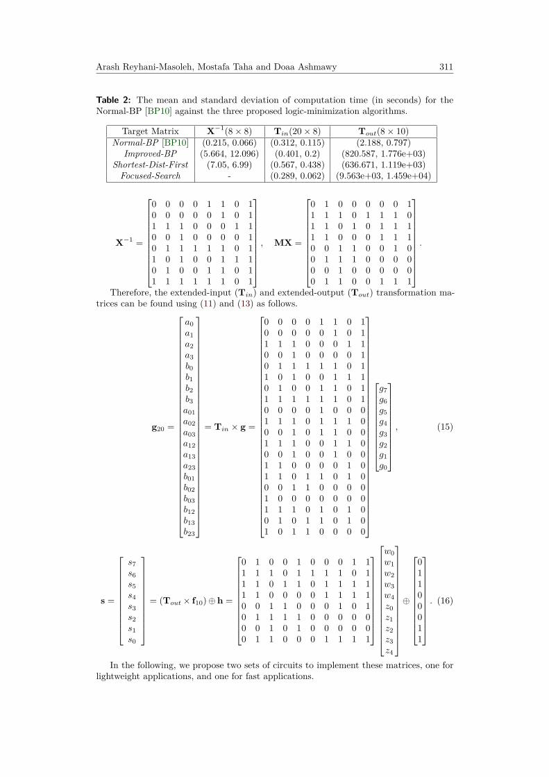
Table 2: The mean and standard deviation of computation time (in seconds) for theNormal-BP [BP10] against the three proposed logic-minimization algorithms.
Target Matrix X−1(8× 8) Tin(20× 8) Tout(8× 10)Normal-BP [BP10] (0.215, 0.066) (0.312, 0.115) (2.188, 0.797)
Improved-BP (5.664, 12.096) (0.401, 0.2) (820.587, 1.776e+03)Shortest-Dist-First (7.05, 6.99) (0.567, 0.438) (636.671, 1.119e+03)Focused-Search - (0.289, 0.062) (9.563e+03, 1.459e+04)
X−1 =
0 0 0 0 1 1 0 10 0 0 0 0 1 0 11 1 1 0 0 0 1 10 0 1 0 0 0 0 10 1 1 1 1 1 0 11 0 1 0 0 1 1 10 1 0 0 1 1 0 11 1 1 1 1 1 0 1
, MX =
0 1 0 0 0 0 0 11 1 1 0 1 1 1 01 1 0 1 0 1 1 11 1 0 0 0 1 1 10 0 1 1 0 0 1 00 1 1 1 0 0 0 00 0 1 0 0 0 0 00 1 1 0 0 1 1 1
.
Therefore, the extended-input (Tin) and extended-output (Tout) transformation ma-trices can be found using (11) and (13) as follows.
g20 =
a0a1a2a3b0b1b2b3a01a02a03a12a13a23b01b02b03b12b13b23
= Tin × g =
0 0 0 0 1 1 0 10 0 0 0 0 1 0 11 1 1 0 0 0 1 10 0 1 0 0 0 0 10 1 1 1 1 1 0 11 0 1 0 0 1 1 10 1 0 0 1 1 0 11 1 1 1 1 1 0 10 0 0 0 1 0 0 01 1 1 0 1 1 1 00 0 1 0 1 1 0 01 1 1 0 0 1 1 00 0 1 0 0 1 0 01 1 0 0 0 0 1 01 1 0 1 1 0 1 00 0 1 1 0 0 0 01 0 0 0 0 0 0 01 1 1 0 1 0 1 00 1 0 1 1 0 1 01 0 1 1 0 0 0 0
g7g6g5g4g3g2g1g0
, (15)
s =
s7s6s5s4s3s2s1s0
= (Tout × f10)⊕h =
0 1 0 0 1 0 0 0 1 11 1 1 0 1 1 1 1 0 11 1 0 1 1 0 1 1 1 11 1 0 0 0 0 1 1 1 10 0 1 1 0 0 0 1 0 10 1 1 1 1 0 0 0 0 00 0 1 0 1 0 0 0 0 00 1 1 0 0 0 1 1 1 1
w0w1w2w3w4z0z1z2z3z4
⊕
01100011
. (16)
In the following, we propose two sets of circuits to implement these matrices, one forlightweight applications, and one for fast applications.

312 Smashing the Implementation Records of AES S-box
4.6 Lightweight ImplementationsFor the lightweight implementations, our first goal is to minimize the implementationarea, expressed as the number of used XOR2 (2-input XOR) gates for the transformationmatrices. Whenever two circuits are equivalent in the area, we select the circuit thatresults in the lower overall delay.
The lightweight implementation of Tin in (15) for the input transformation block ispresented in Table 3(a). These formulations require 19 XOR2 gates (denoted by ⊕ in thetable). The propagation delay, in terms of number of the XOR2 gate delay (DX), for allsignals are presented (in parentheses). Therefore, the longest delay from the inputs to theoutputs and hence the propagation delay of the input transformation block is 5DX .
The lightweight implementation of the Tout in (16) for the output transformationblock requires 16 gates with a delay of 6 gates (6DX) as presented in Table 3(b). Thecomputations presented in Table 3(b) perform the operation of (Tout× f10)⊕h altogether,where XNOR2 gates are sometimes incorporated instead of XOR2 gates to include theeffect of adding the constant h. XNOR2 gates are denoted by � in the table. Note thatthe use of XNOR2 gates does not exactly align with the non-zero entries of h, as theoutputs si are reused in other equations. We coded these equations in VHDL and verifiedthe output with Modelsim R© against the legitimate output of the AES S-box.
Table 3: Lightweight implementation of transformations in Figure 2: (a) Computation ofg20 = Tin×g in (15) for the input transformation. (b) Computation of s = (Tout×f10)⊕hin (16) for the output transformation.
a0 = a1 ⊕ g3 (2DX) a1 = g2 ⊕ g0 (1DX) a2 = a3 ⊕ a23 (3DX)a3 = g5 ⊕ g0 (1DX) b0 = b02 ⊕ b2 (4DX) b1 = b2 ⊕ b12 (5DX)b2 = a0 ⊕ g6 (3DX) b3 = b2 ⊕ b23 (4DX) a01 = g3 (0DX)a02 = a03 ⊕ a23 (3DX) a03 = a13 ⊕ g3 (2DX) a12 = a13 ⊕ a23 (3DX)a13 = g5 ⊕ g2 (1DX) a23 = u0 ⊕ g1 (2DX) b01 = b02 ⊕ b12 (5DX)b02 = g5 ⊕ g4 (1DX) b03 = g7 (0DX) b12 = a02 ⊕ g2 (4DX)b13 = b23 ⊕ b12 (5DX) b23 = b02 ⊕ g7 (2DX) u0 = g7 ⊕ g6 (1DX)
(a)s7 = t1 ⊕ t2 (2DX) s6 = t7 ⊕ t6 (6DX) s5 = t0 � t6 (6DX)s4 = t6 � w2 (6DX) s3 = t4 ⊕ z3 (5DX) s2 = t0 � w1 (3DX)s1 = w2 � w4 (1DX) s0 = t5 ⊕ t3 (4DX) t0 = s1 ⊕ w3 (2DX)t1 = w1 ⊕ z4 (1DX) t2 = w4 ⊕ z3 (1DX) t3 = s7 ⊕ z2 (3DX)t4 = s2 ⊕ t3 (4DX) t5 = s1 ⊕ z1 (2DX) t6 = s0 ⊕ w0 (5DX)t7 = t2 ⊕ z0 (2DX)
(b)
4.7 Fast ImplementationsOur design goal for the fast implementations is to find a circuit with the smallest criticalpath delay. Note that the theoretically minimum critical path delay of the transformationmatrices can be known upfront by computing max(dlog2(HW (Tri))e), for i ∈ [0, r − 1]with HW denoting the Hamming weight function, and Tri is row number i of a generictransformation matrix (Tin or Tout), and r is the number of rows in the Tr matrix (r = 20for Tin and r = 8 for Tout). The theoretically minimum critical path delay of both Tin
and Tout is 3DX , as the maximum number of non-zero entries in Tin and Tout is 8.We used the proposed logic-minimization algorithms while setting the maximum allowed
delay Dmax to 3DX . Therefore, the target of the logic-minimization is to find a plausiblecircuit under this delay constraint.

Arash Reyhani-Masoleh, Mostafa Taha and Doaa Ashmawy 313
The corresponding formulations for fast implementation are presented in Table 4. Forthe input transformation block Tin, the presented implementation in Table 4(a) requires24 XOR2 gates with a propagation delay of 3 XOR2 gates (as required). Table 4(b) showsthe formulations to compute the output transformation block Tout in (16) using 21 gatesat a delay of 3DX (as required).
Similarly, some XOR2 gates have been replaced with XNOR2 gates in order to incor-porate the effect of adding the constant h. The correctness of these formulations werechecked by our codes as will be explained later.
Table 4: Fast implementation of transformations in Figure 2: (a) Computation of g20 =Tin × g in (15) for the input transformation. (b) Computation of s = (Tout × f10)⊕ h in(16) for the output transformation.
a0 = a1 ⊕ g3 (2DX) a1 = g2 ⊕ g0 (1DX) a2 = a3 ⊕ a23 (3DX)a3 = g5 ⊕ g0 (1DX) b0 = u2 ⊕ u4 (3DX) b1 = a1 ⊕ u1 (3DX)b2 = a0 ⊕ g6 (3DX) b3 = u5 ⊕ u4 (3DX) a01 = g3 (0DX)a02 = a03 ⊕ a23 (3DX) a03 = a13 ⊕ g3 (2DX) a12 = a13 ⊕ a23 (3DX)a13 = g5 ⊕ g2 (1DX) a23 = u0 ⊕ g6 (2DX) b01 = u3 ⊕ u5 (3DX)b02 = g5 ⊕ g4 (1DX) b03 = g7 (0DX) b12 = u2 ⊕ u1 (3DX)b13 = u2 ⊕ u3 (2DX) b23 = b02 ⊕ g7 (2DX) u0 = g7 ⊕ g1 (1DX)u1 = u0 ⊕ g5 (2DX) u2 = g6 ⊕ g3 (1DX) u3 = g4 ⊕ g1 (1DX)u4 = a1 ⊕ b02 (2DX) u5 = u2 ⊕ g7 (2DX)
(a)s7 = t0 ⊕ t6 (2DX) s6 = t2 ⊕ t10 (3DX) s5 = s7 � t8 (3DX)s4 = t3 ⊕ t2 (3DX) s3 = t11 ⊕ t12 (2DX) s2 = s1 � t4 (2DX)s1 = w2 � w4 (1DX) s0 = t5 � t2 (3DX) t0 = w1 ⊕ z4 (1DX)t1 = z1 ⊕ z2 (1DX) t2 = t0 ⊕ t1 (2DX) t3 = w0 ⊕ z3 (1DX)t4 = w1 ⊕ w3 (1DX) t5 = w2 ⊕ z3 (1DX) t6 = w4 ⊕ z3 (1DX)t7 = w0 ⊕ w3 (1DX) t8 = t1 ⊕ t7 (2DX) t9 = w0 ⊕ z0 (1DX)t10 = s1 ⊕ t9 (2DX) t11 = w2 ⊕ w3 (1DX) t12 = z2 ⊕ z4 (1DX)
(b)
5 Proposed GF ((24)2) InversionThe GF ((24)2) inversion is the core operation of the proposed S-box, as shown in Figure 2.The proposed GF ((24)2) inversion consists of three main blocks, namely exponentiationcomputation, subfield inverter, and output multipliers. These are explained in this section.
5.1 Exponentiation ComputationBased on the proposed logic-minimization algorithms, we use ν = β = (1000) as discussedin Sec. 4.4. Thus, the exponentiation computation block in Figure 2 generates
D = g17 = AB + (A+B)2β. (17)
Let A =∑3
i=0 aiβ2i = (a0a1a2a3) ∈ GF (24) and B =
∑3i=0 biβ
2i = (b0b1b2b3) ∈ GF (24)be represented in the ONB-I {β, β2, β22
, β23}. Then,
(A+B)2β =3∑
i=0(ai−1 ⊕ bi−1)β2i+1. (18)

314 Smashing the Implementation Records of AES S-box
Since r(β) = 0 in (3), one can find β5 = 1 and so β3 = β23 , β9 = β22 which simplify (18)to
(A+B)2β = (a3 ⊕ b3)β2 + (a2 ⊕ b2)β22+ (a0 ⊕ b0)β23
+ (a1 ⊕ b1)× 1. (19)
Since 1 = (1111) ∈ GF (24), one can change the RNB representation of (A+B)2β in (19)to the corresponding NB as follows:
(A+B)2β = (a1 ⊕ b1)β + (a13 ⊕ b13)β2 + (a12 ⊕ b12)β22+ (a01 ⊕ b01)β23
. (20)
Substituting (20) and the coordinates of C = AB from Lemma 1 into (17), one obtains
D = d0β + d1β2 + d2β
22 + d3β23 = c4β + c4β
2 + c4β22 + c4β
23+(c0 ⊕ a1 ⊕ b1)︸ ︷︷ ︸
d̃0
β + (c1 ⊕ a13 ⊕ b13)︸ ︷︷ ︸d̃1
β2 + (c2 ⊕ a12 ⊕ b12)︸ ︷︷ ︸d̃2
β22 + (c3 ⊕ a01 ⊕ b01)︸ ︷︷ ︸d̃3
β23.
(21)Let us denote D̃ =
∑3i=0 d̃iβ
2i ∈ GF (24) such that D = D̃ + c4, where d̃i ∈ GF (2) for0 ≤ i ≤ 3, is defined in (21). From (21), one can obtain
di = c4 ⊕ d̃i, 0 ≤ i ≤ 3. (22)
To simplify d̃i for 0 ≤ i ≤ 3, one can substitute ci, 0 ≤ i ≤ 3, from (9) into (21) andsimplify them as follows:
d̃0 = (a0b0)⊕ (a12b12)⊕ a1 ⊕ b1d̃1 = (a1 ∨ b1)⊕ a3 ⊕ b3 ⊕ (a23b23)d̃2 = (a2 ∨ b2)⊕ a1 ⊕ b1 ⊕ (a03b03)d̃3 = (a3b3)⊕ (a01 ∨ b01).
(23)
For the simplification of d̃1 from (21) to (23), we use a13 ⊕ b13 = a1 ⊕ b1 ⊕ a3 ⊕ b3and then (a1b1 ⊕ a1 ⊕ b1) = (a1 ∨ b1), where ∨ represents an OR operation. Similarly, forthe simplification of d̃2 from (21) to (23), we use a12 ⊕ b12 = a2 ⊕ b2 ⊕ a1 ⊕ b1 and then(a2b2 ⊕ a2 ⊕ b2) = (a2 ∨ b2). Similar property, i.e., (a01b01 ⊕ a01 ⊕ b01) = (a01 ∨ b01), isused for d̃3.
Our goal is to minimize the chip area in the ASIC implementations. Therefore, weuse NAND and NOR gates instead of AND and OR gates, respectively. This is becauseNAND and NOR gates have lower chip area and delay as compared with AND and ORgates, respectively [WH15]. The coordinate c4 is needed in all four formulations for di,0 ≤ i ≤ 3, in (22) and so one can implement c4 using two NAND gates and one XOR gateas c4 = a02b02⊕ a13b13 = (a02b02)′⊕ (a13b13)′, and share it for the four di’s. As a result ofreplacing OR gates to NOR gates and AND gates to NAND gates, we may need to changeXOR gates to XNOR in order to keep the same function at the outputs. Therefore, thefollowing formulations can be obtained from c4 and (23)
d̃0 = (a1 � b1)⊕ (a0b0)′ � (a12b12)′d̃1 = (a1 ∨ b1)′ ⊕ (a3 � b3)� (a23b23)′d̃2 = (a1 � b1)⊕ (a2 ∨ b2)′ � (a03b03)′d̃3 = (a3b3)′ ⊕ (a01 ∨ b01)′c4 = (a02b02)′ ⊕ (a13b13)′,
(24)
where an XNOR operation of two inputs (XNOR2) is denoted by a1 � b1 = a1 ⊕ b1 ⊕ 1 =(a1 ⊕ b1)′. In (24), having two XNOR operations for d̃0, d̃1 and d̃2 do not change theirfunctions as x� y � z = x⊕ y ⊕ 1⊕ z ⊕ 1 = x⊕ y ⊕ z.
Note that each of the equations that generate d̃0, d̃1 and d̃2 consists of mod-2 additionsbetween three terms (using XOR and XNOR). The order of implementing these three

Arash Reyhani-Masoleh, Mostafa Taha and Doaa Ashmawy 315
1 1( 1)a b
(8 )XD0d
1d(8 )XD
(8 )XD2d
3d
(7 1 )X NANDD D
od
4c
1d
2d
3d
1a
1b
0a
0b
12a
12b
13a
13b
02a
02b
1a
1b
3a
3b
23a
23b
1 1( 1)a b
2a
2b
03a
03b
3a
3b
01b01a
(5 )XD
(2 )XD(4 )XD
(3 )XD(4 )XD
(1 )XD(5 )XD
(3 )XD(1 )XD
(1 )XD(5 )XD
(1 )XD(4 )XD
(2 )XD
(2 )XD
(3 )XD(3 )XD
(2 )XD
(0 )XD
(1 )XD
(4 )XD
(0 )XD
(5 )XD
(1 )XD1 1( 1)a b
0d
(6 1 )X NANDD D
0d
(6 1 )X NORD D
1d
(6 1 )X NORD D2d
(5 1 )X NORD D3d
4c
1d
2d
3d
1a
1b
0a
12a
0b
12b
(1 )XD(3 )XD
(2 )XD(3 )XD
(3 )XD(3 )XD
13a
13b
02a
02b
(1 )XD(2 )XD
(3 )XD(1 )XD
(1 )XD(3 )XD
(2 )XD(2 )XD
(1 )XD(3 )XD
1a
1b
23a
23b
3a
3b
1 1( 1)a b
2a
2b
03a
03b
(3 )XD(3 )XD
(2 )XD
(0 )XD
(1 )XD
(3 )XD
(0 )XD
(3 )XD
3b3a
01b01a
(a) (b)
Figure 3: The proposed exponentiation computation block for the S-box architecture.(a) For the proposed lightweight S-box implementation (b) For the proposed fast S-boximplementation. Note that the order of additions (XOR/XNOR) that generate d1 isdifferent between two circuits.
mod-2 additions affects the overall delay of the circuit. The proper order of additionsshould be selected based on the delay associated with the input terms, which eventuallydepends on the delay of the Tin block. Here, we use the delay associated with each signalof the Tin block, as detailed in Table 3 for the lightweight implementation and in Table 4for the fast implementation.
Therefore, we propose two implementations of the exponentiation computation block,as shown in Figure 3, one for the lightweight implementation highlighted in Figure 3(a)and one for the fast implementation highlighted in Figure 3(b). Both implementationshave the same space complexity. In each figure, we highlight the delay associated with allthe input and output signals in parentheses.
Figure 3(a) shows that the optimum circuit for the lightweight implementation generatesall the di output signals with a maximum total delay of 8DX , where DX is the delay ofone XOR2/XNOR2 gate. This result takes into account that the delay of XOR gate isslightly higher than the delay of a NAND gate. Similarly, Figure 3(b) shows that thehighest delay of the fast implementation is 6DX + 1DNOR, taking into account that thedelay of NOR gate is slightly higher than NAND gate.
Based on Figure 3 and equations (22) and (24), one can find the space and timecomplexities of the proposed exponentiation computation blocks as follows. Note that theXNOR gate that generates (a1 � b1) can be shared.
Proposition 1. The exponentiation computation block consists of 14 XOR2/XNOR2(2-input XOR/XNOR), 7 NAND2 (2-input NAND), and 3 NOR2 (2-input NOR) gateswith the critical path delay of 4DX , where DX is the delay of one XOR2/XNOR2 gate.This exponentiation block adds 3DX and 3DX + 1DNOR to the critical path delay of thelightweight and fast input transformation matrices, respectively, where DNOR is the delayof one NOR2 gate.

316 Smashing the Implementation Records of AES S-box
ie
3id
id
1id
2id
id
3id
2id
Figure 4: The proposed subfield inverter block over GF (24) to generate ei, 0 ≤ i ≤ 3, forE =
∑3i=0 eiβ
2i = D−1, where D =∑3
i=0 diβ2i and the additions in the input indices are
performed modulo 4. Note that d̃i, 0 ≤ i ≤ 3 are the signals from Figure 3 that generatedi = c4 + d̃i.
5.2 Subfield InverterA large number of multiplicative inverse architectures over binary fields are available inthe literature. In [WTS+85] and [Fen89], sequential architectures for computing inverseover GF (2m) are proposed. The inverse architectures proposed in those papers are costlyas they require a NB multiplier and compute the inverse operation in a number of clockcycles. On the other hands, for a fast computation operation, one can compute the inverseas a bit-parallel architecture in composite fields [Paa94]. In [Can05b, Can05a, NNT+10],efficient subfield inverter over tower fields GF ((22)2) are proposed. However, similar tothe schemes proposed in [UHS+15, NNI12], our inverter is over GF (24). The subfieldinverter schemes presented in [UHS+15, NNI12] use the RNB and the polynomial ringrepresentation (PRR) with 5-bit coordinates, whereas our inverter scheme uses the NB(with 4-bit coordinates).
The subfield inverter block of Figure 2 generates the inverse of its input D =(d0d1d2d3) =
∑3i=0 diβ
2i over GF (24). Let us denote E = D−1 ∈ GF (24) as the outputof this block. Let ei ∈ GF (2), be the ith, 0 ≤ i ≤ 3, binary coordinate of E representedwith respect to the ONB-I, i.e., E = (e0e1e2e3) =
∑3i=0 eiβ
2i
. Then, one can obtain ei asfollows.
Lemma 2.ei = di+1d
′i+2(di ⊕ di+3) ∨ di+2(d′i ∨ di+3), 0 ≤ i ≤ 3, (25)
where the additions in the indices are performed modulo 4.
The proof of Lemma 2 is provided in Appendix A.In order to reduce the delay of (25), we use (d̃i ⊕ d̃i+3) instead of (di ⊕ di+3) as
di⊕ di+3 = c4⊕ d̃i⊕ c4⊕ d̃i+3 = (d̃i⊕ d̃i+3). Also, in order to reduce the area and improvethe speed of the ASIC implementations of (25), we use NAND and NOR gates instead ofAND and OR gates, respectively. So, we use De Morgan’s law for (d′i ∨ di+3) = (did
′i+3)′
and change two levels of AND-OR to its equivalent NAND-NAND implementation. As aresult, we conclude the formulation presented in (25) to the following:
Corollary 1. Let D = (d0d1d2d3) =∑3
i=0 diβ2i be the input of the subfield inverter.
Then, the coordinates of the inverse output E = (e0e1e2e3) = D−1 can be found as
ei = ((di+1d′i+2(d̃i ⊕ d̃i+3))′((did
′i+3)′di+2)′)′, 0 ≤ i ≤ 3, (26)
where the additions in the indices are performed modulo 4.

Arash Reyhani-Masoleh, Mostafa Taha and Doaa Ashmawy 317
Based on the architecture shown in Figure 4 for one ei, the space and time complexitiesof the entire subfield inverter (ei, 0 ≤ i ≤ 3,) are as follows. Note that the four NOT gatescan be shared among the four ei outputs.
Proposition 2. The space complexity of the proposed subfield inverter block over GF (24)includes 12 NAND2, 4 NAND3, 4 XOR2 and 4 NOT gates, where NAND2, and NAND3are, respectively, a 2-input and a 3-input NAND gates and XOR2 is a 2-input XOR gate.The time complexity due to gates for the proposed subfield inverter is 3DND +DNT , whereDND and DNT are the delays of a NAND2 and a NOT gate, respectively.
5.3 Output MultipliersThe two output multipliers that are shown in Figure 1 generate W = EB ∈ GF (24) andZ = EA ∈ GF (24) (see (4)). The output of these multipliers are represented in theRNB {β, β2, β22
, β23, 1}, whereas their inputs A =
∑3i=0 aiβ
2i = (a0a1a2a3) ∈ GF (24),B =
∑3i=0 biβ
2i = (b0b1b2b3) ∈ GF (24), and E =∑3
i=0 eiβ2i = (e0e1e2e3) are represented
in the ONB-I {β, β2, β22, β23}. Let W = (w0w1w2w3w4) =
∑3i=0 wiβ
2i + w4 and Z =(z0z1z2z3z4) =
∑3i=0 ziβ
2i + z4 be the outputs of these multipliers. The formulations togenerate wi and zi can be obtained from (9). They can be realized using two levels ofNAND-XOR gates as follows.
w0 = (e0b0)′ ⊕ (e12b12)′w1 = (e1b1)′ ⊕ (e23b23)′w2 = (e2b2)′ ⊕ (e30b30)′w3 = (e3b3)′ ⊕ (e01b01)′w4 = (e02b02)′ ⊕ (e13b13)′,
(27)
z0 = (e0a0)′ ⊕ (e12a12)′z1 = (e1a1)′ ⊕ (e23a23)′z2 = (e2a2)′ ⊕ (e30a30)′z3 = (e3a3)′ ⊕ (e01a01)′z4 = (e02a02)′ ⊕ (e13a13)′,
(28)
where ejk = ej ⊕ ek for 0 ≤ j, k ≤ 3, j 6= k and E = (e0e1e2e3) is the shared input.Note that Ejk = {e01, e02, e03, e12, e13, e23} are shared between the two multipliers and aregenerated using six 2-input XOR gates, denoted as the 6XOR block in Figure 2. Thesesignals are used in (27) and (28) which are implemented by 10 NAND-XOR modules.These modules are shown by the two blocks of NAND-XOR in Figure 2 to implement (27)and (28). The details of the NAND-XOR blocks in Figure 2 are shown in Figure 5.
Based on the architecture shown in Figure 2 and Figure 5, the space and time com-plexities of the output multipliers are as follows.
Proposition 3. The output multipliers in Figure 2 consists of 16 XOR2 and 20 NAND2gates with longest propagation delay of DND + 2DX .
5.4 Complexity AnalysisThe space and time complexities of the input and output transformation blocks, alongwith all the blocks presented in Propositions 1, 2, and 3 are summarized in Table 5. Thistable also shows the space and time complexities of the GF ((24)2) inversion and the entireAES S-box architecture shown in Figure 2 for lightweight and fast implementations. Thecorresponding gate equivalent (GE) of all the blocks are also presented. GE is the chipareas in terms of an equivalent 2-input NAND gates. The provided GEs are based on 65 nmCMOS technology in which the areas of XOR2/XNOR2 gate=2 GEs, 2-input NAND gate

318 Smashing the Implementation Records of AES S-box
NAND-XOR
NAND-XOR
/i iw z
/i ib a
ie
1, 2 1, 2/i i i ib a
1, 2i ie
4 4/w z
1,3 1,3/b a
1,3e
0,2 0,2/b a
0,2e
Figure 5: The proposed output multipliers over GF (24) to generate wi/zi, 0 ≤ i ≤ 3, andw4/z4. Note that the additions in the input indices are performed modulo 4.
(NAND2)=1 GE, 3-input NAND gate (NAND3)=1.25 GEs, 2-input NOR gate (NOR2)=1GE, and a NOT gate=0.75 GEs.
Table 5: Space and time complexities for different blocks and the GF ((24)2) inversion of theentire proposed S-box architecture shown in Figure 2 (X=XOR2/XNOR2, ND=NAND2,N3=NAND3, NR=NOR2, NT=NOT, 1X= 2GEs, 1ND=1NR= 1GE, 1N3= 1.25GEs,1NT= 0.75GEs).
Block/ Space Complexity TimeTarget X ND N3 NR NT GE Complexity
Input Transformation BlockLightweight 19 38 5DX
Fast 24 48 3DX
GF ((24)2) InversionExp. Light. 14 7 3 38 4DX
Exp. Fast 14 7 3 38 3DX + 1DNR
Inverter 4 12 4 4 28 3DND + 1DNT
Multipliers 16 20 52 2DX + 1DND
Total Light. 34 39 4 3 4 118 6DX + 4DND + 1DNT
Total Fast 34 39 4 3 4 118 5DX + 4DND + 1DNT + 1DNR
Input Transformation Block cascaded with the GF ((24)2) InversionLightweight 53 39 4 3 4 156 10DX
1 + 4DND + 1DNT
Fast 58 39 4 3 4 166 8DX + 4DND + 1DNT + 1DNR
Output Transformation BlockLightweight 16 32 6DX
Fast 21 42 3DX
Total Complexity of Proposed S-box (Figure 2)Lightweight 69 39 4 3 4 188 16DX + 4DND + 1DNT
Fast 79 39 4 3 4 208 11DX + 4DND + 1DNT + 1DNR1 One DX can be saved by incorporating the delay of the input transformation block in selecting the orderof mod-2 additions within the exponentiation block.

Arash Reyhani-Masoleh, Mostafa Taha and Doaa Ashmawy 319
6 Our Investigations for the Best ChoicesWe highlight that the aforementioned schemes are proposed as a result of extensiveinvestigation considering many other design options. In this section, we discuss some ofthe design choices that we explored and how the proposed schemes were selected.
6.1 Different Bases and the Corresponding MultipliersThere are three multipliers that are used within the architecture of composite field inversion.Therefore, choosing an appropriate multiplier plays an important role in overall cost ofthe circuit. The three multipliers, as seen in Figure 1, process three subfield elements,namely A, B, and E as their inputs. In other words, each input field element activatestwo multipliers. Here, we are interested in pre-processing the input elements in a way thatcan minimize some of the internal circuits of the two activated multipliers. In other words,instead of minimizing the cost of individual multipliers, we try to minimize the combinedcost of the three multipliers.
Table 6 shows details of the multipliers used in a number of S-boxes. We derived thespace and time complexities of these multipliers based on the circuits and informationprovided in these papers. As shown in the table, the multipliers can be designed uponthree different types of bases; polynomial basis (PB), normal basis (NB) and mixed basis(MB), and are built using a set of AND/NAND and XOR/XNOR gates.
Table 6: Multipliers used in different AES S-boxes with their sharing capability betweendifferent multipliers (X=XOR, ND=NAND, AD=AND).
S-box Multiplier # inputs/ Space Time Sharing# outputs Complexity Complexity Inputs
Subfield GF ((22)2)Satoh et al. [SMTM01] PB [Paa96] 4× 4/4 21X+9AD 4DX +DAD bothCanright [Can05b] NB 4× 4/4 20X+9ND 4DX +DND both
Nogami et al. [NNT+10] MB 4× 4/4 21X+9AD 4DX +DAD bothSubfield GF (24)
Rudra et al. [RDJ+01] PB [Mas91] 4× 4/4 15X+16AD 3DX +DAD oneGueron et al. [GM16] PB 4× 4/4 15X+16ND 3DX +DND noneNekado et al.[NNI12] RNB 5× 5/5 25X+10AD 2DX +DAD bothUeno et al. [UHS+15] RNB [NNI12] 4× 5/5 21X+10AD 2DX +DAD both
This work NB [RH03] 4× 4/5 17X+10ND 2DX +DND both
Assume that the input E with coordinates of ej , 0 ≤ j ≤ 3, is connected to twomultipliers, generating the outputs AE and BE (see for example, the output multipliersin Figure 1). If the two inputs of each multiplier are first processed through a set ofAND/NAND gates, no gate sharing can happen between the multipliers. This is because,the set of gates in the first multiplier (with inputs A and E) will generate aiej , with0 ≤ i, j ≤ 3, while the set in the second multiplier (with inputs B and E) will generatebiej , with 0 ≤ i, j ≤ 3. It is clear that the signals in these two sets do not match, hence nosharing can happen. Such a multiplier was used in [RH04], [KS98], [RH02], [MO86], andrecently in [GM16] while preventing sub-expression sharing between the multipliers. Hence,although the hardware cost of an individual multiplier may be small, the combined cost ofthe three multipliers will be high. As a result, these multipliers are not good candidatesfor our objective.
The Mastrovito multiplier [Mas91], which is used in the scheme proposed by Rudra etal. [RDJ+01], uses a set of AND gates between the bits of one input and a set of XORgates between the bits of the other input. As mentioned in [RDJ+01], no optimization

320 Smashing the Implementation Records of AES S-box
has been performed in their scheme. However, sharing can only happen if the architectureuses the input connected to the set of XOR gates as the common input between the twomultipliers, i.e., E in the multipliers with outputs AE and BE. Therefore, no sharing inthe other inputs (A or B) can be used.
On the other hand, the maximum sharing can be utilized if each input is first processedthrough a set of XOR/XNOR gates between its bits, independently, as a pre-processingstep. For example, the set in the first multiplier (with inputs A and E) will generateai ⊕ aj , with 0 ≤ i, j ≤ 3, i 6= j, and ei ⊕ ej , with 0 ≤ i, j ≤ 3, i 6= j. The set in the secondmultiplier (with inputs B and E) will generate bi ⊕ bj , with 0 ≤ i, j ≤ 3, i 6= j, and ei ⊕ ej ,with 0 ≤ i, j ≤ 3, i 6= j. Here, the six gates ei ⊕ ej , with 0 ≤ i, j ≤ 3, i 6= j are common inthe two multipliers, and can be shared. Such multipliers are used in the schemes proposedby Canright [Can05a, Can05b] and Nogami et al. [NNT+10]. These multipliers are similarto the Karatsuba multiplier [KO63] and are good candidates in terms of sharing. However,using them results in a long delay which is not favorable for our fast objective.
In [NNI12], Nekado et al. presented a fast RNB multiplier with subexpresion sharingin both multiplier inputs. The multiplier uses the RNB representation for the ONE-I overGF (24) generated by the AOP. Both inputs and the output of this multiplier have 5 bits(denoted by 5×5/5 in Table 6). This multiplier requires 25 XOR2 and 10 AND2 gates withdelay of 2DX +DAD. Recently, Ueno et al. [UHS+15] used the RNB multiplier proposedin [NNI12] for the RNB multiplications, where one input has a 4-bit representation whilethe other input and the output are represented in the RNB with 5 bits (denoted by 4× 5/5in Table 6). This multiplier reduces the number of XOR gates to 21 with the same numberof 10 AND2 gates and the delay of 2DX +DAD.
In this paper, we use the NB multiplier proposed in [RH03] for the ONE-I over GF (24)generated by the AOP. Both inputs of this multiplier are represented in the NB, and wechose to represent the output in the 5-bit RNB representation. The original formulationsin [RH03] for this multiplier were based on AND-XOR implementations. However, weimproved this multiplier by using NAND gates instead of AND gates. This modificationimproves both the lightweight and fast implementations as the chip area and delay ofNAND gates are lower than those of AND gates. As seen from Table 6, the multiplierthat we use in this paper has the lowest gate count and the smallest delay available in theliterature to the best of our knowledge.
6.2 Different Input Transformation MatricesIn our proposed scheme for the lightweight S-box architecture (shown in Figure 2), theproposed input transformation matrix Tin is selected to be 20× 8 (see the input transfor-mation matrix Tin presented in (15)). We investigated additional choices for the inputtransformation matrices with a corresponding slight modification in the exponentiationblock in order to obtain smaller overall space/time complexity. In the following items, wedetail our investigations for different input transformation matrices in which 2, 3, and 4new rows are appended to the existing 20× 8 binary matrix Tin. Note that we alreadyconsidered the traditional 8× 8 binary input matrix in Table 1.
• An appended 22 × 8 input matrix: Since our exponentiation computation block(Figure 3) uses a1 ⊕ b1 and a3 ⊕ b3 as inputs, we considered moving the computationof one (or both) of these two formulations into the Tin matrix. The results of ourcode showed that we need an extra one gate (or respectively two gates) in the inputtransformation block. This means that no saving was obtained, while increasing thecomputation time of the logic-minimization algorithms.
• An appended 23 × 8 input matrix: One can derive another set of formulations forD = (A + B)2β + AB using (19) for (A + B)2β with the addition to C = AB

Arash Reyhani-Masoleh, Mostafa Taha and Doaa Ashmawy 321
presented in Lemma 1. The resultant new formulations for D require (a0 ⊕ b0),(a1 ⊕ b1) and (a3 ⊕ b3) in the exponentiation computation block. To consider this,we added 3 additional rows to compute (a0 ⊕ b0), (a1 ⊕ b1) and (a3 ⊕ b3) to the Tin
matrix. This added three more XOR gates to the space complexity and hence, noimprovement was found.
• An appended 24 × 8 input matrix: Similarly, using (20), we found another set offormulations for D in which (a1 ⊕ b1), (a13 ⊕ b13), (a12 ⊕ b12) and (a01 ⊕ b01) areused. Similarly, we added 4 new rows (in order to compute these signals) to theexisting Tin matrix and no improvement in terms of space complexity was obtained.
• A faster 20× 8 input matrix : We searched for a faster input transformation block toreduce its propagation delay from 3DX to 2DX . In fact, we searched for an inputtransformation matrix Tin with at most four 1s in all the 20 rows of the matrix andwe could not find any such a matrix.
6.3 Different Output Transformation MatricesSimilarly, we considered several other revised output transformation matrices with slightmodifications to the output multipliers in Figure 2. The content and the size of the existing8× 10 binary matrix Tout were revised. The size of the first output matrix was reducedto 8× 8, whereas the size of the second and the third output matrices were increased to8× 20 and 8× 10, respectively. These investigations are detailed as follows.
• A revised 8× 8 output matrix: The output subfield elements W = (w0w1w2w3w4)and Z = (z0z1z2z3z4) of the proposed S-box are represented in the 5-bit RNB ofW =
∑3i=0 wiβ
2i + w4 and Z =∑3
i=0 ziβ2i + z4. By adding 8 XOR gates at the
outputs of the GF ((24)2) inversion block, one can obtain the representation of theoutputs with respect to the NB asW =
∑3i=0(wi⊕w4)β2i and Z =
∑3i=0(zi⊕z4)β2i
using T1 in (14). Adding these 8 XOR gates to the result of optimizing the 8× 8output binary matrix MX, we found that our 8× 10 Tout = MXT1 has a smallerarea.
• A revised 8× 20 output matrix : The very last stage in the output multipliers beforegenerating W and Z consists of 10 XOR gates. We moved these gates to the outputtransformation matrix Tout so that the new output matrix has 20 columns (doublethe original one). The result of optimizing this matrix was worse than the 8× 10matrix while significantly increasing the computation time.
• A faster 8× 10 output matrix: The current output transformation matrix Tout in(16) has at most eight 1s in each row. Our current fast implementation of the outputtransformation block has 3DX and to make it faster, we have to find a matrix withat most four 1s in all rows. We searched for such a matrix across all composite fieldrepresentations and we could not find any matrix with this criteria.
6.4 Different Subfield InvertersIn addition to the subfield inverter that was selected in Subsection 5.2, we derived 11 otherequivalent functions using Boolean algebra and Karnough maps. In order to select the bestcircuits in the two design goals (area and speed), we coded all the 12 functions in VHDLand evaluated their ASIC implementation results. The functions and the correspondingASIC implementation results are provided in Appendix B. Based on the hardware results,the circuit presented in Sec. 5.2 was the best in both area and delay.
Moreover, instead of designing the subfield inverter as a 4 inputs/4 outputs circuit, wetested the following choices:

322 Smashing the Implementation Records of AES S-box
1. 4 inputs/10 outputs: The 4 inputs are d0, d1, d2, d3 and the 10 outputs are e0, e1, e2,e3, e01, e02, e03, e12, e13, e23 . In this design, the six 2-input XOR gates used in theoutput multipliers to derive e01, e02, e03, e12, e13, e23 can be shared with the subfieldinverter, suggesting a saving of 12 GEs with reducing 1DX delay.
2. 5 inputs/4 outputs: The 5 inputs are d̃0, d̃1, d̃2, d̃3, c4 and the 4 outputs are e0, e1, e2,e3. Based on this design, the four 2-input XOR gates used to derive d0, d1, d2, d3from d̃0, d̃1, d̃2, d̃3, c4 are no longer needed, suggesting a saving of 8 GEs and reducing1DX delay.
3. 5 inputs/10 outputs: The 5 inputs are d̃0, d̃1, d̃2, d̃3, c4 and the 10 outputs aree0, e1, e2, e3, e01, e02, e03, e12, e13, e23. This design suggests a saving of ten 2-inputXOR gates, a total of 20 GEs with reducing 2DX delay.
The truth table for each new design is used as the design entry method to LogicFriday R© [Ric12]. Logic Friday is then used to minimize the logic expressions for the outputsand VHDL is used for coding. The ASIC implementation results show no improvement inthe speed of these cases compared to the 4 inputs/4 outputs circuit. The overall gate countof the GF ((24)2) inversion circuit using choices #1, #2 and #3 turns out to be 12, 8 and20 GEs, respectively, more than the gate count of the subfield inverter using 4 inputs/4outputs. The delay did not improve as a result of using a new number of inputs and/oroutputs for the subfield inverter, suggesting the use of the 4 inputs/4 outputs circuit inthe final design.
7 Further Optimizations Using CAD ToolsThis section complements the extensive investigation started in the previous section, whileusing technology-supported CAD tools. In order to avoid the pitfall discussed in theintroduction, we invoke CAD tools with behavioral modeling to see if the design blockcould be further optimized using compound/complex gates, in terms of both area anddelay.
To achieve this goal, we coded every block within the S-box architecture, separatelyand combined, using both structural and behavioral modeling of VHDL. In behavioralmodeling, we define the circuits based on their input-output relationship (their behavior),and let the CAD tool selects the best implementation based on the available gates ina target library. In the previous section, we used structural modeling where we definethe exact gates and circuit structure based on formulations, with no optimization in thegate selection by the CAD tool. Then, we compared the ASIC implementation resultsof the behavioral modeling against the structural modeling. The results are shown inTable 7 and Table 8 in terms of area (in both µm2 and GE values), delay (in ns) andpower (in µW ). For all the ASIC synthesis results presented in this paper, we used therelaxed constraints at a clock frequency of 100 MHz. The gate equivalent (GE) valuesare calculated by dividing the corresponding area by the area of a 2-input NAND gate,i.e., 2.08 µm2. Table 7 shows references to the figures (for structural modeling) and theequations (for behavioral modeling) that are used in the comparison.
7.1 Behavioral Modeling of the Composite Field InversionHere, we study the blocks used within the composite field inversion; the exponentiationblock, the subfield inverter block, and the output multipliers block. Then, we concludewith the overall architecture of the composite field inversion.
For the structural modeling of the exponentiation computation block, we evaluatedtwo circuits; Figure 3(a), denoted as Code#1 and Figure 3(b), denoted as Code#2.

Arash Reyhani-Masoleh, Mostafa Taha and Doaa Ashmawy 323
Table 7: ASIC synthesis results for three blocks of the GF ((24)2) inversion and the entireGF ((24)2) inversion.
Block Code Imp. Fig. Area Delay Power# Equ. (#) µm2 GE ns µW
Expon.11 Str. Light. Fig. 3(a) 62.4 30 0.10250 2.6002 Str. Fast Fig. 3(b) 62.4 30 0.09072 2.4793 Beh.2 (24) 60.84 29.25 0.10037 1.851
Subfield 4 Str. Fig. 4 74.88 36 0.12131 3.836Inverter1 5 Beh.3 (22), (26) 64.48 31 0.10244 3.257Output 6 Str. Fig. 5 108.16 52 0.09892 4.096Mults. 7 Beh. (27), (28) 111.28 53.5 0.12088 4.327
Behavioral coding of three blocksModule Codes
8 All-Str. Light. 1 and 3 1, 4, 6 245.44 118 0.41705 25.1329 All-Str. Fast 1 and 3 2, 4, 6 245.44 118 0.40527 25.012
GF ((24)2) 10 All-Beh. 3 3, 5, 7 236.6 113.75 0.49576 23.996inversion 11 All-Beh. 1 249.6 120 0.46065 24.274
12 Comb. Light. 3 3, 5, 6 233.48 112.25 0.49863 23.55413 Comb. Light. 1 240.24 115.5 0.47017 23.86814 Comb. Fast 1 and 3 2, 5, 6 235.04 113 0.43682 23.955
1 The four XOR gates at the output of exponentiation computation block in Figure 3 are moved to thesubfield inverter in Figure 4 for accurate delay comparison.2 See Figure 6(a) for the behavioral-modeling architecture of the exponentiation block.3 See Figure 6(b) for the behavioral-modeling architecture of the subfield inverter block.
While evaluating these two circuits, we moved the four XOR gates at the output of theexponentiation computation block in Figure 3 to the input of the subfield inverter blockin Figure 4 in order to achieve accurate delay comparison. For the behavioral coding ofthe exponentiation block, we coded the formulations provided in (24), and denoted thecircuit as Code#3. The results show that our fast circuit (Code#2 of Figure 3(b)) is trulythe fastest circuit. However, the behavioral modeling brought a slightly smaller circuit byusing 3-input XOR gates instead of two 2-input XOR gates. Figure 6(a) shows the circuitgenerated using behavioral modeling of the exponentiation block.
Similarly, we evaluated the subfield inverter using structural modeling of Figure 4(denoted Code#4), and behavioral modeling of (22) and (26) (denoted Code#5). Thebehavioral modeling presented a circuit that is smaller and faster than Figure 4 by usingthe non-obvious OAI32 (OR-AND-Invert) compound gate as a replacement of the NAND-NAND at the output of Figure 4. Figure 6(b) shows the circuit generated from thebehavioral modeling of the subfield inverter. Using some Boolean algebra and De Morgan’slaws, one can show that Figure 4 is equivalent to Figure 6(b).
For the output multipliers, we evaluated the structural modeling of Figure 5 (denotedCode#6), and the behavioral modeling of (27) and (28) (denoted Code#7). Here, theproposed circuit in Figure 5 (Code#6) outperforms the behavioral modeling in both areaand delay.
Table 7 also shows the options we investigated in building the overall compositefield inversion. We chose 5 different combinations of the evaluated codes from the threeblocks of the GF ((24)2) inversion. Codes#(1,4,6) combines all the structural modelingfor a lightweight design. Codes#(2,4,6) combines all the structural modeling for a fastdesign. Codes#(3,5,7) combines all the behavioral modeling. Then, we combined themost lightweight codes; Codes#(3,5,6), and the fastest codes; Codes#(2,5,6). In addition,

324 Smashing the Implementation Records of AES S-box
0 'd
1 'd
2 'd
3 'd3d
2d
1d
4c
od
1 1( )a b
1 1( )a b
1a
1b
0a
0b
12a
12b
13b13a
02a
02b
1a
1b
3a
3b
23a
23b
2a
2b
03a
03b
3a
3b
01a
01b
3id
id
1 'id
2 'id
'id
3 'id
2 'id
ie
(a) (b)
Figure 6: The least-area synthesized architectures from the behavioral modeling of (a)The exponentiation computation block using 3-input XOR gares. (b) The subfield inverterblock using an OAI32 (OR-AND-Invert) compound gate.
whenever codes from behavioral modeling is used, we test the circuit as a single moduleversus three separate modules. Notation for the resultant codes, along with the ASICimplementation results are listed in Table 7.
The results show that the fastest circuit for the composite field inversion is built usingstructural modeling in each block of the S-box (Code#9). The most lightweight circuit isfound by using the behavioral modeling of both the exponentiation block and the subfieldinverter, along with the structural modeling of the output multipliers (Code#12).
7.2 Behavioral Modeling of the Input/Output Transformation BlocksHere, we apply the same evaluation methodology against the input and output transfor-mation blocks, and list the results in Table 8.
For structural coding of the input transformation block, we used the formulationspresented in Table 3a and Table 4a (Code#15 and Code#16, respectively). In addition,we evaluated the behavioral modeling based on (15) (Code#17). It is interesting to seethat our lightweight structural design has the least area and our fast design has the lowestdelay. In fact, our fast design achieves a smaller area than the behavioral modeling. Theseresults validate our logic-minimization algorithms (presented in Sec. 4).

Arash Reyhani-Masoleh, Mostafa Taha and Doaa Ashmawy 325
Analysis of the output transformation block goes along the same line. We evaluatedthe structural modeling following Table 3b and Table 4b, along with the behavioralmodeling using (16). Similarly, our structural modeling significantly outperforms behavioralmodeling.
Table 8: ASIC synthesis results for the input and transformation matrix blocks.
Trans. Code Implementation Table Area Delay PowerBlock # Equ. (#) µm2 GE ns µW
Input 15 Str. Light. Table 3a 79.04 38 0.266117 6.1824Tin 16 Str. Fast Table 4a 99.84 48 0.166328 6.9038
17 Behavioral (15) 120.64 58 0.205561 6.9460Output 18 Str. Light. Table 3b 66.56 32 0.307335 5.779
Tout 19 Str. Fast Table 4b 87.36 42 0.155989 5.527820 Behavioral (16) 95.68 46 0.190978 5.6164
8 Implementation Results and ComparisonThe overall implementation results are proposed in Table 9. We propose two lightweightcores: the all-structural and the combined cores. The combined core is preferred if theunderlying technology library supports the XOR3 and OAI32 used in its design. Otherwise,the all-structural core should be used. The effect of target technology library will bedetailed in Sec. 8.3. In addition, we propose the all-structural fast core. We include theall-behavioral code for reference.
Logic synthesis was done using VHDL as a design entry to the Synopsys DesignVision R©. The technology library used was STM 65-nm CMOS standard library and theCORE65LPSVT standard cell library which is optimized for low power applications. Thearea, delay and power for all the considered S-boxes are generated by the CAD tool withrelaxed constraints at a clock frequency of 100 MHz.
Table 9: ASIC synthesis results for the proposed S-box architectures.
Architecture Code Using Area Delay Power# codes µm2 GE ns µW
All-Str. Light. (Prop._a) 21 8,15,18 391.04 188 1.080835 39.930Comb. Light. (Prop._b) 24 12,15,18 379.08 182.25 1.197698 38.085All-Str. Fast (Prop.) 22 9,16,19 432.64 208 0.779697 42.750
All-Behavioral 23 10,17,20 452.92 217.75 1.004363 42.259
8.1 Comparisons of the Space and Time ComplexitiesIn this section, we compare the space and time complexities of the proposed lightweightand fast S-box architectures against the fastest and most compact S-boxes available in theliterature. In addition, we propose structural improvements to these architectures.
Tables 10 and 11 provide the gate count and time delay of five S-boxes and comparethem with the proposed architectures. We chose two of the most lightweight schemes,namely Canright [Can05a, Can05b], and the 113-gate design in [Boy16], which was foundusing the Boyar-Peralta heuristic [BP10] while exhaustively searching through all the ties.In addition, we chose three of the fastest schemes, namely the two Boyar et al. designsin [BP12] and [BFP17], along with the Ueno et al. design [UHS+15]. The space complexitycomparison of fast designs helps in detecting where the speed improvements came from

326 Smashing the Implementation Records of AES S-box
Table 10: Space complexity comparison of different S-boxes (X=XOR2/XNOR2,X3=XOR3, A=AND2, O=OR2, ND=NAND2, N3=NAND3, OAI=OAI32, NR=NOR2,NT=NOT).
S-boxes Gate count GEX X3 A O ND N3 OAI NR NT
Ligh
tweigh
t Canright [Can05b] 80 - - - 34 - - 6 - 200Boyar-Op113 [Boy16] 81 - 32 - - - - - - 202Imp. Boyar-Op113 81 - - - 32 - - - - 194
All-Str. Light. (Prop._a)1 69 - - - 39 4 - 3 4 188Comb. Light. (Prop._b) 63 3 - - 27 - 4 7 4 182.25
Fast
Boyar-Dp16-1 [BP12] 94 - 34 - - - - - - 230.5Imp. Boyar-Dp16-1 94 - - - 30 - - 4 - 222
Boyar-Dp16-2 [BFP17] 91 - 34 - - - - - - 224.5Imp. Boyar-Dp16-22 91 - - - 30 - - 4 - 216Ueno et al. [UHS+15] 91 - 38 16 - - - - 4 256.5
Imp. Ueno3 91 - - - 35 4 - 13 4 238All-Str. Fast (Proposed)1 79 - - - 39 4 - 3 4 208
1See Table 5 for the details.2See Appendix C (Table 16) for the improved formulations.3See Appendix C (Table 15) for the improved formulations.
and also in validating the CAD tool results. To the best of our knowledge, these schemesare the most lightweight and the fastest S-boxes available in the literature to date.
The gate count for Canright S-box is obtained from [Can05a] and [Can05b]. Let usdenote the 113-gate design in [Boy16] as Boyar-Op113, the 16-depth circuit, with 128gates in [BP10] as Boyar-Dp16-1, and the new 16-depth circuit, with 125 gates in [BFP17](which is available in [Boy16]) as Boyar-Dp16-2.
The Boyar-Op113 scheme requires 113 gates (81 XOR with 32 AND operations). TheBoyar-Dp16-1 scheme uses 94 XOR2/XNOR2 with 34 AND operations, while the Boyar-Dp16-2 scheme uses 91 XOR2/XNOR2 with 34 AND operations. As mentioned earlier, it ischeaper and faster to use NAND gates instead of AND gates in the ASIC implementations.Therefore, we improved these schemes by changing the AND gates to NAND gates andtracing the results of such changes by replacing some XOR to XNOR and some XNOR toXOR. We also used Boolean algebra whenever the input of an AND gate is complementedto change the AND gate to a NOR gate. To adjust the complement of the other AND input,we moved its complement to the gate that generates it and again trace the complementof this gate to all the other gates. At the end, we verified correctness of the improvedschemes by our test benches and using the CAD tools. The exact formulations that weused for the improved S-boxes are included in Appendix C. Formulations listed in Table 16of the Improved Boyar-Dp16-2 can be used to derive the formulations of the ImprovedBoyar-Dp16-1, as they share the same nonlinear circuit.
The gate count of the original Boyar-Op113 [Boy16], the Boyar-Dp16-1 [BP12], andthe Boyar-Dp16-2 [BFP17] schemes as well as those of the improved schemes are presentedin Table 10. In Table 10, we also provided the GE for all S-box architectures using thecorresponding GE of the gates from the CMOS 65 nm technology. In our GE calculations,we used XOR2/XNOR2 (2 GEs), AND2 (1.25 GEs), OR2 (1.25 GEs), NAND2 (1 GE),NAND3 (1.25 GEs), NOR2 (1 GE), and NOT (0.75 GEs).
The gate count of the GF ((24)2) inversion of the original scheme proposed by Ueno etal. is provided in [UHS+15] as [51 XOR2 + 38 AND2 + 16 OR2 + 4 NOT] gates. However,no information regarding the gate counts of the input matrix (denoted by ∆f in theirpaper) and output matrix (denoted by ∆l in their paper) is provided in the paper. We

Arash Reyhani-Masoleh, Mostafa Taha and Doaa Ashmawy 327
Table 11: Time complexity comparison of different S-boxes (X=XOR2/XNOR2,X3=XOR3, A=AND2, O=OR2, ND=NAND2, N3=NAND3, OAI=OAI32, NR=NOR2,NT=NOT).
Design S-boxes CPD
Ligh
tweigh
t Canright [Can05b] 19DX + 3DND + 1DNR
Boyar-Op113 [Boy16] 21DX + 6DA
Improved Boyar-Op113 21DX + 6DND
All-Str. Light. (Prop._a)1 16DX + 4DND + 1DNT
Comb. Light. (Prop._b) 15DX + 1DX3 + 1DND + 1DOAI + 1DNT
Fast
Boyar-Dp16-1 [BP12] 14DX + 2DA
Improved Boyar-Dp16-1 14DX + 1DND + 1DNR
Boyar-Dp16-2 [BFP17] 13DX + 3DA
Improved Boyar-Dp16-22 14DX + 2DA
Ueno et al. [UHS+15] 11DX + 3DA + 1DO
Improved Ueno3 10DX + 4DND + 1DN3 + 1DNT
All-Str. Fast (Proposed)1 11DX + 5DND + 1DNT1See Table 5 for the details.2See Appendix C (Table 16) for the improved formulations.3See Appendix C (Table 15) for the improved formulations.
drove the gate counts of the input and output matrices (14 and 26) to minimize the totalnumber of XOR2/XNOR2 gates needed in these blocks. Most importantly, we made surethe delays of these transformation matrices are the same as the ones proposed in [UHS+15],namely 2DX and 3DX , respectively. As a result, the delay of the entire S-box remains thesame as the one proposed in [UHS+15], i.e., 11DX + 3DA + 1DO. The same critical pathdelay (CPD) was obtained by the CAD tool after coding the original Ueno et al. [UHS+15]S-box architecture in VHDL. Since the original Ueno et al. used several AND gates, weimproved the design using NAND gates by changing the corresponding formulations of allstages and blocks in their architecture. We provide the details of the new formulations inAppendix C, Table 15. As one can see from Table 10, our proposed Lightweight and Fastschemes have the least GE, as compared with their counterparts.
The CPD of those schemes are also compared with the proposed ones in Table 11.These delays are obtained from the corresponding papers and are also verified by thecodes. More importantly, we used the CAD tool to provide the CPD in terms of thenumber and type of gates. The results from the CAD tool match the ones provided in thecorresponding papers except for the Boyar-Op113 scheme which is reduced to the depthof 27 from the depth of 28 mentioned in [BFP17]. The CPD and the gate count for theimproved schemes are derived by analysis of the improved formulations, and verified usingthe CAD tool. As seen from Table 11, our proposed lightweight S-box is faster than otherlightweight schemes, namely Canright, Boyar-Op113 and the improved Boyar-Op113. Also,our proposed Fast S-box is faster than five other fast schemes and comparable with ourimproved version of the Ueno S-box.
8.2 ASIC Implementations and ComparisonsWe coded all the above-mentioned S-boxes (original and improved ones) in VHDL andpresent their ASIC results in Table 12. For each and every code, we verified the codes bytesting the S-box test benches using Modelsim R©.
The original code for the Canright scheme was obtained from [Can05a], where theyprovide a behavioral modeling (in Verilog) for the combined S-box/inverse S-box core. We

328 Smashing the Implementation Records of AES S-box
Table 12: ASIC comparisons of the S-box architectures.
S-box Code Area Delay Power Area-Time# µm2 GE ns µW product
Canright_Beh. [Can05b] 25 433.68 208.5 1.287395 42.125 268.422Canright_Str. 26 416 200 1.252811 41.023 250.562
Boyar-Op113 [Boy16] 27 420.16 202 1.522775 39.365 307.601Improved Boyar-Op113 28 403.52 194 1.34606 40.471 261.136All-Str. Light. (Prop._a) 21 391.04 188 1.080835 39.930 203.20Comb. Light. (Prop._b) 24 379.08 182.25 1.197698 38.085 218.28Boyar-Dp16-1 [BP12] 29 479.44 230.5 0.960458 44.020 221.386
Improved Boyar-Dp16-1 30 461.76 222 0.905652 44.797 201.055Boyar-Dp16-2 [BFP17] 31 466.96 224.5 0.956535 42.724 214.742Improved Boyar-Dp16-21 32 449.28 216 0.911743 43.645 196.936Ueno et al. [UHS+15] 33 533.52 256.5 0.831007 48.178 213.153Improved Ueno et al.2 34 495.04 238 0.772424 49.609 183.837
All-Str. Fast (Proposed) 22 432.64 208 0.779697 42.750 162.1771See Appendix C (Table 16) for the improved formulations.2See Appendix C (Table 15) for the improved formulations.
revised it, with minimal changes, to a behavioral modeling of an S-box-only core, leadingto a hardware cost of 208.5 GEs (denoted Canright_Beh. in the table). Then, we wrote astructural code following the formulations written in the paper, in order to exactly matchthe hardware complexity provided in the report, leading to a hardware cost of 200GEs(denoted Canright_Str. in the table). Note that in [KR12], the authors mention that theBoyar-Peralta S-box [BP10] can be implemented in 193.8 GEs by converting AND gatesto NAND gates, but they did not detail on the exact equations used.
The results listed in Table 12 show that the proposed combined lightweight design is thesmallest, fastest, lowest power consumption, and most efficient (measured by area×delay)S-box design in this category to date. The all-structural lightweight design, as proposedin this paper, has a slightly less delay and better overall efficiency for a slight higherimplementation area. Similarly, the proposed all-structural fast design is the smallest,fastest (in almost a tie with our improved version of the Ueno S-box), lowest powerconsumption, and most efficient S-box design in this category to date.
8.3 Discussion on the Effect of Target Technology LibraryOur design concept depends on testing the behavioral modeling on the target technologylibrary against the structural modeling of every block to ensure best usage of the availablegates. Following this concept, we tested all the codes under different libraries ([Nan, VTV,NG00]) and found that the results are in-line with Table 12.
The industrial technology libraries, e.g., STM and TSMC, support the XOR3 and OAI32gates that are used in the proposed combined lightweight design, targeting 182.25 GEs.However, other open-source/educational libraries, e.g., the NanGate [Nan], VTVT [VTV]and WPI [NG00] libraries, may not support the XOR3 and/or the OAI32 gates. As a result,behavioral modeling under these technology libraries may lead to a different combinedlightweight design.
As a concrete example, we tested the behavioral modeling of the proposed S-box againstthe NanGate45nm library. NanGate45nm library does not support the XOR3 and OAI32gates, but supports AOI12 and OAI12 gates instead. As a result, the CAD tool reported alightweight design of 186 GEs, instead of 182.25 GEs. The exact hardware complexity of acombined lightweight S-box under the NanGate45nm library is [69 XOR2 + 31 NAND2 +

Arash Reyhani-Masoleh, Mostafa Taha and Doaa Ashmawy 329
7 OAI21 + 1 AOI21 + 3 NOR2 + 5 NOT], that can be compared to Table 10.In any case, the all-structural lightweight and fast S-box designs do not require any
compound gate, only simple 2-input gates and NAND3. Hence, these designs are supportedby all the technology libraries that we aware of and serve as a fallback choice if the targettechnology library does not support any compound gate.
If the 4 NAND3 gates in Figure 4 are not allowed in the design, e.g., for theoreticalcomparison against previous work, we may replace each NAND3 gate (1.25 GEs) by oneNAND2 and one NOR2 gates (1+1=2 GEs), where the inputs of the NOR2 should becomplemented with no cost. Since we use 4 NAND3 gates in each designs (see Table 10),the all-structural lightweight and all-structural fast designs would require 191 and 211GEs, respectively. These designs can be implemented using the same type of gates thatare used by previous work.
9 Conclusions and Future WorkThe contributions proposed in this paper are manyfold. We have proposed two new designsfor the AES S-box that break all the current implementation records in the two designcriteria of lightweight and fast, to the best of our knowledge. We have also introducedseveral improvements to the current logic-minimization heuristics and proposed three newones. More importantly, we have demonstrated that optimum ASIC designs can only beachieved through a perfect synergy between theoretical analysis and technology-assistedCAD tools. Our extensive analysis and exhaustive ASIC implementations show thatthe proposed lightweight and fast architectures outperform in terms of area, delay andefficiency as compared to the best S-box architectures available in the literature.
As a future research direction, we will investigate if a combined S-box/inverse S-boxdesign using composite field architecture over GF ((24)2), as proposed in this paper, canoutperform the combined S-box/inverse S-box designs under tower field architecture overGF (((22)2)2) as proposed in [Can05b] and [RTA18]. In addition, we will investigatedesigning full AES encryption and/or decryption engines, where the field conversionmappings happen only at the data and key inputs and data output. In this case, we maysave the repetitive field conversion mappings that happen at the input and output of eachSubBytes operation as proposed in this paper.
AcknowledgmentsWe would like to thank the reviewers of TCHES for their constructive comments and theCanadian Microelectronics Corporation (CMC) Microsystems for providing the requiredinfrastructure and the CAD tools used in this work. This work was supported by the NaturalSciences and Engineering Research Council (NSERC) of Canada under the Discovery andDiscovery Accelerate Supplement (DAS) Grants awarded to A. Reyhani-Masoleh.
References[AH13] Nabihah Ahmad and S.M. Rezaul Hasan. Low-power compact composite field
AES S-Box/inv S-Box design in 65nm cmos using novel xor gate. Integration,the VLSI Journal, 46(4):333 – 344, 2013.
[BFP17] Joan Boyar, Magnus Find, and René Peralta. Low-depth, low-size circuits forcryptographic applications. In Boolean Functions and their Applications BFA-The 2nd International Workshop on, Os, Hordaland, Norway, July 3-8, 2017,Proceedings, 2017.

330 Smashing the Implementation Records of AES S-box
[BMP08] Joan Boyar, Philip Matthews, and René Peralta. On the shortest linearstraight-line program for computing linear forms. In Edward Ochmanski andJerzy Tyszkiewicz, editors, Mathematical Foundations of Computer Science2008, 33rd International Symposium, MFCS 2008, Torun, Poland, August25-29, 2008, Proceedings, volume 5162 of Lecture Notes in Computer Science,pages 168–179. Springer, 2008.
[BMP13] Joan Boyar, Philip Matthews, and René Peralta. Logic minimization techniqueswith applications to cryptology. Journal of Cryptology, 26(2):280–312, 2013.
[Boy16] CMT: Circuit minimization team, 2016. http://www.cs.yale.edu/homes/peralta/CircuitStuff/CMT.html, last accessed on: 1st April, 2018.
[BP10] Joan Boyar and René Peralta. A new combinational logic minimizationtechnique with applications to cryptology. In Paola Festa, editor, ExperimentalAlgorithms, 9th International Symposium, SEA 2010, Ischia Island, Naples,Italy, May 20-22, 2010, Proceedings, volume 6049 of Lecture Notes in ComputerScience, pages 178–189. Springer, 2010.
[BP12] Joan Boyar and René Peralta. A small depth-16 circuit for the AES S-box.In Dimitris Gritzalis, Steven Furnell, and Marianthi Theoharidou, editors,Information Security and Privacy Research - 27th IFIP TC 11 InformationSecurity and Privacy Conference, SEC 2012, Heraklion, Crete, Greece, June4-6, 2012, Proceedings, volume 376 of IFIP Advances in Information andCommunication Technology, pages 287–298. Springer, 2012.
[Can05a] David Canright. A very compact Rijndael S-box. Technical report, NavalPostgraduate School Technical Report: NPS-MA-05-001, 2005.
[Can05b] David Canright. A very compact S-box for AES. In Josyula R. Rao andBerk Sunar, editors, Cryptographic Hardware and Embedded Systems - CHES2005, 7th International Workshop, Edinburgh, UK, August 29 - September 1,2005, Proceedings, volume 3659 of Lecture Notes in Computer Science, pages441–455. Springer, 2005.
[DR02] Joan Daemen and Vincent Rijmen. The Design of Rijndaels: AES - The Ad-vanced Encryption Standard. Information Security and Cryptography. Springer,2002.
[Fen89] Gui Liang Feng. A VLSI architecture for fast inversion in GF(2m). IEEETrans. Computers, 38(10):1383–1386, 1989.
[FIP01] PUB 197 FIPS. Specification for the advanced encryption standard (AES).National Institute of Standards and Technology, US Department of Commerce„November 2001.
[FWR05] M. Feldhofer, J. Wolkerstorfer, and V. Rijmen. AES implementation on agrain of sand. IEE Proceedings - Information Security, 152:13–20(7), October2005.
[GM16] Shay Gueron and Sanu Mathew. Hardware implementation of AES using area-optimal polynomials for composite-field representation GF((24)2) of GF(28).In Paolo Montuschi, Michael J. Schulte, Javier Hormigo, Stuart F. Oberman,and Nathalie Revol, editors, 23nd IEEE Symposium on Computer Arithmetic,ARITH 2016, Silicon Valley, CA, USA, July 10-13, 2016, Proceedings, pages112–117. IEEE Computer Society, 2016.

Arash Reyhani-Masoleh, Mostafa Taha and Doaa Ashmawy 331
[IT88] Toshiya Itoh and Shigeo Tsujii. A fast algorithm for computing multiplica-tive inverses in GF(2m) using normal bases. Information and computation,78(3):171–177, 1988.
[JKL10] Yong-Sung Jeon, Young-Jin Kim, and Dong-Ho Lee. A compact memory-freearchitecture for the AES algorithm using resource sharing methods. Journalof Circuits, Systems, and Computers, 19(5):1109–1130, 2010.
[JMPS17] Jérémy Jean, Amir Moradi, Thomas Peyrin, and Pascal Sasdrich. Bit-sliding:A generic technique for bit-serial implementations of SPN-based primitives- applications to AES, PRESENT and SKINNY. In Wieland Fischer andNaofumi Homma, editors, Cryptographic Hardware and Embedded Systems -CHES 2017 - 19th International Conference, Taipei, Taiwan, September 25-28,2017, Proceedings, volume 10529 of Lecture Notes in Computer Science, pages687–707. Springer, 2017.
[KO63] A. Karatsuba and Y. Ofman. Multiplication of multidigit numbers on automata.Sov. Phys.-Dokl. (English translation), 7(7):595–596, 1963.
[KR12] Mehran Mozaffari Kermani and Arash Reyhani-Masoleh. Efficient and high-performance parallel hardware architectures for the AES-GCM. IEEE Trans.Computers, 61(8):1165–1178, 2012.
[KS98] Çetin Kaya Koç and Berk Sunar. Low-complexity bit-parallel canonical andnormal basis multipliers for a class of finite fields. IEEE Trans. Computers,47(3):353–356, 1998.
[Mas91] E. D. Mastrovito. VLSI Architectures for Computation in Galois Fields. PhDthesis, Linkoping Univ., Linkoping Sweden, 1991.
[MO86] J. L. Massey and J. K. Omura. Computational method and apparatus forfinite field arithmetic, 1986. US Patent 4,587,627.
[Nan] NanGate open cell library. http://www.nangate.com/, last accessed on: 1stApril, 2018.
[NG00] Carl F. Nielsen and Samuel R. Girgis. WPI 0.5 mm CMOS standard celllibrary databook. Technical report, April 2000.
[NNI12] Kenta Nekado, Yasuyuki Nogami, and Kengo Iokibe. Very short critical pathimplementation of AES with direct logic gates. In Goichiro Hanaoka andToshihiro Yamauchi, editors, Advances in Information and Computer Security- 7th International Workshop on Security, IWSEC 2012, Fukuoka, Japan,November 7-9, 2012, Proceedings, volume 7631 of Lecture Notes in ComputerScience, pages 51–68. Springer, 2012.
[NNT+10] Yasuyuki Nogami, Kenta Nekado, Tetsumi Toyota, Naoto Hongo, and Yoshi-taka Morikawa. Mixed bases for efficient inversion in F((22)2)2 and conversionmatrices of subbytes of AES. In Stefan Mangard and François-Xavier Stan-daert, editors, Cryptographic Hardware and Embedded Systems, CHES 2010,12th International Workshop, Santa Barbara, CA, USA, August 17-20, 2010,Proceedings, volume 6225 of Lecture Notes in Computer Science, pages 234–247.Springer, 2010.
[Paa94] Christof Paar. Efficient VLSI architectures for bit parallel computation inGalios fields. PhD thesis, University of Duisburg-Essen, Germany, 1994.

332 Smashing the Implementation Records of AES S-box
[Paa96] Christof Paar. A new architecture for a parallel finite field multiplier with lowcomplexity based on composite fields. IEEE Trans. Computers, 45(7):856–861,1996.
[RDJ+01] Atri Rudra, Pradeep K. Dubey, Charanjit S. Jutla, Vijay Kumar, Josyula R.Rao, and Pankaj Rohatgi. Efficient Rijndael encryption implementation withcomposite field arithmetic. In Çetin Kaya Koç, David Naccache, and ChristofPaar, editors, Cryptographic Hardware and Embedded Systems - CHES 2001,Third International Workshop, Paris, France, May 14-16, 2001, Proceedings,volume 2162 of Lecture Notes in Computer Science, pages 171–184. Springer,2001.
[RH02] Arash Reyhani-Masoleh and M. Anwar Hasan. A new construction of massey-omura parallel multiplier over GF(2m). IEEE Trans. Computers, 51(5):511–520,2002.
[RH03] Arash Reyhani-Masoleh and M. Anwar Hasan. Efficient multiplication beyondoptimal normal bases. IEEE Trans. Computers, 52(4):428–439, 2003.
[RH04] Arash Reyhani-Masoleh and M. Anwar Hasan. Low complexity bit parallelarchitectures for polynomial basis multiplication over GF(2m). IEEE Trans.Computers, 53(8):945–959, 2004.
[Ric12] Steve Rickman. Logic friday (version 1.1.4)[computer software], 2012.
[RTA18] Arash Reyhani-Masoleh, Mostafa Taha, and Doaa Ashmawy. New area recordfor the AES combined S-box/inverse S-box. In 25th IEEE Symposium on Com-puter Arithmetic, ARITH 2018, Amherst, MA, USA, June 25-27, Proceedings,2018.
[SMTM01] Akashi Satoh, Sumio Morioka, Kohji Takano, and Seiji Munetoh. A compactRijndael hardware architecture with S-box optimization. In Colin Boyd, editor,Advances in Cryptology - ASIACRYPT 2001, 7th International Conferenceon the Theory and Application of Cryptology and Information Security, GoldCoast, Australia, December 9-13, 2001, Proceedings, volume 2248 of LectureNotes in Computer Science, pages 239–254. Springer, 2001.
[UHS+15] Rei Ueno, Naofumi Homma, Yukihiro Sugawara, Yasuyuki Nogami, and Taka-fumi Aoki. Highly efficient GF(28) inversion circuit based on redundant GFarithmetic and its application to AES design. In Tim Güneysu and HelenaHandschuh, editors, Cryptographic Hardware and Embedded Systems - CHES2015 - 17th International Workshop, Saint-Malo, France, September 13-16,2015, Proceedings, volume 9293 of Lecture Notes in Computer Science, pages63–80. Springer, 2015.
[UMHA16] Rei Ueno, Sumio Morioka, Naofumi Homma, and Takafumi Aoki. A highthroughput/gate AES hardware architecture by compressing encryption anddecryption datapaths - toward efficient cbc-mode implementation. In BenediktGierlichs and Axel Y. Poschmann, editors, Cryptographic Hardware and Em-bedded Systems - CHES 2016 - 18th International Conference, Santa Barbara,CA, USA, August 17-19, 2016, Proceedings, volume 9813 of Lecture Notes inComputer Science, pages 538–558. Springer, 2016.
[VSP17] Andrea Visconti, Chiara Valentina Schiavo, and René Peralta. Improvedupper bounds for the expected circuit complexity of dense systems of linearequations over GF(2). Cryptology ePrint Archive, Report 2017/194, 2017.https://eprint.iacr.org/2017/194.

Arash Reyhani-Masoleh, Mostafa Taha and Doaa Ashmawy 333
[VTV] VTVT standard cell library. http://www.vtvt.ece.vt.edu/vlsidesign/cell.php, last accessed on: 1st April, 2018.
[WH15] Neil HE Weste and David Harris. CMOS VLSI design: a circuits and systemsperspective. Pearson Education India, 2015.
[WTS+85] Charles C. Wang, Trieu-Kien Truong, Howard M. Shao, Leslie J. Deutsch,Jim K. Omura, and Irving S. Reed. VLSI architectures for computing multi-plications and inverses in GF(2m). IEEE Trans. Computers, 34(8):709–717,1985.
Appendix A: Proof of Lemma 2Proof. The subfield inverter is a combinational circuit which can be explained by itstruth table. The truth table of the inverter is shown in Table 13, which was calculatedfor each subfield element and then verified by our multiplication formulations coding inMATLAB R©. Then, from the e0 column, one can represent e0 as an OR operation (∨) ofthe corresponding minterms, i.e.,
e0 = m2 ∨m3 ∨m5 ∨m6 ∨m7 ∨m11 ∨m12 ∨m15= (m12 ∨m5) ∨ (m2 ∨m3 ∨m6 ∨m7) ∨ (m3 ∨m7 ∨m11 ∨m15). (29)
One can simplify the first term of (29) as m12 ∨m5 = d0d1d′2d′3 ∨ d′0d1d
′2d3 = d1d
′2(d0d
′3 ∨
d′0d3) = d1d′2(d0 ⊕ d3). Also, the second and third terms of (29) can be simplified as
m2 ∨m3 ∨m6 ∨m7 = d′0d2 and m3 ∨m7 ∨m11 ∨m15 = d2d3, respectively. Therefore,e0 = d1d
′2(d0 ⊕ d3) ∨ d′0d2 ∨ d2d3 = d1d
′2(d0 ⊕ d3) ∨ d2(d′0 ∨ d3).
If the input is changed from D = (d0d1d2d3) =∑3
i=0 diβ2i to its left cyclic shift
D′ = D2−1 =∑3
i=0 diβ2i−1 = (d1d2d3d0), then its inverse at the output will be changed
from E = (e0e1e2e3) = D−1 to E′ = (D′)−1 = (D2−1)−1 = (D−1)2−1 = (e1e2e3e0). Inother words, the cyclic shifts at the inverse input will result in the same cyclic shiftsat its output. Let us denote the 0th coordinate of E = (e0e1e2e3) as the functione0 = I(d0d1d2d3) in terms of its input D = (d0d1d2d3) (see the formulation presented inLemma 2 for the details of the Boolean function I). Then, the bit 0 of E′ = (e1e2e3e0), i.e.,e1, is obtained when the input is D′ = (d1d2d3d0). Therefore, one can find e1 = I(d1d2d3d0)and so other coordinates of E = D−1, say ei, for 1 ≤ i ≤ 3, can be found similarly byadding (i modulo 4) with D, i.e., ei = I(didi+1di+2di+3). This is similar to to the ideaproposed in [MO86, WTS+85, RH02] for multiplication operation.
Replacing D = (d0d1d2d3) by D = (didi+1di+2di+3) concludes the proof.
Table 13: The truth table of the inverter over GF (24) generated by the ONB-I.
d0d1d2d3 e0e1e2e3 d0d1d2d3 e0e1e2e3
00000001001000110100010101100111
00000100100011100001101011011001
10001001101010111100110111101111
00100111010111001011011000111111

334 Smashing the Implementation Records of AES S-box
Appendix B: Other formulations for the subfield inverter
The 12 formulations that were considered in order to obtain the best subfield invertercircuits are as follows:Code# 35: ei = (di+1d
′i+2(di ⊕ di+3)) ∨ (di+2(d′i ∨ di+3)).
Code# 36: ei = ((di+1d′i+2(di ⊕ di+3))′(di+2(did
′i+3)′)′)′.
Code# 37: ei = ((di ∨ di+3)(didi+3)′(di+1d′i+2)) ∨ ((d′i ∨ di+3)di+2).
Code# 38: ei = (((di ∨ di+3)(didi+3)′(d′i+1 ∨ di+2)′)′((did′i+3)′di+2)′)′.
Code# 39: ei = (didi+1d′i+2d
′i+3) ∨ (d′idi+1di+3) ∨ ((d′i ∨ di+3)di+2).
Code# 40: ei = ((didi+1d′i+2d
′i+3)′(d′idi+1di+3)′((did
′i+3)′di+2)′)′.
Code# 41: ei = ((d′i+1d′i+2) ∨ (didi+2d
′i+3) ∨ (did
′i+2di+3) ∨ (d′id′i+2d
′i+3))′.
Code# 42: ei = ((di+1∨di+2)′∨(d′i∨d′i+2∨di+3)′∨(d′i∨di+2∨d′i+3)′∨(di∨di+2∨di+3)′)′.Code# 43: ei = (di+1 ∨ di+2)(d′i ∨ d′i+2 ∨ di+3)(d′i ∨ di+2 ∨ d′i+3)(di ∨ di+2 ∨ di+3).Code# 44: ei = (di+2 ⊕ (didi+2d
′i+3)) ∨ ((di ⊕ di+3)di+1d
′i+2).
Code# 45: ei = ((di+2 ⊕ (didi+2d′i+3)′)((di ⊕ di+3)di+1d
′i+2)′)′.
Code# 46: ei = di+2 ⊕ (didi+2d′i+3)′ ⊕ ((di ⊕ di+3)di+1d
′i+2)′.
Table 14: Synthesis results of different formulations for one bit of the subfield inverter.
Code Area Delay Power# µm2 GE ns nW
35 19.76 9.5 0.09 550.736 (proposed) 16.12 7.75 0.07 493.24
37 23.4 11.25 0.10 581.838 19.24 9.25 0.06 515.939 22.88 11 0.11 510.1540 19.24 9.25 0.08 463.8841 24.96 12 0.10 575.1242 19.76 9.5 0.09 440.0143 23.92 11.5 0.08 514.4544 21.84 10.5 0.10 590.0745 18.72 9 0.09 493.5246 20.28 9.75 0.12 472.28

Arash Reyhani-Masoleh, Mostafa Taha and Doaa Ashmawy 335
Appendix C: Improved S-box Architectures
Table 15: Formulations of the improved Ueno S-box (the original S-box is in [UHS+15]).
Stage 1d0 = ((h1 ⊕ h2) ∨ (l1 ⊕ l2))′ ⊕ ((h3 ⊕ h4) ∨ (l3 ⊕ l4))′ ⊕ (h2 ∨ l2)′ ⊕ (h3l3)′d1 = ((h1 ⊕ h2) ∨ (l1 ⊕ l2))′ ⊕ ((h1 ⊕ h3)(l1 ⊕ l3))′ ⊕ (h3 ∨ l3)′ ⊕ (h4 ∨ l4)′
d2 = ((h1 ⊕ h3) ∨ (l1 ⊕ l3))′ ⊕ ((h1 ⊕ h4)(l1 ⊕ l4))′ ⊕ ((h2 ⊕ h3) ∨ (l2 ⊕ l3))′ ⊕ (h4 ∨ l4)′d3 = ((h1 ⊕ h4) ∨ (l1 ⊕ l4))′ ⊕ ((h2 ⊕ h3) ∨ (l2 ⊕ l3))′ ⊕ ((h2 ⊕ h4)(l2 ⊕ l4))′ ⊕ (h1 ∨ l1)′
d4 = ((h2 ⊕ h4) ∨ (l2 ⊕ l4))′ ⊕ ((h3 ⊕ h4) ∨ (l3 ⊕ l4))′ ⊕ (h1 ∨ l1)′ ⊕ (h2l2)′
Stage 2e0 = ((d1 ∨ d4)′ ∨ (d2 ∨ d3)′)′
e1 = ((d′4(d1 ⊕ d2))′(d0d4(d′2d′3)′)′)′e2 = ((d′3(d2 ⊕ d4))′(d0d3(d′1d′4)′)′)′e3 = ((d′2(d1 ⊕ d3))′(d0d2(d′1d′4)′)′)′e4 = ((d′1(d3 ⊕ d4))′(d0d1(d′2d′3)′)′)′
Stage 3ho
0 = ((l1 ⊕ l4)(e1 ⊕ e4))′ ⊕ ((l2 ⊕ l3)(e2 ⊕ e3))′ho
1 = (l1(e0 ⊕ e1))′ ⊕ ((l2 ⊕ l4)(e2 ⊕ e4))′ho
2 = (l2(e0 ⊕ e2))′ ⊕ ((l3 ⊕ l4)(e3 ⊕ e4))′ho
3 = (l3(e0 ⊕ e3))′ ⊕ ((l1 ⊕ l2)(e1 ⊕ e2))′ho
4 = (l4(e0 ⊕ e4))′ ⊕ ((l1 ⊕ l3)(e1 ⊕ e3))′lo0 = ((h1 ⊕ h4)(e1 ⊕ e4))′ ⊕ ((h2 ⊕ h3)(e2 ⊕ e3))′
lo1 = (h1(e0 ⊕ e1))′ ⊕ ((h2 ⊕ h4)(e2 ⊕ e4))′lo2 = (h2(e0 ⊕ e2))′ ⊕ ((h3 ⊕ h4)(e3 ⊕ e4))′lo3 = (h3(e0 ⊕ e3))′ ⊕ ((h1 ⊕ h2)(e1 ⊕ e2))′lo4 = (h4(e0 ⊕ e4))′ ⊕ ((h1 ⊕ h3)(e1 ⊕ e3))′

336 Smashing the Implementation Records of AES S-box
Table 16: Formulations of the improved Boyar-Dp16-2 S-box. The original S-box is foundfrom [BFP17] with formulations from [Boy16]. In this table, we use lower case letters, e.g.,t44, to represent the complemented signals as compared to the original signals which arerepresented with capital letters, e.g., T44 = (t44)′.
T1 ← U6 ⊕ U4 1DX T59 ← T46 � t45 5DX t101 ← (T86T7)′ 10DX + 2DND
T2 ← U3 ⊕ U0 1DX T60 ← T48 ⊕ T42 5DX + 1DND t102 ← (T81T9)′ 9DX + 2DND
T3 ← U1 ⊕ U2 1DX T61 ← T51 � t50 5DX t103 ← (T80T22)′ D3T4 ← U7 ⊕ T3 2DX T62 ← T53 ⊕ T58 5DX + 1DND t104 ← (T85T2)′ D4T5 ← T1 ⊕ T2 2DX T63 ← T59 ⊕ T56 6DX t105 ← (T88T41)′ 11DX + 2DND
T6 ← U1 ⊕ U5 1DX T64 ← T60 ⊕ T58 6DX + 1DND t106 ← (T84T16)′ 10DX + 2DND
T7 ← U0 ⊕ U6 1DX T65 ← T61 ⊕ T56 6DX T107 ← t104 ⊕ t105 12DX + 2DND
T8 ← T1 ⊕ T6 2DX T66 ← T62 ⊕ T43 6DX + 1DND T108 ← t93 ⊕ t99 10DX + 2DND
T9 ← U6 ⊕ T4 3DX t67 ← T65 � T66 7DX + 1DND T109 ← t96 � T107 13DX + 2DND
T10 ← U3 ⊕ T4 3DX t68 ← (T65T63)′ 6DX + 1DND T110 ← t98 � T108 11DX + 2DND
T11 ← U7 ⊕ T5 3DX t69 ← T64 ⊕ t68 7DX + 1DND T111 ← t91 ⊕ t101 11DX + 2DND
T12 ← T5 ⊕ T6 3DX t70 ← T63 � T64 7DX + 1DND T112 ← t89 ⊕ t92 11DX + 2DND
T13 ← U2 ⊕ U5 1DX t71 ← T66 ⊕ t68 7DX + 1DND T113 ← T107 ⊕ T112 13DX + 2DND
T14 ← T3 ⊕ T5 3DX T72 ← (t71 ∨ t70)′ D0a T114 ← t90 � T110 12DX + 2DND
T15 ← U5 ⊕ T7 2DX T73 ← (t69 ∨ t67)′ D0 T115 ← t89 ⊕ t95 11DX + 2DND
T16 ← U0 ⊕ U5 1DX t74 ← (T63T66)′ 6DX + 2DND T116 ← t94 ⊕ t102 10DX + 2DND
T17 ← U7 ⊕ T8 3DX T75 ← (t70 ∨ t74)′ D0 T117 ← t97 ⊕ t103 11DX + 2DND
T18 ← U6 ⊕ U5 1DX T76 ← t70 ⊕ t68 8DX + 1DND T118 ← t91 � T114 13DX + 2DND
T19 ← T2 ⊕ T18 2DX t77 ← (T64T65)′ 6DX + 2DND T119 ← T111 ⊕ T117 12DX + 2DND
T20 ← T4 ⊕ T15 3DX T78 ← (t67 ∨ t77)′ D0 T120 ← t100 � T108 11DX + 2DND
T21 ← T1 ⊕ T13 2DX T79 ← t67 ⊕ t68 8DX + 1DND T121 ← t92 ⊕ t95 11DX + 2DND
T22 ← U0 ⊕ T4 3DX T80 ← T64 ⊕ T72 D1b T122 ← T110 ⊕ T121 12DX + 2DND
T39 ← T21 ⊕ T5 3DX T81 ← T75 ⊕ T76 9DX + 1DND T123 ← t106 � T119 13DX + 2DND
T40 ← T21 ⊕ T7 3DX T82 ← T66 ⊕ T73 D1 T124 ← t104 � T115 12DX + 2DND
T41 ← T7 ⊕ T19 3DX T83 ← T78 ⊕ T79 9DX + 1DND T125 ← T111 ⊕ T116 12DX + 2DND
T42 ← T16 ⊕ T14 4DX T84 ← T83 ⊕ T81 10DX + 1DND S0 ← T109 ⊕ T122 14DX + 2DND
T43 ← T22 ⊕ T17 4DX T85 ← T80 ⊕ T82 D2d S2 ← T123 � T124 14DX + 2DND
t44 ← (T19T5)′ 2DX + 1DND T86 ← T80 ⊕ T81 10DX + 1DND T128 ← t94 � T107 13DX + 2DND
t45 ← (T20T11)′ 3DX + 1DND T87 ← T82 ⊕ T83 10DX + 1DND S3 ← T113 ⊕ T114 14DX + 2DND
T46 ← T12 � t44 4DX T88 ← T85 ⊕ T84 11DX + 1DND S4 ← T118 ⊕ T128 14DX + 2DND
t47 ← (T10U7)′ 3DX + 1DND t89 ← (T87T5)′ 10DX + 2DND T131 ← t93 ⊕ t101 11DX + 2DND
T48 ← t47 ⊕ t44 4DX + 1DND t90 ← (T83T11)′ 9DX + 2DND T132 ← T112 ⊕ T120 12DX + 2DND
t49 ← (T7T21)′ 2DX + 1DND t91 ← (T82U7)′ D3c S7 ← T113 � T125 14DX + 2DND
t50 ← (T9T4)′ 3DX + 1DND t92 ← (T86T21)′ 10DX + 2DND T134 ← t97 � T116 11DX + 2DND
T51 ← T40 � t49 4DX t93 ← (T81T4)′ 9DX + 2DND T135 ← T131 ⊕ T134 12DX + 2DND
t52 ← (T22T17)′ 3DX + 1DND t94 ← (T80T17)′ D3 T136 ← t93 � T115 12DX + 2DND
T53 ← t52 ⊕ t49 4DX + 1DND t95 ← (T85T8)′ D4e S6 ← T109 � T135 14DX + 2DND
t54 ← (T2T8)′ 2DX + 1DND t96 ← (T88T39)′ 11DX + 2DND T138 ← T119 ⊕ T132 13DX + 2DND
t55 ← (T41T39)′ 3DX + 1DND t97 ← (T84T14)′ 10DX + 2DND S5 ← T109 ⊕ T138 14DX + 2DND
T56 ← t55 ⊕ t54 4DX + 1DND t98 ← (T87T19)′ 10DX + 2DND T140 ← T114 ⊕ T136 13DX + 2DND
t57 ← (T16T14)′ 3DX + 1DND t99 ← (T83T20)′ 9DX + 2DND S1 ← T109 � T140 14DX + 2DND
T58 ← t57 ⊕ t54 4DX + 1DND t100 ← (T82T10)′ D3
aD0 = 7DX + 1DND + 1DNRdD2=9DX + 1DND + 1DNR
eD4 = 9DX + 2DND + 1DNRbD1 = 8DX + 1DND + 1DNR
cD3 = 8DX + 2DND + 1DNR