SKYPER® 32 2nd edition 32 2nd edition - Semikron
24
© by SEMIKRON / 2020-01-27 / Technical Explanation / SKYPER ® 32 2nd edition PROMGT.1026/ Rev.7/ Template Technical Explanation Page 1/24 1. Introduction...............................................................................................................................2 2. Block Diagram ...........................................................................................................................3 3. Handling Instruction and UL Specified Remarks ..............................................................................4 3.1 Handling instruction...............................................................................................................4 3.2 UL specified remarks .............................................................................................................4 4. Application Instruction ................................................................................................................5 4.1 Dimensions ..........................................................................................................................5 4.2 Footprint ..............................................................................................................................5 4.3 Pin assignment .....................................................................................................................6 4.3.1 Pin assignment of pin header X10 | Primary side .................................................................6 4.3.2 Pin assignment of pin header X100 | Secondary side | TOP ..................................................6 4.3.3 Pin assignment of pin header X200 | Secondary side | BOT ..................................................7 4.4 Driver Performance ...............................................................................................................8 4.5 Insulation.............................................................................................................................9 4.6 Isolation test voltage .............................................................................................................9 4.7 Auxiliary power supply ...........................................................................................................9 4.8 Under voltage protection of driver power supply (UVP) ............................................................ 10 4.9 Input signals ...................................................................................................................... 11 4.10 Short pulse suppression (SPS) .............................................................................................. 11 4.11 Error management .............................................................................................................. 12 4.12 Shut down input (SDI) ......................................................................................................... 13 4.13 Dead time generation (Interlock TOP / BOT) (DT) ................................................................... 13 4.14 Dynamic short circuit protection by VCEsat monitoring / de-saturation monitoring (DSCP) .............. 14 4.14.1 Adjustment of DSCP ...................................................................................................... 15 4.14.2 High voltage diode for DSCP ........................................................................................... 16 4.15 Gate resistors ..................................................................................................................... 17 4.16 External boost capacitors (BC) .............................................................................................. 18 4.17 Application example ............................................................................................................ 18 5. Mounting notes ........................................................................................................................ 20 5.1.1 Soldering hints ............................................................................................................. 20 5.1.2 Support posts ............................................................................................................... 20 6. Environmental Conditions .......................................................................................................... 21 7. Marking ................................................................................................................................... 22 Technical Explanation SKYPER ® Revision: 01 Issue date: 2020-01-27 Prepared by: Niklas Hofstötter Reviewed by: Daniel Obernöder Approved by: Marco Honsberg Keyword: IGBT driver core, L5046101, L5046102 32 2 nd edition
-
Upload
khangminh22 -
Category
Documents
-
view
1 -
download
0
Transcript of SKYPER® 32 2nd edition 32 2nd edition - Semikron
© by SEMIKRON / 2020-01-27 / Technical Explanation / SKYPER® 32 2nd edition PROMGT.1026/ Rev.7/ Template Technical Explanation
Page 1/24
1. Introduction ............................................................................................................................... 2
2. Block Diagram ........................................................................................................................... 3
3. Handling Instruction and UL Specified Remarks .............................................................................. 4 3.1 Handling instruction ............................................................................................................... 4 3.2 UL specified remarks ............................................................................................................. 4
4. Application Instruction ................................................................................................................ 5 4.1 Dimensions .......................................................................................................................... 5 4.2 Footprint .............................................................................................................................. 5 4.3 Pin assignment ..................................................................................................................... 6
4.3.1 Pin assignment of pin header X10 | Primary side ................................................................. 6 4.3.2 Pin assignment of pin header X100 | Secondary side | TOP .................................................. 6 4.3.3 Pin assignment of pin header X200 | Secondary side | BOT .................................................. 7
4.4 Driver Performance ............................................................................................................... 8 4.5 Insulation ............................................................................................................................. 9 4.6 Isolation test voltage ............................................................................................................. 9 4.7 Auxiliary power supply ........................................................................................................... 9 4.8 Under voltage protection of driver power supply (UVP) ............................................................ 10 4.9 Input signals ...................................................................................................................... 11 4.10 Short pulse suppression (SPS) .............................................................................................. 11 4.11 Error management .............................................................................................................. 12 4.12 Shut down input (SDI) ......................................................................................................... 13 4.13 Dead time generation (Interlock TOP / BOT) (DT) ................................................................... 13 4.14 Dynamic short circuit protection by VCEsat monitoring / de-saturation monitoring (DSCP) .............. 14
4.14.1 Adjustment of DSCP ...................................................................................................... 15 4.14.2 High voltage diode for DSCP ........................................................................................... 16
4.15 Gate resistors ..................................................................................................................... 17 4.16 External boost capacitors (BC) .............................................................................................. 18 4.17 Application example ............................................................................................................ 18
5. Mounting notes ........................................................................................................................ 20 5.1.1 Soldering hints ............................................................................................................. 20 5.1.2 Support posts ............................................................................................................... 20
6. Environmental Conditions .......................................................................................................... 21
7. Marking ................................................................................................................................... 22
Technical Explanation
SKYPER®
32 2nd edition
Revision: 01
Issue date: 2020-01-27
Prepared by: Niklas Hofstötter
Reviewed by: Daniel Obernöder
Approved by: Marco Honsberg
Keyword: IGBT driver core, L5046101, L5046102
32 2nd edition
© by SEMIKRON / 2020-01-27 / Technical Explanation / SKYPER® 32 2nd edition PROMGT.1026/ Rev.7/ Template Technical Explanation
Page 2/24
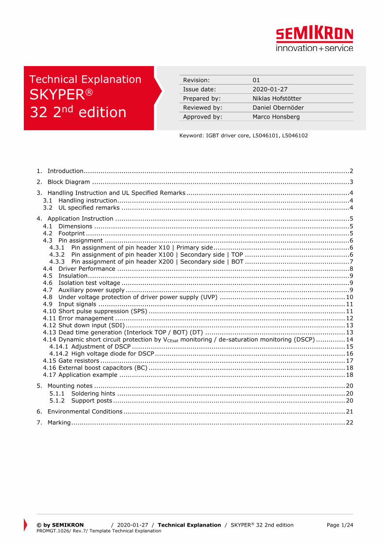
1. Introduction
The SKYPER® 32 2nd edition is a two-channel driver core serving as 1:1 replacement of the industry
standard SKYPER® 32. Designed to master the challenging requirements of today’s driver electronics the SKYPER® 32 2nd edition drivers provides an increased output power, a higher peak output current capability and an increased MTBF rate in comparison to its predecessor. These upgrades combined with its high EMC ruggedness enable the driver to reliably control standard semiconductor power modules.
Figure 1: SKYPER® 32 2nd edition
KEY FEATURES
• Two output channels
• 1.6 W output power per channel
• Two output channels
• Integrated potential free power supply for the secondary side
• Short Pulse Suppression (SPS)
• Under Voltage Protection (UVP)
• Under Voltage Lockout on primary side (UVLO)
• Dynamic short circuit protection (DSCP)
• Drive interlock (dead time) top / bottom (DT)
• Shut Down Input (SDI)
• MTBF rate > 4.2 Million hours at full load
Please note: Unless otherwise specified, all values in this technical explanation are typical values. Typical values are the average values expected in large quantities and are provided for information purposes only. These values
can and do vary in different applications. All operating parameters should be validated by user’s technical experts for each application.
© by SEMIKRON / 2020-01-27 / Technical Explanation / SKYPER® 32 2nd edition PROMGT.1026/ Rev.7/ Template Technical Explanation
Page 3/24
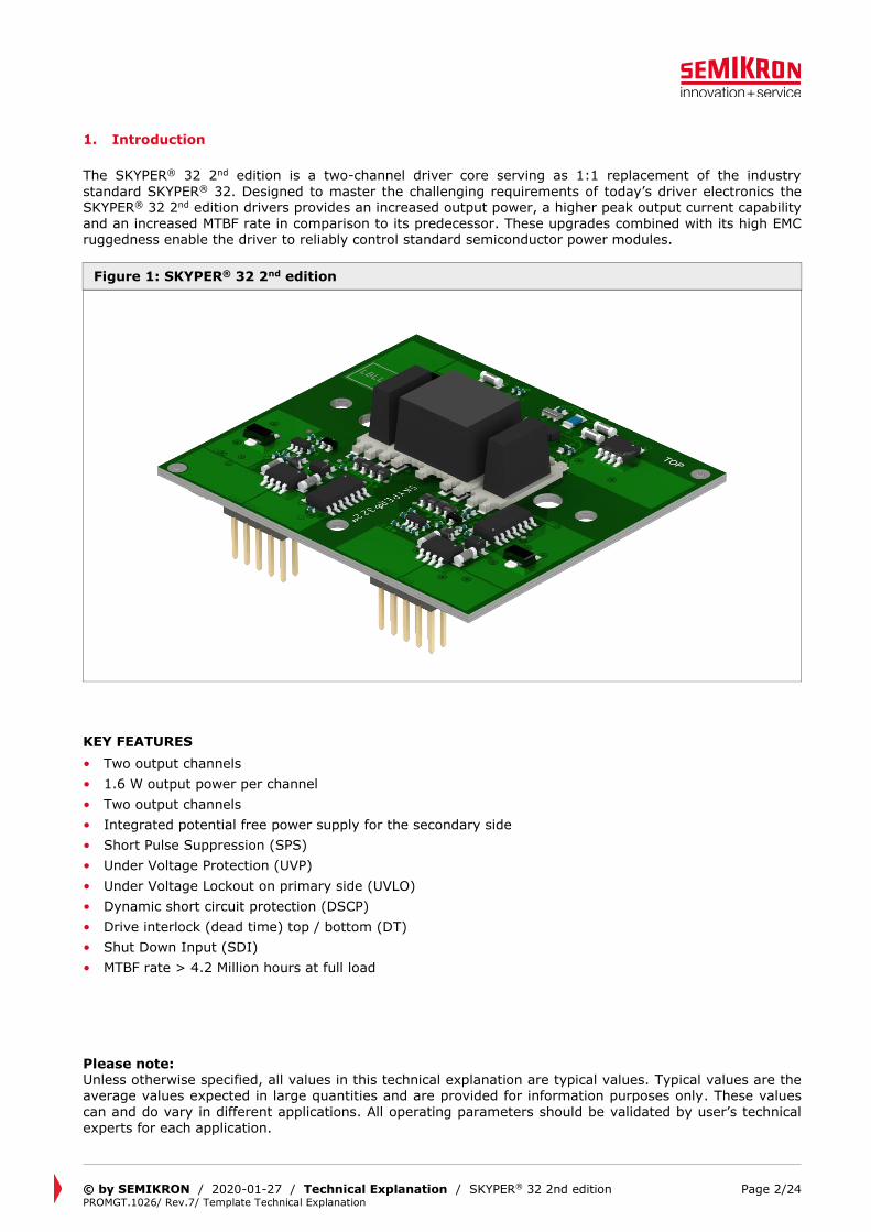
2. Block Diagram
Figure 2: SKYPER® 32 2nd edition | Block diagram
Po
we
r S
up
ply
Ma
na
gem
en
t
Po
we
r S
up
ply
Ma
na
ge
me
nt
Sho
rt P
uls
e
Sup
pressio
n
In
terl
ock
Sig
nal
Pro
cessin
g
Dead T
ime
Gen
era
tion
UV
LO
Erro
r
Ma
na
ge
me
nt
Ga
te D
riv
e
Ma
na
ge
me
nt
Po
we
r S
up
ply
Ma
na
gem
en
t
Erro
r
Ma
na
ge
me
nt
Erro
r
Ma
na
ge
me
nt
Ga
te D
riv
e
Ma
na
ge
me
nt
DS
CP
DS
CP
SE
C_
BO
T_
15
P
SE
C_
BO
T_
GN
D
SE
C_
BO
T_
8N
SE
C_
TO
P_
15
P
SE
C_
TO
P_
GN
D
SE
C_
TO
P_
8N
SE
C_
BO
T_
IG
BT
_O
N
SE
C_
BO
T_
IG
BT
_O
FF
SE
C_
BO
T_
VC
E_
IN
SE
C_
BO
T_
VC
E_
CFG
SE
C_
TO
P_
IG
BT
_O
N
SE
C_
TO
P_
IG
BT
_O
FF
SE
C_
TO
P_
VC
E_
IN
SE
C_
TO
P_
VC
E_
CFG
PR
IM
_P
WR
_1
5P
PR
IM
_P
WR
_G
ND
PR
IM
_T
OP
_IN
PR
IM
_B
OT
_IN
PR
IM
_n
ER
RO
R_
IN
PR
IM
_E
RR
OR
_O
UT
© by SEMIKRON / 2020-01-27 / Technical Explanation / SKYPER® 32 2nd edition PROMGT.1026/ Rev.7/ Template Technical Explanation
Page 4/24
3. Handling Instruction and UL Specified Remarks
3.1 Handling instruction
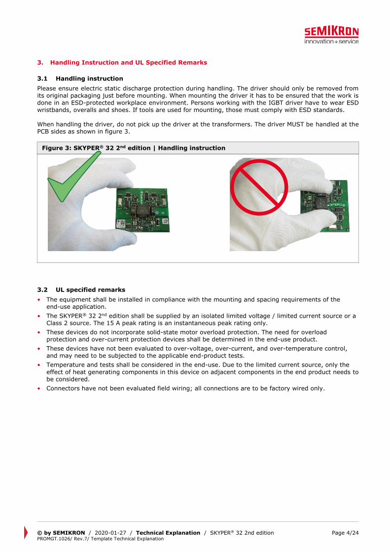
Please ensure electric static discharge protection during handling. The driver should only be removed from its original packaging just before mounting. When mounting the driver it has to be ensured that the work is done in an ESD-protected workplace environment. Persons working with the IGBT driver have to wear ESD wristbands, overalls and shoes. If tools are used for mounting, those must comply with ESD standards.
When handling the driver, do not pick up the driver at the transformers. The driver MUST be handled at the PCB sides as shown in figure 3.
Figure 3: SKYPER® 32 2nd edition | Handling instruction
3.2 UL specified remarks
• The equipment shall be installed in compliance with the mounting and spacing requirements of the end-use application.
• The SKYPER® 32 2nd edition shall be supplied by an isolated limited voltage / limited current source or a Class 2 source. The 15 A peak rating is an instantaneous peak rating only.
• These devices do not incorporate solid-state motor overload protection. The need for overload protection and over-current protection devices shall be determined in the end-use product.
• These devices have not been evaluated to over-voltage, over-current, and over-temperature control, and may need to be subjected to the applicable end-product tests.
• Temperature and tests shall be considered in the end-use. Due to the limited current source, only the
effect of heat generating components in this device on adjacent components in the end product needs to be considered.
• Connectors have not been evaluated field wiring; all connections are to be factory wired only.
© by SEMIKRON / 2020-01-27 / Technical Explanation / SKYPER® 32 2nd edition PROMGT.1026/ Rev.7/ Template Technical Explanation
Page 5/24
4. Application Instruction
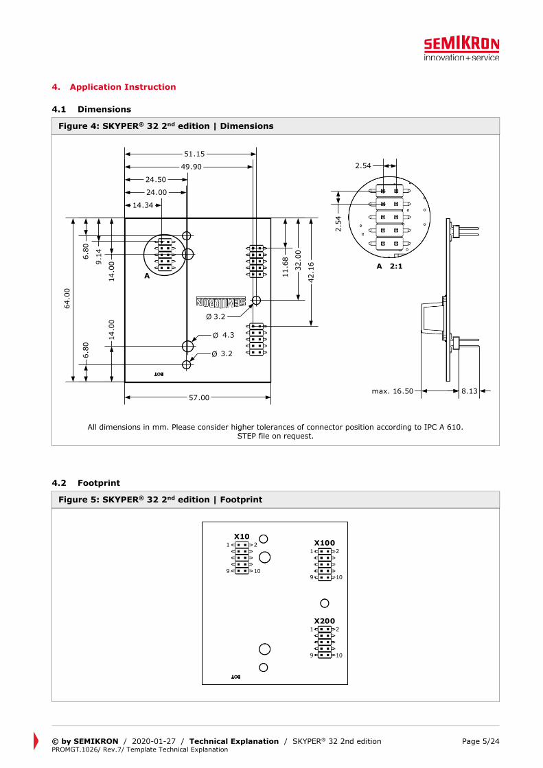
4.1 Dimensions
Figure 4: SKYPER® 32 2nd edition | Dimensions
All dimensions in mm. Please consider higher tolerances of connector position according to IPC A 610. STEP file on request.
4.2 Footprint
Figure 5: SKYPER® 32 2nd edition | Footprint
A
Ø 3,2
Ø 4,45,09
2.5
4
5,212.54
A 2:1
Ø 3,2
6.8
0
11.6
8
64.0
0
57.00
51.15
9.1
4
14.0
014.0
0
6.8
0
49.90
24.50
24.00
14.34
32.0
0
42.1
6
max. 16.50 8,008.13
3.2
4.3
3.2
X101
9
2
10
X200
10
2
9
1
X100
10
2
9
1
© by SEMIKRON / 2020-01-27 / Technical Explanation / SKYPER® 32 2nd edition PROMGT.1026/ Rev.7/ Template Technical Explanation
Page 6/24
4.3 Pin assignment
4.3.1 Pin assignment of pin header X10 | Primary side
Table 1: SKYPER® 32 2nd edition | Pin assignment – Primary side | X10
Pin Signal Function Specification
X10:01 PRIM_PWR_GND GND for power supply and GND
for digital signals
X10:02 PRIM_PWR_GND GND for power supply and GND for digital signals
X10:03 PRIM_ERROR_OUT ERROR output LOW = NO ERROR; open collector
output; max. 30V / 15mA
X10:04 PRIM_nERROR_IN ERROR input 5V logic; LOW active
X10:05 PRIM_PWR_GND GND for power supply and GND for digital signals
X10:06 PRIM_PWR_GND GND for power supply and GND for digital signals
X10:07 PRIM_TOP_IN Switching signal input (TOP switch)
Digital 15 V; 10 kOhm impedance LOW = TOP switch off HIGH = TOP switch on
X10:08 PRIM_BOT_IN Switching signal input
(BOTTOM switch)
Digital 15 V; 10 kOhm impedance
LOW = BOT switch off HIGH = BOT switch on
X10:09 PRIM_PWR_15P Drive core power supply Stabilized +15V ±4%
X10:10 PRIM_PWR_15P Drive core power supply Stabilized +15V ±4%
4.3.2 Pin assignment of pin header X100 | Secondary side | TOP
Table 2: SKYPER® 32 2nd edition | Pin assignment – Secondary side | TOP | X100
Pin Signal Function Specification
X100:01 SEC_TOP_VCE_CFG Input reference voltage adjustment
X100:02 SEC_TOP_VCE_IN Input VCE monitoring
X100:03 SEC_TOP_15P Output power supply for external
buffer capacitors
Stabilized +15V
X100:04 SEC_TOP_15P Output power supply for external buffer capacitors
Stabilized +15V
X100:05 SEC_TOP_GND GND for power supply and GND for digital signals
X100:06 SEC_TOP_IGBT_ON Switch on signal TOP IGBT
© by SEMIKRON / 2020-01-27 / Technical Explanation / SKYPER® 32 2nd edition PROMGT.1026/ Rev.7/ Template Technical Explanation
Page 7/24
X100:07 SEC_TOP_GND GND for power supply and GND for digital signals
X100:08 SEC_TOP_IGBT_OFF Switch off signal TOP IGBT
X100:09 SEC_TOP_8N Output power supply for external buffer capacitors
Stabilized -7V
X100:10 SEC_TOP_8N Output power supply for external buffer capacitors
Stabilized -7V
4.3.3 Pin assignment of pin header X200 | Secondary side | BOT
Table 3: SKYPER® 32 2nd edition | Pin assignment – Secondary side | BOT | X200
Pin Signal Function Specification
X200:01 SEC_BOT_VCE_CFG Input reference voltage adjustment
X200:02 SEC_BOT_VCE_IN Input VCE monitoring
X200:03 SEC_BOT_15P Output power supply for external
buffer capacitors
Stabilized +15V
X200:04 SEC_BOT_15P Output power supply for external buffer capacitors
Stabilized +15V
X200:05 SEC_BOT_GND GND for power supply and GND
for digital signals
X200:06 SEC_BOT_IGBT_ON Switch on signal BOT IGBT
X200:07 SEC_BOT_GND GND for power supply and GND for digital signals
X200:08 SEC_BOT_IGBT_OFF Switch off signal BOT IGBT
X200:09 SEC_BOT_8N Output power supply for external buffer capacitors
Stabilized -7V
X200:10 SEC_BOT_8N Output power supply for external
buffer capacitors
Stabilized -7V
© by SEMIKRON / 2020-01-27 / Technical Explanation / SKYPER® 32 2nd edition PROMGT.1026/ Rev.7/ Template Technical Explanation
Page 8/24
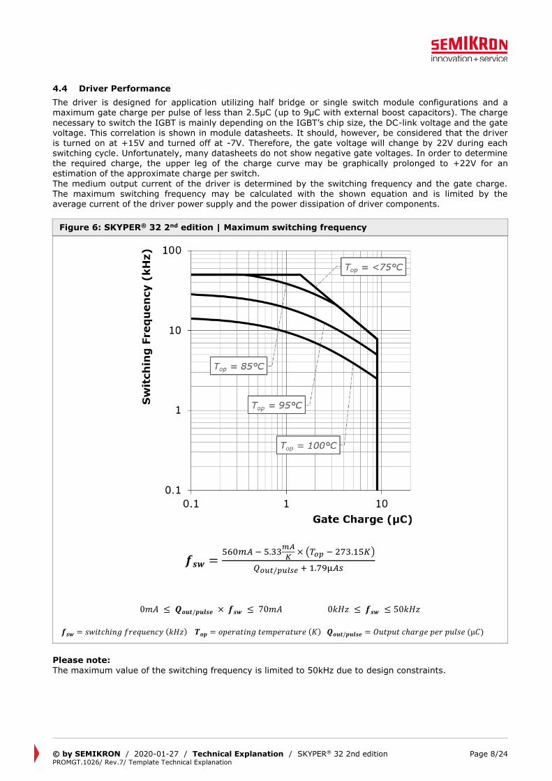
4.4 Driver Performance
The driver is designed for application utilizing half bridge or single switch module configurations and a maximum gate charge per pulse of less than 2.5µC (up to 9µC with external boost capacitors). The charge
necessary to switch the IGBT is mainly depending on the IGBT’s chip size, the DC-link voltage and the gate voltage. This correlation is shown in module datasheets. It should, however, be considered that the driver is turned on at +15V and turned off at -7V. Therefore, the gate voltage will change by 22V during each switching cycle. Unfortunately, many datasheets do not show negative gate voltages. In order to determine the required charge, the upper leg of the charge curve may be graphically prolonged to +22V for an estimation of the approximate charge per switch.
The medium output current of the driver is determined by the switching frequency and the gate charge. The maximum switching frequency may be calculated with the shown equation and is limited by the average current of the driver power supply and the power dissipation of driver components.
Figure 6: SKYPER® 32 2nd edition | Maximum switching frequency
𝒇𝒔𝒘 =560𝑚𝐴 − 5.33
𝑚𝐴
𝐾 × (𝑇𝑜𝑝 − 273.15𝐾)
𝑄𝑜𝑢𝑡/𝑝𝑢𝑙𝑠𝑒 + 1.79µ𝐴𝑠
0𝑚𝐴 ≤ 𝑸𝒐𝒖𝒕/𝒑𝒖𝒍𝒔𝒆 × 𝒇𝒔𝒘 ≤ 70𝑚𝐴 0𝑘𝐻𝑧 ≤ 𝒇𝒔𝒘 ≤ 50𝑘𝐻𝑧
𝒇𝒔𝒘 = 𝑠𝑤𝑖𝑡𝑐ℎ𝑖𝑛𝑔 𝑓𝑟𝑒𝑞𝑢𝑒𝑛𝑐𝑦 (𝑘𝐻𝑧) 𝑻𝒐𝒑 = 𝑜𝑝𝑒𝑟𝑎𝑡𝑖𝑛𝑔 𝑡𝑒𝑚𝑝𝑒𝑟𝑎𝑡𝑢𝑟𝑒 (𝐾) 𝑸𝒐𝒖𝒕/𝒑𝒖𝒍𝒔𝒆 = 𝑂𝑢𝑡𝑝𝑢𝑡 𝑐ℎ𝑎𝑟𝑔𝑒 𝑝𝑒𝑟 𝑝𝑢𝑙𝑠𝑒 (µ𝐶)
Please note:
The maximum value of the switching frequency is limited to 50kHz due to design constraints.

© by SEMIKRON / 2020-01-27 / Technical Explanation / SKYPER® 32 2nd edition PROMGT.1026/ Rev.7/ Template Technical Explanation
Page 9/24
4.5 Insulation
Magnetic transformers are used as insulation barrier between gate driver primary and secondary side. The transformer set consists of pulse transformers which are used bidirectional for turn-on and turn-off signals
of the IGBT and the error feedback between secondary and primary side, and a DC/DC converter. This converter provides a potential separation (galvanic separation) and power supply for the two secondary (TOP and BOT) sides of the driver. Thus, external transformers for external power supply are not required.
Table 4: SKYPER® 32 2nd edition | Creepage and clearance distance
Primary to secondary min 12.2 mm
4.6 Isolation test voltage
The isolation test voltage represents a measure of immunity to transient voltages. The maximum test
voltage and time applied once between input and output, and once between output 1 and output 2 are
indicated in the absolute maximum ratings. The high-voltage isolation tests and repeated tests of an isolation barrier can degrade isolation capability due to partial discharge effects. Hence, repeated isolation voltage tests should be performed with reduced voltage. The test voltage must be reduced by 20% for each repeated test. The isolation of the isolation barrier (transformer) is checked and verified 100% in production. Besides this isolation barrier, no further active parts are used in this SKYPER design that potentially could limit the
isolation voltage at a lower level than specified. An isolation test is not performed as a series test. Therefore, the user can perform once the isolation test with voltage and time indicated in the absolute maximum ratings. Please note: An isolation test is not performed at SEMIKRON as a series test. This shall be performed in the application as part of the mandatory system test requirements.
4.7 Auxiliary power supply
A few basic rules should be followed when dimensioning the customer side power supply for the driver. The following table shows the required features of an appropriate power supply.
Table 5: SKYPER® 32 2nd edition | Requirements of the auxiliary power supply
Regulated power supply +15V ±4%
Maximum rise time of auxiliary power supply 50ms
Minimum peak current of auxiliary supply 1A
Power on reset completed after 150ms
Please note: Do not apply switching signals during power on reset.
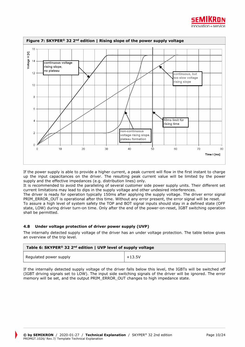
The supplying switched mode power supply may not be turned-off for a short time as consequence of its current limitation. The supply’s output characteristic needs to be considered. Switched mode power supplies with fold-back characteristic or hiccup-mode can create problems if sufficient over current margin to ride through the power up current demand of the SKYPER is not available. The voltage has to rise continuously and without any plateau formation as shown in the following diagram to ensure proper boot-up of the SKYPER.
© by SEMIKRON / 2020-01-27 / Technical Explanation / SKYPER® 32 2nd edition PROMGT.1026/ Rev.7/ Template Technical Explanation
Page 10/24
Figure 7: SKYPER® 32 2nd edition | Rising slope of the power supply voltage
If the power supply is able to provide a higher current, a peak current will flow in the first instant to charge up the input capacitances on the driver. The resulting peak current value will be limited by the power supply and the effective impedances (e.g. distribution lines) only.
It is recommended to avoid the paralleling of several customer side power supply units. Their different set current limitations may lead to dips in the supply voltage and other undesired interferences. The driver is ready for operation typically 150ms after applying the supply voltage. The driver error signal
PRIM_ERROR_OUT is operational after this time. Without any error present, the error signal will be reset. To assure a high level of system safety the TOP and BOT signal inputs should stay in a defined state (OFF state, LOW) during driver turn-on time. Only after the end of the power-on-reset, IGBT switching operation shall be permitted.
4.8 Under voltage protection of driver power supply (UVP)
The internally detected supply voltage of the driver has an under voltage protection. The table below gives an overview of the trip level.
Table 6: SKYPER® 32 2nd edition | UVP level of supply voltage
Regulated power supply +13.5V
If the internally detected supply voltage of the driver falls below this level, the IGBTs will be switched off (IGBT driving signals set to LOW). The input side switching signals of the driver will be ignored. The error memory will be set, and the output PRIM_ERROR_OUT changes to high impedance state.
© by SEMIKRON / 2020-01-27 / Technical Explanation / SKYPER® 32 2nd edition PROMGT.1026/ Rev.7/ Template Technical Explanation
Page 11/24
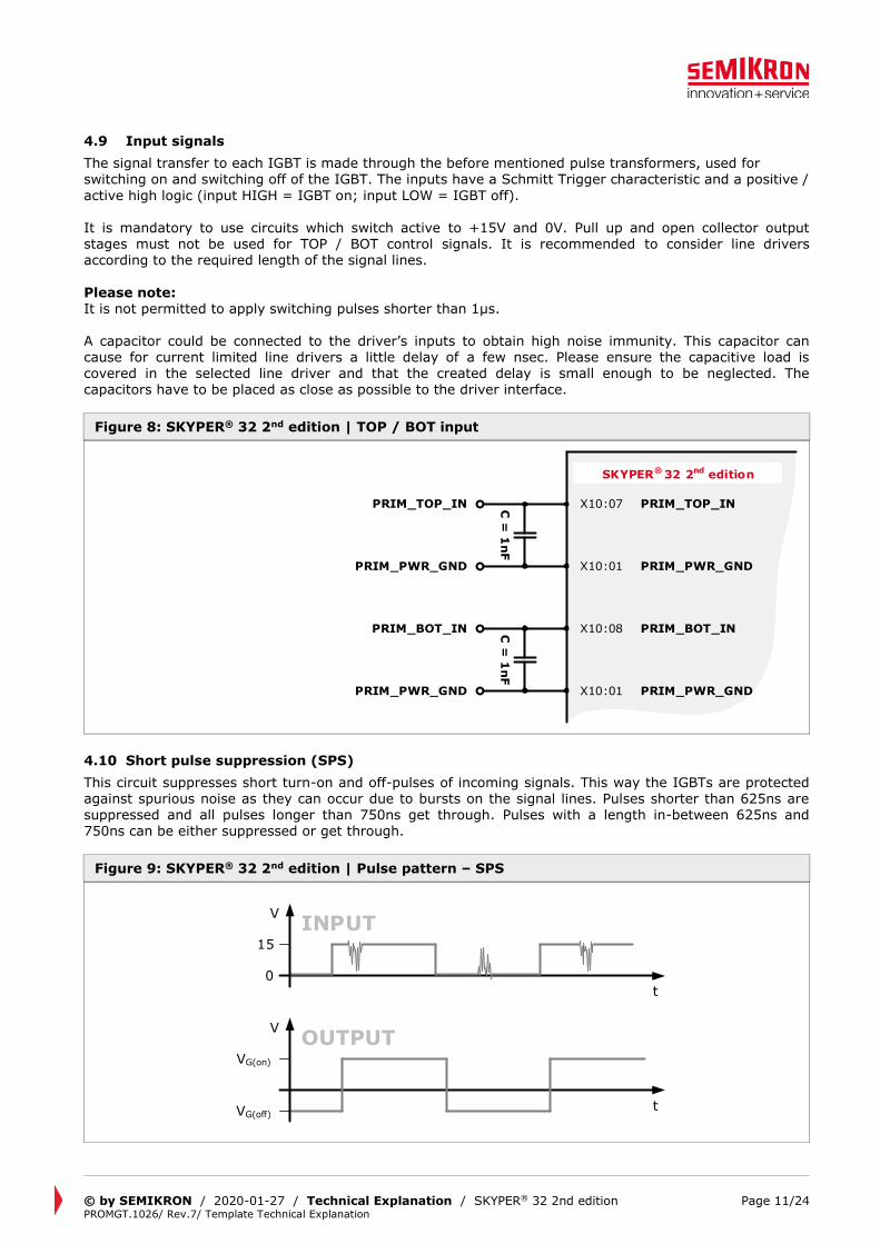
4.9 Input signals
The signal transfer to each IGBT is made through the before mentioned pulse transformers, used for switching on and switching off of the IGBT. The inputs have a Schmitt Trigger characteristic and a positive /
active high logic (input HIGH = IGBT on; input LOW = IGBT off). It is mandatory to use circuits which switch active to +15V and 0V. Pull up and open collector output stages must not be used for TOP / BOT control signals. It is recommended to consider line drivers according to the required length of the signal lines.
Please note: It is not permitted to apply switching pulses shorter than 1µs. A capacitor could be connected to the driver’s inputs to obtain high noise immunity. This capacitor can cause for current limited line drivers a little delay of a few nsec. Please ensure the capacitive load is covered in the selected line driver and that the created delay is small enough to be neglected. The
capacitors have to be placed as close as possible to the driver interface.
Figure 8: SKYPER® 32 2nd edition | TOP / BOT input
4.10 Short pulse suppression (SPS)
This circuit suppresses short turn-on and off-pulses of incoming signals. This way the IGBTs are protected against spurious noise as they can occur due to bursts on the signal lines. Pulses shorter than 625ns are suppressed and all pulses longer than 750ns get through. Pulses with a length in-between 625ns and 750ns can be either suppressed or get through.
Figure 9: SKYPER® 32 2nd edition | Pulse pattern – SPS
SKYPER® 32 2nd edition
C =
1n
F
PRIM_TOP_IN
PRIM_PWR_GND PRIM_PWR_GNDX10:01
PRIM_TOP_INX10:07
C =
1n
F
PRIM_BOT_IN
PRIM_PWR_GND PRIM_PWR_GNDX10:01
PRIM_BOT_INX10:08
V
t
t
V
15
0
VG(on)
VG(off)
INPUT
OUTPUT
© by SEMIKRON / 2020-01-27 / Technical Explanation / SKYPER® 32 2nd edition PROMGT.1026/ Rev.7/ Template Technical Explanation
Page 12/24
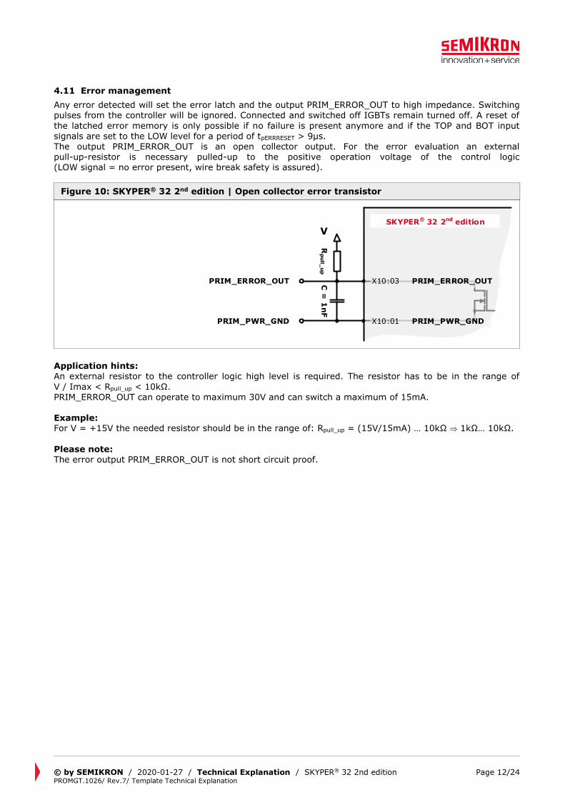
4.11 Error management
Any error detected will set the error latch and the output PRIM_ERROR_OUT to high impedance. Switching pulses from the controller will be ignored. Connected and switched off IGBTs remain turned off. A reset of
the latched error memory is only possible if no failure is present anymore and if the TOP and BOT input signals are set to the LOW level for a period of tpERRRESET > 9µs. The output PRIM_ERROR_OUT is an open collector output. For the error evaluation an external pull-up-resistor is necessary pulled-up to the positive operation voltage of the control logic (LOW signal = no error present, wire break safety is assured).
Figure 10: SKYPER® 32 2nd edition | Open collector error transistor
Application hints: An external resistor to the controller logic high level is required. The resistor has to be in the range of
V / Imax < Rpull_up < 10kΩ. PRIM_ERROR_OUT can operate to maximum 30V and can switch a maximum of 15mA. Example: For V = +15V the needed resistor should be in the range of: Rpull_up = (15V/15mA) … 10kΩ 1kΩ… 10kΩ.
Please note: The error output PRIM_ERROR_OUT is not short circuit proof.
SKYPER® 32 2nd edition
PRIM_ERROR_OUT PRIM_ERROR_OUTX10:03
PRIM_PWR_GND PRIM_PWR_GNDX10:01
Rpull_
up
C =
1n
FV
© by SEMIKRON / 2020-01-27 / Technical Explanation / SKYPER® 32 2nd edition PROMGT.1026/ Rev.7/ Template Technical Explanation
Page 13/24
4.12 Shut down input (SDI)
The shut down input / error input signal can gather error signals of other hardware components for switching off the IGBT (input HIGH = no turn-off; input LOW = turn-off).
A LOW signal at PRIM_nERROR_IN will set the error latch and the output PRIM_ERROR_OUT to high impedance. Switching pulses from the controller will be ignored. A reset of the latched error memory is only possible if no LOW signal at PRIM_nERROR_IN is present anymore and if the TOP and BOT input signals are set to the LOW level for a period of tpERRRESET > 9µs. The SDI function can be disabled by no connection or connecting to 5V.
Figure 11: SKYPER® 32 2nd edition | Connection SDI
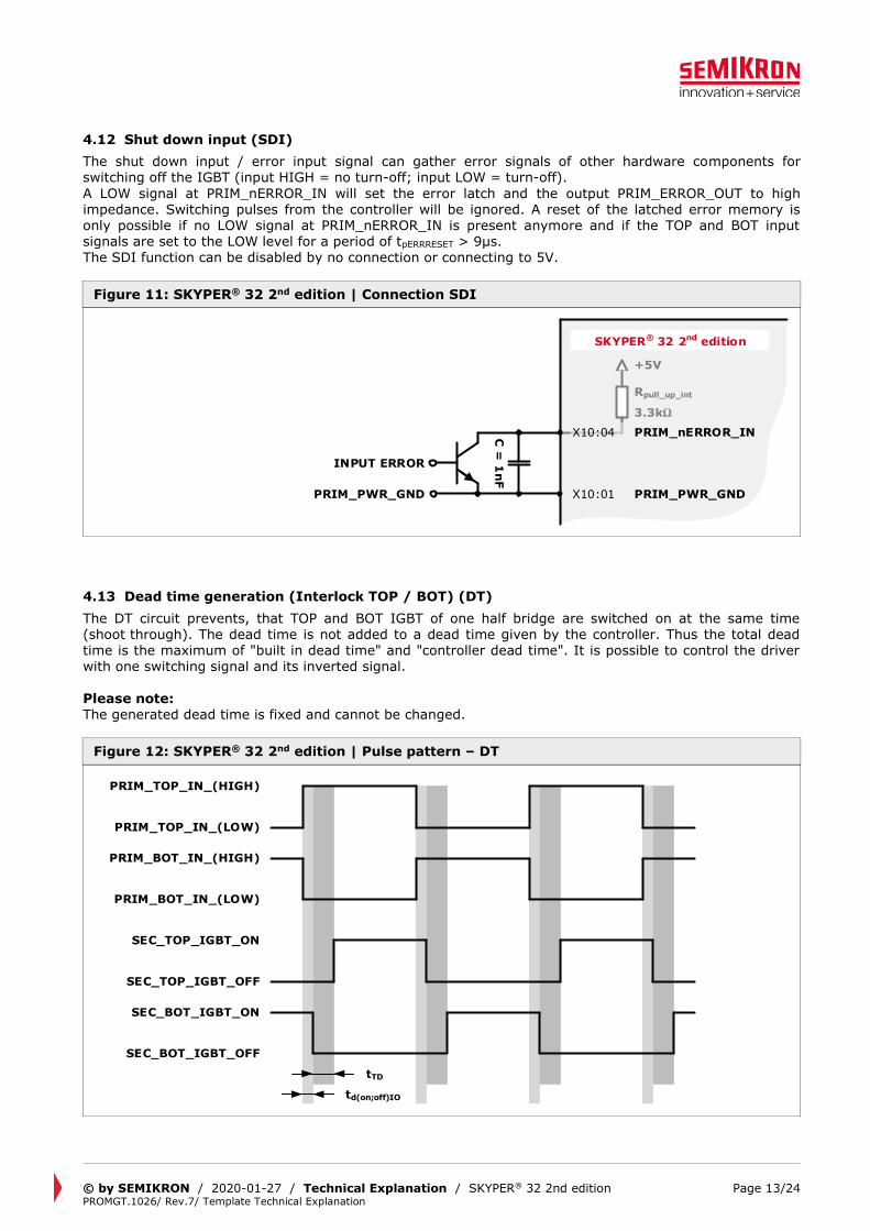
4.13 Dead time generation (Interlock TOP / BOT) (DT)
The DT circuit prevents, that TOP and BOT IGBT of one half bridge are switched on at the same time (shoot through). The dead time is not added to a dead time given by the controller. Thus the total dead
time is the maximum of "built in dead time" and "controller dead time". It is possible to control the driver with one switching signal and its inverted signal.
Please note: The generated dead time is fixed and cannot be changed.
Figure 12: SKYPER® 32 2nd edition | Pulse pattern – DT
SKYPER® 32 2nd edition
INPUT ERROR
PRIM_nERROR_INX10:04
PRIM_PWR_GND PRIM_PWR_GNDX10:01
C =
1n
F+5V
Rpull_up_int
3.3k
PRIM_TOP_IN_(HIGH)
PRIM_TOP_IN_(LOW)
PRIM_BOT_IN_(HIGH)
PRIM_BOT_IN_(LOW)
SEC_TOP_IGBT_ON
SEC_TOP_IGBT_OFF
SEC_BOT_IGBT_ON
SEC_BOT_IGBT_OFF
td(on;off)IO
tTD
© by SEMIKRON / 2020-01-27 / Technical Explanation / SKYPER® 32 2nd edition PROMGT.1026/ Rev.7/ Template Technical Explanation
Page 14/24
The total propagation delay of the driver is the sum of interlock dead time (tTD) and driver input output signal propagation delay (td(on;off)IO) as shown in the pulse pattern. Moreover the switching time of the IGBT chip has to be taken into account (not shown in the pulse pattern). In case both channel inputs (PRIM_TOP_IN and PRIM_BOT_IN) are at high level, the IGBTs will be turned off. If only one channel is switching, there will be no interlock dead time.
Please note: No error message will be generated when overlap of switching signals occurs.
4.14 Dynamic short circuit protection by VCEsat monitoring / de-saturation monitoring (DSCP)
The DSCP circuit is responsible for short circuit sensing. It monitors the collector-emitter voltage VCE of the IGBT during its on-state. Due to the direct measurement of VCEsat on the IGBT's collector, the DSCP circuit switches off the IGBTs and an error is indicated.
The reference voltage VCEref may dynamically be adapted to the IGBTs switching behavior. Immediately after turn-on of the IGBT, a higher value is effective than in steady state. This value will, however, be
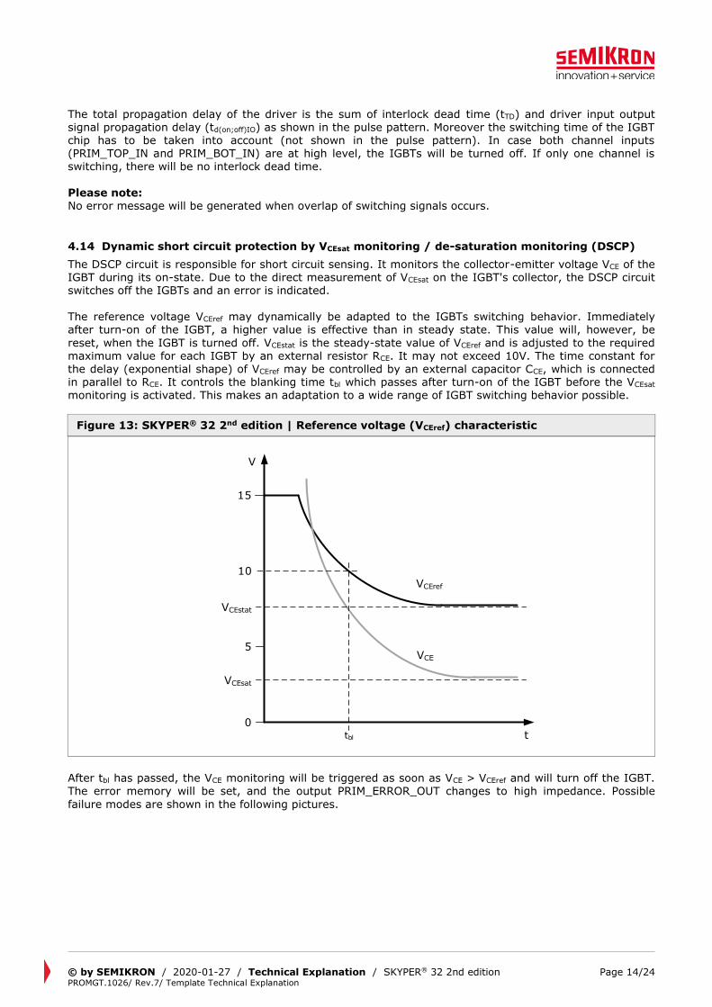
reset, when the IGBT is turned off. VCEstat is the steady-state value of VCEref and is adjusted to the required maximum value for each IGBT by an external resistor RCE. It may not exceed 10V. The time constant for the delay (exponential shape) of VCEref may be controlled by an external capacitor CCE, which is connected in parallel to RCE. It controls the blanking time tbl which passes after turn-on of the IGBT before the VCEsat monitoring is activated. This makes an adaptation to a wide range of IGBT switching behavior possible.
Figure 13: SKYPER® 32 2nd edition | Reference voltage (VCEref) characteristic
After tbl has passed, the VCE monitoring will be triggered as soon as VCE > VCEref and will turn off the IGBT. The error memory will be set, and the output PRIM_ERROR_OUT changes to high impedance. Possible
failure modes are shown in the following pictures.
5
10
15
V
t
VCEsat
VCEref
0tbl
VCEstat
VCE
© by SEMIKRON / 2020-01-27 / Technical Explanation / SKYPER® 32 2nd edition PROMGT.1026/ Rev.7/ Template Technical Explanation
Page 15/24
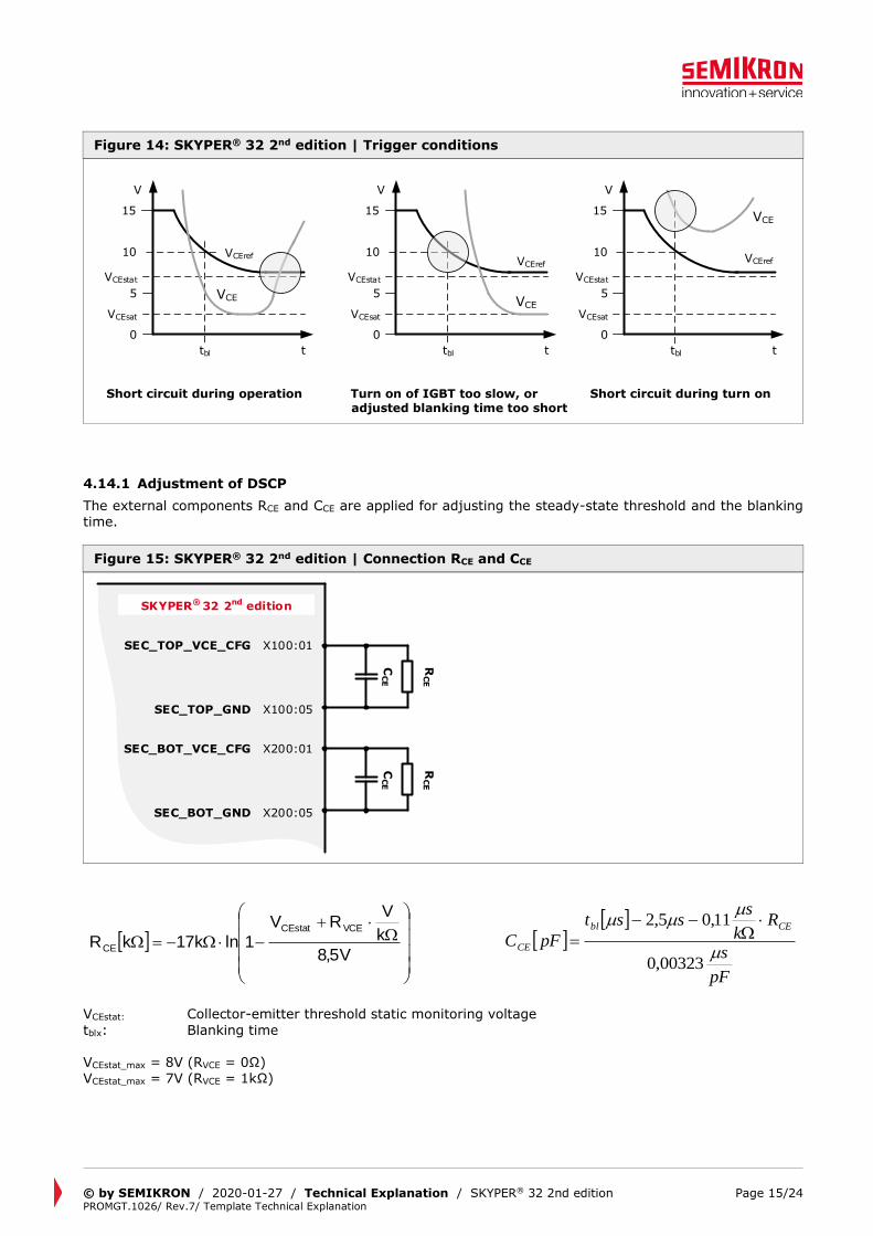
Figure 14: SKYPER® 32 2nd edition | Trigger conditions
Short circuit during operation Turn on of IGBT too slow, or Short circuit during turn on adjusted blanking time too short
4.14.1 Adjustment of DSCP
The external components RCE and CCE are applied for adjusting the steady-state threshold and the blanking time.
Figure 15: SKYPER® 32 2nd edition | Connection RCE and CCE
V5,8
k
VRV
1lnk17kRVCECEstat
CE
pF
s
Rk
ssst
pFCCEbl
CE
00323,0
11,05,2
VCEstat: Collector-emitter threshold static monitoring voltage
tblx: Blanking time VCEstat_max = 8V (RVCE = 0Ω) VCEstat_max = 7V (RVCE = 1kΩ)
5
10
15
V
t
VCEsat
VCEref
0
tbl
VCEstat
VCE 5
10
15
V
t
VCEsat
VCEref
0
tbl
VCEstat
VCE5
10
15
V
t
VCEsat
VCEref
0
tbl
VCEstat
VCE
SKYPER® 32 2nd edition
CCE
SEC_TOP_VCE_CFG X100:01
SEC_TOP_GND X100:05
RCE
CCE
SEC_BOT_VCE_CFG X200:01
SEC_BOT_GND X200:05
RCE
© by SEMIKRON / 2020-01-27 / Technical Explanation / SKYPER® 32 2nd edition PROMGT.1026/ Rev.7/ Template Technical Explanation
Page 16/24
Please Note: The equations are calculated considering the use of high voltage diode BY203/20S. The calculated values VCEstat and tbl are typical values at room temperature. These values can and do vary in the application (e.g. tolerances of used high voltage diode, resistor RCE, capacitor CCE). The DSCP function is not recommended for over current protection.
Application hints If the DSCP function is not used, for example during the experimental phase, SEC_TOP_VCE_IN must be connected with SEC_TOP_GND for disabling SCP @ TOP side and SEC_BOT_VCE_IN must be connected with SEC_BOT_GND for disabling SCP @ BOT side.
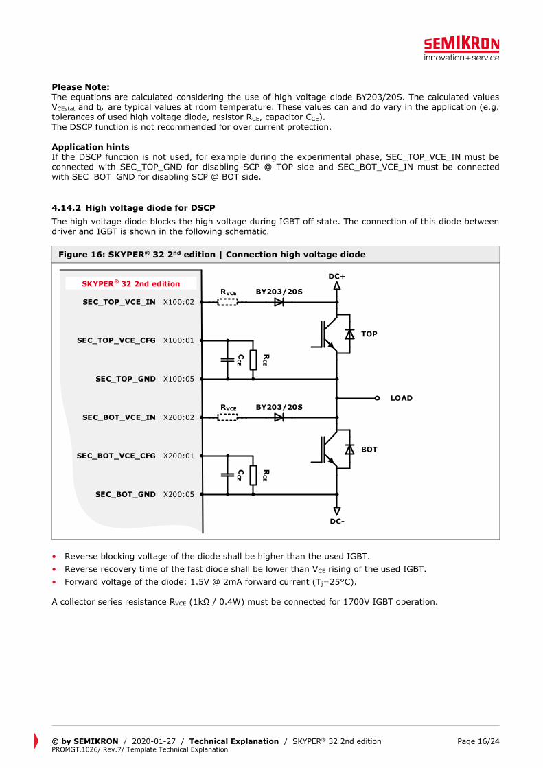
4.14.2 High voltage diode for DSCP
The high voltage diode blocks the high voltage during IGBT off state. The connection of this diode between driver and IGBT is shown in the following schematic.
Figure 16: SKYPER® 32 2nd edition | Connection high voltage diode
• Reverse blocking voltage of the diode shall be higher than the used IGBT.
• Reverse recovery time of the fast diode shall be lower than VCE rising of the used IGBT.
• Forward voltage of the diode: 1.5V @ 2mA forward current (Tj=25°C). A collector series resistance RVCE (1kΩ / 0.4W) must be connected for 1700V IGBT operation.
SKYPER® 32 2nd edition
SEC_TOP_VCE_IN X100:02
SEC_TOP_VCE_CFG X100:01
SEC_TOP_GND X100:05
RVCE BY203/20S
DC+
TOP
DC-
CCE
RCE
SEC_BOT_GND X200:05
SEC_BOT_VCE_IN X200:02
SEC_BOT_VCE_CFG X200:01
RVCE BY203/20S
CCE
RCE
BOT
LOAD
© by SEMIKRON / 2020-01-27 / Technical Explanation / SKYPER® 32 2nd edition PROMGT.1026/ Rev.7/ Template Technical Explanation
Page 17/24
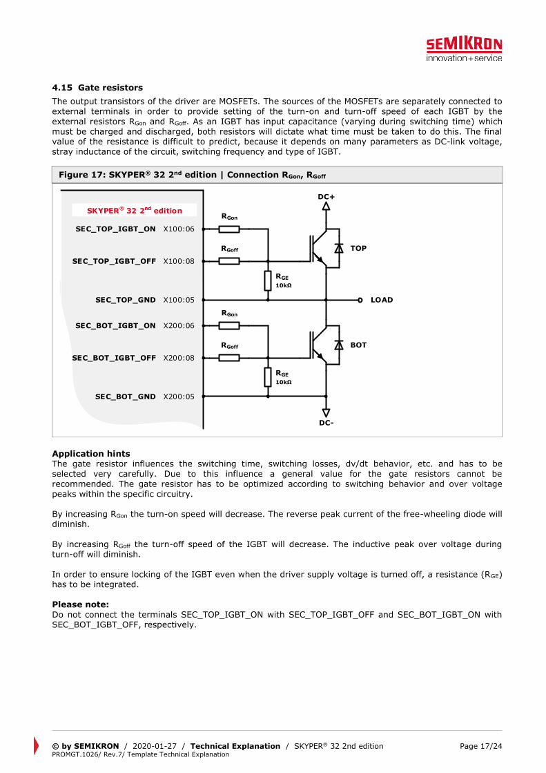
4.15 Gate resistors
The output transistors of the driver are MOSFETs. The sources of the MOSFETs are separately connected to external terminals in order to provide setting of the turn-on and turn-off speed of each IGBT by the
external resistors RGon and RGoff. As an IGBT has input capacitance (varying during switching time) which must be charged and discharged, both resistors will dictate what time must be taken to do this. The final value of the resistance is difficult to predict, because it depends on many parameters as DC-link voltage, stray inductance of the circuit, switching frequency and type of IGBT.
Figure 17: SKYPER® 32 2nd edition | Connection RGon, RGoff
Application hints The gate resistor influences the switching time, switching losses, dv/dt behavior, etc. and has to be selected very carefully. Due to this influence a general value for the gate resistors cannot be
recommended. The gate resistor has to be optimized according to switching behavior and over voltage peaks within the specific circuitry. By increasing RGon the turn-on speed will decrease. The reverse peak current of the free-wheeling diode will diminish.
By increasing RGoff the turn-off speed of the IGBT will decrease. The inductive peak over voltage during turn-off will diminish.
In order to ensure locking of the IGBT even when the driver supply voltage is turned off, a resistance (RGE) has to be integrated. Please note:
Do not connect the terminals SEC_TOP_IGBT_ON with SEC_TOP_IGBT_OFF and SEC_BOT_IGBT_ON with SEC_BOT_IGBT_OFF, respectively.
DC+
RGon
RGE
10k
TOP
SKYPER® 32 2nd edition
SEC_TOP_IGBT_ON X100:06
SEC_TOP_IGBT_OFF X100:08
SEC_TOP_GND X100:05
RGoff
DC-
SEC_BOT_IGBT_ON X200:06
SEC_BOT_IGBT_OFF X200:08
SEC_BOT_GND X200:05
RGon
RGE
10k
BOTRGoff
LOAD
© by SEMIKRON / 2020-01-27 / Technical Explanation / SKYPER® 32 2nd edition PROMGT.1026/ Rev.7/ Template Technical Explanation
Page 18/24
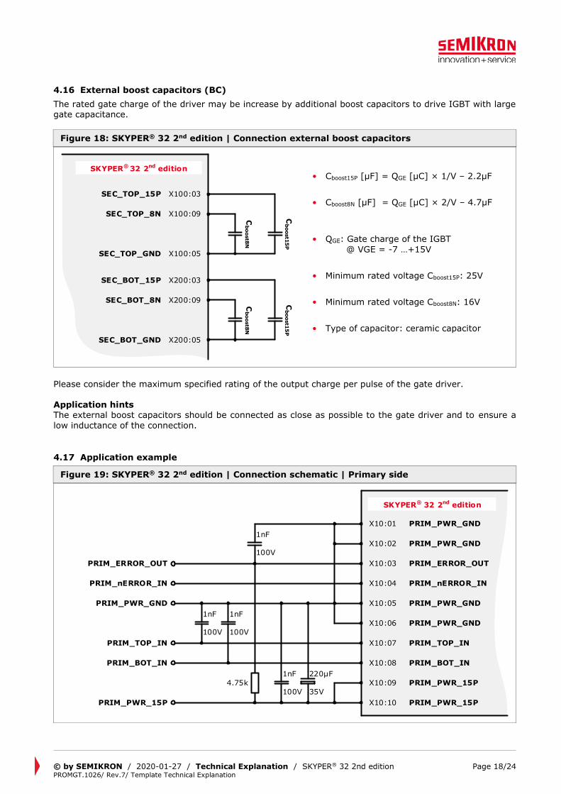
4.16 External boost capacitors (BC)
The rated gate charge of the driver may be increase by additional boost capacitors to drive IGBT with large gate capacitance.
Figure 18: SKYPER® 32 2nd edition | Connection external boost capacitors
Please consider the maximum specified rating of the output charge per pulse of the gate driver. Application hints The external boost capacitors should be connected as close as possible to the gate driver and to ensure a
low inductance of the connection.
4.17 Application example
Figure 19: SKYPER® 32 2nd edition | Connection schematic | Primary side
SKYPER® 32 2nd edition
Cboost1
5P
SEC_TOP_15P X100:03
SEC_TOP_GND X100:05
SEC_TOP_8N X100:09
Cboost8
N
Cboost1
5P
SEC_BOT_15P X200:03
SEC_BOT_GND X200:05
SEC_BOT_8N X200:09
Cboost8
N
220µF
35V
SKYPER® 32 2nd edition
PRIM_ERROR_OUTX10:03
PRIM_PWR_GNDX10:01
PRIM_PWR_GNDX10:02
PRIM_nERROR_INX10:04
PRIM_PWR_GNDX10:06
PRIM_PWR_GNDX10:05
PRIM_ERROR_OUT
PRIM_TOP_INX10:07
PRIM_BOT_INX10:08
PRIM_PWR_15PX10:09
PRIM_PWR_15PX10:10
1nF
100V
1nF
100V
1nF
100V
1nF
100V
4.75k
PRIM_nERROR_IN
PRIM_PWR_GND
PRIM_TOP_IN
PRIM_BOT_IN
PRIM_PWR_15P
• Cboost15P [µF] = QGE [µC] × 1/V – 2.2µF
• Cboost8N [µF] = QGE [µC] × 2/V – 4.7µF
• QGE: Gate charge of the IGBT
@ VGE = -7 …+15V
• Minimum rated voltage Cboost15P: 25V
• Minimum rated voltage Cboost8N: 16V
• Type of capacitor: ceramic capacitor
© by SEMIKRON / 2020-01-27 / Technical Explanation / SKYPER® 32 2nd edition PROMGT.1026/ Rev.7/ Template Technical Explanation
Page 19/24
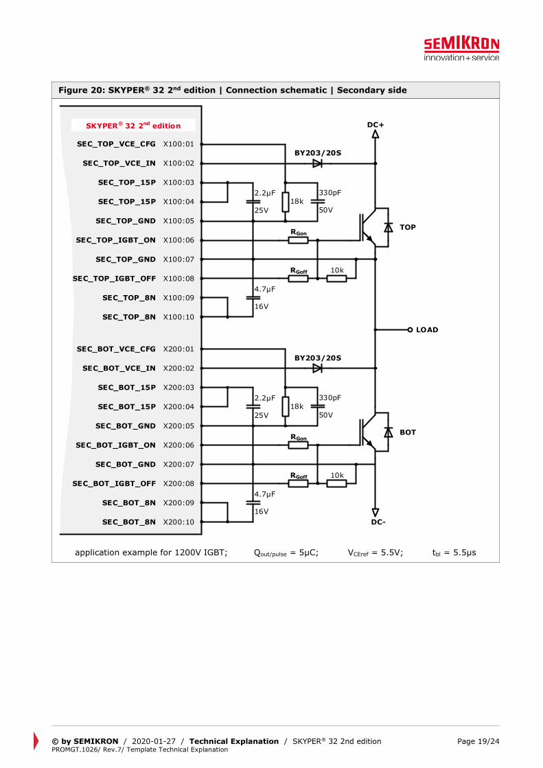
Figure 20: SKYPER® 32 2nd edition | Connection schematic | Secondary side
application example for 1200V IGBT; Qout/pulse = 5µC; VCEref = 5.5V; tbl = 5.5µs
DC+
BY203/20S
TOP
SKYPER® 32 2nd edition
SEC_TOP_VCE_CFG X100:01
SEC_TOP_VCE_IN X100:02
SEC_TOP_15P X100:03
SEC_TOP_15P X100:04
SEC_TOP_GND X100:05
SEC_TOP_IGBT_ON X100:06
SEC_TOP_GND X100:07
SEC_TOP_IGBT_OFF X100:08
SEC_TOP_8N X100:09
SEC_TOP_8N X100:10
330pF
50V
18k
4.7µF
16V
2.2µF
25V
RGon
RGoff 10k
DC-
BY203/20S
BOT
330pF
50V
18k
4.7µF
16V
2.2µF
25V
RGon
RGoff 10k
SEC_BOT_VCE_CFG X200:01
SEC_BOT_VCE_IN X200:02
SEC_BOT_15P X200:03
SEC_BOT_15P X200:04
SEC_BOT_GND X200:05
SEC_BOT_IGBT_ON X200:06
SEC_BOT_GND X200:07
SEC_BOT_IGBT_OFF X200:08
SEC_BOT_8N X200:09
SEC_BOT_8N X200:10
LOAD
© by SEMIKRON / 2020-01-27 / Technical Explanation / SKYPER® 32 2nd edition PROMGT.1026/ Rev.7/ Template Technical Explanation
Page 20/24
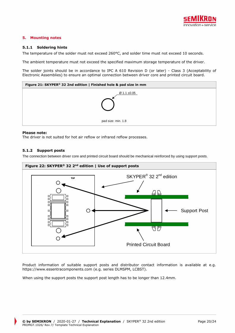
5. Mounting notes
5.1.1 Soldering hints
The temperature of the solder must not exceed 260°C, and solder time must not exceed 10 seconds. The ambient temperature must not exceed the specified maximum storage temperature of the driver.
The solder joints should be in accordance to IPC A 610 Revision D (or later) - Class 3 (Acceptability of Electronic Assemblies) to ensure an optimal connection between driver core and printed circuit board.
Figure 21: SKYPER® 32 2nd edition | Finished hole & pad size in mm
Ø 1.1 ±0.05
pad size: min. 1.8
Please note: The driver is not suited for hot air reflow or infrared reflow processes.
5.1.2 Support posts
The connection between driver core and printed circuit board should be mechanical reinforced by using support posts.
Figure 22: SKYPER® 32 2nd edition | Use of support posts
Product information of suitable support posts and distributor contact information is available at e.g. https://www.essentracomponents.com (e.g. series DLMSPM, LCBST). When using the support posts the support post length has to be longer than 12.4mm.
SKYPER® 32 2
nd edition
Printed Circuit Board
Support Post

© by SEMIKRON / 2020-01-27 / Technical Explanation / SKYPER® 32 2nd edition PROMGT.1026/ Rev.7/ Template Technical Explanation
Page 21/24
6. Environmental Conditions
The driver core is type tested under the environmental conditions below
Table 7: SKYPER® 32 2nd edition | Environmental conditions
Conditions Values (max.)
Vibration
Sinusoidal sweep 20Hz … 500Hz, 5g, 26 sweeps per axis (x, y, z)
• Tested acc. IEC 68-2-6
• Connection between driver core and printed circuit board mechanical reinforced by using support posts.
Shock
Half-sinusoidal pulse, 5g, shock width 18ms, 3 shocks in each direction (±x, ±y, ±z), 18 shocks in total
• Tested acc. IEC 68-2-27
• Connection between driver core and printed circuit board mechanical reinforced by using support posts.
The characteristics and further environmental conditions are indicated in the data sheet.
Please note: The use of aggressive materials in cleaning and potting process of driver core may be detrimental for the device parameters. If the driver core is coated by the user, any warranty (Gewährleistung) expires.
© by SEMIKRON / 2020-01-27 / Technical Explanation / SKYPER® 32 2nd edition PROMGT.1026/ Rev.7/ Template Technical Explanation
Page 22/24
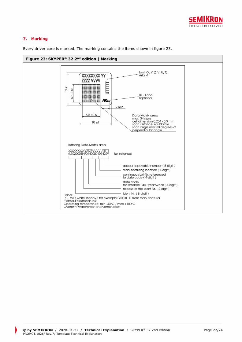
7. Marking
Every driver core is marked. The marking contains the items shown in figure 23.
Figure 23: SKYPER® 32 2nd edition | Marking

© by SEMIKRON / 2020-01-27 / Technical Explanation / SKYPER® 32 2nd edition PROMGT.1026/ Rev.7/ Template Technical Explanation
Page 23/24
Figure 1: SKYPER® 32 2nd edition ....................................................................................................... 2 Figure 2: SKYPER® 32 2nd edition | Block diagram ................................................................................ 3 Figure 3: SKYPER® 32 2nd edition | Handling instruction ....................................................................... 4 Figure 4: SKYPER® 32 2nd edition | Dimensions ................................................................................... 5 Figure 5: SKYPER® 32 2nd edition | Footprint ....................................................................................... 5 Figure 6: SKYPER® 32 2nd edition | Maximum switching frequency ......................................................... 8 Figure 7: SKYPER® 32 2nd edition | Rising slope of the power supply voltage ......................................... 10 Figure 8: SKYPER® 32 2nd edition | TOP / BOT input ........................................................................... 11 Figure 9: SKYPER® 32 2nd edition | Pulse pattern – SPS ...................................................................... 11 Figure 10: SKYPER® 32 2nd edition | Open collector error transistor ..................................................... 12 Figure 11: SKYPER® 32 2nd edition | Connection SDI .......................................................................... 13 Figure 12: SKYPER® 32 2nd edition | Pulse pattern – DT ...................................................................... 13 Figure 13: SKYPER® 32 2nd edition | Reference voltage (VCEref) characteristic ........................................ 14 Figure 14: SKYPER® 32 2nd edition | Trigger conditions ....................................................................... 15 Figure 15: SKYPER® 32 2nd edition | Connection RCE and CCE ............................................................... 15 Figure 16: SKYPER® 32 2nd edition | Connection high voltage diode ..................................................... 16 Figure 17: SKYPER® 32 2nd edition | Connection RGon, RGoff .................................................................. 17 Figure 18: SKYPER® 32 2nd edition | Connection external boost capacitors ............................................ 18 Figure 19: SKYPER® 32 2nd edition | Connection schematic | Primary side ............................................ 18 Figure 20: SKYPER® 32 2nd edition | Connection schematic | Secondary side ......................................... 19 Figure 21: SKYPER® 32 2nd edition | Finished hole & pad size in mm .................................................... 20 Figure 22: SKYPER® 32 2nd edition | Use of support posts ................................................................... 20 Figure 23: SKYPER® 32 2nd edition | Marking..................................................................................... 22
Table 1: SKYPER® 32 2nd edition | Pin assignment – Primary side | X10 .................................................. 6 Table 2: SKYPER® 32 2nd edition | Pin assignment – Secondary side | TOP | X100 ................................... 6 Table 3: SKYPER® 32 2nd edition | Pin assignment – Secondary side | BOT | X200 ................................... 7 Table 4: SKYPER® 32 2nd edition | Creepage and clearance distance ...................................................... 9 Table 5: SKYPER® 32 2nd edition | Requirements of the auxiliary power supply ........................................ 9 Table 6: SKYPER® 32 2nd edition | UVP level of supply voltage ............................................................. 10 Table 7: SKYPER® 32 2nd edition | Environmental conditions ............................................................... 21
References
[1] www.SEMIKRON.com [2] A. Wintrich, U. Nicolai, W. Tursky, T. Reimann, “Application Manual Power Semiconductors”, 2nd
edition, ISLE Verlag 2015, ISBN 978-3-938843-83-3
© by SEMIKRON / 2020-01-27 / Technical Explanation / SKYPER® 32 2nd edition PROMGT.1026/ Rev.7/ Template Technical Explanation
Page 24/24
IMPORTANT INFORMATION AND WARNINGS
The information in this document may not be considered as guarantee or assurance of product characteristics ("Beschaffenheitsgarantie"). This document describes only the usual characteristics of products to be expected in typical applications, which may still vary depending on the specific application. Therefore, products must be tested for the respective application in advance. Application adjustments may be necessary. The user of SEMIKRON products is responsible for the safety of their applications embedding SEMIKRON products and must take adequate safety measures to prevent the applications from causing a physical injury, fire or other problem if any of SEMIKRON products become faulty. The user is responsible to make sure that the application design is compliant with all applicable laws, regulations, norms and standards. Except as otherwise explicitly approved by SEMIKRON in a written document signed by authorized representatives of SEMIKRON, SEMIKRON products may not be used in any applications where a failure of the product or
any consequences of the use thereof can reasonably be expected to result in personal injury. No representation or warranty is given and no liability is assumed with respect to the accuracy, completeness and/or use of any information herein, including without limitation, warranties of non-infringement of intellectual property rights of any third party. SEMIKRON does not assume any liability arising out of the applications or use of any product; neither does it convey any license under its patent rights, copyrights, trade secrets or other intellectual property rights, nor the rights of others. SEMIKRON makes no representation or warranty of non-infringement or alleged non-infringement of intellectual property rights of any third party which may arise from applications. This document supersedes and replaces all information previously supplied and may be superseded by updates. SEMIKRON reserves the right to make changes. SEMIKRON INTERNATIONAL GmbH Sigmundstrasse 200, 90431 Nuremberg, Germany Tel: +49 911 6559 6663, Fax: +49 911 6559 262 [email protected], www.semikron.com