
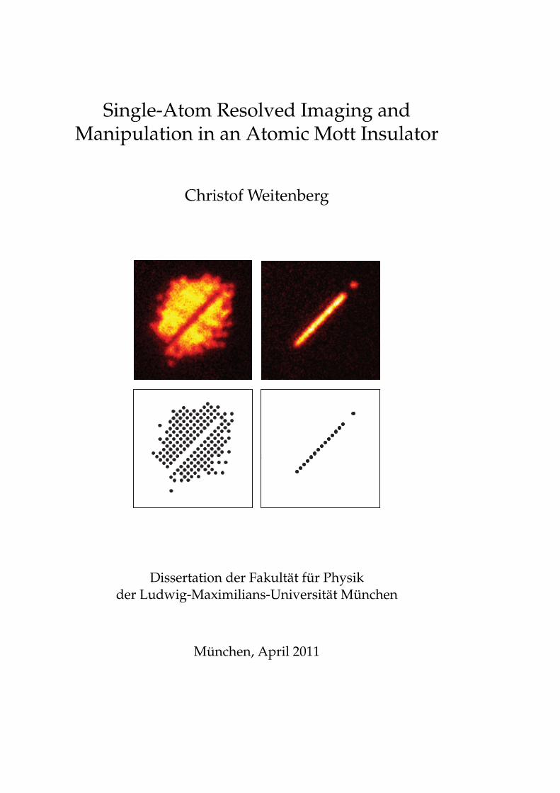
Single-Atom Resolved Imaging and Manipulation in an Atomic ...
120
Single-Atom Resolved Imaging and Manipulation in an Atomic Mott Insulator Christof Weitenberg Dissertation der Fakultät für Physik der Ludwig-Maximilians-Universität München München, April 2011
-
Upload
khangminh22 -
Category
Documents
-
view
2 -
download
0
Transcript of Single-Atom Resolved Imaging and Manipulation in an Atomic ...
Single-Atom Resolved Imaging andManipulation in an Atomic Mott Insulator
Christof Weitenberg
Dissertation der Fakultät für Physikder Ludwig-Maximilians-Universität München
München, April 2011

Erstgutachter: Prof. Dr. Immanuel BlochZweitgutachter: Prof. Dr. Walter Hofstetter
Tag der mündlichen Prüfung: 26. Mai 2011
ii
Single-Atom Resolved Imaging andManipulation in an Atomic Mott Insulator
Dissertation der Fakultät für Physikder Ludwig-Maximilians-Universität München
vorgelegt von
Christof Weitenberg
geboren in Rhede
München, April 2011

iv

Abstract
This thesis reports on new experimental techniques for the study of strongly corre-lated states of ultracold atoms in optical lattices. We used a high numerical apertureimaging system to probe 87Rb atoms in a two-dimensional lattice with single-site res-olution. Fluorescence imaging allows to detect single atoms with a large signal tonoise ratio and to reconstruct the atom distribution on the lattice.
We applied this new technique to a two-dimensional Mott insulator and directlyobserved number squeezing and the emerging shell structure. A comparison of theradial density and variance distributions to theory provides a precise in situ temper-ature and entropy measurement from single images. We find entropies around thecritical value for quantum magnetism.
In a second series of experiments, we demonstrated two-dimensional single-sitespin control in the optical lattice. The differential light shift of a tightly focused laserbeam shifts selected atoms into resonance with a microwave field driving a spin flip.In this way, we reach sub-diffraction limited spatial resolution well below the lat-tice spacing. Starting from a Mott insulator with unity filling we were able to createarbitrary spin patterns. We used this ability to prepare atom distributions to studyone-dimensional single-particle tunneling dynamics in a lattice. By discriminatingthe dynamics of the ground state and of the first excited band, we find that our ad-dressing scheme leaves most atoms in the vibrational ground state.
Moreover, we studied coherent light scattering from the atoms in the optical latticeand found diffraction maxima in the far-field. We showed that an antiferromagneticorder leads to additional diffraction peaks which can be used to detect this order alsowhen single-site resolution is not available.
The new techniques described in this thesis open the path to a wide range of novelapplications from quantum dynamics of spin impurities, entropy transport, imple-mentation of novel cooling schemes, and engineering of quantum many-body phasesto quantum information processing.
v
Zusammenfassung
In dieser Arbeit werden neue experimentelle Techniken für die Untersuchung vonstark korrelierten Zuständen von ultrakalten Atomen in optischen Gittern vorgestellt.Wir untersuchen 87Rb Atome in einem zwei-dimensionalen Gitter und erreichen da-bei eine Auflösung der einzelnen Gitterplätze mit Hilfe eines hochauflösenden Abbil-dungssystems. Fluoreszenzabbildung erlaubt es, einzelne Atome mit großem Signal-zu-Rausch-Verhältnis zu detektieren und die Verteilung der Atome auf dem Gitter zurekonstruieren.
Wir wenden diese neue Technik auf einen zwei-dimensionalen Mott-Isolator anand beobachten direkt das number squeezing und die Schalenstrukur. Ein Vergleichder radialen Dichte- und Varianzverteilung mit der Theorie ermöglicht eine präziseTemperatur- und Entropiemessung an einzelnen Bildern und wir finden Entropienum den kritischen Wert für Quantenmagnetismus.
In einer zweiten Reihe von Experimenten zeigen wir, dass wir gezielt einzelne ato-mare Spinzustände im Gitter manipulieren können ohne die benachbarten Atomezu beeinflussen. Wir benutzen den differentiellen light shift eines stark fokussiertenLaserstrahls, um einzelne Atome in Resonanz mit einem Mikrowellenfeld zu brin-gen, das den Spin umklappt. Auf diese Weise erreichen wir eine Ortsauflösung un-ter der Beugungsgrenze. Wir beginnen mit einem Mott-Isolator mit einem Atom proGitterplatz und können darin beliebige Spinmuster erzeugen. Diese neuen Möglich-keiten zur Präparation atomarer Verteilungen nutzen wir, um die eindimensionaleEinteilchen-Tunneldynamik in einem Gitter zu untersuchen. Wir unterscheiden dieDynamik von Atomen im Grundzustand und im ersten angeregten Band und zeigenso, dass unser Adressierschema die meisten Atome im Grundzustand lässt.
Darüber hinaus untersuchen wir kohärente Lichtstreuung an den Atomen im Git-ter und finden Beugungsmaxima im Fernfeld. Wir zeigen, dass eine antiferromagne-tische Ordnung der Atome zu zusätzlichen Beugungsmaxima führt, die man auchohne unsere hohe Auflösung zum Nachweis dieser Ordnung nutzen könnte.
Die neuen Techniken, die in dieser Arbeit vorgestellt werden, öffnen den Weg fürviele neue Anwendungen von der Quantendynamik von Spin-Defekten, Entropie-transport, der Umsetzung neuer Kühlschemata sowie der Realisierung von Quanten-Vielteilchenphasen bis hin zur Quanteninformationsverarbeitung.
vi
Contents
1 Introduction 1
2 Bose-Hubbard physics with ultracold atoms 52.1 Bose-Hubbard model . . . . . . . . . . . . . . . . . . . . . . . . . . . . . 52.2 Implementation with ultracold atoms . . . . . . . . . . . . . . . . . . . 52.3 Ground state of the Bose-Hubbard model . . . . . . . . . . . . . . . . . 7
3 Experimental setup 93.1 Experimental sequence . . . . . . . . . . . . . . . . . . . . . . . . . . . . 93.2 Optical transport . . . . . . . . . . . . . . . . . . . . . . . . . . . . . . . 123.3 Preparation of 2D systems . . . . . . . . . . . . . . . . . . . . . . . . . . 133.4 Optical lattices . . . . . . . . . . . . . . . . . . . . . . . . . . . . . . . . . 153.5 Laser setup . . . . . . . . . . . . . . . . . . . . . . . . . . . . . . . . . . . 16
4 Single-atom resolved fluorescence imaging 194.1 State of the art . . . . . . . . . . . . . . . . . . . . . . . . . . . . . . . . . 194.2 High-resolution imaging system . . . . . . . . . . . . . . . . . . . . . . 204.3 Light-assisted collisions . . . . . . . . . . . . . . . . . . . . . . . . . . . 254.4 Image evaluation and deconvolution . . . . . . . . . . . . . . . . . . . . 264.5 Optical molasses . . . . . . . . . . . . . . . . . . . . . . . . . . . . . . . 304.6 Possible spin-dependent imaging and single-qubit read-out . . . . . . 384.7 Conclusion . . . . . . . . . . . . . . . . . . . . . . . . . . . . . . . . . . . 38
5 Imaging Mott insulator shells 415.1 State of the art . . . . . . . . . . . . . . . . . . . . . . . . . . . . . . . . . 415.2 Shell structure of Mott insulators . . . . . . . . . . . . . . . . . . . . . . 425.3 Number statistics after parity projection . . . . . . . . . . . . . . . . . . 445.4 Radial density profiles . . . . . . . . . . . . . . . . . . . . . . . . . . . . 455.5 In situ thermometry . . . . . . . . . . . . . . . . . . . . . . . . . . . . . . 505.6 Conclusion . . . . . . . . . . . . . . . . . . . . . . . . . . . . . . . . . . . 53
6 Single-spin addressing 556.1 State of the art . . . . . . . . . . . . . . . . . . . . . . . . . . . . . . . . . 556.2 Addressing scheme . . . . . . . . . . . . . . . . . . . . . . . . . . . . . . 566.3 Writing arbitrary spin patterns . . . . . . . . . . . . . . . . . . . . . . . 596.4 Spin-flip fidelity . . . . . . . . . . . . . . . . . . . . . . . . . . . . . . . . 59
vii
Contents
6.5 Positioning of the addressing beam . . . . . . . . . . . . . . . . . . . . . 616.6 Calibration of the light shift . . . . . . . . . . . . . . . . . . . . . . . . . 646.7 Possible improvements . . . . . . . . . . . . . . . . . . . . . . . . . . . . 686.8 Conclusion . . . . . . . . . . . . . . . . . . . . . . . . . . . . . . . . . . . 68
7 Tunneling dynamics in a lattice 697.1 State of the art . . . . . . . . . . . . . . . . . . . . . . . . . . . . . . . . . 697.2 Ground state tunneling dynamics . . . . . . . . . . . . . . . . . . . . . . 697.3 Tunneling in the first excited band . . . . . . . . . . . . . . . . . . . . . 727.4 Conclusion . . . . . . . . . . . . . . . . . . . . . . . . . . . . . . . . . . . 74
8 Coherent light scattering from a 2D Mott insulator 778.1 State of the art . . . . . . . . . . . . . . . . . . . . . . . . . . . . . . . . . 778.2 Analytic 1D model . . . . . . . . . . . . . . . . . . . . . . . . . . . . . . 778.3 Far-field diffraction pattern . . . . . . . . . . . . . . . . . . . . . . . . . 798.4 Coherence of the fluorescence light . . . . . . . . . . . . . . . . . . . . . 838.5 Detecting antiferromagnetic order in the density . . . . . . . . . . . . . 878.6 Conclusion and outlook . . . . . . . . . . . . . . . . . . . . . . . . . . . 89
9 Conclusion and outlook 91
Bibliography 97
viii
1 Introduction
Ultracold atoms in optical lattices are a versatile tool for the simulation of condensedmatter systems. After the proposal [1] and the subsequent realization [2] of the Bose-Hubbard model with ultracold atoms, the field has attracted much attention [3, 4].The paradigm is to use the atoms in the lattice as a quantum simulator for con-densed matter physics in the spirit of Feynman’s famous proposal [5] to use onewell-controlled quantum system to simulate another quantum system. With ultra-cold atoms, one can implement simple model Hamiltonians, which contain the rele-vant physics, but are intractable on a classical computer.
To simulate a solid state system with ultracold atoms, one replaces the electrons bythe ultracold atoms and the potential formed by the periodically spaced ions by anoptical lattice potential. Although these systems are quite different in the absolute en-ergy and length scales and in the details of the potentials, both can be described by thesame models. The single band Hubbard model, for example, contains only the twoparameters hopping rate and on-site interaction, which comprise all the details of theinteractions and potentials. While the electrons in a solid state crystal are Fermions,the atoms in an optical lattice can either be bosonic or fermionic, depending on theirspin.
Ultracold atoms in optical lattices have several experimental advantages over solidstate systems. In the first place, they constitute a very clean and simple system with-out any lattice defects. Also the effective parameters in the model Hamiltonians canbe calculated from first principles. A second advantage of ultracold atoms is theirhigh degree of controllability not found in solid state crystals. The lattice parameterscan be tuned dynamically and over a wide range. The interactions can be tuned viaFeshbach resonances [6] and the internal states can be controlled to high precision.Also the time scales are much larger, usually in the range of milliseconds such thatthe dynamics becomes easily accessible.
Ultracold atoms currently face one major challenge: due to the much lower density,the energy scales for the atoms are much smaller than in solid state crystals. Whilethe Fermi energy in real materials is on the order of a few thousand Kelvin, suchthat quantum phenomena can already be observed at room temperature, the typicalenergy scales for atoms in optical lattices are on the order of nanokelvin. This has sofar prevented the observation of the interesting phases of antiferromangetic order andthe d-wave superfluid. Novel cooling schemes to reach the required temperatures areunder investigation [7, 8]
Spectacular experimental progress has been made in the last years, diversifyingthe field in many different directions. Fermionic atoms have been brought to degen-
1
1 Introduction
eracy [9] and were used to produce a fermionic Mott insulator [10, 11]. Now the chal-lenge is to realize the antiferromagnetic phase. In a reduced dimensionality, quantumfluctuations play a larger role leading to different physics like the Tonks-Girardeaugas in 1D [12, 13] and the Berezinskii-Kosterlitz-Thouless cross over in 2D [14]. Therecent production of ultracold ground state molecules [15, 16] has opened the path tothe study of long-range and anisotropic interactions in optical lattices. Disorder canlead to Anderson localization of a BEC [17] and its effect on the phase diagram of theHubbard model is now under investigation [18–21].
Artificial magnetic fields have been produced both via rotation of the gas [22–24]and using a geometric phase [25]. They allow to simulate orbital magnetism and thequest is to reach the fractional quantum Hall regime [26, 27]. Superexchange dynam-ics were already observed in double-well optical potentials [28] and they can be usedto simulate quantum magnetism in ultra cold gases [29]. First observations of classi-cal magnetism have been made in different geometries [30, 31]. Ultracold atom havealso been proposed to simulate very different kinds of physics like neutron matter inthe outer crust of neutron stars [32] or color superfluidity and Baryon formation ofquarks [33].
While it is state of the art to detect and manipulate single ions in an ion trap [34]or single atoms in separate dipole traps [35], the application of these techniques tothe strongly-correlated regime of many-body states was so far lacking. The firstexperiments imaging or manipulating atoms in a lattice with single-site resolutionused either large lattice spacings [36–39] or thermal atoms [40–42], which made thesesystems not suitable for the study of many body physics in the strongly correlatedregime. Other experiments did not reach full single atom sensitivity [43, 44].
Only recently was single-atom resolved imaging in a Mott insulator achieved inthe group of Markus Greiner [45, 46] and in our group [47]. These advances allow toprobe strongly correlated states at the single atom level and to fully access the statis-tics. E.g., we can measurement density-density correlations, which are complemen-tary to the first order correlations accessible with previous methods like time-of-flightimaging.
For the first time, we have shown the manipulation of the spin of single atoms in anoptical lattice in the strongly correlated regime [48]. This new techniques opens thepath to a wide range of novel applications from quantum dynamics of spin impuritiesand entropy transport to the implementation of novel cooling schemes.
Besides the quantum simulation aspect, ultracold atoms in optical lattices have alsolong been considered a promising candidate for quantum information processing dueto their exceptionally long coherence times and the intrinsic scalability of the system.Using the clock states as the qubit, coherence times of 58 s have recently been demon-strated [49]. For the initialization of the quantum register, a Mott insulator state withexactly one atom per site in the vibrational ground state is an ideal starting point,which is confirmed by the clouds with extremely low defect density presented in thiswork.
2

Now the newly accomplished technique of single-site addressing brings the con-struction of a full universal quantum computer within reach, both in the circuit-based[50] and the one-way quantum computer architecture [51, 52]. The cluster state re-quired for the later approach has already been demonstrated using entanglement viaspin dependent lattices [53, 54] and the two-qubit quantum gates required for theformer approach have seen many proposals [53, 55] and successful experimental re-alization in dipole traps [56, 57].
Outline
The remaining thesis is organized as follows: Chapter 2 gives a short introduction tothe Bose-Hubbard model. A summary of the experimental sequence for the prepara-tion of two-dimensional degenerate gases is given in Chapter 3. Chapter 4 describesthe high-resolution imaging system and the fluorescence imaging technique whichwe apply in Chapter 5 to obtain single-site resolved images of Mott insulators, featur-ing the number squeezing and the shell structure. Chapter 6 explains our scheme foraddressing the spin of single atoms in the lattice, which we use to study the single-particle tunneling dynamics in a lattice, described in Chapter 7. In Chapter 8 we in-vestigate coherent light scattering from an atomic Mott insulator and show that itcould be used to detect antiferromagnetic order even if single-site resolution is notavailable. Finally, Chapter 9 concludes the thesis and gives an outlook on experi-ments that become possible with the new techniques described in this work.
List of publications
The following papers have been published in refereed journals in the context of thisthesis.
• Single-atom-resolved fluorescence imaging of an atomic Mott insulator.J. F. Sherson*, C. Weitenberg*, M. Endres, M. Cheneau, I. Bloch, S. Kuhr.Nature 467, 68 (2010).*these authors contributed equally to this work
• Single-spin addressing in an atomic Mott insulator.C. Weitenberg, M. Endres, J. F. Sherson, M. Cheneau, P. Schauß, T. Fukuhara,I. Bloch, S. Kuhr.Nature 471, 319 (2011).
• Coherent light scattering from a two-dimensional Mott insulator.C. Weitenberg, P. Schauß, T. Fukuhara, M. Cheneau, M. Endres, I. Bloch, S. Kuhr.Phys. Rev. Lett. 106, 215301 (2011).
3

1 Introduction
4
2 Bose-Hubbard physics with ultracold atoms
This chapter will give a short introduction to the Bose-Hubbard model and its imple-mentation with ultracold atoms. A more detailed description can be found, e.g., inRefs. [58–62].
2.1 Bose-Hubbard model
The Hubbard model was originally developed in solid state physics to describe thebehavior of the valence electron gas in the periodic lattice of the atoms [63]. A bosonicversion was studied to describe the superfluid-to-insulator transition in liquid helium[64]. Finally, it was proposed that this Hamiltonian can be realized with interactingatoms in periodic potentials [1], which was subsequently realized [2]. Since then,mimicking condensed matter physics with ultracold atoms in optical lattice has be-come an active field of research [3, 4].
The Bose-Hubbard Hamiltonian H is written in terms of the annihilation and cre-ation operators ai and a†
i for particles localized at a lattice site i as
H = −J ∑<i,j>
a†i aj + ∑
i(εi − µ)ni + ∑
i
U2
ni(ni − 1), (2.1)
where ni = a†i ai is the number operator and < i, j > denotes the sum over all next
neighboring lattice sites. The Hamiltonian consists of three terms. The first term de-scribes the kinetic energy given by the nearest neighbor hopping from site j to site iwith the hopping rate J/h. The second term describes an external potential with en-ergy εi at site i and introduces the chemical potential µ which sets the particle numberin a grand canonical description. The third term describes the on-site interaction en-ergy with the energy U for each pair of particles at a site.
2.2 Implementation with ultracold atoms
The Hubbard Hamiltonian can be realized with ultracold atoms in optical lattices.The potential of a cubic optical lattice can be factorized and reduced to a one-dimen-sional problem. In each dimension, it has the form Vlat(x) = V0 · sin2(klat · x), whereklat = 2π/λlat = π/alat is the wave vector of the lattice light of wavelength λlat andthe depth V0 is usually given in units of the recoil energy Er = (hklat)
2/(2m) with theatomic mass m.
5
2 Bose-Hubbard physics with ultracold atoms
The periodic potential leads to a band structure in the energy spectrum and theeigenfunctions are delocalized Bloch waves with quasimomenta |q| < π/alat · h. Forexperimentally achieved temperatures, one can restrict the description to the lowestband, and we do not introduce a band index here. The Bloch waves can be combinedto form the localized Wannier functions w(x− xi) at site i as a new orthonormal basis.
Tight binding approximation
For sufficiently deep lattices, the Wannier functions are tightly localized and theyhave a significant overlap only with the Wannier function localized at the nearestneighboring lattice site. In the tight binding approximation, all overlap integrals butthose between next neighboring sites are neglected.
The tunnel coupling J between next neighbors can then be obtained as the exchangeintegral
J =∫
w∗(x− xi+1)
(−h2
2m∇2 + Vlat(x)
)w(x− xi)dx. (2.2)
In this approximation, it is directly related to the energy spectrum, which has a bandwidth of 4J [58].
Ultracold atoms interact with a point-contact interaction quantified by the scatter-ing length as. For two atoms localized on the same site with a wave function w(x),the interactions lead to an energy shift U given by
U = 4πhas/m ·∫|w(x)|4dx. (2.3)
Both J and U can be tuned by changing the lattice depth. In ultracold atoms, theratio U/J can easily be changed over several orders of magnitude. There are alsoapproximative formulas for U and J as a function of the lattice depth valid for deeplattices [59].
Limitations of the Bose-Hubbard description
Ultracold atoms in optical lattices are a nearly ideal realization of the Bose-Hubbardmodel. The restriction to the lowest band is well justified, because the vibrationalspacing is one order of magnitude larger than the energies relevant for the dynamics.Only for very low lattice depths (V0 < 5 Er) do tunneling processes to the second andthird neighboring site play a role [58]. The interactions of ultracold atoms are veryshort ranged and the purely on-site interactions are an excellent approximation.
The calculation of J and U in Eqs. (2.2) and (2.3) use the single particle wave func-tion w(x). However, the interaction can induce a change of the wave function, whichchanges U and J. The changes in U have recently been precisely measured [65] andcan be described by effective multi-body interactions.
6
2.3 Ground state of the Bose-Hubbard model
2.3 Ground state of the Bose-Hubbard model
For the two limiting cases of U J (infinitely shallow lattices) and U J (infini-tively deep lattices) the description of the ground state of the Bose-Hubbard modelis simple. The cases correspond to a superfluid state and a Mott insulating state, re-spectively. We first discuss the homogeneous case, i.e. without an external potential.
Infinitely shallow lattice
Let N and NL denote the total number of atoms and the total number of availablesites, respectively. In the limit where the tunneling energy is much larger that theinteraction energy, all the atoms are condensed in the Bloch wave with zero quasi-momentum
|ψ〉 = 1√N!
(a†
q=0
)N|0〉 , with a†
q=0 =1√NL
NL
∑i
a†i . (2.4)
When the atom number is large, this state becomes indistinguishable from a coherentstate
|ψ〉 = exp(√
Na†q=0
)|0〉 = exp
(√NNL
NL
∑i
a†i
)|0〉 . (2.5)
Since the operators a†i commute at different lattice sites, the above state can be factor-
ized into a product of identical local coherent states
|ψ〉 =NL
∏i
exp
(√NNL
a†i
)|0〉i . (2.6)
The on-site number fluctuations of such a state are known to be Poissonian, with amean value n = N/NL and a variance σ2 = n.
Infinitely deep lattice
We consider here a commensurate filling n = N/NL. Deep in the Mott regime (the socalled atomic limit), the atoms are localized at the node of the lattice and the state ofthe system can be expressed as a product of local Fock states
|ψ〉 =(
NL
∏i(a†
i )n
)|0〉 . (2.7)
The mean occupation is n = n with a variance σ2 = 0. The reduction of the vari-ance compared to the Poissonian case is called number squeezing. Perfect number
7
2 Bose-Hubbard physics with ultracold atoms
squeezing is only expected for zero temperature and zero tunneling. A finite tunnel-ing will lead to the coherent admixture of particle hole pairs and the number squeez-ing continuously changes between the two limiting cases. A finite temperature willalso reduce the amount of number squeezing by inducing thermal excitations (seeSec. 5.4).
Phase transition
Between the above-mentioned two limits, there is a quantum phase transition fromthe superfluid state to the Mott insulating state occurring at a critical ratio (U/J)c.This continuous quantum phase transition is driven by quantum fluctuations andalso exists at zero temperature, when all thermal fluctuations are frozen out. Forhomogeneous conditions and a 2D simple square lattice, the transition is expected tooccur at (U/J)c ' 16.4 (see Ref. [66]), where small shifts of this critical value havebeen reported when the system is additionally exposed to an underlying harmonictrapping potential [67].
Influence of the confining potential
In the homogeneous case, a pure Mott insulating state will only be reached for acommensurate filling, i.e. an integer number of atoms per lattice cite, because anyadditional atoms can freely move on top of the incompressible phase. Fortunately,the situation is more favorable in real experiments which always have an externalconfining potential. In this case, the atoms can distribute over the lattice and changethe local filling factor. The density is then locally pinned to integer values and a shellstructure emerges [68].
One can describe the system in the local density approximation which assigns alocal chemical potential µi = µ − εi to a site i with energy εi. If the external con-finement varies slowly, the system will locally behave like a homogeneous system,however with a fixed chemical potential rather than atom number.
8
3 Experimental setup
Sixteen years after the first realization of a Bose-Einstein condensate (BEC) with ultra-cold gases [69, 70] there is now an impressive number of experiments with ultracoldatoms and many descriptions of the apparatuses and techniques can be found (seee.g. Refs. [60, 62, 71, 72]). This chapter will give a short summary of our experimentalsequence (Sec. 3.1) and detail on a few selected aspects (Sec. 3.2-3.5).
3.1 Experimental sequence
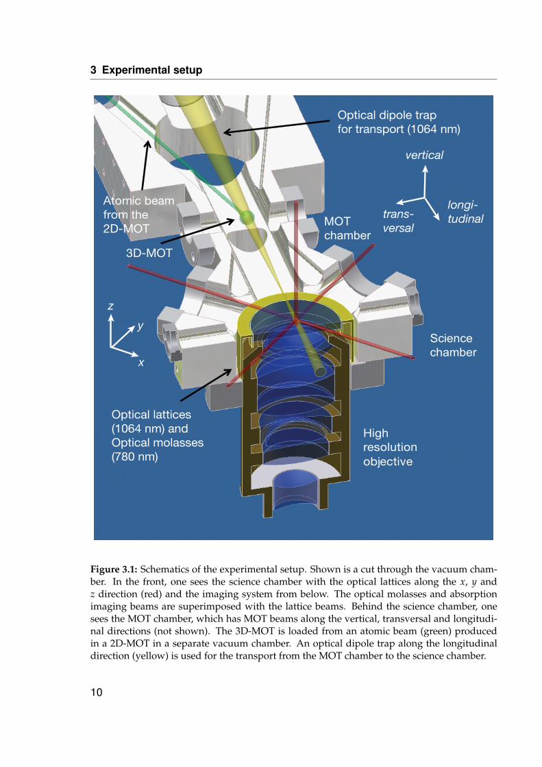
Our experimental setup consists of a steel vacuum chamber with two distinct regions,called the "MOT chamber" and the "science chamber" (see Fig. 3.1). A differentialpumping stage connects the MOT chamber with a 2D-MOT chamber. In the MOTchamber, there is a pair of water-cooled gradient coils with the strong axis along thetransversal direction. It is used both for the 3D-MOT and a magnetic quadrupole trap.Six MOT beams are aligned along the transversal, longitudinal and vertical direction.
In the science chamber, there are optical lattices along the x, y and z directions. Thez lattice beam is reflected from the vacuum window, under which the high-resolutionobjective is situated. A single gradient coil is placed above the atoms and an addi-tional pair of vertical offset coils is used to shift the position of the magnetic fieldzero close to the center of the chamber. An optical dipole trap along the longitudinaldirections connects the MOT chamber and the science chamber. It has a wavelengthλ = 1064 nm and waist radius w0 = 40 µm. The focus position can be moved alongthe optical axis to transport the atoms.
The experimental sequence is sketched in Fig. 3.2. It has a total duration of 22.5 sand consists of the following steps (the duration of each step is given in parenthesis).
1. MOT phase (2.3 s)We load the 3D-MOT from an atomic beam produced in the 2D-MOT (describedin [73]). We end with ∼ 109 atoms.
2. Magnetic trap and microwave evaporation (9.8 s)We load the atoms into the magnetic quadrupole trap by switching the fieldgradient to to 30 G/cm in 300 µs and then ramping it to 120 G/cm in 5 ms. Wetrap about 50% of the atoms in the |F = 1, mF = −1〉 state without additionaloptical pumping. We apply a microwave evaporation knife (on the transition to|F = 2, mF = −2〉) from −150 MHz down to −10 MHz, just before the onset ofMajorana losses and end up with ∼ 108 atoms at 20µK.
9
3 Experimental setup
Optical dipole trapfor transport (1064 nm)
High resolutionobjective
Optical lattices(1064 nm) andOptical molasses(780 nm)
Atomic beam from the2D-MOT
3D-MOT
Sciencechamber
x
y
z
trans-versal
longi-tudinal
vertical
MOTchamber
Figure 3.1: Schematics of the experimental setup. Shown is a cut through the vacuum cham-ber. In the front, one sees the science chamber with the optical lattices along the x, y andz direction (red) and the imaging system from below. The optical molasses and absorptionimaging beams are superimposed with the lattice beams. Behind the science chamber, onesees the MOT chamber, which has MOT beams along the vertical, transversal and longitudi-nal directions (not shown). The 3D-MOT is loaded from an atomic beam (green) producedin a 2D-MOT in a separate vacuum chamber. An optical dipole trap along the longitudinaldirection (yellow) is used for the transport from the MOT chamber to the science chamber.
10

3.1 Experimental sequence
0 5 10 15 200
40
80
1200
40
1201. 8.7.6.5.4.3.2.
Time (s)
Op
tical
pot
entia
ls (µ
K)
Mag
netic
gra
die
nts
(G/c
m)
Dipole trap
z Lattice
Quadrupole field at MOT
Gradient coil at lattice
9.
80
Figure 3.2: Schematics of the experimental sequence. Two exemplary magnetic field gradientsand optical potentials are schematically shown. The gray shaded areas mark the division ofthe sequence as used in the main text.
3. Loading of the optical dipole trap (1.5 s)We position the optical dipole trap 350 µm below the position of the magneticfield zero and ramp it to a depth U = kB · 100 µK in 250 ms. We load the dipoletrap by slowly switching off the magnetic gradient within 1.5 s and end with∼ 107 atoms at ∼ 5 µK in the dipole trap.
4. Optical transport (2.5 s)We move the focus of the optical dipole trap from the MOT chamber to thescience chamber within 2 s (see Sec. 3.2).
5. Hybrid trap and evaporation (2.3 s)We switch on a magnetic quadrupole field within 100 ms. The position of themagnetic zero is shifted ∼ 300 µm below the optical dipole trap and the fieldwith a vertical gradient of 13 G/cm compresses the atom cloud in the axial di-rection of the dipole trap laser beam, which allows high collision rates. Af-ter 500 ms of evaporative cooling in this hybrid trap configuration [74, 75], wetransfer the atoms into the z lattice and populate about 60 antinodes. We thenevaporate again by ramping down the dipole trap intensity and finally switch
11
3 Experimental setup
off the dipole trap. Now we have ∼ 105 atoms in the vertical lattice.
6. 2D system preparation (0.5 s)We prepare a single slice in the vertical lattice using magnetic resonance imag-ing techniques (see Sec. 3.3).
7. Evaporation in z lattice (1.1 s)We perform a final evaporation by ramping down the z lattice from Vz = 54 Er toVz = 22 Er in 1 s while simultaneously tilting the potential along the horizontaldirection with a magnetic field gradient. Then we move the cloud via the offsetfields to a good overlap with the optical lattice. Depending on the end point ofthe evaporation, we are left with a few hundred to few thousand atoms in thedegenerate regime in the |F = 1, mF = −1〉 state.
8. Horizontal lattices (∼ 0.5 s)We ramp up the x and y lattice depths in an s-shaped ramp of 75 ms to create aMott insulator (see Ch. 5) and perform the desired experiment.
9. Fluorescence imaging (2.0 s)Finally we freeze the distribution by ramping all three lattices to ∼ kB · 300 µKdepth in 2 ms and apply the push out pulse to remove the atoms from doublyoccupied sites. We illuminate with an optical molasses and take a fluorescenceimage for 900 ms. Then we drop the atoms and record an image of the back-ground light (see Ch. 4).
3.2 Optical transport
Most experiments with ultracold atoms in lattices use two separate regions for theMOT and for the lattices, because both require a large optical access. Often, the trans-port between the two regions is accomplished by moving the position of the zero of amagnetic field gradient either using many coil pairs [76, 77] or by translating a singlepair of coils [78]. A different approach is to transport optically, either by moving thefocus [79–81] or shifting the phase of an optical lattice [82, 83]. This has the advantageof stealing less optical access in the science chamber.
We transport the atoms in a single beam optical dipole trap (1064 nm, beam waistradius w0 = 40 µm, axial trap frequency 5 Hz at kB 100 µK trap depth). The atomsare transported within 2 s by a distance of 130 mm by translating the focus positionof the dipole trap using mirrors on a motorized micrometer stage (Newport MotionController XMS160, range 160 mm). We use a rather smooth transport profile, i.e. thefocus position as a function of time, which is a concatenated polynomial continuousto third order and has a maximum velocity of 300 mm/s and a maximum accelerationof 2.5 m/s2 [84]. The transport is slightly non-adiabatic with respect to the axial trap-ping frequency of 5 Hz and in this regime one expects to excite oscillations, whose
12
3.3 Preparation of 2D systems
amplitude depend on the precise timing of the transport profile [81]. Although wesee some influence of the parameters of our transport profile, the interpretation isnot clear [84]. After transport we have an oscillation with an amplitude of ∼ 150 µmwhich is damped during the subsequent evaporation in the hybrid trap.
In previous experiments the lens which produces the focus of the dipole trap wasplaced on the translation stage [79]. We found that the alignment was easier if weput the lens before the stage and use the stage to change the length of the subsequentbeam path by changing the position of a pair of retroreflecting mirrors. This alsoincreases the travel range by a factor of two. We want to position the stage far awayfrom the science chamber to avoid magnetic fluctuations at the position of the atoms.Therefore we image the focus of the dipole trap into the vacuum chamber with a 1:1telescope. One of the last mirrors before the chamber is piezo driven and smoothlychanged from one position to another during the optical transport. This allows for anindependent alignment of the transversal dipole trap position at the position of theMOT and the science chamber.
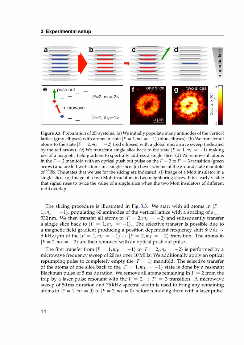
3.3 Preparation of 2D systems
In an optical lattice it is straight forward to reduce the dimensionality by making oneor two lattice axes deep and thereby freezing the dynamics in these directions [85].This amounts to working with many copies of the lower-dimensional system. Forthe imaging, however, we need a single two-dimensional system, and two differentapproaches have been established for its preparation.
One approach is to compress the atom cloud either magnetically [86] or opticallyusing a light sheet [87, 88] or an evanescent wave surface trap [89, 90]. To allowthe resulting high atomic densities, one can reduce the repulsive interactions via aFeshbach resonance in this step [91]. The compressed cloud can then optionally beloaded into a single antinode of an optical lattice with a few µm spacing [14, 90, 91].
Another approach is to first populate several antinodes of an optical lattice andto subsequently prepare a single slice out of it using magnetic resonance imagingtechniques. For lattice spacings around 400 nm, a resolution of about 2 lattices siteshas been reached for degenerate samples [68, 92] and single atoms [41, 93].
We implement this second approach, because the geometry of our chamber neitherallows a larger lattice spacing (via an angle between the two vertical lattice beams)nor sufficient access to create a tightly focused light sheet. This preparation has theadvantage that we can in principle create three-dimensional clouds and observe themtomographically after freezing them. Using a vertical lattice with a small spacing of532 nm also ensures that the extension of the atomic wave packet in the direction ofthe imaging system (<100 nm) is much smaller than the depth of focus of our imagingsystem (∆z = 1.7 µm). If this condition was not fulfilled we might have faced areduction of the imaging resolution and of the addressing fidelity.
13
3 Experimental setup
|F=2, mF=-2>
|F=1, mF=-1>
ba c d
e
mag
netic
fiel
d
microwave
push out two slicesf one slice g
5 µm0
5
10
15
Co
un
ts (x
10
3)
Figure 3.3: Preparation of 2D systems. (a) We initially populate many antinodes of the verticallattice (gray ellipses) with atoms in state |F = 1, mF = −1〉 (blue ellipses). (b) We transfer allatoms to the state |F = 2, mF = −2〉 (red ellipses) with a global microwave sweep (indicatedby the red arrow). (c) We transfer a single slice back to the state |F = 1, mF = −1〉 makinguse of a magnetic field gradient to spectrally address a single slice. (d) We remove all atomsin the F = 2 manifold with an optical push out pulse on the F = 2 to F′ = 3 transition (greenarrow) and are left with atoms in a single slice. (e) Level scheme of the ground state manifoldof 87Rb. The states that we use for the slicing are indicated. (f) Image of a Mott insulator in asingle slice. (g) Image of a two Mott insulators in two neighboring slices. It is clearly visiblethat signal rises to twice the value of a single slice when the two Mott insulators of differentradii overlap.
The slicing procedure is illustrated in Fig. 3.3. We start with all atoms in |F =1, mF = −1〉, populating 60 antinodes of the vertical lattice with a spacing of alat =532 nm. We then transfer all atoms to |F = 2, mF = −2〉 and subsequently transfera single slice back to |F = 1, mF = −1〉. The selective transfer is possible due toa magnetic field gradient producing a position dependent frequency shift ∂ν/∂z ∼5 kHz/µm of the |F = 1, mF = −1〉 ↔ |F = 2, mF = −2〉 transition. The atoms in|F = 2, mF = −2〉 are then removed with an optical push out pulse.
The first transfer from |F = 1, mF = −1〉 to |F = 2, mF = −2〉 is performed by amicrowave frequency sweep of 20 ms over 10 MHz. We additionally apply an opticalrepumping pulse to completely empty the |F = 1〉 manifold. The selective transferof the atoms of one slice back to the |F = 1, mF = −1〉 state is done by a resonantBlackman pulse of 5 ms duration. We remove all atoms remaining in F = 2 from thetrap by a laser pulse resonant with the F = 2 → F′ = 3 transition. A microwavesweep of 50 ms duration and 75 kHz spectral width is used to bring any remainingatoms in |F = 1, mF = 0〉 to |F = 2, mF = 0〉 before removing them with a laser pulse.
14
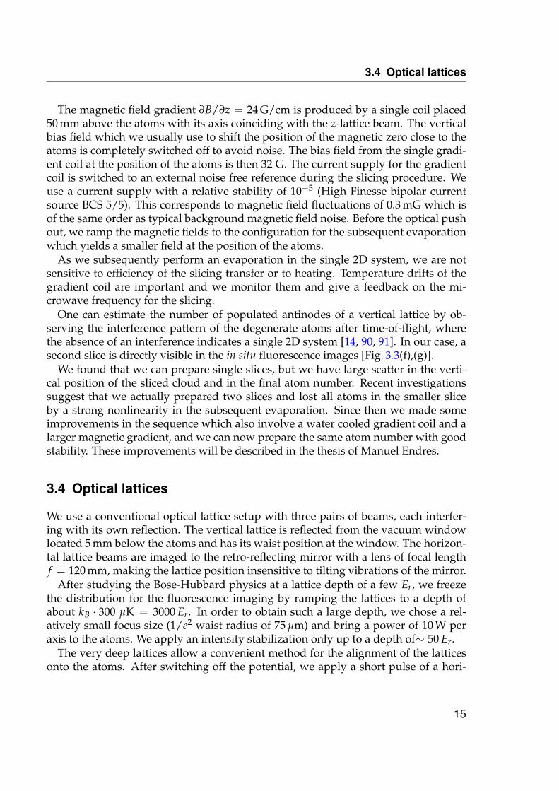
3.4 Optical lattices
The magnetic field gradient ∂B/∂z = 24 G/cm is produced by a single coil placed50 mm above the atoms with its axis coinciding with the z-lattice beam. The verticalbias field which we usually use to shift the position of the magnetic zero close to theatoms is completely switched off to avoid noise. The bias field from the single gradi-ent coil at the position of the atoms is then 32 G. The current supply for the gradientcoil is switched to an external noise free reference during the slicing procedure. Weuse a current supply with a relative stability of 10−5 (High Finesse bipolar currentsource BCS 5/5). This corresponds to magnetic field fluctuations of 0.3 mG which isof the same order as typical background magnetic field noise. Before the optical pushout, we ramp the magnetic fields to the configuration for the subsequent evaporationwhich yields a smaller field at the position of the atoms.
As we subsequently perform an evaporation in the single 2D system, we are notsensitive to efficiency of the slicing transfer or to heating. Temperature drifts of thegradient coil are important and we monitor them and give a feedback on the mi-crowave frequency for the slicing.
One can estimate the number of populated antinodes of a vertical lattice by ob-serving the interference pattern of the degenerate atoms after time-of-flight, wherethe absence of an interference indicates a single 2D system [14, 90, 91]. In our case, asecond slice is directly visible in the in situ fluorescence images [Fig. 3.3(f),(g)].
We found that we can prepare single slices, but we have large scatter in the verti-cal position of the sliced cloud and in the final atom number. Recent investigationssuggest that we actually prepared two slices and lost all atoms in the smaller sliceby a strong nonlinearity in the subsequent evaporation. Since then we made someimprovements in the sequence which also involve a water cooled gradient coil and alarger magnetic gradient, and we can now prepare the same atom number with goodstability. These improvements will be described in the thesis of Manuel Endres.
3.4 Optical lattices
We use a conventional optical lattice setup with three pairs of beams, each interfer-ing with its own reflection. The vertical lattice is reflected from the vacuum windowlocated 5 mm below the atoms and has its waist position at the window. The horizon-tal lattice beams are imaged to the retro-reflecting mirror with a lens of focal lengthf = 120 mm, making the lattice position insensitive to tilting vibrations of the mirror.
After studying the Bose-Hubbard physics at a lattice depth of a few Er, we freezethe distribution for the fluorescence imaging by ramping the lattices to a depth ofabout kB · 300 µK = 3000 Er. In order to obtain such a large depth, we chose a rel-atively small focus size (1/e2 waist radius of 75 µm) and bring a power of 10 W peraxis to the atoms. We apply an intensity stabilization only up to a depth of∼ 50 Er.
The very deep lattices allow a convenient method for the alignment of the latticesonto the atoms. After switching off the potential, we apply a short pulse of a hori-
15
3 Experimental setup
52P3/2
52S1/2
780.25 nm
267 MHz
72 MHz
157 MHz
F’=3
F’=2
F’=1
F’=0
F=2
F=1
c.o. 1-2
c.o. 1-3
78.5 MHz
212 MHz
6.8 GHz
cooling repump
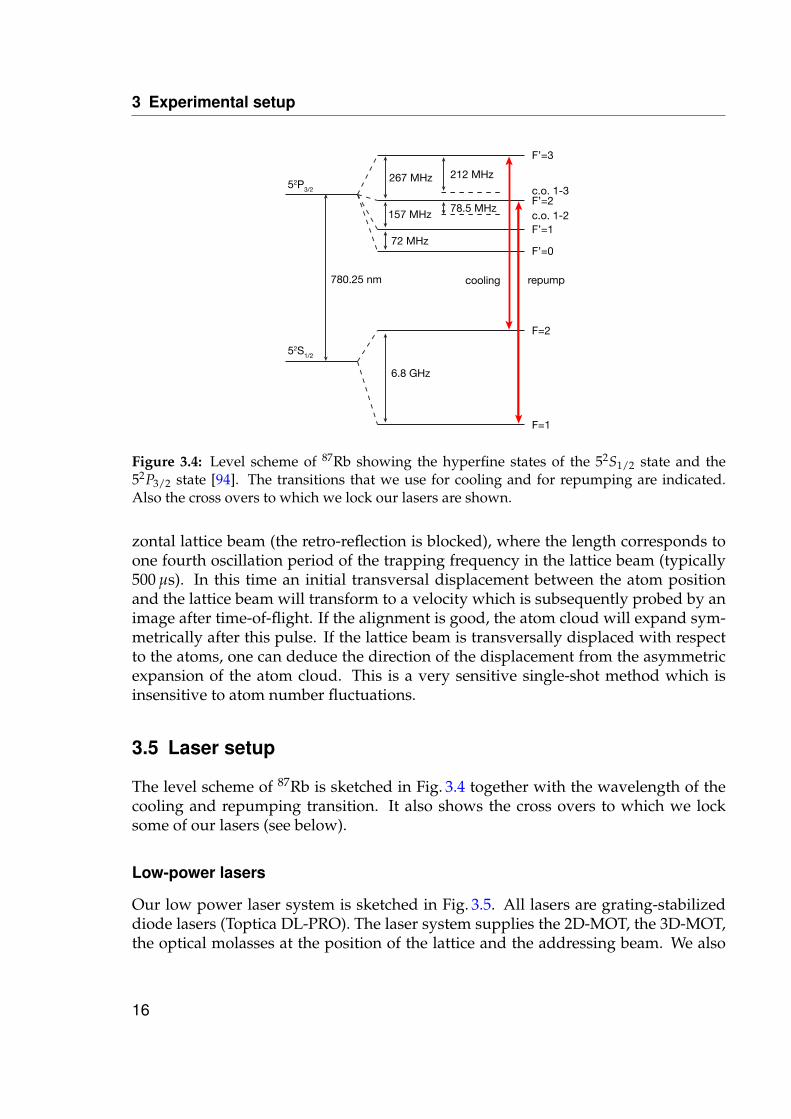
Figure 3.4: Level scheme of 87Rb showing the hyperfine states of the 52S1/2 state and the52P3/2 state [94]. The transitions that we use for cooling and for repumping are indicated.Also the cross overs to which we lock our lasers are shown.
zontal lattice beam (the retro-reflection is blocked), where the length corresponds toone fourth oscillation period of the trapping frequency in the lattice beam (typically500 µs). In this time an initial transversal displacement between the atom positionand the lattice beam will transform to a velocity which is subsequently probed by animage after time-of-flight. If the alignment is good, the atom cloud will expand sym-metrically after this pulse. If the lattice beam is transversally displaced with respectto the atoms, one can deduce the direction of the displacement from the asymmetricexpansion of the atom cloud. This is a very sensitive single-shot method which isinsensitive to atom number fluctuations.
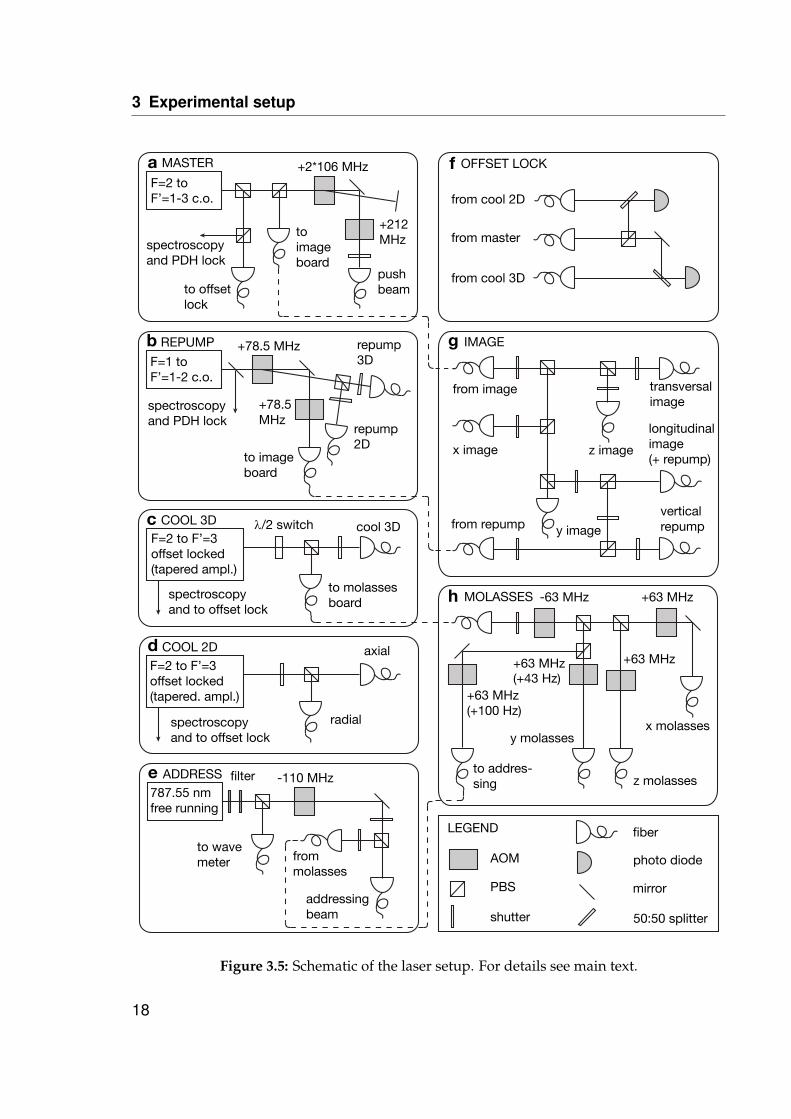
3.5 Laser setup
The level scheme of 87Rb is sketched in Fig. 3.4 together with the wavelength of thecooling and repumping transition. It also shows the cross overs to which we locksome of our lasers (see below).
Low-power lasers
Our low power laser system is sketched in Fig. 3.5. All lasers are grating-stabilizeddiode lasers (Toptica DL-PRO). The laser system supplies the 2D-MOT, the 3D-MOT,the optical molasses at the position of the lattice and the addressing beam. We also
16
3.5 Laser setup
have absorption imaging beams superimposed with the MOT beams and the latticebeams. The following letters refer to the subfigures in Fig. 3.5.
(a) The master laser provides the image beam [via a double-pass acousto-opticalmodulator (AOM)] and the push beam of the 2D MOT [73]. It is stabilized to the 1-3cross over using a Pound-Drewer-Hall lock.
(b) The repump laser for the two MOTs and for the absorption imaging is lockedto the 1-2 cross over and shifted into resonance with the F = 1 to F′ = 1 transitionusing an AOM. As the beams are not needed simultaneously, we extract the imagerepumper from the zeroth order of the first AOM.
(c)-(d) The cooling light for the two MOTs and the molasses is obtained from twotapered amplifiers which are both offset locked to the master. A half-wave plate canbe placed into the beam path to switch the power between the 3D-MOT and the mo-lasses at the lattices at the subsequent polarizing beam splitter cube (PBS).
(e) The addressing laser is not frequency stabilized and monitored with a wavemeter. We can send a molasses beam through the same beam path (see Sec. 6.5).
(f) For the offset lock, the cooling light and the master laser are combined on a 50:50splitter after spatial filtering via an optical fiber. The beam signal is recorded via a fastphoto diode (Hamamatsu MSM Photodetector).
(g) The image beam is distributed over the different imaging ports. Repumping isdone in the vertical direction at the position of the MOT and in longitudinal directionat the position of the lattice. We use one fast shutter to switch the imaging on and off(Uniblitz Eletronic). More shutters in front of each fiber coupling serve to select thedesired imaging direction.
(h) The molasses light is distributed over the x,y, and z direction and can also besent to the addressing port. The AOMs are controlled by phase-locked waveformgenerators such that we can give controlled relative detunings to the molasses beams(see Sec. 4.5).
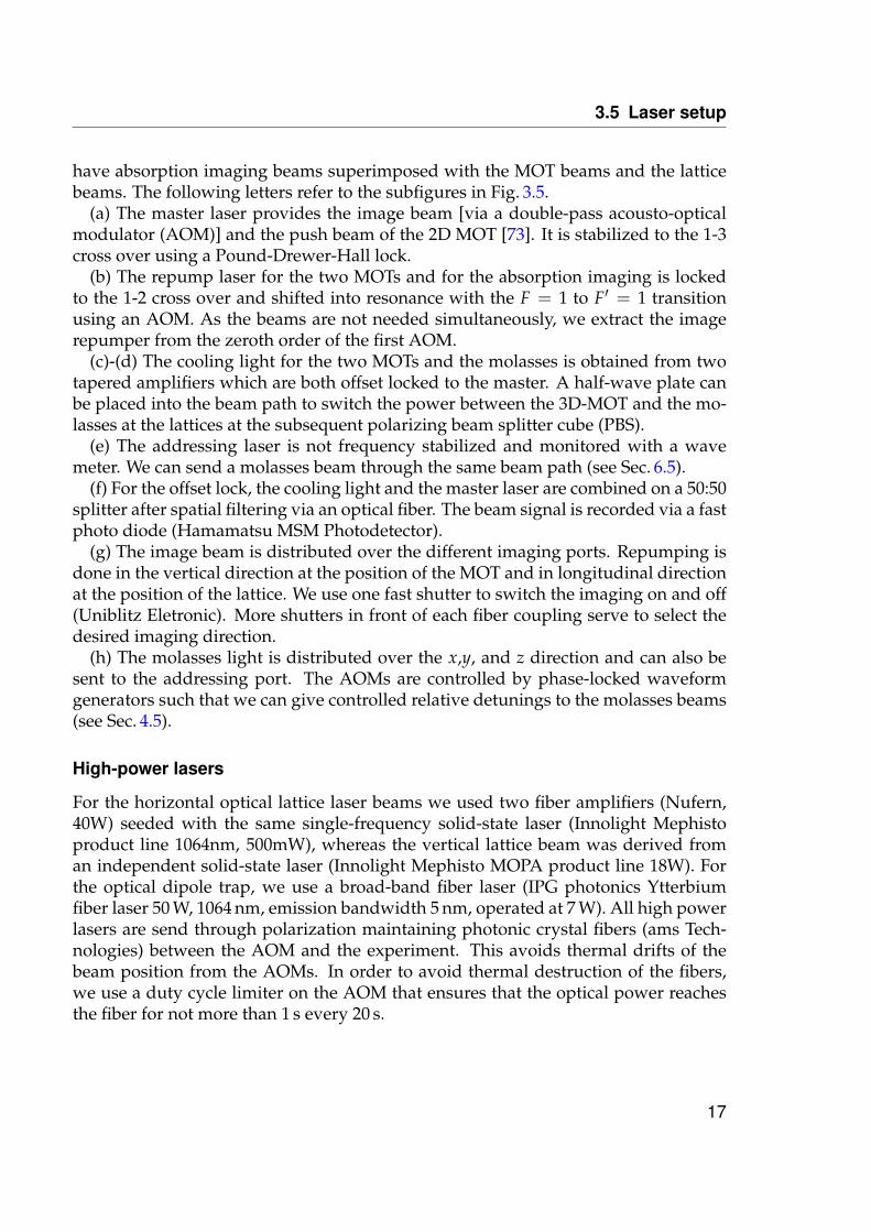
High-power lasers
For the horizontal optical lattice laser beams we used two fiber amplifiers (Nufern,40W) seeded with the same single-frequency solid-state laser (Innolight Mephistoproduct line 1064nm, 500mW), whereas the vertical lattice beam was derived froman independent solid-state laser (Innolight Mephisto MOPA product line 18W). Forthe optical dipole trap, we use a broad-band fiber laser (IPG photonics Ytterbiumfiber laser 50 W, 1064 nm, emission bandwidth 5 nm, operated at 7 W). All high powerlasers are send through polarization maintaining photonic crystal fibers (ams Tech-nologies) between the AOM and the experiment. This avoids thermal drifts of thebeam position from the AOMs. In order to avoid thermal destruction of the fibers,we use a duty cycle limiter on the AOM that ensures that the optical power reachesthe fiber for not more than 1 s every 20 s.
17
3 Experimental setup
MASTER +2*106 MHz
+212 MHz
pushbeam
toimageboard
to offset lock
spectroscopyand PDH lock
REPUMP +78.5 MHz
+78.5MHz
repump2D
to imageboard
spectroscopyand PDH lock
COOL 3D cool 3D
to molassesboard
spectroscopyand to offset lock
COOL 2D axial
radialspectroscopyand to offset lock
λ/2 switch
ADDRESS -110 MHz
addressing beam
from molasses
to wavemeter
filter
from cool 2D
from master
from cool 3D
OFFSET LOCK
IMAGE
MOLASSES
from repump
from image
x image
y image
z image
transversalimage
verticalrepump
longitudinalimage(+ repump)
-63 MHz
to addres-sing
y molasses
z molasses
x molasses
AOM
LEGEND
a
b
c
d
e
f
g
h
PBS
shutter
fiber
photo diode
mirror
50:50 splitter
+63 MHz(+100 Hz)
+63 MHz(+43 Hz)
+63 MHz
+63 MHz
F=2 to F’=3offset locked(tapered ampl.)
F=2 toF’=1-3 c.o.
F=1 toF’=1-2 c.o.
F=2 to F’=3offset locked(tapered. ampl.)
787.55 nmfree running
repump3D
Figure 3.5: Schematic of the laser setup. For details see main text.
18
4 Single-atom resolved fluorescence imaging
This chapter describes how we image the quantum gases in the optical lattice withsingle-site resolution and single-atom sensitivity. We combine fluorescence imag-ing with a high numerical aperture objective (Sec. 4.2). One drawback of fluores-cence imaging are the light-assisted collision, which lead to the rapid pair-wise lossof atoms, such that we detect the parity of the original atom distribution per latticesite (Sec. 4.3). Because we only have to distinguish between one or zero atom perlattice site, we can reconstruct the atom distribution even with a resolution abovethe Rayleigh criterion. We developed a deconvolution algorithm, which tries dif-ferent atom configurations and reconstructs the distribution with very high fidelity(Sec. 4.4). The fidelity is limited by the loss of atoms during the imaging time due tobackground collisions and thermal hopping events in the molasses. Optimization ofthe molasses parameters can largely suppress this thermal hopping (Sec. 4.5). We dis-cuss possible extensions of the imaging technique (Sec. 4.6) and conclude in Sec. 4.7.
4.1 State of the art
Fluorescence imaging is the method of choice for reaching single atom sensitivity,because it yields a large signal-to-noise ratio and atoms can be simultaneously cooledby an optical molasses. The method was demonstrated for imaging single atoms inoptical dipole traps [35], and in optical lattices [38, 95].
However, it remained a challenge to apply it to systems in the strongly correlatedregime. Strong correlations require sufficiently large tunneling rates between the lat-tice sites, which can compete with the technical heating rates to allow an adiabaticramp up of the lattices. As the tunneling rate is exponentially suppressed with thelattice spacing, the latter has to be on the order of 0.5 µm, which is challenging tooptically resolve. In the case of rubidium, Mott insulators were so far created withlattice spacings of ∼ 426 nm [2, 96], 532 nm [97], 680 nm [46], and with a rectangularlattice with spacings 765 nm and 426 nm [98]. Larger spacings might be possible forlighter elements, especially lithium [99].
The first experiments with fluorescence imaging worked either in a 3D lattice of5 µm spacing [38], where tunneling is completely suppressed, or with sparse filling ina 1D lattice with short spacing [42, 95]. In this 1D lattice, nearest neighbor detection ata spacing of 433 nm was reached despite the diffraction limited resolution of 1.8 µmby using an algorithm, which makes use of the discreteness of the spacing and of thedilute filling [42].
19
4 Single-atom resolved fluorescence imaging
An alternative approach demonstrated in the group of Herwig Ott is to applyscanning electron microscopy to ultracold gases, which allows a resolution downto 150 nm, well resolving a lattice of 600 nm spacing [43]. As the electron beam isscanned across the sample, the atoms are ionized by electron impact ionization, ex-tracted with an electrostatic field and subsequently detected by an ion detector. Themethod, however, does not reach full single-atom sensitivity, because impact ioniza-tion constitutes only about 40% of the scattering events, and averaging over manyimages is required so far.
Absorption imaging has been used for in situ imaging of two-dimensional systemswith a resolution of 3-4 µm [91] and 1.2 µm [39]. The former experiment achieveddetection of the shell structure of a Mott insulator and the latter resolved lattice siteswith 2 µm spacing, with a weak tunnel coupling. However, absorption imaging hasnot reached single-atom sensitivity so far.
Only recently was the technique of single-atom sensitive fluorescence imaging com-bined with single-site resolution in a short-period lattice in the group of MarkusGreiner [45].The atoms were placed in a surface trap a few micrometer below a hemi-spheric lens, and the solid immersion effect lead to an effective numerical aperture ofNA = 0.8 for an objective with NA = 0.55 outside the vacuum chamber. Thus thelattice spacing of 680 nm could be well resolved at a resolution of 600 nm (FWHM).The horizontal lattices were generated by projecting a holographic mask through theimaging system. This allowed to change the lattice wavelength for the imaging andobtain the required lattice depth with a convenient laser power. However, the prox-imity to the surface seems to cause problems in the homogeneity of the potentials[46]. Finally, single-atom-resolved images of Mott insulators were obtained in thegroup of Markus Greiner [46] and in our group [47]. This will be described in Ch. 5.
4.2 High-resolution imaging system
Imaging resolution
Due to its finite aperture, an imaging system can only reproduce a limited range ofspatial frequencies of the object. Because the system is linear, the imaging systemcan be completely characterized by the response to a point source, the so called pointspread function (PSF). It has the form of an Airy pattern, the width of which is de-termined by the wavelength and the aperture of the imaging system NA = n sin α.Here, α is the half opening angle and n is the refractive index between the object andthe imaging system. The intensity distribution of the airy pattern is given by (see e.g.Ref. [100])
I(ρ) ∝(
2J1(ρ)
ρ
)2
, (4.1)
20
4.2 High-resolution imaging system
xy
16 µm 0 0.5 1 1.50
2
4
6
8
10
12
Radial distance from center r (µm)
c
3.75 µm
Cou
nts
(x 1
03 )2
4
6
d
0 10.5
a
8
0
1.5
10data from test targetPSF of point source
b
signal from atomsmodel PSF
Cou
nts
(x 1
02 )
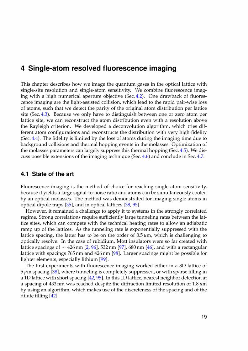
Figure 4.1: Point-spread function of the imaging system. (a) image of a single hole in thetest target. Two of the rings of the Airy pattern can be distinguished. In the test setup, weused a camera with a pixel size of 8 µm, which corresponds to 62 nm in the object plane.(b) azimuthal average of the data in (a) together with an Airy pattern as given by Eq. (4.1)with a resolution of r0 = 700 nm as expected from the numerical aperture NA = 0.68 of theimaging system (red line). The experimental data points (blue circles) lie somewhat outsidethe theoretical curve due to the finite size of the hole (≈ 100 nm). (c) Fluorescence image ofa dilute cloud of atoms. The white dots mark the lattice sites. The individual atoms are welldistinguishable. (d) Azimuthal average of our experimentally obtained point spread functionof a single atom. The data was obtained by averaging over 68 signals of single atoms. The redline is a fit with the double Gaussian of Eq. (4.2).
21
4 Single-atom resolved fluorescence imaging
where J1(ρ) is the Bessel function of first order and ρ = r · 3.795/r0 is the radialdistance r scaled by the resolution r0 and a numerical factor. The Rayleigh resolutionis defined as the first zero of I(ρ) and is linked to the numerical aperture via r0 =1.22 · λ/(2NA). Fig. 4.1(b) shows the PSF of a point source for our numerical apertureof NA = 0.68 and an imaging wavelength of λ = 780 nm (red line), which yieldsr0 = 700 nm.
The Rayleigh criterion states that point sources can be discriminated, if the maxi-mum of one PSF coincides with the first zero of the other PSF, i.e. if their distance isr0. By this definition, we do not have single-site resolution for our lattice spacing ofalat = 532 nm. However, the actual resolution can be well below this diffraction limit,if additional information is given [42, 101], such as the discrete nature of atoms andthe lattice structure.
As the atoms sit on their lattice sites, it is not necessary to determine their position,but only to determine the occupation of each lattice site. Furthermore, there can beonly zero or one atom per lattice site due to the light-induced collisions (Sec. 4.3).Therefore it is sufficient to have an imaging resolution that is able to differentiate zeroor one atom per lattice site. It would be much harder to discriminate between moreatom numbers. The requirement for the optical resolution in this context is to resolvea missing atom within a full shell and for this we should compare the resolution totwice the lattice spacing. This argument holds only for a large signal to noise, wherethe PSF of each atom is well formed on the camera chip. We describe in Sec. 4.4 howwe determine the position of the lattice sites and reconstruct the atom distribution onthe lattice.
The above considerations assume incoherent light, and in fact, imaging with coher-ent light can reduce the resolution [102]. Here, fluorescence imaging has an advan-tage over absorption imaging. Both methods rely on the scattering of photons by theatoms, but in absorption imaging, the usually coherent incident beam with the result-ing shadow is imaged, while in fluorescence imaging only the scattered photons areimaged, and they can lose their coherence via inelastic scattering. In Ch. 8 we showthat the coherent power fraction scattered into the objective is just a few percent.
We use the 5S-5P transition at λ = 780 nm for imaging. Using the 5S-6P transitionat the wavelength of λ = 420 nm instead would allow a much better resolution of370 nm. However, it is not clear if the sub-Doppler molasses (Sec. 4.5) will work onthis transition.
Experimental setup
Our microscope objective was custom made (Leica Microsystems) and is located out-side the vacuum chamber with a working distance of 13 mm. It is optimized for thewavelength range of 420 nm to 780 nm and has a numerical aperture of NA = 0.68for λ = 780 nm and NA = 0.70 for λ = 420 nm. It is diffraction limited with a Strehlof 97%. The camera (iXonEM+ 897 (back-illuminated), ANDOR Technology) has a
22
4.2 High-resolution imaging system
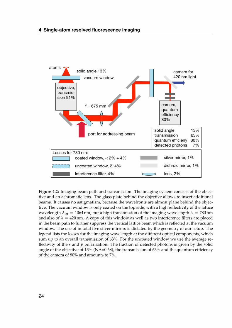
quantum efficiency of 80% and is cooled to −70C in order to reduce dark counts.The beam path is sketch in Fig. 4.2. The objective covers 13% of the solid angle andthe total transmission of the imaging system including the mirrors and filters is 63%.Including the quantum efficiency of the camera, we thus detect 7% of the scatteredphotons at the camera.
The imaging system consists of the objective with effective focal length of 5.19 mmand an achromatic lens with focal length 675 mm, yielding a magnification of 130.Thus the camera pixel size of 16 µm corresponds to 123 nm in the object plane, whichis a reasonable value, since it does not limit the resolution and at the same time avoidsdistribution of the signal on too many pixels. Interference filters serve for the suppres-sion of the light from the vertical lattice. An uncoated glass window in the beam pathallows to send beams through the objective in reverse direction, e.g. a molasses beam(Sec. 4.5) or the addressing beam (Ch. 6).
The objective was tested separately from the main experimental setup using a testtarget with small holes, which was illuminated from the back [103]. The holes werespaced irregularly in order to avoid the Talbot effect with the spatially coherent light[104, 105]. The measured PSF from the test setup agreed with the specified imagingresolution, taking into account the finite size of the holes [see Fig. 4.1(a),(b)]. Theobjective is placed on a positioner (PIFOC P-726, Physik Instrumente GmbH & Co.KG, Karlsruhe), which allows to move it along the optical axis over a range of 100 µmwith a precision of 10 nm.
The placement of the objective outside the vacuum chamber poses stringent re-quirements on the flatness of the vacuum window. Over a region of 15 mm the de-formations must be smaller than λt/4 (λt = 655 nm is the test wavelength). Thisexcludes spherical deformations, which can be compensated by refocussing the ob-jective. We measured the deformations with a Fizeau interferometer (PTI 250 Zy-goLOT, 50 mm aperture) and found 0.15 λt, which degraded to 0.22 λt after baking ofthe vacuum chamber.
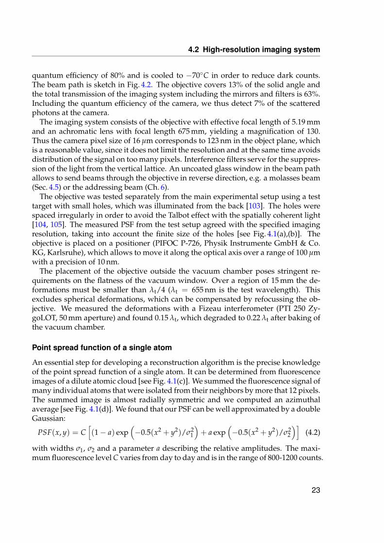
Point spread function of a single atom
An essential step for developing a reconstruction algorithm is the precise knowledgeof the point spread function of a single atom. It can be determined from fluorescenceimages of a dilute atomic cloud [see Fig. 4.1(c)]. We summed the fluorescence signal ofmany individual atoms that were isolated from their neighbors by more that 12 pixels.The summed image is almost radially symmetric and we computed an azimuthalaverage [see Fig. 4.1(d)]. We found that our PSF can be well approximated by a doubleGaussian:
PSF(x, y) = C[(1− a) exp
(−0.5(x2 + y2)/σ2
1
)+ a exp
(−0.5(x2 + y2)/σ2
2
)](4.2)
with widths σ1, σ2 and a parameter a describing the relative amplitudes. The maxi-mum fluorescence level C varies from day to day and is in the range of 800-1200 counts.
23
4 Single-atom resolved fluorescence imaging
atomssolid angle 13%
objective,transmis-sion 91%
silver mirror, 1%coated window, < 2% + 4%
uncoated window, 2 4%
lens, 2%
camera,quantumefficiency80%
dichroic mirror, 1%
interference filter, 4%
port for addressing beam
camera for420 nm light
solid angle 13%transmission 63%quantum efficieny 80%detected photons 7%
Losses for 780 nm:
f = 675 mm
vacuum window
.
Figure 4.2: Imaging beam path and transmission. The imaging system consists of the objec-tive and an achromatic lens. The glass plate behind the objective allows to insert additionalbeams. It causes no astigmatism, because the wavefronts are almost plane behind the objec-tive. The vacuum window is only coated on the top side, with a high reflectivity of the latticewavelength λlat = 1064 nm, but a high transmission of the imaging wavelength λ = 780 nmand also of λ = 420 nm. A copy of this window as well as two interference filters are placedin the beam path to further suppress the vertical lattice beam which is reflected at the vacuumwindow. The use of in total five silver mirrors is dictated by the geometry of our setup. Thelegend lists the losses for the imaging wavelength at the different optical components, whichsum up to an overall transmission of 63%. For the uncoated window we use the average re-flectivity of the s and p polarization. The fraction of detected photons is given by the solidangle of the objective of 13% (NA=0.68), the transmission of 63% and the quantum efficiencyof the camera of 80% and amounts to 7%.
24
4.3 Light-assisted collisions
Parameter Value Unitσ1 2.06(5) pixelσ2 9.6(1.2) pixela 0.075(2) -C 1050(7) counts
Table 4.1: Parameters of the fit of the model function Eq. (4.2) to the atomic PSF.
We expect our PSF to be a convolution of an Airy disk with a Gaussian, taking intoaccount the width of the atomic wave packet in the potential wells and the pixel sizein the object plane of 125 nm. Due to this convolution, the first minimum of the airypattern is not visible in our averaged signal.
Tab. 4.1 lists the parameters of a fit of the model function Eq. (4.2) to the atomic PSF[Fig. 4.1(d)]. The width σ1 = 2.06(5)pixel = 258(6) nm corresponds to a Rayleighresolution of r0 = 740(20) nm and is only slightly above the diffraction limited sizefor ideal point sources.
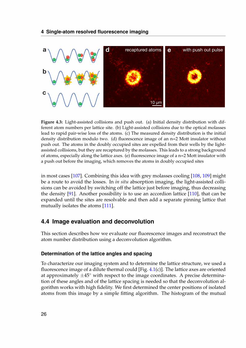
4.3 Light-assisted collisions
During the imaging, atom pairs on a lattice site are immediately lost due to inelasticlight-assisted collisions [35, 46, 47, 106]. The loss is on the time scale of 100 µs for ourparameters which is short compared to the total illumination time of 900 ms, such thatwe do not observe a signal from the atoms before they are expelled. We therefore onlydetect the particle number modulo two on each lattice site. This essentially amountsto recording the parity of the atom number. Fig. 4.3(a)-(c) illustrates this effect, whichhas important consequences for the detection of the number statistics (see Sec. 5.3).
We observed that the expelled atoms can be recaptured by the molasses and lead toa large background in the atom distribution, especially along the lattice axes, wherelattice is deep enough to hold the atoms [Fig. 4.3(d)]. To avoid this, we apply a 50 mspush out pulse from below, which removes the atoms in the doubly occupied sites,before switching on the molasses. The laser is on the F = 2 to F′ = 3 transition,which is 6.8 GHz red detuned for the atoms in F = 1, but excites into the molecularpotentials causing light-assisted collisions. Fig. 4.3(e) illustrates that the backgroundis efficiently removed by the push out pulse.
Parity projection constitutes a loss of information and is in many cases not desir-able. One way around this is to work at an average filling much smaller than one.One might also let the atoms expand in the third direction after freezing the distribu-tion of the 2D system, in order to make it so dilute that doubly occupied sites becomenegligible (see Ch. 7). Using blue detuned light, the energy gained by the atoms in thelight-assisted collision can be limited, leading to the loss of only one of the two atoms
25
4 Single-atom resolved fluorescence imaging
a
b
c10 µm
d recaptured atoms e with push out pulse
Figure 4.3: Light-assisted collisions and push out. (a) Initial density distribution with dif-ferent atom numbers per lattice site. (b) Light-assisted collisions due to the optical molasseslead to rapid pair-wise loss of the atoms. (c) The measured density distribution is the initialdensity distribution modulo two. (d) fluorescence image of an n=2 Mott insulator withoutpush out. The atoms in the doubly occupied sites are expelled from their wells by the light-assisted collisions, but they are recaptured by the molasses. This leads to a strong backgroundof atoms, especially along the lattice axes. (e) fluorescence image of a n=2 Mott insulator witha push out before the imaging, which removes the atoms in doubly occupied sites
in most cases [107]. Combining this idea with grey molasses cooling [108, 109] mightbe a route to avoid the losses. In in situ absorption imaging, the light-assisted colli-sions can be avoided by switching off the lattice just before imaging, thus decreasingthe density [91]. Another possibility is to use an accordion lattice [110], that can beexpanded until the sites are resolvable and then add a separate pinning lattice thatmutually isolates the atoms [111].
4.4 Image evaluation and deconvolution
This section describes how we evaluate our fluorescence images and reconstruct theatom number distribution using a deconvolution algorithm.
Determination of the lattice angles and spacing
To characterize our imaging system and to determine the lattice structure, we used afluorescence image of a dilute thermal could [Fig. 4.1(c)]. The lattice axes are orientedat approximately ±45 with respect to the image coordinates. A precise determina-tion of these angles and of the lattice spacing is needed so that the deconvolution al-gorithm works with high fidelity. We first determined the center positions of isolatedatoms from this image by a simple fitting algorithm. The histogram of the mutual
26
4.4 Image evaluation and deconvolution
45.5 45.6 45.7 45.8 45.9 46.0 46.1 46.20.4
0.5
0.6
0.7
0.8
0.9
Coordinate rotation angle (°)
Wid
th in
his
togr
am (p
ixel
)
0 10 20 30 400
100
200
Distance (pixel)
Freq
uenc
y
0 10 20 30 400
50
100
Distance (pixel)
Freq
uenc
y
a b
c
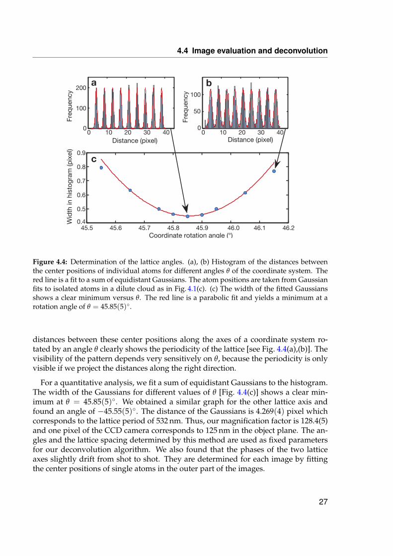
Figure 4.4: Determination of the lattice angles. (a), (b) Histogram of the distances betweenthe center positions of individual atoms for different angles θ of the coordinate system. Thered line is a fit to a sum of equidistant Gaussians. The atom positions are taken from Gaussianfits to isolated atoms in a dilute cloud as in Fig. 4.1(c). (c) The width of the fitted Gaussiansshows a clear minimum versus θ. The red line is a parabolic fit and yields a minimum at arotation angle of θ = 45.85(5).
distances between these center positions along the axes of a coordinate system ro-tated by an angle θ clearly shows the periodicity of the lattice [see Fig. 4.4(a),(b)]. Thevisibility of the pattern depends very sensitively on θ, because the periodicity is onlyvisible if we project the distances along the right direction.
For a quantitative analysis, we fit a sum of equidistant Gaussians to the histogram.The width of the Gaussians for different values of θ [Fig. 4.4(c)] shows a clear min-imum at θ = 45.85(5). We obtained a similar graph for the other lattice axis andfound an angle of −45.55(5). The distance of the Gaussians is 4.269(4) pixel whichcorresponds to the lattice period of 532 nm. Thus, our magnification factor is 128.4(5)and one pixel of the CCD camera corresponds to 125 nm in the object plane. The an-gles and the lattice spacing determined by this method are used as fixed parametersfor our deconvolution algorithm. We also found that the phases of the two latticeaxes slightly drift from shot to shot. They are determined for each image by fittingthe center positions of single atoms in the outer part of the images.
27
4 Single-atom resolved fluorescence imaging
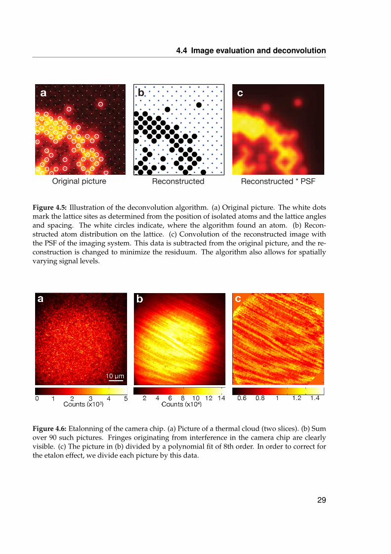
Reconstruction of the atom number distribution
We developed a deconvolution algorithm to reconstruct the atom number distribu-tion from a fluorescence image [Fig. 4.5(a)]. The algorithm tries different model-confi-gurations for each lattice site and its nearest neighbors in order to minimize the differ-ence of the original image with the reconstructed one [Fig. 4.5(b)]. This reconstructedimage is obtained by convoluting the atom number distribution with the atomic PSF[Fig. 4.1(d)]. The algorithm allows for a variance of the fluorescence level of eachatom of ±20% of the mean photon count. These varying fluorescence levels partiallyarise from the inhomogeneous intensity of the molasses light.
We additionally found an increased fluorescence level of about 5%-10% in the cen-ter of very dense n = 1 shells of a Mott insulator, compared to the isolated atoms inthe outer part of the images. This effect might arise from rescattering, which effec-tively blocks a significant part of the solid angle, redirecting the photons out of theplane. The cross section for rescattering a photon in a stimulated Rayleigh transitionis of the order of the resonant cross section [112] which is of the same size as thedistance between the atoms.
We have evaluated the fidelity of the reconstruction algorithm by creating simu-lated images of a known atom distribution using the PSF of our imaging system, thepoissonian and superpoissonian noise contributions of the light hitting the EMCCDcamera (including the amplification process), and the site-to-site fluorescence fluc-tuations of ±20%. Running the reconstruction algorithm over several hundred ofsuch randomly generated images of Mott insulators at finite temperatures, we find areconstruction fidelity of ∼ 99.5%. In our experiment, the main limitations of the fi-delity are atom losses during the detection process due to collisions with backgroundgas atoms (Sec. 4.5). The imaging time of 900 ms is thus a compromise between theacquired signal and the described atom losses.
A more sophisticated algorithm is presently under development and will be de-scribed in the thesis of Peter Schauß.
Etaloning of the camera
We correct for an etaloning effect of the CCD camera, which causes a spatially de-pendent signal strength (see Fig. 4.6). We determined the effect by summing over 90images with two slices of a large thermal cloud [Fig. 4.6(a) and (b)]. To eliminate theshape of the cloud, we fitted the data with an 8th order polynomial and divided thedata by this fit, obtaining the etalon data containing the fringes [Fig. 4.6(c)]. The outerregions with little signal were set to one. All pictures are divided by this etalon datato correct for the effect.
We correct for stray light by subtracting a second picture without the atoms butwith the same molasses parameters.
28
4.4 Image evaluation and deconvolution
Original picture Reconstructed * PSFReconstructed
a cb
Figure 4.5: Illustration of the deconvolution algorithm. (a) Original picture. The white dotsmark the lattice sites as determined from the position of isolated atoms and the lattice anglesand spacing. The white circles indicate, where the algorithm found an atom. (b) Recon-structed atom distribution on the lattice. (c) Convolution of the reconstructed image withthe PSF of the imaging system. This data is subtracted from the original picture, and the re-construction is changed to minimize the residuum. The algorithm also allows for spatiallyvarying signal levels.
Figure 4.6: Etalonning of the camera chip. (a) Picture of a thermal cloud (two slices). (b) Sumover 90 such pictures. Fringes originating from interference in the camera chip are clearlyvisible. (c) The picture in (b) divided by a polynomial fit of 8th order. In order to correct forthe etalon effect, we divide each picture by this data.
29
4 Single-atom resolved fluorescence imaging
4.5 Optical molasses
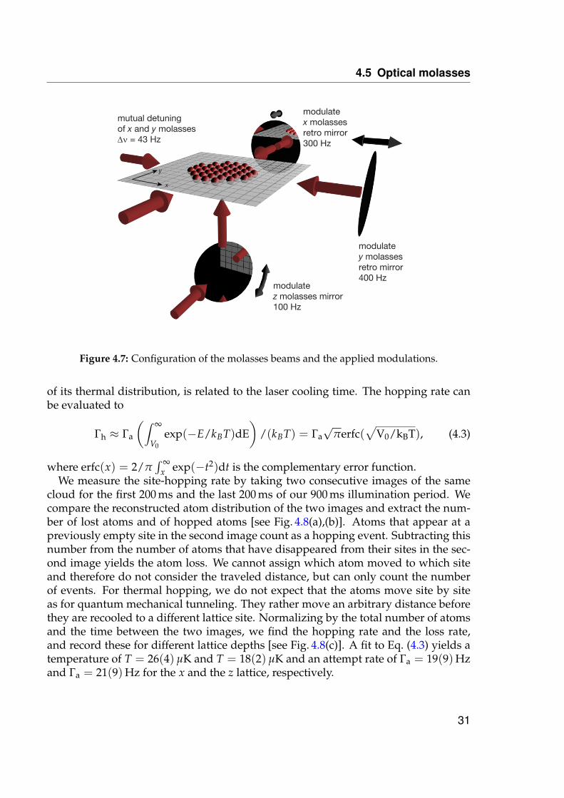
For imaging the atoms, we freeze the distribution by ramping the lattices to a depthof ∼ 300 µK per axis and illuminate them with an optical molasses, which simultane-ously laser cools the atoms. If the parameters are chosen well, the atoms stay in theirlattice site during the imaging time of about 900 ms. With a total scattering rate of∼ 150 kHz, we detect about 7000 photons per atom which allows to reconstruct theatom distribution with high fidelity (see Sec. 4.4).
We use five molasses beams oriented along the lattice axes in a σ+ − σ− configu-ration (see Fig. 4.7). Two horizontal beams are overlapped with the correspondinglattice beams via a dichroic mirror and are retro-reflected after a separation from thelattice beams via another dichroic mirror. The beam radii at the position of the atomsare wx = 940 µm and wy = 790 µm. We use a lens before the retro-reflecting mirror,which allows to have a smaller radius of the reflected beam and therefore to com-pensate for unavoidable power losses. We aligned the radiation pressure from theincoming and retro-reflected beam using a 1D free-space molasses.
A fifth molasses beam is shone in from below, in reverse direction through theimaging system. It has a focus before the objective, such that it is not focused at thefocal plane of the imaging system, but has its focus further up and has a radius ofwz = 4.2(6) µm in the focal plane. In order to further expand the beam, we scan itacross the cloud with a frequency of 100 Hz (see Fig. 4.7), leading to an effective beamradius of about weff
z = 30 µm. The significant stray light from this beam, originat-ing from reflections inside the objective, needs to be taken into account as describedin Sec. 4.4. The scanning of the position of the z molasses beam helps to wash outfringes in this stray light and interferences between the stray light and the signal. Thez molasses beam is not balanced by a counter-propagating beam; the polarizationgradients from the interference with the horizontal beams are sufficient for cooling inthe z direction.
Thermal hopping
When the atomic distribution is frozen by very deep optical lattices, the quantummechanical tunneling rates of the low bands become extremely small. However, thefluorescing atoms can undergo thermal hopping, i.e. overcome the barrier betweenthe lattice sites by their thermal energy. This process can be modeled by the Arrheniuslaw [38], which is often used to describe chemical reaction rates or diffusion of adsor-bates [113, 114]. To a good approximation, the activation energy for a hopping eventis given by the lattice depth V0, because the tunneling rate is suppressed for all but thevery last bound states. The hopping rate Γh can then be written as Γh = ΓaP(E > V0),where Γa is the attempt rate, and P(E > V0) is the probability to find an energy Elarger than the trap depth V0 in the thermal distribution. The laser field acts as a ther-mal bath for the atoms and the attempt rate Γa, with which the atom probes the tail
30
4.5 Optical molasses
modulatex molassesretro mirror300 Hz
modulatez molasses mirror100 Hz
modulatey molassesretro mirror400 Hz
mutual detuningof x and y molasses∆ν = 43 Hz
x
y
Figure 4.7: Configuration of the molasses beams and the applied modulations.
of its thermal distribution, is related to the laser cooling time. The hopping rate canbe evaluated to
Γh ≈ Γa
(∫ ∞
V0
exp(−E/kBT)dE)
/(kBT) = Γa√
πerfc(√
V0/kBT), (4.3)
where erfc(x) = 2/π∫ ∞
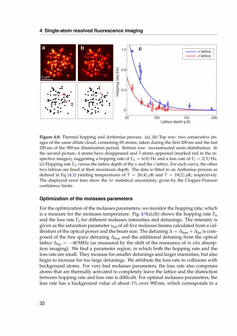
x exp(−t2)dt is the complementary error function.We measure the site-hopping rate by taking two consecutive images of the same
cloud for the first 200 ms and the last 200 ms of our 900 ms illumination period. Wecompare the reconstructed atom distribution of the two images and extract the num-ber of lost atoms and of hopped atoms [see Fig. 4.8(a),(b)]. Atoms that appear at apreviously empty site in the second image count as a hopping event. Subtracting thisnumber from the number of atoms that have disappeared from their sites in the sec-ond image yields the atom loss. We cannot assign which atom moved to which siteand therefore do not consider the traveled distance, but can only count the numberof events. For thermal hopping, we do not expect that the atoms move site by siteas for quantum mechanical tunneling. They rather move an arbitrary distance beforethey are recooled to a different lattice site. Normalizing by the total number of atomsand the time between the two images, we find the hopping rate and the loss rate,and record these for different lattice depths [see Fig. 4.8(c)]. A fit to Eq. (4.3) yields atemperature of T = 26(4) µK and T = 18(2) µK and an attempt rate of Γa = 19(9)Hzand Γa = 21(9)Hz for the x and the z lattice, respectively.
31
4 Single-atom resolved fluorescence imaging
50 100 150 200
0
0.4
0.8
1.2
Lattice depth (µK)H
opp
ing
rate
(Hz)
x latticez lattice
c
5 µm
a b
Figure 4.8: Thermal hopping and Arrhenius process. (a), (b) Top row: two consecutive im-ages of the same dilute cloud, containing 69 atoms, taken during the first 200 ms and the last200 ms of the 900 ms illumination period. Bottom row: reconstructed atom distribution. Inthe second picture, 4 atoms have disappeared and 3 atoms appeared (marked red in the re-spective images), suggesting a hopping rate of Γh = 6(8)Hz and a loss rate of Γl = 2(5)Hz.(c) Hopping rate Γh versus the lattice depth of the x and the z lattice. For each curve, the othertwo lattices are fixed at their maximum depth. The data is fitted to an Arrhenius process asdefined in Eq. (4.3) yielding temperatures of T = 26(4) µK and T = 18(2) µK, respectively.The displayed error bars show the 1σ statistical uncertainty, given by the Clopper-Pearsonconfidence limits.
Optimization of the molasses parameters
For the optimization of the molasses parameters, we monitor the hopping rate, whichis a measure for the molasses temperature. Fig. 4.9(a),(b) shows the hopping rate Γhand the loss rate Γl for different molasses intensities and detunings. The intensity isgiven as the saturation parameter stot of all five molasses beams calculated from a cal-ibration of the optical power and the beam size. The detuning ∆ = ∆free +∆lat is com-posed of the free space detuning ∆free and the additional detuning from the opticallattice ∆lat = −40 MHz (as measured by the shift of the resonance of in situ absorp-tion imaging). We find a parameter region, in which both the hopping rate and theloss rate are small. They increase for smaller detunings and larger intensities, but alsobegin to increase for too large detunings. We attribute the loss rate to collisions withbackground atoms. For very bad molasses parameters, the loss rate also comprisesatoms that are thermally activated to completely leave the lattice and the distinctionbetween hopping rate and loss rate is difficult. For optimal molasses parameters, theloss rate has a background value of about 1% over 900 ms, which corresponds to a
32
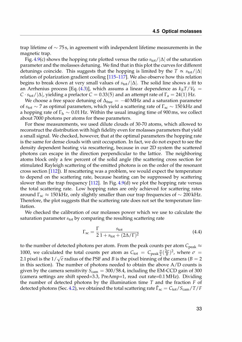
4.5 Optical molasses
trap lifetime of ∼ 75 s, in agreement with independent lifetime measurements in themagnetic trap.
Fig. 4.9(c) shows the hopping rate plotted versus the ratio stot/|∆| of the saturationparameter and the molasses detuning. We find that in this plot the curves for differentdetunings coincide. This suggests that the hopping is limited by the T ∝ stot/|∆|relation of polarization gradient cooling [115–117]. We also observe how this relationbegins to break down at very small values of stot/|∆|. The solid line shows a fit toan Arrhenius process [Eq. (4.3)], which assums a linear dependence as kBT/V0 =C · stot/|∆|, yielding a prefactor C = 0.33(5) and an attempt rate of Γa = 24(1)Hz.
We choose a free space detuning of ∆free = −40 MHz and a saturation parameterof stot ∼ 7 as optimal parameters, which yield a scattering rate of Γsc ∼ 150 kHz anda hopping rate of Γh ∼ 0.01 Hz. Within the usual imaging time of 900 ms, we collectabout 7000 photons per atoms for these parameters.
For these measurements, we used dilute clouds of 30-70 atoms, which allowed toreconstruct the distribution with high fidelity even for molasses parameters that yielda small signal. We checked, however, that at the optimal parameters the hopping rateis the same for dense clouds with unit occupation. In fact, we do not expect to see thedensity dependent heating via rescattering, because in our 2D system the scatteredphotons can escape in the direction perpendicular to the lattice. The neighboringatoms block only a few percent of the solid angle (the scattering cross section forstimulated Rayleigh scattering of the emitted photons is on the order of the resonantcross section [112]). If rescattering was a problem, we would expect the temperatureto depend on the scattering rate, because heating can be suppressed by scatteringslower than the trap frequency [112]. In Fig. 4.9(d) we plot the hopping rate versusthe total scattering rate. Low hopping rates are only achieved for scattering ratesaround Γsc ≈ 150 kHz, only slightly smaller than our trap frequencies of ∼ 200 kHz.Therefore, the plot suggests that the scattering rate does not set the temperature lim-itation.
We checked the calibration of our molasses power which we use to calculate thesaturation parameter stot by comparing the resulting scattering rate
Γsc =Γ2
stot
1 + stot + (2∆/Γ)2 (4.4)
to the number of detected photons per atom. From the peak counts per atom Cpeak ≈1000, we calculated the total counts per atom as Ctot = Cpeak
π2 (
2σB )2, where σ =
2.1 pixel is the 1/√
e radius of the PSF and B is the pixel binning of the camera (B = 2in this section). The number of photons needed to obtain the above A/D counts isgiven by the camera sensitivity Scam = 300/58.4, including the EM-CCD gain of 300(camera settings are shift speed=3.3, PreAmp=1, read out rate=0.1 MHz). Dividingthe number of detected photons by the illumination time T and the fraction F ofdetected photons (Sec. 4.2), we obtained the total scattering rate Γsc = Ctot/Scam/T/F
33
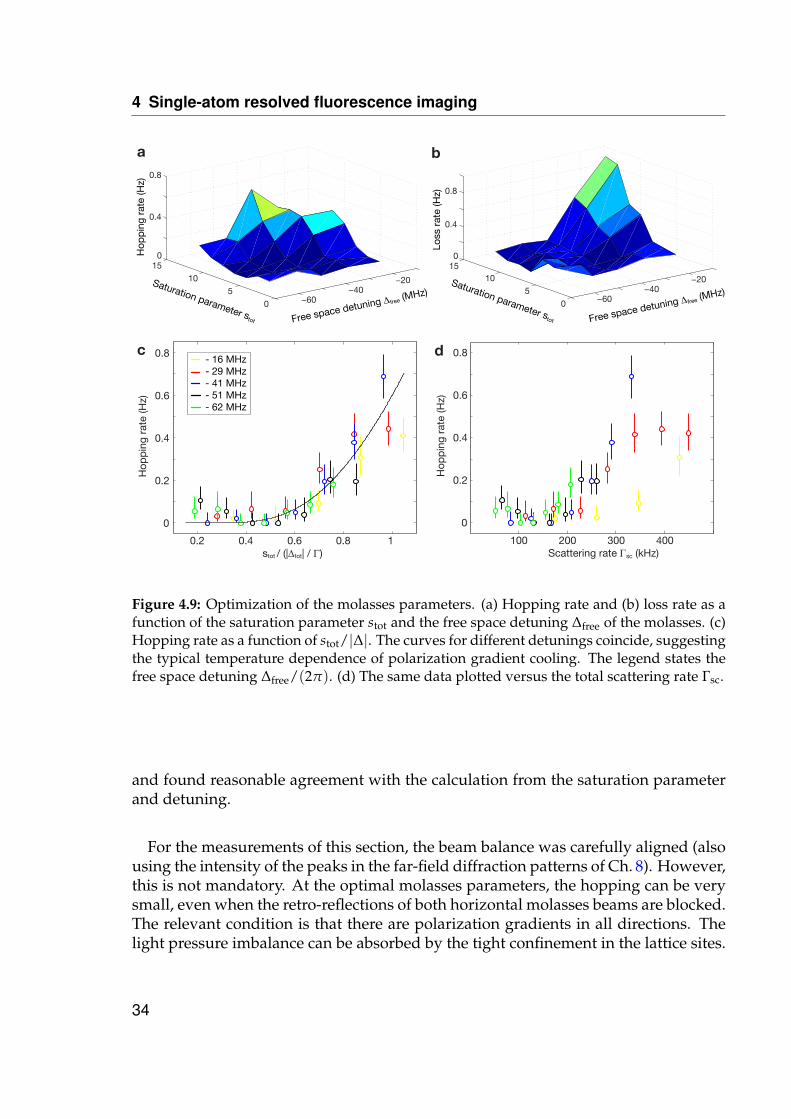
4 Single-atom resolved fluorescence imaging
Free space detuning ∆free (MHz)Saturation parameter stot
Hop
pin
g ra
te (H
z)
Loss
rat
e (H
z)
−60−40
−20
0
5
10
150
0.4
0.8
−60−40
−20
0
5
10150
0.4
0.8
Free space detuning ∆free (MHz)Saturation parameter stot
a b
0.2 0.4 0.6 0.8 1stot / (|∆tot| / Γ)
100 200 300 400
0
0.2
0.4
0.6
0.8
Scattering rate Γsc (kHz)
Hop
pin
g ra
te (H
z)
0
0.2
0.4
0.6
0.8
Hop
pin
g ra
te (H
z)
- 16 MHz- 29 MHz- 41 MHz- 51 MHz- 62 MHz
c d
Figure 4.9: Optimization of the molasses parameters. (a) Hopping rate and (b) loss rate as afunction of the saturation parameter stot and the free space detuning ∆free of the molasses. (c)Hopping rate as a function of stot/|∆|. The curves for different detunings coincide, suggestingthe typical temperature dependence of polarization gradient cooling. The legend states thefree space detuning ∆free/(2π). (d) The same data plotted versus the total scattering rate Γsc.
and found reasonable agreement with the calculation from the saturation parameterand detuning.
For the measurements of this section, the beam balance was carefully aligned (alsousing the intensity of the peaks in the far-field diffraction patterns of Ch. 8). However,this is not mandatory. At the optimal molasses parameters, the hopping can be verysmall, even when the retro-reflections of both horizontal molasses beams are blocked.The relevant condition is that there are polarization gradients in all directions. Thelight pressure imbalance can be absorbed by the tight confinement in the lattice sites.
34
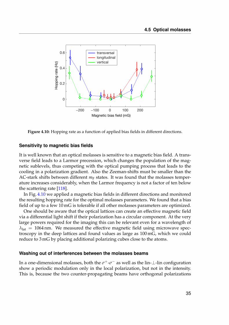
4.5 Optical molasses
−200 −100 0 100 200
0
0.2
0.4
0.6
transversallongitudinalvertical
Hop
pin
g ra
te (H
z)
Magnetic bias field (mG)
Figure 4.10: Hopping rate as a function of applied bias fields in different directions.
Sensitivity to magnetic bias fields
It is well known that an optical molasses is sensitive to a magnetic bias field. A trans-verse field leads to a Larmor precession, which changes the population of the mag-netic sublevels, thus competing with the optical pumping process that leads to thecooling in a polarization gradient. Also the Zeeman-shifts must be smaller than theAC-stark shifts between different mF states. It was found that the molasses temper-ature increases considerably, when the Larmor frequency is not a factor of ten belowthe scattering rate [118].
In Fig. 4.10 we applied a magnetic bias fields in different directions and monitoredthe resulting hopping rate for the optimal molasses parameters. We found that a biasfield of up to a few 10 mG is tolerable if all other molasses parameters are optimized.
One should be aware that the optical lattices can create an effective magnetic fieldvia a differential light shift if their polarization has a circular component. At the verylarge powers required for the imaging this can be relevant even for a wavelength ofλlat = 1064 nm. We measured the effective magnetic field using microwave spec-troscopy in the deep lattices and found values as large as 100 mG, which we couldreduce to 3 mG by placing additional polarizing cubes close to the atoms.
Washing out of interferences between the molasses beams
In a one-dimensional molasses, both the σ+-σ− as well as the lin-⊥-lin configurationshow a periodic modulation only in the local polarization, but not in the intensity.This is, because the two counter-propagating beams have orthogonal polarizations
35
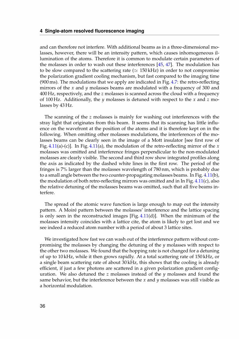
4 Single-atom resolved fluorescence imaging
and can therefore not interfere. With additional beams as in a three-dimensional mo-lasses, however, there will be an intensity pattern, which causes inhomogeneous il-lumination of the atoms. Therefore it is common to modulate certain parameters ofthe molasses in order to wash out these interferences [45, 47]. The modulation hasto be slow compared to the scattering rate (' 150 kHz) in order to not compromisethe polarization gradient cooling mechanism, but fast compared to the imaging time(900 ms). The modulations that we apply are indicated in Fig. 4.7: the retro-reflectingmirrors of the x and y molasses beams are modulated with a frequency of 300 and400 Hz, respectively, and the z molasses is scanned across the cloud with a frequencyof 100 Hz. Additionally, the y molasses is detuned with respect to the x and z mo-lasses by 43 Hz.
The scanning of the z molasses is mainly for washing out interferences with thestray light that originates from this beam. It seems that its scanning has little influ-ence on the wavefront at the position of the atoms and it is therefore kept on in thefollowing. When omitting other molasses modulations, the interferences of the mo-lasses beams can be clearly seen in the image of a Mott insulator [see first row ofFig. 4.11(a)-(c)]. In Fig. 4.11(a), the modulation of the retro-reflecting mirror of the xmolasses was omitted and interference fringes perpendicular to the non-modulatedmolasses are clearly visible. The second and third row show integrated profiles alongthe axis as indicated by the dashed white lines in the first row. The period of thefringes is 7% larger than the molasses wavelength of 780 nm, which is probably dueto a small angle between the two counter-propagating molasses beams. In Fig. 4.11(b),the modulation of both retro-reflecting mirrors was omitted and in In Fig. 4.11(c), alsothe relative detuning of the molasses beams was omitted, such that all five beams in-terfere.
The spread of the atomic wave function is large enough to map out the intensitypattern. A Moiré pattern between the molasses’ interference and the lattice spacingis only seen in the reconstructed images [Fig. 4.11(d)]. When the minimum of themolasses intensity coincides with a lattice cite, the atom is likely to get lost and wesee indeed a reduced atom number with a period of about 3 lattice sites.
We investigated how fast we can wash out of the interference pattern without com-promising the molasses by changing the detuning of the y molasses with respect tothe other two molasses. We found that the hopping rate is not changed for a detuningof up to 10 kHz, while it then grows rapidly. At a total scattering rate of 150 kHz, ora single beam scattering rate of about 30 kHz, this shows that the cooling is alreadyefficient, if just a few photons are scattered in a given polarization gradient config-uration. We also detuned the z molasses instead of the y molasses and found thesame behavior, but the interference between the x and y molasses was still visible asa horizontal modulation.
36
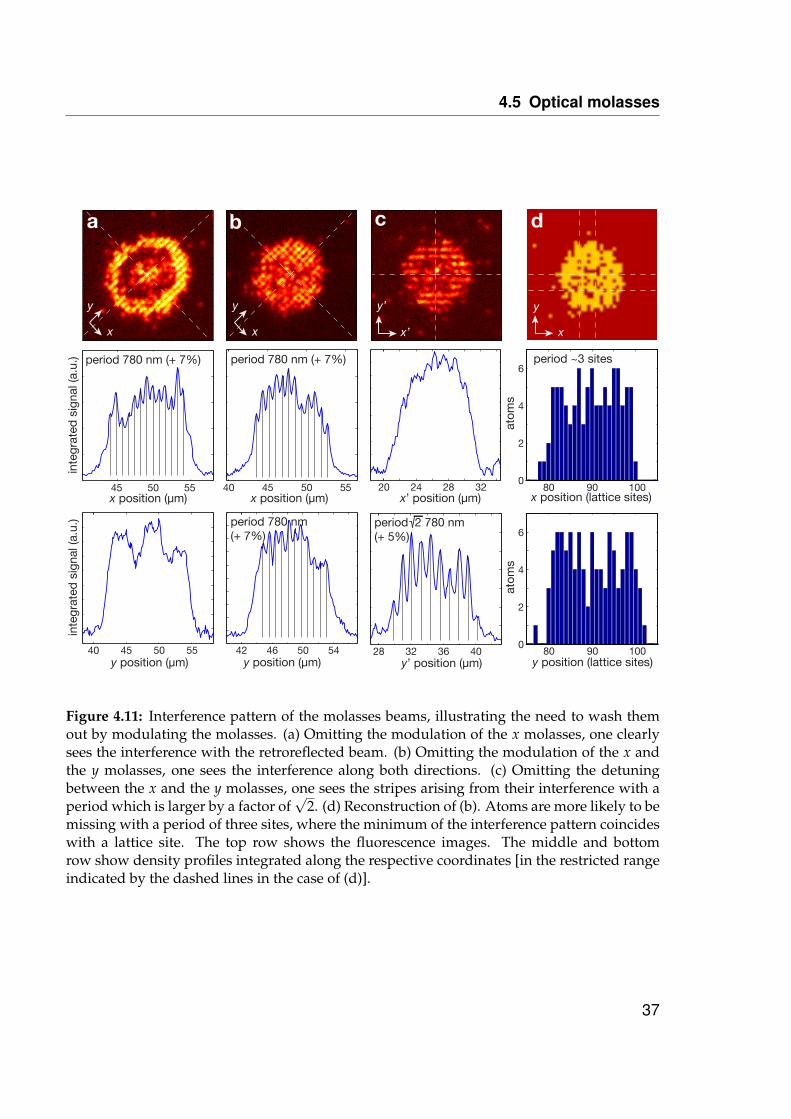
4.5 Optical molasses
40 45 50 55
20 24 28 32
y position (µm)
40 45 50 55
period 780 nm (+ 7%)
42 46 50 54
period 780 nm (+ 7%)
28 32 36 40y’ position (µm)
period 2 780 nm (+ 5%)
a b c
80 90 100y position (lattice sites)
d
45 50 55
period 780 nm (+ 7%)
inte
grat
ed s
igna
l (a.
u.)
80 90 1000
2
4
6
atom
s
period ~3 sites
inte
grat
ed s
igna
l (a.
u.)
y position (µm)
atom
s
0
2
4
6
x position (µm) x’ position (µm) x position (lattice sites)x position (µm)
x’
y’
x
y
x
y
x
y
Figure 4.11: Interference pattern of the molasses beams, illustrating the need to wash themout by modulating the molasses. (a) Omitting the modulation of the x molasses, one clearlysees the interference with the retroreflected beam. (b) Omitting the modulation of the x andthe y molasses, one sees the interference along both directions. (c) Omitting the detuningbetween the x and the y molasses, one sees the stripes arising from their interference with aperiod which is larger by a factor of
√2. (d) Reconstruction of (b). Atoms are more likely to be
missing with a period of three sites, where the minimum of the interference pattern coincideswith a lattice site. The top row shows the fluorescence images. The middle and bottomrow show density profiles integrated along the respective coordinates [in the restricted rangeindicated by the dashed lines in the case of (d)].
37
4 Single-atom resolved fluorescence imaging
4.6 Possible spin-dependent imaging and single-qubit read-out
In the present scheme, spin dependent imaging relies on removing one spin com-ponent before detection (see Ch. 6). For experiments with spin mixtures [29, 119] itwould be desirable to image both spin states in the same experimental run. This canhowever not be done using a molasses, because it mixes all magnetic sub-states. Onepossibility is to apply absorption imaging on one of the components, while shelvingthe other spin component. If the scattering is done on a closed transition F = 2 toF′ = 3 with circular polarized light, one can heat the atom out of the trap before it isdepumped to the F = 1 manifold. Subsequently one can use the molasses to imagethe shelved atoms.
For a future one-way quantum computation scheme [51, 52], it is mandatory toread out qubits during the computation process without affecting the other atoms.This could be done by using two states in the F = 1 manifold as qubit and transferthe selected atom to |F = 2, mF = −2〉 for detection. There it can resonantly scattera few hundred photons on the closed transition F = 2 to F′ = 3 from a single σ−
polarized beam, such that the atom is heated out of the trap before it is depumped tothe F = 1 manifold. One would first transfer from one of the qubit states in the F = 1manifold and detect its population and then transfer the other state and also detectit. As all other atoms remain in the F = 1 manifold, they remain unaffected by thelight on the F = 2 to F′ = 3 transition. The selective transfer to F = 2 can be done bythe combination of a differential light shift from an addressing beam and appropriatemicrowave and radio frequency pulses (see Ch. 6). As there is only one atom imagedat a time, the few hundred scattered photons might be sufficient to detect it, e.g. byimaging the full signal on a single avalanche photo diode. One open question is ifone can ensure that the atom is heated out of the trap without hopping to differentlattice sites and disturbing the atoms there.
4.7 Conclusion
In this chapter we have shown how we image quantum gases in an optical lattice withsingle-site resolution and single-atom sensitivity. We use an imaging system with anumerical aperture of NA = 0.68 located outside the vacuum chamber, yielding adiffraction limit of 700 nm, slightly above the lattice spacing of 532 nm. It was testedin a separate setup and characterized via a test target. We measure the point spreadfunction of single atoms and compare it to that of the test setup.
Light-assisted collisions in the molasses lead to a rapid pair-wise loss of atoms,such that we only detect the parity of the atom number per lattice site. As we onlyhave to discriminate between one or zero atom per site, we can reconstruct the atomdistribution on the lattice despite the resolution above the lattice spacing. For this, weprecisely determined the lattice angles and the lattice spacing from images of a dilute
38
4.7 Conclusion
cloud. A deconvolution algorithm digitizes the images with a fidelity of ∼ 99.5%.During the fluorescence imaging, we apply an optical molasses, which simultane-
ously laser cools the atoms to a temperature∼ 20µK in a lattice with 300 µK depth peraxis. We collect about 7000 photons per atoms in 900 ms yielding a large signal overa small background. By optimizing the molasses parameters, we can make thermalhopping and losses negligible.
39

4 Single-atom resolved fluorescence imaging
40

5 Imaging Mott insulator shells
In this chapter we apply the single-atom resolved imaging technique presented inthe previous chapter to Mott insulators in the atomic limit. We directly observe boththe characteristic shell structure and the number squeezing in the Mott shells. Acomparison of the radial density distribution with theory provides a precise in situtemperature and entropy measurement from single images.
5.1 State of the art
The superfluid-to-Mott-insulator transition has been studied extensively since its firstrealization [2]. When the interactions are increased relative to the kinetic energy, theatoms are localized to their sites, which leads to a number squeezing and the loss ofphase coherence between the different sites. In an external confinement, the densitydistribution changes from the smooth Thomas-Fermi profile of a weakly-interactingBEC to a characteristic shell structure, in which the number distribution is pinned tointeger values. Also the excitation spectrum changes.
In a BEC, arbitrarily small excitations exist, which correspond to phase offset be-tween sites, while in a Mott insulator an energy gap opens, and the smallest possibleexcitation is one particle in excess which has an energy cost of one interaction energyU. All these properties have been verified experimentally and were used to detectedthe Mott insulated state.
The first observation of the Mott insulator was via the the loss of phase coherence,which is a direct consequence of the localization of the atoms [2, 120]. The measure-ment is done by switching off the trap and observing the matter wave interferenceafter time-of-flight, which shows prominent peaks at a momentum of the reciprocallattice vector. The phase coherence is deduced from the visibility of the interferencepattern and the reappearance of this visibility when going back to a shallow latticeshows that one can reversibly cross the phase transition.
Another feature of the Mott insulator, which was already probed in the first exper-iments, is the energy gap in the excitation spectrum. It corresponds to a particle-holepair as lowest lying excitation, which for U/J 1 has an energy of U. Excitationspectra have been recorded by driving the system either by applying a magnetic gra-dient [2] or by amplitude modulation of the lattice [11, 121]. The heating is measuredby ramping back to the superfluid state and by detecting the increased dephasingin the broadening of the central momentum peak after time-of-flight. In the Mottinsulator, the spectra show distinct peaks at energies of U and also 2U, where the
41
5 Imaging Mott insulator shells
latter comes from excitations at the boundaries between two shells. It has been sub-sequently argued that the appearance of the peaks in the excitation spectra alone isnot a prove of a Mott insulating state and that an analysis of the strength of the peaksat different multiples of U would be required.
A method, which tackles the shell structure, is to record the global atom numberstatistics, i.e. the occupation numbers averaged over the entire system for differenttotal atom numbers, and to compare it to theory. For a superfluid one expects to findall occupations numbers for any filling. For the Mott insulator, however, one expectsan enhancement of certain occupation numbers, depending on what shells exist atthe given total atom number. E.g. the fraction of sites with double occupancy is zerofor a perfect Mott insulator with only an n = 1 shell. For larger total atom numbers,which lead to the formation of an n = 2 shell, this fraction increases steadily, untilit decreases again with the formation of the n = 3 shell. Different methods havebeen used to assess the global atom number statistics, ranging from spin changingcollisions [122] to interaction blockade [123] and multi-body interactions [65].
While these methods only probe the global atom number statistics, other exper-iments achieved to image the shell structure. They used a state transfer selective tothe filling factor and recording the spatial distribution of lattice sites with different oc-cupations. The filling-selective state transfer was realized by clock shifts [124] (withbetter data quality in [125]) and by spin-changing collisions [68]. The latter involvestomographic imaging of single 2D slices of a 3D Mott insulator to avoid the integra-tion in one direction.
The shell structure is also revealed in a direct measurement of the density profileobtained from absorption imaging of a 2D Mott insulator with a resolution of 3− 4 µm[91], showing a clear plateau at a density corresponding to unity filling as well asreduced density fluctuations. Finally, Mott insulator shells were imaged with single-site resolution and single-atom sensitivity in the group of Markus Greiner [46] and inour group [47]. Single-site resolved in situ images are of special interest, because theycan directly probe the squeezing of the number statistics, which is the complementaryquantity to the measurement of the phase coherence in the first experiments.
Next to the Bosonic case, the Mott insulator has also been realized for Fermions[10, 11]. In this case, the incompressibility of the insulating state, which can be de-duced from the response to an increased external confinement, is a better measurethan in the Bosonic case, because the Pauli principle forbids the formation of shellswith larger fillings.
5.2 Shell structure of Mott insulators
Our experiments start with a BEC in a single antinode of the vertical z lattice witha depth of Vz = 26(2) Er (The preparation of the BEC is described in Ch. 3). For theMott insulators, the lattice depths along the x and y directions were then increased
42
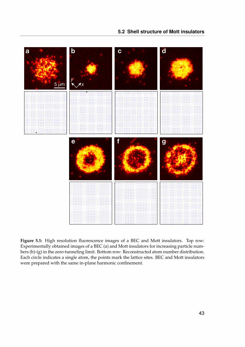
5.2 Shell structure of Mott insulators
b
xy
c
e f g
a d
5 µm
Figure 5.1: High resolution fluorescence images of a BEC and Mott insulators. Top row:Experimentally obtained images of a BEC (a) and Mott insulators for increasing particle num-bers (b)-(g) in the zero-tunneling limit. Bottom row: Reconstructed atom number distribution.Each circle indicates a single atom, the points mark the lattice sites. BEC and Mott insulatorswere prepared with the same in-plane harmonic confinement.
43
5 Imaging Mott insulator shells
in s-shaped ramps within 75 ms up to Vx,y = 23(2) Er. A band structure calculation(see e.g. [60]) yields an interaction energy U = h · 960 Hz and a tunnel couplingJ = h · 3 Hz for this lattice depth, such that U/J ∼ 300 and we are deeply in the atomiclimit of the Mott insulator. The Gaussian beam profile of our lattice beams (1/e2
waist radius of 75 µm) caused an additional harmonic confinement with trappingfrequencies ωx/(2π) = 72(4)Hz and ωy/(2π) = 83(4)Hz at the lattice depths ofVx,y = 23(2) Er and Vz = 26(2) Er. For comparison, we also imaged BECs without thehorizontal lattices, but with similar external confinement dominated by the verticallattice. To freeze out the atom distribution without crossing the phase transition, werapidly ramped up the horizontal lattices within 0.1 ms.
Fig. 5.1 shows the resulting atom distributions of a BEC and Mott insulators in thezero-tunneling limit for different atom numbers. We directly observe dramatic dif-ferences in the density profiles and the on-site number fluctuations. For a BEC wefind that the recorded atomic density exhibits large atom number fluctuations fromsite to site. In contrast, for a Mott insulator we obtain plateaus of constant integerdensity, with almost vanishing fluctuations. The images in Fig. 5.1 show how for in-creasing particle numbers successive Mott insulator shells are formed, which appearas alternating rings of one and zero atoms per site due to our parity measurement(see Sec. 4.3).
In both the raw images and the reconstructed ones, individual defects are directlyvisible as holes or additional atoms. Because the higher atom numbers are obtainedby less evaporation, the larger Mott insulators are hotter than the small ones, whichshows in the less sharp transition between the shells. We find that our atom cloudsare very symmetric in comparison to those in Ref. [46], which sets an upper bound onthe disorder in the optical potentials. A small ellipticity of the clouds is caused by thedifferent harmonic trapping frequencies ωx and ωy.
5.3 Number statistics after parity projection
The on-site number fluctuations are an important indicator for the physical state.For a BEC, they are Poissonian, while for a Mott insulator, the number statistics issqueezed, with unity probability for a certain integer filling depending on the shell.
The statistics can be probed via averaging the occupation of each site over manyshots [46] or via averaging over different sites in a single image [47]. The latter has theadvantage that it is insensitive to shot-to-shot fluctuations of the total atom number oreven cloud position, but it is only good, if the potentials are well characterized. Herewe take azimuthal averages and observe the number statistics in the mean value andthe variance of this average.
The light-assisted collisions in the molasses lead to pair-wise loss of the atoms, suchthat one only detects the parity of the original atom number per site (see Sec. 4.3). Thisprojection has some consequences on the detected statistics. Let us first consider some
44
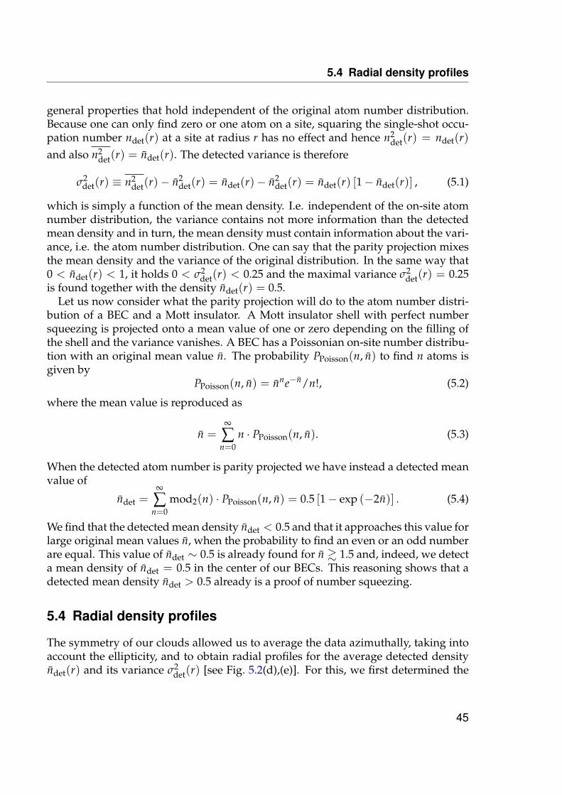
5.4 Radial density profiles
general properties that hold independent of the original atom number distribution.Because one can only find zero or one atom on a site, squaring the single-shot occu-pation number ndet(r) at a site at radius r has no effect and hence n2
det(r) = ndet(r)and also n2
det(r) = ndet(r). The detected variance is therefore
σ2det(r) ≡ n2
det(r)− n2det(r) = ndet(r)− n2
det(r) = ndet(r) [1− ndet(r)] , (5.1)
which is simply a function of the mean density. I.e. independent of the on-site atomnumber distribution, the variance contains not more information than the detectedmean density and in turn, the mean density must contain information about the vari-ance, i.e. the atom number distribution. One can say that the parity projection mixesthe mean density and the variance of the original distribution. In the same way that0 < ndet(r) < 1, it holds 0 < σ2
det(r) < 0.25 and the maximal variance σ2det(r) = 0.25
is found together with the density ndet(r) = 0.5.Let us now consider what the parity projection will do to the atom number distri-
bution of a BEC and a Mott insulator. A Mott insulator shell with perfect numbersqueezing is projected onto a mean value of one or zero depending on the filling ofthe shell and the variance vanishes. A BEC has a Poissonian on-site number distribu-tion with an original mean value n. The probability PPoisson(n, n) to find n atoms isgiven by
PPoisson(n, n) = nne−n/n!, (5.2)
where the mean value is reproduced as
n =∞
∑n=0
n · PPoisson(n, n). (5.3)
When the detected atom number is parity projected we have instead a detected meanvalue of
ndet =∞
∑n=0
mod2(n) · PPoisson(n, n) = 0.5 [1− exp (−2n)] . (5.4)
We find that the detected mean density ndet < 0.5 and that it approaches this value forlarge original mean values n, when the probability to find an even or an odd numberare equal. This value of ndet ∼ 0.5 is already found for n & 1.5 and, indeed, we detecta mean density of ndet = 0.5 in the center of our BECs. This reasoning shows that adetected mean density ndet > 0.5 already is a proof of number squeezing.
5.4 Radial density profiles
The symmetry of our clouds allowed us to average the data azimuthally, taking intoaccount the ellipticity, and to obtain radial profiles for the average detected densityndet(r) and its variance σ2
det(r) [see Fig. 5.2(d),(e)]. For this, we first determined the
45
5 Imaging Mott insulator shells
0
0.5
1
n det
(ato
ms/
site
)
0 2 4 6 8
0
0.25
Radial distance r (μm)
d
e
σde
t (at
oms2 /
site
2 )2
a b c
Figure 5.2: Radial profiles of the mean atom density and its variance. (a)-(c) Reconstructionof the n = 1 and n = 2 Mott insulator images of Fig. 5.1(d),(e) and of the BEC in Fig. 5.1(a)for reference. The circles indicate the (elliptical) azimuthal average at a given radius. (d),(e)Radial profiles of the mean density ndet(r) and the variance σ2
det(r) of the data in (a)-(c). Thedisplayed statistical errors are Clopper-Pearson 68% confidence intervals for the binomiallydistributed number of excitations. For the Mott insulators the density and variance profileswere fitted simultaneously with the model functions of Eqs. (5.7) and (5.1).
46
5.4 Radial density profiles
center of the cloud as the center of mass of the reconstructed distribution. Then webinned the lattice sites according to their distance from the center, thereby correctingfor the ellipticity of 10%. The bin sizes were chosen larger near the center to producesufficient statistics.
We analyze the radial profiles with a simple model for the atomic limit, i.e. vanish-ing tunnel coupling. This is a good approximation for our experiments with U/J '300. Coherent particle-hole fluctuations are suppressed as (J/U)2 and they are neg-ligible here. So the deviations from the integer filling are all induced by thermalfluctuations, which are described by a simple thermodynamic calculation. The atomnumber distribution at a lattice site at radius r is given by
Pr(n) = eβ[µloc(r)n−En]/Z(r), (5.5)
where Z(r) = ∑n eβ[µloc(r)n−En] is the grand canonical partition function, β = 1/(kBT),µloc(r) is the local chemical potential and En = Un(n− 1)/2 is the interaction energy.Using a local density approximation (LDA), we define µloc in terms of the globalchemical potential µ and the external harmonic trapping confinement as
µloc(r) = µ− 12
m(ω2xx2 + ω2
yy2). (5.6)
Taking the light-induced losses into account, we calculate the expected detected den-sity at different radii as
ndet(r) =1
Z(r) ∑n
mod2(n)eβ[µloc(r)n−En] (5.7)
For the Mott insulators in Fig. 5.2, the density and variance profiles were fitted si-multaneously with the model functions of Eqs. (5.7) and (5.1) with T/U, µ/U and a
radius r0 =√
2U/(mωxωy) quantifying the strength of the external confinement asfree parameters [red and orange data and lines in Fig. 5.2(d),(e)]. r0 was not fixed,because it is not clear at which lattice depth and which according external confine-ment the distribution is frozen during the ramp into the atomic limit. The fits yieldedtemperatures T = 0.090(5)U/kB and T = 0.074(5)U/kB, chemical potentials µ =0.73(3)U and µ = 1.17(1)U, and radii r0 = 5.7(1) µm and r0 = 5.95(4) µm for then = 1 Mott insulator (orange) and the n = 2 Mott insulator (red), respectively. Fromthe fitted values of T, µ and r0, we determined the original atom numbers of thesystem before parity projection to N = 270(20) and N = 529(8).
For both the density profiles and the atom number variances we find excellentagreement between the experimental data and the theoretical model for all radialdistances. This supports the assumption that our system is in global thermal equilib-rium, in contrast e.g. to Ref. [126]. The extracted temperatures of T = 0.090(5)U/kB
47
5 Imaging Mott insulator shells
and T = 0.074(5)U/kB for the n = 1 and n = 2 data are well below U/kB and ac-cordingly the shell structure is only slightly washed out by thermal excitations. Ourtemperature estimates are conservative since all defects are attributed to thermal ex-citations in our model. However, defects might also arise due to "collateral damage"caused by atoms undergoing light-assisted collisions.
For reference, we show the corresponding data obtained by freezing out the atomdistribution of a BEC [Fig. 5.2(c) and grey data in Fig. 5.2(d),(e)]. We observe the ex-pected density of ndet = 0.5 in the center of the cloud together with a maximumvariance of σ2
det = 0.25. We note that the thermal shells surrounding a Mott insula-tor core also exhibit this maximum variance and can be as narrow as 1-2 lattice sites.As both the superfluid and the thermal state are expected to show a mean densityof 0.5 after parity projection, it is not possible to discriminate between them in thesepictures. Furthermore a fit to a BEC with finite condensate fraction is not feasible. Aprominent feature of the bimodal density distribution of a partially condensed cloudis the kink between the superfluid core and the thermal wing [71]. However, thisfeature is totally lost in the parity projection.
In Fig. 5.3(b),(c) we plot both Mott insulator data sets from Fig. 5.2 versus the localchemical potential. In a single image, we mapped out an entire line in the phasediagram as illustrated in Fig. 5.3(a). The slightly different temperatures of the twoMott insulators are clearly visible in the different widths of the variance curves.
Entropy per particle
Our measurements also confirm that the entropy is concentrated around the Mottinsulating regions, whereas in the center of a Mott insulator, for local chemical poten-tials of µloc = (n+ 1/2)U with an integer n, number fluctuations are completely sup-pressed and the entropy density is essentially zero. We use the fitted temperature andchemical potential to calculate the original atom number distribution Pr(n) withoutparity projection. As can be seen in Fig. 5.3(b), the deviation from the perfect integerfilling due to thermal excitations is smallest in the center of the n = 1 Mott shell at alocal chemical potential of µloc = 0.5 U. Therefore we insert the radius correspond-ing to µloc = 0.5 U into Pr(1) to extract the maximum of the theoretical probabilityfor unity occupation. For the lowest observed temperature of T = 0.074(5)U/kBwe calculate a 99.7(1)% probability for unity occupation in the center of the n = 1Mott-insulating plateau.
We can furthermore calculate the local entropy per lattice site as
Sloc(r) = −kB ∑n
Pr(n)ln[Pr(n)]. (5.8)
Summing the density and entropy density over the lattice sites, we calculate the totalnumber of particles N = 529(8) and the total entropy S = kB · 180(12) given the fittedvalues of T and µ from the n = 2 data of Fig. 5.2. We find a mean entropy per particle
48
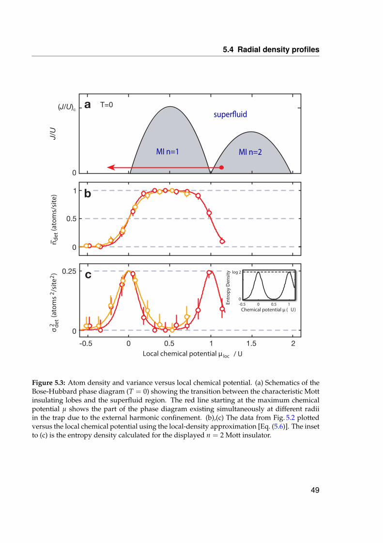
5.4 Radial density profiles
-0.5 0 0.5 1 1.5 2Local chemical potential µ loc
b
c
Chemical potential µ ( U)
Entr
opy
Den
sity
0
log 2
-0.5 0 0.5 1
J/U
MI n=1 MI n=2
superuida
/ U
0
0.5
1
n det
(ato
ms/
site
)
0
0.25
σde
t (at
oms2 /
site
2 )2
0
(J/U)c T=0
Figure 5.3: Atom density and variance versus local chemical potential. (a) Schematics of theBose-Hubbard phase diagram (T = 0) showing the transition between the characteristic Mottinsulating lobes and the superfluid region. The red line starting at the maximum chemicalpotential µ shows the part of the phase diagram existing simultaneously at different radiiin the trap due to the external harmonic confinement. (b),(c) The data from Fig. 5.2 plottedversus the local chemical potential using the local-density approximation [Eq. (5.6)]. The insetto (c) is the entropy density calculated for the displayed n = 2 Mott insulator.
49
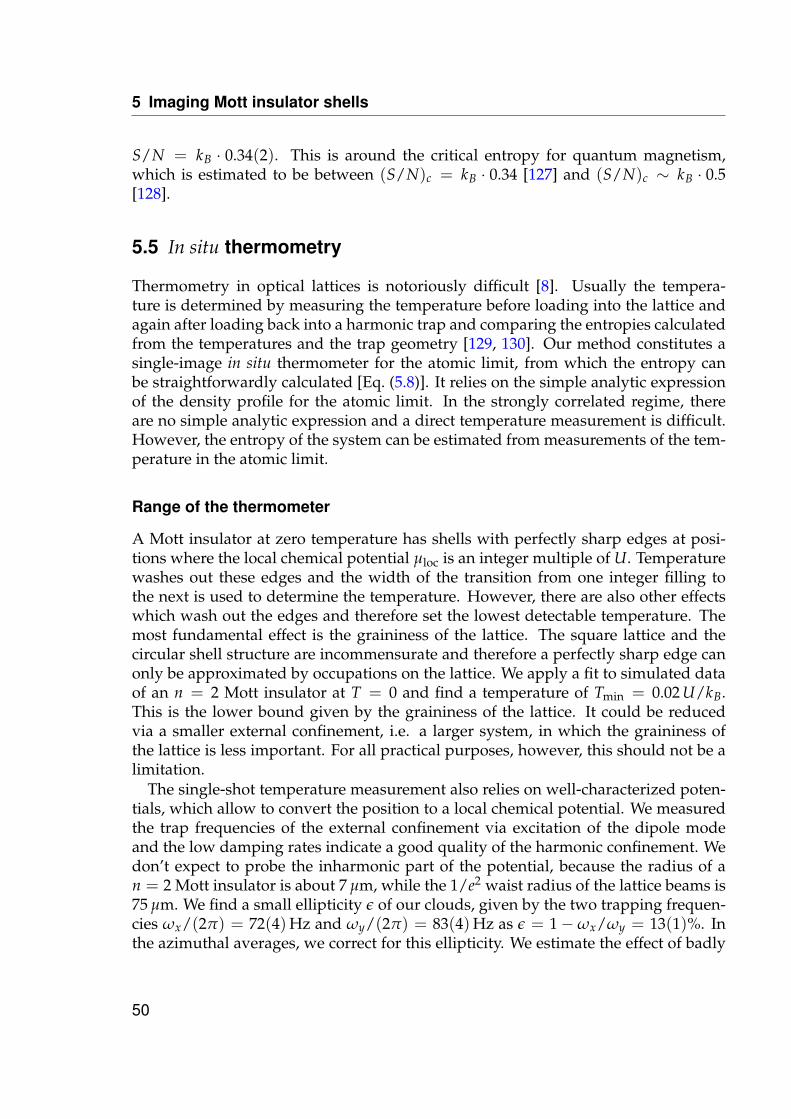
5 Imaging Mott insulator shells
S/N = kB · 0.34(2). This is around the critical entropy for quantum magnetism,which is estimated to be between (S/N)c = kB · 0.34 [127] and (S/N)c ∼ kB · 0.5[128].
5.5 In situ thermometry
Thermometry in optical lattices is notoriously difficult [8]. Usually the tempera-ture is determined by measuring the temperature before loading into the lattice andagain after loading back into a harmonic trap and comparing the entropies calculatedfrom the temperatures and the trap geometry [129, 130]. Our method constitutes asingle-image in situ thermometer for the atomic limit, from which the entropy canbe straightforwardly calculated [Eq. (5.8)]. It relies on the simple analytic expressionof the density profile for the atomic limit. In the strongly correlated regime, thereare no simple analytic expression and a direct temperature measurement is difficult.However, the entropy of the system can be estimated from measurements of the tem-perature in the atomic limit.
Range of the thermometer
A Mott insulator at zero temperature has shells with perfectly sharp edges at posi-tions where the local chemical potential µloc is an integer multiple of U. Temperaturewashes out these edges and the width of the transition from one integer filling tothe next is used to determine the temperature. However, there are also other effectswhich wash out the edges and therefore set the lowest detectable temperature. Themost fundamental effect is the graininess of the lattice. The square lattice and thecircular shell structure are incommensurate and therefore a perfectly sharp edge canonly be approximated by occupations on the lattice. We apply a fit to simulated dataof an n = 2 Mott insulator at T = 0 and find a temperature of Tmin = 0.02 U/kB.This is the lower bound given by the graininess of the lattice. It could be reducedvia a smaller external confinement, i.e. a larger system, in which the graininess ofthe lattice is less important. For all practical purposes, however, this should not be alimitation.
The single-shot temperature measurement also relies on well-characterized poten-tials, which allow to convert the position to a local chemical potential. We measuredthe trap frequencies of the external confinement via excitation of the dipole modeand the low damping rates indicate a good quality of the harmonic confinement. Wedon’t expect to probe the inharmonic part of the potential, because the radius of an = 2 Mott insulator is about 7 µm, while the 1/e2 waist radius of the lattice beams is75 µm. We find a small ellipticity ε of our clouds, given by the two trapping frequen-cies ωx/(2π) = 72(4)Hz and ωy/(2π) = 83(4)Hz as ε = 1− ωx/ωy = 13(1)%. Inthe azimuthal averages, we correct for this ellipticity. We estimate the effect of badly
50
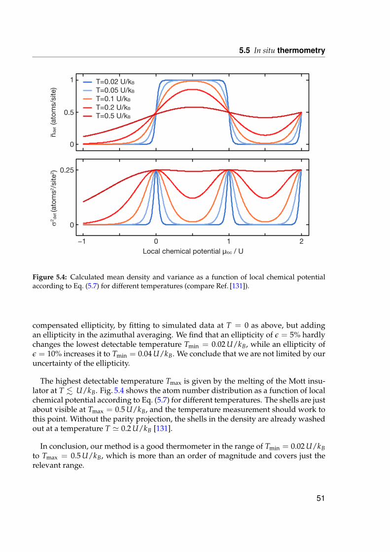
5.5 In situ thermometry
0
0.5
1
ndet
(at
oms/
site
)
−1 0 1 2
0
0.25
Local chemical potential µloc / U
σ2d
et (a
tom
s2 /si
te2 )
T=0.02 U/kB
T=0.05 U/kB
T=0.1 U/kB
T=0.2 U/kB
T=0.5 U/kB
Figure 5.4: Calculated mean density and variance as a function of local chemical potentialaccording to Eq. (5.7) for different temperatures (compare Ref. [131]).
compensated ellipticity, by fitting to simulated data at T = 0 as above, but addingan ellipticity in the azimuthal averaging. We find that an ellipticity of ε = 5% hardlychanges the lowest detectable temperature Tmin = 0.02 U/kB, while an ellipticity ofε = 10% increases it to Tmin = 0.04 U/kB. We conclude that we are not limited by ouruncertainty of the ellipticity.
The highest detectable temperature Tmax is given by the melting of the Mott insu-lator at T . U/kB. Fig. 5.4 shows the atom number distribution as a function of localchemical potential according to Eq. (5.7) for different temperatures. The shells are justabout visible at Tmax = 0.5 U/kB, and the temperature measurement should work tothis point. Without the parity projection, the shells in the density are already washedout at a temperature T ' 0.2 U/kB [131].
In conclusion, our method is a good thermometer in the range of Tmin = 0.02 U/kBto Tmax = 0.5 U/kB, which is more than an order of magnitude and covers just therelevant range.
51
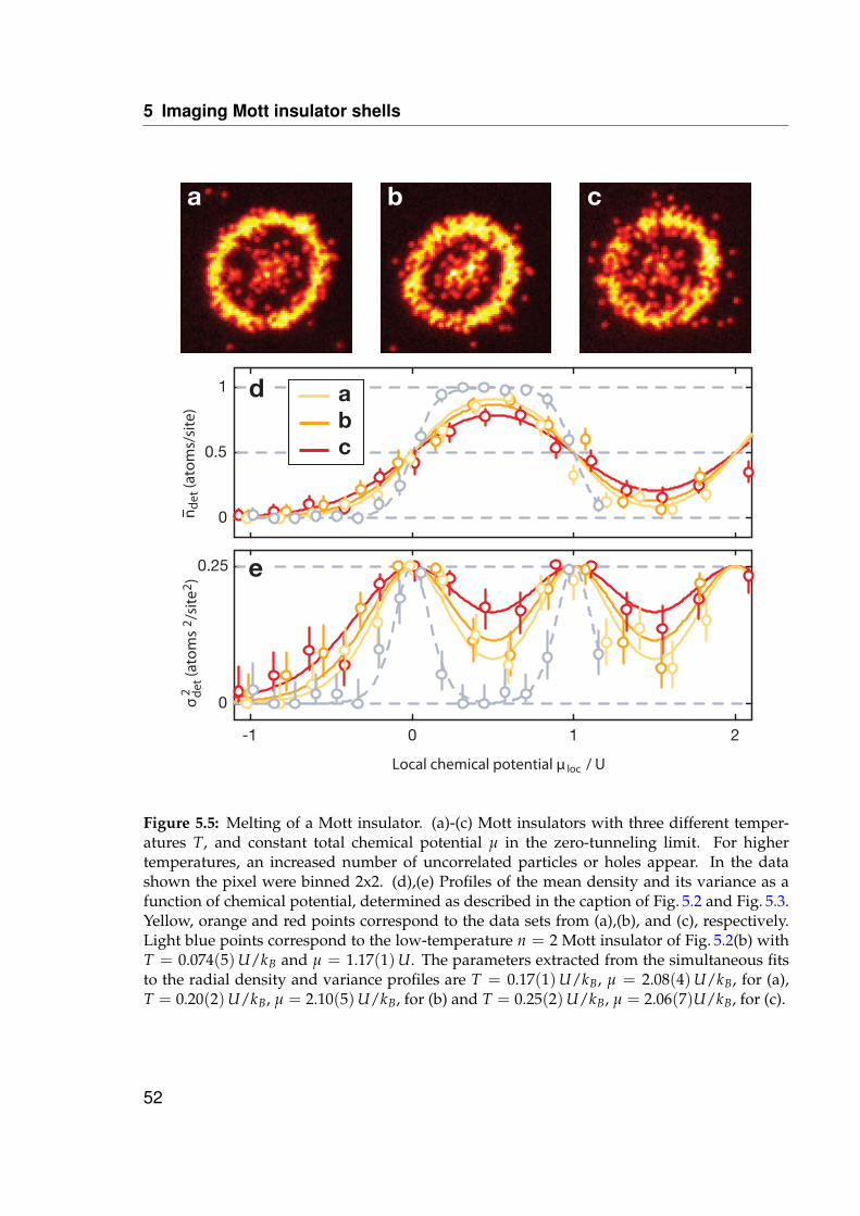
5 Imaging Mott insulator shells
0
0.5
1
-1 0 1 2
0
0.25
σde
t (at
oms
2 /si
te2 )
2
d
e
a b cn d
et (a
tom
s/si
te)
Local chemical potential µ loc / U
abc
Figure 5.5: Melting of a Mott insulator. (a)-(c) Mott insulators with three different temper-atures T, and constant total chemical potential µ in the zero-tunneling limit. For highertemperatures, an increased number of uncorrelated particles or holes appear. In the datashown the pixel were binned 2x2. (d),(e) Profiles of the mean density and its variance as afunction of chemical potential, determined as described in the caption of Fig. 5.2 and Fig. 5.3.Yellow, orange and red points correspond to the data sets from (a),(b), and (c), respectively.Light blue points correspond to the low-temperature n = 2 Mott insulator of Fig. 5.2(b) withT = 0.074(5)U/kB and µ = 1.17(1)U. The parameters extracted from the simultaneous fitsto the radial density and variance profiles are T = 0.17(1)U/kB, µ = 2.08(4)U/kB, for (a),T = 0.20(2)U/kB, µ = 2.10(5)U/kB, for (b) and T = 0.25(2)U/kB, µ = 2.06(7)U/kB, for (c).
52
5.6 Conclusion
Melting of a Mott insulator
We observe how a Mott insulator melts as the temperature (or entropy) of the quan-tum gas is increased (see Fig. 5.5). At constant total chemical potential but increasingtemperatures, one observes that the Mott domains gradually vanish. Although thereis no sharp transition to a normal fluid state in this case, Mott plateaus and numbersqueezing degrade rapidly, once T & 0.2 U/kB [see Fig. 5.5(d),(e)].
Our method yields the temperature in units of the interaction energy U. This isthe relevant energy scale in the atomic limit and only this ratio will enter into thecalculation of the thermodynamic properties, e.g. the entropy. If we want to use theatomic limit as a thermometer, we want to extrapolate to other lattice depths withdifferent interaction energies U. For this, we should compare the entropy, becausethis is the quantity, which is conserved in an adiabatic change of the potential. Thetemperature in contrast will change with the lattice depth.
We can calculate an absolute temperature using the interaction energy U = h ·960 Hz at the end point Vx,y = 23(2) Er of the ramp of the lattice depth. Our lowestmeasured temperature then corresponds to T = 0.074(5)U/kB = 3.6(3) nK. How-ever, when ramping deeply into the atomic limit, the tunneling rate and therefore theequilibration rate get exponentially suppressed. At the final lattice depth, the tunnelcoupling is only J = h · 3 Hz. Hence the thermal excitations will be frozen out at a fi-nite depth with some finite tunneling and the final atom distribution will correspondto this depth and interaction energy. Therefore this absolute temperature is only anupper estimate.
5.6 Conclusion
In this chapter, we have shown single-atom resolved images of Mott insulators inthe atomic limit. When increasing the atom number, we see how successive shellsare formed. Due to the parity projection they show as alternating rings of density oneand zero. The symmetry of our external confinement allows us to obtain a radial den-sity and variance profile from an azimuthal average over the data of a single image.We determine the temperature in a single image by fitting the profiles with a simplegrand-canonical model. We find temperatures as low as T = 0.074(5)U/kB. Thiscorresponds to a 99.7(1)% probability for unity occupation in the center of the n = 1Mott-insulating plateau.
Our pictures show that the entropy is concentrated in the transition regions be-tween the Mott insulator shells and that it is essentially zero in the center of the shells.For our parameters, we calculate a mean entropy per particle of S/N = kB · 0.34(2),which is around the critical entropy for quantum magnetism. We also show how aMott insulator melts as the temperature of the quantum gas is increased. Our methodconstitutes an in situ thermometer in the range 0.02 . kBT/U . 0.5.
53

5 Imaging Mott insulator shells
We studied the simple case of the atomic limit to set a benchmark and confirm thereliability of our technique. A natural extension would be to probe the strongly cor-related state along the quantum phase transition. The same experimental sequencecan be used by simply freezing out the distribution at a different lattice depth. This isongoing work as I write.
54
6 Single-spin addressing
In this chapter we describe how we manipulate the spin of individual atoms in a Mottinsulator with sub-diffraction-limited resolution using a tightly focussed laser beamtogether with a microwave field. We review the state of the art in Sec. 6.1 and describeour scheme in Sec. 6.2. We show in Sec. 6.3 that we can experimentally prepare arbi-trary spin patterns and we discuss the fidelity of the addressing scheme in Sec. 6.4.Some technical details are given in Sec. 6.5 and 6.6 and possible improvements arediscussed in Sec. 6.7.
6.1 State of the art
The quest to address single sites of an optical lattice has a long history, which wasmainly inspired by the potential applications in quantum information processing.Because typical lattice spacings are on the order of half the lattice wavelength, theycannot be fully optically resolved by a focused laser beam of a similar wavelength.Therefore many proposals have been put forward to overcome this diffraction limit.
One idea is to synthesize a localized optical field with zeros on all other sites ofa one-dimensional lattice either using a spatial light modulator [132] or by interfer-ence of many tilted laser beams [133]. Another idea is to use a position-dependentatomic population transfer in multi-level systems [134], e.g. exploiting the nonlin-ear response to the intensity of a control beam in electromagnetically induced trans-parency [135], in the spirit of stimulated emission depletion microscopy (STED) [136].A third idea is to use an auxiliary marker atom in a different internal state, whichis moved independently from the qubit atoms and initiates the selective spin flips[137, 138].
Experimentally, single-site addressing was demonstrated both spatially, i.e. by fo-cused beams [36, 37, 44], and spectrally, i.e. by selective microwave pulses [41, 93,139]. Spatial addressing was performed optically in a one-dimensional lattice of5.3 µm spacing [36] and a two-dimensional microtrap array of 125 µm spacing [37].In both cases, the lattice sites contained several hundred thermal atoms and tunnel-ing was completely suppressed at these lattice spacings. Two-dimensional address-ing of a BEC in a lattice of 600 nm spacing was recently achieved using an electronbeam that can be focused to a much smaller spot than light with optical wavelengths[44]. However, spin manipulation was not possible so far, but only depopulation ofselected lattice sites.
Spectral addressing was demonstrated with a magnetic field gradient in a sparselyfilled one-dimensional lattice of 433 and 532 nm spacing [41, 93] and with an effective
55
6 Single-spin addressing
magnetic field at one site of a double well optical lattice [139]. In both cases, selectedatoms where shifted into resonance with a microwave field and could be coherentlymanipulated.
Here we follow a hybrid approach [140, 141], which combines the advantages ofspatial and spectral addressing. The differential light shift from a tightly focussedlaser beam makes the atoms spectrally addressable via microwave radiation. Thismethod allows to overcome the diffraction limit (Sec. 6.4) and also allows to reach fulltwo-dimensional addressability (Sec. 6.3). The diffraction limit is overcome, becausethe intensity of the laser beam does not need to vanish at the next atom, but onlyneeds to change as much as to allow to spectrally resolve the change in the differentiallight shift. Two-dimensional addressing is in principle also possible with magneticfield gradients in two directions [142], but in practice this substantially limits theregion of interest.
For the first time, we combine two-dimensional single-atom spin control in stronglycorrelated systems with high fidelity single-atom detection.
6.2 Addressing scheme
In order to address the atoms in the lattice, we used an off-resonant laser beam fo-cused by the high-resolution imaging system onto individual lattice sites (Fig. 6.1).The laser beam causes a differential light shift of the two relevant hyperfine levels|0〉 ≡ |F = 1, mF = −1〉 and |1〉 ≡ |F = 2, mF = −2〉 and tunes the addressed atominto resonance with an external microwave field at ∼ 6.8 GHz [140, 141]. The σ−-polarized addressing beam had a wavelength of 787.55 nm, between the D1 and D2lines, in order to obtain a large differential light shift between the two hyperfine lev-els. For perfect σ−-polarization, this ‘magic’ wavelength generates a light shift onlyfor state |1〉, and leaves state |0〉 unaffected (see Fig. 6.2). The beam had a diameterof ∼ 600 nm full-width at half-maximum (FWHM) and could be moved in the objectplane over the entire field of view by changing its angle of incidence into the micro-scope objective with a two-axis piezo mirror. We were able to position the beam withan accuracy better than 0.1 alat using an independent calibration measurement of itsposition together with a feedback that tracks the slowly varying lattice phases (seeSec. 6.5).
If the addressing laser beam is perfectly centered onto one lattice site [see Fig. 6.1(b)],the differential light shift is ∆LS/(2π) ' −70 kHz, whereas a neighboring atom onlyexperiences 10% of the maximum intensity. The resulting difference in light shiftscan be well resolved spectrally by our microwave pulses. In order to flip the spin, weperformed Landau-Zener sweeps yielding a near flat-top frequency spectrum with amaximum population transfer efficiency of ∼ 95%. The microwave sweeps are HS1-
56
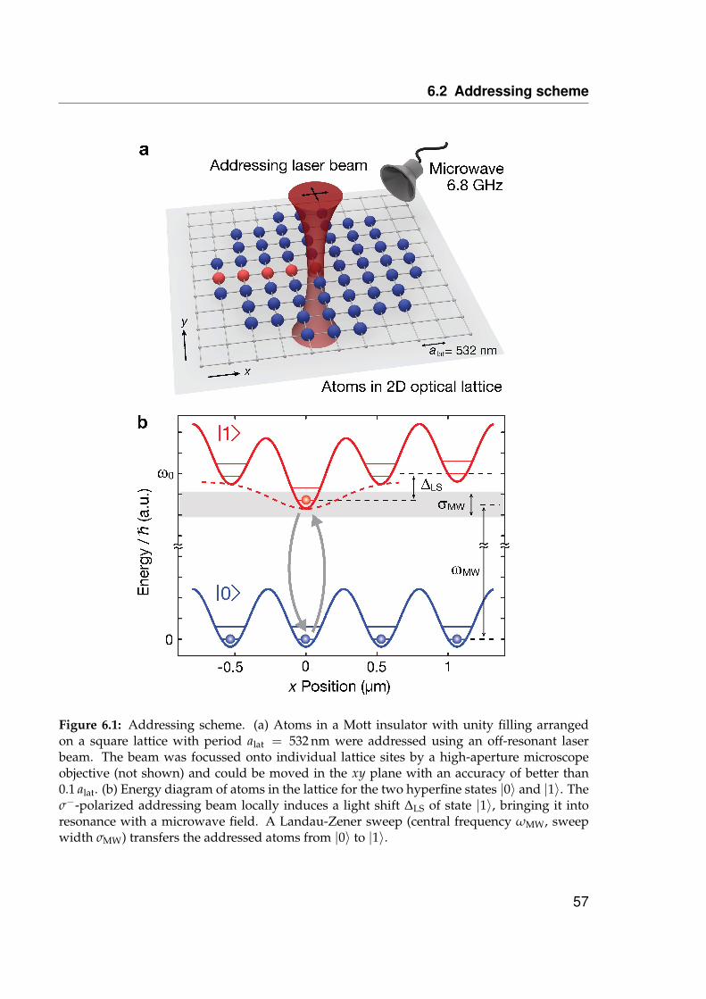
6.2 Addressing scheme
Figure 6.1: Addressing scheme. (a) Atoms in a Mott insulator with unity filling arrangedon a square lattice with period alat = 532 nm were addressed using an off-resonant laserbeam. The beam was focussed onto individual lattice sites by a high-aperture microscopeobjective (not shown) and could be moved in the xy plane with an accuracy of better than0.1 alat. (b) Energy diagram of atoms in the lattice for the two hyperfine states |0〉 and |1〉. Theσ−-polarized addressing beam locally induces a light shift ∆LS of state |1〉, bringing it intoresonance with a microwave field. A Landau-Zener sweep (central frequency ωMW, sweepwidth σMW) transfers the addressed atoms from |0〉 to |1〉.
57
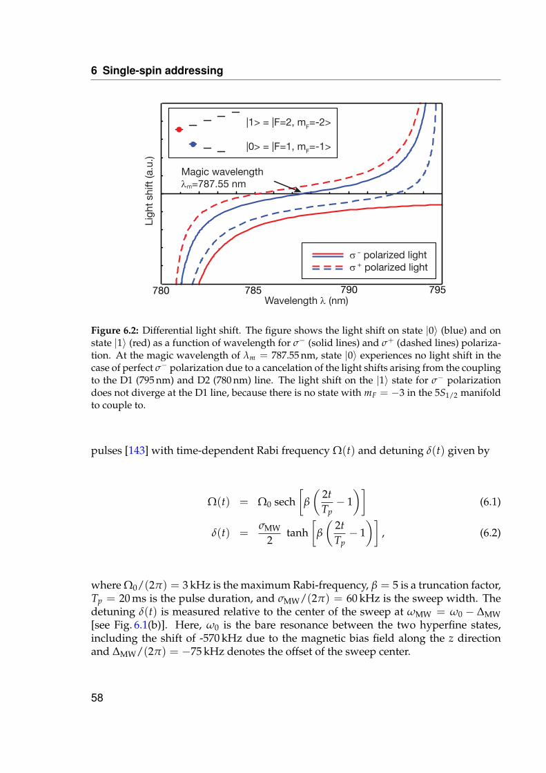
6 Single-spin addressing
780 785 795790
|1> = |F=2, mF=-2>
|0> = |F=1, mF=-1>
σ + polarized light
Magic wavelength λm=787.55 nm
Ligh
t sh
ift (a
.u.)
Wavelength λ (nm)
σ - polarized light
Figure 6.2: Differential light shift. The figure shows the light shift on state |0〉 (blue) and onstate |1〉 (red) as a function of wavelength for σ− (solid lines) and σ+ (dashed lines) polariza-tion. At the magic wavelength of λm = 787.55 nm, state |0〉 experiences no light shift in thecase of perfect σ− polarization due to a cancelation of the light shifts arising from the couplingto the D1 (795 nm) and D2 (780 nm) line. The light shift on the |1〉 state for σ− polarizationdoes not diverge at the D1 line, because there is no state with mF = −3 in the 5S1/2 manifoldto couple to.
pulses [143] with time-dependent Rabi frequency Ω(t) and detuning δ(t) given by
Ω(t) = Ω0 sech[
β
(2tTp− 1)]
(6.1)
δ(t) =σMW
2tanh
[β
(2tTp− 1)]
, (6.2)
where Ω0/(2π) = 3 kHz is the maximum Rabi-frequency, β = 5 is a truncation factor,Tp = 20 ms is the pulse duration, and σMW/(2π) = 60 kHz is the sweep width. Thedetuning δ(t) is measured relative to the center of the sweep at ωMW = ω0 − ∆MW[see Fig. 6.1(b)]. Here, ω0 is the bare resonance between the two hyperfine states,including the shift of -570 kHz due to the magnetic bias field along the z directionand ∆MW/(2π) = −75 kHz denotes the offset of the sweep center.
58
6.3 Writing arbitrary spin patterns
6.3 Writing arbitrary spin patterns
As a first experiment, we sequentially flipped the spin of the atoms at selected latticesites in our Mott insulator with unity filling and spin state |0〉 (see Fig. 6.3(a) andCh. 5). The lattice depths were first changed to Vx = 56 Er, Vy = 90 Er and Vz = 70 Erin order to completely suppress tunneling even when the addressing beam locallyperturbs the lattice potential. For each lattice site, we then switched on the addressinglaser beam with an s-shaped ramp within 2.5 ms, which is adiabatic with respect tothe on-site oscillation frequency of ∼ 30 kHz. Subsequently, a microwave pulse withthe parameters described above produced spin-flips from |0〉 to |1〉. The addressinglaser was switched off again within 2.5 ms, before its position was changed in 5 ms toaddress the next lattice site.
For the image of Fig. 6.3(a), this procedure was repeated 16 times in order to flip thespins along a line. Finally, a 5 ms ‘push-out’ laser pulse, resonant with the F = 2 toF′ = 3 transition, removed all addressed atoms in state |1〉. In order to reveal only thespin-flipped atoms, the spin states of all atoms were flipped by a global microwavesweep before the push-out laser pulse was applied [Fig. 6.3(c),(d)]. However, dueto the finite transfer efficiency of the global sweep, some atoms remaining in state|0〉 were clearly visible in addition to the addressed ones. To avoid this problemwhen detecting the addressed atoms, we initially transferred the whole sample tostate |1〉 by a microwave sweep and then shone in a repumping laser that completelydepopulated state |0〉. Then, we used our addressing scheme to transfer selectedatoms back to |0〉 and subsequently pushed out the atoms in |1〉, yielding typicalimages as shown in Fig. 6.3(b),(e),(f).
By the deterministic creation of arbitrary two-dimensional spin patterns of individ-ual atoms, we realize a scalable single-atom source [35, 107, 144].
6.4 Spin-flip fidelity
We quantified the success rate of our addressing scheme by producing a series ofspin-flips along the y lattice axis in a Mott insulator with unity filling (see Fig. 6.4).The experimental procedure was the same as described above for the realization ofFig. 6.3(a), in which the addressed sites were detected as empty sites. From the recon-structed atom number distribution [Fig. 6.4(a)], we determined the probability p0(δx)of finding an empty site as a function of the pointing offset δx between the address-ing beam and the center of the lattice site [see Fig. 6.4(b)]. We also investigated theeffect of the addressing procedure on next neighboring atoms, which ideally shouldremain unaffected. For this purpose, we monitored the probability of finding a hole atthe sites next to the addressed ones [dark blue regions in Fig. 6.4(a),(b) and dark bluedata points in Fig. 6.4(c)]. In order to distinguish accidentally flipped neighboringatoms from holes that originate from thermal excitations of the initial Mott insulator
59
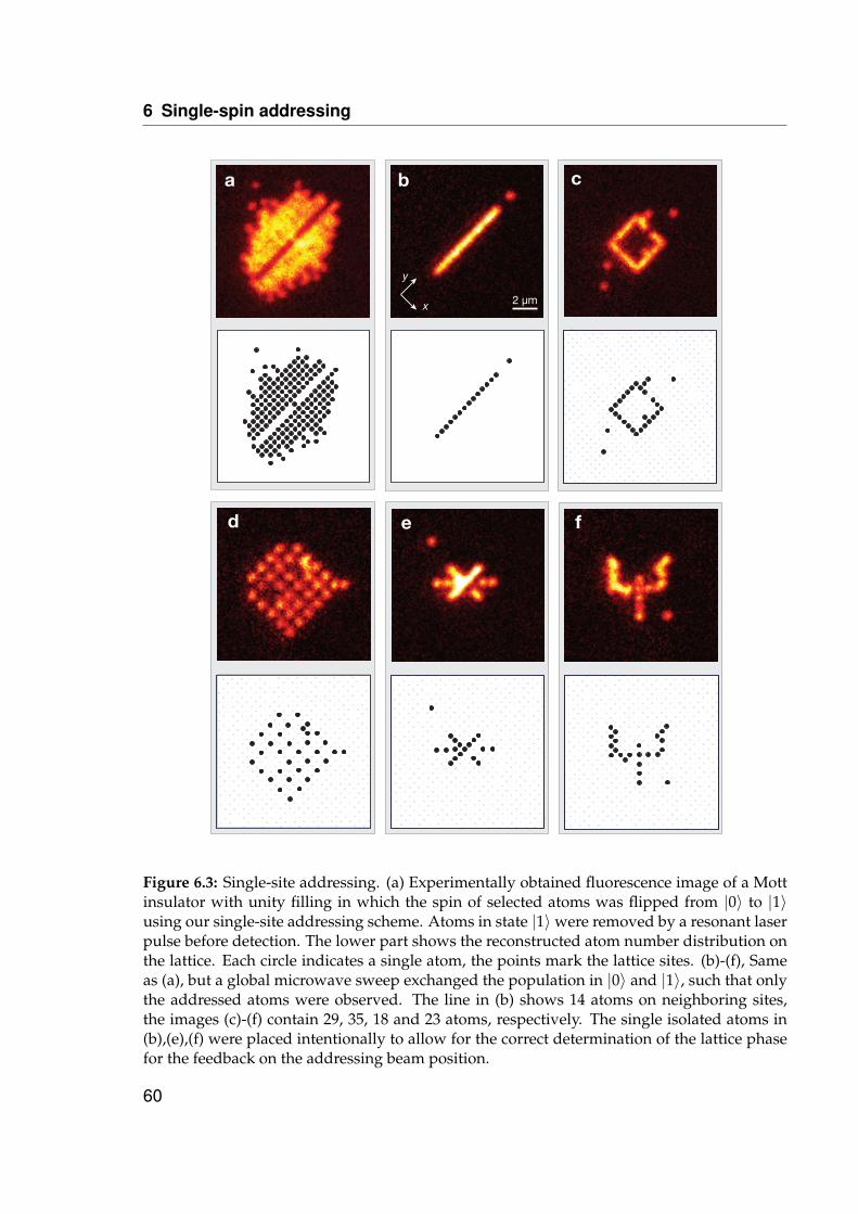
6 Single-spin addressing
d
a
2 µm
b
x
y
c
e f
Figure 6.3: Single-site addressing. (a) Experimentally obtained fluorescence image of a Mottinsulator with unity filling in which the spin of selected atoms was flipped from |0〉 to |1〉using our single-site addressing scheme. Atoms in state |1〉were removed by a resonant laserpulse before detection. The lower part shows the reconstructed atom number distribution onthe lattice. Each circle indicates a single atom, the points mark the lattice sites. (b)-(f), Sameas (a), but a global microwave sweep exchanged the population in |0〉 and |1〉, such that onlythe addressed atoms were observed. The line in (b) shows 14 atoms on neighboring sites,the images (c)-(f) contain 29, 35, 18 and 23 atoms, respectively. The single isolated atoms in(b),(e),(f) were placed intentionally to allow for the correct determination of the lattice phasefor the feedback on the addressing beam position.
60
6.5 Positioning of the addressing beam
(Ch. 5), we also monitored the probability of finding a hole at the second next neigh-bors (light blue regions and data points in Fig. 6.4). As both yielded the same holeprobability of 6(2)%, we attribute all holes to thermal excitations and conclude thatthe probability of addressing a neighboring atom is indiscernibly small.
We fitted the hole probability p0(δx) of the addressed site with a flat-top modelfunction, given by
p0(δx) =A2
[erf(
δx + σa/2σs
)+ erf
(−δx− σa/2
σs
)]+ B. (6.3)
Here, erf(x) = 2/√
π∫ x
0 e−τ2dτ is the error function, σa denotes the full-width at half-
maximum of the flat-top profile and σs the edge sharpness. The offset B is kept fixedat the thermal contribution of 6%. We chose this model function since our HS1-pulsesproduce a flat-top population transfer profile, the edges of which are dominated byrandomly fluctuating quantities (beam pointing and magnetic fields) following Gaus-sian statistics. The addressing fidelity is defined as F = A/(1− B) taking into accountthat the maximum hole probability pmax
0 = A + B also includes holes from thermaldefects. These yield a hole with probability B at unsuccessfully addressed sites whichoccur with probability 1− F, such that pmax
0 = F + (1− F)B. From the fit, we deriveda spin-flip fidelity of 95(2)%, a full-width at half-maximum of σa = 330(10) nm andan edge sharpness of σs = 50(10) nm [Fig. 6.4(c)]. These values correspond to 60%and 10% of the addressing beam diameter, demonstrating that our method reachessub-diffraction-limited resolution, well below the lattice spacing.
The observed maximum spin-flip fidelity is currently limited by the populationtransfer efficiency of our microwave sweep. The edge sharpness σs originates fromthe beam pointing error of . 0.1 alat and from variations in the magnetic bias field.The latter causes frequency fluctuations of ∼ 5 kHz, which translate into an effectivepointing error of 0.05 alat at the maximum slope of the addressing beam profile. Theresolution σa could in principle be further reduced by a narrower microwave sweep,at the cost of a larger sensitivity to the magnetic field fluctuations. A larger addressingbeam power would reduce this sensitivity, but we observed that this deformed thelattice potential, due to the imperfect σ−-polarization, allowing neighboring atoms totunnel to the addressed sites.
6.5 Positioning of the addressing beam
Calibration of the addressing beam position
To move the addressing laser beam in the object plane, we changed the angle of thebeam entering from the reverse direction into the microscope objective using a two-axis piezo mirror (S-334 Physik Instrumente GmbH & Co. KG, Karlsruhe). The devicehas an angular resolution of 5 µrad, corresponding to a theoretical resolution in the
61
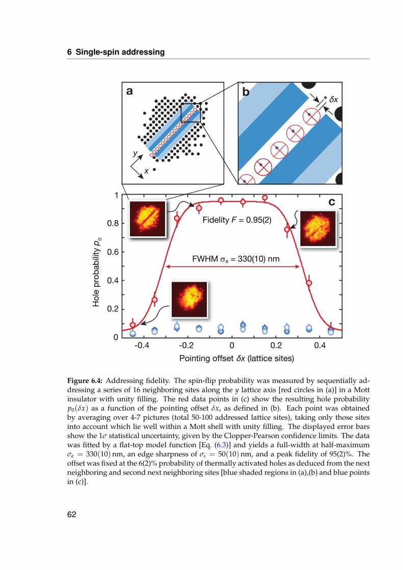
6 Single-spin addressing
a
c
Pointing offset δx (lattice sites)
0.2 0.40-0.2-0.4
0.8
0.6
0.4
0.2
0
1
FWHM σa = 330(10) nm
Hol
e p
rob
abili
ty p
0
Fidelity F = 0.95(2)
y
x
δxb
Figure 6.4: Addressing fidelity. The spin-flip probability was measured by sequentially ad-dressing a series of 16 neighboring sites along the y lattice axis [red circles in (a)] in a Mottinsulator with unity filling. The red data points in (c) show the resulting hole probabilityp0(δx) as a function of the pointing offset δx, as defined in (b). Each point was obtainedby averaging over 4-7 pictures (total 50-100 addressed lattice sites), taking only those sitesinto account which lie well within a Mott shell with unity filling. The displayed error barsshow the 1σ statistical uncertainty, given by the Clopper-Pearson confidence limits. The datawas fitted by a flat-top model function [Eq. (6.3)] and yields a full-width at half-maximumσa = 330(10) nm, an edge sharpness of σs = 50(10) nm, and a peak fidelity of 95(2)%. Theoffset was fixed at the 6(2)% probability of thermally activated holes as deduced from the nextneighboring and second next neighboring sites [blue shaded regions in (a),(b) and blue pointsin (c)].
62
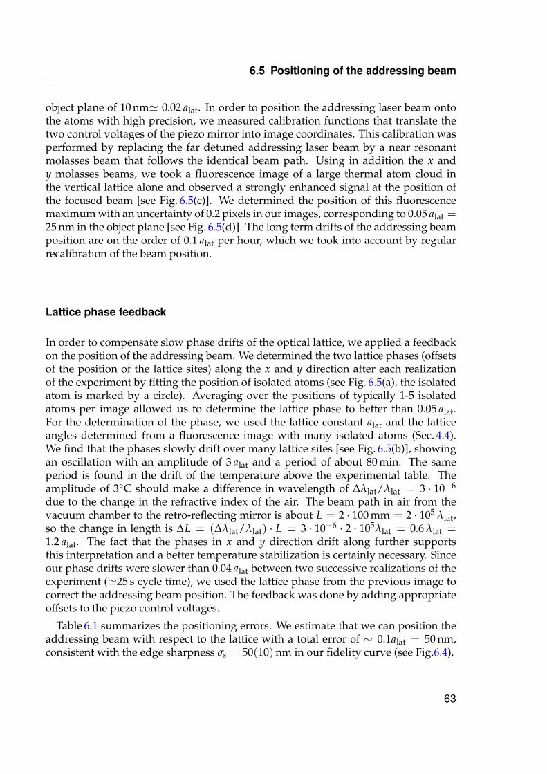
6.5 Positioning of the addressing beam
object plane of 10 nm' 0.02 alat. In order to position the addressing laser beam ontothe atoms with high precision, we measured calibration functions that translate thetwo control voltages of the piezo mirror into image coordinates. This calibration wasperformed by replacing the far detuned addressing laser beam by a near resonantmolasses beam that follows the identical beam path. Using in addition the x andy molasses beams, we took a fluorescence image of a large thermal atom cloud inthe vertical lattice alone and observed a strongly enhanced signal at the position ofthe focused beam [see Fig. 6.5(c)]. We determined the position of this fluorescencemaximum with an uncertainty of 0.2 pixels in our images, corresponding to 0.05 alat =25 nm in the object plane [see Fig. 6.5(d)]. The long term drifts of the addressing beamposition are on the order of 0.1 alat per hour, which we took into account by regularrecalibration of the beam position.
Lattice phase feedback
In order to compensate slow phase drifts of the optical lattice, we applied a feedbackon the position of the addressing beam. We determined the two lattice phases (offsetsof the position of the lattice sites) along the x and y direction after each realizationof the experiment by fitting the position of isolated atoms (see Fig. 6.5(a), the isolatedatom is marked by a circle). Averaging over the positions of typically 1-5 isolatedatoms per image allowed us to determine the lattice phase to better than 0.05 alat.For the determination of the phase, we used the lattice constant alat and the latticeangles determined from a fluorescence image with many isolated atoms (Sec. 4.4).We find that the phases slowly drift over many lattice sites [see Fig. 6.5(b)], showingan oscillation with an amplitude of 3 alat and a period of about 80 min. The sameperiod is found in the drift of the temperature above the experimental table. Theamplitude of 3C should make a difference in wavelength of ∆λlat/λlat = 3 · 10−6
due to the change in the refractive index of the air. The beam path in air from thevacuum chamber to the retro-reflecting mirror is about L = 2 · 100 mm = 2 · 105 λlat,so the change in length is ∆L = (∆λlat/λlat) · L = 3 · 10−6 · 2 · 105λlat = 0.6 λlat =1.2 alat. The fact that the phases in x and y direction drift along further supportsthis interpretation and a better temperature stabilization is certainly necessary. Sinceour phase drifts were slower than 0.04 alat between two successive realizations of theexperiment ('25 s cycle time), we used the lattice phase from the previous image tocorrect the addressing beam position. The feedback was done by adding appropriateoffsets to the piezo control voltages.
Table 6.1 summarizes the positioning errors. We estimate that we can position theaddressing beam with respect to the lattice with a total error of ∼ 0.1alat = 50 nm,consistent with the edge sharpness σs = 50(10) nm in our fidelity curve (see Fig.6.4).
63
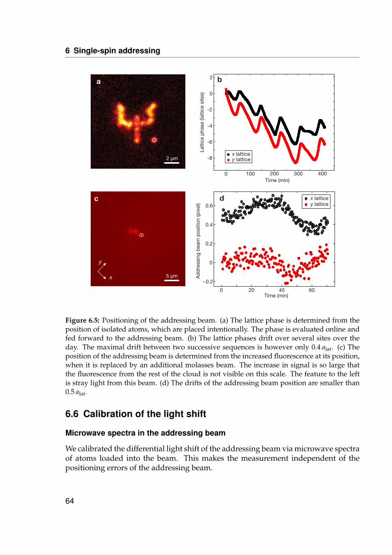
6 Single-spin addressing
0Time (min)
100 200 300 400
Latt
ice
phas
e (la
ttic
e si
tes)
-8
-6
-4
-2
0
2
x latticey lattice
0 20 40 60
−0.2
0
0.2
0.4
0.6
Time (min)
Ad
dre
ssin
g b
eam
pos
ition
(pix
el)
x latticey lattice
b
d
a
c
2 µm
5 µmx
y
Figure 6.5: Positioning of the addressing beam. (a) The lattice phase is determined from theposition of isolated atoms, which are placed intentionally. The phase is evaluated online andfed forward to the addressing beam. (b) The lattice phases drift over several sites over theday. The maximal drift between two successive sequences is however only 0.4 alat. (c) Theposition of the addressing beam is determined from the increased fluorescence at its position,when it is replaced by an additional molasses beam. The increase in signal is so large thatthe fluorescence from the rest of the cloud is not visible on this scale. The feature to the leftis stray light from this beam. (d) The drifts of the addressing beam position are smaller than0.5 alat.
6.6 Calibration of the light shift
Microwave spectra in the addressing beam
We calibrated the differential light shift of the addressing beam via microwave spectraof atoms loaded into the beam. This makes the measurement independent of thepositioning errors of the addressing beam.
64
6.6 Calibration of the light shift
Error source ErrorResolution of mirror 0.02 alatDetermination of lattice phase < 0.05 alatDrifts of lattice phase (per cycle) < 0.04 alatDetermination of addressing beam position 0.05 alat
Overall ∼ 0.1alat
Table 6.1: Error budget for the positioning of the addressing beam with respect to the latticesites.
For perfect σ− polarization, the beam at the magic wavelength should only trapatoms in state |F = 2, mF = −2〉, while atoms in |F = 1, mF = −1〉 should see no lightshift. Therefore, even when we load it from a cloud prepared in |F = 1, mF = −1〉,we mostly load |F = 2, mF = −2〉 into the beam, because there are enough atoms inthe wrong spin state. Indeed, an optical push out on the F = 2 to F′ = 3 transitiondid remove the atoms from the addressing beam and therefore confirmed that thetrapped atoms were in the |F = 2, mF = −2〉 state. For the spectrum, we appliedan HS1 microwave sweep of 30 ms duration, which transfered the atoms down to the|F = 1, mF = −1〉 state, where they were lost from the trap. The resonance thereforeshows as a dip in the atom number (see Fig. 6.6).
In order to count the remaining atoms, we loaded them into a 3D lattice of Vx =Vy = 3.5 Er and Vz = 57 Er depth. When we let them tunnel for 100 ms in this weakhorizontal lattice, they spread over a diameter of ∼ 10 µm. We then ramped up thelattice to freeze the distribution and took a fluorescence image. At this dilute fillingof the lattice, the probability for two atoms at the same lattice sites is very low and wecan neglect losses due to the parity projection. The method is therefore a very reliableway to count small numbers of atoms.
Fig. 6.6(a) shows the resulting spectra for different addressing beam powers. Weloaded around 50 atoms into the addressing beam and lost all of them for resonanttransfer. The microwave frequency is given relative to the bare transition in the ab-sence of magnetic fields. The addressing beam shifts the transition to smaller fre-quencies. For larger addressing beam powers, the resonance does not fully drop tozero atoms, because some |F = 1, mF = −1〉 atoms are trapped due to the imperfectpolarization.
In order to measure the bare transition including the bias magnetic field, but notthe light shift from the addressing beam, we took a spectrum inside the lattice. Weloaded the atoms from the addressing beam in order to have only |F = 2, mF = −2〉atoms and then performed the microwave sweep to the |F = 1, mF = −1〉 state insidethe lattice. Atoms which were not transferred were then removed with an opticalpush out on the F = 2 to F′ = 3 transition and the resonance shows as surviving
65
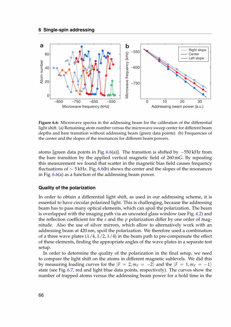
6 Single-spin addressing
−850 −750 −650 −550
0
20
40
60
Microwave frequency (kHz)
Ato
m n
umb
er
0 10 20 30
−750
−650
−550
Addressing beam power (a.u.)
Mic
row
ave
freq
uenc
y (k
Hz)
Right slopeCenterLeft slope
a b
Figure 6.6: Microwave spectra in the addressing beam for the calibration of the differentiallight shift. (a) Remaining atom number versus the microwave sweep center for different beamdepths and bare transition without addressing beam (green data points). (b) Frequencies ofthe center and the slopes of the resonances for different beam powers.
atoms [green data points in Fig. 6.6(a)]. The transition is shifted by −550 kHz fromthe bare transition by the applied vertical magnetic field of 260 mG. By repeatingthis measurement we found that scatter in the magnetic bias field causes frequencyfluctuations of ∼ 5 kHz. Fig. 6.6(b) shows the center and the slopes of the resonancesin Fig. 6.6(a) as a function of the addressing beam power.
Quality of the polarization
In order to obtain a differential light shift, as used in our addressing scheme, it isessential to have circular polarized light. This is challenging, because the addressingbeam has to pass many optical elements, which can spoil the polarization. The beamis overlapped with the imaging path via an uncoated glass window (see Fig. 4.2) andthe reflection coefficient for the s and the p polarization differ by one order of mag-nitude. Also the use of silver mirrors, which allow to alternatively work with anaddressing beam at 420 nm, spoil the polarization. We therefore used a combinationof a three wave plates (λ/4, λ/2, λ/4) in the beam path to pre-compensate the effectof these elements, finding the appropriate angles of the wave plates in a separate testsetup.
In order to determine the quality of the polarization in the final setup, we needto compare the light shift on the atoms in different magnetic sublevels. We did thisby measuring loading curves for the |F = 2, mF = −2〉 and the |F = 1, mF = −1〉state (see Fig. 6.7, red and light blue data points, respectively). The curves show thenumber of trapped atoms versus the addressing beam power for a hold time in the
66
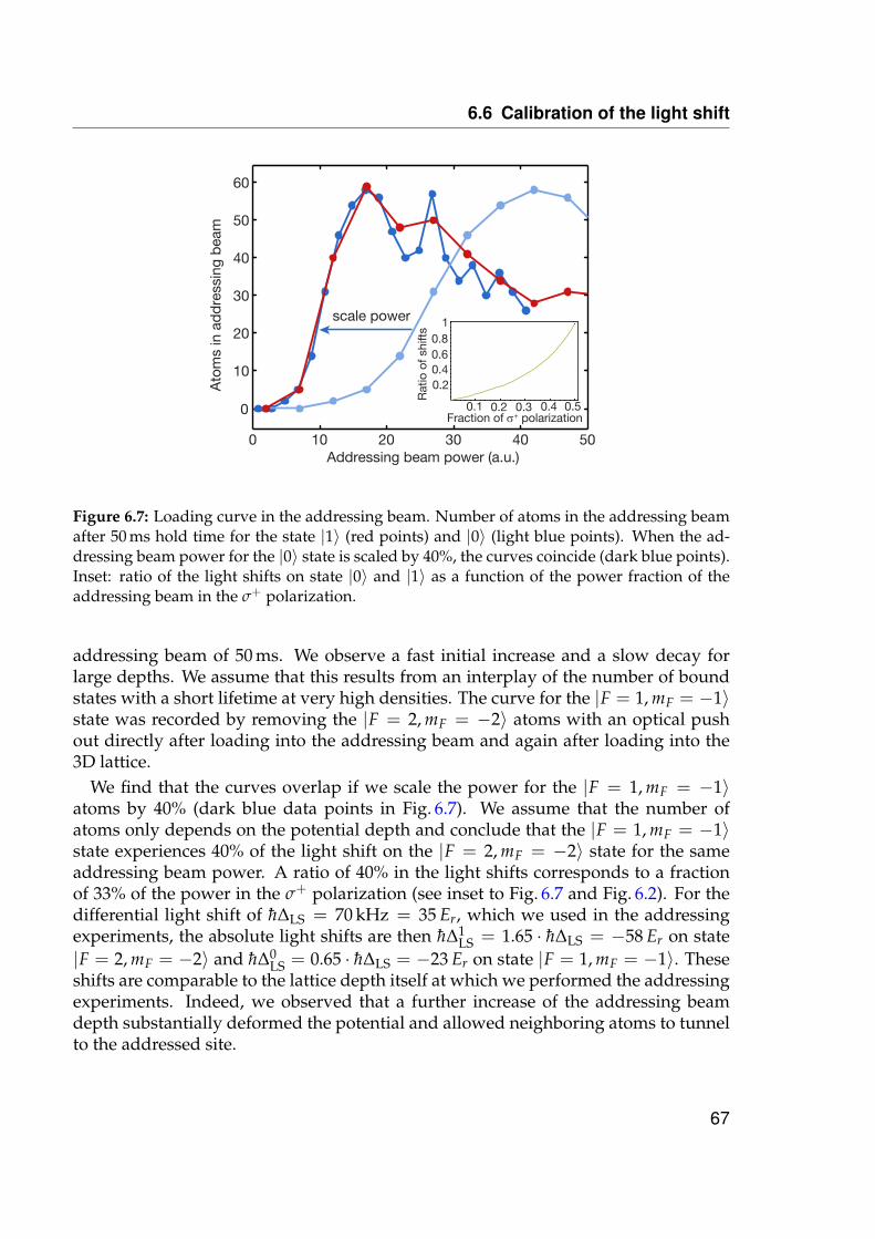
6.6 Calibration of the light shift
0 10 20 30 40 50
10
20
30
40
50
60
Addressing beam power (a.u.)
Ato
ms
in a
dd
ress
ing
bea
m
Fraction of σ+ polarizationR
atio
of s
hift
s
scale power
0.1 0.2 0.3 0.4 0.5
0.20.40.60.8
1
0
Figure 6.7: Loading curve in the addressing beam. Number of atoms in the addressing beamafter 50 ms hold time for the state |1〉 (red points) and |0〉 (light blue points). When the ad-dressing beam power for the |0〉 state is scaled by 40%, the curves coincide (dark blue points).Inset: ratio of the light shifts on state |0〉 and |1〉 as a function of the power fraction of theaddressing beam in the σ+ polarization.
addressing beam of 50 ms. We observe a fast initial increase and a slow decay forlarge depths. We assume that this results from an interplay of the number of boundstates with a short lifetime at very high densities. The curve for the |F = 1, mF = −1〉state was recorded by removing the |F = 2, mF = −2〉 atoms with an optical pushout directly after loading into the addressing beam and again after loading into the3D lattice.
We find that the curves overlap if we scale the power for the |F = 1, mF = −1〉atoms by 40% (dark blue data points in Fig. 6.7). We assume that the number ofatoms only depends on the potential depth and conclude that the |F = 1, mF = −1〉state experiences 40% of the light shift on the |F = 2, mF = −2〉 state for the sameaddressing beam power. A ratio of 40% in the light shifts corresponds to a fractionof 33% of the power in the σ+ polarization (see inset to Fig. 6.7 and Fig. 6.2). For thedifferential light shift of h∆LS = 70 kHz = 35 Er, which we used in the addressingexperiments, the absolute light shifts are then h∆1
LS = 1.65 · h∆LS = −58 Er on state|F = 2, mF = −2〉 and h∆0
LS = 0.65 · h∆LS = −23 Er on state |F = 1, mF = −1〉. Theseshifts are comparable to the lattice depth itself at which we performed the addressingexperiments. Indeed, we observed that a further increase of the addressing beamdepth substantially deformed the potential and allowed neighboring atoms to tunnelto the addressed site.
67
6 Single-spin addressing
6.7 Possible improvements
In our present scheme, we need 30 ms for each addressed lattice site, which is limitedby both the small Rabi frequency of the microwave and the slow movement of the ad-dressing beam. A straight-forward improvement would be to replace the microwavesweep by an optical two-photon Raman transition, which can reach a much fastertransfer. We can still use the differential light shift from the addressing beam to shiftselected atoms into resonance with the Raman transfer. The Raman laser beams canbe large in this case. An alternative is to focus both Raman laser beams onto a singlesite. In this case, the point spread functions need to be squared for the two-photonprocess, which would reduce the effect on the neighboring atom to a few percent.When using the transition at 420 nm the effect on the neighbors would be completelynegligible.
The velocity of the addressing beam is limited to 5 ms per lattice site by the responsetime of the piezo mirror. This can be significantly improved to about 2 µs [145], whenusing an acousto-optical deflector to control the position of the addressing beam [146–148]. This in principle also allows to operate several beams at the same time.
So far, we only performed spin flips driven by frequency sweeps. The scheme is,however, obviously extendable to coherent spin control and would then constitute asingle qubit gate. For driving a Rabi oscillation, the technical requirements are some-what more challenging than for spin flip. The current fluctuations in the backgroundmagnetic field and the pointing error cause a scatter in the resonance frequency ofthe addressed atom of about 5 kHz. In a frequency sweep, one can set the parame-ters to achieve a transfer despite these fluctuations. In a Rabi oscillation, however,this would directly reduce the fidelity of the manipulation and an even better controlwould be required to implement a single-qubit gate with a high fidelity.
6.8 Conclusion
In summary, we have demonstrated two-dimensional single-site and single-atomspin control in an optical lattice in the strongly correlated regime. We focus a laserbeam onto single lattice sites and thereby locally shift the atomic frequency into reso-nance with a microwave driving a spin flip. Starting from a Mott insulator with unityfilling, we create arbitrary two-dimensional spin patterns of individual atoms, thusrealizing a scalable single-atom source. These structures can be used to study ensuingnon-equilibrium quantum dynamics. We achieved a spin-flip fidelity of 95(2)% anda sub-diffraction-limited spatial resolution of 330(10) nm which leads to a negligibleinfluence on the neighboring lattice sites. By correcting for slow drifts of the latticeposition, we position the addressing beam with respect to the lattice with an error of50 nm.
68
7 Tunneling dynamics in a lattice
The ability to prepare arbitrary atom distributions opens up new possibilities for ex-ploring coherent quantum dynamics at the single-atom level. As an example, westudied the one-dimensional tunneling dynamics in a lattice (Sec. 7.2). This allowedus to determine how much our addressing scheme affects the vibrational state of theatoms (Sec. 7.3).
7.1 State of the art
Tunneling processes are among the most intriguing phenomena of quantum mechan-ics and their direct observation is interesting in itself. Tunneling dynamics on a one-dimensional lattice can be seen as a continuous-time version of a quantum walk inposition space, the quantum analog of the random walk. Quantum walks have at-tracted great theoretical interest due to the potential application in quantum informa-tion science [149–152] and their ability to speed up search algorithms compared totheir classical counterparts [153].
Experimental realization of the quantum walk have been reported in various phys-ical systems like nuclear magnetic resonance samples [154, 155] or optical systems[156–158], also for photons in an array of evanescently coupled photonic waveguides[159, 160]. The discrete quantum walk of material quantum particles was observedboth for trapped ions in phase space [161, 162] and for neutral atoms using a sequenceof spin manipulations and spin-dependent transports in an optical lattice [163]. With-out single-particle and single-site resolution, a quantum walk in the ground state hasbeen observed for ultracold fermionic atoms by measuring their ballistic expansionin a weak lattice [164].
No measurement so far has observed the ground state tunneling dynamics of mas-sive particles on a lattice with single-site resolution.
7.2 Ground state tunneling dynamics
We started by preparing a single line of up to 18 atoms along the y direction beforewe lowered the lattice depth along the x direction to Vx = 5.0(5)Er within 200 µs. Atthe same time, the other lattice depths were lowered to Vy = 30 Er and Vz = 23 Er,which reduced the external confinement along the x direction, but still suppressedtunneling in the y and z directions. After a varying hold time t, allowing the atomsto tunnel along x, the atomic distribution was frozen by a rapid 100 µs ramp of the
69
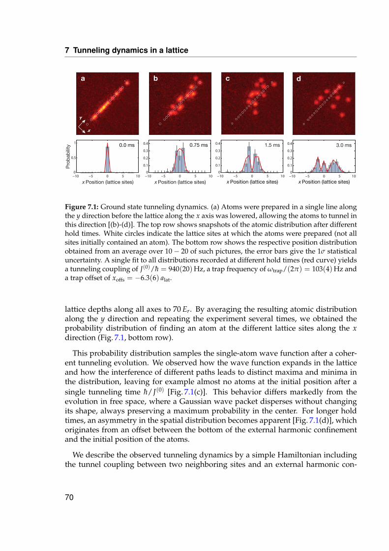
7 Tunneling dynamics in a lattice
b
−10 −5 0 5 100
0.5
1
x Position (lattice sites)−10 −5 0 5 100
0.1
0.2
0.3
0.4
−10 −5 0 5 100
0.1
0.2
0.3
0.4
−10 −5 0 5 100
0.1
0.2
0.3
0.4
x Position (lattice sites)
Pro
bab
ility 1.5 ms 3.0 ms
c da
x
0.0 ms 0.75 ms
x Position (lattice sites) x Position (lattice sites)
y
Figure 7.1: Ground state tunneling dynamics. (a) Atoms were prepared in a single line alongthe y direction before the lattice along the x axis was lowered, allowing the atoms to tunnel inthis direction [(b)-(d)]. The top row shows snapshots of the atomic distribution after differenthold times. White circles indicate the lattice sites at which the atoms were prepared (not allsites initially contained an atom). The bottom row shows the respective position distributionobtained from an average over 10− 20 of such pictures, the error bars give the 1σ statisticaluncertainty. A single fit to all distributions recorded at different hold times (red curve) yieldsa tunneling coupling of J(0)/h = 940(20)Hz, a trap frequency of ωtrap/(2π) = 103(4)Hz anda trap offset of xoffs = −6.3(6) alat.
lattice depths along all axes to 70 Er. By averaging the resulting atomic distributionalong the y direction and repeating the experiment several times, we obtained theprobability distribution of finding an atom at the different lattice sites along the xdirection (Fig. 7.1, bottom row).
This probability distribution samples the single-atom wave function after a coher-ent tunneling evolution. We observed how the wave function expands in the latticeand how the interference of different paths leads to distinct maxima and minima inthe distribution, leaving for example almost no atoms at the initial position after asingle tunneling time h/J(0) [Fig. 7.1(c)]. This behavior differs markedly from theevolution in free space, where a Gaussian wave packet disperses without changingits shape, always preserving a maximum probability in the center. For longer holdtimes, an asymmetry in the spatial distribution becomes apparent [Fig. 7.1(d)], whichoriginates from an offset between the bottom of the external harmonic confinementand the initial position of the atoms.
We describe the observed tunneling dynamics by a simple Hamiltonian includingthe tunnel coupling between two neighboring sites and an external harmonic con-
70
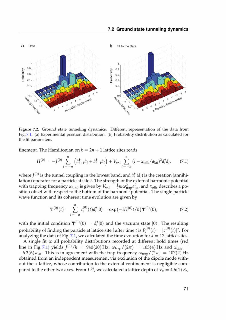
7.2 Ground state tunneling dynamics
0.0
1.5
3.0
-4-3
-2-1
01
23
45
6
0.2
0.4
0.6
0.8
1
Fit to the Data
0.0
1.5
3.0
-4-3
-2-1
01
23
45
6
0.2
0.4
0.6
0.8
1
x-Position (lattice sites)waiting time (m
s)
x-Position (lattice sites)
waiting time (m
s)
Pro
bab
ility
Prob
abili
ty
Dataa b
Figure 7.2: Ground state tunneling dynamics. Different representation of the data fromFig. 7.1. (a) Experimental position distribution. (b) Probability distribution as calculated forthe fit parameters.
finement. The Hamiltonian on k = 2n + 1 lattice sites reads
H(0) = −J(0)n
∑i =−n
(a†
i+1 ai + a†i−1 ai
)+ Vext
n
∑i =−n
(i− xoffs/alat)2 a†
i ai, (7.1)
where J(0) is the tunnel coupling in the lowest band, and a†i (ai) is the creation (annihi-
lation) operator for a particle at site i. The strength of the external harmonic potentialwith trapping frequency ωtrap is given by Vext =
12 mω2
trapa2lat, and xoffs describes a po-
sition offset with respect to the bottom of the harmonic potential. The single particlewave function and its coherent time evolution are given by
Ψ(0)(t) =n
∑i =−n
c(0)i (t)a†i |0〉 = exp
(−iH(0)t/h
)Ψ(0)(0), (7.2)
with the initial condition Ψ(0)(0) = a†0|0〉 and the vacuum state |0〉. The resulting
probability of finding the particle at lattice site i after time t is P(0)i (t) = |c(0)i (t)|2. For
analyzing the data of Fig. 7.1, we calculated the time evolution for k = 17 lattice sites.A single fit to all probability distributions recorded at different hold times (red
line in Fig. 7.1) yields J(0)/h = 940(20)Hz, ωtrap/(2π) = 103(4)Hz and xoffs =−6.3(6) alat. This is in agreement with the trap frequency ωtrap/(2π) = 107(2)Hzobtained from an independent measurement via excitation of the dipole mode with-out the x lattice, whose contribution to the external confinement is negligible com-pared to the other two axes. From J(0), we calculated a lattice depth of Vx = 4.6(1) Er,
71

7 Tunneling dynamics in a lattice
which agrees with an independent calibration via parametric heating. Fig. 7.2 showsthe same data as Fig. 7.1 in a different representation.
The expansion of the wave packet can also be understood by writing the initiallocalized wave function as a superposition of all Bloch waves of quasi-momentum hq,with −π/alat ≤ q ≤ π/alat. To each quasi-momentum hq, we can assign a velocityvq =
1h
∂E∂q , determined by the dispersion relation E(q) = −2J(0) cos(qalat) of the lowest
band. The edges of the wave packet propagate with the largest occurring velocityvmax = 2J(0)alat/h = 1.88(4) alat/ms, in agreement with our data.
We also observed how the dynamics is suppressed, when the tunneling from siteto site is shifted out of resonance by the external confinement. In combination withthe offset xoffs = −6.3(6) alat between the bottom of the external confinement andthe prepared initial atom position, the external confinement leads to a potential gra-dient at the atom position. As the external confinement is caused by the perpen-dicular lattice depths, we increased it by keeping the perpendicular lattice depths atVy = 56 Er and Vz = 70 Er. The trap frequency of the external confinement is thenωtrap/(2π) = 250 Hz and the energy shift from the initial lattice site to the adjacentlattice sites is ∆E = mω2
trapxoffsalat = h · 900 Hz. We found that in this case the atomsstay at the prepared position even after several hundred milliseconds.
7.3 Tunneling in the first excited band
In a second tunneling experiment, we observed the faster dynamics of atoms in thefirst excited band (see Fig. 7.3). For this, we deliberately excited the atoms by in-troducing a pointing offset δx of the addressing beam, which caused a shift of thepotential wells during the switch-on. We repeated the same tunneling experiment asabove with a hold time of t = 1 ms for different pointing offsets δx. For a small point-ing offset [δx = 0.1 alat in Fig. 7.3(b)] we observed a narrow distribution, compared toa much broader one for a large offset [δx = −0.4 alat in Fig. 7.3(a)]. We attribute thisto different fractions f of atoms in the first band which is characterized by the highertunneling rate J(1).
We fitted the distribution of Fig. 7.3(a) to a two-band model and found J(1)/h =
6.22(6) kHz. This is in excellent agreement with the expected value of J(1)/h =
6.14(6) kHz from a band structure calculation in which we used J(0) as an input pa-rameter to calculate the lattice depth.
When including tunneling in the first band, we assume an incoherent sum Ptot(t)of the distributions P(0)(t) of the zeroth band and P(1)(t) of the first band as
Ptot(t) = (1− f )P(0)(t) + f P(1)(t). (7.3)
The Hamiltonian H(1) in the first band and the coherent dynamics are identical tothe ones of the zeroth band (Eqs. 7.1 and 7.2), except for a different tunnel coupling
72
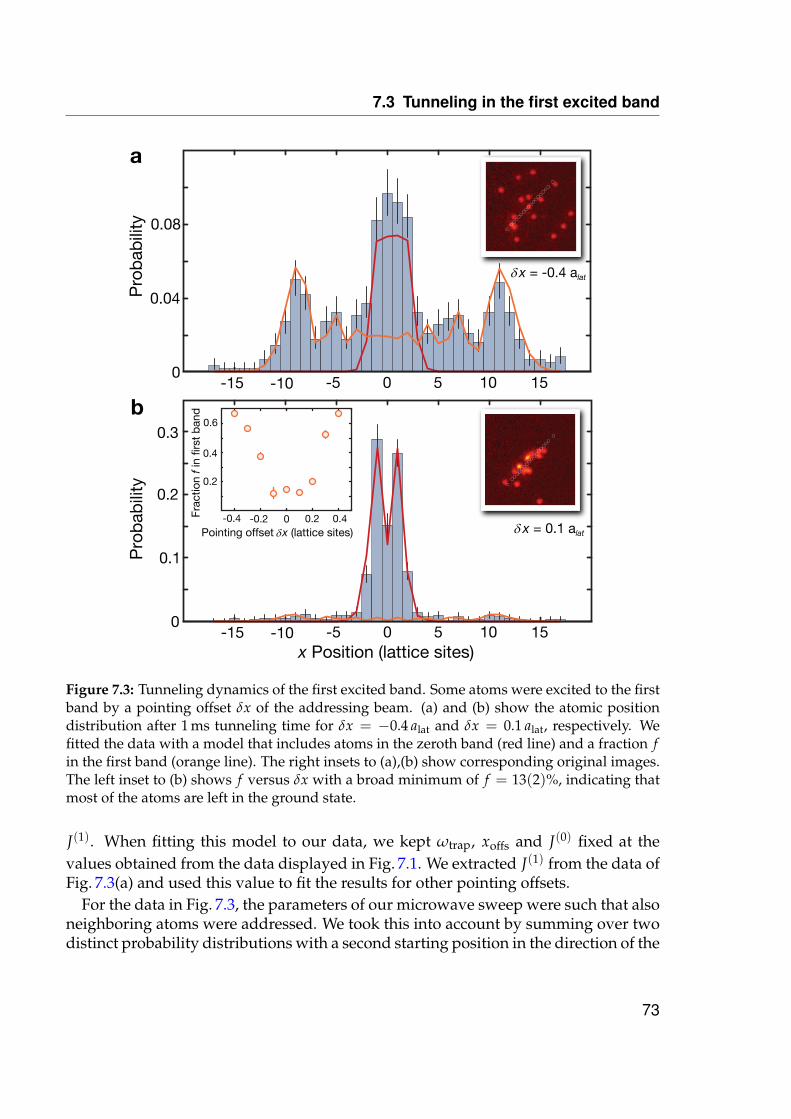
7.3 Tunneling in the first excited band
Pointing offset x (lattice sites)
x Position (lattice sites)
Frac
tion
f in
first
ban
d
0 0.2 0.4-0.2-0.4
0.2
0.6
0.4
b
aP
rob
abili
tyP
rob
abili
ty
1550-15 -10 -5 10
1550-15 -10 -5 10
0.04
0.1
0.3
0.2
0
0.08
0
δ
x = -0.4 alat
x = 0.1 alatδ
δ
Figure 7.3: Tunneling dynamics of the first excited band. Some atoms were excited to the firstband by a pointing offset δx of the addressing beam. (a) and (b) show the atomic positiondistribution after 1 ms tunneling time for δx = −0.4 alat and δx = 0.1 alat, respectively. Wefitted the data with a model that includes atoms in the zeroth band (red line) and a fraction fin the first band (orange line). The right insets to (a),(b) show corresponding original images.The left inset to (b) shows f versus δx with a broad minimum of f = 13(2)%, indicating thatmost of the atoms are left in the ground state.
J(1). When fitting this model to our data, we kept ωtrap, xoffs and J(0) fixed at thevalues obtained from the data displayed in Fig. 7.1. We extracted J(1) from the data ofFig. 7.3(a) and used this value to fit the results for other pointing offsets.
For the data in Fig. 7.3, the parameters of our microwave sweep were such that alsoneighboring atoms were addressed. We took this into account by summing over twodistinct probability distributions with a second starting position in the direction of the
73
7 Tunneling dynamics in a lattice
pointing offset. Interaction effects between the two atoms in the 1D system are negli-gible for our parameters. From the lattice depths we calculate an interaction energy ofUint = h · 610 Hz using a band structure calculation and the known atom-interactionparameters. This has to be compared to the kinetic energy of 4ZJ(0) with the numberof next neighbors Z = 2 in a one-dimensional system. For Uint/(8J(0)) = 0.5 andUint/(8J(1)) = 0.08 we do not expect to observe interaction effects, e.g. repulsivelybound pairs. The study of interaction effects is left for future investigations.
Our measurement of the fraction of excited atoms f as a function of the point-ing offset δx [inset to Fig. 7.3(b)] shows that the atoms are strongly heated for largepointing offsets. By contrast, only a small fraction of the atoms is excited to the firstband for small pointing offsets |δx| ≤ 0.1 alat, yielding a ground state population of1− f = 87(2)%.
This value was not optimized yet. The heating is more than we would expect fromspontaneous scattering of lattice photons even for the relatively long hold times of800 ms. It might be due to a small amplitude shaking of the addressing beam po-sition or intensity noise. Most probably it comes from a sideband transition of themicrowave transfer, which is possible, because the differential light shift of the ad-dressing beam leads to different trap frequencies for the two hyperfine states, whichlifts the orthogonality of the vibrational levels.
7.4 Conclusion
We used our ability to prepare an arbitrary atom distribution for the study of coher-ent tunneling dynamics in a one-dimensional lattice. We started with a single lineof atoms and lowered the perpendicular lattice depth for a varying hold time beforewe freezed and imaged the distribution. By averaging over the copies of the one-dimensional system and over several realizations we mapped out the wave functionand its coherent evolution. We observe the distinct minima and maxima in the distri-bution originating from the interference of different paths.
We fitted the data to a simple model including the next neighbor tunnel couplingand an external confinement and found a tunneling rate in agreement with the expec-tation from a band structure calculation.
We excited atoms to higher bands by giving a pointing offset between the address-ing laser and the lattice during the preparation of the starting position. We observedthat the atoms tunnel much further in this case. We fitted to a model including thedynamics of the zeroth and the first band and extracted the tunneling rate of thefirst band as well as the fraction of atoms in the first band. We found that withoutpointing offset, our addressing scheme leaves 87(2)% of the atoms in the vibrationalground state. The preparation of atoms in the ground state is important for the studyof further non-equilibrium quantum dynamics.
74
7.4 Conclusion
Our measurements constitute the first observation of the ground state tunnelingdynamics of massive particles on a lattice with single-site resolution.
75

7 Tunneling dynamics in a lattice
76
8 Coherent light scattering from a 2D Mott insulator
In this chapter, we investigate coherent light scattering from an atomic Mott insulatorin a two-dimensional square lattice structure [165]. We imaged the far-field diffrac-tion pattern while simultaneously laser cooling the atoms with the probe beams andfound distinct diffraction peaks.
The angular position of the diffraction peaks and the scaling of the peak parameterswith the atom number are described by a simple analytic model (Sec. 8.2). A quanti-tative analysis of the diffraction pattern confirms the coherent nature of the scatteringprocess (Sec. 8.3). From the power fraction in the peaks we deduce the coherence ofthe fluorescence light and discuss the mechanisms that reduce the coherence (Sec. 8.4).
We artificially prepared 1D antiferromagnetic order as a density wave and subse-quently observed additional diffraction peaks, thus demonstrating the usability oflight scattering for the detection of global spin correlations (Sec. 8.5).
8.1 State of the art
Recent interest in cold atoms research has focused on reaching sufficiently low tem-peratures and entropies to observe magnetically ordered quantum phases [3]. In thiscontext, light scattering has been proposed as a new tool to detect these quantumcorrelations. Spin correlations could be mapped onto correlations of scattered light[166–169] or be detected via diffraction peaks from the additional scattering planes forspin-dependent probe light [170]. Light scattering would allow to measure the tem-perature of fermions in an optical lattice [171] or the density fluctuations across thesuperfluid-to-Mott-insulator transition [172–174]. Since the amount of scattered lightis usually very small, several proposals involve a cavity for the detection [175, 176].
Without cavities, elastic Bragg scattering has been used to demonstrate the longrange periodic order of thermal atoms in an optical lattice despite very low fillingfactors [177, 178]. It allowed the measurement of a change of the lattice constant fromthe backaction of the atoms [177, 179], their localization dynamics [180, 181] and tem-perature [179]. Bragg scattering was also studied in a far-detuned one-dimensionallattice [182].
8.2 Analytic 1D model
We begin by introducing a simple analytic 1D model to illustrate the underlyingphysics. Atoms on a 1D lattice (lattice spacing alat = λlat/2, where λlat is the lat-
77
8 Coherent light scattering from a 2D Mott insulator
tice wavelength) are driven by a light field (wavelength λprobe) entering from the xdirection [Fig. 8.1(a)] with wave vector ki = k ex, where k = 2π/λprobe and ex is theunit vector along x. The scattered light is detected at a point r, defined by the angle θwith the z-axis, such that r = r er = r sin θ ex + r cos θ ez. The position of the l-th atomis xl = l alat ex and its distance rl to the detection point is in far-field approximationrl = |r− xl| ≈ r− xl · er. In our model, each atom emits a spherical wave, which atthe detection point can be written as
Fl(rl) = feikrl
rleiδl ≈ f
eikr
re−iK·xl . (8.1)
Here, f denotes the coherently scattered field amplitude, δl = ki · xl is the phaseimprinted by the incoming light field, and K = ko − ki with the wave vector ko =
k er in the observed direction. The differential cross section dσdθ (K) ∝ |∑l e−iK·xl |2 is
obtained by summing over the field amplitudes from all Nx atoms. As a result, weobtain the angular dependence of the scattered light field,
dσ
dθ(θ) ∝
sin2 [k alat(sin θ − 1)Nx/2]sin2 [k alat(sin θ − 1)/2]
. (8.2)
with distinct maxima when the field amplitudes of neighboring atoms interfere con-structively, i.e. when K · (xl − xl+1) = 2π · n, where n is an integer that denotes thediffraction order. The height of the diffraction peak is proportional to N2
x whereas thepeak width scales as 1/Nx. The angles θn, under which the diffraction maxima canbe observed, are given by
sin θn = 1 + nλ
alat. (8.3)
The trivial case n = 0 gives the forward scattered light (θ0 = 90), independentof alat and λ. For our experimental parameters (λprobe = 780 nm, alat = 532 nm),Eq. (8.3) can be additionally fulfilled only for n = −1, yielding the correspondingminus first diffraction order at θ−1 = −27.8 and 207.8. These two out of planescattered waves ensure the momentum conservation in the z direction. Fig. 8.1(b)(blue curve) shows a polar plot of dσ
dθ (θ), displaying the forward scattered light andthe two diffraction peaks, one of which is captured by our imaging system (grayshaded region). If only every second lattice site is occupied (e.g. after removing onespin component in an antiferromagnetically ordered sample), the periodicity of thesystem is doubled. In this case, there are two possible diffraction orders (in the upperhalf plane) at θAFM
−1 = 15.5 and θAFM−2 = θ−1 = −27.8 [green curve in Fig. 8.1(b)].
It is straight-forward to extend this simple model to the two-dimensional case, ifone assumes a rectangular instead of elliptical profile of the cloud. In this case, thetwo directions separate and one finds only the zeroth diffraction order in the directionperpendicular to the incoming beam.
78
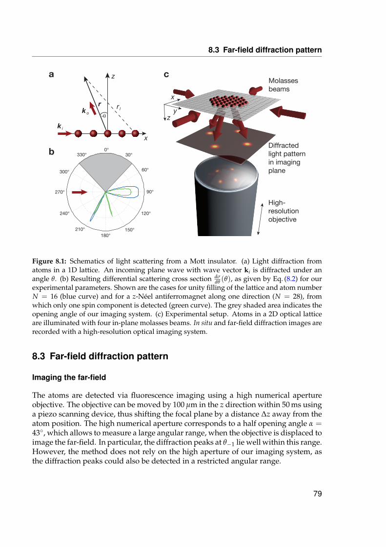
8.3 Far-field diffraction pattern
k i
-θ
r l
x
za
b
cMolasses beams
High-resolutionobjective
Diffracted light patternin imagingplane
zy
x
k o
r
180°
0°
90°270°
210°
240° 120°
150°
30°
60°300°
330°
Figure 8.1: Schematics of light scattering from a Mott insulator. (a) Light diffraction fromatoms in a 1D lattice. An incoming plane wave with wave vector ki is diffracted under anangle θ. (b) Resulting differential scattering cross section dσ
dθ (θ), as given by Eq. (8.2) for ourexperimental parameters. Shown are the cases for unity filling of the lattice and atom numberN = 16 (blue curve) and for a z-Néel antiferromagnet along one direction (N = 28), fromwhich only one spin component is detected (green curve). The grey shaded area indicates theopening angle of our imaging system. (c) Experimental setup. Atoms in a 2D optical latticeare illuminated with four in-plane molasses beams. In situ and far-field diffraction images arerecorded with a high-resolution optical imaging system.
8.3 Far-field diffraction pattern
Imaging the far-field
The atoms are detected via fluorescence imaging using a high numerical apertureobjective. The objective can be moved by 100 µm in the z direction within 50 ms usinga piezo scanning device, thus shifting the focal plane by a distance ∆z away from theatom position. The high numerical aperture corresponds to a half opening angle α =43, which allows to measure a large angular range, when the objective is displaced toimage the far-field. In particular, the diffraction peaks at θ−1 lie well within this range.However, the method does not rely on the high aperture of our imaging system, asthe diffraction peaks could also be detected in a restricted angular range.
79
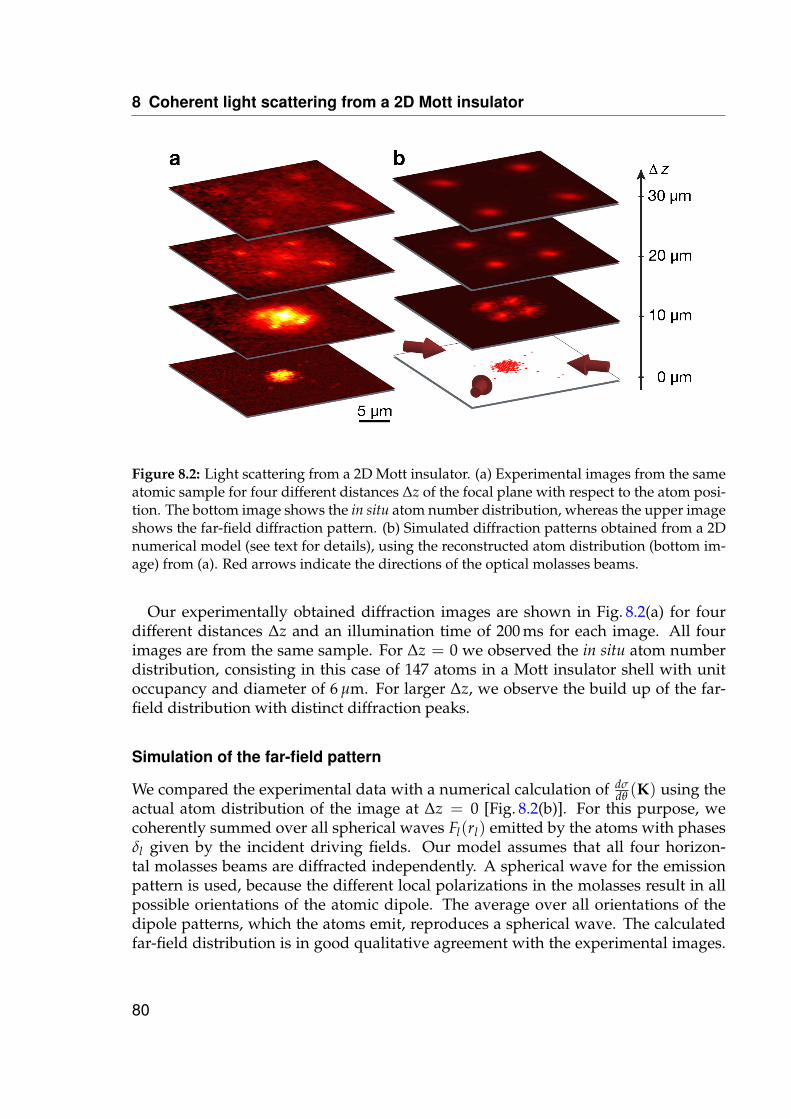
8 Coherent light scattering from a 2D Mott insulator
Figure 8.2: Light scattering from a 2D Mott insulator. (a) Experimental images from the sameatomic sample for four different distances ∆z of the focal plane with respect to the atom posi-tion. The bottom image shows the in situ atom number distribution, whereas the upper imageshows the far-field diffraction pattern. (b) Simulated diffraction patterns obtained from a 2Dnumerical model (see text for details), using the reconstructed atom distribution (bottom im-age) from (a). Red arrows indicate the directions of the optical molasses beams.
Our experimentally obtained diffraction images are shown in Fig. 8.2(a) for fourdifferent distances ∆z and an illumination time of 200 ms for each image. All fourimages are from the same sample. For ∆z = 0 we observed the in situ atom numberdistribution, consisting in this case of 147 atoms in a Mott insulator shell with unitoccupancy and diameter of 6 µm. For larger ∆z, we observe the build up of the far-field distribution with distinct diffraction peaks.
Simulation of the far-field pattern
We compared the experimental data with a numerical calculation of dσdθ (K) using the
actual atom distribution of the image at ∆z = 0 [Fig. 8.2(b)]. For this purpose, wecoherently summed over all spherical waves Fl(rl) emitted by the atoms with phasesδl given by the incident driving fields. Our model assumes that all four horizon-tal molasses beams are diffracted independently. A spherical wave for the emissionpattern is used, because the different local polarizations in the molasses result in allpossible orientations of the atomic dipole. The average over all orientations of thedipole patterns, which the atoms emit, reproduces a spherical wave. The calculatedfar-field distribution is in good qualitative agreement with the experimental images.
80
8.3 Far-field diffraction pattern
The simulation in Fig. 8.2(b) only includes the coherently scattered light, whereas theexperimental data in Fig. 8.2(a) also shows a significant incoherent background.
Evaluation of the diffraction peaks
For a more quantitative analysis, we recorded diffraction patterns of Mott insula-tors for different atom numbers [Fig. 8.3(a)-(c)]. We evaluated cuts (angular sectorsof width 4 ) through the diffraction peaks and through the background signal [seeFig. 8.3(c)] and applied a coordinate transformation from the position x and y in thefar-field plane to polar coordinates θ and φ. We determined the center of the cloudfrom the in situ image and transformed to polar coordinates in the far-field plane withthe radial coordinate r =
√x2 + y2 and the polar angle φ with the x axis. Then we
transformed from the radius r to the angle θ with the z axis as tan(θ) = r/∆z, where∆z is the distance between the in situ plane and the far-field plane. The differentialcross section is transformed as
dσ
dθdφ=
dσ
dxdydet
∂(x, y)∂(θ, φ)
=dσ
dxdy(∆z +
r2
∆z)∆z. (8.4)
Fig. 8.3(d) shows the resulting angular distribution dσdθ (θ) of the differential scattering
cross section. We fitted the resulting peaks with a Gaussian (height A, 1/√
e width w,center position θ−1, and offset fixed at the background value). The peak position, av-eraged over all experimental runs is |θ−1| = 27.4(6) , in excellent agreement with theexpected value of |θ−1| = 27.8 . The error is dominated by the systematic uncertaintyof±1 µm in the determination of ∆z. The systematic deviation of the diffraction anglemight also be due to a small angle between the molasses beams and the lattice beams.
The peak height scales quadratically with the atom number [Fig. 8.3(e)], illustratingthe coherent nature of the scattering. The peak width scales as w ∝ 1/
√N [Fig. 8.3(f)],
in agreement with the result from the 1D model [Eq. (8.2)], assuming Nx =√
N atomsin one dimension.
In addition to the four diffraction peaks from the horizontal molasses beams, a fifthweaker peak is clearly visible in the center left part of the far-field images [see whitecircle in Fig. 8.3(c)]. This peak results from the diffraction of the fifth molasses beamwhich is shone in from the direction of the imaging system. This shows that oursingle plane of a few hundred atoms in the optical lattice acts as a “mirror” for theincoming beam. In contrast to Bragg scattering from a 3D lattice, we expect reflectionfor any incidence angle, because there is only a single lattice plane.
Power fraction in the peaks
We used the far-field images to extract the power scattered into the detected diffrac-tion peaks and the power scattered into the background. We know from Sec. 8.2 that
81
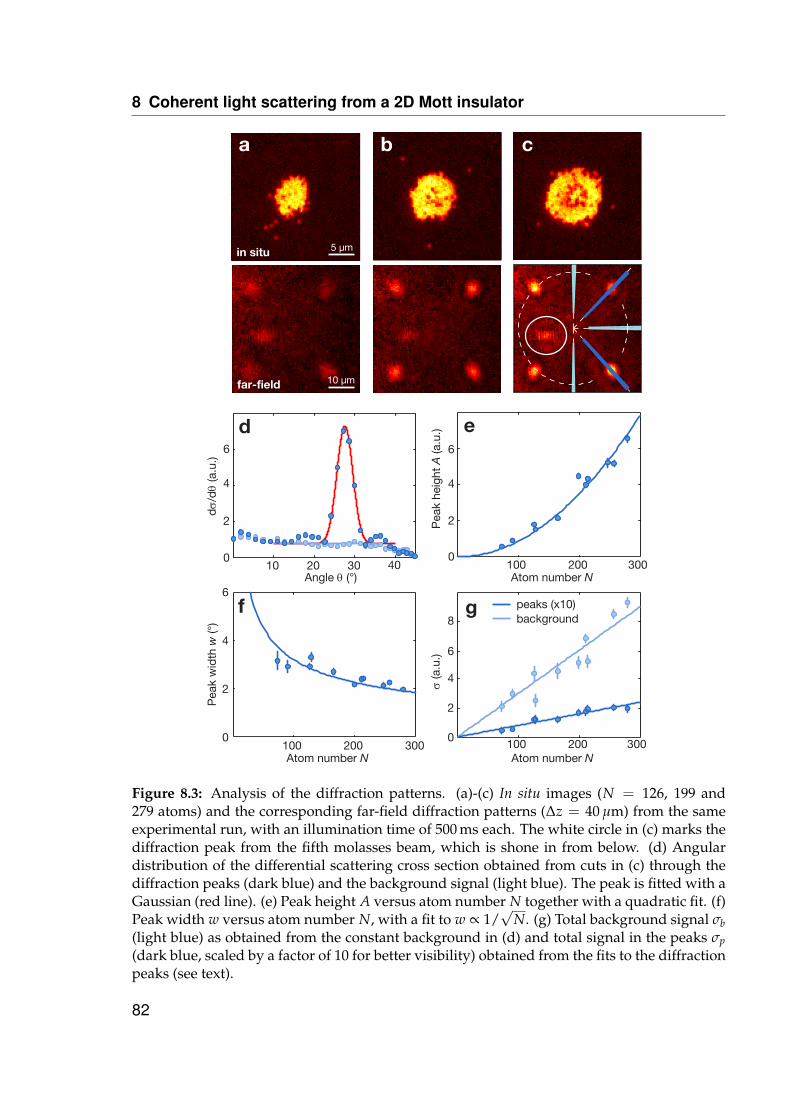
8 Coherent light scattering from a 2D Mott insulator
Angle θ (°)
a
10 20 30 400
2
4
6
dσ/
dθ
(a.u
.)
100 200 3000
2
4
6
Atom number N
Pea
k he
ight
A (a
.u.)
100 200 3000
2
4
6
Atom number N
Pea
k w
idth
w (°
)
0
2
4
6
Atom number N
σ (a
.u.)
5 µm
f
100 200 300
peaks (x10)background
g
e
10 µm
d
b c
far-field
in situ
8
Figure 8.3: Analysis of the diffraction patterns. (a)-(c) In situ images (N = 126, 199 and279 atoms) and the corresponding far-field diffraction patterns (∆z = 40 µm) from the sameexperimental run, with an illumination time of 500 ms each. The white circle in (c) marks thediffraction peak from the fifth molasses beam, which is shone in from below. (d) Angulardistribution of the differential scattering cross section obtained from cuts in (c) through thediffraction peaks (dark blue) and the background signal (light blue). The peak is fitted with aGaussian (red line). (e) Peak height A versus atom number N together with a quadratic fit. (f)Peak width w versus atom number N, with a fit to w ∝ 1/
√N. (g) Total background signal σb
(light blue) as obtained from the constant background in (d) and total signal in the peaks σp(dark blue, scaled by a factor of 10 for better visibility) obtained from the fits to the diffractionpeaks (see text).
82
8.4 Coherence of the fluorescence light
there are three peaks per beam one of which is detected. We exclude here the for-ward scattering light and consider the power in the detected peak and its symmetriccounterpart in the other direction.
In the cuts outside the diffraction peaks [see light blue data in Fig. 8.3(d)], we founda constant background differential cross section (dσ
dθ )b and calculated the total inco-herent scattering cross section σb = 4π(dσ
dθ )b, assuming an isotropic intensity distri-bution. In the data, the background actually drops to zero for angles larger than thehalf opening angle 43 of our imaging system. We also corrected for a global offset,that was due to imperfect stray light substraction.
The total scattering cross section of one peak is given by an integral over the fullsolid angle
σ(1)p =
∫ ∫ dσ
dθdφ(θ, φ) sin(θ)dθdφ, (8.5)
where the differential scattering cross section dσdθdφ (θ, φ) is a peaked function, which
we can approximate by a Gaussian with height A, width w in the radial direction andw cos(θ−1) in the azimuthal direction. The factor cos(θ−1) accounts for the elliptic-ity of the diffraction peaks due to the effective ellipticity of the atomic cloud, whenviewed under the angle θ−1. We obtain these parameters from a Gaussian fit to a cutthrough the peak [see dark blue data and red line in Fig. 8.3(d)].
Because the peak covers only a small range of θ, we can evaluate the factor sin(θ)at the position of the peak and pull it out of the integral. We then obtain for the totalscattering cross section of one peak
σ(1)p ≈ sin(θ−1)2πAw2 cos(θ−1). (8.6)
As there are five molasses beams and a symmetric counterpart in the other directionfor each detected peak, the total scattering cross section in the peaks (excluding theforward scattered light) is σp = 10 · σ(1)
p .Fig. 8.3(g) shows σb and σp, which both scale linearly with the number of atoms.
From the slopes, we find a fraction fp = σp/(σb + σp) ≈ 3% of the power scatteredinto the detected peaks.
8.4 Coherence of the fluorescence light
In Sec. 8.3 we compared the power in the detected diffraction peaks to that in theconstant background and found a fraction of fp = 3% in the peaks. Here we discussthe various mechanisms that lead to this reduced interference and to the backgroundsignal outside the diffraction peaks. We find that the localization of the atoms, theatomic distribution, and the coherence and elasticity of the scattering process play arole.
83
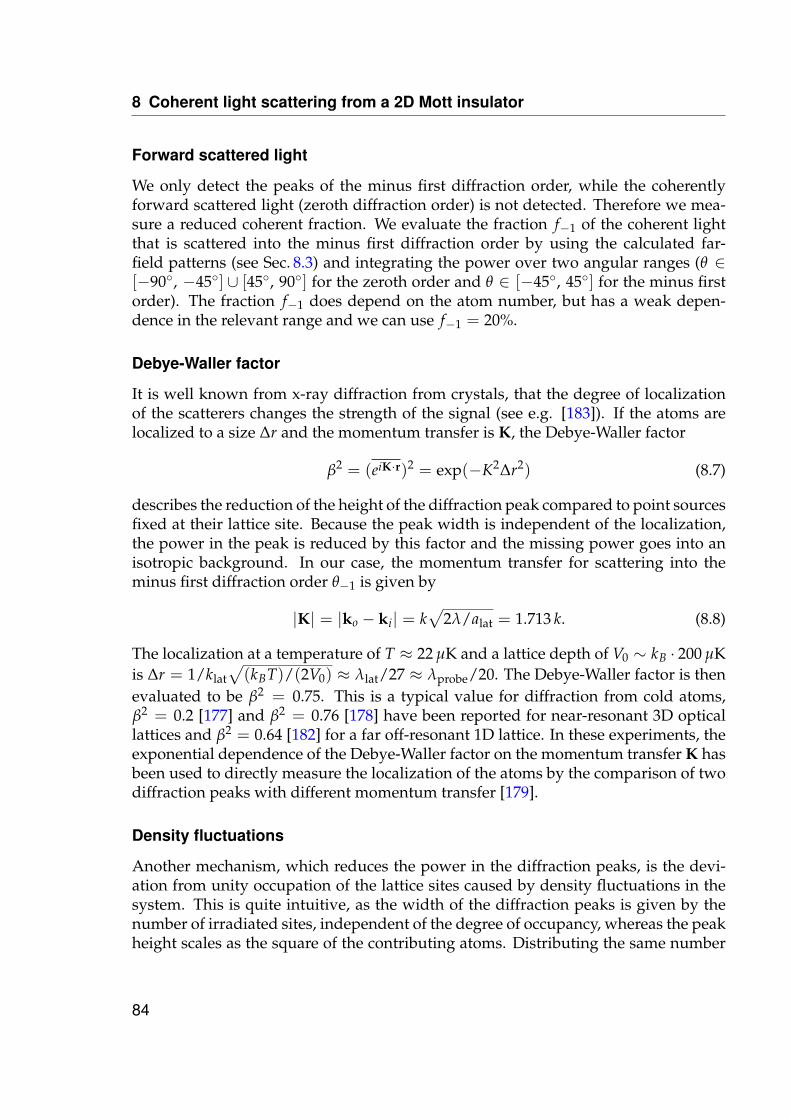
8 Coherent light scattering from a 2D Mott insulator
Forward scattered light
We only detect the peaks of the minus first diffraction order, while the coherentlyforward scattered light (zeroth diffraction order) is not detected. Therefore we mea-sure a reduced coherent fraction. We evaluate the fraction f−1 of the coherent lightthat is scattered into the minus first diffraction order by using the calculated far-field patterns (see Sec. 8.3) and integrating the power over two angular ranges (θ ∈[−90, −45] ∪ [45, 90] for the zeroth order and θ ∈ [−45, 45] for the minus firstorder). The fraction f−1 does depend on the atom number, but has a weak depen-dence in the relevant range and we can use f−1 = 20%.
Debye-Waller factor
It is well known from x-ray diffraction from crystals, that the degree of localizationof the scatterers changes the strength of the signal (see e.g. [183]). If the atoms arelocalized to a size ∆r and the momentum transfer is K, the Debye-Waller factor
β2 = (eiK·r)2 = exp(−K2∆r2) (8.7)
describes the reduction of the height of the diffraction peak compared to point sourcesfixed at their lattice site. Because the peak width is independent of the localization,the power in the peak is reduced by this factor and the missing power goes into anisotropic background. In our case, the momentum transfer for scattering into theminus first diffraction order θ−1 is given by
|K| = |ko − ki| = k√
2λ/alat = 1.713 k. (8.8)
The localization at a temperature of T ≈ 22 µK and a lattice depth of V0 ∼ kB · 200 µKis ∆r = 1/klat
√(kBT)/(2V0) ≈ λlat/27 ≈ λprobe/20. The Debye-Waller factor is then
evaluated to be β2 = 0.75. This is a typical value for diffraction from cold atoms,β2 = 0.2 [177] and β2 = 0.76 [178] have been reported for near-resonant 3D opticallattices and β2 = 0.64 [182] for a far off-resonant 1D lattice. In these experiments, theexponential dependence of the Debye-Waller factor on the momentum transfer K hasbeen used to directly measure the localization of the atoms by the comparison of twodiffraction peaks with different momentum transfer [179].
Density fluctuations
Another mechanism, which reduces the power in the diffraction peaks, is the devi-ation from unity occupation of the lattice sites caused by density fluctuations in thesystem. This is quite intuitive, as the width of the diffraction peaks is given by thenumber of irradiated sites, independent of the degree of occupancy, whereas the peakheight scales as the square of the contributing atoms. Distributing the same number
84
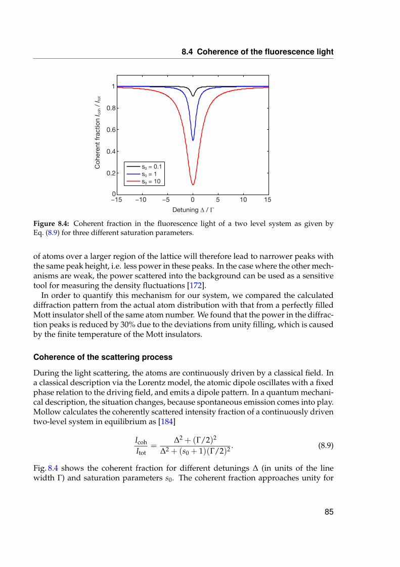
8.4 Coherence of the fluorescence light
−15 −10 −5 0 5 10 150
0.2
0.4
0.6
0.8
1
Detuning ∆ / Γ
Coh
eren
t fr
actio
n I co
h /
I tot
s0 = 0.1s0 = 1s0 = 10
Figure 8.4: Coherent fraction in the fluorescence light of a two level system as given byEq. (8.9) for three different saturation parameters.
of atoms over a larger region of the lattice will therefore lead to narrower peaks withthe same peak height, i.e. less power in these peaks. In the case where the other mech-anisms are weak, the power scattered into the background can be used as a sensitivetool for measuring the density fluctuations [172].
In order to quantify this mechanism for our system, we compared the calculateddiffraction pattern from the actual atom distribution with that from a perfectly filledMott insulator shell of the same atom number. We found that the power in the diffrac-tion peaks is reduced by 30% due to the deviations from unity filling, which is causedby the finite temperature of the Mott insulators.
Coherence of the scattering process
During the light scattering, the atoms are continuously driven by a classical field. Ina classical description via the Lorentz model, the atomic dipole oscillates with a fixedphase relation to the driving field, and emits a dipole pattern. In a quantum mechani-cal description, the situation changes, because spontaneous emission comes into play.Mollow calculates the coherently scattered intensity fraction of a continuously driventwo-level system in equilibrium as [184]
Icoh
Itot=
∆2 + (Γ/2)2
∆2 + (s0 + 1)(Γ/2)2 . (8.9)
Fig. 8.4 shows the coherent fraction for different detunings ∆ (in units of the linewidth Γ) and saturation parameters s0. The coherent fraction approaches unity for
85
8 Coherent light scattering from a 2D Mott insulator
Effect Reduction factorForward scattering not detected 20%Debye-Waller factor β2 75%Density fluctuations 70%Coherence of scattering 99%Inelasticity (change vibrational level) 98%Inelasticity (change mF level) 33%Expected power in detected peaks 3%Measured power in detected peaks 3%
Table 8.1: Reduction of the power scattered into the detected peaks. The table lists the differ-ent effects that lead to a reduction of the power in the peaks together with the reduction factor.The measured reduction agrees well with the expectations, as deduced from multiplying thereduction factor of all effects. For a discussion of the effects see the main text.
small saturation parameters and for large detunings and is above 99% for our param-eters (s0 ≈ 3, ∆ ≈ 14 Γ). From this two-level point of view, the scattering should bealmost completely coherent.
Inelastic scattering processes
Another source of incoherence is the inelasticity of the scattering process, whichcan change both the vibrational state of the atom and its magnetic sublevel. Onaverage, each scattered photon leads to the transfer of two times the recoil energyEprobe
rec = (hkprobe)2/(2m) = h · 3.9 kHz to the atom. When the atom is confined
in a trap, it cannot absorb this energy, but only multiples of the vibrational energyhνtrap, where νtrap ≈ 200 kHz is the trapping frequency. The Lamb-Dicke parameter
η =√
Eproberec /(hνtrap) quantifies the ratio of these two energy scales. In the Lamb-
Dicke regime η 1, where the trap frequency is much larger than the recoil energy,the probability for a scattering process to change the vibrational state is given by η2,which in our case is just η2 = 0.02. Therefore most of the scattering events are elas-tic with respect to the vibrational state, even though the argument is weakened foratoms in higher vibrational states.
The scattering can also change the magnetic sublevel of the atom, emitting photonsof different polarization, which do not interfere. Because for most mF states thereare three decay channels, one can assume in a rough estimate that one third of thescattering events preserves the magnetic sublevel. This dominant mechanism couldbe circumvented by using a single circular polarized beam, which drives a closedtransition. However, using a molasses, which simultaneously cools the atoms, willstill yield the overall largest signal.
86
8.5 Detecting antiferromagnetic order in the density
Summary of the effects
Tab. 8.1 sums up all the different contributions discussed above. Multiplying the re-duction factors of all effects, we find that the measured fraction in the detected peaksagrees well with the expectations. We can only compare the orders of magnitude,because the expected power in the peaks is the product of six different effects andcan only be considered as an estimate. The dominant contribution to the incoher-ent background is inelastic scattering, which changes the magnetic sublevels of theatoms.
We verified our method of extracting the fraction of power scattered into the peaks[Eq. (8.6)], by running the same analysis as in Sec. 8.3 over simulated data as calcu-lated in Sec. 8.3. When we include a coherent fraction in the simulation, we find aboutthe same coherent fraction from the analysis when taking into account the relevanteffects discussed above.
8.5 Detecting antiferromagnetic order in the density
Finally, we demonstrated that light scattering can be used for the detection of spincorrelations. As an example, we created a 1D z-Néel antiferromagnetic order alongthe x direction of the lattice using our single-site addressing technique described inCh. 6. We sequentially flipped all atomic spins in every second row of the latticefrom F = 1 to F = 2 before we applied a resonant laser that removed all atoms inF = 2. Figs. 8.5(a) and (b) show the resulting fluorescence image in the focal planetogether with the reconstructed atom number distribution. The corresponding exper-imental and theoretical diffraction patterns are displayed in Figs. 8.5(c) and (d). Thetwo predicted diffraction peaks of -1st and -2nd order along x are clearly visible in theexperimental picture, although our atomic sample consisted of only 57 atoms. We ob-tain the usual peak position of |θy
−1| = 27.7(6) along the y direction, whereas the twopeaks along x are found at |θx
−1| = 14.5(6) and |θx−2| = 27.4(6) [see Fig. 8.5(e),(f)],
in good agreement with the expected values.
We prepared a 1D antiferromagnetic order, because the additional diffraction peaksthat would arise for a 2D antiferromagnetic order lie outside the opening angle of ourimaging system. However, the position of the diffraction peaks could be varied in a2D geometry by changing the incidence angle of the molasses beams. For an in-planeangle between the lattice and the molasses beams of α = 15, the additional peaks areshifted to smaller angles θ (see Fig. 8.6). An alternative is to use shorter wavelengthprobe light, e.g. near-resonant with the 5S− 6P transition at 420 nm for 87Rb [178].
87
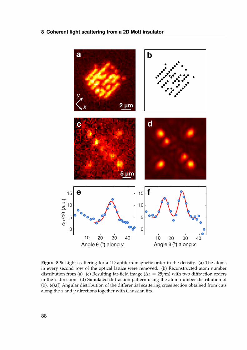
8 Coherent light scattering from a 2D Mott insulator
Angle θ (°) along xAngle θ (°) along y
dσ/
dθ
(a.u
.)b
10 20 30
2 µmx
y
a b
dc
5 µm
40 10 20 30 40
0
5
10
15 e f
0
5
10
15
Figure 8.5: Light scattering for a 1D antiferromagnetic order in the density. (a) The atomsin every second row of the optical lattice were removed. (b) Reconstructed atom numberdistribution from (a). (c) Resulting far-field image (∆z = 25µm) with two diffraction ordersin the x direction. (d) Simulated diffraction pattern using the atom number distribution of(b). (e),(f) Angular distribution of the differential scattering cross section obtained from cutsalong the x and y directions together with Gaussian fits.
88
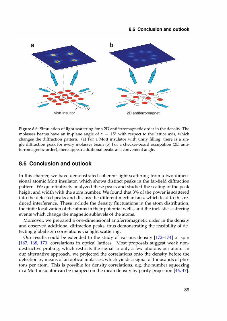
8.6 Conclusion and outlook
a b
Mott insultor 2D antiferromagnet15°x
y
Figure 8.6: Simulation of light scattering for a 2D antiferromagnetic order in the density. Themolasses beams have an in-plane angle of α = 15 with respect to the lattice axis, whichchanges the diffraction pattern. (a) For a Mott insulator with unity filling, there is a sin-gle diffraction peak for every molasses beam (b) For a checker-board occupation (2D anti-ferromagnetic order), there appear additional peaks at a convenient angle.
8.6 Conclusion and outlook
In this chapter, we have demonstrated coherent light scattering from a two-dimen-sional atomic Mott insulator, which shows distinct peaks in the far-field diffractionpattern. We quantitatively analyzed these peaks and studied the scaling of the peakheight and width with the atom number. We found that 3% of the power is scatteredinto the detected peaks and discuss the different mechanisms, which lead to this re-duced interference. These include the density fluctuations in the atom distribution,the finite localization of the atoms in their potential wells, and the inelastic scatteringevents which change the magnetic sublevels of the atoms.
Moreover, we prepared a one-dimensional antiferromagnetic order in the densityand observed additional diffraction peaks, thus demonstrating the feasibility of de-tecting global spin correlations via light scattering.
Our results could be extended to the study of various density [172–174] or spin[167, 168, 170] correlations in optical lattices. Most proposals suggest weak non-destructive probing, which restricts the signal to only a few photons per atom. Inour alternative approach, we projected the correlations onto the density before thedetection by means of an optical molasses, which yields a signal of thousands of pho-tons per atom. This is possible for density correlations, e.g. the number squeezingin a Mott insulator can be mapped on the mean density by parity projection [46, 47].
89

8 Coherent light scattering from a 2D Mott insulator
For spin correlations, we have demonstrated the feasibility of removing one spin stateand observing the additional diffraction peaks from the density structure. This avoidsspin selective coupling of the probe light to the atoms [170], which is incompatiblewith simultaneous laser cooling.
In the 3D case, antiferromagnetic order allows scattering from an additional plane,but it requires careful alignment of the probe beam angle to match the Bragg condi-tion. In contrast, light scattering from a 2D system yields additional peaks from thesame incident beam, which is also convenient for the extraction of the spin correlationlength from the relative height or width of the diffraction peaks.
Finally, we note that the detection of spin correlations via light scattering does notrely on the high aperture of our imaging system. The diffraction peaks could also bedetected in a restricted angular range.
90
9 Conclusion and outlook
This thesis presents novel experimental methods for the study of ultracold atomsin optical lattices. While most experiments so far probed the atoms globally, wehave developed single-site resolved imaging and manipulation of single atoms inthe strongly correlated regime.
We used a high numerical aperture imaging system to resolve single lattice sites.Fluorescence imaging allowed to detect single atoms with a large signal and to recon-struct the atom distribution on the lattice. With this technique we can study stronglycorrelated states at the single particle level. This is complementary to many existingmethods like time-of-flight imaging, because it allows to probe the density correla-tions instead of the coherences.
We applied the technique to Mott insulators in the atomic limit and directly ob-served number squeezing and the shell structure. We determined the temperaturein a single image by fitting the radial density profiles with a simple grand-canonicalmodel. Our pictures show with unprecendented clarity that the entropy is concen-trated in the transition regions between the Mott insulator shells and that it is essen-tially zero in the center of the shells. For our parameters, we calculated an entropyper particle which is around the critical entropy for quantum magnetism.
Moreover, we were able to address single atoms in the lattice and to manipulatetheir spin. We used the differential light shift of a tightly focused laser beam to shiftselected atoms into resonance with a microwave driving the spin flip. This allowedus to reach a high spin-flip fidelity and sub-diffraction-limited resolution. Startingfrom a Mott insulator with unity filling, we we able to prepare arbitrary spin patternsof individual atoms, thus realizing a scalable single-atom source.
This ability to locally manipulate a strongly correlated atomic gas and to preparearbitrary atom distributions opens many perspectives in quantum simulation andcomputation. As an example, we studied the single particle tunneling dynamics ina lattice and directly mapped out the wave function after coherent evolution. Wediscriminated the dynamics of atoms in the ground state and in the first excited bandand found that our addressing scheme leaves most atoms in the ground state. Thepreparation of atoms in the ground state is important for the study of further non-equilibrium quantum dynamics.
Finally, we investigated coherent light scattering as an alternative method to detectantiferromagnetic order also when single-site resolution is not available. We imagedthe far-field diffraction pattern while simultaneously laser cooling the atoms withthe probe beams and found distinct peaks. We quantitatively analyzed the diffrac-tion pattern and found the expected scalings of the peak parameters with the atom
91
9 Conclusion and outlook
number. From the power fraction in the peaks we deduced the coherence of the flu-orescence light and we discuss the mechanisms that reduce the coherence. We arti-ficially prepared 1D antiferromagnetic order as a density wave and observed addi-tional diffraction peaks, thus demonstrating the usability of light scattering for thedetection of global spin correlations.
The following paragraphs will give an outlook on some of the possible future ap-plications of the techniques demonstrated in this thesis.
Even without local manipulation, imaging of single particles in the strongly corre-lated regime is a major step forward. This is valuable in a system with an externalconfinement, where one can have different phases at different positions in the trap,as in the prominent example of the shell structure of a Mott insulator. The measure-ment of the number statistics can be extended to the phase transition [46] and also toone-dimensional systems. A measurement of the density-density correlations [185]should reveal the coherent particle-hole excitations, when switching on tunnelingcoming from the insulating state. While thermal excitations are uncorrelated, thesecoherent excitations are expected to have long-range correlations. Furthermore onecould observe the dynamics after a sudden quench from the Mott insulator to thesuperfluid regime [186] or from 1D to 2D. Also higher-order correlators that are inac-cessible in condensed matter experiments can be tackled. For future work it wouldbe interesting to investigate how entropy propagates in strongly correlated systems,after injecting it on a local scale into the system.
The entropies of our Mott insulators should be sufficiently low to observe quan-tum magnetism in a two-component system with unity total density [29, 119]. Weplan to separate two spin states with a magnetic gradient and observe the mixing dy-namics after switching off the gradient, which is mediated by second order hoppingprocesses.
We can also investigate one-dimensional systems, which are particularly interest-ing due to the enhanced role of quantum fluctuations and the accessibility to numer-ical simulation also of the dynamics. At strong interactions, in the Tonks-Girardeauregime, the bosonic atoms are fermionized, and it would be interesting to detect thefermionized density-density correlations or Friedel oscillations [187–189].
The coherent manipulation of single spins in a Mott insulator opens the path formany new experiments. It will e.g. allow us to create out-of-equilibrium states or lo-cal perturbations in order to observe the ensuing dynamics of the many-body system,such as spin-charge separation [190, 191] or spin impurity dynamics beyond the Lut-tinger liquid theory [192]. Our studies of the tunnelling dynamics at the single-atomlevel can be extended to correlated particle tunneling [98, 160, 193], also in higherdimensions, or to observe transport across local impurities [194] or potential barriers.Further prospects are the implementation of novel cooling schemes relying on thelocal removal of regions with high entropy [7, 195].
Atoms in a Mott insulating state with one atom per lattice site are also very promis-
92
ing as a quantum register for scalable quantum computing, especially with the verylow defect density shown in this work. Combining single-qubit manipulation withlocal readout and a global entanglement operation in a spin-dependent lattice [53, 54]would be the basis of a one-way quantum computer [51, 52]. For the circuit model ofa quantum computer, two-qubit operations can be realized by Rydberg gates, whichwhere already demonstrated in single dipole traps [56, 57]. Implementing them in anoptical lattice will put tens of atoms within the blockade radius, thus allowing gatesbetween selected atom pairs in the lattice without any atom movement.
A Rydberg laser system is currently being set up and will also be used to studycondensed matter physics. E.g., one can generate long-range interactions betweenthe atoms by weakly admixing excited Rydberg states with laser light [196]. Ourhigh-resolution imaging would also allow to directly observe the blockade radius inthe adiabatic formation of Rydberg crystals [197].
Finally, combining the high resolution imaging system with a spatial light modu-lator [37, 198–200] allows to project arbitrary potential shapes with small structuresize, e.g. box potentials, arbitrary lattice geometries [45, 201] or controlled disorder[21, 202]. Using a wavelength with a differential light shift, one can also flip the spinof many selected atoms simultaneously and use this for selective entropy removal [7].
93

94
Danksagung
Hiermit möchte ich mich bei allen herzlich bedanken, die zum Gelingen dieser Arbeitbeigetragen haben. Mein ganz besonderer Dank gilt dabei
Meinen Betreuern Prof. Immanuel Bloch und Prof. Stefan Kuhr, die mir die Mög-lichkeit gegeben haben an diesem spannenden Projekt zu arbeiten, für ihre Begeiste-rungsfähigkeit und tatkräftige Unterstützung. Sie waren stets ansprechbar und offenfür Diskussionen und von ihrer dynamischen und motivierenden Anleitung habe ichsehr profitiert.
Meinen Laborkollegen Dr. Jacob Sherson, Manuel Endres und Dr. Marc Cheneau, mitdenen zusammen ich dieses ehrgeizige Experiment aufbauen durfte, für die gute Zu-sammenarbeit und die erhellenden Diskussionen.
Dr. Takeshi Fukuhara, Peter Schauß und Dr. Christian Gross, die im letzten Jahr dazugestoßen sind und von Anfang an im Labor eine große Hilfe waren.
Prof. Wolfgang Ketterle, der sein Sabbatical am MPQ verbracht hat und unser La-bor mit wertvollen Ideen und inspirierenden Diskussionen bereichert hat.
Unseren Diplomanden, die im Laufe der vier Jahre am Experiment beteiligt waren:Oliver Loesdau, Jan Petersen, Rosa Glöckner, Ralf Labouvie, David Bellem und Ah-med Omran.
Allen weiteren Mitgliedern der Arbeitsgruppe für die guten Diskussionen und diestetige Hilfsbereitschaft.
Allen nicht wissenschaftlichen Mitarbeitern, die das Team engagiert unterstützt ha-ben: Christine Best, Marianne Kargl, Heinz Lenk, Karsten Förster, Markus Böhm undMichael Pruscha.
Meinen Eltern und Geschwistern.
Es war eine besondere Erfahrung, in einem so motivierten Team zu arbeiten und ichbin gespannt auf die Experimente, die noch folgen werden.
95

96
Bibliography
[1] D. Jaksch, C. Bruder, J. I. Cirac, C. Gardiner, and P. Zoller. Cold bosonic atoms inoptical lattices. Phys. Rev. Lett. 81, 3108–3111 (1998).
[2] M. Greiner, O. Mandel, T. Esslinger, T. W. Hänsch, and I. Bloch. Quantum phasetransition from a superfluid to a Mott insulator in a gas of ultracold atoms. Nature415, 39–44 (2002).
[3] M. Lewenstein, A. Sanpera, V. Ahufinger, B. Damski, A. Sen, and U. Sen. Ultra-cold atomic gases in optical lattices: mimicking condensed matter physics and beyond.Adv. Phys. 56, 243–379 (2007).
[4] I. Bloch, J. Dalibard, and W. Zwerger. Many-body physics with ultracold gases.Rev. Mod. Phys. 80, 885–964 (2008).
[5] R. P. Feynman. Simulating physics with computers. Intern. J. Theor. Phys. 21,467–488 (1982).
[6] C. Chin, R. Grimm, P. Julienne, and E. Tiesinga. Feshbach resonances in ultracoldgases. Rev. Mod. Phys. 82, 1225–1286 (2010).
[7] J.-S. Bernier, C. Kollath, A. Georges, L. De Leo, F. Gerbier, C. Salomon, andM. Köhl. Cooling fermionic atoms in optical lattices by shaping the confinement.Phys. Rev. A 79, 061601(R) (2009).
[8] D. C. McKay and B. DeMarco. Cooling in strongly correlated optical lattices :prospects and challenges. Rep. Prog. Phys. 74, 054401 (2011).
[9] B. DeMarco and D. S. Jin. Onset of Fermi degeneracy in a trapped atomic gas. Science285, 1703–1706 (1999).
[10] U. Schneider, L. Hackermüller, S. Will, I. Bloch, T. Best, T. Costi, R. Helmes,D. Rasch, and A. Rosch. Metallic and insulating phases of repulsively interactingFermions in a 3D optical lattice. Science 322, 1520–1525 (2008).
[11] R. Jördens, N. Strohmaier, K. Günter, H. Moritz, and T. Esslinger. A Mott insu-lator of fermionic atoms in an optical lattice. Nature 455, 204–207 (2008).
[12] B. Paredes, A. Widera, V. Murg, O. Mandel, S. Fölling, J. I. Cirac, G. V. Shlyap-nikov, T. Hänsch, and I. Bloch. Tonks-Girardeau gas of ultracold atoms in an opticallattice. Nature 429, 277–281 (2004).
97
Bibliography
[13] T. Kinoshita, T. Wenger, and D. S. Weiss. Observation of a one-dimensional Tonks-Girardeau gas. Science 305, 1125–1128 (2004).
[14] Z. Hadzibabic, P. Krüger, M. Cheneau, B. Battelier, and J. Dalibard. Berezinskii-Kosterlitz-Thouless crossover in a trapped atomic gas. Nature 441, 1118–1121 (2006).
[15] J. G. Danzl, E. Haller, M. Gustavsson, M. J. Mark, R. Hart, N. Bouloufa,O. Dulieu, H. Ritsch, and H.-C. Nägerl. Quantum gas of deeply bound groundstate molecules. Science 321, 1062–1066 (2008).
[16] K.-K. Ni, S. Ospelkaus, M. H. G. de Miranda, A. Pe’er, B. Neyenhuis, J. J. Zirbel,S. Kotochigova, P. S. Julienne, D. S. Jin, and J. Ye. A high phase-space-density gasof polar molecules. Science 322, 231–235 (2008).
[17] J. Billy, V. Josse, Z. Zuo, A. Bernard, B. Hambrecht, P. Lugan, D. Clément,L. Sanchez-Palencia, P. Bouyer, and A. Aspect. Direct observation of Andersonlocalization of matter waves in a controlled disorder. Nature 453, 891–894 (2008).
[18] V. Gurarie, L. Pollet, N. V. Prokofev, B. V. Svistunov, and M. Troyer. Phase dia-gram of the disordered Bose-Hubbard model. Phys. Rev. B 80, 214519 (2009).
[19] U. Bissbort and W. Hofstetter. Stochastic mean-field theory for the disordered Bose-Hubbard model. Europhys. Lett. 86, 50007 (2009).
[20] L. Sanchez-Palencia and M. Lewenstein. Disordered quantum gases under control.Nature Phys. 6, 87–95 (2010).
[21] M. Pasienski, D. McKay, M. White, and B. DeMarco. A disordered insulator in anoptical lattice. Nature Phys. 6, 677–680 (2010).
[22] M. R. Matthews, B. P. Anderson, P. C. Haljan, D. S. Hall, C. E. Wieman, andE. A. Cornell. Vortices in a Bose-Einstein condensate. Phys. Rev. Lett. 83, 2498–2501 (1999).
[23] K. Madison, F. Chevy, W. Wohlleben, and J. Dalibard. Vortex formation in a stirredBose-Einstein condensate. Phys. Rev. Lett. 84, 806–809 (2000).
[24] J. R. Abo-Shaeer, C. Raman, J. M. Vogels, and W. Ketterle. Observation of vortexlattices in Bose-Einstein condensates. Science 292, 476–479 (2001).
[25] Y.-J. Lin, R. L. Compton, K. Jiménez-García, J. V. Porto, and I. B. Spielman. Syn-thetic magnetic fields for ultracold neutral atoms. Nature 462, 628–632 (2009).
[26] N. R. Cooper. Rapidly rotating atomic gases. Adv. Phys. 57, 539–616 (2008).
[27] N. Gemelke, E. Sarajlic, and S. Chu. Rotating few-body atomic systems in the frac-tional quantum Hall regime. arXiv:1007.2677v1 [cond-mat.quant-gas] (2010).
98
Bibliography
[28] S. Trotzky, P. Cheinet, S. Fölling, M. Feld, U. Schnorrberger, A. M. Rey,A. Polkovnikov, E. A. Demler, M. D. Lukin, and I. Bloch. Time-resolved observa-tion and control of superexchange interactions with ultracold atoms in optical lattices.Science 319, 295–299 (2008).
[29] L.-M. Duan, E. Demler, and M. Lukin. Controlling spin exchange interactions ofultracold atoms in optical lattices. Phys. Rev. Lett. 91, 090402 (2003).
[30] J. Simon, W. S. Bakr, R. Ma, M. E. Tai, P. M. Preiss, and M. Greiner. Quantumsimulation of antiferromagnetic spin chains in an optical lattice. Nature 472, 307–312(2011).
[31] P. Soltan-Panahi, J. Struck, P. Hauke, A. Bick, W. Plenkers, G. Meineke,C. Becker, P. Windpassinger, M. Lewenstein, and K. Sengstock. Multi-componentquantum gases in spin-dependent hexagonal lattices. Nature Phys. 7, 434–440 (2011).
[32] A. Gezerlis and J. Carlson. Strongly paired fermions: Cold atoms and neutron mat-ter. Phys. Rev. C 77, 032801(R) (2008).
[33] A. Rapp, G. Zaránd, C. Honerkamp, and W. Hofstetter. Color superfluidity and’Baryon’ formation in ultracold Fermions. Phys. Rev. Lett. 98, 160405 (2007).
[34] R. Blatt and D. Wineland. Entangled states of trapped atomic ions. Nature 453,1008–1015 (2008).
[35] N. Schlosser, G. Reymond, I. Protsenko, and P. Grangier. Sub-poissonian loadingof single atoms in a microscopic dipole trap. Nature 411, 1024–1027 (2001).
[36] R. Scheunemann, F. S. Cataliotti, T. W. Hänsch, and M. Weitz. Resolving andaddressing atoms in individual sites of a CO2-laser optical lattice. Phys. Rev. A 62,051801(R) (2000).
[37] R. Dumke, M. Volk, T. Müther, F. Buchkremer, G. Birkl, and W. Ertmer. Micro-optical realization of arrays of selectively addressable dipole traps: A scalable config-uration for quantum computation with atomic qubits. Phys. Rev. Lett. 89, 097903(2002).
[38] K. D. Nelson, X. Li, and D. S. Weiss. Imaging single atoms in a three-dimensionalarray. Nature Physics 3, 556–560 (2007).
[39] A. Itah, H. Veksler, O. Lahav, A. Blumkin, C. Moreno, C. Gordon, and J. Stein-hauer. Direct observation of a sub-Poissonian number distribution of atoms in anoptical lattice. Phys. Rev. Lett. 104, 113001 (2010).
[40] V. Ossadnik. Direkter Nachweis lichtinduzierter Atomgitter. PhD thesis, Ludwig-Maximilians-Universität München (1996).
99
Bibliography
[41] D. Schrader, I. Dotsenko, M. Khudaverdyan, Y. Miroshnychenko, A. Rauschen-beutel, and D. Meschede. Neutral atom quantum register. Phys. Rev. Lett. 93,150501 (2004).
[42] M. Karski, L. Förster, J. Choi, W. Alt, A. Widera, and D. Meschede. Nearest-neighbor detection of atoms in a 1D optical lattice by fluorescence imaging. Phys. Rev.Lett. 102, 053001 (2009).
[43] T. Gericke, P. Würtz, D. Reitz, T. Langen, and H. Ott. High-resolution scanningelectron microscopy of an ultracold quantum gas. Nature Phys. 4, 949–953 (2008).
[44] P. Würtz, T. Langen, T. Gericke, A. Koglbauer, and H. Ott. Experimental demon-stration of single-site addressability in a two-dimensional optical lattice. Phys. Rev.Lett. 103, 80404 (2009).
[45] W. S. Bakr, J. I. Gillen, A. Peng, S. Fölling, and M. Greiner. A quantum gasmicroscope for detecting single atoms in a Hubbard-regime optical lattice. Nature462, 74–77 (2009).
[46] W. S. Bakr, A. Peng, M. E. Tai, R. Ma, J. Simon, J. I. Gillen, S. Fölling, L. Pollet,and M. Greiner. Probing the superfluid-to-Mott insulator transition at the single-atom level. Science 329, 547–550 (2010).
[47] J. F. Sherson, C. Weitenberg, M. Endres, M. Cheneau, I. Bloch, and S. Kuhr.Single-atom-resolved fluorescence imaging of an atomic Mott insulator. Nature 467,68–72 (2010).
[48] C. Weitenberg, M. Endres, J. F. Sherson, M. Cheneau, P. Schauß, T. Fukuhara,I. Bloch, and S. Kuhr. Single-spin addressing in an atomic Mott insulator. Nature471, 319–324 (2011).
[49] C. Deutsch, F. Ramirez-Martinez, C. Lacroûte, F. Reinhard, T. Schneider, J. N.Fuchs, F. Piéchon, F. Laloë, J. Reichel, and P. Rosenbusch. Spin self-rephasing andvery long coherence times in a trapped atomic ensemble. Phys. Rev. Lett. 105, 020401(2010).
[50] M. A. Nielsen and I. L. Chuang. Quantum Computation and Quantum Information.Cambridge University Press, Cambridge (2000).
[51] R. Raussendorf and H. J. Briegel. A one-way quantum computer. Phys. Rev. Lett.86, 5188–5191 (2001).
[52] H. J. Briegel, D. E. Browne, W. Dür, R. Raussendorf, and M. Van Den Nest.Measurement-based quantum computation. Nature Phys. 5, 19–26 (2009).
100
Bibliography
[53] D. Jaksch, H.-J. Briegel, J. I. Cirac, C. W. Gardiner, and P. Zoller. Entanglement ofatoms via cold controlled collisions. Phys. Rev. Lett. 82, 1975–1978 (1999).
[54] O. Mandel, M. Greiner, A. Widera, T. Rom, T. Hänsch, and I. Bloch. Controlledcollisions for multiparticle entanglement of optically trapped atoms. Nature 425, 937–940 (2003).
[55] D. Jaksch, J. I. Cirac, P. Zoller, S. L. Rolston, R. Cote, and M. D. Lukin. Fastquantum gates for neutral atoms. Phys. Rev. Lett. 85, 2208–2211 (2000).
[56] T. Wilk, A. Gaetan, C. Evellin, J. Wolters, Y. Miroshnychenko, P. Grangier, andA. Browaeys. Entanglement of two individual neutral atoms using Rydberg blockade.Phys. Rev. Lett. 104, 10502 (2010).
[57] L. Isenhower, E. Urban, X. L. Zhang, A. T. Gill, T. Henage, T. A. Johnson, T. G.Walker, and M. Saffman. Demonstration of a neutral atom controlled-NOT quantumgate. Phys. Rev. Lett. 104, 010503 (2010).
[58] D. Jaksch. Bose-Einstein condensation and applications. PhD thesis, Leopold-Franzens-Universität Innsbruck (1999).
[59] W. Zwerger. Mott-Hubbard transition of cold atoms in optical lattices. J. Opt. B:Quantum Semiclass. Opt. 5, 9–16 (2003).
[60] M. Greiner. Ultracold quantum gases in three-dimensional optical lattice potentials.PhD thesis, Ludwig-Maximilians-Universität München (2003).
[61] D. Jaksch and P. Zoller. The cold atom Hubbard toolbox. Annals Phys. 315, 52–79(2005).
[62] S. Fölling. Probing strongly correlated states of ultracold atoms in optical lattices.PhD thesis, Johannes-Gutenberg-Universität Mainz (2008).
[63] J. Hubbard. Electron correlation in narrow energy bands. Proc. Roy. Soc. A 276,238–257 (1963).
[64] M. P. A. Fisher, P. B. Weichman, G. Grinstein, and D. S. Fisher. Boson localizationand the superfluid-insulator transition. Phys. Rev. B 40, 546–570 (1989).
[65] S. Will, T. Best, U. Schneider, L. Hackermüller, D.-S. Lühmann, and I. Bloch.Time-resolved observation of coherent multi-body interactions in quantum phase re-vivals. Nature 465, 197–201 (2010).
[66] W. Krauth and N. Trivedi. Mott and Superfluid Transitions in a Strongly InteractingLattice Boson System. Europhys. Lett. 14, 627–632 (1991).
101
Bibliography
[67] M. Rigol, G. G. Batrouni, V. G. Rousseau, and R. T. Scalettar. State diagrams forharmonically trapped bosons in optical lattices. Phys. Rev. A 79, 053605 (2009).
[68] S. Fölling, A. Widera, T. Müller, F. Gerbier, and I. Bloch. Formation of spatial shellstructure in the superfluid to Mott insulator transition. Phys. Rev. Lett. 97, 060403(2006).
[69] M. Anderson, J. R. Ensher, M. R. Matthews, C. E. Wieman, and E. A. Cornell.Observation of Bose-Einstein condensation in a dilute atomic vapor. Science 269,198–201 (1995).
[70] K. B. Davis, M.-O. Mewes, M. R. Andrews, N. J. van Druten, D. S. Durfee, D. M.Kurn, and W. Ketterle. Bose-Einstein condensation in a gas of sodium atoms. Phys.Rev. Lett. 75, 3969 (1995).
[71] W. Ketterle, D. S. Durfee, and D. M. Stamper-Kurn. Making, probing and un-derstanding Bose-Einstein condensates. In M. Inguscio, S. Stringari, and C. E. Wie-man, editors, Bose-Einstein condensates in atomic gases, pages 67–176, Amsterdam(1999). IOS Press.
[72] T. Rom. Bosonische und fermionische Quantengase in dreidimensionalen optischenGittern. PhD thesis, Ludwig-Maximilians-Universität München (2009).
[73] O. Loesdau. Aufbau und Charakterisierung eines Doppel-MOT-Systems. Diplomathesis, Johannes-Gutenberg-Universität Mainz (2008).
[74] C.-L. Hung, X. Zhang, N. Gemelke, and C. Chin. Accelerating evaporative coolingof atoms into Bose-Einstein condensation in optical traps. Phys. Rev. A 78, 011604(2008).
[75] Y.-J. Lin, A. R. Perry, R. L. Compton, I. B. Spielman, and J. V. Porto. Rapidproduction of $ˆ87$Rb Bose-Einstein condensates in a combined magnetic and opticalpotential. Phys. Rev. A 79, 063631 (2009).
[76] M. Greiner, I. Bloch, T. W. Hänsch, and T. Esslinger. Magnetic transport of trappedcold atoms over a large distance. Phys. Rev. A 63, 031401(R) (2001).
[77] W. Hänsel, J. Reichel, P. Hommelhoff, and T. W. Hänsch. Magnetic conveyorbelt for transporting and merging trapped atom clouds. Phys. Rev. Lett. 86, 608–611(2001).
[78] D. Pertot, D. Greif, S. Albert, B. Gadway, and D. Schneble. Versatile transporterapparatus for experiments with optically trapped Bose-Einstein condensates. J. Phys.B: At. Mol. Opt. Phys. 42, 215305 (2009).
102
Bibliography
[79] T. L. Gustavson, A. P. Chikkatur, A. E. Leanhardt, A. Görlitz, S. Gupta, D. E.Pritchard, and W. Ketterle. Transport of Bose-Einstein condensates with opticaltweezers. Phys. Rev. Lett. 88, 020401 (2002).
[80] A. P. Chikkatur, Y. Shin, A. E. Leanhardt, D. Kielpinski, E. Tsikata, T. L. Gus-tavson, D. E. Pritchard, and W. Ketterle. A continuous source of Bose-Einsteincondensed atoms. Science 296, 2193–2195 (2002).
[81] A. Couvert, T. Kawalec, G. Reinaudi, and D. Guéry-Odelin. Optimal transport ofultracold atoms in the non-adiabatic regime. Europhys. Lett. 83, 13001 (2008).
[82] D. Schrader, S. Kuhr, W. Alt, M. Müller, V. Gomer, and D. Meschede. An opticalconveyor belt for single neutral atoms. Appl. Phys. B 73, 819–824 (2001).
[83] S. Schmid, G. Thalhammer, K. Winkler, F. Lang, and J. Hecker Denschlag. Longdistance transport of ultracold atoms using a 1D optical lattice. New J. Phys. 8, 159(2006).
[84] J. Petersen. Optischer Transport ultrakalter Atome. Diploma thesis, Johannes-Gutenberg-Universität Mainz (2009).
[85] S. Burger, F. S. Cataliotti, C. Fort, P. Maddaloni, F. Minardi, and M. Inguscio.Quasi-2D Bose-Einstein condensation in an optical lattice. Europhys. Lett. 57, 1–6(2002).
[86] A. Görlitz, J. M. Vogels, A. E. Leanhardt, C. Raman, T. Gustavson, J. R. Abo-Shaeer, A. P. Chikkatur, S. Gupta, S. Inouye, T. Rosenband, and W. Ketterle.Realization of Bose-Einstein condensates in lower dimensions. Phys. Rev. Lett. 87,130402 (2001).
[87] N. L. Smith, W. H. Heathcote, G. Hechenblaikner, E. Nugent, and C. J. Foot.Quasi-2D confinement of a BEC in a combined optical and magnetic potential. J. Phys.B: At. Mol. Opt. Phys. 38, 223–235 (2005).
[88] S. P. Rath, T. Yefsah, K. J. Günter, M. Cheneau, R. Desbuquois, M. Holzmann,W. Krauth, and J. Dalibard. The equilibrium state of a trapped two-dimensional Bosegas. Phys. Rev. A 82, 013609 (2010).
[89] D. Rychtarik, B. Engeser, H.-C. Nägerl, and R. Grimm. Two-dimensional Bose-Einstein condensate in an optical surface trap. Phys. Rev. Lett. 92, 173003 (2004).
[90] J. Gillen, W. Bakr, A. Peng, P. Unterwaditzer, S. Fölling, and M. Greiner. Two-dimensional quantum gas in a hybrid surface trap. Phys. Rev. A 80, 021602 (2009).
103
Bibliography
[91] N. Gemelke, X. Zhang, C.-L. Hung, and C. Chin. In situ observation of incom-pressible Mott-insulating domains in ultracold atomic gases. Nature 460, 995–998(2009).
[92] K. Jiménez-Garcia, R. Compton, Y. Lin, W. Phillips, J. Porto, and I. Spielman.Phases of a two-dimensional Bose gas in an optical lattice. Phys. Rev. Lett. 105,110401 (2010).
[93] M. Karski, L. Förster, J.-M. Choi, A. Steffen, N. Belmechri, W. Alt, D. Meschede,and A. Widera. Imprinting patterns of neutral atoms in an optical lattice using mag-netic resonance techniques. New J. Phys. 12, 065027 (2010).
[94] D. A. Steck. Rubidium 87 D Line Data. available online athttp://steck.us/alkalidata page (revision 2.1.4) (2010).
[95] Y. Miroshnychenko, D. Schrader, S. Kuhr, W. Alt, I. Dotsenko, M. Khudav-erdyan, A. Rauschenbeutel, and D. Meschede. Continued imaging of the transportof a single neutral atom. Opt. Expr. 11, 3498–3502 (2003).
[96] I. B. Spielman, W. D. Phillips, and J. V. Porto. Mott-insulator transition in a two-dimensional atomic Bose gas. Phys. Rev. Lett. 98, 080404 (2007).
[97] J. Mun, P. Medley, G. Campbell, L. Marcassa, D. Pritchard, and W. Ketterle.Phase diagram for a Bose-Einstein condensate moving in an optical lattice. Phys. Rev.Lett. 99, 150604 (2007).
[98] S. Fölling, S. Trotzky, P. Cheinet, M. Feld, R. Saers, A. Widera, T. Müller, andI. Bloch. Direct observation of second-order atom tunnelling. Nature 448, 1029–1032(2007).
[99] B. Zimmermann, T. Müller, J. Meineke, T. Esslinger, and H. Moritz. High-resolution imaging of ultracold fermions in microscopically tailored optical potentials.New J. Phys. 13, 043007 (2011).
[100] M. Born and E. Wolf. Principles of optics. Cambridge University Press, Cam-bridge, 7th ed. edition (1999).
[101] S. Van Aert, K. J. Batenburg, M. D. Rossell, R. Erni, and G. Van Tendeloo. Three-dimensional atomic imaging of crystalline nanoparticles. Nature 470, 374–377 (2011).
[102] E. Brainis, C. Muldoon, L. Brandt, and A. Kuhn. Coherent imaging of extendedobjects. Opt. Comm. 282, 465–472 (2009).
[103] R. Gloeckner. Ortsaufgelöster Nachweis ultrakalter Atome in einem optischen Gitter.Diploma thesis, Johannes-Gutenberg-Universität Mainz (2010).
104
Bibliography
[104] H. F. Talbot. Facts relating to optical science. No. IV, Phil. Mag. 9, 401 (1836).
[105] W. D. Montgomery. Algebraic formulation of diffraction applied to self imaging. J.Opt. Soc. Am. 58, 1112–1124 (1968).
[106] M. T. DePue, C. McCormick, S. L. Winoto, S. Oliver, and D. S. Weiss. Unityoccupation of sites in a 3D optical lattice. Phys. Rev. Lett. 82, 2262–2265 (1999).
[107] T. Grünzweig, A. Hilliard, M. McGovern, and M. F. Andersen. Near-deterministic preparation of a single atom in an optical microtrap. Nature Phys. 6,951–954 (2010).
[108] C. Valentin, M.-C. Gagné, J. Yu, and P. Pillet. One-dimension sub-Doppler molassesin the presence of static magnetic field. Europhys. Lett. 17, 133–138 (1992).
[109] D. Boiron, C. Triché, D. R. Meacher, P. Verkerk, and G. Grynberg. Three-dimensional cooling of cesium atoms in four-beam gray optical molasses. Phys. Rev.A 52, R3425 (1995).
[110] S. Al-Assam, R. Williams, and C. Foot. Ultracold atoms in an optical lattice withdynamically variable periodicity. Phys. Rev. A 82, 021604(R) (2010).
[111] M. D. Shotter. Design of a technique to measure the density of ultracold atoms ina short-period optical lattice in three dimensions with single-atom sensitivity. Phys.Rev. A 83, 033617 (2011).
[112] S. Wolf, S. J. Oliver, and D. S. Weiss. Suppression of recoil heating by an opticallattice. Phys. Rev. Lett. 85, 4249–4252 (2000).
[113] J. Barth. Transport of adsorbates at metal surfaces: from thermal migration to hotprecursors. Surf. Sci. Rep. 40, 75–149 (2000).
[114] T. Tansel and O. Magnussen. Video STM studies of adsorbate diffusion at electro-chemical interfaces. Phys. Rev. Lett. 96, 026101 (2006).
[115] J. Dalibard and C. Cohen-Tannoudji. Laser cooling below the Doppler limit bypolarization gradients: simple theoretical models. J. Opt. S. Am. B 6, 2023–2045(1989).
[116] C. Salomon, J. Dalibard, W. D. Phillips, A. Clairon, and S. Guellati. Laser coolingof cesium atoms below 3 µK. Europhys. Lett. 12, 683–688 (1990).
[117] A. M. Steane and C. J. Foot. Laser cooling below the Doppler limit in a magneto-optical trap. Europhys. Lett. 14, 231–236 (1991).
[118] P. D. Lett, W. D. Phillips, S. L. Rolston, C. E. Tanner, R. N. Watts, and C. I.Westbrook. Optical molasses. J. Opt. Soc. Am. B 6, 2084–2107 (1989).
105
Bibliography
[119] A. Kuklov and B. Svistunov. Counterflow superfluidity of two-species ultracoldatoms in a commensurate optical lattice. Phys. Rev. Lett. 90, 100401 (2003).
[120] I. Spielman, W. Phillips, and J. Porto. Condensate fraction in a 2D Bose gas mea-sured across the Mott-insulator transition. Phys. Rev. Lett. 100, 120402 (2008).
[121] T. Stöferle, H. Moritz, C. Schori, M. Köhl, and T. Esslinger. Transition from astrongly interacting 1D superfluid to a Mott insulator. Phys. Rev. Lett. 92, 130403(2004).
[122] F. Gerbier, S. Fölling, A. Widera, O. Mandel, and I. Bloch. Probing number squeez-ing of ultracold atoms across the superfluid-Mott insulator transition. Phys. Rev. Lett.96, 090401 (2006).
[123] P. Cheinet, S. Trotzky, M. Feld, U. Schnorrberger, M. Moreno-Cardoner,S. Fölling, and I. Bloch. Counting atoms using interaction blockade in an opticalsuperlattice. Phys. Rev. Lett. 101, 090404 (2008).
[124] G. K. Campbell, J. Mun, M. Boyd, P. Medley, A. E. Leanhardt, L. Marcassa,D. Pritchard, and W. Ketterle. Imaging the Mott insulator shells by using atomicclock shifts. Science 313, 649–652 (2006).
[125] J. Mun. Bose-Einstein condensates in optical lattices : The superfluid to Mott insulatorphase transition. PhD thesis, Massachusetts Institute of Technology (2008).
[126] C.-L. Hung, X. Zhang, N. Gemelke, and C. Chin. Slow mass transport and statis-tical evolution of an atomic gas across the superfluid-Mott-insulator transition. Phys.Rev. Lett. 104, 160403 (2010).
[127] S. Wessel. Critical entropy of quantum Heisenberg magnets on simple-cubic lattices.Phys. Rev. B 81, 052405 (2010).
[128] B. Capogrosso-Sansone, S. G. Soeyler, N. V. Prokofev, and B. V. Svistunov. Crit-ical entropies for magnetic ordering in bosonic mixtures on a lattice. Phys. Rev. A 81,053622 (2010).
[129] S. Trotzky, L. Pollet, F. Gerbier, U. Schnorrberger, I. Bloch, N. V. Prokofev,B. Svistunov, and M. Troyer. Suppression of the critical temperature for superflu-idity near the Mott transition. Nature Phys. 6, 998–1004 (2010).
[130] R. Jördens, L. Tarruell, D. Greif, T. Uehlinger, N. Strohmaier, H. Moritz,T. Esslinger, L. De Leo, C. Kollath, A. Georges, V. Scarola, L. Pollet, E. Burovski,E. Kozik, and M. Troyer. Quantitative determination of temperature in the approachto magnetic order of ultracold Fermions in an optical lattice. Phys. Rev. Lett. 104,180401 (2010).
106
Bibliography
[131] F. Gerbier. Boson Mott insulators at finite temperatures. Phys. Rev. Lett. 99, 120405(2007).
[132] M. Saffman. Addressing atoms in optical lattices with Bessel beams. Opt. Lett. 29,1016–1018 (2004).
[133] J. Joo, Y. L. Lim, A. Beige, and P. L. Knight. Single-qubit rotations in two-dimensional optical lattices with multiqubit addressing. Phys. Rev. A 74, 042344(2006).
[134] J. Cho. Addressing individual atoms in optical lattices with standing-wave drivingfields. Phys. Rev. Lett. 99, 020502 (2007).
[135] A. V. Gorshkov, L. Jiang, M. Greiner, P. Zoller, and M. D. Lukin. Coherent quan-tum optical control with subwavelength resolution. Phys. Rev. Lett. 100, 093005(2008).
[136] S. W. Hell and J. Wichmann. Breaking the diffraction resolution limit by stimulatedemission: stimulated-emission-depletion fluorescence microscopy. Opt. Lett. 19, 780–782 (1994).
[137] L. You and M. Chapman. Quantum entanglement using trapped atomic spins. Phys.Rev. A 62, 052302 (2000).
[138] T. Calarco, U. Dorner, P. S. Julienne, C. J. Williams, and P. Zoller. Quantumcomputations with atoms in optical lattices: Marker qubits and molecular interactions.Phys. Rev. A 70, 012306 (2004).
[139] N. Lundblad, J. M. Obrecht, I. B. Spielman, and J. V. Porto. Field-sensitive ad-dressing and control of field-insensitive neutral-atom qubits. Nature Phys. 5, 575–580(2009).
[140] D. Weiss, J. Vala, A. Thapliyal, S. Myrgren, U. Vazirani, and K. Whaley. Anotherway to approach zero entropy for a finite system of atoms. Phys. Rev. A 70, 40302(2004).
[141] C. Zhang, S. L. Rolston, and S. Das Sarma. Manipulation of single neutral atomsin optical lattices. Phys. Rev. A 74, 042316 (2006).
[142] K. Shibata, S. Kato, A. Yamaguchi, S. Uetake, and Y. Takahashi. A scalable quan-tum computer with ultranarrow optical transition of ultracold neutral atoms in anoptical lattice. Appl. Phys. B 97, 753–758 (2009).
[143] M. Garwood and L. DelaBarre. The return of the frequency sweep: Designing adia-batic pulses for contemporary NMR. J. Magn. Reson. 153, 155–177 (2001).
107
Bibliography
[144] S. Kuhr, W. Alt, D. Schrader, M. Müller, V. Gomer, and D. Meschede. Determin-istic delivery of a single atom. Science 293, 278–280 (2001).
[145] R. Labouvie. Parametrisches Heizen in optischen Gittern und Charakterisierungeines akusto-optischen Deflektors für die Erzeugung von zeitgemittelten Potentialen.Diploma thesis, Johannes-Gutenberg-Universität Mainz (2010).
[146] F. K. Fatemi, M. Bashkansky, and Z. Dutton. Dynamic high-speed spatial manipu-lation of cold atoms using acousto-optic and spatial light modulation. Opt. Expr. 15,3589–3596 (2007).
[147] S. K. Schnelle, E. D. van Ooijen, M. J. Davis, N. R. Heckenberg, andH. Rubinsztein-Dunlop. Versatile two-dimensional potentials for ultra-cold atoms.Opt. Expr. 16, 159–165 (2008).
[148] K. Henderson, C. Ryu, C. MacCormick, and M. G. Boshier. Experimental demon-stration of painting arbitrary and dynamic potentials for Bose-Einstein condensates.New J. Phys. 11, 043030 (2009).
[149] W. Dür, R. Raussendorf, V. Kendon, and H.-J. Briegel. Quantum walks in opticallattices. Phys. Rev. A 66, 052319 (2002).
[150] J. Kempe. Quantum random walks: an introductory overview. Contemp. Phys. 44,307–327 (2003).
[151] V. I. V. Kendon. Decoherence in quantum walks - a review. Mathematical Structuresin Computer Science 17, 1169–1220 (2007).
[152] A. Childs. Universal computation by quantum walk. Phys. Rev. Lett. 102, 180501(2009).
[153] M. Hillery, D. Reitzner, and V. Bužek. Searching via walking: How to find a markedclique of a complete graph using quantum walks. Phys. Rev. A 81, 062324 (2010).
[154] J. Du, H. Li, X. Xu, M. Shi, J. Wu, X. Zhou, and R. Han. Experimental implemen-tation of the quantum random-walk algorithm. Phys. Rev. A 67, 042316 (2003).
[155] C. A. Ryan, M. Laforest, J. C. Boileau, and R. Laflamme. Experimental imple-mentation of a discrete-time quantum random walk on an NMR quantum-informationprocessor. Phys. Rev. A 72, 062317 (2005).
[156] D. Bouwmeester, I. Marzoli, G. P. Karman, W. Schleich, and J. P. Woerdman.Optical Galton board. Phys. Rev. A 61, 013410 (1999).
[157] B. Do, M. L. Stohler, S. Balasubramanian, D. S. Elliott, C. Eash, E. Fischbach,M. A. Fischbach, A. Mills, and B. Zwickl. Experimental realization of a quantumquincunx by use of linear optical elements. J. Opt. Soc. Am. B 22, 499 (2005).
108
Bibliography
[158] A. Schreiber, K. N. Cassemiro, V. Potocek, A. Gábris, P. J. Mosley, E. Andersson,I. Jex, and C. Silberhorn. Photons walking the line: A quantum walk with adjustablecoin operations. Phys. Rev. Lett. 104, 050502 (2010).
[159] H. B. Perets, Y. Lahini, F. Pozzi, M. Sorel, R. Morandotti, and Y. Silberberg.Realization of quantum walks with negligible decoherence in waveguide lattices. Phys.Rev. Lett. 100, 170506 (2008).
[160] A. Peruzzo, M. Lobino, J. C. F. Matthews, N. Matsuda, A. Politi, K. Poulios,X.-Q. Zhou, Y. Lahini, N. Ismail, K. Wörhoff, Y. Bromberg, Y. Silberberg, M. G.Thompson, and J. L. OBrien. Quantum walks of correlated photons. Science 329,1500–1503 (2010).
[161] H. Schmitz, R. Matjeschk, C. Schneider, J. Glueckert, M. Enderlein, T. Huber,and T. Schaetz. Quantum walk of a trapped ion in phase space. Phys. Rev. Lett. 103,090504 (2009).
[162] F. Zähringer, G. Kirchmair, R. Gerritsma, E. Solano, R. Blatt, and C. F. Roos.Realization of a quantum walk with one and two trapped ions. Phys. Rev. Lett. 104,100503 (2010).
[163] M. Karski, L. Förster, J.-M. Choi, A. Steffen, W. Alt, D. Meschede, andA. Widera. Quantum walk in position space with single optically trapped atoms.Science 325, 174–177 (2009).
[164] U. Schneider, L. Hackermüller, J. P. Ronzheimer, S. Will, S. Braun, T. Best,I. Bloch, E. Demler, S. Mandt, D. Rasch, and A. Rosch. Breakdown of diffusion:From collisional hydrodynamics to a continuous quantum walk in a homogeneous Hub-bard model. arXiv:1005.3545v1 [cond-mat.quant-gas] (2010).
[165] C. Weitenberg, P. Schauß, T. Fukuhara, M. Cheneau, M. Endres, I. Bloch, andS. Kuhr. Coherent light scattering from a two-dimensional Mott insulator. Phys. Rev.Lett. 106, 215301 (2011).
[166] J. Javanainen and J. Ruostekoski. Optical detection of fractional particle number inan atomic Fermi-Dirac gas. Phys. Rev. Lett. 91, 150404 (2003).
[167] I. de Vega, J. I. Cirac, and D. Porras. Detection of spin correlations in optical latticesby light scattering. Phys. Rev. A 77, 051804(R) (2008).
[168] K. Eckert, O. Romero-Isart, M. Rodriguez, M. Lewenstein, E. S. Polzik, andA. Sanpera. Quantum non-demolition detection of strongly correlated systems. Na-ture Phys. 4, 50–54 (2007).
[169] J. Douglas and K. Burnett. Quantum imaging of spin states in optical lattices. Phys.Rev. A 82, 033434 (2010).
109
Bibliography
[170] T. A. Corcovilos, S. K. Baur, J. M. Hitchcock, E. J. Mueller, and R. G. Hulet.Detecting antiferromagnetism of atoms in an optical lattice via optical Bragg scattering.Phys. Rev. A 81, 013415 (2010).
[171] J. Ruostekoski, C. J. Foot, and A. B. Deb. Light scattering for thermometry ofFermionic atoms in an optical lattice. Phys. Rev. Lett. 103, 170404 (2009).
[172] I. B. Mekhov, C. Maschler, and H. Ritsch. Light Scattering from ultracold atomsin optical lattices as an optical probe of quantum statistics. Phys. Rev. A 76, 053618(2007).
[173] K. Lakomy, Z. Idziaszek, and M. Trippenbach. Thermal effects in light scatteringfrom ultracold bosons in an optical lattice. Phys. Rev. A 80, 043404 (2009).
[174] S. Rist, C. Menotti, and G. Morigi. Light scattering by ultracold atoms in an opticallattice. Phys. Rev. A 81, 013404 (2010).
[175] I. B. Mekhov, C. Maschler, and H. Ritsch. Probing quantum phases of ultracoldatoms in optical lattices by transmission spectra in cavity quantum electrodynamics.Nature Phys. 3, 319–323 (2007).
[176] W. Chen, D. Meiser, and P. Meystre. Cavity QED determination of atomic numberstatistics in optical lattices. Phys. Rev. A 75, 023812 (2007).
[177] G. Birkl, M. Gatzke, I. H. Deutsch, S. L. Rolston, and W. D. Phillips. Braggscattering from atoms in optical lattices. Phys. Rev. Lett. 75, 2823–2826 (1995).
[178] M. Weidemüller, A. Hemmerich, A. Görlitz, T. Esslinger, and T. Hänsch. Braggdiffraction in an atomic lattice bound by light. Phys. Rev. Lett. 75, 4583–4586 (1995).
[179] M. Weidemüller, A. Görlitz, T. W. Hänsch, and A. Hemmerich. Local and globalproperties of light-bound atomic lattices investigated by Bragg diffraction. Phys. Rev.A 58, 4647–4661 (1998).
[180] C. I. Westbrook, C. Jurczak, G. Birkl, B. Desruelle, W. D. Phillips, and A. Aspect.A study of atom localization in an optical lattice by analysis of the scattered light. J.Mod. Opt. 44, 1837–1851 (1997).
[181] G. Raithel, G. Birkl, A. Kastberg, W. D. Phillips, and S. L. Rolston. Cooling andLocalization Dynamics in Optical Lattices. Phys. Rev. Lett. 78, 630–633 (1997).
[182] S. Slama, C. von Cube, B. Deh, A. Ludewig, C. Zimmermann, and P. Courteille.Phase-sensitive detection of Bragg scattering at 1D optical lattices. Phys. Rev. Lett.94, 193901 (2005).
110
Bibliography
[183] N. W. Ashcroft and N. D. Mermin. Solid State Physics. Saunders, Philadelphia(1976).
[184] B. R. Mollow. Power spectrum of light scattered by two-level systems. Phys. Rev.188, 1969–1975 (1969).
[185] E. Kapit and E. Mueller. Even-odd correlation functions on an optical lattice. Phys.Rev. A 82, 013644 (2010).
[186] D. Chen, M. White, C. Borries, and B. DeMarco. Quantum quench of an atomicMott insulator. Phys. Rev. Lett. 106, 235304 (2011).
[187] J. Friedel. Metallic alloys. Il Nuovo Cimento 7, 287 (1958).
[188] F. Gleisberg, W. Wonneberger, U. Schlöder, and C. Zimmermann. Noninteractingfermions in a one-dimensional harmonic atom trap: Exact one-particle properties atzero temperature. Phys. Rev. A 62, 063602 (2000).
[189] S. N. Artemenko, G. Xianlong, and W. Wonneberger. Friedel oscillations in a gasof interacting one-dimensional fermionic atoms confined in a harmonic trap. J. Phys.B: At. Mol. Opt. Phys. 37, S49–S58 (2004).
[190] A. Recati, P. O. Fedichev, W. Zwerger, and P. Zoller. Spin-charge separation inultracold quantum gases. Phys. Rev. Lett. 90, 020401 (2003).
[191] A. Kleine, C. Kollath, I. P. McCulloch, T. Giamarchi, and U. Schollwöck. Spin-charge separation in two-component Bose gases. Phys. Rev. A 77, 13607 (2008).
[192] M. B. Zvonarev, V. V. Cheianov, and T. Giamarchi. Spin dynamics in a one-dimensional ferromagnetic Bose gas. Phys. Rev. Lett. 99, 240404 (2007).
[193] K. Winkler, G. Thalhammer, F. Lang, R. Grimm, J. Hecker Denschlag, A. J. Da-ley, A. Kantian, H. P. Büchler, and P. Zoller. Repulsively bound atom pairs in anoptical lattice. Nature 441, 853–856 (2006).
[194] A. Micheli, A. J. Daley, D. Jaksch, and P. Zoller. Single atom transistor in a 1Doptical lattice. Phys. Rev. Lett. 93, 140408 (2004).
[195] J. F. Sherson and K. Mø lmer. Shaking the entropy out of a lattice: atomic filteringby vibrational excitations. arXiv:1012.1457v1 (2010).
[196] G. Pupillo, A. Micheli, M. Boninsegni, I. Lesanovsky, and P. Zoller. Stronglycorrelated gases of Rydberg-dressed atoms: Quantum and classical dynamics. Phys.Rev. Lett. 104, 223002 (2010).
[197] T. Pohl, E. Demler, and M. D. Lukin. Dynamical crystallization in the dipole block-ade of ultracold atoms. Phys. Rev. Lett. 104, 043002 (2010).
111
Bibliography
[198] S. Bergamini, B. Darquié, M. Jones, L. Jacubowiez, A. Browaeys, and P. Grang-ier. Holographic generation of microtrap arrays for single atoms by use of a pro-grammable phase modulator. J. Opt. Soc. Am. B 21, 1889–1894 (2004).
[199] J. Liang, R. N. Kohn, M. F. Becker, and D. J. Heinzen. High-precision laser beamshaping using a binary-amplitude spatial light modulator. Appl. Opt. 49, 1323–1330(2010).
[200] J. F. S. Brachmann, W. S. Bakr, J. Gillen, A. Peng, and M. Greiner. Inducingvortices in a Bose-Einstein condensate using holographically produced light beams.Opt. Expr. 19, 12984–12991 (2011).
[201] R. Shen, L. B. Shao, B. Wang, and D. Y. Xing. Single Dirac cone with a flat bandtouching on line-centered-square optical lattices. Phys. Rev. B 81, 041410(R) (2010).
[202] M. Piraud, A. Aspect, and L. Sanchez-Palencia. Anderson localization of matterwaves in tailored disordered potentials. arXiv:1104.2314v1 [cond-mat.quant-gas](2011).
112