Single atom doping for quantum device development in diamond and silicon
16
1 Single-atom doping for quantum device development in diamond and silicon C. D. Weis 1, 2 , A. Schuh 1, 2 , A. Batra 1 , A. Persaud 1 , I. W. Rangelow 2 , J. Bokor 3, 4 , C. C. Lo 3 , S. Cabrini 4 , E. Sideras-Haddad 5 , G. D. Fuchs 6 , R. Hanson 7 , D. D. Awschalom 6 , and T. Schenkel 1 1 Lawrence Berkeley National Laboratory, 1 Cyclotron Rd, Berkeley, CA 94114, USA 2 Technical University Ilmenau, D-98684 Ilmenau, Germany 3 Department of Electrical Engineering and Computer Science, University of California, Berkeley, CA 94720, USA 4 The Molecular Foundry, Lawrence Berkeley National Laboratory, Berkeley, CA 94720, USA 5 School of Physics, University of the Witwatersrand, Wits 2050, Johannesburg, South Africa 6 Center for Spintronics and Quantum Computation, University of California, Santa Barbara, California 93106, USA 7 Kavli Institute of Nanoscience, Delft University of Technology, P.O. Box 5046, 2600 GA Delft, The Netherlands The ability to inject dopant atoms with high spatial resolution, flexibility in dopant species and high single ion detection fidelity opens opportunities for the study of dopant fluctuation effects and the development of devices in which function is based on the manipulation of quantum states in single atoms, such as proposed quantum computers. We describe a single atom injector, in which the imaging and alignment capabilities of a scanning force microscope (SFM) are integrated with ion beams from a series of ion sources and with 1 Email: [email protected]
Transcript of Single atom doping for quantum device development in diamond and silicon
1
Single-atom doping for quantum device development in diamond and silicon
C. D. Weis1, 2
, A. Schuh1, 2
, A. Batra1, A. Persaud
1, I. W. Rangelow
2, J. Bokor
3, 4, C. C. Lo
3,
S. Cabrini4, E. Sideras-Haddad
5, G. D. Fuchs
6, R. Hanson
7, D. D. Awschalom
6, and T.
Schenkel1
1Lawrence Berkeley National Laboratory, 1 Cyclotron Rd, Berkeley, CA 94114, USA
2Technical University Ilmenau, D-98684 Ilmenau, Germany
3Department of Electrical Engineering and Computer Science, University of California,
Berkeley, CA 94720, USA
4The Molecular Foundry, Lawrence Berkeley National Laboratory, Berkeley, CA 94720, USA
5School of Physics, University of the Witwatersrand, Wits 2050, Johannesburg, South
Africa
6Center for Spintronics and Quantum Computation, University of California, Santa
Barbara, California 93106, USA
7Kavli Institute of Nanoscience, Delft University of Technology, P.O. Box 5046, 2600
GA Delft, The Netherlands
The ability to inject dopant atoms with high spatial resolution, flexibility in dopant
species and high single ion detection fidelity opens opportunities for the study of dopant
fluctuation effects and the development of devices in which function is based on the
manipulation of quantum states in single atoms, such as proposed quantum computers. We
describe a single atom injector, in which the imaging and alignment capabilities of a scanning
force microscope (SFM) are integrated with ion beams from a series of ion sources and with
1 Email: [email protected]
2
sensitive detection of current transients induced by incident ions. Ion beams are collimated by a
small hole in the SFM tip and current changes induced by single ion impacts in transistor
channels enable reliable detection of single ion hits. We discuss resolution limiting factors in ion
placement and processing and paths to single atom (and color center) array formation for
systematic testing of quantum computer architectures in silicon and diamond.
1. Introduction
Continuous miniaturization of classical devices has reached a point where the presence
and location of single dopant atoms can strongly affect transport characteristics, even at room
temperature [1, 2]. And in the quest for quantum coherent manipulation of information, several
implementation proposals are based on the manipulation of quantum states of single atoms in
solid state hosts. The latter include spins of donor electrons and nuclei in silicon [3], and spins
of nitrogen – vacancy color centers (NV-) in diamond [4, 5]. Techniques for the reliable
placement of single atoms into device structures with nm-scale spatial resolution are needed to
test the viability of these implementations of quantum computing as well as to understand dopant
fluctuation effects in classical device scaling. Bottom-up approaches based on scanning
tunneling microscopy and directed self assembly have high (<1 nm) spatial resolution, but are
limited to specific surface chemistries, e. g. of phosphorous on clean silicon surfaces [6]. Ion
implantation is in general more flexible in the selection of ion species, implant energies and
sample materials, but very high resolution ion beams (<20 nm spot size) are primarily available
only for gallium ions at a fixed kinetic energy of 30 keV. Moreover, it is highly desirable to be
able to image the region of interest without implantation, which precludes the use of ion beams
for direct imaging. In our approach to single atom doping, we integrate broad ion beams from a
3
series of ion sources with a scanning force microscope (SFM) [7, 8]. Here, a small (<100 nm)
hole in the tip of the SFM cantilever acts as an aperture and defines the beam spot. With this
technique we have demonstrated formation of arbitrary patterns in resist layers with feature sizes
down to 90 nm [7-10]. Further, we recently demonstrated single atom doping and single atom
implantation into transistors with 100% efficiency [11]. We have also addressed a third
requirement for single atom device development, namely the retention of dopant arrays and
profiles throughout the entire device fabrication process. By studying the diffusion of antimony
atoms implanted into silicon with thin oxide layers, we find antimony, a vacancy diffuser, does
not show any segregation towards the Si/SiO2 interface [12]. This is in contrast to phosphorus
(an interstitial diffuser), which readily segregates to the interface during standard activation
anneals [13]. In the following we describe the single atom doping technique, formation of NV-
center arrays in diamond and single ion implantation studies of silicon transistors.
2. Experimental setup and color center pattern formation in diamond
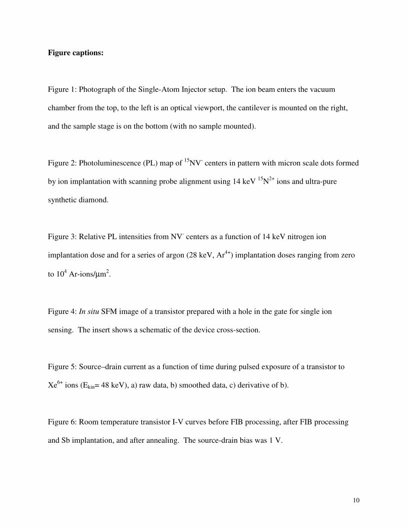
Figure 1 shows a photograph of the vacuum chamber that hosts the SFM. Broad, low
intensity ion beams (~1 pA to 1 µA/mm2) from a series of ion sources enter the implant chamber
from the top, where ions with desired mass to charge ratios were pre-selected in a 90º bending
magnet. An optical microscope (left) allows pre-alignment of the SFM cantilever (right) to
regions of interest on devices and test structures mounted on the sample stage (bottom). The
system has a base pressure of ~10-8
Torr. The ion sources currently coupled to the SFM are an
Electron Beam Ion Trap (EBIT) for high charge state ions (e. g. 121
Sb10-30+
), and Electron
Cyclotron Ion Source (ECR) for medium charge state ions and molecular ions (such as 15
N2+)
and a low plasma density source for singly and doubly charged ions. Test patterns of ion

4
implants can be formed in resist for process development, characterization of tip apertures, or for
studies of qubit center formation, by moving the dynamic shadow mask [14] of the pierced tip
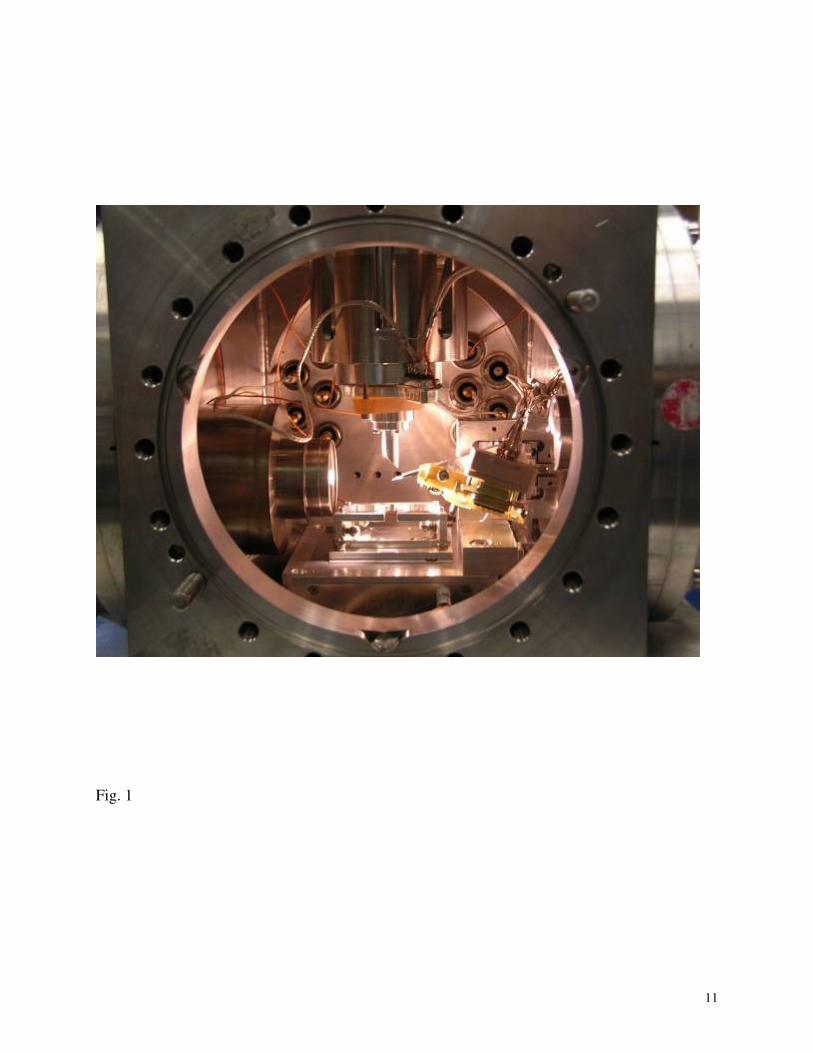
across the sample during ion bombardment [7-10]. In Figure 2, we show a map of
photoluminescence intensities taken at room temperature across a diamond sample that was
implanted with nitrogen (15
N) ions. The map was taken with a long pass filter (>630 nm), which
suppresses contributions from light emitted by NV0 centers. Micron scale spots with ensembles
of 15
NV- centers were formed in ultra pure synthetic diamond (residual
14N concentration <10
ppb) by implantation of doubly charged, atomic 15
N2+
(Ekin=14 keV) followed by thermal
annealing (800º C, 10 min., in Argon). The background signal from naturally occurring 14
N
forming 14
NV- centers in random locations is very low in these samples. A key requirement for
the integration of 15
NV- centers is to achieve center formation with high efficiency [15].
Nitrogen ion doses and Argon ion (28 keV) co-implant doses were varied across the dot pattern
to identify optimal local vacancy densities for 15
NV- center formation. Figure 3 shows the first
results from this study. The PL intensity increases with increasing nitrogen implantation dose.
No PL from 14
NV- centers was observed for implantation of only argon ions at a dose of 2x10
11
cm-2
. Co-implantation of the highest doses of argon ions used here, equivalent to 2x10¹¹
to 1012
cm-2
, together with implantation of nitrogen ions yields increased PL levels from a given
nitrogen implant dose. This demonstrates that the presence of vacancies from the argon co-
implant enhances NV- formation and opens a path to optimization of NV
- formation independent
of nitrogen ion implant energy and dose. Detailed studies of this effect of the local vacancy
density on NV- formation probability for a series of implant and annealing conditions are in
progress.
5
3. Single ion impact detection in transistors
Single atoms and color centers have to be introduced into single atom devices with high
efficiency. The challenge for reliable single ion impact detection can be addressed by detection
of secondary electrons emitted by single ions [2, 8], by collection of electron hole-pairs in diodes
at low temperature [16], or by detection of current changes induced by single ion hits in the
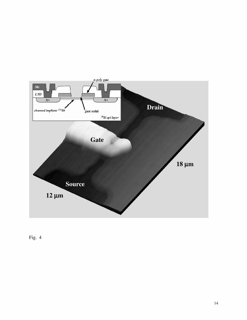
source-drain currents of transistors [11]. Figure 3 shows an in situ SFM image of an
accumulation channel field effect transistor (aFET) formed in 28
Si. Similar aFETs were recently
used for demonstration of spin-dependent neutral impurity scattering, which is a viable
mechanism for single spin state detection [17]. A hole was cut into the gate stack of the
transistor in a combination of Ga+ ion beam drilling in a Focused Ion Beam (FIB) system and
electron beam assisted etching with XeF2. The latter is important to avoid excessive damage to
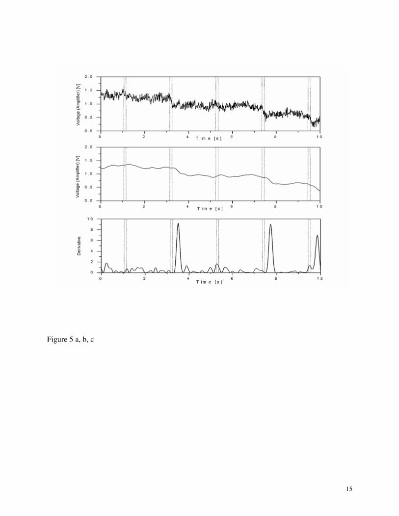
the transistor channel during hole opening. When a pulsed beam of ions impinges onto the
device, the source drain current , Isd, increases when small ensembles and single ions impinge
into the channel region. Figure 4 shows a) the raw Isd data, where the beam of 48 keV Xe6+
ions
is on during the pulses indicated by the vertical lines. Panel b) shows the smoothed data, and c)
the derivative of the smoothed data. Peaks in the derivative signal clearly show (single) ion hits.
The short delay between the peaks in c) and the beam pulses is due to signal processing.
Transistors are biased in the linear regime with a gate bias of 1.1 V and a source drain bias of 0.1
V and are operated at room temperature. The statistics of hits and no-hits for a series of
exposure pulses identifies conditions with single ion hits per pulse. This can be adjusted by
tuning beam intensities and selecting appropriate pulse lengths so that at average one ion hit
occurs every ~10 pulses (for >99% single ion occupancy per pulse). Beams of noble gas ions are
used for tuning, and e. g. antimony ions for formation of (single) dopant atom arrays.
6
Device currents were found to increase (not decrease) upon ion impacts into channel
regions. The data are collected with an inverting pre-amplifier, leading to apparent signal
reduction. The mechanism responsible for the single ion induced current changes is well known
from radiation hardness studies [11]. Ion hits form electron – hole pairs in the gate oxide. While
electrons are quickly swept away, holes remain behind, positive charges enhance the effective
gate bias and increases Isd. For high doses, however, structural damage becomes important and
gradual current reductions are expected.
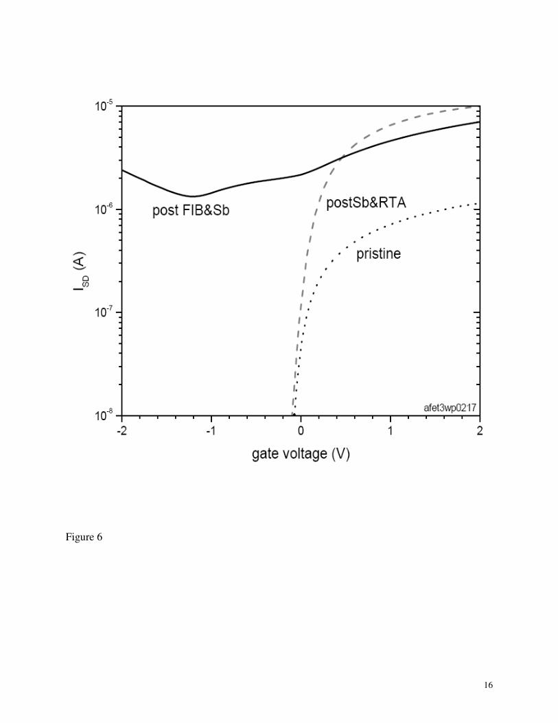
A key requirement for the development of single-atom devices is the survival of the
metallic gates and interconnects of the transistors through the thermal annealing step needed for
dopant activation. Use of tungsten for metallization enables this. In Figure 5 we show I-V
characteristics for a transistor with 2 x 2 µm2 channel area and standard n+pn+ doping
configuration (i. e. p-type channel doping and n+ source drain contacts). The significant increase
in leakage current due to FIB processing and antimony implantation is restored to the pre-
processing performance by the post-implant annealing step (950º C, 20 s, N2, followed by a 10
min. forming gas anneal at 400º C). This enables iterative implantation and electrical
characterization (including low temperature transport) of devices with defined numbers of ions in
defined dopant patterns for testing of single atom based quantum computer architectures.
Evidently, the method of single ion sensing based on detection of small current changes
requires electrical contacting of samples. While this is less universal then e. g. secondary
electron emission, the burden it introduces might not be to great. We note that we are able to
reliably detect current changes of a few times 10-4
(with ~1 µA base currents) at room
temperature and in relatively large, 2x2 µm2, devices. The disruption of the current through a
gate induced two dimensional electron gas by single ion impacts is a very sensitive probe of
7
single ions, and surface currents, or currents through thin sacrificial conductive surface layers are
expected to allow sensitive single ion impact sensing. This single ion detection technique can
thus be adapted to diamond (and other substrates) by detecting current-upset events in
lithographically defined current-channels. Implantation of precise numbers of Nitrogen and
Argon ions provides a pathway to understanding the formation efficiency of NV-centers, and the
creation of NV-center arrays.
3. Discussion and Outlook
The resolution requirements for single atom placement depend on the quantum computer
architecture and can vary from a few nm (for coupled NV- centers in diamond [4, 5]) to 100 nm
(for Lithium atom qubits in silicon [18]). In our approach, resolution limiting factors are 1)
range straggling of ions, 2) the effective beam spot size, and 3) diffusion during activation
annealing. Range straggling scales inversely with the ion atomic mass and implant energy,
favoring heavy ions like antimony and low implant energies. E. g. straggling in the depth
distribution of 25 keV 121
Sb ions in a silicon matrix is <5 nm. Holes with diameters as small as 5
nm have been formed using FIB based drilling and local thin film deposition [19], and recent
demonstrations of electron channeling along the hollow cores of multiwall carbon nanotubes
suggest that these ultimate beam collimators might enable even smaller effective ion beam spot
sizes [20]. Finally, diffusion during required activation anneals is minimal for antimony, and no
segregation effects have been found, confirming bulk like diffusivities of ~6x10-15
cm2/s [12],
which lead to only minimal dopant movement by a few nanometers even for standard rapid
thermal annealing (RTA) conditions (e. g. 1000º C, 10 s). This is in contrast to phosphorus,
which segregates during RTA to the SiO2/Si interface [13].
8
For color center formation in diamond, much more localized wavefunctions of electrons
on defect centers lead to coupling lengths scale of only a few nanometers (<10 nm), setting very
stringent requirements on beam spot sizes and straggling limits. These can be reached for pairs
of coupled NV- centers by implantation of
15N2 molecular ions [21], but conditions for efficient
formation of NV- centers have to be optimized, a task we are addressing through adaptation of
defect engineering techniques, analogous to approaches that have been developed for dopants in
silicon.
In summary, single ion placement with scanning probe alignment is a universal doping
method that enables single atom device development and testing of quantum computer
architectures with single atom based qubits.
Acknowledgments: We thank the staff of the Molecular Foundry and the National
Center for Electron Microscopy at LBNL for their support. This work was supported by NSA
under contract number MOD 713106A, and by the Director, Office of Science, of the
Department of Energy under Contract No. DE-AC02-05CH11231. Work at UCSB is supported
by AFOSR (G.F., D.D.A.). Support by the National Research Foundation of South Africa is
gratefully acknowledged by E. S.-H.
References:
[1] R. W. Keyes, Rep. Prog. Phys. 68, 2701 (2005)
[2] T. Shinada, S. Okamoto, T. Kobayashi, and I. Ohdomari, Nature 437, 1128 (2005)
[3] B. E. Kane, Nature 393, 133 (1998)
[4] F, Jelezko and J. Wrachtrup, Phys. Stat. Sol. A 203, 3207 (2006); A. D. Greentree, et al., J.
9
Phys. Cond. Matt. 18, S825 (2006)
[5] R. Hanson, F. M. Mendoza, R. J. Epstein, D. D. Awschalom, Phys. Rev. Lett. 97, 087601
(2006)
[6] F. J. Ruess, et al., Physica E 40, 1006 (2008)
[7] A. Persaud, et al., NanoLetters 5, 1087 (2005)
[8] A. Persaud et al., J. Vac. Sci. Technol. B 23, 2798 (2005)
[9] T. Schenkel, et al., Microelectr. Engin. 83, 1814 (2006)
[10] W. J. Moberly Chan et al., MRS Bulletin 32, 424 (2007)
[11] A. Batra, et al., Appl. Phys. Lett. 91, 193502 (2007)
[12] T. Schenkel, et al., Appl. Phys. Lett. (2006)
[13] A. Persaud, et al., Quantum Info. Process. 3, 233 (2004)
[14] Stefan Egger, et al., Nano Lett. 5, 15 (2005)
[15] F. C. Warldermann, et al., Diamond and re. Mat. 16, 1887 (2007)
[16] D. N. Jamieson, et al., Appl. Phys. Lett. 86, 202101 (2005)
[17] C. C. Lo, et al., Appl. Phys. Lett. 91, 242106 (2007)
[18] V. N. Smelyanskiy, A. G. Petukhov, and V. V. Osipov, Phys. Rev. B 72, 081304 (2005)
[19] T. Schenkel et al., J. Vac. Sci. Technol. B 21 2720 (2003)
[20] G. Chai, et al., Appl. Phys. Lett. 91, 103101 (2007)
[21] T. Gaebel, et al., Nature Phys. 2, 408 (2006)
10
Figure captions:
Figure 1: Photograph of the Single-Atom Injector setup. The ion beam enters the vacuum
chamber from the top, to the left is an optical viewport, the cantilever is mounted on the right,
and the sample stage is on the bottom (with no sample mounted).
Figure 2: Photoluminescence (PL) map of 15
NV- centers in pattern with micron scale dots formed
by ion implantation with scanning probe alignment using 14 keV 15
N2+
ions and ultra-pure
synthetic diamond.
Figure 3: Relative PL intensities from NV- centers as a function of 14 keV nitrogen ion
implantation dose and for a series of argon (28 keV, Ar4+
) implantation doses ranging from zero
to 104 Ar-ions/µm
2.
Figure 4: In situ SFM image of a transistor prepared with a hole in the gate for single ion
sensing. The insert shows a schematic of the device cross-section.
Figure 5: Source–drain current as a function of time during pulsed exposure of a transistor to
Xe6+
ions (Ekin= 48 keV), a) raw data, b) smoothed data, c) derivative of b).
Figure 6: Room temperature transistor I-V curves before FIB processing, after FIB processing
and Sb implantation, and after annealing. The source-drain bias was 1 V.
11
Fig. 1
12
Fig 2
0 2100
5 µµµµm
PL intensity (a.u.)
13
0 100 200 300 400 500 600 700 800
0
20
40
60
80
100
120
140
160
180
200
220
240
AB8-1-N-Ar-061008
rela
tive
PL
in
ten
sity
15N
2+ dose (ions/µm
2)
no Ar
2E2 Ar µm-2
2E3 Ar µm-2
1E4 Ar µm-2
Figure 3
14
Fig. 4
Dr
Source
Drain
Gate
18 µµµµm
12 µµµµm
15
Figure 5 a, b, c
16
Figure 6