Simulations of Damage, Crack Initiation, and Propagation in Interlayer Dielectric Structures:...
14
IEEE TRANSACTIONS ON DEVICE AND MATERIALS RELIABILITY, VOL. 12, NO. 2, JUNE 2012 241 Simulations of Damage, Crack Initiation, and Propagation in Interlayer Dielectric Structures: Understanding Assembly-Induced Fracture in Dies Abhishek Tambat, Hung-Yun Lin, Ganesh Subbarayan, Dae Young Jung, and Bahgat Sammakia Abstract—Performance enhancement by lowering the dielectric constant of interlayer dielectric (ILD) materials often compro- mises the mechanical integrity of the dielectric stack. At the present time, fracture in the ILD stacks induced by assembly to either an organic substrate or a die stack (3-D) is an important reliability consideration. These interactions include what is pop- ularly referred to as the chip-package interactions. In this paper, we develop insights on the potential crack initiation site within the ILD, die–substrate geometrical parameters that cause most dam- age, as well as insights on the manufacturing process that is critical to failure. Towards this end, we utilize analytical models based on classical elasticity theory as well as sophisticated numerical techniques that are capable of nucleating and propagating cracks at arbitrary locations within the structure without remeshing. Specifically, we analytically estimate the strength of singularities at all the possible multimaterial corners in the ILD stack to provide insight on the likely damage nucleation sites for various material configurations in the ILD stack. Two novel numerical approaches are used for fracture simulation. In the first, cracks are modeled as discontinuous enrichments over an underlying continuous behav- ioral approximation. In the second approach, the underlying ma- terial description is enriched with a cohesive damage description whose stiffness is evolved according to a prescribed damage law. Multilevel finite-element models are used to determine the load imposed on the ILD structure by the substrate. Maximum damage induced in the ILD stack by the above load is used as an indicator of the reliability risk. Parametric simulations are conducted by varying ILD material, die size, die thickness, as well as the solder material. Through analytical models of bonded assemblies, we identify groups of relevant dimensionless parameters to relate the numerically estimated damage in ILD stacks to the die/substrate material and geometrical parameters. We demonstrate that the damage in the ILD stack is least when the flexural rigidity of the die is matched to that of the assembled substrate. We also demonstrate that ILD damage is only weakly correlated to shear deformation on the die surface due to assembly. We generalize the above observations into mathematical fits (for use as design rules) Manuscript received October 21, 2011; revised March 18, 2012; accepted March 22, 2012. Date of publication April 17, 2012; date of current version June 6, 2012. This study was supported by Semiconductor Research Corpo- ration under Task id 1292.061. The development of the code used in this study was made possible by support from Intel Corporation. The authors are thankful for this support. The authors are very thankful to Drs. Sean King and Satish Radhakrishan of Intel and Vikas Gupta of Texas Instruments for all the suggestions and guidance during the course of this work. A. Tambat, H.-Y. Lin, and G. Subbarayan are with the School of Mechan- ical Engineering, Purdue University, West Lafayette, IN 47907 USA (e-mail: [email protected]; [email protected]; [email protected]). D. Y. Jung and B. Sammakia are with the Binghamton University, Binghamton, NY 13850 USA (e-mail: [email protected]; bahgat@ binghamton.edu). Color versions of one or more of the figures in this paper are available online at http://ieeexplore.ieee.org. Digital Object Identifier 10.1109/TDMR.2012.2195006 relating damage in ILD stacks to ILD material choice, relative substrate flexural rigidity, and die size. Index Terms—Chip-package interactions, crack nucleation, damage mechanics, design guidelines, flip-chip packages, fracture mechanics, multiple singularities, reliability. I. I NTRODUCTION T HE TREND towards porous, lower dielectric constant in- terlayer dielectric (ILD) materials often has a consequence on the mechanical integrity of the ILD stack. At the present time, challenging dielectric and package material sets have made ILD fracture, both at interfaces and within the dielectric material, an important reliability consideration. The thermal stresses arising during fabrication, testing, or service due to coefficient of thermal expansion mismatch between package and die is often attributed as the main driving force for fractures in ILD stacks [1]–[3]. Thus, assessing the damage or risk of fracture in ILD stacks during the back end of line fabrication and subsequent processes such as solder reflow and underfill curing is critical at this time. Similar assembly interactions exist in the emerging 3-D or vertically integrated packages [4], [5]. These packages often rely on through silicon vias (TSV) to enable heterogeneous integration. The TSVs may be placed on a small pitch, as small as 10 μm [6], and their collective effect on die deformation is not well understood at the present time. There are both experimental and numerical challenges asso- ciated with analyzing chip-substrate interactions. Experimental challenges mostly relate to the ability to predict bond strength of various interfaces encountered in microelectronic devices [7]. The numerical modeling challenges include an ability to initiate and propagate arbitrary cracks (interface or bulk) in a computationally efficient manner. There is relatively little research in modeling initiation and propagation of arbitrary cracks in structures. Thus, demonstration of such numerical procedures to microelectronic systems in general, and dielectric stacks in particular do not appear to exist in prior literature. Perhaps because of this challenge, there are relatively few studies attempting to model propagation of cracks in ILD structures. One of the few is the work by Ocana et al. [8], who used finite-element models with damage at crack tip described using a cohesive zone model to simulate fracture propagation in ILD structures. This study required cohesive elements being inserted a priori along all potential crack paths. In other studies, Stolarska and Chopp [9] used the extended finite el- ement method (XFEM) to model thermal fatigue cracking in 1530-4388/$31.00 © 2012 IEEE
Transcript of Simulations of Damage, Crack Initiation, and Propagation in Interlayer Dielectric Structures:...
IEEE TRANSACTIONS ON DEVICE AND MATERIALS RELIABILITY, VOL. 12, NO. 2, JUNE 2012 241
Simulations of Damage, Crack Initiation, andPropagation in Interlayer Dielectric Structures:
Understanding Assembly-Induced Fracture in DiesAbhishek Tambat, Hung-Yun Lin, Ganesh Subbarayan, Dae Young Jung, and Bahgat Sammakia
Abstract—Performance enhancement by lowering the dielectricconstant of interlayer dielectric (ILD) materials often compro-mises the mechanical integrity of the dielectric stack. At thepresent time, fracture in the ILD stacks induced by assembly toeither an organic substrate or a die stack (3-D) is an importantreliability consideration. These interactions include what is pop-ularly referred to as the chip-package interactions. In this paper,we develop insights on the potential crack initiation site within theILD, die–substrate geometrical parameters that cause most dam-age, as well as insights on the manufacturing process that is criticalto failure. Towards this end, we utilize analytical models basedon classical elasticity theory as well as sophisticated numericaltechniques that are capable of nucleating and propagating cracksat arbitrary locations within the structure without remeshing.Specifically, we analytically estimate the strength of singularities atall the possible multimaterial corners in the ILD stack to provideinsight on the likely damage nucleation sites for various materialconfigurations in the ILD stack. Two novel numerical approachesare used for fracture simulation. In the first, cracks are modeled asdiscontinuous enrichments over an underlying continuous behav-ioral approximation. In the second approach, the underlying ma-terial description is enriched with a cohesive damage descriptionwhose stiffness is evolved according to a prescribed damage law.Multilevel finite-element models are used to determine the loadimposed on the ILD structure by the substrate. Maximum damageinduced in the ILD stack by the above load is used as an indicatorof the reliability risk. Parametric simulations are conducted byvarying ILD material, die size, die thickness, as well as the soldermaterial. Through analytical models of bonded assemblies, weidentify groups of relevant dimensionless parameters to relate thenumerically estimated damage in ILD stacks to the die/substratematerial and geometrical parameters. We demonstrate that thedamage in the ILD stack is least when the flexural rigidity ofthe die is matched to that of the assembled substrate. We alsodemonstrate that ILD damage is only weakly correlated to sheardeformation on the die surface due to assembly. We generalize theabove observations into mathematical fits (for use as design rules)
Manuscript received October 21, 2011; revised March 18, 2012; acceptedMarch 22, 2012. Date of publication April 17, 2012; date of current versionJune 6, 2012. This study was supported by Semiconductor Research Corpo-ration under Task id 1292.061. The development of the code used in thisstudy was made possible by support from Intel Corporation. The authors arethankful for this support. The authors are very thankful to Drs. Sean King andSatish Radhakrishan of Intel and Vikas Gupta of Texas Instruments for all thesuggestions and guidance during the course of this work.
A. Tambat, H.-Y. Lin, and G. Subbarayan are with the School of Mechan-ical Engineering, Purdue University, West Lafayette, IN 47907 USA (e-mail:[email protected]; [email protected]; [email protected]).
D. Y. Jung and B. Sammakia are with the Binghamton University,Binghamton, NY 13850 USA (e-mail: [email protected]; [email protected]).
Color versions of one or more of the figures in this paper are available onlineat http://ieeexplore.ieee.org.
Digital Object Identifier 10.1109/TDMR.2012.2195006
relating damage in ILD stacks to ILD material choice, relativesubstrate flexural rigidity, and die size.
Index Terms—Chip-package interactions, crack nucleation,damage mechanics, design guidelines, flip-chip packages, fracturemechanics, multiple singularities, reliability.
I. INTRODUCTION
THE TREND towards porous, lower dielectric constant in-terlayer dielectric (ILD) materials often has a consequence
on the mechanical integrity of the ILD stack. At the presenttime, challenging dielectric and package material sets havemade ILD fracture, both at interfaces and within the dielectricmaterial, an important reliability consideration. The thermalstresses arising during fabrication, testing, or service due tocoefficient of thermal expansion mismatch between packageand die is often attributed as the main driving force for fracturesin ILD stacks [1]–[3]. Thus, assessing the damage or risk offracture in ILD stacks during the back end of line fabricationand subsequent processes such as solder reflow and underfillcuring is critical at this time. Similar assembly interactions existin the emerging 3-D or vertically integrated packages [4], [5].These packages often rely on through silicon vias (TSV) toenable heterogeneous integration. The TSVs may be placed ona small pitch, as small as 10 μm [6], and their collective effecton die deformation is not well understood at the present time.
There are both experimental and numerical challenges asso-ciated with analyzing chip-substrate interactions. Experimentalchallenges mostly relate to the ability to predict bond strength ofvarious interfaces encountered in microelectronic devices [7].The numerical modeling challenges include an ability toinitiate and propagate arbitrary cracks (interface or bulk) ina computationally efficient manner. There is relatively littleresearch in modeling initiation and propagation of arbitrarycracks in structures. Thus, demonstration of such numericalprocedures to microelectronic systems in general, and dielectricstacks in particular do not appear to exist in prior literature.Perhaps because of this challenge, there are relatively fewstudies attempting to model propagation of cracks in ILDstructures. One of the few is the work by Ocana et al. [8], whoused finite-element models with damage at crack tip describedusing a cohesive zone model to simulate fracture propagationin ILD structures. This study required cohesive elements beinginserted a priori along all potential crack paths. In otherstudies, Stolarska and Chopp [9] used the extended finite el-ement method (XFEM) to model thermal fatigue cracking in
1530-4388/$31.00 © 2012 IEEE
242 IEEE TRANSACTIONS ON DEVICE AND MATERIALS RELIABILITY, VOL. 12, NO. 2, JUNE 2012
dielectric structures. Zhang et al. [3] have evaluated the energyrelease rates corresponding to prespecified cracks within theILD structure. In general, none of the prior studies appear tohave predicted the likely sites of crack initiation within ILDstacks or developed computational techniques to automaticallypropagate, along arbitrary paths, either a newly initiated, or apredefined crack.
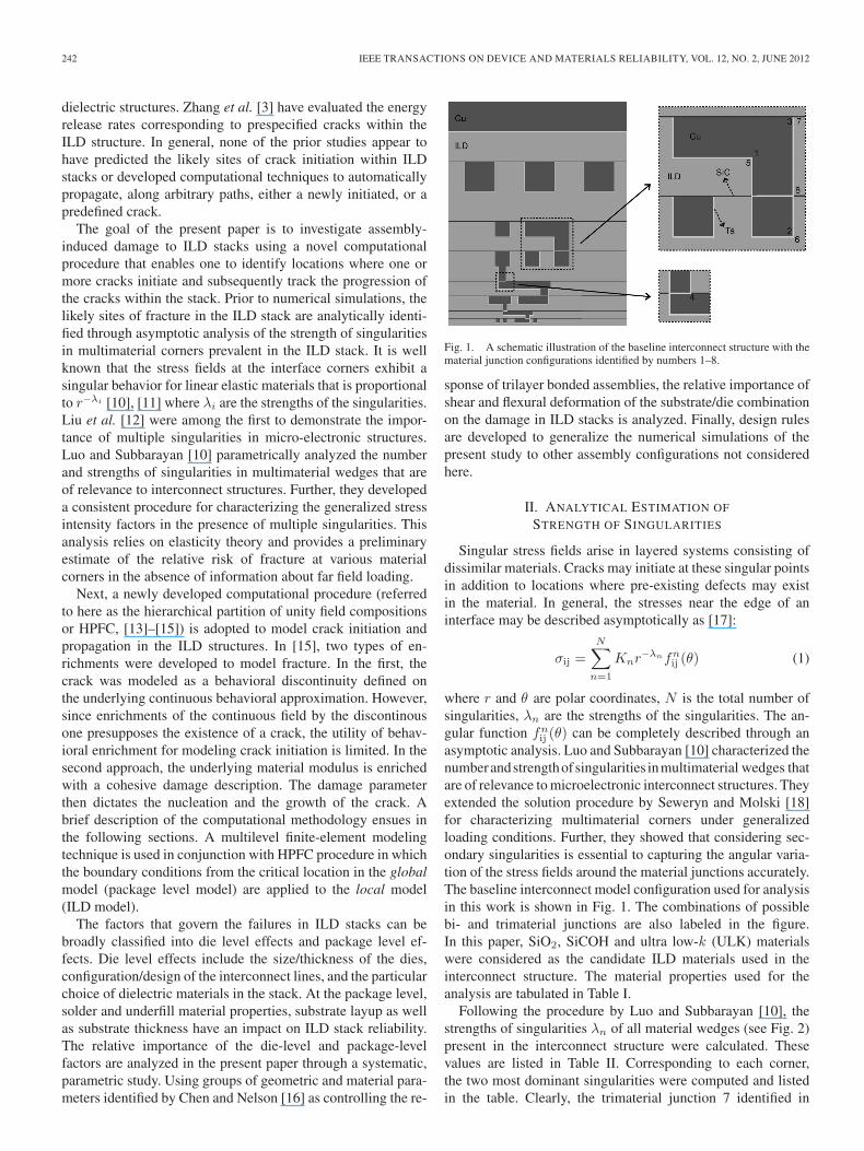
The goal of the present paper is to investigate assembly-induced damage to ILD stacks using a novel computationalprocedure that enables one to identify locations where one ormore cracks initiate and subsequently track the progression ofthe cracks within the stack. Prior to numerical simulations, thelikely sites of fracture in the ILD stack are analytically identi-fied through asymptotic analysis of the strength of singularitiesin multimaterial corners prevalent in the ILD stack. It is wellknown that the stress fields at the interface corners exhibit asingular behavior for linear elastic materials that is proportionalto r−λi [10], [11] where λi are the strengths of the singularities.Liu et al. [12] were among the first to demonstrate the impor-tance of multiple singularities in micro-electronic structures.Luo and Subbarayan [10] parametrically analyzed the numberand strengths of singularities in multimaterial wedges that areof relevance to interconnect structures. Further, they developeda consistent procedure for characterizing the generalized stressintensity factors in the presence of multiple singularities. Thisanalysis relies on elasticity theory and provides a preliminaryestimate of the relative risk of fracture at various materialcorners in the absence of information about far field loading.
Next, a newly developed computational procedure (referredto here as the hierarchical partition of unity field compositionsor HPFC, [13]–[15]) is adopted to model crack initiation andpropagation in the ILD structures. In [15], two types of en-richments were developed to model fracture. In the first, thecrack was modeled as a behavioral discontinuity defined onthe underlying continuous behavioral approximation. However,since enrichments of the continuous field by the discontinousone presupposes the existence of a crack, the utility of behav-ioral enrichment for modeling crack initiation is limited. In thesecond approach, the underlying material modulus is enrichedwith a cohesive damage description. The damage parameterthen dictates the nucleation and the growth of the crack. Abrief description of the computational methodology ensues inthe following sections. A multilevel finite-element modelingtechnique is used in conjunction with HPFC procedure in whichthe boundary conditions from the critical location in the globalmodel (package level model) are applied to the local model(ILD model).
The factors that govern the failures in ILD stacks can bebroadly classified into die level effects and package level ef-fects. Die level effects include the size/thickness of the dies,configuration/design of the interconnect lines, and the particularchoice of dielectric materials in the stack. At the package level,solder and underfill material properties, substrate layup as wellas substrate thickness have an impact on ILD stack reliability.The relative importance of the die-level and package-levelfactors are analyzed in the present paper through a systematic,parametric study. Using groups of geometric and material para-meters identified by Chen and Nelson [16] as controlling the re-
Fig. 1. A schematic illustration of the baseline interconnect structure with thematerial junction configurations identified by numbers 1–8.
sponse of trilayer bonded assemblies, the relative importance ofshear and flexural deformation of the substrate/die combinationon the damage in ILD stacks is analyzed. Finally, design rulesare developed to generalize the numerical simulations of thepresent study to other assembly configurations not consideredhere.
II. ANALYTICAL ESTIMATION OF
STRENGTH OF SINGULARITIES
Singular stress fields arise in layered systems consisting ofdissimilar materials. Cracks may initiate at these singular pointsin addition to locations where pre-existing defects may existin the material. In general, the stresses near the edge of aninterface may be described asymptotically as [17]:
σij =N∑
n=1
Knr−λnfn
ij (θ) (1)
where r and θ are polar coordinates, N is the total number ofsingularities, λn are the strengths of the singularities. The an-gular function fn
ij (θ) can be completely described through anasymptotic analysis. Luo and Subbarayan [10] characterized thenumberandstrengthofsingularities inmultimaterial wedges thatare of relevance to microelectronic interconnect structures. Theyextended the solution procedure by Seweryn and Molski [18]for characterizing multimaterial corners under generalizedloading conditions. Further, they showed that considering sec-ondary singularities is essential to capturing the angular varia-tion of the stress fields around the material junctions accurately.The baseline interconnect model configuration used for analysisin this work is shown in Fig. 1. The combinations of possiblebi- and trimaterial junctions are also labeled in the figure.In this paper, SiO2, SiCOH and ultra low-k (ULK) materialswere considered as the candidate ILD materials used in theinterconnect structure. The material properties used for theanalysis are tabulated in Table I.
Following the procedure by Luo and Subbarayan [10], thestrengths of singularities λn of all material wedges (see Fig. 2)present in the interconnect structure were calculated. Thesevalues are listed in Table II. Corresponding to each corner,the two most dominant singularities were computed and listedin the table. Clearly, the trimaterial junction 7 identified in
TAMBAT et al.: SIMULATIONS OF DAMAGE, CRACK INITIATION, AND PROPAGATION IN INTERLAYER DIELECTRIC STRUCTURES 243
TABLE IPROPERTIES OF MATERIALS USED IN THE INTERCONNECT MODELS
Fig. 2. The eight different material junctions occurring in the structuresconsidered in the present study.
TABLE IITHE CALCULATED STRENGTHS OF SINGULARITIES ASSOCIATED WITH
THE MATERIAL CORNERS SHOWN IN FIG. 2
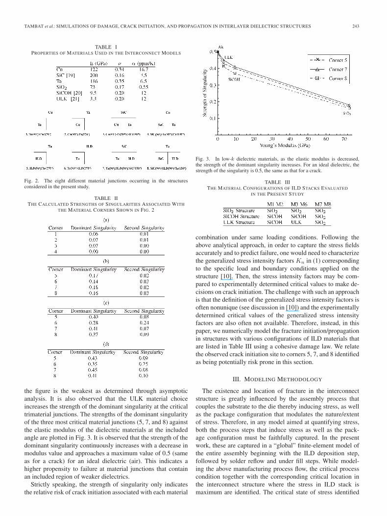
the figure is the weakest as determined through asymptoticanalysis. It is also observed that the ULK material choiceincreases the strength of the dominant singularity at the criticaltrimaterial junctions. The strengths of the dominant singularityof the three most critical material junctions (5, 7, and 8) againstthe elastic modulus of the dielectric materials at the includedangle are plotted in Fig. 3. It is observed that the strength of thedominant singularity continuously increases with a decrease inmodulus value and approaches a maximum value of 0.5 (sameas for a crack) for an ideal dielectric (air). This indicates ahigher propensity to failure at material junctions that containan included region of weaker dielectrics.
Strictly speaking, the strength of singularity only indicatesthe relative risk of crack initiation associated with each material
Fig. 3. In low-k dielectric materials, as the elastic modulus is decreased,the strength of the dominant singularity increases. For an ideal dielectric, thestrength of the singularity is 0.5, the same as that for a crack.
TABLE IIITHE MATERIAL CONFIGURATIONS OF ILD STACKS EVALUATED
IN THE PRESENT STUDY
combination under same loading conditions. Following theabove analytical approach, in order to capture the stress fieldsaccurately and to predict failure, one would need to characterizethe generalized stress intensity factors Kn in (1) correspondingto the specific load and boundary conditions applied on thestructure [10]. Then, the stress intensity factors may be com-pared to experimentally determined critical values to make de-cisions on crack initiation. The challenge with such an approachis that the definition of the generalized stress intensity factors isoften nonunique (see discussion in [10]) and the experimentallydetermined critical values of the generalized stress intensityfactors are also often not available. Therefore, instead, in thispaper, we numerically model the fracture initiation/propagationin structures with various configurations of ILD materials thatare listed in Table III using a cohesive damage law. We relatethe observed crack initiation site to corners 5, 7, and 8 identifiedas being potentially risk prone in this section.
III. MODELING METHODOLOGY
The existence and location of fracture in the interconnectstructure is greatly influenced by the assembly process thatcouples the substrate to the die thereby inducing stress, as wellas the package configuration that modulates the nature/extentof stress. Therefore, in any model aimed at quantifying stress,both the process steps that induce stress as well as the pack-age configuration must be faithfully captured. In the presentwork, these are captured in a “global” finite-element model ofthe entire assembly beginning with the ILD deposition step,followed by solder reflow and under fill steps. While model-ing the above manufacturing process flow, the critical processcondition together with the corresponding critical location inthe interconnect structure where the stress in ILD stack ismaximum are identified. The critical state of stress identified

244 IEEE TRANSACTIONS ON DEVICE AND MATERIALS RELIABILITY, VOL. 12, NO. 2, JUNE 2012
through the global finite-element models is then converted intoappropriate displacement boundary conditions that are next pre-scribed on a (local) interconnect model to study potential riskof crack initiation as well as to study possible crack propagationpath. The global finite-element model is described in detail inAppendix A. The focus below is on a novel meshless procedureused to identify risk of fracture and to simulate the potentialpath of crack propagation.
A. Representation of Cracks through EnrichedField Approximation
The mathematical concept of HPFC developed in [13], [22]posits that an arbitrary approximation to a behavior or materialproperty over a domain can be hierarchically composed fromapproximations over subdomains provided such compositionssatisfy the partition of unity property [23]. Rayasam et al. [22]suggested a natural composition of the complex domain bymirroring the constructive solid geometry procedure of CAD,with each subdomain formed from a geometrically simple“primitive” domain. This allowed the material property as wellas the behavior combination within primitive domains (forminga “primitive” design state) to vary arbitrarily enabling oneto model complex spatially varying materials such as gradedmaterials. Further, they developed rules to construct the globaldesign state through a weighted composition of primitive de-sign states such that the weights satisfy partition of unity overthe global domain. The ideas developed in [13], [22], werefurther extended by Tambat and Subbarayan [15] to enrichthe above constructed approximation with known behavior ormaterial property on surfaces (or curves or even vertices) withinthe domain. These enriched approximations are the meansadopted to describe cracks in the present study and are thereforedescribed briefly below.
The modeling begins by considering the geometry of thedomain Ω and the behavioral field in it to be parametricallydefined as the mapping VΩ(ξ, η, ζ) → x and fΩ(ξ, η, ζ) → u,respectively. Also, the geometry of the lower dimensional en-riching geometry is parametrically defined as CΓe(s, t). Usinghierarchical compositions, the global approximation at anypoint x is represented as (see Fig. 4):
f(x) = wΩfΩ (x(ξ, η, ζ)) + weΩf
eΓ(x) (2)
where weights wΩ and weΩ are constructed such that wΩ +
weΩ = 1. Since the influence of the enriching field must decay
with distance from the enriching geometrical entity, the weightfields are required to be monotonically decreasing functions ofdistance. One form of weight field is the Gaussian weight field:
weΩ = e
−(
ddexp
)2wΓe (3)
where d is a monotonic measure of distance from the enrichinggeometry Γe, dexp is a scaling factor, and wΓe is the weightprescribed on the enriching geometry Γe. The weight field thusconstructed limits the influence of enriching feature over a finitedistance. In the present work, the approximations both overthe domain and on the enriching entities are constructed using
Fig. 4. The global approximation is constructed by composing the lower orderprimitive with the higher order primitive.
Nonuniform Rational B-Splines (NURBS), which are popularin CAD for modeling geometrical surfaces [24]. The use ofNURBS for analysis of behavior was proposed by the authorsin [25], [26]. More recently, such analyses have been referredto as isogeometric analysis [27] since these approximations arebuilt isoparametrically on the geometrical model. In general, aNURBS surface has the mathematical form:
S(s, t) =ni∑
i=0
nj∑j=0
Rij(s, t)Pij (4)
where Pij is the ijth control point (position) vector, ni arenumber of control points in the ith direction (nj is similarlyin jth direction) and Rij are the rational basis functions definedas the tensor product
Rij(s, t) =Ni,p(s)Nj,q(t)wij
nα∑α=0
nβ∑β=0
Nα,p(s)Nβ,q(t)wαβ
(5)
and Ni,p are the pth degree B-spline basis functions definedthrough the recursive relation (Nj,q definition is analogous):
Ni,0={ 1 if si≤s<si+1
0 otherwise
Ni,p=s−si
si+p−siNi,p−1(s)+
si+p+1−ssi+p+1−si+1
Ni+1,p−1(s) (6)
TAMBAT et al.: SIMULATIONS OF DAMAGE, CRACK INITIATION, AND PROPAGATION IN INTERLAYER DIELECTRIC STRUCTURES 245
defined typically on nonperiodic and nonuniform knot interval
U = {0, . . . , 0, sp+1, . . . , sm−p−1, 1, . . . , 1} (7)
NURBS basis functions exhibit properties such as partition ofunity, local support, domain of influence, smoothness, convexhull, and nonnegativity that are critical to ensuring convergenceof approximations to a known solution. An isogeometric ap-proximation is constructed isoparametrically on the geometricentity by replacing the control point vectors Pij with the behav-ioral unknowns uij. Thus, a behavioral approximation may beisoparametrically defined analogous to (4) as:
u(s, t) =∑
I
RI(s, t)uI (8)
where, the summation over i and j have been replaced with asingle summation over all grid points for convenience. In thisform, the NURBS approximations resemble the shape functionsNI(s, t) used in the finite-element method. Henceforth, for thisreason, the basis function is denoted as NI .
In the present study, following [15], the enriching field isapproximated at the control points of the enriching entity asshown below:
feΓ (P (x)) = fe
Γ(s, t) = ψ(x)
(∑I
NI(s, t)uI
)(9)
where uI are the field unknowns at the control points definingthe enriching geometry SΓe(s, t), NI(s, t) are the NURBSbasis functions, and ψ provides the required spatial modulationof the field u to together achieve the desired enrichment. P (x)is a projection from x to the shortest distance point (s, t) on theenriching surface. That is, P : x → (s, t).
The choice of enrichment function depends on an a prioriknowledge of the behavior. For example, to model the discon-tinuity in the solution field across a crack surface, a Heavisidestep function is used as enrichment such that ψ = 1 above thecrack surface and ψ = −1 below it [13], [15], [28], [29]. Asbefore, the continuous and discontinuous fields are modeledcompletely independent of each other and composed to obeypartition of unity. The significant computational advantage ofsuch an enrichment strategy is that the changes are localized tocrack geometry during crack propagation.
B. Stress Intensity Factor Evaluation and Crack Propagation
The decision to propagate the crack may be based on lin-ear elastic fracture mechanics (LEFM), specifically, on thecalculated energy release rate relative to fracture toughness.Two types of failure modes are commonly observed in ILDstructures: cohesive fracture of dielectrics and interfacial de-lamination. In the case of cohesive fracture, the stress inten-sity factors may be directly obtained from the crack openingdisplacements as (replacing ν with ν/1 + ν under plane stressconditions) [30]:
KI =μ√
2π(Δuy)√r(2 − 2ν)
(10)
KII =μ√
2π(Δux)√r(2 − 2ν)
(11)
where μ is the shear modulus, ν is Poisson’s ratio, r is thedistance from the crack tip to the correlation point, and Δux andΔuy are the crack-opening displacements along the co-ordinatedirections at the correlation point. The crack propagation direc-tion is determined using the maximum circumferential stresscriterion:
Δθc = 2arctan
⎛⎜⎜⎝
1 −√
1 + 8(
KII
KI
)2
4(
KII
KI
)⎞⎟⎟⎠ (12)
Crack propagates when the energy release rate of the cohe-sive crack exceeds the fracture toughness of the bulk material,i.e., when G ≥ Gc. Energy release rate is related to the stressintensity factors as:
G =κ+ 18μ
(K2
I +K2II
)(13)
where, the material parameter κ = 3 − 4ν.In the case of interfacial cracks, due to asymmetry in the
elastic moduli with respect to a bimaterial interface, the stressand displacement field around an interfacial crack tip in generalcannot be decoupled into pure Mode I and Mode II fields.Interfacial crack propagation is in general under a mixed modecondition. The stress intensity factors defined by Rice [31] canbe calculated using the displacement extrapolation method as:
KI = 2S
√2πr
[(Δuy − 2εΔux) cosR
+(Δux + 2εΔuy) sinR ] (14)
KII = 2S
√2πr
[−(Δuy − 2εΔux) sinR
+(Δux + 2εΔuy) cosR ] (15)
where
S =2 cosh(επ)[
(κ1+1)μ1
+ (κ2+1)μ2
] (16)
R = ε ln(r
lk
)(17)
Here, κ1 and κ2 are the κ values of the two materials atthe interface, respectively, lk is a characteristic length of thesystem and ε is the material oscillation index, related to secondDundur’s parameter β as:
ε =12π
ln(
1 − β
1 + β
)(18)
The energy release rate and the stress intensity factors thushave the following relationship:
G =1
16 cosh2(επ)
[κ1 + 1μ1
+κ2 + 1μ2
] (K2
I +K2II
)(19)
246 IEEE TRANSACTIONS ON DEVICE AND MATERIALS RELIABILITY, VOL. 12, NO. 2, JUNE 2012
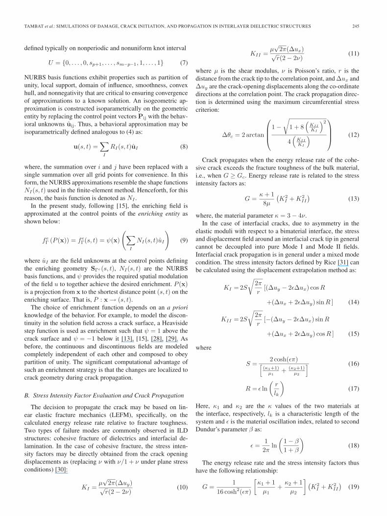
Fig. 5. Smeared representation of a crack (a) crack geometry and (b) damagecaptured as a loss in local material modulus.
and the mode-mixity ratio is defined as:
Θ = arctan(KII
KI
)(20)
The measured interfacial toughness usually depends in themode-mixity ratio, and the crack propagates along the interfaceif the energy release rate exceeds the value G ≥ Gc(Θ).
At the ith step of crack propagation, the fracture criterion isevaluated and the angle of crack propagation θ is computed. Alinear NURBS segment of length Δa is created between cracktip at the ith step and the new crack tip. The original crackgeometry and the new NURBS segment are joined into a singleunivariate NURBS curve for the (i+ 1)th crack propagationstep.
The above-described procedure is implemented in a NURBS-based, symbolic design-analysis integrated meshfree frame-work termed HiDAC [14].
C. Cohesive Damage and Crack Nucleation
While one may use a criterion based on LEFM to predictcrack propagation path, LEFM presumes a pre-existing flaw.Thus, one would not be able to identify locations in theILD stacks where cracks may nucleate through LEFM. Thislimitation is alleviated in the present study by enriching theunderlying elastic modulus with a cohesive damage descriptionto nucleate and propagate cracks. Thus, for an isotropic linearelastic material, the enriched elastic modulus value may berepresented as:
E = (1 − w)E0 + w(1 −D)E0 0 ≤ D ≤ 1 (21)
where, E0 is the elastic modulus of the undamaged material, Dis the measure of damage with D = 0 being the pristine stateand D = 1 being the fully damaged state of the material inwhich it does not bear any load. The weight function w [see(3)] smears the loss in modulus over a finite spatial region.Fracture in brittle materials occurs when D = 1. A smearedrepresentation of crack of width 2a is shown in Fig. 5.
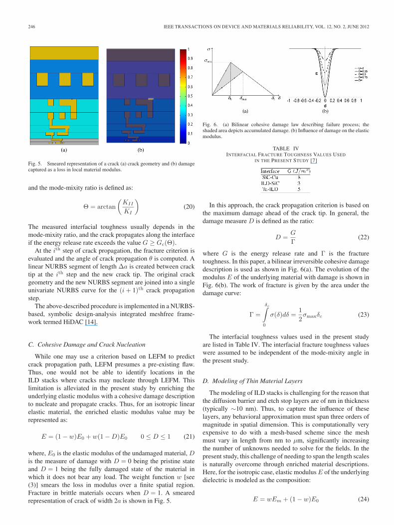
Fig. 6. (a) Bilinear cohesive damage law describing failure process; theshaded area depicts accumulated damage. (b) Influence of damage on the elasticmodulus.
TABLE IVINTERFACIAL FRACTURE TOUGHNESS VALUES USED
IN THE PRESENT STUDY [7]
In this approach, the crack propagation criterion is based onthe maximum damage ahead of the crack tip. In general, thedamage measure D is defined as the ratio:
D =G
Γ(22)
where G is the energy release rate and Γ is the fracturetoughness. In this paper, a bilinear irreversible cohesive damagedescription is used as shown in Fig. 6(a). The evolution of themodulus E of the underlying material with damage is shown inFig. 6(b). The work of fracture is given by the area under thedamage curve:
Γ =
δc∫0
σ(δ)dδ =12σmaxδc (23)
The interfacial toughness values used in the present studyare listed in Table IV. The interfacial fracture toughness valueswere assumed to be independent of the mode-mixity angle inthe present study.
D. Modeling of Thin Material Layers
The modeling of ILD stacks is challenging for the reason thatthe diffusion barrier and etch stop layers are of nm in thickness(typically ∼10 nm). Thus, to capture the influence of theselayers, any behavioral approximation must span three orders ofmagnitude in spatial dimension. This is computationally veryexpensive to do with a mesh-based scheme since the meshmust vary in length from nm to μm, significantly increasingthe number of unknowns needed to solve for the fields. In thepresent study, this challenge of needing to span the length scalesis naturally overcome through enriched material descriptions.Here, for the isotropic case, elastic modulusE of the underlyingdielectric is modeled as the composition:
E = wEm + (1 − w)E0 (24)
TAMBAT et al.: SIMULATIONS OF DAMAGE, CRACK INITIATION, AND PROPAGATION IN INTERLAYER DIELECTRIC STRUCTURES 247
Fig. 7. An illustration of the effect of the scaling parameter d0 on the widthof the smeared zone.
where Em is the elastic modulus of the enriching diffusionbarrier or the etch stop layer, E0 is the underlying material’selastic modulus, and w is the weight field as defined earlier in(3). The weight field w “smears” the properties of the thin layerover a finite spatial width. The scaling factor d0 controls thewidth of the δ function capturing the influence of the enrichingmaterial as shown in Fig. 7. A special case of this enrichedapproximation is the “smeared” crack described earlier, wherethe modulus is degraded with damage as Em = (1 −D)E0.
E. Parametric Models to Study Assembly-Induced Damage
Following the above-described procedure, the assembly-induced damage in the ILD stack due to parametric changesin the assembly configuration was exhaustively modeled. Thedesign variables selected for the parametric study are listedin Table V. The interfacial fracture toughness values used forthe following simulations are listed in Table IV. In all of thesimulations, the ILD structure was modeled as a biquadraticNURBS surface described using a uniformly distributed 40X40control point net (1600 degrees of freedom total). Deformationstate from critical location in the package was extracted andapplied as displacement boundary conditions to the local ILDlevel model. As mentioned earlier, the procedure to extractboundary conditions is described in Appendix A.
IV. RESULTS
In this section, the damage in the ILD stacks listed inTable III is quantified for various values of the die and substrateconfiguration parameters listed in Table V.
A. Damage Induced During FabricationProcess—Baseline Study
In the present study, the value of separation δ0 in the bilinearcohesive damage description was chosen to be 1 nm. It was ob-
TABLE VLIST OF PARAMETERS AND THEIR VALUES
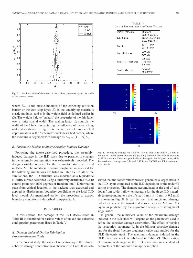
Fig. 8. Predicted damage on a die of size 10 mm × 10 mm × 0.2 mm atthe end of solder reflow process for (a) SiO2 structure (b) SiCOH structure(c) ULK structure. There was practically no damage in the SiO2 structure, whilethe maximum damage was 0.34 and 0.42 in the SiCOH and ULK structures,respectively.
served that the solder reflow process generated a larger stress inthe ILD layers compared to the ILD deposition or the underfillcuring processes. The damage accumulated at the end of cooldown from solder reflow temperature for the three ILD materi-als (corresponding to a die of size 10 mm × 10 mm × 0.2 mm)is shown in Fig. 8. It can be seen that maximum damageindeed occurs at the trimaterial corner between M6 and M7layers as predicted by the asymptotic analysis of strengths ofsingularities.
In general, the numerical value of the maximum damageinduced in the ILD stack will depend on the parameters used todefine the cohesive damage description. The effect of varyingthe separation parameter δ0 in the bilinear cohesive damagelaw for the fixed fracture toughness value was studied for theULK dielectric stack. The maximum damage induced in theULK dielectric stack is tabulated in Table VI. The locationof maximum damage in the ILD stack was independent ofparameters of the cohesive damage description.
248 IEEE TRANSACTIONS ON DEVICE AND MATERIALS RELIABILITY, VOL. 12, NO. 2, JUNE 2012
TABLE VITHE EFFECT OF VARYING THE SEPARATION PARAMETER δ0 ON THE
MAXIMUM DAMAGE INDUCED IN THE ULK DIELECTRIC STACK
Fig. 9. A schematic of ILD structure with the location of the pre-existinginterfacial crack shown inset.
B. Impact of Interfacial Toughness on Crack Propagation Path
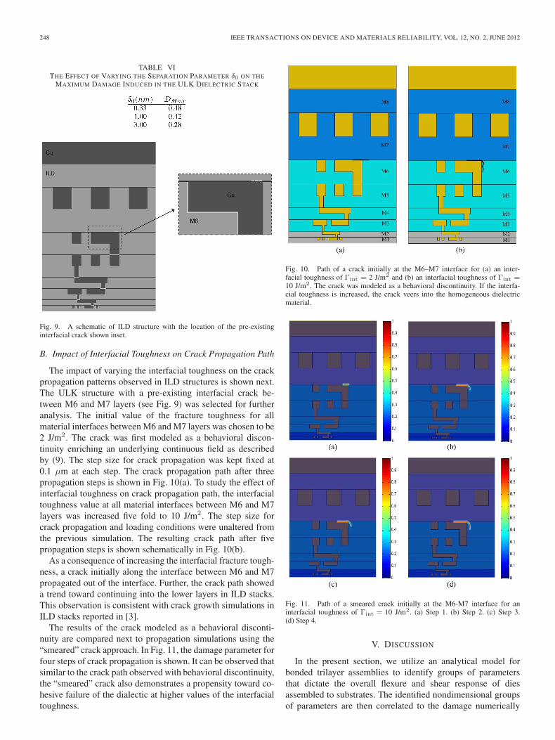
The impact of varying the interfacial toughness on the crackpropagation patterns observed in ILD structures is shown next.The ULK structure with a pre-existing interfacial crack be-tween M6 and M7 layers (see Fig. 9) was selected for furtheranalysis. The initial value of the fracture toughness for allmaterial interfaces between M6 and M7 layers was chosen to be2 J/m2. The crack was first modeled as a behavioral discon-tinuity enriching an underlying continuous field as describedby (9). The step size for crack propagation was kept fixed at0.1 μm at each step. The crack propagation path after threepropagation steps is shown in Fig. 10(a). To study the effect ofinterfacial toughness on crack propagation path, the interfacialtoughness value at all material interfaces between M6 and M7layers was increased five fold to 10 J/m2. The step size forcrack propagation and loading conditions were unaltered fromthe previous simulation. The resulting crack path after fivepropagation steps is shown schematically in Fig. 10(b).
As a consequence of increasing the interfacial fracture tough-ness, a crack initially along the interface between M6 and M7propagated out of the interface. Further, the crack path showeda trend toward continuing into the lower layers in ILD stacks.This observation is consistent with crack growth simulations inILD stacks reported in [3].
The results of the crack modeled as a behavioral disconti-nuity are compared next to propagation simulations using the“smeared” crack approach. In Fig. 11, the damage parameter forfour steps of crack propagation is shown. It can be observed thatsimilar to the crack path observed with behavioral discontinuity,the “smeared” crack also demonstrates a propensity toward co-hesive failure of the dialectic at higher values of the interfacialtoughness.
Fig. 10. Path of a crack initially at the M6–M7 interface for (a) an inter-facial toughness of Γint = 2 J/m2 and (b) an interfacial toughness of Γint =10 J/m2. The crack was modeled as a behavioral discontinuity. If the interfa-cial toughness is increased, the crack veers into the homogeneous dielectricmaterial.
Fig. 11. Path of a smeared crack initially at the M6-M7 interface for aninterfacial toughness of Γint = 10 J/m2. (a) Step 1. (b) Step 2. (c) Step 3.(d) Step 4.
V. DISCUSSION
In the present section, we utilize an analytical model forbonded trilayer assemblies to identify groups of parametersthat dictate the overall flexure and shear response of diesassembled to substrates. The identified nondimensional groupsof parameters are then correlated to the damage numerically
TAMBAT et al.: SIMULATIONS OF DAMAGE, CRACK INITIATION, AND PROPAGATION IN INTERLAYER DIELECTRIC STRUCTURES 249
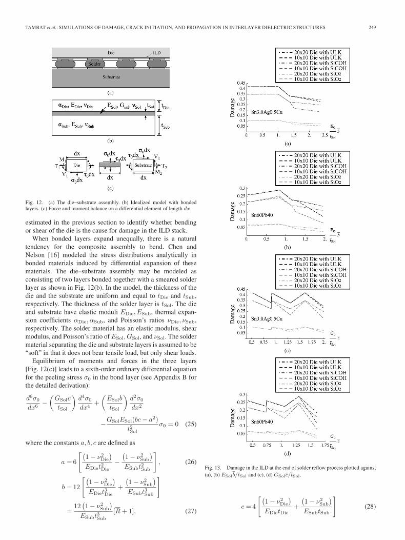
Fig. 12. (a) The die–substrate assembly. (b) Idealized model with bondedlayers. (c) Force and moment balance on a differential element of length dx.
estimated in the previous section to identify whether bendingor shear of the die is the cause for damage in the ILD stack.
When bonded layers expand unequally, there is a naturaltendency for the composite assembly to bend. Chen andNelson [16] modeled the stress distributions analytically inbonded materials induced by differential expansion of thesematerials. The die–substrate assembly may be modeled asconsisting of two layers bonded together with a smeared solderlayer as shown in Fig. 12(b). In the model, the thickness of thedie and the substrate are uniform and equal to tDie and tSub,respectively. The thickness of the solder layer is tSol. The dieand substrate have elastic moduli EDie, ESub, thermal expan-sion coefficients αDie, αSub, and Poisson’s ratios νDie, νSub,respectively. The solder material has an elastic modulus, shearmodulus, and Poisson’s ratio ofESol, GSol, and νSol. The soldermaterial separating the die and substrate layers is assumed to be“soft” in that it does not bear tensile load, but only shear loads.
Equilibrium of moments and forces in the three layers[Fig. 12(c)] leads to a sixth-order ordinary differential equationfor the peeling stress σ0 in the bond layer (see Appendix B forthe detailed derivation):
d6σ0
dx6−(GSolc
tSol
)d4σ0
dx4+(ESolb
tSol
)d2σ0
dx2
−GSolESol(bc− a2)t2Sol
σ0 = 0 (25)
where the constants a, b, c are defined as
a = 6
[(1 − ν2
Die
)EDiet2Die
−(1 − ν2
Sub
)ESubt2Sub
], (26)
b = 12
[(1 − ν2
Die
)EDiet3Die
+
(1 − ν2
Sub
)ESubt3Sub
]
=12(1 − ν2
Sub
)ESubt3Sub
[R+ 1], (27)
Fig. 13. Damage in the ILD at the end of solder reflow process plotted against(a), (b) ESolb/tSol and (c), (d) GSolc/tSol.
c = 4
[(1 − ν2
Die
)EDietDie
+
(1 − ν2
Sub
)ESubtSub
](28)

250 IEEE TRANSACTIONS ON DEVICE AND MATERIALS RELIABILITY, VOL. 12, NO. 2, JUNE 2012
TABLE VIIr2 VALUES FOR POLYNOMIAL FIT
Fig. 14. The effect of relative flexural rigidity on ILD damage when assem-bled with Sn3.0Ag0.5Cu solder joints.
Fig. 15. The effect of relative flexural rigidity on ILD damage when assem-bled with 60Sn40Pb solder joints.
with
R =
[(1 − ν2
Die
)ESubt
3Sub
(1 − ν2Sub)EDiet3Die
](29)
While the above differential equation in σ0 may be solved toestimate stress with the appropriate application of boundaryconditions, instead, in the present study, the groups of para-meters that form the coefficients of the differential equationare physically interpreted as controlling the shear or bendingdeformation of the trilayer assembly and correlated to the previ-ously computed damage. Specifically, the damage is correlatedto the bending controlling nondimensional group of parametersESolb/tSol and the shear determining nondimensional group ofparameters GSolc/tSol. Here, b, c, and tSol are parameters b, c,and tSol normalized by an appropriate power of the thickness of
Fig. 16. Effect of relative flexural rigidity on ILD damage when assembledwith SAC305 solder material.
Fig. 17. Effect of relative flexural rigidity on ILD damage when assembledwith Sn60Pb40 solder material.
the die tDie. The damage is plotted against the nondimensionalparameters in Fig. 13. Regression analysis was also performedwith polynomials fits of degree 1, 2, and 3 to determine theextent of correlation (if any) between damage and the parame-ters ESolb/tSol and GSolc/tSol. As observed from the coeffi-cient of determination (r2) values (see Table VII), the shearparameter GSolc/tSol does not exhibit a strong correlation withdamage in ILD.
Next, the damage trends are plotted against the rela-tive flexural rigidity of the substrate to the die, R = (1 −ν2Die)ESubt
3Sub/(1 − ν2
Sub)EDiet3Die (see Figs. 14 and 15).
Overall, the damage induced in assemblies with Sn3.0Ag0.5Cusolders was greater than those made with 60Sn40Pb soldersindicating a greater reliability risk associated with lead freeassemblies. This is to be expected due to the stiffer responseof the lead free alloys (Table IX). In general, increasing the diesize (to 20 mm × 20 mm from 10 mm × 10 mm) for fixeddie and substrate thicknesses caused an increase in the damage,however, the total increase in damage was only approximately25% in going from 10 mm to 20 mm indicating a relativelyweak influence of die size on damage. Also, the die sizeinfluenced damage only when relative flexural rigidity wasgreater than unity (R > 1). Interestingly, the trends indicatethat the least risk of failure was in packages with relative
TAMBAT et al.: SIMULATIONS OF DAMAGE, CRACK INITIATION, AND PROPAGATION IN INTERLAYER DIELECTRIC STRUCTURES 251
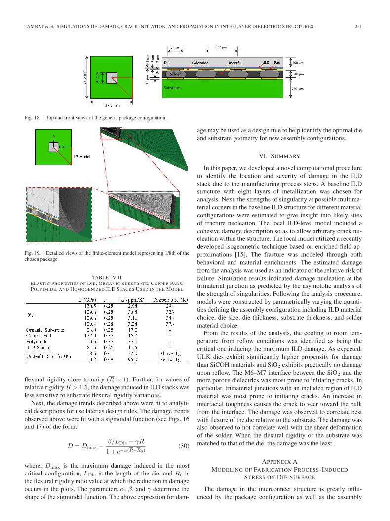
Fig. 18. Top and front views of the generic package configuration.
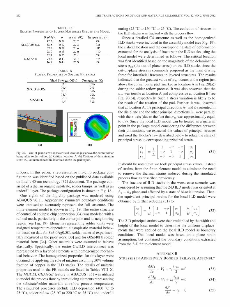
Fig. 19. Detailed views of the finite-element model representing 1/8th of thechosen package.
TABLE VIIIELASTIC PROPERTIES OF DIE, ORGANIC SUBSTRATE, COPPER PADS,POLYIMIDE, AND HOMOGENIZED ILD STACKS USED IN THE MODEL
flexural rigidity close to unity (R ∼ 1). Further, for values ofrelative rigidityR > 1.5, the damage induced in ILD stacks wasless sensitive to substrate flexural rigidity variations.
Next, the damage trends described above were fit to analyti-cal descriptions for use later as design rules. The damage trendsobserved above were fit with a sigmoidal function (see Figs. 16and 17) of the form:
D = Dmax − β/LDie − γR
1 + e−α(R−R0)(30)
where, Dmax is the maximum damage induced in the mostcritical configuration, LDie is the length of the die, and R0 isthe flexural rigidity ratio value at which the reduction in damageoccurs in the plots. The parameters α, β, and γ determine theshape of the sigmoidal function. The above expression for dam-
age may be used as a design rule to help identify the optimal dieand substrate geometry for new assembly configurations.
VI. SUMMARY
In this paper, we developed a novel computational procedureto identify the location and severity of damage in the ILDstack due to the manufacturing process steps. A baseline ILDstructure with eight layers of metallization was chosen foranalysis. Next, the strengths of singularity at possible multima-terial corners in the baseline ILD structure for different materialconfigurations were estimated to give insight into likely sitesof fracture nucleation. The local ILD-level model included acohesive damage description so as to allow arbitrary crack nu-cleation within the structure. The local model utilized a recentlydeveloped isogeometric technique based on enriched field ap-proximations [15]. The fracture was modeled through bothbehavioral and material enrichments. The estimated damagefrom the analysis was used as an indicator of the relative risk offailure. Simulation results indicated damage nucleation at thetrimaterial junction as predicted by the asymptotic analysis ofthe strength of singularities. Following the analysis procedure,models were constructed by parametrically varying the quanti-ties defining the assembly configuration including ILD materialchoice, die size, die thickness, substrate thickness, and soldermaterial choice.
From the results of the analysis, the cooling to room tem-perature from reflow conditions was identified as being thecritical one inducing the maximum ILD damage. As expected,ULK dies exhibit significantly higher propensity for damagethan SiCOH materials and SiO2 exhibits practically no damageupon reflow. The M6–M7 interface between the SiO2 and themore porous dielectrics was most prone to initiating cracks. Inparticular, trimaterial junctions with an included region of ILDmaterial was most prone to initiating cracks. An increase ininterfacial toughness causes the crack to veer toward the bulkfrom the interface. The damage was observed to correlate bestwith flexure of the die relative to the substrate. The damage wasalso observed to not correlate well with the shear deformationof the solder. When the flexural rigidity of the substrate wasmatched to that of the die, the damage was the least.
APPENDIX AMODELING OF FABRICATION PROCESS-INDUCED
STRESS ON DIE SURFACE
The damage in the interconnect structure is greatly influ-enced by the package configuration as well as the assembly
252 IEEE TRANSACTIONS ON DEVICE AND MATERIALS RELIABILITY, VOL. 12, NO. 2, JUNE 2012
TABLE IXELASTIC PROPERTIES OF SOLDER MATERIALS USED IN THE MODEL
TABLE XPLASTIC PROPERTIES OF SOLDER MATERIALS
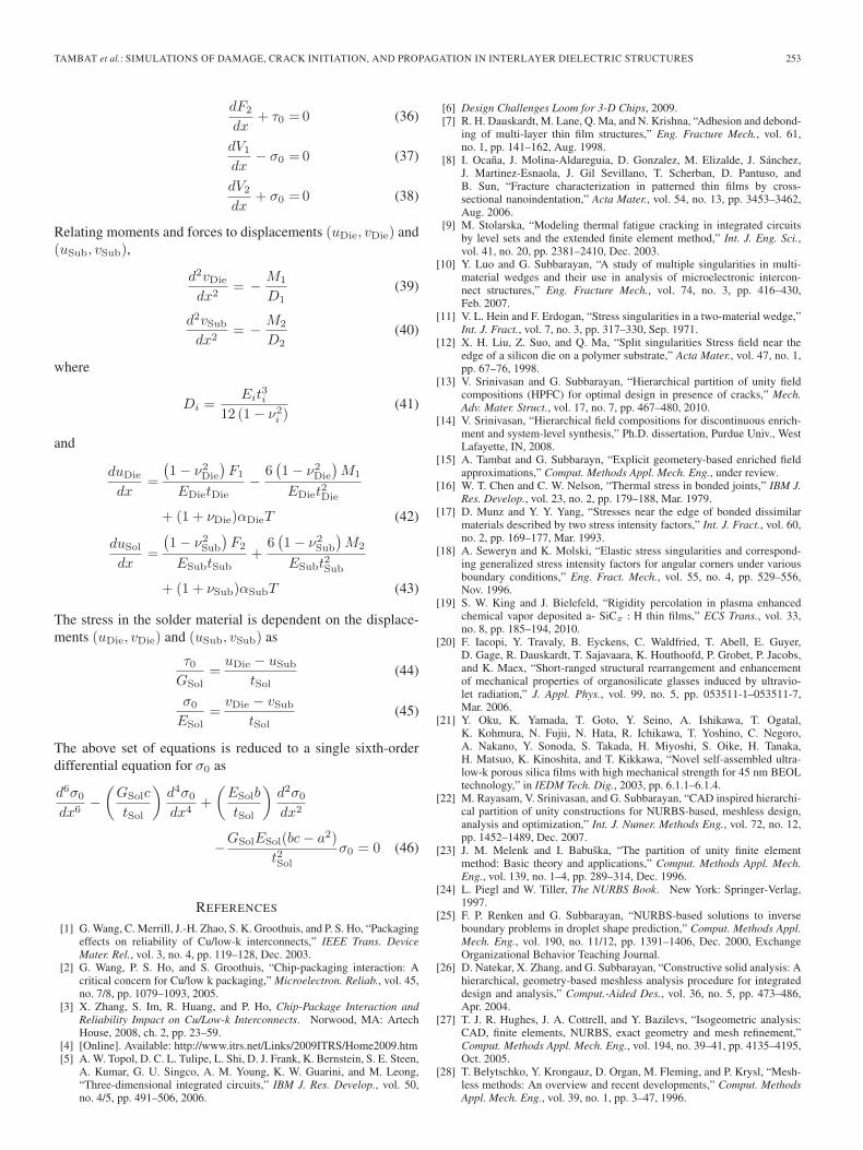
Fig. 20. Out-of-plane stress at the critical location just above the corner solderbump after solder reflow. (a) Critical location A. (b) Contour of delaminationstress σzz at interconnect/die interface above the pad region.
process. In this paper, a representative flip-chip package con-figuration was identified based on the published data availableon Intel’s 45-nm technology [32] document. The package con-sisted of a die, an organic substrate, solder bumps, as well as anunderfill layer. The package configuration is shown in Fig. 18.
One eighth of the flip-chip package was modeled usingABAQUS v6.11. Appropriate symmetry boundary conditionswere imposed to accurately represent the full structure. Thefinite-element model is shown in Fig. 19. The entire structureof controlled collapse chip connection (C4) was modeled with arefined mesh, particularly in the corner joint and its neighboringregion (see Fig. 19). Elements representing solder joints wereassigned temperature-dependent, elastoplastic material behav-ior based on data for Sn3.0Ag0.5Cu solder material experimen-tally measured in the prior work [33] and for 60Sn40Pb soldermaterial from [34]. Other materials were assumed to behaveelastically. Specifically, the entire Cu/ILD interconnect wasrepresented by a layer of elements with homogenized mechan-ical behavior. The homogenized properties for this layer wereobtained by applying the rule of mixture assuming 50% volumefraction of copper in the ILD stacks. The details of materialproperties used in the FE models are listed in Tables VIII–X.The MODEL CHANGE feature in ABAQUS [35] was utilizedto model the process flow by introducing elements representingthe substrate/solder materials at reflow process temperature.The simulated processes include ILD deposition (400 ◦C to25 ◦C), solder reflow (25 ◦C to 220 ◦C to 25 ◦C) and underfill
curing (25 ◦C to 150 ◦C to 25 ◦C). The evolution of stresses inthe ILD stacks was tracked with the process flow.
Since a detailed C4 structure as well as the homogenizedILD stacks were included in the assembly model (see Fig. 19),the critical location and the corresponding state of deformationextracted for the analysis of fracture in the ILD stacks using thelocal model were determined as follows. The critical locationwas first identified based on the magnitude of the delaminationstress σzz (the out-of-plane stress) on the ILD stacks since theout-of-plane stress is commonly proposed as the main drivingforce for interfacial fractures in layered structures. The resultsindicated that the greatest value of σzz occurs at the region justabove the corner bump pad (marked as location A in Fig. 20(a))during the solder reflow process. It was also observed that theσzz was tensile at location A and compressive at location B [seeFig. 20(b)], respectively. Such a stress variation is likely to bethe result of the rotation of the pad. Further, it was observedthat at location A, the principal directions n1 and n2 oriented inthe die plane and the other principal directions n3 were parallelwith the z-axis (due to the fact that σzz was approximately equalto σ3). Since the local ILD model can be treated as a materialpoint in the package model considering the difference betweentheir dimensions, we extracted the values of principal stressesand used the Hooke’s law described below to relate the state ofprincipal stress to corresponding principal strain.⎡
⎣ ε1ε2ε3
⎤⎦ =
1E
⎡⎣ 1 −ν −ν−ν 1 −ν−ν −ν 1
⎤⎦⎡⎣σ1
σ2
σ3
⎤⎦ (31)
It should be noted that we took principal stress values, insteadof strains, from the finite-element model to eliminate the needto remove the thermal strains induced during the simulatedprocess flow as described previously.
The fracture of ILD stacks in the worst case scenario wasconsidered by assuming that the 2-D ILD model was oriented atn1 − n3 plane and affected by a state of bi-axial tension. Then,the equivalent principal strains for the local ILD model wereobtained by further reducing (31) to:[
ε1ε3
]=
1E
[1 −ν−ν 1
] [σ1
σ3
]− ν
E
[σ2
σ2
](32)
The 2-D principal strains were then multiplied by the width andheight of the local model to determine the uniform displace-ments that were applied on the local ILD model as boundaryconditions. This local model was based on a plane strainassumption, but contained the boundary conditions extractedfrom the 3-D finite-element model.
APPENDIX BSTRESSES IN ADHESIVELY BONDED TRILAYER ASSEMBLY
dM1
dx− V1 + τ0
tDie
2= 0 (33)
dM2
dx− V2 + τ0
tSol
2= 0 (34)
dF1
dx− τ0 = 0 (35)
TAMBAT et al.: SIMULATIONS OF DAMAGE, CRACK INITIATION, AND PROPAGATION IN INTERLAYER DIELECTRIC STRUCTURES 253
dF2
dx+ τ0 = 0 (36)
dV1
dx− σ0 = 0 (37)
dV2
dx+ σ0 = 0 (38)
Relating moments and forces to displacements (uDie, vDie) and(uSub, vSub),
d2vDie
dx2= − M1
D1(39)
d2vSub
dx2= − M2
D2(40)
where
Di =Eit
3i
12 (1 − ν2i )
(41)
and
duDie
dx=
(1 − ν2
Die
)F1
EDietDie− 6
(1 − ν2
Die
)M1
EDiet2Die
+ (1 + νDie)αDieT (42)
duSol
dx=
(1 − ν2
Sub
)F2
ESubtSub+
6(1 − ν2
Sub
)M2
ESubt2Sub
+ (1 + νSub)αSubT (43)
The stress in the solder material is dependent on the displace-ments (uDie, vDie) and (uSub, vSub) as
τ0GSol
=uDie − uSub
tSol(44)
σ0
ESol=vDie − vSub
tSol(45)
The above set of equations is reduced to a single sixth-orderdifferential equation for σ0 as
d6σ0
dx6−(GSolc
tSol
)d4σ0
dx4+(ESolb
tSol
)d2σ0
dx2
−GSolESol(bc− a2)t2Sol
σ0 = 0 (46)
REFERENCES
[1] G. Wang, C. Merrill, J.-H. Zhao, S. K. Groothuis, and P. S. Ho, “Packagingeffects on reliability of Cu/low-k interconnects,” IEEE Trans. DeviceMater. Rel., vol. 3, no. 4, pp. 119–128, Dec. 2003.
[2] G. Wang, P. S. Ho, and S. Groothuis, “Chip-packaging interaction: Acritical concern for Cu/low k packaging,” Microelectron. Reliab., vol. 45,no. 7/8, pp. 1079–1093, 2005.
[3] X. Zhang, S. Im, R. Huang, and P. Ho, Chip-Package Interaction andReliability Impact on Cu/Low-k Interconnects. Norwood, MA: ArtechHouse, 2008, ch. 2, pp. 23–59.
[4] [Online]. Available: http://www.itrs.net/Links/2009ITRS/Home2009.htm[5] A. W. Topol, D. C. L. Tulipe, L. Shi, D. J. Frank, K. Bernstein, S. E. Steen,
A. Kumar, G. U. Singco, A. M. Young, K. W. Guarini, and M. Leong,“Three-dimensional integrated circuits,” IBM J. Res. Develop., vol. 50,no. 4/5, pp. 491–506, 2006.
[6] Design Challenges Loom for 3-D Chips, 2009.[7] R. H. Dauskardt, M. Lane, Q. Ma, and N. Krishna, “Adhesion and debond-
ing of multi-layer thin film structures,” Eng. Fracture Mech., vol. 61,no. 1, pp. 141–162, Aug. 1998.
[8] I. Ocaña, J. Molina-Aldareguia, D. Gonzalez, M. Elizalde, J. Sánchez,J. Martinez-Esnaola, J. Gil Sevillano, T. Scherban, D. Pantuso, andB. Sun, “Fracture characterization in patterned thin films by cross-sectional nanoindentation,” Acta Mater., vol. 54, no. 13, pp. 3453–3462,Aug. 2006.
[9] M. Stolarska, “Modeling thermal fatigue cracking in integrated circuitsby level sets and the extended finite element method,” Int. J. Eng. Sci.,vol. 41, no. 20, pp. 2381–2410, Dec. 2003.
[10] Y. Luo and G. Subbarayan, “A study of multiple singularities in multi-material wedges and their use in analysis of microelectronic intercon-nect structures,” Eng. Fracture Mech., vol. 74, no. 3, pp. 416–430,Feb. 2007.
[11] V. L. Hein and F. Erdogan, “Stress singularities in a two-material wedge,”Int. J. Fract., vol. 7, no. 3, pp. 317–330, Sep. 1971.
[12] X. H. Liu, Z. Suo, and Q. Ma, “Split singularities Stress field near theedge of a silicon die on a polymer substrate,” Acta Mater., vol. 47, no. 1,pp. 67–76, 1998.
[13] V. Srinivasan and G. Subbarayan, “Hierarchical partition of unity fieldcompositions (HPFC) for optimal design in presence of cracks,” Mech.Adv. Mater. Struct., vol. 17, no. 7, pp. 467–480, 2010.
[14] V. Srinivasan, “Hierarchical field compositions for discontinuous enrich-ment and system-level synthesis,” Ph.D. dissertation, Purdue Univ., WestLafayette, IN, 2008.
[15] A. Tambat and G. Subbarayn, “Explicit geometery-based enriched fieldapproximations,” Comput. Methods Appl. Mech. Eng., under review.
[16] W. T. Chen and C. W. Nelson, “Thermal stress in bonded joints,” IBM J.Res. Develop., vol. 23, no. 2, pp. 179–188, Mar. 1979.
[17] D. Munz and Y. Y. Yang, “Stresses near the edge of bonded dissimilarmaterials described by two stress intensity factors,” Int. J. Fract., vol. 60,no. 2, pp. 169–177, Mar. 1993.
[18] A. Seweryn and K. Molski, “Elastic stress singularities and correspond-ing generalized stress intensity factors for angular corners under variousboundary conditions,” Eng. Fract. Mech., vol. 55, no. 4, pp. 529–556,Nov. 1996.
[19] S. W. King and J. Bielefeld, “Rigidity percolation in plasma enhancedchemical vapor deposited a- SiCx : H thin films,” ECS Trans., vol. 33,no. 8, pp. 185–194, 2010.
[20] F. Iacopi, Y. Travaly, B. Eyckens, C. Waldfried, T. Abell, E. Guyer,D. Gage, R. Dauskardt, T. Sajavaara, K. Houthoofd, P. Grobet, P. Jacobs,and K. Maex, “Short-ranged structural rearrangement and enhancementof mechanical properties of organosilicate glasses induced by ultravio-let radiation,” J. Appl. Phys., vol. 99, no. 5, pp. 053511-1–053511-7,Mar. 2006.
[21] Y. Oku, K. Yamada, T. Goto, Y. Seino, A. Ishikawa, T. Ogatal,K. Kohmura, N. Fujii, N. Hata, R. Ichikawa, T. Yoshino, C. Negoro,A. Nakano, Y. Sonoda, S. Takada, H. Miyoshi, S. Oike, H. Tanaka,H. Matsuo, K. Kinoshita, and T. Kikkawa, “Novel self-assembled ultra-low-k porous silica films with high mechanical strength for 45 nm BEOLtechnology,” in IEDM Tech. Dig., 2003, pp. 6.1.1–6.1.4.
[22] M. Rayasam, V. Srinivasan, and G. Subbarayan, “CAD inspired hierarchi-cal partition of unity constructions for NURBS-based, meshless design,analysis and optimization,” Int. J. Numer. Methods Eng., vol. 72, no. 12,pp. 1452–1489, Dec. 2007.
[23] J. M. Melenk and I. Babuška, “The partition of unity finite elementmethod: Basic theory and applications,” Comput. Methods Appl. Mech.Eng., vol. 139, no. 1–4, pp. 289–314, Dec. 1996.
[24] L. Piegl and W. Tiller, The NURBS Book. New York: Springer-Verlag,1997.
[25] F. P. Renken and G. Subbarayan, “NURBS-based solutions to inverseboundary problems in droplet shape prediction,” Comput. Methods Appl.Mech. Eng., vol. 190, no. 11/12, pp. 1391–1406, Dec. 2000, ExchangeOrganizational Behavior Teaching Journal.
[26] D. Natekar, X. Zhang, and G. Subbarayan, “Constructive solid analysis: Ahierarchical, geometry-based meshless analysis procedure for integrateddesign and analysis,” Comput.-Aided Des., vol. 36, no. 5, pp. 473–486,Apr. 2004.
[27] T. J. R. Hughes, J. A. Cottrell, and Y. Bazilevs, “Isogeometric analysis:CAD, finite elements, NURBS, exact geometry and mesh refinement,”Comput. Methods Appl. Mech. Eng., vol. 194, no. 39–41, pp. 4135–4195,Oct. 2005.
[28] T. Belytschko, Y. Krongauz, D. Organ, M. Fleming, and P. Krysl, “Mesh-less methods: An overview and recent developments,” Comput. MethodsAppl. Mech. Eng., vol. 39, no. 1, pp. 3–47, 1996.

254 IEEE TRANSACTIONS ON DEVICE AND MATERIALS RELIABILITY, VOL. 12, NO. 2, JUNE 2012
[29] J. Dolbow and T. Belytschko, “Numerical integration of the Galerkinweak form in meshfree methods,” Comput. Mech., vol. 23, no. 3, pp. 219–230, Apr. 1999.
[30] T. Anderson, Fracture Mechanics: Fundamentals and Applications,3rd ed. Boca Raton, FL: Taylor & Francis, 2005.
[31] J. Rice, “Elastic fracture mechanics concepts for interfacial cracks,”J. Appl. Mech., vol. 55, no. 1, pp. 98–103, Mar. 1988.
[32] [Online]. Available: http://intel.com[33] K. Mysore, G. Subbarayan, V. Gupta, and R. Zhang, “Constitutive and
aging behavior of Sn3.0Ag0.5Cu solder alloy,” IEEE Trans. Electron.Packag. Manuf., vol. 32, no. 4, pp. 221–232, Oct. 2009.
[34] R. Darveaux and K. Banerji, “Constitutive relations for tin-based solderjoints,” IEEE Trans. Compon., Hybrids, Manuf. Technol., vol. 15, no. 6,pp. 1013–1024, Dec. 1992.
[35] ABAQUS version 6.11. User’s Manual, 2011.
Abhishek Tambat received the B.E. degree in mechanical engineering fromthe University of Pune, Pune, India, with Award for Academic Excellence in2007. He is currently pursuing the Ph.D. degree from the School of MechanicalEngineering, Purdue University, West Lafayette, IN. He is serving as a GraduateResearch Assistant and Teaching Assistant with Purdue University. His currentresearch interests involve development of novel computational techniquesfor modeling moving boundary problems and reliability of microelectronicspackaging.
Mr. Tambat was a recipient of the Ross Doctoral Fellowship in 2007.
Hung-Yun Lin received the B.S. degree in powermechanical engineering from National Tsing HuaUniversity, Hsinchu, Taiwan, with the DistinguishedAcademic Award of College of Engineering, in 2007,and the Ph.D. degree from the School of MechanicalEngineering, Purdue University, West Lafayette, IN,in 2009.
He is a Graduate Research Assistant with PurdueUniversity. His current research interests include op-timal topological design and reliability of microelec-tronic interconnects and packages.
Mr. Lin was a recipient of the honorary membership of Phi Tau Phi ScholasticHonor Society, R.O.C., in 2007 and elected as a member in the Mid-AmericaChapter of that honor society in 2010.
Ganesh Subbarayan received the B.Tech. degreein mechanical engineering from Indian Institute ofTechnology, Madras, Chennai, India, in 1985 andthe Ph.D. degree in mechanical engineering fromCornell University, Ithaca, NY, in 1991.
He is a Professor of mechanical engineering atPurdue University, West Lafayette, IN. He beganhis professional career at IBM Corporation during1990–1993. His research is in reliability of micro-electronic devices and packages.
Dr. Subbarayan is a Fellow of ASME as well asIEEE, and he served as the Editor-in-Chief of IEEE TRANSACTIONS ON
ADVANCED PACKAGING during 2002–2010. He currently serves as the TopicalEditor for John Wiley’s Encyclopedia of Electrical and Electronics Engineering.Among others, he is a recipient of the 2005 Mechanics Award from the ASMEEPP Division and the NSF CAREER award. Several of his publications co-authored with his students have been recognized with awards.
Dae Young Jung received the B.S. and M.S. degreesin metallurgical engineering from Seoul NationalUniversity, Seoul, Korea, and the Ph.D. degree inphysical metallurgy from the University of Illinois,Champaign-Urbana.
He was a Research Scientist at Korea AtomicEnergy Research Institute, dealing with nuclear fuelfabrication process development for 3 years. He wasemployed at IBM until his retirement in 2007. Heheld various engineering and managerial responsi-bilities at a few IBM research and development
facilities—Endicott, NY, Rochester, MN, and Hopewell Junction, NY. Hejoined the Research Foundation at Binghamton University in April, 2007.He is currently a Senior Scientist at Small Scale Systems Integration andPackaging and a Visiting Professor of Thomas J. Watson School of Engineeringand Applied Science of Binghamton University. He has extensive experiencein the following areas: design and manufacturing process for printed circuitboards, high-performance electronic packaging, semiconductor manufacturingprocess, electronic interconnect materials, reliability evaluation of electronicproducts, materials characterization, and analysis using electron optical instru-ments. His current research is focused on materials used as interconnect forelectronic devices with emphasis on their reliability.
Bahgat Sammakia received the B.S. degree in mechanical engineering fromthe University of Alexandria, Alexandria, Egypt, and the M.S. and Ph.D.degrees in mechanical engineering from the State University of New York,Buffalo, in 1980 and 1982, respectively.
He is a Distinguished Professor and the Interm VP for Research at SUNYBinghamton. He also directs three centers including the Integrated ElectronicsEngineering Center, a New York State’s Center for Advanced Technology,Small Scale Systems, Integration, and Packaging Center, a New York StateCenter of Excellence, and the Army Research Lab-funded Center for AdvancedMicroelectronics Manufacturing focused on flexible electronics. He joined IBMin 1984 as an Engineer in the thermal management area. In 1985, he waspromoted to Manager of the thermal management department. He continued towork in IBM until 1998 in various management positions, including managingthe thermal and mechanical analysis groups, the surface science group, thechemical lab, the site technical assurance group, and his last position in IBMwas a Manager of development for organic packaging in the IBM Microelec-tronics Division. His research work was in the areas of natural convection heattransfer.
Dr. Sammakia serves as the Editor-in-Chief of ASME Journal of ElectronicPackaging.


![AutoCAD Crack Free Registration Code 2022 [New]](https://static.fdokumen.com/doc/165x107/633ddc36d497af1eca0ff28c/autocad-crack-free-registration-code-2022-new.jpg)