The professional qualification for a varied and rewarding career more opportunities

Graphene PyramidsDOI: 10.1002/anie.201306317
Large Hexagonal Bi- and Trilayer Graphene Single Crystals withVaried Interlayer Rotations**Zheng Yan, Yuanyue Liu, Long Ju, Zhiwei Peng, Jian Lin, Gunuk Wang, Haiqing Zhou,Changsheng Xiang, E. L. G. Samuel, Carter Kittrell, Vasilii I. Artyukhov, Feng Wang,*Boris I. Yakobson,* and James M. Tour*
Abstract: Bi- and trilayer graphene have attracted intensiveinterest due to their rich electronic and optical properties,which are dependent on interlayer rotations. However, thesynthesis of high-quality large-size bi- and trilayer graphenesingle crystals still remains a challenge. Here, the synthesis of100 mm pyramid-like hexagonal bi- and trilayer graphenesingle-crystal domains on Cu foils using chemical vapordeposition is reported. The as-produced graphene domainsshow almost exclusively either 08 or 308 interlayer rotations.Raman spectroscopy, transmission electron microscopy, andFourier-transformed infrared spectroscopy were used to dem-onstrate that bilayer graphene domains with 08 interlayerstacking angles were Bernal stacked. Based on first-principlecalculations, it is proposed that rotations originate from thegraphene nucleation at the Cu step, which explains the origin ofthe interlayer rotations and agrees well with the experimentalobservations.
Graphene, a two-dimensional sp2-bonded carbon material,has attracted enormous attention due to its excellent elec-trical, optical and mechanical properties.[1] To date, the best-quality graphene is mechanically exfoliated from graphitethough limited to small flakes and low yields, whereas large-area graphene grown on transition metals by chemical vapordeposition (CVD)[2] has produced polycrystalline structures
with reduced electrical and mechanical properties.[3] Recentadvancements in CVD techniques have enabled the fabrica-tion of large-size and high-quality single-crystal monolayergraphene.[4] However, monolayer graphene has zero bandgap, limiting its potential applications.[1] In contrast, bi- andtrilayer graphene have rich electronic and optical propertiesthat are dependent on their interlayer stacking orders,opening broad applications in nanoelectronics and optics.[1c,5]
Therefore, CVD synthesis of large bi- and trilayer graphenesingle crystals with well-defined interlayer stacking that canbe isolated from their growing substrates would providea material with both fundamental interests and practicalapplications. In addition, it is unclear how the few-layergraphene single crystals are grown, and what determines theinterlayer stacking. A combination of experimental andtheoretical studies would offer useful guidance towardscontrolled synthesis of nanocarbon materials.
We report here the synthesis of about 100 mm pyramid-like bi- and trilayer graphene domains with hexagonal shapeson Cu foils. The as-made graphene domains can be isolatedfrom the Cu surfaces and transferred onto silica wafers ortrench-patterned silica wafers to suspend them withoutintroducing damages or folds. This process has great potentialfor studying stacking-dependent electronics and optics inthese graphene domains. Moreover, we found that the as-produced graphene domains show almost exclusively either 08or 308 interlayer rotations. Raman spectroscopy, transmissionelectron microscopy (TEM), and Fourier-transformed infra-red spectroscopy (FT-IR) with synchrotron radiation wereused to demonstrate that bilayer graphene domains with 08interlayer stacking angles were Bernal stacked. The 08 Bernalstacking is known to dominate in graphite,[6] but the 308interlayer rotation is anomalous as it is incommensuratestacking.[7] Based on first-principle calculations, we proposethat rotations originate from the graphene nucleation at theCu step, which explains the origin of the interlayer rotationsand agrees well with the experimental observations.
The fabrication of single-crystal hexagonal bi- and trilayergraphene domains was achieved in one batch on electro-chemically polished and high-pressure annealed Cu foils usinga double-annealing process (Figure 1a). The detailed growthprocedures are described in the Supporting Information.After growth, graphene domains were transferred onto SiO2
(100 nm)/Si substrates[4a] for optical characterizations, whichpermit the direct visualization of shapes and thicknesses ofthe as-produced graphene domains. Figure 1b–g and Fig-ure S1 provide representative optical images of as-producedgraphene domains on SiO2/Si wafers. From these optical
[*] Z. Yan,[+] Z. Peng, Dr. G. Wang, Dr. H. Zhou, C. Xiang,E. L. G. Samuel, C. Kittrell, Prof. J. M. TourDepartment of Chemistry, Rice UniversityHouston, TX 77005 (USA)E-mail: [email protected]
Y. Liu,[+] Dr. J. Lin, Dr. V. I. Artyukhov, Prof. B. I. Yakobson,Prof. J. M. TourDepartment of Mechanical Engineering and Materials ScienceandThe Smalley Institute for Nanoscale Science and TechnologyRice University, Houston, TX 77005 (USA)E-mail: [email protected]
L. Ju, Prof. F. WangDepartment of Physics, University of California at BerkeleyBerkeley, CA 94720 (USA)E-mail: [email protected]
[+] These authors contributed equally to this work.
[**] The ONR MURI program (grant numbers 00006766 and N00014-09-1-1066) and AFOSR MURI (grant number FA9550-12-1-0035)provided funding. We acknowledge M. Martin and H. Bechtel at theLawrence Berkeley National Laboratory for help on the FTIRmeasurement.
Supporting information for this article is available on the WWWunder http://dx.doi.org/10.1002/anie.201306317.
AngewandteChemie
1Angew. Chem. Int. Ed. 2014, 53, 1 – 6 � 2014 Wiley-VCH Verlag GmbH & Co. KGaA, Weinheim
These are not the final page numbers! � �
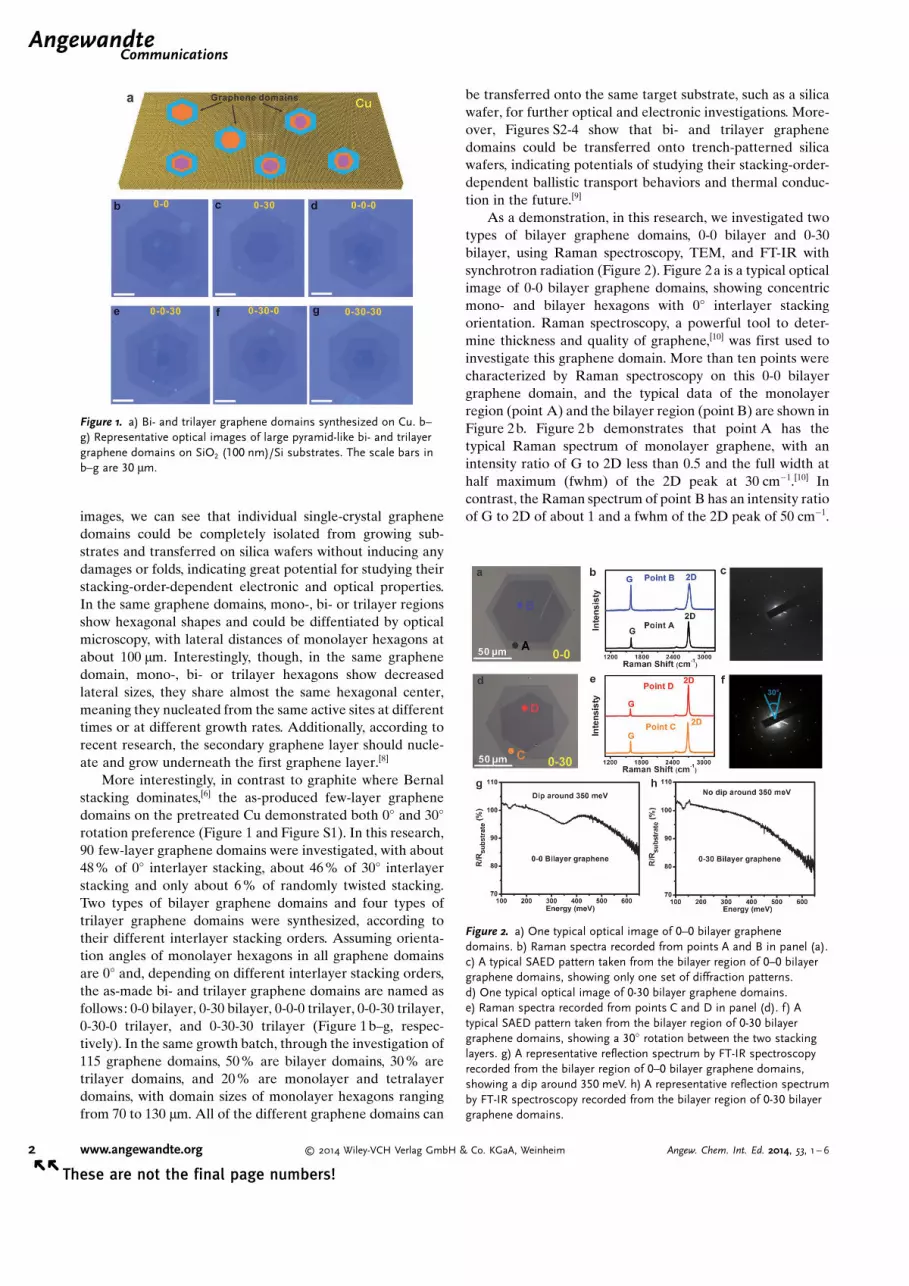
images, we can see that individual single-crystal graphenedomains could be completely isolated from growing sub-strates and transferred on silica wafers without inducing anydamages or folds, indicating great potential for studying theirstacking-order-dependent electronic and optical properties.In the same graphene domains, mono-, bi- or trilayer regionsshow hexagonal shapes and could be diffentiated by opticalmicroscopy, with lateral distances of monolayer hexagons atabout 100 mm. Interestingly, though, in the same graphenedomain, mono-, bi- or trilayer hexagons show decreasedlateral sizes, they share almost the same hexagonal center,meaning they nucleated from the same active sites at differenttimes or at different growth rates. Additionally, according torecent research, the secondary graphene layer should nucle-ate and grow underneath the first graphene layer.[8]
More interestingly, in contrast to graphite where Bernalstacking dominates,[6] the as-produced few-layer graphenedomains on the pretreated Cu demonstrated both 08 and 308rotation preference (Figure 1 and Figure S1). In this research,90 few-layer graphene domains were investigated, with about48% of 08 interlayer stacking, about 46 % of 308 interlayerstacking and only about 6% of randomly twisted stacking.Two types of bilayer graphene domains and four types oftrilayer graphene domains were synthesized, according totheir different interlayer stacking orders. Assuming orienta-tion angles of monolayer hexagons in all graphene domainsare 08 and, depending on different interlayer stacking orders,the as-made bi- and trilayer graphene domains are named asfollows: 0-0 bilayer, 0-30 bilayer, 0-0-0 trilayer, 0-0-30 trilayer,0-30-0 trilayer, and 0-30-30 trilayer (Figure 1b–g, respec-tively). In the same growth batch, through the investigation of115 graphene domains, 50 % are bilayer domains, 30% aretrilayer domains, and 20% are monolayer and tetralayerdomains, with domain sizes of monolayer hexagons rangingfrom 70 to 130 mm. All of the different graphene domains can
be transferred onto the same target substrate, such as a silicawafer, for further optical and electronic investigations. More-over, Figures S2-4 show that bi- and trilayer graphenedomains could be transferred onto trench-patterned silicawafers, indicating potentials of studying their stacking-order-dependent ballistic transport behaviors and thermal conduc-tion in the future.[9]
As a demonstration, in this research, we investigated twotypes of bilayer graphene domains, 0-0 bilayer and 0-30bilayer, using Raman spectroscopy, TEM, and FT-IR withsynchrotron radiation (Figure 2). Figure 2a is a typical opticalimage of 0-0 bilayer graphene domains, showing concentricmono- and bilayer hexagons with 08 interlayer stackingorientation. Raman spectroscopy, a powerful tool to deter-mine thickness and quality of graphene,[10] was first used toinvestigate this graphene domain. More than ten points werecharacterized by Raman spectroscopy on this 0-0 bilayergraphene domain, and the typical data of the monolayerregion (point A) and the bilayer region (point B) are shown inFigure 2b. Figure 2b demonstrates that point A has thetypical Raman spectrum of monolayer graphene, with anintensity ratio of G to 2D less than 0.5 and the full width athalf maximum (fwhm) of the 2D peak at 30 cm�1.[10] Incontrast, the Raman spectrum of point B has an intensity ratioof G to 2D of about 1 and a fwhm of the 2D peak of 50 cm�1.
Figure 1. a) Bi- and trilayer graphene domains synthesized on Cu. b–g) Representative optical images of large pyramid-like bi- and trilayergraphene domains on SiO2 (100 nm)/Si substrates. The scale bars inb–g are 30 mm.
Figure 2. a) One typical optical image of 0–0 bilayer graphenedomains. b) Raman spectra recorded from points A and B in panel (a).c) A typical SAED pattern taken from the bilayer region of 0–0 bilayergraphene domains, showing only one set of diffraction patterns.d) One typical optical image of 0-30 bilayer graphene domains.e) Raman spectra recorded from points C and D in panel (d). f) Atypical SAED pattern taken from the bilayer region of 0-30 bilayergraphene domains, showing a 308 rotation between the two stackinglayers. g) A representative reflection spectrum by FT-IR spectroscopyrecorded from the bilayer region of 0–0 bilayer graphene domains,showing a dip around 350 meV. h) A representative reflection spectrumby FT-IR spectroscopy recorded from the bilayer region of 0-30 bilayergraphene domains.
.AngewandteCommunications
2 www.angewandte.org � 2014 Wiley-VCH Verlag GmbH & Co. KGaA, Weinheim Angew. Chem. Int. Ed. 2014, 53, 1 – 6� �
These are not the final page numbers!
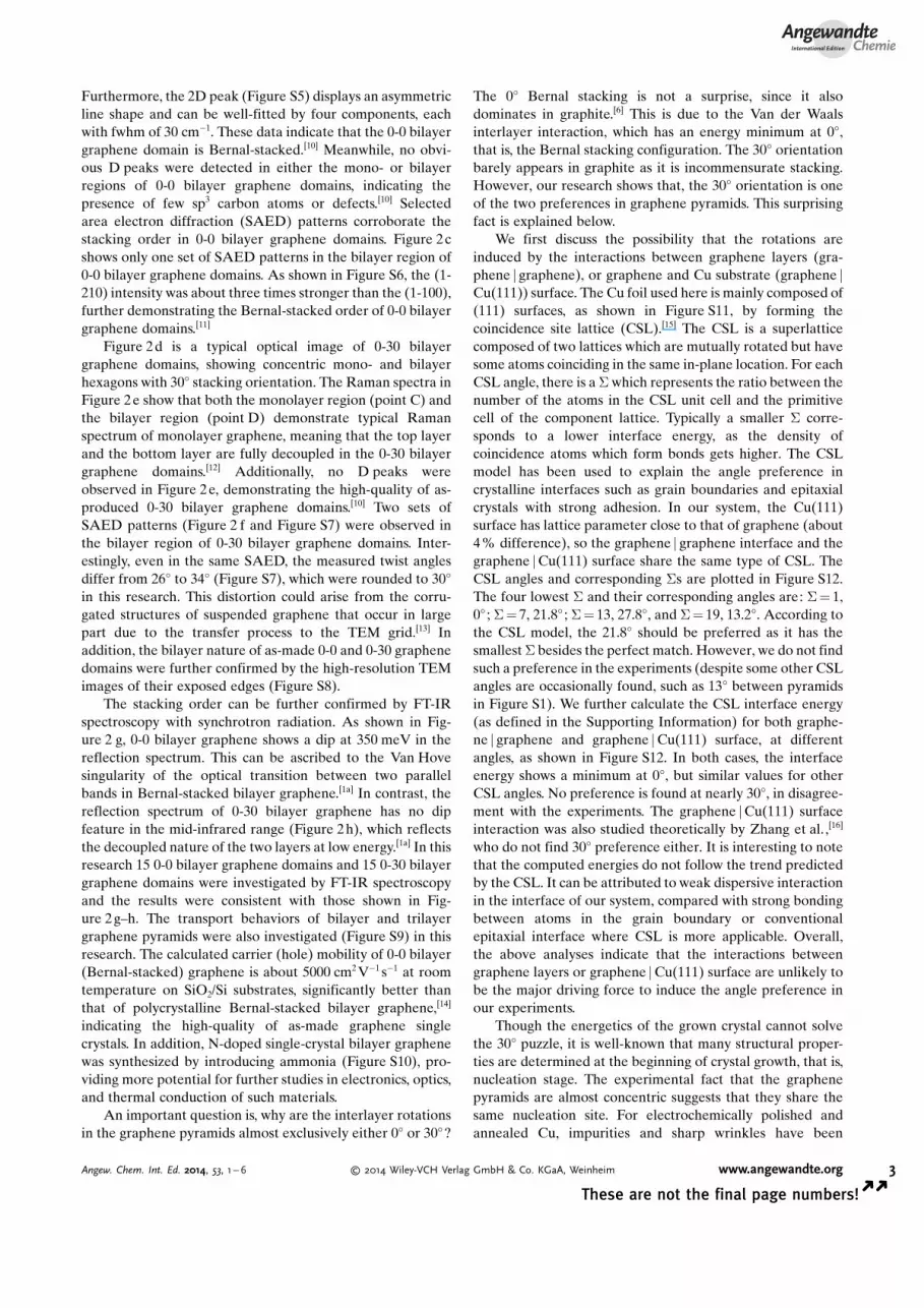
Furthermore, the 2D peak (Figure S5) displays an asymmetricline shape and can be well-fitted by four components, eachwith fwhm of 30 cm�1. These data indicate that the 0-0 bilayergraphene domain is Bernal-stacked.[10] Meanwhile, no obvi-ous D peaks were detected in either the mono- or bilayerregions of 0-0 bilayer graphene domains, indicating thepresence of few sp3 carbon atoms or defects.[10] Selectedarea electron diffraction (SAED) patterns corroborate thestacking order in 0-0 bilayer graphene domains. Figure 2cshows only one set of SAED patterns in the bilayer region of0-0 bilayer graphene domains. As shown in Figure S6, the (1-210) intensity was about three times stronger than the (1-100),further demonstrating the Bernal-stacked order of 0-0 bilayergraphene domains.[11]
Figure 2d is a typical optical image of 0-30 bilayergraphene domains, showing concentric mono- and bilayerhexagons with 308 stacking orientation. The Raman spectra inFigure 2e show that both the monolayer region (point C) andthe bilayer region (point D) demonstrate typical Ramanspectrum of monolayer graphene, meaning that the top layerand the bottom layer are fully decoupled in the 0-30 bilayergraphene domains.[12] Additionally, no D peaks wereobserved in Figure 2e, demonstrating the high-quality of as-produced 0-30 bilayer graphene domains.[10] Two sets ofSAED patterns (Figure 2 f and Figure S7) were observed inthe bilayer region of 0-30 bilayer graphene domains. Inter-estingly, even in the same SAED, the measured twist anglesdiffer from 268 to 348 (Figure S7), which were rounded to 308in this research. This distortion could arise from the corru-gated structures of suspended graphene that occur in largepart due to the transfer process to the TEM grid.[13] Inaddition, the bilayer nature of as-made 0-0 and 0-30 graphenedomains were further confirmed by the high-resolution TEMimages of their exposed edges (Figure S8).
The stacking order can be further confirmed by FT-IRspectroscopy with synchrotron radiation. As shown in Fig-ure 2 g, 0-0 bilayer graphene shows a dip at 350 meV in thereflection spectrum. This can be ascribed to the Van Hovesingularity of the optical transition between two parallelbands in Bernal-stacked bilayer graphene.[1a] In contrast, thereflection spectrum of 0-30 bilayer graphene has no dipfeature in the mid-infrared range (Figure 2h), which reflectsthe decoupled nature of the two layers at low energy.[1a] In thisresearch 15 0-0 bilayer graphene domains and 15 0-30 bilayergraphene domains were investigated by FT-IR spectroscopyand the results were consistent with those shown in Fig-ure 2g–h. The transport behaviors of bilayer and trilayergraphene pyramids were also investigated (Figure S9) in thisresearch. The calculated carrier (hole) mobility of 0-0 bilayer(Bernal-stacked) graphene is about 5000 cm2 V�1 s�1 at roomtemperature on SiO2/Si substrates, significantly better thanthat of polycrystalline Bernal-stacked bilayer graphene,[14]
indicating the high-quality of as-made graphene singlecrystals. In addition, N-doped single-crystal bilayer graphenewas synthesized by introducing ammonia (Figure S10), pro-viding more potential for further studies in electronics, optics,and thermal conduction of such materials.
An important question is, why are the interlayer rotationsin the graphene pyramids almost exclusively either 08 or 308?
The 08 Bernal stacking is not a surprise, since it alsodominates in graphite.[6] This is due to the Van der Waalsinterlayer interaction, which has an energy minimum at 08,that is, the Bernal stacking configuration. The 308 orientationbarely appears in graphite as it is incommensurate stacking.However, our research shows that, the 308 orientation is oneof the two preferences in graphene pyramids. This surprisingfact is explained below.
We first discuss the possibility that the rotations areinduced by the interactions between graphene layers (gra-phene j graphene), or graphene and Cu substrate (graphene jCu(111)) surface. The Cu foil used here is mainly composed of(111) surfaces, as shown in Figure S11, by forming thecoincidence site lattice (CSL).[15] The CSL is a superlatticecomposed of two lattices which are mutually rotated but havesome atoms coinciding in the same in-plane location. For eachCSL angle, there is a � which represents the ratio between thenumber of the atoms in the CSL unit cell and the primitivecell of the component lattice. Typically a smaller � corre-sponds to a lower interface energy, as the density ofcoincidence atoms which form bonds gets higher. The CSLmodel has been used to explain the angle preference incrystalline interfaces such as grain boundaries and epitaxialcrystals with strong adhesion. In our system, the Cu(111)surface has lattice parameter close to that of graphene (about4% difference), so the graphene j graphene interface and thegraphene jCu(111) surface share the same type of CSL. TheCSL angles and corresponding �s are plotted in Figure S12.The four lowest � and their corresponding angles are: � = 1,08 ; � = 7, 21.88 ; � = 13, 27.88, and � = 19, 13.28. According tothe CSL model, the 21.88 should be preferred as it has thesmallest � besides the perfect match. However, we do not findsuch a preference in the experiments (despite some other CSLangles are occasionally found, such as 138 between pyramidsin Figure S1). We further calculate the CSL interface energy(as defined in the Supporting Information) for both graphe-ne j graphene and graphene jCu(111) surface, at differentangles, as shown in Figure S12. In both cases, the interfaceenergy shows a minimum at 08, but similar values for otherCSL angles. No preference is found at nearly 308, in disagree-ment with the experiments. The graphene jCu(111) surfaceinteraction was also studied theoretically by Zhang et al.,[16]
who do not find 308 preference either. It is interesting to notethat the computed energies do not follow the trend predictedby the CSL. It can be attributed to weak dispersive interactionin the interface of our system, compared with strong bondingbetween atoms in the grain boundary or conventionalepitaxial interface where CSL is more applicable. Overall,the above analyses indicate that the interactions betweengraphene layers or graphene jCu(111) surface are unlikely tobe the major driving force to induce the angle preference inour experiments.
Though the energetics of the grown crystal cannot solvethe 308 puzzle, it is well-known that many structural proper-ties are determined at the beginning of crystal growth, that is,nucleation stage. The experimental fact that the graphenepyramids are almost concentric suggests that they share thesame nucleation site. For electrochemically polished andannealed Cu, impurities and sharp wrinkles have been
AngewandteChemie
3Angew. Chem. Int. Ed. 2014, 53, 1 – 6 � 2014 Wiley-VCH Verlag GmbH & Co. KGaA, Weinheim www.angewandte.org
These are not the final page numbers! � �

removed (Figure S13), leaving the Cu steps (Figure 3a) asmajor nucleation sites,[17, 18] since they provide low-energysites for C atoms.[17, 19] The steps on the Cu(111) surface aremicroscopically straight with closest-packed atoms (Fig-ure 3b), as the most stable configuration.[17,19] During nucle-ation, a graphene jCu step interface is formed (Figure 3 b).The strong interface bonding determines the grapheneorientation with respect to Cu(111),[16] and subsequentlyleads to the mutual orientations between graphene layers inthe same pyramid as they nucleate from the same site.Therefore, the energy-preferred graphene jCu step interfacewould lead to preferred orientation between graphene andCu, and eventually result in preferred orientation betweengraphene layers. The optimal graphene jCu step interfaceshould be formed by atomically straight graphene edges,because they could efficiently contact the step atoms andsaturate their dangling bonds. Among all the orientations, the08 and 308 orientations render straight zigzag (ZZ) andarmchair (AC) graphene edges, respectively. Other edgeshave rough shapes with alternating straight segments andkinks,[20] which should lead to high-energy interfaces.
The above mechanism was quantified by first-principlecalculations. The computational details can be found in theSupporting Information. Figure 3 c shows the atomic structureof graphene jCu step interface. Clearly, for 08 (ZZ) and 308(AC) interfaces, both the graphene edge and Cu step remainalmost intactly straight. However, at 19.18 or 25.38, the Custep is distorted, and the graphene edge is highly buckled inthe surface normal direction, suggesting an unstable interface.Figure 3d confirms that the interface energy [defined inEq. (S1)] has two local minima at 08 and 308. Therefore, thegraphene jCu step interface has two preferred orientations:08 and 308.
The energy preference for 08 and 308 is also manifested inthe electronic structure. Figure 4 shows the charge densitydifference between the graphene–Cu system and the isolated
graphene and Cu. The electron density accumulation isobserved at the interface, suggesting a partially covalentbonding feature of graphene jCu step interface. It also showsthat the ZZ and AC edges have different binding sites. TheAC edge (308) is only bound with Cu step atoms, while the ZZedge (08) is also bound with the Cu layer underneath. Theextra coordination of the ZZ edge with Cu helps stabilize theinterface. For other angles, the graphene edges are combina-tions of ZZ and AC segments.[20] Their difference in thebinding sites distorts the graphene jCu step interface (19.18 inFigure 4), and gives rise to the high interface energy.
During the CVD growth, the graphene sheet could growacross the Cu step where it originally nucleated,[18] by additionof surface or subsurface diffusing C atoms to the interface.After that, the graphene edge extends, without being“pinned” by the Cu step. Therefore, the Cu steps are re-exposed and serve as the nucleation sites for a secondgraphene layer. A detailed description on the nucleation ofmultilayer graphene can be found in the Supporting Infor-mation. The new layer again has preference for 08 and 308with respect to the Cu surface. Since the graphene layers inthe same pyramid nucleate from the same site that serves as
Figure 3. a) Graphene nucleation on the Cu surface. C: black, Cu: red.The topmost Cu layer is highlighted in bold color. b) The orientationangle between graphene and Cu(111) surface. c) The relaxed graphe-ne jCu step interface structures for different orientation angles. d) Theinterface energy [defined in Eq. (S1)] as a function of the orientationangle. The two data points at the same orientation angle represent thecomputational accuracy, because of different strain levels of periodiccell size (either using the Cu or graphene lattice parameter; see detailsin the Supporting Information).
Figure 4. Isosurfaces (in blue) of electron density accumulation uponforming the graphene jCu step interface. For clarity, only two Cu layersare displayed.
.AngewandteCommunications
4 www.angewandte.org � 2014 Wiley-VCH Verlag GmbH & Co. KGaA, Weinheim Angew. Chem. Int. Ed. 2014, 53, 1 – 6� �
These are not the final page numbers!
a common reference, their mutual rotations should also havethe preference for 08 and 308. Eventually, graphene pyramidsgrow on clean Cu, with the component layers mutuallyrotated by either 08 or 308.
In summary, we report the CVD synthesis of about100 mm hexagonal bi- and trilayer graphene single crystals onpretreated Cu foils. The as-made graphene domains havealmost exclusively either Bernal stacking (08) or anomalous308 interlayer rotations. The rotations originate from thegraphene nucleation at the Cu step, which is supported byfirst-principle calculations. The as-made graphene domainswere isolated from Cu surfaces and transferred onto silicawafers or trench-patterned silica, enabling the further studiesof their thickness- and orientation-dependent electronics andoptoelectronics.
Received: July 19, 2013Published online: && &&, &&&&
.Keywords: first-principle calculations · graphene ·growth mechanism · single crystals · surface chemistry
[1] a) F. Wang, Y. Zhang, C. Tian, C. Girit, A. Zettl, M. Crommie,Y. R. Shen, Science 2008, 320, 206 – 209; b) A. K. Geim, K. S.Novoselov, Nat. Mater. 2007, 6, 183 – 191; c) Y. Zhang, T. T. Tang,C. Girit, Z. Hao, M. C. Martin, A. Zettl, M. F. Crommie, Y. R.Shen, F. Wang, Nature 2009, 459, 820 – 823.
[2] a) A. Reina, X. Jia, J. Ho, D. Nezich, H. Son, V. Bulovic, M. S.Dresselhaus, J. Kong, Nano Lett. 2009, 9, 30 – 35; b) K. S. Kim, Y.Zhao, H. Jang, S. Y. Lee, J. M. Kim, K. S. Kim, J. H. Ahn, P. Kim,J. Y. Choi, B. H. Hong, Nature 2009, 457, 706 – 710; c) X. S. Li,W. W. Cai, J. An, S. Kim, J. Nah, D. Yang, R. Piner, A.Velamakanni, I. Jung, E. Tutuc, S. K. Banerjee, L. Colombo,R. S. Ruoff, Science 2009, 324, 1312 – 1314.
[3] a) P. Y. Huang, C. S. Ruiz-Vargas, A. M. van der Zande, W. S.Whitney, M. P. Levendorf, J. W. Kevek, S. Garg, J. S. Alden, C. J.Hustedt, Y. Zhu, J. Park, P. L. McEuen, D. A. Muller, Nature2011, 469, 389 – 392; b) Q. K. Yu, L. A. Jauregui, W. Wu, R.Colby, J. Tian, Z. Su, H. Cao, Z. Liu, D. Pandey, D, Wei, T. F.Chung, P. Peng, N. P. Guisinger, E. A. Stach, J. Bao, S. S. Pei,Y. P. Chen, Nat. Mater. 2011, 10, 443 – 449.
[4] a) Z. Yan, J. Lin, Z. Peng, Z. Sun, Y, Zhu, L. Li, C. Xiang, E. L.Samuel, C. Kittrell, J. M. Tour, ACS Nano 2012, 6, 9110 – 9117;b) L.Gao, W. Ren, H. Xu, L. Jin, Z. Wang, T. Ma, L. P. Ma, Z.Zhang, Q. Fu, L. M. Peng, X. Bao, H. M. Cheng, Nat. Commun.2013, DOI: 10.1038/ncomms1702; c) X. S. Li, C. W. Magnuson,A. Venugopal, R. M. Tromp, J. B. Hannon, E. M. Vogel, L.Colombo, R. S. Ruoff, J. Am. Chem. Soc. 2011, 133, 2816 – 2819.
[5] a) X. Zou, J. Shang, J. Leaw, Z. Luo, L. Luo, C. Laovorakiat, L.Cheng, S. A. Cheong, H. Su, J. X. Zhu, Y. Liu, K. P. Loh, A. H. C.Neto, T. Yu, E. E. M. Chia, Phys. Rev. Lett. 2013, 110, 067401;b) Y. Kim, H. Yun, S. G. Nam, M. Son, D. S. Lee, D. C. Kim, S.Seo, H. C. Choi, H. J. Lee, S. W. Lee, J. S. Kim, Phys. Rev. Lett.2013, 110, 096602; c) Y. Wang, Z. Ni, L. Liu, Y. Liu, C. Cong, T.Yu, X. Wang, D. Shen, Z. Shen, ACS Nano 2010, 4, 4074 – 4080;d) L. Zhang, Y. Zhang, J. Camacho, M. Khodas, I. Zaliznyak,Nat. Phys. 2011, 7, 953 – 957.
[6] M. S. Dresselhaus, G. Dresselhaus, K. Sugihara, I. L. Spain,H. A. Goldberg, Graphite Fibers and Filaments, Springer, Berlin,1988.
[7] Y. Shibuta, J. A. Elliott, Chem. Phys. Lett. 2011, 512, 146 – 150.[8] W. Fang, A. L. Hsu, R. Caudillo, Y. Song, A. G. Birdwell, E.
Zakar, M. Kalbac, M. Dubey, T. Palacios, M. S. Dresselhaus, P. T.Araujo, J. Kong, Nano Lett. 2013, 13, 1541 – 1548.
[9] a) K. I. Bolotin, K. J. Sikes, Z. Jiang, M. Klima, G. Fudenberg, J.Hone, P. Kim, H. L. Stormer, Solid State Commun. 2008, 146,351 – 355; b) A. A. Balandin, S. Ghosh, W. Bao, I. Calizo, D.Teweldebrhan, F. Miao, C. N. Lau, Nano Lett. 2013, 13, 902 – 907.
[10] L. M. Malard, M. A. Pimenta, G. Dresselhaus, M. S. Dressel-haus, Phys. Rep. 2009, 473, 51 – 87.
[11] Y. Hernandez, V. Nicolosi, M. Lotya, F. M. Blighe, Z. Sun, S. De,I. T. McGovern, B. Holland, M. Byrne, Y. K. Gun�Ko, J. J.Boland, P. Niraj, G. Duesberg, S. Krishnamurthy, R. Goodhue, J.Hutchison, V. Scardaci, A. C. Ferrari, J. N. Coleman, Nat.Nanotechnol. 2008, 3, 563 – 568.
[12] K. Kim, S. Coh, L. Z. Tan, W. Regan, J. M. Yuk, E. Chatterjee,M. F. Crommie, M. L. Cohen, S. T. Louie, A. Zettl, Phys. Rev.Lett. 2012, 108, 246103.
[13] J. C. Meyer, A. K. Geim, M. I. Katsnelson, K. S. Novoselov, T. J.Booth, S. Roth, Nature 2006, 439-444, 60 – 63.
[14] a) K. Yan, H. Peng, Y. Zhou, H. Li, Z. Liu, Nano Lett. 2011, 11,1106 – 1110; b) S. Lee, K. Lee, Z. Zhong, Nano Lett. 2010, 10,4702 – 4707.
[15] a) W. Bollmann, Crystal Defects and Crystalline Interfaces,Springer, Berlin, 1970 ; b) D. H. Warrington, J. Phys. (Paris),Colloq. 1975, 36, C4-87 – C4-95.
[16] X. Zhang, Z. Xu, L. Hui, J. Xin, F. Ding, J. Phys. Chem. Lett.2012, 3, 2822 – 2827.
[17] a) J. Gao, J. Yip, J. Zhao, B. I. Yakobson, F. Ding, J. Am. Chem.Soc. 2011, 133, 5009 – 5015; b) V. I. Artyukhov, Y. Liu, B. I.Yakobson, Proc. Natl. Acad. Sci. USA 2012, 109, 15136 – 15140.
[18] a) L. Gao, J. R. Guest, N. P. Guisinger, Nano Lett. 2010, 10,3512 – 3516; b) G. H. Han, F. G�nes, J. J. Bae, E. S. Kim, S. J.Chae, H.-J. Shin, J.-Y. Choi, D. Pribat, Y. H. Lee, Nano Lett.2011, 11, 4144 – 4148.
[19] S. Saadi, F. Abild-Pedersen, S. Helveg, J. Sehested, B. Hinne-mann, C. C. Appel, J. K. Nørskov, J. Phys. Chem. C 2010, 114,11221 – 11227.
[20] Y. Liu, A. Dobrinsky, B. I. Yakobson, Phys. Rev. Lett. 2010, 105,235502.
AngewandteChemie
5Angew. Chem. Int. Ed. 2014, 53, 1 – 6 � 2014 Wiley-VCH Verlag GmbH & Co. KGaA, Weinheim www.angewandte.org
These are not the final page numbers! � �

Communications
Graphene Pyramids
Z. Yan, Y. Liu, L. Ju, Z. Peng, J. Lin,G. Wang, H. Zhou, C. Xiang,E. L. G. Samuel, C. Kittrell, V. I. Artyukhov,F. Wang,* B. I. Yakobson,*J. M. Tour* &&&— &&&
Large Hexagonal Bi- and TrilayerGraphene Single Crystals with VariedInterlayer Rotations
Carbon materials : The synthesis of100 mm pyramid-like bi- and trilayer gra-phene domains deposited on copper foilswith hexagonal shape is reported (seepicture). The produced graphenedomains show almost exclusively either08 or 308 interlayer rotations. First-prin-ciple calculations show that the rotationscan originate from the graphene nuclea-tion at a copper step.
.AngewandteCommunications
6 www.angewandte.org � 2014 Wiley-VCH Verlag GmbH & Co. KGaA, Weinheim Angew. Chem. Int. Ed. 2014, 53, 1 – 6� �
These are not the final page numbers!
Copyright © 2022 FDOKUMEN